Zynq 7000 All Programmable SoC Technical Reference Manual (UG585) Tech Ref
User Manual:
Open the PDF directly: View PDF ![]() .
.
Page Count: 1845 [warning: Documents this large are best viewed by clicking the View PDF Link!]
- Zynq-7000 All Programmable SoC
- Table of Contents
- Ch. 1: Introduction
- Ch. 2: Signals, Interfaces, and Pins
- Ch. 3: Application Processing Unit
- Ch. 4: System Addresses
- Ch. 5: Interconnect
- Ch. 6: Boot and Configuration
- Ch. 7: Interrupts
- Ch. 8: Timers
- Ch. 9: DMA Controller
- Introduction
- Functional Description
- DMA Transfers on the AXI Interconnect
- AXI Transaction Considerations
- DMA Manager
- Multi-channel Data FIFO (MFIFO)
- Memory-to-Memory Transfers
- PL Peripheral AXI Transactions
- PL Peripheral Request Interface
- PL Peripheral - Length Managed by PL Peripheral
- PL Peripheral - Length Managed by DMAC
- Events and Interrupts
- Aborts
- Security
- IP Configuration Options
- Programming Guide for DMA Controller
- Programming Guide for DMA Engine
- Programming Restrictions
- System Functions
- I/O Interface
- Ch. 10: DDR Memory Controller
- Introduction
- AXI Memory Port Interface (DDRI)
- DDR Core and Transaction Scheduler (DDRC)
- DDRC Arbitration
- Controller PHY (DDRP)
- Functional Programming Model
- Clock Operating Frequencies
- DDR IOB Impedance Calibration
- DDR IOB Configuration
- DDR Controller Register Programming
- DRAM Reset and Initialization
- DDR Initialization Sequence
- DRAM Input Impedance (ODT) Calibration
- DRAM Output Impedance (RON) Calibration
- DRAM Training
- Write Data Eye Adjustment
- Alternatives to Automatic DRAM Training
- DRAM Write Latency Restriction
- Register Overview
- Error Correction Code (ECC)
- Operational Programming Model
- Ch. 11: Static Memory Controller
- Ch. 12: Quad-SPI Flash Controller
- Ch. 13: SD/SDIO Controller
- Ch. 14: General Purpose I/O (GPIO)
- Ch. 15: USB Host, Device, and OTG Controller
- Introduction
- Functional Description
- Programming Overview and Reference
- Device Mode Control
- Device Endpoint Data Structures
- Device Endpoint Packet Operational Model
- Device Endpoint Descriptor Reference
- Programming Guide for Device Controller
- Programming Guide for Device Endpoint Data Structures
- Host Mode Data Structures
- EHCI Implementation
- Host Data Structures Reference
- Programming Guide for Host Controller
- OTG Description and Reference
- System Functions
- I/O Interfaces
- Ch. 16: Gigabit Ethernet Controller
- Ch. 17: SPI Controller
- Ch. 18: CAN Controller
- Ch. 19: UART Controller
- Ch. 20: I2C Controller
- Ch. 21: Programmable Logic Description
- Ch. 22: Programmable Logic Design Guide
- Ch. 23: Programmable Logic Test and Debug
- Ch. 24: Power Management
- Ch. 25: Clocks
- Ch. 26: Reset System
- Ch. 27: JTAG and DAP Subsystem
- Ch. 28: System Test and Debug
- Ch. 29: On-Chip Memory (OCM)
- Ch. 30: XADC Interface
- Ch. 31: PCI Express
- Ch. 32: Device Secure Boot
- Appx. A: Additional Resources
- Appx. B: Register Details
- Overview
- Acronyms
- Module Summary
- AXI_HP Interface (AFI) (axi_hp)
- CAN Controller (can)
- DDR Memory Controller (ddrc)
- CoreSight Cross Trigger Interface (cti)
- Performance Monitor Unit (cortexa9_pmu)
- CoreSight Program Trace Macrocell (ptm)
- Debug Access Port (dap)
- CoreSight Embedded Trace Buffer (etb)
- PL Fabric Trace Monitor (ftm)
- CoreSight Trace Funnel (funnel)
- CoreSight Intstrumentation Trace Macrocell (itm)
- CoreSight Trace Packet Output (tpiu)
- Device Configuration Interface (devcfg)
- DMA Controller (dmac)
- Gigabit Ethernet Controller (GEM)
- General Purpose I/O (gpio)
- Interconnect QoS (qos301)
- NIC301 Address Region Control (nic301_addr_region_ctrl_registers)
- I2C Controller (IIC)
- L2 Cache (L2Cpl310)
- Application Processing Unit (mpcore)
- On-Chip Memory (ocm)
- Quad-SPI Flash Controller (qspi)
- SD Controller (sdio)
- System Level Control Registers (slcr)
- Static Memory Controller (pl353)
- SPI Controller (SPI)
- System Watchdog Timer (swdt)
- Triple Timer Counter (ttc)
- UART Controller (UART)
- USB Controller (usb)

Zynq-7000
All Programmable SoC
Technical Reference Manual
UG585 (v1.12.1) December 6, 2017

Zynq-7000 AP SoC Technical Reference Manual www.xilinx.com 2
UG585 (v1.12.1) December 6, 2017
Notice of Disclaimer
The information disclosed to you hereunder (the “Materials”) is provided solely for the selection and use of Xilinx products. To the maximum
extent permitted by applicable law: (1) Materials are made available “AS IS” and with all faults, Xilinx hereby DISCLAIMS ALL WARRANTIES
AND CONDITIONS, EXPRESS, IMPLIED, OR STATUTORY, INCLUDING BUT NOT LIMITED TO WARRANTIES OF MERCHANTABILITY,
NON-INFRINGEMENT, OR FITNESS FOR ANY PARTICULAR PURPOSE; and (2) Xilinx shall not be liable (whether in contract or tort, including
negligence, or under any other theory of liability) for any loss or damage of any kind or nature related to, arising under, or in connection with,
the Materials (including your use of the Materials), including for any direct, indirect, special, incidental, or consequential loss or damage
(including loss of data, profits, goodwill, or any type of loss or damage suffered as a result of any action brought by a third party) even if such
damage or loss was reasonably foreseeable or Xilinx had been advised of the possibility of the same. Xilinx assumes no obligation to correct
any errors contained in the Materials or to notify you of updates to the Materials or to product specifications. You may not reproduce,
modify, distribute, or publicly display the Materials without prior written consent. Certain products are subject to the terms and conditions
of Xilinx’s limited warranty, please refer to Xilinx’s Terms of Sale which can be viewed at http://www.xilinx.com/legal.htm#tos; IP cores may be
subject to warranty and support terms contained in a license issued to you by Xilinx. Xilinx products are not designed or intended to be
fail-safe or for use in any application requiring fail-safe performance; you assume sole risk and liability for use of Xilinx products in such
critical applications, please refer to Xilinx’s Terms of Sale which can be viewed at http://www.xilinx.com/legal.htm#tos.
Automotive Applications Disclaimer
AUTOMOTIVE PRODUCTS (IDENTIFIED AS "XA" IN THE PART NUMBER) ARE NOT WARRANTED FOR USE IN THE DEPLOYMENT OF AIRBAGS
OR FOR USE IN APPLICATIONS THAT AFFECT CONTROL OF A VEHICLE ("SAFETY APPLICATION") UNLESS THERE IS A SAFETY CONCEPT OR
REDUNDANCY FEATURE CONSISTENT WITH THE ISO 26262 AUTOMOTIVE SAFETY STANDARD ("SAFETY DESIGN"). CUSTOMER SHALL,
PRIOR TO USING OR DISTRIBUTING ANY SYSTEMS THAT INCORPORATE PRODUCTS, THOROUGHLY TEST SUCH SYSTEMS FOR SAFETY
PURPOSES. USE OF PRODUCTS IN A SAFETY APPLICATION WITHOUT A SAFETY DESIGN IS FULLY AT THE RISK OF CUSTOMER, SUBJECT ONLY
TO APPLICABLE LAWS AND REGULATIONS GOVERNING LIMITATIONS ON PRODUCT LIABILITY.
© Copyright 2012-2017 Xilinx, Inc. Xilinx, the Xilinx logo, Artix, ISE, Kintex, Spartan, Virtex, Vivado, Zynq, and other designated brands
included herein are trademarks of Xilinx in the United States and other countries. All other trademarks are the property of their respective
owners.
The following table shows the revision history for this document. Change bars indicate the latest revisions.
Date Version Revision
04/08/2012 1.0 Xilinx initial release.
06/25/2012 1.1 Removed Chapter 30, Board Design (now part of UG933, Zynq-7000 All Programmable
SoC PCB Design and Pin Planning Guide).
08/08/2012 1.2 Added information about the 7z010 CLG225 device and references to section
2.5.4 MIO-at-a-Glance Table throughout document. Added section headings
1.1.1 Block Diagram and 1.1.2 Documentation Resources, added sections 1.1.3 Notices
and TrustZone Capabilities, and clarified PS MIO I/Os in Chapter 1. Updated Table 2 - 1.
Changed 2.4.2 MIO-EMIO Connections heading to 2.5.2 IOP Interface Connections and
clarified first paragraph. Updated Tab l e 2 - 4. Added section 2.7.1 Clocks and Resets and
Table 2-7, and updated Tab le 2-13 PS MIO I/Os in Chapter 2. Added note under Branch
Prediction and Table 3- 8 in Chapter 3. Updated Tab l e 4-1 in Chapter 4. Added section
5.1.7 Read/Write Request Capability in Chapter 5. Updated NAND Boot MIO pin
assignments and Tab l e 6 - 6 in Chapter 6. Updated section 7.1.5 CPU Interrupt Signal
Pass-through in Chapter 7. Added section heading 10.1.1 Features and added section
10.1.3 Notices in Chapter 10. Updated Parallel (SRAM/NOR) Interface features list and
added section 11.1.3 Notices in Chapter 11. Reorganized, clarified, and expanded
Chapter 12 to include programming models (added sections 12.1.4 Notices,
12.3 Programming Guide, and 12.5.2 MIO Programming). Added last note in section
13.3.4 Using ADMA in Chapter 13. Added Restrictions in Chapter 14. Clarified first
paragraph, added section 15.1.3 Notices, and clarified Figure 15-7 through
Figure 15-17 in Chapter 15. Added section 16.1.4 Notices in Chapter 16. Clarified
sections 17.2.5 SPI FIFOs, 17.2.6 SPI Clocks, and 17.2.7 SPI EMIO Considerations in
Chapter 17. Reorganized, clarified, and expanded Chapter 18 to include programming
models (added sections 18.1.4 Notices and 18.5.1 MIO Programming).

Zynq-7000 AP SoC Technical Reference Manual www.xilinx.com 3
UG585 (v1.12.1) December 6, 2017
08/08/2012 1.2
(Cont’d)
Reorganized, clarified, and expanded Chapter 19 to include programming models
(added sections 19.1.3 Notices, 19.3 Programming Guide, and 19.5.1 MIO
Programming). Updated Table 22-2 and Table 22-3 in Chapter 22. Added section CPU
Clock Divisor Restriction in Chapter 25. Updated Table 26-4 in Chapter 26. Clarified
section 27.3 I/O Signals in Chapter 27. Added section 28.1.2 Notices in Chapter 28.
Clarified Mapping Summary and updated Tab l e 2 9-1, Table 29-3, and Tabl e 2 9 - 5 in
Chapter 29. Added section 30.1.3 Notices in Chapter 30. Updated data sheet references
in section A.3.1 Zynq-7000 AP SoC Documents of Appendix A. Updated register
database in sections B.3 Module Summary through B.34 USB Controller (usb) in
Appendix B.
10/30/2012 1.3 Changed product name from Extensible Processing Platform (EPP) to All Programmable
SoC (AP SoC) throughout document. Added Ta b l e 1 - 1 . Added 2.1.1 Notices, 2.4 PS–PL
Voltage Level Shifter Enables, A summary of the dedicated PS signal pins is shown in
Table 2-2. , VREF Source Considerations, updated Tab l e 2-2, and added warning to
2.5.7 MIO Pin Electrical Parameters. Added Initialization of L1 Caches, 3.2.4 Memory
Ordering, expanded 3.2.5 Memory Management Unit (MMU), added Cache Lockdown
by Way Sequence and 3.9 CPU Initialization Sequence. Added 7z007s and 7z010 Device
Notice and expanded Ta bl e 4 - 7 . Updated and expanded tables in 6.3.4 Quad-SPI Boot
through 6.3.13 Post BootROM State, reworked 6.3.6 Debug Status, and added
6.3.13 Post BootROM State and AXI and DMA Done Status Interrupts. Reworked
Table 7-4. Added 8.1.2 Notices, Interrupt to PS Interrupt Controller, and Reset.
Reorganized and expanded Chapter 9, DMA Controller. Added 10.1.3 Notices,
expanded 10.1.6 I/O Signals, added 10.6.12 DRAM Write Latency Restriction,
10.8.1 ECC Initialization, 10.8.4 ECC Programming Model, and 10.9.1 Operating Modes.
Added 12.2.4 I/O Mode Considerations and updated 12.3.5 Rx/Tx FIFO Response to I/O
Command Sequences. Reworked 16.3.3 I/O Configuration, added 16.4 IEEE 1588 Time
Stamping and 16.6.7 MIO Pin Considerations. Added 18.2.7 CAN0-to-CAN1
Connection. Expanded 19.1 Introduction, 19.1.3 Notices, and Table 19-1. Added
Receiver Timeout Mechanism, updated Figure 19-7. Added 19.2.9 UART0-to-UART1
Connection and 19.2.10 Status and Interrupts, expanded 19.2.11 Modem Control,
reworked 19.3 Programming Guide and 19.4.2 Resets. Added 20.2.7 I2C0-to-I2C1
Connection. Added 21.1.2 PL Resources by Device Type, Voltage Level Shifters and
reorganized content of Chapter 21, Programmable Logic Description. Added
25.7.1 Clock Throttle. Expanded 26.4.1 PL General Purpose User Resets. Updated
register database in sections B.3 Module Summary through B.34 USB Controller (usb)
in Appendix B.
11/16/2012 1.4 Changed second bullet under NAND Flash Interface from “Up to a 4 GB device” to “Up
to a 1 GB device” in Chapter 11, Static Memory Controller.
Date Version Revision

Zynq-7000 AP SoC Technical Reference Manual www.xilinx.com 4
UG585 (v1.12.1) December 6, 2017
03/07/2013 1.5 Added 7z100 device and made minor clarifications to Chapter 1, Introduction. Made
minor clarifications to Chapter 2, Signals, Interfaces, and Pins, Chapter 3, Application
Processing Unit, Chapter 4, System Addresses, and Chapter 5, Interconnect. Clarified
section 6.1 Introduction and other sections, and added PS Independent JTAG
Non-Secure Boot section in Chapter 6, Boot and Configuration. Made minor
clarifications to Chapter 7, Interrupts, Chapter 8, Timers, Chapter 9, DMA Controller,
Chapter 10, DDR Memory Controller, Chapter 11, Static Memory Controller, and
Chapter 12, Quad-SPI Flash Controller. Expanded 12.2 Functional Description in
Chapter 12, Quad-SPI Flash Controller. Made minor clarifications to Chapter 13,
SD/SDIO Controller. Made major clarifications/updates to Chapter 14, General Purpose
I/O (GPIO). Reworked and expanded Chapter 15, USB Host, Device, and OTG Controller.
Made minor clarifications to Chapter 16, Gigabit Ethernet Controller. Reworked and
expanded Chapter 17, SPI Controller. Made minor clarifications to Chapter 18, CAN
Controller, and Chapter 19, UART Controller. Made major clarifications/updates to
Chapter 20, I2C Controller (added new sections, 20.3 Programmer’s Guide, 20.4 System
Functions, and 20.5 I/O Interface). Made minor clarifications to Chapter 21,
Programmable Logic Description and added new sections 21.1.2 PL Resources by Device
Type and 21.1.3 Notices. Made minor clarifications to Chapter 22, Programmable Logic
Design Guide and Chapter 23, Programmable Logic Test and Debug. Reworked and
expanded Chapter 24, Power Management. Made minor clarifications to Chapter 25,
Clocks, Chapter 26, Reset System, Chapter 27, JTAG and DAP Subsystem, Chapter 28,
System Test and Debug, and Chapter 29, On-Chip Memory (OCM). Reworked and
expanded Chapter 30, XADC Interface. Made minor clarifications to Chapter 31, PCI
Express. Reworked and expanded Chapter 32, Device Secure Boot. Updated Appendix A,
Additional Resources. Updated register database in sections B.3 Module Summary
through B.34 USB Controller (usb) in Appendix B.
06/28/2013 1.6 Added icons where applicable. Enhanced first sentence under Quad-SPI Controller in c.
Clarified first paragraph, added step 2, and clarified step 5 in section 2.4 PS–PL Voltage
Level Shifter Enables. Changed “drive strength” to “slew rate” in section 2.5.7 MIO Pin
Electrical Parameters. Added second sentence and updated Table 2 - 1 1 in section
2.7.4 Idle AXI, DDR Urgent/Arb, SRAM Interrupt Signals. Corrected Note 4 in Tabl e 4 - 1
and Tab le 4-2. Made minor clarifications and added new RSA Authentication Time
section to Chapter 6, Boot and Configuration. Made minor clarifications to sections
7.2.2 CPU Private Peripheral Interrupts (PPI) and 7.2.3 Shared Peripheral Interrupts
(SPI), and updated Table 7 - 4 and Tab l e 7 - 5 . Clarified first row in Tab l e 9 - 1 2. Added tip
to section 10.4.3 Aging Counter, added sentence to Write Leveling, and step 2 in section
10.9.2 Changing Clock Frequencies, and moved section 10.9.6 DDR Power Reduction
from Chapter 24, Power Management to this chapter. Added tip to section
11.2.2 Clocks. Added Table 12-8. Added MMC3.31 standard information to section
13.1 Introduction. Added step 6 to section 14.3.1 Start-up Sequence, added section
14.3.5 GPIO as Wake-up Event, added second paragraph to 14.4.1 Clocks. Added
section 16.7 Known Issues. Added note to 17.4.2 Clocks. Changed value of 107 Mb to
140 Mb in second sentence under section 21.4 Configuration. Added values for the
7z100 device in Table 21-2. Clarified first paragraph in section 24.2.2 PL Power-down
Control and updated Table 24-2 . Added note to section 25.6.1 USB Clocks, clarified
second paragraph in section 25.10.4 PLLs, and added sentence to steps 2 and 3 in
Software-Controlled PLL Update section. Changed “RESET_REASON” to
“REBOOT_STATUS in section 26.2.3 System Software Reset, added section 26.5 Register
Overview, deleted first two rows from Ta b le 26-2 and modified last paragraph in section
26.5.1 Persistent Registers. Clarified section 29.1 Introduction, added three paragraphs
to Starvation Scenarios section, and added 29.2.5 Address Mapping heading. Corrected
spelling of “MCTRL” to “MCTL” in sections 30.4 Programming Guide for the PS-XADC
Interface and 30.7.2 Resets.
Date Version Revision

Zynq-7000 AP SoC Technical Reference Manual www.xilinx.com 5
UG585 (v1.12.1) December 6, 2017
06/28/2013 1.6
(Cont’d)
Added section 31.5 Root Complex Use Case. Added FIPS standards and clarified section
32.1.2 Features, updated configuration file and secure boot process steps in
Figure 32-1, added boot time penalty to Power on Reset section, changed “Secure Boot”
heading to ”Secure FSBL Decryption”, changed “ROM code” to “OCM ROM Memory” in
Figure 32-2 and “ROM” to “OCM ROM” in Table 32-3, updated sections 32.2.7 Boot
Image and Bitstream Decryption and Authentication, 32.2.8 HMAC Signature,
32.2.9 AES Key Management, 32.3.1 Non-Secure Boot State, 32.3.4 Boot Partition
Search, and 32.3.7 Secure Boot Modes of Operation (deleted Table 32-4, “Non-secure
Boot Options”). Updated register database in sections B.3 Module Summary through
B.34 USB Controller (usb) in Appendix B.
02/11/2014 1.7 Added 7z015 device, updated device notices, and made minor clarifications throughout
document (denoted with change bars). Added section 3.10 Implementation-Defined
Configurations. Added sections 5.7 Loopback and 5.8 Exclusive AXI Accesses. Reworked
Chapter 6, Boot and Configuration. Added section 7.2.4 Interrupt Sensitivity, Targeting
and Handling. Added sections 8.4.6 Clock Input Option for SWDT and 8.5.6 Clock Input
Option for Counter/Timer. Updated section 10.7 Register Overview. Added section
11.7 NOR Flash Bandwidth. Added sections AXI Read Command Processing and
12.2.7 Supported Memory Read and Write Commands. Added section 16.1.4 Clock
Domains and reworked section 16.7 Known Issues (previously titled “Limitations”.
Updated section 21.1.2 PL Resources by Device Type and added section 21.3.4 GTP
Low-Power Serial Transceivers. Added Peripheral Clock Gating subsection. Updated
Table 26-1 and Table 26-4. Updated register database in sections B.3 Module Summary
through B.34 USB Controller (usb) in Appendix B.
09/16/2014 1.8 Added position information for available device and package combinations for
the signals associated with each GT serial transceiver channel to sections
21.3.3 GTX Low-Power Serial Transceivers and 21.3.4 GTP Low-Power Serial
Transceivers.
09/19/2014 1.8.1 Removed erroneous banner from Chapter 21, Programmable Logic Description.
Corrected send feedback button clarity issue in footers.
11/17/2014 1.9 Added 7z035 device, updated device notices, and made minor clarifications throughout
document (denoted with change bars).
11/19/2014 1.9.1 Corrected document date.
02/23/2015 1.10 Added clarification on the timing relationship between PL power up and the PS
POR reset signal to section 2.2 Power Pins and section 6.3.3 BootROM
Performance: PS_POR_B De-assertion Guidelines.
09/27/2016 1.11 Added 7z007s, 7z012s, and 7z014s single-core devices and updated the respective
device notices throughout document (denoted with change bars). Updated Figure 2-1,
Table 21-1, and Tabl e 2 1 - 2 . Updated device codes in Register PSS_IDCODE Details.
10/20/2017 1.12 Made minor clarifications throughout document (denoted with change bars).
12/06/2017 1.12.1 Removed internal review comment from 6-bit Programmable Divider section.
Date Version Revision

Zynq-7000 AP SoC Technical Reference Manual www.xilinx.com 6
UG585 (v1.12.1) December 6, 2017
Table of Contents
Chapter 1: Introduction
1.1 Overview . . . . . . . . . . . . . . . . . . . . . . . . . . . . . . . . . . . . . . . . . . . . . . . . . . . . . . . . . . . . . . . . . . . . 26
1.1.1 Block Diagram . . . . . . . . . . . . . . . . . . . . . . . . . . . . . . . . . . . . . . . . . . . . . . . . . . . . . . . . . . . . . . . . . . . . . . .27
1.1.2 Documentation Resources . . . . . . . . . . . . . . . . . . . . . . . . . . . . . . . . . . . . . . . . . . . . . . . . . . . . . . . . . . . . .28
1.1.3 Notices . . . . . . . . . . . . . . . . . . . . . . . . . . . . . . . . . . . . . . . . . . . . . . . . . . . . . . . . . . . . . . . . . . . . . . . . . . . . .30
1.2 Processing System (PS) Features and Descriptions . . . . . . . . . . . . . . . . . . . . . . . . . . . . . . . . . . 31
1.2.1 Application Processor Unit (APU) . . . . . . . . . . . . . . . . . . . . . . . . . . . . . . . . . . . . . . . . . . . . . . . . . . . . . . .31
1.2.2 Memory Interfaces . . . . . . . . . . . . . . . . . . . . . . . . . . . . . . . . . . . . . . . . . . . . . . . . . . . . . . . . . . . . . . . . . . .32
1.2.3 I/O Peripherals . . . . . . . . . . . . . . . . . . . . . . . . . . . . . . . . . . . . . . . . . . . . . . . . . . . . . . . . . . . . . . . . . . . . . .34
1.3 Programmable Logic Features and Descriptions . . . . . . . . . . . . . . . . . . . . . . . . . . . . . . . . . . . . 38
1.4 Interconnect Features and Description. . . . . . . . . . . . . . . . . . . . . . . . . . . . . . . . . . . . . . . . . . . . 39
1.4.1 PS Interconnect Based on AXI High Performance Datapath Switches . . . . . . . . . . . . . . . . . . . . . . . . . .39
1.4.2 PS-PL Interfaces . . . . . . . . . . . . . . . . . . . . . . . . . . . . . . . . . . . . . . . . . . . . . . . . . . . . . . . . . . . . . . . . . . . . .40
1.5 System Software . . . . . . . . . . . . . . . . . . . . . . . . . . . . . . . . . . . . . . . . . . . . . . . . . . . . . . . . . . . . . . 41
Chapter 2: Signals, Interfaces, and Pins
2.1 Introduction . . . . . . . . . . . . . . . . . . . . . . . . . . . . . . . . . . . . . . . . . . . . . . . . . . . . . . . . . . . . . . . . . 42
2.1.1 Notices . . . . . . . . . . . . . . . . . . . . . . . . . . . . . . . . . . . . . . . . . . . . . . . . . . . . . . . . . . . . . . . . . . . . . . . . . . . . .42
2.2 Power Pins. . . . . . . . . . . . . . . . . . . . . . . . . . . . . . . . . . . . . . . . . . . . . . . . . . . . . . . . . . . . . . . . . . . 44
2.3 PS I/O Pins . . . . . . . . . . . . . . . . . . . . . . . . . . . . . . . . . . . . . . . . . . . . . . . . . . . . . . . . . . . . . . . . . . . 45
2.4 PS–PL Voltage Level Shifter Enables . . . . . . . . . . . . . . . . . . . . . . . . . . . . . . . . . . . . . . . . . . . . . . 46
2.5 PS-PL MIO-EMIO Signals and Interfaces . . . . . . . . . . . . . . . . . . . . . . . . . . . . . . . . . . . . . . . . . . . 47
2.5.1 I/O Peripheral (IOP) Interface Routing . . . . . . . . . . . . . . . . . . . . . . . . . . . . . . . . . . . . . . . . . . . . . . . . . . .47
2.5.2 IOP Interface Connections . . . . . . . . . . . . . . . . . . . . . . . . . . . . . . . . . . . . . . . . . . . . . . . . . . . . . . . . . . . . .48
2.5.3 MIO Pin Assignment Considerations . . . . . . . . . . . . . . . . . . . . . . . . . . . . . . . . . . . . . . . . . . . . . . . . . . . . .50
2.5.4 MIO-at-a-Glance Table . . . . . . . . . . . . . . . . . . . . . . . . . . . . . . . . . . . . . . . . . . . . . . . . . . . . . . . . . . . . . . . .52
2.5.5 MIO Signal Routing . . . . . . . . . . . . . . . . . . . . . . . . . . . . . . . . . . . . . . . . . . . . . . . . . . . . . . . . . . . . . . . . . . .53
2.5.6 Default Logic Levels . . . . . . . . . . . . . . . . . . . . . . . . . . . . . . . . . . . . . . . . . . . . . . . . . . . . . . . . . . . . . . . . . .53
2.5.7 MIO Pin Electrical Parameters . . . . . . . . . . . . . . . . . . . . . . . . . . . . . . . . . . . . . . . . . . . . . . . . . . . . . . . . . .54
2.6 PS–PL AXI Interfaces. . . . . . . . . . . . . . . . . . . . . . . . . . . . . . . . . . . . . . . . . . . . . . . . . . . . . . . . . . . 55
2.7 PS–PL Miscellaneous Signals . . . . . . . . . . . . . . . . . . . . . . . . . . . . . . . . . . . . . . . . . . . . . . . . . . . . 55
2.7.1 Clocks and Resets . . . . . . . . . . . . . . . . . . . . . . . . . . . . . . . . . . . . . . . . . . . . . . . . . . . . . . . . . . . . . . . . . . . .56
2.7.2 Interrupt Signals . . . . . . . . . . . . . . . . . . . . . . . . . . . . . . . . . . . . . . . . . . . . . . . . . . . . . . . . . . . . . . . . . . . . .57
2.7.3 Event Signals . . . . . . . . . . . . . . . . . . . . . . . . . . . . . . . . . . . . . . . . . . . . . . . . . . . . . . . . . . . . . . . . . . . . . . . .57
2.7.4 Idle AXI, DDR Urgent/Arb, SRAM Interrupt Signals . . . . . . . . . . . . . . . . . . . . . . . . . . . . . . . . . . . . . . . . .57
2.7.5 DMA Req/Ack Signals . . . . . . . . . . . . . . . . . . . . . . . . . . . . . . . . . . . . . . . . . . . . . . . . . . . . . . . . . . . . . . . . .58
2.8 PL I/O Pins . . . . . . . . . . . . . . . . . . . . . . . . . . . . . . . . . . . . . . . . . . . . . . . . . . . . . . . . . . . . . . . . . . . 58

Zynq-7000 AP SoC Technical Reference Manual www.xilinx.com 7
UG585 (v1.12.1) December 6, 2017
Chapter 3: Application Processing Unit
3.1 Introduction . . . . . . . . . . . . . . . . . . . . . . . . . . . . . . . . . . . . . . . . . . . . . . . . . . . . . . . . . . . . . . . . . 60
3.1.1 Basic Functionality . . . . . . . . . . . . . . . . . . . . . . . . . . . . . . . . . . . . . . . . . . . . . . . . . . . . . . . . . . . . . . . . . . .60
3.1.2 System-Level View . . . . . . . . . . . . . . . . . . . . . . . . . . . . . . . . . . . . . . . . . . . . . . . . . . . . . . . . . . . . . . . . . . .62
3.2 Cortex-A9 Processors . . . . . . . . . . . . . . . . . . . . . . . . . . . . . . . . . . . . . . . . . . . . . . . . . . . . . . . . . . 64
3.2.1 Summary . . . . . . . . . . . . . . . . . . . . . . . . . . . . . . . . . . . . . . . . . . . . . . . . . . . . . . . . . . . . . . . . . . . . . . . . . . .64
3.2.2 Central Processing Unit (CPU) . . . . . . . . . . . . . . . . . . . . . . . . . . . . . . . . . . . . . . . . . . . . . . . . . . . . . . . . . .64
3.2.3 Level 1 Caches . . . . . . . . . . . . . . . . . . . . . . . . . . . . . . . . . . . . . . . . . . . . . . . . . . . . . . . . . . . . . . . . . . . . . . .67
3.2.4 Memory Ordering . . . . . . . . . . . . . . . . . . . . . . . . . . . . . . . . . . . . . . . . . . . . . . . . . . . . . . . . . . . . . . . . . . . .70
3.2.5 Memory Management Unit (MMU) . . . . . . . . . . . . . . . . . . . . . . . . . . . . . . . . . . . . . . . . . . . . . . . . . . . . .75
3.2.6 Interfaces . . . . . . . . . . . . . . . . . . . . . . . . . . . . . . . . . . . . . . . . . . . . . . . . . . . . . . . . . . . . . . . . . . . . . . . . . . .88
3.2.7 NEON . . . . . . . . . . . . . . . . . . . . . . . . . . . . . . . . . . . . . . . . . . . . . . . . . . . . . . . . . . . . . . . . . . . . . . . . . . . . . .89
3.2.8 Performance Monitoring Unit . . . . . . . . . . . . . . . . . . . . . . . . . . . . . . . . . . . . . . . . . . . . . . . . . . . . . . . . . .90
3.3 Snoop Control Unit (SCU) . . . . . . . . . . . . . . . . . . . . . . . . . . . . . . . . . . . . . . . . . . . . . . . . . . . . . . . 90
3.3.1 Summary . . . . . . . . . . . . . . . . . . . . . . . . . . . . . . . . . . . . . . . . . . . . . . . . . . . . . . . . . . . . . . . . . . . . . . . . . . .90
3.3.2 Address Filtering . . . . . . . . . . . . . . . . . . . . . . . . . . . . . . . . . . . . . . . . . . . . . . . . . . . . . . . . . . . . . . . . . . . . .91
3.3.3 SCU Master Ports . . . . . . . . . . . . . . . . . . . . . . . . . . . . . . . . . . . . . . . . . . . . . . . . . . . . . . . . . . . . . . . . . . . .91
3.4 L2-Cache . . . . . . . . . . . . . . . . . . . . . . . . . . . . . . . . . . . . . . . . . . . . . . . . . . . . . . . . . . . . . . . . . . . . 92
3.4.1 Summary . . . . . . . . . . . . . . . . . . . . . . . . . . . . . . . . . . . . . . . . . . . . . . . . . . . . . . . . . . . . . . . . . . . . . . . . . . .92
3.4.2 Exclusive L2-L1 Cache Configuration . . . . . . . . . . . . . . . . . . . . . . . . . . . . . . . . . . . . . . . . . . . . . . . . . . . . .95
3.4.3 Cache Replacement Strategy . . . . . . . . . . . . . . . . . . . . . . . . . . . . . . . . . . . . . . . . . . . . . . . . . . . . . . . . . . .96
3.4.4 Cache Lockdown . . . . . . . . . . . . . . . . . . . . . . . . . . . . . . . . . . . . . . . . . . . . . . . . . . . . . . . . . . . . . . . . . . . . .96
3.4.5 Enabling and Disabling the L2 Cache Controller . . . . . . . . . . . . . . . . . . . . . . . . . . . . . . . . . . . . . . . . . . . .98
3.4.6 RAM Access Latency Control . . . . . . . . . . . . . . . . . . . . . . . . . . . . . . . . . . . . . . . . . . . . . . . . . . . . . . . . . . .98
3.4.7 Store Buffer Operation . . . . . . . . . . . . . . . . . . . . . . . . . . . . . . . . . . . . . . . . . . . . . . . . . . . . . . . . . . . . . . . .98
3.4.8 Optimizations Between Cortex-A9 and L2 Controller . . . . . . . . . . . . . . . . . . . . . . . . . . . . . . . . . . . . . . .99
3.4.9 Pre-fetching Operation. . . . . . . . . . . . . . . . . . . . . . . . . . . . . . . . . . . . . . . . . . . . . . . . . . . . . . . . . . . . . . .101
3.4.10 Programming Model. . . . . . . . . . . . . . . . . . . . . . . . . . . . . . . . . . . . . . . . . . . . . . . . . . . . . . . . . . . . . . . .101
3.5 APU Interfaces . . . . . . . . . . . . . . . . . . . . . . . . . . . . . . . . . . . . . . . . . . . . . . . . . . . . . . . . . . . . . . 103
3.5.1 PL Co-processing Interfaces . . . . . . . . . . . . . . . . . . . . . . . . . . . . . . . . . . . . . . . . . . . . . . . . . . . . . . . . . . .103
3.5.2 Interrupt Interface . . . . . . . . . . . . . . . . . . . . . . . . . . . . . . . . . . . . . . . . . . . . . . . . . . . . . . . . . . . . . . . . . .106
3.6 Support for TrustZone . . . . . . . . . . . . . . . . . . . . . . . . . . . . . . . . . . . . . . . . . . . . . . . . . . . . . . . . 107
3.7 Application Processing Unit (APU) Reset . . . . . . . . . . . . . . . . . . . . . . . . . . . . . . . . . . . . . . . . . 107
3.7.1 Reset Functionality . . . . . . . . . . . . . . . . . . . . . . . . . . . . . . . . . . . . . . . . . . . . . . . . . . . . . . . . . . . . . . . . . .107
3.7.2 APU State After Reset. . . . . . . . . . . . . . . . . . . . . . . . . . . . . . . . . . . . . . . . . . . . . . . . . . . . . . . . . . . . . . . .108
3.8 Power Considerations . . . . . . . . . . . . . . . . . . . . . . . . . . . . . . . . . . . . . . . . . . . . . . . . . . . . . . . . 109
3.8.1 Introduction . . . . . . . . . . . . . . . . . . . . . . . . . . . . . . . . . . . . . . . . . . . . . . . . . . . . . . . . . . . . . . . . . . . . . . .109
3.8.2 Standby Mode . . . . . . . . . . . . . . . . . . . . . . . . . . . . . . . . . . . . . . . . . . . . . . . . . . . . . . . . . . . . . . . . . . . . . .109
3.8.3 Dynamic Clock Gating in the L2 Controller . . . . . . . . . . . . . . . . . . . . . . . . . . . . . . . . . . . . . . . . . . . . . . .110
3.9 CPU Initialization Sequence . . . . . . . . . . . . . . . . . . . . . . . . . . . . . . . . . . . . . . . . . . . . . . . . . . . . 110
3.10 Implementation-Defined Configurations . . . . . . . . . . . . . . . . . . . . . . . . . . . . . . . . . . . . . . . . 111
Chapter 4: System Addresses
4.1 Address Map . . . . . . . . . . . . . . . . . . . . . . . . . . . . . . . . . . . . . . . . . . . . . . . . . . . . . . . . . . . . . . . . 112
4.2 System Bus Masters . . . . . . . . . . . . . . . . . . . . . . . . . . . . . . . . . . . . . . . . . . . . . . . . . . . . . . . . . . 114
4.3 SLCR Registers . . . . . . . . . . . . . . . . . . . . . . . . . . . . . . . . . . . . . . . . . . . . . . . . . . . . . . . . . . . . . . . 114
4.4 CPU Private Bus Registers . . . . . . . . . . . . . . . . . . . . . . . . . . . . . . . . . . . . . . . . . . . . . . . . . . . . . 115
4.5 SMC Memory . . . . . . . . . . . . . . . . . . . . . . . . . . . . . . . . . . . . . . . . . . . . . . . . . . . . . . . . . . . . . . . 115

Zynq-7000 AP SoC Technical Reference Manual www.xilinx.com 8
UG585 (v1.12.1) December 6, 2017
4.6 PS I/O Peripherals. . . . . . . . . . . . . . . . . . . . . . . . . . . . . . . . . . . . . . . . . . . . . . . . . . . . . . . . . . . . 116
4.7 Miscellaneous PS Registers . . . . . . . . . . . . . . . . . . . . . . . . . . . . . . . . . . . . . . . . . . . . . . . . . . . . 116
Chapter 5: Interconnect
5.1 Introduction . . . . . . . . . . . . . . . . . . . . . . . . . . . . . . . . . . . . . . . . . . . . . . . . . . . . . . . . . . . . . . . . 118
5.1.1 Features . . . . . . . . . . . . . . . . . . . . . . . . . . . . . . . . . . . . . . . . . . . . . . . . . . . . . . . . . . . . . . . . . . . . . . . . . . .118
5.1.2 Block Diagram . . . . . . . . . . . . . . . . . . . . . . . . . . . . . . . . . . . . . . . . . . . . . . . . . . . . . . . . . . . . . . . . . . . . . .119
5.1.3 Datapaths . . . . . . . . . . . . . . . . . . . . . . . . . . . . . . . . . . . . . . . . . . . . . . . . . . . . . . . . . . . . . . . . . . . . . . . . .121
5.1.4 Clock Domains . . . . . . . . . . . . . . . . . . . . . . . . . . . . . . . . . . . . . . . . . . . . . . . . . . . . . . . . . . . . . . . . . . . . . .122
5.1.5 Connectivity . . . . . . . . . . . . . . . . . . . . . . . . . . . . . . . . . . . . . . . . . . . . . . . . . . . . . . . . . . . . . . . . . . . . . . .125
5.1.6 AXI ID . . . . . . . . . . . . . . . . . . . . . . . . . . . . . . . . . . . . . . . . . . . . . . . . . . . . . . . . . . . . . . . . . . . . . . . . . . . . .125
5.1.7 Read/Write Request Capability . . . . . . . . . . . . . . . . . . . . . . . . . . . . . . . . . . . . . . . . . . . . . . . . . . . . . . . .126
5.1.8 Register Overview . . . . . . . . . . . . . . . . . . . . . . . . . . . . . . . . . . . . . . . . . . . . . . . . . . . . . . . . . . . . . . . . . . .126
5.2 Quality of Service (QoS) . . . . . . . . . . . . . . . . . . . . . . . . . . . . . . . . . . . . . . . . . . . . . . . . . . . . . . . 127
5.2.1 Basic Arbitration . . . . . . . . . . . . . . . . . . . . . . . . . . . . . . . . . . . . . . . . . . . . . . . . . . . . . . . . . . . . . . . . . . . .127
5.2.2 Advanced QoS . . . . . . . . . . . . . . . . . . . . . . . . . . . . . . . . . . . . . . . . . . . . . . . . . . . . . . . . . . . . . . . . . . . . . .127
5.2.3 DDR Port Arbitration . . . . . . . . . . . . . . . . . . . . . . . . . . . . . . . . . . . . . . . . . . . . . . . . . . . . . . . . . . . . . . . .128
5.3 AXI_HP Interfaces . . . . . . . . . . . . . . . . . . . . . . . . . . . . . . . . . . . . . . . . . . . . . . . . . . . . . . . . . . . . 128
5.3.1 Features . . . . . . . . . . . . . . . . . . . . . . . . . . . . . . . . . . . . . . . . . . . . . . . . . . . . . . . . . . . . . . . . . . . . . . . . . . .128
5.3.2 Block Diagram . . . . . . . . . . . . . . . . . . . . . . . . . . . . . . . . . . . . . . . . . . . . . . . . . . . . . . . . . . . . . . . . . . . . . .129
5.3.3 Functional Description . . . . . . . . . . . . . . . . . . . . . . . . . . . . . . . . . . . . . . . . . . . . . . . . . . . . . . . . . . . . . . .130
5.3.4 Performance . . . . . . . . . . . . . . . . . . . . . . . . . . . . . . . . . . . . . . . . . . . . . . . . . . . . . . . . . . . . . . . . . . . . . . .130
5.3.5 Register Overview . . . . . . . . . . . . . . . . . . . . . . . . . . . . . . . . . . . . . . . . . . . . . . . . . . . . . . . . . . . . . . . . . . .131
5.3.6 Bandwidth Management Features . . . . . . . . . . . . . . . . . . . . . . . . . . . . . . . . . . . . . . . . . . . . . . . . . . . . .131
5.3.7 Transaction Types . . . . . . . . . . . . . . . . . . . . . . . . . . . . . . . . . . . . . . . . . . . . . . . . . . . . . . . . . . . . . . . . . . .135
5.3.8 Command Interleaving and Re-Ordering . . . . . . . . . . . . . . . . . . . . . . . . . . . . . . . . . . . . . . . . . . . . . . . .135
5.3.9 Performance Optimization Summary . . . . . . . . . . . . . . . . . . . . . . . . . . . . . . . . . . . . . . . . . . . . . . . . . . .136
5.4 AXI_ACP Interface. . . . . . . . . . . . . . . . . . . . . . . . . . . . . . . . . . . . . . . . . . . . . . . . . . . . . . . . . . . . 137
5.5 AXI_GP Interfaces . . . . . . . . . . . . . . . . . . . . . . . . . . . . . . . . . . . . . . . . . . . . . . . . . . . . . . . . . . . . 138
5.5.1 Features . . . . . . . . . . . . . . . . . . . . . . . . . . . . . . . . . . . . . . . . . . . . . . . . . . . . . . . . . . . . . . . . . . . . . . . . . . .138
5.5.2 Performance . . . . . . . . . . . . . . . . . . . . . . . . . . . . . . . . . . . . . . . . . . . . . . . . . . . . . . . . . . . . . . . . . . . . . . .138
5.6 PS-PL AXI Interface Signals. . . . . . . . . . . . . . . . . . . . . . . . . . . . . . . . . . . . . . . . . . . . . . . . . . . . . 138
5.6.1 AXI Signals . . . . . . . . . . . . . . . . . . . . . . . . . . . . . . . . . . . . . . . . . . . . . . . . . . . . . . . . . . . . . . . . . . . . . . . . .138
5.6.2 AXI Clocks and Resets . . . . . . . . . . . . . . . . . . . . . . . . . . . . . . . . . . . . . . . . . . . . . . . . . . . . . . . . . . . . . . . .142
5.7 Loopback . . . . . . . . . . . . . . . . . . . . . . . . . . . . . . . . . . . . . . . . . . . . . . . . . . . . . . . . . . . . . . . . . . . 143
5.8 Exclusive AXI Accesses . . . . . . . . . . . . . . . . . . . . . . . . . . . . . . . . . . . . . . . . . . . . . . . . . . . . . . . . 144
5.8.1 CPU/L2 . . . . . . . . . . . . . . . . . . . . . . . . . . . . . . . . . . . . . . . . . . . . . . . . . . . . . . . . . . . . . . . . . . . . . . . . . . . .144
5.8.2 ACP . . . . . . . . . . . . . . . . . . . . . . . . . . . . . . . . . . . . . . . . . . . . . . . . . . . . . . . . . . . . . . . . . . . . . . . . . . . . . . .145
5.8.3 DDRC . . . . . . . . . . . . . . . . . . . . . . . . . . . . . . . . . . . . . . . . . . . . . . . . . . . . . . . . . . . . . . . . . . . . . . . . . . . . .145
5.8.4 System Summary . . . . . . . . . . . . . . . . . . . . . . . . . . . . . . . . . . . . . . . . . . . . . . . . . . . . . . . . . . . . . . . . . . .147
Chapter 6: Boot and Configuration
6.1 Introduction . . . . . . . . . . . . . . . . . . . . . . . . . . . . . . . . . . . . . . . . . . . . . . . . . . . . . . . . . . . . . . . . 148
6.1.1 PS Hardware Boot Stages . . . . . . . . . . . . . . . . . . . . . . . . . . . . . . . . . . . . . . . . . . . . . . . . . . . . . . . . . . . . .152
6.1.2 PS Software Boot Stages . . . . . . . . . . . . . . . . . . . . . . . . . . . . . . . . . . . . . . . . . . . . . . . . . . . . . . . . . . . . .152
6.1.3 Boot Device Content. . . . . . . . . . . . . . . . . . . . . . . . . . . . . . . . . . . . . . . . . . . . . . . . . . . . . . . . . . . . . . . . .153
6.1.4 Boot Modes . . . . . . . . . . . . . . . . . . . . . . . . . . . . . . . . . . . . . . . . . . . . . . . . . . . . . . . . . . . . . . . . . . . . . . . .153
6.1.5 BootROM Execution . . . . . . . . . . . . . . . . . . . . . . . . . . . . . . . . . . . . . . . . . . . . . . . . . . . . . . . . . . . . . . . . .154
6.1.6 FSBL / User Code Execution . . . . . . . . . . . . . . . . . . . . . . . . . . . . . . . . . . . . . . . . . . . . . . . . . . . . . . . . . . .155

Zynq-7000 AP SoC Technical Reference Manual www.xilinx.com 9
UG585 (v1.12.1) December 6, 2017
6.1.7 PL Boot Process . . . . . . . . . . . . . . . . . . . . . . . . . . . . . . . . . . . . . . . . . . . . . . . . . . . . . . . . . . . . . . . . . . . . .156
6.1.8 PL Configuration Paths . . . . . . . . . . . . . . . . . . . . . . . . . . . . . . . . . . . . . . . . . . . . . . . . . . . . . . . . . . . . . . .156
6.1.9 Device Configuration Interface . . . . . . . . . . . . . . . . . . . . . . . . . . . . . . . . . . . . . . . . . . . . . . . . . . . . . . . .158
6.1.10 Starting Code on CPU 1 . . . . . . . . . . . . . . . . . . . . . . . . . . . . . . . . . . . . . . . . . . . . . . . . . . . . . . . . . . . . .160
6.1.11 Development Environment . . . . . . . . . . . . . . . . . . . . . . . . . . . . . . . . . . . . . . . . . . . . . . . . . . . . . . . . . .160
6.2 Device Start-up . . . . . . . . . . . . . . . . . . . . . . . . . . . . . . . . . . . . . . . . . . . . . . . . . . . . . . . . . . . . . . 161
6.2.1 Introduction . . . . . . . . . . . . . . . . . . . . . . . . . . . . . . . . . . . . . . . . . . . . . . . . . . . . . . . . . . . . . . . . . . . . . . .161
6.2.2 Power Requirements . . . . . . . . . . . . . . . . . . . . . . . . . . . . . . . . . . . . . . . . . . . . . . . . . . . . . . . . . . . . . . . .161
6.2.3 Clocks and PLLs . . . . . . . . . . . . . . . . . . . . . . . . . . . . . . . . . . . . . . . . . . . . . . . . . . . . . . . . . . . . . . . . . . . . .162
6.2.4 Reset Operations . . . . . . . . . . . . . . . . . . . . . . . . . . . . . . . . . . . . . . . . . . . . . . . . . . . . . . . . . . . . . . . . . . .162
6.2.5 Boot Mode Pin Settings . . . . . . . . . . . . . . . . . . . . . . . . . . . . . . . . . . . . . . . . . . . . . . . . . . . . . . . . . . . . . .165
6.2.6 I/O Pin Connections for Boot Devices . . . . . . . . . . . . . . . . . . . . . . . . . . . . . . . . . . . . . . . . . . . . . . . . . . .166
6.3 BootROM Code . . . . . . . . . . . . . . . . . . . . . . . . . . . . . . . . . . . . . . . . . . . . . . . . . . . . . . . . . . . . . . 167
6.3.1 BootROM Flowchart . . . . . . . . . . . . . . . . . . . . . . . . . . . . . . . . . . . . . . . . . . . . . . . . . . . . . . . . . . . . . . . . .167
6.3.2 BootROM Header . . . . . . . . . . . . . . . . . . . . . . . . . . . . . . . . . . . . . . . . . . . . . . . . . . . . . . . . . . . . . . . . . . .171
6.3.3 BootROM Performance . . . . . . . . . . . . . . . . . . . . . . . . . . . . . . . . . . . . . . . . . . . . . . . . . . . . . . . . . . . . . .176
6.3.4 Quad-SPI Boot . . . . . . . . . . . . . . . . . . . . . . . . . . . . . . . . . . . . . . . . . . . . . . . . . . . . . . . . . . . . . . . . . . . . . .180
6.3.5 NAND Boot . . . . . . . . . . . . . . . . . . . . . . . . . . . . . . . . . . . . . . . . . . . . . . . . . . . . . . . . . . . . . . . . . . . . . . . .183
6.3.6 NOR Boot . . . . . . . . . . . . . . . . . . . . . . . . . . . . . . . . . . . . . . . . . . . . . . . . . . . . . . . . . . . . . . . . . . . . . . . . . .187
6.3.7 SD Card Boot . . . . . . . . . . . . . . . . . . . . . . . . . . . . . . . . . . . . . . . . . . . . . . . . . . . . . . . . . . . . . . . . . . . . . . .188
6.3.8 JTAG Boot . . . . . . . . . . . . . . . . . . . . . . . . . . . . . . . . . . . . . . . . . . . . . . . . . . . . . . . . . . . . . . . . . . . . . . . . .190
6.3.9 Reset, Boot, and Lockdown States . . . . . . . . . . . . . . . . . . . . . . . . . . . . . . . . . . . . . . . . . . . . . . . . . . . . .193
6.3.10 BootROM Header Search . . . . . . . . . . . . . . . . . . . . . . . . . . . . . . . . . . . . . . . . . . . . . . . . . . . . . . . . . . . .195
6.3.11 MultiBoot . . . . . . . . . . . . . . . . . . . . . . . . . . . . . . . . . . . . . . . . . . . . . . . . . . . . . . . . . . . . . . . . . . . . . . . .197
6.3.12 BootROM Error Codes . . . . . . . . . . . . . . . . . . . . . . . . . . . . . . . . . . . . . . . . . . . . . . . . . . . . . . . . . . . . . .198
6.3.13 Post BootROM State . . . . . . . . . . . . . . . . . . . . . . . . . . . . . . . . . . . . . . . . . . . . . . . . . . . . . . . . . . . . . . . .202
6.3.14 Registers Modified by the BootROM – Examples . . . . . . . . . . . . . . . . . . . . . . . . . . . . . . . . . . . . . . . .204
6.4 Device Boot and PL Configuration . . . . . . . . . . . . . . . . . . . . . . . . . . . . . . . . . . . . . . . . . . . . . . . 206
6.4.1 PL Control via PS Software . . . . . . . . . . . . . . . . . . . . . . . . . . . . . . . . . . . . . . . . . . . . . . . . . . . . . . . . . . . .207
6.4.2 Boot Sequence Examples . . . . . . . . . . . . . . . . . . . . . . . . . . . . . . . . . . . . . . . . . . . . . . . . . . . . . . . . . . . . .208
6.4.3 PCAP Bridge to PL . . . . . . . . . . . . . . . . . . . . . . . . . . . . . . . . . . . . . . . . . . . . . . . . . . . . . . . . . . . . . . . . . . .212
6.4.4 PCAP Datapath Configurations . . . . . . . . . . . . . . . . . . . . . . . . . . . . . . . . . . . . . . . . . . . . . . . . . . . . . . . .214
6.4.5 PL Control via User-JTAG . . . . . . . . . . . . . . . . . . . . . . . . . . . . . . . . . . . . . . . . . . . . . . . . . . . . . . . . . . . . .218
6.5 Reference Section . . . . . . . . . . . . . . . . . . . . . . . . . . . . . . . . . . . . . . . . . . . . . . . . . . . . . . . . . . . . 220
6.5.1 PL Configuration Considerations . . . . . . . . . . . . . . . . . . . . . . . . . . . . . . . . . . . . . . . . . . . . . . . . . . . . . . .220
6.5.2 Boot Time Reference . . . . . . . . . . . . . . . . . . . . . . . . . . . . . . . . . . . . . . . . . . . . . . . . . . . . . . . . . . . . . . . .221
6.5.3 Register Overview . . . . . . . . . . . . . . . . . . . . . . . . . . . . . . . . . . . . . . . . . . . . . . . . . . . . . . . . . . . . . . . . . . .223
6.5.4 PS Version and Device Revision . . . . . . . . . . . . . . . . . . . . . . . . . . . . . . . . . . . . . . . . . . . . . . . . . . . . . . . .224
Chapter 7: Interrupts
7.1 Environment . . . . . . . . . . . . . . . . . . . . . . . . . . . . . . . . . . . . . . . . . . . . . . . . . . . . . . . . . . . . . . . . 225
7.1.1 Private, Shared and Software Interrupts . . . . . . . . . . . . . . . . . . . . . . . . . . . . . . . . . . . . . . . . . . . . . . . .226
7.1.2 Generic Interrupt Controller (GIC). . . . . . . . . . . . . . . . . . . . . . . . . . . . . . . . . . . . . . . . . . . . . . . . . . . . . .226
7.1.3 Resets and Clocks . . . . . . . . . . . . . . . . . . . . . . . . . . . . . . . . . . . . . . . . . . . . . . . . . . . . . . . . . . . . . . . . . . .226
7.1.4 Block Diagram . . . . . . . . . . . . . . . . . . . . . . . . . . . . . . . . . . . . . . . . . . . . . . . . . . . . . . . . . . . . . . . . . . . . . .226
7.1.5 CPU Interrupt Signal Pass-through . . . . . . . . . . . . . . . . . . . . . . . . . . . . . . . . . . . . . . . . . . . . . . . . . . . . .227
7.2 Functional Description . . . . . . . . . . . . . . . . . . . . . . . . . . . . . . . . . . . . . . . . . . . . . . . . . . . . . . . . 228
7.2.1 Software Generated Interrupts (SGI) . . . . . . . . . . . . . . . . . . . . . . . . . . . . . . . . . . . . . . . . . . . . . . . . . . .228
7.2.2 CPU Private Peripheral Interrupts (PPI) . . . . . . . . . . . . . . . . . . . . . . . . . . . . . . . . . . . . . . . . . . . . . . . . .229
7.2.3 Shared Peripheral Interrupts (SPI). . . . . . . . . . . . . . . . . . . . . . . . . . . . . . . . . . . . . . . . . . . . . . . . . . . . . .229
7.2.4 Interrupt Sensitivity, Targeting and Handling. . . . . . . . . . . . . . . . . . . . . . . . . . . . . . . . . . . . . . . . . . . . .231

Zynq-7000 AP SoC Technical Reference Manual www.xilinx.com 10
UG585 (v1.12.1) December 6, 2017
7.2.5 Wait for Interrupt Event Signal (WFI) . . . . . . . . . . . . . . . . . . . . . . . . . . . . . . . . . . . . . . . . . . . . . . . . . . .233
7.3 Register Overview. . . . . . . . . . . . . . . . . . . . . . . . . . . . . . . . . . . . . . . . . . . . . . . . . . . . . . . . . . . . 233
7.3.1 Write Protection Lock . . . . . . . . . . . . . . . . . . . . . . . . . . . . . . . . . . . . . . . . . . . . . . . . . . . . . . . . . . . . . . . .234
7.4 Programming Model. . . . . . . . . . . . . . . . . . . . . . . . . . . . . . . . . . . . . . . . . . . . . . . . . . . . . . . . . . 235
7.4.1 Interrupt Prioritization . . . . . . . . . . . . . . . . . . . . . . . . . . . . . . . . . . . . . . . . . . . . . . . . . . . . . . . . . . . . . . .235
7.4.2 Interrupt Handling . . . . . . . . . . . . . . . . . . . . . . . . . . . . . . . . . . . . . . . . . . . . . . . . . . . . . . . . . . . . . . . . . .235
7.4.3 ARM Programming Topics . . . . . . . . . . . . . . . . . . . . . . . . . . . . . . . . . . . . . . . . . . . . . . . . . . . . . . . . . . . .235
7.4.4 Legacy Interrupts and Security Extensions . . . . . . . . . . . . . . . . . . . . . . . . . . . . . . . . . . . . . . . . . . . . . . .236
Chapter 8: Timers
8.1 Introduction . . . . . . . . . . . . . . . . . . . . . . . . . . . . . . . . . . . . . . . . . . . . . . . . . . . . . . . . . . . . . . . . 237
8.1.1 System Diagram . . . . . . . . . . . . . . . . . . . . . . . . . . . . . . . . . . . . . . . . . . . . . . . . . . . . . . . . . . . . . . . . . . . .238
8.1.2 Notices . . . . . . . . . . . . . . . . . . . . . . . . . . . . . . . . . . . . . . . . . . . . . . . . . . . . . . . . . . . . . . . . . . . . . . . . . . . .238
8.2 CPU Private Timers and Watchdog Timers . . . . . . . . . . . . . . . . . . . . . . . . . . . . . . . . . . . . . . . . 239
8.2.1 Clocking . . . . . . . . . . . . . . . . . . . . . . . . . . . . . . . . . . . . . . . . . . . . . . . . . . . . . . . . . . . . . . . . . . . . . . . . . . .239
8.2.2 Interrupt to PS Interrupt Controller . . . . . . . . . . . . . . . . . . . . . . . . . . . . . . . . . . . . . . . . . . . . . . . . . . . .239
8.2.3 Resets. . . . . . . . . . . . . . . . . . . . . . . . . . . . . . . . . . . . . . . . . . . . . . . . . . . . . . . . . . . . . . . . . . . . . . . . . . . . .239
8.2.4 Register Overview . . . . . . . . . . . . . . . . . . . . . . . . . . . . . . . . . . . . . . . . . . . . . . . . . . . . . . . . . . . . . . . . . . .239
8.3 Global Timer (GT) . . . . . . . . . . . . . . . . . . . . . . . . . . . . . . . . . . . . . . . . . . . . . . . . . . . . . . . . . . . . 240
8.3.1 Clocking . . . . . . . . . . . . . . . . . . . . . . . . . . . . . . . . . . . . . . . . . . . . . . . . . . . . . . . . . . . . . . . . . . . . . . . . . . .240
8.3.2 Register Overview . . . . . . . . . . . . . . . . . . . . . . . . . . . . . . . . . . . . . . . . . . . . . . . . . . . . . . . . . . . . . . . . . . .240
8.4 System Watchdog Timer (SWDT). . . . . . . . . . . . . . . . . . . . . . . . . . . . . . . . . . . . . . . . . . . . . . . . 241
8.4.1 Features . . . . . . . . . . . . . . . . . . . . . . . . . . . . . . . . . . . . . . . . . . . . . . . . . . . . . . . . . . . . . . . . . . . . . . . . . . .241
8.4.2 Block Diagram . . . . . . . . . . . . . . . . . . . . . . . . . . . . . . . . . . . . . . . . . . . . . . . . . . . . . . . . . . . . . . . . . . . . . .242
8.4.3 Functional Description . . . . . . . . . . . . . . . . . . . . . . . . . . . . . . . . . . . . . . . . . . . . . . . . . . . . . . . . . . . . . . .242
8.4.4 Register Overview . . . . . . . . . . . . . . . . . . . . . . . . . . . . . . . . . . . . . . . . . . . . . . . . . . . . . . . . . . . . . . . . . . .243
8.4.5 Programming Model . . . . . . . . . . . . . . . . . . . . . . . . . . . . . . . . . . . . . . . . . . . . . . . . . . . . . . . . . . . . . . . . .244
8.4.6 Clock Input Option for SWDT . . . . . . . . . . . . . . . . . . . . . . . . . . . . . . . . . . . . . . . . . . . . . . . . . . . . . . . . . .244
8.4.7 Reset Output Option for SWDT . . . . . . . . . . . . . . . . . . . . . . . . . . . . . . . . . . . . . . . . . . . . . . . . . . . . . . . .244
8.5 Triple Timer Counters (TTC) . . . . . . . . . . . . . . . . . . . . . . . . . . . . . . . . . . . . . . . . . . . . . . . . . . . . 245
8.5.1 Features . . . . . . . . . . . . . . . . . . . . . . . . . . . . . . . . . . . . . . . . . . . . . . . . . . . . . . . . . . . . . . . . . . . . . . . . . . .245
8.5.2 Block Diagram . . . . . . . . . . . . . . . . . . . . . . . . . . . . . . . . . . . . . . . . . . . . . . . . . . . . . . . . . . . . . . . . . . . . . .245
8.5.3 Functional Description . . . . . . . . . . . . . . . . . . . . . . . . . . . . . . . . . . . . . . . . . . . . . . . . . . . . . . . . . . . . . . .246
8.5.4 Register Overview . . . . . . . . . . . . . . . . . . . . . . . . . . . . . . . . . . . . . . . . . . . . . . . . . . . . . . . . . . . . . . . . . . .247
8.5.5 Programming Model . . . . . . . . . . . . . . . . . . . . . . . . . . . . . . . . . . . . . . . . . . . . . . . . . . . . . . . . . . . . . . . . .248
8.5.6 Clock Input Option for Counter/Timer . . . . . . . . . . . . . . . . . . . . . . . . . . . . . . . . . . . . . . . . . . . . . . . . . .249
8.6 I/O Signals . . . . . . . . . . . . . . . . . . . . . . . . . . . . . . . . . . . . . . . . . . . . . . . . . . . . . . . . . . . . . . . . . . 250
Chapter 9: DMA Controller
9.1 Introduction . . . . . . . . . . . . . . . . . . . . . . . . . . . . . . . . . . . . . . . . . . . . . . . . . . . . . . . . . . . . . . . . 251
9.1.1 Features . . . . . . . . . . . . . . . . . . . . . . . . . . . . . . . . . . . . . . . . . . . . . . . . . . . . . . . . . . . . . . . . . . . . . . . . . . .252
9.1.2 System Viewpoint . . . . . . . . . . . . . . . . . . . . . . . . . . . . . . . . . . . . . . . . . . . . . . . . . . . . . . . . . . . . . . . . . . .253
9.1.3 Block Diagram . . . . . . . . . . . . . . . . . . . . . . . . . . . . . . . . . . . . . . . . . . . . . . . . . . . . . . . . . . . . . . . . . . . . . .254
9.1.4 Notices . . . . . . . . . . . . . . . . . . . . . . . . . . . . . . . . . . . . . . . . . . . . . . . . . . . . . . . . . . . . . . . . . . . . . . . . . . . .256
9.2 Functional Description . . . . . . . . . . . . . . . . . . . . . . . . . . . . . . . . . . . . . . . . . . . . . . . . . . . . . . . . 257
9.2.1 DMA Transfers on the AXI Interconnect . . . . . . . . . . . . . . . . . . . . . . . . . . . . . . . . . . . . . . . . . . . . . . . . .258
9.2.2 AXI Transaction Considerations . . . . . . . . . . . . . . . . . . . . . . . . . . . . . . . . . . . . . . . . . . . . . . . . . . . . . . . .260
9.2.3 DMA Manager . . . . . . . . . . . . . . . . . . . . . . . . . . . . . . . . . . . . . . . . . . . . . . . . . . . . . . . . . . . . . . . . . . . . . .260
9.2.4 Multi-channel Data FIFO (MFIFO) . . . . . . . . . . . . . . . . . . . . . . . . . . . . . . . . . . . . . . . . . . . . . . . . . . . . . .262

Zynq-7000 AP SoC Technical Reference Manual www.xilinx.com 11
UG585 (v1.12.1) December 6, 2017
9.2.5 Memory-to-Memory Transfers . . . . . . . . . . . . . . . . . . . . . . . . . . . . . . . . . . . . . . . . . . . . . . . . . . . . . . . .262
9.2.6 PL Peripheral AXI Transactions . . . . . . . . . . . . . . . . . . . . . . . . . . . . . . . . . . . . . . . . . . . . . . . . . . . . . . . .263
9.2.7 PL Peripheral Request Interface . . . . . . . . . . . . . . . . . . . . . . . . . . . . . . . . . . . . . . . . . . . . . . . . . . . . . . .263
9.2.8 PL Peripheral - Length Managed by PL Peripheral . . . . . . . . . . . . . . . . . . . . . . . . . . . . . . . . . . . . . . . . .266
9.2.9 PL Peripheral - Length Managed by DMAC . . . . . . . . . . . . . . . . . . . . . . . . . . . . . . . . . . . . . . . . . . . . . . .267
9.2.10 Events and Interrupts . . . . . . . . . . . . . . . . . . . . . . . . . . . . . . . . . . . . . . . . . . . . . . . . . . . . . . . . . . . . . . .268
9.2.11 Aborts . . . . . . . . . . . . . . . . . . . . . . . . . . . . . . . . . . . . . . . . . . . . . . . . . . . . . . . . . . . . . . . . . . . . . . . . . . .269
9.2.12 Security . . . . . . . . . . . . . . . . . . . . . . . . . . . . . . . . . . . . . . . . . . . . . . . . . . . . . . . . . . . . . . . . . . . . . . . . . .271
9.2.13 IP Configuration Options . . . . . . . . . . . . . . . . . . . . . . . . . . . . . . . . . . . . . . . . . . . . . . . . . . . . . . . . . . . .273
9.3 Programming Guide for DMA Controller . . . . . . . . . . . . . . . . . . . . . . . . . . . . . . . . . . . . . . . . . 274
9.3.1 Startup . . . . . . . . . . . . . . . . . . . . . . . . . . . . . . . . . . . . . . . . . . . . . . . . . . . . . . . . . . . . . . . . . . . . . . . . . . . .274
9.3.2 Execute a DMA Transfer . . . . . . . . . . . . . . . . . . . . . . . . . . . . . . . . . . . . . . . . . . . . . . . . . . . . . . . . . . . . . .274
9.3.3 Interrupt Service Routine . . . . . . . . . . . . . . . . . . . . . . . . . . . . . . . . . . . . . . . . . . . . . . . . . . . . . . . . . . . . .274
9.3.4 Register Overview . . . . . . . . . . . . . . . . . . . . . . . . . . . . . . . . . . . . . . . . . . . . . . . . . . . . . . . . . . . . . . . . . . .275
9.4 Programming Guide for DMA Engine . . . . . . . . . . . . . . . . . . . . . . . . . . . . . . . . . . . . . . . . . . . . 276
9.4.1 Write Microcode to Program CCRx for AXI Transactions . . . . . . . . . . . . . . . . . . . . . . . . . . . . . . . . . . .277
9.4.2 Memory-to-Memory Transfers . . . . . . . . . . . . . . . . . . . . . . . . . . . . . . . . . . . . . . . . . . . . . . . . . . . . . . . .277
9.4.3 PL Peripheral DMA Transfer Length Management . . . . . . . . . . . . . . . . . . . . . . . . . . . . . . . . . . . . . . . .281
9.4.4 Restart Channel using an Event . . . . . . . . . . . . . . . . . . . . . . . . . . . . . . . . . . . . . . . . . . . . . . . . . . . . . . . .283
9.4.5 Interrupting a Processor. . . . . . . . . . . . . . . . . . . . . . . . . . . . . . . . . . . . . . . . . . . . . . . . . . . . . . . . . . . . . .284
9.4.6 Instruction Set Reference . . . . . . . . . . . . . . . . . . . . . . . . . . . . . . . . . . . . . . . . . . . . . . . . . . . . . . . . . . . . .284
9.5 Programming Restrictions . . . . . . . . . . . . . . . . . . . . . . . . . . . . . . . . . . . . . . . . . . . . . . . . . . . . . 285
9.5.1 Updating Channel Control Registers During a DMA Cycle . . . . . . . . . . . . . . . . . . . . . . . . . . . . . . . . . . .286
9.6 System Functions . . . . . . . . . . . . . . . . . . . . . . . . . . . . . . . . . . . . . . . . . . . . . . . . . . . . . . . . . . . . 288
9.6.1 Clocks . . . . . . . . . . . . . . . . . . . . . . . . . . . . . . . . . . . . . . . . . . . . . . . . . . . . . . . . . . . . . . . . . . . . . . . . . . . . .288
9.6.2 Resets. . . . . . . . . . . . . . . . . . . . . . . . . . . . . . . . . . . . . . . . . . . . . . . . . . . . . . . . . . . . . . . . . . . . . . . . . . . . .288
9.6.3 Reset Configuration of Controller . . . . . . . . . . . . . . . . . . . . . . . . . . . . . . . . . . . . . . . . . . . . . . . . . . . . . .288
9.7 I/O Interface . . . . . . . . . . . . . . . . . . . . . . . . . . . . . . . . . . . . . . . . . . . . . . . . . . . . . . . . . . . . . . . . 289
9.7.1 AXI Master Interface. . . . . . . . . . . . . . . . . . . . . . . . . . . . . . . . . . . . . . . . . . . . . . . . . . . . . . . . . . . . . . . . .289
9.7.2 Peripheral Request Interface . . . . . . . . . . . . . . . . . . . . . . . . . . . . . . . . . . . . . . . . . . . . . . . . . . . . . . . . . .289
Chapter 10: DDR Memory Controller
10.1 Introduction . . . . . . . . . . . . . . . . . . . . . . . . . . . . . . . . . . . . . . . . . . . . . . . . . . . . . . . . . . . . . . . 291
10.1.1 Features . . . . . . . . . . . . . . . . . . . . . . . . . . . . . . . . . . . . . . . . . . . . . . . . . . . . . . . . . . . . . . . . . . . . . . . . . .292
10.1.2 Block Diagram . . . . . . . . . . . . . . . . . . . . . . . . . . . . . . . . . . . . . . . . . . . . . . . . . . . . . . . . . . . . . . . . . . . . .293
10.1.3 Notices . . . . . . . . . . . . . . . . . . . . . . . . . . . . . . . . . . . . . . . . . . . . . . . . . . . . . . . . . . . . . . . . . . . . . . . . . . .294
10.1.4 Interconnect . . . . . . . . . . . . . . . . . . . . . . . . . . . . . . . . . . . . . . . . . . . . . . . . . . . . . . . . . . . . . . . . . . . . . .294
10.1.5 DDR Memory Types, Densities, and Data Widths . . . . . . . . . . . . . . . . . . . . . . . . . . . . . . . . . . . . . . . .295
10.1.6 I/O Signals . . . . . . . . . . . . . . . . . . . . . . . . . . . . . . . . . . . . . . . . . . . . . . . . . . . . . . . . . . . . . . . . . . . . . . . .295
10.2 AXI Memory Port Interface (DDRI) . . . . . . . . . . . . . . . . . . . . . . . . . . . . . . . . . . . . . . . . . . . . . 297
10.2.1 Introduction . . . . . . . . . . . . . . . . . . . . . . . . . . . . . . . . . . . . . . . . . . . . . . . . . . . . . . . . . . . . . . . . . . . . . .297
10.2.2 Block Diagram . . . . . . . . . . . . . . . . . . . . . . . . . . . . . . . . . . . . . . . . . . . . . . . . . . . . . . . . . . . . . . . . . . . . .298
10.2.3 AXI Feature Support and Limitations . . . . . . . . . . . . . . . . . . . . . . . . . . . . . . . . . . . . . . . . . . . . . . . . . .298
10.2.4 TrustZone . . . . . . . . . . . . . . . . . . . . . . . . . . . . . . . . . . . . . . . . . . . . . . . . . . . . . . . . . . . . . . . . . . . . . . . .299
10.3 DDR Core and Transaction Scheduler (DDRC). . . . . . . . . . . . . . . . . . . . . . . . . . . . . . . . . . . . . 299
10.3.1 Row/Bank/Column Address Mapping . . . . . . . . . . . . . . . . . . . . . . . . . . . . . . . . . . . . . . . . . . . . . . . . . .300
10.4 DDRC Arbitration . . . . . . . . . . . . . . . . . . . . . . . . . . . . . . . . . . . . . . . . . . . . . . . . . . . . . . . . . . . 300
10.4.1 Priority, Aging Counter and Urgent Signals . . . . . . . . . . . . . . . . . . . . . . . . . . . . . . . . . . . . . . . . . . . . .301
10.4.2 Page-Match . . . . . . . . . . . . . . . . . . . . . . . . . . . . . . . . . . . . . . . . . . . . . . . . . . . . . . . . . . . . . . . . . . . . . . .301
10.4.3 Aging Counter . . . . . . . . . . . . . . . . . . . . . . . . . . . . . . . . . . . . . . . . . . . . . . . . . . . . . . . . . . . . . . . . . . . . .302

Zynq-7000 AP SoC Technical Reference Manual www.xilinx.com 12
UG585 (v1.12.1) December 6, 2017
10.4.4 Stage 1 – AXI Port Arbitration . . . . . . . . . . . . . . . . . . . . . . . . . . . . . . . . . . . . . . . . . . . . . . . . . . . . . . . .302
10.4.5 Stage 2 – Read Versus Write . . . . . . . . . . . . . . . . . . . . . . . . . . . . . . . . . . . . . . . . . . . . . . . . . . . . . . . . .304
10.4.6 High Priority Read Ports . . . . . . . . . . . . . . . . . . . . . . . . . . . . . . . . . . . . . . . . . . . . . . . . . . . . . . . . . . . . .304
10.4.7 Stage 3 – Transaction State . . . . . . . . . . . . . . . . . . . . . . . . . . . . . . . . . . . . . . . . . . . . . . . . . . . . . . . . . .305
10.4.8 Read Priority Management . . . . . . . . . . . . . . . . . . . . . . . . . . . . . . . . . . . . . . . . . . . . . . . . . . . . . . . . . .307
10.4.9 Write Combine . . . . . . . . . . . . . . . . . . . . . . . . . . . . . . . . . . . . . . . . . . . . . . . . . . . . . . . . . . . . . . . . . . . .307
10.4.10 Credit Mechanism . . . . . . . . . . . . . . . . . . . . . . . . . . . . . . . . . . . . . . . . . . . . . . . . . . . . . . . . . . . . . . . .308
10.5 Controller PHY (DDRP) . . . . . . . . . . . . . . . . . . . . . . . . . . . . . . . . . . . . . . . . . . . . . . . . . . . . . . . 308
10.6 Functional Programming Model . . . . . . . . . . . . . . . . . . . . . . . . . . . . . . . . . . . . . . . . . . . . . . . 309
10.6.1 Clock Operating Frequencies . . . . . . . . . . . . . . . . . . . . . . . . . . . . . . . . . . . . . . . . . . . . . . . . . . . . . . . . .309
10.6.2 DDR IOB Impedance Calibration . . . . . . . . . . . . . . . . . . . . . . . . . . . . . . . . . . . . . . . . . . . . . . . . . . . . . .310
10.6.3 DDR IOB Configuration . . . . . . . . . . . . . . . . . . . . . . . . . . . . . . . . . . . . . . . . . . . . . . . . . . . . . . . . . . . . . .311
10.6.4 DDR Controller Register Programming . . . . . . . . . . . . . . . . . . . . . . . . . . . . . . . . . . . . . . . . . . . . . . . . .313
10.6.5 DRAM Reset and Initialization . . . . . . . . . . . . . . . . . . . . . . . . . . . . . . . . . . . . . . . . . . . . . . . . . . . . . . . .313
10.6.6 DDR Initialization Sequence . . . . . . . . . . . . . . . . . . . . . . . . . . . . . . . . . . . . . . . . . . . . . . . . . . . . . . . . . .313
10.6.7 DRAM Input Impedance (ODT) Calibration . . . . . . . . . . . . . . . . . . . . . . . . . . . . . . . . . . . . . . . . . . . . .315
10.6.8 DRAM Output Impedance (RON) Calibration . . . . . . . . . . . . . . . . . . . . . . . . . . . . . . . . . . . . . . . . . . . .315
10.6.9 DRAM Training . . . . . . . . . . . . . . . . . . . . . . . . . . . . . . . . . . . . . . . . . . . . . . . . . . . . . . . . . . . . . . . . . . . .316
10.6.10 Write Data Eye Adjustment . . . . . . . . . . . . . . . . . . . . . . . . . . . . . . . . . . . . . . . . . . . . . . . . . . . . . . . . .318
10.6.11 Alternatives to Automatic DRAM Training . . . . . . . . . . . . . . . . . . . . . . . . . . . . . . . . . . . . . . . . . . . . .318
10.6.12 DRAM Write Latency Restriction . . . . . . . . . . . . . . . . . . . . . . . . . . . . . . . . . . . . . . . . . . . . . . . . . . . . .321
10.7 Register Overview. . . . . . . . . . . . . . . . . . . . . . . . . . . . . . . . . . . . . . . . . . . . . . . . . . . . . . . . . . . 321
10.7.1 DDRI . . . . . . . . . . . . . . . . . . . . . . . . . . . . . . . . . . . . . . . . . . . . . . . . . . . . . . . . . . . . . . . . . . . . . . . . . . . . .321
10.7.2 DDRC . . . . . . . . . . . . . . . . . . . . . . . . . . . . . . . . . . . . . . . . . . . . . . . . . . . . . . . . . . . . . . . . . . . . . . . . . . . .322
10.7.3 DDRP . . . . . . . . . . . . . . . . . . . . . . . . . . . . . . . . . . . . . . . . . . . . . . . . . . . . . . . . . . . . . . . . . . . . . . . . . . . .324
10.8 Error Correction Code (ECC) . . . . . . . . . . . . . . . . . . . . . . . . . . . . . . . . . . . . . . . . . . . . . . . . . . . 325
10.8.1 ECC Initialization . . . . . . . . . . . . . . . . . . . . . . . . . . . . . . . . . . . . . . . . . . . . . . . . . . . . . . . . . . . . . . . . . . .325
10.8.2 ECC Error Behavior . . . . . . . . . . . . . . . . . . . . . . . . . . . . . . . . . . . . . . . . . . . . . . . . . . . . . . . . . . . . . . . . .325
10.8.3 Data Mask During ECC Mode . . . . . . . . . . . . . . . . . . . . . . . . . . . . . . . . . . . . . . . . . . . . . . . . . . . . . . . . .326
10.8.4 ECC Programming Model . . . . . . . . . . . . . . . . . . . . . . . . . . . . . . . . . . . . . . . . . . . . . . . . . . . . . . . . . . . .326
10.9 Operational Programming Model . . . . . . . . . . . . . . . . . . . . . . . . . . . . . . . . . . . . . . . . . . . . . . 327
10.9.1 Operating Modes . . . . . . . . . . . . . . . . . . . . . . . . . . . . . . . . . . . . . . . . . . . . . . . . . . . . . . . . . . . . . . . . . .327
10.9.2 Changing Clock Frequencies . . . . . . . . . . . . . . . . . . . . . . . . . . . . . . . . . . . . . . . . . . . . . . . . . . . . . . . . .327
10.9.3 Power Down . . . . . . . . . . . . . . . . . . . . . . . . . . . . . . . . . . . . . . . . . . . . . . . . . . . . . . . . . . . . . . . . . . . . . .328
10.9.4 Deep Power Down . . . . . . . . . . . . . . . . . . . . . . . . . . . . . . . . . . . . . . . . . . . . . . . . . . . . . . . . . . . . . . . . .328
10.9.5 Self Refresh . . . . . . . . . . . . . . . . . . . . . . . . . . . . . . . . . . . . . . . . . . . . . . . . . . . . . . . . . . . . . . . . . . . . . . .329
10.9.6 DDR Power Reduction . . . . . . . . . . . . . . . . . . . . . . . . . . . . . . . . . . . . . . . . . . . . . . . . . . . . . . . . . . . . . .329
Chapter 11: Static Memory Controller
11.1 Introduction . . . . . . . . . . . . . . . . . . . . . . . . . . . . . . . . . . . . . . . . . . . . . . . . . . . . . . . . . . . . . . . 331
11.1.1 Features . . . . . . . . . . . . . . . . . . . . . . . . . . . . . . . . . . . . . . . . . . . . . . . . . . . . . . . . . . . . . . . . . . . . . . . . . .332
11.1.2 Block Diagram . . . . . . . . . . . . . . . . . . . . . . . . . . . . . . . . . . . . . . . . . . . . . . . . . . . . . . . . . . . . . . . . . . . . .333
11.1.3 Notices . . . . . . . . . . . . . . . . . . . . . . . . . . . . . . . . . . . . . . . . . . . . . . . . . . . . . . . . . . . . . . . . . . . . . . . . . . .334
11.2 Functional Operation . . . . . . . . . . . . . . . . . . . . . . . . . . . . . . . . . . . . . . . . . . . . . . . . . . . . . . . . 334
11.2.1 Boot Device . . . . . . . . . . . . . . . . . . . . . . . . . . . . . . . . . . . . . . . . . . . . . . . . . . . . . . . . . . . . . . . . . . . . . . .334
11.2.2 Clocks . . . . . . . . . . . . . . . . . . . . . . . . . . . . . . . . . . . . . . . . . . . . . . . . . . . . . . . . . . . . . . . . . . . . . . . . . . . .334
11.2.3 Resets . . . . . . . . . . . . . . . . . . . . . . . . . . . . . . . . . . . . . . . . . . . . . . . . . . . . . . . . . . . . . . . . . . . . . . . . . . .335
11.2.4 ECC Support. . . . . . . . . . . . . . . . . . . . . . . . . . . . . . . . . . . . . . . . . . . . . . . . . . . . . . . . . . . . . . . . . . . . . . .335
11.2.5 Interrupts . . . . . . . . . . . . . . . . . . . . . . . . . . . . . . . . . . . . . . . . . . . . . . . . . . . . . . . . . . . . . . . . . . . . . . . .335
11.2.6 PL353 Functionality . . . . . . . . . . . . . . . . . . . . . . . . . . . . . . . . . . . . . . . . . . . . . . . . . . . . . . . . . . . . . . . .336
11.2.7 Address Map . . . . . . . . . . . . . . . . . . . . . . . . . . . . . . . . . . . . . . . . . . . . . . . . . . . . . . . . . . . . . . . . . . . . . .336

Zynq-7000 AP SoC Technical Reference Manual www.xilinx.com 13
UG585 (v1.12.1) December 6, 2017
11.3 I/O Signals . . . . . . . . . . . . . . . . . . . . . . . . . . . . . . . . . . . . . . . . . . . . . . . . . . . . . . . . . . . . . . . . . 337
11.4 Wiring Diagrams . . . . . . . . . . . . . . . . . . . . . . . . . . . . . . . . . . . . . . . . . . . . . . . . . . . . . . . . . . . . 338
11.5 Register Overview. . . . . . . . . . . . . . . . . . . . . . . . . . . . . . . . . . . . . . . . . . . . . . . . . . . . . . . . . . . 339
11.6 Programming Model. . . . . . . . . . . . . . . . . . . . . . . . . . . . . . . . . . . . . . . . . . . . . . . . . . . . . . . . . 340
11.7 NOR Flash Bandwidth. . . . . . . . . . . . . . . . . . . . . . . . . . . . . . . . . . . . . . . . . . . . . . . . . . . . . . . . 340
Chapter 12: Quad-SPI Flash Controller
12.1 Introduction . . . . . . . . . . . . . . . . . . . . . . . . . . . . . . . . . . . . . . . . . . . . . . . . . . . . . . . . . . . . . . . 341
12.1.1 Features . . . . . . . . . . . . . . . . . . . . . . . . . . . . . . . . . . . . . . . . . . . . . . . . . . . . . . . . . . . . . . . . . . . . . . . . . .341
12.1.2 System Viewpoint . . . . . . . . . . . . . . . . . . . . . . . . . . . . . . . . . . . . . . . . . . . . . . . . . . . . . . . . . . . . . . . . . .342
12.1.3 Block Diagram . . . . . . . . . . . . . . . . . . . . . . . . . . . . . . . . . . . . . . . . . . . . . . . . . . . . . . . . . . . . . . . . . . . . .343
12.1.4 Notices . . . . . . . . . . . . . . . . . . . . . . . . . . . . . . . . . . . . . . . . . . . . . . . . . . . . . . . . . . . . . . . . . . . . . . . . . . .343
12.2 Functional Description . . . . . . . . . . . . . . . . . . . . . . . . . . . . . . . . . . . . . . . . . . . . . . . . . . . . . . . 344
12.2.1 Operational Modes. . . . . . . . . . . . . . . . . . . . . . . . . . . . . . . . . . . . . . . . . . . . . . . . . . . . . . . . . . . . . . . . .344
12.2.2 I/O Mode . . . . . . . . . . . . . . . . . . . . . . . . . . . . . . . . . . . . . . . . . . . . . . . . . . . . . . . . . . . . . . . . . . . . . . . . .344
12.2.3 I/O Mode Transmit Registers (TXD) . . . . . . . . . . . . . . . . . . . . . . . . . . . . . . . . . . . . . . . . . . . . . . . . . . .346
12.2.4 I/O Mode Considerations . . . . . . . . . . . . . . . . . . . . . . . . . . . . . . . . . . . . . . . . . . . . . . . . . . . . . . . . . . . .347
12.2.5 Linear Addressing Mode . . . . . . . . . . . . . . . . . . . . . . . . . . . . . . . . . . . . . . . . . . . . . . . . . . . . . . . . . . . .347
12.2.6 Unsupported Devices . . . . . . . . . . . . . . . . . . . . . . . . . . . . . . . . . . . . . . . . . . . . . . . . . . . . . . . . . . . . . . .350
12.2.7 Supported Memory Read and Write Commands . . . . . . . . . . . . . . . . . . . . . . . . . . . . . . . . . . . . . . . . .350
12.3 Programming Guide . . . . . . . . . . . . . . . . . . . . . . . . . . . . . . . . . . . . . . . . . . . . . . . . . . . . . . . . . 351
12.3.1 Configuration . . . . . . . . . . . . . . . . . . . . . . . . . . . . . . . . . . . . . . . . . . . . . . . . . . . . . . . . . . . . . . . . . . . . .351
12.3.2 Linear Addressing Mode . . . . . . . . . . . . . . . . . . . . . . . . . . . . . . . . . . . . . . . . . . . . . . . . . . . . . . . . . . . .352
12.3.3 Configure I/O Mode . . . . . . . . . . . . . . . . . . . . . . . . . . . . . . . . . . . . . . . . . . . . . . . . . . . . . . . . . . . . . . . .352
12.3.4 I/O Mode Interrupts . . . . . . . . . . . . . . . . . . . . . . . . . . . . . . . . . . . . . . . . . . . . . . . . . . . . . . . . . . . . . . . .353
12.3.5 Rx/Tx FIFO Response to I/O Command Sequences . . . . . . . . . . . . . . . . . . . . . . . . . . . . . . . . . . . . . . .354
12.3.6 Register Overview . . . . . . . . . . . . . . . . . . . . . . . . . . . . . . . . . . . . . . . . . . . . . . . . . . . . . . . . . . . . . . . . . .356
12.4 System Functions . . . . . . . . . . . . . . . . . . . . . . . . . . . . . . . . . . . . . . . . . . . . . . . . . . . . . . . . . . . 357
12.4.1 Clocks . . . . . . . . . . . . . . . . . . . . . . . . . . . . . . . . . . . . . . . . . . . . . . . . . . . . . . . . . . . . . . . . . . . . . . . . . . . .357
12.4.2 Resets . . . . . . . . . . . . . . . . . . . . . . . . . . . . . . . . . . . . . . . . . . . . . . . . . . . . . . . . . . . . . . . . . . . . . . . . . . .358
12.5 I/O Interface . . . . . . . . . . . . . . . . . . . . . . . . . . . . . . . . . . . . . . . . . . . . . . . . . . . . . . . . . . . . . . . 359
12.5.1 Wiring Connections . . . . . . . . . . . . . . . . . . . . . . . . . . . . . . . . . . . . . . . . . . . . . . . . . . . . . . . . . . . . . . . .359
12.5.2 MIO Programming . . . . . . . . . . . . . . . . . . . . . . . . . . . . . . . . . . . . . . . . . . . . . . . . . . . . . . . . . . . . . . . . .363
12.5.3 MIO Signals . . . . . . . . . . . . . . . . . . . . . . . . . . . . . . . . . . . . . . . . . . . . . . . . . . . . . . . . . . . . . . . . . . . . . . .365
Chapter 13: SD/SDIO Controller
13.1 Introduction . . . . . . . . . . . . . . . . . . . . . . . . . . . . . . . . . . . . . . . . . . . . . . . . . . . . . . . . . . . . . . . 366
13.1.1 Key Features . . . . . . . . . . . . . . . . . . . . . . . . . . . . . . . . . . . . . . . . . . . . . . . . . . . . . . . . . . . . . . . . . . . . . .367
13.1.2 System Viewpoint . . . . . . . . . . . . . . . . . . . . . . . . . . . . . . . . . . . . . . . . . . . . . . . . . . . . . . . . . . . . . . . . . .368
13.2 Functional Description . . . . . . . . . . . . . . . . . . . . . . . . . . . . . . . . . . . . . . . . . . . . . . . . . . . . . . . 368
13.2.1 AHB Interface and Interrupt Controller . . . . . . . . . . . . . . . . . . . . . . . . . . . . . . . . . . . . . . . . . . . . . . . .368
13.2.2 SD/SDIO Host Controller . . . . . . . . . . . . . . . . . . . . . . . . . . . . . . . . . . . . . . . . . . . . . . . . . . . . . . . . . . . .368
13.2.3 Data FIFO . . . . . . . . . . . . . . . . . . . . . . . . . . . . . . . . . . . . . . . . . . . . . . . . . . . . . . . . . . . . . . . . . . . . . . . . .369
13.2.4 Command and Control Logic . . . . . . . . . . . . . . . . . . . . . . . . . . . . . . . . . . . . . . . . . . . . . . . . . . . . . . . . .369
13.2.5 Bus Monitor . . . . . . . . . . . . . . . . . . . . . . . . . . . . . . . . . . . . . . . . . . . . . . . . . . . . . . . . . . . . . . . . . . . . . .369
13.2.6 Stream Write and Read . . . . . . . . . . . . . . . . . . . . . . . . . . . . . . . . . . . . . . . . . . . . . . . . . . . . . . . . . . . . .370
13.2.7 Clocks . . . . . . . . . . . . . . . . . . . . . . . . . . . . . . . . . . . . . . . . . . . . . . . . . . . . . . . . . . . . . . . . . . . . . . . . . . . .370
13.2.8 Soft Resets . . . . . . . . . . . . . . . . . . . . . . . . . . . . . . . . . . . . . . . . . . . . . . . . . . . . . . . . . . . . . . . . . . . . . . . .370
13.2.9 FIFO Overrun and Underrun Conditions . . . . . . . . . . . . . . . . . . . . . . . . . . . . . . . . . . . . . . . . . . . . . . . .371

Zynq-7000 AP SoC Technical Reference Manual www.xilinx.com 14
UG585 (v1.12.1) December 6, 2017
13.3 Programming Model. . . . . . . . . . . . . . . . . . . . . . . . . . . . . . . . . . . . . . . . . . . . . . . . . . . . . . . . . 372
13.3.1 Data Transfer Protocol Overview . . . . . . . . . . . . . . . . . . . . . . . . . . . . . . . . . . . . . . . . . . . . . . . . . . . . .372
13.3.2 Data Transfers Without DMA . . . . . . . . . . . . . . . . . . . . . . . . . . . . . . . . . . . . . . . . . . . . . . . . . . . . . . . .373
13.3.3 Using DMA . . . . . . . . . . . . . . . . . . . . . . . . . . . . . . . . . . . . . . . . . . . . . . . . . . . . . . . . . . . . . . . . . . . . . . .375
13.3.4 Using ADMA . . . . . . . . . . . . . . . . . . . . . . . . . . . . . . . . . . . . . . . . . . . . . . . . . . . . . . . . . . . . . . . . . . . . . .378
13.3.5 Abort Transaction . . . . . . . . . . . . . . . . . . . . . . . . . . . . . . . . . . . . . . . . . . . . . . . . . . . . . . . . . . . . . . . . . .379
13.3.6 External Interface Usage Example . . . . . . . . . . . . . . . . . . . . . . . . . . . . . . . . . . . . . . . . . . . . . . . . . . . . .381
13.3.7 Supported Configurations . . . . . . . . . . . . . . . . . . . . . . . . . . . . . . . . . . . . . . . . . . . . . . . . . . . . . . . . . . .381
13.3.8 Bus Voltage Translation . . . . . . . . . . . . . . . . . . . . . . . . . . . . . . . . . . . . . . . . . . . . . . . . . . . . . . . . . . . . .382
13.4 SDIO Controller Media Interface Signals. . . . . . . . . . . . . . . . . . . . . . . . . . . . . . . . . . . . . . . . . 382
13.4.1 SDIO EMIO Considerations. . . . . . . . . . . . . . . . . . . . . . . . . . . . . . . . . . . . . . . . . . . . . . . . . . . . . . . . . . .385
Chapter 14: General Purpose I/O (GPIO)
14.1 Introduction . . . . . . . . . . . . . . . . . . . . . . . . . . . . . . . . . . . . . . . . . . . . . . . . . . . . . . . . . . . . . . . 386
14.1.1 Features . . . . . . . . . . . . . . . . . . . . . . . . . . . . . . . . . . . . . . . . . . . . . . . . . . . . . . . . . . . . . . . . . . . . . . . . . .386
14.1.2 Block Diagram . . . . . . . . . . . . . . . . . . . . . . . . . . . . . . . . . . . . . . . . . . . . . . . . . . . . . . . . . . . . . . . . . . . . .387
14.1.3 Notices . . . . . . . . . . . . . . . . . . . . . . . . . . . . . . . . . . . . . . . . . . . . . . . . . . . . . . . . . . . . . . . . . . . . . . . . . . .388
14.2 Functional Description . . . . . . . . . . . . . . . . . . . . . . . . . . . . . . . . . . . . . . . . . . . . . . . . . . . . . . . 388
14.2.1 GPIO Control of Device Pins . . . . . . . . . . . . . . . . . . . . . . . . . . . . . . . . . . . . . . . . . . . . . . . . . . . . . . . . . .388
14.2.2 EMIO Signals . . . . . . . . . . . . . . . . . . . . . . . . . . . . . . . . . . . . . . . . . . . . . . . . . . . . . . . . . . . . . . . . . . . . . .390
14.2.3 Bank0, Bits[8:7] are Outputs . . . . . . . . . . . . . . . . . . . . . . . . . . . . . . . . . . . . . . . . . . . . . . . . . . . . . . . . .390
14.2.4 Interrupt Function . . . . . . . . . . . . . . . . . . . . . . . . . . . . . . . . . . . . . . . . . . . . . . . . . . . . . . . . . . . . . . . . .391
14.3 Programming Guide . . . . . . . . . . . . . . . . . . . . . . . . . . . . . . . . . . . . . . . . . . . . . . . . . . . . . . . . . 392
14.3.1 Start-up Sequence . . . . . . . . . . . . . . . . . . . . . . . . . . . . . . . . . . . . . . . . . . . . . . . . . . . . . . . . . . . . . . . . .392
14.3.2 GPIO Pin Configurations . . . . . . . . . . . . . . . . . . . . . . . . . . . . . . . . . . . . . . . . . . . . . . . . . . . . . . . . . . . . .392
14.3.3 Writing Data to GPIO Output Pins . . . . . . . . . . . . . . . . . . . . . . . . . . . . . . . . . . . . . . . . . . . . . . . . . . . . .393
14.3.4 Reading Data from GPIO Input Pins . . . . . . . . . . . . . . . . . . . . . . . . . . . . . . . . . . . . . . . . . . . . . . . . . . .393
14.3.5 GPIO as Wake-up Event . . . . . . . . . . . . . . . . . . . . . . . . . . . . . . . . . . . . . . . . . . . . . . . . . . . . . . . . . . . . .394
14.3.6 Register Overview . . . . . . . . . . . . . . . . . . . . . . . . . . . . . . . . . . . . . . . . . . . . . . . . . . . . . . . . . . . . . . . . . .394
14.4 System Functions . . . . . . . . . . . . . . . . . . . . . . . . . . . . . . . . . . . . . . . . . . . . . . . . . . . . . . . . . . . 394
14.4.1 Clocks . . . . . . . . . . . . . . . . . . . . . . . . . . . . . . . . . . . . . . . . . . . . . . . . . . . . . . . . . . . . . . . . . . . . . . . . . . . .395
14.4.2 Resets . . . . . . . . . . . . . . . . . . . . . . . . . . . . . . . . . . . . . . . . . . . . . . . . . . . . . . . . . . . . . . . . . . . . . . . . . . .395
14.4.3 Interrupts . . . . . . . . . . . . . . . . . . . . . . . . . . . . . . . . . . . . . . . . . . . . . . . . . . . . . . . . . . . . . . . . . . . . . . . .395
14.5 I/O Interface . . . . . . . . . . . . . . . . . . . . . . . . . . . . . . . . . . . . . . . . . . . . . . . . . . . . . . . . . . . . . . . 395
14.5.1 MIO Programming . . . . . . . . . . . . . . . . . . . . . . . . . . . . . . . . . . . . . . . . . . . . . . . . . . . . . . . . . . . . . . . . .395
Chapter 15: USB Host, Device, and OTG Controller
15.1 Introduction . . . . . . . . . . . . . . . . . . . . . . . . . . . . . . . . . . . . . . . . . . . . . . . . . . . . . . . . . . . . . . . 396
15.1.1 Features . . . . . . . . . . . . . . . . . . . . . . . . . . . . . . . . . . . . . . . . . . . . . . . . . . . . . . . . . . . . . . . . . . . . . . . . . .397
15.1.2 Operating Modes . . . . . . . . . . . . . . . . . . . . . . . . . . . . . . . . . . . . . . . . . . . . . . . . . . . . . . . . . . . . . . . . . .398
15.1.3 Hardware System Viewpoint . . . . . . . . . . . . . . . . . . . . . . . . . . . . . . . . . . . . . . . . . . . . . . . . . . . . . . . . .398
15.1.4 Controller Block Diagram . . . . . . . . . . . . . . . . . . . . . . . . . . . . . . . . . . . . . . . . . . . . . . . . . . . . . . . . . . . .400
15.1.5 Configuration, Control and Status . . . . . . . . . . . . . . . . . . . . . . . . . . . . . . . . . . . . . . . . . . . . . . . . . . . . .402
15.1.6 Data Structures . . . . . . . . . . . . . . . . . . . . . . . . . . . . . . . . . . . . . . . . . . . . . . . . . . . . . . . . . . . . . . . . . . . .402
15.1.7 Implementation Summary . . . . . . . . . . . . . . . . . . . . . . . . . . . . . . . . . . . . . . . . . . . . . . . . . . . . . . . . . . .404
15.1.8 Documentation . . . . . . . . . . . . . . . . . . . . . . . . . . . . . . . . . . . . . . . . . . . . . . . . . . . . . . . . . . . . . . . . . . . .404
15.1.9 Notices . . . . . . . . . . . . . . . . . . . . . . . . . . . . . . . . . . . . . . . . . . . . . . . . . . . . . . . . . . . . . . . . . . . . . . . . . . .406
15.1.10 Chapter Overview . . . . . . . . . . . . . . . . . . . . . . . . . . . . . . . . . . . . . . . . . . . . . . . . . . . . . . . . . . . . . . . . .406
15.2 Functional Description . . . . . . . . . . . . . . . . . . . . . . . . . . . . . . . . . . . . . . . . . . . . . . . . . . . . . . . 407
15.2.1 Controller Flow Diagram . . . . . . . . . . . . . . . . . . . . . . . . . . . . . . . . . . . . . . . . . . . . . . . . . . . . . . . . . . . .407

Zynq-7000 AP SoC Technical Reference Manual www.xilinx.com 15
UG585 (v1.12.1) December 6, 2017
15.2.2 DMA Engine . . . . . . . . . . . . . . . . . . . . . . . . . . . . . . . . . . . . . . . . . . . . . . . . . . . . . . . . . . . . . . . . . . . . . . .407
15.2.3 Protocol Engine . . . . . . . . . . . . . . . . . . . . . . . . . . . . . . . . . . . . . . . . . . . . . . . . . . . . . . . . . . . . . . . . . . . .408
15.2.4 Port Controller . . . . . . . . . . . . . . . . . . . . . . . . . . . . . . . . . . . . . . . . . . . . . . . . . . . . . . . . . . . . . . . . . . . .409
15.2.5 ULPI Link Wrapper . . . . . . . . . . . . . . . . . . . . . . . . . . . . . . . . . . . . . . . . . . . . . . . . . . . . . . . . . . . . . . . . .409
15.2.6 General Purpose Timers . . . . . . . . . . . . . . . . . . . . . . . . . . . . . . . . . . . . . . . . . . . . . . . . . . . . . . . . . . . . .410
15.3 Programming Overview and Reference . . . . . . . . . . . . . . . . . . . . . . . . . . . . . . . . . . . . . . . . . 410
15.3.1 Hardware/Software System . . . . . . . . . . . . . . . . . . . . . . . . . . . . . . . . . . . . . . . . . . . . . . . . . . . . . . . . . .411
15.3.2 Operational Mode Control . . . . . . . . . . . . . . . . . . . . . . . . . . . . . . . . . . . . . . . . . . . . . . . . . . . . . . . . . . .411
15.3.3 Power Management . . . . . . . . . . . . . . . . . . . . . . . . . . . . . . . . . . . . . . . . . . . . . . . . . . . . . . . . . . . . . . . .412
15.3.4 Register Overview . . . . . . . . . . . . . . . . . . . . . . . . . . . . . . . . . . . . . . . . . . . . . . . . . . . . . . . . . . . . . . . . . .412
15.3.5 Interrupt and Status Bits Overview . . . . . . . . . . . . . . . . . . . . . . . . . . . . . . . . . . . . . . . . . . . . . . . . . . . .414
15.3.6 OTG Status/Interrupt and Control Register . . . . . . . . . . . . . . . . . . . . . . . . . . . . . . . . . . . . . . . . . . . . .415
15.4 Device Mode Control . . . . . . . . . . . . . . . . . . . . . . . . . . . . . . . . . . . . . . . . . . . . . . . . . . . . . . . . 415
15.4.1 Controller State . . . . . . . . . . . . . . . . . . . . . . . . . . . . . . . . . . . . . . . . . . . . . . . . . . . . . . . . . . . . . . . . . . . .416
15.4.2 USB Bus Reset Response . . . . . . . . . . . . . . . . . . . . . . . . . . . . . . . . . . . . . . . . . . . . . . . . . . . . . . . . . . . .417
15.5 Device Endpoint Data Structures. . . . . . . . . . . . . . . . . . . . . . . . . . . . . . . . . . . . . . . . . . . . . . . 418
15.5.1 Link-list Endpoint Descriptors . . . . . . . . . . . . . . . . . . . . . . . . . . . . . . . . . . . . . . . . . . . . . . . . . . . . . . . .418
15.5.2 Manage Endpoints . . . . . . . . . . . . . . . . . . . . . . . . . . . . . . . . . . . . . . . . . . . . . . . . . . . . . . . . . . . . . . . . .420
15.5.3 Endpoint Registers . . . . . . . . . . . . . . . . . . . . . . . . . . . . . . . . . . . . . . . . . . . . . . . . . . . . . . . . . . . . . . . . .421
15.5.4 Endpoint Initialization . . . . . . . . . . . . . . . . . . . . . . . . . . . . . . . . . . . . . . . . . . . . . . . . . . . . . . . . . . . . . .422
15.6 Device Endpoint Packet Operational Model. . . . . . . . . . . . . . . . . . . . . . . . . . . . . . . . . . . . . . 424
15.6.1 Prime Transmit Endpoints . . . . . . . . . . . . . . . . . . . . . . . . . . . . . . . . . . . . . . . . . . . . . . . . . . . . . . . . . . .424
15.6.2 Prime Receive Endpoints . . . . . . . . . . . . . . . . . . . . . . . . . . . . . . . . . . . . . . . . . . . . . . . . . . . . . . . . . . . .425
15.6.3 Interrupt and Bulk Endpoint Operational Model . . . . . . . . . . . . . . . . . . . . . . . . . . . . . . . . . . . . . . . . .425
15.6.4 Isochronous Endpoint Operational Model . . . . . . . . . . . . . . . . . . . . . . . . . . . . . . . . . . . . . . . . . . . . . .428
15.6.5 Control Endpoint Operational Model . . . . . . . . . . . . . . . . . . . . . . . . . . . . . . . . . . . . . . . . . . . . . . . . . .430
15.7 Device Endpoint Descriptor Reference . . . . . . . . . . . . . . . . . . . . . . . . . . . . . . . . . . . . . . . . . . 432
15.7.1 Endpoint Queue Head Descriptor (dQH) . . . . . . . . . . . . . . . . . . . . . . . . . . . . . . . . . . . . . . . . . . . . . . .433
15.7.2 Endpoint Transfer Descriptor (dTD) . . . . . . . . . . . . . . . . . . . . . . . . . . . . . . . . . . . . . . . . . . . . . . . . . . .434
15.7.3 Endpoint Transfer Overlay Area . . . . . . . . . . . . . . . . . . . . . . . . . . . . . . . . . . . . . . . . . . . . . . . . . . . . . .435
15.8 Programming Guide for Device Controller . . . . . . . . . . . . . . . . . . . . . . . . . . . . . . . . . . . . . . . 437
15.8.1 Software Model . . . . . . . . . . . . . . . . . . . . . . . . . . . . . . . . . . . . . . . . . . . . . . . . . . . . . . . . . . . . . . . . . . .438
15.8.2 USB Reset . . . . . . . . . . . . . . . . . . . . . . . . . . . . . . . . . . . . . . . . . . . . . . . . . . . . . . . . . . . . . . . . . . . . . . . .438
15.8.3 Register Controlled Reset . . . . . . . . . . . . . . . . . . . . . . . . . . . . . . . . . . . . . . . . . . . . . . . . . . . . . . . . . . .438
15.9 Programming Guide for Device Endpoint Data Structures . . . . . . . . . . . . . . . . . . . . . . . . . . 438
15.9.1 Device Controller Initialization Overview . . . . . . . . . . . . . . . . . . . . . . . . . . . . . . . . . . . . . . . . . . . . . . .438
15.9.2 Manage Transfer Descriptors . . . . . . . . . . . . . . . . . . . . . . . . . . . . . . . . . . . . . . . . . . . . . . . . . . . . . . . .439
15.9.3 Manage Transfers with Transfer Descriptors . . . . . . . . . . . . . . . . . . . . . . . . . . . . . . . . . . . . . . . . . . . .441
15.9.4 Service Device Mode Interrupts . . . . . . . . . . . . . . . . . . . . . . . . . . . . . . . . . . . . . . . . . . . . . . . . . . . . . .443
15.10 Host Mode Data Structures . . . . . . . . . . . . . . . . . . . . . . . . . . . . . . . . . . . . . . . . . . . . . . . . . . 445
15.10.1 Host Controller Transfer Schedule Structures . . . . . . . . . . . . . . . . . . . . . . . . . . . . . . . . . . . . . . . . . .445
15.10.2 Periodic Schedule . . . . . . . . . . . . . . . . . . . . . . . . . . . . . . . . . . . . . . . . . . . . . . . . . . . . . . . . . . . . . . . . .446
15.10.3 Asynchronous Schedule . . . . . . . . . . . . . . . . . . . . . . . . . . . . . . . . . . . . . . . . . . . . . . . . . . . . . . . . . . . .447
15.11 EHCI Implementation . . . . . . . . . . . . . . . . . . . . . . . . . . . . . . . . . . . . . . . . . . . . . . . . . . . . . . . 448
15.11.1 Overview . . . . . . . . . . . . . . . . . . . . . . . . . . . . . . . . . . . . . . . . . . . . . . . . . . . . . . . . . . . . . . . . . . . . . . . .448
15.11.2 Embedded Transaction Translator . . . . . . . . . . . . . . . . . . . . . . . . . . . . . . . . . . . . . . . . . . . . . . . . . . .450
15.11.3 EHCI Functional Changes for the TT . . . . . . . . . . . . . . . . . . . . . . . . . . . . . . . . . . . . . . . . . . . . . . . . . .452
15.11.4 Port Reset Timer Enhancement . . . . . . . . . . . . . . . . . . . . . . . . . . . . . . . . . . . . . . . . . . . . . . . . . . . . .452
15.11.5 Port Speed Detection Mechanism . . . . . . . . . . . . . . . . . . . . . . . . . . . . . . . . . . . . . . . . . . . . . . . . . . .453
15.11.6 FS/LS Data Structures . . . . . . . . . . . . . . . . . . . . . . . . . . . . . . . . . . . . . . . . . . . . . . . . . . . . . . . . . . . . . .453
15.11.7 Operational Model of the TT . . . . . . . . . . . . . . . . . . . . . . . . . . . . . . . . . . . . . . . . . . . . . . . . . . . . . . . .454

Zynq-7000 AP SoC Technical Reference Manual www.xilinx.com 16
UG585 (v1.12.1) December 6, 2017
15.11.8 Port Test Mode . . . . . . . . . . . . . . . . . . . . . . . . . . . . . . . . . . . . . . . . . . . . . . . . . . . . . . . . . . . . . . . . . . .455
15.12 Host Data Structures Reference . . . . . . . . . . . . . . . . . . . . . . . . . . . . . . . . . . . . . . . . . . . . . . 456
15.12.1 Descriptor Usage . . . . . . . . . . . . . . . . . . . . . . . . . . . . . . . . . . . . . . . . . . . . . . . . . . . . . . . . . . . . . . . . .456
15.12.2 Transfer Descriptor Type (TYP) Field . . . . . . . . . . . . . . . . . . . . . . . . . . . . . . . . . . . . . . . . . . . . . . . . . .456
15.12.3 Isochronous (High Speed) Transfer Descriptor (iTD) . . . . . . . . . . . . . . . . . . . . . . . . . . . . . . . . . . . . .457
15.12.4 Split Transaction Isochronous Transfer Descriptor (siTD) . . . . . . . . . . . . . . . . . . . . . . . . . . . . . . . . .461
15.12.5 Queue Element Transfer Descriptor (qTD) . . . . . . . . . . . . . . . . . . . . . . . . . . . . . . . . . . . . . . . . . . . . .465
15.12.6 Queue Head (QH) . . . . . . . . . . . . . . . . . . . . . . . . . . . . . . . . . . . . . . . . . . . . . . . . . . . . . . . . . . . . . . . . .469
15.12.7 Transfer Overlay Area . . . . . . . . . . . . . . . . . . . . . . . . . . . . . . . . . . . . . . . . . . . . . . . . . . . . . . . . . . . . .472
15.12.8 Periodic Frame Span Traversal Node (FSTN) . . . . . . . . . . . . . . . . . . . . . . . . . . . . . . . . . . . . . . . . . . .474
15.13 Programming Guide for Host Controller . . . . . . . . . . . . . . . . . . . . . . . . . . . . . . . . . . . . . . . . 475
15.13.1 Controller Reset . . . . . . . . . . . . . . . . . . . . . . . . . . . . . . . . . . . . . . . . . . . . . . . . . . . . . . . . . . . . . . . . . .475
15.13.2 Run/Stop . . . . . . . . . . . . . . . . . . . . . . . . . . . . . . . . . . . . . . . . . . . . . . . . . . . . . . . . . . . . . . . . . . . . . . . .475
15.14 OTG Description and Reference . . . . . . . . . . . . . . . . . . . . . . . . . . . . . . . . . . . . . . . . . . . . . . 475
15.14.1 Hardware Assistance Features . . . . . . . . . . . . . . . . . . . . . . . . . . . . . . . . . . . . . . . . . . . . . . . . . . . . . .476
15.14.2 OTG Interrupt and Control Bits . . . . . . . . . . . . . . . . . . . . . . . . . . . . . . . . . . . . . . . . . . . . . . . . . . . . . .477
15.15 System Functions . . . . . . . . . . . . . . . . . . . . . . . . . . . . . . . . . . . . . . . . . . . . . . . . . . . . . . . . . . 478
15.15.1 Clocks . . . . . . . . . . . . . . . . . . . . . . . . . . . . . . . . . . . . . . . . . . . . . . . . . . . . . . . . . . . . . . . . . . . . . . . . . . .478
15.15.2 Reset Types . . . . . . . . . . . . . . . . . . . . . . . . . . . . . . . . . . . . . . . . . . . . . . . . . . . . . . . . . . . . . . . . . . . . . .479
15.15.3 System Interrupt . . . . . . . . . . . . . . . . . . . . . . . . . . . . . . . . . . . . . . . . . . . . . . . . . . . . . . . . . . . . . . . . . .480
15.15.4 APB Slave Interface . . . . . . . . . . . . . . . . . . . . . . . . . . . . . . . . . . . . . . . . . . . . . . . . . . . . . . . . . . . . . . .480
15.15.5 AHB Master Interface . . . . . . . . . . . . . . . . . . . . . . . . . . . . . . . . . . . . . . . . . . . . . . . . . . . . . . . . . . . . . .480
15.16 I/O Interfaces . . . . . . . . . . . . . . . . . . . . . . . . . . . . . . . . . . . . . . . . . . . . . . . . . . . . . . . . . . . . . 481
15.16.1 Wiring Connections . . . . . . . . . . . . . . . . . . . . . . . . . . . . . . . . . . . . . . . . . . . . . . . . . . . . . . . . . . . . . . .481
15.16.2 MIO-EMIO Programming . . . . . . . . . . . . . . . . . . . . . . . . . . . . . . . . . . . . . . . . . . . . . . . . . . . . . . . . . . .481
15.16.3 MIO-EMIO Signals . . . . . . . . . . . . . . . . . . . . . . . . . . . . . . . . . . . . . . . . . . . . . . . . . . . . . . . . . . . . . . . . .482
Chapter 16: Gigabit Ethernet Controller
16.1 Introduction . . . . . . . . . . . . . . . . . . . . . . . . . . . . . . . . . . . . . . . . . . . . . . . . . . . . . . . . . . . . . . . 484
16.1.1 Block Diagram . . . . . . . . . . . . . . . . . . . . . . . . . . . . . . . . . . . . . . . . . . . . . . . . . . . . . . . . . . . . . . . . . . . . .485
16.1.2 Features . . . . . . . . . . . . . . . . . . . . . . . . . . . . . . . . . . . . . . . . . . . . . . . . . . . . . . . . . . . . . . . . . . . . . . . . . .485
16.1.3 System Viewpoint . . . . . . . . . . . . . . . . . . . . . . . . . . . . . . . . . . . . . . . . . . . . . . . . . . . . . . . . . . . . . . . . . .486
16.1.4 Clock Domains . . . . . . . . . . . . . . . . . . . . . . . . . . . . . . . . . . . . . . . . . . . . . . . . . . . . . . . . . . . . . . . . . . . . .487
16.1.5 Notices . . . . . . . . . . . . . . . . . . . . . . . . . . . . . . . . . . . . . . . . . . . . . . . . . . . . . . . . . . . . . . . . . . . . . . . . . . .487
16.1.6 Application Notes . . . . . . . . . . . . . . . . . . . . . . . . . . . . . . . . . . . . . . . . . . . . . . . . . . . . . . . . . . . . . . . . . .487
16.2 Functional Description and Programming Model. . . . . . . . . . . . . . . . . . . . . . . . . . . . . . . . . . 488
16.2.1 MAC Transmitter . . . . . . . . . . . . . . . . . . . . . . . . . . . . . . . . . . . . . . . . . . . . . . . . . . . . . . . . . . . . . . . . . .488
16.2.2 MAC Receiver . . . . . . . . . . . . . . . . . . . . . . . . . . . . . . . . . . . . . . . . . . . . . . . . . . . . . . . . . . . . . . . . . . . . .489
16.2.3 MAC Filtering . . . . . . . . . . . . . . . . . . . . . . . . . . . . . . . . . . . . . . . . . . . . . . . . . . . . . . . . . . . . . . . . . . . . .490
16.2.4 Wake-on-LAN Support . . . . . . . . . . . . . . . . . . . . . . . . . . . . . . . . . . . . . . . . . . . . . . . . . . . . . . . . . . . . . .493
16.2.5 DMA Block . . . . . . . . . . . . . . . . . . . . . . . . . . . . . . . . . . . . . . . . . . . . . . . . . . . . . . . . . . . . . . . . . . . . . . . .494
16.2.6 Checksum Offloading . . . . . . . . . . . . . . . . . . . . . . . . . . . . . . . . . . . . . . . . . . . . . . . . . . . . . . . . . . . . . . .504
16.2.7 IEEE 1588 Time Stamp Unit . . . . . . . . . . . . . . . . . . . . . . . . . . . . . . . . . . . . . . . . . . . . . . . . . . . . . . . . . .506
16.2.8 MAC 802.3 Pause Frame Support . . . . . . . . . . . . . . . . . . . . . . . . . . . . . . . . . . . . . . . . . . . . . . . . . . . . .509
16.3 Programming Guide . . . . . . . . . . . . . . . . . . . . . . . . . . . . . . . . . . . . . . . . . . . . . . . . . . . . . . . . . 513
16.3.1 Initialize the Controller. . . . . . . . . . . . . . . . . . . . . . . . . . . . . . . . . . . . . . . . . . . . . . . . . . . . . . . . . . . . . .514
16.3.2 Configure the Controller . . . . . . . . . . . . . . . . . . . . . . . . . . . . . . . . . . . . . . . . . . . . . . . . . . . . . . . . . . . .514
16.3.3 I/O Configuration . . . . . . . . . . . . . . . . . . . . . . . . . . . . . . . . . . . . . . . . . . . . . . . . . . . . . . . . . . . . . . . . . .515
16.3.4 Configure the PHY . . . . . . . . . . . . . . . . . . . . . . . . . . . . . . . . . . . . . . . . . . . . . . . . . . . . . . . . . . . . . . . . . .516
16.3.5 Configure the Buffer Descriptors. . . . . . . . . . . . . . . . . . . . . . . . . . . . . . . . . . . . . . . . . . . . . . . . . . . . . .517

Zynq-7000 AP SoC Technical Reference Manual www.xilinx.com 17
UG585 (v1.12.1) December 6, 2017
16.3.6 Configure Interrupts . . . . . . . . . . . . . . . . . . . . . . . . . . . . . . . . . . . . . . . . . . . . . . . . . . . . . . . . . . . . . . . .519
16.3.7 Enable the Controller . . . . . . . . . . . . . . . . . . . . . . . . . . . . . . . . . . . . . . . . . . . . . . . . . . . . . . . . . . . . . . .520
16.3.8 Transmitting Frames . . . . . . . . . . . . . . . . . . . . . . . . . . . . . . . . . . . . . . . . . . . . . . . . . . . . . . . . . . . . . . . .520
16.3.9 Receiving Frames . . . . . . . . . . . . . . . . . . . . . . . . . . . . . . . . . . . . . . . . . . . . . . . . . . . . . . . . . . . . . . . . . .521
16.3.10 Debug Guide . . . . . . . . . . . . . . . . . . . . . . . . . . . . . . . . . . . . . . . . . . . . . . . . . . . . . . . . . . . . . . . . . . . . .522
16.4 IEEE 1588 Time Stamping . . . . . . . . . . . . . . . . . . . . . . . . . . . . . . . . . . . . . . . . . . . . . . . . . . . . . 523
16.4.1 Overview . . . . . . . . . . . . . . . . . . . . . . . . . . . . . . . . . . . . . . . . . . . . . . . . . . . . . . . . . . . . . . . . . . . . . . . . .523
16.4.2 Controller Initialization. . . . . . . . . . . . . . . . . . . . . . . . . . . . . . . . . . . . . . . . . . . . . . . . . . . . . . . . . . . . . .525
16.4.3 Best Master Clock Algorithm (BMCA) . . . . . . . . . . . . . . . . . . . . . . . . . . . . . . . . . . . . . . . . . . . . . . . . . .526
16.4.4 PTP Packet Handling at the Master . . . . . . . . . . . . . . . . . . . . . . . . . . . . . . . . . . . . . . . . . . . . . . . . . . . .527
16.4.5 PTP Packet Handling at the Slave . . . . . . . . . . . . . . . . . . . . . . . . . . . . . . . . . . . . . . . . . . . . . . . . . . . . .529
16.5 Register Overview. . . . . . . . . . . . . . . . . . . . . . . . . . . . . . . . . . . . . . . . . . . . . . . . . . . . . . . . . . . 530
16.5.1 Control Registers . . . . . . . . . . . . . . . . . . . . . . . . . . . . . . . . . . . . . . . . . . . . . . . . . . . . . . . . . . . . . . . . . .530
16.5.2 Status and Statistics Registers . . . . . . . . . . . . . . . . . . . . . . . . . . . . . . . . . . . . . . . . . . . . . . . . . . . . . . . .531
16.6 Signals and I/O Connections . . . . . . . . . . . . . . . . . . . . . . . . . . . . . . . . . . . . . . . . . . . . . . . . . . 533
16.6.1 MIO–EMIO Interface Routing . . . . . . . . . . . . . . . . . . . . . . . . . . . . . . . . . . . . . . . . . . . . . . . . . . . . . . . .533
16.6.2 Precision Time Protocol . . . . . . . . . . . . . . . . . . . . . . . . . . . . . . . . . . . . . . . . . . . . . . . . . . . . . . . . . . . . .533
16.6.3 Programmable Logic (PL) Implementations . . . . . . . . . . . . . . . . . . . . . . . . . . . . . . . . . . . . . . . . . . . . .533
16.6.4 RGMII Interface via MIO. . . . . . . . . . . . . . . . . . . . . . . . . . . . . . . . . . . . . . . . . . . . . . . . . . . . . . . . . . . . .534
16.6.5 GMII/MII Interface via EMIO . . . . . . . . . . . . . . . . . . . . . . . . . . . . . . . . . . . . . . . . . . . . . . . . . . . . . . . . .535
16.6.6 MDIO Interface Signals via MIO and EMIO . . . . . . . . . . . . . . . . . . . . . . . . . . . . . . . . . . . . . . . . . . . . .536
16.6.7 MIO Pin Considerations . . . . . . . . . . . . . . . . . . . . . . . . . . . . . . . . . . . . . . . . . . . . . . . . . . . . . . . . . . . . .537
16.7 Known Issues . . . . . . . . . . . . . . . . . . . . . . . . . . . . . . . . . . . . . . . . . . . . . . . . . . . . . . . . . . . . . . 537
Chapter 17: SPI Controller
17.1 Introduction . . . . . . . . . . . . . . . . . . . . . . . . . . . . . . . . . . . . . . . . . . . . . . . . . . . . . . . . . . . . . . . 539
17.1.1 Features . . . . . . . . . . . . . . . . . . . . . . . . . . . . . . . . . . . . . . . . . . . . . . . . . . . . . . . . . . . . . . . . . . . . . . . . . .540
17.1.2 System Viewpoint . . . . . . . . . . . . . . . . . . . . . . . . . . . . . . . . . . . . . . . . . . . . . . . . . . . . . . . . . . . . . . . . . .541
17.1.3 Block Diagram . . . . . . . . . . . . . . . . . . . . . . . . . . . . . . . . . . . . . . . . . . . . . . . . . . . . . . . . . . . . . . . . . . . . .542
17.1.4 Notices . . . . . . . . . . . . . . . . . . . . . . . . . . . . . . . . . . . . . . . . . . . . . . . . . . . . . . . . . . . . . . . . . . . . . . . . . . .543
17.2 Functional Description . . . . . . . . . . . . . . . . . . . . . . . . . . . . . . . . . . . . . . . . . . . . . . . . . . . . . . . 544
17.2.1 Master Mode . . . . . . . . . . . . . . . . . . . . . . . . . . . . . . . . . . . . . . . . . . . . . . . . . . . . . . . . . . . . . . . . . . . . .544
17.2.2 Multi-Master Capability . . . . . . . . . . . . . . . . . . . . . . . . . . . . . . . . . . . . . . . . . . . . . . . . . . . . . . . . . . . . .546
17.2.3 Slave Mode . . . . . . . . . . . . . . . . . . . . . . . . . . . . . . . . . . . . . . . . . . . . . . . . . . . . . . . . . . . . . . . . . . . . . . .546
17.2.4 FIFOs . . . . . . . . . . . . . . . . . . . . . . . . . . . . . . . . . . . . . . . . . . . . . . . . . . . . . . . . . . . . . . . . . . . . . . . . . . . .547
17.2.5 FIFO Interrupts . . . . . . . . . . . . . . . . . . . . . . . . . . . . . . . . . . . . . . . . . . . . . . . . . . . . . . . . . . . . . . . . . . . .548
17.2.6 Interrupt Register Bits, Logic Flow . . . . . . . . . . . . . . . . . . . . . . . . . . . . . . . . . . . . . . . . . . . . . . . . . . . .548
17.2.7 SPI-to-SPI Connection . . . . . . . . . . . . . . . . . . . . . . . . . . . . . . . . . . . . . . . . . . . . . . . . . . . . . . . . . . . . . . .549
17.3 Programming Guide . . . . . . . . . . . . . . . . . . . . . . . . . . . . . . . . . . . . . . . . . . . . . . . . . . . . . . . . . 549
17.3.1 Start-up Sequence . . . . . . . . . . . . . . . . . . . . . . . . . . . . . . . . . . . . . . . . . . . . . . . . . . . . . . . . . . . . . . . . .549
17.3.2 Controller Configuration . . . . . . . . . . . . . . . . . . . . . . . . . . . . . . . . . . . . . . . . . . . . . . . . . . . . . . . . . . . .550
17.3.3 . . . . . . . . . . . . . . . . . . . . . . . . . . . . . . . . . . . . . . . . . . . . . . . . . . . . . . . . . Master Mode Data Transfer550
17.3.4 . . . . . . . . . . . . . . . . . . . . . . . . . . . . . . . . . . . . . . . . . . . . . . . . . . . . . . . . . . Slave Mode Data Transfer552
17.3.5 Interrupt Service Routine . . . . . . . . . . . . . . . . . . . . . . . . . . . . . . . . . . . . . . . . . . . . . . . . . . . . . . . . . . . .552
17.3.6 Register Overview . . . . . . . . . . . . . . . . . . . . . . . . . . . . . . . . . . . . . . . . . . . . . . . . . . . . . . . . . . . . . . . . . .553
17.4 System Functions . . . . . . . . . . . . . . . . . . . . . . . . . . . . . . . . . . . . . . . . . . . . . . . . . . . . . . . . . . . 554
17.4.1 Resets . . . . . . . . . . . . . . . . . . . . . . . . . . . . . . . . . . . . . . . . . . . . . . . . . . . . . . . . . . . . . . . . . . . . . . . . . . .554
17.4.2 Clocks . . . . . . . . . . . . . . . . . . . . . . . . . . . . . . . . . . . . . . . . . . . . . . . . . . . . . . . . . . . . . . . . . . . . . . . . . . . .554
17.5 I/O Interfaces . . . . . . . . . . . . . . . . . . . . . . . . . . . . . . . . . . . . . . . . . . . . . . . . . . . . . . . . . . . . . . 555
17.5.1 Protocol . . . . . . . . . . . . . . . . . . . . . . . . . . . . . . . . . . . . . . . . . . . . . . . . . . . . . . . . . . . . . . . . . . . . . . . . . .556
17.5.2 Back-to-Back Transfers . . . . . . . . . . . . . . . . . . . . . . . . . . . . . . . . . . . . . . . . . . . . . . . . . . . . . . . . . . . . . .557

Zynq-7000 AP SoC Technical Reference Manual www.xilinx.com 18
UG585 (v1.12.1) December 6, 2017
17.5.3 MIO/EMIO Routing . . . . . . . . . . . . . . . . . . . . . . . . . . . . . . . . . . . . . . . . . . . . . . . . . . . . . . . . . . . . . . . . .558
17.5.4 Wiring Connections . . . . . . . . . . . . . . . . . . . . . . . . . . . . . . . . . . . . . . . . . . . . . . . . . . . . . . . . . . . . . . . .559
17.5.5 MIO/EMIO Signal Tables . . . . . . . . . . . . . . . . . . . . . . . . . . . . . . . . . . . . . . . . . . . . . . . . . . . . . . . . . . . .562
Chapter 18: CAN Controller
18.1 Introduction . . . . . . . . . . . . . . . . . . . . . . . . . . . . . . . . . . . . . . . . . . . . . . . . . . . . . . . . . . . . . . . 564
18.1.1 Features . . . . . . . . . . . . . . . . . . . . . . . . . . . . . . . . . . . . . . . . . . . . . . . . . . . . . . . . . . . . . . . . . . . . . . . . . .564
18.1.2 System Viewpoint . . . . . . . . . . . . . . . . . . . . . . . . . . . . . . . . . . . . . . . . . . . . . . . . . . . . . . . . . . . . . . . . . .565
18.1.3 Block Diagram . . . . . . . . . . . . . . . . . . . . . . . . . . . . . . . . . . . . . . . . . . . . . . . . . . . . . . . . . . . . . . . . . . . . .565
18.1.4 Notices . . . . . . . . . . . . . . . . . . . . . . . . . . . . . . . . . . . . . . . . . . . . . . . . . . . . . . . . . . . . . . . . . . . . . . . . . . .566
18.2 Functional Description . . . . . . . . . . . . . . . . . . . . . . . . . . . . . . . . . . . . . . . . . . . . . . . . . . . . . . . 567
18.2.1 Controller Modes . . . . . . . . . . . . . . . . . . . . . . . . . . . . . . . . . . . . . . . . . . . . . . . . . . . . . . . . . . . . . . . . . .567
18.2.2 Message Format . . . . . . . . . . . . . . . . . . . . . . . . . . . . . . . . . . . . . . . . . . . . . . . . . . . . . . . . . . . . . . . . . . .570
18.2.3 Message Buffering . . . . . . . . . . . . . . . . . . . . . . . . . . . . . . . . . . . . . . . . . . . . . . . . . . . . . . . . . . . . . . . . .572
18.2.4 Interrupts . . . . . . . . . . . . . . . . . . . . . . . . . . . . . . . . . . . . . . . . . . . . . . . . . . . . . . . . . . . . . . . . . . . . . . . .574
18.2.5 Rx Message Filtering . . . . . . . . . . . . . . . . . . . . . . . . . . . . . . . . . . . . . . . . . . . . . . . . . . . . . . . . . . . . . . . .576
18.2.6 Protocol Engine . . . . . . . . . . . . . . . . . . . . . . . . . . . . . . . . . . . . . . . . . . . . . . . . . . . . . . . . . . . . . . . . . . . .579
18.2.7 CAN0-to-CAN1 Connection . . . . . . . . . . . . . . . . . . . . . . . . . . . . . . . . . . . . . . . . . . . . . . . . . . . . . . . . . .581
18.3 Programming Guide . . . . . . . . . . . . . . . . . . . . . . . . . . . . . . . . . . . . . . . . . . . . . . . . . . . . . . . . . 582
18.3.1 Overview . . . . . . . . . . . . . . . . . . . . . . . . . . . . . . . . . . . . . . . . . . . . . . . . . . . . . . . . . . . . . . . . . . . . . . . . .582
18.3.2 Configuration Mode State . . . . . . . . . . . . . . . . . . . . . . . . . . . . . . . . . . . . . . . . . . . . . . . . . . . . . . . . . . .582
18.3.3 Start-up Controller . . . . . . . . . . . . . . . . . . . . . . . . . . . . . . . . . . . . . . . . . . . . . . . . . . . . . . . . . . . . . . . . .583
18.3.4 Change Operating Mode . . . . . . . . . . . . . . . . . . . . . . . . . . . . . . . . . . . . . . . . . . . . . . . . . . . . . . . . . . . .583
18.3.5 Write Messages to TxFIFO . . . . . . . . . . . . . . . . . . . . . . . . . . . . . . . . . . . . . . . . . . . . . . . . . . . . . . . . . . .584
18.3.6 Write Messages to TxHPB . . . . . . . . . . . . . . . . . . . . . . . . . . . . . . . . . . . . . . . . . . . . . . . . . . . . . . . . . . .584
18.3.7 Read Messages from RxFIFO . . . . . . . . . . . . . . . . . . . . . . . . . . . . . . . . . . . . . . . . . . . . . . . . . . . . . . . . .584
18.3.8 Register Overview . . . . . . . . . . . . . . . . . . . . . . . . . . . . . . . . . . . . . . . . . . . . . . . . . . . . . . . . . . . . . . . . . .585
18.4 System Functions . . . . . . . . . . . . . . . . . . . . . . . . . . . . . . . . . . . . . . . . . . . . . . . . . . . . . . . . . . . 586
18.4.1 Clocks . . . . . . . . . . . . . . . . . . . . . . . . . . . . . . . . . . . . . . . . . . . . . . . . . . . . . . . . . . . . . . . . . . . . . . . . . . . .586
18.4.2 Resets . . . . . . . . . . . . . . . . . . . . . . . . . . . . . . . . . . . . . . . . . . . . . . . . . . . . . . . . . . . . . . . . . . . . . . . . . . .587
18.5 I/O Interface . . . . . . . . . . . . . . . . . . . . . . . . . . . . . . . . . . . . . . . . . . . . . . . . . . . . . . . . . . . . . . . 588
18.5.1 MIO Programming . . . . . . . . . . . . . . . . . . . . . . . . . . . . . . . . . . . . . . . . . . . . . . . . . . . . . . . . . . . . . . . . .588
18.5.2 MIO-EMIO Signals . . . . . . . . . . . . . . . . . . . . . . . . . . . . . . . . . . . . . . . . . . . . . . . . . . . . . . . . . . . . . . . . . .589
Chapter 19: UART Controller
19.1 Introduction . . . . . . . . . . . . . . . . . . . . . . . . . . . . . . . . . . . . . . . . . . . . . . . . . . . . . . . . . . . . . . . 590
19.1.1 Features . . . . . . . . . . . . . . . . . . . . . . . . . . . . . . . . . . . . . . . . . . . . . . . . . . . . . . . . . . . . . . . . . . . . . . . . . .590
19.1.2 System Viewpoint . . . . . . . . . . . . . . . . . . . . . . . . . . . . . . . . . . . . . . . . . . . . . . . . . . . . . . . . . . . . . . . . . .591
19.1.3 Notices . . . . . . . . . . . . . . . . . . . . . . . . . . . . . . . . . . . . . . . . . . . . . . . . . . . . . . . . . . . . . . . . . . . . . . . . . . .591
19.2 Functional Description . . . . . . . . . . . . . . . . . . . . . . . . . . . . . . . . . . . . . . . . . . . . . . . . . . . . . . . 592
19.2.1 Block Diagram . . . . . . . . . . . . . . . . . . . . . . . . . . . . . . . . . . . . . . . . . . . . . . . . . . . . . . . . . . . . . . . . . . . . .592
19.2.2 Control Logic . . . . . . . . . . . . . . . . . . . . . . . . . . . . . . . . . . . . . . . . . . . . . . . . . . . . . . . . . . . . . . . . . . . . . .592
19.2.3 Baud Rate Generator . . . . . . . . . . . . . . . . . . . . . . . . . . . . . . . . . . . . . . . . . . . . . . . . . . . . . . . . . . . . . . .592
19.2.4 Transmit FIFO . . . . . . . . . . . . . . . . . . . . . . . . . . . . . . . . . . . . . . . . . . . . . . . . . . . . . . . . . . . . . . . . . . . . .594
19.2.5 Transmitter Data Stream . . . . . . . . . . . . . . . . . . . . . . . . . . . . . . . . . . . . . . . . . . . . . . . . . . . . . . . . . . . .594
19.2.6 Receiver FIFO . . . . . . . . . . . . . . . . . . . . . . . . . . . . . . . . . . . . . . . . . . . . . . . . . . . . . . . . . . . . . . . . . . . . .595
19.2.7 Receiver Data Capture . . . . . . . . . . . . . . . . . . . . . . . . . . . . . . . . . . . . . . . . . . . . . . . . . . . . . . . . . . . . . .595
19.2.8 I/O Mode Switch . . . . . . . . . . . . . . . . . . . . . . . . . . . . . . . . . . . . . . . . . . . . . . . . . . . . . . . . . . . . . . . . . . .597
19.2.9 UART0-to-UART1 Connection . . . . . . . . . . . . . . . . . . . . . . . . . . . . . . . . . . . . . . . . . . . . . . . . . . . . . . . .599
19.2.10 Status and Interrupts . . . . . . . . . . . . . . . . . . . . . . . . . . . . . . . . . . . . . . . . . . . . . . . . . . . . . . . . . . . . . .599

Zynq-7000 AP SoC Technical Reference Manual www.xilinx.com 19
UG585 (v1.12.1) December 6, 2017
19.2.11 Modem Control . . . . . . . . . . . . . . . . . . . . . . . . . . . . . . . . . . . . . . . . . . . . . . . . . . . . . . . . . . . . . . . . . .601
19.3 Programming Guide . . . . . . . . . . . . . . . . . . . . . . . . . . . . . . . . . . . . . . . . . . . . . . . . . . . . . . . . . 603
19.3.1 Start-up Sequence . . . . . . . . . . . . . . . . . . . . . . . . . . . . . . . . . . . . . . . . . . . . . . . . . . . . . . . . . . . . . . . . .603
19.3.2 Configure Controller Functions . . . . . . . . . . . . . . . . . . . . . . . . . . . . . . . . . . . . . . . . . . . . . . . . . . . . . . .604
19.3.3 Transmit Data . . . . . . . . . . . . . . . . . . . . . . . . . . . . . . . . . . . . . . . . . . . . . . . . . . . . . . . . . . . . . . . . . . . . .605
19.3.4 Receive Data . . . . . . . . . . . . . . . . . . . . . . . . . . . . . . . . . . . . . . . . . . . . . . . . . . . . . . . . . . . . . . . . . . . . . .606
19.3.5 RxFIFO Trigger Level Interrupt . . . . . . . . . . . . . . . . . . . . . . . . . . . . . . . . . . . . . . . . . . . . . . . . . . . . . . . .606
19.3.6 Register Overview . . . . . . . . . . . . . . . . . . . . . . . . . . . . . . . . . . . . . . . . . . . . . . . . . . . . . . . . . . . . . . . . . .607
19.4 System Functions . . . . . . . . . . . . . . . . . . . . . . . . . . . . . . . . . . . . . . . . . . . . . . . . . . . . . . . . . . . 608
19.4.1 Clocks . . . . . . . . . . . . . . . . . . . . . . . . . . . . . . . . . . . . . . . . . . . . . . . . . . . . . . . . . . . . . . . . . . . . . . . . . . . .608
19.4.2 Resets . . . . . . . . . . . . . . . . . . . . . . . . . . . . . . . . . . . . . . . . . . . . . . . . . . . . . . . . . . . . . . . . . . . . . . . . . . .608
19.5 I/O Interface . . . . . . . . . . . . . . . . . . . . . . . . . . . . . . . . . . . . . . . . . . . . . . . . . . . . . . . . . . . . . . . 609
19.5.1 MIO Programming . . . . . . . . . . . . . . . . . . . . . . . . . . . . . . . . . . . . . . . . . . . . . . . . . . . . . . . . . . . . . . . . .609
19.5.2 MIO – EMIO Signals . . . . . . . . . . . . . . . . . . . . . . . . . . . . . . . . . . . . . . . . . . . . . . . . . . . . . . . . . . . . . . . .610
Chapter 20: I2C Controller
20.1 Introduction . . . . . . . . . . . . . . . . . . . . . . . . . . . . . . . . . . . . . . . . . . . . . . . . . . . . . . . . . . . . . . . 611
20.1.1 Features . . . . . . . . . . . . . . . . . . . . . . . . . . . . . . . . . . . . . . . . . . . . . . . . . . . . . . . . . . . . . . . . . . . . . . . . . .611
20.1.2 System Block Diagram . . . . . . . . . . . . . . . . . . . . . . . . . . . . . . . . . . . . . . . . . . . . . . . . . . . . . . . . . . . . . .612
20.1.3 Notices . . . . . . . . . . . . . . . . . . . . . . . . . . . . . . . . . . . . . . . . . . . . . . . . . . . . . . . . . . . . . . . . . . . . . . . . . . .612
20.2 Functional Description . . . . . . . . . . . . . . . . . . . . . . . . . . . . . . . . . . . . . . . . . . . . . . . . . . . . . . . 613
20.2.1 Block Diagram . . . . . . . . . . . . . . . . . . . . . . . . . . . . . . . . . . . . . . . . . . . . . . . . . . . . . . . . . . . . . . . . . . . . .613
20.2.2 Master Mode . . . . . . . . . . . . . . . . . . . . . . . . . . . . . . . . . . . . . . . . . . . . . . . . . . . . . . . . . . . . . . . . . . . . .613
20.2.3 Slave Monitor Mode . . . . . . . . . . . . . . . . . . . . . . . . . . . . . . . . . . . . . . . . . . . . . . . . . . . . . . . . . . . . . . . .615
20.2.4 Slave Mode . . . . . . . . . . . . . . . . . . . . . . . . . . . . . . . . . . . . . . . . . . . . . . . . . . . . . . . . . . . . . . . . . . . . . . .615
20.2.5 I2C Speed . . . . . . . . . . . . . . . . . . . . . . . . . . . . . . . . . . . . . . . . . . . . . . . . . . . . . . . . . . . . . . . . . . . . . . . . .616
20.2.6 Multi-Master Operation . . . . . . . . . . . . . . . . . . . . . . . . . . . . . . . . . . . . . . . . . . . . . . . . . . . . . . . . . . . . .617
20.2.7 I2C0-to-I2C1 Connection . . . . . . . . . . . . . . . . . . . . . . . . . . . . . . . . . . . . . . . . . . . . . . . . . . . . . . . . . . . .618
20.2.8 Status and Interrupts . . . . . . . . . . . . . . . . . . . . . . . . . . . . . . . . . . . . . . . . . . . . . . . . . . . . . . . . . . . . . . .618
20.3 Programmer’s Guide. . . . . . . . . . . . . . . . . . . . . . . . . . . . . . . . . . . . . . . . . . . . . . . . . . . . . . . . . 619
20.3.1 Start-up Sequence . . . . . . . . . . . . . . . . . . . . . . . . . . . . . . . . . . . . . . . . . . . . . . . . . . . . . . . . . . . . . . . . .619
20.3.2 Controller Configuration . . . . . . . . . . . . . . . . . . . . . . . . . . . . . . . . . . . . . . . . . . . . . . . . . . . . . . . . . . . .619
20.3.3 Configure Interrupts . . . . . . . . . . . . . . . . . . . . . . . . . . . . . . . . . . . . . . . . . . . . . . . . . . . . . . . . . . . . . . . .620
20.3.4 Data Transfers . . . . . . . . . . . . . . . . . . . . . . . . . . . . . . . . . . . . . . . . . . . . . . . . . . . . . . . . . . . . . . . . . . . . .620
20.3.5 Register Overview . . . . . . . . . . . . . . . . . . . . . . . . . . . . . . . . . . . . . . . . . . . . . . . . . . . . . . . . . . . . . . . . . .623
20.4 System Functions . . . . . . . . . . . . . . . . . . . . . . . . . . . . . . . . . . . . . . . . . . . . . . . . . . . . . . . . . . . 623
20.4.1 Clocks . . . . . . . . . . . . . . . . . . . . . . . . . . . . . . . . . . . . . . . . . . . . . . . . . . . . . . . . . . . . . . . . . . . . . . . . . . . .623
20.4.2 Reset Controller . . . . . . . . . . . . . . . . . . . . . . . . . . . . . . . . . . . . . . . . . . . . . . . . . . . . . . . . . . . . . . . . . . .623
20.5 I/O Interface . . . . . . . . . . . . . . . . . . . . . . . . . . . . . . . . . . . . . . . . . . . . . . . . . . . . . . . . . . . . . . . 624
20.5.1 Pin Programming . . . . . . . . . . . . . . . . . . . . . . . . . . . . . . . . . . . . . . . . . . . . . . . . . . . . . . . . . . . . . . . . . .624
20.5.2 MIO-EMIO Interfaces . . . . . . . . . . . . . . . . . . . . . . . . . . . . . . . . . . . . . . . . . . . . . . . . . . . . . . . . . . . . . . .624
Chapter 21: Programmable Logic Description
21.1 Introduction . . . . . . . . . . . . . . . . . . . . . . . . . . . . . . . . . . . . . . . . . . . . . . . . . . . . . . . . . . . . . . . 626
21.1.1 Features . . . . . . . . . . . . . . . . . . . . . . . . . . . . . . . . . . . . . . . . . . . . . . . . . . . . . . . . . . . . . . . . . . . . . . . . .626
21.1.2 PL Resources by Device Type . . . . . . . . . . . . . . . . . . . . . . . . . . . . . . . . . . . . . . . . . . . . . . . . . . . . . . . . .628
21.1.3 Notices . . . . . . . . . . . . . . . . . . . . . . . . . . . . . . . . . . . . . . . . . . . . . . . . . . . . . . . . . . . . . . . . . . . . . . . . . . .629
21.2 PL Components . . . . . . . . . . . . . . . . . . . . . . . . . . . . . . . . . . . . . . . . . . . . . . . . . . . . . . . . . . . . . 629
21.2.1 CLBs, Slices, and LUTs . . . . . . . . . . . . . . . . . . . . . . . . . . . . . . . . . . . . . . . . . . . . . . . . . . . . . . . . . . . . . . .629

Zynq-7000 AP SoC Technical Reference Manual www.xilinx.com 20
UG585 (v1.12.1) December 6, 2017
21.2.2 Clock Management . . . . . . . . . . . . . . . . . . . . . . . . . . . . . . . . . . . . . . . . . . . . . . . . . . . . . . . . . . . . . . . . .630
21.2.3 Block RAM . . . . . . . . . . . . . . . . . . . . . . . . . . . . . . . . . . . . . . . . . . . . . . . . . . . . . . . . . . . . . . . . . . . . . . . .631
21.2.4 Digital Signal Processing — DSP Slice . . . . . . . . . . . . . . . . . . . . . . . . . . . . . . . . . . . . . . . . . . . . . . . . . .633
21.3 Input/Output . . . . . . . . . . . . . . . . . . . . . . . . . . . . . . . . . . . . . . . . . . . . . . . . . . . . . . . . . . . . . . 633
21.3.1 PS-PL Interfaces . . . . . . . . . . . . . . . . . . . . . . . . . . . . . . . . . . . . . . . . . . . . . . . . . . . . . . . . . . . . . . . . . . .633
21.3.2 SelectIO . . . . . . . . . . . . . . . . . . . . . . . . . . . . . . . . . . . . . . . . . . . . . . . . . . . . . . . . . . . . . . . . . . . . . . . . . .634
21.3.3 GTX Low-Power Serial Transceivers . . . . . . . . . . . . . . . . . . . . . . . . . . . . . . . . . . . . . . . . . . . . . . . . . . .636
21.3.4 GTP Low-Power Serial Transceivers . . . . . . . . . . . . . . . . . . . . . . . . . . . . . . . . . . . . . . . . . . . . . . . . . . .651
21.3.5 Integrated I/O Block for PCIe . . . . . . . . . . . . . . . . . . . . . . . . . . . . . . . . . . . . . . . . . . . . . . . . . . . . . . . . .652
21.4 Configuration . . . . . . . . . . . . . . . . . . . . . . . . . . . . . . . . . . . . . . . . . . . . . . . . . . . . . . . . . . . . . . 653
Chapter 22: Programmable Logic Design Guide
22.1 Introduction . . . . . . . . . . . . . . . . . . . . . . . . . . . . . . . . . . . . . . . . . . . . . . . . . . . . . . . . . . . . . . . 654
22.2 Programmable Logic for Software Offload . . . . . . . . . . . . . . . . . . . . . . . . . . . . . . . . . . . . . . . 654
22.2.1 Benefits of Using PL to Implement Software Algorithms . . . . . . . . . . . . . . . . . . . . . . . . . . . . . . . . . .654
22.2.2 Designing PL Accelerators . . . . . . . . . . . . . . . . . . . . . . . . . . . . . . . . . . . . . . . . . . . . . . . . . . . . . . . . . . .655
22.2.3 PL Acceleration Limits . . . . . . . . . . . . . . . . . . . . . . . . . . . . . . . . . . . . . . . . . . . . . . . . . . . . . . . . . . . . . .656
22.2.4 Power Offload . . . . . . . . . . . . . . . . . . . . . . . . . . . . . . . . . . . . . . . . . . . . . . . . . . . . . . . . . . . . . . . . . . . . .656
22.2.5 Real Time Offload . . . . . . . . . . . . . . . . . . . . . . . . . . . . . . . . . . . . . . . . . . . . . . . . . . . . . . . . . . . . . . . . . .657
22.2.6 Reconfigurable Computing . . . . . . . . . . . . . . . . . . . . . . . . . . . . . . . . . . . . . . . . . . . . . . . . . . . . . . . . . .658
22.3 PL and Memory System Performance Overview . . . . . . . . . . . . . . . . . . . . . . . . . . . . . . . . . . 659
22.3.1 Theoretical Bandwidth . . . . . . . . . . . . . . . . . . . . . . . . . . . . . . . . . . . . . . . . . . . . . . . . . . . . . . . . . . . . . .659
22.3.2 DDR Efficiency . . . . . . . . . . . . . . . . . . . . . . . . . . . . . . . . . . . . . . . . . . . . . . . . . . . . . . . . . . . . . . . . . . . . .660
22.3.3 OCM Efficiency . . . . . . . . . . . . . . . . . . . . . . . . . . . . . . . . . . . . . . . . . . . . . . . . . . . . . . . . . . . . . . . . . . . .661
22.3.4 Interconnect Throughput Bottlenecks . . . . . . . . . . . . . . . . . . . . . . . . . . . . . . . . . . . . . . . . . . . . . . . . .661
22.4 Choosing a Programmable Logic Interface . . . . . . . . . . . . . . . . . . . . . . . . . . . . . . . . . . . . . . . 662
22.4.1 PL Interface Comparison Summary . . . . . . . . . . . . . . . . . . . . . . . . . . . . . . . . . . . . . . . . . . . . . . . . . . . .662
22.4.2 Cortex-A9 CPU via General Purpose Masters. . . . . . . . . . . . . . . . . . . . . . . . . . . . . . . . . . . . . . . . . . . .662
22.4.3 PS DMA Controller (DMAC) via General Purpose Masters . . . . . . . . . . . . . . . . . . . . . . . . . . . . . . . . .663
22.4.4 PL DMA via AXI High-Performance (HP) Interface . . . . . . . . . . . . . . . . . . . . . . . . . . . . . . . . . . . . . . . .664
22.4.5 PL DMA via AXI ACP . . . . . . . . . . . . . . . . . . . . . . . . . . . . . . . . . . . . . . . . . . . . . . . . . . . . . . . . . . . . . . . .665
22.4.6 PL DMA via General Purpose AXI Slave (GP) . . . . . . . . . . . . . . . . . . . . . . . . . . . . . . . . . . . . . . . . . . . .666
Chapter 23: Programmable Logic Test and Debug
23.1 Introduction . . . . . . . . . . . . . . . . . . . . . . . . . . . . . . . . . . . . . . . . . . . . . . . . . . . . . . . . . . . . . . . 667
23.1.1 Features . . . . . . . . . . . . . . . . . . . . . . . . . . . . . . . . . . . . . . . . . . . . . . . . . . . . . . . . . . . . . . . . . . . . . . . . . .667
23.1.2 Block Diagram . . . . . . . . . . . . . . . . . . . . . . . . . . . . . . . . . . . . . . . . . . . . . . . . . . . . . . . . . . . . . . . . . . . . .668
23.1.3 System Viewpoint . . . . . . . . . . . . . . . . . . . . . . . . . . . . . . . . . . . . . . . . . . . . . . . . . . . . . . . . . . . . . . . . . .669
23.2 Functional Description . . . . . . . . . . . . . . . . . . . . . . . . . . . . . . . . . . . . . . . . . . . . . . . . . . . . . . . 669
23.2.1 Basic Operation . . . . . . . . . . . . . . . . . . . . . . . . . . . . . . . . . . . . . . . . . . . . . . . . . . . . . . . . . . . . . . . . . . . .669
23.2.2 Packet Generation . . . . . . . . . . . . . . . . . . . . . . . . . . . . . . . . . . . . . . . . . . . . . . . . . . . . . . . . . . . . . . . . .670
23.2.3 Packet Format . . . . . . . . . . . . . . . . . . . . . . . . . . . . . . . . . . . . . . . . . . . . . . . . . . . . . . . . . . . . . . . . . . . . .672
23.3 Signals . . . . . . . . . . . . . . . . . . . . . . . . . . . . . . . . . . . . . . . . . . . . . . . . . . . . . . . . . . . . . . . . . . . . 675
23.3.1 General-Purpose Debug Signals . . . . . . . . . . . . . . . . . . . . . . . . . . . . . . . . . . . . . . . . . . . . . . . . . . . . . .675
23.3.2 Trigger Signals . . . . . . . . . . . . . . . . . . . . . . . . . . . . . . . . . . . . . . . . . . . . . . . . . . . . . . . . . . . . . . . . . . . . .675
23.3.3 Trace Signals . . . . . . . . . . . . . . . . . . . . . . . . . . . . . . . . . . . . . . . . . . . . . . . . . . . . . . . . . . . . . . . . . . . . . .676
23.4 Register Overview. . . . . . . . . . . . . . . . . . . . . . . . . . . . . . . . . . . . . . . . . . . . . . . . . . . . . . . . . . . 676
23.5 Programming Model. . . . . . . . . . . . . . . . . . . . . . . . . . . . . . . . . . . . . . . . . . . . . . . . . . . . . . . . . 677
23.5.1 FTM Security . . . . . . . . . . . . . . . . . . . . . . . . . . . . . . . . . . . . . . . . . . . . . . . . . . . . . . . . . . . . . . . . . . . . . .677

Zynq-7000 AP SoC Technical Reference Manual www.xilinx.com 21
UG585 (v1.12.1) December 6, 2017
Chapter 24: Power Management
24.1 Introduction . . . . . . . . . . . . . . . . . . . . . . . . . . . . . . . . . . . . . . . . . . . . . . . . . . . . . . . . . . . . . . . 678
24.1.1 Features . . . . . . . . . . . . . . . . . . . . . . . . . . . . . . . . . . . . . . . . . . . . . . . . . . . . . . . . . . . . . . . . . . . . . . . . . .678
24.2 System Design Considerations. . . . . . . . . . . . . . . . . . . . . . . . . . . . . . . . . . . . . . . . . . . . . . . . . 679
24.2.1 Device Technology Choice . . . . . . . . . . . . . . . . . . . . . . . . . . . . . . . . . . . . . . . . . . . . . . . . . . . . . . . . . . .679
24.2.2 PL Power-down Control . . . . . . . . . . . . . . . . . . . . . . . . . . . . . . . . . . . . . . . . . . . . . . . . . . . . . . . . . . . . .679
24.2.3 APU Maximum Frequency . . . . . . . . . . . . . . . . . . . . . . . . . . . . . . . . . . . . . . . . . . . . . . . . . . . . . . . . . . .680
24.2.4 DDR Memory Clock Frequency . . . . . . . . . . . . . . . . . . . . . . . . . . . . . . . . . . . . . . . . . . . . . . . . . . . . . . .680
24.2.5 DDR Memory Controller Modes and Configurations. . . . . . . . . . . . . . . . . . . . . . . . . . . . . . . . . . . . . .680
24.2.6 Boot Interface Options . . . . . . . . . . . . . . . . . . . . . . . . . . . . . . . . . . . . . . . . . . . . . . . . . . . . . . . . . . . . . .680
24.2.7 PS Clock Gating . . . . . . . . . . . . . . . . . . . . . . . . . . . . . . . . . . . . . . . . . . . . . . . . . . . . . . . . . . . . . . . . . . . .680
24.3 Programming Guides . . . . . . . . . . . . . . . . . . . . . . . . . . . . . . . . . . . . . . . . . . . . . . . . . . . . . . . . 681
24.3.1 System Modules . . . . . . . . . . . . . . . . . . . . . . . . . . . . . . . . . . . . . . . . . . . . . . . . . . . . . . . . . . . . . . . . . . .681
24.3.2 Peripherals . . . . . . . . . . . . . . . . . . . . . . . . . . . . . . . . . . . . . . . . . . . . . . . . . . . . . . . . . . . . . . . . . . . . . . .681
24.3.3 I/O Buffers . . . . . . . . . . . . . . . . . . . . . . . . . . . . . . . . . . . . . . . . . . . . . . . . . . . . . . . . . . . . . . . . . . . . . . . .682
24.4 Sleep Mode . . . . . . . . . . . . . . . . . . . . . . . . . . . . . . . . . . . . . . . . . . . . . . . . . . . . . . . . . . . . . . . . 683
24.4.1 Setup Wake-up Events . . . . . . . . . . . . . . . . . . . . . . . . . . . . . . . . . . . . . . . . . . . . . . . . . . . . . . . . . . . . . .683
24.4.2 Programming Guide . . . . . . . . . . . . . . . . . . . . . . . . . . . . . . . . . . . . . . . . . . . . . . . . . . . . . . . . . . . . . . . .683
24.5 Register Overview. . . . . . . . . . . . . . . . . . . . . . . . . . . . . . . . . . . . . . . . . . . . . . . . . . . . . . . . . . . 685
Chapter 25: Clocks
25.1 Introduction . . . . . . . . . . . . . . . . . . . . . . . . . . . . . . . . . . . . . . . . . . . . . . . . . . . . . . . . . . . . . . . 686
25.1.1 System Block Diagram . . . . . . . . . . . . . . . . . . . . . . . . . . . . . . . . . . . . . . . . . . . . . . . . . . . . . . . . . . . . . .686
25.1.2 Clock Generation . . . . . . . . . . . . . . . . . . . . . . . . . . . . . . . . . . . . . . . . . . . . . . . . . . . . . . . . . . . . . . . . . .687
25.1.3 System Viewpoint . . . . . . . . . . . . . . . . . . . . . . . . . . . . . . . . . . . . . . . . . . . . . . . . . . . . . . . . . . . . . . . . . .688
25.1.4 Power Management . . . . . . . . . . . . . . . . . . . . . . . . . . . . . . . . . . . . . . . . . . . . . . . . . . . . . . . . . . . . . . . .689
25.2 CPU Clock . . . . . . . . . . . . . . . . . . . . . . . . . . . . . . . . . . . . . . . . . . . . . . . . . . . . . . . . . . . . . . . . . 690
25.3 System-wide Clock Frequency Examples . . . . . . . . . . . . . . . . . . . . . . . . . . . . . . . . . . . . . . . . 692
25.4 Clock Generator Design . . . . . . . . . . . . . . . . . . . . . . . . . . . . . . . . . . . . . . . . . . . . . . . . . . . . . . 694
25.5 DDR Clocks . . . . . . . . . . . . . . . . . . . . . . . . . . . . . . . . . . . . . . . . . . . . . . . . . . . . . . . . . . . . . . . . 695
25.6 IOP Module Clocks . . . . . . . . . . . . . . . . . . . . . . . . . . . . . . . . . . . . . . . . . . . . . . . . . . . . . . . . . . 696
25.6.1 USB Clocks . . . . . . . . . . . . . . . . . . . . . . . . . . . . . . . . . . . . . . . . . . . . . . . . . . . . . . . . . . . . . . . . . . . . . . . .696
25.6.2 Ethernet Clocks . . . . . . . . . . . . . . . . . . . . . . . . . . . . . . . . . . . . . . . . . . . . . . . . . . . . . . . . . . . . . . . . . . . .697
25.6.3 SDIO, SMC, SPI, Quad-SPI and UART Clocks . . . . . . . . . . . . . . . . . . . . . . . . . . . . . . . . . . . . . . . . . . . . .698
25.6.4 CAN Clocks . . . . . . . . . . . . . . . . . . . . . . . . . . . . . . . . . . . . . . . . . . . . . . . . . . . . . . . . . . . . . . . . . . . . . . . .699
25.6.5 GPIO and I2C Clocks . . . . . . . . . . . . . . . . . . . . . . . . . . . . . . . . . . . . . . . . . . . . . . . . . . . . . . . . . . . . . . . .699
25.7 PL Clocks . . . . . . . . . . . . . . . . . . . . . . . . . . . . . . . . . . . . . . . . . . . . . . . . . . . . . . . . . . . . . . . . . . 699
25.7.1 Clock Throttle . . . . . . . . . . . . . . . . . . . . . . . . . . . . . . . . . . . . . . . . . . . . . . . . . . . . . . . . . . . . . . . . . . . . .700
25.7.2 Clock Throttle Programming . . . . . . . . . . . . . . . . . . . . . . . . . . . . . . . . . . . . . . . . . . . . . . . . . . . . . . . . .701
25.8 Trace Port Clock . . . . . . . . . . . . . . . . . . . . . . . . . . . . . . . . . . . . . . . . . . . . . . . . . . . . . . . . . . . . 703
25.9 Register Overview. . . . . . . . . . . . . . . . . . . . . . . . . . . . . . . . . . . . . . . . . . . . . . . . . . . . . . . . . . . 703
25.10 Programming Model. . . . . . . . . . . . . . . . . . . . . . . . . . . . . . . . . . . . . . . . . . . . . . . . . . . . . . . . 704
25.10.1 Branch Clock Generator . . . . . . . . . . . . . . . . . . . . . . . . . . . . . . . . . . . . . . . . . . . . . . . . . . . . . . . . . . . .704
25.10.2 DDR Clocks . . . . . . . . . . . . . . . . . . . . . . . . . . . . . . . . . . . . . . . . . . . . . . . . . . . . . . . . . . . . . . . . . . . . . .705
25.10.3 Digitally Controlled Impedance (DCI) Clock . . . . . . . . . . . . . . . . . . . . . . . . . . . . . . . . . . . . . . . . . . . .705
25.10.4 PLLs . . . . . . . . . . . . . . . . . . . . . . . . . . . . . . . . . . . . . . . . . . . . . . . . . . . . . . . . . . . . . . . . . . . . . . . . . . . .705

Zynq-7000 AP SoC Technical Reference Manual www.xilinx.com 22
UG585 (v1.12.1) December 6, 2017
Chapter 26: Reset System
26.1 Introduction . . . . . . . . . . . . . . . . . . . . . . . . . . . . . . . . . . . . . . . . . . . . . . . . . . . . . . . . . . . . . . . 708
26.1.1 Features . . . . . . . . . . . . . . . . . . . . . . . . . . . . . . . . . . . . . . . . . . . . . . . . . . . . . . . . . . . . . . . . . . . . . . . . . .708
26.1.2 Block Diagram . . . . . . . . . . . . . . . . . . . . . . . . . . . . . . . . . . . . . . . . . . . . . . . . . . . . . . . . . . . . . . . . . . . . .708
26.1.3 Reset Hierarchy . . . . . . . . . . . . . . . . . . . . . . . . . . . . . . . . . . . . . . . . . . . . . . . . . . . . . . . . . . . . . . . . . . . .709
26.1.4 Boot Flow . . . . . . . . . . . . . . . . . . . . . . . . . . . . . . . . . . . . . . . . . . . . . . . . . . . . . . . . . . . . . . . . . . . . . . . .710
26.2 Reset Sources . . . . . . . . . . . . . . . . . . . . . . . . . . . . . . . . . . . . . . . . . . . . . . . . . . . . . . . . . . . . . . 711
26.2.1 Power-on Reset (PS_POR_B) . . . . . . . . . . . . . . . . . . . . . . . . . . . . . . . . . . . . . . . . . . . . . . . . . . . . . . . . .711
26.2.2 External System Reset (PS_SRST_B) . . . . . . . . . . . . . . . . . . . . . . . . . . . . . . . . . . . . . . . . . . . . . . . . . . .712
26.2.3 System Software Reset. . . . . . . . . . . . . . . . . . . . . . . . . . . . . . . . . . . . . . . . . . . . . . . . . . . . . . . . . . . . . .712
26.2.4 Watchdog Timer Resets . . . . . . . . . . . . . . . . . . . . . . . . . . . . . . . . . . . . . . . . . . . . . . . . . . . . . . . . . . . . .712
26.2.5 Secure Violation Lock Down . . . . . . . . . . . . . . . . . . . . . . . . . . . . . . . . . . . . . . . . . . . . . . . . . . . . . . . . .712
26.2.6 Debug Resets . . . . . . . . . . . . . . . . . . . . . . . . . . . . . . . . . . . . . . . . . . . . . . . . . . . . . . . . . . . . . . . . . . . . .712
26.3 Reset Effects . . . . . . . . . . . . . . . . . . . . . . . . . . . . . . . . . . . . . . . . . . . . . . . . . . . . . . . . . . . . . . . 713
26.3.1 Peripherals . . . . . . . . . . . . . . . . . . . . . . . . . . . . . . . . . . . . . . . . . . . . . . . . . . . . . . . . . . . . . . . . . . . . . . .713
26.4 PL Resets . . . . . . . . . . . . . . . . . . . . . . . . . . . . . . . . . . . . . . . . . . . . . . . . . . . . . . . . . . . . . . . . . . 714
26.4.1 PL General Purpose User Resets . . . . . . . . . . . . . . . . . . . . . . . . . . . . . . . . . . . . . . . . . . . . . . . . . . . . . .714
26.5 Register Overview. . . . . . . . . . . . . . . . . . . . . . . . . . . . . . . . . . . . . . . . . . . . . . . . . . . . . . . . . . . 714
26.5.1 Persistent Registers . . . . . . . . . . . . . . . . . . . . . . . . . . . . . . . . . . . . . . . . . . . . . . . . . . . . . . . . . . . . . . . .714
26.5.2 System Reset Control . . . . . . . . . . . . . . . . . . . . . . . . . . . . . . . . . . . . . . . . . . . . . . . . . . . . . . . . . . . . . . .715
26.5.3 Peripheral Reset Control . . . . . . . . . . . . . . . . . . . . . . . . . . . . . . . . . . . . . . . . . . . . . . . . . . . . . . . . . . . .715
Chapter 27: JTAG and DAP Subsystem
27.1 Introduction . . . . . . . . . . . . . . . . . . . . . . . . . . . . . . . . . . . . . . . . . . . . . . . . . . . . . . . . . . . . . . . 717
27.1.1 Block Diagram . . . . . . . . . . . . . . . . . . . . . . . . . . . . . . . . . . . . . . . . . . . . . . . . . . . . . . . . . . . . . . . . . . . . .717
27.1.2 Features . . . . . . . . . . . . . . . . . . . . . . . . . . . . . . . . . . . . . . . . . . . . . . . . . . . . . . . . . . . . . . . . . . . . . . . . . .719
27.2 Functional Description . . . . . . . . . . . . . . . . . . . . . . . . . . . . . . . . . . . . . . . . . . . . . . . . . . . . . . . 720
27.3 I/O Signals . . . . . . . . . . . . . . . . . . . . . . . . . . . . . . . . . . . . . . . . . . . . . . . . . . . . . . . . . . . . . . . . . 722
27.4 Programming Model. . . . . . . . . . . . . . . . . . . . . . . . . . . . . . . . . . . . . . . . . . . . . . . . . . . . . . . . . 723
27.4.1 Use Case I: Software Debug with Trace Port Enabled . . . . . . . . . . . . . . . . . . . . . . . . . . . . . . . . . . . . .723
27.4.2 Use Case II: PS and PL Debug with Trace Port Enabled . . . . . . . . . . . . . . . . . . . . . . . . . . . . . . . . . . . .723
27.5 ARM DAP Controller . . . . . . . . . . . . . . . . . . . . . . . . . . . . . . . . . . . . . . . . . . . . . . . . . . . . . . . . . 724
27.6 Trace Port Interface Unit (TPIU) . . . . . . . . . . . . . . . . . . . . . . . . . . . . . . . . . . . . . . . . . . . . . . . 726
27.7 Xilinx TAP Controller. . . . . . . . . . . . . . . . . . . . . . . . . . . . . . . . . . . . . . . . . . . . . . . . . . . . . . . . . 726
Chapter 28: System Test and Debug
28.1 Introduction . . . . . . . . . . . . . . . . . . . . . . . . . . . . . . . . . . . . . . . . . . . . . . . . . . . . . . . . . . . . . . . 728
28.1.1 Features . . . . . . . . . . . . . . . . . . . . . . . . . . . . . . . . . . . . . . . . . . . . . . . . . . . . . . . . . . . . . . . . . . . . . . . . . .728
28.1.2 Notices . . . . . . . . . . . . . . . . . . . . . . . . . . . . . . . . . . . . . . . . . . . . . . . . . . . . . . . . . . . . . . . . . . . . . . . . . . .729
28.2 Functional Description . . . . . . . . . . . . . . . . . . . . . . . . . . . . . . . . . . . . . . . . . . . . . . . . . . . . . . . 729
28.2.1 Debug Access Port (DAP) . . . . . . . . . . . . . . . . . . . . . . . . . . . . . . . . . . . . . . . . . . . . . . . . . . . . . . . . . . . .730
28.2.2 Embedded Cross Trigger (ECT) . . . . . . . . . . . . . . . . . . . . . . . . . . . . . . . . . . . . . . . . . . . . . . . . . . . . . . .731
28.2.3 Program Trace Macrocell (PTM) . . . . . . . . . . . . . . . . . . . . . . . . . . . . . . . . . . . . . . . . . . . . . . . . . . . . . .733
28.2.4 Instrumentation Trace Macrocell (ITM) . . . . . . . . . . . . . . . . . . . . . . . . . . . . . . . . . . . . . . . . . . . . . . . .733
28.2.5 Funnel . . . . . . . . . . . . . . . . . . . . . . . . . . . . . . . . . . . . . . . . . . . . . . . . . . . . . . . . . . . . . . . . . . . . . . . . . . .733
28.2.6 Embedded Trace Buffer (ETB) . . . . . . . . . . . . . . . . . . . . . . . . . . . . . . . . . . . . . . . . . . . . . . . . . . . . . . . .734
28.2.7 Trace Packet Output (TPIU) . . . . . . . . . . . . . . . . . . . . . . . . . . . . . . . . . . . . . . . . . . . . . . . . . . . . . . . . . .734
28.3 I/O Signals . . . . . . . . . . . . . . . . . . . . . . . . . . . . . . . . . . . . . . . . . . . . . . . . . . . . . . . . . . . . . . . . . 735

Zynq-7000 AP SoC Technical Reference Manual www.xilinx.com 23
UG585 (v1.12.1) December 6, 2017
28.4 Register Overview. . . . . . . . . . . . . . . . . . . . . . . . . . . . . . . . . . . . . . . . . . . . . . . . . . . . . . . . . . . 736
28.4.1 Memory Map . . . . . . . . . . . . . . . . . . . . . . . . . . . . . . . . . . . . . . . . . . . . . . . . . . . . . . . . . . . . . . . . . . . . .736
28.4.2 Functionality . . . . . . . . . . . . . . . . . . . . . . . . . . . . . . . . . . . . . . . . . . . . . . . . . . . . . . . . . . . . . . . . . . . . . .737
28.5 Programming Model. . . . . . . . . . . . . . . . . . . . . . . . . . . . . . . . . . . . . . . . . . . . . . . . . . . . . . . . . 740
28.5.1 Authentication Requirements . . . . . . . . . . . . . . . . . . . . . . . . . . . . . . . . . . . . . . . . . . . . . . . . . . . . . . . .740
Chapter 29: On-Chip Memory (OCM)
29.1 Introduction . . . . . . . . . . . . . . . . . . . . . . . . . . . . . . . . . . . . . . . . . . . . . . . . . . . . . . . . . . . . . . . 742
29.1.1 Block Diagram . . . . . . . . . . . . . . . . . . . . . . . . . . . . . . . . . . . . . . . . . . . . . . . . . . . . . . . . . . . . . . . . . . . . .743
29.1.2 Features . . . . . . . . . . . . . . . . . . . . . . . . . . . . . . . . . . . . . . . . . . . . . . . . . . . . . . . . . . . . . . . . . . . . . . . . . .743
29.1.3 System Viewpoint . . . . . . . . . . . . . . . . . . . . . . . . . . . . . . . . . . . . . . . . . . . . . . . . . . . . . . . . . . . . . . . . . .744
29.2 Functional Description . . . . . . . . . . . . . . . . . . . . . . . . . . . . . . . . . . . . . . . . . . . . . . . . . . . . . . . 745
29.2.1 Overview . . . . . . . . . . . . . . . . . . . . . . . . . . . . . . . . . . . . . . . . . . . . . . . . . . . . . . . . . . . . . . . . . . . . . . . . .745
29.2.2 Optimal Transfer Alignment . . . . . . . . . . . . . . . . . . . . . . . . . . . . . . . . . . . . . . . . . . . . . . . . . . . . . . . . .745
29.2.3 Clocking . . . . . . . . . . . . . . . . . . . . . . . . . . . . . . . . . . . . . . . . . . . . . . . . . . . . . . . . . . . . . . . . . . . . . . . . . .745
29.2.4 Arbitration Scheme . . . . . . . . . . . . . . . . . . . . . . . . . . . . . . . . . . . . . . . . . . . . . . . . . . . . . . . . . . . . . . . . .745
29.2.5 Address Mapping . . . . . . . . . . . . . . . . . . . . . . . . . . . . . . . . . . . . . . . . . . . . . . . . . . . . . . . . . . . . . . . . . .747
29.2.6 Interrupts . . . . . . . . . . . . . . . . . . . . . . . . . . . . . . . . . . . . . . . . . . . . . . . . . . . . . . . . . . . . . . . . . . . . . . . .750
29.3 Register Overview. . . . . . . . . . . . . . . . . . . . . . . . . . . . . . . . . . . . . . . . . . . . . . . . . . . . . . . . . . . 751
29.4 Programming Model. . . . . . . . . . . . . . . . . . . . . . . . . . . . . . . . . . . . . . . . . . . . . . . . . . . . . . . . . 751
29.4.1 Changing Address Mapping . . . . . . . . . . . . . . . . . . . . . . . . . . . . . . . . . . . . . . . . . . . . . . . . . . . . . . . . . .751
29.4.2 AXI Responses . . . . . . . . . . . . . . . . . . . . . . . . . . . . . . . . . . . . . . . . . . . . . . . . . . . . . . . . . . . . . . . . . . . . .752
Chapter 30: XADC Interface
30.1 Introduction . . . . . . . . . . . . . . . . . . . . . . . . . . . . . . . . . . . . . . . . . . . . . . . . . . . . . . . . . . . . . . . 753
30.1.1 Features . . . . . . . . . . . . . . . . . . . . . . . . . . . . . . . . . . . . . . . . . . . . . . . . . . . . . . . . . . . . . . . . . . . . . . . . . .754
30.1.2 System Viewpoint . . . . . . . . . . . . . . . . . . . . . . . . . . . . . . . . . . . . . . . . . . . . . . . . . . . . . . . . . . . . . . . . . .755
30.1.3 PS-XADC Interface Block Diagram . . . . . . . . . . . . . . . . . . . . . . . . . . . . . . . . . . . . . . . . . . . . . . . . . . . . .756
30.1.4 Programming Guide . . . . . . . . . . . . . . . . . . . . . . . . . . . . . . . . . . . . . . . . . . . . . . . . . . . . . . . . . . . . . . . .757
30.2 Functional Description . . . . . . . . . . . . . . . . . . . . . . . . . . . . . . . . . . . . . . . . . . . . . . . . . . . . . . . 758
30.2.1 Interface Arbiter (PL-JTAG and PS-XADC) . . . . . . . . . . . . . . . . . . . . . . . . . . . . . . . . . . . . . . . . . . . . . . .758
30.2.2 Serial Communication Channel (PL-JTAG and PS-XADC) . . . . . . . . . . . . . . . . . . . . . . . . . . . . . . . . . . .759
30.2.3 Analog-to-Digital Converter (All) . . . . . . . . . . . . . . . . . . . . . . . . . . . . . . . . . . . . . . . . . . . . . . . . . . . . . .759
30.2.4 Sensor Alarms (PS-XADC and DRP) . . . . . . . . . . . . . . . . . . . . . . . . . . . . . . . . . . . . . . . . . . . . . . . . . . . .759
30.3 PS-XADC Interface Description . . . . . . . . . . . . . . . . . . . . . . . . . . . . . . . . . . . . . . . . . . . . . . . . 760
30.3.1 Serial Channel Clock Frequency . . . . . . . . . . . . . . . . . . . . . . . . . . . . . . . . . . . . . . . . . . . . . . . . . . . . . . .760
30.3.2 Command and Data Packets . . . . . . . . . . . . . . . . . . . . . . . . . . . . . . . . . . . . . . . . . . . . . . . . . . . . . . . . .761
30.3.3 Command Format . . . . . . . . . . . . . . . . . . . . . . . . . . . . . . . . . . . . . . . . . . . . . . . . . . . . . . . . . . . . . . . . . .762
30.3.4 Read Data Format . . . . . . . . . . . . . . . . . . . . . . . . . . . . . . . . . . . . . . . . . . . . . . . . . . . . . . . . . . . . . . . . . .762
30.3.5 Min/Max Voltage Thresholds . . . . . . . . . . . . . . . . . . . . . . . . . . . . . . . . . . . . . . . . . . . . . . . . . . . . . . . .763
30.3.6 Critical Over-temperature Alarm. . . . . . . . . . . . . . . . . . . . . . . . . . . . . . . . . . . . . . . . . . . . . . . . . . . . . .763
30.4 Programming Guide for the PS-XADC Interface . . . . . . . . . . . . . . . . . . . . . . . . . . . . . . . . . . . 763
30.4.1 Read and Write to the FIFOs . . . . . . . . . . . . . . . . . . . . . . . . . . . . . . . . . . . . . . . . . . . . . . . . . . . . . . . . .764
30.4.2 Interrupts . . . . . . . . . . . . . . . . . . . . . . . . . . . . . . . . . . . . . . . . . . . . . . . . . . . . . . . . . . . . . . . . . . . . . . . .765
30.4.3 Command Preparation . . . . . . . . . . . . . . . . . . . . . . . . . . . . . . . . . . . . . . . . . . . . . . . . . . . . . . . . . . . . . .766
30.4.4 Register Overview . . . . . . . . . . . . . . . . . . . . . . . . . . . . . . . . . . . . . . . . . . . . . . . . . . . . . . . . . . . . . . . . . .766
30.5 Programming Guide for the DRP Interface . . . . . . . . . . . . . . . . . . . . . . . . . . . . . . . . . . . . . . . 767
30.6 Programming Guide for the PL-JTAG Interface. . . . . . . . . . . . . . . . . . . . . . . . . . . . . . . . . . . . 767

Zynq-7000 AP SoC Technical Reference Manual www.xilinx.com 24
UG585 (v1.12.1) December 6, 2017
30.7 System Functions . . . . . . . . . . . . . . . . . . . . . . . . . . . . . . . . . . . . . . . . . . . . . . . . . . . . . . . . . . . 767
30.7.1 Clocks . . . . . . . . . . . . . . . . . . . . . . . . . . . . . . . . . . . . . . . . . . . . . . . . . . . . . . . . . . . . . . . . . . . . . . . . . . . .767
30.7.2 Resets . . . . . . . . . . . . . . . . . . . . . . . . . . . . . . . . . . . . . . . . . . . . . . . . . . . . . . . . . . . . . . . . . . . . . . . . . . .768
Chapter 31: PCI Express
31.1 Introduction . . . . . . . . . . . . . . . . . . . . . . . . . . . . . . . . . . . . . . . . . . . . . . . . . . . . . . . . . . . . . . . 769
31.2 Block Diagram . . . . . . . . . . . . . . . . . . . . . . . . . . . . . . . . . . . . . . . . . . . . . . . . . . . . . . . . . . . . . . 770
31.3 Features. . . . . . . . . . . . . . . . . . . . . . . . . . . . . . . . . . . . . . . . . . . . . . . . . . . . . . . . . . . . . . . . . . . 770
31.4 Endpoint Use Case . . . . . . . . . . . . . . . . . . . . . . . . . . . . . . . . . . . . . . . . . . . . . . . . . . . . . . . . . . 771
31.5 Root Complex Use Case . . . . . . . . . . . . . . . . . . . . . . . . . . . . . . . . . . . . . . . . . . . . . . . . . . . . . . 771
Chapter 32: Device Secure Boot
32.1 Introduction . . . . . . . . . . . . . . . . . . . . . . . . . . . . . . . . . . . . . . . . . . . . . . . . . . . . . . . . . . . . . . . 773
32.1.1 Block Diagram . . . . . . . . . . . . . . . . . . . . . . . . . . . . . . . . . . . . . . . . . . . . . . . . . . . . . . . . . . . . . . . . . . . . .773
32.1.2 Features . . . . . . . . . . . . . . . . . . . . . . . . . . . . . . . . . . . . . . . . . . . . . . . . . . . . . . . . . . . . . . . . . . . . . . . . . .773
32.2 Functional Description . . . . . . . . . . . . . . . . . . . . . . . . . . . . . . . . . . . . . . . . . . . . . . . . . . . . . . . 775
32.2.1 Master Secure Boot . . . . . . . . . . . . . . . . . . . . . . . . . . . . . . . . . . . . . . . . . . . . . . . . . . . . . . . . . . . . . . . .775
32.2.2 External Boot Devices . . . . . . . . . . . . . . . . . . . . . . . . . . . . . . . . . . . . . . . . . . . . . . . . . . . . . . . . . . . . . . .777
32.2.3 Secure Boot Image . . . . . . . . . . . . . . . . . . . . . . . . . . . . . . . . . . . . . . . . . . . . . . . . . . . . . . . . . . . . . . . . .777
32.2.4 eFUSE Settings . . . . . . . . . . . . . . . . . . . . . . . . . . . . . . . . . . . . . . . . . . . . . . . . . . . . . . . . . . . . . . . . . . . .779
32.2.5 RSA Authentication . . . . . . . . . . . . . . . . . . . . . . . . . . . . . . . . . . . . . . . . . . . . . . . . . . . . . . . . . . . . . . . . .781
32.2.6 Boot Image and Bitstream Encryption . . . . . . . . . . . . . . . . . . . . . . . . . . . . . . . . . . . . . . . . . . . . . . . . .781
32.2.7 Boot Image and Bitstream Decryption and Authentication . . . . . . . . . . . . . . . . . . . . . . . . . . . . . . . .781
32.2.8 HMAC Signature . . . . . . . . . . . . . . . . . . . . . . . . . . . . . . . . . . . . . . . . . . . . . . . . . . . . . . . . . . . . . . . . . . .782
32.2.9 AES Key Management . . . . . . . . . . . . . . . . . . . . . . . . . . . . . . . . . . . . . . . . . . . . . . . . . . . . . . . . . . . . . .782
32.3 Secure Boot Features . . . . . . . . . . . . . . . . . . . . . . . . . . . . . . . . . . . . . . . . . . . . . . . . . . . . . . . . 782
32.3.1 Non-Secure Boot State . . . . . . . . . . . . . . . . . . . . . . . . . . . . . . . . . . . . . . . . . . . . . . . . . . . . . . . . . . . . . .782
32.3.2 Secure Boot State . . . . . . . . . . . . . . . . . . . . . . . . . . . . . . . . . . . . . . . . . . . . . . . . . . . . . . . . . . . . . . . . . .782
32.3.3 Security Lockdown . . . . . . . . . . . . . . . . . . . . . . . . . . . . . . . . . . . . . . . . . . . . . . . . . . . . . . . . . . . . . . . . .783
32.3.4 Boot Partition Search . . . . . . . . . . . . . . . . . . . . . . . . . . . . . . . . . . . . . . . . . . . . . . . . . . . . . . . . . . . . . . .783
32.3.5 JTAG and Debug Considerations . . . . . . . . . . . . . . . . . . . . . . . . . . . . . . . . . . . . . . . . . . . . . . . . . . . . . .783
32.3.6 Readback . . . . . . . . . . . . . . . . . . . . . . . . . . . . . . . . . . . . . . . . . . . . . . . . . . . . . . . . . . . . . . . . . . . . . . . . .783
32.3.7 Secure Boot Modes of Operation . . . . . . . . . . . . . . . . . . . . . . . . . . . . . . . . . . . . . . . . . . . . . . . . . . . . .784
32.4 Programming Considerations . . . . . . . . . . . . . . . . . . . . . . . . . . . . . . . . . . . . . . . . . . . . . . . . . 785
Appendix A: Additional Resources
A.1 Xilinx Resources . . . . . . . . . . . . . . . . . . . . . . . . . . . . . . . . . . . . . . . . . . . . . . . . . . . . . . . . . . . . . 786
A.2 Solution Centers . . . . . . . . . . . . . . . . . . . . . . . . . . . . . . . . . . . . . . . . . . . . . . . . . . . . . . . . . . . . . 787
A.3 References . . . . . . . . . . . . . . . . . . . . . . . . . . . . . . . . . . . . . . . . . . . . . . . . . . . . . . . . . . . . . . . . . 787
A.3.1 Zynq-7000 AP SoC Documents . . . . . . . . . . . . . . . . . . . . . . . . . . . . . . . . . . . . . . . . . . . . . . . . . . . . . . . .787
A.3.2 PL Documents – Device and Boards . . . . . . . . . . . . . . . . . . . . . . . . . . . . . . . . . . . . . . . . . . . . . . . . . . . .787
A.3.3 Additional Zynq-7000 AP SoC Documents . . . . . . . . . . . . . . . . . . . . . . . . . . . . . . . . . . . . . . . . . . . . . . .788
A.3.4 Software Programming Documents . . . . . . . . . . . . . . . . . . . . . . . . . . . . . . . . . . . . . . . . . . . . . . . . . . . .788
A.3.5 git Information . . . . . . . . . . . . . . . . . . . . . . . . . . . . . . . . . . . . . . . . . . . . . . . . . . . . . . . . . . . . . . . . . . . . .788
A.3.6 Design Tool Resources . . . . . . . . . . . . . . . . . . . . . . . . . . . . . . . . . . . . . . . . . . . . . . . . . . . . . . . . . . . . . . .788
A.3.7 Xilinx Problem Solvers . . . . . . . . . . . . . . . . . . . . . . . . . . . . . . . . . . . . . . . . . . . . . . . . . . . . . . . . . . . . . . .789
A.3.8 Third-Party IP and Standards Documents . . . . . . . . . . . . . . . . . . . . . . . . . . . . . . . . . . . . . . . . . . . . . . .789

Zynq-7000 AP SoC Technical Reference Manual www.xilinx.com 25
UG585 (v1.12.1) December 6, 2017
Appendix B: Register Details
B.1 Overview . . . . . . . . . . . . . . . . . . . . . . . . . . . . . . . . . . . . . . . . . . . . . . . . . . . . . . . . . . . . . . . . . . . 791
B.2 Acronyms . . . . . . . . . . . . . . . . . . . . . . . . . . . . . . . . . . . . . . . . . . . . . . . . . . . . . . . . . . . . . . . . . . 792
B.3 Module Summary . . . . . . . . . . . . . . . . . . . . . . . . . . . . . . . . . . . . . . . . . . . . . . . . . . . . . . . . . . . . 793
B.4 AXI_HP Interface (AFI) (axi_hp) . . . . . . . . . . . . . . . . . . . . . . . . . . . . . . . . . . . . . . . . . . . . . . . . . 795
B.5 CAN Controller (can). . . . . . . . . . . . . . . . . . . . . . . . . . . . . . . . . . . . . . . . . . . . . . . . . . . . . . . . . . 805
B.6 DDR Memory Controller (ddrc) . . . . . . . . . . . . . . . . . . . . . . . . . . . . . . . . . . . . . . . . . . . . . . . . . 845
B.7 CoreSight Cross Trigger Interface (cti). . . . . . . . . . . . . . . . . . . . . . . . . . . . . . . . . . . . . . . . . . . . 916
B.8 Performance Monitor Unit (cortexa9_pmu). . . . . . . . . . . . . . . . . . . . . . . . . . . . . . . . . . . . . . . 950
B.9 CoreSight Program Trace Macrocell (ptm) . . . . . . . . . . . . . . . . . . . . . . . . . . . . . . . . . . . . . . . . 960
B.10 Debug Access Port (dap) . . . . . . . . . . . . . . . . . . . . . . . . . . . . . . . . . . . . . . . . . . . . . . . . . . . . 1008
B.11 CoreSight Embedded Trace Buffer (etb) . . . . . . . . . . . . . . . . . . . . . . . . . . . . . . . . . . . . . . . . 1023
B.12 PL Fabric Trace Monitor (ftm) . . . . . . . . . . . . . . . . . . . . . . . . . . . . . . . . . . . . . . . . . . . . . . . . 1043
B.13 CoreSight Trace Funnel (funnel) . . . . . . . . . . . . . . . . . . . . . . . . . . . . . . . . . . . . . . . . . . . . . . 1064
B.14 CoreSight Intstrumentation Trace Macrocell (itm) . . . . . . . . . . . . . . . . . . . . . . . . . . . . . . . 1078
B.15 CoreSight Trace Packet Output (tpiu) . . . . . . . . . . . . . . . . . . . . . . . . . . . . . . . . . . . . . . . . . . 1125
B.16 Device Configuration Interface (devcfg) . . . . . . . . . . . . . . . . . . . . . . . . . . . . . . . . . . . . . . . . 1146
B.17 DMA Controller (dmac) . . . . . . . . . . . . . . . . . . . . . . . . . . . . . . . . . . . . . . . . . . . . . . . . . . . . . 1169
B.18 Gigabit Ethernet Controller (GEM) . . . . . . . . . . . . . . . . . . . . . . . . . . . . . . . . . . . . . . . . . . . . 1269
B.19 General Purpose I/O (gpio) . . . . . . . . . . . . . . . . . . . . . . . . . . . . . . . . . . . . . . . . . . . . . . . . . . 1347
B.20 Interconnect QoS (qos301) . . . . . . . . . . . . . . . . . . . . . . . . . . . . . . . . . . . . . . . . . . . . . . . . . . 1376
B.21 NIC301 Address Region Control (nic301_addr_region_ctrl_registers) . . . . . . . . . . . . . . . . 1382
B.22 I2C Controller (IIC) . . . . . . . . . . . . . . . . . . . . . . . . . . . . . . . . . . . . . . . . . . . . . . . . . . . . . . . . . 1384
B.23 L2 Cache (L2Cpl310) . . . . . . . . . . . . . . . . . . . . . . . . . . . . . . . . . . . . . . . . . . . . . . . . . . . . . . . . 1395
B.24 Application Processing Unit (mpcore). . . . . . . . . . . . . . . . . . . . . . . . . . . . . . . . . . . . . . . . . . 1432
B.25 On-Chip Memory (ocm) . . . . . . . . . . . . . . . . . . . . . . . . . . . . . . . . . . . . . . . . . . . . . . . . . . . . . 1512
B.26 Quad-SPI Flash Controller (qspi) . . . . . . . . . . . . . . . . . . . . . . . . . . . . . . . . . . . . . . . . . . . . . . 1516
B.27 SD Controller (sdio) . . . . . . . . . . . . . . . . . . . . . . . . . . . . . . . . . . . . . . . . . . . . . . . . . . . . . . . . 1533
B.28 System Level Control Registers (slcr) . . . . . . . . . . . . . . . . . . . . . . . . . . . . . . . . . . . . . . . . . . 1572
B.29 Static Memory Controller (pl353) . . . . . . . . . . . . . . . . . . . . . . . . . . . . . . . . . . . . . . . . . . . . . 1712
B.30 SPI Controller (SPI) . . . . . . . . . . . . . . . . . . . . . . . . . . . . . . . . . . . . . . . . . . . . . . . . . . . . . . . . . 1739
B.31 System Watchdog Timer (swdt) . . . . . . . . . . . . . . . . . . . . . . . . . . . . . . . . . . . . . . . . . . . . . . 1750
B.32 Triple Timer Counter (ttc) . . . . . . . . . . . . . . . . . . . . . . . . . . . . . . . . . . . . . . . . . . . . . . . . . . . 1754
B.33 UART Controller (UART) . . . . . . . . . . . . . . . . . . . . . . . . . . . . . . . . . . . . . . . . . . . . . . . . . . . . . 1775
B.34 USB Controller (usb). . . . . . . . . . . . . . . . . . . . . . . . . . . . . . . . . . . . . . . . . . . . . . . . . . . . . . . . 1794

Zynq-7000 AP SoC Technical Reference Manual www.xilinx.com 26
UG585 (v1.12.1) December 6, 2017
Chapter 1
Introduction
1.1 Overview
The Zynq®-7000 family is based on the Xilinx® All Programmable SoC (AP SoC) architecture. These
products integrate a feature-rich dual or single-core ARM® Cortex™-A9 MPCore™ based processing
system (PS) and Xilinx programmable logic (PL) in a single device, built on a state-of-the-art,
high-performance, low-power (HPL), 28 nm, and high-k metal gate (HKMG) process technology. The
ARM Cortex-A9 MPCore CPUs are the heart of the PS which also includes on-chip memory, external
memory interfaces, and a rich set of I/O peripherals.
The Zynq-7000 family offers the flexibility and scalability of an FPGA, while providing performance,
power, and ease of use typically associated with ASIC and ASSPs. The range of devices in the
Zynq-7000 AP SoC family enables designers to target cost-sensitive as well as high-performance
applications from a single platform using industry-standard tools. While each device in the
Zynq-7000 family contains the same PS, the PL and I/O resources vary between the devices. As a
result, the Zynq-7000 AP SoC devices are able to serve a wide range of applications including:
• Automotive driver assistance, driver information, and infotainment
•Broadcast camera
• Industrial motor control, industrial networking, and machine vision
• IP and smart camera
• LTE radio and baseband
• Medical diagnostics and imaging
• Multifunction printers
• Video and night vision equipment
The Zynq-7000 architecture conveniently maps the custom logic and software in the PL and PS
respectively. It enables the realization of unique and differentiated system functions. The integration
of the PS with the PL provides levels of performance that two-chip solutions (for example, an ASSP
with an FPGA) cannot match due to their limited I/O bandwidth, loose-coupling and power budgets.
Xilinx and the Xilinx Alliance partners offer a large number of soft IP modules for the Zynq-7000
family. Stand-alone and Linux device drivers are available for the peripherals in the PS and the PL
from Xilinx and additional OSes and board support packages (BSPs) from partners. The ISE® Design
Suite Embedded Edition development environment enables a rapid product development for
software, hardware, and systems engineers. Many third-party software development tools are also
available.
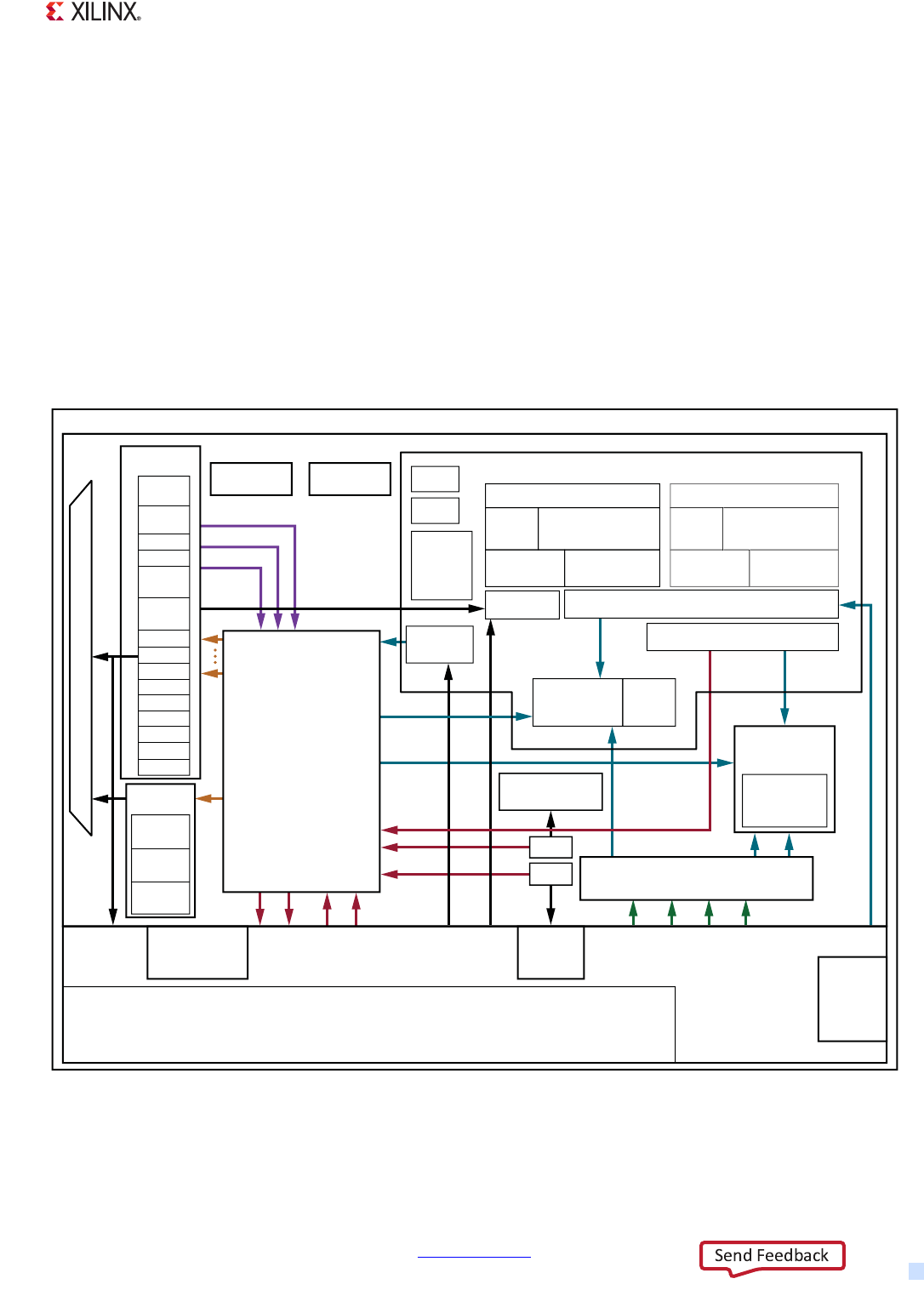
Zynq-7000 AP SoC Technical Reference Manual www.xilinx.com 27
UG585 (v1.12.1) December 6, 2017
Chapter 1: Introduction
The processor(s) in the PS always boot first, allowing a software centric approach for PL system boot
and PL configuration. The PL can be configured as part of the boot process or configured at some
point in the future. Additionally, the PL can be completely reconfigured or used with partial, dynamic
reconfiguration (PR). PR allows configuration of a portion of the PL. This enables optional design
changes such as updating coefficients or time-multiplexing of the PL resources by swapping in new
algorithms as needed. This latter capability is analogous to the dynamic loading and unloading of
software modules. The PL configuration data is referred to as a bitstream.
1.1.1 Block Diagram
Figure 1-1 illustrates the functional blocks of the Zynq-7000 AP SoC. The PS and the PL are on
separate power domains, enabling the user of these devices to power down the PL for power
management if required.
X-Ref Target - Figure 1-1
Figure 1-1: Zynq-7000 AP SoC Overview
2x USB
2x GigE
2x SD
Zynq-7000 AP SoC
I/O
Peripherals
IRQ
IRQ
EMIO
SelectIO
Resources
DMA 8
Channel
CoreSight
Components
Programmable Logic
DAP
DevC
SWDT
DMA
Sync
Notes:
1) Arrow direction shows control (master to slave)
2) Data flows in both directions: AXI 32bit/64bit, AXI 64bit, AXI 32bit, AHB 32bit, APB 32bit, Custom
3) Gray blocks in APU are applicable to dual core devices.
ACP
256K
SRAM
Application Processor Unit
TTC
System
Level
Control
Regs
GigE
CAN
SD
SDIO
UART
GPIO
UART
CAN
I2C
SRAM/
NOR
ONFI 1.0
NAND
Processing System
Memory
Interfaces
Q-SPI
CTRL
USB
GigE
I2C
USB
SD
SDIO
SPI
SPI
Programmable Logic to Memory
Interconnect
MMU
FPU and NEON Engine
Snoop Controller, AWDT, Timer
GIC
3
2 K
B
I-Cache
A
RM
C
ortex-A
9
C
P
U
ARM Cortex-A9
CPU
MMU
FPU and NEON En
g
in
e
Config
AES/
SHA
XADC
12 bit ADC
Memory
Interfaces
512 KB L2 Cache & Controller
OCM
Interconnect
DDR2/3,3L,
LPDDR2
Controller
UG585_c1_01_082216
3
2 K
B
D
-Cache
32 KB
I-Cache
32 KB
D-Cache
MIO
Clock
Generation Reset
Central
Interconnect
General-Purpose
Ports
High-Performance Ports

Zynq-7000 AP SoC Technical Reference Manual www.xilinx.com 28
UG585 (v1.12.1) December 6, 2017
Chapter 1: Introduction
The Zynq-7000 AP SoC is composed of the following major functional blocks:
• Processing System (PS)
°Application processor unit (APU)
°Memory interfaces
°I/O peripherals (IOP)
°Interconnect
• Programmable Logic (PL)
1.1.2 Documentation Resources
Tabl e 1-1 identifies the versions of third-party IP used in the Zynq-7000 AP SoC devices.
The PL is derived from Xilinx 7 series FPGA technology: Artix®-7 for the 7z010/7z015/7z020 (dual
core devices) and 7z007s/7z012s/7z014s (single core devices), and Kintex®-7 for the
7z030/7z035/7z045/7z100 devices. The PL is used to extend the functionality to meet specific
application requirements. The PL includes many different types of resources including configurable
logic blocks (CLBs), port and width configurable block RAM (BRAM), DSP slices with a 25 x 18
multiplier, 48-bit accumulator and pre-adder (DSP48E1), a user configurable analog to digital
convertor (XADC), clock management tiles (CMT), a configuration block with 256b AES for
decryption and SHA for authentication, configurable SelectIO™ technology and optionally GTP or
GTX multi-gigabit transceivers and an integrated PCI Express® (PCIe) block.
Table 1-1: Vendor IP Versions
Unit Supplier Version
Cortex-A9 MPCore ARM r3p0
AMBA Level 2 Cache Controller (PL310) ARM r3p2-50rel0
PrimeCell Static Memory Controller (PL353) ARM r2p1
PrimeCell DMA Controller (PL330) ARM r1p1
Generic Interrupt Controller (PL390) ARM Arch v1.0, r0p0
CoreLink Network Interconnect (NIC-301) ARM r2p2
DesignWare Cores IntelliDDR Multi Protocol Memory Controller Synopsys A07
USB 2.0 High Speed Atlantic Controller Synopsys 2.20a
Watchdog Timer Cadence Rev 07
Inter Intergrated Circuit Cadence r1p10
Gigabit Ethernet MAC Cadence r1p23
Serial Peripheral Interface Cadence r1p06
Universal Asynchronous Receiver Transmitter Cadence r1p08
Triple Timer Counter Cadence Rev 06
SD2.0/SDIO2.0/MMC3.31 AHB Host Controller Arasan 8.9A_apr02nd_2010

Zynq-7000 AP SoC Technical Reference Manual www.xilinx.com 29
UG585 (v1.12.1) December 6, 2017
Chapter 1: Introduction
To learn more about the PL resources, refer to the following Xilinx 7 series FPGA User Guides:
•UG471, 7 Series FPGAs SelectIO Resources User Guide
•UG472, 7 Series FPGAs Clocking Resources User Guide
•UG473, 7 Series FPGAs Memory Resources User Guide
•UG474, 7 Series FPGAs Configurable Logic Block User Guide
•UG476, 7 Series FPGAs GTX Transceiver User Guide
•UG482, 7 Series FPGAs GTP Transceiver User Guide
•PG054, 7 Series FPGAs Integrated Block for PCI Express LogiCORE IP Product Guide
•UG479, 7 Series FPGAs DSP48E1 User Guide
•UG480, 7 Series FPGAs XADC User Guide
The PS and PL can be tightly or loosely coupled using multiple interfaces and other signals that have
a combined total of over 3,000 connections. This enables you to effectively integrate user-created
hardware accelerators and other functions in the PL logic that are accessible to the processors and
can also access memory resources in the processing system.
The PS I/O peripherals, including the static/flash memory interfaces share a multiplexed I/O (MIO) of
up to 54 MIO pins. Zynq-7000 AP SoC devices also include the capability to use the I/Os that are part
of the PL domain for many of the PS I/O peripherals. This is done through an extended multiplexed
I/O interface (EMIO).
The system includes many types of security, test and debug features. The Zynq-7000 AP SoC can be
booted securely or non-securely. The PL configuration bitstream can be applied securely or
non-securely. Both of these use the 256b AES decryption and SHA authentication blocks that are part
of the PL. Therefore, to use these security features, the PL must be powered on.
The boot process is multi-stage and minimally includes the boot ROM and the first-stage boot
loader (FSBL). The Zynq-7000 AP SoC includes a factory-programmed boot ROM that is not user
accessible. The boot ROM determines whether the boot is secure or non-secure, performs some
initialization of the system and clean-ups, reads the mode pins to determine the primary boot device
and finishes once it is satisfied it can execute the FSBL.
After a system reset, the system automatically sequences to initialize the system and process the first
stage boot loader from the selected external boot device. The process enables you to configure the
AP SoC platform as needed, including the PS and the PL. Optionally, the JTAG interface can be
enabled to give the design engineer access to the PS and the PL for test and debug purposes.
Power to the PL can be optionally shut off to reduce power consumption. In addition, the clocks in
the PS can be dynamically slowed down or gated off to reduce power further. Zynq-7000 AP SoC
devices support the ARM standby mode to obtain minimal power drain, but still are able to start up
when certain events occur.
Elements of the Zynq-7000 AP SoC are described from the point of view of the PS. For example, a
general purpose slave interface on the PS to the PL means that the master resides in the PL. A high
performance slave interface means the high performance master resides in the PL. A general purpose
master interface means the PS is the master and the slave resides in the PL.

Zynq-7000 AP SoC Technical Reference Manual www.xilinx.com 30
UG585 (v1.12.1) December 6, 2017
Chapter 1: Introduction
1.1.3 Notices
Zynq-7000 AP SoC Device Family
The PS structure for all Zynq-7000 AP SoC devices is the same except for the following:
7z007s and 7z010 CLG225 Devices
The 7z007s single core and 7z010 dual core CLG225 devices have a limited number of pins (225). This
reduces the capability of the MIO, DDR and XADC subsystems.
• 32 MIO pins, see section 2.5.3 MIO Pin Assignment Considerations
• 16 DDR data, see section 10.1.3 Notices in Chapter 10, DDR Memory Controller
• Four pairs of XADC signals, see Notices in Chapter 30, XADC Interface
Device Revisions
The visual markings are shown in UG865, Zynq-7000 All Programmable SoC Packaging and Pinout
Advance Product Specification.
Software can read the following registers in all Zynq-7000 AP SoC devices to determine silicon
revision:
• devcfg.MCTRL [PS_VERSION]
• slcr.PSS_IDCODE[IDCODE]
The JTAG interface also includes the IDCODE revision content.
TrustZone Capabilities
TrustZone is hardware that is built into all Zynq-7000 AP SoC devices. For more information, see
UG1019, Programming ARM TrustZone Architecture on the Xilinx Zynq-7000 All Programmable Soc.

Zynq-7000 AP SoC Technical Reference Manual www.xilinx.com 31
UG585 (v1.12.1) December 6, 2017
Chapter 1: Introduction
1.2 Processing System (PS) Features and
Descriptions
1.2.1 Application Processor Unit (APU)
The application processor unit (APU) provides an extensive offering of high-performance features
and standards-compliant capabilities.
Dual/Single ARM Cortex-A9 MPCore CPUs with ARM v7
• Run time options allow single processor, asymmetrical (AMP) or symmetrical multiprocessing
(SMP) configurations
• ARM version 7 ISA: standard ARM instruction set and Thumb®-2, Jazelle® RCT and Jazelle DBX
Java™ acceleration
• NEON™ 128b SIMD coprocessor and VFPv3 per MPCore
•32KB instruction and 32 KB data L1 caches with parity per MPCore
• 512 KB of shareable L2 cache with parity
• Private timers and watchdog timers
System Features
• System-Level Control Registers (SLCRs)
°A group of various registers that are used to control the PS behavior
°The register map is located in Chapter 4, System Addresses
°The SLCR registers related to a specific chapter are listed in the register overview table of
that chapter and detailed in Appendix B, Register Details
• Snoop control unit (SCU) to maintain L1 and L2 coherency
• Accelerator coherency port (ACP) from PL (master) to PS (slave)
°64b AXI slave port
°Can access the L2 and the OCM
°Transactions are data coherent with L1 and L2 caches
• 256 KB of on-chip SRAM (OCM) with parity
°Dual ported
°Accessible by the CPUs, PL and central interconnect
°At level of L2, but is not cacheable
• DMA controller
°Four channels for PS (memory copy to/from any memory in system)
°Four channels for PL (memory to PL, PL to memory)

Zynq-7000 AP SoC Technical Reference Manual www.xilinx.com 32
UG585 (v1.12.1) December 6, 2017
Chapter 1: Introduction
• General interrupt controller (GIC)
°Individual interrupt masks and interrupt prioritization
°Five CPU-private peripheral interrupts (PPI)
°Sixteen CPU-private software generated interrupts (SGI)
°Distributes shared peripheral interrupts (SPI) from the rest of the system, PS and PL
- 20 from the PL
°Wait for interrupt (WFI) and wait for event (WFE) signals from CPU sent to PL
°Enhanced security features to support TrustZone™ technology
• Watchdog timer, triple counter/timer
1.2.2 Memory Interfaces
The memory interfaces includes multiple memory technologies.
DDR Controller
• Supports DDR3, DDR3L, DDR2, LPDDR-2
°Rate is determined by speed and temperature grade of the device
• 16b or 32b wide
°ECC on 16b
• Uses up to 73 dedicated PS pins
• Modules (no DIMMs)
°32b wide: 4 x 8b, 2 x 16b, 1 x 32b
°16b wide: 2 x 8b, 1 x 16b
• Autonomous DDR power down entry and exit based on programmable idle periods
• Data read strobe auto-calibration
• Write data byte enables supported for each data beat
• Low latency read mechanism using HPR queue
• Special urgent signaling to each port
• TrustZone regions programmable on 64 MB boundaries
• Exclusive accesses for two different IDs per port (locked transactions are not supported)
DDR Controller Core and Transaction Scheduler
• Transaction scheduling is done to optimize data bandwidth and latency
• Advanced re-ordering engine to maximize memory access efficiency with target of 90%
efficiency with continuous read and write and 80% efficiency with random read and write
• Write-read address collision checking that flushes the write buffer
• Obeys AXI ordering rules

Zynq-7000 AP SoC Technical Reference Manual www.xilinx.com 33
UG585 (v1.12.1) December 6, 2017
Chapter 1: Introduction
Quad-SPI Controller
Key features of the linear Quad-SPI controller (which can be a primary boot device) are:
•Single or dual
• 1x and 2x read support
• 32-bit APB 3.0 interface for I/O mode that allows full device operations including program, read
and configuration
• 32-bit AXI linear address mapping interface for read operations
• Single device select line support
• Supports write protection signal
• 4-bit bidirectional I/O signals
• Read speed of x1, x2 and x4
• Write speed of x1 and x4
• Maximum Quad-SPI clock at master mode is 100 MHz
• 252-byte entry FIFO depth to improve Quad-SPI read efficiency
• Supports Quad-SPI device up to 128 Mb density in I/O and linear mode. >128Mb devices are
supported in IO mode only.
• Supports dual Quad-SPI with two quad-SPI devices in parallel
In addition, the linear address mapping mode features include:
• Supports regular read-only memory access through the AXI interface
• Up to two SPI flash memories
• Up to 16 MB addressing space for one memory and 32 MB for two memories in linear mode
• AXI read acceptance capability of 4
• Both AXI incrementing and wrapping-address burst read
• Automatically converts normal memory read operation to SPI protocol, and vice versa
• Serial, Dual and Quad-SPI modes
Static Memory Controller (SMC)
Either of the following can be the primary boot device:
•NAND controller
°8/16-bit I/O width with one chip select signal
°ONFI specification 1.0
°16-word read and 16-word write data FIFOs
°8-word command FIFO
°Programmable I/O cycle timing
°ECC assist
°Asynchronous memory operating mode

Zynq-7000 AP SoC Technical Reference Manual www.xilinx.com 34
UG585 (v1.12.1) December 6, 2017
Chapter 1: Introduction
• Parallel SRAM/NOR controller
°8-bit data bus width
°One chip select with up to 25 address signals (32 MB)
°Two chip selects with up to 25 address signals (32 MB + 32 MB)
°16-word read and 16-word write data FIFOs
°8-word command FIFO
°Programmable I/O cycle timing on a per chip select basis
°Asynchronous memory operating mode
1.2.3 I/O Peripherals
The I/O Peripherals (IOP) are a collection of industry-standard interfaces for external data
communication.
Note: The controller registers require single 32-bit read/write accesses, do not use byte, halfword,
or double word references.
GPIO
• Up to 54 GPIO signals for device pins routed through the MIO
°Outputs are 3-state capable
• 192 GPIO signals between the PS and PL via the EMIO
°64 Inputs, 128 outputs (64 true outputs and 64 output enables)
• The function of each GPIO can be dynamically programmed on an individual or group basis
°Enable, bit or bank data write, output enable and direction controls
• Programmable Interrupts on individual GPIO basis
°Status read of raw and masked interrupt
°Positive edge, negative edge, either edge, high level, low level sensitivities
Gigabit Ethernet Controllers (Two)
• RGMII interface using MIO pins and external PHY
• Additional interface using PL SelectIO and external PHY with additional soft IP in the PL
• SGMII interface using PL GTP or GTX transceivers
• Built-in DMA with scatter-gather
• IEEE 802.3-2008 and IEEE 1588 revision 2.0
• Wake-on capability

Zynq-7000 AP SoC Technical Reference Manual www.xilinx.com 35
UG585 (v1.12.1) December 6, 2017
Chapter 1: Introduction
USB Controllers: Each as Host, Device or OTG (Two)
• USB 2.0 high speed on-the-go (OTG) dual role USB host controller or USB device controller
operation using the same hardware
• MIO pins only (one USB controller is available in the 7x010 device)
• Built-in DMA
• USB 2.0 high speed device
• USB 2.0 high speed host controller
• The USB host controller registers and data structures are EHCI compatible
• Direct support for USB transceiver low pin interface (ULPI). The ULPI module supports 8 bits
• External PHY required
• Support up to 12 endpoints
SD/SDIO Controllers (Two)
• Bootable SD Card mode (option)
• Built-in DMA
• Host mode support only
• Support for version 2.0 of SD specification
• Full speed and low speed support
• 1-bit and 4-bit data interface support
• Low speed clock 0–400 kHz
• Support for high speed interface
• Full speed clock 0-50 MHz with maximum throughput at 25 MB/s
• Support for memory, I/O, and combination cards
• Support for power control modes
• Support for interrupts
• 1 KB Data FIFO interface
SPI Controllers (Two): Master or Slave
• Four wire bus: MOSI, MISO, SCLK, SS
• Full-duplex operation offers simultaneous receive and transmit
•Master mode
°Manual or auto start transmission of data
°Manual or auto slave select (SS) mode
°Supports up to three slave select lines
°Allows the use of an external peripheral select 3-to-8 decode
°Programmable delays for data transmission

Zynq-7000 AP SoC Technical Reference Manual www.xilinx.com 36
UG585 (v1.12.1) December 6, 2017
Chapter 1: Introduction
•Slave mode
°Programmable start detection mode
• Multi-master environment
°Drives into 3-state if not enabled
°Identifies an error condition if more than one master detected
• Supports 50 MHz maximum external SPI clock rate through MIO
°25 MHz maximum through EMIO to PL SelectIO pins
• Selectable master clock reference
• Programmable master baud rate divisor
• Supports 128-byte read and 128-byte write FIFOs
°Each FIFO is 8-bit wide
• Programmable FIFO thresholds
• Supports programmable clock phase and polarity
• Supports manual or auto start transmission of data
• Software can poll for status or function as interrupt-driven
• Programmable interrupt generation
CAN Controllers (Two)
• Conforms to the ISO 11898 -1, CAN 2.0A, and CAN 2.0B standards
• Supports both standard (11-bit identifier) and extended (29-bit identifier) frames
• Supports bit rates up to 1 Mb/s
• Transmit message FIFO with a depth of 64 messages
• Transmit prioritization through one high-priority transmit buffer
• Support of watermark interrupts for TxFIFO and RxFIFO
• Automatic re-transmission on errors or arbitration loss in normal mode
• Receive message FIFO with a depth of 64 messages
• Acceptance filtering of four acceptance filters
• Sleep mode with automatic wake-up
•Snoop mode
• Loopback mode for diagnostic applications
• Maskable error and status interrupts
• 16-bit time stamping for receive messages
• Readable error counters
UART Controllers (Two)
• Programmable baud rate generator

Zynq-7000 AP SoC Technical Reference Manual www.xilinx.com 37
UG585 (v1.12.1) December 6, 2017
Chapter 1: Introduction
• 64-byte receive and transmit FIFOs
•6, 7, or 8 data bits
• 1, 1.5, or 2 stop bits
• Odd, even, space, mark, or no parity
• Parity, framing and overrun error detection
• Line-break generation and detection
• Automatic echo, local loopback, and remote loopback channel modes
• Interrupts generation
• Rx and Tx signals are on the MIO and EMIO interfaces
• Modem control signals: CTS, RTS, DSR, DTR, RI, and DCD are available on the EMIO interface
I2C Controllers (two)
• Supports 16-byte FIFO
• I2C bus specification version 2
• Programmable normal and fast bus data rates
•Master mode
°Write transfer
°Read transfer
°Extended address support
°Support HOLD for slow processor service
°Supports TO interrupt flag to avoid stall condition
• Slave monitor mode
•Slave mode
°Slave transmitter
°Slave receiver
°Extended address support
°Fully programmable slave response address
°Supports HOLD to prevent overflow condition
°Supports TO interrupt flag to avoid stall condition
• Software can poll for status or function as interrupt-driven device
• Programmable interrupt generation
PS MIO I/Os
The PS MIO I/O buffers are split into two voltage domains. Within each domain, each MIO is
independently programmable.
• Two I/O voltage banks
°Bank 0 voltage bank consists of pins 0:15

Zynq-7000 AP SoC Technical Reference Manual www.xilinx.com 38
UG585 (v1.12.1) December 6, 2017
Chapter 1: Introduction
°Bank 1 voltage bank consists of pins 16:53
• MIO voltage levels can be programmed per bank.
°1.8 and 2.5/3.3 volts
°CMOS single ended or HSTL differential receiver mode
1.3 Programmable Logic Features and Descriptions
The PL provides a rich architecture of user-configurable capabilities.
• Configurable logic blocks (CLB)
°6-input look-up tables (LUTs)
°Memory capability within the LUT
°Register and shift register functionality
°Cascadeable adders
• 36 Kb block RAM
°Dual port
°Up to 72-bits wide
°Configurable as dual 18 Kb
°Programmable FIFO logic
°Built-in error correction circuitry
• Digital signal processing — DSP48E1 Slice
°25 × 18 two's complement multiplier/accumulator high-resolution (48 bit) signal processor
°Power saving 25-bit pre-adder to optimize symmetrical filter applications
°Advanced features: optional pipelining, optional ALU, and dedicated buses for cascading
• Clock management
°High-speed buffers and routing for low-skew clock distribution
°Frequency synthesis and phase shifting
°Low-jitter clock generation and jitter filtering
•Configurable I/Os
°High-performance SelectIO technology
°High-frequency decoupling capacitors within the package for enhanced signal integrity
°Digitally controlled impedance that can be 3-stated for lowest power, high-speed I/O
operation
°High range (HR) I/Os support 1.2V to 3.3V
°High performance (HP) I/Os support 1.2V to 1.8V (7z030, 7z035, 7z045, and 7z100 devices)
• Low-power gigabit transceivers (7z012s, 7z015, 7z030, 7z035, 7z045, and 7z100 devices)

Zynq-7000 AP SoC Technical Reference Manual www.xilinx.com 39
UG585 (v1.12.1) December 6, 2017
Chapter 1: Introduction
°High-performance transceivers capable of up to 12.5 Gb/s (GTX) in 7z030, 7z035, 7z045 and
7z100 devices
°High-performance transceivers capable of up to 6.25 Gb/s (GTP) in 7z012s and 7z015
devices
°Low-power mode optimized for chip-to-chip interfaces
°Advanced transmit pre- and post-emphasis, and receiver linear (CTLE) and decision
feedback equalization (DFE), including adaptive equalization for additional margin
• Analog-to-digital converter (XADC)
°Dual 12-bit 1 MSPS analog-to-digital converters (ADCs)
°Up to 17 flexible and user-configurable analog inputs
°On-chip or external reference option
°On-chip temperature and power supply sensors
°Continuous JTAG access to ADC measurements
• Integrated interface blocks for PCI Express designs (7z015, 7z030, 7z035, 7z045, and 7z100
devices)
°Compatible to the PCI Express base specification 2.1 with Endpoint and Root Port capability
°Supports Gen1 (2.5 Gb/s) and Gen2 (5.0 Gb/s) speeds
°Advanced configuration options, advanced error reporting (AER), and end-to-end CRC
(ECRC) advanced error reporting and ECRC features
1.4 Interconnect Features and Description
Zynq-7000 AP SoC devices uses several interconnect technologies, optimized to the specific
communication needs of the functional blocks. For more information, refer to the block diagram in
Figure 1-1 or a more detailed diagram in Figure 5-1.
1.4.1 PS Interconnect Based on AXI High Performance Datapath
Switches
• OCM interconnect
°Provides access to the 256 KB memory from the central interconnect and the PL
°CPUs and ACP interfaces have the lowest latency access to OCM through the SCU
• Central interconnect
°The central interconnect is 64 bits, connecting the IOP and DMA controller to the DDR
memory controller, on-chip RAM, and the AXI_GP interfaces (through their switches) for the
PL logic
°Connects the local DMA units in the Ethernet, USB and SD/SDIO controllers to the central
interconnect
°Connects masters in the PS to the IOP

Zynq-7000 AP SoC Technical Reference Manual www.xilinx.com 40
UG585 (v1.12.1) December 6, 2017
Chapter 1: Introduction
1.4.2 PS-PL Interfaces
The PS-PL interface contains all the signals available to the PL designer for integrating the PL-based
functions and the PS. There are two types of interfaces between the PL and the PS.
1. Functional interfaces which include AXI interconnect, extended MIO interfaces (EMIO) for most
of the I/O peripherals, interrupts, DMA flow control, clocks, and debug interfaces. These signals
are available for connecting with user-designed IP blocks in the PL.
2. Configuration signals which include the processor configuration access port (PCAP),
configuration status, single event upset (SEU) and Program/Done/Init. These signals are
connected to fixed logic within the PL configuration block, providing PS control.
AXI functional interfaces:
•AXI_ACP
°One 64-bit cache coherent slave port in the APU interfaces to a PL master port
°Connects to the snoop control unit for cache coherency between the CPUs and the PL
• AXI_HP, four high performance/bandwidth master ports on the PS AXI interconnect
°32-bit or 64-bit data master interfaces (independently programmed)
°Efficient resizing in 32-bit slave interface configuration mode
°Efficient upsizing to 64-bits for aligned 32-bit transfers in 32-bit slave interface
configuration mode
°Automatic expansion to 64 bits for unaligned 32-bit transfers in 32-bit slave interface
configuration mode
°Dynamic command upsizing translation between 32-bit and 64-bit interfaces, controllable
through AxCACHE[1]
°Separate R/W programmable issuing capability for read and write commands
°Programmable release threshold of write commands
°Asynchronous clock frequency domain crossing for all AXI interfaces between the PL and PS
°Smoothing out of “long-latency” transfers using 1 KB (128 by 64 bits) data FIFOs for both
reads and writes
°QoS signaling available from PL ports
°Command and data FIFO fill-level counts available to the PL
°Standard AXI 3.0 interfaces supported
°Large slave interface read acceptance capability in the range of 14 to 70 commands (burst
length dependent)
°Large slave interface write acceptance capability in the range of 8 to 32 commands (burst
length dependent)
•AXI_GP, four general purpose ports
°Two, 32-bit master interfaces
°Two, 32-bit slave interfaces
°Asynchronous clock frequency domain crossing for all AXI interfaces between the PL and PS
°Standard AXI 3.0 interfaces supported

Zynq-7000 AP SoC Technical Reference Manual www.xilinx.com 41
UG585 (v1.12.1) December 6, 2017
Chapter 1: Introduction
1.5 System Software
Xilinx provides device drivers for all of the I/O peripherals. These device drivers are provided in
source format and support bare-metal or stand-alone and Linux. An example first-stage boot loader
(FSBL) is also provided in source code format. The source drivers for stand-alone and FSBL are
provided as part of the Xilinx IDE Design Suite Embedded Edition. The Linux drivers are provided
through the Xilinx Open Source Wiki at wiki.xilinx.com
Refer to UG821, Zynq-7000 Software Developers Guide for additional information.
In addition, Xilinx Alliance Program partners provide system software solutions for IP, middleware,
operation systems, etc. Refer to the Zynq-7000 landing page at www.xilinx.com/zynq for the latest
information.

Zynq-7000 AP SoC Technical Reference Manual www.xilinx.com 42
UG585 (v1.12.1) December 6, 2017
Chapter 2
Signals, Interfaces, and Pins
2.1 Introduction
This chapter identifies the user visible signals and interfaces in Zynq-7000 AP SoC devices. The
interfaces and signals are organized into major groups as shown in Figure 2-1. The Zynq-7000
AP SoC devices consist of a Processing System (PS) with a Xilinx Artix™-7 or Kintex™-7 based
Programmable Logic (PL) block.
2.1.1 Notices
7z007s and 7z010 CLG225 Devices
The 7z007s single core and 7z010 dual core CLG225 devices (225 pin packages) support 32 MIO pins
and at most one Ethernet interface through the MIO pins. This is shown in the MIO table in
2.5.4 MIO-at-a-Glance Table. One or both of the Ethernet controllers can interface to logic in the PL.
PS-PL Voltage Level Shifters
All of the signals and interfaces that go between the PS and PL traverse a voltage boundary. These
input and output signals are routed through voltage level shifters that must be enabled and disabled
during the power-up and power-down sequences of the PL. For more information on the voltage
level shifters, refer to section 2.4 PS–PL Voltage Level Shifter Enables.
Pin Timing and Voltage Specifications
Refer to the Zynq-7000 AP SoC Data Sheet for timing and pin voltage information.
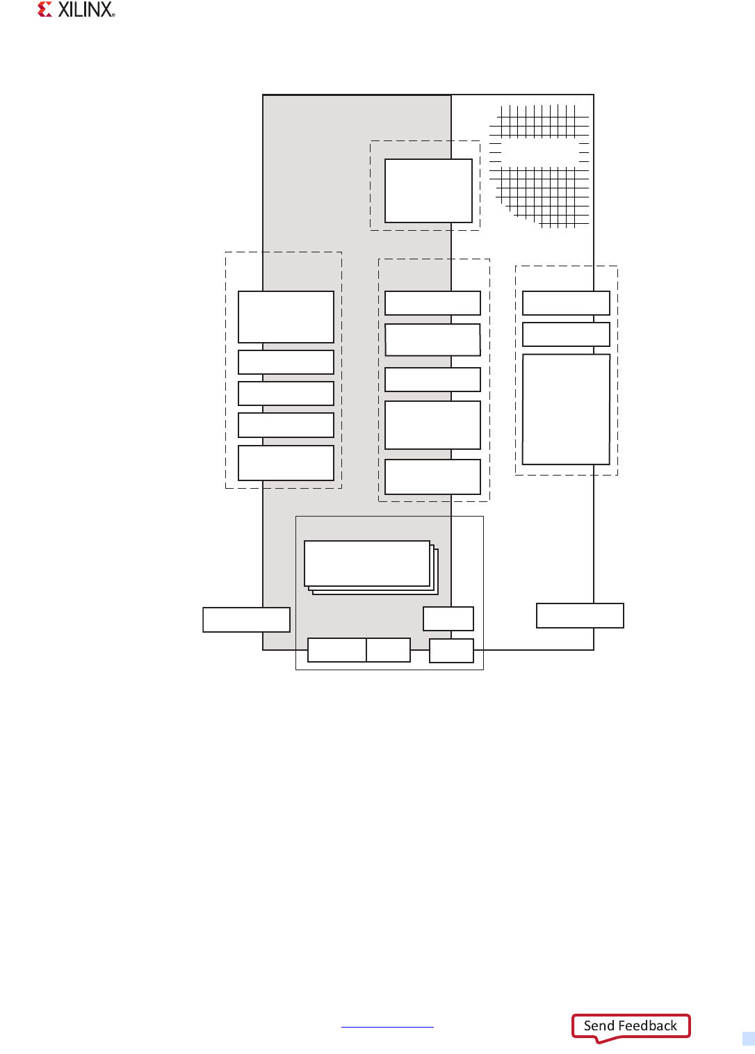
Zynq-7000 AP SoC Technical Reference Manual www.xilinx.com 43
UG585 (v1.12.1) December 6, 2017
Chapter 2: Signals, Interfaces, and Pins
X-Ref Target - Figure 2-1
Figure 2-1: Signals, Interfaces, and Pins
UG585_c2_01_091916
PS_CLK,
POR_RST_N,
SRST_N
PS Signals
and Interfaces Misc. PL
Signals
MIO Pins, EMIO Signals, JTAG
AXI Interfaces
DDR Memory
USB
Quad-SPI
NAND,
NOR/SRAM
EMIO
MIO
Boot Mode
Zynq 7z012s,
7z015, 7z030,
7z035,7z045,
and 7z100
Multi-gigabit
Serial
Transceivers
(MGTX)
PL Signals
User SelectIO
XADC
PL Power Pins
FCLKs
Processing
System (PS)
Zynq 7000 Device Boundary
JTAG
M_AXI_GP x2
S_AXI_GP x2
S_AXI_HP x4
S_AXI_ACP x1
IRQ, Event,
Standby
DMA Req/Ack
PS Power Pins
DDR Arb,
AXI Idle,
SRAM Int
FTMD Trace,
FTMT Trigs
GigE, SDIO,
SPI, I2C, CAN, UART,
GPIO, TTC, SWDT
Programmable
Logic (PL)
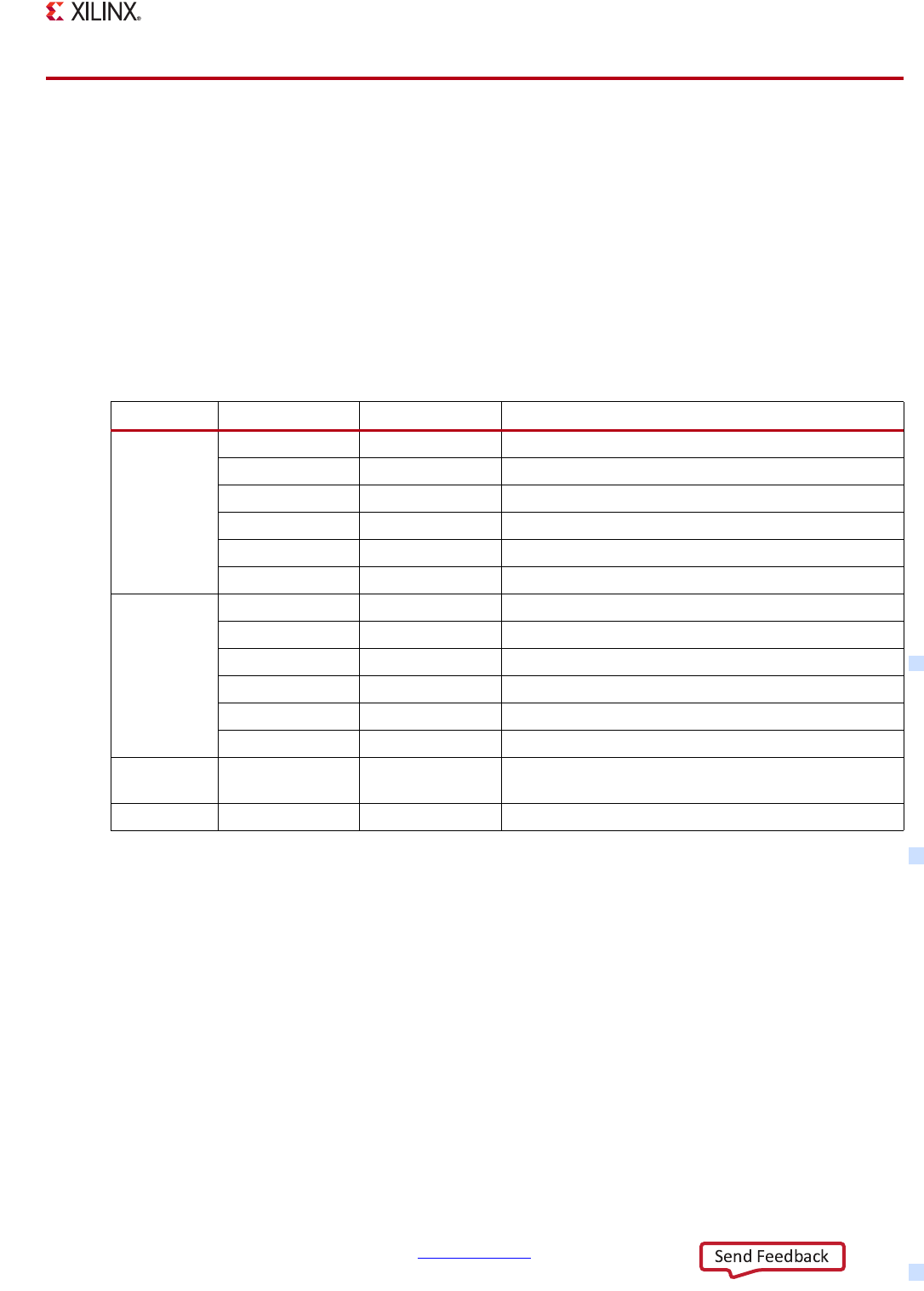
Zynq-7000 AP SoC Technical Reference Manual www.xilinx.com 44
UG585 (v1.12.1) December 6, 2017
Chapter 2: Signals, Interfaces, and Pins
2.2 Power Pins
The PS and PL power supplies are fully independent, however the PS power supply must be present
whenever the PL power supply is active. PL power up needs to maintain a certain timing relationship
with the POR reset signal of the PS. For more details refer to section 6.3.3 BootROM Performance:
PS_POR_B De-assertion Guidelines, page 179.
The PS includes an independent power supply for the DDR I/O and two independent voltage banks
for MIO. The power pins are summarized in Tab le 2 - 1 . The voltage sequencing and electrical
specifications are shown in the applicable Zynq-7000 AP SoC data sheet. Also refer to the Zynq-7000
AP SoC packaging and pin documents for more information.
Note: Refer to the respective data sheet for recommended operating conditions.
Table 2-1: Power Pins
Type Pin Name Nominal Voltage Power Pin Description
PS Power
VCCPINT 1.0V Internal logic
VCCPAUX 1.8V I/O buffer pre-driver
VCCO_DDR 1.2V to 1.8V DDR memory interface
VCCO_MIO0 1.8V to 3.3V MIO bank 0, pins 0:15
VCCO_MIO1 1.8V to 3.3V MIO bank 1, pins 16:53
VCCPLL 1.8V Three PLL clocks, analog
PL Power
VCCINT 1.0V Internal core logic
VCCAUX 1.8V I/O buffer pre-driver
VCCO_# 1.2V to 3.3V I/O buffers drivers (per bank)
VCC_BATT 1.5V PL decryption key memory backup
VCCBRAM 1.0V PL block RAM
VCCAUX_IO_G# 1.8V to 2.0V PL auxiliary I/O circuits
XADC VCCADC,
GNDADC N/A Analog power and ground.
Ground GND Ground Digital and analog grounds
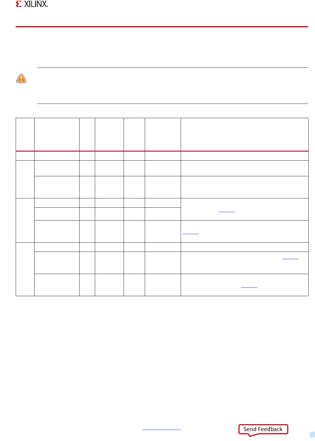
Zynq-7000 AP SoC Technical Reference Manual www.xilinx.com 45
UG585 (v1.12.1) December 6, 2017
Chapter 2: Signals, Interfaces, and Pins
2.3 PS I/O Pins
A summary of the dedicated PS signal pins is shown in Ta b l e 2 -2 .
CAUTION! For MIO pins, the allowable Vin High level voltage depends on the settings of the
slcr.MIO_PIN_xx [IO_Type] and [DisableRcvr] bits. These restrictions and the restrictions for all I/O pins
are defined in the Zynq-7000 AP SoC data sheets. Damage to the input buffer can occur when the limits
are exceeded.
7z007s and 7z010 Devices
The 7z007s single core and 7z010 dual core CLG225 devices (225 pin packages) have fewer pins than
the other Zynq-7000 AP SoC devices (see Ta b le 2 -2 ). Details for DDR and MIO pins can be found in
Chapter 10, DDR Memory Controller and section 2.5.3 MIO Pin Assignment Considerations,
respectively. There is more information about the CLG225 devices in section 1.1.3 Notices.
Table 2-2: PS Signal Pins
Group Name Type
Zynq-7000
Family
Pin
Count(1)
7z007s/
7z010
Device
Pin
Count
Voltage Node Description
Clock PS_CLK I 1 1 VCCO_MIO0 System reference clock. See Chapter 25, Clocks.
Reset
PS_POR_B I 1 1 VCCO_MIO0
Power on reset, active low. See Chapter 26, Reset
System.
PS_SRST_B I 1 1 VCCO_MIO1
Debug system reset, active Low. Forces the system
to enter a reset sequence. See Chapter 26, Reset
System.
MIO
PS_MIO[15:0] I/O 16 16 VCCO_MIO0 Refer to section 2.5 PS-PL MIO-EMIO Signals and
Interfaces and UG865, Zynq-7000 AP SoC Package
and Pinout Guide.
PS_MIO[53:16] I/O 38 16 VCCO_MIO1
PS_MIO_VREF Ref 1 0 VCCO_MIO1
Voltage reference for RGMII input receivers, refer to
UG933, Zynq-7000 AP SoC PCB Design and Pin
Planning Guide.
DDR
PS_DDR_xxx I/O 73 51 VCCO_DDR See Chapter 10, DDR Memory Controller.
PS_DDR_VR[N,P] N/A 2 1 ~
DDR DCI voltage reference pins, refer to UG933,
Zynq-7000 AP SoC PCB Design and Pin Planning
Guide.
PS_DDR_VREF Ref 4 4 ~
Voltage reference for DDR DQ and DQS differential
input receivers, refer to UG933, Zynq-7000 AP SoC
PCB Design and Pin Planning Guide.
Notes:
1. Does not include 7z007s single core and 7z010 dual core CLG225 devices.

Zynq-7000 AP SoC Technical Reference Manual www.xilinx.com 46
UG585 (v1.12.1) December 6, 2017
Chapter 2: Signals, Interfaces, and Pins
2.4 PS–PL Voltage Level Shifter Enables
All of the signals and interfaces that go between the PS and PL traverse a voltage boundary. These
input and output signals are routed through voltage level shifters. The majority of the voltage level
shifters are enabled by the slcr.LVL_SHFTR_EN register. The voltage level shifter enables for some
PS-PL traversing signals are controlled with the PL power state. These include signals for the XADC,
PL, and EMIO JTAGs; the PCAP interface; and other modules.
The enabling and disabling of the voltage level shifters must be managed during the PL power-up
and power-down sequences to avoid extraneous logic level transitions on the input signals to the PS
modules. Disable the voltage level shifters before the PL is powered down. Similarly, enable the level
shifters after the PL is powered up and before the signals are used. The PS must be powered on to
program the logic in the PL.
Example: Power-up Sequence
1. Power-up the PL. Refer to the data sheet for voltage sequencing requirements. The
slcr.LVL_SHFTR_EN register should be equal to 0x0.
2. Enable the PS-to-PL level shifters. Write 0x0A to the slcr.LVL_SHFTR_EN register.
3. Program the PL.
4. Wait for the PL to be programmed. Read devcfg.INT_STS [PCFG_DONE_INT] until = 1 to
indicate that the DONE signals has asserted.
5. Enable the PL-to-PS level shifters. Write 0x0F to the slcr.LVL_SHFTR_EN register.
6. Begin to use the signals and interfaces between the PS and PL.
Example: Power-down Sequence
1. Stop using the signals and interfaces between the PS and PL.
2. Disable the voltage level shifters. Write 0x0 to the slcr.LVL_SHFTR_EN register.
3. Power-down the PL. Refer to the data sheet for voltage sequencing requirements.
4. Leave the slcr.LVL_SHFTR_EN register = 0x0 when the PL is powered down.
TIP: Functionally, there is no reason to enable the voltage level shifters until the PL is fully configured.
The PS does not allow the voltage level shifters to be enabled until the PL global signals indicate that
it is safe to do so. The PL is fully programmed when the PL DONE signal is High. The PL DONE signal
is tracked as an interrupt in the DevC subsystem.
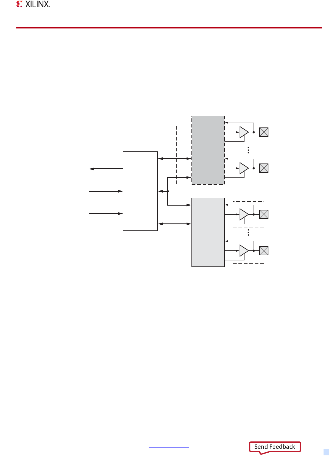
Zynq-7000 AP SoC Technical Reference Manual www.xilinx.com 47
UG585 (v1.12.1) December 6, 2017
Chapter 2: Signals, Interfaces, and Pins
2.5 PS-PL MIO-EMIO Signals and Interfaces
The MIO is fundamental to the I/O peripheral connections due to the limited number of MIO pins.
Software programs the routing of the I/O signals to the MIO pins. The I/O peripheral signals can also
be routed to the PL (including PL device pins) through the EMIO interface. This is useful to gain
access to more device pins (PL pins) and to allow an I/O peripheral controller to interface to user
logic in the PL. See Figure 2-2.
2.5.1 I/O Peripheral (IOP) Interface Routing
The I/O multiplexing of the I/O controller signals differs; that is, some IOP signals are solely available
on the MIO pin interface, some signals are available via MIO or EMIO, and some of the interface
signals are only accessible via EMIO. Some of the routing capabilities for each I/O peripheral are
shown in Ta ble 2 -3. The details for each IOP are included in the chapter that describes the IOP. MIO
pin assignment possibilities are illustrated in section 2.5.4 MIO-at-a-Glance Table.
Note: The routing of the IOP interface I/O signals must be done as a group; that is, the signals must
not be split and routed to different MIO pin groups. For example, if the SPI 0 CLK is routed to MIO
pin 40, then the other signals of the SPI 0 interface must be routed to MIO pins 41 to 45. Similarly,
the signals within an IOP interface must not be split between MIO and EMIO. However, unused
signals within an IOP interface do not necessarily need to be routed. Unused signals can be
configured as a GPIO.
X-Ref Target - Figure 2-2
Figure 2-2: MIO-EMIO Overview
UG585_c2_02_101612
PS I/O
Peripherals
(IOP)
PL
PS PL
AHB
Masters
EMIO
Interface
Device
Boundary
PS MIO
Pins
PL User
Pins
AHB
Slaves
APB
Slaves
MIO
Multiplexer

Zynq-7000 AP SoC Technical Reference Manual www.xilinx.com 48
UG585 (v1.12.1) December 6, 2017
Chapter 2: Signals, Interfaces, and Pins
2.5.2 IOP Interface Connections
For most peripherals, there is flexibility in where the I/O signals can be mapped. The routing
capabilities are shown in Figure 2-4. For example, the XPS design software includes up to 12 possible
MIO port mappings for CAN, or, if selected, a path to the EMIO interface. The peripheral system
connection diagram is shown in Figure 2-3.
The majority of the I/O signals for PS peripherals, other than USB, can be routed to either the PS pins
through the MIO, or to the PL pins through the EMIO. Most peripherals also maintain the same
protocol between MIO and EMIO, except Gigabit Ethernet. To reduce pin count, a 4-bit RGMII
interface runs through the MIO at a 250 MHz data rate (125 MHz clock with a double data rate). The
route through the EMIO includes an 8-bit GMII interface running at a 125 MHz data rate. The USB,
Quad-SPI, and SMC interfaces are not available to the EMIO interface to the PL.
Table 2-3: I/O Peripheral MIO-EMIO Interface Routing
Peripheral MIO Routing EMIO Routing Cross Reference
TTC [0,1]
Clock In, Wave Out.
One pair of signals from
each counter.
Clock In, Wave Out.
Three pairs of signals
from each counter.
See Chapter 8, Timers
SWDT Clock In, Reset Out Clock In, Reset Out See Chapter 8, Timers
SMC Parallel NOR/SRAM and
NAND Flash Not available See Chapter 11, Static Memory
Controller
Quad-SPI [0,1] Serial, dual and quad
modes Not available See Chapter 12, Quad-SPI Flash
Controller
SDIO [0,1] 50 MHz 25 MHz See Chapter 13, SD/SDIO Controller
GPIOs Up to 54 I/O channels
(GPIO Banks 0 and 1)
64 GPIO channels with
input, output, 3-state
control (GPIO banks 2
and 3)
See Chapter 14, General Purpose I/O
(GPIO)
USB [0,1] Host, device, and OTG Not available See Chapter 15, USB Host, Device, and
OTG Controller
Ethernet [0,1] RGMII v2.0 MII/GMII(1) See Chapter 16, Gigabit Ethernet
Controller
SPI [0,1] 50 MHz Available See Chapter 17, SPI Controller
CAN [0,1] ISO 11898 -1,
CAN 2.0A/B Available See Chapter 18, CAN Controller
UART [0,1] Simple UART:
Two pins (TX/RX)
TX, RX, DTR, DCD, DSR,
RI, RTS and CTS See Chapter 19, UART Controller
I2C [0,1] SCL, SDA {0, 1} SCL, SDA {0, 1} See Chapter 20, I2C Controller
PJTAG TCK, TMS, TDI, TDO TCK, TMS, TDI, TDO,
3-state for TDO
See Chapter 27, JTAG and DAP
Subsystem
Trace Port IU Up to 16-bit data Up to 32-bit data See Chapter 28, System Test and Debug
Notes:
1. When the Ethernet MII/GMII interface is routed through EMIO, other MII interfaces (e.g., RMII, RGMII, and SGMII)
can be derived using appropriate shim logic in the PL that attaches to PL pins.
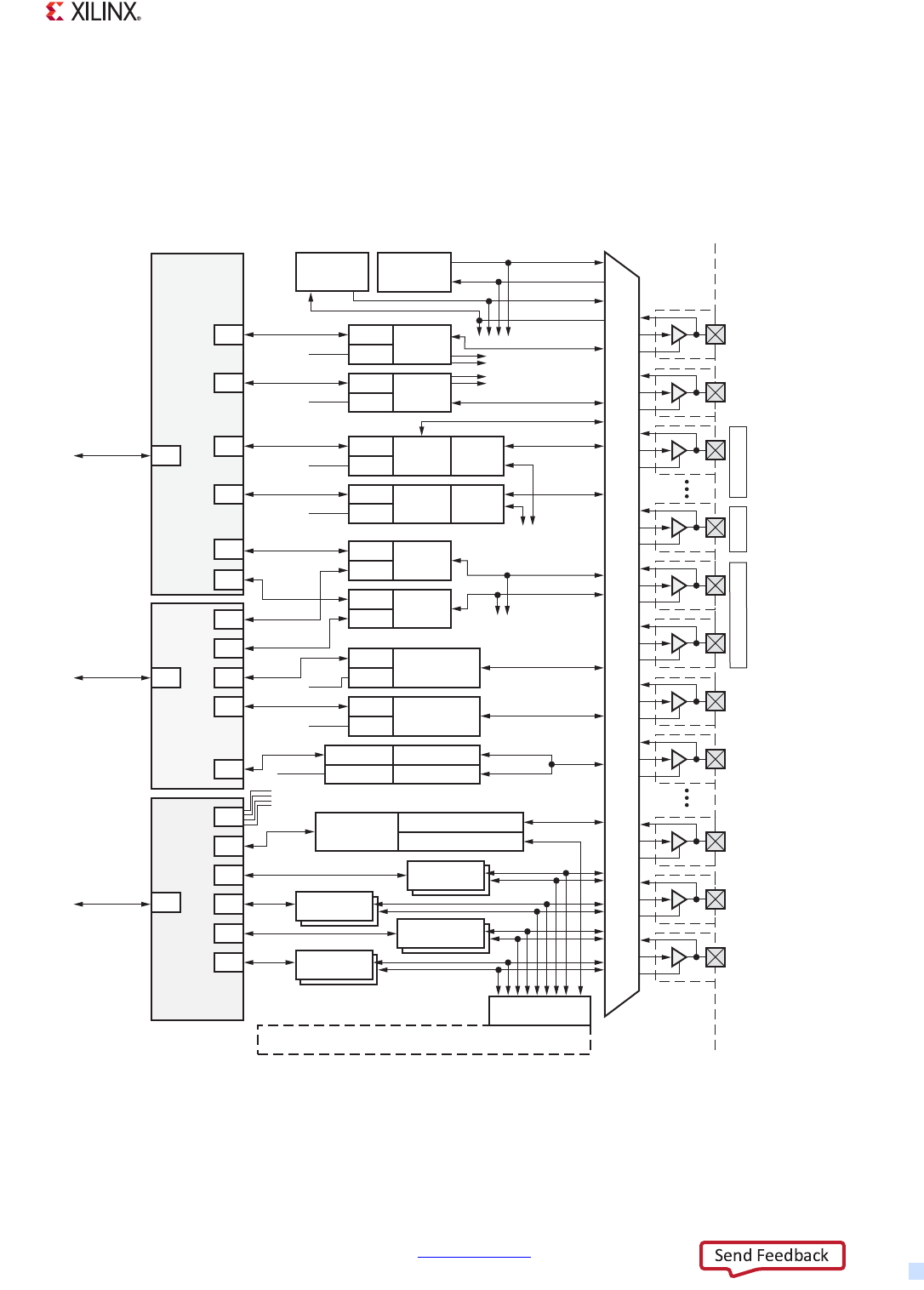
Zynq-7000 AP SoC Technical Reference Manual www.xilinx.com 49
UG585 (v1.12.1) December 6, 2017
Chapter 2: Signals, Interfaces, and Pins
On the interconnect side, the USB, Ethernet and SDIO peripherals are connected to the central
interconnect to service the six DMA masters. Software accesses the slave-only Quad-SPI and SMC
peripherals via the AHB interconnect. The GPIO, SPI, CAN, UART, and I2C save-only controllers are
accessed via the APB bus. All control and status registers are also accessed via the APB interconnect
except for the SDIO controllers which each have two AHB interfaces. This architecture is designed to
balance the bandwidth needs of each controller interface.
X-Ref Target - Figure 2-3
Figure 2-3: I/O Peripherals System Diagram
UG585_c2_03_121613
RGMII 0
Comm
Port
GigE 0
ULPI 1
ULPI 0
to EMIO
MDIO 0
AHB 32
APB
AXI 32
MIO
[0]
MIO
[1]
MIO
[2]
MIO
[51]
MIO
[52]
MIO
[53]
MIO
[6]
MIO
[7]
MIO
[8]
MIO
[9]
MIO
[10]
DMA
Regs
RGMII 1
Comm
Port
GigE 1
AHB 32
APB DMA
Regs
USB 0
WAVE_OUT
CLK_IN
TTC 1, 0
GMII via EMIO
to EMIO
RESET_OUT
CLK_IN
SWDT
Central
Interconnect
Slave
Interconnect
Zynq
Device
Pins
PS AHB 32
APB DMA
Regs
USB 1
AHB 32
APB DMA
Regs
QSPI 1
SMC
ONFi
Parallel
GPIO
QSPI 0
Quad SPI 0
Quad SPI 1
NAND
NOR/SRAM
AXI 32 APB
DMA
Regs
Data Path
Regs
AXI 32
APB
APB
APB
APB
APB
APB
APB
DMA
Regs
SDIO 1
SDIO 0
SDIO 0
Boot Mode
Pins:
MIO[5:2]
Flash/JPEG
MIO[6]
PLL Bypass
MIO[8:7]
Voltage Mode
AHB 32
DMA
Regs
SDIO 1
AHB 32
AHB 32
AHB 32
DMA
Regs
AXI 32
M
AXI 32 S
AXI 32
GPIO Banks 0 & 1
GPIO Banks 2 & 3
SPI {0, 1}
CAN {0, 1}
EMIO
Programmable Logic (PL)
UART {0, 1}
I2C {0, 1}
Control,
Status Regs
To APB slave ports for Regs
Boot DevicesPLLVMODE
Dervice
Boundary
IOPs MIO
Slave
S
S
S
S
S
S
M
S
M
M
M
M
S
M
M
M
M
M
M
to EMIO
Port/PWR
Port/PWR

Zynq-7000 AP SoC Technical Reference Manual www.xilinx.com 50
UG585 (v1.12.1) December 6, 2017
Chapter 2: Signals, Interfaces, and Pins
2.5.3 MIO Pin Assignment Considerations
Normally, each pin is assigned to one function. One exception to this is the dual use boot mode
strapping resistors (MIO [2:8]).
IMPORTANT: There are several important MIO pin assignment considerations. The MIO-at-a-Glance
table, the interface routing table, and these pin assignment considerations are helpful when doing pin
planning.
Interface Frequencies: The clocking frequency for an interface usually depends on device speed
grade and whether the interface is routed via MIO or EMIO. The possible routing paths for each
interface are listed in Table 2-3, page 48. The maximum clock frequency that can be used for each
speed grade and routing path are defined in the Zynq-7000 AP SoC data sheets.
Two MIO Voltage Banks: The MIO pins are split across two independently configured sets of I/O
buffers: Bank 0, MIO[15:0] and Bank 1, MIO[53:16]. The signalling voltage is initially configured using
the VMODE boot mode strapping pins. Each bank can be configure for 1.8V signalling or 2.5V/3.3V.
Boot Mode Strapping Pins: These pins can be assigned to I/O peripherals in addition to functioning
as boot mode pins. MIO pins [8:2], define the boot device, the initial PLL clock bypass mode, and the
voltage mode (VMODE) for the MIO banks. The strapping pins are sampled a few PS_CLK clock cycles
after the PS_POR_B reset signal de-asserts. The board design ties these signals to VCC or ground
using 20 KΩ pull-up and pull-down resisters. More information about the boot mode pin settings is
provided in Chapter 6, Boot and Configuration.
I/O Buffer Output Enable Control: The output enable for each MIO I/O buffer is controlled by a
combination of the setting of the three-state override control bit, the selected signal type (input-only
or not), and the state of the peripheral controller. The three-state override bit can be controlled from
either of two places: the slcr.MIO_PIN_xx [TRI_ENABLE] register bit or the slcr.MIO_MST_TRI register
bits. These bits control the same flip-flop to help control the three-state signal of the I/O buffer. The
I/O buffer output is enabled when the three-state override control bit = 0 and either the signal is an
output-only or the I/O peripheral desires to drive a signal that is configured as I/O.
Boot from SD Card: The BootROM expects the SD card to be connected to MIO pins 40 through 45
(SDIO 0 interface).
Static Memory Controller (SMC) Interface: Only one SMC memory interface can be used in a
design. The SMC controller consumes many of the MIO pins and neither of the SMC memory
interfaces can be routed to the EMIO.
For example, if an 8-bit NAND Flash is implemented, then Quad-SPI, is not available and the test port
is limited to 8-bits. If a 16-bit NAND Flash is implemented, then additional pins are consumed.
Ethernet 0 is not available. The SRAM/NOR interface consumes up to 70% of the MIO pins,
eliminating Ethernet and USB 0.
The SRAM/NOR upper address pins are optional, as appropriate for the attached device. Also note
that the SMC interface straddles the two MIO voltage banks.

Zynq-7000 AP SoC Technical Reference Manual www.xilinx.com 51
UG585 (v1.12.1) December 6, 2017
Chapter 2: Signals, Interfaces, and Pins
Quad-SPI Interface: The lower memory Quad-SPI interface (QSPI_0) must be used if the Quad-SPI
memory subsystem is to be used. The upper interface (QSPI_1) is optional and is only used for a
two-memory arrangement (parallel or stacked). Do not use the Quad-SPI 1 interface alone.
MIO Pins [8:7] are Outputs: These MIO pins are available as output only. GPIO channels 7 and 8 can
only be configured as outputs.
MIO Pins in 7z007s and 7z010 CLG225 Devices: 7z010 dual core and 7z007s single core CLG225
devices have 32 MIO pins, 0:15, 28:39, 48, 49, 52, and 53. All other Zynq-7000 AP SoC devices include
all 54 MIO pins and all devices have the same EMIO interface functionality. Refer to section
1.1.3 Notices.
The 32 MIO pins available in the 7z007s and 7z010 devices restrict the functionality of the PS:
• Either one USB or one Ethernet controller via MIO
• No boot from SD Card
• No NOR/SRAM interfacing
• Width of NAND Flash limited to 8 bits
Zynq-7000 AP SoC Technical Reference Manual www.xilinx.com 52
UG585 (v1.12.1) December 6, 2017
Chapter 2: Signals, Interfaces, and Pins
2.5.4 MIO-at-a-Glance Table
Tabl e 2-4 presents MIO information in a compact format for easy reference; the gray boxes represent
signals that are not usable in devices with CLG225 packages (7z010 dual core and 7z007s single core
devices). Refer to section PS-PL MIO-EMIO Signals and Interfaces for background information. This
section also includes important pin assignment considerations. GPIOs are available for each MIO pin.
Pins 0–31 are controlled by GPIO bank 0. Pins 32–53 are controlled by GPIO bank 1. MIO7 and MIO8
can only be used as outputs.
Table 2-4: MIO-at-a-Glance
MIO Voltage Bank 0
Package Bank 500 MIO Voltage Bank 1 Package Bank 501
0123456789111111111122 222222223333 333333444444 44445555
012345678901 234567890123 456789012345 67890123
Pins not available in
7z010 and 7z007s CLG225 devices
Pins not available in
7z010 and 7z007s
CLG225 devices
BOOT_MODE The 20k ohm Boot Mode
pull-up/down resistors
are sampled at Reset.
Ethernet 0 Ethernet 1 MDIO
Device pll Vtx
ck tx data tx
ctl
rx
ck rx data rx
ctl
tx
ck tx data tx
ctl
rx
ck rx data rx
ctl ck d
Quad SPI 0 Quad SPI 1 USB 0 USB 1
cs
1
cs
0
io
0
io
1
io
2
io
3
s
clk
fb
ck
s
clk
io
0
io
1
io
2
io
3 da
ta dir st
p
nx
tdata ck data da
ta dir st
p
nx
tdata ck data
SPI
1, 0 SPI 1 SPI 0 SPI 1 SPI 0 SPI 1 SPI 0 SPI 1
mo
si
mi
so ck ss
0
ss
1
ss
2ck mi
so
ss
0
ss
1
ss
2
mo
si
mo
si
mi
so ck ss
0
ss
1
ss
2ck mi
so
ss
0
ss
1
ss
2
mo
si
mo
si
mi
so ck ss
0
ss
1
ss
2ck mi
so
ss
0
ss
1
ss
2
mo
si
mo
si
mi
so ck ss
0
ss
1
ss
2
SDIO
1, 0 SDIO 1 SDIO 0 SDIO 1 SDIO 0 SDIO 1 SDIO 0 SDIO 1
io
0
c
m
d
ck io
1
io
2
io
3ck
c
m
d
io
0
io
1
io
2
io
3
io
0
c
m
d
ck io
1
io
2
io
3ck
c
m
d
io
0
io
1
io
2
io
3
io
0
c
m
d
ck io
1
io
2
io
3ck
c
m
d
io
0
io
1
io
2
io
3
io
0
c
m
d
ck io
1
io
2
io
3
SD Card Detect and Write Protect are available in any of the shaded positions in any combination of the four signals.
0123456 910 11 12 13 14 15 16 17 18 19 20 21 22 23 24 25 26 27 28 29 30 31 32 33 34 35 36 37 38 39 40 41 42 43 44 45 46 47 48 49 50 51 52 53
SD Card Power Controls are available on an odd/even pin basis that corresponds to SDIO controllers 0 and 1.
0101010101010101010101 010101010101 010101010101 01010101
SMC interface choice: NOR/SRAM or NAND Flash
cs
0
no
te data oe bls data da
ta address [0:24] NOR/SRAM MIO Pin 1 is optional:
addr 25, cs 1 or gpio
cs alewe io
2
io
0
io
1cle rd io 4 ~ 7 io
3
bu
sy io 8 ~ 15 NAND Flash
0123456789111111111122 222222223333 333333444444 44445555
012345678901 234567890123 456789012345 67890123
CAN 0 rx tx rx tx rx tx rx tx rx tx rx tx rx tx rx tx rx tx rx tx rx tx
1 tx rx tx rx tx rx tx rx tx rx tx rx tx rx tx rx tx rx tx rx tx rx tx rx
CAN External Clocks are optionally available on any pin in any combination
UART 0 rx tx rx tx rx tx rx tx rx tx rx tx rx tx rx tx rx tx rx tx rx tx
1 tx rx tx rx tx rx tx rx tx rx tx rx tx rx tx rx tx rx tx rx tx rx tx rx
I2C 0 ck d ck d ck d ck d ck d ck d ck d ck d ck d ck d ck d
1 ck d ck d ck d ck d ck d ck d ck d ck d ck d ck d ck d
System
Timers
TTC 0 Clk In, Wave Out wck wck wck
TTC 1 Clk In, Wave Out wck wck wck
SWDT Clk In, Reset Out ck rck rck rck rck r
GPIOs are available for each MIO pin. Pins 0 ~ 31 are controlled by GPIO bank 0. Pins 32 ~ 53 are controlled by GPIO bank 1.
012345678910 11 12 13 14 15 16 17 18 19 20 21 22 23 24 25 26 27 28 29 30 31 32 33 34 35 36 37 38 39 40 41 42 43 44 45 46 47 48 49 50 51 52 53
PJTAG Interface t
di
t
do
t
ck
t
ms
t
di
t
do
t
ck
t
ms
t
di
t
do
t
ck
t
ms
t
di
t
do
t
ck
t
ms
ck ctl ck ctl Clock and Control Trace Port User Interface
8 9 10 11 12 13 14 15 23 014567 23 01 Data
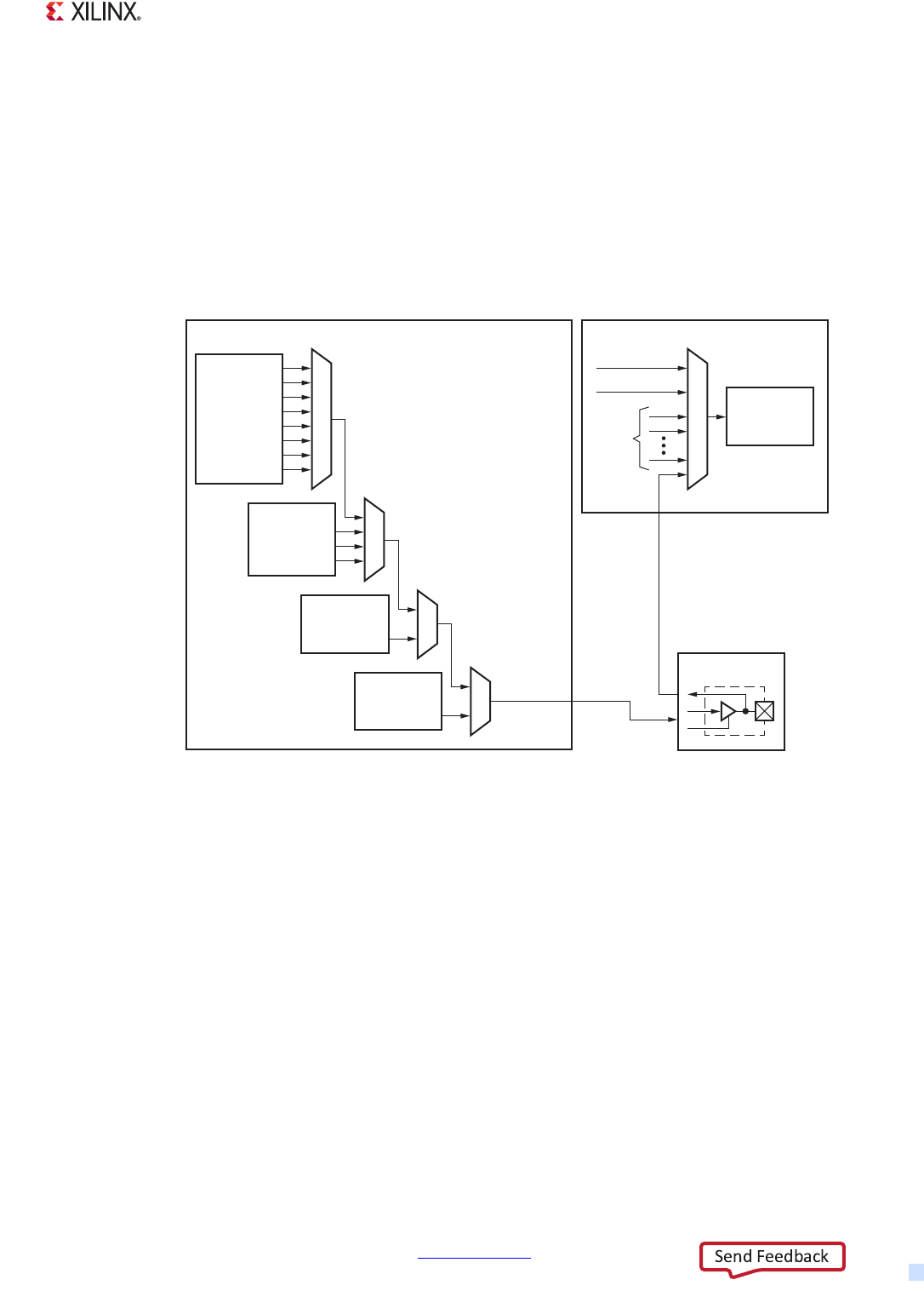
Zynq-7000 AP SoC Technical Reference Manual www.xilinx.com 53
UG585 (v1.12.1) December 6, 2017
Chapter 2: Signals, Interfaces, and Pins
2.5.5 MIO Signal Routing
Signal routing through the MIO is controlled by the MIO_PIN_[53:0] configuration registers located
in the slcr registers set. The MIO multiplexes and de-multiplexes the various input and output signals
to the MIO pins using four stages of multiplexing, as shown in Figure 2-4. The high-speed data
signals (such as RGMII for Gigabit Ethernet and ULPI for USB) are routed through only one
multiplexer stage. The slower signals (such as the UART and I2C ports) are routed through all four
multiplexer stages. The routing for each MIO pin is independently controlled by multiple bit fields in
each MIO_PIN register.
Any of the MIO pins can be programmed to be an external CAN controller reference clock using the
CAN_MIOCLK_CTRL register.
2.5.6 Default Logic Levels
The inputs to the I/O peripherals are driven with default values when another source is not routed to
either the MIO or the EMIO. If an input is routed to EMIO, but the PL is powered down, then the same
default value is driven to the I/O peripheral. (See Figure 2-5.)
For MIO-only signals, the default signal input is driven when the MIO multiplexer does not route the
signal to an MIO pin.
For MIO-EMIO signals, the default signal input is driven when the MIO multiplexer does not route the
signal to an MIO pin (the signal defaults to the EMIO interface) and when the signal is programmed
to be routed through the EMIO, but the PL either does not drive the signal (not configured) or is not
able to drive it (powered down).
X-Ref Target - Figure 2-4
Figure 2-4: MIO Signal Routing
UG585_c2_04_042312
Controller
Outputs
Outputs
from
Controllers
Notice: Not all mux
inputs are populated
with controller outputs.
Inputs to
Controllers
Level 3 Muxing
Level 2 Muxing
0
1
2
3
4
5
6
7
Controller
Outputs
0
Input Tie-Offs
EMIO
Other
MIO
Pins
1
2
3
Level 1 Muxing
Controller
Output
Controller
Input
0
1
Level 0 Muxing
Controller
Output
MIO Pin
0
1
To Program Muxing
Levels, refer to the
select fields in Registers
MIO_PIN_[53:00]
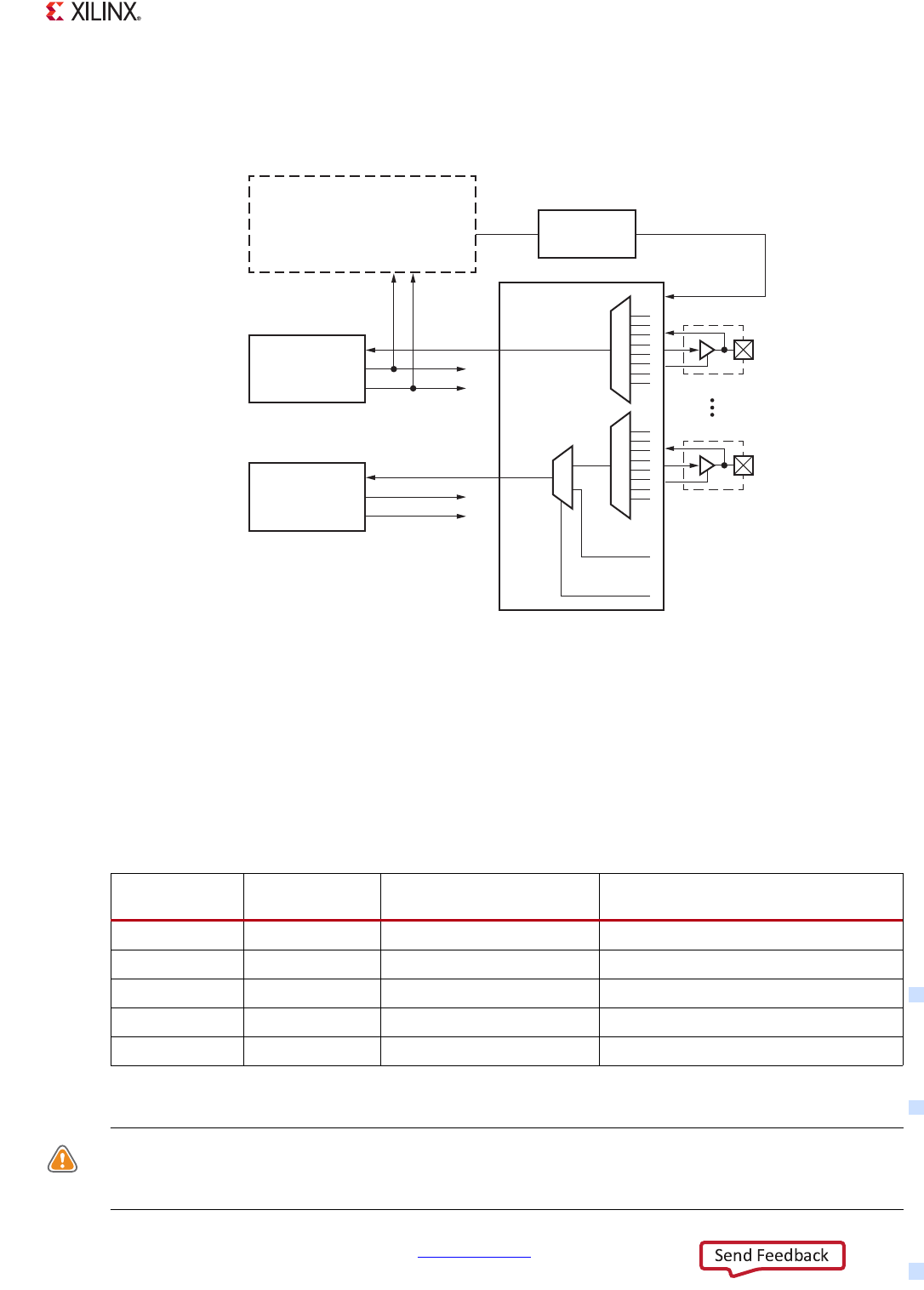
Zynq-7000 AP SoC Technical Reference Manual www.xilinx.com 54
UG585 (v1.12.1) December 6, 2017
Chapter 2: Signals, Interfaces, and Pins
The default input signal logic levels are designed to be benign to the I/O peripheral. As a precaution,
the related peripheral core should also be disabled when not in use. The logic levels are shown in the
signal tables in each chapter for each I/O peripheral.
2.5.7 MIO Pin Electrical Parameters
The MIO_PIN registers include bit fields to control the electrical pin characteristics of each I/O Buffer
(GPIOB). This includes I/O buffer signaling voltage, slew rate, 3-state control, pull-up resistor, and
HSTL enable. These are summarized in Ta b le 2 -5 . Refer to the applicable Zynq-7000 AP SoC data
sheet for electrical specifications.
CAUTION! The allowable Vin High level voltage depends on the settings of the
slcr.MIO_PIN_xx[IO_Type] and [DisableRcvr] bits. The restrictions are defined in the Zynq-7000 AP SoC
data sheets. Damage to the input buffer can occur when the limits are exceeded.
X-Ref Target - Figure 2-5
Figure 2-5: Non-selected Controller Inputs
UG585_c2_05_042312
Hardcoded
Tie-Offs
0
EMIO Output
EMIO Input
Voltage translation
and drives a default
value to the MIO mux.
EMIO Inputs
1
No Interface
Selected
Subsystems
With MIO And
EMIO Routing
MIO Mux
Input Signal
Tie-Offs
Programmable
Logic
MIO
Pins
Subsystems
With MIO-only
Routing
Table 2-5: MIO I/O Buffer Programmable Parameters
I/O Buffer
Parameter
MIO_PIN Register
Bit Field Selections Comments
Signaling I/O_Type LVCMOS (18, 25, 33), HSTL Selects the drive and receiver type
HSTL Receiver(1) DisableRcvr Enable, Disable Enable when IO_Type = HSTL
Slew Rate Speed Fast, Slow Selects edge rate for LVCMOS I/O types
3-State Control 3-State Control Enable, Disable Enables 3-state for all I/O types
Pull-up Pull-up Enable, Disable Enables pull-up for all I/O types
Notes:
1. The HSTL receiver is useful for the GEM Ethernet PHY interface.
Zynq-7000 AP SoC Technical Reference Manual www.xilinx.com 55
UG585 (v1.12.1) December 6, 2017
Chapter 2: Signals, Interfaces, and Pins
VREF Source Considerations
The VREF pins for HSTL signaling can be from an internal or external source. The user should choose
based system design needs. The reference source is selected using the slcr.GPIOB_CTRL
[VREF_SW_EN] register bit.
2.6 PS–PL AXI Interfaces
The PS side of the AXI interfaces are based on the AXI 3 interface specification. Each interface
consists of multiple AXI channels. The interfaces are summarized in Tab le 2-6 . Over a thousand
signals are used to implement these nine PL AXI interfaces.
Note: The PL level shifters must be enabled via LVL_SHFTR_EN before PL logic communication can
occur, refer to section 2.7.1 Clocks and Resets.
2.7 PS–PL Miscellaneous Signals
The programmable logic interface group contains miscellaneous interfaces between PS and the PL.
An input is driven by the PL and an output is driven by the PS. Signals might have suffixes where an
'N' suffix indicates an active Low signal; otherwise the signal is active High. A 'TN’ suffix indicates an
active Low 3-state enable signal and is an output to the PL. Output signals to the PL are always driven
to either a High or Low level state.
PS-PL signal groups are identified in Tab l e 2- 7.
Table 2-6: PL AXI Interfaces
Interface
Name Interface Description Master Slave Signals
M_AXI_GP0 General Purpose (AXI_GP) PS PL Chapter 5, Interconnect has a
section to describe each of these
interfaces.
The AXI signals are listed
individually in section 5.6 PS-PL
AXI Interface Signals.
The AXI_ACP interface is also
described in multiple places in
Chapter 3, Application
Processing Unit, including section
3.5.1 PL Co-processing
Interfaces.
The PS interconnect is shown in
Figure 5-1.
M_AXI_GP1 PS PL
S_AXI_GP0 General Purpose (AXI_GP) PL PS
S_AXI_GP1 PL PS
S_AXI_ACP Accelerator Coherency Port,
cache-coherent transaction (ACP) PL PS
S_AXI_HP0 High Performance ports (AXI_HP) with
read/write FIFOs and two dedicated
memory ports on DDR controller and
a path to the OCM. The AXI_HP
interfaces are known also as AFI.
PL PS
S_AXI_HP1 PL PS
S_AXI_HP2 PL PS
S_AXI_HP3 PL PS
Zynq-7000 AP SoC Technical Reference Manual www.xilinx.com 56
UG585 (v1.12.1) December 6, 2017
Chapter 2: Signals, Interfaces, and Pins
Note: The PL level shifters must be enabled via the slcr.LVL_SHFTR_EN register before PL logic
communication can occur, refer to section 2.7.1 Clocks and Resets.
2.7.1 Clocks and Resets
Clocks
The PS clock module provides four frequency-programmable clocks (FCLKs) to the PL that are
physically spread out along the PS–PL boundary. The clocks can also be individually controlled. The
FCLK clocks can be routed to PL clock buffers to serve as a frequency source.
Note: There is no guaranteed timing relationship between any of the four PL clocks and between
any of the other PS-PL signals. Each clock is independently programmed and operated. The
FCLKCLKTRIGN[3:0] signals are currently not supported. They must be tied to ground in the PL. The
FCLK clocks are described in Chapter 25, Clocks.
Resets
The PS reset subsystem provides four programmable reset signals to the PL. The reset signals are
controlled by writing to the slcr.FPGA_RST_CTRL SLCR[FPGA[3:0]_OUT_RST] bit fields. The resets are
independently programmed and are completely independent of the PL clocks and all other PS-PL
signals. The PS reset subsystem is described in Chapter 26, Reset System.
The PL clocks and resets are summarized in Tab le 2- 8.
Table 2-7: PS-PL Signal Groups
PS-PL Signal Group Signal Name Reference
PL clocks and resets FCLKx 2.7.1 Clocks and Resets
PL interrupts to PS IRQF2Px 2.7.2 Interrupt Signals
IOP interrupts to PL IRQP2Fx 2.7.2 Interrupt Signals
Events EVENTx 2.7.3 Event Signals
IdleAXI, DDR ARB, SRAM
interrupt, FPGA
FPGA, DDR, EMIO 2.7.4 Idle AXI, DDR Urgent/Arb, SRAM
Interrupt Signals
DMA controller DMACx 2.7.5 DMA Req/Ack Signals
EMIO signals EMIOx Table 2-3
USB port indicator and power
control
EMIOUSBx 15.16.3 MIO-EMIO Signals
Table 2-8: PL Clock and Reset Signals
Type PL Signal Name I/O Reference
PL Clocks FCLKCLK[3:0] O Chapter 25, Clocks
PL Clock Throttle Control FCLKCLKTRIG [3:0] I
PL Resets FCLKRESETN [3:0] O Chapter 26, Reset System
Zynq-7000 AP SoC Technical Reference Manual www.xilinx.com 57
UG585 (v1.12.1) December 6, 2017
Chapter 2: Signals, Interfaces, and Pins
2.7.2 Interrupt Signals
The interrupts from the processing system I/O peripherals (IOP) are routed to the PL and assert
asynchronously to the FCLK clocks. In the other direction, the PL can asynchronously assert up to 20
interrupts to the PS. Sixteen of these interrupt signals are mapped to the interrupt controller as a
peripheral interrupt where each interrupt signal is set to a priority level and mapped to one or both
of the CPUs. The remaining four PL interrupt signals are inverted and routed to the nFIQ and nIRQ
interrupt directly to the signals to the private peripheral interrupt (PPI) unit of the interrupt
controller. There is an nFIQ and nIRQ interrupt for each of two CPUs. The PS to PL and PL to PS
interrupts are listed in Ta ble 2 -9. Details of the interrupt signals are described in Chapter 7, Interrupts.
2.7.3 Event Signals
The PS supports processor events to and from the PL (see Tab le 2-1 0). These signals are
asynchronous to the PS and FCLK clocks. For details on these signals, see Chapter 3, Application
Processing Unit.
2.7.4 Idle AXI, DDR Urgent/Arb, SRAM Interrupt Signals
The idle AXI signal to the PS is used to indicate that there are no outstanding AXI transactions in the
PL. It cannot be read from any registers. Driven by the PL, this signal is one of the conditions used to
initiate a PS bus clock shut-down by ensuring that all PL bus devices are idle.
The DDR urgent/arb signal is used to signal a critical memory starvation situation to the DDR
arbitration for the four AXI ports of the PS DDR memory controller. The EMIOSRAMINT signal is used
to alert the PL that the static memory controller has triggered an interrupt.
Table 2-9: PL Interrupt Signals
Type PL Signal Name I/O Destination
PL to PS
Interrupts
IRQF2P[7:0] I SPI: Numbers [68:61].
IRQF2P[15:8] I SPI: Numbers [91:84].
IRQF2P[19:16] I PPI: nFIQ, nIRQ (both CPUs).
PS to PL
Interrupts IRQP2F[27:0] O
Pl Logic. These signals are received from the I/O peripherals and are
forwarded to the interrupt controller. These signals are also provided as
outputs to the PL.
Table 2-10: PL Event Signals
Type PL Signal Name I/O Description
Events EVENTEVENTI I Causes one or both CPUs to wake up from a WFE state.
EVENTEVENTO O Asserted when one of the CPUs has executed the SEV instruction.
Standby
EVENTSTANDBYWFE[1:0] O CPU standby mode: asserted when a CPU is waiting for an event.
EVENTSTANDBYWFI[1:0] O CPU standby mode: asserted when a CPU is waiting for an
interrupt.
Zynq-7000 AP SoC Technical Reference Manual www.xilinx.com 58
UG585 (v1.12.1) December 6, 2017
Chapter 2: Signals, Interfaces, and Pins
2.7.5 DMA Req/Ack Signals
There are four sets of DMA controller flow control signals for use by up to four PL slaves connected
via the M_AXI_GP interfaces (see Ta bl e 2- 11 ). These four sets of flow control signals correspond to
DMA channels 4 through 7, see Chapter 9, DMA Controller.
2.8 PL I/O Pins
A summary of the PL I/O pins is shown in Tabl e 2- 13. Refer to the applicable Zynq-7000 AP SoC data
sheet and Zynq-7000 AP SoC packaging and pin documents for more information.
For more information on multi-gigabit serial transceivers pins, see the Pin Description and Design
Guidelines section in UG476, 7 Series FPGAs GTX Transceivers User Guide. (Four to sixteen
transceivers are available in the Kintex-based Zynq 7z030, 7z035, 7z045, and 7z100 devices.)
7z007s and 7z010 Device Notice
Devices in CLG225 packages (7z010 dual core and 7z007s single core devices) have fewer pins than
the other Zynq-7000 AP SoC devices. For these devices, DXN is tied to ground, Bank 34 has 46 I/Os,
and Bank 35 has 8 I/Os. There are also only four pairs of XADC signals.
Table 2-11: PL AXI Idle, DDR Urgent/Arb and SRAM Interrupt Signals
Type PL Signal Name I/O Destination Reference
Idle PL AXI Interfaces FPGAIDLEN I Central interconnect
clock disable logic
Central Interconnect Clock Disable in
section 25.1.4 Power Management
DDR Urgent Signal DDRARB[3:0] I DDR memory
controller Chapter 10, DDR Memory Controller
SRAM EMIOSRAMINTIN I Static memory
controller interrupt
Chapter 11, Static Memory
Controller
Table 2-12: PL DMA Signals
Type Signal PL Signal Name I/O Reference
Clock and Reset Clock DMA[3:0]ACLK I 9.2.7 PL Peripheral Request Interface
Request
Ready DMA[3:0]DRREADY O
Chapter 9, DMA Controller
Valid DMA[3:0]DRVALID I
Type DMA[3:0]DRTYPE[1:0] I
Last DMA[3:0]DRLAST I
Acknowledge
Ready DMA[3:0]DAREADY I
Valid DMA[3:0]DAVALID O
Type DMA[3:0]DATYPE[1:0] O
Zynq-7000 AP SoC Technical Reference Manual www.xilinx.com 59
UG585 (v1.12.1) December 6, 2017
Chapter 2: Signals, Interfaces, and Pins
CAUTION! The allowable Vin High level voltages are defined in the Zynq-7000 AP SoC data sheets.
Damage to the input buffer can occur when the limits are exceeded.
Table 2-13: PL Pin Summary
Group Name Type Description
User I/O Pins IO_LXXY_#,
IO_XX_# I/O
Most user I/O pins are capable of differential signaling and can be
implemented as pairs. The top and bottom I/O pins are always
single ended.
Multi-Gigabit
Serial
Transceivers
MGTXRX[P,N] I Differential receive and transmit ports. Multi-Gigabit Serial
Transceiver pins. Four transceivers are available in the Zynq-7000
AP SoC 7z030 device and 16 in the 7z035, 7z045 and 7z100 devices.
MGTXTX[P,N] O
MGTAVCC_G# I 1.0V analog power-supply pin for receiver and transmitter internal
circuits.
MGTAVTT_G# I 1.2V analog power-supply pin for the transmit driver.
MGTVCCAUX_G# I 1.8V auxiliary analog Quad PLL voltage supply for the transceivers.
MGTREFCLK0/1P I Positive differential reference clock for the transceivers.
MGTREFCLK0/1N I Negative differential reference clock for the transceivers.
MGTAVTTRCAL N/A Precision reference resistor pin for internal calibration termination.
MGTRREF I Precision reference resistor pin for internal calibration termination.
PL JTAG PL_TCK, PL_TMS,
PL_TDI, PL_TDO I/O See Chapter 27, JTAG and DAP Subsystem.
Configuration
DONE, INIT_B,
PROGRAM_B I/O Refer to the 7-series documentation.
CFGBVS I Pre-configuration I/O standard type for the dedicated
configuration bank 0.
PUDC_B I Active Low input enables internal pull-ups during configuration on
all SelectIO pins.
XADC
VP, VN I Dedicated differential analog inputs.
VREFP, VREFN N/A Reference input (1.25V) and ground.
AD[15:0]P,
AD[15:0]N I 16 differential auxiliary analog inputs.
Multi-function
MRCC I
Clock capable I/Os driving BUFRs, BUFIOs, BUFGs and
MMCMs/PLLs. In addition, these pins can drive the BUFMR for
multi-region BUFIO and BUFR support. These pins become regular
user I/Os when not needed as a clock.
SRCC I Clock capable I/Os driving BUFRs, BUFIOs and MMCMs/PLLs. These
pins become regular user I/Os when not needed for clocks.
T[3:0] I Four memory byte groups.
T[3:0]_DQS I DDR DQS strobe pin that belongs to the memory byte group T0-T3.
Temperature DXP, DXN I Temperature-sensing diode pins.
Reserved RSVDVCC I Tie to VCCO_0.
RSVDGND I Tie to ground.

Zynq-7000 AP SoC Technical Reference Manual www.xilinx.com 60
UG585 (v1.12.1) December 6, 2017
Chapter 3
Application Processing Unit
3.1 Introduction
3.1.1 Basic Functionality
The application processing unit (APU), located within the PS, contains one processor for single-core
devices or two processors for dual-core devices. These are ARM® Cortex™-A9 processors with NEON
co-processors connected in an MP configuration sharing a 512 KB L2 cache. Each processor is a
high-performance and low-power core that implements two separate 32 KB L1 caches for instruction
and data. The Cortex-A9 processor implements the ARM v7-A architecture with full virtual memory
support and can execute 32-bit ARM instructions, 16-bit and 32-bit Thumb instructions, and 8-bit
Java™ byte codes in the Jazelle state. The NEON™ coprocessor media and signal processing
architecture adds instructions that target audio, video, image and speech processing, and 3D
graphics. These advanced single instruction multiple data (SIMD) instructions are available in both
ARM and Thumb states. A block diagram of the APU is shown in Figure 3-1.
The Cortex-A9 processor(s) within the APU are organized in an MP configuration with a snoop
control unit (SCU) responsible for maintaining L1 cache coherency between the two processors and
the ACP interface from the PL. To increase performance, there is a shared unified 512 KB level-two
(L2) cache for instruction and data. In parallel to the L2 cache, there is a 256 KB on-chip memory
(OCM) module that provides a low-latency memory.
An accelerator coherency port (ACP) facilitates communication between the programmable logic (PL)
and the APU. This 64-bit AXI interface allows the PL to implement an AXI master that can access the
L2 and OCM while maintaining memory coherency with the CPU L1 caches.
The unified 512 KB L2 cache is 8-way set-associative and allows you to lock the cache content on a
line, way, or master basis. All accesses through the L2 cache controller can be routed to the DDR
controller or can be sent to other slaves in the PS or PL depending on their address. To reduce
latency to the DDR memory, there is a dedicated port from the L2 controller to the DDR controller.
Debug and trace capability is built into the two processor cores and interconnects as a part of the
CoreSight™ debug and trace system. You can control and interrogate the processor(s) and the
memory through the debug access port (DAP). Furthermore, 32-bit AMBA® trace bus (ATB) masters
from the processor(s) are funneled with other ATB masters, such as Instrumentation Trace Macrocell
(ITM) and Fabric Trace Monitor (FTM), to generate the unified PS trace through the on-chip
embedded trace buffer (ETB) or the trace-port interface units (TPIU).
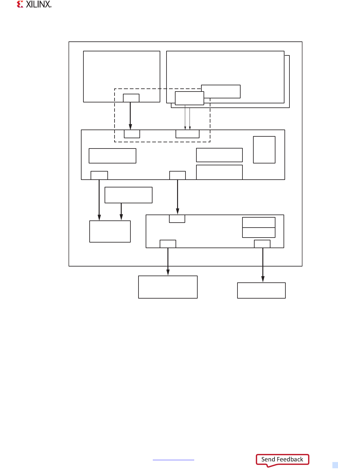
Zynq-7000 AP SoC Technical Reference Manual www.xilinx.com 61
UG585 (v1.12.1) December 6, 2017
Chapter 3: Application Processing Unit
ARM architecture supports multiple operating modes including supervisor, system, and user modes
to provide different levels of protection at the application level. The architecture support for
TrustZone technology helps to create a secure environment to run applications and protect their
contents. TrustZone built into the ARM CPU processor and many peripherals enables a secure system
to handle keys, private data, and encrypted information without allowing these secrets to leak to
non-trusted programs or users.
The APU contains a 32-bit watchdog timer and a 64-bit global timer with auto-decrement features
that can be used as general-purpose timers and also as a mechanism to start up the processors from
standby mode.
X-Ref Target - Figure 3-1
Figure 3-1: APU Block Diagram
UG585_c3_01_100812
DDR
CPUs
Snoopable Data
buffers and caches
SCU
M0 M1
L2 Cache
M0
S
M
S
OCM
Accelerator
Coherency Port
(ACP)
PL Fabric
L1 Cache Line
Updates
S
Read/Write
Requests
Flush Cache Line to
Memory
Maintain L1 Cache
Coherency
APU
Cache Coherent
Transactions
Tag RAM
System
Interconnect
System
Interconnect
M1
Cacheable
and Non-
cacheable
Accesses
Cacheable and Non-
cacheable Accesses to DDR,
PL, Peripherals, and PS
registers
Data RAM
Tag
RAM
Cache Tag RAM
Update

Zynq-7000 AP SoC Technical Reference Manual www.xilinx.com 62
UG585 (v1.12.1) December 6, 2017
Chapter 3: Application Processing Unit
3.1.2 System-Level View
The APU is the most critical component of the system that comprises the PS, the IP cores
implemented in the PL, and board-level devices such as the external memories and the peripherals.
The main interfaces through which the APU communicates to the rest of the system are two
interfaces through the L2 controller and an interface to the OCM that is parallel to the L2 cache. See
Figure 3-1.
All accesses from the dual/single Cortex-A9 MP system go through the SCU and all accesses from
any other master that requires coherency with the Cortex-A9 MP system also need to be routed
through the SCU using the ACP Port. All accesses that are not routed through the SCU are
non-coherent with the CPU and software has to explicitly handle the synchronization and coherency.
Accesses from the APU can target the OCM, DDR, PL, IOP slaves, or registers within the PS
sub-blocks. To minimize the latency to the OCM, a dedicated master port from the SCU provides
direct access by the processors and the ACP to the OCM, offering a latency that is even less than the
L2 cache.
All APU accesses to the DDR are routed through the L2 cache controller. To improve the latencies of
the DDR accesses, there is a dedicated master port from the L2 cache controller to the DDR memory
controller that allows all APU-DDR transactions to bypass the main interconnects which are shared
with the other masters. All other accesses from the APU that are neither OCM-bound nor
DDR-bound go through the L2 controller and are routed through the main interconnect using a
second port. The accesses that pass through the L2 cache controller do not have to be cacheable.
Exclusive access transactions from LDREX/SDREX instructions or ACP exclusive transactions in the
APU are described under Exclusive AXI Accesses in Chapter 5. As shown in Figure 3-2, the APU and
its sub-blocks all operate in the CPU_6x4x clock domain. The interfaces from the APU to the OCM
and to the main interconnects are all synchronous. The main interconnects can run at 1/2 or 1/3 of
the frequency of the CPU. The DDR block is on the DDR_3x clock domain and operates
asynchronously to the APU. The ACP port to the APU block includes a synchronizer and the PL master
that uses this port can have a clock that is asynchronous to the APU.
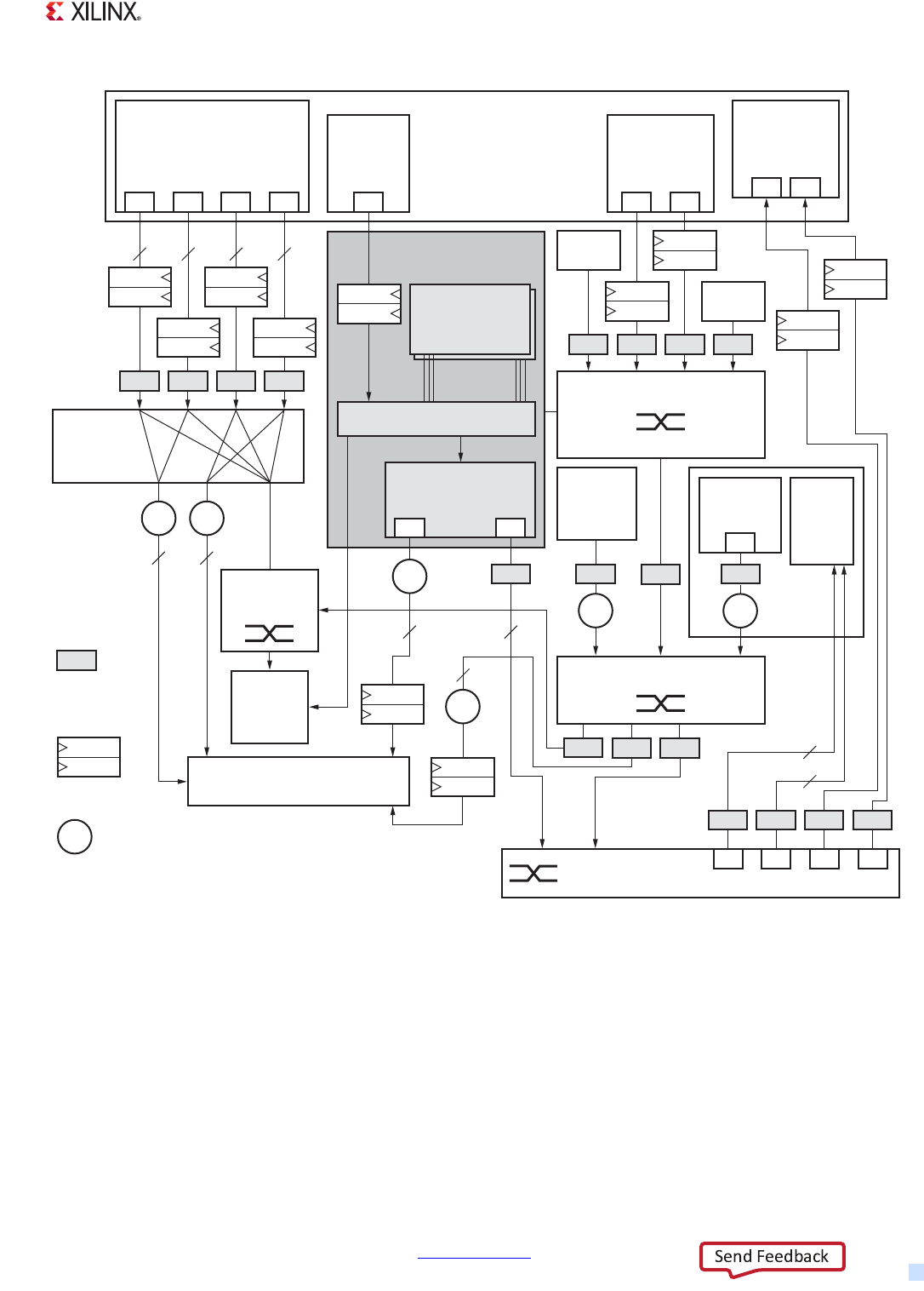
Zynq-7000 AP SoC Technical Reference Manual www.xilinx.com 63
UG585 (v1.12.1) December 6, 2017
Chapter 3: Application Processing Unit
X-Ref Target - Figure 3-2
Figure 3-2: APU System View Diagram
UG585_c3_02_101614
PL Fabric
High Performance
AXI Controllers
(AXI_HP)
Application
Processing Unit
PL Clocks
M0
FIFO
ASYNC
M1 M2 M3
Cache
Coherent
ACP Port
Cortex-A9
NEON MMU
L1 I/D Caches
Slave Interconnect for
Master Peripherals
DMA
Controller
IOP
Instruction
Data Snoop
CPU_6x4x
M
General
Purpose
AXI Masters
M0 M1
General
Purpose
AXI Slaves
S0 S1
FIFOFIFO FIFO
32-/
64-bit
64-bit 64-bit
64-bit 64-bit
32-bit
32-bit
64-bit
ASYNC
ASYNC
Snoop Control Unit
32-/
64-bit
32-/
64-bit
ASYNC
ASYNC
ASYNC
32-/
64-bit
ASYNC
4
DevC
8
QoS
CPU_2x
DDR_3x
Read/Write
Requests
(e.g., 8 reads,
8 writes)
Clock
Synchronizer
Quality of
Service
Priority
Clock Domains
are specified within
Some Blocks
CPU_1x
On-chip
RAM
256 kB
16
4816
8
88 1
ASYNC
ASYNC DAP
CPU_2x
L2 Cache
512 KB
M0 M1
IOP
Masters
IOP
Slave
Reg &
Data
M
Central Interconnect
DDR Controller
CPU_2x
Master Interconnect
for Slave Peripherals
OCM
Interconnect
QoS
QoS
8
QoS
QoS
QoS QoS
AXI_HP
to DDR
Interconnect
ASYNC
ASYNC
ASYNC
1 84 8
M3 M2 M1 M0
8

Zynq-7000 AP SoC Technical Reference Manual www.xilinx.com 64
UG585 (v1.12.1) December 6, 2017
Chapter 3: Application Processing Unit
3.2 Cortex-A9 Processors
3.2.1 Summary
The APU implements a dual/single-core Cortex-A9 MP configuration. Each processor has its own
SIMD media processing engine (NEON), memory management unit (MMU), and separate 32 KB
level-one (L1) instruction and data caches. Each Cortex-A9 processor provides two 64-bit AXI master
interfaces for independent instruction and data transactions to the SCU. Depending on the address
and attributes, these transactions are routed to the OCM, L2 cache, DDR memory, or, through the PS
interconnect, to other slaves in the PS, or to the PL. Each processor interface with the SCU includes
the required snoop signals to provide coherency between the L1 data caches within the processors
and the shared L2 cache for shareable memory. The Cortex-A9 and its subsystem also provide
complete Trustzone extension, necessary for user security.
The Cortex-A9 processor implements the necessary hardware features for program debug and trace
generation support. The processor also provides hardware counters to gather statistics on the
operation of the processor and memory system.
The major sub-blocks within the Cortex-A9 are the central processing unit (CPU), the L1 instruction
and data caches, the memory management unit (MMU), the NEON coprocessor, and the core
interfaces. Their functions are explained in the following subsections.
3.2.2 Central Processing Unit (CPU)
Each Cortex-A9 CPU can issue two instructions in one cycle and execute them out of order. The CPU
implements dynamic branch prediction and with its variable length pipeline can deliver
2.5 DMIPs/MHz. The Cortex-A9 processor implements the ARMv7-A architecture with full virtual
memory support and can execute 32-bit ARM instructions, 16-bit and 32-bit Thumb instructions,
and 8-bit Java™ byte codes in the Jazelle hardware acceleration state. Figure 3-3 shows the
architecture of the Cortex-A9 processor.
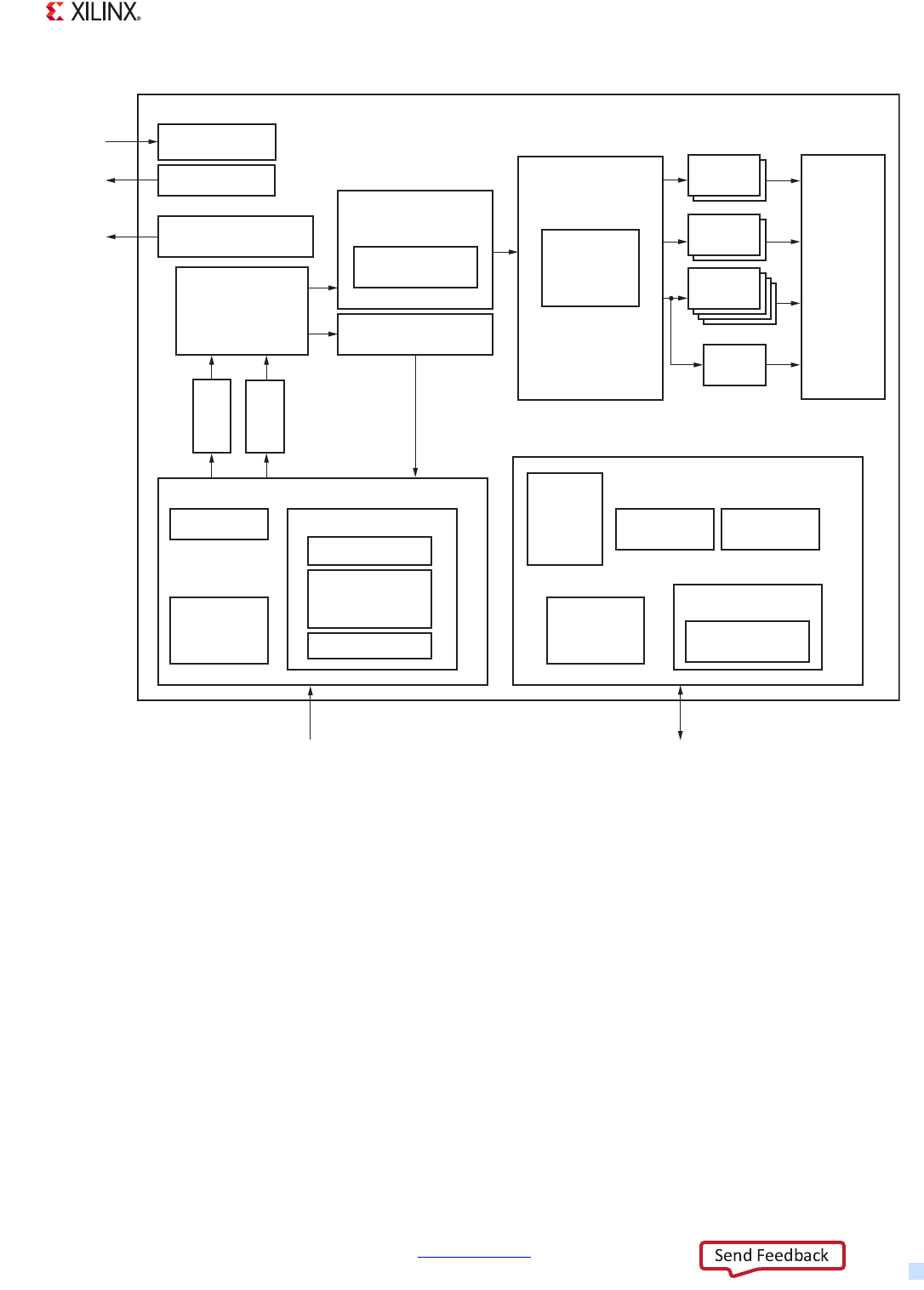
Zynq-7000 AP SoC Technical Reference Manual www.xilinx.com 65
UG585 (v1.12.1) December 6, 2017
Chapter 3: Application Processing Unit
Pipeline
The pipeline implemented in the Cortex-A9 CPU employs advanced fetching of instructions and
branch prediction that decouples the branch resolution from potential memory latency-induced
instruction stalls. In the Cortex-A9 CPU, up to four instruction-cache lines are pre-fetched to reduce
the impact of memory latency on the instruction throughput. The CPU fetch unit can continuously
forward two to four instructions per cycle to the instruction decode buffer to ensure efficient
superscalar pipeline utilization. The CPU implements a superscalar decoder capable of decoding two
full instructions per cycle, and any of the four CPU pipelines can select instructions from the issue
queue. The parallel pipelines support concurrent execution across full dual arithmetic units,
load-store unit, plus resolution of any branch each cycle.
The Cortex-A9 CPU employs speculative execution of instructions enabled by dynamic renaming of
physical registers into an available pool of virtual registers. The CPU employs this virtual register
renaming to eliminate dependencies across registers without jeopardizing the correct execution of
programs. This feature allows code acceleration through an effective hardware based unrolling of
X-Ref Target - Figure 3-3
Figure 3-3: Cortex-A9 Architecture
CoreSight Debug
Access Port
Coresight
Debug
Cortex A9 Processor
Profiling Monitor
Block
Dual Instruction
Decode Stage
Instruction
Queue
Prediction
Queue
Fast Loop Mode
Instruction
Cache
Instruction Pre-fetch Stage
Branch Prediction
Global History Buffer
Branch Target
Address Cache
(BTAC)
Return Stack
Register Rename Stage
Virtual to Physical
Register Pool
Auto
Pre-fetcher
Data
Cache
Load-Store Unit
Store Buffer
Program Trace Unit
MemorySystem
µTLB MMU
Instruction
Queue
&
Dispatch
3 + 1 Dispatch Stage
Out of Order
Multi-issue
with Speculation
ALU/MUL
ALU
FPU/NEON
Address
Out of Order
Write-back
Stage
Coresight
Trace
Branches
Instruction
Interface
Data
Interface
UG585_c3_04_030712

Zynq-7000 AP SoC Technical Reference Manual www.xilinx.com 66
UG585 (v1.12.1) December 6, 2017
Chapter 3: Application Processing Unit
loops, and increases the pipeline utilization by removing data dependencies between adjacent
instructions, which also indirectly reduces interrupt latency.
In the Cortex-A9 CPU, dependent load-store instructions can be forwarded for resolution within the
memory system to further reduce pipeline stalls. The core supports up to four data cache line fill
requests that can be through automatic or user-driven pre-fetching.
A key feature of this CPU is the out-of-order write back of instructions that enables the pipeline
resources to be released independent of the order in which the system provides the required data.
Load/store instructions can be issued speculatively before condition of instruction or a preceding
branch has been resolved or before data to be written has become available. If the condition
required for the execution of the load/store fails, any of the side-effects, such as the action to modify
registers, are flushed.
Branch Prediction
To minimize the branch penalty in its highly pipelined CPU, the Cortex-A9 implements both static
and dynamic branch prediction. Static branch prediction is provided by the instructions and is
decided during compilation. Dynamic branch prediction uses the outcome of the previous
executions of a specific branch to determine whether the branch should be taken or not. The
dynamic branch prediction logic employs a global branch history buffer (GHB) which is a 4,096 entry
table holding 2-bit prediction information for specific branches and is updated every time a branch
gets executed.
The branch execution and the overall instruction throughput also benefit greatly from the
implementation of a branch target address cache (BTAC) which holds the target addresses of the
recent branches. This 512-entry address cache is organized as 2-way × 256 entries and provides the
target address for a specific branch to the pre-fetch unit before the actual target address is
generated based on the calculation of the effective address and its translation to the physical
address. Additionally, if an instruction loop fits in four BTAC entries, instruction cache accesses are
turned off to lower power consumption.
Note: Both GHB and BTAC RAMs implement parity for protection; however, this support has limited
diagnostic value. Corruption in GHB data or BTAC data does not generate functional errors in the
Cortex-A 9 processor. Corruption in GHB data or BTAC data results in faulty branch prediction that is
detected and corrected when the branch gets executed.
The Cortex-A9 CPU can predict conditional branches, unconditional branches, indirect branches,
PC-destination data-processing operations, and branches that switch between ARM and Thumb
states. However, the following branch instructions are not predicted:
• Branches that switch between states (except ARM to Thumb transitions, and Thumb to ARM
transitions)
• Instructions with the S suffix are not predicted, as they are typically used to return from
exceptions and have side effects that can change privilege mode and security state.
• All mode-changing instructions
Users can enable program flow prediction by setting the Z bit in the CP15 c1 Control register to 1.
Refer to the System Control Register in the ARM Cortex-A9 Technical Reference Manual (see
Appendix A, Additional Resources). Before switching the program flow prediction on, a BTAC flush
operation must be performed which has the additional effect of setting the GHB into a known state.

Zynq-7000 AP SoC Technical Reference Manual www.xilinx.com 67
UG585 (v1.12.1) December 6, 2017
Chapter 3: Application Processing Unit
Cortex-A9 also employs an 8-entry return stack cache that holds the 32-bit subroutine return
addresses. This feature greatly reduces the penalty of executing subroutine calls and can address
nested routines up to eight levels deep.
Instruction and Data Alignment
ARM architecture specifies the ARM instructions as being 32-bits wide and requires them to be
word-aligned. Thumb instructions are 16-bits wide and are required to be half-word aligned.
Thumb-2 instructions which are 16- or 32-bits wide are also required to be half-word aligned. Data
accesses can be unaligned and the load/store unit within the CPU breaks them up to aligned
accesses. The data from these accesses are merged and sent to the register file within the CPU as had
been requested.
Note: The application processing unit (APU), and the PS as a whole, support only little-endian
architecture for both instruction and data.
Trace and Debug
The Cortex-A9 processor implements the ARMv7 debug architecture as described in the ARM
Architecture Reference Manual (ARMv7-A). In addition, the processor supports a set of Cortex-A9
processor-specific events and system-coherency events. For more information, see Chapter 11,
Performance Monitoring Unit in the ARM Cortex-A9 Technical Reference Manual.
The debug interface of the processor consists of:
• A baseline CP14 interface that implements the ARMv7 debug architecture and the set of debug
events as described in the ARM Architecture Reference Manual (ARMv7-A)
• An extended CP14 interface that implements a set of debug events specific to this processor as
explained in the ARM Architecture Reference Manual (ARMv7-A)
• An external debug interface connected to an external debugger through a debug access port
(DAP)
The Cortex-A9 includes a program trace module that provides ARM CoreSight technology
compatible program-flow trace capabilities for either of the Cortex-A9 processors and provides full
visibility into the actual instruction flow of the processor. The Cortex-A9 PTM includes visibility over
all code branches and program flow changes with cycle-counting enabling profiling analysis. The
PTM block in conjunction with the CoreSight design kit provides the software developer the ability to
non-obtrusively trace the execution history of multiple processors and either store this, along with
time stamped correlation, into an on-chip buffer, or off chip through a standard trace interface so as
to have improved visibility during development and debug.
The Cortex-A9 processor also implements program counters and event monitors that can be
configured to gather statistics on the operation of the processor and the memory system.
3.2.3 Level 1 Caches
Each of the two Cortex-A9 processors has separate 32 KB level-1 instruction and data caches. Both L1
caches have common features that include:

Zynq-7000 AP SoC Technical Reference Manual www.xilinx.com 68
UG585 (v1.12.1) December 6, 2017
Chapter 3: Application Processing Unit
• Each cache can be disabled independently, using the system control coprocessor. Refer to the
System Control Register in the ARM Cortex-A9 Technical Reference Manual.
• The cache line lengths for both L1 caches are 32 bytes.
• Both caches are 4-way set-associative.
• L1 caches support 4 KB, 64 KB, 1 MB, and 16 MB virtual memory page.
• Neither of the two L1 caches supports the lock-down feature.
• The L1 caches have 64-bit interfaces to the integer core and AXI master ports.
• Cache replacement policy is either pseudo round-robin or pseudo-random. The victim counter
is read at time of miss, not allocation, and it is incremented on allocation. An invalid line in the
set is replaced in preference to using the victim counter.
• On a cache miss, critical word first filling of the cache is performed.
• To reduce power consumption, the number of full cache reads is reduced by taking advantage of
the sequential nature of many cache operations. If a cache read is sequential to the previous
cache read, and the read is within the same cache line, only the data RAM set that was
previously read is accessed.
• Both L1 caches support parity.
• All memory attributes are exported to external memory systems.
• Support for TrustZone security exports the secure or non-secure status to the caches and
memory system.
• Upon a CPU reset, the contents of both L1 caches are cleared to comply with security
requirements.
Note: You must invalidate the instruction cache, the data cache, and BTAC before using them. It is
not required to invalidate the main TLB, even though it is recommended for safety reasons. This
ensures compatibility with future revisions of the processor.
The L1 instruction-side cache (I-Cache) is responsible for providing an instruction stream to the
Cortex-A9 processor. The L1 I-Cache interfaces directly to the pre-fetch unit which contains a
two-level prediction mechanism as described in the Branch Prediction section of this chapter. The L1
instruction cache is virtually indexed and physically tagged.
The L1 data-side cache (D-Cache) is responsible for holding the data used by the Cortex-A9
processor. Key features of the L1 D-Cache include:
• Data cache is physically indexed and physically tagged.
• D-Cache is non-blocking and, therefore, load/store instructions can continue to hit the cache
while it is performing allocations from external memory due to prior read/write misses. The data
cache supports four outstanding reads and four outstanding writes.
• The CPU can support up to four outstanding preload (PLD) instructions. However, explicit
load/store instructions have higher priority.
• The Cortex-A9 load/store unit supports speculative data pre-fetching which monitors sequential
accesses made by program and starts fetching the next expected line before it has been
requested. This feature is enabled in the cp15 Auxiliary Control register (DP bit). The
pre-fetched lines can be dropped before allocation, and PLD instruction has higher priority.
• The data cache supports two 32-byte line-fill buffers and one 32-byte eviction buffer.
• The Cortex-A9 CPU has a store buffer with four 64-bit slots with data merging capability.

Zynq-7000 AP SoC Technical Reference Manual www.xilinx.com 69
UG585 (v1.12.1) December 6, 2017
Chapter 3: Application Processing Unit
• Both data cache read misses and write misses are non-blocking, with up to four outstanding
data cache read misses and up to four outstanding data cache write misses being supported.
• The APU data caches offer full snoop coherency control using the MESI algorithm.
• The data cache in Cortex-A9 contains local load/store exclusive monitor for LDREX/STREX
synchronizations. These instructions are used to implement semaphores. The exclusive monitor
handles one address only, with eight words or one cache line granularity. Therefore, avoid
interleaving LDREX/STREX sequences and always execute a CLREX instruction as part of any
context switch.
• D-Cache only supports write-back/write-allocate policy. Write-through and write-back/no
write-allocate policies are not implemented.
• L1 D-Cache offers support for exclusive operation with respect to the L2 cache. Exclusive
operation implies that a cache line is valid only in L1 or L2 cache and never in both at the same
time. A line-fill into L1 causes the line to be marked invalid in L2. At the same time, eviction of a
line from L1 causes the line to be allocated in L2, even if it is not dirty. A line-fill into L1 from
dirty L2 line forces eviction of the line to external memory. The exclusive operation, disabled by
default, increases cache utilization and reduces power consumption.
Initialization of L1 Caches
Before using the L1 caches, you must invalidate the instruction cache, the data cache, and the BTAC.
It is not required to invalidate the main TLB, even though it is recommended for safety reasons. This
ensures compatibility with future revisions of the processor. Steps to initialize L1 Caches:
1. Invalidate TLBs:
mcr p15, 0, r0, c8, c7, 0 (r0 = 0)
2. Invalidate I-Cache:
mcr p15, 0, r0, c7, c5, 0 (r0 = 0)
3. Invalidate Branch Predictor Array:
mcr p15, 0, r0, c7, c5, 6 (r0 = 0)
4. Invalidate D-Cache:
mcr p15, 0, r11, c7, c14, 2 (should be done for all the sets/ways)
5. Initialize MMU.
6. Enable I-Cache and D-Cache:
mcr p15, 0, r0, c1, c0, 0 (r0 = 0x1004)
7. Synchronization barriers:
dsb (Allows MMU to start)
isb (Flushes pre-fetch buffer)
(Refer to Memory Barriers, page 72 for more details on memory barriers.)

Zynq-7000 AP SoC Technical Reference Manual www.xilinx.com 70
UG585 (v1.12.1) December 6, 2017
Chapter 3: Application Processing Unit
3.2.4 Memory Ordering
Memory Ordering Model
The Cortex-A9 architecture defines a set of memory attributes with the characteristics required to
support all memory and devices in the system memory map. The following mutually-exclusive main
memory type attributes describe the memory regions:
•Normal
•Device
• Strongly-ordered
Device and Strongly Ordered
Accesses to strongly ordered and device memory have the same memory ordering model. System
peripherals come under strongly ordered and device memory. Access rules for this memory are as
follows:
• The number and size of accesses are preserved. Accesses are atomic, and will not be interrupted
part way through.
• Both read and write accesses can have side effects on the system. Accesses are never cached.
Speculative accesses are never be performed.
• Accesses cannot be unaligned.
• The order of accesses arriving at device memory is guaranteed to correspond to the program
order of instructions which access strongly ordered or device memory. This guarantee applies
only to accesses within the same peripheral or block of memory.
• The Cortex-A9 processor can re-order normal memory accesses around strongly ordered or
device memory accesses.
The only difference between device and strongly ordered memory is that:
• A write to strongly ordered memory can complete only when it reaches the peripheral or
memory component accessed by the write.
• A write to device memory is permitted to complete before it reaches the peripheral or memory
component accessed by the write.
Normal Memory
Normal memory is used to describe most parts of the memory system. All ROM and RAM devices are
considered to be normal memory. All code to be executed by the processor must be in normal
memory. Code is not architecturally permitted to be in a region of memory which is marked as device
or strongly ordered. The properties of normal memory are as follows:
• The processor can repeat read and some write accesses.
• The processor can pre-fetch or speculatively access additional memory locations, with no
side-effects (if permitted by MMU access permission settings). The processor does perform
speculative writes.

Zynq-7000 AP SoC Technical Reference Manual www.xilinx.com 71
UG585 (v1.12.1) December 6, 2017
Chapter 3: Application Processing Unit
• Unaligned accesses can be performed.
• Multiple accesses can be merged by processor hardware into a smaller number of accesses of a
larger size. Multiple byte writes could be merged into a single double-word write, for example.
Memory Attributes
In addition to memory types, the ordering of accesses for regions of memory is also defined by the
memory attributes. The following sub-sections discuss these attributes.
Shareability
Shareability domains define zones within the bus topology within which memory accesses are to be
kept consistent (taking place in a predictable way) and potentially coherent (with hardware support).
Outside of this domain, masters might not see the same order of memory accesses as inside it. The
order of memory accesses takes place in these defined domains. Tabl e 3- 1 shows the different
shareability options available in a Cortex-A9 system:
Shareability only applies to normal memory, and to device memory in an implementation that does
not include the large physical address extensions (LPAE). In an implementation that includes the
LPAE, device memory is always outer shareable. For more information on LPAE, refer to the ARM
Technical Reference Manual.
Cacheability
Cacheable attributes apply only for the normal memory type. These attributes provide a mechanism
of coherency control with masters that lie outside the shareability domain of a region of memory.
Each region of normal memory is assigned a cacheable attribute that is one of:
• Write-back cacheable
• Write-through cacheable
• Non-cacheable
Table 3-1: Shareability Domains
Domain Abbreviation Description
Non-Shareable NSH A domain consisting only of the local master. Accesses that never need to
be synchronized with other cores, processors or devices. Not normally
used in SMP systems.
Inner shareable ISH A domain (potentially) shared by multiple masters, but usually not all
masters in the system. A system can have multiple inner shareable
domains. An operation that affects one inner shareable domain does not
affect other inner shareable domains in the system.
Outer shareable OSH A domain almost certainly shared by multiple masters, and quite likely
consisting of several inner shareable domains. An operation that affects an
outer shareable domain also implicitly affects all inner shareable domains
within it.
Full system SY An operation on the full system affects all masters in the system; all
non-shareable regions, all inner shareable regions and all outer shareable
regions.

Zynq-7000 AP SoC Technical Reference Manual www.xilinx.com 72
UG585 (v1.12.1) December 6, 2017
Chapter 3: Application Processing Unit
See the Cache Policies of ARM architecture, for information on these attributes.
The Cortex-A9 CPU also provides independent cacheability attributes for normal memory for two
conceptual levels of cache, the inner and the outer cacheable. Inner refers to the innermost caches,
and always includes the lowest level of cache, that is, L1 cache. Outer cache refers to L2 cache. No
cache controlled by the inner cacheability attributes can lie outside a cache controlled by the outer
cacheability attributes.
Memory Barriers
A memory barrier is an instruction or sequence of instructions that forces synchronization events by
a processor with respect to retiring load/store instructions. Cortex-A9 CPU requires three explicit
memory barriers to support the memory order model. They are:
• Data memory barrier
• Data synchronization barrier
• Instruction synchronization barrier
These barriers provide the functionality to order and complete load/store instructions. This also
helps in context synchronization.
Data Memory Barrier (DMB)
In a program, the use of the DMB instruction ensures that all of the instructions that access memory
should be completed/observed in the system before any memory access instructions that come up
after the DMB instruction. It does not affect the ordering of any other instructions executing on the
processor, or of instruction fetches.
Example: Weakly Ordered Message Passing Problem
Consider the following instructions executing on processor P1 and P2:
P1:
STR R5, [R1] ; set new data
STR R0, [R2] ; send flag indicating data ready
P2:
WAIT ([R2]==1) ; wait on flag
LDR R5, [R1] ; read new data
Here, the order of memory accesses seen by the other processor might not be the order that appears
in the program, for either loads or stores. The addition of barriers ensures that the observed order of
both the reads and the writes allow transfer of data correctly.
P1:
STR R5, [R1] ; set new data
DMB ; ensure that all observers see data before the flag
STR R0, [R2] ; send flag indicating data ready
P2:
WAIT ([R2]==1) ; wait on flag
DMB ; ensure that the load of data is after the flag has been observed
LDR R5, [R1]

Zynq-7000 AP SoC Technical Reference Manual www.xilinx.com 73
UG585 (v1.12.1) December 6, 2017
Chapter 3: Application Processing Unit
Data Synchronization Barrier (DSB)
The DSB instruction has the same effect as the DMB, but in addition to this, it also synchronizes the
memory accesses with the full instruction stream, not just other memory accesses. This means that
when a DSB is issued, execution stalls until all outstanding explicit memory accesses have completed.
When all outstanding reads have completed and the write buffer is drained, execution resumes as
normal. There is no effect on pre-fetching of instructions. An example of DSB use is discussed in the
following section.
Example: Instruction Cache Maintenance Operations
The multiprocessing extensions require that a DSB is executed by the processor which issued an
instruction cache maintenance instruction to ensure its completion; this also ensures that the
maintenance operation is completed on all cores within the shareable (not outer-shareable) domain.
ISB is not broadcast, and so does not have an effect on other cores. This requires that other cores
perform their own ISB synchronization once it is known that the update is visible, if it is necessary to
ensure the synchronization of those other cores.
P1:
STR R11, [R1] ; R11 contains a new instruction to be stored in program memory
DCCMVAU R1 ; clean to PoU (Point of Unification) makes it visible to instruction cache
DSB ; ensure completion of the clean on all processors
ICIMVAU R1 ; ensure instruction cache/branch predictor discard stale data
BPIMVA R1
DSB ; ensure completion of the ICache and branch predictor
; Invalidation on all processors
STR R0, [R2] ; set flag to signal completion
ISB ; synchronize context on this processor
BX R1 ; branch to new code
P2:
WAIT ([R2] == 1) ; wait for flag signaling completion
ISB ; synchronize context on this processor
BX R1 ; branch to new code
Instruction Synchronization Barrier (ISB)
This flushes the pipeline and pre-fetch buffer(s) in the processor, so that all instructions following the
ISB are fetched from cache or memory, after the instruction has completed. This ensures that the
effects of context altering operations (for example, CP15 or ASID changes or TLB or branch predictor
operations), executed before the ISB instruction are visible to any instructions fetched after the ISB.
This does not in itself cause synchronization between data and instruction caches, but is required as
a part of such an operation.
Mismatched Memory Attributes
A physical memory location is accessed with mismatched attributes if all accesses to the location do
not use a common definition of all of the following attributes of that location:

Zynq-7000 AP SoC Technical Reference Manual www.xilinx.com 74
UG585 (v1.12.1) December 6, 2017
Chapter 3: Application Processing Unit
• Memory types: strongly-ordered, device, or normal
• Shareability
• Cacheability
The following rules apply when a physical memory location is accessed with mismatched attributes:
1. When a memory location is accessed with mismatched attributes, the only software visible
effects are one or more of the following:
°Uni-processor semantics for reads and writes to that memory location might be lost. This
means:
- A read of the memory location by a thread of execution might not return the value most
recently written to that memory location by that thread of execution.
-Multiple writes to a memory location by a thread of execution which uses different
memory attributes might not be ordered in program order.
°There might be a loss of coherency when multiple threads of execution attempt to access a
memory location.
°There might be a loss of properties derived from the memory type.
2. If the mismatched attributes for a location mean that multiple cacheable accesses to the location
might be made with different shareability attributes, then coherency is guaranteed only if each
thread of execution that accesses the location with a cacheable attribute performs a clean and
invalidate of the location.
3. The possible loss of properties caused by mismatched attributes for a memory location are
defined more precisely if all of the mismatched attributes define the memory location as one of:
°Strongly-ordered memory
°Device memory
°Normal inner non-cacheable, outer non-cacheable memory
In these cases, the only possible software-visible effects of the mismatched attributes are one or
more of:
°A possible loss of properties derived from the memory type when multiple threads of
execution attempt to access the memory location
°A possible re-ordering of memory transactions to the memory location that use different
memory attributes, potentially leading to a loss of coherency or uni-processor semantics.
Any possible loss of coherency or uniprocessor semantics can be avoided by inserting DMB
barrier instructions between accesses to the same memory location that might use different
attributes.
4. If the mismatched attributes for a memory location all assign the same shareability attribute to
the location, any loss of coherency within a shareability domain can be avoided. To do so,
software must use the techniques that are required for the software management of the
coherency of cacheable locations between threads of execution in different shareability domains.
This means:
°If any thread of execution might have written to the location with the write-back attribute,
before writing to the location not using the write-back attribute, a thread of execution must
invalidate, or clean, the location from the caches. This avoids the possibility of overwriting
the location with stale data.

Zynq-7000 AP SoC Technical Reference Manual www.xilinx.com 75
UG585 (v1.12.1) December 6, 2017
Chapter 3: Application Processing Unit
°After writing to the location with the write-back attribute, a thread of execution must clean
the location from the caches to make the write visible to external memory.
°Before reading the location with a cacheable attribute, a thread of execution must invalidate
the location from the caches to ensure that any value held in the caches reflects the last
value made visible in external memory.
In all cases:
°Location refers to any byte within the current coherency granule.
°A clean and invalidate operation can be used instead of a clean operation, or instead of an
invalidate operation.
°To ensure coherency, all cache maintenance and memory transactions must be completed,
or ordered by the use of barrier operations.
5. If all aliases of a memory location that permit write access to the location assign the same
shareability and cacheability attributes to that location, and all these aliases use a definition of
the shareability attribute that includes all the threads of execution that can access the location,
then any thread of execution that reads the memory location using these shareability and
cacheability attributes accesses it coherently, to the extent required by that common definition
of the memory attributes.
3.2.5 Memory Management Unit (MMU)
The MMU in the ARM architecture involves both memory protection and address translation. The
MMU works closely with the L1 and L2 memory systems in the process of translating virtual
addresses to physical addresses. It also controls accesses to and from the external memory.
The MMU is compatible with the Virtual Memory System Architecture version 7 (VMSAv7)
requirements supporting 4 KB, 64 KB, 1 MB, and 16 MB page table entries and 16 access domains.
The unit provides global and application-specific identifiers to remove the requirement for context
switch TLB flushes and has the capability for extended permission checks. Please see the ARM
Architecture Reference Manual (ARMv7-A) for a full architectural description of the VMSAv7.
The processor implements the ARMv7-A MMU enhanced with security extensions and
multiprocessor extensions to provide address translation and access permission checks. The MMU
controls table-walk hardware that accesses translation tables in main memory. The MMU enables
fine-grained memory system control through a set of virtual-to-physical address mappings and
memory attributes held in instruction and data translation look-aside buffers (TLBs).
In summary, the MMU is responsible for the following operations:
• Checking of virtual address and ASID (address space identifier)
• Checking of domain access permissions
• Checking of memory attributes
• Virtual-to-physical address translation
• Support for four page (region) sizes
• Mapping of accesses to cache, or external memory
• Four entries in the main TLB are lockable
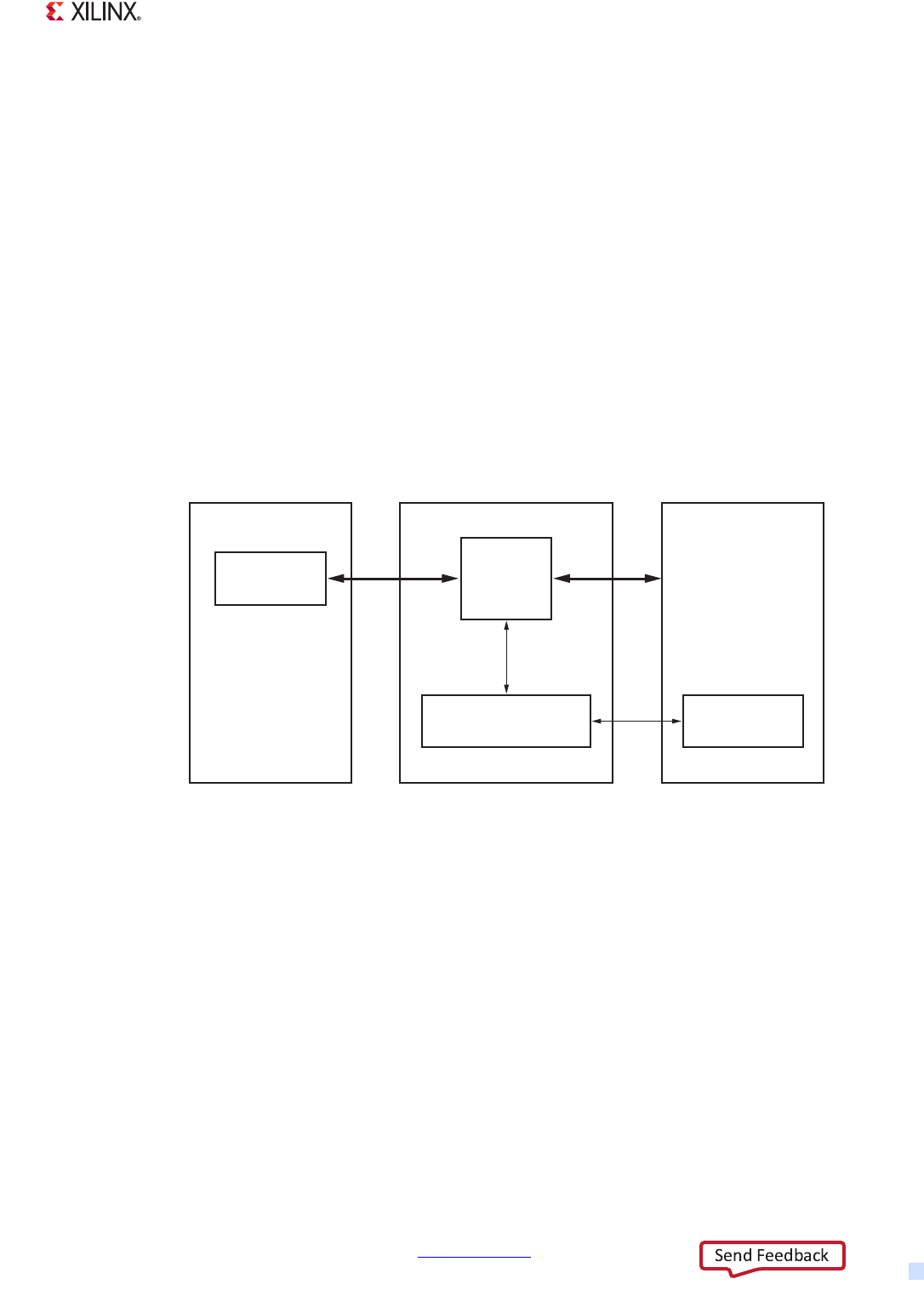
Zynq-7000 AP SoC Technical Reference Manual www.xilinx.com 76
UG585 (v1.12.1) December 6, 2017
Chapter 3: Application Processing Unit
MMU Functional Description
The key feature of MMU is the address translation. It translates addresses of code and data from the
virtual view of memory to the physical addresses in the real system. It enables tasks or applications
to be written in a way which requires them to have no knowledge of the physical memory map of the
system, or about other programs which might be running at the same time. This makes programming
of applications much simpler, as it enables to use the same virtual memory address space for each.
This virtual address space is separate from the actual physical map of memory in the system.
The translation process is based on translation entries stored in the translation table. Refer to
Translation Tables for more details. The two major functional units, shown in Figure 3-4, exist in the
MMU to provide address translation automatically based on the table entries:
• The table walker automatically retrieves the correct translation table entry for a requested
translation.
• The translation look-aside buffer (TLB) stores recently used translation entries, acting like a
cache of the translation table.
Translation Tables
The translation of virtual to physical addresses is based on entries in translation tables; they are often
called as page tables. These contain a series of entries, each of which describes the physical address
translation for part of the memory map. Translation table entries are organized by virtual address.
Each virtual address corresponds to exactly one entry in the translation table. In addition to
describing the translation of that virtual page to a physical page, they also provide access
permissions and memory attributes for that page or block. A single set of translation tables is used
to give the translations and memory attributes which apply to instruction fetches and to data reads
or writes. The process in which the MMU accesses page tables to translate addresses is known as
page table walking.
When developing a table-based address translation scheme, one of the most important design
parameters is the memory page size described by each translation table entry. MMU instances
X-Ref Target - Figure 3-4
Figure 3-4: MMU Architecture Block Diagram
Virtual Memory Space MMU Physical Memory Space
TLB
Page Table
Walk Logic
UG585_c3_05_102112
Translation
Tables
Process

Zynq-7000 AP SoC Technical Reference Manual www.xilinx.com 77
UG585 (v1.12.1) December 6, 2017
Chapter 3: Application Processing Unit
support 4 KB and 64 KB pages, a 1 MB section, and a 16 MB super-section. Using bigger page sizes
means a smaller translation table. Using a smaller page size, 4 KB, greatly increases the efficiency of
dynamic memory allocation and defragmentation, but it would require one million entries to span
the entire 4 GB address range. To reconcile these two requirements, the Cortex-A9 Processor MMU
supports multi-level page table architecture with two levels of page table: level 1 (L1) and level 2 (L2),
which are discussed in the following sub-sections.
Level 1 Page Tables
Level 1 page table sometimes called as a master page table, which divides the full 4 GB address space
into 4,096 equally sized 1 MB sections. The L1 page table therefore contains 4,096 entries, each entry
being word sized. Each entry can either hold a pointer to the base address of a level 2 page table or
a page table entries for translating a 1 MB section. If the page table entry is translating a 1 MB
section, it gives the base address of the 1 MB page in physical memory. The base address of the L1
page table is known as the translation table base address (TTB) and is held within a register in CP15
c2. It must be aligned to a 16 KB boundary.
• An L1 page table entry can be one of four possible types; the least significant two bits [1:0] in
the entry define which one of these the entry contains:
• A fault entry that generates an abort exception. This can be either a pre-fetch or data abort,
depending on the type of memory access. This effectively indicates virtual addresses which are
unmapped.
• A 1 MB section translation entry.
• An entry that points to an L2 page table. This enables a 1 MB piece of memory to be further
sub-divided into smaller pages.
• A 16 MB super-section. This is a special kind of 1 MB section entry, which requires 16 entries in
the page table.
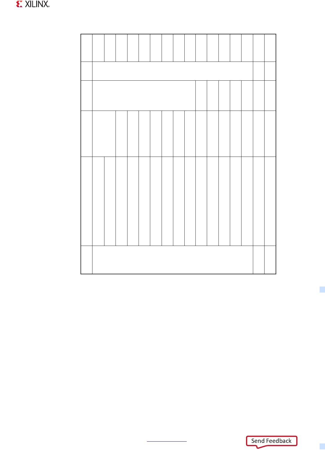
Zynq-7000 AP SoC Technical Reference Manual www.xilinx.com 78
UG585 (v1.12.1) December 6, 2017
Chapter 3: Application Processing Unit
The page table entry for a section (or super-section) contains the physical base address used to
translate the virtual address. Many other bits listed in the page-table entry, including the access
permissions (AP) and memory region attributes TEX, cacheable (C) or bufferable (B) types are
examined in the next section.
Example: Generation of a Physical Address from a L1 Page Table Entry
Assume an L1 page table is placed at address 0x12300000. The processor core issues virtual address
0x00100000. The top 12 bits [31:20] define which 1 MB of virtual address space is being accessed.
In this case 0x001, so you need to read table entry [1]. Each entry is one word (4 bytes). To get the
offset into the table, you must multiply the entry number by entry size: 0x001 * 4 = address offset
of 0x004. The address of the entry is 0x12300000 + 0x004 = 0x12300004. So, upon receiving this
virtual address from the processor, the MMU reads the word from address 0x12300004.
X-Ref Target - Figure 3-5
Figure 3-5: L1 Page Table Entry Format
UG585_c3_06_092817
31
24
23 19 18 17 16 15 13
IGNORE
Page Table Base Address, bits [31:10]
Reserved
FaultPage TableSectionSupersectionReserved
Supersection Base Address PA[31:24]
Extended Base Address PA[35:32]
Domain
AP[2]
AP[1:0]
TEX[2:0]
Section Base
Address, PA [31:20]
0
0
SBZ SBZ
NS
NS
XN C B
nG
Domain
14
12
11
10
9
8
7
6
5
43210
10
11
0
0
0
0S
Extended Base Address PA[39:36]
AP[2]
AP[1:0]
TEX[2:0]
0NS nG1S
1
20
XN CB 1 0
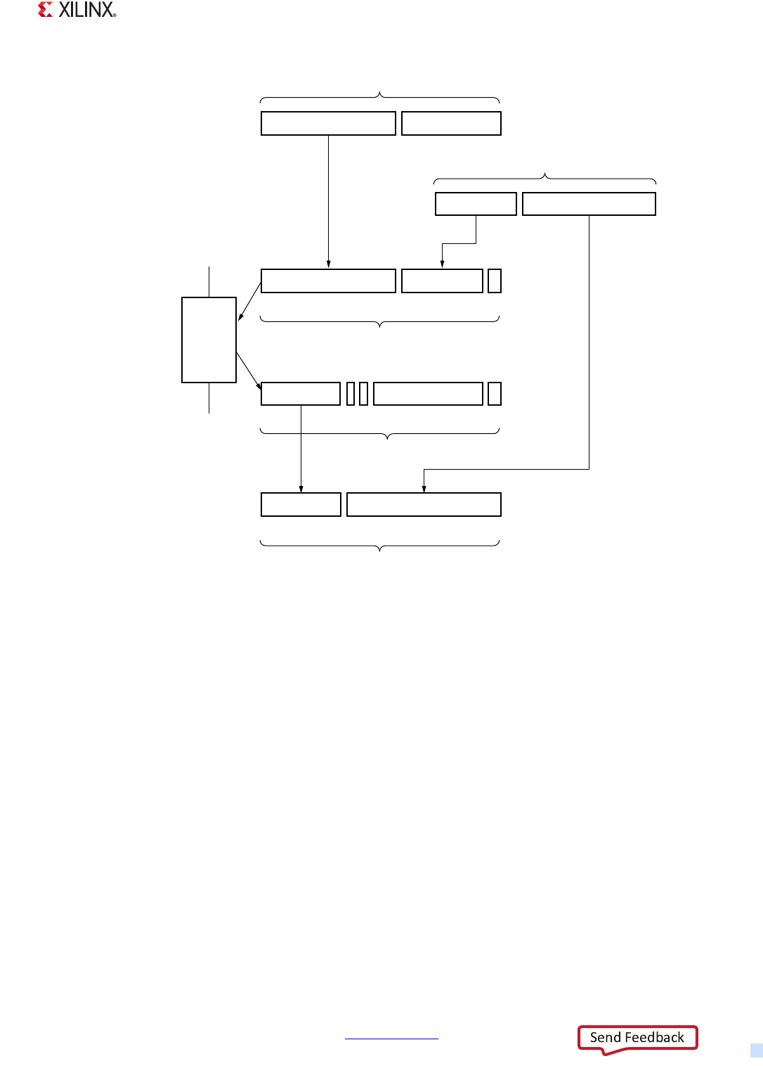
Zynq-7000 AP SoC Technical Reference Manual www.xilinx.com 79
UG585 (v1.12.1) December 6, 2017
Chapter 3: Application Processing Unit
Level 2 Page Tables
An L2 page table has 256 word-sized entries, requires 1KB of memory space and must be aligned to
a 1KB boundary. Each entry translates a 4KB block of virtual memory to a 4KB block in physical
memory. A page table entry can give the base address of either a 4KB or 64KB page. There are three
types of entry used in L2 page tables, identified by the value in the two least significant bits of the
entry:
• A large page entry points to a 64 KB page.
• A small page entry points a 4 KB page.
• A fault page entry generates an abort exception if accessed.
X-Ref Target - Figure 3-6
Figure 3-6: Generating a Physical Address from an L1 Page Table Entry
Translation Table Base Address
31 14 13 0
31 20 19 0
31 14 13 2 10
31 20 17 2 10
100
19 18
31 20 19 0
UG585_c3_07_102112
First Level Descriptor Address
Physical Address
Section Base Address Descriptor
Level 1
Table
Virtual Address

Zynq-7000 AP SoC Technical Reference Manual www.xilinx.com 80
UG585 (v1.12.1) December 6, 2017
Chapter 3: Application Processing Unit
The fields mentioned in Figure 3-7 are discussed in Description of Page Table Entry Fields.
Figure 3-8 summarizes the address translation process when using two layers of page tables. The bits
[31:20] of the virtual address are used to index into the 4096-entry L1 page table, where the base
address is given by the CP15 TTB register. The L1 page table entry points to an L2 page table, which
contains 256 entries. Bits [19:12] of the virtual address are used to select one of those entries which
then gives the base address of the page. The final physical address is generated by combining that
base address with the remaining bits of the physical address.
X-Ref Target - Figure 3-7
Figure 3-7: L2 Page Table Entry Format
UG585_c3_08_1022112
Fault IGNORE
1
0
00
01
BCAPSBZ
TEX
[2:0] S
nG
APX
1BCAP
TEX
[2:0]
S
nG
APX
XN
239451011 786151631 1314 12
Large
Page Large Page Base Address
Small Page Base Address
Small
Page
XN
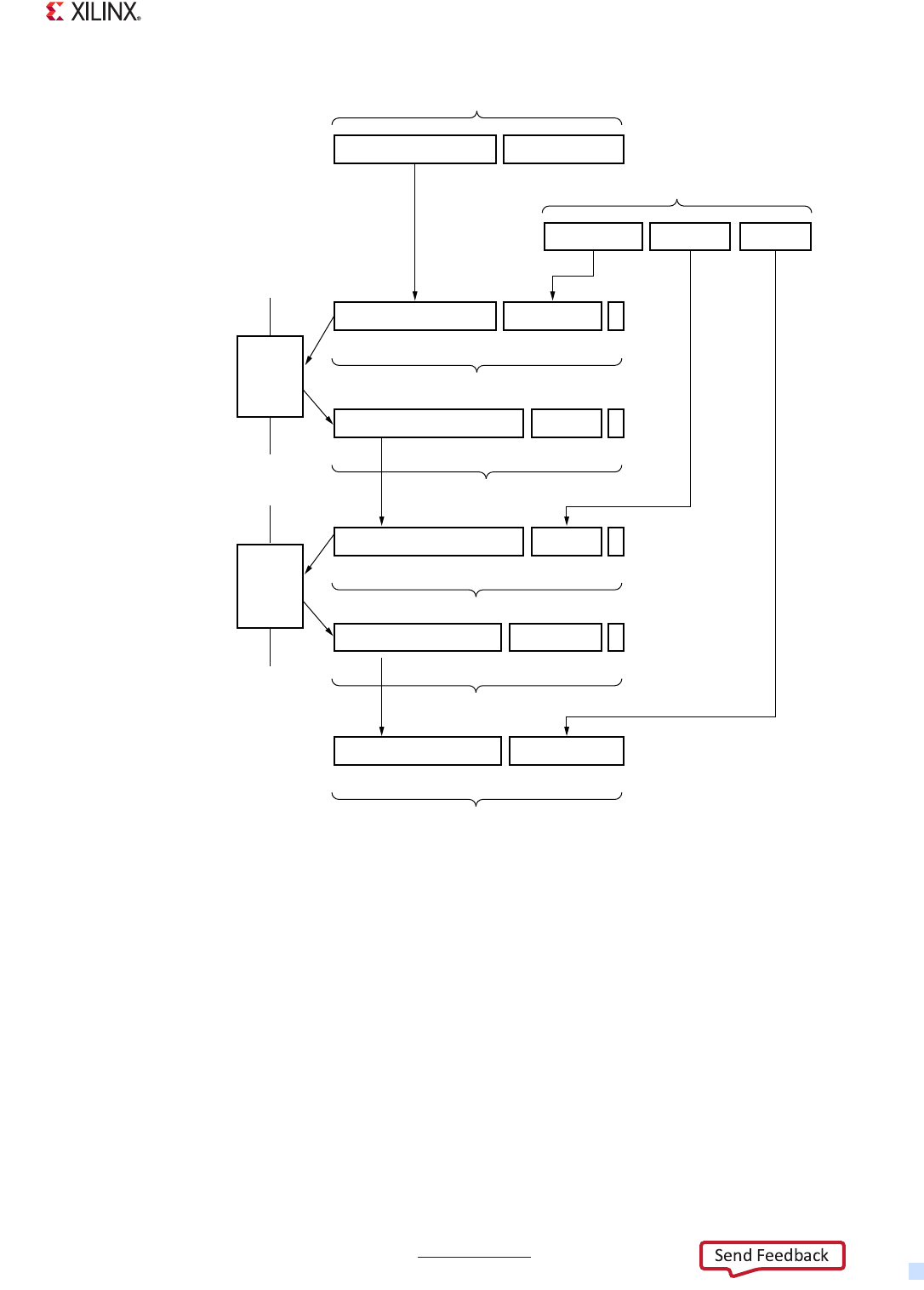
Zynq-7000 AP SoC Technical Reference Manual www.xilinx.com 81
UG585 (v1.12.1) December 6, 2017
Chapter 3: Application Processing Unit
Description of Page Table Entry Fields
Memory Access Permissions (AP and APx)
The access permission (AP and APX) bits in the page table entry give the access permission for a
page. An access which does not have the necessary permission (or which faults) is aborted. On a data
access, this results in a precise data abort exception. On an instruction fetch, the access is marked as
aborted and if the instruction is not subsequently flushed before execution, a pre-fetch abort
exception is taken. Information about the address of the faulting location and the reason for the fault
is stored in CP15 (the fault address and fault status registers). The abort handler can then take
appropriate action. Tab le 3 -2 lists the access permission encodings.
X-Ref Target - Figure 3-8
Figure 3-8: Generating a Physical Address from an L2 Page Table Entry
Translation Table Base Address
31 14 13 0
31 14 13 2 10
31 9 2 10
01
10
10
31 20 19 12 11 0
UG585_c3_09_102112
Level 1 Descriptor Address
Level 2 Table Base Address
31 9 2 1010
Level 2 Descriptor Address
31 11 2 1012
Small Page Base Address
31 11 012
Physical Address
Level 1
Table
Level 2
Table
TTB
2TB
Virtual Address

Zynq-7000 AP SoC Technical Reference Manual www.xilinx.com 82
UG585 (v1.12.1) December 6, 2017
Chapter 3: Application Processing Unit
Memory Attributes (TEX, C and B bits)
TEX, C, and B bits within the page table entry are used to set the memory attributes of a page and
also the cache policies to be used. Memory attributes are discussed in 3.2.4 Memory Ordering, and
for various cache policies refer to the ARM Technical Reference Manual. Ta bl e 3- 3 and Ta b le 3 - 4
summarize these memory attributes.
Table 3-2: Access Permission Encodings
APX AP1 AP0 Privileged Unprivileged Description
00 0
No access No access Permission fault
00 1
Read/Write No access Privileged access only
01 0
Read/Write Read No user-mode write
01 1
Read/Write Read/Write Full access
10 0
~~ Reserved
10 1
Read No access Privileged Read only
11 0
Read Read Read only
11 1
~ ~~ Reserved
Table 3-3: Memory Attributes Encodings
TEX [2:0] C B Description Memory Type
000
Strongly-ordered Strongly ordered
001
shareable device Device
010
Outer and Inner write through, no allocate on write Normal
011
Outer and Inner write back, no allocate on write Normal
100
Outer and Inner non-cacheable Normal
111
Outer and Inner cacheable Normal
10 1 0 Non-Shareable device Device
10 --Reserved -
11 --Reserved -
1XX Y Y Cached memory
XX – Outer Policy
YY – Inner Policy
Normal
Table 3-4: Memory Attributes Encodings
Encoding Bits Cache Attribute
CB
00Non-cacheable
0 1 Write-back, write-allocate
1 0 Write-through, no write-allocate
1 1 Write-back, no write-allocate

Zynq-7000 AP SoC Technical Reference Manual www.xilinx.com 83
UG585 (v1.12.1) December 6, 2017
Chapter 3: Application Processing Unit
Domains
A domain is a collection of memory regions. Domains are only valid for L1 page table entries. The L1
page table entry format supports 16 domains, and requires the software that defines a translation
table to assign each memory region to a domain. The domain field specifies which of the 16 domains
the entry is in, and a two-bit field in the Domain Access Control register (DACR) defines the
permitted access for each domain. The possible settings for each domain are:
• No access – Any access using the translation table descriptor generates a Domain fault.
• Clients – On an access using the translation table descriptor, the access permission attributes
are checked. Therefore, the access might generate a permission fault.
• Managers – On an access using the translation table descriptor, the access permission attributes
are not checked. Therefore, the access cannot generate a Permission fault.
Shareable bit (S)
This bit determines whether the translation is for sharable memory. S = 0, the memory location is
non-shareable, and S = 1, it is sharable. For more information, refer to shareable attributes in section
3.2.4 Memory Ordering.
Non-Global Region Bit (nG)
The nG bit in the translation table entry permits the virtual memory map to be divided into global
and non-global regions. Each non-global region (nG = 1) has an associated address space identifier
(ASID), which is a number assigned by the OS to each individual task. If the nG bit is set for a
particular page, that page is associated with a specific application and is not global. This means that
when the MMU performs a translation, it uses both the virtual address and an ASID values. When a
page table walk occurs and the TLB is updated and the entry is marked as non-global, the ASID value
is stored in the TLB entry in addition to the normal translation information. Subsequent TLB look-ups
only match on that entry if the current ASID matches with the ASID that is stored in the entry. This
means you can have multiple valid TLB entries for a particular page (marked as non-global), but with
different ASID values. This significantly reduces the software overhead of context switches, as it
avoids the need to flush the on-chip TLBs.
Execute Never bit (xN)
When a memory location is marked as Execute Never (its XN attribute is set to 1) in a Client domain,
instructions are not allowed to fetch/prefetch. Any region of memory that is read-sensitive must be
marked as Execute Never to avoid the possibility of a speculative prefetch accessing the memory
region. For example, any memory region that corresponds to a read-sensitive peripheral must be
marked as Execute Never.
TLB Organization
The Cortex-A9 MMU includes two levels of TLBs which include a unified TLB for both instruction and
data and separate micro TLBs for each. The micro TLBs act as the first level TLBs and each have 32
fully associative entries. If an instruction fetch or a load/store address misses in the corresponding
micro TLB, the unified or main TLB is accessed. The unified main TLB provides a 2-way associative
2x64 entry table (128 entries) and supports four lockable entries using the lock-by-entry model. The

Zynq-7000 AP SoC Technical Reference Manual www.xilinx.com 84
UG585 (v1.12.1) December 6, 2017
Chapter 3: Application Processing Unit
TLB uses a pseudo round-robin replacement policy to determine which entry in the TLB should be
replaced in the case of a miss.
Unlike some other RISC processors that require software to manage the updates of the TLB from the
page table that resides in the memory, the main TLB in Cortex-A9 supports hardware page table
walks to perform look-ups in the L1 data cache. This allows the page tables to be cached.
The MMU can be configured to perform hardware translation table walks in cacheable regions by
setting the IRGN bits in the Translation Table Base registers. If the encoding of the IRGN bits is
write-back, then an L1 data cache look-up is performed and data is read from the data cache. If the
encoding of the IRGN bits is write-through or non-cacheable, then an access to external memory is
performed.
TLB entries can be global, or can be assigned to particular processes or applications using the ASIDs
associated with those processes. ASIDs enable TLB entries remain resident during context switches,
avoiding the requirement of reloading them subsequently.
Note: The ARM Linux kernel manages the 8-bit TLB ASID space globally across all CPUs instead of on
a per-CPU basis. The ASID is incremented for each new process. When the ASID rolls over (ASID = 0)
a TLB flush request is sent to both CPUs. However, only the CPU that is in the middle of a context
switch immediately updates its current ASID context. The other CPU continues to run using its
current pre-rollover ASID until a scheduling interval occurs and then it context switches to a new
process.
TLB maintenance and configuration operations are controlled through a dedicated coprocessor,
CP15, integrated within the core. This coprocessor provides a standard mechanism for configuring
the level one memory system.
Micro TLB
The first level of caching for the page table information is a micro TLB of 32 entries implemented on
each of the instruction and data sides. These blocks provide a fully associative look-up of the virtual
addresses in a cycle.
The micro TLB returns the physical address to the cache for the address comparison, and also checks
the protection attributes to signal either a pre-fetch abort or a data abort.
All main TLB related operations affect both the instruction and data micro TLBs, causing them to be
flushed. In the same way, any change of the Context ID register causes the micro TLBs to be flushed.
The main or unified TLB, explained in the next section, should be invalidated after a CPU reset and
before the MMU is enabled.
Main TLB
The main TLB is the second layer in the TLB structure that catches the misses from the Micro TLBs. It
also provides a centralized source for lockable translation entries.
Misses from the instruction and data micro TLBs are handled by a unified main TLB. Accesses to the
main TLB take a variable number of cycles, according to competing requests from each of the micro
TLBs and other implementation-dependent factors.

Zynq-7000 AP SoC Technical Reference Manual www.xilinx.com 85
UG585 (v1.12.1) December 6, 2017
Chapter 3: Application Processing Unit
Entries in the lockable region of the main TLB are lockable at the granularity of a single entry. As long
as the lockable region does not contain any locked entries, it can be allocated with non-locked
entries to increase overall main TLB storage size.
Translation Table Base Register 0 and 1
When managing multiple applications with their individual page tables, there is a need to have
multiple copies of the L1 page table, one for each application. Each of these are 16 KB in size. Most
of the entries are identical in each of the tables, as typically only one region of memory is
task-specific, with the kernel space being unchanged in each case. Furthermore, if there is a need to
modify a global page table entry, the change is needed in each of the tables.
To help reduce the effect of these problems, a second page table base register can be used. CP15
contains two page table base registers, TTBR0 and TTBR1. A control register (the TTB Control
register) is used to program a value in the range 0 to 7. This value (denoted by N) tells the MMU how
many upper bits of the virtual address it should check to determine which of the two TTB registers to
use. When N is 0 (the default), all virtual addresses are mapped using TTBR0. With N in the range 1-7,
the hardware looks at the most significant bits of the virtual address. If the N most significant bits
are all zero, TTBR0 is used, otherwise TTBR1 is used.
TTBR0 is used typically for process-specific addresses. On a context switch, TTBR0 is updated to
point to the first-level translation table for the new context and TTBCR is updated if this change
changes the size of the translation table. This table ranges in size from 128 bytes to 16 KB.
TTBR1 is used for operating system and I/O addresses that do not change on a context switch. The
size of this table is always 16 KB.
TLB Match Process
Each TLB entry contains a virtual address, a page size, a physical address, and a set of memory
properties. Each is marked as being associated with a particular application space, or as global for all
application spaces. A TLB entry matches if bits [31: N] of the modified virtual address (MVA) match,
where N is log2 of the page size for the TLB entry. It is either marked as global, or the ASID matched
the current ASID.
A TLB entry matches when these conditions are true:
• Its virtual address matches that of the requested address.
• Its non-secure TLB ID (NSTID) matches the secure or non-secure state of the MMU request.
• Its ASID matches the current ASID or is global.
The operating system must ensure that, at most, one TLB entry matches at any time. A TLB can store
entries based on the following block sizes:
Supersections:16MB blocks of memory
Sections:1MB blocks of memory
Large pages:64KB blocks of memory
Small pages:4KB blocks of memory

Zynq-7000 AP SoC Technical Reference Manual www.xilinx.com 86
UG585 (v1.12.1) December 6, 2017
Chapter 3: Application Processing Unit
Supersections, sections, and large pages are supported to permit mapping of a large region of
memory while using only a single entry in a TLB. If no mapping for an address is found within the
TLB, then the translation table is automatically read by hardware and a mapping is placed in the TLB.
(The translation table entries are discussed in detail in Translation Table Base Register 0 and 1,
page 85)
Memory Access Sequence
When the processor generates a memory access, the MMU:
1. Performs a look-up for the requested virtual address and current ASID and security state in the
relevant instruction or data micro TLB.
2. If there is a miss in the micro TLB, performs a look-up for the requested virtual address and
current ASID and security state in the main TLB.
3. If there is a miss in main TLB, performs a hardware translation table walk.
The MMU might not find a global mapping or a mapping for the currently selected ASID with a
matching non-secure TLB ID (NSTID) for the virtual address in the TLB. In this case, the hardware
does a translation table walk if the translation table walk is enabled by the PD0 or PD1 bit in the TTB
Control register. If translation table walks are disabled, the processor returns a section translation
fault.
If the MMU finds a matching TLB entry, it uses the information in the entry as follows:
1. The access permission bits and the domain determine if the access is enabled. If the matching
entry does not pass the permission checks, the MMU signals a memory abort. See the ARM
Architecture Reference Manual (ARMv7-A) for a description of access permission bits, abort types
and priorities, and for a description of the Instruction Fault Status register (IFSR) and Data Fault
Status register (DFSR).
2. The memory region attributes specified in both the TLB entry and the CP15 c10 remap registers
control the cache and write buffer, and determine if the access is:
a. Secure or non-secure
b. Shared or not
c. Normal memory, device, or strongly-ordered
3. The MMU translates the virtual address to a physical address for the memory access.
If the MMU does not find a matching entry, a hardware table walk occurs.
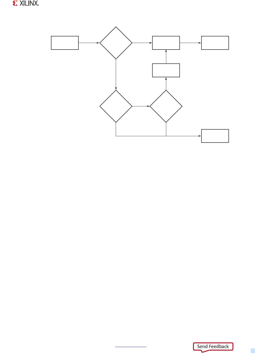
Zynq-7000 AP SoC Technical Reference Manual www.xilinx.com 87
UG585 (v1.12.1) December 6, 2017
Chapter 3: Application Processing Unit
TLB Maintenance Operations
The following rules describe the TLB maintenance operations:
• A TLB invalidate operation is complete when all memory accesses using the TLB entries that
have been invalidated have been observed by all observers to the extent that those accesses are
required to be observed, as determined by the shareability and cacheability of the memory
locations accessed by the accesses. In addition, once the TLB invalidate operation is complete,
no new memory accesses that can be observed by those observers using those TLB entries will
be performed.
• A TLB maintenance operation is only guaranteed to be complete after the execution of a DSB
instruction.
• An ISB instruction, or a return from an exception, causes the effect of all completed TLB
maintenance operations that appear in program order before the ISB or return from exception
to be visible to all subsequent instructions, including the instruction fetches for those
instructions.
• An exception causes all completed TLB maintenance operations that appear in the instruction
stream before the point where the exception was taken to be visible to all subsequent
instructions, including the instruction fetches for those instructions.
• All TLB maintenance operations are executed in program order relative to each other.
• The execution of a Data or Unified TLB maintenance operation is guaranteed not to affect any
explicit memory access of any instruction that appears in program order before the TLB
maintenance operation. This means no memory barrier instruction is required. This ordering is
guaranteed by the hardware implementation.
• The execution of a Data or Unified TLB maintenance operation is only guaranteed to be visible
to a subsequent explicit load or store operation after both:
X-Ref Target - Figure 3-9
Figure 3-9: Translation Process
Translation
Request
Translation
Result
Translation
Fault
Perform
Translation
Entry
exists in
Page
Table?
TLB Update
Is the
translation
in TLB?
Ye s
No
No No
Ye s
Ye s
Ta b l e
walking
enabled?
UG585_c3_10_102112

Zynq-7000 AP SoC Technical Reference Manual www.xilinx.com 88
UG585 (v1.12.1) December 6, 2017
Chapter 3: Application Processing Unit
°The execution of a DSB instruction to ensure the completion of the TLB operation.
°A subsequent ISB instruction, or taking an exception, or returning from an exception.
• The execution of an instruction or unified TLB maintenance operation is only guaranteed to be
visible to subsequent instruction fetch after both:
°The execution of a DSB instruction to ensure the completion of the TLB operation.
°A subsequent ISB instruction, or taking an exception, or returning from an exception.
The following rules apply when writing translation table entries. They ensure that the updated entries
are visible to subsequent accesses and cache maintenance operations.
• A write to the translation tables, after it has been cleaned from the cache if appropriate, is only
guaranteed to be seen by a translation table walk caused by an explicit load or store after the
execution of both a DSB and an ISB. However, it is guaranteed that any writes to the translation
tables are not seen by any explicit memory access that occurs in program order before the write
to the translation tables.
• If the translation tables are held in write-back cacheable memory, the caches must be cleaned to
the point of unification after writing to the translation tables and before the DSB instruction.
This ensures that the updated translation table is visible to a hardware translation table walk.
• A write to the translation tables, after it has been cleaned from the cache if appropriate, is only
guaranteed to be seen by a translation table walk caused by the instruction fetch of an
instruction that follows the write to the translation tables after both a DSB and an ISB.
TLB Lockdown
The TLB supports the TLB lock-by-entry model as described in the ARM Architecture Reference
Manual (ARMv7-A). See the TLB Lockdown register description in the ARM Cortex-A9 Technical
Reference Manual.
3.2.6 Interfaces
AXI and Coherency Interfaces
Each Cortex-A9 processor provides two 64-bit pseudo AXI master interfaces for independent
instruction fetch and data transactions. These interfaces operate at the speed of the processor cores
(CPU_6x4x clock) and are capable of sustaining four double-word writes every five processor cycles
when copying data across a cached region of memory. The instruction side interface is a read-only
interface and does not have the write channel. These interfaces implement an extended version of
the AXI protocol that also provides multiple optimizations to the L2 cache including support for L2
pre-fetch hints and speculative memory accesses. These optimizations are explained in more detail
in the L2-Cache section of this chapter.
The AXI transactions are all routed through the SCU to the OCM or the L2 cache controller based on
their addresses. Each Cortex-A9 also provides a cache coherency bus (CCB) to the SCU to provide the
information required for coherency management between the L1 and L2 caches.

Zynq-7000 AP SoC Technical Reference Manual www.xilinx.com 89
UG585 (v1.12.1) December 6, 2017
Chapter 3: Application Processing Unit
Debug and Trace Interfaces
Each Cortex-A9 processor has a standard 32-bit APB slave port that operates at the CPU_1x clock
frequency and is accessed through the debug APB bus master in the SOC debug block. The operation
of this block is explained in the corresponding chapter of this document.
The Cortex-A9 processors also include a pair of interfaces for trace generation and cross trigger
control. The trace source interface from each core is a 32-bit CoreSight standard ATB master port
that operates at the speed of the PS interconnect (CPU_2x clock), and is connected to the funnel in
the SOC debug block. Each core also has a 4-bit standard CoreSight cross trigger interface that
operates at the interconnect frequency (CPU_2x clock) and is connected to the cross trigger matrix
(CTM) in the SOC debug block.
Other Interfaces
Each Cortex-A9 processor has multiple control bits that are driven through the System-Level Control
register (SLCR). This includes a 4-bit interface that drives the CoreSight standard security signals and
also static configuration signals for controlling CP15 and SW programmability.
There are also other interfaces including the event and interrupt interfaces that are explained later in
this chapter.
3.2.7 NEON
• The Cortex-A9 NEON MPE extends the Cortex-A9 functionality to provide support for the ARM
v7 advanced SIMD and vector floating-point v3 (VFPv3) instruction sets. The Cortex-A9 NEON
MPE supports all addressing modes and data processing operations described in the ARM
Architecture Reference Manual (ARMv7-A).
The Cortex-A9 NEON MPE features are:
• SIMD vector and scalar single-precision floating-point computation
°Unsigned and signed integers
°Single bit coefficient polynomials
°Single-precision floating-point values
• The operations supported by the NEON co-processor include:
°Addition and subtraction
°Multiplication with optional accumulation
°Maximum or minimum value driven lane selection operations
°Inverse square-root approximation
°Comprehensive data-structure load instructions, including register-bank-resident table
lookup.
• Scalar double-precision floating-point computation
• SIMD and scalar half-precision floating-point conversion
• 8, 16, 32, and 64-bit signed and unsigned integer SIMD computation

Zynq-7000 AP SoC Technical Reference Manual www.xilinx.com 90
UG585 (v1.12.1) December 6, 2017
Chapter 3: Application Processing Unit
• 8 or 16-bit polynomial computation for single-bit coefficients
• Structured data load capabilities
• Dual issue with Cortex-A9 processor ARM or Thumb instructions
• Independent pipelines for VFPv3 and advanced SIMD instructions
• Large, shared register file, addressable as:
°Thirty-two 32-bit S (single) registers
°Thirty-two 64-bit D (double) registers
°Sixteen 128-bit Q (quad) registers
See the ARM Architecture Reference Manual (ARMv7-A) for details of the advanced SIMD instructions
and the NEON MPE operation.
3.2.8 Performance Monitoring Unit
The Cortex-A9 processor includes a performance monitoring unit (PMU) which provides six counters
to gather statistics on the operation of the processor and memory system. Each counter can count
any of 58 events available in the Cortex-A9 processor. The PMU counters and their associated control
registers are accessible from the internal CP15 interface as well as from the DAP interface. For details,
refer to the Performance Monitoring Unit section in the ARM Cortex-A9 Technical Reference Manual.
3.3 Snoop Control Unit (SCU)
3.3.1 Summary
The SCU block connects the two Cortex-A9 processors to the memory subsystem and contains the
intelligence to manage the data cache coherency between the two processors and the L2 cache. This
block is responsible for managing the interconnect arbitration, communication, cache and system
memory transfers, and cache coherence for the Cortex-A9 processors. The APU also exposes the
capabilities of the SCU to system accelerators that are implemented in the PL through the accelerator
coherency port (ACP) interface (see ACP Interface, page 103). This interface allows PL masters to
share and access the processor cache hierarchy. The offered system coherence here not only
improves performance but also reduces the software complexity involved in otherwise maintaining
software coherency within each OS driver.
The SCU block communicates with each of the Cortex-A9 processors through a cache coherency bus
(CCB) and manages the coherency between the L1 and the L2 caches. The SCU supports MESI
snooping which provides increased power efficiency and performance by avoiding unnecessary
system accesses. The block implements duplicated 4-way associative tag RAMs acting as a local
directory that lists coherent cache lines held in the CPU L1 data caches. The directory allows the SCU
to check if data is in the L1 data caches with great speed and without interrupting the processors.
Also, accesses can be filtered only to the processor that is sharing the data.

Zynq-7000 AP SoC Technical Reference Manual www.xilinx.com 91
UG585 (v1.12.1) December 6, 2017
Chapter 3: Application Processing Unit
The SCU can also copy clean data from one processor cache to another and eliminate the need for
main memory accesses to perform this task. Furthermore, it can move dirty data between the
processors, skipping the shared state and avoiding the latency associated with the write-back.
IMPORTANT: It is important to note that the Cortex-A9 does not guarantee coherency between the L1
instructions caches as the processor is not capable of modifying the L1 contents directly.
3.3.2 Address Filtering
One of the functions of the SCU is to filter transactions that are generated by the processors and the
ACP based on their addresses and route them accordingly to the OCM or L2 controller. The
granularity of the address filtering within the SCU is 1 MB; therefore, all accesses by the processors
or through the ACP whose addresses are within a 1 MB window can only target the OCM or L2
controller. The default setting of the address filtering within the SCU routes all the upper and lower
1M addresses within the 4G address space to the OCM and the rest of the addresses are routed to
the L2 controller. Refer to the SCU Address Filtering section of Chapter 29, On-Chip Memory (OCM)
for more information on the SCU address filtering.
3.3.3 SCU Master Ports
Each of the SCU AXI master ports to the L2 or OCM has the following write and read issuing
capabilities:
• Write issuing capability:
°10 write transactions per processor:
-8 non-cacheable writes
- 2 evictions from L1
°2 additional writes for eviction traffic from the SCU
°3 more write transactions from the ACP
• Read issuing capability:
°14 read transactions per processor:
- 4 instruction reads
- 6 linefill reads
-4 non-cacheable read
°7 more read transactions from the ACP

Zynq-7000 AP SoC Technical Reference Manual www.xilinx.com 92
UG585 (v1.12.1) December 6, 2017
Chapter 3: Application Processing Unit
3.4 L2-Cache
3.4.1 Summary
The L2 cache controller is based on the ARM PL310 and includes an 8-way set-associative 512 KB
cache for dual/single Cortex-A9 cores. The L2 cache is physically addressed and physically tagged
and supports a fixed 32-byte line size. These are the main features of the L2 cache:
• Supports snoop coherency control utilizing MESI algorithm.
• Offers parity check for L2 cache memory.
• Supports speculative read operations in the SMP mode.
• Provides L1/L2 exclusive mode (that is, data exists in either, but not both).
• Can be locked down by master, line, or way per master.
• Implements 16-entry deep preload engine for loading data into L2 cache memory.
• To improve latency, critical-word-first line-fill is supported.
• Implements pseudo-random victim selection policy with deterministic option.
°Write-through and write-back.
°Read allocate, write allocate, read and write allocate.
• The contents of the L2 data and tag RAMs are cleared upon an L2 reset to comply with security
requirements.
• The L2 controller implements multiple 256-bit line buffers to improve cache efficiency.
°Line fill buffers (LFBs) for external memory access to create a complete cache line into L2
cache memory. Four LFBs are implemented for AXI read interleaving support.
°Two 256-bit line read buffers for each slave port. These buffers hold a line from the L2 cache
in case of cache hit.
°Three 256-bit eviction buffers hold evicted lines from the L2 cache, to be written back to
main memory.
°Three 256-bit store buffers hold bufferable writes before their draining to main memory, or
L2 cache. They enable multiple writes to the same line to be merged.
• The controller implements selectable cache pre-fetching within 4k boundaries.
• The L2 cache controller forwards exclusive requests from L1 to DDR, OCM, or external memory.
Note: The SCU does not maintain coherency between instruction and data L1 caches, so this
coherency must be maintained by software.
The L2 cache implements TrustZone security extension to offer enhanced OS security. The
non-secure (NS) tag bit is added in tag RAM and is used for lookup in the same way as an address bit.
The NS tag bit is also added in all of the buffers. The NS bit in tag RAM is used to determine the
security level of evictions to DDR and OCM. The controller restricts non-secure accesses for control,
configuration, and maintenance registers to restrict access to secure data.

Zynq-7000 AP SoC Technical Reference Manual www.xilinx.com 93
UG585 (v1.12.1) December 6, 2017
Chapter 3: Application Processing Unit
Cache Response
This section describes the general behavior of the cache controller depending on the Cortex-A9
transactions. These are the descriptions for the different type of transactions:
In the ARM architecture, the inner attributes are used to control the behavior of the L1 caches and
write buffers. The outer attributes are exported to the L2 or an external memory system.
In the Cortex-A9 processing system (similar to most modern processors), to improve performance
and power, many optimizations are performed at many levels of the system which cannot be
completely hidden from the outside world and might cause the violation of the expected sequential
execution model. Examples of these optimizations are:
• Multi-issue speculative and out-of-order execution.
• Use of load/store merging to minimize the latency of load/stores.
• In a multicore processor, hardware-based cache coherency management can cause cache lines
to migrate transparently between cores causing different cores to see updates to cached
memory locations in different orders.
• External system characteristics might create additional challenges when external masters are
included in the coherent system through the ACP.
Therefore, it is vital to define certain rules to constrain the order in which the memory accesses of
one core relate to the surrounding instructions, or could be observed by other cores within a
multicore processor system. Typically the memory can be categorized into normal, strongly ordered,
and device regions. For more information, refer to section 3.2.4 Memory Ordering.
Tabl e 3-5 shows the general behavior of the L2 cache controller in response to ARMv7 load/store
transaction types that are supported by Cortex-A9.
Bufferable The transaction can be delayed by the interconnect or any of its components for
an arbitrary number of cycles before reaching its final destination. This is usually
only relevant to writes.
Cacheable The transaction at the final destination does not have to present the
characteristics of the original transaction. For writes, this means that several
different writes can be merged together. For reads, this means that a location can
be pre-fetched or can be fetched just once for multiple read transactions. To
determine if a transaction should be cached, this attribute should be used in
conjunction with the read allocate and write allocate attributes.
Read Allocate If the transfer is a read and it misses in the cache, then it should be allocated.
This attribute is not valid if the transfer is not cacheable.
Write Allocate If the transfer is a write and it misses in the cache, then it should be allocated.
This attribute is not valid if the transfer is not cacheable.

Zynq-7000 AP SoC Technical Reference Manual www.xilinx.com 94
UG585 (v1.12.1) December 6, 2017
Chapter 3: Application Processing Unit
Table 3-5: Cache Controller Behavior for SCU Requests
Transaction Type ARMv7 Equivalent L2 Cache Controller Behavior
Non-cacheable
and
non-bufferable
Strongly ordered • Read: Not cached in L2, results in memory access.
• Write: Not buffered, results in memory access.
Bufferable only Device • Read: Not cached in L2, results in memory access.
• Write: Placed in store buffer, not merged, immediately drained to
memory.
Cacheable but
do not allocate
Outer
non-cacheable
• Read: Not cached in L2, results in memory access.
• Write: Placed in store buffer, write to memory when store buffer is
drained.
Cacheable
write-through,
allocate on read
Outer
write-through, no
write allocate
• Read hit: Read from L2.
• Read miss: Line fill to L2.
• Write hit: Put in store buffer, write to L2 and memory when store
buffer is drained.
• Write miss: Put in store buffer, write to memory when store buffer is
drained.
Cacheable
write-back,
allocate on read
Outer write-back,
no write allocate
• Read hit: Read from L2.
• Read miss: Line fill to L2.
• Write hit: Put in store buffer, write to L2 when store buffer is drained
and mark line as dirty.
• Write miss: Put in store buffer, write to memory when store buffer is
drained.
Cacheable
write-through,
allocate on write
-
• Read hit: Read from L2.
• Read miss: Not cached in L2, causes memory access.
• Write hit: Put in store buffer, write to L2 and memory when store
buffer is drained.
• Write miss: Put in store buffer. When buffer is drained, check if it is
full. If not full, request word or line to memory before allocating
buffer to L2. Allocation to L2. Write to memory.
Cacheable
write-back,
allocate on write
-
• Read hit: Read from L2.
• Read miss: Not cached in L2, causes memory access.
• Write hit: Put in store buffer, write to L2 when store buffer is drained,
and mark line as dirty.
• Write miss: Put in store buffer. When buffer has to be drained, check
if it is full. If it is not full then request word or line to memory before
allocating the buffer to L2. Allocation to L2.

Zynq-7000 AP SoC Technical Reference Manual www.xilinx.com 95
UG585 (v1.12.1) December 6, 2017
Chapter 3: Application Processing Unit
3.4.2 Exclusive L2-L1 Cache Configuration
In the exclusive cache configuration mode, the L1 data cache of the Cortex-A9 processor and the L2
cache are exclusive. At any time, a given address is cached in either L1 data cache or in the L2 cache,
but not in both. This has the effect of increasing the usable space and efficiency of the L2 cache.
When exclusive cache configuration is selected:
• Data cache line replacement policy is modified so that the victim line in the L1 always gets
evicted to the L2, even if it is clean.
• If a line is dirty in the L2 cache, a read request to this address from the processor causes
write-back to external memory and a line-fill to the processor.
Both L1 and L2 caches have to be configured for exclusive caching. Setting the exclusive cache
configuration bit 12 in the auxiliary control register for L2 and bit 7 of the ACTLR register in
Cortex-A9 configure the L2 and L1 caches to operate exclusive to one another.
For reads, the behavior is as follows:
• For a hit, the line is marked as non-valid (the tag RAM valid bit is reset) and the dirty bit is
unchanged. If the dirty bit is set, future accesses can still hit in this cache line, but the line is part
of the preferred choice for future evictions.
• For a miss, the line is not allocated into the L2 cache.
For writes, the behavior depends on the value of attributes from the SCU to indicate if the write
transaction is an eviction from the L1 memory system and whether it is a clean eviction. AWUSERS[8]
attribute indicates an eviction and AWUSERS[9] indicates a clean eviction. The behavior is
summarized as follows:
• For a hit, the line is marked dirty unless the AWUSERS[9:8] = b11. In this case, the dirty bit is
unchanged.
Cacheable
write-through,
allocate on read
and write
Outer
write-through,
allocate on both
reads and writes
• Read hit: Read from L2.
• Read miss: Line fill to L2.
• Write hit: Put in store buffer, write to L2 and memory when store
buffer is drained.
• Write miss: Put in store buffer. When buffer has to be drained, check
whether it is full. If it is not full then request word or line to memory
before allocating the buffer to the L2. Allocation to L2. Write to
memory.
Cacheable
write-back,
allocate on read
and write
Outer write-back,
write allocate
• Read hit: Read from L2.
• Read miss: Line fill to L2.
• Write hit: Put in store buffer, write to L2 when store buffer is drained,
and mark line as dirty.
• Write miss: Put in store buffer. When buffer has to be drained, check
if it is full. If it is not full then request word or line to memory before
allocating the buffer to L2. Allocation to L2.
Table 3-5: Cache Controller Behavior for SCU Requests (Cont’d)
Transaction Type ARMv7 Equivalent L2 Cache Controller Behavior

Zynq-7000 AP SoC Technical Reference Manual www.xilinx.com 96
UG585 (v1.12.1) December 6, 2017
Chapter 3: Application Processing Unit
• For a miss, if the cache line is evicted (AWUSERS[8] is 1), the cache line is allocated and its dirty
status depends on if it is evicted dirty or not. If the cache line is evicted dirty (AWUSERS[8] is 0),
the cache line is allocated only if it is write allocate.
3.4.3 Cache Replacement Strategy
Bit [25] of the Auxiliary Control register configures the replacement strategy. It can be either
round-robin or pseudo-random. The round-robin replacement strategy fills invalid and unlocked
ways first; for each line, when ways are all valid or locked, the victim is chosen as the next unlocked
way. The pseudo-random replacement strategy fills invalid and unlocked ways first; for each line,
when ways are all valid or locked, the victim is chosen randomly between unlocked ways.
When a deterministic replacement strategy is required, the lockdown registers are used to prevent
ways from being allocated. For example, since L2 cache is 512 KB and is 8-way set-associative, each
way is 64 KB. If a piece of code is required to reside in two ways (128 KB), with a deterministic
replacement strategy, ways 1-7 must be locked before the code is filled into the L2 cache. If the first
64 KB of code is allocated into way 0 only, then way 0 must be locked and way 1 unlocked so that the
second half of the code can be allocated in way 1.
There are two lockdown registers, one for data and one for instructions. If required, one can separate
data and instructions into separate ways of the L2 cache.
3.4.4 Cache Lockdown
The L2 cache controller allows locking down entries by line, by way, or by master (includes both CPU
and ACP masters.) Lockdown by line and lockdown by way can be used at the same time; lockdown
by line and lockdown by master can also be used at the same time. However, lockdown by master
and lockdown by way are exclusive, because lockdown by way is a subset of lockdown by master.
Lockdown by Line
When enabled, all newly allocated cache lines get marked as locked. The controller then considers
them as locked and does not naturally evict them. It is enabled by setting bit [0] of the lockdown by
the line enable register. Bit [21] of the tag RAM shows the locked status of each cache line.
TIP: An example of when the lockdown by line feature might be enabled is during the time when a
critical piece of software code is loaded into the L2 cache.
The unlock all lines background operation enables the unlocking of all lines marked as locked by the
lockdown by line mechanism. The status of this operation can be checked by reading the unlock all
lines register. While an unlock all lines operation is in progress, you cannot launch a background
cache maintenance operation. If attempted, a SLVERR error is returned.
Lockdown by Way
The L2 cache is 8-way set-associative and allows users to lock the replacement algorithm on a way
basis, enabling the set count to be reduced from 8-way all the way down to direct mapped. The

Zynq-7000 AP SoC Technical Reference Manual www.xilinx.com 97
UG585 (v1.12.1) December 6, 2017
Chapter 3: Application Processing Unit
32-bit cache address consists of the following fields: [Tag Field], [Index Field], [Word Field], [Byte
Field].
When a cache lookup occurs, the index defines where to look in the cache ways. The number of ways
defines the number of locations with the same index referred to as a set. Therefore, an 8-way set
associative cache has eight locations where an address with index A can exist. There are 211 or 2,048
indices in the 512K L2 cache.
Lockdown format C, as the ARM Architecture Reference Manual (ARMv7-A) describes, provides a
method to restrict the replacement algorithm used for allocations of cache lines within a set. This
method enables:
• Fetch of code or load data into the L2 cache
• Protection from being evicted because of other accesses
• This method can also be used to reduce cache pollution.
The lockdown register in the L2 cache controller is used to lock any of the eight ways in the L2 cache.
To apply lockdown, you set each bit to 1 to lock each respective way. For example, set bit [0] for Way
0, bit [1] for Way 1.
Lockdown by Master
The lockdown by master feature is a superset of the lockdown by way feature. It enables multiple
masters to share the L2 cache and makes the L2 cache behave as though these masters have
dedicated smaller L2 caches. This feature enables you to reserve ways of the L2 cache to specific
master IDs.
There are eight Instruction and eight Data Lock-Down registers in the L2 cache controller
(0xF8F02900 to 0xF8F0293C) and each register is associated with one of the master IDs identified
by AR/WUSERSx[7:5] bits. Each register contains a 16-bit DATALOCK or INSTRLOCK field. By setting
any of the 16 bits in those fields to 1, the user can lock down that specific way for its corresponding
master ID.
The L2 cache controller lockdown by master is only able to distinguish up to eight different masters.
However, there are up to 64 AXI master IDs from the Cortex-A9 MP core. Tab le 3- 6 shows how the 64
master ID values are grouped into eight lockable groups.
Table 3-6: Lockdown by Master ID Group
ID Group Transaction Sources L2 DATA/INSTRLOCKxxx
A9 Core 0 All read/write and instruction fetch requests from Core 0 000
A9 Core 1 All read/write and instruction fetch requests from Core 1 001
A9 Core 2 Reserved for future 010
A9 Core 3 Reserved for future 011
ACP Group0 ACP requests with ID = {000, 001}100
ACP Group1 ACP requests with ID = {010, 011}101

Zynq-7000 AP SoC Technical Reference Manual www.xilinx.com 98
UG585 (v1.12.1) December 6, 2017
Chapter 3: Application Processing Unit
3.4.5 Enabling and Disabling the L2 Cache Controller
The L2 cache is disabled by default and can be enabled by setting bit 0 of the L2 cache control
register independently of the L1 caches. When the cache controller block is not enabled, depending
on their addresses, transactions pass through to the DDR memory or the main interconnect on the
cache controller master ports. The address latency introduced by the disabled cache controller is one
cycle in the slave port from the SCU plus one cycle in the master ports.
3.4.6 RAM Access Latency Control
The L2 cache data and tag RAMs use the same clock as the Cortex-A9 processors; however, it is not
feasible to access these RAMs in a single cycle when the clock runs at its maximum speed. To address
this issue, the L2-cache controller provides a mechanism to adjust the latencies for the write access,
read access, and setup of both RAM arrays by respectively setting bits [10:8], [6:4], and [2:0] of its tag
RAM and data RAM latency control registers. The default value for these fields is 3'b111 for both
registers, which corresponds to the maximum latency of eight CPU_6x4x cycles for the three
attributes of each RAM array. Because these large latencies result in very poor cache performance,
the software should program the attributes as follows:
• Set the latencies for the three tag RAM attributes to 2 by writing 3'b001 to bits [10:8], [6:4],
and [2:0] of the tag RAM latency control register.
• Set the latencies for the write access and setup of the data RAM to 2 by writing 3'b001 to bits
[10:8] and [2:0] of the data RAM latency control register.
• Set the read access latency of the data RAM to 3 by writing 3'b010 to bits [6:4] of the data RAM
latency control register.
3.4.7 Store Buffer Operation
Two buffered write accesses to the same address and the same security bit cause the first write
access to be overridden if the controller does not drain the store buffer after the first access. The
store buffer has merging capabilities, so it merges successive writes to the same line address into the
same buffer slot. This means that the controller does not drain the slots as soon as they contain data,
but rather waits for other potential accesses that target the same cache line. The store buffer
draining policy is as follows. Slave port refers to the port from the SCU to the L2 cache controller:
• The store buffer slot is immediately drained if targeting device memory area.
• The store buffer slots are drained as soon as they are full.
• The store buffer is drained at each strongly-ordered read occurrence in the slave port.
• The store buffer is drained at each strongly ordered write occurrence in the slave port.
• If the three slots of the store buffer contain data, the least recently accessed slot is drained.
ACP Group2 ACP requests with ID = {100, 101}110
ACP Group3 ACP requests with ID = {110, 111}111
Table 3-6: Lockdown by Master ID Group (Cont’d)
ID Group Transaction Sources L2 DATA/INSTRLOCKxxx

Zynq-7000 AP SoC Technical Reference Manual www.xilinx.com 99
UG585 (v1.12.1) December 6, 2017
Chapter 3: Application Processing Unit
• If a hazard is detected with one store buffer slot, it is drained to resolve the hazard. Hazards can
occur when data is present in the cache buffers, but not yet present in the cache RAM or
external memory.
• The store buffer slots are drained when a locked transaction is received by the slave port.
• The store buffer slots are drained when a transaction targeting the configuration registers is
received by the slave port.
Merging condition is based on address and security attribute. Merging takes place only when data is
in the store buffer and it is not draining.
When a write-allocate cacheable slot is drained, misses in the cache, and is not full, the store buffer
sends a request through the master ports to the main interconnects or DDR to complete the cache
line. The corresponding master port sends a read request through the interconnects and provides
data to the store buffer in return. When the slot is full, it can be allocated into the cache.
3.4.8 Optimizations Between Cortex-A9 and L2 Controller
To improve performance, the SCU interface to the L2 controller, and partially the interface to the
on-chip memory controller (OCM), implement several optimizations:
• Early write response
•Pre-fetch hints
• Full line of zero write
• Speculative reads of the Cortex-A9 MPCore processor
These optimizations apply to the transfers from the processor and do not include the ACP.
Early Write Response
During the write transaction from the Cortex-A9 to the L2 cache controller, the write response from
the L2 controller is normally returned to the SCU only when the last data beat has arrived at the L2
controller. This optimization enables the L2 controller to send the write response of certain write
transactions as soon as the store buffer accepts the write address and allows the Cortex-A9
processor to provide a higher bandwidth for writes. This feature is disabled by default and you can
enable it by setting the Early BRESP enable bit in the auxiliary control register for the L2 controller.
The Cortex-A9 does not require any programming to enable this feature. OCM does not support this
feature and its write responses are generated normally.
Pre-fetch Hints
When the Cortex-A9 processor is configured to run in SMP mode, the automatic data pre-fetchers
implemented in the CPUs issue special read accesses to the L2 cache controller. These special reads
are called pre-fetch hints. When the L2 controller receives such pre-fetch hints, it allocates the
targeted cache line into the L2 cache for a miss without returning any data back to the Cortex-A9
processor. You can enable the pre-fetch hint generation by the Cortex-A9 processors through one of
the two following methods:

Zynq-7000 AP SoC Technical Reference Manual www.xilinx.com 100
UG585 (v1.12.1) December 6, 2017
Chapter 3: Application Processing Unit
1. Enabling the L2 pre-fetch hint feature by setting bit [1] of the ACTLR register. When enabled, this
feature sets the Cortex-A9 processor to automatically issue L2 pre-fetch hint requests when it
detects regular fetch patterns on a coherent memory.
2. Use of PLE (pre-load engine) operations. When this feature is used in the Cortex-A9 processor,
the PLE issues a series of L2 pre-fetch hint requests at the programmed addresses.
No additional programming of the L2 Controller is required. Application of the pre-fetch hints to the
OCM memory space does not cause any action because, unlike caches, transfer of data into OCM
RAM requires explicit operations by software.
Full Line of Zero Write
When this feature is enabled, the Cortex-A9 processor can write entire non-coherent cache lines of
zeroes to the L2 cache, using a single write command cycle. This provides a performance
improvement as well as some power savings. The Cortex-A9 processor is likely to use this feature
when a CPU is executing a memset routine to initialize a particular memory area.
This feature is disabled by default and can be enabled by setting the “Full Line of Zero” enable bit of
the auxiliary control register for the L2 controller and the enable bit in the Cortex-A9 ACTLR register.
Care must be taken if this feature is enabled because correct behavior relies on consistent enabling
in both the Cortex-A9 processor and the controller.
To enable this feature, the following steps must be performed:
1. Enable the full line of zero feature in the L2 controller.
2. Enable the L2 cache controller.
3. Enable the full line of zero feature in the Cortex-A9.
The cache controller does not support strongly ordered write accesses with this feature. The feature
is also supported by the OCM if it is enabled in the Cortex-A9
Speculative Reads of the Cortex-A9
This is a feature unique to the Cortex-A9 MP configuration and can be enabled using a dedicated
software control bit in the SCU Control register. For this feature, the Cortex-A9 has to be in the SMP
mode through the use of the SMP bit in the ACTLR register; however, the L2 controller does not
require any specific settings. When the speculative read feature is enabled, on coherent line fills, the
SCU speculatively issues read transactions to the controller in parallel with its tag lookup. The
controller does not return data on these speculative reads and only prepares data in its line read
buffers.
If the SCU misses, it issues a confirmation line fill to the controller. The confirmation is merged with
the previous speculative read in the controller and enables the controller to return data to the L1
cache sooner than a L2 cache hit. If the SCU hits, the speculative read is naturally terminated in the
L2 controller, either after a certain number of cycles, or when a resource conflict exists. The L2
controller informs the SCU when a speculative read ends, either by confirmation or termination.

Zynq-7000 AP SoC Technical Reference Manual www.xilinx.com 101
UG585 (v1.12.1) December 6, 2017
Chapter 3: Application Processing Unit
3.4.9 Pre-fetching Operation
The pre-fetch operation is the capability of attempting to fetch cache lines from memory in advance,
to improve system performance. To enable the pre-fetch feature, you set bit 29 or 28 of the auxiliary
or pre-fetch control register. When enabled, if the slave port from the SCU receives a cacheable read
transaction, a cache lookup is performed on the subsequent cache line. Bits [4:0] of the pre-fetch
control register provide the address of the subsequent cache line. If a miss occurs, the cache line is
fetched from external memory, and allocated to the L2 cache.
By default, the pre-fetch offset is 5'b00000. For example, if S0 receives a cacheable read at address
0x100, the cache line at address 0x120 is pre-fetched. Pre-fetching the next cache line might not
necessarily result in optimal performance. In some systems, it might be better to pre-fetch more in
advance to achieve better performance. The pre-fetch offset enables this by setting the address of
the pre-fetched cache line to Cache Line + 1 + Offset. The optimal value of the pre-fetch offset
depends on the external memory read latency and on the L1 read issuing capability. The pre-fetch
mechanism is not launched for a 4 KB boundary crossing.
Pre-fetch accesses can use a large number of the address slots in the controller master ports. This
prevents non-prefetch accesses being serviced and affects performance. To counter this effect, the
controller can drop pre-fetch accesses. This can be controlled using bit 24 of the Pre-fetch Control
register. When enabled, if a resource conflict exists between pre-fetch and non-pre-fetch accesses in
the controller master ports, pre-fetch accesses are dropped. When data corresponding to these
dropped pre-fetch accesses returns from the external memory, it is discarded and is not allocated
into the L2 cache.
3.4.10 Programming Model
The following applies to the registers used in the L2 cache controller:
• The cache controller is controlled through a set of memory-mapped registers. The memory
region for these registers must be defined with strongly ordered or device memory attributes in
the L1 page tables.
• The reserved bits in all registers must be preserved; otherwise, unpredictable behavior of the
device might occur.
• All registers support read and write accesses unless otherwise stated in the relevant text. A write
updates the contents of a register and a read returns the contents of the register.
• All writes to registers automatically perform an initial cache sync operation before proceeding.
Initialization Sequence
As an example, a typical cache controller start-up programming sequence consists of the following
register operations:
•Write 0x020202 to the register at 0xF8000A1C. This is a mandatory step.
• Write to the auxiliary, tag RAM latency, data RAM latency, pre-fetch, and Power Control registers
using a read-modify-write to set up global configurations:
°Associativity and way size

Zynq-7000 AP SoC Technical Reference Manual www.xilinx.com 102
UG585 (v1.12.1) December 6, 2017
Chapter 3: Application Processing Unit
°Latencies for RAM accesses
°Allocation policy
°Pre-fetch and power capabilities
• Secure write to invalidate by way, offset 0x77C, to invalidate all entries in cache:
°Write 0xFFFF to 0x77C
°Poll the cache maintenance register until invalidate operation is complete.
• If required, write to register 9 to lock down D and lock down I.
• Write to the interrupt clear register to clear any residual raw interrupts set.
• Write to the interrupt mask register if it is desired to enable interrupts.
• Write to control register 1 with the LSB set to 1 to enable the cache.
If a write is performed to the auxiliary, tag RAM latency, or data RAM latency control register with the
L2 cache enabled, a SLVERR (error) results. The L2 cache must be disabled by writing to the control
register before writing to these registers.
Cache Lockdown by Way Sequence
These are the steps to be followed for locking code by way:
1. Ensure the code to be locked is in a cacheable memory region. This can be done by programming
page table entry for the region with appropriate memory attributes. Refer to Memory Attributes.
2. Ensure the code to lockdown is in a non-cacheable memory region. For example, the region can
be marked as a strongly ordered region.
The following is the sequence that needs to be implemented in lockdown routine:
3. Disable the interrupts.
4. Clean and invalidate the entire L2 cache. This step is for ensuring that the code to be locked is
not loaded into L2 cache.
5. Find the number of ways required for loading code based on the code size.
6. Unlock the calculated ways and lock all the ways remaining. This is done by writing into data
lockdown registers. Refer to the PL310 L2 Cache Controller Document for information on these
registers.
7. Load the code into the L2 cache using PLD instruction. The PLD instruction always generates data
references; this is the reason for using data lockdown registers. For more information on PLD
instruction, refer to the ARMv7 TRM. This step loads the code into unlocked ways.
8. Lock the loaded ways and unlock the remaining ways by writing into data lockdown registers.
9. Enable Interrupts.
TIP: To check for whether the code is really locked into L2 cache, generate more references to the code
that has been locked. These references can be monitored by the L2 cache instruction hit event. For more
information on the available events of L2 cache and their initialization, refer to the PL310 L2 Cache
Controller document. This event initialization should be done prior to code locking. So more the

Zynq-7000 AP SoC Technical Reference Manual www.xilinx.com 103
UG585 (v1.12.1) December 6, 2017
Chapter 3: Application Processing Unit
references to code, more the instruction hits. For example, the code that is locked can be called from a
timer interrupt handler which generates references as per the number of interrupts programmed.
3.5 APU Interfaces
3.5.1 PL Co-processing Interfaces
ACP Interface
The accelerator coherency port (ACP) is a 64-bit AXI slave interface on the SCU that provides an
asynchronous cache-coherent access point directly from the PL to the Cortex-A9 MP-Core processor
subsystem. A range of system PL masters can use this interface to access the caches and the memory
subsystem exactly the way the APU processors do to simplify software, increase overall system
performance, or improve power consumption. This interface acts as a standard AXI slave and
supports all standard read and write transactions without any additional coherency requirements
placed on the PL components. Therefore, the ACP provides cache-coherent access from the PL to
ARM caches while any memory local to the PL are non-coherent with the ARM.
Any read transactions through the ACP to a coherent region of memory interact with the SCU to
check whether the required information is stored within the processor L1 caches. If it is, the data is
returned directly to the requesting component. If it misses in the L1 cache, then there is also the
opportunity to hit in L2 cache before finally being forwarded to the main memory. For write
transactions to any coherent memory region, the SCU enforces coherence before the write is
forwarded to the memory system. The transaction can also optionally allocate into the L2 cache,
removing the power and performance impact of writing through to the off-chip memory.
ACP Requests
The read and write requests performed on the ACP behave differently depending on whether the
request is coherent or not. This behavior is as follows:
ACP coherent read requests: An ACP read request is coherent when ARUSER[0] = 1 and
ARCACHE[1] = 1 alongside ARVALID. In this case, the SCU enforces coherency. When the data is
present in one of the Cortex-A9 processors, the data is read directly from the relevant processor and
returned to the ACP port. When the data is not present in any of the Cortex-A9 processors, the read
request is issued on one of the SCU AXI master ports, along with all its AXI parameters, with the
exception of the locked attribute.
ACP non-coherent read requests: An ACP read request is non-coherent when ARUSER[0] = 0 or
ARCACHE[1] =0 alongside ARVALID. In this case, the SCU does not enforce coherency, and the read
request is directly forwarded to one of the available SCU AXI master ports to the L2 cache controller
or OCM.
ACP coherent write requests: An ACP write request is coherent when AWUSER[0] = 1 and
AWCACHE[1] =1 alongside AWVALID. In this case, the SCU enforces coherency. When the data is
present in one of the Cortex-A9 processors, the data is first cleaned and invalidated from the

Zynq-7000 AP SoC Technical Reference Manual www.xilinx.com 104
UG585 (v1.12.1) December 6, 2017
Chapter 3: Application Processing Unit
relevant CPU. When the data is not present in any of the Cortex-A9 processors, or when it has been
cleaned and invalidated, the write request is issued on one of the SCU AXI master ports, along with
all corresponding AXI parameters with the exception of the locked attribute.
Note: The transaction can optionally allocate into the L2 cache if the write parameters are set
accordingly.
ACP non-coherent write requests: An ACP write request is non-coherent when AWUSER[0] = 0 or
AWCACHE[1] = 0 alongside AWVALID. In this case, the SCU does not enforce coherency and the write
request is forwarded directly to one of the available SCU AXI master ports.
ACP Usage
The ACP provides a low latency path between the PS and the accelerators implemented in the PL
when compared with a legacy cache flushing and loading scheme. Steps that must take place in an
example of a PL-based accelerator are as follows:
1. The CPU prepares input data for the accelerator within its local cache space.
2. The CPU sends a message to the accelerator using one of the general purpose AXI master
interfaces to the PL.
3. The accelerator fetches the data through the ACP, processes the data, and returns the result
through the ACP.
4. The accelerator sets a flag by writing to a known location to indicate that the data processing is
complete. Status of this flag can be polled by the processor or could generate an interrupt.
Tabl e 3-7 shows ACP read and write behavior based on current cache status. Clearly, access latency
is small when cache hits occur.
When compared to a tightly-coupled coprocessor, ACP access latencies are relatively long. Therefore,
ACP is not recommended for fine-grained instruction level acceleration. On the other hand, for
coarse-grain acceleration such as video frame-level processing, ACP does not have a clear advantage
over traditional memory-mapped PL acceleration because the transaction overhead is small relative
to the transaction time, and might potentially cause undesirable cache thrashing. ACP is therefore
optimal for medium-grain acceleration, such as block-level crypto accelerator and video
macro-block level processing.
Table 3-7: ACP Read and Write Behavior
Action Description
ACP read – I (invalid) SCU fetches data from external memory through one of two AXI master
interfaces. Data is forwarded to the ACP directly. It does not affect the CPU
L1 cache state.
ACP read – M (modified) SCU fetches data from L1 cache with M status. It does not affect the L1
cache state.
ACP read – S (shared) SCU fetches data from any L1 cache with S status. It does not affect the L1
cache state.
ACP read – E (exclusive) SCU fetches data from the L1 cache with E status. It does not affect the L1
cache state.
ACP write – I (invalid) Data is written to external memory through one of two AXI master
interfaces. It does not affect the CPU L1 cache state.

Zynq-7000 AP SoC Technical Reference Manual www.xilinx.com 105
UG585 (v1.12.1) December 6, 2017
Chapter 3: Application Processing Unit
ACP Limitations
The accelerator coherency port (ACP) has these limitations:
• Exclusive accesses are not allowed for coherent memory.
• Locked accesses are not allowed for coherent memory.
• Optimized coherent read and write transfers when byte strobes are not all set. More specifically,
write transactions with AWLEN = 3, AWSIZE = 3, and WSTRB not equal to 11111111 are not
supported and can cause the L1 cache line in the CPUs to be corrupted. Potential user
workarounds include:
°Perform smaller, non-optimized, and coherent accesses.
°Perform a read/modify/write sequence where the write has all byte strobes set.
°Align user software data structures to avoid needing to deassert any write strobes,
overwriting the bytes instead.
• Continuous access to the OCM over the ACP can starve accesses from other AXI masters. To
allow access from other masters, the ACP bandwidth to OCM should be moderated to less than
the peak OCM bandwidth. This can be accomplished by regulating burst sizes to less than eight
64-bit words.
• Blocks, such as PCIe, which prioritize write requests over read requests should not be connected
to the ACP port, as they might create deadlock. Connecting these devices to the other the GP
and HP AXI ports does not manifest the mentioned deadlock issue.
Note: The Xilinx HDL wrapper around the PS7 primitive provides a function to flag the third
limitation (cache lines being corrupted). If enabled, the Xilinx ACP adapter watches for transactions
that could potentially corrupt the cache and generate an error response to the master that is
requesting the write request. The write transaction is allowed to proceed to the ACP interface, so the
possibility of cache corruption is NOT eliminated. The master is notified of the possible issue to take
the appropriate action. The ACP adapter can also generate an interrupt signal to the CPUs, which can
be used by the software to detect such a situation.
Event Interface
The event bus provides a low-latency and direct mechanism to transfer status and implement a wake
mechanism between the APU and the PL. The event input and output signals on this interface use
toggle signaling in which an event is communicated by toggling the signal to the opposite logic level
on both edges. The event bus includes these signals:
ACP write – M (modified) Data in L1 cache with M status is flushed out to external memory first.
After that, ACP data is written into external memory interface. L1 cache
previously with M status is changed to I status. If the SCU overwrites the
entire cache line, L1 cache flush is skipped.
ACP write – S (shared) Data is written to external memory through one of two AXI master
interfaces. L1 cache previously with S status is changed to I state
ACP write – E (exclusive) Data is written to external memory through one of two AXI master
interfaces. Any L1 cache previously with S status is changed to I status.
Table 3-7: ACP Read and Write Behavior (Cont’d)
Action Description

Zynq-7000 AP SoC Technical Reference Manual www.xilinx.com 106
UG585 (v1.12.1) December 6, 2017
Chapter 3: Application Processing Unit
The event bus can be used to implement PL-based accelerators. The event output can be used to
trigger an ACP accelerator to read from a predefined address. Further on in the process, the event
input can be used to communicate that the data has been written back over the ACP and is ready to
be consumed by a CPU. A detailed description of this example follows:
1. CPU0 generates the data that is required by the accelerator in the L1/L2 cache. This data can
contain both commands and information to be processed.
2. CPU0 issues an SEV (send event) instruction, causing EVENTEVENTO to toggle to the PL. The
signal is connected to an accelerator IP implemented in the PL.
3. CPU0 next issues a WFE (wait For event) instruction, placing the CPU in a lower-power standby
state. This is reflected in the EVENTSTANDBYWFE[0] status output to the PL.
4. The accelerator notices the toggled EVENTEVENTO signal and realizes that CPU0 is waiting. The
accelerator fetches data from a prearranged address and data format through the ACP interface
and begins processing.
5. After writing the result data back through the ACP, the accelerator asserts the EVENTEVENTI
input to indicate that processing is complete and wakes up CPU0.
6. CPU0 wakes from its standby state, which is reflected in the EVENTSTANDBYWFE[0] output, and
CPU0 continues execution using the processed data.
3.5.2 Interrupt Interface
The PS general interrupt controller (GIC) supports 64 interrupt input lines that are driven from other
blocks within the PS or the PL. Six of the 64 interrupt inputs are driven from within the APU. These
include the L1 parity fail, L2 interrupt (all reasons), and PMU (performance monitor unit) interrupt.
The interrupt output of the GIC drives either the IRQ or FIQ inputs of each of the Cortex-A9
processors. The selection as to which processor is interrupted is accomplished through an SCU
register within the APU. Tab le 3 - 8 defines the interrupts specific to the APU.
EVENTEVENTO A toggle output signal indicating that either CPU is executing the SEV
instruction. SEV (Send Event) causes an event to be signaled to all
CPUs within a multi-processor system.
EVENTEVENTI A toggle input signal that wakes up either one or both CPUs if they
are in a standby state initiated by the WFE instruction.
EVENTSTANDBYWFE[1:0] Two-level output signals indicating the state of the two CPUs. A bit is
asserted if the corresponding CPU is in standby state following the
execution of the WFE (wait for event) instruction. If the event register
is currently set, WFE clears it and returns immediately. If the event
register is not set, the processor suspends execution until an event is
signaled by another processor using Send Event.
EVENTSTANDBYWFI[1:0] Two-level output signals indicating the state of the two CPUs. A bit is
asserted if the corresponding CPU is in standby state following the
execution of the WFI (wait for interrupt) instruction.

Zynq-7000 AP SoC Technical Reference Manual www.xilinx.com 107
UG585 (v1.12.1) December 6, 2017
Chapter 3: Application Processing Unit
3.6 Support for TrustZone
TrustZone is hardware that is built into all Zynq-7000 AP SoC devices. For more information, see
Programming ARM TrustZone Architecture on the Xilinx Zynq-7000 All Programmable SoC (UG1019).
3.7 Application Processing Unit (APU) Reset
3.7.1 Reset Functionality
The APU supports several reset modes that enable you to reset different parts of the block
independently. Applicable resets and their functions are as follows:
The APU supports different reset modes that enable the user to reset different parts of the block
independently. Applicable resets and their functions are as follows:
Table 3-8: APU Interrupts
Interrupt Description
32 Any of the L1 instruction cache, L1 data cache, TLB, GHB, and BTAC parity errors from CPU 0
33 Any of the L1 instruction cache, L1 data cache, TLB, GHB, and BTAC parity errors from CPU 1
34 Any errors, including parity errors, from the L2 controller
92 Any of the parity errors from SCU generate a third interrupt
37 Performance monitor unit (PMU) of CPU0
38 Performance monitor unit (PMU) of CPU1
Power-on Reset The power-on reset or cold reset is applied when the power is first
applied to the system or through the PS_POR_B device pin. In this
reset mode, both CPUs, the NEON coprocessors, and the debug logic
is reset.
System Reset A system reset initializes the Cortex-A9 processor and the NEON
coprocessors, apart from the debug logic. Break points and watch
points are retained during this reset. This reset is applied through the
PS_SRST_B device pin.
Software Reset A software or warm reset initializes the Cortex-A9 processor and the
NEON coprocessors, apart from the debug logic. Break points and
watch points are retained during this reset. Processor reset is
typically used for resetting a system that has been operating for
some time. This reset is applied through the
A9_CPU_RST_CTRL.A9_RSTx register.

Zynq-7000 AP SoC Technical Reference Manual www.xilinx.com 108
UG585 (v1.12.1) December 6, 2017
Chapter 3: Application Processing Unit
Note: The APU in Zynq-7000 AP SoC devices does not support an independent reset for the NEON
coprocessors.
Note: Unlike the POR or system resets, when the user applies a software reset to a single processor,
the user must stop the associated clock, de-assert the reset, and then restart the clock. During a
system or POR reset, hardware automatically takes care of this. Therefore, a CPU cannot run the code
that applies the software reset to itself. This reset needs to be applied by the other CPU or through
JTAG or PL. Assuming the user wants to reset CPU0, the user must to set the following fields in the
slcr.A9_CPU_RST_CTRL (address 0x000244) register in the order listed:
1. A9_RST0 = 1 to assert reset to CPU0
2. A9_CLKSTOP0 = 1 to stop clock to CPU0
3. A9_RST0 = 0 to release reset to CPU0
4. A9_CLKSTOP0 = 0 to restart clock to CPU0
3.7.2 APU State After Reset
Tabl e 3-9 summarizes the state of the APU after the reset. For a CPU, including its L1 caches and
MMU, this reset is a CPU reset that can be triggered through all resets. The reset to the SCU and the
L2 cache can occur as a result of a system software reset, external system reset, debug system reset,
and watchdog timer resets.
System Debug Reset This reset is similar to the software reset; however, it is triggered
through the JTAG interface.
Debug Reset This reset initializes the debug logic in a Cortex-A9 processor,
including break point and watch point values. It is triggered through
the JTAG interface.
Table 3-9: APU State after Reset
Function State after Reset
CPU1 Kept in a WFE state while executing code located at address 0xFFFFFE00 to
0xFFFFFFF0
L1 Caches
Validation
Disabled
Unknown (requires invalidation prior to usage)
MMUs Disabled
SCU Disabled
Address Filtering Upper and lower 1M addresses within the 4G address space are mapped to OCM and the
rest of the addresses are routed to the L2
L2 Cache
L2 wait states
Validation
Disabled
Tag RAM and Data RAM wait states are both 7-7-7 for setup latency, write access latency,
and read access latency
Unknown (requires invalidation prior to usage)

Zynq-7000 AP SoC Technical Reference Manual www.xilinx.com 109
UG585 (v1.12.1) December 6, 2017
Chapter 3: Application Processing Unit
3.8 Power Considerations
The system-level power consideration are described in Chapter 24, Power Management. System
Modules, page 681 includes additional information on the APU.
3.8.1 Introduction
The APU incorporates many features to improve its dynamic power efficiency:
• Either of the CPUs can be put in the standby mode and started up when a event or interrupt is
detected.
• The L2 cache can be put in the standby mode when the CPUs are in that mode.
• Clock gating is extensively used in all the sub-blocks within the module. Dynamic clock gating in
the Cortex-A9 can be enabled in the CP15 power control register. If enabled, the clocks to the
CPU internal blocks are dynamically disabled in idle periods. The gated blocks include the
integer core, the system control block, and the data engine.
• Accurate branch and return prediction reduces the number of incorrect instruction fetch and
decode operations.
• Physically addressed caches reduce the number of cache flushes and refills, saving energy in the
system.
• The CPUs implement micro TLBs for local address translation which reduces the power
consumed in translation and protection look-ups.
• The tag RAMs and data RAMs are accessed sequentially to eliminate accesses to the unwanted
data RAMs, and thus minimize unnecessary power consumption.
• To reduce power consumption in the L1 caches, the number of full cache reads is reduced by
taking advantage of the sequential nature of memory accesses. If a cache read is sequential to
the previous cache read, and the address is within the same cache line, only the data RAM set
that was previously read is accessed.
• If an instruction loop fits in four BTAC entries, then instruction cache accesses are turned off to
lower power consumption.
• The clock to the NEON engine is dynamically controlled by the CPU and the engine gets clocked
only when a NEON instruction is issued.
Note: Power to the APU or any of its sub-blocks cannot be turned off while the PS is powered on.
3.8.2 Standby Mode
In the standby mode of operation, the device is still powered-up, but most of its clocks are gated off.
This means that the processor is in a static state and the only power drawn is due to leakage currents
and the clocking of the small amount of logic which looks out for the wake-up condition.
This mode is entered using either the WFI (wait for interrupt) or WFE (wait for event) instructions. It
is recommended that a DSB memory barrier be used before WFI or WFE, to ensure that pending
memory transactions complete.

Zynq-7000 AP SoC Technical Reference Manual www.xilinx.com 110
UG585 (v1.12.1) December 6, 2017
Chapter 3: Application Processing Unit
The processor stops execution until a wake-up event is detected. The wake-up condition is
dependent on the entry instruction. For WFI, an interrupt or external debug request wakes the
processor. For WFE, several specified events exist, including another processor in an MP system
executing the SEV instruction. A request from the SCU can also wake up the clock for a cache
coherency operation in an MP system. This means that the cache of a processor which is in standby
state continues to be coherent with caches of other processors. A processor reset always forces the
processor to exit from the standby condition.
The standby mode in the SCU is enabled by setting the corresponding bit in the
mpcore.SCU_CONTROL_REGISTER. When this feature is enabled, the SCU stops its internal clocks
when the following conditions are met:
• CPUs are in WFI mode
• No pending requests on the ACP
• No remaining activity in the SCU
The SCU resumes normal operation when a CPU leaves WFI mode or a request on the ACP occurs.
The standby mode of the L2 cache controller can be enabled by setting bit 0 of the L2 controller
power control register (l2cpl310.reg15_power_ctrl). This mode is used in conjunction with the wait
state (WFI/WFE) of the processor that drives the controller. Before entering the wait state, the
Cortex-A9 processor must set its status field in the CPU power status register of the SCU to signal its
entering standby mode. The Cortex-A9 processor then executes a WFI or WFE entry instruction. The
SCU CPU power status register bits can also be read by a Cortex-A9 processor exiting low-power
mode to determine its state before executing its reset setup.
If the MP system is in the standby mode, the SCU signals to the L2 cache controller to gate its clock
and the controller honors that when the L2 becomes idle. Any transaction from the SCU to the L2
restarts the clock and triggers a response with 2-3 clock cycles of delay.
3.8.3 Dynamic Clock Gating in the L2 Controller
Bit 1 of the L2 Controller Power Control register enables the dynamic clock gating feature within the
controller. If this feature is enabled, the cache controller stops its clock when it is idle for 32 clock
cycles. The controller stops the clock until there is a transaction on its slave interface from the SCU.
If this interface detects a transaction, it restarts its clock and accepts the new transaction with two to
three cycles of delay.
3.9 CPU Initialization Sequence
Typically, these are the following steps to initialize CPU:
1. Set the vector base address register.
2. Invalidate L1 caches, TLB, branch predictor array (refer to Initialization of L1 Caches).
3. Invalidate L2 cache.

Zynq-7000 AP SoC Technical Reference Manual www.xilinx.com 111
UG585 (v1.12.1) December 6, 2017
Chapter 3: Application Processing Unit
4. Prepare page tables and load into physical memory. (For more information on page tables, refer
to Translation Table Base Register 0 and 1.)
5. Setup the stack.
6. Load the page table base address into the translation table base register (refer to Translation
Table Base Register 0 and 1).
7. Set the MMU enable bit of the system control register.
8. Initialize and enable L2 cache (refer to L2-Cache, section 3.4.10 Programming Model).
9. Enable L1 caches by writing to the system control register.
10. Jump to entry of application.
3.10 Implementation-Defined Configurations
The Zynq-7000 AP SoC APU has implemented some configurations which determine the reset values
of some CP15 register fields. Tab le 3- 10 shows these configuration signals and the reset values of
the corresponding register fields.
Table 3-10: Implementation Configuration Signals and Register Fields
Configuration Signal Register Fields Bits Reset Value
MAXCLKLATENCY c15.Power control register [10:8] b111
CFGEND c1.SCTLR.EE [25] b0
CFGNMFI c1.SCTLR.NMFI [27] b1
TEINIT c1.SCTLR.TE [30] b0
VINITHI c1.SCTLR.V [13] b0
CLUSTERID c0.MPIDR.ClustreID [11:8] b0000
(none) c0.REVIDR [31:0] 0x0
(none) c0.AIDR (Auxiliary ID register) [31:0] 0x0
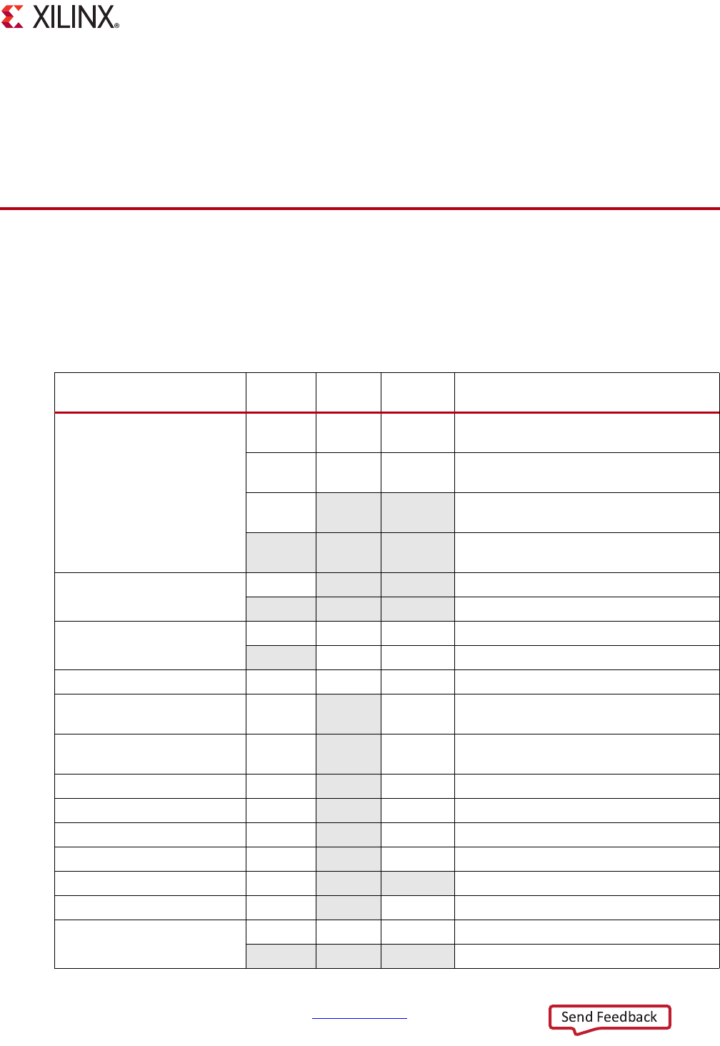
Zynq-7000 AP SoC Technical Reference Manual www.xilinx.com 112
UG585 (v1.12.1) December 6, 2017
Chapter 4
System Addresses
4.1 Address Map
The comprehensive system level address map is shown in Tab le 4 -1 . The shaded entries indicate that
the address range is reserved and should not be accessed. Tab le 4- 2 identifies reserved address
ranges.
Table 4-1: System-Level Address Map
Address Range CPUs and
ACP AXI_HP Other Bus
Masters(1) Notes
0000_0000 to 0003_FFFF(2)
OCM OCM OCM Address not filtered by SCU and OCM is
mapped low
DDR OCM OCM Address filtered by SCU and OCM is
mapped low
DDR Address filtered by SCU and OCM is not
mapped low
Address not filtered by SCU and OCM is
not mapped low
0004_0000 to 0007_FFFF DDR Address filtered by SCU
Address not filtered by SCU
0008_0000 to 000F_FFFF DDR DDR DDR Address filtered by SCU
DDR DDR Address not filtered by SCU(3)
0010_0000 to 3FFF_FFFF DDR DDR DDR Accessible to all interconnect masters
4000_0000 to 7FFF_FFFF PL PL General Purpose Port #0 to the PL,
M_AXI_GP0
8000_0000 to BFFF_FFFF PL PL General Purpose Port #1 to the PL,
M_AXI_GP1
E000_0000 to E02F_FFFF IOP IOP I/O Peripheral registers, see Tab le 4-6
E100_0000 to E5FF_FFFF SMC SMC SMC Memories, see Tab le 4-5
F800_0000 to F800_0BFF SLCR SLCR SLCR registers, see Table 4- 3
F800_1000 to F880_FFFF PS PS PS System registers, see Tab l e 4-7
F890_0000 to F8F0_2FFF CPU CPU Private registers, see Tab l e 4 -4
FC00_0000 to FDFF_FFFF(4) Quad-SPI Quad-SPI Quad-SPI linear address for linear mode
FFFC_0000 to FFFF_FFFF(2) OCM OCM OCM OCM is mapped high
OCM is not mapped high
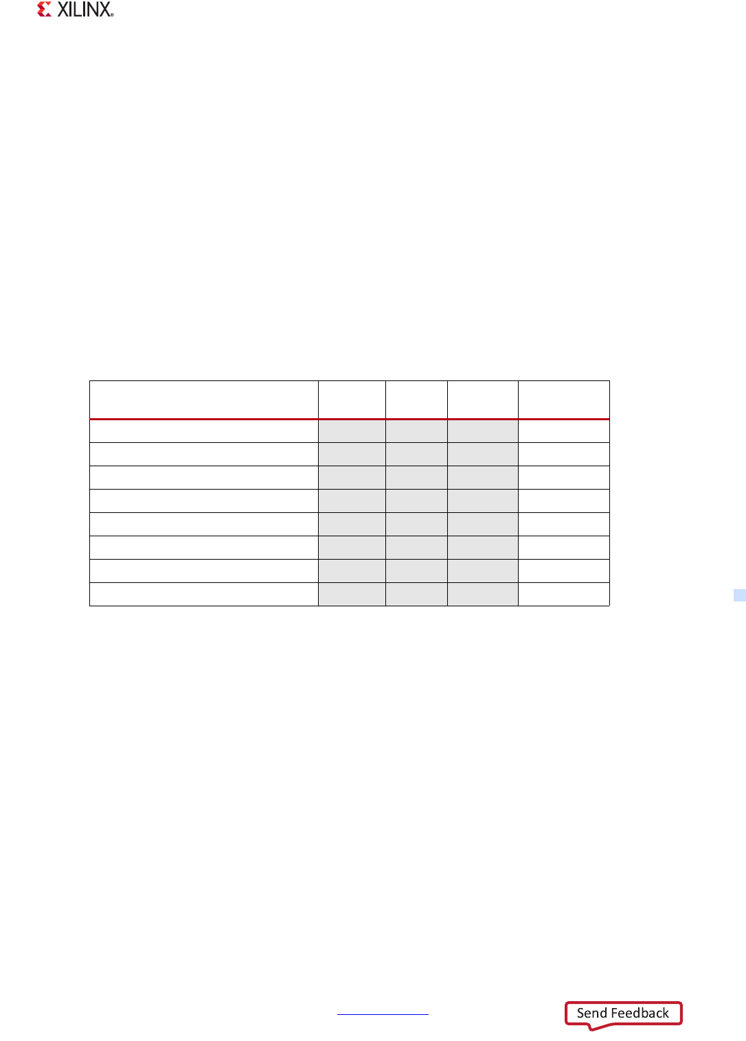
Zynq-7000 AP SoC Technical Reference Manual www.xilinx.com 113
UG585 (v1.12.1) December 6, 2017
Chapter 4: System Addresses
PL AXI Interface Note
There are two general purpose interconnect ports that go to the PL, M_AXI_GP{1,0}. Each port is
addressable by masters in the PS and each port occupies 1 GB of system address space in the ranges
specified in Tab le 4- 1. The M_AXI_GP addresses are directly from the PS; they are not remapped on
their way to the PL. The addresses outside of these ranges are not presented to the PL.
Execute-In-Place Capable Devices
The following devices are execute-in-place capable:
• DDR
•OCM
•SMC SRAM/NOR
• Quad-SPI (linear addressing mode)
• M_AXI_GP{1, 0} (PL block RAM or external memory with a suitable PL slave controller)
Notes:
1. The other bus masters include the S_AXI_GP interfaces, Device configuration interface (DevC), DAP controller, DMA
controller and the various controllers with local DMA units (Ethernet, USB and SDIO).
2. The OCM is divided into four 64 KB sections. Each section is mapped independently to either the low or high
addresses ranges, but not both at the same time. In addition, the SCU can filter addresses destined for the OCM
low address range to the DDR DRAM controller instead. A detailed discussion of the OCM is explained in
Chapter 29, On-Chip Memory (OCM).
3. For each 64 KB section mapped to the high OCM address range via slcr.OCM_CFG[RAM_HI] which is not also part
of the SCU address filtering range will be aliased for CPU and ACP masters at a range of (0x000C_0000 to
0x000F_FFFF). See Chapter 29, On-Chip Memory (OCM) for more information.
4. When a single device is used, it must be connected to QSPI 0. In this case, the address map starts at FC00_0000
and goes to a maximum of FCFF_FFFF (16 MBs). When two devices are used, both devices must be the same
capacity. The address map for two devices depends on the size of the devices and their connection configuration.
For the shared 4-bit stacked I/O bus, the QSPI 0 device starts at FC00_0000 and goes to a maximum of
FCFF_FFFF (16 MBs). The QSPI 1 device starts at FD00_0000 and goes to a maximum of FDFF_FFFF (another
16 MBs). If the first device is less than 16 MBs in size, then there will be a memory space hole between the two
devices. For the 8-bit dual parallel mode (8-bit bus), the memory map is continuous from FC00_0000 to a
maximum of FDFF_FFFF (32 MBs).
Table 4-2: System-Level Address Map (Reserved Addresses)
Address Range CPUs and
ACP AXI_HP Other Bus
Masters(1) Notes
C000_0000 to DFFF_FFFF Reserved
E030_0000 to E0FF_FFFF Reserved
E600_0000 to F7FF_FFFF Reserved
F800_0C00 to F800_0FFF Reserved
F881_0000 to F889_0FFF Reserved
F8F0_3000 to FBFF_FFFF Reserved
FE00_0000 to FFFB_FFFF Reserved
0xF889_E000 to 0xF88F_FFFF Reserved

Zynq-7000 AP SoC Technical Reference Manual www.xilinx.com 114
UG585 (v1.12.1) December 6, 2017
Chapter 4: System Addresses
4.2 System Bus Masters
The CPUs and AXI_ACP see the same memory map, except the CPUs have a private bus to access their
private timer, interrupt controller, and shared L2 cache / SCU registers. The AXI_HP interfaces provide
high bandwidth to the DDR DRAM and OCM memory. The other system bus masters include:
• DMA controller, see Chapter 9, DMA Controller
• Device configuration interface (DevC), see Chapter 6, Boot and Configuration
• Debug access port (DAP), see Chapter 28, System Test and Debug
• PL bus master controllers attached to AXI general purpose ports (S_AXI_GP[1:0]), see Chapter 5,
Interconnect and Chapter 21, Programmable Logic Description
• AHB bus master ports with local DMA units (Ethernet, USB, and SDIO)
4.3 SLCR Registers
The System-Level Control registers (SLCR) consist of various registers that are used to control the PS
behavior. These registers are accessible via the central interconnect using load and store instructions.
The detailed descriptions for each register can be found in Appendix B, Register Details. A summary
of the SLCR registers with their base addresses is shown in Table 4 -3.
Table 4-3: SLCR Register Map
Register Base
Address Description Reference
F800_0000 SLCR write protection lock and security
F800_0100 Clock control and status See Chapter 25, Clocks
F800_0200 Reset control and status See Chapter 26, Reset System
F800_0300 APU control See Chapter 3, Application Processing Unit
F800_0400 TrustZone control
See UG1019, Programming ARM TrustZone
Architecture on the Xilinx Zynq-7000 All
Programmable SoC
F800_0500 CoreSight SoC debug control See Chapter 28, System Test and Debug
F800_0600 DDR DRAM controller See Chapter 10, DDR Memory Controller
F800_0700 MIO pin configuration See Chapter 2, Signals, Interfaces, and Pins
F800_0800 MIO parallel access See Chapter 2, Signals, Interfaces, and Pins
F800_0900 Miscellaneous control See Chapter 29, On-Chip Memory (OCM)
F800_0A00 On-chip memory (OCM) control See Chapter 29, On-Chip Memory (OCM)
F800_0B00 I/O buffers for MIO pins (GPIOB) and
DDR pins (DDRIOB) See Chapter 2, Signals, Interfaces, and Pins

Zynq-7000 AP SoC Technical Reference Manual www.xilinx.com 115
UG585 (v1.12.1) December 6, 2017
Chapter 4: System Addresses
4.4 CPU Private Bus Registers
The registers shown in Tab l e 4- 4 are only accessible by the CPU on the CPU private bus. The
accelerator coherency port (ACP) cannot access any of the private CPU registers. The private CPU
registers are used to control subsystems in the APU.
4.5 SMC Memory
The SMC memories are accessed via a 32-bit AHB bus (see Tabl e 4- 5). The SMC control registers are
listed in Tabl e 4 -6 . Refer to Chapter 11, Static Memory Controller for information on the functionality
of the NAND and SRAM/NOR controllers.
7z007s and 7z010 Device Notice
The 7z010 dual core and 7z007s single core devices have CLG225 packages with a limited number of
pins. For SMC, only an 8-bit NAND interface is supported. These devices do not support the
NOR/SRAM interface or a 16-bit NAND interface.
Table 4-4: CPU Private Register Map
Register Base Address Description
F890_0000 to F89F_FFFF Top-level interconnect configuration and Global
Programmers View (GPV)
F8F0_0000 to F8F0_00FC SCU control and status
F8F0_0100 to F8F0_01FF Interrupt controller CPU
F8F0_0200 to F8F0_02FF Global timer
F8F0_0600 to F8F0_06FF Private timers and private watchdog timers
F8F0_1000 to F8F0_1FFF Interrupt controller distributor
F8F0_2000 to F8F0_2FFF L2-cache controller
Table 4-5: SMC Memory Address Map
Register Base Address Description
E100_0000 SMC NAND Memory address range
E200_0000 SMC SRAM/NOR CS 0 Memory address range
E400_0000 SMC SRAM/NOR CS 1 Memory address range

Zynq-7000 AP SoC Technical Reference Manual www.xilinx.com 116
UG585 (v1.12.1) December 6, 2017
Chapter 4: System Addresses
4.6 PS I/O Peripherals
The I/O Peripheral registers are accessed via a 32-bit APB bus, shown in Tabl e 4 -6 .
4.7 Miscellaneous PS Registers
The PS system registers are accessed via a 32-bit AHB bus (see Ta b le 4 -7 ).
Table 4-6: I/O Peripheral Register Map
Register Base Address Description
E000_0000, E000_1000 UART Controllers 0, 1
E000_2000, E000_3000 USB Controllers 0, 1
E000_4000, E000_5000 I2C Controllers 0, 1
E000_6000, E000_7000 SPI Controllers 0, 1
E000_8000, E000_9000 CAN Controllers 0, 1
E000_A000 GPIO Controller
E000_B000, E000_C000 Ethernet Controllers 0, 1
E000_D000 Quad-SPI Controller
E000_E000 Static Memory Controller (SMC)
E010_0000, E010_1000 SDIO Controllers 0, 1
Table 4-7: PS System Register Map
Register Base Address Description (Acronym) Register
Set
F800_1000, F800_2000 Triple timer counter 0, 1 (TTC 0, TTC 1) ttc.
F800_3000 DMAC when secure (DMAC S) dmac.
F800_4000 DMAC when non-secure (DMAC NS) dmac.
F800_5000 System watchdog timer (SWDT) swdt.
F800_6000 DDR memory controller ddrc.
F800_7000 Device configuration interface (DevC) devcfg.
F800_8000 AXI_HP 0 high performance AXI interface w/ FIFO afi.
F800_9000 AXI_HP 1 high performance AXI interface w/ FIFO afi.
F800_A000 AXI_HP 2 high performance AXI interface w/ FIFO afi.
F800_B000 AXI_HP 3 high performance AXI interface w/ FIFO afi.
F800_C000 On-chip memory (OCM) ocm.
F800_D000 eFuse(1) -
F800_F000 Reserved Reserved

Zynq-7000 AP SoC Technical Reference Manual www.xilinx.com 117
UG585 (v1.12.1) December 6, 2017
Chapter 4: System Addresses
F880_0000 CoreSight debug control cti.
Notes:
1. One-time programmable non-volatile memory used to support RSA authentication of the FSBL.
Table 4-7: PS System Register Map (Cont’d)
Register Base Address Description (Acronym) Register
Set

Zynq-7000 AP SoC Technical Reference Manual www.xilinx.com 118
UG585 (v1.12.1) December 6, 2017
Chapter 5
Interconnect
5.1 Introduction
The interconnect located within the PS comprises multiple switches to connect system resources
using AXI point-to-point channels for communicating addresses, data, and response transactions
between master and slave clients. This ARM AMBA 3.0 interconnect implements a full array of the
interconnect communications capabilities and overlays for QoS, debug, and test monitoring. The
interconnect manages multiple outstanding transactions and is architected for low-latency paths for
the ARM CPUs and, for the PL master controllers, a high-throughput and cache coherent datapaths.
5.1.1 Features
The interconnect is the primary mechanism for data communications. The following summarizes the
interconnect features:
• The interconnect is based on AXI high performance datapath switches:
°Snoop control unit
°L2 cache controller
• Interconnect switches based on ARM NIC-301
°Central interconnect
°Master interconnect for slave peripherals
°Slave interconnect for master peripherals
°Memory interconnect
°OCM interconnect
°AHB and APB bridges
•PS-PL Interfaces
°AXI_ACP, one cache-coherent slave port in the PL connected to the PS APU coherency slave
port.
°AXI_HP, four high performance, high bandwidth slave port in the PL that becomes a master
port on the PS AXI interconnect.
°AXI_GP, four general purpose ports (two master ports and two slave ports)

Zynq-7000 AP SoC Technical Reference Manual www.xilinx.com 119
UG585 (v1.12.1) December 6, 2017
Chapter 5: Interconnect
5.1.2 Block Diagram
This section discusses the block diagram for all the interconnect, including the interconnect masters,
the snoop control unit, central interconnect, master interconnect, slave interconnect, memory
interconnect, and OCM interconnect. Figure 5-1 shows the block diagram for the interconnect.
Interconnect Masters
The interconnect masters are shown at the top of Figure 5-1, and include:
• CPUs and accelerator coherency port (ACP)
• High performance PL interfaces, AXI_HP{3:0}
• General purpose PL interfaces, AXI_GP{1:0}
• DMA controller
• AHB masters (I/O peripherals with local DMA units)
• Device configuration (DevC) and debug access port (DAP)
Snoop Control Unit (SCU)
The functionality of the snoop control unit is described in Chapter 3, Application Processing Unit.
The address filtering feature of the SCU makes the SCU function like a switch from the perspective of
the traffic from its AXI slave ports to its AXI master ports.
Central Interconnect
The central interconnect is the core of the ARM NIC301-based interconnect switches.
Master Interconnect
The master interconnect switches the low-to-medium speed traffic from the central interconnect to
M_AXI_GP ports, I/O peripherals (IOP) and other blocks.
Slave Interconnect
The slave interconnect switches the low-to-medium speed traffic from S_AXI_GP ports, DevC and
DAP to the central interconnect.
Memory Interconnect
The memory interconnect switches the high speed traffic from the AXI_HP ports to DDR DRAM and
on-chip RAM (through another interconnect).
OCM Interconnect
The OCM interconnect switches the high speed traffic from the central interconnect and the memory
interconnect.
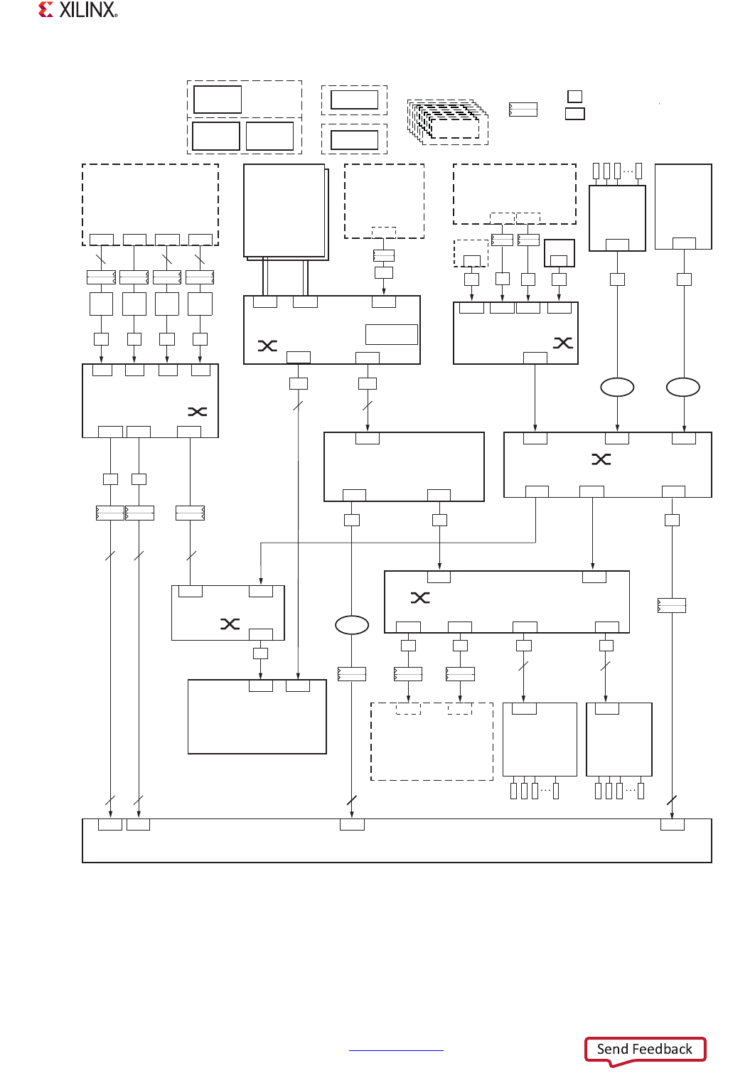
Zynq-7000 AP SoC Technical Reference Manual www.xilinx.com 120
UG585 (v1.12.1) December 6, 2017
Chapter 5: Interconnect
X-Ref Target - Figure 5-1
Figure 5-1: Interconnect Block Diagram
OCM
Interconnect
Master Interconnect
for Slave Peripherals
APB
Slaves
Registers
Slaves
Reg & Data
General Purpose
AXI Controllers
(S_AXI_GP[1:0])
Cortex A9
NEON/FPU
Jazelle, Thumb-2,
MMUs,
L1 i/dCaches
Snoop Control Unit
(SCU)
M0 M1
M
L2 Cache
Controller
M0 M1
S
512 kB
M
S
Central
Interconnect
S1
M1
S1S0S2S3
S
M
M2M0
M0 M1
Slave Interconnect
for Master Peripherals
M
S3
S0 S1 S2
DevC DAP
M
S0
M2M0 M1
General Purpose
AXI Controllers
(M_AXI_GP[1:0])
S1S0
S1
S0 S2
M3
S
DDR Memory Controller
32-bit
CPU_2x
CPU_1x
CPU_2x
64-bit
Cache
Coherent
ACP port
(S_AXI_ACP)
AHB/APB
Clock
cpu_1x
CPU_1x
ASYNC
ASYNC ASYNC ASYNC
PL Logic
DDR_3x Clock
PL Logic
CPU_2x
CPU_1x
Masters
Data
DMA
Controller
CPU_6x4x
CPU_6x4x
CPU_6x4x
8
Read/Write Request Capability
ASYNC
Async
crossing
4881 88
88
88 4 1
32-bit
32-bit
8
High Performance
AXI Controllers
(AXI_HP[3:0])
S3S2S1S0
M2M0 M1
M3M2M1M0
FIFOFIFOFIFOFIFO
PL clocks
ASYNCASYNCASYNCASYNC
888
88
256 kB
S1 S0
S0
M
S1
64-bit
PL Fabric
PL Fabric
64-bit
DDR_2x
ASYNC ASYNC
64-bit
ASYNC
32-bit
64-bit
ASYNC
ASYNC
CPU_2x
Memory
Interconnect
64-bit
M
32- / 64-bit
Cache Tag
RAM
CPU, L1
Clock
cpu_6x4x
CPU_2x
DDR Clock
ddr_2x
DDR Clock
ddr_3x
Each of the eight
AXI interfaces are
asynchronous to
all else.
OCM
Clock
cpu_2x
64-bit
PL
64-bit 64-bit
UG585_c5_01_120813
CPU_6x4x
CPU_2x
On-chip
RAM
32-bit
64-bit
8
8,3
4
ASYNC
SS
QoS
QoS QoS
4,4
7,3
7,3
(e.g. 1 number: 8 reads, 8 writes)
(e.g. 2 numbers: 7 reads, 3 writes)
Synchronous CPU clock domain
is asynchronous to all else. Asynchronous to
all else.

Zynq-7000 AP SoC Technical Reference Manual www.xilinx.com 121
UG585 (v1.12.1) December 6, 2017
Chapter 5: Interconnect
L2 Cache Controller
The functionality of the L2 cache controller is described in Chapter 3, Application Processing Unit.
The address filtering feature of the L2 cache controller makes the L2 cache controller function like a
switch from the perspective of the traffic from its AXI slave ports to its AXI master ports.
Interconnect Slaves
The interconnect slaves are shown toward the bottom of Figure 5-1. The Interconnect slaves include:
• On-chip RAM (OCM)
• DDR DRAM
• General purpose PL interfaces, M_AXI_GP{1:0}
• AHB slaves (IOP with local DMA units)
• APB slaves (programmable registers in various blocks)
• GPV (programmable registers of the interconnect, not shown in Figure 5-1)
5.1.3 Datapaths
Tabl e 5-1 lists the major datapaths used by the PS interconnect.
Table 5-1: Interconnect Datapaths
Source Destination Type Clock
at source
Clock
at destination
Sync
or
Async(1)
Data
width
R/W
Request
Capability
Advanced
QoS
CPU SCU AXI CPU_6x4x CPU_6x4x Sync 64 7, 12 -
AXI_ACP SCU AXI SAXIACPACLK CPU_6x4x Async 64 7, 3 -
AXI_HP FIFO AXI SAXIHPnACLK DDR_2x Async 32/64 14-70,
8-32(2) -
S_AXI_GP Master
interconnect AXI SAXIGPnACLK CPU_2x Async 32 8, 8 -
DevC Master
interconnect AXI CPU_1x CPU_2x Sync 32 8, 4 -
DAP Master
interconnect AHB CPU_1x CPU_2x Sync 32 1, 1 -
AHB masters Central
interconnect AXI CPU_1x CPU_2x Sync 32 8, 8 X
DMA
controller
Central
interconnect AXI CPU_2x CPU_2x Sync 64 8, 8 X
Master
interconnect
Central
interconnect AXI CPU_2x CPU_2x Sync 64 - -
FIFO Memory
interconnect AXI DDR_2x DDR_2x Sync 64 8, 8 -
SCU L2 Cache AXI CPU_6X4x CPU_6x4x Sync 64 8, 3 -

Zynq-7000 AP SoC Technical Reference Manual www.xilinx.com 122
UG585 (v1.12.1) December 6, 2017
Chapter 5: Interconnect
5.1.4 Clock Domains
The interconnect, masters, and slaves use the clocks shown inTa ble 5 -2.:
Memory
interconnect
OCM
interconnect AXI DDR_2x CPU_2x Async 64 - -
Central
interconnect
OCM
interconnect AXI CPU_2x CPU_2x Sync 64 - -
L2 Cache Slave
interconnect AXI CPU_6x4x CPU_2x Sync 64 8, 8 -
Central
interconnect
Slave
interconnect AXI CPU_2x CPU_2x Sync 64 - -
SCU On-chip
RAM AXI CPU_6x4x CPU_2x Sync 64 4, 4 -
OCM
interconnect
On-chip
RAM AXI CPU_2x CPU_2x Sync 64 4, 4 -
Slave
interconnect APB slaves APB CPU_2x CPU_1x Sync 32 1, 1 -
Slave
interconnect AHB slaves AXI CPU_2x CPU_1x Sync 32 4, 4 -
Slave
interconnect AXI_GP AXI CPU_2x MAXIGPnACLK Async 32 8, 8 -
L2 cache DDR
controller AXI CPU_6x4x DDR_3x Async 64 8, 8 X
Central
interconnect
DDR
controller AXI CPU_2x DDR_3x Async 64 8, 8 -
Memory
interconnect
DDR
controller AXI DDR_2x DDR_3x Async 64 8, 8 -
Slave
interconnect GPV (3) CPU_2x (multiple) - - - -
Notes:
1. Each asynchronous path includes an asynchronous bridge for clock domain crossing.
2. Burst-length dependent (see AXI_HP Interfaces).
3. The path from the slave interconnect to GPV is an internal path within the entire interconnect structure. When accessing
GPV, ensure that all clocks are on.
Table 5-1: Interconnect Datapaths (Cont’d)
Source Destination Type Clock
at source
Clock
at destination
Sync
or
Async(1)
Data
width
R/W
Request
Capability
Advanced
QoS
Table 5-2: Clocks used by Interconnect, Masters, and Slaves
CPU_6x4x: CPUs, SCU, L2 Cache controller, On-Chip RAM
CPU_2x Central interconnect, master interconnect, slave interconnect, OCM interconnect
CPU_1x AHB masters, AHB slaves, APB slaves, DevC, DAP
DDR_3x DDR Memory Controller
DDR_2x Memory interconnect, FIFOs

Zynq-7000 AP SoC Technical Reference Manual www.xilinx.com 123
UG585 (v1.12.1) December 6, 2017
Chapter 5: Interconnect
Except for CPU_6X4X, CPU_2X, and CPU_1X, which are synchronous clocks with a ratio of 6:2:1 or
4:2:1, all clocks in Tabl e 5 -2 are asynchronous to one another, as shown in Figure 5-2.
SAXIACPACLK AXI_ACP slave port
SAXIHP0ACLK AXI_HP0 slave port
SAXIHP1ACLK AXI_HP1 slave port
SAXIHP2ACLK AXI_HP2 slave port
SAXIHP3ACLK AXI_HP3 slave port
SAXIGP0ACLK AXI_GP0 slave port
SAXIGP1ACLK AXI_GP1 slave port
MAXIGP0ACLK AXI_GP0 master port
MAXIGP1ACLK AXI_GP1 master port
Table 5-2: Clocks used by Interconnect, Masters, and Slaves (Cont’d)
CPU_6x4x: CPUs, SCU, L2 Cache controller, On-Chip RAM
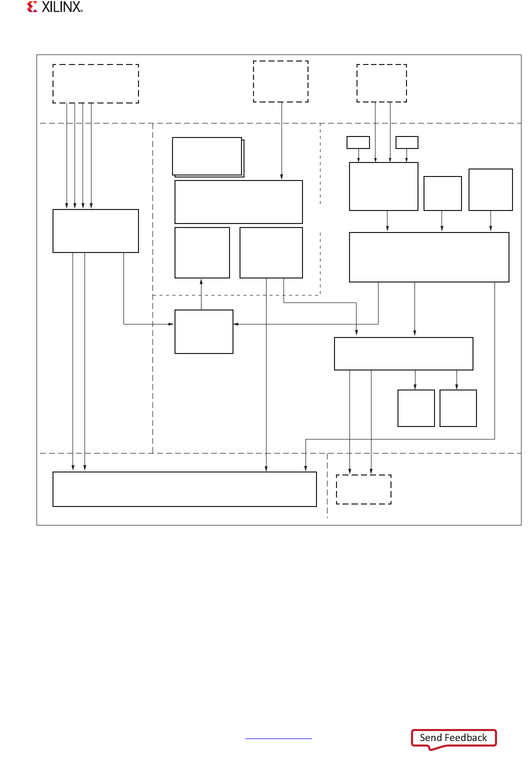
Zynq-7000 AP SoC Technical Reference Manual www.xilinx.com 124
UG585 (v1.12.1) December 6, 2017
Chapter 5: Interconnect
X-Ref Target - Figure 5-2
Figure 5-2: Interconnect Clock Domains
Master
Interconnect
S_AXI_GP
M_AXI_GP
CPUs
Snoop Control Unit (SCU)
L2 Cache
Central
Interconnect
Slave
Interconnect
DevC DAP
DDR Memory Controller
CPU_2x
CPU_2x
Cache
Coherent
AXI P port
(
AXI_ACP)
DDR_3x
CPU_2xCPU_1x
Masters
DMA
Controller
CPU_6x4x
CPU_6x4x
High Performance
AXI Controllers
(AXI_HP)
On-chip
RAM
CPU_6x4x
CPU_2x
DDR_2x
Memory
Interconnect
CPU_2x
APB
Slaves
CPU_1x
Slaves
CPU_1x
CPU_6x4x
Async
AsyncAsync
Async
OCM
Interconnect
Async
UG585_c5_02_120813
Async
Async
CPU_2x
6:2:1 or
4:2:1
Ratio
Zynq-7000 AP SoC Technical Reference Manual www.xilinx.com 125
UG585 (v1.12.1) December 6, 2017
Chapter 5: Interconnect
5.1.5 Connectivity
The interconnect is not a full cross-bar structure. Ta ble 5 -3 shows which master can access which
slave.
5.1.6 AXI ID
The interconnect uses 13-bit AXI IDs, consisting of (from MSB to LSB):
• Three bits that identify the interconnect (central, master, slave, etc.)
• Eight bits supplied by the master; width is determined by the largest AXI ID width among all
masters
• Two bits that identify the slave interface of the identified interconnect
Tabl e 5-4 lists all possible AXI ID values that a slave can observe.
Table 5-3: Master - Slave Access
Master
Slave
On-chip
RAM
DDR
Port 0
DDR
Port 1
DDR
Port 2
DDR
Port 3
M_AXI
_GP
AHB
Slaves
APB
Slaves GPV
CPUs XX XXXX
AXI_ACP XX XXXX
AXI_HP{0,1} XX
AXI_HP{2,3} XX
S_AXI_GP{0,1} X X XXX
DMA Controller X X XXX
AHB Masters X X XXX
DevC, DAP X X XXX
Table 5-4: Slave Visible AXI ID Values
Master Master ID Width AXI ID (as seen by the slaves)
AXI_HP0 6 13’b00000xxxxxx00
AXI_HP1 6 13’b00000xxxxxx01
AXI_HP2 6 13’b00000xxxxxx10
AXI_HP3 6 13’b00000xxxxxx11
DMAC controller 4 13’b0010000xxxx00
AHB masters 3 13’b00100000xxx01
DevC 0 13’b0100000000000

Zynq-7000 AP SoC Technical Reference Manual www.xilinx.com 126
UG585 (v1.12.1) December 6, 2017
Chapter 5: Interconnect
5.1.7 Read/Write Request Capability
The R/W Request Capability shown in Figure 5-1 and in Ta ble 5 -1 describes the maximum number of
requests that the master of a datapath can issue. This does not mean the master can always issue the
maximum number of requests under all circumstances or scenarios. There are conditions where other
limiting factors can be active to reduce the number of requests.
One particular example is the extended write rule in the deadlock avoidance scheme, which ensures
the network only issues a write transaction (on the AW channel) if all the outstanding write
transactions have had the last write data beat transmitted (on the W channel). Under this rule, if the
number of write data beats is large, preventing a second write request from being issued in a certain
spot in the network, because the network must wait until the last beat of write data of the first write
is transmitted, then only a single write request can be issued by a master.
5.1.8 Register Overview
Tabl e 5-5 provides an overview of the GPV registers.
DAP 0 13’b0100000000001
S_AXI_GP0 6 13’b01000xxxxxx10
S_AXI_GP1 6 13’b01000xxxxxx11
CPUs, AXI_ACP
through L2 M1 port 813’b011xxxxxxxx00
CPUs, AXI_ACP
through L2 M0 port 813’b100xxxxxxxx00
Notes:
1. x, which can be either 0 or 1, originates from the requesting master.
Table 5-4: Slave Visible AXI ID Values (Cont’d)
Master Master ID Width AXI ID (as seen by the slaves)
Table 5-5: GPV Register Overview
Function Name Overview
TrustZone security_gp0_axi
security_gp1_axi
Control boot secure settings for the slave ports
of the slave interconnect.
Advanced QoS qos_cntl,
max_ot, max_comb_ot,
aw_p, aw_b, aw_r,
ar_p, ar_b, ar_r
Control advanced QoS features, maximum
number of outstanding transactions, AW and AR
channel peak rates, burstiness, average rates.

Zynq-7000 AP SoC Technical Reference Manual www.xilinx.com 127
UG585 (v1.12.1) December 6, 2017
Chapter 5: Interconnect
5.2 Quality of Service (QoS)
5.2.1 Basic Arbitration
Each interconnect (central, master, slave, memory) uses a two-level arbitration scheme to resolve
contention. The first-level arbitration is based on the priority indicated by the AXI QoS signals from
the master or programmable registers. The highest QoS value has the highest priority. The
second-level arbitration is based on a least recently granted (LRG) scheme and is used when multiple
requests are pending with the same QoS signal value. Information on OCM arbitration can be found
in Chapter 10, DDR Memory Controller.
5.2.2 Advanced QoS
In addition to the basic arbitration, the interconnect provides an advanced QoS control mechanism.
This programmable mechanism influences interconnect arbitration for requests from these masters:
• CPUs and ACP requests to DDR (through L2 cache controller port M0)
• DMA controller requests to DDR and OCM (through the central interconnect)
• AMBA master requests to DDR and OCM (through the central interconnect)
In the PS, advanced QoS modules exist on the following paths:
•Path from L2 cache to DDR
• Path from DMA controller to the central interconnect
• Path from AHB masters to the central interconnect
The QoS module is based on ARM QoS-301, which is an extension to the NIC-301 network
interconnect. They provide facilities to regulate transactions as follows:
• Maximum number of outstanding transactions
•Peak rates,
•Average rates
•Burstiness
For more information, refer to CoreLink QoS-301 Network Interconnect Advanced Quality of Service
Technical Reference Manual.
The use of QoS arbitration for all slave interfaces should be performed with careful deliberation, as
fixed priority arbitration leads to starvation issues if not used properly. By default, all ports have
equal priority so starvation is not an issue.
Rationale
You are expected to create “well behaved” masters in the PL, which sufficiently throttle their rate of
command issuance, or use the AXI_HP issuance capability settings. However, traffic from CPUs

Zynq-7000 AP SoC Technical Reference Manual www.xilinx.com 128
UG585 (v1.12.1) December 6, 2017
Chapter 5: Interconnect
(through L2 cache), the DMA controller, and the IOP masters can interfere with traffic from the PL.
The QoS modules allow you to throttle these PS masters to ensure expected/consistent throughput
and latency for the user design in the PL or specific PS masters. This is especially useful for video,
which requires guaranteed maximum latency. By regulating the “irregular” masters such as
CPUs, the DMA controller, and IOP masters, it is possible to guarantee maximum latency for
PL-based video.
5.2.3 DDR Port Arbitration
The PS interconnect uses all four QoS signals except where it attaches to the DDR memory controller,
which takes only the most significant QoS signal. A 3-input mux selects among this QoS signal,
another signal from the SLCR.DDR_URGENT register, and a DDRARB signal directly from the PL to
determine if a request is urgent. Refer to Chapter 10, DDR Memory Controller for more details.
5.3 AXI_HP Interfaces
The four AXI_HP interfaces provide PL bus masters with high bandwidth datapaths to the DDR and
OCM memories. Each interface includes two FIFO buffers for read and write traffic. The PL to memory
interconnect routes the high-speed AXI_HP ports to two DDR memory ports or the OCM. The AXI_HP
interfaces are also referenced as AFI (AXI FIFO interface), to emphasize their buffering capabilities.
The PL level shifters must be enabled through LVL_SHFTR_EN before PL logic communication can
occur.
5.3.1 Features
The interfaces are designed to provide a high throughput datapath between PL masters and PS
memories, including the DDR and on-chip RAM. The main features include:
• 32- or 64-bit data wide master interfaces (independently programmed per port)
• Efficient dynamic upsizing to 64-bits for aligned transfers in 32-bit interface mode, controllable
through AxCACHE[1]
• Automatic expansion to 64-bits for unaligned 32-bit transfers in 32-bit interface mode
• Programmable release threshold of write commands
• Asynchronous clock frequency domain crossing for all AXI interfaces between the PL and PS
• Smoothing out of “long-latency” transfers using 1 KB (128 by 64 bit) data FIFOs for both reads
and writes
• QoS signaling available from PL ports
• Command and data FIFO fill-level counts available to the PL
• Standard AXI 3.0 interfaces supported
• Programmable command issuance to the interconnect, separately for read and write commands
• Large slave interface read acceptance capability in the range of 14 to 70 commands (burst
length dependent)
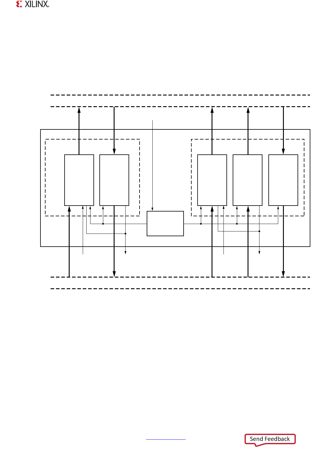
Zynq-7000 AP SoC Technical Reference Manual www.xilinx.com 129
UG585 (v1.12.1) December 6, 2017
Chapter 5: Interconnect
• Large slave interface write acceptance capability in the range of 8 to 32 commands (burst length
dependent)
5.3.2 Block Diagram
Figure 5-3 shows the block diagram for the AXI_HP interfaces.
X-Ref Target - Figure 5-3
Figure 5-3: AXI_HP Block Diagram
64-bit
PS AXI
Channels
RdAddr RdData WrAddr BRespWrData
WrAddr BRespWrDataRdAddr RdData
APB I/F
Registers
RdAddr
Channel
Q
RdData
Channel
FIFO
WrAddr
Channel
Q
WrData
Channel
FIFO
BResp
Channel
Q
Read Channel Write Channel
QoS en
Issue
Capability
FIFO
Levels
QoS en
Issue
Capability
FIFO
Levels
32/64-bit
PL AXI
Channels
UG585_c5_03_121613
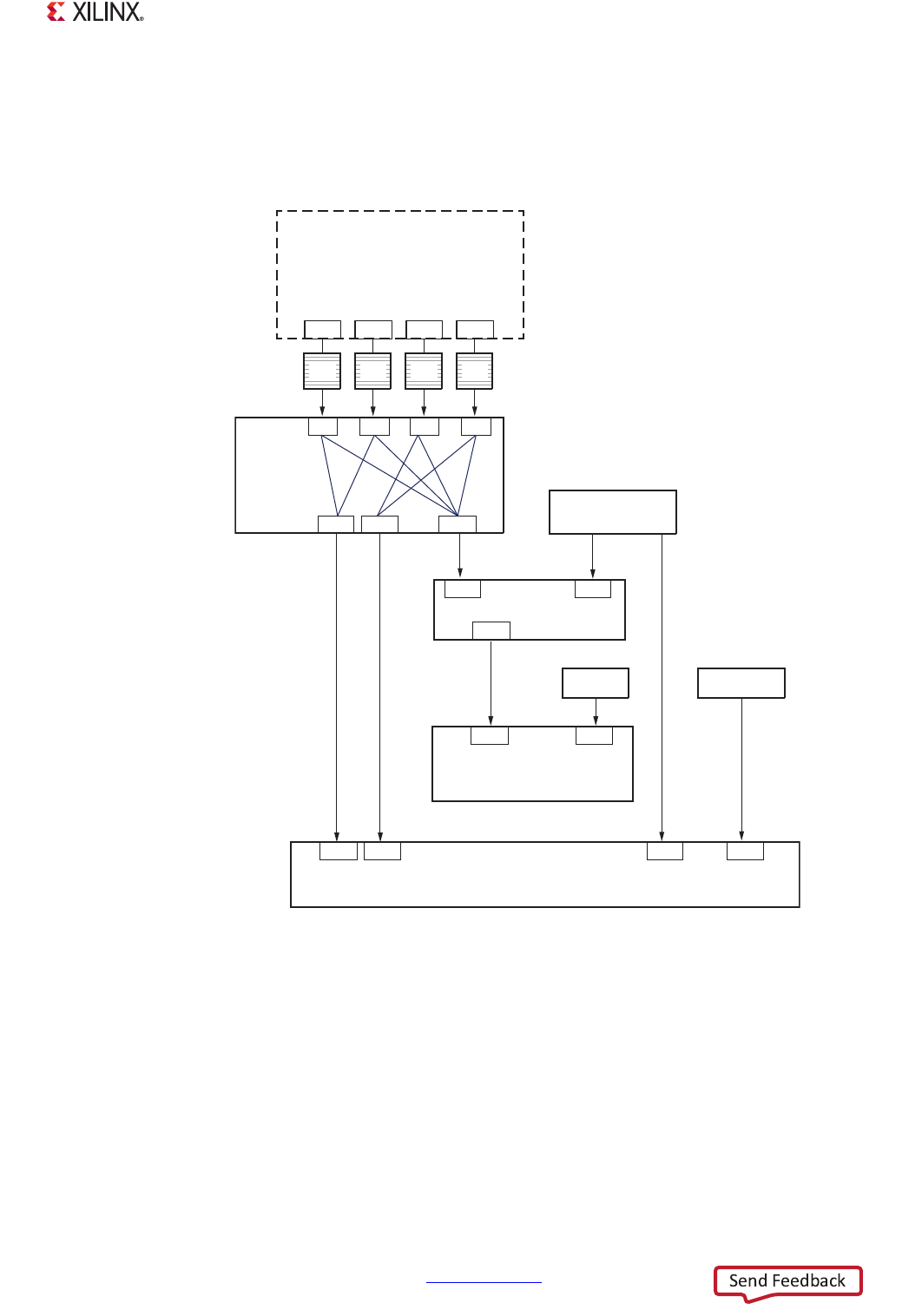
Zynq-7000 AP SoC Technical Reference Manual www.xilinx.com 130
UG585 (v1.12.1) December 6, 2017
Chapter 5: Interconnect
5.3.3 Functional Description
There are two sets of AXI ports, one set connecting directly to the PL and the other connecting to the
AXI interconnect matrix, allowing access to DDR and OCM memory (see Figure 5-4).
5.3.4 Performance
See Chapter 22, Programmable Logic Design Guide for more information.
X-Ref Target - Figure 5-4
Figure 5-4: High Performance (AXI_HP) Connectivity
High Performance
AXI Controllers
(AXI_HP)
S3S2S1S0
M2M0 M1
M3M2M1M0
FIFOFIFOFIFOFIFO
Memory
Interconnect
S2S3
DDR Memory Controller
UG585_c5_04_050212
S1
S1 S0
On-chip
RAM
OCM Interconnect
S0
M
S1
Central
Interconnect
SCU
S0
L2-cache

Zynq-7000 AP SoC Technical Reference Manual www.xilinx.com 131
UG585 (v1.12.1) December 6, 2017
Chapter 5: Interconnect
5.3.5 Register Overview
A partial list of registers related to the high performance AXI port is listed in Tab le 5 -6
5.3.6 Bandwidth Management Features
For applications requiring multiple programmable logic masters on multiple high performance AXI
interface ports simultaneously, and in the presence of a medium or heavily loaded PS system, the
management of the bandwidth per programmable logic port or “thread” becomes more difficult.
For example, if real-time type traffic is required on one thread, possibly mixed with non real-time
traffic on other threads/ports, the standard AXI 3.0 bus protocol does not explicitly provide methods
to manage priority.
The high performance AXI interface module does provide several functions to assist priority and
queue management. The majority of management functions are provided to both the programmable
logic design as PL signals and the PS as registers, as performance optimization is application
dependent. This allows maximum flexibility, while simplifying the high performance AXI interface
requirements.
The additional signals provided to the PL in addition to standard AXI3 signals are provided in
Tabl e 5-7 . The priority and occupancy management functions provided are discussed in the
following sections.
Table 5-6: High Performance (AFI) AXI Register Overview
Module Register Name Overview
AXI_HP
AFI_RDCHAN_CTRL
AFI_WRCHAN_CTRL
Select 64- or 32-bit interface width mode.
Various bandwidth management control settings.
AFI_RDCHAN_ISSUINGCAP
AFI_WRCHAN_ISSUINGCAP Maximum outstanding read/write commands
AFI_RDQOS
AFI_WRQOS
Read/write register-based quality of service (QoS)
priority value
AFI_RDDATAFIFO_LEVEL
AFI_WRDATAFIFO_LEVEL Read/write data FIFO register occupancy
OCM OCM_CONTROL
Change arbitration priority of HP (and central
interconnect) accesses at OCM with respect to SCU
writes.
DDRC
axi_priority_rd_port2
axi_priority_wr_port2
Various priority settings for arbitration at DDR
controller for AXI_HP (AFI) ports 2 and 3
axi_priority_rd_port3
axi_priority_wr_port3
Various priority settings for arbitration at DDR
controller for AXI_HP (AFI) ports 0 and 1
SLCR LVL_SHFTR_EN Level shifters. Must be enabled before using any of the
PL AXI interfaces.

Zynq-7000 AP SoC Technical Reference Manual www.xilinx.com 132
UG585 (v1.12.1) December 6, 2017
Chapter 5: Interconnect
QoS Priority
The AXI QoS input signals can be used to assign an arbitration priority to the read and write
commands.
Note that the PS interconnect allows either master control or programmable (register) control as a
configuration option. For the AFI, it is desirable to have the ability for masters to dynamically change
the QOS inputs. However, to provide flexibility the register field axi_hp.AFI_RDCHAN_CTRL
[FabricQosEn] is provided. This allows a static QoS value to be programmed through the high
performance AXI interface port, ignoring the PL AXI QoS inputs.
FIFO Occupancy
The level of the data and command FIFOs for both read and write are exported to the PL, allowing
you to take advantage of the QOS feature supported by the top-level interconnect. Based on the
relative levels of these FIFOs, a PL controller could dynamically change the priority of the individual
read and write requests into the high performance AXI interface block(s). For example, if a particular
PL master read data FIFO is getting too empty, the priority of the read requests could be increased.
The filling of this FIFO now takes priority over the other three FIFOs. When the FIFO reaches an
acceptable fill-level, the priority typically is reduced again. The exact scheme used to control the
relative priorities is flexible, as it must be performed in the programmable logic. Note that the “FIFO
Level” should be used as a relative level, as opposed to an exact level, because clock domain crossing
is involved.
Another possible application of the FIFO levels is using them to “look ahead” at the data fill level to
determine if data can be read or written without having to use AXI RVALID/WREADY handshake
signals. This could potentially simplify the AXI interface design logic, enabling higher speeds of
operation.
Table 5-7: Additional per-port HP PL Signals
Type PS-PL Signal Name I/O Description
FIFO occupancy
SAXIHP{0-3}RCOUNT[7:0] O Fill level of the RdData channel FIFO
SAXIHP{0-3}WCOUNT[7:0] O Fill level of the WrData channel FIFO
SAXIHP{0-3}RACOUNT[2:0] O Fill level of the RdAddr channel FIFO
SAXIHP{0-3}WACOUNT[5:0] O Fill level of the WrAddr channel FIFO
Quality of service
SAXIHP{0-3}AWQOS[3:0] I WrAddr channel QOS input. Qualified by
SAXIHP{0-3}AWVALID
SAXIHP{0-3}ARQOS[3:0] I RdAddr channel QOS input. Qualified by
SAXIHP{0-3}ARVALID
Interconnect
issuance
throttling
SAXIHP{0-3}RDISSUECAP1EN I
When asserted (1), indicates that the maximum
outstanding read commands (issuing capability)
should be derived from the “rdIssueCap1” register.
SAXIHP{0-3}WRISSUECAP1EN I
When asserted (1), indicates that the maximum
outstanding write commands (issuing capability)
should be derived from the “wrIssueCap1” register.

Zynq-7000 AP SoC Technical Reference Manual www.xilinx.com 133
UG585 (v1.12.1) December 6, 2017
Chapter 5: Interconnect
Interconnect Issuance Throttling
To optimize the latency or throughput of other masters in the system such as the CPUs, it might be
desirable to constrain the number of outstanding transactions that a high-performance port
requests to the system interconnect. Issuing capability is the maximum number of outstanding
commands that a HP can request at any one time.
Control of the read and write command issuing capability of the high performance AXI interface is
available as a primary input from the logic. This option can be enabled by means o the
axi_hp.AFI_{RD, WR}CHAN_CTRL [FabricOutCmdEn] register fields.
The logic signals, SAXIHP{0-3}RDISSUECAP1_EN and SAXIHP{0-3}WRISSUECAP1_EN allow you to
change the issuing capability of the AFI block to the PS dynamically between two levels.
Write FIFO Store and Forward
The write channels can be configured to store and forward write commands or allow them to pass
through with no storage. The following two registers control the mode of write, store, and forward:
• axi_hp.AFI_WRCHAN_CTRL [WrCmdReleaseMode]
• axi_hp.AFI_WRCHAN_CTRL [WrDataThreshold]
The mode register selects between a complete AXI burst store and forward, a partial AXI burst store
and forward, or a pass through (no store at all). If absolute minimum latency for write commands is
required, the pass-through mode could be selected. However, in cases where multiple masters are
competing for the system slaves, better system performance can likely be achieved using at least the
partial AXI burst store and forward mode. This is because once an AXI write is committed at each
point throughout the PS, the entire burst must be processed before any other write data from other
write commands can be processed.
For example, using pass-through mode, if one HP port with a slow clock rate issues a long burst, a
second port with a faster clock rate might need to wait until the entire slower write data burst has
been transferred, even if all of the write data on the fast clock is available. This is different from the
case of reads, where read data interleaving is permitted.
32-bit Interface Considerations
Each physical high performance PL AXI interface is programmable to be either a 32-bit or 64-bit
interface through the register field axi_hp.AFI_{RD, WR}CHAN_CTRL [32BitEn]. Note that the read and
write channels have separate enables and can therefore be configured differently.
Upsizing and Expansion
In 32-bit mode, some form of translation between the 32-bit port and the 64-bit port is required. For
write data, the 32-bit data (and write strobes) must be aligned correctly onto the appropriate lanes
in the 64-bit domain. For read data, the appropriate lanes of the 64-bit data must be aligned onto
the 32-bit data bus. This data alignment between different width interfaces are automatically dealt
with by the high performance AXI interface module.

Zynq-7000 AP SoC Technical Reference Manual www.xilinx.com 134
UG585 (v1.12.1) December 6, 2017
Chapter 5: Interconnect
For the 32-bit mode, an “expansion” or “upsizing” must be performed to the 64-bit bus. These are
defined as follows:
•Expansion. The AxSIZE[] and AxLEN[] signals remain unchanged on the 64-bit bus. The number
of data beats in the 64-bit domain is therefore the same as the number of data beats in the
32-bit domain. This is the simplest option but also the most inefficient in terms of bandwidth
utilization.
• Upsizing. This is an optimization that makes better use of the 64-bit bus available bandwidth.
The AxSIZE[] signal can be changed to `64-BIT (expansion case it is `32-BIT or less) and the
AxLEN[] field can potentially be adjusted to make use of the 64-bit bus. For a full width transfer,
the number of data beats in the 64-bit domain is now, at best, half the number of data beats in
the 32-bit domain. For example, a burst of 16x32-bit is upsized to a burst of 8×64-bit.
Note: Upsizing only occurs if the AxCACHE[1] bit is set; if it is not, expansion of the command
occurs. This means that you can dynamically control, on a per-command basis, whether to
expand or upsize.
Note: In 64-bit mode, there is no translation between the programmable logic transactions and the
internal 64-bit PS transactions. Whatever appears at the PL port is passed as is to the PS port. In
64-bit mode, no upsizing or expansion is performed. This also applies to narrow transactions in the
64-bit mode.
32-bit Interface Limitations
The high performance AXI interface imposes the following constraints:
1. In 32-bit mode, only burst multiples of 2, incremental burst read commands, aligned to 64-bit
boundaries are upsized. All other 32-bit commands are expanded. These include all narrow
transactions (wrap as well as fixed burst types).
2. Whenever an expanded read command is accepted from the programmable logic by the AFI, this
command is blocked until all outstanding high performance AXI interface read commands in the
pipeline are flushed. The flushing occurs automatically under control of the AFI.
The implication is that for expanded commands, performance is very limited, as command pipelining
is essentially disabled.
Note: All valid AXI command are still supported, just not optimized to take advantage of the 64-bit
bus bandwidth.
In the case of write commands completing out-of-order, no performance penalty is incurred because
the BRESP can be issued in any order directly back to the PL ports.
To be symmetric across read and write operations, the high performance AXI interface also only
upsizes 64-bit aligned burst multiples of 2, incremental burst write commands, in 32-bit mode.
However, in the case of writes, no “blocking” of expanded commands occurs. Write performance for
expanded commands in 32-bit mode is therefore much higher than read performance.

Zynq-7000 AP SoC Technical Reference Manual www.xilinx.com 135
UG585 (v1.12.1) December 6, 2017
Chapter 5: Interconnect
5.3.7 Transaction Types
Tabl e 5-8 summarizes the command types issued to the high performance AXI interface from the PL,
and the command modifications that occur.
5.3.8 Command Interleaving and Re-Ordering
When multi-threaded commands are used in AXI, there is the potential for commands being
processed out-of-order as well as interleaving of data beats.
The DDR controller guarantees that all read commands are completed continuously, that is, it does
not interleave read data onto its external AXI ports. It does however take advantage of re-ordering of
read and write commands, to perform internal optimizations. It is therefore expected that read and
write commands issued to the DDR controller are sometimes completed in a different order from
which they were issued.
Read data interleaving is not supported by either the DDR or the OCM. However, the interconnect
might introduce read data interleaving into the system when a single PL port issues multi-threaded
read commands to both the DDR and OCM memories.
From the high performance AXI interface perspective:
• Both read and write commands can be re-ordered.
• Read data interleaving might occur.
Table 5-8: High Performance AXI Interface Command Types
No. Mode Command Type Translation Comments
1 64-bit 64-bit reads all burst types None Best optimization possible
2 64-bit Narrow read None
Because no upsizing is performed, the
narro wer the width, the more inefficient the
transaction.
3 64-bit 64-bit write all burst types None Best optimization possible
4 64-bit Narrow write None
Because no upsizing is performed, the
narro wer the width, the more inefficient the
transaction.
532-bit
32-bit INCR read aligned to
64-bit even burst multiples
Upsized
to 64-bits Best 32-bit mode optimization possible
6 32-bit All other 32-bit read commands Expanded
to 64-bits
Each read command is blocked until all
previous read commands are completed.
Extremely inefficient.
732-bit
32-bit INCR write aligned to
64-bit even burst multiples
Upsized
to 64-bits Best 32-bit mode optimization possible
8 32-bit All other 32-bit write commands Expanded
to 64-bits
Relatively inefficient because no upsizing is
performed. No blocking occurs for writes.

Zynq-7000 AP SoC Technical Reference Manual www.xilinx.com 136
UG585 (v1.12.1) December 6, 2017
Chapter 5: Interconnect
5.3.9 Performance Optimization Summary
This section summarizes the most important considerations when using the high performance AXI
interface module from a software or user perspective.
• For general purpose AXI transfers, use the general purpose PS AXI ports and not these ports.
These ports are optimized for high throughput applications, but have various limitations.
•Tabl e 5-8 summarizes the different command types issued to the high performance AXI
interface module from the PL and the way in which they are dealt with.
• When using 32-bit mode, it is strongly recommended not to use commands of the type shown
in line 6 of Tab le 5 -8 , as this impacts performance significantly.
• The QoS PL inputs can be controlled from physical programmable logic signals or statically
configured in APB registers. The signals allow QoS values to be changed on a per-command
basis. The register control is static for all commands.
• The AxCACHE[1] must be set for upsizing to occur. If this bit is not set, expansion always occurs.
• If the PL design demands a continuous read data flow after the first data beat has been read, the
design must first allow the read data FIFO to fill with the complete transaction data before
popping the first data beat out. The FIFO level is exported to the PL for this purpose. This
behavior might be useful if the PL master is not able to be throttled by RVALID after the first
data exits the read FIFO.
• Wait states can be inserted if write commands are not asserted at least one cycle ahead of the
corresponding first write data beat in 32-bit AXI channel slave interface mode.
• The PL masters should be able to handle read data interleaving. If it is desired that they not deal
with this issue, they should not issue multi-threaded read commands to both the OCM and DDR
from the same port by using the same ARID value for all outstanding read requests.
• The relationship of write FIFO occupancy to the write data ready to accept signal (WREADY)
varies as follows:
°In 64-bit AXI mode, FIFO not full (SAXIHP0WCOUNT << 128) always implies WREADY=1.
°In 32-bit AXI mode, there is a dependency between the write address (AWVALID) and the
write data (WVALID). If the write address is presented at least one cycle before the first beat
of any given write data burst, then the FIFO not full (SAXIHP0WCOUNT << 128) implies
WREADY=1. If not, then WREADY is deasserted until the write address is produced. The
reason for this back pressure is that in 32-bit mode, expansion/upsizing is performed on the
data into the write data FIFO.
• Write response (BVALID) latency is dependent on many factors, such as DDR latency, DDR
transaction reordering, and other conflicting traffic (including higher-priority transactions).
Write commands and data are sent the entire path to the slave (DDR or OCM) and the response
is issued by the slave to return to the high performance AXI interface. Transactions issued after
reception of the write response is guaranteed to be committed later at the slave than the
responded write transaction. Note that by default, all PS peripherals are set to secure Trustzone
mode. This means that any non-secure accesses indicated with AxPROT[1]=1 will received a
DECERR response.
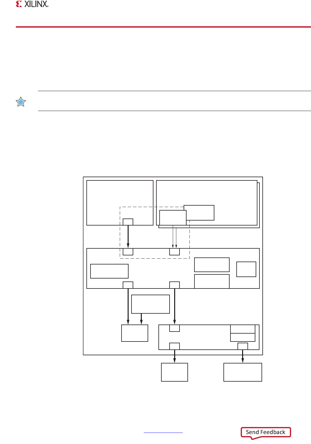
Zynq-7000 AP SoC Technical Reference Manual www.xilinx.com 137
UG585 (v1.12.1) December 6, 2017
Chapter 5: Interconnect
5.4 AXI_ACP Interface
The accelerator coherency port provides low-latency access to programmable logic masters, with
optional coherency with L1 and L2 cache. From a system perspective, the ACP interface has similar
connectivity as the APU CPUs. Due to this close connectivity, the ACP directly competes with them for
resource access outside of the APU block. Figure 5-5 gives an overview of the ACP connectivity.
IMPORTANT: The PL level shifters must be enabled by LVL_SHFTR_EN before PL logic communication
can occur.
Note: By default, all PS peripherals are set to secure Trustzone mode. This means that any
non-secure accesses indicated with AxPROT[1]=1 will receive a DECERR response.
For more information about the ACP interface, including its limitations, see Chapter 3, Application
Processing Unit.
X-Ref Target - Figure 5-5
Figure 5-5: ACP Connectivity Diagram
UG585_c5_05_101212
OCM
DDR
SCU
System
Interconnect
Cacheable
and Non-
cacheable
Accesses
Cacheable and Non-cacheable
Accesses to DDR, PL, Peripherals,
and PS Registers
System
Interconnect
APU
Accelerator Coherency
Port (ACP)
PL Logic
Cache Coherent
Transactions
M
S S
M0 M1
CPUs
Snoopable Data Buffers
And Caches
Read/Write
Requests
L1 Cache
Line Updates
Cache Tag
RAM Update
Flush Cache
Line to Memory Ta g
RAM
L2 Cache
S
M0 M1
Tag RAM
Data RAM
Maintain L1 Cache
Coherency

Zynq-7000 AP SoC Technical Reference Manual www.xilinx.com 138
UG585 (v1.12.1) December 6, 2017
Chapter 5: Interconnect
5.5 AXI_GP Interfaces
5.5.1 Features
AXI_GP features include:
• Standard AXI protocol
• Data bus width: 32
• Master port ID width: 12
• Master port issuing capability: 8 reads, 8 writes
• Slave port ID width: 6
• Slave port acceptance capability: 8 reads, 8 writes
5.5.2 Performance
These interfaces are connected directly to the ports of the master interconnect and the slave
interconnect, without any additional FIFO buffering, unlike the AXI_HP interfaces which has elaborate
FIFO buffering to increase performance and throughput. Therefore, the performance is constrained
by the ports of the master interconnect and the slave interconnect. These interfaces are for
general-purpose use only and are not intended to achieve high performance.
IMPORTANT: The PL level shifters must be enabled by LVL_SHFTR_EN before PL logic communication
can occur.
Note: By default, all PS peripherals are set to secure Trustzone mode. This means that any
non-secure accesses indicated with AxPROT[1]=1 will received a DECERR response.
PL bus master controllers attached to AXI general purpose ports (S_AXI_GP[1:0]) can access PS I/O
Peripherals and cannot access CPU Private Bus Registers.
5.6 PS-PL AXI Interface Signals
5.6.1 AXI Signals
AXI signals are identified in Tab le 5- 9. The PL level shifters must be enabled by the LVL_SHFTR_EN
register before PL logic communication can occur, refer to section 2.4 PS–PL Voltage Level Shifter
Enables.

Zynq-7000 AP SoC Technical Reference Manual www.xilinx.com 139
UG585 (v1.12.1) December 6, 2017
Chapter 5: Interconnect
Table 5-9: AXI Signals Summary
AXI Channel
AXI PS Masters AXI PS Slaves
M_AXI_GP{0,1} I/O
S_AXI_GP{0,1}
S_AXI_HP{0:3}
S_AXI_ACP
I/O
Clock, Reset
MAXIGP{0,1}ACLK I SAXIGP{0,1}ACLK
SAXIHP{0:3}ACLK
SAXIACPACLK
I
MAXIGP{0,1}ARESETN O SAXIGP{0,1}ARESETN
SAXIHP{0:3}ARESETN
SAXIACPARESETN
O
Read Address
MAXIGP{0,1}ARADDR[31:0] O SAXIGP{0,1}ARADDR[31:0]
SAXIHP{0:3}ARADDR[31:0]
SAXIACPARADDR[31:0]
I
MAXIGP{0,1}ARVALID O SAXIGP{0,1}ARVALID
SAXIHP{0:3}ARVALID
SAXIACPARVALID
I
MAXIGP{0,1}ARREADY I SAXIGP{0,1}ARREADY
SAXIHP{0:3}ARREADY
SAXIACPARREADY
O
MAXIGP{0,1}ARID[11:0] O SAXIGP{0,1}ARID[5:0]
SAXIHP{0:3}ARID[5:0]
SAXIACPARID[2:0]
I
MAXIGP{0,1}ARLOCK[1:0] O SAXIGP{0,1}ARLOCK[1:0]
SAXIHP{0:3}ARLOCK[1:0]
SAXIACPARLOCK[1:0]
I
MAXIGP{0,1}ARCACHE[3:0] O SAXIGP{0,1}ARCACHE[3:0]
SAXIHP{0:3}ARCACHE[3:0]
SAXIACPARCACHE[3:0]
I
MAXIGP{0,1}ARPROT[2:0] O SAXIGP{0,1}ARPROT[2:0]
SAXIHP{0:3}ARPROT[2:0]
SAXIACPARPROT[2:0]
I
MAXIGP{0,1}ARLEN[3:0] O SAXIGP{0,1}ARLEN[3:0]
SAXIHP{0:3}ARLEN[3:0]
SAXIACPARLEN[3:0]
I
MAXIGP{0,1}ARSIZE[1:0] O SAXIGP{0,1}ARSIZE[1:0]
SAXIHP{0:3}ARSIZE[2:0]
SAXIACPARSIZE[2:0]
I
MAXIGP{0,1}ARBURST[1:0] O SAXIGP{0,1}ARBURST[1:0]
SAXIHP{0:3}ARBURST[1:0]
SAXIACPARBURST[1:0]
I
MAXIGP{0,1}ARQOS[3:0] O SAXIGP{0,1}ARQOS[3:0]
SAXIHP{0:3}ARQOS[3:0]
SAXIACPARQOS[3:0]
I

Zynq-7000 AP SoC Technical Reference Manual www.xilinx.com 140
UG585 (v1.12.1) December 6, 2017
Chapter 5: Interconnect
~~
~
SAXIACPARUSER[4:0]
I
Read Data
MAXIGP{0,1}RDATA[31:0] I SAXIGP{0,1}RDATA[31:0]
SAXIHP{0:3}RDATA[63:0]
SAXIACPRDATA[63:0]
O
MAXIGP{0,1}RVALID I SAXIGP{0,1}RVALID
SAXIHP{0:3}RVALID
SAXIACPRVALID
O
MAXIGP{0,1}RREADY O SAXIGP{0,1}RREADY
SAXIHP{0:3}RREADY
SAXIACPRREADY
I
MAXIGP{0,1}RID[11:0] I SAXIGP{0,1}RID[5:0]
SAXIHP{0:3}RID[5:0]
SAXIACPRID[2:0]
O
MAXIGP{0,1}RLAST I SAXIGP{0,1}RLAST
SAXIHP{0:3}RLAST
SAXIACPRLAST
O
MAXIGP{0,1}RRESP[1:0] I SAXIGP{0,1}RRESP[2:0]
SAXIHP{0:3}RRESP[2:0]
SAXIACPRRESP[2:0]
O
~~
SAXIHP{0:3}RCOUNT[7:0]
~
O
~~
SAXIHP{0:3}RACOUNT[2:0]
~
O
~~
SAXIHP{0:3}RDISSUECAP1EN
~
I
Write Address
MAXIGP{0,1}AWADDR[31:0] O SAXIGP{0,1}AWADDR[31:0]
SAXIHP{0:3}AWADDR[31:0]
SAXIACPAWADDR[31:0]
I
MAXIGP{0,1}AWVALID O SAXIGP{0,1}AWVALID
SAXIHP{0:3}AWVALID
SAXIACPAWVALID
I
Table 5-9: AXI Signals Summary (Cont’d)
AXI Channel
AXI PS Masters AXI PS Slaves
M_AXI_GP{0,1} I/O
S_AXI_GP{0,1}
S_AXI_HP{0:3}
S_AXI_ACP
I/O

Zynq-7000 AP SoC Technical Reference Manual www.xilinx.com 141
UG585 (v1.12.1) December 6, 2017
Chapter 5: Interconnect
MAXIGP{0,1}AWREADY I SAXIGP{0,1}AWREADY
SAXIHP{0:3}AWREADY
SAXIACPAWREADY
O
MAXIGP{0,1}AWID[11:0] O SAXIGP{0,1}AWID[5:0]
SAXIHP{0:3}AWID[5:0]
SAXIACPAWID[2:0]
I
MAXIGP{0,1}AWLOCK[1:0] O SAXIGP{0,1}AWLOCK[1:0]
SAXIHP{0:3}AWLOCK[1:0]
SAXIACPAWLOCK[1:0]
I
MAXIGP{0,1}AWCACHE[3:0] O SAXIGP{0,1}AWCACHE[3:0]
SAXIHP{0:3}AWCACHE[3:0]
SAXIACPAWCACHE[3:0]
I
MAXIGP{0,1}AWPROT[2:0] O SAXIGP{0,1}AWPROT[2:0]
SAXIHP{0:3}AWPROT[2:0]
SAXIACPAWPROT[2:0]
I
MAXIGP{0,1}AWLEN[3:0] O SAXIGP{0,1}AWLEN[3:0]
SAXIHP{0:3}AWLEN[3:0]
SAXIACPAWLEN[3:0]
I
MAXIGP{0,1}AWSIZE[1:0] O SAXIGP{0,1}AWSIZE[1:0]
SAXIHP{0:3}AWSIZE[2:0]
SAXIACPAWSIZE[2:0]
I
MAXIGP{0,1}AWBURST[1:0] O SAXIGP{0,1}AWBURST[1:0]
SAXIHP{0:3}AWBURST[1:0]
SAXIACPAWBURST[1:0]
I
MAXIGP{0,1}AWQOS[3:0] O SAXIGP{0,1}AWQOS[3:0]
SAXIHP{0:3}AWQOS[3:0]
SAXIACPAWQOS[3:0]
I
~~
~
SAXIACPAWUSER[4:0]
I
Write Data
MAXIGP{0,1}WDATA[31:0] O SAXIGP{0,1}WDATA[31:0]
SAXIHP{0:3}WDATA[63:0]
SAXIACPWDATA[63:0]
I
MAXIGP{0,1}WVALID O SAXIGP{0,1}WVALID
SAXIHP{0:3}WVALID
SAXIACPWVALID
I
MAXIGP{0,1}WREADY I SAXIGP{0,1}WREADY
SAXIHP{0:3}WREADY
SAXIACPWREADY
O
Table 5-9: AXI Signals Summary (Cont’d)
AXI Channel
AXI PS Masters AXI PS Slaves
M_AXI_GP{0,1} I/O
S_AXI_GP{0,1}
S_AXI_HP{0:3}
S_AXI_ACP
I/O

Zynq-7000 AP SoC Technical Reference Manual www.xilinx.com 142
UG585 (v1.12.1) December 6, 2017
Chapter 5: Interconnect
5.6.2 AXI Clocks and Resets
Each interface has a single clock for all five channels that make up an interface. This clock is provided
by the PL.
All clocks must be active and all resets must be inactive on all PS-PL AXI interfaces for the GPV to
function properly. The entire PS might hang if this condition is not satisfied and a GPV access is
MAXIGP{0,1}WID[11:0] O SAXIGP{0,1}WID[5:0]
SAXIHP{0:3}WID[5:0]
SAXIACPWID[2:0]
I
MAXIGP{0,1}WLAST O SAXIGP{0,1}WLAST
SAXIHP{0:3}WLAST
SAXIACPWLAST
I
MAXIGP{0,1}WSTRB[3:0] O SAXIGP{0,1}WSTRB[3:0]
SAXIHP{0:3}WSTRB[7:0]
SAXIACPWSTRB[7:0]
I
~~
SAXIHP{0:3}WCOUNT[7:0]
~
O
~~
SAXIHP{0:3}WACOUNT[5:0]
~
O
~~
SAXIHP{0:3}WRISSUECAP1EN
~
I
Write Response
MAXIGP{0,1}BVALID I SAXIGP{0,1}BVALID
SAXIHP{0:3}BVALID
SAXIACPBVALID
O
MAXIGP{0,1}BREADY O SAXIGP{0,1}BREADY
SAXIHP{0:3}BREADY
SAXIACPBREADY
I
MAXIGP{0,1}BID[11:0] I SAXIGP{0,1}BID[5:0]
SAXIHP{0:3}BID[5:0]
SAXIACPBID[2:0]
O
MAXIGP{0,1}BRESP[1:0] I SAXIGP{0,1}BRESP[1:0]
SAXIHP{0:3}BRESP[1:0]
SAXIACPBRESP[1:0]
O
Table 5-9: AXI Signals Summary (Cont’d)
AXI Channel
AXI PS Masters AXI PS Slaves
M_AXI_GP{0,1} I/O
S_AXI_GP{0,1}
S_AXI_HP{0:3}
S_AXI_ACP
I/O

Zynq-7000 AP SoC Technical Reference Manual www.xilinx.com 143
UG585 (v1.12.1) December 6, 2017
Chapter 5: Interconnect
attempted. Therefore, no GPV access should be attempted if not all of the clocks for the PS-PL AXI
interfaces are connected and operating.
5.7 Loopback
Sometimes it can be advantageous to provide a loopback path from the PS to PL and back. A
loopback path means that there will be an AXI connection between a PS master and PS slave through
the PL, so that designs can manipulate AXI transaction address and/or data in the PL before the data
reaches the intended target in the PS. Such a loopback path typically includes a combinatorial shim
that translates the destination address from an address in the PL to an address in the PS.
It is not considered a loopback path if the AXI transaction from the PS is terminated in the PL, a
separate AXI transaction is created from the PL to the PS, and there is no interlocking dependency
between the two transactions.
In the AP SoC, the only allowed loopback path is from the GM ports to the HP ports within a set of
constraints. Note that HP0 and HP1 share an internal switch, and HP2 and HP3 shares an internal
switch. When there is a loopback path from the GM port to an HP port, there can be no other masters
than the loopback on the HP port being used, as well as the other HP port sharing its internal switch.
For an example, if there is a loopback path from GM1 port to HP1 port, then there can be no other
masters on both HP0 and HP1 ports. Similarly, if there is a loopback path from GM0 port to HP2 port,
then there can be no other masters on both HP2 and HP3 ports. See Figure 5-6.
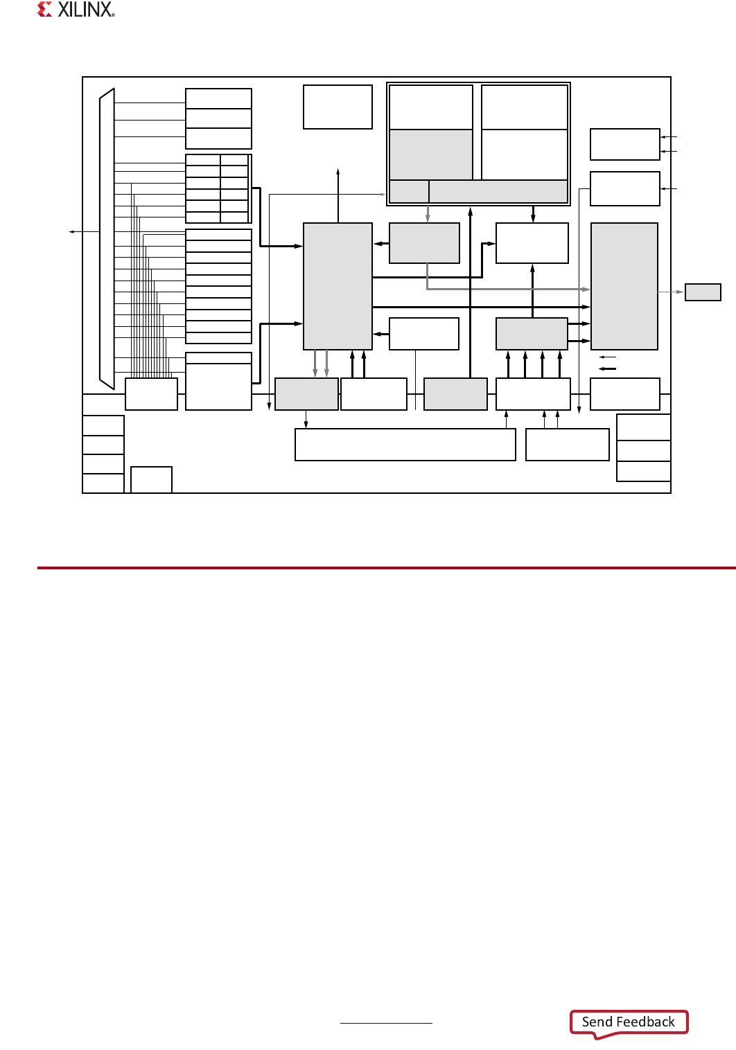
Zynq-7000 AP SoC Technical Reference Manual www.xilinx.com 144
UG585 (v1.12.1) December 6, 2017
Chapter 5: Interconnect
5.8 Exclusive AXI Accesses
This section provides a summary of AXI exclusive accesses support and details its architectural
limitations. Exclusive AXI accesses are most commonly generated by software in exclusive load and
store instructions to implement semaphore structures.
The two Cortex-A9 cores and PL masters from the S_ACP, S_GP and S_HP ports can perform exclusive
access. To succeed, exclusive accesses must also terminate to a slave that contains an exclusive
monitor. However, the only exclusive monitors in the PS are in L1 cache, and each of the four PS
DDRC ports (the OCM RAM does not have an exclusive monitor and so cannot accept exclusive
accesses). A user-created L3 exclusive monitor can also be potentially created in the PL.
5.8.1 CPU/L2
There are exclusive monitors in APU L1 cache, but not in the L2 level cache. This means the exclusive
access address must either terminate in L1 cache or L3 memory, but not in L2.
X-Ref Target - Figure 5-6
Figure 5-6: Loopback Path
PCIe
GTX
GTX
GTX
GTX
NOTE: The GTX and PCIe
functionality is available in
some of the Device Versions.
IRQ
20 I, 29 O
L2
Cache Memory
512 KB
DDR
Memory
Controller
16-bit
32-bit
16-bit w/ECC
DMA
8 channel
PCAP
Processor Config
Access Port
M_AXI_GP x 2
General Purpose
32-bit AXI Master
S_AXI_GP x 2
General Purpose
32-bit AXI Slave
S_AXI_HP x 4
AXI Data
32/64-bit Slave
SCU – Snoop Control Unit
Central
Interconnect
ARM A9
32 KB I-Cache
32 KB D-Cache
NEON
SP, DP FPU
128-bit Vector DSP
OCM
On Chip Memory
256 KB
S_AXI_ACP
AXI Coherent
64-bit Slave
Mem Switch
SLCR
System Level
Control
Registers
Security
Config
XADC
16 ch ADC
Quad-SPI
1,2,4,8-bit
Parallel 8-bit
NOR/SRAM
NAND 8,16-bit
UART
UART
SPI
SPI
I2C
I2C
CAN
CAN
TTC/WDT
PJTAG
Reset
CLK / PLL
ARM, I/O, DDR
PS_POR_B
PS_SRST_B
PS_CLK
32-bit AXI
64-bit AXI
DDR
CoreSight
Trace In
Trace Out
Cross Trigger
DAP
Loopback IPcore Other
Masters
APB
Register Access
Processing
System (PS)
EMIO
USB
USB
GigE
GigE
SD
SD
DMA
DMA
DMA
DMA
DMA
DMA
GPIO x54, x64
MIO
Pins
NEON
SP, DP FPU
128-bit Vector DSP
ARM A9
32 KB I-Cache
32 KB D-Cache
UG585_c5_06_121613
Programmable
Logic (PL)

Zynq-7000 AP SoC Technical Reference Manual www.xilinx.com 145
UG585 (v1.12.1) December 6, 2017
Chapter 5: Interconnect
To use the L1 exclusive monitor, the addressed MMU region must be set to be inner cacheable and
inner cache write-back with write-allocate. This allows an address targeted by a particular exclusive
access to always be allocated to L1 cache.
To use the L3 exclusive monitor, the access must not terminate at the APU L2 cache. From the ARM
CPU perspective, this means the address must be shareable, normal and non-cacheable. Also, the L2
cache controller shared override option (bit 22 in the L2 auxiliary control register) must be set in the
auxiliary control register. By default in the APU L2 cache controller, any non-cacheable shared reads
are treated as cacheable non-allocatable, while non-cacheable shared writes are treated as cacheable
write-through/no write-allocate. The L2 cache controller shared override option in the PL310
auxiliary control register overrides this behavior and prevents allocation into L2 cache.
5.8.2 ACP
The PL ACP port does not support exclusive access to coherent memory. Therefore, if the ACP needs
to perform exclusive accesses with the CPUs, the access must go to L3: DDR or PL.
5.8.3 DDRC
The following are the supported features for exclusive accesses to the PS DDR controller:
• The AXI port supports concurrent monitoring of two exclusive addresses (with different IDs).
• Burst type INCR/WRAP, length='h0 - 'hF, is supported.
• The slave supports OKAY and EXOKAY responses for exclusive accesses.
°According to the AXI specification, the slave sends out an EXOKAY response for successful
exclusive access transactions. For DDRC, this includes reads (up to two active) and writes
that match a preceding exclusive read transaction, if the monitored location(s) is still valid.
°If a monitored location is overwritten by another exclusive or non-exclusive write
transaction through any slave port before its corresponding exclusive write, the slave
returns an OKAY response for the exclusive write and will not update the corresponding
memory locations.
The DDRC exclusive monitor uses AXI bus ID to determine which master is doing the exclusive load
and store. While it is possible for a master to generate different IDs, a particular ID will always
originate from the same master. The master should also make sure to use the same ID for their LDREX
and STREX pair. Cortex-A9 processor will generate the same ID for its LDREX/STREX pair.
There are a some limitations:
1. While only two address locations (ranges) can be monitored concurrently by the DDRC, either of
these locations can be updated by another exclusive read transaction while the current
transactions have not been completed by their corresponding exclusive writes. In this case, the
exclusive write for an earlier monitored address location will receive an OKAY response. The

Zynq-7000 AP SoC Technical Reference Manual www.xilinx.com 146
UG585 (v1.12.1) December 6, 2017
Chapter 5: Interconnect
exclusive monitor picks the slot to be used using round-robin mechanism. An example exclusive
access sequence is shown inTabl e 5-1 0, assuming one AXI ID per master:
2. Exclusive access between different AXI ports is not supported because the monitors do not share
information with each other, thus the DDRC does not support exclusive access across different
ports. This means only masters that will access the same DDR port can do exclusive access to a
memory through DDR. Example master topologies able to perform exclusive access together are
shown in Table 5 -11 .
Table 5-10: Example DDR Port Behavior
Masters action DDR Port behavior
Master 1 issues exclusive load to address A Exclusive monitor 1 now has address A and master 1
recorded
Master 2 issues exclusive load to address B Exclusive monitor 2 now has address B and master 2
recorded
Master 3 issues exclusive load to address C Exclusive monitor 1 now has address C and master 3
recorded
Master 1 issues exclusive store to address A DDRC returns with OKAY, indicating exclusive access had
failed
Master 2 issues exclusive store to address B DDRC returns with EXOKAY, indicating exclusive access
successful
Master 3 issues exclusive store to address C DDRC returns with EXOKAY, indicating exclusive access
successful
Table 5-11: Example Master Topologies
Master Topology Can Perform Exclusives Accesses Together to DDRC?
A9 core 0, A9 Core 1 Yes
A9 core 0, ACP Yes
PL master on GP0/1 with Cortex-A9 No, GP0/1 ports and Cortex-A9 CPUs use different AXI DDRC
AXI ports.
Master on HP0 with master on HP1 Yes, (HP0 and HP1) and (HP2 and HP3) each share a common
DDRC AXI port.
Master on HP1 with master on HP2 No, HP1 and HP2 use different DDRC ports.
Master on GP0 with master HP0 No, GP0/1 ports and HP0-3 ports use different DDRC ports.
Master on GP0 with master on GP1 Yes, GP0/1 ports share a common DDRC AXI port.

Zynq-7000 AP SoC Technical Reference Manual www.xilinx.com 147
UG585 (v1.12.1) December 6, 2017
Chapter 5: Interconnect
5.8.4 System Summary
Exclusive AXI accesses are summarized inTab le 5- 12.
Table 5-12: Exclusive AXI Accesses Summary
Exclusive Operation
Exclusive
Accesses
Supported
Notes
Two A9 CPUs to L1 cache Yes Normal, inner-cacheable, write-back with write-allocate
memory regions only
ACP doing exclusive access to L1 No ACP does not support exclusive access to coherent
memory.
CPU0 and CPU1 to location in L2 No L2 does not have exclusive monitors.
Two A9 CPU and ACP do exclusive access
to DDR
Yes DDR only support two addresses per port for exclusive
access. If there are more than two masters, more than two
addresses might be involved, and it might cause live-lock.
Extra care should be taken to not get in a live-lock
situation.
ACP and one of the CPUs do exclusive
access to DDR
Yes Only two masters are allowed.
Exclusive access from two A9 CPUs to
DDR
Yes When L1 and L2 cache is disabled, or when memory is
marked as shared, normal, non-cacheable and the L2
shared override bit is set.
Masters on GP and HP ports doing
exclusive access to DDR:
• GP0 and GP1 can do exclusive access
with each other only
• HP0 and HP1 can do exclusive access
with each other only
• HP2 and HP3 can do exclusive access
with each other only
Yes DDRC cannot synchronize exclusive accesses across
separate DDRC AXI ports. If more than 2 PL masters or AXI
IDs are used per port of DDR, additional software is needed
to prevent live-lock.

Zynq-7000 AP SoC Technical Reference Manual www.xilinx.com 148
UG585 (v1.12.1) December 6, 2017
Chapter 6
Boot and Configuration
6.1 Introduction
Immediately after the PS_POR_B reset pin deasserts, the hardware samples the boot strap pins and
optionally enables the PS clock PLLs. Then, the PS begins executing the BootROM code in the
on-chip ROM to boot the system. The POR resets the entire device with no previous state saved. The
non-POR type resets also cause the BootROM to execute, but without the hardware sampling the
strap pins. After a non-POR reset, some registers values are preserved and the device is aware of its
previous security mode. Non-POR resets include the PS_SRST_B pin and several internal reset
sources.
The BootROM is the first software to run in the APU. The BootROM executes on CPU 0 and CPU 1
executes the wait-for-event (WFE) instruction. The main tasks of the BootROM are to configure the
system, copy the Boot Image FSBL/User code from the boot device to the OCM, and then branch the
code execution to the OCM. Optionally, the FSBL/User code can be executed directly from a
Quad-SPI or NOR device in a non-secure environment.
The PS Master boot device holds one or more boot images. A boot image is made up of the
BootROM Header (also referred to as the Boot Image Header) and the first stage boot loader (FSBL).
The boot device can also hold a bitstream to configure the PL and an embedded operating system,
but these are not accessed by the BootROM code. The flash memory device for boot can be
Quad-SPI, NAND, NOR, or SD card.
The BootROM execution flow is affected by the pin strap settings, the BootROM Header, and what
the BootROM code discovers about the system. The BootROM can execute in a secure environment
with encrypted FSBL/User code, or a non-secure environment. After the BootROM executes, the
FSBL/User code takes responsibility of the system as described in UG821, Zynq-7000 All
Programmable SoC Software Developers Guide.
For development, the system can be booted in JTAG mode. Or, JTAG can be enabled after a
non-secure flash device boot. JTAG always implies a non-secure environment, but it allows for access
to the ARM debug access port (DAP) controller in the CPU complex (APU) and the Xilinx test access
port (TAP) controller in the PL.
PS Master Boot Mode
In master boot mode, the system boots from a flash memory device. Here, the BootROM configures
the PS to access the boot device, reads the BootROM header, validates the header, and then usually
copies the FSBL/User code to the OCM memory. Master mode can be a secure or non-secure
environment.

Zynq-7000 AP SoC Technical Reference Manual www.xilinx.com 149
UG585 (v1.12.1) December 6, 2017
Chapter 6: Boot and Configuration
In secure mode, the boot image is always written to OCM memory by the CPU. From there, it is sent
(using DMA) in and out of the AES/HMAC units for decryption and authentication. The decrypted
boot image is written back to OCM memory and executed after the BootROM is finished. Security
hardware is described in this chapter and in Chapter 32, Device Secure Boot.
In non-secure mode, the BootROM header can instruct the PS to execute the boot image directly
from a Quad-SPI or NOR boot device that supports the execute-in-place option. In other cases, the
FSBL/User code is copied to the OCM memory for execution.
If the BootROM header in the flash device is invalid, the BootROM code searches for another header.
The header search continues until a valid header is found or the entire range has been searched. The
BootROM header search is supported for Quad-SPI, NAND, and NOR boot modes. For SD card boot
mode, only one header is read.
JTAG Slave Boot
In JTAG boot mode, the BootROM code does minimal system configuration and enables a JTAG
interface. Then, the system goes into an idle state waiting for the DAP controller to restart CPU 0. The
cascade JTAG boot mode loops the DAP and TAP controllers, and is the most common JTAG boot
mode. The independent JTAG boot mode connects the TAP controller to the PL JTAG pins and gives
time for the user to configure the PL using the TAP controller to connect the DAP controller to the
EMIO JTAG interface. The paths are shown in Figure 6-7, page 190.
In non-secure master boot mode, the JTAG interface is enabled for debug when the PL is
powered-up. The JTAG interface can be used to access the TAP and DAP controllers.
Boot and Configuration Subsections
Boot and Configuration is divided into the following sections:
•Figure 6-1
°Overview of bring-up and configuration
•Device Start-up
°Power-up, resets, clocks, Boot mode pins
•BootROM Code
°Execution flow, BootROM header
°Boot modes, image search, multiboot
°Error codes, system state post-BootROM
•Device Boot and PL Configuration
°PL initialization, configuration, and enable
°PS/PL bring-up examples
°PCAP bridge, JTAG (cascade/independent)
•Reference Section
°PL bring-up time factors, register overview, and device IDs
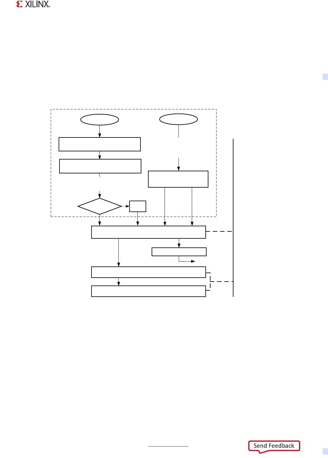
Zynq-7000 AP SoC Technical Reference Manual www.xilinx.com 150
UG585 (v1.12.1) December 6, 2017
Chapter 6: Boot and Configuration
Device Boot Flowchart
The POR reset causes the hardware to samples the pin straps, disable modules in the device, and
optionally enables the PS clock PLLs. These hardware actions are not performed after a non-POR
reset.
The first software to run is the BootROM code, then the FSBL/User code and system code. All of these
steps are shown in Figure 6-1.
BootROM and Header Parameters
The BootROM header includes a dozen parameters that guide the BootROM execution flow. For
example, the header includes a parameter to select the security mode: the Encryption Status
parameter. In secure mode, the FSBL/User code, bitstream, and other software are encrypted. The
BootROM has the ability to authenticate and decrypt the encrypted FSBL/User code. The header
itself is never encrypted.
As another example, the header includes the Length of Image parameter that defines the length of
the FSBL/User code that the BootROM loads into the OCM for execution. This code is limited to
192 KB in length. This parameter can be set to zero to indicate the desire to execute code directly
X-Ref Target - Figure 6-1
Figure 6-1: PS/PL Boot Process for Hardware and Software
325 1RQ325
5HVHWDOO5HJLVWHUV
+DUGZDUH6DPSOHV0RGHB3LQV
-7$*,23''5HWF
FRQWUROOHUVDUHGLVDEOHG
5HVHWVDOOUHJLVWHUVH[FHSW
WKHSHUVLVWHQWUHJLVWHUV
:LWKRUZLWKRXW
3RZHUXS
1RQ
6HFXUH
3//%\SDVV"
%RRW520([HFXWHV
(QDEOH
3//V
2SHUDWLQJ6\VWHP
)6%/8VHU&RGH
/RFNGRZQ
6HFXUH
,QLWLDOL]H&RQILJXUH(QDEOH
7KH)6%/8VHU$SSOLFDWLRQ
FRGHFDQFOHDUSURJUDPDQG
HQDEOHWKH3/
36+DUGZDUH)XQFWLRQV
)DLOXUH6XFFHVV
7KLVFRXOGEHDVHFXUH%RRW0RGH7KHPRGH
ZLOOEHGHWHUPLQHGE\WKH%RRW520XVLQJWKH
KHDGHU(QFU\SWLRQ6WDWXVSDUDPHWHU
6WDUWXS3RZHUXS
7KH3/KDUGZDUHLQFOXGHVD
VHOIVWDUWXSVHTXHQFHWR
SUHSDUHLWIRULQLWLDOL]DWLRQE\
WKH%RRW520RU8VHUFRGH
(UURU&RGH*HQHUDWHG
,QLWLDOL]H
7KH3/PXVWEHSRZHUHGXS
IRU6HFXUHPRGHRULIWKH
-7$*LQWHUIDFHLVUHTXLUHG
6WDJH
6WDJH
6WDJH
8*BFBB
3/7LPHOLQH
1R
<HV
5HWDLQWKHSUHYLRXV%RRW0RGHDV
6HFXUHRU1RQ6HFXUHXVLQJWKH
GHYFIJ&75/>6(&B(1@UHJLVWHUELW
IRUDFFHVVE\WKH%RRW520

Zynq-7000 AP SoC Technical Reference Manual www.xilinx.com 151
UG585 (v1.12.1) December 6, 2017
Chapter 6: Boot and Configuration
from the boot device (execute-in-place). All of the header parameters are described in section
6.3.2 BootROM Header.
The last two functions of the BootROM are to disable access to its ROM code and transfer CPU code
execution to the FSBL/User code. The execution of the BootROM is detailed in section
6.3.1 BootROM Flowchart.
PL Initialization and Configuration
The PL must be powered-up before it can be initialized and then configured with the bitstream. The
power-up and bring-up stages of the PL operate independently of the PS, but PL power up needs to
maintain a certain timing relationship with the POR reset signal of the PS. For more details refer to
section 6.3.3 BootROM Performance: PS_POR_B De-assertion Guidelines, page 179.
The PL can be under the control of FSBL/User code using GPIOs or serial interfaces to external
devices. Internally, the BootROM and FSBL/User code can determine the state of the PL power.
FSBL/User code can receive interrupts when the PL power state changes.
The PL boot process has four stages: start-up, initialize, configure, and enable. The start-up stage is
self-timed after power is ramped-up to a stable state. The initialization stage clears the SRAM cells in
the PL to prepare it for programming by the bitstream (configuration stage). The functional PS-PL
interfaces are then enabled under PS software control. The BootROM code does not configure the
PL, but it can read its status to determine when it can enable the PL JTAG chain and also when it
needs to use the HMAC/AES decryption hardware.
Secure PS Images and PL Bitstreams
The secure environment starts with an encrypted boot process where the PS software acts as the
system master and the BootROM reads an encrypted FSBL/user code image from the selected flash
memory device and processes it using the hardened, PL based Hash-based Message Authentication
Code (HMAC) and an Advanced Encryption Standard (AES) module with a Cipher Block Chaining
Mode (CBC). These modules are accessed from the PS through the DevC interface and the
downstream Processor Configuration Access Port (PCAP) located in the PL.
The BootROM verifies that the PL has power before attempting to decrypt the FSBL/User code. After
the PS has finished executing the BootROM, the PL can be configured by the FSBL/user software
using an encrypted bitstream or the PL can be configured or reconfigured later.
The low-level secure environment starts at the I/O pin activity and all potential access points to the
PS operating environment. The secure operating environment is maintained through the BootROM
execution and transferred to a secure software operating environment.
Various device configuration functions and operating examples are described in section 6.4 Device
Boot and PL Configuration. The details of secure boot are covered in Chapter 32, Device Secure Boot.
Security at the operating system level are described in WP429, TrustZone Technology Support in
Zynq-7000 All Programmable SoC. The BootROM can also authenticate files using RSA, refer to section
32.2.5 RSA Authentication.

Zynq-7000 AP SoC Technical Reference Manual www.xilinx.com 152
UG585 (v1.12.1) December 6, 2017
Chapter 6: Boot and Configuration
Software Developers Guide and Kit
The boot modes and operations are summarized in chapter 3 of the UG821 Zynq-7000 Software
Developers Guide. The chapter describes boot methods and ways to program the hardware using the
FSBL. The software developers guide also discusses software architectures, tools, and various boot
environments, including Linux U-Boot.
The software developers kit (SDK) can be used to develop and debug bare-metal applications. It can
also be used to create FSBL/User code boot images and application programs running on an
operating system.
6.1.1 PS Hardware Boot Stages
The PS hardware boot stages include power supply ramping, clocking, resets, pin strap sampling and
PLL initialization. The PL can be powered up while the PS boots up. The PL boot process is described
in section 6.1.7 PL Boot Process.
External PS Control Pins
Within 45 clock cycles of the PS_CLK reference clock, the hardware samples the seven Boot Mode
strap pins (see Figure 6-4) and stores their settings in read-only registers. The strap pins define the
initial voltage sensitivity for the MIO input buffers, select the JTAG chain route, and select the flash
device that contains the boot image. Development boards automatically deassert the PS_POR_B
reset pin after the board is powered-up. These boards also include a POR reset button that can be
used to generate a POR reset. A non-POR system reset can be generated using the PS_SRST_B reset
pin. The details of the PS hardware boot functions are described in section 6.2 Device Start-up.
PS PLL Initialization
The PS PLLs are enabled by MIO pin 6, the BOOT_MODE[4] strap pin. When the PLLs are enabled, the
execution of the BootROM is delayed until the PLL outputs lock. If the PLLs are not enabled, the
PS_CLK reference clock input pin is bypassed around the PLLs and the clock subsystem is driven at
the frequency of PS_CLK input. The PLL clocks are described in section 6.2.3 Clocks and PLLs and in
Chapter 25, Clocks.
6.1.2 PS Software Boot Stages
The PS software boot process is controlled by the BootROM and then the FSBL/User code. The
BootROM code operation is influenced by the boot strap pins, the BootROM Header, and what the
BootROM code detects in the system.
Stage 0 (BootROM: BootROM Header)
Hard-coded BootROM executes on the primary CPU (CPU 0) after a power-on reset (POR) or
non-POR system reset (PS_SRST_B, debug, watchdog, software). The BootROM reads the BootROM
Header programmed into the boot flash device to determine the boot flow and transitions to
stage 1. After the hardware boot sequence, both CPUs start executing the same BootROM code

Zynq-7000 AP SoC Technical Reference Manual www.xilinx.com 153
UG585 (v1.12.1) December 6, 2017
Chapter 6: Boot and Configuration
located at address 0x0 (where the BootROM is initially located) to determine their own identity. Note
that single-core devices contain one processor, dual-core devices contain two. CPU 1, when present,
parks itself by executing the WFE instruction. CPU 0 continues to execute the BootROM.
Stage 1 (FSBL / User code)
This is generally the First Stage Boot Loader, but it can be any user-controlled code. Refer to UG821,
Zynq-7000 All Programmable SoC Software
Developer
s Guide for details about the FSBL.
Stage 2 (U-Boot / System / Application)
This is generally the system software, but it could also be a second stage boot loader (SSBL). This
stage is also completely within user control and is not described in this chapter. Refer to UG821,
Zynq-7000 All Programmable SoC Software Developers Guide for details about FSBL and stage 2
images.
6.1.3 Boot Device Content
The boot device can store multiple components and multiple versions of the components:
• BootROM Header (required by BootROM)
• FSBL/User code ELF file (required by BootROM)
• PL Bitstream (not accessed by BootROM)
• System/Application ELF file (not accessed by BootROM)
The BootROM Header is detailed in section 6.3.2 BootROM Header. The FSBL/User code
requirements are described in UG821, Zynq-7000 All Programmable SoC Software Developers Guide.
6.1.4 Boot Modes
The boot modes include the four master boot mode devices and two JTAG slave boot modes.
Flash Devices (Master Mode Boot)
When the system boots from a flash memory device, it is considered a Master Mode boot. The
following boot devices are described in subsections of section 6.3 BootROM Code:
• Quad-SPI with optional Execute-in-Place mode
•SD Memory Card
•NAND
• NOR with optional Execute-in-Place mode
Specific devices that Xilinx recommends for each boot interface are listed in AR# 50991.

Zynq-7000 AP SoC Technical Reference Manual www.xilinx.com 154
UG585 (v1.12.1) December 6, 2017
Chapter 6: Boot and Configuration
JTAG (Slave Mode Boot)
The JTAG boot mode is considered a Slave Mode boot and is always a non-secure boot mode. The
JTAG chain can be configured in cascade or independent mode. During the boot sequence, the chain
is configured according to the setting of the MIO [2] boot strapping pin. Normally, the system is
configured for cascade mode. When the TRM refers to JTAG boot mode, it means JTAG cascade mode
unless stated otherwise. The JTAG interface is enabled in all non-secure boot modes.
• Cascade JTAG chain (most popular):
°Access DAP and TAP controllers through PL JTAG.
• Independent JTAG chain (common):
°Access TAP controller through PL JTAG.
°Access DAP controller through EMIO JTAG via SelectIO pins after configuring the PL with a
bitstream.
• Independent JTAG chain (rarely used):
°Access TAP controller through PL JTAG.
°Access DAP controller through MIO PJTAG.
The JTAG interfaces are discussed in section 6.4.5 PL Control via User-JTAG and detailed in
Chapter 27, JTAG and DAP Subsystem.
6.1.5 BootROM Execution
The BootROM execution begins soon after a POR or non-POR reset. A POR reset causes the Hardware
Boot stage to occur and then starts the BootROM execution. A non-POR reset skips the hardware
stage and starts the BootROM execution almost immediately.
The BootROM executes the on-chip ROM code to perform the system boot process. The BootROM
disables all access to the ROM code before transferring code execution over to the FSBL/User code.
Details of how the system memory is remapped are shown in Figure 6-11, page 203.
Early in the BootROM execution, it sets up the APU and performs some self-checking. It reads the
boot mode pin information and, if the boot mode is not JTAG, the BootROM configures the controller
for the selected boot device. The BootROM reads the BootROM Header to further configure the
system for the desired boot process. In addition to the BootROM Header, the boot device provides
the first stage boot loader (FSBL) and/or user code that takes over system control when the
BootROM is done.
The boot device can also provide an image for the operating system, refer to UG821, Zynq-7000 All
Programmable SoC Software Developers Guide. BootROM execution is detailed in section
6.3.1 BootROM Flowchart. The BootROM Header is described in 6.3.2 BootROM Header.
Secure Boot
The BootROM can operate in non-secure or secure mode depending on the configuration setup by
the BootROM Header. In secure mode, the FSBL/User code is moved from the flash device, decrypted
and written into the OCM memory. The CPU executes the code from the OCM.

Zynq-7000 AP SoC Technical Reference Manual www.xilinx.com 155
UG585 (v1.12.1) December 6, 2017
Chapter 6: Boot and Configuration
If the system is booted in secure mode and then reset by a non-POR reset with a BootROM Header
that indicates a non-secure boot, then the system goes into a secure lockdown with error code
0x201A.
BootROM Header Search
If the BootROM does not detect a valid BootROM Header, the BootROM performs a search function
to find another BootROM Header. The search function is described in section 6.3.10 BootROM
Header Search. BootROM Header search is supported for Quad-SPI, NAND and NOR boot modes.
The BootROM Header is never encrypted and the search functions work with an encrypted or
un-encrypted FSBL/User code images.
BootROM Execution Influencers
The BootROM is influenced by different conditions. Some are intentional, others are not.
•Pin strapping
• Reset signal pins
• Validity of the BootROM Header (checksum for header search)
• BootROM Header boot mode and conflicts that cause lockdown errors
Error Detection, Device Lockdown and Error Codes
If the BootROM detects an error while executing the BootROM Header, it locks down the system and
generate an error code. There are two lockdown types:
• Secure Lockdown (no access to device, requires a POR to restart the system).
• Non-secure Lockdown (JTAG might be enabled and any system reset can restart the system to
run the BootROM again).
When a lockdown occurs, the error code is written into the slcr.REBOOT_STATUS register. The error
codes are listed in Table 6-20, page 199.
6.1.6 FSBL / User Code Execution
The FSBL/User code executes after the BootROM is finished. The FSBL/User code reconfigures the PS
as needed and optionally configures the PL. The BootROM loads the FSBL/User code into the OCM
unless the execute-in-place option is enabled. The FSBL/User code operations:
• Initialize the PS using the PS7 Init data that is generated by Vivado tools (MIO, DDR, etc.)
• Program the PL using a bitstream (if provided).
• Load the second stage bootloader or bare-metal application code into DDR memory.
• Hand off system control to the second stage bootloader or bare-metal application.
The FSBL/User code requirements are explained in UG821, Zynq-7000 All Programmable SoC Software
Developers Guide. FSBL code can be generated by the Vivado SDK for bare-metal applications.

Zynq-7000 AP SoC Technical Reference Manual www.xilinx.com 156
UG585 (v1.12.1) December 6, 2017
Chapter 6: Boot and Configuration
The user code can force the device into a secure lockdown, if desired, by writing to the devcfg.CTRL
[FORCE_RST] bit. A POR reset is required to start up the system from this and all secure lockdowns.
FSBL Image Fallback and Multiboot
If the FSBL detects an error or wants to use a different FSBL image, then it writes the boot image
address to the devcfg.MULTIBOOT_ADDR [MULTIBOOT_ADDR] field and performs a software system
reset. This is briefly described in section 6.3.11 MultiBoot. Also refer to UG821, Zynq-7000 All
Programmable SoC Software Developers Guide for information on how to use both fallback and
multiboot.
6.1.7 PL Boot Process
The PL boot process includes start-up, initialization, configuration, and enable.
• Start-up (power-up the PL voltage).
• Initialization (using PS software or INIT/PROGRAM control pins).
• Configuration (through PS PCAP, JTAG, or PL ICAP).
• Enable PS-PL Interface (using PS software).
These steps and their subcomponents are illustrated in Figure 6-1, page 150.
6.1.8 PL Configuration Paths
The PL can be configured and reconfigured by PS software in secure or non-secure mode. The PCAP
path is the most commonly deployed method as it does not require that the PL be pre-programmed
with a bitstream. The PL can also be configured by the TAP controller on the JTAG chain in
non-secure mode. Multiplexing of the datapath is done in the PL configuration module using the
devc.CTRL [PCAP_MODE] and [PCAP_PR] bits. Also refer to section 6.5 Reference Section.
• JTAG debug using TAP Controller (common for development):
°Non-secure
°Initialize and configure the PL through the TAP controller.
•PS PCAP path (common for deployment):
°Secure or non-secure.
°Initialize and configure the PL through the device configuration interface (DevC).
•ICAP path (not a common option):
°Secure or non-secure.
°Reconfiguration only by logic instantiated in the PL.
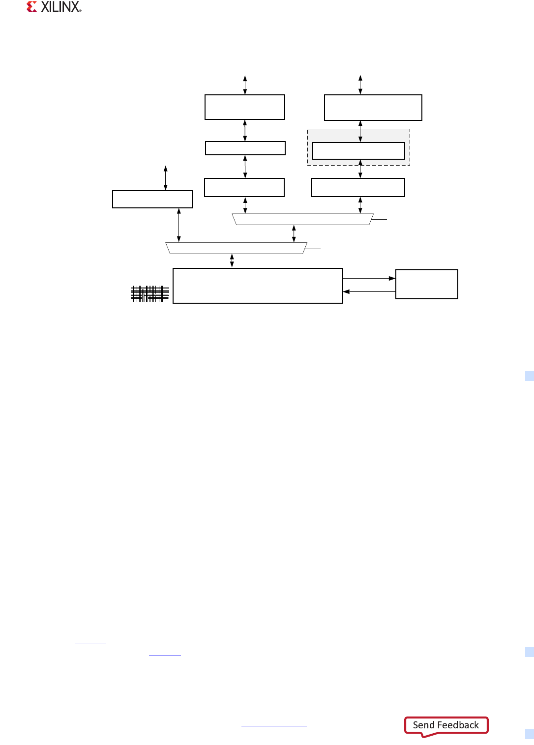
Zynq-7000 AP SoC Technical Reference Manual www.xilinx.com 157
UG585 (v1.12.1) December 6, 2017
Chapter 6: Boot and Configuration
TAP Controller
The TAP controller can be assessed by any of the JTAG interfaces as shown in Figure 27-1, page 718.
To enable the JTAG debug path, make sure the other controllers are finished using the PL
configuration module and then set the [PCAP_MODE] bit = 0. The TAP controller is often used in a
debug/development environment. This path is always non-secure.
PCAP Controller
The connection for the PCAP controller is explained in section 6.1.9 Device Configuration Interface.
To enable the PCAP path, make sure the other controllers are finished using the PL configuration
module and then set the [PCAP_MODE] and [PCAP_PR] bits = 1. The PCAP path is often used for
deployment. This path can be secure or non-secure.
ICAP Controller
The connection for the ICAP controller is explained in the product guide and data sheet for the
AXI_HWICAP pcore. To enable the ICAP path from the ICAP controller to the PL configuration
module, make sure the other controllers are finished using the PL configuration module and then set
the [PCAP_MODE] bit = 1 and the [PCAP_PR] bit = 0. The ICAP path is used when a MicroBlaze
processor is controlling the PL reconfiguration or as an alternative to the PCAP path. This path can be
secure or non-secure. For secure mode, the system must maintain a secure environment as described
in UG821, Zynq-7000 All Programmable SoC Software Developers Guide for the FSBL and, for the
operating system, WP429, TrustZone Technology Support in Zynq-7000 All Programmable SoC.
X-Ref Target - Figure 6-2
Figure 6-2: PL Configuration Paths
PL pre-programmed.
Encrypted
DevC with DMA
TAP Controller
PS Software
AES/HMAC
Units
PCAP Path
JTAG
Debug
Serial
Interface
ICAP Path
AXI_HWICAP
PL Configuration Module
Processes Bitstreams
Non-secure
PL Logic
PL or PS-based
Software
PCAP Controller ICAP Controller
Fabric
Decrypted
devc.CTRL [PCAP_PR]
Multiplexer 01
Multiplexer 10 devc.CTRL [PCAP_MODE]
8*BFBB

Zynq-7000 AP SoC Technical Reference Manual www.xilinx.com 158
UG585 (v1.12.1) December 6, 2017
Chapter 6: Boot and Configuration
IMPORTANT: The ICAP must be configured for x32 mode in the PL design. If the ICAP is configured
for x8 mode or x16 mode, the PS connection to the PCAP will break after the PL bitstream has loaded.
6.1.9 Device Configuration Interface
The device
confi
guration interface (DevC) includes three logic modules to initialize and configure the
PL under PS software control (PCAP path), manage device security, and access the XADC. The DevC also
includes a set of control/status registers for these three main functional modules.
Features
• PCAP Bridge with DMA is used by the PS software to configure the PL and decrypt images. This
provides the PS software with a path to the PL Configuration module. This path can:
°Decrypt a secure FSBL/User code.
°Process secure and non-secure PL bitstreams; download/upload concurrently.
°Process PL bitstream compression commands as needed.
• Security Management Module monitors system activity to maintain a secure operating
environment.
°Basic device security management.
°Enforce system-level security, including debug controls.
•XADC interface provides the PS software with access to the Analog-to-Digital converters in the
PL, refer to Chapter 30, XADC Interface.
°Serial interface.
°Alarm and over-temperature interrupts.
Block Diagram
The top part of Figure 6-3 connects to the PS AXI interconnect and the lower part connects to the PL.
DevC Control and Status Registers
The APB registers are used to configure and read the status of the DevC. They are memory mapped
in PS address space 0xF800_7000, refer to Table 4-7, page 116. The registers are summarized in
Table 6-26, page 223.
Interrupts and Status Bits
Interrupts can be generated from any of the three modules in the DevC block. These interrupts are
enabled and controlled by register bits before driving the DevC interrupt signal (IRQ ID# 40) to the
PS system interrupt controller (GIC).
There are interrupts and status bits to determine the state of the PL, the activity of the DMA
controller in the PCAP bridge, and for the XADC operations.
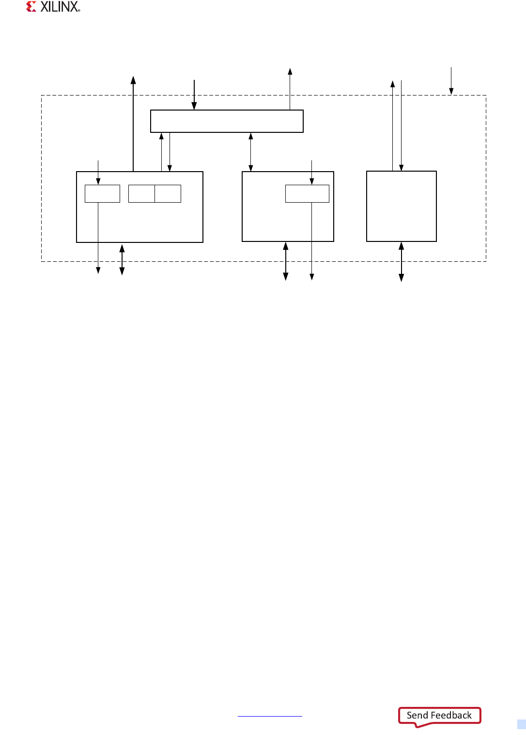
Zynq-7000 AP SoC Technical Reference Manual www.xilinx.com 159
UG585 (v1.12.1) December 6, 2017
Chapter 6: Boot and Configuration
PCAP Bridge Module
For deployment, the PCAP bridge is a main component in the configuration of the PL and to
decrypt/authenticate the images. The bridge is described in various subsections of section
6.4 Device Boot and PL Configuration.
Device Security Module
The DevC contains a security management module that provides these functions:
• Monitors the system security and can assert a security reset when conflicting status is detected
that could indicate inconsistent system configuration or tampering.
• Controls and monitors the PL configuration logic through the APB interface.
• Controls the ARM CoreSight debug access port (DAP) and debug levels.
• Disables the on-chip BootROM code at the end of BootROM execution to protect its contents
from being read by setting the write-once devcfg.ROM_SHADOW register.
The device security features and functions are described in Chapter 32, Device Secure Boot.
XADC Interface
The XADC interface is one path to access the hardened analog-to-digital converters in the PL voltage
domain. The two other paths and the information on how to access the XADC are described in
Chapter 30, XADC Interface.
X-Ref Target - Figure 6-3
Figure 6-3: DevC Block Diagram
36$;,,QWHUFRQQHFW
3&$3,QWHUIDFH
%LWVWUHDP$(6+0$&
8*BFBB
$;,3&$3%ULGJH
&RQWURO6WDWXV5HJLVWHUV
$;,
0DVWHU '0$
(QJLQH
'HYLFH
&RQILJXUDWLRQ
,QWHUIDFH
'HY&
6HFXULW\6LJQDOV
6HFXUH/RFNGRZQ
520GLVDEOH
2WKHUV
36$;,,QWHUFRQQHFW
$3%,QWHUIDFH
'HY&,54
,QWHUUXSWV
DQG&RQWURO
36
3/
VODYH
&38B[FORFN
3/
6HFXULW\
0DQDJHPHQW
0RGXOH
;$'&
;$'&
,QWHUIDFH
'LYLGHE\
RU
'LYLGHE\
RU
3&$3FORFN 3&$3B[FORFN
PDVWHU
6HULDO
,QWHUIDFH

Zynq-7000 AP SoC Technical Reference Manual www.xilinx.com 160
UG585 (v1.12.1) December 6, 2017
Chapter 6: Boot and Configuration
6.1.10 Starting Code on CPU 1
CPU 0 is in charge of starting code execution on CPU 1. The BootROM puts CPU 1 into the Wait for
Event mode. Nothing has been enabled and only a few general purpose registers have been
modified to place it in a state where it is waiting at the WFE instruction.
There is a small amount of protocol required for CPU 0 to start an application on CPU1. When CPU 1
receives a system event, it immediately reads the contents of address 0xFFFFFFF0 and jumps to that
address. If the SEV is issued prior to updating the destination address location (0xFFFFFFF0), CPU 1
continues in the WFE state because 0xFFFFFFF0 has the address of the WFE instruction as a safety
net. If the software that is written to address 0xFFFFFFF0 is invalid or points to uninitialized memory,
results are unpredictable.
Only ARM-32 ISA code is supported for the initial jump on CPU 1. Thumb and Thumb-II code is not
supported at the destination of the jump. This means that the destination address must be 32-bit
aligned and must be a valid ARM-32 instruction. If these conditions are not met, results are
unpredictable.
The steps for CPU 0 to start an application on CPU 1 are as follows:
1. Write the address of the application for CPU 1 to 0xFFFFFFF0.
2. Execute the SEV instruction to cause CPU 1 to wake up and jump to the application.
The address range 0xFFFFFE00 to 0xFFFFFFF0 is reserved and not available for use until the stage 1
or above application is fully functional. Any access to these regions prior to the successful start-up
of the second CPU causes unpredictable results.
6.1.11 Development Environment
For development and debug, the JTAG interface provides access to the DAP and TAP controllers for
system control. These controllers provide a wide range of capabilities for the developer. The
developer also has the optional ability to access the ARM Test Port User Interface (TPUI) to have a
high bandwidth debug datapath from the APU to the debug tools. These test and debug features are
described in Chapter 27, JTAG and DAP Subsystem.
In JTAG boot mode, a flash device is not required, but can be part of the system. When booting from
a flash device in non-secure mode, the JTAG interface and DAP/TAP controllers can be enabled for
debug and test.
In JTAG boot mode, the BootROM disables access to the hard-coded ROM memory, as usual, and
then executes the WFE instruction in the CPU. JTAG boot mode has control flexibility for a
development environment with access to the PS AXI interconnect via the DAP controller shown in
Figure 5-1, page 120.
The JTAG I/O connections are explained in Chapter 27, JTAG and DAP Subsystem. The debug
environment is described in Chapter 28, System Test and Debug.
Zynq-7000 AP SoC Technical Reference Manual www.xilinx.com 161
UG585 (v1.12.1) December 6, 2017
Chapter 6: Boot and Configuration
6.2 Device Start-up
This section includes the following subsections:
•section 6.2.1 Introduction
•section 6.2.2 Power Requirements
•section 6.2.3 Clocks and PLLs
•section 6.2.4 Reset Operations
•section 6.2.5 Boot Mode Pin Settings
•section 6.2.6 I/O Pin Connections for Boot Devices
6.2.1 Introduction
The Zynq-7000 device start-up requires proper voltage sequencing and I/O pin control. The flow of
the BootROM is controlled by the type of reset, the boot mode pin settings, and the Boot Image. The
BootROM expects certain pin connections for the selected boot device.
IMPORTANT: Zynq-7000 AP SoC devices have power, clock, and reset requirements that must be met
for successful BootROM execution. The data sheets and this section describe the requirements.
6.2.2 Power Requirements
The BootROM power requirements for the PS and PL are shown in Tabl e 6 -1 . Power control is
discussed in Chapter 24, Power Management. Power supply voltage and ramp time requirements are
specified in the data sheet.
In the early stages of BootROM execution, the BootROM checks if the PL is powered up. If it is not
powered-up, the BootROM continues with execution. If the PL is powered up, the BootROM initiates
a cleaning cycle. The BootROM waits up to 90 seconds for the cleaning to occur. If the cleaning does
not finish in this amount of time, then a secure lockdown occurs.
If the PL is needed by the BootROM, it waits for up to 90 seconds for the PL to power-up. If the PL
does not power-up in this time frame, then the system shuts down without providing an error code.
Table 6-1: PS and PL Power Requirements
Boot Option Secure After
POR Reset PS Power PL Power
NAND, NOR, SD card, or Quad-SPI Yes Required Required
No Required Not required
PL JTAG and EMIO JTAG Required Required
MIO JTAG Required Not required

Zynq-7000 AP SoC Technical Reference Manual www.xilinx.com 162
UG585 (v1.12.1) December 6, 2017
Chapter 6: Boot and Configuration
PL Power-Down
The PL power-down sequence includes stopping the use of all signals between the PS and PL,
disabling the voltage level shifters, and powering off the PL. An example sequence is shown in
section 2.4 PS–PL Voltage Level Shifter Enables.
6.2.3 Clocks and PLLs
The PS_CLK reference clock is routed to multiple sections of the device, including the three PS clock
PLLs. The frequency of the PS_CLK affects the boot time of the device. The PLLs multiply the PS_CLK
to generate high frequency clocks for various system clock modules. When needed, the PLLs can be
bypassed to deliver the PS_CLK frequency directly to the system clock modules.
If the PLLs are enabled, then the PS_CLK must be stable before the PLLs are enabled and must remain
stable. The clock frequency must be within its operating range as specified in the data sheet.
If the PLLs are bypassed, the PS_CLK can be toggled as slow as desired and up to its rated input
frequency. This can be used to single-step the bring-up processes, control the clock with software, or
operate the system at a low clock frequency. Operating the system at a low clock frequency might
preclude the use of some modules within the device (e.g., the USB ULPI clock must be at a lower
frequency than the CPU_1x clock).
The device clocks, PS PLLs, and system clock modules are detailed in Chapter 25, Clocks.
Note: The maximum frequency during BootROM execution is 500 MHz across all speed grade
specifications.
6.2.4 Reset Operations
There are two types of system resets: POR and non-POR. The details of the system resets are
described in Chapter 26, Reset System. All of these resets cause the BootROM to execute.
POR Reset
The POR resets reset the whole system, including all of the registers. All states except the eFuse and
BBRAM are lost.
• PS_POR_B pin, described in more detail, below.
Non-POR Resets
Non-POR reset events are recorded in the slcr.REBOOT_STATUS register. A non-POR reset also causes
the BootROM to execute, but the BootROM retains knowledge about the security level of the
previous boot in the devcfg.CTRL [SEC_EN] bit. Not all of the registers are reset by a non-POR reset,
refer to Table 26-2, page 715.
The non-POR reset sources include:
• PS_SRST_B pin, described in more detail, below.
• Internal system resets

Zynq-7000 AP SoC Technical Reference Manual www.xilinx.com 163
UG585 (v1.12.1) December 6, 2017
Chapter 6: Boot and Configuration
External Reset Signal Pins
There are two external reset pins, PS_POR_B and PS_SRST_B:
PS_POR_B: The POR reset is the only reset to sample the boot mode pin strap resistors. For the
power-up sequence, the PS_POR_B input is required to be asserted Low until VCCPINT, VCCPAUX and
VCCO_MIO0 have reached their minimum operating levels to ensure PS eFUSE integrity.
For the power-down sequence, at least one of the four following conditions is required before
VCCPINT reaches 0.80V (the condition must be held True until VCCPINT reaches 0.40V to ensure PS
eFUSE integrity):
• PS_POR_B input is asserted Low,
• Reference clock to the PS_CLK input is disabled,
•V
CCPAUX is lower than 0.70V, or
•V
CCO_MIO0 is lower than 0.90V.
Note: PS_POR_B must not be de-asserted during a certain timing window relative to when the
last PL power supply starts to ramp. Asserting PS_POR_B during this window can cause a
lock-down event. Refer to section 6.3.3 BootROM Performance: PS_POR_B De-assertion
Guidelines, page 179 for more details.
PS_SRST_B: This reset is used to force a system reset. It can be tied or pulled High, and can be High
during the PS power supply ramp-up. The PS_SRST_B reset is a non-POR reset.
Note: The PS_SRST_B signal must not be asserted while the BootROM is executing from a POR
reset, otherwise a lock-down event occurs and prevents the BootROM from completing the
system boot process. To recover from this type of lockdown, the PS_POR_B reset must be
asserted. The time taken by Boot ROM to complete its execution and handoff to the FSBL/user
application depends on the several factors. Please refer to Boot Time Reference, page 221 for
details on how to arrive at the boot time for a specific user configuration.
Reset Signal Sequencing
The reset sequencing required for boot are illustrated in Figure 6-4. The effects of the resets are
described in this chapter and in Chapter 26, Reset System. If PS_SRST_B is asserted while the
BootROM is executing, then a system lockdown occurs without an error code being generated.
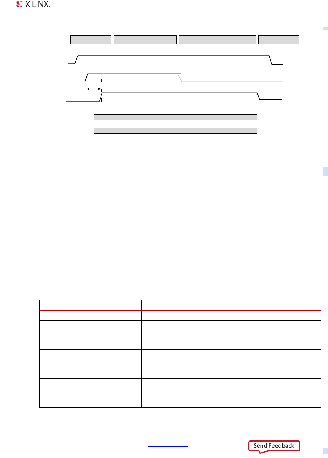
Zynq-7000 AP SoC Technical Reference Manual www.xilinx.com 164
UG585 (v1.12.1) December 6, 2017
Chapter 6: Boot and Configuration
Internal Resets
The internal resets are all non-POR resets. Resets are described in Chapter 26, Reset System.
• Software controlled reset: write 1 to slcr.PSS_RST_CTRL [SOFT_RST].
• Watchdog timers: AWDT0, AWDT1, and SWDT controllers.
• JTAG interface and debug.
Reset Reason
The type of reset that last occurred (reset reason) is recorded in the slcr.REBOOT_STATUS register.
This register also includes the BootROM error code, when it is generated. The register is accessible
to the BootROM and FSBL/User code. The Reboot Status register is reset by a POR reset, but
preserved by a non-POR reset.
X-Ref Target - Figure 6-4
Figure 6-4: Power and Reset Sequencing Waveform
PS-PL power
PS_CLK
(PLL enabled)
PS_SRST_B
PS_POR_B
PS_CLK
(PLL bypass)
Stable High Freq Clock
0 to 60 MHz Clock Transitions
BootROM Executes
Minimum of 2 μs
PS_SRST_B must stay High
Power On FSBL, User Code, OS
UG585_c6_04_100317
PS_SRST_B can be driven Low to reset
the system after BootROM executes
Power Off
Table 6-2: Reboot Status Register
slcr.REBOOT_STATUS Bit Source
[REBOOT_STATE] 31:24 R/W bit field that remains persistent through all non-POR resets.
Reserved 23 Reserved.
[POR] 22 PS_POR_B reset signal. This is the only reset set after a POR reset.
[SRST_B] 21 PS_SRST_B reset signal.
[DBG_RST] 20 Debug command in the DAP controller.
[SLC_RST] 19 Write to the slcr.PSS_RST_CTRL [SOFT_RST] bit.
[AWDT1_RST] 18 CPU 1 watchdog timer.
[AWDT0_RST] 17 CPU 0 watchdog timer.
[SWDT_RST] 16 System watchdog timer.
[BOOTROM_ERROR_CODE] 15:0 BootROM, refer to Tab l e 6 -20.

Zynq-7000 AP SoC Technical Reference Manual www.xilinx.com 165
UG585 (v1.12.1) December 6, 2017
Chapter 6: Boot and Configuration
System Reset Effects
The effects of the system resets (POR and non-POR) are summarized in Tab le 6- 3.
User Defined Persistent Bit Field
The 16-bit user defined persistent bit field is located in the devcfg.MULTIBOOT_ADDR register, bits
31:16. These register bits are R/W and persist through a non-POR reset (PS_SRST, watchdog, etc.).
The [USERDEF_PERSISTENT] bit field can be used to pass status and command information between
one non-POR FSBL/User code boot and another.
6.2.5 Boot Mode Pin Settings
There are 7 boot mode strapping pins that are hardware programmed on the board using MIO pins
[8:2]. They are sampled by the hardware soon after PS_POR_B deasserts and their values are written
to software readable registers for use by the BootROM and user software. The board hardware must
connect each strapping pin, MIO [8:2], to a 20 kΩ pull-up or pull-down resistor. The encoding of the
mode pins are shown in Ta bl e 6- 4. A pull-up resistor specifies a logic 1 and a pull-down resistor
specifies a logic 0.
Five pins, BOOT_MODE[4:0], are used to select the boot mode, JTAG chain config, and if the PLLs are
bypassed. The sampled values of these pins are written into the slcr.BOOT_MODE [BOOT_MODE] and
[PLL_BYPASS] bit fields.
• Boot modes are explained in section 6.3 BootROM Code.
• Boot strap pins are listed in Tabl e 6 -4 .
• JTAG chains are described in section 6.4.5 PL Control via User-JTAG.
• PLLs are described in section 6.2.3 Clocks and PLLs.
Table 6-3: System Reset Effects
Reset Type POR Non-POR
Sample Pin Straps Yes No
Initialize PS PLLs(1) Yes, by the hardware Yes, by the BootROM
PS RAM (FIFOs, buffers, etc.) Cleared Cleared
IOP clocks Disabled Disabled
BootROM executes Yes Yes
Retains previous boot mode No Yes
Reboot Status register Resets it Accumulates the system reset type.
Device Registers All Persistent registers.(2)
Resets PL Yes Yes
Notes:
1. The Boot_Mode [4] pin strap determines if the PLLs are enabled or bypassed.
2. There are a number of register and individual register bit fields that are not affected by a non-POR
reset. Refer to Table 26-2, page 715 for a list.
Zynq-7000 AP SoC Technical Reference Manual www.xilinx.com 166
UG585 (v1.12.1) December 6, 2017
Chapter 6: Boot and Configuration
Two pins, VMODE[1:0], are used to select the voltage signaling levels for the two MIO voltage banks.
The sampled values of these pins are written into the slcr.GPIOB_DRVR_BIAS_CTRL [RB_VCFG] and
[LB_VCFG] bit fields. The VMODE settings are used by the BootROM to initially set the
MIO_PIN_{53:00} registers to the selected I/O signaling standard. VMODE[0] controls MIO pins 15:0
and VMODE[1] controls MIO pins 53:16. A pull-up causes the BootROM to select LVCMOS18. A
pull-down selects LVCMOS33 which is deemed compatible with LVCMOS25. The MIO pin I/O
programming descriptions are described in the slcr.MIO_PIN_00 register definition in Appendix B,
Register Details.
The FSBL/User code can change the initial boot mode settings for the JTAG chain, the PLLs and the
I/O voltage standard for the MIO pins on individual MIO pin basis.
6.2.6 I/O Pin Connections for Boot Devices
The BootROM expects certain external pins to be connected. Some pins connections are necessary
for all boot modes. Others depend on the boot mode pin straps and the BootROM Header. After the
BootROM executes, user code can reconfigure the I/O pin connections as desired.
Table 6-4: Boot Mode MIO Strapping Pins
Pin-signal /
Mode
MIO[8] MIO[7] MIO[6] MIO[5] MIO[4] MIO[3] MIO[2]
VMODE[1] VMODE[0] BOOT_MODE[4] BOOT_MODE[0] BOOT_MODE[2] BOOT_MODE[1]BOOT_MODE[3]
Boot Devices
JTAG Boot Mode; cascaded is most
common(1) 000
JTAG Chain Routing(2)
0: Cascade mode
1: Independent mode
NOR Boot(3) 001
NAND 010
Quad-SPI(3) 100
SD Card 110
Mode for all 3 PLLs
PLL Enabled 0Hardware waits for PLL to lock, then executes BootROM.
PLL
Bypassed 1Allows for a wide PS_CLK frequency range.
MIO Bank Voltage(4)
Bank 1 Bank 0 Voltage Bank 0 includes MIO pins 0 thru 15.
Voltage Bank 1 includes MIO pins 16 thru 53.
2.5 V, 3.3 V 00
1.8 V 11
Notes:
1. JTAG cascaded mode is most common and is the assumed mode in all the references to JTAG mode except where noted.
2. For secure mode, JTAG is not enabled and MIO[2] is ignored.
3. The Quad-SPI and NOR boot modes support execute-in-place (this support is always non-secure)
4. Voltage Banks 0 and 1 must be set to the same value when an interface spans across these voltage banks. Examples
include NOR, 16-bit NAND, and a wide TPIU test port. Other interface configuration may also span the two banks.

Zynq-7000 AP SoC Technical Reference Manual www.xilinx.com 167
UG585 (v1.12.1) December 6, 2017
Chapter 6: Boot and Configuration
• Connections required for all boot configurations:
°PS power supply
°PS_POR_B, PS_SRST_B, and PS_CLK_B
• MIO connections for specific boot devices
°Quad-SPI (auto detect 1, 2, 4, or 8-bit interface)
°SD memory card (SDIO 0, MIO pins 40-47)
°NAND (auto detect 8 or 16-bit interface)
°NOR (CS 0)
°JTAG (PLJTAG interface), normally used in Cascade Chain mode
6.3 BootROM Code
The BootROM executes after a system reset to configure the PS as described in the introduction. This
section provides the details of the boot process, the format of the BootROM Header, the BootROM
performance with examples, the functions and needs of each boot device, the various boot images,
and the boot failure error codes.
This section includes the following subsections:
•6.3.1 BootROM Flowchart
•6.3.2 BootROM Header
•6.3.3 BootROM Performance
•6.3.4 Quad-SPI Boot
•6.3.5 NAND Boot
•6.3.6 NOR Boot
•6.3.7 SD Card Boot
•6.3.8 JTAG Boot
•6.3.9 Reset, Boot, and Lockdown States
•6.3.10 BootROM Header Search
•6.3.11 MultiBoot
•6.3.12 BootROM Error Codes
•6.3.13 Post BootROM State
•6.3.14 Registers Modified by the BootROM – Examples
6.3.1 BootROM Flowchart
Zynq-7000 configuration starts after a system reset. The overall boot process is illustrated in
Figure 6-1, page 150 and the BootROM execution is shown in Figure 6-5, page 170. CPU 0 executes
the BootROM code with the DAP and TAP JTAG controllers disabled. The DDR memory controller and
other peripherals are not initialized by the BootROM.

Zynq-7000 AP SoC Technical Reference Manual www.xilinx.com 168
UG585 (v1.12.1) December 6, 2017
Chapter 6: Boot and Configuration
The PL power-up and initialization sequences can occur in parallel with or after the PS start-up. If the
BootROM needs the PL powered up, then early in the BootROM execution the BootROM writes to the
devcfg.CTRL [PCFG_PROG_B] bit and waits for the devcfg.STATUS [PCFG_INIT] bit to assert before
proceeding with BootROM execution.
PL power is needed for PCAP access and image decryption. The BootROM tests the PL state before
accessing its resources using a 90 second timeout. The PROGRAM_B device pin must be held High
during the boot process. Holding the PROGRAM_B device pin Low during the boot process causes a
device lockdown event.

Zynq-7000 AP SoC Technical Reference Manual www.xilinx.com 169
UG585 (v1.12.1) December 6, 2017
Chapter 6: Boot and Configuration
Secure/Non-Secure
For security reasons, CPU 0 is always the first device out of reset among all master modules within
the PS. CPU 1 is held in an WFE state. While the BootROM is running, JTAG is always disabled,
regardless of the reset type, to ensure security. After the BootROM runs, JTAG is enabled if the boot
mode is non-secure.
The BootROM code is also responsible for loading the FSBL/User code. When the BootROM releases
control to stage 1, user software assumes full control of the entire system. The only way to execute
the BootROM again is by generating one of the system resets. The FSBL/User code size, encrypted
and unencrypted, is limited to 192 KB. This limit does not apply with the non-secure
execute-in-place option.
The PS boot source is selected using the BOOT_MODE strapping pins (indicated by a weak pull-up or
pull-down resistor), which are sampled once during power-on reset (POR). The sampled values are
stored in the slcr.BOOT_MODE register.
The BootROM supports encrypted/authenticated, and unencrypted images referred to as secure boot
and non-secure boot, respectively.
The BootROM supports execution of the stage 1 image directly from NOR or Quad-SPI when using
the execute-in-place option, but only for non secure boot images. Execute-in-place is possible only
for NOR and Quad-SPI boot modes.
In secure boot, the CPU, running the BootROM code, decrypts and authenticates the user PS image
on the boot device, stores it in the OCM, and then branches to it.
In non-secure boot, the CPU, running the BootROM code, disables all secure boot features including
the AES unit within the PL before branching to the user image in the OCM memory or the flash
device (if execute-in-place is used).
Any subsequent boot stages for either the PS or the PL are your responsibility and are under your
control. The BootROM code is not accessible to you. Following a stage 1 secure boot, you can
proceed with either secure or non-secure subsequent boot stages. Following a non-secure first stage
boot, only non-secure subsequent boot stages are possible.
Boot Sources
There are five possible boot sources: NAND, NOR, SD card, Quad-SPI, and JTAG. The first four boot
sources are used in master boot methods in which the CPU loads the external boot image from
nonvolatile memory into the PS.
JTAG is the slave boot mode, and is only supported with a non-secure boot. An external host
computer acts as the master to load the boot image into the OCM through a JTAG connection. The
PS CPU remains in idle mode as the boot image is loaded.
The configuration flow for the BootROM is shown in Figure 6-5.
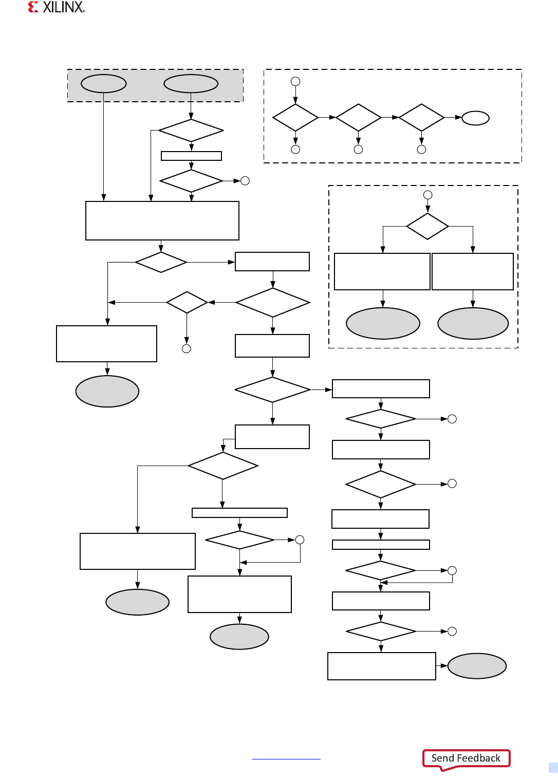
Zynq-7000 AP SoC Technical Reference Manual www.xilinx.com 170
UG585 (v1.12.1) December 6, 2017
Chapter 6: Boot and Configuration
X-Ref Target - Figure 6-5
Figure 6-5: BootROM Configuration Flowchart
%RRW0RGH" %RRW520+HDGHU
6HDUFK
9DOLG+HDGHU
)RXQG"
%
(QFU\SWLRQ
6WDWXV" &KHFNLI3/LV3RZHUHG8S
3HUIRUP1RQVHFXUH
%RRW0RGH5HJLVWHU
,QLWLDOL]DWLRQ
56$(QDEOHG" &
([HFXWHIURP2&0
([HFXWHLQSODFH
3HUIRUP6HFXUH%RRW0RGH
5HJLVWHU,QLWLDOL]DWLRQ
33.
9HULILHG"
&
8*BFBB
325
33.9HULILFDWLRQH)XVH33.+DVK 6+$33.
63.6LJQDWXUH9HULILFDWLRQ56$33.63.6LJQDWXUH 3DGGLQJ__6+$63.
)6%/6LJQDWXUH9HULILFDWLRQ56$63.)6%/6LJQDWXUH 3DGGLQJ__6+$)6%/&HUWLILFDWH,PDJH
63.
9HULILHG"
)6%/
9HULILHG"
%
1R
<HV
%
<HV
%
<HV
6HFXUH/RFNGRZQ
([LWXVLQJ325UHVHW
56$
6HFXUH
1RQ6HFXUH
1R 1R
5HWXUQ
&38&38
DUHLQ:)(VWDWH
-7$* )ODVK'HYLFH
6HFXUH
%
6WDWH"
3UHYLRXVO\
6HFXUHDQG
1RQ325
3UHYLRXVO\
1RQ6HFXUH
2U325
4XDG63,RU
125RQO\
<HV
1R
1R
<HV
<HV
1R
([HFXWHLQSODFH ([HFXWH
IURP2&0
1RQ325
6HFXUHRU
1RQVHFXUH
%RRW520
([HFXWHV
1RQVHFXUH6HWXS
520&RGHDFFHVVLVGLVDEOHG
-7$*LVHQDEOHG
%UDQFKWR8VHU&RGHLQ)ODVK'HYLFH
1RQVHFXUH6HWXS
520&RGHDFFHVVLVGLVDEOHG
-7$*LVHQDEOHG
%UDQFKWR8VHU&RGHLQ2&0
6HFXUH6HWXS
520&RGHDFFHVVLVGLVDEOHG
%UDQFKWR8VHU&RGHLQ2&0
'HFU\SWWKH)6%/XVLQJ
3&$3DQGORDGLQWR2&0
([HFXWHIURP2&0
1RQVHFXUH6HWXS
520&RGHDFFHVVLVGLVDEOHG
-7$*LVHQDEOHG
,VVXH:)(,QVWUXFWLRQ
<HV
1R
56$
6\VWHP
6WDWH"
1RQ6HFXUH
&38&38
DUHLQ:)(VWDWH
1RQVHFXUH/RFNGRZQ
520&RGHDFFHVVLVGLVDEOHG
-7$*LVHQDEOHG
,VVXH:)(,QVWUXFWLRQ
/RFNGRZQ
6HFXUH/RFNGRZQ
&OHDQ363/
&OHDQDOOLQWHUQDO5$0V
6\VWHPKHOGLQUHVHW
6HFXUHDQG1RQVHFXUH
1R
/RDGWKH)6%/LQWRWKH2&0
/RDGWKH)6%/LQWRWKH2&0
56$
%RRW520,QLWLDOL]HVWKH$38
%RRW520,QLWLDOL]HV6\VWHP)XQFWLRQ
520&5&FKHFNRSWLRQDO
0,2IRUERRWGHYLFH
3/,QLWLDOL]DWLRQLILWVSRZHUHGXS
36+DUGZDUH)XQFWLRQV 6HH)LJXUH
7KH3//LV
HLWKHUDOUHDG\
VWDEOHRULV
E\SDVVHG
3//7LPH2XW" %
<HV
1R
6HFXUH
/RFNGRZQ
3//%\SDVVHG"
<HV
1R
,QLW3//V
6HFXUHDQG1RQVHFXUH
6HFXULW\VWDWHWR
EHGHWHUPLQHG
/RDG%RRW520+HDGHU
6HFXULW\VWDWHGHILQHG
(QDEOHDQG/RFNWKH6HFXUH
6WDWHRIWKH6\VWHP
%6HFXUH/RFNGRZQ
7LPH2XW"
([HFXWH
LQSODFH" %
<HV 6HFXUH/RFNGRZQ
&
<HV
56$(QDEOHG"
3DVV+0$&" %6HFXUH/RFNGRZQ
([HFXWH
LQSODFH"
1R
Zynq-7000 AP SoC Technical Reference Manual www.xilinx.com 171
UG585 (v1.12.1) December 6, 2017
Chapter 6: Boot and Configuration
APU Initialization
The BootROM configures the APU and MIO multiplexer to support the boot process. The state of the
MIO pins for each boot mode is described in tables in the Boot Device sections (for example,
Tabl e 6-9 for Quad-SPI). The BootROM uses CPU 0 to execute the ROM code. CPU 1 executes the WFE
instruction. The caches and TLBs are invalidated. The BootROM configures the MMU and other
system resources to meet the needs of the BootROM execution. The state of the APU is described in
section 6.3.13 Post BootROM State.
Note: FSBL/User code and operating system software must configure the APU for their own needs
and should consider the CPU initialization steps described in section Chapter 3, Application
Processing Unit.
6.3.2 BootROM Header
The BootROM requires a header for all master boot modes (flash devices). In JTAG slave boot mode,
the BootROM Header is not used and the BootROM code does not load the FSBL/User code.
The BootROM Header parameters are shown in Tab le 6- 5 with their word number, byte address
offset, and applicability for the three types of device boot modes.
Note: The BootROM Header is referred to as the Boot Image Header in UG821, Zynq-7000 All
Programmable SoC Software Developers Guide. They both refer to the same table of parameters
provided in Table 6 -5.
Table 6-5: BootROM Header Parameters
Header Address 32-bit
Word Parameter
Boot Device
Secure
Usage
Non-Secure
Usages
OCM OCM Execute In
Place (6)
0x000 - 0x01F 0 - 7 Interrupt Table for
Execution-in-Place no no yes
0x020 8 Width Detection Quad-SPI Quad-SPI Quad-SPI
0x024 9 Image Identification yes yes yes
0x028 10 Encryption Status yes yes yes
0x02C 11 FSBL/User Defined (3) ~~~
0x030 12 Source Offset yes yes ~
0x034 13 Length of Image yes yes set = 0
0x038 14 FSBL Load Address ~ ~ set = 0
0x03C 15 Start of Execution yes yes yes
0x040 16 Total Image Length note (1) note (2) set = 0
0x044 17 QSPI Config Word ,set to 0x01 ~~~
0x048 18 Header Checksum yes yes yes
0x04C - 0x097 19 - 39 FSBL/User Defined (76-Byte)(3) ~~~

Zynq-7000 AP SoC Technical Reference Manual www.xilinx.com 172
UG585 (v1.12.1) December 6, 2017
Chapter 6: Boot and Configuration
Interrupt Table for Execution-in-Place — 0x000 to 0x01C
Eight 32-bit words are reserved for interrupt mapping. This is useful for execute-in-place for NOR
and Quad-SPI devices. It allows the CPU vector table to be managed in two ways. The first is to use
the MMU to remap the flash linear address space to 0x0. The second method to manage the vector
table location is to use the coprocessor VBAR register. For more information on setting this register,
refer to the ARM v7-AR Architecture Reference Manual (listed in Appendix A, Additional Resources).
Width Detection — 0x020
Width Detection is required for the Quad-SPI boot mode. Ensure that the BootROM Header includes
the value of 0xAA995566 so the BootROM can determine the maximum hardware I/O data
connection width of the flash device(s). This value helps the BootROM to determine the data width of
a single Quad-SPI device (x1, x2, or x4) and to detect a second device in 8-bit parallel I/O
configuration. If this value is not present for the Quad-SPI boot mode then the BootROM lockdowns
the system and generates an error code. The error code number depends on other conditions. The
error codes are listed in Table 6-20, page 199. Details of the detection operation are explained in
section 6.3.4 Quad-SPI Boot.
0x0A0 - 0x89F 40 - 551 Register Initialization
(2048-Byte) (4) yes yes yes
0x8A0 - 0x8BF 552 - 559 Image Header(3) yes yes yes
0x8C0 - 0x8FF 560 - 576 Partition Header yes yes yes
0x900 577 and up FSBL Image or User Code 192 KB 192 KB see (5)
Notes:
1. In secure mode, the Total Image Length parameter is greater than Length of Image parameter because of
encryption.
2. In non-secure OCM mode, the Total Image Length parameter must be set equal to the Length of Image parameter.
3. The FSBL/User Defined parameter and FSBL Image and User Code fields are not used by the BootROM code and
do not affect the hardware. See UG821, Zynq-7000 All Programmable SoC Software Developers Guide for more
information.
4. The addresses that can be accessed by Register Initialization is restricted, see Ta b l e 6 - 7 . The secure boot mode has
more address restrictions than a non-secure boot.
5. The size of the FSBL image (or User code) for Execute-in-place depends on the allowed capacity of the boot device
less the 0x8C0 (the size of the BootROM Header). The maximum Quad-SPI size is described in section
6.3.4 Quad-SPI Boot. For NOR, refer to section 6.3.6 NOR Boot.
6. To select the execute-in-place feature, set the Length of Image and Total Image Length parameters to 0 and load
the PS interconnect address into the Source Offset.
Table 6-5: BootROM Header Parameters (Cont’d)
Header Address 32-bit
Word Parameter
Boot Device
Secure
Usage
Non-Secure
Usages
OCM OCM Execute In
Place (6)
Zynq-7000 AP SoC Technical Reference Manual www.xilinx.com 173
UG585 (v1.12.1) December 6, 2017
Chapter 6: Boot and Configuration
Image Identification — 0x024
This word has a mandatory value of 0x584C4E58,'XLNX'. This value allows the BootROM (along with
the header checksum field) to determine that a valid BootROM Header is present. If the value is not
matched, the BootROM code performs a Header search if the boot mode is either Quad-SPI, NAND,
or NOR. If the boot mode is SD card, the BootROM lockdowns the system and generates an error
code.
Encryption Status — 0x028
Encryption Status determines if the boot is secure (the boot image is encrypted) or non-secure
mode. Valid values for this field are:
•0xA5C3C5A3 Encrypted FSBL/User code (requires eFUSE key source).
•0x3A5C3C5A Encrypted FSBL/User code (requires battery-backed RAM key source).
•Not
0xA5C3C5A3 or 0x3A5C3C5A. Non-encrypted FSBL/User code (no key).
The eFuse states and the encryption status word determines the source of the encryption key, if any.
The valid combination are shown in Tab le 6 - 6.
FSBL/User Defined — 0x02C
This word is used to store the BootROM header version. Refer to UG821, Zynq-7000 All
Programmable SoC Software Developers Guide for more information. The BootROM does not
interpret or use this field.
Source Offset — 0x030
This parameter contains the number of bytes from the beginning of the valid BootROM Header to
where the FSLB/User code image resides. This offset must be aligned to a 64-byte boundary and must be
at or above address offset 0x8C0 from the beginning of the BootROM Header.
Length of Image — 0x034
This word contains the byte count of the load image to transfer to the OCM. For non-secure mode,
the Length of Image equals the Total Image Length parameter and has a maximum value of 192 KB.
For secure mode, the Length of Image is set equal to the length of the image after it has gone
Table 6-6: BootROM Requirements for Encryption Status Word
eFuse States (described in Table 32-2, page 779)
eFuse Secure Boot Not Blown Not Blown Blown
BBRAM Key Disable Not Blown Blown Don’t Care
Encryption Status Word
Non-secure Okay Okay Lockdown
Secure with BBRAM Key Okay Lockdown Lockdown
Secure with eFuse Key Okay Okay Okay

Zynq-7000 AP SoC Technical Reference Manual www.xilinx.com 174
UG585 (v1.12.1) December 6, 2017
Chapter 6: Boot and Configuration
through the authentication and decryption process steps. In this case, the Length of Image is always
less than 192 KB because of the encryption overhead.
A value of zero with a Quad-SPI or NOR flash mode causes the BootROM to execute the FSBL/User
code from the associated flash device without copying the image to OCM (execute-in-place).
FSB Load Address— 0x038
Destination address to which to copy the FSBL.
Start of Execution — 0x03C
• This is a byte address that is relative to the start of system memory and is used for both
executing the FSBL/User code from the OCM or using the optional execute-in-place feature of
Quad-SPI and NOR boot modes. The byte address must be aligned to a 64-byte boundary.
FSBL/User code executes from OCM:
°Execution attempts outside of the OCM memory address space cause a secure lockdown.
°Non-secure mode: address must be equal to or greater than 0x0 and less than 0x30000.
°Secure mode: the address must equal 0x0.
• Execute-in-place FSBL/User code:
°The address must point to a location within the first 16 MB of memory for x4 Quad-SPI and
the first 32 MB of memory for NOR and dual x8 parallel Quad-SPI boot modes.
Total Image Length — 0x040
This is the total number of bytes loaded into the OCM by the BootROM from the flash memory.
For non-secure boot, the Total Image Length parameter must be set equal to the Length of Image
parameter.
For secure images, the Total Image Length parameter includes the HMAC header, the encryption
overhead and the alignment requirements and is always larger than the Length of Image parameter.
The Total Image Length parameter is provided by the design tools.
QSPI Config Word — 0x044
QSPI configuration word, hard-coded to 0x01.
Header Checksum — 0x048
The is the checksum value of the header which is checked prior to using the data within the header.
The checksum is calculated by summing the words from 0x020 to 0x044 and inverting the result.
FSBL/User Defined— 0x04C to 0x097
This can be used in Bootgen using the udf_data field of the BIF file. Refer to Appendix-A in UG821,
Zynq-7000 All Programmable SoC Software Developers Guide for more information.

Zynq-7000 AP SoC Technical Reference Manual www.xilinx.com 175
UG585 (v1.12.1) December 6, 2017
Chapter 6: Boot and Configuration
Boot Header Table Offset — 0x098
Pointer to Image Header table.
QSPI Config Word — 0x09C
Pointer to the Partition Header table.
Register Initialization Parameters — 0x0A0 to 0x89C
This region contains 256 pairs of address and data words that can be used to initialize PS registers for
the MIO multiplexer, boot device clocks, and other functions before the FSBL/User code is accessed
from the boot device; either to copy the image to the OCM or to execute-in-place. The register writes
are commonly used to optimize the boot device interface and set its clock frequency to maximize
performance.
A register initialization pair appears as two 32-bit words, first a register address, then a register write
value. Register initializations can be in any order, and the same register can be initialized with
different values as many times as desired. The register initialization is performed prior to copying the
FSBL/User code so the user can modify the default reset register values to reduce the time to access
the code and process it.
The BootROM stops processing the Register Initialization list when either the address register =
0xFFFF_FFFF or the end of the list (256 address/write data pairs).
Usage of the register initialization parameters are explained in the “Register Initialization to Optimize
Boot Times” section of section 6.3.3 BootROM Performance.
Restricted Addresses
The register address space for the Register Initialization address-data writes is restricted. Register
addresses outside of the allowed address range cause the BootROM to lockdown the system and
generate error code 0x2111. The allowed register accesses depend on the boot mode and are listed
in Tab le 6-7 .
These restrictions are enforced by the BootROM. They do not apply when the FSBL/User code begins
to execute. The BootROM screens the register initialization writes and disallows certain addresses
from being accessed.
Table 6-7: BootROM Accessible Address Ranges for Register Initialization
Control Registers Non-Secure Boot Mode Secure Boot Mode
Ranges Exceptions to Range(1)
UART 1 E000_1000 to E000_1FFC ~No
Quad-SPI E000_D000 to E000_DFFC ~No
SMC E000_E000 to E000_EFFC ~No
SDIO 0 E010_0004 to E010_0FFC E010_0058 No
DDR Memory F800_6000 to F800_6FFC ~No

Zynq-7000 AP SoC Technical Reference Manual www.xilinx.com 176
UG585 (v1.12.1) December 6, 2017
Chapter 6: Boot and Configuration
FSBL/User Defined — 0x8A0 - 0x8BF
This memory area may be used by the FSBL or User code. Refer to UG821, Zynq-7000 All
Programmable SoC Software Developers Guide for more information.
FSBL Image or User Code Start Address — 0x8C0
The FSBL Image or User Code must start at or above this location. The location is pointed to by the
Source Offset parameter and must be aligned to 64 bytes.
6.3.3 BootROM Performance
The BootROM performance is an important factor to the total bring-up time of the system that
includes: Power-up, BootROM execution, FSBL/User code execution, U-boot time, and OS loading
time. The entire boot and configuration process is explained in section 6.4 Device Boot and PL
Configuration.
Below are a few topics related to BootROM execution that include using the Register Initialization
mechanism in the BootROM Header to optimize the bandwidth of the flash device interface. The
flash device bandwidth is the single most important factor in speeding up boot times.
SLCR registers
PLL, Peripheral, AMBA and
CPU clock controls F800_0100 to F800_0234 Reserved: F800_01B0
PS Reset Ctrl: F800_0200
PLL, Peripheral and
PL clock controls:
F800_0100 to F800_01AC
SWDT Reset F800_024C ~
SWDT clock,
TZ configuration,
PS ID code,
DDR configuration,
MIO pins, SD card WP/CD
routing
F800_0304 to F800_0834 ~
Reserved F800_0A00 to F800_0A8C ~
Rese r v e d , G P I O a n d D DR I/O
controls F800_0AB0 to F800_0B74 ~
UART 0, USB, I2C, SPI, CAN,
GPIO, GigE, TTC, DMAC,
SWDT, DDR, DevC, AXI HP
Not accessible Not accessible
Notes:
1. The registers in this column are not accessible by the Register Initialization writes.
Table 6-7: BootROM Accessible Address Ranges for Register Initialization (Cont’d)
Control Registers Non-Secure Boot Mode Secure Boot Mode
Ranges Exceptions to Range(1)

Zynq-7000 AP SoC Technical Reference Manual www.xilinx.com 177
UG585 (v1.12.1) December 6, 2017
Chapter 6: Boot and Configuration
Typical BootROM Execution
The BootROM time is measured from when the system powers-up to when the BootROM branches to
the FSBL/User code:
1. PS Power-up time, see table in section 6.5 Reference Section.
2. PS PLL lock time, see PS PLL Lock Time.
3. BootROM CRC check of ROM code (if enabled).
4. PL ready time (TPOR) required when the PL is required:
°Voltage ramp-up – time depends on the power supply performance.
°PL Cleaning – time depends on the size of the device.
5. BootROM Header register initialization writes to optimize the flash device interface bandwidth.
6. BootROM normally copies FSBL/User code to OCM memory and optionally performs decryption
and authentication:
°BootROM RSA authentication, if enabled by eFuse.
°BootROM AES/SHA decryption/authentication (secure boot).
7. BootROM branches to FSBL/User code.
Start-up details and PL configuration information is provided in section 6.4 Device Boot and PL
Configuration.
PS PLL Lock Time
The PLL is enabled by a pin strap. If the PLL is in bypass mode and then enabled by PS software, the
PLL with take some time to lock. The length of time is specified by the tLOCK_PSPLL parameter in the
data sheet. The programming of the PLLs are described in section 25.10.4 PLLs. Also refer to section
6.5 Reference Section. The length of the PLL lock time varies, but it is relatively small compared to
the other boot stages.
Register Initialization to Optimize Boot Times
The clocking and I/O configuration can be modified before the FSBL/User code is accessed by using
the register initialization parameters in the BootROM Header. These settings can be matched to the
specific device used and the board layout. Register initialization takes a negligible amount of time,
but can have a drastic effect on performance while copying the FSLB/User code to the OCM memory
or routing it to the decryption unit in the PL. Many of the optimizations done via register
initialization are only available in non-secure boot mode as listed in Table 6-7, page 175. Secure
mode optimizations are limited to clocking controls for the clock subsystem (not the IO controller).
There are register initialization optimization examples for each boot device:
•Quad-SPI, Ta ble 6 -10
•NAND, Tab le 6- 12
•NOR, Ta bl e 6 -1 4
•SD Card, Tab le 6 - 16

Zynq-7000 AP SoC Technical Reference Manual www.xilinx.com 178
UG585 (v1.12.1) December 6, 2017
Chapter 6: Boot and Configuration
CRC Check for BootROM Code Option
After the power-on and hardware sequences are completed, the BootROM begins to execute. If the
BootROM 128 KB CRC Enable eFuse is set, then the BootROM perform a CRC on its own code space
at the beginning of the BootROM execution. Enabling the CRC check adds about 25 ms to the
BootROM time. Because the CRC check is done before the register initialization parameters are
processed, this time cannot be improved by the register initialization mechanism.
PL Considerations
When the PS and PL are powered-up together, the BootROM is delayed until PL power-on sequence
(TPOR). This delay occurs regardless of whether the BootROM needs to use resources in the PL
voltage domain or not. If the PL is powered-up the BootROM senses this and waits for it to be
initialized.
When the PL power is required, the BootROM checks to determine if the PL is powered on before
accessing modules in the PL. If the PL is powered-up, then it checks to see if the PL clearing process
completed. It waits up to 90 seconds (PS_CLK = 60 MHz) for the process to be done. A slower PS_CLK
frequency means the BootROM will wait longer than the 90 seconds. If the PL is not cleared by this
time, then the BootROM locks down the system and generate an error code. After the PL is cleared,
the BootROM initializes the PL so it is ready for the bitstream that is loaded by the FSBL/User code.
PL Power-on Reset Time (TPOR)
TPOR is the PL voltage ramp time and it is important to the boot time when PL power is required for
the boot process and it is not already powered-up. PL power is needed in the situations listed in
Table 6-1, page 161.
In a normal cold power-up, the PS and PL power supplies come up together so there can be some
overlap of activities.
If the PL is already powered on when the BootROM needs it, then TPOR is not a factor. Refer to the
appropriate data sheet, DS187 or DS191 for times. The power-on timing is also discussed in
AR# 55572.
In a non-secure boot, when both the PS and the PL are powered on, the BootROM does not wait for
the TPOR time. The BootROM loads the FSBL/User code into the OCM, and the FSBL starts configuring
the PS. Before the PL bitstream is loaded, you might have to wait up to 50 ms for the PL to be ready
after it is powered on. To ensure the PL is ready, the user code can check the devcfg.STATUS
[PCFG_INIT] bit before programming the bitstream. For details, see section 6.5 Reference Section.
In secure boot mode, the AES and HMAC units in the PL is used for decryption and authentication of
the FSBL. If the board is being powered up for the first time, the BootROM waits for the PL to be
ready, which includes the TPOR for the PL. If the board was already powered up and only the device
is being reset, then because the PL was already powered on and voltage ramp has already taken
place, the TPOR parameter is not a factor in the PL bring-up time. In this case, you only have to wait
for the PL initialization time, which is device dependent.

Zynq-7000 AP SoC Technical Reference Manual www.xilinx.com 179
UG585 (v1.12.1) December 6, 2017
Chapter 6: Boot and Configuration
PS_POR_B De-assertion Guidelines
To prevent security attacks from tampering with the PL power supply voltage, the BootROM checks
for PL power stability by sampling power status multiple times. Any change in PL power supply seen
at the sampling points is treated as a security attack on the device and the PS enters secure lock
down. To prevent secure lock down from occurring in a system, the user needs to ensure that the PL
power is stable before the bootROM checks for its stability. This can be achieved by controlling the
timing relationship between de-assertion of PS_POR_B with respect to the last PL power supply
starting to ramp.The timing window that defines the above relationship (Secure Lock Down window)
is influenced by the following design parameters:
•PS_CLK frequency
• PLL bypass mode
• Efuse CRC 128K enable
• PL power supply ramp rate
• Device size
A timing window calculator that also takes into account PVT variations provides a quick way to assess
if the design is exposed to the risk of a secure lock down as described above. The calculator is
available through AR# 63149. PS_POR_B must be de-asserted outside the Secure Lock Down window
shown in the calculator to avoid the risk.
Note: Tslw(min) and Tslw(max) values can be negative in some cases. This indicates that PS_POR_B
needs to be de-asserted before the last PL power supply starts to ramp.
AES Decryption and HMAC Authentication
AES decryption requires the image to be accessed by DMA through the PCAP interface and then be
written to OCM memory. HMAC authentication requires another pass through the PCAP interface to
access the HMAC unit.
RSA Authentication Time
The BootROM can authenticate a secure or non-secure FSBL prior to execution using the RSA public
key authentication. This feature is enabled by triggering the RSA Authentication Enable fuse in the
eFuse array.
The RSA authentication time takes about 56 ms for a 128 KB FSBL using a 33.33 MHz PS_CLK, and
default register settings (that is, the CPU divider value 4). Under these conditions, the CPU runs at
215 MHz. The CPU divider value can be changed to divide by 2 by the register initialization
parameters. This cuts the authentication time in half (28 ms) because the CPU runs at 433 MHz.
BootROM and Image Copy Time
The image copy time and execute time vary greatly depending on the configuration of the boot
interface. Ta bl e 6-8 lists the BootROM times for the primary boot modes with default and optimized
register values. All values assume a 33.33 MHz PS_CLK clock and are for a 128 KB FSBL/User code
image size.
Zynq-7000 AP SoC Technical Reference Manual www.xilinx.com 180
UG585 (v1.12.1) December 6, 2017
Chapter 6: Boot and Configuration
The boot times in Ta bl e 6- 8 include the time from the deassertion of the PS_POR_B signal until the
BootROM branches to the FSBL image copied into the OCM. This includes PLL lock time, BootROM
execution time, PL initialization time, and the time to copy the FSBL to the OCM. For secure boot, it
also includes the time to decrypt and authenticate the FSBL through the AES/SHA unit. The PL TPOR,
RSA authentication time, or the time for the 128 KB CRC check on the BootROM is not included. The
PL TPOR time includes power-up and internal hardware sequencing.
6.3.4 Quad-SPI Boot
Quad-SPI boot has these features:
• x1, x2, and x4 single device configuration.
• Dual SS, 8-bit parallel I/O device configuration.
•Dual SS, 4-bit stacked I/O configuration.
• Execute-in-place option.
RECOMMENDED: For details on the specific devices that Xilinx recommends for each boot interface,
refer to AR# 50991.
Notes:
1. The dual SS, 4-bit stacked I/O device configuration is supported, but the BootROM only searches
within the first 16 MB address range. The BootROM accesses the device connected to the
QSPI0_SS_B slave select signal.
2. In cases of Quad-SPI boot, if the image is authenticated, then the boot image should be placed
at a 32K offset other than 0x0 (the image should not be placed starting at 0x0 offset in
Quad-SPI).
3. There are special reset requirements when using more than 16 MBs of Flash memory. For
hardware, refer to AR# 57744 for information. For software considerations, refer to UG821,
Zynq-7000 All Programmable SoC Software Developers Guide.
4. Boot Image requirements when using larger than 16MB QSPI and RSA Authentication (refer
AR# 57900).
Table 6-8: BootROM Times for the Master Boot Modes
Boot Mode Non-Secure Boot Secure Boot
Default Regs (ms) Reg-Init (ms) Default Regs (ms) Reg- Init (ms)
Quad-SPI (4-bit) 98.4 16 100 24
Quad-SPI (8-bit) 72 12 74 20
NAND x8 114 52 120 60
NAND x16 92 50 92 56
NOR72127222
SD card 216 196 216 204

Zynq-7000 AP SoC Technical Reference Manual www.xilinx.com 181
UG585 (v1.12.1) December 6, 2017
Chapter 6: Boot and Configuration
I/O Configuration Detection
The BootROM can detect the intended I/O width of the Quad-SPI interface using the Width
Detection (0xAA995566) parameter value and, in the 8-bit parallel case, also using the Image
Identification (0x584C4E58) parameter value.
4-bit I/O Detection
During the Quad-SPI boot process, the BootROM configures the controller with 4-bit I/O. This
configuration includes a single device and the dual 4-bit stacked case. The BootROM reads the first
(and, perhaps, only) Quad-SPI device in x1 mode. It reads the Width Detection parameter in the
BootROM Header. If the Width Detection parameter is equal to 0xAA995566, then the BootROM
assumes it found a valid header that is requesting a 4-bit I/O configuration. It might be one device
or it might be a dual 4-bit stacked configuration. In the latter case, the second device is always
ignored by the BootROM, but it might be accessed by user code. After reading the Width Detection
parameter in x1 mode, the BootROM attempts to read the parameter in x4 mode. If x4 mode fails, it
tries x2 mode. After this, the BootROM uses the widest supported I/O bus width to access the
Quad-SPI device.
8-bit I/O Detection
The BootROM also looks for the dual device, 8-bit parallel configuration. In this case, the BootROM
only reads the even bits of the BootROM Header because it is only accessing the first device and the
header is split across both devices. The BootROM forms a 32-bit word that includes the even bits of
the Width Detection (0x20) and Image Identification (0x24) parameter values. When the BootROM
detects this condition, it assumes the system uses the 8-bit parallel configuration and programs the
controller for the x8 operating mode. This mode is used for the rest of the boot process. The
Quad-SPI I/O configurations are shown in section 12.5 I/O Interface.
BootROM Header Search
If the BootROM does not detect a valid header, then the BootROM searches until one is found or the
32 MB search limit is reached. In the 4-bit stacked I/O case, only the first Quad-SPI device is searched
and the search is limited to the first 16 MB of memory. The BootROM Header search is described in
section 6.3.10 BootROM Header Search.
MIO Programming
The values loaded in to MIO_PIN registers during the Quad-SPI boot mode process are shown in
Tabl e 6-9 . Initially, the BootROM enables 4-bit mode. If the width detection mechanism determines
an 8-bit data width, then additional MIO pins are enabled as shown in the table.
Zynq-7000 AP SoC Technical Reference Manual www.xilinx.com 182
UG585 (v1.12.1) December 6, 2017
Chapter 6: Boot and Configuration
Execute-in-Place Option
For the execute-in-place option, the BootROM uses the linear addressing feature of the Quad-SPI
controller for non-secure boot modes. In this case, the initial FSBL/User code must fit inside the first
16 MB of memory for a single device and 32 MB of memory for a x8 dual Quad-SPI device system.
Configuration Register Settings
The BootROM sets qspi.LQSPI_CFG to use these settings:
•CLK_POL:
0, CLK_PH: 0
• BAUD_RATE_DIV: 1 (by 4)
• INST_CODE is set as:
°x1 mode = 0x03, x2 mode =0x3B, x4 mode = 0x6B
• DUMMY_BYTE is set as:
°x1 mode= 0, x2 and x4 mode = 1
• SEP_BUS and TWO_MEM are set if a dual x4 configuration is used
Table 6-9: Quad-SPI Boot MIO Register Settings
Quad-SPI
I/O Interface
Signal Name
MIO Pin
Number
MIO_PIN
Register
Setting(1)
Pin State
I/O I/O Buffer
Output, Pull-up
External
Connection
Quad-SPI Boot
QSPI_CS0 MIO 1 0x0602 OEnabled ~
QSPI_IO[0:3] MIO 2 to 5 0x0602 I/O Enabled Pull up/down
QSPI_SCLK0 MIO 6 0x0602 OEnabledPull up/down
not Quad-SPI MIO 7 0x0601 O 3-state Pull up/down
QSPI_SCLK_FB_OUT
(not used for boot) MIO 8 0x0601 O 3-state Pull up/down
not Quad-SPI MIO 14 to 53 0x1601 I 3-state ~
4-bit Quad-SPI Boot
QSPI_CS1 MIO 0 0x1601 I 3-state ~
QSPI_SCLK1 MIO 9 0x1601 I 3-state ~
QSPI_IO[4:7] MIO 10 to 13 0x1601 I 3-state ~
8-bit Quad-SPI Boot
QSPI_CS1 MIO 0 0x0602 OEnabled ~
QSPI_SCLK1 MIO 9 0x0602 OEnabled ~
QSPI_IO[4:7] MIO 10 to 13 0x1602 I/O Enabled, Pull-up ~
Notes:
1. These register settings are for LVCMOS25/33. Change the 6 to a 2 for LVCMOS18 (bits 11:9 change from
011 to 001).

Zynq-7000 AP SoC Technical Reference Manual www.xilinx.com 183
UG585 (v1.12.1) December 6, 2017
Chapter 6: Boot and Configuration
Boot Time Optimizations
The Quad-SPI boot process can be sped up by modifying the operating mode before the process to
read the flash contents into OCM begins. You program the BootROM Header Register Initialization
parameters to improve boot times or select modes. The Register Initialization parameters are
explained at the end of section 6.3.2 BootROM Header.
The optimized values for the registers in the following examples are obtained from vendor data
sheets. The following examples show the settings for the Quad-SPI interface. These are examples;
they might not be optimized for a specific flash device or board design. The settings assume a 33
MHz PS_CLK. If a faster clock is used, then a larger divider must be considered.
The optimizations for the MIO multiplexer, clock controls and other configurations are shown in
Tabl e 6-1 0. If the width or security combination is not listed for a register, then the post BootROM
value is used.
6.3.5 NAND Boot
NAND boot has these features:
• 8-bit or 16-bit NAND flash devices
• Supports ONFI 1.0 device protocol
• Bad block support
• 1-bit hardware ECC support
The boot image must be located within the first 128 MB address space of the NAND flash device for
the BootROM Header search function.
Note: The BootROM reads the ONFI compliant parameter information in 8-bit mode to determine
the device width. If the device is 16 bits wide, then the BootROM enables the upper eight I/O signals
for a 16-bit data bus. The 16-bit NAND interface is not available in 7z010 dual core and 7z007s single
core CLG225 devices.
Table 6-10: Quad-SPI Boot Time Optimization Register Setting Examples
Register Width Security (2) Register
Value Description
slcr.ARM_CLK_CTRL All Both
0x1F000200
CPU divisor = 2 (433 MHz)
slcr.MIO_PIN_08 All Non-secure
0x00000602
Feedback clock, 3.3V
slcr.LQSPI_CLK_CTRL All Non-secure
0x00000521
Controller divisor = 5 (173 MHz)
All Secure
0x00000621
Controller divisor = 6 (144 MHz)
qspi.Config_reg All Non-secure
0x800238C1
Baud rate divide-by-2 (86 MHz)
qspi.LPBK_DLY_ADJ All Non-secure
0x00000020
Clock Loopback, 0 delay
qspi.LQSPI_CFG All Non-secure (1) Device Configuration
1. The qspi.LQSPI_CFG register value depends on the type of device, the interface width and the number of devices
attached. Optimized values for the qspi.LQSPI_CFG register are shown in Table 12-3, page 349.
2. In secure mode, the qspi and slcr.MIO_PIN registers are not accessible for optimization using the Register
Initialization writes as shown in Tabl e 6-7 .
Zynq-7000 AP SoC Technical Reference Manual www.xilinx.com 184
UG585 (v1.12.1) December 6, 2017
Chapter 6: Boot and Configuration
RECOMMENDED: For details on the specific devices that Xilinx recommends for each boot interface,
refer to AR# 50991.
The MIO pin programming for 8- and 16-bit boot modes are listed in Ta bl e 6- 1 1.
Boot Time Optimizations
To improve NAND boot time, raise the clock rates, and optimize the I/O protocol by setting the
registers listed in Tab le 6-1 2. The example values might not be appropriate or optimal for all NAND
devices or board layouts. The settings assume a 33 MHz PS_CLK. If a faster clock is used, then a larger
divider must be considered.
Table 6-11: NAND Boot MIO Register Settings
NAND Flash
I/O Interface
Signal Name
(SMC controller)
MIO Pin
Number
MIO_PIN
Register
Setting(1)
Pin State
I/O I/O Buffer
Output, Pull-up
External
Connection
NAND Boot
NAND_CE_B MIO 0 0x0610 I/O Enabled
non NAND MIO 1 0x1601 I 3-state ~
NAND_ALE MIO 2 0x0610 O Enabled Pull-up/down
NAND_WE_B MIO 3 0x0610 O Enabled Pull-up/down
NAND_IO[2] MIO 4 0x0610 I/O Enabled Pull-up/down
NAND_IO[0] MIO 5 0x0610 I/O Enabled Pull-up/down
NAND_IO[1] MIO 6 0x0610 I/O Enabled Pull-up/down
NAND_CLE MIO 7 0x0610 O Enabled Pull-up/down
NAND_RE_B MIO 8 0x0610 O Enabled Pull-up/down
NAND_IO[4:7] MIO 9 to 12 0x1610 I/O Enabled, pull-up ~
NAND_IO[3] MIO 13 0x1610 I/O Enabled, pull-up ~
NAND_BUSY(2) MIO 14 0x0610 I 3-state ~
not NAND MIO 15 0x1601 I 3-state ~
not NAND MIO 24 to 53 0x1601 I 3-state ~
8-bit NAND Boot
non 8-bit NAND MIO 16 to 23 0x1601 I 3-state ~
16-NAND Boot
NAND_IO[8:15] MIO 16 to 23 0x1610 I/O Enabled, pull-up ~
Notes:
1. These register settings are for LVCMOS25/33. Change the 6 to a 2 for LVCMOS18 (bits 11:9 change from
011 to 001).
2. Place 4.7kΩ pull-up resistors on CE and RB near the NAND device.

Zynq-7000 AP SoC Technical Reference Manual www.xilinx.com 185
UG585 (v1.12.1) December 6, 2017
Chapter 6: Boot and Configuration
BootROM Operations
The BootROM responds to three flash device situations.
•Bad Blocks: Read and write data reliably.
• ECC: Recover from bit disturbances.
• Partition Memory: dividing flash memory into logical sections (partitions) with consideration for
bad blocks.
Bad Block Management
The BootROM manages bad blocks in the following ways:
• It looks for a bad block table (BBT) in the last four blocks of the NAND flash device.
• It supports a primary and secondary BBT with versioning allowing safe software updates.
• If a BBT is not present, the BootROM scans the flash reading the out-of-band (OOB) information
to determine the locations of bad blocks.
• The BootROM only performs read operations – it does not write to the flash.
While reading from NAND, the BootROM skips blocks that are marked as bad in the BBT, or in the
OOB information if a BBT does not exist.
For example: consider a flash device that has bad blocks located at blocks 1 and 3 (see Figure 6-6):
• When programming the image into the flash device, blocks 1 and 3 must be skipped.
• When reading, the BootROM reads the full user data from the good blocks as they are
encountered.
Table 6-12: NAND Boot Time Optimization Register Setting Example
Register Width Security (1) Value Description
slcr.ARM_CLK_CTRL Both Both
0x1F000200
CPU divisor = 2 (433 MHz)
slcr.SMC_CLK_CTRL Both Both
0x00000921
Baud rate divisor = 9 (96 MHz, 10.4 ns)
smc.set_cycles Both Non-secure
0x00225133
Timing Parameters:
t_rr=2, t_ar=1, t_clr=1, t_wp=2,
t_rea=1, t_wc=3, t_rc=3
smc.set_opmode 8-bit Non-secure
0x00000000
8-bit width
16-bit Non-secure
0x00000001
16-bit width
smc.direct_cmd Both Non-secure
0x02400000
Select ModeReg and UpdateRegs
1. In secure mode, the smc registers are not accessible for optimization using the Register Initialization writes
as shown in Table 6-7 .
Zynq-7000 AP SoC Technical Reference Manual www.xilinx.com 186
UG585 (v1.12.1) December 6, 2017
Chapter 6: Boot and Configuration
ECC Management
The NAND controller can manage 1 bit of ECC in hardware. For more details on the ECC capabilities
of the controller, see Chapter 11, Static Memory Controller. The BootROM is aware of on-die ECC
devices and disables the controller ECC checking, allowing the NAND device to take care of ECC.
Memory Partitions
The BootROM treats NAND flash as one continuous partition. From a user perspective, this only
affects the Multiboot register. The Multiboot register value written is offset by the number of bad
blocks leading up to the target address. Consider the following example:
°Image with two multiboot sections
°Image is 1 MB in size
°Block size is 128 KB
°Second multiboot section starts at 512 KB
°Bad blocks are located at 128 KB and 256 KB offsets
In this scenario, the image should be programmed as one partition, which results in the second
multiboot section being offset by 256 KB total (two blocks worth). When the Multiboot register is
written, it can be set to 512 KB offset and the BootROM takes care of calculating the new start
address based on where the bad blocks reside.
X-Ref Target - Figure 6-6
Figure 6-6: NAND Flash Device with Bad Blocks Example
User Data 0
UG585_c6_06_081514
User Image
Block 0
User Data 1
Flash Device
Block 1
User Data 2 Block 2
Unused
Unused
Unused
Block 3
Block 4
Block 5
Block 6
Unused Block 7
User Data 0 Block 0
Block 1
User Data 1 Block 2
Unused
Block 3
Block 4
Block 5
Block 6
Unused Block 7
Bad Block
User Data 3 Bad Block
User Data 2
User Data 3
Unused
User Data
Bad Block

Zynq-7000 AP SoC Technical Reference Manual www.xilinx.com 187
UG585 (v1.12.1) December 6, 2017
Chapter 6: Boot and Configuration
I/O Signal Timing
The BootROM uses the following NAND timing values in the smc.SET_CYCLES register:
• t_rr = 2, t_ar = 2, t_clr = 1, t_wp = 3, t_rea = 2, t_wc = 5, t_rc = 5
6.3.6 NOR Boot
NOR boot has these features:
• x8 asynchronous flash devices
• Densities up to 256 Mb
• Execute-in-place option
The BootROM does not try to perform any configuration detection of NOR flash devices. When NOR
is the selected boot device, the BootROM programs the MIO pins as shown in Ta bl e 6- 1 3 .
Note: The NOR interface is not available in 7z010 dual core and 7z007s single core CLG225 devices.
The BootROM uses the following NOR timing values in the smc.SET_CYCLES register:
• we_n asserts 2 clocks after cs_n, t_ta=1, t_pc=2, t_wp=5, t_ceoe=2, t_wc=7, t_rc=7
Table 6-13: NOR Boot MIO Register Settings
NOR Flash
I/O Interface
Signal Name
(SMC controller)
MIO Pin
Number
MIO_PIN
Register
Setting(1)
Pin State
I/O I/O Buffer
Output, Pull-up
External
Connection
SRAM_CE_B[0] MIO 0 0x0608 OEnabled ~
Not used for NOR boot MIO 1 0x1601 I 3-state ~
Not NOR/SRAM MIO 2 0x0601 I 3-state Pull-up/down
SRAM_DQ[0:3] MIO 3 to 6 0x0608 I/O Enabled Pull-up/down
SRAM_OE_B MIO 7 0x0608 O Enabled Pull-up/down
SRAM_BLS_B MIO 8 0x0640 O Enabled Pull-up/down
SRAM_DQ[6:7] MIO 9 to 10 0x1608 I/O Enabled, pull-up ~
SRAM_DQ4 MIO 11 0x1608 I/O Enabled, pull-up ~
Not NOR/SRAM MIO 12 0x0608 I 3-state ~
SRAM_DQ5 MIO 13 0x1608 I/O Enabled, pull-up ~
Not NOR/SRAM MIO 14 0x1601 I 3-state ~
SRAM_A[0:24] MIO 15 to 39 0x0608 OEnabled ~
Not NOR/SRAM MIO 40 to 53 0x1601 I 3-state ~
Notes:
1. These register settings are for LVCMOS25/33. Change the 6 to a 2 for LVCMOS18 (bits 11:9 change from
011 to 001).
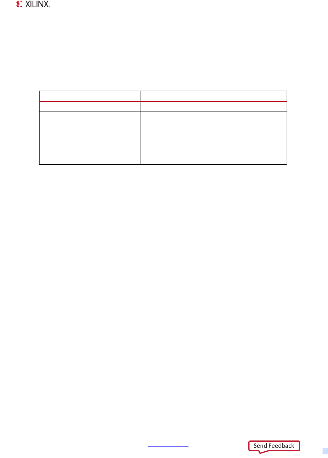
Zynq-7000 AP SoC Technical Reference Manual www.xilinx.com 188
UG585 (v1.12.1) December 6, 2017
Chapter 6: Boot and Configuration
Boot Time Optimizations
To improve NOR boot time, raise the clock rates, and optimize the I/O protocol by setting the
registers listed in Tab le 6 -14 . The example values might not be appropriate or optimal for all NOR
devices or board layouts. The settings assume a 33 MHz PS_CLK. If a faster clock is used, then a larger
divider must be considered.
6.3.7 SD Card Boot
SD card boot supports these features:
• Boot from standard SD or SDHC cards
• FAT 16/32 file system
• Up to 32 GB card densities
Note: The SD card boot mode is not supported in 7z010 dual core and 7z007s single core CLG225
devices.
Note: The SD card boot mode does not support header search or multiboot.
BootROM Steps
The BootROM performs these steps in SD card boot mode:
1. Initializes the MIO pins listed in Tabl e 6-1 5.
2. Configures SDIO_CLK_CTRL to a divisor of 32 and SD_CLK_CTL_R with a value of 1 (divide by 2).
3. Sets the SD controller to operate in 4-bit mode and use 3-byte addressing.
4. Tests the interface.
5. Reads BOOT.BIN from the root of the SD file system and copies it into OCM after parsing the
required BootROM Header.
6. BootROM transfer CPU execution to code downloaded into the OCM.
Table 6-14: NOR Boot Time Optimization Register Setting Example
Register Security Value Description
slcr.ARM_CLK_CTRL both
0x1F000200
CPU divisor = 2 (433 MHz)
slcr.SMC_CLK_CTRL both
0x00000D21
Baud rate divisor = 13 (66 MHz, 15 ns)
smc.set_cycles Non-secure
0x0002AA77
Timing Parameters:
we_n asserts 2 clocks after cs_n, t_ta=1,
t_pc=2, t_wp=5, t_ceoe=2, t_wc=7, t_rc=7
smc.set_opmode Non-secure
0x00000110
32-beat bursts, 8-bit width
smc.direct_cmd Non-secure
0x00400000
Select UpdateRegs

Zynq-7000 AP SoC Technical Reference Manual www.xilinx.com 189
UG585 (v1.12.1) December 6, 2017
Chapter 6: Boot and Configuration
Note: Production devices do not test the Card Detection status. For preproduction devices, refer to
AR# 52016.
File Partitions
For the BootROM to read the BOOT.BIN file, the SD card must be partitioned so that the first
partition is a FAT 16/32 file system. Additional non-FAT partitions are permitted, but the BootROM
does not read the other partitions.
Boot Page Access
When the SD card is reset, it defaults to providing access to the boot page. The BootROM assumes
that the boot page is accessible when it executes. If user code changes to a different page and a Zynq
system reset occurs without resetting the SD card, then the BootROM will not be able to read the
BootROM Header from the boot page of the SD card.
BootROM Header Search and Multiboot
In SD card boot mode, the BootROM does not perform a header search and does not support
multiboot.
Boot Time Optimizations
To improve the boot time of SD card, set the CPU clock divider to 2 instead of 4. The setting assumes
a 33 MHz PS_CLK. If a faster clock is used, then a larger divider must be considered.
Table 6-15: SD Card Boot MIO Register Settings
SDIO
I/O Interface
Signal Name
MIO Pin
Number
MIO_PIN
Register
Setting(1)
Pin State
I/O I/O Buffer
Output, Pull-up
External
Connection
Not SD card boot MIO 0, 1 0x1601 I 3-state ~
Not SD card boot MIO 2 to 8 0x0601 I 3-state Pull-up/down
Not SD card boot MIO 9 to 39 0x1601 I 3-state ~
SDIO_0_CLK MIO 40 0x0680 OEnabled ~
SDIO_0_CMD MIO 41 0x0680 OEnabled ~
SDIO_0_DATA[0:3] MIO 42:45 0x1680 I/O Enabled, pull-up ~
Notes:
1. These register settings are for LVCMOS25/33. Change the 6 to a 2 for LVCMOS18 (bits 11:9 change from
011 to 001).
Table 6-16: SD Card Boot Time Optimization Register Setting Example
Register Security Value Description
slcr.ARM_CLK_CTRL Both 0x1F000200 CPU divisor = 2 (433 MHz)
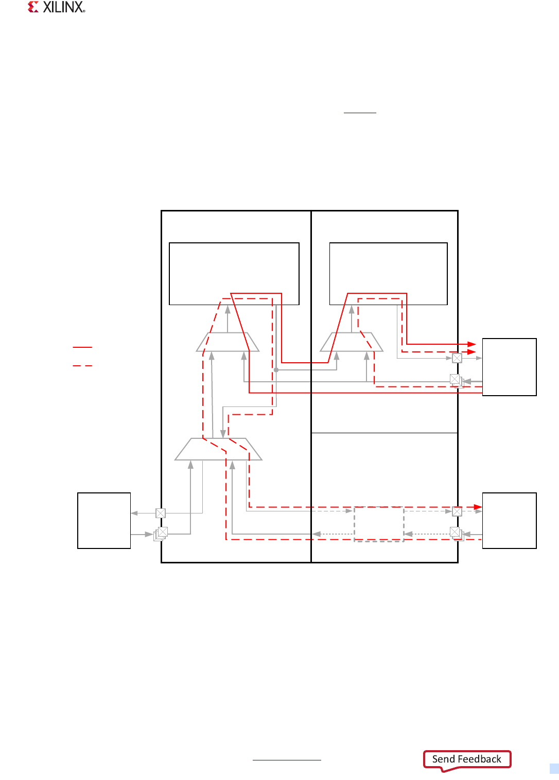
Zynq-7000 AP SoC Technical Reference Manual www.xilinx.com 190
UG585 (v1.12.1) December 6, 2017
Chapter 6: Boot and Configuration
6.3.8 JTAG Boot
There are two JTAG controllers in the Zynq device: the TAP and DAP controllers. The test access port
(TAP) controller can control the PL configuration process and other functions in the PL. Detailed
information regarding the TAP controller can be found in UG470, 7 Series FPGAs Configuration User
Guide. The debug access port (DAP) controller is in the application processing unit (APU), see
Chapter 3, Application Processing Unit. Detailed DAP controller information can be found in
Chapter 27, JTAG and DAP Subsystem. There are two chaining modes to access these JTAG
controllers: cascade and independent modes, as shown in Figure 6-7.
JTAG Enable/Disable Control
The DAP and TAP controllers are controlled by a few mechanisms.
• Cascade versus Independent mode
• Enable/disable DAP and TAP controllers
X-Ref Target - Figure 6-7
Figure 6-7: PS Cascade and Independent JTAG Chain Diagram
369ROWDJH'RPDLQ
7'2
7',7&.706
'HGLFDWHG
3LQVLQ3/
'RPDLQ
(0,2
-7$*
3/6HOHFW,2
3LQV
&RQILJXUDEOH
0,23LQV
7$3&RQWUROOHU
3DVV
WKURXJK
7'2
7',7&.706
7',7&.706
7'2
;LOLQ[3ODWIRUP
&DEOH
$50
,&(
+DUG/RJLF +DUG/RJLF
3/)DEULF
'$3&RQWUROOHU
'HEXJ$FFHVV3RUW
3/9ROWDJH'RPDLQ
&DVFDGH
,QGHSHQGHQW
0,2
3-7$*
3/-7$*
8*BFBB

Zynq-7000 AP SoC Technical Reference Manual www.xilinx.com 191
UG585 (v1.12.1) December 6, 2017
Chapter 6: Boot and Configuration
• Permanently disable JTAG
The JTAG connections can be enabled and disabled using the devcfg.CTRL [JTAG_CHAIN_DIS] bit. It
is set = 1 to disable JTAG to protect the PL from unwanted JTAG accesses.
The DAP controller is enabled by setting the devcfg.CTRL [DAP_EN] bit = 111. Any other value causes
the DAP controller to be bypassed. This bit is lockable by setting the devcfg.LOCK [DBG_LOCK] bit =
1. Once locked, it can only be unlocked with a POR reset.
The DAP and TAP controllers can be permanently disabled by blowing the JTAG Chain Disable eFuse.
Once the eFuse is blown, the controllers can never be accessed again. The software can read the state
of the eFuse bit using the devcfg.STATUS [EFUSE_JTAG_DIS] bit.
Note: If software attempts to unlock the APB register space in the DevC module without the proper
key, then this disables the DAP controller until the next POR reset is issued. This condition can be
detected by reading the devcfg.STATUS [ILLEGAL_APB_ACCESS] bit.
When the JTAG Boot mode is selected, the BootROM disables access to all security-related items,
enables the JTAG port, and halts the CPU by executing the WFE instruction. It is the User’s
responsibility to manage downloading the boot image into OCM or DDR memory through the DAP
controller before waking up the CPU and continuing the boot process.
Example: JTAG Boot Sequence
JTAG Boot mode is always non-secure; the AES unit is disabled and encrypted images are not
supported. The JTAG boot and PS/PL configuration flows are shown in Figure 6-7. The sequence is as:
1. PS and PL are powered-on; PS_CLK is stable.
2. PS_POR_B reset deasserts.
3. BootROM begins to execute and determines the boot mode.
4. BootROM performs CRC self-check, if enabled.
5. BootROM programs VMODE on MIO.
6. BootROM disables all security features and enables the DAP controller.
7. BootROM enables JTAG path(s):
a. Cascade: JTAG chain is set to cascade; the DAP and TAP controllers are accessible using the
PL JTAG interface.
Table 6-17: JTAG Requirements and Control
Function DAP Controller TAP Controller
Power requirements PS and PL PS and PL
PL configuration Not required Not required for Cascade mode.
Required for Independent mode.
devcfg.CTRL [JTAG_CHAIN_DIS] Must = 0Must = 0
devcfg.CTRL [DAP_EN] Must = 111 Must = 111 for Cascade mode.
Don’t care for Independent mode.
APB register space is unlocked with
the wrong key Disabled until POR reset Not affected

Zynq-7000 AP SoC Technical Reference Manual www.xilinx.com 192
UG585 (v1.12.1) December 6, 2017
Chapter 6: Boot and Configuration
b. Independent: JTAG chain is set to independent mode; the TAP controller is accessible via the
PL JTAG interface and the DAP controller is accessed through the EMIO JTAG. In this case, the
BootROM waits up to 90 seconds for you to program the PL (using the TAP controller) for the
EMIO JTAG connection.
8. BootROM shuts down and leaves CPUs running the wait for event (WFE) instruction:
a. Cascade: BootROM shuts down and releases system control to the JTAG interface for the TAP
and DAP controllers.
b. Independent: BootROM waits until the PL to initialized and then shuts down. The EMIO JTAG
interface for the DAP controller must be routed through the PL using a bitstream to be
operational.
9. User can access the DAP controller for PS system debug:
a. Cascade: First device on the PL JTAG interface chain.
b. Independent: Single device on the EMIO JTAG interface chain.
10. User can access the TAP controller to configure PL:
a. Cascade: Second device on the PL JTAG interface chain.
b. Independent: Single device on the PL JTAG interface chain.
Note: For high system reliability when using the L2-cache, set the slcr.L2C_RAM register to the value
of 0x0002_0202 as explained in AR# 54190.
Cascaded JTAG Chain Mode
The controllers are normally accessed using the cascaded JTAG chain mode. In cascade mode, both
controllers are accessed using the PL JTAG interface pins; the TDI signal from the interface goes to
the DAP controller. The TDO signal from the DAP controller is daisy chained to the TAP controller. The
TDO signal from the TAP controller go to the JTAG interface. The DAP registers and data are the last
to be shifted into the JTAG chain.
• DAP controller, then the TAP controller.
• PL configuration not required.
• Both controller must be enabled.
• Instructions and data must not adversely affect the unintended target.
Independent JTAG Chain Mode
The independent JTAG chain mode connects the TAP controller to the PL JTAG interface and provides
time for the user to use the TAP controller to configure the PL with a bitstream that routes the DAP
controller signals to the EMIO JTAG interface on the SelectIO pins as shown in Figure 6-7, page 190.
The BootROM waits up to 90 seconds for the PL configuration to complete before it enables the DAP
controller and continues with the boot process. If the PL is not configured in time, then the system
locks down.
• TAP controller is accessed through the PL JTAG pins and is used to configure the PL.
• DAP controller become accessible after the PL is configured with a bitstream.
In independent mode, the TAP controller behaves like the TAP controller in a Xilinx 7 series FPGA.
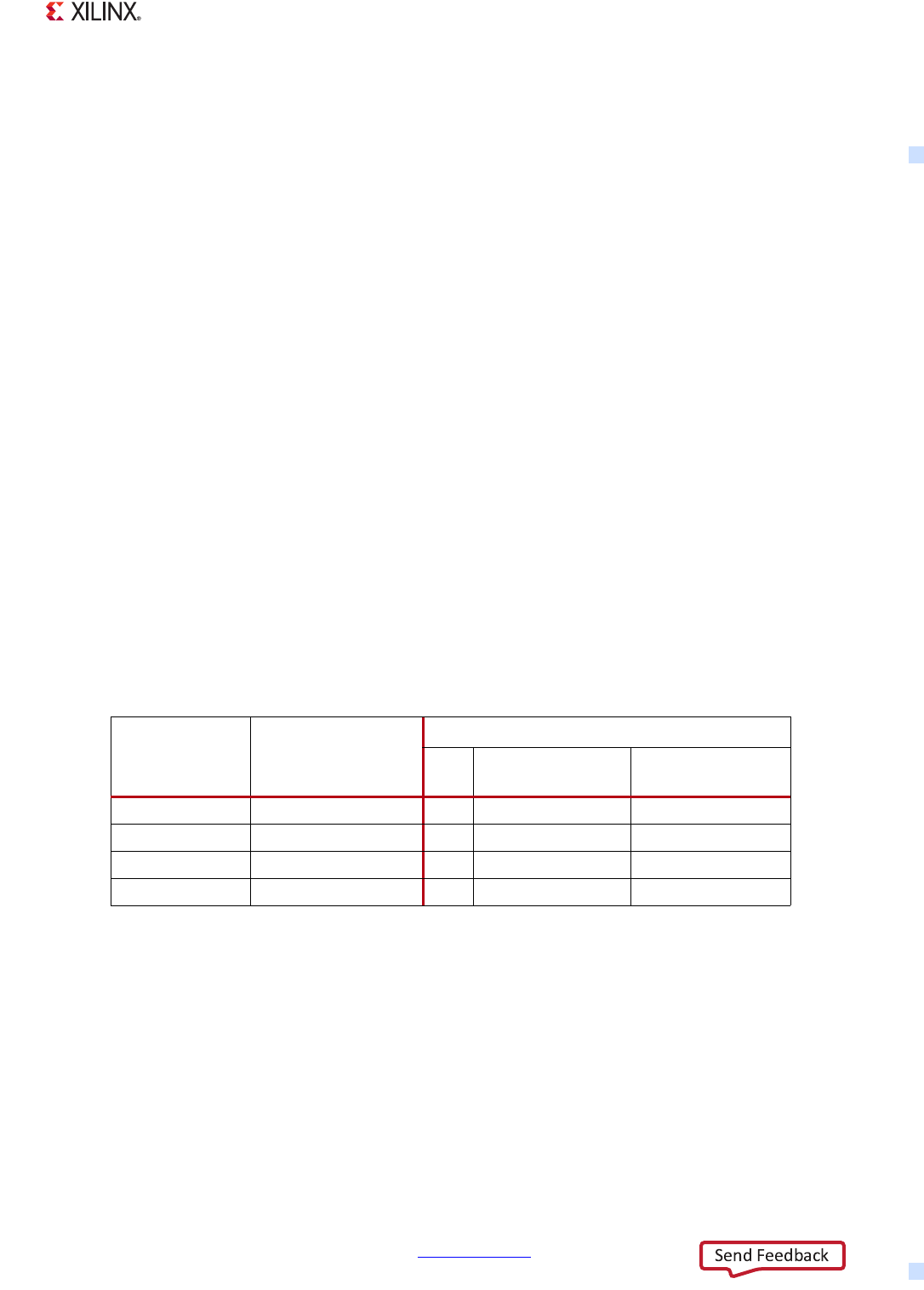
Zynq-7000 AP SoC Technical Reference Manual www.xilinx.com 193
UG585 (v1.12.1) December 6, 2017
Chapter 6: Boot and Configuration
EMIO PJTAG Interface for Independent Mode
The PL must be configured with a bitstream to enable the EMIO PJTAG interface to connect to the
DAP controller. After boot, the PL can be initialized by asserting the PROGRAM_B signal and then
loading the bitstream into the PL after the DONE signal is asserted. This can be done to enable the
EMIO PJTAG interface to control the DAP controller in independent JTAG mode.
Note: This functionality is only supported on production silicon and requires for the system to be
booted in independent JTAG boot mode. In this mode, the BootROM waits until the PL is self
initialized, then enables the PS-PL level shifters, enables the PL JTAG interface, and issues the WFE
instruction on the CPU.
MIO PJTAG Interface for Independent Mode
The DAP controller can interface to the MIO PJTAG interface, but it requires the FSBL/User code to
program the MIO multiplexer using the slcr.MIO_PIN_xx registers. The MIO PJTAG interface can be
routed to one of four sets of MIO pins as shown in Table 2-4, page 52. PL power is not required for
the MIO PJTAG interface and DAP controller to be used.
The TAP controller cannot program the MIO multiplexer. You must boot from a flash device that
includes FSBL/User code that configures the MIO multiplexer for the MIO PJTAG interface. After the
MIO multiplexer is programmed, the DAP controller is accessible using the MIO PJTAG interface.
MIO Pin States for JTAG Boot Mode
The values for the MIO registers in the JTAG boot mode state are shown in Tab le 6 -18 . These values
are valid for cascade and independent JTAG boot mode.
6.3.9 Reset, Boot, and Lockdown States
Reset State
When reset is asserted (PS_POR_B or PS_SRST_B), all of the I/O pins go to a 3-state mode and all
registers are reset except those listed in Table 26-2, page 715. When reset de-asserts, then the
Table 6-18: MIO Pin States for JTAG Boot Mode
MIO Pin MIO_PIN Register
Setting Value (1)
Pin State
I/O I/O Buffer
(GPIOB)
External
Connection
MIO pin [0:1] 0x1601 I 3-state, pull-up ~
MIO pin [2:6] 0x0601 I 3-state Pull-up/down
MIO pin [7:8] 0x0601 O 3-state Pull-up/down
MIO pin [9:53] 0x1601 I 3-state, pull-up ~
Notes:
1. These register values are based on the VMODE [0, 1] strapping pins. The register values shown are
for LVCMOS 25/33. For LVCMOS18, use: 0x1201 and 0x0201 (bits 11:9 change from 011 to
001).

Zynq-7000 AP SoC Technical Reference Manual www.xilinx.com 194
UG585 (v1.12.1) December 6, 2017
Chapter 6: Boot and Configuration
BootROM begins to execute to configure the PS. The default reset values for the device are shown
Appendix B, Register Details.
Boot State
The BootROM will modify MIO registers depending on the boot mode. The user can program the
Time Optimization registers using the Register Initialization parameters in the BootROM Header.
•Quad-SPI Boot
°Tabl e 6 -9: Qu ad -SP I B oot MIO Register Settings
°Table 6-10: Quad-SPI Boot Time Optimization Register Setting Examples
•NAND Boot
°Table 6-11: NAND Boot MIO Register Settings
°Table 6-12: NAND Boot Time Optimization Register Setting Example
•NOR Boot
°Table 6-13: NOR Boot MIO Register Settings
°Table 6-14: NOR Boot Time Optimization Register Setting Example
•SD Card Boot
°Table 6-15: SD Card Boot MIO Register Settings
°Table 6-16: SD Card Boot Time Optimization Register Setting Example
•JTAG Boot
°Table 6-17: JTAG Requirements and Control
°Table 6-18: MIO Pin States for JTAG Boot Mode
Lockdown State
The lockdown state differs between secure and non-secure mode. In secure mode, all interfaces are
disabled until a POR reset occurs. An error code is signaled on the INIT_B signal as described in
section 6.3.12 BootROM Error Codes.
Note: When a non-secure LockDown occurs while booting from a Flash device, the BootROM sets
the devcfg.CTRL [PCFG_PROG_B] bit = 0. This prevents the user from being able to program the PL
until the bit is cleared. The [PCFG_PROG_B] bit can be cleared using a software debugger.
The lockdown values for the MIO registers are shown in Ta b le 6 -1 9
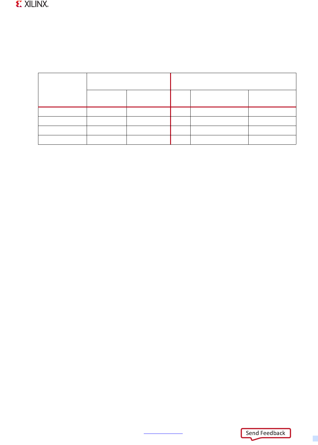
Zynq-7000 AP SoC Technical Reference Manual www.xilinx.com 195
UG585 (v1.12.1) December 6, 2017
Chapter 6: Boot and Configuration
MIO Pin State
The MIO Register pin settings for system reset and secure/non-secure lockdown boot are listed in
Tabl e 6-1 9.
6.3.10 BootROM Header Search
The BootROM reads the BootROM Header and performs two check to verify that the header is valid.
It looks to see that the Image Identification parameter contains 0x584C4E58 and that the Header
Checksum parameter matches the checksum calculated by the BootROM. If either of these tests fail,
then the BootROM Header address increments by 32 KB and the tests are repeated. The header
search is part of the BootROM flow and occurs after a POR or non-POR reset. The header search is
not supported in SD card boot; a valid BootROM Header is assumed to be in the boot page of the SD
card.
The header search function is shown in Figure 6-8. Normally the device boots from the first header
but in the event the BootROM detects an issue with the checksum or Image Identification parameter,
it looks for the next BootROM Header. The BootROM continues to search until if finds a valid header
or reaches the end of the search window.
• BootROM looks for Image Identification parameter XLNX at 0x024.
• Header checksum calculated by the BootROM matches Header Checksum parameter 0x048.
Table 6-19: MIO Pin States for Reset, and Lockdown Boot Mode
MIO Pin
MIO_PIN
Register Setting Pin State
Reset
Value
Lockdown
Value (1) I/O I/O Buffer
(GPIOB)
External
Connection
MIO pin [0:1] 0x1601 0x1601 I 3-state, Pull-up ~
MIO pin [2:6] 0x0601 0x0601 I 3-state Pull-up/down
MIO pin [7:8] 0x0601 0x0601 O 3-state Pull-up/down
MIO pin [9:53] 0x1601 0x1601 I 3-state, Pull-up ~
Notes:
1. These register values are based on the VMODE [0, 1] strapping pins. The register values shown are for
LVCMOS 25/33. For LVCMOS18, use: 0x1201 and 0x0201 (bits 11:9 change from 011 to 001).
Zynq-7000 AP SoC Technical Reference Manual www.xilinx.com 196
UG585 (v1.12.1) December 6, 2017
Chapter 6: Boot and Configuration
The BootROM Header search mechanism protects against:
• An update that was started on the first image but the system was interrupted after erasing the
section requiring an update.
• The write operation began but the write process did not finish.
The BootROM Header search mechanism does not protect against:
• The memory holding the BootROM Header becoming corrupt.
• A complete header was written but it did not pass the tests. If a header is non-functional, this
might lead to a system lockdown.
The BootROM Header search does not verify the integrity of the header beyond what is listed above.
If the header indicates an invalid operation or includes instructions that contradict each other, then
the BootROM might generate a system lockdown. The lockdown error codes are listed in section
6.3.12 BootROM Error Codes.
BootROM Header Search Stepping and Range
The BootROM searches on 32-KB boundaries until a valid header is detected or the end of the range
is encountered. The header search is done for all boot devices except SD card. The search occurs
after a POR or non-POR reset including after a Multiboot operation.
The BootROM searches within a limited address space on the boot device:
•NAND: first 128MB
•NOR: first 32MB
• Quad-SPI, signal/dual SS with 4-bit I/O: first 16 MB
• Quad-SPI, dual SS with 8-bit Parallel I/O: first 32 MB
• SD card: single image in boot page, no searching
X-Ref Target - Figure 6-8
Figure 6-8: BootROM Header Search
First
Location
0x000000
Third
Location
0x010000
0x0008C0
0x0108C0
Second
Location
0x008000
0x0088C0
Invalid
Invalid
Invalid
UG585_c6_07_081514
continue
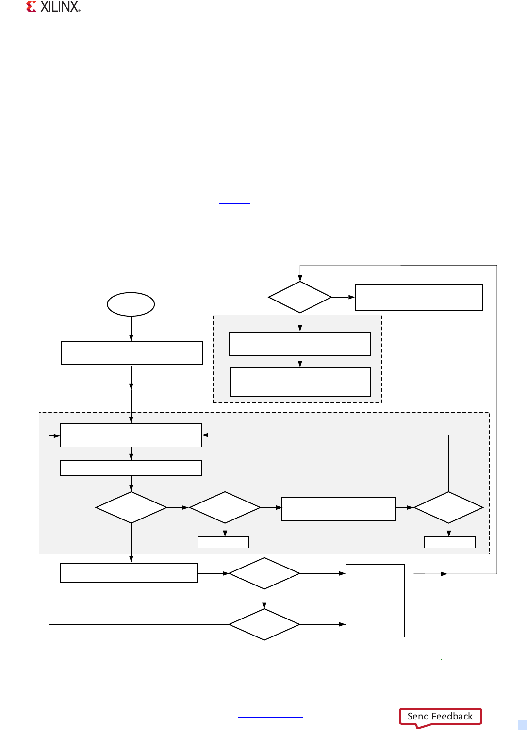
Zynq-7000 AP SoC Technical Reference Manual www.xilinx.com 197
UG585 (v1.12.1) December 6, 2017
Chapter 6: Boot and Configuration
6.3.11 MultiBoot
Multiboot is a feature that allows the FSBL or User code to select the BootROM Header from multiple
images on the boot device. To select an image, the FSBL/User code writes the base memory address
location of the BootROM Header into the devcfg.MULTIBOOT_ADDR [MULTIBOOT_ADDR] bit field
and then generates a non-POR system reset. The BootROM tries to fetch the BootROM Header
located at that address. If the BootROM determines that the header is not valid, it performs a
BootROM Header search by incrementing the MULITBOOT_ADDR register until a valid header is
found or the end of the range is detected. The range depends on the boot mode and is given in the
BootROM Header Search Stepping and Range section of section 6.3.10 BootROM Header Search.
Note: In secure mode, multiboot is not supported when using an eFuse key. Fallback and multiboot
are discussed in this below and in UG821, Zynq-7000 All Programmable SoC Software
Developer
s
Guide.
Multiboot is shown in Figure 6-9 along with the BootROM Header search function.
X-Ref Target - Figure 6-9
Figure 6-9: BootROM Header Search and FSBL/User Code Multiboot Flowchart
325
%RRW,PDJH$GGUHVV
GHYFIJ08/7,%227B$''5>@
0XOWLERRW"
5HUXQ%RRW520
:ULWHWRVOFU366B567B&75/
>62)7B567@IRUQRQ325UHVHW
)6%/8VHU
&RGH([HFXWLRQ
%RRW,PDJH$GGUHVV
GHYFIJ08/7,%227B$''5>@.%
&RQWLQXH
)6%/8VHUFRGHH[HFXWLRQ
3URJUDPERRWLPDJHDGGUHVV
'HYFIJ08/7,%227B$''5>@
%RRW520([HFXWLRQ
)6%/8VHU&RGH
0XOWLERRW
<HV
5HDG%RRW520+HDGHU
9DOLG+HDGHU" 1R
,QFUHPHQW
GHYFIJ08/7,%227B$''5>@
0RYH,PDJHWR2&0PHPRU\
%RRW520
+HDGHU6HDUFK
<HV
8*BFBB
([HFXWH
)6%/8VHU
FRGH
1R
2XWRI5DQJH"
1R
<HV
6'&DUG%RRW" 1R
<HV
/RFNGRZQ /RFNGRZQ
<HV
56$RQ)6%/" 1R
56$3DVV"
1R <HV

Zynq-7000 AP SoC Technical Reference Manual www.xilinx.com 198
UG585 (v1.12.1) December 6, 2017
Chapter 6: Boot and Configuration
Multiboot Programming Steps
1. Determine the physical byte address. The address must be aligned to 32 KB.
2. Divide the physical memory address by 32 KB (shift out the 15 LSBs). Write the upper address bits
into the devcfg.MULTIBOOT_ADDR [MULTIBOOT_ADDR] field.
3. Perform a software system reset by writing to the slcr.PSS_RST_CTRL [SOFT_RST] register bit.
When the BootROM executes after the non-POR reset, it looks for the BootROM Header pointed to
by the devcfg.MULTIBOOT_ADDR [MULTIBOOT_ADDR] field.
6.3.12 BootROM Error Codes
The BootROM can detect an error while processing the BootROM Header or while processing the
FSBL/User code for decryption and authentication. When a boot failure occurs, the BootROM puts
the device into either a secure or non-secure lockdown; an Error Code is normally generated. The
BootROM flowchart with error conditions is shown in Figure 6-5. The error codes are listed in
Tabl e 6-2 0.
The error code is visible by observing a bit pulse train on the INIT_B pin (secure lockdown) or by
reading the slcr.REBOOT_STATUS [BOOTROM_ERROR_CODE] bit field (non-secure lockdown).
1. INIT_B pin observations:
°In secure mode INIT_B pulses the 16-bit error code.
°In non-secure mode INIT_B drives Low, indicating a failure. JTAG is enabled.
2. JTAG access to error code register read:
°When JTAG is enabled, the DAP controller can be used to read the error code in the
slcr.REBOOT_STATUS [BOOTROM_ERROR_CODE] register field.
The INIT_B pulses are meant to be visually read with an LED on the INIT_B pin. The pulses are
active-High. A long Low pulse on the pin indicates a 1 and a short pulse indicates a 0. The bit order
is LSB to MSB. The pulse train is repeated three times. An example pulse train is shown in Figure 6-10
using a 60 MHz PS_CLK frequency. The timing will scale linearly with the PS_CLK frequency.
Note: This waveform is based on the development board and the INIT_B polarity signal is inverted.
X-Ref Target - Figure 6-10
Figure 6-10: Error Code INIT_B Bit Waveform Example
(UURU&RGH%LWV
6OFU5(%227B67$786
>%227520B(5525B&2'(@
/RQJ
3XOVH
6KRUW
3XOVH
%LW %LW
/RQJ
3XOVH
6KRUW
3XOVH
6WDUW %LW %LW %LW
6KRUW
3XOVH
3XOVH7LPHVLQ6HFRQGV
%DVHGRQ0+]36B&/.DQG
VOFU&38B&/.B&75/>',9,625@
8*BFBB
'HYHORSPHQW
%RDUG/('V
*UHHQ
5HG
,1,7B%
V
VV
V V V
VVV V

Zynq-7000 AP SoC Technical Reference Manual www.xilinx.com 199
UG585 (v1.12.1) December 6, 2017
Chapter 6: Boot and Configuration
Non-secure boot failures result in the BootROM disabling access to the AES unit, clearing the PL, and
enabling JTAG. The slcr.REBOOT_STATUS register can be read to determine the source of the boot
failure.
Error Code Numbers
The error codes listed in Ta bl e 6- 2 0 describe the functionality of production devices. For
preproduction devices, the error code numbers and the reporting scheme are described in
AR# 55082. Other error code numbers might be generated by the BootROM, but are unlikely. If an
error code occurs that is not listed in Tab le 6- 20 for production parts or in AR# 55082 for
preproduction parts, then contact Xilinx.
Lockdown Types
The Lockdown Type column includes information based on the type of reset that started the
BootROM execution.
• POR reset (P)
• Non-POR reset (NP)
The type of lockdown indicated in Ta b le 6 - 20 includes the following notations:
•Non-secure: A non-secure lockdown occurs (system can be accessed by JTAG).
•Header: The lockdown type is defined by the Encryption Status parameter in the header.
•Secure: Always a secure lockdown (the system becomes inaccessible).
•Previous: Applies only after a non-POR reset. If the previous boot mode was secure, then this
subsequent lockdown is secure. If the previous boot was non-secure, then this subsequent
lockdown is non-secure.
Table 6-20: BootROM Error Codes
Error
Code
Lockdown
Type(1) Description Solution
0x0002 P: Non-secure
NP: Non-secure
The system successfully booted in JTAG
mode.
• Use the JTAG interface to the DAP and
TAP controllers.
0x2000 P: Non-secure
NP: Previous
Quad-SPI boot mode. The BootROM
detected a x8 parallel device configuration
using x1 mode, but then failed to read the
expected header parameters using x8 mode.
The BootROM continues with header search
using x8 mode, but it was unable to find the
Width Detection word using header search
within the image search range.
• Check that the Quad-SPI device is
properly connected to the QSPI MIO
pins.
• Be sure that the Width Detection word is
set equal to the data pattern
0xAA995566 and that the Image
Identification word has 0x584C4E58,
‘XLNX’
• Ensure that the device content is not
blank In single device applications.
0x2001 P: Non-secure
NP: Previous
NAND boot mode. The BootROM could not
determine the ECC mode for the device.
• Check that the NAND device is on the
vendor approved list, refer to (Xilinx
AR# 50991).

Zynq-7000 AP SoC Technical Reference Manual www.xilinx.com 200
UG585 (v1.12.1) December 6, 2017
Chapter 6: Boot and Configuration
0x200A P: Non-secure
NP: Previous
SD card boot mode. The BootROM could not
find the boot image at the root of the SD
card; only a single boot image is supported
for this boot mode.
If the SD card was accessed by the FSBL/User
code and then a system reset occurs without
resetting the SD card, then the SD card
might be left in 4-byte addressing mode.
• Check that there is a valid BootROM
Header in the root directory of the SD
card named BOOT.BIN.
• Make sure the SD interface is operating
reliably; for example using XMD or other
debug tool to access it.
• Make sure the SD card is in 3-byte
addressing mode.
• Check the mode pin settings.
0x200B P: Non-secure
NP: Previous
NOR boot mode. The BootROM could not
find a valid boot image in the NOR device
after searching.
• Check that there is a valid BootROM
Header within the search range, refer to
the BootROM Header Search and
Multiboot sections.
0x200C P: Non-secure
NP: Previous
Quad-SPI boot mode. The BootROM is
unable to find a valid header within the
image search range.
• Check that there is a valid image written
within the boot partition address search
space for the device, refer to the
BootROM Header Search and Multiboot
sections.
0x200D P: Non-secure
NP: Previous
NAND boot mode. The BootROM is unable
to find a valid header within the image
search range.
• Check that there is a valid image written
within the boot partition address search
space for the device, refer to the
BootROM Header Search and Multiboot
sections.
0x200E P: Header
NP: Previous
An address in the Register Initialization field
of the BootROM Header is out of the
accessible range.
• Check that all addresses are within the
range based on boot mode, refer to the
Register Initialization address range
table.
0x200F P: Secure
NP: Secure
Secure boot mode. The Start of Execution
word does not equal 0.
• The Start of Execution word must be
equal to 0 in secure mode (boot from
OCM).
0x2011 P: Header
NP: Previous
NAND boot mode. Length of Image
parameter is = 0. The execute-in-place mode
is not supported in the NAND boot mode.
• Set the Length of Image parameter to
the length of the boot image. Must fit
into the 192 KB of available OCM
memory.
0x2012 P: Header
NP: Previous
SD card boot mode. Length of Image
parameter is = 0. The execute-in-place mode
is not supported in the SD card boot mode.
• Set the Length of Image parameter to
the length of the boot image. Must fit
into the 192 KB of available OCM
memory.
0x2019 P: Secure
NP: Secure
The encryption and eFuse combinations are
not valid, refer to Table 6 - 7 .
• Make sure the Encryption Status
parameter and the eFuse states are
consistent.
0x201A P: Secure
NP: Secure
Security Violation was detected. The system
tried to transition from a secure operating
mode to a non-secure boot mode without
using POR.
• Assert the POR reset to boot in
non-secure mode when the system was
previously booted in secure mode.
Table 6-20: BootROM Error Codes (Cont’d)
Error
Code
Lockdown
Type(1) Description Solution

Zynq-7000 AP SoC Technical Reference Manual www.xilinx.com 201
UG585 (v1.12.1) December 6, 2017
Chapter 6: Boot and Configuration
0x2023 P: Non-secure
NP: Previous
There is a mismatch between the value in the
Header Checksum word and the calculated
checksum for the header, or the Image
Identification word in the BootROM Header
does not contain 0x584C4E58,'XLNX'.
• Verify that the Header Checksum is
correct.
• Make sure the Image Identification word
has 0x584C4E58.
• Verify that the boot device can be
accessed reliably using the JTAG boot
mode.
0x2024 P: Header
NP: Previous
The Image Identification word in the
BootROM Header does not contain
0x584C4E58, 'XLNX'.
• Make sure the Image Identification word
equals 0x584C4E58.
• Verify that the boot device can be
accessed reliably using the JTAG boot
mode.
0x2100 P: Non-secure
NP: Previous
The Image Identification word in the
BootROM Header does not equal
0x584C4E58, 'XLNX'.
• Make sure the Image Identification word
has 0x584C4E58.
• Verify that the boot device can be
accessed reliably. Boot in JTAG mode and
test, if necessary.
0x2101 P: Non-secure
NP: Previous BootROM Header checksum fails.
• Verify that the Header Checksum is
correct.
• Verify that the boot device can be
accessed reliably using the JTAG boot
mode.
0x2102 P: Non-secure
NP: Previous
The address value in the Source Offset word
points to a location within the BootROM
Header instead of where the image is
actually located.
• Check the address value in the Source
Offset word.
0x2103 P: Non-secure
NP: Previous
The address value in the Source Offset word
is not aligned to a 64B boundary.
• Align the address in the Source Offset
word to a 64-byte boundary.
0x2104 P: Non-secure
NP: Previous
Non-secure and execute from OCM mode.
This error occurs if the image destination
address crosses the 192 KB boundary (i.e.,
0x070000).
• Reduce the size of the initial FSBL/User
code that is loaded into the OCM.
0x2105 P: Non-secure
NP: Previous
Non-secure and execute from OCM mode.
This error occurs if the image destination
address is less than 0x00040000 if the
image length is not equal to 0.
• Execute the image at 0x00040000.
0x2106 P: Non-secure
NP: Previous
Non-secure and execute from OCM mode.
The Length of Image parameter exceeds the
192 KB limit of the OCM for the initial
FSBL/User code.
• Reduce the size of the initial FSBL/User
code that is loaded into the OCM.
0x2108 P: Non-secure
NP: Previous
Non-secure and execute from OCM mode.
The Start of Execution parameter is greater
than 192 KB (0x03 0000).
•The Start of Execution value must be
within the OCM.
0x2109 P: Non-secure
NP: Previous
The Reserved parameter (0x038) is not set =
0.
• Set the reserved parameter at 0x038 to
0.
Table 6-20: BootROM Error Codes (Cont’d)
Error
Code
Lockdown
Type(1) Description Solution

Zynq-7000 AP SoC Technical Reference Manual www.xilinx.com 202
UG585 (v1.12.1) December 6, 2017
Chapter 6: Boot and Configuration
6.3.13 Post BootROM State
The state of the PS after the BootROM executes depends on these conditions:
• Decryption Status parameter.
• Boot strap mode pins.
•Actions of the BootROM based on system discovery.
The mode pins impact which MIO are enabled and what I/O standard they are set to after exiting the
BootROM. Additionally, the mode setting impacts the boot peripheral settings. For example, if
Quad-SPI is the selected boot source, the needed MIO is enabled and the Quad-SPI controller is set
0x210A P: Non-secure
NP: Previous
Applies to secure boot mode. The Length of
Image word in the header is set to 0
(execute-in-place).
• Execute-in-place is not supported in
secure mode. Either specify non-secure
mode, or change the Length of Image
word to match the image length after
decryption.
0x210B P: Secure
NP: Previous Secure mode. HMAC error occurred. • Verify that the key and key source are the
same for encryption and decryption.
0x210D P: Header
NP: Previous
This error occurs if the image length is not
equal to 0 and the length is greater than
192 KB.
• Reduce the size of the initial FSBL/User
code that is loaded into the OCM.
0x210E P: Header
NP: Previous
The Length of Image parameter is set to 0
indicating an execute-in-place boot, but the
selected boot mode does not support
execute-in-place.
• Check the boot mode settings.
• NAND and SD card do not support
execute-in-place.
0x210F P: Header
NP: Previous
BootROM Header checksum failed before
processing the Register Initialization words.
• Verify that the Header Checksum is
correct.
• Verify that the boot device can be
accessed reliably using the JTAG boot
mode.
0x2110 P: Header
NP: Previous
The Image Identification word in the
BootROM Header does not contain
0x584C4E58, 'XLNX'.
• Make sure the Image Identification word
has 0x584C4E58.
• Verify that the boot device can be
accessed reliably by using the JTAG boot
mode to download test software.
0x2111 P: Header
NP: Previous
One or more address/write-data pairs in the
Register Initialization section of the
BootROM Header contains an address
outside of the allowed range.
• Make sure the addresses in the Register
Initialization section are within the
ranges defined in the TRM table 6-13
Boot Image Address-Data Write Address
Ranges.
0x2200 P: Secure
NP: Previous
Secure boot mode. The image size after
decryption does fit into the 192 KB of
available OCM memory.
• Reduce the size of the initial FSBL/User
code that is loaded into the OCM.
Notes:
1. There are two reset types, POR (P) and non-POR (NP). Refer to the text preceding the table for an explanation of the
lockdown type column.
Table 6-20: BootROM Error Codes (Cont’d)
Error
Code
Lockdown
Type(1) Description Solution
Zynq-7000 AP SoC Technical Reference Manual www.xilinx.com 203
UG585 (v1.12.1) December 6, 2017
Chapter 6: Boot and Configuration
with the necessary settings to read from flash. The modified values for each boot source are
documented in the associated boot devices section.
APU and OCM State after BootROM
The general processor state upon BootROM exit is as follows:
• MMU, Icache, Dcache, L2 cache are all disabled.
• Both processors are in the supervisor state.
• ROM code is inaccessible.
• 192 KB of OCM memory is accessible starting at address 0x0000_0000 while the upper 64 KB of
the OCM is accessible starting at address 0xFFFF_0000.
• CPU 0 branches into the stage 1 boot image if no failure takes place.
• CPU 1 is in a WFE state while executing code located at address 0xFFFF_FE00 to 0xFFFF_FFF0.
Memory Map During BootROM Execution
The system memory map during BootROM execution places 192 KB of OCM at the bottom of
memory and 64 KB at the top as shown in Figure 6-11. The 64 KB memory block is used is used by
the BootROM to store the BootROM Header and program variables. After the BootROM is finished,
the 64 KB OCM memory block is freed-up for the FSBL to use.
Post BootROM Security
If secure mode is enabled, the AES unit is accessible post BootROM. In non-secure mode, the AES
unit is not accessible.
X-Ref Target - Figure 6-11
Figure 6-11: System Memory Map During BootROM Execution
During
BootROM Loading FSBL
UG585_c6_10_081514
OCM RAM
Empty
DDR
Peripherals
Empty
OCM RAM
1 MB
1 GB
0
M_AXI_GP0
M_AXI_GP1
2 GB
3 GB
4 GB
192 KB
At Handoff from
BootROM Execution to FSBL/User Code
64 KB BootROM Program Memory
OCM ROM
256 KB
192 KB FSBL Code (buffer)
OCM Memory
Empty
DDR
Peripherals
Empty
OCM Memory
1 MB
1 GB
0
M_AXI_GP0
M_AXI_GP1
2 GB
3 GB
4 GB
192 KB Empty
256 KB
192 KB FSBL Code
Parameters/Variables
and BootROM Header
64 KB BootROM Code
64 KB FSBL Program Memory

Zynq-7000 AP SoC Technical Reference Manual www.xilinx.com 204
UG585 (v1.12.1) December 6, 2017
Chapter 6: Boot and Configuration
The BootROM locks several bits in the DevC module prior to exiting to ensure security. The bits the
BootROM locks are listed in Tab le 6 - 2 1 ; where 1 = locked. The Lock bits are used to disable writes to
bits in the devcfg.CTRL register. Once a lock bit is set, it cannot be cleared except by a POR reset. The
BootROM will lock some of these bits before turning PS control over to the FSPL/User code.
Post BootROM Debug
In the event of a failure while booting non-secure the BootROM enables JTAG access so that the
REBOOT_STATUS and other registers can be read using the DAP controller. A debugging tool like
XMD has full access to the processor when JTAG is enabled and includes the DAP controller in the
chain.
If a failure occurs while booting in secure mode, the BootROM disables the AES unit, clears the OCM,
clears the PL, and halts the processor. JTAG is not enabled, consequently, the REBOOT_STATUS value
is not available to be read. Instead, the 16-bit error code is shown by toggling the INIT_B pin.
6.3.14 Registers Modified by the BootROM – Examples
Examples of registers modified by the BootROM are listed in Tab le 6 -22 . When multiple register
values appear in the table, this indicates that the value depends on other factors. Refer to the
footnotes and text for more information. These are values that have been observed when the
BootROM transfers CPU control from the FSBL/User code.
These values were obtained from test run on the ZC702 board with the 7z020 production device and
the ZC706 board with the 7z035/7z045 production devices.
Table 6-21: devcfg.LOCK Register
Bit Position Bit Name BootROM Secure
Boot Lock Status
BootROM
Non-Secure Boot
Lock Status
31:5 Reserved ~~
4 AES_FUSE_LOCK 10
3 AES_EN_LOCK 0 1
2SEU_LOCK 00
1SEC_LOCK 10
0DBG_LOCK 00
Table 6-22: BootROM Modified Registers
Address Register Name(1) Reset Value JTAG Boot Quad-SPI Boot SD Card Boot
devcfg Registers
0xF800_7000
CTRL 0x0C006000 0x4E00E07F 0x4C00E07F
0x4E80EE80
0x4E00E07F
0x4E80EE80
0xF800_7004
LOCK 0x00000000 0x0000001A 0x0000001A
0x00000012
0x0000001A
0x00000012
0xF800_7008
CFG 0x00000508 reset value reset value reset value

Zynq-7000 AP SoC Technical Reference Manual www.xilinx.com 205
UG585 (v1.12.1) December 6, 2017
Chapter 6: Boot and Configuration
0xF800_700C
INT_STS 0x00000000
0xF8020006
0xA802000A
0xA802000B
0xA803000A
0xA803100A
0xA883100A
0xA802000A
0xA803000A
0xF800_7014
STATUS 0x40000820 0x40000F30
0x40000A30 0x40000A30 0x40000A30
0xF800_7028
ROM_SHADOW 0x00000000 0xFFFFFFFF
0xF800_7034
UNLOCK 0x00000000 0x757BDF0D 0x757BDF0D 0x757BDF0D
0xF800_7080
MCTRL x0x10800000
0x30800100 0x30800100 0x30800100
l2cache Registers
0xF8F0_2104
reg1_aux_control 0x02050000 0x02060000
0xF8F0_2F40
reg15_debug_ctrl 0x00000000 0x00000004 0x00000004
0x00000000
0x00000004
0x00000000
mpcore Registers
0xF8F0_0040
Filtering_Start_Addr 0x00100000 reset
value reset value reset value
0xF8F0_0044
Filtering_End_Addr 0x00000000 0xFFE00000 0xFFE00000 0xFFE00000
0xF8F0_0108
ICCBPR 0x00000002 reset value
0xF8F0_0200
Global_Timer_Counter_0 0x00000000 The value depends on when the register is read.
0xF8F0_0204
Global_Timer_Counter_1 0x00000000 The value depends on when the register is read.
0xF8F0_0208
Global_Timer_Control 0x00000000 0x00000001 0x00000001
slcr Registers
0xF800_0258
REBOOT_STATUS(2) 0x00400000 0x00400002 0x00400000
0x00600000
0x00400000
0x00600000
0xF800_0910
OCM_CFG 0x00000000 0x00000018 0x00000018 0x00000018
0xF800_0A1C
Reserved 0x00010101 0x00010101 0x00020202 0x00020202
0xF800_0B04
GIOB_CFG_CMOS18 0x00000000 0x0C301166 0x0C301166 0x0C301166
0xF800_0B08
GIOB_CFG_CMOS25 0x00000000 0x0C301100 0x0C301100 0x0C301100
0xF800_0B0C
GIOB_CFG_CMOS33 0x00000000 0x0C301166 0x0C301166 0x0C301166
0xF800_0B14
GIOB_CFG_HSTL 0x00000000 0x0C750077 0x0C750077 0x0C750077
0xF800_0B70
DDRIOB_DCI_CTRL 0x00000020 reset value 0x00000823 0x00000823
uart1 Registers
0xE000_1000
Control_reg0 0x00000128 0x00000114 0x00000114 0x00000114
0xE000_1004
mode_reg0 0x00000000 0x00000020 0x00000020 0x00000020
0xE000_1014
Chnl_int_sts_reg0 0x00000200 reset value 0x00000E10 0x00000E10
0xE000_1018
Baud_rate_gen_reg0 0x0000028B reset value 0x0000003E 0x0000003E
0xE000_1028
Modem_sts_reg0 x 0x000000FB 0x000000FB 0x000000FB
0xE000_102C
Channel_sts_reg0 0x00000000 reset value 0x00006812 0x00006812
Table 6-22: BootROM Modified Registers (Cont’d)
Address Register Name(1) Reset Value JTAG Boot Quad-SPI Boot SD Card Boot

Zynq-7000 AP SoC Technical Reference Manual www.xilinx.com 206
UG585 (v1.12.1) December 6, 2017
Chapter 6: Boot and Configuration
6.4 Device Boot and PL Configuration
The Zynq device is a complex system that can be tightly controlled (secured) by the PS boot process
or be open and accessible in a friendly and/or development environment. The PS-centric control of
the Zynq device assumes a secure environment after a POR reset until the Encryption Status
parameter in the BootROM Header is read or until JTAG boot mode is detected. When security
discrepancies are detected, the BootROM executes a system lockdown.
Basic Boot Sequence
There are many different boot sequences. The common thread is that after a system reset (POR and
non-POR), the BootROM executes first to configure and control the system. After a POR reset, there
are a few hardware activities that are performed before the BootROM executes. These hardware
activities are described in Figure 6-1, page 150. After the BootROM executes, the FSBL/User code
takes control of the PS and is able to further configure the device, including the PL.
1. Power-up and Reset Operations. See section 6.2 Device Start-up.
2. BootROM Execution. See section 6.3.3 BootROM Performance.
3. FSBL/User Code to Configure PS. Refer to UG821, Zynq-7000 All Programmable SoC Software
Developers Guide for information on creating FSBL/User code.
4. FSBL/User Code to Initialize and Configure PL. The controls are shown in Figure 6-12. Refer to
UG821, Zynq-7000 All Programmable SoC Software Developers Guide for information on creating
FSBL/User code.
In a development environment (non-secure), the user can access the Xilinx TAP controller in the PL
and the ARM DAP controller in the PS. This section focusses on the boot process from the PS
software perspective with a section on configuring the PL using JTAG.
Chapter Sections
This chapter section includes the following subsections to explain various aspects of device
configuration:
•6.4.1 PL Control via PS Software
•6.4.2 Boot Sequence Examples
•6.4.3 PCAP Bridge to PL
•6.4.4 PCAP Datapath Configurations
0xE000_1034
Baud_rate_divider 0x0000000F reset value 0x00000006 0x00000006
Notes:
1. Some register names are truncated or abbreviated to keep them short in this table.
2. In the REBOOT_STATUS register, a 4 means a POR reset and a 6 means an SRST (non-POR) reset.
Table 6-22: BootROM Modified Registers (Cont’d)
Address Register Name(1) Reset Value JTAG Boot Quad-SPI Boot SD Card Boot
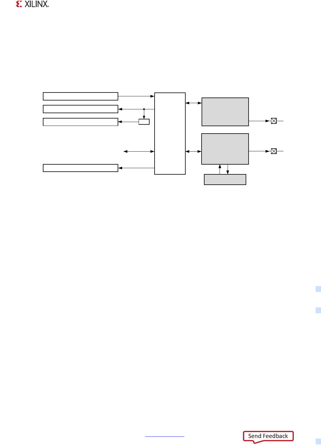
Zynq-7000 AP SoC Technical Reference Manual www.xilinx.com 207
UG585 (v1.12.1) December 6, 2017
Chapter 6: Boot and Configuration
•6.4.5 PL Control via User-JTAG
6.4.1 PL Control via PS Software
The PL is controlled by PS software (Figure 6-12) through the PCAP bridge or using external pins and
the JTAG interface associated with the PL (Figure 6-20, page 219).
PL Initialization via PS Software
At any time, the devcfg.CTRL [PCFG_PROG_B] bit can be used to issue a global reset to the PL. If this
bit is set Low, the PL begins its initialization process and the devcfg.STATUS [PCFG_INIT] bit is held
Low until the [PCFG_PROG_B] bit is set High by the hardware. The programming sequence to
initialize the PL include these steps:
1. Set [PCFG_PROG_B] signal to High
2. Set [PCFG_PROG_B] signal to Low
3. Poll the [PCFG_INIT] status for Reset
4. Set [PCFG_PROG_B] signal to High
5. Poll the [PCFG_INIT] status for Set
PL Configuration via PS Software
PL configuration and reconfiguration support are illustrated with an example that simplifies software
knowledge of state. The sequence assumes the PL is uninitialized and system state is unknown. Users
can build on these steps.
To configure the PL, enable the interface and select the PCAP programming path. Clear interrupts,
initialize the PL, and disable the internal DevC loopback function. The new bitstream is transferred to
the PL using the DevC DMA unit. Both the PS and PL must be powered on to configure or reconfigure
the PL.
X-Ref Target - Figure 6-12
Figure 6-12: PCAP Path for PL Initialization and Configuration
PL Initialization
Circuits
INIT_B
devcfg.INT_STS
[PCFG_INIT_NE_INT]
devcfg.INT_STS
[PCFG_DONE_INT]
devcfg.INT_STS
[PCFG_INIT]
devcfg.CTRL
[PCFG_PROG_B]
edge
PL
Configuration
Module
Bitstream
DevC
PCAP
Path
PS Software
Enable PCAP;
Initiate Bitstream DMA;
Wait until done;
AES/HMAC Units
[PCAP_PR] = 1
[PCAP_MODE] = 1
DONE
UG585_c6_12_060915
(open drain output)
(open drain output)

Zynq-7000 AP SoC Technical Reference Manual www.xilinx.com 208
UG585 (v1.12.1) December 6, 2017
Chapter 6: Boot and Configuration
6.4.2 Boot Sequence Examples
There are a multitude of variables in the boot process of the PS and PL. An entire boot sequence can
include PS and PL hardware operations, BootROM execution, FSBL/User code execution and starting
the operating system software.
When considering a secure environment, there are multiple resources to reference. At the low-level,
refer to this chapter and Chapter 32, Device Secure Boot. As the system transitions to the FSBL and
the Operating System, refer to UG821, Zynq-7000 All Programmable SoC Software Developers Guide.
The fastest boot times are obtained in PS-only non-secure mode. For time critical applications, there
are several areas to consider. Major time sinks for time critical applications include the bandwidth of
the boot device, decryption, power supply ramp time, and the ROM code CRC check.
IMPORTANT: The time it takes for each boot process to complete can be difficult to calculate because
of all the variables involved. The values provided here are meant as a guide, not a definitive answer. If
you have any questions, please contact your Xilinx FAE Sales Engineer.
This section starts by defining a few different boot sequences that are controlled by PS software
(BootROM or FSBL/User code).
Example Sequences
• Seq 1: PS Non-secure Bring-up (no PL power)
• Seq 2: PS Secure Bring-up with PL Configuration
• Seq 3: PL Bring-up by FSBL/User Code
PS Non-secure Bring-up Example
The PS and PL can be brought up together in a secure or non-secure mode. The simultaneous
bring-up of the PS and PL is shown in Figure 6-12. Also refer to Figure 6-4, page 164 for details on
power, reset, and clock interactions and timing examples.The PS non-secure bring-up using a flash
device without JTAG illustrates a simple example with minimal resources. The example is shown in
Figure 6-14. When the PL is needed later in the system operation, its bring-up is explained in the PL
Bring-up by FSBL/User Code example.
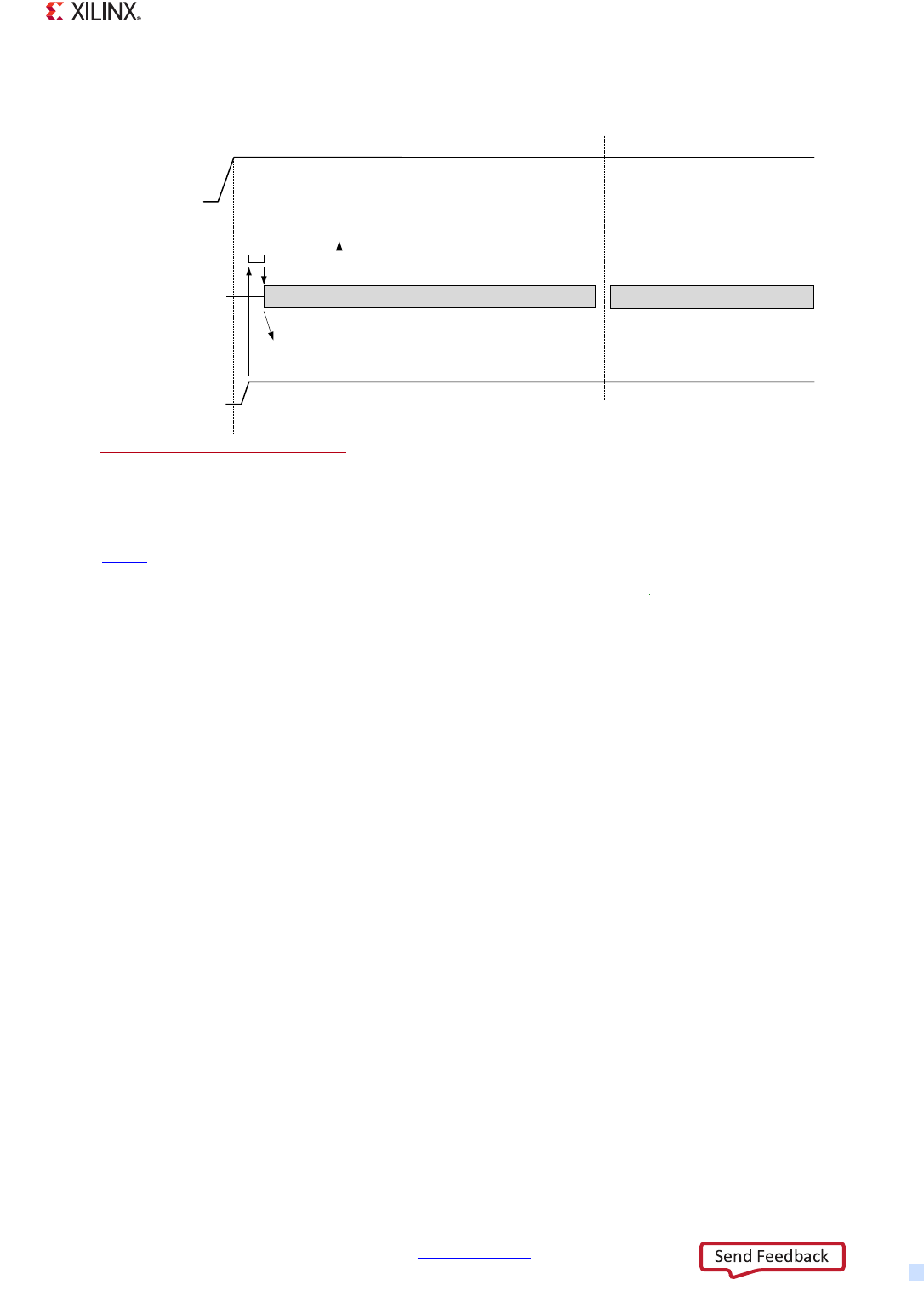
Zynq-7000 AP SoC Technical Reference Manual www.xilinx.com 209
UG585 (v1.12.1) December 6, 2017
Chapter 6: Boot and Configuration
PS Bring-up with PL Configuration Example
The PS and PL can be brought up together in a secure or non-secure mode. The simultaneous
bring-up of the PS and PL is shown in Figure 6-15. Also refer to Figure 6-4, page 164 for details on
power, reset, and clock interactions and timing examples.
In this example, the bring-up process boots from a flash memory device. The BootROM supports
both secure (encrypted images) and non-secure boot modes (no encryption). This bring-up
sequence is summarized in these steps below. The non-secure boot without the PL is illustrated in
Figure 6-14 and the secure boot mode with PL is illustrated in Figure 6-15:
1. Power-supplies are stable, PS_CLK is stable. See section 6.2.3 Clocks and PLLs.
2. PS_POR_B reset deasserts; for Secure boot, the PL is powered-on with the PS and self initializes.
3. BootROM executes in CPU 0:
a. Reads slcr.BOOT_MODE register to determine boot device.
b. Reads BootROM Header to determine encryption status and image destination.
c. Secure: Ensures PL is powered on to begin FSBL/User code decryption.
4. BootROM prepares for the CPU to execute the FSBL/User code:
a. Non-Secure: BootROM loads the FSBL/User code into OCM (or prepares for
execute-in-place) on Quad-SPI and NOR devices.
X-Ref Target - Figure 6-13
X-Ref Target - Figure 6-14
Figure 6-14: PS Non-secure Bring-up Example
1) PLL lock time. The PLL lock time is discussed in section 6.3.3 BootROM Performance.
2) BootROM Execution. This time is highly dependent on the bandwidth of the flash device interface. For BootROM
execution, refer to section 6.3.3 BootROM Performance.
3) FSBL/User Code Execution. The execution time for the FSBL/User code is beyond the scope of UG585, please refer to
UG821, Zynq-7000 All Programmable SoC Software Developers Guide.
UG585_c6_11_081514
Sequence 1:
PS Non-secure Bring-up
PS_POR_B
FSBL / User Code Executes
PS CPU 0
BootROM Executes after the PLLs lock.
BootROM Executes
15 to 200 ms, see note 2.
BootROM Moves
FSBL/User Code to OCM Memory
See note 3.
PS
Power-on
PLL Lock
<300 us
See note 1.
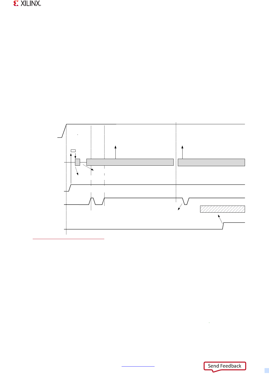
Zynq-7000 AP SoC Technical Reference Manual www.xilinx.com 210
UG585 (v1.12.1) December 6, 2017
Chapter 6: Boot and Configuration
b. Secure: BootROM programs the DevC DMA controller to transfer the encrypted FSBL/User
code into the RxFIFO and send it to the AES and HMAC modules in the PL. The decrypted
image accumulates in the TxFIFO and is written into the OCM memory by the DMA controller.
5. BootROM is disabled and CPU control is transferred to the FSBL/User code.
a. Non-Secure: Code can be in OCM memory or executed directly from the boot device.
b. Secure: Code is executed from OCM memory.
6. The FSBL/User code loads PL bitstream. (Optional)
a. Non-Secure: The code loads the bitstream using the PCAP controller.
b. Secure: The code loads the encrypted bitstream though the PCAP interface to the
AES/HMAC modules.
X-Ref Target - Figure 6-15
Figure 6-15: PS Bring-up with PL Configuration Option Example
1) PL TPOR and PLL Lock Time. The TPOR time is dependent on the voltage ramp of the power supply and is defined in
the data sheet. If the PL is already powered-up, then TPOR time = 0. The PLL Lock time is specified in the data sheet
with the TLOCK_PSPLL parameter. The PLL is locked before the BootROM starts to execute.
2) PL Init Time. This happens very quickly and is affected by the size of the PL.
3) BootROM Decrypts FSLB/User Code. The BootROM copies the encrypted boot image to OCM memory. The DevC
DMA controller reads the image into its RxFIFO, sends it through the AES or HMAC units, and then writes the image
back to OCM memory. The time depends on many factors: type of Flash device interface, PS_CLK frequency and the
image size. This time range is taken from Table 6-8, page 180.
4) FSBL/User Code Configures PL. The PS software programs the DMA to read the bitstream and optionally decrypt it
before going to the PL Configuration module. The time depends on many factors: type of Flash device interface,
PS_CLK frequency, bitstream size, and if the bitstream is encrypted.
5) Enable PL. After the PL is configured, the [PCFG_DONE_INT] bit asserts and the user code enables the voltage level
shifters. A power-up sequence example is shown in section 2.4 PS–PL Voltage Level Shifter Enables.
8*BFBDB
,1,7B%
2'2XWSXW
'21(
2'2XWSXW
%RRW520,QLWLDOL]HG3/IRUHQFU\SWHG
FRGHWRJJOHV>3&)*B352*B%@ELW
3/LV
&RQILJXUHG
36B325B%
)6%/8VHU&RGH([HFXWHV
36&38
6HOIWLPHG
%RRW520([HFXWHVDIWHUWKH3//VORFN
%RRW520([HFXWHV
3/
,QLW
>3&)*B'21(B,17@
5HDG
6HTXHQFH
36%ULQJXSZLWK3/&RQILJXUDWLRQ2SWLRQ
QRWH
WRPVVHHQRWH
3/
7325
WRPV
QRWH
7KH3/LVLQDFFHVVLEOHWRWKHXVHUIURP36B325B%UHVHWGHDVVHUWLRQ
XQWLOLWLVHQDEOHGE\WKH%RRW520
%RRW520'HFU\SWV
)6%/8VHU&RGH
)6%/,QLWLDOL]HG3/SULRU
WR&RQILJXUDWLRQWRJJOHV
>3&)*B352*B%@ELW
6HHQRWH
363/
3RZHURQ
3///RFN
XV
)6%/8VHU&RGH
&RQILJXUHV3/
%RRW520ZDLWVIRU3/7325
127()LJXUHQRWWRVFDOH
WRPV
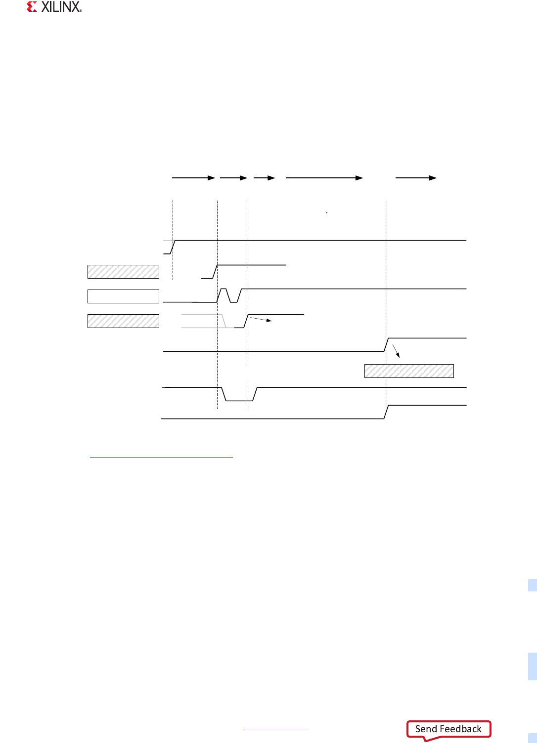
Zynq-7000 AP SoC Technical Reference Manual www.xilinx.com 211
UG585 (v1.12.1) December 6, 2017
Chapter 6: Boot and Configuration
PL Bring-up by FSBL/User Code Example
The PL may not be initially initialized and configured after a device boot. The PL may also be shut
down during system operation. This example illustrates how the PL can be configured from scratch
under the control the FSBL/User code.
Configure the PL via PCAP Bridge Example
1. Enable the PCAP bridge and select PCAP for reconfiguration. Write ones to devcfg.CTRL
[PCAP_MODE] and [PCAP_PR] bits.
2. Clear the Interrupts. Write all ones to the devcfg.INT_STS register.
3. (Optional) Initialize the PL (clears previous configuration):
a. Write 1 to [PCFG_PROG_B] bit.
X-Ref Target - Figure 6-16
Figure 6-16: PL Bring-up by FSBL/User Code Example
3/
7325
3/,QLW
(QDEOH
3&$3
8*BFBEB
>3&)*B,1,7@
>3&)*B352*B%@
'21(
2'2XWSXW
WRPV
QRWH QRWH QRWH
127()LJXUHQRWWRVFDOH
3/SRZHU
3RZHUXS
>3&)*B325B%@
,1,7B%
2'2XWSXW
3&)*B'21(B,17
,QWHUUXSWWR*,&
1RWH7KHWZRRSHQGUDLQ2'RXWSXWVLJQDOVDUHREVHUYDEOHWRWKHXVHU
EXWERDUGORJLFPXVWQRWGULYHWKHPORZZKLOHWKH36LVLQFRQWURORIWKH3/
LQLWLDOL]DWLRQDQGFRQILJXUDWLRQ
5HDG
:ULWH
5HDG
6HTXHQFH
3/%ULQJXSE\)6%/8VHU&RGH
3/LV&RQILJXUHG
>3&)*B'21(B,17@
5HDG
)6%/,QLWLDOL]HG3/SULRUWR
3/&RQILJXUDWLRQ
WRJJOHV>3&)*B352*B%@ELW
&RQILJXUHWKH3/
6HHQRWH
&RQILJXUH3/
ZLWKD%LWVWUHDP
QRWH
(QDEOH
3/
QRWH
1) PL TPOR Time. The TPOR time is dependent on the voltage ramp of the power supply. The allowed PL voltage
ramp time and TPOR times are specified in the data sheet. If the PL is already powered-up, then TPOR time = 0.
2) PL Init Time. The PL initialization time.
3) Enable PCAP. The PCAP control is described in section 6.4.3 PCAP Bridge to PL.
4) Configure the PL. Loading the PL Bitstream depends on many factors, see Table6-25, page222.
5) Enabled. The PL is in user mode when the [PCFG_DONE_INT] bit reads a 1. There is an example PL enable
sequence in section 2.4 PS–PL Voltage Level Shifter Enables.

Zynq-7000 AP SoC Technical Reference Manual www.xilinx.com 212
UG585 (v1.12.1) December 6, 2017
Chapter 6: Boot and Configuration
b. Write 0 to [PCFG_PROG_B] bit.
c. Wait for devcfg.STATUS [PCFG_INIT] bit = 0.
d. Write 1 to [PCFG_PROG_B] bit.
e. Clear the PL configuration done interrupt: Write 1 to devcfg.INT_STS [PCFG_DONE_INT].
4. Ensure that the PL is ready for programming: Wait for the devcfg.STATUS [PCFG_INIT] bit to = 1.
5. Check that there is room in the Command Queue. Verify devcfg.STATUS [DMA_CMD_Q_F] = 0.
Note, this step is not necessary if the PL is in the initialized state.
6. Disable the PCAP loopback. Write a zero (0) to the devcfg.MCTRL [INT_PCAP_LPBK] bit.
7. Program the PCAP_2x clock divider.
a. Secure Mode: Set devcfg.CTRL [QUARTER_PCAP_RATE_EN] bit = 1.
b. Non-secure Mode: Clear [QUARTER_PCAP_RATE_EN] bit = 0.
8. Queue-up a DMA transfer using the devcfg DMA registers:
a. Source Address: Location of new PL bitstream.
b. Destination Address: 0xFFFF_FFFF.
c. Source Length: Total number of 32-bit words in the new PL bitstream.
d. Destination Length: Total number of 32-bit words in the new PL bitstream. Write to the
devcfg.DMA_DEST_LEN register last to move the value of all four registers into the Command
Queue.
9. Wait for the DMA transfer to be done. Wait for the devcfg.INT_STS [DMA_DONE_INT] bit = 1.
10. Check for errors. Interrogate bits in the devcfg.INI_STS register: AXI_WERR_INT, AXI_RTO_INT,
AXI_RERR_INT, RX_FIFO_OV_INT, DMA_CMD_ERR_INT, DMA_Q_OV_INT, P2D_LEN_ERR_INT,
PCFG_HMAC_ERR_INT.
11. Make sure the PL configuration is done. Poll for [PCFG_DONE_INT] bit = 1.
If the PL is cleared using devcfg.CTRL [PCFG_PROG_B], then the devcfg.INT_STS [PCFG_DONE_INT]
bit is set when the PL is ready for reconfiguration. If the PL is cleared by asserting the PROGRAM_B
signal pin, then the DONE signal is asserted and the devcfg.INT_STS [D_P_DONE_INT] bit is set when
the operation is completed.
6.4.3 PCAP Bridge to PL
The PCAP bridge (also known as the AXI-PCAP bridge or PCAP interface) can be used to configure
the PL with a bitstream, decrypt boot images and bitstreams, and authenticate files. The bridge has
these operating modes:
• PCAP PL Bitstream Configuration Programming (encrypted and non-encrypted)
• PCAP PL Bitstream Readback
• PCAP Data Stream Decryption/Authentication
• Loopback for DMA transfers of Boot Images by BootROM and FSBL
The bridge’s DMA controller moves boot images between the FIFOs and a memory device; typically
the OCM memory, the DDR memory, or one of the linearly addressable flash devices (Quad-SPI or
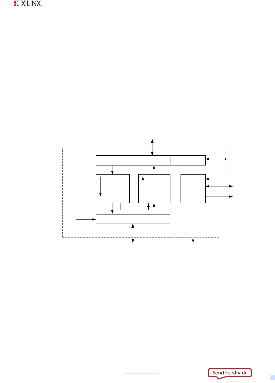
Zynq-7000 AP SoC Technical Reference Manual www.xilinx.com 213
UG585 (v1.12.1) December 6, 2017
Chapter 6: Boot and Configuration
NOR). The DMA controller is register programmed and can generate PS interrupts. It is a master on
the PS AXI interconnect. The bridge FIFOs normally interface with the PCAP configuration module to
transfer boot images and bitstreams.
Note: The DevC DMA controller is specifically designed for tasks associated with boot operations.
For general DMA needs, the DMA controller described in Chapter 9, DMA Controller must be used.
The bridge supports both concurrent (bidirectional) and non-concurrent (unidirectional) download
and upload of boot images. Transmit and receive FIFOs buffer data between the PS AXI Interconnect
and the PCAP interface. For PCAP data, the bridge converts 32-bit AXI formatted data to the 32-bit
PCAP protocol and vice versa.
Non-secure bitstreams and boot images sent to the PCAP interface can be sent every PCAP clock
cycle. Secure (encrypted) data is sent to the PCAP interface every four PCAP clock cycles.
The architecture of the PCAP bridge is shown in Figure 6-17.
The PL must be powered on to use the DevC module, including the PCAP bridge and PCAP
configuration module. The PCAP interface is enabled by setting the devcfg.CTRL [PCAP_MODE] and
[PCAP_PR] bits = 1 as illustrated in Figure 6-2, page 157. If encrypted bitstreams or boot images are
being sent, then the devcfg.CTRL [QUARTER_PCAP_RATE_EN] bit must be set = 1 to match the 32-bit
PCAP interface to the 8-bit AES/HMAC unit interface.
To start a DMA transfer, these four DMA registers must be written in this order:
1. Source Address register, devcfg.DMA_SRC_ADDR
2. Destination Address register, devcfg.DMA_DST_ADDR
3. Source Length register, devcfg.DMA_SRC_LEN
4. Destination Length register, devcfg.DMA_DEST_LEN (triggers DMA transfer)
X-Ref Target - Figure 6-17
Figure 6-17: PCAP Bridge Architecture
PCAP Control
UG585_c6_14_081514
AXI Master Interface
AXI-PCAP Bridge
PS AXI Interconnect
DMA Controller
TxFIFO RxFIFO
Control and
Status
Registers
CPU_1x clock
PCAP Interface
APB
uploaddownload
PL PCAP
PCAP clock
IRQ 40
Loopback

Zynq-7000 AP SoC Technical Reference Manual www.xilinx.com 214
UG585 (v1.12.1) December 6, 2017
Chapter 6: Boot and Configuration
In all modes, the DMA transactions must be 64-byte aligned to prevent accidently crossing a 4K byte
boundary. The DMA status is tracked using the devcfg.INT_STS [DMA_DONE_INT] and
[D_P_DONE_INT] bits. They can be monitored using either interrupts or a polling method.
6.4.4 PCAP Datapath Configurations
The PCAP bridge provides the FSBL/User code software with access to the PL configuration module
and decryption unit. The configuration module processes the bitstream and loads the SRAM in the
PL. The decryption unit is used to decrypt the bitstream and code files. The PL must be powered up
to use the bridge.
There are four common datapaths used with the PCAP bridge. The paths are illustrated in Figure 6-18
and Figure 6-19.
• Non-secure bitstream (unencrypted)
• Secure bitstreams and software boot images (encrypted)
• PL bitstream readback (from PL)
• Loopback for boot image transfers
Non-Secure PL Bitstream
The non-encrypted bitstream is usually accessed by DMA from the DDR memory and directly into the
PL configuration module. It bypasses the AES and HMAC units. This path can be used for
configuration and reconfiguration of the PL.
Secure Bitstreams and Software Boot Images
The encrypted bitstream is accessed by DMA from the DDR memory to the AES and HMAC units in
the PL. From the AES/HMAC units, the decrypted bitstream is routed directly to the PL configuration
module. This path can be used for configuration and reconfiguration of the PL.
There is a separate datapath and FIFO for receive and transmit in the PCAP interface bridge. This path
can be used by the FSBL/User code and operating system code.
To transfer boot images and bitstreams to the PL through the PCAP interface, the destination address
must be 0xFFFF_FFFF. Similarly, to read bitstreams from the PL through the PCAP interface, the
source address must be 0xFFFF_FFFF. Encrypted PS images must also be sent across the PCAP
interface because the AES and HMAC units reside within the PL. In this case, the DMA source address
could be an external memory interface and the destination address could be OCM memory.
Status Interrupts Bits
The DMA controller can trigger the DevC interrupt to the GIC interrupt controller upon completion
of the PL configuration transfer. The interrupt can be triggered when the AXI side of the DMA
transaction is complete (DMA_DONE_INT) or when both the AXI and PCAP transfers are complete
(D_P_DONE_INT). The AXI interconnect completion interrupt allows the software that is controlling
the DMA to perform scatter-gather type operations by issuing multiple DMA commands but holding
off the last transfer interrupt until all of the PCAP transactions are done.
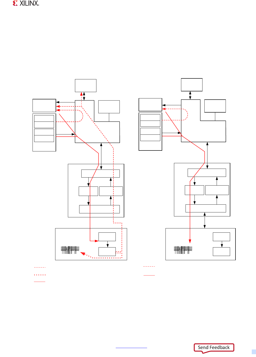
Zynq-7000 AP SoC Technical Reference Manual www.xilinx.com 215
UG585 (v1.12.1) December 6, 2017
Chapter 6: Boot and Configuration
Setting the two LSBs of the source and destination address to 2'b01 indicates to the DevC DMA
module the last DMA command of an overall transfer. The DMA controller uses this information to
appropriately set the DMA done interrupt. For the last DMA command, the DMA done interrupt is
triggered when both the AXI and PCAP interfaces are done. For all other DMA commands, the DMA
done interrupt is set when the AXI transfers are done; however, there might still be on-going PCAP
transfers. This distinction is made to allow overlapping AXI and PCAP transfers for all except the last
DMA transfer.
X-Ref Target - Figure 6-18
Figure 6-18: Non-Secure and Secure PL Bitstream Path Diagrams
3&$3%ULGJHLQ'HY&
8*BFBB
2&0
,23
1$1'
125
463,
&38
$;,ZLWK'0$
5HFHLYHU
),)2
7UDQVPLWWHU
),)2
3&$3,QWHUIDFH
3/&RQILJXUDWLRQ0RGXOH
6'FDUG
1RQ6HFXUH
3/%LWVWUHDP
3&$3%ULGJHLQ'HY&
2&0
,23
1$1'
125
463,
$;,ZLWK'0$
5HFHLYHU
),)2
7UDQVPLWWHU
),)2
3&$3,QWHUIDFH
3/&RQILJXUDWLRQ0RGXOH
6'FDUG
&RPPRQ3DWK
36$;,
,QWHUFRQQHFW
'5$0
&38
36$;,
,QWHUFRQQHFW
'5$0
25
6HFXUH
3/%LWVWUHDP
)6%/8VHU&RGH3DWK
&38
PDQDJHG
&38
PDQDJHG
$(6
+0$&
Fabric
$(6
+0$&
Fabric
3/%LWVWUHDP3DWK
)6%/8VHU&RGH3DWK
3/%LWVWUHDP3DWK

Zynq-7000 AP SoC Technical Reference Manual www.xilinx.com 216
UG585 (v1.12.1) December 6, 2017
Chapter 6: Boot and Configuration
PL Bitstream Readback
The PCAP interface can also be used to perform a PL bitstream readback. To perform a readback, the
PS must be running software capable of generating the correct PL readback commands. Two DMA
accesses are required to complete a PL configuration readback. The first access is used to issue the
readback command to the PL configuration module. The second access is needed to read the PL
bitstream from the PCAP. The smallest amount of bitstream data that can be read back from the PL
is one configuration frame which contains 101 32-bit words. An example program sequence is shown
below. The datapath is illustrated in Figure 6-19.
Example: PL Bitstream Readback
This example shows the first DMA access for a PL bitstream readback:
1. DMA Source Address – location of PL readback command sequence.
2. DMA Destination Address – desired location to store readback bitstream, note that the OCM
memory is not large enough to hold a complete PL bitstream readback.
3. DMA Source Length – number of commands in the PL readback command sequence.
4. DMA Destination Length – number of readback words expected from the PL.
There are four limitations when accessing the PL configuration module:
1. Readback of configuration registers or the bitstream cannot be performed until the
devcfg.INT_STS [PCFG_DONE] bit asserts.
2. A single PCAP readback access cannot be split across multiple DMA accesses. If the readback
command sent to the PL requests 505 words, the DevC DMA must also be set up to transfer 505
words. Splitting the transaction into two DMA accesses results in data loss and unexpected DMA
behavior.
3. The DMA must have sufficient bandwidth to process the PL readback due to a lack of data flow
control on the PL side of the PCAP. Overflow of the PCAP RxFIFO results in data loss and
unrecoverable DMA behavior. If adequate bandwidth cannot be allocated to the DevC DMA, then
the PCAP clock could be slowed down or the readback could be broken up into multiple smaller
transactions.
4. All DMA transactions must be 64-byte aligned to prevent accidently crossing a 4K byte boundary.
For more information regarding PL bitstream readback, see UG470, 7 Series FPGAs Configuration
User Guide.
Loopback For Boot Image Transfers
The DMA controller is used to move boot images. Loopback is enabled by setting the devcfg.MCTRL
[INT_PCAP_LPBK] bit = 1; the boot image is read into the RxFIFO and written to another memory
location from the TxFIFO. The DMA source address can be to a linearly addressable flash device and
the destination can be OCM or DDR memory. The PL does not need to be powered-up to use the
loopback datapath. The datapath is illustrated in Figure 6-19.
Note: Caution should be taken in loopback mode when transferring boot images between slave
ports that prioritize writes over reads. This situation can lead to a DevC DMA hang condition.
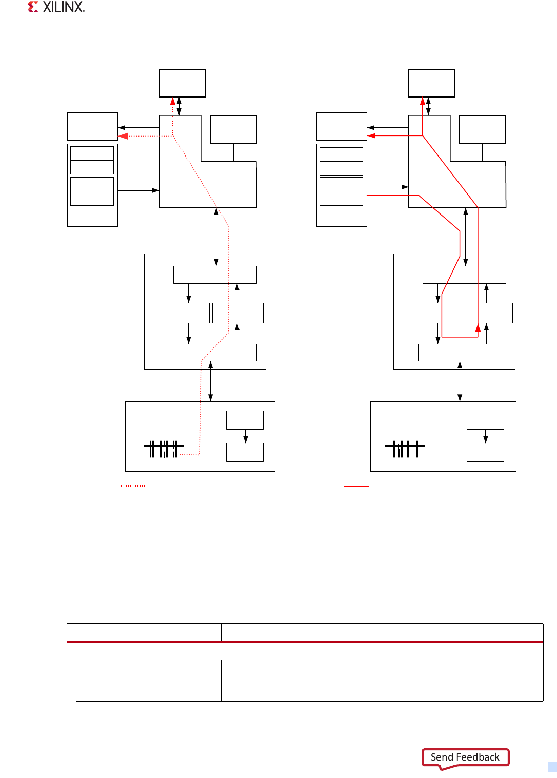
Zynq-7000 AP SoC Technical Reference Manual www.xilinx.com 217
UG585 (v1.12.1) December 6, 2017
Chapter 6: Boot and Configuration
PL Initialization and Configuration Registers
There are several control and status bits in the devcfg register space that the PS software can use to
initialize and configure the PL. These are listed in Table 6- 23 .
X-Ref Target - Figure 6-19
Figure 6-19: PL Bitstream Readback and PCAP Loopback Diagrams
3/%LWVWUHDP5HDGEDFN3DWK
3&$3%ULGJHLQ'HY&
8*BFBDB
2&0
,23
1$1'
125
463,
&38
$;,ZLWK'0$
5HFHLYHU
),)2
7UDQVPLWWHU
),)2
3&$3,QWHUIDFH
$(6
+0$&
3/&RQILJXUDWLRQ0RGXOH
6'FDUG
3/%LWVWUHDP
5HDGEDFN
3&$3%ULGJHLQ'HY&
2&0
,23
1$1'
125
463,
$;,ZLWK'0$
5HFHLYHU
),)2
7UDQVPLWWHU
),)2
3&$3,QWHUIDFH
3/&RQILJXUDWLRQ0RGXOH
6'FDUG
3&$3/RRSEDFN'DWD3DWK
36$;,
,QWHUFRQQHFW
'5$0
&38
36$;,
,QWHUFRQQHFW
'5$0
25
3&$3
/RRSEDFN
25
Fabric
$(6
+0$&
Fabric
Table 6-23: PL Control and Status Register Bits
Bit Field Bit Type Description
devcfg.CTRL
[PCFG_PROG_B] 30 RW
PL Reset Control. Similar to pulsing the PROGRAM_B pin
High-Low-High.
0: PL held in reset. 1: PL released from reset.

Zynq-7000 AP SoC Technical Reference Manual www.xilinx.com 218
UG585 (v1.12.1) December 6, 2017
Chapter 6: Boot and Configuration
6.4.5 PL Control via User-JTAG
The user can initialize the PL by toggling the PROGRAM_B signal high-low-high. The PL asserts the
INIT_B pin while the PL is initializing after which time the INIT_B open drain pin is left to float high.
The user can then proceed with programming the PL by accessing the Xilinx TAP controller. The
control and status signals and the TAP controller connection is shown in Figure 6-20.
[PCFG_POR_CNT_4K] 29 RW
Power-up Reset Timer Rate Select. Timer is used during PL
initialization.
0: Use 64K timer. 1: Use 4K timer (faster initialization of reset
stage).
devcfg.MCTRL
[PCFG_POR_B] 8 RO PL power on/off indicator: 0: power is off. 1: power is on.
[INT_PCAP_LPBK] 4 RW PCAP Loopback: 0: disabled, 1: enabled.
devcfg.STATUS
[PSS_CFG_RESET_B] 5 RO PL Reset State indicator.
0: reset state. 1: not reset state.
[PCFG_INIT] 4 RO
PL initialization complete indicator:
0: not ready.
1: ready for bitstream programming.
Status interrupt for positive and negative edges:
[PCFG_INIT_{PE,NE}_INT].
Maskable using devcfg.INT_MASK [M_PCFG_INIT_{PE,NE}_INT].
devcfg.INT_STS
[PSS_CFG_RESET_B_INT] 27 WTC PL reset interrupt detected, either edge.
Maskable using devcfg.INT_MASK [M_PSS_CFG_RESET_B_INT].
[PSS_CFG_RESET_B] 5 RO PL Reset State indicator.
0: reset state. 1: not reset state.
[PCFG_POR_B_INT] 4 WTC PL loss of power interrupt.
Maskable using devcfg.INT_MASK [M_PCFG_POR_B_INT].
[PCFG_CFG_RST_INT] 3 WTC PL configuration module reset level interrupt.
Maskable using devcfg.INT_MASK [M_PCFG_CFG_RST_INT].
[PCFG_DONE_INT] 2 WTC
PL Programming Done Indicator.
0: PL is not available.
1: Bitstream programming is complete and PL is in user mode.
Maskable using devcfg.INT_MASK [M_PCFG_DONE_INT].
[PCFG_INIT_PE_INT] 1 WTC
INIT_B Signal Positive-edge Detector Interrupt.
Triggered when a positive edge is detected on the INIT_B signal.
Maskable using devcfg.INT_MASK [M_PCFG_INIT_PE_INT].
[PCFG_INIT_NE_INT] 0 WTC
INIT_B Signal Negative-edge Detector Interrupt.
Triggered when a negative edge is detected on the INIT_B signal.
Maskable using devcfg.INT_MASK [M_PCFG_INIT_NE_INT].
Table 6-23: PL Control and Status Register Bits (Cont’d)
Bit Field Bit Type Description
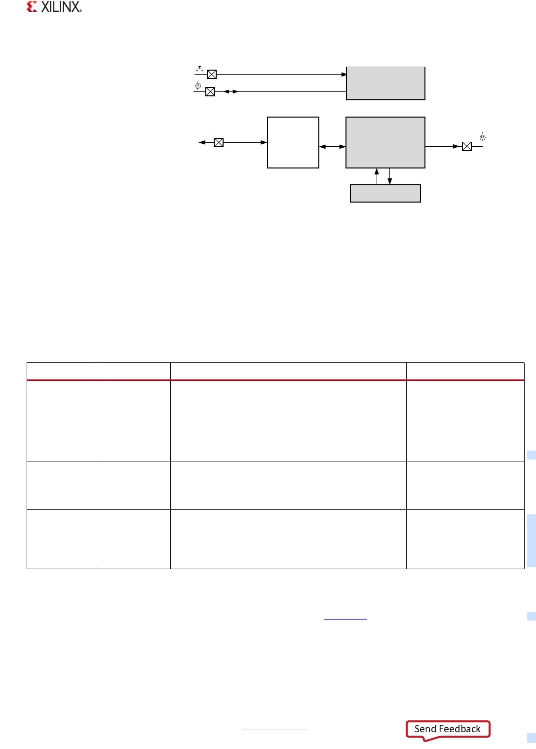
Zynq-7000 AP SoC Technical Reference Manual www.xilinx.com 219
UG585 (v1.12.1) December 6, 2017
Chapter 6: Boot and Configuration
PL User Control and Status Signals
The PROGRAM_B signal can be asserted using a push button to initiate a PL initialization process.
The red LED on the INIT_B signal will turn on when the PL is being initialized and then go out. At this
time, the user can use the TAP controller to configure the PL. There is green LED to indicate when the
DONE signal goes High. This signals that the PL has been successfully programmed. The PL
initialization signal pins are part of the PL voltage domain.
X-Ref Target - Figure 6-20
Figure 6-20: PL Initialization and Configuration Using User-JTAG
JTAG TAP
Controller
UG585_c6_12a_081514
PROGRAM_B PL Initialization
Circuits
PL
Configuration
Module
Bitstream
JTAG Debug
AES/HMAC Units
[PCAP_PR] = x
[PCAP_MODE] = 0
DONE
O.D.
INIT_B
Configure PL:
Initialize PL:
Table 6-24: PL Initialization Signals
Signal Name Type Description Board Connection
PROGRAM_B Active-Low
input
Reset PL Configuration Logic. The PROGRAM_B input
is usually pulsed Low by external means to reset the PL
and allow the PS software or JTAG TAP controller to
program the PL with a bitstream. When PROGRAM_B is
driven Low, the PL initialization sequence begins,
causing the PL to drive the INIT_B signal Low during the
process(2).
External 4.7 kΩ (or
stronger) pull-up resistor
to VCCO_0. Use a push
button to GND to
generate a configuration
reset.
INIT_B Active-Low
open-drain I/O
PL Initialization Activity and Configuration Error.
The PL drives the INIT_B pin Low when the PL is
initializing (clearing) its configuration memory, or
when the PL has detected a configuration error.(1)
External 4.7 kΩ (or
stronger) pull-up resistor
to VCCO_0 to ensure clean
Low-to-High transitions.
DONE
Active-High
open-drain
output
PL Configuration Done Indicator. The PL drives the
DONE signal Low until the PL is successfully
configured.
DONE has an internal
pull-up resistor of
approximately 10 kΩ.
External 330Ω resistor
circuits are not required.
Notes:
1. Unlike FPGAs, the INIT_B should not be externally held Low to delay the PL configuration sequence because this is not
indicated in the devcfg.STATUS [PCFG_INIT] register bit that is visible to PS software.
2. Ensure that PROGRAM_B is pulled up (High) during boot. Refer to Xilinx AR# 56272.

Zynq-7000 AP SoC Technical Reference Manual www.xilinx.com 220
UG585 (v1.12.1) December 6, 2017
Chapter 6: Boot and Configuration
6.5 Reference Section
This section includes content on these topics:
•Section 6.5.1 PL Configuration Considerations
•Section 6.5.2 Boot Time Reference
•Section 6.5.3 Register Overview
•Section 6.5.4 PS Version and Device Revision
6.5.1 PL Configuration Considerations
In master boot mode, the PL can be configured by PS software using the PCAP interface. Users are
free to configure the PL at any time, whether it is directly after PS boot using the FSBL/User code, or
at some later time using another image loaded into the PS memory. In JTAG boot mode, the PL can
be configured using the TAP controller. The PL configuration paths are illustrated in Figure 6-2,
page 157.
PCAP/ICAP/JTAG/User Access Exclusivity
The operation of the PCAP, ICAP and JTAG interfaces to the PL configuration module are mutually
exclusive. Care must be taken when switching among the three PL control paths: PCAP, JTAG and
ICAP, shown in Figure 6-2, page 157. Ensure that all outstanding transactions are completed before
changing interfaces.
Note: The user or external logic should not assert INIT_B when using the PS software to configure
the PL because the software does not have visibility to an external device delaying PL configuration.
Secure Mode PL Configuration
To perform a secure PL configuration, the PS must boot securely. The AES and HMAC units can only
be enabled by the BootROM. The procedure for loading a secure bitstream is the same as loading a
non-secure bitstream except the devcfg.CTRL [QUARTER_PCAP_RATE_EN] bit must be set = 1.
Because the AES unit only decrypts one byte at a time, the PCAP can only send one 32-bit word to
the PL for every four clock cycles.
Determine the PL State
The PL must first be powered on and initialized before it can be configured. When power is applied
to the PL, it begins its independent power-on reset sequence followed by initialization which clears
all of the PL configuration SRAM cells. The power-on reset status of the PL can be monitored by the
PS software.
The power status of the PL is tracked in the devcfg.MCTRL [PCFG_POR_B] bit. If the [PCFG_POR_B] bit
is set = 1, then the PL has power. The PL power status can also be tracked using the devcfg.INT_STS
[PCFG_POR_B_INT] interrupt.

Zynq-7000 AP SoC Technical Reference Manual www.xilinx.com 221
UG585 (v1.12.1) December 6, 2017
Chapter 6: Boot and Configuration
Additional information about the PL power-up status can be obtained by reading the devcfg.STATUS
[PSS_CFG_RESET_B] register bit. If the bit is Low, then the PL is in a reset state. A transition from a Low
to a High indicates the start of the PL initialization process.
PL Initialization Time Optimization
The devcfg.CTRL [PCFG_POR_CNT_4K] control bit can be set by the FSBL/User code to improve the
initialization time of a PL power-up sequence that occurs after the FSBL/User code has had a chance
to execute. In this case, the FSBL/User code sets the [PCFG_POR_CNT_4K] control bit and initiates a
PL power-up sequence in secure or non-secure mode. This optimization is useful when the PL is
powered-up by the FSBL/User code for configuration. This control bit is not accessible through the
Register Initialization writes and is reset by all system resets (POR and non-POR).
This function is similar to asserting the OVERRIDE pin on a 7 series FPGA and may be referred to as
an override function. Additional information on the use of the [PCFG_POR_CNT_4K] bit is described
in UG821, Zynq-7000 All Programmable SoC Software Developers Guide.
PCAP Clocking
The bitstream datapath to the PL configuration module is clocked by the PCAP clock, which is a
divided down PCAP_2x clock. The frequency range for the PCAP clock is specified in the data sheet.
To get a 100 MHz PCAP clock, program the PCAP_2x clock to 200 MHz.
PCAP Throughput
In non-secure mode, the transfer rate through the PCAP is approximately 145 MB/s. The PL
configuration module can accept data at the rate of 32 bits per PCAP clock, but the overall
throughput is limited by the PS AXI interconnect. This approximation assumes a 100 MHz PCAP
clock, a 133 MHz APB bus clock, a read issuing capability of 4 on the PS AXI interconnect, and a DMA
burst length of 8.
The throughput on the interconnect can be improved by about 20% by transferring the boot image
and bitstream from OCM memory and raising the CPU_1x clock rate by using a CPU clock ratio of
4:2:1. Refer to the data sheet for allowed clock rates.
In secure mode, the AES unit can only accept 8 bits per PCAP clock. To match this 8-bit data width
with the 32-bit datapath of the PCAP interface, software must set the devcfg.CTRL
[QUARTER_PCAP_RATE_EN] bit = 1. In this case, the demand for data by the PCAP interface is about
100 MB/s and is usually sustained by the PS AXI interconnect.
6.5.2 Boot Time Reference
Boot time activities include hardware activities, BootROM execution to configure the PS and load the
FSBL/User code, PL initialization and configuration, and the load and boot time of Linux or other
operating system. The factors that influence this boot process are summarized in Tab le 6 - 25 . Boot
time is heavily influenced by:
• The bandwidth of the flash interface. This is based on the memory vendor specifications, board
parameters, and optimized register values.

Zynq-7000 AP SoC Technical Reference Manual www.xilinx.com 222
UG585 (v1.12.1) December 6, 2017
Chapter 6: Boot and Configuration
• The Zynq-7000 device version (affects the PL initialization time and bitstream load time).
• The size of the loaded images (e.g., Linux image size).
IMPORTANT: The time it takes for each boot and configuration process to complete can be hard to
calculate because of all the variables involved. The values provided here are meant as a guide, not a
definitive answer. If you have any questions, please contact your Xilinx FAE Sales Engineer.
Table 6-25: Factors that Affect Boot and Configuration Time
Functional Area Description Boot Time Considerations
Zynq Device
Version
All device versions share the same PS and
boot time characteristics except when the PL
is involved.
PL size impacts the time for initialization
(cleaning/clearing) and configuration (bitstream).
Security
Encryption Decryption is required for secure boot.
Software uses the AES unit in the PL.
The decryption time is highly dependent on the
size of the boot image/bitstream and the PS_CLK
frequency. The decryption time is also impacted
by low bandwidth boot devices(5).
HMAC
Authentication
Authentication is done in the HMAC unit in
the PL.
The HMAC authentication time depends on the
PS_CLK frequency and size of the image.
RSA
Authentication Performed by the BootROM. The RSA authentication time depends on many
factors(6).
Flash Device Attributes
Boot Device
Vendor and Model
The Flash memory manufacturer and model
impacts performance. Situations vary(1).
Boot Interface The performance of the boot device
interface is the most important factor.
Table 6-8 shows relative performances of various
boot devices in a example context.
Boot Interface
Optimization
BootROM Header register initialization is
available.
Improves the read bandwidth of the flash device
all flash accesses(2).
Execute-in-place Quad-SPI and NOR option.
In non-secure mode, allows the CPU to execute
the FSBL/User code without needing to copy it to
the OCM memory.
PS Hardware Requirements
PS Voltage Ramp
This is power supply performance
specification. A fast power supply might
have a 5 to 10 ms voltage ramp time.
The minimum ramp time is provided in the data
sheet.
PS Hardware Boot
After a POR reset, the hardware samples the
strapping pins, does some hardware
housekeeping.
Less than 10 microseconds.
PS Hardware and BootROM Options
PS PLL Startup and
Lock
After a POR, the PLL programming is done
by the hardware before the BootROM
executes. After a non-POR reset the
BootROM re-programs the PLLs and waits
for them to lock before continuing
execution.
PLL lock time is a data sheet specification. Refer
to DS187 or DS191. The three PLLs are enabled by
the BOOT_MODE [4] pin.

Zynq-7000 AP SoC Technical Reference Manual www.xilinx.com 223
UG585 (v1.12.1) December 6, 2017
Chapter 6: Boot and Configuration
6.5.3 Register Overview
Tabl e 6-2 6 provides an overview of the device configuration registers.
CRC check of
128 KB ROM
This is an eFuse option that causes the
BootROM to check the integrity of its own
code at the beginning of execution.
Requires about 26 ms to perform (PS_CLK
frequency = 33 MHz).
PL Hardware Functions
PL Voltage Ramp
This is power supply performance
specification. A typical board might have a
10 ms voltage ramp time.
The minimum ramp time is provided in the data
sheet.
PL Initialization This can be done in parallel with the PS
power up, or be initiated by FSBL/User code.
If the FSBL/User code runs before PL initialization,
the time can be sped-up(3).
PL TPOR
TPOR occurs when the PL is powered-up. It
includes the PL Voltage Ramp time plus the
PL Initialization (cleaning/clearing) time.
This time is influenced by the performance of the
PL power supply and status of the PL. The range
for TPOR is specified in the data sheet. If the PL is
already powered up then only the initialization
time is needed before programming the PL.
PL Configuration This is done by FSBL/User code after the PL
has been initialized. This time is influenced by many factors(4).
PL Partial
Configuration
This is a special operation that programs
only part of the PL at a time. It is used for
very time-sensitive applications.
Contact your Xilinx FAE Sales Engineer to learn
more about partial configuration and
reconfiguration.
Notes:
1. The device type and model depend on the Boot Mode (e.g., for Quad-SPI, this includes ability to use linear addressing mode
for Flash devices ≤128Mb, or needing to use managed mode for larger devices).
2. The performance of the boot interface can be optimized by using the BootROM Header register initialization mechanism.
This is most effective in non-secure mode because more registers are accessible for optimization, see Table 6-7, page 175.
The register initialization can also be helpful in secure mode. The available optimizations are listed for each boot device in
section 6.3.3 BootROM Performance.
3. The PL initialization time can be decreased when the FSBL/User code executes before initializing the PL. Refer to “PL
Initialization Time Optimization” section in section 6.5.1 PL Configuration Considerations for information.
4. The PL configuration time is most dependent on whether the bitstream is encrypted or not. PL configuration time can be
reduced by using a compressed bitstream, but the size of the compressed file cannot be predicted nor can the time to
decompress the file be calculated.
5. For decryption or HMAC authentication, the PCAP configuration module must be operated at 1/4 the PCAP clock rate by
setting the devcfg.CTRL [QUARTER_PCAP_RATE_EN] bit = 1.
6. RSA authentication time depends from where the boot image and bitstream are sourced from and written to, the size of the
data, and the PS_CLK frequency. An example is shown in section 6.3.3 BootROM Performance, RSA Authentication Time.
Table 6-25: Factors that Affect Boot and Configuration Time (Cont’d)
Functional Area Description Boot Time Considerations
Table 6-26: DevC and Boot Registers
Function Description Hardware Register Type
Control and
configuration
Control devcfg.CTRL Read/Write
Sticky locks require POR to reset devcfg.LOCK R/Sticky Write
Configuration devcfg.CFG Read/Write
Zynq-7000 AP SoC Technical Reference Manual www.xilinx.com 224
UG585 (v1.12.1) December 6, 2017
Chapter 6: Boot and Configuration
6.5.4 PS Version and Device Revision
The device versions and revisions are hard coded into two read-only registers. Each device is a
combination of the slcr.PSS_IDCODE9 [DEVICE] and devcfg.MCTRL [PS_VERSION] register bit fields.
This Zynq-7000 All Programmable SoC Technical Reference Manual contains information pertaining to
production silicon (v3.1). The functionality of preproduction devices that is different from production
devices is described in AR# 47916 Zynq-7000 AP SoC Devices - Silicon Revision Differences.
DevC
status
Interrupt status: PL init, done, DMA/AXI
errors devcfg.INT_STS R + Clr or W
Interrupt mask devcfg.INT_MASK Read/Write
Status: eFuse, Init, Lockdown, PS control,
DevC DMA/FIFOs devcfg.STATUS Read-only
PCAPDMA
DMA source address devcfg.DMA_SRC_ADDR Read/Write
DMA destination address devcfg.DMA_DST_ADDR Read/Write
DMA source length devcfg.DMA_SRC_LEN Read/Write
DMA destination length devcfg.DMA_DEST_LEN Read/Write
Boot
Multi-Boot offset devcfg.MULTIBOOT_ADDR Read/Write
Miscellaneous control devcfg.MCTRL Read/Write
Reset Reason and Lockdown error code slcr.REBOOT_STATUS Read/Write
Boot and PLL mode slcr.BOOT_MODE Read-only
Table 6-26: DevC and Boot Registers (Cont’d)
Function Description Hardware Register Type
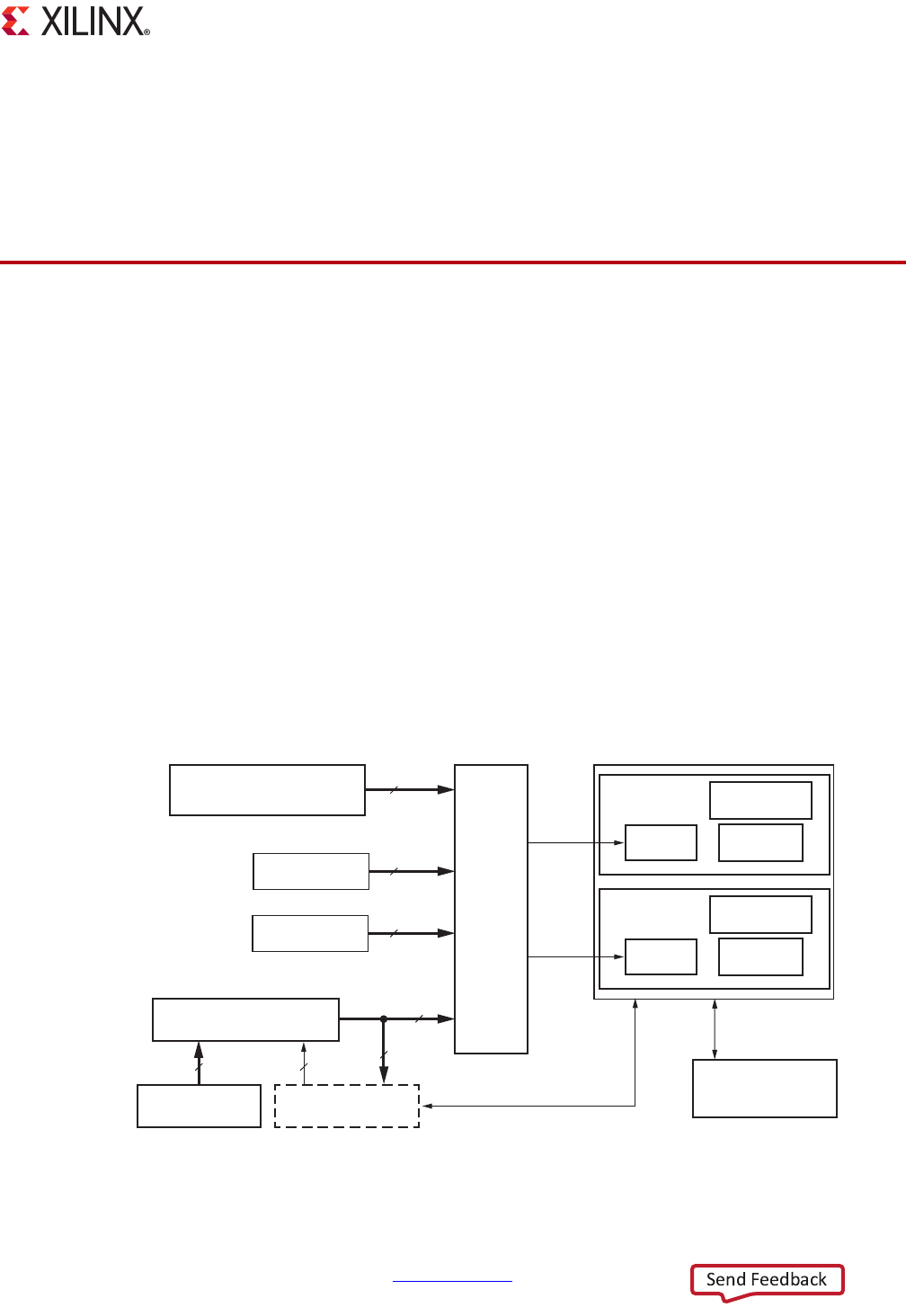
Zynq-7000 AP SoC Technical Reference Manual www.xilinx.com 225
UG585 (v1.12.1) December 6, 2017
Chapter 7
Interrupts
7.1 Environment
This chapter describes the system-level interrupt environment and the functions of the interrupt
controller (see Figure 7-1). The PS is based on ARM architecture, utilizing two Cortex-A9 processors
(CPUs) and the GIC pl390 interrupt controller. Note that single-core devices contain one Cortex-A9
processor (CPU), dual-core devices contain two. This chapter discusses the dual-core
configuration.
The interrupt structure is closely associated with the CPUs and accepts interrupts from the I/O
peripherals (IOP) and the programmable logic (PL). This chapter includes these key topics:
•Private, shared and software interrupts
• GIC functionality
• Interrupt prioritization and handling
X-Ref Target - Figure 7-1
Figure 7-1: System-Level Block Diagram
Shared Peripheral
Interrupts (SPI)
Software Generated
Interrupts (SGI)
Private Peripheral
Interrupts (PPI)
Shared Peripherals
Software Interrupts
Programmable
Logic
PS
I/O Peripherals (IOP)
Generic Interrupt
Controller
Enable, Classify, Distribute
and Prioritize
CPU 0
Private 5
16
44
Private Peripheral
Interrupts (PPI)
CPU 1
Private Interrupt
Interface
CPU 1
Execution
Unit
Private Interrupt
Registers
60
5
Interrupt
Control and Status
Registers
UG585_c7_01_030912
60
CPU 0
CPU 1
CPU 0
CPU 1
CPU 0
CPU 1
16 each
IRQ/FIQ
CPU Private
Bus
WFI, WFE and
Event Indicators
Interrupt
Interface
Execution
Unit
Private Interrupt
Registers
IRQ/FIQ
CPU 0

Zynq-7000 AP SoC Technical Reference Manual www.xilinx.com 226
UG585 (v1.12.1) December 6, 2017
Chapter 7: Interrupts
7.1.1 Private, Shared and Software Interrupts
Each CPU has a set of private peripheral interrupts (PPIs) with private access using banked registers.
The PPIs include the global timer, private watchdog timer, private timer, and FIQ/IRQ from the PL.
Software generated interrupts (SGIs) are routed to one or both CPUs. The SGIs are generated by
writing to the registers in the generic interrupt controller (GIC), refer to section 7.3 Register
Overview. The shared peripheral interrupts (SPIs) are generated by the various I/O and memory
controllers in the PS and PL. They are routed to either or both CPUs. The SPI interrupts from the PS
peripherals are also routed to the PL.
7.1.2 Generic Interrupt Controller (GIC)
The generic interrupt controller (GIC) is a centralized resource for managing interrupts sent to the
CPUs from the PS and PL. The controller enables, disables, masks, and prioritizes the interrupt
sources and sends them to the selected CPU (or CPUs) in a programmed manner as the CPU interface
accepts the next interrupt. In addition, the controller supports security extension for implementing a
security-aware system.
The controller is based on the ARM Generic Interrupt Controller Architecture version 1.0 (GIC v1),
non-vectored.
The registers are accessed via the CPU private bus for fast read/write response by avoiding
temporary blockage or other bottlenecks in the interconnect.
The interrupt distributor centralizes all interrupt sources before dispatching the one with the highest
priority to the individual CPUs. The GIC ensures that an interrupt targeted to several CPUs can only
be taken by one CPU at a time. All interrupt sources are identified by a unique interrupt ID number.
All interrupt sources have their own configurable priority and list of targeted CPUs.
7.1.3 Resets and Clocks
The interrupt controller is reset by the reset subsystem by writing to the PERI_RST bit of the
A9_CPU_RST_CTRL register in the SLCR. The same reset signal also resets the CPU private timers and
private watchdog timers (AWDT). Upon reset, all interrupts that are pending or being serviced are
ignored.
The interrupt controller operates with the CPU_3x2x clock (half the CPU frequency).
7.1.4 Block Diagram
The shared peripheral interrupts are generated from various subsystems that include the I/O
peripherals in the PS and logic in the PL. The interrupt sources are illustrated in Figure 7-2.
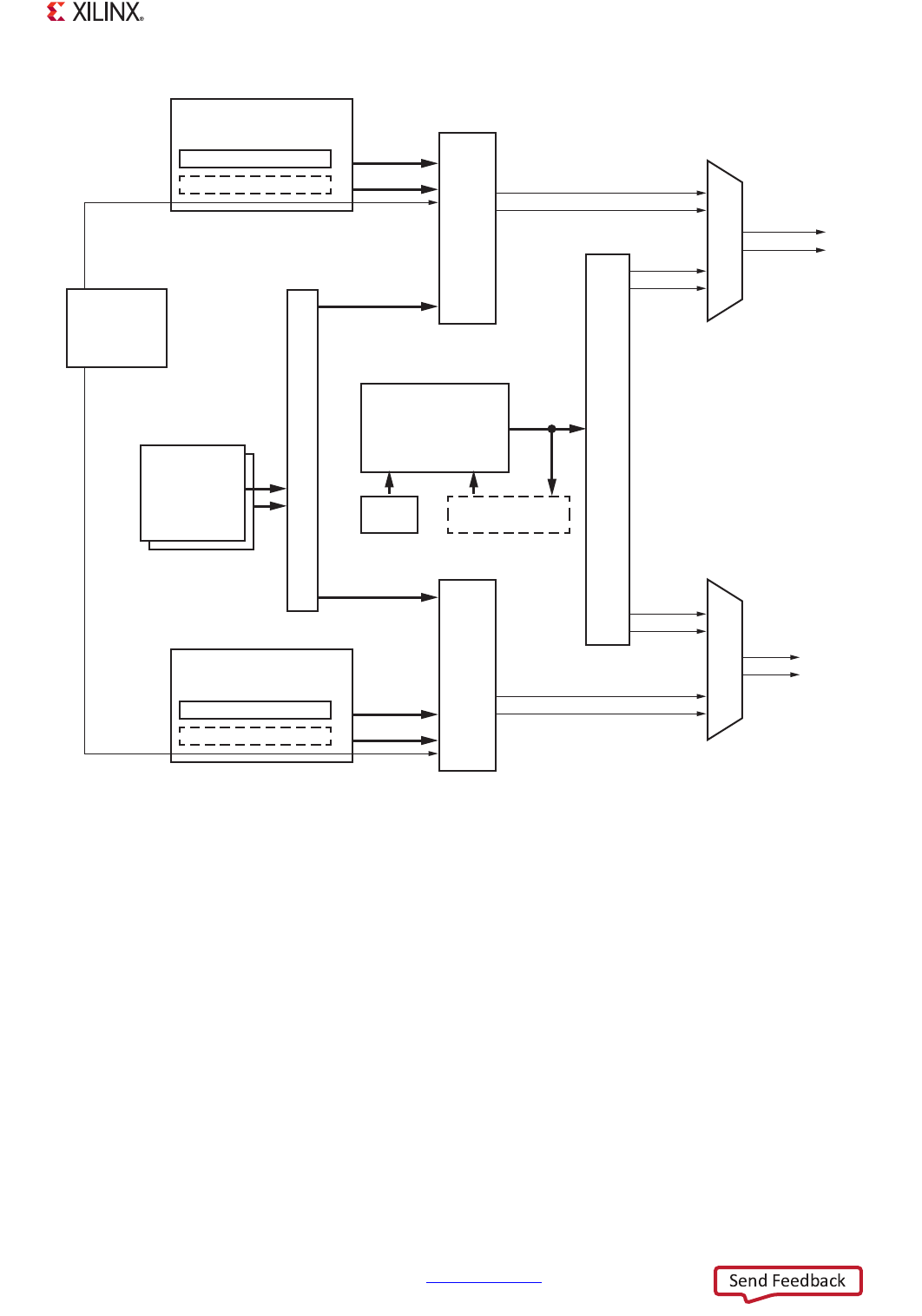
Zynq-7000 AP SoC Technical Reference Manual www.xilinx.com 227
UG585 (v1.12.1) December 6, 2017
Chapter 7: Interrupts
7.1.5 CPU Interrupt Signal Pass-through
The IRQ/FIQ from the PL can be routed through the GIC as PPI#4 and #1, or bypass the GIC using the
pass-through multiplexer shown in Figure 7-3. This logic is instantiated for both CPUs. The
pass-through mode is enabled through the mpcore.ICCICR register, according to Tabl e 7-1 .
X-Ref Target - Figure 7-2
Figure 7-2: Interrupt Controller Block Diagram
Interrupt Controller Distributor (ICD)
nIRQ
nFIQ
nIRQ
nFIQ
nIRQ
nFIQ
Shared
Peripheral
Interrupts (SPI)
CPU 0 Timer and AWDT
PL FIQ 0, IRQ 0
nIRQ
nFIQ
nIRQ
nFIQ
nIRQ
nFIQ
CPU 0
Distributor
CPU 1
Distributor
Private Peripheral
Interrupts (PPI)
Software
Generated
Interrupts
(SGI)
System
Watchdog
Timer
PL
CPU 0
CPU 1
CPU 0
SGI Distributor
CPU 1 Timer and AWDT
PL FIQ 1, IRQ 1
Private Peripheral
Interrupts (PPI)
CPU 1
UG585_c7_02_012813
CPU 1
Interface
CPU 0
Interface
IOP
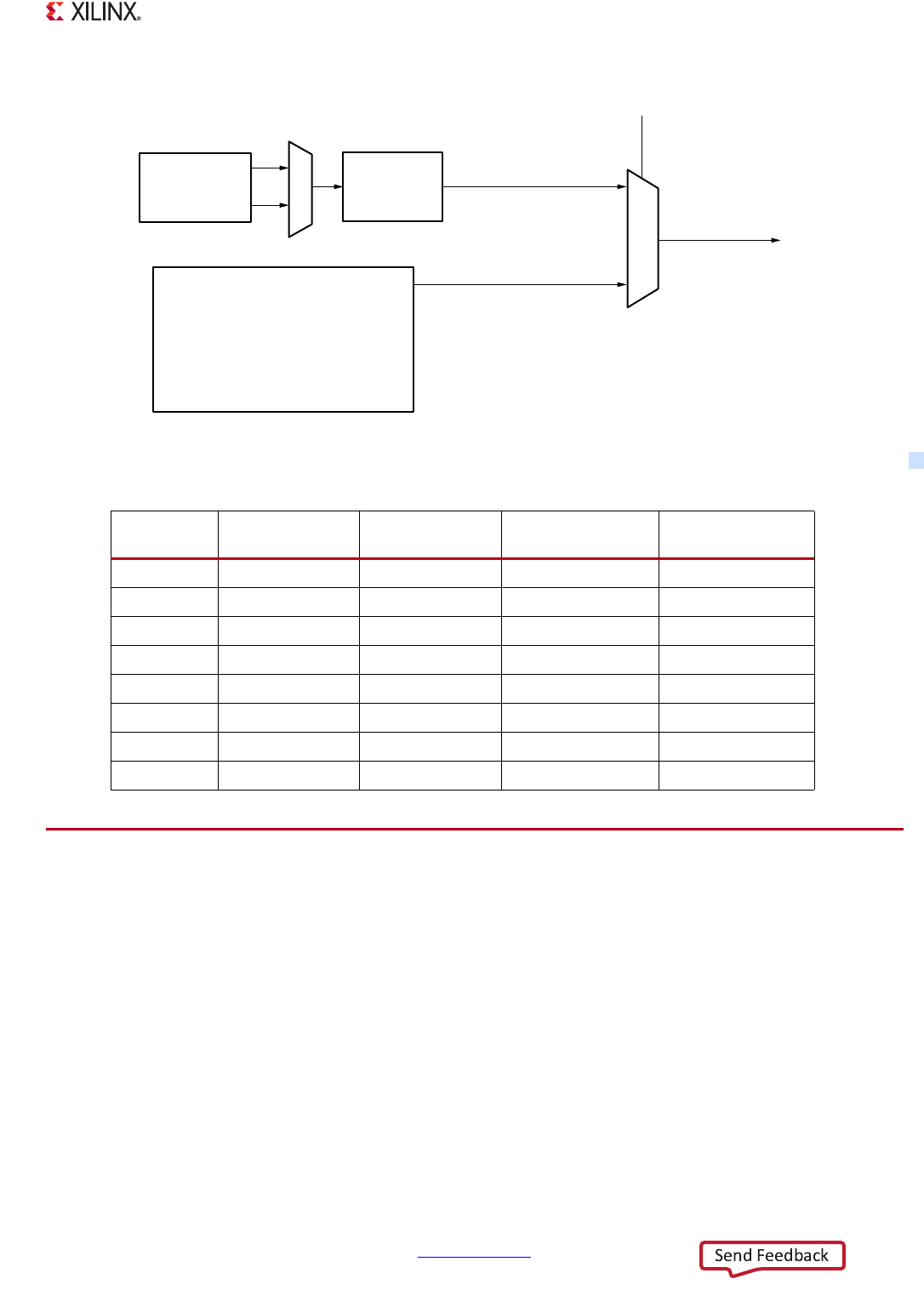
Zynq-7000 AP SoC Technical Reference Manual www.xilinx.com 228
UG585 (v1.12.1) December 6, 2017
Chapter 7: Interrupts
7.2 Functional Description
7.2.1 Software Generated Interrupts (SGI)
Each CPU can interrupt itself, the other CPU, or both CPUs using a software generated interrupt (SGI).
There are 16 software generated interrupts (see Ta b le 7 - 2). An SGI is generated by writing the SGI
interrupt number to the ICDSGIR register and specifying the target CPU(s). This write occurs via the
CPU's own private bus. Each CPU has its own set of SGI registers to generate one or more of the 16
software generated interrupts. The interrupts are cleared by reading the ICCIAR (Interrupt
Acknowledge) register or writing a 1 to the corresponding bits of the ICDICPR (Interrupt
Clear-Pending) register.
X-Ref Target - Figure 7-3
Figure 7-3: Legacy IRQ/FIQ Interrupt Pass-Through Multiplexer
Table 7-1: Pass-through Mode
FIQEn
(ICCICR[3])
SecureS
(ICCICR[0])
SecureNS
(ICCICR[1])
IRQ
to CPU x
FIQ
to CPU x
00 0pass through pass through
00 1driven by GIC pass through
01 0driven by GIC pass through
01 1driven by GIC pass through
10 0pass through pass through
10 1driven by GIC pass through
11 0pass through driven by GIC
11 1driven by GIC driven by GIC
Programmable Logic (PL)
CPU0, IRQ: IRQF2P[16]
CPU0, FIQ: IRQF2P[18]
CPU1, IRQ: IRQF2P[17]
CPU1, FIQ: IRQF2P[19]
IRQ / FIQ
IRQ / FIQ
To CPU x
CPU x
Interface
IRQ / FIQ
GIC
Interrupt
Distributors
Pass-through
Mux
mpcore.ICCICR [31:0]
0
!0
UG585_c7_03_100417

Zynq-7000 AP SoC Technical Reference Manual www.xilinx.com 229
UG585 (v1.12.1) December 6, 2017
Chapter 7: Interrupts
All SGIs are edge triggered. The sensitivity types for SGIs are fixed and cannot be changed; the
ICDICFR0 register is read-only, since it specifies the sensitivity types of all the 16 SGIs.
7.2.2 CPU Private Peripheral Interrupts (PPI)
Each CPU connects to a private set of five peripheral interrupts. The PPIs are listed in Tabl e 7 -3 .
The sensitivity types for PPIs are fixed and cannot be changed; therefore, the ICDICFR1 register is
read-only, since it specifies the sensitivity types of all the 5 PPIs. Note that the fast interrupt (FIQ)
signal and the interrupt (IRQ) signal from the PL are inverted and then sent to the interrupt
controller. Therefore, they are active High at the PS-PL interface, although the ICDICFR1 register
reflects them as active Low level.
7.2.3 Shared Peripheral Interrupts (SPI)
A group of approximately 60 interrupts from various modules can be routed to one or both of the
CPUs or the PL. The interrupt controller manages the prioritization and reception of these interrupts
for the CPUs.
Except for IRQ #61 through #68 and #84 through #91, all interrupt sensitivity types are fixed by the
requesting sources and cannot be changed. The GIC must be programmed to accommodate this. The
boot ROM does not program these registers; therefore the SDK device drivers must program the GIC
to accommodate these sensitivity types.
Table 7-2: Software Generated Interrupts (SGI)
IRQ ID# Name SGI# Type Description
0 Software 0 0 Rising edge A set of 16 interrupt sources that are private to each
CPU that can be routed to up to 16 common interrupt
destinations where each destination can be one or
more CPUs.
1 Software 1 1 Rising edge
~ ... ~ ...
15 Software 15 15 Rising edge
Table 7-3: Private Peripheral Interrupts (PPI)
IRQ ID# Name PPI# Type Description
26:16 Reserved ~ ~ Reserved
27 Global Timer 0 Rising edge Global timer
28 nFIQ 1
Active Low level
(active High at PS-PL interface)
Fast interrupt signal from the PL:
CPU0: IRQF2P[18]
CPU1: IRQF2P[19]
29 CPU Private Timer 2 Rising edge Interrupt from private CPU timer
30 AWDT{0, 1} 3 Rising edge Private watchdog timer for each CPU
31 nIRQ 4
Active Low level
(active High at PS-PL interface)
Interrupt signal from the PL:
CPU0: IRQF2P[16]
CPU1: IRQF2P[17]

Zynq-7000 AP SoC Technical Reference Manual www.xilinx.com 230
UG585 (v1.12.1) December 6, 2017
Chapter 7: Interrupts
For an interrupt of level sensitivity type, the requesting source must provide a mechanism for the
interrupt handler to clear the interrupt after the interrupt has been acknowledged. This requirement
applies to any IRQF2P[n] (from PL) with a high level sensitivity type.
For an interrupt of rising edge sensitivity, the requesting source must provide a pulse wide enough
for the GIC to catch. This is normally at least 2 CPU_2x3x periods. This requirement applies to any
IRQF2P[n] (from PL) with a rising edge sensitivity type.
The ICDICFR2 through ICDICFR5 registers configure the interrupt types of all the SPIs. Each interrupt
has a 2-bit field, which specifies sensitivity type and handling model.
The SPI interrupts are listed in Tabl e 7- 4 .
Table 7-4: PS and PL Shared Peripheral Interrupts (SPI)
Source Interrupt Name IRQ ID# Status Bits
(mpcore Registers) Required Type PS-PL Signal Name I/O
APU
CPU 1, 0 (L1, TLB, BTAC) 33:32 spi_status_0[1:0] Rising edge ~ ~
L2 Cache 34 spi_status_0[2] High level ~ ~
OCM 35 spi_status_0[3] High level ~ ~
Reserved ~ 36 spi_status_0[3] ~ ~ ~
PMU PMU [1,0] 38, 37 spi_status_0[6:5] High level ~ ~
XADC XADC 39 spi_status_0[7] High level ~ ~
DevC DevC 40 spi_status_0[8] High level ~ ~
SWDT SWDT 41 spi_status_0[9] Rising edge ~ ~
Timer TTC 0 44:42 spi_status_0[12:10] High level ~ ~
DMAC DMAC Abort 45 spi_status_0[13] High level IRQP2F[28] Output
DMAC [3:0] 49:46 spi_status_0[17:14] High level IRQP2F[23:20] Output
Memory SMC 50 spi_status_0[18] High level IRQP2F[19] Output
Quad SPI 51 spi_status_0[19] High level IRQP2F[18] Output
Reserved ~ ~~
Always driven
Low
IRQP2F[17] Output
IOP
GPIO 52 spi_status_0[20] High level IRQP2F[16] Output
USB 0 53 spi_status_0[21] High level IRQP2F[15] Output
Ethernet 0 54 spi_status_0[22] High level IRQP2F[14] Output
Ethernet 0 Wake-up 55 spi_status_0[23] Rising edge IRQP2F[13] Output
SDIO 0 56 spi_status_0[24] High level IRQP2F[12] Output
I2C 0 57 spi_status_0[25] High level IRQP2F[11] Output
SPI 0 58 spi_status_0[26] High level IRQP2F[10] Output
UART 0 59 spi_status_0[27] High level IRQP2F[9] Output
CAN 0 60 spi_status_0[28] High level IRQP2F[8] Output

Zynq-7000 AP SoC Technical Reference Manual www.xilinx.com 231
UG585 (v1.12.1) December 6, 2017
Chapter 7: Interrupts
7.2.4 Interrupt Sensitivity, Targeting and Handling
There are three types of interrupts that come into the GIC as explained in section : SPI, PPI and SGI.
In a general sense, the interrupt signals includes a sensitivity setting, whether one or both CPUs
handle the interrupt, and which CPU or CPUs are targeted: zero, one, or both. However, the
functionality of most interrupt signals include fixed settings, while others are partially
programmable.
There are two sets of control registers for sensitivity, handling, and targeting:
• mpcore.ICDICFR[5:0] registers: sensitivity and handling. See Figure 7-4.
• mpcore.ICDIPTR[23:0] registers: targeting CPU(s). See Figure 7-5.
Shared Peripheral Interrupts (SPI)
The SPI interrupts can be targeted to any number of CPUs, but only one CPU handles the interrupt.
If an interrupt is targeted to both CPUs and they respond to the GIC at the same time, the MPcore
ensures that only one of the CPUs reads the active interrupt ID#. The other CPU receives the Spurious
ID# 1023 interrupt or the next pending interrupt, depending on the timing. This removes the
requirement for a lock in the interrupt service routine. Targeting the CPU is done by the ICDIPTR
[23:8] registers. The sensitivity of each SPI interrupt must be programmed to match those listed in
PL
PL [2:0] 63:61 spi_status_0[31:29] Rising edge/
High level
IRQF2P[2:0] Input
PL [7:3] 68:64 spi_status_1[4:0] Rising edge/
High level
IRQF2P[7:3] Input
Timer TTC 1 71:69 spi_status_1[7:5] High level ~ ~
DMAC DMAC[7:4] 75:72 spi_status_1[11:8] High level IRQP2F[27:24] Output
IOP
USB 1 76 spi_status_1[12] High level IRQP2F[7] Output
Ethernet 1 77 spi_status_1[13] High level IRQP2F[6] Output
Ethernet 1 Wake-up 78 spi_status_1[14] Rising edge IRQP2F[5] Output
SDIO 1 79 spi_status_1[15] High level IRQP2F[4] Output
I2C 1 80 spi_status_1[16] High level IRQP2F[3] Output
SPI 1 81 spi_status_1[17] High level IRQP2F[2] Output
UART 1 82 spi_status_1[18] High level IRQP2F[1] Output
CAN 1 83 spi_status_1[19] High level IRQP2F[0] Output
PL PL [15:8] 91:84 spi_status_1[27:20] Rising edge/
High level
IRQF2P[15:8] Input
SCU Parity 92 spi_status_1[28] Rising edge ~ ~
Reserved ~ 95:93 spi_status_1[31:29] ~ ~ ~
Table 7-4: PS and PL Shared Peripheral Interrupts (SPI) (Cont’d)
Source Interrupt Name IRQ ID# Status Bits
(mpcore Registers) Required Type PS-PL Signal Name I/O
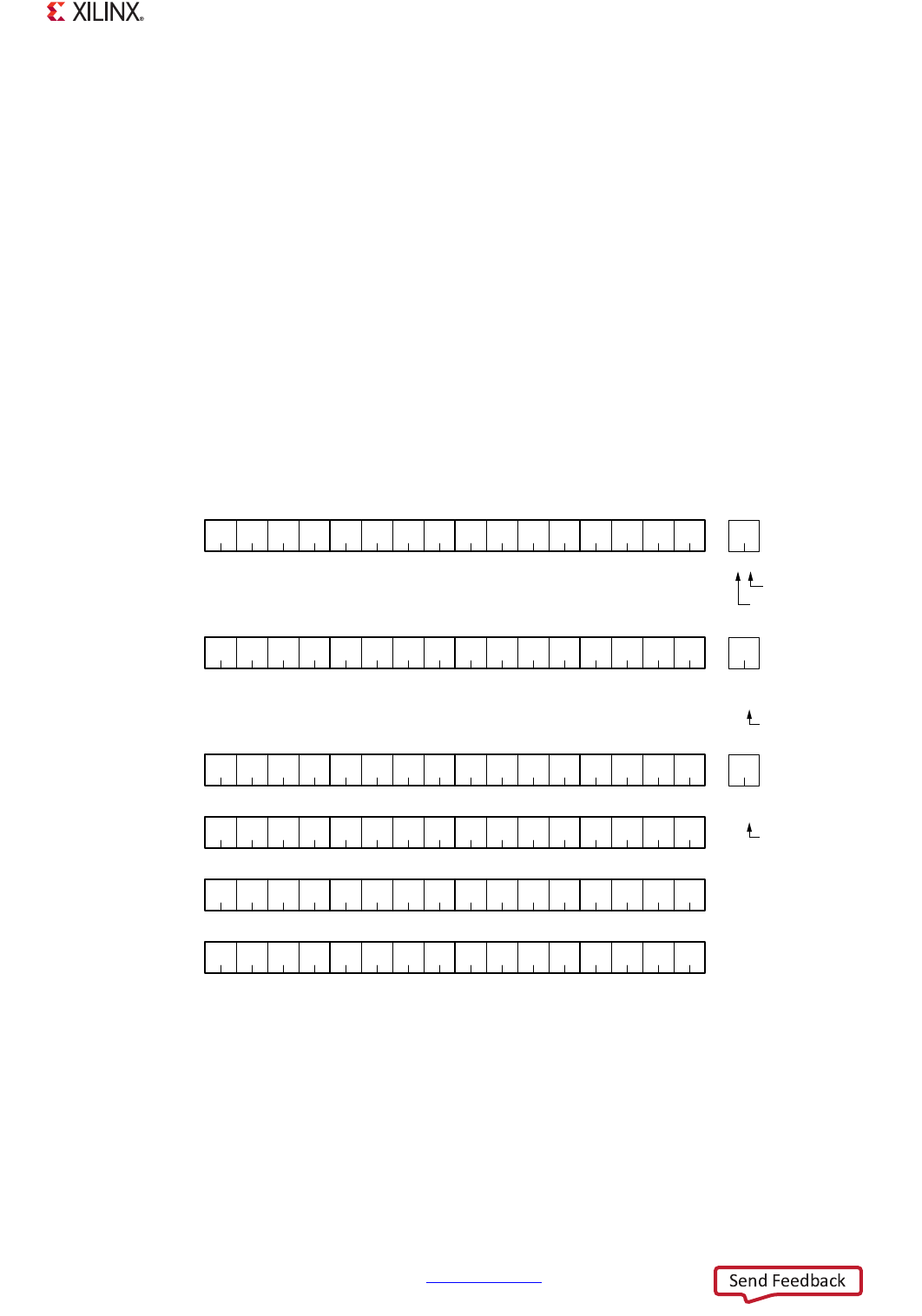
Zynq-7000 AP SoC Technical Reference Manual www.xilinx.com 232
UG585 (v1.12.1) December 6, 2017
Chapter 7: Interrupts
Tabl e 7-4 , PS and PL Shared Peripheral Interrupts (SPI). The sensitivity is programmed using the
ICDICFR [5:2] registers.
Private Peripheral Interrupts (PPI)
Each CPU has its own separate PPI interrupts with fixed functionality; the sensitivity, handling, and
targeting of these interrupts are not programmable. Each interrupt only goes to its own CPU and is
handled by that CPU. The ICDICFR [1] register is read-only and the ICDIPTR [5:2] registers are
essentially reserved.
Software Generated Interrupts (SGI)
The SGI interrupts are always edge sensitive and are generated when software writes the interrupt
number to ICDSGIR register. All of the targeted CPUs defined in the ICDIPTR [23:8] must handle the
interrupt in order to clear it. See Figure 7-4 and Figure 7-5.
X-Ref Target - Figure 7-4
Figure 7-4: Interrupts ICDICFR Register for Sensitivity and Handling
Private Peripheral Interrupts (PPI)
62
63 61 60
Shared Peripheral Interrupts (SPI)
58
59 57 56 5455 53 52 5051 49 48
ICD ICFR 3
78
79 77 76 7475 73 72 7071 69 68 6667 65 64
ICD ICFR 4
x
31
xx92 9091 89 88 8687 85 84 8283 81 80
24 16 8 0
ICD ICFR 5
46
47 45 44 4243 41 40 3839 37 x 3435 33 32
ICD ICFR 2
30
31 29 28
Software Generated Interrupts (SGI)
x
27 x x xxxx xxxx
ICD ICFR 1
14
15 13 12 1011 9 8 6754 2310
ICD ICFR 0
Edge sensitive.
01: High-level active.
11: Rising-edge active.
IRQ
IRQ
Read-only.
0xAAAA AAAA
Read-only.
0x7DC0 0000 01: Low-level active.
11 : Edge sensitive.
IRQ
(IRQ ID #36, 93, 94 and 95 are reserved.) Private CPU only.
Other bit combinations
are reserved.
1 0 All targeted CPUs must
handle the interrupt
.
Handled by one CPU.
Sensitivity and
CPU handling model:
UG585_c7_04_121613
Zynq-7000 AP SoC Technical Reference Manual www.xilinx.com 233
UG585 (v1.12.1) December 6, 2017
Chapter 7: Interrupts
7.2.5 Wait for Interrupt Event Signal (WFI)
The CPU can go into a wait state where it waits for an interrupt (or event) signal to be generated. The
wait for interrupt signal that is sent to the PL is described in Chapter 3, Application Processing Unit.
7.3 Register Overview
The ICC and ICD registers are part of the pl390 GIC register set. There are 60 SPI interrupts. This is far
fewer than what the pl390 can support, so there are far fewer interrupt enable, status, prioritization
and processor target registers in the ICD than is possible for the pl390. A summary of the ICC and ICD
registers are listed in Tab le 7 -5
X-Ref Target - Figure 7-5
Figure 7-5: Interrupts ICDIPTR Register for Targeting CPU
reserved
31 24 16 8 0
IRQ # 3
ICD IPTR [3:0]
00: not targeted
01: targeted to CPU 0
10: targeted to CPU 1
11: targeted to both CPUs
reserved reserved reserved
IRQ # 2 IRQ # 1 IRQ # 0
31 24 16 8 0
ICD IPTR [8] reserved
IRQ # 35
reserved reserved reserved
IRQ # 34 IRQ # 33 IRQ # 32
ICD IPTR [22] reserved
IRQ # 91
reserved reserved reserved
IRQ # 90 IRQ # 89 IRQ # 88
ICD IPTR [23]
IRQ # 95
reserved
IRQ # 94 IRQ # 93 IRQ # 92
reserved reserved reserved
IRQ # 7 IRQ # 6 IRQ # 5 IRQ # 4
IRQ # 11 IRQ # 10 IRQ # 9 IRQ # 8
IRQ # 15 IRQ # 14 IRQ # 13 IRQ # 12
ICD IPTR [7:4] Reserved, these interrupts are always targeted to their private CPU.
IRQ # 36, 93, 94, and
95 are reserved.
SGI
PPI
SPI
SPI
SPI
UG585_c7_05_121613
Table 7-5: Interrupt Controller Register Overview
Name Register Description Write Protection Lock
Interrupt Controller CPU (ICC)
ICCICR CPU interface control Yes, except EnableNS
ICCPMR Interrupt priority mask ~
ICCBPR Binary point for interrupt priority ~

Zynq-7000 AP SoC Technical Reference Manual www.xilinx.com 234
UG585 (v1.12.1) December 6, 2017
Chapter 7: Interrupts
7.3.1 Write Protection Lock
The interrupt controller provides the facility to prevent write accesses to critical configuration
registers. This is done by writing a one to the APU_CTRL[CFGSDISABLE] bit. The APU_CTRL register is
part of the AP SoC’s System Level Control register set, SLCR. This controls the write behavior for the
secure interrupt control registers.
RECOMMENDED: If the user wants to set the CFGSDISABLE bit, it is recommended that this be done
during the user software boot process which occurs after the software has configured the Interrupt
ICCIAR Interrupt acknowledge ~
ICCEOIR End of interrupt ~
ICCRPR Running priority ~
ICCHPIR Highest pending interrupt ~
ICCABPR Aliased non-secure binary point ~
Interrupt Controller Distributor (ICD)
ICDDCR Secure/non-secure mode select Yes
ICDICTR, ICDIIDR Controller implementation ~
ICDISR [2:0] Interrupt security Yes
ICDISER [2:0],
ICDICER [2:0]
Interrupt set-enable and clear-enable Yes
ICDISPR [2:0],
ICDICPR [2:0]
Interrupt set-pending and clear-pending Yes
ICDABR [2:0] Interrupt active ~
ICDIPR [23:0] Interrupt priority, 8-bit fields. Only the upper 5 bits of each
8-bit field are writable; the lower bits are always 0. There are
32 priority levels.
Yes
ICDIPTR [23:0] Interrupt processor targets, 8-bit fields. Yes
ICDICFR [5:0] Interrupt sensitivity type, 2-bit fields (level/edge, handling
model) Yes
PPI and SPI Status
PPI_STATUS PPI status: Corresponds to ICDISR[0], ICDISER[0], ICDICER[0],
ICDISPR[0], ICDICPR[0], and ICDABR[0] registers (security,
enable, pending and active).
~
SPI_STATUS [2:1] SPI status: Corresponds to ICDISR[2:1], ICDISER[2:1],
ICDICER[2:1], ICDISPR[2:1], ICDICPR[2:1], and ICDABR[2:1]
registers (security, enable, pending and active).
~
Software Generated Interrupts (SGI)
ICDSGIR Software-generated interrupts ~
Disable Write Accesses (SLCR register)
APU_CTRL CFGSDISABLE bit disables some write accesses ~
Table 7-5: Interrupt Controller Register Overview (Cont’d)
Name Register Description Write Protection Lock

Zynq-7000 AP SoC Technical Reference Manual www.xilinx.com 235
UG585 (v1.12.1) December 6, 2017
Chapter 7: Interrupts
Controller registers. The CFGSDISABLE bit can only be cleared by a power-on reset (POR.) After the
CFGSDISABLE bit is set, it changes the protected register bits to read-only and therefore the behavior of
these secure interrupts cannot be changed, even in the presence of rogue code executing in the secure
domain.
7.4 Programming Model
7.4.1 Interrupt Prioritization
All of the interrupt requests (PPI, SGI and SPI) are assigned a unique ID number. The controller uses
the ID number to arbitrate. The interrupt distributor holds the list of pending interrupts for each
CPU, and then selects the highest priority interrupt before issuing it to the CPU interface. Interrupts
of equal priority are resolved by selecting the lowest ID.
The prioritization logic is physically duplicated to enable the simultaneous selection of the highest
priority interrupt for each CPU. The interrupt distributor holds the central list of interrupts,
processors and activation information, and is responsible for triggering software interrupts to the
CPUs.
SGI and PPI distributor registers are banked to provide a separate copy for each connected
processor. Hardware ensures that an interrupt targeting several CPUs can only be taken by one CPU
at a time.
The interrupt distributor transmits to the CPU interfaces the highest pending interrupt. It receives
back the information that the interrupt has been acknowledged, and can then change the status of
the corresponding interrupt. Only the CPU that acknowledges the interrupt can end that interrupt.
7.4.2 Interrupt Handling
The response of the GIC to a pending interrupt when an IRQ line de-asserts is described in the ARM
document: IHI0048B_gic_architecture_specification.pdf (see Appendix A, Additional Resources). See
the Note in Section 1.4.2 with additional information in Section 3.2.4.
If the interrupt is pending in the GIC and IRQ is de-asserted, the interrupt in the GIC becomes
inactive (and the CPU never sees it).
If the interrupt is active in the GIC (because the CPU interface has acknowledged the interrupt), then
the software ISR determines the cause by checking the GIC registers first and then polling the I/O
Peripheral interrupt status registers.
7.4.3 ARM Programming Topics
The ARM GIC architecture specification includes these programming topics:
• GIC register access

Zynq-7000 AP SoC Technical Reference Manual www.xilinx.com 236
UG585 (v1.12.1) December 6, 2017
Chapter 7: Interrupts
• Distributor and CPU Interfaces
• Affects of the GIC security extensions
• PU Interface registers
• Preserving and restoring controller state
7.4.4 Legacy Interrupts and Security Extensions
When the legacy interrupts (IRQ, FIQ) are used, and an interrupt handler accesses both IRQs and FIQs
in secure mode (via ICCICR[AckCtl]=1), race conditions occasionally occur when reading the
interrupt IDs. There is also a risk of seeing FIQ IDs in the IRQ handler, as the GIC only knows what
security state the handler is reading from, not which type of handler.
There are two workable solutions:
• Only signal IRQs to a re-entrant IRQ handler and use the preemption feature in the GIC.
• Use FIQ and IRQ with ICCICR[AckCtl]=0 and use the TLB tables to handle IRQ in non-secure
mode, and handle FIQ in secure mode.

Zynq-7000 AP SoC Technical Reference Manual www.xilinx.com 237
UG585 (v1.12.1) December 6, 2017
Chapter 8
Timers
8.1 Introduction
Each Cortex-A9 processor has its own private 32-bit timer and 32-bit watchdog timer. Both
processors share a global 64-bit timer. These timers are always clocked at 1/2 of the CPU frequency
(CPU_3x2x).
On the system level, there is a 24-bit watchdog timer and two 16-bit triple timer/counters. The
system watchdog timer is clocked at 1/4 or 1/6 of the CPU frequency (CPU_1x), or can be clocked by
an external signal from an MIO pin or from the PL. The two triple timers/counters are always clocked
at 1/4 or 1/6 of the CPU frequency (CPU_1x), and are used to count the widths of signal pulses from
an MIO pin or from the PL.
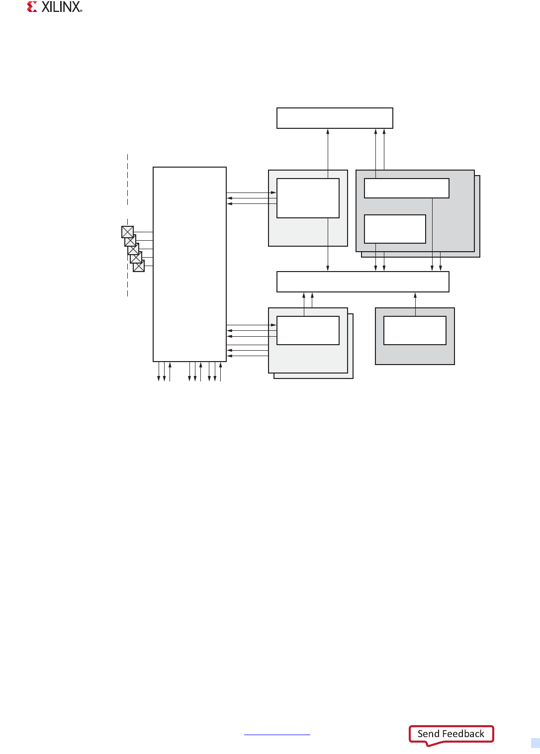
Zynq-7000 AP SoC Technical Reference Manual www.xilinx.com 238
UG585 (v1.12.1) December 6, 2017
Chapter 8: Timers
8.1.1 System Diagram
The relationships of the system timers are shown in Figure 8-1.
8.1.2 Notices
7z007s and 7z007s CLG225 Devices
The 7z007s single core and 7z010 dual core CLG225 devices support 32 MIO pins (not 54). This is
shown in the MIO table in section 2.5.4 MIO-at-a-Glance Table. The 7z007s and 7z010 CLG225
devices restrict the available MIO pins so connections through the EMIO might need to be
considered. All of the 7z007s and 7z010 CLG225 device restrictions are listed in section
1.1.3 Notices.
X-Ref Target - Figure 8-1
Figure 8-1: System View
UG585_c8_01_072512
System
Watchdog
Timer
CPU WatchDog
CPU Private
Timer
System Reset (POR)
Interrupt Controller
Clock in
Reset Out
Clock in
Waveform
Out
The System Watchdog
Timer can optionally
reset the whole chip.
The CPU Private
WatchDogs can optionally
reset the whole chip.
TTC 0
TTC 1
CPU 0
CPU 1
Triple Timer
Counter
Global Timer
Counter
CPU_3x2x
CPU_3x2x
MIO / EMIO
MIO Pins
EMIO
TTC 0, 1SWDT
CPU

Zynq-7000 AP SoC Technical Reference Manual www.xilinx.com 239
UG585 (v1.12.1) December 6, 2017
Chapter 8: Timers
8.2 CPU Private Timers and Watchdog Timers
The CPU private timers and watchdog timers are fully documented in the Cortex-A9 MPCore
Technical Requirements Document, sections 4.1 and 4.2 (see Appendix A, Additional Resources).
Both the timer and watchdog blocks have the following features:
• 32-bit counter that generates an interrupt when it reaches zero
• 8-bit prescaler to enable better control of the interrupt period
• Configurable single-shot or auto-reload modes
•Configurable starting values for the counter
8.2.1 Clocking
All private timers and watchdog timers are always clocked at 1/2 of the CPU frequency (CPU_3x2x).
8.2.2 Interrupt to PS Interrupt Controller
The interrupts sent to the interrupt controller are described in section 7.2.2 CPU Private Peripheral
Interrupts (PPI).
8.2.3 Resets
The time and watchdog resets are sent to the PS reset subsystem, see section 26.3 Reset Effects.
8.2.4 Register Overview
A register overview of the CPU private and watchdog timers is provided in Tabl e 8-1 .
Table 8-1: CPU Private Timers Register Overview
Function Name Overview
CPU Private Timers
Reload and current values Timer Load
Timer Counter
Values to be reloaded into the decrementer.
Current value of the decrementer.
Control and interrupt Timer Control
Timer Interrupt Enable, auto reload, IRQ, prescaler, interrupt status.
CPU Private Watchdogs (AWDT 0 and 1)
Reload and current values Watchdog Load
Watchdog Counter
Values to be reloaded into the decrementer.
Current value of the decrementer.
Control and interrupt Watchdog Control
Watchdog Interrupt
Enable, Auto reload, IRQ, prescaler, interrupt status.
(this register cannot disable watchdog)

Zynq-7000 AP SoC Technical Reference Manual www.xilinx.com 240
UG585 (v1.12.1) December 6, 2017
Chapter 8: Timers
8.3 Global Timer (GT)
The Global Timer is fully documented in the Cortex-A9 MPCore Technical Requirements Document,
sections 4.3 and 4.4 (see Appendix A, Additional Resources). The global timer is a 64-bit
incrementing counter with an auto-incrementing feature. The global timer is memory mapped in the
same address space as the private timers. The global timer is accessed at reset in secure state only.
The global timer is accessible to all Cortex-A9 processors. Each Cortex-A9 processor has a 64-bit
comparator that is used to assert a private interrupt when the global timer has reached the
comparator value.
8.3.1 Clocking
The GTC is always clocked at 1/2 of the CPU frequency (CPU_3x2x).
8.3.2 Register Overview
A register overview of the GTC is provided in Tabl e 8-2 .
Reset status Watchdog Reset Status
Reset status as a result of watchdog reaching 0.
Cleared with POR only, so SW can tell if the reset was
caused by watchdog.
Disable Watchdog Disable Disable watchdog through a sequence of writes of
two specific words.
Table 8-1: CPU Private Timers Register Overview (Cont’d)
Function Name Overview
Table 8-2: Global Timer Register Overview
Function Name Overview
Global Timer (GTC)
Current values Global Timer Counter Current value of the incrementer
Control and interrupt Global Timer Control
Global Interrupt
Enable timer, enable comparator, IRQ,
auto-increment, interrupt status
Comparator Comparator Value
Comparator Increment
Current value of the comparator
Increment value for the comparator
Global Timer Disable Disable watchdog through a sequence of writes of
two specific words

Zynq-7000 AP SoC Technical Reference Manual www.xilinx.com 241
UG585 (v1.12.1) December 6, 2017
Chapter 8: Timers
8.4 System Watchdog Timer (SWDT)
In addition to the two CPU private watchdog timers, there is a system watchdog timer (SWDT) for
signaling additional catastrophic system failure, such as a PS PLL failure. Unlike the AWDT, the SWDT
can run off the clock from an external device or the PL, and provides a reset output to an external
device or the PL.
8.4.1 Features
Key features of the available timers/counters are as follows:
• An internal 24-bit counter
• Selectable clock input from:
°Internal PS bus clock (CPU_1x)
°Internal clock (from PL)
°External clock (from MIO)
• On timeout, outputs one or a combination of:
°System interrupt (PS)
°System reset (PS, PL, MIO)
• Programmable timeout period:
°Timeout range 32,760 to 68,719,476,736 clock cycles (330 µs to 687.2s at 100 MHz)
•Programmable output signal duration on timeout:
°System interrupt pulse 4, 8, 16, or 32 clock cycles (CPU_1x clock)
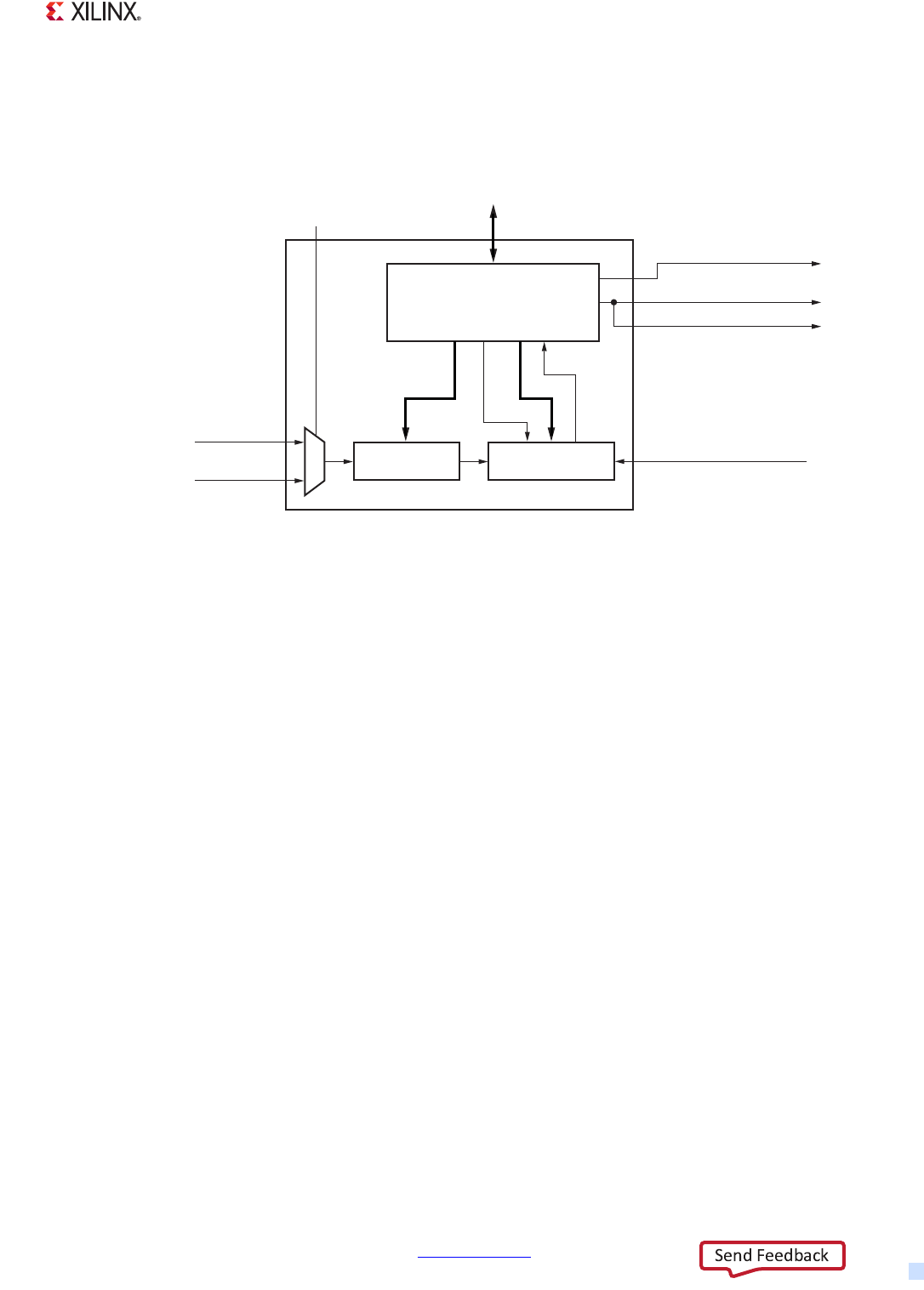
Zynq-7000 AP SoC Technical Reference Manual www.xilinx.com 242
UG585 (v1.12.1) December 6, 2017
Chapter 8: Timers
8.4.2 Block Diagram
A block diagram of the SWDT is shown in Figure 8-2.
Notes relevant to Figure 8-2:
• SLCR programmable registers (WDT_CLK_SEL, MIO control) select the clock input.
• SWDT programmable registers set the values for CLKSEL and CRV.
• Signal restart causes the 24-bit counter to reload the CRV values, and restart counting.
• Signal halt causes the counter to halt during CPU debug (same behavior as AWDT).
8.4.3 Functional Description
The control logic block has an APB interface connected to the system interconnect. Each write data
received from the APB has a key field which must match the key of the register in order to be able to
write to the register.
The Zero Mode register controls the behavior of the SWDT when its internal 24-bit counter reaches
zero. Upon receiving a zero signal, the control logic block asserts the interrupt output signal for
IRQLN clock cycles if both WDEN and IRQEN are set, and also asserts the reset output signals for
approximately one CPU_1x cycle if WDEN is set. The 24-bit counter then stays at zero until it is
restarted.
The Counter Control register sets the timeout period, by setting reload values in
swdt.CONTROL[CLKSET] and swdt.CONTROL[CRV] to control the prescaler and the 24-bit counter.
The Restart register is used to restart the counting process. Writing to this register with a matched
key causes the prescaler and the 24-bit counter to reload the values from CRV signals.
X-Ref Target - Figure 8-2
Figure 8-2: System Watchdog Timer Block Diagram
UG585_c8_02_120913
Control Logic
24-bit CounterPrescaler
Interrupt Controller ID41
Halt (during CPU debug)
SWDT Reset
(to PS reset system)
Restart
MIO Pin, EMIOWDTRSTO
Zero
CRV
CLKSEL
APB
CPU_1x
MIO Pins,
EMIOWDTCLKI
slcr.WDT_CLK_SEL[0]
slcr.MIO_PIN_xx
]
INTERCONNECT

Zynq-7000 AP SoC Technical Reference Manual www.xilinx.com 243
UG585 (v1.12.1) December 6, 2017
Chapter 8: Timers
The Status register shows whether the 24-bit counter reaches zero. Regardless of the WDEN bit in the
Zero Mode register, the 24-bit counter always keeps counting down to zero if it is not zero and the
selected clock source is present. Once it reaches zero, the WDZ bit of the Status register is set and
remains set until the 24-bit counter is restarted.
The prescaler block divides down the selected clock input. The CLKSEL signal is sampled at every
rising clock edge.
The internal 24-bit counter counts down to zero and stays at zero until it is restarted. While the
counter is at zero, the zero output signal is High.
Interrupt to PS Interrupt Controller
The pulse length from the SWDT (four CPU_1x clock cycles) is sufficient for the interrupt controller to
capture the interrupt using rising-edge sensitivity.
Reset
The watchdog reset is sent to the PS reset subsystem to cause a non-POR reset, see section
26.3 Reset Effects. The reset output to the MIO pin or EMIOWDTRSTO is active High.
TIP: To generate a signal pulse for the PS_POR_B and other board resets, route the EMIOWDTRSTO
signal from the SWDT through the PL and to a pin that can be externally latched to generate a valid
reset pulse. Alternatively, use an external watchdog timer device that is managed by PS software via a
GPIO output pin. The PS_POR_B reset pulse width requirements are defined in the data sheet.
8.4.4 Register Overview
A register overview of the SWDT is provided in Tabl e 8-3 .
Table 8-3: System Watchdog Timer Register Overview
Function Name Overview
Clock select slcr.WDT_CLK_SEL Selects between the CPU_1x and external clock source (MIO/EMIO).
MIO routing slcr.MIO_PIN_xx Routes the SWDT clock input through the MIO multiplexer or EMIO if
no MIO routing.
Reset reason slcr.REBOOT_STATUS The [SWDT_RST] bit gets set when the SWDT generates a system reset.
Zero mode swdt.MODE Enable SWDT, enable interrupt and reset outputs on timeout, set
output pulse lengths.
Reload values swdt.CONTROL Set the reload values for prescaler and 24-bit counter on timeout.
Restart swdt.RESTART Cause the prescaler and the 24-bit counter to reload and restart.
Status swdt.STATUS Indicates watchdog reaching zero.

Zynq-7000 AP SoC Technical Reference Manual www.xilinx.com 244
UG585 (v1.12.1) December 6, 2017
Chapter 8: Timers
8.4.5 Programming Model
System Watchdog Timer Enable Sequence
1. Select clock input source using the slcr.WDT_CLK_SEL[SEL] bit:
Ensure that the SWDT is disabled (swdt.MODE[WDEN] = 0) and the clock input source to be
selected is running before proceeding with this step. Changing the clock input source when the
SWDT is enabled results in unpredictable behavior. Changing the clock input source to a
non-running clock results in APB access hang.
2. Set the timeout period (Counter Control register):
The swdt.CONTROL[CKEY] field must be 0x248 to be able to write this register.
3. Enable the counter; enable output pulses; set up output pulse lengths (Zero Mode register):
The swdt.MODE[ZKEY] field must be 0xABC to be able to write this register. Ensure that IRQLN
meets the specified minimum values.
4. To run the SWDT with a different setting, disable the timer first (swdt.MODE[ZKEY] bit). Then
repeat steps 1, 2, and 3.
8.4.6 Clock Input Option for SWDT
The following code shows how the AP SoC selects the clock source for SWDT:
if slcr.WDT_CLK_SEL[0] is 0, use CPU_1X
else if slcr.MIO_PIN_14[7:0] is 01100000, use MIO pin 14
else if slcr.MIO_PIN_26[7:0] is 01100000, use MIO pin 26
else if slcr.MIO_PIN_38[7:0] is 01100000, use MIO pin 38
else if slcr.MIO_PIN_50[7:0] is 01100000, use MIO pin 50
else if slcr.MIO_PIN_52[7:0] is 01100000, use MIO pin 52
else use EMIOWDTCLKI
8.4.7 Reset Output Option for SWDT
The following code shows how the AP SoC selects the reset output pin for SWDT:
if slcr.MIO_PIN_15[7:0] is 01100000, use MIO pin 15
else if slcr.MIO_PIN_27[7:0] is 01100000, use MIO pin 27
else if slcr.MIO_PIN_39[7:0] is 01100000, use MIO pin 39
else if slcr.MIO_PIN_51[7:0] is 01100000, use MIO pin 51
else if slcr.MIO_PIN_53[7:0] is 01100000, use MIO pin 53
else use EMIOWDTRSTO

Zynq-7000 AP SoC Technical Reference Manual www.xilinx.com 245
UG585 (v1.12.1) December 6, 2017
Chapter 8: Timers
8.5 Triple Timer Counters (TTC)
The TTC contains three independent timers/counters. There are two TTC modules in the PS, for a total
of six timers/counters. TTC 1 controller can be configured for secure or non-secure mode using the
nic301_addr_region_ctrl_registers.security_apb [ttc1_apb] register bit. The three timers within a TTC
controller have the same security state.
8.5.1 Features
Each of the triple timer counters has:
• Three independent 16-bit prescalers and 16-bit up/down counters
• Selectable clock input from:
°Internal PS bus clock (CPU_1x)
°Internal clock (from PL)
°External clock (from MIO)
• Three interrupts, one for each counter
• Interrupt on overflow, at regular interval, or counter matching programmable values
• Generates waveform output (for example, PWM) through the MIO and to the PL
8.5.2 Block Diagram
A block diagram of the TTC is shown in Figure 8-3. The clock-in and wave-out multiplexing for
Timer/Clock 0 is controlled by the slcr.MIO_PIN_xx registers. If no selection is made in these
registers, then the default becomes the EMIO interface.
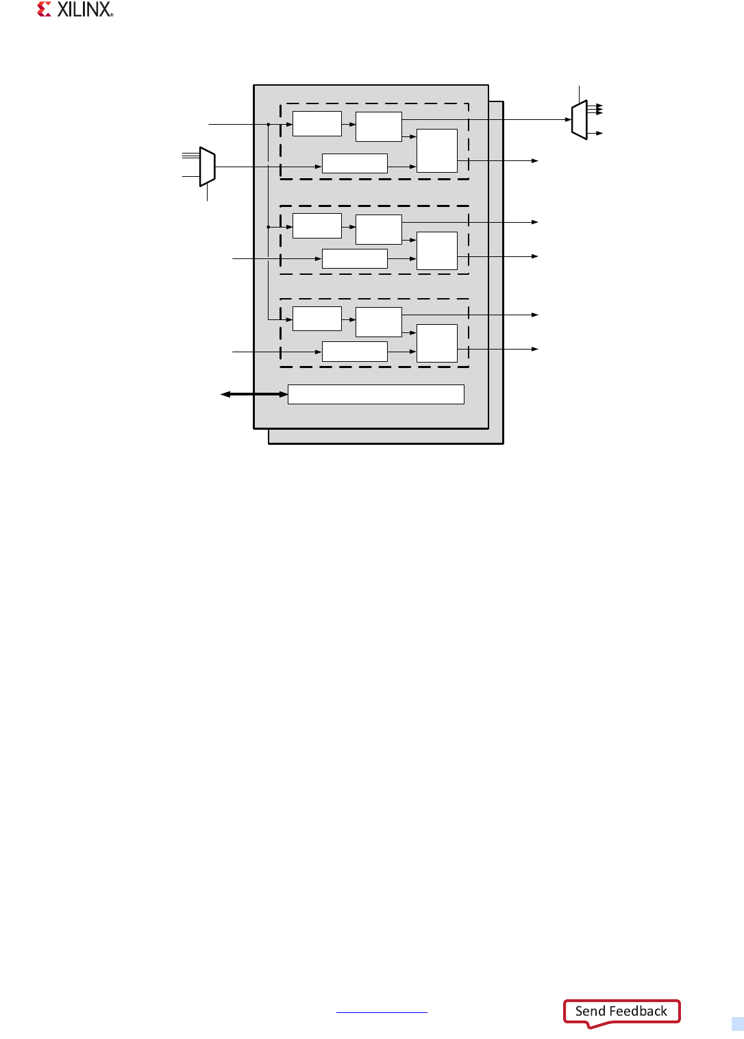
Zynq-7000 AP SoC Technical Reference Manual www.xilinx.com 246
UG585 (v1.12.1) December 6, 2017
Chapter 8: Timers
8.5.3 Functional Description
Each prescaler module can be independently programmed to use the PS internal bus clock (CPU_1x),
or an external clock from the MIO or the PL. For an external clock, SLCR registers determine the exact
pinout through the MIO or from the PL. The selected clock is then divided down from /2 to /65536,
before being applied to the counter.
The counter module can count up or count down, and can be configured to count for a given
interval. It also compares three match registers to the counter value, and generate an interrupt if one
matches.
The interrupt module combines interrupts of various types: counter interval, counter matches,
counter overflow, event timer overflow. Each type can be individually enabled.
Modes of Operation
Each counter module can be independently programmed to operate in either of the following two
modes:
Interval mode: The counter increments or decrements continuously between 0 and the value of the
Interval register, with the direction of counting determined by the DEC bit of the Counter Control
register. An interval interrupt is generated when the counter passes through zero. The corresponding
match interrupt is generated when the counter value equals one of the Match registers.
X-Ref Target - Figure 8-3
Figure 8-3: Triple Counter Timer Block Diagram
UG585_c8_08_120913
EMIO
Interface
Pre-scaler
TTC 0
16-bit
Counter
Event Timer
MIO
EMIO
CPU_1x
Interrupt
Timer/Clock 0
Wave-Out
Interrupt (GIC)
TTC_0: IRQ ID # 42
TTC_1: IRQ ID # 69
Pre-scaler 16-bit
Counter
Event Timer
Clock-In (EMIO) Interrupt
Timer/Clock 1
Wave-Out (EMIO)
Pre-scaler 16-bit
Counter
Event Timer Interrupt
Timer/Clock 2
TTC 1
MIO
EMIO
Wave-Out (EMIO)
Clock-In
Clock-In (EMIO)
APB Status and Control Registers
Interrupt (GIC)
TTC_0: IRQ ID # 43
TTC_1: IRQ ID # 70
Interrupt (GIC)
TTC_0: IRQ ID # 44
TTC_1: IRQ ID # 71
slcr.MIO_PIN_xx.
slcr.MIO_PIN_xx

Zynq-7000 AP SoC Technical Reference Manual www.xilinx.com 247
UG585 (v1.12.1) December 6, 2017
Chapter 8: Timers
Overflow mode: The counter increments or decrements continuously between 0 and 0xFFFF, with
the direction of counting determined by the DEC bit of the Counter Control register. An overflow
interrupt is generated when the counter passes through zero. The corresponding match interrupt is
generated when the counter value equals one of the Match registers.
Event Timer Operation
The event timer operates by having an internal (invisible to users) 16-bit counter clocked at CPU_1x
which:
• Resets to 0 during the non-counting phase of the external pulse
• Increments during the counting phase of the external pulse
The Event Control Timer register controls the behavior of the internal counter:
•E_En bit: When 0, immediately resets the internal counter to 0, and stops incrementing
•E_Lo bit: Specifies the counting phase of the external pulse
•E_Ov bit: Specifies how to handle overflow at the internal counter (during the counting phase
of the external pulse)
°When 0: Overflow causes E_En to be 0 (see E_En bit description)
°When 1: Overflow causes the internal counter to wrap around and continues incrementing
°An interrupt is always generated (subject to further enabling through another register)
when an overflow occurs.
The Event register is updated with the non-zero value of the internal counter at the end of the
counting-phase of the external pulse; therefore, it shows the widths of the external pulse, measured
in number of cycles of CPU_1x.
If the internal counter is reset to 0, due to overflow, during the counting phase of the external pulse,
the Event register will not be updated and maintains the old value from the last non-overflowing
counting operation.
8.5.4 Register Overview
A register overview of the TTC is provided in Tab le 8 - 4.
Table 8-4: Triple Timer Counter Register Overview
Function Name Overview
Clock control
Clock Control
register Controls prescaler, selects clock input, edge
Counter Control
register
Enables counter, sets mode of operation, sets up/down
counting, enables matching, enables waveform output
Status Counter Value
register Returns current counter value

Zynq-7000 AP SoC Technical Reference Manual www.xilinx.com 248
UG585 (v1.12.1) December 6, 2017
Chapter 8: Timers
8.5.5 Programming Model
Counter Enable Sequence
1. Select clock input source, set prescaler value (slcr.MIO_MUX_SEL registers, TTC Clock Control
register). Ensure TTC is disabled (ttc.Counter_Control_x [DIS] = 1) before proceeding with this
step.
2. Set interval value (Interval register). This step is optional, for interval mode only.
3. Set match value (Match registers). This step is optional, if matching is to be enabled.
4. Enable interrupt (Interrupt Enable register). This step is optional, if interrupt is to be enabled.
5. Enable/disable waveform output, enable/disable matching, set counting direction, set mode,
enable counter (TTC Counter Control register). This step starts the counter.
Counter Stop Sequence
1. Read back the value of the Counter Control register.
2. Set DIS bit to 1, while keeping other bits.
3. Write back to Counter Control register.
Counter Restart Sequence
1. Read back the value of Counter Control register.
2. Set RST bit to 1, while keeping other bits.
3. Write back to Counter Control register.
Event Timer Enable Sequence
1. Select external pulse source (slcr.MIO_MUX_SEL registers). The width of the selected external
pulse is measured in CPU_1x period.
Counter
Control
Interval register Sets interval value
Match register 1
Match register 2
Match register 3
Sets match values, total 3
Interrupt
Interrupt register Shows current interrupt status
Interrupt Enable
register Enable interrupts
Event
Event Control
Timer register Enable event timer, stop timer, sets phrase
Event register Shows width of external pulse
Table 8-4: Triple Timer Counter Register Overview (Cont’d)
Function Name Overview

Zynq-7000 AP SoC Technical Reference Manual www.xilinx.com 249
UG585 (v1.12.1) December 6, 2017
Chapter 8: Timers
2. Set overflow handling, select external pulse level, enable the event timer (Event Control Timer
register). This step starts measuring the width of the selected level (High or Low) of the external
pulse.
3. Enable interrupt (Interrupt Enable register). This step is optional, if interrupt is to be enabled.
4. Read the measured width (Event register). Note that the returned value is not correct when
overflow happened. See the description for the E_Ov bit of the Event Control Timer register in
section 8.5.3 Functional Description.
Interrupt Clear and Acknowledge Sequence
1. Read Interrupt register: All bits in the Interrupt register are cleared on read.
8.5.6 Clock Input Option for Counter/Timer
The following shows how AP SoC selects the clock source for TTC0 counter/timer 0:
if slcr.MIO_PIN_19[6:0] is 1100000, use MIO pin 19
else if slcr.MIO_PIN_31[6:0] is 1100000, use MIO pin 31
else if slcr.MIO_PIN_43[6:0] is 1100000, use MIO pin 43
else use EMIOTTC0CLKI0
TTC0 counter/timer 1 can use only EMIOTTC0CLKI1.
TTC0 counter/timer 2 can use only EMIOTTC0CLKI2.
The following shows how Zynq SoC selects the clock source for TTC1 counter/timer 0:
if slcr.MIO_PIN_17[6:0] is 1100000, use MIO pin 17
else if slcr.MIO_PIN_29[6:0] is 1100000, use MIO pin 29
else if slcr.MIO_PIN_41[6:0] is 1100000, use MIO pin 41
else use EMIOTTC1CLKI0
TTC1 counter/timer 1 can use only EMIOTTC1CLKI1.
TTC1 counter/timer 2 can use only EMIOTTC1CLKI2.
IMPORTANT: When an MIO pin or EMIOTTCxCLKIx is chosen to be the clock source, if the clock stops
running, the corresponding Count Value register retains the old value, regardless of the fact that the
clock has already stopped. Caution must be exercised in this case.
Zynq-7000 AP SoC Technical Reference Manual www.xilinx.com 250
UG585 (v1.12.1) December 6, 2017
Chapter 8: Timers
8.6 I/O Signals
Timer I/O signals are identified in Tab le 8- 5. The MIO pins and any restrictions based on device
version are shown in the MIO table in section 2.5.4 MIO-at-a-Glance Table.
There are two triple timer counters (TTC0 and TTC1) in the system. Each TTC has three sets of
interface signals: clock in and wave out for counter/timers 0, 1, and 2.
For each triple timer counter, the signals for counter/timer 0 can be routed to the MIO using the
MIO_PIN registers. If the clock in or wave out signal is not selected by the MIO_PIN register, then the
signal is routed to EMIO by default.
The signals for counter/timers 1 and 2 are only available through the EMIO.
System watchdog timer I/O signals are identified in Tab le 8- 6.
Table 8-5: TTC I/O Signals
TTC Timer Signal I/O MIO Pins EMIO Signals
Controller
Default
Input
Value
TTC0
Counter/Timer 0 clock in I 19, 31, 43 EMIOTTC0CLKI0 0
Counter/Timer 0 wave out O 18, 30, 42 EMIOTTC0WAVEO0 ~
Counter/Timer 1 clock in I N/A EMIOTTC0CLKI1 0
Counter/Timer 1 wave out O N/A EMIOTTC0WAVEO1 ~
Counter/Timer 2 clock in I N/A EMIOTTC0CLKI2 0
Counter/Timer 2 wave out O N/A EMIOTTC0WAVEO2 ~
TTC1
Counter/Timer 0 clock in I 17, 29, 41 EMIOTTC1CLKI0 0
Counter/Timer 0 wave out O 16, 28, 40 EMIOTTC1WAVEO0 ~
Counter/Timer 1 clock in I N/A EMIOTTC1CLKI1 0
Counter/Timer 1 wave out O N/A EMIOTTC1WAVEO1 ~
Counter/Timer 2 clock in I N/A EMIOTTC1CLKI2 0
Counter/Timer 2 wave out O N/A EMIOTTC1WAVEO2 ~
Table 8-6: Watchdog Timer I/O Signals
SWDT Signal I/O MIO Pins EMIO Signals Controller Default
Input Value
Clock in I 14, 26, 38, 50, 52 EMIOWDTCLKI 0
Reset out O 15, 27, 39, 51, 53 EMIOWDTRSTO ~

Zynq-7000 AP SoC Technical Reference Manual www.xilinx.com 251
UG585 (v1.12.1) December 6, 2017
Chapter 9
DMA Controller
9.1 Introduction
The DMA controller (DMAC) uses a 64-bit AXI master interface operating at the CPU_2x clock rate to
perform DMA data transfers to/from system memories and PL peripherals. The transfers are
controlled by the DMA instruction execution engine. The DMA engine runs on a small instruction set
that provides a flexible method of specifying DMA transfers. This method provides greater flexibility
than the capabilities of DMA controller methods.
The program code for the DMA engine is written by software in to a region of system memory that
is accessed by the controller using its AXI master interface. The DMA engine instruction set includes
instructions for DMA transfers and management instructions to control the system.
The controller can be configured with up to eight DMA channels. Each channel corresponds to a
thread running on the DMA engine’s processor. When a DMA thread executes a load or store
instruction, the DMA Engine pushes the memory request to the relevant read or write queue. The
DMA controller uses these queues to buffer AXI read/write transactions. The controller contains a
multi-channel FIFO (MFIFO) to store data during the DMA transfers. The program code running on
the DMA engine processor views the MFIFO as containing a set of variable-depth parallel FIFOs for
DMA read and write transactions. The program code must manage the MFIFO so that the total depth
of all of the DMA FIFOs does not exceed the 1,024-byte MFIFO.
The DMAC is able to move large amounts of data without processor intervention. The source and
destination memory can be anywhere in the system (PS or PL). The memory map for the DMAC
includes DDR, OCM, linear addressed Quad-SPI read memory, SMC memory and PL peripherals or
memory attached to an M_GP_AXI interface.
The flow control method for transfers with PS memories use the AXI interconnect. Accesses with PL
peripherals can use the AXI flow control or the DMAC’s PL Peripheral Request Interface. There are no
peripheral request interfaces directed to the PS I/O Peripherals (IOPs). For the PL peripheral AXI
transactions, software running on a CPU is used in a programmed IO method using interrupts or
status polling.
The controller has two sets of control and status registers. One set is accessible in secure mode and
the other in non-secure mode. Software accesses these registers via the controller’s 32-bit APB slave
interface. The entire controller is either operated in secure or non-secure mode; there is no mixing of
modes on a channel basis. Security configuration changes are controlled by slcr registers and require
a controller reset to take effect.

Zynq-7000 AP SoC Technical Reference Manual www.xilinx.com 252
UG585 (v1.12.1) December 6, 2017
Chapter 9: DMA Controller
9.1.1 Features
The DMA Controller provides:
• DMA Engine processor with a flexible instruction set for DMA transfers:
°Flexible scatter-gather memory transfers
°Full control over addressing for source and destination
°Define AXI transaction attributes
°Manage byte streams
• Eight cache lines and each cache line is four words wide
• Eight concurrent DMA channels threads
°Allows multiple threads to execute in parallel
°Issue commands for up to eight read and up to eight write AXI transactions
• Eight interrupts to the PS interrupt controller and the PL
• Eight events within DMA Engine program code
• 128 (64-bit) word MFIFO to buffer the data that the controller writes or reads during a transfer
•Security
°Dedicated APB slave interface for secure register accessing
°Entire controller is configured as either secure or non-secure
• Memory-to-memory DMA transfers
• Four PL peripheral request interfaces to manage flow control to and from the PL logic
°Each interface accepts up to four active requests
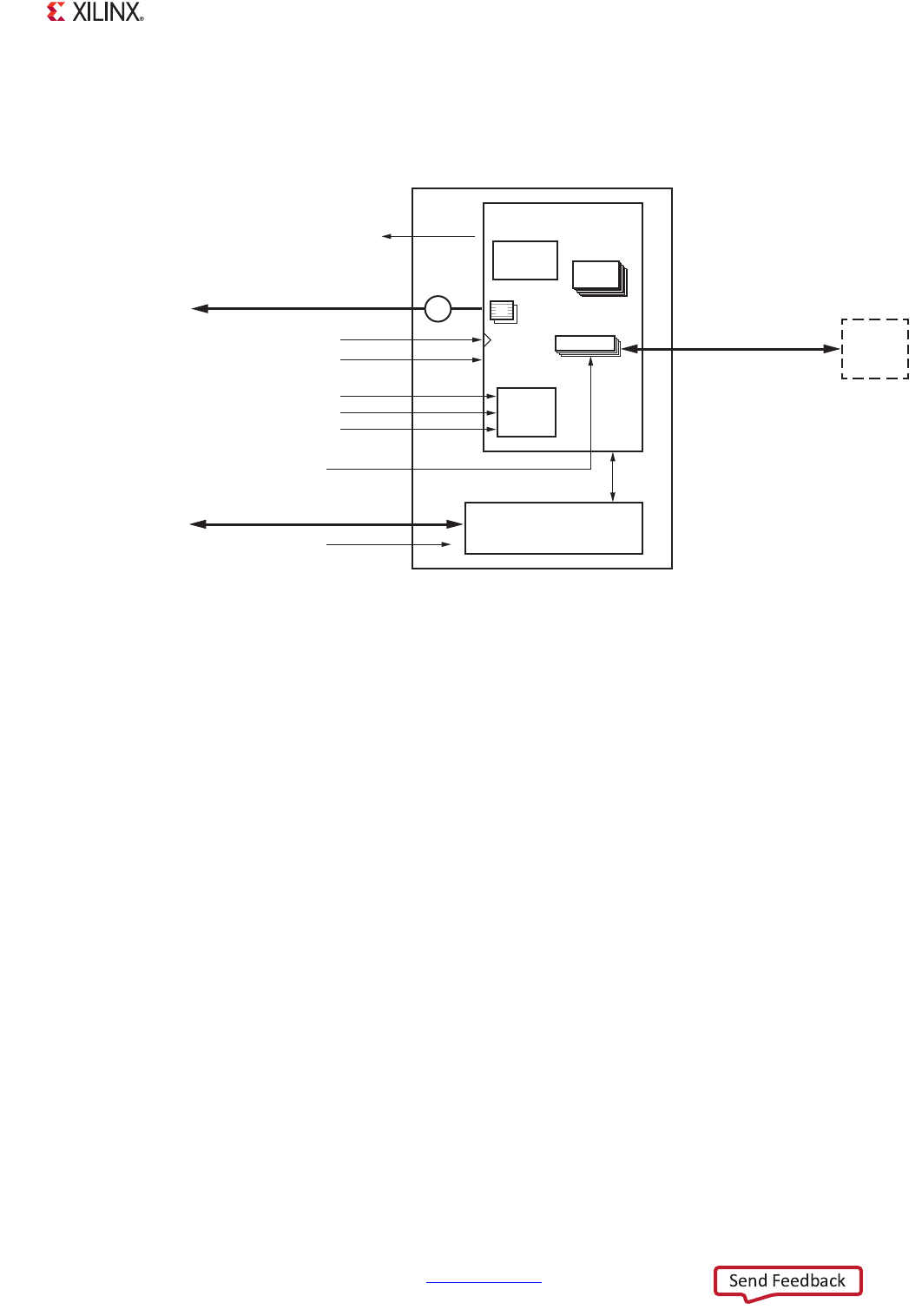
Zynq-7000 AP SoC Technical Reference Manual www.xilinx.com 253
UG585 (v1.12.1) December 6, 2017
Chapter 9: DMA Controller
9.1.2 System Viewpoint
The system viewpoint of the DMA controller is shown in Figure 9-1.
System Functions
The following system functions are described in section 9.6 System Functions:
•Clocks
• Resets and Reset Configuration
DMA Controller Functions and Programming
A block diagram for the DMA controller is shown in Figure 9-2. A brief description of each block
follows the diagram. Each functional unit is described in detail in these three main sections:
• Overall description in section 9.2 Functional Description.
• SDK Software programming methods are in section 9.3 Programming Guide for DMA Controller.
• DMA Engine programming methods are in section 9.4 Programming Guide for DMA Engine.
• Programming restrictions for these methods are in section 9.5 Programming Restrictions:
X-Ref Target - Figure 9-1
Figure 9-1: DMA Controller System Viewpoint
PL
Slave Interconnect
Register Access
APB 32-bit Control and Status
Registers
UG585_c9_01_021113
DMAC_CPU2X_RST signal
Secure and
Non-Secure
Slave Ports
FPGA_DMA{0:3}_RST signal
CPU_1X clock
Central Interconnect
Data and Controller
Instructions
AXI 64-bit Master
CPU_2X clock
QoS
R/W
8Peripheral Request
Interfaces 0 ~ 3
DMA Controller
DMA{0:3}_DAVALID
DMA{0:3}_DATYPE{0,1}
DMA{0:3}_DAREADY
DMA{0:3}_DRVALID
DMA{0:3}_DRTYPE{0,1}
DMA{0:3}_DRLAST
DMA{0:3}_DRREADY
Channels
0 ~ 7
Execution
Engine
TZ_DMA_NS [0]
TZ_DMA_IRQ_NS [15:0]
TZ_DMA_PERIPH_NS [3:0]
Security
Control
IRQ ID# {45, 46~49, 72~75}
To Interrupt Controller
IRQ ID# {25, 20~27}
To PL
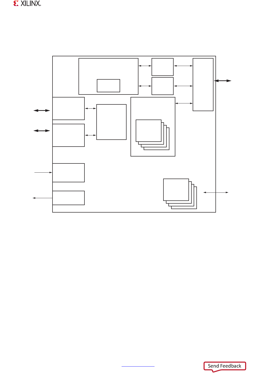
Zynq-7000 AP SoC Technical Reference Manual www.xilinx.com 254
UG585 (v1.12.1) December 6, 2017
Chapter 9: DMA Controller
9.1.3 Block Diagram
The block diagram of the DMA controller is shown in Figure 9-2.
Note: Refer to ARM PrimeCell DMA Controller (PL330, r1p1) Technical Reference Manual: AXI
Characteristics for a DMA Transfer and AXI Master for more information.
DMA Instruction Execution Engine
The DMAC contains an instruction processing block that enables it to process program code that
controls a DMA transfer. The DMAC maintains a separate state machine for each thread.
• Channel arbitration
°Round-robin scheme to service the active DMA channels
°Services the DMA manager prior of servicing the next DMA channel
°Changes to the arbitration process are not supported
• Channel prioritization
°Responds to all active DMA channels with equal priority
°Changes to the priority of a DMA channel over any other DMA channels are not supported
X-Ref Target - Figure 9-2
Figure 9-2: DMA Controller Block Diagram
Central
Interconnect
Register Access
For the
Non-secure State
Register Access
For the
Secure State
Tie-os
IRQs Interrupt
Interface
Reset
Initialization
Interface
Secure
APB Slave
Interface
0xF800_3000
Non-secure
APB Slave
Interface
0xF800_4000 Control and
Status
Registers
Instruction
Cache
DMA Instruction
Execution
Engine
Read
Instruction
Queue
AXI
Master
Interface
Instruction
Instruction
Data
Write
Instruction
Queue
MFIFO Data Buer
Channel
Data
0••7
Peripheral
Request
Interface
012
3
DMA Controller
PL Fabric
UG_585_c9_02_030712

Zynq-7000 AP SoC Technical Reference Manual www.xilinx.com 255
UG585 (v1.12.1) December 6, 2017
Chapter 9: DMA Controller
Instruction Cache
The controller stores instructions temporarily in a cache. When a thread requests an instruction from
an address, the cache performs a look-up. If a cache hit occurs then the cache immediately provides
the data, otherwise the thread is stalled while the controller uses the AXI interface to perform a
cache line fill from system memory. If an instruction is greater than four bytes, or spans the end of a
cache line, then it performs multiple cache accesses to fetch the instruction.
Note: When a cache line fill is in progress, the controller enables other threads to access the cache,
but if another cache miss occurs the pipeline is stalled until the first line fill is complete.
Note: Instruction cache latency for fill operations is dependent on the read latency of the system
memory where the DMA engine instructions are written. The performance of the DMAC is highly
dependent on the bandwidth of the 64-bit AXI master interface (CPU_2x clock).
Read/Write Instruction Queues
When a channel thread executes a load or store instruction the controller adds the instruction to the
relevant read queue or write queue. The controller uses these queues as an instruction storage buffer
prior to issuing transactions on the AXI interconnect.
Multi-channel Data FIFO
The DMAC uses a multi-channel first-in-first-out (MFIFO) data buffer to store data that it reads, or
writes, during a DMA transfer. Refer to 9.2.4 Multi-channel Data FIFO (MFIFO) for more information.
AXI Master Interface for Instruction Fetch and DMA Transfers
The program code is stored in a region of system memory that the controller accesses using the
64-bit AXI master interface. The AXI master interface also enables the DMA to transfer data from a
source AXI slave to a destination AXI slave.
APB Slave Interface for Register Accesses
The controller responds to two address ranges used by software to read and write the control and
status registers via the 32-bit APB slave interface.
• Non-secure register accesses
• Secure register accesses
Interrupt Interface
The interrupt interface enables efficient communications of events to the interrupt controller.
PL Peripheral DMA Request Interface
The PL peripheral request interface supports the connection of DMA-capable peripherals resident in
the PL. Each PL peripheral request interface is asynchronous to one another and asynchronous to the

Zynq-7000 AP SoC Technical Reference Manual www.xilinx.com 256
UG585 (v1.12.1) December 6, 2017
Chapter 9: DMA Controller
DMA itself. The request/acknowledge signals to and from the PL are described in section 9.2.6 PL
Peripheral AXI Transactions.
Reset Initialization Interface
This interface enables the software to initialize the operating state of the DMAC as it exits from reset.
Refer to section 9.6.3 Reset Configuration of Controller for more information.
9.1.4 Notices
ARM IP Core
The DMAC is an Advanced Microcontroller Bus Architecture (AMBA) PrimeCell peripheral that is
developed, tested, and licensed by ARM.
A list of the ARM Reference Documents for the DMA controller are summarized in Appendix A,
Additional Resources.
•Technical Reference Manual: ARM PrimeCell DMA Controller (PL330) Technical Reference
Manual.
•Example Application Notes: ARM Application Note 239: Example programs for the CoreLink
DMA Controller DMA-330 and refer to 9.4 Programming Guide for DMA Engine.
Secure/Non-Secure Modes
The DMAC includes features to enable it to co-exist with ARM’s TrustZone hardware to accelerate the
performance of secure systems. The hardware is not required to ensure a secure environment. This
chapter includes many references to secure and non-secure modes. It may not be complete. For
additional information related to the use of the DMA PL330 controller with ARM TrustZone, refer to
UG1019, Programming ARM TrustZone Architecture on the Zynq-7000 All Programmable SoC.
Other DMA Controllers
There are other DMA controllers in the system that are local to the IOPs in the PS. These include:
• GigE controller, refer to Chapter 16, Gigabit Ethernet Controller.
• SDIO controller, refer to Chapter 13, SD/SDIO Controller.
• USB controller, refer to Chapter 15, USB Host, Device, and OTG Controller.
• DevC Interface, refer to section 6.4 Device Boot and PL Configuration.

Zynq-7000 AP SoC Technical Reference Manual www.xilinx.com 257
UG585 (v1.12.1) December 6, 2017
Chapter 9: DMA Controller
9.2 Functional Description
Common to all DMAC operating conditions
•9.2.1 DMA Transfers on the AXI Interconnect
•9.2.2 AXI Transaction Considerations
•9.2.3 DMA Manager
•9.2.4 Multi-channel Data FIFO (MFIFO)
Memory-to-memory transfers are managed by the DMAC
•9.2.5 Memory-to-Memory Transfers
When the PL Peripheral Request Interface is used
•9.2.6 PL Peripheral AXI Transactions
• Length management option: 9.2.8 PL Peripheral - Length Managed by PL Peripheral
• Length management option: 9.2.9 PL Peripheral - Length Managed by DMAC
Advanced DMAC operating features
•9.2.10 Events and Interrupts
•9.2.11 Aborts
•9.2.12 Security
IP core Configuration
• Based on the ARM PrimeCell DMA Controller (PL330) refer to 9.2.13 IP Configuration Options

Zynq-7000 AP SoC Technical Reference Manual www.xilinx.com 258
UG585 (v1.12.1) December 6, 2017
Chapter 9: DMA Controller
9.2.1 DMA Transfers on the AXI Interconnect
All of the DMA transactions use AXI interfaces to move data between the on-chip memory, DDR
memory and slave peripherals in the PL. The slave peripherals in the PL normally connect to the
DMAC peripheral request interface to control data flow. The DMAC can conceivable access IOPs in
the PS, but this is normally not useful because these paths offer no flow control signals.
The data paths that are normally used by the DMAC are shown in Figure 9-3. The peripheral request
interface (used for flow control) is not shown in the figure. Each AXI path can be a read or write.
There are many combinations. Two typical DMA transaction examples include:
• Memory to memory (On-chip memory to DDR memory)
• Memory to/from PL peripheral (DDR memory to PL peripheral)
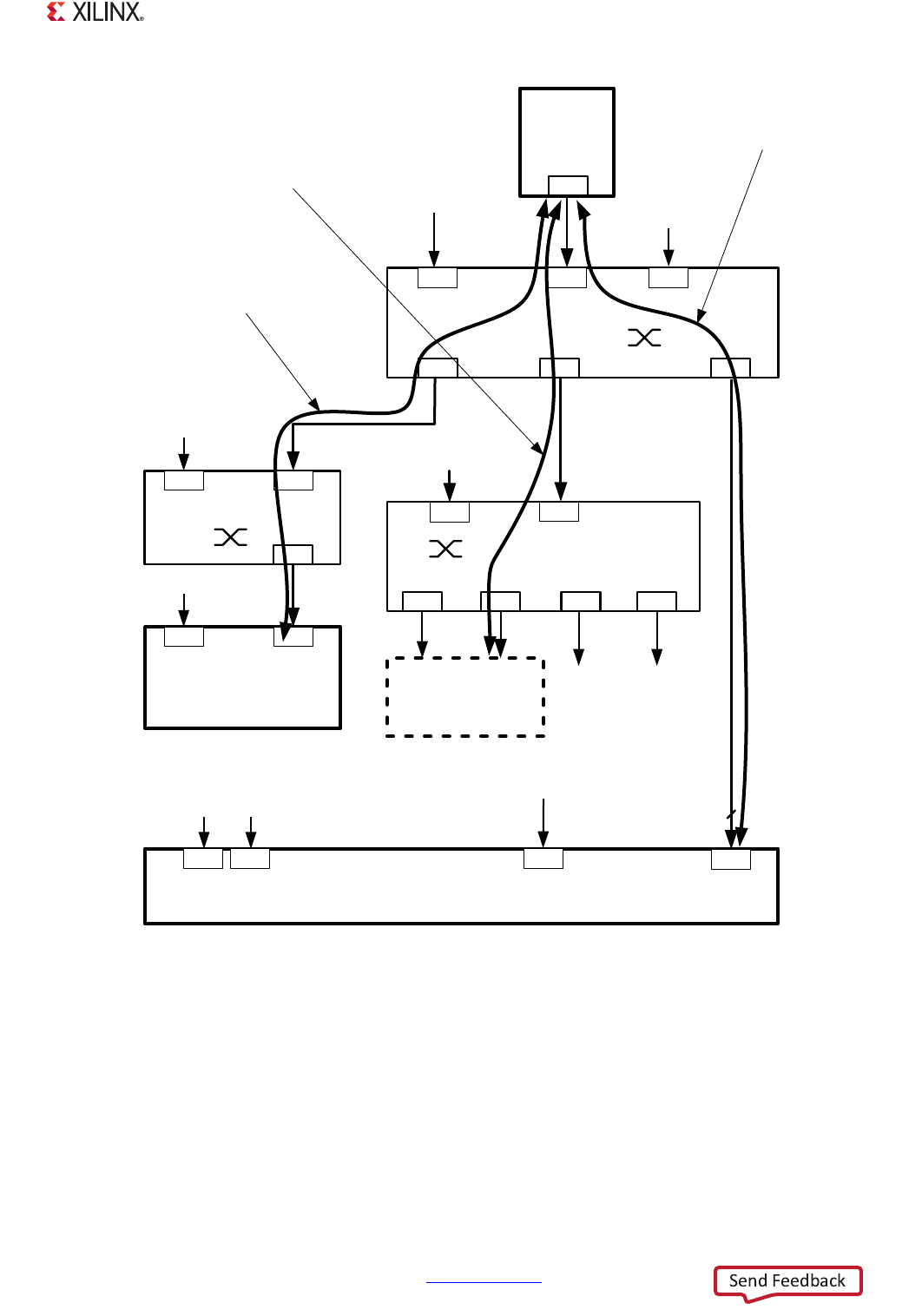
Zynq-7000 AP SoC Technical Reference Manual www.xilinx.com 259
UG585 (v1.12.1) December 6, 2017
Chapter 9: DMA Controller
X-Ref Target - Figure 9-3
Figure 9-3: DMAC Reads/Writes DDR, On-chip RAM, and PL Peripheral
UG585_c9_07_021113
AXI_GP1
OCM
Interconnect
Slave
Interconnect
M
S1
M1
S1
S0S2S3
M2M0
S0
M2M0 M1
PL
S1
S0 S2
M3
DDR Memory Controller
64-bit
DMA
Controller
32-bit
256 KB
S1S0
S0
M
S1
64-bit
64-bit
On-chip
RAM
AXI_GP0
SCU
AHB
slaves
APB
slaves
L2 Cache
IOP
Masters
AXI_GP,
DevC
and DAP
AXI_HP
Memory
Interconnect
L2 Cache
AXI_HP
Memory
Interconnect
64-bit
DDR Memory
(Read and Write)
64-bit-bit
PL Memory
(Read and Write)
Central
Interconnect
On-Chip RAM
(Read and Write)

Zynq-7000 AP SoC Technical Reference Manual www.xilinx.com 260
UG585 (v1.12.1) December 6, 2017
Chapter 9: DMA Controller
9.2.2 AXI Transaction Considerations
• AXI data transfer size
°Performs data accesses up to the 64-bit width of the AXI data bus
°Signals a precise abort if the user programs the src_burst_size or dst_burst_size fields to be
larger than 64 bits
°Maximum burst length is 16 data beats
• AXI bursts crossing 4 KB boundaries
°The AXI specification does not permit AXI bursts to cross 4 KB address boundaries
°If the controller is programmed with a combination of burst start address, size, and length
that would cause a single burst to cross a 4 KB address boundary, then the controller
instead generates a pair of bursts with a combined length equal to that specified. This
operation is transparent to the DMAC channel thread program so that, for example, the
DMAC responds to a single DMALD instruction by generating the appropriate pair of AXI
read bursts.
• AXI burst types
°Can be programmed to generate only fixed-address or incrementing-address burst types for
data accesses. Wrapping-address bursts are not generated for data accesses or for
instruction fetches.
• AXI write addresses
°Can issue multiple outstanding write addresses up to eight (write issuing capability)
°The DMAC does not issue a write address until it has read in all of the data bytes required to
fulfill that write transaction.
• AXI write data interleaving
°Does not generate interleaved write data. All write data beats for one write transaction are
output before any write data beat for the next write transaction.
• AXI characteristics
°Does not support locked or exclusive accesses
9.2.3 DMA Manager
This section describes how to issue instructions to the DMA manager using one of the two APB
interfaces available.
When the DMAC is operating in real time, the user can only issue the following limited subset of
instructions:
DMAGO Starts a DMA transfer using a DMA channel that the user specifies.
DMASEV Signals the occurrence of an event, or interrupt, using an event number that the
user specifies.
DMAKILL Terminates a thread.

Zynq-7000 AP SoC Technical Reference Manual www.xilinx.com 261
UG585 (v1.12.1) December 6, 2017
Chapter 9: DMA Controller
The appropriate APB interface must be used depending on the security state in which the SLCR
register TZ_DMA_NS initializes the DMA manager to operate. For example, if the DMA manager is in
the secure state, the instruction using the secure APB interface must be used or the DMAC ignores
the instruction. The non-secure APB interface is the suggested port to use to start or restart a DMA
channel when the DMA manager is in the non-secure state, however, the secure APB interface can be
used in non-secure mode. (Refer to section 9.2.12 Security for more details.) For additional
information related to the use of the DMA PL330 controller with ARM TrustZone, refer to UG1019,
Programming ARM TrustZone Architecture on the Zynq-7000 All Programmable SoC.
Before issuing instructions using the Debug Instruction registers or the DBGCMD register, the
DBGSTATUS register must be read to ensure that debug is idle, otherwise, the DMA manager ignores
the instructions. Refer to the Debug Command register and Debug Status register in Appendix B,
Register Details.
When the DMA manager receives an instruction from an APB slave interface, it can take several clock
cycles before it can process the instruction — for example, if the pipeline is busy processing another
instruction.
Prior to issuing DMAGO, the system memory must contain a suitable program for the DMA channel
thread to execute, starting at the address that the DMAGO specifies.
Example: Start DMA Channel Thread
The following example shows the steps required to start a DMA channel thread using the debug
instruction registers.
1. Create a program for the DMA channel.
2. Store the program in a region of system memory.
Use one of the APB interfaces on the DMAC to program a DMAGO instruction as follows:
3. Poll the dmac.DBGSTATUS register to ensure that debug is idle, that is, the dbgstatus bit is 0.
Refer to the Debug Status register in Appendix B, Register Details.
4. Write to the dmac.DBGINST0 register and enter the:
a. Instruction byte 0 encoding for DMAGO.
b. Instruction byte 1 encoding for DMAGO.
c. Debug thread bit to 0. This selects the DMA manager. Refer to the Debug Instruction-0
register in Appendix B, Register Details.
5. Write to the dmac.DBGINST1 register with the DMAGO instruction byte [5:2] data, refer to the
Debug Instruction-1 register in Appendix B, Register Details. These four bytes must be set to the
address of the first instruction in the program that was written to system memory in Step 2.
Instruct the DMAC to execute the instruction that the debug instruction registers contain:
6. Write a 0 to the dmac.DBGCMD register. The DMAC starts the DMA channel thread and sets the
dbgstatus bit to 1. Refer to the Debug Command register in Appendix B, Register Details. After
the DMAC completes execution of the instruction, it clears the dbgstatus bit to 0.

Zynq-7000 AP SoC Technical Reference Manual www.xilinx.com 262
UG585 (v1.12.1) December 6, 2017
Chapter 9: DMA Controller
9.2.4 Multi-channel Data FIFO (MFIFO)
The MFIFO is a shared resource utilized on a first-come, first-served basis by all currently active
channels. To a program, it appears as a set of variable-depth parallel FIFOs, one per channel, with the
restriction that the total depth of all the FIFOs cannot exceed the size of the MFIFO. The DMAC
maximum MFIFO depth is 128 (64-bit) words.
The controller is capable of realigning data from the source to the destination. For example, the
DMAC shifts the data by two byte lanes when it reads a word from address 0x103 and writes to
address 0x205. The storage and packing of the data in the MFIFO is determined by the destination
address and transfer characteristics.
When a program specifies that incrementing memory transfers are to be performed to the
destination, the DMAC packs data into the MFIFO to minimize the usage of the MFIFO entries. For
example, the DMAC packs two 32-bit words into a single entry in the MFIFO when the DMAC has a
64-bit AXI data bus and the program uses a source address of 0x100, and destination address of
0x200.
In certain situations, the number of entries required to store the data loaded from a source is not a
simple calculation of the amount of source data divided by MFIFO width. The calculation of the
number of entries required is not simple when any of the following occur:
• Source address is not aligned to the AXI bus width
• Destination address is not aligned to the AXI bus width
• Memory transfers are to a fixed destination, that is, a non-incrementing address
The DMALD and DMAST instructions each specify that an AXI bus transaction is to be performed. The
amount of data transferred by an AXI bus transaction depends on the values programmed in to the
CCRn register and the address of the transaction. Refer to the AMBA AXI Protocol Specification for
information about unaligned transfers.
Refer to section 9.3 Programming Guide for DMA Controller for considerations about MFIFO
utilization.
9.2.5 Memory-to-Memory Transfers
The controller includes an AXI master interface to access memories in the PS system, such as:
•OCM
• DDR
Through the same AXI central interconnect, the controller can potentially access the majority of the
peripheral subsystems. If a target peripheral can be seen as a memory-mapped region (or memory
port location) without a FIFO or need for flow control, then the DMAC can be used to read and write
to it. Typical examples include:
• QSPI in Linear addressing mode
•NOR flash
•NAND flash

Zynq-7000 AP SoC Technical Reference Manual www.xilinx.com 263
UG585 (v1.12.1) December 6, 2017
Chapter 9: DMA Controller
The memory map for the DMA controller is shown in Chapter 4, System Addresses.
For more information on the AXI Interfaces, refer to . Examples of memory-to-memory transfer are
provided in section 9.4.2 Memory-to-Memory Transfers.
9.2.6 PL Peripheral AXI Transactions
The majority of PL peripherals allow transferring data through FIFOs. These FIFOs must be managed
to avoid overflow and underflow situations. For this reason, four specific peripheral request
interfaces are available to connect the DMAC to DMA-capable peripherals in the PL. Each one of
these interfaces can be assigned to any DMA channel.
The DMAC is configured to accept up to four active requests for each PL peripheral interface. An
active request is where the DMAC has not started the requested AXI data transaction. The DMAC has
a request FIFO for each PL peripheral interface, which it uses to capture the requests from a PL
peripheral. When a request FIFO is full, the DMAC sets the corresponding DMA{3:0}_DRREADY Low to
signal that the DMAC cannot accept any requests sent from the PL peripheral.
Note: There are no peripheral request interfaces directed to the I/O peripherals (IOP) in the PS.
Processor intervention is needed to avoid underflow or overflow of the FIFOs in the targeted PS
peripheral. This section discusses the AXI transactions to/from PL peripherals.
There are two different way to handle the quantity of data flowing between the DMAC and the PL
peripheral:
PL Peripheral length management: The PL peripheral controls the quantity of data that is
contained in a DMA cycle.
DMAC length management: The DMAC is controlling the quantity of data in a DMA
cycle.
Programming Examples
Refer to section 9.4.3 PL Peripheral DMA Transfer Length Management.
9.2.7 PL Peripheral Request Interface
Figure 9-4 shows that the PL peripheral request interface consists of a PL peripheral request bus and
a DMAC acknowledge bus that use the prefixes:
DR PL Peripheral request bus
DA DMAC acknowledge bus
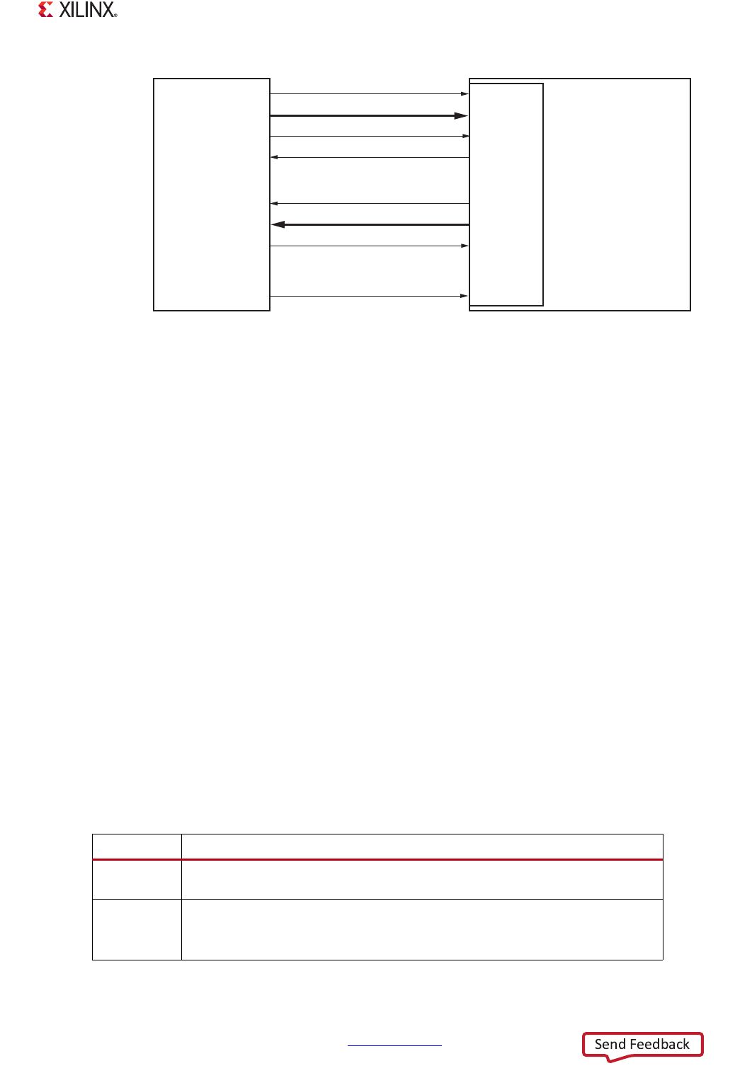
Zynq-7000 AP SoC Technical Reference Manual www.xilinx.com 264
UG585 (v1.12.1) December 6, 2017
Chapter 9: DMA Controller
Both buses use the valid-ready handshake that the AXI protocol describes. For more information on
the handshake process, refer to the AMBA AXI Protocol v1.0 Specification.
The PL peripheral uses the DMA{3:0}_DRTYPE[1:0] registers to:
• Request a single AXI transaction
• Request a AXI burst transaction
• Acknowledge a flush request
The DMAC uses the DMA{3:0}_DATYPE[1:0] registers to:
• Signal when it completes the requested single AXI transaction
• Signal when it completes the requested AXI burst transaction
• Issue a flush request
The PL peripheral uses DMA{3:0}_DRLAST to:
• Signal to the DMAC when the last data cycle of the AXI transaction commences
Handshake Rules
The DMAC uses the DMA handshake rules that Tab le 9- 1 shows, when a DMA channel thread is
active, that is, not in the stopped state. Refer to the Figure 9-5, page 265 for more information.
X-Ref Target - Figure 9-4
Figure 9-4: DMAC PL Peripheral Request Interface Request/Acknowledge Signals
Table 9-1: DMAC PL Peripheral Request Interface Handshake Rules
Rule Description(1)
1DMA{3:0}_DRVALID can change from Low to High on any DMA{3:0}_ACLK cycle,
but must only change from High to Low when DMA{3:0}_DRREADY is High.
2
DMA{3:0}_DRTYPE can only change when either:
• DMA{3:0}_DRREADY is High
• DMA{3:0}_DRVALID is Low
DMA{3:0}_DRTYPE[1:0]
Peripheral
{3:0}
DMA{3:0}_DRLAST
DMA{3:0}_DATYPE[1:0]
DMA{3:0}_DAVALID
DMA{3:0}_DRREADY
DMA{3:0}_DAREADY
DMA{3:0}_DRVALID
DMAC
UG585_c9_05_030312
Peripheral
Request
Interface
{3:0}
DMA{3:0}_ACLK
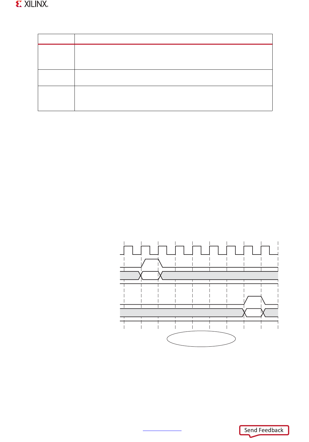
Zynq-7000 AP SoC Technical Reference Manual www.xilinx.com 265
UG585 (v1.12.1) December 6, 2017
Chapter 9: DMA Controller
Map PL Peripheral Interface to a DMA Channel
The DMAC enables software to assign a PL peripheral request interface to any of the DMA channels.
When a DMA channel thread executes DMAWFP, the value programmed in the PL peripheral [4:0]
field specifies the PL peripheral associated with that DMA channel. Refer to the DMAWFP instruction
in Table 9-8, page 273.
PL Peripheral Request Interface Timing Diagram
Figure 9-5 shows an example of the functional operation of the PL peripheral request interface using
the rules that handshake rules described, when a PL peripheral requests an AXI burst transaction.
State transitions in Figure 9-5:
T1 The DMAC detects a request for an AXI burst transaction.
Between T2 and T7 The DMAC performs the AXI burst transaction.
3
DMA{3:0}_DRLAST can only change when either:
• DMA{3:0}_DRREADY is High
• DMA{3:0}_DRVALID is Low
4DMA{3:0}_DAVALID can change from Low to High on any DMA{3:0}_ACLK cycle,
but must only change from High to Low when DMA{3:0}_DAREADY is High
5
DMA{3:0}_DATYPE can only change when either:
• DMA{3:0}_DAREADY is High
• DMA{3:0}_DAVALID is Low
Notes:
1. All signals are synchronous to the DMA{3:0}_ACLK clock.
X-Ref Target - Figure 9-5
Figure 9-5: DMAC PL Peripheral Request Interface Burst Request Signaling
Table 9-1: DMAC PL Peripheral Request Interface Handshake Rules (Cont’d)
Rule Description(1)
T0
Burst
Ack
AXI Data Burst
DMA Activity on the
AXI Data Bus
UG585_c9_06_030712
DMA{3:0}_ACLK
DMA{3:0}_DRVALID
DMA{3:0}_DRTYPE[1:0]
DMA{3:0}_DRREADY
DMA{3:0}_DAVALID
DMA{3:0}_DATYPE[1:0]
DMA{3:0}_DAREADY
T1 T2 T3 T4 T5 T6 T7 T8 T9

Zynq-7000 AP SoC Technical Reference Manual www.xilinx.com 266
UG585 (v1.12.1) December 6, 2017
Chapter 9: DMA Controller
T7 The DMAC sets DMA{3:0}_DAVALID High and sets DMA{3:0}_DATYPE[1:0]
to indicate that the transaction is complete.
For more timing diagrams refer to ARM PrimeCell DMA Controller (PL330) Technical Reference
Manual: Peripheral Request Interface Timing Diagrams, keeping in mind that each PL peripheral
request interface is asynchronous to one another and asynchronous to the DMA itself.
9.2.8 PL Peripheral - Length Managed by PL Peripheral
The PL peripheral request interface enables a PL peripheral to control the quantity of data that an AXI
transfer contains, without the DMAC being aware of how many data cycles the transfer contains. The
PL peripheral controls the AXI transaction by using:
DMA{3:0}_DRTYPE[1:0] Selects a single or burst AXI Transaction
DMA{3:0}_DRLAST Notifies the DMAC when it commences the final request in the
current series
When the DMAC executes a DMAWFP instruction, it halts execution of the thread and waits for the PL
peripheral to send a request. When the PL peripheral sends the request, the DMAC sets the state of
the request flags depending on the state of the following signals:
DMA{3:0}_DRTYPE[1:0] The DMAC sets the state of the request_type flag:
00: request_type = Single
01: request_type = Burst
DMA{3:0}_DRLAST The DMAC sets the state of the request_last flag:
0: request_last = 0
1:request_last = 1
If the DMAC executes a DMAWFP single or DMAWFP burst instruction then the DMAC sets:
• The request_type{3:0} flag to Single or Burst, respectively
• The request_last{3:0} flag to 0
DMALPFE is an assembler directive which forces the associated DMALPEND instruction to have its nf
bit set to 0. This creates a program loop that does not use a loop counter to terminate the loop. The
DMAC exits the loop when the request_last flag is set to 1.
The DMAC conditionally executes the following instructions, depending on the state of the
request_type and request_last flags:
DMALD, DMAST, DMALPEND
When these instructions use the optional B|S suffix then the DMAC executes a DMANOP if
the request_type flag does not match.

Zynq-7000 AP SoC Technical Reference Manual www.xilinx.com 267
UG585 (v1.12.1) December 6, 2017
Chapter 9: DMA Controller
DMALDP<B|S>, DMASTP<B|S>
The DMAC executes a DMANOP if the request_type flag does not match the B|S suffix.
DMALPEND
When the nf bit is 0, the DMAC executes a DMANOP if the request_last flag is set.
The DMALDB, DMALDPB, DMASTB and DMASTPB instructions should be used if the DMAC is
required to issue an AXI burst transaction when the DMAC receives a burst request, that is, when
DMA{3:0}_DRTYPE[1:0] = b01. The values in the CCRn register control the amount of data in the DMA
transfer. Refer to the Channel Control registers in Appendix B, Register Details.
The DMALDS, DMALDPS, DMASTS, and DMASTPS instructions should be used if the DMAC is
required to issue a single AXI transaction when the DMAC receives a single request, that is, when
DMA{3:0}_DRTYPE[1:0] = b00. The DMAC ignores the value of the src_burst_len and dst_burst_len
fields in the CCRn register and sets the arlen[3:0] or awlen[3:0] buses to 0x0.
Refer to the Programming Guide for DMA Controller for an example of microcode for PL peripheral
length management.
9.2.9 PL Peripheral - Length Managed by DMAC
DMAC length management is the process by which the DMAC controls the total amount of data to
transfer. Using the PL peripheral request interface, the PL peripheral notifies the DMAC when a
transfer of data in either direction is required. The DMA channel thread controls how the DMAC
responds to the PL peripheral requests.
The following constraints apply to DMAC length management:
• The total quantity of data for all of the single requests from a PL peripheral must be less than
the quantity of data for a burst request for that PL peripheral.
• The CCRn register controls how much data is transferred for a burst request and a single
request. ARM recommends that a CCRn register not be updated while a transfer is in progress
for that channel. Refer to the Channel Control registers in Appendix B, Register Details.
• After the PL peripheral sends a burst request, the PL peripheral must not send a single request
until the DMAC acknowledges that the burst request is complete.
The DMAWFP single instruction should be used when the program thread is required to halt
execution until the PL peripheral request interface receives any request type. If the head entry
request type in the request FIFO is:
Single: The DMAC pops the entry from the FIFO and continues program execution.
Burst: The DMAC leaves the entry in the FIFO and continues program execution.
Note: The burst request entry remains in the request FIFO until the DMAC executes a DMAWFP
burst instruction or a DMAFLUSHP instruction.

Zynq-7000 AP SoC Technical Reference Manual www.xilinx.com 268
UG585 (v1.12.1) December 6, 2017
Chapter 9: DMA Controller
The DMAWFP burst instruction should be used when the program thread is required to halt
execution until the PL peripheral request interface receives a burst request. If the head entry request
type in the request FIFO is:
Single: The DMAC removes the entry from the FIFO and program execution remains halted.
Burst: The DMAC pops the entry from the FIFO and continues program execution.
The DMALDP instruction should be used when the DMAC is required to send an acknowledgement
to the PL peripheral when it completes the AXI read transaction. Similarly, the DMASTP instruction
should be used when the DMAC is required to send an acknowledgement to the PL peripheral when
it completes the AXI write transaction. The DMAC uses the DMA{3:0}_DATYPE[1:0] bus to
acknowledge the transaction to the PL peripheral {3:0}.
The DMAC sends an acknowledgement for a read transaction when rvalid and rlast are High and for
a write transaction when bvalid is High. If the system is able to buffer AXI write transactions, it might
be possible for the DMAC to send an acknowledgement to the PL peripheral, but the transaction of
write data to the end destination is still in progress.
The DMAFLUSHP instruction should be used to reset the request FIFO for the PL peripheral request
interface. After the DMAC executes DMAFLUSHP, it ignores PL peripheral requests until the PL
peripheral acknowledges the flush request. This enables the DMAC and PL peripheral to synchronize
with each other.
Refer to section 9.3 Programming Guide for DMA Controller for an example of microcode for DMA
length management.
9.2.10 Events and Interrupts
The DMAC supports 16 events. The first 8 of these events can be interrupt signals, IRQs [7:0]. Each of
the eight interrupts are outputs going to both the PS interrupt controller and the PL at the same
time. The events are used internal to the DMA engine to cross-trigger channel-to-channel or
manager-to-channel.
Tabl e 9-2 shows the mapping between events and interrupts. Refer to the Interrupt Enable register in
Appendix B, Register Details for programming details.
When the DMA engine executes a DMASEV instruction it modifies the event/interrupt that the user
specifies.
• If the INTEN register sets the event/interrupt resource to function as an event, the DMAC
generates an event for the specified event/interrupt resource. When the DMAC executes a
DMAWFE instruction for the same event-interrupt resource then it clears the event.
Table 9-2: DMAC Events and Interrupts
DMAC
Event/IRQ #
System IRQ#
(to the PS)
IRQP2F
(to the PL)
DMA Engine
Event#
0 ~ 3 46 ~ 49 20 ~ 23 0 ~ 3
4 ~ 7 72 ~ 75 24 ~ 27 4 ~ 7
8 ~ 15 na na 8 ~ 15

Zynq-7000 AP SoC Technical Reference Manual www.xilinx.com 269
UG585 (v1.12.1) December 6, 2017
Chapter 9: DMA Controller
• If the INTEN register sets the event/interrupt resource to function as an interrupt, the DMAC
sets irq<event_num> High, where event_num is the number of the specified event-resource. To
clear the interrupt, the user must write to the INTCLR register. Refer to the Interrupt Clear
register in Appendix B, Register Details.
Refer to section 9.3 Programming Guide for DMA Controller for more information and Chapter 7,
Interrupts for more details about the System IRQs.
9.2.11 Aborts
An abort is sent to the CPUs via IRQ ID #45 and the PL peripheral via the IRQP2F[28] signal. Tab le 9- 3
summarizes all of the possible causes for an abort. Tabl e 9- 3 explains the actions that the DMAC
takes after an abort condition. After an abort occurs the action the DMAC takes depends on the
thread type. Table 9- 5 describes the actions that the processors or the PL peripheral must take after
the Abort signal is received. Refer to the ARM PrimeCell DMA Controller (PL330) Technical Reference
Manual: Aborts for details.
Table 9-3: DMAC Abort Types and Conditions
Abort Types Condition
Precise
The DMAC updates the PC
register with the address of the
instruction that created the
abort.
Note: When the DMAC signals a
precise abort, the instruction
that triggers the abort is not
executed; the DMAC executes a
DMANOP instead.
Security Violation on Channel Control Registers
A DMA channel thread in a non-secure state attempts to program the Channel Control
registers and generates a secure AXI bus transaction.
Security Violation on Events
A DMA channel thread in a non-secure state executes DMAWFE or DMASEV for an
event that is set as secure. The SLCR register TZ_DMA_IRQ_NS controls the security
state for an event.
Security Violation on PL Peripheral Request Interfaces
A DMA channel thread in a non-secure state executes DMAWFP, DMALDP, DMASTP, or
DMAFLUSHP for a PL peripheral request interface that is set as secure. The SLCR
register TZ_DMA_PERIPH_NS controls the security state for a PL peripheral request
interface.
Security Violation on DMAGO
The DMA manager in a non-secure state executes DMAGO to attempt to start a secure
DMA channel thread.
Error on AXI Master Interface
The DMAC receives an ERROR response on the AXI master interface when it performs
an instruction fetch. For example; trying to access reserved memory.
Error on Execution Engine
A thread executes an undefined instruction or executes an instruction with an operand
that is invalid for the configuration of the DMAC.

Zynq-7000 AP SoC Technical Reference Manual www.xilinx.com 270
UG585 (v1.12.1) December 6, 2017
Chapter 9: DMA Controller
Imprecise
The PC register might contain
the address of an instruction that
did not cause the abort occur.
Error on Data Load
The DMAC receives an ERROR response on the AXI master interface when it performs
a data load.
Error on Data Store
The DMAC receives an ERROR response on the AXI master interface when it performs
a data store.
Error on MFIFO
A DMA channel thread executes DMALD and the MFIFO is too small to store the data
or executes DMAST and the MFIFO contains insufficient data to complete the AXI
transaction.
Watchdog Abort
The DMAC can lock up if one or more DMA channel programs are running and the
MFIFO is too small to satisfy the storage requirements of the DMA programs.
The DMAC contains logic to prevent it from remaining in a state where it is unable to
complete a DMA transfer. The DMAC detects a lock up when all of the following
conditions occur:
• Load queue is empty
•Store queue is empty
• All of the running channels are prevented from executing a DMALD instruction
either because the MFIFO does not have sufficient free space or another channel
owns the load-lock
When the DMAC detects a lock up it signals an interrupt and can also abort the
contributing channels. The DMAC behavior depends on the state of the wd_irq_only
bit in the WD register. For more information, refer to the subsection Resource
Sharing Between DMA Channels, page 287.
Table 9-3: DMAC Abort Types and Conditions (Cont’d)
Abort Types Condition
Table 9-4: DMAC Abort Handling
Thread Type DMAC Actions
Channel thread
Sets IRQ#45 interrupt and IRQP2F[28] signal High
Stops executing instructions for the DMA channel
Invalidates all cache entries for the DMA channel
Updates the Channel Program Counter registers to contain the address of the aborted
instruction provided that the abort was precise
Does not generate AXI accesses for any instructions remaining in the read queue and write
queue
Permits currently active AXI bus transactions to complete
DMA manager Sets IRQ#45 interrupt and IRQP2F[28] signal High
Table 9-5: DMAC Thread Termination
Processor or PL Peripheral Actions
Reads the status of Fault Status DMA Manager register to determine if the DMA manager is faulting and to determine
the cause of the abort
Reads the status of Fault Status DMA Channel register to determine if a DMA channel is faulting and to determine the
cause of the abort

Zynq-7000 AP SoC Technical Reference Manual www.xilinx.com 271
UG585 (v1.12.1) December 6, 2017
Chapter 9: DMA Controller
9.2.12 Security
When the DMAC exits from reset, the status of the reset initialization interface signals configures the
security for the:
• DMA manager (SLCR register TZ_DMA_NS)
• Event/Interrupt resources (SLCR register TZ_DMA_IRQ_NS)
• PL peripheral request interfaces (SLCR register TZ_DMA_PERIPH_NS)
Refer to the section 9.6.3 Reset Configuration of Controller for more details.
When the DMA manager executes a DMAGO instruction for a DMA, it sets the security state of the
channel by setting the ns bit. The status of the channel is provided by the dynamic non-secure bit,
CNS in the Channel Status register.
Note: For more information refer to UG1019, Programming ARM TrustZone Architecture on the
Zynq-7000 All Programmable SoC.
Nomenclature
Tabl e 9-6 describes how the nomenclature used in this chapter corresponds to ARM nomenclature.
Programs the Debug Instruction-0 register with the encoding for the DMAKILL instruction
Writes to the Debug Command register.
Table 9-5: DMAC Thread Termination (Cont’d)
Processor or PL Peripheral Actions
Table 9-6: DMAC Security Nomenclature
ARM Name XILINX Name Description
DNS DMAC_NS in
TZ_DMA_NS
DMA Non-secure
When the DMAC exits from reset, this signal controls the security
state of the DMA manager:
0: DMA manager operates in the secure state
1: DMA manager operates in the non-secure state
INS DMAC_IRQ_NS<x> in
TZ_DMA_IRQ_NS
Interrupt Non-secure
When the DMAC exits from reset, this signal controls the security
state of an event/interrupt:
0: DMAC interrupt/event bit is in the secure state
1: DMAC interrupt/event bit is in the non-secure state
PNS DMAC_PERIPH_NS<x> in
TZ_DMA_PERIPH_NS
PL Peripheral Non-secure
When the DMAC exits from reset, this signal controls the security
state of a PL peripheral request interface:
0: DMAC PL peripheral request interface is in the secure state
1: DMAC PL peripheral request interface is in the non-secure state

Zynq-7000 AP SoC Technical Reference Manual www.xilinx.com 272
UG585 (v1.12.1) December 6, 2017
Chapter 9: DMA Controller
Security by DMA Manager
A quick summary of the security usage for the DMA Manager is given in Tab le 9- 7.
ns ns in
DMAGO instruction
DMAGO Non-secure
Bit 1 of the DMAGO instruction:
0: DMA channel thread starts in the secure state
1: DMA channel thread starts in the secure state
CNS CNS in CSR<x>
CHANNEL Non-secure
The security state of each DMA channel is provided by bit CNS in
the Channel Status register:
0: DMA channel thread operates in the secure state
1: DMA channel thread operates in the secure state
Table 9-6: DMAC Security Nomenclature (Cont’d)
ARM Name XILINX Name Description
Table 9-7: DMAC Security by DMA Manager
DNS Instruction ns INS Description
DMA
Manager
0
DMAGO
0-
The instruction must be issued using the secure APB
interface. The DMA channel thread starts in secure state
(CNS= 0).
1-
The instruction must be issued using the secure APB
interface. The DMA channel thread starts in non-secure state
(CNS=1).
DMASEV - X
The instruction must be issued using the secure APB
interface. It signals the appropriate event irrespective of the
INS bit.
1
DMAGO
0-The instruction must be issued using the non-secure APB
interface. Abort (see section 9.2.11 Aborts).
1-
The instruction must be issued using the non-secure APB
interface. The DMA channel thread starts in non-secure state
(CNS=1).
DMASEV
-0The instruction must be issued using the non-secure APB
interface. Abort (see section 9.2.11 Aborts).
-1The instruction must be issued using the non-secure APB
interface. It signals the appropriate event.
Zynq-7000 AP SoC Technical Reference Manual www.xilinx.com 273
UG585 (v1.12.1) December 6, 2017
Chapter 9: DMA Controller
Security by DMA Channel Thread
A quick summary of the security usage for the DMA Channel Threads is given in Ta b le 9 - 8.
9.2.13 IP Configuration Options
The Xilinx implementation of the DMAC uses the IP configuration options shown in Table 9 -9.
Table 9-8: DMAC Security by DMA Channel Thread
CNS bit Instruction PNS bit INS bit Description
DMA
Channel
Thread
0
DMAWFE - X On event, execution continues, irrespective of the INS bit
DMASEV - X Signals the appropriate event, irrespective of the INS bit
DMAWFP X - On peripheral request, execution continues, irrespective of
the PNS bit
DMALP,
DMASTP X-
Sends a message to the PL peripheral to communicate that
the last AXI transaction of the DMA transfer is complete,
irrespective of the PNS bit
DMAFLUSH X - Clears the state of the peripheral and sends a message to the
peripheral to resend its level status, irrespective of the PNS bit
1
DMAWFE -0Abort
-1On event, execution continues
DMASEV -0Abort
-1It signals the appropriate event
DMAWFP
0-Abort
1- On peripheral request, execution continues
DMALP,
DMASTP
0-Abort
1-Sends a message to the peripheral to communicate that the
last AXI transaction of the DMA transfer is complete
DMAFLUSHP
0-Abort
1-It only clears the state of the peripheral and sends a message
to the peripheral to resend its level status
Table 9-9: DMAC IP Configuration Options
IP Configuration Option Value
Data width (bits) 64
Number of channels 8
Number of interrupts 16 (8 interrupts, 8 events)
Number of peripherals 4 (to PL)
Number of cache lines 8
Cache line width (words) 4
Buffer depth (MIFIFO depth) 1
Read queue depth 16

Zynq-7000 AP SoC Technical Reference Manual www.xilinx.com 274
UG585 (v1.12.1) December 6, 2017
Chapter 9: DMA Controller
9.3 Programming Guide for DMA Controller
9.3.1 Startup
Example: Start-up Controller
1. Configure Clocks. Refer to section 9.6.1 Clocks
2. Configure Security State. Refer to section 9.6.3 Reset Configuration of Controller
3. Reset the Controller. Refer to section 9.6.2 Resets
4. Create Interrupt Service Routine. Refer to section 9.3.3 Interrupt Service Routine
5. Execute DMA Transfers. Refer to section 9.3.2 Execute a DMA Transfer
9.3.2 Execute a DMA Transfer
1. Write Microcode into Memory for DMA Transfer. Refer to section 9.4 Programming Guide for
DMA Engine
a. Create a program for the DMA channel.
b. Store the program in a region of system memory.
2. Start the DMA Channel Thread. Refer to section 9.2.3 DMA Manager
9.3.3 Interrupt Service Routine
There are two types of interrupt signals from the DMA controller to the PS interrupt controller:
°Eight DMAC IRQs [75:72] and [49:46]
°One DMAC ABOART IRQ [45]
An interrupt service routine (ISR) can be use for each type of interrupt. The two ISRs are described
below. For more information on interrupts, refer to section 9.2.10 Events and Interrupts.
Write queue depth 16
Read issuing capability 8
Write issuing capability 8
Peripheral request capabilities All capabilities
Secure APB base address 0xF800_3000
Non-secure APB base address 0xF800_4000
Table 9-9: DMAC IP Configuration Options (Cont’d)
IP Configuration Option Value

Zynq-7000 AP SoC Technical Reference Manual www.xilinx.com 275
UG585 (v1.12.1) December 6, 2017
Chapter 9: DMA Controller
Example: IRQ Interrupt Service Routine
The following steps need to be performed in this routine. This routine can support all 8 DMAC IRQs.
1. Check which event has caused the interrupt. Read dmac.INT_EVENT_RIS.
2. Clear the corresponding event. Write to the dmac.INTCLR register.
3. Inform the application that the DMA transfer has finished. Call the user callback function if
registered during DMA transfer setup.
Example: IRQ_ABORT Interrupt Service Routine
The following steps need to be performed in this routine.
1. Determine if a Manager fault occurred. Read dmac.FSRD. If the value of fs_mgr field is set, read
dmac.FTRD to know about the fault type.
2. Determine if a Channel fault occurred. Read dmac.FSRC. If the value of fault_status field for a
channel is set, read dmac.FTRx of the corresponding channel to know about the fault type.
3. Execute DMAKILL instruction. Do this for the DMA Manager or the DMA Channel Thread:
a. For the DMA Manager write the dmac.DBGINST0 register (refer to Appendix B, Register
Details) and enter the:
- Instruction byte 0 encoding for DMAKILL.
- debug_thread bit to 0. This selects the DMA manager.
b. For the DMA Channel Thread write the dmac.DBGINST0 register and enter the:
- Instruction byte 0 encoding for DMAKILL.
- channel_num bit set to the channel number to kill.
- debug_thread bit to 1. This selects the DMA channel thread.
c. Wait until the dbgstatus field in dmac.DBGSTATUS is busy.
d. Write 0x0 to the dmac.DBGCMD register to execute the instruction that the DBGINSTx
registers contain.
9.3.4 Register Overview
Tabl e 9-1 0 provides an overview of the DMA Controller registers.
Table 9-10: DMAC Register Overview
Function Register Name Overview
DMAC Control dmac.XDMAPS_DS
dmac.XDMAPS_DPC
Provides the security state and the program counter.
Interrupts and Events dmac.INT_EVENT_RIS
dmac.INTCLR
dmac.INTEN
dmac.INTMIS
Enables/disables the interrupt detection, mask interrupt sent to
the interrupt controller, and reads raw interrupt status.

Zynq-7000 AP SoC Technical Reference Manual www.xilinx.com 276
UG585 (v1.12.1) December 6, 2017
Chapter 9: DMA Controller
9.4 Programming Guide for DMA Engine
The programming guide for the DMA Engine includes these section:
•9.4.1 Write Microcode to Program CCRx for AXI Transactions
•9.4.2 Memory-to-Memory Transfers
•9.4.3 PL Peripheral DMA Transfer Length Management
•9.4.4 Restart Channel using an Event
•9.4.5 Interrupting a Processor
•9.4.6 Instruction Set Reference
Note: Tabl e 9 -1 4 and Table 9-15, page 285 summarize the DMAC instructions and commands.
Note: Refer to the ARM Application Note 239: Example programs for the CoreLink DMA Controller
DMA-330 for more programming examples.
Fault Status and Type dmac.FSRD
dmac.FSRC
dmac.FTRD
dmac.FTR{7:0}
Provides the fault status and type for the manager and the
channels.
Channel Thread
Status
dmac.CPC{7:0}
dmac.CSR{7:0}
dmac.SAR{7:0}
dmac.DAR{7:0}
dmac.CCR{7:0}
dmac.LC0_{7:0}
dmac.LC1_{7:0}
These registers provide the status of the DMA channel threads.
Debug dmac.DBGSTATUS
dmac.DBGCMD
dmac.DBGINST{1,0}
These registers enable the user to send instructions to a channel
thread.
IP Configuration dmac.XDMAPS_CR{4:0}
dmac.XDMAPS_CRDN
These registers enable system firmware to discover the hardwired
configuration of the DMAC
Watchdog dmac.WD Controls how the DMAC responds when it detects a lock-up
condition.
System-level slcr.DMAC_RST_CTRL
slcr.TZ_DMAC_NS
slcr.TZ_DMA_IRQ_NS
slcr.TZ_DMAC_PERIPH_NS
slcr.DMAC_RAM
slcr.APER_CLK_CTRL
Control reset, clock, and security state.
Table 9-10: DMAC Register Overview (Cont’d)
Function Register Name Overview

Zynq-7000 AP SoC Technical Reference Manual www.xilinx.com 277
UG585 (v1.12.1) December 6, 2017
Chapter 9: DMA Controller
9.4.1 Write Microcode to Program CCRx for AXI Transactions
The channel microcode is used to set the dmac.CCRx registers to define the attributes of the AXI
transactions. This is done using the DMAMOV CCR instruction.
The user should program the microcode to write to the dmac.CCR{7:0} register before it initiates a
DMA transfer. Here are the AXI attributes that the microcode writes:
1. Program the src_inc and dst_inc bit fields based on the type of burst (incrementing or fixed
address). This affects the ARBURST[0] and AWBURST[0] AXI signals.
2. Program the src_burst_size and dst_burst_size bit fields (number bytes per data beat on AXI).
This affects the ARSIZE[2:0] and AWSIZE[2:0] AXI signals.
3. Program the src_burst_len and dst_burst_len bit fields (number of data beats per AXI burst
transaction). This affects the ARLEN[3:0] and AWLEN[3:0] AXI signals.
4. Program the src_cache_ctrl and dst_cache_ctrl bit fields (caching strategy). This affects the
ARCACHE [2:0] and AWCACHE[2:0] AXI signals.
5. Program the src_prot_ctrl and dst_prot_ctrl bit fields (security state of the manager thread.) If the
manager thread is secure, ARPROT[1] should be set = 0 and if non-secure then it should be set
= 1. ARPROT[0] and ARPROT[2] values should be set = 0. For example:
- Set src_prot_ctrl = 0’b000 if DMA Manager is secure,
- Set scr_prot_ctrl = 0’b010 if DMA Manager is non-secure
6. Program endian_swap_size = 0 (no swapping).
9.4.2 Memory-to-Memory Transfers
This section shows examples of microcode that the DMAC executes to perform aligned, unaligned,
and fixed data transfers. Refer to Tab le 9 -11 for aligned transfer, Tabl e 9-1 2 for unaligned transfer,
and Tabl e 9- 13 for Fixed transfer. MFIFO utilization is also described.
Note: If cached memory is used for the DMA transfers, the programmer should ensure that the
cache coherency be maintained using appropriate cache operations. The cache entries
corresponding to the memory address range should be cleaned and invalidated before
programming DMA channel.

Zynq-7000 AP SoC Technical Reference Manual www.xilinx.com 278
UG585 (v1.12.1) December 6, 2017
Chapter 9: DMA Controller
Table 9-11: DMAC Aligned Memory-to-Memory Transfers
Description Code MFIFO Usage
Simple Aligned Program
In this program the source address and
destination address are aligned with the
AXI data bus width.
DMAMOV CCR, SB4 SS64
DB4 DS64
DMAMOV SAR, 0x1000
DMAMOV DAR, 0x4000
DMALP 16
DMALD
DMAST
DMALPEND
DMAEND
Each DMALD requires four entries and
each DMAST removes four entries.
This example has a static requirement
of zero MFIFO entries and a dynamic
requirement of four MFIFO entries.
Aligned asymmetric program with
multiple loads
The following program performs four
loads for each store and the source
address and destination address are
aligned with the AXI data bus width.
DMAMOV CCR, SB1 SS64
DB4 DS64
DMAMOV SAR, 0x1000
DMAMOV DAR, 0x4000
DMALP 16
DMALD
DMALD
DMALD
DMALD
DMAST
DMALPEND
Each DMALD requires one entry and
each DMAST removes four entries.
This example has a static requirement
of zero MFIFO entries and a dynamic
requirement of four MFIFO entries.
Aligned asymmetric program with
multiple stores
The following program performs four
stores for each load and the source
address and destination address are
aligned with the AXI data bus width.
DMAMOV CCR, SB4 SS64
DB1 DS64
DMAMOV SAR, 0x1000
DMAMOV DAR, 0x4000
DMALP 16
DMALD
DMAST
DMAST
DMAST
DMAST
DMALPEND
DMAEND
Each DMALD requires four entries and
each DMAST removes one entry.
This example has a static requirement
of zero MFIFO entries and a dynamic
requirement of four MFIFO entries.

Zynq-7000 AP SoC Technical Reference Manual www.xilinx.com 279
UG585 (v1.12.1) December 6, 2017
Chapter 9: DMA Controller
Table 9-12: DMAC Unaligned Transfers
Description Code MFIFO Usage
Aligned source address to unaligned
destination address
In this program, the source address is
aligned with the AXI data bus width
but the destination address is
unaligned. The destination address is
not aligned to the destination burst
size so the first DMAST instruction
removes less data than the first
DMALD instruction reads. Therefore, a
final DMAST of a single word is
required to clear the data from the
MFIFO.
DMAMOV CCR, SB4 SS64
DB4 DS64
DMAMOV SAR, 0x1000
DMAMOV DAR, 0x4004
DMALP 16
DMALD
DMAST
DMALPEND
DMAMOV CCR, SB4 SS64
DB1 DS32
DMAST
DMAEND
The first DMALD instruction loads four
double words but because the
destination address is unaligned, the
DMAC shifts them by four bytes, and
therefore it only removes three entries
on the first loop, leaving one static
MFIFO entry. Each DMAST requires
only four entries of data and therefore
the extra entry remains in use for the
duration of the program until it is
emptied by the last DMAST.
This example has a static requirement
of one MFIFO entry and a dynamic
requirement of four MFIFO entries.
Unaligned source address to aligned
destination address
In this program the source address is
unaligned with the AXI data bus width
but the destination address is aligned.
The source address is not aligned to
the source burst size so the first
DMALD instruction reads in less data
than the DMAST requires. Therefore,
an extra DMALD is required to satisfy
the first DMAST.
DMAMOV CCR, SB4 SS64
DB4 DS64
DMAMOV SAR, 0x1004
DMAMOV DAR, 0x4000
DMALD
DMALP 15
DMALD
DMAST
DMALPEND
DMAMOV CCR, SB1 SS32
DB4 DS64
DMALD
DMAST
DMAEND
The first DMALD instruction does not
load sufficient data to enable the
DMAC to execute a DMAST and
therefore the program includes an
additional DMALD, prior to the start of
the loop. After the first DMALD, the
subsequent DMALDs align with the
source burst size. This optimizes the
performance but it requires a larger
number of MFIFO entries.
This example has a static requirement
of four MFIFO entries and a dynamic
requirement of four MFIFO entries.

Zynq-7000 AP SoC Technical Reference Manual www.xilinx.com 280
UG585 (v1.12.1) December 6, 2017
Chapter 9: DMA Controller
Unaligned source address to aligned
destination address, with excess
initial load
This program is an alternative to that
described in unaligned source address
to aligned destination address. The
program uses a different sequence of
source bursts which might be less
efficient but requires fewer MFIFO
entries.
DMAMOV CCR, SB5 SS64
DB4 DS64
DMAMOV SAR, 0x1004
DMAMOV DAR, 0x4000
DMALD
DMAST
DMAMOV CCR, SB4 SS64
DB4 DS64
DMALP 14
DMALD
DMAST
DMALPEND
DMAMOV CCR, SB3 SS64
DB4 DS64
DMALD
DMAMOV CCR, SB1 SS32
DB4 DS64
DMALD
DMAST
DMAEND
The first DMALD instruction loads five
beats of data to enable the DMAC to
execute the first DMAST. After the first
DMALD, the subsequent DMALDs are
not aligned to the source burst size,
for example the second DMALD reads
from address 0x1028. After the loop,
the final two DMALDs read the data
required to satisfy the final DMAST.
This example has a static requirement
of one MFIFO entry and a dynamic
requirement of four MFIFO entries.
Aligned burst size, unaligned MFIFO
In this program the destination
address, which is narrower than the
MFIFO width, aligns with the burst size
but does not align with the MFIFO
width.
DMAMOV CCR, SB4 SS32
DB4 DS32
DMAMOV SAR, 0x1000
DMAMOV DAR, 0x4004
DMALP 16
DMALD
DMAST
DMALPEND
DMAEND
If the DMAC configuration has a 32-bit
AXI data bus width then this program
requires four MFIFO entries. However,
in this example the DMAC has a 64-bit
AXI data bus width and, because the
destination address is not 64-bit
aligned, it requires three rather than
the expected two MFIFO entries.
This example has a static requirement
of zero MFIFO entries and a dynamic
requirement of three MFIFO entries.
Table 9-12: DMAC Unaligned Transfers (Cont’d)
Description Code MFIFO Usage
Table 9-13: DMAC Fixed Transfers
Description Code MFIFO Usage
Fixed destination with aligned
address
In this program the source address
and destination address are aligned
with the AXI data bus width, and the
destination address is fixed.
DMAMOV CCR, SB2 SS64
DB4 DS32 DAF
DMAMOV SAR, 0x1000
DMAMOV DAR, 0x4000
DMALP 16
DMALD
DMAST
DMALPEND
DMAEND
Each DMALD in the program loads two
64-bit data transfers into the MFIFO.
Because the destination address is a
32-bit fixed address then the DMAC
splits each 64-bit data item across two
entries in the MFIFO.
This example has a static requirement
of zero MFIFO entries and a dynamic
requirement of four MFIFO entries.

Zynq-7000 AP SoC Technical Reference Manual www.xilinx.com 281
UG585 (v1.12.1) December 6, 2017
Chapter 9: DMA Controller
9.4.3 PL Peripheral DMA Transfer Length Management
Example: Length Managed by Peripheral
The following example shows a DMAC program that transfers 64 words from memory to peripheral
0 when the peripheral sends a burst request (DMA{3:0}_DRTYPE[1:0] = 01). When the peripheral
sends a single request (DMA{3:0}_DRTYPE[1:0] = 00) then the DMAC program transfers one word
from memory to peripheral 0.
To transfer the 64 words, the program instructs the DMAC to perform 16 AXI bus transactions. Each
transaction consists of a 4-beat burst (SB=4, DB=4), each beat of which moves a word of data
(SS=32, DS=32).
In this example, the program shows use of the following instructions:
• DMAWFP instruction. The DMAC waits for either a burst or single request from the peripheral.
• DMASTPB and DMASTPS instructions. The DMAC informs the peripheral when a transfer is
complete.
# Set up for burst transfers (4-beat burst, so SB4 and DB4),
# (word data width, so SS32 and DS32)
DMAMOV CCR SB4 SS32 DB4 DS32
DMAMOV SAR ...
DMAMOV DAR ...
# Initialize peripheral '0'
DMAFLUSHP P0
# Perform peripheral transfers
# Outer loop - DMAC responds to peripheral requests until peripheral
# sets drlast_0 = 1
DMALPFE
# Wait for request, DMAC sets request_type0 flag depending on the
# request type it receives
DMAWFP 0, periph
# Set up loop for burst request: first 15 of 16 sets of transactions
# Note: B suffix - conditionally executed only if request_type0
# flag = Burst
DMALP 15
DMALDB
DMASTB
# Only loopback if servicing a burst, otherwise treat as a NOP
DMALPENDB
# Perform final transaction (16 of 16). Send the peripheral
# acknowledgement of burst request completion
DMALDB
DMASTPB P0
# Perform transaction if the peripheral signals a single request
# Note: S suffix - conditionally executed only if request_type0
# flag = Single

Zynq-7000 AP SoC Technical Reference Manual www.xilinx.com 282
UG585 (v1.12.1) December 6, 2017
Chapter 9: DMA Controller
DMALDS
DMASTPS P0
# Exit loop if DMAC receives the last request, that is, drlast_0 = 1
DMALPEND
DMAEND
Example: Length Managed by DMAC
This example shows a DMAC program that can transfer 1,027 words when a peripheral signals 16
consecutive burst requests and 3 consecutive single requests.
# Set up for AXI burst transfer
# (4-beat burst, so SB4 and DB4), (word data width, so SS32 and DS32)
DMAMOV CCR SB4 SS32 DB4 DS32
DMAMOV SAR ...
DMAMOV DAR ...
# Initialize peripheral '0'
DMAFLUSHP P0
# Perform peripheral transfers
# Burst request loop to transfer 1024 words
DMALP 16
# Wait for the peripheral to signal a burst request.
# DMAC transfers 64 words for each burst request
DMAWFP 0, burst
# Set up loop for burst request: first 15 of 16 sets of transactions
DMALP 15
DMALD
DMAST
DMALPEND
# Perform final transaction (16 of 16).
# Send the peripheral acknowledgement of burst request completion
DMALD
DMASTPB 0
# Finish burst loop
DMALPEND
# Set up for AXI single transfer (word data width, so SS32 and DS32)
DMAMOV CCR SB1 SS32 DB1 DS32
# Single request loop to transfer 3 words
DMALP 3
# Wait for the peripheral to signal a single request. DMAC to transfer
# one word
DMAWFP 0, single
# Perform transaction for single request and send completion
# acknowledgement to the peripheral
DMALDS

Zynq-7000 AP SoC Technical Reference Manual www.xilinx.com 283
UG585 (v1.12.1) December 6, 2017
Chapter 9: DMA Controller
DMASTPS P0
# Finish single loop
DMALPEND
# Flush the peripheral, in case the single transfers were in response
# to a burst request
DMAFLUSHP 0
DMAEND
9.4.4 Restart Channel using an Event
When the INTEN register is programmed to generate an event, the DMASEV and DMAWFE
instructions can be used to restart one or more DMA channels. Refer to the Interrupt Enable register
in Appendix B, Register Details.
The following sections describe the DMAC behavior when:
• DMAC executes DMAWFE before DMASEV
• DMAC executes DMASEV before DMAWFE
DMAC Executes DMAWFE before DMASEV
To restart a single DMA channel:
1. The first DMA channel executes DMAWFE and then stalls while it waits for the event to occur.
2. The other DMA channel executes DMASEV using the same event number. This generates an
event, and the first DMA channel restarts. The DMAC clears the event, one DMA{3:0}_ACLK cycle
after it executes DMASEV.
Multiple channels can be programmed to wait for the same event. For example, if four DMA channels
have all executed DMAWFE for event 12, then when another DMA channel executes DMASEV for
event 12, the four DMA channels all restart at the same time. The DMAC clears the event one clock
cycle after it executes DMASEV.
DMAC Executes DMASEV before DMAWFE
If the DMAC executes DMASEV before another channel executes DMAWFE, then the event remains
pending until the DMAC executes DMAWFE. When the DMAC executes DMAWFE, it halts execution
for one DMA{3:0}_ACLK cycle, clears the event, and then continues execution of the channel thread.
For example, if the DMAC executes DMASEV 6 and none of the other threads have executed
DMAWFE 6, then the event remains pending. If the DMAC executes DMAWFE 6 instruction for
channel 4 and then executes DMAWFE 6 instruction for channel 3, then:
1. The DMAC halts execution of the channel 4 thread for one DMA{3:0}_ACLK cycle.
2. The DMAC clears event 6.
3. The DMAC resumes execution of the channel 4 thread.

Zynq-7000 AP SoC Technical Reference Manual www.xilinx.com 284
UG585 (v1.12.1) December 6, 2017
Chapter 9: DMA Controller
4. The DMAC halts execution of the channel 3 thread and the thread stalls while it waits for the next
occurrence of event 6.
9.4.5 Interrupting a Processor
The controller provides the seven active-High sensitive interrupts (IRQ ID #75:72 and 49:46) to the
CPUs via the interrupt controller (GIC). When the INTEN register is programmed to generate an
interrupt, after the DMAC executes DMASEV, the controller sets the corresponding interrupt to an
active High state. The controller can also generate an Abort interrupt (IRQ ID #45) as described in
section 9.2.11 Aborts. The DMAC interrupt enable and mask control registers are shown in
Appendix B, Register Details.
An external microprocessor can clear the interrupt by writing to the Interrupt Clear register.
Executing DMAWFE does not clear an interrupt.
If the DMASEV instruction is used to notify a microprocessor when the DMAC completes a DMALD or
DMAST instruction, ARM recommends that a memory barrier instruction be inserted before the
DMASEV. Otherwise the DMAC might signal an interrupt before the AXI transaction complete.
This is demonstrated in the following example:
DMALD
DMAST
# Issue a write memory barrier
# Wait for the AXI write transfer to complete before the DMAC can
# send an interrupt
DMAWMB
# The DMAC sends the interrupt
DMASEV
9.4.6 Instruction Set Reference
Tabl e 9-1 4 and Ta bl e 9-1 5 summarize the DMAC instructions and commands.
Refer to ARM PrimeCell DMA Controller (PL330) Technical Reference Manual: AXI Characteristics for a
DMA Transfer and AXI Master for more information about the DMA Engine instructions.
Table 9-14: DMA Engine Instruction Summary
Instruction Mnemonic
Thread Usage:
M = DMA Manager
C = DMA Channel
Add Halfword DMAADDH - C
Add Negative Halfword DMAADNH - C
End DMAEND - C
Flush and Notify Peripheral DMAFLUSHP - C
Go DMAGO M -

Zynq-7000 AP SoC Technical Reference Manual www.xilinx.com 285
UG585 (v1.12.1) December 6, 2017
Chapter 9: DMA Controller
9.5 Programming Restrictions
Note: Refer to the ARM PrimeCell DMA Controller (PL330) Technical Reference Manual: Programming
Restrictions for details about restrictions that apply when programming the DMAC.
There are four considerations:
• Fixed unaligned bursts
• Endian swap size restrictions
• Updating channel control registers during a DMA cycle (section, below)
Kill DMAKILL M C
Load DMALD - C
Load and Notify Peripheral DMALDP - C
Loop DMALP - C
Loop End DMALPEND - C
Loop Forever DMALPFE - C
Move DMAMOV - C
No operation DMANOP M C
Read memory Barrier DMARMB - C
Send Event DMASEV M C
Store DMAST - C
Store and Notify Peripheral DMASTP - C
Store Zero DMASTZ - C
Wait For Event DMAWFE - C
Wait For Peripheral DMAWFP - C
Write memory Barrier DMAWMB - C
Table 9-15: DMA Engine Additional Commands Provided by the Assembler
Directives Mnemonic
Place a 32-bit immediate DCD
Place a 8-bit immediate DCB
Loop DMALP
Loop Forever DMALPFE
Loop End DMALPEND
Move CCR DMAMOV CCR
Table 9-14: DMA Engine Instruction Summary (Cont’d)
Instruction Mnemonic
Thread Usage:
M = DMA Manager
C = DMA Channel

Zynq-7000 AP SoC Technical Reference Manual www.xilinx.com 286
UG585 (v1.12.1) December 6, 2017
Chapter 9: DMA Controller
• Full MFIFO causes DMAC watchdog to abort a DMA channel (section, below, titled Resource
sharing between DMA channels)
The following sections describe these last two restrictions in detail.
9.5.1 Updating Channel Control Registers During a DMA Cycle
Prior to the DMAC executing a sequence of DMALD and DMAST instructions, the values software
programs in to the CCRn register, SARn register, and DARn register control the data byte lane
manipulation that the DMAC performs when it transfers the data from the source address to the
destination address. Refer to the Channel Control registers, Source Address registers, and
Destination Address registers in Appendix B, Register Details.
These registers can be updated during a DMA cycle, but if certain register fields are changed, the
DMAC might discard data. The following sections describe the register fields that might have a
detrimental impact on a data transfer:
• Updates that affect the destination address
• Updates that affect the source address
Updates That Affect the Destination Address
If a DMAMOV instruction is used to update the DARn register or CCRn register part way through a
DMA cycle, a discontinuity in the destination datastream might occur. A discontinuity occurs if any of
the following is changed:
•dst_inc bit
• dst_burst_size field when dst_inc = 0, (fixed-address burst)
• DARn register so that it modifies the destination byte lane alignment. For example, when the
bus width is 64 bits and bits [2:0] in the DARn register are changed.
When a discontinuity in the destination datastream occurs, the DMAC:
1. Halts execution of the DMA channel thread.
2. Completes all outstanding read and write operations for the channel (just as if the DMAC was
executing DMARMB and DMAWMB instructions).
3. Discards any residual MFIFO data for the channel.
4. Resumes execution of the DMA channel thread.
Updates That Affect the Source Address
If a DMAMOV instruction is used to update the SARn register or CCRn register part way through a
DMA cycle, a discontinuity in the source datastream might occur. A discontinuity occurs if any of the
following is changed:
•src_inc bit
• src_burst_size field

Zynq-7000 AP SoC Technical Reference Manual www.xilinx.com 287
UG585 (v1.12.1) December 6, 2017
Chapter 9: DMA Controller
• SARn register so that it modifies the source byte lane alignment. For example, when the bus
width is 32 bits and bits [1:0] in the SARn register are changed.
When a discontinuity in the source datastream occurs, the DMAC:
1. Halts execution of the DMA channel thread.
2. Completes all outstanding read operations for the channel (just as if the DMAC was executing
DMARMB instruction).
3. Resumes execution of the DMA channel thread. No data is discarded from the MFIFO.
Resource Sharing Between DMA Channels
DMA channel programs share the MFIFO data storage resource. A set of concurrently running DMA
channel programs must not be started with a resource requirement that exceeds the configured size
of the MFIFO. If this limit is exceeded, the DMAC might lock up and generate a watchdog abort.
The DMAC includes a mechanism called the load-lock to ensure that the shared MFIFO resource is
used correctly. The load-lock is either owned by one channel, or it is free. The channel that owns the
load-lock can execute DMALD instructions successfully. A channel that does not own the load-lock
pauses at a DMALD instruction until it takes ownership of the load-lock.
A channel claims ownership of the load-lock when:
• It executes a DMALD or DMALDP instruction.
• No other channel currently owns the load-lock.
A channel releases ownership of the load-lock when any of the following controller actions occur:
• Executes a DMAST, DMASTP, or DMASTZ.
• Reaches a barrier, that is, it executes DMARMB or DMAWMB.
• Waits, that is, it executes DMAWFP or DMAWFE.
• Terminates normally, that is, it executes DMAEND.
• Aborts for any reason, including DMAKILL.
The MFIFO resource usage of a DMA channel program is measured in MFIFO entries, and rises and
falls as the program proceeds. The MFIFO resource requirement of a DMA channel program is
described using a static requirement and a dynamic requirement which are affected by the load-lock
mechanism.
ARM defines the static requirement to be the maximum number of MFIFO entries that a channel is
currently using before that channel does one of the following:
• Executes a WFP or WFE instruction.
• Claims ownership of the load-lock.
ARM defines the dynamic requirement to be the difference between the static requirement and the
maximum number of MFIFO entries that a channel program uses at any time during its execution.
To calculate the total MFIFO requirement, add the largest dynamic requirement to the sum of all the
static requirements.

Zynq-7000 AP SoC Technical Reference Manual www.xilinx.com 288
UG585 (v1.12.1) December 6, 2017
Chapter 9: DMA Controller
To avoid DMAC lock-up, the total MFIFO requirement of the set of channel programs must be equal
to or less than the maximum MFIFO depth. The DMAC maximum MFIFO depth is 1 words, 64 bits
each.
9.6 System Functions
9.6.1 Clocks
The controller is clocked by the CPU_1x clock for the APB interface and by the CPU_2x clock on the
AXI interface. Programming information for the CPU_1x and CPU_2x clocks is in Chapter 25, Clocks.
Example: Enable Clocks
1. Enable CPU_1x clock for APB. This clock is likely already enabled for the interconnect.
2. Enable CPU_2x clock for AXI. This clock is likely already enabled for the interconnect by writing
a 1 to slcr.AER_CLK_CTRL[DMA_CPU_2XCLKACT].
Peripheral Request Interface Clock
The peripheral request interface is clocked by the DMA{3:0}_ACLK signals. All of the interface signals are
listed in section 9.7.2 Peripheral Request Interface.
9.6.2 Resets
Controller Reset
The controller is reset using the slcr.DMAC_RST_CLTR[DMAC_RST] register bit. This bit is used in the
controller startup example shown in section Example: Start-up Controller.
PL Peripheral Reset
Use a general purpose I/O or other signal to the PL to reset PL peripherals.
9.6.3 Reset Configuration of Controller
Tabl e 9-1 6 shows the tie-off signals used to program security state of the DMAC. Depending on the
state of the SLCR registers after reset, the DMA is configured in secure or non-secure mode. Refer to
the ARM PrimeCell DMA Controller (PL330) Technical Reference Manual: Security Usage for more
details.
Note: When set, each security state remains constant until the DMAC resets.
Note: After reset, the controller waits for software to begin executing, refer to section 9.2.3 DMA
Manager.

Zynq-7000 AP SoC Technical Reference Manual www.xilinx.com 289
UG585 (v1.12.1) December 6, 2017
Chapter 9: DMA Controller
9.7 I/O Interface
9.7.1 AXI Master Interface
The AXI bus transaction attributes for caching, burst type and size, protection, etc are programmed
by microcode as described in section 9.4.1 Write Microcode to Program CCRx for AXI Transactions.
9.7.2 Peripheral Request Interface
The peripheral request interfaces support the connection of DMA-capable peripherals to enable
memory-to-peripheral and peripheral-to-memory DMA transfers to occur, without intervention from
a microprocessor. These peripherals must be in the PL and attached to the M_AXI_GP interface. All
peripheral request interface signals are synchronous to the respective clocks.
Table 9-16: DMAC Initialization Signals
Name Type Source Description
boot_manager_ns Input SLCR register
TZ_DMA_NS
Controls the security state of the DMA manager, when the
DMAC exits from reset:
0: Assigns DMA manager to the secure state
1: Assigns DMA manager to the non-secure state
boot_irq_ns[15:0] Input SLCR register
TZ_DMA_IRQ_NS
Controls the security state of an event-interrupt resource,
when the DMAC exits from reset:
• boot_irq_ns[x] is Low: Assigns event<x> or irq[x] to the
secure state
• boot_irq_ns[x] is High: Assigns event<x> or irq[x] to the
non-secure state
boot_periph_ns[3:0] Input SLCR register
TZ_DMA_PERIPH_NS
Controls the security state of a peripheral request interface,
when the DMAC exits from reset:
• boot_periph_ns[x] is Low: Assigns peripheral request
interface x to the secure state
• boot_periph_ns[x] is High: Assigns peripheral request
interface x to the non-secure state
boot_addr[31:0] Input Hard-wired
32'h0
Configures the address location that contains the first
instruction that the DMAC executes, when the DMAC exits
from reset.
Note: The DMAC only uses this address when boot_from_pc
is High.
boot_from_pc Input Hard-wired
1'b0
Controls the location of where the DMAC executes its initial
instruction, after the DMAC exits from reset:
0: DMAC waits for an instruction from either APB interface
1: DMA manager executes the instruction that is located
at the address provided by boot_addr[31:0]

Zynq-7000 AP SoC Technical Reference Manual www.xilinx.com 290
UG585 (v1.12.1) December 6, 2017
Chapter 9: DMA Controller
Table 9-17: DMAC PL Peripheral Request Interface Signals
Type I/O Name Description
Clock I DMA{3:0}_ACLK Clock for DMA request transfers
DMA
Request
I DMA{3:0}_DRVALID Indicates when the peripheral provides valid control information:
0: No control information is available
1: DMA{3:0}_DRTYPE[1:0] and DMA{3:0}_DRLAST contain valid
information for the DMAC
I DMA{3:0}_DRLAST Indicates that the peripheral is sending the last AXI data transaction
for the current DMA transfer:
0: Last data request is not in progress
1: Last data request is in progress
Note: The DMAC only uses this signal when DMA{3:0}_DRTYPE[1:0] is
b00 or b01.
I DMA{3:0}_DRTYPE[1:0] Indicates the type of acknowledgement, or request, that the
peripheral signals:
00: Single level request
01: Burst level request
10: Acknowledging a flush request that the DMAC requested
11: Reserved
O DMA{3:0}_DRREADY Indicates if the DMAC can accept the information that the peripheral
provides on DMA{3:0}_DRTYPE[1:0]:
0: DMAC not ready
1: DMAC ready
DMA
Acknowledge
O DMA{3:0}_DAVALID Indicates when the DMAC provides valid control information:
0: No control information is available
1: DMA{3:0}_DATYPE[1:0] contains valid information for the
peripheral
I DMA{3:0}_DAREADY Indicates if the peripheral can accept the information that the DMAC
provides on DMA{3:0}_DATYPE[1:0]:
0: Peripheral not ready
1: Peripheral ready
I DMA{3:0}_DATYPE[1:0] Indicates the type of acknowledgement, or request, that the DMAC
signals:
00: DMAC has completed the single AXI transaction
01: DMAC has completed the AXI burst transaction
10: DMAC requesting the peripheral to perform a flush request
11: Reserved

Zynq-7000 AP SoC Technical Reference Manual www.xilinx.com 291
UG585 (v1.12.1) December 6, 2017
Chapter 10
DDR Memory Controller
10.1 Introduction
The DDR memory controller supports DDR2, DDR3, DDR3L, and LPDDR2 devices and consists of
three major blocks: an AXI memory port interface (DDRI), a core controller with transaction scheduler
(DDRC) and a controller with digital PHY (DDRP).
The DDRI block interfaces with four 64-bit synchronous AXI interfaces to serve multiple AXI masters
simultaneously. Each AXI interface has its own dedicated transaction FIFO.
The DDRC contains two 32-entry content addressable memories (CAMs) to perform DDR data service
scheduling to maximize DDR memory efficiency. It also contains fly-by channel for low latency
channel to allow access to DDR memory without going through the CAM.
The PHY processes read/write requests from the controller and translates them into specific signals
within the timing constraints of the target DDR memory. Signals from the controller are used by the
PHY to produce internal signals that connect to the pins via the digital PHYs. The DDR pins connect
directly to the DDR device(s) via the PCB signal traces.
The system accesses the DDR via DDRI via its four 64-bit AXI memory ports. One AXI port is
dedicated to the L2-cache for the CPUs and ACP, two ports are dedicated to the AXI_HP interfaces,
and the fourth port is shared by all the other masters on the AXI interconnect.
The DDR interface (DDRI) arbitrates the requests from the eight ports (four reads and four writes).
The arbiter selects a request and passes it to the DDR controller and transaction scheduler (DDRC).
The arbitration is based on a combination of how long the request has been waiting, the urgency of
the request, and if the request is within the same page as the previous request.
The DDRC receives requests from the DDRI through a single interface. Both reads and writes flow
through this interface. Read requests include a tag field that is returned with the data from the DDR.
The DDR controller PHY (DDRP) drives the DDR transactions.

Zynq-7000 AP SoC Technical Reference Manual www.xilinx.com 292
UG585 (v1.12.1) December 6, 2017
Chapter 10: DDR Memory Controller
10.1.1 Features
DDR Controller System Interface (DDRI)
The DDR controller system interface has these features:
• Four identical 64-bit AXI ports support INCR and WRAP burst types
• Four 64-bit AXI interfaces with separate read/write ports and 32-bit addressing
• Write data byte enable support for each data beat
• Sophisticated arbitration schemes to prevent data starvation
• Low latency path using urgent bit to bypass arbitration logic
• Deep read and write command acceptance capability
• Out-of-order read data returned for requests with different master ID
• Nine-bit AXI ID signals on all ports
• Burst length support from 1 to 16 data beats
• Burst sizes of 1, 2, 4, 8 (bytes per beat)
• Does not support locked accesses from any AXI port
• Low latency read mechanism using HPR queue
• Special urgent signaling to each port
• TrustZone regions programmable on 64 MB boundaries
• Exclusive accesses for two different IDs per port (locked transactions are not supported, cannot
do exclusive access across different ports, see Exclusive AXI Accesses in Chapter 5)
DDR Controller PHY (DDRP)
The DDR controller PHY has these features:
• Compatible DDR I/Os
°1.2V LPDDR2
°1.8V DDR2
°1.5V DDR3 and 1.35V DDR3L
• Selectable 16-bit and 32-bit data bus widths
• Optional ECC in 16-bit data width configuration
• Self-refresh entry on software command and automatic exit on command arrival
• Autonomous DDR power down entry and exit based on programmable idle periods
• Data read strobe auto-calibration
DDR Controller Core and Transaction Scheduler (DDRC)
The DDR controller core and transaction scheduler has these features:
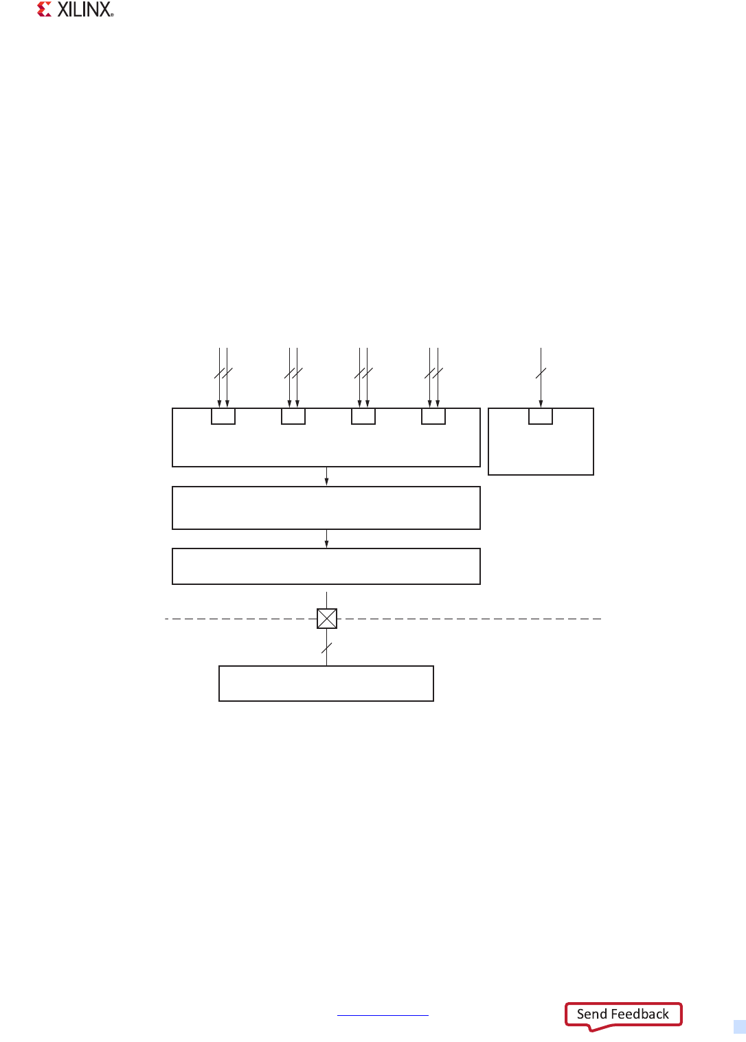
Zynq-7000 AP SoC Technical Reference Manual www.xilinx.com 293
UG585 (v1.12.1) December 6, 2017
Chapter 10: DDR Memory Controller
• Efficient transaction scheduling to optimize data bandwidth and latency
• Advanced re-ordering engine to maximize memory access efficiency for continuous reads and
writes as well as random reads and writes
• Write - read address collision detection to avoid data corruption
• Obeys AXI ordering rules
10.1.2 Block Diagram
The block diagram for the DDR memory controller is shown in Figure 10-1. The DDR memory
controller consists of an arbiter, a core with transaction scheduler, and the physical sequencing of the
DDR memory signals.
The controller core and transaction scheduler contains two 32-entry CAMs to perform DDR data
service re-ordering to maximize DDR memory access efficiency. It also contains a fly-by channel for
low latency access to DDR memory without going through the CAM.
The PHY processes read/write requests from the controller and translates them into specific signals
within the timing constraints of the target DDR memory. Signals from the controller are used by the
PHY to produce internal signals that connect to the pads of the PS using the PHY. The pads connect
directly, via the PCB signal traces, to the external memory devices.
The arbiter arbitrates across the four AXI ports for access to the DDR core. The arbitration is priority
based and also allows promotion of priorities via an urgent mechanism.
X-Ref Target - Figure 10-1
Figure 10-1: DDR Memory Controller Block Diagram
UG585_c10_01_120913
DDR Interface Configuration
Registers
CPUs
and ACP
• AXI 3 Port Arbiter
• Seperate Read/Write Requests
DDR Core • Transaction Scheduler and Queues
• Programmable Algorithms
DDR PHY • DDR2, LPDDR2, DDR3, DDR3L
DDR DRAM Memory Device(s)
S0
64-bit
Other Bus
Masters
S1
64-bit
AXI_
HP{2,3}
S2
64-bit
16 or 32-bit
AXI_
HP{1,0}
S3 S
64-bit 32-bit
APB
Device Boundary
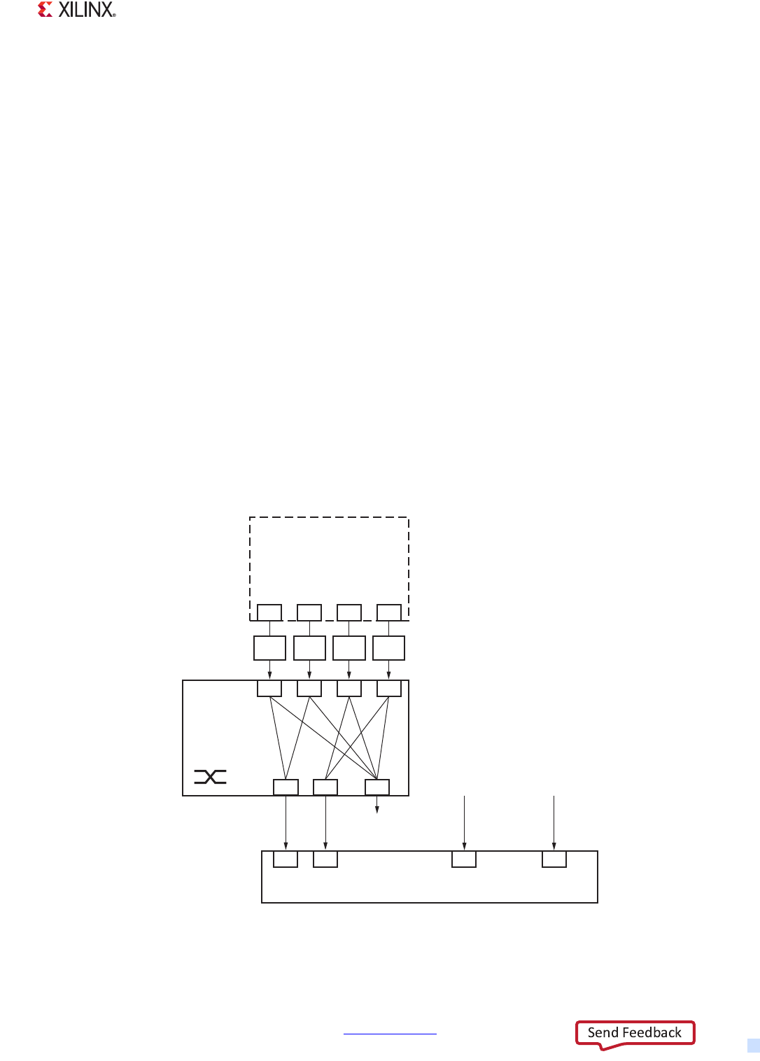
Zynq-7000 AP SoC Technical Reference Manual www.xilinx.com 294
UG585 (v1.12.1) December 6, 2017
Chapter 10: DDR Memory Controller
10.1.3 Notices
7z007s and 7z010 CLG225 Devices
All devices support the 32- and 16-bit data bus width options except the 7z007s single core and
7z010 dual core CLG225 devices. These CLG225 devices only support the 16-bit data bus width, not
the 32-bit bus.
10.1.4 Interconnect
The four AXI_HP interfaces are multiplexed down, in pairs, and are connected to ports 2 and 3 as
shown in Figure 10-2. These ports are commonly configured for high bandwidth traffic. The path
from these four interfaces to the DDR include two ports on the DDR memory port arbiter. The
interconnect switch arbitrates back-and-forth between each of the two ports. Read and write
channels operate separately. The arbitration in the bridge can be affected by the QoS signals from
each PL interface. A requestor with a higher QoS value is given preferential treatment by the
interconnect bridge. Arbitration is priority based using QoS as priority. In the event of a tie, an LRG
scheme is used to break the tie.
The L2-cache is connected to port 0 and is used to serve the CPUs and the ACP interface to the PL.
This port is commonly configured for low-latency. The other masters on the AXI interconnect are
connected to port 1.
X-Ref Target - Figure 10-2
Figure 10-2: DDRC System Viewpoint
UG585_c10_02_032012
to OCM
From Central
Interconnect
High Performance
AXI Controllers
(AXI_HP)
AXI_HP
Path to DDR
PL
64-bit
M0
FIFO
M1 M2 M3
S0 S1 S2
M0 M1 M2
S3
FIFOFIFO
From L2
Cache
FIFO
AXI_HP
to DDR
Interconnect
S3 S2 S1 S0
DDR Memory Controller
Zynq-7000 AP SoC Technical Reference Manual www.xilinx.com 295
UG585 (v1.12.1) December 6, 2017
Chapter 10: DDR Memory Controller
10.1.5 DDR Memory Types, Densities, and Data Widths
The DDR memory controller is able to connect to devices under the conditions identified in
Tabl e 10- 1.
Tabl e 10- 2 provides a collection of example memory configurations.
10.1.6 I/O Signals
The DDR signal pins are listed in Table 10-3. The DDR I/O buffers are powered by the VCC_DDR
power pins. The I/O state (including initial state) of the DDR signals is controlled via registers:
• slcr.DDRIOB_ADDR0
• slcr.DDRIOB_ADDR1
• slcr.DDRIOB_DATA0
• slcr.DDRIOB_DATA1
• slcr.DDRIOB_DIFF0
• slcr.DDRIOB_DIFF1
• slcr.DDRIOB_CLOCK
The output characteristics are controlled by the following registers and are reserved to specific
values produced by Xilinx tools:
• slcr.DDRIOB_DRIVE_SLEW_ADDR
Table 10-1: Connectivity Limitations
Parameter Value Notes
Maximum Total Memory Density 1 GB 1 GB of address map is allocated to DRAM
Total Data Width (bits) 16, 32 ECC can only use a 32-bit configuration: 16 data bits, 10
check bits
Component Data Width (bits) 8, 16, 32 4-bit devices are not supported
Maximum Ranks 1
Maximum Row Address (bits) 15
Maximum Bank Address (bits) 3
Table 10-2: Example Memory Configurations
Technology Component
Configuration
Number of
Components
Component
Density Total W idth Total Density
DDR3/DDR3L x16 2 4 Gb 32 1 GB
DDR2 x8 4 2 Gb 32 1 GB
LPDDR2 x32 1 2 Gb 32 256 MB
LPDDR2 x16 2 4 Gb 32 1 GB
LPDDR2 x16 1 2 Gb 16 256 MB
Zynq-7000 AP SoC Technical Reference Manual www.xilinx.com 296
UG585 (v1.12.1) December 6, 2017
Chapter 10: DDR Memory Controller
• slcr.DDRIOB_DRIVE_SLEW_DATA
• slcr.DDRIOB_DRIVE_SLEW_DIFF
• slcr.DDRIOB_DRIVE_SLEW_CLOCK
The input Vref settings are controlled by slcr.DDRIOB_DDR_CTRL. The DDR DCI settings are
controlled by slcr.DDRIOB_DCI_CTRL.
Note: The 7z010 dual core and 7z007s single core CLG225 devices only support a 16-bit data bus
width, not a 32-bit bus width.
Table 10-3: DDR I/O Signal Pin List
Device Pin Name I/O
Connections
Description
DDR2 LPDDR2 DDR3/
DDR3L
PS_DDR_CKP
PS_DDR_CKN
O X X X Differential clock outputs
PS_DDR_CKE O X X X Clock enable
PS_DDR_CS_B O X X X Chip select
PS_DDR_RAS_B O X X RAS row address strobe
PS_DDR_CAS_B O X X RAS column address strobe
PS_DDR_WE_B O X X Write enable
PS_DDR_BA[2:0] O X X Bank address
PS_DDR_A[14:0] O XXX
DDR3/DDR3L/DDR2: Row/Column Address
LPDDR2: CA[9:0] = DDR_A[9:0]
PS_DDR_ODT O X X Output dynamic termination signal
PS_DDR_DRST_B O X Reset
PS_DDR_DQ[31:0] IO X X X
32-bit Data bus: [31:0]
16-bit Data bus: [15:0]
16-bit Data with ECC
PS_DDR_DM[3:0] O X X X Data byte masks
PS_DDR_DQS_P[3:0]
PS_DDR_DQS_N[3:0]
IO X X X Differential data strobes
PS_DDR_VR{P,N} ~ X X X
DCI voltage reference. Used to calibrate input
termination. and DDR I/O drive strength. Connect
DDR_VRP to a resistor to GND. Connect DDR_VRN
to a resister to VCC_DDR.[Ref 1]
PS_DDR_VREF[1:0] ~ X X X Voltage reference
Notes:
1. PS_DDR_VR{P,N} signals should be bypassed from BSCAN.

Zynq-7000 AP SoC Technical Reference Manual www.xilinx.com 297
UG585 (v1.12.1) December 6, 2017
Chapter 10: DDR Memory Controller
10.2 AXI Memory Port Interface (DDRI)
10.2.1 Introduction
Each AXI master port has an associated slave port in the arbiter. The command FIFO located inside
the port stores the address, length and ID contained in the command. The RAM in the write port
stores the write data and byte enable. The RAM in the read port stores the read data coming back
from the core.
Because the read data coming back from the core can come out of order, the RAM is used for data
re-ordering. Each AXI command can make a request (write or read) for up to 16 data transfers (up to
the AXI limit). A single command coming from the AXI can be split into multiple requests going to
the arbiter logic and the controller.
The incoming command is first stored in the command FIFO. After a valid command is detected in
the write or read port, the value of the length field is checked and the number of requests associated
with this command is calculated. The logic then sends arbiter requests to the arbitration logic. The
arbitration logic looks at the requests from all the ports and gives the grant to one port at a time.
When a write port receives the grant from the arbiter, it generates write address, and write data
pointer and asserts the command valid. A read port on receiving grant generates read address, read
command length and the read token and asserts the command valid. Requests from various ports are
multiplexed using the grant signal.
When a write command is accepted by the DDR controller, it sends the write data pointer back to the
arbiter. The write data from all ports is multiplexed using the port ID contained in the write data
pointer.
When the read data comes back from the core, an associated ID is used to direct the data to the
appropriate read port. According to AXI specifications, the read data with the same ID is required to
be given back to the AXI read master in the same order in which read commands were received by
the port.
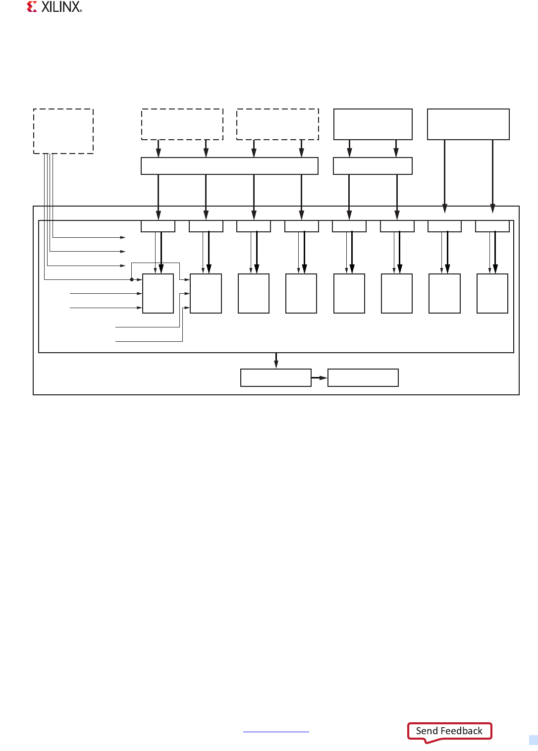
Zynq-7000 AP SoC Technical Reference Manual www.xilinx.com 298
UG585 (v1.12.1) December 6, 2017
Chapter 10: DDR Memory Controller
10.2.2 Block Diagram
The block diagram of the DDRI is shown in Figure 10-3.
10.2.3 AXI Feature Support and Limitations
This list shows supported and unsupported features for the AXI ports into the DDRI:
• Fixed burst type is not supported. Note that the behavior is unknown if this transfer type is
received at one of the AXI ports.
• Byte, half-word and word sub-width commands are supported.
• EXCL accesses are only supported on a single DDR port, ie., there is no support for EXCL
accesses across DDR ports.
• AWPROT/ARPROT[1] bit is used for trust zone support, AWPROT/ARPROT[0], and
AWPROT/ARPROT[2] bits are ignored and do not have any effect.
• ARCACHE[3:0]/AWCACHE[3:0] (cache support) are ignored, and do not have any effect.
• Sparse AXI write transfers (random strobes asserted/de-asserted for any data beat) are
supported.
• Unaligned transfers are supported.
X-Ref Target - Figure 10-3
Figure 10-3: DDRI Block Diagram
UG585_c10_03_012113
Aging Write 3 DDR Interface
Read 3
Urgent R
Read
Request
PL Fabric
Write
Request
Priority
Level
Priority
Level
Page Match Write 3
Aging Read 3
Page Match Read 3
Urgent Read/Write 3
Urgent Read/Write 2
Urgent Read/Write 1
Urgent Read/Write 0 Write 3
Urgent W
AXI_HP to DDR Interconnect
AXI_HP 0, 1
PL Fabric
URGENT
PL Signals PL Fabric
AXI_HP 2, 3
(Via Central Interconnect)
Other Masters
(Via L2 Cache)
CPUs/ACP
Interconnect
DDR Core DDR PHY
Read 2
Read
Request
Write
Request
Priority
Level
Priority
Level
Write 2 Read 1
Read
Request
Write
Request
Priority
Level
Priority
Level
Write 1 Read 0
Read
Request
Write
Request
Priority
Level
Priority
Level
Write 0
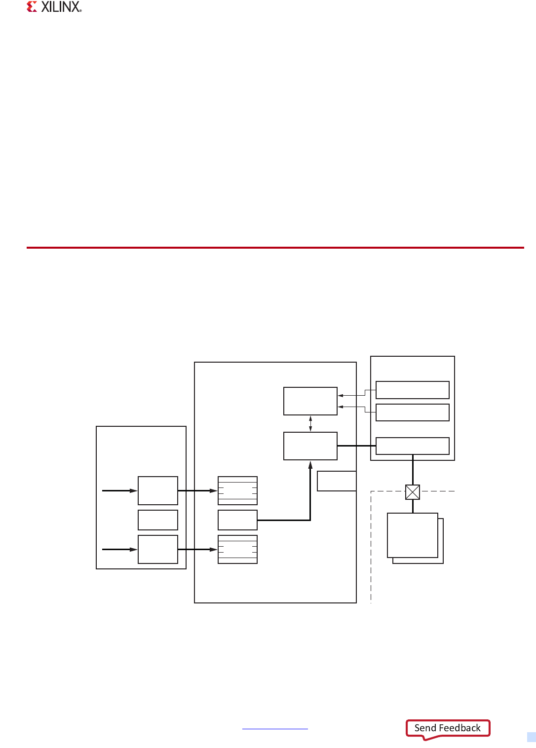
Zynq-7000 AP SoC Technical Reference Manual www.xilinx.com 299
UG585 (v1.12.1) December 6, 2017
Chapter 10: DDR Memory Controller
10.2.4 TrustZone
The DDR memory can be configured in 64 MB sections. Each section can be configured to be either
secure or non-secure. This configuration is provided via a system level control register.
•A 0 on a particular bit indicates a secure memory region for that particular memory segment.
•A 1 on a particular bit indicates a non-secure memory region for that particular memory
segment.
In the case of a non-secure access to a secure region, a DECERR response is returned back to the
master. For writes, the write data is masked out before being sent to the controller which results in
no actual writes occurring in the DRAM. On reads, the read data is all zeros on a TZ violation. For
more information on TrustZone see Programming ARM TrustZone Architecture on the Xilinx
Zynq-7000 All Programmable SoC (UG1019).
10.3 DDR Core and Transaction Scheduler (DDRC)
The DDRC is comprised of queues for pending read and write transactions and a scheduler that pops
off the queues and sends the next transaction to the DDR PHY. Between the DDRI and the DDRC,
there is arbitration logic to decide which transaction is sent to the DDRC next.
X-Ref Target - Figure 10-4
Figure 10-4: DDRC Block Diagram
UG585_c10_04_032012
DDR Interface
DDR Core
DDR PHY
Pending DDR
Transactions
Read
Request
Stage 1
Read
Arbiter
AXI Port Arbiter
Self-Coherent
and with DDR
Write
Request
Reads
Transaction
Scheduler
Optimization
Algorithms
Stage 2
Stage 3
DRAM R/W State
Open Bank State
Sequencer
DDR
DRAM
Device(s)
Writes
Write
Arbiter

Zynq-7000 AP SoC Technical Reference Manual www.xilinx.com 300
UG585 (v1.12.1) December 6, 2017
Chapter 10: DDR Memory Controller
10.3.1 Row/Bank/Column Address Mapping
The DDRC is responsible for mapping byte-addressable physical addresses used by the PS and PL AXI
masters to DDR row, bank and column addresses. This address mapping has a limited configurability
to allow user optimization. Optimizing the mapping to specific data access patterns can allow
increased DDR utilization by reducing page and row change overhead.
Note: Many combinations of address remapping are not available, notably a complete
bank-row-column mapping.
The address mapper associates linear request addresses to DRAM addresses by selecting the AXI bit
that maps to each and every applicable DRAM address bit. The full available address space is only
accessible to the user when no two DRAM address bits are determined by the same AXI address bit.
Each DRAM row, bank, and column address bit has an associated register vector to determine its
associated AXI source in the DDRC DRAM_addr_map_bank, DRAM_addr_map_row, and
DRAM_addr_map_col registers. The associated AXI address bit is determined by adding the internal
base of a given register to the programmed value for that register, as described in the following
equation:
[internal base] + [register value] = [AXI address bit number]
For example, from the description for reg_ddrc_addrmap_col_b3, it can be seen that this register
determines the mapping for DRAM column bit 4 and its internal base is 6. When the full data bus is
in use, DRAM column bit 4 is determined by the following:
[internal base] + [register value].
If reg_ddrc_addrmap_col_b3 register is programmed to 2, then the AXI address bit is:
6 + 2 = 8.
In other words, the column address bit 4 sent to DRAM is mapped to AXI address bit *_ADDR[8].
All the column bits left-shift one bit in half bus width mode (including ECC). In this case,
reg_ddrc_addrmap_col_b2 determines the mapping of DRAM column address bit 4. In the full bus
width case, reg_ddrc_addrmap_col_b3 determines DRAM column address 4.
10.4 DDRC Arbitration
The DDRC arbitration consists of three stages (see Figure 10-5):
• Stage 1 is AXI read/write port arbitration
• Stage 2 is winner of read and write compete
• Stage 3 is transaction scheduler
Each of these stages has their own arbitration steps that will be discussed in more detail.
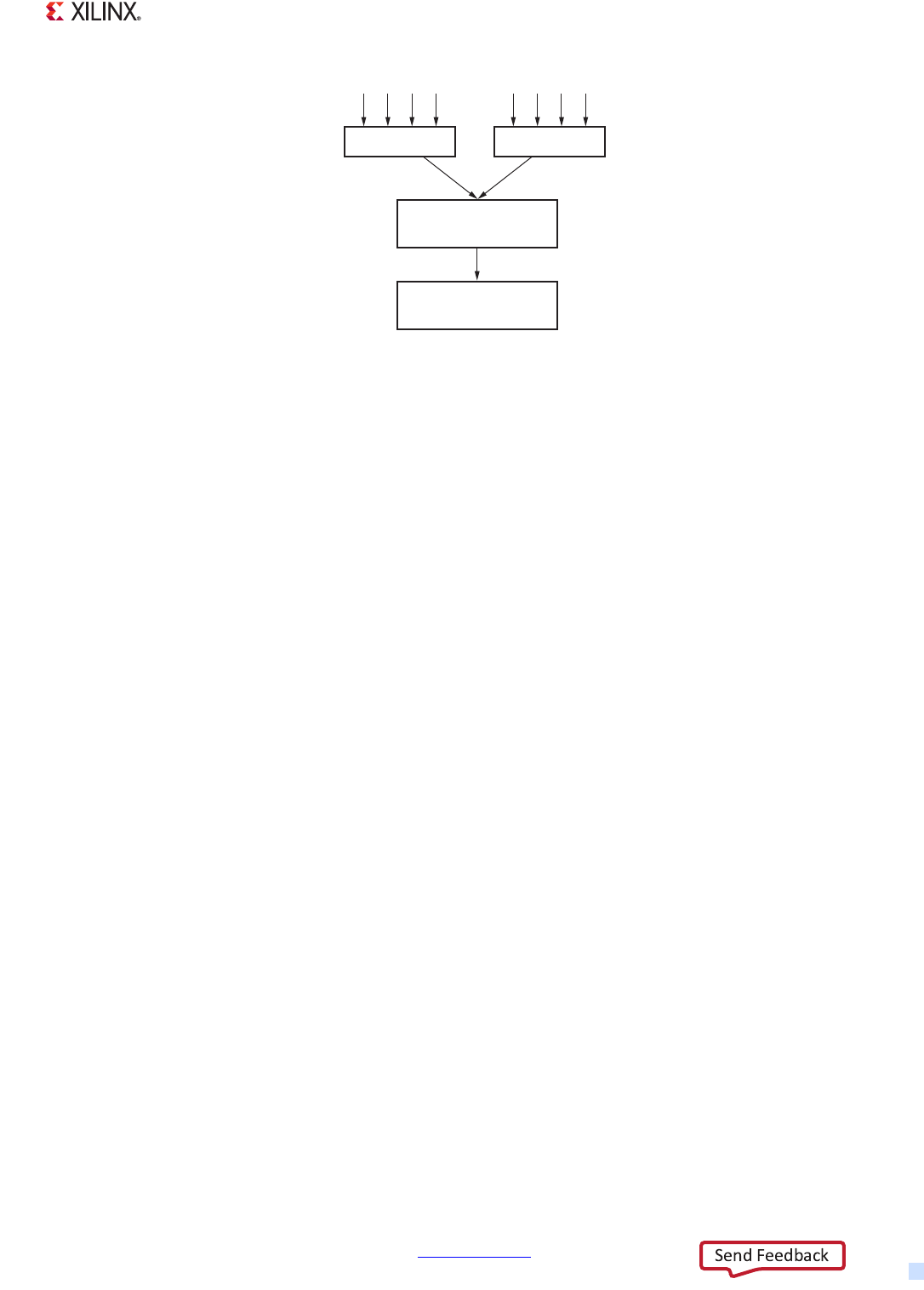
Zynq-7000 AP SoC Technical Reference Manual www.xilinx.com 301
UG585 (v1.12.1) December 6, 2017
Chapter 10: DDR Memory Controller
10.4.1 Priority, Aging Counter and Urgent Signals
DDR controller arbitration is based on round robin with aging. The round robin mechanism circularly
scans all requesting devices and services all outstanding requests before servicing the same device
again. The aging mechanism measures the time each request has been pending and assigns higher
priority to requests with longer wait times.
Each of the DDRC read and write ports is assigned a 10-bit priority value (see registers
axi_priority_wr_port0-3 and axi_priority_rd_port0-3). This value is used as an initial value for an aging
counter that counts down. Thus at any instant, a lower aging counter value takes priority over a
higher one.
In addition, each of the DDRC read and write ports has an urgent input signal. This signal acts as a
reset to the aging counter. When urgent is asserted, the aging counter for that port is reset, instantly
making this port's priority the highest. The source of the urgent bit is selectable via an SLCR
host-programmable register (DDR_URGENT_SEL) to be one of the following:
• The most-significant bit of the 4-bit QoS signal in the AXI interface for a port (except for
memory port 0 used by the CPUs and APU)
• A programmable SLCR register value (DDR_URGENT)
• One of the PL signal DDRARB[3:0] bits
While the priority value is static in nature, the urgent bit and QoS signal can be manipulated
dynamically.
10.4.2 Page-Match
To improve DDR utilization, the address of each new request is compared with the address of the
previous request. The DDRC has a preference for taking new requests that are to the same page as
the previous request. The memory port compares the addresses to determine if there is a page
match. A port that has been selected by the arbiter continues to get preference (priority 0) as long
as there continues to be page hits. They will compete against other ports with a priority of 0.
X-Ref Target - Figure 10-5
Figure 10-5: DDRC Arbitration
UG585_c10_05_032012
Stage 1 Read
Stage 2
Queue to DDR PHY
Stage 3
Transaction Scheduler
Stage 1 Write

Zynq-7000 AP SoC Technical Reference Manual www.xilinx.com 302
UG585 (v1.12.1) December 6, 2017
Chapter 10: DDR Memory Controller
The page size is defined by PAGE_MASK (32 bit register that all bits are the mask) and is always
address aligned. For proper operation, the software must program the page size in the PAGE_MASK
to match the size of the DDR memory. Setting this register to 0 disables the page-match step of the
arbitration.
10.4.3 Aging Counter
When a request is pending and not serviced, a decrementing aging counter is enabled. The starting
value of this counter is loaded from the 10-bit value in the priority register
(axi_priority_<rd/wr>_port<n>, there are 8 registers, one for each ports). The counter reloads when
the request is serviced. The value of this counter is used to help indicate the priority of an AXI
memory port. The lower the value of this counter, the higher the priority. When the priority reaches
0, the request has the highest priority.
For arbitration purposes, only the upper-most 5 bits are used to differentiate priority among ports.
This keeps the arbitration mechanism to a manageable size and latency, while still comprehending an
approximation of the age-based priority of each port.
TIP: In normal usage mode, enabling aging is the suggested option. Disabling aging can result in
excessive latencies/starvation of low priority ports.
10.4.4 Stage 1 – AXI Port Arbitration
The eight ports (four read and four write) compete to get the DDRC to accept their request. The
arbiter grants a request based on many factors. Read and write requests are treated the same,
meaning they go through the same arbitration. Each port maintains a priority level that steadily
moves from a preset state to the highest state or 0. This mechanism is important to maintain a
minimum bandwidth on a port. Each port also has different ways to signal an urgent situation, either
on a per-transaction basis (QoS) or for multiple transactions. The per-transaction urgency can be
good for low-latency masters.
The priority as shown in Figure 10-6 has the following logic. If there is a port with Priority 0 or 0 in
its aging counter (the highest priority), then it wins. If there is no port with 0 priority, the arbitration
checks if the port being serviced has a page match. If there is no page match, the lowest value in the
aging counter wins. If there is a tie for the lowest value in the aging counter, round robin is used to
resolve any ties.
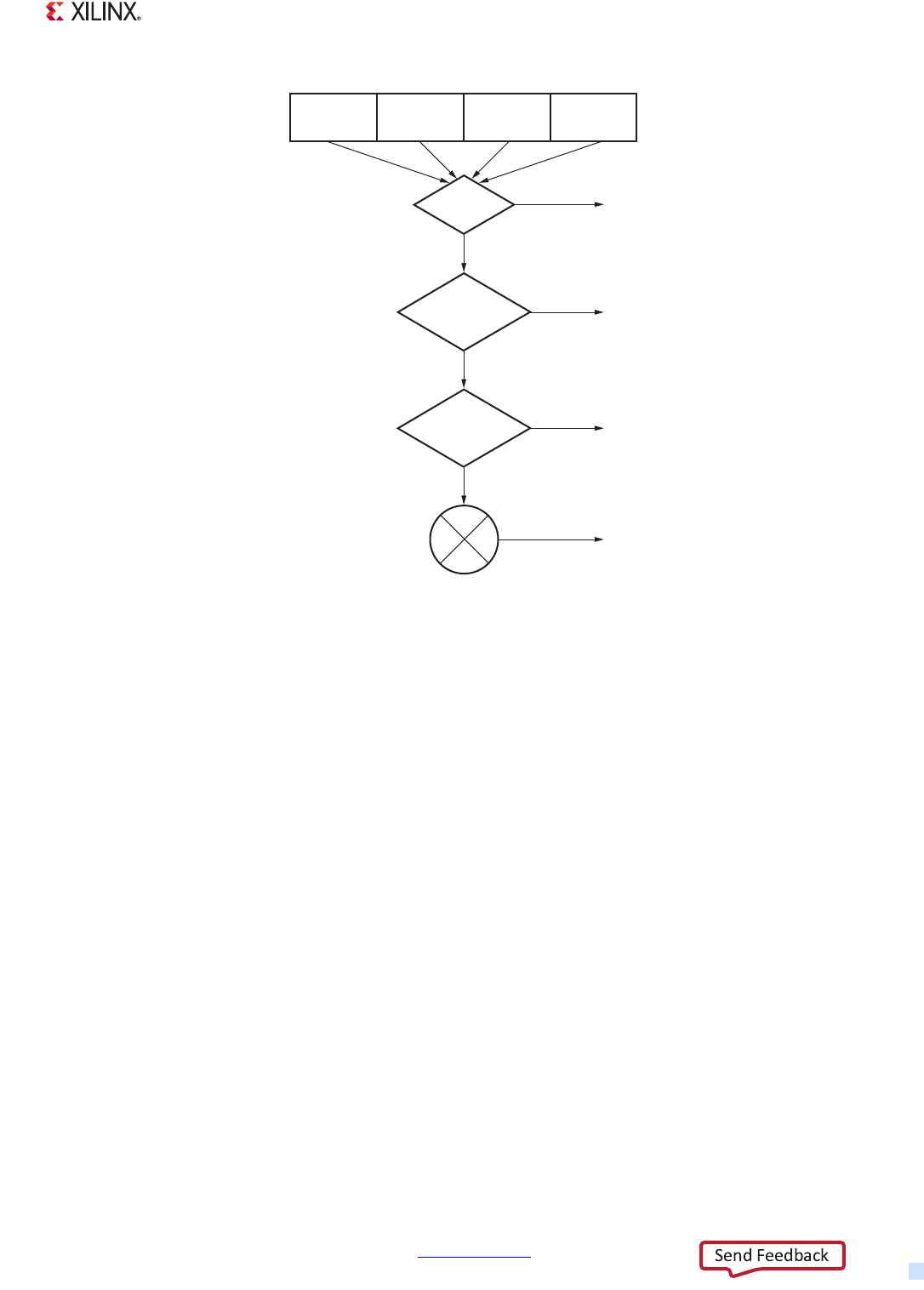
Zynq-7000 AP SoC Technical Reference Manual www.xilinx.com 303
UG585 (v1.12.1) December 6, 2017
Chapter 10: DDR Memory Controller
X-Ref Target - Figure 10-6
Figure 10-6: Stage 1 – AXI Port Arbitration
UG585_c10_06_050212
Aging
Counter 0
Aging
Counter 1
Aging
Counter 2
Aging
Counter 3
Is 0?
Page
Match?
Lowest
Priority
Round Robin Winner
Winner
Winner
Winner
T
T
Tie
F
F
0
2
31
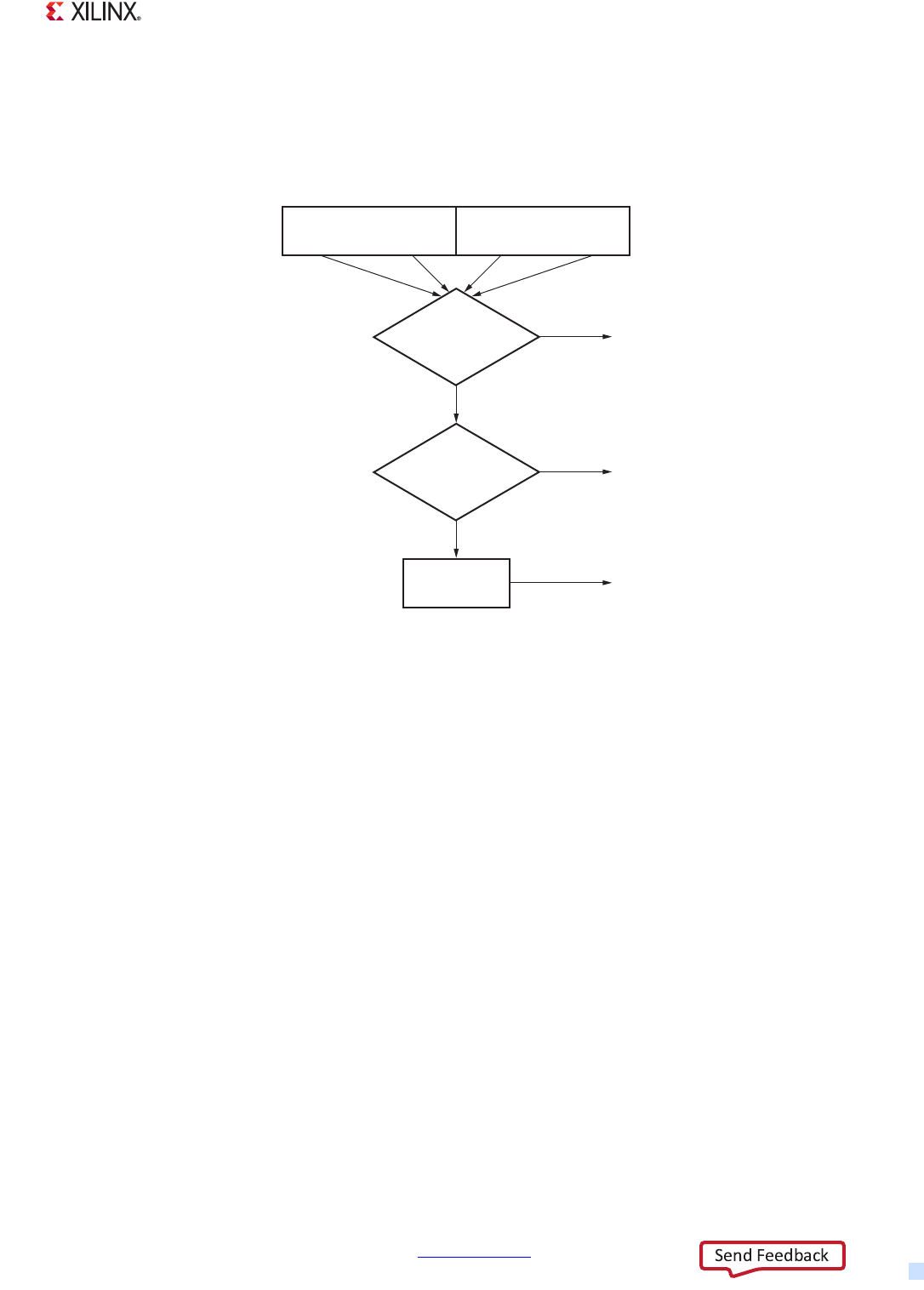
Zynq-7000 AP SoC Technical Reference Manual www.xilinx.com 304
UG585 (v1.12.1) December 6, 2017
Chapter 10: DDR Memory Controller
10.4.5 Stage 2 – Read Versus Write
The reads and the writes each have a queue in the DDR Core. The entries in these queues then vie for
the next level of arbitration, shown in Figure 10-7.
This stage of arbitration starts with the aging counter as shown in Figure 10-7. If there is a same type
of transaction with a priority 0, it wins. For example if a read won the last round of arbitration and
there is a read with priority 0, it wins. If there is not a same type of transaction with priority 0, and
another type of transaction with a priority 0 is present, it wins. If there is no Priority 0 in the queue
then it stays with the same type of transaction. An appropriate credit availability check is done before
selecting any request in all the above cases.
10.4.6 High Priority Read Ports
Before going into Stage 3 of the arbitration, a feature of the DDRC, the high priority read, needs to
be described. The HPR, or high priority read feature, allows splitting the read data queue (32 words)
within the DDRC into two separate queues for low and high priority. Each of the four read ports can
be assigned a low or high priority. By default this feature is disabled. When used, a high priority read
device is not slowed down by the (potentially slower) read data rate of a low-priority device. In a
typical use case, HPR is enabled on port 0 (CPU), thus reducing the CPU average read latency. The
split of the read data queue does not have to be two equal parts. Thus giving the CPU a small queue
to bypass the larger queue to service reads that need a lower latencies. Figure 10-8 shows where the
read queue is split.
X-Ref Target - Figure 10-7
Figure 10-7: Stage 2 – Read Versus Write
UG585_c10_07_032012
Write Winner
Aging Counter
Read Winner
Aging Counter
Stay with
Same Type
Other Type
Priority 0? Winner
T
Winner
F
Same Type
Priority 0? Winner
T
F
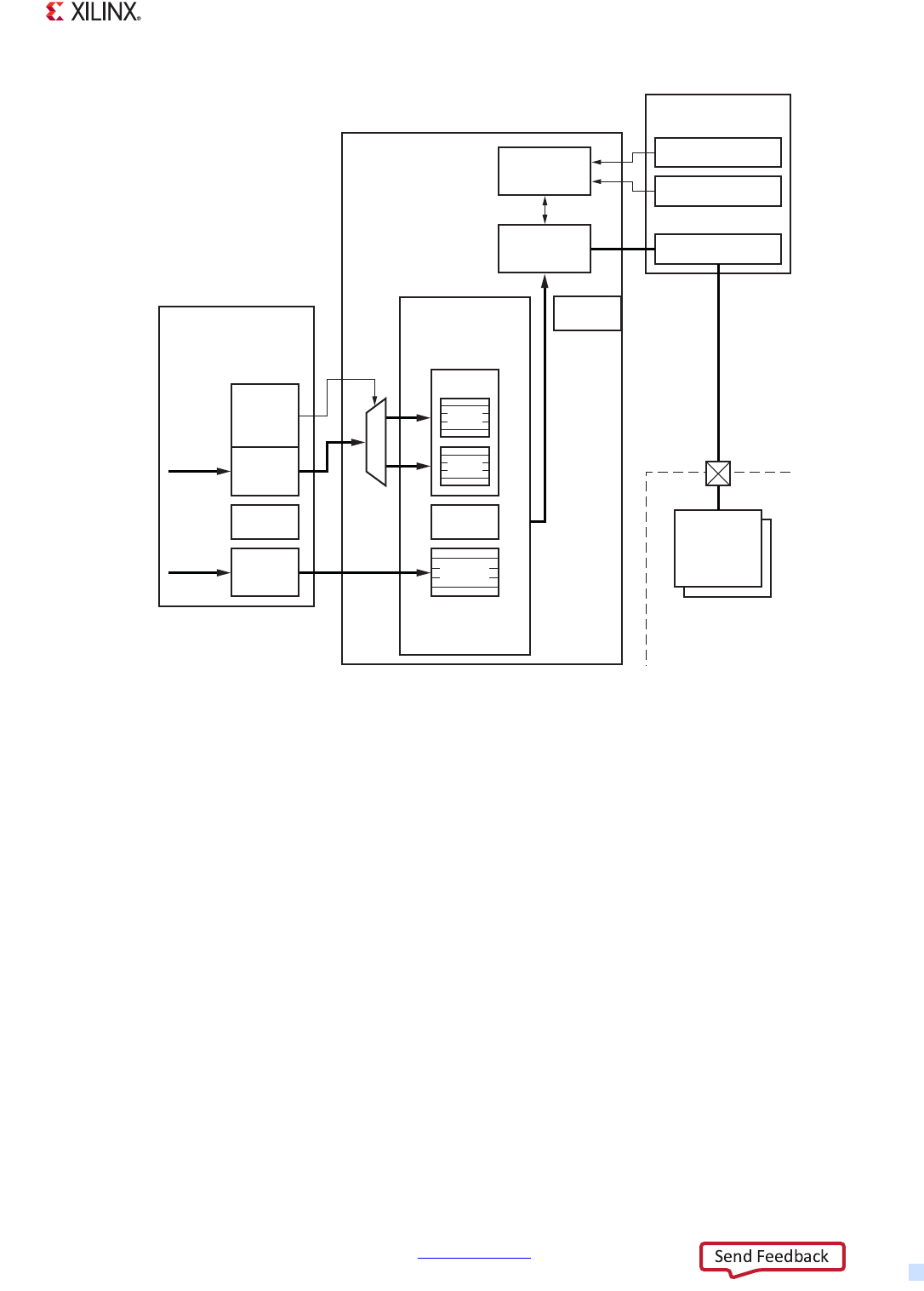
Zynq-7000 AP SoC Technical Reference Manual www.xilinx.com 305
UG585 (v1.12.1) December 6, 2017
Chapter 10: DDR Memory Controller
This can be changed by setting the reg_arb_set_hpr_rd_port<n> bit to 1'b1 for AXI ports (this is in
the axi_priority_<rd/wr>_port<n> register). The DDRC is configured by default to serve only LPR.
The read CAM can service only LPR by default. The total CAM depth is 32 for Read. (However, one slot
is always allocated for ECC purposes.) The reg_ddrc_lpr_num_entries register field in the DDRC
ctrl_reg1 register specifies the number of entries reserved for LPR. Taking 31 and subtracting the
reg_ddrc_lpr_num_entries gives the number of entries reserved for HPR.
It is necessary to change the REG_DDRC_LPR_NUM_ENTRIES field if a port is configured as an HPR
port to avoid deadlock in the credit mechanism
10.4.7 Stage 3 – Transaction State
The transaction state is the last stage of arbitration before the transaction goes to the DDR PHY and
the DDR device. The transaction state can be read or write. To change the transaction state there
must be no more transactions of that type or there can be a critical transaction of the other type.
Figure 10-9 shows the simple state machine for this.
X-Ref Target - Figure 10-8
Figure 10-8: Read Queue
UG585_c10_08_032012
DDR Interface
DDR Core
DDR PHY
Pending DDR
Transactions
Read
Request
Port
Priority
Select
Stage 1
Read
Arbiter
AXI Port Arbiter
Self-Coherent
and with DDR
Write
Request
Reads
LPR
HPR
Transaction
Scheduler
Optimization
Algorithms
Stage 2
Stage 3
DRAM R/W State
Open Bank State
Sequencer
DDR
DRAM
Device(s)
Writes
Write
Arbiter
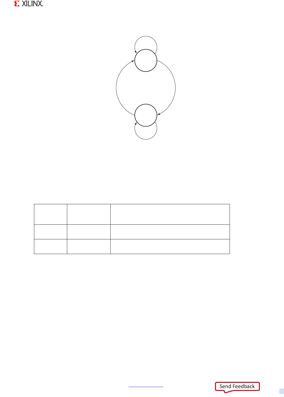
Zynq-7000 AP SoC Technical Reference Manual www.xilinx.com 306
UG585 (v1.12.1) December 6, 2017
Chapter 10: DDR Memory Controller
The transaction state stays the same until the other type of transaction is critical or there is no more
of that type of transaction. The state machine defaults to the read state. Table 10-4 shows how a
transaction in the queue can go from a normal state to critical.
Taking the low priority read transaction store as an example, it is expected that the transaction store
generally functions independently based on the following signals:
•lpr_max_starve_x32
• lpr_xact_run_length
• lpr_min_non_critical
The reg_arb_go2critical_en field in the DDRC ctrl_reg2 register enables the arbiter to drive
co_gs_go2critical_* signals to the DDRC. There are sideband signals on AXI (awurgent and arurgent)
that drive the co_gs_go2critical_* signals. If any port asserts their urgent sideband signal, and if this
feature is enabled, the arbiter asserts the corresponding co_gs_go2critical_* signal to the controller.
X-Ref Target - Figure 10-9
Figure 10-9: Stage 3 – Transaction State
UG585_c10_09_032012
Write
Mode
Read
Mode
Critical Write
OR Write
and No Read
Critical Read
OR Read
and No Write
Read, No Critical Write
Write, No Critical Read
Table 10-4: Transaction Store State Transitions
Normal Critical A transaction has been pending for this transaction
store and has not been serviced for a count of
*_max_starve_x32 pulses of the 32-cycle timer.
Critical Hard Non-Critical *_xact_run_length number of transactions has been
serviced from this transaction store.
Hard
Non-Critical
Normal *_min_non_critical number of cycles has passed in
this state.
Notes:
* Can be WR, LPR or HPR. Example is wr_max_starve_x32 which is a field of the WR_Reg.

Zynq-7000 AP SoC Technical Reference Manual www.xilinx.com 307
UG585 (v1.12.1) December 6, 2017
Chapter 10: DDR Memory Controller
Inside the controller, assertion of this signal causes the state machine to switch from one state to
another. For example, if the DDRC is currently servicing reads and co_gs_go2critical_wr goes High,
the controller ignores the normal state switching methods (starvation counter etc), and jumps to
servicing writes. There is a register in the controller to control how long to keep servicing the current
command type before switching to the other (reg_ddrc_go2critical_hysteresis field in the DDRC
ctrl_reg2).
In summary, this go2critical feature is used in the controller and ensures fast switching between
reads and writes for transactions with super high priority.
Note:
1. The normal programming condition is expected to be reg_ddrc_prefer_Write=0. (this is a bit field
in the DRAM_param_reg4 register) This means that the read requests are always serviced
immediately when received by an idle controller. Also, it is often desirable to set the
reg_ddrc_rdwr_idle_gap (this field is in the ddrc_ctrl register) to a very low number (such as 0, 1,
or 2) to ensure that writes do not go un-serviced in an otherwise-idle controller for any length of
time, wasting bandwidth. (The trade-off here is that by servicing writes more quickly, the
likelihood increases that reads issued to the controller immediately following writes incurs
additional latency to allow writes to be serviced and turn the bus around.)
2. Because the ordering is guaranteed on all requests issued to the controller, write latency must
not be a concern to system design. (In the event that write data is required by a subsequent read,
the controller automatically forces the write data out to DRAM before servicing the read.)
10.4.8 Read Priority Management
Normally in a read mode, high priority read requests are preferred for service over low priority read
requests. However, if the low priority read transaction store is critical and the high priority read
transaction store is not, then low priority read requests are preferred over high priority read requests.
This prevents starvation of low priority reads.
10.4.9 Write Combine
The write combine feature allow multiple writes to the same address to be combined into a single
write to DRAM. When a new write collides with a queued write in the CAM:
• If write combine is enabled, the DDRC overwrites the data for the old write with that from the
new write and only performs one write transaction (write combine).
• If write combine is disabled, the DDRC follows the following sequence of operations:
°Holds the new write transaction in a temporary buffer
°Applies flow control back to the core to prevent more transactions from arriving
°Flushes the internal queue holding the colliding transaction until that transaction has been
serviced
°Accepts the new transaction and removes flow control

Zynq-7000 AP SoC Technical Reference Manual www.xilinx.com 308
UG585 (v1.12.1) December 6, 2017
Chapter 10: DDR Memory Controller
10.4.10 Credit Mechanism
The DRAM controller employs a credit mechanism to ensure that buffers do not overflow (pending
DDR transactions). The interface making the request to the controller can only request commands
for which it has been granted credits or open slots in the queues to issue.
Credits are tracked separately for the following three command types:
•High priority reads
• Low priority reads
•Writes
Credits are counted for each command type independently according to the following rules:
• Initially the interface has zero credits.
• Following the de-assertion of reset to the DRAM controller, credits are issued to the interface
for each command type. A given credit count increments every time a credit is issued by the
DRAM controller, indicated by the assertion of the appropriate *_credit signal on the rising edge
of the clock.
• When the credit count is greater than zero, the interface can issue requests of that type to the
controller. Each time a request is issued to the controller, the associated credit count is
decremented.
10.5 Controller PHY (DDRP)
The DDRP processes read and write requests from the DDRC and translates them into specific signals
within the timing constraints of the target DDR memory. The DDRP is composed of functional units
including PHY control, master DLL, and read/write leveling logic. The PHY data slice block handles
the DQ, DM, DQS, DQ_OE and DQS_OE signals. The PHY control block synchronizes all of the control
signals with the DDR_x3 clock.
There are two kinds of DLLs, the master DLL, and the slave DLL. The DLLs are responsible for creating
the precise timing windows required by the DDR memories to read and write data. The master DLL
measures the cycle period in terms of a number of taps and passes this number through the ratio
logic to the slave DLLs. The slave DLLs can be separated on the target die to minimize skew and delay
and to account for process, temperature and voltage variations.
Write leveling and read leveling are new functions required for DDR3, DDR3L operation. These
functions help automatically determine delay timings required to align data to the optimal window
for reliable data capture:
• Read leveling and write leveling for DDR3, DDR3L
• Support for 16- and 32-bit data bus width with one rank
• Optional ECC with a 16-bit data width
• Individual bytes with read data mask bits
Zynq-7000 AP SoC Technical Reference Manual www.xilinx.com 309
UG585 (v1.12.1) December 6, 2017
Chapter 10: DDR Memory Controller
10.6 Functional Programming Model
The memory controller has several functional features; their programming is described in this
section. Programming for the operational features are described in section 10.9 Operational
Programming Model. To start operation of the PS DRAM interface, the following sequence of
operations must take place:
1. DDR clock initialization
2. DDR I/O buffers (DDR IOB) initialization and calibration
3. DDR controller (DDRC) register programming
4. DRAM reset and initialization
5. DRAM input impedance (ODT) calibration
6. DRAM output impedance (Ron) calibration
7. DRAM Training
a. Write leveling
b. Read DQS gate training
c. Read data eye training
This section is intended for reference and debug purposes only. Generally, programming for steps 1–
7 are provided by the Vivado® Design suite.
10.6.1 Clock Operating Frequencies
Prior to DDR initialization, a DDR clock must be active. Both the DDR_2x and DDR_3x clocks must be
configured properly. The DDR_3x clock is the clock used by the DRAM and should be set to the
desired operating frequency (note that the data rate per bit is twice the operating frequency). The
DDR_2x clock is used by the interconnect and is typically set to 2/3 of the operating frequency. The
DDR PLL frequency should be set to an even multiple of the operating frequency.
Tabl e 10- 5 provides frequency configuration examples assuming a 50 MHz reference clock.
Table 10-5: DDR Clock Operating Frequency
Operating
Frequency
DDR PLL
Frequency
DDR_3x Clock
Frequency
DDR_2x Clock
Frequency
PLL Feedback
Divider
DDR_3x Clock
Divider
DDR_2x Clock
Divider
525.00 1050.00 525.00 350.00 21 2 3
400.00 1600.00 400.00 266.67 32 4 6

Zynq-7000 AP SoC Technical Reference Manual www.xilinx.com 310
UG585 (v1.12.1) December 6, 2017
Chapter 10: DDR Memory Controller
Programming the DDR clock involves the DDR_PLL_CTRL and DDR_CLK_CTRL registers in the SLCR.
Refer to the programming example in section 10.9.2 Changing Clock Frequencies. General PLL
programming is described in section 25.10.4 PLLs.
In addition to the main DDR clock, a 10 MHz clock is used by the digitally controlled impedance (DCI)
function built into the DDR IOB. This clock is configured via the SLCR DCI_CLK_CTRL register.
10.6.2 DDR IOB Impedance Calibration
The DDR IOBs support calibrated drive strength and termination strength using the DCI digitally
controlled impedance mode of the IOB. In DDR2/DDR3/DDR3L modes this is used to calibrate
termination strength. In LPDDR2 mode this is used to calibrate drive strength. The DCI state machine
requires two external pins, VRN and VRP, which are connected to external resistors to VCCO_DDR and
ground, respectively. DCI settings are shown in Table 10-6.
When enabled, the DCI state machine will automatically match drive and termination impedance to
the external resistors. This background calibration takes 1-2 ms to lock and then runs continuously.
Calibration
1. Configure the clock module to configure a 10 MHz clock on dci_clk
2. Enable the DDR DCI calibration system using the SLCR registers DDRIOB_DCI_CTRL and
DDRIOB_DCI_STATUS
a. Toggle DDRIOB_DCI_CTRL.RESET_B to 0 and set to 1
b. Set DDRIOB_DCI_CTRL.PREF_OPT, and NREF_OPT fields according to Table 10-7
c. Set DDRIOB_DCI_CTRL. UPDATE_CONTROL to 0
d. Set DDRIOB_DCI_CTRL.ENABLE to 1
e. Poll on the DDRIOB_DCI_STATUS.DONE bit until it is 1
Table 10-6: DCI Settings
DDR standard Termination
Impedance Drive Impedance VRN resistor
(to VCCO_DDR)
VRP resistor
(to ground)
DDR3/DDR3L 40Ω N/A 80Ω 80Ω
DDR2 50Ω N/A 100Ω 100Ω
LPDDR2 None 40Ω 40Ω 40Ω
Table 10-7: Calibration
Field Name Reset Power
Down
DCI Enable
DDR3/DDR3L
DCI Enable
DDR2
DCI Enable
LPDDR2 DCI Disabled
UPDATE_CONTROL 00 0 0 0 1
PREF_OPT2[2:0] 000 000 000 000 000 000
PREF_OPT1[1:0] 00 00 00 00 10 00
NREF_OPT4[2:0] 000 000 001 001 001 000

Zynq-7000 AP SoC Technical Reference Manual www.xilinx.com 311
UG585 (v1.12.1) December 6, 2017
Chapter 10: DDR Memory Controller
10.6.3 DDR IOB Configuration
The DDR IOBs must be configured to function as I/O. Each type of DDR IOB is controlled by two
different SLCR configuration registers. The configuration registers configure the IOB's input mode,
output mode, DCI mode, and other functions.
Configuration
The DDR system supports DDR3L/DDR3/DDR2/LPDDR2 in 16 and 32 bit modes and power down
modes. The registers identified in Tabl e 10- 8 control groups of I/Os and must be configured
depending on the particular mode.
NREF_OPT2[2:0] 000 000 000 000 000 000
NREF_OPT1[1:0] 00 00 00 00 10 00
Table 10-7: Calibration (Cont’d)
Field Name Reset Power
Down
DCI Enable
DDR3/DDR3L
DCI Enable
DDR2
DCI Enable
LPDDR2 DCI Disabled
Table 10-8: DDR IOB Configuration Registers
Register Affected I/O Blocks Description
DDRIOB_DDR_CTRL VREF, VRN, VRP, DRST Controls special I/O modes for internal and external
VREF and DCI reference pins VRN and VRP
DDRIOB_DCI_CTRL DCI controller Enables the DCI controller
DDRIOB_DCI_STATUS DCI controller Status for the DCI controller
DDRIOB_ADDR0
DDRIOB_ADDR1
DDR_A[14:0], DDR_CKE, DDR_BA[2:0],
DDR_ODT, DDR_WE_B, DDR_CAS_B,
DDR_RAS_B DDR_CS_B
Configuration settings for address and control
outputs used by LPDDR2, DDR2 and DDR3/DDR3L
DDRIOB_CLOCK DDR_CK_P, DDR_CK_P Configuration settings for the differential clock
outputs. Controls DDR_CK_P, DDR_CK_P
DDRIOB_DATA0 DDR_DQ[15:0], DDR_DM[1:0],
DDR_FIFO_IN[0], DDR_FIFO_OUT[0]
Configuration settings for data and mask bits for
lower 16-bits
DDRIOB_DATA1 DDR_DQ[31:16], DDR_DM[3:2],
DDR_FIFO_IN[1], DDR_FIFO_OUT[1]
Configuration settings for data and mask bits for
upper16-bits
DDRIOB_DIFF0 DDR_DQS_P[1:0], DDR_DQS_N[1:0] Configuration settings for dqs bits for lower 16-bits
DDRIOB_DIFF1 DDR_DQS_P[3:2], DDR_DQS_N[3:2] Configuration settings for dqs bits for upper 16-bits
DDRIOB_DRIVE_SLEW
_ADDR
DDR_A[14:0], DDR_CKE, DDR_BA[2:0],
DDR_ODT, DDR_WE_B, DDR_CAS_B,
DDR_RAS_B, DDR_CS_B
Drive strength and slew rate settings for address
and control output
DDRIOB_DRIVE_SLEW
_CLOCK
DDR_CK_P, DDR_CK_P Drive strength and slew rate settings for the clock
outputs
DDRIOB_DRIVE_SLEW
_DATA
DDR_DQ[31:0], DDR_DM[3:0],
DDR_FIFO_IN[1:0], DDR_FIFO_OUT[1:0]
Drive strength and slew rate settings for data I/Os
DDRIOB_DRIVE_SLEW
_DIFF
DDR_DQS_P[3:0], DDR_DQS_N[3:2] Drive strength and slew rate settings for data strobe
I/Os

Zynq-7000 AP SoC Technical Reference Manual www.xilinx.com 312
UG585 (v1.12.1) December 6, 2017
Chapter 10: DDR Memory Controller
Set the IOB configuration as follows:
1. Set DCI_TYPE to DCI Drive for all LPDDR2 I/Os.
2. Set DCI_TYPE to DCI Termination for DDR2/DDR3/DDR3L bidirectional I/Os.
3. Set OUTPUT_EN = obuf to enable outputs.
4. Set TERM_DISABLE_MODE and IBUF_DISABLE_MODE to enable power saving input modes. The
TERM_DISABLE_MODE and IBUF_DISABLE_MODE fields should not be set before DDR training
has completed.
5. Set INP_TYPE to VREF based differential receiver for SSTL, HSTL for single ended inputs.
6. Set INP_TYPE to Differential input receiver for differential inputs.
7. Set TERM_EN to enabled for DDR3/DDR32L and DDR2 bidirectional I/Os (Outputs and LPRDDR2
IOs are not terminated).
8. Set DDRIOB_DATA1 and DDRIOB_DIFF1 registers to power down if only 16 bits of DQ DDR are
used (including ECC bits).
9. For DDR2 and DDR3/DDR3L – DCI only affects termination strength, so address and clock
outputs do not use DCI.
10. For LPDDR2 – DCI affects drive strength, so all I/Os use DCI.
VREF Configuration
DDR I/Os use a differential input receiver. One input to this receiver is connected to the data input,
and the other is connected to a voltage reference called VREF. For DDR2/3 and LPDDR2 DRAM
interfaces, the VREF voltage is set to half of the I/O VCCO voltage. The VREF can be supplied either
externally over dedicated VREF pads, or from an internal voltage source. External VREF is
recommended for all designs to provide additional timing margin, but requires external board
components. To configure the VREF reference supply, set the DDRIOB_DDR_CTRL register as follows:
• To enable internal VREF
°Set DDRIOB_DDR_CTRL.VREF_EXT_EN to 00 (disconnect I/Os from external signal)
°Set DDRIOB_DDR_CTRL.VREF_SEL to the appropriate voltage setting depending on the DDR
standard (VREF=VCCO_DDR/2)
°Set DDRIOB_DDR_CTRL.VREF_INT_EN to 1 to enable the internal VREF generator
• To enable external VREF
°Set DDRIOB_DDR_CTRL.VREF_INT_EN to 0 to disable the internal VREF generator
°Set DDRIOB_DDR_CTRL.VREF_SEL to 0000
°Set DDRIOB_DDR_CTRL.VREF_EXT_EN to 11 to connect the IOBs VREF input to the external
pad for a 32-bit interface
°Set DDRIOB_DDR_CTRL.VREF_EXT_EN to 01 to connect the IOBs VREF input to the external
pad for a 16-bit interface

Zynq-7000 AP SoC Technical Reference Manual www.xilinx.com 313
UG585 (v1.12.1) December 6, 2017
Chapter 10: DDR Memory Controller
10.6.4 DDR Controller Register Programming
Prior to enabling the DDRC, all DDRC registers must be initialized to system-specific values. About
80 registers with over 350 parameters might be set or left at their power-on default values. The DDRC
is then enabled, by writing to the ddrc_ctrl register. Once enabled, the DDRC automatically performs
the initialization steps 4-7 (Functional Programming Model). DDRC operation is autonomous,
requiring no further programming unless functionality changes are desired (e.g. changing AXI port
priority levels).
10.6.5 DRAM Reset and Initialization
The DDRC performs DRAM reset and initialization per the JEDEC specs, including reset, refresh, and
mode registers initialization.
10.6.6 DDR Initialization Sequence
LPDDR2 Initialization Sequence
When used with LPDDR2 DRAM, the initialization state machine executes the following initialization
sequence:
1. Power up VDD and VDDQ simultaneously. Assert and hold CKE
2. Apply stable clock
3. Issue NOP/Deselect for duration specified by reg_ddrc_pre_cke_x1024 (spec requires at least
200 us with stable power and clock)
4. Issue PRECHARGE ALL command
5. Issue REFRESH
6. Issue REFRESH
7. Load Mode Register
8. Load Extended Mode Register
9. Issue ACTIVE command
10. Issue NOP/Deselect for reg_ddrc_final_wait_x32 cycles (no spec requirement)
11. Begin normal operation
DDR2 Initialization Sequence
For DDR2, the initialization state machine executes the following initialization sequence:
1. Power up
2. Issue NOP/Deselect for duration specified by reg_ddrc_pre_cke_x1024 (spec requires at least
200 us with stable power and clock)
3. Assert CKE and issue NOP/Deselect for reg_ddrc_post_cke_x1024 (spec requires at least 400 ns)
4. Issue PRECHARGE ALL followed by NOP/Deselect for reg_ddrc_t_rp cycles

Zynq-7000 AP SoC Technical Reference Manual www.xilinx.com 314
UG585 (v1.12.1) December 6, 2017
Chapter 10: DDR Memory Controller
5. Program EMR2 to the reg_ddrc_emr2 value followed by NOP/Deselect for reg_ddrc_t_mrd cycles
6. Program EMR3 to the reg_ddrc_emr3 value followed by NOP/Deselect for reg_ddrc_t_mrd cycles
7. Enable DLL by programming EMR to the reg_ddrc_emr value followed by NOP/deselect for
reg_ddrc_t_mrd cycles
8. Issue DLL reset by programming MR to the reg_ddrc_mr value followed by NOP/Deselect for
reg_ddrc_t_mrd cycles
9. Issue Precharge All followed by NOP/Deselect for (reg_ddrc_t_rp+1) cycles
10. Issue Refresh followed by NOP/Deselect for reg_ddrc_t_rfc_min cycles. Repeat 9 times.
11. Program MR without resetting the DLL by setting MR to reg_ddrc_mr value with bit 8 set to 1.
12. Issue NOP/Deselect for duration specified by reg_ddrc_pre_ocd_x32 (no spec requirement)
13. Issue "OCD complete" command, indicating that no on-chip driver calibration will be performed
14. Issue NOP/Deselect for reg_ddrc_final_wait_x32 cycles (no spec requirement)
15. Begin normal operation
DDR3 Initialization Sequence
For DDR3, the initialization state machine will execute the following initialization sequence:
1. Power up
2. Issue NOP/Deselect for duration specified by reg_ddrc_pre_cke_x1024 (spec requires at least
200 us with stable power and clock)
3. Assert CKE and issue NOP/Deselect for reg_ddrc_post_cke_x1024 (spec requires at least 500 us)
4. Issue MRS command to load MR2 with reg_ddrc_emr2 value, followed by NOP/Deselect for
duration of reg_ddrc_t_mrd
5. Issue MRS command to load MR3 with reg_ddrc_emr3, followed by NOP/Deselect for duration of
reg_ddrc_t_mrd
6. Issue MRS command to load MR1 with reg_ddrc_emr, followed by NOP/Deselect for duration of
reg_ddrc_t_mrd
7. Issue MRS command to load MR0 with reg_ddrc_mr, followed by NOP/Deselect for duration of
reg_ddrc_t_mod
8. Start counting of reg_ddrc_t_zq_long_nop, and issue ZQCL command to start ZQ calibration
9. Wait for reg_ddrc_t_zq_long_nop counting to finish. Ensure wait from step 7 is larger than tDLLK
10. Begin normal operation

Zynq-7000 AP SoC Technical Reference Manual www.xilinx.com 315
UG585 (v1.12.1) December 6, 2017
Chapter 10: DDR Memory Controller
10.6.7 DRAM Input Impedance (ODT) Calibration
The DRAM mode and extended mode set commands are controlled by the ddrc.DRAM_EMR_MR_reg
and ddrc.DRAM_EMR_reg registers. The encoding for these registers can be found in DRAM device
data sheets or JEDEC specifications. The register format for of these commands are shown in
Appendix B, Register Details.
The on-die-termination (ODT) is available in DDR2 and DDR3/DDR3L devices with the following
features:
• In DDR3/DDR3L devices, the ODT value is controlled via Mode register MR1. It can be disabled,
or set to one of the following values: 120Ω, 60Ω, or 40Ω.
• In DDR2 devices, the ODT value is controlled via the mode register EMR. It can be disabled, or
set to one of the following values: 75Ω, 150Ω, or 50Ω.
• Both DDR2 and DDR3/DDR3L devices have a dedicated ODT input pin that is used to enable the
ODT during write operations, and disable it otherwise.
Calibration
DDR3/DDR3L devices provide ODT calibration via the ZQCL and ZQCS commands. The ZQCL (ZQ
calibration long) command is issued as part of the DRAM initialization procedure and is used for
initial calibration, which takes about 512 DDR_3x clock cycles. The ZQCS (ZQ calibration short) is
subsequently issued automatically by the DDRC for minor calibration adjustments. A typical ZQCS
interval is 100 ms.
DDR2 (and LPDDR2) devices do not provide ODT calibration.
10.6.8 DRAM Output Impedance (RON) Calibration
DRAM device MR/EMR registers are controlled via the ddrc.DRAM_EMR_MR_reg and
ddrc.DRAM_EMR_reg registers. MR/EMR encodings can be found in DRAM device data sheets or
JEDEC specifications.
The output impedance control feature is available in DDR2, DDR3/DDR3L and LPDDR2 devices.
• In DDR2 devices, the value is controlled via the mode register EMR, and can be set to full
strength or reduced strength.
• In DDR3/DDR3L devices, the value is controlled via the mode register MR1, and can be set to
one of the following values: 40Ω or 35Ω.
• In LPDDR2 devices, the value is controlled via MR3, and can be set between 34Ω and 120Ω
(default value is 40Ω).
Calibration
In DDR3/DDR3L and LPDDR2 devices, the output impedance is calibrated by the same ZQCL/ZQCS
commands discussed above.
In DDR2 devices, the DDR2 external calibration procedure (OCD for off-chip driver calibration) is not
supported by the DDRC.

Zynq-7000 AP SoC Technical Reference Manual www.xilinx.com 316
UG585 (v1.12.1) December 6, 2017
Chapter 10: DDR Memory Controller
10.6.9 DRAM Training
DRAM training includes three steps, executed in the following order:
1. Write leveling
2. Read DQS gate training
3. Read data eye training
Not all DRAM types support all three steps, as detailed below. Each step can be enabled or disabled
independently.
If a training step is enabled, the user must provide an initial delay value as a starting point of the
automatic training procedure. The value is a rough estimate of the expected delay or skew (see
details below) on the system board, minus some margin.
If a training step is disabled, the user must provide a delay value to be used to compensate for the
board delay or skew.
There are several possible reasons why the user might choose to disable a training step.
• The step is not supported by the particular DRAM type. For example, write leveling is not
supported by DDR2 and LPDDR2.
• Board delays are well-known and operating conditions are such that timing variance is minimal,
and training is not required.
• Delay settings are known from previous training events.
Training time is on the order of 1-2 ms at a 500 MHz DRAM clock.
Note: For training to be successful, all of the data signals need to be connected to the DRAM
device(s) even when ECC is used (16-bit data, 10-bit ECC).
Write Leveling
Goal Adjust WR DQS relative to CLK
Desired Nominal DQS aligned with clock (0 phase offset)
Final Ratio Equal to the DQS to CLK board delay at the DRAM
Initial Ratio Final value minus 0.5 cycle. If < 0 set to 0. If skew is too small, invert clock.
Applies To DDR3/DDR3L only
Write leveling is part of the DDR3/DDR3L specification. Due to the fly-by topology recommended for
DDR3/DDR3L systems, the clock (CLK) tends to lag relative to write DQS at the DRAM input. In order
to align CLK and DQS as required by the DRAM specification, the PHY delays the DQS signal to match
the board skew. The write leveling procedure is used to find the required delay.
When write leveling is enabled (via MR1), the DRAM asynchronously feeds back CLK, sampled with
the rising edge of DQS, through the DQ bus. The controller repeatedly delays DQS until a transition
from 0 to 1 is detected. Write leveling is performed independently for each byte lane. The calibration

Zynq-7000 AP SoC Technical Reference Manual www.xilinx.com 317
UG585 (v1.12.1) December 6, 2017
Chapter 10: DDR Memory Controller
logic OR's the DQ bits in a byte to determine the transition because different memory vendors use
different bits in a byte as feedback.
The DDRC supports write leveling as part of the initialization procedure. Optionally, write leveling
can be disabled and pre-determined delay values can be programmed via registers (required for
DDR2 and LPDDR2 where write leveling is not supported).
IMPORTANT: Successful training depends on providing an approximate minimum DQS to CLK delay
value. This value should be estimated based on system board layout as well as package delay
information.
Read DQS Gate Training
Goal Adjust valid RD DQS window.
Desired Nominal Surround the 4 (BL=8) valid DQS pulses
Final Ratio 2 * board delay. Add 0.5 cycle if the clock is inverted
Initial Ratio Final ratio minus 0.125 cycle (0x20 units), but not < 0.
Applies To DDR3/DDR3L, LPDDR2
The read DQS gate training is used by the PHY to identify the valid interval of read DQS and capture
the read data. It is necessary to align the valid read window to the read data burst and exclude the
preamble period and any period during which the DQS signal is tri-stated or driven by the PHY itself.
The DDRC supports read DQS gate training as part of the initialization procedure. Optionally,
training can be disabled and pre-determined delay values can be programmed via registers (required
for DDR2, where read training is not supported).
Note that when using LPDDR2, with read gate training, automatic training is not recommended.
Instead, the following procedure is recommended (Xilinx tools implement this flow):
1. The even byte lanes are trained and the results are recorded by software.
2. The odd byte lanes are trained and the results are recorded by software.
3. The results from 1 and 2 are then applied during DRAM controller initialization, with automatic
training disabled.
IMPORTANT: Successful training depends on providing an approximate minimum Zynq-7000
AP SoC-to-DRAM board delay value. This value should be estimated based on system board layout.
Read Data Eye Training
Goal Adjust RD DQS relative to RD data.
Desired Nominal DQS edge in the middle of data eye
Final Ratio Nominal ideal value is 0.25 cycle since at DRAM output DQ and DQS are aligned

Zynq-7000 AP SoC Technical Reference Manual www.xilinx.com 318
UG585 (v1.12.1) December 6, 2017
Chapter 10: DDR Memory Controller
Initial Ratio None required
Applies To DDR3/DDR3L, LPDDR2
Enabled by the MPR bit-field in MR3, DDR3/DDR3L Read data eye training is done to compensate for
possible imbalanced loading on the read path. In this mode, the DRAM outputs a stream of
01010101 in a burst length of 8 bits with a regular memory read command. Given the known data
pattern, the memory controller adjusts the internal DQS delay so that DQS edges occur in the middle
of the data eye.
The DDRC supports read data eye training as part of the initialization procedure. Optionally, training
can be disabled and pre-determined delay values can be programmed via registers (required for
DDR2 where read training is not supported).
10.6.10 Write Data Eye Adjustment
There is no DDRC support for write data eye training, i.e., automatic alignment of write data relative
to write DQS (recall that write leveling adjusts write DQS relative to CLK). However, manual alignment
is possible.
Nominally, write DQS edges should be aligned in the middle of the write data eye at the DRAM
inputs. The DDRC PHY provides a user-programmable phase shift value of data relative to DQS. The
default nominal value is a 90 degrees phase shift. Given a balanced board design in which the DQ
and DQS signals exhibit the same delay and loading, the default value is adequate. Otherwise, the
user can provide a different phase shift value. The recommended value based on characterization
across PVT is slightly less than 90 degrees, and will be automatically provided by Vivado Design Suite
for inclusion into the FSBL or other user code.
10.6.11 Alternatives to Automatic DRAM Training
If for some reason the automatic training is not successful, alternative calibration schemes can also
be used.
TIP: Training failures can be detected by performing a simple memory write-read-compare test. Since
training is done independently for each byte lane, the memory test should check each data byte
independently. In the event of training failure, two possible solutions are proposed here: a
semi-automatic and a manual training method. As the method gets more manual, the training time
increases. It is therefore recommended to follow this sequence:
1. Try automatic training, verify board measurement-driven initial values
2. If failed, try semi-automatic training
3. If failed, use manual training
Automatic Training
The standard training procedure is described above.
The estimated time for initialization and training is 1-2 ms.

Zynq-7000 AP SoC Technical Reference Manual www.xilinx.com 319
UG585 (v1.12.1) December 6, 2017
Chapter 10: DDR Memory Controller
Semi-Automatic Training
This method is useful when system/board delays are known, but PVT timing uncertainty causes the
automatic training to fail. Note that only two initial timing parameters are needed to enable
successful automatic training:
•Write DQS to CLK skew
• The one-way board delay from Zynq to DRAM
These values are known in this case, but the PHY PVT variations modify these values in an additive
fashion. Therefore, given a nominal delay value T, the actual value might be in the range (T-delta,
T+delta), where delta is the maximum PVT variation.
The semi-automatic training method is performed as follows:
1. Divide the range (T-delta, T+delta) into n parts, and thus create (n+1) possible values for each of
the two delay parameters.
2. Perform (n+1)2 automatic training procedures and follow each one with a memory test.
For example, for n=2, the three data points for each parameter are T-delta, T, and T+delta. Perform
nine automatic training procedures and observe the results. For n=4, perform 25 tests, etc.
As final parameters, pick the values that are in the center of the successful tests region. Note that
each data byte lane (aka data slice) has its own independent parameters, and should be tested
independently in the memory tests.
The estimated time for a training iteration is 1-2 ms plus the duration of the memory test. Assuming
a simple 1,000 word read-write test and an average access time of 30 cycles, test duration is on the
order of 60,000 cycles or about 0.12 ms at 500 MHz. Thus, a 25-iteration semi-automatic training
might last 25-50 ms.
Multi-Set Semi-Automatic Training
RECOMMENDED: Before resorting to manual training, a multi-set semi automatic training method is
recommended.
The DDR PHY contains five adjustable delay elements, four of which are per byte lane (so the actual
number of unique adjustable delay elements is 17). Of these five elements, only three are adjusted by
the automatic training. These three elements are the write DQS delay, read DQS delay, and read data
delay. The remaining two elements are the write data delay, and the control path delay, which take
their value from a programmable register, and the value is not adjusted by the automatic training.
The automatic training process varies the delay of those three elements over a wide range, and the
semi-automatic procedure increases that range. If both automatic and semi-automatic procedures
fail, it is highly likely that one or both of the remaining two delay elements require adjustment.
Therefore, multiple sets of semi-automatic training procedures can be run, each set using different
values of the two remaining delay values. Thus we still take advantage of the efficiency of the
automatic training, and reduce the total number of experiments compared to all-manual training.

Zynq-7000 AP SoC Technical Reference Manual www.xilinx.com 320
UG585 (v1.12.1) December 6, 2017
Chapter 10: DDR Memory Controller
Manual Training
This method is useful when nothing is known, or if the semi-automatic method has failed. In its
simplest form, this method consists of:
• Disabling the automatic training
• Performing a manual sweep of all delay parameters over their entire range. For each setting:
°Initialize the DDRC with training disabled
°Perform a memory test
• Keeping a scoreboard of results
• Locating the mid-point of all delay parameters (which might be different for each data lane)
The recommended delay increment value per iteration is 1/32 of a clock cycle, thus requiring 32
iterations to cover a one-cycle delay range per parameter.
The estimated time for a manual training iteration is 700 us (500 us are required as part of the DRAM
reset/initialization procedure for DDR3/DDR3L) plus the duration of the memory test, or about
0.8 ms. Simplifying assumptions can be used to reduce the search range, but even then the number
of iterations might be on the order of 1,000, bringing the manual training time to about one second.
Tabl e 10- 9 provides summary of register values involved in manual training. All values are in units of
1/256 of a clock cycles (256 units = 1 clock cycle, 8 units = 1/32 of a clock cycle).
Table 10-9: Manual Training Register Summary
Parameter Register Nominal Value
Minimum
Suggested
Search Range
1 Write DQS delay/write leveling reg_phy_wr_dqs_slave_ratio[9:0] DQS to DCLK delay 0 -256
2 Write data delay/write data eye
adjustment
reg_phy_wr_data_slave_ratio[9:0] DQS to DCLK delay + 64 64-320
3 Read DQS gate
delay/read DQS gate training
reg_phy_fifo_we_slave_ratio[10:0] 2 * board delay 0-512
4 Read data to DQS delay/read
data eye training
reg_phy_rd_dqs_slave_ratio[9:0] 53, placing the DQS edges in
the middle of the data eye
0 - 104(1)
5 Control reg_phy_ctrl_slave_ratio[9:0] 128 (64 for LPDDR2) 64-192
(32-96 for
LPDDR2)
Notes:
1. Parameter 4 is an offset value relative to parameter 3.

Zynq-7000 AP SoC Technical Reference Manual www.xilinx.com 321
UG585 (v1.12.1) December 6, 2017
Chapter 10: DDR Memory Controller
10.6.12 DRAM Write Latency Restriction
Note that the minimum DRAM write latency supported is 3. This implies that the minimum CAS
latency is 4.
10.7 Register Overview
In general, the DDRC registers are static and can only be changed while the DDRC is in reset.
However, there is a set of registers labeled as dynamic in their description that can be modified at
anytime.
10.7.1 DDRI
Table 10-10 shows an overview of DDRI registers. There are no dynamic bit fields in the DDRI
registers.
Table 10-10: DDRI Registers Overview
Function Register Name Description
Arbitration page_mask Set this register based on the value programmed on the
reg_ddrc_addrmap_* registers.
Sets the column address bits to 0. Sets the page and
bank address bits to 1.
This is used for calculating page_match inside the slave
modules in Arbiter. The page_match is considered
during the arbitration process. This mask applies to
64-bit address and not byte address.
Setting this value to 0 disables transaction prioritization
based on page/bank match.
axi_priority_{wr,rd}_port{0:3} See Appendix B, Register Details for descriptions of the
eight registers variants.
Misc axi_id ID and revision information.

Zynq-7000 AP SoC Technical Reference Manual www.xilinx.com 322
UG585 (v1.12.1) December 6, 2017
Chapter 10: DDR Memory Controller
10.7.2 DDRC
Table 10-11 shows an overview of DDRC registers.
Table 10-11: DDRI Registers Overview
Function Hardware Register Name Dynamic Bit Fields Description
Status mode_sts_reg ~ Controller operation
mode status
Transaction
Scheduler
HPR_reg ~ HPR queue control
LPR_reg ~ LPR queue control
WR_reg ~ WR queue control
DDR
Protocol
DRAM_param_reg0 [13:6]: t_rfc_min DRAM parameters 0
DRAM_param_reg1 ~ DRAM parameters 1
DRAM_param_reg2 ~ DRAM parameters 2
DRAM_param_reg3 [20:16]: refresh_to_x32 DRAM parameters 3
DRAM_param_reg4 ~ DRAM parameters 4
DRAM_odt_reg ~ DRAM ODT control
odt_delay_hold ~ ODT delay and ODT hold
ctrl_reg1 [12]: selfref_en
[8]: refresh_update_level
Controller 1
ctrl_reg2 ~ Controller 2
ctrl_reg3 ~ Controller 3
ctrl_reg4 ~ Controller 4
mode_reg_read ~ Mode register read data
lpddr_ctrl{0:3} ~ lpddr control registers 0
through 3
dfi_timing ~ DFI timing register
DDR Refresh
CHE_REFRESH_TIMER01 ~ Reserved
CHE_T_ZQ [16]: dis_auto_refresh ZQ parameters
CHE_T_ZQ_Short_Interval_Reg ~ Misc parameters
DDR Init
DRAM_init_param ~ DRAM initialization
parameters
DRAM_EMR_reg ~ DRAM EMR2, EMR3
access
DRAM_EMR_MR_reg ~ DRAM EMR, MR access
DRAM_burst8_rdwr ~ DRAM burst 8 read/write
DRAM_disable_dq [1]: dis_dq DRAM disable DQ
Address
Mapping
DRAM_addr_map_{bank,col,row} ~ Selects the address bits
used as DRAM bank,
column, or row address
bits

Zynq-7000 AP SoC Technical Reference Manual www.xilinx.com 323
UG585 (v1.12.1) December 6, 2017
Chapter 10: DDR Memory Controller
Power
Reduction
deep_pwrdwn_reg [0]: deeppowerdown_en Deep powerdown
(LPDDR2)
ECC
CHE_ECC_CONTROL ~ ECC error clear
CHE_CORR_ECC ~ ECC error correction
CHE_UNCORR_ECC
_LOG
_ADDR
_DATA_31_0
_DATA_63_32
_ECC_DATA_71_64
~
ECC unrecoverable error
status
address
data low
data middle
data high
CHE_ECC_STATS ~ ECC error count
ECC_scrub ~ ECC mode/scrub
CHE_ECC_CORR_BIT_MASK
_31_0
_63_32
~
ECC data mask
low
high
Table 10-11: DDRI Registers Overview (Cont’d)
Function Hardware Register Name Dynamic Bit Fields Description

Zynq-7000 AP SoC Technical Reference Manual www.xilinx.com 324
UG585 (v1.12.1) December 6, 2017
Chapter 10: DDR Memory Controller
10.7.3 DDRP
Table 10-12 shows an overview of DDRP registers.
Table 10-12: DDRP Registers Overview
Function Hardware Register Name Dynamic Bit Fields Description
DDR Control
ddrc_ctrl [ ]: soft_rstb
[ ]: powerdown_en
DDRC control
Two_rank_cfg [ ]: t_rfc_nom_x32 Two rank configuration
PHY_Config{0:3} ~ PHY configuration register for data
slices 0 through 3
phy_cmd_timeout_rddata_cpt ~ PHY command time out and read
data capture FIFO
Training
phy_{wr,rd,gate}_lvl_fsm ~
phy_init_ratio{0:3} ~ PHY initialization ratio register for
data slices 0 through 3
reg_64
reg_65 ~Training control 2
Training control 3
reg_2c
reg_2d
~ Training control
Misc debug
reg69_6a{0:3} ~ Training results for data slices 0
through 3
reg6e_71{0:3} ~ Training results for data slices 0
through 3
DLL
DLL_calib ~ DLL calibration
phy_ctrl_sts ~ PHY control status, read
phy_ctrl_sts_reg2 ~ PHY control status (2), read
phy_dll_sts{0:3} ~ Slave DLL results for data slice
dll_lock_sts ~ DLL lock status, read
wr_data_slv{0:3}
~
PHY write data slave ratio
configuration for data slice 0
through 3
phy_rd_dqs_cfg{0:3}
phy_wr_dqs_cfg{0:3} ~PHY read/write DQS Configuration
registers for data slice 0 through 3
phy_we_cfg{0:3} ~ PHY FIFO write enable
configuration for data slices 0
through 3
Others phy_rcvr_enable ~ PHY Receiver Enable register
phy_dbg_reg ~ PHY Debug register
Zynq-7000 AP SoC Technical Reference Manual www.xilinx.com 325
UG585 (v1.12.1) December 6, 2017
Chapter 10: DDR Memory Controller
10.8 Error Correction Code (ECC)
There is optional ECC support in half-bus width (16-bit) data width configuration only.
Externally 26 bits of a DRAM DDR device are required, 16-bits for data and 10 bits for ECC. Each data
byte uses an independent 5-bit ECC field. This mode provides single error correction and dual error
detection. The ECC bits are interlaced with the data bits and unused bits as shown in Table 10-13.
10.8.1 ECC Initialization
ECC is supported in 16-bit bus mode only. When enabled, a write operation computes and stores an
ECC code along with the data, and a read operation reads and checks the data against the stored ECC
code. It is therefore possible to receive ECC errors when reading uninitialized memory locations. To
avoid this problem, all memory locations must be written before being read. Note that, since ECC is
computed and checked over a byte resolution, a read of 1 byte is done to a 16-bit location that has
only that byte initialized (second byte of 16-bit location is uninitialized) does not result in an ECC
error. The controller only checks ECC on the byte that has been read. Writing to the entire DDR DRAM
through the CPU can be time intensive. It may be worthwhile to use a DMA device to generate larger
bursts to the DDR controller initialization and offload the CPU. Note that only the ARM CPU and ACP
interfaces can access the lowest 512 KB of DDR (see Tab le 4 -1 ), CPU software may still need to
initialize this region of ECC-based DDR.
Note that while only two data byte lanes are used for actual data, all four lanes are used in ECC mode,
and therefore DDR training must be performed on all lanes.
10.8.2 ECC Error Behavior
For correctable ECC errors, there is no error actively signaled via an interrupt or AXI response.
For uncorrectable ECC errors, the controller returns a SLVERR response back to the re-questing AXI
bus master. In both cases, information regarding the error (such as column, row and bank error
address, error byte lane, etc.) is logged in the controller register space.
When the controller detects a correctable ECC error, it does the following:
Table 10-13: ECC Data Bit Assignments
DRAM DQ pin Number of Pins Function
DQ[7:0] 8 First Data Byte
DQ[15:8] 8 Second Data Byte
DQ[20:16] 5 ECC bits associated with first Data Byte
DQ[23:21] 3 Unused bits. Connect to DRAM for proper
initialization purpose
DQ[28:24] 5 ECC bits associated with second Data Byte
DQ[31:29] 3 Unused bits. Connect to DRAM for proper
initialization purpose

Zynq-7000 AP SoC Technical Reference Manual www.xilinx.com 326
UG585 (v1.12.1) December 6, 2017
Chapter 10: DDR Memory Controller
• Sends the corrected data to the core as part of the read data.
• Sends the ECC error information to the register interface for logging.
• Performs a RMW operation to correct the data present in the DRAM (only if ECC scrubbing is
enabled (reg_ddrc_dis_scrub = 0). This RMW operation is invisible to the core. Only one scrub
RMW command can be outstanding in the controller at any time. No scrub is performed on
single-bit ECC errors that occur while the controller is processing another scrub RMW.
When the controller detects an uncorrectable error, it does the following:
• Sends the uncorrectable data with an error response to the core. This results in an AXI SLVERR
response on the AXI interface along with the corrupted data. An AXI SLVERR response will be
returned to the transaction master to be handled – potentially generating L2/DMA interrupts,
CPU prefetch/data exceptions, or being forwarded directly to a PL AXI master.
• Sends the ECC error information to the register module for logging.
10.8.3 Data Mask During ECC Mode
ECC is calculated over a byte of data and hence any data byte can be masked if necessary with ECC
enabled. This alleviates the need for the controller to perform a RMW operation when byte masking
occurs.
10.8.4 ECC Programming Model
The following details the ECC programming requirements. Note that these configurations are in
addition to the regular DDR initialization programming. Also note that initialization of the whole
DDR space before reading any data from it is recommended, to prevent ECC error generation as a
result of accessing uninitialized areas of memory. Refer to section 10.8.1 ECC Initialization section
for further details.
Enabling ECC operation (Switching from Non-ECC Mode to ECC Mode)
1. Program reg_ddrc_soft_rstb to 0 (resets the controller)
2. Program the ECC mode by programming reg_ddrc_ecc_mode to 3'b100
3. Program reg_ddrc_dis_scrub to 1'b0
4. Program reg_ddrc_data_bus_width to 2'b1
5. Program reg_ddrc_soft_rstb to 1 (takes the controller out of reset)
Note that re-initialization of the whole DDR space before reading any data from it is recommended
to prevent ECC error generation as a result of accessing uninitialized areas of memory.
Disabling the ECC Operation (Switching from ECC Mode to Non-ECC Mode)
1. Program the reg_ddrc_soft_rstb to 0 (resets the controller)
2. Program the ECC mode by programming the reg_ddrc_ecc_mode to 3'b000
3. Program the reg_ddrc_dis_scrub to 1'b1
4. Program the reg_ddrc_data_bus_width to 2'b00

Zynq-7000 AP SoC Technical Reference Manual www.xilinx.com 327
UG585 (v1.12.1) December 6, 2017
Chapter 10: DDR Memory Controller
5. Program the reg_ddrc_soft_rstb to 1 (takes the controller out of reset)
A sample test program tests the ECC correctable/uncorrectable error detection by inserting error bits
into DDR memory is describes in AR# 58684.
Monitoring ECC Status
1. CHE_CORR_ECC_ADDR_REG_OFFSET gives the bank/row/column information of the ECC error
correction
2. CHE_UNCORR_ECC_ADDR_REG_OFFSET gives the bank/row/column information of the ECC
unrecoverable error
3. B[0] of CHE_CORR_ECC_LOG_REG_OFFSET indicates correctable ECC status
4. B[0] of CHE_UNCORR_ECC_LOG_REG_OFFSET indicates uncorrectable ECC status
5. CHE_ECC_STATS_REG_OFFSET
°B[7:0] -> gives the number of uncorrectable errors
°B[15:8] -> gives the number of correctable errors
Note: CHE_ECC_STATS_REG_OFFSET reports the number of burst transactions with correctable and
uncorrectable ECC errors observed since the last read of the register.
10.9 Operational Programming Model
The memory controller has several operational features; their programming is described in this
section. Programming for the functional features are described in section 10.6 Functional
Programming Model.
10.9.1 Operating Modes
The operating mode register bits, mode_sts_reg.ddrc_reg_operating_mode, can be polled to
determine the current mode of operation of the controller. The different modes are:
•000 – uninitialized. The controller might be in soft reset, or it might be out of soft reset, but
DRAM initialization sequence has not yet completed.
•001 – normal operating mode. The controller is ready to accept read and write requests and the
controller can issue reads and writes to DRAM.
•010 – DRAM is in power down mode.
•011 – DRAM is in self refresh mode.
•100 : 111 – For LPDDR2 designs only, indicates DRAM is in deep power down.
10.9.2 Changing Clock Frequencies
The process of changing clock frequencies is as follows:
1. Request the controller to place the DRAM into self refresh mode, by asserting
ctrl_reg1.reg_ddrc_selfref_en.

Zynq-7000 AP SoC Technical Reference Manual www.xilinx.com 328
UG585 (v1.12.1) December 6, 2017
Chapter 10: DDR Memory Controller
2. Wait until mode_sts_reg.ddrc_reg_operating_mode[1:0]== 11 indicating that the controller is in
self refresh mode. In the case of LPDDR2 check that ddrc_reg_operating_mode[2:0]== 011.
3. Change the clock frequency to the controller (see 10.6.1 Clock Operating Frequencies and
25.10.4 PLLs.).
4. Update any registers which might be required to change for the new frequency. This includes
static and dynamic registers. If the updated registers involve any of reg_ddrc_mr, reg_ddrc_emr,
reg_ddrc_emr2 or reg_ddrc_emr3, then go to step 5. Otherwise go to step 6.
5. Assert reg_ddrc_soft_rstb to reset the controller. When the controller is taken out of reset, it
re-initializes the DRAM. During initialization, the mode register values updated in step 4 are
written to DRAM. Anytime after de-asserting reset, go to step 6.
6. Take the controller out of self refresh by de-asserting reg_ddrc_selfref_en.
Note: This sequence can be followed in general for changing DDRC settings, in addition to just clock
frequencies.
Note: DRAM content preservation is not guaranteed when the controller is reset.
10.9.3 Power Down
Enable power down mode in the Master Control register, ddrc_ctrl. Once enabled, the DDRC
automatically puts the DRAM into pre-charge all power down after the programmed number of idle
cycles (DDRC_param_reg1.reg_ddrc_powerdown_to_x32).
A refresh request brings the DRAM out of power down. It goes back into power down after the idle
period.
Any transaction brings the DRAM out of power down automatically.
Clearing the power down enable bit also brings the DRAM out of power down.
10.9.4 Deep Power Down
Note: Deep power down only applies to LPDDR2 mode.
Set deep_pwrdwn_reg.deeppowerdown_en=1. The DDRC puts the DRAM into deep power down as
soon as the transaction buffers are empty. If transactions keep arriving the DDRC never puts the
DRAM into deep power down.
deep_pwrdwn_reg.deeppowerdown_en must be reset to 0 to take DRAM out of deep power down
mode. During deep power down exit, the controller performs automatic DRAM initialization.
In LPDDR2, once deep_pwrdwn_reg.deeppowerdown_en is reset to 0, there is a wait period
(determined by register reg_ddrc_deeppowerdown_to_x1024) before the DRAM comes out of deep
power down. The value from the spec for this register is 500 us.
Note that any command that comes in while the DRAM is in deep power down mode is stored in the
CAM and is processed after deep power down exit and DRAM re-initialization.

Zynq-7000 AP SoC Technical Reference Manual www.xilinx.com 329
UG585 (v1.12.1) December 6, 2017
Chapter 10: DDR Memory Controller
10.9.5 Self Refresh
Set the Self Refresh Request bit in the Master Control register, ddrc_ctrl. The DDRC puts the DRAM
into self refresh as soon as the transaction buffers are empty.
Software must ensure that no transactions arrive. If transactions keep arriving the DDRC never puts
the DRAM into self refresh.
The first valid transaction brings the DRAM out of self refresh.
10.9.6 DDR Power Reduction
Clock Stop
When this feature is enabled, the DDR PHY is allowed to stop the clocks going to the DRAM. For
DDR2 and DDR3/DDR3L this feature is effective in self refresh mode only. For LPDDR2 this feature
becomes effective in:
•Idle periods
• Power down mode
• Self refresh mode
• Deep power down mode
Precharge Power Down
When enabled, the DDR memory controller dynamically uses precharge power down mode to reduce
power consumption during idle periods. Normal operation continues when a new request is received
by the DDRC.
Self Refresh
When enabled the DDRC dynamically puts the DRAM into self-refresh mode during idle periods.
Normal operation continues when a new request is received by the DDRC. In this mode DRAM
contents are maintained even when the DDRC core logic is fully powered down, thus allowing to stop
the DDR2X and DDR3X/DDR3LX clocks. Also the DCI clock, which controls the DDR termination, can
be shut down. The power can be further reduced by disabling the DDR I/Os, listed in Tab le 10 -3,
page 296. Set DDRIOB_*.OUTPUT_EN to 00 to disable the DDR I/Os.
Self Refresh Sequence
To put the DDR memory into self-refresh mode the following sequence can be used. When executing
these steps, the executing CPU should be the only still active master, to guarantee that no new
requests are issued to the DDR memory. This mode is typically used in sleep mode. Note that in the
following sequence, Tddr is the period of the DDR clock.
ddrc.ctrl_reg1[reg_ddrc_selfref_en] = 1
ddrc.DRAM_param_reg3 [reg_ddrc_en_dfi_dram_clk_disable] = 1
while (ddrc.mode_sts_reg[ddrc_reg_operating_mode] != 3)

Zynq-7000 AP SoC Technical Reference Manual www.xilinx.com 330
UG585 (v1.12.1) December 6, 2017
Chapter 10: DDR Memory Controller
while (ddrc.mode_sts_reg[ddrc_reg_dbg_hpr_q_depth] ||
ddrc.mode_sts_reg[ddrc_reg_dbg_lpr_q_depth] ||
ddrc.mode_sts_reg[ddrc_reg_dbg_wr_q_depth)
delay(40 * Tddr)
slcr.DDR_CLK_CTRL[DDR_2XCLKACT] = 0
slcr.DDR_CLK_CTRL[DDR_3XCLKACT] = 0
slcr.DCI_CLK_CTRL[CLKACT] = 0
To resume normal DDR operation the DDR I/Os must be re-enabled first, if DDR I/Os are disabled.
Then the clocks must be re-enabled, making DRAM accessible again and the clock stop and
self-refresh features can be disabled.
IMPORTANT: Precharge power down and self refresh modes are mutually exclusive and must not be
activated at the same time.
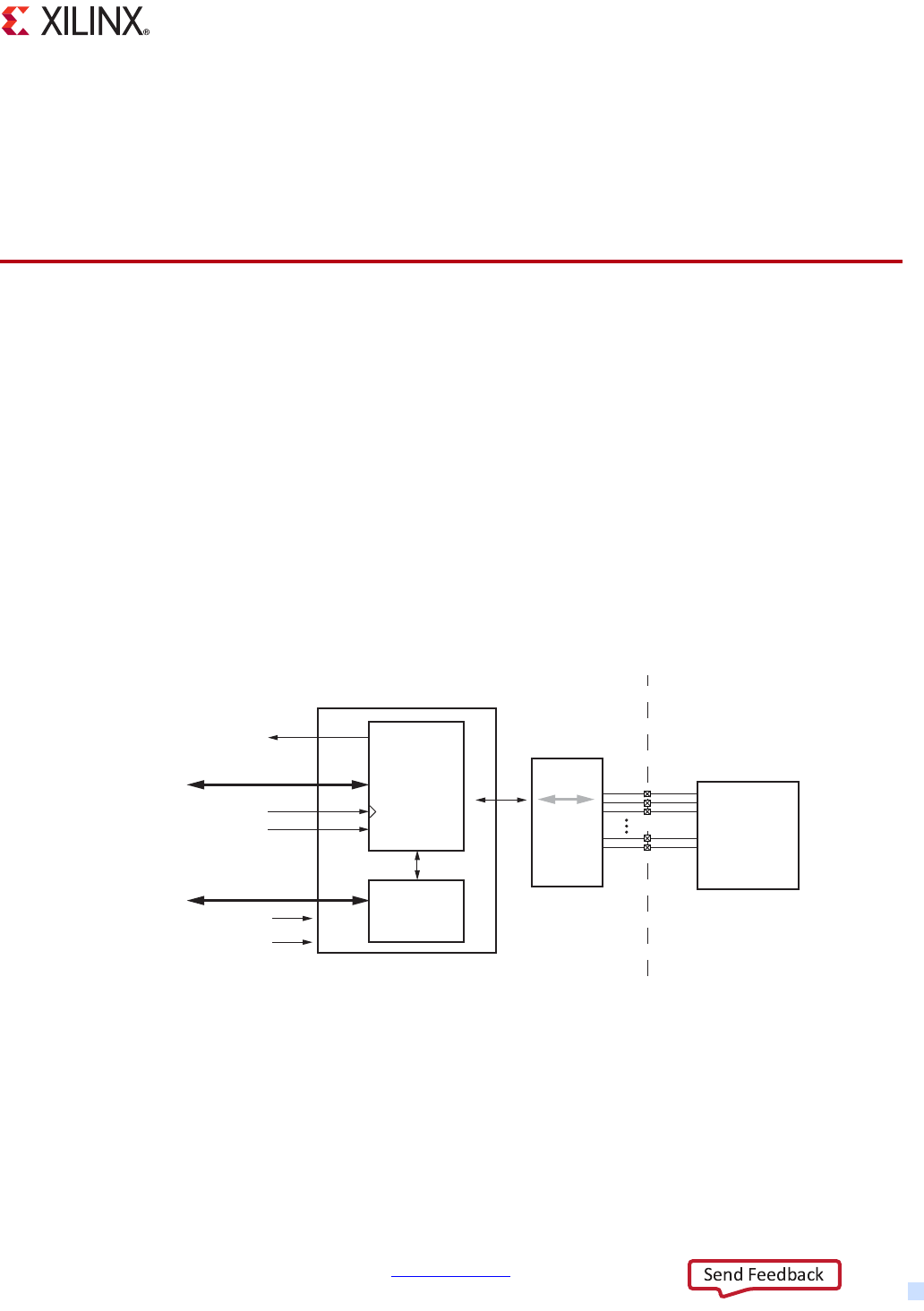
Zynq-7000 AP SoC Technical Reference Manual www.xilinx.com 331
UG585 (v1.12.1) December 6, 2017
Chapter 11
Static Memory Controller
11.1 Introduction
The static memory controller (SMC) can be used either as a NAND flash controller or a parallel port
memory controller supporting the following memory types:
•NAND flash
• Asynchronous SRAM
•NOR flash
System bus masters can access the SMC controller as shown in Figure 11-1. The operational registers
of the SMC are configured through an APB interface. The memory mapping for the SMC is described
in Chapter 4, System Addresses. The SMC handles all commands, addresses, data, and the memory
device protocols. It allows the users to access the controller by reading or writing into the
operational registers. The SMC is based on ARM's PL353 static memory controller.
X-Ref Target - Figure 11-1
Figure 11-1: SMC System Level Diagram
NAND Flash
Or SRAM
Or NOR
MIO
Interconnect
APB
MIO
Pins
SMC_Ref clock
SMC_Ref reset
IRQ ID# 50
Control
and Status
Registers
Slave
port
CPU_1x clock
SMC CPU_1x reset
SMC
Controller
Interconnect
AXI
Slave
port
Device
Boundary
UG585_c11_01_102014

Zynq-7000 AP SoC Technical Reference Manual www.xilinx.com 332
UG585 (v1.12.1) December 6, 2017
Chapter 11: Static Memory Controller
11.1.1 Features
Features of the SMC are listed for each type of memory. The controller is configured to operate in
one of two interface modes.
NAND Flash Interface
• ONFI Specification 1.0
• Up to a 1 GB device
°Because the NAND flash Interface supports only 1-bit ECC and one chip select, the density is
limited to 1 GB.
• 8/16-bit IO width with a single chip select
• 16-word read and 16-word write data FIFOs
• 8-word command FIFO
• Programmable IO cycle timing
• 1-bit ECC hardware with software assist
• Asynchronous memory operating mode
Parallel (SRAM/NOR) Interface
• 8-bit data bus width
• One chip select with up to 25 address signals (32 MB)
• Two chip selects with up to 25 address (32 + 32 MB)
• 16-word read and 16-word write data FIFOs
• 8-word command FIFO
• Programmable I/O cycle timing on a per chip select basis
• Asynchronous memory operating mode
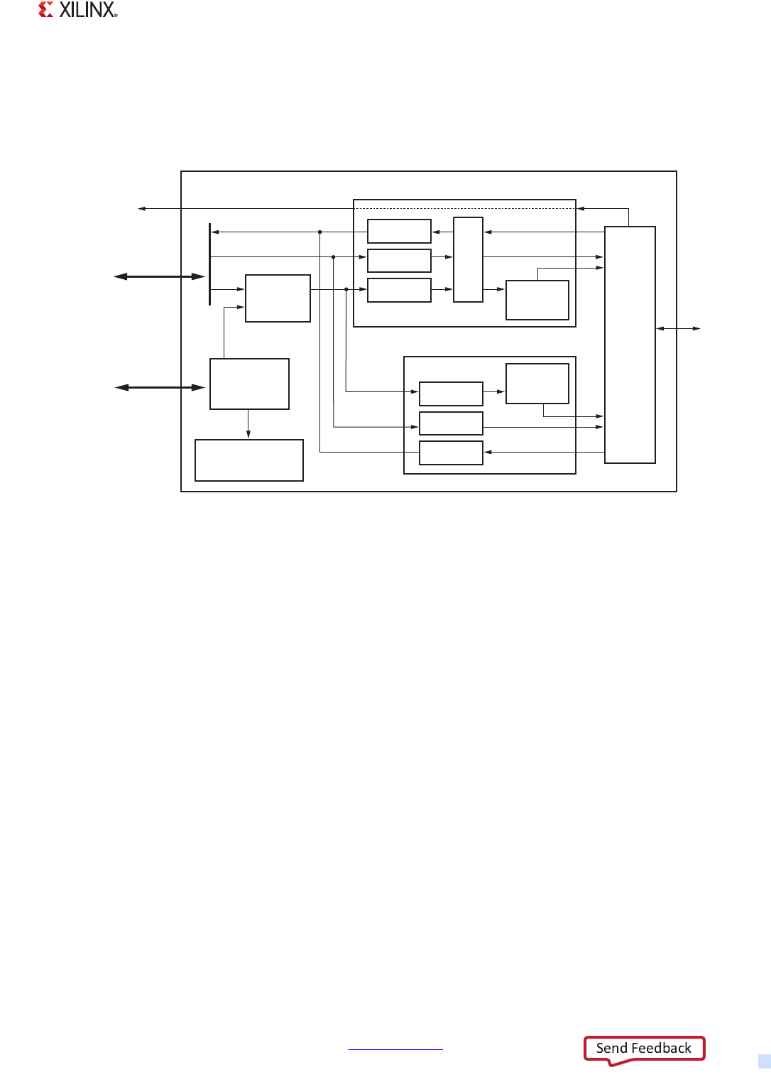
Zynq-7000 AP SoC Technical Reference Manual www.xilinx.com 333
UG585 (v1.12.1) December 6, 2017
Chapter 11: Static Memory Controller
11.1.2 Block Diagram
The block diagram for the SMC is shown in Figure 11-2.
Interconnect Interfaces
For the NOR/SRAM controller mode, the AXI interface is memory mapped so software can read and
write to/from memory. For the NAND flash controller mode, software writes commands to the NAND
controller via the AXI interface. Details can be found in the ARM specification.
The APB bus interface provides a memory mapped area for the software to read and write the control
and status registers.
Memory Manager
The memory manager tracks and controls the current state of the CPU_1x clock domain state
machine. This block is responsible for updating register values that are used in the memory clock
domain and controlling direct commands issued to memory and controlling entry-to and exit-from
low-power mode through the APB interface.
Format
The format block arbitrates between memory accesses from the AXI slave interface and the memory
manager. Requests from the manager have the highest priority. Requests from AR and AW channels
are arbitrated on a round-robin basis. The format block also maps AXI transfers onto appropriate
memory transfers and passes these to the memory interface through the command FIFO.
X-Ref Target - Figure 11-2
Figure 11-2: SMC Block Diagram
Interconnect
APB
MIO
to the
Memory
Device
IRQ ID# 50
Control and
Status Registers
Slave
port
Interconnect
AXI
Slave
port
NAND Flash Controller
IO
Buffer
Control
SRAM/NOR Controller
Memory
Manager
Format
Write Data
Read Data
SMC
Command
FIFO
Write Data
FIFO
Read Data
FIFO
Memory
Interface
Controller
Command
FIFO
Write Data
FIFO
Read Data
FIFO
ECC
Memory
Interface
Controller
UG585_c11_02_031812

Zynq-7000 AP SoC Technical Reference Manual www.xilinx.com 334
UG585 (v1.12.1) December 6, 2017
Chapter 11: Static Memory Controller
11.1.3 Notices
7z007s and 7z010 CLG225 Devices
The 7z007s single core 7z010 dual core CLG225 devices do not support the NOR/SRAM interface.
The NAND interface is supported in the 8-bit interface, but not the 16-bit interface.
MIO Pin Options
MIO Pin 1 can be programmed to be CS1 or address bit 25 for the NOR/SRAM controller. This pin can
also be programmed as a GPIO. Programming is controlled by the slcr.MIO_PIN_01 register. Program
this pin to CS1 when two NOR devices are in the system. Program this pin to address bit 25 when the
device is larger than 32 MB, however, it's functionality requires one of two work-arounds as
described in Xilinx AR# 60848. Table 11-1 summarizes of how the SMC works for NOR/SRAM.
11.2 Functional Operation
The functional operation of the SMC is described in the ARM Static Memory Controller (PL350 series)
Technical Reference Manual. Additional information is provided in the following sections.
11.2.1 Boot Device
The NOR and NAND Flash controllers can be configured as a boot device. Its memory interface can
only be routed through the MIO.
11.2.2 Clocks
The SMC has two clock domains that are driven by the CPU_1x and SMC_Ref clocks, see Table 11-2.
These clocks are controlled by the clock generator, refer to Chapter 25, Clocks. The two clock
domains are asynchronous to each other. The main benefit of asynchronous clocking is to maximize
the memory performance while running the interconnect interface at a fixed system frequency.
Table 11-1: MIO Pin 1 Programming for the NOR/SRAM Controller
slcr.MIO_PIN_01
{L2_SEL} Address Accessed MIO0 MIO1
01 (ADDR25) 0xe200_0000 1->0->1 (acts as active CS0) 1 (acts as inverted ADDR25)
01 (ADDR25) 0xe400_0000 0 (acts as inactive CS0) 0 (acts as inverted ADDR25)
10 (CS1) 0xe200_0000 1->0->1 (acts as active CS0) 1 (acts as inactive CS1)
10 (CS1) 0xe400_0000 1 (acts as inactive CS0) 1->0->1 (acts as active CS1)
00 (GPIO) 0xe200_0000 1->0->1 (acts as active CS0) 1 (reset state, internal pull-up)
00 (GPIO) 0xe400_0000 1 (acts as inactive CS0) 1 (reset state, internal pull-up)

Zynq-7000 AP SoC Technical Reference Manual www.xilinx.com 335
UG585 (v1.12.1) December 6, 2017
Chapter 11: Static Memory Controller
TIP: For power management, the clock enable in the slcr register can be used to turn off the clock. The
operating frequency for the reference clock is defined in the data sheet. (Clock gating is used to stop the
clock to save power.)
11.2.3 Resets
The controller has two reset inputs that are controlled by the reset subsystem; refer to Chapter 26,
Reset System. This SMC CPU_1x reset is used for the AXI and APB interfaces. The SMC_Ref reset is for
the FIFOs and the rest of the controller including the control and status registers.
11.2.4 ECC Support
User code can determine if the NAND device includes on-chip ECC or not by reading the
manufacturer and device ID's in the flash device. The supported boot devices are listed in Xilinx
AR50991. The vendor specifications for NAND device should be reviewed for ECC support. On-chip
ECC errors are flagged using the NAND Interrupt.
When a flash device does not support on-chip ECC, then the 1-bit ECC unit in the SMC controller can
be used. Refer to ARM PrimeCell Static Memory Controller (PL350 series) Technical Reference Manual,
Revision r2p1 for programming information. ECC errors detected by the SMC controller are flagged
with the ECC Interrupt.
When programming NAND, the SMC controller adds an inversion of the ECC code if the number of
ones (bits=1) in the ECC block (512bytes = 4096bits) is odd. To match the hardware behavior,
software should add an inversion of the ECC code if the number of ones (bits=1) in the ECC block
(512 bytes = 4096 bits) is even.
11.2.5 Interrupts
The controller includes three interrupt sources. These interrupts are controlled by the
smc.MEMC_STATUS register. When enabled, the interrupt generates the IRQ ID # 50 signal to the
system interrupt controller.
• NAND ECC is triggered by SMC ECC logic.
• NAND Interrupt is triggered on the rising edge of the NAND_BUSY input pin on MIO.
• SRAM Interrupt is triggered on the rising edge of the EMIOSRAMINTIN signal from PL.
The source of the interrupt is determined by reading the smc.MEMC_STATUS register.
Table 11-2: SMC Clocks and Resets
Clock Resets Clock Domain Description
CPU_1x CPU_1x Interconnect
domain
This clock runs at 1/6th or 1/4th the CPU clock rate depending on
the CPU clock mode. To stop this clock, first put the SMC is in
low-power mode.
SMC_Ref SMC_Ref SMC domain This clock is used to control the I/O memory interfaces.
Zynq-7000 AP SoC Technical Reference Manual www.xilinx.com 336
UG585 (v1.12.1) December 6, 2017
Chapter 11: Static Memory Controller
11.2.6 PL353 Functionality
The SMC is based on ARM's PL353 Primecell core and is hard-coded such that controller 0 can
operate in SRAM/NOR mode and controller 1 can operate in NAND flash mode. The SRAM/NOR or
NAND interface can be used in a system, but not both. The SRAM/NOR interface does not support
PSRAM. The NAND flash controller does not support wear leveling.
When referencing ARM documentation, for programming and other purposes, refer to the
implementation notes in Table 11-3.
Note: ARM's PL353 documentation has a different timing naming convention (used in the
SET_CYCLES register) than the ONFI Specification 1.0.
11.2.7 Address Map
The registers and memory base address are listed in Table 11-4.
Table 11-3: SMC PL353 Implementation Notes
Parameter Value Design Notes
Chip Selects (Interface 0) 2 SRAM/NOR interface chip selects operate independently.
Chip Select (Interface 1) 1 NAND flash interface chip select
NAND flash mode data width 16 Data width can be 8 or 16 bits
SRAM mode data width 8 Data width is 8 bits.
System interface bus width 32 AXI
System interface clock rate ~ CPU_1x (1/6th or 1/4th the CPU clock frequency)
Command FIFO depth 8 Maximum supported depth on both interfaces
Read data word FIFO depth 16 Maximum supported depth on both interfaces
Write data word FIFO depth 16 Maximum supported depth on both interfaces
ECC support Yes 1-bit ECC hardware with assistance from software
ECC Extra Block Yes Supported
Table 11-4: SMC Address Map Summary
Base Address Mnemonic Description Type
0xE000_E000 SMC Configuration registers base address Registers
0xE100_0000 SMC_NAND SMC NAND memory base address Memory
0xE200_0000 SMC_SRAM0 SMC SRAM Chip Select 0 base address Memory
0xE400_0000 SMC_SRAM1 SMC SRAM Chip Select 1 base address Memory

Zynq-7000 AP SoC Technical Reference Manual www.xilinx.com 337
UG585 (v1.12.1) December 6, 2017
Chapter 11: Static Memory Controller
11.3 I/O Signals
The MIO pin assignments for SRAM/NOR and NAND flash connections are shown in Table 11-5. The
SMC interface signals are routed only to the MIO pins, they are not available on the EMIO interface.
The MIO pins and restrictions (no NOR/SRAM and only 8-bit NAND) are shown in the MIO table in
section 2.5.4 MIO-at-a-Glance Table.
Table 11-5: SMC MIO Pins
MIO
Pin
SRAM/NOR Interface Mode MIO
Pin
NAND Flash Interface Mode
Signal Name I/O Default
Value Description Signal Name I/O Default
Value Description
MIO Voltage Bank 0
0 SRAM_CE_B[0] O - SRAM/NOR chip sel 0 0 NAND_CE_B O - NAND chip select
1 SRAM_CE_B[1] O - SRAM/NOR chip sel 1 1 - - - -
2 - - - - 2 NAND_ALE O - NAND address latch
3 SRAM_DQ[0] IO 0 SRAM/NOR data 3 NAND_WE_B O - NAND write enable
4 SRAM_DQ[1] IO 0 SRAM/NOR data 4 NAND_IO[2] IO 0 NAND
data/address/cmd
5 SRAM_DQ[2] IO 0 SRAM/NOR data 5 NAND_IO[0] IO 0 NAND
data/address/cmd
6 SRAM_DQ[3] IO 0 SRAM/NOR data 6 NAND_IO[1] IO 0 NAND
data/address/cmd
7 SRAM_OE_B O - SRAM/NOR output en 7 NAND_CLE O - NAND command
latch enable
8 SRAM_BLS_B O - SRAM/NOR write en 8 NAND_RE_B O - NAND read enable
9 SRAM_DQ[6] IO 0 SRAM/NOR data 9 NAND_IO[4] IO 0 NAND
data/address/cmd
10 SRAM_DQ[7] IO 0 SRAM/NOR data 10 NAND_IO[5] IO 0 NAND
data/address/cmd
11 SRAM_DQ[4] IO 0 SRAM/NOR data 11 NAND_IO[6] IO 0 NAND
data/address/cmd
12 - - - - 12 NAND_IO[7] IO 0 NAND
data/address/cmd
13 SRAM_DQ[5] IO 0 SRAM/NOR data 13 NAND_IO[3] IO 0 NAND
data/address/cmd
14 - - - - 14 NAND_BUSY I 0 NAND busy
15 SRAM_A[0] O - SRAM/NOR address 15 - - - -
MIO Voltage Bank 1
23:16 SRAM_A [8:1] O - SRAM/NOR address 23:16 NAND_IO [15:8] IO 0 NAND
data/address/cmd
39:24 SRAM_A [24:9] O - SRAM/NOR address 39:24 - - - -
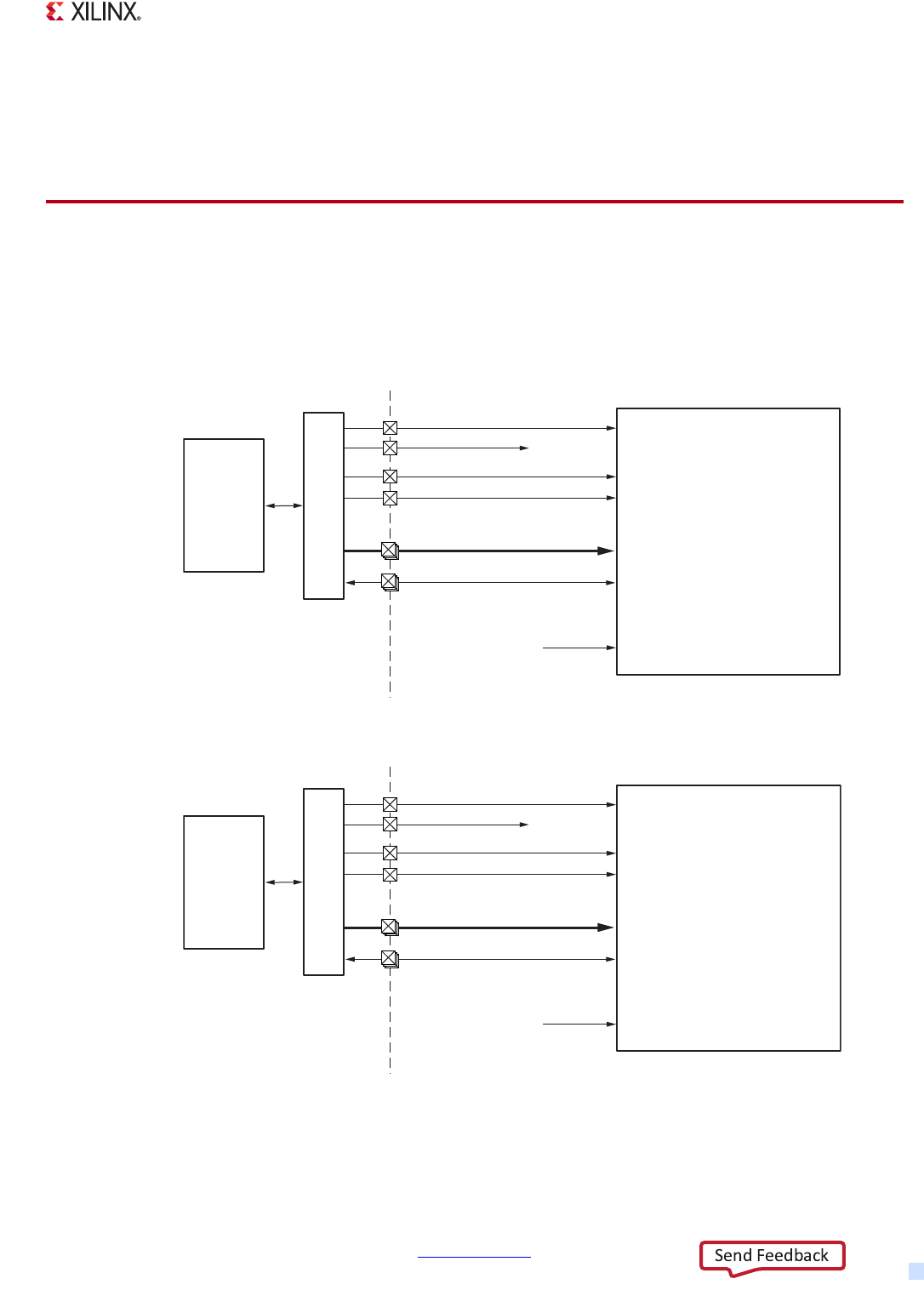
Zynq-7000 AP SoC Technical Reference Manual www.xilinx.com 338
UG585 (v1.12.1) December 6, 2017
Chapter 11: Static Memory Controller
Optional Pins
• For either SRAM or NOR, the upper address bits are optional. When not used, they can be
assigned to other functions.
11.4 Wiring Diagrams
The SMC supports the configurations shown in Figure 11-3, Figure 11-4, and Figure 11-5. The
NOR/SRAM mode of the SMC can support two devices (NOR and/or SRAM) using chip selects 0
and 1.
X-Ref Target - Figure 11-3
Figure 11-3: NOR Device Wiring Diagram
X-Ref Target - Figure 11-4
Figure 11-4: SRAM Device Wiring Diagram
SRAM_CE_B0
MIO
Multiplexer
SRAM_CE_B1
SRAM_OE_B
SRAM_BLS_B
SRAM_DQ[7:0]
NOR Device
SRAM_A[24:0]
Zynq Device
Boundary
CEn
OEn
WEn
DQ[7:0]
A[24:0]
NOR or SRAM
Device
RESETn
System Reset#
SMC
Controller
UG585_c11_03_102014
SRAM_CE_B0
MIO
Multiplexer
SRAM_CE_B1
SRAM_OE_B
SRAM_BLS_B
SRAM_DQ[7:0]
SRAM Device
SRAM_A[24:0]
Zynq Device
Boundary
CEn
OEn
WEn
DQ[7:0]
A[24:0]
NOR or SRAM
Device
RESETn
System Reset#
SMC
Controller
UG585_c11_04_102014
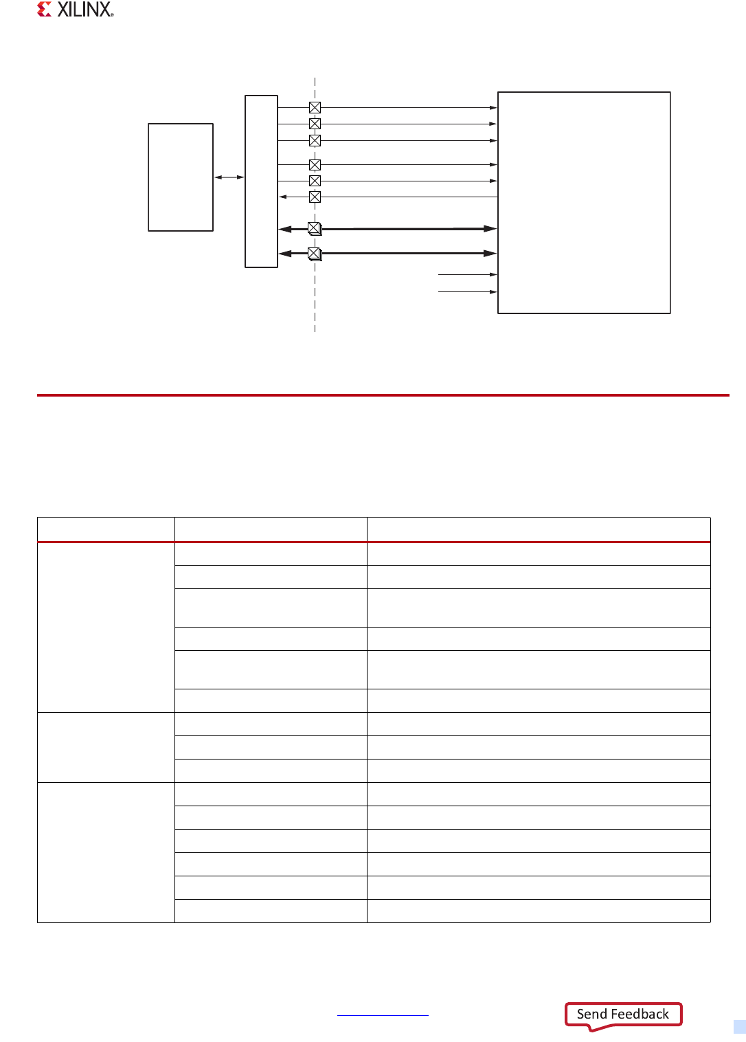
Zynq-7000 AP SoC Technical Reference Manual www.xilinx.com 339
UG585 (v1.12.1) December 6, 2017
Chapter 11: Static Memory Controller
11.5 Register Overview
The SMC registers are summarized in Tab le 11 -6 .
X-Ref Target - Figure 11-5
Figure 11-5: NAND Flash Device Wiring Diagram
NAND_CE_B0
MIO
Multiplexer
NAND_CLE
NAND_ALE
NAND_RE_B
NAND_WE_B
NAND_BUSY
NAND_IO[15:0] (for 16-bit data)
NAND Flash
NAND_IO[7:0]
Zynq Device
Boundary
CEn
ALE
CLE
RE#
WE#
IO[15:8]
IO[7:0]
RESETn
System Reset#
WPn
GPIO
SMC
Controller
UG585_c11_05_020613
R/B#
Table 11-6: SMC Register Overview
Controller Register Name Description
Both
MEMC STATUS Operating and interrupt status, read-only
MEMIF_CFG SMC configuration information, read-only
MEMC_CFG_{SET, CLR} Enable/disable/clear interrupts and control low power
state
DIRECT_CMD Issue a set command, write-only
SET_{CYCLES, OPMODE} Stage a cycles or opmode operation to the SRAM/NOR
and NAND flash registers
USER_{STATUS, CONFIG}
SRAM/NOR
CS 0, 1
REFRESH_PERIOD_{0,1} Insert idle cycles between SRAM/NOR burst cycles
SRAM_CYCLES0_{0,1} Timing cycles
OPMODE0_{0,1} Operating mode
NAND Flash
NAND_CYCLES1_0 Timing cycles
OPMODE1_0 Operating mode
ECC_{STATUS, MEMCFG}_1 ECC status and configuration
ECC_MEMCOMMAND{2:1}_1 Commands used for ECC reads and writes
ECC_ADDR{1:0}_1 Address generated by controller
ECC_VALUE{3:0}_1 Value generated by controller

Zynq-7000 AP SoC Technical Reference Manual www.xilinx.com 340
UG585 (v1.12.1) December 6, 2017
Chapter 11: Static Memory Controller
11.6 Programming Model
The programming model is described in the ARM Static Memory Controller (PL350 series) Technical
Reference Manual (see Appendix A, Additional Resources). The configuration of the SMC is
summarized in Tab le 11 -3.
11.7 NOR Flash Bandwidth
The bandwidth measurement details of NOR Flash are:
Environment: Standalone
NOR flash device used: PC28F256M29EW
SMC (NOR flash controller) clock: 100 MHz
Data transfer size 1 MB
Bandwidth achieved:
Read bandwidth
Write bandwidth
9.02 MB/S
7.36 KB/S

Zynq-7000 AP SoC Technical Reference Manual www.xilinx.com 341
UG585 (v1.12.1) December 6, 2017
Chapter 12
Quad-SPI Flash Controller
12.1 Introduction
The Quad-SPI flash controller is part of the input/output peripherals (IOP) located within the PS. It is
used to access multi-bit serial flash memory devices for high throughput and low pin count
applications.
The controller operates in one of three modes: I/O mode, linear addressing mode, and legacy SPI
mode. In I/O mode, software interacts closely with the flash device protocol. The software writes the
flash commands and data to the controller using the four TXD registers. Software reads the RXD
register that contains the data received from the flash device.
Linear addressing mode uses a subset of device operations to eliminate the software overhead that
the I/O mode requires to read the flash memory. Linear Mode engages hardware to issue commands
to the flash memory and control the flow of data from the flash memory bus to the AXI interface. The
controller responds to memory requests on the AXI interface as if the flash memory were a ROM
memory. In legacy mode, QSPI controller acts as a normal SPI controller.
The controller can interface to one or two flash devices. Two devices can be connected in parallel for
8-bit performance, or in a stacked, 4-bit arrangement to minimize pin count. The two device
combinations are shown in Figure 12-1.
12.1.1 Features
• 32-bit AXI interface for Linear Addressing mode transfers
• 32-bit APB interface for I/O mode transfers
• Programmable bus protocol for flash memories from Micron and Spansion
• Legacy SPI and scalable performance: 1x, 2x, 4x, 8x I/O widths
•Flexible I/O
°Single SS 4-bit I/O flash interface mode
°Dual SS 8-bit parallel I/O flash interface mode
°Dual SS 4-bit stacked I/O flash interface mode
°Single SS, legacy SPI interface
• 16 MB addressing per device (32 MB for two devices)
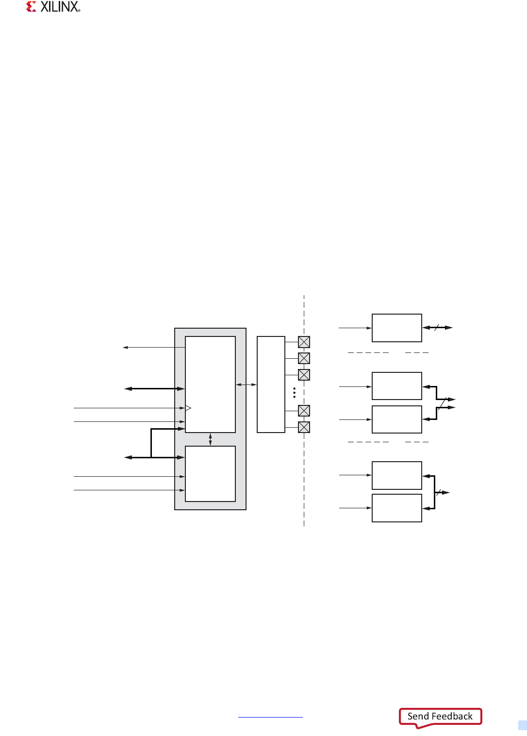
Zynq-7000 AP SoC Technical Reference Manual www.xilinx.com 342
UG585 (v1.12.1) December 6, 2017
Chapter 12: Quad-SPI Flash Controller
• Device densities up to 128 Mb for I/O and linear mode. Densities greater than 128 Mb are
supported in I/O mode.
• I/O mode (flash commands and data)
°Software issues instructions and manages flash operations
°Interrupts for FIFO control
°63-word RxFIFO, 63-word TxFIFO
• Linear addressing mode (executable read accesses)
°Memory reads and writes are interpreted by the controller
°AXI port buffers up to four read requests
°AXI incrementing and wrapping address functions
12.1.2 System Viewpoint
The Quad-SPI flash controller is part of the IOP and connects to external SPI flash memory through
the MIO as shown in Figure 12-1. The controller supports one or two memories.
Address Map and Device Matching for Linear Address Mode
When a single device is used, the address map for direct memory reads starts at FC00_0000 and
goes to a maximum of FCFF_FFFF (16 MB). The address map for a two-device system depends on
the memory devices and the I/O configuration. In two-device systems, the Quad-SPI devices need to
be from the same vendor so they have the same protocol.
X-Ref Target - Figure 12-1
Figure 12-1: Quad-SPI Controller System Viewpoint
UG585_c12_01_101912
Quad-SPI
Controller
Control
and Status
Registers
Device
Boundary
Quad-SPI
Device
MIO MIO
Pins
QSPI 0 SS
OR
Single SS 4-bit I/O
QSPI 0 SS
Quad-SPI
Device
Quad-SPI
Device
Dual SS 8-bit Parallel I/O
OR
Quad-SPI
Device
QSPI 1 SS Quad-SPI
Device
Dual SS 4-bit Stacked I/O
Quad-SPI Ref Reset
Quad-SPI Ref Clock
IRQ ID# 51
Slave
Port
AXI
Interconnect
Slave
Port
APB
Interconnect
Quad-SPI CPU 1x Reset
CPU 1x Clock
4-bit I/O
8-bit I/O
4-bit I/O
QSPI 0 SS
QSPI 1 SS
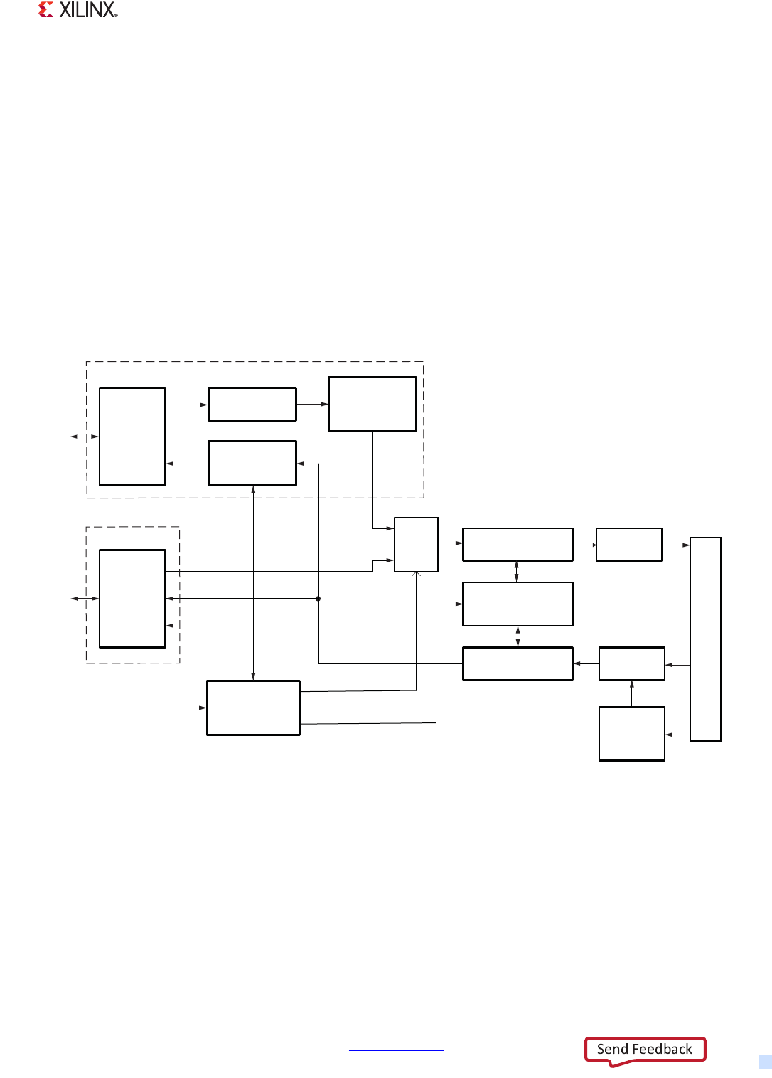
Zynq-7000 AP SoC Technical Reference Manual www.xilinx.com 343
UG585 (v1.12.1) December 6, 2017
Chapter 12: Quad-SPI Flash Controller
The 8-bit parallel I/O configuration also requires that the devices have the same capacity. The
address map for the parallel I/O configuration starts at FC00_0000 and goes to the address of the
combined memory capacities, up to a maximum of FDFF_FFFF (32 MB).
For the 4-bit Stacked I/O configuration, the devices can have difference capacities, but must have the
same protocol. If using two different size devices, Xilinx recommends using a 128 Mb device at the
lower address. In this mode, the QSPI 0 device starts at FC00_0000 and goes to a maximum of
FCFF_FFFF (16 MB). The QSPI 1 device starts at FD00_0000 and goes to a maximum of FDFF_FFFF
(another 16 MB). If the first device is less than 16 MB in size, then there will be a memory space hole
between the two devices.
12.1.3 Block Diagram
The block diagram of the is shown in Figure 12-2.
12.1.4 Notices
Operating Restrictions
When a single device is used, it must be connected to QSPI 0. When two devices are used, both
devices must be identical (same vendor and same protocol sequencing).
X-Ref Target - Figure 12-2
Figure 12-2: Quad-SPI Controller Block Diagram
UG585_c12_02_101912
Tx FIFO
Rx FIFO
Command
FIFO
Control
Serializer
De -
serializer
AXI
Interface
AXI-to-SPI
Command
Converter
SPI-to-AXI
Data
Formatter
APB
Interface
Mux
Config, Control,
and Status
Registers Loopback
Clock
Control
Linear Addressing Mode
I/O Mode
MIO
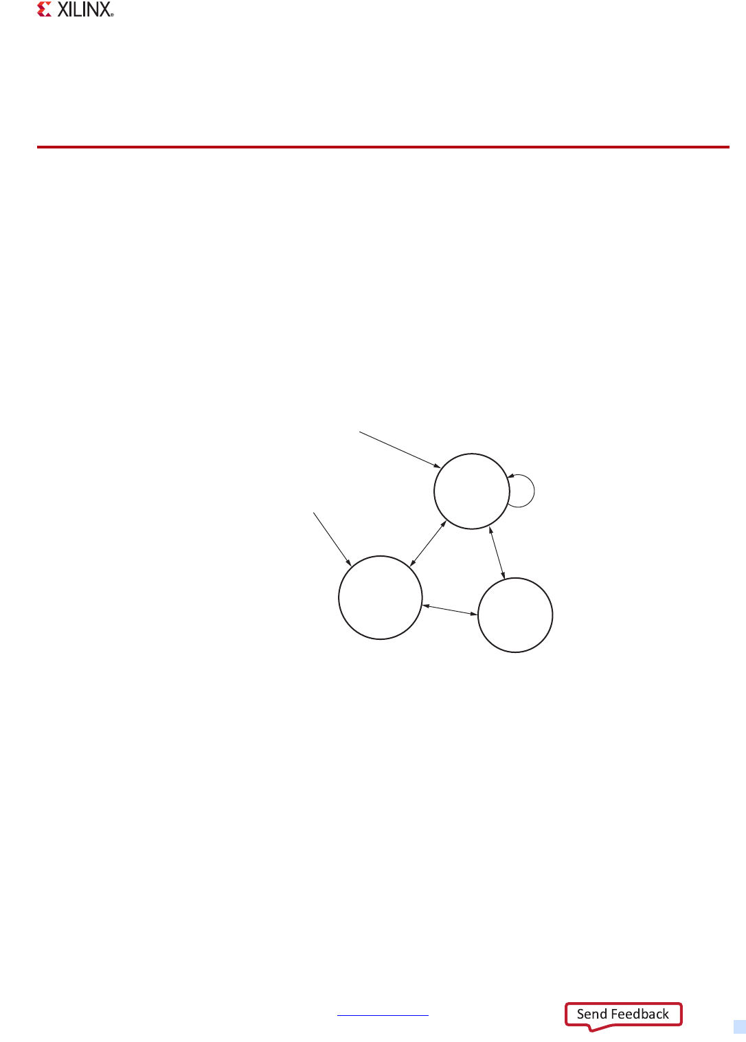
Zynq-7000 AP SoC Technical Reference Manual www.xilinx.com 344
UG585 (v1.12.1) December 6, 2017
Chapter 12: Quad-SPI Flash Controller
The MIO pins for the Quad-SPI controller conflict with both the NOR and NAND interfaces of the
SMC controller. The NOR/SRAM and NAND interfaces cannot be used when Quad-SPI is used. More
information about the MIO pins is provided in section 2.5 PS-PL MIO-EMIO Signals and Interfaces.
12.2 Functional Description
The Quad-SPI flash controller can operate in either I/O mode or linear addressing mode. For reads,
the controller supports single, dual and quad read modes in both I/O and linear addressing modes.
For writes, single and quad modes are supported in I/O mode. Writes are not supported in linear
addressing mode.
12.2.1 Operational Modes
Quad-SPI operating mode transitions are shown in Figure 12-3.
In I/O mode, software can choose varying degrees of control over different aspects of read data
management by setting appropriate register bits. In linear mode, the controller carries out all
necessary read data management and the memory reads like a ROM to software.
12.2.2 I/O Mode
In I/O mode, the software is responsible for preparing and formatting commands and data into
instructions according to the Quad-SPI protocol. The formatted instruction sequence, consisting of
CMD and data, is then pushed into a transmit FIFO by repeated writing into a TXD register. The
transmit logic serializes the content of the TxFIFO in accordance with the Quad-SPI interface
specification and send the data out to the flash memory. While the transmit logic is sending out the
X-Ref Target - Figure 12-3
Figure 12-3: Quad-SPI Operating Mode Transitions
Linear
Addressing
Mode I/O Mode
UG585_c12_10_072612
Reset Software
Reset
slcr.QSPI_RST_CTRL[QSPIx_REF_RST, LQSPIx_CPU1x_RST]
Software Reset:
Boot Mode
Quad-SPI

Zynq-7000 AP SoC Technical Reference Manual www.xilinx.com 345
UG585 (v1.12.1) December 6, 2017
Chapter 12: Quad-SPI Flash Controller
content of the TxFIFO, it concurrently samples the raw serial data, performs serial-to-parallel
conversion, and stores data into RxFIFO.
In the case of a read command, when data is to be driven by the flash memory after the command
and address bytes, the MIO switches from output to input at the appropriate time under the control
of the transmit logic. Data shifted into the RxFIFO reflects the switch resulting in valid data in the
RxFIFO at the corresponding FIFO entry
Software needs to filter the raw data from the RxFIFO to obtain the relevant data content. The
controller does not modify either the instruction written by software or the captured data put into
the RxFIFO.
The controller supports little endian mode and the most significant bit of the least significant byte
of a 4-byte word of an instruction is sent first.
Flow Control
I/O mode has different modes of flow control during data transfer. The user can select between
automatic and manual mode, controlled by config_reg.MANSTARTEN (Man_start_com). In Manual
mode, the user can further select manual or automatic chip select with Config_reg.SSFORCE
(Manaual_CS). Asserting chip select signals the beginning of a command sequence on MIO.
Immediately following the CS assertion, serial data on D0 is interpreted as command by the flash
memory.
In automatic mode, the entire transmission sequence, including control of chip select is done in
hardware. No software intervention is required. The transmission starts as soon as data is pushed
into the TxFIFO via writing to TXD, chip select automatically becomes active. Data transmission ends
when the TxFIFO is empty and chip select automatically becomes inactive. In this mode, to carry out
continuous data transfer, software must be able to keep up with supplying data to the TxFIFO at a
rate equal or higher than the rate of data movement on the MIO. This can be difficult since reading
from RXD and writing to TXD occurs at the APB clock rate.
In Manual mode, the user controls the start of data transmission. In this case, software either writes
the entire transmission sequence to the TxFIFO or until the TxFIFO is full. Upon writing of the
Man_start_en bit, the controller takes over, asserts CS, shifts data out of the TxFIFO and into the
RxFIFO, controls the input/ouput state of the MIO as appropriate, and terminates the sequence when
the TxFIFO is empty by de-asserting CS. The maximum number of bytes per command sequence in
this mode is limited by the depth of the TxFIFO of 252 bytes.
In manual mode, the user can further choose to control the chip select in addition to controlling the
start of transmission. Software again writes the transmission sequence to the TxFIFO starting with
the command until the TxFIFO is full. Software then asserts CS, followed by manual start. The
hardware takes over. However, CS is not de-asserted when the TxFIFO becomes empty. Software can
fill the TxFIFO again with the appropriate data to continue the previous command. This method
removes the limit on the number of bytes per command sequence and can be used effectively for
large data transfers. On completion of the command sequence, the software de-asserts CS by writing
to the Manual_CS bit.
Zynq-7000 AP SoC Technical Reference Manual www.xilinx.com 346
UG585 (v1.12.1) December 6, 2017
Chapter 12: Quad-SPI Flash Controller
12.2.3 I/O Mode Transmit Registers (TXD)
Software writes byte sequences that are needed for the specific flash device. Refer to the Quad-SPI
device vendor's specification. The controller has four write-only 32-bit TXD registers for software to
issue a stream of commands to get status and read/write data from the flash memory. Quad-SPI TXD
register write formats are described in Table 12-1. Each access to the TXD0, TXD1, TXD2, or TXD3
register results into a corresponding write to the TxFIFO.
The user must empty the TxFIFO between consecutive accesses from:
• TXD0 to TXD1/TXD2/TXD3
• TXD1 to TXD0/TXD1/TXD2/TXD3
• TXD2 to TXD0/TXD1/TXD2/TXD3
• TXD3 to TXD0/TXD1/TXD2/TXD3
You need not empty the FIFO for TxD0 to TXD0 accesses.
Note: The dummy data bytes, which are required in some of the instructions for the selected
memory, should be part of the instruction sequence along with the number of bytes intended to be
read from memory. The dummy data bytes ensure enough bus turnaround time for switching I/O
from output to input. If the number of dummy data bytes is insufficient for an instruction, the
memory reads the wrong data. For more information on the number of dummy data bytes needed
for a particular instruction, consult the data sheet for the targeted memory.
FIFO Reads and Writes
The TxFIFO and RxFIFO share the same gated clock. Therefore for every byte, including command
and address bytes shifted out of the TxFIFO, a corresponding byte is shifted into the RxFIFO
To read data from Quad-SPI flash memory, the software writes the appropriate command, address,
mode (when in Quad or Dual I/O mode) and dummy data as required by the Quad-SPI flash memory
into the TxFIFO. In addition, software must pad the TxFIFO with additional dummy data. This
additional dummy data provides the CLK needed to shift data into the RxFIFO. See section
12.3.5 Rx/Tx FIFO Response to I/O Command Sequences for additional programming details.
Table 12-1: Quad-SPI TXD Register Write Formats
Register Write Data Format Example Usage
31:24 23:16 15:8 7:0
TXD 1 Reserved Reserved Reserved Data or command Set write enable
TXD 2 Reserved Reserved Data 0 Data or command Write status with data
TXD 3 Reserved Data 1 Data 0 Data or command Read status with two dummy bytes
TXD 0 Data 3 Data 2 Data 1 Data or command Write data to transmit or dummy data for
reads

Zynq-7000 AP SoC Technical Reference Manual www.xilinx.com 347
UG585 (v1.12.1) December 6, 2017
Chapter 12: Quad-SPI Flash Controller
12.2.4 I/O Mode Considerations
The RxFIFO interrupt status bit indicates when data is available before data is actually available for
read. The latency is associated with clock domain crossing and is almost always made-up by the time
that software takes to service the interrupt.
During a read command, software must write to the TxFIFO with dummy data to receive data from
the device. In automatic mode, if TxFIFO goes empty, the Quad-SPI controller deasserts chip select.
To further receive data, software must send the read command and address to the device.
12.2.5 Linear Addressing Mode
The controller has a 32-bit AXI slave interface to support linear address mapping for read operations.
When a master issues an AXI read command through this port, the Quad-SPI controller generates
QSPI commands to load the corresponding memory data and send it back through the AXI interface.
In linear mode, the flash memory subsystem behaves like a typical read-only memory with an AXI
interface that supports a command pipeline depth of four. The linear mode improves both the user
friendliness and the overall read memory throughput over that of the I/O mode by reducing the
amount of software overhead. From a software perspective, there is no perceived difference between
accessing the linear Quad-SPI memory subsystem and that of other ROMs, except for a potentially
longer latency.
Transfer to LQSPI mode happens when the qspi.LQSPI_CFG.[LQ_MODE] bit is set to 1. Before entering
into linear addressing mode, the user must ensure that both the TXFIFO and RXFIFO are empty. Once
the qspi.LQSPI_CFG.[LQ_MODE] bit is set, the FIFOs are automatically controlled by the LQSPI module
and IO access to TXD and RXD are undefined.
In linear mode the CS pins are automatically controlled by the QSPI controller. Before a transition
into LQSPI mode, the user must ensure that qspi.Config_reg[Man_start_en] and qspi.Config_reg[PCS]
are both zero.
A simplified block diagram of the controller showing the linear and I/O portions is shown in
Figure 12-2.
AXI Interface Operation
Only AXI read commands are supported by the linear addressing mode. All valid write addresses and
write data are acknowledged immediately but are ignored, that is, no corresponding programming
(write) of the flash memory is carried out. All AXI writes generate an SLVERR error on the write
response channel.
Both incrementing- or wrapping-address burst reads are supported. Fixed-address bursts are not
supported and cause an SLVERR error. Therefore, the only recognized arburst[1:0] value is either
2'b01 or 2'b10. All read accesses must be word-aligned and the data width must be 32-bits (no
narrow burst transfers are allowed).

Zynq-7000 AP SoC Technical Reference Manual www.xilinx.com 348
UG585 (v1.12.1) December 6, 2017
Chapter 12: Quad-SPI Flash Controller
Tabl e 12- 2 lists the read address channel signals from a master that are ignored by the interface.
The AXI slave interface provides a read acceptance capability of 4 so that it can accept up to four
outstanding AXI read commands.
AXI Read Command Processing
AXI read burst commands are translated into SPI flash read instructions that are sent to the Quad-SPI
controller TxFIFO. The controller transmit logic is responsible for retrieving the read instructions from
the FIFO and passing them along to the SPI flash memory according to the SPI protocol.
A 64-deep FIFO is used to provide read data buffering to hold up to four burst-of-16 data. Since the
Rx FIFO starts receiving data as soon as the chip-select signal is active, the linear address module
removes incoming data that corresponds to the instruction code, if any, the address, the dummy
cycles, and responses to the AXI read instruction with valid data.
Interface Configuration and Read Modes
AXI read burst transfers are translated into SPI flash read instructions that are sent to the controller's
TxFIFO. The transmit logic retrieves the read instructions from the TxFIFO and passes them to the SPI
flash memory device according to the SPI protocol.
Software defines the SPI read command that is used in linear addressing mode by writing to
qspi.LQSPI_CFG[INST_CODE]. The supported read command codes and the recommended
configuration register settings (qspi.LQSPI_CFG) are listed in Tab le 1 2 -3 . The optimal register values
for Quad-SPI boot performance using a 33 MHz PS_CLK are shown in Tabl e 6- 10 and Table 12-3.
These Quad-SPI registers can be programmed in non-secure mode using the Register Initialization
feature in the BootROM header to speed up loading of the FSBL/User code. If a faster PS_CLK is used,
then the clock dividers need to be adjusted.
The choice of operating mode depends on the capabilities of the attached device. The I/O Fast Read
modes use 4-bit parallel transfers for address and data. This leads to the fastest performance. The
Output Fast Read modes use 4-bit parallel transfers for data only. These are still faster than a serial
bit mode.
Table 12-2: Ignored AXI Read Address Channel Signals
Signal Value
araddr[1:0] Ignored, assumed to be 0, i.e., always assumed to be word aligned
arsize[2:0] Ignored, always a 32-bit interface
arlock[1:0] Ignored
arcache[3:0] Ignored
arprot[2:0] Ignored
Zynq-7000 AP SoC Technical Reference Manual www.xilinx.com 349
UG585 (v1.12.1) December 6, 2017
Chapter 12: Quad-SPI Flash Controller
Performance Modes
To get the highest performance, the user should use the Quad-SPI controller in the Quad I/O mode.
The user can improve read performance by using the Quad-SPI device in continuous read mode.
This eliminates read instruction overhead for successive commands. Please refer to the LQSPI_CFG
register for more details (see Appendix B, Register Details).
Refer to the applicable Zynq-7000 AP SoC data sheet for operating frequencies.
Read Data Management
A 63-deep RxFIFO provides read data buffering to hold a minimum of three AXI burst transfer
lengths of 16 bytes each. Since the RxFIFO starts receiving data as soon as the chip-select signal is
active, the linear address adapter removes incoming data that corresponds to the instruction code,
if any, the address, and the dummy cycles.
The read data must be aligned with the corresponding word boundary specified by the address. For
data alignment purposes, the controller can modify the address as illustrated in Figure 12-4 before
it is sent to the flash memory device. The address modification involves reducing the address by up
to 3 byte locations such that the intended return data is word aligned automatically. The amount of
address change is transparent to the AXI interface, and is instruction dependent.
For example, if Cmd + address + mode + dummy (QSPI_intruction) does not end on a 32 bit
boundary, the linear controller subtracts 1,2,3 from the address to align data on the 32 bit boundary.
Table 12-3: Quad-SPI Device Configuration Register Values
Operating
Mode
Instruction
Code
Winbond & Spansion Micron
1 Device 2 Devices 1 Device 2 Devices
Read (serial bit) 0x03 0x80000003 0xE0000003 0x80000003 0xE0000003
Fast Read (serial bit) 0x0B 0x8000010B 0xE000010B 0x8000010B 0xE000010B
Dual Output Fast Read 0x3B 0x8000013B 0xE000013B 0x8000013B 0xE000013B
Quad Output Fast Read 0x6B 0x8000016B 0xE000016B 0x8000016B 0xE000016B
Dual I/O Fast Read 0xBB 0x82FF00BB 0xE2FF00BB 0x82FF01BB 0xE2FF01BB
Quad I/O Fast Read 0xEB 0x82FF02EB 0xE2FF02EB 0x82FF04EB 0xE2FF06EB
X-Ref Target - Figure 12-4
Figure 12-4: Automatic Address Offset For Word Alignment
UG585_c12_05_022712
Address Offset
Flash mem addr =
AXI read addr - x
Where x depends
on the instr type and
is either 0, 1, 2 or 3
AXI read addr Flash mem addr

Zynq-7000 AP SoC Technical Reference Manual www.xilinx.com 350
UG585 (v1.12.1) December 6, 2017
Chapter 12: Quad-SPI Flash Controller
Read Latency
In linear mode, the default read mode is fast Quad I/O. The following is an example to calculate latency
at the memory in the Quad I/O mode at 100 MHz with 2 dummy bytes. For a single device, the number
of clock cycles from the time an 8-bit instruction code and a 24-bit address is available to the time
when the first 32-bit data becomes available is:
Total latency = instruction latency + address latency + overhead (mode + dummy bites + offset) +
latency
= 8 cycles + 6 cycles + 8 (2+4+2) cycles + 8 cycles
=30 cycles
With the SPI clock of 100 MHz, the latency at the memory interface is 320 ns. Other read modes have
higher latency and can be calculated in a similar manner.
12.2.6 Unsupported Devices
A number of devices implement custom 4-bit wide SPI-like interfaces for flash memory access, such
as the SQI devices from SST, and the Fast4 devices from Atmel. Some other Quad-SPI devices, like
some Micron/Numonyx devices, offer an option to switch operation to such a custom 4-bit interface,
through a non-volatile configuration bit.
These interfaces operate differently from the devices supported by the Quad-SPI controller. These
flash memory devices operate in 4-bit mode during the instruction phase, as well as the address and
data phases. This requires the Quad-SPI flash controller to power up in 4-bit mode and remain in that
mode permanently (or until configured otherwise, if that option is available). There are no plans to
enable the support for these custom interfaces.
12.2.7 Supported Memory Read and Write Commands
Supports commands that transfers address one bit per rising edge of SCK and return data 1, 2, or 4
bits of data per rising edge of SCK. These commands are called Read or Fast Read for 1-bit data; Dual
Output Read for 2-bit data, and Quad Output for 4-bit data.
Supports commands that transfer both address and data 2 or 4 bits per rising edge of SCK. These are
called Dual I/O for 2-bit and Quad I/O for 4-bit.
Table 12-4: Memory Read and Write Commands
Instruction
Name Description Code(Hex)
READ Read. Single-bit address sent for every rising edge of clock.
Data returned one bit per rising edge of SCLK.
03
FAST_READ Read Fast. Single-bit address sent for every rising edge of
clock. Data returned one bit per rising edge of SCLK.
0B
DOR Read Dual Out. Single-bit address sent for every rising edge of
clock. Data returned two bits per rising edge of SCLK.
3B

Zynq-7000 AP SoC Technical Reference Manual www.xilinx.com 351
UG585 (v1.12.1) December 6, 2017
Chapter 12: Quad-SPI Flash Controller
12.3 Programming Guide
Example: Start-up Sequence
1. Configure Clocks. Refer to section 12.4.1 Clocks.
2. Configure Tx/Rx Signals. Refer to section 12.5.2 MIO Programming.
3. Reset the Controller. Refer to section 12.4.2 Resets.
4. Configure the Controller. Refer to section 12.3.1 Configuration.
Now, either configure the controller for linear addressing mode (section 12.2.5 Linear Addressing
Mode) or configure the controller for I/O mode (section 12.3.3 Configure I/O Mode and section
12.3.4 I/O Mode Interrupts).
12.3.1 Configuration
Example: Configure Controller
This example applies to both linear addressing and I/O modes. It prepares the controller baud rate,
FIFO, flash mode, clock phase/polarity, and programs the loopback delay.
The values to program into the qspi.Config_reg register are shown in Table 12-3, page 349.
1. Configure the controller. Write to the qspi.Config_reg register.
a. Set baud rate, [BAUD_RATE_DIV].
b. Select master mode, [MODE_SEL] = 1.
c. Select flash mode (not Legacy SPI), [LEG_FLSH] = 1.
d. Select Little Endian, [endian] = 0.
QOR Read Quad Out. Single-bit address sent for every rising edge
of clock. Data returned four bits per rising edge of SCLK.
6B
DIOR Dual I/O Read. Two-bit address sent for every rising edge of
clock. Data returned four bits per rising edge of SCLK.
BB
QIOR Quad I/O Read. Four-bit address sent for every rising edge of
clock. Data returned four bits per rising edge of SCLK.
EB
PP Page Program. Single-bit address sent for every rising edge of
clock. Data sent single bit per rising edge of SCLK.
02
QPP Quad Page Program. Single-bit address sent for every rising
edge of clock. Data sent four bits per rising edge of SCLK.
32 in case of Spansion and
Micron devices.
38 in case of Macronix
devices.
Table 12-4: Memory Read and Write Commands (Cont’d)
Instruction
Name Description Code(Hex)

Zynq-7000 AP SoC Technical Reference Manual www.xilinx.com 352
UG585 (v1.12.1) December 6, 2017
Chapter 12: Quad-SPI Flash Controller
e. Set FIFO width to 32 bits, [FIFO_WIDTH].
f. Set clock phase, [CLK_PH] and Polarity, [CLK_POL].
2. If baud rate divider is 2, then change default setting. If the qspi.Config_reg[BAUD_RATE_DIV]
is set to 0b00, configure the qspi.LPBK_DLY_ADJ (loopback delay adjustment) register with the
following settings:
a. Set to select internal clock. qspi.LPBK_DLY_ADJ[USE_LPBK] = 1.
b. Set the clock delay 0. qspi.LPBK_DLY_ADJ[DLY0] = 0b00.
c. Set the clock delay 1. qspi.LPBK_DLY_ADJ[DLY1] = 0b00.
12.3.2 Linear Addressing Mode
Example: Linear Addressing Mode (Memory Reads)
The sequence of operations for data reads in linear addressing mode is as follows:
1. Set manual start enable to auto mode. Set qspi.Config_reg[Man_start_en] = 0.
2. Assert the chip select. Set qspi.Config_reg[PCS] = 0.
3. Program the configuration register for linear addressing mode. Example values are shown in
Table 12-3, page 349.
4. Enable the controller. Set qspi.En_REG[SPI_EN] = 1.
5. Read data from the linear address memory region. The memory range depends on the size
and number of devices. The range is from 0xFC00_0000 up to 0xFDFF_FFFF.
6. Disable the controller. Set qspi.En_REG[SPI_EN] = 0.
7. De-assert chip select. Set qspi.Config_reg[PCS] = 1.
12.3.3 Configure I/O Mode
Example: I/O Mode (Memory Reads and Writes)
The sequence of operations uses I/O mode for reads and writes.
1. Enable manual mode. Write 1 to qspi.Config_reg[Man_start_en, Manual_CS] = 1.
2. Configure the flash device. Refer to Figure 12-6, page 360. Use reset values of the
qspi.LQSPI_CFG register for a single flash device. In case of a parallel dual flash device, write 1 to
the TWO_MEM, SEP_BUS bit fields.
3. Assert chip select. Set qspi.Config_reg[PCS] = 0.
4. Enable the controller. Set qspi.En_REG[SPI_EN] = 1.
5. Write byte sequences to the flash memory. Write from 1 to 4 bytes to the TxFIFO using the TXD
registers. Refer to section 12.2.3 I/O Mode Transmit Registers (TXD).
6. Avoid TxFIFO overflow. When the TxFIFO is empty, 252 bytes can be written. After that, software
can avoid overflowing the TxFIFO by reading qspi.Intr_status_REG[TX_FIFO_full] and waiting until
it equals 0 before writing to a TXD register.

Zynq-7000 AP SoC Technical Reference Manual www.xilinx.com 353
UG585 (v1.12.1) December 6, 2017
Chapter 12: Quad-SPI Flash Controller
7. Enable the interrupts. Write to qspi.Intrpt_en_REG. Interrupt handlers that handle the interrupt
conditions are discussed in interrupt handlers section.
8. Start data transfer. Set qspi.Config_reg[Man_start_com] = 1.
9. Interrupt handler: Transfer all the required data to QSPI flash during program/read operations
to Quad-SPI flash. (See Example: I/O Mode Interrupt Service Routine, page 353.)
10. If read operations are carried out: re-arrange the READ data to eliminate the data read due to
dummy cycles.
11. De-assert chip select. Set QSPI.Config_reg[PCS] = 1.
12. Disable controller. Set qspi.En_REG[SPI_EN] = 0.
Note that the TxFIFO width must be programmed to 32 bits: qspi.Config_reg[FIFO_WIDTH] = 0b11.
Software needs to take care of “consecutive non word aligned” transfers.
Example: I/O Mode Interrupt Service Routine
1. Configure the ISR to handle the interrupt conditions based on the Quad-SPI device type. To
read from the Quad-SPI device, the simplest ISR reads data from the RxFIFO and writes content
to the TxFIFO. The system interrupt controller (GIC) is described in Chapter 7, Interrupts. The
controller generates a system peripheral interrupt (SPI), IRQ ID #51. The interrupt mechanism for
the Quad-SPI controller is described in section 12.3.4 I/O Mode Interrupts.
a. Read transfer interrupt. RxFIFO Not Empty Interrupt
b. Write transfer interrupt. TxFIFO Not Full Interrupt
12.3.4 I/O Mode Interrupts
Interrupts are only used in I/O mode. The controller interrupt is asserted whenever any of the
interrupt conditions are met. The Quad-SPI interrupt handler checks the cause of the interrupt. A
single interrupt service routine can manage all of the interrupt conditions.
Example: Interrupt Handler for Rx and Tx
The interrupt handler is trigger by IRQ ID #51. The example reads the RxFIFO until it is empty and
then fills-up the TxFIFO. The RxFIFO Not Empty Interrupt status is used to determine if content can
be read from the RxFIFO. The TxFIFO Not Full interrupt indicates if there is room in the TxFIFO for
more content.
1. Disable all of the interrupts in the controller. Set qspi.Intrpt_dis_REG[TX_FIFO_not_full,
RX_FIFO_full] both = 1.
2. Clear the interrupts. Write 1s to the interrupt status register qspi.Intr_status_REG.
3. Empty the RxFIFO. Check if RxFIFO Not Empty interrupt is asserted. If
qspi.Intr_status_REG[RX_FIFO_not_empty] = 1, then there is data in the RxFIFO.
a. If the status is asserted, then read data from the RxFIFO. Read the data using the
qspi.RX_data_REG register.
b. Read data from the RxFIFO and poll the interrupt status until the RxFIFO is empty. The
RxFIFO is empty when qspi.Intr_status_REG[RX_FIFO_not_empty] = 0.

Zynq-7000 AP SoC Technical Reference Manual www.xilinx.com 354
UG585 (v1.12.1) December 6, 2017
Chapter 12: Quad-SPI Flash Controller
4. Fill the TxFIFO. Check if the TxFIFO Not Full status is asserted. If
qspi.Intr_status_REG[TX_FIFO_not_Full] = 1, then there is data to be sent to the flash device
(program and/or read operations):
a. Write data to the qspi.TXD0 register.
b. Poll for qspi.Intr_status_REG[TX_FIFO_full] = 1, which indicates TX FIFO is full.
c. Follow steps a and b until all the data is written to the TxFIFO or until
qspi.Intr_status_REG[TX_FIFO_full] = 1.
5. Enable the interrupts. Set qspi.Intrpt_en_REG[TX_FIFO_not_full, RX_FIFO_full] both = 1.
6. Start the data transfer. Set qspi.Config_reg[MANSTRTEN] = 1.
Note: There is a delay in updating the QSPI Intr_status_reg.RX_FIFO_not_empty bit. This can cause
polling software to erroneously assume that there is still data in the RxFIFO when there is none and
cause the RxFIFO to under-run. This leads to invalid data being read. To avoid this, software can read
the Intr_status_reg.RX_FIFO_not_empty bit twice to allow enough time for the controller to update
the status bit (see AR# 47575). The not empty threshold event is detected with a change in the FIFO
level as it crosses the threshold, but changing the threshold register to a value to less than the
current level does not generate an interrupt.
12.3.5 Rx/Tx FIFO Response to I/O Command Sequences
Example command and sequences:
•Write Enable Command
• Read Status Command
• Read Data Sequence
In these examples, YY can have any value. Each YY pair could have a different value.
To receive data in serial legacy mode, the value is sampled from MISO/DQ1 line into RxFIFO
synchronous to clock, while the command and address transactions occur on MOSI/DQ0.
Example: Write Enable Command (code 0x06)
1. Send the Write Enable Command (WREN). Write 0xYYYY_YY06 to the qspi.TXD1 register.
a. WREN command = 0x06.
b. YY = 0.
c. The controller shifts one byte out of the TxFIFO to the device and receives one byte in the
RxFIFO.
2. Read Status. Reads the qspi.RXD register and receive 0xYYPP_PPPP.
a. Value is 0x0000_0000 when YY = 0x0 (the status) and PP_PPPP = 0x0 (previous state of the
bits).
b. Software remembers that one byte resulted from the Write Enable command and returns
0xYY to the calling function.
Zynq-7000 AP SoC Technical Reference Manual www.xilinx.com 355
UG585 (v1.12.1) December 6, 2017
Chapter 12: Quad-SPI Flash Controller
The content in the RxFIFO after sending the WREN command follows. (Previous means that the value
has not changed from the register's previous value.)
Example: Read Status Command (code 0x05)
1. Send the Read Status Command (RDSR). Write 0xYYYY_DD05 to the qspi.TXD2 register.
a. Command is 0x05, DD = dummy data, YY =0
b. The controller shifts two bytes out of the TxFIFO to the flash memory and receives two bytes
in the RxFIFO.
2. Read Status Value. Read 0xZZYY_PPPP from the qspi.RXD register.
a. Value is 0x0300_0000 when ZZ = 0x03, YY == 0x0 and PPPP = 0x0.
b. Software remembers that two bytes are valid and returns 0x00, 0x03 to the calling function.
The content in the RxFIFO after sending the RDSR command is shown in the table (previous means
the value has not changed from the register's previous value):
Example: Read Data Sequence
This example returns the four bytes of data at address 0 to the calling function.
1. Send the data read instruction. Write 0xA2A1_A003 to the qspi.TXD0 register.
a. Instruction includes command (0x03) plus address (A0, A1 and A2).
2. Send dummy data. Write 0xD0D1_D2D3 (dummy data) to the qspi.TXD0 register (second TxFIFO
entry).
a. The controller shifts 8 bytes out of the TxFIFO to the flash memory and receives 8 bytes in the
RxFIFO.
The content of the TxFIFO for this example follows. The byte sequence from controller to the device
is: 0x03, A0, A1, A2, D0, D1, D2 and D3.
RxFIFO Entry MSB LSB
1Invalid Invalid Invalid Invalid
000 Previous Previous Previous
TxFIFO Entry MSB LSB
1Invalid Invalid Invalid Invalid
00x3 0x00 Previous Previous
TxFIFO Entry MSB LSB
1D3 D2 D1 D0
0A2 A1 A0 0x03

Zynq-7000 AP SoC Technical Reference Manual www.xilinx.com 356
UG585 (v1.12.1) December 6, 2017
Chapter 12: Quad-SPI Flash Controller
3. Read past the instruction word. Read the qspi.RXD register and receive 0xYYYY_YYYY:
a. YY = 0.
4. Read flash memory data. Read the RXD register again and receives 0xD3D2_D1D0.
a. For the second read, software remembers that four bytes are valid.
b. Example data: 0x2468ACEF.
c. Overall, software reads these bytes: 0x00, 0x00, 0x00, 0x00, 0x24, 0x68, 0xAC,
0xEF and returns the four bytes of data to the calling function.
The content of the RxFIFO for this example follows. The byte sequence from the device to controller
is: YY, YY, YY, YY, 0xEF, 0xAC, 0x68 and 0x24.
12.3.6 Register Overview
The register overview is provided in Tab le 12 -5 .
RxFIFO Entry MSB LSB
10x24 0x68 0xAC 0xEF
0YY YY YY YY
Table 12-5: Quad-SPI Register Overview
Address
Offset
Mnemonic Software
Name Description
0x00 Config_reg Configuration
0x04 Intr_status_REG Interrupt status
0x08 Intrpt_en_REG Interrupt enable
0x0C Intrpt_dis_REG Interrupt disable
0x10 Intrpt_mask_REG Interrupt mask
0x14 En_REG Controller enable
0x18 Delay_REG Delay
0x1C TXD0 Transmit 1-byte command and 3-byte data
OR 4-byte data
0x20 Rx_data_REG Receive data (RxFIFO)
0x24 Slave_Idle_count_REG Slave idle count
0x28 TX_thres_REG TxFIFO threshold level (in 4-byte words)
0x2C RX_thres_REG RxFIFO Threshold level (in 4-byte words)
0x30 GPIO General purpose inputs and outputs
0x38 LPBK_DLY_ADJ Loopback master clock delay adjustment
0x80 TXD1 Transmit 1-byte command
0x84 TXD2 Transmit 1-byte command and 1-byte data
0x88 TXD3 Transmit 3-byte 1-byte command and 2-byte data

Zynq-7000 AP SoC Technical Reference Manual www.xilinx.com 357
UG585 (v1.12.1) December 6, 2017
Chapter 12: Quad-SPI Flash Controller
12.4 System Functions
12.4.1 Clocks
The controller and I/O interface are driven by the reference clock (QSPI_REF_CLK). The controller's
interconnect also requires an APB interface CPU_1x clock. These clocks are generated by the PS clock
subsystem.
CPU_1x Clock
Refer to section 25.2 CPU Clock, for general clock programming information. The CPU_1x clock runs
asynchronous to the Quad-SPI reference clock.
QSPI_REF_CLK and Quad-SPI Interface Clocks
The QSPI_REF_CLK is the main controller clock. The QSPI_REF_CLK is sourced from the PS Clock
Subsystem. The clock enable, PLL select, and divisor setting are programmed using the
slcr.LQSPI_CLK_CTRL register. Refer to section 25.6.3 SDIO, SMC, SPI, Quad-SPI and UART Clocks to
program the QSPI_REF_CLK frequency.
To generate the Quad-SPI interface clock, the QSPI_REF_CLK is divided down by 2, 4, 8, 16, 32, 64,
128, or 256 using the qspi.Config_reg [BAUD_RATE_DIV] bit field.
For power management, the clock enable in the slcr register can be used to turn off the clock. The
operating frequency for the reference clock is defined in the data sheet.
Clock Ratio Restriction in Manual Mode
In manual mode, the QSPI_REF_CLK frequency must be of greater than or equal value to that of
CPU_1x clock frequency for reliable operation of the controller.
There is no such restriction in automatic mode.The reference clock is divided down by
qspi.Config_reg[baud_rate_divisor] to generate the SCLK clock for the flash memory.
Example: Setup Reference Clock
This example assumes the selected PLL (ARM, DDR or IO) is operating at 1000 MHz and the desired
Quad-SPI reference clock frequency is 200 MHz.
0xA0 LQSPI_CFG Linear mode configuration
0xA4 LQSPI_STS Linear mode status
0xFC MOD_ID Module ID
Table 12-5: Quad-SPI Register Overview (Cont’d)
Address
Offset
Mnemonic Software
Name Description

Zynq-7000 AP SoC Technical Reference Manual www.xilinx.com 358
UG585 (v1.12.1) December 6, 2017
Chapter 12: Quad-SPI Flash Controller
1. Select PLL source, divisors and enable. Write 0x0000_0501 to the slcr.QSPI_CLK_CTRL
register.
a. Enable the reference clock.
b. Divide the I/O PLL clock by 5: DIVISOR = 0x05.
c. Select the I/O PLL as the clock source.
Quad-SPI Feedback Clock
The Quad-SPI interface supports an optional feedback clock pin named qspi_sclk_fb_out. This pin is
used with the high speed Quad-SPI timing mode, where the memory interface clock needs to be
greater than 40 MHz. The feedback signal is received from the internal input from the I/O so MIO pin
8 needs to be programmed and allowed to freely toggle. Refer to optional programming example in
section 12.5.2 MIO Programming for instructions on how to program the MIO_PIN_08 register.
When Quad-SPI feedback mode is used, the qspi_sclk_fb_out pin should only be connected to a
pull-up or pull-down resistor which is needed to set the MIO voltage mode (vmode).
When operating at a Quad-SPI clock frequency greater than FQSPICLK2, the MIO 8 pin must be
programmed as the feedback output clock and the MIO 8 pin must only be connected to a
pull-up/pull-down resistor on the PCB for boot strapping.
12.4.2 Resets
The controller has two reset domains: the APB interface and the controller itself. The reset for two
domain must be used together. The effects for each reset type are summarized in Table 12-6.
Example: Reset the APB Interface and Quad-SPI Controller
1. Set controller resets. Write a 1 to the slcr.LQSPI_RST_CTRL[QSPI__REF_RST and
LQSPI_CPU1X_RST] bit fields.
2. Clear controller resets. Write a 0 to the slcr.LQSPI_RST_CTRL[QSPI__REF_RST and
LQSPI_CPU1X_RST] bit fields.
Table 12-6: Quad-SPI Reset Effects
Name APB
Interface
TxFIFO
and
RxFIFO
Protocol
Engine Registers
ABP Interface Reset
slcr.LQSPI_RST_CTRL[LQSPI_CPU1X_RST] Yes Yes No Yes
PS Reset Subsystem
slcr.LQSPI_RST_CTRL[QSPI_REF_RST] No Yes Yes No
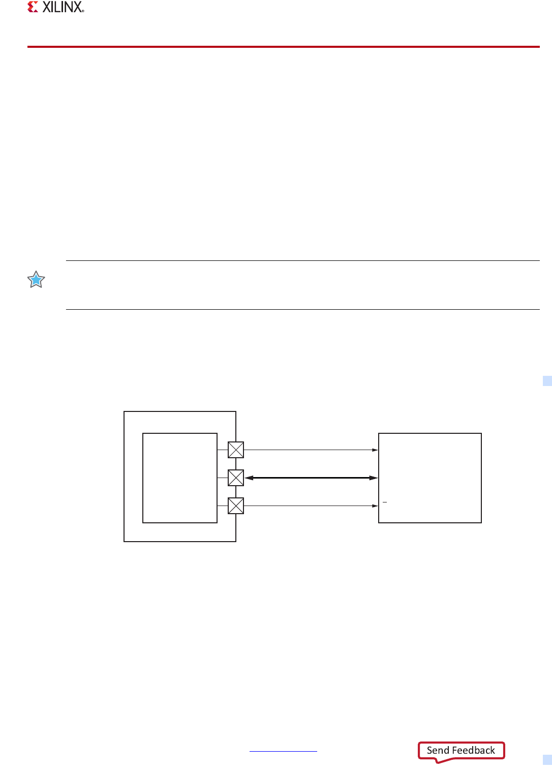
Zynq-7000 AP SoC Technical Reference Manual www.xilinx.com 359
UG585 (v1.12.1) December 6, 2017
Chapter 12: Quad-SPI Flash Controller
12.5 I/O Interface
12.5.1 Wiring Connections
The I/O signals are available via the MIO pins. The Quad-SPI controller supports up to two SPI flash
memories in either a shared or separate bus configuration. The controller supports operation in
several configurations:
• Quad-SPI single SS, 4-bit I/O
• Quad-SPI dual SS, 8-bit parallel I/O
• Quad-SPI dual SS, 4-bit stacked I/O
•Quad-SPI single SS, legacy I/O
IMPORTANT: QSPI 0 should always be present if the QSPI memory subsystem is to be used. QSPI 1 is
optional and is only required for the two-memory arrangement. Therefore, QSPI_1 cannot be used
alone.
Single SS, 4-bit I/O
A block diagram of the 4-bit flash memory interface connected to the controller configuration is
shown in Figure 12-5. This configuration supports execution-in-place functionality.
X-Ref Target - Figure 12-5
Figure 12-5: Quad-SPI Single SS 4-bit I/O
UG585_c12_06_102014
Quad-SPI
Controller
Zynq Device
Quad-SPI
Flash
Memory
QSPI0_IO[3:0] IO[3:0]
CLK
S
QSPI0_SCLK
QSPI0_SS_B
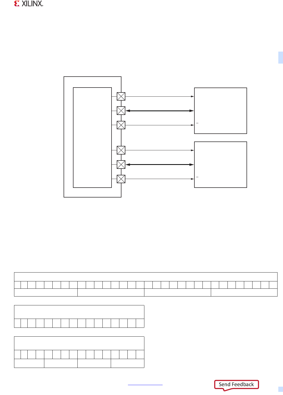
Zynq-7000 AP SoC Technical Reference Manual www.xilinx.com 360
UG585 (v1.12.1) December 6, 2017
Chapter 12: Quad-SPI Flash Controller
Dual SS, 8-bit Parallel
The controller supports up to two SPI flash memories operating in parallel, as shown in Figure 12-6.
This configuration increases the maximum addressable SPI flash memory from 16 MB (24-bit
addressing) to 32 MB (25-bit addressing). The execution-in-place feature is not supported in this
configuration.
For 8 bit parallel configuration, even bits of the data words are located in lower memory and odd bits
of data are located in upper memory. The controller takes care of data management in both I/O and
linear mode. The Quad-SPI controller does a read from the two Quad-SPI devices and ORs (or
operation) both device’s status information before writing the status data in the RXFIFO. Table 12-7
shows the data bit arrangement of a 32-bit data word for 8 bit parallel configuration. Table 12-8
shows Quad-SPI CMD behavior in Dual Quad-SPI parallel mode.
X-Ref Target - Figure 12-6
Figure 12-6: Quad-SPI Dual SS, 8-bit Parallel I/O
UG585_c12_07_102014
Quad-SPI
Controller
Zynq Device
Quad-SPI
Flash
Memory
QSPI0_IO[3:0] IO[3:0]
CLK
S
QSPI0_SCLK
QSPI0_SS_B
Quad-SPI
Flash
Memory
(Upper)
QSPI1_IO[3:0] IO[3:0]
CLK
S
QSPI1_SCLK
QSPI1_SS_B
Table 12-7: Quad-SPI Dual SS, 8-bit Parallel I/O Data Management
Single Device
7 6 5 4 3 2 1 0 15 14 13 12 11 10 9 8 23 22 21 20 19 18 17 16 31 30 29 28 27 26 25 24
byte 0 byte 1 byte 2 byte 3
Dual Devices
Lower Memory
642 0 1412108 2220181630282624
Dual Devices
Upper Memory
753 1 1513119 2321191731292725
byte 0 byte 1 byte 2 byte 3

Zynq-7000 AP SoC Technical Reference Manual www.xilinx.com 361
UG585 (v1.12.1) December 6, 2017
Chapter 12: Quad-SPI Flash Controller
In 8 bit parallel configuration, total addressable memory size is 32 MB. This requires a 25-bit address.
All accesses to memory must be word aligned and have double-byte resolution. In linear mode, the
Quad-SPI controller divides the AXI address by 2 and sends the divided address to the Quad-SPI
device. In IO mode, software is responsible for doing the address translation to comply with SPI
24-bit address support.
Dual SS, 4-bit Stacked I/O
To reduce the I/O pin count, the controller also supports up to two SPI flash memories in a shared
bus configuration, as shown in Figure 12-7. This configuration increases the maximum addressable
SPI flash memory from 16 MB (24-bit addressing) to 32 MB (25-bit addressing), but the throughput
remains the same as for single memory mode. Note that in this configuration, the device level XIP
mode (read instruction codes of 0xBB and 0xEB), is not supported.
The lower SPI flash memory should always be connected if the linear Quad-SPI memory subsystem
is used, and the upper flash memory is optional. Total address space is 32 MB with a 25-bit address.
In IO mode, the MSB of the address is defined by U_PAGE which is located at bit 28 of register 0xA0.
In Linear address mode, AXI address bit 24 determines the upper or lower memory page. All of the
commands will be executed by the device selected by U_PAGE in I/O mode and address bit 24 in
linear mode.
Table 12-8: Quad-SPI CMD Behavior in Dual Quad-SPI Parallel Mode
Command Dual Parallel Quad-SPI Controller Behavior
Sector Erase The Quad-SPI controller sends erase command to both chips; 64 KB erase operation is done
to each part. Effectively erases combined 128 KB from both memories.
Read ID Only takes received data from the lower flash bus and places it in RXD. Hence no need to
combine the data. It is therefore required that the upper and lower flash parts be identical
parts when using Parallel Flash Mode.
Page Program Even and odd bits are separated and programed in both memories. Refer to Table 12 - 7 for
more information.
Read Even and odd data bits are read from both device and are interleaved as shown in Ta bl e 12-7.
RDSR The WIP bit from both parts are OR'ed together to form the LSB .of the data read, the other
7 bits come just from the lower bus.
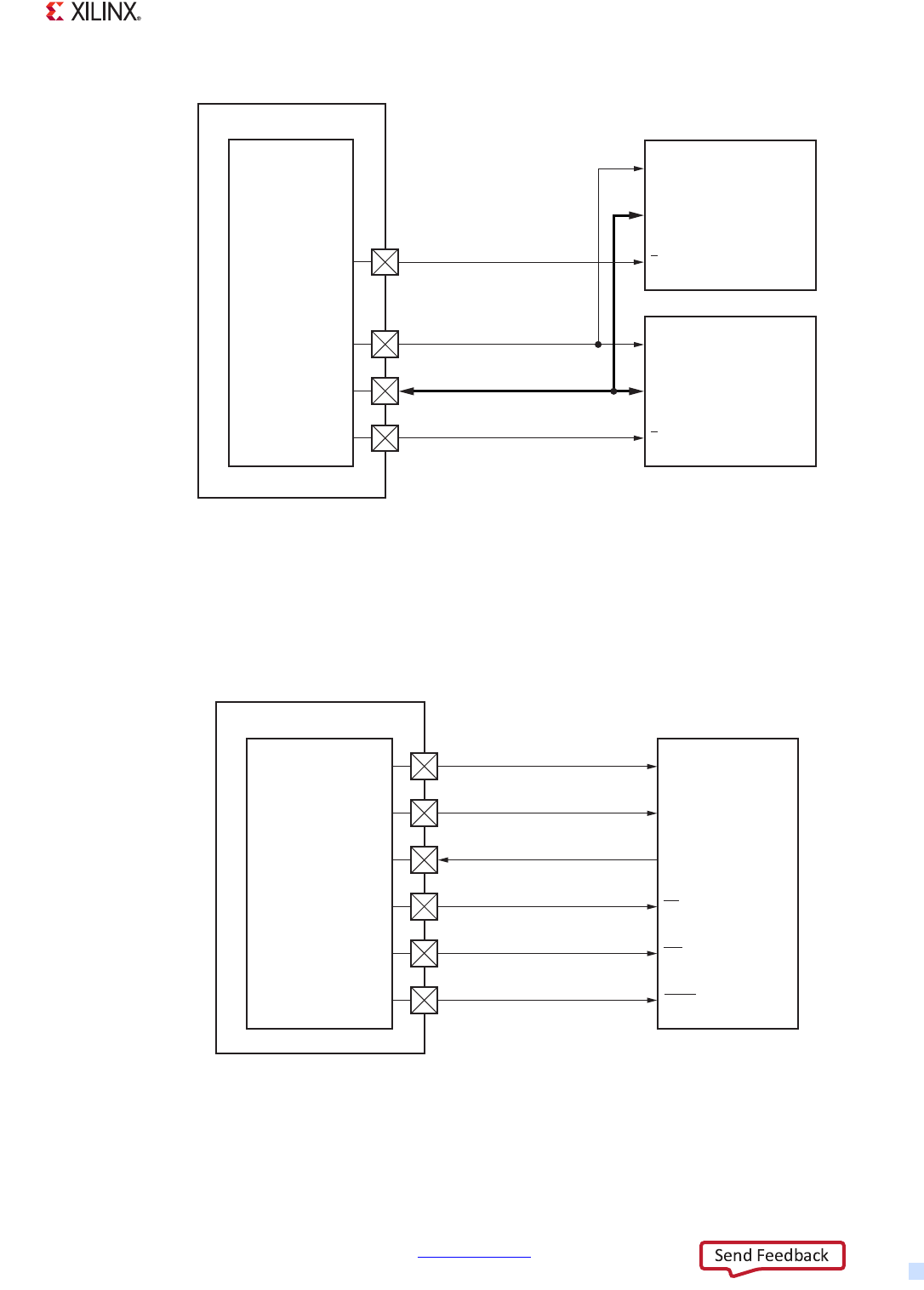
Zynq-7000 AP SoC Technical Reference Manual www.xilinx.com 362
UG585 (v1.12.1) December 6, 2017
Chapter 12: Quad-SPI Flash Controller
Single SS, Legacy I/O
The Quad-SPI controller can be operated in legacy single-bit serial interface mode for 1x, 2x and 4x
I/O modes as shown in Figure 12-8.
X-Ref Target - Figure 12-7
Figure 12-7: Quad-SPI Dual SS 4-bit Stacked I/O
X-Ref Target - Figure 12-8
Figure 12-8: Quad-SPI Single SS, Legacy I/O
UG585_c12_08_102014
Quad-SPI
Controller
Zynq Device
Quad-SPI
Flash
Memory
QSPI0_IO[3:0] IO[3:0]
CLK
S
QSPI0_SCLK
QSPI0_SS_B
Quad-SPI
Flash
Memory
(Upper)
IO[3:0]
CLK
S
QSPI1_SS_B
UG585_c12_09_102014
Quad-SPI
Controller
Zynq Device (SPI Master)
SPI
Slave
HOLD
QSPI0_SS_N
QSPI0_IO[2]
QSPI0_IO[3]
WP
SS
MISO
MOSI
CLK
QSPI0_SCLK
QSPI0_IO[0]
QSPI0_IO[1]

Zynq-7000 AP SoC Technical Reference Manual www.xilinx.com 363
UG585 (v1.12.1) December 6, 2017
Chapter 12: Quad-SPI Flash Controller
12.5.2 MIO Programming
The Quad-SPI signals can be routed to specific MIO pins, refer to Table 12-9, Quad-SPI Interface
Signals. Wiring diagrams are shown in Figure 12-5 to Figure 12-8. The general routing concepts and
MIO I/O buffer configurations are explained in section 2.4 PS–PL Voltage Level Shifter Enables.
If a four-bit I/O bus is used, then use Quad-SPI 0. If a bus frequency of greater than 40 MHz is
needed, then the Quad-SPI feedback clock must be routed on MIO pin 8.
Example: Program I/O for a Single Device
These steps are required for all of the Quad-SPI I/O interface connections listed above.
1. Configure MIO pin 1 for chip select 0 output. Write 0x0000_1202 to the slcr.MIO_PIN_01
register:
a. Route Quad-SPI 0 chip select to pin 1.
b. 3-state controlled by Quad-SPI (TRI_ENABLE = 0).
c. LVCMOS18 (refer to the register definition for other voltage options).
d. Slow CMOS edge (benign setting).
e. Enable internal pull-up resistor.
f. Disable HSTL receiver (disabled because LVCMOS is selected).
2. Configure MIO pins 2 through 5 for I/O. Write 0x0000_0302 to each of the
slcr.MIO_PIN_{02:05} registers:
a. Route Quad-SPI 0 I/O pins to pin 2 through 5.
b. 3-state controlled by Quad-SPI (TRI_ENABLE = 0).
c. LVCMOS18 (refer to the register definition for other voltage options).
d. Slow CMOS drive edge.
e. Disable internal pull-up resistor.
f. Disable HSTL receiver.
3. Configure MIO pin 6 for serial clock 0 output. Write 0x0000_0302 to the slcr.MIO_PIN_06
register:
a. Route Quad-SPI 0 serial clock to pin 6.
b. 3-state controlled by Quad-SPI (TRI_ENABLE = 0).
c. LVCMOS18 (refer to the register definition for other voltage options).
d. Slow CMOS edge (benign setting).
e. Disable internal pull-up resistor.
f. Disable HSTL receiver.
Option: Add Second Device Chip Select
This step is required for the following I/O connections:
• Dual selects, shared 4-bit data memory interface.

Zynq-7000 AP SoC Technical Reference Manual www.xilinx.com 364
UG585 (v1.12.1) December 6, 2017
Chapter 12: Quad-SPI Flash Controller
• Dual selects, separate 4-bit data memory interface.
4. Configure MIO pin 0 for chip select 1 output. Write 0x0000_1302 to the slcr.MIO_PIN_00
register:
a. Route Quad-SPI 1 chip select to pin 0.
b. 3-state controlled by Quad-SPI (TRI_ENABLE = 0).
c. LVCMOS18 (refer to the register definition for other voltage options).
d. Slow CMOS edge (benign setting).
e. Enable internal pull-up resistor.
f. Disable HSTL receiver.
Option: Add Second Serial Clock
This step is required for the Dual Selects, Separate 4-bit Data Memory Interface:
5. Configure MIO pin 9 for serial clock 1 output. Write 0x0000_0302 to the slcr.MIO_PIN_09
register:
a. Route Quad-SPI 1 serial clock to pin 9.
b. 3-state controlled by Quad-SPI (TRI_ENABLE = 0).
c. LVCMOS18 (refer to the register definition for other voltage options).
d. Slow CMOS edge (benign setting).
e. Disable internal pull-up resistor.
f. Disable HSTL receiver.
Option: Add 4-bit Data
These steps are required for the dual selects, separate 4-bit data memory interface:
6. Configure MIO pins 10 through 13 for I/O. Write 0x0000_0302 to each of the
slcr.MIO_PIN_{10:13} registers:
a. Route Quad-SPI 1 I/O pins to pin 9 through 13.
b. 3-state controlled by Quad-SPI (TRI_ENABLE = 0).
c. LVCMOS18 (refer to the register definition for other voltage options).
d. Slow CMOS drive edge.
e. Disable internal pull-up resistor.
f. Disable HSTL receiver.
Option: Add Feedback Output Clock
The optional feedback clock is used when the I/O interface is operated above 40 MHz. It should only
be connected to a pull-up or pull-down resistor for pin strapping resistor for MIO voltage mode,
vmode. The feedback clock must also be enabled.
7. Configure MIO pin 8 for feedback clock. Write 0x0000_0302 to the slcr.MIO_PIN_08 register:

Zynq-7000 AP SoC Technical Reference Manual www.xilinx.com 365
UG585 (v1.12.1) December 6, 2017
Chapter 12: Quad-SPI Flash Controller
a. Route Quad-SPI feedback clock output to pin 8.
b. 3-state controlled by Quad-SPI (TRI_ENABLE = 0).
c. LVCMOS18 (refer to the register definition for other voltage options).
d. Slow CMOS edge (benign setting).
e. Disable internal pull-up resistor.
f. Diable HSTL receiver.
12.5.3 MIO Signals
The Quad-SPI flash memory signals are routed through the MIO multiplexer to the MIO device pins.
Each side of the dual controller port can be individually enabled or operate together as an 8-bit I/O
interface.
The Quad-SPI flash memory signals are routed to the MIO pins as shown in Ta ble 1 2 -9 .
Table 12-9: Quad SPI Interface Signals
Quad-SPI Flash Memory Interface MIO Pin Controller
Default
Input
Value
Signal
I/O Mode for Data
Quad SPI 0 Quad SPI 1 I/O Name
1-Bit
Data
2-Bit
Data
4-Bit
Data
Flash Chip
Select ~ 1 0 O QSPI{1,0}_SS_B ~
Serial Clock ~ 6 9 O QSPI{1,0}_SCLK ~
Output
Feedback Clk ~8OQSPI_SCLK_FB_OUT~
I/O 0 Master
Output
I/O 0 I/O 0 210IOQSPI{1,0}_IO_00
I/O 1 Master
Input
I/O 1 I/O 1 311IOQSPI{1,0}_IO_10
I/O 2 Write
Protect
Write
Protect
I/O 2 412IOQSPI{1,0}_IO_20
I/O 3 Hold Hold I/O 3 5 13 IO QSPI{1,0}_IO_3 0

Zynq-7000 AP SoC Technical Reference Manual www.xilinx.com 366
UG585 (v1.12.1) December 6, 2017
Chapter 13
SD/SDIO Controller
13.1 Introduction
The SD/SDIO controller communicates with SDIO devices, SD memory cards, and MMC cards with up
to four data lines. On the SD interface, one (DAT0) or four (DAT0-DAT3) lines can be used for data
transfer. The SDIO interface can be routed through the MIO multiplexer to the MIO pins or through
the EMIO to SelectIO pin in the PL. The controller can support SD and SDIO applications in a wide
range of portable low-power applications such as 802.11 devices, GPS, WiMAX, UWB, and others.
The SD/SDIO controller block diagram is shown in Figure 13-1.
The SD/SDIO controller is compatible with the standard SD Host Controller Specification Version 2.0
Part A2 with SDMA (single operation DMA), ADMA1 (4 KB boundary limited DMA), and ADMA2
(ADMA2 allows data of any location and any size to be transferred in a 32-bit system memory -
scatter-gather DMA) support. The core also supports up to seven functions in SD1, SD4, but does not
support SPI mode. The Zynq-7000 AP SoC is expected to work with eMMC devices because the
protocol is the same as SD, but this has not been extensively verified. Users must be careful to meet
all timing requirements as they might or might not comply with eMMC. It does support SD
high-speed (SDHS) and SD High Capacity (SDHC) card standards. The user should be familiar with
the SD2.0/SDIO 2.0 specifications. These are listed in Appendix A, Additional Resources. The
SD/SDIO controller also supports MMC3.31 standard. eMMC flash memories are not primary boot
devices for Zynq-7000 family, but can be used as secondary boot devices. For details, refer to UG821,
Zynq-7000 Software Developers Guide.
The SD/SDIO controller is accessed by the ARM processor via the AHB bus. The controller also
includes a DMA unit with an internal FIFO to meet throughput requirements.
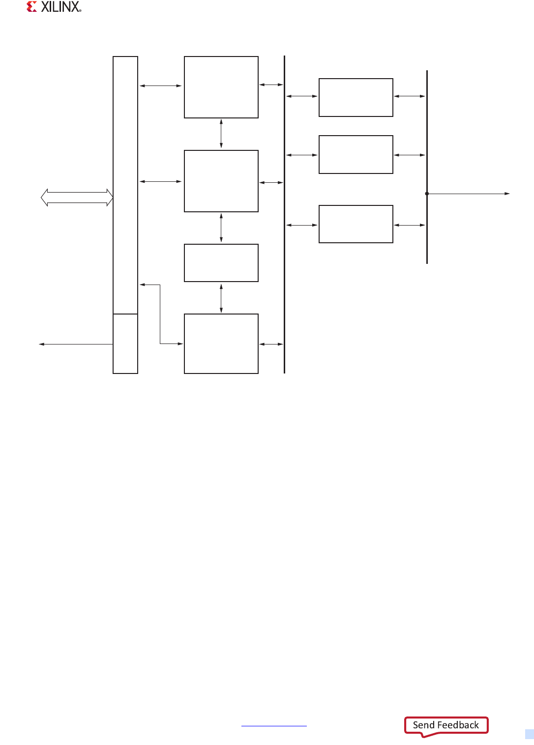
Zynq-7000 AP SoC Technical Reference Manual www.xilinx.com 367
UG585 (v1.12.1) December 6, 2017
Chapter 13: SD/SDIO Controller
13.1.1 Key Features
The two SDIO controllers are controlled and operate independently with the same feature set:
• Host mode controller
°Four I/O signals (MIO or EMIO)
°Command, Clock, CD, WP, Pwr Ctrl (MIO or EMIO)
°LED control, bus voltage (EMIO)
°Interrupt or polling driven
• AHB master-slave interface operating at the CPU_1x clock rate
Master mode for DMA transfers (with 1 KB FIFO)
°Slave mode for register accesses
• SDIO Specification 2.0
°Low-speed, 1 KHz to 400 KHz
°Full-speed, 1 MHz to 50 MHz (25 MB/sec)
°High-speed and high-capacity memory cards
X-Ref Target - Figure 13-1
Figure 13-1: SD/SDIO Controller Block Diagram
UG585_c13_01_020613
SDMA
ADMA1
ADMA2 Command
Decoder
Response
Generator
Transmitter/
Receiver
SD/SDIO Bus
Interrupt
AHB
InterruptsAHB Interface
SD/SDIO
Host
Controller
CPRM
FIFO
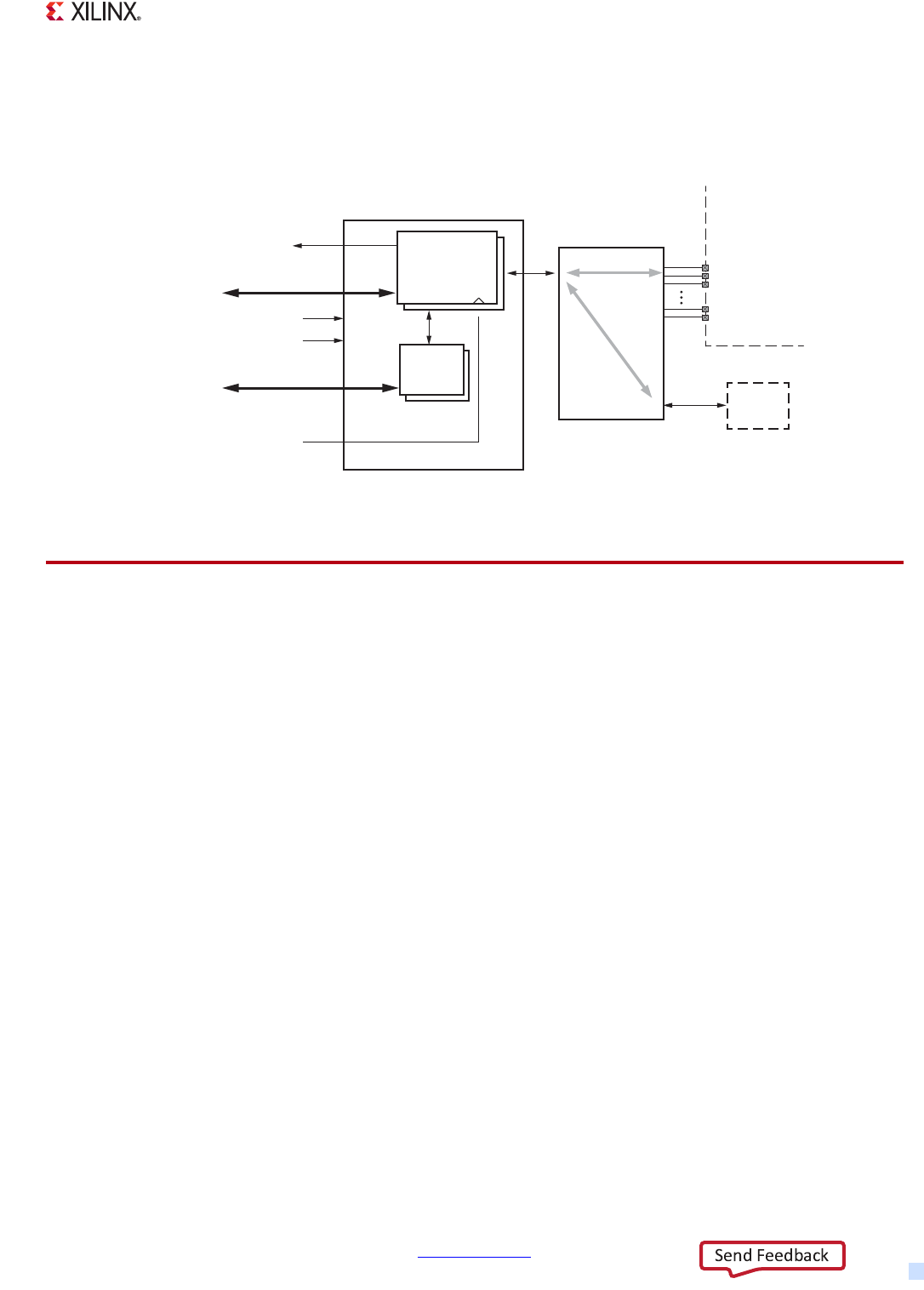
Zynq-7000 AP SoC Technical Reference Manual www.xilinx.com 368
UG585 (v1.12.1) December 6, 2017
Chapter 13: SD/SDIO Controller
13.1.2 System Viewpoint
Figure 13-2 shows the SD/SDIO controller system viewpoint.
13.2 Functional Description
13.2.1 AHB Interface and Interrupt Controller
When using programmed I/O for data transfers, software reads and writes the sdio.Buffer_Data_Port
register.
When using the local DMA unit for data transfers, the DMA unit initiates read or write memory
transactions. The SDIO controller cannot be used with the PS DMAC.
The controller can generate IRQ interrupt #56 and 79 for SDIO 0 and SDIO 1, respectively. The status
and masking of the interrupts are controlled by registers.
13.2.2 SD/SDIO Host Controller
The SD/SDIO host controller comprises:
• Host-AHB controller
• All control registers
•Bus monitor
• Clock generator
• CRC generator and checker (CRC7 and CRC16)
X-Ref Target - Figure 13-2
Figure 13-2: SD/SDIO Controller System Viewpoint Diagram
PL
MIO – EMIO
Routing
Interconnect AHB MIO
Pins
UG585_c13_02_031812
Device
Boundary
EMIO
Signals
IRQ ID# {56, 79}
Control
Registers
Master
port
Interconnect AHB
Slave
port
CPU_1x clock
SDIO{0, 1} CPU_1x reset
SDIO{0, 1} Ref Clock
SDIO
Interface
Controller

Zynq-7000 AP SoC Technical Reference Manual www.xilinx.com 369
UG585 (v1.12.1) December 6, 2017
Chapter 13: SD/SDIO Controller
The host-AHB controller acts as bridge between the AHB bus and the host controller. The SD/SDIO
controller registers are programmed by the processor through the AHB interface. Interrupts are
generated based on the values set in the Interrupt Status and Interrupt Enable registers.
The bus monitor checks for violations occurring on the SD bus and timeout conditions. The clock
generation block generates the SD clock depending on the value programmed in the Clock Control
register.
The CRC7 and CRC16 generators calculate the CRC for command and data transfers to the SD/SDIO
card. The CRC7 and CRC16 checker checks for any CRC errors in the response and data received from
the SD/SDIO card. To detect data defects on the card, the host can include error correction codes in
the payload data. ECC code is used to store data on the card. This ECC code is used by the application
to decode the user data.
13.2.3 Data FIFO
The controller uses two 512 byte dual port FIFOs for performing write and read transactions. During
a write transaction (data is transferred from the processor to an attached card) data is written by the
processor alternatively into the first and second FIFO. When data is transferred to an attached card,
alternatively the second and first FIFO is used, providing maximum data throughput.
During a read transaction (data is transferred from an attached card to the processor) the data from
the card is alternatively written in the two FIFOs. When data from one FIFO is transferred to the
processor the second FIFO is filled with data from the card and vice versa, optimizing data
throughput.
If the controller cannot accept any data from a connected card, it issues a read wait, stopping the
data transfer from the card by stopping the clock.
13.2.4 Command and Control Logic
The control logic block transmits data on the data lines during a write transaction and receives data
during read transaction The command control logic block transmits commands on the command
lines and receives the response from the SD2.0 or SDIO2.0.
13.2.5 Bus Monitor
The bus monitor checks for violations occurring in the SD bus, and timeout conditions.

Zynq-7000 AP SoC Technical Reference Manual www.xilinx.com 370
UG585 (v1.12.1) December 6, 2017
Chapter 13: SD/SDIO Controller
13.2.6 Stream Write and Read
This functionality applies to both DMA and non-DMA modes.
WRITE_DAT_UNTIL_STOP(CMD20) writes a data stream from the host, starting at the given address,
until a STOP_TRANSMISSION follows.
READ_DAT_UNTIL_STOP(CMD11) reads a data stream from the card, starting at the given address,
until a STOP_TRANSMISSION follows.
The host controller switches to the second FIFO after writing/reading a block of data to/from the first
FIFO, but the stream transaction block size is not be programmed by the driver. So for both stream
write and stream read transactions, it is recommended that the host driver writes the maximum FIFO
size value to the Block Size register. Because the SDIO FIFO slice is set to 512 bytes, the host driver
must write 512 bytes to the Block Size register. Therefore FIFO switching occurs after writing/reading
the 512 bytes of data.
13.2.7 Clocks
The SDIO clock is derived from SDIO reference clock based on the Clock Control register value
programmed by the driver and is available when the SD clock enable is set by the driver. The
maximum frequency is 50 MHz.
The AHB system clock is used for the AHB interface.
The host controller supports both full speed and high speed cards. For the high speed card, the host
controller should clock out the data at the rising edge of the SDIO clock. For the full speed card, the
host controller should clock out the data at the falling edge of the SDIO clock.
Refer to Table 24-2, page 681 for the more details about power management. Refer to Chapter 25,
Clocks for details about the clocks. Layout and clock termination guidelines are presented in UG933,
Zynq-7000 All programmable SoC PCB Design Guide.
Note: The SDIO reference clock must be set to more than 100 MHz during the card initialization
sequence. This is needed to ensure the SD card interface frequency is no more than 400 kHz as
required for initialization. The divisor value is set to 0x80 (256) yielding a 390 kHz clock from the
100 MHz reference.
13.2.8 Soft Resets
The host controller supports all soft resets mentioned in the SD2.0/SDIO2.0 Host Controller
Specification.

Zynq-7000 AP SoC Technical Reference Manual www.xilinx.com 371
UG585 (v1.12.1) December 6, 2017
Chapter 13: SD/SDIO Controller
13.2.9 FIFO Overrun and Underrun Conditions
This functionality applies to both DMA and non-DMA modes.
Write
During the write transaction, the host controller transmits data to the card only when a block of data
is ready to transmit and the card is not busy. Therefore an under-run condition cannot occur in the
SD side.
• In DMA mode, the host controller initiates a DMA READ from the ARM processor only if space is
available to accept a block of data.
• In non-DMA mode, the host controller asserts a buffer write ready interrupt only if space is
available to accept a block of data.
Read
During the read transaction when the FIFO is full (the FIFO does not have enough space to accept a
block of data from the card) the host controller stops the clk_sd to the card. Therefore an over-run
condition cannot occur in SD side.
• In DMA mode the host controller initiates a DMA WRITE to the ARM processor only on
reception of a block of data from card.
• In non-DMA mode, the host controller asserts a buffer read ready interrupt only on reception of
a block of data from card.
Limitation
The interconnect switch (ARM NIC-301) converts the AXI transaction to AHB transaction going to the
SD/SDIO Controller. But it does not handle WSTRB signal propagation from the PL. If the PL master
issues a 2 byte wide transaction with AWSIZE=2 (4 bytes), the upper two bytes are undefined.
Therefor the recommendation is to use AxSIZE=1 for 2 byte transfers.

Zynq-7000 AP SoC Technical Reference Manual www.xilinx.com 372
UG585 (v1.12.1) December 6, 2017
Chapter 13: SD/SDIO Controller
13.3 Programming Model
13.3.1 Data Transfer Protocol Overview
SD transfers are basically classified into following three types according to how the number of blocks
is specified:
Single Block Transfer
The number of blocks is specified to the host controller before the transfer. The number of blocks
specified is always one.
Multiple Block Transfer
The number of blocks is specified to the host controller before the transfer. The number of blocks
specified is one or more.
Infinite Block Transfer
The number of blocks is not specified to the host controller before the transfer. This transfer is
continued until an abort transaction is executed. This abort transaction is performed by CMD12 in
the case of an SD memory card and by CMD52 in the case of an SDIO card.
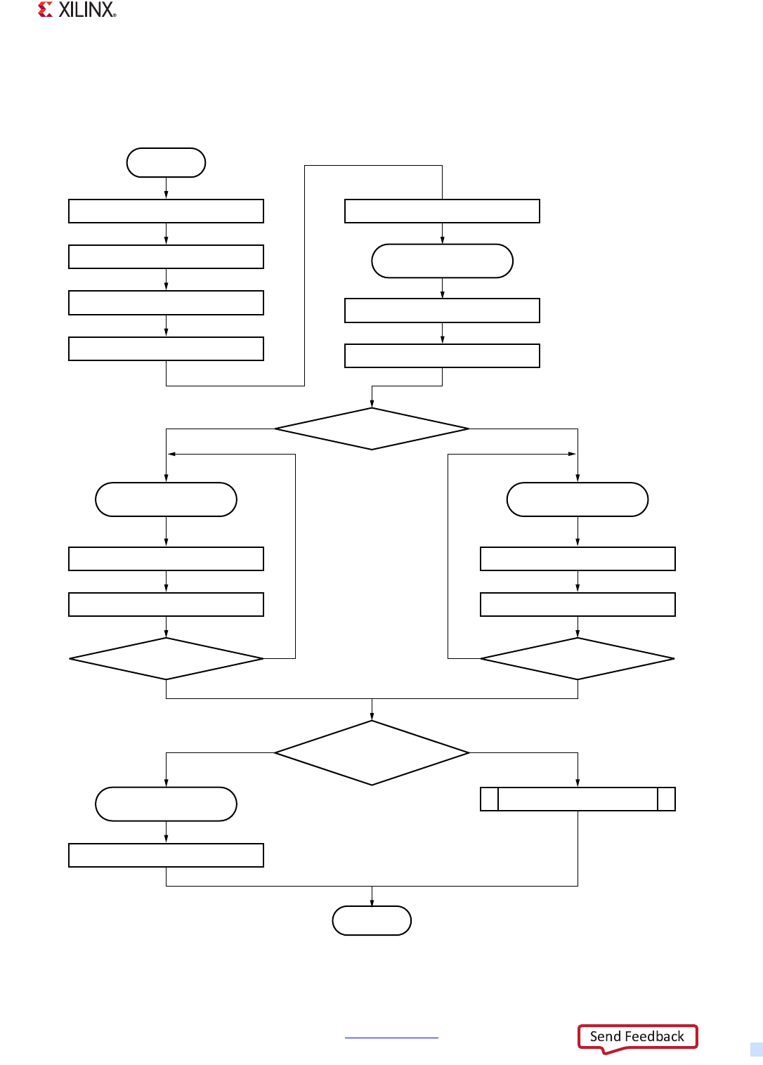
Zynq-7000 AP SoC Technical Reference Manual www.xilinx.com 373
UG585 (v1.12.1) December 6, 2017
Chapter 13: SD/SDIO Controller
13.3.2 Data Transfers Without DMA
Figure 13-3 shows data transfers without using DMA.
X-Ref Target - Figure 13-3
Figure 13-3: Data Transfer Using DAT Line Sequence (Without Using DMA)
UG585_c13_03_031812
Start
(1) (5)
(6)
Set Block Size Reg
(2)
Set Block Count Reg
Set Command Reg
(7)
Clr Command Complete Sts
Command Complete Int Occur
Buffer Read
Ready Int Occur
Single or Multi
Block Transfer
Transfer Complete Int Occur
Infinite
Block Transfer
Buffer Write
Ready Int Occur
(8)
Get Response Data
(3)
Set Argument Reg
(4)
Set Transfer Mode Reg
Wait for Buffer Write
Ready Int
(10-W)
Wait for Transfer
Complete Int
(15)
(10-R)
Clr Buffer Wr Rdy Sts
Wait for Command
Complete Int
(12-W)
Set Block Data
(16)
Clr Transfer Complete Sts
(13-W)
(14)
Yes Yes
No No
Wait for Buffer Write
Ready Int
Clr Buffer Rd Rdy Sts
(12-R)
(11-W) (11-R)
Get Block Data
(17)
Abort Transaction
(13-R)
End
(9) ReadWrite Write or Read
More Blocks? More Blocks?
Single / Multi / Infinite
Block Transfer?

Zynq-7000 AP SoC Technical Reference Manual www.xilinx.com 374
UG585 (v1.12.1) December 6, 2017
Chapter 13: SD/SDIO Controller
The sequence for data transfers without using DMA is as follows:
1. Set the value corresponding to the executed data byte length of one block to the Block Size
register.
2. Set the value corresponding to the executed data block count to the Block Count register.
3. Set the value corresponding to the issued command to the Argument register.
4. Set the value to Multi/Single Block Select and Block Count Enable. Set the value corresponding
to the issued command to Data Transfer Direction, Auto CMD12 Enable, and DMA Enable.
5. Set the value corresponding to the issued command to the Command register.
Note: When writing the upper byte of the command register, the SD command is issued.
6. Wait for the command complete interrupt.
7. Write a 1 to the Command Complete bit in the Normal Interrupt Status register to clear this bit.
8. Read the Response register and get the necessary information in accordance with the issued
command.
9. In the case where this sequence is for writing to a card, go to Step (10-W). In case of read from
a card, go to Step (10-R).
(10-W). Wait for a buffer write ready interrupt.
°Non-DMA Write Transfer
On receiving the buffer write ready interrupt the ARM processor acts as a master and starts
transferring the data via the Buffer Data Port register (FIFO_1). The transmitter starts sending
the data on the SD bus when a block of data is ready in FIFO_1. While transmitting the data
on the SD bus the buffer write ready interrupt is sent to the ARM processor for the second
block of data. The ARM processor acts as a master and starts sending the second block of
data via the buffer data port register to FIFO_2. The buffer write ready interrupt is asserted
only when a FIFO is empty and available to receive a block of data.
(11-W). Write a 1 to the Buffer Write Ready bit in the Normal Interrupt Status register to clear this
bit.
(12-W). Write a block of data (according to the number of bytes specified in Step (1)) to the Buffer
Data Port register.
(13-W). Repeat until all blocks are sent and then go to Step (14).
°Non-DMA Read Transfer
A buffer read ready interrupt is asserted whenever a block of data is ready in one of the
FIFOs. On receiving the buffer read ready interrupt, the ARM processor acts as a master and
starts reading the data via the Buffer Data Port register (FIFO_1). The receiver starts reading
the data from the SD bus only when a FIFO is empty and available to receive a block of data.
When both of the FIFOs are full the host controller stops the data coming from the card by
means of a read wait mechanism (if the card supports read wait) or through clock stopping.
(10-R). Wait for a buffer read ready interrupt
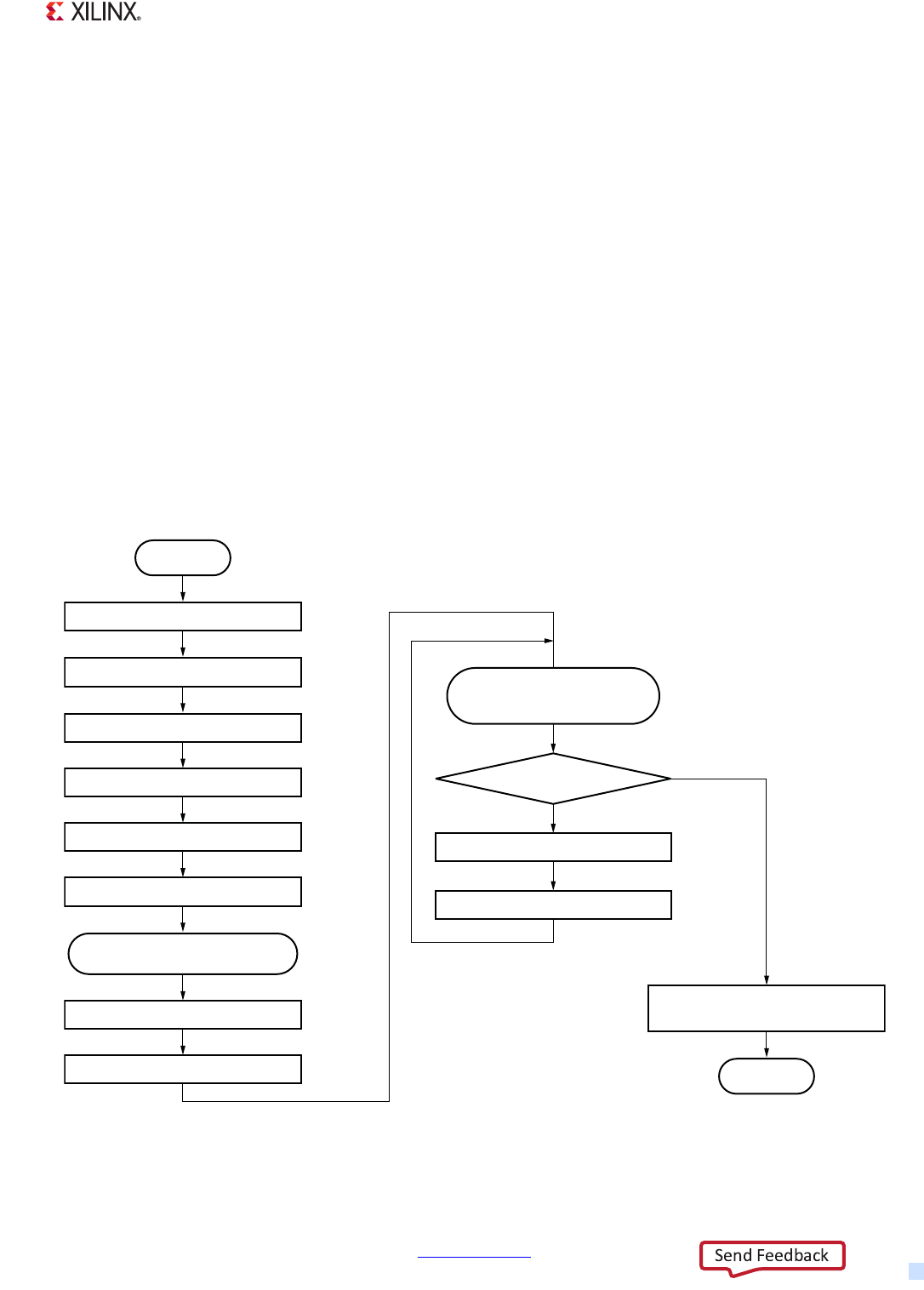
Zynq-7000 AP SoC Technical Reference Manual www.xilinx.com 375
UG585 (v1.12.1) December 6, 2017
Chapter 13: SD/SDIO Controller
(11-R). Write a 1 to the Buffer Read Ready bit in the Normal Interrupt Status register to clear this bit.
(12-R). Read a block of data (according to the number of bytes specified in Step (1)) from the Buffer
Data Port register.
(13-R). Repeat until all blocks are received and then go to Step (14).
14. If this sequence is for a single or multiple block transfer, go to Step (15). In case of an infinite
block transfer, go to Step (17).
10. Wait for a transfer complete interrupt.
11. Write a 1 to the Transfer Complete bit in the Normal Interrupt Status register to clear this bit.
12. Perform the sequence for abort transaction.
Note: Step (1) and Step (2) can be executed at same time. Step (4) and Step (5) can be executed at
same time.
13.3.3 Using DMA
Figure 13-4 shows data transfers using DMA.
X-Ref Target - Figure 13-4
Figure 13-4: SDIO Controller Data Transfer Using DMA
Start
(1)
(2)
(3)
(11)
(12)
(13)
(14)
(10)
Set System Address Reg
End
Wait For
Command Command Int
Wait For
Transfer Complete Int
and DMA Int
Set Block Size Reg
Set Block Count Reg
(4)
Set Argument Reg
(5)
Set Transfer Mode Reg
(6)
(7)
Set Command Reg
(8)
Clr Command Complete Status
(9)
Get Response Data
Clr DMA Interrupt Status
Get System Address Reg
Clr Transfer Complete Status
Clr DMA Interrupt Status
Check
Interrupt Status
Command Complete Int Occur
Transfer Complete Int Occur
UG585_c13_04_031812

Zynq-7000 AP SoC Technical Reference Manual www.xilinx.com 376
UG585 (v1.12.1) December 6, 2017
Chapter 13: SD/SDIO Controller
Burst types such as an 8-beat incrementing burst or a 4-beat incrementing burst, or a single transfer
is used to transfer or receive the data from the system memory mainly to avoid the hold of the AHB
bus by the master for a longer time.
The sequence for using DMA is as follows:
1. Set the system address for DMA in the System Address register.
2. Set the value corresponding to the executed data byte length of one block in the Block Size
register.
3. Set the value corresponding to the executed data block count in the Block Count register.
4. Set the value corresponding to the issued command to the Argument register.
5. Set the value to Multi/Single Block Select and Block Count Enable. Set the value corresponding
to the issued command to Data Transfer Direction, Auto CMD12 Enable, and DMA Enable.
6. Set the value corresponding to the issued command to the Command register.
Note: When writing to the upper byte of the Command register, the SD command is issued.
7. Wait for the command complete interrupt.
8. Write a 1 to the Command Complete in the Normal Interrupt Status register for clearing this bit.
9. Read the Response register and get the necessary information in accordance with the issued
command.
°DMA Write Transfer
On receiving the Response End Bit from the card for the write command (data is flowing from
the host to the card) the SD host controller acts as the master and requests the AHB bus.
After receiving the grant the host controller starts reading a block of data from system
memory and fills the first half of the FIFO. Whenever a block of data is ready the transmitter
starts sending the data on the SD bus.
While transmitting the data on the SD bus the host controller requests the bus to fill the
second block in the second half of the FIFO. “Ping Pong” FIFOs are used to increase the
throughput. Similarly, the host controller reads a block of data from system memory
whenever a FIFO is empty. This continues until all of the blocks are read from system memory.
A transfer complete interrupt is set only after transferring all of the blocks of data to the card.
°DMA Read Transfer
The block of data received from the card (data is flowing from the card to the host) is stored
in the first half of the FIFO. Whenever a block of data is ready the SD host controller acts as
the master and request the AHB bus. After receiving the grant the host controller starts
writing a block of data into system memory from the first half of the FIFO.
While transmitting data into system memory the host controller receives the second block of
data and stores it in the second half of the FIFO. Similarly the host controller writes a block
of data into system memory whenever data is ready. This continues until all of the blocks are
transferred to system memory. A transfer complete interrupt is set only after transferring all
of the blocks of data into system memory.
Note: The host controller receives a block of data from the card only when it has room to
store a block of data in the FIFO. When both FIFOs are full the host controller stops the data
coming from the card through a “read wait” mechanism (if the card supports read wait) or
through clock stopping.

Zynq-7000 AP SoC Technical Reference Manual www.xilinx.com 377
UG585 (v1.12.1) December 6, 2017
Chapter 13: SD/SDIO Controller
10. Wait for the transfer complete interrupt and DMA interrupt.
11. If Transfer Complete is set to 1, go to Step (14). If DMA Interrupt is set to 1 go to Step (12).
Transfer Complete has a higher priority than DMA Interrupt.
12. Write a 1 to the DMA Interrupt bit in the Normal Interrupt Status register to clear this bit.
13. Set the next system address of the next data position to the System Address register and go to
Step (10).
14. Write a 1 to the Transfer Complete and DMA Interrupt in the Normal Interrupt Status register to
clear this bit.
Note: Step (2) and Step (3) can be executed at same time. Step (5) and Step (6) can also be executed
at same time.
For example, if the host wants to transfer 4 KB of data to the card and assuming the maximum block
size is 256 bytes, the host driver programs the Block Size register as 256 and Block Count register
with the value 16. The AHB master and transmitter residing inside the SD2.0/SDIO2.0 host controller
get the information (how much data to transfer) from these registers. Using the above information,
the AHB master acts as a master and initiates a data read transaction (to read a block of data —
256 bytes from the system memory).
The following types of burst are used mainly to avoid hold of the AHB bus by the master for a longer
time.
• Single transfer
• 4-beat incrementing burst
• 8-beat incrementing burst
The first block of data is received in the first half of the FIFO and the second block in the second half
of the FIFO. Similarly, the remaining blocks are received in alternate FIFOs. Whenever a block of data
is ready in FIFO, the transmitter starts transmitting the block of data (256 bytes) onto the SD bus.
After transmitting the entire block of data to the card, the transmitter waits for a status response
from the card. Transmitter sends the next block of data only when it receives a good status response
from the card for the previous block of data, otherwise the transaction is aborted and the host goes
for a fresh transaction.
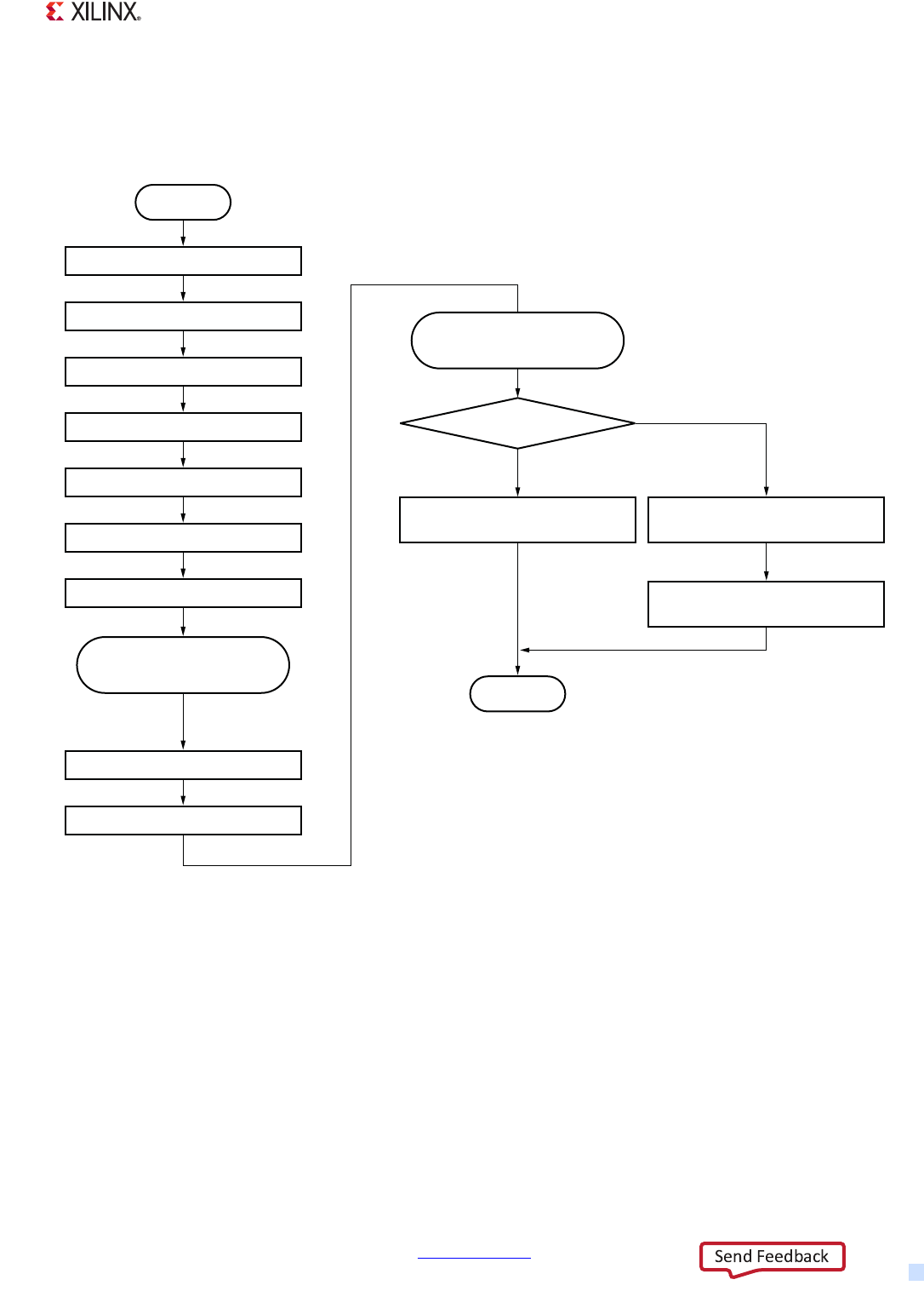
Zynq-7000 AP SoC Technical Reference Manual www.xilinx.com 378
UG585 (v1.12.1) December 6, 2017
Chapter 13: SD/SDIO Controller
13.3.4 Using ADMA
Figure 13-5 shows data transfers using ADMA.
The sequence for using ADMA is as follows
1. Create a descriptor table for ADMA in system memory.
2. Set the descriptor address for ADMA in the ADMA System Address register.
3. Set the value corresponding to the executed data byte length of one block in the Block Size
register.
4. Set the value corresponding to the executed data block count in the Block Count register in
accordance with SDIO register map.
X-Ref Target - Figure 13-5
Figure 13-5: SDIO Controller Data Transfer Using ADMA
Start
(1)
(11)
(12)
Create Descriptor Table
(2)
Set ADMA System Address Reg
(3)
Set Block Size Reg
(4)
Set Block Count Reg
(5)
Set Argument Reg
(6)
Set Transfer Mode Reg
(7)
(8)
Set Command Reg
(9)
Clr Command Complete Status
(10)
Get Response Data
(13) (14)
(15)
Clr Transfer Complete
Interrupt Status
End
Clr ADMA Error
Interrupt Status
Abort ADMA
Operation
Wait For
Transfer Complete Int
and ADMA Error Int
Check
Interrupt Status
Wait For
Command Complet Int
Command Complete
Int Occurs
ADMA Error Int. Occurs
Transfer Complete
Int. Occurs
UG585_c13_05_031812

Zynq-7000 AP SoC Technical Reference Manual www.xilinx.com 379
UG585 (v1.12.1) December 6, 2017
Chapter 13: SD/SDIO Controller
If the Block Count Enable bit in the Transfer Mode register is set to 1, the total data length can
be designated by the Block Count register and the descriptor table. These two parameters shall
indicate same data length. However, transfer length is limited by the 16-bit Block Count register.
If the Block Count Enable bit in the Transfer Mode register is set to 0, the total data length is
designated not by Block Count register, but the descriptor table. In this case, if the ADMA reads
more data than the length programmed in the descriptor from the SD card, the operation is
aborted asynchronously and the extra read data is discarded when the ADMA is completed.
5. Set the argument value to the Argument register.
6. Set the value to the Transfer Mode register. The host driver determines Multi/Single Block Select,
Block Count Enable, Data Transfer Direction, Auto CMD12 Enable and DMA Enable. Multi/Single
Block Select and Block Count Enable are determined according to SDIO register map.
7. Set the value to the Command register.
Note: When writing to the upper byte [3] of the Command register, the SD command is issued
and DMA is started.
8. Wait for the command complete interrupt.
9. Write a 1 to the Command Complete bit in the Normal Interrupt Status register to clear this bit.
10. Read the Response register and get the necessary information from the issued command.
11. Wait for the transfer complete interrupt and ADMA error interrupt.
12. If the Transfer Complete is set to 1, go to Step (13). If the ADMA Error Interrupt is set to 1, go to
Step (14).
13. Write a 1 to the Transfer Complete Status bit in the Normal Interrupt Status register to clear this
bit.
14. Write a 1 to the ADMA Error Interrupt Status bit in the Error Interrupt Status register to clear this
bit.
15. Abort ADMA operation. SD card operation should be stopped by issuing an abort command. If
necessary, the host driver checks the ADMA Error Status register to detect why the ADMA error
is generated.
Note: Step (3) and Step (4) can be executed simultaneously. Step (6) and Step (7) can also be
executed simultaneously.
Note: During ADMA2 operation, the controller will not generate a DMA interrupt if the INT attribute
is set along with NOP, RSVD, or LINK attribute.
13.3.5 Abort Transaction
An abort transaction is performed using CMD12 for a SD memory card and by using CMD52 for a
SDIO card. There are two cases where the HD needs to do an abort transaction:
• When the HD stops infinite block transfers.
• When the HD stops transfers while a multiple block transfer is executing.
There are two ways to issue an abort command. The first is an asynchronous abort. The second is a
synchronous abort. In an asynchronous abort sequence, the HD can issue an abort command at
anytime unless the Command Inhibit (CMD) bit in the Present State register is set to 1. In a
synchronous abort, the HD issues an abort command after the data transfer stopped via the Stop At
Block Gap Request bit in the Block Gap Control register.
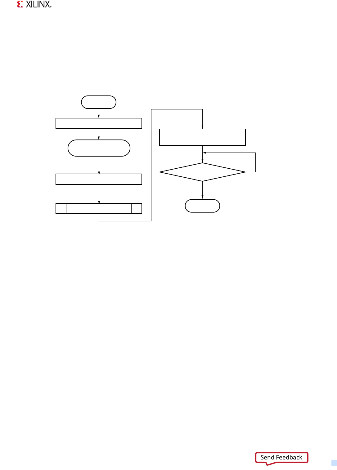
Zynq-7000 AP SoC Technical Reference Manual www.xilinx.com 380
UG585 (v1.12.1) December 6, 2017
Chapter 13: SD/SDIO Controller
Synchronous Abort
The following sequence performs a synchronous abort.
1. Set the Stop At Block Gap Request bit in the Block Gap Control register to 1 to stop SD
transactions.
2. Wait for a transfer complete interrupt.
3. Set the Transfer Complete bit to 1 in the Normal Interrupt Status register to clear this bit.
4. Issue an abort command.
5. Set both the Software Reset for DAT Line and Software Reset for CMD Line bits to 1 in the
Software Reset register to do a software reset.
6. Check the Software Reset for DAT Line and Software Reset for CMD Line in the Software Reset
register. If both Software Reset for DAT Line and Software Reset for CMD Line are 0, go to “END”.
If either the Software Reset for DAT Line or the Software Reset for CMD Line is 1, repeat Step (6).
X-Ref Target - Figure 13-6
Figure 13-6: SDIO Controller Synchronous Abort Sequence
(1)
(2)
(5)
(6)
(3)
Set Stop at Block Gap Request
Set Software Reset For
DAT Line (DR) and CMD Line (CR)
Clr Transfer Complete Status
Transfer Complete
Int Occur
DR=1 or CR=1
DR=0 and CR=0
Wait For
Transfer Complete Int
(4)
Issue Abort Command
Start
End
Check
DR and CR
UG585_c13_06_031812
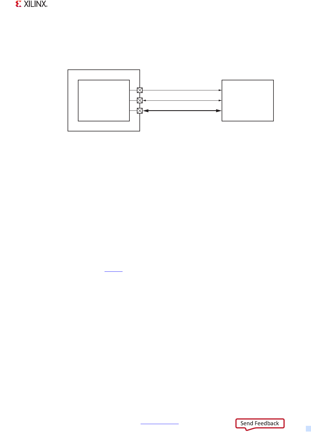
Zynq-7000 AP SoC Technical Reference Manual www.xilinx.com 381
UG585 (v1.12.1) December 6, 2017
Chapter 13: SD/SDIO Controller
13.3.6 External Interface Usage Example
Zynq-7000 devices provide two secure digital (SD) ports that support SD and SDIO devices (see
Figure 13-7).
13.3.7 Supported Configurations
The SD/SDIO controller supports operation in several configurations:
• Secure digital (SD) memory
• Secure digital input/output (SDIO)
Some SD card slots provide two additional pins: card detect (CDn) to signal the insertion or presence
of a card, and write protect (WP) to report the position of the write protect switch on the memory
card. These signals must be externally pulled up. The card normally pulls CDn Low when inserted. If
the WP switch is set to protect the card from writes, then the WP signal remains High. The wiring
schematic is shown in Figure 13-8. If the card does not function in this manner, then an alternate
method is required to signal the insertion or presence of the card. Additional board design
information is located in UG933, Zynq-7000 All Programmable SoC PCB Design Guide.
Production versions of the BootROM do not look for CDn to be pulled Low; it assumes the card is
installed. Xilinx drivers require that these signals are routed through the MIO and function properly
to provide card state to the software. The routing is done using a slcr.SD{1,0}_WP_CD_SEL register.
X-Ref Target - Figure 13-7
Figure 13-7: SDIO Controller Device Wiring Diagram
Zynq Device
SDIO Device
CLK
CMD
DAT[3:0]
SDx_CLK
SDx_CMD
SDx_DAT[3:0]
SD/SDIO
Controller
UG595_c13_07_031812
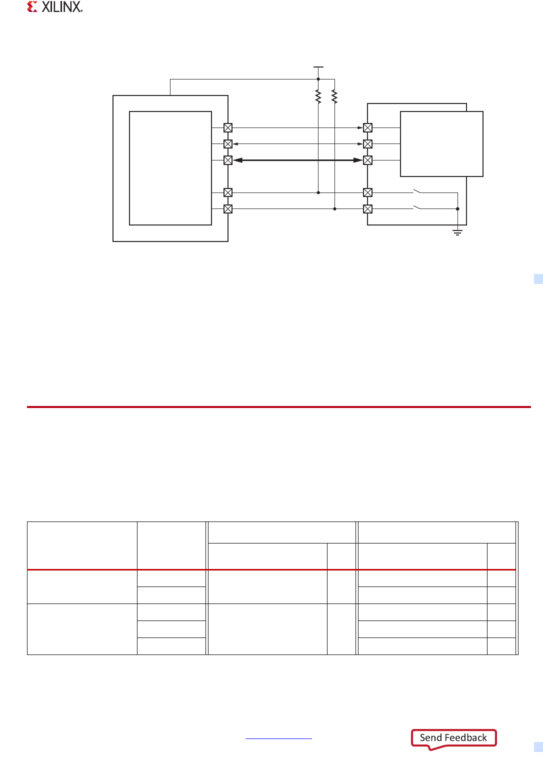
Zynq-7000 AP SoC Technical Reference Manual www.xilinx.com 382
UG585 (v1.12.1) December 6, 2017
Chapter 13: SD/SDIO Controller
13.3.8 Bus Voltage Translation
The SDIO power pin SDx_POW can be used to control power to the SDIO slots. Depending on the I/O
voltage for the selected MIO bank and the SD/SDIO devices connected to the bus, it might be
necessary to use a level translator.
13.4 SDIO Controller Media Interface Signals
The SDIO media interface signals are independently routed to the MIO pins or to a set of EMIO
interface signals, see Table 1 3-1 . The MIO pins and any restrictions based on device version are
shown in the MIO table in section 2.5.4 MIO-at-a-Glance Table.
X-Ref Target - Figure 13-8
Figure 13-8: SDIO Controller SD Card Detect and Write Protect Diagram
SD Card
Slot
SDx_CLK
SDx_DAT[3:0]
SDx_CMD
Zynq Device
SD/SDIO
Controller
SD
Memory
Card
CLK
DAT[3:0]
CMD
SDx_CDn
SDx_WP
VIO
UG595_c13_08_100617
Table 13-1: SDIO Interface Signals
SDIO Interface
Default
Controller
Input
Value
MIO Pin EMIO Signal(1)
Number I/O Name I/O
SDIO 0 Clock
0
16, 28, 40 IO EMIOSDIO0CLKFB I
~ EMIOSDIO0CLK O
SDIO 0 Command
0
17, 29, 41 IO
EMIOSDIO0CMDI I
~ EMIOSDIO0CMDO O
~ EMIOSDIO0CMDTN O

Zynq-7000 AP SoC Technical Reference Manual www.xilinx.com 383
UG585 (v1.12.1) December 6, 2017
Chapter 13: SD/SDIO Controller
SDIO 0 Data 0
0
18, 30, 42 IO
EMIOSDIO0DATAI0 I
~ EMIOSDIO0DATAO0 O
~ EMIOSDIO0DATATN0 O
SDIO 0 Data 1
0
19, 31, 43 IO
EMIOSDIO0DATAI1 I
~ EMIOSDIO0DATAO1 O
~ EMIOSDIO0DATATN1 O
SDIO 0 Data 2
0
20, 32, 44 IO
EMIOSDIO0DATAI2 I
~ EMIOSDIO0DATAO2 O
~ EMIOSDIO0DATATN2 O
SDIO 0 Data 3
0
21, 33, 45 IO
EMIOSDIO0DATAI3 I
~ EMIOSDIO0DATAO3 O
~ EMIOSDIO0DATATN3 O
SDIO 0 Card Detect Any pin except 7 and 8 I EMIOSDIO0CDN I
SDIO 0 Write Protect Any pin except 7 and 8 I EMIOSDIO0WP I
SDIO 0 Power Control ~ Any even pin O EMIOSDIO0BUSPOW O
SDIO 0 LED Control ~ ~ ~ EMIOSDIO0LED O
SDIO 0 Bus Voltage ~ ~ ~ EMIOSDIO0BUSVOLT[2:0] O
SDIO 1 Clock
0
12, 24, 36, 48 IO EMIOSDIO1CLKFB I
~ EMIOSDIO1CLK O
SDIO 1 Command
0
11, 23, 35, 47 IO
EMIOSDIO1CMDI I
~ EMIOSDIO1CMDO O
~ EMIOSDIO1CMDTN O
SDIO 1 Data 0
0
10, 22, 34, 46 IO
EMIOSDIO1DATAI0 I
~ EMIOSDIO1DATAO0 O
~ EMIOSDIO1DATATN0 O
SDIO 1 Data 1
0
13, 25, 37, 49 IO
EMIOSDIO1DATAI1 I
~ EMIOSDIO1DATAO1 O
~ EMIOSDIO1DATATN1 O
SDIO 1 Data 2
0
14. 26, 38, 50 IO
EMIOSDIO1DATAI2 I
~ EMIOSDIO1DATAO2 O
~ EMIOSDIO1DATATN2 O
SDIO 1 Data 3
0
15, 27, 39, 51 IO
EMIOSDIO1DATAI3 I
~ EMIOSDIO1DATAO3 O
~ EMIOSDIO1DATATN3 O
Table 13-1: SDIO Interface Signals (Cont’d)
SDIO Interface
Default
Controller
Input
Value
MIO Pin EMIO Signal(1)
Number I/O Name I/O

Zynq-7000 AP SoC Technical Reference Manual www.xilinx.com 384
UG585 (v1.12.1) December 6, 2017
Chapter 13: SD/SDIO Controller
SDIO 0 Data 0
0
18, 30, 42 IO
EMIOSDIO0DATAI0 I
~ EMIOSDIO0DATAO0 O
~ EMIOSDIO0DATATN0 O
SDIO 0 Data 1
0
19, 31, 43 IO
EMIOSDIO0DATAI1 I
~ EMIOSDIO0DATAO1 O
~ EMIOSDIO0DATATN1 O
SDIO 0 Data 2
0
20, 32, 44 IO
EMIOSDIO0DATAI2 I
~ EMIOSDIO0DATAO2 O
~ EMIOSDIO0DATATN2 O
SDIO 0 Data 3
0
21, 33, 45 IO
EMIOSDIO0DATAI3 I
~ EMIOSDIO0DATAO3 O
~ EMIOSDIO0DATATN3 O
SDIO 0 Card Detect Any pin except 7 and 8 I EMIOSDIO0CDN I
SDIO 0 Write Protect Any pin except 7 and 8 I EMIOSDIO0WP I
SDIO 0 Power Control ~ Any even pin O EMIOSDIO0BUSPOW O
SDIO 0 LED Control ~ ~ ~ EMIOSDIO0LED O
SDIO 0 Bus Voltage ~ ~ ~ EMIOSDIO0BUSVOLT[2:0] O
SDIO 1 Clock
0
12, 24, 36, 48 IO EMIOSDIO1CLKFB I
~ EMIOSDIO1CLK O
SDIO 1 Command
0
11, 23, 35, 47 IO
EMIOSDIO1CMDI I
~ EMIOSDIO1CMDO O
~ EMIOSDIO1CMDTN O
SDIO 1 Data 0
0
10, 22, 34, 46 IO
EMIOSDIO1DATAI0 I
~ EMIOSDIO1DATAO0 O
~ EMIOSDIO1DATATN0 O
SDIO 1 Data 1
0
13, 25, 37, 49 IO
EMIOSDIO1DATAI1 I
~ EMIOSDIO1DATAO1 O
~ EMIOSDIO1DATATN1 O
SDIO 1 Data 2
0
14. 26, 38, 50 IO
EMIOSDIO1DATAI2 I
~ EMIOSDIO1DATAO2 O
~ EMIOSDIO1DATATN2 O
SDIO 1 Data 3
0
15, 27, 39, 51 IO
EMIOSDIO1DATAI3 I
~ EMIOSDIO1DATAO3 O
~ EMIOSDIO1DATATN3 O
Table 13-1: SDIO Interface Signals (Cont’d)
SDIO Interface
Default
Controller
Input
Value
MIO Pin EMIO Signal(1)
Number I/O Name I/O

Zynq-7000 AP SoC Technical Reference Manual www.xilinx.com 385
UG585 (v1.12.1) December 6, 2017
Chapter 13: SD/SDIO Controller
13.4.1 SDIO EMIO Considerations
The SDIO interfaces are enabled through the MIO as well as the EMIO interface. They are mutually
exclusive in that once the interface is routed through the MIO it no longer is available via the EMIO.
If the designer chooses to use the EMIO interface for SDIO due to other MIO priorities, the designer
should know that the maximum operating frequency for SDIO via EMIO is limited. The PL
connectivity should connect the EMIO signals directly to the SelectIO pins. Additionally, it might be
necessary to restrict the SDIO to operate in full or low speed modes, refer to the data sheet for
frequency and timing values.
SDIO 1 Card Detect Any pin except 7 and 8 I EMIOSDIO1CDN I
SDIO 1 Write Protect Any pin except 7 and 8 I EMIOSDIO1WP I
SDIO 1 Power Control ~ Any odd pin O EMIOSDIO1BUSPOW O
SDIO 1 LED Control ~ ~ ~ EMIOSDIO1LED O
SDIO 1 Bus Voltage ~ ~ ~ EMIOSDIO1BUSVOLT[2:0] O
Notes:
1. In production silicon, the EMIO three-state control signals are inverted by the Processing_System7 wrapper.
Table 13-1: SDIO Interface Signals (Cont’d)
SDIO Interface
Default
Controller
Input
Value
MIO Pin EMIO Signal(1)
Number I/O Name I/O

Zynq-7000 AP SoC Technical Reference Manual www.xilinx.com 386
UG585 (v1.12.1) December 6, 2017
Chapter 14
General Purpose I/O (GPIO)
14.1 Introduction
The general purpose I/O (GPIO) peripheral provides software with observation and control of up to
54 device pins via the MIO module. It also provides access to 64 inputs from the Programmable Logic
(PL) and 128 outputs to the PL through the EMIO interface. The GPIO is organized into four banks of
registers that group related interface signals.
Each GPIO is independently and dynamically programmed as input, output, or interrupt sensing.
Software can read all GPIO values within a bank using a single load instruction, or write data to one
or more GPIOs (within a range of GPIOs) using a single store instruction. The GPIO control and status
registers are memory mapped at base address 0xE000_A000.
14.1.1 Features
Key features of the GPIO peripheral are summarized as follows:
• 54 GPIO signals for device pins (routed through the MIO multiplexer)
°Outputs are 3-state capable
• 192 GPIO signals between the PS and PL via the EMIO interface
°64 Inputs, 128 outputs (64 true outputs and 64 output enables)
• The function of each GPIO can be dynamically programmed on an individual or group basis
• Enable, bit or bank data write, output enable and direction controls
• Programmable interrupts on individual GPIO basis
°Status read of raw and masked interrupt
°Selectable sensitivity: Level-sensitive (High or Low) or edge-sensitive (positive, negative, or
both)
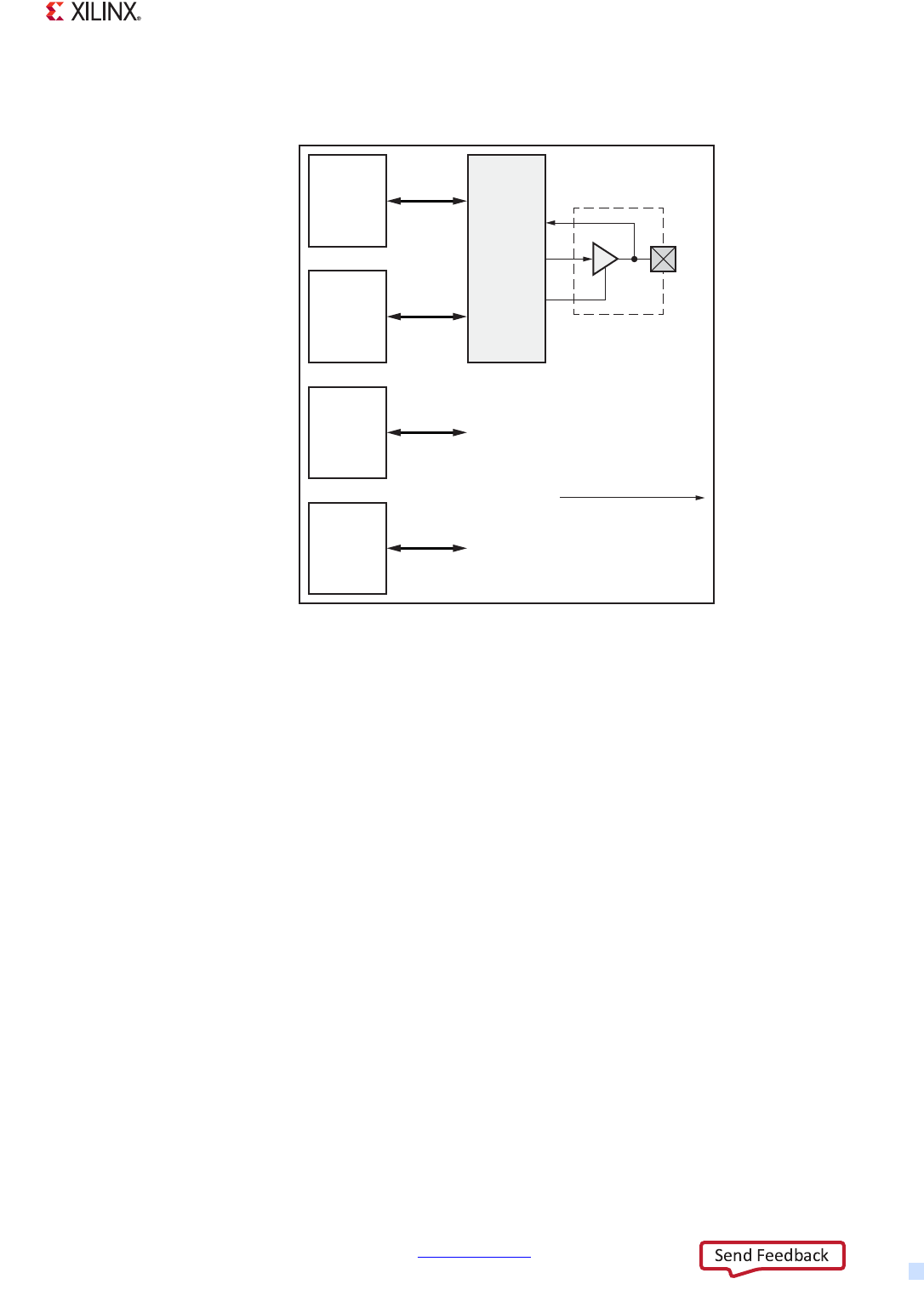
Zynq-7000 AP SoC Technical Reference Manual www.xilinx.com 387
UG585 (v1.12.1) December 6, 2017
Chapter 14: General Purpose I/O (GPIO)
14.1.2 Block Diagram
As shown in Figure 14-1, the GPIO module is divided into four banks:
• Bank0: 32-bit bank controlling MIO pins[31:0]
• Bank1: 22-bit bank controlling MIO pins[53:32]
Note: Bank1 is limited to 22 bits because the MIO has a total of 54 pins.
• Bank2: 32-bit bank controlling EMIO signals[31:0]
• Bank3: 32-bit bank controlling EMIO signals[63:32]
The GPIO is controlled by software through a series of memory-mapped registers. The control for
each bank is the same, although there are minor differences between the MIO and EMIO banks due
to their differing functionality.
X-Ref Target - Figure 14-1
Figure 14-1: GPIO Block Diagram
UG585_c14_01_022212
32b
GPIO
Bank
0
MIO
GPIO
Bank
1
22b
GPIO
Bank
2
EMIOGPIOI[31:0],
EMIOGPIOO[31:0],
EMIOGPIOTN[31:0]
32b
GPIO
Bank
3
EMIOGPIOI[63:32],
EMIOGPIOO[63:32],
EMIOGPIOTN[63:32]
32b
EMIO Interface to PL
x 54

Zynq-7000 AP SoC Technical Reference Manual www.xilinx.com 388
UG585 (v1.12.1) December 6, 2017
Chapter 14: General Purpose I/O (GPIO)
14.1.3 Notices
7z007s and 7z010 CLG225 Devices
The 7z007s single core and 7z010 dual core CLG225 devices reduce the available MIO pins to 32 as
shown in the MIO table in section 2.5.4 MIO-at-a-Glance Table. Thus, in these devices, the only GPIO
pins that are available for MIO are 15:0, 39:28, 48, 49, 52, and 53. The other MIO pins are unconnected and
should not be used. All EMIO signals are available.
MIO Considerations
Banks 0 and 1 of the GPIO peripheral module are routed to device pins through the MIO module.
Refer to section 2.5 PS-PL MIO-EMIO Signals and Interfaces for a complete description of MIO
operation. Primary control of the MIO is achieved through the slcr.MIO_PIN_xx registers. Please note
the following:
• The user must choose the proper Type of I/O using the IO_Type, PULLUP, DisableRcvr, and Speed
fields according to the user’s system.
• The user must select the GPIO module through the multiplexor control fields L0_SEL, L1_SEL,
L2_SEL, and L3_SEL. Note that each I/O pin can be individually selected. When an MIO pin is
used for an IOP device, it is not available as a GPIO.
• TRI_ENABLE should be set to 0. This enables the GPIO to control the 3-state mode of the I/O. If
TRI_ENABLE is set to 1 in the MIO, then the output driver will be 3-stated regardless of GPIO
settings.
14.2 Functional Description
14.2.1 GPIO Control of Device Pins
This section describes the operation of Bank0 and Bank1 (see Figure 14-2).
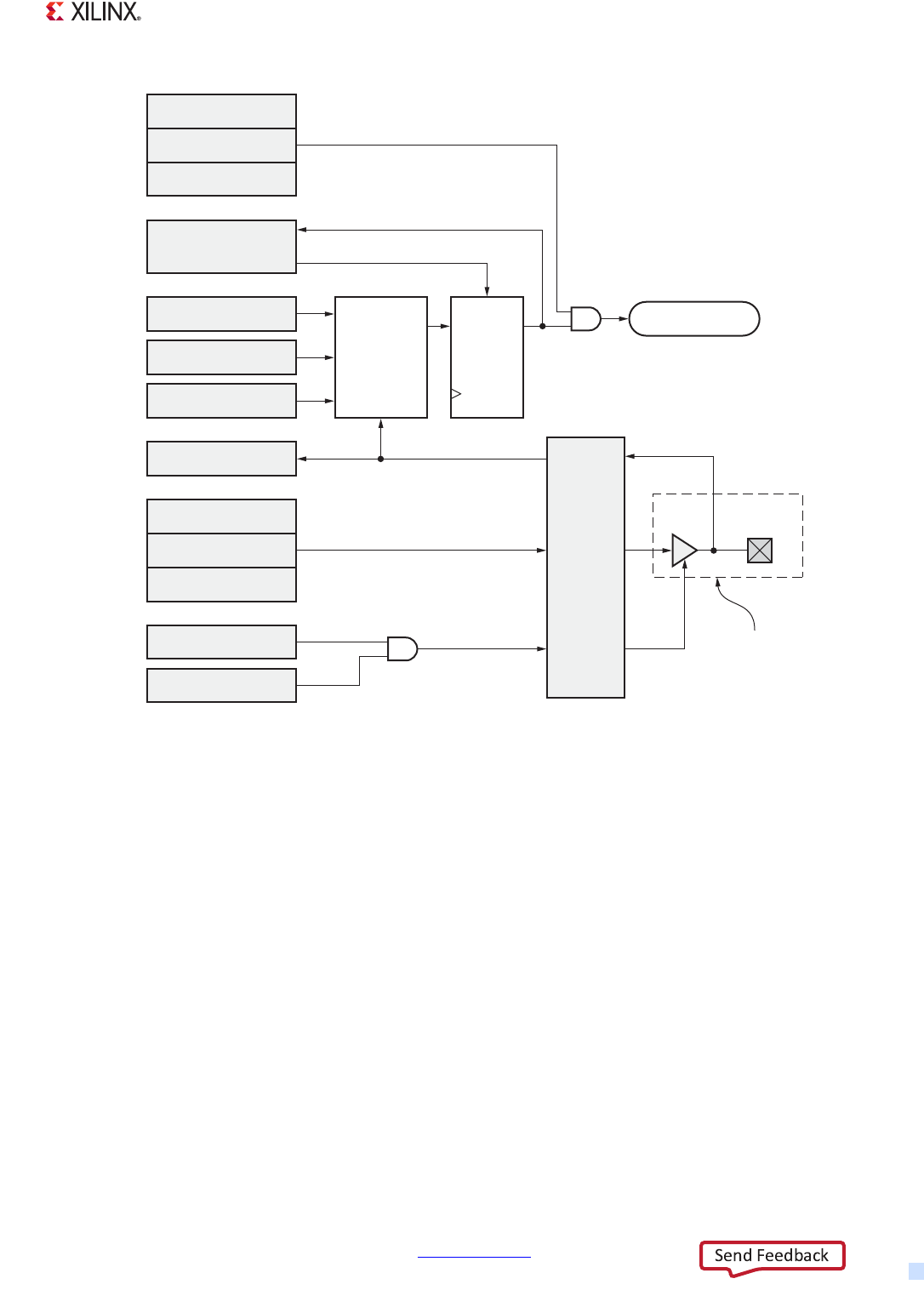
Zynq-7000 AP SoC Technical Reference Manual www.xilinx.com 389
UG585 (v1.12.1) December 6, 2017
Chapter 14: General Purpose I/O (GPIO)
Software configures the GPIO as either an output or input. The DATA_RO register always returns the
state of the GPIO pin regardless of whether the GPIO is set to input (OE signal false) or output (OE
signal true). To generate an output waveform, software repeatedly writes to one or more GPIOs
(usually using the MASK_DATA register).
Applications might need to switch more than one GPIO at the same time (less a small amount of
inherent skew time between two I/O buffers). In this case, all of the GPIOs that need to be switched
simultaneously must be from the same 16-bit half-bank (i.e., either the most-significant 16 bits or the
least-significant 16 bits) of GPIOs to enable the MASK_DATA register to write to them in one store
instruction.
GPIO bank control (for Bank0 and Bank1) is summarized as follows:
•DATA_RO: This register enables software to observe the value on the device pin. If the GPIO
signal is configured as an output, then this would normally reflect the value being driven on the
output. Writes to this register are ignored.
Note: If the MIO is not configured to enable this pin as a GPIO pin, then DATA_RO is
unpredictable because software cannot observe values on non-GPIO pins through the GPIO
registers.
X-Ref Target - Figure 14-2
Figure 14-2: GPIO Channel
UG585_c14_02_022712
DIRM
INT_MASK
INT_DIS
INT_EN
INT_TYPE IRQ #52 to GIC
INT_POLARITY
Interrupt
Detection
Logic
INT
State
DQ
Clr
INT_ANY
INT_STAT
Read
Write-1-to-clear
Input
Output
Output Enable
DATA
MASK_DATA_LSW
MASK_DATA_MSW
OEN
DATA_RO
MIO
(Banks
0 & 1)
or
EMIO
(Banks
2 & 3)
GPIO
Device Pad
MIO Device I/O
Buffers and Pins
(Banks 0 & 1)

Zynq-7000 AP SoC Technical Reference Manual www.xilinx.com 390
UG585 (v1.12.1) December 6, 2017
Chapter 14: General Purpose I/O (GPIO)
•DATA: This register controls the value to be output when the GPIO signal is configured as an
output. All 32 bits of this register are written at one time. Reading from this register returns the
previous value written to either DATA or MASK_DATA_{LSW,MSW}; it does not return the current
value on the device pin.
•MASK_DATA_LSW: This register enables more selective changes to the desired output value.
Any combination of up to 16 bits can be written. Those bits that are not written are unchanged
and hold their previous value. Reading from this register returns the previous value written to
either DATA or MASK_DATA_{LSW,MSW}; it does not return the current value on the device pin.
This register avoids the need for a read-modify-write sequence for unchanged bits.
•MASK_DATA_MSW: This register is the same as MASK_DATA_LSW, except it controls the
upper16 bits of the bank.
•DIRM: Direction Mode. This controls whether the I/O pin is acting as an input or an output.
Since the input logic is always enabled, this effectively enables/disables the output driver. When
DIRM[x]==0, the output driver is disabled.
•OEN: Output Enable. When the I/O is configured as an output, this controls whether the output
is enabled or not. When the output is disabled, the pin is 3-stated. When OEN[x]==0, the output
driver is disabled.
Note: If MIO TRI_ENABLE is set to 1, enabling 3-state and disabling the driver, then OEN is
ignored and the output is 3-stated.
14.2.2 EMIO Signals
This section describes the operation of Bank2 and Bank3 (see Figure 14-2).
The register interface for the EMIO banks is the same as for the MIO banks described in the previous
section. However, the EMIO interface is simply wires between the PS and the PL, so there are a few
differences:
• The inputs are wires from the PL and are unrelated to the output values or the OEN register.
They can be read from the DATA_RO register when DIRM is set to 0, making it an input.
• The output wires are not 3-state capable, so they are unaffected by OEN. The value to be output
is programmed using the DATA, MASK_DATA_LSW, and MASK_DATA_MSW registers. DIRM must
be set to 1, making it an output.
• The output enable wires are simply outputs from the PS. These are controlled by the DIRM/OEN
registers as follows: EMIOGPIOTN[x] = DIRM[x] & OEN[x]
The EMIO I/Os are not connected to the MIO I/Os in any way. The EMIO inputs cannot be connected
to the MIO outputs and the MIO inputs cannot be connected to the EMIO outputs. Each bank is
independent and can only be used as software observable/controllable signals.
14.2.3 Bank0, Bits[8:7] are Outputs
GPIO bits[8:7] of Bank0 correspond to package pins that are used to control the voltage mode of the
I/O buffers themselves during reset. These pins are called the VMODE pin straps for the MIO banks
(see section Boot Mode Pin Settings, page 165). They must be driven by the external system
according to the proper voltage mode. To prevent them from being driven by other system logic,
they cannot be used as general purpose inputs.

Zynq-7000 AP SoC Technical Reference Manual www.xilinx.com 391
UG585 (v1.12.1) December 6, 2017
Chapter 14: General Purpose I/O (GPIO)
These bits can be used as general purpose outputs since the output driver is disabled at reset. The
system can start using these as outputs after the voltage mode has been read during system boot.
14.2.4 Interrupt Function
The interrupt detection logic monitors the GPIO input signal. The interrupt trigger can be a positive
edge, negative edge, either edge, Low-level or High-level. The trigger sensitivity is programmed
using the INT_TYPE, INT_POLARITY and INT_ANY registers.
If an interrupt is detected, the GPIO's INT_STAT state is set true by the interrupt detection logic. If the
INT_STAT state is enabled (unmasked), then the interrupt propagates through to a large OR function.
This function combines all interrupts for all GPIOs in all four banks to one output (IRQ ID#52) to the
interrupt controller. If the interrupt is disabled (masked), then the INT_STAT state is maintained until
cleared, but it does not propagate to the interrupt controller unless the INT_EN is later written to
disable the mask. As all GPIOs share the same interrupt, software must consider both INT_MASK and
INT_STAT to determine which GPIO is causing an interrupt.
The interrupt mask state is controlled by writing a 1 to the INT_EN and INT_DIS registers. Writing a
1 to the INT_EN register disables the mask allowing an active interrupt to propagate to the interrupt
controller. Writing a 1 to the INT_DIS register enables the mask. The state of the interrupt mask can
be read using the INT_MASK register.
If the GPIO interrupt is edge sensitive, then the INT state is latched by the detection logic. The INT
latch is cleared by writing a 1 to the INT_STAT register. For level-sensitive interrupts, the source of the
interrupt input to the GPIO must be cleared in order to clear the interrupt signal. Alternatively,
software can mask that input using the INT_DIS register.
The state of the interrupt signal going to the interrupt controller can be inferred by reading the
INT_STAT and INT_MASK registers. This interrupt signal is asserted if INT_STAT=1 and INT_MASK=0.
GPIO bank control is summarized as follows:
•INT_MASK: This register is read-only and shows which bits are currently masked and which are
un-masked/enabled.
•INT_EN: Writing a 1 to any bit of this register enables/unmasks that signal for interrupts.
Reading from this register returns an unpredictable value.
•INT_DIS: Writing a 1 to any bit of this register masks that signal for interrupts. Reading from
this register returns an unpredictable value.
•INT_STAT: This registers shows if an interrupt event has occurred or not. Writing a 1 to a bit in
this register clears the interrupt status for that bit. Writing a 0 to a bit in this register is ignored.
•INT_TYPE: This register controls whether the interrupt is edge sensitive or level sensitive.
•INT_POLARITY: This register controls whether the interrupt is active-Low or active High (or
falling-edge sensitive or rising-edge sensitive).
•INT_ON_ANY: If INT_TYPE is set to edge sensitive, then this register enables an interrupt event
on both rising and falling edges. This register is ignored if INT_TYPE is set to level sensitive.

Zynq-7000 AP SoC Technical Reference Manual www.xilinx.com 392
UG585 (v1.12.1) December 6, 2017
Chapter 14: General Purpose I/O (GPIO)
Limitation
The GPIO controller registers require single 32-bit read/write accesses, do not use byte, halfword, or
double word references.
14.3 Programming Guide
The GPIO Controller has four banks, two each for MIO and EMIO. Each GPIO pin can be programmed
individually. Multiple pins can be programmed with a single write as described in section
14.2.1 GPIO Control of Device Pins.
14.3.1 Start-up Sequence
Main Example: Start-up Sequence
1. Resets: The reset options are described in section 14.4.2 Resets.
2. Clocks: The clocks are described in section 14.4.1 Clocks.
3. GPIO Pin Configurations: Configure pin as input/output is described in section 14.3.2 GPIO Pin
Configurations.
4. Write Data to GPIO Output pin: Refer to example in section 14.3.3 Writing Data to GPIO
Output Pins.
5. Read Data from GPIO Input pin: Refer to example in section 14.3.4 Reading Data from GPIO
Input Pins .
6. Set GPIO pin as wake-up event: Refer to example in section GPIO as Wake-up Event.
14.3.2 GPIO Pin Configurations
Each individual GPIO pin can be configured as input/output. However, bank0 [8:7] pins must be
configured as outputs. Refer to section 14.2.3 Bank0, Bits[8:7] are Outputs for further details.
Example: Configure MIO pin 10 as an output
1. Set the direction as output: Write 0x0000_0400 to the gpio.DIRM_0 register.
Table 14-1: GPIO Interrupt Trigger Settings
Type gpio.INT_TYPE_0 gpio.INT_POLARITY_0 gpio.INT_ANY_0
Rising edge-sensitive 110
Falling edge-sensitive 100
Both rising- and falling edge-sensitive 1X1
Level sensitive, asserted High 01X
Level sensitive, asserted Low 00X

Zynq-7000 AP SoC Technical Reference Manual www.xilinx.com 393
UG585 (v1.12.1) December 6, 2017
Chapter 14: General Purpose I/O (GPIO)
2. Set the output enable: Write 0x0000_0400 to the gpio.OEN_0 register.
Note: The output enable has significance only when the GPIO pin is configured as an output.
Example: Configure MIO pin 10 as an input
1. Set the direction as input: Write 0x0 to the gpio.DIRM_0 register. This sets gpio.DIRM_0[10] = 0.
14.3.3 Writing Data to GPIO Output Pins
For GPIO pins configured as outputs, there are two options to program the desired value.
Option 1: Read, modify, and update the GPIO pin using the gpio.DATA_0 register.
Example: Set GPIO output pin 10 using the DATA_0 register.
1. Read the gpio.DATA_0 register: Read gpio.DATA_0 register to the reg_val variable.
2. Modify the value: Set reg_val [10] =1.
3. Write updated value to output pin: Write reg_val to the gpio.DATA_0 register.
Option 2: Use the MASK_DATA_x_MSW/LSW registers to update one or more GPIO pins.
Example: Set output pins 20, 25, and 30 to 1 using the MASK_DATA_0_MSW register.
1. Generate the mask value for pins 20, 25, and 30: To drive pins 20, 25 and 30, 0xBDEF is the
mask value for gpio.MASK_DATA_0_MSW [MASK_0_MSW].
2. Generate the data value for pins 20, 25, 30: To drive 1 on pins 20, 25, and 30, 0x4210 is the
data value for gpio.MASK_DATA_0_MSW [DATA_0_MSW].
3. Write the mask and data to the MASK_DATA_x_MSW register: Write 0xBDEF_4210 to the
gpio.MASK_DATA_0_MSW register.
14.3.4 Reading Data from GPIO Input Pins
For GPIO pins configured as inputs, there are two options to monitor the input.
Option 1: Use the gpio.DATA_RO_x register of each bank.
Example: Read the state of all GPIO input pins in bank 0 using the DATA_RO_0 register.
1. Read Input Bank 0: Read the gpio.DATA_0 register.
Option 2: Use interrupt logic on input pins (refer to section 14.2.4 Interrupt Function).
Example: Configure MIO pin 12 to be triggered as rising edge.
1. Set the trigger as a rising edge: Write 1 to gpio.INT_TYPE_0 [12]. Write 1 to
gpio.INT_POLARITY_0 [12]. Write 0 to gpio.INT_ANY_0 [12].
2. Enable interrupt: Write 1 to gpio.INT_EN_0 [12].
3. Status of Input pin: gpio.INT_STAT_0 [12] =1 implies that an interrupt event occurred.

Zynq-7000 AP SoC Technical Reference Manual www.xilinx.com 394
UG585 (v1.12.1) December 6, 2017
Chapter 14: General Purpose I/O (GPIO)
4. Disable interrupt: Write 1 to gpio.INT_DIS_0 [12].
14.3.5 GPIO as Wake-up Event
The GPIO can be configured as a wake-up device.
IMPORTANT: The GIC must be set up correctly.
1. Enable the GPIO interrupt in the GIC.
2. Enable the GPIO interrupt for the wanted pin(s) using the gpio.INT_EN_{0..3} register. Set 1 to
gpio.INT_EN_0[10] to enable the GPIO10 interrupt.
3. Do not turn off any GPIO related clocks.
14.3.6 Register Overview
An overview of the GPIO registers is shown in Ta ble 1 4-2 (also refer to section 14.2.1 GPIO Control
of Device Pins). Details of registers are provided in Appendix B, Register Details.
14.4 System Functions
The controller clocks and resets are described in this section. All of the interrupts generated in the
GPIO controller are routed to IRQ 52. The GPIO I/O signals are routed to either the MIO or EMIO.
Table 14-2: GPIO Register Overview
Function Register Name Overview Type
Data Reads and Data Writes
gpio.MASK_DATA_{3:0}_{MSW,LSW} Bit masked data output writes. Mixed
gpio.DATA_{3:0} 32-bit data output write R/W
gpio.DATA_{3:0}_RO 32-bit data read of inputs RO
I/O Buffer Control gpio.DIRM_{3:0} Direction R/W
gpio.OEN_{3:0} Output Enable R/W
Interrupt Controls
gpio.INT_MASK_{3:0} Interrupt Mask RO
gpio.INT_EN_{3:0} Interrupt Enable WO
gpio.INT_DIS_{3:0} Interrupt Disable WO
gpio.INT_STAT_{3:0} Interrupt Status WTC
gpio.INT_TYPE_{3:0} Interrupt Type RW
gpio.INT_POLARITY_{3:0} Interrupt Polarity RW
gpio.INT_ANY_{3:0} Interrupt Any RW

Zynq-7000 AP SoC Technical Reference Manual www.xilinx.com 395
UG585 (v1.12.1) December 6, 2017
Chapter 14: General Purpose I/O (GPIO)
14.4.1 Clocks
The controller is clocked by the CPU_1x clock from the APB interface. All outputs and input sampling
is done using the CPU_1x clock.
For power management, clock gating can be employed on the GPIO controller clock using
slcr.APER_CLK_CTRL[GPIO_CPU_1XCLKACT].
14.4.2 Resets
The controller is reset by the slcr.GPIO_RST_CTRL [GPIO_CPU1X_RST] bit. Refer to Chapter 26, Reset
System, for more information. This reset only affects the bus interface, not the controller logic itself.
14.4.3 Interrupts
The controller interrupts are explained in section 14.2.4 Interrupt Function. The controller asserts IRQ
# 52 to the GIC. A programming example is described in section 14.3.4 Reading Data from GPIO Input
Pins .
14.5 I/O Interface
14.5.1 MIO Programming
Bank 0 and Bank 1 pins are routed through the MIO. These pins can be configured as GPIO using the
slcr.MIO_PIN_XX register.
Example: Configure MIO pin 6 as a GPIO signal
1. Select MIO pin as GPIO: Set L0_SEL, L1_SEL, L2_SEL, L3_SEL =0.
2. Set TRI_ENABLE = 0.
3. LVCMOS18 (refer to the register definition for other voltage options).
4. Slow CMOS edge.
5. Enable internal pull-up resistor.
6. Disable HSTL receiver.
Note: If TRI_ENABLE=1, then the output is 3-stated regardless of any GPIO settings. If
TRI_ENABLE=0, then 3-state is controlled by the gpio.OEN_x register.

Zynq-7000 AP SoC Technical Reference Manual www.xilinx.com 396
UG585 (v1.12.1) December 6, 2017
Chapter 15
USB Host, Device, and OTG Controller
15.1 Introduction
The USB controller is capable of fulfilling a wide range of applications for USB 2.0 implementations
as a host, a device, or On-the-Go. Two identical controllers are in the Zynq-7000 device. Each
controller is configured and controlled independently. The USB controller I/O uses the ULPI protocol
to connect external ULPI PHY via the MIO pins. The ULPI interface provides an 8-bit parallel SDR data
path from the controller’s internal UTMI-like bus to the PHY. The ULPI interface minimizes device pin
count and is controlled by a 60 MHz clock output from the PHY.
USB is a cable bus that supports data exchange between a host device and a wide range of computer
peripherals. The attached peripherals share USB bandwidth through a host-scheduled, token-based
protocol. The bus allows peripherals to be attached, configured, used, and detached while the host
and other peripherals remain operational.
The USB controller in USB 2.0 Host compatible with the EHCI specification with some enhancements
and minor deviations. The OTG operating mode software switches the controller between Idle and
either Device or Host mode as needed by the application using the Host Negotiation Protocol (HNP)
and Session Request Protocol (SRP).
The controller is designed to make efficient use of the system resources in an SoC design. The DMA
engine is responsible for moving USB transaction data between the Rx/Tx FIFOs and system memory.
The FIFOs are used to buffer the high-speed USB data rates with periodic delays associated with the
PS Interconnect data transfers.
The EHCI-compatible host controller is a schedule driven environment for data transfers of periodic
(interrupt and isochronous) and asynchronous (control and bulk) types. Device mode includes a
simple pair of descriptors to respond to USB data transfers in a timely manner between the software
and USB.
The transfer descriptors of the host schedules and device endpoints control the DMA engine to move
data between the 32-bit AHB master system bus interface and the Rx and Tx data FIFOs that respond
in real-time to the USB.
The controller makes strategic use of software for tasks that do not require time-critical responses.
This approach reduces the amount of hardware logic. At the same time, the controller includes
hardware assistance logic to enable the controller to respond quickly to USB events and simplify the
software.

Zynq-7000 AP SoC Technical Reference Manual www.xilinx.com 397
UG585 (v1.12.1) December 6, 2017
Chapter 15: USB Host, Device, and OTG Controller
15.1.1 Features
The USB controller has the following key features:
• USB 2.0 High Speed Host controller (480 Mb/s).
°Intel® EHCI software programming model.
• USB 2.0 HS and FS Device controller.
°Up to 12 Endpoint: Control Endpoint plus 11 configurable Endpoints
•USB 1.1 legacy FS/LS.
°Embedded Transaction Translator to support FS/LS in Host mode.
• On-the-Go, OTG 1.3 supplement.
°Host Negotiation Protocol (HNP).
°Session Request Protocol (SRP).
• All USB Transaction types
°Control, Bulk, Interrupt, Isochronous
•Local DMA Engine.
°AHB Bus Master.
°Transfers data between system memory and controller FIFOs.
°Processes transfer descriptors for Device Endpoints and Host Schedules.
•Protocol Engine
°Interprets USB packets
°Responds in real-time based on controller status
• Port/Transceiver Controller
°8-bit parallel data pass-thru bus
• ULPI Link Wrapper
°Translates Rx and Tx transfers between ULPI I/O interface and a UTMI-like interface.
°Bridge between the protocol engine and the ULPI interface.
°Rx and Tx commands
• ULPI I/O interface
°8-bit SDR data plus clock, direction, next, stop signals.
°12 ULPI PHY signals via MIO pins.
°Clocked by PHY in Clock-out mode.
°Viewport access to ULPI PHY registers
• Host port indicator, power select and power fail indicator signals.
°4 signals per controller via EMIO.
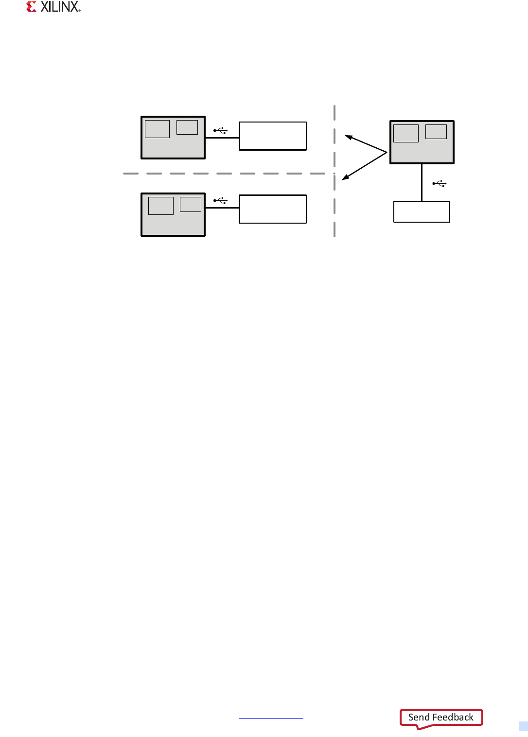
Zynq-7000 AP SoC Technical Reference Manual www.xilinx.com 398
UG585 (v1.12.1) December 6, 2017
Chapter 15: USB Host, Device, and OTG Controller
15.1.2 Operating Modes
The USB controller can operate in the modes shown in Figure 15-1.
Host mode. In host mode, the software includes driver-layer programming to discover and
enumerate the bus, manage PHY operations, and setup the periodic and asynchronous schedules of
transfer descriptors.
°EHCI software model except as described in section 15.11 EHCI Implementation.
Device mode. In device mode, the controller responds to host commands. Software can include
driver-layer programming to respond, as a single- or multi-function device, to the upstream
commands.
On-the-Go. The OTG software switches between Host and Device modes based on the Host
Negotiated Protocol (HNP) and the Session Request Protocol (SRP). Once the controller is in device
or host mode, it has all the functionality of the selected mode.
15.1.3 Hardware System Viewpoint
The USB controllers are integrated into the PS IOP to bridge between the PS interconnect and an
external ULPI PHY. The controller’s registers are memory mapped and the local DMA engine initiates
reads and writes to system memory. The ULPI signals flow through the MIO. There are sideband
signals (port indicators and power controls) that flow through the EMIO interface where they are
normally routed to PL SelectIO pins. The system-level viewpoint is shown in Figure 15-2.
X-Ref Target - Figure 15-1
Figure 15-1: USB Controller Operating Modes
UG585_c15_30_030712
Host Mode
Zynq PHY
Zynq PHY
Device or
Downstream Hub
HNP
SRP
HS: EHCI
FS/LS: TT in EHCI
Device Mode
Zynq
HS, FS
Host or
Upstream Hub
OTG
Zynq PHY
Another OTG
Device
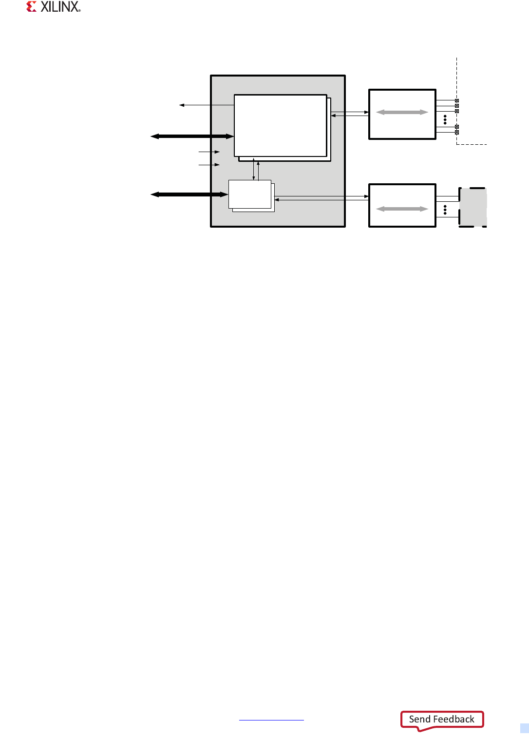
Zynq-7000 AP SoC Technical Reference Manual www.xilinx.com 399
UG585 (v1.12.1) December 6, 2017
Chapter 15: USB Host, Device, and OTG Controller
The two independent USB controllers have individual control and status registers. Each ULPI
interface is independently enabled through the MIO. There are separate port indicator and power
signals for each controller that are routed through the EMIO. The system functions are further
described in section 15.15 System Functions.
System Interfaces
Each controller is an AHB bus master to the PS interconnect for DMA transfers. The control and status
registers are accessed via the controller’s APB slave interface. Each controller has its own reset input
from the PS reset module and interrupt output to the interrupt controller, GIC. There is a ULPI clock
input for each controller and a CPU_1x clock for the AMBA AHB and APB interfaces. Details are in
section 15.15 System Functions.
ULPI I/O signals
The I/O signals are described in section 15.16 I/O Interfaces. The MIO pin muxing scheme is
described, in general terms, in section 2.5 PS-PL MIO-EMIO Signals and Interfaces.
I/O Wiring
The ULPI interface on the MIO pins is an 8-bit SDR data bus that is augmented with port indicators
and power control signals routed through the EMIO interface to the PL. The PS GPIO module,
Chapter 14, General Purpose I/O (GPIO), can provide a PHY reset signal to the PHY.
An I/O wiring diagram is shown in Figure 15-19 USB I/O Signal and PHY Wiring Diagram, page 481.
Here is a summary of the I/O signals:
•ULPI via MIO. The controller interfaces to the external ULPI PHY via 12 MIO pins: 8 data I/Os,
direction input, control input, clock input and a stop output.
•GPIO. A PS GPIO signal can be used to reset the external PHY.
X-Ref Target - Figure 15-2
Figure 15-2: USB Hardware System Block Diagram
PL
MIO
USB
Controllers
ULPI
Pins
Control
Registers
Interconnect
AHB
Master
port
USB {0, 1} CPU 1x clock
USB {0, 1} CPU 1x reset
Device
Boundary
IRQ ID# {53, 76}
Interconnect
APB
Slave
port
Data, flow control
Port Indicator,
Power Control
ULPI
EMIO
UG585_c15_31_030713
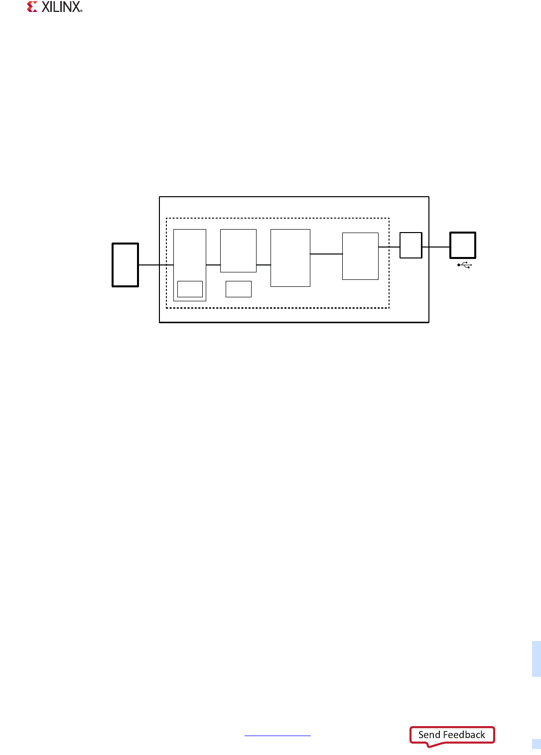
Zynq-7000 AP SoC Technical Reference Manual www.xilinx.com 400
UG585 (v1.12.1) December 6, 2017
Chapter 15: USB Host, Device, and OTG Controller
•Port Indicator and Power Pins via EMIO. The USB port indicator outputs, power select output,
and power fault input signals are routed through the EMIO to the SelectIO pins in the PL and
external board logic.
15.1.4 Controller Block Diagram
The controller interfaces to the PS system memory on one side and an external ULPI PHY device on
the USB side. A block diagram is shown in Figure 15-3. A detailed functional block is shown in section
15.1.9 Notices.
System Memory
The PS system memory is accessible to the DMA engine that holds transfer descriptors and data
buffers. The system memory can be DDR, OCM and memory that is mapped in the PL. The system
memory map is shown in section 4.1 Address Map. In this table, the USB controller is one of the
“Other Bus Masters,” refer to the table footnotes.
DMA, Protocol Engines, Context and FIFOs
The DMA engine works with the Protocol engine to process endpoints, periodic elements, queue
heads, and other transfer descriptors. Software writes these data structures into the system memory.
The DMA engine fetches these data structures and copies them into the controller’s local
dual-ported RAM (DPRAM). The controller reads and writes the data structures in the DPRAM as the
data structures are processed. The descriptors are written back to memory by the DMA engine when
a transfer is complete.
In addition to the context information of the data structures, the dual-port RAM is also used by the
controller to implement Rx and Tx data FIFOs. These FIFOs decouple the system processor memory
bus transfers from the real-time requirements of the USB.
The use of the FIFOs differs between host and device mode operation. In Host mode, a single data
channel is maintained in each direction through the dual-port RAM. In Device mode, Rx and Tx data
FIFO channels are maintained for each of the active device endpoints and these FIFO channels can
operate simultaneously and asynchronously.
X-Ref Target - Figure 15-3
Figure 15-3: USB Controller Block Diagram
UG585_c15_32_030713
DMA
Engine
System
Memory
ULPI
Link
Wrapper
USB Controller (Host and Device)
AHB
Similar to
UTMI+
Protocol
Engine Port
Controller
Interface
MIO
Zynq-7000 AP SoC
ULPI
PHY
Dual-port
RAM
Rx & Tx
FIFOs
Dual-port
RAM
Context

Zynq-7000 AP SoC Technical Reference Manual www.xilinx.com 401
UG585 (v1.12.1) December 6, 2017
Chapter 15: USB Host, Device, and OTG Controller
Port Transceiver Controller
The port transceiver controller provides suspend/resume and, for device mode, chirp control
functions. The port transceiver controller is fairly simple because the 8-bit data bus of the protocol
engine is passed-through to the 8-bit ULPI and the entire back-end of the USB controller works
synchronously to the 60 MHz USB clock from the PHY.
ULPI Link Wrapper
The protocol engine includes an internal bus that is similar to UTMI+. The ULPI wrapper provides an
bridge between this bus similar to UTMI+ and the ULPI interface. This is transparent to the user. The
ULPI Link wrapper passes-through packet data and interprets Rx commands as well as send Tx
commands.
ULPI Rx/Tx Commands
The ULPI Rx commands are initiated by the PHY to set status bits to give software visibility to PHY
events. The commands set controller status bits. The Tx commands are initiated by register writes by
software to control PHY functions. These commands are defined by the ULPI specification.
ULPI PHY Viewport
The ULPI viewport provides a mechanism for software to read and write PHY registers with explicit
control of the address and data using the usb.VIEWPORT register. An interrupt is generated when a
transaction is complete, including when the requested read data is available.
Programmable Timers
There are two independent general-purpose timers that can be used to generate a timeout or to
measure time related activities. The programmable timers should not be confused with the
controller’s interval timers which are used by the controller to generate frame and microframe
intervals and to generate strobes for the host controller scheduler. The programmable timers are
described in section 15.2.6 General Purpose Timers.
Software Programming Interface
In addition to maintaining data and buffer structures in system memory, the software reads and
writes the control and status registers. The CPU environment that executes the software is described
in Chapter 15, USB Host, Device, and OTG Controller. The controller can generate interrupts cause by
the DMA and Protocol engine activities, the PHY, and other controller functions. The interrupts are
summarized in Table 15-2 USB Interrupt and Status Register Bits.
The system will include either a Host Controller Driver (HCD) or a Device Controller Driver (DCD).
There may be additional of software to support the OTG functions.

Zynq-7000 AP SoC Technical Reference Manual www.xilinx.com 402
UG585 (v1.12.1) December 6, 2017
Chapter 15: USB Host, Device, and OTG Controller
Control and Status Registers
The control and status registers include constants, configuration and operational/status for EHCI
compatibility (Host mode) and non-EHCI functions (Device, OTG and enhanced Host mode). The
registers are summarized in section 15.3.4 Register Overview.
Clocks
The ULPI interface and Protocol engine are clocked by the 60 MHz input on the ULPI interface (PHY
clock output). The AHB interface is clocked by the CPU_1x clock. The clock domain crossing between
the CPU_1x clock and the 60 MHz ULPI PHY clock for the Protocol engine is at the dual-port RAM.
Resets
There are several different types of resets associated with the USB controller, these are further
discussed in section 15.15.2 Reset Types.
• Controller Resets
°PS Reset System (full controller reset),
°usb.USBCMD [RST] bit (partial controller reset useful for OTG).
• ULPI PHY reset (output from PS GPIO).
• USB Bus Resets
°Auto-Reset feature in OTG mode.
°USB reset control transfer.
15.1.5 Configuration, Control and Status
Software manages the controller itself (configuration and control) and a consistent set of data
structures and memory buffers for USB transactions. There are two data structure models (host and
data) and three controller modes (host, device, and OTG). OTG uses either the host or device mode.
The controller registers are outlined in Table 15-1 USB Controller Register Overview.
15.1.6 Data Structures
The controller processes descriptors to facilitate FS/LS and HS USB operations. Device and host
modes use descriptors in very different ways. The models are illustrated in Figure 15-4.
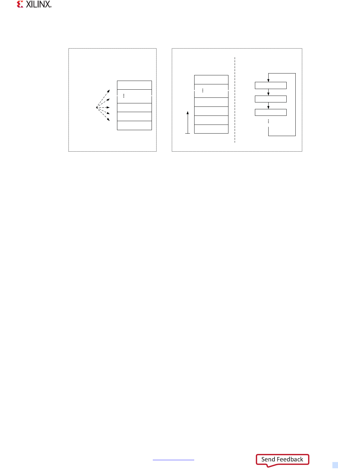
Zynq-7000 AP SoC Technical Reference Manual www.xilinx.com 403
UG585 (v1.12.1) December 6, 2017
Chapter 15: USB Host, Device, and OTG Controller
Device Mode
As requested by the host, the Device Controller Driver (DCD) sets up descriptors for endpoints and
manages the real-time needs of the endpoints. The high-speed data transfers between memory and
ULPI are managed by the controller using queue heads and transfer descriptors. The results of each
transfer is reviewed by DCD to take appropriate action.
Device Endpoints. The device controller includes a simple descriptor model to enable the controller
to quickly respond to host requests. Each of the 12 endpoints has two device Queue Heads (dQH);
one for IN and the other for OUT transfer types. There are a total of 24 device dQH’s. An endpoint
data transfer in defined with one dQH and one or more linked list of device Transfer Descriptors
(dTD). An example is shown in Figure 15-13.
Host Mode
Host Schedules. The Host Controller Driver (HCD) maintains two types of transaction schedules to
generate USB traffic: periodic (isochronous/interrupt) and asynchronous (bulk/control).
• The Periodic schedule is a list of high to low priority-order periodic transfers. An element in the
periodic frame list is executed at the start of every frame (SOF). The list includes elements that
indicate when to execute (periodic interval) and what to execute. An example is shown in
Figure 15-15.
• The asynchronous schedule is a circular loop of Queue Heads that point to transfer descriptors
that are processed in a round-robin priority. Within each microframe, the asynchronous
schedule is executed after the periodic schedule is finished. An example is shown in
Figure 15-16.
Link-list Concept
The host and device controllers use link-list descriptors to manage transfers to and from memory
buffers. The concept is shown in Figure 15-5. The first Transfer Descriptors (TD) is pointed to by a
X-Ref Target - Figure 15-4
Figure 15-4: USB Endpoint Descriptors (device mode) and Schedules (host mode)
Endpoint Queue Heads
Endpoint 11 IN
EndPoint 0 IN
EndPoint 1 OUT
EndPoint 0 OUT
Device
Responds
to Host
Requests
Queue Head
List
Host Schedules (EHCI)
Queue Head a
Aysnchronous
Queue Heads
Queue Head b
Frame n Elements
Periodic Frame
List
Frame 3 Elements
Frame 1 Elements
Frame 2 Elements
Frame 0 Elements
dQH
FRINDEX pointer is advanced
for every USB Frame Round Robin as
Bandwidth allows.
Programmable
number of
elements Insert and
Remove
QH’s as
needed
Maintain
Queue
Head List
Queue Head b
UG585_c15_33_030713
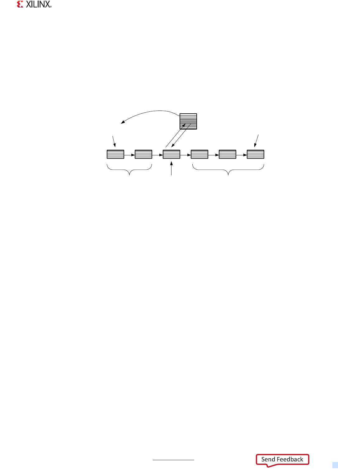
Zynq-7000 AP SoC Technical Reference Manual www.xilinx.com 404
UG585 (v1.12.1) December 6, 2017
Chapter 15: USB Host, Device, and OTG Controller
Queue Head (QH). Each dTD can point to another dTD (using next dTD pointer) or terminate the
linked list by setting its (T) bit = 1.
The controller maintains a local, working copy of the dQH that it overlays with the one or more dTDs
as the transaction request is processed. After each dTD transfer is complete, the dTD overlay is
written back to the system memory with transfer results (status). While a transfer is in progress, the
overlay area of the dQH in controller memory is used as a staging area for the dTDs.
15.1.7 Implementation Summary
There are EHCI enhancements to support the embedded Transaction Translator and hardware
assistance features to support OTG. Here is a summary of special features, enhancements, deviations
and unsupported features.
• EHCI Enhancements and Deviations, section 15.11 EHCI Implementation.
• Hardware Assistance Features for OTG, section 15.14.1 Hardware Assistance Features.
• Embedded Transaction Translator (no separate companion controller hardware), section
15.11.2 Embedded Transaction Translator.
• The AHB interface is a master-only and used by the DMA controller (no PCI registers).
•The ULPI Carkit feature is not supported.
15.1.8 Documentation
Scope of TRM
The Zynq-7000 Technical Reference Manual (TRM) describes hardware functionality and
register-level software programming for Host controller mode drivers (HCD) and Device controller
mode drivers (DCD). Guidance for the upper software layers, including device classes and
applications, are beyond the scope of the TRM.
X-Ref Target - Figure 15-5
Figure 15-5: USB Controller Link-list Concept
UG585_c15_34_030713
QH
First TD
Completed TD’s TD’s Queued and Ready
Current
TD
Last TD
T = 1
Read
TD Write
Result

Zynq-7000 AP SoC Technical Reference Manual www.xilinx.com 405
UG585 (v1.12.1) December 6, 2017
Chapter 15: USB Host, Device, and OTG Controller
Documents and Specifications
The reader should be familiar of USB technology and access to the following documents. These
documents are mentioned in the text and are listed in Third-Party IP and Standards Documents in
Appendix A.
Zynq-7000 AP SoC Documents
°TRM for all Zynq-7000 series; UG585. Architecture and register-level programming.
°Data Sheet for 7z010, 7z015, and 7z020 dual core and 7z007s, 7z012s, and 7z014s single
core devices; DS187. Electrical specifications.
°Data Sheet for 7z030, 7z035, 7z045, and 7z100 devices; DS191. Electrical specifications.
°Errata Sheets for all devices; ENxxx (multiple). Related AR list, AR47916.
7-Series FPGA Documents
°Refer to the list in A.3.2 PL Documents – Device and Boards.
USB Specifications
°USB 2.0 Specification
°UTMI+ Low Pin Interface (ULPI) Specification
°Enhanced Host Controller Interface (EHCI) Specification for Universal Serial Bus
Chapter Nomenclature
• Refer to the USB 2.0 Specification, Chapter 2 Terms and Abbreviations.
• Xilinx Corporate glossary includes general terms.
• Chapter-specific terms:
°DCD means device controller driver. This is the device driver software used in device mode.
°HCD means host controller driver. This is the device driver software used in host mode.
°The term Frame applies to FS/LS mode. Microframe applies to HS mode. (Micro)frame
applies to FS/LS and HS modes.
°In the USB Controller chapter, DWord means 32 bits. In the rest of the PS, a word is defined
to mean 32 bits.
°There are two dual-purpose registers (for host and device mode) listed in Table 15-1. The
usb.ASYNCLISTADDR_ENDPOINTLISTADDR register is referred to as usb.ASYNCLISTADDR_
when discussing Host mode and usb._ENDPOINTLISTADDR when discussing Device mode.
The usb.PERIODICLISTBASE_DEVICEADDR register is similar.

Zynq-7000 AP SoC Technical Reference Manual www.xilinx.com 406
UG585 (v1.12.1) December 6, 2017
Chapter 15: USB Host, Device, and OTG Controller
15.1.9 Notices
7z007s and 7z010 CLG225 Devices
The 7z007s single core and 7z010 dual core CLG225 devices support 32 MIO pins as shown in the
MIO table in section MIO-at-a-Glance Table in Chapter 2. Only one USB interface is available in these
CLG225 devices. If USB and GigE are required, the GigE I/O signals must interface through the EMIO.
15.1.10 Chapter Overview
Functional Descriptions and Programming Guides
The USB controller chapter includes multiple sections of introductions, functional descriptions and
programming guides. The functional descriptions explain controller functionality and includes
register programming information that is related to hardware functions.
• Content for All Modes
°15.1 Introduction
°15.2 Functional Description
°15.3 Programming Overview and Reference
°15.15 System Functions
°15.16 I/O Interfaces
• Device Operating Mode
°15.4 Device Mode Control
°15.5 Device Endpoint Data Structures
°15.6 Device Endpoint Packet Operational Model
°15.7 Device Endpoint Descriptor Reference
°15.8 Programming Guide for Device Controller
°15.9 Programming Guide for Device Endpoint Data Structures
• Host Operating Mode
°15.10 Host Mode Data Structures
°15.11 EHCI Implementation
°15.12 Host Data Structures Reference
°15.13 Programming Guide for Host Controller
• OTG Operating Mode
°15.14 OTG Description and Reference
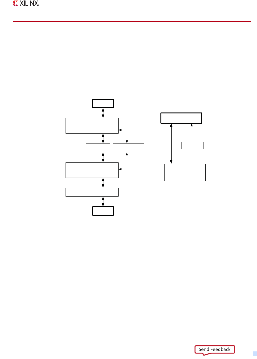
Zynq-7000 AP SoC Technical Reference Manual www.xilinx.com 407
UG585 (v1.12.1) December 6, 2017
Chapter 15: USB Host, Device, and OTG Controller
15.2 Functional Description
This section generally applies to both device and host modes.
15.2.1 Controller Flow Diagram
The controller flow diagram in Figure 15-6 shows the USB data transfer flows, the descriptor flows,
and the interface to software.
15.2.2 DMA Engine
Data Transfers
In host mode, the data structures are defined by the EHCI specification and represent queues of
periodic and asynchronous transfers to be performed by the host controller including the split
transaction requests that allow the controller to direct packets to FS/LS devices that are downstream
of an external HS hub or root hub. Host mode uses the queue head (QH), queue element transfer
descriptor (qTD), isochronous transfer descriptor (iTD), split transaction isochronous transfer
descriptor (siTD) and the periodic frame span transversal node (FSTN) data structures.
In device mode, the data structures are simpler and consist of device queue heads (dQH) and device
transfer descriptors (dTD) that are used in a linked-list fashion.
X-Ref Target - Figure 15-6
Figure 15-6: USB Controller Flow Diagram
* Bus Interface
* Data Movement
* Host: Periodic and Async Schedules
* Device: Endpoint Queue Head
System
Memory
AHB Master
Control and Status
Registers
DMA Engine
Tx and Rx FIFO
channels
Dual-port
RAM
* Interval Timers
* Error Handling
* CRC Handling
* Bus Handshake Generation
Protocol Engine
* Port Status and Control
* Transceiver Interface Logic
Port Controller
ULPI
Interface
Interrupts
Microprocessor(s)
APB Slave
ULPI Master
Context (QH and TD
data structures)
IRQ to GIC
DMA DMA
UG585_c15_35_030713

Zynq-7000 AP SoC Technical Reference Manual www.xilinx.com 408
UG585 (v1.12.1) December 6, 2017
Chapter 15: USB Host, Device, and OTG Controller
The DMA engine is a 32-bit bus master on the AHB interface to access the PS system interconnect.
15.2.3 Protocol Engine
The protocol engine parses the USB tokens, generates response packets and performs error checking
functions. Data packets are passed through the transfer buffers, the DMA engine and system
memory.
The controller does not provide a hardware-based Transaction Translator for Low and Full speed
operations. Instead, the DMA and Protocol engines are used to support this functionality as
described in section 15.11.2 Embedded Transaction Translator.
X-Ref Target - Figure 15-7
Figure 15-7: USB DMA Controller Block Diagram
UG585_c15_36_030713
Control and Status Registers
DMA Traffic
Protocol
Engine
Port
Controller
* Burst Movement
* Bus State
* FIFO Arbitration
Traffic Context
Registers
DMA
Arbitrator
* Packet Movement
* Host: HS
* Device: HS and FS
ULPI
DMA Control
Host Mode:
* EHCI
* Scheduler
Device Mode:
* Prime/Unprime Control
* Endpoint Manager
* Context Storage Dual-port RAM
* Update Logic
DMA Context
* Byte Count ALU
* Address Incrementing
AHB
APB
Slave
Master
Tx FIFO
Rx FIFO
ULPI Link
Wrapper
Dual-port
RAM
PS Interconnect
PS Interconnect
X-Ref Target - Figure 15-8
Figure 15-8: USB Protocol Engine Block Diagram
UG585_c15_37_030713
Control and Status Registers
AHB
I/O Interface
APB
Protocol Engine Control
DMA
Controller
* Muxing / Pipelining
* FIFO Control
* CRC
Protocol Engine Data Path
Host:
* SOF Generation
* PID Generation
ULPI
Interval
Timers
* Generate Frame/MicroFrame
* Generate Scheduler Timing Strobes
Timebase Interval Timers
* Bus Timeout
* Inter-Packet Delay
Device:
* Prime Endpoint Logic
* PID Tracking
* Handshake Decision Logic
* Datapath Control
Port
Controller
Slave
Master
Tx FIFO
Rx FIFO
ULPI Link
Wrapper
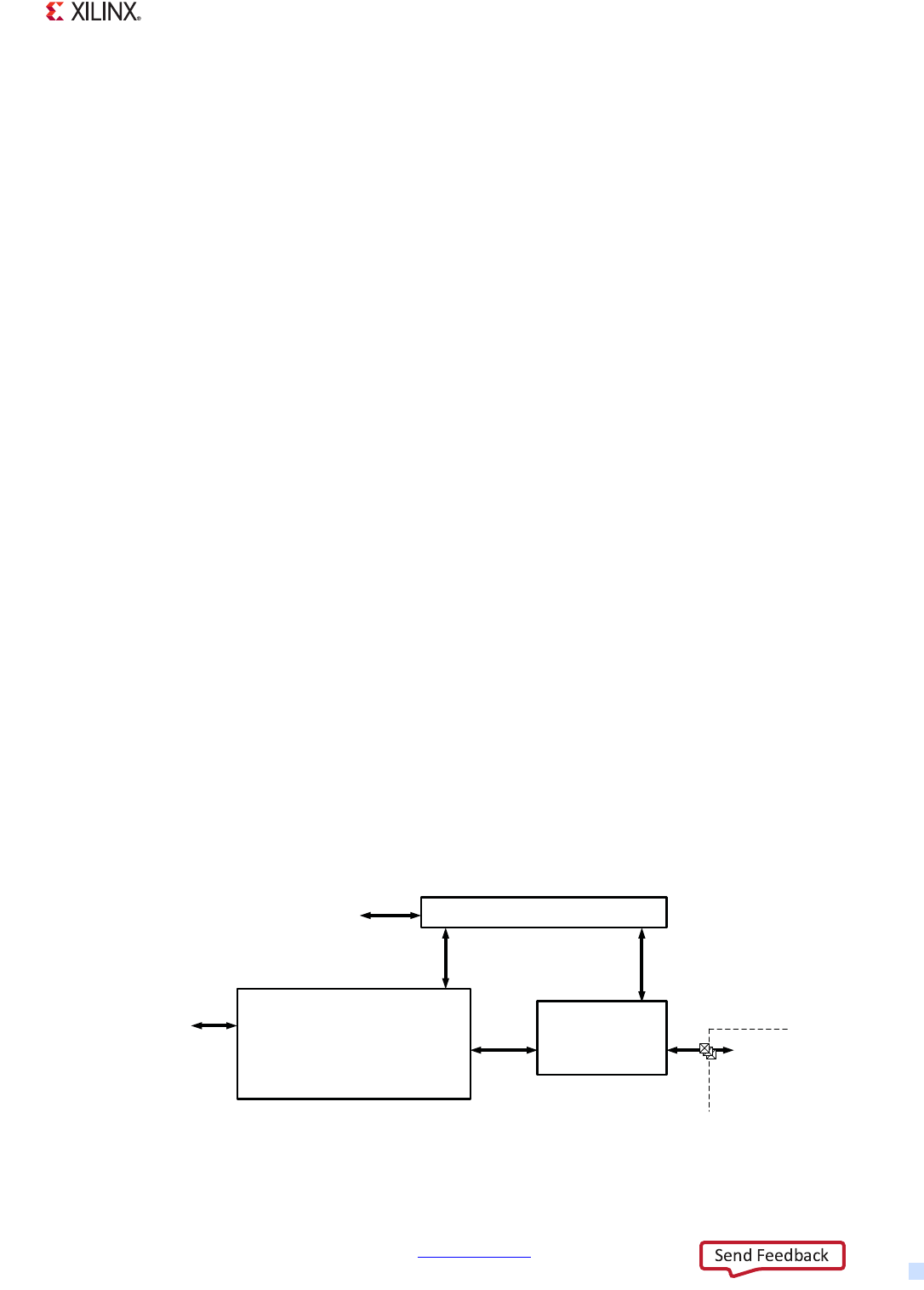
Zynq-7000 AP SoC Technical Reference Manual www.xilinx.com 409
UG585 (v1.12.1) December 6, 2017
Chapter 15: USB Host, Device, and OTG Controller
The protocol engine is responsible for all error checking, check field generation, formatting all the
handshake, Ping and data response packets on the bus, and for generating signals that are needed
based on a USB based time frame.
Protocol Engine Functions
The protocol engine contains several functions for both host and device mode:
• The token state machines track all of the tokens on the bus and filters the traffic based on the
address and endpoint information in the token.
• The CRC5 and CRC16 CRC generator/checker circuits check and generate the CRC check fields
for the token and data packets.
• The data and handshake state machines generate any responses required on the USB and move
the packet data through the dual port RAM to the DMA controller.
• The Interval Timers provide timing strobes that identify important bus timing events: the bus
timeout interval, the microframe interval, the start of frame interval, and the bus reset, resume,
and suspend intervals.
• Reports all transfer status to the DMA engine.
15.2.4 Port Controller
The port transceiver controller provides a couple of basic functions:
• Suspend/Resume
• For device mode, Chirp control.
15.2.5 ULPI Link Wrapper
The ULPI Link wrapper passes-through packet data and interprets Rx commands as well as send Tx
commands and provide viewport services to the software.
The ULPI link wrapper interfaces between the port controller (a bus similar to UTMI+ that connects
to the rest of the controller and its registers) and the ULPI interface.
X-Ref Target - Figure 15-9
Figure 15-9: USB Port Controller and ULPI Link Wrapper Block Diagram
UG585_c15_38_030713
Control and Status Registers
Protocol
Engine
I/O Interface
APB
Port Controller Control
Host:
* Port State Machine
ULPI
Device:
* Port State Machine
* Chirp Control
* Suspend/Resume
Slave
* Transceiver Logic
ULPI Link
Wrapper
Similar to
UTMI+

Zynq-7000 AP SoC Technical Reference Manual www.xilinx.com 410
UG585 (v1.12.1) December 6, 2017
Chapter 15: USB Host, Device, and OTG Controller
15.2.6 General Purpose Timers
The two independently programmable timers can be used to generate a timeout or to measure time
related activities.The programmable timers should not be confused with the controller’s interval
timers which are used by the controller to generate frame and microframe intervals and to generate
strobes for the host controller scheduler.
A timer is controlled by its control and load registers; usb.GPTIMERxCTRL and usb.GPTIMERxLD. The
load register contains the value that is loaded into the timer when a timer reset occurs.
The control register contains timer configuration and a data field which can be queried to determine
the running count value. The timer has granularity of 1 microsecond and can be programmed to
count for a little over 16 seconds. There are two modes for this timer; one-shot and looped count.
When the timer counter value transitions to 0, an interrupt is controllable using the usb.USBSTS and
usb.USBINTR registers.
The one-shot mode, usb.GPTIMERxCTRL [GPTMODE] = 0, selects a single timer countdown where the
timer will count down to 0, generate an interrupt and stop until the counter is reset by software.
In repeat, looped countdown, the timer will count down to 0, generate an interrupt and automatically
reload the counter from the usb.GPTIMERxLD register to begin to count down again.
15.3 Programming Overview and Reference
This section includes an overview of the programming model for host and device modes. The
programming model details for each mode are separately described in other sections of the Zynq-7000 AP
SoC Technical Reference Manual (TRM).
Limitation
The USB controller registers require single 32-bit read/write accesses, do not use byte, halfword, or
double word references.
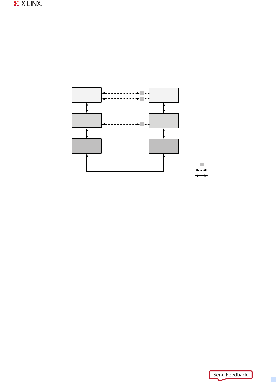
Zynq-7000 AP SoC Technical Reference Manual www.xilinx.com 411
UG585 (v1.12.1) December 6, 2017
Chapter 15: USB Host, Device, and OTG Controller
15.3.1 Hardware/Software System
The physical and virtual data flows for a USB hardware/software system are illustrated in
Figure 15-10. These flows form the basis of USB. The TRM is focused on the operations of the bus
interface and device layers as a foundation for writing drivers that include the functional layer.
15.3.2 Operational Mode Control
States
The controller can be configured for device mode or host mode. In OTG mode, the controller must
perform tasks independent of the device and host controller modes to determine what mode to put
the controller into. Software can use the usb.USBCMD [RST] reset bit to reset the vast majority of the
controller, but preserve register values and controller state to support OTG operations. This reset
transitions the controller out of host or device mode and into an idle state as shown in figure
Figure 15-11. OTG tasks are performed independent of the [RST] bit reset as well as independent of
the controller mode.
The software sets the usb.USBMODE [CM] mode bit to select either host or device mode.
X-Ref Target - Figure 15-10
Figure 15-10: USB System Stack
UG585_c15_39_030713
Data pipes
Application
Software
System
Software
Host
Controller
Function
Interface
USB Logical
Device
Bus
Interface
USB Host
Control pipe
USB Cabling and Hubs
USB Device
Function Layer
Device Layer
Bus Interface Layer
Virtual Data Flow
Physical Data Flow
Endpoints

Zynq-7000 AP SoC Technical Reference Manual www.xilinx.com 412
UG585 (v1.12.1) December 6, 2017
Chapter 15: USB Host, Device, and OTG Controller
15.3.3 Power Management
Stop-Clock
The USB controller can be held in reset by the PS reset subsystem and the PHY clock from the PHY
can be stopped to reduce power consumption. The clocks and resets are described in section
15.15 System Functions.
Suspend and Resume
The USB controller supports Suspend/Resume functions for both host and device modes.
15.3.4 Register Overview
Each controller includes its own set of independent control and status registers that are memory
mapped at 0xE000_2000 for controller 0 and at 0xE000_3000 for controller 1. The register address
offsets and brief descriptions are summarized in Table 1 5-1 . The detailed descriptions are in
Appendix B.
The controller and all registers are reset by the assertion of the USB Ref Reset from the PS. The
mechanism is described in Chapter 26, Reset System. The reset value of the controller registers are
shown in Appendix B. Software can reset the controller and the non-OTG registers by writing a 1 to
the usb.USBCMD [RST] bit. The registers that are reset by usb.USBCMD [RST] are identified in a the
last column of Table 15-1.
Register Overview Table
The controller registers include configuration constants, capability constants and operational
registers for EHCI compatibility (Host mode) and non-EHCI functions (Device and OTG modes). The
non-EHCI registers support device mode and OTG functions. The EHCI register fields are overlaid
into the controller’s register set.
•OTG/Mode registers provide control and status for HNP and SRP.
X-Ref Target - Figure 15-11
Figure 15-11: USB Controller Mode Diagram
UG585_c15_40_030713
Device
Mode
Idle
Host
Mode
* PS_POR_B reset (all USB registers)
* slcr.USB_RST_CTRL [USB_CPU1X_RST] (all USB registers)
* usb.USBCMD [RST] (USB registers except those for OTG functionality)
Reset
usb.USBMODE [CM] = 11
usb.USBMODE [CM] = 10
reset
reset
Zynq-7000 AP SoC Technical Reference Manual www.xilinx.com 413
UG585 (v1.12.1) December 6, 2017
Chapter 15: USB Host, Device, and OTG Controller
•Dev register is used by the device controller driver software (DCD).
•Host register is used by the host controller driver software (HCD).
•EHCI register includes content from the specification. ‘x’ means partial. ‘ex’ means exclusive.
Table 15-1: USB Controller Register Overview
Offset
Address
Register Name OTG/
Mode Dev Host EHCI Type Affected by
USBCMD Reset
Bit Acronym
Identification: Configuration Constants.
0x0000 ID xxx RO no
0x0004 HWGENERAL xxx RO no
0x0008 HWHOST ~~x RO no
0x000C HWDEVICE ~x~ RO no
0x0010 HWTXBUF ~xx RO no
0x0014 HWRXBUF ~xx RO no
General Purpose (GP) Timers.
0x0080/88 GPTIMER{0,1}LD xxx~ rw yes
0x0084/8C GPTIMER{0,1}CTRL xxx~ mixed yes
AXI Interconnect
0x0090 SBUSCFG xxx~ RW yes
Capability: Controller and EHCI Capabilities Constants (IP Configuration Constants).
0x0100 CAPLENGTH_HCIVERSION xxxx RO no
0x0104 HCSPARAMS x~x ex RO no
0x0108 HCCPARAMS ~~xex RO no
0x0120 DCIVERSION xx x RO no
0x0124 DCCPARAMS xx RO no
Operational: Interrupts, Schedule Pointers (Host), and Endpoint Pointers (Device).
0x0140 USBCMD xxx x RW yes
0x0144 USBSTS, refer to Table 15-2.xxx xRW, R/W1C, RO yes, except RO
0x0148 USBINTR xxxexRW, R/W1C, RO yes, except RO
0x014C FRINDEX ~xx x RW yes
0x0154 PERIODICLISTBASE_ ~~xex RW yes
_DEVICEADDR ~x~~ RW yes
0x0158 ASYNCLISTADDR_ ~~xex RW yes
_ENDPOINTLISTADDR ~x~~ RW yes
Operational: Transaction Translator.
0x015C TTCTRL ~~x~ RW, RO yes, except RO
Operational: Misc.
0x0160 BURSTSIZE xxx~ RW yes
0x0164 TXFILLTUNING RW, R/W1C yes
0x0168 TXTTFILLTUNING RW, R/W1C yes
0x016C IC_USB xxx~ RW yes
0x0170 ULPI_VIEWPORT xxx~ RW, RO yes, except RO
Operational: Endpoint Control (Device mode), refer to Figure 15-4 for details.
Zynq-7000 AP SoC Technical Reference Manual www.xilinx.com 414
UG585 (v1.12.1) December 6, 2017
Chapter 15: USB Host, Device, and OTG Controller
15.3.5 Interrupt and Status Bits Overview
Each controller has a IRQ interrupt signal to the PS interrupt controller that is an accumulation of
enable interrupts listed in Tabl e 15- 2 except for some Status-only bit that can’t generate an
interrupt.
• Controller 0: IRQ ID #53
• Controller 1: IRQ ID #76
USBSTS Interrupt, Status and Enable Registers
The interrupt and status bits of the usb.USBSTS registers are listed in Table 15-2 USB Interrupt and
Status Register Bits. The interrupt bits are maskable using the usb.USBINTR registers. The status bits
do not generate an interrupt and are read-only to provide status information to software.
0x0178 ENDPTNAK x~~ R/WTC
0x017C ENDPTNAKEN x~~ RW
Operational: Host mode (EHCI) and Device mode.
0x0180 CONFIGFLAG xxxx RO
0x0184 PORTSC1 xxxxRW, RO, R/W1C partial
[WKDS] [WKCN] [WKOC] no
[PIC] [PR] no
others yes
Operational: Mode Control.
0x01A4 OTGSC x~~~RW, RO, R/W1C no
0x01A8 USBMODE xxx~ RW yes
Endpoint Configuration and Control (Device mode), refer to Figure 15-4 for details.
0x01AC ENDPTSETUPSTAT ~x~~ R/W1C yes
0x01B0 ENDPTPRIME ~x~~ R/W1S yes
0x01B4 EMDPTFLUSH ~x~~ R/W1S yes
0x01B8 ENDPTSTAT ~x~~ RO no
0x01BC ENDPTCOMPLETE ~x~~ R/W1C yes
0x01C0 ENDPTCTRL 0 ~x~~ RW, RO yes, except RO
0x01C4 to
0x01EC ENDPTCTRL {1 to 11} ~x~~ RW, R/W1C yes
Table 15-1: USB Controller Register Overview (Cont’d)
Offset
Address
Register Name OTG/
Mode Dev Host EHCI Type Affected by
USBCMD Reset
Bit Acronym

Zynq-7000 AP SoC Technical Reference Manual www.xilinx.com 415
UG585 (v1.12.1) December 6, 2017
Chapter 15: USB Host, Device, and OTG Controller
15.3.6 OTG Status/Interrupt and Control Register
The programming model for On-the-Go (OTG) USB is supported by the OTG status and control register
(OTGSC). The OTG operation works independently of the host and device modes. In OTG mode, once the
controller has determined which mode to operate in, the full features of that mode (host or device) are
available to the software. Please refer to 15.14.2 OTG Interrupt and Control Bits.
15.4 Device Mode Control
When the controller is in device mode, software enables its control endpoint, prepares descriptors based
on the functionality of the device and prepares the necessary endpoints.
Table 15-2: USB Interrupt and Status Register Bits
USBSTS
(status)
Bit Field
Type
USBINTR
(enable)
Bit Field
Description Dev Host Cross Reference
[TI1] 25 Interrupt 25 Timer 1. xx
15.2.6 General Purpose Timers
[TI0] 24 Interrupt 24 Timer 0. xx
[UPI] 19 Interrupt 19 Periodic qTD complete. ~x
[UAI] 18 Interrupt 18 Async qTD complete. ~x
[NAKI] 16 Interrupt 16 Device generated NAK. x~
[AS] 15 Status-only na Async Schedule state. ~x
[PS] 14 Status-only na Periodic Schedule state. ~x
[RCL] 13 Status-only na Host Reclamation status. ~x
[HCH] 12 Status-only na Halt status of Run/Stop.
[ULPII] 10 Interrupt 10 ULPI Viewport transfer complete. xx
[SLI] 8 Interrupt 8 Device enters Suspend state. x~
[SRI] 7 Interrupt 7 Start of Frame (SOF) received. x~
Table 15-17
[URI] 6 Interrupt 6 Reset received. x~
[AAI] 5 Interrupt 5 Async schedule advance. ~x
[SEI] 4 Interrupt 4 System Error response on AHB. xx
[FRI] 3 Interrupt 3 Periodic Frame List rollover. ~x
[PCI] 2 Interrupt 2 Port Change Detect. xx
[UEI] 1 Interrupt 1 USB Transaction Error.
[UI] 0Interrupt 0TD complete xTable 15-17
Zynq-7000 AP SoC Technical Reference Manual www.xilinx.com 416
UG585 (v1.12.1) December 6, 2017
Chapter 15: USB Host, Device, and OTG Controller
15.4.1 Controller State
The device mode includes the active physical state of the controller, left side of Figure 15-12, and the
suspend state maintained in software, right side of the figure. Power interruptions, resets and USB
activity all contribute to the sequencing through these states.
It is the responsibility of software to maintain a state variable to differentiate between the default
FS/HS state and the address/configured states. Change of state from default to address and the
configured states is part of the enumeration process described in the device framework section of
the USB 2.0 Specification.
X-Ref Target - Figure 15-12
Figure 15-12: USB Device State Diagram
Active State
Powered
Attach
Default
FS/HS
Address
FS/HS
Configured
FS/HS
Suspend
FS/HS
Set the Run bit:
usb.USBCMD [RS] = 1.
Power
Interruption
When the
host resets
the device
returns to
the default
state.
Reset
Address
Assigned
Device
Configured
Device
Deconfigured
Software Maintained State
Bus Inactive
Bus Activity
Bus Inactive
Bus Activity
Bus Inactive
Bus Activity
Suspend
FS/HS
Suspend
FS/HS
Suspend State
UG585_c15_12_030413

Zynq-7000 AP SoC Technical Reference Manual www.xilinx.com 417
UG585 (v1.12.1) December 6, 2017
Chapter 15: USB Host, Device, and OTG Controller
As a result of entering the address state, the device address register (usb._DEVICEADDR) must be
programmed by the DCD.
Entry into the configured state indicates that all endpoints to be used in the operation of the device
have been properly initialized by programming the usb.ENDPTCTRLx registers and initializing the
associated queue heads.
15.4.2 USB Bus Reset Response
A USB bus reset is used by the host to initialize downstream devices. The USB reset is one of several
types of resets in the system, refer to section 15.15.2 Reset Types for a list.
When a bus reset is detected, the device controller hardware renegotiates its attachment speed,
reset the device address to 0 and notify the DCD by interrupt (assuming the USB reset interrupt
enable is set). After a reset is received, all endpoints (except EP 0) are disabled and any primed
transactions are canceled by the device controller. The concept of priming will be clarified below, but
the DCD must perform the following tasks when a reset is received.
DCD Actions
1. Clear all setup token semaphores by reading the usb.ENDPTSETUPSTAT register and writing the
same value back to the usb.ENDPTSETUPSTAT register. Clear all the endpoint complete status bits
by reading the usb.ENDPTCOMPLETE register and writing the same value back to the
usb.ENDPTCOMPLETE register.
2. Cancel all primed status by waiting until all bits in the usb.ENDPTPRIME register are 0 and then
writing FFFF_FFFFh to usb.ENDPTFLUSH register.
3. Read the reset bit in the PORTSC1 register and make sure that it is still active. A USB reset occurs
for a minimum of 3 ms and software must reach this point in the reset cleanup before end of the
reset occurs, otherwise a hardware reset of the device controller is recommended (rare).
Device Controller Reset
4. A hardware reset can be performed by writing a 1 to the usb.USBCMD [RST] reset bit. A hardware
reset will cause the device to detach from the bus by clearing the run/stop bit. Thus, software
must completely re-initialize the device controller after a hardware reset.
5. Free all allocated dTD’s because they will no longer be executed by the device controller. If this
is the first time the DCD is processing a USB reset event, then it is likely that no dTD’s have been
allocated.
At this time, the DCD might release control back to the OS because no further changes to the device
controller are permitted until a port change detect is indicated.
Table 15-3: USB Device State Information Bits
Bit Description Register Bit Interrupt
Suspend Mode usb.USBSTS [SLI] Yes
USB Reset Received usb.USBSTS [URI] Yes
Port Change Detect usb.USBSTS [PCI] Yes
High-Speed Port usb.PORTSC1 [PSPD] No

Zynq-7000 AP SoC Technical Reference Manual www.xilinx.com 418
UG585 (v1.12.1) December 6, 2017
Chapter 15: USB Host, Device, and OTG Controller
Port Change Detect
After a port change detect, the device has reached the default state and the DCD can read the
PORTSC1 register to determine if the device is operating in FS or HS mode. At this time, the device
controller has reached normal operating mode and the DCD can respond to enumeration according
to the USB2.0 specification Chapter 9 - Device Framework.
The DCD can use the FS/HS mode information to determine the bandwidth mode of the device.
Note: Before resume signaling can be used, the host must be enabled using the Set Feature
command defined in device framework of the USB 2.0 Specification.
Note: It is necessary for the DCD to use the flush bit(s) to de-prime one or more endpoints when a
USB device reset is received. Refer to Example: Flushing/De-priming an Endpoint, page 442.
15.5 Device Endpoint Data Structures
The device endpoint data structures consist of link-list endpoint descriptors that must be initialized and
managed by software. This consists of programming the endpoint control registers, maintaining a set of
descriptors in system memory, and managing system memory buffers.
15.5.1 Link-list Endpoint Descriptors
There are two types of descriptors used for the device controller: the device Queue Head (dQH) and
the device Transfer Descriptor (dTD). Figure 15-13 shows how these are used in a link-list fashion.
The DMA engine uses link-list descriptors to respond to endpoint packet transfer requests from the
host.
It is necessary for the DCD to maintain head and tail pointers to the linked list of dTD’s for each
respective queue head. This is necessary because the dQH only maintains pointers to the current
working dTD and the next dTD to be executed. The operations described in next section for
managing dTD will assume the DCD can reference the head and tail of the dTD linked list.
Note: To conserve memory, the reserved fields at the end of the dQH can be used to store the Head
and Tail pointers but it still remains the responsibility of the DCD to maintain the pointers.
Zynq-7000 AP SoC Technical Reference Manual www.xilinx.com 419
UG585 (v1.12.1) December 6, 2017
Chapter 15: USB Host, Device, and OTG Controller
The device controller API software incorporates and abstracts for the application developer all of the
information contained in the device operational model. Each Endpoint can be configured for
bi-directional transfers (contain both IN and OUT endpoints).
Queue Head and Linked Transfer Descriptors:
•15.7.1 Endpoint Queue Head Descriptor (dQH)
•15.7.2 Endpoint Transfer Descriptor (dTD)
•15.7.3 Endpoint Transfer Overlay Area
Descriptor and Data Flow
The top portion of Figure 15-14 shows the list of queue heads (one for each endpoint) and the list of
transfer descriptors that are referenced by the dQH and other dTD descriptors. The low portion of
the figure shows data being transferred between memory and the ULPI connection to USB.
X-Ref Target - Figure 15-13
Figure 15-13: USB Device Link-list Endpoints Example
4KB Memory
Buffer
Endpoint 11
IN
Endpoint 0
IN
Endpoint 1
OUT
Endpoint 0
OUT
usb.ENDPOINTLISTADDR
Endpoint Queue
Heads (dQH)
0x040
0x080
0x5C0
dTD Pointer
0x600
0x0B0
dTD Pointer
dTD
dTD Pointer
T=0
Buffer
Pointer
Queue
Head List
dTD
T=1
Buffer
Pointer
4KB Memory
Buffer
4KB Memory
Buffer
dTD
T=1
Buffer
Pointer
dTD Pointer
4KB Memory
Buffer
dTD
T=1
Buffer
Pointer
dTD Pointer
4KB Memory
Buffer
dTD
T=0
Buffer
Pointer
dTD Pointer
4KB Memory
Buffer
dTD
T=0
Buffer
Pointer
dTD Pointer
Transaction
Descriptors (dTD)
Transfer
Buffers
After a dTD is processed,
the controller will generate
an interrupt
if its IOC bit is set = 1.
UG585_c15_41_030713
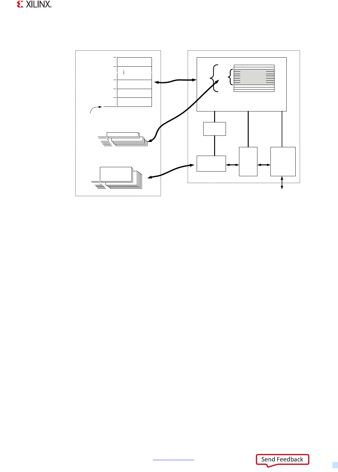
Zynq-7000 AP SoC Technical Reference Manual www.xilinx.com 420
UG585 (v1.12.1) December 6, 2017
Chapter 15: USB Host, Device, and OTG Controller
15.5.2 Manage Endpoints
The USB 2.0 Specification defines an endpoint, also called a device endpoint or an address endpoint
as a uniquely addressable portion of a USB device that can source or sink data in a communications
channel between the host and the device. The endpoint address is specified by the combination of
the endpoint number and the endpoint direction.
The channel between the host and an endpoint at a specific device represents a data pipe. Endpoint
0 for a device is always a control type data channel used for device discovery and enumeration. Other
types of endpoints support by USB include bulk, interrupt, and isochronous. Each endpoint type has
specific behavior related to packet response and error handling. More detail on endpoint operation
can be found in the USB 2.0 Specification.
The device controller hardware is configured to support up to 12 endpoints. The DCD can enable,
disable and configure endpoint type up to the maximum selected during synthesis.
Each endpoint direction is essentially independent and can be configured with differing behavior in
each direction. For example, the DCD can configure endpoint 1 IN to be a bulk endpoint and
endpoint 1 OUT to be an isochronous endpoint. This helps to conserve the total number of endpoints
required for device operation. The only exception is that control endpoints must use both directions
on a single endpoint number to function as a control endpoint. Endpoint 0, for example, is always a
control endpoint and uses the pair of directions.
Each endpoint direction requires a queue head allocated in memory. For 12 endpoints, numbers is
used, then 24 queue heads are required one for each endpoint direction being used by the device
X-Ref Target - Figure 15-14
Figure 15-14: USB Device Descriptor and Data Flow
DMA
Engine
System Memory
Rx and Tx
FIFOs
(Latency Buffers)
DMA
Protocol
Engine
Port
Controller
and ULPI
Link
Wrapper
ULPI
dTD
Read/Write
dQH
Read/Write
Dual-port RAM
Buffer
Pointers
Transfer Buffers
4KB each
Memory Buffers
EndPoint dTD
Next dTD
Pointers dTD
Transfer Descriptors
Endpoint 11 IN
EndPoint 0 IN
EndPoint 1 OUT
EndPoint 0 OUT
usb.ENDPOINTLISTADDR [31:11]
dQH
0x040
0x600
0x080
0x5C0
0x0C0
0x000
Queue Head
List dQH dTD
Transfer
Overlay Area
(7 DWords)
31 0
Transaction Descriptor
Processor
USB Controller
UG585_c15_42_030713

Zynq-7000 AP SoC Technical Reference Manual www.xilinx.com 421
UG585 (v1.12.1) December 6, 2017
Chapter 15: USB Host, Device, and OTG Controller
controller. The operation of an endpoint and use of queue heads are described later in this
document.
15.5.3 Endpoint Registers
The endpoint registers are listed in Table 15-4 USB Device Endpoint Register Summary. These
registers were summarized at the end of Table 15-1, page 413.
In general, there is one bit for each endpoint. The lower half of the register bits are for Rx endpoints
and the upper half is for Tx endpoints. Exceptions include the ENDPTSETUPSTAT and the endpoint
control registers, ENDPTCTRL{11:0}.
Endpoint Registers
Table 15-4: USB Device Endpoint Register Summary
Register Name Description and Register Bit Field Type
Tx Endpoint (11:0) Rx Endpoint (11:0)
ENDPTNAK
Bit is set when an endpoint sends a NAK to the Host. Read and
Write-one-to-clear.
[EPTN], 27:16
(IN token)
[EPRN], 11:0
(OUT or Ping token)
ENDPTNAKEN Interrupt enable bits for ENDPTNAK bits. Read/Write.
[EPTNE], 27:16 [EPRNE], 11:0
ENDPTSETUPSTAT Bit is set when an endpoint receives a Setup transaction. Read and
Write-one-to-clear.
~ [ENDPTSETUPSTAT], 11:0
ENDPTPRIME
Software sets a bit to instruct the controller to prepare for a
packet transfer. The QH, dTD’s, and endpoint registers are
ready.
Read and
Write-one-to-set.
[PETB], 27:16
(IN or Interrupt)
[PERB], 11:0
(OUT)
ENDPTFLUSH
Software sets a bit to instruct the controller to flush an
endpoint.
Note: Flushing an endpoint in the controller also causes the
endpoint to be de-primed (the endpoint must be completely
re-initialized to continue the transaction).
Read and
Write-one-to-set.
[FETB], 27:16 [FERB], 11:0
ENDPTSTAT
Indicates that the controller hardware has primed the endpoint
as requested by the ENDPTPRIME register.
Read-only.
[ETBR], 27:16 [ERBR], 11:0
ENDPTCOMPLETE
Indicates that the controller has completed the transfer that
was primed.
Read and
Write-one-to-clear.
[ETCE], 27:16 [ERCE], 11:0

Zynq-7000 AP SoC Technical Reference Manual www.xilinx.com 422
UG585 (v1.12.1) December 6, 2017
Chapter 15: USB Host, Device, and OTG Controller
Endpoint Configuration Registers
15.5.4 Endpoint Initialization
After hardware reset, all endpoints except endpoint 0 are uninitialized and disabled. The DCD must
configure and enable each endpoint by writing to the configuration register usb.ENDPTCTRLx. Each
32-bit usb.ENDPTCTRLx is split into an upper and lower half. The lower half of usb.ENDPTCTRLx
register is used to configure the receive or OUT endpoint and the upper half is likewise used to
configure the corresponding transmit or IN endpoint. Control endpoints must be configured the
same in both the upper and lower half of the usb.ENDPTCTRLx register otherwise the behavior is
undefined. Table 15-6 shows how to construct a configuration word for endpoint initialization.
Table 15-5: USB Device Endpoint Configuration Register Summary
Register Name Description and Register Bit Field Type
Tx Rx
ENDPTCTRL0
Software can control the STALL behavior for Rx and Tx
transactions to the control endpoint. Software can read the
control endpoint configuration.
(see below)
[TXS], 16 [RXS], 0 Read-write.
Others: always enabled, Tx and Rx capable. Read-only.
ENDPTCTRL {11:0}
Software configuration and control bits for each endpoint.
Refer to Table 15-6, page 422.
Read-write.
Force controller to send Stall responses.
[TXS], 16 [RXS], 0
Always set = 0 (datapath includes FIFOs).
[TXS], 17 [RXS], 1
Select endpoint type (Control, ISO, Bulk, Interrupt).
[TXS], 19:18 [RXS], 3:2
Always set = 0 (test mode to ignore data toggling).
[TXS], 21 [RXS], 5
Data toggle reset (write 1 to synchronize data PIDs). Write-one.
[TXS], 22 [RXS], 6
Endpoint enable. Read-write.
[TXS], 23 [RXS], 7
Table 15-6: USB Device Endpoint Initialization
Field Value Meaning
Data Toggle Reset, usb.ENDPTCTRLx [TXR]1Restart transfers with DATA0 PID.
Date Toggle Inhibit, usb.ENDPTCTRLx [TXI]0Toggle between DATA0 and DATA1 PIDs.
Zynq-7000 AP SoC Technical Reference Manual www.xilinx.com 423
UG585 (v1.12.1) December 6, 2017
Chapter 15: USB Host, Device, and OTG Controller
Stall
There are two occasions where the device controller might need to return a STALL to the host:
• Functional Stall: software initiated (non-control endpoints only).
• Protocol Stall: hardware initiates (control endpoint).
The functional stall, which is a condition set by the DCD as described in the USB 2.0 device
framework. A functional stall is only used on non-control endpoints and can be enabled in the device
controller by setting the usb.ENDPTCTRLx [TXS] stall bit associated with the given endpoint and the
given direction. In a functional stall condition, the device controller will continue to return STALL
responses to all transactions occurring on the respective endpoint and direction until the endpoint
stall bit is cleared by the DCD.
A protocol stall, unlike a function stall, is used on control endpoints and automatically cleared by the
device controller at the start of a new control transaction (setup phase). When enabling a protocol
stall, the DCD should enable the stall bits (both directions) as a pair. A single write to the
usb.ENDPTCTRLx register can ensure that both stall bits are set at the same instant.
Note: Any write to the usb.ENDPTCTRLx register during operational mode must preserve the
endpoint type field (i.e. perform a read-modify-write of this register and preserve the [TXT] field).
Data Toggle
Data toggle is a mechanism to maintain data ordering between the host and device for a given data
pipe. For more information on data toggle, refer to the USB 2.0 specification.
The DCD can reset the data toggle state bit and cause the data toggle sequence to reset in the device
controller by writing a 1 to the data toggle reset bit in the usb.ENDPTCTRLx [TXR] register bit. This
should only be necessary when configuring/initializing an endpoint or returning from a STALL
condition.
Endpoint Type, usb.ENDPTCTRLx [TXT]Depends on the
setup request.
00: Control
01: Isochronous
10: Bulk
11: Interrupt
Endpoint Stall, usb.ENDPTCTRLx [TXS]0Do not force stall response.
Table 15-7: USB Device Packet Mismatch Response
USB Packet Type
Received Endpoint Type Stall Bit setting
[TXS]
Hardware action
on Stall bit Bus Response
Setup Control x Clears [TXS] ACK
Non-Control x None STALL
IN/OUT/Ping All 0 None ACK/NAK/NYET
All 1 None STALL
Table 15-6: USB Device Endpoint Initialization (Cont’d)
Field Value Meaning

Zynq-7000 AP SoC Technical Reference Manual www.xilinx.com 424
UG585 (v1.12.1) December 6, 2017
Chapter 15: USB Host, Device, and OTG Controller
Data Toggle Inhibit
This feature is for test purposes only and should never be used during normal device controller
operation. Setting the data toggle inhibit bit active (usb.ENTPTCTRLx [RXI] bit = 1) causes the device
controller to ignore the data toggle pattern that is normally sent and accept all incoming data
packets regardless of the data toggle state.
In normal operation, the device controller checks the DATA0/DATA1 bit against the data toggle to
determine if the packet is valid. If Data PID does not match the data toggle state bit maintained by
the device controller for that endpoint, the Data toggle is considered not valid. If the data toggle is
not valid, the device controller assumes the packet was already received and discards the packet (not
reporting it to the DCD). To prevent the host controller from re-sending the same packet, the device
controller will respond to the error packet by acknowledging it with either an ACK or NYET response.
15.6 Device Endpoint Packet Operational Model
All transactions on the USB bus are initiated by the host and in turn, the device must respond to any
request from the host within the turnaround time stated in the USB 2.0 Specification. At USB 1.1 Full
or Low Speed rates, this turnaround time was significant and the USB 1.1 device controllers were
designed so that the device controller could access main memory or interrupt a host protocol
processor in order to respond to the USB 1.1 transaction. The architecture of the USB 2.0 device
controller must be different because the same methods will not meet USB 2.0 High-speed
turnaround time requirements.
A USB host sends requests to the device controller in an order that cannot be precisely predicted as
a single pipeline, so it is not possible to prepare a single packet for the device controller to execute.
However, the order of packet requests is predictable when the endpoint number and direction is
considered. For example, if endpoint 3 (transmit direction) is configured as a bulk pipe, then we can
expect the host will send IN requests to that endpoint.
Prime and Flush Endpoints
This device controller is designed in such a way that it can prepare packets for each endpoint or
direction in anticipation of the host request. The process of preparing the device controller to send
or receive data in response to host initiated transaction on the bus is referred to as ‘priming’ the
endpoint. The term ‘flushing’ is used to describe the action of clearing a packet that was queued for
execution.
Note: Flushing an endpoint in the controller also causes the endpoint to be de-primed (the
endpoint must be completely re-initialized to continue the transaction).
15.6.1 Prime Transmit Endpoints
Priming a transmit endpoint will cause the device controller to fetch the dTD for the transaction
pointed to by the dQH. After the dTD is fetched, it will be copied in the dQH until the device
controller completes the transfer described by the dTD. Copying the dTD in the dQH overlay area

Zynq-7000 AP SoC Technical Reference Manual www.xilinx.com 425
UG585 (v1.12.1) December 6, 2017
Chapter 15: USB Host, Device, and OTG Controller
allows the device controller to fetch the operating context needed to handle a request from the host
without the need to follow the linked list, starting at the dQH when the host request is received.
After the device has loaded the dTD, the leading data in the packet is stored in a FIFO in the device
controller. This FIFO is split into virtual channels so that the leading data can be stored for any
endpoint up to the maximum number of endpoints configured at device synthesis time.
After a priming request is complete, an endpoint state of primed is indicated in the ENDPTSTATUS
register. For a primed transmit endpoint, the device controller can respond to an IN request from the
host and meet the stringent bus turnaround time of High Speed USB.
Since only the leading data is stored in the device controller FIFO, it is necessary for the device
controller to begin filling in behind leading data after the transaction starts. The FIFO must be sized
to account for the maximum latency that can be incurred by the system memory bus.
15.6.2 Prime Receive Endpoints
Priming receive endpoints is identical to priming of transmit endpoints from the point of view of the
DCD. At the device controller the major difference in the operational model is that there is no data
movement of the leading packet data simply because the data is to be received from the host.
Note as part of the architecture, the FIFO for the receive endpoints is not partitioned into multiple
channels like the transmit FIFO. Thus, the size of the RxFIFO does not scale with the number of
endpoints.
15.6.3 Interrupt and Bulk Endpoint Operational Model
The behaviors of the device controller for interrupt and bulk endpoints are identical. All valid IN and
OUT transactions to bulk pipes will handshake with a NAK unless the endpoint had been primed.
Once the endpoint has been primed, data delivery will commence.
A dTD will be retired by the device controller when the packets described in the transfer descriptor
have been completed. Each dTD describes N packets to be transferred according to the USB Variable
Length transfer protocol. The formula and table on the following page describe how the device
controller computes the number and length of the packets to be sent/received by the USB vary
according to the total number of bytes and maximum packet length.
With Zero Length Termination dTD.ZLT = 0,
N = INT(Number of Bytes/Max. Packet Length) + 1
With Zero Length Termination dTD.ZLT = 1,
N = MAXINT(Number of Bytes/Max. Packet Length)

Zynq-7000 AP SoC Technical Reference Manual www.xilinx.com 426
UG585 (v1.12.1) December 6, 2017
Chapter 15: USB Host, Device, and OTG Controller
Note: The dQH.Mult field must be set to 00 for Bulk, Interrupt, and Control endpoints.
The dQH.ZLT bit operates as follows on Bulk and Control transfers:
dQH.ZLT = 0, the default value
The zero length termination is active. With the dQH.ZLT option enabled, when the device is
transmitting, the hardware automatically appends a zero length packet when the following
conditions are true:
• The packet transmitted equals maximum packet length
• The dTD has exhausted the field Total Bytes
After this the dTD will be retired. When the device is receiving, if the last packet length received equal
maximum packet length and the total bytes is 0, it will wait for a zero length packet from the host to
retire the current dTD.
dQH.ZLT = 1
The zero length termination is inactive. With the dQH.ZLT option disabled, when the device is
transmitting, the hardware will not append any zero length packet. When receiving, it will not require
a zero length packet to retire a dTD whose last packet was equal to the maximum packet length
packet. The dTD is retired as soon as total bytes field goes to 0, or a short packet is received.
Each transfer is defined by one dTD, so the zero length termination is for each dTD.
In some software application cases, the logic transfer does not fit into just one dTD, so it does not
make sense to add a zero length termination packet each time a dTD is consumed. On those cases we
recommend to turn off this dQH.ZLT feature and use the DCD to generate the zero length
termination.
Tx dTD Completes
• All packets described in the dTD were successfully transmitted. Total bytes in dTD equals 0 when
this occurs.
Table 15-8: USB Device Variable Length Transfer Protocol Examples
Bytes
dTD
Max. Packet
Length
dQH
dTD.ZLT = 0 dTD.ZLT = 1
N P1 P2 P3 N P1 P2 P3
511 256 2 256 256 2 256 256
512 256 3 256 256 0 2 256 256
512 512 2 512 0 1 512
Zynq-7000 AP SoC Technical Reference Manual www.xilinx.com 427
UG585 (v1.12.1) December 6, 2017
Chapter 15: USB Host, Device, and OTG Controller
Rx dTD Completes
• All packets described in dTD were successfully received. Total bytes in dTD equals 0 when this
occurs.
• A short packet (number of bytes < maximum packet length) was received. This is a successful
transfer completion; the DCD must check Total Bytes in dTD to determine the number of bytes
that are remaining. From the total bytes remaining in the dTD, the DCD can compute the actual
bytes received.
• A long packet was received (number of bytes > maximum packet size) OR (total bytes received >
total bytes specified). This is an error condition. The device controller will discard the remaining
packet, and set the Buffer Error bit in the dTD. In addition, the endpoint will be flushed and the
USBERR interrupt will become active.
On the successful completion of the packet(s) described by the dTD, the active bit in the dTD will be
cleared and the next pointer will be followed when the Terminate bit is clear. When the Terminate bit
is set, the device controller will flush the endpoint/direction and cease operations for that
endpoint/direction.
On the unsuccessful completion of a packet (see long packet above), the dQH is left pointing to the
dTD that was in error. In order to recover from this error condition, the DCD must properly reinitialize
the dQH by clearing the active bit and update the next dTD pointer before attempting to re-prime
the endpoint.
Note: All packet level errors such as a missing handshake or CRC error are retried automatically by
the device controller.
There is no required interaction with the DCD for handling such errors.
Interrupt and Bulk Endpoint Bus Response
The shaded column in Table 15-9 is the normal operating mode.
Table 15-9: USB Device Interrupt and Bulk Endpoint Bus Response
Packet
Identifier
Stall Bit
[TXS]
Endpoint
Not Primed
Endpoint
Primed
Buffer
Underflow
Buffer
Overflow
Endpoint
Not Enabled
Setup Ignore Ignore Ignore N/A N/A BTO
IN STALL NAK Transmit BS Error N/A BTO
OUT STALL NAK
Receive and
then
NYET/ACK
N/A NAK BTO
Ping STALL NAK ACK N/A N/A BTO

Zynq-7000 AP SoC Technical Reference Manual www.xilinx.com 428
UG585 (v1.12.1) December 6, 2017
Chapter 15: USB Host, Device, and OTG Controller
15.6.4 Isochronous Endpoint Operational Model
Isochronous endpoints are used for real-time scheduled delivery of data and their operational model
is significantly different than the host throttled bulk, interrupt, and control data pipes. Real time
delivery by the device controller is accomplished by the following:
• Exactly MULT Packets per (micro)frame are transmitted/received.
Note: MULT is a two-bit field in the device queue head. The variable length packet protocol is
not used on isochronous endpoints.
• NAK responses are not used. Instead, zero length packets are sent in response to an IN request
to an unprimed endpoints. For unprimed Rx endpoints, the response to an OUT transaction is to
ignore the packet within the device controller.
• Prime requests always schedule the transfer described in the dTD for the next (micro)frame. If
the ISO-dTD is still active after that frame, then the ISO-dTD is held ready until executed or
canceled by the DCD.
Note: If the MULT field is set to more packets than present in the dTD to be transmitted, the
controller sends zero length packets to all extra incoming IN tokens and report fulfillment error
(transaction error) in current dTD. If more dTD’s exist in memory, the controller moves to the next
dTD to be transmitted in the next (micro)frame. Because of this behavior it is recommended to
always use the correct MULT matching the number of packets to be processed for a given dTD.
An EHCI compatible host controller uses the periodic frame list to schedule data exchanges to
Isochronous endpoints. The operational model for the device controller does not use such a data
structure. Instead, the same dTD used for Control/Bulk/Interrupt endpoints is also used for
isochronous endpoints. The difference is in the handling of the dTD.
The first difference between bulk and iso endpoints is that priming an iso endpoint is a delayed
operation such that an endpoint will become primed only after a SOF is received. After the DCD
writes the prime bit, the prime bit will be cleared as usual to indicate to the DCD that the device
controller completed a priming the dTD for transfer. Internal to the design, the device controller
hardware masks that prime start until the next frame boundary. This behavior is hidden from the DCD
but occurs so that the device controller can match the dTD to a specific (micro)frame.
Another difference with isochronous endpoints is that the transaction must wholly complete in a
(micro)frame. Once an isochronous transaction is started in a (micro)frame it will retire the
Invalid Ignore Ignore Ignore Ignore Ignore BTO
Notes:
1. BS Error — Force Bit Stuff Error.
2. NYET/ACK — NYET unless the Transfer Descriptor has packets remaining according to the USB variable length
protocol then ACK.
3. SYSERR — System error should never occur when the latency FIFOs are correctly sized and the DCD is
responsive.
4. BTO — Bus Time Out.
Table 15-9: USB Device Interrupt and Bulk Endpoint Bus Response (Cont’d)
Packet
Identifier
Stall Bit
[TXS]
Endpoint
Not Primed
Endpoint
Primed
Buffer
Underflow
Buffer
Overflow
Endpoint
Not Enabled

Zynq-7000 AP SoC Technical Reference Manual www.xilinx.com 429
UG585 (v1.12.1) December 6, 2017
Chapter 15: USB Host, Device, and OTG Controller
corresponding dTD when MULT transactions occur or the device controller finds a fulfillment
condition.
The transaction error bit set in the status field indicates a fulfillment error condition. When a
fulfillment error occurs, the frame after the transfer failed to complete wholly, the device controller
will force retire the iso dTD and move to the next iso dTD.
It is important to note that fulfillment errors are only caused due to partially completed packets. If no
activity occurs to a primed iso endpoint, the transaction will stay primed indefinitely. This means it is
up to the DCD to discard transmit iso dTD’s that pile up from a failure of the host to move the data.
Finally, the last difference with iso packets is in the data level error handling. When a CRC error
occurs on a received packet, the packet is not retried similar to bulk and control endpoints. Instead,
the CRC is noted by setting the Transaction Error bit and the data is stored as usual for the
application software to sort out.
Tx Isochronous Packet Retired
The Tx Packet is retired when:
• MULT counter reaches 0.
• Fulfillment Error [Transaction Error bit is set]
# Packets Occurred > 0 AND # Packets Occurred < MULT
Note: For Tx isochronous endpoint, the MULT Counter can be loaded with a lesser value in the dTD
Multiplier Override field. If the Multiplier Override is 0, the MULT Counter is initialized to the
dQH.Mult field.
Rx Isochronous Packet Retired
The Rx Packet is retired when:
• MULT counter reaches 0.
• Non-MDATA Data PID is received
• Overflow Error:
Packet received is > maximum packet length. [Buffer Error bit is set]
Packet received exceeds total bytes allocated in dTD. [Buffer Error bit is set]
• Fulfillment Error [Transaction Error bit is set]
# Packets Occurred > 0 AND # Packets Occurred < MULT
• CRC Error [Transaction Error bit is set]
Note: For isochronous transfers, when a dTD is retired, the next dTD is primed for the next frame.
For continuous (micro)frame to (micro)frame operation the DCD should ensure that the dTD
linked-list is out ahead of the device controller by at least two (micro)frames.
Zynq-7000 AP SoC Technical Reference Manual www.xilinx.com 430
UG585 (v1.12.1) December 6, 2017
Chapter 15: USB Host, Device, and OTG Controller
Isochronous Pipe Synchronization
When it is necessary to synchronize an isochronous data pipe to the host, the (micro)frame number
(read the FRINDEX register) can be used as a marker. To cause a packet transfer to occur at a specific
(micro)frame number [N], the DCD should interrupt on SOF during frame N - 1. When the FRINDEX
= N - 1, the DCD must write the prime bit. The device controller primes the isochronous endpoint in
(micro)frame N - 1 so that the device controller executes delivery during (micro)frame N.
Caution: Priming an endpoint towards the end of (micro)frame N - 1 does not guarantee delivery in
(micro)frame N. The delivery might actually occur in (micro)frame N+1 if device controller does not
have enough time to complete the prime before the SOF for packet N is received.
Isochronous Endpoint Bus Response
15.6.5 Control Endpoint Operational Model
All requests to a control endpoint begin with a setup phase followed by an optional data phase and
a required status phase. The device controller always accepts the setup phase unless the setup
lockout is engaged.
Lockout and Tripwire for Setup Packets
The setup lockout can be engage so that future setup packets from the host are ignored by the
controller while the DCD retrieves the current setup packet. Lockout of setup packets ensures that
while the DCD is reading the setup packet stored in the queue head data is not written as it is being
read potentially causing an invalid setup packet.
The setup lockout mechanism can be disabled and a tripwire type semaphore will ensure that the
setup packet payload is extracted from the queue head without being corrupted by an incoming
setup packet. This is the preferred behavior because ignoring repeated setup packets due to long
software interrupt latency would be a compliance issue.
The tripwire semaphore can ensure the proper addition of a new dTD to an active (primed)
endpoint’s linked list. The add dTD tripwire bit, usb.USBCMD [ATDTW] can be set and cleared by
software. This bit can be cleared by hardware when its state machine is in a hazard region for which
adding a dTD to a primed endpoint may go unrecognized.
Table 15-10: USB Device Isochronous Endpoint Bus Response
Token Type Stall Bit
[TXS]
Endpoint
Not Primed
Endpoint
Primed
Buffer
Underflow
Buffer
Overflow
Endpoint
Not Enabled
Setup STALL STALL STALL N/A N/A BTO
IN NULL Packet NULL Packet Transmit BS Error N/A BTO
OUT Ignore Ignore Receive N/A Drop Packet BTO
Ping Ignore Ignore Ignore Ignore Ignore BTO
Invalid Ignore Ignore Ignore Ignore Ignore BTO

Zynq-7000 AP SoC Technical Reference Manual www.xilinx.com 431
UG585 (v1.12.1) December 6, 2017
Chapter 15: USB Host, Device, and OTG Controller
Setup Packet Handling using the Tripwire
Disable setup lockout by writing 1 to setup lockout mode, usb.USBMODE [SLOM] bit field; once at
initialization. Setup lockout is not necessary when using the tripwire as described in the example
below.
Example: Setup Packet Handing using the Tripwire
After receiving an interrupt and inspecting usb.ENDPTSETUPSTAT register to determine that a setup
packet was received on a particular pipe (i.e., the dQH was written to memory by the hardware):
1. Setup the Tripwire Mechanism: Write 1 to usb.USBCMD [SUTW].
2. Read the Setup Buffer: Copy the contents of dQH.SetupBuffer into local software byte array.
3. Test to see if another Setup Packet was received. Read the tripwire bit [SUTW] again.
a. If [SUTW] = 1 (not received), then continue to step 4 and process the setup buffer.
b. If [SUTW] = 0 (another packet received), then go to step 1 and copy that setup buffer, too.
4. Clear the Interrupt: Write 1 to clear corresponding usb.ENDPTSETUPSTAT register bit.
A poll loop should be used to wait until usb.ENDPTSETUPSTAT transitions to 0 and before
priming for the status/handshake phases.
The time from writing a 1 to usb.ENDPTSETUPSTAT register and reading back a 0 is very short
(approximately 1 to 2 microsecond) so a poll loop in the DCD should not be harmful in most
systems.
5. Clear the Tripwire: Write 0 to clear setup tripwire bit usb.USBCMD [SUTW].
6. Process setup packet: Use the local software byte array copy and execute status/handshake
phases.
7. Check Endpoint status: Before priming for status/handshake phases, ensure that the
usb.ENDPTSETUPSTAT bit is = 0.
Note: After receiving a new setup packet, the status and/or handshake phases might still be
pending from a previous control sequence. These should be flushed and deallocated before linking
a new status and/or handshake dTD for the most recent setup packet.
Data Phase
Following the setup phase, the DCD must create a device transfer descriptor for the data phase and
prime the transfer.
After priming the packet, the DCD must verify a new setup packet has not been received by reading
the usb.ENDPTSETUPSTAT register immediately verifying that the prime had completed. A prime
completes when the associated bit in the usb.ENDPTPRIME register is 0 and the associated bit in the
usb.ENDPTSTATUS register is a 1. If a prime fails, i.e., the usb.ENDPTPRIME bit goes to 0 and the
usb.ENDPTSTATUS bit is not set, then the prime has failed. This can only be due to improper setup of
the dQH, dTD or a setup arriving during the prime operation. If a new setup packet is indicated after
the endpoint prime bit is cleared, then the transfer descriptor can be freed and the DCD must
reinterpret the setup packet.
Zynq-7000 AP SoC Technical Reference Manual www.xilinx.com 432
UG585 (v1.12.1) December 6, 2017
Chapter 15: USB Host, Device, and OTG Controller
Should a setup arrive after the data stage is primed, the device controller automatically clears the
prime status (usb.ENDPTSTATUS) to enforce data ordering with the setup packet.
Note: The dQH.Mult field must be set to 00 for bulk, interrupt, and control endpoints. Error
handling of data phase packets is the same as bulk packets described previously.
Status Phase
Similar to the data phase, the DCD must create a transfer descriptor (with byte length equal 0) and
prime the endpoint for the status phase. The DCD must also perform the same checks of the
usb.ENDPTSETUPSTAT as described above in the data phase.
Note: The dQH.Mult bit field must be set to 00 for bulk, interrupt, and control endpoints. Error
handling of data phase packets is the same as bulk packets described previously.
Control Endpoint Bus Response
The device controller response to packets on a control endpoint according to the device controller
state is shown in Table 15-11. The normal operating mode is shaded.
15.7 Device Endpoint Descriptor Reference
This section contains the definitions of the endpoint descriptors for the device controller. There
usages are described in other chapter sections, including section 15.5.1 Link-list Endpoint
Descriptors.
•15.7.1 Endpoint Queue Head Descriptor (dQH)
•15.7.2 Endpoint Transfer Descriptor (dTD)
Table 15-11: USB Device Control Endpoint Bus Response
Packet
Identifier
Stall Bit
[TXS]
Endpoint
Not Primed
Endpoint
Primed
Buffer
Underflow
Buffer
Overflow
Endpoint
Not Enabled
Setup
Lockout
Setup ACK ACK ACK N/A SYSERR BTO
IN STALL NAK Transmit BS Error N/A BTO N/A
OUT STALL NAK
Receive and
then
NYET/ACK
N/A NAK BTO N/A
Ping STALL NAK ACK N/A N/A BTO N/A
Invalid Ignore Ignore Ignore Ignore Ignore BTO Ignore
Notes:
1. BS Error — Force Bit Stuff Error.
2. NYET/ACK — NYET unless the Transfer Descriptor has packets remaining according to the USB variable length
protocol then ACK.
3. SYSERR — System error should never occur when the latency FIFOs are correctly sized and the DCD is responsive.
4. BTO — Bus Time Out.
Zynq-7000 AP SoC Technical Reference Manual www.xilinx.com 433
UG585 (v1.12.1) December 6, 2017
Chapter 15: USB Host, Device, and OTG Controller
•15.7.3 Endpoint Transfer Overlay Area
15.7.1 Endpoint Queue Head Descriptor (dQH)
The device Endpoint Queue Head (dQH) is where all device controller transfers are managed. The
dQH is a 48-byte data structure, but must be aligned on 64-byte boundaries. During priming of an
endpoint, the hardware reads the dQH and the first device transfer descriptor (dTD) from system
memory and overlays it onto DWords 2 through 8 of the dQH as shown in Table 15-12.
Table 15-12: USB Device Queue Head (dQH) Descriptor Format
Reference Type 3130292827262524 2322212019181716151413 121110 9 8 7 6 5 4 32 1 0DWord
Table 15-13 Mult ZLT 0 Maximum Packet Length IOS 0 0
Current Pointer Current dTD Pointer 01
Table 15-15
Transfer Overlay Area
Next dTD Pointer 0000 T2
0Total Bytes IOC C_Page MultO 0Status 3
Buffer Pointer (Page 0) Current Offset 4
Buffer Pointer (Page 1) reserved 5
Buffer Pointer (Page 2) reserved 6
Buffer Pointer (Page 3) reserved 7
Buffer Pointer (Page 4) reserved 8
Table 15-13
reserved 9
Setup Buffer Bytes 3..0 10
Setup Buffer Bytes 7..4 11
Device Controller Read/Write Device Controller Read-only
Table 15-13: USB Device dQH DWords 0 to 11: Descriptor Bit Details
Bits Description
DWord 0: Endpoint Capabilities/Characteristics
31:30 High-Bandwidth Pipe Multiplier, Mult. This field is used to indicate the number of packets executed
per transaction description as given by the following:
•00: Execute N Transactions as demonstrated by the USB variable length packet protocol where
N is computed using the Maximum Packet Length (dQH) and the Total Bytes field (dTD).
•01: Execute 1 Transaction.
•10: Execute 2 Transactions.
•11: Execute 3 Transactions.
Non-Isochronous endpoints: must set Mult = 00.
Isochronous endpoints: must set Mult = 01, 10, or 11 as needed.
29 Zero Length Termination Select, ZLT. This bit is used to indicate when a zero length packet is used
to terminate transfers where to total transfer length is a multiple. This bit is not relevant for
Isochronous.
•0: Enable zero length packet to terminate transfers equal to a multiple
of the Maximum Packet Length.
•1: Disable the zero length packet on transfers that are equal in length to
a multiple Maximum Packet Length.
28:27 Reserved. Field reserved and should be set to 0.
26:16 Maximum Packet Length. This directly corresponds to the maximum packet size of the associated
endpoint (wMaxPacketSize). The maximum value this field can contain is 400h (1,024).
Zynq-7000 AP SoC Technical Reference Manual www.xilinx.com 434
UG585 (v1.12.1) December 6, 2017
Chapter 15: USB Host, Device, and OTG Controller
15.7.2 Endpoint Transfer Descriptor (dTD)
The dTD describes to the device controller the location and quantity of data to be sent/received for
given transfer. The DCD should not attempt to modify any field in an active dTD except the Next dTD
Pointer.
The dTD descriptors are illustrated in Tabl e 15- 14 . The fields are detailed in Tabl e 15- 8 and described
in section 15.7.3 Endpoint Transfer Overlay Area.
15 Interrupt On Setup, IOS. This bit is used on control type endpoints to indicate if USBINT is set in
response to a setup being received.
14:0 Reserved. Field reserved and should be set to 0.
DWord 1: Current dTD Pointer
31:5 Current dTD Pointer. Pointer to the dTD that is represented in the transfer overlay area. This field
will be modified by the Device Controller to next dTD pointer during endpoint priming or queue
advance.
The current dTD pointer is used by the device controller to locate the transfer in progress. This word
is for the Device Controller hardware’s use only and should not be modified by the DCD.
4:0 Reserved. Field reserved and should be set to 0.
DWords 2 to 8: Overlay Area, refer to Table 15-15 USB Device Transfer Overlay.
DWord 9: reserved.
DWord 10: Setup Buffer Bytes 3:0
31:24
24:16
15:8
7:0
Byte 3
Byte 2
Byte 1
Byte 0
Table 15-13: USB Device dQH DWords 0 to 11: Descriptor Bit Details (Cont’d)
Bits Description
Table 15-14: USB Device Transfer Descriptor (dTD) Format
Reference Type 3130292827262524 2322212019181716151413 121110 9 8 7 6 5 4 32 1 0DWord
Table 15-15
Transfer Overlay Area
Next dTD Pointer 0000 T 0
0Total Bytes IOC C_Page MultO 0Status 1
Buffer Pointer (Page 0) Current Offset 2
Buffer Pointer (Page 1) RFrame Number 3
Buffer Pointer (Page 2) reserved 4
Buffer Pointer (Page 3) reserved 5
Buffer Pointer (Page 4) reserved 6
Device Controller Read/Write Device Controller Read-only

Zynq-7000 AP SoC Technical Reference Manual www.xilinx.com 435
UG585 (v1.12.1) December 6, 2017
Chapter 15: USB Host, Device, and OTG Controller
15.7.3 Endpoint Transfer Overlay Area
The dQH is read from memory by the controller and links to a dTD. The dTD is also read from
memory and is written into the overlay area of the dQH as shown in Table 15-15.
The seven DWords in the overlay area represent a transaction working space for the device
controller. After an endpoint is readied, the dTD will be copied into this dQH overlay area by the
device controller. Until a transfer is expired, the DCD must not write the queue head overlay area or
the associated transfer descriptor. When the transfer is complete, the device controller will write the
dTD back to system memory (with transfer status results added) and advance the queue pointer.
If the link list continues, then another dTD is fetched from memory and written into the transfer
overlay area of the dQH. After the link list is processed, the dQH is written back to system memory
and the endpoint servicing is completed.
The Overlay Transaction dQH DWords 2 through 8 are nearly identical to the dTD DWords 0 through
6 as shown in Table 15-15.
Transfer Overlay Table
The transfer overlay DWords that are used in both dQH and dTD descriptors are listed in Table 15-15
USB Device Transfer Overlay. The descriptions for Total Bytes and Multiplier Override fields are
described in the beginning of this section.
Table 15-15: USB Device Transfer Overlay
Bits Description dTD
DWord
dQH
DWord
Next dTD Pointer and Terminate.
0 2
31:5 Next Transfer Element Pointer, Next dTD Pointer. System memory address [31:5] of the
next dTD to be processed.
4:1 Reserved. Field reserved and should be set to 0.
0 Terminate transfer, T.
•0: link to the Next dTD Pointer field; the address is valid.
•1: end the transaction, the Next dTD Pointer field is not valid.

Zynq-7000 AP SoC Technical Reference Manual www.xilinx.com 436
UG585 (v1.12.1) December 6, 2017
Chapter 15: USB Host, Device, and OTG Controller
Multiplier Override (MultO) Bit Field
The total bytes field is used for both dQH and dTD descriptors and is also used for transmit iso IN
endpoints to override the multiplier in the dQH. This field must be 0 for all packet types that are not
transmit (IN) iso endpoints. For maximal efficiency, the DCD should compute MultO = greatest
integer of (Total Bytes / Max. Packet Size) except for the case when Total Bytes = 0; then MultO
should be set = 1.
Example 1: Send three packets
•If dQH.multiplier = 3; Max packet size = 8; Total Bytes = 15; dQH.Mult = 0 (default),
then three packets are sent: Data2 (8) + Data1 (7) + Data0 (0).
Total Bytes, MultO, and Status.
13
31 Reserved. Field reserved and should be set to 0.
30:16 Total Bytes. Total number of bytes to be moved with this transfer descriptor. Refer to
section Total Bytes to Transfer Parameter for more info.
15 Interrupt On Complete, IOC. Indicates if USBINT is to be set in response to device
controller being finished with this dTD.
14:12 Current Page, C_Page. Reserved in Device mode.
11:10 Multiplier Override, MultO. Used for transmit isochronous packets, refer to text.
9:8 Reserved. Field reserved and should be set to 0.
7:0 Status. This field is used by the device controller to communicate individual command
execution status back to the DCD. This field contains the status of the last transaction
performed on this dTD. Bit [7] Active Status. Bit [6] Halted Status.
Bit [5] Data Buffer Error Status. Bit [3] Transaction Error Status.
Other bits: reserved.
Buffer Pointer Page 0 and Current Offset
24
31:12 Buffer Pointer. 4KB aligned pointer to system memory address bits [31:12].
11:0 Current Offset.
Frame Number and Buffer Pointer Page 1
35
31:12 Buffer Pointer. 4KB aligned pointer to system memory address bits [31:12].
11 Reserved, R. Field reserved and should be set to 0.
10:0 Frame Number. Written by the device controller to indicate the frame number in which
a packet finishes. This is typically used to correlate relative completion times of packets
on an iso endpoint.
Buffer Pointer Pages 2 to 4
4 to 6 6 to 8
31:12 Buffer Pointer. 4KB aligned pointer to system memory address bits [31:12].
11:0 Reserved. Field reserved and should be set to 0.
Table 15-15: USB Device Transfer Overlay (Cont’d)
Bits Description dTD
DWord
dQH
DWord

Zynq-7000 AP SoC Technical Reference Manual www.xilinx.com 437
UG585 (v1.12.1) December 6, 2017
Chapter 15: USB Host, Device, and OTG Controller
Example 2: Send two packets
•If dQH.multiplier = 3; Max packet size = 8; Total Bytes = 15; dQH.Mult = 2,
then two packets are sent: Data1 (8) +Data0 (7).
Buffer Pointer Pages
The buffer pointers are aligned to 4KB boundaries. The total byes and buffer pointers are discussed
in section Total Bytes to Transfer Parameter.
Total Bytes to Transfer Parameter
The Total Bytes bit field specifies the total number of bytes to be moved with the transfer descriptor.
This field is decremented by the number of bytes actually moved during the transaction and only on
the successful completion of the transaction. This bit field applies to:
• qTD for host mode, refer to section 15.12.5 Queue Element Transfer Descriptor (qTD).
• dTD for device mode, refer to section 15.7.2 Endpoint Transfer Descriptor (dTD).
The maximum value that the DCD may store in the field is 5 times 4 KB (5000h). This is the maximum
number of bytes that 5 page pointers can reference. Although it is possible to create a transfer up to
20 KB this assumes the 1st offset into the first page is 0. When the offset cannot be predetermined,
crossing past the 5th page can be guaranteed by limiting the total bytes to 16 KB. Therefore, the
maximum recommended transfer is 16 KB (4000h).
Device Mode Note
If the value of the Total Bytes bit field is 0 when the device controller fetches this transfer descriptor
(and the active bit is set), the reaction of the device controller depends on the setting of the dQH.ZLT
bit. Refer to section 15.6.3 Interrupt and Bulk Endpoint Operational Model.
• It is not a requirement for that Total Bytes To Transfer be an even multiple of Maximum Packet
Length. If the DCD builds such a transfer descriptor for a transfer, the last transaction will always
be less that Maximum Packet Length.
15.8 Programming Guide for Device Controller
The function of the device controller is to transfer a request in the memory image to and from the
USB. The device controller programs and primes the endpoints based on the application protocol.
The controller executes a set of linked list transfer descriptors, pointed to by a queue head that the
device controller executes to perform the requested data transfers. The following sections explain
the use of the device controller from the DCD point-of-view and further describe how specific USB
bus events relate to status changes in the device controller’s registers.

Zynq-7000 AP SoC Technical Reference Manual www.xilinx.com 438
UG585 (v1.12.1) December 6, 2017
Chapter 15: USB Host, Device, and OTG Controller
15.8.1 Software Model
The USB device controller API software provides a framework of routines to control the USB
controller in device applications. The software should be designed to significantly simplify the
software tasks required to develop a USB device application. The API software presents a high-level
data transfer interface to the user's application code. All the register, interrupt and DMA interactions
with the controller are managed by the API. The API also includes routines that handle all the USB
device framework commands which are required for all USB devices.
15.8.2 USB Reset
After receiving a USB reset from the bus, the port enters the default FS or default HS state in
accordance with the reset protocol described in Appendix C.2 of the USB Specification Rev. 2.0. The
state diagram shown in Figure 15-12 depicts the state of the controller in device mode.
15.8.3 Register Controlled Reset
To reset the controller, the DCD writes a 1 to the usb.USBCMD [RST] bit. When the reset process is
completed, the controller hardware sets this bit to 0. Once the reset is started, the controller cannot
stop the process. Writing a 0 has no effect.
Writing a 1 to the [RST] bit will reset the internal pipelines, timers, counters, and state machines to
their initial value. Writing a 1 when the device is in the attached state is not recommended since the
effects on an attached host are undefined. In order to ensure that the device is not in an attached
state, all primed endpoints should be flushed and the usb.USBCMD [RS] bit should be set to 0.
15.9 Programming Guide for Device Endpoint Data
Structures
This section describes how to manage the device endpoint data structures. These are images written in
system memory that are accessed by the controller to service USB transaction initiated by the host. These
structures are the basis for the device controller functions.
15.9.1 Device Controller Initialization Overview
After hardware reset, the device is disabled until the Run/Stop bit is set to a 1. In the disabled state,
the pull-up on the USB D+ is not active which prevents an attach event from occurring. At a
minimum, it is necessary to have the queue heads setup for endpoint 0 before the device attach
occurs. Shortly after the device is enabled, a USB reset occurs followed by setup packet arriving at
endpoint 0. A Queue head must be prepared so that the device controller can store the incoming
setup packet.
In order to initialize a device, the DCD should perform the following steps:

Zynq-7000 AP SoC Technical Reference Manual www.xilinx.com 439
UG585 (v1.12.1) December 6, 2017
Chapter 15: USB Host, Device, and OTG Controller
1. Set the controller to device mode. Write 10 to the usb.USBMODE [CM] bit.
°Transitioning from host mode to device mode requires a device controller reset before
modifying USBMODE.
°Set usb.OTGSC [OT] bit = 1.
2. Allocate and initialize dQH’s.
°Minimum: Initialize dQH’s for endpoint 0 for Tx and Rx.
°All control endpoint queue heads must be initialized before the control endpoint is enabled.
Non-control queue heads must be initialized before the endpoint is used and not
necessarily before the endpoint is enabled.
°For information on device queue heads, refer to section 15.7.1 Endpoint Queue Head
Descriptor (dQH).
3. Configure the Endpoint List Address. Write the memory address for the Queue Head endpoint
list into the usb._ENDPOINTLISTADDR [31:11] bit field.
4. Enable the software interrupt.
°Enable IRQ interrupt signal in GIC (ID#53 for USB 0 and ID#76 for USB 1).
°Enable device interrupts in the usb.USBINTR register:
- USB interrupt [UI]
- USB Error Interrupt [UEI]
- Port change detect [PCI]
- USB Reset received [URI]
- DCSuspend [SLI]
°For a list of available interrupts refer to Table 15-2 USB Interrupt and Status Register Bits.
5. Enable Run mode. Set Run/Stop bit to Run Mode.
°After the run bit is set, a device USB reset occurs. The DCD must monitor the reset event and
adjust the DCD state as described in the Bus Reset section of the following Port State and
Control section below.
°Endpoint 0 is designed as a control endpoint only and does not need to be configured using
ENDPTCTRL0 register.
°It is also not necessary to initially prime Endpoint 0 because the first packet received will
always be a setup packet. The contents of the first setup packet will require a response in
accordance with USB device framework (Chapter 9) command set.
15.9.2 Manage Transfer Descriptors
The function of the endpoint is to instruct the DMA engine to move data between system memory
and the Tx and Rx FIFOs. Each endpoint has two data structures: one for IN and the other for OUT
data transfers. The device mode data structures include a device Queue Head (dQH) and one or more
device Transfer Descriptors (dTD). The dQH defines the type of data transfer and points to the first
dTD. The dTD includes a system address pointer to the memory buffer(s) where data is either stored
or read from.

Zynq-7000 AP SoC Technical Reference Manual www.xilinx.com 440
UG585 (v1.12.1) December 6, 2017
Chapter 15: USB Host, Device, and OTG Controller
The dQH’s are indexed (two for each endpoint) in the 24-element Endpoint Queue Head List. To
setup a transfer, software constructs the dQH and dTD(s) for an IN or OUT operation. Software must
maintain a consistent set of descriptors, schedules/lists, and data buffers in system memory for the
controller. When the endpoint is ready to receive or send the data, software primes the endpoint.
When an endpoint is primed, the device controller reads the associated dQH and dTD into the
controller’s dual-port RAM for easy access by the DMA and protocol engines. When the DMA for a
dTD is done, the controller writes the dTD back to system memory with transfer results (status). If the
terminate bit, T = 0 (do not terminate) then the controller fetches and processes the next dTD from
system memory. If T = 1, then the controller stops processing the endpoint dQH and writes the dQH
back to system memory.In a long link-list the controller will repeatedly cause the controller to read
and write dTD’s between system memory the controller’s dual-port RAM.
Example: Initialize dQH
One pair of device queue heads must be initialized before an endpoint is primed to respond to the
host. To initialize a device queue head (dQH):
1. Write the wMaxPacketSize field as required by the USB specification Chapter 9 or application
specific protocol.
2. Write the multiplier field to 0 for control, bulk, and interrupt endpoints. For IsoUSB endpoints,
set the multiplier to 1, 2, or 3 as required bandwidth and in conjunction with the USB Chapter 9
protocol. Note: In FS mode, the multiplier field can only be 1 for IsoUSB endpoints.
3. To terminate the Transfer: Set T = 1 in the Terminate bit of the next dTD.
4. Write the Active bit in the status field to 0.
5. Write the Halt bit in the status field to 0.
Note: The DCD must only modify dQH if the associated endpoint is not primed and there are no
outstanding dTD's.
Example: Operational Model for Setup Transfers
As discussed in 15.6.5 Control Endpoint Operational Model, setup transfer requires special
treatment by the DCD. A setup transfer does not use a dTD but instead stores the incoming data from
a setup packet in an 8-byte buffer within the dQH.
1. Copy setup buffer contents from dQH - Rx to software buffer.
2. Acknowledge setup packet by writing a 1 to the corresponding bit in usb.ENDPTSETUPSTAT.
a. The acknowledge must occur before continuing to process the setup packet.
b. After the acknowledge has occurred, the DCD must not attempt to access the setup buffer in
the dQH - Rx. Only the local software copy should be examined.
3. Check for pending data or status dTD's from previous control transfers and flush if any exist as
discussed in section Flushing/De-priming an Endpoint.
a. It is possible for the device controller to receive setup packets before previous control
transfers complete. Existing control packets in progress must be flushed and the new control
packet completed.

Zynq-7000 AP SoC Technical Reference Manual www.xilinx.com 441
UG585 (v1.12.1) December 6, 2017
Chapter 15: USB Host, Device, and OTG Controller
1. Decode setup packet and prepare data phase (optional) and status phase transfer as required by
the USB Chapter 9 or application specific protocol.
15.9.3 Manage Transfers with Transfer Descriptors
Example: Build a Transfer Descriptor
Before a transfer can be executed, a dTD must be built to describe the transfer. Use the following
procedure for building dTD’s. To hold the 8-DWord dTD in memory, allocate a 32-Byte block of
system memory aligned to a 32-Byte boundary (address [4:0] = 00000).
Write the following fields:
1. Initialize first 7 DWords. Write 0 all bits in all DWords.
2. Program the Terminate Bit. If only one dTD or its the last dTD, set the terminate bit to 1.
3. Fill in total bytes with transfer size.
4. Set the interrupt on complete if desired.
5. Initialize the status field with the active bit set to 1 and all remaining status bits set to 0.
6. Fill in buffer pointer page 0 and the current offset to point to the start of the data buffer.
7. Initialize buffer pointer page 1 through page 4 to be one greater than each of the previous buffer
pointer.
Example: Execute a Transfer Descriptor
To safely add a dTD, the DCD must be follow this procedure which will handle the event where the
device controller reaches the end of the dTD list at the same time a new dTD is being added to the
end of the list.
Determine whether the link list is empty:. Check to see if pipe is empty (internal software
representation of linked-list should indicate if any packets are outstanding).
Case 1: Link list is empty
1. Write dQH next pointer and the dQH terminate bit to 0 as a single DWord operation.
2. Clear active and halt bit in dQH (in case set from a previous error).
3. Prime endpoint by writing 1 to correct bit position in usb.ENDPTPRIME.
Case 2: Link list is not empty
1. Add dTD to end of linked list.
2. Read correct prime bit in usb.ENDPTPRIME - if 1 DONE.
3. Set the usb.USBCMD [ATDTW] bit = 1.
4. Read correct status bit in usb.ENDPTSTAT. (store in tmp. variable for later)
5. Read usb.USBCMD [ATDTW] bit.

Zynq-7000 AP SoC Technical Reference Manual www.xilinx.com 442
UG585 (v1.12.1) December 6, 2017
Chapter 15: USB Host, Device, and OTG Controller
If 0 go to step 3.
If 1 continue to step 6.
6. Write usb.USBCMD [ATDTW] bit = 0.
7. If status bit read in (4) is 1 DONE.
8. If status bit read in (4) is 0 then Goto Case 1: step 1.
Transfer Completion
After a dTD has been initialized and the associated endpoint primed the device controller will
execute the transfer upon the host-initiated request. The DCD will be notified with a USB interrupt if
the interrupt on complete bit was set or alternately, the DCD can poll the endpoint complete register
to find when the dTD had been executed. After a dTD has been executed, the DCD can check the
status bits to determine success or failure.
Caution: Multiple dTD can be completed in a single endpoint complete notification. After clearing
the notification, the DCD must search the dTD linked list and retire all dTD’s that have finished
(Active bit cleared).
By reading the status fields of the completed dTD’s, the DCD can determine if the transfers
completed successfully. Success is determined with the following combination of status bits:
Active = 0
Halted = 0
Transaction Error = 0
Data Buffer Error = 0
Should any combination other than the one shown above exist, the DCD must take proper action.
Transfer failure mechanisms are indicated in the device error matrix.
In addition to checking the status bit, the DCD must read the Transfer Bytes field to determine the
actual bytes transferred. When a transfer is complete, the Total Bytes transferred is decremented by
the actual bytes transferred. For Transmit packets, a packet is only complete after the actual bytes
reach 0, but for receive packets, the host might send fewer bytes in the transfer according the USB
variable length packet protocol.
Example: Flushing/De-priming an Endpoint
It is necessary for the DCD to use the flush bit(s) to de-prime one or more endpoints when a USB
device reset is received or when a broken control transfer occurs. There can also be application
specific requirements to stop transfers in progress. The following procedure can be used by the DCD
to stop a transfer in progress and ensure the transfer has stopped:
1. Write a 1 to the corresponding bit(s) in usb.ENDPTFLUSH.
2. Wait until all bits in usb.ENDPTFLUSH are 0.
Software interrupt routine note: This operation can take a large amount of time depending on
the USB bus activity. It is not desirable to have this wait loop within an interrupt service routine.
3. Read usb.ENDPTSTAT to ensure that for all endpoints commanded to be flushed, that the
corresponding bits are now 0. If the corresponding bits are 1 after step #2 has finished, then the

Zynq-7000 AP SoC Technical Reference Manual www.xilinx.com 443
UG585 (v1.12.1) December 6, 2017
Chapter 15: USB Host, Device, and OTG Controller
flush failed: in very rare cases, a packet is in progress to the particular endpoint when
commanded flush using usb.ENDPTFLUSH. A safeguard is in place to refuse the flush to ensure
that the packet in progress completes successfully. The DCD might need to repeatedly flush any
endpoints that fail to flush be repeating steps 1–3 until each endpoint is successfully flushed.
Note: A time out counter can be programmed to recover from when an endpoint flush fails.
Device Errors
Table 15-16 summarizes packet errors that are not automatically handled by the device controller.
Notice that the device controller handles all errors on Bulk/Control/Interrupt Endpoints except for a
data buffer overflow. However, for IsoUSB endpoints, errors packets are not retried and errors are
tagged as indicated.
15.9.4 Service Device Mode Interrupts
Note: The interrupt service routine must consider that there are high-frequency, low-frequency
operations, and error interrupts. It is likely that multiple interrupts will stack up on a call to the
Interrupt Service Routine (ISR) and then during the execution of the interrupt service routine.
The interrupt handling strategy is up to the user. The ISR can poll the high-frequency and then
low-frequency interrupts before exiting. If another interrupt is detected and processed, then the ISR
would perform another ‘last scan’ of the interrupts before exiting.
High-Frequency Interrupts
High frequency interrupts, in particular, should be handed in the order shown in Table 15-17. The
most important of these are the first two, 1a and 1b. They have equal priority because the software
Table 15-16: USB Device Errors
Error Direction Packet
Type
Data Buffer
Error Bit
(dTD.Status
bit 5)
Transaction
Error Bit
(dTD.Status
bit 3)
Description
Overflow Rx Any 10
Number of bytes received exceeded max. packet size or
total buffer length. This error will also set the Halt bit in
the dQH and if there are dTD’s remaining in the linked
list for the endpoint, then those will not be executed.
Isochronous
Packet Rx Iso 01
CRC Error on received isochronous packet. Contents not
guaranteed to be correct.
Isochronous
Fulfillment Both Iso 01
Host failed to complete the number of packets defined
in the dQH.Mult field within the given (micro)frame. For
scheduled data delivery the DCD might need to readjust
the data queue because a fulfillment error will cause
Device Controller to cease data transfers on the pipe for
one (micro)frame. During the “dead” (micro)frame, the
Device Controller reports error on the pipe and primes
for the following frame.

Zynq-7000 AP SoC Technical Reference Manual www.xilinx.com 444
UG585 (v1.12.1) December 6, 2017
Chapter 15: USB Host, Device, and OTG Controller
must acknowledge a setup token in the timeliest manner possible to have the control endpoint and
buffer always available for another Setup token. The SOF interrupt is next important.
Low-Frequency Interrupts
The low frequency events include the following interrupts. These interrupt can be handled in any
order since they do not occur often in comparison to the high-frequency interrupts.
Error Interrupts
Error interrupts will be least frequent and should be placed last in the interrupt service routine.
Table 15-17: USB Device High Frequency Interrupt
Execution
Order Interrupt usb.USBSTS Action
1a USB Interrupt
ENDPTSETUPSTATUS [UI]
Copy contents of setup buffer and acknowledge setup packet.
Process setup packet according to USB 2.0 Chapter 9 or
application specific protocol.
1b USB Interrupt
ENDPTCOMPLETE [UI] Handle completion of dTD.
2SOF Interrupt [SRI]
Action as deemed necessary by application. This interrupt might
not have a use in all applications.
Table 15-18: USB Low-Frequency Interrupt
Interrupt usb.USBSTS Action
Port Change [PCI] Change the software state information.
Suspend [SLI] Change the software state information.
Reset Received [URI] Change the software state information. Abort pending transfers.
Table 15-19: USB Device Error Interrupt
Interrupt usb.USBSTS Action
USB Error [UEI]
This error is redundant because it combines USB Interrupt and an
error status in the dTD. The DCD will more aptly handle
packet-level errors by checking dTD status field upon receipt of
USB Interrupt (with ENDPTCOMPLETE).
System Error [SEI] Unrecoverable error. Immediate Reset of controller, free transfers
buffers in progress and restart the software.

Zynq-7000 AP SoC Technical Reference Manual www.xilinx.com 445
UG585 (v1.12.1) December 6, 2017
Chapter 15: USB Host, Device, and OTG Controller
15.10 Host Mode Data Structures
The programming model follows the EHCI specification model and includes additional registers and
bits to support a virtual transaction translator that is embedded into the DMA and protocol engines
of the high speed host controller.
The Rx and Tx data FIFOs must respond to the USB in real-time. Packet sizes can be up to 1024 bytes.
The transfer descriptors must have memory bandwidth for accessing descriptors and DMA to/from
the FIFOs.
The embedded transaction translator uses QH and qTD descriptors for interrupt endpoints and siTD’s
for isochronous endpoints.
The host controller is a schedule driven environment of periodic (interrupt / isochronous) and
asynchronous (control / bulk) data transfers.
EHCI Enhancements and Deviations
These are listed in section 15.11 EHCI Implementation.
Transfer Schedules
The structures of the Transfer Schedules are defined in the EHCI specification.
Suspend and Resume
The programming model for suspend and resume is defined in the EHCI specification.
15.10.1 Host Controller Transfer Schedule Structures
The host controller uses two types of schedules to communicate control, status, and data between
the HCD and the EHCI-compatible host controller in support of USB functions: periodic and
asynchronous. The HCD writes the data structures for these schedules in to system memory (32-bit
address space) and the controller hardware reads and modifies these structures as it executes the
transaction schedules.
The periodic schedule includes the periodic frame list which is the root of all periodic (isochronous
and interrupt transfer type) transfers, refer to section 15.10.2 Periodic Schedule.
The asynchronous schedule includes the bulk and control queue heads list which is a circular set of
pointers which are at the root of all the bulk and control transfer types, refer to section
15.10.3 Asynchronous Schedule.
The host controller uses different types of descriptors for the periodic and asynchronous schedules
in support of the Isochronous, Interrupt, Control and Bulk transfers as described in section
15.12.1 Descriptor Usage.
• Isochronous data streams are managed using isochronous transaction descriptors (iTD).
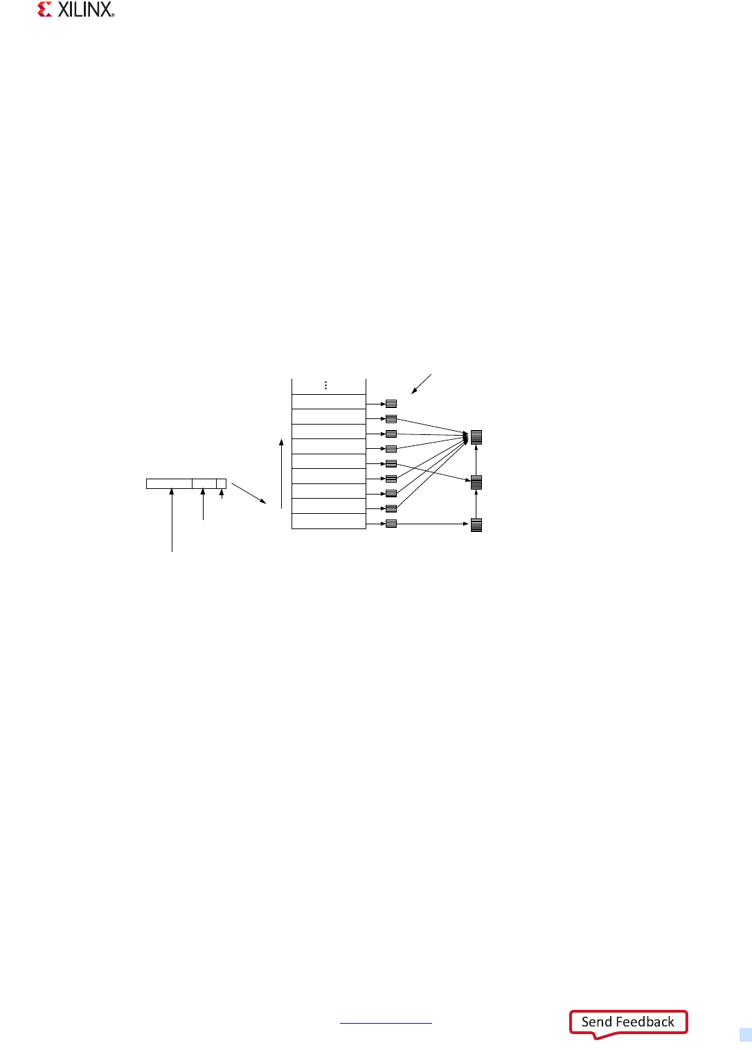
Zynq-7000 AP SoC Technical Reference Manual www.xilinx.com 446
UG585 (v1.12.1) December 6, 2017
Chapter 15: USB Host, Device, and OTG Controller
• Isochronous split transaction data streams are managed with split-transaction isochronous
transfer descriptors (siTD).
• Interrupt, Control, and Bulk data streams are managed via queue heads (QH) and queue
element transfer descriptors (qTD). These data structures are optimized to reduce the total
memory footprint of the schedule and to reduce (on average) the number of memory accesses
needed to execute a USB transaction.
15.10.2 Periodic Schedule
The periodic schedule provides interrupt and isochronous transfers by using the Periodic Frame list
of elements and transfer descriptors as shown in Figure 15-15.
Periodic Frame List
The host controller uses the Periodic Frame List to schedule isochronous and interrupt transfers. The
periodic frame list is written into memory by the HCD. The host controller hardware reads the
elements using the usb.PERIODICLISTBASE_ base address and the FRINDEX index registers. The
current element within the periodic frame list is pointed to by the FRINDEX register. The Periodic
Frame List implements a sliding window of work over time.
Note: The periodic frame list is a 4 KB page-aligned array for pointers to Isochronous and interrupt
transfer descriptors. The length of the frame list is programmable: 8, 16, 32, 64, 128, 256, 512, or
1024 elements using the usb.USBCMD [FS2] and [FS0] bit fields. When [FS2] is set = 0, then the EHCI
programming model: 256, 512 and 1024 elements can be used in [FS0]. The length of the frame list
affects the amount of system memory to allocate and the number of periodic transactions that can
be queued.
The HCD writes the memory address of the first element in the periodic frame list in the
usb.PERIODICLISTBASE_ [PERBASE_] bit field. The controller beings processing the periodic frame list
when the (micro)frame time stamp occurs.
X-Ref Target - Figure 15-15
Figure 15-15: USB Host Periodic Schedule with Example
UG585_c15_43_030713
Periodic Frame
List (EHCI)
Frame 3 Elements
Frame 1 Elements
Frame 2 Elements
Frame 0 Elements
advanced for every
USB Frame.
Programmable
number of elements:
8, 16, 32, … 1024.
Programmed by
usb.USBCMD [FS2] [FS0]
usb.PERIODLISTBASE_ [31:12]
Periodic Frame List
Element Address
(32-bit system address)
usb.FRINDEX
000
Frame 7 Elements
Frame 5 Elements
Frame 6 Elements
Frame 4 Elements
Frame 8 Elements
Interrupt QH executed
every 8 Frames
Interrupt QH executed
every 4 Frames
Interrupt QH executed
every Frame
Isochronous
Transfer
Descriptors
Last QH has terminate
bit set, T = 1.
Link Pointer
Link Pointer
Example

Zynq-7000 AP SoC Technical Reference Manual www.xilinx.com 447
UG585 (v1.12.1) December 6, 2017
Chapter 15: USB Host, Device, and OTG Controller
Note: The HCD should write only periodic schedule items (QH, iTD, siTD, FSTN) into the periodic
schedule. When using QH, it is an interrupt endpoint.
15.10.3 Asynchronous Schedule
The asynchronous schedule includes a circular list of queue heads for control and bulk transfers. The
host controller executes the data transfers after the periodic schedule is handled. This happens:
• after the controller processes the periodic list
• the periodic list is disabled, or
• the periodic list is empty.
Table 15-20: USB Host Periodic Frame List Element Bit Fields
Bits Bit Field Description
31:5 Pointer
Frame List Link Pointer (system memory pointer, 32-byte aligned):
The referenced object might be:
• an isochronous transfer descriptor (iTD for HS devices),
• a split-transaction isochronous transfer descriptor (siTD for FS
isochronous endpoints), or
• a queue head (QH for FS/LS/HS interrupts).
4:3 reserved Set = 00.
2:1 TYP Transaction Descriptor Type, TYP. Refer to section 15.12.2 Transfer
Descriptor Type (TYP) Field.
0T
Terminate Linking, T:
0: Continue linking using Frame List Link Pointer.
1: Terminate transaction (done), host controller ignores the link pointer.
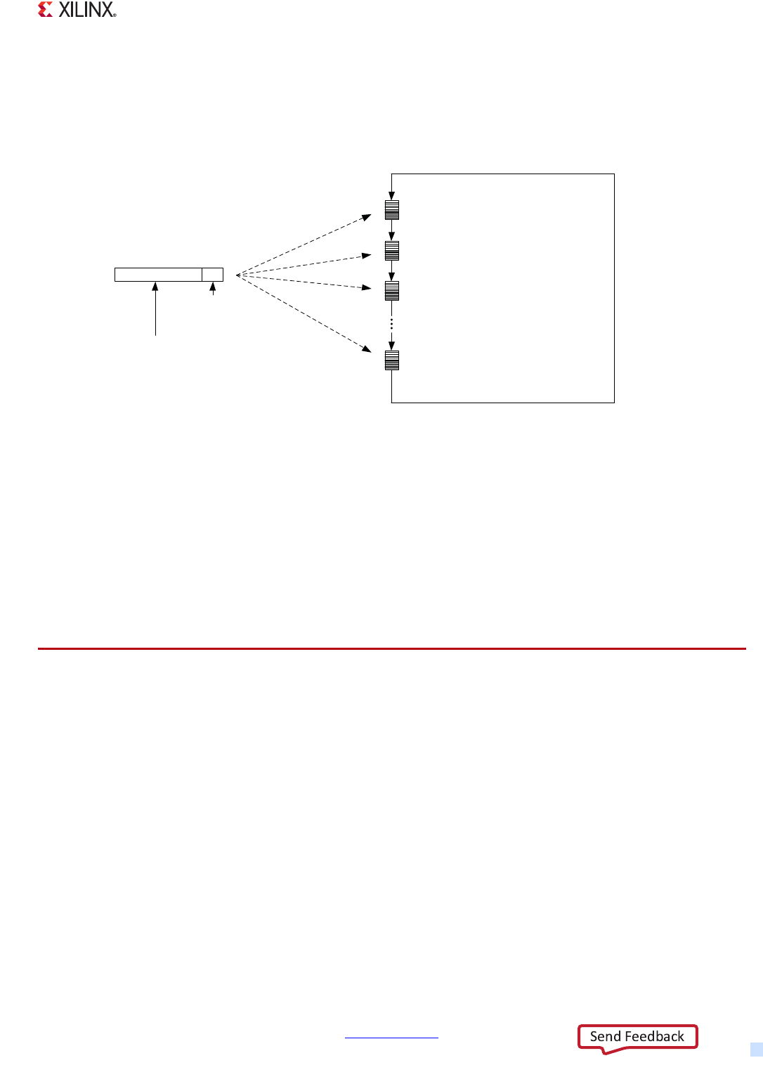
Zynq-7000 AP SoC Technical Reference Manual www.xilinx.com 448
UG585 (v1.12.1) December 6, 2017
Chapter 15: USB Host, Device, and OTG Controller
The asynchronous list is a simple circular list of queue heads that are aligned on 32-byte address
boundaries. The usb.ASYNCLISTADDR_ [31:5] bit field is a pointer to the next queue head. This bit
field is initialized by software. Hardware uses this field to traverse the Asynchronous schedule.
Hardware does not modify this field. The Asynchronous schedule implements a pure round-robin
service for the queue heads. Each queue head has one or more transfer descriptors (qTD’s). The
number of queue heads in the circular can be added to and reduced. The number of QH’s is not
limited by the EHCI specification.
15.11 EHCI Implementation
The host controller utilizes the programming mode of the Intel EHCI 1.0 specification. This includes
register models and host functionality.
15.11.1 Overview
The host controller operational mode is nearly compatible with the EHCI 1.0 specification. There are
a few differences and enhancements to handle an FS/LS link:
• Embedded Transaction Translator
•EHCI Reserved Bits
•No PCI registers
• SOF Interrupt
X-Ref Target - Figure 15-16
Figure 15-16: USB Host Controller Asynchronous Schedule Organization
UG585_c15_44_030713
Queue Head 0
Aysnchronous Queue Heads
(Bulk and Control)
Queue Head 2
Round Robin Priority.
QHs are processed as
Bandwidth allows.
Insert and Remove QH’s as needed
Queue Head 1
usb.ASYNCLISTADDR_ [31:05]
Asynchronous QH
Address Pointer
(32-bit system address)
00000
Queue Head n
Start of List
End of List

Zynq-7000 AP SoC Technical Reference Manual www.xilinx.com 449
UG585 (v1.12.1) December 6, 2017
Chapter 15: USB Host, Device, and OTG Controller
Embedded Transaction Translator
The host controller uses the DMA and protocol engines to emulate the transaction translator (TT) for
FS/LS devices attached to Zynq. The embedded transaction translator (TT) affects multiple functions
in the host controller:
°Discovery Mechanism, refer to section 15.11.3 EHCI Functional Changes for the TT
°FS/LS Data Structures, refer to section 15.11.6 FS/LS Data Structures
°Operational Model of the TT, refer to section 15.11.7 Operational Model of the TT
°Capability and Operational registers/bits, refer to section 15.11.3 EHCI Functional Changes
for the TT
°PHY Rx Commands, refer to section 15.11.3 EHCI Functional Changes for the TT
The embedded transaction translator is described in section 15.11.2 Embedded Transaction
Translator.
EHCI Reserved Bits
EHCI reserved fields should be set to zero, except those that are assigned to other functions. The
register set is summarized in section 15.3.4 Register Overview and detailed in Appendix B.
No PCI Bus Registers
This controller does not have a PCI Interface and the PCI configuration registers described in the
EHCI specification are not applicable (e.g., the frame adjustment register is not supported; the starts
of the microframes are timed by the controllers timers to deliver 125-microsecond intervals based on
the 60 MHz clock from the ULPI PHY).
SOF Interrupt
This SOF Interrupt a free running 125-microsecond interrupt for the host controller. EHCI does not
specify this interrupt but it has been added for convenience and as a potential an HCD time base. The
interrupt is indicated and enabled in the USBSTS and USBINTR registers.
Capability Register Bit Fields Added
The following additions have been added to the capability registers:
•usb.HCSPARAMS [N_TT]
• usb.HCSPARAMS [N_PTT}
Operational Register and Bit Field Added
The following additions have been added to the operational registers:
• TTCTRL is a new register.
• Addition of two-bit Port Speed: usb.PORTSC1 [PSPD].

Zynq-7000 AP SoC Technical Reference Manual www.xilinx.com 450
UG585 (v1.12.1) December 6, 2017
Chapter 15: USB Host, Device, and OTG Controller
15.11.2 Embedded Transaction Translator
The host controller emulates one transaction translator (TT) with up to 16 periodic (Iso/Int) contexts
and 2 asynchronous (bulk/ctrl) contexts. The TT allows FS/LS devices to be attached directly to the
controller in host mode without the need for hardware to implement a companion controller.
The transaction translator is modeled as an extension to EHCI specification by making use of the
standard data structures and operational models that exist in the EHCI specification. The TT is
responsible for:
• All error checking
• Field generation checking
• Formatting of all the necessary handshake actions
• Ping and data response packets on the bus
For any signal that must be generated based on a USB based time in the host controller, the protocol
engine also generates all of the token packets required by the USB protocol.
There is no separate transaction translator hardware to handle FS/LS protocols. The transaction
translator function implemented within the DMA and the protocol engine blocks to support direct
connection to LS and FS devices.
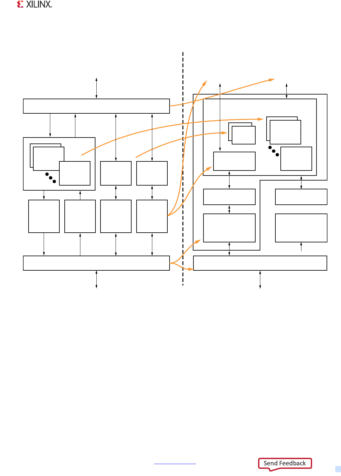
Zynq-7000 AP SoC Technical Reference Manual www.xilinx.com 451
UG585 (v1.12.1) December 6, 2017
Chapter 15: USB Host, Device, and OTG Controller
Functional Block Diagram
On the left side of Figure 15-17 is a typical hub implementation with a companion transaction
translator controller. It shows two ongoing asynchronous transactions capable of ping-pong access
from each end. Periodic traffic is aggregated into a single data stream for each direction while a table
of state and context for each pipe is stored within the transaction translator.
The right side of Figure 15-17 shows how the same functions have been integrated into the host
controller. The advantage of integrating those functions into the host controller is that the changes
to the EHCI host controller driver (HCD) are minimal while allowing direct connection of FS and LS
devices without the need for a companion controller or external USB 2.0 hub. In addition, the host
controller with the transaction translator requires less local data storage than a hub-based
transaction translator because the data storage is provided by main memory instead of
hardware-based RAM. The host controller supports 16 periodic contexts and 2 asynchronous
contexts.
X-Ref Target - Figure 15-17
Figure 15-17: USB Host Embedded Transaction Translator Implementation
UG585_c15_11_030413
Traditional Hardware Based Companion
Controller In a Hub-based Design
Embedded Transaction Translator in Host Mode
Using EHCI Software Model
EHCI High Speed Controller
Port Controller
Latency FIFOs
Small
Latency FIFOs
High Speed
Protocol Engine
Full/Low Speed
Protocol Engine
High-speed Handler
Full/Low Speed Handler
HS USB 2.0
EHCI Shared
Memory
EHCI Software
Stack
FS/LS USB FS/LS USB
Iso/Int
State &
Context Iso/Int
State &
Context
B/C
State &
Context
B/C
Transfer
TT Traffic
Management
Iso/Int
Transfer
(16)
(2)
(16) Iso/Int
Transfer
B/C
State &
Context
B/C
In/Out
FIFO
B/C
In/Out
FIFO
Iso/Int
Start-
split
FIFO
Iso/Int
Compl.
Split
FIFO

Zynq-7000 AP SoC Technical Reference Manual www.xilinx.com 452
UG585 (v1.12.1) December 6, 2017
Chapter 15: USB Host, Device, and OTG Controller
15.11.3 EHCI Functional Changes for the TT
This section includes:
• Port Reset Timer to off-load software
• Port Speed detection
In a standard EHCI controller design, the Host controller driver (HCD) detects a full-speed or
low-speed device by noting if the port enable bit is set after the port reset operation. The port
enable is set after the port reset operation when the host and device negotiate a High-Speed
connection (i.e., chirp completes successfully).
Because the controller emulates a transaction translator (TT), the port enable is always set after the
port reset operation regardless of the result of the host device chirp result. The resulting port speed
is indicated by the usb.PORTSC1 [PSPD] bit field.
Therefore, a standard EHCI HCD requires alteration to handle direct connection to Full and Low
speed devices or hubs. The changes are fundamental and summarized in Table 15-21.
15.11.4 Port Reset Timer Enhancement
The port connect methods specified by EHCI require setting the port reset bit in the PORTSC register
for a duration of 10 ms. The controller has timers that can count the 10 ms reset pulse to alleviate the
requirement of the HCD to control this timing. The basic connection for the HCD software:
Example: Port Reset Timer for Discovery
This example show a simple attach event and the step that is made optional because of the Port
Reset Timer feature.
1. Wait for device to attach. Receive a port connect change [Port Change Interrupt].
Table 15-21: EHCI HCD Alteration
Function Standard EHCI Embedded Transaction Translator
Hub Speed After port enable bit is set following a
connection and reset sequence, the
device/hub is assumed to be HS.
After port enable bit is set following a connection and reset
sequence, the device (hub) speed is noted from PORTSC1.
FS/LS devices FS and LS devices are assumed to be
downstream from a HS hub thus, all
port-level control is performed through
the Hub Class to the nearest Hub.
FS/LS device can be either downstream from an HS hub or
directly attached. When its downstream, then port-level
control is done using the Hub Class through the nearest
Hub. When a FS/LS device is directly attached, then
port-level control is accomplished using PORTSC1.
Split Target FS and LS devices are assumed to be
downstream from a HS hub with
HubAddr=X; where HubAddr > 0 and
HubAddr is the address of the Hub
where the bus transitions from HS to
FS/LS (i.e. Split target hub).
FS/LS device can be either downstream from a HS hub with
HubAddr = X [HubAddr > 0] or directly attached; where
HubAddr = [TTHA]. [TTHA] is programmable and defaults
to 0. HubAddr is the address of the Root Hub where the bus
transitions from HS to FS/LS (i.e. Split target hub is the root
hub).

Zynq-7000 AP SoC Technical Reference Manual www.xilinx.com 453
UG585 (v1.12.1) December 6, 2017
Chapter 15: USB Host, Device, and OTG Controller
2. Reset the device. Writes a 1 to the usb.PORTSC1 [PR] bit. assumes the
3. Optional Step to de-assert Reset. The HCD normally writes a 0 to the [PR] bit to de-assert the
reset after 10 ms. This step, which is necessary in a standard EHCI design, can be omitted. Should
the EHCI HCD attempt to write a 0 to the reset bit while a reset is in progress, the write is ignored
and the reset continues until completion.
4. Wait for device to be operational. Receive the [PCI] interrupt to indicate the Port Enable
Change. The device is now operational and at this point the port speed has been determined.
15.11.5 Port Speed Detection Mechanism
After the port change interrupt indicates that a port is enabled, the EHCI stack should determine the
port speed. Unlike the EHCI implementation which re-assign the port owner for any device that does
not connect at High-Speed, this host controller supports direct attach of non High-Speed devices.
Therefore, the following differences are important regarding port speed detection:
• Port owner is read-only and always reads 0.
• A 2-bit port speed indicator (PSPD) has been added to PORTSC1 to provide the current
operating speed of the port to the HCD.
• A 1-bit High Speed indicator (HSP) has been added to PORTSC1 to signify that the port is in
High-Speed vs. Full/Low Speed - This information is redundant with the 2-bit Port Speed
indicator above.
15.11.6 FS/LS Data Structures
The data structures used by the TT for FS/LS transactions are similar to an HS hub. The hub address
and endpoint speed fields should be set for directly attached FS/LS devices and hubs:
• QH (FS/LS)- Asynchronous (Bulk and Control endpoints) and Periodic (Interrupt endpoint)
°Hub Address = TTHA (default TTHA = 0)
°Transactions to directly attached device or hub.
-QH.EPS = Port Speed (for both FS and LS)
°Transactions to a device downstream from direct attached HS hub.
- QH.EPS = Downstream Device Speed
°Maximum Packet Size must be less than or equal 64 or undefined behavior might result.
°When QH.EPS = 01 (LS) and usb.PORTSC1 [PSPD] = 00 (FS), a LS-pre-PID will be sent before
the transmitting LS traffic.
• siTD (FS) - Periodic (ISO endpoint)
°All FS IsoUSB transactions:
- Hub Address = (default TTHA = 0)
-siTD.EPS = 00 (full speed)
°Maximum Packet Size must less than or equal to 1023 or undefined behavior might result.
Note: FSTN data structures are used for FS and LS devices that are downstream of a high speed hub
(not when FS or LS device is connected directly to the host controller.)

Zynq-7000 AP SoC Technical Reference Manual www.xilinx.com 454
UG585 (v1.12.1) December 6, 2017
Chapter 15: USB Host, Device, and OTG Controller
15.11.7 Operational Model of the TT
The operational models are well defined for the behavior of the transaction translator (see USB 2.0
specification) and for the EHCI controller to move packets between system memory and a USB-HS
hub. Since the transaction translator exists within the host controller there is no physical bus
between EHCI HCD and the USB FS/LS bus. These sections briefly discuss the operational model for
how the EHCI and transaction translator operational models are combined without the physical bus
between. The following sections assume the reader is familiar with both the EHCI and USB 2.0
transaction translator operational models.
Microframe Pipeline
The EHCI operational model uses the concept of H-frames and B-frames to describe the pipeline
between the Host (H) and the Bus (B). The embedded transaction translator shall use the same
pipeline algorithms specified in the USB 2.0 specification for a Hub-based Transaction Translator.
All periodic transfers always begin at B-frame 0 (after SOF) and continue until the stored periodic
transfers are complete. As an example of the microframe pipeline implemented in the embedded
transaction translator, all periodic transfers that are tagged in EHCI to execute in H-frame 0 will be
ready to execute on the bus in B-frame 0.
It is important to note that when programming the S-mask and C-masks in the EHCI data structures
to schedule periodic transfers for the embedded transaction translator, the EHCI HCD must follow
the same rules specified in EHCI for programming the S-mask and C-mask for downstream
hub-based transaction translators.
Once periodic transfers are exhausted, any stored asynchronous transfer will be moved.
Asynchronous transfers are opportunistic in that they shall execute whenever possible and their
operation is not tied to Hframe and B-frame boundaries with the exception that an asynchronous
transfer cannot babble through the SOF (start of B-frame 0.)
Split Transfer State Machines
When the controller attaches to a downstream FS/LS device via an HS hub, the controller can initiates
split transfers to allow for traffic to other devices to be intertwined.
The start and complete split operational model differs from EHCI slightly because there is no bus
medium between the EHCI controller and the embedded transaction translator. Where a start or
complete-split operation would occur by requesting the split to the HS hub, the start/complete split
operation is simple an internal operation to the embedded transaction translator. Table 15-22
summarizes the conditions where handshakes are emulated from internal state instead of actual
handshakes to HS split bus traffic.
Table 15-22: USB Handshake Emulation Conditions
Condition TT Response
Start-Split: All asynchronous buffers full. NAK
Start-Split: All periodic buffers full. ERR
Start-Split: Success for start of async. transaction. ACK

Zynq-7000 AP SoC Technical Reference Manual www.xilinx.com 455
UG585 (v1.12.1) December 6, 2017
Chapter 15: USB Host, Device, and OTG Controller
Asynchronous Transaction Scheduling and Buffer Management
The following USB 2.0 specification items are implemented in the Transaction Translator:
USB 2.0 - 11.17.3Sequencing is provided and a packet length estimator ensures
no full-speed/low-speed packet babbles into SOF time.
USB 2.0 - 11.17.4Transaction tracking for 2 data pipes.
USB 2.0 - 11.17.5Clear_TT_Buffer capability provided through the use of the
TTCTRL register.
Periodic Transaction Scheduling and Buffer Management
The following USB 2.0 specification items are implemented in the transaction translator:
USB 2.0 - 11.18.6.[1-2]Abort of pending start-splits
- EOF (and not started in microframes 6)
- Idle for more than 4 microframes (Abort of pending complete-splits)
-EOF
- Idle for more than 4 microframes
USB 2.0 - 11.18.[7-8]Transaction tracking for up to 16 data pipes.
Caution: Limiting the number of tracking pipes in the embedded -TT to four (4) will impose the
restriction that no more than four periodic transactions (INTERRUPT/ISOCHRONOUS) can be
scheduled through the TT per frame. the number 16 was chosen in the USB specification because it
is sufficient to ensure that the high-speed to full-speed periodic pipeline can remain full. keeping the
pipeline full puts no constraint on the number of periodic transactions that can be scheduled in a
frame and the only limit becomes the flight time of the packets on the bus.
Note: There is no data schedule mechanism for these transactions other than the microframe
pipeline. The emulated TT assumes the number of packets scheduled in a frame does not exceed the
frame duration (1 ms) or else undefined behavior might result.
15.11.8 Port Test Mode
Port Test Control mode behaves as described by EHCI. The modes are set using the usb.PORTSC1
[PTC] bit field.
Start-Split: Start periodic transaction. No Handshake (OK)
Complete-Split: Failed to find transaction in queue. Bus Time Out
Complete-Split: Transaction in queue is busy. NYET
Complete-Split: Transaction in queue is complete. Actual Handshake
Table 15-22: USB Handshake Emulation Conditions (Cont’d)
Condition TT Response
Zynq-7000 AP SoC Technical Reference Manual www.xilinx.com 456
UG585 (v1.12.1) December 6, 2017
Chapter 15: USB Host, Device, and OTG Controller
15.12 Host Data Structures Reference
These descriptor data structures are compatible with the EHCI specification with some differences as
noted in section 15.11 EHCI Implementation.
The data structures defined in this section are (from the host controller's perspective) a mix of
read-only and read/writable fields. The host controller preserves the read-only fields.
Section Content
•15.12.1 Descriptor Usage
•15.12.2 Transfer Descriptor Type (TYP) Field
•15.12.3 Isochronous (High Speed) Transfer Descriptor (iTD)
•15.12.4 Split Transaction Isochronous Transfer Descriptor (siTD)
•15.12.5 Queue Element Transfer Descriptor (qTD)
•15.12.6 Queue Head (QH)
•15.12.7 Transfer Overlay Area
•15.12.8 Periodic Frame Span Traversal Node (FSTN)
15.12.1 Descriptor Usage
15.12.2 Transfer Descriptor Type (TYP) Field
The Transaction Type bit field is defined and used in the situations listed in Table 15-24.
Table 15-23: USB Host Descriptor Usage
Descriptors Periodic Frame List Asynchronous List
Isochronous Interrupt Bulk Control
iTD, siTD yes no no
QH, qTD no yes yes yes
FSTN (Low-, Full-speed) no yes
Table 15-24: USB Host Transfer Descriptor Type (TYP) Bit Field
Data Structure iTD
00
QH
01
siTD
10
FSTN
11 Description
Periodic Frame List XXXX
Figure 15-15 USB Host Periodic Schedule with Example
iTD X~~~
Table 15-25 USB Host Isochronous Transfer Descriptor
(iTD) Format
siTD ~X~~
Table 15-29 USB Host Split-Transaction Isochronous
Descriptor (siTD) Format
Zynq-7000 AP SoC Technical Reference Manual www.xilinx.com 457
UG585 (v1.12.1) December 6, 2017
Chapter 15: USB Host, Device, and OTG Controller
15.12.3 Isochronous (High Speed) Transfer Descriptor (iTD)
The format of a high-speed isochronous transfer descriptor is illustrated in Table 15-25. This
structure is used only for high-speed isochronous endpoints. The iTD’s must be aligned on a 32-byte
boundary.
iTD DWord 0: Next Link Pointer
The first DWord of an iTD is a pointer to the next schedule data structure.
QH ~~X~
Table 15-40 USB Host Queue Head (QH) Descriptor Format
FSTN ~~~X
Table 15-45 USB Host Frame Span Traversal Node
Descriptor (FSTN) Format
Table 15-24: USB Host Transfer Descriptor Type (TYP) Bit Field (Cont’d)
Data Structure iTD
00
QH
01
siTD
10
FSTN
11 Description
Table 15-25: USB Host Isochronous Transfer Descriptor (iTD) Format
Reference Type 3130292827262524 2322212019181716151413 121110 9 8 7 6 5 4 32 1 0DWord
Table 15-26 Next dTD Next Link Pointer 00 TYP T 0
Table 15-27
Transaction Status and Control
Status Transaction 0 Length IOC PG * Transaction 0 Offset * 1
Status Transaction 1 Length IOC PG * Transaction 1 Offset * 2
Status Transaction 2 Length IOC PG * Transaction 2 Offset * 3
Status Transaction 3 Length IOC PG * Transaction 3 Offset * 4
Status Transaction 4 Length IOC PG * Transaction 4 Offset * 5
Status Transaction 5 Length IOC PG * Transaction 5Offset * 6
Status Transaction 6 Length IOC PG * Transaction 6 Offset * 7
Status Transaction 7 Length IOC PG * Transaction 7 Offset * 8
Table 15-28
Buffer Pointer List
Buffer Pointer (Page 0) EndPt R Device Address 9
Buffer Pointer (Page 1) IO Maximum Packet Size 10
Buffer Pointer (Page 2) reserved Mult 11
Buffer Pointer (Page 3) reserved 12
Buffer Pointer (Page 4) reserved 13
Buffer Pointer (Page 5) reserved 14
Buffer Pointer (Page 6) reserved 15
Host Controller Read/Write Host Controller Read-only
* means these fields may be modified by the Host controller if the IO field indicates an OUT (DWords 1 to 8).
Table 15-26: USB Host iTD DWord 0: Next Link Pointer
Bits Description
31:5 Next Link Pointer. These bits correspond to memory address signals [31:5], respectively. This field
points to another isochronous transaction descriptor (iTD/siTD) or a QH.
4:3 Reserved. Field reserved and should be set to 0.

Zynq-7000 AP SoC Technical Reference Manual www.xilinx.com 458
UG585 (v1.12.1) December 6, 2017
Chapter 15: USB Host, Device, and OTG Controller
iTD DWords 1 to 8: Transaction Status and Control List
DWords 1 through 8 are transaction control and status. Each transaction description includes:
• Status results field
• Transaction length (bytes to send for OUT transactions and bytes received for IN transactions)
• Buffer offset. The PG and Transaction x Offset fields are used with the buffer pointer list to
construct the starting buffer address for the transaction
The host controller uses the information in each transaction description plus the endpoint
information contained in the first three DWords of the Buffer Page Pointer list, to execute a
transaction on the USB.
2:1 Transaction Descriptor Type, TYP. Set to 00 (iTD type). Refer to section 15.12.2 Transfer Descriptor
Type (TYP) Field for general information.
0 Terminate transfer, T.
•0: link to the Next iTD Pointer field; the address is valid.
•1: end the transaction, the Next iTD Pointer field is not valid.
Table 15-27: USB Host iTD Dwords 1 to 8: Transaction Status and Control List
Bits Description
31:28 Status:
Active Status [31]. Set to 1 by the HCD to enable the execution of an isochronous transaction. When
the transaction associated with this descriptor is completed, the host controller sets this bit to 0
indicating that a transaction for this element should not be executed when it is next encountered in
the schedule.
Data Buffer Error Status [30]. Set to a 1 by the host controller during status update to indicate that
the host controller is unable to keep up with the reception of incoming data (overrun) or is unable to
supply data fast enough during transmission (under run). If an overrun condition occurs, no action is
necessary.
Babble Detected Status [29]. Set to 1 by the host controller during status update when 'babble' is
detected during the transaction generated by this descriptor.
Transaction Error Status [28]. Set to 1 by the host controller during status update in the case where
the host did not receive a valid response from the device (Timeout, CRC, Bad PID, etc.). This bit can
only be set for isochronous IN transactions.
27:16 Transaction {7:0} Length. For an OUT transaction, this field is the number of data bytes the host
controller will send during the transaction. The host controller is not required to update this field to
reflect the actual number of bytes transferred during the transfer.
For an IN transaction, the initial value of the field is the number of bytes the host expects the
endpoint to deliver. During the status update, the host controller writes back the field the number of
bytes successfully received.
• 000h: zero length data.
• 001h: one byte.
• 002h: two bytes.
• ...
• C00h: 3072 bytes (maximum).
Table 15-26: USB Host iTD DWord 0: Next Link Pointer (Cont’d)
Bits Description

Zynq-7000 AP SoC Technical Reference Manual www.xilinx.com 459
UG585 (v1.12.1) December 6, 2017
Chapter 15: USB Host, Device, and OTG Controller
iTD DWords 9 to 15: Buffer Page Pointer List
DWords 9-15 of an isochronous transaction descriptor are nominally page pointers (4 KB aligned) to
the data buffer for this transfer descriptor. This data structure requires the associated data buffer to
be contiguous, but allows the physical memory pages to be non-contiguous. Seven page pointers
are provided to support the expression of eight isochronous transfers. The seven pointers allow for
3 (transactions) * 1,024 (maximum packet size) * 8 (transaction records) (24,576 bytes) to be moved
with this data structure, regardless of the alignment offset of the first page.
Since each pointer is a 4 KB aligned page pointer, the least significant 12 bits in several of the page
pointers are used for other purposes.
15 Interrupt On Complete, IOC. If this bit is set to 1, it specifies that when this transaction completes,
the host controller should issue an interrupt at the next interrupt threshold.
14:12 Page Select, PG. These bits are set by the HCD to indicate which of the buffer page pointers the offset
field in this slot should be concatenated to produce the starting memory address for this transaction.
The valid range of values for this field is 0 to 6.
11:0 Transaction {7:0} Offset. This field is a value that is an offset, expressed in bytes, from the beginning
of a buffer. This field is concatenated onto the buffer page pointer indicated in the adjacent PG field
to produce the starting buffer address for this transaction.
Table 15-28: USB Host iTD DWords 9 to 15: Buffer Page Pointer List
Bits Description
DWord 9
31:12 Buffer Pointer (Page 0). 4KB-aligned pointer to system memory address bits [31:12].
11:8 Endpoint Number (EndPt). Select the endpoint for the device serving as the data source or sink.
7 Reserved. Bit reserved for future use and should be initialized by the HCD to 0.
6:0 Device Address. Select the specific device serving as the data source or sink.
DWord 10
31:12 Buffer Pointer (Page 1). 4KB-aligned pointer to system memory address bits [31:12].
11 Direction (IO). Select the high-speed transaction for an IN or OUT PID.
•0: OUT
•1: IN
10:0 Maximum Packet Size. This directly corresponds to the maximum packet size of the associated
endpoint (wMaxPacketSize). This field is used for high-bandwidth endpoints where more than one
transaction is issued per transaction description (e.g., per microframe).
This field is used with the Multi field to support high-bandwidth pipes. This field is also used for all
IN transfers to detect packet babble. The HCD should not set a value larger than 1,024 (400h). Any
value larger yields undefined results.
DWord 11
31:12 Buffer Pointer (Page 2). 4KB-aligned pointer to system memory address bits [31:12].
11:2 Reserved. This bit reserved for future use and should be set to 0.
Table 15-27: USB Host iTD Dwords 1 to 8: Transaction Status and Control List (Cont’d)
Bits Description

Zynq-7000 AP SoC Technical Reference Manual www.xilinx.com 460
UG585 (v1.12.1) December 6, 2017
Chapter 15: USB Host, Device, and OTG Controller
1:0 Mult. Selects the number of transactions to execute per transaction description (e.g. per
microframe).
•00: Reserved. A 0 in this field yields undefined results
•01: One transaction to be issued for this endpoint per microframe
•10: Two transactions to be issued for this endpoint per microframe
•11: Three transactions to be issued for this endpoint per microframe
DWords 12 to 15
31:12 Buffer Pointer (Pages 3 to 6). 4KB-aligned pointer to memory address bits [31:12].
11:0 Reserved. This bit reserved for future use and should be set to 0.
Table 15-28: USB Host iTD DWords 9 to 15: Buffer Page Pointer List (Cont’d)
Bits Description
Zynq-7000 AP SoC Technical Reference Manual www.xilinx.com 461
UG585 (v1.12.1) December 6, 2017
Chapter 15: USB Host, Device, and OTG Controller
15.12.4 Split Transaction Isochronous Transfer Descriptor (siTD)
This data structure is used to manage FS isochronous transfers via split transactions to USB 2.0 Hub
Transaction Translator. There are additional fields used for addressing the hub and scheduling the
protocol transactions (for periodic).
siTD DWord 0: Next Link Pointer
DWord 0 of a siTD is a pointer to the next schedule data structure.
siTD DWords 1 and 2: Endpoint Capabilities and Characteristics
DWords 1 and 2 specify static information about the full-speed endpoint, the addressing of the
parent Companion Controller, and microframe scheduling control.
Table 15-29: USB Host Split-Transaction Isochronous Descriptor (siTD) Format
Reference Type 3130292827262524 2322212019181716151413 121110 9 8 7 6 5 4 32 1 0DWord
Table 15-30 Next Ptr Next Link Pointer 00 TYP T 0
Table 15-31 Endpt
Cap/Char
IO Port Number R Hub Addr reserved EndPt R Device Address 1
reserved Microframe C-mask Microframe S-mask 2
Table 15-32 xfer State IOC Preserved Total Bytes Microframe C-prog-mask Status 3
Table 15-33 Buffer
Page Ptrs
Buffer Pointer (Page 0) Current Offset 4
Buffer Pointer (Page 1) reserved TP T-count 5
Table 15-34 Back Link Back Pointer 0 T 6
Host Controller Read/Write Host Controller Read-only
Table 15-30: USB Host siTD DWord 0: Next Link Pointer
Bits Description
31:5 Next Link Pointer. This field contains the address of the next data object to be processed in the
periodic list and corresponds to memory address signals [31:5], respectively.
2:1 Transaction Descriptor Type, TYP. Set to 10 (siTD type). Refer to section 15.12.2 Transfer Descriptor
Type (TYP) Field for general information.
0 Terminate transfer, T.
•0: link to the Next Link Pointer field; the address is valid.
•1: end the transaction, the Next Link Pointer field is not valid.
Table 15-31: USB Host siTD DWords 1 and 2:Endpoint State
Bits Description
DWord 1: Endpoint and Transaction Translator Characteristics
31 Direction, IO. Encodes the FS transaction as an IN or OUT.
•0: OUT
•1: IN
30:24 Port Number. This field is the port number of the recipient Transaction Translator.
23 Reserved. Bit reserved and should be set to 0.
22:16 Hub Address, Hub Addr. Device address of the Companion Controller’s hub.

Zynq-7000 AP SoC Technical Reference Manual www.xilinx.com 462
UG585 (v1.12.1) December 6, 2017
Chapter 15: USB Host, Device, and OTG Controller
Microframe C-mask
The split completion mask field, siTD.Microframe C-mask, along with the Active and SplitXstate fields in the
Status byte, is used to determine during which microframes the host controller should execute complete-split
transactions. This field is a straight bit position field, so if bit [0] is set then the complete-split transaction should
occur in the first microframe, if bit [1] is set = 1 then it should occur in the second microframe, and so on. When
the criteria for using this field is met, a 0 value has undefined behavior.
The host controller uses the value of the three low-order bits of the FRINDEX register to index into this bit field.
If the FRINDEX register value indexes to a position where the microframe C-Mask field is a 1, then this siTD is a
candidate for transaction execution.
There can be more than one bit in this mask set.
The C-Mask can be set for multiple micro frames, as it is not known in which microframe the transaction will
complete. So the C-Mask can be set for the micro frame after the S-Mask and all subsequent micro fames
thereafter. The C-Mask field should not have a bit set to the same microframe as the S-Mask is set to.
Microframe S-mask
The split start mask field, siTD.Micro S-mask, along with the Active and SplitX-state fields in the Status byte, is
used to determine during which microframes the host controller should execute start-split transactions.
The host controller uses the value of the three low-order bits of the FRINDEX register to index into this bit field.
If the FRINDEX register value indexes to a position where the microframe S-mask field is a 1, then this siTD is a
candidate for transaction execution.
A 0 value in this field, in combination with existing periodic frame list, has undefined results.
This field should have only one bit set to 1 at any given time. Having more than one bit set will result in
undefined results.
15:12 Reserved. Field reserved and should be set to 0.
11:8 Endpoint Number, EndPt. 4-bit field selects the endpoint on the device serving as the data source or
sink.
7 Reserved. Bit reserved and should be set to 0.
6:0 Device Address. Select the specific device serving as the data source or sink.
DWord 2: Microframe Schedule Control
31:16 Reserved. Field reserved and should be set to 0.
15:8 Split Completion Mask, Microframe C-mask.
This field (along with the Active and SplitXstate fields in the Status byte) is used to determine during
which microframes the host controller should execute complete-split transactions. Refer to the text
for details.
7:0 Split Start Mask, Microframe S-mask.
This field (along with the Active and SplitX-state fields in the Status byte) is used to determine during
which microframes the host controller should execute start-split transactions. Refer to the text for
details.
Table 15-31: USB Host siTD DWords 1 and 2:Endpoint State (Cont’d)
Bits Description

Zynq-7000 AP SoC Technical Reference Manual www.xilinx.com 463
UG585 (v1.12.1) December 6, 2017
Chapter 15: USB Host, Device, and OTG Controller
siTD DWord 3: Transfer Status and Control
DWord 3 is used to manage the state of the split data transfer.
Status bits [7:0]
•Active Status [7]. Set to 1 by the HCD to enable the execution of an isochronous split
transaction by the Host Controller
•ERR Status [6]. Set to a 1 by the host controller when an ERR response is received from the
Companion Controller.
•Data Buffer Error Status [5]. Set to a 1 by the host controller during status update to indicate
that the host controller is unable to keep up with the reception of incoming data (overrun) or is
unable to supply data fast enough during transmission (under run). In the case of an under run,
the host controller will transmit an incorrect CRC (thus invalidating the data at the endpoint). If
an overrun condition occurs, no action is necessary.
•Babble Detected Status [4]. Set to 1 by the Host Controller during status update when 'babble'
is detected during the transaction generated by this descriptor.
•Transaction Error Status [3]. Set to 1 by the host controller during status update in the case
where the host did not receive a valid response from the device (Timeout, CRC, Bad PID, etc.).
This bit can only be set for isochronous IN transactions.
•Missed Microframe Status [2]. The host controller detected that a host-induced holdoff
caused the host controller to miss a required complete-split transaction.
•Split Transaction State Status [1].
- 0: Do Start Split. This value directs the host controller to issue a Start split transaction to
the endpoint when a match is encountered in the S-mask.
- 1: Do Complete Split. This value directs the host controller to issue a Complete split
transaction to the endpoint when a match is encountered in the C-mask.
•Reserved [0]. Bit reserved for future use and should be set to 0.
Table 15-32: USB Host siTD DWord 3: Transfer Status and Control
Bits Description
31 Interrupt On Complete, IOC.
•0: Do not interrupt when transaction is complete
•1: Do interrupt when transaction is complete
When the host controller determines that the split transaction has completed it will assert a hardware
interrupt at the next interrupt threshold.
30 Page Select, P. Used to indicate which data page pointer should be concatenated with the Current
Offset field to construct a data buffer pointer (0 selects Page 0 pointer and 1 selects Page 1). The host
controller is not required to write this field back when the siTD is retired (Active bit transitioned from
a 1 to a 0).
29:26 Reserved. Field reserved and should be set to 0.
25:16 Total Bytes To Transfer, Total Bytes. This field is initialized by the HCD to the total number of bytes
expected in this transfer. Maximum value is 1,023 (3FFh).
15:8 Microframe Complete-split Progress Mask, uFrame C prog-mask. This field is used by the host
controller to record which split-completes has been executed.
7:0 Status [7:0]. Refer to text.

Zynq-7000 AP SoC Technical Reference Manual www.xilinx.com 464
UG585 (v1.12.1) December 6, 2017
Chapter 15: USB Host, Device, and OTG Controller
siTD DWords 4 and 5: Buffer Pointer List
DWords 4 and 5 are the data buffer page pointers for the transfer. This structure supports one
physical page cross. The most significant 20 bits of each DWord in this section are the 4K (page)
aligned buffer pointers. The least significant 12 bits of each DWord are used as additional transfer
state.
siTD DWord 6: Back Link Pointer
DWord 6 of a siTD is simply another schedule link pointer. This pointer is either 0 or references an
siTD data structure. This pointer cannot reference any other schedule data structure.
Table 15-33: USB Host siTD DWords 4 and 5: Buffer Pointers
Bits Description
DWord 4
31:12 Buffer Pointer (Page 0). 4 KB aligned pointer to system memory address bits [31:12].
11:0 Current Offset. The 12 least significant bits of the Page 0 pointer is the current byte offset for the
current page pointer (as selected with the page select bit (P field)). The host controller is not required
to write this field back when the siTD is retired (Active bit transitioned from a 1 to a 0).
DWord 5
31:12 Buffer Pointer (Page 1). 4 KB aligned pointer to system memory address bits [31:12].
11:5 Reserved. Bit reserved for future use and should be set to 0.
4:3 Transition position, TP. This field is used with T-count to determine whether to send all, first, middle,
or last with each outbound transaction payload. The HCD must initialize this field with the
appropriate starting value. The host controller must correctly manage this state during the lifetime
of the transfer. The bit encodings are:
•00: All. Entire FS transaction data payload is in this transaction (the payload is less than or equal
to 188 bytes.)
•01: Begin. First data payload for a FS transaction that is greater than 188 bytes.
•10: Mid. Middle payload for a FS OUT transaction that is greater than 188 bytes.
•11: End. Last payload for a FS OUT transaction that was greater than 188 bytes.
2:0 Transaction count, T-Count. The HCD initializes this field with the number of OUT start-splits this
transfer requires. Any value larger than 6 is undefined.
Table 15-34: USB Host siTD DWord 6: Back Pointer
Bits Description
31:5 Back Pointer. Physical memory pointer to a siTD.
4:1 Reserved. Field reserved and should be set to 0.
0 Terminate transfer, T.
•0: link to the Back Pointer field; the address is valid.
•1: end the transaction, the Back Pointer field is not valid.
Zynq-7000 AP SoC Technical Reference Manual www.xilinx.com 465
UG585 (v1.12.1) December 6, 2017
Chapter 15: USB Host, Device, and OTG Controller
15.12.5 Queue Element Transfer Descriptor (qTD)
This data structure is only used with a queue head. This data structure is used for one or more USB
transactions. This data structure is used to transfer up to 20,480 (5 times 4,096) bytes. The structure
contains two structure pointers used for queue advancement, a DWord of transfer state, and a
five-element array of data buffer pointers. This structure is 32 bytes (or one 32-byte cache line). This
data structure must be physically contiguous.
The buffer associated with this transfer must be virtually contiguous. The buffer can start on any byte
boundary. A separate buffer pointer list element must be used for each physical page in the buffer,
regardless of whether the buffer is physically contiguous.
Host controller updates (host controller writes) to stand-alone qTD’s only occur during transfer
retirement. References in the following bit field definitions of updates to the qTD are to the qTD
portion of a queue head.
qTD DWord 0: Next Pointer
The first DWord of an element transfer descriptor is a pointer to another transfer element descriptor.
Table 15-35: USB Host Transfer Descriptor (qTD) Format
Reference Type 3130292827262524 2322212019181716151413 121110 9 8 7 6 5 4 32 1 0DWord
Table 15-36
Transfer Overlay Area
Next qTD Pointer 0000 T 0
Table 15-37 Alternate Next qTD Pointer 0000 T 1
Table 15-38
Transfer
Results
DT Total Bytes IOC C_Page Cerr PID Status 2
Table 15-39
Buffer Pointer (Page 0) Current Offset 3
Buffer Pointer (Page 1) reserved 4
Buffer Pointer (Page 2) reserved 5
Buffer Pointer (Page 3) reserved 6
Buffer Pointer (Page 4) reserved 7
Host Controller Read/Write Host Controller Read-only
Table 15-36: USB Host qTD DWord 0: Next Element Transfer Pointer
Bits Description
31:5 Next Transfer Element Pointer, Next qTD Pointer. This field contains the physical memory address of
the next qTD to be processed. The field corresponds to memory address bits [31:5], respectively.
4:1 Reserved. Field reserved and should be set to 0.
0 Terminate transfer, T.
•0: link to the Next qTD Pointer field; the address is valid.
•1: end the transaction, the Next qTD Pointer field is not valid.

Zynq-7000 AP SoC Technical Reference Manual www.xilinx.com 466
UG585 (v1.12.1) December 6, 2017
Chapter 15: USB Host, Device, and OTG Controller
qTD DWord 1: Alternate Next Element Pointer
The second DWord of a queue element transfer descriptor is used to support hardware-only advance
of the data stream to the next client buffer on short packet. To be more explicit the host controller
will always use this pointer when the current qTD is retired due to short packet.
qTD DWord 2: Token
The third DWord of a queue element transfer descriptor contains most of the information the host
controller requires to execute a USB transaction (the remaining endpoint-addressing information is
specified in the queue head). The status field reflects the last transaction performed on this qTD.
Note: The field descriptions forward reference fields defined in the queue head. Where necessary,
these forward references are preceded with a QH notation.
Table 15-37: USB Host qTD DWord 1: Alternate Next Element Pointer
Bits Description
31:5 Alternate Next Transfer Element Pointer, Alternate Next qTD Pointer.
This field contains the physical memory address of the next qTD to be processed in the event that the
current qTD execution encounters a short packet (for an IN transaction). The field corresponds to
memory address signals [31:5], respectively.
4:1 Reserved. Field reserved and should be set to 0.
0 Terminate transfer, T.
•0: link to the Alternate Next dTD Pointer field; the address is valid.
•1: end the transaction, the Alternate Next dTD Pointer field is not valid.
Table 15-38: USB Host qTD DWord 2: DT, Total Bytes
Bits Description
31 Data Toggle, DT. This is the data toggle sequence bit. The use of this bit depends on the setting of
the Data Toggle Control bit in the queue head.
30:16 Total Bytes to Transfer, Total Bytes. This field specifies the total number of bytes to be moved with
this transfer descriptor. Refer to section Total Bytes to Transfer Parameter for more info.
15 Interrupt On Complete, IOC. If this bit is set to a 1, it specifies that when this qTD is completed, the
host controller should issue an interrupt at the next interrupt threshold.
14:12 Current Page, C_Page. This field is used as an index into the qTD buffer pointer list. Valid values are
in the range 0 to 4. The host controller is not required to write this field back when the qTD is
retired.

Zynq-7000 AP SoC Technical Reference Manual www.xilinx.com 467
UG585 (v1.12.1) December 6, 2017
Chapter 15: USB Host, Device, and OTG Controller
11:10 Error Counter, Cerr. This field is a 2-bit down counter that keeps track of the number of consecutive
Errors detected while executing this qTD.
HCD write:
• 00: the controller will not count errors for this qTD and there will be no limit on the retries of this
qTD.
• 01 to 11: the controller decrements this field for each consecutive USB transaction error [UEI] that
occurs while processing this qTD. If the counter counts from 01 to 00, the controller marks the
qTD inactive, sets the Halted bit = 1, and sets the usb.USBINTR [CERR] error status bit.
Transaction Error Yes
Stall No, see note 1 below.
Babble Detected No, see note 1 below.
No Error No, see note 2 below.
Data Buffer Error No, see note 3 below.
Notes:
1. Detection of Babble or Stall automatically halts the queue head. Thus, count is not decremented
2. If the QH.EPS field indicates a HS device or the queue head is in the Asynchronous Schedule (and PID
code indicates an IN or OUT) and a bus transaction completes and the host controller does not detect
a transaction error, then the host controller should reset Cerr to extend the total number of errors for
this transaction. For example, Cerr should be reset with maximum value (3) on each successful
completion of a transaction. The host controller must never reset this field if the value at the start of
the transaction is 00b.
3. Data buffer errors are host problems. They don't count against the device's retries.
Note: The HCD must not program Cerr to a value of 0 when the QH.EPS field is programmed with
a value indicating a FS or LS device. This combination could result in undefined behavior.
9:8 PID Code, PID. This field is an encoding of the token, which should be used for transactions
associated with this transfer descriptor. Encodings are:
•00: DUT. Token generates token (E1h)
•01: IN. Token generates token (69h)
•10: Setup. Token generates token (2Dh) (undefined if end-point is an Interrupt transfer type,
e.g. microFrame S-mask field in the queue head is non-zero.)
•11: Reserved.
7Active Status. Set to 1 by the HCD to enable the execution of transactions by the host controller.
6Halted Status. Set to a 1 by the host controller during status updates to indicate that a serious error
has occurred at the device/endpoint addressed by this qTD. This can be caused by babble, the error
counter counting down to 0, or reception of the STALL handshake from the device during a
transaction. Any time that a transaction results in the Halted bit being set to a 1, the Active bit is
also set to 0.
5Data Buffer Error Status. Set to a 1 by the Host Controller during status update to indicate that
the Host Controller is unable to keep up with the reception of incoming data (overrun) or is unable
to supply data fast enough during transmission (under run). If an overrun condition occurs, the Host
Controller will force a timeout condition on the USB, invalidating the transaction at the source. If
the host controller sets this bit to a 1, then it remains a 1 for the duration of the transfer.
4Babble Detected Status. Set to a 1 by the host controller during status update when “babble” is
detected during the transaction. In addition to setting this bit, the host controller also sets the
Halted bit to a 1. Since “babble” is considered a fatal error for the transfer, setting the Halted bit to
a 1 insures that no more transactions occur because of this descriptor.
Table 15-38: USB Host qTD DWord 2: DT, Total Bytes (Cont’d)
Bits Description

Zynq-7000 AP SoC Technical Reference Manual www.xilinx.com 468
UG585 (v1.12.1) December 6, 2017
Chapter 15: USB Host, Device, and OTG Controller
qTD DWord 3 to 7: Buffer page Pointer List
The last five DWords of a queue element transfer descriptor is an array of physical memory address
pointers. These pointers reference the individual pages of a data buffer.
The HCD initializes current offset field to the starting offset into the current page, where current
page is selected via the value in the C_Page field.
The field C_Page specifies the current active pointer. When the transfer element descriptor is
fetched, the starting buffer address is selected using C_Page (similar to an array index to select an
array element). If a transaction spans a 4 KB buffer boundary, the host controller must detect the
page-span boundary in the data stream, increment C_Page and advance to the next buffer pointer in
the list, and conclude the transaction via the new buffer pointer.
3Transaction Error Status. Set to a 1 by the host controller during status update in the case where
the host did not receive a valid response from the device (Timeout, CRC, Bad PID, etc.). If the
controller sets this bit to a 1, then it remains a 1 for the duration of the transfer.
2Missed Microframe Status. This bit is ignored unless the QH.EPS field indicates a full- or low-speed
endpoint and the queue head is in the periodic list. This bit is set when the host controller detected
that a host-induced hold-off caused the controller to miss a required complete-split transaction. If
the controller sets this bit to a 1, then it remains a 1 for the duration of the transfer.
1Split Transaction State Status. This bit is ignored by the host controller unless the QH.EPS field
indicates a FS or LS endpoint. When a Full- or Low speed device, the host controller uses this bit to
track the state of the split transaction. The functional requirements of the controller for managing
this state bit and the split transaction protocol depends on whether the endpoint is in the periodic
or asynchronous schedule.
•0: Do Start Split. This value directs the host controller to issue a Start split transaction to the
endpoint.
•1: Do Complete Split. This value directs the host controller to issue a Complete split transaction
to the endpoint.
0Ping State/ERR Status. If the QH.EPS field indicates a HS device and the PID indicates an OUT
endpoint, then this is the state bit for the Ping protocol.
•0: Do OUT. This value directs the controller to issue an OUT PID to the endpoint.
•1: Do Ping. This value directs the controller to issue a Ping PID to the endpoint.
If the QH.EPS field does not indicate a HS device, then this field is used as an error indicator bit. It
is set to a 1 by the controller whenever a periodic split-transaction receives an ERR handshake.
Table 15-39: USB Host qTD DWord 3 to 7: Buffer Pointers
Bits Description
31:1
2DWords 3 to 7: Buffer Pointer. 4KB page-aligned memory address.
11:0 DWord 3: Current Offset. Byte offset into the active page (as selected by C_Page). The host controller
is not required to write this field back when the qTD is retired.
DWords 4 to 7: Reserved. Field reserved and should be set to 0.
Table 15-38: USB Host qTD DWord 2: DT, Total Bytes (Cont’d)
Bits Description
Zynq-7000 AP SoC Technical Reference Manual www.xilinx.com 469
UG585 (v1.12.1) December 6, 2017
Chapter 15: USB Host, Device, and OTG Controller
15.12.6 Queue Head (QH)
The first three DWords of the QH include Static State information about the endpoint. The current
qTD pointer is the system memory address pointer for the current qTD and is updated by the
hardware when a new qTD is written (overlaid) in the QH’s overlay area.
QH Horizontal Link Pointer, DWord 0
The first DWord of a Queue Head contains a link pointer to the next data object to be processed after
any required processing in this queue has been completed, as well as the control bits defined below.
This pointer can reference a queue head or one of the isochronous transfer descriptors. It must not
reference a queue element transfer descriptor.
Table 15-40: USB Host Queue Head (QH) Descriptor Format
Reference Type 3130292827262524 232221201918171615 14 13 121110 9 8 7 6 5 4 321 0DWord
Table 15-41 Static
Endpoint
State
Queue Head Horizontal Link Pointer 00 TYP T 0
Table 15-42 RL C Maximum Packet Length H DTC EPS EndPt I Device Address 1
Mult Port Number * Hub Addr * uFrame C-mask * uFrame S-mask 2
Table 15-43 Current Pointer Current qTD Pointer 00000 3
Table 15-44
Transfer Overlay Area
Next qTD Pointer 0000 T4
Transf er Results
Area
Alternate Next qTD Pointer NakCnt T5
DT Total Bytes IOC C_Page Cerr PID Status P6
Buffer Pointer (Page 0) Current Offset 7
Buffer Pointer (Page 1) reserved C-prog-mask * 8
Buffer Pointer (Page 2) S-Bytes * Split_Frame_Tag * 9
Table 15-45 Buffer Pointer (Page 3) reserved 10
Buffer Pointer (Page 4) reserved 11
Host Controller Read/Write Host Controller Read-only
* means these fields are used exclusively to support Split Transactions to USB 2.0 Hubs.
Table 15-41: USB Host QH DWord 0: Link Pointer
Bits Description
31:5 Queue Head Horizontal Link Pointer. System memory address of the next data object in the
periodic list.
4:3 Reserved. Field reserved and should be set to 0.
2:1 Transaction Descriptor Type, TYP. Set to 01 (QH type). Refer to section 15.12.2 Transfer Descriptor
Type (TYP) Field for general information.
0Termination Bit, T.
Periodic List Schedule response:
0: link to the next QH; the Queue Head Horizontal Link Pointer field is valid.
1: end of the periodic list processing; the pointer field is invalid.
Asynchronous Schedule response: Ignored.

Zynq-7000 AP SoC Technical Reference Manual www.xilinx.com 470
UG585 (v1.12.1) December 6, 2017
Chapter 15: USB Host, Device, and OTG Controller
QH DWords 1 and 2: Endpoint Capabilities and Characteristics
The second and third DWords of a Queue Head specifies static information about the endpoint. This
information does not change over the lifetime of the endpoint. The host controller must not modify
the bits in these DWords.
Table 15-42: USB Host QH DWords 1 and 2: Endpoint Capabilities and Characteristics
Bits Description
DWord 1: Capabilities and Characteristics.
These are the USB endpoint characteristics including addressing, maximum packet size, and endpoint speed.
31:28 NAK Count Reload, RL. This field contains a value, which is used by the host controller to reload the
NAK Counter field.
27 Control Endpoint Flag, C. If the QH.EPS field indicates the endpoint is not a high speed device, and
the endpoint is a control endpoint, then the HCD must set this bit to a 1. Otherwise, it should always
set this bit to a 0.
26:16 Maximum Packet Length. This directly corresponds to the maximum packet size of the associated
endpoint (wMaxPacketSize). The maximum value this field can contain is 400h (1,024).
15 Head of Reclamation List Flag, H. This bit is set by the HCD to mark a queue head as being the head
of the reclamation list.
14 Data Toggle Control, DTC. This bit specifies where the host controller should get the initial data
toggle on an overlay transition.
•0: Ignore DT bit from incoming qTD. Host controller preserves DT bit in the queue head.
•1: Initial data toggle comes from incoming qTD DT bit. Host controller replaces DT bit in the
queue head from the DT bit in the qTD.
13:12 Endpoint Speed, EPS. Select speed of the associated endpoint.
•00: Full-Speed (12Mb/s)
•01: Low-Speed (1.5Mb/s)
•10: High-Speed (480Mb/s)
•11: Reserved
11:8 Endpoint Number, EndPt. This 4-bit field selects the particular endpoint number on the device
serving as the data source or sink.
7 Inactivate on Next Transaction, I. The HCD requests that the host controller set the Active status bit
to 0. This field is only valid when the QH is in the Periodic Schedule and the QH.EPS field indicates
an FS or LS endpoint. Setting this bit to a 1 when the queue head is in the Asynchronous Schedule
or the QH.EPS field indicates a high-speed device yields undefined results.
6:0 Device Address. Select the specific device serving as the data source or sink.
DWord 2: Capabilities and Characteristics
These are adjustable parameters of the endpoint. They affect how the endpoint data stream is managed by
the host controller.
31:30 High-Bandwidth Pipe Multiplier, Mult. This field is a multiplier used to key the host controller as the
number of successive packets the host controller can submit to the endpoint in the current execution.
The host controller makes the simplifying assumption that the HCD properly initializes this field
(regardless of location of queue head in the schedules or other run time parameters).
•00: Reserved. A 0 in this field yields undefined results.
•01: One transaction to be issued for this endpoint per microframe.
•10: Two transactions to be issued for this endpoint per microframe.
•11: Three transactions to be issued for this endpoint per microframe.

Zynq-7000 AP SoC Technical Reference Manual www.xilinx.com 471
UG585 (v1.12.1) December 6, 2017
Chapter 15: USB Host, Device, and OTG Controller
uFrame C-Mask
The split completion mask field, QH.uFRAME C-Mask, is ignored by the host controller unless the
QH.EPS field indicates this device is LS or FS and this QH is in the periodic list. This field (along with
the Active and SplitX-state fields) is used to determine which microframes the host controller should
execute a complete-split transaction. This field is a straight bit position field, so if bit [0] is set then
the complete-split transaction should occur in the first microframe, if bit 1 is set then it should occur
in the second microframe, and so on.
When the criteria for using this field are met, a 0 value in this field has undefined behavior. This field
is used by the host controller to match against the three low-order bits of the FRINDEX register. If the
FRINDEX register bits decode to a position where the QH.uFrame C-Mask field is a 1, then this queue
head is a candidate for transaction execution. There can be more than one bit in this mask set.
The C-Mask can be set for multiple micro frames, as it is not known in which microframe the
transaction will complete. So the C-Mask can be set for the micro frame after the S-Mask and all
subsequent micro fames thereafter. The C-Mask field should not have a bit set to the same
microframe as the S-Mask is set to.
uFrame S-mask
The interrupt schedule mask field, QH.uFrame S-mask, is used for all endpoint speeds. The HCD
should set this field = 0 when the QH is on the asynchronous schedule. A non-zero value in this field
indicates an interrupt endpoint.
The host controller uses the value of the three low-order bits of the FRINDEX register as an index into
a bit position in this bit vector. If the QH.uFrame S-mask field has a 1 at the indexed bit position then
this queue head is a candidate for transaction execution.
If the QH.EPS field indicates the endpoint is a high-speed endpoint, then the transaction executed is
determined by the PID field contained in the execution area.
This field is also used to support split transaction types: Interrupt (IN/OUT). This condition is true
when this field is non-zero and the QH.EPS field indicates this is either a full- or low-speed device.
29:23 Port Number. This is used in the split-transaction protocol.This field is ignored by the host controller
unless the QH.EPS field indicates a full- or low-speed device. The value is the port number identifier
on the USB 2.0 Hub (for hub at device address Hub Addr below), below which the full- or low-speed
device associated with this endpoint is attached.
22:16 Hub Address, Hub Addr. This field is used in the split-transaction protocol. This field is ignored by
the host controller unless the QH.EPS field indicates a full-or low-speed device. The value is the USB
device address of the USB 2.0 Hub below which the full- or low-speed device associated with this
endpoint is attached.
15:8 Split Completion Mask, uFrame C-Mask. Refer to the text.
7:0 Interrupt Schedule Mask, uFrame S-mask. Refer to the text.
Table 15-42: USB Host QH DWords 1 and 2: Endpoint Capabilities and Characteristics (Cont’d)
Bits Description

Zynq-7000 AP SoC Technical Reference Manual www.xilinx.com 472
UG585 (v1.12.1) December 6, 2017
Chapter 15: USB Host, Device, and OTG Controller
A 0 value in this field, in combination with existing in the periodic frame list has undefined results.
This field should have only one bit set to 1 at any given time. Having more than one bit set will result
in undefined results.
QH DWord 3: Current qTD Pointer
The DWord 3 of a Queue Head contains a pointer to the source qTD currently associated with the
overlay. The host controller uses this pointer to write back the overlay area into the source qTD after
the transfer is complete.
15.12.7 Transfer Overlay Area
The nine DWords in this area represent a transaction working space for the host controller. The
general operational model is that the host controller can detect whether the overlay area contains a
description of an active transfer. If it does not contain an active transfer, then it follows the Queue
Head Horizontal Link Pointer to the next queue head. The host controller will never follow the Next
Transfer Queue Element or Alternate Queue Element pointers unless it is actively attempting to
advance the queue. For the duration of the transfer, the host controller keeps the incremental status
of the transfer in the overlay area. When the transfer is complete, the results are written back to the
original queue element.
Table 15-43: USB Host QH DWord 3
Bits Description
31:5 Current Element Transaction Descriptor Link Pointer. Current qTD Pointer. This field contains the
address Of the current transaction being processed in this queue and corresponds to memory address
signals [31:5].
4:0 Reserved. Write 0.
Table 15-44: USB Host Transfer Overlay Descriptors
Bits Description qTD
DWord
QH
DWord
Next qTD Pointer
04
31:5 Next qTD Pointer. This field contains the address of the next transaction being processed in
this queue and corresponds to memory address signals [31:5], respectively.
4:1 Reserved. Write 0.
0 Terminate transfer, T.
•0: link to the Next qTD Pointer field; the address is valid.
•1: end the transaction, the Next qTD Pointer field is not valid.

Zynq-7000 AP SoC Technical Reference Manual www.xilinx.com 473
UG585 (v1.12.1) December 6, 2017
Chapter 15: USB Host, Device, and OTG Controller
Alternate Next qTD Pointer
15
31:5 Alternate Next qTD Pointer.
4:1 NAK Counter, NakCnt. This field is a counter the host controller decrements whenever a
transaction for the endpoint associated with this queue head results in a Nak or Nyet
response.
This counter is reloaded from RL before a transaction is executed during the first pass of the
reclamation list (relative to an Asynchronous List Restart condition). It is also loaded from RL
during an overlay.
0 Terminate transfer, T.
•0: link to the Alternate Next qTD Pointer field; the address is valid.
•1: end the transaction, the Alternate Next qTD Pointer field is not valid.
Total Bytes
26
31 Data toggle, DT. The Data Toggle Control controls whether the host controller preserves this
bit when an overlay operation is performed.
30:16 Total Bytes. Refer to section Total Bytes to Transfer Parameter for more info.
15 Interrupt On Complete, IOC. The IOC control bit is always inherited from the source qTD
when the overlay operation is performed.
14:12 C_Page.
11:10 Error Counter, Cerr. This two-bit field is copied from the qTD during the overlay and written
back during queue advancement.
9:8 Port ID, PID.
7:0 Reserved. Write 0.
0 Ping State, /PERR. If the QH.EPS field indicates a high-speed endpoint, then this field should
be preserved during the overlay operation.
Buffer Pointer (page 0)
37
31:12 Buffer Pointer. 4KB aligned pointer to system memory address bits [31:12].
11:0 Current Offset.
Buffer Pointer (page 1)
48
31:12 Buffer Pointer. 4KB aligned pointer to system memory address bits [31:12].
11:8 Reserved.
7:0 QH (split transactions only): C-prog-mask.
qTD and non-split QH: Reserved.
Buffer Pointer (page 2)
59
31:12 Buffer Pointer. 4KB aligned pointer to system memory address bits [31:12].
11:5 S-bytes. This field is used to keep track of the number of bytes sent or received during an IN
or OUT split transaction. The HCD must ensure that the S-bytes field in a qTD is 0 before
activating the qTD.
4:0 Split-transaction Frame Tag, Split_Frame_Tag. This field is used to track the progress of an
interrupt split-transaction. This field is initialized to 0 during any overlay.
Table 15-44: USB Host Transfer Overlay Descriptors (Cont’d)
Bits Description qTD
DWord
QH
DWord
Zynq-7000 AP SoC Technical Reference Manual www.xilinx.com 474
UG585 (v1.12.1) December 6, 2017
Chapter 15: USB Host, Device, and OTG Controller
15.12.8 Periodic Frame Span Traversal Node (FSTN)
This data structure is to be used only for managing Full- and Low-speed transactions that span a
Host-frame boundary. The HCD must not use an FSTN in the Asynchronous Schedule. An FSTN in the
Asynchronous schedule results in undefined behavior.
FSTN DWord 0: Normal Path Pointer
The first DWord of an FSTN contains a link pointer to the next schedule object. This object can be of
any valid periodic schedule data type.
FSTN DWord 1: Back Path Link Pointer
The second DWord of an FTSN node contains a link pointer to a queue head. If the T-bit in this
pointer is a 0, then this FSTN is a Save-Place indicator. Its TYP field must be set by the HCD to
indicate the target data structure is a queue head. If the T-bit in this pointer is set to a 1, then this
FSTN is the Restore indicator. When the T-bit is a 1, the host controller ignores the TYP field.
Buffer Pointer (pages 3 and 4)
6
and 7
10
and 11
31:12 Buffer Pointer. 4KB aligned pointer to system memory address bits [31:12].
11:0 Reserved.
Table 15-44: USB Host Transfer Overlay Descriptors (Cont’d)
Bits Description qTD
DWord
QH
DWord
Table 15-45: USB Host Frame Span Traversal Node Descriptor (FSTN) Format
Reference Type 3130292827262524 2322212019181716151413 121110 9 8 7 6 5 4 32 1 0DWord
Table 15-46 Normal Path Link Pointer 00 TYP T 0
Table 15-47 Back Path Link Pointer 00 TYP T 1
Host Controller Read-only
Table 15-46: USB Host FSTN DWord: Normal Path Pointer
Bits Description
31:5 Normal Path Link Pointer. Address of the next data object to be processed in the periodic list and
corresponds to memory address bits [31:5], respectively.
4:3 Reserved. Field reserved and should be set to 0.
2:1 Transaction Descriptor Type, TYP. Set to 11 (FSTN type). Refer to section 15.12.2 Transfer Descriptor
Type (TYP) Field for general information.
0Terminate bit, T.
• 0: Link Pointer field points to a valid system memory offset from CTRLDSSEGMENT and the FSTN
is a Save-Place indicator.
• 1: Link Pointer field is invalid and the FSTN is a Restore indicator.

Zynq-7000 AP SoC Technical Reference Manual www.xilinx.com 475
UG585 (v1.12.1) December 6, 2017
Chapter 15: USB Host, Device, and OTG Controller
15.13 Programming Guide for Host Controller
The host controller driver software (HCD) provides a layered software architecture to control all
aspects of a USB bus system. The HCD controls the functions of an embedded EHCI host controller.
The USB driver layer provides all the USB driver functions to enumerate, manage and schedule a USB
bus system, while the upper layers of the stack support standard USB device class interfaces to the
device drives running on the embedded system.
15.13.1 Controller Reset
The controller has multiple types of resets, as described in section 15.15.2 Reset Types.
15.13.2 Run/Stop
When the HCD sets the usb.USBCMD [RS] bit = 1, the controller proceeds to the execute the periodic
and asynchronous schedules. The controller continues execution as long as this bit is set to a 1. When
this bit is set to 0, the host controller completes the current transaction on the USB and then halts.
When the controller is finished with the transaction and has entered the stopped state, it writes a 1
to the usb.USBSTS [HCH] bit. Software should not write a 1 to the [RS] bit to enable the controller
unless the controller is in the Halted state, usb.USBSTS [HCH] bit = 1.
15.14 OTG Description and Reference
The register bits that are used for OTG operations are not reset when software writes a 1 to the
usb.USBCMD [RST] reset bit. These bits are identified in Table 15-1, page 413.
Table 15-47: USB Host FSTN DWord 1: Back Path Link Pointer
Bits Description
31:5 Back Path Link Pointer. This field contains the address of a Queue Head. This field corresponds to
memory address signals [31:5], respectively.
4:3 Reserved. Field reserved and should be set to 0.
2:1 Transaction Descriptor Type, TYP. Set to 11 (FSTN type). Refer to section 15.12.2 Transfer Descriptor
Type (TYP) Field for general information.
0Terminate bit, T.
• 1: Link Pointer field is invalid and the FSTN is a Restore indicator.
• 0: Link Pointer field points to a valid system memory offset from CTRLDSSEGMENT
and the FSTN is a Save-Place indicator.

Zynq-7000 AP SoC Technical Reference Manual www.xilinx.com 476
UG585 (v1.12.1) December 6, 2017
Chapter 15: USB Host, Device, and OTG Controller
15.14.1 Hardware Assistance Features
The hardware assist mechanisms provide automated response and sequencing that might not be
possible using software due to significant interrupt latency response times. The use of this additional
circuitry is optional and can be used to assist the three sequences below.
• Auto-Reset [HAAR]: Reset after a connect event.
• Data-Pulse [HADP]: Generates a 7 ms pulse on the DP signal.
• B-Disconnect to A-Connect Event [HABA].
Auto-Reset Option
When the usb.OTGSC [HAAR] bit is set to 1, the host controller will automatically start a reset after a
connect event. This shortcuts the normal process where the software is notified of the connect event
and starts the reset. The software will still receive notification of the connect event but should not
write the reset bit when the [HAAR] bit is set = 1. The software will be notified again after the reset
is complete via the enable change bit in the PORTSC1 register which cause a port change interrupt.
This hardware assistance feature will ensure the OTG parameter TB_ACON_BSE0_MAX = 1 ms is met.
Data-Pulse
Writing a 1 to usb.OTGSC [HADP] bit will start a data pulse of approximately 7 ms in duration and
then automatically cease the data pulsing. During the data pulse, the DP signal will be set and then
cleared. This automation relieves the software from accurately controlling the data-pulse duration.
During the data pulse, the HCD can poll to see that the [HADP] and [DP] bits have returned low to
recognize the completion or simply launch the data pulse and wait to see if a VBUS Valid interrupt
occurs when the A-side supplies bus power.
This hardware assistance feature will ensure data pulsing meets the OTG requirement of > 5 ms and
< 10 ms.
B-Disconnect to A-Connect
During HNP, the B-Disconnect occurs from the OTG A_suspend state and within 3 ms, the A-device
must enable the pull-up on the DP signal in the A-peripheral state. When usb.OTGSC [HABA] is set =
1, the Host Controller port is in suspend mode, and the device disconnects, then this hardware assist
begins.
1. Reset the OTG controller.
2. Set the OTG controller into device mode.
3. Write the device run bit to a 1 and enable necessary interrupts including:
4. USB Reset Enable [URE]; enables interrupt on USB bus reset to device
5. Sleep Enable [SLE]; enables interrupt on device suspend
6. Port Change Detect Enable [PCE]; enables interrupt on device connect
Zynq-7000 AP SoC Technical Reference Manual www.xilinx.com 477
UG585 (v1.12.1) December 6, 2017
Chapter 15: USB Host, Device, and OTG Controller
When the HCD has enabled this hardware assist, it must not interfere during the transition and
should not write any control registers until it gets an interrupt from the device controller signifying
that a reset interrupt has occurred or at least first verify that the controller has entered device mode.
The HCD must not activate the soft reset at any time since this action is performed by hardware.
During the transition, the HCD might see an interrupt from the disconnect and/or other spurious
interrupts (i.e., SOF/etc.) that might or might not cascade and can be cleared by the soft reset
depending on the HCD response time.
After the controller has entered device mode by the hardware assist, the HCD must ensure that the
usb.ENDPTLISTADDR is programmed properly before the host sends a setup packet. Since the end of
the reset duration, which can be initiated quickly (a few microseconds) after connect, will require at
a minimum 50 ms, this is the time for which the HCD must be ready to accept setup packets after
having received notification that the reset has been detected or simply that the OTG is in device
mode whichever occurs first.
In the case where the A-peripheral fails to see a reset after the controller enters device mode and
engages the DP-pull-up, the interrupt software signifying that a suspend has occurred.
This assist will ensure the parameter TA_BDIS_ACON_MAX = 3 ms is met.
15.14.2 OTG Interrupt and Control Bits
The interrupt and control bits are included in one register, the OTGSC register. Changes in the status
activity will latched events. The status bits indicate the current activity. Software reads the latched
events and status activity bits to determine there was an event and its status. The IRQ interrupt signal
to the GIC interrupt controller will be asserted to the GIC interrupt controller when both the interrupt
enable bit (controlled by software) and the associated status activity bit (controlled by hardware) are
equal to 1.
Table 15-48: USB OTG Status/Interrupt and Control Bits in the OTGSC Register
Interrupts Control Bits
3130292827262524232221201918171615141312111098765432 1 0
rEnable (R/W) r Latched Event (W1C) r Status (read-only) HABA HADP IDPU DP OT HAAR VC VD
Interrupts:
• Status Activity
•Latched Events
• Interrupt Enable
Data Pulse
1 ms
B Session End
B Session Valid
A Session Valid
A VBus
USB ID
0: VD: Vbus Discharge enable (rw)
1: VC: VBus Charge enable (rw)
2: HAAR: Hardware Auto-Reset enable (rw)
3: OT: OTG Device mode DP M pull-down enable (rw)
4: DP: Assert DP pull-up during SRP (rw)
5: IDPU: ID Pull-up enable (rw)
6: HADP: Hardware Assist Data-pulse generator (rw)
7: HABA: Hardware Assist B-disconnect to A-connect (rw)
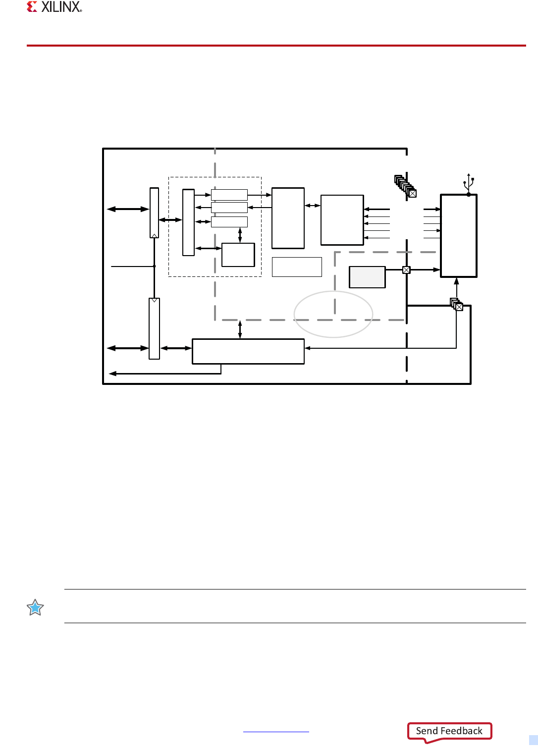
Zynq-7000 AP SoC Technical Reference Manual www.xilinx.com 478
UG585 (v1.12.1) December 6, 2017
Chapter 15: USB Host, Device, and OTG Controller
15.15 System Functions
The system functions include clocks, resets, memory interfaces and system interrupts.
15.15.1 Clocks
The vast majority of the controller logic is driven by the 60 MHz clock from the ULPI PHY. The
controller's interconnect is driven by the AHB/APB interface CPU_1x clock which is generated by the
PS clock subsystem.
CPU_1x Clock
Refer to section 25.3 System-wide Clock Frequency Examples, for general clock programming
information. The CPU_1x clock runs asynchronous to the 60 MHz PHY Clock.
IMPORTANT: The frequency of the CPU_1x clock must be set higher than the 60 MHz ULPI clock from
the external PHY.
X-Ref Target - Figure 15-18
Figure 15-18: USB Detailed System Block Diagram
Zynq-7000
PL
Protocol
Engine
12
MIO Pins
Port Indicator x2
Power Control
Power Fault
SelectIO
Pins
Port
Controller
and
ULPI Link
Wrapper
4 EMIO
Signals
External
ULPI
PHY
&
Board
Logic
ULPI
PS GPIO
controller
reset
8-bit Data
DIR (direction)
NXT (control)
STP
CLK
8-bit
60 MHz
Single Data
Rate
PS
Host,
Device
or OTG
AHB
32-bit Master
Interface
DMA
Control
CPU_1x
Control and Status
Registers
Interrupt
MIO or
EMIO
APB
32-bit Slave
Interface
GPIO
Clock
CPU_1x
60 MHz
ULPI
Clock
Domains
Tx FIFO
Rx FIFO
60 MHz
ULPI
Clock
CPU_1x
Clock
Programmable
Timers
DMA Engine
Descriptors
Arbitor
UG585_c15_45_030413

Zynq-7000 AP SoC Technical Reference Manual www.xilinx.com 479
UG585 (v1.12.1) December 6, 2017
Chapter 15: USB Host, Device, and OTG Controller
60 MHz PHY Clock
The external PHY provides a 60 MHz clock that the ULPI is sync’d to and is used by the a majority of
the controller logic.
15.15.2 Reset Types
To reset the controller, software writes a 1 to the usb.USBCMD [RST] bit. When the reset process is
completed, the controller hardware sets this bit to 0. Once the reset is started, the controller cannot
stop the process. Writing a 0 has no effect.
When software writes a 1 to this bit, the Controller resets its internal pipelines, timers, counters, and
state machines to their initial value. Any transaction currently in progress on USB is immediately
terminated. A USB reset is not driven to downstream ports. Software should not set this bit to a 1
when the host controller halt bit, usb.USBSTS [HCH], = 0. Attempting to reset an actively running
host controller will result in undefined behavior.
Controller Resets
• PS Reset System (full controller reset),
• usb.USBCMD [RST] bit (partial controller reset useful for OTG).
• OTG Mode Auto-Reset
ULPI PHY Reset
The USB controller does not have a reset output for the ULPI PHY. If the PHY requires a reset, then,
a PS or PL GPIO (or other software controlled reset signal) must be connected to the PHY as shown
in Figure 15-19, page 481.
USB Bus Reset
The host controller generates the standard USB reset as described in the EHCI specification. The
optional light host reset is not supported. The response by the device controller is described in
section 15.4.2 USB Bus Reset Response.
Summary of Resets
The controller has multiple reset sources and multiple reset domains. These are summarized in
Table 15-49 USB Resets Summary List.

Zynq-7000 AP SoC Technical Reference Manual www.xilinx.com 480
UG585 (v1.12.1) December 6, 2017
Chapter 15: USB Host, Device, and OTG Controller
fs
15.15.3 System Interrupt
Each controller sends its own IRQ interrupt to the GIC interrupt controller and to the EMIO interface
based on events within the controller. Controller 0 generates IRQ #53 and controller 1 generates IRQ
#76. These are shown in more detail in section 7.2.3 Shared Peripheral Interrupts (SPI).
The individual host and device mode interrupts can be read and cleared using the usb.USBSTS
register and masked using the usb.USBINTR register. These interrupts are described in section
15.3.5 Interrupt and Status Bits Overview.
The individual OTG interrupts are contained in the usb.OTGSC register and described in section
15.14.2 OTG Interrupt and Control Bits.
15.15.4 APB Slave Interface
The 32-bit APB slave interface is used by the software to read and write the control and status
registers. The interface is AMBA 3.0 compatible. All signals are used except PRESET_N and PSLVERR.
15.15.5 AHB Master Interface
The 32-bit AHB master interface is used by the DMA controller to read and write data packets and
transfer descriptors. The interface is AMBA 3.0 compatible.
Unused Signals
All of the AHB interface signals are used except:
• PROT[3:0] are tied to 0001 (non-cacheable transactions).
Table 15-49: USB Resets Summary List
Reset Name Controller
State Registers IRQ Reference
PS System Reset
AMBA (APB/AHB) Interface Reset
slcr.USB_RST_CTRL [USBx_CPU1X_RST]
Yes Yes no
Chapter 26, Reset System.
Reset values: Appendix B,
Register Details.
usb.USBCMD [RST]
(partial controller reset) Partial no Device and Host Modes
OTG mode Auto-Reset
Hardware Assistance usb.USBOTG [HAAR] no Section 15.14.1 Hardware
Assistance Features
PHY reset
Output from PS GPIO controller no effect no effect no
Chapter 15, USB Host, Device,
and OTG Controller
Send USB Reset (Host Mode) no effect no effect no Software Example.
Receive USB Reset (Device Mode) no effect no effect [URI] Software Example.
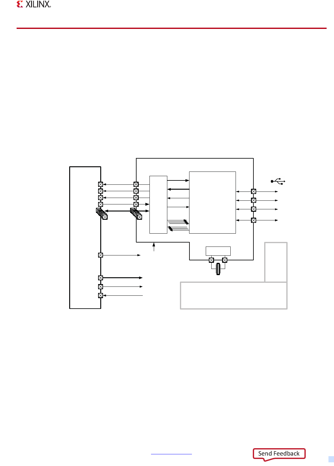
Zynq-7000 AP SoC Technical Reference Manual www.xilinx.com 481
UG585 (v1.12.1) December 6, 2017
Chapter 15: USB Host, Device, and OTG Controller
15.16 I/O Interfaces
The controller has multiple I/O interfaces including the main ULPI that interfaces via MIO to the external
PHY and the port indicator and power signals via EMIO. The routing of the ULPI through the MIO must be
programmed. The routing of the signals through the EMIO is always available to logic in the PL that can
route these signals to the SelectIO pins.
15.16.1 Wiring Connections
The wiring connections for both MIO and EMIO are shown in Figure 15-19.
15.16.2 MIO-EMIO Programming
MIO Pins
The ULPI signals from each controller are routed to specific MIO pins. In this chapter, refer to
Table 15-50 USB ULPI Signals on MIO. A wiring diagram is shown in Figure 15-19, page 481.
The general routing concepts and MIO I/O buffer configurations are explained in section 2.5 PS-PL
MIO-EMIO Signals and Interfaces. A summary of the MIO pins is shown in section
2.5.4 MIO-at-a-Glance Table.
X-Ref Target - Figure 15-19
Figure 15-19: USB I/O Signal and PHY Wiring Diagram
ULPI
Signals via
MIO
USB D+
USB ID
USB
Signals via
EMIO
CLK
DIR
NXT
STP
DATA
ULPI
Pwr Select
Port Indicators
Pwr Fault
USB D-
VBUS
8-bit
60 MHz
Single Data
Rate
Host,
Device
or OTG
UTMI Clock
UTMI Data In
UTMI Data Out
UTMI PHY
ULPI PHY
Other UTMI
Signals
Zynq-7000
GPIO
Ex: PHY Reset
UTMI Reset
Oscillator
and PLL
DP
DM
VBUS
ID
Board Components
PS GPIO
Power, Port
Signals
UTMI PHY
Wrapper
UG585_c15_46_030413

Zynq-7000 AP SoC Technical Reference Manual www.xilinx.com 482
UG585 (v1.12.1) December 6, 2017
Chapter 15: USB Host, Device, and OTG Controller
Example: Program I/O for Controller 1
These steps configure the USB controller 1 onto MIO pins 40 to 51.
1. Configure MIO pins 40, 44 - 47 and 49 -51 for data I/O. Write to the associated slcr registers,
MIO_PIN_{40, 44-47}:
a. Route USB ULPI data signal to I/O buffer.
b. 3-state controlled by USB controller (TRI_ENABLE = 0).
c. LVCMOS18 (refer to the register definition for other voltage options).
d. Slow CMOS edge.
e. Disable internal pull-up resistor.
f. Disable HSTL receiver.
2. Configure MIO pins 41, 43, and 48 for input. Write to each of the slcr.MIO_PIN_{48, 43, 41}
registers:
a. Route USB ULPI input signals DIR to pin 41, STP to pin 43 and CLK to pin 48.
b. Disable output (TRI_ENABLE = 1).
c. LVCMOS18 (refer to the register definition for other voltage options).
d. Slow CMOS drive edge (benign setting).
e. Disable internal pull-up resistor.
f. Disable HSTL receiver.
3. Configure MIO pin 42 for output. Write to the slcr.MIO_PIN_42 register:
a. Route USB ULPI output signal STP to pin 42.
b. 3-state controlled by USB Controller (TRI_ENABLE = 0).
c. LVCMOS18 (refer to the register definition for other voltage options).
d. Slow CMOS edge.
e. Disable internal pull-up resistor.
f. Disable HSTL receiver.
15.16.3 MIO-EMIO Signals
The ULPI interface signals are listed in Table 15-50. The port indicator and power signals are shown
in Tab le 15- 51 .
The 7z010 dual core and 7z007s single core CLG225 devices support 32 MIO pins. Pin restrictions are
shown in the MIO table in section 2.5.4 MIO-at-a-Glance Table.
Zynq-7000 AP SoC Technical Reference Manual www.xilinx.com 483
UG585 (v1.12.1) December 6, 2017
Chapter 15: USB Host, Device, and OTG Controller
Table 15-50: USB ULPI Signals on MIO
USB Port Signals
MIO Pins Default
Input
Value to
Controller
USB 0 USB 1 I/O Name
Transmit and receive data 4 28 40 IO USB{0,1}_ULPI_DATA4 ~
Data bus direction control 29 41 I USB{0,1}_ULPI_DIR 0
Stop the Transfer (end/interrupt) 30 42 O USB{0,1}_ULPI_STP ~
Data flow control signal 31 43 I USB{0,1}_ULPI_NXT 0
Transmit and receive data 0 32 44 IO USB{0,1}_ULPI_DATA0 ~
Transmit and receive data 1 33 45 IO USB{0,1}_ULPI_DATA1 ~
Transmit and receive data 2 34 46 IO USB{0,1}_ULPI_DATA2 ~
Transmit and receive data 3 35 47 IO USB{0,1}_ULPI_DATA3 ~
Transceiver clock for ULPI 36 48 I USB{0,1}_ULPI_CLK 0
Transmit and receive data 5 37 49 IO USB{0,1}_ULPI_DATA5 ~
Transmit and receive data 6 38 50 IO USB{0,1}_ULPI_DATA6 ~
Transmit and receive data 7 39 51 IO USB{0,1}_ULPI_DATA7 ~
Table 15-51: USB Port Indicator and Power Signals on EMIO
USB Port Signals
EMIO Signals Default
Input
Value to
Controller
Name I/O
Port Indicator EMIOUSB{0,1}PORTINDCTL{0,1} O ~
Power Fault EMIOUSB{0,1}VBUSPWRFAULT I 0
Power Select EMIOUSB{0,1}VBUSPWRSELECT O ~

Zynq-7000 AP SoC Technical Reference Manual www.xilinx.com 484
UG585 (v1.12.1) December 6, 2017
Chapter 16
Gigabit Ethernet Controller
16.1 Introduction
The Gigabit Ethernet Controller (GEM) implements a 10/100/1000 Mb/s Ethernet MAC compatible
with the IEEE 802.3-2008 standard capable of operating in either half or full duplex mode at all three
speeds. The PS is equipped with two Gigabit Ethernet Controllers. Each controller can be configured
independently. To access pins via MIO, each controller uses an RGMII interface (to save pins). Access
to the PL is through the EMIO which provides the GMII interface.
Other Ethernet communications interfaces can be created in the PL using the GMII available on the
EMIO interface. For example, the PL can be used to implement these interfaces:
• SGMII and 1000 Base-X, in devices with GTX
• RGMII v2.0 for PHY devices with HSTL Class 1 drivers and receivers
Registers are used to configure the features of the MAC, select different modes of operation, and
enable and monitor network management statistics. The DMA controller connects to memory
through an AHB bus interface. It is attached to the controller’s FIFO interface of the MAC to provide
a scatter-gather type capability for packet data storage in an embedded processing system.
The controllers provide MDIO interfaces for PHY management. The PHYs can be controlled from
either of the MDIO interfaces.
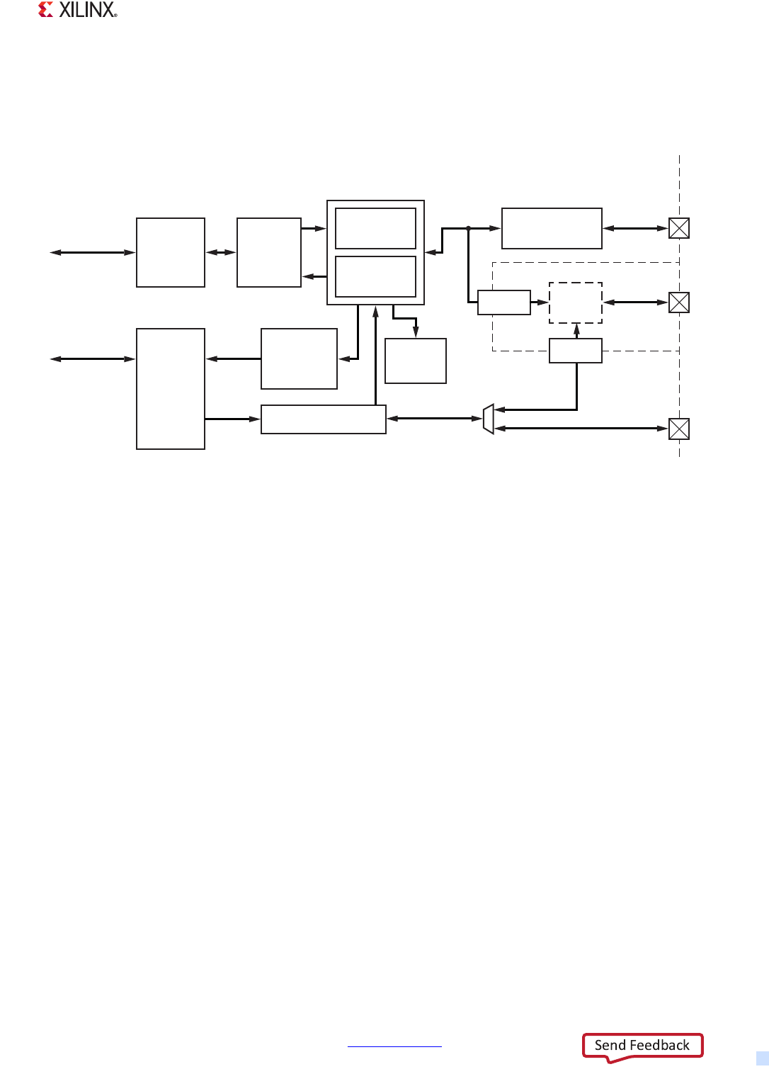
Zynq-7000 AP SoC Technical Reference Manual www.xilinx.com 485
UG585 (v1.12.1) December 6, 2017
Chapter 16: Gigabit Ethernet Controller
16.1.1 Block Diagram
A block diagram of one Ethernet controller is shown in Figure 16-1.
16.1.2 Features
Each Gigabit Ethernet MAC controller has the following features:
•IEEE Standard 802.3-2008 compatible, supporting 10/100/1000 Mb/s transfer rates
• Full and half duplex operation
• RGMII interface with external PHY when using MIO pins
• GMII/MII interface to the PL to allow connection of interfaces such as TBI, SGMII, 1000 Base-X
and RGMII v2.0 support using soft cores (Note: SGMII and 1000 Base-X interfaces require a
gigabit transceiver, MGT)
• MDIO interface for physical layer management
• 32-bit AHB DMA master, 32-bit APB bus for control registers access
• Scatter-gather DMA capability
• Interrupt generation to signal receive and transmit completion, or errors and wake-up
• Automatic pad and cyclic redundancy check (CRC) generation on transmitted frames
• Automatic discard of frames received with errors
• Programmable IPG stretch
• Full duplex flow control with recognition of incoming pause frames and hardware generation of
transmitted pause frames
X-Ref Target - Figure 16-1
Figure 16-1: Ethernet Controller
UG585_c16_01_042512
PL
GMII to RGMII
Adapter
EMIO
MAC
Transmitter
AHB
Interface
FIFO
Frame
Filtering
Control Registers
Status and
Statistics
Registers
MAC
Receiver
MIO
Pins
RGMII
Device
Boundry
MDC, MDIO
AHB Master
GMII/MII
PL
Signals
User
Defined
DMA
Controller
APB Slave
Register
Interface
MIO
Pins
EMIO
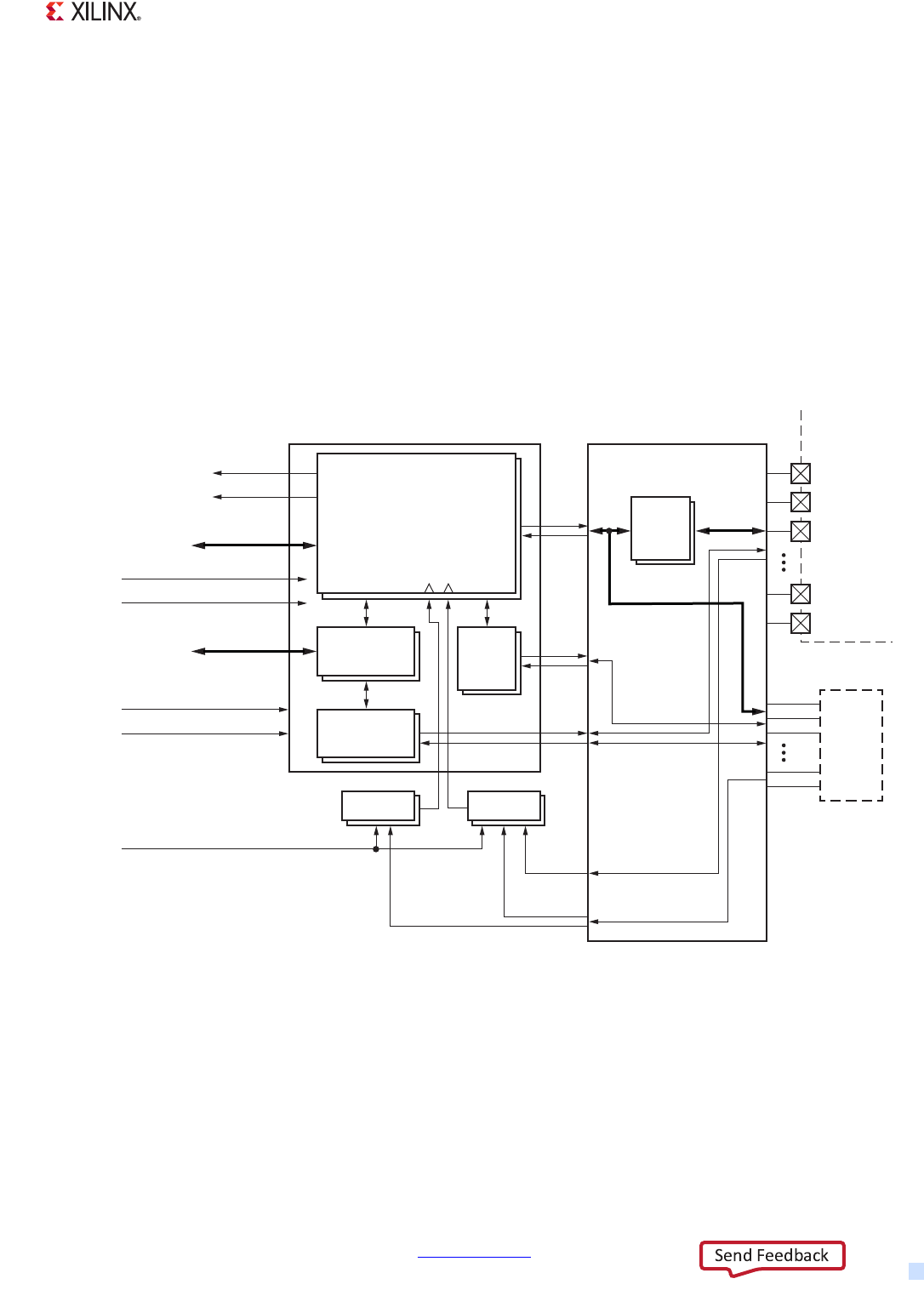
Zynq-7000 AP SoC Technical Reference Manual www.xilinx.com 486
UG585 (v1.12.1) December 6, 2017
Chapter 16: Gigabit Ethernet Controller
• Address checking logic for four specific 48-bit addresses, four type ID values, promiscuous
mode, hash matching of unicast and multicast destination addresses and Wake-on-LAN
•802.1Q VLAN tagging with recognition of incoming VLAN and priority tagged frames
• Supports Ethernet loopback mode
• IPv4 and IPv6 transmit and receive IP, TCP and UDP checksum offload
• Recognition of 1588 rev. 2 PTP frames
• Statistics counter registers for RMON/MIB
16.1.3 System Viewpoint
Figure 16-2 shows Zynq system viewpoint for the Gigabit Ethernet controllers.
X-Ref Target - Figure 16-2
Figure 16-2: System Viewpoint
UG585_c16_02_071112
GigE {0, 1} CPU 1x Reset
Tx, Rx
GigE {0, 1} CPU 1x Clock
Ethernet
GMII
Tx, Rx
GMII Tx, Rx
Rx Clock
Tx, Rx Clocks
RGMII
Tx, Rx
PTP
MDC, MDIO
IRQ ID# {54, 77}
Wakeup
IRQ ID# {55, 78}
Master
Port
AHB
Interconnect
Slave
Port
APB
Interconnect
GigE {0, 1} Ref Reset
GigE {0, 1} Ref Clock Internal Clock Source
MIO Clock
Source
GigE {0, 1} Rx Reset
Control
Registers
Management
Interface
Tx Clock Rx Clock
Gigabit
Ethernet
Controllers
MIO - EMIO
Time
Stamp
Unit
GMII to
RGMII
Adapter
EMIO Clock
Sources
MIO
Pins
EMIO
Device
Boundry
PL

Zynq-7000 AP SoC Technical Reference Manual www.xilinx.com 487
UG585 (v1.12.1) December 6, 2017
Chapter 16: Gigabit Ethernet Controller
16.1.4 Clock Domains
The Gigabit Ethernet controller has the following clocks:
• AHB clock: AHB clock used by DMA block
• APB clock: APB clock used by MAC register block
• TSU clock: Alternate clock source for the Time Stamp Unit
• TX clock: MAC transmit clock used by MAC transmit block in MII/RGMII/GMII mode
• Rx clock: MAC receive clock used MAC receive synchronisation in MII/RGMII/GMII mode
• Invert TX clock: Inverted Tx clock used in loop back mode
Refer to Table 24-2, page 681 for the more details about power management. Refer to Chapter 25,
Clocks for details about the clocks.
16.1.5 Notices
7z007s and 7z010 CLG225 Devices
The 7z007s single core and 7z010 dual core CLG225 devices support 32 MIO pins and at most one
Ethernet interface through the MIO pins. This is shown in the MIO table in section
2.5.4 MIO-at-a-Glance Table. One or both of the Ethernet controllers can interface to logic in the PL.
All of these CLG225 device restrictions are listed in section 1.1.3 Notices.
Jumbo Frames
Jumbo frames are not supported.
Half Duplex
Gigabit Half Duplex is not supported.
IEEE 1588 Time Stamp
IEEE 1588 version 2 introduces transparent clocks of which there are two kinds, peer-to-peer (P2P)
and end-to-end (E2E). There is no transparent clock support in the time stamp unit.
16.1.6 Application Notes
There are two useful application notes, XAPP1026 for standalone/lwip applications and XAPP1082
for Linux. These application notes include benchmark performance values and other helpful
information.

Zynq-7000 AP SoC Technical Reference Manual www.xilinx.com 488
UG585 (v1.12.1) December 6, 2017
Chapter 16: Gigabit Ethernet Controller
16.2 Functional Description and Programming
Model
The controller comprises four main components:
• MAC controlling transmit, receive, address checking, and loopback
• Control and status registers, statistics registers, and synchronization logic
• DMA controlling data transmit and receive through an AHB master interface
• Time stamp unit (TSU) for calculating the IEEE 1588 timer values
10/100/1000 Operation
The gigabit enable bit in the Network Configuration register selects between 10/100 Mb/s Ethernet
operation and 1000 Mb/s mode. The 10/100 Mb/s speed bit in the network configuration register is
used to select between 10 Mb/s and 100 Mb/s.
MDIO Interface
Both controllers provide MDIO interfaces, however, only one interface is needed to control both of
the external PHYs due to the difference in PHY address.
16.2.1 MAC Transmitter
The MAC transmitter can operate in either half duplex or full duplex mode, and transmits frames in
accordance with the Ethernet IEEE 802.3 standard. In half duplex mode, the CSMA/CD protocol of the
IEEE 802.3 specification is followed.
Frame assembly starts by adding the preamble and the start frame delimiter. Data is taken from the
transmit FIFO a word at a time. When the controller is configured for gigabit operation, the data
output to the PHY uses all eight bits of the txd[7:0] output. In 10/100 mode, transmit data to the PHY
is nibble wide and least significant nibble first using txd[3:0] with txd[7:4] tied to logic 0.
If necessary, padding is added to take the frame length to 60 bytes. CRC is calculated using an order
32 bit polynomial. This is inverted and appended to the end of the frame taking the frame length to
a minimum of 64 bytes. If the no-CRC bit is set in the second word of the last buffer descriptor of a
transmit frame, neither pad nor CRC are appended. The no-CRC bit can also be set through the FIFO.
In full duplex mode (at all data rates), frames are transmitted immediately. Back-to-back frames are
transmitted at least 96 bit times apart to guarantee the interframe gap.
In half duplex mode, the transmitter checks carrier sense. If asserted, the transmitter waits for the
signal to become inactive, and then starts transmission after the interframe gap of 96 bit times. If the
collision signal is asserted during transmission, the transmitter transmits a jam sequence of 32 bits
taken from the data register and then retries transmission after the back off time has elapsed. If the
collision occurs during either the preamble or SFD, then these fields are completed prior to
generation of the jam sequence.

Zynq-7000 AP SoC Technical Reference Manual www.xilinx.com 489
UG585 (v1.12.1) December 6, 2017
Chapter 16: Gigabit Ethernet Controller
The back off time is based on an XOR of the 10 least significant bits of the data coming from the
transmit FIFO and a 10-bit pseudo random number generator. The number of bits used depends on
the number of collisions seen. After the first collision 1 bit is used, then the second 2 bits and so on
up to the maximum of 10 bits. All 10 bits are used above ten collisions. An error is indicated and no
further attempts are made if 16 consecutive attempts cause a collision. This operation is compatible
with the description in Clause 4.2.3.2.5 of the IEEE 802.3 standard which refers to the truncated binary
exponential back off algorithm.
In 10/100 mode, both collisions and late collisions are treated identically, and back off and retry are
performed up to 16 times. When operating in gigabit mode, late collisions are treated as an
exception and transmission is aborted, without retry. This condition is reported in the transmit buffer
descriptor word 1 (late collision, bit 26) and also in the Transmit Status register (late collision, bit 7).
An interrupt can also be generated (if enabled) when this exception occurs, and bit 5 in the Interrupt
Status Register is set.
When bit [28] is set in the Network Configuration register the IPG can be stretched beyond 96 bits
depending on the length of the previously transmitted frame and the value written to the
IPG_STRETCH register. The least significant 8 bits of the IPG_STRETCH register multiply the previous
frame length (including preamble) the next significant 8 bits (+1 so as not to get a divide by zero)
divide the frame length to generate the IPG. IPG stretch only works in full duplex mode and when bit
28 is set in the Network Configuration register. The IPG_STRETCH register cannot be used to shrink
the IPG below 96 bits.
If the back pressure bit is set in the Network Control register or if the half_duplex_flow_control_en
input is set in 10M or 100M half duplex mode, the transmit block transmits 64 bits of data, which can
consist of 16 nibbles of 1011 or in bit rate mode 64 1s, whenever it sees an incoming frame to force
a collision. This provides a way of implementing flow control in half duplex mode.
16.2.2 MAC Receiver
All processing within the MAC receiver uses 16-bit data paths. The MAC receiver checks for valid
preamble, FCS, alignment, and length. It then sends the received frames to the FIFO (to either the
DMA controller or external to the IP core) and stores the frames destination address for use by the
address checking block.
If, during frame reception, the frame is found to be too long, a bad frame indication is sent to the
FIFO. The receiver logic ceases to send data to memory as soon as this condition occurs.
At end of frame reception the receive block indicates to the DMA block whether the frame is good
or bad. The DMA block recovers the current receive buffer if the frame was bad.
Ethernet frames are normally stored in DMA memory or to the FIFO complete with the FCS. Setting
the FCS remove bit in the network configuration register (bit [17]) causes frames to be stored
without their corresponding FCS. The reported frame length field is reduced by four bytes to reflect
this operation.
The receive block signals to the register block to increment the alignment, CRC (FCS), short frame,
long frame, jabber or receive symbol errors when any of these exception conditions occur.
If bit [26] is set in the network configuration CRC errors are ignored and frames with CRC errors are
not discarded, though the Frame Check Sequence Errors Statistic register is still incremented. Bit[13]

Zynq-7000 AP SoC Technical Reference Manual www.xilinx.com 490
UG585 (v1.12.1) December 6, 2017
Chapter 16: Gigabit Ethernet Controller
of the receiver descriptor word 1 is updated to indicate the FCS validity for the particular frame. This
is useful for applications where individual frames with FCS errors must be identified.
Received frames can be checked for length field error by setting the length field error frame discard
bit of the Network Configuration register (bit [16]). When this bit is set, the receiver compares a
frame's measured length with the length field (bytes 13 and 14) extracted from the frame. The frame
is discarded if the measured length is shorter. This checking procedure is for received frames
between 64 bytes and 1,518 bytes in length.
Each discarded frame is counted in the 10-bit length field Error Statistics register. Frames where the
length field is greater than or equal to 0x0600 are not checked.
16.2.3 MAC Filtering
The MAC filter determines which frames should be written to the AHB interface FIFO and onto the
DMA controller.
Whether a frame is passed depends on what is enabled in the Network Configuration register, the
state of the external matching pins, the contents of the specific address, type, and hash registers and
the frame's destination address and type field.
If bit [25] of the Network Configuration register is not set, a frame is not copied to memory if the
Gigabit Ethernet controller is transmitting in half duplex mode at the time a destination address is
received.
Ethernet frames are transmitted a byte at a time, least significant bit first. The first six bytes (48 bits)
of an Ethernet frame make up the destination address. The first bit of the destination address, which
is the LSB of the first byte of the frame, is the group or individual bit. This is one for multicast
addresses and zero for unicast. The all-ones address is the broadcast address and a special case of
multicast.
The Gigabit Ethernet controller supports recognition of four specific addresses. Each specific address
requires two registers, Specific Address register bottom and Specific Address register top. Specific
address register bottom stores the first four bytes of the destination address and Specific Address
register top contains the last two bytes. The addresses stored can be specific, group, local or
universal.
The destination address of received frames is compared against the data stored in the Specific
Address registers once they have been activated. The addresses are deactivated at reset or when
their corresponding Specific Address register bottom is written. They are activated when Specific
Address register top is written. If a receive frame address matches an active address, the frame is
written to the FIFO and on to DMA controller, if used.
Frames can be filtered using the type ID field for matching. Four type ID registers exist in the register
address space and each can be enabled for matching by writing a one to the MSB (bit [31]) of the
respective register. When a frame is received, the matching is implemented as an OR function of the
various types of match.
The contents of each type ID registers (when enabled) are compared against the length/type ID of
the frame being received (e.g., bytes 13 and 14 in non-VLAN and non-SNAP encapsulated frames)
and copied to memory if a match is found. The encoded type ID match bits (Word 0, bit [22] and bit

Zynq-7000 AP SoC Technical Reference Manual www.xilinx.com 491
UG585 (v1.12.1) December 6, 2017
Chapter 16: Gigabit Ethernet Controller
[23]) in the receive buffer descriptor status are set indicating which type ID register generated the
match, if the receive checksum offload is disabled. The reset state of the type ID registers is zero,
hence each is initially disabled.
The Address and Type ID filtering are independent of each other. If both the Specific Address
registers and Type ID Match registers are set up, then the received frame will be written into the
system memory for either an address match or a ID match.
The following example illustrates the use of the address and type ID match registers for a MAC
address of 21:43:65:87:A9:CB
Preamble 55
SFD D5
DA (Octet 0 - LSB) 21
DA (Octet 1) 43
DA (Octet 2) 65
DA (Octet 3) 87
DA (Octet 4) A9
DA (Octet 5 - MSB) CB
SA (LSB) 00*
SA 00*
SA 00*
SA 00*
SA 00*
SA (MSB) 00*
Type ID (MSB) 43
Type ID (LSB) 21
Note: * – contains the address of the transmitting device.
The sequence above shows the beginning of an Ethernet frame. Byte order of transmission is from
top to bottom as shown. For a successful match to specific address 1, the following address matching
registers must be set up:
Specific address 1 bottom (Address 0x088)0x87654321
Specific address 1 top (Address 0x08C)0x0000CBA9
And for a successful match to the type ID, the following type ID match 1 register must be set up:
Type ID Match 1 (Address 0x0A8)0x80004321
Broadcast Address
Frames with the broadcast address of 0xFFFFFFFFFFFF are stored to memory only if the 'no
broadcast' bit in the Network Configuration register is set to zero.
Hash Addressing
The Hash Address register is 64 bits long and takes up two locations in the memory map. The least
significant bits are stored in Hash register bottom and the most significant bits in Hash register top.
The unicast hash enable and the multicast hash enable bits in the Network Configuration register
enable the reception of hash matched frames. The destination address is reduced to a 6 bit index into

Zynq-7000 AP SoC Technical Reference Manual www.xilinx.com 492
UG585 (v1.12.1) December 6, 2017
Chapter 16: Gigabit Ethernet Controller
the 64 bit hash register using the following hash function. The hash function is an XOR of every sixth
bit of the destination address.
hash_index[05] = da[05]°^°da[11]°^°da[17]°^°da[23]°^°da[29]°^°da[35]°^°da[41]°^°da[47]
hash_index[04] = da[04]°^°da[10]°^°da[16]°^°da[22]°^°da[28]°^°da[34]°^°da[40]°^°da[46]
hash_index[03] = da[03]°^°da[09]°^°da[15]°^°da[21]°^°da[27]°^°da[33]°^°da[39]°^°da[45]
hash_index[02] = da[02]°^°da[08]°^°da[14]°^°da[20]°^°da[26]°^°da[32]°^°da[38]°^°da[44]
hash_index[01] = da[01]°^°da[07]°^°da[13]°^°da[19]°^°da[25]°^°da[31]°^°da[37]°^°da[43]
hash_index[00] = da[00]°^°da[06]°^°da[12]°^°da[18]°^°da[24]°^°da[30]°^°da[36]°^°da[42]
da[0] represents the least significant bit of the first byte received, that is, the multicast/unicast
indicator, and da[47] represents the most significant bit of the last byte received.
If the hash index points to a bit that is set in the Hash register then the frame is matched according
to whether the frame is multicast or unicast.
A multicast match is signaled if the multicast hash enable bit is set, da[0] is logic 1 and the hash index
points to a bit set in the Hash register. A unicast match is signaled if the unicast hash enable bit is set,
da[0] is logic 0 and the hash index points to a bit set in the Hash register. To receive all multicast
frames, the Hash register should be set with all ones and the multicast hash enable bit should be set
in the Network Configuration register.
Copy All Frames (or Promiscuous Mode)
If the copy all frames bit is set in the Network Configuration register then all frames (except those
that are too long, too short, have FCS errors, or have rx_er asserted during reception) are copied to
memory. Frames with FCS errors are copied if bit [26] is set in the Network Configuration register.
Disable Copy of Pause Frames
Pause frames can be prevented from being written to memory by setting the disable copying of
pause frames control bit [23] in the Network Configuration register. When set, pause frames are not
copied to memory regardless of the copy all frames bit, whether a hash match is found, a type ID
match is identified, or if a destination address match is found.
VLAN Support
An Ethernet encoded 802.1Q VLAN tag is shown in Table 16-1
The VLAN tag is inserted at the 13th byte of the frame adding an extra four bytes to the frame. To
support these extra four bytes, the Gigabit Ethernet controller can accept frame lengths up to 1,536
bytes by setting bit [8] in the Network Configuration register.
Table 16-1: VLAN Tag Control Information
TPID (Tag Protocol Identifier) 16 Bits TCI (Tag Control Information) 16 Bits
0x8100 First 3 bits priority, then CFI bit, last 12 bits VID

Zynq-7000 AP SoC Technical Reference Manual www.xilinx.com 493
UG585 (v1.12.1) December 6, 2017
Chapter 16: Gigabit Ethernet Controller
If the VID (VLAN identifier) is null (0x000) a priority-tagged frame is indicated.
The following bits in the receive buffer descriptor status word provide information about VLAN
tagged frames:
• Bit [21] set if receive frame is VLAN tagged (i.e. type id of 0x8100).
• Bit [20] set if receive frame is priority tagged (i.e. type id of 0x8100 and null VID). (If bit [20] is
set bit [21] is also set).
• Bits [19], [18] and [17] set to priority if bit [21] is set.
• Bit [16] set to CFI if bit [21] is set.
The controller can be configured to reject all frames except VLAN tagged frames by setting the
discard non-VLAN frames bit in the Network Configuration register.
16.2.4 Wake-on-LAN Support
The receive block supports Wake-on-LAN by detecting the following events on incoming receive
frames:
•Magic packet
• ARP request to the device IP address
• Specific address 1 filter match
• Multicast hash filter match
If one of these events occurs, Wake-on-LAN detection is indicated by asserting the wake-up
interrupt. These events can be individually enabled through bits[19:16] of the Wake-on-LAN register.
Also, for Wake-on-LAN detection to occur receive enable must be set in the Network Control
register, however a receive buffer does not have to be available.
The wake-up interrupt is asserted due to multicast filter events, an ARP request, or a specific address
1 match even in the presence of a frame error. For magic packet events, the frame must be correctly
formed and error free.
A magic packet event is detected if all of the following are true:
• Magic packet events are enabled through bit [16] of the Wake-on-LAN register
• The frame's destination address matches specific address 1
• The frame is correctly formed with no errors
• The frame contains at least 6 bytes of 0xFF for synchronization
• There are 16 repetitions of the contents of Specific Address 1 register immediately following the
synchronization
An ARP request event is detected if all of the following are true:
• ARP request events are enabled through bit [17] of the Wake-on-LAN register
• Broadcasts are allowed by bit 5 in the Network Configuration register
• The frame has a broadcast destination address (bytes 1 to 6)

Zynq-7000 AP SoC Technical Reference Manual www.xilinx.com 494
UG585 (v1.12.1) December 6, 2017
Chapter 16: Gigabit Ethernet Controller
• The frame has a typeID field of 0x0806 (bytes 13 and 14)
• The frame has an ARP operation field of 0x0001 (bytes 21 and 22)
• The least significant 16 bits of the frame's ARP target protocol address (bytes 41 and 42) match
the value programmed in bits[15:0] of the Wake-on-LAN register
The decoding of the ARP fields adjusts automatically if a VLAN tag is detected within the frame. The
reserved value of 0x0000 for the Wake-on-LAN target address value does not cause an ARP request
event, even if matched by the frame.
A specific address 1 filter match event occurs if all of the following are true:
• Specific address 1 events are enabled through bit [18] of the Wake-on-LAN register
• The frame's destination address matches the value programmed in the Specific Address 1
registers
A multicast filter match event occurs if all of the following are true:
• Multicast hash events are enabled through bit [19] of the Wake-on-LAN register
• Multicast hash filtering is enabled through bit [6] of the Network Configuration register
• The frame destination address matches against the multicast hash filter
• The frame destination address is not a broadcast
16.2.5 DMA Block
The DMA controller is attached to the FIFO to provide a scatter-gather type capability for packet data
storage in an embedded processing system.
Packet Buffer DMA
The controller uses a packet buffer which has the following features
• 32 data bus width support
• Easier to guarantee maximum line rate due to the ability to store multiple frames in the packet
buffer
• More efficient use of the AHB interface
• Full store and forward
• Support for Transmit TCP/IP checksum offload
• Support for priority queuing
• When a collision on the line occurs during transmission, the packet is automatically replayed
directly from the packet buffer memory rather than having to re-fetch through the AHB
interface
• Received error packets are automatically dropped before any of the packet is presented to the
AHB, thus reducing AHB activity
• Supports manual RX packet flush capabilities
• RX packet flush when there is lack of AHB resource

Zynq-7000 AP SoC Technical Reference Manual www.xilinx.com 495
UG585 (v1.12.1) December 6, 2017
Chapter 16: Gigabit Ethernet Controller
DMA Controller
The DMA uses separate transmit and receive lists of buffer descriptors, with each descriptor
describing a buffer area in memory. This allows Ethernet packets to be broken up and scattered
around the AHB memory space.
The DMA controller performs four types of operation on the AHB bus. In order of priority these are:
• Receive buffer manager write/read
• Transmit buffer manager write/read
• Receive data DMA write
• Transmit data DMA read
Transfer size is set to 32-bit words using the AHB bus width select bits in the Network Configuration
register, and burst size may be programmed to single access or bursts of 4, 8, or 16 words using the
DMA Configuration register.
Rx Buffers
Received frames, optionally including FCS, are written to receive AHB buffers stored in memory. The
start location for each receive AHB buffer is stored in memory in a list of receive buffer descriptors
at an address location pointed to by the receive-buffer queue pointer. The base address for the
receive-buffer queue pointer is configured in software using the Receive Buffer Queue Base Address
register.
Each list entry consists of two words. The first is the address of the receive AHB buffer and the
second the receive status. If the length of a receive frame exceeds the AHB buffer length, the status
word for the used buffer is written with zeroes except for the start of frame bit, which is always set for
the first buffer in a frame. Bit zero of the address field is written to 1 to show that the buffer has been
used. The receive-buffer manager then reads the location of the next receive AHB buffer and fills that
with the next part of the received frame data. AHB buffers are filled until the frame is complete and
the final buffer descriptor status word contains the complete frame status. Refer to Table 16-2 for
details of the receive buffer descriptor list.
Each receive AHB buffer start location is a word address. The start of the first AHB buffer in a frame
can be offset by up to three bytes depending on the value written to bits [14] and [15] of the Network
Configuration register. If the start location of the AHB buffer is offset the available length of the first
AHB buffer is reduced by the corresponding number of bytes.
Table 16-2: Rx Buffer Descriptor Entry
Bit Function
Word 0
31:2 Address of beginning of buffer.
1 Wrap - marks last descriptor in receive buffer descriptor list.
0 Ownership - needs to be zero for the controller to write data to the receive buffer. The controller
sets this to 1 once it has successfully written a frame to memory. Software must clear this bit before
the buffer can be used again.

Zynq-7000 AP SoC Technical Reference Manual www.xilinx.com 496
UG585 (v1.12.1) December 6, 2017
Chapter 16: Gigabit Ethernet Controller
Word 1
31 Global all ones broadcast address detected.
30 Multicast hash match.
29 Unicast hash match.
28 Reserved.
27 Specific address register match found,. bit 25 and bit 26 indicate which specific address register
causes the match.
26:25 Specific address register match. Encoded as follows:
00b: Specific address register 1 match
01b: Specific address register 2 match
10b: Specific address register 3 match
11b: Specific address register 4 match
If more than one specific address is matched only one is indicated with priority 4 down to 1.
24 This bit has a different meaning depending on whether RX checksum offloading is enabled.
• With RX checksum offloading disabled: (bit [24] clear in Network Configuration) Type ID register
match found, bit [22] and bit [23] indicate which type ID register causes the match.
• With RX checksum offloading enabled: (bit [24] set in Network Configuration)
0b: The frame was not SNAP encoded and/or had a VLAN tag with the CFI bit set.
1b: The frame was SNAP encoded and had either no VLAN tag or a VLAN tag with the CFI bit not
set.
23:22 This bit has a different meaning depending on whether RX checksum offloading is enabled.
With RX checksum offloading disabled: (bit [24] clear in Network Configuration) Type ID register
match. Encoded as follows:
00b: Type ID register 1 match
01b: Type ID register 2 match
10b: Type ID register 3 match
11b: Type ID register 4 match
If more than one Type ID is matched only one is indicated with priority 4 down to 1.
With RX checksum offloading enabled: (bit [24] set in Network Configuration)
00b: Neither the IP header checksum nor the TCP/UDP checksum was checked.
01b: The IP header checksum was checked and was correct. Neither the TCP or UDP checksum
was checked.
10b: Both the IP header and TCP checksum were checked and were correct.
11b: Both the IP header and UDP checksum were checked and were correct.
21 VLAN tag detected – type ID of 0x8100. For packets incorporating the stacked VLAN processing
feature, this bit is set if the second VLAN tag has a type ID of 0x8100.
20 Priority tag detected – type ID of 0x8100 and null VLAN identifier. For packets incorporating the
stacked VLAN processing feature, this bit is set if the second VLAN tag has a type ID of 0x8100
and a null VLAN identifier.
19:17 VLAN priority – only valid if bit [21] is set.
16 Canonical format indicator (CFI) bit – only valid if bit 21 is set.
15 End of frame – when set the buffer contains the end of a frame. If end of frame is not set, then the
only valid status bit is start of frame (bit 14).
Table 16-2: Rx Buffer Descriptor Entry (Cont’d)
Bit Function

Zynq-7000 AP SoC Technical Reference Manual www.xilinx.com 497
UG585 (v1.12.1) December 6, 2017
Chapter 16: Gigabit Ethernet Controller
The start location of the receive-buffer descriptor list must be written with the receive-buffer queue
base address before reception is enabled (receive enable in the Network Control register). Once
reception is enabled, any writes to the Receive-buffer Queue Base Address register are ignored.
When read, it returns the current pointer position in the descriptor list, though this is only valid and
stable when receive is disabled.
If the filter block indicates that a frame should be copied to memory, the receive data DMA
operation starts writing data into the receive buffer. If an error occurs, the buffer is recovered.
An internal counter represents the receive-buffer queue pointer and it is not visible through the CPU
interface. The receive-buffer queue pointer increments by two words after each buffer has been
used. It re-initializes to the receive-buffer queue base address if any descriptor has its wrap bit set.
As receive AHB buffers are used, the receive AHB buffer manager sets bit zero of the first word of the
descriptor to logic one indicating the AHB buffer has been used.
Software should search through the “used” bits in the AHB buffer descriptors to find out how many
frames have been received, checking the start of frame and end of frame bits.
Received frames are written out to the AHB buffers as soon as enough frame data exists in the packet
buffer. This might mean that several full AHB buffers are used before some error conditions can be
detected. If a receive error is detected the receive buffer currently being written is recovered.
Previous buffers are not recovered. For example, when receiving frames with CRC errors or excessive
length, it is possible that a frame fragment might be stored in a sequence of AHB receive buffers.
Software can detect this by looking for the start of frame bit set in a buffer following a buffer with no
end of frame bit set.
For a properly working 10/100/1000 Ethernet system there should be no excessive length frames or
frames greater than 128 bytes with CRC errors. Collision fragments are less than 128 bytes long,
therefore it is a rare occurrence to find a frame fragment in a receive AHB buffer, when using the
default value of 128 bytes for the receive buffers size.
14 Start of frame – when set the buffer contains the start of a frame. If both bits 15 and 14 are set, the
buffer contains a whole frame.
13 This bit has a different meaning depending on whether ignore FCS mode are enabled. This bit is
zero if ignore FCS mode is disabled.
With ignore FCS mode enabled: (bit [26] set in Network Configuration Register). This indicates per
frame FCS status as follows:
0b: Frame had good FCS.
1b: Frame had bad FCS, but was copied to memory as ignore FCS enabled.
12:0 These bits represent the length of the received frame which might or might not include FCS
depending on whether FCS discard mode is enabled.
• With FCS discard mode disabled: (bit [17] clear in Network Configuration Register) Least
significant 12-bits for length of frame including FCS.
• With FCS discard mode enabled: (bit [17] set in Network Configuration Register) Least significant
12-bits for length of frame excluding FCS.
Table 16-2: Rx Buffer Descriptor Entry (Cont’d)
Bit Function

Zynq-7000 AP SoC Technical Reference Manual www.xilinx.com 498
UG585 (v1.12.1) December 6, 2017
Chapter 16: Gigabit Ethernet Controller
Only good received frames are written out of the DMA, so no fragments exist in the AHB buffers due
to MAC receiver errors. There is still the possibility of fragments due to DMA errors, for example used
bit read on the second buffer of a multi-buffer frame.
If bit zero of the receive buffer descriptor is already set when the receive buffer manager reads the
location of the receive AHB buffer, then the buffer has been already used and cannot be used again
until software has processed the frame and cleared bit zero. In this case, the “buffer not available” bit
in the Receive Status register is set and an interrupt is triggered. The receive resource error statistics
register is also incremented.
The user can optionally select whether received frames should be automatically discarded when no
AHB buffer resource is available. This feature is selected via bit [24] of the DMA Configuration
register (by default, the received frames are not automatically discarded). If this feature is off, then
received packets remain stored in the packet buffer until an AHB buffer resource next becomes
available. This can lead to an eventual packet buffer overflow if packets continue to be received when
bit zero (used bit) of the receive-buffer descriptor remains set. Note that after a used bit has been
read, the receive-buffer manager re-reads the location of the receive buffer descriptor every time a
new packet is received.
A receive overrun condition occurs when the receive packet buffer is full, or because hresp was not
okay. In all other modes, a receive overrun condition occurs when either the AHB bus was not
granted quickly enough, or because hresp was not okay, or because a new frame has been detected
by the receive block, but the status update or write back for the previous frame has not yet finished.
For a receive overrun condition, the receive overrun interrupt is asserted and the buffer currently
being written is recovered. The next frame that is received whose address is recognized reuses the
buffer.
A write to bit [18] of the Network Control register forces a packet from the receive packet buffer to
be flushed. This feature is only acted upon when the RX DMA is not currently writing packet data out
to AHB – i.e., it is in an IDLE state. If the RX DMA is active, a write to this bit is ignored.
Tx Buffers
Frames to transmit are stored in one or more transmit AHB buffers. It should be noted that zero
length AHB buffers are allowed and that the maximum number of buffers permitted for each
transmit frame is 128.
The start location for each transmit AHB buffer is stored in memory in a list of transmit buffer
descriptors at a location pointed to by the transmit-buffer queue pointer. The base address for this
queue pointer is set in software using the Transmit-buffer Queue Base Address register. Each list
entry consists of two words. The first is the byte address of the transmit buffer and the second
containing the transmit control and status. For the packet buffer DMA, the start location for each
AHB buffer is a byte address, the bottom bits of the address being used to offset the start of the data
from the data-word boundary For the FIFO based DMA, the address of the buffer is also a byte
address. Frames can be transmitted with or without automatic CRC generation. If CRC is
automatically generated, pad will also be automatically generated to take frames to a minimum
length of 64 bytes. When CRC is not automatically generated (as defined in word 1 of the transmit
buffer descriptor or through the control bus of the FIFO), the frame is assumed to be at least 64 bytes
long and pad is not generated.

Zynq-7000 AP SoC Technical Reference Manual www.xilinx.com 499
UG585 (v1.12.1) December 6, 2017
Chapter 16: Gigabit Ethernet Controller
To transmit frames, the buffer descriptors must be initialized by writing an appropriate byte address
to bits [31:0] in the first word of each descriptor list entry.
The second word of the transmit-buffer descriptor is initialized with control information that
indicates the length of the frame, whether or not the MAC is to append CRC, and whether the buffer
is the last buffer in the frame.
After transmission the status bits are written back to the second word of the first buffer along with
the used bit. Bit [31] is the used bit which must be zero when the control word is read if transmission
is to take place. It is written to one when the frame has been transmitted. Bits[29:20] indicate various
transmit error conditions. Bit [30] is the wrap-bit which can be set for any buffer within a frame. If no
wrap bit is encountered the queue pointer continues to increment.
The Transmit-buffer Queue Base Address register can only be updated while transmission is disabled
or halted; otherwise any attempted write is ignored. When transmission is halted the transmit-buffer
queue pointer maintains its value. Therefore, when transmission is restarted the next descriptor read
from the queue is from immediately after the last successfully transmitted frame. While transmit is
disabled (bit [3] of the network control is set Low), the transmit-buffer queue pointer resets to point
to the address indicated by the Transmit-buffer Queue Base Address register. Note that disabling
receive does not have the same effect on the receive-buffer queue pointer.
When the transmit queue is initialized, transmit is activated by writing to the transmit start bit (bit
[9]) of the Network Control register. Transmit is halted when a buffer descriptor with its used bit set
is read, a transmit error occurs, or by writing to the transmit halt bit of the Network Control register.
Transmission is suspended if a pause frame is received while the pause enable bit is set in the
network configuration register. Rewriting the start bit while transmission is active is allowed. This is
implemented with a tx_go variable which is readable in the Transmit Status register at bit location 3.
The tx_go variable is reset when:
• Transmit is disabled
• A buffer descriptor with its ownership bit set is read
• Bit [10], tx_halt, of the Network Control register is written
• There is a transmit error such as too many retries, late collision (gigabit mode only) or a transmit
under-run
To set tx_go, write to bit [9], tx_start, of the Network Control register. Transmit halt does not take
effect until any ongoing transmit finishes.
The entire contents of the frame are read into the transmit packet buffer memory, so the retry
attempt is replayed directly from the packet buffer memory rather than having to re-fetch through
the AHB.
If a used bit is read mid way through transmission of a multi buffer frame this is treated as a transmit
error. Transmission stops, tx_er is asserted and the FCS is bad.
If transmission stops due to a transmit error or a used bit being read, transmission is restarted from
the first buffer descriptor of the frame being transmitted when the transmit start bit is rewritten.
Refer to Table 16-3 for details of the transmit buffer descriptor list.

Zynq-7000 AP SoC Technical Reference Manual www.xilinx.com 500
UG585 (v1.12.1) December 6, 2017
Chapter 16: Gigabit Ethernet Controller
Table 16-3: Tx Buffer Descriptor Entry
Bit Function
Word 0
31:0 Byte address of buffer.
Word 1
31 Used – must be zero for the controller to read data to the transmit buffer. The controller sets this
to one for the first buffer of a frame once it has been successfully transmitted. Software must clear
this bit before the buffer can be used again.
30 Wrap – marks last descriptor in transmit buffer descriptor list. This can be set for any buffer within
the frame.
29 Retry limit exceeded, transmit error detected.
28 Always set to 0.
27 Transmit frame corruption due to AHB error – set if an error occurs whilst midway through reading
transmit frame from the AHB, including HRESP errors and buffers exhausted mid frame (if the
buffers run out during transmission of a frame then transmission stops, FCS shall be bad and tx_er
asserted).
26 Late collision, transmit error detected. Late collisions only force this status bit to be set in gigabit
mode.
25:23 Reserved.
22:20 Transmit IP/TCP/UDP checksum generation offload errors:
•000b: No Error.
•001b: The Packet was identified as a VLAN type, but the header was not fully complete, or had
an error in it.
•010b: The Packet was identified as a SNAP type, but the header was not fully complete, or had
an error in it.
•011b: The Packet was not of an IP type, or the IP packet was invalidly short, or the IP was not of
type IPv4/IPv6.
•100b: The Packet was not identified as VLAN, SNAP or IP.
•101b: Non supported packet fragmentation occurred. For IPv4 packets, the IP checksum was
generated and inserted.
•110b: Packet type detected was not TCP or UDP. TCP/UDP checksum was therefore not
generated. For IPv4 packets, the IP checksum was generated and inserted.
•111b: A premature end of packet was detected and the TCP/UDP checksum could not be
generated.
19:17 Reserved.
16 No CRC to be appended by MAC. When set this implies that the data in the buffers already contains
a valid CRC and hence no CRC or padding is to be appended to the current frame by the MAC.
This control bit must be set for the first buffer in a frame and is ignored for the subsequent buffers
of a frame. Note that this bit must be clear when using the transmit IP/TCP/UDP checksum
generation offload, otherwise checksum generation and substitution does not occur.
15 Last buffer, when set this bit indicates that the last buffer in the current frame has been reached.
14 Reserved.
13:0 Length of buffer.

Zynq-7000 AP SoC Technical Reference Manual www.xilinx.com 501
UG585 (v1.12.1) December 6, 2017
Chapter 16: Gigabit Ethernet Controller
DMA Bursting on the AHB
The DMA always uses SINGLE, or INCR type AHB accesses for buffer management operations. When
performing data transfers, the AHB burst length used can be programmed using bits [4:0] of the
DMA Configuration register so that either SINGLE, INCR or fixed length incrementing bursts (INCR4,
INCR8 or INCR16) are used where possible.
When there is enough space and enough data to be transferred, the programmed fixed length bursts
are used. If there is not enough data or space available, for example when at the beginning or the
end of a buffer, SINGLE type accesses are used. SINGLE type accesses are also used at 1,024 byte
boundaries, so that the 1 KB boundaries are not burst over per AHB requirements.
The DMA does terminate a fixed length burst early, unless an error condition occurs on the AHB or
if receive or transmit are disabled in the Network Control register.
DMA Packet Buffer
The DMA uses packet buffers for both transmit and receive paths. This mode allows multiple packets
to be buffered in both transmit and receive directions. This allows the DMA to withstand far greater
access latencies on the AHB and make more efficient use of the AHB bandwidth.
Full packets are buffered which provides the opportunity to:
• Discard packets with error on the receive path before they are partially written out of the DMA
thus saving AHB bus bandwidth and driver processing overhead
• Retry collided transmit frames from the buffer, thus saving AHB bus bandwidth,
• Implement transmit IP/TCP/UDP checksum generation offload.
With the packet buffers included, the structure of the controller data paths is as shown in Table 16-3.
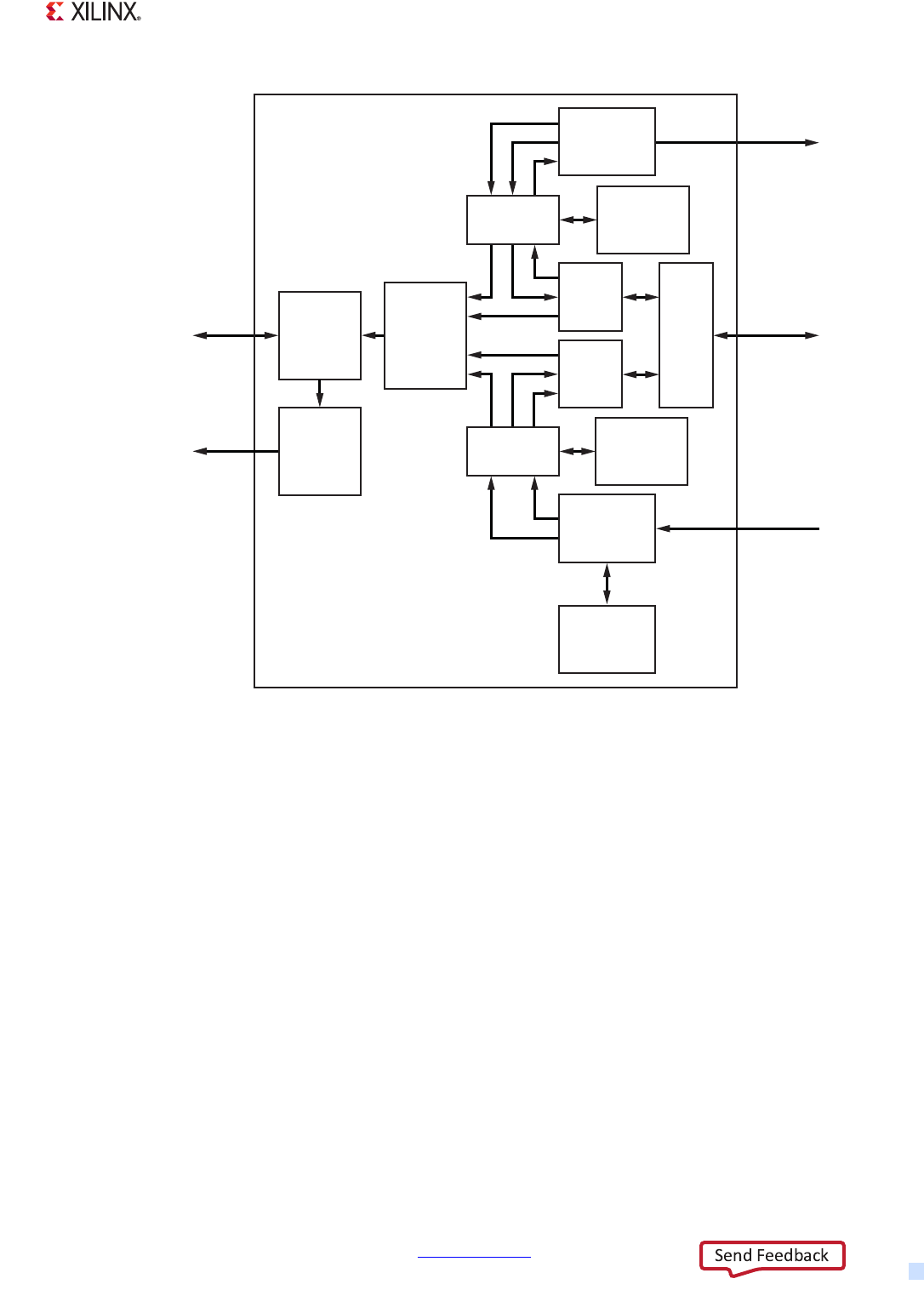
Zynq-7000 AP SoC Technical Reference Manual www.xilinx.com 502
UG585 (v1.12.1) December 6, 2017
Chapter 16: Gigabit Ethernet Controller
X-Ref Target - Figure 16-3
Figure 16-3: DMA Packet Buffer
UG585_c16_03_101812
APB AHB
TX GMII
Register
Interface
Status
and
Statistic
Registers
TX
DMA
AHB
DMA
MAC
Transmitter
Gigabit
Ethernet
Controller
MAC
Receive
Frame
Filtering
RX
DMA
TX Packet
Buffer
TX Packet
Buffer
DPSRAM
RX GMII
RX Packet
Buffer
DPSRAM
RX Packet
Buffer
MDIO Control
Registers
Interconnect
MIO or EMIO
MIO or EMIO
Interconnect
MIO or EMIO

Zynq-7000 AP SoC Technical Reference Manual www.xilinx.com 503
UG585 (v1.12.1) December 6, 2017
Chapter 16: Gigabit Ethernet Controller
In the transmit direction, the DMA continues to fetch packet data up to a limit of 256 packets, or until
the buffer is full. The size of the buffer has a maximum usable size of 4 KB.
In the receive direction, if the buffer becomes full, then an overflow occur.s An overflow also occurs
if the limit of 256 packets is breached. The size of the external buffer has a maximum usable size of
4KB.
Tx Packet Buffer
The transmitter packet buffer continues to attempt to fetch frame data from the AHB system memory
until the packet buffer itself is full, at which point it attempts to maintain its full level.
To accommodate the status and statistics associated with each frame, three words per packet are
reserved at the end of the packet data. If the packet was bad and requires to be dropped, the status
and statistics are the only information held on that packet. Storing the status in the DPRAM is
required to decouple the DMA interface of the buffer from the MAC interface, to update the MAC
status/stats, and to generate interrupts in the order in which the packets that they represent were
fetched from the AHB memory.
If any errors occur on the AHB while reading the transmit frame, the fetching of packet data from
AHB memory is halted. The MAC transmitter continues to fetch packet data, thereby emptying the
packet buffer and allowing any good non-errored frames to be transmitted successfully. When these
have been fully transmitted, the status/stats for the errored frame is updated and software is
informed via an interrupt that an AHB error occurred. This way, the error is reported in the correct
packet order.
The transmit packet buffer only attempts to read more frame data from the AHB when space is
available in the packet buffer memory. If space is not available it must wait until the packet fetched
by the MAC completes transmission and is subsequently removed from the packet buffer memory.
Note that if full store and forward mode is active, and if a single frame is fetched that is too large for
the packet buffer memory, the frame is flushed and the DMA is halted with an error status. This is
because a complete frame must be written into the packet buffer before transmission can begin, and
therefore the minimum packet buffer memory size should be chosen to satisfy the maximum frame
to be transmitted in the application.
When the complete transmit frame is written into the packet buffer memory, a trigger is sent across
to the MAC transmitter, which then begins reading the frame from the packet buffer memory.
Because the whole frame is present and stable in the packet buffer memory, an underflow of the
transmitter is not possible. The frame is kept in the packet buffer until notification is received from
the MAC that the frame data has either been successfully transmitted or can no longer be
re-transmitted (too many retries in half duplex mode). When this notification is received the frame is
flushed from memory to make room for a new frame to be fetched from AHB system memory.
In half duplex mode, the frame is kept in the packet buffer until notification is received from the MAC
that the frame data has either been successfully transmitted or can no longer be re-transmitted (too
many retries in half duplex mode). When this notification is received the frame is flushed from
memory to make room for a new frame to be fetched from AHB system memory.
In full duplex mode, the frame is removed from the packet buffer on-the-fly.

Zynq-7000 AP SoC Technical Reference Manual www.xilinx.com 504
UG585 (v1.12.1) December 6, 2017
Chapter 16: Gigabit Ethernet Controller
Other than underflow, the only MAC related errors that can occur are due to collisions during half
duplex transmissions. When a collision occurs the frame still exists in the packet buffer memory so it
can be retried directly from there. Only when the MAC transmitter has failed to transmit after sixteen
attempts is the frame finally flushed from the packet buffer.
Rx Packet Buffer
The receive packet buffer stores frames from the MAC receiver along with their status and statistics.
Frames with errors are flushed from the packet buffer memory, good frames are pushed onto the
DMA AHB interface.
The receiver packet buffer monitors the FIFO writes from the MAC receiver and translates the FIFO
pushes into packet buffer writes. At the end of the received frame the status and statistics are
buffered so that the information can be used when the frame is read out. When programmed in full
store and forward mode, if the frame has an error the frame data is immediately flushed from the
packet buffer memory allowing subsequent frames to utilize the freed up space. The status and
statistics for bad frames are still used to update the controller’s registers.
Note: To accommodate the status and statistics associated with each frame, three words per packet
are reserved at the end of the packet data. If the packet was bad and requires to be dropped, the
status and statistics are the only information held on that packet.
The receiver packet buffer also detects a full condition such that an overflow condition can be
detected. If this occurs, subsequent packets are dropped and an RX overflow interrupt is raised.
The DMA only begins packet fetches when the status and statistics for a frame are available. If the
frame has a bad status due to a frame error, the status and statistics are passed onto the controller’s
registers. If the frame has a good status, the information is used to read the frame from the packet
buffer memory and burst onto the AHB using the DMA buffer management protocol. After the last
frame data has been transferred to the FIFO, the status and statistics are updated to the controller’s
registers.
16.2.6 Checksum Offloading
The controller can be programmed to perform IP, TCP, and UDP checksum offloading in both receive
and transmit directions, enabled by setting bit [24] in the Network Configuration register for receive,
and bit [11] in the DMA Configuration register for transmit.
IPv4 packets contain a 16-bit checksum field, which is the 16-bit 1's complement of the 1's
complement sum of all 16-bit words in the header. TCP and UDP packets contain a 16-bit checksum
field, which is the 16-bit 1's complement of the 1's complement sum of all 16-bit words in the header,
the data, and a conceptual IP pseudo header.
To calculate these checksums in software requires each byte of the packet to be processed. For TCP
and UDP this can use a large amount of processing power. Offloading the checksum calculation to
hardware can result in significant performance improvements.
For IP, TCP, or UDP checksum offload to be useful, the operating system containing the protocol stack
must be aware that this offload is available so that it can make use of the fact that the hardware can
either generate or verify the checksum.

Zynq-7000 AP SoC Technical Reference Manual www.xilinx.com 505
UG585 (v1.12.1) December 6, 2017
Chapter 16: Gigabit Ethernet Controller
Note: While enabling UDP checksum offloading in hardware, if the checksum fields pointed to by
the DMA descriptor are not initialized to 0, the calculated checksum does not provide the proper
value. Therefor the checksum fields need to be initialized to 0 for checksum offloading to work
properly.
Rx Checksum Offload
When receive checksum offloading is enabled, the IPv4 header checksum is checked per RFC 791,
where the packet meets the following criteria:
• If present, the VLAN header must be four octets long and the CFI bit must not be set
• Encapsulation must be RFC 894 Ethernet Type encoding or RFC 1042 SNAP encoding
•IPv4 packet
• IP header is of a valid length
The controller also checks the TCP checksum per RFC 793, or the UDP checksum per RFC 768, if the
following criteria are met:
• IPv4 or IPv6 packet
• Good IP header checksum (if IPv4)
• No IP fragmentation
•TCP or UDP packet
When an IP, TCP, or UDP frame is received, the receive buffer descriptor provides an indication if the
controller was able to verify the checksums. There is also an indication if the frame had LLC SNAP
encapsulation. These indication bits replace the type ID match indication bits when receive checksum
offload is enabled.
If any of the checksums are verified to be incorrect by the controller, the packet is discarded and the
appropriate statistics counter is incremented.
Tx Checksum Offload
The transmitter checksum offload is only available when the full store and forward mode is enabled.
This is because the complete frame to be transmitted must be read into the packet buffer memory
before the checksum can be calculated and written back into the headers at the beginning of the
frame.
Transmitter checksum offload is enabled by setting bit [11] in the DMA Configuration register. When
enabled, it monitors the frame as it is written into the transmitter packet buffer memory to
automatically detect the protocol of the frame. Protocol support is identical to the receiver checksum
offload.
For transmit checksum generation and substitution to occur, the protocol of the frame must be
recognized and the frame must be provided without the FCS field, by ensuring that bit [16] of the
transmit descriptor word 1 is clear. If the frame data already had the FCS field, this would be
corrupted by the substitution of the new checksum fields.
If these conditions are met, the transmit checksum offload engine calculates the IP, TCP, and UDP
checksums as appropriate. When the full packet is completely written into packet buffer memory, the

Zynq-7000 AP SoC Technical Reference Manual www.xilinx.com 506
UG585 (v1.12.1) December 6, 2017
Chapter 16: Gigabit Ethernet Controller
checksums are valid and the relevant DPRAM locations are updated for the new checksum fields as
per standard IP/TCP and UDP packet structures.
If the transmitter checksum engine is prevented from generating the relevant checksums, bits [22:20]
of the transmitter DMA writeback status are updated to identify the reason for the error. Note that
the frame is still transmitted but without the checksum substitution, as typically the reason that the
substitution did not occur was that the protocol was not recognized.
16.2.7 IEEE 1588 Time Stamp Unit
IEEE 1588 is a standard for precision time synchronization in local area networks. It works with the
exchange of special precision time protocol (PTP) frames. The PTP messages can be transported over
IEEE 802.3/Ethernet, over Internet Protocol Version 4 or over Internet Protocol Version 6 as described
in the annex of IEEE P1588.D2.1.
The controller detects when the PTP event messages sync, delay_req, pdelay_req and pdelay_resp are
transmitted and received.
Synchronization between master and slave clocks is a two stage process.
• First, the offset between the master and slave clocks is corrected by the master sending a sync
frame to the slave with a follow up frame containing the exact time the sync frame was sent.
Hardware assist modules at the master and slave side detect exactly when the sync frame was
sent by the master and received by the slave. The slave then corrects its clock to match the
master clock.
• Second, the transmission delay between the master and slave is corrected. The slave sends a
delay request frame to the master which sends a delay response frame in reply. Hardware assist
modules at the master and slave side detect exactly when the delay request frame was sent by
the slave and received by the master. The slave then has enough information to adjust its clock
to account for delay. For example, if the slave was assuming zero delay the actual delay is half
the difference between the transmit and receive time of the delay request frame (assuming
equal transmit and receive times) because the slave clock is lagging the master clock by the
delay time already.
For hardware assist it is necessary to timestamp when sync and delay_req messages are sent and
received. The timestamp is taken when the message timestamp point passes the clock timestamp
point. The message timestamp point is the SFD and the clock timestamp point is the MII interface.
(The 1588 spec refers to sync and delay_req messages as event messages as these require
timestamping. Follow up, delay response and management messages do not require timestamping
and are referred to as general messages.)
1588 version 2 defines two additional PTP event messages. These are the peer delay request
(Pdelay_Req) and peer delay response (Pdelay_Resp) messages. These messages are used to calculate
the delay on a link. Nodes at both ends of a link send both types of frames (regardless of whether
they contain a master or slave clock). The Pdelay_Resp message contains the time at which a
Pdelay_Req was received and is itself an event message. The time at which a Pdelay_Resp message is
received is returned in a Pdelay_Resp_Follow_Up message.

Zynq-7000 AP SoC Technical Reference Manual www.xilinx.com 507
UG585 (v1.12.1) December 6, 2017
Chapter 16: Gigabit Ethernet Controller
The controller recognizes four different encapsulations for PTP event messages:
• 1588 version 1 (UDP/IPv4 multicast)
• 1588 version 2 (UDP/IPv4 multicast)
• 1588 version 2 (UDP/IPv6 multicast)
• 1588 version 2 (Ethernet multicast)
Note: Only multicast packets are supported.
The TSU consists of a timer and registers to capture the time at which PTP event frames cross the
message timestamp point. These are accessible through the APB interface. An interrupt is issued
when a capture register is updated.
The MAC provides timestamp registers that capture the departure time (for transmit) or arrival time
(for receive) of PTP event packets (sync and delay request) and peer event packets (peer delay
request or peer delay response). Interrupts are optionally generated upon timestamp capture.
The MAC also provides an option to timestamp all received packets by replacing the packet's FCS
word with the nanoseconds portion of the timestamp. This eliminates the need to respond to
received timestamp interrupts and to associate the timestamps with the correct received packets.
The timestamp unit includes a 62-bit timer counter. The lower 30 bits count nanoseconds and the
upper 32 bits count seconds. Every clock cycle the counter is incremented by a programmable
number of nanoseconds, and a mechanism is provided to handle fractional values. For example, at
120 MHz, the clock period is 8.333 ns. Every 3 clock cycles the counter is incremented twice by 8 and
once by 9, for an average increment of 8.333 ns. The counter is clocked by the CPU 1x which is
derived from the CPU clock.
There are six additional registers that capture the time at which PTP event frames are transmitted
and received. An interrupt is issued when these registers are updated.
IEEE 1588 Limitations
These topics can be addressed by software, but the added software workload limits the capabilities
and accuracy of the IEEE1588 support. In many non-real-time operating systems, the interrupt
response time is long, making it more difficult to achieve high accuracy.
Time Counter Clock Input
The 62-bit time counter is clocked by the CPU_1x clock and there is no option for a separate clock
input. Thus the choice of clock frequency and precision is related to the CPU clock frequency.
62-bit Time Counter Accuracy
The counter accuracy is limited to 62 bits. The least significant bits are in nanosecond units, and
there is no direct support for counting fractions of nanoseconds. A mechanism is provided to allow
fractional increments by averaging between two integer values, but its accuracy is limited and it
creates jitter of up to ±128 ns.

Zynq-7000 AP SoC Technical Reference Manual www.xilinx.com 508
UG585 (v1.12.1) December 6, 2017
Chapter 16: Gigabit Ethernet Controller
Counter Value to the PL
The 62-bit counter value is only accessible by reading a register. It is therefore not directly possible
to schedule hardware events upon the counter reaching a specific value.
One Pulse per Second Output
Because there is no hardware access to the counter value, it is not possible to provide a 1 pps signal
that is commonly used for lab tests of the synchronization accuracy.
Event Scheduling
The MAC does not provide event scheduling capability such as generating an interrupt upon the
counter reaching a specific value.
Synchronizing the Two Ethernet Controllers
The two Ethernet cores are completely independent, and there is no hardware mechanism provided
for synchronizing the counter values of the two Ethernet cores, or for making the counter of one
Ethernet core slave to the other.
Single Packet Queue — No Tagging
All received packets are written into the same queue (or packet buffer) in memory. Similarly, all
transmitted packets are read from the same queue. There is no support for multiple queues. A single
queue makes it more difficult for the software to associate (tag) a packet with a timestamp.
FIFO Depth
The timestamp registers are 1-deep, so new events overwrite old values. This requires the software to
have a fast enough response time to avoid event overrun.
Designing the Timestamp Unit in the PL
Improvement in performance and accuracy of time stamping can be achieved by implementing the
timestamp unit in the PL instead of using the built-in timestamp unit in the MAC. Using this
approach, the time counter and the timestamp registers are implemented in the PL, and the PTP
frame recognition remains in the Ethernet core.
The outputs from the controller can be used to implement the timestamp unit in the PL. The EMIO
signals for this are listed in Table 16-12, page 535. The following items are not supported:
• Support of unicast PTP packets
• Support of transparent clocks
• Single packet queue – no tagging

Zynq-7000 AP SoC Technical Reference Manual www.xilinx.com 509
UG585 (v1.12.1) December 6, 2017
Chapter 16: Gigabit Ethernet Controller
Designing a PTP Packet Tagging and Capture Module
Designing a separate timestamp unit as described above addresses most of the items, but it does not
address the hardware mechanism for tagging the PTP packets, i.e., associating the packets with their
corresponding timestamp. For example, if along with the timestamp some identifying packet
attribute were captured, it would allow software to easily associate the timestamp with the correct
PTP event. Examples of useful packet attributes are packet identification or serial number, or the
memory address it was read from or written to. It is also possible to capture the entire packet along
with its timestamp (for both transmit and receive), and make it available to software, for example via
FIFOs or via circular buffers in main memory. Such a function can be implemented in the PL along
with the timestamp unit as described above.
However, implementation requires access to the packet data stream itself. In order to have access to
the packet data stream, the controller needs to be pinned-out through the EMIO using GMII, instead
of MIO. By selecting this option, the GMII signals are exposed to the PL and can be used to detect
and capture the PTP packets. Note that it is still possible to use the PTP frame recognition in the
MAC, or it is possible to design this function in the PL as well (e.g., if support for unicast packets is
required).
16.2.8 MAC 802.3 Pause Frame Support
Note: See Clause 31, and Annex 31A and 31B of the IEEE standard 802.3 for a full description of
pause operation.
The start of an 802.3 pause frame is shown in Table 16-4
The controller supports both hardware controlled pause of the transmitter upon reception of a pause
frame and hardware generated pause frame transmission.
802.3 Pause Frame Reception
Bit [13] of the Network Configuration register is the pause enable control for reception. If this bit is
set transmission pauses if a non zero pause quantum frame is received.
If a valid pause frame is received then the pause time register is updated with the new frame's pause
time regardless of whether a previous pause frame is active or not. An interrupt (either bit [12] or bit
[13] of the Interrupt Status register) is triggered when a pause frame is received, but only if the
interrupt has been enabled (bit [12] and bit [13] of the Interrupt Mask register). Pause frames
received with non zero quantum are indicated through the interrupt bit [12] of the Interrupt Status
register. Pause frames received with zero quantum are indicated on bit [13] of the Interrupt Status
register.
When the pause time register is loaded and the frame currently being transmitted has been sent, no
new frames are transmitted until the pause time reaches zero. The loading of a new pause time, and
Table 16-4: Pause Frame Information
Destination Address Source Address Type
(MAC Control Frame) Pause Opcode Pause Time
0x0180C2000001 6 bytes 0x8808 0x0001 2 bytes

Zynq-7000 AP SoC Technical Reference Manual www.xilinx.com 510
UG585 (v1.12.1) December 6, 2017
Chapter 16: Gigabit Ethernet Controller
hence the pausing of transmission, only occurs when the controller is configured for full duplex
operation. If the controller is configured for half duplex there is no transmission pause, but the pause
frame received interrupt is still triggered. A valid pause frame is defined as having a destination
address that matches either the address stored in Specific Address register 1 or if it matches the
reserved address of 0x0180C2000001. It must also have the MAC control frame type ID of 0x8808
and have the pause opcode of 0x0001.
Pause frames that have FCS or other errors are treated as invalid and are discarded. 802.3 Pause
frames that are received after priority based flow control (PFC) has been negotiated are also
discarded. Valid pause frames received increment the Pause Frames Received Statistic register.
The Pause Time register decrements every 512 bit times once transmission has stopped. For test
purposes, the retry test bit can be set (bit [12] in the Network Configuration register) which causes
the Pause Time register to decrement every tx_clk cycle when transmission has stopped.
The interrupt (bit [13] in the Interrupt Status register) is asserted whenever the pause time register
decrements to zero (assuming it has been enabled by bit [13] in the Interrupt Mask register). This
interrupt is also set when a zero quantum pause frame is received.
802.3 Pause Frame Transmission
Automatic transmission of pause frames is supported through the transmit pause frame bits of the
Network Control register and from the external input pins tx_pause, tx_pause_zero and tx_pfc_sel. If
either bit [11] or bit [12] of the Network Control register is written with logic 1, or if the input signal
tx_pause is toggled when tx_pfc_sel is Low, an 802.3 pause frame is transmitted providing full duplex
is selected in the Network Configuration register and the transmit block is enabled in the Network
Control register.
Pause frame transmission occurs immediately if transmit is inactive or if transmit is active between
the current frame and the next frame due to be transmitted.
Transmitted pause frames comprise of the following:
• A destination address of 01-80-C2-00-00-01
• A source address taken from Specific Address register 1
•A type ID of 88-08 (MAC control frame)
•A pause opcode of 00-01
• A pause quantum register
• Fill of 00 to take the frame to minimum frame length
•Valid FCS
The pause quantum used in the generated frame depends on the trigger source for the frame as
follows:
• If bit [11] is written with a one, the pause quantum is taken from the Transmit Pause Quantum
register. The Transmit Pause Quantum register resets to a value of 0xFFFF giving maximum
pause quantum as the default.
• If bit [12] is written with a one, the pause quantum is zero.

Zynq-7000 AP SoC Technical Reference Manual www.xilinx.com 511
UG585 (v1.12.1) December 6, 2017
Chapter 16: Gigabit Ethernet Controller
• If the tx_pause input is toggled, tx_pfc_sel is Low and the tx_pause_zero input is held Low until
the next toggle, the pause quantum is taken from the Transmit Pause Quantum register.
• If the tx_pause input is toggled, tx_pfc_sel is Low and the tx_pause_zero input is held High until
the next toggle, the pause quantum is zero.
After transmission, a pause frame transmitted interrupt is generated (bit [14] of the Interrupt Status
register) and the only statistics register that is incremented is the Pause Frames Transmitted register.
Pause frames can also be transmitted by the MAC using normal frame transmission methods.
MAC PFC Priority Based Pause Frame Support
Note: Refer to the 802.1Qbb standard for a full description of priority based pause operation.
The controller supports PFC priority based pause transmission and reception. Before PFC pause
frames can be received, bit 16 of the Network Control register must be set. The start of a PFC pause
frame is shown in Table 16-5.
PFC Pause Frame Reception
The ability to receive and decode priority based pause frames is enabled by setting bit [16] of the
Network Control register. When this bit is set, the controller matches either classic 802.3 pause
frames or PFC priority based pause frames. Once a priority based pause frame has been received and
matched, then from that moment on the controller only matches on priority based pause frames (this
is an 802.1Qbb requirement, known as PFC negotiation). Once priority based pause has been
negotiated, any received 802.3x format pause frames are not acted upon. The state of PFC
negotiation is identified via the output pfc_negotiate.
If a valid priority based pause frame is received then the controller decodes the frame and
determines which, if any, of the eight priorities require to be paused. Up to eight Pause Time
registers are then updated with the eight pause times extracted from the frame, regardless of
whether a previous pause operation is active or not. An interrupt (either bit [12] or bit [13] of the
Interrupt Status register) is triggered when a pause frame is received, but only if the interrupt has
been enabled (via bit[12] and bit[13] of the Interrupt Mask register).
Pause frames received with non zero quantum are indicated through the interrupt bit[12] of the
Interrupt Status register. Pause frames received with zero quanta are indicated on bit[13] of the
Interrupt Status register. The state of the eight pause time counters are indicated through the
outputs rx_pfc_paused. These outputs remain High for the duration of the pause time quanta. The
loading of a new pause time only occurs when the controller is configured for full duplex operation.
If the controller is configured for half duplex, the pause time counters are not loaded, but the pause
frame received interrupt is still triggered.
Table 16-5: PFC Priority Based Pause Frame Info
Destination Address Source Address Type
(MAC Control Frame)
Pause
Opcode
Priority
Enable Vector
Pause
Times
0x0180C2000001 6 bytes 0x8808 0x0101 2 bytes 8 * 2 bytes

Zynq-7000 AP SoC Technical Reference Manual www.xilinx.com 512
UG585 (v1.12.1) December 6, 2017
Chapter 16: Gigabit Ethernet Controller
A valid pause frame is defined as having a destination address that matches either the address
stored in Specific Address register 1 or if it matches the reserved address of 0x0180C2000001. It
must also have the MAC control frame type ID of 0x8808 and have the pause opcode of 0x0101.
Pause frames that have FCS or other errors are treated as invalid and are discarded. Valid pause
frames received increment the pause Frames Received Statistic register.
The Pause Time registers decrement every 512 bit times immediately following the PFC frame
reception. For test purposes, the retry test bit can be set (bit [12] in the Network Configuration
register) which causes the Pause Time register to decrement every rx_clk cycle once transmission has
stopped.
The interrupt (bit [13] in the Interrupt Status register) is asserted whenever the Pause Time register
decrements to zero (assuming it has been enabled by bit [13] in the Interrupt Mask register). This
interrupt is also set when a zero quantum pause frame is received.
PFC Pause Frame Transmission
Automatic transmission of pause frames is supported through the transmit priority based pause
frame bit of the Network Control register and from the external input pins tx_pause,
tx_pfc_pause[7:0], tx_pfc_pause_zero[7:0], and tx_pfc_sel. If bit 17 of the Network Control register is
written with logic 1, or if the input signal tx_pause is toggled when tx_pfc_sel is High, a PFC pause
frame is transmitted providing full duplex is selected in the Network Configuration register and the
transmit block is enabled in the Network Control register. When bit 17 of the Network Control
register is set, the fields of the priority based pause frame are built using the values stored in the
Transmit PFC Pause register.
Pause frame transmission occurs immediately if transmit is inactive or if transmit is active between
the current frame and the next frame due to be transmitted.
Transmitted pause frames comprise of the following:
• A destination address of 01-80-C2-00-00-01
• A source address taken from Specific Address register 1
•A type ID of 88-08 (MAC control frame)
•A pause opcode of 01-01
• A priority enable vector taken from tx_pfc_pause or the Transmit PFC Pause register
• Eight pause quantum registers
• Fill of 00 to take the frame to minimum frame length
•Valid FCS
The Pause Quantum registers used in the generated frame depend on the trigger source for the
frame as follows:
• If bit [17] of the Network Control register is written with a one then the priority enable vector of
the priority based pause frame is set equal to the value stored in the Transmit PFC Pause register
[7:0]. For each entry equal to zero in the Transmit PFC Pause register[15:8], the pause quantum
field of the pause frame associated with that entry is taken from the Transmit Pause Quantum
register. For each entry equal to one in the Transmit PFC Pause register[15:8], the pause
quantum associated with that entry is zero.

Zynq-7000 AP SoC Technical Reference Manual www.xilinx.com 513
UG585 (v1.12.1) December 6, 2017
Chapter 16: Gigabit Ethernet Controller
• The Transmit Pause Quantum register resets to a value of 0xFFFF giving maximum pause
quantum as default.
• If the tx_pause input is toggled and tx_pfc_sel is High then the priority enable vector of the
priority based pause frame is set equal to the value in tx_pfc_pause [7:0]. For each entry equal to
zero in tx_pfc_pause_zero[7:0], the pause quantum field of the pause frame associated with that
entry is taken from the Transmit Pause Quantum register. For each entry equal to one in
tx_pfc_pause_zero [7:0], the pause quantum associated with that entry is zero.
After transmission, a pause frame transmitted interrupt is generated (bit 14 of the Interrupt Status
register) and the only statistics register that is incremented is the Pause Frames Transmitted register.
PFC Pause frames can also be transmitted by the MAC using normal frame transmission methods.
Limitation
The GEM controller registers require single 32-bit read/write accesses, do not use byte, halfword, or
double word references.
16.3 Programming Guide
The controller functionality is described in detail in section 16.2 Functional Description and
Programming Model. All of the controller registers are listed in Table 16-9 and Table 16-10 and are
described in detail in Appendix B, Register Details.
Example: Programming Steps
1. 16.3.1 Initialize the Controller
2. 16.3.2 Configure the Controller
3. 16.3.3 I/O Configuration
4. 16.3.4 Configure the PHY
5. 16.3.5 Configure the Buffer Descriptors
6. 16.3.6 Configure Interrupts
7. 16.3.7 Enable the Controller
8. 16.3.8 Transmitting Frames
9. 16.3.9 Receiving Frames
10. 16.3.10 Debug Guide
For information on building the ethernet system for Zynq, refer to the followings:
•XAPP1026, LightWeight IP Application Examples
•XAPP1082, PS and PL Ethernet Performance and Jumbo Frame Support with PL Ethernet in the
Zynq-7000 AP SoC
•Baremetal Drivers and Libraries
•OS and Libraries Document Collection
•Zynq PL Ethernet

Zynq-7000 AP SoC Technical Reference Manual www.xilinx.com 514
UG585 (v1.12.1) December 6, 2017
Chapter 16: Gigabit Ethernet Controller
16.3.1 Initialize the Controller
1. Clear the Network Control register. Write 0x0 to gem.net_ctrl register.
2. Clear the Statistics registers. Write a 1 to gem.net_ctrl[clear_stat_regs].
3. Clear the Status registers. Write a 1 to the Status registers. gem.rx_status = 0x0F and
gem.tx_status = 0xFF.
4. Disable all interrupts. Write 0x7FF_FEFF to the gem.intr_dis register.
5. Clear the buffer queues. Write 0x0 to the gem.rx_qbar and gem.tx_qbar registers.
16.3.2 Configure the Controller
The following example describes a typical programming sequence for configuration of the controller.
Refer to Appendix B, Register Details for further details on the Controller registers.
1. Program the Network Configuration register (gem.net_cfg). The network configuration
register is used to set the mode of operation.
Examples:
a. Enable Full Duplex. Write a 1 to the gem.net_cfg[full_duplex] register.
b. Enable Gigabit mode. Write a 1 to the gem.net_cfg[gige_en] register.
c. Enable default speed for 100 Mbps. Write a 1 to the gem.net_cfg[speed] register.
Note: The speed bit might have to be re-written after PHY auto-negotiation.
d. Enable reception of broadcast or multicast frames. Write a 0 to the
gem.net_cfg[no_broadcast] register to enable broadcast frames and write a 1 to the
gem.net_cfg[multi_hash_en] register to enable multicast frames.
e. Enable promiscuous mode. Write a 1 to the gem.net_cfg[copy_all] register.
f. Enable TCP/IP checksum offload feature on receive. Write a 1 to the
gem.net_cfg[rx_chksum_offld_en] register. (Refer to section 16.2.6 Checksum Offloading.)
g. Enable Pause frames. Write a 1 to gem.net_cfg[pause_en] register.
h. Set the MDC clock divisor. Write the appropriate MDC clock divisor to the
gem.net_cfg[mdc_clk_div] register. (Refer to section 16.3.4 Configure the PHY.)
2. Set the MAC address. Write to the gem.spec1_addr1_bot and gem.spec1_addr1_top registers.
The least significant 32 bits of the MAC address go to gem.spec1_addr1_bot and the most
significant 16 bits go to gem.spec1_addr1_top.
3. Program the DMA Configuration register (gem.dma_cfg).
a. Set the receive buffer size to 1,600 bytes. Write a value of 0x19 to the
gem.dma_cfg[ahb_mem_rx_buf_size] register.
b. Set the receiver packet buffer memory size to the full configured addressable space of
8KB. Write 0x3 to the gem.dma_cfg[rx_pktbuf_memsz_sel] register.
c. Set the transmitter packet buffer memory size to the full configured addressable space
of 4 KB. Write 0x1 to the gem.dma_cfg[tx_pktbuf_memsz_sel] register.

Zynq-7000 AP SoC Technical Reference Manual www.xilinx.com 515
UG585 (v1.12.1) December 6, 2017
Chapter 16: Gigabit Ethernet Controller
d. Enable TCP/IP checksum generation offload on the transmitter. Write 0x1 to the
gem.dma_cfg[csum_gen_offload_en] register.
e. Configure for Little Endian system. Write 0x0 to the
gem.dma_cfg[ahb_endian_swp_pkt_en] register.
f. Configure AHB fixed burst length. Write 0x10 to the gem.dma_cfg[ahb_fixed_burst_len]
register to use INCR16 AHB burst for higher performance.
4. Program the Network Control Register (gem.net_ctrl).
a. Enable MDIO. Write a 1 to the gem.net_ctrl[mgmt_port_en] register.
b. Enable the Transmitter. Write a 1 to the gem.net_ctrl[tx_en] register.
c. Enable the Receiver. Write a 1 to the gem.net_ctrl[rx_en] register.
16.3.3 I/O Configuration
The block diagram in section 16.1.1 Block Diagram describes the connection details of the Gigabit
Ethernet Controller to the external network.
Gigabit Ethernet Controller using MIO
The controller provides an RGMII interface through the MIO. Pins 16-27 are used for Controller 0 and
28-39 for Controller 1. Refer to section 16.6 Signals and I/O Connections for more information on
the pin-out.
Example: Configuring Controllers for MIO
The controllers can be configured to operate in HSTL or CMOS IO standards. Refer to Chapter 2,
Signals, Interfaces, and Pins for more information on MIO pin configuration. The following steps
illustrate the configuration for Controller 0.
1. Write to the slcr.MIO_PIN{16:21} registers for the transmit signals. This programs the MIO
I/O buffers (GPIOB) for the four transmit data signals, transmit clock and transmit control signals.
Example: A value of 0x0000_3902 disables the HSTL receiver, specifies HSTL I/O type, enables
internal pull-up, disables 3-state control and routes the transmit data, clock, and control signals.
2. Write to the slcr.MIO_PIN{22:27} registers for the receive signals.
Example: A value of 0x0000_1903 enables HSTL receiver, specifies HSTL I/O type, enables
internal pull-up, disables 3-state control and routes the receive data, clock, and control signals.
3. Write to slcr.MIO_PIN{52:53} registers for the management signals.
Example: A value of 0x0000_1280 enables the HSTL receiver, specifies HSTL I/O type, enables
internal pull-up, and routes the MDIO clock/data.
4. Write a value of 0x0000_0001 to the slcr.GPIOB register to enable the VREF internal
generator.
Similarly, replace SLCR.MIO_PIN{16:27} with SLCR.MIO_PIN{28:39} for Controller 1.
Note: The clock might have to be reprogrammed after auto-negotiation.

Zynq-7000 AP SoC Technical Reference Manual www.xilinx.com 516
UG585 (v1.12.1) December 6, 2017
Chapter 16: Gigabit Ethernet Controller
Gigabit Ethernet Controller using EMIO
The EMIO interface allows for derivation of other physical MII interfaces using appropriate
shim-logic in the PL. The Controller provides a GMII interface through the EMIO.
Example: Configure Controllers for EMIO
1. Unlock the SLCR module. Write a value of 0xDF0D to the slcr.SLCR_UNLOCK register.
2. Enable the level shifters for PS user inputs to FPGA. Write a value of 4'b1010 to bit field
slcr.LVL_SHFTR_EN[USER_LVL_SHFTR_EN].
3. Write a value of 0 to the slcr.FPGA_RST_CTRL register.
4. Perform a software reset. Write 0b1 to bits slcr.FPGA_RST_CTRL[FPGA{0-3}_OUT_RST].
5. Write a value of 0 to the slcr.FPGA_RST_CTRL register.
6. Lock the SLCR module. Write a value of 0x767B to the slcr.SLCR_LOCK register.
Configure Clocks
The Gigabit Ethernet Controller clocks are controlled through four registers in the SLCR module.
Example: Configuring Clocks for MIO
1. Unlock the SLCR module. Write a value of 0xDF0D to slcr.SLCR_UNLOCK register.
2. Configure the clock by writing to the slcr.GEM0_CLK_CTRL register.
Example: A value of 0x0050_0801 enables the Controller0 reference clock, first divisor for the
source clock is 8 and second divisor is 5. This gives a default speed of 100 Mb/s if the Ethernet
source clock is IO PLL which has a frequency of 1,000 MHz.
3. Enable Controller 0 receive clock control. Write a value of 0x0000_0001 to the
slcr.GEM0_RCLK_CTRL register.
4. Lock the SLCR module. Write a value of 0x767B to slcr.SLCR_LOCK register.
Similar steps must be followed for Controller 1 by writing to the appropriate registers.
16.3.4 Configure the PHY
The PHY connected to the controller is initialized through the available management interface
(MDIO) using the PHY maintenance register (gem.phy_maint). Writing to this register starts a shift
operation which is signaled as complete when the bit gem.net_status[phy_mgmt_idle] is set.
The MDIO interface clock (MDC) for GigE is generated by dividing down the CPU_1x clock.
Note: MDC is active only during MDIO read or write operations during which the PHY registers are
read or written.
The MDC must not exceed 2.5 MHz as defined by the IEEE802.3 standard. The
gem.net_cfg[mdc_clk_div] bits are used to set the divisor for the CPU_1x clock.

Zynq-7000 AP SoC Technical Reference Manual www.xilinx.com 517
UG585 (v1.12.1) December 6, 2017
Chapter 16: Gigabit Ethernet Controller
Example: Consider a case with the CPU clock set to 666.667 MHz clock and the available CPU_1x
clock is 111.11 MHz. The clock divisor, in this case should be set to 48 (0b011) in
gem.net_cfg[mdc_clk_div] to set the maximum possible frequency of 2.314 MHz for the MDC.
PHY configuration and initialization is unique for every system. Refer to the vendor data sheet for
more information and PHY register details.
Example: PHY Read/Write Operation
1. Check to see that no MDIO operation is in progress. Read until
gem.net_status[phy_mgmt_idle] = 1.
2. Write data to the PHY maintenance register(gem.phy_maint). This initiates the shift
operation over MDIO. Refer to Appendix B, Register Details section B.18 Gigabit Ethernet
Controller (GEM)for register information.
3. Wait for completion of operation. Read until gem.net_statusp[phy_mgmt_idle] = 1.
4. Read data bits for a read operation. The PHY register data is available in gem.phy_maint[data].
Example: PHY Initialization
1. Detect the PHY address. Read the PHY identifier fields in PHY registers 2 and 3 for all the PHY
addresses ranging from 1 to 32. The register contents will be valid for a valid PHY address.
2. Advertise the relevant speed/duplex settings. These bits can be set to suit the system. Refer to
the PHY vendor data sheet for more information.
3. Configure the PHY as applicable. This could include options to set PHY mode, timing options
in the PHY or others as applicable to the system. Refer to the PHY vendor datasheet for more
information.
4. Wait for completion of Auto-negotiation. Read the PHY status register. Refer to the PHY
vendor data sheet for more information.
5. Update Controller with auto-negotiated speed and duplex settings. Read the relevant PHY
registers to determine the negotiated speed and duplex. Set the speed in gem.net_cfg[gige_en]
and gem.net_cfg[speed] bits and the duplex in gem.net_cfg[full_duplex].
Note: The SLCR register must be updated for clock updates (refer to Configure Clocks, page 516).
16.3.5 Configure the Buffer Descriptors
Receive Buffer Descriptor List
The data received by the controller is written to pre-allocated buffer descriptors in system memory.
These buffer descriptor entries are listed in the receive buffer queue. Refer to section 16.2.5 DMA
Block and Table 16-2, page 495 for more information on implementation and structure of the Rx
Buffer Descriptor.
The Receive-buffer Queue Pointer register (gem.rx_qbar) points to this data structure as shown in
Figure 16-4.
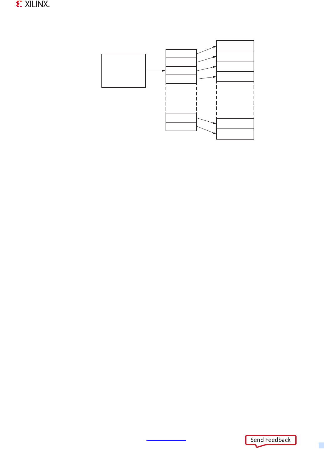
Zynq-7000 AP SoC Technical Reference Manual www.xilinx.com 518
UG585 (v1.12.1) December 6, 2017
Chapter 16: Gigabit Ethernet Controller
To create this list of buffers:
1. Allocate a number (N) of buffers of X bytes in system memory, where X is the DMA buffer length
programmed in the DMA Configuration register.
Example: This controller assumes that the maximum size of an Ethernet packet without jumbo
frame support can reach up to 1,536 bytes. So allocate N number of buffers each with a size of
1,536 bytes in system memory. The buffers typically need to be aligned to cache-line boundaries
to improve performance. Typical values of N can be 64 or 128.
2. Each buffer descriptor is of 8 bytes length. Hence allocate an area of 8N bytes for the receive
buffer descriptor list in system memory. This creates N entries in this list.
Note: A single cache line for the Zynq-7000 AP SoC is 32 bytes and can contain 4 buffer
descriptors. This means flushing or invalidating a single buffer descriptor entry in the cache
memory results in flushing or invalidation of a cache line which in turn affects the adjacent buffer
descriptors. This can result in undesirable behavior. It is typical to allocate the buffer descriptor
list in an un-cached memory region.
3. Mark all entries in this list as owned by controller. Set bit 0 of word 0 of each buffer descriptor to
0.
4. Mark the last descriptor in the buffer descriptor list with the wrap bit (bit 1 in word 0) set.
5. Write the base address of receive buffer descriptor list to controller register gem.rx_qbar.
6. Fill the addresses of the allocated buffers in the buffer descriptors (bits 31-2, Word 0).
7. Write the base address of this buffer descriptor list to the gem.rx_qbar register.
Transmit Buffer Descriptor List
The data to be transmitted is read from buffers present in system memory. These buffers are listed
in the transmit buffer queue. Refer to section 16.2.5 DMA Block and Table 16-2, page 495 for more
information on implementation and structure of the Tx buffer descriptor.
X-Ref Target - Figure 16-4
Figure 16-4: Rx Buffer Queue Structure
UG585_c16_04_022712
Rx Buffer
Queue Pointer
MAC Register
Rx
Descripter List
List in Main
Memory Buffer in Main
Memory
Rx Buffers

Zynq-7000 AP SoC Technical Reference Manual www.xilinx.com 519
UG585 (v1.12.1) December 6, 2017
Chapter 16: Gigabit Ethernet Controller
The Transmit Buffer Queue Pointer register (gem.tx_qbar) register points to this data structure.
To create this list of buffer descriptors with N entries:
1. Each buffer descriptor is 8 bytes in length. Hence allocate an area of 8N bytes for the transmit
buffer descriptor list in system memory which creates N entries in this list. It is advisable to use
un-cached memory for allocating the complete buffer descriptor list for the reasons already
described for the Receive Buffer Descriptor List.
2. Mark all entries in this list as owned by the controller. Set bit[31] of word 1 to 0.
3. Mark the last descriptor in the list with the wrap bit. Set bit[30] in word 1 to 1.
4. Write the base address of transmit buffer descriptor list to Controller register gem.tx_qbar.
16.3.6 Configure Interrupts
There are 26 interrupt conditions that are detected within the controller which are OR-ed to generate
a single interrupt. Additionally there is a Wake-on-LAN interrupt driven from the Ethernet controller.
These two interrupts are then passed to the GIC pl390 interrupt controller.
Refer to the description of register, gem.intr_status in Appendix B, Register Details for more
information on the list of interrupt conditions identified by the controller.
An appropriate handler for the interrupt should be registered with the CPU for processing an
interrupt condition. The CPU suspends its normal activity, moves to interrupt processing mode and
executes the corresponding handler for an interrupt condition.
Example: Configuring Interrupts
1. Register a handler. There are two interrupts generated by the controller - Wake-on-LAN and
another interrupt for all other functions. Register the handler for each of these interrupt types
with the CPU.
Note: In a typical case, a single handler is used for both transmission and reception of packets.
Once the control reaches the handler, the software should read the gem.intr_status register to
determine the source and perform the relevant function.
2. Enable the necessary interrupt conditions. The relevant bits in the gem.intr_en register must
be set. The interrupt conditions necessary are determined by the system architecture.
Note: Read the read-only register gem.intr_mask for current the mask state of each interrupt.

Zynq-7000 AP SoC Technical Reference Manual www.xilinx.com 520
UG585 (v1.12.1) December 6, 2017
Chapter 16: Gigabit Ethernet Controller
16.3.7 Enable the Controller
The receiver and transmitter must be enabled after configuration:
1. Enable the Transmitter. Write a 1 to gem.net_ctrl[tx_en].
2. Enable the Receiver. Write a 1 to gem.net_ctrl[rx_en].
16.3.8 Transmitting Frames
Example: Transmitting a Frame
1. Allocate buffers in system memory to contain the Ethernet frame. GigE supports
scatter-gather functionality; hence an Ethernet frame can be split into multiple buffers with each
buffer processed by a buffer descriptor.
2. Write the Ethernet frame data in the allocated buffers. These Ethernet frames should have
their header fields such as destination MAC address, source MAC address and type/length field
set appropriately.
Notes:
°The FCS field is added by the MAC in most cases. However if there is a need to append a
custom FCS, bit 16 in word 1 of the corresponding buffer descriptor must be set.
°The buffer that contains the Ethernet frame data should be flushed from cache if cached
memory is being used.
3. Allocate buffer descriptor(s) for the Ethernet frame buffers. This involves setting bits 0-31 in
the buffer descriptor word 0 with the address of the buffer and setting bits 0-13 in word 1 with
the length of the buffer to be transmitted.
Notes:
°For single buffer Ethernet frames, bit 15 (Last buffer bit) of the word 1 must also be set.
°For Ethernet frames scattered across multiple buffers the buffer descriptors must be
allocated serially and the buffer descriptor containing the last buffer should have the bit 15
of word 1 set.
Example: For an Ethernet frame of 1,000 bytes split across two buffers with the first buffer
containing the Ethernet header (14 bytes) and the next buffer containing the remaining 986
bytes, the buffer descriptor with index N should be allocated for the first buffer and the buffer
descriptor with index N+1 should be allocated for the second buffer. Bit 15 of word 1 of the N+1
buffer descriptor must also be set to mark it as the last buffer in the scattered list of Ethernet
frames.
4. Clear the used bit (bit 31) in word 1 for all allocated buffer descriptors. However, wait to
clear the bit in the first descriptor until after all the others have been cleared.
5. Enable transmission. Write a 1 to gem.net_ctrl[start_tx].
6. Wait until the transmission is complete. An interrupt is generated by the controller upon
successful completion of the transmission. Read and clear the gem.intr_status[tx_complete] bit
by writing a 1 to the bit In the interrupt handler. Also read and clear the gem.tx_status register by
writing a 1 to gem.tx_status[tx_complete] bit. Clear all bits in the BD except the used and wrap
bits.

Zynq-7000 AP SoC Technical Reference Manual www.xilinx.com 521
UG585 (v1.12.1) December 6, 2017
Chapter 16: Gigabit Ethernet Controller
16.3.9 Receiving Frames
When a frame is received with the receive circuits enabled, the controller checks the address and the
frame is written to system memory in the following cases:
• The destination address matches one of the four specific address registers. This is applicable for
cases where the MAC address for the controller is set in thr gem.spec_addr{1:4}_bot and
gem.spec_addr{1:4}_top registers.
• The received frame's type/length field matches one of the four type ID registers. The available
type id registers are gem.type_id_match{1:4}. This is applicable for cases where Ethernet
type/length field based filtering is required.
• Unicast or Multicast hash is enabled through gem.net_cfg[uni_hash_en] or
gem.net_cfg[multi_hash_en] register bits, then the received frame is accepted only if the hash is
matched.
• The destination address is a broadcast address (0xFFFFFFFFFFFF) and broadcasts are allowed.
This option is set using the gem.net_cfg[no_broadcast] register bit.
• The controller is configured for promiscuous mode with the gem.net_cfg[copy_all] register bit
set.
The register gem.rx_qbar points to the next entry in the receive buffer descriptor list and the
controller uses this as the address in system memory to write the frame. When the frame has been
completely received and written to system memory, the controller then updates the receive buffer
descriptor entry with the reason for the address match, marks the area as being owned by software,
and sets the receive complete interrupt (gem.intr_status[rx_complete] = 1). Software is then
responsible for copying the data to the application area and releasing the buffer.
If the controller is unable to write the data at a rate to match the incoming frame, then the receiver
overrun interrupt is set (gem.intr_status[rx_overrun] = 1). If there is no receive buffer available, i.e.,
the next buffer is still owned by software, a receive-buffer not available interrupt is set. If the frame
is not successfully received, a Statistic register is incremented and the frame is discarded without
informing software.
Example: Handling a Received Frame
1. Wait for the controller to receive a frame. The receive complete interrupt,
gem.intr_status[rx_complete], is generated when a frame is received.
2. Service the interrupt. Read and clear the gem.intr_status[rx_complete] register bit writing a 1 to
the bit in the interrupt handler. Also read and clear the gem.rx_status register by writing a 1 to
gem.rx_status[frame_recd] bit.
3. Process the data in the buffer. Scan the buffer descriptor list for the buffer descriptors with the
ownership bit (bit 0, Word 0) set. When the DMA receive buffer size programmed to 1,600 bytes
(gem.dma_cfg[ahb_mem_rx_buf_size] = 0x19), the packets on the receive side are not scattered
and always go into a single buffer. For a buffer descriptor with the ownership bit set, process the
buffer allocated in the corresponding buffer descriptor and set the ownership bit to 0. Read
other bit fields in the relevant buffer descriptor word 1, take necessary action, and clear them.

Zynq-7000 AP SoC Technical Reference Manual www.xilinx.com 522
UG585 (v1.12.1) December 6, 2017
Chapter 16: Gigabit Ethernet Controller
16.3.10 Debug Guide
The GigE can encounter different kinds of errors while receiving or transmitting Ethernet frames.
Refer to Appendix B, Register Details for more information on the transmit and receive error
conditions listed in the description for gem.tx_status and gem.rx_status registers, respectively. Some
common errors and the action necessary is described in Tabl e 16- 6 and Table 16-7.
Table 16-6: RX Status Errors
Error Condition Necessary Action
Hresp not OK This is a condition from which the controller cannot recover easily. Re-initialize the
controller and buffer descriptors for receive and transmit paths after clearing the
relevant register status bits: gem.rx_status[hresp_not_ok] and
gem.intr_status[hresp_not_ok].
Receive overrun This condition implies that the packet is dropped because the packet buffer is full and
occurs occasionally when the controller is unable to process the packets when they
arrive very fast. In most conditions, no action for error recovery needs to be taken.
Ensure that the packet buffer is configured for 8 KB (see section 16.3.2 Configure the
Controller) and clear bits gem.rx_status[rx_overrun] and gem.intr_status[rx_overrun].
Buffer not available This condition implies that the controller could not get a buffer descriptor with the
ownership bit set to 0. It can also mean that the software is unable to keep pace with
the incoming packet rate. Clear bits gem.rx_status[buffer_not_avail] and
gem.intr_status[rx_used_read] in the interrupt handler. Attempt increasing the number
of buffer descriptors on the receive path to allocate more number of buffers. The
software processing can be optimized further to accelerate processing of received
frames.
Table 16-7: TX Status Errors
Error Condition Necessary Action
Hresp not OK This is a condition from which the controller cannot recover easily. Re-initialize the
controller and buffer descriptors for receive and transmit paths after clearing the
relevant register status bits: gem.tx_status[hresp_not_ok] and
gem.intr_status[hresp_not_ok].
Transmit underrun This implies a severe error condition on the transmit side in processing of the transmit
buffers and buffer descriptors. For effective error recovery, the software must disable
the transmitter by writing a 0 to the gem.net_ctrl[tx_en] bit, then re-initialize the buffer
descriptors on the transmit side and enable the transmitter by writing a 1 to the
gem.net_ctrl[tx_en] bit. The bit gem.tx_status[tx_under_run] must be cleared in the
interrupt handler.
Transmit buffer
exhausted
This is a severe error condition on the transmit side. For effective error recovery, the
software must disable the transmitter by writing a a 0 to the gem.net_ctrl[tx_en] bit,
then re-initialize the transmit buffer descriptors and transmitter. The register bits
gem.tx_status[tx_corr_ahb_err] and gem.intr_status[tx_corrupt_ahb_err] must be
cleared in the interrupt handler.

Zynq-7000 AP SoC Technical Reference Manual www.xilinx.com 523
UG585 (v1.12.1) December 6, 2017
Chapter 16: Gigabit Ethernet Controller
16.4 IEEE 1588 Time Stamping
16.4.1 Overview
Refer to the IEEE 1588 standard specification for more information on the protocol and section
16.2.7 IEEE 1588 Time Stamp Unit for more information on the implementation of the Timestamp
Unit. The following section briefly reviews the essential terms prior to discussion of the programming
model.
The PTP system deals with the following different entities:
•A grandmaster clock. This is typically the IEEE1588 master clock which is the ultimate source of
time on the network.
•A boundary clock. It is a multi-port switch containing one port that is a PTP slave to a master
clock, while the other ports are masters to downstream slave clocks.
•A transparent clock. This is a PTP enhanced switch which modifies the precise time stamps
within relevant PTP packets to account for transmit and receive delays within the individual
switch itself.
•An ordinary clock. This is the typical PTP client.
For more information on different types of PTP clocks refer to the IEEE1588-2008 standard
specification.
Synchronization and management of a PTP system is achieved through the exchange of messages
across the network. PTP uses the following message types:
• Sync, Delay_Req, Follow_up, and Delay_Resp messages are used by ordinary and boundary
clocks. They are used to communicate timing information for clock synchronization.
• Pdelay_Req, Pdelay_Resp, and Pdelay_Resp_Follow_Up are used to measure path delays across
the communication medium so that they can be compensated for by the system. These are
extensively used by transparent clocks and are available only in PTPv2.
• Announce messages are used by best master clock algorithm (BMCA) to build a clock hierarchy
and select the grandmaster clock.
Retry limit exceeded This implies there are a series of collisions for which an Ethernet frame could not be
sent out even with a number of retries in half-duplex communication. This Ethernet
frames are dropped at the transmitter. The bits gem.tx_status[retry_limit_exceeded]
and gem.intr_status[retry_ex_late_collisn]must be cleared in the interrupt handler. No
drastic measures need to be taken for this error. However it could also mean that there
is a duplex setting mismatch.
Collisions This error indicates that there are collisions for half duplex communication. Some
collisions are expected in half duplex mode and can be ignored. When a collision
occurs, the frame is retransmitted after a while and the frame is not dropped. The
register bit gem.tx_status[collision] must be cleared in the interrupt handler.
Table 16-7: TX Status Errors (Cont’d)
Error Condition Necessary Action

Zynq-7000 AP SoC Technical Reference Manual www.xilinx.com 524
UG585 (v1.12.1) December 6, 2017
Chapter 16: Gigabit Ethernet Controller
• Management messages are used for network monitoring and management.
• Signaling frames are used for non -time critical communication across clocks.
Refer to IEEE1588-2008 Clause 13 for more information on message types and formats.
PTP Message Format
All PTP messages contain a header, body and suffix. The PTP message header is 34 bytes long. Please
refer to IEEE1588-2008 Clause 13 for more information on message formats. The important fields in
the message header are described briefly as follows:
• Each clock port is identified by Source Port Identity (sourcePortIdentity) which is a 10 byte
address. The sourcePortIdentity is common for all PTP messages.
• Each PTP message is identified with a message Type which is a 4 bit field in the PTP message
header. Message Types are identified in Table 16-8
•The versionPTP field signifies which PTP version is being used – PTPv1 or PTPv2.
•The messageLength field signifies the total length of the PTP message. It is different for different
PTP messages.
•The flag field is used for various purposes and can carry different values for different types of
frames. An example of use for this field as a twoStepFlag in Sync and PDelay_Req frames is to
distinguish one-step and two-step time stamping. If the sending master clock can perform
one-step time stamping, the twoStepFlag carries a value of 0.
Note: The Zynq-7000 AP SoC supports two-step timestamping – the twoStepFlag should always
be 1.
•The correctionField is generally significant for transparent clocks. The transparent clocks update
the correctionField to specify the slave regarding the exact time the PTP frames took to traverse
through the transparent clocks. If transparent clocks are not present in the path of a PTP
message, the correctionField can have a zero value.
•The sequenceId field is extensively used in the PTP messages. The originator of certain PTP
frames message Types assigns a sequence ID to the corresponding message through the
sequenceId field.
Table 16-8: Message Types
PTP Frames Message Type
Sync 0x0
Delay_Req 0x1
PDelay_Req 0x2
PDelay_Resp 0x3
Follow_up 0x8
Delay_Resp 0x9
PDelay_Resp_Follow_Up 0xA
Announce 0xB
Management 0xC
Signaling 0xD

Zynq-7000 AP SoC Technical Reference Manual www.xilinx.com 525
UG585 (v1.12.1) December 6, 2017
Chapter 16: Gigabit Ethernet Controller
•The controlField is provided to maintain backward compatibility with PTPv1 based hardware
designs. It contains different values for different types of PTP frames.
•The logMessageInterval field is provided to represent the mean time interval between successive
PTP messages.
The steps to develop a simple and typical non-OS standalone example which can be used to
synchronize PTP clocks between two Zynq-7000 AP SoC systems are described in the following
sections. This information should be used for reference purpose only and is not meant to provide the
best possible implementation for accuracy. Please refer to the IEEE1588 standard specification for
more information.
The IEEE1588 implementation involves the following.
1. Controller initialization
2. Best master clock algorithm (BMCA)
3. PTP packet handling at the master port
4. PTP packet handling at the slave port
Notes:
1. The following sections do not describe the handling of management and signaling frames
because they are not integral to the implementation of the core PTP functionality.
2. The illustrations in these sections do not describe an implementation-specific mechanism to
change clock attributes dynamically.
3. The PTP packets processed here are simple Ethernet multicast packets. The scope of the
following sections do not include UDP based multicast packets. The explanation refers to non-OS
based standalone implementation which does not implement a TCP/IP stack.
16.4.2 Controller Initialization
The controller must be initialized with the interrupts, timer and PTP.
1. Initialize the controller with interrupts and timers. Refer to section 16.3 Programming Guide.
2. Enable the PTP interrupts. Refer to section 16.3.6 Configure Interrupts
3. Setup a timer with interrupts and appropriate interrupt handlers to enable periodic
transmission of packets. TTC timers or CPU private timers can be used for this purpose. For a
typical case, interrupts can be generated every 500 ms.
4. Setup the UART to monitor debug messages from the application. Refer to Chapter 19, UART
Controller to program the UART.
The following steps are specifically for the PTP functionality:
1. Initialize the seconds and nanoseconds timers. Write appropriate values to the gem.timer_s
and gem.timer_ns registers, respectively.
2. Program the timer increment value in the gem.timer_incr register.
Example: For a CPU clock that runs at 666.67 MHz and PTP clocked with CPU_1x clock of
111.11 MHz, 1 PTP clock cycle corresponds to 9 ns. The gem.timer_incr[ns_delta] register bit in
this case should be set to 9.

Zynq-7000 AP SoC Technical Reference Manual www.xilinx.com 526
UG585 (v1.12.1) December 6, 2017
Chapter 16: Gigabit Ethernet Controller
As another example, consider a CPU_1x clock of 120 MHz, 1 PTP clock cycle corresponds to
8.33 ns. In this case, the counter should increment by 8 ns for 2 clock cycles and 9 ns for 1 clock
cycle to average 8.33 ns in 3 clock cycles. For such a setting, register bit gem.timer_incr[ns_delta]
is set to 8, gem.timer_incr[alt_ct_ns_delta] is set to 9, and gem.timer_incr[incr_b4_alt] is set to 2.
3. Initialize the common fields of data structures used for various PTP packets. All PTP packets
have a common message header.
Timer Interrupt Handler
A timer is initialized to generate interrupts at pre-defined intervals. The operation of the interrupt
handler at the master and slave clock ports are briefly illustrated.
Example: Master Clock Port
1. Initiate a transmission of Sync and Announce frames at pre-defined intervals.
2. Initiate a transmission of PDelay_Req frames at regular intervals.
Example: Slave Clock Port
1. Initiate a transmission of PDelay_Req frames at regular intervals.
2. Wait for Sync frame for a predefined interval of time. If a Sync timeout occurs, change to become
a PTP master.
3. Wait for an Announce frame for a pre-defined interval of time. If an Announce timeout occurs,
change to become a PTP master.
If a PDelay_Req frame is not received for a predefined period of time, or no Pdelay_resp and
PDelay_resp_Follow_Up were received for a PDelay_Req packet, then there is a grave error. As part of
error handling, the whole PTP state machine can be stopped (for both PTP master and slave) and no
clock synchronization done (if it is a slave port).
The intervals as mandated by the protocol range from 2-128 to 2127 seconds. The interval is decided
by the system specification. Since the same timer is used for Sync, Announce and PDelay_Req frames,
the timer expiry duration is decided by the minimum time interval for all these frames.
In a typical use case, the Sync frames can be sent out every 125 milliseconds, Announce frames and
PDelay_Req frames every 1 second. Similarly, typical Announce frame timeouts can be 2-3 seconds
and PDelay_Req, PDelay_Resp, PDelay_Resp_Follow_up timeouts can be 3-5 seconds.
16.4.3 Best Master Clock Algorithm (BMCA)
The BMCA performs a distributed selection of the best candidate clock (which becomes the
grandmaster clock) based on different clock properties for the available clocks in the network:
•Priority1
•Clock class
• Clock accuracy
• Clock variance (offset scaled log variance)

Zynq-7000 AP SoC Technical Reference Manual www.xilinx.com 527
UG585 (v1.12.1) December 6, 2017
Chapter 16: Gigabit Ethernet Controller
•Priority2
• Clock identity (to break the tie)
Refer to the IEEE 1588 Standard Specification for more information on clock attributes and BMCA.
In a typical implementation, each clock port can be identified with a structure which has fields for the
above clock properties. Other than these properties, the BMCA clock port can also be identified with
the steps removed field. For more information regarding this field refer to the IEEE1588
specifications. When a slave receives Announce frames from multiple master hosts, the steps removed
field can become significant in deciding the master clock.
The implementation should maintain an identical structure to identify the current grandmaster clock
properties. The BMCA is invoked when an Announce frame is received by the slave.
Example: BMCA
1. Compare the fields of the Announce frame received with that of the current grandmaster starting
with Priority1, progressing to the next field in the event of a tie.
2. The one with a higher priority becomes the new grandmaster.
16.4.4 PTP Packet Handling at the Master
Refer to IEEE 1588 Standard Specification for more information on packet formats and protocol.
1. Form and send Sync frames at regular intervals. For two-step clocks (as in the Zynq-7000
AP SoC) the originTimestamp field should be zero. The sequenceId should be 1 greater than the
sequenceId of the last Sync frame transmitted from the same master port. Refer to section
16.4.1 Overview for some examples on setting header fields.
2. Read and store exact time stamp for the transmitted Sync frame. The Controller generates an
interrupt on successful transmission of a Sync frame. The registers gem.ptp_tx_s and
gem.ptp_tx_ns are read and stored to represent the exact time stamp for the transmitted Sync
frame in the interrupt handler.
3. Form and send the Follow_Up frame immediately after the successful transmission of the
Sync frame. The sequenceId should be the same as that of the just transmitted Sync frame. The
10 byte preciseOriginTimestamp field should be created using the stored seconds and
nanoseconds timestamp for the Sync frame. The Follow_Up frame is transmitted and since it is
not an event message, it is not time stamped by the hardware.
Note: The clock time stamp point for the AP SoC’s GigE is the MII interface. Since the Sync frame
travels through the external PHY after this time stamp point, the hardware observed time stamp
does not take care of the delay introduced by the external PHY. Users should determine the
typical external PHY latencies for their systems and add the same to the preciseOriginTimestamp
field.
4. Form and send Announce frames at regular intervals. The Announce frame should be set with
the clock attributes for the PTP master clock. The Announce frame is transmitted and since it is
not an event message, it is not time stamped by the hardware.
5. Send PDelay_Req frames at regular intervals. The master, acting as a peer for the PDelay
measurement state machine must send PDelay_Req frames at regular intervals. The sequenceId
field is assigned with a value of 1 greater than the last sent PDelay_Req frame. The field
originTimestamp can typically be filled up with a zero value along with the reserved field.

Zynq-7000 AP SoC Technical Reference Manual www.xilinx.com 528
UG585 (v1.12.1) December 6, 2017
Chapter 16: Gigabit Ethernet Controller
6. Read and store the exact time stamp for the transmitted PDelay_Req frame. The controller
generates an interrupt on successful transmission of the PDelay_Req frame. The registers
gem.ptp_peer_tx_s and gem.ptp_peer_tx_ns are read and stored to represent the time stamp of
the transmitted PDelay_Req frame in the interrupt handler. Let this time stamp be t1.
Note: Since the clock time stamp point is the MII interface and the PDelay_Req frame travels
through the external PHY after this point, the exact time stamp should be created by adding the
introduced delays by the external PHY.
7. Store the time stamp for the received PDelay_Resp frame. The Master receives a PDelay_Resp
frame from the peer clock. The controller generates a PDelay_Resp received interrupt. The master
reads the registers gem.ptp_peer_rx_s and gem.ptp_peer_rx_ns registers and stores them as the
received timestamp for the PDelay_Resp frame. Let this timestamp be t4.
Note: Since the PTP message first travels through the external PHY before being time stamped
at the MII interface by the hardware, for calculating the exact time stamp for the received packet,
the delay introduced by the external PHY must be subtracted from the hardware reported time
stamp to reach at the exact time stamp.
8. Read the time stamp for the PDelay_Req frame received at the slave (peer). The master
validates the received PDelay_Resp for correct sequenceId which should be the same as that for
the PDelay_Req frame sent by the master. Similarly the master validates the PTP message body
field requestingPortIdentity for the correct value which should be same as the sourcePortIdentity
of the master. The master reads the PTP message body field requestReceiptTimestamp and stores
it. This is the timestamp when the slave (peer) received the PDelay_Req packet. Let this time
stamp be t2.
9. Process the received PDelay_Resp_Follow_Up frame. The Master receives a
PDelay_Resp_Follow_Up frame from the slave (peer) clock port. This is a general PTP message and
hence no PTP event interrupt is generated. The master validates for sequenceId and
requestingPortIdentity fields as described above. The master reads the PTP message body field
responseOriginTimestamp to get the exact timestamp when the last received PDelay_Resp
message was transmitted from the slave (peer). Let the time stamp be t3.
10. Calculate the peer delay. The master calculates the peer delay as (t4-t1) - (t3-t2). The calculated
peer delay is not used by the master; however every node on a PTP network should maintain
peer delays with other PTP peers on the network.
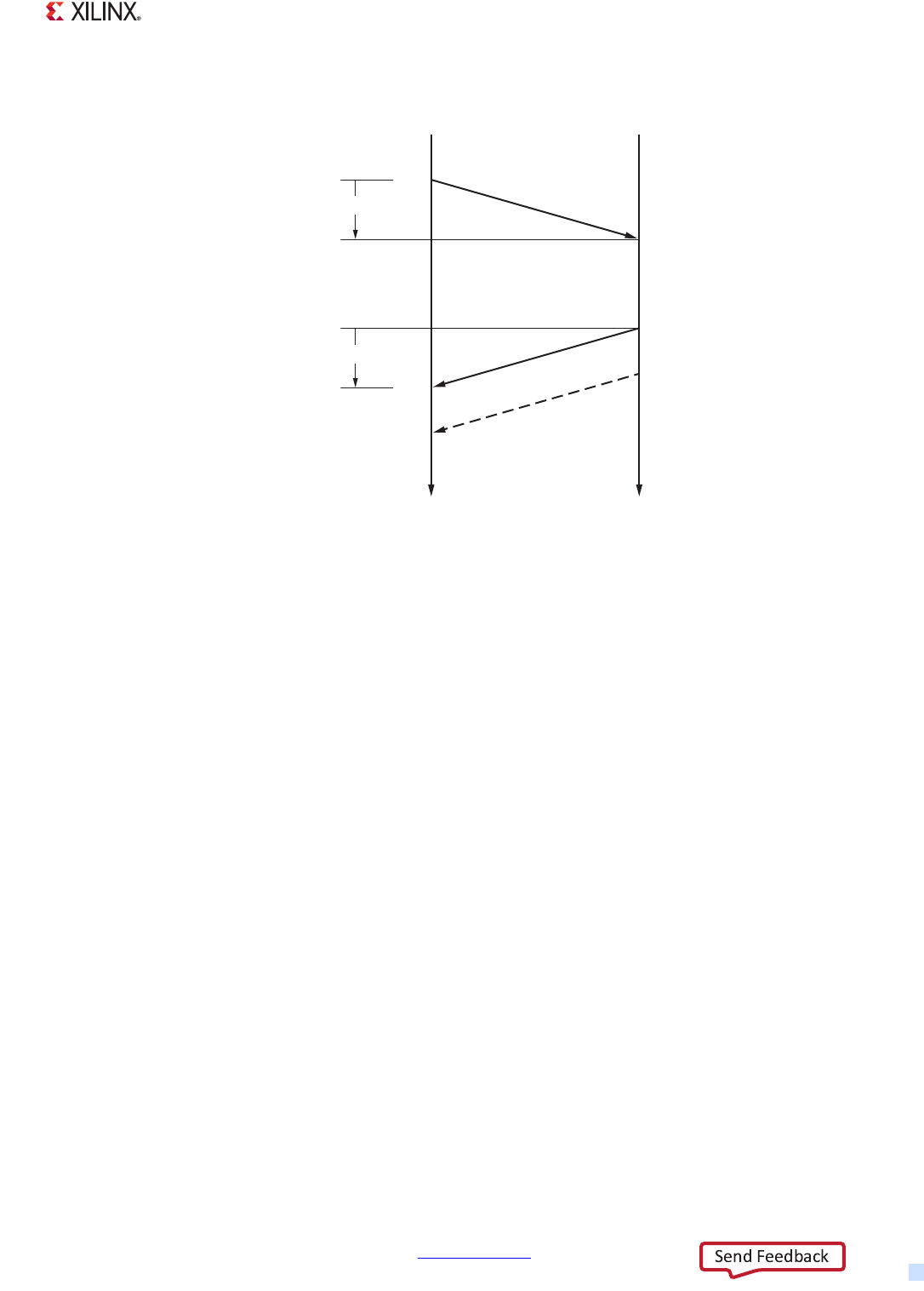
Zynq-7000 AP SoC Technical Reference Manual www.xilinx.com 529
UG585 (v1.12.1) December 6, 2017
Chapter 16: Gigabit Ethernet Controller
16.4.5 PTP Packet Handling at the Slave
Refer to IEEE 1588 Standard Specification for more information on packet formats and protocol.
1. Calculate the peer delay as described in steps 5-9 in section 16.4.4 PTP Packet Handling at
the Master.
Note: When the slave sends timestamps, the delays introduced by the external PHY at the slave
clock port should be taken care of.
2. Read and store timestamp for the received Sync frame. The controller generates an interrupt
for PTP Sync frame received. The slave reads the gem.ptp_rx_s and gem.ptp_rx_ns registers and
stores them. Let this time stamp be t5.
3. Process the Follow_Up frame received. The controller does not generate a PTP event interrupt
for a received Follow_Up frame. The Slave does a validation for the sequenceId field which should
match with that for the previously received Sync frame. The slave extracts the
preciseOriginTimestamp field from the Follow_up frame and stores it. This is the time at which the
Sync frame left the master. The slave then adds the peer delay calculated in step (1) with this time
to take care of the path delay of the PTP frame from master to slave. Let this time be t6.
4. Calculate the final clock offset. This is the difference between t6 and t5 and is typically
represented in nanoseconds.
5. Adjust the PTP clock. The slave adjusts the PTP clock by writing to the gem.timer_adjust
register. If t6 is greater than t5, the gem.timer_adjust[add_subn] is written as 0, otherwise it is
written as 1. The actual nanosecond difference is written in the gem.timer_adjust[ns_delta]
register bits.
6. Become the master in the event of a Sync or Announce timeout.
X-Ref Target - Figure 16-5
Figure 16-5: Link Delay Measurement
Port-1
Time
Port-2
Time
Pdelay_Req
Pdelay_Resp
Pdelay_Resp_Follow_Up
UG585_c16_08_100512
t2
t1
tsm
tms
t3
T4

Zynq-7000 AP SoC Technical Reference Manual www.xilinx.com 530
UG585 (v1.12.1) December 6, 2017
Chapter 16: Gigabit Ethernet Controller
16.5 Register Overview
16.5.1 Control Registers
Control registers drive the management data input/output (MDIO) interface, set-up DMA activity,
start frame transmission, and select the different modes of operation such as full duplex, half duplex
and 10/100/1000 Mb/s operation. (See Tab le 1 6-9.)
Table 16-9: Ethernet Control Register Overview
Function Register Name Description
MAC Configuration
net_{cfg,ctrl,status}
tx_pauseq
rx_pauseq
tx_pfc_pause
ipg_stretch
stacked_vlan
Network control, configuration and status.
Rx, Tx Pause clocks.
IPG stretch.
DMA Unit
tx_status
rx_status
tx_qbar
rx_qbar
dma_cfg
Control.
Receive, Transmit Status.
Receive, Transmit Queue Base Address Control.
Interrupts
intr_{status,en,dis, mask} Interrupt status, enable/disable, and mask
intr_dis_pq{1:7}
intr_en_pq{1:7}
intr_mask_pq{1:7}
wake_on_lan
isr_pq{1:7}
PHY Maintenance phy_maint PHY maintenance
MAC Address
Filtering and ID
Match
hash_{top,bot}
spec_addr{1:4}_{bot,top}
spec_addr1_mask_{bot,top}
type_id_match{1:4}
Hash address, Specific {4:1} addresses High/Low.
Match Type.
IEEE 1588 –
Precision Time
Protocol
timer_{s,ns}
timer_{adjust,incr}
timer_strobe_{s,ns}
IEEE 1588 second, nanosecond counter and
adjustment, increment.
ptp_tx_{s,ns}
ptp_peer_tx_{s,ns}
IEEE 1588 Tx normal/peer second, nanosecond
counter.
ptp_rx_{s,ns}
ptp_peer_rx_{s,ns}
IEEE 1588 Rx normal/peer second, nanosecond
counter.

Zynq-7000 AP SoC Technical Reference Manual www.xilinx.com 531
UG585 (v1.12.1) December 6, 2017
Chapter 16: Gigabit Ethernet Controller
16.5.2 Status and Statistics Registers
The statistics registers hold counts for various types of events associated with transmit and receive
operations. These registers, along with the status words stored in the receive buffer list, enable
software to generate network management statistics compatible with IEEE 802.3. (See Table 16-10).
Clocks and Reset
slcr.GEM{1,0}_CLK_CTRL
slcr.GEM{1,0}_RCLK_CTRL
slcr.GEM{1,0}_CPU_1XCLKACT
slcr.GEM_RST_CTRL
Refer to Chapter 25, Clocks and Chapter 26, Reset
System for more information.
I/O Signal Routing slcr.MIO_PIN_{xxx} Refer to IOP Interface Connections, page 48 for MIO
pin programming information.
Table 16-9: Ethernet Control Register Overview (Cont’d)
Function Register Name Description
Table 16-10: Ethernet Status and Statistics Register Overview
Function Hardware Register Name Description
Frame Tx Statistics
frames_tx
broadcast_frames_tx
multi_frames_tx
Error-free Tx frame, pause frame counts and bytes
counts.
frames_64b_tx
frames_65to127b_tx
frames_128to255b_tx
frames_256to511b_tx
frames_512to1023b_tx
frames_1024to1518b_tx
Error-free frames transmitted: totals by size.
octets_tx_{top,bot} Octets transmitted.
deferred_tx_frames
pause_frames_tx
tx_under_runs Frames received High/Low, Under-run error count.
Frame Tx Statistics
for Half Duplex
Transmission
{multi,single}_collisn_frames
excessive_collisns
late_collisns
carrier_sense_errs
Single/multiple frame, excessive/late collisions,
deferred Tx frames, Tx carrier sense error counters.

Zynq-7000 AP SoC Technical Reference Manual www.xilinx.com 532
UG585 (v1.12.1) December 6, 2017
Chapter 16: Gigabit Ethernet Controller
Frame Rx Statistics
frames_rx
bdcast_fames_rx
multi_frames_rx
Error-free frames received: normal, broadcast,
multicast, pause.
frames_64b_rx
frames_65to127b_rx
frames_128to255b_rx
frames_256to511b_rx
frames_512to1023b_rx
frames_1024to1518b_rx
Error-free frames received: totals by size.
{undersz,oversz,jab}_rx Undersize, oversize and jabber frames.
fcs_errors
length_field_errors
Frame sequence, length, symbol, alignment error
counters.
octets_rx_{top,bot}
rx_symbol_errors
align_errors
rx_resource_errors
rx_overrun_errors
Rx resource, overrun and last statistic clearing offset for
clearing.
Frame Rx Checksum
Error Statistics
ip_hdr_csum_errors
tcp_csum_errors
udp_csum_errors
Checksum error counters: IP Header, TCP, UDP
Table 16-10: Ethernet Status and Statistics Register Overview (Cont’d)
Function Hardware Register Name Description
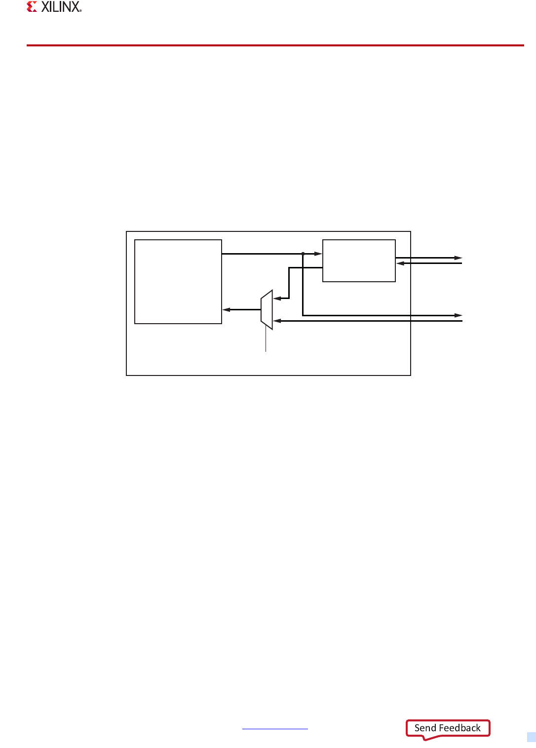
Zynq-7000 AP SoC Technical Reference Manual www.xilinx.com 533
UG585 (v1.12.1) December 6, 2017
Chapter 16: Gigabit Ethernet Controller
16.6 Signals and I/O Connections
16.6.1 MIO–EMIO Interface Routing
The I/O interface is routed to the MIO for RGMII, and to the EMIO for GMII/MII connectivity. The PL
can modify the GMII/MII interface from the MAC to construct other Ethernet interfaces that connect
to external devices via PL pins. The routing of the Ethernet communications signals are shown in
Figure 16-6. The Ethernet communications ports are independently routed to the MIO pins (as
RGMII) or to a set of EMIO interface signals (as GMII). When using the EMIO interface both the TX
and RX clocks are inputs to the PS.
16.6.2 Precision Time Protocol
The PTP signals connected to the Ethernet controller provide the capability to handle IEEE-1588
precision time protocol (PTP) signaling.
16.6.3 Programmable Logic (PL) Implementations
There are options to provide further external interface standard support by linking the GMII signals
on the EMIO interface to the PL. Users can design and connect logic to generate other interface
standards on the PL pins.
TBI support can be provided by connecting the GMII to a TBI compatible logic core in the PL which
provides the PCS functions required for ten-bit interfacing to an external PHY via the PL pins. SGMII
or 1000 Base-X support can be provided by connecting the GMII to an SGMII or 1000 Base-X
compatible logic core which provides the required PCS functions and signal adaptation and drives an
MGT for serial interfacing to an external PHY.
X-Ref Target - Figure 16-6
Figure 16-6: Interface Select Multiplexer
UG585_c16_05_013013
GMII Rx
MAC
Ethernet
Controller
GMII / RGMII
Adapter
GMII Tx
GMII / MII
(EMIO)
slcr.GEM{1:0}_RCLK_CTRL[SRC_SEL]
RGMII
(MIO)
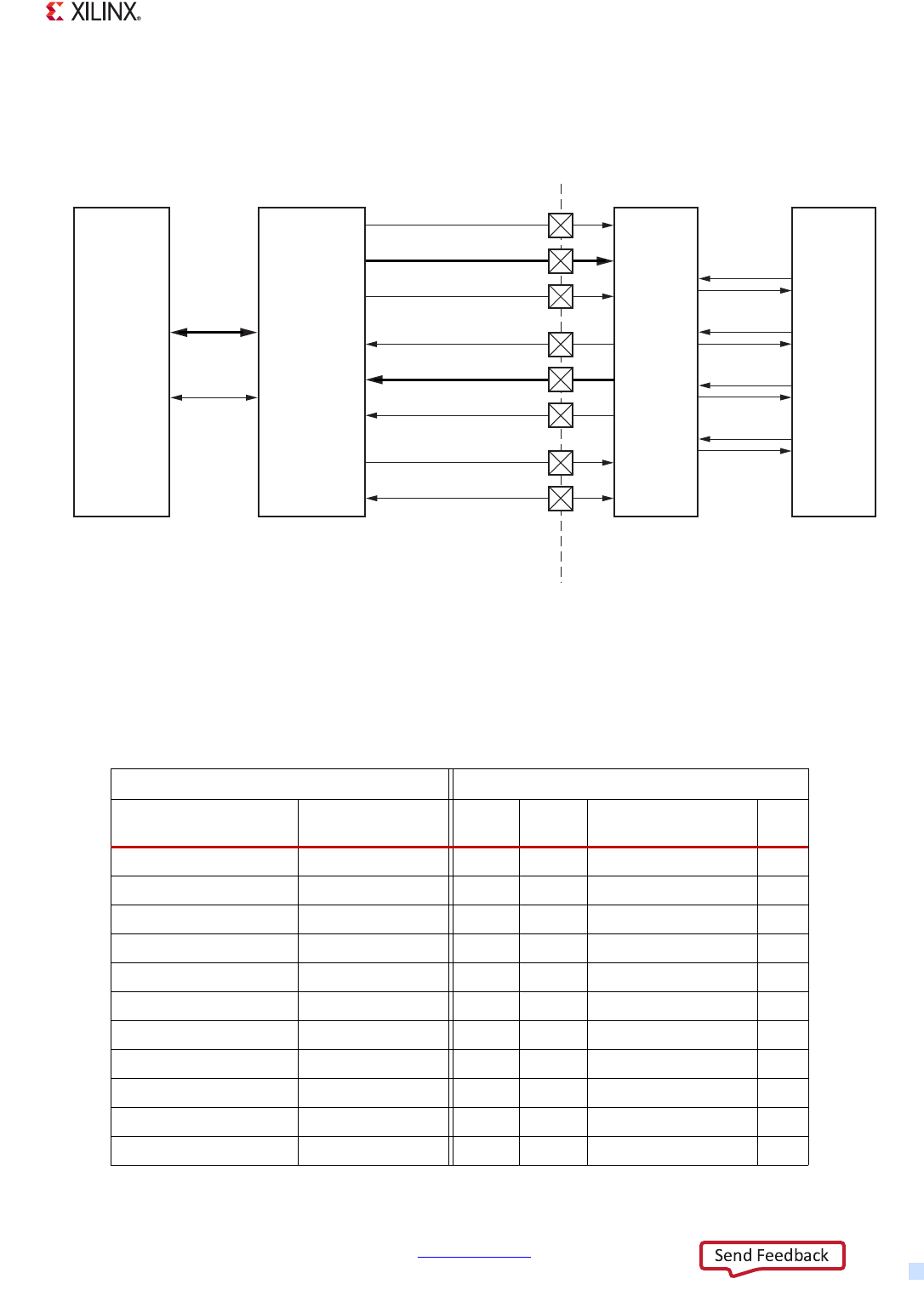
Zynq-7000 AP SoC Technical Reference Manual www.xilinx.com 534
UG585 (v1.12.1) December 6, 2017
Chapter 16: Gigabit Ethernet Controller
16.6.4 RGMII Interface via MIO
An example Ethernet communications wiring connection is shown in Figure 16-7
All Ethernet I/O pins routed through the MIO are on MIO Bank 1 (see Table 16-11).The MIO pins and
restrictions based on device version are shown in the MIO table in section 2.5.4 MIO-at-a-Glance
Tabl e.
X-Ref Target - Figure 16-7
Figure 16-7: Ethernet Communications Wiring Connections
UG585_c16_06_022712
MIO
Multiplexer
Ethernet
Controller
Zynq Device
Boundary
External
PHY
Device
RJ-45
Conn.
ENET_RGMII_TX_CLK
ENET_RGMII_TX_CTL
ENET_RGMII_RX_CLK
ENET_RGMII_TXD[3:0]
ENET_RGMII_RXD[3:0]
RGMII
ENET_MDC
ENET_MDIO
MD
ENET_RGMII_RX_CTL
MDI 0 P/N
MDI 1 P/N
MDI 2 P/N
MDI 3 P/N
Table 16-11: Ethernet RGMII Interface Signals via MIO Pins
Controller Signal MIO Pins
Signal Description Default Controller
Input Value GigE 0 GigE 1 Name I/O
Tx clock to PHY ~ 16 28 RGMII_TX_CLK O
Tx control to PHY ~ 21 33 RGMII_TX_CTL O
Tx data 0 to PHY ~ 17 29 RGMII_TX_D0 O
Tx data 1 to PHY ~ 18 30 RGMII_TX_D1 O
Tx data 2 to PHY ~ 19 31 RGMII_TX_D2 O
Tx data 3 to PHY ~ 20 32 RGMII_TX_D3 O
Rx clock from PHY 022 34 RGMII_RX_CLK I
Rx control from PHY 027 39 RGMII_RX_CTL I
Rx data 0 from PHY 023 35 RGMII_RX_D0 I
Rx data 1 from PHY 024 36 RGMII_RX_D1 I
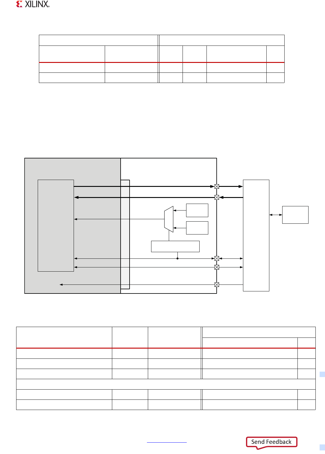
Zynq-7000 AP SoC Technical Reference Manual www.xilinx.com 535
UG585 (v1.12.1) December 6, 2017
Chapter 16: Gigabit Ethernet Controller
16.6.5 GMII/MII Interface via EMIO
An example illustrating the GMII interface connections through the PL to the PL pins is shown in
Figure 16-8. Ethernet GMII/MII interface signals routed through the EMIO are identified in
Table 16-12.
Rx data 2 from PHY 025 37 RGMII_RX_D2 I
Rx data 3 from PHY 026 38 RGMII_RX_D3 I
Table 16-11: Ethernet RGMII Interface Signals via MIO Pins (Cont’d)
Controller Signal MIO Pins
Signal Description Default Controller
Input Value GigE 0 GigE 1 Name I/O
X-Ref Target - Figure 16-8
Figure 16-8: GMII Interface via EMIO Connections
UG585_c16_07_100212
MAC
INTERRUPT
PS
TX
clock
PL
Zynq-7000 AP SoC Device
PHY
1
0Ethernet
2.5 or 25
MHz Clock
125 MHz
Clock
MDIO
IRQF2Px
MDIO
GMII: Tx Signals
Auto-negotiated Speed
Detection Logic
MDC
MDIO
EMIOENETxMDIOMDC
EMIOENETxMDIO{I, O, TN}
Optional PS7 Wrapper
GIC
EMIOENETxGMIITXCLK
Without Tx Clock
Tx Clock
GMII: Rx Signals
Table 16-12: Ethernet GMII/MII Interface Signals via EMIO Interface
Interface Signal Reference
Clock
Default Controller
Input Value
EMIO Interface Signals
Name I/O
Carrier sense ~ EMIOENET[1,0]GMIICRS I
Collision detect ~ EMIOENET[1,0]GMIICOL I
Controller interrupt wake-up ~ EMIOENET[1,0]IRQF2P [5, 13] I
Tx Signals
Tx Clock ~ EMIOENET[1,0]GMIITXCLK I
Tx Data (7:0) Tx Clk ~ EMIOENET[1,0]GMIITXD[7:0] O
Zynq-7000 AP SoC Technical Reference Manual www.xilinx.com 536
UG585 (v1.12.1) December 6, 2017
Chapter 16: Gigabit Ethernet Controller
16.6.6 MDIO Interface Signals via MIO and EMIO
MDIO interface signals routed through the MIO and EMIO are identified in Table 16-13.
Tx Enable Tx Clk ~ EMIOENET[1,0]GMIITXEN O
Tx Error Tx Clk ~ EMIOENET[1,0]GMIITXER O
Tx Timestamp Signals
Tx Start-of-Frame Tx Clk ~ EMIOENET[1,0]SOFTX O
Tx PTP delay req frame detected Tx Clk ~ EMIOENET[1,0]PTPDELAYREQTXO
Tx PTP peer delay frame detect Tx Clk ~ EMIOENET[1,0]PTPPDELAYREQTXO
Tx PTP pear delay response frame
detected Tx Clk ~ EMIOENET[1,0]PTPPDELAYRESPTX O
Tx PTP sync frame detected Tx Clk ~ EMIOENET[1,0]PTPSYNCFRAMETX O
Rx Signals
Rx Clock ~ EMIOENET[1,0]GMIIRXCLK I
Rx Data (7:0) Rx Clk EMIOENET[1,0]GMIIRXD[7:0] I
Rx Data valid Rx Clk EMIOENET[1,0]GMIIRXDV I
Rx Error Rx Clk EMIOENET[1,0]GMIIRXER I
Rx Timestamp Signals
Rx Start of Frame Rx Clk ~ EMIOENET[1,0]GMIISOFRX O
Rx PTP delay req frame detected Rx Clk ~ EMIOENET[1,0]PTPDELAYREQRXO
Rx PTP peer delay frame detected Rx Clk ~ EMIOENET[1,0]PTPPDELAYREQRX O
Rx PTP peer delay response frame
detected Rx Clk ~ EMIOENET{0.1}PTPPDELAYRESPRX O
Rx PTP sync frame detected Rx Clk ~ EMIOENET{0.1}PTPSYNCFRAMERX O
Notes:
1. If using MII connect the RX[7:4] bits to logic zero.
Table 16-12: Ethernet GMII/MII Interface Signals via EMIO Interface (Cont’d)
Interface Signal Reference
Clock
Default Controller
Input Value
EMIO Interface Signals
Name I/O
Table 16-13: MDIO Interface Signals via MIO and EMIO
MDIO Interface
Default
Controller
Input Value
MIO Pins EMIO Interface Signals
GigE 0 GigE 1 I/O Name Name I/O
MD clock output ~ 52 52 O MDIO_CLK EMIOENET[1:0]MDIOMDC O
MD data output ~
53 53 IO MDIO_IO
EMIOENET[1:0]MDIOO O
MD data 3-state ~ EMIOENET[1:0]MDIOTN O
MD data input 0 EMIOENET[1:0]MDIOI I

Zynq-7000 AP SoC Technical Reference Manual www.xilinx.com 537
UG585 (v1.12.1) December 6, 2017
Chapter 16: Gigabit Ethernet Controller
16.6.7 MIO Pin Considerations
LVCMOS33 is not supported for the RGMII interface. Recommendation is to use 1.8/2.5V I/O
standards.
16.7 Known Issues
1. On TX, GigE needs multiple descriptors with the last descriptor in the BD ring having the used bit
set. It is needed to ensure the GigE does not wrap and attempt to transmit the same frames more
than once.
On RX, there is no hard requirement to have multiple buffer descriptors, although it is a very
sensible thing to minimize the chance of getting buffer resource errors (where the hardware has
a frame to write to memory, but there is no free buffer(s) to write to). Extreme overflow
conditions in general are more likely when these buffer resource errors occur.
Workaround: Configure at least two buffer descriptors for both Tx/Rx data paths.
2. It is possible to have the last frame(s) stuck in the RX FIFO with the software having no way to get
the last frame(s) out of there. The GEM only initiates a descriptor request when it receives
another frame. Therefore, when a frame is in the FIFO and a descriptor only becomes available at
a later time and no new frames arrive, there is no way to get that frame out or even know that it
exists.
This issue does not occur under typical operating conditions. Typical operating conditions are
when the system always has incoming Ethernet frames. The above mentioned issue occurs when
the MAC stops receiving the Ethernet frames.
Workaround: There is no workaround in the software except to ensure a continual flow of
Ethernet frames.
3. When discarding a frame or detecting an error, the GEM stores a status packet in the receive FIFO
(write side) indicating the erroneous condition. Once that status packet reaches the front of the
FIFO (read side) the error counter is incremented. When the FIFO is full no additional status
packets can be written into the FIFO and any further errors are discarded. For example, there
could be thousands of overflow errors but the overflow error counter only registers the first few.
This problem applies to all errors for which stats are maintained.
As a secondary problem the errors are only visible once they reach the front of the FIFO. If there
is a packet at the beginning of the FIFO that cannot be written to memory because of
unavailability of a RX DMA descriptor, many errors could occur that are not visible to software.
The error counters stay at zero because all the error status packets are backed up behind the data
packet.
Workaround: There is no workaround in the software.
4. GigE has an issue with the Rx packet buffer DMA design. The issue occurs under extreme Rx
traffic conditions with not enough DMA bandwidth. This results in the Rx packet buffer filling up,
leading to an overflow. The packet buffer overflow causes an overflow status word to be written
into the packet buffer for reporting. If the extreme traffic condition persists for a long time, this

Zynq-7000 AP SoC Technical Reference Manual www.xilinx.com 538
UG585 (v1.12.1) December 6, 2017
Chapter 16: Gigabit Ethernet Controller
results in a large number of such overflow status words being written into the packet buffer. This
eventually overflows an 8-bit internal counter in the GigE Rx module used to track the number of
packets in the Rx buffer needing a "read out." Once the 8-bit counter overflows, it leads to
corruption of local fill level counters in the GigE, which results in a deadlock on the Rx path.
The chances of running into this issue is very high if GigE is subjected to a heavy Rx traffic
condition with small-sized packets. A typical example could be small-sized UDP packets.
Workaround: Once a deadlock is hit on the Rx path, reset the Rx path by first writing a 0 to the
gem.net_ctrl[rx_en] bit and then a writing a 1 to the same bit. The software can have a timer
mechanism to perform this task. In a typical example, the software can create a timer which
expires every 100 milliseconds. In the timer handler the software can monitor the register
gem.frames_rx, which stores the number of received error-free frames. If the SW finds out that
the GigE has stopped receiving error-free frames in two successive invocation of the timer
handler, it resets the Rx path by writing a 0 and then a 1 to the gem.net_ctrl[rx_en] bit.

Zynq-7000 AP SoC Technical Reference Manual www.xilinx.com 539
UG585 (v1.12.1) December 6, 2017
Chapter 17
SPI Controller
17.1 Introduction
The SPI bus controller enables communications with a variety of peripherals such as memories,
temperature sensors, pressure sensors, analog converters, real-time clocks, displays, and any SD card
with serial mode support. The SPI controller can function in master mode, slave mode or
multi-master mode. The Zynq-7000 devices include two SPI controllers. The controller is based on
the Cadence SPI core.
In master mode, the controller drives the serial clock and slave selects with an option to support SPI’s
multi-master mode. The serial clock is derived from the PS clock subsystem. The controller initiates
messages using up to 3 individual slave select (SS) output signals that can be externally expanded.
The controller reads and writes to slave devices by writing bytes to the 32-bit read/write data port
register.
In multi-master mode, the controller three-states its output signals when the controller is not active
and can detect contention errors when enabled. The outputs are three-stated immediately by
resetting the SPI enable bit. An Interrupt Status register indicates a mode fault.
In slave mode, the controller receives the serial clock from the external device and uses the
SPI_Ref_Clk to synchronize data capture. The slave mode includes a programmable start detection
mechanism when the controller is enabled while the SS is asserted.
The read and write FIFOs provide buffering between the SPI I/O interface and the software servicing
the controller via the APB slave interface. The FIFO are used for both slave and master I/O modes.
This chapter is organized into the following sections:
•17.1 Introduction
•17.2 Functional Description
•17.3 Programming Guide
•17.4 System Functions
•17.5 I/O Interfaces

Zynq-7000 AP SoC Technical Reference Manual www.xilinx.com 540
UG585 (v1.12.1) December 6, 2017
Chapter 17: SPI Controller
17.1.1 Features
Each SPI controller is configured and controlled independently, They include the following features:
• Four wire bus – MOSI, MISO, SCLK, and SS
°up to 3 slave selects for master mode
• Full-duplex operation offers simultaneous receive and transmit
• 32-bit register programming via APB slave interface
• Memory mapped read/write data ports for Rx/Tx FIFOs (byte-wide)
°128-byte read and 128-byte write FIFOs
°Programmable FIFO thresholds status and interrupts
•Master I/O mode
°Manual and auto start transmission of data
°Manual and auto slave select (SS) mode
°Slave select signals can be connected directly to slave devices or expanded externally
°Programmable SS and MOSI delays
•Slave I/O mode
°Programmable start detection mode
• Multi-master I/O Capable
°Drives I/O buffers into 3-state if controller is not enabled
°Generates a Mode Failure interrupt when another master is detected
• 50 MHz SCLK clock frequency when I/O signals are routed to the MIO pins
°25 MHz SCLK when the I/O signals are routed via the EMIO interface to the PL pins
• Programmable clock phase and polarity (CPHA, CPOL)
• Programmable interrupt-driven device or poll status
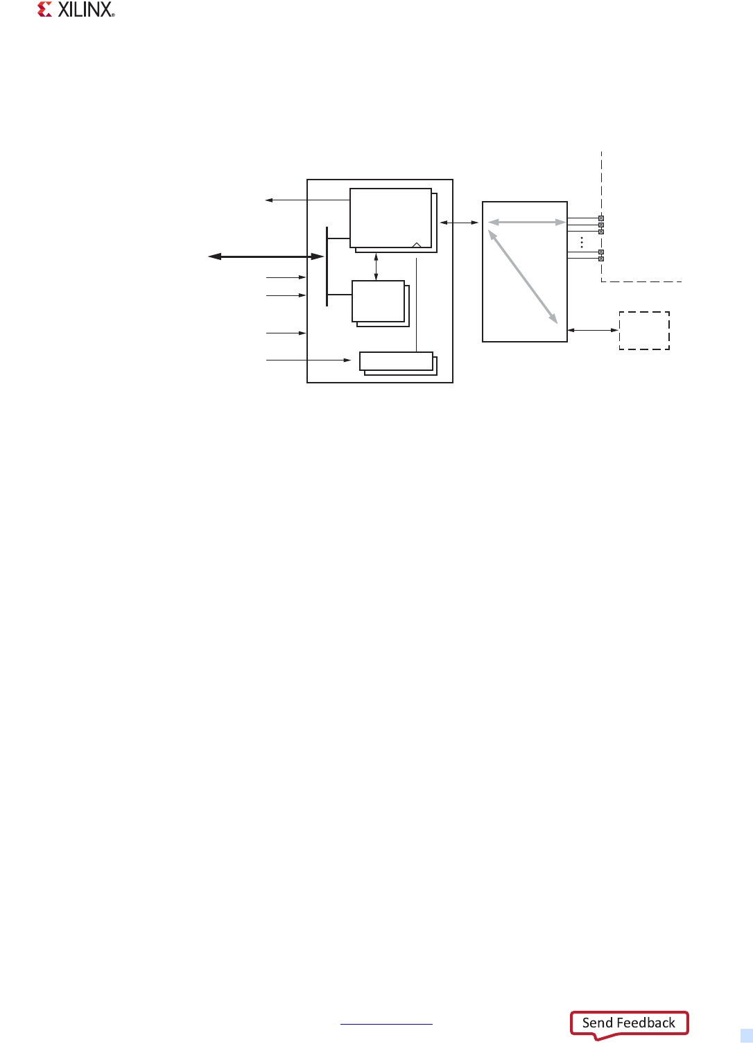
Zynq-7000 AP SoC Technical Reference Manual www.xilinx.com 541
UG585 (v1.12.1) December 6, 2017
Chapter 17: SPI Controller
17.1.2 System Viewpoint
The system viewpoint diagram of the SPI controller is shown in Figure 17-1.
SPI Interface Controller
There are two independent SPI interface controllers (SPIx; where x = 0 or 1). The I/O signals of each
independent controller can be routed to MIO pins or the EMIO interface. Each controller also has
individual interrupts signals to the PS interrupt controller and a separate reset signal. Each controller
has its own set of control and status registers.
Clocking
The PS clock subsystem provides a reference clock to the SPI controller. The SPI_Ref_Clk clock is used
for the controller logic and by the baud rate generator to create the SCLK clock for master mode.
MIO-EMIO
The SPI I/O signals can be routed to the MIO pins or the EMIO interface to the PL, as explained in
17.5 I/O Interfaces. The general routing of signals is explained in Chapter 2, Signals, Interfaces, and
Pins.
X-Ref Target - Figure 17-1
Figure 17-1: SPI System Block Diagram
PL
MIO – EMIO
Routing
Interconnect APB
MIO
Pins
UG585_c17_01_030212
Device
Boundary
EMIO
Signals
SPI REF clock
IRQ ID# {58, 81}
SPI REF reset
Control
Registers
Slave
port
CPU_1x clock
SPI{0, 1} CPU_1x reset
SPI
Interface
Controller
Clocking
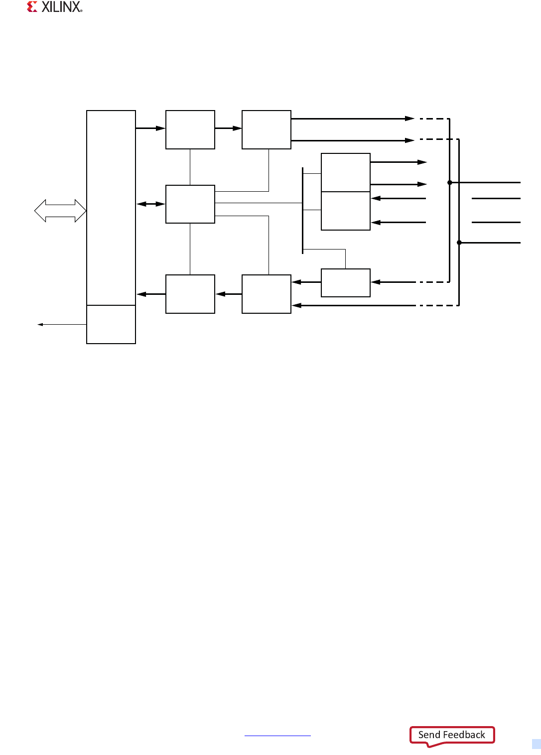
Zynq-7000 AP SoC Technical Reference Manual www.xilinx.com 542
UG585 (v1.12.1) December 6, 2017
Chapter 17: SPI Controller
17.1.3 Block Diagram
A functional block diagram of the SPI controller is shown in Figure 17-2.
APB Slave Interface
The 32-bit APB slave interface responds to register reads and writes, including data ports for reading
and writing commands and data from and to the FIFOs. All registers transactions are 32 bits. The data
ports use bits [7:0] of these ports. The configuration and status registers are listed in Appendix B,
Register Details.
SPI Master Mode
When the controller operates in master mode, it drives the SCLK clock and up to 3 slave select output
signals.The SS and start of transmission on MOSI can be manually controlled by software or
automatically controlled by the hardware.
SPI Slave Mode
When the controller operates in slave mode, it uses a single slave select input (SS 0). The SPI signals
are shown in Figure 17-2 and listed in section 17.5 I/O Interfaces. The SCLK is synchronized to the
controller reference clock (SPI_Ref_Clk). Refer to section 17.2.3 Slave Mode.
X-Ref Target - Figure 17-2
Figure 17-2: SPI Peripheral Block Diagram
APB
APB
Interface
SPI CTRL
TxFIFO
RxFIFO
Transmit
Receive
SPI
Master
MO
SO
SS[2:0]
SCLK
SCLK
SS
SCLK
SS
SI
SPI Interface
Pins
UG585_c17_02_072512
MOSI
MISO
MI
SPI
Slave
Slave
Sync
Interrupts
Interrupts

Zynq-7000 AP SoC Technical Reference Manual www.xilinx.com 543
UG585 (v1.12.1) December 6, 2017
Chapter 17: SPI Controller
Tx and Rx FIFOs
Each FIFO is 128 bytes. Software reads and writes these FIFOs using the register mapped data port
registers. FIFO management for master mode is described in 17.3.3 Master Mode Data Transfer and
for slave mode in 17.3.4 Slave Mode Data Transfer.
The FIFOs bridge two clock domains; APB interface and the controller’s SPI_Ref_Clk. Software writes
to the TxFIFO in the APB clock domain and the controller reads the TxFIFO in the SPI_Ref_Clk domain.
The controller fills the RxFIFO in the SPI_Ref_Clk domain and software reads the RxFIFO in the APB
clock domain.
17.1.4 Notices
7z007s and 7z010 CLG225 Devices
The 7z007s single core and 7z010 dual core CLG225 devices support 32 MIO pins (not 54). This is
shown in the MIO table in section 2.5.4 MIO-at-a-Glance Table. These devices restrict the available
MIO pins so connections through the EMIO should be considered. All of these CLG225 device
restrictions are listed in section 1.1.3 Notices.

Zynq-7000 AP SoC Technical Reference Manual www.xilinx.com 544
UG585 (v1.12.1) December 6, 2017
Chapter 17: SPI Controller
17.2 Functional Description
•17.2.1 Master Mode
•17.2.2 Multi-Master Capability
•17.2.3 Slave Mode
•17.2.4 FIFOs
•17.2.5 FIFO Interrupts
•17.2.6 Interrupt Register Bits, Logic Flow
•17.2.7 SPI-to-SPI Connection
17.2.1 Master Mode
In master mode, the SPI I/O interface can transmit data to a slave or initiate a transfer to receive data
from a slave. The controller selects one slave device at the time using one of the three slave select
lines. If more than three slave devices need to be connected to the master, it is possible to add an
external peripheral select 3-to-8 decode on the board.
Data Transfer
The SCLK clock and MOSI signals are under control of the master. Data to be transmitted is written
into the TxFIFO by software using register writes and then unloaded for transmission by the
controller hardware in a manual or automatic start sequence. Data is driven onto the master output
(MOSI) data pin. Transmission is continuous while there is data in the TxFIFO.
Data is received serially on the MISO data pin and is loaded 8 bits at a time into the RxFIFO. Software
reads the RxFIFO using register reads. For every “n” bytes written to the TxFIFO, there will be “n”
bytes stored in RxFIFO that must be read by software before starting the next transfer.
Auto/Manual SS and Start
Data transfers on the I/O interface can be manually started using software or automatically started
by the controller hardware. In addition, the slave select assertion/de-assertion can be done by the
controller hardware or from software. These four combinations are shown in Tab le 17- 1.
Table 17-1: SPI Master Mode SS and Start Modes
Slave Select
Control
Data Transfer
Start Control
Manual
Slave
Select
Manual Start
Enable &
Command
Operation
Manual SS
(software)
Manual Start 1 1 Software controls the slave select and must issue
the start command to serialize data.
Auto Start 10
Software controls the slave select, but the
controller hardware automatically starts to
serialize data when there is data in the TxFIFO.
Recommended for general use.

Zynq-7000 AP SoC Technical Reference Manual www.xilinx.com 545
UG585 (v1.12.1) December 6, 2017
Chapter 17: SPI Controller
Manual SS
Software selects the manual slave select method by setting the spi.Config_reg0 [Manual_CS] bit = 1.
In this mode, software must explicitly control the slave select assertion/de-assertion. When the
[Manual_CS] bit = 0, the controller hardware automatically asserts the slave select during a data
transfer.
Automatic SS
Software selects the auto slave select method by programming the spi.Config_reg0 [Manual_CS] bit
= 0. The SPI controller asserts/de-asserts the slave select for each transfer of TxFIFO content on to
the MOSI signal. Software writes data to the TxFIFO and the controller asserts the slave select
automatically, transmits the data in the TxFIFO and then de-asserts the slave select. The slave select
gets de-asserted after all the data in the Tx FIFO is transmitted. This is the end of the transfer.
Software ensures the following in automatic slave select mode.
• Software continuously fills the TxFIFO with the data bytes to be transmitted, without the TxFIFO
becoming empty, to maintain an asserted slave select.
• Software continuously reads data bytes received in the RxFIFO to avoid overflow.
Software uses the TxFIFO and RxFIFO threshold levels to avoid FIFO under- and over-flows. The
TxFIFO Not Full condition is flagged when the number of bytes in TxFIFO is less than the TxFIFO
threshold level. The RxFIFO full condition is flagged when the number of bytes in RxFIFO is equal to
128.
Manual Start
Enable
Software selects the manual transfer method by setting the spi.Config_reg0 [Man_start_en] bit = 1.
In this mode, software must explicitly start the data transfer using manual start command
mechanism. When the [Man_start_en] bit = 0, the controller hardware automatically starts the data
transfer when there is data available in the TxFIFO.
Auto SS
(controller)
Manual Start 0 1
Controller hardware controls the slave select, but
the software must issue the start command to
serialize data in the TxFIFO. This mode is applicable
for specific use cases such as sending small chunks
of data that fit into the SPI controller FIFO.
Auto Start 00
Controller hardware controls the slave select and
serializes data when there is data in the TxFIFO.
Table 17-1: SPI Master Mode SS and Start Modes (Cont’d)
Slave Select
Control
Data Transfer
Start Control
Manual
Slave
Select
Manual Start
Enable &
Command
Operation

Zynq-7000 AP SoC Technical Reference Manual www.xilinx.com 546
UG585 (v1.12.1) December 6, 2017
Chapter 17: SPI Controller
Command
Software starts a manual transfer by writing a 1 to the spi.Config_reg0 [Man_start_com] bit. When
the software writes the 1, the controller hardware starts the data transfer and transfers all the data
bytes present in the TxFIFO. The [Man_start_com] bit is self-clearing. Writing a 1 to this bit is ignored
if [Man_start_en] = 0. Writing a 0 to [Man_start_com] has no effect, regardless of mode.
17.2.2 Multi-Master Capability
For Multi-master mode, the controller is programmed for master mode [MODE_SEL] and can initiate
transfers on any of the slave selects. When the software is ready to initiate a transfer, it enables the
controller using the [SPI_EN] bit. When the transaction is done, the software disables the controller.
The controller cannot be selected by an external master when the controller is in Master Mode.
The controller detects another master on the bus by monitoring the open-drain slave select signal
(active Low). The detection mechanism is enabled by the [Modefail_gen_en]. When the controller
detects another master, it sets the spi.Intr_status_reg0 [MODE_FAIL] interrupt status bit and clears
the spi.En_reg0 [SPI_EN] control bit. The software can receive the [MODE_FAIL] interrupt so it can
abort the transfer, reset the controller, and re-send the transfer.
17.2.3 Slave Mode
In slave mode, the controller receives messages from the external master and outputs a simultaneous
reply. The controller enters slave mode when spi.Config_reg0 [MODE_SEL] = 0 and spi.En_reg0
[SPI_EN] = 1.
The SCLK latches data on the MOSI input. If the slave select input signal is High (inactive), the
controller ignores the MOSI input. When the slave select is asserted, it must be held active for the
duration of the transfer. If SS de-asserts during the transfer, the controller sets the
spi.Intr_status_reg0 [MODE_FAIL] interrupt bit. The software receives the [MODE_FAIL] interrupt so it
can abort the transfer, reset the controller, and re-send the transfer.
The error mechanism is enabled by the [Modefail_gen_en] bit.
Data to be sent to the master is written into the TxFIFO by software and then serialized onto the
master input (MISO) signal by the controller. Transmission continues while there is still data in the
TxFIFO and the slave select signal remains asserted (active Low).
Clocking
The slave select input pin must be driven synchronously to the SCLK input. The controller operates in
the SPI_Ref_Clk clock domain. The input signals are synchronized and analyzed in the SPI_Ref_Clk
domain.
Word Detection
The start of a word is detected in th SPI_Ref_Clk clock domain.

Zynq-7000 AP SoC Technical Reference Manual www.xilinx.com 547
UG585 (v1.12.1) December 6, 2017
Chapter 17: SPI Controller
•Detection when Controller is enabled: If the controller is enabled (from a disabled state) at a
time when SS is Low (active), the controller will ignore the data and wait for the SCLK to be
inactive (a word boundary) before capturing data. The controller counts SCLK inactivity in the
SPI_Ref_Clk domain. A new word is assumed when the SCLK idle count reaches the value
programmed into the [Slave_Idle_coun] bit field.
•Detection when SS asserts: With the controller enabled and SS is detected High (inactive), the
controller will assume the start of the word occurs on the next active edge of SCLK after SS
transitions Low (active).
Note: The start condition must be held active for at least four SPI_Ref_Clk cycles to be detected.
If slave mode is enabled at a time when the external master is very close to starting a data transfer,
there is a small probability that false synchronization will occur, causing packet corruption. This issue
can be avoided by any of the following means:
• Ensure that the external master does not initiate data transfer until at least ten SPI_Ref_Clk
cycles have passed after slave mode has been enabled.
• Ensure that slave mode is enabled before the external master is enabled.
• Ensure that the slave select input signal is not active when the slave is enabled.
17.2.4 FIFOs
The Rx and Tx FIFOs are each 128 bytes deep.
RxFIFO
If the controller attempts to push data into a full RxFIFO then the content is lost and the sticky
overflow flag is set. No data is added to a full RxFIFO. Software writes a 1 to the bit to clear the
[RX_OVERFLOW] bit.
TxFIFO
If the TxFIFO is full, [TX_FIFO_full] = 1, then do not write more data. The TX_FIFO_Full bit remains
asserted until the TxFIFO level is less than the [TxFIFO_Not_Full] threshold level. Data written to a full
TxFIFO may be lost without any indication.
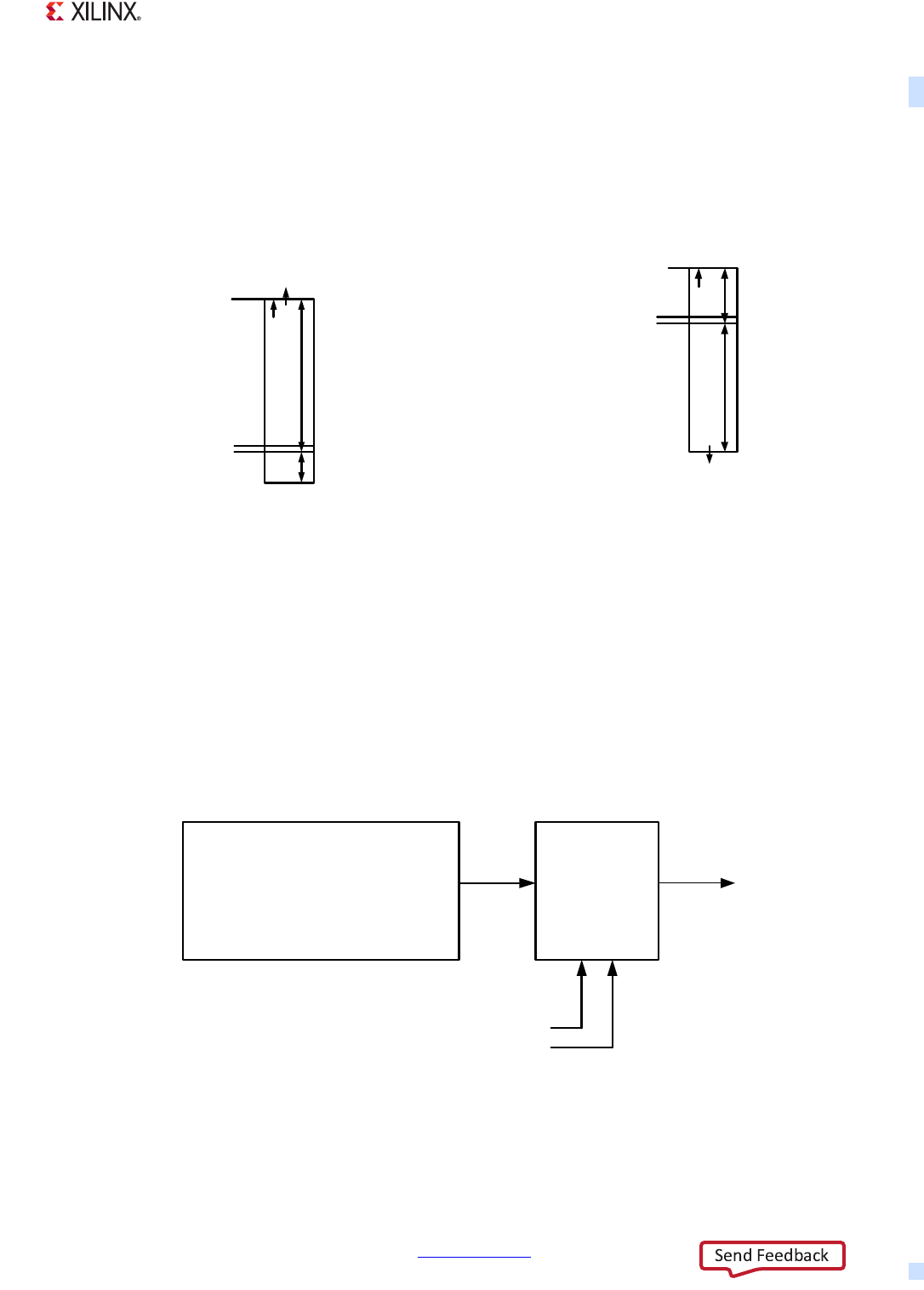
Zynq-7000 AP SoC Technical Reference Manual www.xilinx.com 548
UG585 (v1.12.1) December 6, 2017
Chapter 17: SPI Controller
17.2.5 FIFO Interrupts
The Rx and Tx FIFO interrupts are illustrated in Figure 17-3.
17.2.6 Interrupt Register Bits, Logic Flow
The interrupt status bits (sticky and dynamic) are filtered by the mask register and then sent to the
system interrupt controller. The mask register is controlled by the en/dis interrupt control registers
(see Figure 17-4).
X-Ref Target - Figure 17-3
Figure 17-3: SPI Rx and Tx FIFO Interrupts
TxFIFO (128 bytes)
Full Interrupt
RxFIFO (128 bytes)
Full Interrupt
[TX_FIFO_full]
[RX_FIFO_full]
Overflow Interrupt
[RX_OVERFLOW]
Underflow Interrupt
[TX_FIFO_underflow]
TxFIFO Threshold
spi.TX_thres_reg0
RxFIFO Threshold
spi.RX_thres_reg0
Not Full = 0 (full)
Not Full = 1
Not Full Interrupt
[TX_FIFO_not_full]
Not Empty = 1
Not Empty = 0 (empty)
Not Empty Interrupt
[RX_FIFO_not_empty]
UG585_c17_03_022613
X-Ref Target - Figure 17-4
Figure 17-4: SPI Interrupt Register Bits, Logic Flow
UG585_c17_04_121113
PS Interrupt IRQ
ID #58 / #81
spi.Intrpt_status_reg0
Bit 6: [TX_FIFO_underflow] (sticky)
Bit 5: [RX_FIFO_full]
Bit 4: [RX_FIFO_not_empty]
Bit 3: [TX_FIFO_full]
Bit 2: [TX_FIFO_not_full]
Bit 1: [MODE_FAIL] (sticky)
Bit 0: [RX_OVERFLOW] (sticky)
0: masked
1: enabled
spi.Intrpt_dis_reg0
spi.Intrpt_en_reg0
spi.Intrpt_mask_reg0
Interrupts:
Enable
1
0
Mask
1
0

Zynq-7000 AP SoC Technical Reference Manual www.xilinx.com 549
UG585 (v1.12.1) December 6, 2017
Chapter 17: SPI Controller
17.2.7 SPI-to-SPI Connection
The I/O signals of the two SPI controller in the PC are connected together signals when the
slcr.MIO_LOOPBACK [SPI_LOOP_SPI1] bit is set = 1. In this mode, the clock, slave select, MISO, and
MOSI signals from one controller are connected to the other controller’s clock, slave, MISO, and
MOSI signals. respectively.
Limitation
The SPI controller registers require single 32-bit read/write accesses, do not use byte, halfword, or
double word references.
17.3 Programming Guide
•17.3.1 Start-up Sequence
•17.3.2 Controller Configuration
•17.3.3 Master Mode Data Transfer
•17.3.4 Slave Mode Data Transfer
•17.3.5 Interrupt Service Routine
•17.3.6 Register Overview
17.3.1 Start-up Sequence
Example: Start-up Sequence
1. Reset controller: Assert and de-assert the Ref and CPU_1x resets, refer to section 17.4.1 Resets.
2. Program clocks: Program the SPI_Ref_Clk, refer to section 17.4.2 Clocks.
3. Tx/Rx signal routing: Refer to section 17.5 I/O Interfaces.
4. Controller configuration: Refer to section 17.3.2 Controller Configuration.
5. Interrupt configuration: Configure the ISR to handle the interrupt conditions. The simplest ISR
reads data from the RxFIFO and writes content to the TxFIFO. The PS interrupt controller is
described in Chapter 7, Interrupts. The interrupt mechanism for the SPI controller is described in
section 17.3.5 Interrupt Service Routine.
6. Start data transfers:
°Master Mode operation select: Manual/Auto start and SS, refer to section 17.3.3 Master
Mode Data Transfer.
°Slave Mode operation, refer to section 17.3.4 Slave Mode Data Transfer.

Zynq-7000 AP SoC Technical Reference Manual www.xilinx.com 550
UG585 (v1.12.1) December 6, 2017
Chapter 17: SPI Controller
17.3.2 Controller Configuration
Set controller parameters by writing to the spi.Config_reg register:
• Set baud rate [BAUD_RATE_DIV].
• Set clock phase [CLK_PH] and Polarity [CLK_POL].
• Select Master/Slave mode [MODE_SEL].
• Set Mode fail generation, [Modefail_gen_en], for multi-master mode systems.
•Set SS to 0b1111 to de-assert all the slave selects before the start of transfers.
Example: SPI 0 Configuration for Master Mode
This example uses a single chip select, a baud rate of 12.5 Mb/s, a clock phase set to inactive, and a
clock polarity of quiescent High.
1. Configure the controller: Write 0x0002_FC0F to the spi.Config_reg register.
a. De-assert all chip selects (for now): [CS] = 1111.
b. No external 3-to-8 chip select decoder. [PERI_SEL] = 0.
c. Set baud rate to 12.5 Mbps. [BAUD_RATE_DIV] = 1.
This example assumes a 50 MHz SPI_Ref_Clk. Baud rate generator description is in section
17.3.3 Master Mode Data Transfer.
d. Set clock phase, [CLK_PH] and Polarity, [CLK_POL] to 1. These parameters are discussed in
section 17.5.1 Protocol.
e. Select Master mode: [MODE_SEL] = 1.
f. Look for bus collisions: [Modefail_gen_en] = 1.
g. Do not initiate a transmission. [Man_start_com] = 0.
17.3.3 Master Mode Data Transfer
The four combinations of master operating mode are described in section 17.2.1 Master Mode. The
examples below illustrate the programming steps for each mode.
Example: Master Mode – Manual SS and Manual Start
1. Enable manual SS: Write 1 to spi.Config_reg [Manual_CS].
2. Select manual start: Write 1 to spi.Config_reg [Man_start_en].
3. Assert slave select: Set spi.Config_reg [CS] = 1101 to assert slave select 1.
4. Enable the controller: Write 1 to spi.EN_reg0 [SPI_EN].
5. Write bytes to the TxFIFO:
a. Write the data to the TxFIFO using the register spi.Tx_data_reg.
b. Continue to write data to the TxFIFO to its full depth or until no further data is needed to be
written.
c. Increment the data byte counter in the driver software after each byte is written to the TxFIFO.

Zynq-7000 AP SoC Technical Reference Manual www.xilinx.com 551
UG585 (v1.12.1) December 6, 2017
Chapter 17: SPI Controller
6. Enable the interrupts: Write 0x27 to spi.Intrpt_en_reg to enableRxFIFO full, RxFIFO overflow,
TXFIFO empty, and fault conditions.
7. Start the data transfer: Set spi.Config_reg0 [Man_start_com] = 1.
8. Wait for interrupts.
9. Interrupt handler: Transfer any additional data to the slave the required data to SPI slave using
the interrupt handler.
10. Disable interrupts: Write 0x27 to the spi.Intrpt_dis_reg to disable RxFIFO full, RxFIFO overlflow,
TxFIFO empty, and fault conditions.
11. Disable the controller: Set spi.En_reg0 [SPI_EN] = 0.
12. De-assert slave select: Set spi.Config_reg0 [CS] = 1111.
Example: Master Mode – Manual SS and Auto Start
1. Enable manual SS: Write 1 to spi.Config_reg [Manual_CS].
2. Assert slave select: Set spi.Config_reg [CS] = 1101 to use slave select 1.
3. Enable the controller: Write 1 to spi.EN_reg0 [SPI_EN].
4. Write bytes to the TxFIFO:
a. Write the data to the TxFIFO using the register spi.Tx_data_reg.
b. Continue to write data to the TxFIFO to its full depth or until no further data is needed to be
written.
c. Increment the data byte counter in the driver software after each byte is written to the TxFIFO.
5. Enable the interrupts: Write 0x27 to spi.Intrpt_en_reg to enable RxFIFO full, RxFIFO overflow,
TxFIFO empty, and fault conditions.
6. Wait for interrupts.
7. Interrupt handler: Transfer any additional data to the slave the required data to SPI slave using
the interrupt handler.
8. Disable interrupts: Write 0x27 to the spi.Intrpt_dis_reg to disable RxFIFO full, RxFIFO overlflow,
TxFIFO empty and fault conditions.
9. Disable the controller: Set spi.En_reg0 [SPI_EN] = 0.
10. De-assert slave select: Set spi.Config_reg0 [CS] = 1111.
Example: Master Mode – Auto SS and Manual Start
1. Select manual start: Write 1 to spi.Config_reg0 [Man_start_en].
2. Assert slave select: Set spi.Config_reg0 [CS] = 1101 to use slave select 1.
3. Enable the controller: Write 1 to spi.EN_reg0 [SPI_EN].
4. Write bytes to the TxFIFO:
a. Write the data to the TxFIFO using the register spi.Tx_data_reg.
b. Continue to write data to the TxFIFO to its full depth or until no further data is needed to be
written.
c. Increment the data byte counter in the driver software after each byte is written to the
TxFIFO.

Zynq-7000 AP SoC Technical Reference Manual www.xilinx.com 552
UG585 (v1.12.1) December 6, 2017
Chapter 17: SPI Controller
5. Set the FIFO threshold levels: Set spi.TX_thres_reg0 and spi.RX_thres_reg0 threshold levels.
Refer to the description at “automatic mode of operation” section.
6. Enable the interrupts: Write 0x27 to spi.Intrpt_en_reg to enable RxFIFO full, RxFIFO overflow,
TxFIFO empty, and fault conditions.
7. Start the data transfer: Set spi.Config_reg0 [Man_start_com] = 1.
8. Interrupt handler: Transfer any additional data to the slave the required data to SPI slave using
the interrupt handler.
9. Disable interrupts: Write 0x27 to the spi.Intrpt_dis_reg to disable RxFIFO full, RxFIFO overlflow,
TxFIFO empty, and fault conditions.
10. Disable the controller: Set spi.En_reg0 [SPI_EN] = 0.
11. De-assert slave select: Set spi.Config_reg0 [CS] = 1111.
17.3.4 Slave Mode Data Transfer
Example: Slave Mode - Interrupt Driven
Ensure that the controller configuration is done and then:
1. Slave configuration: Write 0 to spi_Config_reg0.
2. Enable the interrupts: Write 0x37 to spi.Intrpt_en_reg to enable RxFIFO Not empty, RxFIFO full,
RxFIFO overflow, TxFIFO empty, and fault conditions.
3. Enable the controller: Write 1 to spi.En_reg [SPI_EN].
4. Interrupt Handler: Receive data from master using the interrupt handler.
5. Disable the interrupts: Write 0x37 to spi.Intrpt_DIS_reg to disable RxFIFO Not empty, RxFIFO
full, RxFIFO overflow, TxFIFO empty, and fault conditions.
6. Disable the controller: Write 0 to spi_En_reg0 [SPI_EN].
Note: In SPI slave mode operation, it is recommended to set RxFIFO threshold to 1 by setting
spi.RX_Thres_reg0[Threshold_of_RX_FIFO] to 1.
17.3.5 Interrupt Service Routine
Example: Interrupt Service Routine
This example handles RxFIFO overflow/underflow, multi-master collision (mode fail) and handles Rx
and Tx data transfers.
1. Disable all interrupts except TxFIFO Full and RxFIFO Not Empty: Write 0x027 to
spi.Intr_dis_REG.
2. Determine the source of the interrupt: Read the interrupt status register spi.Intr_status_reg0.
3. Clear the interrupts: Write 1s to the interrupt status register spi.Intr_status_reg0.

Zynq-7000 AP SoC Technical Reference Manual www.xilinx.com 553
UG585 (v1.12.1) December 6, 2017
Chapter 17: SPI Controller
4. Check for Mode fail Interrupt: (multi-master operation). On mode fail, abort the current
transfer:
a. Reset the controller
b. Re-configure the controller
c. Re-send the data.
5. Empty the RxFIFO: Read spi.Intr_status_reg0 [RX_FIFO_full] bits:
a. Read data from the spi.Rx_Data_reg register. Continue to receive bytes using the data byte
counter.
6. Fill the TxFIFO: More data can be written to the TxFIFO, if needed:
a. Write data to the spi.Tx_Data_reg0 register.
b. Continue to fill data until FIFO depth is reached or there is no further data.
c. Increment the data byte counter after each byte is pushed.
7. Check for overflow or underflow: Read the [TX_FIFO_underflow] or [RX_OVERFLOW] status
bits. Handle the overflow and underflow conditions accordingly.
8. Enable the interrupts: If more data need to be transmitted or received, set spi.Intrpt_en_reg0
[TX_FIFO_not_full] and [RX_FIFO_full] both = 1.
9. If there is data to be transferred (Sent/Received), then start the data transfer:
°When in master mode, and data transfer is done using manual start (for both manual/auto
SS), set spi.Config_reg [Man_start_en] = 1.
17.3.6 Register Overview
The SPI registers are detailed Appendix B, Register Details. The register overview is provided in
Tabl e 17- 2.
Table 17-2: SPI Register Overview
Type Register Name Description
Controller
Configuration Config_reg0 Configuration
Controller enable En_reg0 SPI controller enable
Interrupt
Intr_status_reg0 Interrupt status (Rx full, not empty and Tx full, not full)
Intrpt_en_reg0 Interrupt enable
Intrpt_dis_reg0 Interrupt disable
Intrpt_mask_reg0 Interrupt mask/enable
FIFO thresholds TX_thres_reg0 TxFIFO threshold level for not full
RX_thres_reg0 RxFIFO Threshold level for not empty
Master mode Delay_reg0 SS delays and separation counts in master mode
FIFO data ports Tx_data_reg0 Transmit data (TxFIFO)
Rx_data_reg0 Receive data (RxFIFO)
Slave mode Slave_Idle_count_reg0 Slave idle count detects inactive SCLK

Zynq-7000 AP SoC Technical Reference Manual www.xilinx.com 554
UG585 (v1.12.1) December 6, 2017
Chapter 17: SPI Controller
17.4 System Functions
•17.4.1 Resets
•17.4.2 Clocks
17.4.1 Resets
The controller has two reset domains: the APB interface and the controller itself. The reset for the two
domain must be used together. The effects for each reset type are summarized in Table 17-3.
Example: Reset the APB Interface and SPI 0 Controller
1. Write to the slcr reset register for SPI. Write a 1, and after some delay write a 0 to the
slcr.SPI_RST_CTRL [SPI0_REF_RST] and [SPI0_CPU1X_RST] bit fields.
17.4.2 Clocks
The core of each SPI controller is driven by the same reference clock (SPI_Ref_Clk) that is generated
by the PS clock subsystem, Chapter 25, Clocks. The APB interface is clocked by the CPU_1x clock. The
CPU_1x clock runs asynchronous to the reference clock. The operating frequency specifications for
the controller clocks are defined in the data sheet. The I/O signals are clocked synchronously by the
SCLK.
Note: Clock gating is used as power management feature for SPI. Please refer section
24.3.2 Peripherals for more details.
CPU_1x
The CPU_1x clock part of the CPU clock domain, refer section 25.2 CPU Clock.
SPI_Ref_Clk
The clock enable, PLL select and divisor settings are programmed using the slcr.SPI_CLK_CTRL
register as described in section 25.6.3 SDIO, SMC, SPI, Quad-SPI and UART Clocks.
Frequency Restriction Note: The SPI_Ref_Clk must be always be set to a higher frequency than the
CPU_1x clock frequency.
Table 17-3: SPI Reset Effects
Name APB
Interface
TxFIFO
and
RxFIFO
Protocol
Engine Registers
ABP Interface Reset
slcr.SPI_RST_CTRL [SPIx_CPU1X_RST] Yes Yes No Yes
PS Reset Subsystem
slcr.SPI_RST_CTRL [SPIx_REF_RST] No Yes Yes No

Zynq-7000 AP SoC Technical Reference Manual www.xilinx.com 555
UG585 (v1.12.1) December 6, 2017
Chapter 17: SPI Controller
Master Mode SCLK
The SCLK is driven by the controller in master mode. It is generated by the a divided-down
SPI_Ref_Clk using the spi.Config_reg0 [BAUD_RATE_DIV] bit field.
Frequency Ratio Note: The range of the baud rate divider is from a minimum of 4 to a maximum of
256 in binary steps (i.e., divide by 4, 8, 16,... 256).
Example: SCLK for Master Mode
This example shows how to program the SPI_Ref_Clk to 100 MHz and the SCLK to 25 MHz. The
example assumes the I/O PLL is at 1,000 MHz. The CPU_1x clock frequency must be less than
100 MHz.
1. Program SPI_Ref_Clk: Select PLL source, divisors and enable: Write 0x0000_0A01 to the
slcr.SPI_CLK_CTRL register.
a. Select the I/O PLL: [SRCSEL] = 00.
b. Divide the I/O PLL clock by 10: [DIVISOR] = 0x0A.
c. Enable the SPI 0 reference clock: [CLKACT0] = 1.
2. Program the Baud Rate Generator: Write 001 to the spi.Contro_reg0 [BAUD_RATE_DIV] when
configuring the controller, refer to section 17.3.2 Controller Configuration.
Slave Mode SCLK
The controller clocks the MOSI and SS signals with the SCLK from the external master. These signals
are synchronized to the SPI_Ref_Clk and processed by the controller.
Frequency Ratio Note: The SPI_Ref_Clk frequency should be at least 2x the SCLK frequency in order
for the controller to properly detect the start of the word transfer on the SPI bus.
17.5 I/O Interfaces
17.5.1 Protocol
17.5.2 Back-to-Back Transfers
17.5.3 MIO/EMIO Routing
17.5.4 Wiring Connections
17.5.5 MIO/EMIO Signal Tables
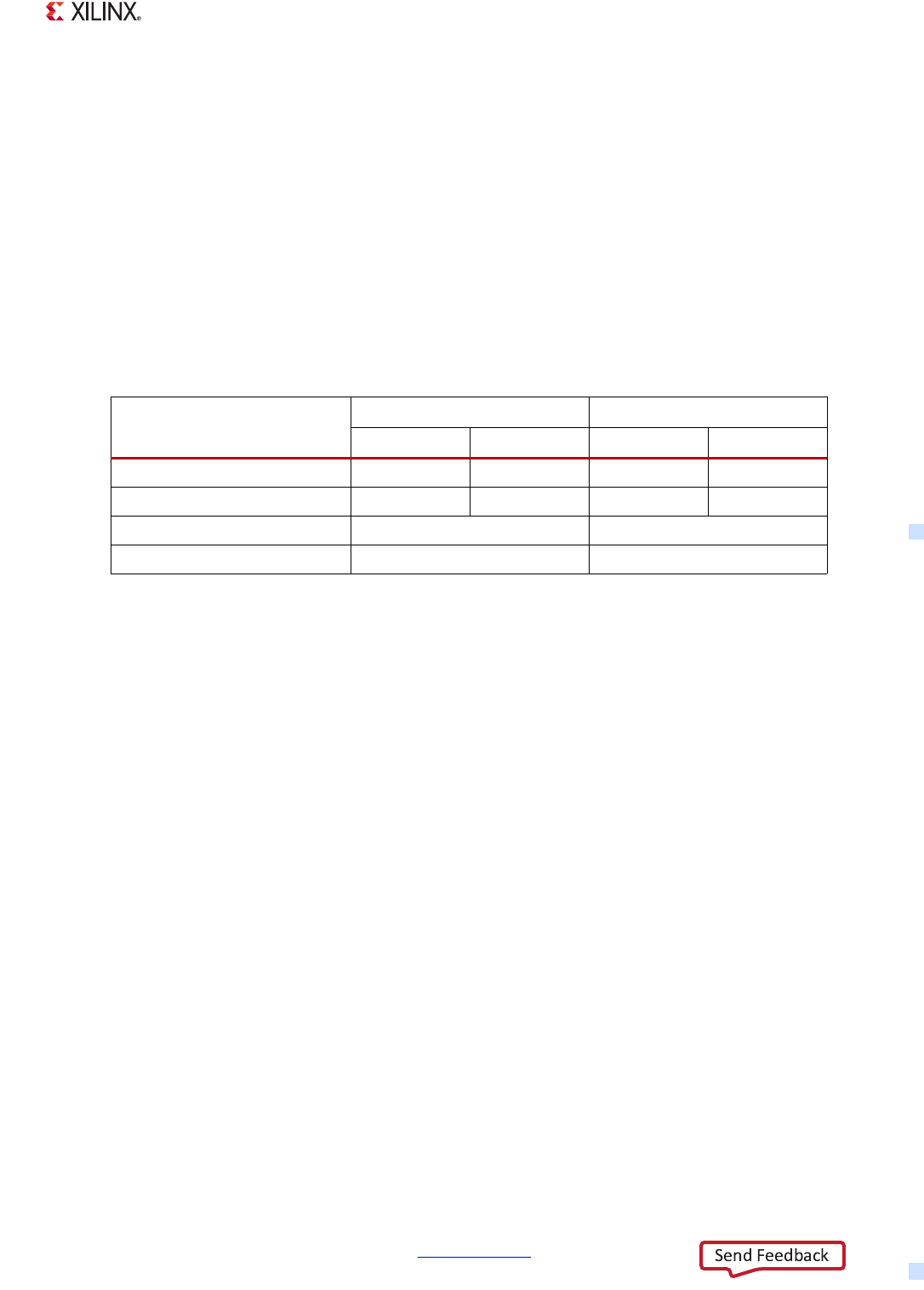
Zynq-7000 AP SoC Technical Reference Manual www.xilinx.com 556
UG585 (v1.12.1) December 6, 2017
Chapter 17: SPI Controller
17.5.1 Protocol
Master Mode
The controller supports various I/O signaling relationships for master mode. There are four
combinations for setting the phase and polarity control bits, spi.Config_reg0 [CLK_PH] and
[CLK_POL]. These parameters affect the active edge of the serial clock, the assertion of the slave
select and the idle state of the SCLK.
The clock phase parameter defines the state of the SS between words and the state of SCLK when the
controller is not transmitting bits. The phase and polarity parameters are summarized in Ta ble 1 7-4
and illustrated in Figure 17-5.
Clock Phase Setting, CPHA (CLK_PH)
In master mode, the value of the clock phase bit, spi.Config_reg0 [CLK_PH] affects the I/O protocol
using parameters in the spi.Delay_reg0 register as follows (see Figure 17-5):
CLK_PH = 0
•SS Activity: The master automatically drives the SS outputs inactive (High) for a the time
programmed into the spi.Delay_reg0 [d_nss] bit field: Time = (1 + [d_nss]) * SPI_Ref_Clk clock
period. The minimum time is 2 SPI_Ref_Clk clock periods.
•Delay between Words: The delay between the last bit period of the current word and the first
bit period on the next word: Time = (2 + [d_btwn]) * SPI_Ref_Clk clock period. The minimum
time is 3 SPI_Ref_Clk clock periods. This delay enables the TxFIFO to be unloaded and ready for
the next parallel-to-serial conversion and to toggle slave select inactive High.
CLK_PH = 1
•SS Activity: The SS output signals are not driven inactive between words.
•Delay between Words: The minimum delay between the last bit period of the current word and
the first bit period on the next word is, by default, one SPI_Ref_Clk cycles (configurable by the
spi.Delay_reg0 register). This allows the TxFIFO to be unloaded and ready for the next parallel-to
serial-conversion.
Table 17-4: SPI Clock Phase and Polarity Controls
CLK_PH = 0 CLK_PH = 1
CLK_POL = 0 CLK_POL = 1 CLK_POL = 0 CLK_POL = 1
Driving Edge negative positive positive negative
Sampling Edge positive negative negative positive
SS State between Words inactive active
SCLK State outside of Word active inactive
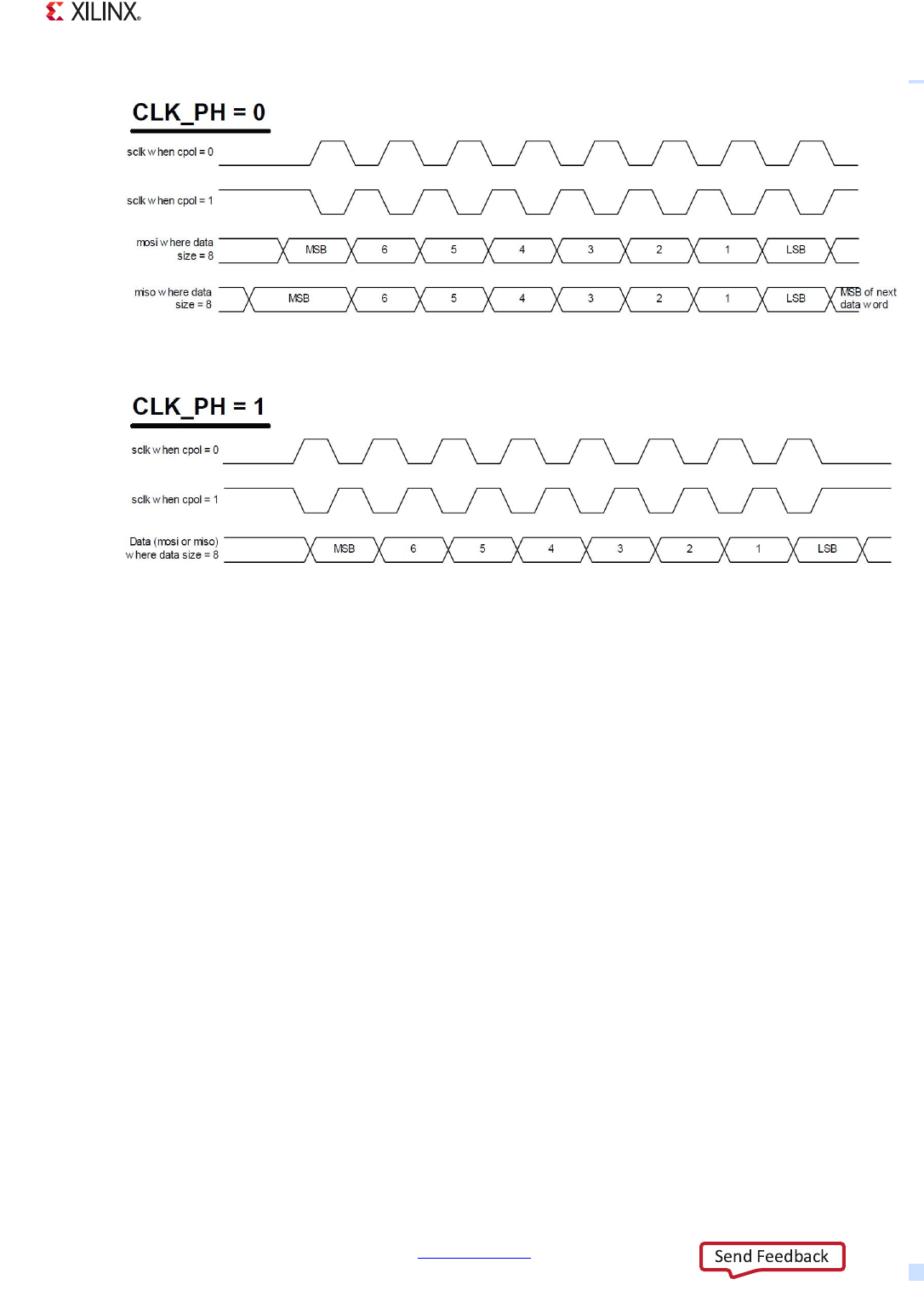
Zynq-7000 AP SoC Technical Reference Manual www.xilinx.com 557
UG585 (v1.12.1) December 6, 2017
Chapter 17: SPI Controller
17.5.2 Back-to-Back Transfers
(See Figure 17-6.)
Slave Mode Requirements
In slave mode, the controller can accept back-to-back transfers.
Master Mode Options
• Auto SS, auto start (order these four starting with importance and include cross-reference for
each)
• Auto SS, manual start
• Manual SS, auto start
• Manual SS, manual start
X-Ref Target - Figure 17-5
Figure 17-5: SPI I/O Signal Waveforms for Clock Phase and Polarity
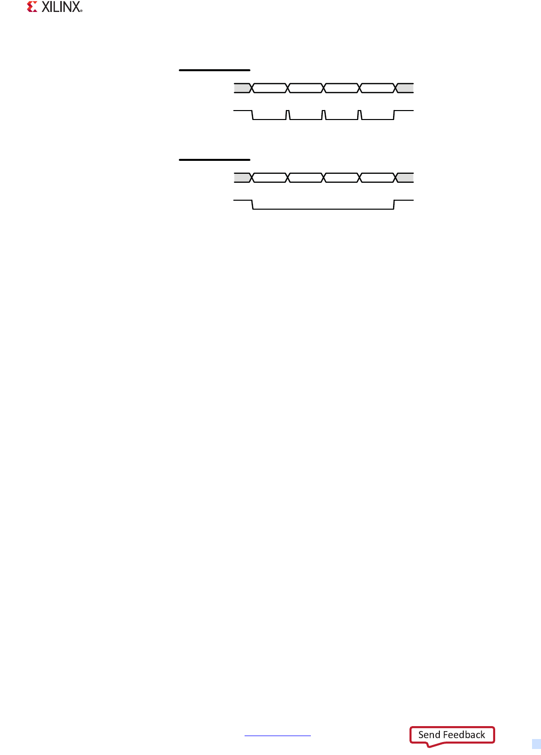
Zynq-7000 AP SoC Technical Reference Manual www.xilinx.com 558
UG585 (v1.12.1) December 6, 2017
Chapter 17: SPI Controller
17.5.3 MIO/EMIO Routing
The SPI interface signals can be routed either through the MIO pins or the EMIO interface. When the
system is reset (e.g., PS_POR_B, PS_SRST_B and other methods), all of the I/O signals are routed to
the EMIO interface by default.
The SPI bus can operate up to 50 MHz when the bus signals are routed via the MIO. When the signals
are routed via EMIO to the PL pins, the nominal clock rate is 25 MHz. Refer to the frequency
specifications that are defined in the data sheet.
To use the EMIO interface, the user must create logic in the PL to directly connect the SPI EMIO
interface to PL I/O buffers attached to PL pins. The EMIO route supports up to 25 MHz I/O clocking.
The SPI signals can be routed to specific MIO pins. Wiring diagrams are shown in section
17.5.4 Wiring Connections. The general routing concepts and MIO I/O buffer configurations are
explained in section 2.5 PS-PL MIO-EMIO Signals and Interfaces.
Example: Program the I/O for SPI 0 on to MIO pins 16 to 21
This example enables Master SPI 0 onto pins 16 to 21 using up to three slave selects.
1. Configure MIO pin 16 for clock output. Write 0x0000_22A0 to the slcr.MIO_PIN_16 register.
a. Route SPI 0 clock to pin 16.
b. Enable output, [TRI_ENABLE] = 0.
c. LVCMOS18: [IO_TYPE] = 001
d. Slow CMOS drive edge.
e. Disable internal pull-up resistor.
f. Disable HSTL receiver.
X-Ref Target - Figure 17-6
Figure 17-6: SPI Back-to-Back Transfers
UG585_c17_06_022613
MISO
SS
Word 0
MOSI
CLK_PH = 1
CLK_PH = 0
Word 1 Word 2 Word 3
MISO
SS
Word 0
MOSI Word 1 Word 2 Word 3

Zynq-7000 AP SoC Technical Reference Manual www.xilinx.com 559
UG585 (v1.12.1) December 6, 2017
Chapter 17: SPI Controller
2. Configure MIO pins 17 for MISO input. Write 0x0000_02A0 to each of the slcr.MIO_PIN_17
register.
a. Route SPI 0 MISO to pin 17.
b. Disable output. [TRI_ENABLE] = 1.
c. LVCMOS18: [IO_TYPE] = 001.
d. Slow CMOS drive edge.
e. Disable internal pull-up resistor.
f. Disable HSTL receiver.
3. Configure MIO pin 18, 19 and/or 20 for Slave Select outputs. Write 0x0000_32A0 to the
slcr.MIO_PIN_18, 19 and/or 20 registers. The internal pull-up is enabled.
a. Route SPI 0 slave selects signal(s) to pins 18, 19 and/or 20. Any and all of the slave selects can
be activated for master mode. In slave mode, SS 0 must be used.
b. 3-state controlled by SPI: [TRI_ENABLE] = 0.
c. LVCMOS18: [IO_TYPE] = 001.
d. Slow CMOS drive edge.
e. Enable internal pull-up resistor.
f. Disable HSTL receiver.
4. Configure MIO pins 21 for MOSI. Write 0x0000_22A0 to each of the slcr.MIO_PIN_21 register:
a. Route SPI 0 MOSI to pin 21.
b. 3-state controlled by SPI [TRI_ENABLE] = 0.
c. LVCMOS18: [IO_TYPE] = 001.
d. Slow CMOS drive edge.
e. Disable internal pull-up resistor.
f. Disable HSTL receiver.
17.5.4 Wiring Connections
The user can connect the each SPI controller to external SPI slaves or an SPI master via the MIO pins
or the EMIO interface to PL pins. Wiring examples:
•Master Mode via MIO, Figure 17-7
• Master Mode via EMIO, Figure 17-8
• Slave Mode via MIO, Figure 17-9
The I/O signals of the two SPI controllers in the PS can be connected together as described in section
17.2.7 SPI-to-SPI Connection.
IMPORTANT: In master mode, connect SS0 to VCC if SS0 is not used. This is important because the
controller snoops this signal in master mode to detect a multi-master mode situation; if SS0 is a logic
Low, then the controller assumes multi-master mode and waits for SS0 to de-assert before issuing a
transaction.
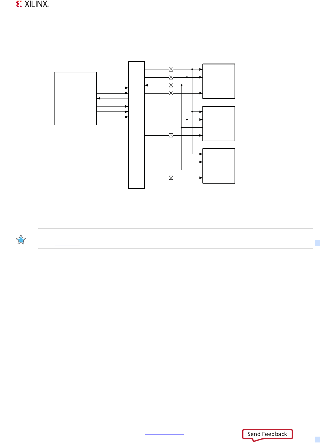
Zynq-7000 AP SoC Technical Reference Manual www.xilinx.com 560
UG585 (v1.12.1) December 6, 2017
Chapter 17: SPI Controller
Master Mode via MIO
IMPORTANT: When using MIO pins always use SS0. For existing designs that do not use SS0, refer to
Xilinx AR58294.
X-Ref Target - Figure 17-7
Figure 17-7: SPI Master Mode Wiring Diagram via MIO
UG585_c17_07_102214
Connect up to 3 slave
devices (directly).
For one slave device,
connect it to any of the
slave selects.
SPI Master
Controller
Slave 0
SCLK
MOSI
MISO
SS0
SS2
SS1
Slave 1
Slave 2
SCLK
MOSI
MISO
SS0
SS1
SS2
MIO
Device
Boundary
Zynq-7000 AP SoC External Devices
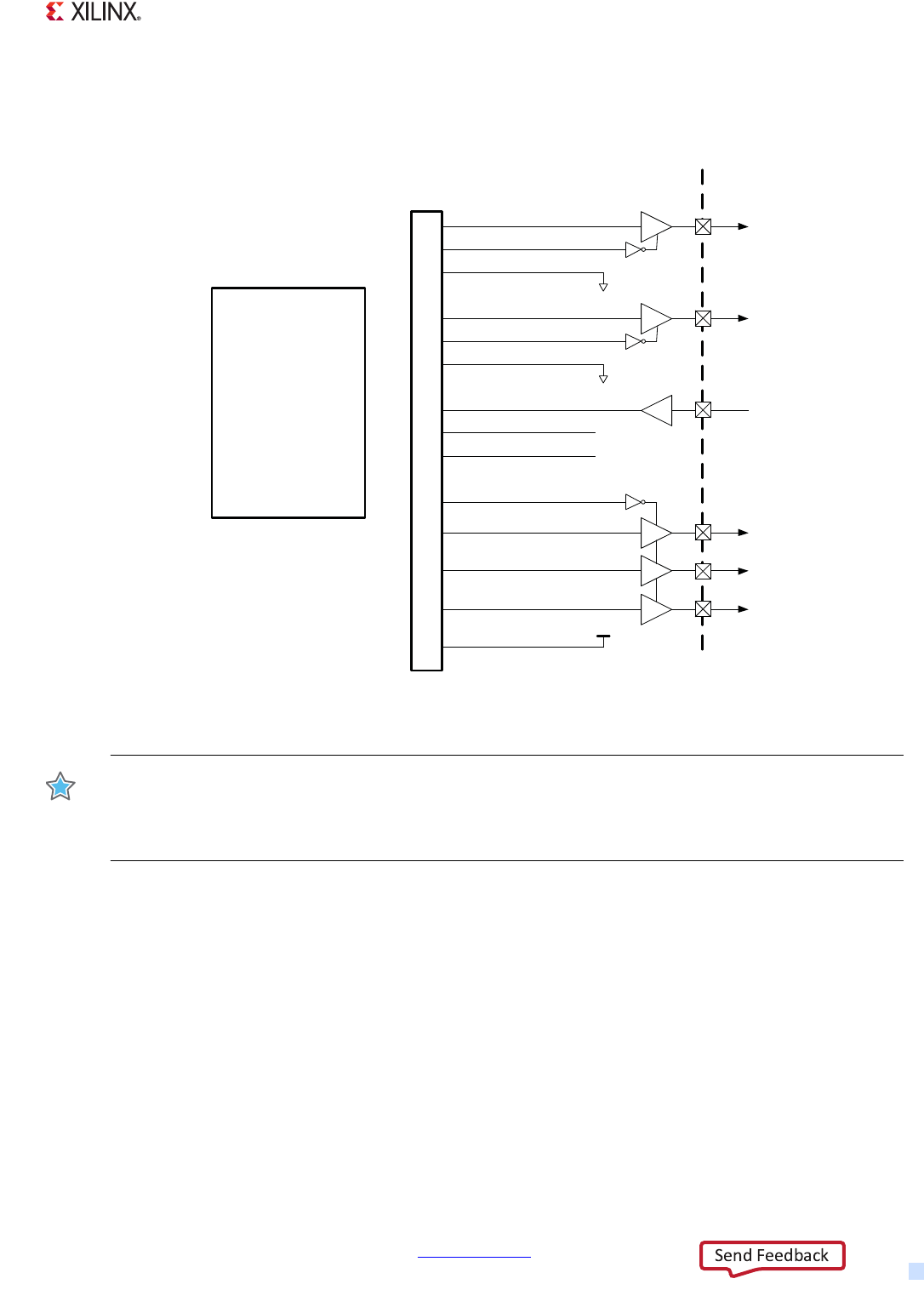
Zynq-7000 AP SoC Technical Reference Manual www.xilinx.com 561
UG585 (v1.12.1) December 6, 2017
Chapter 17: SPI Controller
Master Mode via EMIO
IMPORTANT: When using EMIO pins, tie SSIN High in the PL bitstream. Ensure that the PS–PL voltage
level shifters are enabled, and that the PL is powered and configured. Otherwise the SPI controller will
not function properly. For more information about enabling the voltage shift registers, refer to PS–PL
Voltage Level Shifter Enables, page 46.
X-Ref Target - Figure 17-8
Figure 17-8: SPI Master Mode Wiring Diagram via EMIO
UG585_c17_08_022613
SPI Master
Controller
EMIO SPI x SCLKI
SCLK
EMIO
Device
Boundary
EMIO SPI x SCLKTN
EMIO SPI x SCLKO
EMIO SPI x SI
MOSI
EMIO SPI x MOTN
EMIO SPI x MO
EMIO SPI x SO
MISO
EMIO SPI x SOTN
EMIO SPI x MI
nc
EMIO SPI x SSON 1
SS 0
EMIO SPI x SSNTN
EMIO SPI x SSON 0
nc
EMIO SPI x SSON 2 SS 2
EMIO SPI x SSIN
SS 1
PL
I/O Select
PS IOP
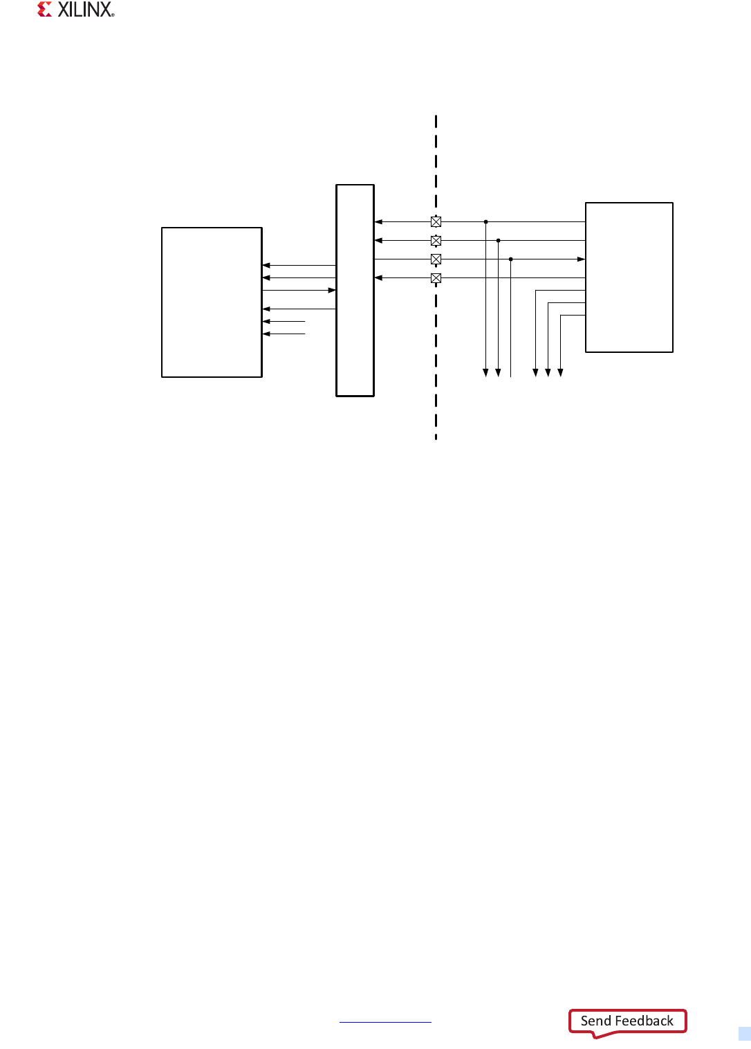
Zynq-7000 AP SoC Technical Reference Manual www.xilinx.com 562
UG585 (v1.12.1) December 6, 2017
Chapter 17: SPI Controller
Slave Mode via MIO
17.5.5 MIO/EMIO Signal Tables
The SPI I/O interface signals routing has some options. The routing options include multiple
positions in the MIO pins. The options are illustrated in section 2.5.4 MIO-at-a-Glance Table and in
Tabl e 17- 5.
Default Input Signal Routing: If the I/O signals are not routed to a set of MIO pins (MIO_PIN_xx
register programming), then the EMIO interface input signals are enabled.
MIO Pin Limitation
Small Package Note: The MIO pin restrictions based on device version are shown in the MIO table
in section 2.5.4 MIO-at-a-Glance Table. Each SPI I/O interface is selected as a group.
X-Ref Target - Figure 17-9
Figure 17-9: SPI Slave Mode Wiring Diagram via MIO
UG585_c17_09_022613
Other External
Slave Devices
SPI Slave
Controller
SCLK
MOSI
MISO
SS 0
SCLK
MOSI
MISO
SS 0
SS 1
SS 2
MIO
Device
Boundary
Zynq-7000 AP SoC
External
Master
Device
nc
nc
SCLK
MOSI
MISO
SS a
SS c
SS b
SS d
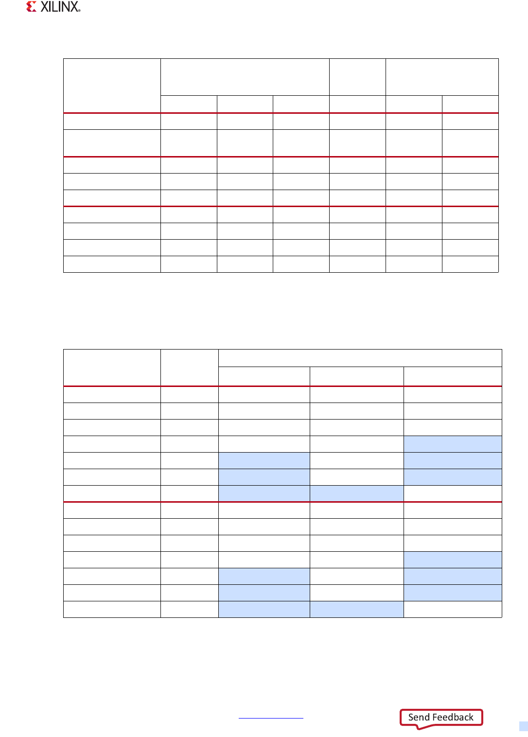
Zynq-7000 AP SoC Technical Reference Manual www.xilinx.com 563
UG585 (v1.12.1) December 6, 2017
Chapter 17: SPI Controller
EMIO Signals
The SPI I/O interface signals available on the EMIO interface are identified in Ta ble 17 -6 .
Table 17-5: SPI MIO Pins
SPI Interface
I/O
SPI Signals
Slave or
Master
Mode
Master Mode
Clock MOSI MISO SS 0 SS 1 SS 2
Signal Type IO IO IO IO O O
Controller Default
Input Value 0001~~
SPI 0, choice 1 16 21 17 18 19 20
SPI 0, choice 2 28 33 29 30 31 32
SPI 0, choice 3 40 45 41 42 43 44
SPI 1, choice 1 12 10 11 13 14 15
SPI 1, choice 2 24 22 23 25 26 27
SPI 1, choice 3 36 34 35 37 38 39
SPI 1, choice 4 48 46 47 49 50 51
Table 17-6: SPI EMIO Signals
SPI Interface
Controller
Default
Input Value
EMIO Signals
Input Name (I) Output Name (O) 3-state Name (O)
SPI 0 Clock 0EMIOSPI0SCLKI EMIOSPI0SCLKO EMIOSPI0SCLKTN
SPI 0 MOSI 0EMIOSPI0SI EMIOSPI0MO EMIOSPI0MOTN
SPI 0 MISO 0EMIOSPI0MI EMIOSPI0SO EMIOSPI0STN
SPI 0 Slave Select 0 1EMIOSPI0SSIN EMIOSPI0SSON0
SPI 0 Slave Select 1 ~EMIOSPI0SSON1
SPI 0 Slave Select 2 ~EMIOSPI0SSON2
SPI 0 SS 3-state ~EMIOSPI0SSNTN
SPI 1 Clock 0EMIOSPI1SCLKI EMIOSPI1SCLKO EMIOSPI1SCLKTN
SPI 1 MOSI 0EMIOSPI1SI EMIOSPI1MO EMIOSPI1MOTN
SPI 1 MISO 0EMIOSPI1MI EMIOSPI1SO EMIOSPI1STN
SPI 1 Slave Select 0 1EMIOSPI1SSIN EMIOSPI1SSON0
SPI 1 Slave Select 1 ~EMIOSPI1SSON1
SPI 1 Slave Select 2 ~EMIOSPI1SSON2
SPI 1 SS 3-state ~EMIOSPI1SSNTN

Zynq-7000 AP SoC Technical Reference Manual www.xilinx.com 564
UG585 (v1.12.1) December 6, 2017
Chapter 18
CAN Controller
18.1 Introduction
This chapter describes the architecture and features of the CAN controllers and the functions of the
various registers in the design. There are two nearly identical CAN controllers in the PS that are
independently operable. Defining the CAN protocol is outside the scope of this document, and
knowledge of the specifications is assumed.
18.1.1 Features
CAN Controller features are summarized as follows:
• Compatible with the ISO 11898 -1, CAN 2.0A, and CAN 2.0B standards
• Standard (11-bit identifier) and extended (29-bit identifier) frames
• Bit rates up to 1 Mb/s
• Transmit message FIFO (TxFIFO) with a depth of 64 messages
• Transmit prioritization through one high-priority transmit buffer (TxHPB)
• Watermark interrupts for TxFIFO and RxFIFO
• Automatic re-transmission on errors or arbitration loss in normal mode
• Receive message FIFO (RxFIFO) with a depth of 64 messages
• Four Rx acceptance filters with enables, masks and IDs
• Loopback and snoop modes for diagnostic applications
• Maskable error and status interrupts
• 16-Bit time stamping for receive messages
• Readable Rx/Tx error counters
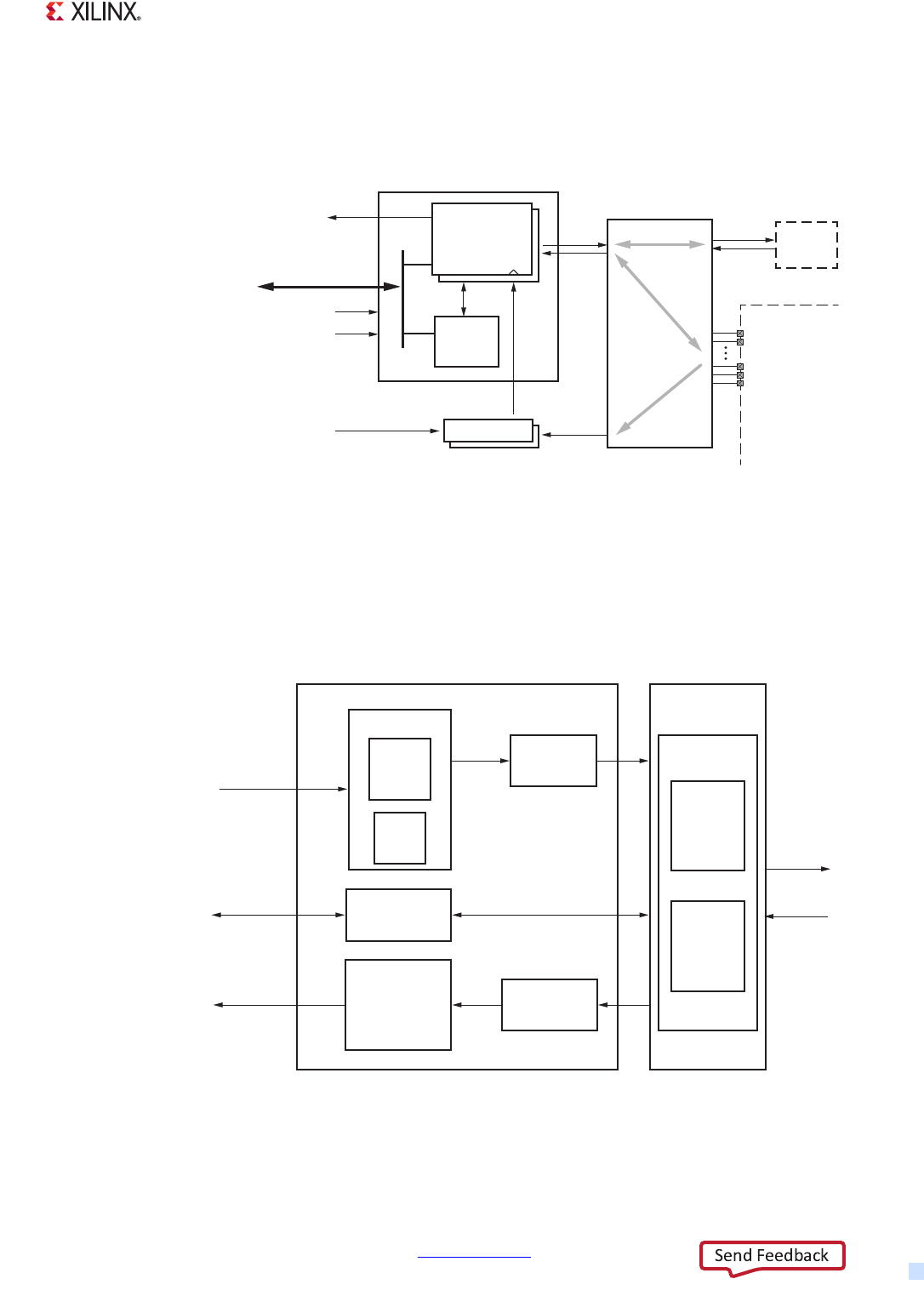
Zynq-7000 AP SoC Technical Reference Manual www.xilinx.com 565
UG585 (v1.12.1) December 6, 2017
Chapter 18: CAN Controller
18.1.2 System Viewpoint
The system viewpoint of the CAN controller is shown in Figure 18-1.
18.1.3 Block Diagram
The high-level architecture of the CAN core is shown in Figure 18-2. The sub-modules are described
in subsequent sections.
X-Ref Target - Figure 18-1
Figure 18-1: CAN Controller System Viewpoint
MIO
Pins
MIO – EMIO
Routing
Interconnect APB
PL
Tx, Rx
Tx, Rx
Clock
UG585_c18_01_071612
Device
Boundary
EMIO
CAN{0, 1} REF clock
IRQ ID# {60, 83}
Control
Registers
Tx, Rx
External
Clock
Source
Slave
port
CAN{0, 1} CPU_1x clock
CAN{0, 1} CPU_1x reset
CAN
Controllers
Clocking
X-Ref Target - Figure 18-2
Figure 18-2: CAN Controller Block Diagram
Transfer Layer
- Protocol Engine
Bit Stream
Processor
Bit Timing
Logic
Object Layer - Data Buffer and Filtering
APB
Interface TX Priority
Logic
Acceptance
Filter
TX Storage
UG585_c18_02_021213
Tx
FIFO
Tx
HPB
Rx FIFO
Configuration
Registers
Data Write
Register R/W
Data Read
CAN Tx
CAN Rx

Zynq-7000 AP SoC Technical Reference Manual www.xilinx.com 566
UG585 (v1.12.1) December 6, 2017
Chapter 18: CAN Controller
Configuration Registers
The CAN Controller Configuration register defines the configuration registers. This module allows
for read and write access to the registers through the APB interface. An overview of the CAN
controller registers are shown in section 18.3.8 Register Overview.
Transmit and Receive Messages
Separate storage buffers exist for transmit (TxFIFO) and receive (RxFIFO) messages through a FIFO
structure. Each buffer can store up to 64 messages. Once a message is written into the TxFIFO it takes
a total delay of 2*(Tx Driver delay + Propagation delay + Rx Driver delay) to transmit over the CAN
bus.
Tx High Priority Buffer
Each controller also has a transfer high priority buffer (TxHPB) provides storage for one transmit
message. Messages written on this buffer have maximum transmit priority. They are queued for
transmission immediately after the current transmission is complete, preempting any message in the
TxFIFO.
Acceptance Filters
Acceptance filters sort incoming messages with the user-defined acceptance mask and ID registers
to determine whether to store messages in the RxFIFO, or to acknowledge and discard them.
Messages passed through acceptance filters are stored in the RxFIFO.
18.1.4 Notices
Restrictions
There is a single PS clock generator for both controllers. When the internal clock is used, it will be of
the same clock frequency, but the clock to each controller can be individually enabled using the slcr
register, see section The Quad-SPI clock is divided down by at least two using the Quad-SPI baud
rate divider, see section 12.4.1 Clocks. In master mode, the SPI clock is divided down by at least four
using the SPI baud rate divider, see section 17.4.2 Clocks.. Also, either or both controllers can be
clocked from an external source via an MIO pin, see section 18.4.1 Clocks.
RECOMMENDED: For all clocking sources, set the can.BRPR register to a value of 2 or greater and a
prescaler value of at least 3.

Zynq-7000 AP SoC Technical Reference Manual www.xilinx.com 567
UG585 (v1.12.1) December 6, 2017
Chapter 18: CAN Controller
18.2 Functional Description
Each controller is independently configured and controlled. There are two CAN controllers (CANx;
where x = 0 or 1). The register name preface for the CAN registers is 'can' (e.g., can.MSR register).
18.2.1 Controller Modes
The CAN controller supports the following modes of operation:
•Configuration
•Normal
• Sleep
•Loop Back
•Snoop mode
Configuration Mode
The CAN controller enters the Configuration mode when any of the following actions are performed,
regardless of the operation mode:
•Writing a 0 to the CEN bit in the SRR register.
•Writing a 1 to the SRST bit in the SRR register. The core enters the Configuration mode
immediately following the software reset.
•Driving a 0 on the reset input. The core continues to be in reset as long as reset is 0. The core
enters Configuration mode after reset is negated to 1.
Normal Mode
Normal mode transmits and receives messages on the Tx and Rx I/O signals as
def
ined by the Bosch
and IEEE
specif
ications.
Sleep Mode
Sleep mode can be used to save a small amount of power during idle times. When in sleep mode, the
controller can transition to normal mode or
conf
iguration mode. In sleep mode:
• When another node transmits a message, the controller receives the message and exits sleep
mode.
• If there is a new Tx request then the hardware switches the controller to normal mode and the
controller
ser
vices the request(s).
• An interrupt can be generated when the controller enters sleep mode.
• An interrupt can be generated when the controller wakes up.
Sleep mode is exited by the hardware when there is CAN bus activity or a request in either TxFIFO or

Zynq-7000 AP SoC Technical Reference Manual www.xilinx.com 568
UG585 (v1.12.1) December 6, 2017
Chapter 18: CAN Controller
TxHPB. When the controller exits sleep mode, can.MSR[SLEEP] is set to
0
by the hardware and an
interrupt can be generated.
The CAN controller enters Sleep mode from Configuration mode when the LBACK bit in MSR is
0
, the
SLEEP bit in MSR is 1, and the CEN bit in SRR is 1. The CAN controller enters Sleep mode only when
there are no pending transmission requests from either the TX FIFO or the TX High Priority Buffer.
The CAN controller enters Sleep mode from Normal mode only when the SLEEP bit is 1, the CAN bus
is idle, and there are no pending transmission requests from either the TX FIFO or TX High Priority
Buffer.
When another node transmits a message, the CAN controller receives the transmitted message and
exits Sleep mode. When the controller is in Sleep mode, if there are new transmission requests from
either the TX FIFO or the TX High Priority Buffer, these requests are serviced, and the CAN controller
exits Sleep mode. Interrupts are generated when the CAN controller enters Sleep mode or wakes up
from Sleep mode. From sleep mode, the CAN controller can enter either the Configuration or Normal
modes.
Loop Back Mode (Diagnostics)
Loop back mode is used for diagnostic purposes. When in loop back mode, the controller must only
be programmed to enter
conf
iguration mode or issue reset. In loop back mode:
• The controller transmits a recessive bitstream onto the CAN_TX bus signal.
• Tx messages are internally looped back to the Rx line and are acknowledged.
• Tx messages are not sent on the CAN_TX bus signal.
• The controller receives all message that it transmits.
• The controller does not receive any messages transmitted by other CAN nodes.
Snoop Mode (Diagnostics)
Snoop mode is used for diagnostic purposes. When in snoop mode, the controller must only be
programmed to enter
conf
iguration mode or be held in reset. In snoop mode:
• The controller transmits a recessive bitstream onto the CAN bus.
• The controller does not participate in normal bus communication.
• The controller receives messages that are transmitted by other CAN nodes.
• Software can program acceptance
f
ilters to dynamically enable/disable and change criteria. Error
counters are disabled and cleared to 0. Reads to error counter registers return 0.
Mode Transitions
The supported mode transitions are shown in Figure 18-3. The transitions are primarily controlled by
the resets, the CEN bit, the MSR register settings, and a hardware wake-up mechanism.
To enter normal mode from configuration mode:
• Clear can.MSR[LBACK, SNOOP, SLEEP] = 0
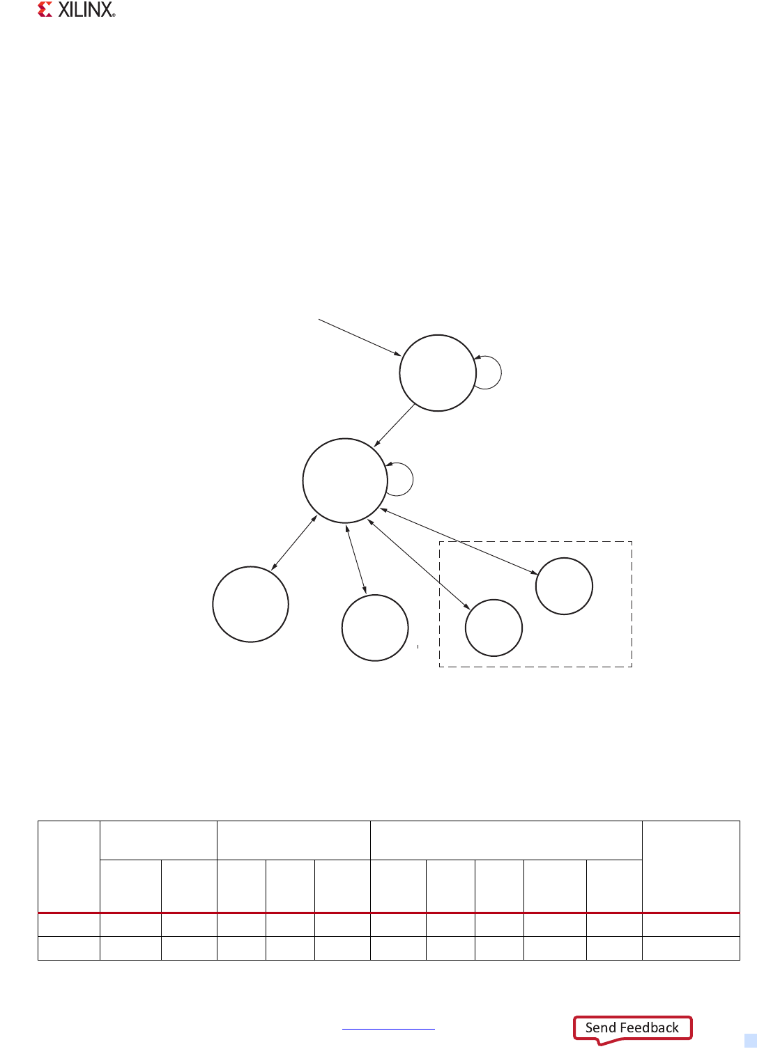
Zynq-7000 AP SoC Technical Reference Manual www.xilinx.com 569
UG585 (v1.12.1) December 6, 2017
Chapter 18: CAN Controller
• Set can.SRR[CEN] = 1
To enter sleep mode from normal mode (interrupt generated):
• Set can.MSR[SLEEP] = 1
Events that cause the controller to exit sleep mode (interrupt generated):
• Rx signal activity (hardware sets can.MSR[SLEEP] = 0)
• TxFIFO or TxHPB activity (hardware sets can.MSR[SLEEP] = 0)
• Software writes 0 to can.MSR[SLEEP]
Mode Settings
Tabl e 18- 1 defines the CAN controller modes of operation and corresponding control and status bits.
.
X-Ref Target - Figure 18-3
Figure 18-3: CAN Operating Mode Transitions
can.SRR[CEN] = 0
Configuration
Normal
Loop
Back
Snoop
Sleep
Diagnostics
UG585_c18_05_021113
Reset Reset
slcr.CAN_RST_CTRL[CANx_CPU1x_RST] =1
OR
can.SRR[SRST] = 1
(Self-clearing)
Hardware Forces
can.SRR[CEN] = 0
Reset:
slcr.CAN_RST_CTRL[CANx_CPU1x_RST] = 0
Table 18-1: CAN Controller Modes of Operation
CAN
CPU_1x
PS Reset
(slcr)
Software Reset
Register (can.SRR)
Mode Select Register
(MSR) (Read/Write bits)
Status Register (SR)
(Read Only bits) Operational
Mode
SRST
(CAN
Reset)
CEN
(CAN
Enable)
LBACK SLEEP SNOOP CONFIG LBACK SLEEP NORMAL SNOOP
1XXXXX100 0 0Reset
01XXXX 100 0 0Reset
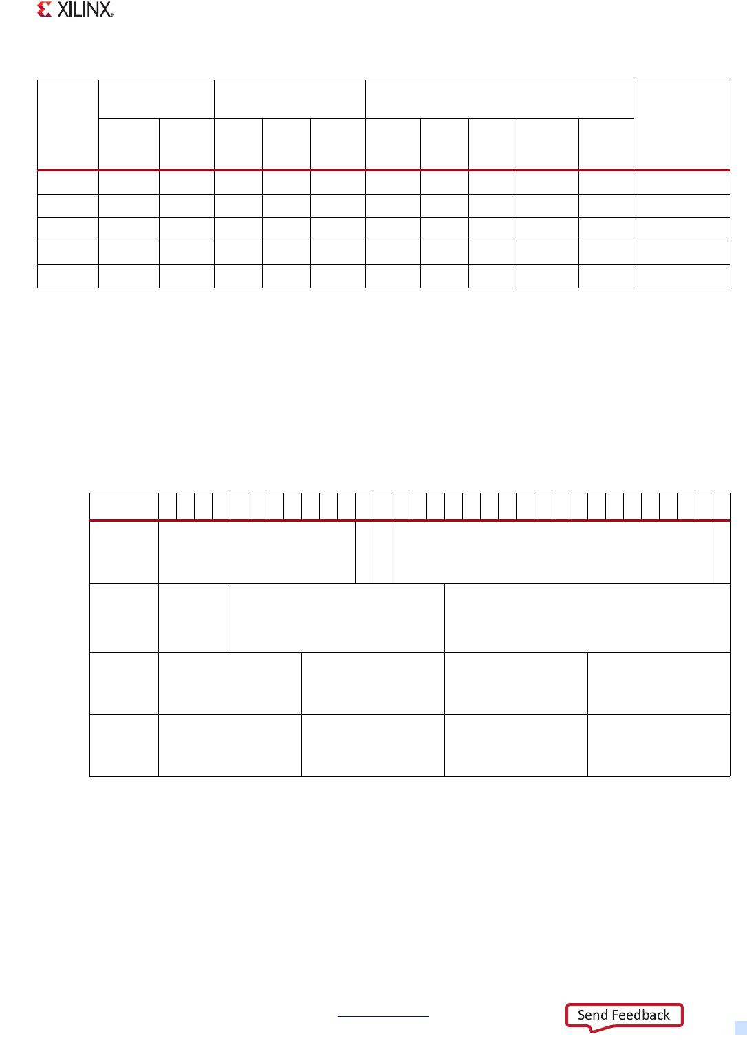
Zynq-7000 AP SoC Technical Reference Manual www.xilinx.com 570
UG585 (v1.12.1) December 6, 2017
Chapter 18: CAN Controller
18.2.2 Message Format
The same message format is used for RxFIFO and Tx (FIFO and HPB). Each message includes four
words (16 bytes). Software must read and write all four words regardless of the actual number of data
bytes and valid fields in the message.
The message words, fields and structure are shown in Ta ble 1 8-2 . The details of each field are in
Tabl e 18- 3.
Bit Field Details
Writes
If a bit field or data byte is not required, then write zeros. Software should write the default values
shown in Table 1 8-3 for unused functions.
000XX X 100 0 0Configuration
0011XX 010 0 0Loop back
0 0 1010 001 0 0Sleep
0 0 1001 000 1 1Snoop
0 0 1000 000 1 0Normal
Table 18-1: CAN Controller Modes of Operation (Cont’d)
CAN
CPU_1x
PS Reset
(slcr)
Software Reset
Register (can.SRR)
Mode Select Register
(MSR) (Read/Write bits)
Status Register (SR)
(Read Only bits) Operational
Mode
SRST
(CAN
Reset)
CEN
(CAN
Enable)
LBACK SLEEP SNOOP CONFIG LBACK SLEEP NORMAL SNOOP
Table 18-2: CAN Message Format
31
30
29
28
27
26
25
24
23
22
21
20
19
18
17
16
15
14
13
12
11
10
9
8
7
6
5
4
3
2
1
0
Message
Identifier
[IDR}
ID[28:18]
STR/RTR
IDE
ID[17:0]
RTR
Data
Length
Code
[DLCR]
DLC[3:0] Reserved Time Stamp
(Rx only, Reserved for Tx)
Data
Word 1
[DW1R]
DB0[7:0] DB1[7:0] DB2[7:0] DB3[7:0]
Data
Word 2
[DW2R]
DB4[7:0] DB5[7:0] DB6[7:0] DB7[7:0]

Zynq-7000 AP SoC Technical Reference Manual www.xilinx.com 571
UG585 (v1.12.1) December 6, 2017
Chapter 18: CAN Controller
Reads
Data starts at byte 0 and continues for the number of counts in DLC. Software should read both data
words, but the only valid bytes are determined by DLC.
Tabl e 18- 3 provides bit descriptions for the identifier word bits, the DLC word bits, and data word 1
and data word 2 bits.
Table 18-3: CAN Message Word Register Bit Fields
Bits Name Default
Value Description
Identifier Word
31:21 ID[28:18] 0
Standard Message ID
The identifier portion for a standard frame is 11 bits.
These bits indicate the standard frame ID.
This field is valid for both standard and extended frames.
20 SRR/RTR 0
Substitute Remote Transmission Request
This bit differentiates between data frames and remote
frames. Valid only for standard frames. For extended
frames this bit is 1.
1: Indicates that the message frame is a Remote Frame.
0: Indicates that the message frame is a Data Frame.
19 IDE 0
Identifier Extension
This bit differentiates between frames using the Standard
Identifier and those using the Extended Identifier. Valid
for both Standard and Extended Frames.
1: Indicates the use of an extended message identifier.
0: Indicates the use of a standard message identifier.
18:1 ID[17:0] 0
Extended Message ID
This field indicates the extended identifier. Valid only for
extended frames.
For standard frames, reads from this field return 0s.
For Standard frames, writes to this field should be 0s.
0RTR0
Remote Transmission Request
This bit differentiates between data frames and remote
frames.
Valid only for extended frames.
1: Indicates the message object is a remote frame.
0: Indicates the message object is a data frame.
For standard frames, reads from this bit returns 0.
For standard frames, writes to this bit should be 0.
DLC Word
31-28 DLC 0
Data Length Code
This is the data length portion of the control field of the
CAN frame. This indicates the number valid data bytes (0
to 8) that are in the Data Word 1 and Data Word 2
registers.
Zynq-7000 AP SoC Technical Reference Manual www.xilinx.com 572
UG585 (v1.12.1) December 6, 2017
Chapter 18: CAN Controller
18.2.3 Message Buffering
Rx Messages
The RxFIFO can store up to 64 Rx CAN messages that are received and optionally filtered. Rx
messages that pass any of the acceptance filters are stored in the RxFIFO. When no acceptance filter
has been selected, all received messages are stored in the RxFIFO. Software reads these messages as
described in 18.3.7 Read Messages from RxFIFO.
A timestamp is added to each successfully stored Rx message. A free running 16-bit counter is
clocked using the CAN bit time clock. The rules for time stamping an Rx message are:
• The counter rolls over. There is no status bit to indicate that the roll over condition occurred.
• The timestamp included when a Rx message is successfully collected. The sampling of the
counter takes place at the last bit of EOF.
• The counter is cleared when CEN=0 or by software writing a 1 to the can.TCR register.
Software must read all four registers of an Rx message in the RxFIFO, regardless of how many data
bytes are in the message. The first word is read using the RXFIFO_ID register and contains the
identifier of the received message (IDR). The second word is read using the RXFIFO_DLC register and
contains the 16-bit timestamp and data length code (DLC) field. The third and fourth words contain
data word 1 (DW1R) and data word 2 (DW2R).
Writes to the RxFIFO registers are ignored. Read data from an empty RxFIFO are invalid and might
generate an interrupt.
The messages in the RxFIFO are retained even if the CAN controller enters Bus off state or
Configuration mode.
27-0 Reserved 0Reads from this field return 0s.
Writes to this field should be 0s.
Data Word 1
DW1R[31:24] DB0[7:0] 0Data Byte 0
DW1R[23:16] DB1[7:0] 0 Data Byte 1
DW1R[15:8] DB2[7:0] 0Data Byte 2
DW1R[7:0] DB3[7:0] 0Data Byte 3
Data Word 2
DW2R[31:24] DB4[7:0] 0Data Byte 4
DW2R[23:16] DB5[7:0] 0Data Byte 5
DW2R[15:8] D6[7:0] 0Data Byte 6
DW2R[7:0] DB7[7:0] 0Data Byte 7
Table 18-3: CAN Message Word Register Bit Fields (Cont’d)
Bits Name Default
Value Description

Zynq-7000 AP SoC Technical Reference Manual www.xilinx.com 573
UG585 (v1.12.1) December 6, 2017
Chapter 18: CAN Controller
Tx Messages
The controller has a configurable TxFIFO that software can use buffer up to 64 Tx CAN messages. The
controller also has a high priority transmit buffer (Tx HPB), with storage for one message. When a
higher priority message needs to be sent, software writes the message to the high priority transmit
buffer when it is available. The message in the TxHPB has higher priority over messages in the TxFIFO.
When arbitration loss or errors occur during the transmission of a message, the controller tries to
retransmit the message. No subsequent message, even a newer, higher priority message is
transmitted until the original message is transmitted without errors or arbitration loss.
The controller transmits the message starting with bit 31 of the IDR word. After the identifier word
is transmitted, the DLCR word is transmitted. This is followed by the data bytes in this order: DB0,
DB1, ... DB7. The last bit in the data portion of the message is DB7, bit 0. See Table 18-2, page 570.
The status bit, can.ISR[TXOK] is set = 1 after the controller successfully transmits a message from
either the TxFIFO or TxHPB.
The messages in the TxFIFO and TxHPB are retained even if the CAN controller enters Bus off state or
Configuration mode.
The message format is described in 18.2.2 Message Format.
Reads from RxFIFO
All 16 bytes must be read from the RxFIFO to receive the complete message. The first word read
(4 bytes) returns the identifier of the received message (IDR). The second read returns the 16-bit
receive time stamp and data length code (DLC) field of the received message (DLCR). The third read
returns data word 1 (DW1R), and the fourth read returns data word 2 (DW2R).
A free running 16-bit counter provides a time stamp relative to the time the message was
successfully received.
All four words must be read for each message, even if the message contains less than eight data
bytes. Write transactions to the RxFIFO are ignored. Reads from an empty RxFIFO return invalid data
and generates an Rx Underflow interrupt.
Rx and Tx Error Counters
When an Rx or Tx error occurs, the associated error counters in the protocol engine (see section
18.2.6 Protocol Engine) are incremented. The two error counters are 8 bits wide and are read using
the read-only can.ECR register, bit fields REC and TEC.
The Rx and Tx counters are reset when any the these situations occur:
•After a 1 is written to can.SRR[SRST] field = 1. This bit write is self-clearing.
•Anytime can.SRR[CEN] = 0 (configuration mode).
• When the controller enters Bus Off state.

Zynq-7000 AP SoC Technical Reference Manual www.xilinx.com 574
UG585 (v1.12.1) December 6, 2017
Chapter 18: CAN Controller
18.2.4 Interrupts
Each CAN controller has a single interrupt signal to the GIC interrupt controller. CAN 0 connects to
IRQ ID#60 and CAN 1 connects to ID #83. The source of an interrupt can be grouped into one of the
following:
•TxFIFO and TxHPB
•RxFIFO
• Message passing and arbitration
• Sleep mode and bus off
Enable and disable interrupts using the can.IER register. Check the raw status of the interrupt using
can.ISR. Clear interrupts by writing a 1 to can.ICR. Some interrupt sources have an additional method
to clear the interrupt as shown in Table 18-4.
List of Interrupts
All of the CAN interrupts are sticky; that is, once the hardware sets them they stay set until cleared
by software. CAN status and interrupts are identified in Table 18-4.
Table 18-4: List of CAN Status and Interrupts
Name Bit Number
Additional
Method to Clear
Interrupt
Usage
TxFIFO Watermark 13 none Operational threshold.
TxFIFO Empty 14 none Empty indicator.
TxFIFO Full 2 none Full indicator.
TxHPB Full 3 none This status indicates if the buffer is in-use and
should not be written.
RxFIFO Watermark 12 none Operational threshold.
RxFIFO Not Empty 7 none One or more messages can be read.
RxFIFO overflow 6 Write 0 to
can.SRR[CEN]
FIFO was full and message(s) likely lost.
RxFIFO underflow 5 none Programming error, message read from RxFIFO
when no messages were there.
Message Rx 4 Write 0 to
can.SRR[CEN]
Message Tx 1 Write 0 to
can.SRR[CEN]
Message Error 8 Write 0 to
can.SRR[CEN]
Any of the five CAN errors in the Error Status
register.
Arbitration Lost 0 none
Enter Sleep Mode 10 Write 0 to
can.SRR[CEN]
Zynq-7000 AP SoC Technical Reference Manual www.xilinx.com 575
UG585 (v1.12.1) December 6, 2017
Chapter 18: CAN Controller
RxFIFO and TxFIFO Interrupts
The FIFO watermark levels and all the FIFO interrupts are illustrated in Figure 18-4, CAN RxFIFO and
TxFIFO Watermark Interrupts.
Example: Program RxFIFO Watermark Interrupt (12)
The following steps can be used to setup and control the RxFIFO watermark interrupt. See
Figure 18-4. The watermark status and control interrupts are described in Protocol Engine, page 579.
1. Disable RxFIFO watermark interrupt. Write a 0 to can.IER[12].
2. Program RxFIFO full watermark level. Write to can.WIR[FW].
3. Clear RxFIFO watermark interrupt. Write a 1 to can.ICR[12].
4. Read RxFIFO watermark status. Read can.ISR[12].
5. Enable RxFIFO watermark interrupt. Write a 1 to can.IER[12].
Example: Program TxFIFO Watermark Interrupt (13)
The following steps can be used to setup and control the TxFIFO watermark interrupt. See
Figure 18-4. The watermark status and control interrupts are described in Protocol Engine, page 579.
1. Disable TxFIFO watermark interrupt. Write a 0 to can.IER[13].
2. Program TxFIFO empty watermark level. Write to can.WIR[EW].
Exit Sleep Mode 11 Write 0 to
can.SRR[CEN]
Controller can go to normal or configuration
mode.
Bus Off 9 Write 0 to
can.SRR[CEN]
Table 18-4: List of CAN Status and Interrupts
Name Bit Number
Additional
Method to Clear
Interrupt
Usage
X-Ref Target - Figure 18-4
Figure 18-4: CAN RxFIFO and TxFIFO Watermark Interrupts
TxFIFO (64 messages)
Full Interrupt
can.ISR[2]
Empty Interrupt
can.ISR[14]
Watermark
Interrupt
can.ISR[13]
RxFIFO (64 messages)
Overflow Interrupt
can.ISR[6]
Not Empty
Interrupt
can.ISR[7]
Watermark Interrupt
can.ISR[12]
Interrupt bit RXFWMFLL is
asserted when the number of
messages in RxFIFO exceeds
the can.WIR[FW, bits 5:0]
threshold.
Interrupt bit TXFWMEMP
is asserted when the
number of messages in
TxFIFO is less than the
can.WIR[EW, bits 13:8]
threshold.
FIFO is Filling FIFO is Emptying
Underflow Interrupt
can.ISR[5]
UG585_c18_06_071012

Zynq-7000 AP SoC Technical Reference Manual www.xilinx.com 576
UG585 (v1.12.1) December 6, 2017
Chapter 18: CAN Controller
3. Clear TxFIFO watermark interrupt. Write a 1 to can.ICR[13].
4. Read TxFIFO watermark status. Read can.ISR[13].
5. Enable TxFIFO watermark interrupt. Write a 1 to can.IER[13].
Example: Program TxFIFO Empty Interrupt (14)
The following steps can be used to control the TxFIFO empty interrupt:
1. Disable TxFIFO empty interrupt. Write a 1 to can.IER[14].
2. Clear TxFIFO empty interrupt. Write a 1 to can.ICR[14].
3. Enable TxFIFO empty interrupt. Write a 1 to can.IER[14].
4. Read TxFIFO empty status. Read can.ISR[14]. It indicates the status whether TxFIFO is empty or
not.
18.2.5 Rx Message Filtering
To filter Rx messages, configure and enable up to four acceptance filters with acceptance mask and
ID registers to determine whether to store messages in the RxFIFO, or to acknowledge and discard
them.
Acceptance filtering is performed in the following sequence:
1. The incoming identifier is masked with the bits in the Acceptance Filter Mask register.
2. The Acceptance Filter ID register is also masked with the bits in the Acceptance Filter Mask
register.
3. Both resulting values are compared.
4. If both these values are equal, then the message is stored in the RxFIFO.
5. Acceptance filtering is processed by each of the defined filters. If the incoming identifier passes
through any acceptance filter, then the message is stored in the RxFIFO.
Acceptance Filter Enable
The Acceptance Filter register (AFR) defines which acceptance filters to use. It includes four enable
bits that correspond to the four acceptance filters. Each Acceptance Filter ID register (AFIR) and
Acceptance Filter Mask register (AFMR) pair is associated with a use acceptance filter (UAF) bit.
When the UAF bit is 1, the corresponding acceptance filter pair is used for acceptance filtering.
When the UAF bit is 0, the corresponding acceptance filter pair is not used for acceptance filtering.
To modify an acceptance filter pair in normal mode, the corresponding UAF bit in this register must
first be set to 0. After the acceptance filter is modified, the corresponding UAF bit must be set to 1
for the filter to be enabled.
The UAF bits in the can.AFR register enable the Rx acceptance filters:
• If all UAF bits are set to 0, then all received messages are stored in the RxFIFO.
• If the UAF bits are changed from a 1 to 0 during reception of a CAN message, the message will
not be stored in the RxFIFO.

Zynq-7000 AP SoC Technical Reference Manual www.xilinx.com 577
UG585 (v1.12.1) December 6, 2017
Chapter 18: CAN Controller
If any of the enabled filters (up to four) satisfy this equation, then the Rx message is stored in the
RxFIFO:
If (AFMR & Message_ID) == (AFMR & AFIR) then Capture Message
Each acceptance filter is independently enabled. The filters are selected by the can.AFR register.
• Set can.AFR[UAF4] = 1 to enable AFMR4 and AFID4.
• Set can.AFR[UAF3] = 1 to enable AFMR3 and AFID3.
• Set can.AFR[UAF2] = 1 to enable AFMR2 and AFID2.
• Set can.AFR[UAF1] = 1 to enable AFMR1 and AFID1.
If all can.AFR[UAFx] bits are set = 0, then all received messages are stored in the RxFIFO. The UAF bits
are sampled by the hardware at the start of an incoming message.
Acceptance Filter Mask
The Acceptance Filter Mask registers (AFMR) contain mask bits used for acceptance filtering. The
incoming message identifier portion of a message frame is compared with the message identifier
stored in the Acceptance Filter ID register. The mask bits define which identifier bits stored in the
Acceptance Filter ID register are compared to the incoming message identifier.
There are four AFMRs. These registers are stored in a memory. Reads from AFMRs return 'X's if the
memory is uninitialized. Asserting a software reset or hardware reset does not clear register
contents. These registers can be read from and written to. These registers are written to only when
the corresponding UAF bits in the can.AFR register are 0 and the ACFBSY bit in the can.SR register is
0.
The following conditions govern AFMRs:
Extended Frames All bit fields (AMID [28:18], AMSRR, AMIDE, AMID [17:0] and AMRTR) need to be
defined.
Standard Frames Only AMID [28:18], AMSRR and AMIDE need to be defined. AMID [17:0] and
AMRTR should be written as 0.
Acceptance Filter Identifier
The Acceptance Filter ID registers (AFIR) contain Identifier bits, which are used for acceptance
filtering. There are four Acceptance Filter ID registers.
These registers can be read from and written to. These registers should be written to only when the
corresponding UAF bits in the SR are 0 and the ACFBSY bit in the SR is 0.
The following conditions govern the use of the AFIRs:
Extended Frames All the bit fields (AIID [28..18], AISRR, AIIDE, AIID [17:0] and AIRTR) must be
defined.
Standard Frames Only AIID [28:18], AISRR and AIIDE need to be defined. AIID [17:0] and AIRTR
should be written with 0.

Zynq-7000 AP SoC Technical Reference Manual www.xilinx.com 578
UG585 (v1.12.1) December 6, 2017
Chapter 18: CAN Controller
The user must ensure proper programming of the IDE bit for standard and extended frames. If the
user sets the IDE bit in AMIR to 0, then it is considered to be a standard frame ID check only.
Example: Program Acceptance Filter
Each acceptance filter has its own mask, can.AFMR{1,2,3,4}, and ID register, can.AFIR{1,2,3,4}.
1. Disable acceptance filters. Write 0 to the can.AFR register.
2. Wait for filter to be not busy. Poll on can.SR[ACFBSY] for 0.
3. Write a filter mask and ID. Write to a pair of AFMR and AFIR registers (refer to the example
below).
4. Write additional filter masks and IDs. Go to step 2.
5. Enable one or more Filters. To enable all filters, write 0x0000_000F to the can.AFR register.
Program the AFMR and AFIR Registers
The valid fields for sending Tx messages to the controller are summarized in Table 18-5. These fields
are described in section 18.2.2 Message Format.
In the AFMR mask register, enable (unmask) the compare functions for each field for the incoming Rx
CAN message by writing a 1 to the bit field. In the AFIR register, write the values that are to be
compared to the in-coming Tx CAN message.
Example: Program the AFMR and AFIR for Standard Frames
This example sets up the acceptance filter for standard frames. The frame ID number is shown to be
0x5DF, but could be set to desired value for the application.
1. Configure filter mask for standard frames. Write 0xFFF8_0000 to the can.AFMR register:
a. Enable the compare for the standard message ID, [AMIDE] = 1.
b. Compare all bits in the standard message ID, [AMIDH] = 0x7FF.
c. Enable the compare for substitute remote transmission request, [AMSRR] = 1.
d. Zero-out the extended frame bits, [AMIDL, AMRTR] = 0.
2. Configure filter ID for standard frames. Write 0xABC0_0000 to the can.AFIR register:
a. Select the standard frame message mode, [AIIDE] = 0.
b. Program the standard message ID, [AIIDH] = 0x55E.
c. Disable substitute remote transmission request, [AISRR] = 0.
d. Zero-out extended frame bits, [AIIDL, AIRTR] = 0.
Table 18-5: CAN Message Identifier Register (IDR) Fields
ID[28:18] STR/RTR IDE ID[17:0] RTR
Standard
Frame Valid Valid Valid Ignored Ignored
Extended
Frame Valid Valid Valid Valid Valid
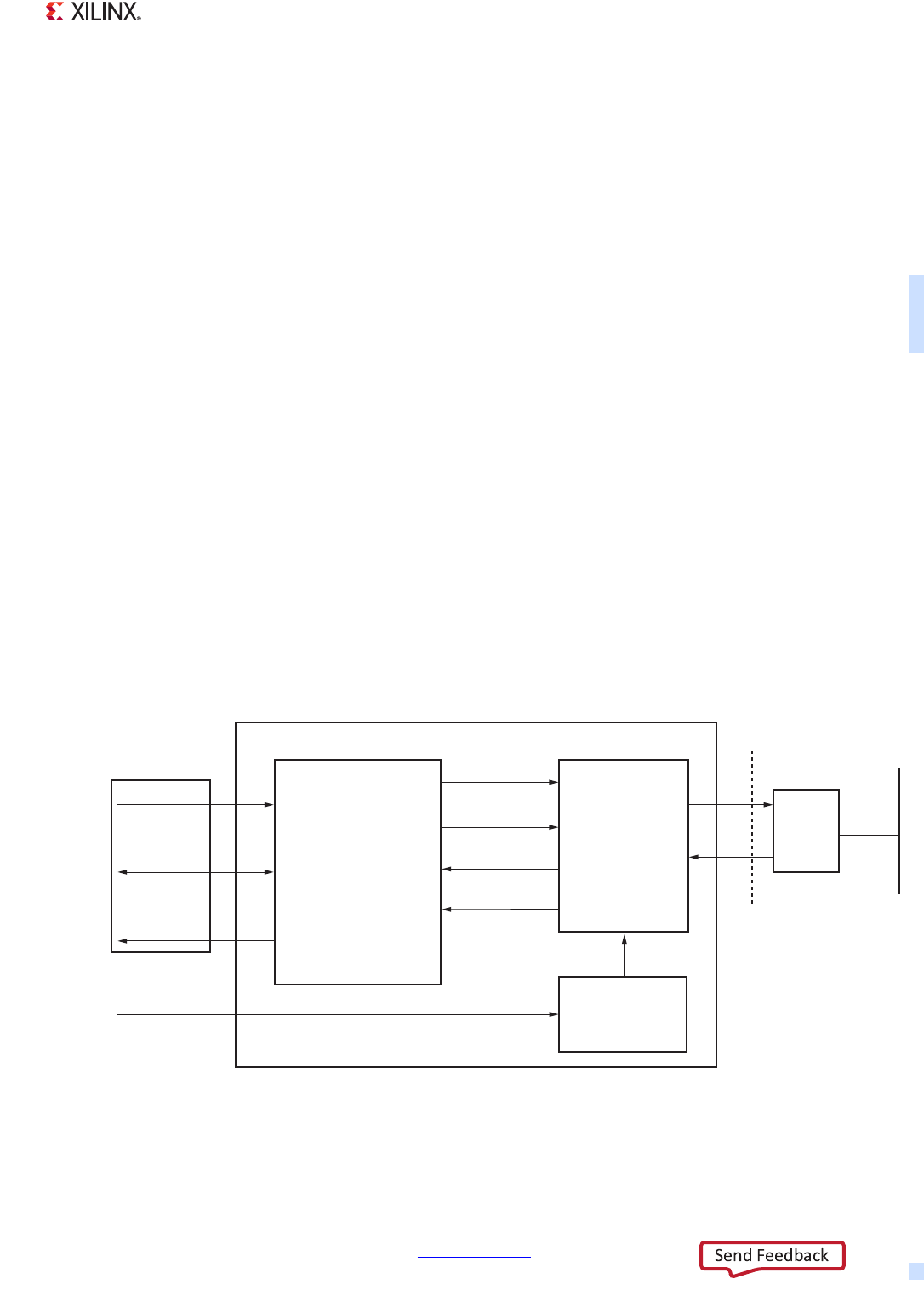
Zynq-7000 AP SoC Technical Reference Manual www.xilinx.com 579
UG585 (v1.12.1) December 6, 2017
Chapter 18: CAN Controller
Example: Program the AFMR and AFIR for Extended Frames
This example setups up the acceptance filter for extended frames. The Frame ID number is shown to
be 0x5DF, but could be set to desired value for the application.
1. Configure filter mask for extended frames. Write 0xFFFF_FFFF to the can.AFMR register:
a. Enable the substitute remote transmission request mask for frame, [AMSRR] = 1.
b. Compare all bits in the compare for the standard message ID, [AMIDH] = 0x7FF.
c. Enable the extended frame, [AMIDE] = 1.
d. Extended ID, [AMIDL] = 0x3FFFF
e. Remote transmission request bit for extended frame, [AMRTR] = 1.
2. Configure filter ID for extended frames. Write 0xABDF_9BDE to the can.AFIR register:
a. Standard ID, [AIIDH] = 0x55E.
b. Remote transmission request bit for standard frame, [AISRR] = 1.
c. Select standard/extended frame, [AIIDE] = 1.
d. Extended ID, [AIIDL] = 3CDEF.
e. Remote transmission request bit for extended frame, [AIRTR] = 0
18.2.6 Protocol Engine
The CAN protocol engine consists primarily of the bit timing logic (BTL) and the bitstream processor
(BSP) modules. Figure 18-5 shows a block diagram of the CAN protocol engine.
X-Ref Target - Figure 18-5
Figure 18-5: CAN Protocol Engine
Protocol Engine - Data Layer
UG585_c18_03_101012
Bit Timing
Logic
Bitstream
Processor
Reference Clock
TX Bit
PHY
TX
RX
CAN
BUS
Clock
Prescalar
Control
RX Bit
Buffer and Filter
TX Message
Control /
Status
RX Message
Sampling
Clock
Physical
Layer
Device
Boundary
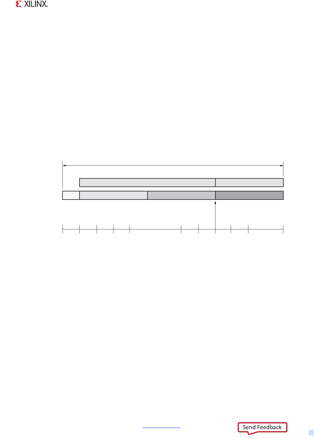
Zynq-7000 AP SoC Technical Reference Manual www.xilinx.com 580
UG585 (v1.12.1) December 6, 2017
Chapter 18: CAN Controller
Rx/Tx Bit Timing Logic
The primary functions of the bit timing logic (BTL) module include:
• Generate the Rx sampling clock for the bitstream processor (BSP)
• Synchronize the CAN controller to CAN traffic on the bus
• Sample the bus and extracting the data stream from the bus during reception
• Insert the transmit bit stream onto the bus during transmission
The nominal length of the bit time clock period is based on the CAN_REF_CLK clock frequency, the
baud rate generator divider (can.BRPR register) and the segment lengths (can.BTR register).
The bit timing logic module manages the re-synchronization function for CAN using the sync width
parameter in the can.BTR[SJW] bit field. The CAN bit timing is shown in Figure 18-6.
Sync Segment count always equals one time quanta period.
The TS 1 and TS 2 period counts are programmable using the can.BTR[TS1, TS2] bit fields. These
registers are written when the controller is in Configuration mode. The width of the propagation
segment (PROP_SEG) must be less than the actual propagation delay.
Time Quanta Clock
The time quanta clock (TQ_CLK) is derived from the controller reference clock (CAN_REF_CLK) divided
by the baud rate prescaler (BRP).
tTQ_CLK = tCAN_REF_CLK * (can.BRPR[BRP] + 1)
freqTQ_CLK = freqCAN_REF_CLK / (can.BRPR[BRP] + 1)
tSYNC_SEGMENT = 1 * tTQ_CLK
tTIME_SEGMENT1 = tTQ_CLK * (can.BTR[TS1] + 1)
tTIME_SEGMENT2 = tTQ_CLK * (can.BTR[TS2] + 1)
X-Ref Target - Figure 18-6
Figure 18-6: CAN Bit Time
......
Nominal Bit Time
Sync
Segment
Propagation
Segment
Phase
Segment 1
Phase
Segment 2
UG585_c18_04_073012
TS1 TS2
Sample
Point
Time Quanta
Clock (TQ_CLK)

Zynq-7000 AP SoC Technical Reference Manual www.xilinx.com 581
UG585 (v1.12.1) December 6, 2017
Chapter 18: CAN Controller
tBIT_RATE = tSYNC_SEGMENT + tTIME_SEGMENT1 + tTIME_SEGMENT2
freqBIT_RATE = freqCAN_REF_CLK / ((can.BRPR[BRP] + 1) * (3 + can.BTR[TS1] + can.BTR[TS2]))
TIP: A given bit-rate can be achieved with several bit-time configurations, but values should be
selected after careful consideration of oscillator tolerances and CAN propagation delays. For more
information on CAN bit-time register settings, refer to the CAN 2.0A, CAN 2.0B, and ISO 11898-1
specifications.
Bitstream Processor
The bitstream processor (BSP) module performs several functions while sending and receiving CAN
messages. The BSP obtains a message for transmission from either the TxFIFO or the TxHPB and
performs the following functions before passing the bitstream to the BTL.
• Serializing the message
• Inserting stuff bits, CRC bits, and other protocol defined fields during transmission
During transmission the BSP simultaneously monitors Rx data and performs bus arbitration tasks. It
then transmits the complete frame when arbitration is won, and retrying when arbitration is lost.
During reception the BSP removes stuff bits, CRC bits, and other protocol fields from the received
bitstream. The BSP state machine also analyses bus traffic during transmission and reception for
Form, CRC, ACK, Stuff, and Bit violations. The state machine then performs error signaling and error
confinement tasks. The CAN controller does not voluntarily generate overload frames but does
respond to overload flags detected on the bus.
This module determines the error state of the CAN controller: error active, error passive or bus-off.
When Tx or Rx errors are observed on the bus, the BSP updates the transmit and receive error
counters according to the rules defined in the CAN 2.0 A, CAN 2.0 B and ISO 11898-1 standards.
Based on the values of these counters, the error state of the CAN controller is updated by the BSP.
18.2.7 CAN0-to-CAN1 Connection
The I/O signals of the two CAN controllers in the PS can be connected together. In this mode, the RX
signal of one CAN controller is connected to the TX signal of the other controller. These connections
are enabled using the slcr.MIO_LOOPBACK [CAN0_LOOP_CAN1] bit.
Limitation
The CAN controller registers require single 32-bit read/write accesses, do not use byte, halfword, or
double word references.

Zynq-7000 AP SoC Technical Reference Manual www.xilinx.com 582
UG585 (v1.12.1) December 6, 2017
Chapter 18: CAN Controller
18.3 Programming Guide
18.3.1 Overview
The controller has several operating modes and different ways to receive and transmit messages. The
low-level functions were described in 18.2 Functional Description. The system-level operations are
described in section 18.4 System Functions.
All the controller registers are listed in Table 18-6 and are described in detail in Appendix B, Register
Details.
18.3.2 Configuration Mode State
The CAN controller enters configuration mode, irrespective of the operation mode, when any of
these actions are performed:
•Writing a 0 to the CEN bit in the SRR register.
•Writing a 1 to the SRST bit in the SRR register. The controller enters Configuration mode
immediately following the software reset.
•Driving a 1 on the Reset input controlled via SLCR. The controller continues to be in reset as
long as Reset is 1. The controller enters configuration mode after Reset is negated to 0.
In configuration mode the following apply:
• The CAN controller loses synchronization with the CAN bus and drives a constant recessive bit
on the bus line.
• The Error Count register (ECR) is reset.
• The Error Status register (ESR) is reset.
• The Bit Timing register (BTR) and Baud Rate Prescaler register (BRPR) can be modified.
• The CAN controller does not receive any new messages.
• The CAN controller does not transmit any messages. Messages in the TxFIFO and the TxHPB are
appended. These packets are sent when normal operation is resumed.
• Reads from the RxFIFO can be performed.
• Writes to the TxFIFO and TxHPB can be performed (provided the SNOOP bit is not set).
• Interrupt Status register bits ARBLST, TXOK, RXOK, RXOFLW, ERROR, BSOFF, SLP, and WKUP are
be cleared.
• Interrupt Status register bits RXNEMP and RXUFLW can be set due to read operations to the
RxFIFO.
• Interrupt Status register bits TXBFLL and TXFLL, and Status register bits TXBFLL and TXFLL can be
set due to write operations to the TX HPB and TX FIFO, respectively.
• Interrupts are generated if the corresponding bits in the Interrupt Enable register (IER) are 1.
• All Configuration registers are accessible.

Zynq-7000 AP SoC Technical Reference Manual www.xilinx.com 583
UG585 (v1.12.1) December 6, 2017
Chapter 18: CAN Controller
When in configuration mode, the CAN controller stays in this mode until the CEN bit in the SRR
register is set to 1. After the CEN bit is set to 1 the CAN controller waits for a sequence of 11
recessive bits before exiting configuration mode.
The CAN controller enters normal, loop back, snoop, or sleep modes from configuration mode,
depending on the LBACK, SNOOP, and SLEEP bits in the MSR register.
18.3.3 Start-up Controller
The controller can operate in Normal, Sleep, Snoop and Loop Back modes. Refer to Figure 18-3 for
supported transitions. On start-up the controller clocks and configuration bits are programmed.
Then the operating mode is selected and enabled.
Example: Start-up Sequence
1. Configure clocks. Refer to section 18.4.1 Clocks.
2. Configure Tx/Rx signals. Refer to section 18.5.1 MIO Programming.
3. Wait for configuration mode. Read can.SR[CONFIG] until it equals 1.
4. Reset the controller. The controller comes up in Configuration mode. Refer to section
18.4.2 Resets.
5. Program the bit sampling clock. Refer to section Rx/Tx Bit Timing Logic.
6. Program the interrupts, as needed. Refer to section 18.2.4 Interrupts.
7. Program the acceptance filters. Refer to section 18.2.5 Rx Message Filtering.
8. Select operating mode. Normal, Sleep, Snoop or LoopBack. Refer to section 18.3.4 Change
Operating Mode.
9. Enable the controller. Write a 1 to can.SRR[CEN].
18.3.4 Change Operating Mode
Example: Normal to Sleep Mode
Sleep mode is entered from Normal Mode when the following conditions are met:
1. Select Sleep Mode. Write 1 to can.MSR[SLEEP].
2. Wait for CAN bus to go idle.
3. Wait for all TxFIFO and TxHPB messages to be transmitted.
Note: In normal mode, can.MSR[LBACK] = 0 and can.SSR[CEN] = 1. Also, can.MSR[SNOOP] = don't
care.
Example: Configuration to Sleep Mode
Sleep mode is entered from Configuration Mode when the following conditions are met:
1. Select Sleep Mode. Write 1 to can.MSR[SLEEP] and write 0 to can.MSR[LBACK].

Zynq-7000 AP SoC Technical Reference Manual www.xilinx.com 584
UG585 (v1.12.1) December 6, 2017
Chapter 18: CAN Controller
2. Enable the controller. Write 1 to can.SSR[CEN].
3. Wait for TxFIFO or TxHPB to empty.
Note: In configuration mode, can.MSR[SNOOP] = don't care.
Sleep mode is exited when I/O bus activity is detected or when software writes a message to either
the TxFIFO or the TxHPB. When the controller exits sleep mode, can.MSR[SLEEP] is set to 0 by the
hardware and an interrupt can be generated.
18.3.5 Write Messages to TxFIFO
With either option, can.SR[TXFLL] can be polled before writing a message.
All messages written to the TxFIFO should follow the format defined in Message Structure.
Example: Write Message to TxFIFO Using Polling Method
1. Poll the TxFIFO status. Read can.SR[TXFLL] for 0 and can.SR[TXFEMP] for 1 and then message
can be written into the TxFIFO.
2. Write message to TxFIFO. Write to all four data registers (can.TXFIFO_ID, can.TXFIFO_DLC,
can.TXFIFO_DATA1, and can.TXFIFO_DATA2).
Example: Write Message to TxFIFO Using Interrupt Method
In interrupt mode, writes can continue until can.ISR[TXFLL] generates an interrupt.
Messages can be continuously written to the TxFIFO until the TxFIFO is full. When the TxFIFO is full
the can.ISR[TXFLL] and can.SR[TXFLL] are set to 1. When the TxFIFO is empty, can.ISR[TXFEMP] is set
to 1.
18.3.6 Write Messages to TxHPB
All messages written to the TxHPB use the polling method. The format should follow section
18.2.2 Message Format.
Example: Write Message to TxHPB
1. Poll the TxHPB status. Read can.SR[TXBFLL] until it equals 0 and then write the message into the
TxHPB.
2. Write message to TxHPB. Write to all four data registers (can.TXHPB_ID, can.TXHPB_DLC,
can.TXHPB_DATA1, and can.TXHPB_DATA2).
18.3.7 Read Messages from RxFIFO
Whenever a new message is received and put into the RxFIFO, the can.ISR[RXNEMP] and
can.ISR[RXOK] bits are set to 1. If the RxFIFO is empty when the message is read, then the
can.ISR[RXUFLW] is also set to 1.

Zynq-7000 AP SoC Technical Reference Manual www.xilinx.com 585
UG585 (v1.12.1) December 6, 2017
Chapter 18: CAN Controller
Example: Read Message from RxFIFO Using Polling Method
1. Poll the RxFIFO status. Read can.ISR[RXOK] or can.ISR[RXNEMP] register until a message is
received. Proceed to step 2 when a bit is set.
2. Read message from the RxFIFO. Read all four of the registers (can.RXFIFO_ID, can.RXFIFO_DLC,
can.RXFIFO_DATA1, can.RXFIFO_DATA2).
3. Determine if more messages are in the RxFIFO. Read can.ISR[RXNEMP].
Example: Read Message from RxFIFO Using Interrupt Method
The can.ISR[RXOK] and/or can.ISR[RXNEMP] bit fields can generate the interrupt.
1. Program RxFIFO watermark level interrupt. Write to can.WIR[FW] to set watermark
can.ISR[RXFWMFLL] interrupt.
2. Proceed to step 3 when an interrupt is received.
3. Wait until a message is received. Read can.ISR[RXOK] or can.ISR[RXFWMFLL].
4. Read message from the RxFIFO. Read all four of the registers (can.RXFIFO_ID, can.RXFIFO_DLC,
can.RXFIFO_DATA1, can.RXFIFO_DATA2).
5. Determine if RxFIFO is not empty. Read can.ISR[RXNEMP].
6. Repeat until the RxFIFO is empty.
7. Clear the interrupt.
18.3.8 Register Overview
The control and status registers are listed in see Tabl e 18 - 6. Each of these registers is 32-bits wide.
Any read operations to reserved bits or bits that are not used return 0. A 0 should be written to
reserved bits and bit fields not used. Writes to reserved locations are ignored.
Table 18-6: CAN Register Overview
Function
Register Names
(CAN registers, except
where noted)
Overview
Configuration and Control SRR
MSR
BRPR
BTR
ECR
TCR
Enable/disable and reset the controller.
Setup baud rate and timing.
Clear timestamp counter.
Interrupt Processing ISR
IER
ICR
WIR
Enable/disable the interrupt detection,
mark interrupt sent to the interrupt
controller, read raw interrupt status.
Status ECR
ESR
SR
Inform about the status of the controller.

Zynq-7000 AP SoC Technical Reference Manual www.xilinx.com 586
UG585 (v1.12.1) December 6, 2017
Chapter 18: CAN Controller
18.4 System Functions
18.4.1 Clocks
The controller and I/O interface are driven by the reference clock (CANx_REF_CLK). The controller's
interconnect also requires an APB interface clock. The APB interconnect clock (CPU_1x) always comes
from the PS clock subsystem.
The reference clock normally comes from the PS clock subsystem, but it can alternatively be driven
by an external clock source via any available MIO pin. The reference clock is used by the protocol
engine, the baud rate generator, and the datapath. The controllers share the same reference clock
frequency from the PS clock subsystem. If the reference clock is from an MIO pin, then the
frequencies can be different.
CPU_1x Clock
Refer to Chapter 25, Clocks, for general clock programming information. The CPU_1x clock runs
asynchronous to the CAN reference clock.
Transmit FIFO TXFIFO_ID
TXFIFO_DLC
TXFIFO_DATA1
TXFIFO_DATA2
Write message to be transmitted.
Transmit High Priority Buffer TXHPB_ID
TXHPB_DLC
TXHPB_DATA1
TXHPB_DATA2
Store one high priority transmit message.
Receive FIFO RXFIFO_ID
RXFIFO_DLC
RXFIFO_DATA1
RXFIFO_DATA2
Read received message.
Acceptance Filter AFR
AFMR[4:1]
AFIR[4:1]
Configure and control the four acceptance
filters.
System level slcr.CAN_CLK_CTRL
slcr.CAN_MIOCLK_CTRL
slcr.CAN_RST_CTRL
A controller reset and clock control.
Table 18-6: CAN Register Overview (Cont’d)
Function
Register Names
(CAN registers, except
where noted)
Overview

Zynq-7000 AP SoC Technical Reference Manual www.xilinx.com 587
UG585 (v1.12.1) December 6, 2017
Chapter 18: CAN Controller
Reference Clock
CAN_REF_CLK is normally sourced from the PS clock subsystem, but it can alternatively be driven by
an external clock source via an MIO pin. Internally, the PS has three PLLs and two clock divider pairs.
The clock source choice, PS clock subsystem or external MIO pin, is controlled by the
CAN_MIOCLK_CTRL register.
The CAN clocks in the PS are controlled by slcr.CAN_CLK_CTRL. The generation of the CAN reference
clock by the PS is described in section The Quad-SPI clock is divided down by at least two using the
Quad-SPI baud rate divider, see section 12.4.1 Clocks. In master mode, the SPI clock is divided down
by at least four using the SPI baud rate divider, see section 17.4.2 Clocks.. There is one clock
generator in the PS for both CAN controllers. If an MIO pins is used instead, the selected MIO_PIN
Mux register is programmed as an input.
Example: Configure and Route Internal Clock for Reference Clock
Configure the clock and disable MIO path. Assume the PLL is operating at 1000 MHz and the
required CAN reference clock is 24 MHz (23.8095 MHz).
1. Program the clock subsystem. Write 0x0030_0E03 to the slcr.CAN_CLK_CTRL register:
a. Enable both CAN reference clocks.
b. Divide the I/O PLL clock by 42 (0x02A): DIVISOR0= 0x0E and DIVISOR1=0x03 used by both
controllers.
2. Disable the MIO path. Write 0x0000_0000 to the slcr.CAN_MIOCLK_CTRL register to select the
clock from the internal clock subsystem/PLL for both controllers.
Example: Source Controller Clock from MIO Pin
This example uses MIO pin 45 as a controller clock reference.
1. Configure MIO device pin. Write 0x0000_1200 to the slcr.MIO_PIN_45 register:
a. Route MIO pin 45 to the GPIO controller (this is overridden in the next step).
b. Disable the output driver (TRI_ENABLE = 1).
c. LVCMOS18 (refer to the register definition for other voltage options).
d. Slow CMOS edge (benign setting).
e. Enable internal pull-up resistor.
f. Disable HSTL receiver.
2. Enable MIO path. Write to the slcr.CAN_MIOCLK_CTRL register to override the MIO PIN register
setting that was written in the previous step.
Write a 1 to slcr.CAN_MIOCLK_CTRL[CANx__REF_SEL] and write the desired MIO pin number into
the slcr.CAN_MIOCLK_CTRL[CANx_MUX] bit field to match the pin in the previous step.
18.4.2 Resets
The effects for each reset type are summarized in Table 18-7.

Zynq-7000 AP SoC Technical Reference Manual www.xilinx.com 588
UG585 (v1.12.1) December 6, 2017
Chapter 18: CAN Controller
Example: Reset using Local CAN Reset
1. Write to the Local CAN reset register. Write a 1 to can.SRR[SRST] bit field. This bit is
self-clearing.
Example: Reset using Reset Subsystem
1. Write to the slcr reset register for CAN. Write a 1 then a 0 to the
slcr.CAN_RST_CTRL[CANx_CPU1X_RST] bit field.
18.5 I/O Interface
18.5.1 MIO Programming
Each set of controller Rx/Tx signals is connected to either MIO pins or the EMIO interface, refer to
Table 18-8, page 589. The general routing concepts and MIO I/O buffer configurations are explained
in section 2.4 PS–PL Voltage Level Shifter Enables. The MIO routing to use an external reference
clock (CAN_REF_CLK) is described in section 18.4.1 Clocks.
Example: Configure Rx/Tx Signals to MIO Pins
1. Configure MIO pin 46 for the Rx signal. Write 0x0000_1221 to the slcr.MIO_PIN_46 register:
a. Route CAN0 Rx signal to pin 46.
b. Output disabled (set TRI_ENABLE = 1).
c. LVCMOS18 (refer to the register definition for other voltage options).
d. Slow CMOS edge (benign setting).
e. Enable internal pull-up resistor.
f. Diable HSTL receiver.
2. Configure MIO pin 47 for the Tx signal. Write 0x0000_1220 to the slcr.MIO_PIN_47 register:
a. Route CAN0 Tx signal to pin 47.
b. 3-state controlled by CAN (TRI_ENABLE = 0).
c. LVCMOS18 (refer to the register definition for other voltage options).
d. Slow CMOS drive edge.
Table 18-7: CAN Reset Effects
Name APB
Interface
Rx and Tx
FIFOs
Protocol
Engine
Control and
Status
Registers
Acceptance Filters
(ID and Mask)
Local CAN Reset
can.SRR[SRST] Yes Yes Yes Yes No
PS Reset Subsystem
slcr.CAN_RST_CTRL[CANx_CPU1X_RST] Yes Yes Yes Yes No
Zynq-7000 AP SoC Technical Reference Manual www.xilinx.com 589
UG585 (v1.12.1) December 6, 2017
Chapter 18: CAN Controller
e. Enable internal pull-up resistor.
f. Disable HSTL receiver.
18.5.2 MIO-EMIO Signals
The CAN I/O Signals are identified in Ta ble 18 -8 . Refer to section 2.4 PS–PL Voltage Level Shifter
Enables for routing details. The MIO pins and any restrictions based on device versions are shown in
the MIO table in section 2.5.4 MIO-at-a-Glance Table.
Table 18-8: CAN MIO Pins and EMIO Signals
CAN
Interface
Default
Controller
Input Value
MIO Pins EMIO Signals
Numbers I/O Name I/O
CAN 0 Rx 010, 14, 18, 22, 26, 30, 34, 38, 42, 46, 50 I EMIOCAN0PHYRX I
CAN 0 Tx ~ 11, 15, 19, 23, 27, 31, 35, 39, 43, 47, 51 O EMIOCAN0PHYTX O
CAN 0 CLK ~ Any MIO pin I ~ ~
CAN 1 Rx 09, 13, 17, 21, 25, 29, 33, 37, 41, 45, 49, 53 I EMIOCAN1PHYRX I
CAN 1 Tx ~ 8, 12, 16, 20, 24, 28, 32, 36, 40, 44, 48, 52 O EMIOCAN1PHYTX O
CAN 1 CLK ~ Any MIO pin I ~ ~

Zynq-7000 AP SoC Technical Reference Manual www.xilinx.com 590
UG585 (v1.12.1) December 6, 2017
Chapter 19
UART Controller
19.1 Introduction
The UART controller is a full-duplex asynchronous receiver and transmitter that supports a wide
range of programmable baud rates and I/O signal formats. The controller can accommodate
automatic parity generation and multi-master detection mode.
The UART operations are controlled by the configuration and mode registers. The state of the FIFOs,
modem signals and other controller functions are read using the status, interrupt status and modem
status registers.
The controller is structured with separate Rx and Tx data paths. Each path includes a 64-byte FIFO.
The controller serializes and de-serializes data in the Tx and Rx FIFOs and includes a mode switch to
support various loopback configurations for the RxD and TxD signals. The FIFO interrupt status bits
support a polling or interrupt driven handler. Software reads and writes data bytes using the Rx and
Tx data port registers.
When the UART is being used in a modem-like application, the modem control module detects and
generates the modem handshake signals and also controls the receiver and transmitter paths
according to the handshaking protocol.
19.1.1 Features
Each UART controller (UART 0 and UART 1) has the following features:
• Programmable baud rate generator
• 64-byte receive and transmit FIFOs
• Programmable protocol:
°6, 7, or 8 data bits
°1, 1.5, or 2 stop bits
°Odd, even, space, mark, or no parity
• Parity, framing and overrun error detection
• Line-break generation
• Interrupts generation
• RxD and TxD modes: Normal/echo and diagnostic loopbacks using the mode switch
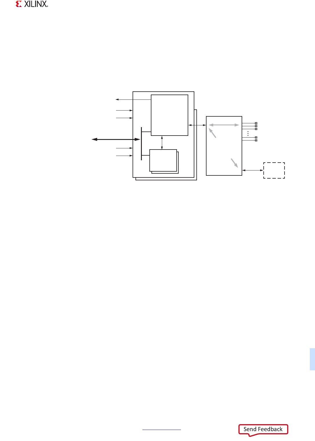
Zynq-7000 AP SoC Technical Reference Manual www.xilinx.com 591
UG585 (v1.12.1) December 6, 2017
Chapter 19: UART Controller
• Loop UART 0 with UART 1 option
• Modem control signals: CTS, RTS, DSR, DTR, RI and DCD are available only on the EMIO interface
19.1.2 System Viewpoint
The system viewpoint diagram for the UART controllers is shown in Figure 19-1.
The slcr register set (refer to section 4.3 SLCR Registers) includes control bits for the UART clocks,
resets and MIO-EMIO signal mapping. Software accesses the UART controller registers using the APB
32-bit slave interface attached to the PS AXI interconnect. The IRQ from each controller is connected
to the PS interrupt controller and routed to the PL.
19.1.3 Notices
Reference Clock Operating Restrictions
There is a single PS clock generator for both UART controllers. The reference clocks (UART_Ref_Clk)
going to the baud rate generator of each UART controller are of the same clock frequency, but are
individually enabled, refer to section 25.6.3 SDIO, SMC, SPI, Quad-SPI and UART Clocks. The
controllers are always clocked by the internal, PS clock generator.
Note: There are no frequency restrictions in the relationship between the CPU_1x and UART_Ref_clk
clocks.
7z007s and 7z010 CLG225 Devices
The 7z007s single core and 7z010 dual core CLG225 devices support 32 MIO pins as shown in the
MIO-at-a-Glance Table, page 52. This restricts the availability of the UART signals on the MIO pins. If
needed, the TxD and RxD UART signals can be routed through the EMIO interface and
passed-through to the PL pins. All of the CLG225 device restrictions are listed in section
1.1.3 Notices.
X-Ref Target - Figure 19-1
Figure 19-1: UART System Viewpoint
PL
MIO – EMIO
Routing
PS Slave
Interconnect
APB
MIO
Pins
UG585_c19_01_010112
EMIO
Signals
UART REF_CLK
IRQ ID# {59, 82}
UART REF_RST
Control
And Status
Registers
Slave
ports
Tx, Rx
Tx, Rx, CTSN,
DCDN, DSRN,
RIN, DTRN,
RTSN
CPU_1x clock
UART{0, 1} CPU1X_RST
UART
Interface
Controller
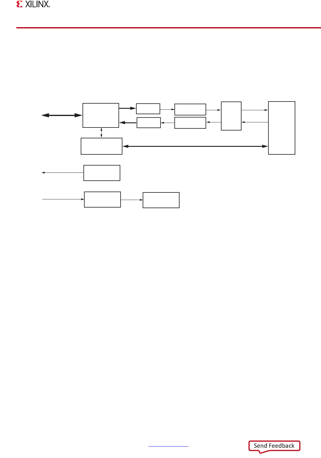
Zynq-7000 AP SoC Technical Reference Manual www.xilinx.com 592
UG585 (v1.12.1) December 6, 2017
Chapter 19: UART Controller
19.2 Functional Description
19.2.1 Block Diagram
The block diagram for the UART module is shown in Figure 19-2
19.2.2 Control Logic
The control logic contains the Control register and the Mode register, which are used to select the
various operating modes of the UART.
The Control register enables, disables, and issues soft resets to the receiver and transmitter modules.
In addition, it restarts the receiver timeout period, and controls the transmitter break logic.
Receive line break detection must be implemented in Software. It will be indicated by a Frame Error
followed by one or more zero bytes in the RxFIFO.
The Mode register selects the clock used by the baud rate generator. It also selects the bit length,
parity bit and stop bit to be used by transmitted and received data. In addition, it selects the mode
of operation of the UART, switching between normal UART mode, automatic echo, local loopback, or
remote loopback, as required.
19.2.3 Baud Rate Generator
The baud rate generator furnishes the bit period clock, or baud rate clock, for both the receiver and
the transmitter. The baud rate clock is implemented by distributing the base clock uart_clk and a
single cycle clock enable to achieve the effect of clocking at the appropriate frequency division. The
effective logic for the baud rate generation is shown in Figure 19-3.
X-Ref Target - Figure 19-2
Figure 19-2: UART Block Diagram
Interrupt
Controller (GIC)
TxFIFO Transmitter
MIO/EMIO
Mode
Switch
UG585_c19_02_020613
Baud Rate
Generator
PS AXI
Interconnect APB
Slave
Interface
Control and
Status Registers
RxFIFO
Interrupts
Receiver
EMIO
UART TxD
UART RxD
CTS, RTS, DSR, DCD, RI, DTR
UART Ref Clock Optional
Divide by 8
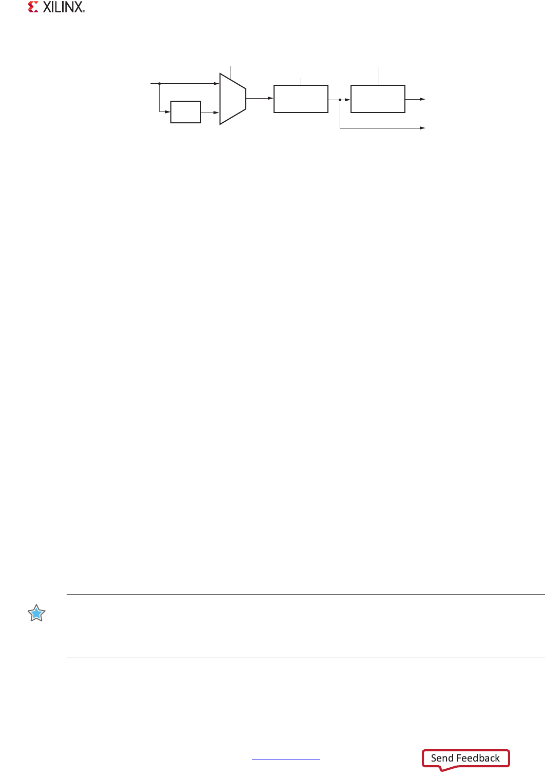
Zynq-7000 AP SoC Technical Reference Manual www.xilinx.com 593
UG585 (v1.12.1) December 6, 2017
Chapter 19: UART Controller
The baud rate generator can use either the master clock signal, uart_ref_clk, or the master clock
divided by eight, uart_ref_clk/8. The clock signal used is selected according to the value of the CLKS
bit in the Mode register (uart.mode_reg0). The resulting selected clock is termed sel_clk in the
following description.
The sel_clk clock is divided down to generate three other clocks: baud_sample, baud_tx_rate, and
baud_rx_rate. The baud_tx_rate is the target baud rate used for transmitting data. The baud_rx_rate
is nominally at the same rate, but gets resynchronised to the incoming received data. The
baud_sample runs at a multiple ([BDIV] + 1) of baud_rx_rate and baud_tx_rate and is used to
over-sample the received data.
The sel_clk clock frequency is divided by the CD field value in the Baud Rate Generator register to
generate the baud_sample clock enable. This register can be programmed with a value between 1
and 65535.
The baud_sample clock is divided by [BDIV] plus 1. BDIV is a programmable field in the Baud Rate
Divider register and can be programmed with a value between 4 and 255. It has a reset value of 15,
inferring a default ratio of 16 baud_sample clocks per baud_tx_clock / baud_rx_rate.
Thus the frequency of the baud_sample clock enable is shown in Equation 19-1.
Equation 19-1
The frequency of the baud_rx_rate and baud_tx_rate clock enables is show in Equation 19-2.
Equation 19-2
IMPORTANT: It is essential to disable the transmitter and receiver before writing to the Baud Rate
Generator register (uart.Baud_rate_gen_reg0), or the baud rate divider register
(uart.Baud_rate_divider_reg0). A soft reset must be issued to both the transmitter and receiver before
they are re-enabled.
Some examples of the relationship between the uart_ref_clk clock, baud rate, clock divisors (CD and
BDIV), and the rate of error are shown in Table 19-1. The highlighted entry shows the default reset
X-Ref Target - Figure 19-3
Figure 19-3: UART Board Rate Generator
uart.mode_reg0[0]
Divide
by 8
CD
Programmable
Divider
sel_clk
UART Ref clock
Rx and Tx
Baud rate
UG585_c19_03_071912
0
1
Sel
Clk
uart.Baud_rate_gen_reg0[15:0]
BDIV
Programmable
Divider
uart.Baud_rate_divider_reg0[7:0]
Baud
Sample
baud_sample sel_clk
CD
---------------
=
baud_rate sel_clk
CD BDIV 1+()×
------------------------------------
=

Zynq-7000 AP SoC Technical Reference Manual www.xilinx.com 594
UG585 (v1.12.1) December 6, 2017
Chapter 19: UART Controller
values for CD and BDIV. For these examples, a system clock rate of UART_Ref_Clk = 50 MHz and
Uart_ref_clk/8 = 6.25 MHz is assumed. The frequency of the UART reference clock can be changed to
get a more accurate Baud rate frequency, refer to Chapter 25, Clocks for details to program the
UART_Ref_Clk.
19.2.4 Transmit FIFO
The transmit FIFO (TxFIFO) stores data written from the APB interface until it is removed by the
transmit module and loaded into its shift register. The TxFIFO’s maximum data width is eight bits.
Data is loaded into the TxFIFO by writing to the TxFIFO register.
When data is loaded into the TxFIFO, the TxFIFO empty flag is cleared and remains in this Low state
until the last word in the TxFIFO has been removed and loaded into the transmitter shift register. This
means that host software has another full serial word time until the next data is needed, allowing it
to react to the empty flag being set and write another word in the TxFIFO without loss in transmission
time.
The TxFIFO full interrupt status (TFULL) indicates that the TxFIFO is completely full and prevents any
further data from being loaded into the TxFIFO. If another APB write to the TxFIFO is performed, an
overflow is triggered and the write data is not loaded into the TxFIFO. The transmit FIFO nearly full
flag (TNFULL) indicates that there is not enough free space in the FIFO for one more write of the
programmed size, as controlled by the WSIZE bits of the Mode register.
The TxFIFO nearly-full flag (TNFULL) indicates that there is only byte free in the TxFIFO.
A threshold trigger (TTRIG) can be setup on the TxFIFO fill level. The Transmitter Trigger register can
be used to setup this value, such that the trigger is set when the TxFIFO fill level reaches this
programmed value.
19.2.5 Transmitter Data Stream
The transmit module removes parallel data from the TxFIFO and loads it into the transmitter shift
register so that it can be serialized.
Table 19-1: UART Parameter Value Examples
Clock Baud
Rate
Calculated
CD
Actual
CD BDIV Actual
Baud Rate
Error
(BPS) % Error
UART Ref clock 600 10416.667 10417 7 599.980 0.020 -0.003
UART Ref clock /8 9,600 81.380 81 7 9,645.061 45.061 0.469
UART Ref clock 9,600 651.041 651 7 9,600.614 0.614 0.006
UART Ref clock 28,800 347.222 347 4 28,818.44 18.44 0.064
UART Ref clock 115,200 62.004 62 6 115,207.37 7.373 0.0064
UART Ref clock 230,400 31.002 31 6 230,414.75 14.75 0.006
UART Ref clock 460,800 27.127 9 11 462,962.96 2,162.96 0.469
UART Ref clock 921,600 9.042 9 5 925,925.92 4,325.93 0.469

Zynq-7000 AP SoC Technical Reference Manual www.xilinx.com 595
UG585 (v1.12.1) December 6, 2017
Chapter 19: UART Controller
The transmit module shifts out the start bit, data bits, parity bit, and stop bits as a serial data stream.
Data is transmitted, least significant bit first, on the falling edge of the transmit baud clock enable
(baud_tx_rate). A typical transmitted data stream is illustrated in Figure 19-4.
The uart.mode_reg0[CHRL] register bit selects the character length, in terms of the number of data
bits. The uart.mode_reg0[NBSTOP] register bit selects the number of stop bits to transmit.
19.2.6 Receiver FIFO
The RxFIFO stores data that is received by the receiver serial shift register. The RxFIFO’s maximum
data width is eight bits.
When data is loaded into the RxFIFO, the RxFIFO empty flag is cleared and this state remains Low
until all data in the RxFIFO has been transferred through the APB interface. Reading from an empty
RxFIFO returns zero.
The RxFIFO full status (Chnl_int_sts_reg0 [RFUL] and Channel_sts_reg0 [RFUL] bits) indicates that the
RxFIFO is full and prevents any further data from being loaded into the RxFIFO. When a space
becomes available in the RxFIFO, any character stored in the receiver will be loaded.
A threshold trigger (RTRIG) can be setup on the RxFIFO fill level. The Receiver Trigger Level register
(Rcvr_FIFO_trigger_level0) can be used to setup this value, such that the trigger is set when the
RxFIFO fill level transitions this programmed value. The Range is 1 to 63.
19.2.7 Receiver Data Capture
The UART continuously over-samples the UARTx_RxD signal using UARTx REF_CLK and the clock
enable (baud_sample). When the samples detect a transition to a Low level, it can indicate the
beginning of a start bit. When the UART senses a Low level at the UART_RxD input, it waits for a count
of half of BDIV baud rate clock cycles, and then samples three more times. If all three bits still
indicate a Low level, the receiver considers this to be a valid start bit, as illustrated in Figure 19-5 for
the default BDIV of 15.
X-Ref Target - Figure 19-4
Figure 19-4: Transmitted Data Stream
baud_tx_rate
TXD D0 D1 D2 D3 D4 D5 D6 D7 PA S
UG585_c19_04_020613
START STOP
X-Ref Target - Figure 19-5
Figure 19-5: Default BDIV Receiver Data Stream
baud_sample
rxd
12345678
Start Bit
9 10111213141516 1 2
Data (LSB)
UG585_c19_05_022612
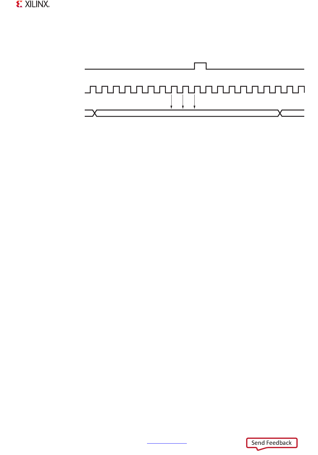
Zynq-7000 AP SoC Technical Reference Manual www.xilinx.com 596
UG585 (v1.12.1) December 6, 2017
Chapter 19: UART Controller
When a valid start bit is identified, the receiver baud rate clock enable (baud_rx_rate) is
re-synchronised so that further sampling of the incoming UART RxD signal occurs around the
theoretical mid-point of each bit, as illustrated in Figure 19-6.
When the re-synchronised baud_rx_rate is High, the last three sampled bits are compared. The logic
value is determined by majority voting; two samples having the same value define the value of the
data bit. When the value of a serial data bit has been determined, it is shifted to the receive shift
register. When a complete character has been assembled, the contents of the register are then
pushed to the RxFIFO.
Receiver Parity Error
Each time a character is received, the receiver calculates the parity of the received data bits in
accordance with the uart.mode_reg0 [PAR] bit field. It then compares the result with the received
parity bit. If a difference is detected, the parity error bit is set = 1, uart.Chnl_int_sts_reg0 [PARE]. An
interrupt is generated, if enabled.
Receiver Framing Error
When the receiver fails to receive a valid stop bit at the end of a frame, the frame error bit is set =1,
uart.Chnl_int_sts_reg0 [FRAME]. An interrupt is generated, if enabled.
Receiver Overflow Error
When a character is received, the controller checks to see if the RxFIFO has room. If it does, then the
character is written into the RxFIFO. If the RxFIFO is full, then the controller waits. If a subsequent
start bit on RxD is detected and the RxFIFO is still full, then data is lost and the controller sets the Rx
overflow interrupt bit, uart.Chnl_int_sts_reg0 [ROVR] = 1. An interrupt is generated, if enabled.
Receiver Timeout Mechanism
The receiver timeout mechanism enables the receiver to detect an inactive RxD signal (a persistent
High level). The timeout period is programmed by writing to the uart.Rcvr_timeout_reg0 [RTO] bit
field. The timeout mechanism uses a 10-bit decrementing counter. The counter is reloaded and starts
counting down whenever a new start bit is received on the RxD signal, or whenever software writes
a 1 to uart.Control_reg0 [RSTTO] (regardless of the previous [RSTTO] value).
X-Ref Target - Figure 19-6
Figure 19-6: Re-synchronized Receiver Data Stream
baud_sample
baud_rx_rate
rxd
12345678
Data Bit
9 10111213141516 1 2
UG585_c19_06_022612

Zynq-7000 AP SoC Technical Reference Manual www.xilinx.com 597
UG585 (v1.12.1) December 6, 2017
Chapter 19: UART Controller
If no start bit or reset timeout occurs for 1,023 bit periods, a timeout occurs. The Receiver timeout
error bit [TIMEOUT] will be set in the interrupt status register, and the [RSTTO] bit in the Control
register should be written with a 1 to restart the timeout counter, which loads the newly
programmed timeout value.
The upper 8 bits of the counter are reloaded from the value in the [RTO] bit field and the lower 2 bits
are initialized to zero. The counter is clocked by the UART bit clock. As an example, if [RTO] = 0xFF,
then the timeout period is 1,023 bit clocks (256 x 4 minus 1). If 0 is written into the [RTO] bit, the
timeout mechanism is disabled.
When the decrementing counter reaches 0, the receiver timeout occurs and the controller sets the
timeout interrupt status bit uart.Chnl_int_sts_reg0 [TIMEOUT] = 1. If the interrupt is enabled
(uart.Intrpt_mask_reg0 [TIMEOUT] = 1), then the IRQ signal to the PS interrupt controller is asserted.
Whenever the timeout interrupt occurs, it is cleared with a write back of 1 to the Chnl_int_sts_reg0
[TIMEOUT] bit. Software must set uart.Control_reg0 [RSTTO] = 1 to generate further receive timeout
interrupts.
19.2.8 I/O Mode Switch
The mode switch controls the routing of the RxD and TxD signals within the controller as shown in
Figure 19-7. The loopback using the mode switch occurs regardless of the MIO-EMIO routing of the
UARTx TxD/RxD I/O signals. There are four operating modes as shown in Figure 19-7. The mode is
controlled by the uart.mode_reg0 [CHMODE] register bit field: normal, automatic echo, local
loopback and remote loopback.
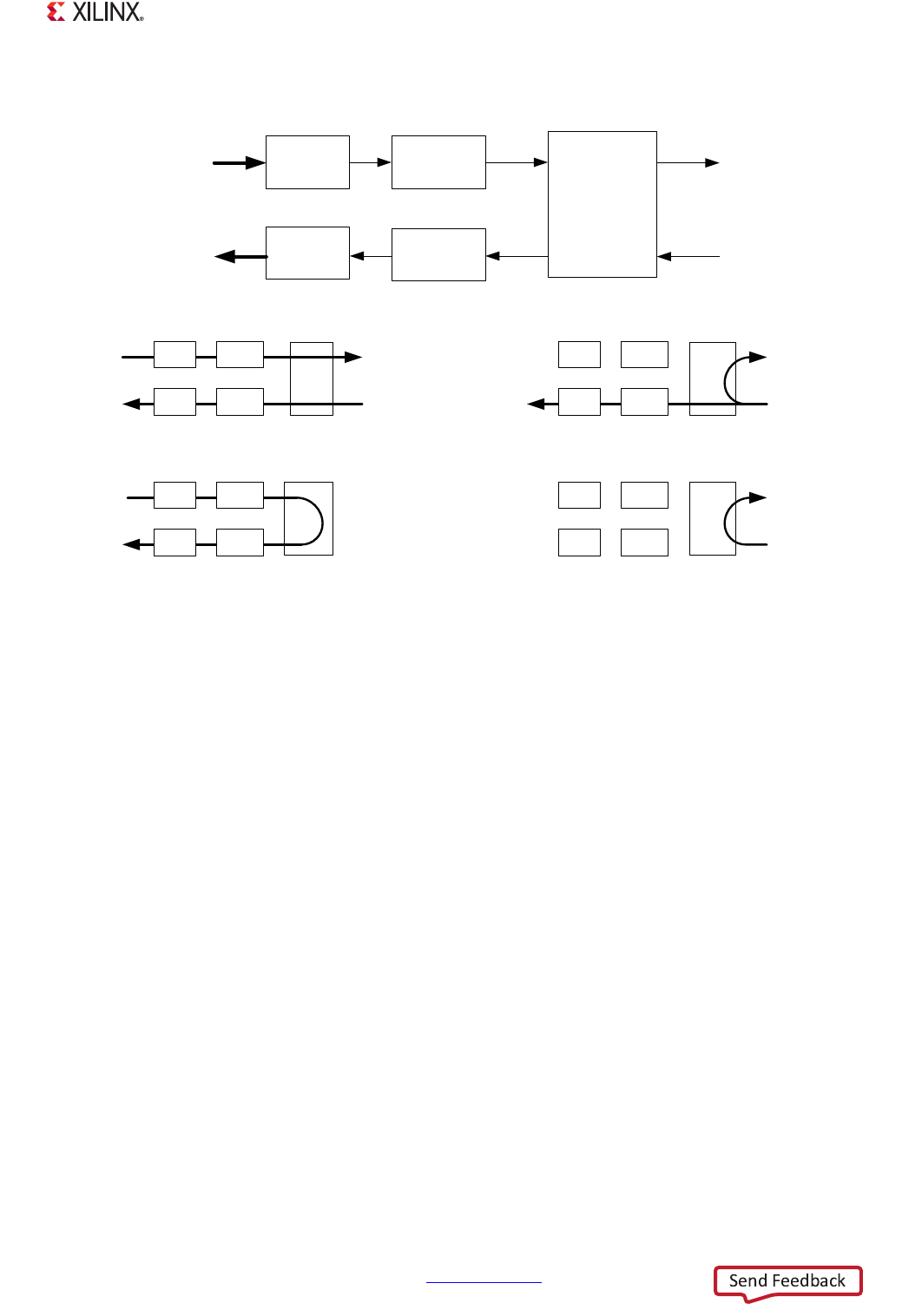
Zynq-7000 AP SoC Technical Reference Manual www.xilinx.com 598
UG585 (v1.12.1) December 6, 2017
Chapter 19: UART Controller
Normal Mode
Normal mode is used for standard UART operations.
Automatic Echo Mode
Echo mode receives data on RxD and the mode switch routes the data to both the receiver and the
TxD pin. Data from the transmitter cannot be sent out from the controller.
Local Loopback Mode
Local loopback mode does not connect to the RxD or TxD pins. Instead, the transmitted data is
looped back around to the receiver.
Remote Loopback Mode
Remote loopback mode connects the RxD signal to the TxD signal. In this mode, the controller
cannot send anything on TxD and the controller does not receive anything on RxD.
X-Ref Target - Figure 19-7
Figure 19-7: UART Mode Switch for TxD and RxD
UG585_c19_13_100512
Mode
Switch
Mode
Switch
Mode
Switch
Transmit
Mode
Switch
UARTx TxD
Receive
TxFIFO
RxFIFO UARTx RxD
UARTx TxD
UARTx RxD
Transmit
Receive
TxFIFO
RxFIFO
UARTx TxD
UARTx RxD
Transmit
Receive
TxFIFO
RxFIFO
Transmit
Receive
TxFIFO
RxFIFO
Transmit
Receive
TxFIFO
RxFIFO
Normal Mode
Local Loopback Mode
Mode
Switch
Remote Loopback Mode
UARTx TxD
UARTx RxD
UARTx TxD
UARTx RxD
Automatic Echo Mode
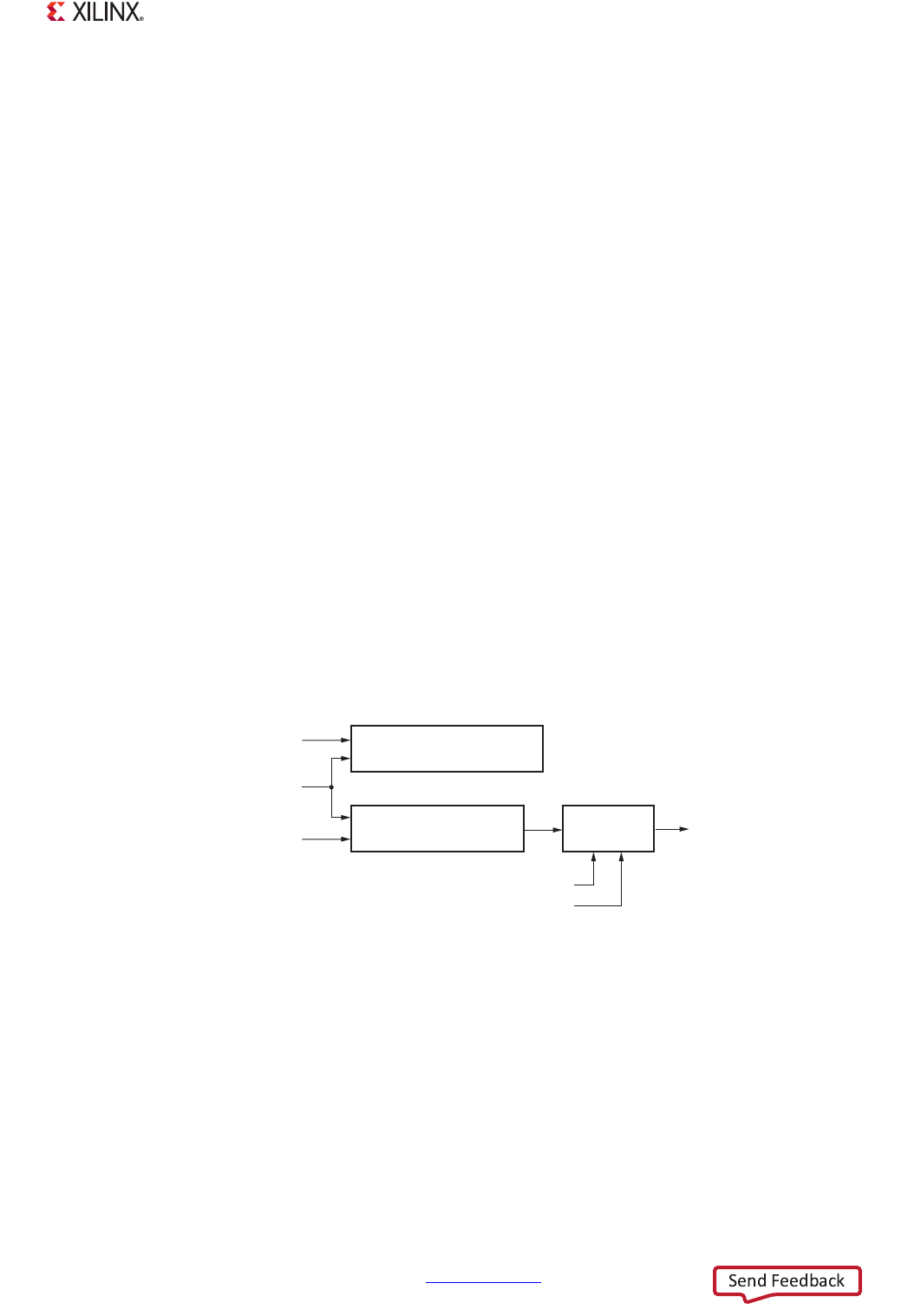
Zynq-7000 AP SoC Technical Reference Manual www.xilinx.com 599
UG585 (v1.12.1) December 6, 2017
Chapter 19: UART Controller
19.2.9 UART0-to-UART1 Connection
The I/O signals of the two UART controllers in the PS can be connected together. In this mode, the
RxD and CTS input signals from one controller are connected to the TxD and RTS output signals of
the other UART controller by setting the slcr.LOOP [UA0_LOOP_UA1] bit = 1. The other flow control
signals are not connected. This UART-to-UART connection occurs regardless of the MIO-EMIO
programming.
19.2.10 Status and Interrupts
Interrupt and Status Registers
There are two status registers that can be read by software. Both show raw status. The
Chnl_int_sts_reg0 register can be read for status and generate an interrupt. The Channel_sts_reg0
register can only be read for status.
The Chnl_int_sts_reg0 register is sticky; once a bit is set, the bit stays set until software clears it. Write
a 1 to clear a bit. This register is bit-wise AND'ed with the Intrpt_mask_reg0 mask register. If any of
the bit-wise AND functions have a result = 1, then the UART interrupt is asserted to the PS interrupt
controller.
•Channel_sts_reg0: Read-only raw status. Writes are ignored.
The various FIFO and system indicators are routed to the uart.Channel_sts_reg0 register and/or the
uart.Chnl_int_sts_reg0 register as shown in Figure 19-8.
X-Ref Target - Figure 19-8
Figure 19-8: Interrupts and Status Signals
uart.Channel_sts_reg0[14:10, 4:0]
(all bits are dynamic)
PS Interrupt IRQ
ID #59 / #82
UG585_c19_03_010613
Status
0: Masked
1: Enabled
uart.Intrpt_mask_reg0
uart.Chnl_int_sts_reg0[12:0]
(all bits are sticky)
Interrupts
FIFO
and other
System
Indicators
uart.Intrpt_en_reg0
uart.Intrpt_dis_reg0
Mask Enable
0 1
1 0

Zynq-7000 AP SoC Technical Reference Manual www.xilinx.com 600
UG585 (v1.12.1) December 6, 2017
Chapter 19: UART Controller
The interrupt registers and bit fields are summarized in Tab le 19 -2.
Interrupt Mask Register
Intrpt_mask_reg0 is a read-only interrupt mask/enable register that is used to mask individual raw
interrupts in the Chnl_int_sts_reg0 register:
•If the mask bit = 0, the interrupt is masked.
•If the mask bit = 1, the interrupt is enabled.
This mask is controlled by the write-only Intrpt_en_reg0 and Intrpt_dis_reg0 registers. Each
associated enable/disable interrupt bit should be set mutually exclusive (e.g., to enable an interrupt,
write 1 to Intrpt_en_reg0[x] and write 0 to Intrpt_dis_reg0[x]).
Channel Status
These status bits are in the Channel_sts_reg0 register.
•TACTIVE: Transmitter state machine active status. If in an active state, the transmitter is
currently shifting out a character.
•RACTIVE: Receiver state machine active status. If in an active state, the receiver is has detected
a start bit and is currently shifting in a character.
•FDELT: Receiver flow delay trigger continuous status. The FDELT status bit is used to monitor the
RxFIFO level in comparison with the flow delay trigger level.
Non-FIFO Interrupts
These interrupt status bits are in the Chnl_int_sts_reg0 register.
•TIMEOUT: Receiver Timeout Error interrupt status. This event is triggered whenever the receiver
timeout counter has expired due to a long idle condition.
•PARE: Receiver Parity Error interrupt status. This event is triggered whenever the received parity
bit does not match the expected value.
•FRAME: Receiver Framing Error interrupt status. This event is triggered whenever the receiver
fails to detect a valid stop bit. Refer to section 19.2.7 Receiver Data Capture.
Table 19-2: UART Interrupt Status Bits
Interrupt Register Names and Bit Assignments
14 13 12 11 10 9 8 7 6 5 4 3 2 1 0
uart.Intrpt_en_reg0
uart.Intrpt_dis_reg0
uart.Intrpt_mask_reg0
uart.Chnl_int_sts_reg0
x x TOVR TNFUL TTRIG DMSI TIME
OUT
PARE FRAME ROVR TFUL TEMPTY RFUL REMPTY RTRIG
uart.Channel_sts_reg0
TNFUL TTRIG FDELT TACTIVE RACTIVE X X X X X TFUL TEMPTY RFUL REMPTY RTRIG
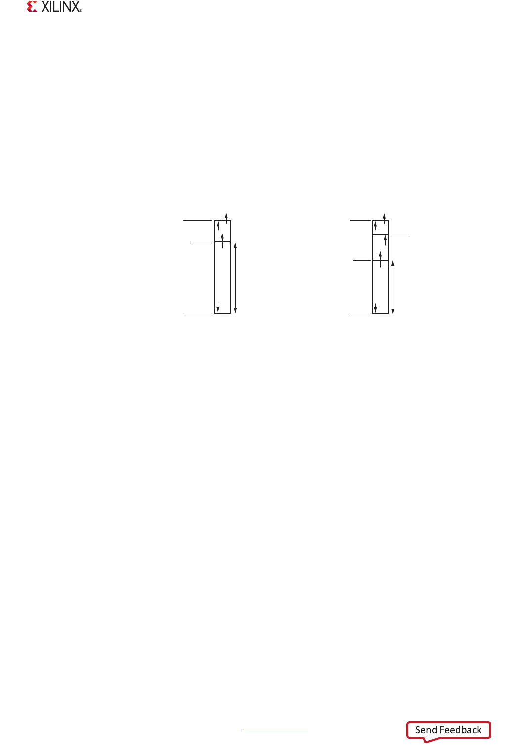
Zynq-7000 AP SoC Technical Reference Manual www.xilinx.com 601
UG585 (v1.12.1) December 6, 2017
Chapter 19: UART Controller
•DMSI: indicates a change of logic level on the DCD, DSR, RI or CTS modem flow control signals.
This includes High-to-Low and Low-to-High logic transitions on any of these signals.
FIFO Interrupts
The status bits for the FIFO interrupts listed in Ta ble 1 9-2 are illustrated in Figure 19-9. These
interrupt status bits are in the Channel Status (uart.Channel_sts_reg0) and Channel Interrupt Status
(uart.Chnl_int_sts_reg0) registers with the exception that the [TOVR] and [ROVR] bits are not part of
the uart.Channel_sts_reg0 register.
The FIFO trigger levels are controlled by these bit fields:
• uart.Rcvr_FIFO_trigger_level0[RTRIG], a 6-bit field
• uart.Tx_FIFO_trigger_level0[TTRIG], a 6-bit field
19.2.11 Modem Control
The modem control module facilitates the control of communication between a modem and the
UART. It contains the Modem Status register, the Modem Control register, the DMSI bit in interrupt
status register, and FDELT in the channel status register. This event is triggered whenever the DCTS,
DDSR, TERI, or DDCD in the modem status register are being set.
The read-only Modem Status register is used to read the values of the clear to send (CTS), data carrier
detect (DCD), data set ready, (DSR) and ring indicator (RI) modem inputs. It also reports changes in
any of these inputs and indicates whether automatic flow control mode is currently enabled. The bits
in the Modem Status register are cleared by writing a 1 to the particular bit.
The read/write only Modem Control register is used to set the data terminal ready (DTR) and request
to send (RTS) outputs, and to enable the Automatic Flow Control Mode register.
By default, the automatic flow control mode is disabled, meaning that the modem inputs and
outputs work completely under software control. When the automatic flow control mode is enabled
by setting the FCM bit in the Modem Control register, the UART transmission and reception status is
automatically controlled using the modem handshake inputs and outputs.
X-Ref Target - Figure 19-9
Figure 19-9: UART RxFIFO and TxFIFO Interrupt
TxFIFO (64 bytes)
Full Interrupt
[TFUL]
Empty Interrupt
[TEMPTY]
Trigger Interrupt
[TTRIG]
RxFIFO (64 bytes)
Full Interrupt
[RFUL]
Overflow Interrupt
[ROVR]
Trigger Interrupt
[RTRIG]
Nearly Full Interrupt
[TNFUL]
Empty Interrupt
[REMPTY]
UG585_c19_12_102912
Overflow Interrupt
[TOVR]
uart.Rcvr_FIFO_trigger_level0
uart.Tx_FIFO_trigger_level0

Zynq-7000 AP SoC Technical Reference Manual www.xilinx.com 602
UG585 (v1.12.1) December 6, 2017
Chapter 19: UART Controller
In automatic flow control mode the request to send output is asserted and de-asserted based on the
current fill level of the receiver FIFO, which results in the far-end transmitter pausing transmission
and preventing an overflow of the UART receiver FIFO. The FDEL field in the Flow Delay register
(Flow_delay_reg0) is used to setup a trigger level on the Receiver FIFO which causes the de-assertion
of the request to send. It remains Low until the FIFO level has dropped to below four less than FDEL.
Additionally in automatic flow control mode, the UART only transmits while the clear to send input
is asserted. When the clear to send is de-asserted, the UART pauses transmission at the next
character boundary.
If flow control is selected as automatic, then Flow Delay register must be programmed in order to
have a control on the inflow of data, which is done by de-asserting RTS signal. The value corresponds
to the RxFIFO level at which RTS signal will be de-asserted. It will be re-asserted when the RxFIFO
level drops to four below the value programmed in the Flow Delay register.
The uart.Channel_sts_reg0 [FDELT] register bit is used to monitor the RxFIFO level in comparison with
the flow delay trigger level. The [FDELT] bit is set whenever the RxFIFO level is greater than or equal
to trigger the level programmed in the Flow Delay register.
The trigger level programmed in the Flow Delay register has no dependency on the Rx Trigger Level
register. This is to only control the inflow of data using the RTS modem signal.
The CPU will be interrupted by receive data only on receipt of an Rx Trigger interrupt. Data is
retrieved based on the trigger level programmed in the Rx Trigger Level register.
Programmable Parameters
The UART flow control signals, DTR and RTS are generated by the UART controller.
• The RTS flow control signal is used to signal for Rx (ready to send signal to the attached
terminal).
• The DTR flow control signal indicates the status of the UART controller (data terminal ready).
The DTR and RTS can be controlled manually by software or automatically by the controller.
• In automatic mode, the modem control unit asserts and de-asserts the RTS and DTR signals.
• In manual mode, software controls the RTS and DTR signals using uart.Modem_ctrl_reg0.
uart.Modem_ctrl_reg0:
• [DTR]: Data Terminal Ready output signal
• [RTS]: Request to Send output signal
• [FCM]: Select Automatic or Manual flow control.
uart.Modem_sts_reg0:
• [DCTS]: Delta Clear To Send (input) status
• [DDSR]: Delta Data Set Ready (input) status
• [TERI]: Trailing-edge Ring Indicator (input) status
• [DDCD]: Delta Data Carrier Detect (input) status

Zynq-7000 AP SoC Technical Reference Manual www.xilinx.com 603
UG585 (v1.12.1) December 6, 2017
Chapter 19: UART Controller
Select one of the following operating options:
Example: Automatic Flow Control
1. Set RTS trigger level. Write to the uart.Flow_Delay_reg0 register. This is the trigger level to
de-assert modem signal RTS.
2. Select automatic flow control. Write a 1 to uart.Modem_ctrl_reg0 [FCM].
3. Verify the mode change to automatic. Read uart.Modem_sts_reg0 [FCMS] until it equals 1.
When software writes a 1 to uart.Modem_ctrl_reg0 [FCM], the modem changes to automatic mode.
The change of mode from manual to automatic is verified by reading the status bit FCMS in the
Modem Status register.
Example: Manual Flow Control
1. Select manual flow control. Write a 0 to uart.Modem_ctrl_reg0 [FCM].
Option a. Control the DTR output signal using uart.Modem_ctrl_reg0 [DTR].
Option b. Control the RTS output signal using uart.Modem_ctrl_reg0 [RTS].
Example: Monitor for a Change in the DCD DSR RI CTS Flow Control Signals
A logic level change to the DCD DSR RI CTS flow control signals is detected by the controller. When
a logic level change is detected, the hardware sets the uart.Chnl_int_sts_reg0 [DMSI] bit. This change,
or channel status can optionally generate an interrupt.
1. Check flow control signal status. uart.Modem_sts_reg0 register reports the modem status.
In interrupt mode, the ISR can run when the DMSI interrupt occurs when there is a change of status
on modem lines.
Limitation
The UART controller registers require single 32-bit read/write accesses, do not use byte, halfword, or
double word references.
19.3 Programming Guide
19.3.1 Start-up Sequence
Main Example: Start-up Sequence
1. Reset controller: The reset programming model is described in section 19.4.2 Resets.
2. Configure I/O signal routing: Rx/Tx can be routed to either MIO or EMIO. The modem control
signals are only available on the EMIO interface. Refer to section 19.5.1 MIO Programming.

Zynq-7000 AP SoC Technical Reference Manual www.xilinx.com 604
UG585 (v1.12.1) December 6, 2017
Chapter 19: UART Controller
3. Configure UART_Ref_Clk: The UART clock architecture and programming model are described
in section 19.4.1 Clocks.
4. Configure controller functions: Program the I/O signal characteristics and controller functions
using the uart.Control_reg0 and uart.mode_reg0 registers. Examples are shown in section
19.3.2 Configure Controller Functions.
5. Configure interrupts: Interrupts are used to manage the Rx/Tx FIFOs in all modes. Refer to
section 19.2.10 Status and Interrupts and the program example in section 19.3.5 RxFIFO Trigger
Level Interrupt.
6. Configure modem controls (optional): Polling and interrupt driven options. Refer to section
19.2.11 Modem Control.
7. Manage transmit and receive data: Polling and interrupt driven handlers are supportable. Refer
to sections 19.3.3 Transmit Data and 19.3.4 Receive Data.
19.3.2 Configure Controller Functions
Example: Configure Controller Functions
This example configures the character frame, the baud rate, the FIFO trigger levels, the Rx timeout
mechanism, and enables the controller. All of these steps are necessary after a reset, but not
necessary between enabling and disabling the controller.
1. Configure UART character frame. Write 0x0000_0020 into the uart.mode_reg0:
a. Disables clock pre-divider, UART_REF_CLK/8: [CLKS] = 0
b. Selects 8-bit character length: [CHRL] = 00
c. Selects no parity: [PAR] = 100
d. Selects 1 stop bit: [NBSTOP] = 00
e. Selects normal channel mode (Mode Switch): [CHMODE] = 00
2. Configure the Baud Rate. Write to three registers: uart.Control_reg0, uart.Baud_rate_gen_reg0,
and uart.Baud_rate_divider_reg0. Examples for the calculated CD and BDIV values are shown in
table Table 19-1, page 594. The baud rate generator is described in section 19.2.3 Baud Rate
Generator.
a. Disable the Rx path: set uart.Control_reg0 [RXEN] = 0 and [RXDIS] = 1.
b. Disable the Txpath: set uart.Control_reg0 [TXEN] = 0 and [TXDIS] = 1.
c. Write the calculated CD value into the uart.Baud_rate_gen_reg0 [CD] bit field.
d. Write the calculated BDIV value into the uart.Baud_rate_divider_reg0 [BDIV] bit value.
e. Reset Tx and Rx paths: uart.Control_reg0 [TXRST] and [RXRST] = 1. These bits are
self-clearing.
f. Enable the Rx path: Set [RXEN] = 1 and [RXDIS] = 0.
g. Enable the Tx path: Set [TXEN] = 1 and [TXDIS] = 0.
3. Set the level of the RxFIFO trigger level. Write the trigger level into the
uart.Rcvr_FIFO_trigger_level0 register.
°Option a: Enable the Rx trigger level: Write a value of 1 to 63 into the [RTRIG] bit field.

Zynq-7000 AP SoC Technical Reference Manual www.xilinx.com 605
UG585 (v1.12.1) December 6, 2017
Chapter 19: UART Controller
°Option b: Disable the Rx trigger level: Write 0 into the [RTRIG] bit field.
4. Enable the Controller. Write 0x0000_0117 into the uart.Control_reg0 register.
a. Reset Tx and Rx paths: uart.Control_reg0 [TXRST] and [RXRST] = 1. These bits are
self-clearing.
b. Enables the Rx path: [RXEN] = 1 and [RXDIS] = 0.
c. Enables the Tx path: [TXEN] = 1 and [TXDIS] = 0.
d. Restarts the Receiver Timeout Counter: [RSTTO] = 1.
e. Does not start to transmit a break: [STTBRK] = 0.
f. Stop Break transmitter: [STPBRK] = 1
5. Program the Receiver Timeout Mechanism. Write the timeout value into the
uart.Rcvr_timeout_reg0 register. Refer to Receiver Timeout Mechanism, page 596.
a. To enable the timeout mechanism, write a value of 1 to 255 into the [RSTTO] bit field.
b. To disable the timeout mechanism, write a 0 into the [RSTTO] bit field.
19.3.3 Transmit Data
Software can used polling or interrupts to control the flow of data to the TxFIFO and RxFIFO.
Note: When the TxFIFO Empty status is true, software can write 64 bytes (the size of the TxFIFO)
without checking the TxFIFO status. In reality, software can write more than 64 bytes when the
transmitter is active because while the software is writing data to the TxFIFO, the controller is
removing data and serializing it onto the TxD signal.
Example: Transmit Data using the Polling Method
In this example, the software can choose to fill the TxFIFO until the Full status bit is set or wait for the
TxFIFO to be empty (and write up to 64 bytes). The software can always write a byte when the TxFIFO
is nearly full.
1. Check to see if the TxFIFO is empty. Wait until uart.Channel_sts_reg0[TEMPTY] = 1.
2. Fill the TxFIFO with data. Write 64 bytes of data to the uart.TX_RX_FIFO0 register.
3. Write more data to the TxFIFO. There are two methods:
Option A: Check to see if the TxFIFO has room to another byte of data (i.e., the TxFIFO is not
full): Read uart.Channel_sts_reg0 [TFUL] until it equals 0. When [TFUL] = 0, write a single byte of
data into the TxFIFO and then read [TFUL] again.
Option B: Wait until the TxFIFO goes empty. Read uart.Channel_sts_reg0 [TEMPTY] until it
equals 1, then go to step 2 to fill the TxFIFO with 64 bytes of data.
Example: Transmit Data using the Interrupt Method
This example initially fills the TxFIFO in a similar way as the polling method. Then, software enables
the TxFIFO Empty interrupt to alert the software to fill-up the TxFIFO again.
1. Disable the TxFIFO Empty interrupt. Write a 1 to uart.Intrpt_dis_reg0 [TEMPTY].

Zynq-7000 AP SoC Technical Reference Manual www.xilinx.com 606
UG585 (v1.12.1) December 6, 2017
Chapter 19: UART Controller
2. Fill the TxFIFO with data. Write 64 bytes of data to the uart.TX_RX_FIFO0 register.
3. Check to see if the TxFIFO has room to another byte of data (i.e., the TxFIFO is not full): read
uart.Channel_sts_reg0 [TFUL] until it equals 0. When [TFUL] = 0, write a single byte of data into
the TxFIFO and then read [TFUL] again.
4. Repeat step 2 and 3. Repeat until uart.Channel_sts_reg0 [TFUL] is not set.
5. Enable the interrupt. Enable the interrupt with a write of 1 to uart.Intrpt_en_reg0 [TEMPTY].
6. Wait until the TxFIFO is empty. Repeat from step 1 when uart.Channel_int_sts_reg0 [TEMPTY] is
set to 1.
19.3.4 Receive Data
Example: Receive Data using the Polling Method
1. Wait until the RxFIFO is filled up to the trigger level. Check to see if
uart.Channel_sts_reg0[RTRIG] = 1 or uart.Chnl_int_sts_reg0 [TIMEOUT] = 1.
2. Read data from the RxFIFO. Read data from the uart.TX_RX_FIFO0 register.
3. Repeat step 2 until FIFO is empty. Check that uart.Channel_sts_reg0 [REMPTY] = 1.
4. Clear if Rx timeout interrupt status bit is set. Write 1 to Chnl_int_sts_reg0 [TIMEOUT].
Example: Receive Data using the Interrupt Method
1. Enable interrupts. Write a 1 to uart.Intrpt_en_reg0 [TIMEOUT] and uart.Intrpt_en_reg0[RTRIG].
2. Wait until the RxFIFO is filled up to the trigger level or Rx timeout. Check that
uart.Chnl_int_sts_reg0 [RTRIG] = 1 or uart.Chnl_int_sts_reg0 [TIMEOUT] = 1.
3. Read data from the RxFIFO. Read data from the uart.TX_RX_FIFO0 register.
4. Repeat step 2 and 3 until the FIFO is empty. Check that uart.Channel_sts_reg0 [REMPTY] = 1.
5. Clear the interrupt status bits if set. Write a 1 to Chnl_int_sts_reg0 [TIMEOUT] or
Chnl_int_sts_reg0 [RTRIG].
19.3.5 RxFIFO Trigger Level Interrupt
Example: Set the RxFIFO Trigger Level and Enable the Interrupt
The Intrpt_en_reg0 register has bits to enable the interrupt mask and Intrpt_dis_reg0 has bits to
forcefully disable the interrupts. Each pair of bits should be set mutually exclusive (i.e., one register
has a 1 for the bit and the other register has a 0):
• Intrpt_en_reg0: Write-only. Enable interrupt bit(s).
• Intrpt_dis_reg0: Write-only. Force disable of interrupt bit(s).
1. Program the Trigger Level. Write to the 6-bit field, uart.Rcvr_FIFO_trigger_level0[RTRIG].
2. Enable the RTRIG interrupt. Set the enable bit, clear the disable bit, and verify the mask value:
a. Set uart.Intrpt_en_reg0[RTRIG] = 1.

Zynq-7000 AP SoC Technical Reference Manual www.xilinx.com 607
UG585 (v1.12.1) December 6, 2017
Chapter 19: UART Controller
b. Clear uart.Intrpt_dis_reg0[RTRIG] = 0.
c. The uart.intrpt_mask_reg0[RTRIG] read back = 1 (enabled interrupt).
3. Disable the RTRIG interrupt. Set the disable bit, clear the enable bit, and verify the mask value:
a. Set uart.Intrpt_dis_reg0[RTRIG] =1.
b. Clear uart.Intrp_en_reg0[RTRIG] = 0.
c. The uart.intrpt_mask_reg0[RTRIG] read back = 0 (disabled interrupt).
4. Clear the RTRIG interrupt. Write a one to the uart.Intrpt_dis_reg0[RTRIG] bit field.
When both the enable and disable bits are set for an interrupt, the interrupt is disabled.
The state of the interrupt enable/disable mechamism can be determined by reading the
uart.Intrpt_mask_reg0 register. If the mask bit = 1, then the interrupt is enabled.
19.3.6 Register Overview
An overview of the UART registers is shown in Table 19-3. Details are provided in Appendix B,
Register Details.
Table 19-3: UART Register Overview
Function uart. Register Names Overview
Configuration Control_reg0
mode_reg0
Baud_rate_gen_reg0
Baud_rate_divider_reg0
Configure mode and baud rate.
Interrupt processing Intrpt_en_reg0
Intrpt_dis_reg0
Intrpt_mask_reg0
Chnl_int_sts_reg0
Channel_sts_reg0
Enable/disable interrupt mask, channel interrupt status,
channel status
Rx and Tx Data TX_RX_FIFO0 Read data Received.
Write data to be Transmitted.
Receiver Rcvr_timeout_reg0
Rcvr_FIFO_trigger_level0
Configure receiver timeout and RxFIFO trigger level value.
Transmitter Tx_FIFO_trigger_level0 Configure TxFIFO trigger level value.
Modem Modem_ctrl_reg0
Modem_sts_reg0
Flow_delay_reg0
Configure modem-like application.

Zynq-7000 AP SoC Technical Reference Manual www.xilinx.com 608
UG585 (v1.12.1) December 6, 2017
Chapter 19: UART Controller
19.4 System Functions
19.4.1 Clocks
The controller and I/O interface are driven by the reference clock (UART_REF_CLK). The controller's
interconnect also requires an APB interface clock (CPU_1x). Both of these clocks always come from
the PS clock subsystem.
CPU_1x Clock
Refer to section 25.2 CPU Clock, for general clock programming information. The CPU_1x clock runs
asynchronous to the UART reference clock.
Reference Clock
The generation of the reference clock in the PS clock subsystem is controlled by the
slcr.UART_CLK_CTRL register. This register can select the PLL that the clock is derived from and sets
the divider frequency. This register also controls the clock enables for each UART controller. The
generation of the UART reference clock is described in section 25.6.3 SDIO, SMC, SPI, Quad-SPI and
UART Clocks.
Operating Restrictions
Note: The clock operating restrictions are described in section 19.1.3 Notices.
Example: Configure Reference Clock
The clock can be based on any of the PLLs in the PS clock subsystem. In this example, the I/O PLL is
used with a 1,000 MHz clock and the clock divisor is 0x14 to generate a 50 MHz clock for the UART
controllers.
1. Program the UART Reference clock. Write 0x0000_1401 to the slcr.UART_CLK_CTRL register.
a. Clock divisor, slcr.UART_CLK_CTRL[DIVISOR] = 0x14.
b. Select the IO PLL, slcr.UART_CLK_CTRL[SRCSEL] = 0.
c. Enable the UART 0 Reference clock, slcr.UART_CLK_CTRL [CLKACT0] = 1.
d. Disable UART 1 Reference clock, slcr.UART_CLK_CTRL [CLKACT1] bit = 0.
19.4.2 Resets
The controller reset bits are generated by the PS, see Chapter 26, Reset System.

Zynq-7000 AP SoC Technical Reference Manual www.xilinx.com 609
UG585 (v1.12.1) December 6, 2017
Chapter 19: UART Controller
Example: Controller Reset
Option 1. Assert Controller Reset: Set both slcr.UART_RST_CTRL[UARTx_REF_RST,
UARTx_CPU1X_RST]
bits = 1.
Option 2. De-assert Controller Reset: Clear both slcr.UART_RST_CTRL[UARTx_REF_RST,
UARTx_CPU1X_RST] bits = 0.
19.5 I/O Interface
19.5.1 MIO Programming
The UART RxD and TxD signals can be routed to one of many sets of MIO pins or to the EMIO
interface. All of the modem flow control signals are always routed to the EMIO interface and are not
available on the MIO pins. All of the UART signals are listed in Table 19-4. The routing of the RxD and
TxD signals are described in section 2.4 PS–PL Voltage Level Shifter Enables.
Example: Route UART 0 RxD/TxD Signals to MIO Pins 46, 47
In this example, the UART 0 RxD and TxD signals are routed through MIO pins 46 and 47. Many other
pin options are possible.
1. Configure MIO pin 46 for the RxD signal. Write 0x0000_12E1 to the slcr.MIO_PIN_46 register:
a. Route UART 0 RxD signal to pin 46.
b. Output disabled (set TRI_ENABLE = 1).
c. LVCMOS18 (refer to the register definition for other voltage options).
d. Slow CMOS edge (benign setting).
e. Enable internal pull-up resistor.
f. Disable HSTL receiver.
2. Configure MIO pin 47 for the TxD signal. Write 0x0000_12E0 to the slcr.MIO_PIN_47 register:
a. Route UART 0 TxD signal to pin 47.
b. 3-state controlled by the UART (TRI_ENABLE = 0).
c. LVCMOS18 (refer to the register definition for other voltage options).
d. Slow CMOS drive edge.
e. Enable internal pull-up resistor.
f. Disable HSTL receiver.

Zynq-7000 AP SoC Technical Reference Manual www.xilinx.com 610
UG585 (v1.12.1) December 6, 2017
Chapter 19: UART Controller
19.5.2 MIO – EMIO Signals
The UART I/O signals are identified in Table 19-4. The MIO pins and any restrictions based on device
versions are shown in the MIO table in section 2.5.4 MIO-at-a-Glance Table.
Table 19-4: UART MIO Pins and EMIO Signals
UART
Interface Signal
Default
Controller
Input Value
MIO Pins EMIO Signals
Numbers I/O Name I/O
UART 0 Transmit ~ 11, 15, 19, 23, 27, 31, 35, 39, 43, 47, 51 O EMIOUART0TX O
UART 0 Receive 10, 14, 18, 22, 26, 30, 34, 38, 42, 46, 50 I EMIOUART0RX I
UART 0 Clear to Send ~ ~ EMIOUART0CTSN I
UART 0 Ready to Send ~ ~ ~ EMIOUART0RTSN O
UART 0 Data Set Ready ~ ~ EMIOUART0DSRN I
UART 0 Data Carrier Detect ~ ~ EMIOUART0DCDN I
UART 0 Ring Indicator ~ ~ EMIOUART0RIN I
UART 0 Data Terminal Ready ~ ~ ~ EMIOUART0DTRN O
UART 1 Transmit ~ 8, 12, 16, 20, 24, 28, 32, 36, 40, 44, 48, 52 O EMIOUART1TX O
UART 1 Receive 9, 13, 17, 21, 25, 29, 33, 37, 41, 45, 49, 53 I EMIOUART1RX I
UART 1 Clear to Send ~ ~ EMIOUART1CTSN I
UART 1 Ready to Send ~ ~ ~ EMIOUART1RTSN O
UART 1 Data Set Ready ~ ~ EMIOUART1DSRN I
UART 1 Data Carrier Detect ~ ~ EMIOUART1DCDN I
UART 1 Ring Indicator ~ ~ EMIOUART1RIN I
UART 1 Data Terminal Ready ~ ~ ~ EMIOUART1DTRN O

Zynq-7000 AP SoC Technical Reference Manual www.xilinx.com 611
UG585 (v1.12.1) December 6, 2017
Chapter 20
I2C Controller
20.1 Introduction
This I2C module is a bus controller that can function as a master or a slave in a multi-master design.
It supports an extremely wide clock frequency range from DC (almost) up to 400 Kb/s.
In master mode, a transfer can only be initiated by the processor writing the slave address into the
I2C address register. The processor is notified of any available received data by a data interrupt or a
transfer complete interrupt. If the HOLD bit is set, the I2C interface holds the SCL line Low after the
data is transmitted to support slow processor service. The master can be programmed to use both
normal (7-bit) addressing and extended (10-bit) addressing modes.
In slave monitor mode, the I2C interface is set up as a master and continues to attempt a transfer to
a particular slave until the slave device responds with an ACK.
The HOLD bit can be set to prevent the master from continuing with the transfer, preventing an
overflow condition in the slave.
A common feature between master mode and slave mode is the timeout (TO) interrupt flag. If at any
point the SCL line is held Low by the master or the accessed slave for more than the period specified
in the Timeout register, a timeout (TO) interrupt is generated to avoid stall conditions.
20.1.1 Features
The PS supports two I2C devices with these key features:
• I2C bus specification version 2
• Supports 16-byte FIFO
• Programmable normal and fast bus data rates
•Master mode
°Write transfer
°Read transfer
°Extended address support
°Support HOLD for slow processor service
°Supports TO interrupt flag to avoid stall condition
• Slave monitor mode
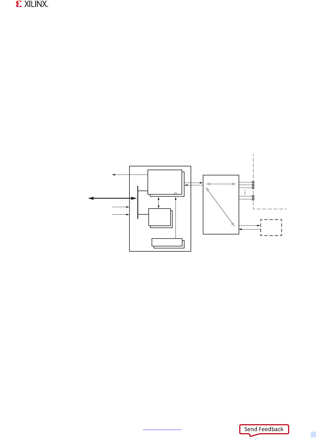
Zynq-7000 AP SoC Technical Reference Manual www.xilinx.com 612
UG585 (v1.12.1) December 6, 2017
Chapter 20: I2C Controller
•Slave mode
°Slave transmitter
°Slave receiver
°Fully programmable slave response address
°Supports HOLD to prevent overflow condition
°Supports TO interrupt flag to avoid stall condition
• Software can poll for status or function as interrupt-driven device
• Programmable interrupt generation
20.1.2 System Block Diagram
The system viewpoint diagram for the I2C module is shown in Figure 20-1.
20.1.3 Notices
7z007s and 7z010 CLG225 Devices
The 7z007s single core and 7z010 dual core CLG225 devices support 32 MIO pins as shown in
section 2.5.4 MIO-at-a-Glance Table. This restricts the availability of the I2C signals on the MIO pins.
As needed, I2C signals can be routed through the EMIO interface and passed-through to the PL pins.
All CLG225 device restrictions are listed in section 1.1.3 Notices.
X-Ref Target - Figure 20-1
Figure 20-1: I2C System Block Diagram
PL
MIO – EMIO
Routing
Interconnect APB
MIO
Pins
UG585_c20_01_030612
Device
Boundary
EMIO
IRQ ID# {57, 80}
Control
Registers
Slave
port
I2C{0, 1} CPU1x reset
I2C{0, 1} CPU_1x clock
I2C
Controllers
SCL, SDA
SCL, SDA,
SCL_T
Clocking
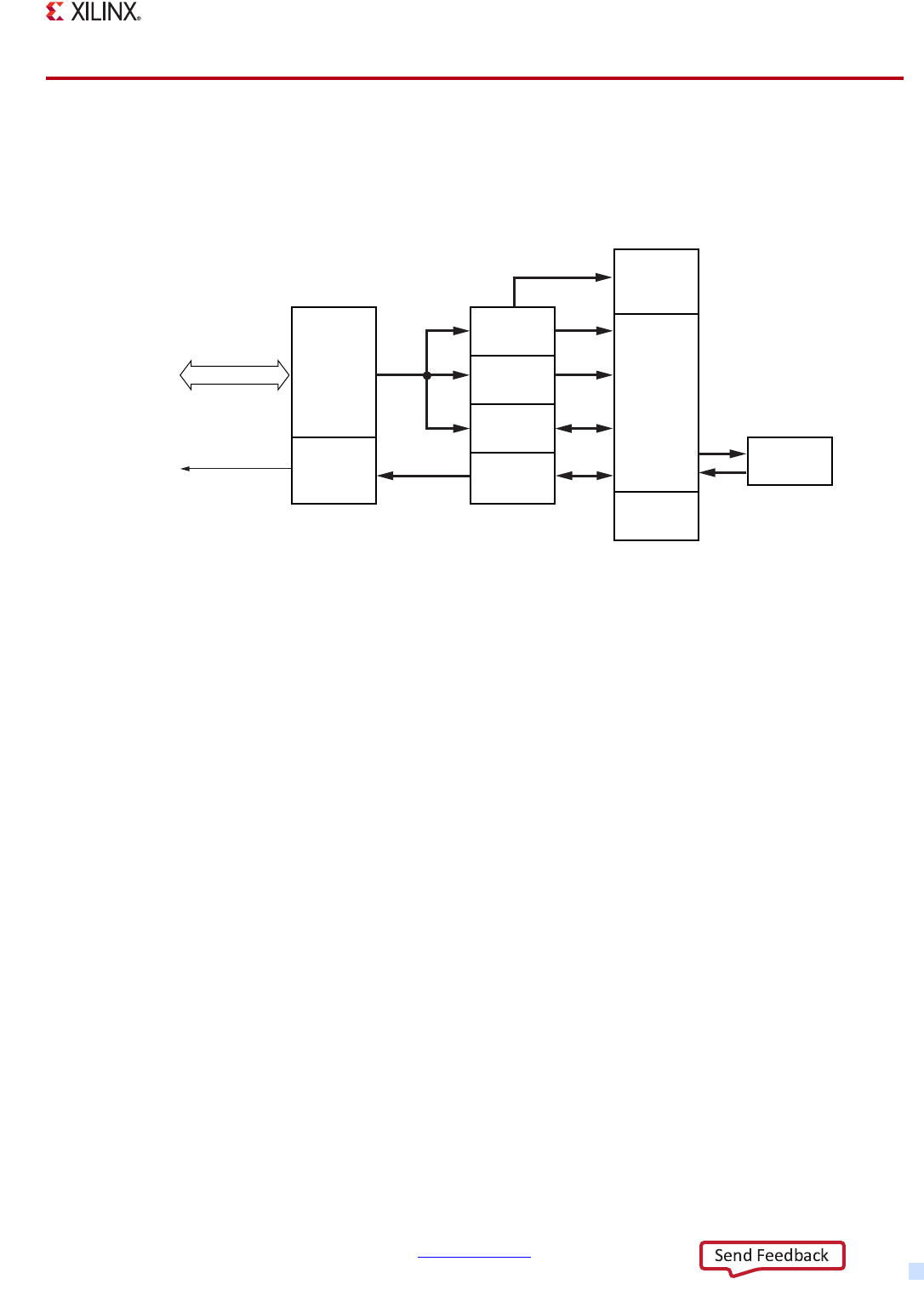
Zynq-7000 AP SoC Technical Reference Manual www.xilinx.com 613
UG585 (v1.12.1) December 6, 2017
Chapter 20: I2C Controller
20.2 Functional Description
20.2.1 Block Diagram
20.2.2 Master Mode
An I2C transfer can only be initiated by the APB host, and two types of transfers can be performed:
• Write transfer, where the I2C becomes master transmitter
• Read transfer, where the I2C becomes master receiver
Write Transfer
To accomplish an I2C write transfer, the host must perform these steps:
1. Write to the control register to set up SCL speed and addressing mode.
2. Set the MS, ACKEN, and CLR_FIFO bits and clear the RW bit in the Control register.
3. If required, set the HOLD bit. Otherwise write the first byte of data to the I2C Data register.
4. Write the slave address into the I2C address register. This initiates the I2C transfer.
5. Continue to load the remaining data to be sent to the slave by writing to the I2C Data register.
The data is pushed in the FIFO each time the host writes to the I2C Data register.
When all data is transferred successfully, the COMP bit is set in the interrupt status register. A data
interrupt is generated whenever there are only two bytes left for transmission in the FIFO.
When all data is transferred successfully, If the HOLD bit is not set, the I2C interface generates a STOP
condition and terminates the transfer. If the HOLD bit is set, the I2C interface holds the SCL line Low
X-Ref Target - Figure 20-2
Figure 20-2: I2C Peripheral Block Diagram
UG585_c20_02_030612
APB
Interface
Control
Register
SCL/SDA
Interface
TX Data
Register
RX Data
Register
Clock
Enable
Generator
Control
FSM
Status
Register
Interrupts
Interrupts
APB
RX Shift
Register

Zynq-7000 AP SoC Technical Reference Manual www.xilinx.com 614
UG585 (v1.12.1) December 6, 2017
Chapter 20: I2C Controller
after the data is transmitted. The host is notified of this event by a transfer complete interrupt
(COMP bit set) and the TXDV bit in the status register is cleared. At this point, the host can proceed
in three ways:
1. Clear the HOLD bit. This causes the I2C interface to generate a STOP condition.
2. Supply more data by writing to the I2C address register. This causes the I2C interface to continue
with the transfer, writing more data to the slave.
If at any point the slave responds with a NACK, the transfer automatically terminates and a transfer
NACK interrupt is generated (the NACK bit set). When a NACK is received the Transfer Size register
indicates the number of bytes that still need to be sent minus one. Unless the very last byte written
by the host into the FIFO was a NACK byte, TXDV remains High. In this case, the host must clear the
FIFO by setting the CLR_FIFO bit in the Control register.
If at any point the SCL line is held Low by the master or the accessed slave for more than the period
specified in the Timeout register, a TO interrupt is generated and the outstanding amount of data
minus one is then read from the Transfer Size register.
Read Transfer
To accomplish an I2C read transfer, the host must perform these steps:
1. Write to the Control register to set up the SCL speed and addressing mode.
2. Set the MS, ACKEN, CLR_FIFO bits, and the RW bit in the Control register.
3. If the host wants to hold the bus after the data is received, it must also set the HOLD bit.
4. Write the number of requested bytes in the Transfer Size register.
5. Write the slave address in the I2C Address register. This initiates the I2C transfer.
The host is notified of any available received data in two ways:
1. If an outstanding transfer size is equal to or greater than the FIFO size -2, a data interrupt is
generated (DATA bit set) when there are two free locations available in the FIFO.
2. If an outstanding transfer size is less than FIFO size -2, a transfer complete interrupt is generated
(COMP bit set) when the outstanding transfer size bytes are received.
In both cases, the RXDV bit in the status register is set.
The I2C interface automatically returns a NACK after receiving the last expected byte and terminates
the transfer by generating a STOP condition. If the HOLD bit is set during a master read transfer, the
I2C interface drives the SCL line Low.
If at any point the slave responds with NACK while the master transmits a slave address for a master
read transfer, the transfer automatically terminates and a transfer NACK interrupt is generated
(NACK bit is set). The outstanding amount of data can be read from the Transfer Size register.
If at any point the SCL line is held Low by the master or the accessed slave for more than the period
specified in the Timeout register, a TO interrupt is generated.

Zynq-7000 AP SoC Technical Reference Manual www.xilinx.com 615
UG585 (v1.12.1) December 6, 2017
Chapter 20: I2C Controller
20.2.3 Slave Monitor Mode
This mode is meaningful only when the module is in master mode and bit SLVMON in the control
register is set. The host must set the MS and SLVMON bits and clear the RW bit in the Control
register. Also, it must initialize the Slave Monitor Pause register.
The master attempts a transfer to a particular slave whenever the host writes to the I2C Address
register. If the slave returns a NACK when it receives the address, the master waits for the time
interval established by the Slave Monitor Pause register and attempts to address the slave again. The
master continues this cycle until the slave responds with an ACK to its address or until the host clears
the SLVMON bit in the Control register. If the addressed slave responds with an ACK, the I2C
interface terminates the transfer by generating a STOP condition and a SLV_RDY interrupt.
20.2.4 Slave Mode
The I2C interface is set up as a slave by clearing the MS bit in the Control register. The I2C slave must
be given a unique identifying address by writing to the I2C address register. The SCL speed must also
be set up at least as fast as the fastest SCL frequency expected to be seen. When in slave mode, the
I2C interface operates as either a slave transmitter or a slave receiver.
Slave Transmitter
The slave becomes a transmitter after recognizing the entire slave address sent by the master and
when the R/W field in the last address byte sent is High. This means that the slave has been
requested to send data over the I2C bus and the host is notified of this through an interrupt through
an interrupt to the GIC (refer to Figure 20-1, page 612). At the same time, the SCL line is held Low to
allow the host to supply data to the I2C slave before the I2C master starts sampling the SDA line. The
host is notified of this event by setting the DATA interrupt flag.
At the same time, the SCL line is held Low to allow the host to supply data to the I2C slave before the
I2C master starts sampling the SDA line.
The host must supply data for transmission through the I2C data register so that the SCL line is
released and transfer continues. If it does not write to the I2C data register before the timeout period
expires, an interrupt is generated and a TO interrupt flag is set.
After the host writes to the I2C data register, the transfer continues by loading data in the FIFO while
the transfer is in progress. The amount of data loaded in the FIFO might be a known system
parameter or communicated in advance through a higher level protocol using the I2C bus.
When there are only two valid bytes left in the FIFO for transmission, an interrupt is generated and
the DATA interrupt flag is set. If the I2C master returns a NACK on the last byte transmitted from the
FIFO, an interrupt is generated, and the COMP interrupt flag is set as soon as the I2C master
generates a STOP condition.
The transfer must continue if the master acknowledges on the last byte sent out from the FIFO. At
that moment, the DATA interrupt flag is set. The TXDV flag in the Status register is cleared because
the FIFO is empty.

Zynq-7000 AP SoC Technical Reference Manual www.xilinx.com 616
UG585 (v1.12.1) December 6, 2017
Chapter 20: I2C Controller
If the I2C master terminates the transfer before all of the data in the FIFO is sent by the slave, the
host is notified, and the NACK interrupt flag is set while TXDV remains set and the Transfer Size
register indicates the remaining bytes in the FIFO. The host must set the CLR_FIFO bit in the Control
register to clear the FIFO and the TXDV bit.
Slave Receiver
The slave becomes a receiver after recognizing the entire slave address sent by the master and when
the R/W bit in the first address byte is Low. This means that the master is about to send one or more
data bytes to the slave over the I2C bus.
After a byte is acknowledged by the I2C slave, the RXDV bit in the Status register is set, indicating
that new data has been received. The host reads the received data through the I2C Data register. An
interrupt is generated and the DATA interrupt flag is set when there are only two free locations left
in the FIFO.
Whenever the I2C master generates a STOP condition, an interrupt is generated and the COMP
interrupt flag is set. The Transfer Size register then contains the number of bytes received that are
available in the FIFO. This number is decremented by the host on each read of the I2C Data register.
If the FIFO is full when one or more bytes are received by the I2C interface, an interrupt is generated
and the RX_OVF interrupt flag is set. The last byte received is not acknowledged and the data in the
FIFO is kept intact.
The HOLD bit can be set in the Control register to avoid overflow conditions when it is impossible to
respond to interrupts in a reasonable time. If the HOLD bit is set, the I2C interface keeps the SCL line
Low until the host clears resources for data reception. This prevents the master from continuing with
the transfer, causing an overflow condition in the slave. The host clears resources for data reception
by reading the data register.
If the HOLD bit is set and the I2C interface keeps the SCL line Low for longer than the timeout period,
an interrupt is generated and the TO interrupt flag is set.
20.2.5 I2C Speed
The main clock used within the I2C interface is the clock enable signal (see Figure 20-3).
• In slave mode, the clock enable is used to extract synchronization information for correct
sampling of the SDA line.
• In master mode, the clock enable is used to establish a time base for generating the desired SCL
frequency.
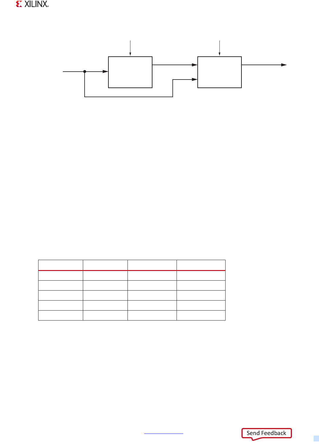
Zynq-7000 AP SoC Technical Reference Manual www.xilinx.com 617
UG585 (v1.12.1) December 6, 2017
Chapter 20: I2C Controller
The frequency of the clock_enable signal is defined by the frequency of the CPU_1x clock and the
values of divisor_a and divisor_b using Equation 20-1
Equation 20-1
Note: As seen from the above calculation, the SCL clock frequency range is limited by the cpu_1x
clock. This means that for some cpu_1x clock rates there will be some SCL frequencies that are not
possible.
See I2C register map in Appendix B, Register Details for details of register fields.
Tabl e 20- 1 lists the calculated values for standard and high speed SCL clock values. A programming
example is provided in Section 20.3.2.
I2C SCL Clock = CPU_1X_Clock / (22 * (divisor_a + 1) * (divisor_b + 1))
20.2.6 Multi-Master Operation
In I2C multi master mode, the bus is shared with other masters. In this mode, the I2C clock
(I2C_SCL)is driven by the device that acts as the master.
X-Ref Target - Figure 20-3
Figure 20-3: I2C Clock Generator
Table 20-1: Calculated Values for Standard and High Speed SCL Clock Values
I2C SCL Clock CPU_1X_Clock divisor_a divisor_b
100 KHz 111 MHz 2 16
400 KHz 111 MHz 0 12
100 KHz 133 MHz 0 60
400 KHz 133 MHz 2 4
100 KHz 166 MHz 3 16
1 to 4
divider
divisor_a
CPU_1x Clock
Clock_Enable
1 to 64
divider
divisor_b
UG585_c20_03_022912
FreqClock_Enable FreqCPU_1x
divisor_a 1+()divisor_b 1+()×
-----------------------------------------------------------------------
=

Zynq-7000 AP SoC Technical Reference Manual www.xilinx.com 618
UG585 (v1.12.1) December 6, 2017
Chapter 20: I2C Controller
20.2.7 I2C0-to-I2C1 Connection
The I/O signals of the two I2C controllers in the PS are connected together when the
slcr.MIO_LOOPBACK [I2C0_LOOP_I2C1] bit is set = 1. In this mode, the serial clocks are connected
together and the serial data signals are connected together.
20.2.8 Status and Interrupts
The registers i2c.Interrupt_status_reg0, i2c.Intrpt_mask_reg0, i2c.Intrpt_enable_reg0 and
i2c.Intrpt_disable_reg0 provide interrupt capability. See Table 20-2 for Interrupt and Status register
names and bit assignments.
Interrupt Mask Register
Intrpt_mask_reg0 is a read-only interrupt mask register used to enable/disable individual interrupts
in the i2c.interrupt_status_reg0 register:
•If the mask bit = 0, the interrupt is enabled.
•If the mask bit = 1, the interrupt is disabled.
This mask is controlled by the write-only Intrpt_enable_reg0 and Intrpt_disable_reg0 registers.
Each associated enable/disable interrupt bit should be set mutually exclusive (e.g., to enable an
interrupt, write 1 to Intrpt_enable_reg0[x] and write 0 to Intrpt_disable_reg0[x]).
Table 20-2: Interrupt and Status Register Names and Bit Assignments
15 14 13 12 11 10 9 8 7 6 5 4 3 2 1 0
i2c.Interrupt_status_reg0
i2c.Intrpt_mask_reg0
i2c.Intrpt_enable_reg0
i2c.Intrpt_disable_reg0
X X X X X X ARB_LOST X RX_UNF TX_OVF RX_OVF SLV_RDY TO NACK DATA COMP
i2c.Status_reg0
X X X X X X X BA RXOVF TXDV RXDV X RX_RW X X X

Zynq-7000 AP SoC Technical Reference Manual www.xilinx.com 619
UG585 (v1.12.1) December 6, 2017
Chapter 20: I2C Controller
Interrupt Status Register
All the bits are sticky.
• Read: Reads interrupt status.
• Write: Write 1 to clear
Status Register
All bits present the raw status of the interface. Bits in this register dynamically change based on FIFO and
other conditions.
Limitation
The I2C controller registers require single 32-bit read/write accesses, do not use byte, halfword, or double
word references.
20.3 Programmer’s Guide
20.3.1 Start-up Sequence
1. Reset controller: Programming resets is described in section 20.4.2 Reset Controller.
2. Configure I/O signal routing: I2C signals SCL and SDA can be routed to either MIO or EMIO.
Refer to Table 20-4. Example of I2C SCL and SDA signal routed to MIO is provided in section
20.5.1 Pin Programming.
3. Configure Clocks: The I2C clock architecture is described in section 20.4.1 Clocks.
4. Controller Configuration: Program I2C transfer parameters using i2c.Control_reg0 etc. Refer to
section 20.4.2 Reset Controller.
5. Configure Interrupts: Interrupts help to control data in FIFO. Refer to section 20.2.8 Status and
Interrupts and programming example in section 20.3.3 Configure Interrupts.
6. Data Transfers: Transfers in master mode and slave monitor mode can be referred in section
20.3.4 Data Transfers.
20.3.2 Controller Configuration
The user should choose interface mode, addressing mode, direction of transfer, timeout, and
program the I2C bus speed before initiating an I2C transfer. Optionally, the user can clear FIFOs and
hold the bus if required, in case of large data or combined transfers.
Example: Master Write Transfer
1. Configure the Control parameters. Write 0x0000_324E to the i2c.Control_reg0 register:
a. Select Master mode: Set i2c.Control_reg0[MS] = 1.

Zynq-7000 AP SoC Technical Reference Manual www.xilinx.com 620
UG585 (v1.12.1) December 6, 2017
Chapter 20: I2C Controller
b. Set Direction of transfer as Master Transmitter: Set i2c.Control_reg0[RW] = 0.
c. Select Normal Addressing [7-bit] mode: Set i2c.Control_reg0[NEA] = 1.
d. Enable the transmission of ACK: Set i2c.Control_reg0[ACKEN] = 1.
e. Clear the FIFOs: Set i2c.Control_reg0[CLR_FIFO] = 1.
f. Program the clock divisors:
- Set i2c.Control_reg0[divisor_a] = 0.
- Set i2c.Control_reg0[divisor_b] = 50.
These divisors generate an I2C SCL of 99 KHz using the CPU_1X clock of 111 MHz. For further
details refer to section 20.2.5 I2C Speed.
2. Configure Timeout. Write 0x0000_00FF to the i2c.Time_out_reg0 register. Wait 255 SCL cycles
when the SCL is held Low, before generating a timeout interrupt.
20.3.3 Configure Interrupts
The interrupts are described in section 20.2.8 Status and Interrupts. The i2c.Intrpt_enable_reg0 register
has bits to enable the interrupt mask and i2c.Intrpt_disable_reg0 has bits to forcefully disable the
interrupts. Each pair of bits should be set mutually exclusive:
Example: Program Example to Configure Completion Interrupt
1. Enable the completion interrupt. Set the enable bit, clear the disable bit, and verify the mask
value:
a. Set i2c.Intrpt_enable_reg0[COMP] = 1.
b. Clear i2c.Intrpt_disable_reg0[COMP] = 0.
c. i2c.intrpt_mask_reg0[COMP] reads back = 1.
2. Disable the completion interrupt. Set the enable bit, clear the disable bit, and verify the mask
value:
a. Set i2c.Intrpt_disable_reg0[COMP] = 1.
b. Clear i2c.Intrpt_enable_reg0[COMP] = 0.
c. i2c.Intrpt_mask_reg0[COMP] reads back = 0.
3. Monitor completion interrupt. I2c.Interrupt_status_reg0 provides status of completion
interrupt.:
a. Read i2c.Interrupt_status_reg0 [COMP]. 1 indicates that an interrupt occurred.
4. Clear completion interrupt. Write 1 to the i2c.Interrupt_status_reg0[COMP] bit field.
20.3.4 Data Transfers
Transfers can be achieved in polled mode or interrupt driven mode. Limitation on data count while
performing a master read transfer is 255 bytes. Below are examples of read and write transfer in
Master mode and example for Slave Monitor mode. Refer to section 20.2.3 Slave Monitor Mode for
details.

Zynq-7000 AP SoC Technical Reference Manual www.xilinx.com 621
UG585 (v1.12.1) December 6, 2017
Chapter 20: I2C Controller
Example: Master Read Using Polled Method
1. Set direction of transfer as read and clear the FIFOs. Write 0x41 to i2c.Control_reg0.
2. Clear interrupts. Read and write back the read value to i2c.Interrupt_status_reg0.
3. Write read data count to transfer size register and hold bus if required. Write read data
count value to i2c.Transfer_size_reg0. If read data count greater than FIFO depth, set
i2c.Control_reg0 [HOLD] = 1.
4. Write the slave address. Write the address to the i2c.I2C_address_reg0 register.
5. Wait for data to be received into the FIFO. Poll on i2c.Status_reg0 [RXDV] = 1.
a. If i2c.Status_reg0 [RXDV] = 0, and any of i2c.Interrupt_status_register [NACK],
i2c.Interrupt_status_register [ARB_LOST], i2c.Interrupt_status_register [RX_OVF],
i2c.Interrupt_status_register [RX_UNF] interrupts are set, then stop the transfer and report
the error, otherwise continue to poll on i2c.Status_reg0 [RXDV].
b. If i2c.Status_reg0 [RXDV] = 1, and if any of i2c.Interrupt_status_register [NACK],
i2c.Interrupt_status_register [ARB_LOST], i2c.Interrupt_status_register [RX_OVF],
i2c.Interrupt_status_register [RX_UNF] interrupts are set, then stop the transfer and report
the error. Otherwise, go to step 6.
6. Read data and update count. Read data from FIFO until i2c.Status_reg0[RXDV] = 1. Decrement
the read data count and if it is less than or equal to the FIFO depth, clear i2c.Control_reg0[HOLD].
7. Check for Completion of transfer. If total read count reaches zero, poll on
i2c.Interrupt_status_reg0 [COMP] = 1. Otherwise continue from step 5.
Example: Master Write Using Polled Method
1. Set Direction of transfer as write and Clear the FIFO’s. Write 0x40 to i2c.Control_reg0.
2. Clear Interrupts. Read and write back the read value to i2c.Interrupt_status_reg0.
3. Calculate the space available in FIFO. Subtract i2c.Transfer_size_reg0 value from FIFO depth.
4. Fill the data into FIFO. Write the data to i2c.I2C_data_reg0 based on the count obtained in
step 3.
5. Write the Slave Address. Write the address to i2c.I2C_address_reg0 register.
6. Wait for TX FIFO to be empty. Poll on i2c.Status_reg0 [TXDV] = 0.
a. If i2c.Status_reg0 [TXDV] = 1, any of i2c.Interrupt_status_register [NACK],
i2c.Interrupt_status_register [ARB_LOST], i2c.Interrupt_status_register [RX_OVF],
i2c.Status_register [TX_OVF] are set, then stop the transfer and report the error otherwise
continue to poll.
b. If i2c.Status_reg0 [TXDV] = 0, repeat step 3, 4 and 6 until there is no further data.
7. Wait for completion of transfer. Check for i2c.Interrupt_status_reg0 [COMP] = 1.
Example: Master Read Using Interrupt Method
1. Set direction of transfer as read and clear the FIFO’s. Write 0x41 to i2c.Control_reg0.
2. Clear interrupts. Read and write back the read value to i2c.Interrupt_status_reg0.
3. Enable Timeout, NACK, Rx overflow, Arbitration lost, DATA, Completion interrupts. Write
0x22F to i2c.Intrpt_en_reg0.

Zynq-7000 AP SoC Technical Reference Manual www.xilinx.com 622
UG585 (v1.12.1) December 6, 2017
Chapter 20: I2C Controller
4. Write read data count to transfer size register and hold bus if required. Write read data
count value to i2c.Transfer_size_reg0. If read data count greater than FIFO depth, set
i2c.Control_reg0 [HOLD].
5. Write the slave address. Write the address to the i2c.I2C_address_reg0 register.
6. Wait for data to be received into FIFO.
a. If read data count is equal to or greater than FIFO depth, wait for i2c.Interrupt_status_reg0
[DATA] = 1. Read 14 bytes from FIFO. Decrement the read data count by 14 and if it is less
than or equal to the FIFO depth, clear i2c.Control_reg0[HOLD]
b. Otherwise, wait for i2c.Interrupt_status_reg0 [COMP] = 1 and read data from the FIFO based
on the read data count.
7. Check for completion of transfer. Check if read count reaches zero. Otherwise repeat from step
6.
Example: Master Write Using Interrupt Method
1. Set direction of transfer as write and clear the FIFO’s. Write 0x40 to i2c.Control_reg0.
2. Clear Interrupts. Read and write back the read value to i2c.Interrupt_status_reg0.
3. Enable Timeout, NACK, Tx Overflow, Arbitration lost, DATA, Completion interrupts. Write
0x24F to the i2c.Intrpt_en_reg0 register.
4. Enable bus HOLD logic. Set i2c.Control_reg0 [HOLD] if the write data count is greater than the
FIFO depth.
5. Calculate the space available in FIFO. Subtract the i2c.Transfer_size_reg0 value from the FIFO
depth.
6. Fill the data into FIFO. Write the data to i2c.I2C_data_reg0 based on the count obtained in
step 5.
7. Write the slave address. Write the address to the i2c.I2C_address_reg0 register.
8. Wait for data to be sent. Check for i2c.Interrupt_status_reg0 [COMP] to be set.
a. If further data is to be written, repeat steps 5, 6 and 8.
b. If there is no further data, set i2c.Control_reg0 [HOLD] = 0.
9. Wait for completion of transfer. Check for i2c.Interrupt_status_reg0 [COMP] to be set.
Example: Slave Monitor Mode
Slave monitor mode helps to monitor when the slave is in the busy state. The slave ready interrupt
occurs only when slave is not busy. This can be done only in master mode:
1. Select slave monitor mode and clear the FIFOs. Write 0x60 to i2c.Control_reg0.
2. Clear interrupts. Read and write back the read value to i2c.Interrupt_status_reg0.
3. Enable Interrupts. Set i2c.Intrpt_en_reg0 [SLV_RDY] = 1.
4. Set slave monitor delay. Set i2c.Slave_mon_pause_reg0 with 0xF.
5. Write the Slave Address. Write the address to the i2c.I2C_address_reg0 register.
6. Wait for slave to be ready. Poll on i2c.Interrupt_status_reg0 [SLV_RDY] = 1.

Zynq-7000 AP SoC Technical Reference Manual www.xilinx.com 623
UG585 (v1.12.1) December 6, 2017
Chapter 20: I2C Controller
20.3.5 Register Overview
An overview of the I2C registers is provided in Table 20-3.
20.4 System Functions
20.4.1 Clocks
The controller, I/O interface and APB interconnect are driven by CPU_1X clock. This clock comes from the
PS clock subsystem.
PS Clock Subsystem
CPU_1x Clock
Refer to section 25.2 CPU Clock, for general clock programming information.
Operating Restrictions
The clock operating restrictions are described in section 20.1.3 Notices.
20.4.2 Reset Controller
The controller reset bits are generated by the PS, see Chapter 26, Reset System.
Example: Controller Reset
1. Assert Controller Reset: Set slcr.I2C_RST_CTRL[I2Cx_CPU1X_RST] bit = 1.
2. De-assert Controller Reset: Clear slcr.I2C_RST_CTRL[I2Cx_CPU1X_RST] bit = 0.
Table 20-3: I2C Register Overview
Function Register Names Overview
Configuration Control_reg0 Configure the operating mode
Data I2C_address_reg0
I2C_data_reg0
Transfer_size_register0
Slave_mon_pause_reg0
Time_out_reg0
Staus_reg0
Transfer data and monitors status.
Interrupt Processing Interrupt_status_reg0
Interrupt_mask_reg0
Interrupt_enable_reg0
Interrupt_disable_reg0
Enable/disable interrupt detection, mask interrupt
set to the interrupt controller, read raw interrupt
status.

Zynq-7000 AP SoC Technical Reference Manual www.xilinx.com 624
UG585 (v1.12.1) December 6, 2017
Chapter 20: I2C Controller
20.5 I/O Interface
20.5.1 Pin Programming
The I2C SCL and SDA signals can be routed to one of many sets of MIO pins or to the EMIO interface.
All of the I2C signals are listed in Table 20-2. The routing of the SCL and SDA signals are described
in section 2.5 PS-PL MIO-EMIO Signals and Interfaces.
Example: Route I2C 0 SCL and SDA Signals to MIO Pins 50, 51
In this example, the I2C 0 SCL and SDA signals are routed through MIO pins 50 and 51. Many other
pin options are possible.
1. Configure MIO pin 50 for the SCL signal. Write 0x0000_1240 to the slcr.MIO_PIN_50 register:
a. Route I2C 0 SCL signal to pin 50.
b. 3-state controlled by I2C (set TRI_ENABLE = 0).
c. LVCMOS18 (refer to the register definition for other voltage options).
d. Slow CMOS edge (benign setting).
e. Enable internal pull-up resistor.
f. Disable HSTL receiver.
2. Configure MIO pin 51 for the SDA signal. Write 0x0000_1240 to the slcr.MIO_PIN_51 register:
a. Route I2C 0 SDA signal to pin 51.
b. 3-state controlled by the I2C (set TRI_ENABLE = 0).
c. LVCMOS18 (refer to the register definition for other voltage options).
d. Slow CMOS drive edge.
e. Enable internal pull-up resistor.
f. Disable HSTL receiver.
20.5.2 MIO-EMIO Interfaces
Tabl e 20- 4 identifies the interface signals to the I2C controller. The MIO pins and any restrictions
based on device version are shown in the MIO table in section 2.5.4 MIO-at-a-Glance Table.
Table 20-4: I2C MIO Pins and EMIO Signals
I2C
Interface
Default
Controller
Input Value
MIO Pins EMIO Signals
Numbers I/O Name I/O
I2C 0, Serial Clock 010, 14, 18, 22, 26, 30, 34, 38, 42, 46, 50 IO
EMIOI2C0SCLI I
EMIOI2C0SCLO O
EMIOI2C0SCLTN O

Zynq-7000 AP SoC Technical Reference Manual www.xilinx.com 625
UG585 (v1.12.1) December 6, 2017
Chapter 20: I2C Controller
I2C 0, Serial Data ~ 11, 15, 19, 23, 27, 31, 35, 39, 43, 47, 51 IO
EMIOI2C0SDAI I
EMIOI2C0SDAO O
EMIOI2C0SDATN O
I2C 1, Serial Clock 012, 16, 20, 24, 28, 32, 36, 40, 44, 48, 52 IO
EMIOI2C1SCLI I
EMIOI2C1SCLO O
EMIOI2C1SCLTN O
I2C 1, Serial Data ~ 13, 17, 21, 25, 29, 33, 37, 41, 45, 49, 53 IO
EMIOI2C1SDAI I
EMIOI2C1SDAO O
EMIOI2C1SDATN O
Table 20-4: I2C MIO Pins and EMIO Signals (Cont’d)
I2C
Interface
Default
Controller
Input Value
MIO Pins EMIO Signals
Numbers I/O Name I/O

Zynq-7000 AP SoC Technical Reference Manual www.xilinx.com 626
UG585 (v1.12.1) December 6, 2017
Chapter 21
Programmable Logic Description
21.1 Introduction
The Zynq®-7000 AP SoC devices integrates a feature-rich dual/single core ARM® Cortex™-A9
MPCore™ based processing system (PS) and Xilinx programmable logic (PL) in a single device. Each
Zynq-7000 device contains the same PS while the PL and I/O resources vary between the devices. The
PL of the six smallest devices, the 7z010/7z015/7z020 (dual core) and the 7z007s/7z012s/7z014s
(single core) is based on Artix®-7 FPGA logic. The three biggest devices, the 7z030, 7z035, 7z045,
and 7z100 are based on Kintex®-7 FPGA logic. For documentation resources, refer to DS190,
Zynq-7000 All Programmable SoC Overview.
The PS and PL can be tightly or loosely coupled using multiple interfaces and other signals that have
a combined total of over 3,000 connections. This enables the designer to effectively integrate
user-created hardware accelerators and other functions in the PL logic that are accessible to the
processors and can also access memory resources in the PS. Zynq customers are able to differentiate
their product in hardware by customizing their applications using PL.
The processors in the PS always boot first, allowing a software centric approach for PL configuration.
The PL can be configured as part of the boot process or configured at some point in the future.
Additionally, the PL can be completely reconfigured or used with partial, dynamic reconfiguration
(PR). PR allows configuration of a portion of the PL. This enables optional design changes such as
updating coefficients or time-multiplex the PL resources by swapping in new algorithms as needed.
This latter capability is analogous to the dynamic loading and unloading of software modules. The PL
configuration data is referred to as a bitstream.
The PL can be on a separate power domain from the PS. This enables users to save power by
completely shutting down the PL. In this mode, the PL consumes no static or dynamic power, thus
significantly reducing the power consumption of the device. The PL must be reconfigured when
coming out of this mode. Users need to take into account the re-configuration time of the PL for
their particular application as this varies depending on the size of the bitstream for their application.
21.1.1 Features
The PL provides a rich architecture of user-configurable capabilities. The key features are:
• Configurable logic blocks (CLB)
°6-input look-up tables (LUTs)
°Memory capability within the LUT

Zynq-7000 AP SoC Technical Reference Manual www.xilinx.com 627
UG585 (v1.12.1) December 6, 2017
Chapter 21: Programmable Logic Description
°Register and shift register functionality
°Cascadable adders
•36KB block RAM
°Dual port
°Up to 72 bit-wide
°Configurable as dual 18 KB
°Programmable FIFO logic
°Built-in error correction circuitry
• Digital signal processing – DSP48E1 Slice
°25 × 18 two's complement multiplier/accumulator high-resolution 48-bit
multiplier/accumulator
°Power saving 25-bit pre-adder to optimize symmetrical filter applications
°Advanced features: optional pipelining, optional ALU, and dedicated buses for cascading
• Clock management
°High-speed buffers and routing for low-skew clock distribution
°Frequency synthesis and phase shifting
°Low-jitter clock generation and jitter filtering
•Configurable I/Os
°High-performance SelectIO technology
°High-frequency decoupling capacitors within the package for enhanced signal integrity
°Digitally controlled impedance that can be 3-stated for lowest power, high-speed I/O
operation
°High-range (HR) I/O supporting 1.2V to 3.3V
°High performance (HP) I/Os support 1.2V to 1.8V (7z030, 7z035, 7z045, and 7z100 devices)
• Low-power serial transceivers (7z012s, 7z015, 7z030, 7z035, 7z045 and 7z100 devices)
°High-performance transceivers capable of up to 12.5 Gb/s (GTX) in 7z030, 7z035, 7z045, and
7z100 devices.
°High-performance transceivers capable of up to 6.25 Gb/s (GTP) in 7z012s and 7z015
devices.
°Low-power mode optimized for chip-to-chip interfaces
°Advanced transmit pre and post emphasis, and receiver linear (CTLE) and decision feedback
equalization (DFE), including adaptive equalization for additional margin
• Integrated interface block for PCI Express designs
°Compatible with the PCI Express Base Specification 2.1 with Endpoint and Root Port
capability
°Supports Gen2 (5.0 Gb/s)
°Advanced configuration options, advanced error reporting (AER), and end-to-end CRC
(ECRC) advanced error reporting and ECRC features

Zynq-7000 AP SoC Technical Reference Manual www.xilinx.com 628
UG585 (v1.12.1) December 6, 2017
Chapter 21: Programmable Logic Description
21.1.2 PL Resources by Device Type
The PL resources on a per-device type are summarized in Ta ble 21 -1 .
Table 21-1: PL Resources by Device Type
Resource 7z007s 7z012s 7z014s 7z010 7z015 7z020 7z030 7z035 7z045 7z100
Logic Slices
Total 3,600(1) 8,600(1) 10,150(1) 4,400 11,550 13,300 19,650 42,975 54,650 69,350
Type L 1,100 5,000 5,800 2,900 7,950 8,950 13,000 25,375 37,050 42,300
Type M 1,500 3,600 4,350 1,500 3,600 4,350 6,650 17,600 17,600 27,050
LUTs
Total 14,400 34,400 40,600 17,600 46,200 53,200 78,600 171,900 218,600 277,400
Flip-flops 28,800 68,800 81,200 35,200 92,400 106,400 157,200 343,800 437,200 554,800
Logic cells 23,000 55,000 65,000 28,160 73,920 85,120 125,760 275,040 349,760 443,840
LUTRAM
Kb
375 900 1,088 375 900 1,088 1,663 4,400 4,400 6,763
SRL Kb 188 450 544 188 450 544 831 2,200 2,200 3,381
Memory Resources
Block RAM
count
50(2) 72(2) 107(2) 60 95 140 265 500 545 755
Kb 1,800 2,590 3,850 2,160 3,420 5,040 9,540 18,000 19,620 27,180
KB 220 320 480 240 380 560 1,060 2,250 2,180 3,020
Columns
per device
55655689912
Block
RAMs per
column
Varies,
usually
20
Varies,
usually
30
Varies,
usually
30
Varies,
usually
20
Varies,
usually
30
Varies,
usually
30
Varies,
usually
40
Varies,
usually
70
Varies,
usually
70
Varies,
usually
70
Clocking
MMCM/
PLL count
2342345888
DSPs (DSP48E1)
Count 66(2) 120(2) 170(2) 80 160 220 400 900 900 2,020
Columns
per device
44544567715
DSPs per
column
Varies,
usually
40
Varies,
usually
60
Varies,
usually
60
Varies,
usually
40
Varies,
usually
60
Varies,
usually
60
Varies,
usually
80
Varies,
usually
140
Varies,
usually
140
Varies,
usually
140
Gigabit Transceivers(3)
GTP 0400400000
GTX 00000048 or 16
(3) 8 or 16(3) 16
PCIe
capable
no yes no no yes no yes yes yes yes
Select I/O(4)
Bank count2342345888

Zynq-7000 AP SoC Technical Reference Manual www.xilinx.com 629
UG585 (v1.12.1) December 6, 2017
Chapter 21: Programmable Logic Description
21.1.3 Notices
XADC Analog Mixed Signal Module (AMS)
The XADC is physically located in the PL and is powered by the PL. To use the XADC module, the PL
must be powered up, but the PL does not need to be configured. The XADC is explained in
Chapter 30, XADC Interface.
Device Configuration (DevC)
The device configuration module (with option to use AES/HMAC decryption) is physically located in
the PL and is powered by the PL. To use the device configuration module, the PL must be powered
up but does not need to be configured. Device configuration is explained in section 6.4 Device Boot
and PL Configuration.
21.2 PL Components
21.2.1 CLBs, Slices, and LUTs
A CLB element contains a pair of slices, and each slice is composed of four 6-input Look Up Tables (LUTs)
and eight storage elements.
• SLICE(0) - slice at the bottom of the CLB and in the left column.
• SLICE(1) - slice at the top of the CLB and in the right column.
These two slices do not have direct connections to each other, and each slice is organized as a column. Each
slice in a column has an independent carry chain. The LUTs have the following features:
• Single 6 input LUT with one output, or two 5 input LUTs.
• Memory capability within the LUT.
• Register and shift register functionality.
HR 100 150 200 100 150 200 100 250 250 250
HP 100 150 200 000 150 200 100 250 250 250
Notes:
1. Number of slices corresponding to the number of flip-flops and LUTRAM supported in the device.
2. The total count is limited by tools.
3. The number of transceivers in the 7z035 and 7z045 devices depends on the package type. Refer to the Serial Transceiver Channels
by Device/Package table in the Zynq-7000 AP SoC Packaging Guide (UG865) for exact counts.
4. This table shows the maximum I/Os that are available for each device type. The package size might restrict the SelectIO pin counts,
refer to the Zynq-7000 AP SoC Packaging Guide (UG865).
Table 21-1: PL Resources by Device Type (Cont’d)
Resource 7z007s 7z012s 7z014s 7z010 7z015 7z020 7z030 7z035 7z045 7z100

Zynq-7000 AP SoC Technical Reference Manual www.xilinx.com 630
UG585 (v1.12.1) December 6, 2017
Chapter 21: Programmable Logic Description
Between 25–50% of all slices can use their LUTs as distributed 64-bit RAM, as 32-bit shift register
(SRL32), or as two 16-bit shift registers (SRL16). Modern synthesis tools take advantage of these
highly efficient logic, arithmetic, and memory features.
For more details on Configuration Logic Blocks, see UG474, 7 Series FPGAs Configurable Logic Block
User Guide.
21.2.2 Clock Management
Some of the key highlights of the clock management architecture include:
• High-speed buffers and routing for low-skew clock distribution
• Frequency synthesis and phase shifting
• Low-jitter clock generation and jitter filtering
Each Zynq-7000 AP SoC device has up to eight clock management tiles (CMTs), each consisting of
one mixed-mode clock manager (MMCM) and one phase-locked loop (PLL).
Mixed-Mode Clock Manager and Phase-Locked Loop
The mixed-mode clock manager (MMCM) and the phase-locked loop (PLL) share many
characteristics. Both can serve as a frequency synthesizer for a wide range of frequencies and as a
jitter filter for incoming clocks. At the center of both components is a voltage-controlled oscillator
(VCO), which speeds up and slows down depending on the input voltage it receives from the phase
frequency detector (PFD).
There are three sets of programmable frequency dividers: D, M, and O. The pre-divider D
(programmable by configuration and afterwards via Dynamic Configuration Port (DRP)) reduces the
input frequency and feeds one input of the traditional PLL phase/frequency comparator. The
feedback divider M (programmable by configuration and afterwards via DRP) acts as a multiplier
because it divides the VCO output frequency before feeding the other input of the phase
comparator. The values of D and M must be chosen appropriately to keep the VCO within its
specified frequency range.
The VCO has eight equally-spaced output phases (0°,45°, 90°, 135°, 180°, 225°, 270°, and 315°). Each
can be selected to drive one of the output dividers (six for the PLL, O0 to O5, and seven for the
MMCM, O0 to O6), each programmable by configuration to divide by any integer from 1 to 128.
The MMCM and PLL have three input-jitter filter options: Low-bandwidth mode which has the best
jitter attenuation; high-bandwidth mode, which has the best phase offset; and optimized mode,
which allows the tools to find the best setting.
MMCM Additional Programmable Features
The MMCM can have a fractional counter in either the feedback path (acting as a multiplier) or in one
output path. Fractional counters allow non-integer increments of 1/8 and can thus increase
frequency synthesis capabilities by a factor of eight.

Zynq-7000 AP SoC Technical Reference Manual www.xilinx.com 631
UG585 (v1.12.1) December 6, 2017
Chapter 21: Programmable Logic Description
The MMCM can also provide fixed or dynamic phase shift in small increments that depend on the
VCO frequency. At 1,600 MHz, the phase-shift timing increment is 11.2 ps.
Clock Distribution
Each Zynq-7000 AP SoC device provides six different types of clock lines (BUFG, BUFR, BUFIO, BUFH,
BUFMR, and the high-performance clock) to address the different clocking requirements of high
fanout, short propagation delay, and extremely low skew.
Global Clock Lines
In each Zynq-7000 AP SoC device, 32 global clock lines have the highest fanout and can reach every
flip-flop clock, clock enable, and set/reset as well as many logic inputs. There are 12 global clock
lines within any clock region driven by the horizontal clock buffers (BUFH). Each BUFH can be
independently enabled/disabled, allowing for clocks to be turned off within a region, thereby
offering fine-grain control over which clock regions consume power. Global clock lines can be driven
by global clock buffers, which can also perform glitchless clock multiplexing and clock enable
functions. Global clocks are often driven from the CMT, which can completely eliminate the basic
clock distribution delay.
Regional Clocks
Regional clocks can drive all clock destinations in their region. A region is defined as any area that is
50 I/O and 50 CLB high and half the device wide. Zynq-7000 AP SoC devices have between eight and
twenty-four regions. There are four regional clock tracks in every region. Each regional clock buffer
can be driven from either of four clock-capable input pins, and its frequency can optionally be
divided by any integer from 1 to 8.
I/O Clocks
I/O clocks are especially fast and serve only I/O logic and serializer/deserializer (SerDes) circuits, as
described in Input/Output.
Direct connection from the MMCM to the I/O is provided for low-jitter, high-performance interfaces.
For more details on clocking resources, see UG472, Series FPGAs Clocking Resources User Guide.
21.2.3 Block RAM
Some of the key features of the block RAM include:
• Dual-port 36 KB block RAM with port widths of up to 72
• Programmable FIFO logic
• Built-in optional error correction circuitry
Every Zynq-7000 AP SoC device has between 60 and 465 dual-port block RAMs, each storing 36 Kb.
Each block RAM has two completely independent ports that share nothing but the stored data.

Zynq-7000 AP SoC Technical Reference Manual www.xilinx.com 632
UG585 (v1.12.1) December 6, 2017
Chapter 21: Programmable Logic Description
Synchronous Operation
Each memory access, read or write, is controlled by the clock. All inputs, data, address, clock enables,
and write enables are registered. The input address is always clocked, retaining data until the next
operation. An optional output data pipeline register allows higher clock rates at the cost of an extra
cycle of latency.
During a write operation, the data output can reflect either the previously stored data, the newly
written data, or can remain unchanged.
Programmable Data Width
Each port can be configured as 32K ×1, 16K ×2, 8K ×4, 4K ×9 (or x8), 2K ×18 (or x16), 1K ×36 (or 32),
or 512 ×72 (or x64). The two ports can have different widths without any constraints.
Each block RAM can be divided into two completely independent 18 Kb block RAMs that can each be
configured to any aspect ratio from 16K × 1 to 512 × 36. Everything described previously for the full
36 Kb block RAM also applies to each of the smaller 18 Kb block RAMs.
Only in simple dual-port (SDP) mode can data widths of greater than 18 bits (18 Kb RAM) or 36 bits
(36 Kb RAM) be accessed. In this mode, one port is dedicated to read operations, the other to write
operations. In SDP mode, one side (read or write) can be variable, while the other is fixed to 32/36 or
64/72.
Both sides of the dual-port 36 Kb RAM can be of variable width.
Two adjacent 36 Kb block RAMs can be configured as one 64K × 1 dual-port RAM without any
additional logic.
Error Detection and Correction
Each 64-bit-wide block RAM can generate, store, and utilize eight additional Hamming code bits and
perform single-bit error correction and double-bit error detection (ECC) during the read process. The
ECC logic can also be used when writing to or reading from external 64- to 72-bit-wide memories.
FIFO Controller
The built-in FIFO controller for single-clock (synchronous) or dual-clock (asynchronous or multirate)
operation increments the internal addresses and provides four handshaking flags: full, empty, almost
full, and almost empty. The almost full and almost empty flags are freely programmable. Similar to
the block RAM, the FIFO width and depth are programmable, but the write and read ports always
have identical width.
First word fall-through mode presents the first-written word on the data output even before the first
read operation. After the first word has been read, there is no difference between this mode and the
standard mode.
For more details on Block RAM, see UG473, 7 Series FPGAs Memory Resources User Guide.

Zynq-7000 AP SoC Technical Reference Manual www.xilinx.com 633
UG585 (v1.12.1) December 6, 2017
Chapter 21: Programmable Logic Description
21.2.4 Digital Signal Processing — DSP Slice
Some highlights of the DSP functionality include:
• 25 × 18 two's complement multiplier/accumulator high-resolution (48 bit) signal processor
• Power saving pre-adder to optimize symmetrical filter applications
• Advanced features: optional pipelining, optional ALU, and dedicated buses for cascading
DSP applications use many binary multipliers and accumulators, best implemented in dedicated DSP
slices. All Zynq-7000 AP SoC devices have many dedicated, full custom, low-power DSP slices,
combining high speed with small size while retaining system design flexibility.
Each DSP slice fundamentally consists of a dedicated 25 × 18 bit two's complement multiplier and a
48-bit accumulator. The multiplier can be dynamically bypassed, and two 48-bit inputs can feed a
single-instruction-multiple-data (SIMD) arithmetic unit (dual 24-bit or quad 12-bit
adder/subtracter/accumulator), or a logic unit that can generate any one of ten different logic
functions of the two operands.
The DSP includes an additional pre-adder, typically used in symmetrical filters. This pre-adder
improves performance in densely packed designs and reduces the DSP slice count by up to 50%. The
DSP also includes a 48-bit-wide pattern detector that can be used for convergent or symmetric
rounding. The pattern detector is also capable of implementing 96-bit-wide logic functions when
used in conjunction with the logic unit.
The DSP slice provides extensive pipelining and extension capabilities that enhance the speed and
efficiency of many applications beyond digital signal processing, such as wide dynamic bus shifters,
memory address generators, wide bus multiplexers, and memory-mapped I/O register files. The
accumulator can also be used as a synchronous up/down counter.
For more details on DSP slices, see UG479, 7 Series FPGAs DSP48E1 User Guide.
21.3 Input/Output
21.3.1 PS-PL Interfaces
The PS-PL interface contains all the signals available to the PL designer for integrating the PL-based
functions and the PS.
There are two types of interfaces between the PL and the PS:
1. Functional interfaces – available for connecting with user-designed IP blocks in the PL
a. AXI interconnect
b. Extended MIO interfaces for most of the I/O Peripherals
c. Interrupts
d. DMA flow control

Zynq-7000 AP SoC Technical Reference Manual www.xilinx.com 634
UG585 (v1.12.1) December 6, 2017
Chapter 21: Programmable Logic Description
e. Clocks
f. Debug interfaces
2. Configuration interface – connected to fixed logic within the PL configuration block, providing
PS control
a. PCAP
b. Configuration status
c. SEU
d. Program/Done/Init
For details on PS-PL interfaces refer to Chapter 2, Signals, Interfaces, and Pins.
Voltage Level Shifters
All of the signals between the PS and PL pass through voltage level shifters. The programming of
these level shifters is explained in section 2.4 PS–PL Voltage Level Shifter Enables.
21.3.2 SelectIO
Some highlights of the input/output functionality include:
• High-performance SelectIO technology with support for 1,866 Mb/s DDR3
• High-frequency decoupling capacitors within the package for enhanced signal integrity
• Digitally controlled impedance that can be 3-stated for lowest power, high-speed I/O operation
The number of I/O pins varies depending on device and package size. Each I/O is configurable and
can comply with a large number of I/O standards. With the exception of the supply pins and a few
dedicated configuration pins, all other PL pins have the same I/O capabilities, constrained only by
certain banking rules. The SelectIO resources in Zynq-7000 AP SoC devices are classed as either high
range (HR) or high performance (HP). The HR I/Os offer the widest range of voltage support, from
1.2V to 3.3V. The HP I/Os are optimized for highest performance operation, from 1.2V to 1.8V.
All I/O pins are organized in banks, with 50 pins per bank. Each bank has one common VCCO output
supply, which also powers certain input buffers. Some single-ended input buffers require an
internally generated or an externally applied reference voltage (VREF). There are two VREF pins per
bank (except configuration bank 0). A single bank can have only one VREF voltage value.
Zynq-7000 AP SoC devices use a variety of package types to suit the needs of the user, including
small form factor wire-bond packages for lowest cost; conventional, high performance flip-chip
packages; and lidless flip-chip packages that balance smaller form factor with high performance. In
the flip-chip packages, the silicon device is attached to the package substrate using a
high-performance flip-chip process. Controlled ESR discrete decoupling capacitors are mounted on
the package substrate to optimize signal integrity under simultaneous switching of outputs (SSO)
conditions.

Zynq-7000 AP SoC Technical Reference Manual www.xilinx.com 635
UG585 (v1.12.1) December 6, 2017
Chapter 21: Programmable Logic Description
I/O Electrical Characteristics
Single-ended outputs use a conventional CMOS push/pull output structure driving High towards
VCCO or Low towards ground, and can be put into a high-Z state. The system designer can specify the
slew rate and the output strength. The input is always active but is usually ignored while the output
is active. Each pin can optionally have a weak pull-up or a weak pull-down resistor.
Most signal pin pairs can be configured as differential input pairs or output pairs. Differential input
pin pairs can optionally be terminated with a 100Ω internal resistor. All Zynq-7000 AP SoC devices
support differential standards beyond LVDS: HT, RSDS, BLVDS, differential SSTL, and differential
HSTL.
Each of the I/Os supports memory I/O standards, such as single-ended and differential HSTL as well
as single-ended SSTL and differential SSTL. The SSTL I/O standard can support data rates of up to
1,866 Mb/s for DDR3 interfacing applications.
3-State Digitally Controlled Impedance and Low-Power I/O Features
The 3-state digitally controlled impedance (T_DCI) can control the output drive impedance (series
termination) or can provide parallel termination of an input signal to VCCO or split (Thevenin)
termination to VCCO/2. This allows users to eliminate off-chip termination for signals using T_DCI. In
addition to board space savings, the termination automatically turns off when in output mode or
when 3-stated, saving considerable power compared to off-chip termination. The I/Os also have
low-power modes for IBUF and IDELAY to provide further power savings, especially when used to
implement memory interfaces.
I/O Logic
Input and Output Delay
All inputs and outputs can be configured as either combinatorial or registered. Double data rate
(DDR) is supported by all inputs and outputs. Any input and some outputs can be individually
delayed by up to 32 increments of 78 ps or 52 ps each.
Such delays are implemented as IDELAY and ODELAY. The number of delay steps can be set by
configuration and can also be incremented or decremented while in use. ODELAY is only available for
HP Select I/O. It is not available for HR select I/Os. HP Select I/O pins are available in the 7z030,
7z035, 7z045, and 7z100 devices, refer to Tabl e 21- 1.
ISERDES and OSERDES
Many applications combine high-speed, bit-serial I/O with slower parallel operation inside the
device. This requires a serializer and deserializer (SerDes) inside the I/O structure. Each I/O pin
possesses an 8-bit IOSERDES (ISERDES and OSERDES) capable of performing serial-to-parallel or
parallel-to-serial conversions with programmable widths of 2, 3, 4, 5, 6, 7, or 8 bits. By cascading two
IOSERDES from two adjacent pins (default from differential I/O), wider width conversions of 10 and
14 bits can also be supported.
The ISERDES has a special oversampling mode capable of asynchronous data recovery for
applications like a 1.25 Gb/s LVDS I/O-based SGMII interface.
For more details on Select I/Os, see UG471, 7 Series FPGAs SelectIO Resources User Guide.

Zynq-7000 AP SoC Technical Reference Manual www.xilinx.com 636
UG585 (v1.12.1) December 6, 2017
Chapter 21: Programmable Logic Description
21.3.3 GTX Low-Power Serial Transceivers
GTX low-power serial gigabit transceivers are available in the 7z030, 7z035, 7z045, and 7z100 devices
except where noted in the Serial Transceiver Channels by Device/Package table in UG865, Zynq-7000
AP SoC Packaging Guide. The 7z030 has 0 or 4 GTX transceivers, the 7z035/7z045 has 8 or 16, and the
7z100 device has 16 GTX transceivers. Refer to the packaging guide to get the transceiver count for
each package type.
The 7z012s and 7z015 devices includes 4 GTP low-power serial transceivers. The GTP transceivers
are discussed in section 21.3.4 GTP Low-Power Serial Transceivers.
Some highlights of the GTX low-power gigabit transceivers include:
• High-performance transceivers capable of up to 12.5 Gb/s line rates with flipchip packages and
up to 6.6Gb/s with bare-die flipchip packages.
• Low-power mode optimized for chip-to-chip interfaces.
• Advanced Transmit pre and post emphasis, and receiver linear (CTLE) and decision feedback
equalization (DFE), including adaptive equalization for additional margin
Ultra-fast serial data transmission to optical modules, between ICs on the same PCB, over the
backplane, or over longer distances is becoming increasingly popular and important to enable
customer line cards to scale to 200 Gb/s. It requires specialized dedicated on-chip circuitry and
differential I/O capable of coping with the signal integrity issues at these high data rates.
The Zynq-7000 AP SoC devices transceiver counts range from 0 to 16 transceiver circuits. Each serial
transceiver is a combined transmitter and receiver. The various Zynq-7000 serial transceivers can use
a combination of ring oscillators and LC tank architecture to allow the ideal blend of flexibility and
performance while enabling IP portability across the family members. Lower data rates can be
achieved using logic-based oversampling of PL. The serial transmitter and receiver are independent
circuits that use an advanced PLL architecture to multiply the reference frequency input by certain
programmable numbers between 4 and 25 to become the bit-serial data clock. Each transceiver has
a large number of user-definable features and parameters. All of these can be defined during device
configuration, and many can also be modified during operation.
Transmitter
The transmitter is fundamentally a parallel-to-serial converter with a conversion ratio of 16, 20, 32,
40, 64, or 80. This allows the designer to trade-off datapath width for timing margin in
high-performance designs. These transmitter outputs drive the PC board with a single-channel
differential output signal. TXOUTCLK is the appropriately divided serial data clock and can be used
directly to register the parallel data coming from the internal logic. The incoming parallel data is fed
through an optional FIFO and has additional hardware support for the 8B/10B, 64B/66B, or 64B/67B
encoding schemes to provide a sufficient number of transitions. The bit-serial output signal drives
two package pins with differential signals. This output signal pair has programmable signal swing as
well as programmable pre- and post-emphasis to compensate for PC board losses and other
interconnect characteristics. For shorter channels, the swing can be reduced to reduce power
consumption.

Zynq-7000 AP SoC Technical Reference Manual www.xilinx.com 637
UG585 (v1.12.1) December 6, 2017
Chapter 21: Programmable Logic Description
Receiver
The receiver is fundamentally a serial-to-parallel converter, changing the incoming bit-serial
differential signal into a parallel stream of words, each 16, 20, 32, 40, 64, or 80 bits. This allows the
designers to trade-off internal datapath width versus logic timing margin. The receiver takes the
incoming differential data stream, feeds it through programmable linear and decision feedback
equalizers (to compensate for PC board and other interconnect characteristics), and uses the
reference clock input to initiate clock recognition. There is no need for a separate clock line. The data
pattern uses non-return-to-zero (NRZ) encoding and optionally guarantees sufficient data
transitions by using the selected encoding scheme. Parallel data is then transferred into the PL using
the RXUSRCLK clock. For short channels, the transceivers offers a special low power mode (LPM) for
additional power reduction.
Out-of-Band Signaling
The transceivers provide out-of-band (OOB) signaling, often used to send low-speed signals from
the transmitter to the receiver while high-speed serial data transmission is not active. This is typically
done when the link is in a powered-down state or has not yet been initialized. This benefits PCI
Express and SATA/SAS applications.
For more details on GTX Transceivers, see UG476, 7 Series FPGAs GTX Transceiver User Guide.
Zynq-7000 AP SoC Technical Reference Manual www.xilinx.com 638
UG585 (v1.12.1) December 6, 2017
Chapter 21: Programmable Logic Description
Placement Information by Device/Package
This section provides position information for available device and package combinations along with
the pad numbers for the signals associated with each GTX serial transceiver channel.
XC7Z30-FBG484 Package Placement Diagram
Figure 21-1 shows the placement diagram for the XC7Z30-FBG484 device.
X-Ref Target - Figure 21-1
Figure 21-1: XC7Z30-FBG484 Package Placement Diagram
AA5 MGTXRXN0_112
AA6 MGTXRXP0_112
AB3 MGTXTXN0_112
AB4 MGTXTXP0_112
Y3 MGTXRXN1_112
UG585_C21_01_090914
Y4 MGTXRXP1_112
AA1 MGTXTXN1_112
AA2 MGTXTXP1_112
V3 MGTXRXN2_112
V4 MGTXRXP2_112
W1 MGTXTXN2_112
W2 MGTXTXP2_112
T3 MGTXRXN3_112
T4 MGTXRXP3_112
U1 MGTXTXN3_112
U2 MGTXTXP3_112
U5 MGTREFCLK0N_112
U6 MGTREFCLK0P_112
W5 MGTREFCLK1N_112
W6 MGTREFCLK1P_112
XC7Z30-FBG484:
GTXE2_CHANNEL_X0Y0
MGT_BANK_112
XC7Z30-FBG484:
GTXE2_CHANNEL_X0Y1
XC7Z30-FBG484:
GTXE2_CHANNEL_X0Y2
XC7Z30-FBG484:
GTXE2_CHANNEL_X0Y3
XC7Z30-FBG484:
GTXE2_COMMON_X0Y0

Zynq-7000 AP SoC Technical Reference Manual www.xilinx.com 639
UG585 (v1.12.1) December 6, 2017
Chapter 21: Programmable Logic Description
XC7Z30-FBG676/FFG676 Package Placement Diagram
Figure 21-2 shows the placement diagram for the XC7Z30-FBG676/FFG676 device.
X-Ref Target - Figure 21-2
Figure 21-2: XC7Z30-FBG676/FFG676 Package Placement Diagram
AB3 MGTXRXN0_112
AB4 MGTXRXP0_112
AA1 MGTXTXN0_112
AA2 MGTXTXP0_112
Y3 MGTXRXN1_112
UG585_C21_02_090914
Y4 MGTXRXP1_112
W1 MGTXTXN1_112
W2 MGTXTXP1_112
V3 MGTXRXN2_112
V4 MGTXRXP2_112
U1 MGTXTXN2_112
U2 MGTXTXP2_112
T3 MGTXRXN3_112
T4 MGTXRXP3_112
R1 MGTXTXN3_112
R2 MGTXTXP3_112
R5 MGTREFCLK0N_112
R6 MGTREFCLK0P_112
U5 MGTREFCLK1N_112
U6 MGTREFCLK1P_112
XC7Z30-FBG676:
GTXE2_CHANNEL_X0Y0
XC7Z30-FFG676:
GTXE2_CHANNEL_X0Y0
MGT_BANK_112
XC7Z30-FBG676:
GTXE2_CHANNEL_X0Y1
XC7Z30-FFG676:
GTXE2_CHANNEL_X0Y1
XC7Z30-FBG676:
GTXE2_CHANNEL_X0Y2
XC7Z30-FFG676:
GTXE2_CHANNEL_X0Y2
XC7Z30-FBG676:
GTXE2_CHANNEL_X0Y3
XC7Z30-FFG676:
GTXE2_CHANNEL_X0Y3
XC7Z30-FBG676:
GTXE2_COMMON_X0Y0
XC7Z30-FFG676:
GTXE2_COMMON_X0Y0

Zynq-7000 AP SoC Technical Reference Manual www.xilinx.com 640
UG585 (v1.12.1) December 6, 2017
Chapter 21: Programmable Logic Description
XC7Z30-SBG485 Package Placement Diagram
Figure 21-3 shows the placement diagram for the XC7Z30-SBG485 device.
X-Ref Target - Figure 21-3
Figure 21-3: XC7Z30-SBG485 Package Placement Diagram
AB7 MGTXRXN0_112
AA7 MGTXRXP0_112
AB3 MGTXTXN0_112
AA3 MGTXTXP0_112
Y8 MGTXRXN1_112
UG585_C21_03_090914
W8 MGTXRXP1_112
Y4 MGTXTXN1_112
W4 MGTXTXP1_112
AB9 MGTXRXN2_112
AA9 MGTXRXP2_112
AB5 MGTXTXN2_112
AA5 MGTXTXP2_112
Y6 MGTXRXN3_112
W6 MGTXRXP3_112
Y2 MGTXTXN3_112
W2 MGTXTXP3_112
V9 MGTREFCLK0N_112
U9 MGTREFCLK0P_112
V5 MGTREFCLK1N_112
U5 MGTREFCLK1P_112
XC7Z30-SBG485:
GTXE2_CHANNEL_X0Y0
MGT_BANK_112
XC7Z30-SBG485:
GTXE2_CHANNEL_X0Y1
XC7Z30-SBG485:
GTXE2_CHANNEL_X0Y2
XC7Z30-SBG485:
GTXE2_CHANNEL_X0Y3
XC7Z30-SBG485:
GTXE2_COMMON_X0Y0
Zynq-7000 AP SoC Technical Reference Manual www.xilinx.com 641
UG585 (v1.12.1) December 6, 2017
Chapter 21: Programmable Logic Description
XC7Z35-FBG676/FFG676 and XC7Z45-FBG676/FFG676 Package Placement Diagrams
Figure 21-4 shows the placement diagrams for the XC7Z35-FBG676/FFG676 and
XC7Z45-FBG676/FFG676 devices, MGT Bank 111.
X-Ref Target - Figure 21-4
Figure 21-4: XC7Z35-FBG676/FFG676 and XC7Z45-FBG676/FFG676 MGT Bank 111 Package Placement
Diagram
AD7 MGTXRXN0_111
AD8 MGTXRXP0_111
AF7 MGTXTXN0_111
AF8 MGTXTXP0_111
AE5 MGTXRXN1_111
UG585_C21_04_100917
AE6 MGTXRXP1_111
AF3 MGTXTXN1_111
AF4 MGTXTXP1_111
AC5 MGTXRXN2_111
AC6 MGTXRXP2_111
AE1 MGTXTXN2_111
AE2 MGTXTXP2_111
AD3 MGTXRXN3_111
AD4 MGTXRXP3_111
AC1 MGTXTXN3_111
AC2 MGTXTXP3_111
W5 MGTREFCLK0N_111
W6 MGTREFCLK0P_111
AA5 MGTREFCLK1N_111
AA6 MGTREFCLK1P_111
XC7Z35/XC7Z45-FBG676:
GTXE2_CHANNEL_X0Y8
XC7Z35/XC7Z45-FFG676:
GTXE2_CHANNEL_X0Y8
MGT_BANK_111
XC7Z35/XC7Z45-FBG676:
GTXE2_CHANNEL_X0Y9
XC7Z35/XC7Z45-FFG676:
GTXE2_CHANNEL_X0Y9
XC7Z35/XC7Z45-FBG676:
GTXE2_CHANNEL_X0Y10
XC7Z35/XC7Z45-FFG676:
GTXE2_CHANNEL_X0Y10
XC7Z35/XC7Z45-FBG676:
GTXE2_CHANNEL_X0Y11
XC7Z35/XC7Z45-FFG676:
GTXE2_CHANNEL_X0Y11
XC7Z35/XC7Z45-FBG676:
GTXE2_COMMON_X0Y2
XC7Z35/XC7Z45-FFG676:
GTXE2_COMMON_X0Y2
Zynq-7000 AP SoC Technical Reference Manual www.xilinx.com 642
UG585 (v1.12.1) December 6, 2017
Chapter 21: Programmable Logic Description
Figure 21-5 shows the placement diagram for the XC7Z35-FBG676/FFG676 and
XC7Z45-FBG676/FFG676 devices, MGT Bank 112.
X-Ref Target - Figure 21-5
Figure 21-5: XC7Z35-FBG676/FFG676 and XC7Z45-FBG676/FFG676 MGT Bank 112 Package Placement
Diagram
AB3 MGTXRXN0_112
AB4 MGTXRXP0_112
AA1 MGTXTXN0_112
AA2 MGTXTXP0_112
Y3 MGTXRXN1_112
UG585_C21_05_100917
Y4 MGTXRXP1_112
W1 MGTXTXN1_112
W2 MGTXTXP1_112
V3 MGTXRXN2_112
V4 MGTXRXP2_112
U1 MGTXTXN2_112
U2 MGTXTXP2_112
T3 MGTXRXN3_112
T4 MGTXRXP3_112
R1 MGTXTXN3_112
R2 MGTXTXP3_112
R5 MGTREFCLK0N_112
R6 MGTREFCLK0P_112
U5 MGTREFCLK1N_112
U6 MGTREFCLK1P_112
XC7Z35/XC7Z45-FBG676:
GTXE2_CHANNEL_X0Y12
XC7Z35/XC7Z45-FFG676:
GTXE2_CHANNEL_X0Y12
MGT_BANK_112
XC7Z35/XC7Z45-FBG676:
GTXE2_CHANNEL_X0Y13
XC7Z35/XC7Z45-FFG676:
GTXE2_CHANNEL_X0Y13
XC7Z35/XC7Z45-FBG676:
GTXE2_CHANNEL_X0Y14
XC7Z35/XC7Z45-FFG676:
GTXE2_CHANNEL_X0Y14
XC7Z35/XC7Z45-FBG676:
GTXE2_CHANNEL_X0Y15
XC7Z35/XC7Z45-FFG676:
GTXE2_CHANNEL_X0Y15
XC7Z35/XC7Z45-FBG676:
GTXE2_COMMON_X0Y3
XC7Z35/XC7Z45-FFG676:
GTXE2_COMMON_X0Y3
Zynq-7000 AP SoC Technical Reference Manual www.xilinx.com 643
UG585 (v1.12.1) December 6, 2017
Chapter 21: Programmable Logic Description
XC7Z35-FFG900, XC7Z45-FFG900, and XC7Z100-FFG900 Package Placement Diagram
Figure 21-6 shows the placement diagram for the XC7Z35-FFG900, XC7Z45-FFG900, and
XC7Z100-FFG900 devices, MGT Bank 109.
X-Ref Target - Figure 21-6
Figure 21-6: XC7Z35-FFG900, XC7Z45-FFG900, and XC7Z100-FFG900, MGT Bank 109 Package Placement
Diagram
AH9 MGTXRXN0_109
AH10 MGTXRXP0_109
AK9 MGTXTXN0_109
AK10 MGTXTXP0_109
AJ7 MGTXRXN1_109
UG585_C21_06_110514
AJ8 MGTXRXP1_109
AK5 MGTXTXN1_109
AK6 MGTXTXP1_109
AG7 MGTXRXN2_109
AG8 MGTXRXP2_109
AJ3 MGTXTXN2_109
AJ4 MGTXTXP2_109
AE7 MGTXRXN3_109
AE8 MGTXRXP3_109
AK1 MGTXTXN3_109
AK2 MGTXTXP3_109
AD9 MGTREFCLK0N_109
AD10 MGTREFCLK0P_109
AF9 MGTREFCLK1N_109
AF10 MGTREFCLK1P_109
XC7Z35/XC7Z45/XC7Z100-FFG900:
GTXE2_CHANNEL_X0Y0
MGT_BANK_109
XC7Z35/XC7Z45/XC7Z100-FFG900:
GTXE2_CHANNEL_X0Y1
XC7Z35/XC7Z45/XC7Z100-FFG900:
GTXE2_CHANNEL_X0Y2
XC7Z35/XC7Z45/XC7Z100-FFG900:
GTXE2_CHANNEL_X0Y3
XC7Z35/XC7Z45/XC7Z100-FFG900:
GTXE2_COMMON_X0Y0
Zynq-7000 AP SoC Technical Reference Manual www.xilinx.com 644
UG585 (v1.12.1) December 6, 2017
Chapter 21: Programmable Logic Description
Figure 21-7 shows the placement diagram for the XC7Z35-FFG900, XC7Z45-FFG900, and
XC7Z100-FFG900 devices, MGT Bank 110.
X-Ref Target - Figure 21-7
Figure 21-7: XC7Z35-FFG900, XC7Z45-FFG900, and XC7Z100-FFG900, MGT Bank 110 Package Placement
Diagram
AH5 MGTXRXN0_110
AH6 MGTXRXP0_110
AH1 MGTXTXN0_110
AH2 MGTXTXP0_110
AG3 MGTXRXN1_110
UG585_C21_07_110514
AG4 MGTXRXP1_110
AF1 MGTXTXN1_110
AF2 MGTXTXP1_110
AF5 MGTXRXN2_110
AF6 MGTXRXP2_110
AE3 MGTXTXN2_110
AE4 MGTXTXP2_110
AD5 MGTXRXN3_110
AD6 MGTXRXP3_110
AD1 MGTXTXN3_110
AD2 MGTXTXP3_110
AA7 MGTREFCLK0N_110
AA8 MGTREFCLK0P_110
AC7 MGTREFCLK1N_110
AC8 MGTREFCLK1P_110
XC7Z35/XC7Z45/XC7Z100-FFG900:
GTXE2_CHANNEL_X0Y4
MGT_BANK_110
XC7Z35/XC7Z45/XC7Z100-FFG900:
GTXE2_CHANNEL_X0Y5
XC7Z35/XC7Z45/XC7Z100-FFG900:
GTXE2_CHANNEL_X0Y6
XC7Z35/XC7Z45/XC7Z100-FFG900:
GTXE2_CHANNEL_X0Y7
XC7Z35/XC7Z45/XC7Z100-FFG900:
GTXE2_COMMON_X0Y0
Zynq-7000 AP SoC Technical Reference Manual www.xilinx.com 645
UG585 (v1.12.1) December 6, 2017
Chapter 21: Programmable Logic Description
Figure 21-8 shows the placement diagram for the XC7Z35-FFG900, XC7Z45-FFG900, and
XC7Z100-FFG900 devices, MGT Bank 111.
X-Ref Target - Figure 21-8
Figure 21-8: XC7Z35-FFG900, XC7Z45-FFG900, and XC7Z100-FFG900, MGT Bank 111 Package Placement
Diagram
AC3 MGTXRXN0_111
AC4 MGTXRXP0_111
AB1 MGTXTXN0_111
AB2 MGTXTXP0_111
AB5 MGTXRXN1_111
UG585_C21_08_110514
AB6 MGTXRXP1_111
Y1 MGTXTXN1_111
Y2 MGTXTXP1_111
Y5 MGTXRXN2_111
Y6 MGTXRXP2_111
W3 MGTXTXN2_111
W4 MGTXTXP2_111
AA3 MGTXRXN3_111
AA4 MGTXRXP3_111
V1 MGTXTXN3_111
V2 MGTXTXP3_111
U7 MGTREFCLK0N_111
U8 MGTREFCLK0P_111
W7 MGTREFCLK1N_111
W8 MGTREFCLK1P_111
XC7Z35/XC7Z45/XC7Z100-FFG900:
GTXE2_CHANNEL_X0Y8
MGT_BANK_111
XC7Z35/XC7Z45/XC7Z100-FFG900:
GTXE2_CHANNEL_X0Y9
XC7Z35/XC7Z45/XC7Z100-FFG900:
GTXE2_CHANNEL_X0Y10
XC7Z35/XC7Z45/XC7Z100-FFG900:
GTXE2_CHANNEL_X0Y11
XC7Z35/XC7Z45/XC7Z100-FFG900:
GTXE2_COMMON_X0Y0

Zynq-7000 AP SoC Technical Reference Manual www.xilinx.com 646
UG585 (v1.12.1) December 6, 2017
Chapter 21: Programmable Logic Description
Figure 21-9 shows the placement diagram for the XC7Z35-FFG900, XC7Z45-FFG900, and
XC7Z100-FFG900 devices, MGT Bank 112.
X-Ref Target - Figure 21-9
Figure 21-9: XC7Z35-FFG900, XC7Z45-FFG900, and XC7Z100-FFG900, MGT Bank 112 Package Placement
Diagram
V5 MGTXRXN0_112
V6 MGTXRXP0_112
T1 MGTXTXN0_112
T2 MGTXTXP0_112
U3 MGTXRXN1_112
UG585_C21_09_110514
U4 MGTXRXP1_112
R3 MGTXTXN1_112
R4 MGTXTXP1_112
T5 MGTXRXN2_112
T6 MGTXRXP2_112
P1 MGTXTXN2_112
P2 MGTXTXP2_112
P5 MGTXRXN3_112
P6 MGTXRXP3_112
N3 MGTXTXN3_112
N4 MGTXTXP3_112
N7 MGTREFCLK0N_112
N8 MGTREFCLK0P_112
R7 MGTREFCLK1N_112
R8 MGTREFCLK1P_112
XC7Z35/XC7Z45/XC7Z100-FFG900:
GTXE2_CHANNEL_X0Y12
MGT_BANK_112
XC7Z35/XC7Z45/XC7Z100-FFG900:
GTXE2_CHANNEL_X0Y13
XC7Z35/XC7Z45/XC7Z100-FFG900:
GTXE2_CHANNEL_X0Y14
XC7Z35/XC7Z45/XC7Z100-FFG900:
GTXE2_CHANNEL_X0Y15
XC7Z35/XC7Z45/XC7Z100-FFG900:
GTXE2_COMMON_X0Y0
Zynq-7000 AP SoC Technical Reference Manual www.xilinx.com 647
UG585 (v1.12.1) December 6, 2017
Chapter 21: Programmable Logic Description
XC7Z100-FFG1156 Package Placement Diagram
Figure 21-10 shows the placement diagram for the XC7Z100-FFG1156 device, MGT Bank 109.
X-Ref Target - Figure 21-10
Figure 21-10: XC7Z100-FFG1156, MGT Bank 109 Package Placement Diagram
AN7 MGTXRXN0_109
AN8 MGTXRXP0_109
AP1 MGTXTXN0_109
AP2 MGTXTXP0_109
AP5 MGTXRXN1_109
UG585_C21_10_090914
AP6 MGTXRXP1_109
AM1 MGTXTXN1_109
AM2 MGTXTXP1_109
AM5 MGTXRXN2_109
AM6 MGTXRXP2_109
AL3 MGTXTXN2_109
AL4 MGTXTXP2_109
AN3 MGTXRXN3_109
AN4 MGTXRXP3_109
AK1 MGTXTXN3_109
AK2 MGTXTXP3_109
AJ7 MGTREFCLK0N_109
AJ8 MGTREFCLK0P_109
AL7 MGTREFCLK1N_109
AL8 MGTREFCLK1P_109
XC7Z100-FFG1156:
GTXE2_CHANNEL_X0Y0
MGT_BANK_109
XC7Z100-FFG1156:
GTXE2_CHANNEL_X0Y1
XC7Z100-FFG1156:
GTXE2_CHANNEL_X0Y2
XC7Z100-FFG1156:
GTXE2_CHANNEL_X0Y3
XC7Z100-FFG1156:
GTXE2_COMMON_X0Y0

Zynq-7000 AP SoC Technical Reference Manual www.xilinx.com 648
UG585 (v1.12.1) December 6, 2017
Chapter 21: Programmable Logic Description
Figure 21-11 shows the placement diagram for the XC7Z100-FFG1156 device, MGT Bank 110.
X-Ref Target - Figure 21-11
Figure 21-11: XC7Z100-FFG1156, MGT Bank 110 Package Placement Diagram
AK5 MGTXRXN0_110
AK6 MGTXRXP0_110
AH1 MGTXTXN0_110
AH2 MGTXTXP0_110
AJ3 MGTXRXN1_110
UG585_C21_11_090914
AJ4 MGTXRXP1_110
AG3 MGTXTXN1_110
AG4 MGTXTXP1_110
AH5 MGTXRXN2_110
AH6 MGTXRXP2_110
AF1 MGTXTXN2_110
AF2 MGTXTXP2_110
AF5 MGTXRXN3_110
AF6 MGTXRXP3_110
AE3 MGTXTXN3_110
AE4 MGTXTXP3_110
AE7 MGTREFCLK0N_110
AE8 MGTREFCLK0P_110
AG7 MGTREFCLK1N_110
AG8 MGTREFCLK1P_110
XC7Z100-FFG1156:
GTXE2_CHANNEL_X0Y4
MGT_BANK_110
XC7Z100-FFG1156:
GTXE2_CHANNEL_X0Y5
XC7Z100-FFG1156:
GTXE2_CHANNEL_X0Y6
XC7Z100-FFG1156:
GTXE2_CHANNEL_X0Y7
XC7Z100-FFG1156:
GTXE2_COMMON_X0Y0

Zynq-7000 AP SoC Technical Reference Manual www.xilinx.com 649
UG585 (v1.12.1) December 6, 2017
Chapter 21: Programmable Logic Description
Figure 21-12 shows the placement diagram for the XC7Z100-FFG1156 device, MGT Bank 111.
X-Ref Target - Figure 21-12
Figure 21-12: XC7Z100-FFG1156, MGT Bank 111 Package Placement Diagram
AD5 MGTXRXN0_111
AD6 MGTXRXP0_111
AD1 MGTXTXN0_111
AD2 MGTXTXP0_111
AC3 MGTXRXN1_111
UG585_C21_12_090914
AC4 MGTXRXP1_111
AB1 MGTXTXN1_111
AB2 MGTXTXP1_111
AB5 MGTXRXN2_111
AB6 MGTXRXP2_111
AA3 MGTXTXN2_111
AA4 MGTXTXP2_111
Y5 MGTXRXN3_111
Y6 MGTXRXP3_111
Y1 MGTXTXN3_111
Y2 MGTXTXP3_111
Y7 MGTREFCLK0N_111
Y8 MGTREFCLK0P_111
AC7 MGTREFCLK1N_111
AC8 MGTREFCLK1P_111
XC7Z100-FFG1156:
GTXE2_CHANNEL_X0Y8
MGT_BANK_111
XC7Z100-FFG1156:
GTXE2_CHANNEL_X0Y9
XC7Z100-FFG1156:
GTXE2_CHANNEL_X0Y10
XC7Z100-FFG1156:
GTXE2_CHANNEL_X0Y11
XC7Z100-FFG1156:
GTXE2_COMMON_X0Y0
Zynq-7000 AP SoC Technical Reference Manual www.xilinx.com 650
UG585 (v1.12.1) December 6, 2017
Chapter 21: Programmable Logic Description
Figure 21-13 shows the placement diagram for the XC7Z100-FFG1156 device, MGT Bank 112.
X-Ref Target - Figure 21-13
Figure 21-13: XC7Z100-FFG1156, MGT Bank 112 Package Placement Diagram
W3 MGTXRXN0_112
W4 MGTXRXP0_112
V1 MGTXTXN0_112
V2 MGTXTXP0_112
V5 MGTXRXN1_112
UG585_C21_13_090914
V6 MGTXRXP1_112
T1 MGTXTXN1_112
T2 MGTXTXP1_112
U3 MGTXRXN2_112
U4 MGTXRXP2_112
R3 MGTXTXN2_112
R4 MGTXTXP2_112
T5 MGTXRXN3_112
T6 MGTXRXP3_112
P1 MGTXTXN3_112
P2 MGTXTXP3_112
R7 MGTREFCLK0N_112
R8 MGTREFCLK0P_112
U7 MGTREFCLK1N_112
U8 MGTREFCLK1P_112
XC7Z100-FFG1156:
GTXE2_CHANNEL_X0Y12
MGT_BANK_112
XC7Z100-FFG1156:
GTXE2_CHANNEL_X0Y13
XC7Z100-FFG1156:
GTXE2_CHANNEL_X0Y14
XC7Z100-FFG1156:
GTXE2_CHANNEL_X0Y15
XC7Z100-FFG1156:
GTXE2_COMMON_X0Y0
Zynq-7000 AP SoC Technical Reference Manual www.xilinx.com 651
UG585 (v1.12.1) December 6, 2017
Chapter 21: Programmable Logic Description
21.3.4 GTP Low-Power Serial Transceivers
The 7z012s and 7z015 devices provides four GTP low-power serial transceivers that can operate up
to 6.25 Mb/s per transceiver. The GTX and the GTP transceivers are similar to each other except as
noted in UG482, 7 Series FPGAs GTP Transceivers User Guide. Table 1-1 (in UG482) includes a
summary of differences; the GTP transceivers include a 2-byte internal datapath (but not a 4-byte
path), two shared ring oscillator PLLs, and does not include the decision feedback equalization (DFE).
Placement Information by Device/Package
This section provides position information for available device and package combinations along with
the pad numbers for the signals associated with each GTP serial transceiver channel.
XC7Z012-CLG485 and XC7Z015-CLG485 Package Placement Diagram
Figure 21-14 shows the placement diagram for the XC7Z012s-CLG485 single core and
XC7Z015-CLG485 dual core devices.
X-Ref Target - Figure 21-14
Figure 21-14: XC7Z012S-CLG485and XC7Z015-CLG485 Package Placement Diagram
AB7 MGTPRXN0_112
AA7 MGTPRXP0_112
AB3 MGTPTXN0_112
AA3 MGTPTXP0_112
Y8 MGTPRXN1_112
UG585_C21_14_090914
W8 MGTPRXP1_112
Y4 MGTPTXN1_112
W4 MGTPTXP1_112
AB9 MGTPRXN2_112
AA9 MGTPRXP2_112
AB5 MGTPTXN2_112
AA5 MGTPTXP2_112
Y6 MGTPRXN3_112
W6 MGTPRXP3_112
Y2 MGTPTXN3_112
W2 MGTPTXP3_112
V9 MGTREFCLK0N_112
U9 MGTREFCLK0P_112
V5 MGTREFCLK1N_112
U5 MGTREFCLK1P_112
XC7Z15-CLG485:
GTPE2_CHANNEL_X0Y0
MGT_BANK_112
XC7Z15-CLG485:
GTPE2_CHANNEL_X0Y1
XC7Z15-CLG485:
GTPE2_CHANNEL_X0Y2
XC7Z15-CLG485:
GTPE2_CHANNEL_X0Y3
XC7Z15-CLG485:
GTPE2_COMMON_X0Y0

Zynq-7000 AP SoC Technical Reference Manual www.xilinx.com 652
UG585 (v1.12.1) December 6, 2017
Chapter 21: Programmable Logic Description
21.3.5 Integrated I/O Block for PCIe
The integrated PCI Express I/O block is only supported in the 7z012s, 7z015, 7z030, 7z035, 7z045,
and 7z100 devices. Highlights of the integrated blocks for PCI Express include:
• Compatible with the PCI Express Base Specification 2.1 with Endpoint and Root Port capability
• Supports Gen1 (2.5 Gb/s) and Gen2 (5 Gb/s)
• Advanced configuration options, advanced error reporting (AER), and end-to-end CRC (ECRC)
advanced error reporting and ECRC features in the integrated block depending on family
All Zynq-7000 AP SoC devices with transceivers include an integrated block for PCI Express
technology that can be configured as an Endpoint or Root Port, compatible with the PCI Express Base
Specification Revision 2.1. The Root Port can be used to build the basis for a compatible Root
Complex, to allow custom communication between the Zynq-7000 AP SoC device and other devices
via the PCI Express protocol, and to attach ASSP Endpoint devices, such as Ethernet controllers or
fibre channel HBAs, to the Zynq-7000 devices.
This block is highly configurable to system design requirements and can operate 1, 2, 4, or 8 lanes at
the 2.5 Gb/s and 5.0 Gb/s data rates. For high-performance applications, advanced buffering
techniques of the block offer a flexible maximum payload size of up to 1,024 bytes. The integrated
block interfaces to the integrated high-speed transceivers for serial connectivity and to block RAMs
for data buffering. Combined, these elements implement the physical layer, data link layer, and
transaction layer of the PCI Express protocol.
Xilinx provides a light-weight, configurable, easy-to-use LogiCORE™ IP wrapper that ties the various
building blocks (the integrated block for PCI Express, the transceivers, block RAM, and clocking
resources) into an Endpoint or Root Port solution. The system designer has control over many
configurable parameters: lane width, maximum payload size, programmable logic interface speeds,
reference clock frequency, and base address register decoding and filtering.
Xilinx offers AXI4 memory mapped wrapper for the integrated block. AXI4 (memory mapped) is
designed for Vivado/EDK design flow and MicroBlaze™ processor based designs.
For more details on PCIe, see PG054, 7 Series FPGAs Integrated Block for PCI Express LogiCORE IP
Product Guide.

Zynq-7000 AP SoC Technical Reference Manual www.xilinx.com 653
UG585 (v1.12.1) December 6, 2017
Chapter 21: Programmable Logic Description
21.4 Configuration
Zynq-7000 AP SoC device stores its customized PL configuration store their customized
configuration in SRAM-type internal latches. The number of configuration bits is between 17 Mb and
140 Mb, depending on device size and user-design implementation options. The configuration
storage is volatile and must be reloaded after the PL is power cycled. The PS software or the Xilinx
JTAG TAP controller can reload the configuration at any time. For details about different boot and
configuration modes refer to Chapter 6, Boot and Configuration. Uncompressed/unencrypted PL
bitstream lengths are provided in Tab le 21 -2 .
In all devices, the PL bitstream, which contains sensitive customer IP, can be protected with 256-bit
AES encryption and HMAC/SHA-256 authentication to prevent unauthorized copying of the design.
The PL performs decryption on the fly during configuration using an internally stored 256-bit key.
This key can reside in battery-backed RAM or in nonvolatile eFUSE bits.
Most configuration data can be read back without affecting the system's operation. Typically,
configuration is an all-or-nothing operation, the device also supports partial reconfiguration. This is
an extremely powerful and flexible feature that allows the user to change portions of the logic in the
PL while other portions remain static. Users can time-slice these portions to fit more IP into smaller
devices, saving cost and power. Where applicable in certain designs, partial reconfiguration can
greatly improve the versatility of the Zynq-7000 AP SoC device.
Table 21-2: Uncompressed/Unencrypted PL Bitstream Lengths
Zynq 7000 AP SoC Device Length (bits) Length, rounded up
(MB)
Single Core Devices
7z007s 16,669,920 2
7z012s 28,085,344 3.5
7z014s 32,364,512 3.9
Dual Core Devices
7z010 16,669,920 2
7z015 28,085,344 3.5
7z020 32,364,512 3.9
7z030 47,839,328 5.8
7z035 106,571,232 12.8
7z045 106,571,232 12.8
7z100 139,330,784 16.7

Zynq-7000 AP SoC Technical Reference Manual www.xilinx.com 654
UG585 (v1.12.1) December 6, 2017
Chapter 22
Programmable Logic Design Guide
22.1 Introduction
This chapter covers the following topics:
•Programmable Logic for Software Offload is intended to introduce the user to high-level
concepts of using the Programmable Logic (PL) to offload CPU functions.
•PL and Memory System Performance Overview discusses various performance-related behaviors
of memory paths through the PS.
•Choosing a Programmable Logic Interface contrasts different PL interfaces available and shows
typical uses.
22.2 Programmable Logic for Software Offload
Zynq devices have the unique capability of mapping software algorithms directly to programmable
logic. Benefits might include reduced execution time, reduced operating power per function,
reduced memory traffic and predictable low latency.
This section describes these benefits from a general perspective. Later sections describe specific
performance and potential programmable logic topologies.
22.2.1 Benefits of Using PL to Implement Software Algorithms
Performance
Algorithms implemented in programmable logic can often be scaled to a full parallel implementation
delivering maximum throughput, or to an intermediate throughput level at lower area cost. This
allows the performance of an algorithm to be scaled well beyond what is achievable on the A9 or
NEON units.
For example, consider an algorithm which requires 100 basic operations roughly equivalent to 100
instructions or lines of C code on the A9. A fully parallel programmable logic implementation might
implement these operations using CLBs, DSP slices, and block RAMs. If the PL executes these 100
operations in parallel and is clocked at ¼ the rate of the ARM clock, this function would have a
potential speedup of 25x. This assumes that the PL implementation is not limited by I/O or resources.

Zynq-7000 AP SoC Technical Reference Manual www.xilinx.com 655
UG585 (v1.12.1) December 6, 2017
Chapter 22: Programmable Logic Design Guide
Power
An additional benefit of moving operations to the programmable logic is a reduction in power.
Depending on the operations, programmable logic can reduce power per OP by 10-100x. Thus it
might be useful to implement algorithms in the PL solely to reduce system power.
One issue to be aware of is that if the algorithm requires access to external memory, the energy cost
of accessing the external memory could dominate the energy budget making a reduction in the
operation power irrelevant.
Latency
Parallel logic in the PL has a low predictable delay, and cannot be interrupted. For this reason
algorithms which are used to respond to real time events originating the in PL might best be serviced
by algorithms in the programmable logic. This approach can reduce response time from thousands
of clocks to tens of clocks.
22.2.2 Designing PL Accelerators
Programmable logic accelerators are typically created in the RTL languages Verilog or VHDL.
Experienced RTL engineers can use C-code as a golden model to create an efficient hardware
implementation of the algorithm in programmable logic.
For software programmers who are more comfortable with the C language, C-to-Gates compilers
exist which can allow a user to build HW accelerators using the C language. Keeping in mind that C
is a sequential language, automated compiler methods can be used to map the sequential code to
parallel hardware without user intervention.
For instance, a FOR loop such as “for(i=0; i<10; i++){ x[i]=a[i]+b[i]; }” can be
unrolled to create 10 individual adders all operating in parallel.
For video and DSP algorithms, tools such as Matlab Simulink and Xilinx System Generator can be
used to directly create logic from algorithmic flowgraphs. A primary advantage of using Matlab
Simulink is the rich library of functions which can be used to model, simulate and verify the hardware
implementation.
Dataflow
Regardless of how an accelerator or offload engine is designed, once implemented it requires
efficient dataflow to and from the accelerator. In many cases, scheduling the dataflow between the
accelerator and DRAM can be more of a design challenge than implementing the actual algorithm.
The word dataflow is used to reference the motion of data between system memories and PL
functional units using AXI interconnect and local interconnect.

Zynq-7000 AP SoC Technical Reference Manual www.xilinx.com 656
UG585 (v1.12.1) December 6, 2017
Chapter 22: Programmable Logic Design Guide
22.2.3 PL Acceleration Limits
The achievable speedup of an accelerator can be limited by I/O, resource, and latency requirements.
I/O Rate Limits
A key observation is that processing cannot proceed faster than the speed of the data transfers to
and from the functional unit. For functions with a high ratio of operations to I/O the data rates are
not a limiting factor, however for operations with a low ratio of operations to I/O, dataflow limits the
maximum performance attainable.
For example, assume 12 bytes of input data is being read from DDR and 4 bytes of results are written
back to DDR. DDR3 at 32-bits, 1,066 Mb/s and 75% utilization is limited to roughly 3,200 Mb/s. If 16
bytes are required per operation, the dataflow limits the performance to 3,200/16, or 200M
function/sec. Note that this is independent of the complexity of the function. Even a simple 3 input
adder is limited by the DDR bandwidth to 200M operations/sec and is not likely to be faster than an
ARM A9 CPU. If however, the function consists of several thousands of operations all of which can
proceed in parallel, or in a pipelined fashion, then the PL can often achieve speedups of a 10-100x.
Resource Limits
While potential speedup can be quite high, the amount of logic in the PL can limit the achievable
speedup. For instance, an application which requires 100 DSP slices to achieve a speedup of 24x
might be limited to a 12x speedup if only 50 DSP slices are available.
Latency Limits
The examples above assume that the PL can effectively proceed without intervention by the ARM
processor. This is the case in situations where the PL implements a predetermined algorithm and
dataflow using pre-allocated buffers and data is not resident in caches. In cases where the processor
is creating data for the PL accelerator, additional CPU tasks might be required before the PL can
begin working on the data. The CPU might need to allocate buffers and pass physical buffer
addresses to the PL, or data might be flushed from cache to DDR or OCM or signal the PL to start
processing. These additional steps add delays (called latency) to the total processing time. If these
delays are significant, the potential acceleration is reduced. Typically it takes 100-200 clocks for the
ARM processor to write a few words of data to a PL function. In general, CPU to PL calling latency is
not a significant impact for applications processing more than 4 KB of data.
22.2.4 Power Offload
The PL can be used to implement individual functions at lower energy cost than when executed on
the ARM A9 application processors. Less energy per operation is required because when a function
is implemented in the PL, data is transferred from operator to operator in a local assembly line
fashion using short, low capacitance local connections.
The same function implemented on a processor requires an instruction and data fetch from local
caches or external memory and a result to be written back to registers or the memory system over
longer, higher capacitance interfaces. When functions require data to be stored in memory, block
Zynq-7000 AP SoC Technical Reference Manual www.xilinx.com 657
UG585 (v1.12.1) December 6, 2017
Chapter 22: Programmable Logic Design Guide
RAM can be used at lower energy cost than processor caches. Table 22-1 summarizes the
approximate energy cost for various functions implemented on both the A9 processor and the 7
series programmable logic.
Typically, the energy cost to read or write external DDR memory is roughly the same and much larger
than the operation cost. As a consequence the energy required by functions which require even a
small percentage of external access is dominated by the energy cost of the external access and the
total cost will be the same in both PL and CPU implementations. Thus a key to minimizing energy
cost is to localize data movement to the PL. If space allows, rather than storing data structures off
chip, store them in OCM, BRAM, LUTRAM or flip-flops and avoid the use of unnecessary storage. This
approach might require code to be restructured to avoid the use of unnecessary buffers.
22.2.5 Real Time Offload
The ARM A9 CPUs are optimized for application processing rather than real-time response and are
often running an operating system such as Linux. The PL can be used augment the A9s with excellent
real time response.
MicroBlaze Assisted Real Time Processing
One or more MicroBlaze processors can be used to as microcontrollers to manage reatime events.
MicroBlaze offers excellent real-time response and can be dedicated to particular tasks. MicroBlaze
controllers can typically use a few block RAMs, approximately 2,000 LUTs, and run at 100-200 MHz.
Interrupt response times are in the 10s of clocks. Alternately the MicroBlaze can poll for events which
can be serviced in just a few clocks. Code can be written in C or for ultimate real time control in
assembly. Unlike the Cortex-A9 CPUs, MicroBlaze has a fixed execution pipeline and offers
predictable response times. For many applications a PicoBlaze processor might be adequate and
uses just a few hundred LUTs.
Table 22-1: Estimated Energy Costs for Common Operations
Operation PL
Resource
ARM A9
Resource
PL energy/OP
(pico Joules op
mW/GOP/sec)
Logical Op of 2 var LUT/FF ALU 1.3
32-bit ADD LUT/FF ALU 1.3
16x16 Mult DSP ALU 8.0
32-bit Read/Write register LUTRAM L1 1.4
32-bit Read/Write AXI register LUT/FF AXI 30
32-bit Read/Write local RAM BRAM L2 23.7/17.2
32-bit Read/Write OCM AXI/OCM CPU/OCM 44
32-bit Read/Write DDR3 AXI/DDR CPU/DDR 541/211
Notes:
1. PL Energy costs for custom programmable logic functions are estimated using the Xilinx XPE power
estimator http://www.xilinx.com/ise/power_tools/license_7series.htm.

Zynq-7000 AP SoC Technical Reference Manual www.xilinx.com 658
UG585 (v1.12.1) December 6, 2017
Chapter 22: Programmable Logic Design Guide
PL Interrupt Servicing
PS interrupts are routed to the PL and can be serviced by a MicroBlaze processor or by hardware
state machines.
HW State Machines
When programmable response times from a MicroBlaze or PicoBlaze CPU are not sufficient,
hardware state machines can be created to respond to events. These state machines are generally
created in RTL, but can also be generated using MATLAB Simulink and Labview graphical design
languages.
22.2.6 Reconfigurable Computing
The programmable logic in each Zynq device can be reconfigured as needed to provide new
hardware accelerators. Either the entire device can be reconfigured, or a selected portion of the PL
can be reconfigured. This allows for a library of accelerator functions to be stored on disk, flash
memory, or DRAM and downloaded on demand. The PS can be used to orchestrate this
reconfiguration over the PCAP interface and manage the allocation of PL resources.
Programmable Engines
Typically programmable logic based accelerators implement a specific data flow graph which directly
converts input data to output data. An example would be a matrix multiply which pushes data from
an input buffer through an array of multipliers and adders and stores the result in a result buffer. An
alternative approach might be to build a programmable engine with multipliers and adder
instructions to implement the algorithms and general purpose memories to store the data.
While not generally as efficient as fixed function flowgraphs, programmable engines have the
advantage of being reprogrammable to implement alternate algorithms. An additional advantage is
that they can be used to implement complex functions as the number of operations is limited only by
the instruction memory or the bandwidth required to fetch instructions from DRAM. Also a
programmable engine might more easily match the required computational rate than a fixed
function flowgraph. In general, programmable engines require access to local memories for code
and data storage and can require significantly more memory than fixed function flowgraphs as well
as additional logic for address generation and instruction decoding.
OpenCL has been used as a programming language for these types of engines, but assembly code is
also viable. These engines are an area of active research and some IP is now commercially available.

Zynq-7000 AP SoC Technical Reference Manual www.xilinx.com 659
UG585 (v1.12.1) December 6, 2017
Chapter 22: Programmable Logic Design Guide
22.3 PL and Memory System Performance Overview
This section provides a comparison of various performance-related behaviors of memory paths
through the PS. It is intended to familiarize the designer with the performance-related behaviors of
the PL and PS memory system.
22.3.1 Theoretical Bandwidth
Tabl e 22- 2 and Table 22-3 provide a basic introduction of relative performance capabilities between
various programmable interfaces, DMA, and memory controllers. The bandwidth are calculated as
the interface width multiplied by a typical clock rate, not including any protocol overhead.
Table 22-2: Theoretical Bandwidth of PS-PL and PS Memory Interfaces
Interface Type
Bus
Width
(bits)
IF Clock
(MHz)
Read
Bandwidth
(MB/s)
Write
Bandwidth
(MB/s)
R+W
Bandwidth
(MB/s)
Number of
Interfaces
Total
Bandwidth
(MB/s)
General Purpose
AXI PS Slave 32 150 600 600 1,200 2 2,400
General Purpose
AXI
PS
Master 32 150 600 600 1,200 2 2,400
High Performance
(AFI) AXI_HP PS Slave 64 150 1,200 1,200 2,400 4 9,600
AXI _ACP PS Slave 64 150 1,200 1,200 2,400 1 2,400
DDR External
Memory 32 1,066 4,264 4,264 4,264 1 4,264
OCM Internal
Memory 64 222 1,779 1,779 3,557 1 3,557
Table 22-3: Theoretical Bandwidth of PS DMA Controllers
DMA Type IF Width
(Bits)
IF Clock
(MHz)
Read BW
(MB/s)
Write BW
(MB/s)
R+W BW
(MB/s)
Number of
Interfaces
Total
Bandwidth
(MB/s)
DMAC ARM PL310 64 222 1,776 1,776 3,552 1 3,552
Gigabit
Ethernet PS Master 4 250 125 125 250 2 500
USB PS Master 8 60 60 60 60 2 120
SD PS Master 4 50 25 25 25 2 50

Zynq-7000 AP SoC Technical Reference Manual www.xilinx.com 660
UG585 (v1.12.1) December 6, 2017
Chapter 22: Programmable Logic Design Guide
A few performance insights can be inferred from these relative throughputs.
• The OCM or DDR memories are not able to be fully utilized by a single master, except if a low
DDR clock rate is used. For example, DDR read bandwidth is limited to 2,840 MB/s on a
particular port by the memory interconnect.
• The interconnect generally provides enough bandwidth to sustain access to the memory
devices.
22.3.2 DDR Efficiency
One design consideration when using the PL to access external memory is the total amount of DDR
memory bandwidth that is available. One useful metric of DDR bandwidth is the efficiency of the
controller. Efficiency is the total data passed through the controller versus its theoretical throughput
during a test period. Table 22-5 and Table 22-6 lists the efficiency the DDR controller under various
access types. The system is configured according to Tab l e 22 -7.
From a design planning perspective, accesses tested in Tab l e 22- 5 could be described as optimistic
to near-typical values. The random read/write pattern is not worst case as the DDR controller
optimization features are still able to improve efficiency; there might be other more pessimistic
access patterns. Overall, the DDR controller was designed to have a maximum efficiency of
approximately 75%.
Tabl e 22- 6 lists a DDR efficiency versus burst length example. It illustrates that moderate length
bursts do not result in significant DDR efficiency loss. These moderate burst lengths can be useful in
latency-sensitive environments where longer bursts can increase latency for higher-priority masters
in the system.
Table 22-4: Theoretical Bandwidth of PS Interconnect
Interconnect Clock
Domain
IF Width
(Bits)
IF Clock
(MHz)
Read BW
(MB/S)
Read BW
(MB/S)
R+W BW
(MB/s)
Central Interconnect CPU_2x 64 222 1,776 1,776 3,552
Masters CPU_1x 32 111 444 444 888
Slaves CPU_1x 32 111 444 444 888
Master Interconnect CPU_2x 32 222 888 888 1,776
Slave Interconnect CPU_2x 32 222 888 888 1,776
Memory Interconnect DDR_2x 64 355 2,840 2,840 5,680
Table 22-5: DDR Efficiency (System #1, 4 HP/AFI masters, AXI Burst Length of 16)
Access Type Address Pattern Efficiency (%)
Reads Sequential 97
Reads Random 92
Writes Sequential 90
Writes Random 87
Reads and Writes Sequential 87
Reads and Writes Random 79

Zynq-7000 AP SoC Technical Reference Manual www.xilinx.com 661
UG585 (v1.12.1) December 6, 2017
Chapter 22: Programmable Logic Design Guide
22.3.3 OCM Efficiency
A similar efficiency test to the DDR example above using four high-performance ports to OCM show
a maximum efficiency of 80%.
22.3.4 Interconnect Throughput Bottlenecks
At typical high-performance clock ratios, the PS interconnect is not typically the limiting factor in a
high-performance system. One exception to this is when using two high-performance (HP/AFI) ports
to DDR. Since ports 0/1 and 2/3 are arbitrated before the DDR controller, it is beneficial in the two
port case to use one port each from these pairs, such as port 0 and 2.
Table 22-6: DDR Efficiency versus AXI Burst Length (System #1, 4 HP/AFI masters, Sequential
Read/Writes)
Burst Length DDR Efficiency (%)
487
887
16 87
Table 22-7: Latency Example Measurement Systems
System PL AXI Clock
(MHz)
CPU_6x4x
(MHz)
CPU_2x
(MHz)
DDR_3x
(MHz)
DDR_2x
(MHz) DRAM DRAM
(Mb/s)
#1 150 675 225 525 350 DDR3 1,050

Zynq-7000 AP SoC Technical Reference Manual www.xilinx.com 662
UG585 (v1.12.1) December 6, 2017
Chapter 22: Programmable Logic Design Guide
22.4 Choosing a Programmable Logic Interface
This section discusses various options to connecting Programmable Logic (PL) to the Processing
System (PS). The main emphasis is on data movement tasks such as direct memory access (DMA).
22.4.1 PL Interface Comparison Summary
Tabl e 22- 8 presents a qualitative overview of data transfer use cases. The estimated throughput
column reflects suggested maximum throughput in a single direction (read/write).
22.4.2 Cortex-A9 CPU via General Purpose Masters
The least intrusive method from a software perspective is to use the Cortex-A9 to move data
between the PS and PL (see Figure 22-1). Data flow is directly moved by a CPU, removing the need
to handle events from a separate DMA. Access to the PL is provided through the two M_AXI_GP
master ports, which each have a memory address range to originate PL AXI transactions. The PL
design is also simplified since as little as a single AXI slave can be implemented to service the CPU
requests.
Table 22-8: Data Movement Method Comparison Summary
Method Benefits Drawbacks Suggested Uses Estimated
Throughput
CPU Programmed I/O • Simple Software
• Least PL Resources
• Simple PL Slaves
• Lowest Throughput • Control Functions <25 MB/s
PS DMAC • Least PL Resources
• Medium Throughput
• Multiple Channels
• Simple PL Slaves
•Somewhat complex
DMA programming
• Limited PL
Resource DMAs
600 MB/s
PL AXI_HP DMA • Highest Throughput
•Multiple Interfaces
• Command/Data FIFOs
• OCM/DDR access only
•More complex PL
Master design
• High Performance
DMA for large
datasets
1,200 MB/s
(per interface)
PL AXI_ACP DMA • Highest Throughput
• Lowest Latency
• Optional Cache
Coherency
• Large burst might cause
cache thrashing
•Shares CPU
Interconnect bandwidth
•More complex PL
Master design
• High Performance
DMA for smaller,
coherent datasets
•Medium
granularity CPU
offload
1,200 MB/s
PL AXI_GP DMA • Medium Throughput • More complex PL
Master design
•PL to PS Control
Functions
•PS I/O Peripheral
Access
600 MB/s
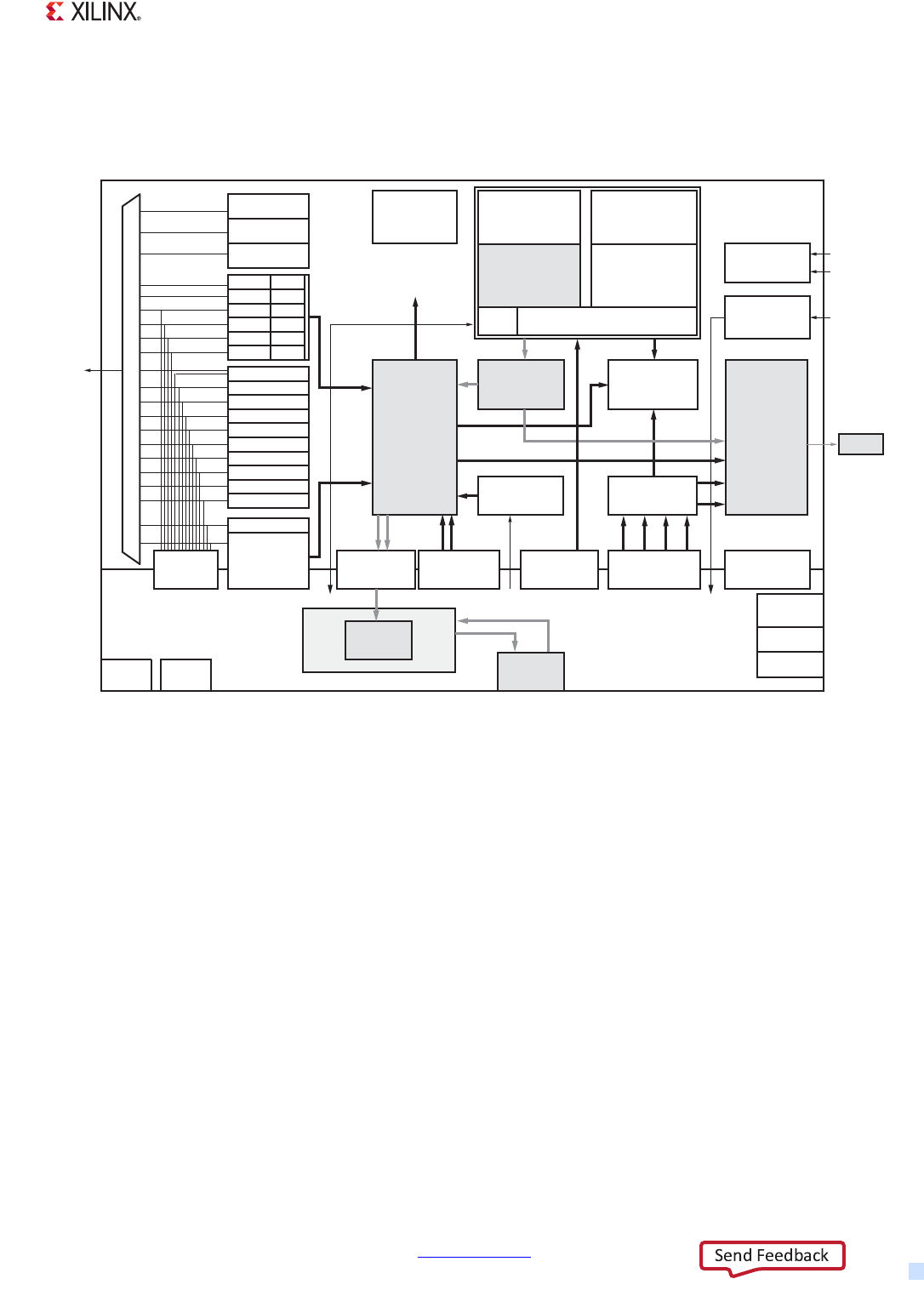
Zynq-7000 AP SoC Technical Reference Manual www.xilinx.com 663
UG585 (v1.12.1) December 6, 2017
Chapter 22: Programmable Logic Design Guide
Drawbacks of using a CPU to move data is that a sophisticated CPU is spending cycles performing
simple data movement instead of complex control and computation tasks, and the limited
throughput available. Transfer rates less than 25 MB/s are reasonable with this method.
22.4.3 PS DMA Controller (DMAC) via General Purpose Masters
The PS DMA controller (DMAC) provides a flexible DMA engine that can provide moderate levels of
throughput with little PL logic resource usage (see Figure 22-2). The DMAC resides in the PS and
must be programmed via DMA instructions residing in memory, typically prepared by a CPU. With
support for up to eight channels, multiple DMA fabric cores can potentially be served in the single
DMAC. However, the flexible programmable model might increase software complexity relative to
CPU transfer or specialized PL DMA.
The DMAC interface to the PL is through the general purpose AXI master interfaces, whose 32-bit
width along with the centralized DMA nature (a read and write transaction for each movement) of the
DMAC to limit the DMAC from highest throughput. A peripheral request interface also allows PL
slaves to provide status to the DMAC on buffer state, to prevent transactions involving a stalled PL
peripheral from unnecessarily also stalling interconnect and DMAC bandwidth.
See Chapter 9, DMA Controller for more information on the DMAC controller. More information on
the M_AXI_GP interfaces can be found in Chapter 5, Interconnect.
X-Ref Target - Figure 22-1
Figure 22-1: Example Cortex-A9 PL Data Movement Topology
IRQ
L2
Cache Memory
512 KB
DDR
Memory
Controller
16-bit
32-bit
16-bit w/ECC
DMA
8 channel
PCAP
Processor Config
Access Port
M_AXI_GP x 2
General Purpose
32-bit AXI Master
S_AXI_GP x 2
General Purpose
32-bit AXI Slave
S_AXI_HP x 4
AXI Data
32/64-bit Slave
SCU – Snoop Control Unit
Central
Interconnect
ARM A9
32 KB I-Cache
32 KB D-Cache
NEON
SP, DP FPU
128-bit Vector DSP
OCM
On Chip Memory
256 KB
S_AXI_ACP
AXI Coherent
64-bit Slave
Mem Switch
SLCR
System Level
Control
Registers
I/O Interface Security
Config
XADC
16 ch ADC
Block RAM User
IP
PCIe
Quad-SPI
1,2,4,8-bit
Parallel 8-bit
NOR/SRAM
NAND 8,16-bit
UART
UART
SPI
SPI
I2C
I2C
CAN
CAN
TTC/SWDT
PJTAG
Reset
CLK / PLL
ARM, I/O, DDR
PS_POR_B
PS_SRST_B
PS_CLK
DDR
CoreSight
Trace In
Trace Out
Cross Trigger
DAP
APB
Register Access
Processing
System (PS)
EMIO
USB
USB
GigE
GigE
SD
SD
DMA
DMA
DMA
DMA
DMA
DMA
GPIO x54, x64
MIO
Pins
GTX or
GTP
NEON
SP, DP FPU
128-bit Vector DSP
ARM A9
32 KB I-Cache
32 KB D-Cache
UG585_c22_03_102414
Programmable
Logic (PL)
NOTE: GigaBit Transceiver and PCIe
functionality are not available in
all device versions and packages.

Zynq-7000 AP SoC Technical Reference Manual www.xilinx.com 664
UG585 (v1.12.1) December 6, 2017
Chapter 22: Programmable Logic Design Guide
22.4.4 PL DMA via AXI High-Performance (HP) Interface
The high-performance (S_AXI_HP) PL interfaces provide high-bandwidth PL slave interfaces to OCM
and DDR memories. The AXI_HP ports are unable to access any other slaves. With four, 64-bit wide
interfaces, the AXI_HP provide the greatest aggregate interface bandwidth. The multiple interfaces
also save PL resources by reducing the need to a PL AXI interconnect. Each AXI_HP contains control
and data FIFOs to provide buffering of transactions for larger sets of bursts, making it ideal for
workloads such as video frame buffering in DDR. This additional logic and arbitration does result in
higher minimum latency than other interfaces.
The user IP logic residing in the PL will generally consist of a low-speed control interface and higher
performance burst interface, as shown in Figure 22-3. If control flow is orchestrated by the
Cortex-A9 CPU, the general purpose M_AXI_GP port can be used for tasks such as configuring the
memory addresses the User IP should access and transaction status. Transaction status can also be
conveyed via PL to PS interrupts. Higher performance devices connected to AXI_HP should be able to
issue multiple outstanding transactions to take advantage of the AXI_HP FIFOs.
The PL design complexity of multiple AXI interfaces along with the associated PL utilization are the
primary drawbacks of implementing a DMA engine in the PL for both S_AXI_HP and S_AXI_ACP
interfaces.
See Chapter 5, Interconnect for more information on the AXI_HP interface.
X-Ref Target - Figure 22-2
Figure 22-2: Example DMAC DMA Topology
IRQ
L2
Cache Memory
512 KB
DDR
Memory
Controller
16-bit
32-bit
16-bit w/ECC
DMA
8 channel
PCAP
Processor Config
Access Port
M_AXI_GP x 2
General Purpose
32-bit AXI Master
S_AXI_GP x 2
General Purpose
32-bit AXI Slave
S_AXI_HP x 4
AXI Data
32/64-bit Slave
SCU – Snoop Control Unit
Central
Interconnect
ARM A9
32 KB I-Cache
32 KB D-Cache
NEON
SP, DP FPU
128-bit Vector DSP
OCM
On Chip Memory
256 KB
S_AXI_ACP
AXI Coherent
64-bit Slave
Mem Switch
SLCR
System Level
Control
Registers
I/O Interface Security
Config
XADC
16 ch ADC
Block RAM User
IP
Control
Quad-SPI
1,2,4,8-bit
Parallel 8-bit
NOR/SRAM
NAND 8,16-bit
UART
UART
SPI
SPI
I2C
I2C
CAN
CAN
TTC/SWDT
PJTAG
Reset
CLK / PLL
ARM, I/O, DDR
PS_POR_B
PS_SRST_B
PS_CLK
DDR
CoreSight
Trace In
Trace Out
Cross Trigger
DAP
APB
Register Access
Processing
System (PS)
EMIO
USB
USB
GigE
GigE
SD
SD
DMA
DMA
DMA
DMA
DMA
DMA
GPIO x54, x64
MIO
Pins
NEON
SP, DP FPU
128-bit Vector DSP
ARM A9
32 KB I-Cache
32 KB D-Cache
UG585_c22_04_102414
Programmable
Logic (PL)
PCIe
GTX or
GTP
NOTE: GigaBit Transceiver and PCIe
functionality are not available in
all device versions and packages.
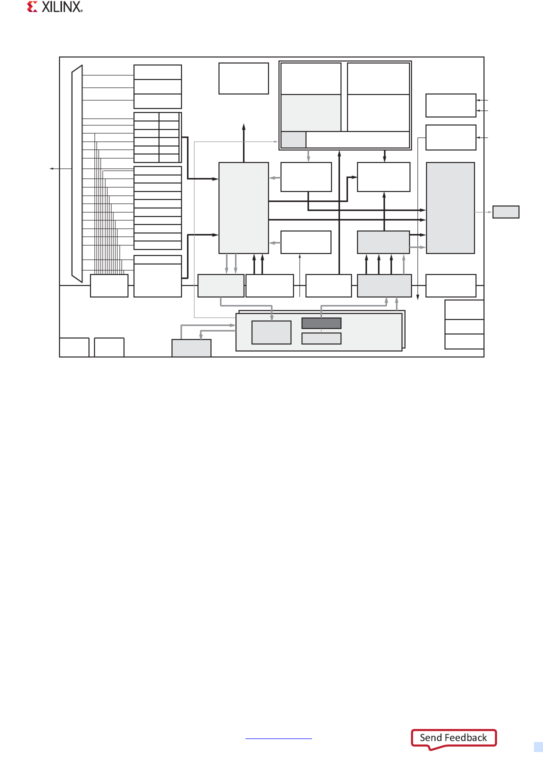
Zynq-7000 AP SoC Technical Reference Manual www.xilinx.com 665
UG585 (v1.12.1) December 6, 2017
Chapter 22: Programmable Logic Design Guide
22.4.5 PL DMA via AXI ACP
The AXI ACP interface (S_AXI_ACP) provides a similar user IP topology as the high performance
S_AXI_HP interfaces. Also 64 bits wide, the ACP also provides highest throughput capability for a
single AXI interface. As shown in Figure 22-4, the User IP topology is likely often similar to the
S_AXI_HP example in the previous section.
The ACP differs from the HP performance ports due to its connectivity inside of the PS. The ACP
connects to the snoop control unit (SCU) which is also connected to the CPU L1 and the L2 cache.
This connectivity allows ACP transactions to interact with the cache subsystems, potentially
decreasing total latency for data to be consumed by a CPU. These optionally cache-coherent
operations can prevent the need to invalidate and flush cache lines. The ACP also has the lowest
memory latency to memory of the PL interfaces. The connectivity of the ACP is similar to that of the
CPUs.
The drawbacks from using the ACP besides those shared with the S_AXI_HP interfaces also stem from
the locality to the cache and CPUs. Memory accesses through the ACP utilize the same interconnect
paths as the APU, potentially decreasing CPU performance. Large, coherent ACP transfers can cause
thrashing of the cache. Thus ACP coherent transfers are best suited for less than the largest
data-sets. The ACP low-latency access allows opportunity for algorithm acceleration of medium
granularity.
X-Ref Target - Figure 22-3
Figure 22-3: Example High-Performance (HP) DMA Topology
IRQ
L2
Cache Memory
512 KB
DDR
Memory
Controller
16-bit
32-bit
16-bit w/ECC
DMA
8 channel
PCAP
Processor Config
Access Port
M_AXI_GP x 2
General Purpose
32-bit AXI Master
S_AXI_GP x 2
General Purpose
32-bit AXI Slave
S_AXI_HP x 4
AXI Data
32/64-bit Slave
SCU – Snoop Control Unit
Central
Interconnect
ARM A9
32 KB I-Cache
32 KB D-Cache
NEON
SP, DP FPU
128-bit Vector DSP
OCM
On Chip Memory
256 KB
S_AXI_ACP
AXI Coherent
64-bit Slave
Mem Switch
SLCR
System Level
Control
Registers
Security
Config
XADC
16 ch ADC
Block RAM
DMA User
IP
Control
I/O Interface
Quad-SPI
1,2,4,8-bit
Parallel 8-bit
NOR/SRAM
NAND 8,16-bit
UART
UART
SPI
SPI
I2C
I2C
CAN
CAN
TTC/SWDT
PJTAG
Reset
CLK / PLL
ARM, I/O, DDR
PS_POR_B
PS_SRST_B
PS_CLK
DDR
CoreSight
Trace In
Trace Out
Cross Trigger
DAP
APB
Register Access
Processing
System (PS)
EMIO
USB
USB
GigE
GigE
SD
SD
DMA
DMA
DMA
DMA
DMA
DMA
GPIO x54, x64
MIO
Pins
NEON
SP, DP FPU
128-bit Vector DSP
ARM A9
32 KB I-Cache
32 KB D-Cache
UG585_c22_05_102414
Programmable
Logic (PL)
PCIe
GTX or
GTP
NOTE: GigaBit Transceiver and PCIe
functionality are not available in
all device versions and
packages.
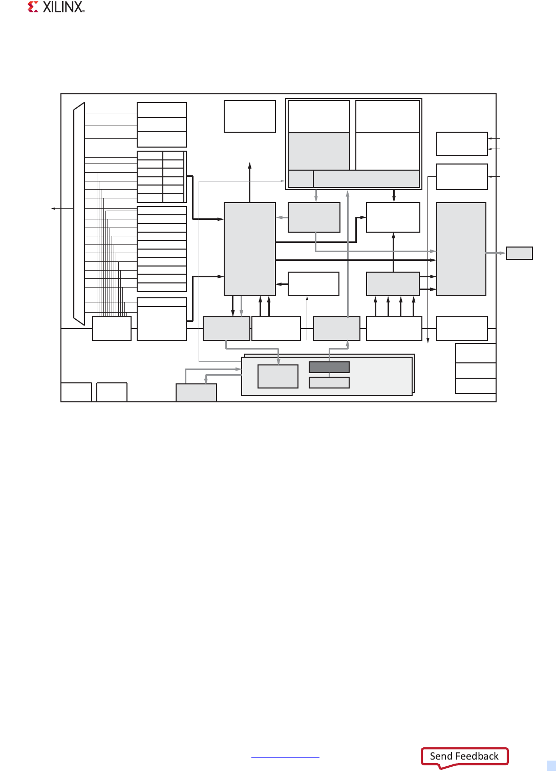
Zynq-7000 AP SoC Technical Reference Manual www.xilinx.com 666
UG585 (v1.12.1) December 6, 2017
Chapter 22: Programmable Logic Design Guide
For more information on S_ACI_ACP, see Chapter 3, Application Processing Unit. See Chapter 29,
On-Chip Memory (OCM) when using ACP with OCM.
22.4.6 PL DMA via General Purpose AXI Slave (GP)
While the general purpose AXI Slave (S_AXI_GP) has reasonably low latency to OCM and DDR, its
narrow 32-bit interface limits its utility as a DMA interface. The two S_AXI_GP interfaces are more
likely to be used for lower-performance control access to the PS memories, registers and peripherals.
More information on the S_AXI_GP interfaces can be found in Chapter 5, Interconnect.
X-Ref Target - Figure 22-4
Figure 22-4: Example ACP DMA Topology
PCIe
GTX or
GTP
NOTE: GigaBit Transceiver and PCIe
functionality are not available in
all device versions
and packages.
IRQ
L2
Cache Memory
512 KB
DDR
Memory
Controller
16-bit
32-bit
16-bit w/ECC
DMA
8 channel
PCAP
Processor Config
Access Port
M_AXI_GP x 2
General Purpose
32-bit AXI Master
S_AXI_GP x 2
General Purpose
32-bit AXI Slave
S_AXI_HP x 4
AXI Data
32/64-bit Slave
SCU – Snoop Control Unit
Central
Interconnect
ARM A9
32 KB I-Cache
32 KB D-Cache
NEON
SP, DP FPU
128-bit Vector DSP
OCM
On Chip Memory
256 KB
S_AXI_ACP
AXI Coherent
64-bit Slave
Mem Switch
SLCR
System Level
Control
Registers
Security
Config
XADC
16 ch ADC
Block RAM
DMA User
IP
Control
I/O Interface
Quad-SPI
1,2,4,8-bit
Parallel 8-bit
NOR/SRAM
NAND 8,16-bit
UART
UART
SPI
SPI
I2C
I2C
CAN
CAN
TTC/SWDT
PJTAG
Reset
CLK / PLL
ARM, I/O, DDR
PS_POR_B
PS_SRST_B
PS_CLK
DDR
Coresight
Trace In
Trace Out
Cross Trigger
DAP
APB
Register Access
Processing
System (PS)
EMIO
USB
USB
GigE
GigE
SD
SD
DMA
DMA
DMA
DMA
DMA
DMA
GPIO x54, x64
MIO
Pins
NEON
SP, DP FPU
128-bit Vector DSP
ARM A9
32 KB I-Cache
32 KB D-Cache
UG585_c22_06_102414
Programmable
Logic (PL)

Zynq-7000 AP SoC Technical Reference Manual www.xilinx.com 667
UG585 (v1.12.1) December 6, 2017
Chapter 23
Programmable Logic Test and Debug
23.1 Introduction
Zynq-7000 AP SoC devices provides extensive debug capability for accessing the PS debug structure
(see Chapter 28, System Test and Debug) from the PL. This allows for integrated test and debug on
both PS and PL simultaneously.
Xilinx provides the fabric trace monitor (FTM) for programmable logic test and debug. It is based on
the ARM CoreSight architecture, and is a component of the trace source class (see Chapter 28,
System Test and Debug) in the CoreSight system within Zynq-7000 AP SoC devices. The FTM receives
trace data from the PL and formats it into trace packets to be combined with the trace packets from
other trace source components such as PTM and ITM. With this capability, PL events can easily be
traced simultaneously with PS events. The FTM also supports cross-triggering between the PS and
PL, except for the trace dumping feature. In addition, the FTM provides general-purpose debug
signals between the PS and PL.
23.1.1 Features
The key features of the PL test and debug are as follows:
• ARM CoreSight compliant
• 32-bit trace data from the PL
• 4-bit trace ID from the PL
• Clock domain crossing between the PL and PS
• FIFO buffering for trace packets to absorb bursts of trace data from the PL
• Indication of FIFO overflow via generation of an overflow packet
• Trace packets are compatible with ARM trace port software and hardware
• Trigger signals to/from the PL
• General-purpose I/Os to/from the PL
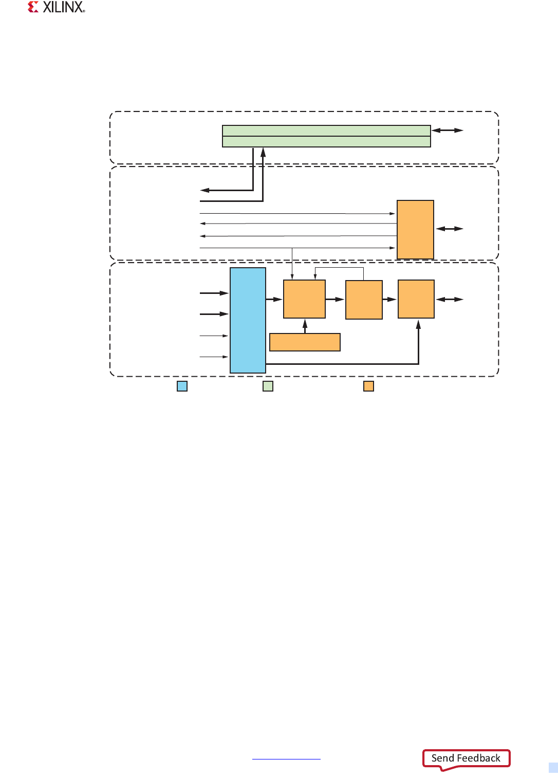
Zynq-7000 AP SoC Technical Reference Manual www.xilinx.com 668
UG585 (v1.12.1) December 6, 2017
Chapter 23: Programmable Logic Test and Debug
23.1.2 Block Diagram
A block diagram of the FTM is shown in Figure 23-1.
As shown in Figure 23-1, the following functional blocks comprise the FTM:
•APB Interface
°This is the interface to the CoreSight debug APB, through which CPUs and JTAG can interact
with the FTM.
•FTM Registers
°These are programmable registers.
• Clock Domain Crossing
°This block synchronizes signals between the PL clock domain and the PS clock domain.
•PL Debug Ports
°This block provides:
- General purpose I/Os, 32 bits to the PL and 32 bits from the PL. These are accessed
through reads and writes to registers.
- Trigger signals, 4 pairs to the PL and 4 pairs from the PL. Each pair consists of a trigger
signal and an acknowledge signal, and follows ARM standard CTI handshake protocol.
X-Ref Target - Figure 23-1
Figure 23-1: FTM Block Diagram
ATB
Interface
Cross
Trigger
Interface
FTMDTRACEINDATA[31:0]
ATB
FPGA Clock Domain Debug APB Clock Domain ATB Clock Domain
FTMDTRACEINATID[3:0]
FIFO
Cycle Count
Generator
Packet
Formatter
Clock
Domain
Crossing
FTMDTRACEINCLOCK
FTMDTRACEINVALID
FTMTF2PTRIG[0]
APB Interface
FTM Registers
APB
FTMTF2PTRIGACK[3:0]
FTMTP2FTRIG[3:0]
FTMTP2FTRIGACK[3:0]
FTMTF2PTRIG[3:0]
CTI
FTMTF2PDEBUG[31:0]
FTMTP2FDEBUG[31:0]
PL Debug
PL Trace
UG585_c23_01_030312

Zynq-7000 AP SoC Technical Reference Manual www.xilinx.com 669
UG585 (v1.12.1) December 6, 2017
Chapter 23: Programmable Logic Test and Debug
- Trigger input 0 (FTMTF2PTRIG[0]) can be used to generate trigger packets.
• Packet Formatter
°This block is responsible for gathering trace data and formatting the data into trace packets.
In addition to trace packets, the packet formatter can also generate various other types of
packets to convey additional information to the CoreSight system within the PS.
• Cycle Count Generator
°This block is used to provide a binary count value for time stamping packets. This is
achieved by a counter, which is:
- 32-bit, free-running, clocked by CPU_2x
- Pre-scaled by 2^CYCOUNTPRE (range:1 to 32,768)
- Reset by POR, FTMGLBCTRL[FTMENABLE]==0, CoreSight reset request through JTAG
•FIFO
°The FIFO is used to buffer packets before they are sent to the ATB. The FIFO has these
properties:
- 64-packets deep
- When the FIFO overflows, it signals the packet formatter to generate an overflow packet.
In this case, some trace data is lost.
•ATB Interface
°This is the interface to the CoreSight ATB, over which packets are sent.
• Cross Trigger Interface
°This block is the interface to the CoreSight ECT system (see Chapter 28, System Test and
Debug).
23.1.3 System Viewpoint
For details on how the FTM is connected to, and interacts with, the rest of the CoreSight system
within the PS, see Chapter 28, System Test and Debug.
23.2 Functional Description
23.2.1 Basic Operation
The PL trace module captures the trace data from the PL. The user supplies the trace data, trace ID,
valid, and clock signals to the FTM at the PL-PS boundary. All data, ID, and valid signals must be
stable on the rising edge of the FTMDTRACEINCLOCK signal for the FTM to correctly sample them.
When FTMDTRACEINVALID is asserted, the PL trace signals are available to the clock domain crossing
interface, which synchronizes the data and ID, and sends them to the packet formatter.
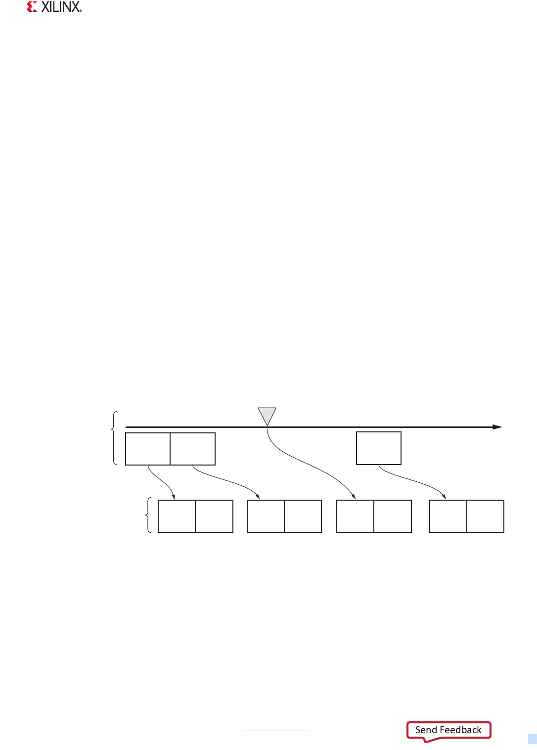
Zynq-7000 AP SoC Technical Reference Manual www.xilinx.com 670
UG585 (v1.12.1) December 6, 2017
Chapter 23: Programmable Logic Test and Debug
The packet formatter generates packets and submits them to the FIFO. The packet formatter can
generate the following types of packets:
• Trace packets: These packets are generated when valid trace data is available from the PL.
• Trigger packets: These trigger packets can only be generated by the FTMTF2PTRIG[0] signal.
• Cycle count packets: These packets provide continuous timestamps that are used to reconstruct
a real-time trace.
• Overflow packets: These packets are generated when the FIFO overflows.
• Synchronization packets: These packets are for packet analysis tools to re-align to packet
boundaries.
The cross trigger interface communicates with the CoreSight ECT structure. This interface passes
re-synchronized trigger signals between the PL and the ECT. This provides the capability of
cross-triggering each other between the PS and PL.
23.2.2 Packet Generation
The following are some common scenarios that illustrate packet generation by the FTM.
Typical Case – Trace Enabled, Cycle Count Enabled
When a valid PL trace (FTMDTRACEINVALID is asserted) is captured, a trace packet and a cycle count
packet are generated and sent to the ATB. When a trigger occurs (via the FTMTF2PTRIG[0] signal), a
trigger packet and a cycle count packet are generated and sent to the ATB.
X-Ref Target - Figure 23-2
Figure 23-2: Packet Generation, Typical Case
PL Trace
Valid
Trace
Packet
Cycle
Count
Packet
PL Trace
Valid
UG585_c23_02_030312
PL Trace
Valid
PL
Activity
Packets
Generated
Time
Trigger
Trigger
Packet
Cycle
Count
Packet
Trace
Packet
Cycle
Count
Packet
Trace
Packet
Cycle
Count
Packet
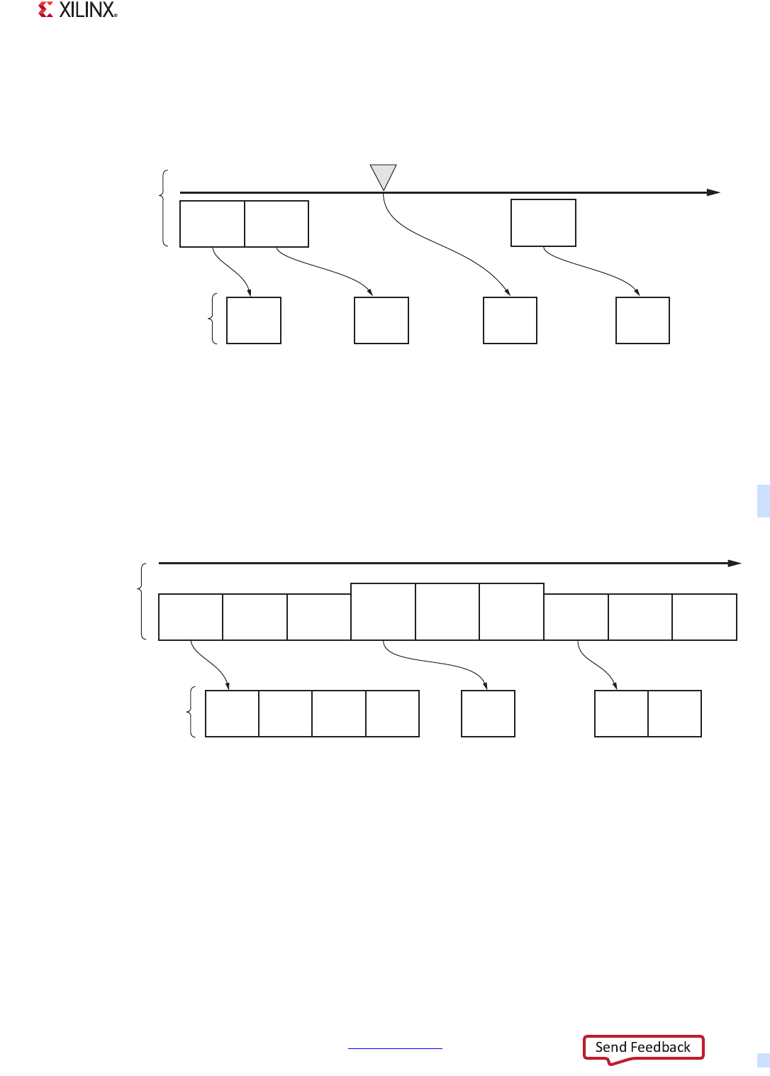
Zynq-7000 AP SoC Technical Reference Manual www.xilinx.com 671
UG585 (v1.12.1) December 6, 2017
Chapter 23: Programmable Logic Test and Debug
No Cycle Count Case – Trace Enabled, Cycle Count Disabled
This is similar to the preceding case, except that cycle count packets are not generated.
FIFO Overflow Case – Lost Trace
In this scenario, trace packets are not generated until the FIFO is no longer in an overflow condition.
An overflow packet is generated to indicate that there was an overflow condition and some trace
packets are lost. At least 8 clock cycles of FTMDTRACEINCLOCK are needed between
FTMDTRACEINDATA packets to avoid a FIFO overflow condition.
X-Ref Target - Figure 23-3
Figure 23-3: Packet Generation, No Cycle Count Case
X-Ref Target - Figure 23-4
Figure 23-4: Packet Generation, FIFO Overflow Case
PL Trace
Valid
Trace
Packet
PL Trace
Valid
UG585_c23_03_030312
PL Trace
Valid
PL
Activity
Packets
Generated
Time
Trigger
Trigger
Packet
Trace
Packet
Trace
Packet
PL Trace
Valid
Trace
Packet
Cycle
Count
Packet
PL Trace
Valid
PL Trace
Valid
UG585_c23_04_030712
PL Trace
Valid
(lost)
PL Trace
Valid
(lost)
PL Trace
Valid
(lost)
PL Trace
Valid
PL Trace
Valid
PL Trace
Valid
PL
Activity
Packets
Generated
Time
Overflow
Packet
Trace
Packet
Cycle
Count
Packet
Trace
Packet
Cycle
Count
Packet
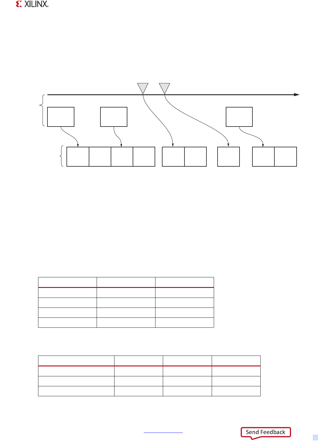
Zynq-7000 AP SoC Technical Reference Manual www.xilinx.com 672
UG585 (v1.12.1) December 6, 2017
Chapter 23: Programmable Logic Test and Debug
Synchronization Case
This scenario illustrates how a synchronization packet is generated amid other types of packets. The
FTMSYNCRELOAD register sets the number of packets for which a synchronization packet must be
generated.
23.2.3 Packet Format
General Format
A packet consists of a number of bytes. Table 23-1 shows the basic format of a packet. Except for the
synchronization packet and the cycle count packet, the first and the last bytes of a packet have their
MSB set to 0 to signify the start/stop of the packet; all bytes between the first and the last bytes have
their MSB set to 1.
Tabl e 23- 2 shows the encoding values for the “type” byte.
X-Ref Target - Figure 23-5
Figure 23-5: Packet Generation, Synchronization Case
PL Trace
Valid
Trace
Packet
Cycle
Count
Packet
PL Trace
Valid
UG585_c23_05_030712
PL Trace
Valid
PL
Activity
Packets
Generated
Time
Trigger Sync
Trace
Packet
Cycle
Count
Packet
Trace
Packet
Cycle
Count
Packet
Sync
Packet
Trace
Packet
Cycle
Count
Packet
Table 23-1: General Packet Format
Byte [7] [6:0]
00type
11data
…1data
n0data
Table 23-2: “Type” Byte Encoding
Type [7] [6:3] [2:0]
Trace packet 0trace[3:0] 101
Trigger packet 0 0100 000
Cycle count packer 1count[3:0] 100
Zynq-7000 AP SoC Technical Reference Manual www.xilinx.com 673
UG585 (v1.12.1) December 6, 2017
Chapter 23: Programmable Logic Test and Debug
Trace Packet
A trace packet contains the 32-bit value from each captured FTMDTRACEINDATA[31:0] from the PL.
The MSB of the last byte is determined by the presence of an immediately following cycle count
packet. If a cycle count packet follows, the MSB is 1, otherwise it is 0.
Trigger Packet
A trigger packet is generated for each acknowledged trigger input [0] from the PL, i.e., when both
FTMTF2PTRIG[0] and FTMTF2PTRIGACK[0] are High.
Cycle Count Packet
A cycle count packet is generated when FTMCONTROL[CYCEN] is set, and a trace packet or a trigger
packet is generated. It contains a binary count value taken from the current value of the internal
32-bit free-running counter. It is always a continuation of an immediately preceding trace packet or
trigger packet.
FIFO overflow packet 0 1101 000
Synchronization packet 0 0000 000
Table 23-3: Trace Packet Format
Byte [7] [6:0]
00data[3:0], 101
11data[10:4]
21data[17:11]
31data[24:18]
4 count data[31:25]
Table 23-4: Trigger Packet Format
Byte [7:0]
00x20
10xA0
20xA0
30x20 or 0xA0
Table 23-5: Cycle Count Packet Format
Byte [7] [6:0]
01count[3:0], 100
11count[10:4]
21count[17:11]
Table 23-2: “Type” Byte Encoding (Cont’d)
Type [7] [6:3] [2:0]
Zynq-7000 AP SoC Technical Reference Manual www.xilinx.com 674
UG585 (v1.12.1) December 6, 2017
Chapter 23: Programmable Logic Test and Debug
FIFO Overflow Packet
A FIFO overflow packet is generated when a FIFO overflow occurs.
First Packet After Enable
The trace buffer might include a packet with the value 0x28A8A828 after the FTM is enabled.
Synchronization Packet
A synchronization packet allows the packet analysis tools to periodically re-align to correct packet
boundaries, because the packet formatter does not maintain 32-bit word boundaries for packets. The
synchronization packet follows the same format as other CoreSight components.
31count[24:18]
40count[31:25]
Table 23-6: Overflow Packet Format
Byte [7:0]
00x68
10xE8
20xE8
30x68
Table 23-7: Synchronization Packet Format
Byte [7:0]
0-7 0x00
80x80
Table 23-5: Cycle Count Packet Format (Cont’d)
Byte [7] [6:0]

Zynq-7000 AP SoC Technical Reference Manual www.xilinx.com 675
UG585 (v1.12.1) December 6, 2017
Chapter 23: Programmable Logic Test and Debug
23.3 Signals
The FTM control signals are described in the following sections.
23.3.1 General-Purpose Debug Signals
23.3.2 Trigger Signals
Table 23-8: General-Purpose Debug Signals
Group PS-PL Signal IO Description
General purpose
debug output
FTMTP2FDEBUG[7:0] O The FTMP2FDBG0 register controls its value.
FTMTP2FDEBUG[15:8] O The FTMP2FDBG1 register controls its value.
FTMTP2FDEBUG[23:16] O The FTMP2FDBG2 register controls its value.
FTMTP2FDEBUG[31:24] O The FTMP2FDBG3 register controls its value.
General purpose
debug input
FTMTF2PDEBUG[7:0] I The FTMF2PDBG0 register shows its value.
FTMTF2PDEBUG[15:8] I The FTMF2PDBG1 register shows its value.
FTMTF2PDEBUG[23:16] I The FTMF2PDBG2 register shows its value.
FTMTF2PDEBUG[31:24] I The FTMF2PDBG3 register shows its value.
Table 23-9: Trigger Signals
Group PS-PL Signal IO Description
Trigger from
PS to PL
FTMTP2FTRIG[3:0] O
Each bit is an asynchronous trigger signal from the
CoreSight ECT structure in the PS to the PL. Users must
program the CTI connected to the FTM to enable these
trigger output signals.
FTMTP2FTRIGACK[3:0] I Each bit is the asynchronous acknowledge signal for the
corresponding FTMTP2FTRIG signal.
Trigger from
PL to PS
FTMTF2PTRIG[3:0] I
Each bit is an asynchronous trigger signal from the PL
to the CoreSight ECT structure in the PS. Users must
program the CTI connected to FTM to enable these
trigger input signals.
FTMTF2PTRIGACK[3:0] O Each bit is the asynchronous acknowledge signal for the
corresponding FTMTF2PTRIG signal.

Zynq-7000 AP SoC Technical Reference Manual www.xilinx.com 676
UG585 (v1.12.1) December 6, 2017
Chapter 23: Programmable Logic Test and Debug
23.3.3 Trace Signals
23.4 Register Overview
Table 23-10: Trace Signals
Group PS-PL Signal IO Description
Trace from
PL to PS
FTMDTRACEINCLOCK I Clock signal for the trace data interface. Asynchronous
to the PS.
FTMDTRACEINVALID I
When this signal is sampled High by the PS using
FTMDTRACEINCLOCK, the values on
TRMDTRACEINDATA and FTMDTRACEINATID are valid.
FTMDTRACEINDATA[31:0] I Trace data. All 32 bits must be provided.
FTMDTRACEINATID[3:0] I Trace ID to be carried over to the ATB. All 4 bits must be
provided.
Table 23-11: Register Overview
Function Name Overview
Control FTMGLBCTRL
FTMCONTROL
Enable FTM, enable cycle count packets, enable trace
packets.
Status FTMSTATUS Idle status, security signal values, FIFO full/empty.
General debug FTMP2FDBG
FTMF2PDGB
Set the values of the signals presented to the PL.
Read the values of the signals from the PL.
Cycle counter prescaler FTMCYCCOUNTPRE Set the prescaler value for the cycle counter.
Synchronization counter FTMSYNCRELOAD
FTMSYNCCOUNT
Set how often synchronization packets should be
generated.
Configuration FTMDTRACEINATID Set the ATID value to the ATB bus.
CoreSight management
Peripheral ID
Component ID
Device ID, type
Authentication
Integration test
These registers provide:
• Identification information
• Authentication and access control
• Integration test

Zynq-7000 AP SoC Technical Reference Manual www.xilinx.com 677
UG585 (v1.12.1) December 6, 2017
Chapter 23: Programmable Logic Test and Debug
23.5 Programming Model
23.5.1 FTM Security
FTM security is controlled through the use of the standard CoreSight mechanisms, the SPNIDEN,
SPIDEN, NIDEN, and DBGEN signals from the DevC module.
The following actions are taken by the FTM when the corresponding signals are asserted:
• SPNIDEN: FTM trace operations can be enabled.
• SPIDEN: The FTMP2FDBG registers can be modified.
• NIDEN: No effect.
• DBGEN: No effect.

Zynq-7000 AP SoC Technical Reference Manual www.xilinx.com 678
UG585 (v1.12.1) December 6, 2017
Chapter 24
Power Management
24.1 Introduction
Power optimization can start with selecting the right Zynq-7000 AP SoC device. For low-power
applications, choose either the 7z010 or 7z020 dual core device or the 7z007s, 7z012s, or 7z014s
single core device. Power can dramatically be reduced by shutting-down the PL side of the device.
I/O voltage and termination choice also affects power consumption. The clocks to individual PS
subsystems can be stopped.
The functionality of the PS is the same for all Zynq-7000 AP SoC devices except that the 7z007S and
7z010 devices have a reduced MIO pin count which impacts the availability of the Ethernet, USB and
other controllers. The two Zynq data sheets describe the clock frequency differences. The PL resource
differences for each device type are shown in section 21.1.2 PL Resources by Device Type.
Detailed device level power estimates for the PS and PL can be obtained using the XPE power
estimator spreadsheet. Power specifications are found in the Zynq-7000 AP SoC device datasheets
(see Appendix A, Additional Resources for a list of related documents).
24.1.1 Features
Key system power management features are as follows.
• Choose between device technology:
°7z010 and 7z020 dual core or 7z007s, 7z012s, or 7z014s single core (derived from Artix AP
FPGA technology)
°7z030, 7z035, 7z045, and 7z100 (derived from Kintex AP FPGA technology)
•PL power-off
• Cortex A9 processor standby mode
•Clock gating for most PS subsystems
• Three PLLs can be programmed to minimize power consumption
• Subsystem clocks can be programmed for optional clock frequency
• Programmable voltage for I/O Banks:
°MIO: HSTL 1.8V, LVCMOS 1.8V, 2.5V and 3.3V
°DDR: DDR2 1.8V, DDR3 1.5V and LPDDR2 1.2V
• DDR3 and LPDDR2 low power mode

Zynq-7000 AP SoC Technical Reference Manual www.xilinx.com 679
UG585 (v1.12.1) December 6, 2017
Chapter 24: Power Management
• DDR 16 or 32-bit data I/O
• Internal and external voltage measurements using XADC
24.2 System Design Considerations
The section includes these system design considerations:
•24.2.1 Device Technology Choice
•24.2.2 PL Power-down Control
•24.2.3 APU Maximum Frequency
•24.2.4 DDR Memory Clock Frequency
•24.2.5 DDR Memory Controller Modes and Configurations
•24.2.6 Boot Interface Options
•24.2.7 PS Clock Gating
24.2.1 Device Technology Choice
There is a power and performance distinction between the low power devices (7z010/7z020 dual
core and 7z007s/7z012s/7z014s single core) and the high performance devices (7z030, 7z035, 7z045,
and 7z100). The low power devices are derived from the 7 series Artix AP FPGAs. The larger and
higher performance devices are derived from the Kintex AP FPGAs.
Within the PS and PL, multiple power supplies are used to power core logic, I/Os, and auxiliary
circuits. Independent I/O banks allow a mix of 1.8V, 2.5V, and 3.3V I/O standards. The PS also contains
a DDR interface supporting DDR2, DDR3, and LPDDR2 which operate at 1.8V, 1.5V and 1.2V,
respectively.
The Zynq-7000 AP SoC family supports voltage and temperature monitoring by utilizing the sensors
in the Xilinx ADC (XADC) subsystem (refer to Chapter 30, XADC Interface). The XADC provides
real-time monitoring of voltage and temperature levels within the device.
24.2.2 PL Power-down Control
In case the PL is not used, it can be completely shut down to save power. This requires independently
connected power supplies for the PS and PL. Furthermore, some restrictions apply during boot and
power off. Refer to DS187 and DS191, Zynq-7000 All Programmable SoC DC and AC Switching
Characteristics for more details. An example sequence to power-down the PL is provided in section
2.4 PS–PL Voltage Level Shifter Enables.
The PL power system can be controlled via GPIOs, the I2C controller, or an external processor. When
the PL is powered off all PS to PL signals, including EMIO, PL AXI, should not be accessed.
The PL loses its configuration when powered down and must be reconfigured when it is powered on
again. Software should determine when it is safe to power down the PL.

Zynq-7000 AP SoC Technical Reference Manual www.xilinx.com 680
UG585 (v1.12.1) December 6, 2017
Chapter 24: Power Management
24.2.3 APU Maximum Frequency
For applications which do not require the maximum amount of processing performance, the APU
maximum frequency can be reduced to meet application needs. A lower clock frequency can
significantly reduce the operating power when compared to operating at a higher frequency.
24.2.4 DDR Memory Clock Frequency
For applications which do not require the maximum amount of DDR bandwidth, the DDR bandwidth
can be reduced to meet application needs. This can reduce operating power significantly compared
operating at a higher frequency, but more importantly, allows the use of lower power DDR standards
and configurations.
24.2.5 DDR Memory Controller Modes and Configurations
The DDR2, DDR3, and LPDDR2 DDR standards are supported in both 16- and 32-bit data operation.
DDR power can be a significant percentage of total power, so minimizing DDR power is an important
means of reducing system power.
The following features impact DDR power:
• The highest power DDR standard is a DDR2 due to the 1.8V operating voltage and the
termination requirements.
• The highest speed DDR standard is DDR3 operating up to 1,066 Mb/s in -1 devices.
• The lowest power interface DDR standard is LPDDR2 due to the 1.2V operating voltage and the
unterminated I/Os, however rates are limited compared to DDR3.
• DDR width can be set to 16 or 32 bits. Note that, for ECC, use a 32-bit bus width (16-bit data,
10-bit ECC).
• The total number of DDR devices in the system impacts system power. For example, four 8-bit
DDR devices have a higher system power than two 16-bit devices.
• 32-bit DDR devices are available only for LPDDR2.
• Termination strength: If possible use the highest possible termination value. A termination value
of 40Ω is 50% more termination power than 60Ω.
24.2.6 Boot Interface Options
The PS supports boot from Quad-SPI, NAND, and NOR devices. Boot devices do not impact system
level dynamic power as the boot process only occurs once at device power up. Lower voltage 1.8V
devices are of lower static power than higher 3.3V devices.
24.2.7 PS Clock Gating
The PS supports many clock domains, each with independent clock gating control. When the system
is in run mode, the user is allowed to shut down the clock domains that are not used and reduce the
dynamic power dissipation.

Zynq-7000 AP SoC Technical Reference Manual www.xilinx.com 681
UG585 (v1.12.1) December 6, 2017
Chapter 24: Power Management
24.3 Programming Guides
24.3.1 System Modules
The power management features of the Zynq-7000 AP SoC's system modules are described in detail
in their respective chapter. Please refer to Tabl e 24- 4 for an overview and further references.
24.3.2 Peripherals
The primary peripheral power management mechanisms are clock scaling and gating. Chapter 25,
Clocks describes the system clocks and how they can be controlled through dividers, gates, and
multiplexers. Table 24-2 gives a brief overview of the power management capabilities for the device
subsystems. Every peripheral includes clock gating and, in some cases, low-power states.
With all these pieces working together, the system-level sleep mode is defined. (Refer to section
24.4 Sleep Mode.) In sleep mode the whole chip enters a low-power state, waiting for a wake-up
event to continue operation.
Peripheral Clock Gating
For peripherals with an independent clock domain for the interconnect, disable the device's
interconnect clock last and enable it first to avoid accesses to inaccessible register areas. See
Chapter 25, Clocks and the respective chapter for a peripheral for additional details.
Table 24-1: Power Management for System Modules
System Module Clocked in
Standby Mode Description
APU Yes See Chapter 3, Application Processing Unit.
SCU (with GIC) Yes See Chapter 3, Application Processing Unit.
L2-Cache Yes See Chapter 3, Application Processing Unit.
Interconnect Yes Clocks are stopped automatically if enabled, refer to
Chapter 25, Clocks.
Peripherals Depends Peripheral used as a wake-up source must be clocked, refer to
Table 24-2 .
Table 24-2: Power Management for Peripheral Controls
Peripheral Wake-up Source Clock Gating Low-Power
Mode Other Low-Power Modes
PCAP No No None
Timers Yes
Chapter 8, Timers
Yes
Chapter 25, Clocks None
DMA Controller No
Yes
Section 9.6 System
Functions
None

Zynq-7000 AP SoC Technical Reference Manual www.xilinx.com 682
UG585 (v1.12.1) December 6, 2017
Chapter 24: Power Management
24.3.3 I/O Buffers
Power management for I/O buffer controls are shown in Table 24-3.
DDR Controller No Yes
Section 10.9 Operational Programming Model
Static Memory Controller No Yes
11.2.2 Clocks None
Quad-SPI Controller No
Yes
Section 12.4 System
Functions
None
SDIO Controller No Yes
Chapter 25, Clocks None
GPIO Controller
Yes
Section 14.4 System
Functions
Yes
Section 14.4 System
Functions
None
USB Controller
Yes
Chapter 15, USB Host,
Device, and OTG
Controller
Suspened/Resume
Chapter 15, USB Host,
Device, and OTG Controller
Ethernet Controller Yes
Chapter 25, Clocks
SPI Controller No Yes
18.4 System Functions
CAN Controller Yes
18.4 System Functions
Sleep Mode
18.2.1 Controller Modes
UART Controller
Yes
19.3.5 RxFIFO Trigger
Level Interrupt
Yes
19.4 System Functions None
I2C Controller No Yes
20.4 System Functions None
Programmable Logic Yes
Chapter 25, Clocks User Defined
Table 24-2: Power Management for Peripheral Controls (Cont’d)
Peripheral Wake-up Source Clock Gating Low-Power
Mode Other Low-Power Modes
Table 24-3: Power Management for I/O Buffer Controls
I/O Buffer Signal Voltage Termination and Mode
DDR 1.8V/1.5V/1.2V See section 10.6.3 DDR IOB Configuration
MIO0 and MIO1 1.8V/2.5V/3.3V

Zynq-7000 AP SoC Technical Reference Manual www.xilinx.com 683
UG585 (v1.12.1) December 6, 2017
Chapter 24: Power Management
24.4 Sleep Mode
Sleep mode is defined at the system level to include the APU in standby mode and multiple
controllers being held in reset without a clock.
Going into sleep mode can greatly reduce power consumption. In sleep mode, most function clock
groups are turned off or powered off. The only required active devices are one CPU, the snoop
control unit (SCU), and a wake-up device. Ideally, the only devices causing dynamic power
consumption should be the SCU and the wake-up peripheral device. The wake-up device can be
UART, GPIO, or any device that can generate an interrupt.
If the wake-up device is an AXI bus master, which can start transactions targeting the DRAM,
additional limitations apply. Because the whole interconnect and the DDR memory are in low power
modes and inaccessible, it must be assured that the CPU goes through the full wake-up process
before any transactions to the DRAM take place. This guarantees that potential transactions
targeting the DRAM are served correctly.
24.4.1 Setup Wake-up Events
Every interrupt signaled to the PS can be used as a wake-up event. To make this happen, the wanted
interrupt must be enabled in the peripheral and the GIC. A wake-up device must be able to generate
the interrupt in sleep mode, which means, that its clocks might not be gated off. See GPIO as
Wake-up Event, page 394 for more information.
Refer to the respective chapter for information about available interrupts and how to configure the
peripherals to generate them.
24.4.2 Programming Guide
The following shows the preliminary steps to enter PS sleep mode from normal running mode and
exit from it. In sleep mode, the master CPU is responsible for shutting down all non-wake up devices,
including all other masters in the system and the PL, if possible. Since clock frequencies change when
clock dividers and PLL configurations are changed, configuring a wake-up device might not only
mean activating the wanted wake-up interrupt, but also changing the peripheral configuration to be
able to cope with the modified clock frequency. If both CPUs are running, the master CPU should
shut down the secondary CPU first before proceeding with the steps described below. It is user’s
choice, which CPU acts as master CPU. Furthermore, precautions must be taken to keep code which
is executed while the DDR clocks are disabled accessible in this period e.g., by placing those
code-segments in OCM, or locking the L2 cache and TLB. Depending on the actual implementation
this can, amongst others, apply to:
• Code executed when DDR is not available
• Routine for entering and exiting standby mode
•Translation table
•Stacks

Zynq-7000 AP SoC Technical Reference Manual www.xilinx.com 684
UG585 (v1.12.1) December 6, 2017
Chapter 24: Power Management
The location of the currently used translation table(s) and stacks are controllable through the TTBR
and SP registers, respectively. This allows switching between different structures for normal running
mode and standby mode if needed.
During the standby sequence interrupts are disabled in the CPUs. This way execution cannot be
interrupted while entering standby mode and once the wake-up event occurs execution resumes
right after the wfi instruction instead of jumping to a vector table. The wake-up interrupt must be
enabled in the corresponding wake-up device and in the GIC interrupt controller to cause a qualified
wake-up event. Once interrupts are re-enabled after waking up, the wake-up interrupt is still pending
and causes the CPU to jump to its interrupt handler, as usual.
Enter Sleep Mode
A CPU must execute the following steps to enter sleep mode from normal run mode:
1. Disable interrupts. Execute cpsid if.
2. Configure wake-up device.
3. Enable L2 cache dynamic clock gating. Set l2cpl310.reg15_power_ctrl[dynamic_clk_gating_en]
= 1.
4. Enable SCU standby mode. Set mpcore.SCU_CONTROL_REGISTER[SCU_standby_enable] = 1.
5. Enable topswitch clock stop. Set slcr.TOPSW_CLK_CTRL[CLK_DIS] = 1.
6. Enable Cortex-A9 dynamic clock gating. Set
cp15.power_control_register[dynamic_clock_gating] = 1.
7. Put the external DDR memory into self-refresh mode. Refer to section 10.9.6 DDR Power
Reduction.
8. Put the PLLs into bypass mode. Set slcr.{ARM, DDR, IO}_PLL_CTRL[PLL_BYPASS_FORCE] = 1.
9. Shut down the PLLs. Set slcr.{ARM, DDR, IO}_PLL_CTRL[PLL_PWRDWN] = 1.
10. Increase the clock divisor to slow down the CPU clock. Set slcr.ARM_CLK_CTRL[DIVISOR] =
0x3f.
11. Execute the wfi instruction to enter WFI mode.
Exit Sleep Mode
Exiting sleep mode is triggered by the configured interrupt occurring. The interrupt wakes up the
CPU which resumes execution. The newly starting activity also triggers the topswitch, SCU, and L2
cache controller to leave their idle states and continue normal operation. The procedure for waking
up is outlined below.
To exit from sleep mode:
1. Restore CPU clock divisor setting. Set slcr.ARM_CLK_CTRL[DIVISOR] = <original value>.
2. Power on the PLLs. Set slcr.{ARM, DDR, IO}_PLL_CTRL[PLL_PWRDWN] = 0.
3. Wait for PLL power-on and lock. Wait for slcr.PLL_STATUS[{ARM, DDR, IO}_PLL_LOCK] == 1.
4. Disable PLL bypass mode. Set slcr.{ARM, DDR, IO}_PLL_CTRL[PLL_BYPASS_FORCE] = 0.

Zynq-7000 AP SoC Technical Reference Manual www.xilinx.com 685
UG585 (v1.12.1) December 6, 2017
Chapter 24: Power Management
5. Disable L2 cache dynamic clock gating. Set l2cpl310.reg15_power_ctrl[dynamic_clk_gating_en]
= 0.
6. Disable SCU standby mode. Set mpcore.SCU_CONTROL_REGISTER[SCU_standby_enable] = 0.
7. Disable Interconnect clock stop. Set slcr.TOPSW_CLK_CTRL[CLK_DIS] = 0.
8. Disable Cortex-A9 dynamic clock gating. Set
cp15.power_control_register[dynamic_clock_gating] = 0.
9. Enable all required peripheral devices, including DDR controller clocks.
10. Re-enable and serve interrupts. Execute cpsie if.
IMPORTANT: Bypassing the PLLs and modifying clock dividers change the clock frequencies in the
system. Proper care must be taken clocking the wake-up device, and watchdog timers (if used), etc.,
under these conditions.
24.5 Register Overview
Tabl e 24- 4 provides an overview of the power management registers.
Table 24-4: Power Management Register Overview
Register Description Comment
APU
cp15.Power Control register Control APU power
management features
cp15.TTBR Translation Table Base register
mpcore.SCU_CONTROL_REGISTER Enable/disable SCU standby
mode
l2cpl310.reg15_power_ctrl Power Control register
DDR
ddrc.ctrl_reg1 DDRC control register (1) Set DDRC operating mode (e.g.
self-refresh)
ddrc.DRAM_param_reg3 DRAM parameters (3) Enable/disable clock stop
ddrc.mode_sts_reg Controller operation mode status
PS Clock Module
slcr.{ARM, DDR, IO}_PLL_CFG Program PLL clock generators
slcr.xxx_CLK_CTRL Enable CPU_1x and reference clocks
slcr.PLL_STATUS PLL stable/lock status
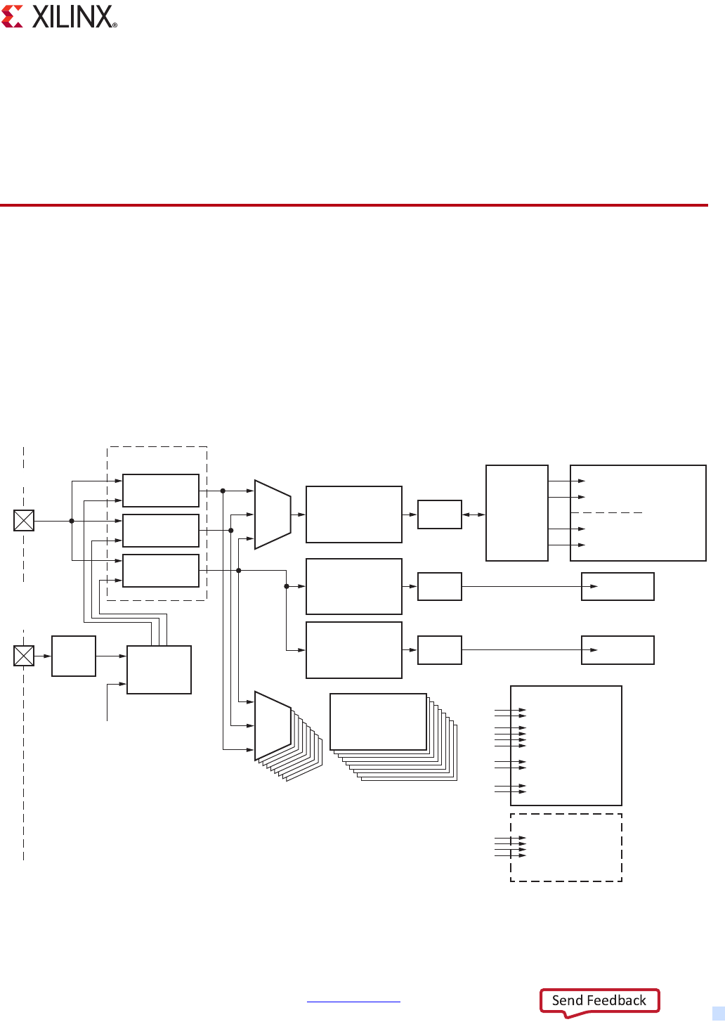
Zynq-7000 AP SoC Technical Reference Manual www.xilinx.com 686
UG585 (v1.12.1) December 6, 2017
Chapter 25
Clocks
25.1 Introduction
All of the clocks generated by the PS clock subsystem are derived from one of three programmable
PLLs: CPU, DDR and I/O. Each of these PLLs is loosely associated with the clocks in the CPU, DDR and
peripheral subsystems.
25.1.1 System Block Diagram
The major components of the clock subsystem are shown in Figure 25-1.
X-Ref Target - Figure 25-1
Figure 25-1: PS Clock System Block Diagram
UG585_c25_01_102414
ARM PLL 6-bit
Programmable
Divider
6-bit
Programmable
Divider
6-bit
Programmable
Divider
6-bit
Programmable
Divider (s)
Bypass
Control
POR
Latch
Gate
Glitch-Free
Glitch-Free
Glitch-Free
Async
Bypass Control Registers:
ARM_PLL_CTRL
DDR_PLL_CTRL
IO_PLL_CTRL
en
I/O PLL
Ethernet
SDIO, SMC,
SPI, QSPI, UART
CAN, I2C
ddr_3x
Async
ddr_2x
I/O Peripherals
(IOP)
PL Clocks
PL
Gate
Glitch-Free
Gate
Glitch-Free
en
DDR PLL
en
PS_CLK
PLLs
Boot Mode
Pin PLL
Bypass
Mux
Mux
Clock
Ratio
Generator
cpu_6x4x
Sync
cpu_3x2x
cpu_2x
cpu_1x
CPU, SCU,
OCM
AXI
Interconnect

Zynq-7000 AP SoC Technical Reference Manual www.xilinx.com 687
UG585 (v1.12.1) December 6, 2017
Chapter 25: Clocks
25.1.2 Clock Generation
During normal operation, the PLLs are enabled, driven by the PS_CLK clock pin. In bypass mode, the
clock signal on the PS_CLK pin provides the source for the various clock generators instead of the
PLLs. (Refer to the applicable Zynq-7000 AP SoC data sheet for PS_CLK characteristics.)
When the PS_POR reset signal deasserts, the PLL bypass boot mode pin is sampled and selects
between PLL bypass and PLL enabled for all three PLLs. The bypass mode runs the system
significantly slower than normal mode, but is useful for low-power applications and debug. After the
boot process and when the user code executes, the bypass mode and output frequency of each PLL
can be individually controlled by software.
The clock generation paths include glitch-free multiplexers and glitch-free clock gates to support
dynamic clock control.
Three Programmable PLLs
• Single external reference clock input for all three PLLs
°ARM PLL: Recommended clock source for the CPUs and the interconnect
°DDR PLL: Recommended clock for the DDR DRAM controller and AXI_HP interfaces
°I/O PLL: Recommended clock for I/O peripherals
• Individual PLL bypass control and frequency programming
• Shared bandgap reference voltage circuit for VCOs
Clock Branches
• Six-bit programmable frequency dividers
• Dynamic switching on most clock circuits
• Four clock generators for the PL
Reset
The clock subsystem is an integral part of the PS and is only reset when the entire system is reset.
When this occurs, all of the registers that control the clocking module return to their reset values.
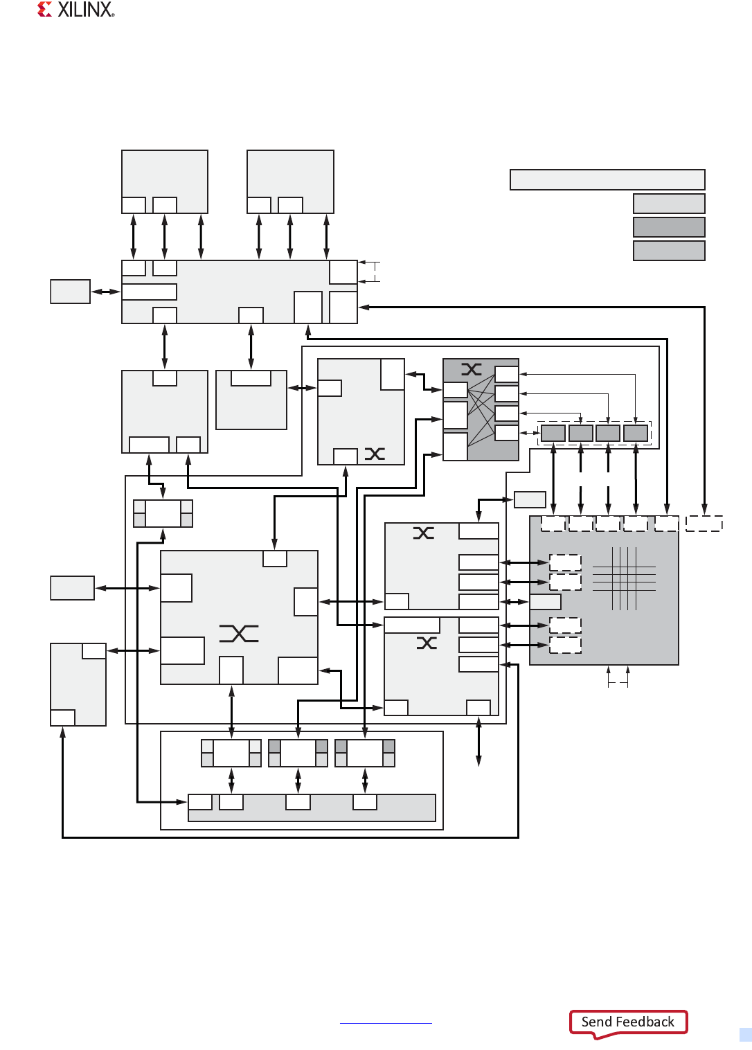
Zynq-7000 AP SoC Technical Reference Manual www.xilinx.com 688
UG585 (v1.12.1) December 6, 2017
Chapter 25: Clocks
25.1.3 System Viewpoint
Figure 25-1 shows the clock network and related domains from a system viewpoint.
X-Ref Target - Figure 25-2
Figure 25-2: System Clock Domains
UG585_c25_02_021213
A9 MP Core
TAG
32K I-Cache
32L D-Cache
M0
DMAC
M1
L-2 Cache
Controller
Snoop Control
Unit (SCU)
512 KB Cache
M0 AS M1
S0
TAG CTRL
S1 GIC Peripheral +
PL Interrupts
EVENT
AS: Async Domain
US: Up Sync
DS: Down Sync
UZ: Up Size
DZ: Down Size
ACP
EVT
ACP
AXI
M1
AFI AFI AFI AFI
M0 M1 M2 M3
M0
M0
S0
OCM
Interconnect
64-bit
CPU_2x
M2
S3
S2
S1
S0
M1
US
M0
US
s1
S0
AS
256 KB OCM
RAM
S0 DS
M0 Event
I-AXI D-AXI Coherent
A9 MP Core
PL
32K I-Cache
32L D-Cache
M0 M1
I-AXI D-AXI Coherent
Master
Interconnect
32-Bit
CPU_2x
M0
S0 US
S1 AS
S2 AS
DAP
DVC
M1
M0
S3 US
Slave
Interconnect
32-Bit
CPU_2x
M3
S0
M0 ASS1 DS/DZ
M1 AS
M2 DS
Central
Interconnect
(3x3)
64-Bit CPU_2x
Top Bus
Switch
DDR
Controller
M0
M1
DS/DZ
Async
Bridge
S0 QoS
US/UZ
S2
QoS
M2
AS
Async
Bridge
Async
Bridge
S1
UZ
S0
S1
Peripheral
Interrupts
Peripheral
APB
S1S0 S2 S3
Async
QoS
M0
S0
IOP
32-Bit
CPU_1x
DDR 3X CLK
CPU CLK (CPU_6x, CPU_2x, and CPU_1x)
DDR 2X CLK
FPGA CLKs
AXI_HP 64/32

Zynq-7000 AP SoC Technical Reference Manual www.xilinx.com 689
UG585 (v1.12.1) December 6, 2017
Chapter 25: Clocks
A version of the CPU clock is used for most of the internal clocking. The asynchronous DMA
peripheral request interfaces between the DMAC and the PL are not shown in Figure 25-2. In
addition, PL AXI channels (AXI_HP, AXI_ACP and AXI_GP) have asynchronous interfaces between the
PS and PL. The synchronization, where the clock domain crossing occurs, is located inside the PS.
Therefore, the PL provides the interface clock to the PS. Each of the aforementioned interfaces could
use unique clocks in the PL.
25.1.4 Power Management
The overall approach to power management is described in Chapter 24, Power Management. The
clock generation subsystem facilitates clock disabling and frequency control which affects power
consumption.
The PLL power consumption is directly related to the PLL output frequency. The power consumption
can be reduced by using a lower PLL output frequency. Power can also be reduced if one or two of
the PLLs are not required. For example, if all of the clock generators can be driven by the DDR PLL,
then the ARM and I/O PLLs can be disabled to reduce power consumption. The DDR PLL is the only
unit that can drive all of the clock generators.
Each clock can be individually disabled when not in use. In some cases, individual subsystems
contain additional clock disabling and other power reduction features.
Central Interconnect Clock Disable
The CPU clocks for the central interconnect (CPU_2x and CPU_1x) can be stopped by setting the
TOPSW_CLK_CTRL [0] bit to a 1. When this bit is set, the clock controller waits for the AXI interfaces
to the L2-cache and SCU to become idle and for the FPGAIDLEN signal from the PL to assert before
shutting off the clock to the central interconnect. For the other interfaces, the system software must
ensure that the interfaces are idle before disabling the interconnect clock. As soon as the PS detects
traffic on the L2-cache or the SCU, or the FPGAIDLEN is deasserted, the clocks will be re-enabled.
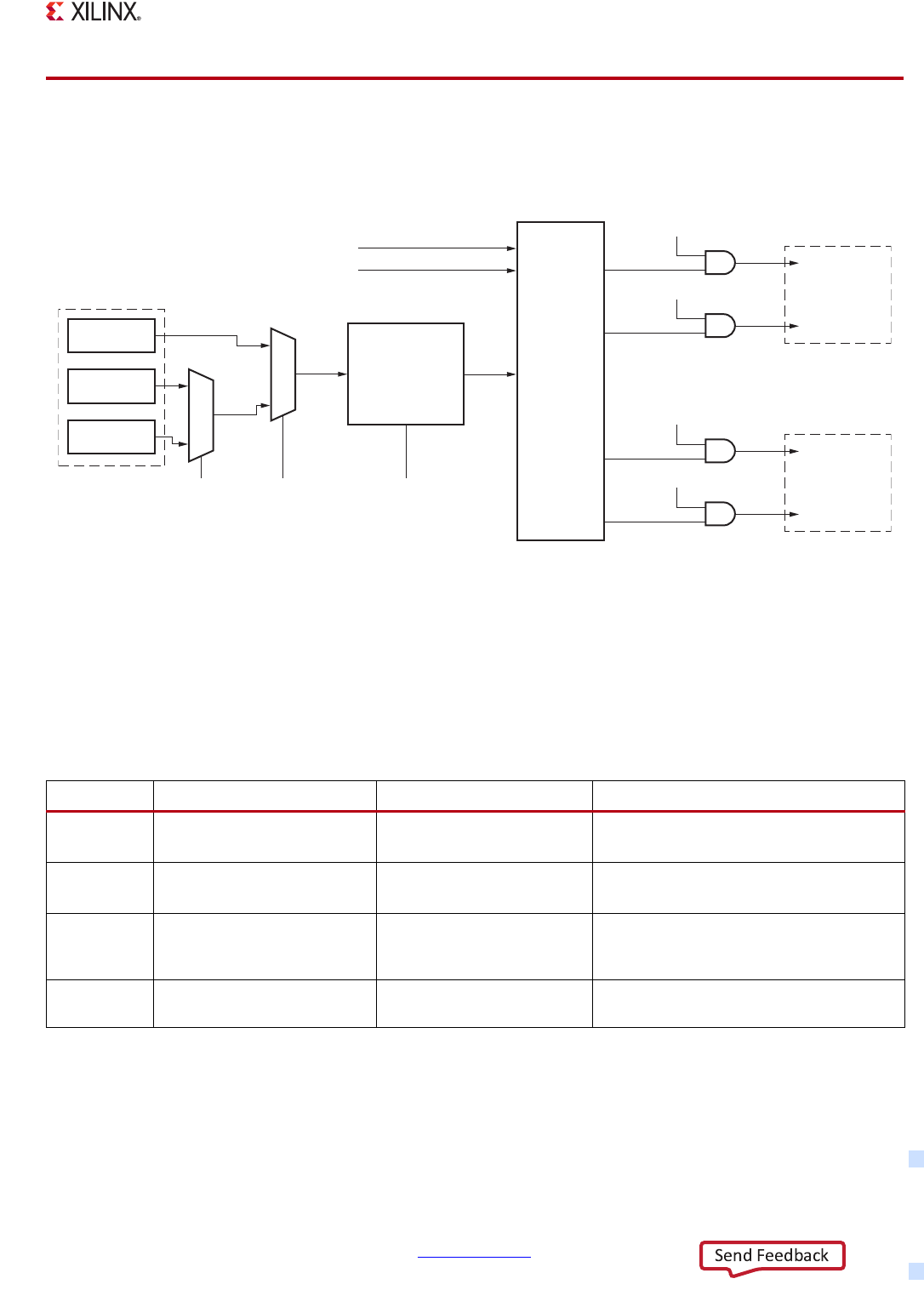
Zynq-7000 AP SoC Technical Reference Manual www.xilinx.com 690
UG585 (v1.12.1) December 6, 2017
Chapter 25: Clocks
25.2 CPU Clock
Figure 25-3 shows the clock generation network in the CPU clock domains.
Ratio Examples
The CPU clock domain operates in two modes 6:2:1 and 4:2:1. Tab le 25 -1 shows example frequencies
for these modes and modules operating in each clock domain. (See the applicable Zynq-7000 AP SoC
data sheet for the specific allowed frequencies for each clock.)
CPU Clock Divisor Restriction
To improve the quality of the high speed clocks going to the CPU and DDR, there is a requirement
that they get divided by an even number in the slcr.ARM_CLK_CTRL [DIVISOR] bit field. For the
slcr.ARM_CLK_CTRL [DIVISOR], software must program it to be equal or greater than 2.
X-Ref Target - Figure 25-3
Figure 25-3: CPU Clock Generation and Domains
UG585_c25_03_100917
ARM PLL
DDR PLL
IO PLL
[5][4]
6-bit
Programmable
Divider
[13:8]
ARM_CLK_CTRL
ARM_CLK_CTRL
ARM_CLK_CTRL [24]
CPU_6x4x
Glitch-
Free
Glitch-Free
Glitch-
Free
Glitch-
Free
1
0
1
0
1
Clock
Ratio
Generator
ARM_CLK_CTRL [25] Closely Coupled,
Always 2:1 Ratio
CPU_3x2x
2:1
ARM_CLK_CTRL [26]
CPU_2x
2:1 or 3:1
ARM_CLK_CTRL [27] Closely Coupled,
Always 2:1 Ratio
CPU_1x
6:1 or 4:1
CLK_621_TRUE [0]
CPU_PERICLKACT
Table 25-1: CPU Clock Frequency Ratio Examples
CPU Clock 6:2:1 4:2:1 Clock Domain Modules
CPU_6x4x 800 MHz
(6 times faster than CPU_1x)
600 MHz
(4 times faster than CPU_1x)
CPU clock frequency, SCU, and OCM
arbitration, NEON, L2 cache memory
CPU_3x2x 400 MHz
(3 times faster than CPU_1x)
300 MHz
(2 times faster than CPU_1x)
APU timers
CPU_2x 266 MHz
(2 times faster than CPU_1x)
300 MHz
(2 times faster than CPU_1x)
I/O peripherals, central interconnect,
master interconnect, slave interconnect,
and OCM RAM
CPU_1x 133 MHz 150 MHz I/O peripherals AHB and APB interface
busses

Zynq-7000 AP SoC Technical Reference Manual www.xilinx.com 691
UG585 (v1.12.1) December 6, 2017
Chapter 25: Clocks
Clock Usage
During normal usage, most system clocks will be derived by taking the input clock PS_CLK, sending
it through the PLL, and finally dividing it down to be used within the PS. While the PS generates many
different clocks, as shown in Figure 25-1, there are three clock domains that have the largest
interaction and importance in the system: These are the DDR_3x domain, the DDR_2x domain, and
the CPU clock domain. The DDR_3x clock domain includes the DDR memory controller. The DDR_2x
domain is primarily used for the high performance AXI interfaces to the PL (AXI_HP{0:3}) and the
interconnect. The CPU clock domain controls the ARM processors along with many of the CPU
peripherals.
The CPU clock domain is composed of four separate clocks: CPU_6x4x, CPU_3x2x, CPU_2x, and
CPU_1x. These four clocks are named according to their frequencies, which are related by one of two
ratios: 6:3:2:1 or 4:2:2:1 (abbreviated 6:2:1 and 4:2:1). The operating clock ratio is determined by the
CLK_621_TRUE [0] bit value. In the 6:2:1 mode, the frequency of the CPU_6x4x clock is 6 times as fast
as the CPU_1x clock. Table 25-1, page 690 shows examples of how these clocks are related. Refer to
the applicable Zynq-7000 AP SoC data sheet for the maximum clock frequency of each clock domain.
All the CPU clocks are synchronous to each other; while the DDR clocks are independent of each
other and the CPU clocks. The I/O peripheral clocks, such as CAN reference clocks and SDIO
reference clocks, are all generated by a similar method, starting from the PS_CLK pin, through a PLL,
then a divider, and finally to the peripheral destination. Each peripheral clock is completely
asynchronous to all other clocks.
Interconnect Clock Domains
The individual clock domains are shown in Figure 25-2. The central interconnect has two main clock
domains: the DDR_2x and the CPU_2x. For the five sub-switches, four clocks are in the CPU_2x clock
domain, while the memory interconnect clock is in the DDR_2x clock domain. The direct path
between the CPU (via the L2 cache) and DDR controller is in the DDR_3x clock domain, ensuring
maximum throughput.The direct path between CPU and OCM is in the CPU_6x4x clock domain. The
direct path between the SCU ACP and the PL is in the CPU_6x4x clock domain (clock domain crossing
between the PL clock domain and the CPU clock domain is done in an asynchronous AXI bridge in
the PS.
CPU Clock Stop
Each CPU clock can be individually stopped using slcr.A9_CPU_RST_CTRL.A9_CLKSTOP{0,1}.
PS Peripheral AMBA Clocks
Every peripheral within the PS is supplied with its own independently gated version of the CPU clock
for its AMBA bus connection to the control and status registers and sometimes to the controller logic
itself. This clock can be disabled when it is guaranteed that the peripheral is not addressed. This
gating is applied with a glitch-free clock gate as shown in Table 25-2.

Zynq-7000 AP SoC Technical Reference Manual www.xilinx.com 692
UG585 (v1.12.1) December 6, 2017
Chapter 25: Clocks
System Performance
The clock frequencies of the different clock domains of the PS help dictate total system performance.
In many cases, the highest frequency CPU clock results in the highest performance. However, some
users will find that the CPU is not the critical performer in the system and that bandwidth across the
interconnect is the bottleneck. In that case, it might be useful to switch the ratio from 6:2:1 to 4:2:1
mode. Depending on the device speed grade, the frequency of the CPU clocks might be limited by
the cpu_6x while in 6:2:1 mode and might be limited by the cpu_2x clock while in 4:2:1 mode.
Therefore, it is suggested that for those applications that might exchange some CPU performance
for interconnect performance, check the appropriate data sheet to determine the optimal
frequencies.
25.3 System-wide Clock Frequency Examples
There are two clock configuration examples for 6:2:1 mode in Table 25-3. The first example is when
the input PS_ CLK is at 33.33 MHz and the second example is when the input frequency is at 50 MHz.
Table 25-2: PS Peripheral Clock Control
AMBA Bus
Peripheral Base Clock
Control Bits in APER_CLK_CTRL
0: Disable
1: Enable
DMAC CPU_2x DMA_CPU_2XCLKACT [0]
USB 0 CPU_1x USB0_CPU_1XCLKACT [2]
USB 1 CPU_1x USB1_CPU_1XCLKACT [3]
GigE 0 CPU_1x GEM0_CPU_1XCLKACT [6]
GigE 1 CPU_1x GEM1_CPU_1XCLKACT [7]
SDIO 0 CPU_1x SDI0_CPU_1XCLKACT [10]
SDIO 1 CPU_1x SDI1_CPU_1XCLKACT [11]
SPI 0 CPU_1x SPI0_CPU_1XCLKACT [14]
SPI 1 CPU_1x SPI1_CPU_1XCLKACT [15]
CAN 0 CPU_1x CAN0_CPU_1XCLKACT [16]
CAN 1 CPU_1x CAN1_CPU_1XCLKACT [17]
I2C 0 CPU_1x I2C0_CPU_1XCLKACT [18]
I2C 1 CPU_1x I2C1_CPU_1XCLKACT [19]
UART 0 CPU_1x UART0_CPU_1XCLKACT [20]
UART 1 CPU_1x UART1_CPU_1XCLKACT [21]
GPIO CPU_1x GPIO_CPU_1XCLKACT [22]
Quad-SPI CPU_1x LQSPI_CPU_1XCLKACT [23]
SMC CPU_1x SMC_CPU_1XCLKACT [24]
Zynq-7000 AP SoC Technical Reference Manual www.xilinx.com 693
UG585 (v1.12.1) December 6, 2017
Chapter 25: Clocks
The PLL output frequency is determined by the frequency of the input clock PS_CLK multiplied by the
PLL feedback divider value (M value). The example below assumes the ARM PLL feedback divider
value is 40, which generates an ARM PLL output frequency of 33.33 MHz * 40 = 1.33 GHz. For each
of the clocks listed in the lower half of the table, the clock frequency equals the sourced PLL
frequency divided by the divisor value. For some of the peripheral clocks, such as CAN, Ethernet, and
the PL, there are two cascaded dividers.
Table 25-3: Clock Frequency Setting Examples for 6:2:1 Mode
Example 1 Example 2
PS_CLK 33.33 MHz 50 MHz
PLL PLL Feedback
Divider Value
PLL Output
Frequency
(MHz)
PLL Feedback
Divider value
PLL Output
Frequency
(MHz)
ARM PLL 40 1333 20 1000
DDR PLL 32 1067 16 800
I/O PLL 30 1000 20 1000
Clock No. PLL Source Divisor 0 Divisor 1 Clock
Frequency
(MHz)
Divisor 0 Divisor 1 Clock
Frequency
(MHz)
cpu_6x4x 1 ARM PLL
2
~(1) 667
2
~500
cpu_3x2x 1 ARM PLL ~ 333 ~ 250
cpu_2x 1 ARM PLL ~ 222 ~ 167
cpu_1x 1 ARM PLL ~ 111 ~ 83
ddr_3x 1 DDR PLL 2 ~ 533 2 ~ 400
ddr_2x 1 DDR PLL 3 ~ 356 3 ~ 267
DDR DCI 1 DDR PLL 7 15 10 7 15 8
SMC 1 IO PLL 10 ~ 100 12 ~ 83
QSPI(2) 1 IO PLL 5 ~ 200 6 ~ 167
GigE 2 IO PLL 8 1 125 8 1 125
SDIO 2 IO PLL 10 ~ 100 10 ~ 100
UART 1 IO PLL 40 ~ 25 40 ~ 25
SPI(3) 2 IO PLL 5 ~ 200 8 ~ 125
CAN 2 IO PLL 10 1 100 12 1 83
PCAP_2x(4) 1 IO PLL 5 ~ 200 6 ~ 167
trace_clk(5) 1 IO PLL 10 ~ 100 15 ~ 67
PLL FCLKs 4 IO PLL 20 1 50 20 1 50
Notes:
1. "~" in the table indicates that there is no second divider (not applicable).
2. The QSPI clock is divided down by at least 2 using the Quad-SPI baud rate divider, see section 12.4.1 Clocks.
3. In master mode, the SPI clock is divided down by at least 4 using the SPI baud rate divider, see section 17.4.2 Clocks.
4. The PCAP_2x clock is always twice the frequency of the PCAP clock.
5. The trace_clk is always twice the frequency of the TPIU clock.
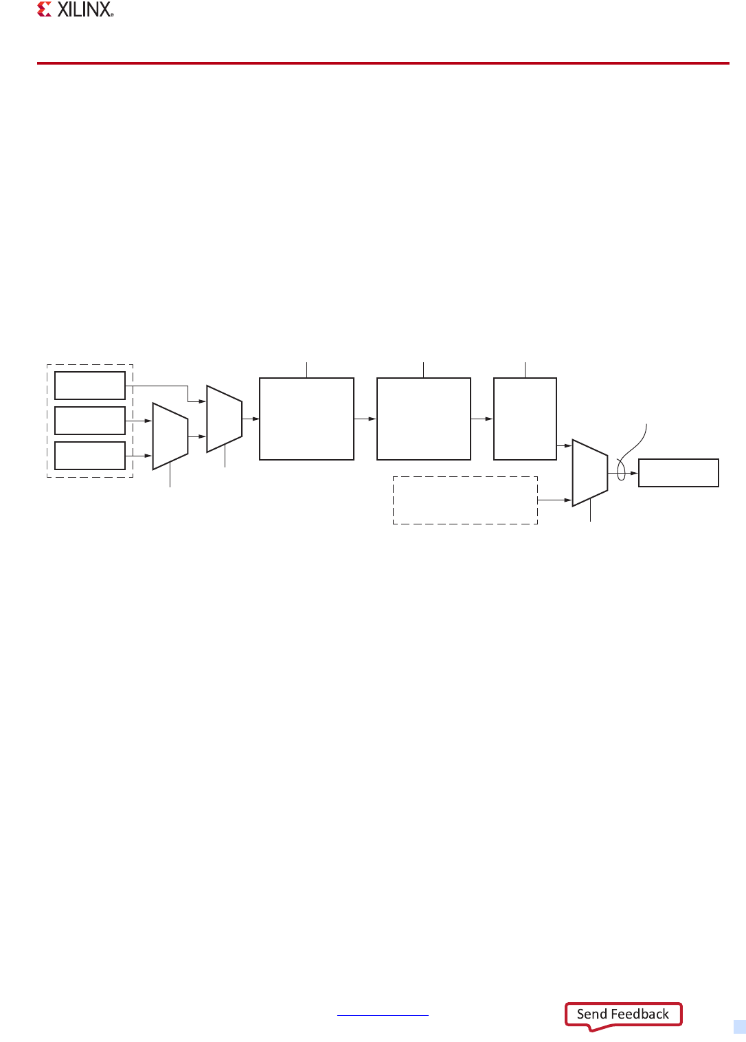
Zynq-7000 AP SoC Technical Reference Manual www.xilinx.com 694
UG585 (v1.12.1) December 6, 2017
Chapter 25: Clocks
25.4 Clock Generator Design
There are several different components to each clock generation circuit. This section describes a
generic template that is used to explain the pieces used for all of the following I/O peripheral clocks.
The most basic types include:
• 2-to-1 multiplexers for selecting a clock source
• Programmable divider(s)
• Glitch-free clock activation gate
These features are shown in Figure 25-4.
PLL
The PLL uses a feedback divider to create an output clock that is equal to the input reference clock
multiplied by the PLL_FDIV value supplied by the SLCR.
Glitch-Free Clock Multiplexers
When a dynamic selection is required between two clock sources, the glitch-free multiplexers (GFMs)
change the clock selection on the low phase of the clock before starting the newly selected clock at
the beginning of its low phase. The GFM operates properly only if both input clocks are active.
Switching while either of the clocks is inactive causes the switching operation to fail.
Glitch-Free Divider
The glitch-free dividers take an input clock and divide it based on the divisor. When the divisor is
changed, the output smoothly transitions to the new clock frequency without any glitches.
X-Ref Target - Figure 25-4
Figure 25-4: Basic Clock Branch Design
UG585_c25_04_021213
6-bit
Programmable
Divider 1
Glitch-Free
Clock
Gate
I/O Peripheral
I/O PLL
ARM PLL
DDR PLL
Alternative Clock Signal
(from MIO or PL)
Glitch-Free
Not
Glitch-
Free
Exists for some Clock Generators
Select Bit
Select Bit
Select Bit
Basic Clock Generator Design
DIVISOR_0 Activate Bit
DIVISOR_1
Exists for some
Clock Generators
6-bit
Programmable
Divider 0
Glitch-Free
Glitch-
Free
Glitch-
Free
<I/O Peripheral>_
REF_CLK
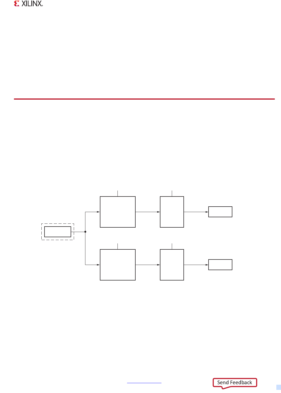
Zynq-7000 AP SoC Technical Reference Manual www.xilinx.com 695
UG585 (v1.12.1) December 6, 2017
Chapter 25: Clocks
Glitch-Free Clock Gate
The glitch-free clock gate is used when a dynamic gating is required to enable and disable a clock
source. The gate ensures that the clock is terminated and re-enabled cleanly on its low phase.
Clock Select Multiplexers
The clock source multiplexers select between the local clock generated by a clock generator and
another source that is external to the clock generator. The clock source multiplexer is not glitch free.
25.5 DDR Clocks
There are two independent DDR clock domains: DDR_2x and DDR_3x. The DDR AXI interface, core,
and PHY are all clocked by DDR_3x (see Figure 25-5). The AXI_HP ports and the AXI_HP interconnect
paths from the AXI_HP to the DDR Interconnect module are clocked by DDR_2x.
These clocks are asynchronous to each other and can have a wide range of frequency ratios between
them. The DIVISOR (DDR_CLK_CTRL[25:20]) for the DDR_3XCLK must be an even value. The DIVISOR
for DDR_2X can be any value.
X-Ref Target - Figure 25-5
Figure 25-5: DDR Clock Generation
UG585_c25_05_022912
Clock
Gate
DDR PLL
DDR_2x
Glitch-Free
en
Note: The DDR_2x
and DDR_3x clocks
are independent and
asynchronous to
each other.
6-bit
Programmable
Divider
Glitch-Free
Clock
Gate DDR_3x
Glitch-Free
Glitch-Free
Output
Glitch-Free
Output
Glitch-Free
Output
Glitch-Free
Output
en
DDR_CLK_
CTRL [31:26] DDR_CLK_CTRL [1]
DDR_CLK_
CTRL [25:20] DDR_CLK_CTRL [0]
6-bit
Programmable
Divider
Glitch-Free
Zynq-7000 AP SoC Technical Reference Manual www.xilinx.com 696
UG585 (v1.12.1) December 6, 2017
Chapter 25: Clocks
25.6 IOP Module Clocks
The IOP module clock (used for the internal controller logic) can be generated by the clock
subsystem or, in some cases, the IOP's external interface. In all cases, the IOP's control and status
registers are clocked by its AMBA interface clock (CPU_1x). Sometimes the CPU_1x clock is the only
clock used by the IOP.
Each clock is discussed in more detail in the following sections and in the system functions section
of each chapter.
•USB: ULPI PHY interface clock input on MIO.
• Ethernet: Clock generator or EMIO. For Rx, can be clocked by RGMII clock input on MIO.
• SDIO: Clock generator.
• SMC: Clock generator.
• SPI: Clock generator.
• Quad-SPI: clock generator.
• UART: Clock generator.
• CAN: Clock generator or MIO pin.
• GPIO: AMBA APB CPU_1x clock.
• I2C: AMBA APB CPU_1x clock and SCL interface clock.
25.6.1 USB Clocks
The USB controller module clock is generated externally and input on the ULPI PHY interface on MIO
as shown in Figure 25-6. USB clocks are described in section 15.15.1 Clocks.
X-Ref Target - Figure 25-6
Figure 25-6: USB Clocks
UG585_c25_06_102414
USB
Controller
USB PHY Interface Input Clock
(from MIO)
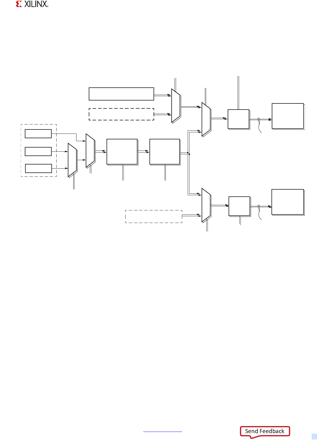
Zynq-7000 AP SoC Technical Reference Manual www.xilinx.com 697
UG585 (v1.12.1) December 6, 2017
Chapter 25: Clocks
25.6.2 Ethernet Clocks
The Ethernet Clocks generation network is shown in Figure 25-7.
Ethernet Receiver Clocks
There are two Ethernet receiver clocks. In normal functional mode, these are either sourced from an
external Ethernet PHY via the MIO or an extended MIO (EMIO). For MAC internal loopback mode,
these clocks are sourced from the internal Ethernet reference clocks. They are also gated with an
enable that can be used for power saving control. These are used to clock the receiver side of the
Gigabit Ethernet MAC IP.
The source selection multiplexer and the loopback selection multiplexer are not glitch free because
the source clocks might not be present. It is recommended that the clock be disabled before the
multiplexers are changed. To support loopback mode, enet0_rx_clk and enet1_rx_clk are supplied
with enet0_ref_clk and enet1_ref_clk.
Ethernet Transmit Clocks
Two Ethernet clocks are required to be generated: enet0_tx_clk and enet1_tx_clk. These are used to
clock the transmit side of the Ethernet MACs and as a source synchronous output clock for the RGMII
X-Ref Target - Figure 25-7
Figure 25-7: Ethernet Clock Generation
ARM PLL
DDR PLL
I/O PLL
6-bit
Programmable
Divider 0
GEM{0,1}_CLK_CTRL
ENET{0,1}_REF_CLK
6-bit
Programmable
Divider 1
1
0
1
0
MIO_ENET{0,1}_RX_CLK
ENET{0,1}_RX_CLK
Clock
Gate
NET_CTRL
[LOOPBACK_LOCAL, 1]
EMIO_ENET{0,1}_RX_CLK
Ethernet
Controller
(Rx)
[5]
[6]
1
0
1
0
ENET{0,1}_TX_CLK
Clock
Gate
EMIO_ENET{0,1}_TX_CLK
(signal from PL) 1
0Ethernet
Controller
(Tx)
Glitch-
Free
[25:20][13:8]
[4]
[0]
GEM{0,1}_CLK_CTRL
GEM{0,1}_RCLK_CTRL
[0][4]
Not
Glitch-Free
Not
Glitch-Free
UG585_C25_07_022912
Not
Glitch-Free
Glitch-
Free
Glitch-Free Glitch-Free
Glitch-Free
Glitch-Free
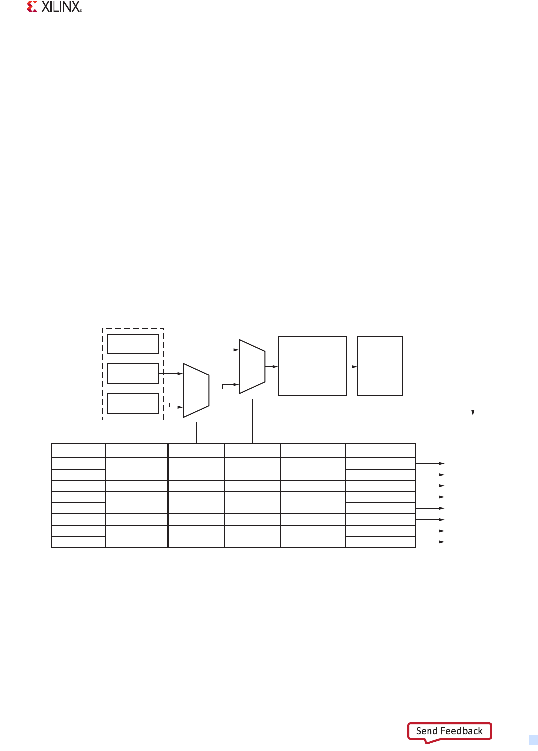
Zynq-7000 AP SoC Technical Reference Manual www.xilinx.com 698
UG585 (v1.12.1) December 6, 2017
Chapter 25: Clocks
interface. They are also used to provide a stable reference clock to the Ethernet receive paths when
internal loopback mode is selected.
These clocks can also be sourced from the EMIO. In this case, the associated RGMII interface is
disabled and the MAC connects to the PL through an MII or GMII interface. In this case, the Ethernet
reference clock must be provided by the PL. This is regardless of MII or GMII, where normally tx_clk
is an input in MII and an output in GMII.
When operating in MII or GMII mode, its reference clock is provided by the PL through the
eth*_emio_tx_clk. The EMIO source multiplexer is not glitch free because the EMIO source clock
cannot be relied upon to be present. It is anticipated that this source selection is a static
configuration or that the generated clock be gated before changing to the EMIO source. To support
loopback mode, gem0_rx_clk and gem1_rx_clk are supplied with gem0_ref_clk and gem1_ref_clk.
25.6.3 SDIO, SMC, SPI, Quad-SPI and UART Clocks
The SDIO, SMC, Quad SPI, and UART peripheral clocks all have the same programming model (see
Figure 25-8. The PLL source and divider values are shared for each I/O peripheral controller. The
clocks for each SDIO, SPI and the UART controller can be individually enabled/disabled. There is a
single clock, each, for the SMC and Quad SPI controllers.
The Quad-SPI clock is divided down by at least two using the Quad-SPI baud rate divider, see section
12.4.1 Clocks. In master mode, the SPI clock is divided down by at least four using the SPI baud rate
divider, see section 17.4.2 Clocks.
X-Ref Target - Figure 25-8
Figure 25-8: SDIO, SMC, SPI, Quad SPI and UART Reference Clocks
UG585_c25_08_100917
I/O PLL
ARM PLL
DDR PLL
Clock
Gate
I/O Peripheral
Reference
Clocks
Glitch-Free
6-bit
Programmable
Divider
Glitch-Free
Divider Ctrl FieldMux Ctrl FieldMux Ctrl FieldControl RegisterI/O Peripheral Clock Enable Field
SMC
DIVISOR, 13:8SRCSEL, 5SRCSEL, 4SDIO_CLK_CTRL
DIVISOR, 13:8SRCSEL, 5SRCSEL, 4SMC_CLK_CTRL
SDIO 0
SDIO 1
CLKACT0, 0
CLKACT1, 1
DIVISOR, 13:8SRCSEL, 5SRCSEL, 4SPI_CLK_CTRL
SPI 0
SPI 1
CLKACT0, 0
CLKACT1, 1
CLKACT, 0
Quad-SPI DIVISOR, 13:8SRCSEL, 5SRCSEL, 4LQSPI_CLK_CTRL
DIVISOR, 13:8SRCSEL, 5SRCSEL, 4UART_CLK_CTRL
UART 0
UART 1
CLKACT0, 0
CLKACT1, 1
CLKACT, 0
SDIO0_REF_CLK
SDIO
SMC
SPI
Quad SPI
UART
Glitch-
Free
0
1
SDIO1_REF_CLK
SMC_REF_CLK
SPI0_REF_CLK
SPI1_REF_CLK
QSPI_REF_CLK
UART0_REF_CLK
UART1_REF_CLK
Glitch-
Free
0
1
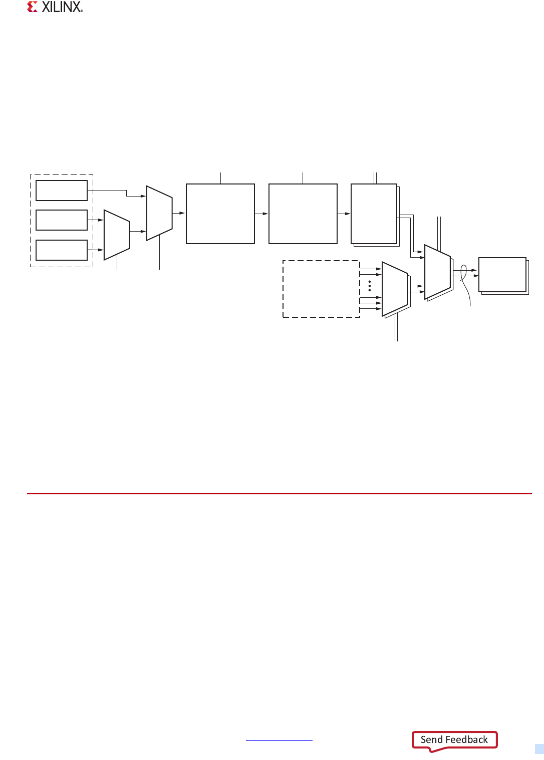
Zynq-7000 AP SoC Technical Reference Manual www.xilinx.com 699
UG585 (v1.12.1) December 6, 2017
Chapter 25: Clocks
25.6.4 CAN Clocks
There are two controller area network (CAN) reference clocks: CAN0_REF_CLK and CAN1_REF_CLK.
Both clocks share the same PLL source selection and dividers as shown in Figure 25-9. Each clock has
independent alternate source selection (MIO pin or the clock generator), and independent clock
gates. These clocks are used for the I/O interface side of the CAN peripherals.
25.6.5 GPIO and I2C Clocks
The GPIO and I2C peripherals are clocked by the CPU_1x APB bus interface clock provided by the
interconnect (refer to section 25.2 CPU Clock).
25.7 PL Clocks
The PL has its own clock management generation and distribution features and also receives four
clock signals from the clock generator in the PS (see Figure 25-10). For the details of the PL clocking
structures, see the 7 series FPGAs clocking documentation.
The four clocks that are generated by the PS are completely asynchronous to each other with no
relationship to other PL clocks.
The four clocks are derived from individually selected PLLs in the PS. Each of the PL clocks are
independent output signals that produce suitable clock waveforms for PL use.
X-Ref Target - Figure 25-9
Figure 25-9: CAN Clock Generation
UG585_c25_09_022912
6-bit
Programmable
Divisor 1
Glitch-Free
Clock
Gate
CAN Reference
Clock from
MIO pin
Glitch-Free
[13:8] [25:20] [0], [1]
[6], [22]
6-bit
Programmable
Divisor 0
Glitch-Free
I/O PLL
ARM PLL
DDR PLL
[5][4]
0
1
Glitch-
Free
Glitch-
Free
0
1
CAN_CLK_CTRL
[5:0], [21:16]
CAN_MIOCLK_CTRL
CAN_MIOCLK_CTRL
CAN_CLK_CTRL
Not
Glitch-
Free
0
1
0
53 CAN{0, 1}_REF_CLK
CAN
Controller
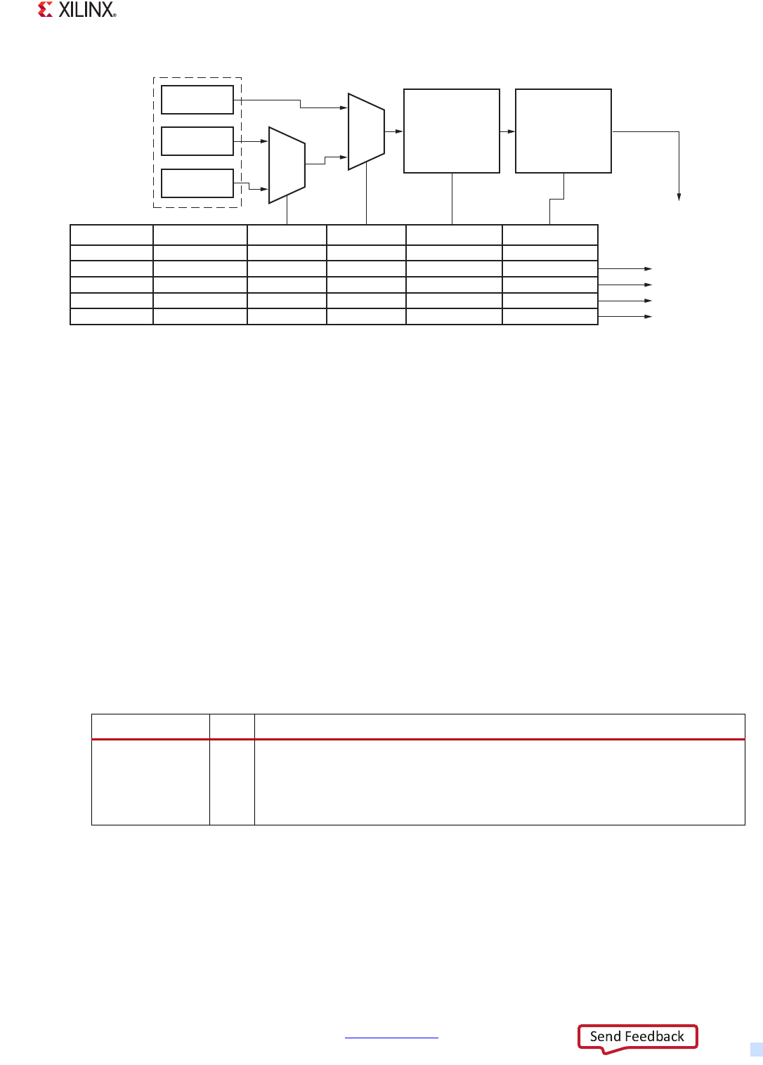
Zynq-7000 AP SoC Technical Reference Manual www.xilinx.com 700
UG585 (v1.12.1) December 6, 2017
Chapter 25: Clocks
25.7.1 Clock Throttle
Each of the four PL clocks includes logic to start and stop the clock and to assist with PL design
debug and co-simulation. The clock throttle behavior is controlled by software and the trigger input
signal from the PL. The clock throttle functions include:
• Start/stop clock under software control
• Run clock for a pre-programmed number of pulses
• Run clock and use PL logic to pause the clock pulses
Each clock throttle has a 16-bit counter that is programmed for the number of clock pulses to
generate. For a continuous clock output, write a 0 to the counter, which is the default value. The
current count can be read by software. The counting and clock pulses can be paused by the PL logic
using the FCLKCLKTRIGxN input signal from the PL. The software can re-start the clocking by writing
to the PL clock control register.
X-Ref Target - Figure 25-10
Figure 25-10: PL Clock Generation
UG585_c25_10_041612
IO PLL
ARM PLL
DDR PLL
Four
Independent
PL Clocks
6-bit
Programmable
Divisor 0
Glitch-Free
Divider 0 Ctrl FieldMux Ctrl FieldMux Ctrl FieldControl RegisterPL FCLK Clock Divider 1 Ctrl Field
PL FCLK 0 DIVISOR 0, 13:8SRCSEL, 5SRCSEL, 4FPGA0_CLK_CTRL DIVISOR 1, 25:20
Glitch-
Free
0
1
6-bit
Programmable
Divisor 1
Glitch-Free
FCLKCLK0
PL FCLK 1 DIVISOR 0, 13:8SRCSEL, 5SRCSEL, 4FPGA1_CLK_CTRL DIVISOR 1, 25:20 FCLKCLK1
PL FCLK 2 DIVISOR 0, 13:8SRCSEL, 5SRCSEL, 4FPGA2_CLK_CTRL DIVISOR 1, 25:20 FCLKCLK2
PL FCLK 3 DIVISOR 0, 13:8SRCSEL, 5SRCSEL, 4FPGA3_CLK_CTRL DIVISOR 1, 25:20 FCLKCLK3
Glitch-
Free
0
1
Table 25-4: PL Clock Throttle Input Signal
Signal Name I/O Description
FCLKCLKTRIGxN I The PL clock trigger signal is an input from the PL logic and is used to halt (pause)
the PL clock when counting a programmed number of clock pulses. The halt mode
is entered by the rising edge (logic 0 to logic 1) of the FCLKCLKTRIGxN signal. This
signal can be asserted asynchronously to the FCLK and all other signals. This pin
has no affect when the clock is running continuously, [LAST_CNT] = 0.
Zynq-7000 AP SoC Technical Reference Manual www.xilinx.com 701
UG585 (v1.12.1) December 6, 2017
Chapter 25: Clocks
Clock Controller States
The clock controller states are illustrated in Figure 25-11.
25.7.2 Clock Throttle Programming
Example: Stop/Start Clock
This example illustrates a simple method to stop and start a PL clock (FCLKCLKx) using writes to the
last count field in the throttle count register, slcr.FPGAx_THR_CNT [LAST_CNT]. The example assumes
the slcr.FPGAx_THR_CTRL register is kept in its default state of 0x0000_0000.
1. Stop Clock: Write 0x0000_0001 to slcr.FPGAx_THR_CTRL to immediately stop the clock.
°[LAST_CNT] = 1
°[Reserved] = 0
2. Start Clock: Write 0x0000_0000 to slcr.FPGAx_THR_CTRL to resume a continuous clock.
°[LAST_CNT] = 0
°[Reserved] = 0
X-Ref Target - Figure 25-11
Figure 25-11: PL Clock Throttle States
UG585_c25_11_102912
Software
RUN
decrement
[CURR_VAL]
HALT
Clock stopped &
halt [CURR_VAL]
Hardware:
[CURR_VAL]
= 0
PL signal driven 0 to 1:
FCLKCLKTRIGxN
Software:
Rising edge of
CPU_[START]
Software:
Rising edge of
[CPU_START]

Zynq-7000 AP SoC Technical Reference Manual www.xilinx.com 702
UG585 (v1.12.1) December 6, 2017
Chapter 25: Clocks
Example: Run the PL Clock for 592 Pulses and Stop
In this example, there will be 592 clock pulses and stops. The slcr.FPGAx_THR_CTRL [CPU_START] bit
is positive edge triggered to start the clock.
1. Prime the Start Clock bit: write 0x0000_0004 to the control register, slcr.FPGAx_THR_CTRL.
°[CPU_START] = 0
°[CNT_RST] = 0
°[Reserved] = 0x001
2. Program a count of 592: write 0x0000_0250 to the count register, slcr.FPGAx_THR_CNT.
°[LAST_CNT] = 0x0250
°[Reserved] = 0
3. Assert the Start Clock bit: write 0x0000_0005 to the control register, slcr.FPGAx_THR_CTRL.
°[CPU_START] = 1
°[CNT_RST] = 0
°[Reserved] = 0x001
Example: Program 592 Pulses and Interact with the PL Trigger Input
In this example, there will be 592 clock pulses that are paused by the clock trigger signal
(FCLKCLKTRIGxN) and re-started by software. The slcr.FPGAx_THR_CTRL [CPU_START] bit is positive
edge triggered to start the clock.
1. Prime the Start Clock bit: See previous example.
2. Program a count of 592: See previous example.
3. Assert the Start Clock bit: See previous example.
4. PL Logic Pauses the Clock (HALT state): the logic asserts FCLKCLKTRIGxN input to stop the
clock.
5. Prime the Start Clock bit: See previous example.
Assert the Start Clock bit: See previous example.
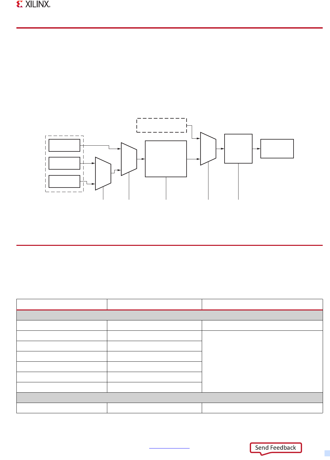
Zynq-7000 AP SoC Technical Reference Manual www.xilinx.com 703
UG585 (v1.12.1) December 6, 2017
Chapter 25: Clocks
25.8 Trace Port Clock
The trace port clock is used to clock the TPIU and trace buffer when the MIO interface is chosen and
must be twice the frequency of the desired TPIU clock. The TPIU clock frequency must be chosen to
be fast enough to allow the trace port to keep up with the amount of data being traced, but slow
enough to meet the dynamic characteristics of the data output buffers of the TPIU. To allow some
flexibility, the trace clock is generated from a divided PLL output for MIO. When the trace port is
routed through EMIO, the EMIOTRACECLK input is used to clock the TPIU as shown in Figure 25-12.
25.9 Register Overview
An overview of the PS clock subsystem registers is shown in Tabl e 25- 5.
X-Ref Target - Figure 25-12
Figure 25-12: Trace Port Clock Generation
UG585_c25_11_072512
IO PLL
ARM PLL
DDR PLL
EMIOTRACECLK
Clock
Gate
Glitch-Free
6-bit
Programmable
Divider
Glitch-Free
DBG_CLK_CTRL Register Bit Fields
0
1
Debug
Subsystem
Not
Glitch-
Free
1
0
Glitch-
Free
Glitch-
Free
0
1
[6][5][6] [0][13:8]
Table 25-5: Clock Generation Register Overview
Register Description Comments
PLL
PLL_STATUS PLL status
ARM_PLL_CTRL CPU PLL control
• Control registers include:
• Reset, power-down, bypass
• Divisor(s)
• Configuration registers include:
• PLL control parameters (see Table 25-6)
ARM_PLL_CFG CPU PLL configuration
DDR_PLL_CTRL DDR PLL control
DDR_PLL_CFG DDR PLL configuration
IO_PLL_CTRL I/O PLL control
IO_PLL_CFG I/O PLL configuration
CPU, DDR and Interconnect
ARM_CKL_CTRL CPU clock control

Zynq-7000 AP SoC Technical Reference Manual www.xilinx.com 704
UG585 (v1.12.1) December 6, 2017
Chapter 25: Clocks
25.10 Programming Model
25.10.1 Branch Clock Generator
Each clock generator has a clock control register <module>_CLK_CTRL. Within the clock control
register, the SRCSEL field selects a clock source and the DIVISOR field is the amount the source clock
is divided down to produce the desired clock frequency. Some clock generators have two cascaded
dividers.
To prevent the clock generator from exceeding the maximum frequency of the attached subsystem,
program the SRCSEL and the DIVISOR values in three separate steps:
1. Increase the value of the DIVISOR, as needed, so that the two PLL clock sources will not cause the
clock generator to exceed the maximum clock frequency of the subsystem.
2. Set the SRCSEL to the desired source.
3. Update the DIVISOR to the desired value.
CLK_621_TRUE Select CPU clock frequency ratio 6:2:1 or 4:2:1
DDR_CLK_CTRL DDR clock control
APER_CLK_CTRL AMBA peripheral clock control
TOPSW_CLK_CTRL Top-level switch clock control
PL Clocks
FPGA{3:0}_CLK_CTRL PS to PL output clock control
FPGA{3:0}_THR_{CTRL, CNT, STA} PS to PL output clock throttle
control, count and status
I/O Peripheral Clocks
GEM{1, 0}_RCLK_CTRL Gigabit Ethernet Rx clock control
• DIVISOR bit field (one or two parameters,
depending on the peripheral)
• Clock enable active control
GEM{1, 0}_CLK_CTRL Gigabit Ethernet ref clock control
SMC_CLK_CTRL SMC ref clock control
LQSPI_CLK_CTRL Quad-SPI ref clock control
SDIO_CLK_CTRL SDIO ref clock control
UART_CLK_CTRL UART ref clock control
SPI_CLK_CTRL SPI ref clock control
CAN_CLK_CTRL CAN ref clock control
CAN_MIOCLK_CTRL CAN comm port clock control
System Debug Clocks
DBG_CLK_CTRL CoreSight SoC trace clk control
PCAP_CLK_CTRL PCAP clock control This controls the frequency and enable of the
PCAP_2X clock for the DevC module.
Table 25-5: Clock Generation Register Overview (Cont’d)
Register Description Comments

Zynq-7000 AP SoC Technical Reference Manual www.xilinx.com 705
UG585 (v1.12.1) December 6, 2017
Chapter 25: Clocks
6-bit Programmable Divider
The 6-bit divider provides a divide range of 1 to 63, supports both even and odd divide values
producing a close to 50% duty cycle, and is glitchless (divide values can be modified dynamically).
The two exceptions to this rule: the DDR_3X divider can only be programmed to divide by an even
divisor, and the ARM_CLK_CTRL[DIVISOR] must be programmed with a value of 3 or greater when the
PLL is being used. Some reference clocks have one divider and some have two dividers.
25.10.2 DDR Clocks
IMPORTANT: It is a requirement that the DDR_3x clock must always be programmed to an even divisor.
RECOMMENDED: Changing the divider frequency does not produce glitches on the clock, however the
DDR controller will not necessarily operate correctly if the frequency is changed without modifying its
timing parameters. Therefore, it is suggested to first idle the DDR controller when the DDR clock is to
be reprogrammed.
25.10.3 Digitally Controlled Impedance (DCI) Clock
The digitally controlled impedance (DCI) clock is required by the DDR PHY for calibration. The DCI
clock is a low frequency clock, normally set to 10 MHz.
25.10.4 PLLs
The three PLLs share the clock input signal, PS_ CLK. Each PLL can be bypassed individually under
software control. As part of the power-on reset sequence, all PLLs can be bypassed using the
pll_bypass boot mode pin straps. (Refer to the boot mode section of Chapter 6, Boot and
Configuration.)
The PLL configuration and control registers are in the SLCR. The PLL frequency control registers
include the M (feedback divide ratio also known as PLL_FDIV), LOCK_CNT, PLL_CP, and PLL_RES
control fields. For each divide ratio M, the PLL_CP, PLL_RES, and LOCK_CNT fields must always be
written with the values shown in Table 25-6; the reset default values are not supported. After being
enabled, the PLL with take some time to lock. The length of time is specified by the tLOCK_PSPLL
data sheet parameter.
Zynq-7000 AP SoC Technical Reference Manual www.xilinx.com 706
UG585 (v1.12.1) December 6, 2017
Chapter 25: Clocks
Enable PLL Mode when PLL Bypass Mode Pin is Tied High
After the system boots in bypass mode, the following sequence can be used to enable a PLL. Each PLL
can be individually enabled. This example shows how to enable the ARM PLL:
1. Program the ARM_PLL CTRL[PLL_FDIV] value and the PLL configuration register,
ARM_PLL_CFG[LOCK_CNT, PLL_CP, PLL_RES], to their required values.
2. Force the PLL into bypass mode by writing a 1 to ARM_PLL_CTRL [PLL_BYPASS_FORCE, 4] and
setting the ARM_PLL_CTRL [PLL_BYPASS_QUAL, 3] bit to a 0. This de-asserts the reset to the ARM
PLL.
3. Assert and de-assert the PLL reset by writing a 1 and then a 0 to ARM_PLL_CTRL [PLL_RESET, 0].
4. Verify that the PLL is locked by reading PLL_STATUS [ARM_PLL_LOCK, 3].
5. Disable the PLL bypass mode by writing a 0 to ARM_PLL_CTRL [4].
The DDR and I/O PLLs are programmed in a similar fashion.
Software-Controlled PLL Update
The following steps are required for software to update the PLL clock frequency. This example is for
the I/O PLL. Tab le 25- 6 shows the possible multiplier values and the required settings for each of
those multiplier values.
1. Program the IO_PLL_CTRL[PLL_FDIV] value and the PLL configuration register, IO_PLL_CFG
[LOCK_CNT, PLL_CP, PLL_RES].
2. Force the PLL into bypass mode by writing a 1 to IO_PLL_CTRL [PLL_BYPASS_FORCE, 4]. (When the
PLL goes into reset in the next step, its output will be undefined.)
3. Assert and de-assert the PLL reset by writing 1 and then a 0 to IO_PLL_CTRL [PLL_RESET, 0]. (This
is when the new values from step one are actually consumed by the PLL.)
4. Verify that the PLL is locked by reading PLL_STATUS [IO_PLL_LOCK, 2].
5. Disable the PLL bypass mode by writing a 0 to IO_PLL_CTRL [4].
Table 25-6: PLL Frequency Control Settings
Desired PLL
Multiplier
Required PLL Control and Configuration Bit Fields
PLL_FDIV PLL CP PLL RES LOCK CNT
13 13 2 6 750
14 14 2 6 700
15 15 2 6 650
16 16 2 10 625
17 17 2 10 575
18 18 2 10 550
19 19 2 10 525
20 20 2 12 500
21 21 2 12 475
22 22 2 12 450
Zynq-7000 AP SoC Technical Reference Manual www.xilinx.com 707
UG585 (v1.12.1) December 6, 2017
Chapter 25: Clocks
23 23 2 12 425
24 ~ 25 24 ~ 25 2 12 400
26 26 2 12 375
27 ~ 28 27 ~ 28 2 12 350
29 ~ 30 29 ~ 30 2 12 325
31 ~ 33 31 ~ 33 2 2 300
34 ~ 36 34 ~ 36 2 2 275
37 ~ 40 37 ~ 40 2 2 250
41 ~ 47 41 ~ 47 3 12 250
48 ~ 66 48 ~ 66 2 4 250
Table 25-6: PLL Frequency Control Settings (Cont’d)
Desired PLL
Multiplier
Required PLL Control and Configuration Bit Fields
PLL_FDIV PLL CP PLL RES LOCK CNT

Zynq-7000 AP SoC Technical Reference Manual www.xilinx.com 708
UG585 (v1.12.1) December 6, 2017
Chapter 26
Reset System
26.1 Introduction
The reset system includes resets generated by hardware, watchdog timers, the JTAG controller, and
software. Every module and system in Zynq-7000 AP SoC devices includes a reset that is driven by
the reset system. Hardware resets are driven by the power-on reset signal (PS_POR_B) and the system
reset signal (PS_SRST_B).
There are three watchdog timers in the PS that can generate resets. The JTAG controller can generate
a reset that only resets the debug portion of the PS and a system-level reset. Software can generate
individual sub-module resets or a system-level reset.
Resets are caused by many different sources and go to many different destinations. This chapter
identifies all of the resets and either explains their functionality or provides a pointer to another
chapter or another document.
26.1.1 Features
The key features of the reset system:
• Collects resets from hardware, watchdog timers, the JTAG controller and software
• Drives the reset of every module and subsystem
• Is an integral part of the device security system
• Executes a three-stage sequence: power-on, memory clear, and system enabling
26.1.2 Block Diagram
Figure 26-1 illustrates the logical dependencies of the main types of generated resets upon these
reset triggers. This block diagram is intended to highlight dependencies, and does not accurately
depict implementation detail or sequence timing.
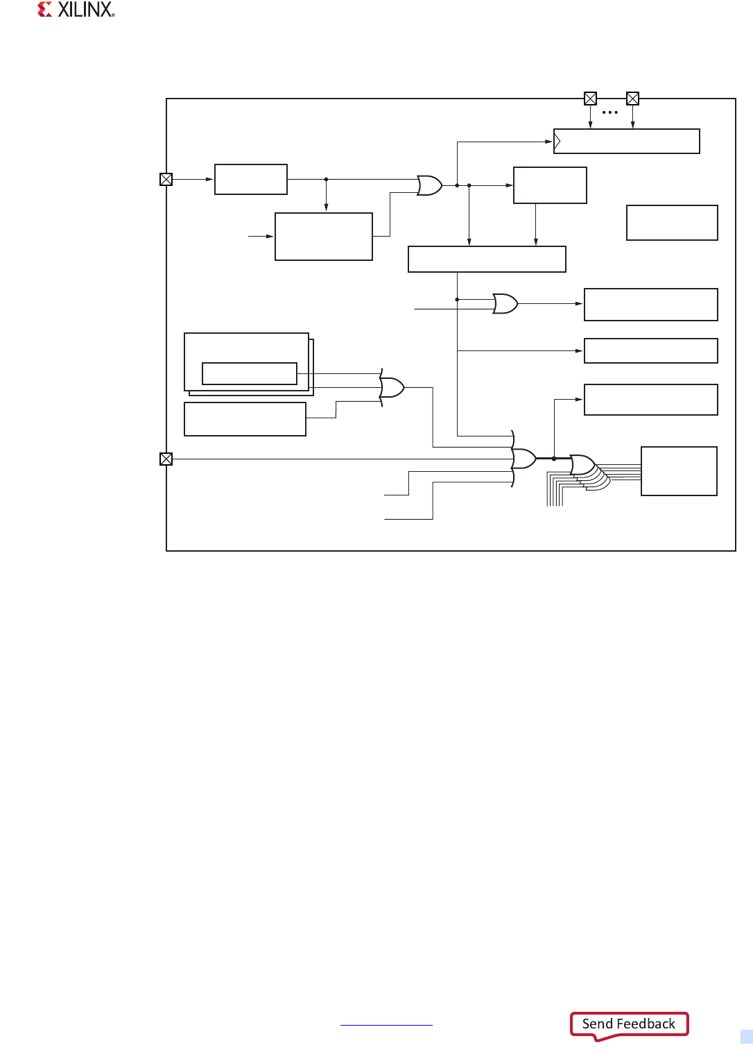
Zynq-7000 AP SoC Technical Reference Manual www.xilinx.com 709
UG585 (v1.12.1) December 6, 2017
Chapter 26: Reset System
26.1.3 Reset Hierarchy
There are many different types of resets within the PS, from power-on reset that resets the entire
system, to a peripheral reset which resets a single subsystem under software control. Figure 26-2
shows the relationships between all major reset signals within the PS. Reset signals flow from the top
downwards. The rectangles at the end of the diagram represent the blocks that are reset. For
example, power-on reset (POR) resets all logic within the PS, but system reset only resets the
functions indicated in the diagram. This diagram presents the reset hierarchy of operation rather
than the reset signal routing shown in Figure 26-1.
X-Ref Target - Figure 26-1
Figure 26-1: Resets Block Diagram
PS_SRST_B
PS_POR_B
CPU Processors
Watchdog Timer
Security
Lockdown
Reset
Peripheral Reset
Control Registers
Persistent
Registers
Clear
POR Reset
Signal Filter
Detect & Hold
Reset
Boot Mode Register
MODE_PINS
PS Clock
Generator
Reset Deassertion Delay
SLCR & Dev Config
Registers
Internal Registers
Debug Reset SoC Debug Domain
SLCR Soft Reset
System Watchdog
Timer
Debug System Reset
PLL
Locked
Resets
UG585_c26_01_052813
Peripheral
Resets
Bypass
Dedicated
Pin
Dedicated
Pin
MIO Pin
Zynq-7000 AP SoC Technical Reference Manual www.xilinx.com 710
UG585 (v1.12.1) December 6, 2017
Chapter 26: Reset System
26.1.4 Boot Flow
The complete reset sequence is shown as in Figure 26-3. The first two steps are controlled by the
external system and PS logic only starts to respond when power on reset (POR) is de-asserted. When
the PS is operational, any type of reset can occur after POR. Those resets would insert into the flow
chart, at their respective locations.
The POR signal can be asserted or de-asserted asynchronously. When the POR signal is de-asserted,
it is conditioned to allow it to propagate cleanly to the clock module input logic and, if enabled, to
the PLL clock circuits.
There is a BOOT_MODE strapping pin to select between all PLLs enabled and all PLLs disabled
(bypassed). When the PLL is bypassed, the boot process takes longer.
After POR_N is released, the eFUSE controller comes out of reset. It automatically applies some data
to the PLL and provides redundancy information to some of the RAMs in the PS. This activity is not
visible to the user and cannot be affected by the user. This activity requires from 50 us to 100 us of
time to complete.
If the PLLs are enabled, then the POR signal is delayed at this point until the PLL clocks have locked.
If PLL bypass mode is selected, the POR signal is not delayed.
Before the BootROM starts executing, the internal RAMs are cleared by hardware writing zeros into
all addresses. For a listing of the times it takes to go through these steps, see section 6.3.3 BootROM
Performance in Chapter 6, Boot and Configuration.
X-Ref Target - Figure 26-2
Figure 26-2: Reset Hierarchy Diagram
Power-on
Reset
Debug
Reset
SoC Debug
Security Lock
Down
External System Reset
System Software Reset
Watchdog Timer Resets
Debug System Reset
CPU 0 Software Reset
AWDT 0 Reset
CPU 1 Software Reset
AWDT 1 Reset
PL
Software
Resets
CPU 0 w/
NEON
CPU 1 w/
NEON I/O Peripherals
IOP
Software
Resets
Programmable
Logic
Control
Logic
Legend
Interconnect
SLCR
L-2 Cache
SCU
UG585_c26_02_101812
Zynq-7000 AP SoC Technical Reference Manual www.xilinx.com 711
UG585 (v1.12.1) December 6, 2017
Chapter 26: Reset System
26.2 Reset Sources
26.2.1 Power-on Reset (PS_POR_B)
The PS supports external power-on reset signals. The power-on reset is the master reset of the entire
chip. This signal resets every register in the device capable of being reset. While PS_POR_B is held
Low, all PS I/Os are held in 3-state and a weak pull-up is enabled on most MIO pins. The pull-up for
each MIO pin is independently controlled by the MIO_PIN_xx [PULLUP] bit. The reset value of bit 12
can be read in the SLCR register summary table.
The PS_POR_B reset pin is held Low until all PS power supplies are at their required voltage levels and
PS_CLK is active. It can be asynchronously asserted and is internally synchronized and filtered. The
X-Ref Target - Figure 26-3
Figure 26-3: Power-On Reset Flow Diagram
Stable PS_CLK clock
Release PS_POR_B
Process Boot Image Header
BootROM starts to execute
System Resets
Software
SRST_B
Watchdog Timers
Security Reset
De-assert all Resets for
CPUs and peripherals
Sample Bootstrap Pins
PLL
BYPASS?
(BOOT_MODE)
RAM Memory Clear
De-assert DBGRESET
Apply eFUSE bits
Wait for PLLs to Lock
No
UG585_c26_03_121113
Yes
Stable Voltage
User Visible
User Visible
User Visible
User Code
User Config
Power-on
Reset
Sequence

Zynq-7000 AP SoC Technical Reference Manual www.xilinx.com 712
UG585 (v1.12.1) December 6, 2017
Chapter 26: Reset System
filter prevents High-going glitches from entering the PS while the signal is intended to be held Low.
It does not filter Low-going glitches when the signal is intended to be held high. Any Low-going
glitch that is detected causes an immediate reset of the device.
The PS_POR_B signal is often connected to the power-good signal from the power supply. When
PS_POR_B is de-asserted, the system samples the boot strap mode pins and begins its internal
initialization process.
26.2.2 External System Reset (PS_SRST_B)
Power-on reset erases all debug configurations. The external system reset allows the user to reset all
of the functional logic within the device without disturbing the debug environment. For example, the
previous break points set by the user remain valid after the external system reset. While PS_SRST_B
is held Low, all PS I/Os are held in 3-state.
Due to security concerns, system reset erases all memory content within the PS, including the OCM.
The PL is also reset in system reset. System reset does not re-sample the boot mode strapping pins.
If this pin is not used in the system, it should be tied high.
26.2.3 System Software Reset
The user can reset the entire system by asserting a software reset. By asserting
PSS_RST_CTRL[SOFT_RST], the entire system is reset with the same end result as the user pressing the
PS_SRST_B pin (other than the REBOOT_STATUS register value being different).
Just like the other system resets, all of the RAMs are cleared and the PL is reset as well.
26.2.4 Watchdog Timer Resets
The watchdog timer resets are internally generated by the watchdog timers when they are enabled
and the timer expires. There are three different watchdog timers in the PS: one system-level timer
(SWDT) and one private timer in each of the two ARM cores (AWDT0 and AWDT1). The system-level
timer reset signal always resets the entire system, while the private watchdog timers can either reset
just the ARM core where it is housed, or the entire system.
26.2.5 Secure Violation Lock Down
When a security violation is detected, the entire PS is reset and locked down. After a security lock
down occurs, the PS only becomes active again by asserting and de-asserting the PS_POR_B reset
pin. Refer to Chapter 32, Device Secure Boot for details of how and when this signal is asserted.
26.2.6 Debug Resets
There are two types of debug resets that originate from the debug access port (DAP) controller;
debug system reset and debug reset.

Zynq-7000 AP SoC Technical Reference Manual www.xilinx.com 713
UG585 (v1.12.1) December 6, 2017
Chapter 26: Reset System
Debug system reset is a command from the ARM DAP which is controlled by JTAG. This causes the
system to reset, just like the external system reset.
Debug reset resets certain portions of the SoC debug block including the JTAG logic.
The PS does not support the external TRST, although it does support assertion of a reset sequence
using TMS. The JTAG logic is only reset at power-on reset or assertion of CDBGRSTREQ from the ARM
debug access port (DAP) Controller (JTAG). All of the logic in the JTAG TCK clock domain is reset by
this signal.
26.3 Reset Effects
The effects of various resets are described in Table 26-1.
26.3.1 Peripherals
All PS peripherals are reset when the PS is reset. In addition, individual peripheral resets might also
be asserted under software control, through programmable bits within the SLCR.
Most peripherals have the ability to reset each of the clock domains within that peripheral. For
instance, the Ethernet controller can reset the RX side, TX side, or the interconnect side. Each clock
domain can be reset separately. Individual peripherals might have their own resets defined within
those blocks.
Peripheral resets do not result in the RAM memory clear logic being activated to clear all memories
within the design.
Table 26-1: Reset Effects
Reset Name Source Portion of System that is
Reset RAMs Cleared slcr.REBOOT_STATUS
Bits set = 1
Power-On Reset (PS_POR_B) Device pin Entire chip, including
debug (All)
The PL must be
re-programmed.
All [POR]
Security Lock Down
(requires a power-on reset to
recover)
DevC All N/A
External System Reset (PS_SRST_B) Device pin
All except debug and
persistent registers.
The PL must be
re-programmed.
All [SRST_RST]
System Software SLCR All [SLC_RST]
System Debug Reset JTAG All [DBG_RST]
System Watchdog Timer SWDT All [SWDT_RST]
CPU0 and CPU1 Watchdog Timers
(when slcr.RS_AWDT_CTRL{1,0} = 0)AWDT All [AWDT{1,0}_RST]
CPU0 and CPU1 Watchdog Timers
(when slcr.RS_AWDT_CTRL{1,0} = 1)AWDT CPU (s) only. None N/A
Debug Reset JTAG Debug logic. None N/A
Peripherals SLCR Selected peripherals or
CPUs. None N/A

Zynq-7000 AP SoC Technical Reference Manual www.xilinx.com 714
UG585 (v1.12.1) December 6, 2017
Chapter 26: Reset System
26.4 PL Resets
26.4.1 PL General Purpose User Resets
There are four separate reset signals, FCLKRESETN[3:0], routed to the PL which could be used as
general purpose reset signals for PL logic. These reset signals are not removed until the PS is out of
its boot sequence and user code de-asserts them. They are controllable by the slcr.FPGA_RST_CTRL
register. SLCR.FPGA_RST_CTRL. PL logic connecting to the PS must not be reset when active bus
transactions exist, since uncompleted transactions could be left pending in the PS.
The reset signal is loosely associated with the FCLK of the same number, however, the timing is such
that it must be considered an asynchronous reset to the PL. If the user requires a synchronized reset,
the user must synchronize it themselves in the PL. (The FCLK needs to be toggling for the reset to
propagate out of the PS.)
26.5 Register Overview
The following sections provide an overview of the reset control registers.
26.5.1 Persistent Registers
All registers are reset when the PS_POR_B reset signal is asserted. There are several registers and
register bits that persist through a non-POR reset (PS_SRST, watchdog, etc.). The persistent registers
are listed in Table 26-2.
Note: POR required to unlock slcr.SCL [LOCK] register bit, affecting: SCL, PSS_RST_CTRL, APU_CTRL,
and WDT_CLK_SEL.

Zynq-7000 AP SoC Technical Reference Manual www.xilinx.com 715
UG585 (v1.12.1) December 6, 2017
Chapter 26: Reset System
26.5.2 System Reset Control
System Reset registers are identified in Tabl e 26- 3.
26.5.3 Peripheral Reset Control
The reset domains and register bits are identified in Ta ble 2 6-4 . Resetting the AXI interconnect
causes the system to no longer be accessible. Resetting other parts of the system might cause
undesirable results. Reset a peripheral only when that part of the system is quiescent.
Table 26-2: Persistent Register and Register Bits
Type Name
Registers devcfg.LOCK
devcfg.MULTIBOOT_ADDR(1)
devcfg.UNLOCK
scu.Watchdog_Reset_Status_Register
slcr.REBOOT_STATUS
Register bits devcfg.CTRL [PCFG_AES_EN]
devcfg.CTRL [PCFG_AES_FUSE]
devcfg.CTRL [SEC_EN]
devcfg.CTRL [SEU_EN]
devcfg.STATUS [ILLEGAL_APB_ACCESS]
devcfg.STATUS [SECURE_RST]
slcr.APU_CTRL [CFGSDISABLE]
slcr.APU_CTRL [CP15SDISABLE]
slcr.ARM_CLK_CTRL [SRCSEL]
Notes:
1. The upper 16 bits of the devcfg.MULTIBOOT_ADDR register, [31:16], are available
to store data that remain persistent through a non-POR reset.
Table 26-3: System Reset Control
Name Systems Affected HW Register Name
System Software Reset All slcr.PSS_RST_CTRL
Table 26-4: Peripheral Reset Control Registers Overview
Peripheral Name Description HW Register
AXI Interconnect Central, Master, Slave, and OCM
Switches
slcr.TOPSW_RST_CTRL
CPU 0 CPU 0 slcr.A9_CPU_RST_CTRL [A9_RST0]
CPU 1 CPU 1 slcr.A9_CPU_RST_CTRL [A9_RST1]
CPU Peripherals AWDT/Timers/GIC slcr.A9_CPU_RST_CTRL [PER_RST]
SCU, L2-cache Snoop Control, L2-cache System reset (POR or non-POR)
OCM On chip memory slcr.OCM_RST_CTRL
CAN CPU 1x slcr.CAN_RST_CTRL

Zynq-7000 AP SoC Technical Reference Manual www.xilinx.com 716
UG585 (v1.12.1) December 6, 2017
Chapter 26: Reset System
DDR DDR PHY/controller/control registers slcr.DDR_RST_CTRL
DMA DMA interface slcr.DMAC_RST_CTRL
Ethernet Ref, Rx and CPU 1x slcr.GEM_RST_CTRL
PS–PL General purpose PL resets slcr.FPGA_RST_CTRL
GPIO CPU 1x slcr.GPIO_RST_CTRL
I2C CPU 1x slcr.I2C_RST_CTRL
Quad-SPI Ref and CPU 1x slcr.LQSPI_RST_CTRL
SDIO Ref and CPU 1x slcr.SDIO_RST_CTRL
SPI Ref and CPU 1x slcr.SPI_RST_CTRL
SMC Ref and CPU 1x slcr.SMC_RST_CTRL
UART Ref and CPU 1x slcr.UART_RST_CTRL
USB ULPI and CPU 1x slcr.USB_RST_CTRL
Table 26-4: Peripheral Reset Control Registers Overview (Cont’d)
Peripheral Name Description HW Register

Zynq-7000 AP SoC Technical Reference Manual www.xilinx.com 717
UG585 (v1.12.1) December 6, 2017
Chapter 27
JTAG and DAP Subsystem
27.1 Introduction
The Zynq-7000 family of AP SoC devices provides debug access via a standard JTAG (IEEE 1149.1)
debug interface. Internally, the AP SoC device implements both an ARM debug access port (DAP)
inside the Processing System (PS) as well as a standard JTAG test access port (TAP) controller inside
the Programmable Logic (PL). The ARM DAP as part of ARM CoreSight debug architecture allows the
user to leverage industry standard third-party debug tools.
In addition to the standard JTAG functionality, the Xilinx TAP controller supports a number of PL
features including PL Debug, eFuse/BBRAM programming, on-chip XADC access, etc. Most
importantly, it also allows debugging of ARM software through the DAP and PL hardware by using
the TAP simultaneously with a trace buffer and cross triggering interface between the PS and PL.
Another important debug feature the Zynq-7000 AP SoC includes is debug trace support. This
feature allows the user to capture both the PS and PL trace into a common trace buffer that is either
read out through JTAG, described below, or sent out through the trace port interface unit (TPIU),
described in Chapter 28, System Test and Debug.
27.1.1 Block Diagram
Figure 27-1 shows the top level DAP/TAP architecture. As soon as the BootROM passes control to
user software, the JTAG chain is enabled automatically, assuming a non-secure boot process. This
allows debugging from the user software entry point.
JTAG supports two different modes: cascaded JTAG mode (also referred to as single chain mode) and
independent JTAG mode (also referred to as split chain mode). The mode is determined through the
mode input when the system comes out of reset.
In cascaded JTAG chain mode, both the TAP and DAP are visible from external JTAG debug tools or a
JTAG tester. With dedicated PL_TDO/TMS/TCK/TDI I/O at the PL side, only one JTAG cable can be
connected, though it has access both to PS and PL features concurrently.
To debug ARM software and the PL design simultaneously with separate cables, the user must switch
to independent JTAG mode. In this mode, JTAG cables only see the Xilinx TAP controller from the
dedicated PL_TDO/TMS/TCK/TDI pins. To debug ARM software, the user can route the ARM DAP
signals (PJTAG) through the MIO or through the EMIO and to PL SelectIO pins.
It is important to note that both the PS and PL must be powered on to use JTAG debug. Due to
security reasons, the JTAG chain is protected with triple redundancy gating logic to prevent
Zynq-7000 AP SoC Technical Reference Manual www.xilinx.com 718
UG585 (v1.12.1) December 6, 2017
Chapter 27: JTAG and DAP Subsystem
accidental debug enablement under the security environment due to a single event upset (SEU).
Zynq-7000 AP SoC devices also provide JTAG disable lock-down to prevent debug enablement due
to software errors.
The Zynq-7000 AP SoC provides for permanently disabling JTAG, by using one eFuse bit to record.
Care should be used when selecting this option because the eFuse JTAG disable is not reversible.
Figure 27-2 shows the debug trace architecture. The user can enable debug trace source, PTM, ITM,
and FTM using either the JTAG/DAP interface or software through the debug APB bus.
This section focuses on the trace port interface unit, which is one of the trace sink modules used to
dump real-time trace to an external trace capture module. Both TPIU and ETB receive exact same
copies of aggregated trace from multiple trace sources.
Although ETB is able to support high trace bandwidth, the 4 KB limit only allows capturing the trace
in a small time window. To monitor trace information over a longer period of time, the user must
enable the TPIU to dump either through MIO or EMIO so the trace is captured by external trace
capture equipment such as an HP logic analyzer, Lauterbach Trace32, ARM DStream, etc.
X-Ref Target - Figure 27-1
Figure 27-1: JTAG System Block Diagram
UG585_c27_01_011713
PS Domain PL Domain
PL
JTAG
TDO
Dedicated
Pins in PL
Domain
EMIO
PJTAG
PL SelectIO
Pins
MIO
PJTAG
Configurable
MIO Pins
Xilinx PL TAP
* 6-bit instructions
* ICAP
Pass-
through
TDO
TDO
Xilinx Platform
Cable
ARM
ICE
Hard Logic Hard Logic
Programmable Logic
ARM DAP
(Debug Access Port)
* 4-bit instructions
* ARM CPU Debug
* PS AXI Master
TDI, TCK, TMS
TDI, TCK, TMS
TDI, TCK, TMS
Zynq-7000 AP SoC Technical Reference Manual www.xilinx.com 719
UG585 (v1.12.1) December 6, 2017
Chapter 27: JTAG and DAP Subsystem
27.1.2 Features
Key features of the JTAG debug interface are:
• JTAG 1149.1 boundary scan support
• Two 1149.1 compliance TAP controllers: One JTAG TAP controller and one ARM DAP
• Single unique IDCODE from the Xilinx TAP for each of the Zynq 7000 family of devices
• IEEE 1532 programming in-system-configurable (ISC) devices support
°eFuse programming
°BBRAM programming
°XADC access
• On-board flash programming
• Xilinx chipscope debug support
• ARM CoreSight debug center control using ARM DAP
•Indirect PS address space access through DAP-AP port
• External trace capture using MIO in PS, or EMIO in PL
X-Ref Target - Figure 27-2
Figure 27-2: Debug Trace Port
UG585_c27_02_050212
Funnel
(CSTF)
TPIU 4K
ETB
Debug APB
PS
Trace ATB
Soft IP
EMIO
MIO
Trace Port
Trace
Port
PTM ITM FTM

Zynq-7000 AP SoC Technical Reference Manual www.xilinx.com 720
UG585 (v1.12.1) December 6, 2017
Chapter 27: JTAG and DAP Subsystem
27.2 Functional Description
Figure 27-3 shows the ARM DAP and JTAG TAP controllers connected in daisy-chain order with the
ARM DAP at the front of chain. The two JTAG controllers belong to two different power domains. The
ARM DAP is in the PS power domain while the TAP is in the PL power domain. JTAG I/O pads are
located in the PL power domain to take advantage of existing JTAG I/O pads in the PL. Although the
PS supports PL power down mode, both power domains must be powered on to support all JTAG
related features.
The ARM DAP controller has a 4-bit IR length and the TAP controller has a 6-bit IR length. The two
controllers operate completely independently. The user can access the TAP and ARM DAP controller
simultaneously in independent mode. Due to security reasons, the ARM DAP controller is bypassed
when the PS is out of reset. The Xilinx TAP controller within the PL can be disabled through the eFuse
or the control register within the PL configuration logic.
All debug components within the PS are under direct control of the debug tools, such as ARM RVDS
or Xilinx XDK, through ARM DAP. All debug components (including DAP) within the PS are designed
and integrated following ARM CoreSight architecture. Although there is no CoreSight component
within the PL, FTM components within the PS allows a PL trace to be dumped into the ETB. CTI/CTM
supports cross triggering between the PS and PL.
As shown in Figure 27-3, all PS debug components are tied to the debug APB bus with the DAP as the
only bus master. External debug tools connected to the ARM DAP through JTAG uses the debug APB
bus to configure all debug components including CPU, CTI/CTM, PTM, ITM, and FTM. Debug APB is
also used to extract trace data from the ETB. It is a complicated process to configure all of the debug
components properly to support user debug needs. Fortunately, most of the work is automatically
handled by the debug tools. However, understanding Zynq debug architecture is necessary to better
utilize the full system debug capability.
Other than debug control, the ARM DAP also acts as master device within the system interconnect.
In previous debug systems, it was required to halt the CPU in order to probe system address space.
This new arrangement allows the user to access system address space without halting the CPU. (See
Chapter 28, System Test and Debug for more information).
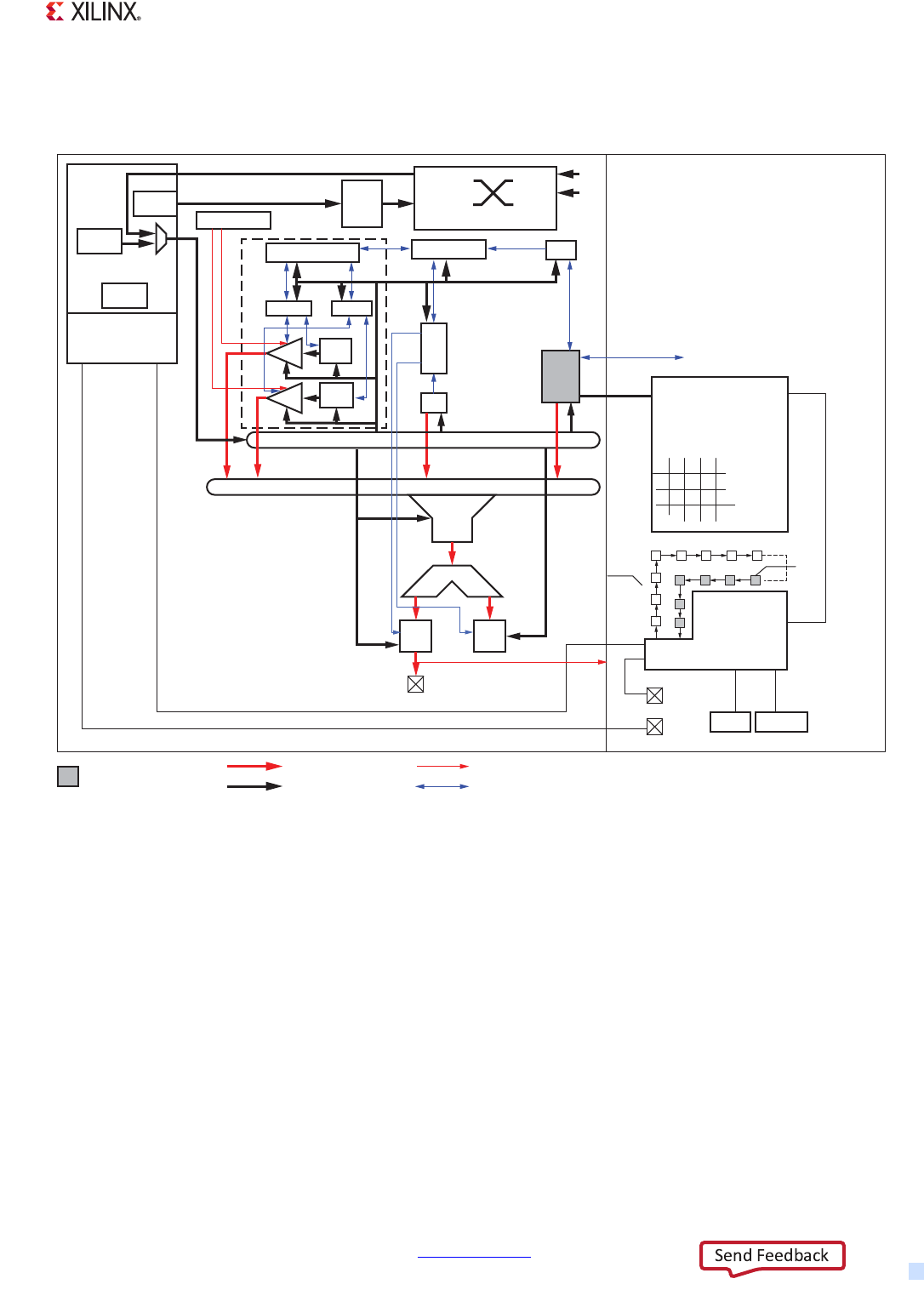
Zynq-7000 AP SoC Technical Reference Manual www.xilinx.com 721
UG585 (v1.12.1) December 6, 2017
Chapter 27: JTAG and DAP Subsystem
The PL Xilinx TAP controller serves four key purposes: boundary scan test, eFuse programming,
BBRAM programming, and PL debug chipscope.
The TPIU provides the mechanism to capture trace over long periods of time. There is no internal
time limit to how long a trace can be dumped so the only practical limit is the Zynq-7000 bandwidth.
If doing a trace dump using PS I/O through MIO, the maximum trace bandwidth depends on how
many MIO trace I/Os could be allocated. Another alternative is trace dump through EMIO. PL soft
logic connects the EMIO trace signal to the PL SelectIO. There are other potential innovative ways to
handle EMIO trace.
For example, users could loopback EMIO trace data back to the PS and store it in DDR memory or
export trace via gigabit Ethernet to enable remote debug or monitor. In typical debug flow, the user
enables minimum trace source dumping capability to fit trace data into allocated TPIU throughput.
After a small time window when debug occurs as determined through trace monitoring, the user
could enable full trace dumping capability if required, and store short periods of data into the ETB
for the next level of debug. Other than debugging, trace port also brings significant value for
software profiling. Soft profiling helps the user to identify those software routines that consume the
X-Ref Target - Figure 27-3
Figure 27-3: Debug System Architecture
PL Logic
CTM
ITM
Funnel
(CSTF)
TPIU 4K
ETB
Trace Port
Top Switch
AHB-
AXI
Debug JTAG Interface
(Chipscope)
PL
XILINX TAP
JTAG-DP
ARM DAP
PS_Pad
PL_Pad
TDO
TDI TDO
TDI
Xilinx Custom Design
Debug APB
FTM Trace
TDI
TDO
PS
Trace ATB
AHB-AP
CTI
CPU
PTM
CPU
PTM
CTI
APB-AP
CTI
CTI
CTM
Time Stamp
Time Stamp
Cross Triggering
Trace Bus(ATB)
Debug APB
CPU Debug
ROM
eFuse BBRAM
UG585_c27_03_021313
Cross Trig(8)
Zynq-7000 AP SoC Technical Reference Manual www.xilinx.com 722
UG585 (v1.12.1) December 6, 2017
Chapter 27: JTAG and DAP Subsystem
most CPU power. Based on that, the user could decide to either perform software optimization or
offload the process to the PL.
27.3 I/O Signals
In cascaded JTAG mode, only PL_TDO/TMS/TCK/TDI at the PL side are meaningful to users. Through
them, users can access both the ARM DAP and Xilinx TAP.
In independent JTAG mode, users can only access the Xilinx TAP, through PL_TDO/TMS/TCK/TDI. To
access the ARM DAP, users must use PJTAG signals, as shown in Tab le 27 -1. There are two choices to
route PJTAG signals to chip pinouts: via EMIO to the PL SelectIO, or via MIO.
The MIO pins and any restrictions based on device version are shown in the MIO table in section
2.5.4 MIO-at-a-Glance Table.
The TPIU output, as shown at the bottom of Figure 27-3, can be routed to either EMIO or MIO (but
not both). The TPIU signals are listed in section 28.3 I/O Signals.
Table 27-1: PJTAG Signals
Signal Name via EMIO via MIO
Signal I/O Pin I/O
TCK EMIOPJTAGTCK I MIO 12, 24, 36 or 48 I
TMS EMIOPJTAGTMS I MIO 13, 25, 37 or 49 I
TDI EMIOPJTAGTDI I MIO 10, 22, 34 or 46 I
TDO EMIOPJTAGTDO O MIO 11, 23, 35 or 47 O
TDO 3-state EMIOPJTAGTDTN O
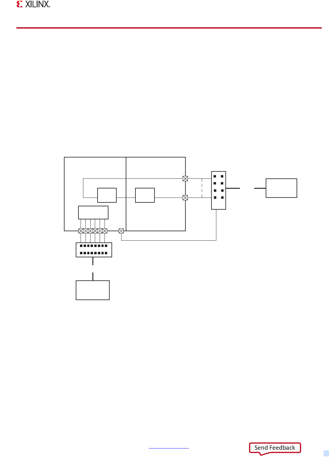
Zynq-7000 AP SoC Technical Reference Manual www.xilinx.com 723
UG585 (v1.12.1) December 6, 2017
Chapter 27: JTAG and DAP Subsystem
27.4 Programming Model
27.4.1 Use Case I: Software Debug with Trace Port Enabled
This is the normal debug case for most applications. Figure 27-4 shows ARM tool chain solution. It is
also possible to replace ARM Real View ICE with a Xilinx or Lauterbach debug tool. In this case, there
is no PL programming required and the user is able to start on software debug as soon as chip power
is on. In this use case, the DAP is active to support software debug needs but the TAP is put into
bypass mode. Trace port is also enabled through the MIO pin. Although bandwidth might be limited
due to limited MIO availability in some cases, the user could enable a trace dump without depending
on PL configuration in this configuration. The major challenge for most users is to allocate MIO pins
for the Trace port.
27.4.2 Use Case II: PS and PL Debug with Trace Port Enabled
The second use case shows how to enable PS software and PL hardware at the same time with two
separate debug tools. The tool connected to the Xilinx TAP is typically a Xilinx debug tool. The tools
connected to the PS DAP could be Xilinx or any third-party debug tools from ARM or Lauterbach.
To support this mode, PL configuration is required to bring the DAP JTAG signals to the PL SelectIOs.
Figure 27-5 shows trace port access through the PL SelectIO, but the user could use the MIO trace
port as in the previous use case if there is way to manage to fit the trace port into the limited MIO
pin multiplexing. Trace port access through SelectIO could support up to 32-bit trace data and gives
users enough trace port throughput to address most debug need. As with the JTAG DAP access, the
X-Ref Target - Figure 27-4
Figure 27-4: User Case I: Software Debug with Trace Port Enabled
DAP TAP
TPIU
JTAG SS
SS
SRST
PS PL
ARM
DStream
ARM Real
View ICE
UG585_c27_04_031812
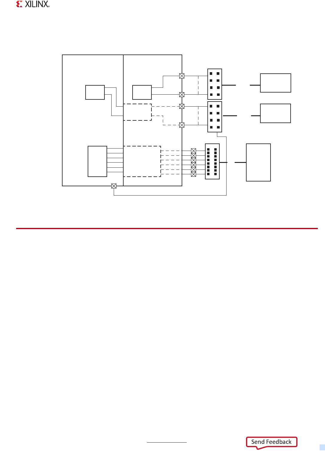
Zynq-7000 AP SoC Technical Reference Manual www.xilinx.com 724
UG585 (v1.12.1) December 6, 2017
Chapter 27: JTAG and DAP Subsystem
PL must be configured to route the trace signal from the EMIO at the PS/PL boundary to the PL
SelectIO.
27.5 ARM DAP Controller
The debug access port (DAP) is an implementation of an ARM debug interface standard comprising
a number of components supplied in a single configuration. All of the supplied components fit into
the various architectural components for debug ports (DPs) which are used to access the DAP from
an external debugger, and access ports (APs) to access on-chip system resources.
With the JTAG-DP, IEEE 1149.1 scan chains are used to read or write register information. A pair of
scan chain registers is used to access the main control and access registers within the debug port:
•DPACC used for debug port (DP) accesses
• APACC used for access port (AP) accesses
An APACC might access a register of a debug component of the system to which the interface is
connected. The scan chain model implemented by a JTAG-DP has the concepts of capturing the
current value of APACC or DPACC, and of updating APACC or DPACC with a new value. An update
might cause a read or write access to a DAP register that might then cause a read or write access to
a debug register of a connected debug component.
Tabl e 27- 2 shows four Tap ARM DAP IR Instructions. All other IR Instructions are implemented as
BYPASS.
X-Ref Target - Figure 27-5
Figure 27-5: User Case II: PS and PL Debug with Trace Port Enabled
DAP TAP
TPIU
JTAG
Xilinx
Platform
Cable
SS
Soft Core
PS PL
ARM
Review
ICE
SS
ARM
DStream
SS
Soft Core
SRST
JTAG
UG585_c27_05_031812
Zynq-7000 AP SoC Technical Reference Manual www.xilinx.com 725
UG585 (v1.12.1) December 6, 2017
Chapter 27: JTAG and DAP Subsystem
The ARM DAP is composed of one debug port (DP) and up to three access ports (APs). Among the
three APs, Zynq-7000 devices only implement APB-AP as the bus master to access all debug
components and AHB-AP to access system memory space directly. Ta ble 2 7- 3 lists all registers within
the DP.
Tabl e 27- 4 shows AHB-AP and APB-AP registers in the DAP. For each AP, there is a unique set of
registers associated with each AP port. Although the DAP allows JTAG-AP, Zynq devices do not
support this feature.
Table 27-2: ARM DAP IR Instruction
IR Instruction Binary Code[3:0] DR Width Description
ABORT 1000 35 JTAG-DP abort register
DPACC 1010 35 JTAG DP access register
APACC 1011 35 JTAG-AP access Register
ARM_IDCODE 1110 32 IDCODE for ARM DAP IP
BYPASS 1111 1
Table 27-3: DP Registers Summary
DP Register Access Description
CTRL/STAT IR=DPACC/ADDRESS =
0x4
DP Control and Status register
SELECT IR=DPACC/ADDRESS =
0x8
Its main purpose is to select the current access port and
the active four-word register window in that access port
Table 27-4: AP Registers Summary
AP Register Access Description
CSW IR=APACC/ADDRESS = 0x0 Control and status word
TAR IR=APACC/ADDRESS = 0x4 Transfer address, TAR
DRW IR=APACC/ADDRESS = 0xC Data read/write
BD0-3 IR=APACC/ADDRESS = 0x10 to 0x1C Band data 0 to 3

Zynq-7000 AP SoC Technical Reference Manual www.xilinx.com 726
UG585 (v1.12.1) December 6, 2017
Chapter 27: JTAG and DAP Subsystem
27.6 Trace Port Interface Unit (TPIU)
Tabl e 27- 5 shows all registers within the TPIU.
27.7 Xilinx TAP Controller
The Xilinx TAP contains four mandatory dedicated pins as specified by the protocol and typical JTAG
architecture. Tab le 2 7-6 shows Xilinx TAP IR commands. Refer to UG470, 7 Series FPGAs Configuration
User Guide for more details about the IR commands.
Table 27-5: TPIU Registers Summary
TPIU Register Offset Description
SUPPORT_PORT_SIZE 0x0 32-bit register with each bit indicating whether a single port size
is allowed
CURRENT_PORT_SIZE 0x4 Indicates current trace port size with only 1 of 32-bits that could
be set
TRIG_MODE 0x100 Indicates trigger mode support
TRG_COUNT 0x104 8-bit register to enable delaying the indication of triggers to the
external trace capture device
TRIG_MULT 0x108 Trigger counter multiplier
TEST_PATTERN 0x200-0x208 Configures a test pattern to generate a known bit sequence that
could be capture by external capture device
FORMAT_SYNC 0x300-0x308 Control generation of stop, trigger, and flush events
Table 27-6: JTAG Commands
Boundary Scan Command Binary Code[5:0] Description
EXTEST 000000 Enables boundary-scan EXTEST operation
SAMPLE 000001 Enables boundary-scan SAMPLE operation
USER1 000010 Access user-defined register 1
USER2 000011 Access user-defined register 2
USER3 100010 Access user-defined register 3
USER4 100011 Access user-defined register 4
CFG_OUT 000100 Access the configuration bus for readback
CFG_IN 000101 Access the configuration bus for configuration
USERCODE 001000 Enables shifting out user code
IDCODE 001001 Enables shifting out of ID code
ISC_ENABLE 010000 Marks the beginning of ISC configuration; full
shutdown is executed

Zynq-7000 AP SoC Technical Reference Manual www.xilinx.com 727
UG585 (v1.12.1) December 6, 2017
Chapter 27: JTAG and DAP Subsystem
Note: VRP and VRN pins are special pins that needs to be excluded from the boundary scan test.
ISC_PROGRAM 010001 Enables in-system programming
ISC_PROGRAM_SECURITY 010010 Change security status from secure to non-secure
mode and vice versa
ISC_NOOP 010100 No operation
ISC_READ 101011 Used to read back BBR
ISC_DISABLE 010111 Completes ISC configuration. Startup sequence is
executed
BYPASS 111111 Enables bypass
Table 27-6: JTAG Commands (Cont’d)
Boundary Scan Command Binary Code[5:0] Description

Zynq-7000 AP SoC Technical Reference Manual www.xilinx.com 728
UG585 (v1.12.1) December 6, 2017
Chapter 28
System Test and Debug
28.1 Introduction
The PS and PL can be debugged together as a complete system using intrusive and non-intrusive
debug techniques. In addition to software code debug, there are key hardware points in the PS and
user-selected key hardware points in the PL that can capture system activity to help with the debug
process.
The test and debug capability is based on the ARM CoreSight v1.0 Architecture Specification and
consists mostly of ARM-supplied components, but also includes one Xilinx-supplied component (the
fabric trace module (FTM), see Chapter 23, Programmable Logic Test and Debug). ARM CoreSight
architecture defines four classes of CoreSight components: access and control, trace source, trace
link, and trace sink.
Components of the access and control class provide a user interface to access the debug
infrastructure through JTAG or memory-mapped locations. This class of components also
coordinates the operation of separate CoreSight components with a trigger signal distribution
network. Components of the trace source class capture debug information, like instruction
addresses, bus transaction addresses, and generate trace packets. These trace packets are routed to
components of the trace link class where trace packets can be combined or replicated. Components
of the trace sink class receive trace packets and dump them into an on-chip trace buffer, or output
them to chip pinouts (via the MIO) or to the PL (via the EMIO).
CoreSight components are connected together via three major types of buses/signals; programming,
trigger, and trace. The programming bus is the path for the access and control class to convey
programming information from the JTAG or from processors to other CoreSight components. The
trigger signals are used by all classes of components to receive and send triggers from/to each other
to coordinate their operation. The trace bus is the main pathway for trace packets to flow, connecting
trace source, trace links, and trace sinks.
28.1.1 Features
The CoreSight components provide the following capabilities for the system-wide trace:
• Debug and trace visibility of whole systems with a single debugger connection
• Cross triggering support between SoC subsystems
• Multi-source trace in a single stream
• Higher data compression than previous solutions
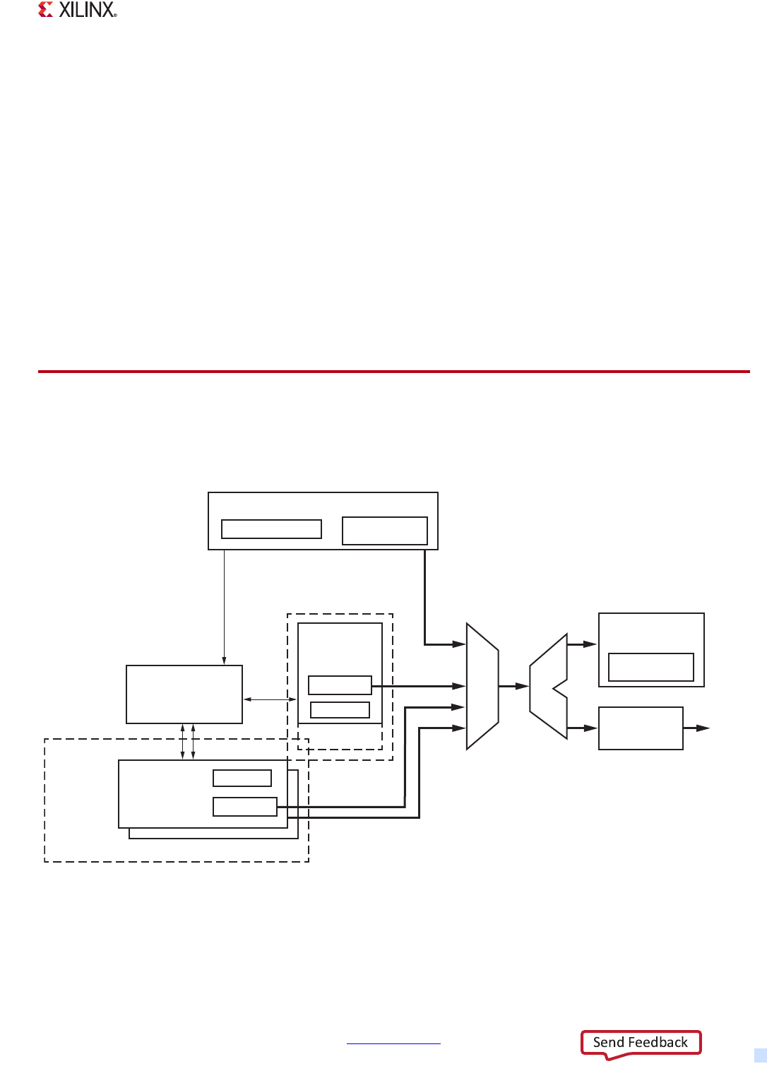
Zynq-7000 AP SoC Technical Reference Manual www.xilinx.com 729
UG585 (v1.12.1) December 6, 2017
Chapter 28: System Test and Debug
• Standard programmer's models for standard tools support
• Automatic discovery of topology
• Open interfaces for third party soft cores
• Low pin count options
28.1.2 Notices
7z007s and 7z010 CLG225 Devices
The 7z007s single core and 7z010 dual core CLG225 devices support 32 MIO pins as shown in the
MIO table in section 2.5.4 MIO-at-a-Glance Table. The width of the TPIU in these CLG225 devices is
restricted to 1, 2 or 4-bits via the MIO pins. All 32 data signals are available on the EMIO interface.
All of the CLG225 device restrictions are listed in section 1.1.3 Notices.
28.2 Functional Description
The block diagram for the CoreSight system is shown in Figure 28-1.
X-Ref Target - Figure 28-1
Figure 28-1: CoreSight System Block Diagram
PTM Triggers (x2)
ITM
Trigger
Trace/Packet
Output (TPIU)
Embedded Cross
Trigger (ECT)
Detector
Packetizer
Program Trace
Macrocell
(PTM)
Detector
Packetizer
Fabric Trace
Monitor (FTM)
Trigger Register Write Packet
Registers
Instrumentation Trace Macrocell (ITM)
Funnel
UG585_c28_01_022612
MIO/
EMIO
Read Packet
Registers
Embedded Trace
Buer (ETB)
CPU 0
CPU 1
Replicator
FTM
Trigger
PL Fabric
CPUs

Zynq-7000 AP SoC Technical Reference Manual www.xilinx.com 730
UG585 (v1.12.1) December 6, 2017
Chapter 28: System Test and Debug
Figure 28-1 shows the four classes of CoreSight components:
• Access and control: DAP, ECT
• Trace source: PTM, FTM, ITM
• Trace link: Funnel, Replicator
• Trace sink: ETB, TPIU
The components are connected by three types of buses/signals:
•Programming
• Trigger
•Trace
The CoreSight system interacts with:
• CPUs through PTM for debug and trace
• CPUs through ITM for trace
• PL through FTM for debug and trace
• CPUs through ETB for dumping trace
• EMIO/MIO through TPIU for dumping trace
• CPUs/JTAG through DAP for programming CoreSight components
28.2.1 Debug Access Port (DAP)
The DAP is the front-end for user access to the Zynq-7000s AP SoC system test and debug
functionalities. It is a CoreSight component of the access and control class, and connects to other
components using the programming bus. DAP provides the user, with two interfaces to access the
CoreSight infrastructure:
• External: JTAG, from chip pinout
• Internal: APB slave, from the slave interconnect
A debugger can use JTAG to communicate with the CoreSight infrastructure, while software running
on a CPU uses APB through memory-mapped addresses assigned to the CoreSight infrastructure.
The DAP forwards access requests arriving via either interface to the requested CoreSight
component.
In addition, the DAP also has another interface to access subsystems other than CoreSight, on the PS:
• Internal: AHB master, to the master interconnect
With AHB, the DAP can forward access requests from JTAG to other subsystems in the PS, subject to
authentication requirements. For example, a debugger can query the value of a location in DDR or
the value of a coprocessor register.
The DAP follows the access model described in ARM Debug Interface v5 Architecture Specification
and ARM Debug Interface v5.1 Architecture Supplement, where JTAG indirectly accesses debug
components and resources by way of registers in the DAP.
Zynq-7000 AP SoC Technical Reference Manual www.xilinx.com 731
UG585 (v1.12.1) December 6, 2017
Chapter 28: System Test and Debug
The DAP block is an ARM-supplied IP with the following configuration:
• JTAG is the only external interface on chip pinout. Serial wire interface (SW-DP) is not present.
• APB slave and AHB master are the two internal interfaces. JTAG at the DAP's internal side
(JTAG-AP) is present, but only the nSRSTOUT[0] output is connected to the system reset
controller.
• Power-down is not supported.
Note: When JTAG-AP nSRSTOUT[0] is used to assert system reset, DAP is removed from the JTAG
chain. The same sequence for bringing DAP into the chain must be followed again.
28.2.2 Embedded Cross Trigger (ECT)
ECT is the cross-triggering mechanism. Through ECT, a CoreSight component can interact with other
components by sending and receiving triggers. ECT is implemented with two components:
• CTM: Cross Trigger Matrix
• CTI: Cross Trigger Interface
One or more CTMs form an event broadcasting network with multiple channels. A CTI listens to one
or more channels for an event, maps a received event into a trigger, and sends the trigger to one or
more CoreSight components connected to the CTI. A CTI also combines and maps the triggers from
the connected CoreSight components and broadcasts them as events on one or more channels. Both
CTM and CTI are CoreSight components of the control and access class.
ECT is configured with:
• Four broadcast channels
•Four CTIs
• Power-down is not supported.
Tabl e 28- 1 lists the connections of trigger inputs and outputs of the CTIs.
Table 28-1: CTI Trigger Inputs and Outputs
CTI Trigger Port Signal
CTI (connected to ETB, TPIU)
Trigger input 2 ETB full
Trigger input 3 ETB acquisition complete
Trigger input 4 ITM trigger
Trigger output 0 ETB flush
Trigger output 1 ETB trigger
Trigger output 2 TPIU flush
Trigger output 3 TPIU trigger
CTI (connected to FTM)
Trigger input 0 FTM trigger

Zynq-7000 AP SoC Technical Reference Manual www.xilinx.com 732
UG585 (v1.12.1) December 6, 2017
Chapter 28: System Test and Debug
Trigger input 1 FTM trigger
Trigger input 2 FTM trigger
Trigger input 3 FTM trigger
Trigger output 0 FTM trigger
Trigger output 1 FTM trigger
Trigger output 2 FTM trigger
Trigger output 3 FTM trigger
CTI (connected to CPU0)
Trigger input 0 CPU0 DBGACK
Trigger input 1 CPU0 PMU IRQ
Trigger input 2 PTM0 EXT
Trigger input 3 PTM0 EXT
Trigger input 4 CPU0 COMMTX
Trigger input 5 CPU0 COMMRX
Trigger input 6 PTM0 TRIGGER
Trigger output 0 CPU0 debug request
Trigger output 1 PTM0 EXT
Trigger output 2 PTM0 EXT
Trigger output 3 PTM0 EXT
Trigger output 4 PTM0 EXT
Trigger output 7 CPU0 restart request
CTI (connected to CPU1)
Trigger input 0 CPU1 DBGACK
Trigger input 1 CPU1 PMU IRQ
Trigger input 2 PTM1 EXT
Trigger input 3 PTM1 EXT
Trigger input 4 CPU1 COMMTX
Trigger input 5 CPU1 COMMRX
Trigger input 6 PTM1 TRIGGER
Trigger output 0 CPU1 debug request
Trigger output 1 PTM1 EXT
Trigger output 2 PTM1 EXT
Trigger output 3 PTM1 EXT
Trigger output 4 PTM1 EXT
Trigger output 7 CPU1 restart request
Table 28-1: CTI Trigger Inputs and Outputs (Cont’d)
CTI Trigger Port Signal

Zynq-7000 AP SoC Technical Reference Manual www.xilinx.com 733
UG585 (v1.12.1) December 6, 2017
Chapter 28: System Test and Debug
Note: For details on the two CTIs connected to CPU0 and CPU1, refer to the CoreSight PTM-A9
Technical Reference Manual, r1p0, DDI0401C, section 1.3.6.
28.2.3 Program Trace Macrocell (PTM)
The PTM is the block for tracing processor execution flow. It is based on the ARM program flow trace
(PFT) architecture, and is a CoreSight component of the trace source class. The PTM generates
information that trace tools use to reconstruct the execution of a program, by tracing only certain
points in program execution called waypoints. This reduces the amount of trace data. Timestamps
are supported for correlating multiple trace streams and coarse grain code profiling.
The PTM provides some general resources, such as address/ID comparators, counter, sequencers, for
setting up user-defined event triggering conditions. This enhances the base functions of tracing
program execution.
The PTM block in Zynq-7000 AP SoC devices is the standard ARM-supplied IP, with the no custom
configuration.
28.2.4 Instrumentation Trace Macrocell (ITM)
The ITM is the block for software to generate a trace. It is a CoreSight component of the trace source
class. Triggering and coarse-grained time stamping are also supported. The main uses include:
• printf style debugging
• Trace OS and application events
• Emit diagnostic system information
The ITM block in Zynq-7000 AP SoC devices is the standard ARM-supplied IP, with the no custom
configuration.
28.2.5 Funnel
The funnel is the block for merging trace data from multiple sources into a single stream. It is a
CoreSight component of the trace link class. Users select the sources to be merged and assign
priorities to them.
The funnel in Zynq-7000 AP SoC devices is the standard ARM-supplied IP, with the no custom
configuration.
Tabl e 28- 2 lists the connections of the input ports of the Funnel.
[
Table 28-2: Funnel Input Port List
Port Trace Source
0PTM0
1PTM1
2FTM

Zynq-7000 AP SoC Technical Reference Manual www.xilinx.com 734
UG585 (v1.12.1) December 6, 2017
Chapter 28: System Test and Debug
28.2.6 Embedded Trace Buffer (ETB)
The ETB is the on-chip storage of trace data. It is a CoreSight component of the trace sink class. The
ETB provides real-time full-speed storing capability, but is limited in size. Triggering is supported for
events such as buffer full and acquisition complete.
The ETB block in Zynq-7000 AP SoC devices is an ARM-supplied IP, with the following configuration:
•RAM size: 4KB
28.2.7 Trace Packet Output (TPIU)
The TPIU is the block for outputting trace data to the PL or to chip pinout. It is a CoreSight
component of the trace sink class. The TPIU provides unlimited trace data output, but is limited in
bandwidth. Triggering and flushing are both supported.
The TPIU block is an ARM-supplied IP, with the following configuration:
• Max data width: 32
Tabl e 28- 3 shows the two operating modes of TPIU.
Figure 28-2 shows the waveforms of TPIU I/O signals in the two modes. In EMIO mode, the PL
supplies the trace clock signal to TPIU; PL can use the same clock to sample the trace data and
control signals from PS. In MIO mode, all signals, including data, control, and clock, are aligned at
the selected MIO pins; therefore, the external device should delay the trace clock output by
approximately half the clock period to successfully sample the trace data and control signals. Before
3ITM
4-7 unused
Table 28-2: Funnel Input Port List (Cont’d)
Port Trace Source
Table 28-3: Operating Modes of TPIU
slcr.DBG_CLK_CTRL[6], MIO_PIN_xx (Details in Table 28-4)
10
Active interface EMIO MIO
Clock source to operate the TPIU EMIOTRACECLK PS clock controller
Output clock present? No Yes
Clock edge(s) to sample trace data
and control
Rising Rising and falling
Supported data widths 1, 2, 4, 8, 16, 32 1, 2, 4, 8, 16
Application Note Since PL supplies the clock to
TPIU, PL can use the same clock
to sample.
External device should delay
the trace clock output by
approximately half clock
period, and use the delayed
clock to sample.
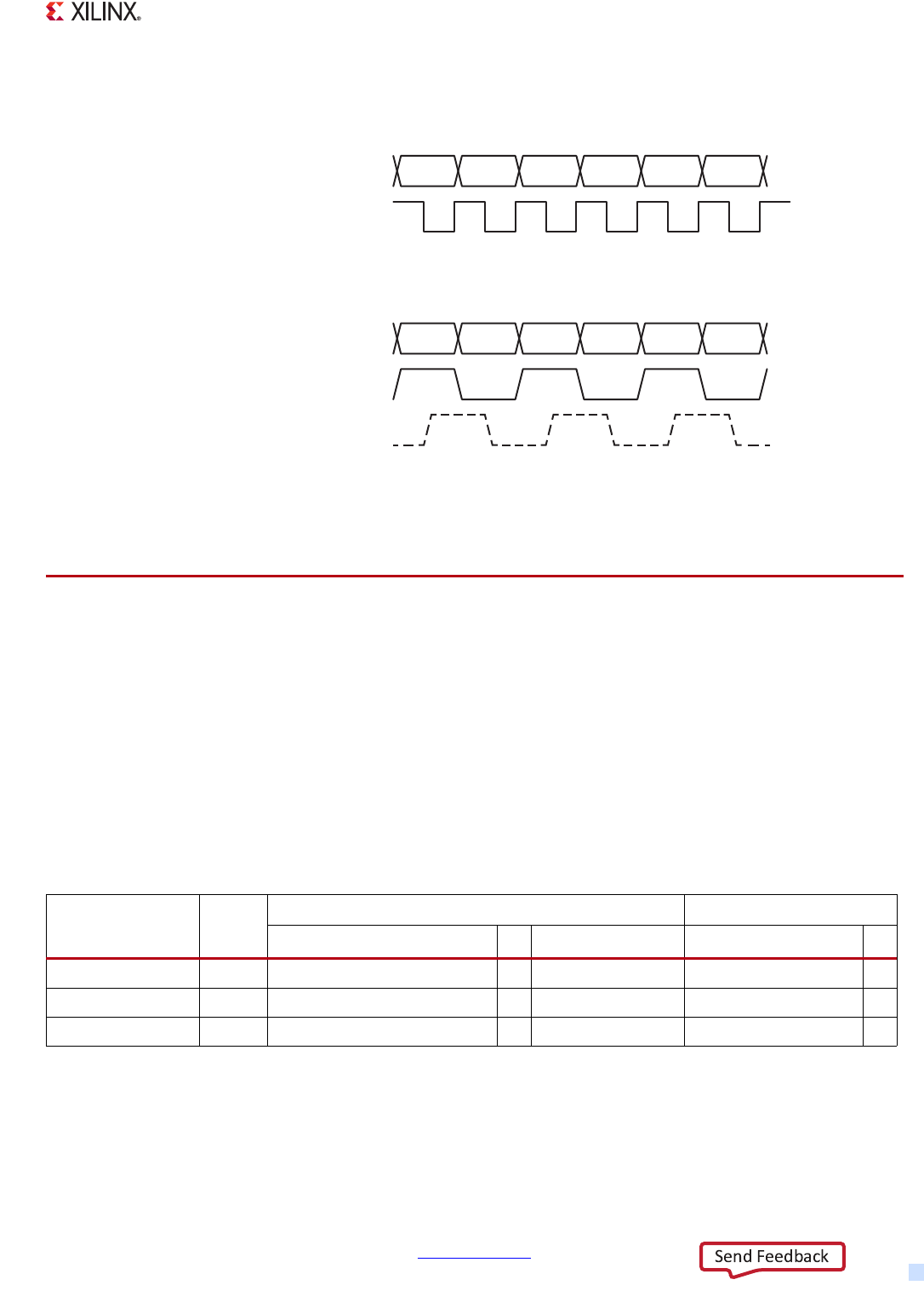
Zynq-7000 AP SoC Technical Reference Manual www.xilinx.com 735
UG585 (v1.12.1) December 6, 2017
Chapter 28: System Test and Debug
changing the active interface to EMIO, ensure that EMIOTRACELCK is running. Changing the clock
input source to a non-running clock results in an APB access hang.
28.3 I/O Signals
Tabl e 28- 4 identifies the TPIU port signals. The TPIU port data can be routed to either an MIO or
EMIO interface, but not both. EMIO supports 32-bit data at a single data rate clock that is sourced
from the PL as an EMIO input.
MIO supports 16-bit data at a double data rate clock sourced by the clock generator and driven out
on MIO. Pin restrictions based on device version are explained in section 28.1.2 Notices.
Tabl e 28- 4 identifies the system test and debug I/O signals. The MIO pins and any restrictions based
on device version are shown in the MIO table in section 2.5.4 MIO-at-a-Glance Table.
Sammie!161
X-Ref Target - Figure 28-2
Figure 28-2: TPIU Operating Mode Waveforms
EMIOTRACEDATA
EMIOTRACECTL
EMIOTRACECLK
UG585_c28_02_022612
trace data, control output
on selected MIO pins
trace clock output
on selected MIO pins
trace clock delayed by
approximately half period
TPIU Signals on EMIO
TPIU Signals on MIO
Table 28-4: TPIU Signals List
TPIU Signal
Default
Input
Value
MIO Pins EMIO Signals
Number I/O Pin Name Signal Name I/O
EMIO trace clock 0~ ~ ~ EMIOTRACECLK I
MIO Trace Clock ~ 12 or 24 O TRACE_CLK ~ ~
Trace control ~ 13 or 25 O TRACE_CTL EMIOTRACECTL O

Zynq-7000 AP SoC Technical Reference Manual www.xilinx.com 736
UG585 (v1.12.1) December 6, 2017
Chapter 28: System Test and Debug
28.4 Register Overview
28.4.1 Memory Map
Per the CoreSight specification, each CoreSight component has 4 kB address space. Table 2 8- 5 lists
the base address of each CoreSight component.
Trace data ~
1-bit 14 or 26
O TRACE_DATA[15:0] EMIOTRACEDATA[31:0] O
2-bit 15, 14 or 27, 26
4-bit 11, 10, 15, 14 or
23, 22, 27, 26
8-bit 11, 10, 15, 14 or
23, 22, 27, 26
16-bit 9-2,19-16,11,10,15,14
Table 28-4: TPIU Signals List (Cont’d)
TPIU Signal
Default
Input
Value
MIO Pins EMIO Signals
Number I/O Pin Name Signal Name I/O
Table 28-5: Memory Map
Component Base Address
DAP ROM 0xF880_0000
ETB 0xF880_1000
CTI (connected to ETB, TPIU) 0xF880_2000
TPIU 0xF880_3000
Funnel 0xF880_4000
ITM 0xF880_5000
CTI (connected to FTM) 0xF880_9000
FTM 0xF880_B000
Cortex-A9 ROM 0xF888_0000
CPU0 debug logic 0xF889_0000
CPU0 PMU 0xF889_1000
CPU1 debug logic 0xF889_2000
CPU1 PMU 0xF889_3000
CTI (connected to CPU0, PTM0) 0xF889_8000
CTI (connected to CPU1, PTM1) 0xF889_9000
PTM0 (for CPU0) 0xF889_C000
PTM1 (for CPU1) 0xF889_D000

Zynq-7000 AP SoC Technical Reference Manual www.xilinx.com 737
UG585 (v1.12.1) December 6, 2017
Chapter 28: System Test and Debug
Note: CPU0 debug logic and CPU1 debug logic can also be accessed through CP14 coprocessor
instructions. See the Cortex-A9 Technical Reference Manual for details.
28.4.2 Functionality
Tabl e 28- 6 summarizes the registers in each CoreSight component.
Table 28-6: CoreSight Component Register Summary
Function Name Overview
DAP ROM
Pointers Entry0-9 Pointers to other CoreSight components
CoreSight management Peripheral ID0-7
Component ID0-3
These registers provide identification information
ETB
Control CTL Enable/disable capture
Status STS Status on pipeline, acquisition, trigger, full/empty
RAM depth RDP Depth of RAM in words
RAM read RRD, RRP Read pointer and data
RAM write RWD, RWP Write pointer and data
Trigger counter TRG Sets the number of words to be stored after a trigger event
Formatter and flush FFCR, FFSR Stop events, trigger mark, flush start, formatting control
CoreSight management Peripheral ID
Component ID
Device ID, type
Claim, lock, authentication
Integration test
These registers provide:
• Identification information
• Authentication and access control
• Integration test
CTI
Control CONTROL Enable/disable CTI
Acknowledge INTACK Provide for SW to acknowledge TRIGOUT when no hardware
acknowledge is supplied
Channel event
generation
APPSET, APPCLR, APPPULSE Raise/clear/pulse channel events, used with GATE register to
create local events
Channel event gating GATE Prevent the channel events from propagating to other CTI's
in the system
Forwarding control INEN,
OUTEN
Enable the forwarding of events between the trigger
interface and the channel interface
Trigger/Channel
interface status
TRIGINSTATUS,
TRIGOUTSTATUS,
CHINSTATUS, CHOUTSTATUS
Provide the current status of the trigger and channel
interfaces

Zynq-7000 AP SoC Technical Reference Manual www.xilinx.com 738
UG585 (v1.12.1) December 6, 2017
Chapter 28: System Test and Debug
CoreSight management Peripheral ID
Component ID
Device ID, type
Claim, lock, authentication
Integration test
These registers provide:
• Identification information
• Authentication and access control
• Integration test
TPIU
Supported feature Show maximum and current values of supported port size,
test patterns, etc.
Trigger Set Trigger counter, multiplier
Testing Set test pattern, modes and repeat count
Format and finish Control and status of formatter and flush
CoreSight management Peripheral ID
Component ID
Device ID, type
Claim, lock, authentication
Integration test
These registers provide:
• Identification information
• Authentication and access control
• Integration test
Funnel
Control Control, Priority Enable slave ports, set hold time, and priority
CoreSight management Peripheral ID
Component ID
Device ID, type
Claim, lock, authentication
Integration test
These registers provide:
• Identification information
• Authentication and access control
• Integration test
ITM
Control CR, SCR Enable ITM, configure features like timestamp, sync packets,
sync count, etc.
Stimulus SPR Cause the write data to be inserted into the FIFO for packets
Trace TER, TTR Enable trace and trigger
CoreSight management Peripheral ID
Component ID
Device ID, type
Claim, lock, authentication
Integration test
These registers provide:
• Identification information
• Authentication and access control
• Integration test
FTM
Cortex-A9 Integration ROM
Pointers Entry Pointers to other CoreSight components for A9
CoreSight management Peripheral ID
Component ID
These registers provide identification information
CPU debug
Table 28-6: CoreSight Component Register Summary (Cont’d)
Function Name Overview

Zynq-7000 AP SoC Technical Reference Manual www.xilinx.com 739
UG585 (v1.12.1) December 6, 2017
Chapter 28: System Test and Debug
Control DBGDSCCR Controls cache behavior while the CPU is in debug state
Breakpoints BVR
BCR
Set breakpoint values, and control breakpoints. A breakpoint
can be set on an Instruction Virtual Address (IVA) or/and a
Context ID
Watchpoints WVR
WCR
Set watchpoint values, and control watchpoints. A
watchpoint can be set on a Data Virtual Address (DVA) or
with a Context ID
CoreSight management Peripheral ID
Component ID
Device ID, type
Claim, lock, authentication
Integration test
These registers provide:
• Identification information
• Authentication and access control
• Integration test
CPU PMU
Control PMCR Performance monitor control
Status PMOVSR Overflow flag status
Counter PMCNTENSET
PMCNTENCLR
PMSELR
PMCCNTR
Counter enable set/clear, software increment, cycle count
Event counters PMXEVTYPER
PMXEVCNTR
Counters to gather statistics on the operation of the
processor and memory system
User enable PMUSERENR User enable
Interrupt Enable PMINTENSET
PMINTENCLR
Interrupt enable set/clear
PTM
Configuration ETMCR, ETMCCR,
ETMTRIGGER, ETMSR,
ETMSCR
Main control registers, configuration, set trigger events, and
status
Trace Enable control ETMSSSCR, ETMTEEVR,
ETMTECR1
Trace enable start/stop, Trace enable event, Trace enable
control
Address comparators ETMACVR, ETMACTR Address comparator values, types
Counters ETMCNTRLDVR,
ETMCNTENR,
ETMCNTVR
Counter reload values, enable events, reload events, current
values
Sequencers ETMSQMNEVR,
ETMSQR
Sequencer state transition events, sequencer current state
External output event ETMEXTOUTEVER Set events that control the corresponding external output
Context ID comparators ETMCIDCVR1, ETMCIDCMR Context ID comparator value, mask
Sync frequency, ID
General control ETMSYNCFR, ETMIDR Sync frequency, ID
Table 28-6: CoreSight Component Register Summary (Cont’d)
Function Name Overview

Zynq-7000 AP SoC Technical Reference Manual www.xilinx.com 740
UG585 (v1.12.1) December 6, 2017
Chapter 28: System Test and Debug
28.5 Programming Model
28.5.1 Authentication Requirements
ARM CoreSight infrastructure uses four signals to control authentication:
• DBGEN Invasive debug enable
• NIDEN Non-invasive debug enable
• SPIDEN Secure invasive debug enable
• SPNIDEN Secure non-invasive debug enable
Tabl e 28- 7 lists the Zynq-7000 AP SoC device authentication requirements for the CoreSight
components.
Misc. ETMCCER, ETMEXTINSELR,
ETMTSEVR, ETMAUXCR,
ETMTRACEIDR, ETMOSLSR
Configuration code, external input selection, timestamp,
auxiliary control, CoreSight trace ID, OS lock, power-down
CoreSight management Peripheral ID
Component ID
Device ID, type
Claim, lock, authentication
Integration test
These registers provide:
• Identification information
• Authentication and access control
• Integration test
Table 28-6: CoreSight Component Register Summary (Cont’d)
Function Name Overview
Table 28-7: CoreSight Authentication Requirements by Component
Requirement DBGEN NIDEN SPIDEN SPNIDEN
DAP AHB master
Non-secure access 1x0x
Secure access 1x1x
CTI (connected to ETB, TPIU)
CTI (connected to FTM)
Enable all trigger inputs xxxx
Enable all trigger outputs xxxx
CTI (connected to CPU0)
CTI (connected to CPU1)
Enable trigger input 0 x 1xx
Enable trigger input 1 x 1xx
Enable trigger input 2 x 1xx
Enable trigger input 3 x 1xx
Enable trigger input 4 x 1xx
Zynq-7000 AP SoC Technical Reference Manual www.xilinx.com 741
UG585 (v1.12.1) December 6, 2017
Chapter 28: System Test and Debug
Enable trigger input 5 x 1xx
Enable trigger input 6 x 1xx
Trigger output 0 1xxx
Trigger output 1 xxxx
Trigger output 2 xxxx
Trigger output 3 xxxx
Trigger output 4 xxxx
Trigger output 6 1xxx
Trigger output 7 xxxx
Funnel
TPIU
ETB
(no authentication is required) xxxx
ITM
Disable stimulus registers 0-15 0000
Disable stimulus registers 16-31 x x 00
CPU debug
CPU PMU
Non-secure invasive debug 1xxx
Non-secure non-invasive debug 1xxx
01xx
Secure invasive debug 1x1x
Secure non-invasive debug 1x1x
1xx1
x11x
x1x1
PTM
Prohibited regions of trace Use the following to determine:
if (~NIDEN & ~DBGEN)
Prohibited = 1
else if (security level == non-secure)
Prohibited = 0
else if ((privilege level == user) & (SUNIDEN))
Prohibited = 0
else if (SPIDEN || SPNIDEN)
Prohibited = 0
else
Prohibited = 1
Table 28-7: CoreSight Authentication Requirements by Component (Cont’d)
Requirement DBGEN NIDEN SPIDEN SPNIDEN

Zynq-7000 AP SoC Technical Reference Manual www.xilinx.com 742
UG585 (v1.12.1) December 6, 2017
Chapter 29
On-Chip Memory (OCM)
29.1 Introduction
The on-chip memory (OCM) module contains 256 KB of RAM and 128 KB of ROM (BootROM). It
supports two 64-bit AXI slave interface ports, one dedicated for CPU/ACP access via the APU snoop
control unit (SCU), and the other shared by all other bus masters within the processing system (PS)
and programmable logic (PL). The BootROM memory is used exclusively by the boot process and is
not visible to the user.
OCM supports high AXI read and write throughput for RAM access by implementing the RAM as a
double-wide memory (128 bits). To take advantage of the high RAM access throughput, the user
application must use even AXI burst sizes and 128-bit aligned addresses.
The TrustZone feature is supported at 4-KB memory granularity. The entire 256 KB of RAM can be
divided into sixty four 4-KB blocks, and assigned security attributes independently. See Programming
ARM TrustZone Architecture on the Xilinx Zynq-7000 All Programmable SoC (UG1019).
As shown in Figure 29-1, there are 10 AXI channels associated with the OCM, five for the CPU/ACP
(SCU) port and five for the other PS/PL masters (OCM switch port). Arbitration between the read and
write channels of the SCU and OCM switch ports is performed within the OCM module. Parity
generation and checking is performed on RAM accesses only. Other main interfaces are an interrupt
signal (IRQ ID #35) as well as a register access APB port.
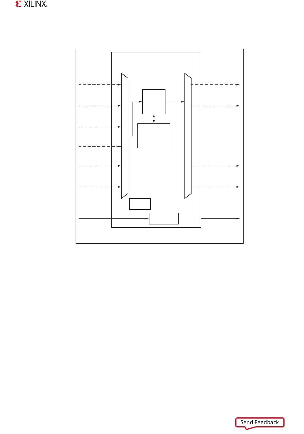
Zynq-7000 AP SoC Technical Reference Manual www.xilinx.com 743
UG585 (v1.12.1) December 6, 2017
Chapter 29: On-Chip Memory (OCM)
29.1.1 Block Diagram
29.1.2 Features
Key features of the OCM include:
• On-chip 256 KB RAM
• On-chip 128 KB BootROM (not user visible)
• Two AXI 3.0, 64-bit slave interfaces
• Low latency path for CPU/ACP reads to OCM (CPU at 667 MHz – minimum 23 cycles)
• Round-robin pre-arbitration between read and write AXI channels on OCM-interconnect port
(non-CPU port)
• Fixed priority arbitration between the CPU/ACP (via SCU) and OCM-interconnect AXI ports
• Supports full AXI 64-bit bandwidth of simultaneous read and write commands (with optimal
alignment restrictions) on the OCM interconnect port
• Random access supported to RAM from AXI masters
X-Ref Target - Figure 29-1
Figure 29-1: OCM Block Diagram
UG585_c29_01_042512
Parity
Generation
& Checking
256 KB
RAM
Arbiter
Registers
4-port Mem
Controller
SCU
AXI64 WrData
OCM Switch
AXI64 WrData
OCM Switch
AXI64 RdCmd
OCM Switch
AXI64 WrCmd
SCU
AXI64 WrCmd
SCU
AXI64 RdCmd
APB I/F
OCM Switch
AXI64 Bresp
OCM Switch
AXI64 RdData
SCU
AXI64 Bresp
SCU
AXI64 RdData
IRQ
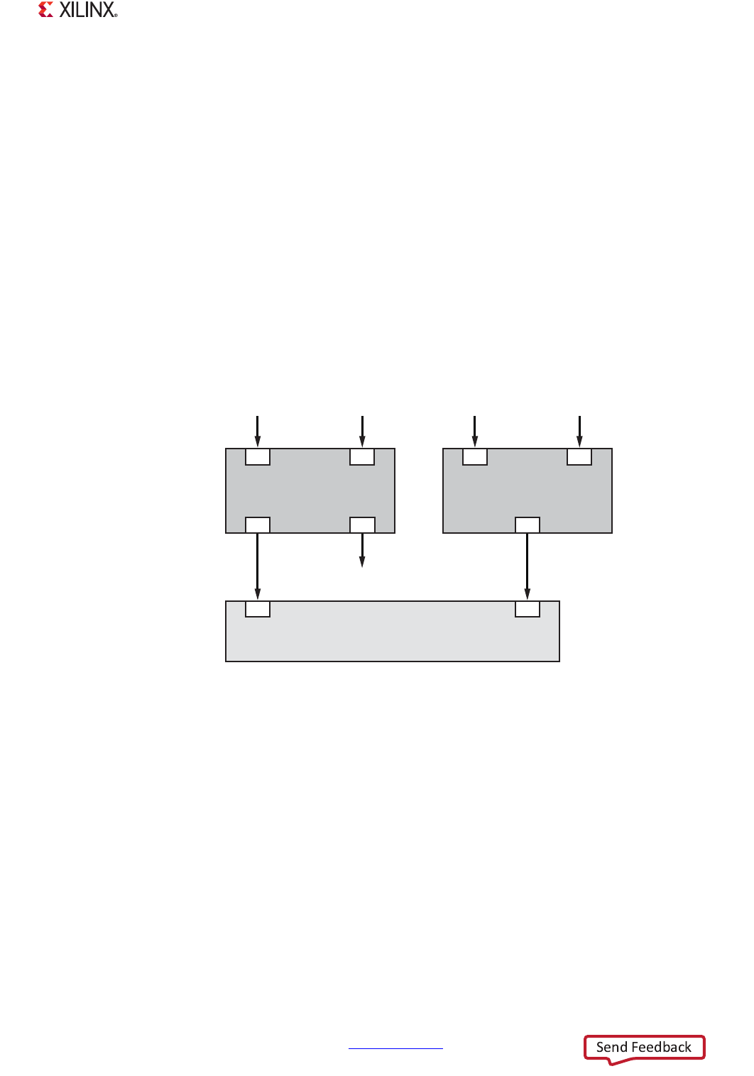
Zynq-7000 AP SoC Technical Reference Manual www.xilinx.com 744
UG585 (v1.12.1) December 6, 2017
Chapter 29: On-Chip Memory (OCM)
• TrustZone support for on-chip RAM with 4 KB page granularity
• Flexible address mapping capability
• RAM byte-wise parity generation, checking, and interrupt support
• Support for the following non-AXI features on the CPU (SCU) port:
°Zero line fill
°Pre-fetch hint
°Early BRESP
°Speculative line pre-fetch
29.1.3 System Viewpoint
A system viewpoint of the OCM is illustrated in Figure 29-2.
X-Ref Target - Figure 29-2
Figure 29-2: OCM System Viewpoint
UG585_c29_02_022212
Snoop
Control Unit
CPUs
S0 S1
On-chip RAM
256 kB
S0 S1
M0 M1
AXI_ACP
DDR
OCM
Interconnect
AXI_HP
S0 S1
M
All other Masters
Via Central
Interconnect

Zynq-7000 AP SoC Technical Reference Manual www.xilinx.com 745
UG585 (v1.12.1) December 6, 2017
Chapter 29: On-Chip Memory (OCM)
29.2 Functional Description
29.2.1 Overview
The OCM module is mainly composed of a RAM memory block. The OCM module also contains
arbitration, framing, parity, and interrupt logic in addition to the RAM array.
29.2.2 Optimal Transfer Alignment
The RAM is implemented as a single-ported, double-width (128-bit) module that can emulate a
dual-ported memory under specific conditions. This emulation of dual-ported operation occurs
automatically when 128-bit aligned, even burst multiples of AXI commands are used to access the
64-bit wide OCM AXI interfaces. Optimized bursts are theoretically able to achieve 100% throughput
of the RAM. If bursts are not aligned to 128 bits or burst lengths are odd multiples of 64-bits, the
control logic automatically realigns transfers inside the module — start and end addresses can be
presented to the RAM as 64-bit operations instead of more optimal 128-bit operations.
Configuring OCM memory as device memory in the MMU or using narrow, non-modifiable accesses
through the ACP port is not recommended. In this mode, pipelined 32-bit accesses are generated on
the SCU port. This type of traffic pattern does not take advantage the double-width memory and
effectively reduces OCM efficiency to 25%.
29.2.3 Clocking
The OCM module is clocked by the CPU_6x4x clock. However, the RAM array itself is an exception,
and is clocked by CPU_2x, though its 128-bit width is double that of any of the incoming 64-bit wide
AXI channels. The OCM switch feeding the OCM module is clocked by CPU_2x, and the SCU is
clocked by CPU_6x4x.
29.2.4 Arbitration Scheme
Apart from the CPUs and ACP, all other AXI bus masters are assumed to not have a strong latency
requirement. Therefore, the OCM uses a fixed arbitration scheme (on a data beat basis) between the
two AXI slave interfaces. The default order of decreasing priorities is:
1. SCU-Rd
2. SCU-Wr
3. OCM-Switch
Using the ocm.OCM_CONTROL.ScuWrPriorityLo register setting (see Appendix B, Register Details),
the decreasing priority arbitration can be modified to:
1. SCU-Rd
2. OCM-Switch
3. SCU-Wr
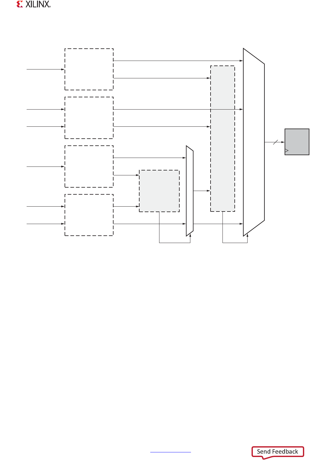
Zynq-7000 AP SoC Technical Reference Manual www.xilinx.com 746
UG585 (v1.12.1) December 6, 2017
Chapter 29: On-Chip Memory (OCM)
Arbitration is implemented as shown in Figure 29-3.
There is an additional round-robin pre-arbitration process that selects between a read or write
transaction on a per data-beat basis for the OCM-switch port traffic.
Note: Arbitration is performed on a transfer (data beat or clock cycle) basis, not on an AXI command
basis. The in-coming AXI read and write commands are split into individual addresses (or 128-bit
address pairs for aligned bursts) before arbitration.
Note: Each individual write address beat will not request access to the memory array until the write
data associated with it is available inside the OCM module — this prevents the scenario of a write
request being stalled due to write data not being available.
Starvation Scenarios
System constraints on the OCM are:
• The RAM array and OCM Switch port are clocked with CPU_2x which runs at one third or one
half the CPU clock.
• The SCU (CPU/ACP) port is clocked at full the CPU clock rate.
• Each of the four incoming AXI data channels are 64-bits wide.
X-Ref Target - Figure 29-3
Figure 29-3: Default (ScuWrPriorityLo=0) OCM Arbitration
UG585_c29_03_042512
Break Burst
Into Individual
Addresses Or
Address Pairs
(128-bit aligned)
256 KB
RAM
SCU
AXI64 RdCmd
Addr/Cmd
Req
Addr/Cmd/Data
Req
Addr/Cmd
Req
Req
Addr/Cmd/Data
Gnt[1:0]
Break Burst
Into Individual
Addresses Or
Address Pairs
(128-bit aligned)
SCU
AXI64 WrCmd
SCU
AXI64 WrData
Break Burst
Into Individual
Addresses Or
Address Pairs
(128-bit aligned)
OCM Switch
AXI64 RdCmd
Gnt[2:0]
Req
Hi
Priority
Med
Priority
Low
Priority
OCM
Switch
RoundRobin
Arbiter
Fixed
Priority
Arbiter
Break Burst
Into Individual
Addresses Or
Address Pairs
(128-bit aligned)
OCM Switch
AXI64 WrCmd
OCM Switch
AXI64 WrData
128

Zynq-7000 AP SoC Technical Reference Manual www.xilinx.com 747
UG585 (v1.12.1) December 6, 2017
Chapter 29: On-Chip Memory (OCM)
• The RAM array is 128-bits wide.
• The OCM switch port has separate read and write channels that can be simultaneously active.
• The SCU (CPU/ACP) port has separate read and write channels that can be simultaneously
active.
• The SCU (CPU/ACP) port channels have a fixed arbitration priority higher than the OCM switch
port by default.
As a result of these constraints, saturation of the RAM can occur by the SCU CPUs or ACP interfaces,
starving the OCM switch and the masters it serves. However, if the CPU(s) are running with caches on,
the rate at which they produce new commands to this module is sufficiently low to allow the OCM
switch port to share the RAM. The arbitration priority of the OCM switch can also be raised above the
priority of the SCU write channels.
Configuring OCM memory as Device Memory in the MMU or using narrow, non-modifiable accesses
through the ACP can also contribute to OCM switch port starvation; see section 29.2.2 Optimal
Transfer Alignment.
In general, the guidelines of ACP usage detailed under the ACP chapter should be followed, as this
port effectively produces commands on the SCU port to the OCM, which might cause starvation to
the OCM switch.
29.2.5 Address Mapping
The address range assigned to the OCM can be modified to exist in the first or last 256 KB of the
address map, to flexibly handle the ARM low or high exception vector modes. In addition, the CPU
and ACP AXI interfaces can have their lowest 1 MB address range accesses diverted to DDR, using
the SCU address filtering feature. This section describes these features through a series of example
address configurations.
Mapping Summary
(See Appendix B, Register Details for detailed register information.)
When addressing the OCM the following details should be considered:
• The 256 KB RAM array can be mapped to either a low address range (0x0000_0000 to
0x0003_FFFF) or a high address range (0xFFFC_0000 to 0xFFFF_FFFF) in a granularity of
four independent 64 KB sections via the 4-bit slcr.OCM_CFG[RAM_HI].
• The SCU address filtering (mpcore.SCU_CONTROL_REGISTER[Address_filtering_enable]) field is
set by hardware on any form of reset and should not be disabled by the user. Address filtering
on non-OCM addresses is necessary to correctly route transactions between the two
downstream SCU ports.The address filtering range has a 1 MB granularity.
• The SCU address filtering feature is able to redirect accesses from its CPU and ACP masters
targeting the range (0x0000_0000 to 0x000F_FFFF) which includes the OCM's low address
range, to the PS DDR DRAM, independent of the RAM address settings.
• For each 64 KB section mapped to the high OCM address range via slcr.OCM_CFG[RAM_HI]
which is not also part of the SCU address filtering range will be aliased for CPU and ACP masters
at a range of 0x000C_0000-0x000F_FFFF.

Zynq-7000 AP SoC Technical Reference Manual www.xilinx.com 748
UG585 (v1.12.1) December 6, 2017
Chapter 29: On-Chip Memory (OCM)
• All other masters that do not pass through the SCU are always unable to access the lower
512 KB of DDR in the OCM's low address range (0x0000_0000 to 0x0007_FFFF).
• Accesses to addresses which the RAM array is not currently mapped to are given an error
response.
Initial View
Upon entering user mode, the BootROM is no longer accessible, and the RAM space is split. Note
that one 64 KB range resides at the high OCM address, and the other 192 KB resides at the lower
address range. Table 2 9-1 and Ta ble 2 9 -2 identify the initial OCM/DDR address map and register
settings, respectively.
Attempted accesses to reserved areas return all zeroes along with a SLVERR bus response.
Table 29-1: Initial OCM/DDR Address Map
Address Range (Hex) Size CPUs/ACP Other Masters
0000_0000 - 0000_FFFF 64 KB OCM OCM
0001_0000 - 0001_FFFF 64 KB OCM OCM
0002_0000 - 0002_FFFF 64 KB OCM OCM
0003_0000 - 0003_FFFF 64 KB Reserved Reserved
0004_0000 - 0007_FFFF 256 KB Reserved Reserved
0008_0000 - 000B_FFFF 256 KB Reserved DDR
000C_0000 - 000C_FFFF 64 KB Reserved DDR
000D_0000 - 000D_FFFF 64 KB Reserved DDR
000E_0000 - 000E_FFFF 64 KB Reserved DDR
000F_0000 - 000F_FFFF 64 KB OCM3 (alias) DDR
0010_0000 - 3FFF_FFFF 1,023 MB DDR DDR
FFFC_0000 - FFFC_FFFF 64 KB Reserved Reserved
FFFD_0000 - FFFD_FFFF 64 KB Reserved Reserved
FFFE_0000 - FFFE_FFFF 64 KB Reserved Reserved
FFFF_0000 - FFFF_FFFF 64 KB OCM3 OCM3
Table 29-2: Initial Register Settings
Register Value
slcr.OCM_CFG[RAM_HI] 1000
mpcore.SCU_CONTROL_REGISTER[Address_filtering_enable] 1
mpcore.Filtering_Start_Address_Register 0x0010_0000
mpcore.Filtering_End_Address_Register 0xFFE0_0000

Zynq-7000 AP SoC Technical Reference Manual www.xilinx.com 749
UG585 (v1.12.1) December 6, 2017
Chapter 29: On-Chip Memory (OCM)
OCM Relocation
For a contiguous RAM address range, RAM located at address 0x0000_0000 to 0x0002_FFFF can
be relocated to base address 0xFFFC_0000 by programming the SLCR registers.
Each bit of slcr.OCM_CFG[RAM_HI] corresponds to a 64 KB range, with the MSB corresponding to the
highest address offset range. For more register programming details, refer to the SLCR information
in the system level control registers section of Appendix B, Register Details.
Tabl e 29- 3 and Ta bl e 29- 4 identify an example OCM relocation address map and OCM relocation
register settings, respectively.
SCU Address Filtering
The view of the OCM as seen by the CPUs and ACP via the SCU port relative to other masters via the
OCM switch is potentially different. The SCU uses its own dedicated address filtering mechanism to
address slaves other than the OCM while the other bus masters in the system are routed via a fixed
address decode scheme built into the system interconnects.
Table 29-3: Example OCM Relocation Address Map
Address Range (Hex) Size CPUs/ACP Other Masters
0000_0000 - 0000_FFFF 64 KB Reserved Reserved
0001_0000 - 0001_FFFF 64 KB Reserved Reserved
0002_0000 - 0002_FFFF 64 KB Reserved Reserved
0003_0000 - 0003_FFFF 64 KB Reserved Reserved
0004_0000 - 0007_FFFF 256 KB Reserved Reserved
000C_0000 - 000C_FFFF 64 KB OCM0 (alias) DDR
000D_0000 - 000D_FFFF 64 KB OCM1 (alias) DDR
000E_0000 - 000E_FFFF 64 KB OCM2 (alias) DDR
000F_0000 - 000F_FFFF 64 KB OCM3 (alias) DDR
0010_0000 - 3FFF_FFFF 1,023 MB DDR DDR
FFFC_0000 - FFFC_FFFF 64 KB OCM0 OCM0
FFFD_0000 - FFFD_FFFF 64 KB OCM1 OCM1
FFFE_0000 - FFFE_FFFF 64 KB OCM2 OCM2
FFFF_0000 - FFFF_FFFF 64 KB OCM3 OCM3
Table 29-4: Example OCM Relocation Register Settings
Register Value
slcr.OCM_CFG[RAM_HI] 1111
mpcore.SCU_CONTROL_REGISTER[Address_filtering_enable] 1
mpcore.Filtering_Start_Address_Register 0x0010_0000
mpcore.Filtering_End_Address_Register 0xFFE0_0000
Zynq-7000 AP SoC Technical Reference Manual www.xilinx.com 750
UG585 (v1.12.1) December 6, 2017
Chapter 29: On-Chip Memory (OCM)
These other bus masters always see the OCM with accesses (from address 0x0000_0000 to
0x0007_FFFF and address 0xFFFC_0000 to 0xFFFF_FFFF) going to OCM space. Depending on
how the SLCR OCM registers are configured, these accesses either terminate at the RAM array or to
a default reserved address, resulting in an AXI SLVERR error. These other masters potentially see gaps
in the RAM address maps.
The CPU/ACP view, however, can be different using the SCU address filtering. For example, if the CPU
wants DDR DRAM to be located at address 0x0000_0000, it can configure the address filtering and
SLCR OCM registers so that the address map shown in Tab l e 29- 5 is seen. In Tabl e 29- 5, note that the
CPU/ACP masters are able to address the entire DDR address range, while all other masters cannot
address the lower 512 KB of DDR. Table 29-6 identifies example of OCM relocation register settings.
29.2.6 Interrupts
The OCM module is able to assert an interrupt signal to the APU under the following circumstances:
• Single-bit Parity Error
• Multiple-bit Parity Error
• Unsupported LOCK Request
All interrupts are enabled via the OCM.OCM_PARITY_CTRL register. Individual interrupt status is
accessed via the OCM.OCM_IRQ_STS register, and cleared with a write of 1 to each bit location.
Parity on the RAM array is performed when the OCM.OCM_PARITY_CTRL[ParityCheckDis] is not
asserted. When parity checking is enabled, a single- or multi-bit parity error sets the appropriate
interrupt status, and triggers an external interrupt if the associated enable bit is set. The address
offset of the first parity error is stored in the OCM.OCM_PARITY_ERRADDRESS register. For reads, a
Table 29-5: Example SCU Address Filtering Address Map
Address Range (Hex) Size CPUs/ACP Other Masters
0000_0000 - 0007_FFFF 512 KB DDR Reserved
0008_0000 - 000F_FFFF 512 KB DDR DDR
0010_0000 - 3FFF_FFFF 1,023 MB DDR DDR
FFFC_0000 - FFFC_FFFF 64 KB OCM0 OCM0
FFFD_0000 - FFFD_FFFF 64 KB OCM1 OCM1
FFFE_0000 - FFFE_FFFF 64 KB OCM2 OCM2
FFFF_0000 - FFFF_FFFF 64 KB OCM3 OCM3
Table 29-6: Example OCM Relocation Register Settings
Register Value
slcr.OCM_CFG[RAM_HI] 1111
mpcore.SCU_CONTROL_REGISTER[Address_filtering_enable] 1
mpcore.Filtering_Start_Address_Register 0x0000_0000
mpcore.Filtering_End_Address_Register 0xFFE0_0000

Zynq-7000 AP SoC Technical Reference Manual www.xilinx.com 751
UG585 (v1.12.1) December 6, 2017
Chapter 29: On-Chip Memory (OCM)
SLVERR response can also be issued to the requesting master for devices that are unable to or prefer
not to handle interrupts.
29.3 Register Overview
A partial list of registers related to the OCM is listed in Table 29-7. (See Appendix B, Register Details
for the complete list.)
29.4 Programming Model
29.4.1 Changing Address Mapping
A method for reorganizing the OCM address space and performing DDR remapping is as follows:
1. Complete all outstanding transactions by issuing data (DSB) and instruction (ISB)
synchronization barrier commands.
2. Since the changing the address map may prevent the fetching of the nearby instructions, enable
L1 instruction cache, and prefetch cache lines for the remainder of the function, typically with PLI
instructions.
3. To facilitate prefetching, consider aligning the instructions to be prefetched to start at a
cacheline boundary.
4. Ensure that the instruction prefetching has completed by issuing an ISB instruction.
Table 29-7: On-Chip Memory Register Overview
Module Register Name Overview
OCM OCM_PARITY_ERRADDRESS Returns RAM parity error address
OCM_PARITY_CTRL Set interrupt enables, AXI read response error enable,
parity enable, odd parity generation
OCM_IRQ_STS Read raw interrupt status, clear interrupts
OCM_CONTROL Change pre-arbitration priority
slcr SLCR_LOCK SLCR register write disable
SLCR_UNLOCK SLCR register write enable
OCM_RST_CTRL OCM subsystem reset
TZ_OCM_RAM0/1 OCM TrustZone
OCM_CFG Configures RAM address mapping
mpcore SCU_CONTROL_REGISTER SCU address filtering enable
Filtering_Start_Address_Register SCU address filtering base address
Filtering_End_Address_Register SCU address filtering end address

Zynq-7000 AP SoC Technical Reference Manual www.xilinx.com 752
UG585 (v1.12.1) December 6, 2017
Chapter 29: On-Chip Memory (OCM)
5. Unlock the SLCR by writing the unlock key value to the slcr.SLCR_unlock register.
6. Modify the slcr.OCM_CFG register to change the address ranges that the RAM responds to.
7. Re-lock the SLCR by writing the lock key value to the slcr.SLCR_lock register, if desired.
8. Modify the mpcore.Filtering_Start_Address_Register to the desired start address of transactions
that should be filtered away from the OCM for SCU masters. Typical settings are 0x0010_0000
(default, do not redirect lower 1 MB), and 0x0000_0000 (start redirect at lowest address to DDR
RAM).
9. Modify the mpcore.Filtering_End_Address_Register to the desired end address of transactions
that should be filtered away from the OCM for SCU masters. A typical setting is 0xFFE0_0000.
10. Set mpcore.SCU_CONTROL_REGISTER[Address_filtering_enable] to enable address filtering.
11. Ensure that the access has completed to the SLCR by issuing a data memory barrier (DMB)
instruction. This allows subsequent accesses to rely on the new address mapping.
29.4.2 AXI Responses
The OCM module produces the following AXI responses:
OKAY Generated for exclusive access transactions, indicating exclusive access failure. (OCM
does not support exclusive access transactions). Also generated for all other successful
transactions.
DECERR Generated for TrustZone (TZ) violations when accessing RAM/BootROM. A TZ violation
occurs when a non-secure AXI access (AxPROT[1] = 1) is attempted to a secure 4 KB
region of RAM/BootROM (TZ operations occur at a 4 KB page granularity).
SLVERR Generated for attempted access to reserved locations. SLVERR also generated for parity
errors detected on RAM read access, if enabled.

Zynq-7000 AP SoC Technical Reference Manual www.xilinx.com 753
UG585 (v1.12.1) December 6, 2017
Chapter 30
XADC Interface
30.1 Introduction
The Xilinx analog mixed signal module, referred to as the XADC, is a hard macro. It has JTAG and
DRP interfaces for accessing the XADC’s status and control registers in the 7-series FPGAs.
Zynq-7000 AP SoC devices add a third interface, the PS-XADC interface for the PS software to
control the XADC. The Zynq-7000 AP SoC devices combine a flexible analog-to-digital converter with
programmable logic to address a broad range of analog data acquisition and monitoring
requirements. The XADC is part of a larger analog mixed signal (AMS) topic that is a combination of
analog and digital circuits.
The XADC has two 12-bit 1 mega samples per second (MSPS) ADCs with separate track and hold
amplif
iers, an analog multiplexer (up to 17 external analog input channels), and on-chip thermal and
on-chip voltage sensors. The two ADCs can be
conf
igured to simultaneously sample two
external-input analog channels. The track and hold
amplif
iers support a range of analog input signal
types, including unipolar, bipolar, and differential. The analog inputs can support signal bandwidth
of 500KHz at sample rate of 1 MSPS. An external analog multiplexer can be used to increase the
number of external channels supported without the cost of additional package pins.
The XADC optionally uses an on-chip reference circuit, thereby eliminating the need for external
active components for basic on-chip monitoring of temperature and power supply rails. To achieve
the full 12-bit performance of the ADCs, an external 1.25V reference IC is recommended.
The most recent measurement results (together with maximum and minimum readings) are stored in
dedicated registers.
User-def
ined alarm thresholds can automatically indicate over-temperature
events and unacceptable power supply variation. A
user
-
specif
ied limit (for example, 100°C) can be
used to initiate a software-controlled system power-down.
Control Interfaces
Software running in the PS can communicate with the XADC in one of two ways:
• PS-XADC Interface: a 32-bit APB slave interface on the PS interconnect that is FIFO’d and
serialized.
• PS to PL AXI master could also be used to control the XADC via the AXI XADC core logic.
Development tools can connect to the PL-JTAG pins and control many parts of the AP SoC including
the XADC. The interface is described in Chapter 27, JTAG and DAP Subsystem. The PL-JTAG interface
and the internal PS-XADC interface cannot be used at the same time. The selection between the

Zynq-7000 AP SoC Technical Reference Manual www.xilinx.com 754
UG585 (v1.12.1) December 6, 2017
Chapter 30: XADC Interface
these interfaces is controlled by the devcfg.XADCIF_CFG[ENABLE] bit. However, the XADC arbitrates
between the selected interface (PL-JTAG or PS-XADC) and the DRP interface.
System Considerations
For high-performance ADC applications managed by the PS, use the IP core Core Logic connected to an
M_AXI_GP interface. This is a parallel data path. When using the PS-XADC interface, FIFOs are used for
commands and read data to allow software to quickly queue-up commands without having to wait for
serialization, but on the back end the data is serialized to the XADC much like the PL-JTAG interface. This is
the serial datapath and is much slower.
30.1.1 Features
Analog-to-Digital Converters
• Dual 12-bit 1 MSPS analog-to-digital converters (ADCs)
• Up to 17 flexible and user-configurable analog inputs
• On-chip or external reference option
• On-chip temperature and power supply sensors
• JTAG access to ADC measurements
PS-XADC Interface
• Read and write XADC registers
• Serial data transfers to/from XADC
• Buffered read-write data operations
• 15-word by 32-bit command FIFO
• 15-word by 32-bit
•Read Data FIFO
• Programmable FIFO-level interrupts
• Programmable alarm interrupts
•
Conf
igured interface operations (using devcfg registers)
• When the PS-XADC interface is used, the PL-JTAG interface is disabled
DRP Parallel Interface
• Highest interface bandwidth
• 16-bit sample data
PL-JTAG Interface
• Access the XADC when the PL is not programmed but is powered-up
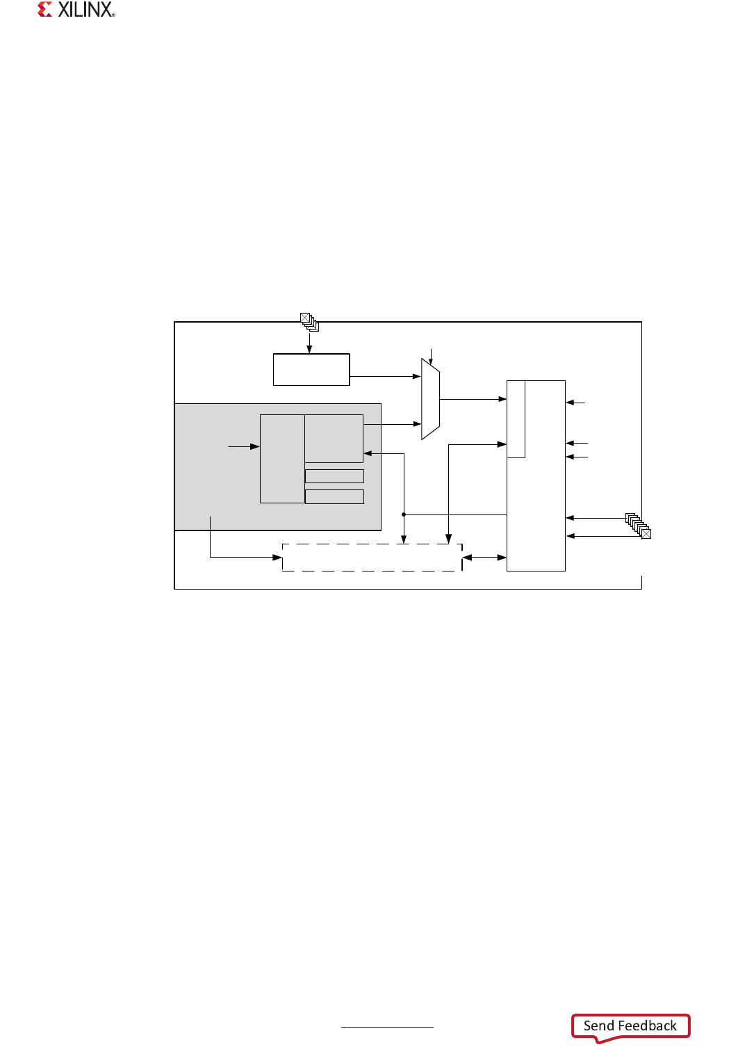
Zynq-7000 AP SoC Technical Reference Manual www.xilinx.com 755
UG585 (v1.12.1) December 6, 2017
Chapter 30: XADC Interface
• Uses the JTAG TAP controller to access the XADC registers
• Enables JTAG access to all XADC registers including ADC measurements
30.1.2 System Viewpoint
The XADC is a implemented in hard logic and resides in the PL power domain. The PS-XADC interface
is part of the PS and can be accessed by the PS APU without the PL being programmed. The PL must
be powered up to configure the PS-XADC interface, use the PL-JTAG or DRP interfaces, and to
operate the XADC. A system level block diagram is shown in Figure 30-1.
Note: The XADC arbitrates between the DRP interface and either the PS-XADC or the PL-JTAG
interface.
PS-XADC Interface
The PS-XADC interface description consumes the majority of this chapter. Software running in the PS
configures the interface using the devcfg registers. Software writes commands to the interface that
are pushed into the Command FIFO. These 32-bit writes, consisting of DRP command, address and
data, are serialized and sent to the XADC in a loopback path that fills the returning Read Data FIFO
that is read by the software.
The interface is configured by the devcfg registers, refer to Appendix B, Register Details.
DRP Interface
The DRP interface is a parallel 16-bit bidirectional interface that can connect to a PL bus master via
the LogiCORE IP AXI XADC PL logic using an AXI4-Lite interface to enable the PS or a MicroBlaze
X-Ref Target - Figure 30-1
Figure 30-1: XADC Module System Viewpoint
PS
PL
Zynq-7000 AP SoC Device
PS-XADC
Interrupt Status
32-bit APB
Slave
(from Master
Interconnect)
DevC
(devcfg)
Security
PCAP XADC
Arbitor
Internal
Voltages
LogiCORE IP AXI XADC Core Logic
External
Voltages
PL-JTAG
Interface
32-bit AXI
(M_AXI_GP)
JTAG Dedicated
pins in PL
devcfg.XADCIF_CFG [31]
0
1
Internal
Temperature
Serial
Alarm and OT
Signals
Refer to the PG019 Product Specification
Configured by
Bitstream or via
DRP commands.
DRP
Serial
Dual purpose
PL pins.
16-bit data
Misc.
Signals
UG585_c30_10_021913

Zynq-7000 AP SoC Technical Reference Manual www.xilinx.com 756
UG585 (v1.12.1) December 6, 2017
Chapter 30: XADC Interface
processor to control the XADC. The IP core receives 16 bits of data with each AXI4-Lite read/write
transaction. The interface is described in DS790, Product Specification.
The PL-AXI interface provides the highest performance. This interface uses the PL-AXI interface protocol
and provides flexibility of integrating additional signal processing IPs in the data path of XADC’s samples.
For example, a FIR filter can be instantiated in the PL-AXI data path between the XADC and the M_AXI_GP
interface of PS (or other logic in the PL).
PL JTAG Interface
The JTAG interface features and functions are described in UG480, 7 Series FPGAs and Zynq-7000 All
Programmable SoC XADC Dual 12-Bit 1 MSPS Analog-to-Digital Converter User Guide. This interface
connects to the development tools.
The Chipscope™ application can use the PL JTAG interface to read and write to the XADC status and
control registers respectively.
Note: The PL-JTAG interface is disabled, including control by Chipscope, when the PS-XADC
interface is selected.
Alarms
The seven alarm and over temperature signals are routed to the PS-XADC interface and made
available to the PL. For the PS-XADC interface, these are described in section 30.3 PS-XADC Interface
Description. Their use by the LogiCORE IP is described in PG091, LogiCORE IP XADC Wizard Product
Guide.
30.1.3 PS-XADC Interface Block Diagram
The block diagram for the PS-XADC interface is shown in Figure 30-2.
The PS-XADC interface is normally controlled by software executing in the APU. The software writes
32-bit commands and NOPs to the command FIFO. The command FIFO output is serialized by the
Serial Communications Channel in 32-bit packets for the XADC.
There is a programmable idle gap (IGAP) time between packets to allow time for the XADC to load read
data in response to the previous packet. For every word shift out from the command FIFO, a corresponding
word is shifted in to the Read Data FIFO. In the case of a DRP read command, as it is shifted out of the
command FIFO, the old content of XADC_DRP’s DR register is shifted out. After IGAP time, the result of the
current DRP read is available in XADC DRP’s DR register. When the next command from TXFIFO is shifted
out, the result of the current read which is in the DR register, is shifted into the RDFIFO.
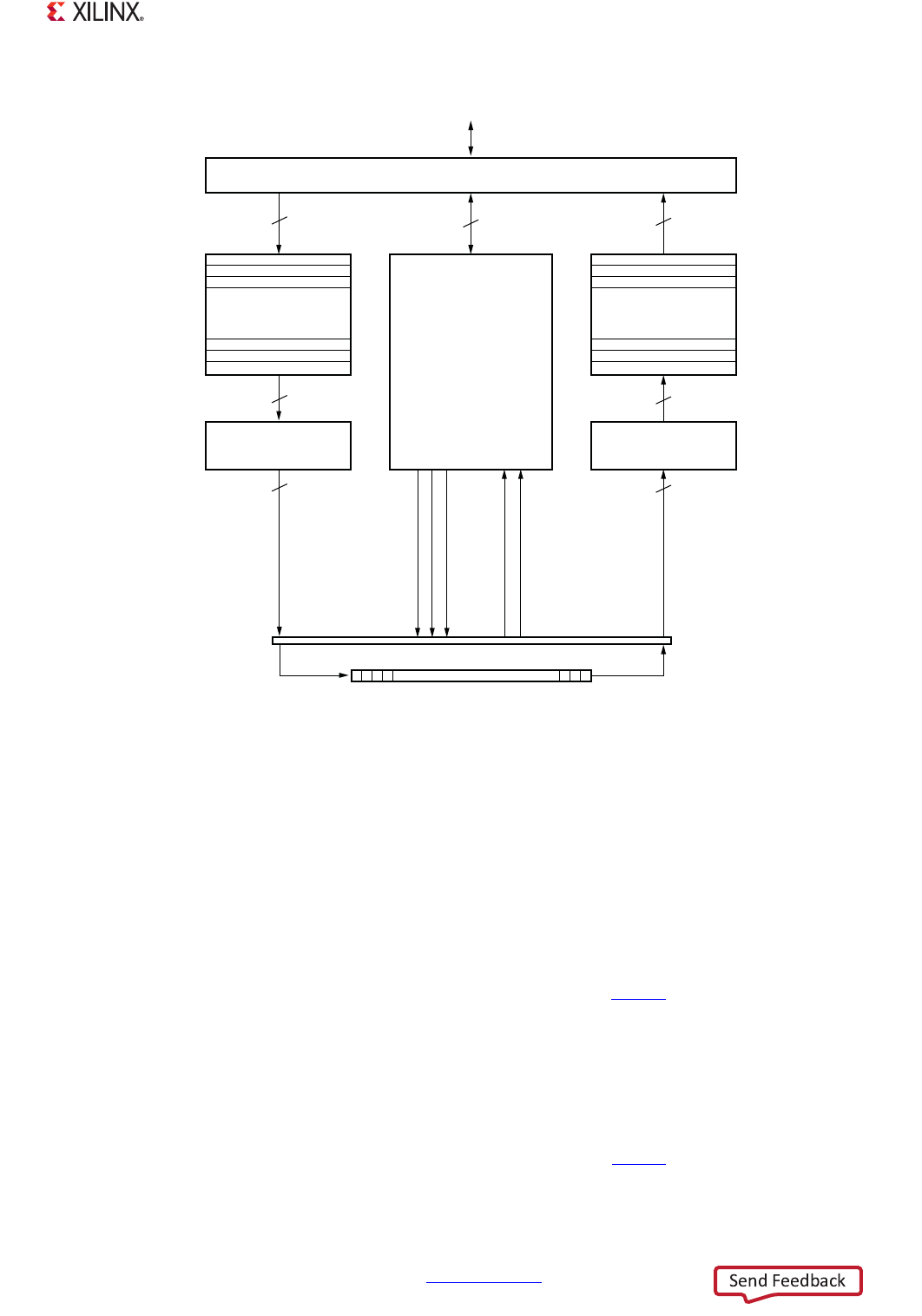
Zynq-7000 AP SoC Technical Reference Manual www.xilinx.com 757
UG585 (v1.12.1) December 6, 2017
Chapter 30: XADC Interface
30.1.4 Programming Guide
PS-XADC Interface
The programming model for the PS-XADC interface is described in 30.3 PS-XADC Interface Description.
DRP Interface
The programming model for the DRP interface is described in UG480, 7 Series FPGAs and Zynq-7000
All Programmable SoC XADC Dual 12-Bit 1 MSPS Analog-to-Digital Converter User Guide. This
interface can connect to the LogiCORE IP AXI XADC interface to provide an AXI4-lite interface as
described in the AXI XADC Interface product specification.
PL-JTAG Interface
The programming model for the PL-JTAG interface is described in UG480, 7 Series FPGAs and Zynq-7000
All Programmable SoC XADC Dual 12-Bit 1 MSPS Analog-to-Digital Converter User Guide.
X-Ref Target - Figure 30-2
Figure 30-2: XADC PS-XADC Interface Block Diagram
PS Interconnect
APB 3.0 Interface
Configuration,
Control, and
Status
Registers
Word in XADC
Parallel-to-serial
Converter
15-deep
Command FIFO
Serial-to-parallel
Converter
UG585_c31_01_021913
32
32
1
32
32
1
15-deep
Read Data FIFO
XADC_PS_TDO
XADC_PS_TDI
XADC_PS_TCK
XADC_PS_RESET
XADC_PS_EN
XADC_PS_ALARM[6:0]
XADC_PS_OT
32

Zynq-7000 AP SoC Technical Reference Manual www.xilinx.com 758
UG585 (v1.12.1) December 6, 2017
Chapter 30: XADC Interface
Notices
7z007s and 7z010 CLG225 Devices
The 7z007s single core and 7z010 dual core CLG225 devices provide four external ADC signal pairs
(differential inputs). All other Zynq-7000 devices provide 12 external ADC signal pairs. The hardware pin
information is provided in UG865, Zynq-7000 All Programmable SoC Packaging and Pinout product
Specification.
30.2 Functional Description
The system level block diagram is shown in Figure 30-2, page 757. A block diagram of the XADC is
provided in UG480, 7 Series FPGAs and Zynq-7000 All Programmable SoC XADC Dual 12-Bit 1 MSPS
Analog-to-Digital Converter User Guide.
This section includes functionally that is common to more than one of the interfaces that can control
the XADC. This content is not necessarily available in other documents:
•30.2.1 Interface Arbiter (PL-JTAG and PS-XADC)
•30.2.2 Serial Communication Channel (PL-JTAG and PS-XADC)
•30.2.3 Analog-to-Digital Converter (All)
•30.2.4 Sensor Alarms (PS-XADC and DRP)
30.2.1 Interface Arbiter (PL-JTAG and PS-XADC)
The XADC actively arbitrates requests between two of the three XADC interfaces. One of the
interfaces is always the DRP interface that is optionally connected to the LogiCORE XADC bridge.
The interfaces that are arbitrated depend on the setting of the devcfg.XADCIF_CFG [ENABLE] bit.
•[ENABLE] = 0: DRP and PL-JTAG (reset default)
•[ENABLE]
= 1: DRP and PS-XADC
If a JTAG transaction is in progress when a DRP request occurs, the LogiCORE XADC bridge can buffer
the request until the JTAG transaction is complete. The XADC asserts the JTAGBUSY signal to indicate
an ongoing JTAG transaction.
A JTAG transaction can start, but the DRP transaction in progress is allowed to complete before the
JTAG operation. For more details on the arbitration, refer to UG480, 7 Series FPGAs and Zynq-7000
All Programmable SoC XADC Dual 12-Bit 1 MSPS Analog-to-Digital Converter User Guide.

Zynq-7000 AP SoC Technical Reference Manual www.xilinx.com 759
UG585 (v1.12.1) December 6, 2017
Chapter 30: XADC Interface
30.2.2 Serial Communication Channel (PL-JTAG and PS-XADC)
The serial communication channel connects the XADC to the PS-XADC or PL-JTAG interface,
depending on the devcfg.XADCIF_CFG [ENABLE] bit setting.
The channel is a full duplex synchronous bit-serial link with dedicated control signals using a JTAG
protocol. By default, after reset, the connection between the PS and XADC (PS-XADC interface) is
disabled. PS software can write a
1
to the devcfg.XADCIF_CFG [ENABLE] bit to control the source
and switch the communication channel from the PL-JTAG interface to the PS-XADC interface. When
the PS-XADC interface is enabled to control the XADC, the XADC is no longer accessible by the
PL-JTAG interface. The inverse is true, when XADC is accessible by PL-JTAG, it can not be accessed by
the PS-XADC.
The PS-XADC interface interacts with the PS via an APB 3.0 interface on the PS interconnect. This
interface is part of the DevC module and is described in section 6.4 Device Boot and PL
Configuration.
30.2.3 Analog-to-Digital Converter (All)
The functions and features of the XADC are described in UG480, 7 Series FPGAs and Zynq-7000 All
Programmable SoC XADC Dual 12-Bit 1 MSPS Analog-to-Digital Converter User Guide.
30.2.4 Sensor Alarms (PS-XADC and DRP)
The XADC can generate an alarm signal when an internal sensor measurement exceeds the value
programmed into the XADC threshold register. The alarm thresholds are stored in the XADC Control
registers, refer to UG480 for their descriptions.
PS-XADC Interface
The alarm signals are routed directly from the XADC block into the PS_XADC interface block, thus
allowing alarm status to be reflected directly in the PS XADC’s interface registers and enabling alarms
to trigger interrupts.
Individual alarm interrupts can be disabled using the devcfg.XADCIF_INT_MASK register.
The alarm signals are sent to the PS-XADC Interface Status register. This register is masked and the
masked interrupts are OR’d together to generate the IRQ ID #39 interrupt to the PS interrupt
controller.
When an alarm goes active, it triggers a maskable interrupt. The alarm signals get latched in the
PS-XADC interface devcfg.XADCIF_INT_STS register and it can be used to determine which alarm was
activated. Writing a 1 to the active alarm bit in the devcfg.XADCIF_INT_STS register clears the
interrupt. The unmasked status of the alarm signals can be read using the devcfg.XADCIF_MSTS
register.

Zynq-7000 AP SoC Technical Reference Manual www.xilinx.com 760
UG585 (v1.12.1) December 6, 2017
Chapter 30: XADC Interface
DRP Interface
The alarms and OT signals are available on the DRP interface. They are actively connected to and
used by the LogiCORE AXI_XADC bridge, refer to PG019, LogiCORE IP AXI XADC Product Guide.
Functional Description
When the measured value on a voltage sensor is greater than the maximum thresholds or less than
the minimum threshold values, then the output alarm signal goes active. The alarm is reset (inactive)
when a subsequent measurement value falls between the upper and lower threshold values.
This operation differs for the temperature sensor alarm, The temperature alarm goes active when the
measured temperature exceeds the high threshold. The temperature alarm is reset (inactive) when
the temperature falls below the lower threshold value.
The alarm signals are summarized in Table 30-1.
30.3 PS-XADC Interface Description
The main function of the PS-XADC interface is to serialize commands written by software before
sending them to the XADC, and to perform a serial-to-parallel conversion when serial data is received
from the XADC for the software to read.
30.3.1 Serial Channel Clock Frequency
The serial communications channel between the PS-XADC interface and the XADC should not be
clocked faster than 50 MHz. The serial clock is derived from the PCAP_2x clock generated by the PS
clock subsystem (refer to Chapter 25, Clocks). This clock has a nominal frequency of 200 MHz. A
configurable clock divider is controlled by the devcfg.XADCIF_CFG [TCLK_RATE] bit field to reduce
the PCAP_2x clock frequency to no more than 50 MHz.
XADC serial clock = PCAP_2x clock / [TCLK_RATE]
Table 30-1: XADC Alarm Signals
Alarm Description Upper/Lower Threshold Control and Maximum/Minimum
Status Registers
ALM[0]
Programmable Temperature sensor alarm
Refer to the LogiCORE User Guide sections:
• Maximum and Minimum Status Registers
• Automatic Alarms
ALM[1]
VCCINT sensor alarm (PL internal voltage)
ALM[2]
VCCAUX sensor alarm (PL auxiliary voltage)
ALM[3]
VCCBRAM sensor alarm (PL BRAM voltage)
ALM[4]
VCCPINT sensor alarm (PS internal voltage)
ALM[5]
VCCPAUX sensor alarm (PS auxiliary voltage)
ALM[6]
VCCO_DDR sensor alarm (PS DDR I/O voltage)
OT Over-temperature Alarm
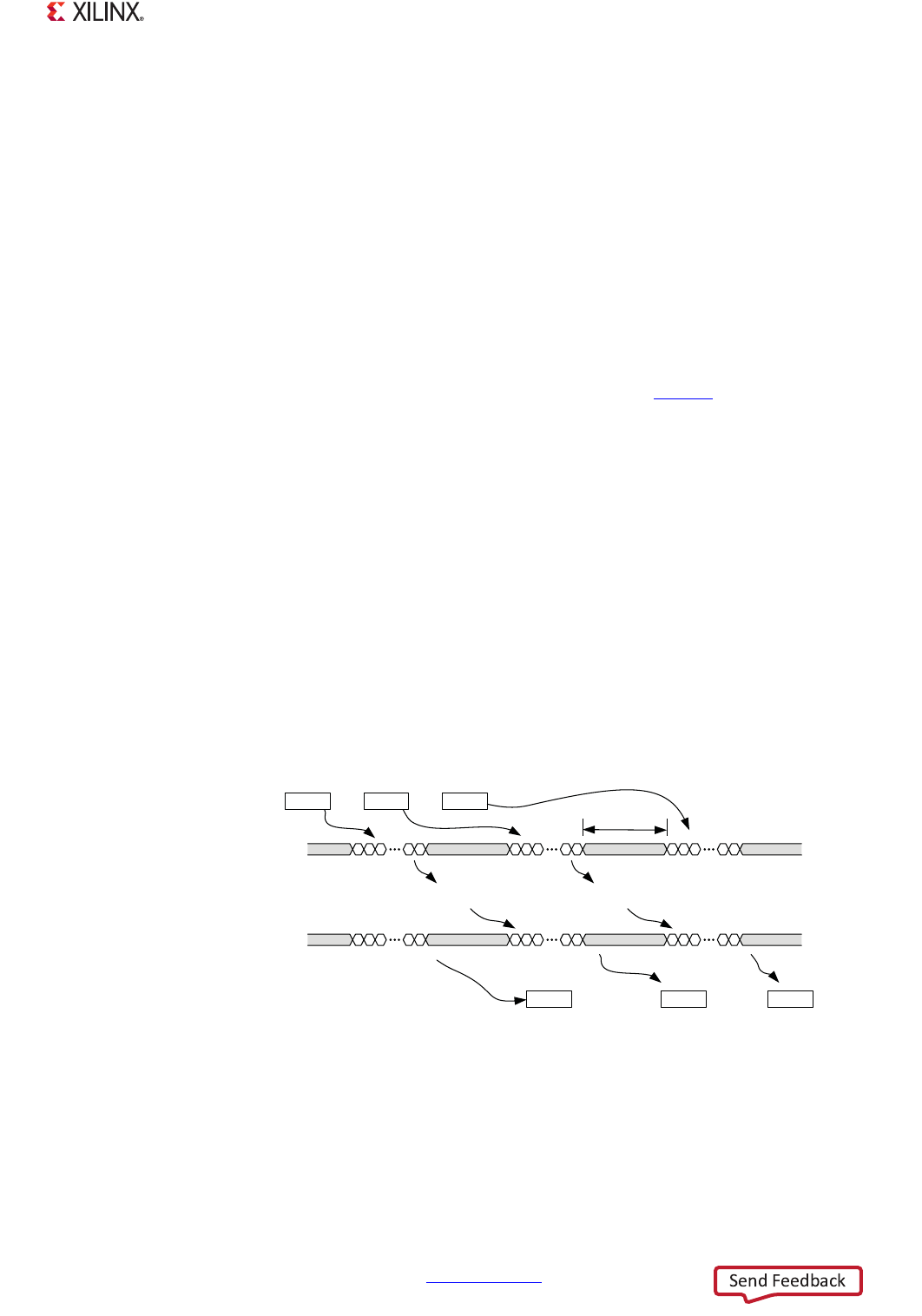
Zynq-7000 AP SoC Technical Reference Manual www.xilinx.com 761
UG585 (v1.12.1) December 6, 2017
Chapter 30: XADC Interface
The XADC serial clock drives the DCLK that is described in the LogiCORE User Guide.
30.3.2 Command and Data Packets
The PS-XADC interface buffers the 32-bit reads and writes to minimize the effects of the slow serial
transfer process on PS system throughput. The PS-XADC interface buffers up to 15 commands. Each
command is serialized and communicated to the XADC. For every command that is written to the
PS-XADC interface, a data word is received in the Read Data FIFO. The Read Data FIFO can store 15
data words. Up to 15 commands at a time to be written and up to 15 read data words can be in
FIFOs. After a read command has been written, the corresponding read data is available after the
next command is serialized to the XADC, see Figure 30-3. Therefore, if the last command in CMD FIFO
is a read command, one additional NOP command is always needed to push out the last read data.
The XADC commands are listed in the LogiCORE user guide and in UG480, 7 Series FPGAs and
Zynq-7000 All Programmable SoC XADC Dual 12-Bit 1 MSPS Analog-to-Digital Converter User Guide.
All control commands, read requests, write requests, and NOPs shift data into the Read Data FIFO
that can be read using the devcfg.XADCIF_RDFIFO register. The software controlling the PS-XADC
interface should account for this and should read and discard data not generated by a read
command. XADC read data is 32-bits but only the 16 LSBs of the 32-bit word contain ADC data.
PS-XADC Event Timing
•Command register write
• Serialized to XADC (control and data)
• Programmable idle gap width, devcfg.XADCIF_CFG [IGAP]
The status of the command and Read Data FIFOs can be monitored using the devcfg.XADCIF_MSTS
Interface Miscellaneous Status register. Software can also setup interrupts using the
devcfg.XADCIF_INT_STS Interrupt Status register.
X-Ref Target - Figure 30-3
Figure 30-3: XADC PS-XADC Interface Event Timing Diagram
UG585_c30_11_022513
n
Write Sequence to the Command FIFO
n + 1
PS_TDO Signal
(commands)
PS_TDI Signal
(results)
Command is processed
by the XADC.
n - 1
n + 2
nn +1
Dummy
Data or Previous
Command Result
Dummy
Data
Second
Command
First
Command
Result from
First
Command
Result from
Second
Command
Command is processed
by the XADC.
Reads from
Data Read FIFO
Idle Gap
Time
32-bit
32 bits
32-bit
Zynq-7000 AP SoC Technical Reference Manual www.xilinx.com 762
UG585 (v1.12.1) December 6, 2017
Chapter 30: XADC Interface
Note: Reading from an empty Read Data FIFO causes an APB slave bus error.
One packet remains in the XADC when the Command FIFO is emptied. To retrieve the packet, write a
dummy command.
30.3.3 Command Format
Figure 30-4 shows the data format of the PS-XADC interface commands. The
f
irst 16 LSBs of the
XADCIF_CMD_FIFO contain the DRP register data. For both read and write operations, the address
bits, XADCIF_CMD_FIFO [25:16], hold the DRP target register address. The command bits,
XADCIF_CMD_FIFO [29:26], s pe c if y a re ad , write, or no operation (see Table 30-2).
DPR Address and DRP Data
The full list of XADC DRP registers and instructions on how to
conf
igure them can be found in the
UG480, 7 Series FPGAs and Zynq-7000 All Programmable SoC XADC Dual 12-Bit 1 MSPS
Analog-to-Digital Converter User Guide.
30.3.4 Read Data Format
The XADC data is returned in the lower 16 bits of the devcfg.XADCIF_RDFIFO register read. The
interpretation of the DRP data can be found in the UG480 LogiCORE User Guide.
X-Ref Target - Figure 30-4
Figure 30-4: PS-XADC Interface Command Register
Table 30-2: PS-XADC Interface DRP Command Format
CMD [3:0] Operation
0000No operation
0001DRP read
0010DRP Write
Others Not defined
UG585_c30_12_021913
X X CMD [3:0] DRP Address [9:0] DRP Data [15:0]
31 30 29 26 25 16 15 0
X-Ref Target - Figure 30-5
Figure 30-5: PS-XADC Interface Read Data Format
UG585_c30_13_021913
DRP Data [15:0]
31
0
16 15 0

Zynq-7000 AP SoC Technical Reference Manual www.xilinx.com 763
UG585 (v1.12.1) December 6, 2017
Chapter 30: XADC Interface
30.3.5 Min/Max Voltage Thresholds
The XADC tracks the minimum and maximum values recorded for the internal supply sensors since
the last power-up or the last reset of the XADC control logic. The maximum and minimum values
recorded are stored in the DRP Status registers. On power-up or after reset, all Minimum registers are
set to FFFFh and all Maximum registers are set to 0000h. Each new measurement generated for an
on-chip sensor is compared to the contents of its Maximum and Minimum register. If the measured
value is greater than the contents of it Maximum register, the measured value is written to the
Maximum register. Similarly, for the Minimum register, if the measured value is less than the contents
of its Minimum register, the measured value is written to the Minimum register. This check is carried
out each time a measurement result is written to the Status register.
30.3.6 Critical Over-temperature Alarm
Note: This feature sends an interrupt status to the PS and causes an automatic shutdown feature for
the PL side of the Zynq-7000 device if enabled. The PL shutdown is enabled via the bitstream and the
PL will only come out of power-down if the over-temperature alarm goes inactive or a
reconfiguration occurs.
The on-chip temperature measurement is used for critical temperature warnings. The default over
temperature threshold is 125°C. This threshold is used when the contents of the OT Upper Alarm
register (listed in UG480) have not been
conf
igured. When the die temperature exceeds the
threshold set in the XADC’s Control register, the over-temperature alarm (OT) becomes active. The OT
signal resets when the die temperature has fallen below set threshold.
The OT alarm can also be used to automatically power down the PL upon activation. The OT alarm can
be disabled by writing a
1
to the OT bit in the XADC’s
Conf
iguration register.
Note: these registers are in the XADC and are accessible using the DRP.
The XADC OT alarm signal is sent to the PS via the dedicated PS-XADC interface. When the OT alarm
goes active it triggers a maskable interrupt. The OT bit of the XADCIF_INT_STS register needs to be
cleared by writing a
1
to the bit location. The real time value of the OT alarm signal can be found on the
XADCIF_MSTS register.
30.4 Programming Guide for the PS-XADC Interface
The following sequence describes how to configure and interact with the PS-XADC interface to read
an internal VCC auxiliary PS voltage (VCCPAUX) and raise an Alarm interrupt when VCCPAUX value does
not fall between higher and lower thresholds. The PS-XADC interface specifies commands to be sent
in a specific format as described in section 30.3.3 Command Format. Refer to detailed examples in
section 30.4.3 Command Preparation.
Example: Initialization of XADC via the PS-XADC Interface
This example resets the communications channel and the XADC. It also flushes the FIFOs; leaving a
NOOP (dummy) word in the XADC.

Zynq-7000 AP SoC Technical Reference Manual www.xilinx.com 764
UG585 (v1.12.1) December 6, 2017
Chapter 30: XADC Interface
1. Reset the serial communication channel. Write a 1 and then a 0 to devcfg.XADCIF_MCTL
[RESET].
2. Reset the XADC. Write any 16-bit value to DRP address 0x03 (reset register). Write 08030000h
to the devcfg.XADCIF_CMDFIFO register.
3. Flush the FIFOs. There is no reset signal, instead write 15 NOOPs to the FIFO:
a. Wait for the Command FIFO to empty. The last command should be a NOOP (dummy write).
b. Read the Read Data FIFO until empty.
Example: Start-up Sequence via the PS-XADC Interface
This example sets various interface parameters and includes steps for interrupts and data transfers. It
assumes the interface and the XADC are already initialized.
1. Configure the PS-XADC interface: Program the configuration register. Write 80001114h into
the devcfg.XADCIF_CFG register:
a. Use default Minimum idle gap, [IGAP] = 14h (20 serial clocks).
b. Use default XADC serial clock frequency to 1/4 of PCAP_2x clock frequency, [TCKRATE] = 01.
c. Use default FIFO serial read capture edge (rising), [REDGE] = 1.
d. Use default FIFO serial write launch edge (falling), [WEDGE] = 0.
e. Use default Read Data FIFO threshold level, [DFIFOTH] = 0x0.
f. Use default Command FIFO threshold level, [CFIFOTH] = 0.
g. Enable the PS access of XADC. Write 0x1 to devcfg.XADCIF_CFG [ENABLE].
2. Configure the interrupts: Interrupts are used to manage the alarms from the XADC and
Command/Read Data FIFOs. Refer to the program example in section 30.5.3 Interrupts.
3. Data transfers to the XADC: Refer to section 30.5.2 Read and Write FIFOs.
30.4.1 Read and Write to the FIFOs
This example configures the devcfg.XADCIF_CFG register for the FIFOs and communications channel.
This register controls the command and Read Data FIFO thresholds, the clock rate of the
XADC_PS_TCK, the clocking edges for the serial bus and the idle gap between serial packets.
After power on Command and Read Data FIFOs of the PS-XADC interface are empty, but must be
flushed after an XADC interface reset. Commands for writing to or reading from XADC registers are
sent to the XADC using the Command FIFO, and data returned from the XADC is collected in the Read
Data FIFO.
Example: Write Command to the XADC
This example writes to the XADC VCCPAUX Alarm Upper threshold register.
1. Prepare command. Prepare the command as described in section 30.4.3 Command Preparation
for writing to the XADC VCCPAUX Alarm Upper threshold register (0x5A) with required threshold.
2. Fill the Command FIFO with data. Write the data formatted in step 1 to the
devcfg.XADCIF_CMDFIFO register.

Zynq-7000 AP SoC Technical Reference Manual www.xilinx.com 765
UG585 (v1.12.1) December 6, 2017
Chapter 30: XADC Interface
3. Wait until the Command FIFO becomes empty. Wait until devcfg.XADCIF_MSTS [CFIFOE] = 1.
Note: For every write to the devcfg.XADCIF_CMDFIFO register, data is shifted into the
devcfg.XADCIF_RDFIFO register (Read Data FIFO).
Example: Read the VCCPAUX value from the XADC
This example reads the current VCCPAUX value from the XADC VCCPAUX status register.
1. Prepare command. Prepare the command as described in section 30.4.3 Command Preparation
for reading the XADC VCCPAUX Status register (0x0E).
2. Write data to Command FIFO. Write data formatted in step 1 to the devcfg.XADCIF_CMDFIFO
register.
3. Wait until the Command FIFO becomes empty. Wait until devcfg.XADCIF_MSTS [CFIFOE] = 1.
4. Read dummy data from the Read Data FIFO. Read the devcfg.XADCIF_RDFIFO register.
5. Format data. Prepare Command for No operation as described in 30.4.3 Command Preparation.
6. Write data to the Command FIFO. Write the formatted data in step 5 to the
devcfg.XADCIF_CMDFIFO register.
7. Read the Read Data FIFO. Read the devcfg.XADCIF_RDFIFO register.
Note: After a read command has been sent to the XADC, the corresponding read data will be
available during the next shift period. Therefore, one dummy command write (as shown in step 5) is
always needed to push out the last read data.
30.4.2 Interrupts
Example: Configure and Manage Alarm 5 (VCCPAUX)
This example configures the XADC registers to set alarm thresholds, operating mode, and enables
the Alarm 5 (VCCPAUX) interrupt in the PS-XADC interface. The XADC hard macro has to be operated
in Independent mode because alarms are not enabled in Default mode (refer to the XADC Operating
Modes section of UG480, 7 Series FPGAs and Zynq-7000 All Programmable SoC XADC Dual 12-Bit 1
MSPS Analog-to-Digital Converter User Guide.
1. Prepare commands. Prepare commands as described in section 30.4.3 Command Preparation
for writing to the XADC hard macro alarm threshold registers (VCCPAUX Upper-0x5A and VCCPAUX
Lower-0x5E) with the required thresholds and XADC Config_Reg1 (0x41) to set the XADC in
Independent mode.
2. Write commands to the Command FIFO. Write the commands prepared in step 1 to the
devcfg.XADCIF_CMDFIFO register.
3. Enable the Alarm 5 interrupt in the PS-XADC interface. Write devcfg.XADCIF_INT_MASK
[M_ALM] =7Eh.
4. Check if Alarm 5 is triggered. Poll for devcfg.XADCIF_INT_STS [M_ALM] = 1.
5. Clear the Alarm 5 interrupt. Write devcfg.XADCIF_INT_STS [M_ALM] = 1.
6. Disable the Alarm 0 interrupt. Write devcfg.XADCIF_INT_MASK [M_ALM] = 7Fh

Zynq-7000 AP SoC Technical Reference Manual www.xilinx.com 766
UG585 (v1.12.1) December 6, 2017
Chapter 30: XADC Interface
30.4.3 Command Preparation
Example: Prepare Data for Writing to the XADC Register
This example formats data for writing to XADC Configuration Register 1 to set the XADC in
Independent mode. Refer to Table 30-2, page 762.
1. DRP data. Data to set the XADC in independent mode is 8000h. Refer to the XADC Register
Interface section of UG480.
2. DRP address. The address of the XADC Configuration Register 1 is 0x41.
3. Write command. The command for a write operation is 0010b.
The command to write 8000h in XADC Configuration Register 1 (0x41) is 08418000h.
Example: Prepare Data for Reading from the XADC Register
This example formats data for reading the XADC VCCPAUX Status register, 0x0E.
1. DRP data. Data can be any arbitrary data for the read operation (0).
2. DRP address. The address of the XADC VCCPAUX Status register is 0x0E.
3. Write command. The command for a read operation is 0001b.
The command to read the XADC VCCPAUX Status register, 0x0E, is 040E0000h.
30.4.4 Register Overview
An overview of the PS-XADC Interface control registers is shown in Table 30-3. Register bit details are
provided in Appendix B, Register Details. Refer to the XADC Register Interface section of UG480
LogiCORE User Guide for register details of the XADC.
Note: After power-up (refer to the Zynq-7000 AP SoC data sheet for the proper voltage sequencing),
PS-to-PL voltage shifters are automatically enabled. The PL must be powered-up to access the
PS-XADC interface registers, but the PL does not need to be configured to access the registers.
Tabl e 30- 3 shows an overview of XADC Interface registers.
Table 30-3: Register Overview
Function Mnemonic Description Type
Configuration
devcfg.XADCIF_CFG Configuration: Enable, FIFO threshold,
frequency ratio, and launch edge.
Read/Write
devcfg.XADCIF_MCTL XADC Interface Misc. Control register Read/Write
Interrupts devcfg.XADCIF_INT_STS XADC Interface Interrupt Status register Read,
Write 1 to clear
devcfg.XADCIF_INT_MASK XADC Interface Interrupt Mask register Read/Write
devcfg.XADCIF_MSTS XADC Interface Misc. Status register Read

Zynq-7000 AP SoC Technical Reference Manual www.xilinx.com 767
UG585 (v1.12.1) December 6, 2017
Chapter 30: XADC Interface
30.5 Programming Guide for the DRP Interface
The XADC can also be accessed by instantiating a LogiCORE AXI XADC bridge in the PL. This method
provides more powerful features and easy access to all XADC registers and signals using a register
read/write programming model for microprocessors.
30.6 Programming Guide for the PL-JTAG Interface
The PS-XADC interface commands are similar to the JTAG DRP commands. Refer to the JTAG DRP
commands shown in UG480, 7 Series FPGAs and Zynq-7000 All Programmable SoC XADC Dual 12-Bit
1 MSPS Analog-to-Digital Converter User Guide.
Note: PL-JTAG cannot access the XADC if the PS-XADC interface is accessing the XADC (i.e.,
devcfg.XADCIF_CFG [ENABLE] = 1).
30.7 System Functions
30.7.1 Clocks
Clocking is determined by the interface choice.
PS-XADC Interface Clocks
1. The PS-XADC interface uses FIFOs to cross between the PS system clock and the XADCIF clock.
2. PS system interface clock is the CPU_1x clock.
3. The XADCIF clock frequency is the PCAP_2x clock / [TCLKRATE].
a. The XADCIF clock maximum frequency is 50 MHz.
b. The PCAP_2x clock frequency is nominally 200 MHz.
c. The [TCLKRATE] bit: divide 2, 4 (default), 8, or 16.
See Chapter 25, Clocks for more information about the PS clocks.
Command and
Read Data FIFOs
devcfg.XADCIF_CMDFIFO XADC Interface Command FIFO Write
devcfg.XADCIF_RDFIFO XADC Interface Read Data FIFO Read
Table 30-3: Register Overview (Cont’d)
Function Mnemonic Description Type

Zynq-7000 AP SoC Technical Reference Manual www.xilinx.com 768
UG585 (v1.12.1) December 6, 2017
Chapter 30: XADC Interface
DRP Interface Clocks
The PL-AXI interface is a soft core instantiated within the PL and uses a clock from one of the PL’s
PLLs.
PL-JTAG Interface Clocks
PL-JTAG uses the JTAG port to interface with the XADC and uses the JTAG clock, TCK.
30.7.2 Resets
There are several resets in the XADC module.
PS-XADC Interface Reset
The PS-XADC interface and its serial communication channel to the XADC are reset using
devcfg.XADCIF_MCTL [RESET].
Note: The PS-XADC FIFOs are not cleared by the interface reset.
XADC Reset
The XADC is reset by writing to the reset register using a DRP address of 03h. Write 0x08030000 to
the devcfg.XADCIF_CMDFIFO register. The data that is included is ignored by the XADC.

Zynq-7000 AP SoC Technical Reference Manual www.xilinx.com 769
UG585 (v1.12.1) December 6, 2017
Chapter 31
PCI Express
31.1 Introduction
The Zynq-7000 7z012s, 7z015, 7z030, 7z035, Zynq-7z045, and Zynq-7z100 AP SoC devices include
the Xilinx 7 series Integrated block for PCI Express core which is a reliable, high-bandwidth,
third-generation I/O solution.
The PCI Express solution for these Zynq AP SoC devices supports x1, x2, x4, and x8 lane Root Port and
Endpoint configurations at up to 5 Gb/s (Gen2) speed. Attention must be paid to system level
bandwidth if full Gen 2 – x8 throughput is needed. This might include either inline processing of the
data in PL before storing it to the PS DDR memory or using a wider DDR3 memory interface in the
PL. The Root Port configuration can be used to build a Root Complex solution. These configurations
are compatible with the PCI Express Base Specification, Rev 2.1.
The PCI Express module supports the AXI4-stream interface for the user interface at both 64-bit and
128-bit widths.
For more detailed information regarding the 7 Series FPGAs Integrated block for PCI Express core,
refer to these documents on the Xilinx website:
•PG054, 7 Series FPGAs Integrated Block for PCI Express LogiCORE IP Product Guide
•PG055, AXI Memory Mapped to PCI Express (PCIe)Gen2 LogiCORE IP Product Guide
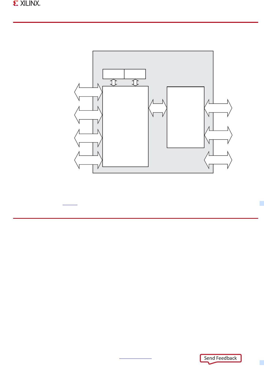
Zynq-7000 AP SoC Technical Reference Manual www.xilinx.com 770
UG585 (v1.12.1) December 6, 2017
Chapter 31: PCI Express
31.2 Block Diagram
For additional information regarding the different interfaces to the Integrated block for PCI Express
core, refer to PG054, 7 Series FPGAs Integrated Block for PCI Express LogiCORE IP Product Guide.
31.3 Features
The PCI Express core provides these key features:
• High-performance, highly flexible, scalable, and reliable, general-purpose I/O core
°Compatible with the PCI Express Base Specification, rev. 2.1
°Compatible with conventional PCI software model
• Incorporates Xilinx® Smart-IP™ technology to guarantee critical timing
• Uses GTXE2 transceivers for 7 Series FPGA families
°2.5 Gb/s and 5.0 Gb/s line speed
°Supports 1-lane, 2-lane, 4-lane, and 8-lane operation
°Elastic buffers and clock compensation
°Automatic clock data recovery
X-Ref Target - Figure 31-1
Figure 31-1: PCI Express Block Diagram
UG585_c32_01_021313
LogiCORE IP 7 Series FPGAs
Integrated Block for PCI Express Core
7 Series FPGAs
Integrated Block for
PCI Express
(PCIE_2_1)
Transceivers
Optional Debug
System
(SYS)
User Logic
PCI
Express
Logic
Clock
and
Reset
PCI Express
(PCI_EXP)
User
Logic
Physical Layer
Control and Status
Host
Interface
Transaction
(AXI-ST)
User
Logic Optional Debug
(DRP)
Physical
(PL)
Configuration
(CFG)
TX
Block RAM
RX
Block RAM

Zynq-7000 AP SoC Technical Reference Manual www.xilinx.com 771
UG585 (v1.12.1) December 6, 2017
Chapter 31: PCI Express
• Supports Endpoint and Root Port configurations
• 8B/10B encode and decode
• Supports lane reversal and lane polarity inversion per PCI Express specification requirements
• Standardized user interface
°Supports AXI4-stream interface
°Easy-to-use packet-based protocol
°Full-duplex communication
°Back-to-back transactions enable greater link bandwidth utilization
°Supports flow control of data and discontinuation of an in-process transaction in transmit
direction
• Supports flow control of data in receive direction
• Compatible with PCI/PCI Express power management functions
• Supports a maximum transaction payload of up to 1,024 bytes
• Supports multi-vector MSI for up to 32 vectors and MSI-X
• Up-configure capability enables application-driven bandwidth scalability
• Compatible with PCI Express transaction ordering rules
31.4 Endpoint Use Case
For an example of a Zynq Endpoint use case, refer to UG963, ZC706 PCIe Targeted Reference Design
User Guide.
31.5 Root Complex Use Case
A Zynq PCIe Root Complex design can be implemented in a number of different ways. Figure 31-2
shows an example of a basic design using the AXI PCIe bridge described in PG055, LogiCORE IP AXI
Bridge for PCI Express.
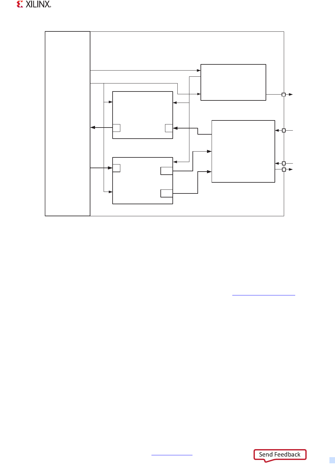
Zynq-7000 AP SoC Technical Reference Manual www.xilinx.com 772
UG585 (v1.12.1) December 6, 2017
Chapter 31: PCI Express
Note: The AXI PCIe bridge master and slave ports are connected to separate AXI interconnects to
avoid potential deadlock scenarios.
The compiled Linux kernel already has the required AXI PCIe bridge driver enabled, so no additional
configuration is needed. Software drivers for the connected endpoint device might need to be
installed.
For information on building the Linux kernel for Zynq, refer to the Xilinx Zynq Linux Wiki.
X-Ref Target - Figure 31-2
Figure 31-2: Example Zynq PCIe Root Complex
PL
Axi_interconnect_0
Axi_interconnect_1
AXI PCIe bridge
PS
S_AXI_HP0
M_AXI_GP0
S
M_AXI
S_AXI
S_AXI_CTRL
M0
S
M
M1
pci_exp_rxn/p
pci_exp_txn/p
Proc_sys_reset_0
pcie_a_perst_n
REFCLK
peripheral_aresetn
100 / 250MHz
FCLK_0
FCLK_RESET0_N
ARESETN
ext_reset_in
ARESETN
interconnect_reset
ACLK
ACLK
slow_sync_clk
UG585_c31_02_052413

Zynq-7000 AP SoC Technical Reference Manual www.xilinx.com 773
UG585 (v1.12.1) December 6, 2017
Chapter 32
Device Secure Boot
32.1 Introduction
Zynq-7000 AP SoC devices support the ability to perform a secure boot to load authenticated and
encrypted PS images and PL bitstreams.
Note: The BootROM Header is referred to as the Boot Image Header in UG821, Zynq-7000 All
Programmable SoC Software Developers Guide. They both refer to the same table of parameters
provided in Table 6 -5.
32.1.1 Block Diagram
Figure 32-1 is a block diagram showing the different systems involved in a secure boot.
32.1.2 Features
Zynq-7000 AP SoC devices provide the following secure boot features:
• Advanced Encryption Standard
°AES-CBC with 256-bit key (FIPS197)
°Encryption key stored on-chip in either eFuse or Battery-backed RAM (BBRAM)
• Keyed-hashed message authentication code (HMAC, FIPS198-1)
°SHA-256 authentication engine (FIPS180-4)
• RSA public key authentication (FIPS186-3)
°2048-bit public key
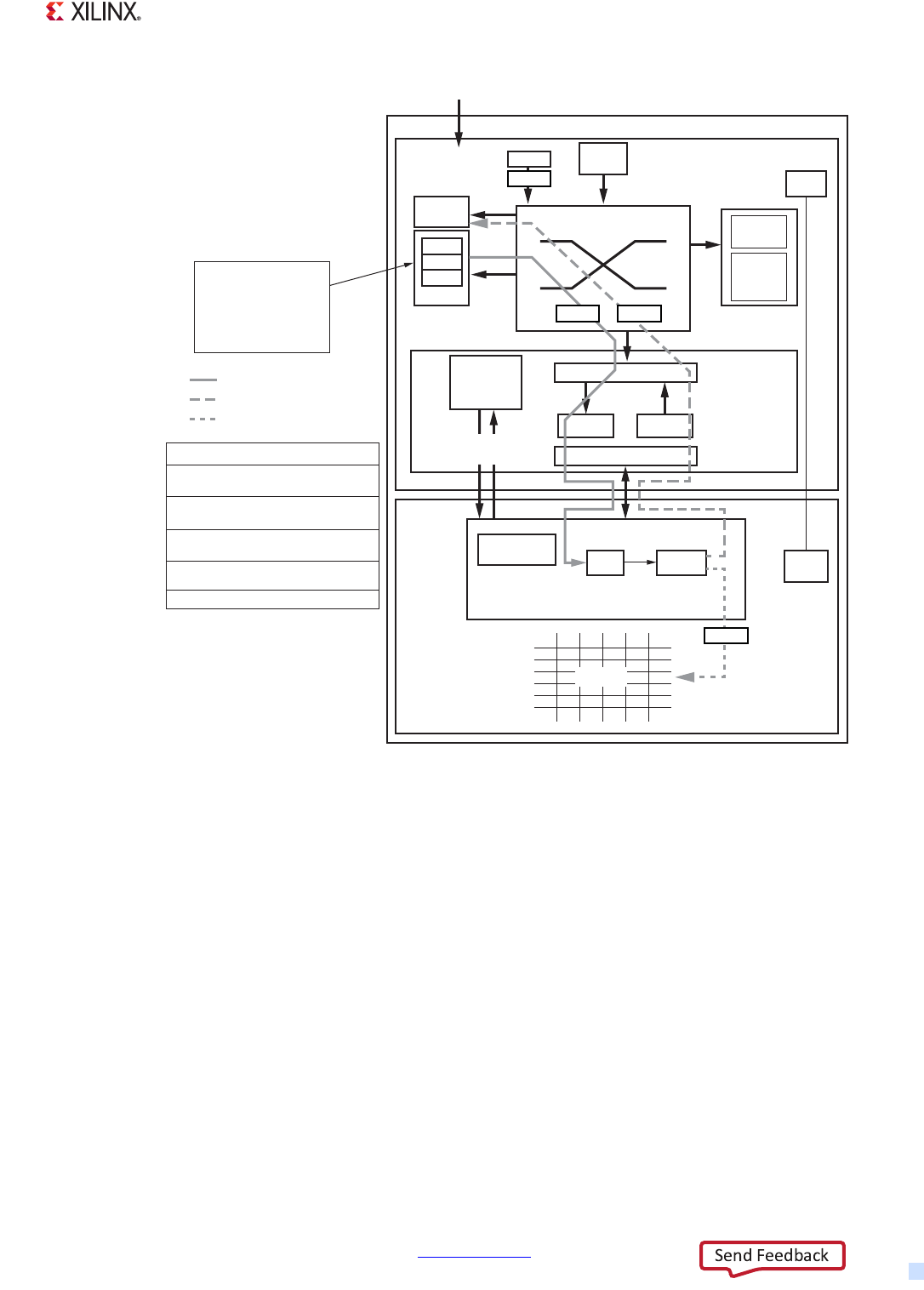
Zynq-7000 AP SoC Technical Reference Manual www.xilinx.com 774
UG585 (v1.12.1) December 6, 2017
Chapter 32: Device Secure Boot
A device secure boot involves several systems contained within the AP SoC device. The secure boot
process is always initiated by the BootROM. If RSA authentication has been enabled the BootROM will
use the public key to authenticate the first stage boot loader (FSBL) before it is decrypted or executed.
If the boot image header indicates a secure boot, the BootROM enables the AES and HMAC engines
which reside in the PL. The encrypted FSBL is then sent by the BootROM to the AES and HMAC, a
hardened core within the PL, via the processor configuration access port (PCAP). The FSBL image is
decrypted and sent back to the PS via the PCAP where it is loaded into the on-chip RAM (OCM) for
execution. The PS is then able to securely configure the PL by sending an encrypted bitstream
through the PCAP to the AES/HMAC for decryption, authentication, and distribution to the PL
memory cells.
X-Ref Target - Figure 32-1
Figure 32-1: Secure Boot Block Diagram
CPU0
CPU1
AXI Top Switch
Configuration File 1
Secure FSBL
RSA authenticated,
AES encrypted
with SHA-256 HMAC)
NAND
NOR
QSPI
IOP
On-Chip
RAM
DDR
Memory
Controller
MDDR
FIFO
Secure
Vault
Processing System
Zynq-7000 AP SoC
Programmable Logic
Common Boot Path
PS Boot Path
PL Configuration Path
Step 1: Power applied, BootROM begins
execution
Step 2: (Optional) RSA authentication
performed on encrypted FSBL
Step 3: FSBL decryption (AES) and
authentication (HMAC)
Step 4: Decrypted, authenticated FSBL
stored in OCM
Step 5: (Optional) PL configuration
Secure Boot Process
JTAG
DAP
Device Key
AXI
FIFO
eFuse/BBRAM
Security
AES HMAC
PCAP
Device
Configuration
Block
ROM
Step 1
Mode_Mode MIO pins
PL
UG585_c33_01_052913
Step 3 Step 4
Step 5

Zynq-7000 AP SoC Technical Reference Manual www.xilinx.com 775
UG585 (v1.12.1) December 6, 2017
Chapter 32: Device Secure Boot
32.2 Functional Description
32.2.1 Master Secure Boot
Master secure boot is the only secure boot mode supported in Zynq-7000 AP SoC devices. It uses the
hardened AES decryption engine and the hardened HMAC authentication engine within the PL to
decrypt PS images and PL bitstreams. If RSA authentication is enabled, the BootROM authenticates
the encrypted FSBL using the public key prior to decryption (see Table 32-3). The boot process for
the master secure boot mode is shown in Figure 32-2.
IMPORTANT: The master secure boot mode uses the AES
decr
yption and HMAC authentication engines
within the PL, therefore the PL must be powered on during the secure boot process. The BootROM ensures
that the PL is powered before reading the encrypted image from the external boot device. It is the user’s
responsibility to ensure that the PL is powered on before trying to decrypt any new configuration files.
Power on Reset
After the power-on and reset sequences have completed, the on-chip BootROM begins to execute.
An optional eFuse setting can be used to perform a full 128 KB CRC on the BootROM for a small
boot time penalty (around 25 ms at default boot settings). After the integrity check the BootROM
reads the boot mode setting specified by the bootstrap pins. The BootROM code then reads the
BootROM header from the specified external memory.
RSA Authentication Performed on FSBL
If RSA authentication is enabled the BootROM loads the boot image header (including the Register
Initialization parameters) and the FSBL into the first 192 KB of the OCM. Next the public key is loaded
from the boot image (see section 32.2.3 Secure Boot Image) and validated by calculating a SHA-256
signature and comparing it to the hash value stored in eFuse. If the values match, the BootROM
calculates the signature for the FSBL and authenticates it with the public key. If the public key
signature does not match the hash value stored in eFuse or the authentication fails on the FSBL, the
BootROM performs a fallback and searches for a new FSBL if the boot device is NAND, NOR, or QSPI.
If the fallback fails or the boot device is SD, the BootROM enters either an error state and enables
JTAG or enters a secure lockdown if the boot image was encrypted. If the authentication of the FSBL
passes, the BootROM continues the boot process. For more details see section 32.2.5 RSA
Authentication.
Secure FSBL Decryption
If a secure boot is
specif
ied in the boot image header, the BootROM starts by checking the power-on
status of the PL. Since the AES and HMAC engines reside within the PL, the PL must be powered up
to perform a secure boot. The BootROM waits until the PL is powered up before continuing the secure
boot sequence. After the power-on status of the PL is
conf
i r m e d , the BootROM begins to load the
encrypted FSBL into the AES engine via the PCAP. The PL sends the decrypted FSBL back to the PS via
the PCAP. The decrypted image is then loaded into the OCM. The BootROM also monitors the HMAC
Zynq-7000 AP SoC Technical Reference Manual www.xilinx.com 776
UG585 (v1.12.1) December 6, 2017
Chapter 32: Device Secure Boot
authentication status of the FSBL and if an authentication error occurs, the BootROM puts the PS into
a secure lockdown state.
Handoff to FSBL
Once the FSBL has been successfully loaded and authenticated, control is turned over to the
decrypted FSBL which now resides in the OCM. Based on the user application, the FSBL could then
start processing, configure the PL, load additional software, or wait for further instruction from an
external source.
X-Ref Target - Figure 32-2
Figure 32-2: PS Boot Flow
Power On Reset
(Debug access with JTAG disabled)
Internal memory hardware clean process
(Optional BootROM CRC)
Load boot image header
AES decryption of FSBL
(Decrypted FSBL loaded to internal RAM)
Secure boot Non-secure boot
UG585_c33_02_100917
HMAC authentication of FSBL
Disable BootROM memory
Pass control to FSBL
Disable and LOCK all security features
(AES and HMAC)
Load FSBL into internal RAM
or external DDR memory
Disable BootROM memory
Enable JTAG
Pass Control to FSBL
RSA authentication performed on FSBL
RSA enabled
Zynq-7000 AP SoC Technical Reference Manual www.xilinx.com 777
UG585 (v1.12.1) December 6, 2017
Chapter 32: Device Secure Boot
32.2.2 External Boot Devices
Secure boot mode is restricted to NOR, NAND, SDIO, or Quad-SPI flash as the external boot device.
A secure boot from JTAG or any other external interface is not allowed.
32.2.3 Secure Boot Image
The secure boot image format is shown in Figure 32-3 The secure boot image consists of a boot
image header (required), a FSBL partition (required), a FSBL RSA authentication certificate (optional),
and any number, including zero, of succeeding partitions.
Boot Image Header
The boot image header identifies the image as secure or non-secure at offset 0x028. The value
stored in the boot image header at offset 0x028 determines the AES key source (see Ta ble 3 2-1 ).
More information regarding the boot image header can be found in Chapter 6, Boot and
Configuration.
The boot image header is never encrypted.
Note: The two terms, BootROM header and BootROM image header are synonymous and both refer
to the same table of parameters, Tab l e 6 - 5.
Partition Data
Partition data is signed and encrypted. The partition data is decrypted and authenticated by the AES
and HMAC engines within the PL.
Table 32-1: BootROM Header Summary
BootROM Header Value at 0x028 Description
0xA5C3C5A3 Encrypted image using eFuse key
0x3A5C3C5A Encrypted image using BBRAM key
All others Non-encrypted image
Zynq-7000 AP SoC Technical Reference Manual www.xilinx.com 778
UG585 (v1.12.1) December 6, 2017
Chapter 32: Device Secure Boot
RSA Authentication Certificate Format
The RSA authentication certificate consists of three major components; the authentication header,
the PPK and SPK, and the SPK and FSBL signatures (see Figure 32-4). The authentication header is
32-bits with the following value 0x00000101, padded to a 512-bit boundary. Each public key
consists of three parts, a 2,048-bit modulus, a 2,048-bit modulus extension to speed up calculations,
and a 32-bit public exponent which gets padded to 512 bits. The other component is the 2,048-bit
SPK and FSBL signatures. Since SHA-256 is used as the secure hash algorithm, the FSBL, partition,
and authentication certificates must be padded to a 512-bit boundary.
X-Ref Target - Figure 32-3
Figure 32-3: Secure Boot Image Format
AES Encrypted Image
HMAC Authenticated Image
FSBL
HMAC Signature
Boot Image Header
UG585_c33_03_022513
Encrypted FSBL
(AES & HMAC)
FSBL RSA authentication
certificate (optional)
Partition
Partition
Partition RSA authentication
certificate (optional)
Partition RSA authentication
certificate (optional)
Partition
Partition RSA authentication
certificate (optional)
.
.
.
AES Encrypted Image
HMAC Authenticated Image
PS Image or PL Bitstream
HMAC Signature
Expansion Space
Zynq-7000 AP SoC Technical Reference Manual www.xilinx.com 779
UG585 (v1.12.1) December 6, 2017
Chapter 32: Device Secure Boot
Note: The FSBL signature includes the FSBL image and the boot image header.
32.2.4 eFUSE Settings
PL eFUSE Settings
The secure boot features can also be controlled via three PL eFuse bits that are described in
Tabl e 32- 2.
X-Ref Target - Figure 32-4
Figure 32-4: RSA Authentication Certificate Format
Authentication Header
UG585_c33_04_022513
Authentication Header Padding
Modulus (n)
Public Exponent
SPK Signature
32 bits
Padding to 512-bit boundary
2,048 bits
Modulus Extension 2,048 bits
32 bits, padded to 512-bit boundary
Modulus (n) 2,048 bits
Modulus Extension 2,048 bits
Public Exponent 32 bits, padded to 512-bit boundary
2,048 bits
FSBL Signature 2,048 bits
PPK
SPK
Table 32-2: PL eFuse Settings Summary
eFUSE Parameters Description
XSK_EFUSEPL_FORCE_USE_AES_ONLY
(eFUSE Control Register (FUSE_CNTL), Bit
Position 8.)
eFuse Secure Boot. The AP SoC device must boot securely
and use the eFuse key as the AES key source. Non-secure
boot of the device is not allowed. If the boot image header
does not match this setting, a security lockdown occurs.

Zynq-7000 AP SoC Technical Reference Manual www.xilinx.com 780
UG585 (v1.12.1) December 6, 2017
Chapter 32: Device Secure Boot
Additional information on Zynq-7000 user-configurable PL eFUSE parameters can be found in
UG643, OS and Libraries Document Collection.
PS and PL eFUSE summary and correlation with Xilinx Documents are explained in AR# 65110.
PS eFUSE Settings
The PS also has an eFuse array. The primary purpose is to store the memory built in self repair
information and the RSA public key hash. The PS eFuse also has a number of fuses that can be used
to control the security boot flow of the device. (see Table 32-3).
IMPORTANT: The Zynq-7000 AP SoC Design for Test (DFT) mode is a Xilinx internal test feature and
represents a potential threat to design security as it bypasses the BootROM code. When enabled, the
internal memory and configuration are completely cleared, and the device is placed in an unsecure
mode, disabling all security features. This is a valuable feature for device test and for debugging
problems. While Zynq-7000 AP SoCs have been designed to ensure these test features do not pose
vulnerability, the user can permanently disable them. When debug capabilities are no longer needed
and device security is paramount, the user can blow redundant eFUSEs to permanently disable the
device's test capabilities.
XSK_EFUSEPL_BBRAM_KEY_DISABLE
(FUSE_CNTL[10])
BBRAM Key Disable. If the AP SoC device is booted in
secure mode, then the eFuse key must be selected.
Non-secure boot of the device is allowed. If the boot image
header does not match this setting, a security lockdown
occurs.
XSK_EFUSEPL_DISABLE_JTAG_CHAIN
(FUSE_CNTL[9])
JTAG Chain Disable. The ARM DAP and PL TAP are
permanently disabled. Any attempt to active the ARM DAP
or the PL TAP controllers causes a security lockdown.
Note: This is because of security implications. If
devci.ctrl[JTAG_CHAIN_DIS]=0, it would cause a secure
lockdown driving a 0 on TDO and
devci.ctrl[JTAG_CHAIN_DIS]=1 essentially means PL TAP is
also not accessible (no secure lockdown case).
Table 32-3: PS eFUSE Setting Summary
eFUSE Parameters Description
eFuse Write Protection (2 fuses) Blow both of these fuses to permanently disable all writes to the PS eFuse
array.
BootROM 128KB CRC Enable Enables a full 128 KB CRC on the ROM prior to loading the FSBL.
RSA Authentication Enable Enables RSA authentication for NAND, NOR, SD, or QSPI.
DFT JTAG Disable The ARM DAP and PL TAP are disabled when the device is booted in DFT
mode, any attempt to activate the ARM DAP or the PL TAP causes a security
lockdown.
DFT Mode Disable The DFT boot mode is permanently disabled. Booting in DFT mode
immediately triggers a security lockdown.
RSA PPK Hash (310 fuses) SHA-256 signature for the RSA primary public key including extra ECC bits.
Table 32-2: PL eFuse Settings Summary (Cont’d)
eFUSE Parameters Description
Zynq-7000 AP SoC Technical Reference Manual www.xilinx.com 781
UG585 (v1.12.1) December 6, 2017
Chapter 32: Device Secure Boot
CAUTION! If any of the eFuse bits identified in Table 32-4 are programmed to 1, return material
authorization (RMA) returns cannot be accepted:
See A.3.3 Additional Zynq-7000 AP SoC Documents for more information on BBRAM and eFUSE
Programming.
32.2.5 RSA Authentication
The BootROM has the ability to authenticate a secure FSBL prior to decryption or a non-secure FSBL
prior to execution using RSA public key authentication. This feature is enabled by blowing the RSA
Authentication Enable fuse in the PS eFuse array.
When RSA authentication is enabled, the BootROM starts by loading the FSBL into the OCM. Then
the Primary Public Key (PPK) is loaded and a SHA-256 signature is calculated. This calculated
signature is compared to the PPK Hash value stored in the PS eFuse. If the PPK signature matches the
PPK Hash value, then the boot continues. The BootROM then loads the Secondary Public Key (SPK)
from the boot image and the SPK signature. The SPK is authenticated using the PPK. Failure to
authenticate the PPK or SPK triggers a fallback mode by the BootROM. If a new FSBL is not found, the
device enters a secure lockdown.
Once the SPK has been authenticated, the BootROM calculates the SHA-256 hash value for the FSBL
stored in OCM. The FSBL is authenticated using the SPK. If the authentication passes, a secure FSBL
is then decrypted using the AES or a non-secure FSBL will start execution.
32.2.6 Boot Image and Bitstream Encryption
Boot images are assembled and encrypted using software provided by Xilinx, bootgen. A FSBL and
any additional PS images or PL bitstreams along with the encryption key and authentication
signature must be supplied to bootgen. The correct headers are generated automatically when
bootgen builds the boot image.
32.2.7 Boot Image and Bitstream Decryption and Authentication
For PS image and PL bitstream decryption, Xilinx uses the advanced encryption standard (AES) in
cipher block chaining (CBC) mode with a 256-bit key. PS images and PL bitstreams are authenticated
with a keyed-hashed message authentication code (HMAC) using the SHA-256 hash algorithm. When
the BootROM detects that the FSBL image is encrypted, it enables the decryption and authentication
engines within the PL. Both are enabled or disabled in tandem and cannot be separated.
Table 32-4: List of eFuses that prevent the RMA Returns
PL eFUSE
XSK_EFUSEPL_FORCE_USE_AES_ONLY
XSK_EFUSEPL_DISABLE_JTAG_CHAIN
PS eFUSE
DFT JTAG disable
DFT Mode disable

Zynq-7000 AP SoC Technical Reference Manual www.xilinx.com 782
UG585 (v1.12.1) December 6, 2017
Chapter 32: Device Secure Boot
Subsequent PS images do not have to be encrypted. Once an encrypted FSBL has been loaded, it is
“trusted” and can then load a non-encrypted second stage boot loader or application directly to
OCM. Loading of non-encrypted PS images after a secure boot is not recommended and should only
be done after fully evaluating the system-level security.
32.2.8 HMAC Signature
HMAC authentication is performed whenever the AES is used. When creating an encrypted boot
image, the HMAC key must be provided to the bootgen software. The HMAC key and signature are
then encrypted with the boot file. Unlike the AES key, the HMAC key and signature are part of the
encrypted image. During the on-chip decryption process, the HMAC signature is extracted from the
image and used by the authentication algorithm. No on-chip storage for the HMAC key is required.
32.2.9 AES Key Management
The AES encryption key is stored on-chip within the PL. It can be loaded into either volatile
battery-backed RAM (BBRAM) or in non-volatile eFuse storage. The keys are loaded into the PL via
the JTAG interface. (See UG470, 7 Series FPGAs Configuration User Guide for more information.)
32.3 Secure Boot Features
32.3.1 Non-Secure Boot State
The non-secure state is entered when the BootROM detects that the FSBL is not encrypted. In this
state the AES decryption and HMAC authentication engines are disabled and locked requiring a
power-on reset (POR) to re-enable. RSA authentication is still available in non-secure boots. All
subsequent PS images, PL configuration bitstreams, and PL partial re-configuration bitstreams must
be non-encrypted.
There is no mechanism to move from the non-secure state to the secure state, aside from power-on
reset. Any attempt to load encrypted data after non-encrypted data results in a security violation and
security lockdown.
32.3.2 Secure Boot State
The Zynq AP SoC always powers up in the secure state, only switching to the non-secure state when
the BootROM detects that the FSBL is not encrypted. In the secure state the encrypted FSBL is loaded
into the PS. The first configuration bitstream loaded into the PL must also be encrypted.
Since the encrypted FSBL loaded in a secure boot is “trusted”, it is possible to load additional
non-encrypted PS images. PL partial re-configuration bitstreams can be loaded via the PCAP or ICAP
interfaces as encrypted or non-encrypted. Subsequent PS images or PL bitstreams must use the
same key source as the FSBL, key switching is not allowed. Loading of non-encrypted images or
bitstreams after a secure boot is not recommended.

Zynq-7000 AP SoC Technical Reference Manual www.xilinx.com 783
UG585 (v1.12.1) December 6, 2017
Chapter 32: Device Secure Boot
32.3.3 Security Lockdown
The PS's device configuration interface contains a security policy block that is used to monitor the
system security. When conflicting status is detected either from the PS or the PL that could indicate
inconsistent system configuration or tampering, a security lockdown is triggered. In a security
lockdown the on-chip RAM is cleared along with all the system caches. The PL is reset and the PS
enters a lockdown mode that can only be cleared by issuing a power-on reset. The following
conditions cause a security lockdown:
• Non-secure boot specified in the boot image header and secure boot only eFuse is set
• Enabling the JTAG chain or the ARM DAP with the JTAG chain disable eFuse set
• SEU error tracking has been enabled in the PS and the PL reports an SEU error
• A discrepancy in the redundant AES enable logic
• Software sets the FORCE_RST bit of the Device Configuration Control register
32.3.4 Boot Partition Search
The BootROM supports the capability to fall-back and reload a different FSBL if there is a problem
with the initial FSBL. In a secure boot, this feature is only supported if the RSA authentication fails,
regardless of the encryption status of the FSBL. The new FSBL being loaded must also be signed. If
the decryption or HMAC authentication of the FSBL fails, then the device enters secure lockdown.
See section 6.3.10 BootROM Header Search for more information.
32.3.5 JTAG and Debug Considerations
Whenever the BootROM is running, the PS DAP and the PL TAP controllers are disabled, eliminating
any JTAG access to the AP SoC device.
In non-secure boot modes JTAG access is restored once the BootROM has completed execution.
In secure boot modes JTAG access can be restored by the FSBL or subsequent PS images as these
applications are considered trusted. Access to the DAP enable registers can be locked out using the
Device Configuration Interface LOCK register.
The PS DAP and PL TAP controllers can be permanently disabled using the JTAG CHAIN DISABLE
eFuse. The JTAG access to the PL can also be disabled by setting the DISABLE_JTAG configuration
option when creating the PL bitstream. (see UG628, Command Line Tools User Guide for more
information.
32.3.6 Readback
Whenever an encrypted bitstream is loaded into the PL, readback of the internal configuration
memory cannot be performed by any of the external interfaces, including JTAG. The only readback
access to the configuration memory after an encrypted bitstream load is via PCAP or ICAP. The PCAP
and ICAP interfaces are trusted channels since access to these interfaces are from an authenticated
PS image or an authenticated PL bitstream.
Zynq-7000 AP SoC Technical Reference Manual www.xilinx.com 784
UG585 (v1.12.1) December 6, 2017
Chapter 32: Device Secure Boot
32.3.7 Secure Boot Modes of Operation
Zynq RSA authentication and AES encryption features can be used in a number of combinations to
deliver a flexible secure boot solution. Table 32-5 through Table 32-7 show the possible
authentication and encryption options available for a Zynq secure boot. The following three points
must be taken into consideration when using secure boot:
1. The FSBL must be encrypted if any other PS images or PL bitstreams are required to be
encrypted.
2. The BootROM only provides authentication for the FSBL. If any other PS images or PL bitstreams
require authentication, the RSA algorithm must be provided as user software.
3. In the secure boot scenario, with the AES key stored in eFUSE, the SRST causes secure lockdown.
Note: The AES engine requires secure mode. In non-secure boot mode, the AES engine cannot be
used to load an encrypted bitstream. If a non-encrypted bitstream is loaded in secure mode, the AES
engine is turned off. Therefore, when a non-encrypted bitstream is loaded, an encrypted application
will not work.
Table 32-5: RSA Authentication Options in Non-secure Mode
BootROM RSA User SW RSA AES / HMAC
FSBL Yes No No
PL Bitstream No User Option No
u-Boot No User Option No
Linux No User Option No
Applications No User Option No
Table 32-6: Secure Boot Options without RSA Authentication Enabled
BootROM RSA User SW RSA AES / HMAC
FSBL No No Yes
PL Bitstream No User Option User Option
u-Boot No User Option User Option
Linux No User Option User Option
Applications No User Option User Option
Table 32-7: Secure Boot Options with RSA Authentication Enabled
BootROM RSA User SW RSA AES / HMAC
FSBL Yes No Yes
PL Bitstream No User Option User Option
u-Boot No User Option User Option
Linux No User Option User Option
Applications No User Option User Option

Zynq-7000 AP SoC Technical Reference Manual www.xilinx.com 785
UG585 (v1.12.1) December 6, 2017
Chapter 32: Device Secure Boot
Secure Fallback Flow with eFUSE
In the secure boot scenario, with the AES key stored in eFUSE, the Fallback scenario is handled by
FSBL without going through a soft reset and is different than the other flows (see the Secure Fallback
Flow with eFUSE section in UG821, Zynq-7000 All Programmable SoC Software Developers Guide for
more information).
In this scenario the Multiboot must be handled by the user without going through a soft reset (the
SRST causes secure lockdown). The only reset that can be used to successfully re-boot the system is
PS_POR_B. You need to configure the Watchdog timers for Interrupt and not SRST. You can route the
Watchdog Interrupt to perform the POR through a GPIO.
32.4 Programming Considerations
Although most of the secure boot process is handled by the BootROM, it is possible to decrypt PS
images or PL bitstreams after the initial boot. To decrypt secure images the PL must be powered on.
The PL is powered on and ready to accept new encrypted data if the PCFG_INIT bit of the Device
Configuration Interface (DevC) Status register is set.
To send encrypted data to the PL for decryption, the PCAP_MODE and PCAP_PR bits of the DevC
Control register must be set to 1. Because the AES engine decrypts data one byte at a time, the
QUARTER_PCAP_RATE_EN bit on the DevC Control register must also be set to 1.
To disable the AES and HMAC engines, the three PCFG_AES_EN bits of the DevC Control register must
be set to 0. All three bits must be set with the same register write or a security violation occurs,
resulting in a security lockdown of the device. Once the AES and HMAC engines have been disabled,
they cannot be enabled again without a power-on-reset.

Zynq-7000 AP SoC Technical Reference Manual www.xilinx.com 786
UG585 (v1.12.1) December 6, 2017
Appendix A
Additional Resources
A.1 Xilinx Resources
Product Support and Documentation
• For support resources such as Answers, Documentation, Downloads, and Forums, see the Xilinx
Support website.
• For continual updates, add the Answer Record to your myAlerts.
Device User Guides
http://www.xilinx.com/support/index.htm
Zynq-7000 AP SoC Product Page
http://www.xilinx.com/products/silicon-devices/soc/zynq-7000/index.htm
Xilinx Design Tools: Release Notes, Installation, and Licensing
http://www.xilinx.com/support/index.html/content/xilinx/en/supportNav/design_tools.html
Xilinx Forums and Wiki Links
°http://forums.xilinx.com
°http://wiki.xilinx.com
°http://wiki.xilinx.com/zynq-linux
°http://wiki.xilinx.com/zynq-uboot
Xilinx git Websites
https://github.com/xilinx

Zynq-7000 AP SoC Technical Reference Manual www.xilinx.com 787
UG585 (v1.12.1) December 6, 2017
Appendix A: Additional Resources
A.2 Solution Centers
See the Xilinx Solution Centers for support on devices, software tools, and intellectual property at all
stages of the design cycle. Topics include design assistance, advisories, and troubleshooting tips.
A.3 References
A.3.1 Zynq-7000 AP SoC Documents
Refer to the following Zynq-7000 AP SoC documents for further reference:
°DS190, Zynq-7000 AP SoC Product Overview
°DS187, Zynq-7000 AP SoC (7z007s, 7z012s, 7z014s, 7z010, 7z015, and 7z020): AC and DC
Switching Characteristics Data Sheet
°DS191, Zynq-7000 AP SoC (7z030, 7z045, and 7z100): AC and DC Switching Characteristics
Data Sheet
°UG865, Zynq-7000 AP SoC Packaging and Pinout Specifications
°UG821, Zynq-7000 AP SoC Software Developers Guide
°UG933, Zynq-7000 AP SoC PCB Design and Pin Planning Guide
These user guides and additional relevant information can be found on the Xilinx Zynq-7000 AP SoC
product page:
http://www.xilinx.com/support/index.html/content/xilinx/en/supportNav/silicon_devices/soc/zy
nq-7000.html
A.3.2 PL Documents – Device and Boards
To learn more about the PL resources, refer to the following 7 Series FPGA User Guides:
°DS821, Xilinx LogiCORE IP 7 Series FPGAs Integrated Block for PCI Express Product
Specification
°UG471, Xilinx 7 Series FPGAs SelectIO Resources User Guide
°UG472, Xilinx 7 Series FPGAs Clocking Resources User Guide
°UG473, Xilinx 7 Series FPGAs Memory Resources User Guide
°UG474, Xilinx 7 Series FPGAs Configurable Logic Block User Guide
°UG476, Xilinx 7 Series FPGAs GTX Transceiver User Guide
°PG054, 7 Series FPGAs Integrated Block for PCI Express LogiCORE IP Product Guide
°UG479, Xilinx 7 Series FPGAs DSP48E1 User Guide
°UG480, Xilinx 7 Series FPGAs XADC User Guide
°UG483, Xilinx 7-Series FPGAs PCB and Pin Planning Guide

Zynq-7000 AP SoC Technical Reference Manual www.xilinx.com 788
UG585 (v1.12.1) December 6, 2017
Appendix A: Additional Resources
These user guides and additional relevant information can be found on the Xilinx 7 Series product
page:
http://www.xilinx.com/support/index.html/content/xilinx/en/supportNav/silicon_devices/fpga/n
um-7-series.html
A.3.3 Additional Zynq-7000 AP SoC Documents
•UG761, AXI Reference Guide
•UG761, AXI Reference Guide <existing>
• UG1046, UltraFast Embedded Design Methodology Guide
A.3.4 Software Programming Documents
•UG821, Zynq-7000 All Programmable SoC Software Developers Guide
•UG873, Zynq-7000 All Programmable SoC: Concepts, Tools, and Techniques (CTT)
• UG908, Vivado Design Suite Programming and Debugging User Guide
•UG643, OS and Libraries Document Collection
• XAPP1175, Secure Boot of Zynq-7000 All Programmable SoC
• XAPP1223, Changing the Cryptographic Key in Zynq-7000 AP SoC
• XAPP1278, eFUSE Programming on a Device Programmer
The source drivers for stand alone and FSBL are provided as part of the Xilinx IDE Design Suite
Embedded Edition. The Linux drivers are provided via the Xilinx Open Source Wiki at:
http://wiki.xilinx.com
Xilinx Alliance Program partners provide system software solutions for IP, middleware, operation sys
tems, etc. For the latest information refer to the Zynq-7000 landing page at:
http://www.xilinx.com/products/silicon-devices/soc/zynq-7000
A.3.5 git Information
°http://git-scm.com
°http://git-scm.com/documentation
°http://git-scm.com/download
A.3.6 Design Tool Resources
Xilinx Vivado Design Suite
http://www.xilinx.com/support/index.html/content/xilinx/en/supportNav/design_tools.html

Zynq-7000 AP SoC Technical Reference Manual www.xilinx.com 789
UG585 (v1.12.1) December 6, 2017
Appendix A: Additional Resources
Xilinx ISE Design Suite
http://www.xilinx.com/support/index.html/content/xilinx/en/supportNav/design_tools/ise_desi
gn_suite.html
Xilinx Embedded Development Kit (EDK)
http://www.xilinx.com/support/index.html/content/xilinx/en/supportNav/design_tools/embedd
ed_development_kit__edk.html
ChipScope Pro Documentation
http://www.xilinx.com/support/index.html/content/xilinx/en/supportNav/design_tools/chipscop
e_pro.html
A.3.7 Xilinx Problem Solvers
http://www.xilinx.com/support/troubleshoot.htm
A.3.8 Third-Party IP and Standards Documents
To learn about functional details related to vendor IP cores contained in Zynq-7000 devices or
related international interface standards, refer the following documents:
Note: ARM documents can be found at: http://infocenter.arm.com/help/index.jsp
°ARM AMBA Level 2 Cache Controller (L2C-310) TRM (also called PL310)
°ARM AMBA Specification Revision 2.0, 1999 (IHI 0011A)
°ARM Architecture Reference Manual (ARMv7-A) (DDI0406C)
°ARM Cortex-A Series Programmer's Guide
°ARM Cortex-A9 Technical Reference Manual, Revision r3p0
°ARM Cortex-A9 MPCore Technical Reference Manual, Revision r3p0 (DDI0407F) – includes
descriptions for accelerator coherency port (ACP), CPU private timers and watchdog timers
(AWDT), event bus, general interrupt controller (GIC), and snoop control unit (SCU)
°ARM Cortex-A9 NEON Media Processing Engine Technical Reference Manual, Revision r3p0
°ARM Cortex-A9 Floating-Point Unit Technical Reference Manual, Revision r3p0
°ARM CoreSight v1.0 Architecture Specification – includes descriptions for ATB Bus, and
Authentication
°ARM CoreSight Program Flow Trace Architecture Specification
°ARM Debug Interface v5.1 Architecture Specification
°ARM Debug Interface v5.1 Architecture Specification Supplement
°ARM CoreSight Components TRM – includes descriptions for embedded cross trigger (ECT),
embedded trace buffer (ETB), instrumentation trace macrocell (ITM), debug access port
(DAP), and trace port interface unit (TPIU)

Zynq-7000 AP SoC Technical Reference Manual www.xilinx.com 790
UG585 (v1.12.1) December 6, 2017
Appendix A: Additional Resources
°ARM CoreSight PTM-A9 TRM
°ARM CoreSight Trace Memory Controller Technical Reference Manual
°ARM Generic Interrupt Controller v1.0 Architecture Specification (IHI 0048B)
°ARM Generic Interrupt Controller PL390 Technical Reference Manual (DDI0416B)
°ARM PrimeCell DMA Controller (PL330) Technical Reference Manual
°ARM Application Note 239: Example programs for CoreLink DMA Controller DMA-330
°ARM PrimeCell Static Memory Controller (PL350 series) Technical Reference Manual, Revision
r2p1, 12 October 2007 (ARM DDI 0380G)
• BOSCH, CAN Specification Version 2.0 PART A and PART B, 1991
• Cadence, Watchdog Timer (SWDT) Specification
• IEEE 802.3-2008 - IEEE Standard for Information technology-Specific requirements - Part 3:
Carrier Sense Multiple Access with Collision Detection (CSMA/CD) Access Method and Physical
Layer Specifications, 2008
•Universal Serial Bus (USB) Specification, Revision 2.0
•UTMI+ Low Pin Interface (ULPI) Specification, Revision 1.1
•Enhanced Host Controller Interface (EHCI) Specification for USB, Revision 1.0
• SD Association, Part A2 SD Host Controller Standard Specification Ver2.00 Final 070130
• SD Association, Part E1 SDIO Specification Ver2.00 Final 070130
• SD Group, Part 1 Physical Layer Specification Ver2.00 Final 060509
• Cadence Inter Integrated Circuit (I2C) Data Sheet

Zynq-7000 AP SoC Technical Reference Manual www.xilinx.com 791
UG585 (v1.12.1) December 6, 2017
Appendix B
Register Details
B.1 Overview
This appendix provides details of all the memory-mapped registers in the Zynq®-7000 AP SoC.
Throughout this manual, the names of registers and register bit fields used match those given in the
hardware. They are called the hardware names. C header files are delivered with this product which
define register and bit field names for easy use in software code. In some cases, the software names
are different from the hardware names. This appendix includes software names where they differ
from hardware names:
• Software Module Name: This is included in the module introduction section and is named
Software Name.
• Software Register Name: This is included in the detailed register description and is also named
Software Name.
• Software Bit field Name: These are included in the register bit field tables in the Field Name
column. These names follow the hardware field name and are contained in parentheses.
Note: If a software name does not exist in the C header files or if it exists but is the same as the
hardware name, it is not included in this appendix and the above fields are not present.
The software register name will be:
<software module name>_<software register name>_<optional suffix>. One
common suffix used for register names is “OFFSET”, which would give the OFFSET address of that
register from the base address for the module.
The software bit field name will be:
<software module name>_<software register name>_<software bit field
name>_<optional suffix>. One common suffix used for bit field names is “MASK”, which would
be useful when extracting the bit field of interest from the full register.

Zynq-7000 AP SoC Technical Reference Manual www.xilinx.com 792
UG585 (v1.12.1) December 6, 2017
Appendix B: Register Details
B.2 Acronyms
The following acronyms are used for many of the registers.
Access Type Description
clronrd Readable, clears value on read
clronwr Readable, clears value on write
nsnsro During non-secure access, if thread is non-secure, it is read only
nsnsrw During non-secure access, if thread is non-secure, it is read write
nsnswo During non-secure access, if thread is non-secure, it is write only
nssraz During non-secure access, if thread is secure, it is read as zero
raz Read as zero
ro Read-only
rud Read undefined
rw Normal read/write
rwso Read/write, set only
sro During secure access, it is read only
srw During secure access, it is read write
swo During secure access, it is write only
waz Write as zero
wo Write-only
wtc Readable, write a one to clear
z Access (read or write) as zero
Zynq-7000 AP SoC Technical Reference Manual www.xilinx.com 793
UG585 (v1.12.1) December 6, 2017
Appendix B: Register Details
B.3 Module Summary
Module Name Module Type Base Address Description
axi_hp0 axi_hp 0xF8008000 AXI_HP Interface (AFI), Interface 0
axi_hp1 axi_hp 0xF8009000 AXI_HP Interface (AFI), Interface 1
axi_hp2 axi_hp 0xF800A000 AXI_HP Interface (AFI), Interface 2
axi_hp3 axi_hp 0xF800B000 AXI_HP Interface (AFI), Interface 3
can0 can 0xE0008000 Controller Area Network
can1 can 0xE0009000 Controller Area Network
ddrc ddrc 0xF8006000 DDR memory controller
debug_cpu_cti
0
cti 0xF8898000 Cross Trigger Interface, CPU 0
debug_cpu_cti
1
cti 0xF8899000 Cross Trigger Interface, CPU 1
debug_cpu_p
mu0
cortexa9_pmu 0xF8891000 Cortex A9 Performance Monitoring Unit, CPU 0
debug_cpu_p
mu1
cortexa9_pmu 0xF8893000 Cortex A9 Performance Monitoring Unit, CPU 1
debug_cpu_pt
m0
ptm 0xF889C000 CoreSight PTM-A9, CPU 0
debug_cpu_pt
m1
ptm 0xF889D000 CoreSight PTM-A9, CPU 1
debug_cti_etb
_tpiu
cti 0xF8802000 Cross Trigger Interface, ETB and TPIU
debug_cti_ftm cti 0xF8809000 Cross Trigger Interface, FTM
debug_dap_ro
m
dap 0xF8800000 Debug Access Port ROM Table
debug_etb etb 0xF8801000 Embedded Trace Buffer
debug_ftm ftm 0xF880B000 Fabric Trace Macrocell
debug_funnel funnel 0xF8804000 CoreSight Trace Funnel
debug_itm itm 0xF8805000 Instrumentation Trace Macrocell
debug_tpiu tpiu 0xF8803000 Trace Port Interface Unit
devcfg devcfg 0xF8007000 Device configuraion Interface
dmac0_ns dmac 0xF8004000 Direct Memory Access Controller, PL330, Non-Secure
Mode
dmac0_s dmac 0xF8003000 Direct Memory Access Controller, PL330, Secure Mode
gem0 GEM 0xE000B000 Gigabit Ethernet Controller
gem1 GEM 0xE000C000 Gigabit Ethernet Controller
gpio gpio 0xE000A000 General Purpose Input / Output
Zynq-7000 AP SoC Technical Reference Manual www.xilinx.com 794
UG585 (v1.12.1) December 6, 2017
Appendix B: Register Details
50 modules, 2040 registers.
gpv_qos301_c
pu
qos301 0xF8946000 AMBA Network Interconnect Advanced Quality of Service
(QoS-301), CPU-to-DDR
gpv_qos301_d
mac
qos301 0xF8947000 AMBA Network Interconnect Advanced Quality of Service
(QoS-301), DMAC
gpv_qos301_io
u
qos301 0xF8948000 AMBA Network Interconnect Advanced Quality of Service
(QoS-301), IOU
gpv_trustzone nic301_addr_r
egion_ctrl_regi
sters
0xF8900000 AMBA NIC301 TrustZone.
i2c0 IIC 0xE0004000 Inter Integrated Circuit (I2C)
i2c1 IIC 0xE0005000 Inter Integrated Circuit (I2C)
l2cache L2Cpl310 0xF8F02000 L2 cache PL310
mpcore mpcore 0xF8F00000 Mpcore - SCU, Interrupt controller, Counters and Timers
ocm ocm 0xF800C000 On-Chip Memory Registers
qspi qspi 0xE000D000 LQSPI module Registers
sd0 sdio 0xE0100000 SD2.0/ SDIO2.0/ MMC3.31 AHB Host ControllerRegisters
sd1 sdio 0xE0101000 SD2.0/ SDIO2.0/ MMC3.31 AHB Host ControllerRegisters
slcr slcr 0xF8000000 System Level Control Registers
smcc pl353 0xE000E000 Shared memory controller
spi0 SPI 0xE0006000 Serial Peripheral Interface
spi1 SPI 0xE0007000 Serial Peripheral Interface
swdt swdt 0xF8005000 System Watchdog Timer Registers
ttc0 ttc 0xF8001000 Triple Timer Counter
ttc1 ttc 0xF8002000 Triple Timer Counter
uart0 UART 0xE0000000 Universal Asynchronous Receiver Transmitter
uart1 UART 0xE0001000 Universal Asynchronous Receiver Transmitter
usb0 usb 0xE0002000 USB controller registers
usb1 usb 0xE0003000 USB controller registers
Module Name Module Type Base Address Description
Zynq-7000 AP SoC Technical Reference Manual www.xilinx.com 795
UG585 (v1.12.1) December 6, 2017
Appendix B: Register Details
B.4 AXI_HP Interface (AFI) (axi_hp)
Register Summary
Register (axi_hp) AFI_RDCHAN_CTRL
Module Name AXI_HP Interface (AFI) (axi_hp)
Base Address 0xF8008000 axi_hp0
0xF8009000 axi_hp1
0xF800A000 axi_hp2
0xF800B000 axi_hp3
Description AXI_HP Interface (AFI)
Vendor Info Xilinx S_AXI_HP
Register Name Address Width Type Reset Value Description
AFI_RDCHAN_CTRL 0x00000000 32 mixed 0x00000000 Read Channel Control Register
AFI_RDCHAN_ISSUING
CAP
0x00000004 32 mixed 0x00000007 Read Issuing Capability Register
AFI_RDQOS 0x00000008 32 mixed 0x00000000 QOS Read Channel Register
AFI_RDDATAFIFO_LEVE
L
0x0000000C 32 mixed 0x00000000 Read Data FIFO Level Register
AFI_RDDEBUG 0x00000010 32 mixed 0x00000000 Read Channel Debug Register
AFI_WRCHAN_CTRL 0x00000014 32 mixed 0x00000F00 Write Channel Control Register
AFI_WRCHAN_ISSUING
CAP
0x00000018 32 mixed 0x00000007 Write Issuing Capability Register
AFI_WRQOS 0x0000001C 32 mixed 0x00000000 QOS Write Channel Register
AFI_WRDATAFIFO_LEVE
L
0x00000020 32 mixed 0x00000000 Write Data FIFO Level Register
AFI_WRDEBUG 0x00000024 32 mixed 0x00000000 Write Channel Debug Register
Name AFI_RDCHAN_CTRL
Relative Address 0x00000000
Absolute Address axi_hp0: 0xF8008000
axi_hp1: 0xF8009000
axi_hp2: 0xF800A000
axi_hp3: 0xF800B000
Width 32 bits
Access Type mixed
Reset Value 0x00000000
Description Read Channel Control Register

Zynq-7000 AP SoC Technical Reference Manual www.xilinx.com 796
UG585 (v1.12.1) December 6, 2017
Appendix B: Register Details
Register AFI_RDCHAN_CTRL Details
Control fields for Read Channel operation.
The associated "FPGA_RST_CTRL.FPGA_AXDSN_RST" register field
must be written with "0" before accessing this register
Register (axi_hp) AFI_RDCHAN_ISSUINGCAP
Field Name Bits Type Reset Value Description
reserved 31:4 raz 0x0 Return 0 when read
QosHeadOfCmdQEn 3 rw 0x0 When set, allows the priority of a transaction at
the head of the RdCmdQ to be promoted if higher
priority transactions are backed up behind it. The
entire RdCmdQ will therefore be promoted when
the fabric RdQos signal is promoted.
When disabled, only the new read commands
issued will receive the promotion.
FabricOutCmdEn 2 rw 0x0 Enable control of outstanding read commands
from the fabric
0: The maximum number of outstanding read
commands is always taken from APB register
field, rdIssueCap0
1: The maximum outstanding number of
read commands is selected from the fabric input,
axds_rdissuecap1_en, as follows:
IF (axds_rdissuecap1_en)
Max Outstanding Read Commands =
rdIssueCap1
ELSE
Max Outstanding Read Commands =
rdIssueCap0
FabricQosEn 1 rw 0x0 Enable control of qos from the fabric
0: The qos bits are derived from APB register,
AFI_RDQOS.staticQos
1: The qos bits are dynamically driven from the
fabric input, axds_arqos[3:0]
32BitEn 0 rw 0x0 Configures the Read Channel as a 32-bit
interface.
1: 32-bit enabled
0: 64-bit enabled
Name AFI_RDCHAN_ISSUINGCAP
Relative Address 0x00000004

Zynq-7000 AP SoC Technical Reference Manual www.xilinx.com 797
UG585 (v1.12.1) December 6, 2017
Appendix B: Register Details
Register AFI_RDCHAN_ISSUINGCAP Details
Sets the maximum number of Outstanding Read Commands allowed (Issuing Capability). Refers to
the commands that can be outstanding from the AXI_HP to the SAM switch and back. Fields are
selected by the 'axds_rdissuecap1_en' input. The associated "FPGA_RST_CTRL.FPGA_AXDSN_RST"
register field
must be written with "0" before accessing this register
Register (axi_hp) AFI_RDQOS
Absolute Address axi_hp0: 0xF8008004
axi_hp1: 0xF8009004
axi_hp2: 0xF800A004
axi_hp3: 0xF800B004
Width 32 bits
Access Type mixed
Reset Value 0x00000007
Description Read Issuing Capability Register
Field Name Bits Type Reset Value Description
reserved 31:7 raz 0x0 Return 0 when read
rdIssueCap1 6:4 rw 0x0 Max number of outstanding read commands
(Read Issuing Capability) field 1:
3'b000: 1 command
3'b001: 2 commands' ' '3'b111: 8 commands
reserved 3 raz 0x0 Return 0 when read
rdIssueCap0 2:0 rw 0x7 Max number of outstanding read commands
(Read Issuing Capability) field 0:
3'b000: 1 command
3'b001: 2 commands' ' '3'b111: 8 commands
Name AFI_RDQOS
Relative Address 0x00000008
Absolute Address axi_hp0: 0xF8008008
axi_hp1: 0xF8009008
axi_hp2: 0xF800A008
axi_hp3: 0xF800B008
Width 32 bits
Access Type mixed
Reset Value 0x00000000
Description QOS Read Channel Register

Zynq-7000 AP SoC Technical Reference Manual www.xilinx.com 798
UG585 (v1.12.1) December 6, 2017
Appendix B: Register Details
Register AFI_RDQOS Details
Sets the static Qos value to be used for the read channel. If APB register field, 'FabricQosEn' is 0 or
('FabricQosEn' is 1 and 'QosHeadOfCmdQEn' is 1), this static Qos value will be applied to all read
commands enqueued into the RdCmdQ. If ('FabricQosEn' is 1 and 'QosHeadOfCmdQEn' is 0), this
static Qos field will be ignored. The associated "FPGA_RST_CTRL.FPGA_AXDSN_RST" register field
must be written with "0" before accessing this register
Register (axi_hp) AFI_RDDATAFIFO_LEVEL
Register AFI_RDDATAFIFO_LEVEL Details
Returns the Level of the Read Data FIFO in Qwords. Note that this register should only be read if a
valid HP port clock is actively running. If no clock is running the APB access will hang. The associated
"FPGA_RST_CTRL.FPGA_AXDSN_RST" register field
must be written with "0" before accessing this register
Field Name Bits Type Reset Value Description
reserved 31:4 raz 0x0 Return 0 when read
staticQos 3:0 rw 0x0 Sets the level of the Qos field to be used for the
read channel
4'b0000: Lowest Priority' ' '4'b1111: Highest
Priority
Name AFI_RDDATAFIFO_LEVEL
Relative Address 0x0000000C
Absolute Address axi_hp0: 0xF800800C
axi_hp1: 0xF800900C
axi_hp2: 0xF800A00C
axi_hp3: 0xF800B00C
Width 32 bits
Access Type mixed
Reset Value 0x00000000
Description Read Data FIFO Level Register
Field Name Bits Type Reset Value Description
reserved 31:8 raz 0x0 Return 0 when read
FifoLevel 7:0 ro 0x0 Returns the level measured in Dwords (64-bits) of
the Read Data FIFO
8'h00: 0 Entries
8'h01: 1 Entry' ' '8'h8F: 128 Entries

Zynq-7000 AP SoC Technical Reference Manual www.xilinx.com 799
UG585 (v1.12.1) December 6, 2017
Appendix B: Register Details
Register (axi_hp) AFI_RDDEBUG
Register AFI_RDDEBUG Details
Miscellaneous debug fields for the Read channel. Not to be used for functional purposes. The
associated "FPGA_RST_CTRL.FPGA_AXDSN_RST" register field
must be written with "0" before accessing this register
Register (axi_hp) AFI_WRCHAN_CTRL
Name AFI_RDDEBUG
Relative Address 0x00000010
Absolute Address axi_hp0: 0xF8008010
axi_hp1: 0xF8009010
axi_hp2: 0xF800A010
axi_hp3: 0xF800B010
Width 32 bits
Access Type mixed
Reset Value 0x00000000
Description Read Channel Debug Register
Field Name Bits Type Reset Value Description
reserved 31:5 raz 0x0 Return 0 when read
OutRdCmds 4:1 ro 0x0 Returns the number of read commands in flight
between the AXI_HP and the SAM switch
4'h0: 0
4'h1: 1
etc
RdDataFifoOverflow 0 ro 0x0 Bit is set if the RdDataFIFO overflows
Name AFI_WRCHAN_CTRL
Relative Address 0x00000014
Absolute Address axi_hp0: 0xF8008014
axi_hp1: 0xF8009014
axi_hp2: 0xF800A014
axi_hp3: 0xF800B014
Width 32 bits
Access Type mixed
Reset Value 0x00000F00
Description Write Channel Control Register

Zynq-7000 AP SoC Technical Reference Manual www.xilinx.com 800
UG585 (v1.12.1) December 6, 2017
Appendix B: Register Details
Register AFI_WRCHAN_CTRL Details
Control fields for Write Channel operation. The associated "FPGA_RST_CTRL.FPGA_AXDSN_RST"
register field
must be written with "0" before accessing this register
Field Name Bits Type Reset Value Description
reserved 31:12 raz 0x0 Return 0 when read
WrDataThreshold 11:8 rw 0xF Sets the threshold at which to send the write
command. Note that this is measured in data
beats, and is therefore dependent on the '32bitEn'
field.
4'b0000: Send Write Command When 1 data beat
is pushed into the Write Data FIFO
4'b0001: Send Write Command When 2 data
beats are pushed into the Write Data FIFO' '
'4'b1111: Send Write Command When 16 data
beats are pushed into the Write Data FIFO
Note: If this field is programmed to be less than
the actual burst length of the write command, the
'Wlast' will take priority. For example, if
'WrDataThreshold' is set to 4'b1111 (indicates 16
beats), and a Wlast is received after 8 beats, the
write command is sent.
reserved 7:6 raz 0x0 Return 0 when read
WrCmdReleaseMode 5:4 rw 0x0 Mode of Write Command Release.
2'b00: Release Wr Command on 'Wlast' enqueue
into Write Data FIFO
2'b01: Release Wr Command on a particular
threshold being reached on the enqueue into
Write Data FIFO. The 'WrDataThreshold' field is
used to program the actual threshold.
2'b10: Reserved
2'b11: Reserved
QosHeadOfCmdQEn 3 rw 0x0 When set, allows the priority of a transaction at
th e head of the WrCm dQ to be p romoted if hi gher
priority transactions are backed up behind it. The
entire WrCmdQ will therefore be 'promoted' when
the fabric 'WrQos' signal is promoted.
When disabled, only the new write commands
issued will receive the 'promotion'.

Zynq-7000 AP SoC Technical Reference Manual www.xilinx.com 801
UG585 (v1.12.1) December 6, 2017
Appendix B: Register Details
Register (axi_hp) AFI_WRCHAN_ISSUINGCAP
Register AFI_WRCHAN_ISSUINGCAP Details
Sets the maximum number of Outstanding Write Commands (Issuing Capability) allowed. Refers to
the commands that can be outstanding from the AXI_HP to the SAM switch and back. Fields are
selected by the 'axds_wrissuecap1_en' input. The associated "FPGA_RST_CTRL.FPGA_AXDSN_RST"
register field
must be written with "0" before accessing this register
FabricOutCmdEn 2 rw 0x0 Enable control of outstanding write commands
from the fabric
0: The maximum number of outstanding write
commands is always taken from APB register
field, 'wrIssueCap0'1: The maximum outstanding
number of
write commands is selected from the fabric input,
'axds_wrissuecap1_en', as follows:
IF (axds_wrissuecap1_en)
Max Outstanding Write Commands =
wrIssueCap1
ELSE
Max Outstanding Write Commands =
wrIssueCap0
FabricQosEn 1 rw 0x0 Enable control of qos from the fabric
0: The qos bits are derived from APB register,
'AFI_WRQOS.staticQos'1: The qos bits are
dynamically driven from the fabric input,
'axds_awqos[3:0]'
32BitEn 0 rw 0x0 Configures the Write Channel as a 32-bit
interface.
1: 32-bit enabled
0: 64-bit enabled
Field Name Bits Type Reset Value Description
Name AFI_WRCHAN_ISSUINGCAP
Relative Address 0x00000018
Absolute Address axi_hp0: 0xF8008018
axi_hp1: 0xF8009018
axi_hp2: 0xF800A018
axi_hp3: 0xF800B018
Width 32 bits
Access Type mixed
Reset Value 0x00000007
Description Write Issuing Capability Register

Zynq-7000 AP SoC Technical Reference Manual www.xilinx.com 802
UG585 (v1.12.1) December 6, 2017
Appendix B: Register Details
Register (axi_hp) AFI_WRQOS
Register AFI_WRQOS Details
Sets the static Qos value to be used for the write channel. If APB register field, 'FabricQosEn' is 0 or
('FabricQosEn' is 1 and 'QosHeadOfCmdQEn' is 1), this static Qos value will be applied to all write
commands enqueued into the WrCmdQ. If ('FabricQosEn' is 1 and 'QosHeadOfCmdQEn' is 0), this
static Qos field will be ignored. The associated "FPGA_RST_CTRL.FPGA_AXDSN_RST" register field
must be written with "0" before accessing this register
Field Name Bits Type Reset Value Description
reserved 31:7 raz 0x0 Return 0 when read
wrIssueCap1 6:4 rw 0x0 Max number of outstanding write commands
(Write Issuing Capability) field 1:
3'b000: 1 command
3'b001: 2 commands' ' '3'b111: 8 commands
reserved 3 raz 0x0 Return 0 when read
wrIssueCap0 2:0 rw 0x7 Max number of outstanding write commands
(Write Issuing Capability) field 0:
3'b000: 1 command
3'b001: 2 commands' ' '3'b111: 8 commands
Name AFI_WRQOS
Relative Address 0x0000001C
Absolute Address axi_hp0: 0xF800801C
axi_hp1: 0xF800901C
axi_hp2: 0xF800A01C
axi_hp3: 0xF800B01C
Width 32 bits
Access Type mixed
Reset Value 0x00000000
Description QOS Write Channel Register
Field Name Bits Type Reset Value Description
reserved 31:4 raz 0x0 Return 0 when read
staticQos 3:0 rw 0x0 Sets the level of the Qos field to be used for the
write channel
4'b0000: Lowest Priority' ' '4'b1111: Highest
Priority

Zynq-7000 AP SoC Technical Reference Manual www.xilinx.com 803
UG585 (v1.12.1) December 6, 2017
Appendix B: Register Details
Register (axi_hp) AFI_WRDATAFIFO_LEVEL
Register AFI_WRDATAFIFO_LEVEL Details
Returns the Level of the Write Data FIFO in Dwords. Note that this register should only be read if a
valid HP port clock is actively running. If no clock is present, the APB access will hang. The associated
"FPGA_RST_CTRL.FPGA_AXDSN_RST" register field
must be written with "0" before accessing this register
Register (axi_hp) AFI_WRDEBUG
Name AFI_WRDATAFIFO_LEVEL
Relative Address 0x00000020
Absolute Address axi_hp0: 0xF8008020
axi_hp1: 0xF8009020
axi_hp2: 0xF800A020
axi_hp3: 0xF800B020
Width 32 bits
Access Type mixed
Reset Value 0x00000000
Description Write Data FIFO Level Register
Field Name Bits Type Reset Value Description
reserved 31:8 raz 0x0 Return 0 when read
FifoLevel 7:0 ro 0x0 Returns the level measured in Dwords (64-bits) of
the Write Data FIFO
8'h00: 0 Entries
8'h01: 1 Entry' ' '8'h8F: 128 Entries
Name AFI_WRDEBUG
Relative Address 0x00000024
Absolute Address axi_hp0: 0xF8008024
axi_hp1: 0xF8009024
axi_hp2: 0xF800A024
axi_hp3: 0xF800B024
Width 32 bits
Access Type mixed
Reset Value 0x00000000
Description Write Channel Debug Register

Zynq-7000 AP SoC Technical Reference Manual www.xilinx.com 804
UG585 (v1.12.1) December 6, 2017
Appendix B: Register Details
Register AFI_WRDEBUG Details
The associated "FPGA_RST_CTRL.FPGA_AXDSN_RST" register field
must be written with "0" before accessing this register
Field Name Bits Type Reset Value Description
reserved 31:5 raz 0x0 Return 0 when read
OutWrCmds 4:1 ro 0x0 Returns the number of write commands in flight
between the AXI_HP and the SAM switch
4'h0: 0
4'h1: 1
etc
WrDataFifoOverflow 0 ro 0x0 Bit is set if the WrDataFIFO overflows

Zynq-7000 AP SoC Technical Reference Manual www.xilinx.com 805
UG585 (v1.12.1) December 6, 2017
Appendix B: Register Details
B.5 CAN Controller (can)
Register Summary
Module Name CAN Controller (can)
Software Name XCANPS
Base Address 0xE0008000 can0
0xE0009000 can1
Description Controller Area Network
Vendor Info Xilinx CAN
Register Name Address Width Type Reset Value Description
XCANPS_SRR_OFFSET 0x00000000 32 rw 0x00000000 Software Reset Register
XCANPS_MSR_OFFSET 0x00000004 32 rw 0x00000000 Mode Select Register
XCANPS_BRPR_OFFSET 0x00000008 32 rw 0x00000000 Baud Rate Prescaler Register
XCANPS_BTR_OFFSET 0x0000000C 32 rw 0x00000000 Bit Timing Register
XCANPS_ECR_OFFSET 0x00000010 32 ro 0x00000000 Error Counter Register
XCANPS_ESR_OFFSET 0x00000014 32 mixed 0x00000000 Error Status Register
XCANPS_SR_OFFSET 0x00000018 32 mixed 0x00000001 Status Register
XCANPS_ISR_OFFSET 0x0000001C 32 mixed 0x00006000 Interrupt Status Register
XCANPS_IER_OFFSET 0x00000020 32 rw 0x00000000 Interrupt Enable Register
XCANPS_ICR_OFFSET 0x00000024 32 mixed 0x00000000 Interrupt Clear Register
XCANPS_TCR_OFFSET 0x00000028 32 mixed 0x00000000 Timestamp Control Register
XCANPS_WIR_OFFSET 0x0000002C 32 rw 0x00003F3F Watermark Interrupt Register
XCANPS_TXFIFO_ID_OF
FSET
0x00000030 32 wo 0x00000000 transmit message fifo message
identifier
XCANPS_TXFIFO_DLC_
OFFSET
0x00000034 32 rw 0x00000000 transmit message fifo data
length code
XCANPS_TXFIFO_DW1_
OFFSET
0x00000038 32 rw 0x00000000 transmit message fifo data word
1
XCANPS_TXFIFO_DW2_
OFFSET
0x0000003C 32 rw 0x00000000 transmit message fifo data word
2
XCANPS_TXHPB_ID_OF
FSET
0x00000040 32 wo 0x00000000 transmit high priority buffer
message identifier
XCANPS_TXHPB_DLC_O
FFSET
0x00000044 32 rw 0x00000000 transmit high priority buffer
data length code
XCANPS_TXHPB_DW1_
OFFSET
0x00000048 32 rw 0x00000000 transmit high priority buffer
data word 1
XCANPS_TXHPB_DW2_
OFFSET
0x0000004C 32 rw 0x00000000 transmit high priority buffer
data word 2

Zynq-7000 AP SoC Technical Reference Manual www.xilinx.com 806
UG585 (v1.12.1) December 6, 2017
Appendix B: Register Details
Register (can) XCANPS_SRR_OFFSET
Register XCANPS_SRR_OFFSET Details
Writing to the Software Reset Register (SRR) places the CAN controller in Configuration mode. Once
in Configuration mode, the CAN controller drives recessive on the bus line and does not transmit or
receive messages. During power-up, CEN and SRST bits are '0' and CONFIG bit in the Status Register
(SR) is '1.' The Transfer Layer Configuration Registers can be changed only when CEN bit in the SRR
Register is '0.' If the CEN bit is changed during core operation, it is recommended to reset the core
so that operations start afresh.
XCANPS_RXFIFO_ID_OF
FSET
0x00000050 32 ro x receive message fifo message
identifier
XCANPS_RXFIFO_DLC_
OFFSET
0x00000054 32 rw x receive message fifo data length
code
XCANPS_RXFIFO_DW1_
OFFSET
0x00000058 32 rw x receive message fifo data word
1
XCANPS_RXFIFO_DW2_
OFFSET
0x0000005C 32 rw x receive message fifo data word
2
XCANPS_AFR_OFFSET 0x00000060 32 rw 0x00000000 Acceptance Filter Register
XCANPS_AFMR1_OFFSE
T
0x00000064 32 rw x Acceptance Filter Mask Register
1
XCANPS_AFIR1_OFFSET 0x00000068 32 rw x Acceptance Filter ID Register 1
XCANPS_AFMR2_OFFSE
T
0x0000006C 32 rw x Acceptance Filter Mask Register
2
XCANPS_AFIR2_OFFSET 0x00000070 32 rw x Acceptance Filter ID Register 2
XCANPS_AFMR3_OFFSE
T
0x00000074 32 rw x Acceptance Filter Mask Register
3
XCANPS_AFIR3_OFFSET 0x00000078 32 rw x Acceptance Filter ID Register 3
XCANPS_AFMR4_OFFSE
T
0x0000007C 32 rw x Acceptance Filter Mask Register
4
XCANPS_AFIR4_OFFSET 0x00000080 32 rw x Acceptance Filter ID Register 4
Register Name Address Width Type Reset Value Description
Name XCANPS_SRR_OFFSET
Software Name SRR
Relative Address 0x00000000
Absolute Address can0: 0xE0008000
can1: 0xE0009000
Width 32 bits
Access Type rw
Reset Value 0x00000000
Description Software Reset Register

Zynq-7000 AP SoC Technical Reference Manual www.xilinx.com 807
UG585 (v1.12.1) December 6, 2017
Appendix B: Register Details
Register (can) XCANPS_MSR_OFFSET
Register XCANPS_MSR_OFFSET Details
Writing to the Mode Select Register (MSR) enables the CAN controller to enter Snoop, Sleep, Loop
Back, or Normal modes. In Normal mode, the CAN controller participates in normal bus
communication. If the SLEEP bit is set to '1,' the CAN controller enters Sleep mode. If the LBACK bit
is set to '1,' the CAN controller enters Loop Back mode. If the SNOOP mode is set to '1', the CAN
controller enters Snoop mode and does not participate in bus communication but only receives
messages.
The LBACK and SLEEP bits should never be set to '1' at the same time. At any given point the CAN
controller can be either in Loop Back mode or Sleep mode, but not both simultaneously. If both bits
are set, then LBACK Mode takes priority. SNOOP Mode has least priority. In order for core to enter
SNOOP mode LBACK and SLEEP modes should be set to '0'.
Field Name Bits Type Reset Value Description
reserved 31:2 rw 0x0 Reserved.
XCANPS_SRR_CEN_MA
SK
(CEN)
1 rw 0x0 Can Enable
The Enable bit for the CAN controller.
1: The CAN controller is in Loop Back, Sleep or
Normal mode depending on the LBACK and SLEEP
bits in the MSR.
0: The CAN controller is in the Configuration
mode.
If the CEN bit is changed during core operation, it
is recommended to reset the core so that
operations start afresh.
XCANPS_SRR_SRST_MA
SK
(SRST)
0rw0x0 Reset
The Software reset bit for the CAN controller.
1: CAN controller is reset.
If a 1 is written to this bit, all the CAN controller
configuration registers (including the SRR) are
reset. Reads to this bit always return a 0.
Name XCANPS_MSR_OFFSET
Software Name MSR
Relative Address 0x00000004
Absolute Address can0: 0xE0008004
can1: 0xE0009004
Width 32 bits
Access Type rw
Reset Value 0x00000000
Description Mode Select Register

Zynq-7000 AP SoC Technical Reference Manual www.xilinx.com 808
UG585 (v1.12.1) December 6, 2017
Appendix B: Register Details
Register (can) XCANPS_BRPR_OFFSET
Register XCANPS_BRPR_OFFSET Details
The BRPR can be programmed to any value in the range 0-255. The actual value is 1 more than the
value written into the register.
Please refer to the CAN chapter for more details.
Field Name Bits Type Reset Value Description
reserved 31:3 rw 0x0 Reserved.
XCANPS_MSR_SNOOP_
MASK
(SNOOP)
2 rw 0x0 Snoop Mode Select
The Snoop Mode Select bit.
1: CAN controller is in Snoop mode.
0: CAN controller is in Normal, Loop Back,
Configuration, or Sleep mode.
This bit can be written to only when CEN bit in
SRR is 0.
XCANPS_MSR_LBACK_
MASK
(LBACK)
1 rw 0x0 Loop Back Mode Select
The Loop Back Mode Select bit.
1: CAN controller is in Loop Back mode.
0: CAN controller is in Normal, Snoop,
Configuration, or Sleep mode.
This bit can be written to only when CEN bit in
SRR is 0.
XCANPS_MSR_SLEEP_M
ASK
(SLEEP)
0 rw 0x0 Sleep Mode Select
The Sleep Mode select bit.
1: CAN controller is in Sleep mode.
0: CAN controller is in Normal, Snoop,
Configuration or Loop Back mode.
This bit is cleared when the CAN controller wakes
up from the Sleep mode.
Name XCANPS_BRPR_OFFSET
Software Name BRPR
Relative Address 0x00000008
Absolute Address can0: 0xE0008008
can1: 0xE0009008
Width 32 bits
Access Type rw
Reset Value 0x00000000
Description Baud Rate Prescaler Register

Zynq-7000 AP SoC Technical Reference Manual www.xilinx.com 809
UG585 (v1.12.1) December 6, 2017
Appendix B: Register Details
Register (can) XCANPS_BTR_OFFSET
Register XCANPS_BTR_OFFSET Details
The Bit Timing Register (BTR) specifies the bits needed to configure bit time. Specifically, the
Propagation Segment, Phase segment 1, Phase segment 2, and Synchronization Jump Width (as
defined in CAN 2.0A, CAN 2.0B and ISO 11891-1) are written to the BTR. The actual value of each of
these fields is one more than the value written to this register.
Field Name Bits Type Reset Value Description
reserved 31:8 rw 0x0 Reserved
XCANPS_BRPR_BRP_M
ASK
(BRP)
7:0 rw 0x0 Baud Rate Prescaler
These bits indicate the prescaler value. The actual
value ranges from 1 to 256.
Name XCANPS_BTR_OFFSET
Software Name BTR
Relative Address 0x0000000C
Absolute Address can0: 0xE000800C
can1: 0xE000900C
Width 32 bits
Access Type rw
Reset Value 0x00000000
Description Bit Timing Register
Field Name Bits Type Reset Value Description
reserved 31:9 rw 0x0 Reserved
XCANPS_BTR_SJW_MAS
K
(SJW)
8:7 rw 0x0 Synchronization Jump Width
Indicates the Synchronization Jump Width as
specified in the CAN 2.0A and CAN 2.0B standard.
The actual value is one more than the value
written to the register.
XCANPS_BTR_TS2_MAS
K
(TS2)
6:4 rw 0x0 Time Segment 2
Indicates Phase Segment 2 as specified in the
CAN 2.0A and CAN 2.0B standard. The actual
value is one more than the value written to the
register.
XCANPS_BTR_TS1_MAS
K
(TS1)
3:0 rw 0x0 Time Segment 1
Indicates the Sum of Propagation Segment and
Phase Segment 1 as specified in the CAN 2.0A and
CAN 2.0B standard. The actual value is one more
than the value written to the register.

Zynq-7000 AP SoC Technical Reference Manual www.xilinx.com 810
UG585 (v1.12.1) December 6, 2017
Appendix B: Register Details
Register (can) XCANPS_ECR_OFFSET
Register XCANPS_ECR_OFFSET Details
The ECR is a read-only register. Writes to the ECR have no effect. The value of the error counters in
the register reflect the values of the transmit and receive error counters in the CAN Protocol Engine
Module (see Figure 1).
The following conditions reset the Transmit and Receive Error counters:
* When '1' is written to the SRST bit in the SRR
* When '0' is written to the CEN bit in the SRR
* When the CAN controller enters Bus Off state
* During Bus Off recovery when the CAN controller enters Error Active state after 128 occurrences of
11 consecutive recessive bits
When in Bus Off recovery, the Receive Error counter is advanced by 1 when a sequence of 11
consecutive recessive bits is seen.
Register (can) XCANPS_ESR_OFFSET
Name XCANPS_ECR_OFFSET
Software Name ECR
Relative Address 0x00000010
Absolute Address can0: 0xE0008010
can1: 0xE0009010
Width 32 bits
Access Type ro
Reset Value 0x00000000
Description Error Counter Register
Field Name Bits Type Reset Value Description
reserved 31:16 ro 0x0 Reserved
XCANPS_ECR_REC_MAS
K
(REC)
15:8 ro 0x0 Receive Error Counter
Indicates the Value of the Receive Error Counter.
XCANPS_ECR_TEC_MAS
K
(TEC)
7:0 ro 0x0 Transmit Error Counter
Indicates the Value of the Transmit Error Counter.
Name XCANPS_ESR_OFFSET
Software Name ESR

Zynq-7000 AP SoC Technical Reference Manual www.xilinx.com 811
UG585 (v1.12.1) December 6, 2017
Appendix B: Register Details
Register XCANPS_ESR_OFFSET Details
The Error Status Register (ESR) indicates the type of error that has occurred on the bus. If more than
one error occurs, all relevant error flag bits are set in this register. The ESR is a write-to-clear register.
Writes to this register will not set any bits, but will clear the bits that are set.
Relative Address 0x00000014
Absolute Address can0: 0xE0008014
can1: 0xE0009014
Width 32 bits
Access Type mixed
Reset Value 0x00000000
Description Error Status Register
Field Name Bits Type Reset Value Description
reserved 31:5 rw 0x0 Reserved
XCANPS_ESR_ACKER_M
ASK
(ACKER)
4wtc0x0 ACK Error
Indicates an acknowledgment error.
1: Indicates an acknowledgment error has
occurred.
0: Indicates an acknowledgment error has not
occurred on the bus since the last write to this
register.
If this bit is set, writing a 1 clears it.
XCANPS_ESR_BERR_MA
SK
(BERR)
3wtc0x0 Bit Error
Indicates the received bit is not the same as the
transmitted bit during bus communication.
1: Indicates a bit error has occurred.
0: Indicates a bit error has not occurred on the
bus since the last write to this register.
If this bit is set, writing a 1 clears it.
XCANPS_ESR_STER_MA
SK
(STER)
2 wtc 0x0 Stuff Error
Indicates an error if there is a stuffing violation.
1: Indicates a stuff error has occurred.
0: Indicates a stuff error has not occurred on the
bus since the last write to this register.
If this bit is set, writing a 1 clears it.

Zynq-7000 AP SoC Technical Reference Manual www.xilinx.com 812
UG585 (v1.12.1) December 6, 2017
Appendix B: Register Details
Register (can) XCANPS_SR_OFFSET
Register XCANPS_SR_OFFSET Details
The CAN Status Register provides a status of all conditions of the Core. Specifically, FIFO status, Error
State, Bus State and Configuration mode are reported.
XCANPS_ESR_FMER_M
ASK
(FMER)
1wtc0x0 Form Error
Indicates an error in one of the fixed form fields
in the message frame.
1: Indicates a form error has occurred.
0: Indicates a form error has not occurred on the
bus since the last write to this register.
If this bit is set, writing a 1 clears it.
XCANPS_ESR_CRCER_M
ASK
(CRCER)
0wtc0x0 CRC Error
Indicates a CRC error has occurred.
1: Indicates a CRC error has occurred.
0: Indicates a CRC error has not occurred on the
bus since the last write to this register.
If this bit is set, writing a 1 clears it.
In case of a CRC Error and a CRC delimiter
corruption, only the FMER bit is set.
Field Name Bits Type Reset Value Description
Name XCANPS_SR_OFFSET
Software Name SR
Relative Address 0x00000018
Absolute Address can0: 0xE0008018
can1: 0xE0009018
Width 32 bits
Access Type mixed
Reset Value 0x00000001
Description Status Register
Field Name Bits Type Reset Value Description
reserved 31:13 rw 0x0 Reserved
XCANPS_SR_SNOOP_M
ASK
(SNOOP)
12 ro 0x0 Snoop Mode
Indicates the CAN controller is in Snoop Mode.
1: Indicates the CAN controller is in Snoop Mode.
0: Indicates the CAN controller is not in Snoop
mode.

Zynq-7000 AP SoC Technical Reference Manual www.xilinx.com 813
UG585 (v1.12.1) December 6, 2017
Appendix B: Register Details
XCANPS_SR_ACFBSY_M
ASK
(ACFBSY)
11 ro 0x0 Acceptance Filter Busy indicator.
Indicates write-ablity of the Mask and ID
registers, read-only:
0: writable
1: not writable. This bit reads 1 when a 0 is written
to any of the valid UAF bits in an Acceptance Filter
Register.
XCANPS_SR_TXFLL_MA
SK
(TXFLL)
10 ro 0x0 Transmit FIFO Full
Indicates that the TX FIFO is full.
1: Indicates the TX FIFO is full.
0: Indicates the TX FIFO is not full.
XCANPS_SR_TXBFLL_M
ASK
(TXBFLL)
9 ro 0x0 High Priority Transmit Buffer Full
Indicates the High Priority Transmit Buffer is full.
1: Indicates the High Priority Transmit Buffer is
full.
0: Indicates the High Priority Transmit Buffer is
not full.
XCANPS_SR_ESTAT_MA
SK
(ESTAT)
8:7 ro 0x0 Error Status
Indicates the error status of the CAN controller.
00: Indicates Configuration Mode (CONFIG = 1).
Error State is undefined.
01: Indicates Error Active State.
11: Indicates Error Passive State.
10: Indicates Bus Off State.
XCANPS_SR_ERRWRN_
MASK
(ERRWRN)
6 ro 0x0 Error Warning
Indicates that either the Transmit Error counter or
the Receive Error counter has exceeded a value of
96.
1: One or more error counters have a value
greater than or equal to 96.
0: Neither of the error counters has a value
greater than or equal to 96.
XCANPS_SR_BBSY_MAS
K
(BBSY)
5 ro 0x0 Bus Busy
Indicates the CAN bus status.
1: Indicates that the CAN controller is either
receiving a message or transmitting a message.
0: Indicates that the CAN controller is either in
Configuration mode or the bus is idle.
XCANPS_SR_BIDLE_MA
SK
(BIDLE)
4 ro 0x0 Bus Idle
Indicates the CAN bus status.
1: Indicates no bus communication is taking
place.
0: Indicates the CAN controller is either in
Configuration mode or the bus is busy.
Field Name Bits Type Reset Value Description

Zynq-7000 AP SoC Technical Reference Manual www.xilinx.com 814
UG585 (v1.12.1) December 6, 2017
Appendix B: Register Details
XCANPS_SR_ACFBSY_M
ASK
(ACFBSY)
11 ro 0x0 Acceptance Filter Busy indicator.
Indicates write-ablity of the Mask and ID
registers, read-only:
0: writable
1: not writable. This bit reads 1 when a 0 is written
to any of the valid UAF bits in an Acceptance Filter
Register.
XCANPS_SR_TXFLL_MA
SK
(TXFLL)
10 ro 0x0 Transmit FIFO Full
Indicates that the TX FIFO is full.
1: Indicates the TX FIFO is full.
0: Indicates the TX FIFO is not full.
XCANPS_SR_TXBFLL_M
ASK
(TXBFLL)
9 ro 0x0 High Priority Transmit Buffer Full
Indicates the High Priority Transmit Buffer is full.
1: Indicates the High Priority Transmit Buffer is
full.
0: Indicates the High Priority Transmit Buffer is
not full.
XCANPS_SR_ESTAT_MA
SK
(ESTAT)
8:7 ro 0x0 Error Status
Indicates the error status of the CAN controller.
00: Indicates Configuration Mode (CONFIG = 1).
Error State is undefined.
01: Indicates Error Active State.
11: Indicates Error Passive State.
10: Indicates Bus Off State.
XCANPS_SR_ERRWRN_
MASK
(ERRWRN)
6 ro 0x0 Error Warning
Indicates that either the Transmit Error counter or
the Receive Error counter has exceeded a value of
96.
1: One or more error counters have a value
greater than or equal to 96.
0: Neither of the error counters has a value
greater than or equal to 96.
XCANPS_SR_BBSY_MAS
K
(BBSY)
5 ro 0x0 Bus Busy
Indicates the CAN bus status.
1: Indicates that the CAN controller is either
receiving a message or transmitting a message.
0: Indicates that the CAN controller is either in
Configuration mode or the bus is idle.
XCANPS_SR_BIDLE_MA
SK
(BIDLE)
4 ro 0x0 Bus Idle
Indicates the CAN bus status.
1: Indicates no bus communication is taking
place.
0: Indicates the CAN controller is either in
Configuration mode or the bus is busy.
Field Name Bits Type Reset Value Description

Zynq-7000 AP SoC Technical Reference Manual www.xilinx.com 815
UG585 (v1.12.1) December 6, 2017
Appendix B: Register Details
Register (can) XCANPS_ISR_OFFSET
Register XCANPS_ISR_OFFSET Details
The Interrupt Status Register (ISR) contains bits that are set when a particular interrupt condition
occurs. If the corresponding mask bit in the Interrupt Enable Register is set, an interrupt is generated.
Interrupt bits in the ISR can be cleared by writing to the Interrupt Clear Register. For all bits in the ISR,
a set condition takes priority over the clear condition and the bit continues to remain '1.'
XCANPS_SR_NORMAL_
MASK
(NORMAL)
3ro0x0 Normal Mode
Indicates the CAN controller is in Normal Mode.
1: Indicates the CAN controller is in Normal Mode.
0: Indicates the CAN controller is not in Normal
mode.
XCANPS_SR_SLEEP_MA
SK
(SLEEP)
2ro0x0 Sleep Mode
Indicates the CAN controller is in Sleep mode.
1: Indicates the CAN controller is in Sleep mode.
0: Indicates the CAN controller is not in Sleep
mode.
XCANPS_SR_LBACK_MA
SK
(LBACK)
1ro0x0 Loop Back Mode
Indicates the CAN controller is in Loop Back
mode.
1: Indicates the CAN controller is in Loop Back
mode.
0: Indicates the CAN controller is not in Loop Back
mode.
XCANPS_SR_CONFIG_
MASK
(CONFIG)
0 ro 0x1 Configuration Mode Indicator
Indicates the CAN controller is in Configuration
mode.
1: Indicates the CAN controller is in Configuration
mode.
0: Indicates the CAN controller is not in
Configuration mode.
Field Name Bits Type Reset Value Description
Name XCANPS_ISR_OFFSET
Software Name ISR
Relative Address 0x0000001C
Absolute Address can0: 0xE000801C
can1: 0xE000901C
Width 32 bits
Access Type mixed
Reset Value 0x00006000
Description Interrupt Status Register

Zynq-7000 AP SoC Technical Reference Manual www.xilinx.com 816
UG585 (v1.12.1) December 6, 2017
Appendix B: Register Details
Field Name Bits Type Reset Value Description
reserved 31:15 rw 0x0 reserved
XCANPS_IXR_TXFEMP_
MASK
(IXR_TXFEMP)
14 ro 0x1 Transmit FIFO EmptyInterrupt
A 1 indicates that the Transmit FIFO is empty.
The interrupt continues to assert as long as the TX
FIFO is empty.
This bit can be cleared only by writing to the ICR.
XCANPS_IXR_TXFWME
MP_MASK
(IXR_TXFWMEMP)
13 ro 0x1 Transmit FIFO Watermark Empty Interrupt
A 1 indicates that the TX FIFO is empty based on
watermark programming.
The interrupt continues to assert as long as the
number of empty spaces in the TX FIFO is greater
than TX FIFO empty watermark.
This bit can be cleared only by writing to the
Interrupt Clear Register.
XCANPS_IXR_RXFWMFL
L_MASK
(IXR_RXFWMFLL)
12 ro 0x0 Receive FIFO Watermark Full Interrupt
A 1 indicates that the RX FIFO is full based on
watermark programming.
The interrupt continues to assert as long as the RX
FIFO count is above RX FIFO Full watermark.
This bit can be cleared only by writing to the
Interrupt Clear Register.
XCANPS_IXR_WKUP_M
ASK
(IXR_WKUP)
11 ro 0x0 Wake up Interrupt
A 1 indicates that the CAN controller entered
Normal mode from Sleep Mode.
This bit can be cleared by writing to the ICR.
This bit is also cleared when a 0 is written to the
CEN bit in the SRR.
XCANPS_IXR_SLP_MAS
K
(IXR_SLP)
10 ro 0x0 Sleep Interrupt
A 1 indicates that the CAN controller entered
Sleep mode.
This bit can be cleared by writing to the ICR.
This bit is also cleared when a 0 is written to the
CEN bit in the SRR.
XCANPS_IXR_BSOFF_M
ASK
(IXR_BSOFF)
9 ro 0x0 Bus Off Interrupt
A 1 indicates that the CAN controller entered the
Bus Off state.
This bit can be cleared by writing to the ICR.
This bit is also cleared when a 0 is written to the
CEN bit in the SRR.
XCANPS_IXR_ERROR_M
ASK
(IXR_ERROR)
8 ro 0x0 Error Interrupt
A 1 indicates that an error occurred during
message transmission or reception.
This bit can be cleared by writing to the ICR.
This bit is also cleared when a 0 is written to the
CEN bit in the SRR.

Zynq-7000 AP SoC Technical Reference Manual www.xilinx.com 817
UG585 (v1.12.1) December 6, 2017
Appendix B: Register Details
XCANPS_IXR_RXNEMP_
MASK
(IXR_RXNEMP)
7 ro 0x0 Receive FIFO Not Empty Interrupt
A 1 indicates that the Receive FIFO is not empty.
This bit can be cleared only by writing to the ICR.
XCANPS_IXR_RXOFLW_
MASK
(IXR_RXOFLW)
6 ro 0x0 RX FIFO Overflow Interrupt
A 1 indicates that a message has been lost. This
condition occurs when a new message is being
received and the Receive FIFO is Full.
This bit can be cleared by writing to the ICR.
This bit is also cleared when a 0 is written to the
CEN bit in the SRR.
XCANPS_IXR_RXUFLW_
MASK
(IXR_RXUFLW)
5 ro 0x0 RX FIFO Underflow Interrupt
A 1 indicates that a read operation was attempted
on an empty RX FIFO.
This bit can be cleared only by writing to the ICR.
XCANPS_IXR_RXOK_MA
SK
(IXR_RXOK)
4 ro 0x0 New Message Received Interrupt
A 1 indicates that a message was received
successfully and stored into the RX FIFO.
This bit can be cleared by writing to the ICR.
This bit is also cleared when a 0 is written to the
CEN bit in the SRR.
XCANPS_IXR_TXBFLL_M
ASK
(IXR_TXBFLL)
3 ro 0x0 High Priority Transmit Buffer Full Interrupt
A 1 indicates that the High Priority Transmit Buffer
is full.
The status of the bit is unaffected if write
transactions occur on the High Priority Transmit
Buffer when it is already full.
This bit can be cleared only by writing to the ICR.
XCANPS_IXR_TXFLL_M
ASK
(IXR_TXFLL)
2 ro 0x0 Transmit FIFO Full Interrupt
A 1 indicates that the TX FIFO is full.
The status of the bit is unaffected if write
transactions occur on the Transmit FIFO when it is
already full.
This bit can be cleared only by writing to the
Interrupt Clear Register.
XCANPS_IXR_TXOK_MA
SK
(IXR_TXOK)
1 ro 0x0 Transmission Successful Interrupt
A 1 indicates that a message was transmitted
successfully.
This bit can be cleared by writing to the ICR.
This bit is also cleared when a 0 is written to the
CEN bit in the SRR.
In Loop Back mode, both TXOK and RXOK bits are
set. The RXOK bit is set before the TXOK bit.
XCANPS_IXR_ARBLST_
MASK
(IXR_ARBLST)
0 ro 0x0 Arbitration Lost Interrupt
A 1 indicates that arbitration was lost during
message transmission.
This bit can be cleared by writing to the ICR.
This bit is also cleared when a 0 is written to the
CEN bit in the SRR.
Field Name Bits Type Reset Value Description

Zynq-7000 AP SoC Technical Reference Manual www.xilinx.com 818
UG585 (v1.12.1) December 6, 2017
Appendix B: Register Details
Register (can) XCANPS_IER_OFFSET
Register XCANPS_IER_OFFSET Details
Name XCANPS_IER_OFFSET
Software Name IER
Relative Address 0x00000020
Absolute Address can0: 0xE0008020
can1: 0xE0009020
Width 32 bits
Access Type rw
Reset Value 0x00000000
Description Interrupt Enable Register
Field Name Bits Type Reset Value Description
reserved 31:15 rw 0x0 Reserved
XCANPS_IXR_TXFEMP_
MASK
(IXR_TXFEMP)
14 rw 0x0 Enable TXFIFO Empty Interrupt
Writes to this bit enable or disable interrupts
when the TXFEMP bit in the ISR is set.
1: Enable interrupt generation if TXFEMP bit in ISR
is set.
0: Disable interrupt generation if TXFEMP bit in
ISR is set.
XCANPS_IXR_TXFWME
MP_MASK
(IXR_TXFWMEMP)
13 rw 0x0 Enable TXFIFO watermark Empty Interrupt
Writes to this bit enable or disable interrupts
when the TXFWMEMP bit in the ISR is set.
1: Enable interrupt generation if TXFWMEMP bit
in ISR is set.
0: Disable interrupt generation if TXFWMEMP bit
in ISR is set.
XCANPS_IXR_RXFWMFL
L_MASK
(IXR_RXFWMFLL)
12 rw 0x0 Enable RXFIFO watermark Full Interrupt
Writes to this bit enable or disable interrupts
when the RXFLL bit in the ISR is set.
1: Enable interrupt generation if RXFWMFLL bit in
ISR is set.
0: Disable interrupt generation if RXFWMFLL bit in
ISR is set.
XCANPS_IXR_WKUP_M
ASK
(IXR_WKUP)
11 rw 0x0 Enable Wake up Interrupt
Writes to this bit enable or disable interrupts
when the WKUP bit in the ISR is set.
1: Enable interrupt generation if WKUP bit in ISR
is set.
0: Disable interrupt generation if WKUP bit in ISR
is set.

Zynq-7000 AP SoC Technical Reference Manual www.xilinx.com 819
UG585 (v1.12.1) December 6, 2017
Appendix B: Register Details
XCANPS_IXR_SLP_MAS
K
(IXR_SLP)
10 rw 0x0 Enable Sleep Interrupt
Writes to this bit enable or disable interrupts
when the SLP bit in the ISR is set.
1: Enable interrupt generation if SLP bit in ISR is
set.
0: Disable interrupt generation if SLP bit in ISR is
set.
XCANPS_IXR_BSOFF_M
ASK
(IXR_BSOFF)
9 rw 0x0 Enable Bus OFF Interrupt
Writes to this bit enable or disable interrupts
when the BSOFF bit in the ISR is set.
1: Enable interrupt generation if BSOFF bit in ISR
is set.
0: Disable interrupt generation if BSOFF bit in ISR
is set.
XCANPS_IXR_ERROR_M
ASK
(IXR_ERROR)
8 rw 0x0 Enable Error Interrupt
Writes to this bit enable or disable interrupts
when the ERROR bit in the ISR is set.
1: Enable interrupt generation if ERROR bit in ISR
is set.
0: Disable interrupt generation if ERROR bit in ISR
is set.
XCANPS_IXR_RXNEMP_
MASK
(IXR_RXNEMP)
7 rw 0x0 Enable Receive FIFO Not Empty Interrupt
Writes to this bit enable or disable interrupts
when the RXNEMP bit in the ISR is set.
1: Enable interrupt generation if RXNEMP bit in
ISR is set.
0: Disable interrupt generation if RXNEMP bit in
ISR is set.
XCANPS_IXR_RXOFLW_
MASK
(IXR_RXOFLW)
6 rw 0x0 Enable RX FIFO Overflow Interrupt
Writes to this bit enable or disable interrupts
when the RXOFLW bit in the ISR is set.
1: Enable interrupt generation if RXOFLW bit in
ISR is set.
0: Disable interrupt generation if RXOFLW bit in
ISR is set.
XCANPS_IXR_RXUFLW_
MASK
(IXR_RXUFLW)
5 rw 0x0 Enable RX FIFO Underflow Interrupt
Writes to this bit enable or disable interrupts
when the RXUFLW bit in the ISR is set.
1: Enable interrupt generation if RXUFLW bit in
ISR is set.
0: Disable interrupt generation if RXUFLW bit in
ISR is set.
XCANPS_IXR_RXOK_MA
SK
(IXR_RXOK)
4 rw 0x0 Enable New Message Received Interrupt
Writes to this bit enable or disable interrupts
when the RXOK bit in the ISR is set.
1: Enable interrupt generation if RXOK bit in ISR is
set.
0: Disable interrupt generation if RXOK bit in ISR
is set.
Field Name Bits Type Reset Value Description

Zynq-7000 AP SoC Technical Reference Manual www.xilinx.com 820
UG585 (v1.12.1) December 6, 2017
Appendix B: Register Details
Register (can) XCANPS_ICR_OFFSET
XCANPS_IXR_TXBFLL_M
ASK
(IXR_TXBFLL)
3 rw 0x0 Enable High Priority Transmit Buffer Full Interrupt
Writes to this bit enable or disable interrupts
when the TXBFLL bit in the ISR is set.
1: Enable interrupt generation if TXBFLL bit in ISR
is set.
0: Disable interrupt generation if TXBFLL bit in ISR
is set.
XCANPS_IXR_TXFLL_M
ASK
(IXR_TXFLL)
2 rw 0x0 Enable Transmit FIFO Full Interrupt
Writes to this bit enable or disable interrupts
when TXFLL bit in the ISR is set.
1: Enable interrupt generation if TXFLL bit in ISR is
set.
0: Disable interrupt generation if TXFLL bit in ISR
is set.
XCANPS_IXR_TXOK_MA
SK
(IXR_TXOK)
1 rw 0x0 Enable Transmission Successful Interrupt
Writes to this bit enable or disable interrupts
when the TXOK bit in the ISR is set.
1: Enable interrupt generation if TXOK bit in ISR is
set.
0: Disable interrupt generation if TXOK bit in ISR
is set.
XCANPS_IXR_ARBLST_
MASK
(IXR_ARBLST)
0 rw 0x0 Enable Arbitration Lost Interrupt
Writes to this bit enable or disable interrupts
when the ARBLST bit in the ISR is set.
1: Enable interrupt generation if ARBLST bit in ISR
is set.
0: Disable interrupt generation if ARBLST bit in
ISR is set.
Field Name Bits Type Reset Value Description
Name XCANPS_ICR_OFFSET
Software Name ICR
Relative Address 0x00000024
Absolute Address can0: 0xE0008024
can1: 0xE0009024
Width 32 bits
Access Type mixed
Reset Value 0x00000000
Description Interrupt Clear Register

Zynq-7000 AP SoC Technical Reference Manual www.xilinx.com 821
UG585 (v1.12.1) December 6, 2017
Appendix B: Register Details
Register XCANPS_ICR_OFFSET Details
Field Name Bits Type Reset Value Description
reserved 31:15 rw 0x0 Reserved
XCANPS_IXR_TXFEMP_
MASK
(IXR_TXFEMP)
14 wo 0x0 Clear TXFIFO Empty Interrupt
Writing a 1 to this bit clears the TXFEMP bit in the
ISR.
XCANPS_IXR_TXFWME
MP_MASK
(IXR_TXFWMEMP)
13 wo 0x0 Clear TXFIFO Watermark Empty Interrupt
Writing a 1 to this bit clears the TXFWMEMP bit in
the ISR.
XCANPS_IXR_RXFWMFL
L_MASK
(IXR_RXFWMFLL)
12 wo 0x0 Clear RXFIFO Watermark Full Interrupt
Writing a 1 to this bit clears the RXFWMFLL bit in
the ISR.
XCANPS_IXR_WKUP_M
ASK
(IXR_WKUP)
11 wo 0x0 Clear Wake up Interrupt
Writing a 1 to this bit clears the WKUP bit in the
ISR.
XCANPS_IXR_SLP_MAS
K
(IXR_SLP)
10 wo 0x0 Clear Sleep Interrupt
Writing a 1 to this bit clears the SLP bit in the ISR.
XCANPS_IXR_BSOFF_M
ASK
(IXR_BSOFF)
9 wo 0x0 Clear Bus Off Interrupt
Writing a 1 to this bit clears the BSOFF bit in the
ISR.
XCANPS_IXR_ERROR_M
ASK
(IXR_ERROR)
8 wo 0x0 Clear Error Interrupt
Writing a 1 to this bit clears the ERROR bit in the
ISR.
XCANPS_IXR_RXNEMP_
MASK
(IXR_RXNEMP)
7 wo 0x0 Clear Receive FIFO Not Empty Interrupt
Writing a 1 to this bit clears the RXNEMP bit in the
ISR.
XCANPS_IXR_RXOFLW_
MASK
(IXR_RXOFLW)
6 wo 0x0 Clear RX FIFO Overflow Interrupt
Writing a 1 to this bit clears the RXOFLW bit in the
ISR.
XCANPS_IXR_RXUFLW_
MASK
(IXR_RXUFLW)
5 wo 0x0 Clear RX FIFO Underflow Interrupt
Writing a 1 to this bit clears the RXUFLW bit in the
ISR.
XCANPS_IXR_RXOK_MA
SK
(IXR_RXOK)
4 wo 0x0 Clear New Message Received Interrupt
Writing a 1 to this bit clears the RXOK bit in the
ISR.
XCANPS_IXR_TXBFLL_M
ASK
(IXR_TXBFLL)
3wo0x0 Clear High Priority Transmit Buffer Full Interrupt
Writing a 1 to this bit clears the TXBFLL bit in the
ISR.
XCANPS_IXR_TXFLL_M
ASK
(IXR_TXFLL)
2 wo 0x0 Clear Transmit FIFO Full Interrupt
Writing a 1 to this bit clears the TXFLL bit in the
ISR.

Zynq-7000 AP SoC Technical Reference Manual www.xilinx.com 822
UG585 (v1.12.1) December 6, 2017
Appendix B: Register Details
Register (can) XCANPS_TCR_OFFSET
Register XCANPS_TCR_OFFSET Details
Register (can) XCANPS_WIR_OFFSET
XCANPS_IXR_TXOK_MA
SK
(IXR_TXOK)
1 wo 0x0 Clear Transmission Successful Interrupt
Writing a 1 to this bit clears the CTXOK bit in the
ISR.
XCANPS_IXR_ARBLST_
MASK
(IXR_ARBLST)
0 wo 0x0 Clear Arbitration Lost Interrupt
Writing a 1 to this bit clears the ARBLST bit in the
ISR.
Field Name Bits Type Reset Value Description
Name XCANPS_TCR_OFFSET
Software Name TCR
Relative Address 0x00000028
Absolute Address can0: 0xE0008028
can1: 0xE0009028
Width 32 bits
Access Type mixed
Reset Value 0x00000000
Description Timestamp Control Register
Field Name Bits Type Reset Value Description
reserved 31:1 rw 0x0 reserved
XCANPS_TCR_CTS_MAS
K
(CTS)
0wo0x0 Clear Timestamp
Internal free running counter is cleared to 0 when
CTS=1.
This bit only needs to be written once with a 1 to
clear the counter.
The bit will automatically return to 0.
Name XCANPS_WIR_OFFSET
Software Name WIR
Relative Address 0x0000002C
Absolute Address can0: 0xE000802C
can1: 0xE000902C
Width 32 bits
Access Type rw
Reset Value 0x00003F3F

Zynq-7000 AP SoC Technical Reference Manual www.xilinx.com 823
UG585 (v1.12.1) December 6, 2017
Appendix B: Register Details
Register XCANPS_WIR_OFFSET Details
The TXFIFO Empty watermark (EW) programmed in this register will be applied to TX FIFO only. The
RXFIFO Full watermark (FW) programmed in this register will be applied to RX FIFO only. The
watermark register is allowed to program only when CEN=0 in SRR register.
The TXFIFO Watermark EMPTY interrupt (TXFWMEMP) will continue to assert as long as the number
of empty spaces in the TX FIFO is greater than the TXFIFO Empty watermark (EW). The RXFLL
interrupt will continue to assert as long as the RX FIFO count remains above the RXFIFO Full
watermark (FW).
Register (can) XCANPS_TXFIFO_ID_OFFSET
Description Watermark Interrupt Register
Field Name Bits Type Reset Value Description
reserved 31:16 rw 0x0 reserved
XCANPS_WIR_EW_MAS
K
(EW)
15:8 rw 0x3F TXFIFO Empty watermark
TXFIFO generates an EMPTY interrupt based on
the value programmed in this field. The valid
range is (1-63). No protection is given for illegal
programming in this field. This field can be
written to only when CEN bit in SRR is 0.
XCANPS_WIR_FW_MAS
K
(FW)
7:0 rw 0x3F RXFIFO Full watermark
RXFIFO generates FULL interrupt based on the
value programmed in this field. The valid range is
(1-63). No protection is given for illegal
programming in this field. This field can be
written to only when CEN bit in SRR is 0.
Name XCANPS_TXFIFO_ID_OFFSET
Software Name TXFIFO_ID
Relative Address 0x00000030
Absolute Address can0: 0xE0008030
can1: 0xE0009030
Width 32 bits
Access Type wo
Reset Value 0x00000000
Description transmit message fifo message identifier

Zynq-7000 AP SoC Technical Reference Manual www.xilinx.com 824
UG585 (v1.12.1) December 6, 2017
Appendix B: Register Details
Register XCANPS_TXFIFO_ID_OFFSET Details
Register (can) XCANPS_TXFIFO_DLC_OFFSET
Field Name Bits Type Reset Value Description
XCANPS_IDR_ID1_MAS
K
(IDR_ID1)
31:21 wo 0x0 Standard Message ID
The Identifier portion for a Standard Frame is 11
bits. These bits indicate the Standard Frame ID.
This field is valid for both Standard and Extended
Frames.
XCANPS_IDR_SRR_MAS
K
(IDR_SRR)
20 wo 0x0 Substitute Remote Transmission Request
This bit differentiates between data frames and
remote frames. Valid only for Standard Frames.
For Extended frames, if writing '1' it sends '1' and
if writing '0' it sends '0'.
1: Indicates that the message frame is a Remote
Frame.
0: Indicates that the message frame is a Data
Frame.
XCANPS_IDR_IDE_MAS
K
(IDR_IDE)
19 wo 0x0 Identifier Extension
This bit differentiates between frames using the
Standard Identifier and those using the Extended
Identifier. Valid for both Standard and Extended
Frames.
1: Indicates the use of an Extended Message
Identifier.
0: Indicates the use of a Standard Message
Identifier.
XCANPS_IDR_ID2_MAS
K
(IDR_ID2)
18:1 wo 0x0 Extended Message ID
This field indicates the Extended Identifier. Valid
only for Extended Frames. For Standard Frames,
reads from this field return 0s. For Standard
Frames, writes to this field should be 0s.
XCANPS_IDR_RTR_MAS
K
(IDR_RTR)
0 wo 0x0 Remote Transmission Request
This bit differentiates between data frames and
remote frames. Valid only for Extended Frames.
1: Indicates the message object is a Remote
Frame
0: Indicates the message object is a Data Frame
For Standard Frames, reads from this bit returns 0
For Standard Frames, writes to this bit should be 0
Name XCANPS_TXFIFO_DLC_OFFSET
Software Name TXFIFO_DLC
Relative Address 0x00000034
Absolute Address can0: 0xE0008034
can1: 0xE0009034
Width 32 bits

Zynq-7000 AP SoC Technical Reference Manual www.xilinx.com 825
UG585 (v1.12.1) December 6, 2017
Appendix B: Register Details
Register XCANPS_TXFIFO_DLC_OFFSET Details
Register (can) XCANPS_TXFIFO_DW1_OFFSET
Register XCANPS_TXFIFO_DW1_OFFSET Details
Access Type rw
Reset Value 0x00000000
Description transmit message fifo data length code
Field Name Bits Type Reset Value Description
XCANPS_DLCR_DLC_M
ASK
(DLCR_DLC)
31:28 rw 0x0 Data Length Code
This is the data length portion of the control field
of the CAN frame. This indicates the number valid
data bytes in Data Word 1 and Data Word 2
registers.
reserved 27:0 rw 0x0 reserved
Name XCANPS_TXFIFO_DW1_OFFSET
Software Name TXFIFO_DW1
Relative Address 0x00000038
Absolute Address can0: 0xE0008038
can1: 0xE0009038
Width 32 bits
Access Type rw
Reset Value 0x00000000
Description transmit message fifo data word 1
Field Name Bits Type Reset Value Description
XCANPS_DW1R_DB0_M
ASK
(DW1R_DB0)
31:24 rw 0x0 Data Byte 0
Reads from this field return invalid data if the
message has no data.
XCANPS_DW1R_DB1_M
ASK
(DW1R_DB1)
23:16 rw 0x0 Data Byte 1
Reads from this field return invalid data if the
message has only 1 byte of data or fewer
XCANPS_DW1R_DB2_M
ASK
(DW1R_DB2)
15:8 rw 0x0 Data Byte 2
Reads from this field return invalid data if the
message has only 2 byte of data or fewer
XCANPS_DW1R_DB3_M
ASK
(DW1R_DB3)
7:0 rw 0x0 Data Byte 3
Reads from this field return invalid data if the
message has only 3 byte of data or fewer

Zynq-7000 AP SoC Technical Reference Manual www.xilinx.com 826
UG585 (v1.12.1) December 6, 2017
Appendix B: Register Details
Register (can) XCANPS_TXFIFO_DW2_OFFSET
Register XCANPS_TXFIFO_DW2_OFFSET Details
Register (can) XCANPS_TXHPB_ID_OFFSET
Name XCANPS_TXFIFO_DW2_OFFSET
Software Name TXFIFO_DW2
Relative Address 0x0000003C
Absolute Address can0: 0xE000803C
can1: 0xE000903C
Width 32 bits
Access Type rw
Reset Value 0x00000000
Description transmit message fifo data word 2
Field Name Bits Type Reset Value Description
XCANPS_DW2R_DB4_M
ASK
(DW2R_DB4)
31:24 rw 0x0 Data Byte 4
Reads from this field return invalid data if the
message has only 4 byte of data or fewer
XCANPS_DW2R_DB5_M
ASK
(DW2R_DB5)
23:16 rw 0x0 Data Byte 5
Reads from this field return invalid data if the
message has only 5 byte of data or fewer
XCANPS_DW2R_DB6_M
ASK
(DW2R_DB6)
15:8 rw 0x0 Data Byte 6
Reads from this field return invalid data if the
message has only 6 byte of data or fewer
XCANPS_DW2R_DB7_M
ASK
(DW2R_DB7)
7:0 rw 0x0 Data Byte 7
Reads from this field return invalid data if the
message has 7 byte of data or fewer
Name XCANPS_TXHPB_ID_OFFSET
Software Name TXHPB_ID
Relative Address 0x00000040
Absolute Address can0: 0xE0008040
can1: 0xE0009040
Width 32 bits
Access Type wo
Reset Value 0x00000000
Description transmit high priority buffer message identifier

Zynq-7000 AP SoC Technical Reference Manual www.xilinx.com 827
UG585 (v1.12.1) December 6, 2017
Appendix B: Register Details
Register XCANPS_TXHPB_ID_OFFSET Details
Register (can) XCANPS_TXHPB_DLC_OFFSET
Field Name Bits Type Reset Value Description
XCANPS_IDR_ID1_MAS
K
(IDR_ID1)
31:21 wo 0x0 Standard Message ID
The Identifier portion for a Standard Frame is 11
bits. These bits indicate the Standard Frame ID.
This field is valid for both Standard and Extended
Frames.
XCANPS_IDR_SRR_MAS
K
(IDR_SRR)
20 wo 0x0 Substitute Remote Transmission Request
This bit differentiates between data frames and
remote frames. Valid only for Standard Frames.
For Extended frames, if writing '1' it sends '1' and
if writing '0' it sends '0'.
1: Indicates that the message frame is a Remote
Frame.
0: Indicates that the message frame is a Data
Frame.
XCANPS_IDR_IDE_MAS
K
(IDR_IDE)
19 wo 0x0 Identifier Extension
This bit differentiates between frames using the
Standard Identifier and those using the Extended
Identifier. Valid for both Standard and Extended
Frames.
1: Indicates the use of an Extended Message
Identifier.
0: Indicates the use of a Standard Message
Identifier.
XCANPS_IDR_ID2_MAS
K
(IDR_ID2)
18:1 wo 0x0 Extended Message ID
This field indicates the Extended Identifier. Valid
only for Extended Frames. For Standard Frames,
reads from this field return 0s. For Standard
Frames, writes to this field should be 0s.
XCANPS_IDR_RTR_MAS
K
(IDR_RTR)
0 wo 0x0 Remote Transmission Request
This bit differentiates between data frames and
remote frames. Valid only for Extended Frames.
1: Indicates the message object is a Remote
Frame
0: Indicates the message object is a Data Frame
For Standard Frames, reads from this bit returns 0
For Standard Frames, writes to this bit should be 0
Name XCANPS_TXHPB_DLC_OFFSET
Software Name TXHPB_DLC
Relative Address 0x00000044
Absolute Address can0: 0xE0008044
can1: 0xE0009044
Width 32 bits

Zynq-7000 AP SoC Technical Reference Manual www.xilinx.com 828
UG585 (v1.12.1) December 6, 2017
Appendix B: Register Details
Register XCANPS_TXHPB_DLC_OFFSET Details
Register (can) XCANPS_TXHPB_DW1_OFFSET
Register XCANPS_TXHPB_DW1_OFFSET Details
Access Type rw
Reset Value 0x00000000
Description transmit high priority buffer data length code
Field Name Bits Type Reset Value Description
XCANPS_DLCR_DLC_M
ASK
(DLCR_DLC)
31:28 rw 0x0 Data Length Code
This is the data length portion of the control field
of the CAN frame. This indicates the number valid
data bytes in Data Word 1 and Data Word 2
registers.
reserved 27:0 rw 0x0 reserved
Name XCANPS_TXHPB_DW1_OFFSET
Software Name TXHPB_DW1
Relative Address 0x00000048
Absolute Address can0: 0xE0008048
can1: 0xE0009048
Width 32 bits
Access Type rw
Reset Value 0x00000000
Description transmit high priority buffer data word 1
Field Name Bits Type Reset Value Description
XCANPS_DW1R_DB0_M
ASK
(DW1R_DB0)
31:24 rw 0x0 Data Byte 0
Reads from this field return invalid data if the
message has no data.
XCANPS_DW1R_DB1_M
ASK
(DW1R_DB1)
23:16 rw 0x0 Data Byte 1
Reads from this field return invalid data if the
message has only 1 byte of data or fewer
XCANPS_DW1R_DB2_M
ASK
(DW1R_DB2)
15:8 rw 0x0 Data Byte 2
Reads from this field return invalid data if the
message has only 2 byte of data or fewer
XCANPS_DW1R_DB3_M
ASK
(DW1R_DB3)
7:0 rw 0x0 Data Byte 3
Reads from this field return invalid data if the
message has only 3 byte of data or fewer

Zynq-7000 AP SoC Technical Reference Manual www.xilinx.com 829
UG585 (v1.12.1) December 6, 2017
Appendix B: Register Details
Register (can) XCANPS_TXHPB_DW2_OFFSET
Register XCANPS_TXHPB_DW2_OFFSET Details
Register (can) XCANPS_RXFIFO_ID_OFFSET
Name XCANPS_TXHPB_DW2_OFFSET
Software Name TXHPB_DW2
Relative Address 0x0000004C
Absolute Address can0: 0xE000804C
can1: 0xE000904C
Width 32 bits
Access Type rw
Reset Value 0x00000000
Description transmit high priority buffer data word 2
Field Name Bits Type Reset Value Description
XCANPS_DW2R_DB4_M
ASK
(DW2R_DB4)
31:24 rw 0x0 Data Byte 4
Reads from this field return invalid data if the
message has only 4 byte of data or fewer
XCANPS_DW2R_DB5_M
ASK
(DW2R_DB5)
23:16 rw 0x0 Data Byte 5
Reads from this field return invalid data if the
message has only 5 byte of data or fewer
XCANPS_DW2R_DB6_M
ASK
(DW2R_DB6)
15:8 rw 0x0 Data Byte 6
Reads from this field return invalid data if the
message has only 6 byte of data or fewer
XCANPS_DW2R_DB7_M
ASK
(DW2R_DB7)
7:0 rw 0x0 Data Byte 7
Reads from this field return invalid data if the
message has 7 byte of data or fewer
Name XCANPS_RXFIFO_ID_OFFSET
Software Name RXFIFO_ID
Relative Address 0x00000050
Absolute Address can0: 0xE0008050
can1: 0xE0009050
Width 32 bits
Access Type ro
Reset Value x
Description receive message fifo message identifier

Zynq-7000 AP SoC Technical Reference Manual www.xilinx.com 830
UG585 (v1.12.1) December 6, 2017
Appendix B: Register Details
Register XCANPS_RXFIFO_ID_OFFSET Details
Register (can) XCANPS_RXFIFO_DLC_OFFSET
Field Name Bits Type Reset Value Description
XCANPS_IDR_ID1_MAS
K
(IDR_ID1)
31:21 ro x Standard Message ID
The Identifier portion for a Standard Frame is 11
bits.
These bits indicate the Standard Frame ID.
This field is valid for both Standard and Extended
Frames.
XCANPS_IDR_SRR_MAS
K
(IDR_SRR)
20 ro x Substitute Remote Transmission Request
This bit differentiates between data frames and
remote frames. Valid only for Standard Frames.
For Extended frames this bit is 1.
1: Indicates that the message frame is a Remote
Frame.
0: Indicates that the message frame is a Data
Frame.
XCANPS_IDR_IDE_MAS
K
(IDR_IDE)
19 ro x Identifier Extension
This bit differentiates between frames using the
Standard Identifier and those using the Extended
Identifier. Valid for both Standard and Extended
Frames.
1: Indicates the use of an Extended Message
Identifier.
0: Indicates the use of a Standard Message
Identifier.
XCANPS_IDR_ID2_MAS
K
(IDR_ID2)
18:1 ro x Extended Message ID
This field indicates the Extended Identifier.
Valid only for Extended Frames.
For Standard Frames, reads from this field return
0s
For Standard Frames, writes to this field should be
0s
XCANPS_IDR_RTR_MAS
K
(IDR_RTR)
0 ro x Remote Transmission Request
This bit differentiates between data frames and
remote frames.
Valid only for Extended Frames.
1: Indicates the message object is a Remote
Frame
0: Indicates the message object is a Data Frame
For Standard Frames, reads from this bit returns 0
For Standard Frames, writes to this bit should be 0
Name XCANPS_RXFIFO_DLC_OFFSET
Software Name RXFIFO_DLC
Relative Address 0x00000054

Zynq-7000 AP SoC Technical Reference Manual www.xilinx.com 831
UG585 (v1.12.1) December 6, 2017
Appendix B: Register Details
Register XCANPS_RXFIFO_DLC_OFFSET Details
Register (can) XCANPS_RXFIFO_DW1_OFFSET
Register XCANPS_RXFIFO_DW1_OFFSET Details
Absolute Address can0: 0xE0008054
can1: 0xE0009054
Width 32 bits
Access Type rw
Reset Value x
Description receive message fifo data length code
Field Name Bits Type Reset Value Description
XCANPS_DLCR_DLC_M
ASK
(DLCR_DLC)
31:28 rw x Data Length Code
This is the data length portion of the control field
of the CAN frame. This indicates the number valid
data bytes in Data Word 1 and Data Word 2
registers.
reserved 27:16 rw x reserved
RXT 15:0 rw x RX Timestamp
Name XCANPS_RXFIFO_DW1_OFFSET
Software Name RXFIFO_DW1
Relative Address 0x00000058
Absolute Address can0: 0xE0008058
can1: 0xE0009058
Width 32 bits
Access Type rw
Reset Value x
Description receive message fifo data word 1
Field Name Bits Type Reset Value Description
XCANPS_DW1R_DB0_M
ASK
(DW1R_DB0)
31:24 rw x Data Byte 0
Reads from this field return invalid data if the
message has no data.
XCANPS_DW1R_DB1_M
ASK
(DW1R_DB1)
23:16 rw x Data Byte 1
Reads from this field return invalid data if the
message has only 1 byte of data or fewer

Zynq-7000 AP SoC Technical Reference Manual www.xilinx.com 832
UG585 (v1.12.1) December 6, 2017
Appendix B: Register Details
Register (can) XCANPS_RXFIFO_DW2_OFFSET
Register XCANPS_RXFIFO_DW2_OFFSET Details
Register (can) XCANPS_AFR_OFFSET
XCANPS_DW1R_DB2_M
ASK
(DW1R_DB2)
15:8 rw x Data Byte 2
Reads from this field return invalid data if the
message has only 2 byte of data or fewer
XCANPS_DW1R_DB3_M
ASK
(DW1R_DB3)
7:0 rw x Data Byte 3
Reads from this field return invalid data if the
message has only 3 byte of data or fewer
Field Name Bits Type Reset Value Description
Name XCANPS_RXFIFO_DW2_OFFSET
Software Name RXFIFO_DW2
Relative Address 0x0000005C
Absolute Address can0: 0xE000805C
can1: 0xE000905C
Width 32 bits
Access Type rw
Reset Value x
Description receive message fifo data word 2
Field Name Bits Type Reset Value Description
XCANPS_DW2R_DB4_M
ASK
(DW2R_DB4)
31:24 rw x Data Byte 4
Reads from this field return invalid data if the
message has only 4 byte of data or fewer
XCANPS_DW2R_DB5_M
ASK
(DW2R_DB5)
23:16 rw x Data Byte 5
Reads from this field return invalid data if the
message has only 5 byte of data or fewer
XCANPS_DW2R_DB6_M
ASK
(DW2R_DB6)
15:8 rw x Data Byte 6
Reads from this field return invalid data if the
message has only 6 byte of data or fewer
XCANPS_DW2R_DB7_M
ASK
(DW2R_DB7)
7:0 rw x Data Byte 7
Reads from this field return invalid data if the
message has 7 byte of data or fewer
Name XCANPS_AFR_OFFSET
Software Name AFR
Relative Address 0x00000060

Zynq-7000 AP SoC Technical Reference Manual www.xilinx.com 833
UG585 (v1.12.1) December 6, 2017
Appendix B: Register Details
Register XCANPS_AFR_OFFSET Details
The Acceptance Filter Register (AFR) defines which acceptance filters to use. Each Acceptance Filter
ID Register (AFIR) and Acceptance Filter Mask Register (AFMR) pair is associated with a UAF bit.
When the UAF bit is '1,' the corresponding acceptance filter pair is used for acceptance filtering.
When the UAF bit is '0,' the corresponding acceptance filter pair is not used for acceptance filtering.
To modify an acceptance filter pair in Normal mode, the corresponding UAF bit in this register must
be set to '0.'After the acceptance filter is modified, the corresponding UAF bit must be set to '1.'The
following conditions govern the number of UAF bits that can exist in the.
* If all UAF bits are set to '0,' then all received messages are stored in the RX FIFO
* If the UAF bits are changed from a '1' to '0' during reception of a CAN message, the message may
not be stored in the RX FIFO.
Absolute Address can0: 0xE0008060
can1: 0xE0009060
Width 32 bits
Access Type rw
Reset Value 0x00000000
Description Acceptance Filter Register
Field Name Bits Type Reset Value Description
reserved 31:4 rw 0x0 reserved
XCANPS_AFR_UAF4_M
ASK
(UAF4)
3 rw 0x0 Use Acceptance Filter Number 4
Enables the use of acceptance filter pair 4.
1: Indicates Acceptance Filter Mask Register 4 and
Acceptance Filter ID Register 4 are used for
acceptance filtering.
0: Indicates Acceptance Filter Mask Register 4 and
Acceptance Filter ID Register 4 are not used for
acceptance filtering.
XCANPS_AFR_UAF3_M
ASK
(UAF3)
2 rw 0x0 Use Acceptance Filter Number 3
Enables the use of acceptance filter pair 3.
1: Indicates Acceptance Filter Mask Register 3 and
Acceptance Filter ID Register 3 are used for
acceptance filtering.
0: Indicates Acceptance Filter Mask Register 3 and
Acceptance Filter ID Register 3 are not used for
acceptance filtering.

Zynq-7000 AP SoC Technical Reference Manual www.xilinx.com 834
UG585 (v1.12.1) December 6, 2017
Appendix B: Register Details
Register (can) XCANPS_AFMR1_OFFSET
XCANPS_AFR_UAF2_M
ASK
(UAF2)
1 rw 0x0 Use Acceptance Filter Number 2
Enables the use of acceptance filter pair 2.
1: Indicates Acceptance Filter Mask Register 2 and
Acceptance Filter ID Register 2 are used for
acceptance filtering.
0: Indicates Acceptance Filter Mask Register 2 and
Acceptance Filter ID Register 2 are not used for
acceptance filtering.
XCANPS_AFR_UAF1_M
ASK
(UAF1)
0 rw 0x0 Use Acceptance Filter Number 1.
Enables the use of acceptance filter pair 1.
1: Indicates Acceptance Filter Mask Register 1 and
Acceptance Filter ID Register 1 are used for
acceptance filtering.
0: Indicates Acceptance Filter Mask Register 1 and
Acceptance Filter ID Register 1 are not used for
acceptance filtering.
Field Name Bits Type Reset Value Description
Name XCANPS_AFMR1_OFFSET
Software Name AFMR1
Relative Address 0x00000064
Absolute Address can0: 0xE0008064
can1: 0xE0009064
Width 32 bits
Access Type rw
Reset Value x
Description Acceptance Filter Mask Register 1

Zynq-7000 AP SoC Technical Reference Manual www.xilinx.com 835
UG585 (v1.12.1) December 6, 2017
Appendix B: Register Details
Register XCANPS_AFMR1_OFFSET Details
Field Name Bits Type Reset Value Description
AMIDH 31:21 rw x Standard Message ID Mask
These bits are used for masking the Identifier in a
Standard Frame.
1: Indicates the corresponding bit in Acceptance
Mask ID Register is used when comparing the
incoming message identifier.
0: Indicates the corresponding bit in Acceptance
Mask ID Register is not used when comparing the
incoming message identifier.
AMSRR 20 rw x Substitute Remote Transmission Request Mask
This bit is used for masking the RTR bit in a
Standard Frame.
1: Indicates the corresponding bit in Acceptance
Mask ID Register is used when comparing the
incoming message identifier.
0: Indicates the corresponding bit in Acceptance
Mask ID Register is not used when comparing the
incoming message identifier.
AMIDE 19 rw x Identifier Extension Mask
Used for masking the IDE bit in CAN frames.
1: Indicates the corresponding bit in Acceptance
Mask ID Register is used when comparing the
incoming message identifier.
0: Indicates the corresponding bit in Acceptance
Mask ID Register is not used when comparing the
incoming message identifier.
If AMIDE = 1 and the AIIDE bit in the
corresponding Acceptance ID register is 0, this
mask is applicable to only Standard frames.
If AMIDE = 1 and the AIIDE bit in the
corresponding Acceptance ID register is 1, this
mask is applicable to only extended frames.
If AMIDE = 0 this mask is applicable to both
standard and extended frames.

Zynq-7000 AP SoC Technical Reference Manual www.xilinx.com 836
UG585 (v1.12.1) December 6, 2017
Appendix B: Register Details
Register (can) XCANPS_AFIR1_OFFSET
Register XCANPS_AFIR1_OFFSET Details
AMIDL 18:1 rw x Extended Message ID Mask
These bits are used for masking the Identifier in
an Extended Frame.
1: Indicates the corresponding bit in Acceptance
Mask ID Register is used when comparing the
incoming message identifier.
0: Indicates the corresponding bit in Acceptance
Mask ID Register is not used when comparing the
incoming message identifier.
AMRTR 0 rw x Remote Transmission Request Mask.
This bit is used for masking the RTR bit in an
Extended Frame.
1: Indicates the corresponding bit in Acceptance
Mask ID Register is used when comparing the
incoming message identifier.
0: Indicates the corresponding bit in Acceptance
Mask ID Register is not used when comparing the
incoming message identifier.
Field Name Bits Type Reset Value Description
Name XCANPS_AFIR1_OFFSET
Software Name AFIR1
Relative Address 0x00000068
Absolute Address can0: 0xE0008068
can1: 0xE0009068
Width 32 bits
Access Type rw
Reset Value x
Description Acceptance Filter ID Register 1
Field Name Bits Type Reset Value Description
AIIDH 31:21 rw x Standard Message ID
Standard Identifier
AISRR 20 rw x Substitute Remote Transmission Request
Indicates the Remote Transmission Request bit for
Standard frames
AIIDE 19 rw x Identifier Extension
Differentiates between Standard and Extended
frames

Zynq-7000 AP SoC Technical Reference Manual www.xilinx.com 837
UG585 (v1.12.1) December 6, 2017
Appendix B: Register Details
Register (can) XCANPS_AFMR2_OFFSET
Register XCANPS_AFMR2_OFFSET Details
AIIDL 18:1 rw x Extended Message ID Mask Extended Identifier
AIRTR 0 rw x Remote Transmission Request Mask RTR bit for
Extended frames.
Field Name Bits Type Reset Value Description
Name XCANPS_AFMR2_OFFSET
Software Name AFMR2
Relative Address 0x0000006C
Absolute Address can0: 0xE000806C
can1: 0xE000906C
Width 32 bits
Access Type rw
Reset Value x
Description Acceptance Filter Mask Register 2
Field Name Bits Type Reset Value Description
AMIDH 31:21 rw x Standard Message ID Mask
These bits are used for masking the Identifier in a
Standard Frame.
1: Indicates the corresponding bit in Acceptance
Mask ID Register is used when comparing the
incoming message identifier.
0: Indicates the corresponding bit in Acceptance
Mask ID Register is not used when comparing the
incoming message identifier.
AMSRR 20 rw x Substitute Remote Transmission Request Mask
This bit is used for masking the RTR bit in a
Standard Frame.
1: Indicates the corresponding bit in Acceptance
Mask ID Register is used when comparing the
incoming message identifier.
0: Indicates the corresponding bit in Acceptance
Mask ID Register is not used when comparing the
incoming message identifier.

Zynq-7000 AP SoC Technical Reference Manual www.xilinx.com 838
UG585 (v1.12.1) December 6, 2017
Appendix B: Register Details
Register (can) XCANPS_AFIR2_OFFSET
AMIDE 19 rw x Identifier Extension Mask
Used for masking the IDE bit in CAN frames.
1: Indicates the corresponding bit in Acceptance
Mask ID Register is used when comparing the
incoming message identifier.
0: Indicates the corresponding bit in Acceptance
Mask ID Register is not used when comparing the
incoming message identifier.
If AMIDE = 1 and the AIIDE bit in the
corresponding Acceptance ID register is 0, this
mask is applicable to only Standard frames.
If AMIDE = 1 and the AIIDE bit in the
corresponding Acceptance ID register is 1, this
mask is applicable to only extended frames.
If AMIDE = 0 this mask is applicable to both
standard and extended frames.
AMIDL 18:1 rw x Extended Message ID Mask
These bits are used for masking the Identifier in
an Extended Frame.
1: Indicates the corresponding bit in Acceptance
Mask ID Register is used when comparing the
incoming message identifier.
0: Indicates the corresponding bit in Acceptance
Mask ID Register is not used when comparing the
incoming message identifier.
AMRTR 0 rw x Remote Transmission Request Mask.
This bit is used for masking the RTR bit in an
Extended Frame.
1: Indicates the corresponding bit in Acceptance
Mask ID Register is used when comparing the
incoming message identifier.
0: Indicates the corresponding bit in Acceptance
Mask ID Register is not used when comparing the
incoming message identifier.
Field Name Bits Type Reset Value Description
Name XCANPS_AFIR2_OFFSET
Software Name AFIR2
Relative Address 0x00000070
Absolute Address can0: 0xE0008070
can1: 0xE0009070
Width 32 bits
Access Type rw
Reset Value x
Description Acceptance Filter ID Register 2

Zynq-7000 AP SoC Technical Reference Manual www.xilinx.com 839
UG585 (v1.12.1) December 6, 2017
Appendix B: Register Details
Register XCANPS_AFIR2_OFFSET Details
Register (can) XCANPS_AFMR3_OFFSET
Field Name Bits Type Reset Value Description
AIIDH 31:21 rw x Standard Message ID
Standard Identifier
AISRR 20 rw x Substitute Remote Transmission Request
Indicates the Remote Transmission Request bit for
Standard frames
AIIDE 19 rw x Identifier Extension
Differentiates between Standard and Extended
frames
AIIDL 18:1 rw x Extended Message ID Mask Extended Identifier
AIRTR 0 rw x Remote Transmission Request Mask RTR bit for
Extended frames.
Name XCANPS_AFMR3_OFFSET
Software Name AFMR3
Relative Address 0x00000074
Absolute Address can0: 0xE0008074
can1: 0xE0009074
Width 32 bits
Access Type rw
Reset Value x
Description Acceptance Filter Mask Register 3

Zynq-7000 AP SoC Technical Reference Manual www.xilinx.com 840
UG585 (v1.12.1) December 6, 2017
Appendix B: Register Details
Register XCANPS_AFMR3_OFFSET Details
Field Name Bits Type Reset Value Description
AMIDH 31:21 rw x Standard Message ID Mask
These bits are used for masking the Identifier in a
Standard Frame.
1: Indicates the corresponding bit in Acceptance
Mask ID Register is used when comparing the
incoming message identifier.
0: Indicates the corresponding bit in Acceptance
Mask ID Register is not used when comparing the
incoming message identifier.
AMSRR 20 rw x Substitute Remote Transmission Request Mask
This bit is used for masking the RTR bit in a
Standard Frame.
1: Indicates the corresponding bit in Acceptance
Mask ID Register is used when comparing the
incoming message identifier.
0: Indicates the corresponding bit in Acceptance
Mask ID Register is not used when comparing the
incoming message identifier.
AMIDE 19 rw x Identifier Extension Mask
Used for masking the IDE bit in CAN frames.
1: Indicates the corresponding bit in Acceptance
Mask ID Register is used when comparing the
incoming message identifier.
0: Indicates the corresponding bit in Acceptance
Mask ID Register is not used when comparing the
incoming message identifier.
If AMIDE = 1 and the AIIDE bit in the
corresponding Acceptance ID register is 0, this
mask is applicable to only Standard frames.
If AMIDE = 1 and the AIIDE bit in the
corresponding Acceptance ID register is 1, this
mask is applicable to only extended frames.
If AMIDE = 0 this mask is applicable to both
standard and extended frames.

Zynq-7000 AP SoC Technical Reference Manual www.xilinx.com 841
UG585 (v1.12.1) December 6, 2017
Appendix B: Register Details
Register (can) XCANPS_AFIR3_OFFSET
Register XCANPS_AFIR3_OFFSET Details
AMIDL 18:1 rw x Extended Message ID Mask
These bits are used for masking the Identifier in
an Extended Frame.
1: Indicates the corresponding bit in Acceptance
Mask ID Register is used when comparing the
incoming message identifier.
0: Indicates the corresponding bit in Acceptance
Mask ID Register is not used when comparing the
incoming message identifier.
AMRTR 0 rw x Remote Transmission Request Mask.
This bit is used for masking the RTR bit in an
Extended Frame.
1: Indicates the corresponding bit in Acceptance
Mask ID Register is used when comparing the
incoming message identifier.
0: Indicates the corresponding bit in Acceptance
Mask ID Register is not used when comparing the
incoming message identifier.
Field Name Bits Type Reset Value Description
Name XCANPS_AFIR3_OFFSET
Software Name AFIR3
Relative Address 0x00000078
Absolute Address can0: 0xE0008078
can1: 0xE0009078
Width 32 bits
Access Type rw
Reset Value x
Description Acceptance Filter ID Register 3
Field Name Bits Type Reset Value Description
AIIDH 31:21 rw x Standard Message ID
Standard Identifier
AISRR 20 rw x Substitute Remote Transmission Request
Indicates the Remote Transmission Request bit for
Standard frames
AIIDE 19 rw x Identifier Extension
Differentiates between Standard and Extended
frames

Zynq-7000 AP SoC Technical Reference Manual www.xilinx.com 842
UG585 (v1.12.1) December 6, 2017
Appendix B: Register Details
Register (can) XCANPS_AFMR4_OFFSET
Register XCANPS_AFMR4_OFFSET Details
AIIDL 18:1 rw x Extended Message ID Mask Extended Identifier
AIRTR 0 rw x Remote Transmission Request Mask RTR bit for
Extended frames.
Field Name Bits Type Reset Value Description
Name XCANPS_AFMR4_OFFSET
Software Name AFMR4
Relative Address 0x0000007C
Absolute Address can0: 0xE000807C
can1: 0xE000907C
Width 32 bits
Access Type rw
Reset Value x
Description Acceptance Filter Mask Register 4
Field Name Bits Type Reset Value Description
AMIDH 31:21 rw x Standard Message ID Mask
These bits are used for masking the Identifier in a
Standard Frame.
1: Indicates the corresponding bit in Acceptance
Mask ID Register is used when comparing the
incoming message identifier.
0: Indicates the corresponding bit in Acceptance
Mask ID Register is not used when comparing the
incoming message identifier.
AMSRR 20 rw x Substitute Remote Transmission Request Mask
This bit is used for masking the RTR bit in a
Standard Frame.
1: Indicates the corresponding bit in Acceptance
Mask ID Register is used when comparing the
incoming message identifier.
0: Indicates the corresponding bit in Acceptance
Mask ID Register is not used when comparing the
incoming message identifier.

Zynq-7000 AP SoC Technical Reference Manual www.xilinx.com 843
UG585 (v1.12.1) December 6, 2017
Appendix B: Register Details
Register (can) XCANPS_AFIR4_OFFSET
AMIDE 19 rw x Identifier Extension Mask
Used for masking the IDE bit in CAN frames.
1: Indicates the corresponding bit in Acceptance
Mask ID Register is used when comparing the
incoming message identifier.
0: Indicates the corresponding bit in Acceptance
Mask ID Register is not used when comparing the
incoming message identifier.
If AMIDE = 1 and the AIIDE bit in the
corresponding Acceptance ID register is 0, this
mask is applicable to only Standard frames.
If AMIDE = 1 and the AIIDE bit in the
corresponding Acceptance ID register is 1, this
mask is applicable to only extended frames.
If AMIDE = 0 this mask is applicable to both
standard and extended frames.
AMIDL 18:1 rw x Extended Message ID Mask
These bits are used for masking the Identifier in
an Extended Frame.
1: Indicates the corresponding bit in Acceptance
Mask ID Register is used when comparing the
incoming message identifier.
0: Indicates the corresponding bit in Acceptance
Mask ID Register is not used when comparing the
incoming message identifier.
AMRTR 0 rw x Remote Transmission Request Mask.
This bit is used for masking the RTR bit in an
Extended Frame.
1: Indicates the corresponding bit in Acceptance
Mask ID Register is used when comparing the
incoming message identifier.
0: Indicates the corresponding bit in Acceptance
Mask ID Register is not used when comparing the
incoming message identifier.
Field Name Bits Type Reset Value Description
Name XCANPS_AFIR4_OFFSET
Software Name AFIR4
Relative Address 0x00000080
Absolute Address can0: 0xE0008080
can1: 0xE0009080
Width 32 bits
Access Type rw
Reset Value x
Description Acceptance Filter ID Register 4

Zynq-7000 AP SoC Technical Reference Manual www.xilinx.com 844
UG585 (v1.12.1) December 6, 2017
Appendix B: Register Details
Register XCANPS_AFIR4_OFFSET Details
Field Name Bits Type Reset Value Description
AIIDH 31:21 rw x Standard Message ID
Standard Identifier
AISRR 20 rw x Substitute Remote Transmission Request
Indicates the Remote Transmission Request bit for
Standard frames
AIIDE 19 rw x Identifier Extension
Differentiates between Standard and Extended
frames
AIIDL 18:1 rw x Extended Message ID Mask Extended Identifier
AIRTR 0 rw x Remote Transmission Request Mask RTR bit for
Extended frames.
Zynq-7000 AP SoC Technical Reference Manual www.xilinx.com 845
UG585 (v1.12.1) December 6, 2017
Appendix B: Register Details
B.6 DDR Memory Controller (ddrc)
Register Summary
Module Name DDR Memory Controller (ddrc)
Base Address 0xF8006000 ddrc
Description DDR memory controller
Vendor Info Virage Logic/Synopsys
Register Name Address Width Type Reset Value Description
ddrc_ctrl 0x00000000 32 rw 0x00000200 DDRC Control
Two_rank_cfg 0x00000004 29 rw 0x000C1076 Two Rank Configuration
HPR_reg 0x00000008 26 rw 0x03C0780F HPR Queue control
LPR_reg 0x0000000C 26 rw 0x03C0780F LPR Queue control
WR_reg 0x00000010 26 rw 0x0007F80F WR Queue control
DRAM_param_reg0 0x00000014 21 rw 0x00041016 DRAM Parameters 0
DRAM_param_reg1 0x00000018 32 rw 0x351B48D9 DRAM Parameters 1
DRAM_param_reg2 0x0000001C 32 rw 0x83015904 DRAM Parameters 2
DRAM_param_reg3 0x00000020 32 mixed 0x250882D0 DRAM Parameters 3
DRAM_param_reg4 0x00000024 28 mixed 0x0000003C DRAM Parameters 4
DRAM_init_param 0x00000028 14 rw 0x00002007 DRAM Initialization Parameters
DRAM_EMR_reg 0x0000002C 32 rw 0x00000008 DRAM EMR2, EMR3 access
DRAM_EMR_MR_reg 0x00000030 32 rw 0x00000940 DRAM EMR, MR access
DRAM_burst8_rdwr 0x00000034 29 mixed 0x00020034 DRAM Burst 8 read/write
DRAM_disable_DQ 0x00000038 13 mixed 0x00000000 DRAM Disable DQ
DRAM_addr_map_bank 0x0000003C 20 rw 0x00000F77 Row/Column address bits
DRAM_addr_map_col 0x00000040 32 rw 0xFFF00000 Column address bits
DRAM_addr_map_row 0x00000044 28 rw 0x0FF55555 Select DRAM row address bits
DRAM_ODT_reg 0x00000048 30 rw 0x00000249 DRAM ODT control
phy_dbg_reg 0x0000004C 20 ro 0x00000000 PHY debug
phy_cmd_timeout_rdda
ta_cpt
0x00000050 32 mixed 0x00010200 PHY command time out and
read data capture FIFO
mode_sts_reg 0x00000054 21 ro 0x00000000 Controller operation mode
status
DLL_calib 0x00000058 17 rw 0x00000101 DLL calibration
ODT_delay_hold 0x0000005C 16 rw 0x00000023 ODT delay and ODT hold
ctrl_reg1 0x00000060 13 mixed 0x0000003E Controller 1
Zynq-7000 AP SoC Technical Reference Manual www.xilinx.com 846
UG585 (v1.12.1) December 6, 2017
Appendix B: Register Details
ctrl_reg2 0x00000064 18 mixed 0x00020000 Controller 2
ctrl_reg3 0x00000068 26 rw 0x00284027 Controller 3
ctrl_reg4 0x0000006C 16 rw 0x00001610 Controller 4
ctrl_reg5 0x00000078 32 mixed 0x00455111 Controller register 5
ctrl_reg6 0x0000007C 32 mixed 0x00032222 Controller register 6
CHE_REFRESH_TIMER0
1
0x000000A0 24 rw 0x00008000 CHE_REFRESH_TIMER01
CHE_T_ZQ 0x000000A4 32 rw 0x10300802 ZQ parameters
CHE_T_ZQ_Short_Interv
al_Reg
0x000000A8 28 rw 0x0020003A Misc parameters
deep_pwrdwn_reg 0x000000AC 9 rw 0x00000000 Deep powerdown (LPDDR2)
reg_2c 0x000000B0 29 mixed 0x00000000 Training control
reg_2d 0x000000B4 11 rw 0x00000200 Misc Debug
dfi_timing 0x000000B8 25 rw 0x00200067 DFI timing
CHE_ECC_CONTROL_RE
G_OFFSET
0x000000C4 2 rw 0x00000000 ECC error clear
CHE_CORR_ECC_LOG_R
EG_OFFSET
0x000000C8 8 mixed 0x00000000 ECC error correction
CHE_CORR_ECC_ADDR_
REG_OFFSET
0x000000CC 31 ro 0x00000000 ECC error correction address log
CHE_CORR_ECC_DATA_
31_0_REG_OFFSET
0x000000D0 32 ro 0x00000000 ECC error correction data log
low
CHE_CORR_ECC_DATA_
63_32_REG_OFFSET
0x000000D4 32 ro 0x00000000 ECC error correction data log
mid
CHE_CORR_ECC_DATA_
71_64_REG_OFFSET
0x000000D8 8 ro 0x00000000 ECC error correction data log
high
CHE_UNCORR_ECC_LO
G_REG_OFFSET
0x000000DC 1 clron
wr
0x00000000 ECC unrecoverable error status
CHE_UNCORR_ECC_AD
DR_REG_OFFSET
0x000000E0 31 ro 0x00000000 ECC unrecoverable error address
CHE_UNCORR_ECC_DA
TA_31_0_REG_OFFSET
0x000000E4 32 ro 0x00000000 ECC unrecoverable error data
low
CHE_UNCORR_ECC_DA
TA_63_32_REG_OFFSET
0x000000E8 32 ro 0x00000000 ECC unrecoverable error data
middle
CHE_UNCORR_ECC_DA
TA_71_64_REG_OFFSET
0x000000EC 8 ro 0x00000000 ECC unrecoverable error data
high
CHE_ECC_STATS_REG_O
FFSET
0x000000F0 16 clron
wr
0x00000000 ECC error count
ECC_scrub 0x000000F4 4 rw 0x00000008 ECC mode/scrub
CHE_ECC_CORR_BIT_M
ASK_31_0_REG_OFFSET
0x000000F8 32 ro 0x00000000 ECC data mask low
Register Name Address Width Type Reset Value Description

Zynq-7000 AP SoC Technical Reference Manual www.xilinx.com 847
UG585 (v1.12.1) December 6, 2017
Appendix B: Register Details
CHE_ECC_CORR_BIT_M
ASK_63_32_REG_OFFSE
T
0x000000FC 32 ro 0x00000000 ECC data mask high
phy_rcvr_enable 0x00000114 8 rw 0x00000000 Phy receiver enable register
PHY_Config0 0x00000118 31 rw 0x40000001 PHY configuration register for
data slice 0.
PHY_Config1 0x0000011C 31 rw 0x40000001 PHY configuration register for
data slice 1.
PHY_Config2 0x00000120 31 rw 0x40000001 PHY configuration register for
data slice 2.
PHY_Config3 0x00000124 31 rw 0x40000001 PHY configuration register for
data slice 3.
phy_init_ratio0 0x0000012C 20 rw 0x00000000 PHY init ratio register for data
slice 0.
phy_init_ratio1 0x00000130 20 rw 0x00000000 PHY init ratio register for data
slice 1.
phy_init_ratio2 0x00000134 20 rw 0x00000000 PHY init ratio register for data
slice 2.
phy_init_ratio3 0x00000138 20 rw 0x00000000 PHY init ratio register for data
slice 3.
phy_rd_dqs_cfg0 0x00000140 20 rw 0x00000040 PHY read DQS configuration
register for data slice 0.
phy_rd_dqs_cfg1 0x00000144 20 rw 0x00000040 PHY read DQS configuration
register for data slice 1.
phy_rd_dqs_cfg2 0x00000148 20 rw 0x00000040 PHY read DQS configuration
register for data slice 2.
phy_rd_dqs_cfg3 0x0000014C 20 rw 0x00000040 PHY read DQS configuration
register for data slice 3.
phy_wr_dqs_cfg0 0x00000154 20 rw 0x00000000 PHY write DQS configuration
register for data slice 0.
phy_wr_dqs_cfg1 0x00000158 20 rw 0x00000000 PHY write DQS configuration
register for data slice 1.
phy_wr_dqs_cfg2 0x0000015C 20 rw 0x00000000 PHY write DQS configuration
register for data slice 2.
phy_wr_dqs_cfg3 0x00000160 20 rw 0x00000000 PHY write DQS configuration
register for data slice 3.
phy_we_cfg0 0x00000168 21 rw 0x00000040 PHY FIFO write enable
configuration for data slice 0.
phy_we_cfg1 0x0000016C 21 rw 0x00000040 PHY FIFO write enable
configuration for data slice 1.
phy_we_cfg2 0x00000170 21 rw 0x00000040 PHY FIFO write enable
configuration for data slice 2.
phy_we_cfg3 0x00000174 21 rw 0x00000040 PHY FIFO write enable
configuration for data slice 3.
Register Name Address Width Type Reset Value Description
Zynq-7000 AP SoC Technical Reference Manual www.xilinx.com 848
UG585 (v1.12.1) December 6, 2017
Appendix B: Register Details
wr_data_slv0 0x0000017C 20 rw 0x00000080 PHY write data slave ratio config
for data slice 0.
wr_data_slv1 0x00000180 20 rw 0x00000080 PHY write data slave ratio config
for data slice 1.
wr_data_slv2 0x00000184 20 rw 0x00000080 PHY write data slave ratio config
for data slice 2.
wr_data_slv3 0x00000188 20 rw 0x00000080 PHY write data slave ratio config
for data slice 3.
reg_64 0x00000190 32 rw 0x10020000 Training control 2
reg_65 0x00000194 20 rw 0x00000000 Training control 3
reg69_6a0 0x000001A4 29 ro 0x00070000 Training results for data slice 0.
reg69_6a1 0x000001A8 29 ro 0x00060200 Training results for data slice 1.
reg6c_6d2 0x000001B0 28 ro 0x00040600 Training results for data slice 2.
reg6c_6d3 0x000001B4 28 ro 0x00000E00 Training results for data slice 3.
reg6e_710 0x000001B8 30 ro x Training results (2) for data slice
0.
reg6e_711 0x000001BC 30 ro x Training results (2) for data slice
1.
reg6e_712 0x000001C0 30 ro x Training results (2) for data slice
2.
reg6e_713 0x000001C4 30 ro x Training results (2) for data slice
3.
phy_dll_sts0 0x000001CC 27 ro 0x00000000 Slave DLL results for data slice 0.
phy_dll_sts1 0x000001D0 27 ro 0x00000000 Slave DLL results for data slice 1.
phy_dll_sts2 0x000001D4 27 ro 0x00000000 Slave DLL results for data slice 2.
phy_dll_sts3 0x000001D8 27 ro 0x00000000 Slave DLL results for data slice 3.
dll_lock_sts 0x000001E0 24 ro 0x00F00000 DLL Lock Status, read
phy_ctrl_sts 0x000001E4 30 ro x PHY Control status, read
phy_ctrl_sts_reg2 0x000001E8 27 ro 0x00000013 PHY Control status (2), read
axi_id 0x00000200 26 ro 0x00153042 ID and revision information
page_mask 0x00000204 32 rw 0x00000000 Page mask
axi_priority_wr_port0 0x00000208 20 mixed 0x000803FF AXI Priority control for write
port 0.
axi_priority_wr_port1 0x0000020C 20 mixed 0x000803FF AXI Priority control for write
port 1.
axi_priority_wr_port2 0x00000210 20 mixed 0x000803FF AXI Priority control for write
port 2.
axi_priority_wr_port3 0x00000214 20 mixed 0x000803FF AXI Priority control for write
port 3.
axi_priority_rd_port0 0x00000218 20 mixed 0x000003FF AXI Priority control for read port
0.
Register Name Address Width Type Reset Value Description

Zynq-7000 AP SoC Technical Reference Manual www.xilinx.com 849
UG585 (v1.12.1) December 6, 2017
Appendix B: Register Details
Register (ddrc) ddrc_ctrl
Register ddrc_ctrl Details
axi_priority_rd_port1 0x0000021C 20 mixed 0x000003FF AXI Priority control for read port
1.
axi_priority_rd_port2 0x00000220 20 mixed 0x000003FF AXI Priority control for read port
2.
axi_priority_rd_port3 0x00000224 20 mixed 0x000003FF AXI Priority control for read port
3.
excl_access_cfg0 0x00000294 18 rw 0x00000000 Exclusive access configuration
for port 0.
excl_access_cfg1 0x00000298 18 rw 0x00000000 Exclusive access configuration
for port 1.
excl_access_cfg2 0x0000029C 18 rw 0x00000000 Exclusive access configuration
for port 2.
excl_access_cfg3 0x000002A0 18 rw 0x00000000 Exclusive access configuration
for port 3.
mode_reg_read 0x000002A4 32 ro 0x00000000 Mode register read data
lpddr_ctrl0 0x000002A8 12 rw 0x00000000 LPDDR2 Control 0
lpddr_ctrl1 0x000002AC 32 rw 0x00000000 LPDDR2 Control 1
lpddr_ctrl2 0x000002B0 22 rw 0x003C0015 LPDDR2 Control 2
lpddr_ctrl3 0x000002B4 18 rw 0x00000601 LPDDR2 Control 3
Register Name Address Width Type Reset Value Description
Name ddrc_ctrl
Relative Address 0x00000000
Absolute Address 0xF8006000
Width 32 bits
Access Type rw
Reset Value 0x00000200
Description DDRC Control
Field Name Bits Type Reset Value Description
reserved 31:17 rw 0x0 reserved
reg_ddrc_dis_auto_refr
esh
16 rw 0x0 Disable auto-refresh.
0: do not disable auto-refresh.
1: disable auto-refresh.
Dynamic Bit Field.
Note: When this transitions from 0 to 1, any
pending refreshes will be immediately scheduled
by the controller.

Zynq-7000 AP SoC Technical Reference Manual www.xilinx.com 850
UG585 (v1.12.1) December 6, 2017
Appendix B: Register Details
reg_ddrc_dis_act_bypas
s
15 rw 0x0 Only present in designs supporting activate
bypass. For Debug only.
0: Do not disable bypass path for high priority
read activates.
1: disable bypass path for high priority read
activates.
reg_ddrc_dis_rd_bypass 14 rw 0x0 Only present in designs supporting read bypass.
For Debug only.
0: Do not disable bypass path for high priority
read page hits.
1: disable bypass path for high priority read page
hits.
reg_ddrc_rdwr_idle_ga
p
13:7 rw 0x4 When the preferred transaction store is empty for
this many clock cycles, switch to the alternate
transaction store if it is non-empty. The read
transaction store (both high and low priority) is
the default preferred transaction store and the
write transaction store is the alternate store.
When 'Prefer write over read' is set this is
reversed.
reg_ddrc_burst8_refres
h
6:4 rw 0x0 Refresh timeout. Programmed value plus one will
be the number of refresh timeouts that will be
allowed to accumulate before traffic is blocked
and the refreshes are forced to execute. Closing
pages to perform a refresh is a one-time penalty
that must be paid for each group of refreshes;
therefo re, per fo rm ing refreshes in a burst reduce s
the per-refresh penalty of these page closings.
Higher numbers for burst_of_N_refresh slightly
increases DRAM utilization; lower numbers
decreases the worst-case latency associated with
refreshes.
0: single refresh
1: burst-of-2
...
7: burst-of-8 refresh
reg_ddrc_data_bus_wid
th
3:2 rw 0x0 DDR bus width control
00: 32-bit
01: 16-bit
1x: reserved
Field Name Bits Type Reset Value Description

Zynq-7000 AP SoC Technical Reference Manual www.xilinx.com 851
UG585 (v1.12.1) December 6, 2017
Appendix B: Register Details
Register (ddrc) Two_rank_cfg
Register Two_rank_cfg Details
Most of this register only applies to a dual rank DRAM system
reg_ddrc_powerdown_e
n
1 rw 0x0 Controller power down control. Update during
normal operation. Enable the controller to
powerdown after it becomes idle.
Dynamic Bit Field.
0: disable
1: enable
reg_ddrc_soft_rstb 0 rw 0x0 Active low soft reset. Update during normal
operation.
0: Resets the controller
1: Takes the controller out of reset.
Dynamic Bit Field.
Note: Software changes DRAM controller register
values only when the controller is in the reset
state, except for bit fields that can be dymanically
updated.
Field Name Bits Type Reset Value Description
Name Two_rank_cfg
Relative Address 0x00000004
Absolute Address 0xF8006004
Width 29 bits
Access Type rw
Reset Value 0x000C1076
Description Two Rank Configuration
Field Name Bits Type Reset Value Description
reserved 28 rw 0x0 Reserved. Do not modify.
reserved 27 rw 0x0 Reserved. Do not modify.
reserved 26:22 rw 0x0 Reserved. Do not modify.
reserved 21 rw 0x0 Reserved. Do not modify.
reserved 20:19 rw 0x1 Reserved. Do not modify.
reg_ddrc_addrmap_cs_
bit0
18:14 rw 0x10 Must be manually set to 0x0
reserved 13:12 rw 0x1 Reserved. Do not modify.
reg_ddrc_t_rfc_nom_x3
2
11:0 rw 0x76 tREFI - Average time between refreshes. Unit: in
multiples of 32 clocks.
DRAM related. Default value is set for DDR3.
Dynamic Bit Field.

Zynq-7000 AP SoC Technical Reference Manual www.xilinx.com 852
UG585 (v1.12.1) December 6, 2017
Appendix B: Register Details
Register (ddrc) HPR_reg
Register HPR_reg Details
Register (ddrc) LPR_reg
Register LPR_reg Details
Name HPR_reg
Relative Address 0x00000008
Absolute Address 0xF8006008
Width 26 bits
Access Type rw
Reset Value 0x03C0780F
Description HPR Queue control
Field Name Bits Type Reset Value Description
reg_ddrc_hpr_xact_run_
length
25:22 rw 0xF Number of transactions that will be serviced once
the HPR queue goes critical is the smaller of this
number and the number of transactions available.
reg_ddrc_hpr_max_star
ve_x32
21:11 rw 0xF Number of clocks that the HPR queue can be
starved before it goes critical. Unit: 32 clocks
reg_ddrc_hpr_min_non
_critical_x32
10:0 rw 0xF Number of counts that the HPR queue is
guaranteed to be non-critical (1 count = 32 DDR
clocks).
Name LPR_reg
Relative Address 0x0000000C
Absolute Address 0xF800600C
Width 26 bits
Access Type rw
Reset Value 0x03C0780F
Description LPR Queue control
Field Name Bits Type Reset Value Description
reg_ddrc_lpr_xact_run_l
ength
25:22 rw 0xF Number of transactions that will be serviced once
the LPR queue goes critical is the smaller of this
number and the number of transactions available
reg_ddrc_lpr_max_starv
e_x32
21:11 rw 0xF Number of clocks that the LPR queue can be
starved before it goes critical. Unit: 32 clocks
reg_ddrc_lpr_min_non_
critical_x32
10:0 rw 0xF Number of clocks that the LPR queue is
guaranteed to be non-critical. Unit: 32 clocks

Zynq-7000 AP SoC Technical Reference Manual www.xilinx.com 853
UG585 (v1.12.1) December 6, 2017
Appendix B: Register Details
Register (ddrc) WR_reg
Register WR_reg Details
Register (ddrc) DRAM_param_reg0
Name WR_reg
Relative Address 0x00000010
Absolute Address 0xF8006010
Width 26 bits
Access Type rw
Reset Value 0x0007F80F
Description WR Queue control
Field Name Bits Type Reset Value Description
reg_ddrc_w_max_starve
_x32
25:15 rw 0xF Number of clocks that the Write queue can be
starved before it goes critical. Unit: 32 clocks. FOR
PERFORMANCE ONLY.
reg_ddrc_w_xact_run_le
ngth
14:11 rw 0xF Number of transactions that will be serviced once
the WR queue goes critical is the smaller of this
number and the number of transactions available
reg_ddrc_w_min_non_c
ritical_x32
10:0 rw 0xF Number of clock cycles that the WR queue is
guaranteed to be non-critical.
Name DRAM_param_reg0
Relative Address 0x00000014
Absolute Address 0xF8006014
Width 21 bits
Access Type rw
Reset Value 0x00041016
Description DRAM Parameters 0

Zynq-7000 AP SoC Technical Reference Manual www.xilinx.com 854
UG585 (v1.12.1) December 6, 2017
Appendix B: Register Details
Register DRAM_param_reg0 Details
Register (ddrc) DRAM_param_reg1
Register DRAM_param_reg1 Details
Field Name Bits Type Reset Value Description
reg_ddrc_post_selfref_g
ap_x32
20:14 rw 0x10 Minimum time to wait after coming out of self
refresh before doing anything. This must be
bigger than all the constraints that exist. (spec:
Maximum of tXSNR and tXSRD and tXSDLL which
is 512 clocks). Unit: in multiples of 32 clocks.
DRAM Related
reg_ddrc_t_rfc_min 13:6 rw 0x40 tRFC(min) - Minimum time (units = clk cycles)
from refresh to refresh or activate. DRAM Related.
Default value is set for DDR3.
Dynamic Bit Field.
reg_ddrc_t_rc 5:0 rw 0x16 tRC - Min time between activates to same bank.
DRAM Related. Default value is set for DDR3.
Name DRAM_param_reg1
Relative Address 0x00000018
Absolute Address 0xF8006018
Width 32 bits
Access Type rw
Reset Value 0x351B48D9
Description DRAM Parameters 1
Field Name Bits Type Reset Value Description
reg_ddrc_t_cke 31:28 rw 0x3 Minimum number of cycles of CKE HIGH/LOW
during power down and self refresh.
DDR2 and DDR3: Set this to tCKE value.
LPDDR2: Set this to the larger of tCKE or tCKESR.
Unit: clocks.
reg_ddrc_t_ras_min 26:22 rw 0x14 tRAS(min) - Minimum time between activate and
precharge to the same bank.
Unit: clocks
DRAM related.
Default value is set for DDR3.

Zynq-7000 AP SoC Technical Reference Manual www.xilinx.com 855
UG585 (v1.12.1) December 6, 2017
Appendix B: Register Details
Register (ddrc) DRAM_param_reg2
reg_ddrc_t_ras_max 21:16 rw 0x1B tRAS(max) - Maximum time between activate and
precharge to same bank. Maximum time that a
page can be kept open (spec is 70 us). If this is
zero then the page is closed after each
transaction.
Unit: Multiples of 1024 clocks
DRAM related.
reg_ddrc_t_faw 15:10 rw 0x12 tFAW - At most 4 banks must be activated in a
rolling window of tFAW cycles. Unit: clocks. DRAM
Related.
reg_ddrc_powerdown_t
o_x32
9:5 rw 0x6 After this many clocks of NOP or DESELECT the
controller will put the DRAM into power down.
This must be enabled in the Master Control
Register. Unit: Multiples of 32 clocks.
reg_ddrc_wr2pre 4:0 rw 0x19 Minimum time between write and precharge to
same bank
DDR and DDR3: WL + BL/2 + tWR
LPDDR2: WL + BL/2 + tWR + 1
Unit: Clocks
Where,
WL: write latency.
BL: burst length. This must match the value
programmed in the BL bit of the mode register to
the DRAM. BST is not supported at present.
tW R: w rite rec over y time. T his c ome s direct ly fr om
the DRAM specs.
Field Name Bits Type Reset Value Description
Name DRAM_param_reg2
Relative Address 0x0000001C
Absolute Address 0xF800601C
Width 32 bits
Access Type rw
Reset Value 0x83015904
Description DRAM Parameters 2

Zynq-7000 AP SoC Technical Reference Manual www.xilinx.com 856
UG585 (v1.12.1) December 6, 2017
Appendix B: Register Details
Register DRAM_param_reg2 Details
Field Name Bits Type Reset Value Description
reg_ddrc_t_rcd 31:28 rw 0x8 tRCD - AL Minimum time from activate to read or
write command to same bank. Min value for this
is 1. AL = Additive Latency. DRAM Related.
reg_ddrc_rd2pre 27:23 rw 0x6 Minimum time from read to precharge of same
bank
DDR2: AL + BL/2 + max(tRTP, 2) - 2
DDR3: AL + max (tRTP, 4)
LPDDR2: BL/2 + tRTP - 1
AL: Additive Latency; BL: DRAM Burst Length;
tRTP: value from spec. DRAM related.
reg_ddrc_pad_pd 22:20 rw 0x0 If pads have a power-saving mode, this is the
greater of the time for the pads to enter power
down or the time for the pads to exit power down.
Used only in non-DFI designs.
Unit: clocks.
reg_ddrc_t_xp 19:15 rw 0x2 tXP: Minimum time after power down exit to any
operation. DRAM related.
reg_ddrc_wr2rd 14:10 rw 0x16 Minimum time from write command to read
command. Includes time for bus turnaround and
recovery times and all per-bank, per-rank, and
global constraints.
DDR2 and DDR3: WL + tWTR + BL/2
LPDDR2: WL + tWTR + BL/2 + 1
Unit: clocks.
Where, WL: Write latency. BL: burst length.
This must match the value programmed in the BL
bit of the mode register to the DRAM.
tWTR: internal WRITE to READ command delay.
This comes directly from the DRAM specs.

Zynq-7000 AP SoC Technical Reference Manual www.xilinx.com 857
UG585 (v1.12.1) December 6, 2017
Appendix B: Register Details
Register (ddrc) DRAM_param_reg3
Register DRAM_param_reg3 Details
reg_ddrc_rd2wr 9:5 rw 0x8 Minimum time from read command to write
command. Include time for bus turnaround and
all per-bank, per-rank, and global constraints.
DDR2 and DDR3:
RL + BL/2 + 2 - WL
LPDDR2: RL + BL/2 + RU (tDQSCKmax / tCK) + 1 -
WL
Write Pre-amble and DQ/DQS jitter timer is
included in the above equation.
DRAM RELATED.
reg_ddrc_write_latency 4:0 rw 0x4 Time from write command to write data on DDRC
to PHY Interface. (PHY adds an extra flop delay on
the write data path; hence this value is one less
than the write latency of the DRAM device itself).
DDR2 and DDR3: WL -1
LPDDR2: WL
Where, WL: Write Latency of DRAM
DRAM related.
In non-LPDDR mode, the minimum DRAM Write
Latency (DDR2) supported is 3.
In LPDDR mode, the required DRAM Write
Latency of 1 is supported.
Since write latency (CWL) min is 3, and DDR2 CWL
is CL-1, the min (DDR2) CL supported is 4
Field Name Bits Type Reset Value Description
Name DRAM_param_reg3
Relative Address 0x00000020
Absolute Address 0xF8006020
Width 32 bits
Access Type mixed
Reset Value 0x250882D0
Description DRAM Parameters 3
Field Name Bits Type Reset Value Description
reserved 31 rw 0x0 Reserved. Do not modify.
reg_ddrc_dis_pad_pd 30 rw 0x0 1: disable the pad power down feature
0: Enable the pad power down feature.
reg_phy_mode_ddr1_d
dr2
29 rw 0x1 unused

Zynq-7000 AP SoC Technical Reference Manual www.xilinx.com 858
UG585 (v1.12.1) December 6, 2017
Appendix B: Register Details
reg_ddrc_read_latency 28:24 rw 0x5 Non-LPDDR2: not used.
DDR2 and DDR3: Set to Read Latency, RL. Time
from Read command to Read data on DRAM
interface. It is used to calculate when DRAM clock
may be stopped.
Unit: DDR clock.
reg_ddrc_en_dfi_dram_
clk_disable
23 rw 0x0 Enables the assertion of
ddrc_dfi_dram_clk_disable.
In DDR2/DDR3, only asserted in Self Refresh.
In mDDR/LPDDR2, can be asserted in following:
- during normal operation (Clock Stop),
- in Power Down
- in Self Refresh
- In Deep Power Down
reg_ddrc_mobile 22 rw 0x0 0: DDR2 or DDR3 device.
1: LPDDR2 device.
reg_ddrc_sdram 21 rw 0x0 Must be set = 0.
reg_ddrc_refresh_to_x3
2
20:16 rw 0x8 If the refresh timer (tRFC_nom, as known as tREFI)
has expired at least once, but it has not expired
burst_of_N_refresh times yet, then a 'speculative
refresh' may be performed. A speculative refresh
is a refresh performed at a time when refresh
would be useful, but before it is absolutely
required. When the DRAM bus is idle for a period
of time determined by this refresh idle timeout
and the refresh timer has expired at least once
since the last refresh, then a 'speculative refresh'
will be performed. Speculative refreshes will
continue successively until there are no refreshes
pending or until new reads or writes are issued to
the controller.
Dynamic Bit Field.
reg_ddrc_t_rp 15:12 rw 0x8 tRP - Minimum time from precharge to activate of
same bank.
DRAM RELATED
reg_ddrc_refresh_margi
n
11:8 rw 0x2 Issue critical refresh or page close this many
cycles before the critical refresh or page timer
expires. It is recommended that this not be
changed from the default value.
reg_ddrc_t_rrd 7:5 rw 0x6 tRRD - Minimum time between activates from
bank A to bank B. (spec: 10ns or less)
DRAM RELATED
reg_ddrc_t_ccd 4:2 rw 0x4 tCCD - Minimum time between two reads or two
writes (from bank a to bank b). DRAM related.
reserved 1:0 ro 0x0 Reserved
Field Name Bits Type Reset Value Description

Zynq-7000 AP SoC Technical Reference Manual www.xilinx.com 859
UG585 (v1.12.1) December 6, 2017
Appendix B: Register Details
Register (ddrc) DRAM_param_reg4
Register DRAM_param_reg4 Details
Name DRAM_param_reg4
Relative Address 0x00000024
Absolute Address 0xF8006024
Width 28 bits
Access Type mixed
Reset Value 0x0000003C
Description DRAM Parameters 4
Field Name Bits Type Reset Value Description
reg_ddrc_mr_rdata_vali
d
27 clronr
d
0x0 This bit indicates whether the Mode Register Read
Data present at address 0xA9 is valid or not. This
bit is 0 by default. This bit will be cleared (0),
whenever a Mode Register Read command is
issued. This bit will be set to 1, when the Mode
Register Read Data is written to register 0xA9.
reg_ddrc_mr_type 26 rw 0x0 Indicates whether the Mode register operation is
read or write
0: write
1: read
ddrc_reg_mr_wr_busy 25 ro 0x0 Core must initiate a MR write / read operation
only if this signal is low. This signal goes high in
the clock after the controller accepts the write /
read request. It goes low when (i) MR write
command has been issued to the DRAM (ii) MR
Read data has been returned to Controller. Any
MR write / read command that is received when
'ddrc_reg_mr_wr_busy' is high is not accepted.
0: Indicates that the core can initiate a mode
register write / read operation.
1: Indicates that mode register write / read
operation is in progress.
reg_ddrc_mr_data 24:9 rw 0x0 DDR2 and DDR3: Mode register write data.
LPDDR2: The 16 bits are interpreted for reads and
writes:
Reads: MR Addr[7:0], Don't Care[7:0].
Writes: MR Addr[7:0], MR Data[7:0].
reg_ddrc_mr_addr 8:7 rw 0x0 DDR2 and DDR3: Mode register address.
LPDDR2: not used.
00: MR0
01: MR1
10: MR2
11: MR3

Zynq-7000 AP SoC Technical Reference Manual www.xilinx.com 860
UG585 (v1.12.1) December 6, 2017
Appendix B: Register Details
Register (ddrc) DRAM_init_param
Register DRAM_init_param Details
Register (ddrc) DRAM_EMR_reg
reg_ddrc_mr_wr 6 wo 0x0 A low to high signal on this signal will do a mode
register write or read. Controller will accept this
command, if this signal is detected high and
"ddrc_reg_mr_wr_busy" is detected low.
reserved 5:2 rw 0xF Reserved. Do not modify.
reg_ddrc_prefer_write 1 rw 0x0 0: Bank selector prefers reads over writes
1: Bank selector prefers writes over reads
reg_ddrc_en_2t_timing_
mode
0 rw 0x0 1: DDRC will use 2T timing
0: DDRC will use 1T timing
Field Name Bits Type Reset Value Description
Name DRAM_init_param
Relative Address 0x00000028
Absolute Address 0xF8006028
Width 14 bits
Access Type rw
Reset Value 0x00002007
Description DRAM Initialization Parameters
Field Name Bits Type Reset Value Description
reg_ddrc_t_mrd 13:11 rw 0x4 tMRD - Cycles between Load Mode commands.
DRAM related. Default value is set for DDR3.
reg_ddrc_pre_ocd_x32 10:7 rw 0x0 Wait period before driving the 'OCD Complete'
command to DRAM. Units are in counts of a
global timer that pulses every 32 clock cycles.
There is no known spec requirement for this. It
may be set to zero.
reg_ddrc_final_wait_x3
2
6:0 rw 0x7 Cycles to wait after completing the DRAM init
sequence
before starting the dynamic scheduler. Units are
in counts of a global timer that pulses every 32
clock cycles. Default value is set for DDR3.
Name DRAM_EMR_reg
Relative Address 0x0000002C
Absolute Address 0xF800602C
Width 32 bits

Zynq-7000 AP SoC Technical Reference Manual www.xilinx.com 861
UG585 (v1.12.1) December 6, 2017
Appendix B: Register Details
Register DRAM_EMR_reg Details
Register (ddrc) DRAM_EMR_MR_reg
Access Type rw
Reset Value 0x00000008
Description DRAM EMR2, EMR3 access
Field Name Bits Type Reset Value Description
reg_ddrc_emr3 31:16 rw 0x0 DDR2: Value loaded into EMR3 register
DDR3: Value loaded into
MR3 register. Set Bit[2:0] to 3'b000. These bits are
set appropriately by the Controller during Read
Data eye training and Read DQS gate leveling.
LPDDR2: Unused
reg_ddrc_emr2 15:0 rw 0x8 DDR2: Value loaded into EMR2 register
DDR3: Value loaded into
MR2 register
LPDDR2: Value loaded into
MR3 register
Name DRAM_EMR_MR_reg
Relative Address 0x00000030
Absolute Address 0xF8006030
Width 32 bits
Access Type rw
Reset Value 0x00000940
Description DRAM EMR, MR access

Zynq-7000 AP SoC Technical Reference Manual www.xilinx.com 862
UG585 (v1.12.1) December 6, 2017
Appendix B: Register Details
Register DRAM_EMR_MR_reg Details
Register (ddrc) DRAM_burst8_rdwr
Register DRAM_burst8_rdwr Details
Field Name Bits Type Reset Value Description
reg_ddrc_emr 31:16 rw 0x0 DDR2: Value loaded into EMR1 register. (Bits[9:7]
are for OCD and the setting in this reg is ignored.
Controller sets this bits appropriately during
initialization
DDR3: Value loaded into
MR1 register. Set Bit[7] to 0. This bit is set
appropriately by the Controller during Write
Leveling
LPDDR2: Value loaded into
MR2 register
reg_ddrc_mr 15:0 rw 0x940 DDR2: Value loaded into MR register. (Bit[8] is for
DLL and the setting here is ignored. Controller
sets this bit appropriately
DDR3: Value loaded into MR0 register.
LPDDR2: Value loaded into
MR1 register
Name DRAM_burst8_rdwr
Relative Address 0x00000034
Absolute Address 0xF8006034
Width 29 bits
Access Type mixed
Reset Value 0x00020034
Description DRAM Burst 8 read/write
Field Name Bits Type Reset Value Description
reg_ddrc_burstchop 28 rw 0x0 Feature not supported. When 1, Controller is out
in burstchop mode.
reserved 27:26 ro 0x0 Reserved
reg_ddrc_post_cke_x10
24
25:16 rw 0x2 Clock cycles to wait after driving CKE high to start
the DRAM initialization sequence.
Units: 1024 clocks.
DDR2 typically require a 400 ns delay, requiring
this value to be programmed to 2 at all clock
speeds. LPDDR2 - Typically require this to be
programmed for a delay of 200 us.
reserved 15:14 ro 0x0 Reserved

Zynq-7000 AP SoC Technical Reference Manual www.xilinx.com 863
UG585 (v1.12.1) December 6, 2017
Appendix B: Register Details
Register (ddrc) DRAM_disable_DQ
Register DRAM_disable_DQ Details
reg_ddrc_pre_cke_x102
4
13:4 rw 0x3 Clock cycles to wait after a DDR software reset
before driving CKE high to start the DRAM
initialization sequence.
Units: 1024 clock cycles.
DDR2 Specifications typically require this to be
programmed for a delay of >= 200 uS.
LPDDR2 - tINIT0 of 20 mS (max) + tINIT1 of 100
nS (min)
reg_ddrc_burst_rdwr 3:0 rw 0x4 Controls the burst size used to access the DRAM.
This must match the BL mode register setting in
the DRAM.
0010: Burst length of 4
0100: Burst length of 8
1000: Burst length of 16 (LPDDR2 with 16-bit
data)
All other values are reserved
Field Name Bits Type Reset Value Description
Name DRAM_disable_DQ
Relative Address 0x00000038
Absolute Address 0xF8006038
Width 13 bits
Access Type mixed
Reset Value 0x00000000
Description DRAM Disable DQ
Field Name Bits Type Reset Value Description
reserved 12:9 rw 0x0 Reserved. Do not modify.
reserved 8 rw 0x0 Reserved. Do not modify.
reserved 7 rw 0x0 Reserved. Do not modify.
reserved 6 rw 0x0 Reserved. Do not modify.
reserved 5:2 ro 0x0 Reserved

Zynq-7000 AP SoC Technical Reference Manual www.xilinx.com 864
UG585 (v1.12.1) December 6, 2017
Appendix B: Register Details
Register (ddrc) DRAM_addr_map_bank
Register DRAM_addr_map_bank Details
Note: address bits are relative to a byte address. For example, the value 0x777 in bits[11:0] selects
byte address bits [14:12] as bank address bits.
reg_ddrc_dis_dq 1 rw 0x0 When 1, DDRC will not de-queue any transactions
from the CAM. Bypass will also be disabled. All
transactions will be queued in the CAM. This is for
debug only; no reads or writes are issued to
DRAM as long as this is asserted.
Dynamic Bit Field.
reg_ddrc_force_low_pri
_n
0 rw 0x0 Read Transaction Priority disable.
0: read transactions forced to low priority (turns
off Bypass).
1: HPR reads allowed if enabled in the AXI priority
read registers.
Field Name Bits Type Reset Value Description
Name DRAM_addr_map_bank
Relative Address 0x0000003C
Absolute Address 0xF800603C
Width 20 bits
Access Type rw
Reset Value 0x00000F77
Description Row/Column address bits
Field Name Bits Type Reset Value Description
reg_ddrc_addrmap_col_
b6
19:16 rw 0x0 Full bus width mode: Selects the address bits used
as column address bits 7.
Half bus width mode:
Selects the address bits used as column address
bits 8. Valid range is 0-7. Internal Base 9. The
selected address bit for each of the column
address bits is determined by adding the Internal
Base to the value of this field.
reg_ddrc_addrmap_col_
b5
15:12 rw 0x0 Full bus width mode: Selects the address bits used
as column address bits 6.
Half bus width mode:
Selects the address bits used as column address
bits 7. Valid range is 0-7. Internal Base 8. The
selected address bit for each of the column
address bits is determined by adding the Internal
Base to the value of this field.

Zynq-7000 AP SoC Technical Reference Manual www.xilinx.com 865
UG585 (v1.12.1) December 6, 2017
Appendix B: Register Details
Register (ddrc) DRAM_addr_map_col
Register DRAM_addr_map_col Details
Selects the address bits used as DRAM column address bits
reg_ddrc_addrmap_ban
k_b2
11:8 rw 0xF Selects the AXI address bit used as bank address
bit 2. Valid range 0 to 14, and 15. Internal Base: 7.
The selected address bit is determined by adding
the Internal Base to the value of this field. If set to
15, bank address bit 2 is set to 0.
reg_ddrc_addrmap_ban
k_b1
7:4 rw 0x7 Selects the address bits used as bank address bit
1. Valid Range: 0 to 14; Internal Base: 6.
The selected address bit for each of the bank
address bits is determined by adding the Internal
Base to the value of this field.
reg_ddrc_addrmap_ban
k_b0
3:0 rw 0x7 Selects the address bits used as bank address bit
0. Valid Range: 0 to 14. Internal Base: 5.
The selected address bit for each of the bank
address bits is determined by adding the Internal
Base to the value of this field.
Field Name Bits Type Reset Value Description
Name DRAM_addr_map_col
Relative Address 0x00000040
Absolute Address 0xF8006040
Width 32 bits
Access Type rw
Reset Value 0xFFF00000
Description Column address bits

Zynq-7000 AP SoC Technical Reference Manual www.xilinx.com 866
UG585 (v1.12.1) December 6, 2017
Appendix B: Register Details
Field Name Bits Type Reset Value Description
reg_ddrc_addrmap_col_
b11
31:28 rw 0xF Full bus width mode: Selects the address bit used
as column address bit 13. (Column address bit 12
in LPDDR2 mode)
Half bus width mode: Unused. To make it unused,
this should be set to 15. (Column address bit 13 in
LPDDR2 mode)
Valid Range: 0 to 7, and 15.
Internal Base: 14.
The selected address bit is determined by adding
the Internal Base to the value of this field. If set to
15, this column address bit is set to 0. Note: Per
JEDEC DDR2 spec, column address bit 10 is
reserved for indicating auto-precharge, and
hence no source address bit can be mapped to
column address bit 10. In LPDDR2, there is a
dedicated bit for auto-precharge in the CA bus,
and hence column bit 10 is used.
reg_ddrc_addrmap_col_
b10
27:24 rw 0xF Full bus width mode: Selects the address bit used
as column address bit 12. (Column address bit 11
in LPDDR2 mode)
Half bus width mode: Selects the address bit used
as column address bit 13. (Column address bit 12
in LPDDR2 mode) Valid Range: 0 to 7, and 15.
Internal Base: 13
The selected address bit is determined by adding
the Internal Base to the value of this field. If set to
15, this column address bit is set to 0. Note: Per
JEDEC DDR2 spec, column address bit 10 is
reserved for indicating auto-precharge, and
hence no source address bit can be mapped to
column address bit 10. In LPDDR2, there is a
dedicated bit for auto-precharge in the CA bus,
and hence column bit 10 is used.
reg_ddrc_addrmap_col_
b9
23:20 rw 0xF Full bus width mode: Selects the address bit used
as column address bit 11. (Column address bit 10
in LPDDR2 mode)
Half bus width mode: Selects the address bit used
as column address bit 12. (Column address bit 11
in LPDDR2 mode)
Valid Range: 0 to 7, and 15
Internal Base: 12
The selected address bit is determined by adding
the Internal Base to the value of this field. If set to
15, this column address bit is set to 0.
Note: Per JEDEC DDR2 spec, column address bit
10 is reserved for indicating auto-precharge, and
hence no source address bit can be mapped to
column address bit 10. In LPDDR2, there is a
dedicated bit for auto-precharge in the CA bus,
and hence column bit 10 is used.

Zynq-7000 AP SoC Technical Reference Manual www.xilinx.com 867
UG585 (v1.12.1) December 6, 2017
Appendix B: Register Details
reg_ddrc_addrmap_col_
b8
19:16 rw 0x0 Full bus width mode: Selects the address bit used
as column address bit 9.
Half bus width mode: Selects the address bit used
as column address bit 11. (Column address bit 10
in LPDDR2 mode)
Valid Range: 0 to 7, and 15
Internal Base: 11
The selected address bit is determined by adding
the Internal Base to the value of this field. If set to
15, this column address bit is set to 0.
Note: Per JEDEC spec, column address bit 10 is
reserved for indicating auto-precharge, and
hence no source address bit can be mapped to
column address bit 10. In LPDDR2, there is a
dedicated bit for auto-precharge in the CA bus,
and hence column bit 10 is used.
reg_ddrc_addrmap_col_
b7
15:12 rw 0x0 Full bus width mode: Selects the address bit used
as column address bit 8.
Half bus width mode: Selects the address bit used
as column address bit 9.
Valid Range: 0 to 7, and 15.
Internal Base: 10.
The selected address bit is determined by adding
the Internal Base to the value of this field. If set to
15, this column address bit is set to 0.
Note: Per JEDEC spec, column address bit 10 is
reserved for indicating auto-precharge, and
hence no source address bit can be mapped to
column address bit 10.In LPDDR2, there is a
dedicated bit for auto-precharge in the CA bus,
and hence column bit 10 is used.
reg_ddrc_addrmap_col_
b4
11:8 rw 0x0 Full bus width mode: Selects the address bit used
as column address bit 5.
Half bus width mode: Selects the address bit used
as column address bit 6. Valid Range: 0 to 7.
Internal Base: 7.
The selected address bit for each of the column
address bits is determined by adding the Internal
Base to the value of this field.
Field Name Bits Type Reset Value Description

Zynq-7000 AP SoC Technical Reference Manual www.xilinx.com 868
UG585 (v1.12.1) December 6, 2017
Appendix B: Register Details
Register (ddrc) DRAM_addr_map_row
Register DRAM_addr_map_row Details
reg_ddrc_addrmap_col_
b3
7:4 rw 0x0 Full bus width mode: Selects the address bit used
as column address bit 4.
Half bus width mode: Selects the address bit used
as column address bit 5.
Valid Range: 0 to 7
Internal Base: 6
The selected address bit is determined by adding
the Internal Base to the value of this field.
reg_ddrc_addrmap_col_
b2
3:0 rw 0x0 Full bus width mode: Selects the address bit used
as column address bit 3.
Half bus width mode: Selects the address bit used
as column address bit 4.
Valid Range: 0 to 7. Internal Base: 5
The selected address bit is determined by adding
the Internal Base to the value of this field.
Field Name Bits Type Reset Value Description
Name DRAM_addr_map_row
Relative Address 0x00000044
Absolute Address 0xF8006044
Width 28 bits
Access Type rw
Reset Value 0x0FF55555
Description Select DRAM row address bits
Field Name Bits Type Reset Value Description
reg_ddrc_addrmap_row
_b15
27:24 rw 0xF Selects the AXI address bit used as row address
bit 15. Valid Range: 0 to 5, Internal Base: 24 The
selected address bit is determined by adding the
Internal Base to the value of this field. If set to 15,
row address bit 15 is set to 0.
reg_ddrc_addrmap_row
_b14
23:20 rw 0xF Selects the AXI
address bit used as row address bit 14. Valid
Range: 0 to 6, Internal Base: 23 The selected
address bit is determined by adding the Internal
Base to the value of this field. If set to 15, row
address bit 14 is set to 0.
reg_ddrc_addrmap_row
_b13
19:16 rw 0x5 Selects the AXI address bit used as row address
bit 13. Valid Range: 0 to 7, Internal Base: 22 The
selected address bit is determined by adding the
Internal Base to the value of this field. If set to 15,
row address bit 13 is set to 0.

Zynq-7000 AP SoC Technical Reference Manual www.xilinx.com 869
UG585 (v1.12.1) December 6, 2017
Appendix B: Register Details
Note: address bits are relative to a byte address. For example, the value 0x0FFF6666 selects byte
address bits [29:15] as row ddress bits in a 32-bit bus width configuration.
Register (ddrc) DRAM_ODT_reg
Register DRAM_ODT_reg Details
Parts of this register are unused.
reg_ddrc_addrmap_row
_b12
15:12 rw 0x5 Selects the AXI address bit used as row address
bit 12. Valid Range: 0 to 8, Internal Base: 21 The
selected address bit is determined by adding the
Internal Base to the value of this field. If set to 15,
row address bit 12 is set to 0.
reg_ddrc_addrmap_row
_b2_11
11:8 rw 0x5 Selects the AXI address bits used as row address
bits 2 to 11. Valid Range: 0 to 11. Internal Base: 11
(for row address bit 2) to 20 (for row address bit
11) The selected address bit for each of the row
address bits is determined by adding the Internal
Base to the value of this field.
reg_ddrc_addrmap_row
_b1
7:4 rw 0x5 Selects the AXI address bits used as row address
bit 1. Valid Range: 0 to 11. Internal Base: 10 The
selected address bit for each of the row address
bits is determined by adding the Internal Base to
the value of this field.
reg_ddrc_addrmap_row
_b0
3:0 rw 0x5 Selects the AXI address bits used as row address
bit 0. Valid Range: 0 to 11. Internal Base: 9
The selected address bit for each of the row
address bits is determined by adding the Internal
Base to the value of this field
Field Name Bits Type Reset Value Description
Name DRAM_ODT_reg
Relative Address 0x00000048
Absolute Address 0xF8006048
Width 30 bits
Access Type rw
Reset Value 0x00000249
Description DRAM ODT control
Field Name Bits Type Reset Value Description
reserved 29:27 rw 0x0 Reserved. Do not modify.
reserved 26:24 rw 0x0 Reserved. Do not modify.
reserved 23:21 rw 0x0 Reserved. Do not modify.
reserved 20:18 rw 0x0 Reserved. Do not modify.

Zynq-7000 AP SoC Technical Reference Manual www.xilinx.com 870
UG585 (v1.12.1) December 6, 2017
Appendix B: Register Details
Register (ddrc) phy_dbg_reg
reg_phy_idle_local_odt 17:16 rw 0x0 Value to drive on the 2-bit local_odt PHY outputs
when output enable is not asserted and a read is
not in progress. Typically this is the value required
to disable termination to save power when idle.
reg_phy_wr_local_odt 15:14 rw 0x0 Value to drive on the 2-bit local_odt PHY outputs
when write levelling is enabled for DQS.
reg_phy_rd_local_odt 13:12 rw 0x0 Value to drive on the 2-bit local_odt PHY outputs
when output enable is not asserted and a read is
in progress (where 'in progress' is defined as after
a read command is issued and until all read data
has been returned all the way to the controller.)
Typically this is set to the value required to enable
termination at the desired strength for read
usage.
reserved 11:9 rw 0x1 Reserved. Do not modify.
reserved 8:6 rw 0x1 Reserved. Do not modify.
reg_ddrc_rank0_wr_odt 5:3 rw 0x1 [1:0] - Indicates which remote ODT's must be
turned on during a write to rank 0. Each of the 2
ranks has a remote ODT (in the DRAM) which can
be turned on by setting the appropriate bit here.
Rank 0 is controlled by the LSB; Rank 1 is
controlled by bit next to the LSB.
For each rank, set its bit to 1 to enable its ODT.
[2]: If 1 then local ODT is enabled during writes to
rank 0.
reg_ddrc_rank0_rd_odt 2:0 rw 0x1 Unused.
[1:0] - Indicates which remote ODTs must be
turned ON during a read to rank 0. Each of the 2
ranks has a remote ODT (in the DRAM) which can
be turned on by setting the appropriate bit here.
Rank 0 is controlled by the LSB; Rank 1 is
controlled by bit next to the LSB. For each rank,
set its bit to 1 to enable its ODT.
[2]: If 1 then local ODT is enabled during reads to
rank 0.
Field Name Bits Type Reset Value Description
Name phy_dbg_reg
Relative Address 0x0000004C
Absolute Address 0xF800604C
Width 20 bits
Access Type ro
Reset Value 0x00000000
Description PHY debug

Zynq-7000 AP SoC Technical Reference Manual www.xilinx.com 871
UG585 (v1.12.1) December 6, 2017
Appendix B: Register Details
Register phy_dbg_reg Details
Register (ddrc) phy_cmd_timeout_rddata_cpt
Field Name Bits Type Reset Value Description
phy_reg_bc_fifo_re3 19 ro 0x0 Debug read capture FIFO read enable for data
slice 3.
phy_reg_bc_fifo_we3 18 ro 0x0 Debug read capture FIFO write enable, for data
slice 3.
phy_reg_bc_dqs_oe3 17 ro 0x0 Debug DQS output enable for data slice 3.
phy_reg_bc_dq_oe3 16 ro 0x0 Debug DQ output enable for data slice 3.
phy_reg_bc_fifo_re2 15 ro 0x0 Debug read capture FIFO read enable for data
slice 2.
phy_reg_bc_fifo_we2 14 ro 0x0 Debug read capture FIFO write enable, for data
slice 2.
phy_reg_bc_dqs_oe2 13 ro 0x0 Debug DQS output enable for data slice 2.
phy_reg_bc_dq_oe2 12 ro 0x0 Debug DQ output enable for data slice 2.
phy_reg_bc_fifo_re1 11 ro 0x0 Debug read capture FIFO read enable for data
slice 1.
phy_reg_bc_fifo_we1 10 ro 0x0 Debug read capture FIFO write enable, for data
slice 1.
phy_reg_bc_dqs_oe1 9 ro 0x0 Debug DQS output enable for data slice 1.
phy_reg_bc_dq_oe1 8 ro 0x0 Debug DQ output enable for data slice 1.
phy_reg_bc_fifo_re0 7 ro 0x0 Debug read capture FIFO read enable for data
slice 0.
phy_reg_bc_fifo_we0 6 ro 0x0 Debug read capture FIFO write enable, for data
slice 0.
phy_reg_bc_dqs_oe0 5 ro 0x0 Debug DQS output enable for data slice 0.
phy_reg_bc_dq_oe0 4 ro 0x0 Debug DQ output enable for data slice 0.
phy_reg_rdc_fifo_rst_er
r_cnt
3:0 ro 0x0 Counter for counting how many times the
pointers of read capture FIFO differ when they are
reset by dll_calib.
Name phy_cmd_timeout_rddata_cpt
Relative Address 0x00000050
Absolute Address 0xF8006050
Width 32 bits
Access Type mixed
Reset Value 0x00010200
Description PHY command time out and read data capture FIFO

Zynq-7000 AP SoC Technical Reference Manual www.xilinx.com 872
UG585 (v1.12.1) December 6, 2017
Appendix B: Register Details
Register phy_cmd_timeout_rddata_cpt Details
Field Name Bits Type Reset Value Description
reg_phy_wrlvl_num_of_
dq0
31:28 rw 0x0 This register value determines the number of
samples used for each ratio increment during
Write Leveling.
Num_of_iteration = reg_phy_wrlvl_num_of_dq0 +
1
The recommended value for this register is 8.
Accuracy is better with higher value, but this will
cause leveling to run longer.
reg_phy_gatelvl_num_o
f_dq0
27:24 rw 0x0 This register value determines register
determines the number of samples used for each
ratio increment during Gate Training.
Num_of_iteration = reg_phy_gatelvl_num_of_dq0
+ 1
The recommended value for this register is 8.
Accuracy is better with higher value, but this will
cause leveling to run longer.
reserved 23:20 ro 0x0 Reserved
reg_phy_clk_stall_level 19 rw 0x0 1: stall clock, for DLL aging control
reg_phy_dis_phy_ctrl_rs
tn
18 rw 0x0 Disable the reset from Phy Ctrl macro.
1: PHY Ctrl macro reset port is always HIGH
0: PHY Ctrl macro gets power on reset.
reg_phy_rdc_fifo_rst_er
r_cnt_clr
17 rw 0x0 Clear/reset for counter rdc_fifo_rst_err_cnt[3:0].
0: no clear
1: clear
Note: This is a synchronous dynamic signal that
must have timing closed.
reg_phy_use_fixed_re 16 rw 0x1 When 1: PHY generates FIFO read enable after
fixed number of clock cycles as defined by
reg_phy_rdc_we_to_re_delay[3:0].
When 0: PHY uses the not_empty method to do
the read enable generation.
Note: This port must be set HIGH during
training/leveling process i.e. when
ddrc_dfi_wrlvl_en/ ddrc_dfi_rdlvl_en/
ddrc_dfi_rdlvl_gate_en port is set HIGH.
reg_phy_rdc_fifo_rst_di
sable
15 rw 0x0 When 1, disable counting the number of times the
Read Data Capture FIFO has been reset when the
FIFO was not empty.
reserved 14:12 ro 0x0 Reserved

Zynq-7000 AP SoC Technical Reference Manual www.xilinx.com 873
UG585 (v1.12.1) December 6, 2017
Appendix B: Register Details
Register (ddrc) mode_sts_reg
Register mode_sts_reg Details
reg_phy_rdc_we_to_re_
delay
11:8 rw 0x2 This register value + 1 give the number of clock
cycles between writing into the Read Capture
FIFO and the read operation.
The setting of this register determines the read
data timing and depends upon total delay in the
system for read operation which include fly-by
delays, trace delay, clkout_invert etc.
This is used only if reg_phy_use_fixed_re=1.
reg_phy_wr_cmd_to_da
ta
7:4 rw 0x0 Not used in DFI PHY.
reg_phy_rd_cmd_to_dat
a
3:0 rw 0x0 Not used in DFI PHY.
Field Name Bits Type Reset Value Description
Name mode_sts_reg
Relative Address 0x00000054
Absolute Address 0xF8006054
Width 21 bits
Access Type ro
Reset Value 0x00000000
Description Controller operation mode status
Field Name Bits Type Reset Value Description
ddrc_reg_dbg_hpr_q_d
epth
20:16 ro 0x0 Indicates the number of entries currently in the
High Priority Read (HPR) CAM.
ddrc_reg_dbg_lpr_q_de
pth
15:10 ro 0x0 Indicates the number of entries currently in the
Low Priority Read (LPR) CAM.
ddrc_reg_dbg_wr_q_de
pth
9:4 ro 0x0 Indicates the number of entries currently in the
Write CAM.
ddrc_reg_dbg_stall 3 ro 0x0 0: commands are being accepted.
1: no commands are accepted by the controller.
ddrc_reg_operating_m
ode
2:0 ro 0x0 Gives the status of the controller.
0: DDRC Init
1: Normal operation
2: Powerdown mode
3: Self-refresh mode
4 and above: deep power down mode (LPDDR2
only)

Zynq-7000 AP SoC Technical Reference Manual www.xilinx.com 874
UG585 (v1.12.1) December 6, 2017
Appendix B: Register Details
Register (ddrc) DLL_calib
Register DLL_calib Details
Register (ddrc) ODT_delay_hold
Register ODT_delay_hold Details
Name DLL_calib
Relative Address 0x00000058
Absolute Address 0xF8006058
Width 17 bits
Access Type rw
Reset Value 0x00000101
Description DLL calibration
Field Name Bits Type Reset Value Description
reg_ddrc_dis_dll_calib 16 rw 0x0 When 1, disable dll_calib generated by the
controller. The core should issue the dll_calib
signal using co_gs_dll_calib input. This input is
changeable on the fly.
When 0, controller will issue dll_calib periodically
reserved 15:8 rw 0x1 Reserved. Do not modify.
reserved 7:0 rw 0x1 Reserved. Do not modify.
Name ODT_delay_hold
Relative Address 0x0000005C
Absolute Address 0xF800605C
Width 16 bits
Access Type rw
Reset Value 0x00000023
Description ODT delay and ODT hold
Field Name Bits Type Reset Value Description
reg_ddrc_wr_odt_hold 15:12 rw 0x0 Cycles to hold ODT for a Write Command. When
0x0, ODT signal is ON for 1 cycle. When 0x1, it is
ON for 2 cycles, etc. The values to program in
different modes are :
DRAM Burst of 4 -2: 4-2 => 2
DRAM Burst of 8 -4: 8-4 => 4
reg_ddrc_rd_odt_hold 11:8 rw 0x0 Unused

Zynq-7000 AP SoC Technical Reference Manual www.xilinx.com 875
UG585 (v1.12.1) December 6, 2017
Appendix B: Register Details
Register (ddrc) ctrl_reg1
Register ctrl_reg1 Details
reg_ddrc_wr_odt_delay 7:4 rw 0x2 The delay, in clock cycles, from issuing a write
command to setting ODT values associated with
that command. ODT setting should remain
constant for the entire time that DQS is driven by
the controller. The suggested value for DDR2 is
WL - 5 and for DDR3 is 0. WL is Write latency.
DDR2 ODT has a 2-cycle on-time delay and a
2.5-cycle off-time delay.
ODT is not applicable to LPDDR2.
reg_ddrc_rd_odt_delay 3:0 rw 0x3 UNUSED
Field Name Bits Type Reset Value Description
Name ctrl_reg1
Relative Address 0x00000060
Absolute Address 0xF8006060
Width 13 bits
Access Type mixed
Reset Value 0x0000003E
Description Controller 1
Field Name Bits Type Reset Value Description
reg_ddrc_selfref_en 12 rw 0x0 If 1, then the controller will put the DRAM into self
refresh when the transaction store is empty.
Dynamic Bit Field.
reserved 11 ro 0x0 Always keep this set to 0x0
reg_ddrc_dis_collision_
page_opt
10 rw 0x0 When this is set to 0, auto-precharge will be
disabled for the flushed command in a collision
case. Collision cases are write followed by read to
same address, read followed by write to same
address, or write followed by write to same
address with DIS_WC bit = 1 (where 'same
address' comparisons exclude the two address
bits representing critical word).
reg_ddrc_dis_wc 9 rw 0x0 Disable Write Combine:
0: enable
1: disable
reg_ddrc_refresh_updat
e_level
8 rw 0x0 Toggle this signal to indicate that refresh
register(s) have been updated. The value will be
automatically updated when exiting soft reset. So
it does not need to be toggled initially.
Dynamic Bit Field.

Zynq-7000 AP SoC Technical Reference Manual www.xilinx.com 876
UG585 (v1.12.1) December 6, 2017
Appendix B: Register Details
Register (ddrc) ctrl_reg2
Register ctrl_reg2 Details
reg_ddrc_auto_pre_en 7 rw 0x0 When set, most reads and writes will be issued
with auto-prec ha rge. (Exceptions c an be ma de for
collision cases.)
reg_ddrc_lpr_num_entri
es
6:1 rw 0x1F Number of entries in the low priority transaction
store is this value plus 1. In this design, by default
all read ports are treated as low priority and
hence the value of 0x1F. The hpr_num_entries is
32 minus this value. Bit [6] is ignored.
reg_ddrc_pageclose 0 rw 0x0 If true, bank will be closed and kept closed if no
transactions are available for it. If false, bank will
remain open until there is a need to close it (to
open a different page, or for page timeout or
refresh timeout.) This does not apply when
auto-refresh is used.
Field Name Bits Type Reset Value Description
Name ctrl_reg2
Relative Address 0x00000064
Absolute Address 0xF8006064
Width 18 bits
Access Type mixed
Reset Value 0x00020000
Description Controller 2
Field Name Bits Type Reset Value Description
reg_arb_go2critical_en 17 rw 0x1 0: Keep reg_ddrc_go2critical_wr and
reg_ddrc_go2critical_rd signals going to DDRC at
0.
1: Set reg_ddrc_go2critical_wr and
reg_ddrc_go2critical_rd signals going to DDRC
based on Urgent input coming from AXI master.
reserved 16:13 ro 0x0 Reserved
reg_ddrc_go2critical_hy
steresis
12:5 rw 0x0 Describes the number of cycles that
co_gs_go2critical_rd or co_gs_go2critical_wr must
be asserted before the corresponding queue
moves to the 'critical' state in the DDRC. The
arbiter controls the co_gs_go2critical_* signals; it
is designed for use with this hysteresis field set to
0.
reserved 4:0 ro 0x0 Reserved

Zynq-7000 AP SoC Technical Reference Manual www.xilinx.com 877
UG585 (v1.12.1) December 6, 2017
Appendix B: Register Details
Register (ddrc) ctrl_reg3
Register ctrl_reg3 Details
Register (ddrc) ctrl_reg4
Name ctrl_reg3
Relative Address 0x00000068
Absolute Address 0xF8006068
Width 26 bits
Access Type rw
Reset Value 0x00284027
Description Controller 3
Field Name Bits Type Reset Value Description
reg_ddrc_dfi_t_wlmrd 25:16 rw 0x28 DDR2 and LPDDR2: not applicable.
DDR3: First DQS/DQS# rising edge after write
leveling mode is programmed. This is same as the
tMLRD value from the DRAM spec.
reg_ddrc_rdlvl_rr 15:8 rw 0x40 DDR2 and LPDDR2: not applicable.
DDR3: Read leveling read-to-read delay. Specifies
the minimum number of clock cycles from the
assertion of a read command to the next read
command.
Only applicable when connecting to PHYs
operating in PHY RdLvl Evaluation mode.
reg_ddrc_wrlvl_ww 7:0 rw 0x27 DDR2: not applicable.
LPDDR2 and DDR3: Write leveling write-to-write
delay. Specifies the minimum number of clock
cycles from the assertion of a
ddrc_dfi_wrlvl_strobe signal to the next
ddrc_dfi_wrlvl_strobe signal. Only applicable
when connecting to PHYs operating in PHY RdLvl
Evaluation mode.
Recommended value is: (RL +
reg_phy_rdc_we_to_re_delay + 50)
Name ctrl_reg4
Relative Address 0x0000006C
Absolute Address 0xF800606C
Width 16 bits
Access Type rw
Reset Value 0x00001610
Description Controller 4

Zynq-7000 AP SoC Technical Reference Manual www.xilinx.com 878
UG585 (v1.12.1) December 6, 2017
Appendix B: Register Details
Register ctrl_reg4 Details
Register (ddrc) ctrl_reg5
Register ctrl_reg5 Details
Field Name Bits Type Reset Value Description
dfi_t_ctrlupd_interval_
max_x1024
15:8 rw 0x16 This is the maximum amount of time between
Controller initiated DFI update requests. This
timer resets with each update request; when the
timer expires, traffic is blocked for a few cycles.
PHY can use this idle time to recalibrate the delay
lines to the DLLs. The DLL calibration is also used
to reset PHY FIFO pointers in case of data capture
errors. Updates are required to maintain
calibration over PVT, but frequent updates may
impact performance. Units: 1024 clocks
dfi_t_ctrlupd_interval_
min_x1024
7:0 rw 0x10 This is the minimum amount of time between
Controller initiated DFI update requests (which
will be executed whenever the controller is idle).
Set this number higher to reduce the frequency of
update requests, which can have a small impact
on the latency of the first read request when the
controller is idle. Units: 1024 clocks
Name ctrl_reg5
Relative Address 0x00000078
Absolute Address 0xF8006078
Width 32 bits
Access Type mixed
Reset Value 0x00455111
Description Controller register 5
Field Name Bits Type Reset Value Description
reserved 31:26 ro 0x0 Reserved
reg_ddrc_t_ckesr 25:20 rw 0x4 Minimum CKE low width for Self Refresh entry to
exit Timing in memory clock cycles.
Recommended settings:
LPDDR2: tCKESR
DDR2: tCKE
DDR3: tCKE+1

Zynq-7000 AP SoC Technical Reference Manual www.xilinx.com 879
UG585 (v1.12.1) December 6, 2017
Appendix B: Register Details
Register (ddrc) ctrl_reg6
reg_ddrc_t_cksrx 19:16 rw 0x5 This is the time before Self Refresh Exit that CK is
maintained as a valid clock before issuing SRX.
Specifies the clock stable time before SRX.
Recommended settings:
LPDDR2: 2
DDR2: 1
DDR3: tCKSRX
reg_ddrc_t_cksre 15:12 rw 0x5 This is the time after Self Refresh Entry that CK is
maintained as a valid clock. Specifies the clock
disable delay after SRE.
Recommended settings:
LPDDR2: 2
DDR2: 1
DDR3: tCKSRE
reg_ddrc_dfi_t_dram_cl
k_enable
11:8 rw 0x1 Specifies the number of DFI clock cycles from the
de-assertion of the ddrc_dfi_dram_clk_disable
signal on the DFI until the first valid rising edge
of the clock to the DRAM memory devices at the
PHY-DRAM boundary. If the DFI clock and the
memory clock are not phase aligned, this timing
parameter should be rounded up to the next
integer value.
reg_ddrc_dfi_t_dram_cl
k_disable
7:4 rw 0x1 Specifies the number of DFI clock cycles from the
assertion of the ddrc_dfi_dram_clk_disable signal
on the DFI until the clock to the DRAM memory
devices, at the PHY-DRAM boundary, maintains a
low value. If the DFI clock and the memory clock
are not phase aligned, this timing parameter
should be rounded up to the next integer value.
reg_ddrc_dfi_t_ctrl_dela
y
3:0 rw 0x1 Specifies the number of DFI clock cycles after an
assertion or deassertion of the DFI control signals
that the control signals at the PHY-DRAM
interface reflect the assertion or de-assertion. If
the DFI clock and the memory clock are not
phase-aligned, this timing parameter should be
rounded up to the next integer value.
Field Name Bits Type Reset Value Description
Name ctrl_reg6
Relative Address 0x0000007C
Absolute Address 0xF800607C
Width 32 bits
Access Type mixed
Reset Value 0x00032222
Description Controller register 6

Zynq-7000 AP SoC Technical Reference Manual www.xilinx.com 880
UG585 (v1.12.1) December 6, 2017
Appendix B: Register Details
Register ctrl_reg6 Details
Register (ddrc) CHE_REFRESH_TIMER01
Register CHE_REFRESH_TIMER01 Details
Field Name Bits Type Reset Value Description
reserved 31:20 ro 0x0 Reserved
reg_ddrc_t_ckcsx 19:16 rw 0x3 This is the time before Clock Stop Exit that CK is
maintained as a valid clock before issuing DPDX.
Specifies the clock stable time before next
command after Clock Stop Exit.
Recommended setting for LPDDR2: tXP + 2.
reg_ddrc_t_ckdpdx 15:12 rw 0x2 This is the time before Deep Power Down Exit that
CK is maintained as a valid clock before issuing
DPDX. Specifies the clock stable time before
DPDX.
Recommended setting for LPDDR2: 2.
reg_ddrc_t_ckdpde 11:8 rw 0x2 This is the time after Deep Power Down Entry that
CK is maintained as a valid clock. Specifies the
clock disable delay after DPDE.
Recommended setting for LPDDR2: 2.
reg_ddrc_t_ckpdx 7:4 rw 0x2 This is the time before Power Down Exit that CK is
maintained as a valid clock before issuing PDX.
Specifies the clock stable time before PDX.
Recommended setting for LPDDR2: 2.
reg_ddrc_t_ckpde 3:0 rw 0x2 This is the time after Power Down Entry that CK is
maintained as a valid clock. Specifies the clock
disable delay after PDE.
Recommended setting for LPDDR2: 2.
Name CHE_REFRESH_TIMER01
Relative Address 0x000000A0
Absolute Address 0xF80060A0
Width 24 bits
Access Type rw
Reset Value 0x00008000
Description CHE_REFRESH_TIMER01
Field Name Bits Type Reset Value Description
reserved 23:12 rw 0x8 Reserved. Do not modify.
reserved 11:0 rw 0x0 Reserved. Do not modify.

Zynq-7000 AP SoC Technical Reference Manual www.xilinx.com 881
UG585 (v1.12.1) December 6, 2017
Appendix B: Register Details
Register (ddrc) CHE_T_ZQ
Register CHE_T_ZQ Details
Register (ddrc) CHE_T_ZQ_Short_Interval_Reg
Name CHE_T_ZQ
Relative Address 0x000000A4
Absolute Address 0xF80060A4
Width 32 bits
Access Type rw
Reset Value 0x10300802
Description ZQ parameters
Field Name Bits Type Reset Value Description
reg_ddrc_t_zq_short_no
p
31:22 rw 0x40 DDR2: not applicable.
LPDDR2 and DDR3: Number of cycles of NOP
required after a ZQCS (ZQ calibration short)
command is issued to DRAM. Units: Clock cycles.
reg_ddrc_t_zq_long_no
p
21:12 rw 0x300 DDR2: not applicable.
LPDDR2 and DDR3: Number of cycles of NOP
required after a ZQCL (ZQ calibration long)
command is issued to DRAM. Units: Clock cycles.
reg_ddrc_t_mod 11:2 rw 0x200 Mode register set command update delay
(minimum d'128)
reg_ddrc_ddr3 1 rw 0x1 Indicates operating in DDR2/DDR3 mode. Default
value is set for DDR3.
reg_ddrc_dis_auto_zq 0 rw 0x0 1=disable controller generation of ZQCS
command. Co_gs_zq_calib_short can be used
instead to control ZQ calibration commands.
0=internally generate ZQCS commands based on
reg_ddrc_t_zq_short_interval_x1024. This is only
present for implementations supporting DDR3
and LPDDR2 devices.
Name CHE_T_ZQ_Short_Interval_Reg
Relative Address 0x000000A8
Absolute Address 0xF80060A8
Width 28 bits
Access Type rw
Reset Value 0x0020003A
Description Misc parameters

Zynq-7000 AP SoC Technical Reference Manual www.xilinx.com 882
UG585 (v1.12.1) December 6, 2017
Appendix B: Register Details
Register CHE_T_ZQ_Short_Interval_Reg Details
Register (ddrc) deep_pwrdwn_reg
Register deep_pwrdwn_reg Details
Register (ddrc) reg_2c
Field Name Bits Type Reset Value Description
dram_rstn_x1024 27:20 rw 0x2 Number of cycles to assert DRAM reset signal
during init sequence. Units: 1024 Clock cycles.
Applicable for DDR3 only.
t_zq_short_interval_x10
24
19:0 rw 0x3A DDR2: not used.
LPDDR2 and DDR3: Average interval to wait
between automatically issuing ZQCS (ZQ
calibration short) commands to DDR3 devices.
Meaningless if reg_ddrc_dis_auto_zq=1. Units:
1024 Clock cycles.
Name deep_pwrdwn_reg
Relative Address 0x000000AC
Absolute Address 0xF80060AC
Width 9 bits
Access Type rw
Reset Value 0x00000000
Description Deep powerdown (LPDDR2)
Field Name Bits Type Reset Value Description
deeppowerdown_to_x1
024
8:1 rw 0x0 DDR2 and DDR3: not sued.
LPDDR2: Minimum deep power down time. DDR
exits from deep power down mode immediately
after reg_ddrc_deeppowerdown_en is deasserted.
Value from the spec is 500us. Units are in 1024
clock cycles.
For performance only.
deeppowerdown_en 0 rw 0x0 DDR2 and DDR3: not used.
LPDDR2:
0: Brings Controller out of Deep Powerdown
mode.
1: Puts DRAM into Deep Powerdown mode when
the transaction store is empty.
For performance only. Dynamic Bit Field.
Name reg_2c

Zynq-7000 AP SoC Technical Reference Manual www.xilinx.com 883
UG585 (v1.12.1) December 6, 2017
Appendix B: Register Details
Register reg_2c Details
Relative Address 0x000000B0
Absolute Address 0xF80060B0
Width 29 bits
Access Type mixed
Reset Value 0x00000000
Description Training control
Field Name Bits Type Reset Value Description
reg_ddrc_dfi_rd_data_e
ye_train
28 rw 0x0 DDR2: not applicable.
LPDDR2 and DDR3:
0: Read Data Eye training is disabled
1: Read Data Eye training mode has been enabled
as part of init sequence.
reg_ddrc_dfi_rd_dqs_ga
te_level
27 rw 0x0 0: Read DQS gate leveling is disabled.
1: Read DQS Gate Leveling mode has been
enabled as part of init sequence; Valid only for
DDR3 DFI designs
reg_ddrc_dfi_wr_level_e
n
26 rw 0x0 0: Write leveling disabled.
1: Write leveling mode has been enabled as part
of init sequence; Valid only for DDR3 DFI designs
ddrc_reg_trdlvl_max_er
ror
25 clron
wr
0x0 DDR2: not applicable.
LPDDR2 and DDR3: When '1' indicates that the
reg_ddrc_dfi_rdrlvl_max_x1024 timer has timed
out. This is a Clear-on-Write register. If read
leveling or gate training timed out, an error is
indicated by the DDRC and this bit gets set. The
value is held at that value until it is cleared.
Clearing is done by writing a '0' to this register.
ddrc_reg_twrlvl_max_er
ror
24 clron
wr
0x0 When '1' indicates that the
reg_ddrc_dfi_wrlvl_max_x1024 timer has timed
out. This is a Clear-on-Write register. If write
leveling timed out, an error is indicated by the
DDRC and this bit gets set. The value is held until
it is cleared.
Clearing is done by writing a '0' to this register.
Only present in designs that support DDR3.

Zynq-7000 AP SoC Technical Reference Manual www.xilinx.com 884
UG585 (v1.12.1) December 6, 2017
Appendix B: Register Details
Register (ddrc) reg_2d
Register reg_2d Details
Register (ddrc) dfi_timing
dfi_rdlvl_max_x1024 23:12 rw 0x0 Read leveling maximum time.
Specifies the maximum number of clock cycles
that the controller will wait for a response
(phy_dfi_rdlvl_resp) to a read leveling enable
signal (ddrc_dfi_rdlvl_en or
ddrc_dfi_rdlvl_gate_en). Only applicable when
connecting to PHY's operating in 'PHY RdLvl
Evaluation' mode. Typical value 0xFFF Units 1024
clocks
dfi_wrlvl_max_x1024 11:0 rw 0x0 Write leveling maximum time. Specifies the
maximum number of clock cycles that the
controller will wait for a response
(phy_dfi_wrlvl_resp) to a write leveling enable
signal (ddrc_dfi_wrlvl_en). Only applicable when
connecting to PHY's operating in 'PHY WrLvl
Evaluation' mode. Typical value 0xFFF Units 1024
clocks
Field Name Bits Type Reset Value Description
Name reg_2d
Relative Address 0x000000B4
Absolute Address 0xF80060B4
Width 11 bits
Access Type rw
Reset Value 0x00000200
Description Misc Debug
Field Name Bits Type Reset Value Description
reserved 10 rw 0x0 Reserved. Do not modify.
reg_ddrc_skip_ocd 9 rw 0x1 This register must be kept at 1'b1. 1'b0 is NOT
supported.
1: Indicates the controller to skip OCD adjustment
step during DDR2 initialization. OCD_Default and
OCD_Exit are performed instead.
0: Not supported.
reserved 8:0 rw 0x0 Reserved. Do not modify.
Name dfi_timing
Relative Address 0x000000B8

Zynq-7000 AP SoC Technical Reference Manual www.xilinx.com 885
UG585 (v1.12.1) December 6, 2017
Appendix B: Register Details
Register dfi_timing Details
Register (ddrc) CHE_ECC_CONTROL_REG_OFFSET
Register CHE_ECC_CONTROL_REG_OFFSET Details
Absolute Address 0xF80060B8
Width 25 bits
Access Type rw
Reset Value 0x00200067
Description DFI timing
Field Name Bits Type Reset Value Description
reg_ddrc_dfi_t_ctrlup_
max
24:15 rw 0x40 Specifies the maximum number of clock cycles
that the ddrc_dfi_ctrlupd_req signal can assert.
reg_ddrc_dfi_t_ctrlup_
min
14:5 rw 0x3 Specifies the minimum number of clock cycles
that the ddrc_dfi_ctrlupd_req signal must be
asserted.
reg_ddrc_dfi_t_rddata_
en
4:0 rw 0x7 Time from the assertion of a READ command on
the DFI interface to the assertion of the
phy_dfi_rddata_en signal.
DDR2 and DDR3: RL - 1
LPDDR: RL
Where RL is read latency of DRAM.
Name CHE_ECC_CONTROL_REG_OFFSET
Relative Address 0x000000C4
Absolute Address 0xF80060C4
Width 2 bits
Access Type rw
Reset Value 0x00000000
Description ECC error clear
Field Name Bits Type Reset Value Description
Clear_Correctable_DRA
M_ECC_error
1 rw 0x0 Writing 1 to this bit will clear the correctable log
valid bit and the correctable error counters.
Write 0 to this bit will start capturing incoming
correctable error count.
Clear_Uncorrectable_D
RAM_ECC_error
0 rw 0x0 Writing 1 to this bit will clear the uncorrectable
log valid bit and the uncorrectable error counters.
Write 0 to this bit will start capturing incoming
uncorrectable error count.

Zynq-7000 AP SoC Technical Reference Manual www.xilinx.com 886
UG585 (v1.12.1) December 6, 2017
Appendix B: Register Details
Register (ddrc) CHE_CORR_ECC_LOG_REG_OFFSET
Register CHE_CORR_ECC_LOG_REG_OFFSET Details
Register (ddrc) CHE_CORR_ECC_ADDR_REG_OFFSET
Name CHE_CORR_ECC_LOG_REG_OFFSET
Relative Address 0x000000C8
Absolute Address 0xF80060C8
Width 8 bits
Access Type mixed
Reset Value 0x00000000
Description ECC error correction
Field Name Bits Type Reset Value Description
ECC_CORRECTED_BIT_
NUM
7:1 clron
wr
0x0 Indicator of the bit number syndrome in error for
single-bit errors. The field is 7-bit wide to handle
72-bits of data.
There are only 13-valid bits going to an ECC lane
(8-data + 5-ECC). Only 4-bits are needed to
encode a max value of d'13. Bit[7] of this register
is used to indicate the exact byte lane. When a
error happens, if CORR_ECC_LOG_COL[0] from
register 0xF80060CC is 1'b0, then the error
happened in Lane 0 or 1. If
CORR_ECC_LOG_COL[0] is 1'b1, then the error
happened in Lane 2 or 3. Bit[7] of this register
indicates whether the error is from upper or lower
byte lane. If it is 0, then it is lower byte lane and if
it is 1, then it is upper byte lane. Together with
CORR_ECC_LOG_COL[0] and bit[7] of this register,
the exact byte lane with correctable error can be
determined.
CORR_ECC_LOG_VALID 0 ro 0x0 Set to 1 when a correctable ECC error is captured.
As long as this is 1 no further ECC errors will be
captured. This is cleared when a 1 is written to
register bit[1] of ECC control register,
0xF80060C4.
Name CHE_CORR_ECC_ADDR_REG_OFFSET
Relative Address 0x000000CC
Absolute Address 0xF80060CC
Width 31 bits
Access Type ro
Reset Value 0x00000000
Description ECC error correction address log

Zynq-7000 AP SoC Technical Reference Manual www.xilinx.com 887
UG585 (v1.12.1) December 6, 2017
Appendix B: Register Details
Register CHE_CORR_ECC_ADDR_REG_OFFSET Details
Register (ddrc) CHE_CORR_ECC_DATA_31_0_REG_OFFSET
Register CHE_CORR_ECC_DATA_31_0_REG_OFFSET Details
Register (ddrc) CHE_CORR_ECC_DATA_63_32_REG_OFFSET
Field Name Bits Type Reset Value Description
CORR_ECC_LOG_BANK 30:28 ro 0x0 Bank [2:0]
CORR_ECC_LOG_ROW 27:12 ro 0x0 Row [15:0]
CORR_ECC_LOG_COL 11:0 ro 0x0 Column [11:0]
Name CHE_CORR_ECC_DATA_31_0_REG_OFFSET
Relative Address 0x000000D0
Absolute Address 0xF80060D0
Width 32 bits
Access Type ro
Reset Value 0x00000000
Description ECC error correction data log low
Field Name Bits Type Reset Value Description
CORR_ECC_LOG_DAT_3
1_0
31:0 ro 0x0 Bits [31:0] of the data that caused the captured
correctable ECC error. (Data associated with the
first ECC error if multiple errors occurred since
CORR_ECC_LOG_VALID was cleared). Since each
ECC engine handles 8-bits of data, only the lower
8-bits of this register have valid data. The upper
24-bits will always be 0.
Name CHE_CORR_ECC_DATA_63_32_REG_OFFSET
Relative Address 0x000000D4
Absolute Address 0xF80060D4
Width 32 bits
Access Type ro
Reset Value 0x00000000
Description ECC error correction data log mid

Zynq-7000 AP SoC Technical Reference Manual www.xilinx.com 888
UG585 (v1.12.1) December 6, 2017
Appendix B: Register Details
Register CHE_CORR_ECC_DATA_63_32_REG_OFFSET Details
Register (ddrc) CHE_CORR_ECC_DATA_71_64_REG_OFFSET
Register CHE_CORR_ECC_DATA_71_64_REG_OFFSET Details
Register (ddrc) CHE_UNCORR_ECC_LOG_REG_OFFSET
Field Name Bits Type Reset Value Description
CORR_ECC_LOG_DAT_6
3_32
31:0 ro 0x0 Bits [63:32] of the data that caused the captured
correctable ECC error. (Data associated with the
first ECC error if multiple errors occurred since
CORR_ECC_LOG_VALID was cleared) Since each
ECC engine handles 8-bits of data and that is
logged in register 0x34, all the 32-bits of this
register will always be 0.
Name CHE_CORR_ECC_DATA_71_64_REG_OFFSET
Relative Address 0x000000D8
Absolute Address 0xF80060D8
Width 8 bits
Access Type ro
Reset Value 0x00000000
Description ECC error correction data log high
Field Name Bits Type Reset Value Description
CORR_ECC_LOG_DAT_7
1_64
7:0 ro 0x0 Bits [71:64] of the data that caused the captured
correctable ECC error. (Data associated with the
first ECC error if multiple errors occurred since
CORR_ECC_LOG_VALID was cleared) 5-bits of ECC
are calculated over 8-bits of data.
Bits[68:64] carries these 5-bits. Bits[71:69] are
always 0.
Name CHE_UNCORR_ECC_LOG_REG_OFFSET
Relative Address 0x000000DC
Absolute Address 0xF80060DC
Width 1 bits
Access Type clronwr
Reset Value 0x00000000
Description ECC unrecoverable error status

Zynq-7000 AP SoC Technical Reference Manual www.xilinx.com 889
UG585 (v1.12.1) December 6, 2017
Appendix B: Register Details
Register CHE_UNCORR_ECC_LOG_REG_OFFSET Details
Register (ddrc) CHE_UNCORR_ECC_ADDR_REG_OFFSET
Register CHE_UNCORR_ECC_ADDR_REG_OFFSET Details
Register (ddrc) CHE_UNCORR_ECC_DATA_31_0_REG_OFFSET
Field Name Bits Type Reset Value Description
UNCORR_ECC_LOG_VA
LID
0clron
wr
0x0 Set to 1 when an uncorrectable ECC error is
captured. As long as this is a 1, no further ECC
errors will be captured. This is cleared when a 1 is
written to register bit[0] of ECC CONTROL
REGISTER (0x31).
Name CHE_UNCORR_ECC_ADDR_REG_OFFSET
Relative Address 0x000000E0
Absolute Address 0xF80060E0
Width 31 bits
Access Type ro
Reset Value 0x00000000
Description ECC unrecoverable error address
Field Name Bits Type Reset Value Description
UNCORR_ECC_LOG_BA
NK
30:28 ro 0x0 Bank [2:0]
UNCORR_ECC_LOG_RO
W
27:12 ro 0x0 Row [15:0]
UNCORR_ECC_LOG_CO
L
11:0 ro 0x0 Column [11:0]
Name CHE_UNCORR_ECC_DATA_31_0_REG_OFFSET
Relative Address 0x000000E4
Absolute Address 0xF80060E4
Width 32 bits
Access Type ro
Reset Value 0x00000000
Description ECC unrecoverable error data low

Zynq-7000 AP SoC Technical Reference Manual www.xilinx.com 890
UG585 (v1.12.1) December 6, 2017
Appendix B: Register Details
Register CHE_UNCORR_ECC_DATA_31_0_REG_OFFSET Details
Register (ddrc) CHE_UNCORR_ECC_DATA_63_32_REG_OFFSET
Register CHE_UNCORR_ECC_DATA_63_32_REG_OFFSET Details
Register (ddrc) CHE_UNCORR_ECC_DATA_71_64_REG_OFFSET
Field Name Bits Type Reset Value Description
UNCORR_ECC_LOG_DA
T_31_0
31:0 ro 0x0 bits [31:0] of the data that caused the captured
uncorrectable ECC error. (Data associated with the
first ECC error if multiple errors occurred since
UNCORR_ECC_LOG_VALID was cleared). Since
each ECC engine handles 8-bits of data, only the
lower 8-bits of this register have valid data. The
upper 24-bits will always be 0.
Name CHE_UNCORR_ECC_DATA_63_32_REG_OFFSET
Relative Address 0x000000E8
Absolute Address 0xF80060E8
Width 32 bits
Access Type ro
Reset Value 0x00000000
Description ECC unrecoverable error data middle
Field Name Bits Type Reset Value Description
UNCORR_ECC_LOG_DA
T_63_32
31:0 ro 0x0 bits [63:32] of the data that caused the captured
uncorrectable ECC error. (Data associated with the
first ECC error if multiple errors occurred since
CORR_ECC_LOG_VALID was cleared) Since each
ECC engine handles 8-bits of data and that is
logged in register 0x34, all the 32-bits of this
register will always be 0.
Name CHE_UNCORR_ECC_DATA_71_64_REG_OFFSET
Relative Address 0x000000EC
Absolute Address 0xF80060EC
Width 8 bits
Access Type ro
Reset Value 0x00000000
Description ECC unrecoverable error data high

Zynq-7000 AP SoC Technical Reference Manual www.xilinx.com 891
UG585 (v1.12.1) December 6, 2017
Appendix B: Register Details
Register CHE_UNCORR_ECC_DATA_71_64_REG_OFFSET Details
Register (ddrc) CHE_ECC_STATS_REG_OFFSET
Register CHE_ECC_STATS_REG_OFFSET Details
Register (ddrc) ECC_scrub
Field Name Bits Type Reset Value Description
UNCORR_ECC_LOG_DA
T_71_64
7:0 ro 0x0 bits [71:64] of the data that caused the captured
uncorrectable ECC error. (Data associated with the
first ECC error if multiple errors occurred since
UNCORR_ECC_LOG_VALID was cleared) 5-bits of
ECC are calculated over 8-bits of data. Bits[68:64]
carries these 5-bits. Bits[71:69] are always 0.
Name CHE_ECC_STATS_REG_OFFSET
Relative Address 0x000000F0
Absolute Address 0xF80060F0
Width 16 bits
Access Type clronwr
Reset Value 0x00000000
Description ECC error count
Field Name Bits Type Reset Value Description
STAT_NUM_CORR_ERR 15:8 clron
wr
0x0 Returns the number of correctable ECC errors
seen since the last read. Counter saturates at max
value. This is cleared when a 1 is written to
register bit[1] of ECC control regsiter 0xF80060C4.
STAT_NUM_UNCORR_E
RR
7:0 clron
wr
0x0 Returns the number of uncorrectable errors since
the last read. Counter saturates at max value. This
is cleared when a 1 is written to register bit[0] of
ECC control regsiter 0xF80060C4.
Name ECC_scrub
Relative Address 0x000000F4
Absolute Address 0xF80060F4
Width 4 bits
Access Type rw
Reset Value 0x00000008
Description ECC mode/scrub

Zynq-7000 AP SoC Technical Reference Manual www.xilinx.com 892
UG585 (v1.12.1) December 6, 2017
Appendix B: Register Details
Register ECC_scrub Details
Register (ddrc) CHE_ECC_CORR_BIT_MASK_31_0_REG_OFFSET
Register CHE_ECC_CORR_BIT_MASK_31_0_REG_OFFSET Details
Register (ddrc) CHE_ECC_CORR_BIT_MASK_63_32_REG_OFFSET
Field Name Bits Type Reset Value Description
reg_ddrc_dis_scrub 3 rw 0x1 0: Enable ECC scrubs (valid only when
reg_ddrc_ecc_mode = 100).
1: Disable ECC scrubs
reg_ddrc_ecc_mode 2:0 rw 0x0 DRAM ECC Mode. To run the design in ECC mode,
set reg_ddrc_data_bus_width to 2'b01 (Half bus
width) and reg_ddrc_ecc_mode to 100. In this
mode, there will be 16-data bits plus 10-bit ECC
on the DRAM bus. Controller must NOT be put in
full bus width mode, when ECC is turned On.
000 : No ECC.
100: SEC/DED over 1-beat
others: reserve
Name CHE_ECC_CORR_BIT_MASK_31_0_REG_OFFSET
Relative Address 0x000000F8
Absolute Address 0xF80060F8
Width 32 bits
Access Type ro
Reset Value 0x00000000
Description ECC data mask low
Field Name Bits Type Reset Value Description
ddrc_reg_ecc_corr_bit_
mask
31:0 ro 0x0 Bits [31:0] of ddrc_reg_ecc_corr_bit_mask register.
Indicates the mask of the corrected data.
1: on any bit indicates that the bit has been
corrected by the DRAM ECC logic
0: on any bit indicates that the bit has NOT been
corrected by the DRAM ECC logic. Valid when
'STAT_NUM_CORR_ERR' is more than 0. This mask
doesn't indicate any correction that has been
made in the ECC check bits. If there are errors in
multiple lanes, then this signal will have the mask
for the lowest lane. Each ECC engine works on
8-bits of data. Hence only the lower 8-bits carry
valid information. Upper 24-bits are always 0.
Name CHE_ECC_CORR_BIT_MASK_63_32_REG_OFFSET

Zynq-7000 AP SoC Technical Reference Manual www.xilinx.com 893
UG585 (v1.12.1) December 6, 2017
Appendix B: Register Details
Register CHE_ECC_CORR_BIT_MASK_63_32_REG_OFFSET Details
Register (ddrc) phy_rcvr_enable
Relative Address 0x000000FC
Absolute Address 0xF80060FC
Width 32 bits
Access Type ro
Reset Value 0x00000000
Description ECC data mask high
Field Name Bits Type Reset Value Description
ddrc_reg_ecc_corr_bit_
mask
31:0 ro 0x0 Bits [63:32] of ddrc_reg_ecc_corr_bit_mask
register. Indicates the mask of the corrected data.
1: on any bit indicates that the bit has been
corrected by the DRAM ECC logic
0: on any bit indicates that the bit has NOT been
corrected by the DRAM ECC logic. Valid when
'STAT_NUM_CORR_ERR' is more than 0. This mask
doesn't indicate any correction that has been
made in the ECC check bits. If there are errors in
multiple lanes, then this signal will have the mask
for the lowest lane. Each ECC engine works on
8-bits of data and this is reported in register 0x3E.
All 32-bits of this register are 0 always.
Name phy_rcvr_enable
Relative Address 0x00000114
Absolute Address 0xF8006114
Width 8 bits
Access Type rw
Reset Value 0x00000000
Description Phy receiver enable register

Zynq-7000 AP SoC Technical Reference Manual www.xilinx.com 894
UG585 (v1.12.1) December 6, 2017
Appendix B: Register Details
Register phy_rcvr_enable Details
Register (ddrc) PHY_Config0
Note: This register is the first in an array of 4 identical registers listed in the table below. The details
provided in this section apply to the entire array.
Field Name Bits Type Reset Value Description
reg_phy_dif_off 7:4 rw 0x0 Value to drive to IO receiver enable pins when
turning it OFF.
When in powerdown or self-refresh (CKE=0) this
value will be sent to the IOs to control receiver
on/off.
IOD is the size specified by the IO_DIFEN_SIZE
parameter.
Depending on the IO, one of these signals dif_on
or dif_off can be used.
reg_phy_dif_on 3:0 rw 0x0 Value to drive to IO receiver enable pins when
turning it ON.
When NOT in powerdown or self-refresh (when
CKE=1) this value will be sent to the IOs to control
receiver on/off.
IOD is the size specified by the IO_DIFEN_SIZE
parameter.
Name PHY_Config0
Relative Address 0x00000118
Absolute Address 0xF8006118
Width 31 bits
Access Type rw
Reset Value 0x40000001
Description PHY configuration register for data slice 0.
Name Address
PHY_Config0 0xf8006118
PHY_Config1 0xf800611c
PHY_Config2 0xf8006120
PHY_Config3 0xf8006124

Zynq-7000 AP SoC Technical Reference Manual www.xilinx.com 895
UG585 (v1.12.1) December 6, 2017
Appendix B: Register Details
Register PHY_Config0 to PHY_Config3 Details
Register (ddrc) phy_init_ratio0
Note: This register is the first in an array of 4 identical registers listed in the table below. The details
provided in this section apply to the entire array.
Field Name Bits Type Reset Value Description
reg_phy_dq_offset 30:24 rw 0x40 Offset value from DQS to DQ. Default value: 0x40
(for 90 degree shift).
This is only used when reg_phy_use_wr_level=1.
#Note: When a port width (W) is multiple of N
instances of Ranks or Slices, each instance will get
W/N bits. Instance n will get (n+1)*(W/N) -1: n
(W/N) bits where n (0, 1, to N-1) is the instance
number of Rank or Slice.
reserved 23:15 rw 0x0 Reserved. Do not modify.
reserved 14:6 rw 0x0 Reserved. Do not modify.
reserved 5 rw 0x0 Reserved. Do not modify.
reserved 4 rw 0x0 Reserved. Do not modify.
reg_phy_wrlvl_inc_mod
e
3 rw 0x0 reserved
reg_phy_gatelvl_inc_m
ode
2 rw 0x0 reserved
reg_phy_rdlvl_inc_mod
e
1 rw 0x0 reserved
reg_phy_data_slice_in_
use
0 rw 0x1 Data bus width selection for Read FIFO RE
generation. One bit for each data slice.
0: read data responses are ignored.
1: data slice is valid.
Note: The Phy Data Slice 0 must always be
enabled.
Name phy_init_ratio0
Relative Address 0x0000012C
Absolute Address 0xF800612C
Width 20 bits
Access Type rw
Reset Value 0x00000000
Description PHY init ratio register for data slice 0.
Name Address
phy_init_ratio0 0xf800612c
phy_init_ratio1 0xf8006130
Zynq-7000 AP SoC Technical Reference Manual www.xilinx.com 896
UG585 (v1.12.1) December 6, 2017
Appendix B: Register Details
Register phy_init_ratio0 to phy_init_ratio3 Details
Register (ddrc) phy_rd_dqs_cfg0
Note: This register is the first in an array of 4 identical registers listed in the table below. The details
provided in this section apply to the entire array.
Register phy_rd_dqs_cfg0 to phy_rd_dqs_cfg3 Details
phy_init_ratio2 0xf8006134
phy_init_ratio3 0xf8006138
Name Address
Field Name Bits Type Reset Value Description
reg_phy_gatelvl_init_rat
io
19:10 rw 0x0 The user programmable init ratio used Gate
Leveling FSM
reg_phy_wrlvl_init_ratio 9:0 rw 0x0 The user programmable init ratio used by Write
Leveling FSM
Name phy_rd_dqs_cfg0
Relative Address 0x00000140
Absolute Address 0xF8006140
Width 20 bits
Access Type rw
Reset Value 0x00000040
Description PHY read DQS configuration register for data slice 0.
Name Address
phy_rd_dqs_cfg0 0xf8006140
phy_rd_dqs_cfg1 0xf8006144
phy_rd_dqs_cfg2 0xf8006148
phy_rd_dqs_cfg3 0xf800614c
Field Name Bits Type Reset Value Description
reg_phy_rd_dqs_slave_
delay
19:11 rw 0x0 If reg_phy_rd_dqs_slave_force is 1, replace
delay/tap value for read DQS slave DLL with this
value.
Zynq-7000 AP SoC Technical Reference Manual www.xilinx.com 897
UG585 (v1.12.1) December 6, 2017
Appendix B: Register Details
Register (ddrc) phy_wr_dqs_cfg0
Note: This register is the first in an array of 4 identical registers listed in the table below. The details
provided in this section apply to the entire array.
Register phy_wr_dqs_cfg0 to phy_wr_dqs_cfg3 Details
reg_phy_rd_dqs_slave_f
orce
10 rw 0x0 0: Use reg_phy_rd_dqs_slave_ratio for the read
DQS slave DLL
1: overwrite the delay/tap value for read DQS
slave DLL with the value of the
reg_phy_rd_dqs_slave_delay bus.
reg_phy_rd_dqs_slave_r
atio
9:0 rw 0x40 Ratio value for read DQS slave DLL. This is the
fraction of a clock cycle represented by the shift
to be applied to the read DQS in units of 256ths.
In other words, the full-cycle tap value from the
master DLL will be scaled by this number over 256
to get the delay value for the slave delay line.
Provide a default value of 0x40 for most
applications
Field Name Bits Type Reset Value Description
Name phy_wr_dqs_cfg0
Relative Address 0x00000154
Absolute Address 0xF8006154
Width 20 bits
Access Type rw
Reset Value 0x00000000
Description PHY write DQS configuration register for data slice 0.
Name Address
phy_wr_dqs_cfg0 0xf8006154
phy_wr_dqs_cfg1 0xf8006158
phy_wr_dqs_cfg2 0xf800615c
phy_wr_dqs_cfg3 0xf8006160
Field Name Bits Type Reset Value Description
reg_phy_wr_dqs_slave_
delay
19:11 rw 0x0 If reg_phy_wr_dqs_slave_force is 1, replace
delay/tap value for write DQS slave DLL with this
value.

Zynq-7000 AP SoC Technical Reference Manual www.xilinx.com 898
UG585 (v1.12.1) December 6, 2017
Appendix B: Register Details
Register (ddrc) phy_we_cfg0
Note: This register is the first in an array of 4 identical registers listed in the table below. The details
provided in this section apply to the entire array.
reg_phy_wr_dqs_slave_f
orce
10 rw 0x0 0: Use reg_phy_wr_dqs_slave_ratio for the write
DQS slave DLL
1: overwrite the delay/tap value for write DQS
slave DLL with the value of the
reg_phy_wr_dqs_slave_delay bus.
reg_phy_wr_dqs_slave_r
atio
9:0 rw 0x0 Ratio value for write DQS slave DLL. This is the
fraction of a clock cycle represented by the shift
to be applied to the write DQS in units of 256ths.
In other words, the full-cycle tap value from the
master DLL will be scaled by this number over 256
to get the delay value for the slave delay line.
(Used to program the manual training ratio value)
Field Name Bits Type Reset Value Description
Name phy_we_cfg0
Relative Address 0x00000168
Absolute Address 0xF8006168
Width 21 bits
Access Type rw
Reset Value 0x00000040
Description PHY FIFO write enable configuration for data slice 0.
Name Address
phy_we_cfg0 0xf8006168
phy_we_cfg1 0xf800616c
phy_we_cfg2 0xf8006170
phy_we_cfg3 0xf8006174

Zynq-7000 AP SoC Technical Reference Manual www.xilinx.com 899
UG585 (v1.12.1) December 6, 2017
Appendix B: Register Details
Register phy_we_cfg0 to phy_we_cfg3 Details
Register (ddrc) wr_data_slv0
Note: This register is the first in an array of 4 identical registers listed in the table below. The details
provided in this section apply to the entire array.
Field Name Bits Type Reset Value Description
reg_phy_fifo_we_in_del
ay
20:12 rw 0x0 Delay value to be used when
reg_phy_fifo_we_in_force
is set to 1.
reg_phy_fifo_we_in_for
ce
11 rw 0x0 0: Use reg_phy_fifo_we_slave_ratio as ratio value
for fifo_we_X slave DLL
1: overwrite the delay/tap value for fifo_we_X
slave DLL with the value of the
reg_phy_fifo_we_in_delay bus.
i.e. The 'force' bit selects between specifying the
delay in 'ratio' units or tap delay units
reg_phy_fifo_we_slave_
ratio
10:0 rw 0x40 Ratio value to be used when
reg_phy_fifo_we_in_force is set to 0.
Name wr_data_slv0
Relative Address 0x0000017C
Absolute Address 0xF800617C
Width 20 bits
Access Type rw
Reset Value 0x00000080
Description PHY write data slave ratio config for data slice 0.
Name Address
wr_data_slv0 0xf800617c
wr_data_slv1 0xf8006180
wr_data_slv2 0xf8006184
wr_data_slv3 0xf8006188

Zynq-7000 AP SoC Technical Reference Manual www.xilinx.com 900
UG585 (v1.12.1) December 6, 2017
Appendix B: Register Details
Register wr_data_slv0 to wr_data_slv3 Details
Register (ddrc) reg_64
Register reg_64 Details
Field Name Bits Type Reset Value Description
reg_phy_wr_data_slave_
delay
19:11 rw 0x0 If reg_phy_wr_data_slave_force is 1, replace
delay/tap value for write data slave DLL with this
value.
reg_phy_wr_data_slave_
force
10 rw 0x0 0: Selects reg_phy_wr_data_slave_ratio for write
data slave DLL
1: overwrite the delay/tap value for write data
slave DLL with the value of the
reg_phy_wr_data_slave_force bus.
reg_phy_wr_data_slave_
ratio
9:0 rw 0x80 Ratio value for write data slave DLL. This is the
fraction of a clock cycle represented by the shift
to be applied to the write DQ muxes in units of
256ths. In other words, the full-cycle tap value
from the master DLL will be scaled by this number
over 256 to get the delay value for the slave delay
line.
Name reg_64
Relative Address 0x00000190
Absolute Address 0xF8006190
Width 32 bits
Access Type rw
Reset Value 0x10020000
Description Training control 2
Field Name Bits Type Reset Value Description
reserved 31 rw 0x0 Reserved. Do not modify.
reg_phy_cmd_latency 30 rw 0x0 If set to 1, command comes to phy_ctrl through a
flop.
reg_phy_lpddr 29 rw 0x0 0: LPDDR2, DDR2 or DDR3
1: reserved
reserved 28 rw 0x1 Reserved. Do not modify.
reg_phy_ctrl_slave_dela
y
27:21 rw 0x0 If reg_phy_rd_dqs_slave_force is 1, replace
delay/tap value for address/command timing
slave DLL with this value. This is a bit value, the
remaining 2 bits are in register 0x65 bits[19:18].

Zynq-7000 AP SoC Technical Reference Manual www.xilinx.com 901
UG585 (v1.12.1) December 6, 2017
Appendix B: Register Details
Register (ddrc) reg_65
reg_phy_ctrl_slave_forc
e
20 rw 0x0 0: Use reg_phy_ctrl_slave_ratio for
address/command timing slave DLL
1: overwrite the delay/tap value for
address/command timing slave DLL with the
value of the reg_phy_rd_dqs_slave_delay bus.
reg_phy_ctrl_slave_rati
o
19:10 rw 0x80 Ratio value for address/command launch timing
in phy_ctrl macro. This is the fraction of a clock
cycle represented by the shift to be applied to the
read DQS in units of 256ths. In other words, the
full cycle tap value from the master DLL will be
scaled by this number over 256 to get the delay
value for the slave delay line.
reg_phy_sel_logic 9 rw 0x0 Selects one of the two read leveling
algorithms.'b0: Select algorithm # 1'b1: Select
algorithm # 2
Please refer to Read Data Eye Training section in
PHY User Guide for details about the Read
Leveling algorithms
reserved 8 rw 0x0 Reserved. Do not modify.
reg_phy_invert_clkout 7 rw 0x0 Inverts the polarity of DRAM clock.
0: core clock is passed on to DRAM
1: inverted core clock is passed on to DRAM.
Use this when CLK can arrive at a DRAM device
ahead of DQS or coincidence with DQS based on
board topology. This effectively delays the CLK to
the DRAM device by half -cycle, providing a CLK
edge that DQS can align to during leveling.
reserved 6:5 rw 0x0 Reserved. Do not modify.
reserved 4 rw 0x0 Reserved. Do not modify.
reserved 3 rw 0x0 Reserved. Do not modify.
reserved 2 rw 0x0 Reserved. Do not modify.
reg_phy_bl2 1 rw 0x0 Reserved for future Use.
reserved 0 rw 0x0 Reserved. Do not modify.
Field Name Bits Type Reset Value Description
Name reg_65
Relative Address 0x00000194
Absolute Address 0xF8006194
Width 20 bits
Access Type rw
Reset Value 0x00000000
Description Training control 3

Zynq-7000 AP SoC Technical Reference Manual www.xilinx.com 902
UG585 (v1.12.1) December 6, 2017
Appendix B: Register Details
Register reg_65 Details
Field Name Bits Type Reset Value Description
reg_phy_ctrl_slave_dela
y
19:18 rw 0x0 If reg_phy_rd_dqs_slave_force is 1, replace
delay/tap value for address/command timing
slave DLL with this value
reg_phy_dis_calib_rst 17 rw 0x0 Disable the dll_calib (internally generated) signal
from resetting the Read Capture FIFO pointers
and portions of phy_data.
Note: dll_calib is
(i) generated by dfi_ctrl_upd_req or
(ii) by the PHY when it detects that the clock
frequency variation has exceeded the bounds set
by reg_phy_dll_lock_diff or
(iii) periodically throughout the leveling process.
dll_calib will update the slave DL with
PVT-compensated values according to master
DLL outputs
reg_phy_use_rd_data_e
ye_level
16 rw 0x0 Read Data Eye training control.
0: Use register programmed ratio values
1: Use ratio for delay line calculated by data eye
leveling
Note: This is a Synchronous dynamic signal that
requires timing closure
reg_phy_use_rd_dqs_ga
te_level
15 rw 0x0 Read DQS Gate training control.
0: Use register programmed ratio values
1: Use ratio for delay line calculated by DQS gate
leveling
Note: This is a Synchronous dynamic signal that
requires timing closure.
reg_phy_use_wr_level 14 rw 0x0 Write Leveling training control.
0: Use register programmed ratio values
1: Use ratio for delay line calculated by write
leveling
Note: This is a Synchronous dynamic signal that
requires timing closure.
reg_phy_dll_lock_diff 13:10 rw 0x0 The Maximum number of delay line taps variation
allowed while maintaining the master DLL lock.
When the PHY is in locked state and the variation
on the clock exceeds the variation indicated by
the register, the lock signal is deasserted

Zynq-7000 AP SoC Technical Reference Manual www.xilinx.com 903
UG585 (v1.12.1) December 6, 2017
Appendix B: Register Details
The fifo_we_slave ratios for each slice(0 through 3) must be interpreted by software in the following
way:
Slice 0: fifo_we_ratio_slice_0[10:0] = {reg69_6a1[9],reg69_6a0[18:9]}
Slice1: fifo_we_ratio_slice_1[10:0] = {reg6c_6d2[10:9],reg69_6a1[18:10]}
Slice2: fifo_we_ratio_slice_2[10:0] = {reg6c_6d3[11:9],reg6c_6d2[18:11]}
Slice3: fifo_we_ratio_slice_3[10:0] = {phy_reg_rdlvl_fifowein_ratio_slice3_msb,reg6c_6d3[18:12]}
Register (ddrc) reg69_6a0
Register reg69_6a0 Details
reg_phy_rd_rl_delay 9:5 rw 0x0 This delay determines when to select the active
rank's ratio logic delay for Read Data and Read
DQS slave delay lines after PHY receives a read
command at Control Interface.
The programmed value must be (Read Latency -
3) with a minimum value of 1.
reg_phy_wr_rl_delay 4:0 rw 0x0 This delay determines when to select the active
rank's ratio logic delay for Write Data and Write
DQS slave delay lines after PHY receives a write
command at Control Interface.
The programmed value must be (Write Latency -
4) with a minimum value of 1.
Field Name Bits Type Reset Value Description
Name reg69_6a0
Relative Address 0x000001A4
Absolute Address 0xF80061A4
Width 29 bits
Access Type ro
Reset Value 0x00070000
Description Training results for data slice 0.
Field Name Bits Type Reset Value Description
phy_reg_status_fifo_we
_slave_dll_value
27:19 ro 0x0 Delay value applied to FIFO WE slave DLL.
phy_reg_rdlvl_fifowein_
ratio
18:9 ro 0x380 Ratio value generated by Read Gate training FSM.
reserved 8:0 ro 0x0 Reserved. Do not modify.

Zynq-7000 AP SoC Technical Reference Manual www.xilinx.com 904
UG585 (v1.12.1) December 6, 2017
Appendix B: Register Details
Register (ddrc) reg69_6a1
Register reg69_6a1 Details
Register (ddrc) reg6c_6d2
Register reg6c_6d2 Details
Name reg69_6a1
Relative Address 0x000001A8
Absolute Address 0xF80061A8
Width 29 bits
Access Type ro
Reset Value 0x00060200
Description Training results for data slice 1.
Field Name Bits Type Reset Value Description
phy_reg_status_fifo_we
_slave_dll_value
27:19 ro 0x0 Delay value applied to FIFO WE slave DLL.
phy_reg_rdlvl_fifowein_
ratio
18:9 ro 0x301 Ratio value generated by Read Gate training FSM.
reserved 8:0 ro 0x0 Reserved. Do not modify.
Name reg6c_6d2
Relative Address 0x000001B0
Absolute Address 0xF80061B0
Width 28 bits
Access Type ro
Reset Value 0x00040600
Description Training results for data slice 2.
Field Name Bits Type Reset Value Description
phy_reg_status_fifo_we
_slave_dll_value
27:19 ro 0x0 Delay value applied to FIFO WE slave DLL.

Zynq-7000 AP SoC Technical Reference Manual www.xilinx.com 905
UG585 (v1.12.1) December 6, 2017
Appendix B: Register Details
Register (ddrc) reg6c_6d3
Register reg6c_6d3 Details
Register (ddrc) reg6e_710
phy_reg_rdlvl_fifowein_
ratio
18:9 ro 0x203 Ratio value generated by Read Gate training FSM.
phy_reg_bist_err 8:0 ro 0x0 Mismatch error flag from the BIST Checker. 1 bit
per data slice.
1'b1: Pattern mismatch error
1'b0: All patterns matched
This is a sticky flag. In order to clear this bit, port
reg_phy_bist_err_clr must be set HIGH. Note that
reg6b is unused.
Field Name Bits Type Reset Value Description
Name reg6c_6d3
Relative Address 0x000001B4
Absolute Address 0xF80061B4
Width 28 bits
Access Type ro
Reset Value 0x00000E00
Description Training results for data slice 3.
Field Name Bits Type Reset Value Description
phy_reg_status_fifo_we
_slave_dll_value
27:19 ro 0x0 Delay value applied to FIFO WE slave DLL.
phy_reg_rdlvl_fifowein_
ratio
18:9 ro 0x7 Ratio value generated by Read Gate training FSM.
phy_reg_bist_err 8:0 ro 0x0 Mismatch error flag from the BIST Checker. 1 bit
per data slice. 1'b1: Pattern mismatch error 1'b0:
All patterns matched This is a sticky flag. In order
to clear this bit, port reg_phy_bist_err_clr must be
set HIGH. Note that reg6b is unused.
Name reg6e_710
Relative Address 0x000001B8
Absolute Address 0xF80061B8
Width 30 bits
Access Type ro
Reset Value x
Description Training results (2) for data slice 0.

Zynq-7000 AP SoC Technical Reference Manual www.xilinx.com 906
UG585 (v1.12.1) December 6, 2017
Appendix B: Register Details
Note: This register is the first in an array of 4 identical registers listed in the table below. The details
provided in this section apply to the entire array.
Register reg6e_710 to reg6e_713 Details
Register (ddrc) phy_dll_sts0
Note: This register is the first in an array of 4 identical registers listed in the table below. The details
provided in this section apply to the entire array.
Name Address
reg6e_710 0xf80061b8
reg6e_711 0xf80061bc
reg6e_712 0xf80061c0
reg6e_713 0xf80061c4
Field Name Bits Type Reset Value Description
phy_reg_rdlvl_dqs_ratio 29:20 ro x Ratio value generated by Read Data Eye training
FSM.
phy_reg_wrlvl_dq_ratio 19:10 ro x Ratio value generated by the write leveling FSM
for Write Data.
phy_reg_wrlvl_dqs_rati
o
9:0 ro x Ratio value generated by the write leveling FSM
for Write DQS.
Name phy_dll_sts0
Relative Address 0x000001CC
Absolute Address 0xF80061CC
Width 27 bits
Access Type ro
Reset Value 0x00000000
Description Slave DLL results for data slice 0.
Name Address
phy_dll_sts0 0xf80061cc
phy_dll_sts1 0xf80061d0
phy_dll_sts2 0xf80061d4
phy_dll_sts3 0xf80061d8

Zynq-7000 AP SoC Technical Reference Manual www.xilinx.com 907
UG585 (v1.12.1) December 6, 2017
Appendix B: Register Details
Register phy_dll_sts0 to phy_dll_sts3 Details
Register (ddrc) dll_lock_sts
Register dll_lock_sts Details
Field Name Bits Type Reset Value Description
phy_reg_status_wr_dqs
_slave_dll_value
26:18 ro 0x0 Delay value applied to write DQS slave DLL
phy_reg_status_wr_data
_slave_dll_value
17:9 ro 0x0 Delay value applied to write data slave DLL
phy_reg_status_rd_dqs_
slave_dll_value
8:0 ro 0x0 Delay value applied to read data slave DLL
Name dll_lock_sts
Relative Address 0x000001E0
Absolute Address 0xF80061E0
Width 24 bits
Access Type ro
Reset Value 0x00F00000
Description DLL Lock Status, read
Field Name Bits Type Reset Value Description
phy_reg_rdlvl_fifowein_
ratio_slice3_msb
23:20 ro 0xF Used as 4-msbits of slice3's ratio value generated
by Read Gate training FSM.
Refer to description of reg69_6a[1:0],
fifo_we_slave ratio, for more details
phy_reg_status_dll_slav
e_value_1
19:11 ro 0x0 Shows the current Coarse and Fine delay values
going to all the Slave DLLs
[1:0] - Fine value (For Master DLL 1)
[8:2] - Coarse value
(For Master DLL 1)
phy_reg_status_dll_slav
e_value_0
10:2 ro 0x0 Shows the current Coarse and Fine delay values
going to all the Slave DLLs
[1:0] - Fine value (For Master DLL 0)
[8:2] - Coarse value (For Master DLL 0)
phy_reg_status_dll_lock
_1
1 ro 0x0 Status Master DLL 1 signal:
0: not locked
1: locked
phy_reg_status_dll_lock
_0
0 ro 0x0 Master DLL 0 Status signal:
0: not locked
1: locked

Zynq-7000 AP SoC Technical Reference Manual www.xilinx.com 908
UG585 (v1.12.1) December 6, 2017
Appendix B: Register Details
Register (ddrc) phy_ctrl_sts
Register phy_ctrl_sts Details
Register (ddrc) phy_ctrl_sts_reg2
Name phy_ctrl_sts
Relative Address 0x000001E4
Absolute Address 0xF80061E4
Width 30 bits
Access Type ro
Reset Value x
Description PHY Control status, read
Field Name Bits Type Reset Value Description
phy_reg_status_phy_ctr
l_of_in_lock_state
29:28 ro 0x0 Lock status from Master DLL Output Filter.
0: not locked, 1: locked.
Bit 28: Fine delay line.
Bit 29: Coarse delay line.
phy_reg_status_phy_ctr
l_dll_slave_value
27:20 ro 0x0 Values applied to the PHY_CTRL Slave DLL:
Bit field 21:20 is the Fine value
Bit field 27:22 is the Course value
phy_reg_status_phy_ctr
l_dll_lock
19 ro 0x0 PHY Control Master DLL Status:
0: not locked, 1: locked
phy_reg_status_of_out_
delay_value
18:10 ro x Values from Master DDL Output Filter (no default
value).
Bit field 11:10 is the Fine value
Bit field 18:12 is the Coarse value
phy_reg_status_of_in_d
elay_value
9:0 ro x Values applied to Master DDL Output Filter (no
default value):
Bit field 1:0 is the Fine value
Bit field 9:2 is the Coarse value
Name phy_ctrl_sts_reg2
Relative Address 0x000001E8
Absolute Address 0xF80061E8
Width 27 bits
Access Type ro
Reset Value 0x00000013
Description PHY Control status (2), read

Zynq-7000 AP SoC Technical Reference Manual www.xilinx.com 909
UG585 (v1.12.1) December 6, 2017
Appendix B: Register Details
Register phy_ctrl_sts_reg2 Details
Register (ddrc) axi_id
Register axi_id Details
Register (ddrc) page_mask
Field Name Bits Type Reset Value Description
phy_reg_status_phy_ctr
l_slave_dll_value
26:18 ro 0x0 Delay value applied to read DQS slave DLL.
reserved 17:9 ro 0x0 reserved
phy_reg_status_phy_ctr
l_of_in_delay_value
8:0 ro 0x13 Values applied to Master DLL Output Filter:
Bit field 1:0 is the Fine value
Bit field 8:2 is the Coarse value
Name axi_id
Relative Address 0x00000200
Absolute Address 0xF8006200
Width 26 bits
Access Type ro
Reset Value 0x00153042
Description ID and revision information
Field Name Bits Type Reset Value Description
reg_arb_rev_num 25:20 ro 0x1 Revision Number
reg_arb_prov_num 19:12 ro 0x53 Prov number
reg_arb_part_num 11:0 ro 0x42 Part Number
Name page_mask
Relative Address 0x00000204
Absolute Address 0xF8006204
Width 32 bits
Access Type rw
Reset Value 0x00000000
Description Page mask
Zynq-7000 AP SoC Technical Reference Manual www.xilinx.com 910
UG585 (v1.12.1) December 6, 2017
Appendix B: Register Details
Register page_mask Details
Register (ddrc) axi_priority_wr_port0
Note: This register is the first in an array of 4 identical registers listed in the table below. The details
provided in this section apply to the entire array.
Register axi_priority_wr_port0 to axi_priority_wr_port3 Details
Field Name Bits Type Reset Value Description
reg_arb_page_addr_ma
sk
31:0 rw 0x0 Set this register based on the value programmed
on the reg_ddrc_addrmap_* registers.
Set the Column address bits to 0. Set the Page an d
Bank address bits to 1.
This is used for calculating page_match inside the
slave modules in Arbiter. The page_match is
considered during the arbitration process. This
mask applies to 64-bit address and not byte
address.
Setting this value to 0 disables transaction
prioritization based on page/bank match.
Name axi_priority_wr_port0
Relative Address 0x00000208
Absolute Address 0xF8006208
Width 20 bits
Access Type mixed
Reset Value 0x000803FF
Description AXI Priority control for write port 0.
Name Address
axi_priority_wr_port0 0xf8006208
axi_priority_wr_port1 0xf800620c
axi_priority_wr_port2 0xf8006210
axi_priority_wr_port3 0xf8006214
Field Name Bits Type Reset Value Description
reserved 19 rw 0x1 Reserved. Do not modify.
reg_arb_dis_page_matc
h_wr_portn
18 rw 0x0 Disable the page match feature.
reg_arb_disable_urgent
_wr_portn
17 rw 0x0 Disable urgent for this Write Port.
reg_arb_disable_aging_
wr_portn
16 rw 0x0 Disable aging for this Write Port.

Zynq-7000 AP SoC Technical Reference Manual www.xilinx.com 911
UG585 (v1.12.1) December 6, 2017
Appendix B: Register Details
Register (ddrc) axi_priority_rd_port0
Note: This register is the first in an array of 4 identical registers listed in the table below. The details
provided in this section apply to the entire array.
Register axi_priority_rd_port0 to axi_priority_rd_port3 Details
reserved 15:10 ro 0x0 Reserved
reg_arb_pri_wr_portn 9:0 rw 0x3FF Priority of this Write Port n. Value in this register
used to load the aging counters (when respective
port request is asserted and grant is generated to
that port). These register can be reprogrammed
to set priority of each port. Lower the value more
will be priority given to the port. For example if
0x82 (port 0) value is set to 'h3FF, and 0x83 (port
1) is set to 'h0FF, and both port0 and port1 have
requests, in this case port1 will get high priority
and grant will be given to port1. Note that the
minimum write priority should be set to 0x4.
Field Name Bits Type Reset Value Description
Name axi_priority_rd_port0
Relative Address 0x00000218
Absolute Address 0xF8006218
Width 20 bits
Access Type mixed
Reset Value 0x000003FF
Description AXI Priority control for read port 0.
Name Address
axi_priority_rd_port0 0xf8006218
axi_priority_rd_port1 0xf800621c
axi_priority_rd_port2 0xf8006220
axi_priority_rd_port3 0xf8006224
Field Name Bits Type Reset Value Description
reg_arb_set_hpr_rd_por
tn
19 rw 0x0 Enable reads to be generated as HPR for this Read
Port.
reg_arb_dis_page_matc
h_rd_portn
18 rw 0x0 Disable the page match feature.
reg_arb_disable_urgent
_rd_portn
17 rw 0x0 Disable urgent for this Read Port.
reg_arb_disable_aging_
rd_portn
16 rw 0x0 Disable aging for this Read Port.
Zynq-7000 AP SoC Technical Reference Manual www.xilinx.com 912
UG585 (v1.12.1) December 6, 2017
Appendix B: Register Details
Register (ddrc) excl_access_cfg0
Note: This register is the first in an array of 4 identical registers listed in the table below. The details
provided in this section apply to the entire array.
Register excl_access_cfg0 to excl_access_cfg3 Details
Register (ddrc) mode_reg_read
reserved 15:10 ro 0x0 Reserved. Do not modify.
reg_arb_pri_rd_portn 9:0 rw 0x3FF Priority of this Read Port n. Value in this register
used to load the aging counters (when respective
port request is asserted and grant is generated to
that port). These register can be reprogrammed
to set priority of each port. Lower the value more
will be priority given to the port. For example if
0x82 (port 0) value is set to 'h3FF, and 0x83 (port
1) is set to 'h0FF, and both port0 and port1 have
requests, in this case port1 will get high priority
and grant will be given to port1.
Field Name Bits Type Reset Value Description
Name excl_access_cfg0
Relative Address 0x00000294
Absolute Address 0xF8006294
Width 18 bits
Access Type rw
Reset Value 0x00000000
Description Exclusive access configuration for port 0.
Name Address
excl_access_cfg0 0xf8006294
excl_access_cfg1 0xf8006298
excl_access_cfg2 0xf800629c
excl_access_cfg3 0xf80062a0
Field Name Bits Type Reset Value Description
reg_excl_acc_id1_port 17:9 rw 0x0 Reserved
reg_excl_acc_id0_port 8:0 rw 0x0 Reserved
Name mode_reg_read
Relative Address 0x000002A4

Zynq-7000 AP SoC Technical Reference Manual www.xilinx.com 913
UG585 (v1.12.1) December 6, 2017
Appendix B: Register Details
Register mode_reg_read Details
This registers is applicable only when LPDDR2 is selected.
Register (ddrc) lpddr_ctrl0
Register lpddr_ctrl0 Details
This registers is applicable only when LPDDR2 is selected.
Absolute Address 0xF80062A4
Width 32 bits
Access Type ro
Reset Value 0x00000000
Description Mode register read data
Field Name Bits Type Reset Value Description
ddrc_reg_rd_mrr_data 31:0 ro 0x0 Mode register read Data. Valid when
ddrc_co_rd_mrr_data_valid is high. Bits[7:0] carry
the 8-bit MRR value. Valid for LPDDR2 only.
Name lpddr_ctrl0
Relative Address 0x000002A8
Absolute Address 0xF80062A8
Width 12 bits
Access Type rw
Reset Value 0x00000000
Description LPDDR2 Control 0
Field Name Bits Type Reset Value Description
reg_ddrc_mr4_margin 11:4 rw 0x0 UNUSED
reserved 3 rw 0x0 Reserved. Datasheet does not mention this field
reg_ddrc_derate_enabl
e
2 rw 0x0 0: Timing parameter derating is disabled.
1: Timing parameter derating is enabled using
MR4 read value.
This feature should only be enabled after LPDDR2
initialization is completed

Zynq-7000 AP SoC Technical Reference Manual www.xilinx.com 914
UG585 (v1.12.1) December 6, 2017
Appendix B: Register Details
Register (ddrc) lpddr_ctrl1
Register lpddr_ctrl1 Details
Register (ddrc) lpddr_ctrl2
reg_ddrc_per_bank_refr
esh
1 rw 0x0 0:Al l ban k ref resh Pe r ban k ref resh allows t raff ic to
flow to other banks.
1:Per bank refresh
Recommended setting is 0. If per bank refresh is
required, please follow recommended procedure
outlined in Errata.
reg_ddrc_lpddr2 0 rw 0x0 0: DDR2 or DDR3 in use.
1: LPDDR2 in Use.
Field Name Bits Type Reset Value Description
Name lpddr_ctrl1
Relative Address 0x000002AC
Absolute Address 0xF80062AC
Width 32 bits
Access Type rw
Reset Value 0x00000000
Description LPDDR2 Control 1
Field Name Bits Type Reset Value Description
reg_ddrc_mr4_read_int
erval
31:0 rw 0x0 Interval between two MR4 reads, USED to derate
the timing parameters.
Name lpddr_ctrl2
Relative Address 0x000002B0
Absolute Address 0xF80062B0
Width 22 bits
Access Type rw
Reset Value 0x003C0015
Description LPDDR2 Control 2

Zynq-7000 AP SoC Technical Reference Manual www.xilinx.com 915
UG585 (v1.12.1) December 6, 2017
Appendix B: Register Details
Register lpddr_ctrl2 Details
Register (ddrc) lpddr_ctrl3
Register lpddr_ctrl3 Details
Field Name Bits Type Reset Value Description
reg_ddrc_t_mrw 21:12 rw 0x3C0 Time to wait during load mode register writes.
Present only in designs configured to support
LPDDR2. LPDDR2 typically requires value of 5.
reg_ddrc_idle_after_res
et_x32
11:4 rw 0x1 Idle time after the reset command, tINIT4.
Units: 32 clock cycles.
reg_ddrc_min_stable_cl
ock_x1
3:0 rw 0x5 Time to wait after the first CKE high, tINIT2.
Units: 1 clock cycle. LPDDR2 typically requires 5 x
tCK delay.
Name lpddr_ctrl3
Relative Address 0x000002B4
Absolute Address 0xF80062B4
Width 18 bits
Access Type rw
Reset Value 0x00000601
Description LPDDR2 Control 3
Field Name Bits Type Reset Value Description
reg_ddrc_dev_zqinit_x3
2
17:8 rw 0x6 ZQ initial calibration, tZQINIT.
Units: 32 clock cycles. LPDDR2 typically requires 1
us.
reg_ddrc_max_auto_init
_x1024
7:0 rw 0x1 Maximum duration of the auto initialization,
tINIT5.
Units: 1024 clock cycles. LPDDR2 typically
requires 10 us.

Zynq-7000 AP SoC Technical Reference Manual www.xilinx.com 916
UG585 (v1.12.1) December 6, 2017
Appendix B: Register Details
B.7 CoreSight Cross Trigger Interface (cti)
Register Summary
Module Name CoreSight Cross Trigger Interface (cti)
Base Address 0xF8898000 debug_cpu_cti0
0xF8899000 debug_cpu_cti1
0xF8802000 debug_cti_etb_tpiu
0xF8809000 debug_cti_ftm
Description Cross Trigger Interface
Vendor Info
Register Name Address Width Type Reset Value Description
CTICONTROL 0x00000000 1 rw 0x00000000 CTI Control Register
CTIINTACK 0x00000010 8 wo 0x00000000 CTI Interrupt Acknowledge
Register
CTIAPPSET 0x00000014 4 rw 0x00000000 CTI Application Trigger Set
Register
CTIAPPCLEAR 0x00000018 4 wo 0x00000000 CTI Application Trigger Clear
Register
CTIAPPPULSE 0x0000001C 4 wo 0x00000000 CTI Application Pulse Register
CTIINEN0 0x00000020 4 rw 0x00000000 CTI Trigger to Channel Enable 0
Register
CTIINEN1 0x00000024 4 rw 0x00000000 CTI Trigger to Channel Enable 1
Register
CTIINEN2 0x00000028 4 rw 0x00000000 CTI Trigger to Channel Enable 2
Register
CTIINEN3 0x0000002C 4 rw 0x00000000 CTI Trigger to Channel Enable 3
Register
CTIINEN4 0x00000030 4 rw 0x00000000 CTI Trigger to Channel Enable 4
Register
CTIINEN5 0x00000034 4 rw 0x00000000 CTI Trigger to Channel Enable 5
Register
CTIINEN6 0x00000038 4 rw 0x00000000 CTI Trigger to Channel Enable 6
Register
CTIINEN7 0x0000003C 4 rw 0x00000000 CTI Trigger to Channel Enable 7
Register
CTIOUTEN0 0x000000A0 4 rw 0x00000000 CTI Channel to Trigger Enable 0
Register
CTIOUTEN1 0x000000A4 4 rw 0x00000000 CTI Channel to Trigger Enable 1
Register
Zynq-7000 AP SoC Technical Reference Manual www.xilinx.com 917
UG585 (v1.12.1) December 6, 2017
Appendix B: Register Details
CTIOUTEN2 0x000000A8 4 rw 0x00000000 CTI Channel to Trigger Enable 2
Register
CTIOUTEN3 0x000000AC 4 rw 0x00000000 CTI Channel to Trigger Enable 3
Register
CTIOUTEN4 0x000000B0 4 rw 0x00000000 CTI Channel to Trigger Enable 4
Register
CTIOUTEN5 0x000000B4 4 rw 0x00000000 CTI Channel to Trigger Enable 5
Register
CTIOUTEN6 0x000000B8 4 rw 0x00000000 CTI Channel to Trigger Enable 6
Register
CTIOUTEN7 0x000000BC 4 rw 0x00000000 CTI Channel to Trigger Enable 7
Register
CTITRIGINSTATUS 0x00000130 8 ro x CTI Trigger In Status Register
CTITRIGOUTSTATUS 0x00000134 8 ro 0x00000000 CTI Trigger Out Status Register
CTICHINSTATUS 0x00000138 4 ro x CTI Channel In Status Register
CTICHOUTSTATUS 0x0000013C 4 ro 0x00000000 CTI Channel Out Status Register
CTIGATE 0x00000140 4 rw 0x0000000F Enable CTI Channel Gate
Register
ASICCTL 0x00000144 8 rw 0x00000000 External Multiplexor Control
Register
ITCHINACK 0x00000EDC 4 wo 0x00000000 ITCHINACK Register
ITTRIGINACK 0x00000EE0 8 wo 0x00000000 ITTRIGINACK Register
ITCHOUT 0x00000EE4 4 wo 0x00000000 ITCHOUT Register
ITTRIGOUT 0x00000EE8 8 wo 0x00000000 ITTRIGOUT Register
ITCHOUTACK 0x00000EEC 4 ro 0x00000000 ITCHOUTACK Register
ITTRIGOUTACK 0x00000EF0 8 ro 0x00000000 ITTRIGOUTACK Register
ITCHIN 0x00000EF4 4 ro 0x00000000 ITCHIN Register
ITTRIGIN 0x00000EF8 8 ro 0x00000000 ITTRIGIN Register
ITCTRL 0x00000F00 1 rw 0x00000000 IT Control Register
CTSR 0x00000FA0 4 rw 0x0000000F Claim Tag Set Register
CTCR 0x00000FA4 4 rw 0x00000000 Claim Tag Clear Register
LAR 0x00000FB0 32 wo 0x00000000 Lock Access Register
LSR 0x00000FB4 3 ro 0x00000003 Lock Status Register
ASR 0x00000FB8 4 ro x Authentication Status Register
DEVID 0x00000FC8 20 ro 0x00040800 Device ID
DTIR 0x00000FCC 8 ro 0x00000014 Device Type Identifier Register
PERIPHID4 0x00000FD0 8 ro 0x00000004 Peripheral ID4
PERIPHID5 0x00000FD4 8 ro 0x00000000 Peripheral ID5
PERIPHID6 0x00000FD8 8 ro 0x00000000 Peripheral ID6
Register Name Address Width Type Reset Value Description
Zynq-7000 AP SoC Technical Reference Manual www.xilinx.com 918
UG585 (v1.12.1) December 6, 2017
Appendix B: Register Details
Register (cti) CTICONTROL
Register CTICONTROL Details
Register (cti) CTIINTACK
PERIPHID7 0x00000FDC 8 ro 0x00000000 Peripheral ID7
PERIPHID0 0x00000FE0 8 ro 0x00000006 Peripheral ID0
PERIPHID1 0x00000FE4 8 ro 0x000000B9 Peripheral ID1
PERIPHID2 0x00000FE8 8 ro 0x0000002B Peripheral ID2
PERIPHID3 0x00000FEC 8 ro 0x00000000 Peripheral ID3
COMPID0 0x00000FF0 8 ro 0x0000000D Component ID0
COMPID1 0x00000FF4 8 ro 0x00000090 Component ID1
COMPID2 0x00000FF8 8 ro 0x00000005 Component ID2
COMPID3 0x00000FFC 8 ro 0x000000B1 Component ID3
Register Name Address Width Type Reset Value Description
Name CTICONTROL
Relative Address 0x00000000
Absolute Address debug_cpu_cti0: 0xF8898000
debug_cpu_cti1: 0xF8899000
debug_cti_etb_tpiu: 0xF8802000
debug_cti_ftm: 0xF8809000
Width 1 bits
Access Type rw
Reset Value 0x00000000
Description CTI Control Register
Field Name Bits Type Reset Value Description
GLBEN 0 rw 0x0 Enables or disables the ECT. When disabled, all
cross triggering mapping logic functionality is
disabled for this processor.
Name CTIINTACK
Relative Address 0x00000010
Absolute Address debug_cpu_cti0: 0xF8898010
debug_cpu_cti1: 0xF8899010
debug_cti_etb_tpiu: 0xF8802010
debug_cti_ftm: 0xF8809010
Width 8 bits

Zynq-7000 AP SoC Technical Reference Manual www.xilinx.com 919
UG585 (v1.12.1) December 6, 2017
Appendix B: Register Details
Register CTIINTACK Details
Register (cti) CTIAPPSET
Register CTIAPPSET Details
Access Type wo
Reset Value 0x00000000
Description CTI Interrupt Acknowledge Register
Field Name Bits Type Reset Value Description
INTACK 7:0 wo 0x0 Acknowledges the corresponding CTITRIGOUT
output:
1 = CTITRIGOUT is acknowledged and is cleared
when MAPTRIGOUT is LOW.
0 = no effect
There is one bit of the register for each
CTITRIGOUT output.
Name CTIAPPSET
Relative Address 0x00000014
Absolute Address debug_cpu_cti0: 0xF8898014
debug_cpu_cti1: 0xF8899014
debug_cti_etb_tpiu: 0xF8802014
debug_cti_ftm: 0xF8809014
Width 4 bits
Access Type rw
Reset Value 0x00000000
Description CTI Application Trigger Set Register
Field Name Bits Type Reset Value Description
APPSET 3:0 rw 0x0 Setting a bit HIGH generates a channel event for
the selected channel.
Read:
0 = application trigger inactive (reset)
1 = application trigger active.
Write:
0 = no effect
1 = generate channel event.
There is one bit of the register for each channel.

Zynq-7000 AP SoC Technical Reference Manual www.xilinx.com 920
UG585 (v1.12.1) December 6, 2017
Appendix B: Register Details
Register (cti) CTIAPPCLEAR
Register CTIAPPCLEAR Details
Register (cti) CTIAPPPULSE
Name CTIAPPCLEAR
Relative Address 0x00000018
Absolute Address debug_cpu_cti0: 0xF8898018
debug_cpu_cti1: 0xF8899018
debug_cti_etb_tpiu: 0xF8802018
debug_cti_ftm: 0xF8809018
Width 4 bits
Access Type wo
Reset Value 0x00000000
Description CTI Application Trigger Clear Register
Field Name Bits Type Reset Value Description
APPCLEAR 3:0 wo 0x0 Clears corresponding bits in the CTIAPPSET
register.
1 = application trigger disabled in the CTIAPPSET
register
0 = no effect.
There is one bit of the register for each channel.
Name CTIAPPPULSE
Relative Address 0x0000001C
Absolute Address debug_cpu_cti0: 0xF889801C
debug_cpu_cti1: 0xF889901C
debug_cti_etb_tpiu: 0xF880201C
debug_cti_ftm: 0xF880901C
Width 4 bits
Access Type wo
Reset Value 0x00000000
Description CTI Application Pulse Register

Zynq-7000 AP SoC Technical Reference Manual www.xilinx.com 921
UG585 (v1.12.1) December 6, 2017
Appendix B: Register Details
Register CTIAPPPULSE Details
Register (cti) CTIINEN0
Register CTIINEN0 Details
Register (cti) CTIINEN1
Field Name Bits Type Reset Value Description
APPULSE 3:0 wo 0x0 Setting a bit HIGH generates a channel event
pulse for the selected channel.
Write:
1 = channel event pulse generated for one CTICLK
period
0 = no effect.
There is one bit of the register for each channel.
Name CTIINEN0
Relative Address 0x00000020
Absolute Address debug_cpu_cti0: 0xF8898020
debug_cpu_cti1: 0xF8899020
debug_cti_etb_tpiu: 0xF8802020
debug_cti_ftm: 0xF8809020
Width 4 bits
Access Type rw
Reset Value 0x00000000
Description CTI Trigger to Channel Enable 0 Register
Field Name Bits Type Reset Value Description
TRIGINEN 3:0 rw 0x0 Enables a cross trigger event to the
corresponding channel when an CTITRIGIN is
activated.
1 = enables the CTITRIGIN signal to generate an
event on the respective channel of the CTM.
There is one bit of the register for each of the four
channels. For example in register CTIINEN0,
TRIGINEN[0] set to 1 enables CTITRIGIN onto
channel 0.
0 = disables the CTITRIGIN signal from generating
an event on the respective channel of the
CTM.
Name CTIINEN1
Relative Address 0x00000024

Zynq-7000 AP SoC Technical Reference Manual www.xilinx.com 922
UG585 (v1.12.1) December 6, 2017
Appendix B: Register Details
Register CTIINEN1 Details
Register (cti) CTIINEN2
Absolute Address debug_cpu_cti0: 0xF8898024
debug_cpu_cti1: 0xF8899024
debug_cti_etb_tpiu: 0xF8802024
debug_cti_ftm: 0xF8809024
Width 4 bits
Access Type rw
Reset Value 0x00000000
Description CTI Trigger to Channel Enable 1 Register
Field Name Bits Type Reset Value Description
TRIGINEN 3:0 rw 0x0 Enables a cross trigger event to the
corresponding channel when an CTITRIGIN is
activated.
1 = enables the CTITRIGIN signal to generate an
event on the respective channel of the CTM.
There is one bit of the register for each of the four
channels. For example in register CTIINEN0,
TRIGINEN[0] set to 1 enables CTITRIGIN onto
channel 0.
0 = disables the CTITRIGIN signal from generating
an event on the respective channel of the
CTM.
Name CTIINEN2
Relative Address 0x00000028
Absolute Address debug_cpu_cti0: 0xF8898028
debug_cpu_cti1: 0xF8899028
debug_cti_etb_tpiu: 0xF8802028
debug_cti_ftm: 0xF8809028
Width 4 bits
Access Type rw
Reset Value 0x00000000
Description CTI Trigger to Channel Enable 2 Register

Zynq-7000 AP SoC Technical Reference Manual www.xilinx.com 923
UG585 (v1.12.1) December 6, 2017
Appendix B: Register Details
Register CTIINEN2 Details
Register (cti) CTIINEN3
Register CTIINEN3 Details
Field Name Bits Type Reset Value Description
TRIGINEN 3:0 rw 0x0 Enables a cross trigger event to the
corresponding channel when an CTITRIGIN is
activated.
1 = enables the CTITRIGIN signal to generate an
event on the respective channel of the CTM.
There is one bit of the register for each of the four
channels. For example in register CTIINEN0,
TRIGINEN[0] set to 1 enables CTITRIGIN onto
channel 0.
0 = disables the CTITRIGIN signal from generating
an event on the respective channel of the
CTM.
Name CTIINEN3
Relative Address 0x0000002C
Absolute Address debug_cpu_cti0: 0xF889802C
debug_cpu_cti1: 0xF889902C
debug_cti_etb_tpiu: 0xF880202C
debug_cti_ftm: 0xF880902C
Width 4 bits
Access Type rw
Reset Value 0x00000000
Description CTI Trigger to Channel Enable 3 Register
Field Name Bits Type Reset Value Description
TRIGINEN 3:0 rw 0x0 Enables a cross trigger event to the
corresponding channel when an CTITRIGIN is
activated.
1 = enables the CTITRIGIN signal to generate an
event on the respective channel of the CTM.
There is one bit of the register for each of the four
channels. For example in register CTIINEN0,
TRIGINEN[0] set to 1 enables CTITRIGIN onto
channel 0.
0 = disables the CTITRIGIN signal from generating
an event on the respective channel of the
CTM.

Zynq-7000 AP SoC Technical Reference Manual www.xilinx.com 924
UG585 (v1.12.1) December 6, 2017
Appendix B: Register Details
Register (cti) CTIINEN4
Register CTIINEN4 Details
Register (cti) CTIINEN5
Name CTIINEN4
Relative Address 0x00000030
Absolute Address debug_cpu_cti0: 0xF8898030
debug_cpu_cti1: 0xF8899030
debug_cti_etb_tpiu: 0xF8802030
debug_cti_ftm: 0xF8809030
Width 4 bits
Access Type rw
Reset Value 0x00000000
Description CTI Trigger to Channel Enable 4 Register
Field Name Bits Type Reset Value Description
TRIGINEN 3:0 rw 0x0 Enables a cross trigger event to the
corresponding channel when an CTITRIGIN is
activated.
1 = enables the CTITRIGIN signal to generate an
event on the respective channel of the CTM.
There is one bit of the register for each of the four
channels. For example in register CTIINEN0,
TRIGINEN[0] set to 1 enables CTITRIGIN onto
channel 0.
0 = disables the CTITRIGIN signal from generating
an event on the respective channel of the
CTM.
Name CTIINEN5
Relative Address 0x00000034
Absolute Address debug_cpu_cti0: 0xF8898034
debug_cpu_cti1: 0xF8899034
debug_cti_etb_tpiu: 0xF8802034
debug_cti_ftm: 0xF8809034
Width 4 bits
Access Type rw
Reset Value 0x00000000
Description CTI Trigger to Channel Enable 5 Register

Zynq-7000 AP SoC Technical Reference Manual www.xilinx.com 925
UG585 (v1.12.1) December 6, 2017
Appendix B: Register Details
Register CTIINEN5 Details
Register (cti) CTIINEN6
Register CTIINEN6 Details
Field Name Bits Type Reset Value Description
TRIGINEN 3:0 rw 0x0 Enables a cross trigger event to the
corresponding channel when an CTITRIGIN is
activated.
1 = enables the CTITRIGIN signal to generate an
event on the respective channel of the CTM.
There is one bit of the register for each of the four
channels. For example in register CTIINEN0,
TRIGINEN[0] set to 1 enables CTITRIGIN onto
channel 0.
0 = disables the CTITRIGIN signal from generating
an event on the respective channel of the
CTM.
Name CTIINEN6
Relative Address 0x00000038
Absolute Address debug_cpu_cti0: 0xF8898038
debug_cpu_cti1: 0xF8899038
debug_cti_etb_tpiu: 0xF8802038
debug_cti_ftm: 0xF8809038
Width 4 bits
Access Type rw
Reset Value 0x00000000
Description CTI Trigger to Channel Enable 6 Register
Field Name Bits Type Reset Value Description
TRIGINEN 3:0 rw 0x0 Enables a cross trigger event to the
corresponding channel when an CTITRIGIN is
activated.
1 = enables the CTITRIGIN signal to generate an
event on the respective channel of the CTM.
There is one bit of the register for each of the four
channels. For example in register CTIINEN0,
TRIGINEN[0] set to 1 enables CTITRIGIN onto
channel 0.
0 = disables the CTITRIGIN signal from generating
an event on the respective channel of the
CTM.

Zynq-7000 AP SoC Technical Reference Manual www.xilinx.com 926
UG585 (v1.12.1) December 6, 2017
Appendix B: Register Details
Register (cti) CTIINEN7
Register CTIINEN7 Details
Register (cti) CTIOUTEN0
Name CTIINEN7
Relative Address 0x0000003C
Absolute Address debug_cpu_cti0: 0xF889803C
debug_cpu_cti1: 0xF889903C
debug_cti_etb_tpiu: 0xF880203C
debug_cti_ftm: 0xF880903C
Width 4 bits
Access Type rw
Reset Value 0x00000000
Description CTI Trigger to Channel Enable 7 Register
Field Name Bits Type Reset Value Description
TRIGINEN 3:0 rw 0x0 Enables a cross trigger event to the
corresponding channel when an CTITRIGIN is
activated.
1 = enables the CTITRIGIN signal to generate an
event on the respective channel of the CTM.
There is one bit of the register for each of the four
channels. For example in register CTIINEN0,
TRIGINEN[0] set to 1 enables CTITRIGIN onto
channel 0.
0 = disables the CTITRIGIN signal from generating
an event on the respective channel of the
CTM.
Name CTIOUTEN0
Relative Address 0x000000A0
Absolute Address debug_cpu_cti0: 0xF88980A0
debug_cpu_cti1: 0xF88990A0
debug_cti_etb_tpiu: 0xF88020A0
debug_cti_ftm: 0xF88090A0
Width 4 bits
Access Type rw
Reset Value 0x00000000
Description CTI Channel to Trigger Enable 0 Register

Zynq-7000 AP SoC Technical Reference Manual www.xilinx.com 927
UG585 (v1.12.1) December 6, 2017
Appendix B: Register Details
Register CTIOUTEN0 Details
Register (cti) CTIOUTEN1
Register CTIOUTEN1 Details
Field Name Bits Type Reset Value Description
TRIGOUTEN 3:0 rw 0x0 Changing the value of this bit from a 0 to a 1
enables a channel event for the corresponding
channel to generate an CTITRIGOUT output:
0 = the channel input (CTICHIN) from the CTM is
not routed to the CTITRIGOUT output
1 = the channel input (CTICHIN) from the CTM is
routed to the CTITRIGOUT output.
There is one bit for each of the four channels. For
example in register CTIOUTEN0, enabling
bit 0 enables CTICHIN[0] to cause a trigger event
on the CTITRIGOUT[0] output.
Name CTIOUTEN1
Relative Address 0x000000A4
Absolute Address debug_cpu_cti0: 0xF88980A4
debug_cpu_cti1: 0xF88990A4
debug_cti_etb_tpiu: 0xF88020A4
debug_cti_ftm: 0xF88090A4
Width 4 bits
Access Type rw
Reset Value 0x00000000
Description CTI Channel to Trigger Enable 1 Register
Field Name Bits Type Reset Value Description
TRIGOUTEN 3:0 rw 0x0 Changing the value of this bit from a 0 to a 1
enables a channel event for the corresponding
channel to generate an CTITRIGOUT output:
0 = the channel input (CTICHIN) from the CTM is
not routed to the CTITRIGOUT output
1 = the channel input (CTICHIN) from the CTM is
routed to the CTITRIGOUT output.
There is one bit for each of the four channels. For
example in register CTIOUTEN0, enabling
bit 0 enables CTICHIN[0] to cause a trigger event
on the CTITRIGOUT[0] output.

Zynq-7000 AP SoC Technical Reference Manual www.xilinx.com 928
UG585 (v1.12.1) December 6, 2017
Appendix B: Register Details
Register (cti) CTIOUTEN2
Register CTIOUTEN2 Details
Register (cti) CTIOUTEN3
Name CTIOUTEN2
Relative Address 0x000000A8
Absolute Address debug_cpu_cti0: 0xF88980A8
debug_cpu_cti1: 0xF88990A8
debug_cti_etb_tpiu: 0xF88020A8
debug_cti_ftm: 0xF88090A8
Width 4 bits
Access Type rw
Reset Value 0x00000000
Description CTI Channel to Trigger Enable 2 Register
Field Name Bits Type Reset Value Description
TRIGOUTEN 3:0 rw 0x0 Changing the value of this bit from a 0 to a 1
enables a channel event for the corresponding
channel to generate an CTITRIGOUT output:
0 = the channel input (CTICHIN) from the CTM is
not routed to the CTITRIGOUT output
1 = the channel input (CTICHIN) from the CTM is
routed to the CTITRIGOUT output.
There is one bit for each of the four channels. For
example in register CTIOUTEN0, enabling
bit 0 enables CTICHIN[0] to cause a trigger event
on the CTITRIGOUT[0] output.
Name CTIOUTEN3
Relative Address 0x000000AC
Absolute Address debug_cpu_cti0: 0xF88980AC
debug_cpu_cti1: 0xF88990AC
debug_cti_etb_tpiu: 0xF88020AC
debug_cti_ftm: 0xF88090AC
Width 4 bits
Access Type rw
Reset Value 0x00000000
Description CTI Channel to Trigger Enable 3 Register

Zynq-7000 AP SoC Technical Reference Manual www.xilinx.com 929
UG585 (v1.12.1) December 6, 2017
Appendix B: Register Details
Register CTIOUTEN3 Details
Register (cti) CTIOUTEN4
Register CTIOUTEN4 Details
Field Name Bits Type Reset Value Description
TRIGOUTEN 3:0 rw 0x0 Changing the value of this bit from a 0 to a 1
enables a channel event for the corresponding
channel to generate an CTITRIGOUT output:
0 = the channel input (CTICHIN) from the CTM is
not routed to the CTITRIGOUT output
1 = the channel input (CTICHIN) from the CTM is
routed to the CTITRIGOUT output.
There is one bit for each of the four channels. For
example in register CTIOUTEN0, enabling
bit 0 enables CTICHIN[0] to cause a trigger event
on the CTITRIGOUT[0] output.
Name CTIOUTEN4
Relative Address 0x000000B0
Absolute Address debug_cpu_cti0: 0xF88980B0
debug_cpu_cti1: 0xF88990B0
debug_cti_etb_tpiu: 0xF88020B0
debug_cti_ftm: 0xF88090B0
Width 4 bits
Access Type rw
Reset Value 0x00000000
Description CTI Channel to Trigger Enable 4 Register
Field Name Bits Type Reset Value Description
TRIGOUTEN 3:0 rw 0x0 Changing the value of this bit from a 0 to a 1
enables a channel event for the corresponding
channel to generate an CTITRIGOUT output:
0 = the channel input (CTICHIN) from the CTM is
not routed to the CTITRIGOUT output
1 = the channel input (CTICHIN) from the CTM is
routed to the CTITRIGOUT output.
There is one bit for each of the four channels. For
example in register CTIOUTEN0, enabling
bit 0 enables CTICHIN[0] to cause a trigger event
on the CTITRIGOUT[0] output.

Zynq-7000 AP SoC Technical Reference Manual www.xilinx.com 930
UG585 (v1.12.1) December 6, 2017
Appendix B: Register Details
Register (cti) CTIOUTEN5
Register CTIOUTEN5 Details
Register (cti) CTIOUTEN6
Name CTIOUTEN5
Relative Address 0x000000B4
Absolute Address debug_cpu_cti0: 0xF88980B4
debug_cpu_cti1: 0xF88990B4
debug_cti_etb_tpiu: 0xF88020B4
debug_cti_ftm: 0xF88090B4
Width 4 bits
Access Type rw
Reset Value 0x00000000
Description CTI Channel to Trigger Enable 5 Register
Field Name Bits Type Reset Value Description
TRIGOUTEN 3:0 rw 0x0 Changing the value of this bit from a 0 to a 1
enables a channel event for the corresponding
channel to generate an CTITRIGOUT output:
0 = the channel input (CTICHIN) from the CTM is
not routed to the CTITRIGOUT output
1 = the channel input (CTICHIN) from the CTM is
routed to the CTITRIGOUT output.
There is one bit for each of the four channels. For
example in register CTIOUTEN0, enabling
bit 0 enables CTICHIN[0] to cause a trigger event
on the CTITRIGOUT[0] output.
Name CTIOUTEN6
Relative Address 0x000000B8
Absolute Address debug_cpu_cti0: 0xF88980B8
debug_cpu_cti1: 0xF88990B8
debug_cti_etb_tpiu: 0xF88020B8
debug_cti_ftm: 0xF88090B8
Width 4 bits
Access Type rw
Reset Value 0x00000000
Description CTI Channel to Trigger Enable 6 Register

Zynq-7000 AP SoC Technical Reference Manual www.xilinx.com 931
UG585 (v1.12.1) December 6, 2017
Appendix B: Register Details
Register CTIOUTEN6 Details
Register (cti) CTIOUTEN7
Register CTIOUTEN7 Details
Field Name Bits Type Reset Value Description
TRIGOUTEN 3:0 rw 0x0 Changing the value of this bit from a 0 to a 1
enables a channel event for the corresponding
channel to generate an CTITRIGOUT output:
0 = the channel input (CTICHIN) from the CTM is
not routed to the CTITRIGOUT output
1 = the channel input (CTICHIN) from the CTM is
routed to the CTITRIGOUT output.
There is one bit for each of the four channels. For
example in register CTIOUTEN0, enabling
bit 0 enables CTICHIN[0] to cause a trigger event
on the CTITRIGOUT[0] output.
Name CTIOUTEN7
Relative Address 0x000000BC
Absolute Address debug_cpu_cti0: 0xF88980BC
debug_cpu_cti1: 0xF88990BC
debug_cti_etb_tpiu: 0xF88020BC
debug_cti_ftm: 0xF88090BC
Width 4 bits
Access Type rw
Reset Value 0x00000000
Description CTI Channel to Trigger Enable 7 Register
Field Name Bits Type Reset Value Description
TRIGOUTEN 3:0 rw 0x0 Changing the value of this bit from a 0 to a 1
enables a channel event for the corresponding
channel to generate an CTITRIGOUT output:
0 = the channel input (CTICHIN) from the CTM is
not routed to the CTITRIGOUT output
1 = the channel input (CTICHIN) from the CTM is
routed to the CTITRIGOUT output.
There is one bit for each of the four channels. For
example in register CTIOUTEN0, enabling
bit 0 enables CTICHIN[0] to cause a trigger event
on the CTITRIGOUT[0] output.

Zynq-7000 AP SoC Technical Reference Manual www.xilinx.com 932
UG585 (v1.12.1) December 6, 2017
Appendix B: Register Details
Register (cti) CTITRIGINSTATUS
Register CTITRIGINSTATUS Details
Register (cti) CTITRIGOUTSTATUS
Name CTITRIGINSTATUS
Relative Address 0x00000130
Absolute Address debug_cpu_cti0: 0xF8898130
debug_cpu_cti1: 0xF8899130
debug_cti_etb_tpiu: 0xF8802130
debug_cti_ftm: 0xF8809130
Width 8 bits
Access Type ro
Reset Value x
Description CTI Trigger In Status Register
Field Name Bits Type Reset Value Description
TRIGINSTATUS 7:0 ro x Shows the status of the CTITRIGIN inputs:
1 = CTITRIGIN is active
0 = CTITRIGIN is inactive.
Because the register provides a view of the raw
CTITRIGIN inputs, the reset value is
unknown. There is one bit of the register for each
trigger input.
Name CTITRIGOUTSTATUS
Relative Address 0x00000134
Absolute Address debug_cpu_cti0: 0xF8898134
debug_cpu_cti1: 0xF8899134
debug_cti_etb_tpiu: 0xF8802134
debug_cti_ftm: 0xF8809134
Width 8 bits
Access Type ro
Reset Value 0x00000000
Description CTI Trigger Out Status Register

Zynq-7000 AP SoC Technical Reference Manual www.xilinx.com 933
UG585 (v1.12.1) December 6, 2017
Appendix B: Register Details
Register CTITRIGOUTSTATUS Details
Register (cti) CTICHINSTATUS
Register CTICHINSTATUS Details
Register (cti) CTICHOUTSTATUS
Field Name Bits Type Reset Value Description
TRIGOUTSTATUS 7:0 ro 0x0 Shows the status of the CTITRIGOUT outputs.
1 = CTITRIGOUT is active
0 = CTITRIGOUT is inactive (reset).
There is one bit of the register for each trigger
output.
Name CTICHINSTATUS
Relative Address 0x00000138
Absolute Address debug_cpu_cti0: 0xF8898138
debug_cpu_cti1: 0xF8899138
debug_cti_etb_tpiu: 0xF8802138
debug_cti_ftm: 0xF8809138
Width 4 bits
Access Type ro
Reset Value x
Description CTI Channel In Status Register
Field Name Bits Type Reset Value Description
CTCHINSTATUS 3:0 ro x Shows the status of the CTICHIN inputs:
1 = CTICHIN is active
0 = CTICHIN is inactive.
Because the register provides a view of the raw
CTICHIN inputs from the CTM, the reset
value is unknown. There is one bit of the register
for each channel input.
Name CTICHOUTSTATUS
Relative Address 0x0000013C
Absolute Address debug_cpu_cti0: 0xF889813C
debug_cpu_cti1: 0xF889913C
debug_cti_etb_tpiu: 0xF880213C
debug_cti_ftm: 0xF880913C
Width 4 bits
Access Type ro

Zynq-7000 AP SoC Technical Reference Manual www.xilinx.com 934
UG585 (v1.12.1) December 6, 2017
Appendix B: Register Details
Register CTICHOUTSTATUS Details
Register (cti) CTIGATE
Register CTIGATE Details
Register (cti) ASICCTL
Reset Value 0x00000000
Description CTI Channel Out Status Register
Field Name Bits Type Reset Value Description
CTCHOUTSTATUS 3:0 ro 0x0 Shows the status of the CTICHOUT outputs.
1 = CTICHOUT is active
0 = CTICHOUT is inactive (reset).
There is one bit of the register for each channel
output.
Name CTIGATE
Relative Address 0x00000140
Absolute Address debug_cpu_cti0: 0xF8898140
debug_cpu_cti1: 0xF8899140
debug_cti_etb_tpiu: 0xF8802140
debug_cti_ftm: 0xF8809140
Width 4 bits
Access Type rw
Reset Value 0x0000000F
Description Enable CTI Channel Gate Register
Field Name Bits Type Reset Value Description
CTIGATEEN3 3 rw 0x1 Enable CTICHOUT3.
CTIGATEEN2 2 rw 0x1 Enable CTICHOUT2.
CTIGATEEN1 1 rw 0x1 Enable CTICHOUT1.
CTIGATEEN0 0 rw 0x1 Enable CTICHOUT0.
Name ASICCTL
Relative Address 0x00000144
Absolute Address debug_cpu_cti0: 0xF8898144
debug_cpu_cti1: 0xF8899144
debug_cti_etb_tpiu: 0xF8802144
debug_cti_ftm: 0xF8809144
Zynq-7000 AP SoC Technical Reference Manual www.xilinx.com 935
UG585 (v1.12.1) December 6, 2017
Appendix B: Register Details
Register ASICCTL Details
Register (cti) ITCHINACK
Register ITCHINACK Details
Register (cti) ITTRIGINACK
Width 8 bits
Access Type rw
Reset Value 0x00000000
Description External Multiplexor Control Register
Field Name Bits Type Reset Value Description
ASICCTL 7:0 rw 0x0 Implementation defined ASIC control, value
written to the register is output on ASICCTL[7:0].
Name ITCHINACK
Relative Address 0x00000EDC
Absolute Address debug_cpu_cti0: 0xF8898EDC
debug_cpu_cti1: 0xF8899EDC
debug_cti_etb_tpiu: 0xF8802EDC
debug_cti_ftm: 0xF8809EDC
Width 4 bits
Access Type wo
Reset Value 0x00000000
Description ITCHINACK Register
Field Name Bits Type Reset Value Description
CTCHINACK 3:0 wo 0x0 Set the value of the CTCHINACK outputs
Name ITTRIGINACK
Relative Address 0x00000EE0
Absolute Address debug_cpu_cti0: 0xF8898EE0
debug_cpu_cti1: 0xF8899EE0
debug_cti_etb_tpiu: 0xF8802EE0
debug_cti_ftm: 0xF8809EE0
Width 8 bits
Access Type wo
Reset Value 0x00000000

Zynq-7000 AP SoC Technical Reference Manual www.xilinx.com 936
UG585 (v1.12.1) December 6, 2017
Appendix B: Register Details
Register ITTRIGINACK Details
Register (cti) ITCHOUT
Register ITCHOUT Details
Register (cti) ITTRIGOUT
Description ITTRIGINACK Register
Field Name Bits Type Reset Value Description
CTTRIGINACK 7:0 wo 0x0 Set the value of the CTTRIGINACK outputs
Name ITCHOUT
Relative Address 0x00000EE4
Absolute Address debug_cpu_cti0: 0xF8898EE4
debug_cpu_cti1: 0xF8899EE4
debug_cti_etb_tpiu: 0xF8802EE4
debug_cti_ftm: 0xF8809EE4
Width 4 bits
Access Type wo
Reset Value 0x00000000
Description ITCHOUT Register
Field Name Bits Type Reset Value Description
CTCHOUT 3:0 wo 0x0 Set the value of the CTCHOUT outputs
Name ITTRIGOUT
Relative Address 0x00000EE8
Absolute Address debug_cpu_cti0: 0xF8898EE8
debug_cpu_cti1: 0xF8899EE8
debug_cti_etb_tpiu: 0xF8802EE8
debug_cti_ftm: 0xF8809EE8
Width 8 bits
Access Type wo
Reset Value 0x00000000
Description ITTRIGOUT Register
Zynq-7000 AP SoC Technical Reference Manual www.xilinx.com 937
UG585 (v1.12.1) December 6, 2017
Appendix B: Register Details
Register ITTRIGOUT Details
Register (cti) ITCHOUTACK
Register ITCHOUTACK Details
Register (cti) ITTRIGOUTACK
Register ITTRIGOUTACK Details
Field Name Bits Type Reset Value Description
CTTRIGOUT 7:0 wo 0x0 Set the value of the CTTRIGOUT outputs
Name ITCHOUTACK
Relative Address 0x00000EEC
Absolute Address debug_cpu_cti0: 0xF8898EEC
debug_cpu_cti1: 0xF8899EEC
debug_cti_etb_tpiu: 0xF8802EEC
debug_cti_ftm: 0xF8809EEC
Width 4 bits
Access Type ro
Reset Value 0x00000000
Description ITCHOUTACK Register
Field Name Bits Type Reset Value Description
CTCHOUTACK 3:0 ro 0x0 Read the values of the CTCHOUTACK inputs
Name ITTRIGOUTACK
Relative Address 0x00000EF0
Absolute Address debug_cpu_cti0: 0xF8898EF0
debug_cpu_cti1: 0xF8899EF0
debug_cti_etb_tpiu: 0xF8802EF0
debug_cti_ftm: 0xF8809EF0
Width 8 bits
Access Type ro
Reset Value 0x00000000
Description ITTRIGOUTACK Register
Field Name Bits Type Reset Value Description
CTTRIGOUTACK 7:0 ro 0x0 Read the values of the CTTRIGOUTACK inputs

Zynq-7000 AP SoC Technical Reference Manual www.xilinx.com 938
UG585 (v1.12.1) December 6, 2017
Appendix B: Register Details
Register (cti) ITCHIN
Register ITCHIN Details
Register (cti) ITTRIGIN
Register ITTRIGIN Details
Register (cti) ITCTRL
Name ITCHIN
Relative Address 0x00000EF4
Absolute Address debug_cpu_cti0: 0xF8898EF4
debug_cpu_cti1: 0xF8899EF4
debug_cti_etb_tpiu: 0xF8802EF4
debug_cti_ftm: 0xF8809EF4
Width 4 bits
Access Type ro
Reset Value 0x00000000
Description ITCHIN Register
Field Name Bits Type Reset Value Description
CTCHIN 3:0 ro 0x0 Read the values of the CTCHIN inputs
Name ITTRIGIN
Relative Address 0x00000EF8
Absolute Address debug_cpu_cti0: 0xF8898EF8
debug_cpu_cti1: 0xF8899EF8
debug_cti_etb_tpiu: 0xF8802EF8
debug_cti_ftm: 0xF8809EF8
Width 8 bits
Access Type ro
Reset Value 0x00000000
Description ITTRIGIN Register
Field Name Bits Type Reset Value Description
CTTRIGIN 7:0 ro 0x0 Read the values of the CTTRIGIN inputs
Name ITCTRL
Relative Address 0x00000F00
Zynq-7000 AP SoC Technical Reference Manual www.xilinx.com 939
UG585 (v1.12.1) December 6, 2017
Appendix B: Register Details
Register ITCTRL Details
Register (cti) CTSR
Register CTSR Details
Register (cti) CTCR
Absolute Address debug_cpu_cti0: 0xF8898F00
debug_cpu_cti1: 0xF8899F00
debug_cti_etb_tpiu: 0xF8802F00
debug_cti_ftm: 0xF8809F00
Width 1 bits
Access Type rw
Reset Value 0x00000000
Description IT Control Register
Field Name Bits Type Reset Value Description
0 rw 0x0 Enable IT Registers
Name CTSR
Relative Address 0x00000FA0
Absolute Address debug_cpu_cti0: 0xF8898FA0
debug_cpu_cti1: 0xF8899FA0
debug_cti_etb_tpiu: 0xF8802FA0
debug_cti_ftm: 0xF8809FA0
Width 4 bits
Access Type rw
Reset Value 0x0000000F
Description Claim Tag Set Register
Field Name Bits Type Reset Value Description
SET 3:0 rw 0xF The claim tag register is used for any
interrogating tools to determine if the device is
being programmed or has been programmed.
Read:
1= Claim tag is implemented, 0 = Claim tag is not
implemented
Write:
1= Set claim tag bit, 0= No effect
Name CTCR

Zynq-7000 AP SoC Technical Reference Manual www.xilinx.com 940
UG585 (v1.12.1) December 6, 2017
Appendix B: Register Details
Register CTCR Details
Register (cti) LAR
Relative Address 0x00000FA4
Absolute Address debug_cpu_cti0: 0xF8898FA4
debug_cpu_cti1: 0xF8899FA4
debug_cti_etb_tpiu: 0xF8802FA4
debug_cti_ftm: 0xF8809FA4
Width 4 bits
Access Type rw
Reset Value 0x00000000
Description Claim Tag Clear Register
Field Name Bits Type Reset Value Description
CLEAR 3:0 rw 0x0 The claim tag register is used for any
interrogating tools to determine if the device is
being programmed or has been programmed.
Read: Current value of claim tag.
Write: 1= Clear claim tag bit, 0= No effect
Name LAR
Relative Address 0x00000FB0
Absolute Address debug_cpu_cti0: 0xF8898FB0
debug_cpu_cti1: 0xF8899FB0
debug_cti_etb_tpiu: 0xF8802FB0
debug_cti_ftm: 0xF8809FB0
Width 32 bits
Access Type wo
Reset Value 0x00000000
Description Lock Access Register

Zynq-7000 AP SoC Technical Reference Manual www.xilinx.com 941
UG585 (v1.12.1) December 6, 2017
Appendix B: Register Details
Register LAR Details
Register (cti) LSR
Field Name Bits Type Reset Value Description
KEY 31:0 wo 0x0 Write Access Code.
Write behavior depends on PADDRDBG31 pin:
- PADDRDBG31=0 (lower 2GB):
After reset (via PRESETDBGn), CTI is locked, i.e.,
writes to all other registers using lower 2GB
addresses are ignored.
To unlock, 0xC5ACCE55 must be written this
register.
After the required registers are written, to lock
again, write a value other than 0xC5ACCE55 to
this register.
- PADDRDBG31=1 (upper 2GB):
CTI is unlocked when upper 2GB addresses are
used to write to all the registers.
However, write to this register is ignored using a
upper 2GB address!
Note: read from this register always returns 0,
regardless of PADDRDBG31.
Name LSR
Relative Address 0x00000FB4
Absolute Address debug_cpu_cti0: 0xF8898FB4
debug_cpu_cti1: 0xF8899FB4
debug_cti_etb_tpiu: 0xF8802FB4
debug_cti_ftm: 0xF8809FB4
Width 3 bits
Access Type ro
Reset Value 0x00000003
Description Lock Status Register

Zynq-7000 AP SoC Technical Reference Manual www.xilinx.com 942
UG585 (v1.12.1) December 6, 2017
Appendix B: Register Details
Register LSR Details
Register (cti) ASR
Register ASR Details
Field Name Bits Type Reset Value Description
8BIT 2 ro 0x0 Set to 0 since CTI implements a 32-bit lock access
register
STATUS 1 ro 0x1 Read behavior depends on PADDRDBG31 pin:
- PADDRDBG31=0 (lower 2GB):
When a lower 2GB address is used to read this
register, this bit indicates whether CTI is in locked
state
(1= locked, 0= unlocked).
- PADDRDBG31=1 (upper 2GB):
always returns 0.
IMP 0 ro 0x1 Read behavior depends on PADDRDBG31 pin:
- PADDRDBG31=0 (lower 2GB):
always returns 1, meaning lock mechanism are
implemented.
- PADDRDBG31=1 (upper 2GB):
always returns 0, meaning lock mechanism is NOT
implemented.
Name ASR
Relative Address 0x00000FB8
Absolute Address debug_cpu_cti0: 0xF8898FB8
debug_cpu_cti1: 0xF8899FB8
debug_cti_etb_tpiu: 0xF8802FB8
debug_cti_ftm: 0xF8809FB8
Width 4 bits
Access Type ro
Reset Value x
Description Authentication Status Register
Field Name Bits Type Reset Value Description
NIDEN 3 ro x Current value of noninvasive debug enable
signals
NIDEN_CTL 2 ro 0x1 Non-invasive debug controlled
IDEN 1 ro x Current value of invasive debug enable signals
IDEN_CTL 0 ro 0x1 Invasive debug controlled

Zynq-7000 AP SoC Technical Reference Manual www.xilinx.com 943
UG585 (v1.12.1) December 6, 2017
Appendix B: Register Details
Register (cti) DEVID
Register DEVID Details
Register (cti) DTIR
Register DTIR Details
Name DEVID
Relative Address 0x00000FC8
Absolute Address debug_cpu_cti0: 0xF8898FC8
debug_cpu_cti1: 0xF8899FC8
debug_cti_etb_tpiu: 0xF8802FC8
debug_cti_ftm: 0xF8809FC8
Width 20 bits
Access Type ro
Reset Value 0x00040800
Description Device ID
Field Name Bits Type Reset Value Description
NumChan 19:16 ro 0x4 Number of channels available
NumTrig 15:8 ro 0x8 Number of triggers available
res 7:5 ro 0x0 reserved
ExtMux 4:0 ro 0x0 no external muxing
Name DTIR
Relative Address 0x00000FCC
Absolute Address debug_cpu_cti0: 0xF8898FCC
debug_cpu_cti1: 0xF8899FCC
debug_cti_etb_tpiu: 0xF8802FCC
debug_cti_ftm: 0xF8809FCC
Width 8 bits
Access Type ro
Reset Value 0x00000014
Description Device Type Identifier Register
Field Name Bits Type Reset Value Description
7:0 ro 0x14 major type is a debug control logic component,
sub-type is cross trigger
Zynq-7000 AP SoC Technical Reference Manual www.xilinx.com 944
UG585 (v1.12.1) December 6, 2017
Appendix B: Register Details
Register (cti) PERIPHID4
Register PERIPHID4 Details
Register (cti) PERIPHID5
Register PERIPHID5 Details
Register (cti) PERIPHID6
Name PERIPHID4
Relative Address 0x00000FD0
Absolute Address debug_cpu_cti0: 0xF8898FD0
debug_cpu_cti1: 0xF8899FD0
debug_cti_etb_tpiu: 0xF8802FD0
debug_cti_ftm: 0xF8809FD0
Width 8 bits
Access Type ro
Reset Value 0x00000004
Description Peripheral ID4
Field Name Bits Type Reset Value Description
4KB_count 7:4 ro 0x0 4KB Count, set to 0
JEP106ID 3:0 ro 0x4 JEP106 continuation code
Name PERIPHID5
Relative Address 0x00000FD4
Absolute Address debug_cpu_cti0: 0xF8898FD4
debug_cpu_cti1: 0xF8899FD4
debug_cti_etb_tpiu: 0xF8802FD4
debug_cti_ftm: 0xF8809FD4
Width 8 bits
Access Type ro
Reset Value 0x00000000
Description Peripheral ID5
Field Name Bits Type Reset Value Description
7:0 ro 0x0 reserved
Name PERIPHID6
Zynq-7000 AP SoC Technical Reference Manual www.xilinx.com 945
UG585 (v1.12.1) December 6, 2017
Appendix B: Register Details
Register PERIPHID6 Details
Register (cti) PERIPHID7
Register PERIPHID7 Details
Register (cti) PERIPHID0
Relative Address 0x00000FD8
Absolute Address debug_cpu_cti0: 0xF8898FD8
debug_cpu_cti1: 0xF8899FD8
debug_cti_etb_tpiu: 0xF8802FD8
debug_cti_ftm: 0xF8809FD8
Width 8 bits
Access Type ro
Reset Value 0x00000000
Description Peripheral ID6
Field Name Bits Type Reset Value Description
7:0 ro 0x0 reserved
Name PERIPHID7
Relative Address 0x00000FDC
Absolute Address debug_cpu_cti0: 0xF8898FDC
debug_cpu_cti1: 0xF8899FDC
debug_cti_etb_tpiu: 0xF8802FDC
debug_cti_ftm: 0xF8809FDC
Width 8 bits
Access Type ro
Reset Value 0x00000000
Description Peripheral ID7
Field Name Bits Type Reset Value Description
7:0 ro 0x0 reserved
Name PERIPHID0
Relative Address 0x00000FE0
Absolute Address debug_cpu_cti0: 0xF8898FE0
debug_cpu_cti1: 0xF8899FE0
debug_cti_etb_tpiu: 0xF8802FE0
debug_cti_ftm: 0xF8809FE0
Zynq-7000 AP SoC Technical Reference Manual www.xilinx.com 946
UG585 (v1.12.1) December 6, 2017
Appendix B: Register Details
Register PERIPHID0 Details
Register (cti) PERIPHID1
Register PERIPHID1 Details
Register (cti) PERIPHID2
Width 8 bits
Access Type ro
Reset Value 0x00000006
Description Peripheral ID0
Field Name Bits Type Reset Value Description
7:0 ro 0x6 PartNumber0
Name PERIPHID1
Relative Address 0x00000FE4
Absolute Address debug_cpu_cti0: 0xF8898FE4
debug_cpu_cti1: 0xF8899FE4
debug_cti_etb_tpiu: 0xF8802FE4
debug_cti_ftm: 0xF8809FE4
Width 8 bits
Access Type ro
Reset Value 0x000000B9
Description Peripheral ID1
Field Name Bits Type Reset Value Description
JEP106ID 7:4 ro 0xB JEP106 Identity Code [3:0]
PartNumber1 3:0 ro 0x9 PartNumber1
Name PERIPHID2
Relative Address 0x00000FE8
Absolute Address debug_cpu_cti0: 0xF8898FE8
debug_cpu_cti1: 0xF8899FE8
debug_cti_etb_tpiu: 0xF8802FE8
debug_cti_ftm: 0xF8809FE8
Width 8 bits
Access Type ro
Reset Value 0x0000002B
Zynq-7000 AP SoC Technical Reference Manual www.xilinx.com 947
UG585 (v1.12.1) December 6, 2017
Appendix B: Register Details
Register PERIPHID2 Details
Register (cti) PERIPHID3
Register PERIPHID3 Details
Register (cti) COMPID0
Description Peripheral ID2
Field Name Bits Type Reset Value Description
RevNum 7:4 ro 0x2 Revision number of Peripheral
JEDEC 3 ro 0x1 Indicates that a JEDEC assigned value is used
JEP106ID 2:0 ro 0x3 JEP106 Identity Code [6:4]
Name PERIPHID3
Relative Address 0x00000FEC
Absolute Address debug_cpu_cti0: 0xF8898FEC
debug_cpu_cti1: 0xF8899FEC
debug_cti_etb_tpiu: 0xF8802FEC
debug_cti_ftm: 0xF8809FEC
Width 8 bits
Access Type ro
Reset Value 0x00000000
Description Peripheral ID3
Field Name Bits Type Reset Value Description
RevAnd 7:4 ro 0x0 RevAnd, at top level
CustMod 3:0 ro 0x0 Customer Modified
Name COMPID0
Relative Address 0x00000FF0
Absolute Address debug_cpu_cti0: 0xF8898FF0
debug_cpu_cti1: 0xF8899FF0
debug_cti_etb_tpiu: 0xF8802FF0
debug_cti_ftm: 0xF8809FF0
Width 8 bits
Access Type ro
Reset Value 0x0000000D
Description Component ID0

Zynq-7000 AP SoC Technical Reference Manual www.xilinx.com 948
UG585 (v1.12.1) December 6, 2017
Appendix B: Register Details
Register COMPID0 Details
Register (cti) COMPID1
Register COMPID1 Details
Register (cti) COMPID2
Register COMPID2 Details
Field Name Bits Type Reset Value Description
7:0 ro 0xD Preamble
Name COMPID1
Relative Address 0x00000FF4
Absolute Address debug_cpu_cti0: 0xF8898FF4
debug_cpu_cti1: 0xF8899FF4
debug_cti_etb_tpiu: 0xF8802FF4
debug_cti_ftm: 0xF8809FF4
Width 8 bits
Access Type ro
Reset Value 0x00000090
Description Component ID1
Field Name Bits Type Reset Value Description
7:0 ro 0x90 Preamble
Name COMPID2
Relative Address 0x00000FF8
Absolute Address debug_cpu_cti0: 0xF8898FF8
debug_cpu_cti1: 0xF8899FF8
debug_cti_etb_tpiu: 0xF8802FF8
debug_cti_ftm: 0xF8809FF8
Width 8 bits
Access Type ro
Reset Value 0x00000005
Description Component ID2
Field Name Bits Type Reset Value Description
7:0 ro 0x5 Preamble

Zynq-7000 AP SoC Technical Reference Manual www.xilinx.com 949
UG585 (v1.12.1) December 6, 2017
Appendix B: Register Details
Register (cti) COMPID3
Register COMPID3 Details
Name COMPID3
Relative Address 0x00000FFC
Absolute Address debug_cpu_cti0: 0xF8898FFC
debug_cpu_cti1: 0xF8899FFC
debug_cti_etb_tpiu: 0xF8802FFC
debug_cti_ftm: 0xF8809FFC
Width 8 bits
Access Type ro
Reset Value 0x000000B1
Description Component ID3
Field Name Bits Type Reset Value Description
7:0 ro 0xB1 Preamble

Zynq-7000 AP SoC Technical Reference Manual www.xilinx.com 950
UG585 (v1.12.1) December 6, 2017
Appendix B: Register Details
B.8 Performance Monitor Unit (cortexa9_pmu)
Register Summary
Register (cortexa9_pmu) PMXEVCNTR0
Module Name Performance Monitor Unit (cortexa9_pmu)
Base Address 0xF8891000 debug_cpu_pmu0
0xF8893000 debug_cpu_pmu1
Description Cortex A9 Performance Monitoring Unit
Vendor Info ARM
Register Name Address Width Type Reset Value Description
PMXEVCNTR0 0x00000000 32 rw x PMU event counter 0
PMXEVCNTR1 0x00000004 32 rw x PMU event counter 1
PMXEVCNTR2 0x00000008 32 rw x PMU event counter 2
PMXEVCNTR3 0x0000000C 32 rw x PMU event counter 3
PMXEVCNTR4 0x00000010 32 rw x PMU event counter 4
PMXEVCNTR5 0x00000014 32 rw x PMU event counter 5
PMCCNTR 0x0000007C 32 rw x pmccntr
PMXEVTYPER0 0x00000400 32 rw x pmevtyper0
PMXEVTYPER1 0x00000404 32 rw x pmevtyper1
PMXEVTYPER2 0x00000408 32 rw x pmevtyper2
PMXEVTYPER3 0x0000040C 32 rw x pmevtyper3
PMXEVTYPER4 0x00000410 32 rw x pmevtyper4
PMXEVTYPER5 0x00000414 32 rw x pmevtyper5
PMCNTENSET 0x00000C00 32 rw 0x00000000 pmcntenset
PMCNTENCLR 0x00000C20 32 rw 0x00000000 pmcntenclr
PMINTENSET 0x00000C40 32 rw 0x00000000 pmintenset
PMINTENCLR 0x00000C60 32 rw 0x00000000 pmintenclr
PMOVSR 0x00000C80 32 rw x pmovsr
PMSWINC 0x00000CA0 32 wo x pmswinc
PMCR 0x00000E04 32 rw 0x41093000 pmcr
PMUSERENR 0x00000E08 32 rw 0x00000000 pmuserenr
Name PMXEVCNTR0
Relative Address 0x00000000

Zynq-7000 AP SoC Technical Reference Manual www.xilinx.com 951
UG585 (v1.12.1) December 6, 2017
Appendix B: Register Details
Register PMXEVCNTR0 Details
Register (cortexa9_pmu) PMXEVCNTR1
Register PMXEVCNTR1 Details
Register (cortexa9_pmu) PMXEVCNTR2
Absolute Address debug_cpu_pmu0: 0xF8891000
debug_cpu_pmu1: 0xF8893000
Width 32 bits
Access Type rw
Reset Value x
Description PMU event counter 0
Field Name Bits Type Reset Value Description
PMXEVCNTR0 31:0 rw x PMU event counter 0
Name PMXEVCNTR1
Relative Address 0x00000004
Absolute Address debug_cpu_pmu0: 0xF8891004
debug_cpu_pmu1: 0xF8893004
Width 32 bits
Access Type rw
Reset Value x
Description PMU event counter 1
Field Name Bits Type Reset Value Description
PMXEVCNTR1 31:0 rw x PMU event counter 1
Name PMXEVCNTR2
Relative Address 0x00000008
Absolute Address debug_cpu_pmu0: 0xF8891008
debug_cpu_pmu1: 0xF8893008
Width 32 bits
Access Type rw
Reset Value x
Description PMU event counter 2

Zynq-7000 AP SoC Technical Reference Manual www.xilinx.com 952
UG585 (v1.12.1) December 6, 2017
Appendix B: Register Details
Register PMXEVCNTR2 Details
Register (cortexa9_pmu) PMXEVCNTR3
Register PMXEVCNTR3 Details
Register (cortexa9_pmu) PMXEVCNTR4
Register PMXEVCNTR4 Details
Register (cortexa9_pmu) PMXEVCNTR5
Field Name Bits Type Reset Value Description
PMXEVCNTR2 31:0 rw x PMU event counter 2
Name PMXEVCNTR3
Relative Address 0x0000000C
Absolute Address debug_cpu_pmu0: 0xF889100C
debug_cpu_pmu1: 0xF889300C
Width 32 bits
Access Type rw
Reset Value x
Description PMU event counter 3
Field Name Bits Type Reset Value Description
PMXEVCNTR3 31:0 rw x PMU event counter 3
Name PMXEVCNTR4
Relative Address 0x00000010
Absolute Address debug_cpu_pmu0: 0xF8891010
debug_cpu_pmu1: 0xF8893010
Width 32 bits
Access Type rw
Reset Value x
Description PMU event counter 4
Field Name Bits Type Reset Value Description
PMXEVCNTR4 31:0 rw x PMU event counter 4
Name PMXEVCNTR5
Zynq-7000 AP SoC Technical Reference Manual www.xilinx.com 953
UG585 (v1.12.1) December 6, 2017
Appendix B: Register Details
Register PMXEVCNTR5 Details
Register (cortexa9_pmu) PMCCNTR
Register PMCCNTR Details
Register (cortexa9_pmu) PMXEVTYPER0
Relative Address 0x00000014
Absolute Address debug_cpu_pmu0: 0xF8891014
debug_cpu_pmu1: 0xF8893014
Width 32 bits
Access Type rw
Reset Value x
Description PMU event counter 5
Field Name Bits Type Reset Value Description
PMXEVCNTR5 31:0 rw x PMU event counter 5
Name PMCCNTR
Relative Address 0x0000007C
Absolute Address debug_cpu_pmu0: 0xF889107C
debug_cpu_pmu1: 0xF889307C
Width 32 bits
Access Type rw
Reset Value x
Description pmccntr
Field Name Bits Type Reset Value Description
PMCCNTR 31:0 rw x pmccntr
Name PMXEVTYPER0
Relative Address 0x00000400
Absolute Address debug_cpu_pmu0: 0xF8891400
debug_cpu_pmu1: 0xF8893400
Width 32 bits
Access Type rw
Reset Value x
Description pmevtyper0

Zynq-7000 AP SoC Technical Reference Manual www.xilinx.com 954
UG585 (v1.12.1) December 6, 2017
Appendix B: Register Details
Register PMXEVTYPER0 Details
Register (cortexa9_pmu) PMXEVTYPER1
Register PMXEVTYPER1 Details
Register (cortexa9_pmu) PMXEVTYPER2
Register PMXEVTYPER2 Details
Register (cortexa9_pmu) PMXEVTYPER3
Field Name Bits Type Reset Value Description
PMXEVTYPER0 31:0 rw x pmevtyper0
Name PMXEVTYPER1
Relative Address 0x00000404
Absolute Address debug_cpu_pmu0: 0xF8891404
debug_cpu_pmu1: 0xF8893404
Width 32 bits
Access Type rw
Reset Value x
Description pmevtyper1
Field Name Bits Type Reset Value Description
PMXEVTYPER1 31:0 rw x pmevtyper1
Name PMXEVTYPER2
Relative Address 0x00000408
Absolute Address debug_cpu_pmu0: 0xF8891408
debug_cpu_pmu1: 0xF8893408
Width 32 bits
Access Type rw
Reset Value x
Description pmevtyper2
Field Name Bits Type Reset Value Description
PMXEVTYPER2 31:0 rw x pmevtyper2
Name PMXEVTYPER3

Zynq-7000 AP SoC Technical Reference Manual www.xilinx.com 955
UG585 (v1.12.1) December 6, 2017
Appendix B: Register Details
Register PMXEVTYPER3 Details
Register (cortexa9_pmu) PMXEVTYPER4
Register PMXEVTYPER4 Details
Register (cortexa9_pmu) PMXEVTYPER5
Relative Address 0x0000040C
Absolute Address debug_cpu_pmu0: 0xF889140C
debug_cpu_pmu1: 0xF889340C
Width 32 bits
Access Type rw
Reset Value x
Description pmevtyper3
Field Name Bits Type Reset Value Description
PMXEVTYPER3 31:0 rw x pmevtyper3
Name PMXEVTYPER4
Relative Address 0x00000410
Absolute Address debug_cpu_pmu0: 0xF8891410
debug_cpu_pmu1: 0xF8893410
Width 32 bits
Access Type rw
Reset Value x
Description pmevtyper4
Field Name Bits Type Reset Value Description
PMXEVTYPER4 31:0 rw x pmevtyper4
Name PMXEVTYPER5
Relative Address 0x00000414
Absolute Address debug_cpu_pmu0: 0xF8891414
debug_cpu_pmu1: 0xF8893414
Width 32 bits
Access Type rw
Reset Value x
Description pmevtyper5

Zynq-7000 AP SoC Technical Reference Manual www.xilinx.com 956
UG585 (v1.12.1) December 6, 2017
Appendix B: Register Details
Register PMXEVTYPER5 Details
Register (cortexa9_pmu) PMCNTENSET
Register PMCNTENSET Details
Register (cortexa9_pmu) PMCNTENCLR
Register PMCNTENCLR Details
Register (cortexa9_pmu) PMINTENSET
Field Name Bits Type Reset Value Description
PMXEVTYPER5 31:0 rw x pmevtyper5
Name PMCNTENSET
Relative Address 0x00000C00
Absolute Address debug_cpu_pmu0: 0xF8891C00
debug_cpu_pmu1: 0xF8893C00
Width 32 bits
Access Type rw
Reset Value 0x00000000
Description pmcntenset
Field Name Bits Type Reset Value Description
PMCNTENSET 31:0 rw 0x0 pmcntenset
Name PMCNTENCLR
Relative Address 0x00000C20
Absolute Address debug_cpu_pmu0: 0xF8891C20
debug_cpu_pmu1: 0xF8893C20
Width 32 bits
Access Type rw
Reset Value 0x00000000
Description pmcntenclr
Field Name Bits Type Reset Value Description
PMCNTENCLR 31:0 rw 0x0 pmcntenclr
Name PMINTENSET

Zynq-7000 AP SoC Technical Reference Manual www.xilinx.com 957
UG585 (v1.12.1) December 6, 2017
Appendix B: Register Details
Register PMINTENSET Details
Register (cortexa9_pmu) PMINTENCLR
Register PMINTENCLR Details
Register (cortexa9_pmu) PMOVSR
Relative Address 0x00000C40
Absolute Address debug_cpu_pmu0: 0xF8891C40
debug_cpu_pmu1: 0xF8893C40
Width 32 bits
Access Type rw
Reset Value 0x00000000
Description pmintenset
Field Name Bits Type Reset Value Description
PMINTENSET 31:0 rw 0x0 pmintenset
Name PMINTENCLR
Relative Address 0x00000C60
Absolute Address debug_cpu_pmu0: 0xF8891C60
debug_cpu_pmu1: 0xF8893C60
Width 32 bits
Access Type rw
Reset Value 0x00000000
Description pmintenclr
Field Name Bits Type Reset Value Description
PMINTENCLR 31:0 rw 0x0 pmintenclr
Name PMOVSR
Relative Address 0x00000C80
Absolute Address debug_cpu_pmu0: 0xF8891C80
debug_cpu_pmu1: 0xF8893C80
Width 32 bits
Access Type rw
Reset Value x
Description pmovsr
Zynq-7000 AP SoC Technical Reference Manual www.xilinx.com 958
UG585 (v1.12.1) December 6, 2017
Appendix B: Register Details
Register PMOVSR Details
Register (cortexa9_pmu) PMSWINC
Register PMSWINC Details
Register (cortexa9_pmu) PMCR
Register PMCR Details
Register (cortexa9_pmu) PMUSERENR
Field Name Bits Type Reset Value Description
PMOVSR 31:0 rw x pmovsr
Name PMSWINC
Relative Address 0x00000CA0
Absolute Address debug_cpu_pmu0: 0xF8891CA0
debug_cpu_pmu1: 0xF8893CA0
Width 32 bits
Access Type wo
Reset Value x
Description pmswinc
Field Name Bits Type Reset Value Description
PMSWINC 31:0 wo x pmswinc
Name PMCR
Relative Address 0x00000E04
Absolute Address debug_cpu_pmu0: 0xF8891E04
debug_cpu_pmu1: 0xF8893E04
Width 32 bits
Access Type rw
Reset Value 0x41093000
Description pmcr
Field Name Bits Type Reset Value Description
PMCR 31:0 rw 0x41093000 pmcr
Name PMUSERENR

Zynq-7000 AP SoC Technical Reference Manual www.xilinx.com 959
UG585 (v1.12.1) December 6, 2017
Appendix B: Register Details
Register PMUSERENR Details
Relative Address 0x00000E08
Absolute Address debug_cpu_pmu0: 0xF8891E08
debug_cpu_pmu1: 0xF8893E08
Width 32 bits
Access Type rw
Reset Value 0x00000000
Description pmuserenr
Field Name Bits Type Reset Value Description
PMUSERENR 31:0 rw 0x0 pmuserenr
This register is read-only in user mode.

Zynq-7000 AP SoC Technical Reference Manual www.xilinx.com 960
UG585 (v1.12.1) December 6, 2017
Appendix B: Register Details
B.9 CoreSight Program Trace Macrocell (ptm)
Register Summary
Module Name CoreSight Program Trace Macrocell (ptm)
Base Address 0xF889C000 debug_cpu_ptm0
0xF889D000 debug_cpu_ptm1
Description CoreSight PTM-A9
Vendor Info
Register Name Address Width Type Reset Value Description
ETMCR 0x00000000 30 rw 0x00000401 Main Control Register
ETMCCR 0x00000004 32 ro 0x8D294004 Configuration Code Register
ETMTRIGGER 0x00000008 17 rw 0x00000000 Trigger Event Register
ETMSR 0x00000010 4 mixed 0x00000002 Status Register
ETMSCR 0x00000014 15 ro 0x00000000 System Configuration Register
ETMTSSCR 0x00000018 24 rw 0x00000000 TraceEnable Start/Stop Control
Register
ETMTEEVR 0x00000020 32 rw 0x00000000 TraceEnable Event
ETMTECR1 0x00000024 26 rw 0x00000000 TraceEnable Control Register 1
ETMACVR1 0x00000040 32 rw 0x00000000 Address Comparator Value
Register 1
ETMACVR2 0x00000044 32 rw 0x00000000 Address Comparator Value
Register 2
ETMACVR3 0x00000048 32 rw 0x00000000 Address Comparator Value
Register 3
ETMACVR4 0x0000004C 32 rw 0x00000000 Address Comparator Value
Register 4
ETMACVR5 0x00000050 32 rw 0x00000000 Address Comparator Value
Register 5
ETMACVR6 0x00000054 32 rw 0x00000000 Address Comparator Value
Register 6
ETMACVR7 0x00000058 32 rw 0x00000000 Address Comparator Value
Register 7
ETMACVR8 0x0000005C 32 rw 0x00000000 Address Comparator Value
Register 8
ETMACTR1 0x00000080 12 mixed 0x00000001 Address Comparator Access
Type Register 1
ETMACTR2 0x00000084 12 mixed 0x00000001 Address Comparator Access
Type Register 2

Zynq-7000 AP SoC Technical Reference Manual www.xilinx.com 961
UG585 (v1.12.1) December 6, 2017
Appendix B: Register Details
ETMACTR3 0x00000088 12 mixed 0x00000001 Address Comparator Access
Type Register 3
ETMACTR4 0x0000008C 12 mixed 0x00000001 Address Comparator Access
Type Register 4
ETMACTR5 0x00000090 12 mixed 0x00000001 Address Comparator Access
Type Register 5
ETMACTR6 0x00000094 12 mixed 0x00000001 Address Comparator Access
Type Register 6
ETMACTR7 0x00000098 12 mixed 0x00000001 Address Comparator Access
Type Register 7
ETMACTR8 0x0000009C 12 mixed 0x00000001 Address Comparator Access
Type Register 8
ETMCNTRLDVR1 0x00000140 16 rw 0x00000000 Counter Reload Value Register 1
ETMCNTRLDVR2 0x00000144 16 rw 0x00000000 Counter Reload Value Register 2
ETMCNTENR1 0x00000150 18 mixed 0x00020000 Counter Enable Event Register 1
ETMCNTENR2 0x00000154 18 mixed 0x00020000 Counter Enable Event Register 2
ETMCNTRLDEVR1 0x00000160 17 rw 0x00000000 Counter Reload Event Register 1
ETMCNTRLDEVR2 0x00000164 17 rw 0x00000000 Counter Reload Event Register 2
ETMCNTVR1 0x00000170 16 rw 0x00000000 Counter Value Register 1
ETMCNTVR2 0x00000174 16 rw 0x00000000 Counter Value Register 2
ETMSQ12EVR 0x00000180 17 rw 0x00000000 Sequencer State Transition
Event Register 12
ETMSQ21EVR 0x00000184 17 rw 0x00000000 Sequencer State Transition
Event Register 21
ETMSQ23EVR 0x00000188 17 rw 0x00000000 Sequencer State Transition
Event Register 23
ETMSQ31EVR 0x0000018C 17 rw 0x00000000 Sequencer State Transition
Event Register 31
ETMSQ32EVR 0x00000190 17 rw 0x00000000 Sequencer State Transition
Event Register 32
ETMSQ13EVR 0x00000194 17 rw 0x00000000 Sequencer State Transition
Event Register 13
ETMSQR 0x0000019C 2 rw 0x00000000 Current Sequencer State
Register
ETMEXTOUTEVR1 0x000001A0 17 rw 0x00000000 External Output Event Register 1
ETMEXTOUTEVR2 0x000001A4 17 rw 0x00000000 External Output Event Register 2
ETMCIDCVR1 0x000001B0 32 rw 0x00000000 Context ID Comparator Value
Register
ETMCIDCMR 0x000001BC 32 rw 0x00000000 Context ID Comparator Mask
Register
ETMSYNCFR 0x000001E0 12 mixed 0x00000400 Synchronization Frequency
Register
Register Name Address Width Type Reset Value Description
Zynq-7000 AP SoC Technical Reference Manual www.xilinx.com 962
UG585 (v1.12.1) December 6, 2017
Appendix B: Register Details
ETMIDR 0x000001E4 32 ro 0x411CF301 ID Register
ETMCCER 0x000001E8 26 ro 0x000008EA Configuration Code Extension
Register
ETMEXTINSELR 0x000001EC 14 rw 0x00000000 Extended External Input
Selection Register
ETMTSEVR 0x000001F8 32 rw 0x00000000 Timestamp Event
ETMAUXCR 0x000001FC 4 rw 0x00000000 Auxiliary Control Register
ETMTRACEIDR 0x00000200 7 rw 0x00000000 CoreSight Trace ID Register
OSLSR 0x00000304 32 ro 0x00000000 OS Lock Status Register
ETMPDSR 0x00000314 32 ro 0x00000001 Device Powerdown Status
Register
ITMISCOUT 0x00000EDC 10 wo 0x00000000 Miscellaneous Outputs Register
ITMISCIN 0x00000EE0 7 ro x Miscellaneous Inputs Register
ITTRIGGER 0x00000EE8 1 wo 0x00000000 Trigger Register
ITATBDATA0 0x00000EEC 5 wo 0x00000000 ATB Data 0 Register
ITATBCTR2 0x00000EF0 2 ro x ATB Control 2 Register
ITATBID 0x00000EF4 7 wo 0x00000000 ATB Identification Register
ITATBCTR0 0x00000EF8 10 wo 0x00000000 ATB Control 0 Register
ETMITCTRL 0x00000F00 1 rw 0x00000000 Integration Mode Control
Register
CTSR 0x00000FA0 8 rw 0x000000FF Claim Tag Set Register
CTCR 0x00000FA4 8 rw 0x00000000 Claim Tag Clear Register
LAR 0x00000FB0 32 wo 0x00000000 Lock Access Register
LSR 0x00000FB4 3 ro 0x00000003 Lock Status Register
ASR 0x00000FB8 8 ro x Authentication Status Register
DEVID 0x00000FC8 32 ro 0x00000000 Device ID
DTIR 0x00000FCC 32 ro 0x00000013 Device Type Identifier
(ETMDEVTYPE)
PERIPHID4 0x00000FD0 8 ro 0x00000004 Peripheral ID4
PERIPHID5 0x00000FD4 8 ro 0x00000000 Peripheral ID5
PERIPHID6 0x00000FD8 8 ro 0x00000000 Peripheral ID6
PERIPHID7 0x00000FDC 8 ro 0x00000000 Peripheral ID7
PERIPHID0 0x00000FE0 8 ro 0x00000050 Peripheral ID0
PERIPHID1 0x00000FE4 8 ro 0x000000B9 Peripheral ID1
PERIPHID2 0x00000FE8 8 ro 0x0000001B Peripheral ID2
PERIPHID3 0x00000FEC 8 ro 0x00000000 Peripheral ID3
COMPID0 0x00000FF0 8 ro 0x0000000D Component ID0
COMPID1 0x00000FF4 8 ro 0x00000090 Component ID1
Register Name Address Width Type Reset Value Description

Zynq-7000 AP SoC Technical Reference Manual www.xilinx.com 963
UG585 (v1.12.1) December 6, 2017
Appendix B: Register Details
Register (ptm) ETMCR
Register ETMCR Details
COMPID2 0x00000FF8 8 ro 0x00000005 Component ID2
COMPID3 0x00000FFC 8 ro 0x000000B1 Component ID3
Register Name Address Width Type Reset Value Description
Name ETMCR
Relative Address 0x00000000
Absolute Address debug_cpu_ptm0: 0xF889C000
debug_cpu_ptm1: 0xF889D000
Width 30 bits
Access Type rw
Reset Value 0x00000401
Description Main Control Register
Field Name Bits Type Reset Value Description
ReturnStackEn 29 rw 0x0 Return stack enable
TimestampEn 28 rw 0x0 Timestamp enable
ProcSelect 27:25 rw 0x0 Select for external multiplexor if PTM is shared
between multiple processors.
reserved 24:16 rw 0x0 Reserved
ContexIDSize 15:14 rw 0x0 Context ID Size
Enumerated Value List:
NONE=0.
8BIT=1.
16BIT=2.
32BIT=3.
reserved 13 rw 0x0 Reserved
CycleAccurate 12 rw 0x0 Enables cycle counting
reserved 11 rw 0x0 Reserved
ProgBit 10 rw 0x1 This bit must be set to b1 when the PTM is being
programmed.
DebugReqCtrl 9 rw 0x0 Debug Request Control
When set to b1 and the trigger event occurs, the
PTMDBGRQ output is asserted until PTMDBGACK
is observed. This enables a debugger to force the
processor into Debug state.
BranchOutput 8 rw 0x0 When this bit is set to b1, addresses are output for
all executed branches, both direct and indirect.

Zynq-7000 AP SoC Technical Reference Manual www.xilinx.com 964
UG585 (v1.12.1) December 6, 2017
Appendix B: Register Details
Register (ptm) ETMCCR
Register ETMCCR Details
reserved 7:1 rw 0x0 Reserved
PowerDown 0 rw 0x1 This bit enables external control of the PTM. This
bit must be cleared by the trace software tools at
the beginning of a debug session.
When this bit is set to b0, both the PTM and the
trace interface in the processor are enabled.
To avoid corruption of trace data, this bit must
not be set before the Programming Status bit in
the PTM Status Register has been read as 1.
Field Name Bits Type Reset Value Description
Name ETMCCR
Relative Address 0x00000004
Absolute Address debug_cpu_ptm0: 0xF889C004
debug_cpu_ptm1: 0xF889D004
Width 32 bits
Access Type ro
Reset Value 0x8D294004
Description Configuration Code Register
Field Name Bits Type Reset Value Description
IDRegPresent 31 ro 0x1 Indicates that the ID Register is present.
reserved 30:28 ro 0x0 Reserved
SoftwareAccess 27 ro 0x1 Indicates that software access is supported.
TraceSSB 26 ro 0x1 Indicates that the trace start/stop block is
present.
NumCntxtIDComp 25:24 ro 0x1 Specifies the number of Context ID comparators,
one.
FIFOFULLLogic 23 ro 0x0 Indicates that it is not possible to stall the
processor to prevent FIFO overflow.
NumExtOut 22:20 ro 0x2 Specifies the number of external outputs, two.
NumExtIn 19:17 ro 0x4 Specifies the number of external inputs, four.
Sequencer 16 ro 0x1 Indicates that the sequencer is present.
NumCounters 15:13 ro 0x2 Specifies the number of counters, two.
reserved 12:4 ro 0x0 Reserved
NumAddrComp 3:0 ro 0x4 Specifies the number of address comparator
pairs, four.

Zynq-7000 AP SoC Technical Reference Manual www.xilinx.com 965
UG585 (v1.12.1) December 6, 2017
Appendix B: Register Details
Register (ptm) ETMTRIGGER
Register ETMTRIGGER Details
Register (ptm) ETMSR
Name ETMTRIGGER
Relative Address 0x00000008
Absolute Address debug_cpu_ptm0: 0xF889C008
debug_cpu_ptm1: 0xF889D008
Width 17 bits
Access Type rw
Reset Value 0x00000000
Description Trigger Event Register
Field Name Bits Type Reset Value Description
TrigEvent 16:0 rw 0x0 Trigger event. Subdivided as:
Function, bits [16:14]
Specifies the function that combines the two
resources that define the event.
Resource B, bits [13:7] and Resource A, bits [6:0]
Specify the two resources that are combined by
the logical operation specified by the Function
field.
Name ETMSR
Relative Address 0x00000010
Absolute Address debug_cpu_ptm0: 0xF889C010
debug_cpu_ptm1: 0xF889D010
Width 4 bits
Access Type mixed
Reset Value 0x00000002
Description Status Register

Zynq-7000 AP SoC Technical Reference Manual www.xilinx.com 966
UG585 (v1.12.1) December 6, 2017
Appendix B: Register Details
Register ETMSR Details
Register (ptm) ETMSCR
Register ETMSCR Details
Register (ptm) ETMTSSCR
Field Name Bits Type Reset Value Description
TrigFlag 3 rw 0x0 Trigger bit. Set when the trigger occurs and
prevents the trigger from being output until the
PTM is next programmed.
TSSRStat 2 rw 0x0 Holds the current status of the trace start/stop
resource. If set to 1, indicates that a trace start
address has been matched, without a
corresponding trace stop address match.
ProgBit 1 ro 0x1 Effective state of the Programming bit. You must
wait for this bit to go to b1 before starting to
program the PTM.
Overflow 0 ro 0x0 If set to 1, there is an overflow that has not yet
been traced.
Name ETMSCR
Relative Address 0x00000014
Absolute Address debug_cpu_ptm0: 0xF889C014
debug_cpu_ptm1: 0xF889D014
Width 15 bits
Access Type ro
Reset Value 0x00000000
Description System Configuration Register
Field Name Bits Type Reset Value Description
NumProcs 14:12 ro 0x0 Number of supported processors minus 1.
reserved 11:9 ro 0x0 Reserved
FIFOFULL 8 ro 0x0 FIFOFULL not supported
reserved 7:0 ro 0x0 Reserved
Name ETMTSSCR
Relative Address 0x00000018
Absolute Address debug_cpu_ptm0: 0xF889C018
debug_cpu_ptm1: 0xF889D018
Width 24 bits

Zynq-7000 AP SoC Technical Reference Manual www.xilinx.com 967
UG585 (v1.12.1) December 6, 2017
Appendix B: Register Details
Register ETMTSSCR Details
Register (ptm) ETMTEEVR
Register ETMTEEVR Details
Access Type rw
Reset Value 0x00000000
Description TraceEnable Start/Stop Control Register
Field Name Bits Type Reset Value Description
StopAddrSel 23:16 rw 0x0 When a bit is set to 1, it selects a single address
comparator (8-1) as a stop address for the
TraceEnable
Start/Stop block. For example, if you set bit [16]
to 1 it selects single address comparator 1 as a
stop address.
reserved 15:8 rw 0x0 Reserved
StartAddrSel 7:0 rw 0x0 When a bit is set to 1, it selects a single address
comparator (8-1) as a start address for the
TraceEnable
Start/Stop block. For example, if you set bit [0] to
1 it selects single address comparator 1 as a start
address.
Name ETMTEEVR
Relative Address 0x00000020
Absolute Address debug_cpu_ptm0: 0xF889C020
debug_cpu_ptm1: 0xF889D020
Width 32 bits
Access Type rw
Reset Value 0x00000000
Description TraceEnable Event
Field Name Bits Type Reset Value Description
reserved 31:17 rw 0x0 reserved
Function 16:14 rw 0x0 Specifies the logical operation that combines the
two resources that define the event.
ResourceB 13:7 rw 0x0 See [ResourceA] bit decription.
ResourceA 6:0 rw 0x0 Specify the two resources that are combined by
the logical operation specified by the Function
field.

Zynq-7000 AP SoC Technical Reference Manual www.xilinx.com 968
UG585 (v1.12.1) December 6, 2017
Appendix B: Register Details
Register (ptm) ETMTECR1
Register ETMTECR1 Details
Register (ptm) ETMACVR1
Name ETMTECR1
Relative Address 0x00000024
Absolute Address debug_cpu_ptm0: 0xF889C024
debug_cpu_ptm1: 0xF889D024
Width 26 bits
Access Type rw
Reset Value 0x00000000
Description TraceEnable Control Register 1
Field Name Bits Type Reset Value Description
TraceSSEn 25 rw 0x0 Trace start/stop control enable. The possible
values of this bit are:
0 Tracing is unaffected by the trace start/stop
logic.
1 Tracing is controlled by the trace on and off
addresses configured for the trace start/stop
logic.
The trace start/stop resource is not affected by
the value of this bit.
ExcIncFlag 24 rw 0x0 Exclude/include flag. The possible values of this
bit are:
0 Include. The specified address range
comparators indicate the regions where tracing
can occur.
No tracing occurs outside this region.
1 Exclude. The specified address range
comparators indicate regions to be excluded from
the
trace. When outside an exclude region, tracing
can occur.
reserved 23:4 rw 0x0 Reserved
AddrCompSel 3:0 rw 0x0 When a bit is set to 1, it selects an address range
comparator, 4-1, for include/exclude control. For
example, bit [0] set to 1 selects address range
comparator 1.
Name ETMACVR1
Relative Address 0x00000040
Zynq-7000 AP SoC Technical Reference Manual www.xilinx.com 969
UG585 (v1.12.1) December 6, 2017
Appendix B: Register Details
Register ETMACVR1 Details
Register (ptm) ETMACVR2
Register ETMACVR2 Details
Register (ptm) ETMACVR3
Absolute Address debug_cpu_ptm0: 0xF889C040
debug_cpu_ptm1: 0xF889D040
Width 32 bits
Access Type rw
Reset Value 0x00000000
Description Address Comparator Value Register 1
Field Name Bits Type Reset Value Description
Address 31:0 rw 0x0 Address for comparison
Name ETMACVR2
Relative Address 0x00000044
Absolute Address debug_cpu_ptm0: 0xF889C044
debug_cpu_ptm1: 0xF889D044
Width 32 bits
Access Type rw
Reset Value 0x00000000
Description Address Comparator Value Register 2
Field Name Bits Type Reset Value Description
Address 31:0 rw 0x0 Address for comparison
Name ETMACVR3
Relative Address 0x00000048
Absolute Address debug_cpu_ptm0: 0xF889C048
debug_cpu_ptm1: 0xF889D048
Width 32 bits
Access Type rw
Reset Value 0x00000000
Description Address Comparator Value Register 3
Zynq-7000 AP SoC Technical Reference Manual www.xilinx.com 970
UG585 (v1.12.1) December 6, 2017
Appendix B: Register Details
Register ETMACVR3 Details
Register (ptm) ETMACVR4
Register ETMACVR4 Details
Register (ptm) ETMACVR5
Register ETMACVR5 Details
Register (ptm) ETMACVR6
Field Name Bits Type Reset Value Description
Address 31:0 rw 0x0 Address for comparison
Name ETMACVR4
Relative Address 0x0000004C
Absolute Address debug_cpu_ptm0: 0xF889C04C
debug_cpu_ptm1: 0xF889D04C
Width 32 bits
Access Type rw
Reset Value 0x00000000
Description Address Comparator Value Register 4
Field Name Bits Type Reset Value Description
Address 31:0 rw 0x0 Address for comparison
Name ETMACVR5
Relative Address 0x00000050
Absolute Address debug_cpu_ptm0: 0xF889C050
debug_cpu_ptm1: 0xF889D050
Width 32 bits
Access Type rw
Reset Value 0x00000000
Description Address Comparator Value Register 5
Field Name Bits Type Reset Value Description
Address 31:0 rw 0x0 Address for comparison
Name ETMACVR6

Zynq-7000 AP SoC Technical Reference Manual www.xilinx.com 971
UG585 (v1.12.1) December 6, 2017
Appendix B: Register Details
Register ETMACVR6 Details
Register (ptm) ETMACVR7
Register ETMACVR7 Details
Register (ptm) ETMACVR8
Relative Address 0x00000054
Absolute Address debug_cpu_ptm0: 0xF889C054
debug_cpu_ptm1: 0xF889D054
Width 32 bits
Access Type rw
Reset Value 0x00000000
Description Address Comparator Value Register 6
Field Name Bits Type Reset Value Description
Address 31:0 rw 0x0 Address for comparison
Name ETMACVR7
Relative Address 0x00000058
Absolute Address debug_cpu_ptm0: 0xF889C058
debug_cpu_ptm1: 0xF889D058
Width 32 bits
Access Type rw
Reset Value 0x00000000
Description Address Comparator Value Register 7
Field Name Bits Type Reset Value Description
Address 31:0 rw 0x0 Address for comparison
Name ETMACVR8
Relative Address 0x0000005C
Absolute Address debug_cpu_ptm0: 0xF889C05C
debug_cpu_ptm1: 0xF889D05C
Width 32 bits
Access Type rw
Reset Value 0x00000000
Description Address Comparator Value Register 8

Zynq-7000 AP SoC Technical Reference Manual www.xilinx.com 972
UG585 (v1.12.1) December 6, 2017
Appendix B: Register Details
Register ETMACVR8 Details
Register (ptm) ETMACTR1
Register ETMACTR1 Details
Register (ptm) ETMACTR2
Field Name Bits Type Reset Value Description
Address 31:0 rw 0x0 Address for comparison
Name ETMACTR1
Relative Address 0x00000080
Absolute Address debug_cpu_ptm0: 0xF889C080
debug_cpu_ptm1: 0xF889D080
Width 12 bits
Access Type mixed
Reset Value 0x00000001
Description Address Comparator Access Type Register 1
Field Name Bits Type Reset Value Description
SecLevelCtrl 11:10 rw 0x0 Security level control
Enumerated Value List:
IGNORE=0.
NONSEC=1.
SECURE=2.
ContextIDCompCtrl 9:8 rw 0x0 Context ID comparator control.
Enumerated Value List:
IGNORE=0.
MATCH1=1.
MATCH2=2.
MATCH3=3.
reserved 7:3 rw 0x0 Reserved
AccessType 2:0 ro 0x1 Access type. Returns the value: Instruction
execute.
Name ETMACTR2
Relative Address 0x00000084
Absolute Address debug_cpu_ptm0: 0xF889C084
debug_cpu_ptm1: 0xF889D084
Width 12 bits
Access Type mixed

Zynq-7000 AP SoC Technical Reference Manual www.xilinx.com 973
UG585 (v1.12.1) December 6, 2017
Appendix B: Register Details
Register ETMACTR2 Details
Register (ptm) ETMACTR3
Reset Value 0x00000001
Description Address Comparator Access Type Register 2
Field Name Bits Type Reset Value Description
SecLevelCtrl 11:10 rw 0x0 Security level control
Enumerated Value List:
IGNORE=0.
NONSEC=1.
SECURE=2.
ContextIDCompCtrl 9:8 rw 0x0 Context ID comparator control.
Enumerated Value List:
IGNORE=0.
MATCH1=1.
MATCH2=2.
MATCH3=3.
reserved 7:3 rw 0x0 Reserved
AccessType 2:0 ro 0x1 Access type. Returns the value: Instruction
execute.
Name ETMACTR3
Relative Address 0x00000088
Absolute Address debug_cpu_ptm0: 0xF889C088
debug_cpu_ptm1: 0xF889D088
Width 12 bits
Access Type mixed
Reset Value 0x00000001
Description Address Comparator Access Type Register 3

Zynq-7000 AP SoC Technical Reference Manual www.xilinx.com 974
UG585 (v1.12.1) December 6, 2017
Appendix B: Register Details
Register ETMACTR3 Details
Register (ptm) ETMACTR4
Register ETMACTR4 Details
Field Name Bits Type Reset Value Description
SecLevelCtrl 11:10 rw 0x0 Security level control
Enumerated Value List:
IGNORE=0.
NONSEC=1.
SECURE=2.
ContextIDCompCtrl 9:8 rw 0x0 Context ID comparator control.
Enumerated Value List:
IGNORE=0.
MATCH1=1.
MATCH2=2.
MATCH3=3.
reserved 7:3 rw 0x0 Reserved
AccessType 2:0 ro 0x1 Access type. Returns the value: Instruction
execute.
Name ETMACTR4
Relative Address 0x0000008C
Absolute Address debug_cpu_ptm0: 0xF889C08C
debug_cpu_ptm1: 0xF889D08C
Width 12 bits
Access Type mixed
Reset Value 0x00000001
Description Address Comparator Access Type Register 4
Field Name Bits Type Reset Value Description
SecLevelCtrl 11:10 rw 0x0 Security level control
Enumerated Value List:
IGNORE=0.
NONSEC=1.
SECURE=2.
ContextIDCompCtrl 9:8 rw 0x0 Context ID comparator control.
Enumerated Value List:
IGNORE=0.
MATCH1=1.
MATCH2=2.
MATCH3=3.

Zynq-7000 AP SoC Technical Reference Manual www.xilinx.com 975
UG585 (v1.12.1) December 6, 2017
Appendix B: Register Details
Register (ptm) ETMACTR5
Register ETMACTR5 Details
Register (ptm) ETMACTR6
reserved 7:3 rw 0x0 Reserved
AccessType 2:0 ro 0x1 Access type. Returns the value: Instruction
execute.
Field Name Bits Type Reset Value Description
Name ETMACTR5
Relative Address 0x00000090
Absolute Address debug_cpu_ptm0: 0xF889C090
debug_cpu_ptm1: 0xF889D090
Width 12 bits
Access Type mixed
Reset Value 0x00000001
Description Address Comparator Access Type Register 5
Field Name Bits Type Reset Value Description
SecLevelCtrl 11:10 rw 0x0 Security level control
Enumerated Value List:
IGNORE=0.
NONSEC=1.
SECURE=2.
ContextIDCompCtrl 9:8 rw 0x0 Context ID comparator control.
Enumerated Value List:
IGNORE=0.
MATCH1=1.
MATCH2=2.
MATCH3=3.
reserved 7:3 rw 0x0 Reserved
AccessType 2:0 ro 0x1 Access type. Returns the value: Instruction
execute.
Name ETMACTR6
Relative Address 0x00000094
Absolute Address debug_cpu_ptm0: 0xF889C094
debug_cpu_ptm1: 0xF889D094
Width 12 bits
Access Type mixed

Zynq-7000 AP SoC Technical Reference Manual www.xilinx.com 976
UG585 (v1.12.1) December 6, 2017
Appendix B: Register Details
Register ETMACTR6 Details
Register (ptm) ETMACTR7
Reset Value 0x00000001
Description Address Comparator Access Type Register 6
Field Name Bits Type Reset Value Description
SecLevelCtrl 11:10 rw 0x0 Security level control
Enumerated Value List:
IGNORE=0.
NONSEC=1.
SECURE=2.
ContextIDCompCtrl 9:8 rw 0x0 Context ID comparator control.
Enumerated Value List:
IGNORE=0.
MATCH1=1.
MATCH2=2.
MATCH3=3.
reserved 7:3 rw 0x0 Reserved
AccessType 2:0 ro 0x1 Access type. Returns the value: Instruction
execute.
Name ETMACTR7
Relative Address 0x00000098
Absolute Address debug_cpu_ptm0: 0xF889C098
debug_cpu_ptm1: 0xF889D098
Width 12 bits
Access Type mixed
Reset Value 0x00000001
Description Address Comparator Access Type Register 7

Zynq-7000 AP SoC Technical Reference Manual www.xilinx.com 977
UG585 (v1.12.1) December 6, 2017
Appendix B: Register Details
Register ETMACTR7 Details
Register (ptm) ETMACTR8
Register ETMACTR8 Details
Field Name Bits Type Reset Value Description
SecLevelCtrl 11:10 rw 0x0 Security level control
Enumerated Value List:
IGNORE=0.
NONSEC=1.
SECURE=2.
ContextIDCompCtrl 9:8 rw 0x0 Context ID comparator control.
Enumerated Value List:
IGNORE=0.
MATCH1=1.
MATCH2=2.
MATCH3=3.
reserved 7:3 rw 0x0 Reserved
AccessType 2:0 ro 0x1 Access type. Returns the value: Instruction
execute.
Name ETMACTR8
Relative Address 0x0000009C
Absolute Address debug_cpu_ptm0: 0xF889C09C
debug_cpu_ptm1: 0xF889D09C
Width 12 bits
Access Type mixed
Reset Value 0x00000001
Description Address Comparator Access Type Register 8
Field Name Bits Type Reset Value Description
SecLevelCtrl 11:10 rw 0x0 Security level control
Enumerated Value List:
IGNORE=0.
NONSEC=1.
SECURE=2.
ContextIDCompCtrl 9:8 rw 0x0 Context ID comparator control.
Enumerated Value List:
IGNORE=0.
MATCH1=1.
MATCH2=2.
MATCH3=3.
Zynq-7000 AP SoC Technical Reference Manual www.xilinx.com 978
UG585 (v1.12.1) December 6, 2017
Appendix B: Register Details
Register (ptm) ETMCNTRLDVR1
Register ETMCNTRLDVR1 Details
Register (ptm) ETMCNTRLDVR2
Register ETMCNTRLDVR2 Details
Register (ptm) ETMCNTENR1
reserved 7:3 rw 0x0 Reserved
AccessType 2:0 ro 0x1 Access type. Returns the value: Instruction
execute.
Field Name Bits Type Reset Value Description
Name ETMCNTRLDVR1
Relative Address 0x00000140
Absolute Address debug_cpu_ptm0: 0xF889C140
debug_cpu_ptm1: 0xF889D140
Width 16 bits
Access Type rw
Reset Value 0x00000000
Description Counter Reload Value Register 1
Field Name Bits Type Reset Value Description
InitValue 15:0 rw 0x0 Counter initial value
Name ETMCNTRLDVR2
Relative Address 0x00000144
Absolute Address debug_cpu_ptm0: 0xF889C144
debug_cpu_ptm1: 0xF889D144
Width 16 bits
Access Type rw
Reset Value 0x00000000
Description Counter Reload Value Register 2
Field Name Bits Type Reset Value Description
InitValue 15:0 rw 0x0 Counter initial value
Name ETMCNTENR1

Zynq-7000 AP SoC Technical Reference Manual www.xilinx.com 979
UG585 (v1.12.1) December 6, 2017
Appendix B: Register Details
Register ETMCNTENR1 Details
Register (ptm) ETMCNTENR2
Relative Address 0x00000150
Absolute Address debug_cpu_ptm0: 0xF889C150
debug_cpu_ptm1: 0xF889D150
Width 18 bits
Access Type mixed
Reset Value 0x00020000
Description Counter Enable Event Register 1
Field Name Bits Type Reset Value Description
Reserved_1 17 ro 0x1 Reserved, RAO/WI
ExtOutEvent 16:0 rw 0x0 Count enable event. Subdivided as:
Function, bits [16:14]
Specifies the function that combines the two
resources that define the event.
Resource B, bits [13:7] and Resource A, bits [6:0]
Specify the two resources that are combined by
the logical operation specified by the Function
field.
Name ETMCNTENR2
Relative Address 0x00000154
Absolute Address debug_cpu_ptm0: 0xF889C154
debug_cpu_ptm1: 0xF889D154
Width 18 bits
Access Type mixed
Reset Value 0x00020000
Description Counter Enable Event Register 2

Zynq-7000 AP SoC Technical Reference Manual www.xilinx.com 980
UG585 (v1.12.1) December 6, 2017
Appendix B: Register Details
Register ETMCNTENR2 Details
Register (ptm) ETMCNTRLDEVR1
Register ETMCNTRLDEVR1 Details
Register (ptm) ETMCNTRLDEVR2
Field Name Bits Type Reset Value Description
Reserved_1 17 ro 0x1 Reserved, RAO/WI
ExtOutEvent 16:0 rw 0x0 Count enable event. Subdivided as:
Function, bits [16:14]
Specifies the function that combines the two
resources that define the event.
Resource B, bits [13:7] and Resource A, bits [6:0]
Specify the two resources that are combined by
the logical operation specified by the Function
field.
Name ETMCNTRLDEVR1
Relative Address 0x00000160
Absolute Address debug_cpu_ptm0: 0xF889C160
debug_cpu_ptm1: 0xF889D160
Width 17 bits
Access Type rw
Reset Value 0x00000000
Description Counter Reload Event Register 1
Field Name Bits Type Reset Value Description
CntReloadEvent 16:0 rw 0x0 Count reload event. Subdivided as:
Function, bits [16:14]
Specifies the function that combines the two
resources that define the event.
Resource B, bits [13:7] and Resource A, bits [6:0]
Specify the two resources that are combined by
the logical operation specified by the Function
field.
Name ETMCNTRLDEVR2
Relative Address 0x00000164
Absolute Address debug_cpu_ptm0: 0xF889C164
debug_cpu_ptm1: 0xF889D164
Width 17 bits
Zynq-7000 AP SoC Technical Reference Manual www.xilinx.com 981
UG585 (v1.12.1) December 6, 2017
Appendix B: Register Details
Register ETMCNTRLDEVR2 Details
Register (ptm) ETMCNTVR1
Register ETMCNTVR1 Details
Register (ptm) ETMCNTVR2
Access Type rw
Reset Value 0x00000000
Description Counter Reload Event Register 2
Field Name Bits Type Reset Value Description
CntReloadEvent 16:0 rw 0x0 Count reload event. Subdivided as:
Function, bits [16:14]
Specifies the function that combines the two
resources that define the event.
Resource B, bits [13:7] and Resource A, bits [6:0]
Specify the two resources that are combined by
the logical operation specified by the Function
field.
Name ETMCNTVR1
Relative Address 0x00000170
Absolute Address debug_cpu_ptm0: 0xF889C170
debug_cpu_ptm1: 0xF889D170
Width 16 bits
Access Type rw
Reset Value 0x00000000
Description Counter Value Register 1
Field Name Bits Type Reset Value Description
CurrCount 15:0 rw 0x0 Current counter value.
Name ETMCNTVR2
Relative Address 0x00000174
Absolute Address debug_cpu_ptm0: 0xF889C174
debug_cpu_ptm1: 0xF889D174
Width 16 bits
Access Type rw
Reset Value 0x00000000

Zynq-7000 AP SoC Technical Reference Manual www.xilinx.com 982
UG585 (v1.12.1) December 6, 2017
Appendix B: Register Details
Register ETMCNTVR2 Details
Register (ptm) ETMSQ12EVR
Register ETMSQ12EVR Details
Register (ptm) ETMSQ21EVR
Description Counter Value Register 2
Field Name Bits Type Reset Value Description
CurrCount 15:0 rw 0x0 Current counter value.
Name ETMSQ12EVR
Relative Address 0x00000180
Absolute Address debug_cpu_ptm0: 0xF889C180
debug_cpu_ptm1: 0xF889D180
Width 17 bits
Access Type rw
Reset Value 0x00000000
Description Sequencer State Transition Event Register 12
Field Name Bits Type Reset Value Description
TransEvent 16:0 rw 0x0 A Sequencer State Transition Event Register,
ETMSQmnEVR, defines the evnet that causes the
sequencer state transition from state m to state n.
The format is subdivided as:
Function, bits [16:14]
Specifies the function that combines the two
resources that define the event.
Resource B, bits [13:7] and Resource A, bits [6:0]
Specify the two resources that are combined by
the logical operation specified by the Function
field.
Name ETMSQ21EVR
Relative Address 0x00000184
Absolute Address debug_cpu_ptm0: 0xF889C184
debug_cpu_ptm1: 0xF889D184
Width 17 bits
Access Type rw
Reset Value 0x00000000

Zynq-7000 AP SoC Technical Reference Manual www.xilinx.com 983
UG585 (v1.12.1) December 6, 2017
Appendix B: Register Details
Register ETMSQ21EVR Details
Register (ptm) ETMSQ23EVR
Register ETMSQ23EVR Details
Description Sequencer State Transition Event Register 21
Field Name Bits Type Reset Value Description
TransEvent 16:0 rw 0x0 A Sequencer State Transition Event Register,
ETMSQmnEVR, defines the evnet that causes the
sequencer state transition from state m to state n.
The format is subdivided as:
Function, bits [16:14]
Specifies the function that combines the two
resources that define the event.
Resource B, bits [13:7] and Resource A, bits [6:0]
Specify the two resources that are combined by
the logical operation specified by the Function
field.
Name ETMSQ23EVR
Relative Address 0x00000188
Absolute Address debug_cpu_ptm0: 0xF889C188
debug_cpu_ptm1: 0xF889D188
Width 17 bits
Access Type rw
Reset Value 0x00000000
Description Sequencer State Transition Event Register 23
Field Name Bits Type Reset Value Description
TransEvent 16:0 rw 0x0 A Sequencer State Transition Event Register,
ETMSQmnEVR, defines the evnet that causes the
sequencer state transition from state m to state n.
The format is subdivided as:
Function, bits [16:14]
Specifies the function that combines the two
resources that define the event.
Resource B, bits [13:7] and Resource A, bits [6:0]
Specify the two resources that are combined by
the logical operation specified by the Function
field.

Zynq-7000 AP SoC Technical Reference Manual www.xilinx.com 984
UG585 (v1.12.1) December 6, 2017
Appendix B: Register Details
Register (ptm) ETMSQ31EVR
Register ETMSQ31EVR Details
Register (ptm) ETMSQ32EVR
Name ETMSQ31EVR
Relative Address 0x0000018C
Absolute Address debug_cpu_ptm0: 0xF889C18C
debug_cpu_ptm1: 0xF889D18C
Width 17 bits
Access Type rw
Reset Value 0x00000000
Description Sequencer State Transition Event Register 31
Field Name Bits Type Reset Value Description
TransEvent 16:0 rw 0x0 A Sequencer State Transition Event Register,
ETMSQmnEVR, defines the evnet that causes the
sequencer state transition from state m to state n.
The format is subdivided as:
Function, bits [16:14]
Specifies the function that combines the two
resources that define the event.
Resource B, bits [13:7] and Resource A, bits [6:0]
Specify the two resources that are combined by
the logical operation specified by the Function
field.
Name ETMSQ32EVR
Relative Address 0x00000190
Absolute Address debug_cpu_ptm0: 0xF889C190
debug_cpu_ptm1: 0xF889D190
Width 17 bits
Access Type rw
Reset Value 0x00000000
Description Sequencer State Transition Event Register 32

Zynq-7000 AP SoC Technical Reference Manual www.xilinx.com 985
UG585 (v1.12.1) December 6, 2017
Appendix B: Register Details
Register ETMSQ32EVR Details
Register (ptm) ETMSQ13EVR
Register ETMSQ13EVR Details
Register (ptm) ETMSQR
Field Name Bits Type Reset Value Description
TransEvent 16:0 rw 0x0 A Sequencer State Transition Event Register,
ETMSQmnEVR, defines the evnet that causes the
sequencer state transition from state m to state n.
The format is subdivided as:
Function, bits [16:14]
Specifies the function that combines the two
resources that define the event.
Resource B, bits [13:7] and Resource A, bits [6:0]
Specify the two resources that are combined by
the logical operation specified by the Function
field.
Name ETMSQ13EVR
Relative Address 0x00000194
Absolute Address debug_cpu_ptm0: 0xF889C194
debug_cpu_ptm1: 0xF889D194
Width 17 bits
Access Type rw
Reset Value 0x00000000
Description Sequencer State Transition Event Register 13
Field Name Bits Type Reset Value Description
TransEvent 16:0 rw 0x0 A Sequencer State Transition Event Register,
ETMSQmnEVR, defines the evnet that causes the
sequencer state transition from state m to state n.
The format is subdivided as:
Function, bits [16:14]
Specifies the function that combines the two
resources that define the event.
Resource B, bits [13:7] and Resource A, bits [6:0]
Specify the two resources that are combined by
the logical operation specified by the Function
field.
Name ETMSQR
Relative Address 0x0000019C

Zynq-7000 AP SoC Technical Reference Manual www.xilinx.com 986
UG585 (v1.12.1) December 6, 2017
Appendix B: Register Details
Register ETMSQR Details
Register (ptm) ETMEXTOUTEVR1
Register ETMEXTOUTEVR1 Details
Register (ptm) ETMEXTOUTEVR2
Absolute Address debug_cpu_ptm0: 0xF889C19C
debug_cpu_ptm1: 0xF889D19C
Width 2 bits
Access Type rw
Reset Value 0x00000000
Description Current Sequencer State Register
Field Name Bits Type Reset Value Description
CurrentSeqState 1:0 rw 0x0 Indicates the current sequencer state
Name ETMEXTOUTEVR1
Relative Address 0x000001A0
Absolute Address debug_cpu_ptm0: 0xF889C1A0
debug_cpu_ptm1: 0xF889D1A0
Width 17 bits
Access Type rw
Reset Value 0x00000000
Description External Output Event Register 1
Field Name Bits Type Reset Value Description
ExtOutputEvent 16:0 rw 0x0 External output event. Subdivided as:
Function, bits [16:14]
Specifies the function that combines the two
resources that define the event.
Resource B, bits [13:7] and Resource A, bits [6:0]
Specify the two resources that are combined by
the logical operation specified by the Function
field.
Name ETMEXTOUTEVR2
Relative Address 0x000001A4
Absolute Address debug_cpu_ptm0: 0xF889C1A4
debug_cpu_ptm1: 0xF889D1A4
Zynq-7000 AP SoC Technical Reference Manual www.xilinx.com 987
UG585 (v1.12.1) December 6, 2017
Appendix B: Register Details
Register ETMEXTOUTEVR2 Details
Register (ptm) ETMCIDCVR1
Register ETMCIDCVR1 Details
Register (ptm) ETMCIDCMR
Width 17 bits
Access Type rw
Reset Value 0x00000000
Description External Output Event Register 2
Field Name Bits Type Reset Value Description
ExtOutputEvent 16:0 rw 0x0 External output event. Subdivided as:
Function, bits [16:14]
Specifies the function that combines the two
resources that define the event.
Resource B, bits [13:7] and Resource A, bits [6:0]
Specify the two resources that are combined by
the logical operation specified by the Function
field.
Name ETMCIDCVR1
Relative Address 0x000001B0
Absolute Address debug_cpu_ptm0: 0xF889C1B0
debug_cpu_ptm1: 0xF889D1B0
Width 32 bits
Access Type rw
Reset Value 0x00000000
Description Context ID Comparator Value Register
Field Name Bits Type Reset Value Description
ContextID 31:0 rw 0x0 Holds a 32-bit Context ID value
Name ETMCIDCMR
Relative Address 0x000001BC
Absolute Address debug_cpu_ptm0: 0xF889C1BC
debug_cpu_ptm1: 0xF889D1BC
Width 32 bits
Access Type rw

Zynq-7000 AP SoC Technical Reference Manual www.xilinx.com 988
UG585 (v1.12.1) December 6, 2017
Appendix B: Register Details
Register ETMCIDCMR Details
Register (ptm) ETMSYNCFR
Register ETMSYNCFR Details
Register (ptm) ETMIDR
Reset Value 0x00000000
Description Context ID Comparator Mask Register
Field Name Bits Type Reset Value Description
ContextMask 31:0 rw 0x0 Holds a 32-bit Context ID mask
Name ETMSYNCFR
Relative Address 0x000001E0
Absolute Address debug_cpu_ptm0: 0xF889C1E0
debug_cpu_ptm1: 0xF889D1E0
Width 12 bits
Access Type mixed
Reset Value 0x00000400
Description Synchronization Frequency Register
Field Name Bits Type Reset Value Description
SyncFreq 11:2 rw 0x100 Synchronization frequency
reserved 1:0 ro 0x0 Reserved
Name ETMIDR
Relative Address 0x000001E4
Absolute Address debug_cpu_ptm0: 0xF889C1E4
debug_cpu_ptm1: 0xF889D1E4
Width 32 bits
Access Type ro
Reset Value 0x411CF301
Description ID Register

Zynq-7000 AP SoC Technical Reference Manual www.xilinx.com 989
UG585 (v1.12.1) December 6, 2017
Appendix B: Register Details
Register ETMIDR Details
Register (ptm) ETMCCER
Register ETMCCER Details
Field Name Bits Type Reset Value Description
ImplCode 31:24 ro 0x41 Implementor code. The field reads 0x41, ASCII
code for A, indicating ARM Limited.
reserved 23:21 ro 0x0 Reserved
reserved 20 ro 0x1 Reserved, RAO
SecExtSupp 19 ro 0x1 Support for security extensions.
Thumb32Supp 18 ro 0x1 Support for 32-bit Thumb instructions.
reserved 17:16 ro 0x0 Reserved
Reserved_F 15:12 ro 0xF Reserved, 0b1111
MajorVer 11:8 ro 0x3 Major architecture version number, 0b0011
MinorVer 7:4 ro 0x0 Minor architecture version number, 0b0000
ImplRev 3:0 ro 0x1 Implementation revision.
Name ETMCCER
Relative Address 0x000001E8
Absolute Address debug_cpu_ptm0: 0xF889C1E8
debug_cpu_ptm1: 0xF889D1E8
Width 26 bits
Access Type ro
Reset Value 0x000008EA
Description Configuration Code Extension Register
Field Name Bits Type Reset Value Description
BarrTS 25 ro 0x0 Timestamps are not generated for DMB/DSB
BarrWP 24 ro 0x0 DMB/DSB instructions are not treated as
waypoints.
RetStack 23 ro 0x0 Return stack implemented.
Timestamp 22 ro 0x0 Timestamping implemented.
reserved 21:16 ro 0x0 Reserved
InstrumRes 15:13 ro 0x0 Specifies the number of instrumentation
resources.
Reserved_1 12 ro 0x0 Reserved, RAO
RegReads 11 ro 0x1 Indicates that all registers, except some
Integration Test Registers, are readable.
Zynq-7000 AP SoC Technical Reference Manual www.xilinx.com 990
UG585 (v1.12.1) December 6, 2017
Appendix B: Register Details
Register (ptm) ETMEXTINSELR
Register ETMEXTINSELR Details
Register (ptm) ETMTSEVR
ExtInSize 10:3 ro 0x1D Specifies the size of the extended external input
bus, 29.
ExtInSel 2:0 ro 0x2 Specifies the number of extended external input
selectors, 2.
Field Name Bits Type Reset Value Description
Name ETMEXTINSELR
Relative Address 0x000001EC
Absolute Address debug_cpu_ptm0: 0xF889C1EC
debug_cpu_ptm1: 0xF889D1EC
Width 14 bits
Access Type rw
Reset Value 0x00000000
Description Extended External Input Selection Register
Field Name Bits Type Reset Value Description
ExtInSel2 13:8 rw 0x0 Second extended external input selector
reserved 7:6 rw 0x0 Reserved
ExtInSel1 5:0 rw 0x0 First extended external input selector
Name ETMTSEVR
Relative Address 0x000001F8
Absolute Address debug_cpu_ptm0: 0xF889C1F8
debug_cpu_ptm1: 0xF889D1F8
Width 32 bits
Access Type rw
Reset Value 0x00000000
Description Timestamp Event

Zynq-7000 AP SoC Technical Reference Manual www.xilinx.com 991
UG585 (v1.12.1) December 6, 2017
Appendix B: Register Details
Register ETMTSEVR Details
Register (ptm) ETMAUXCR
Register ETMAUXCR Details
Field Name Bits Type Reset Value Description
reserved 31:17 rw 0x0 reserved
Function 16:14 rw 0x0 Specifies the logical operation that combines the
two resources that define the event.
ResourceB 13:7 rw 0x0 See [ResourceA] bit decription.
ResourceA 6:0 rw 0x0 Specify the two resources that are combined by
the logical operation specified by the Function
field.
Name ETMAUXCR
Relative Address 0x000001FC
Absolute Address debug_cpu_ptm0: 0xF889C1FC
debug_cpu_ptm1: 0xF889D1FC
Width 4 bits
Access Type rw
Reset Value 0x00000000
Description Auxiliary Control Register
Field Name Bits Type Reset Value Description
ForceSyncInsert 3 rw 0x0 Force insertion of synchronization packets,
regardless of current trace activity.
Possible values for this bit are:
b0 = Synchronization packets delayed when trace
activity is high. This is the reset value.
b1 = Synchronization packets inserted regardless
of trace activity.
This bit might be set if synchronization packets
occur too far apart. Setting this bit might cause
the trace FIFO to overflow more frequently when
trace activity is high.
DisableWPUpdate 2 rw 0x0 Specifies whether the PTM issues waypoint
update packets if there are more than 4096 bytes
between waypoints. Possible values for this bit
are:
b0 = PTM always issues update packets if there
are more than 4096 bytes between waypoints.
This is the reset value.
b1 = PTM does not issue waypoint update packets
unless required to do so as the result of an
exception or debug entry.

Zynq-7000 AP SoC Technical Reference Manual www.xilinx.com 992
UG585 (v1.12.1) December 6, 2017
Appendix B: Register Details
Register (ptm) ETMTRACEIDR
Register ETMTRACEIDR Details
Register (ptm) OSLSR
DisableTSOnBarr 1 rw 0x0 Specifies whether the PTM issues a timestamp on
a barrier instruction. Possible values for this bit
are:
b0 = PTM issues timestamps on barrier
instructions. This is the reset value.
b1 = PTM does not issue timestamps on barriers
DisableForcedOF 0 rw 0x0 Specifies whether the PTM enters overflow state
when synchronization is requested,
and the previous synchronization sequence has
not yet completed. This does not affect entry to
overflow state when the FIFO becomes full.
Possible values for this bit are:
b0 = Forced overflow enabled. This is the reset
value.
b1 = Forced overflow disabled.
Field Name Bits Type Reset Value Description
Name ETMTRACEIDR
Relative Address 0x00000200
Absolute Address debug_cpu_ptm0: 0xF889C200
debug_cpu_ptm1: 0xF889D200
Width 7 bits
Access Type rw
Reset Value 0x00000000
Description CoreSight Trace ID Register
Field Name Bits Type Reset Value Description
TraceID 6:0 rw 0x0 Before trace is generated, you must program this
register with a non-reserved value.
Reserved values are 0x00 and any value in the
range 0x70-0x7F. The reset value of this register is
0x00.
Name OSLSR
Relative Address 0x00000304
Absolute Address debug_cpu_ptm0: 0xF889C304
debug_cpu_ptm1: 0xF889D304
Width 32 bits
Zynq-7000 AP SoC Technical Reference Manual www.xilinx.com 993
UG585 (v1.12.1) December 6, 2017
Appendix B: Register Details
Register OSLSR Details
Register (ptm) ETMPDSR
Register ETMPDSR Details
Register (ptm) ITMISCOUT
Access Type ro
Reset Value 0x00000000
Description OS Lock Status Register
Field Name Bits Type Reset Value Description
31:0 ro 0x0 Shows that OS Locking is not implemented.
Name ETMPDSR
Relative Address 0x00000314
Absolute Address debug_cpu_ptm0: 0xF889C314
debug_cpu_ptm1: 0xF889D314
Width 32 bits
Access Type ro
Reset Value 0x00000001
Description Device Powerdown Status Register
Field Name Bits Type Reset Value Description
31:0 ro 0x1 Indicates that the PTM Trace Registers can be
accessed.
Name ITMISCOUT
Relative Address 0x00000EDC
Absolute Address debug_cpu_ptm0: 0xF889CEDC
debug_cpu_ptm1: 0xF889DEDC
Width 10 bits
Access Type wo
Reset Value 0x00000000
Description Miscellaneous Outputs Register
Zynq-7000 AP SoC Technical Reference Manual www.xilinx.com 994
UG585 (v1.12.1) December 6, 2017
Appendix B: Register Details
Register ITMISCOUT Details
Register (ptm) ITMISCIN
Register ITMISCIN Details
Register (ptm) ITTRIGGER
Field Name Bits Type Reset Value Description
PTMEXTOUT 9:8 wo 0x0 Drives the PTMEXTOUT[1:0] outputs
reserved 7:6 wo 0x0 Reserved
PTMIDLEACK 5 wo 0x0 Drives the PTMIDLEACK output
PTMDBGREQ 4 wo 0x0 Drives the PTMDBGREQ output
reserved 3:0 wo 0x0 Reserved
Name ITMISCIN
Relative Address 0x00000EE0
Absolute Address debug_cpu_ptm0: 0xF889CEE0
debug_cpu_ptm1: 0xF889DEE0
Width 7 bits
Access Type ro
Reset Value x
Description Miscellaneous Inputs Register
Field Name Bits Type Reset Value Description
STANDBYWFI 6 ro x Returns the value of the STANDBYWFI input
reserved 5 ro 0x0 Reserved
PTMDBGACK 4 ro x Returns the value of the PTMDBGACK input
EXTIN 3:0 ro x Returns the value of the EXTIN[3:0] inputs
Name ITTRIGGER
Relative Address 0x00000EE8
Absolute Address debug_cpu_ptm0: 0xF889CEE8
debug_cpu_ptm1: 0xF889DEE8
Width 1 bits
Access Type wo
Reset Value 0x00000000
Description Trigger Register
Zynq-7000 AP SoC Technical Reference Manual www.xilinx.com 995
UG585 (v1.12.1) December 6, 2017
Appendix B: Register Details
Register ITTRIGGER Details
Register (ptm) ITATBDATA0
Register ITATBDATA0 Details
Register (ptm) ITATBCTR2
Field Name Bits Type Reset Value Description
PTMTRIGGER 0 wo 0x0 Drives the PTMTRIGGER output
Name ITATBDATA0
Relative Address 0x00000EEC
Absolute Address debug_cpu_ptm0: 0xF889CEEC
debug_cpu_ptm1: 0xF889DEEC
Width 5 bits
Access Type wo
Reset Value 0x00000000
Description ATB Data 0 Register
Field Name Bits Type Reset Value Description
ATDATAM31 4 wo 0x0 Drives the ATDATAM[31] output
ATDATAM23 3 wo 0x0 Drives the ATDATAM[23] output
ATDATAM15 2 wo 0x0 Drives the ATDATAM[15] output
ATDATAM7 1 wo 0x0 Drives the ATDATAM[7] output
ATDATAM0 0 wo 0x0 Drives the ATDATAM[0] output
Name ITATBCTR2
Relative Address 0x00000EF0
Absolute Address debug_cpu_ptm0: 0xF889CEF0
debug_cpu_ptm1: 0xF889DEF0
Width 2 bits
Access Type ro
Reset Value x
Description ATB Control 2 Register

Zynq-7000 AP SoC Technical Reference Manual www.xilinx.com 996
UG585 (v1.12.1) December 6, 2017
Appendix B: Register Details
Register ITATBCTR2 Details
Register (ptm) ITATBID
Register ITATBID Details
Register (ptm) ITATBCTR0
Register ITATBCTR0 Details
Field Name Bits Type Reset Value Description
AFVALIDM 1 ro x Returns the value of the AFVALIDM input
ATREADYM 0 ro x Returns the value of the ATREADYM input
Name ITATBID
Relative Address 0x00000EF4
Absolute Address debug_cpu_ptm0: 0xF889CEF4
debug_cpu_ptm1: 0xF889DEF4
Width 7 bits
Access Type wo
Reset Value 0x00000000
Description ATB Identification Register
Field Name Bits Type Reset Value Description
ATIDM 6:0 wo 0x0 Drives the ATIDM[6:0] outputs
Name ITATBCTR0
Relative Address 0x00000EF8
Absolute Address debug_cpu_ptm0: 0xF889CEF8
debug_cpu_ptm1: 0xF889DEF8
Width 10 bits
Access Type wo
Reset Value 0x00000000
Description ATB Control 0 Register
Field Name Bits Type Reset Value Description
ATBYTESM 9:8 wo 0x0 Drives the ATBYTESM[9:8] outputs
reserved 7:2 wo 0x0 Reserved

Zynq-7000 AP SoC Technical Reference Manual www.xilinx.com 997
UG585 (v1.12.1) December 6, 2017
Appendix B: Register Details
Register (ptm) ETMITCTRL
Register ETMITCTRL Details
Register (ptm) CTSR
AFREADYM 1 wo 0x0 Drives the AFREADYM output
ATVALIDM 0 wo 0x0 Drives the ATVALIDM output
Field Name Bits Type Reset Value Description
Name ETMITCTRL
Relative Address 0x00000F00
Absolute Address debug_cpu_ptm0: 0xF889CF00
debug_cpu_ptm1: 0xF889DF00
Width 1 bits
Access Type rw
Reset Value 0x00000000
Description Integration Mode Control Register
Field Name Bits Type Reset Value Description
0 rw 0x0 Enable Integration Test registers.
Before entering integration mode, the PTM must
be powered up and in programming mode.
THis means bit 0 of the Main Control Register is
set to 0, and bit 10 of the Main Control Register
ist set 1.
After leaving integration mode, the PTM must be
reset before attempting to perform tracing.
Name CTSR
Relative Address 0x00000FA0
Absolute Address debug_cpu_ptm0: 0xF889CFA0
debug_cpu_ptm1: 0xF889DFA0
Width 8 bits
Access Type rw
Reset Value 0x000000FF
Description Claim Tag Set Register

Zynq-7000 AP SoC Technical Reference Manual www.xilinx.com 998
UG585 (v1.12.1) December 6, 2017
Appendix B: Register Details
Register CTSR Details
Register (ptm) CTCR
Register CTCR Details
Register (ptm) LAR
Field Name Bits Type Reset Value Description
7:0 rw 0xFF The claim tag register is used for any
interrogating tools to determine if the device is
being programmed or has been programmed.
Read:
1= Claim tag is implemented, 0 = Claim tag is not
implemented
Write:
1= Set claim tag bit, 0= No effect
Name CTCR
Relative Address 0x00000FA4
Absolute Address debug_cpu_ptm0: 0xF889CFA4
debug_cpu_ptm1: 0xF889DFA4
Width 8 bits
Access Type rw
Reset Value 0x00000000
Description Claim Tag Clear Register
Field Name Bits Type Reset Value Description
7:0 rw 0x0 The claim tag register is used for any
interrogating tools to determine if the device is
being programmed or has been programmed.
Read: Current value of claim tag.
Write: 1= Clear claim tag bit, 0= No effect
Name LAR
Relative Address 0x00000FB0
Absolute Address debug_cpu_ptm0: 0xF889CFB0
debug_cpu_ptm1: 0xF889DFB0
Width 32 bits
Access Type wo
Reset Value 0x00000000
Description Lock Access Register

Zynq-7000 AP SoC Technical Reference Manual www.xilinx.com 999
UG585 (v1.12.1) December 6, 2017
Appendix B: Register Details
Register LAR Details
Register (ptm) LSR
Register LSR Details
Field Name Bits Type Reset Value Description
31:0 wo 0x0 Write Access Code.
Write behavior depends on PADDRDBG31 pin:
- PADDRDBG31=0 (lower 2GB):
After reset (via PRESETDBGn), PTM is locked, i.e.,
writes to all other registers using lower 2GB
addresses are ignored.
To unlock, 0xC5ACCE55 must be written this
register.
After the required registers are written, to lock
again, write a value other than 0xC5ACCE55 to
this register.
- PADDRDBG31=1 (upper 2GB):
PTM is unlocked when upper 2GB addresses are
used to write to all the registers.
However, write to this register is ignored using a
upper 2GB address!
Note: read from this register always returns 0,
regardless of PADDRDBG31.
Name LSR
Relative Address 0x00000FB4
Absolute Address debug_cpu_ptm0: 0xF889CFB4
debug_cpu_ptm1: 0xF889DFB4
Width 3 bits
Access Type ro
Reset Value 0x00000003
Description Lock Status Register
Field Name Bits Type Reset Value Description
8BIT 2 ro 0x0 Set to 0 since PTM implements a 32-bit lock
access register

Zynq-7000 AP SoC Technical Reference Manual www.xilinx.com 1000
UG585 (v1.12.1) December 6, 2017
Appendix B: Register Details
Register (ptm) ASR
Register ASR Details
STATUS 1 ro 0x1 Read behavior depends on PADDRDBG31 pin:
- PADDRDBG31=0 (lower 2GB):
When a lower 2GB address is used to read this
register, this bit indicates whether PTM is in
locked state
(1= locked, 0= unlocked).
- PADDRDBG31=1 (upper 2GB):
always returns 0.
IMP 0 ro 0x1 Read behavior depends on PADDRDBG31 pin:
- PADDRDBG31=0 (lower 2GB):
always returns 1, meaning lock mechanism are
implemented.
- PADDRDBG31=1 (upper 2GB):
always returns 0, meaning lock mechanism is NOT
implemented.
Field Name Bits Type Reset Value Description
Name ASR
Relative Address 0x00000FB8
Absolute Address debug_cpu_ptm0: 0xF889CFB8
debug_cpu_ptm1: 0xF889DFB8
Width 8 bits
Access Type ro
Reset Value x
Description Authentication Status Register
Field Name Bits Type Reset Value Description
SNI 7:6 ro 0x0 Secure non-invasive debug
Always 2'b00,.
This functionality is not implemented
SI 5:4 ro 0x0 Secure invasive debug
Always 2'b00.
This functionality is not implemented.

Zynq-7000 AP SoC Technical Reference Manual www.xilinx.com 1001
UG585 (v1.12.1) December 6, 2017
Appendix B: Register Details
Register (ptm) DEVID
Register DEVID Details
Register (ptm) DTIR
Register DTIR Details
See CoreSight PTM-A9 Technical Reference Manual and CoreSight Program Flow Trace Architecture
Specification for more information.
NSNI 3:2 ro x Non-secure non-invasive debug
IF NIDEN or DBGEN is 1, this field is 2'b11,
indicating the functionality is implemented and
enabled.
Otherwise, this field is 2'b10 (implemented but
disabled)
NSI 1:0 ro 0x0 Non-secure invasive debug
Always 2'b00.
This functionality is not implemented.
Field Name Bits Type Reset Value Description
Name DEVID
Relative Address 0x00000FC8
Absolute Address debug_cpu_ptm0: 0xF889CFC8
debug_cpu_ptm1: 0xF889DFC8
Width 32 bits
Access Type ro
Reset Value 0x00000000
Description Device ID
Field Name Bits Type Reset Value Description
31:0 ro 0x0 Component capability
Name DTIR
Relative Address 0x00000FCC
Absolute Address debug_cpu_ptm0: 0xF889CFCC
debug_cpu_ptm1: 0xF889DFCC
Width 32 bits
Access Type ro
Reset Value 0x00000013
Description Device Type Identifier (ETMDEVTYPE)
Zynq-7000 AP SoC Technical Reference Manual www.xilinx.com 1002
UG585 (v1.12.1) December 6, 2017
Appendix B: Register Details
Register (ptm) PERIPHID4
Register PERIPHID4 Details
Register (ptm) PERIPHID5
Register PERIPHID5 Details
Field Name Bits Type Reset Value Description
TRACE 31:8 ro 0x0 A trace source and processor trace
SUBTYPE 7:4 ro 0x1 Sub type, 0x1, processor trace
MAINTYPE 3:0 ro 0x3 Main type, 0x3, trace source
Name PERIPHID4
Relative Address 0x00000FD0
Absolute Address debug_cpu_ptm0: 0xF889CFD0
debug_cpu_ptm1: 0xF889DFD0
Width 8 bits
Access Type ro
Reset Value 0x00000004
Description Peripheral ID4
Field Name Bits Type Reset Value Description
4KB_count 7:4 ro 0x0 4KB Count, set to 0
JEP106ID 3:0 ro 0x4 JEP106 continuation code
Name PERIPHID5
Relative Address 0x00000FD4
Absolute Address debug_cpu_ptm0: 0xF889CFD4
debug_cpu_ptm1: 0xF889DFD4
Width 8 bits
Access Type ro
Reset Value 0x00000000
Description Peripheral ID5
Field Name Bits Type Reset Value Description
7:0 ro 0x0 reserved

Zynq-7000 AP SoC Technical Reference Manual www.xilinx.com 1003
UG585 (v1.12.1) December 6, 2017
Appendix B: Register Details
Register (ptm) PERIPHID6
Register PERIPHID6 Details
Register (ptm) PERIPHID7
Register PERIPHID7 Details
Register (ptm) PERIPHID0
Name PERIPHID6
Relative Address 0x00000FD8
Absolute Address debug_cpu_ptm0: 0xF889CFD8
debug_cpu_ptm1: 0xF889DFD8
Width 8 bits
Access Type ro
Reset Value 0x00000000
Description Peripheral ID6
Field Name Bits Type Reset Value Description
7:0 ro 0x0 reserved
Name PERIPHID7
Relative Address 0x00000FDC
Absolute Address debug_cpu_ptm0: 0xF889CFDC
debug_cpu_ptm1: 0xF889DFDC
Width 8 bits
Access Type ro
Reset Value 0x00000000
Description Peripheral ID7
Field Name Bits Type Reset Value Description
7:0 ro 0x0 reserved
Name PERIPHID0
Relative Address 0x00000FE0
Absolute Address debug_cpu_ptm0: 0xF889CFE0
debug_cpu_ptm1: 0xF889DFE0
Width 8 bits
Access Type ro
Zynq-7000 AP SoC Technical Reference Manual www.xilinx.com 1004
UG585 (v1.12.1) December 6, 2017
Appendix B: Register Details
Register PERIPHID0 Details
Register (ptm) PERIPHID1
Register PERIPHID1 Details
Register (ptm) PERIPHID2
Reset Value 0x00000050
Description Peripheral ID0
Field Name Bits Type Reset Value Description
7:0 ro 0x50 PartNumber0
Name PERIPHID1
Relative Address 0x00000FE4
Absolute Address debug_cpu_ptm0: 0xF889CFE4
debug_cpu_ptm1: 0xF889DFE4
Width 8 bits
Access Type ro
Reset Value 0x000000B9
Description Peripheral ID1
Field Name Bits Type Reset Value Description
JEP106ID 7:4 ro 0xB JEP106 Identity Code [3:0]
PartNumber1 3:0 ro 0x9 PartNumber1
Name PERIPHID2
Relative Address 0x00000FE8
Absolute Address debug_cpu_ptm0: 0xF889CFE8
debug_cpu_ptm1: 0xF889DFE8
Width 8 bits
Access Type ro
Reset Value 0x0000001B
Description Peripheral ID2
Zynq-7000 AP SoC Technical Reference Manual www.xilinx.com 1005
UG585 (v1.12.1) December 6, 2017
Appendix B: Register Details
Register PERIPHID2 Details
Register (ptm) PERIPHID3
Register PERIPHID3 Details
Register (ptm) COMPID0
Register COMPID0 Details
Field Name Bits Type Reset Value Description
RevNum 7:4 ro 0x1 Revision number of Peripheral
JEDEC 3 ro 0x1 Indicates that a JEDEC assigned value is used
JEP106ID 2:0 ro 0x3 JEP106 Identity Code [6:4]
Name PERIPHID3
Relative Address 0x00000FEC
Absolute Address debug_cpu_ptm0: 0xF889CFEC
debug_cpu_ptm1: 0xF889DFEC
Width 8 bits
Access Type ro
Reset Value 0x00000000
Description Peripheral ID3
Field Name Bits Type Reset Value Description
RevAnd 7:4 ro 0x0 RevAnd, at top level
CustMod 3:0 ro 0x0 Customer Modified
Name COMPID0
Relative Address 0x00000FF0
Absolute Address debug_cpu_ptm0: 0xF889CFF0
debug_cpu_ptm1: 0xF889DFF0
Width 8 bits
Access Type ro
Reset Value 0x0000000D
Description Component ID0
Field Name Bits Type Reset Value Description
7:0 ro 0xD Preamble
Zynq-7000 AP SoC Technical Reference Manual www.xilinx.com 1006
UG585 (v1.12.1) December 6, 2017
Appendix B: Register Details
Register (ptm) COMPID1
Register COMPID1 Details
Register (ptm) COMPID2
Register COMPID2 Details
Register (ptm) COMPID3
Name COMPID1
Relative Address 0x00000FF4
Absolute Address debug_cpu_ptm0: 0xF889CFF4
debug_cpu_ptm1: 0xF889DFF4
Width 8 bits
Access Type ro
Reset Value 0x00000090
Description Component ID1
Field Name Bits Type Reset Value Description
7:0 ro 0x90 Preamble
Name COMPID2
Relative Address 0x00000FF8
Absolute Address debug_cpu_ptm0: 0xF889CFF8
debug_cpu_ptm1: 0xF889DFF8
Width 8 bits
Access Type ro
Reset Value 0x00000005
Description Component ID2
Field Name Bits Type Reset Value Description
7:0 ro 0x5 Preamble
Name COMPID3
Relative Address 0x00000FFC
Absolute Address debug_cpu_ptm0: 0xF889CFFC
debug_cpu_ptm1: 0xF889DFFC
Width 8 bits
Access Type ro

Zynq-7000 AP SoC Technical Reference Manual www.xilinx.com 1008
UG585 (v1.12.1) December 6, 2017
Appendix B: Register Details
B.10 Debug Access Port (dap)
Register Summary
Module Name Debug Access Port (dap)
Base Address 0xF8800000 debug_dap_rom
Description Debug Access Port ROM Table
Vendor Info
Register Name Address Width Type Reset Value Description
ROMENTRY00 0x00000000 32 ro 0x00001003 ROM entry 00
ROMENTRY01 0x00000004 32 ro 0x00002003 ROM entry 01
ROMENTRY02 0x00000008 32 ro 0x00003003 ROM entry 02
ROMENTRY03 0x0000000C 32 ro 0x00004003 ROM entry 03
ROMENTRY04 0x00000010 32 ro 0x00005003 ROM entry 04
ROMENTRY05 0x00000014 32 ro 0x00009003 ROM entry 05
ROMENTRY06 0x00000018 32 ro 0x0000A003 ROM entry 06
ROMENTRY07 0x0000001C 32 ro 0x0000B003 ROM entry 07
ROMENTRY08 0x00000020 32 ro 0x0000C003 ROM entry 08
ROMENTRY09 0x00000024 32 ro 0x00080003 ROM entry 09
ROMENTRY10 0x00000028 32 rw 0x00000000 ROM entry 10
ROMENTRY11 0x0000002C 32 rw 0x00000000 ROM entry 11
ROMENTRY12 0x00000030 32 rw 0x00000000 ROM entry 12
ROMENTRY13 0x00000034 32 rw 0x00000000 ROM entry 13
ROMENTRY14 0x00000038 32 rw 0x00000000 ROM entry 14
ROMENTRY15 0x0000003C 32 rw 0x00000000 ROM entry 15
PERIPHID4 0x00000FD0 8 ro 0x00000003 Peripheral ID4
PERIPHID5 0x00000FD4 8 ro 0x00000000 Peripheral ID5
PERIPHID6 0x00000FD8 8 ro 0x00000000 Peripheral ID6
PERIPHID7 0x00000FDC 8 ro 0x00000000 Peripheral ID7
PERIPHID0 0x00000FE0 8 ro 0x000000B2 Peripheral ID0
PERIPHID1 0x00000FE4 8 ro 0x00000093 Peripheral ID1
PERIPHID2 0x00000FE8 8 ro 0x00000028 Peripheral ID2
PERIPHID3 0x00000FEC 8 ro 0x00000007 Peripheral ID3
COMPID0 0x00000FF0 8 ro 0x0000000D Component ID0
COMPID1 0x00000FF4 8 ro 0x00000010 Component ID1

Zynq-7000 AP SoC Technical Reference Manual www.xilinx.com 1009
UG585 (v1.12.1) December 6, 2017
Appendix B: Register Details
Register (dap) ROMENTRY00
Register ROMENTRY00 Details
Register (dap) ROMENTRY01
COMPID2 0x00000FF8 8 ro 0x00000005 Component ID2
COMPID3 0x00000FFC 8 ro 0x000000B1 Component ID3
Register Name Address Width Type Reset Value Description
Name ROMENTRY00
Relative Address 0x00000000
Absolute Address 0xF8800000
Width 32 bits
Access Type ro
Reset Value 0x00001003
Description ROM entry 00
Field Name Bits Type Reset Value Description
AddressOffset 31:12 ro 0x1 Base address of the component, relative to the
ROM address.
Negative values are permitted using two's
complement.
ComponentAddress = ROMAddress +
(AddressOffset SHL 12)
reserved 11:2 ro 0x0 Reserved
Format 1 ro 0x1 Format of ROM entry
Enumerated Value List:
32BIT=1.
8BIT=0.
EntryPresent 0 ro 0x1 Set HIGH to indicate an entry is present.
Name ROMENTRY01
Relative Address 0x00000004
Absolute Address 0xF8800004
Width 32 bits
Access Type ro
Reset Value 0x00002003
Description ROM entry 01

Zynq-7000 AP SoC Technical Reference Manual www.xilinx.com 1010
UG585 (v1.12.1) December 6, 2017
Appendix B: Register Details
Register ROMENTRY01 Details
Register (dap) ROMENTRY02
Register ROMENTRY02 Details
Field Name Bits Type Reset Value Description
AddressOffset 31:12 ro 0x2 Base address of the component, relative to the
ROM address.
Negative values are permitted using two's
complement.
ComponentAddress = ROMAddress +
(AddressOffset SHL 12)
reserved 11:2 ro 0x0 Reserved
Format 1 ro 0x1 Format of ROM entry
Enumerated Value List:
32BIT=1.
8BIT=0.
EntryPresent 0 ro 0x1 Set HIGH to indicate an entry is present.
Name ROMENTRY02
Relative Address 0x00000008
Absolute Address 0xF8800008
Width 32 bits
Access Type ro
Reset Value 0x00003003
Description ROM entry 02
Field Name Bits Type Reset Value Description
AddressOffset 31:12 ro 0x3 Base address of the component, relative to the
ROM address.
Negative values are permitted using two's
complement.
ComponentAddress = ROMAddress +
(AddressOffset SHL 12)
reserved 11:2 ro 0x0 Reserved
Format 1 ro 0x1 Format of ROM entry
Enumerated Value List:
32BIT=1.
8BIT=0.
EntryPresent 0 ro 0x1 Set HIGH to indicate an entry is present.

Zynq-7000 AP SoC Technical Reference Manual www.xilinx.com 1011
UG585 (v1.12.1) December 6, 2017
Appendix B: Register Details
Register (dap) ROMENTRY03
Register ROMENTRY03 Details
Register (dap) ROMENTRY04
Name ROMENTRY03
Relative Address 0x0000000C
Absolute Address 0xF880000C
Width 32 bits
Access Type ro
Reset Value 0x00004003
Description ROM entry 03
Field Name Bits Type Reset Value Description
AddressOffset 31:12 ro 0x4 Base address of the component, relative to the
ROM address.
Negative values are permitted using two's
complement.
ComponentAddress = ROMAddress +
(AddressOffset SHL 12)
reserved 11:2 ro 0x0 Reserved
Format 1 ro 0x1 Format of ROM entry
Enumerated Value List:
32BIT=1.
8BIT=0.
EntryPresent 0 ro 0x1 Set HIGH to indicate an entry is present.
Name ROMENTRY04
Relative Address 0x00000010
Absolute Address 0xF8800010
Width 32 bits
Access Type ro
Reset Value 0x00005003
Description ROM entry 04

Zynq-7000 AP SoC Technical Reference Manual www.xilinx.com 1012
UG585 (v1.12.1) December 6, 2017
Appendix B: Register Details
Register ROMENTRY04 Details
Register (dap) ROMENTRY05
Register ROMENTRY05 Details
Field Name Bits Type Reset Value Description
AddressOffset 31:12 ro 0x5 Base address of the component, relative to the
ROM address.
Negative values are permitted using two's
complement.
ComponentAddress = ROMAddress +
(AddressOffset SHL 12)
reserved 11:2 ro 0x0 Reserved
Format 1 ro 0x1 Format of ROM entry
Enumerated Value List:
32BIT=1.
8BIT=0.
EntryPresent 0 ro 0x1 Set HIGH to indicate an entry is present.
Name ROMENTRY05
Relative Address 0x00000014
Absolute Address 0xF8800014
Width 32 bits
Access Type ro
Reset Value 0x00009003
Description ROM entry 05
Field Name Bits Type Reset Value Description
AddressOffset 31:12 ro 0x9 Base address of the component, relative to the
ROM address.
Negative values are permitted using two's
complement.
ComponentAddress = ROMAddress +
(AddressOffset SHL 12)
reserved 11:2 ro 0x0 Reserved
Format 1 ro 0x1 Format of ROM entry
Enumerated Value List:
32BIT=1.
8BIT=0.
EntryPresent 0 ro 0x1 Set HIGH to indicate an entry is present.

Zynq-7000 AP SoC Technical Reference Manual www.xilinx.com 1013
UG585 (v1.12.1) December 6, 2017
Appendix B: Register Details
Register (dap) ROMENTRY06
Register ROMENTRY06 Details
Register (dap) ROMENTRY07
Name ROMENTRY06
Relative Address 0x00000018
Absolute Address 0xF8800018
Width 32 bits
Access Type ro
Reset Value 0x0000A003
Description ROM entry 06
Field Name Bits Type Reset Value Description
AddressOffset 31:12 ro 0xA Base address of the component, relative to the
ROM address.
Negative values are permitted using two's
complement.
ComponentAddress = ROMAddress +
(AddressOffset SHL 12)
reserved 11:2 ro 0x0 Reserved
Format 1 ro 0x1 Format of ROM entry
Enumerated Value List:
32BIT=1.
8BIT=0.
EntryPresent 0 ro 0x1 Set HIGH to indicate an entry is present.
Name ROMENTRY07
Relative Address 0x0000001C
Absolute Address 0xF880001C
Width 32 bits
Access Type ro
Reset Value 0x0000B003
Description ROM entry 07

Zynq-7000 AP SoC Technical Reference Manual www.xilinx.com 1014
UG585 (v1.12.1) December 6, 2017
Appendix B: Register Details
Register ROMENTRY07 Details
Register (dap) ROMENTRY08
Register ROMENTRY08 Details
Field Name Bits Type Reset Value Description
AddressOffset 31:12 ro 0xB Base address of the component, relative to the
ROM address.
Negative values are permitted using two's
complement.
ComponentAddress = ROMAddress +
(AddressOffset SHL 12)
reserved 11:2 ro 0x0 Reserved
Format 1 ro 0x1 Format of ROM entry
Enumerated Value List:
32BIT=1.
8BIT=0.
EntryPresent 0 ro 0x1 Set HIGH to indicate an entry is present.
Name ROMENTRY08
Relative Address 0x00000020
Absolute Address 0xF8800020
Width 32 bits
Access Type ro
Reset Value 0x0000C003
Description ROM entry 08
Field Name Bits Type Reset Value Description
AddressOffset 31:12 ro 0xC Base address of the component, relative to the
ROM address.
Negative values are permitted using two's
complement.
ComponentAddress = ROMAddress +
(AddressOffset SHL 12)
reserved 11:2 ro 0x0 Reserved
Format 1 ro 0x1 Format of ROM entry
Enumerated Value List:
32BIT=1.
8BIT=0.
EntryPresent 0 ro 0x1 Set HIGH to indicate an entry is present.

Zynq-7000 AP SoC Technical Reference Manual www.xilinx.com 1015
UG585 (v1.12.1) December 6, 2017
Appendix B: Register Details
Register (dap) ROMENTRY09
Register ROMENTRY09 Details
Register (dap) ROMENTRY10
Register ROMENTRY10 Details
Name ROMENTRY09
Relative Address 0x00000024
Absolute Address 0xF8800024
Width 32 bits
Access Type ro
Reset Value 0x00080003
Description ROM entry 09
Field Name Bits Type Reset Value Description
AddressOffset 31:12 ro 0x80 Base address of the component, relative to the
ROM address.
Negative values are permitted using two's
complement.
ComponentAddress = ROMAddress +
(AddressOffset SHL 12)
reserved 11:2 ro 0x0 Reserved
Format 1 ro 0x1 Format of ROM entry
Enumerated Value List:
32BIT=1.
8BIT=0.
EntryPresent 0 ro 0x1 Set HIGH to indicate an entry is present.
Name ROMENTRY10
Relative Address 0x00000028
Absolute Address 0xF8800028
Width 32 bits
Access Type rw
Reset Value 0x00000000
Description ROM entry 10
Field Name Bits Type Reset Value Description
31:0 rw 0x0 Invalid entry

Zynq-7000 AP SoC Technical Reference Manual www.xilinx.com 1016
UG585 (v1.12.1) December 6, 2017
Appendix B: Register Details
Register (dap) ROMENTRY11
Register ROMENTRY11 Details
Register (dap) ROMENTRY12
Register ROMENTRY12 Details
Register (dap) ROMENTRY13
Name ROMENTRY11
Relative Address 0x0000002C
Absolute Address 0xF880002C
Width 32 bits
Access Type rw
Reset Value 0x00000000
Description ROM entry 11
Field Name Bits Type Reset Value Description
31:0 rw 0x0 Invalid entry
Name ROMENTRY12
Relative Address 0x00000030
Absolute Address 0xF8800030
Width 32 bits
Access Type rw
Reset Value 0x00000000
Description ROM entry 12
Field Name Bits Type Reset Value Description
31:0 rw 0x0 Invalid entry
Name ROMENTRY13
Relative Address 0x00000034
Absolute Address 0xF8800034
Width 32 bits
Access Type rw
Reset Value 0x00000000
Description ROM entry 13
Zynq-7000 AP SoC Technical Reference Manual www.xilinx.com 1017
UG585 (v1.12.1) December 6, 2017
Appendix B: Register Details
Register ROMENTRY13 Details
Register (dap) ROMENTRY14
Register ROMENTRY14 Details
Register (dap) ROMENTRY15
Register ROMENTRY15 Details
Register (dap) PERIPHID4
Field Name Bits Type Reset Value Description
31:0 rw 0x0 Invalid entry
Name ROMENTRY14
Relative Address 0x00000038
Absolute Address 0xF8800038
Width 32 bits
Access Type rw
Reset Value 0x00000000
Description ROM entry 14
Field Name Bits Type Reset Value Description
31:0 rw 0x0 Invalid entry
Name ROMENTRY15
Relative Address 0x0000003C
Absolute Address 0xF880003C
Width 32 bits
Access Type rw
Reset Value 0x00000000
Description ROM entry 15
Field Name Bits Type Reset Value Description
31:0 rw 0x0 Invalid entry
Name PERIPHID4
Relative Address 0x00000FD0

Zynq-7000 AP SoC Technical Reference Manual www.xilinx.com 1018
UG585 (v1.12.1) December 6, 2017
Appendix B: Register Details
Register PERIPHID4 Details
Register (dap) PERIPHID5
Register PERIPHID5 Details
Register (dap) PERIPHID6
Absolute Address 0xF8800FD0
Width 8 bits
Access Type ro
Reset Value 0x00000003
Description Peripheral ID4
Field Name Bits Type Reset Value Description
4KB_count 7:4 ro 0x0 4KB Count, set to 0
3:0 ro 0x3 JEP106 continuation code
Name PERIPHID5
Relative Address 0x00000FD4
Absolute Address 0xF8800FD4
Width 8 bits
Access Type ro
Reset Value 0x00000000
Description Peripheral ID5
Field Name Bits Type Reset Value Description
reserved 7:0 ro 0x0 Reserved
Name PERIPHID6
Relative Address 0x00000FD8
Absolute Address 0xF8800FD8
Width 8 bits
Access Type ro
Reset Value 0x00000000
Description Peripheral ID6
Zynq-7000 AP SoC Technical Reference Manual www.xilinx.com 1019
UG585 (v1.12.1) December 6, 2017
Appendix B: Register Details
Register PERIPHID6 Details
Register (dap) PERIPHID7
Register PERIPHID7 Details
Register (dap) PERIPHID0
Register PERIPHID0 Details
Register (dap) PERIPHID1
Field Name Bits Type Reset Value Description
reserved 7:0 ro 0x0 Reserved
Name PERIPHID7
Relative Address 0x00000FDC
Absolute Address 0xF8800FDC
Width 8 bits
Access Type ro
Reset Value 0x00000000
Description Peripheral ID7
Field Name Bits Type Reset Value Description
reserved 7:0 ro 0x0 Reserved
Name PERIPHID0
Relative Address 0x00000FE0
Absolute Address 0xF8800FE0
Width 8 bits
Access Type ro
Reset Value 0x000000B2
Description Peripheral ID0
Field Name Bits Type Reset Value Description
PartNumber0 7:0 ro 0xB2 PartNumber0
Name PERIPHID1
Relative Address 0x00000FE4
Zynq-7000 AP SoC Technical Reference Manual www.xilinx.com 1020
UG585 (v1.12.1) December 6, 2017
Appendix B: Register Details
Register PERIPHID1 Details
Register (dap) PERIPHID2
Register PERIPHID2 Details
Register (dap) PERIPHID3
Absolute Address 0xF8800FE4
Width 8 bits
Access Type ro
Reset Value 0x00000093
Description Peripheral ID1
Field Name Bits Type Reset Value Description
JEP106ID 7:4 ro 0x9 JEP106 Identity Code [3:0]
PartNumber1 3:0 ro 0x3 PartNumber1
Name PERIPHID2
Relative Address 0x00000FE8
Absolute Address 0xF8800FE8
Width 8 bits
Access Type ro
Reset Value 0x00000028
Description Peripheral ID2
Field Name Bits Type Reset Value Description
RevNum 7:4 ro 0x2 Revision number of Peripheral
JEDEC 3 ro 0x1 Indicates that a JEDEC assigned value is used
JEP106ID 2:0 ro 0x0 JEP106 Identity Code [6:4]
Name PERIPHID3
Relative Address 0x00000FEC
Absolute Address 0xF8800FEC
Width 8 bits
Access Type ro
Reset Value 0x00000007
Description Peripheral ID3
Zynq-7000 AP SoC Technical Reference Manual www.xilinx.com 1021
UG585 (v1.12.1) December 6, 2017
Appendix B: Register Details
Register PERIPHID3 Details
Register (dap) COMPID0
Register COMPID0 Details
Register (dap) COMPID1
Register COMPID1 Details
Register (dap) COMPID2
Field Name Bits Type Reset Value Description
RevAnd 7:4 ro 0x0 RevAnd, at top level
CustMod 3:0 ro 0x7 Customer Modified
Name COMPID0
Relative Address 0x00000FF0
Absolute Address 0xF8800FF0
Width 8 bits
Access Type ro
Reset Value 0x0000000D
Description Component ID0
Field Name Bits Type Reset Value Description
Preamble 7:0 ro 0xD Preamble
Name COMPID1
Relative Address 0x00000FF4
Absolute Address 0xF8800FF4
Width 8 bits
Access Type ro
Reset Value 0x00000010
Description Component ID1
Field Name Bits Type Reset Value Description
Preamble 7:0 ro 0x10 Preamble
Name COMPID2

Zynq-7000 AP SoC Technical Reference Manual www.xilinx.com 1022
UG585 (v1.12.1) December 6, 2017
Appendix B: Register Details
Register COMPID2 Details
Register (dap) COMPID3
Register COMPID3 Details
Relative Address 0x00000FF8
Absolute Address 0xF8800FF8
Width 8 bits
Access Type ro
Reset Value 0x00000005
Description Component ID2
Field Name Bits Type Reset Value Description
Preamble 7:0 ro 0x5 Preamble
Name COMPID3
Relative Address 0x00000FFC
Absolute Address 0xF8800FFC
Width 8 bits
Access Type ro
Reset Value 0x000000B1
Description Component ID3
Field Name Bits Type Reset Value Description
Preamble 7:0 ro 0xB1 Preamble

Zynq-7000 AP SoC Technical Reference Manual www.xilinx.com 1023
UG585 (v1.12.1) December 6, 2017
Appendix B: Register Details
B.11 CoreSight Embedded Trace Buffer (etb)
Register Summary
Module Name CoreSight Embedded Trace Buffer (etb)
Base Address 0xF8801000 debug_etb
Description Embedded Trace Buffer
Vendor Info
Register Name Address Width Type Reset Value Description
RDP 0x00000004 32 ro 0x00000400 RAM Depth Register
STS 0x0000000C 4 ro 0x00000000 Status Register
RRD 0x00000010 32 ro 0x00000000 RAM Read Data Register
RRP 0x00000014 10 rw 0x00000000 RAM Read Pointer Register
RWP 0x00000018 10 rw 0x00000000 RAM Write Pointer Register
TRG 0x0000001C 10 rw 0x00000000 Trigger Counter Register
CTL 0x00000020 1 rw 0x00000000 Control Register
RWD 0x00000024 32 rw 0x00000000 RAM Write Data Register
FFSR 0x00000300 2 ro 0x00000002 Formatter and Flush Status
Register
FFCR 0x00000304 14 mixed 0x00000200 Formatter and Flush Control
Register
ITMISCOP0 0x00000EE0 2 wo 0x00000000 Integration Test Miscellaneous
Output Register 0
ITTRFLINACK 0x00000EE4 2 wo 0x00000000 Integration Test Trigger In and
Flush In Acknowledge Register
ITTRFLIN 0x00000EE8 2 wo 0x00000000 Integration Test Trigger In and
Flush In Register
ITATBDATA0 0x00000EEC 5 ro 0x00000000 Integration Test ATB Data
Register
ITATBCTR2 0x00000EF0 2 wo 0x00000000 Integration Test ATB Control
Register 2
ITATBCTR1 0x00000EF4 7 ro 0x00000000 Integration Test ATB Control
Register 1
ITATBCTR0 0x00000EF8 10 ro 0x00000000 Integration Test ATB Control
Register 0
IMCR 0x00000F00 1 rw 0x00000000 Integration Mode Control
Register
CTSR 0x00000FA0 4 rw 0x0000000F Claim Tag Set Register
CTCR 0x00000FA4 4 rw 0x00000000 Claim Tag Clear Register
Zynq-7000 AP SoC Technical Reference Manual www.xilinx.com 1024
UG585 (v1.12.1) December 6, 2017
Appendix B: Register Details
Register (etb) RDP
Register RDP Details
Register (etb) STS
LAR 0x00000FB0 32 wo 0x00000000 Lock Access Register
LSR 0x00000FB4 3 ro 0x00000003 Lock Status Register
ASR 0x00000FB8 8 ro 0x00000000 Authentication Status Register
DEVID 0x00000FC8 6 ro 0x00000000 Device ID
DTIR 0x00000FCC 8 ro 0x00000021 Device Type Identifier Register
PERIPHID4 0x00000FD0 8 ro 0x00000004 Peripheral ID4
PERIPHID5 0x00000FD4 8 ro 0x00000000 Peripheral ID5
PERIPHID6 0x00000FD8 8 ro 0x00000000 Peripheral ID6
PERIPHID7 0x00000FDC 8 ro 0x00000000 Peripheral ID7
PERIPHID0 0x00000FE0 8 ro 0x00000007 Peripheral ID0
PERIPHID1 0x00000FE4 8 ro 0x000000B9 Peripheral ID1
PERIPHID2 0x00000FE8 8 ro 0x0000003B Peripheral ID2
PERIPHID3 0x00000FEC 8 ro 0x00000000 Peripheral ID3
COMPID0 0x00000FF0 8 ro 0x0000000D Component ID0
COMPID1 0x00000FF4 8 ro 0x00000090 Component ID1
COMPID2 0x00000FF8 8 ro 0x00000005 Component ID2
COMPID3 0x00000FFC 8 ro 0x000000B1 Component ID3
Register Name Address Width Type Reset Value Description
Name RDP
Relative Address 0x00000004
Absolute Address 0xF8801004
Width 32 bits
Access Type ro
Reset Value 0x00000400
Description RAM Depth Register
Field Name Bits Type Reset Value Description
31:0 ro 0x400 Defines the depth, in words, of the trace RAM.
Name STS
Relative Address 0x0000000C

Zynq-7000 AP SoC Technical Reference Manual www.xilinx.com 1025
UG585 (v1.12.1) December 6, 2017
Appendix B: Register Details
Register STS Details
Register (etb) RRD
Register RRD Details
Absolute Address 0xF880100C
Width 4 bits
Access Type ro
Reset Value 0x00000000
Description Status Register
Field Name Bits Type Reset Value Description
FtEmpty 3 ro 0x0 Formatter pipeline empty. All data stored to RAM.
AcqComp 2 ro 0x0 Acquisition complete.
The acquisition complete flag indicates that
capture has been completed when the formatter
stops because of any of the methods defined in
the Formatter and Flush Control Register, or
TraceCaptEn = 0. This also results in FtStopped in
the Formatter and Flush Status Register going
HIGH.
Triggered 1 ro 0x0 The Triggered bit is set when a trigger has been
observed. This does not indicate that a trigger has
been embedded in the trace data by the
formatter, but is determined by the programming
of the Formatter and Flush Control Register.
Full 0 ro 0x0 RAM Full.
The flag indicates when the RAM write pointer has
wrapped around.
Name RRD
Relative Address 0x00000010
Absolute Address 0xF8801010
Width 32 bits
Access Type ro
Reset Value 0x00000000
Description RAM Read Data Register
Field Name Bits Type Reset Value Description
31:0 ro 0x0 Data read from the ETB Trace RAM.

Zynq-7000 AP SoC Technical Reference Manual www.xilinx.com 1026
UG585 (v1.12.1) December 6, 2017
Appendix B: Register Details
Register (etb) RRP
Register RRP Details
Register (etb) RWP
Register RWP Details
Register (etb) TRG
Name RRP
Relative Address 0x00000014
Absolute Address 0xF8801014
Width 10 bits
Access Type rw
Reset Value 0x00000000
Description RAM Read Pointer Register
Field Name Bits Type Reset Value Description
9:0 rw 0x0 Sets the read pointer used to read entries from
the Trace RAM over the APB interface.
Name RWP
Relative Address 0x00000018
Absolute Address 0xF8801018
Width 10 bits
Access Type rw
Reset Value 0x00000000
Description RAM Write Pointer Register
Field Name Bits Type Reset Value Description
9:0 rw 0x0 Sets the write pointer used to write entries from
the CoreSight bus into the Trace RAM
Name TRG
Relative Address 0x0000001C
Absolute Address 0xF880101C
Width 10 bits
Access Type rw
Reset Value 0x00000000

Zynq-7000 AP SoC Technical Reference Manual www.xilinx.com 1027
UG585 (v1.12.1) December 6, 2017
Appendix B: Register Details
Register TRG Details
Register (etb) CTL
Register CTL Details
Description Trigger Counter Register
Field Name Bits Type Reset Value Description
9:0 rw 0x0 The counter is used as follows:
- Trace after
The counter is set to a large value, slightly less
than the number of entries in the RAM.
- Trace before
The counter is set to a small value.
- Trace about
The counter is set to half the depth of the Trace
RAM.
This register must not be written to when trace
capture is enabled (FtStopped=0,
TraceCaptEn=1). If a write is attempted, the
register is not updated. A read access is permitted
with trace capture enabled.
Name CTL
Relative Address 0x00000020
Absolute Address 0xF8801020
Width 1 bits
Access Type rw
Reset Value 0x00000000
Description Control Register
Field Name Bits Type Reset Value Description
TraceCaptEn 0 rw 0x0 ETB Trace Capture Enable.
1 = enable trace capture
0 = disable trace capture.
This is the master enable bit forcing FtStopped
HIGH when TraceCaptEn is LOW.
When capture is disabled, any remaining data in
the ATB formatter is stored to RAM.
When all data is stored the formatter outputs
FtStopped. Capture is fully disabled, or complete,
when FtStopped goes HIGH.

Zynq-7000 AP SoC Technical Reference Manual www.xilinx.com 1028
UG585 (v1.12.1) December 6, 2017
Appendix B: Register Details
Register (etb) RWD
Register RWD Details
Register (etb) FFSR
Name RWD
Relative Address 0x00000024
Absolute Address 0xF8801024
Width 32 bits
Access Type rw
Reset Value 0x00000000
Description RAM Write Data Register
Field Name Bits Type Reset Value Description
31:0 rw 0x0 Data written to the ETB Trace RAM.
When trace capture is disabled, the contents of
this register are placed into the ETB Trace RAM
when this register is written to.
Writing to this register increments the RAM Write
Pointer Register.
If trace capture is enabled, and this register is
accessed, then a read from this register outputs
0xFFFFFFFF. Reads of this register never increment
the RAM Write Pointer Register. A constant
stream of 1s being output corresponds to a
synchronization output from the ETB. If a write
access is attempted, the data is not written into
Trace RAM.
Name FFSR
Relative Address 0x00000300
Absolute Address 0xF8801300
Width 2 bits
Access Type ro
Reset Value 0x00000002
Description Formatter and Flush Status Register

Zynq-7000 AP SoC Technical Reference Manual www.xilinx.com 1029
UG585 (v1.12.1) December 6, 2017
Appendix B: Register Details
Register FFSR Details
Register (etb) FFCR
Register FFCR Details
Field Name Bits Type Reset Value Description
FtStopped 1 ro 0x1 Formatter stopped. The formatter has received a
stop request signal and all trace data and
post-amble has been output. Any more trace data
on the ATB interface is ignored and ATREADYS
goes HIGH.
FlInProg 0 ro 0x0 Flush In Progress. This is an indication of the
current state of AFVALIDS.
Name FFCR
Relative Address 0x00000304
Absolute Address 0xF8801304
Width 14 bits
Access Type mixed
Reset Value 0x00000200
Description Formatter and Flush Control Register
Field Name Bits Type Reset Value Description
StopTrig 13 rw 0x0 Stop the formatter when a Trigger Event has been
observed.
StopFl 12 rw 0x0 Stop the formatter when a flush has completed
(return of AFREADYS). This forces the FIFO to
drain off any part-completed packets. Setting this
bit enables this function but this is clear on reset
(disabled).
reserved 11 ro 0x0 Reserved
TrigFl 10 rw 0x0 Indicate a trigger on Flush completion (AFREADYS
being returned).
TrigEvt 9 rw 0x1 Indicate a trigger on a Trigger Event.
TrigIn 8 rw 0x0 Indicate a trigger on TRIGIN being asserted.
reserved 7 ro 0x0 Reserved
FOnMan 6 rw 0x0 Manually generate a flush of the system. Setting
this bit causes a flush to be generated. This is
cleared when the flush has been serviced. This bit
is clear on reset.
FOnTrig 5 rw 0x0 Generate flush using Trigger event. Set this bit to
cause a flush of data in the system when a Trigger
Event occurs. This bit is clear on reset.

Zynq-7000 AP SoC Technical Reference Manual www.xilinx.com 1030
UG585 (v1.12.1) December 6, 2017
Appendix B: Register Details
Register (etb) ITMISCOP0
Register ITMISCOP0 Details
Register (etb) ITTRFLINACK
FOnFlIn 4 rw 0x0 Generate flush using the FLUSHIN interface. Set
this bit to enable use of the FLUSHIN connection.
This bit is clear on reset.
reserved 3:2 ro 0x0 Reserved
EnFCont 1 rw 0x0 Continuous Formatting. Continuous mode in the
ETB corresponds to normal mode with the
embedding of triggers. Can only be changed
when FtStopped is HIGH. This bit is clear on reset.
EnFTC 0 rw 0x0 Enable Formatting. Do not embed Triggers into
the formatted stream. Trace disable cycles and
triggers are indicated by TRACECTL, where fitted.
Can only be changed when FtStopped is HIGH.
This bit is clear on reset.
Field Name Bits Type Reset Value Description
Name ITMISCOP0
Relative Address 0x00000EE0
Absolute Address 0xF8801EE0
Width 2 bits
Access Type wo
Reset Value 0x00000000
Description Integration Test Miscellaneous Output Register 0
Field Name Bits Type Reset Value Description
FULL 1 wo 0x0 Set the value of FULL
ACQCOMP 0 wo 0x0 Set the value of ACQCOMP
Name ITTRFLINACK
Relative Address 0x00000EE4
Absolute Address 0xF8801EE4
Width 2 bits
Access Type wo
Reset Value 0x00000000
Description Integration Test Trigger In and Flush In Acknowledge Register

Zynq-7000 AP SoC Technical Reference Manual www.xilinx.com 1031
UG585 (v1.12.1) December 6, 2017
Appendix B: Register Details
Register ITTRFLINACK Details
Register (etb) ITTRFLIN
Register ITTRFLIN Details
Register (etb) ITATBDATA0
Register ITATBDATA0 Details
Field Name Bits Type Reset Value Description
FLUSHINACK 1 wo 0x0 Set the value of FLUSHINACK
TRIGINACK 0 wo 0x0 Set the value of TRIGINACK
Name ITTRFLIN
Relative Address 0x00000EE8
Absolute Address 0xF8801EE8
Width 2 bits
Access Type wo
Reset Value 0x00000000
Description Integration Test Trigger In and Flush In Register
Field Name Bits Type Reset Value Description
FLUSHIN 1 wo 0x0 Read the value of FLUSHIN
TRIGIN 0 wo 0x0 Read the value of TRIGIN
Name ITATBDATA0
Relative Address 0x00000EEC
Absolute Address 0xF8801EEC
Width 5 bits
Access Type ro
Reset Value 0x00000000
Description Integration Test ATB Data Register
Field Name Bits Type Reset Value Description
ATDATA31 4 ro 0x0 Read the value of ATDATA[31]
ATDATA23 3 ro 0x0 Read the value of ATDATA[23]
ATDATA15 2 ro 0x0 Read the value of ATDATA[15]
Zynq-7000 AP SoC Technical Reference Manual www.xilinx.com 1032
UG585 (v1.12.1) December 6, 2017
Appendix B: Register Details
Register (etb) ITATBCTR2
Register ITATBCTR2 Details
Register (etb) ITATBCTR1
Register ITATBCTR1 Details
Register (etb) ITATBCTR0
ATDATA7 1 ro 0x0 Read the value of ATDATA[7]
ATDATA0 0 ro 0x0 Read the value of ATDATA[0]
Field Name Bits Type Reset Value Description
Name ITATBCTR2
Relative Address 0x00000EF0
Absolute Address 0xF8801EF0
Width 2 bits
Access Type wo
Reset Value 0x00000000
Description Integration Test ATB Control Register 2
Field Name Bits Type Reset Value Description
AFVALIDS 1 wo 0x0 Set the value of AFVALIDS
ATREADYS 0 wo 0x0 Set the value of ATREADYS
Name ITATBCTR1
Relative Address 0x00000EF4
Absolute Address 0xF8801EF4
Width 7 bits
Access Type ro
Reset Value 0x00000000
Description Integration Test ATB Control Register 1
Field Name Bits Type Reset Value Description
ATID 6:0 ro 0x0 Read the value of ATIDS
Name ITATBCTR0
Relative Address 0x00000EF8
Zynq-7000 AP SoC Technical Reference Manual www.xilinx.com 1033
UG585 (v1.12.1) December 6, 2017
Appendix B: Register Details
Register ITATBCTR0 Details
Register (etb) IMCR
Register IMCR Details
Register (etb) CTSR
Absolute Address 0xF8801EF8
Width 10 bits
Access Type ro
Reset Value 0x00000000
Description Integration Test ATB Control Register 0
Field Name Bits Type Reset Value Description
ATBYTES 9:8 ro 0x0 Read the value of ATBYTES
reserved 7:2 ro 0x0 Reserved
AFREADY 1 ro 0x0 Read the value of AFREADYS
ATVALID 0 ro 0x0 Read the value of ATVALIDS
Name IMCR
Relative Address 0x00000F00
Absolute Address 0xF8801F00
Width 1 bits
Access Type rw
Reset Value 0x00000000
Description Integration Mode Control Register
Field Name Bits Type Reset Value Description
0 rw 0x0 Enable Integration Test registers.
Name CTSR
Relative Address 0x00000FA0
Absolute Address 0xF8801FA0
Width 4 bits
Access Type rw
Reset Value 0x0000000F
Description Claim Tag Set Register

Zynq-7000 AP SoC Technical Reference Manual www.xilinx.com 1034
UG585 (v1.12.1) December 6, 2017
Appendix B: Register Details
Register CTSR Details
Register (etb) CTCR
Register CTCR Details
Register (etb) LAR
Field Name Bits Type Reset Value Description
3:0 rw 0xF The claim tag register is used for any
interrogating tools to determine if the device is
being programmed or has been programmed.
Read:
1= Claim tag is implemented, 0 = Claim tag is not
implemented
Write:
1= Set claim tag bit, 0= No effect
Name CTCR
Relative Address 0x00000FA4
Absolute Address 0xF8801FA4
Width 4 bits
Access Type rw
Reset Value 0x00000000
Description Claim Tag Clear Register
Field Name Bits Type Reset Value Description
3:0 rw 0x0 The claim tag register is used for any
interrogating tools to determine if the device is
being programmed or has been programmed.
Read: Current value of claim tag.
Write: 1= Clear claim tag bit, 0= No effect
Name LAR
Relative Address 0x00000FB0
Absolute Address 0xF8801FB0
Width 32 bits
Access Type wo
Reset Value 0x00000000
Description Lock Access Register
Zynq-7000 AP SoC Technical Reference Manual www.xilinx.com 1035
UG585 (v1.12.1) December 6, 2017
Appendix B: Register Details
Register LAR Details
Register (etb) LSR
Register LSR Details
Field Name Bits Type Reset Value Description
31:0 wo 0x0 Write Access Code.
Write behavior depends on PADDRDBG31 pin:
- PADDRDBG31=0 (lower 2GB):
After reset (via PRESETDBGn), ETB is locked, i.e.,
writes to all other registers using lower 2GB
addresses are ignored.
To unlock, 0xC5ACCE55 must be written this
register.
After the required registers are written, to lock
again, write a value other than 0xC5ACCE55 to
this register.
- PADDRDBG31=1 (upper 2GB):
ETB is unlocked when upper 2GB addresses are
used to write to all the registers.
However, write to this register is ignored using a
upper 2GB address!
Note: read from this register always returns 0,
regardless of PADDRDBG31.
Name LSR
Relative Address 0x00000FB4
Absolute Address 0xF8801FB4
Width 3 bits
Access Type ro
Reset Value 0x00000003
Description Lock Status Register
Field Name Bits Type Reset Value Description
8BIT 2 ro 0x0 Set to 0 since ETB implements a 32-bit lock access
register

Zynq-7000 AP SoC Technical Reference Manual www.xilinx.com 1036
UG585 (v1.12.1) December 6, 2017
Appendix B: Register Details
Register (etb) ASR
Register ASR Details
Register (etb) DEVID
STATUS 1 ro 0x1 Read behavior depends on PADDRDBG31 pin:
- PADDRDBG31=0 (lower 2GB):
When a lower 2GB address is used to read this
register, this bit indicates whether ETB is in locked
state
(1= locked, 0= unlocked).
- PADDRDBG31=1 (upper 2GB):
always returns 0.
IMP 0 ro 0x1 Read behavior depends on PADDRDBG31 pin:
- PADDRDBG31=0 (lower 2GB):
always returns 1, meaning lock mechanism are
implemented.
- PADDRDBG31=1 (upper 2GB):
always returns 0, meaning lock mechanism is NOT
implemented.
Field Name Bits Type Reset Value Description
Name ASR
Relative Address 0x00000FB8
Absolute Address 0xF8801FB8
Width 8 bits
Access Type ro
Reset Value 0x00000000
Description Authentication Status Register
Field Name Bits Type Reset Value Description
7:0 ro 0x0 Indicates functionality not implemented
Name DEVID
Relative Address 0x00000FC8
Absolute Address 0xF8801FC8
Width 6 bits
Access Type ro
Reset Value 0x00000000
Description Device ID

Zynq-7000 AP SoC Technical Reference Manual www.xilinx.com 1037
UG585 (v1.12.1) December 6, 2017
Appendix B: Register Details
Register DEVID Details
Register (etb) DTIR
Register DTIR Details
Register (etb) PERIPHID4
Register PERIPHID4 Details
Field Name Bits Type Reset Value Description
SyncATCLK 5 ro 0x0 ETB RAM is synchronous to ATCLK
InputMux 4:0 ro 0x0 no input multiplexing
Name DTIR
Relative Address 0x00000FCC
Absolute Address 0xF8801FCC
Width 8 bits
Access Type ro
Reset Value 0x00000021
Description Device Type Identifier Register
Field Name Bits Type Reset Value Description
7:0 ro 0x21 A trace sink and specifically an ETB
Name PERIPHID4
Relative Address 0x00000FD0
Absolute Address 0xF8801FD0
Width 8 bits
Access Type ro
Reset Value 0x00000004
Description Peripheral ID4
Field Name Bits Type Reset Value Description
4KB_count 7:4 ro 0x0 4KB Count, set to 0
JEP106ID 3:0 ro 0x4 JEP106 continuation code
Zynq-7000 AP SoC Technical Reference Manual www.xilinx.com 1038
UG585 (v1.12.1) December 6, 2017
Appendix B: Register Details
Register (etb) PERIPHID5
Register PERIPHID5 Details
Register (etb) PERIPHID6
Register PERIPHID6 Details
Register (etb) PERIPHID7
Name PERIPHID5
Relative Address 0x00000FD4
Absolute Address 0xF8801FD4
Width 8 bits
Access Type ro
Reset Value 0x00000000
Description Peripheral ID5
Field Name Bits Type Reset Value Description
7:0 ro 0x0 reserved
Name PERIPHID6
Relative Address 0x00000FD8
Absolute Address 0xF8801FD8
Width 8 bits
Access Type ro
Reset Value 0x00000000
Description Peripheral ID6
Field Name Bits Type Reset Value Description
7:0 ro 0x0 reserved
Name PERIPHID7
Relative Address 0x00000FDC
Absolute Address 0xF8801FDC
Width 8 bits
Access Type ro
Reset Value 0x00000000
Description Peripheral ID7

Zynq-7000 AP SoC Technical Reference Manual www.xilinx.com 1039
UG585 (v1.12.1) December 6, 2017
Appendix B: Register Details
Register PERIPHID7 Details
Register (etb) PERIPHID0
Register PERIPHID0 Details
Register (etb) PERIPHID1
Register PERIPHID1 Details
Register (etb) PERIPHID2
Field Name Bits Type Reset Value Description
7:0 ro 0x0 reserved
Name PERIPHID0
Relative Address 0x00000FE0
Absolute Address 0xF8801FE0
Width 8 bits
Access Type ro
Reset Value 0x00000007
Description Peripheral ID0
Field Name Bits Type Reset Value Description
7:0 ro 0x7 PartNumber0
Name PERIPHID1
Relative Address 0x00000FE4
Absolute Address 0xF8801FE4
Width 8 bits
Access Type ro
Reset Value 0x000000B9
Description Peripheral ID1
Field Name Bits Type Reset Value Description
JEP106ID 7:4 ro 0xB JEP106 Identity Code [3:0]
PartNumber1 3:0 ro 0x9 PartNumber1
Name PERIPHID2
Zynq-7000 AP SoC Technical Reference Manual www.xilinx.com 1040
UG585 (v1.12.1) December 6, 2017
Appendix B: Register Details
Register PERIPHID2 Details
Register (etb) PERIPHID3
Register PERIPHID3 Details
Register (etb) COMPID0
Relative Address 0x00000FE8
Absolute Address 0xF8801FE8
Width 8 bits
Access Type ro
Reset Value 0x0000003B
Description Peripheral ID2
Field Name Bits Type Reset Value Description
RevNum 7:4 ro 0x3 Revision number of Peripheral
JEDEC 3 ro 0x1 Indicates that a JEDEC assigned value is used
JEP106ID 2:0 ro 0x3 JEP106 Identity Code [6:4]
Name PERIPHID3
Relative Address 0x00000FEC
Absolute Address 0xF8801FEC
Width 8 bits
Access Type ro
Reset Value 0x00000000
Description Peripheral ID3
Field Name Bits Type Reset Value Description
RevAnd 7:4 ro 0x0 RevAnd, at top level
CustMod 3:0 ro 0x0 Customer Modified
Name COMPID0
Relative Address 0x00000FF0
Absolute Address 0xF8801FF0
Width 8 bits
Access Type ro
Reset Value 0x0000000D
Description Component ID0

Zynq-7000 AP SoC Technical Reference Manual www.xilinx.com 1041
UG585 (v1.12.1) December 6, 2017
Appendix B: Register Details
Register COMPID0 Details
Register (etb) COMPID1
Register COMPID1 Details
Register (etb) COMPID2
Register COMPID2 Details
Register (etb) COMPID3
Field Name Bits Type Reset Value Description
7:0 ro 0xD Preamble
Name COMPID1
Relative Address 0x00000FF4
Absolute Address 0xF8801FF4
Width 8 bits
Access Type ro
Reset Value 0x00000090
Description Component ID1
Field Name Bits Type Reset Value Description
7:0 ro 0x90 Preamble
Name COMPID2
Relative Address 0x00000FF8
Absolute Address 0xF8801FF8
Width 8 bits
Access Type ro
Reset Value 0x00000005
Description Component ID2
Field Name Bits Type Reset Value Description
7:0 ro 0x5 Preamble
Name COMPID3
Relative Address 0x00000FFC

Zynq-7000 AP SoC Technical Reference Manual www.xilinx.com 1042
UG585 (v1.12.1) December 6, 2017
Appendix B: Register Details
Register COMPID3 Details
Absolute Address 0xF8801FFC
Width 8 bits
Access Type ro
Reset Value 0x000000B1
Description Component ID3
Field Name Bits Type Reset Value Description
7:0 ro 0xB1 Preamble
Zynq-7000 AP SoC Technical Reference Manual www.xilinx.com 1043
UG585 (v1.12.1) December 6, 2017
Appendix B: Register Details
B.12 PL Fabric Trace Monitor (ftm)
Register Summary
Module Name PL Fabric Trace Monitor (ftm)
Base Address 0xF880B000 debug_ftm
Description Fabric Trace Macrocell
Vendor Info
Register Name Address Width Type Reset Value Description
FTMGLBCTRL 0x00000000 1 rw 0x00000000 FTM Global Control.
FTMSTATUS 0x00000004 8 ro 0x00000082 FTM Status Register
FTMCONTROL 0x00000008 3 rw 0x00000000 FTM Configuration
FTMP2FDBG0 0x0000000C 8 rw 0x00000000 FPGA Debug Register P2F0
FTMP2FDBG1 0x00000010 8 rw 0x00000000 FPGA Debug Register P2F1
FTMP2FDBG2 0x00000014 8 rw 0x00000000 FPGA Debug Register P2F2
FTMP2FDBG3 0x00000018 8 rw 0x00000000 FPGA Debug Register P2F3
FTMF2PDBG0 0x0000001C 8 ro 0x00000000 FPGA Debug Register F2P0
FTMF2PDBG1 0x00000020 8 ro 0x00000000 FPGA Debug Register F2P1
FTMF2PDBG2 0x00000024 8 ro 0x00000000 FPGA Debug Register F2P2
FTMF2PDBG3 0x00000028 8 ro 0x00000000 FPGA Debug Register F2P3
CYCOUNTPRE 0x0000002C 4 rw 0x00000000 AXI Cycle Count clock pre-scaler
FTMSYNCRELOAD 0x00000030 12 rw 0x00000000 FTM Synchronization Counter
reload value
FTMSYNCCOUT 0x00000034 12 ro 0x00000000 FTM Synchronization Counter
value
FTMATID 0x00000400 7 rw 0x00000000 FTM ATID Value Register
FTMITTRIGOUTACK 0x00000ED0 4 ro 0x00000000 Trigger Output Acknowledge
Integration Test Register
FTMITTRIGGER 0x00000ED4 4 wo 0x00000000 Trigger Output Integration Test
Register
FTMITTRACEDIS 0x00000ED8 1 ro 0x00000000 External Trace Disable
Integration Test Register
FTMITCYCCOUNT 0x00000EDC 32 rw 0x00000001 Cycle Counter Test Register
FTMITATBDATA0 0x00000EEC 5 wo 0x00000000 ATB Data Integration Test
Register 0
FTMITATBCTR2 0x00000EF0 2 ro 0x00000001 ATB Control Integration Test
Register 2
Zynq-7000 AP SoC Technical Reference Manual www.xilinx.com 1044
UG585 (v1.12.1) December 6, 2017
Appendix B: Register Details
Register (ftm) FTMGLBCTRL
FTMITATBCTR1 0x00000EF4 7 rw 0x00000000 ATB Control Integration Test
Register 1
FTMITATBCTR0 0x00000EF8 10 wo 0x00000000 ATB Control Integration Test
Register 0
FTMITCR 0x00000F00 1 rw 0x00000000 FTM Test Control Register
CLAIMTAGSET 0x00000FA0 8 rw 0x000000FF Claim Tag Set Register
CLAIMTAGCLR 0x00000FA4 8 rw 0x00000000 Claim Tag Clear Register
LOCK_ACCESS 0x00000FB0 32 wo 0x00000000 Lock Access Register
LOCK_STATUS 0x00000FB4 3 ro 0x00000003 Lock Status Register
FTMAUTHSTATUS 0x00000FB8 8 ro 0x00000088 Authentication Status Register
FTMDEVID 0x00000FC8 1 ro 0x00000000 Device Configuration Register
FTMDEV_TYPE 0x00000FCC 8 ro 0x00000033 Device Type Identification
Register
FTMPERIPHID4 0x00000FD0 8 ro 0x00000000 Peripheral ID4
FTMPERIPHID5 0x00000FD4 8 ro 0x00000000 Peripheral ID5
FTMPERIPHID6 0x00000FD8 8 ro 0x00000000 Peripheral ID6
FTMPERIPHID7 0x00000FDC 8 ro 0x00000000 Peripheral ID7
FTMPERIPHID0 0x00000FE0 8 ro 0x00000001 Peripheral ID0
FTMPERIPHID1 0x00000FE4 8 ro 0x00000090 Peripheral ID1
FTMPERIPHID2 0x00000FE8 8 ro 0x0000000C Peripheral ID2
FTMPERIPHID3 0x00000FEC 8 ro 0x00000000 Peripheral ID3
FTMCOMPONID0 0x00000FF0 8 ro 0x0000000D Component ID0
FTMCOMPONID1 0x00000FF4 8 ro 0x00000090 Component ID1
FTMCOMPONID2 0x00000FF8 8 ro 0x00000005 Component ID2
FTMCOMPONID3 0x00000FFC 8 ro 0x000000B1 Component ID3
Register Name Address Width Type Reset Value Description
Name FTMGLBCTRL
Relative Address 0x00000000
Absolute Address 0xF880B000
Width 1 bits
Access Type rw
Reset Value 0x00000000
Description FTM Global Control.
Zynq-7000 AP SoC Technical Reference Manual www.xilinx.com 1045
UG585 (v1.12.1) December 6, 2017
Appendix B: Register Details
Register FTMGLBCTRL Details
Register (ftm) FTMSTATUS
Register FTMSTATUS Details
Register (ftm) FTMCONTROL
Field Name Bits Type Reset Value Description
FTMENABLE 0 rw 0x0 Enable FTM
Name FTMSTATUS
Relative Address 0x00000004
Absolute Address 0xF880B004
Width 8 bits
Access Type ro
Reset Value 0x00000082
Description FTM Status Register
Field Name Bits Type Reset Value Description
IDLE 7 ro 0x1 FTM IDLE Status
SPIDEN 6 ro 0x0 Trustzone SPIDEN signal status
DBGEN 5 ro 0x0 Trustzone DBGEN signal status
SPNIDEN 4 ro 0x0 Trustzone SPNIDEN signal status
NIDEN 3 ro 0x0 Trustzone NIDEN signal status
FIFOFULL 2 ro 0x0 1 = FIFO is full
FIFOEMPTY 1 ro 0x1 1 = FIFO is empty
LOCKED 0 ro 0x0 Always read as zero
Name FTMCONTROL
Relative Address 0x00000008
Absolute Address 0xF880B008
Width 3 bits
Access Type rw
Reset Value 0x00000000
Description FTM Configuration
Zynq-7000 AP SoC Technical Reference Manual www.xilinx.com 1046
UG585 (v1.12.1) December 6, 2017
Appendix B: Register Details
Register FTMCONTROL Details
Register (ftm) FTMP2FDBG0
Register FTMP2FDBG0 Details
Register (ftm) FTMP2FDBG1
Field Name Bits Type Reset Value Description
CYCEN 2 rw 0x0 Enable Cycle Count packets
TRACEN 1 rw 0x0 Enable Trace packets
PROG 0 rw 0x0 Not used
Name FTMP2FDBG0
Relative Address 0x0000000C
Absolute Address 0xF880B00C
Width 8 bits
Access Type rw
Reset Value 0x00000000
Description FPGA Debug Register P2F0
Field Name Bits Type Reset Value Description
PSS2FPGA 7:0 rw 0x0 Signals presented to the fabric. These signals do
not affect the FTM, they are provided for user
specific debug. To modify the contents of this
register, the SPIDEN pin must be asserted.
Name FTMP2FDBG1
Relative Address 0x00000010
Absolute Address 0xF880B010
Width 8 bits
Access Type rw
Reset Value 0x00000000
Description FPGA Debug Register P2F1
Zynq-7000 AP SoC Technical Reference Manual www.xilinx.com 1047
UG585 (v1.12.1) December 6, 2017
Appendix B: Register Details
Register FTMP2FDBG1 Details
Register (ftm) FTMP2FDBG2
Register FTMP2FDBG2 Details
Register (ftm) FTMP2FDBG3
Field Name Bits Type Reset Value Description
PSS2FPGA 7:0 rw 0x0 Signals presented to the fabric. These signals do
not affect the FTM, they are provided for user
specific debug. To modify the contents of this
register, the SPIDEN pin must be asserted.
Name FTMP2FDBG2
Relative Address 0x00000014
Absolute Address 0xF880B014
Width 8 bits
Access Type rw
Reset Value 0x00000000
Description FPGA Debug Register P2F2
Field Name Bits Type Reset Value Description
PSS2FPGA 7:0 rw 0x0 Signals presented to the fabric. These signals do
not affect the FTM, they are provided for user
specific debug. To modify the contents of this
register, the SPIDEN pin must be asserted.
Name FTMP2FDBG3
Relative Address 0x00000018
Absolute Address 0xF880B018
Width 8 bits
Access Type rw
Reset Value 0x00000000
Description FPGA Debug Register P2F3
Zynq-7000 AP SoC Technical Reference Manual www.xilinx.com 1048
UG585 (v1.12.1) December 6, 2017
Appendix B: Register Details
Register FTMP2FDBG3 Details
Register (ftm) FTMF2PDBG0
Register FTMF2PDBG0 Details
Register (ftm) FTMF2PDBG1
Register FTMF2PDBG1 Details
Field Name Bits Type Reset Value Description
PSS2FPGA 7:0 rw 0x0 Signals presented to the fabric. These signals do
not affect the FTM, they are provided for user
specific debug. To modify the contents of this
register, the SPIDEN pin must be asserted.
Name FTMF2PDBG0
Relative Address 0x0000001C
Absolute Address 0xF880B01C
Width 8 bits
Access Type ro
Reset Value 0x00000000
Description FPGA Debug Register F2P0
Field Name Bits Type Reset Value Description
FPGA2PSS 7:0 ro 0x0 Signals that are presented to the PS from the
Fabric.
Name FTMF2PDBG1
Relative Address 0x00000020
Absolute Address 0xF880B020
Width 8 bits
Access Type ro
Reset Value 0x00000000
Description FPGA Debug Register F2P1
Field Name Bits Type Reset Value Description
FPGA2PSS 7:0 ro 0x0 Signals that are presented to the PS from the
Fabric.

Zynq-7000 AP SoC Technical Reference Manual www.xilinx.com 1049
UG585 (v1.12.1) December 6, 2017
Appendix B: Register Details
Register (ftm) FTMF2PDBG2
Register FTMF2PDBG2 Details
Register (ftm) FTMF2PDBG3
Register FTMF2PDBG3 Details
Register (ftm) CYCOUNTPRE
Name FTMF2PDBG2
Relative Address 0x00000024
Absolute Address 0xF880B024
Width 8 bits
Access Type ro
Reset Value 0x00000000
Description FPGA Debug Register F2P2
Field Name Bits Type Reset Value Description
FPGA2PSS 7:0 ro 0x0 Signals that are presented to the PS from the
Fabric.
Name FTMF2PDBG3
Relative Address 0x00000028
Absolute Address 0xF880B028
Width 8 bits
Access Type ro
Reset Value 0x00000000
Description FPGA Debug Register F2P3
Field Name Bits Type Reset Value Description
FPGA2PSS 7:0 ro 0x0 Signals that are presented to the PS from the
Fabric.
Name CYCOUNTPRE
Relative Address 0x0000002C
Absolute Address 0xF880B02C
Width 4 bits
Access Type rw
Reset Value 0x00000000

Zynq-7000 AP SoC Technical Reference Manual www.xilinx.com 1050
UG585 (v1.12.1) December 6, 2017
Appendix B: Register Details
Register CYCOUNTPRE Details
Register (ftm) FTMSYNCRELOAD
Register FTMSYNCRELOAD Details
Register (ftm) FTMSYNCCOUT
Description AXI Cycle Count clock pre-scaler
Field Name Bits Type Reset Value Description
PRESCALE 3:0 rw 0x0 The incoming clock is divided by 2^ PRESCALE.
For example: PRESCALE = 15 indicates that the
Cycle Counter runs at the AXI clock divided by
2^15 = 32,768 (PRESCALE = 0 indicates no clock
scaling)
Name FTMSYNCRELOAD
Relative Address 0x00000030
Absolute Address 0xF880B030
Width 12 bits
Access Type rw
Reset Value 0x00000000
Description FTM Synchronization Counter reload value
Field Name Bits Type Reset Value Description
SYNCCOUNTTERM 11:0 rw 0x0 Reset FTM Synchronization packet counter when
this number of packets has been transmitted. The
minimum value is 12.
Name FTMSYNCCOUT
Relative Address 0x00000034
Absolute Address 0xF880B034
Width 12 bits
Access Type ro
Reset Value 0x00000000
Description FTM Synchronization Counter value

Zynq-7000 AP SoC Technical Reference Manual www.xilinx.com 1051
UG585 (v1.12.1) December 6, 2017
Appendix B: Register Details
Register FTMSYNCCOUT Details
Register (ftm) FTMATID
Register FTMATID Details
Register (ftm) FTMITTRIGOUTACK
Field Name Bits Type Reset Value Description
SYNCCOUT 11:0 ro 0x0 Current value of the Synchronization packet
counter. The initial value is zero. The counter
value increments every time a packet is issued by
the FTM. When the counter reaches
SYNCCOUNTTERM, a Synchronization packet is
emitted.
Name FTMATID
Relative Address 0x00000400
Absolute Address 0xF880B400
Width 7 bits
Access Type rw
Reset Value 0x00000000
Description FTM ATID Value Register
Field Name Bits Type Reset Value Description
ATID 6:0 rw 0x0 ATID value supplied to ATB bus. The upper three
bits, ATID[6:4], are directly driven from this
register. The lower four bits, ATID[3:0], are OR-ed
with the FTMDTRACEINATID[3:0] pins.
Name FTMITTRIGOUTACK
Relative Address 0x00000ED0
Absolute Address 0xF880BED0
Width 4 bits
Access Type ro
Reset Value 0x00000000
Description Trigger Output Acknowledge Integration Test Register

Zynq-7000 AP SoC Technical Reference Manual www.xilinx.com 1052
UG585 (v1.12.1) December 6, 2017
Appendix B: Register Details
Register FTMITTRIGOUTACK Details
Register (ftm) FTMITTRIGGER
Register FTMITTRIGGER Details
Register (ftm) FTMITTRACEDIS
Register FTMITTRACEDIS Details
Register (ftm) FTMITCYCCOUNT
Field Name Bits Type Reset Value Description
TRIGACK 3:0 ro 0x0 Read the current value of the
FTMTP2FTRIGACK[3:0] inputs
Name FTMITTRIGGER
Relative Address 0x00000ED4
Absolute Address 0xF880BED4
Width 4 bits
Access Type wo
Reset Value 0x00000000
Description Trigger Output Integration Test Register
Field Name Bits Type Reset Value Description
TRIGGER 3:0 wo 0x0 When ITEN is 1, this field determines the
FTMTP2FTRIG[3:0]
Name FTMITTRACEDIS
Relative Address 0x00000ED8
Absolute Address 0xF880BED8
Width 1 bits
Access Type ro
Reset Value 0x00000000
Description External Trace Disable Integration Test Register
Field Name Bits Type Reset Value Description
TRACEDIS 0 ro 0x0 Always read as zero.
Name FTMITCYCCOUNT

Zynq-7000 AP SoC Technical Reference Manual www.xilinx.com 1053
UG585 (v1.12.1) December 6, 2017
Appendix B: Register Details
Register FTMITCYCCOUNT Details
Register (ftm) FTMITATBDATA0
Register FTMITATBDATA0 Details
Register (ftm) FTMITATBCTR2
Relative Address 0x00000EDC
Absolute Address 0xF880BEDC
Width 32 bits
Access Type rw
Reset Value 0x00000001
Description Cycle Counter Test Register
Field Name Bits Type Reset Value Description
FTMCYCCOUNT 31:0 rw 0x1 Read/write the value of the cycle counter
Name FTMITATBDATA0
Relative Address 0x00000EEC
Absolute Address 0xF880BEEC
Width 5 bits
Access Type wo
Reset Value 0x00000000
Description ATB Data Integration Test Register 0
Field Name Bits Type Reset Value Description
ATDATA31 4 wo 0x0 When ITEN is 1, this value determines the
ATDATAM[31] output
ATDATA23 3 wo 0x0 When ITEN is 1, this value determines the
ATDATAM[23] output
ATDATA15 2 wo 0x0 When ITEN is 1, this value determines the
ATDATAM[15] output
ATDATA7 1 wo 0x0 When ITEN is 1, this value determines the
ATDATAM[7] output
ATDATA0 0 wo 0x0 When ITEN is 1, this value determines the
ATDATAM[0] output
Name FTMITATBCTR2
Relative Address 0x00000EF0

Zynq-7000 AP SoC Technical Reference Manual www.xilinx.com 1054
UG585 (v1.12.1) December 6, 2017
Appendix B: Register Details
Register FTMITATBCTR2 Details
Register (ftm) FTMITATBCTR1
Register FTMITATBCTR1 Details
Register (ftm) FTMITATBCTR0
Absolute Address 0xF880BEF0
Width 2 bits
Access Type ro
Reset Value 0x00000001
Description ATB Control Integration Test Register 2
Field Name Bits Type Reset Value Description
AFVALID 1 ro 0x0 Read the current value of the AFVALIDM input
ATREADY 0 ro 0x1 Read the current value of the ATREADYM input
Name FTMITATBCTR1
Relative Address 0x00000EF4
Absolute Address 0xF880BEF4
Width 7 bits
Access Type rw
Reset Value 0x00000000
Description ATB Control Integration Test Register 1
Field Name Bits Type Reset Value Description
ATID_test 6:0 rw 0x0 When ITEN is 1, this value determines the ATID
output
Name FTMITATBCTR0
Relative Address 0x00000EF8
Absolute Address 0xF880BEF8
Width 10 bits
Access Type wo
Reset Value 0x00000000
Description ATB Control Integration Test Register 0

Zynq-7000 AP SoC Technical Reference Manual www.xilinx.com 1055
UG585 (v1.12.1) December 6, 2017
Appendix B: Register Details
Register FTMITATBCTR0 Details
Register (ftm) FTMITCR
Register FTMITCR Details
Register (ftm) CLAIMTAGSET
Field Name Bits Type Reset Value Description
ATBYTES 9:8 wo 0x0 When ITEN is 1, this value determines the
ATBYTESM[1:0] output
reserved 7:2 wo 0x0 Reserved
AFREADY 1 wo 0x0 When ITEN is 1, this value determines the
AFREADY output
ATVALID 0 wo 0x0 When ITEN is 1, this value determines the
ATVALID output
Name FTMITCR
Relative Address 0x00000F00
Absolute Address 0xF880BF00
Width 1 bits
Access Type rw
Reset Value 0x00000000
Description FTM Test Control Register
Field Name Bits Type Reset Value Description
ITEN 0 rw 0x0 Integration Test Enable
Name CLAIMTAGSET
Relative Address 0x00000FA0
Absolute Address 0xF880BFA0
Width 8 bits
Access Type rw
Reset Value 0x000000FF
Description Claim Tag Set Register
Zynq-7000 AP SoC Technical Reference Manual www.xilinx.com 1056
UG585 (v1.12.1) December 6, 2017
Appendix B: Register Details
Register CLAIMTAGSET Details
Register (ftm) CLAIMTAGCLR
Register CLAIMTAGCLR Details
Register (ftm) LOCK_ACCESS
Register LOCK_ACCESS Details
Field Name Bits Type Reset Value Description
CLAIMTAGSETVAL 7:0 rw 0xFF Read: 1 = Claim tag implemented, 0 = not
implemented
Write: 1 = Set claim tag bit, 0 = no effect
Name CLAIMTAGCLR
Relative Address 0x00000FA4
Absolute Address 0xF880BFA4
Width 8 bits
Access Type rw
Reset Value 0x00000000
Description Claim Tag Clear Register
Field Name Bits Type Reset Value Description
CLAIMTAGCLRVAL 7:0 rw 0x0 Read: value of CLAIMTAGSETVAL
Write: 1 = Clear claim tag bit, 0 = no effect
Name LOCK_ACCESS
Relative Address 0x00000FB0
Absolute Address 0xF880BFB0
Width 32 bits
Access Type wo
Reset Value 0x00000000
Description Lock Access Register
Field Name Bits Type Reset Value Description
LOCKACCESS 31:0 wo 0x0 A value of 0xC5ACCE55 allows write access to
FTM, any other value blocks write access

Zynq-7000 AP SoC Technical Reference Manual www.xilinx.com 1057
UG585 (v1.12.1) December 6, 2017
Appendix B: Register Details
Register (ftm) LOCK_STATUS
Register LOCK_STATUS Details
Register (ftm) FTMAUTHSTATUS
Register FTMAUTHSTATUS Details
Register (ftm) FTMDEVID
Name LOCK_STATUS
Relative Address 0x00000FB4
Absolute Address 0xF880BFB4
Width 3 bits
Access Type ro
Reset Value 0x00000003
Description Lock Status Register
Field Name Bits Type Reset Value Description
8BITACCESS 2 ro 0x0 8-bit lock access is not used
LOCKSTATUS 1 ro 0x1 1:Access Locked, 0:Access OK
LOCKIMP 0 ro 0x1 1:Lock exists if PADDRDBG31 is low, else 0
Name FTMAUTHSTATUS
Relative Address 0x00000FB8
Absolute Address 0xF880BFB8
Width 8 bits
Access Type ro
Reset Value 0x00000088
Description Authentication Status Register
Field Name Bits Type Reset Value Description
AUTH_SPNIDEN 7:6 ro 0x2 Secure Non-Invasive Debug
reserved 5:4 ro 0x0 Secure Invasive Debug
AUTH_NIDEN 3:2 ro 0x2 Non-Secure Non-Invasive Debug
reserved 1:0 ro 0x0 Non-Secure Invasive Debug
Name FTMDEVID
Relative Address 0x00000FC8
Zynq-7000 AP SoC Technical Reference Manual www.xilinx.com 1058
UG585 (v1.12.1) December 6, 2017
Appendix B: Register Details
Register FTMDEVID Details
Register (ftm) FTMDEV_TYPE
Register FTMDEV_TYPE Details
Register (ftm) FTMPERIPHID4
Absolute Address 0xF880BFC8
Width 1 bits
Access Type ro
Reset Value 0x00000000
Description Device Configuration Register
Field Name Bits Type Reset Value Description
reserved 0 ro 0x0 Reserved
Name FTMDEV_TYPE
Relative Address 0x00000FCC
Absolute Address 0xF880BFCC
Width 8 bits
Access Type ro
Reset Value 0x00000033
Description Device Type Identification Register
Field Name Bits Type Reset Value Description
SubType 7:4 ro 0x3 Sub Type: Associated with a Data Engine or
Co-processor
MajorType 3:0 ro 0x3 Major Type: Trace Source
Name FTMPERIPHID4
Relative Address 0x00000FD0
Absolute Address 0xF880BFD0
Width 8 bits
Access Type ro
Reset Value 0x00000000
Description Peripheral ID4

Zynq-7000 AP SoC Technical Reference Manual www.xilinx.com 1059
UG585 (v1.12.1) December 6, 2017
Appendix B: Register Details
Register FTMPERIPHID4 Details
Register (ftm) FTMPERIPHID5
Register FTMPERIPHID5 Details
Register (ftm) FTMPERIPHID6
Register FTMPERIPHID6 Details
Register (ftm) FTMPERIPHID7
Field Name Bits Type Reset Value Description
4KBCount 7:4 ro 0x0 4KB Count
JEP106 3:0 ro 0x0 JEP106 Continuation Code
Name FTMPERIPHID5
Relative Address 0x00000FD4
Absolute Address 0xF880BFD4
Width 8 bits
Access Type ro
Reset Value 0x00000000
Description Peripheral ID5
Field Name Bits Type Reset Value Description
reserved 7:0 ro 0x0 Reserved
Name FTMPERIPHID6
Relative Address 0x00000FD8
Absolute Address 0xF880BFD8
Width 8 bits
Access Type ro
Reset Value 0x00000000
Description Peripheral ID6
Field Name Bits Type Reset Value Description
reserved 7:0 ro 0x0 Reserved
Name FTMPERIPHID7

Zynq-7000 AP SoC Technical Reference Manual www.xilinx.com 1060
UG585 (v1.12.1) December 6, 2017
Appendix B: Register Details
Register FTMPERIPHID7 Details
Register (ftm) FTMPERIPHID0
Register FTMPERIPHID0 Details
Register (ftm) FTMPERIPHID1
Relative Address 0x00000FDC
Absolute Address 0xF880BFDC
Width 8 bits
Access Type ro
Reset Value 0x00000000
Description Peripheral ID7
Field Name Bits Type Reset Value Description
reserved 7:0 ro 0x0 Reserved
Name FTMPERIPHID0
Relative Address 0x00000FE0
Absolute Address 0xF880BFE0
Width 8 bits
Access Type ro
Reset Value 0x00000001
Description Peripheral ID0
Field Name Bits Type Reset Value Description
PARTNUMLOWER 7:0 ro 0x1 Part Number Lower
Name FTMPERIPHID1
Relative Address 0x00000FE4
Absolute Address 0xF880BFE4
Width 8 bits
Access Type ro
Reset Value 0x00000090
Description Peripheral ID1

Zynq-7000 AP SoC Technical Reference Manual www.xilinx.com 1061
UG585 (v1.12.1) December 6, 2017
Appendix B: Register Details
Register FTMPERIPHID1 Details
Register (ftm) FTMPERIPHID2
Register FTMPERIPHID2 Details
Register (ftm) FTMPERIPHID3
Register FTMPERIPHID3 Details
Field Name Bits Type Reset Value Description
JEP106 7:4 ro 0x9 JEP106 identity bits [3:0]
PARTNUMUPPER 3:0 ro 0x0 Part Number Upper [11:8]
Name FTMPERIPHID2
Relative Address 0x00000FE8
Absolute Address 0xF880BFE8
Width 8 bits
Access Type ro
Reset Value 0x0000000C
Description Peripheral ID2
Field Name Bits Type Reset Value Description
REVISION 7:4 ro 0x0 Revision
JEDEC 3 ro 0x1 JEDEC used
JEP106 2:0 ro 0x4 JEP106 Identity [6:4]
Name FTMPERIPHID3
Relative Address 0x00000FEC
Absolute Address 0xF880BFEC
Width 8 bits
Access Type ro
Reset Value 0x00000000
Description Peripheral ID3
Field Name Bits Type Reset Value Description
RevAnd 7:4 ro 0x0 RevAnd
CustMod 3:0 ro 0x0 Customer Modified

Zynq-7000 AP SoC Technical Reference Manual www.xilinx.com 1062
UG585 (v1.12.1) December 6, 2017
Appendix B: Register Details
Register (ftm) FTMCOMPONID0
Register FTMCOMPONID0 Details
Register (ftm) FTMCOMPONID1
Register FTMCOMPONID1 Details
Register (ftm) FTMCOMPONID2
Name FTMCOMPONID0
Relative Address 0x00000FF0
Absolute Address 0xF880BFF0
Width 8 bits
Access Type ro
Reset Value 0x0000000D
Description Component ID0
Field Name Bits Type Reset Value Description
Preamble 7:0 ro 0xD Preamble
Name FTMCOMPONID1
Relative Address 0x00000FF4
Absolute Address 0xF880BFF4
Width 8 bits
Access Type ro
Reset Value 0x00000090
Description Component ID1
Field Name Bits Type Reset Value Description
CompClass 7:4 ro 0x9 Component Class :CoreSight Component
Preamble 3:0 ro 0x0 Preamble
Name FTMCOMPONID2
Relative Address 0x00000FF8
Absolute Address 0xF880BFF8
Width 8 bits
Access Type ro
Reset Value 0x00000005
Zynq-7000 AP SoC Technical Reference Manual www.xilinx.com 1063
UG585 (v1.12.1) December 6, 2017
Appendix B: Register Details
Register FTMCOMPONID2 Details
Register (ftm) FTMCOMPONID3
Register FTMCOMPONID3 Details
Description Component ID2
Field Name Bits Type Reset Value Description
Preamble 7:0 ro 0x5 Preamble
Name FTMCOMPONID3
Relative Address 0x00000FFC
Absolute Address 0xF880BFFC
Width 8 bits
Access Type ro
Reset Value 0x000000B1
Description Component ID3
Field Name Bits Type Reset Value Description
Preamble 7:0 ro 0xB1 Preamble

Zynq-7000 AP SoC Technical Reference Manual www.xilinx.com 1064
UG585 (v1.12.1) December 6, 2017
Appendix B: Register Details
B.13 CoreSight Trace Funnel (funnel)
Register Summary
Module Name CoreSight Trace Funnel (funnel)
Base Address 0xF8804000 debug_funnel
Description CoreSight Trace Funnel
Vendor Info
Register Name Address Width Type Reset Value Description
Control 0x00000000 12 rw 0x00000300 CSTF Control Register
PriControl 0x00000004 24 rw 0x00FAC688 CSTF Priority Control Register
ITATBDATA0 0x00000EEC 5 rw 0x00000000 Integration Test ATB Data 0
Register
ITATBCTR2 0x00000EF0 2 rw 0x00000000 Integration Test ATB Control 2
Register
ITATBCTR1 0x00000EF4 7 rw 0x00000000 Integration Test ATB Control 1
Register
ITATBCTR0 0x00000EF8 10 mixed 0x00000000 Integration Test ATB Control 0
Register
IMCR 0x00000F00 1 rw 0x00000000 Integration Mode Control
Register
CTSR 0x00000FA0 4 rw 0x0000000F Claim Tag Set Register
CTCR 0x00000FA4 4 rw 0x00000000 Claim Tag Clear Register
LAR 0x00000FB0 32 wo 0x00000000 Lock Access Register
LSR 0x00000FB4 3 ro 0x00000003 Lock Status Register
ASR 0x00000FB8 8 ro 0x00000000 Authentication Status Register
DEVID 0x00000FC8 8 ro 0x00000028 Device ID
DTIR 0x00000FCC 8 ro 0x00000012 Device Type Identifier Register
PERIPHID4 0x00000FD0 8 ro 0x00000004 Peripheral ID4
PERIPHID5 0x00000FD4 8 ro 0x00000000 Peripheral ID5
PERIPHID6 0x00000FD8 8 ro 0x00000000 Peripheral ID6
PERIPHID7 0x00000FDC 8 ro 0x00000000 Peripheral ID7
PERIPHID0 0x00000FE0 8 ro 0x00000008 Peripheral ID0
PERIPHID1 0x00000FE4 8 ro 0x000000B9 Peripheral ID1
PERIPHID2 0x00000FE8 8 ro 0x0000001B Peripheral ID2
PERIPHID3 0x00000FEC 8 ro 0x00000000 Peripheral ID3
COMPID0 0x00000FF0 8 ro 0x0000000D Component ID0

Zynq-7000 AP SoC Technical Reference Manual www.xilinx.com 1065
UG585 (v1.12.1) December 6, 2017
Appendix B: Register Details
Register (funnel) Control
Register Control Details
COMPID1 0x00000FF4 8 ro 0x00000090 Component ID1
COMPID2 0x00000FF8 8 ro 0x00000005 Component ID2
COMPID3 0x00000FFC 8 ro 0x000000B1 Component ID3
Register Name Address Width Type Reset Value Description
Name Control
Relative Address 0x00000000
Absolute Address 0xF8804000
Width 12 bits
Access Type rw
Reset Value 0x00000300
Description CSTF Control Register
Field Name Bits Type Reset Value Description
MinHoldTime 11:8 rw 0x3 The formatting scheme can easily become
inefficient if fast switching occurs, so, where
possible, this must be minimized. If a source has
nothing to transmit, then
another source is selected irrespective of the
minimum number of cycles. Reset is 0x3. The CSTF
holds for the minimum hold time and one
additional cycle.
The mFunnelum value that can be entered is 0xE
and this equates to 15 cycles.
0xF is reserved.
EnableSlave7 7 rw 0x0 Setting this bit enables this slave port. If the bit is
not set then this has the effect of excluding the
port from the priority selection scheme.
EnableSlave6 6 rw 0x0 Setting this bit enables this slave port. If the bit is
not set then this has the effect of excluding the
port from the priority selection scheme.
EnableSlave5 5 rw 0x0 Setting this bit enables this slave port. If the bit is
not set then this has the effect of excluding the
port from the priority selection scheme.
EnableSlave4 4 rw 0x0 Setting this bit enables this slave port. If the bit is
not set then this has the effect of excluding the
port from the priority selection scheme.
EnableSlave3 3 rw 0x0 Setting this bit enables this slave port. If the bit is
not set then this has the effect of excluding the
port from the priority selection scheme.

Zynq-7000 AP SoC Technical Reference Manual www.xilinx.com 1066
UG585 (v1.12.1) December 6, 2017
Appendix B: Register Details
Register (funnel) PriControl
Register PriControl Details
Register (funnel) ITATBDATA0
EnableSlave2 2 rw 0x0 Setting this bit enables this slave port. If the bit is
not set then this has the effect of excluding the
port from the priority selection scheme.
EnableSlave1 1 rw 0x0 Setting this bit enables this slave port. If the bit is
not set then this has the effect of excluding the
port from the priority selection scheme.
EnableSlave0 0 rw 0x0 Setting this bit enables this slave port. If the bit is
not set then this has the effect of excluding the
port from the priority selection scheme.
Field Name Bits Type Reset Value Description
Name PriControl
Relative Address 0x00000004
Absolute Address 0xF8804004
Width 24 bits
Access Type rw
Reset Value 0x00FAC688
Description CSTF Priority Control Register
Field Name Bits Type Reset Value Description
PriPort7 23:21 rw 0x7 8th port priority value.
PriPort6 20:18 rw 0x6 7th port priority value.
PriPort5 17:15 rw 0x5 6th port priority value.
PriPort4 14:12 rw 0x4 5th port priority value.
PriPort3 11:9 rw 0x3 4th port priority value.
PriPort2 8:6 rw 0x2 3rd port priority value.
PriPort1 5:3 rw 0x1 2nd port priority value.
PriPort0 2:0 rw 0x0 1st port priority value.
Name ITATBDATA0
Relative Address 0x00000EEC
Absolute Address 0xF8804EEC
Width 5 bits
Access Type rw

Zynq-7000 AP SoC Technical Reference Manual www.xilinx.com 1067
UG585 (v1.12.1) December 6, 2017
Appendix B: Register Details
Register ITATBDATA0 Details
Register (funnel) ITATBCTR2
Register ITATBCTR2 Details
Register (funnel) ITATBCTR1
Reset Value 0x00000000
Description Integration Test ATB Data 0 Register
Field Name Bits Type Reset Value Description
ATDATA31 4 rw 0x0 Read the value of ATDATAS[31], set the value of
ATDATAM[31]
ATDATA23 3 rw 0x0 Read the value of ATDATAS[23], set the value of
ATDATAM[23]
ATDATA15 2 rw 0x0 Read the value of ATDATAS[15], set the value of
ATDATAM[15]
ATDATA7 1 rw 0x0 Read the value of ATDATAS[7], set the value of
ATDATAM[7]
ATDATA0 0 rw 0x0 Read the value of ATDATAS[0], set the value of
ATDATAM[0]
Name ITATBCTR2
Relative Address 0x00000EF0
Absolute Address 0xF8804EF0
Width 2 bits
Access Type rw
Reset Value 0x00000000
Description Integration Test ATB Control 2 Register
Field Name Bits Type Reset Value Description
AFREADY 1 rw 0x0 Read the value of AFVALIDM. Set the value of
AFVALIDS<n>, where <n> is defined by the status
of the CSTF Control Register.
0 rw 0x0 Read the value of ATREADYM. Set the value of
ATREADYS<n>, where <n> is defined by the
status of the CSTF Control Register.
Name ITATBCTR1
Relative Address 0x00000EF4
Absolute Address 0xF8804EF4

Zynq-7000 AP SoC Technical Reference Manual www.xilinx.com 1068
UG585 (v1.12.1) December 6, 2017
Appendix B: Register Details
Register ITATBCTR1 Details
Register (funnel) ITATBCTR0
Register ITATBCTR0 Details
Register (funnel) IMCR
Width 7 bits
Access Type rw
Reset Value 0x00000000
Description Integration Test ATB Control 1 Register
Field Name Bits Type Reset Value Description
ATID 6:0 rw 0x0 Read the value of ATIDS. Set the value of ATIDM.
Name ITATBCTR0
Relative Address 0x00000EF8
Absolute Address 0xF8804EF8
Width 10 bits
Access Type mixed
Reset Value 0x00000000
Description Integration Test ATB Control 0 Register
Field Name Bits Type Reset Value Description
ATBYTES 9:8 rw 0x0 Read the value of ATBYTESS<n>. Set the value of
ATBYTESM.
reserved 7:2 ro 0x0 Reserved
AFREADY 1 rw 0x0 Read the value of AFREADYS<n>. Set the value of
AFREADYM.
ATVALID 0 rw 0x0 Read the value of ATVALIDS<n>. Set the value of
ATVALIDM.
Name IMCR
Relative Address 0x00000F00
Absolute Address 0xF8804F00
Width 1 bits
Access Type rw
Reset Value 0x00000000
Description Integration Mode Control Register

Zynq-7000 AP SoC Technical Reference Manual www.xilinx.com 1069
UG585 (v1.12.1) December 6, 2017
Appendix B: Register Details
Register IMCR Details
Register (funnel) CTSR
Register CTSR Details
Register (funnel) CTCR
Field Name Bits Type Reset Value Description
0 rw 0x0 Enable Integration Test registers.
Name CTSR
Relative Address 0x00000FA0
Absolute Address 0xF8804FA0
Width 4 bits
Access Type rw
Reset Value 0x0000000F
Description Claim Tag Set Register
Field Name Bits Type Reset Value Description
3:0 rw 0xF The claim tag register is used for any
interrogating tools to determine if the device is
being programmed or has been programmed.
Read:
1= Claim tag is implemented, 0 = Claim tag is not
implemented
Write:
1= Set claim tag bit, 0= No effect
Name CTCR
Relative Address 0x00000FA4
Absolute Address 0xF8804FA4
Width 4 bits
Access Type rw
Reset Value 0x00000000
Description Claim Tag Clear Register

Zynq-7000 AP SoC Technical Reference Manual www.xilinx.com 1070
UG585 (v1.12.1) December 6, 2017
Appendix B: Register Details
Register CTCR Details
Register (funnel) LAR
Register LAR Details
Register (funnel) LSR
Field Name Bits Type Reset Value Description
3:0 rw 0x0 The claim tag register is used for any
interrogating tools to determine if the device is
being programmed or has been programmed.
Read: Current value of claim tag.
Write: 1= Clear claim tag bit, 0= No effect
Name LAR
Relative Address 0x00000FB0
Absolute Address 0xF8804FB0
Width 32 bits
Access Type wo
Reset Value 0x00000000
Description Lock Access Register
Field Name Bits Type Reset Value Description
31:0 wo 0x0 Write Access Code.
Write behavior depends on PADDRDBG31 pin:
- PADDRDBG31=0 (lower 2GB):
After reset (via PRESETDBGn), Funnel is locked,
i.e., writes to all other registers using lower 2GB
addresses are ignored.
To unlock, 0xC5ACCE55 must be written this
register.
After the required registers are written, to lock
again, write a value other than 0xC5ACCE55 to
this register.
- PADDRDBG31=1 (upper 2GB):
Funnel is unlocked when upper 2GB addresses are
used to write to all the registers.
However, write to this register is ignored using a
upper 2GB address!
Note: read from this register always returns 0,
regardless of PADDRDBG31.
Name LSR
Relative Address 0x00000FB4

Zynq-7000 AP SoC Technical Reference Manual www.xilinx.com 1071
UG585 (v1.12.1) December 6, 2017
Appendix B: Register Details
Register LSR Details
Register (funnel) ASR
Register ASR Details
Absolute Address 0xF8804FB4
Width 3 bits
Access Type ro
Reset Value 0x00000003
Description Lock Status Register
Field Name Bits Type Reset Value Description
8BIT 2 ro 0x0 Set to 0 since Funnel implements a 32-bit lock
access register
STATUS 1 ro 0x1 Read behavior depends on PADDRDBG31 pin:
- PADDRDBG31=0 (lower 2GB):
When a lower 2GB address is used to read this
register, this bit indicates whether Funnel is in
locked state
(1= locked, 0= unlocked).
- PADDRDBG31=1 (upper 2GB):
always returns 0.
IMP 0 ro 0x1 Read behavior depends on PADDRDBG31 pin:
- PADDRDBG31=0 (lower 2GB):
always returns 1, meaning lock mechanism are
implemented.
- PADDRDBG31=1 (upper 2GB):
always returns 0, meaning lock mechanism is NOT
implemented.
Name ASR
Relative Address 0x00000FB8
Absolute Address 0xF8804FB8
Width 8 bits
Access Type ro
Reset Value 0x00000000
Description Authentication Status Register
Field Name Bits Type Reset Value Description
7:0 ro 0x0 Indicates functionality not implemented
Zynq-7000 AP SoC Technical Reference Manual www.xilinx.com 1072
UG585 (v1.12.1) December 6, 2017
Appendix B: Register Details
Register (funnel) DEVID
Register DEVID Details
Register (funnel) DTIR
Register DTIR Details
Register (funnel) PERIPHID4
Name DEVID
Relative Address 0x00000FC8
Absolute Address 0xF8804FC8
Width 8 bits
Access Type ro
Reset Value 0x00000028
Description Device ID
Field Name Bits Type Reset Value Description
StaticPrio 7:4 ro 0x2 CSTF implements a static priority scheme
NumInPorts 3:0 ro 0x8 Number of input ports
Name DTIR
Relative Address 0x00000FCC
Absolute Address 0xF8804FCC
Width 8 bits
Access Type ro
Reset Value 0x00000012
Description Device Type Identifier Register
Field Name Bits Type Reset Value Description
7:0 ro 0x12 a trace link and specifically a funnel/router
Name PERIPHID4
Relative Address 0x00000FD0
Absolute Address 0xF8804FD0
Width 8 bits
Access Type ro
Reset Value 0x00000004
Zynq-7000 AP SoC Technical Reference Manual www.xilinx.com 1073
UG585 (v1.12.1) December 6, 2017
Appendix B: Register Details
Register PERIPHID4 Details
Register (funnel) PERIPHID5
Register PERIPHID5 Details
Register (funnel) PERIPHID6
Register PERIPHID6 Details
Description Peripheral ID4
Field Name Bits Type Reset Value Description
4KB_count 7:4 ro 0x0 4KB Count, set to 0
JEP106ID 3:0 ro 0x4 JEP106 continuation code
Name PERIPHID5
Relative Address 0x00000FD4
Absolute Address 0xF8804FD4
Width 8 bits
Access Type ro
Reset Value 0x00000000
Description Peripheral ID5
Field Name Bits Type Reset Value Description
7:0 ro 0x0 reserved
Name PERIPHID6
Relative Address 0x00000FD8
Absolute Address 0xF8804FD8
Width 8 bits
Access Type ro
Reset Value 0x00000000
Description Peripheral ID6
Field Name Bits Type Reset Value Description
7:0 ro 0x0 reserved

Zynq-7000 AP SoC Technical Reference Manual www.xilinx.com 1074
UG585 (v1.12.1) December 6, 2017
Appendix B: Register Details
Register (funnel) PERIPHID7
Register PERIPHID7 Details
Register (funnel) PERIPHID0
Register PERIPHID0 Details
Register (funnel) PERIPHID1
Name PERIPHID7
Relative Address 0x00000FDC
Absolute Address 0xF8804FDC
Width 8 bits
Access Type ro
Reset Value 0x00000000
Description Peripheral ID7
Field Name Bits Type Reset Value Description
7:0 ro 0x0 reserved
Name PERIPHID0
Relative Address 0x00000FE0
Absolute Address 0xF8804FE0
Width 8 bits
Access Type ro
Reset Value 0x00000008
Description Peripheral ID0
Field Name Bits Type Reset Value Description
7:0 ro 0x8 PartNumber0
Name PERIPHID1
Relative Address 0x00000FE4
Absolute Address 0xF8804FE4
Width 8 bits
Access Type ro
Reset Value 0x000000B9
Description Peripheral ID1
Zynq-7000 AP SoC Technical Reference Manual www.xilinx.com 1075
UG585 (v1.12.1) December 6, 2017
Appendix B: Register Details
Register PERIPHID1 Details
Register (funnel) PERIPHID2
Register PERIPHID2 Details
Register (funnel) PERIPHID3
Register PERIPHID3 Details
Field Name Bits Type Reset Value Description
JEP106ID 7:4 ro 0xB JEP106 Identity Code [3:0]
PartNumber1 3:0 ro 0x9 PartNumber1
Name PERIPHID2
Relative Address 0x00000FE8
Absolute Address 0xF8804FE8
Width 8 bits
Access Type ro
Reset Value 0x0000001B
Description Peripheral ID2
Field Name Bits Type Reset Value Description
RevNum 7:4 ro 0x1 Revision number of Peripheral
JEDEC 3 ro 0x1 Indicates that a JEDEC assigned value is used
JEP106ID 2:0 ro 0x3 JEP106 Identity Code [6:4]
Name PERIPHID3
Relative Address 0x00000FEC
Absolute Address 0xF8804FEC
Width 8 bits
Access Type ro
Reset Value 0x00000000
Description Peripheral ID3
Field Name Bits Type Reset Value Description
RevAnd 7:4 ro 0x0 RevAnd, at top level
CustMod 3:0 ro 0x0 Customer Modified

Zynq-7000 AP SoC Technical Reference Manual www.xilinx.com 1076
UG585 (v1.12.1) December 6, 2017
Appendix B: Register Details
Register (funnel) COMPID0
Register COMPID0 Details
Register (funnel) COMPID1
Register COMPID1 Details
Register (funnel) COMPID2
Name COMPID0
Relative Address 0x00000FF0
Absolute Address 0xF8804FF0
Width 8 bits
Access Type ro
Reset Value 0x0000000D
Description Component ID0
Field Name Bits Type Reset Value Description
7:0 ro 0xD Preamble
Name COMPID1
Relative Address 0x00000FF4
Absolute Address 0xF8804FF4
Width 8 bits
Access Type ro
Reset Value 0x00000090
Description Component ID1
Field Name Bits Type Reset Value Description
7:0 ro 0x90 Preamble
Name COMPID2
Relative Address 0x00000FF8
Absolute Address 0xF8804FF8
Width 8 bits
Access Type ro
Reset Value 0x00000005
Description Component ID2
Zynq-7000 AP SoC Technical Reference Manual www.xilinx.com 1077
UG585 (v1.12.1) December 6, 2017
Appendix B: Register Details
Register COMPID2 Details
Register (funnel) COMPID3
Register COMPID3 Details
Field Name Bits Type Reset Value Description
7:0 ro 0x5 Preamble
Name COMPID3
Relative Address 0x00000FFC
Absolute Address 0xF8804FFC
Width 8 bits
Access Type ro
Reset Value 0x000000B1
Description Component ID3
Field Name Bits Type Reset Value Description
7:0 ro 0xB1 Preamble

Zynq-7000 AP SoC Technical Reference Manual www.xilinx.com 1078
UG585 (v1.12.1) December 6, 2017
Appendix B: Register Details
B.14 CoreSight Intstrumentation Trace Macrocell
(itm)
Register Summary
Module Name CoreSight Intstrumentation Trace Macrocell (itm)
Base Address 0xF8805000 debug_itm
Description Instrumentation Trace Macrocell
Vendor Info
Register Name Address Width Type Reset Value Description
StimPort00 0x00000000 32 rw 0x00000000 Stimulus Port Register 0
StimPort01 0x00000004 32 rw 0x00000000 Stimulus Port Register 1
StimPort02 0x00000008 32 rw 0x00000000 Stimulus Port Register 2
StimPort03 0x0000000C 32 rw 0x00000000 Stimulus Port Register 3
StimPort04 0x00000010 32 rw 0x00000000 Stimulus Port Register 4
StimPort05 0x00000014 32 rw 0x00000000 Stimulus Port Register 5
StimPort06 0x00000018 32 rw 0x00000000 Stimulus Port Register 6
StimPort07 0x0000001C 32 rw 0x00000000 Stimulus Port Register 7
StimPort08 0x00000020 32 rw 0x00000000 Stimulus Port Register 8
StimPort09 0x00000024 32 rw 0x00000000 Stimulus Port Register 9
StimPort10 0x00000028 32 rw 0x00000000 Stimulus Port Register 10
StimPort11 0x0000002C 32 rw 0x00000000 Stimulus Port Register 11
StimPort12 0x00000030 32 rw 0x00000000 Stimulus Port Register 12
StimPort13 0x00000034 32 rw 0x00000000 Stimulus Port Register 13
StimPort14 0x00000038 32 rw 0x00000000 Stimulus Port Register 14
StimPort15 0x0000003C 32 rw 0x00000000 Stimulus Port Register 15
StimPort16 0x00000040 32 rw 0x00000000 Stimulus Port Register 16
StimPort17 0x00000044 32 rw 0x00000000 Stimulus Port Register 17
StimPort18 0x00000048 32 rw 0x00000000 Stimulus Port Register 18
StimPort19 0x0000004C 32 rw 0x00000000 Stimulus Port Register 19
StimPort20 0x00000050 32 rw 0x00000000 Stimulus Port Register 20
StimPort21 0x00000054 32 rw 0x00000000 Stimulus Port Register 21
StimPort22 0x00000058 32 rw 0x00000000 Stimulus Port Register 22
StimPort23 0x0000005C 32 rw 0x00000000 Stimulus Port Register 23
StimPort24 0x00000060 32 rw 0x00000000 Stimulus Port Register 24
Zynq-7000 AP SoC Technical Reference Manual www.xilinx.com 1079
UG585 (v1.12.1) December 6, 2017
Appendix B: Register Details
StimPort25 0x00000064 32 rw 0x00000000 Stimulus Port Register 25
StimPort26 0x00000068 32 rw 0x00000000 Stimulus Port Register 26
StimPort27 0x0000006C 32 rw 0x00000000 Stimulus Port Register 27
StimPort28 0x00000070 32 rw 0x00000000 Stimulus Port Register 28
StimPort29 0x00000074 32 rw 0x00000000 Stimulus Port Register 29
StimPort30 0x00000078 32 rw 0x00000000 Stimulus Port Register 30
StimPort31 0x0000007C 32 rw 0x00000000 Stimulus Port Register 31
TER 0x00000E00 32 rw 0x00000000 Trace Enable Register
TTR 0x00000E20 32 rw 0x00000000 Trace Trigger Register
CR 0x00000E80 24 mixed 0x00000004 Control Register
SCR 0x00000E90 12 rw 0x00000400 Synchronization Control
Register
ITTRIGOUTACK 0x00000EE4 1 ro 0x00000000 Integration Test Trigger Out
Acknowledge Register
ITTRIGOUT 0x00000EE8 1 wo 0x00000000 Integration Test Trigger Out
Register
ITATBDATA0 0x00000EEC 2 wo 0x00000000 Integration Test ATB Data
Register 0
ITATBCTR2 0x00000EF0 1 ro 0x00000001 Integration Test ATB Control
Register 2
ITATABCTR1 0x00000EF4 7 wo 0x00000000 Integration Test ATB Control
Register 1
ITATBCTR0 0x00000EF8 2 wo 0x00000000 Integration Test ATB Control
Register 0
IMCR 0x00000F00 1 rw 0x00000000 Integration Mode Control
Register
CTSR 0x00000FA0 8 rw 0x000000FF Claim Tag Set Register
CTCR 0x00000FA4 8 rw 0x00000000 Claim Tag Clear Register
LAR 0x00000FB0 32 wo 0x00000000 Lock Access Register
LSR 0x00000FB4 3 ro 0x00000003 Lock Status Register
ASR 0x00000FB8 8 ro 0x00000088 Authentication Status Register
DEVID 0x00000FC8 13 ro 0x00000020 Device ID
DTIR 0x00000FCC 8 ro 0x00000043 Device Type Identifier Register
PERIPHID4 0x00000FD0 8 ro 0x00000004 Peripheral ID4
PERIPHID5 0x00000FD4 8 ro 0x00000000 Peripheral ID5
PERIPHID6 0x00000FD8 8 ro 0x00000000 Peripheral ID6
PERIPHID7 0x00000FDC 8 ro 0x00000000 Peripheral ID7
PERIPHID0 0x00000FE0 8 ro 0x00000013 Peripheral ID0
PERIPHID1 0x00000FE4 8 ro 0x000000B9 Peripheral ID1
Register Name Address Width Type Reset Value Description

Zynq-7000 AP SoC Technical Reference Manual www.xilinx.com 1080
UG585 (v1.12.1) December 6, 2017
Appendix B: Register Details
Register (itm) StimPort00
Register StimPort00 Details
PERIPHID2 0x00000FE8 8 ro 0x0000002B Peripheral ID2
PERIPHID3 0x00000FEC 8 ro 0x00000000 Peripheral ID3
COMPID0 0x00000FF0 8 ro 0x0000000D Component ID0
COMPID1 0x00000FF4 8 ro 0x00000090 Component ID1
COMPID2 0x00000FF8 8 ro 0x00000005 Component ID2
COMPID3 0x00000FFC 8 ro 0x000000B1 Component ID3
Register Name Address Width Type Reset Value Description
Name StimPort00
Relative Address 0x00000000
Absolute Address 0xF8805000
Width 32 bits
Access Type rw
Reset Value 0x00000000
Description Stimulus Port Register 0
Field Name Bits Type Reset Value Description
31:0 rw 0x0 Each of the 32 stimulus ports is represented by a
virtual address, creating 32 stimulus registers. A
write to one of these locations causes data to be
written into the FIFO if the corresponding bit in
the Trace Enable Register is set and ITM is
enabled. Reading from any of the stimulus ports
returns the FIFO status (notFull(1) / Full(0)) only if
the ITM is enabled. This enables more efficient
core register allocation because the stimulus
address has already been generated.
The ITM transmits SWIT packets using leading
zero compression. Packets can be 8, 16, or 32 bits.
The bank of 32 registers is split into a low-16 (0 to
15) and a high-16 (16 to 31). Writes to the high-16
are discarded by the ITM whenever secure
non-invasive trace is disabled, regardless of how
the Trace Enable Register bits [31:16] are set. Both
the high-16 and
low-16 are be disabled when non-invasive trace is
disabled. When an input is disabled it must not
alter the interface response and must always
return an OK without stalling.

Zynq-7000 AP SoC Technical Reference Manual www.xilinx.com 1081
UG585 (v1.12.1) December 6, 2017
Appendix B: Register Details
Register (itm) StimPort01
Register StimPort01 Details
Register (itm) StimPort02
Name StimPort01
Relative Address 0x00000004
Absolute Address 0xF8805004
Width 32 bits
Access Type rw
Reset Value 0x00000000
Description Stimulus Port Register 1
Field Name Bits Type Reset Value Description
31:0 rw 0x0 Each of the 32 stimulus ports is represented by a
virtual address, creating 32 stimulus registers. A
write to one of these locations causes data to be
written into the FIFO if the corresponding bit in
the Trace Enable Register is set and ITM is
enabled. Reading from any of the stimulus ports
returns the FIFO status (notFull(1) / Full(0)) only if
the ITM is enabled. This enables more efficient
core register allocation because the stimulus
address has already been generated.
The ITM transmits SWIT packets using leading
zero compression. Packets can be 8, 16, or 32 bits.
The bank of 32 registers is split into a low-16 (0 to
15) and a high-16 (16 to 31). Writes to the high-16
are discarded by the ITM whenever secure
non-invasive trace is disabled, regardless of how
the Trace Enable Register bits [31:16] are set. Both
the high-16 and
low-16 are be disabled when non-invasive trace is
disabled. When an input is disabled it must not
alter the interface response and must always
return an OK without stalling.
Name StimPort02
Relative Address 0x00000008
Absolute Address 0xF8805008
Width 32 bits
Access Type rw
Reset Value 0x00000000
Description Stimulus Port Register 2

Zynq-7000 AP SoC Technical Reference Manual www.xilinx.com 1082
UG585 (v1.12.1) December 6, 2017
Appendix B: Register Details
Register StimPort02 Details
Register (itm) StimPort03
Field Name Bits Type Reset Value Description
31:0 rw 0x0 Each of the 32 stimulus ports is represented by a
virtual address, creating 32 stimulus registers. A
write to one of these locations causes data to be
written into the FIFO if the corresponding bit in
the Trace Enable Register is set and ITM is
enabled. Reading from any of the stimulus ports
returns the FIFO status (notFull(1) / Full(0)) only if
the ITM is enabled. This enables more efficient
core register allocation because the stimulus
address has already been generated.
The ITM transmits SWIT packets using leading
zero compression. Packets can be 8, 16, or 32 bits.
The bank of 32 registers is split into a low-16 (0 to
15) and a high-16 (16 to 31). Writes to the high-16
are discarded by the ITM whenever secure
non-invasive trace is disabled, regardless of how
the Trace Enable Register bits [31:16] are set. Both
the high-16 and
low-16 are be disabled when non-invasive trace is
disabled. When an input is disabled it must not
alter the interface response and must always
return an OK without stalling.
Name StimPort03
Relative Address 0x0000000C
Absolute Address 0xF880500C
Width 32 bits
Access Type rw
Reset Value 0x00000000
Description Stimulus Port Register 3

Zynq-7000 AP SoC Technical Reference Manual www.xilinx.com 1083
UG585 (v1.12.1) December 6, 2017
Appendix B: Register Details
Register StimPort03 Details
Register (itm) StimPort04
Field Name Bits Type Reset Value Description
31:0 rw 0x0 Each of the 32 stimulus ports is represented by a
virtual address, creating 32 stimulus registers. A
write to one of these locations causes data to be
written into the FIFO if the corresponding bit in
the Trace Enable Register is set and ITM is
enabled. Reading from any of the stimulus ports
returns the FIFO status (notFull(1) / Full(0)) only if
the ITM is enabled. This enables more efficient
core register allocation because the stimulus
address has already been generated.
The ITM transmits SWIT packets using leading
zero compression. Packets can be 8, 16, or 32 bits.
The bank of 32 registers is split into a low-16 (0 to
15) and a high-16 (16 to 31). Writes to the high-16
are discarded by the ITM whenever secure
non-invasive trace is disabled, regardless of how
the Trace Enable Register bits [31:16] are set. Both
the high-16 and
low-16 are be disabled when non-invasive trace is
disabled. When an input is disabled it must not
alter the interface response and must always
return an OK without stalling.
Name StimPort04
Relative Address 0x00000010
Absolute Address 0xF8805010
Width 32 bits
Access Type rw
Reset Value 0x00000000
Description Stimulus Port Register 4

Zynq-7000 AP SoC Technical Reference Manual www.xilinx.com 1084
UG585 (v1.12.1) December 6, 2017
Appendix B: Register Details
Register StimPort04 Details
Register (itm) StimPort05
Field Name Bits Type Reset Value Description
31:0 rw 0x0 Each of the 32 stimulus ports is represented by a
virtual address, creating 32 stimulus registers. A
write to one of these locations causes data to be
written into the FIFO if the corresponding bit in
the Trace Enable Register is set and ITM is
enabled. Reading from any of the stimulus ports
returns the FIFO status (notFull(1) / Full(0)) only if
the ITM is enabled. This enables more efficient
core register allocation because the stimulus
address has already been generated.
The ITM transmits SWIT packets using leading
zero compression. Packets can be 8, 16, or 32 bits.
The bank of 32 registers is split into a low-16 (0 to
15) and a high-16 (16 to 31). Writes to the high-16
are discarded by the ITM whenever secure
non-invasive trace is disabled, regardless of how
the Trace Enable Register bits [31:16] are set. Both
the high-16 and
low-16 are be disabled when non-invasive trace is
disabled. When an input is disabled it must not
alter the interface response and must always
return an OK without stalling.
Name StimPort05
Relative Address 0x00000014
Absolute Address 0xF8805014
Width 32 bits
Access Type rw
Reset Value 0x00000000
Description Stimulus Port Register 5

Zynq-7000 AP SoC Technical Reference Manual www.xilinx.com 1085
UG585 (v1.12.1) December 6, 2017
Appendix B: Register Details
Register StimPort05 Details
Register (itm) StimPort06
Field Name Bits Type Reset Value Description
31:0 rw 0x0 Each of the 32 stimulus ports is represented by a
virtual address, creating 32 stimulus registers. A
write to one of these locations causes data to be
written into the FIFO if the corresponding bit in
the Trace Enable Register is set and ITM is
enabled. Reading from any of the stimulus ports
returns the FIFO status (notFull(1) / Full(0)) only if
the ITM is enabled. This enables more efficient
core register allocation because the stimulus
address has already been generated.
The ITM transmits SWIT packets using leading
zero compression. Packets can be 8, 16, or 32 bits.
The bank of 32 registers is split into a low-16 (0 to
15) and a high-16 (16 to 31). Writes to the high-16
are discarded by the ITM whenever secure
non-invasive trace is disabled, regardless of how
the Trace Enable Register bits [31:16] are set. Both
the high-16 and
low-16 are be disabled when non-invasive trace is
disabled. When an input is disabled it must not
alter the interface response and must always
return an OK without stalling.
Name StimPort06
Relative Address 0x00000018
Absolute Address 0xF8805018
Width 32 bits
Access Type rw
Reset Value 0x00000000
Description Stimulus Port Register 6

Zynq-7000 AP SoC Technical Reference Manual www.xilinx.com 1086
UG585 (v1.12.1) December 6, 2017
Appendix B: Register Details
Register StimPort06 Details
Register (itm) StimPort07
Field Name Bits Type Reset Value Description
31:0 rw 0x0 Each of the 32 stimulus ports is represented by a
virtual address, creating 32 stimulus registers. A
write to one of these locations causes data to be
written into the FIFO if the corresponding bit in
the Trace Enable Register is set and ITM is
enabled. Reading from any of the stimulus ports
returns the FIFO status (notFull(1) / Full(0)) only if
the ITM is enabled. This enables more efficient
core register allocation because the stimulus
address has already been generated.
The ITM transmits SWIT packets using leading
zero compression. Packets can be 8, 16, or 32 bits.
The bank of 32 registers is split into a low-16 (0 to
15) and a high-16 (16 to 31). Writes to the high-16
are discarded by the ITM whenever secure
non-invasive trace is disabled, regardless of how
the Trace Enable Register bits [31:16] are set. Both
the high-16 and
low-16 are be disabled when non-invasive trace is
disabled. When an input is disabled it must not
alter the interface response and must always
return an OK without stalling.
Name StimPort07
Relative Address 0x0000001C
Absolute Address 0xF880501C
Width 32 bits
Access Type rw
Reset Value 0x00000000
Description Stimulus Port Register 7

Zynq-7000 AP SoC Technical Reference Manual www.xilinx.com 1087
UG585 (v1.12.1) December 6, 2017
Appendix B: Register Details
Register StimPort07 Details
Register (itm) StimPort08
Field Name Bits Type Reset Value Description
31:0 rw 0x0 Each of the 32 stimulus ports is represented by a
virtual address, creating 32 stimulus registers. A
write to one of these locations causes data to be
written into the FIFO if the corresponding bit in
the Trace Enable Register is set and ITM is
enabled. Reading from any of the stimulus ports
returns the FIFO status (notFull(1) / Full(0)) only if
the ITM is enabled. This enables more efficient
core register allocation because the stimulus
address has already been generated.
The ITM transmits SWIT packets using leading
zero compression. Packets can be 8, 16, or 32 bits.
The bank of 32 registers is split into a low-16 (0 to
15) and a high-16 (16 to 31). Writes to the high-16
are discarded by the ITM whenever secure
non-invasive trace is disabled, regardless of how
the Trace Enable Register bits [31:16] are set. Both
the high-16 and
low-16 are be disabled when non-invasive trace is
disabled. When an input is disabled it must not
alter the interface response and must always
return an OK without stalling.
Name StimPort08
Relative Address 0x00000020
Absolute Address 0xF8805020
Width 32 bits
Access Type rw
Reset Value 0x00000000
Description Stimulus Port Register 8

Zynq-7000 AP SoC Technical Reference Manual www.xilinx.com 1088
UG585 (v1.12.1) December 6, 2017
Appendix B: Register Details
Register StimPort08 Details
Register (itm) StimPort09
Field Name Bits Type Reset Value Description
31:0 rw 0x0 Each of the 32 stimulus ports is represented by a
virtual address, creating 32 stimulus registers. A
write to one of these locations causes data to be
written into the FIFO if the corresponding bit in
the Trace Enable Register is set and ITM is
enabled. Reading from any of the stimulus ports
returns the FIFO status (notFull(1) / Full(0)) only if
the ITM is enabled. This enables more efficient
core register allocation because the stimulus
address has already been generated.
The ITM transmits SWIT packets using leading
zero compression. Packets can be 8, 16, or 32 bits.
The bank of 32 registers is split into a low-16 (0 to
15) and a high-16 (16 to 31). Writes to the high-16
are discarded by the ITM whenever secure
non-invasive trace is disabled, regardless of how
the Trace Enable Register bits [31:16] are set. Both
the high-16 and
low-16 are be disabled when non-invasive trace is
disabled. When an input is disabled it must not
alter the interface response and must always
return an OK without stalling.
Name StimPort09
Relative Address 0x00000024
Absolute Address 0xF8805024
Width 32 bits
Access Type rw
Reset Value 0x00000000
Description Stimulus Port Register 9

Zynq-7000 AP SoC Technical Reference Manual www.xilinx.com 1089
UG585 (v1.12.1) December 6, 2017
Appendix B: Register Details
Register StimPort09 Details
Register (itm) StimPort10
Field Name Bits Type Reset Value Description
31:0 rw 0x0 Each of the 32 stimulus ports is represented by a
virtual address, creating 32 stimulus registers. A
write to one of these locations causes data to be
written into the FIFO if the corresponding bit in
the Trace Enable Register is set and ITM is
enabled. Reading from any of the stimulus ports
returns the FIFO status (notFull(1) / Full(0)) only if
the ITM is enabled. This enables more efficient
core register allocation because the stimulus
address has already been generated.
The ITM transmits SWIT packets using leading
zero compression. Packets can be 8, 16, or 32 bits.
The bank of 32 registers is split into a low-16 (0 to
15) and a high-16 (16 to 31). Writes to the high-16
are discarded by the ITM whenever secure
non-invasive trace is disabled, regardless of how
the Trace Enable Register bits [31:16] are set. Both
the high-16 and
low-16 are be disabled when non-invasive trace is
disabled. When an input is disabled it must not
alter the interface response and must always
return an OK without stalling.
Name StimPort10
Relative Address 0x00000028
Absolute Address 0xF8805028
Width 32 bits
Access Type rw
Reset Value 0x00000000
Description Stimulus Port Register 10

Zynq-7000 AP SoC Technical Reference Manual www.xilinx.com 1090
UG585 (v1.12.1) December 6, 2017
Appendix B: Register Details
Register StimPort10 Details
Register (itm) StimPort11
Field Name Bits Type Reset Value Description
31:0 rw 0x0 Each of the 32 stimulus ports is represented by a
virtual address, creating 32 stimulus registers. A
write to one of these locations causes data to be
written into the FIFO if the corresponding bit in
the Trace Enable Register is set and ITM is
enabled. Reading from any of the stimulus ports
returns the FIFO status (notFull(1) / Full(0)) only if
the ITM is enabled. This enables more efficient
core register allocation because the stimulus
address has already been generated.
The ITM transmits SWIT packets using leading
zero compression. Packets can be 8, 16, or 32 bits.
The bank of 32 registers is split into a low-16 (0 to
15) and a high-16 (16 to 31). Writes to the high-16
are discarded by the ITM whenever secure
non-invasive trace is disabled, regardless of how
the Trace Enable Register bits [31:16] are set. Both
the high-16 and
low-16 are be disabled when non-invasive trace is
disabled. When an input is disabled it must not
alter the interface response and must always
return an OK without stalling.
Name StimPort11
Relative Address 0x0000002C
Absolute Address 0xF880502C
Width 32 bits
Access Type rw
Reset Value 0x00000000
Description Stimulus Port Register 11

Zynq-7000 AP SoC Technical Reference Manual www.xilinx.com 1091
UG585 (v1.12.1) December 6, 2017
Appendix B: Register Details
Register StimPort11 Details
Register (itm) StimPort12
Field Name Bits Type Reset Value Description
31:0 rw 0x0 Each of the 32 stimulus ports is represented by a
virtual address, creating 32 stimulus registers. A
write to one of these locations causes data to be
written into the FIFO if the corresponding bit in
the Trace Enable Register is set and ITM is
enabled. Reading from any of the stimulus ports
returns the FIFO status (notFull(1) / Full(0)) only if
the ITM is enabled. This enables more efficient
core register allocation because the stimulus
address has already been generated.
The ITM transmits SWIT packets using leading
zero compression. Packets can be 8, 16, or 32 bits.
The bank of 32 registers is split into a low-16 (0 to
15) and a high-16 (16 to 31). Writes to the high-16
are discarded by the ITM whenever secure
non-invasive trace is disabled, regardless of how
the Trace Enable Register bits [31:16] are set. Both
the high-16 and
low-16 are be disabled when non-invasive trace is
disabled. When an input is disabled it must not
alter the interface response and must always
return an OK without stalling.
Name StimPort12
Relative Address 0x00000030
Absolute Address 0xF8805030
Width 32 bits
Access Type rw
Reset Value 0x00000000
Description Stimulus Port Register 12

Zynq-7000 AP SoC Technical Reference Manual www.xilinx.com 1092
UG585 (v1.12.1) December 6, 2017
Appendix B: Register Details
Register StimPort12 Details
Register (itm) StimPort13
Field Name Bits Type Reset Value Description
31:0 rw 0x0 Each of the 32 stimulus ports is represented by a
virtual address, creating 32 stimulus registers. A
write to one of these locations causes data to be
written into the FIFO if the corresponding bit in
the Trace Enable Register is set and ITM is
enabled. Reading from any of the stimulus ports
returns the FIFO status (notFull(1) / Full(0)) only if
the ITM is enabled. This enables more efficient
core register allocation because the stimulus
address has already been generated.
The ITM transmits SWIT packets using leading
zero compression. Packets can be 8, 16, or 32 bits.
The bank of 32 registers is split into a low-16 (0 to
15) and a high-16 (16 to 31). Writes to the high-16
are discarded by the ITM whenever secure
non-invasive trace is disabled, regardless of how
the Trace Enable Register bits [31:16] are set. Both
the high-16 and
low-16 are be disabled when non-invasive trace is
disabled. When an input is disabled it must not
alter the interface response and must always
return an OK without stalling.
Name StimPort13
Relative Address 0x00000034
Absolute Address 0xF8805034
Width 32 bits
Access Type rw
Reset Value 0x00000000
Description Stimulus Port Register 13

Zynq-7000 AP SoC Technical Reference Manual www.xilinx.com 1093
UG585 (v1.12.1) December 6, 2017
Appendix B: Register Details
Register StimPort13 Details
Register (itm) StimPort14
Field Name Bits Type Reset Value Description
31:0 rw 0x0 Each of the 32 stimulus ports is represented by a
virtual address, creating 32 stimulus registers. A
write to one of these locations causes data to be
written into the FIFO if the corresponding bit in
the Trace Enable Register is set and ITM is
enabled. Reading from any of the stimulus ports
returns the FIFO status (notFull(1) / Full(0)) only if
the ITM is enabled. This enables more efficient
core register allocation because the stimulus
address has already been generated.
The ITM transmits SWIT packets using leading
zero compression. Packets can be 8, 16, or 32 bits.
The bank of 32 registers is split into a low-16 (0 to
15) and a high-16 (16 to 31). Writes to the high-16
are discarded by the ITM whenever secure
non-invasive trace is disabled, regardless of how
the Trace Enable Register bits [31:16] are set. Both
the high-16 and
low-16 are be disabled when non-invasive trace is
disabled. When an input is disabled it must not
alter the interface response and must always
return an OK without stalling.
Name StimPort14
Relative Address 0x00000038
Absolute Address 0xF8805038
Width 32 bits
Access Type rw
Reset Value 0x00000000
Description Stimulus Port Register 14

Zynq-7000 AP SoC Technical Reference Manual www.xilinx.com 1094
UG585 (v1.12.1) December 6, 2017
Appendix B: Register Details
Register StimPort14 Details
Register (itm) StimPort15
Field Name Bits Type Reset Value Description
31:0 rw 0x0 Each of the 32 stimulus ports is represented by a
virtual address, creating 32 stimulus registers. A
write to one of these locations causes data to be
written into the FIFO if the corresponding bit in
the Trace Enable Register is set and ITM is
enabled. Reading from any of the stimulus ports
returns the FIFO status (notFull(1) / Full(0)) only if
the ITM is enabled. This enables more efficient
core register allocation because the stimulus
address has already been generated.
The ITM transmits SWIT packets using leading
zero compression. Packets can be 8, 16, or 32 bits.
The bank of 32 registers is split into a low-16 (0 to
15) and a high-16 (16 to 31). Writes to the high-16
are discarded by the ITM whenever secure
non-invasive trace is disabled, regardless of how
the Trace Enable Register bits [31:16] are set. Both
the high-16 and
low-16 are be disabled when non-invasive trace is
disabled. When an input is disabled it must not
alter the interface response and must always
return an OK without stalling.
Name StimPort15
Relative Address 0x0000003C
Absolute Address 0xF880503C
Width 32 bits
Access Type rw
Reset Value 0x00000000
Description Stimulus Port Register 15

Zynq-7000 AP SoC Technical Reference Manual www.xilinx.com 1095
UG585 (v1.12.1) December 6, 2017
Appendix B: Register Details
Register StimPort15 Details
Register (itm) StimPort16
Field Name Bits Type Reset Value Description
31:0 rw 0x0 Each of the 32 stimulus ports is represented by a
virtual address, creating 32 stimulus registers. A
write to one of these locations causes data to be
written into the FIFO if the corresponding bit in
the Trace Enable Register is set and ITM is
enabled. Reading from any of the stimulus ports
returns the FIFO status (notFull(1) / Full(0)) only if
the ITM is enabled. This enables more efficient
core register allocation because the stimulus
address has already been generated.
The ITM transmits SWIT packets using leading
zero compression. Packets can be 8, 16, or 32 bits.
The bank of 32 registers is split into a low-16 (0 to
15) and a high-16 (16 to 31). Writes to the high-16
are discarded by the ITM whenever secure
non-invasive trace is disabled, regardless of how
the Trace Enable Register bits [31:16] are set. Both
the high-16 and
low-16 are be disabled when non-invasive trace is
disabled. When an input is disabled it must not
alter the interface response and must always
return an OK without stalling.
Name StimPort16
Relative Address 0x00000040
Absolute Address 0xF8805040
Width 32 bits
Access Type rw
Reset Value 0x00000000
Description Stimulus Port Register 16

Zynq-7000 AP SoC Technical Reference Manual www.xilinx.com 1096
UG585 (v1.12.1) December 6, 2017
Appendix B: Register Details
Register StimPort16 Details
Register (itm) StimPort17
Field Name Bits Type Reset Value Description
31:0 rw 0x0 Each of the 32 stimulus ports is represented by a
virtual address, creating 32 stimulus registers. A
write to one of these locations causes data to be
written into the FIFO if the corresponding bit in
the Trace Enable Register is set and ITM is
enabled. Reading from any of the stimulus ports
returns the FIFO status (notFull(1) / Full(0)) only if
the ITM is enabled. This enables more efficient
core register allocation because the stimulus
address has already been generated.
The ITM transmits SWIT packets using leading
zero compression. Packets can be 8, 16, or 32 bits.
The bank of 32 registers is split into a low-16 (0 to
15) and a high-16 (16 to 31). Writes to the high-16
are discarded by the ITM whenever secure
non-invasive trace is disabled, regardless of how
the Trace Enable Register bits [31:16] are set. Both
the high-16 and
low-16 are be disabled when non-invasive trace is
disabled. When an input is disabled it must not
alter the interface response and must always
return an OK without stalling.
Name StimPort17
Relative Address 0x00000044
Absolute Address 0xF8805044
Width 32 bits
Access Type rw
Reset Value 0x00000000
Description Stimulus Port Register 17

Zynq-7000 AP SoC Technical Reference Manual www.xilinx.com 1097
UG585 (v1.12.1) December 6, 2017
Appendix B: Register Details
Register StimPort17 Details
Register (itm) StimPort18
Field Name Bits Type Reset Value Description
31:0 rw 0x0 Each of the 32 stimulus ports is represented by a
virtual address, creating 32 stimulus registers. A
write to one of these locations causes data to be
written into the FIFO if the corresponding bit in
the Trace Enable Register is set and ITM is
enabled. Reading from any of the stimulus ports
returns the FIFO status (notFull(1) / Full(0)) only if
the ITM is enabled. This enables more efficient
core register allocation because the stimulus
address has already been generated.
The ITM transmits SWIT packets using leading
zero compression. Packets can be 8, 16, or 32 bits.
The bank of 32 registers is split into a low-16 (0 to
15) and a high-16 (16 to 31). Writes to the high-16
are discarded by the ITM whenever secure
non-invasive trace is disabled, regardless of how
the Trace Enable Register bits [31:16] are set. Both
the high-16 and
low-16 are be disabled when non-invasive trace is
disabled. When an input is disabled it must not
alter the interface response and must always
return an OK without stalling.
Name StimPort18
Relative Address 0x00000048
Absolute Address 0xF8805048
Width 32 bits
Access Type rw
Reset Value 0x00000000
Description Stimulus Port Register 18

Zynq-7000 AP SoC Technical Reference Manual www.xilinx.com 1098
UG585 (v1.12.1) December 6, 2017
Appendix B: Register Details
Register StimPort18 Details
Register (itm) StimPort19
Field Name Bits Type Reset Value Description
31:0 rw 0x0 Each of the 32 stimulus ports is represented by a
virtual address, creating 32 stimulus registers. A
write to one of these locations causes data to be
written into the FIFO if the corresponding bit in
the Trace Enable Register is set and ITM is
enabled. Reading from any of the stimulus ports
returns the FIFO status (notFull(1) / Full(0)) only if
the ITM is enabled. This enables more efficient
core register allocation because the stimulus
address has already been generated.
The ITM transmits SWIT packets using leading
zero compression. Packets can be 8, 16, or 32 bits.
The bank of 32 registers is split into a low-16 (0 to
15) and a high-16 (16 to 31). Writes to the high-16
are discarded by the ITM whenever secure
non-invasive trace is disabled, regardless of how
the Trace Enable Register bits [31:16] are set. Both
the high-16 and
low-16 are be disabled when non-invasive trace is
disabled. When an input is disabled it must not
alter the interface response and must always
return an OK without stalling.
Name StimPort19
Relative Address 0x0000004C
Absolute Address 0xF880504C
Width 32 bits
Access Type rw
Reset Value 0x00000000
Description Stimulus Port Register 19

Zynq-7000 AP SoC Technical Reference Manual www.xilinx.com 1099
UG585 (v1.12.1) December 6, 2017
Appendix B: Register Details
Register StimPort19 Details
Register (itm) StimPort20
Field Name Bits Type Reset Value Description
31:0 rw 0x0 Each of the 32 stimulus ports is represented by a
virtual address, creating 32 stimulus registers. A
write to one of these locations causes data to be
written into the FIFO if the corresponding bit in
the Trace Enable Register is set and ITM is
enabled. Reading from any of the stimulus ports
returns the FIFO status (notFull(1) / Full(0)) only if
the ITM is enabled. This enables more efficient
core register allocation because the stimulus
address has already been generated.
The ITM transmits SWIT packets using leading
zero compression. Packets can be 8, 16, or 32 bits.
The bank of 32 registers is split into a low-16 (0 to
15) and a high-16 (16 to 31). Writes to the high-16
are discarded by the ITM whenever secure
non-invasive trace is disabled, regardless of how
the Trace Enable Register bits [31:16] are set. Both
the high-16 and
low-16 are be disabled when non-invasive trace is
disabled. When an input is disabled it must not
alter the interface response and must always
return an OK without stalling.
Name StimPort20
Relative Address 0x00000050
Absolute Address 0xF8805050
Width 32 bits
Access Type rw
Reset Value 0x00000000
Description Stimulus Port Register 20

Zynq-7000 AP SoC Technical Reference Manual www.xilinx.com 1100
UG585 (v1.12.1) December 6, 2017
Appendix B: Register Details
Register StimPort20 Details
Register (itm) StimPort21
Field Name Bits Type Reset Value Description
31:0 rw 0x0 Each of the 32 stimulus ports is represented by a
virtual address, creating 32 stimulus registers. A
write to one of these locations causes data to be
written into the FIFO if the corresponding bit in
the Trace Enable Register is set and ITM is
enabled. Reading from any of the stimulus ports
returns the FIFO status (notFull(1) / Full(0)) only if
the ITM is enabled. This enables more efficient
core register allocation because the stimulus
address has already been generated.
The ITM transmits SWIT packets using leading
zero compression. Packets can be 8, 16, or 32 bits.
The bank of 32 registers is split into a low-16 (0 to
15) and a high-16 (16 to 31). Writes to the high-16
are discarded by the ITM whenever secure
non-invasive trace is disabled, regardless of how
the Trace Enable Register bits [31:16] are set. Both
the high-16 and
low-16 are be disabled when non-invasive trace is
disabled. When an input is disabled it must not
alter the interface response and must always
return an OK without stalling.
Name StimPort21
Relative Address 0x00000054
Absolute Address 0xF8805054
Width 32 bits
Access Type rw
Reset Value 0x00000000
Description Stimulus Port Register 21

Zynq-7000 AP SoC Technical Reference Manual www.xilinx.com 1101
UG585 (v1.12.1) December 6, 2017
Appendix B: Register Details
Register StimPort21 Details
Register (itm) StimPort22
Field Name Bits Type Reset Value Description
31:0 rw 0x0 Each of the 32 stimulus ports is represented by a
virtual address, creating 32 stimulus registers. A
write to one of these locations causes data to be
written into the FIFO if the corresponding bit in
the Trace Enable Register is set and ITM is
enabled. Reading from any of the stimulus ports
returns the FIFO status (notFull(1) / Full(0)) only if
the ITM is enabled. This enables more efficient
core register allocation because the stimulus
address has already been generated.
The ITM transmits SWIT packets using leading
zero compression. Packets can be 8, 16, or 32 bits.
The bank of 32 registers is split into a low-16 (0 to
15) and a high-16 (16 to 31). Writes to the high-16
are discarded by the ITM whenever secure
non-invasive trace is disabled, regardless of how
the Trace Enable Register bits [31:16] are set. Both
the high-16 and
low-16 are be disabled when non-invasive trace is
disabled. When an input is disabled it must not
alter the interface response and must always
return an OK without stalling.
Name StimPort22
Relative Address 0x00000058
Absolute Address 0xF8805058
Width 32 bits
Access Type rw
Reset Value 0x00000000
Description Stimulus Port Register 22

Zynq-7000 AP SoC Technical Reference Manual www.xilinx.com 1102
UG585 (v1.12.1) December 6, 2017
Appendix B: Register Details
Register StimPort22 Details
Register (itm) StimPort23
Field Name Bits Type Reset Value Description
31:0 rw 0x0 Each of the 32 stimulus ports is represented by a
virtual address, creating 32 stimulus registers. A
write to one of these locations causes data to be
written into the FIFO if the corresponding bit in
the Trace Enable Register is set and ITM is
enabled. Reading from any of the stimulus ports
returns the FIFO status (notFull(1) / Full(0)) only if
the ITM is enabled. This enables more efficient
core register allocation because the stimulus
address has already been generated.
The ITM transmits SWIT packets using leading
zero compression. Packets can be 8, 16, or 32 bits.
The bank of 32 registers is split into a low-16 (0 to
15) and a high-16 (16 to 31). Writes to the high-16
are discarded by the ITM whenever secure
non-invasive trace is disabled, regardless of how
the Trace Enable Register bits [31:16] are set. Both
the high-16 and
low-16 are be disabled when non-invasive trace is
disabled. When an input is disabled it must not
alter the interface response and must always
return an OK without stalling.
Name StimPort23
Relative Address 0x0000005C
Absolute Address 0xF880505C
Width 32 bits
Access Type rw
Reset Value 0x00000000
Description Stimulus Port Register 23

Zynq-7000 AP SoC Technical Reference Manual www.xilinx.com 1103
UG585 (v1.12.1) December 6, 2017
Appendix B: Register Details
Register StimPort23 Details
Register (itm) StimPort24
Field Name Bits Type Reset Value Description
31:0 rw 0x0 Each of the 32 stimulus ports is represented by a
virtual address, creating 32 stimulus registers. A
write to one of these locations causes data to be
written into the FIFO if the corresponding bit in
the Trace Enable Register is set and ITM is
enabled. Reading from any of the stimulus ports
returns the FIFO status (notFull(1) / Full(0)) only if
the ITM is enabled. This enables more efficient
core register allocation because the stimulus
address has already been generated.
The ITM transmits SWIT packets using leading
zero compression. Packets can be 8, 16, or 32 bits.
The bank of 32 registers is split into a low-16 (0 to
15) and a high-16 (16 to 31). Writes to the high-16
are discarded by the ITM whenever secure
non-invasive trace is disabled, regardless of how
the Trace Enable Register bits [31:16] are set. Both
the high-16 and
low-16 are be disabled when non-invasive trace is
disabled. When an input is disabled it must not
alter the interface response and must always
return an OK without stalling.
Name StimPort24
Relative Address 0x00000060
Absolute Address 0xF8805060
Width 32 bits
Access Type rw
Reset Value 0x00000000
Description Stimulus Port Register 24

Zynq-7000 AP SoC Technical Reference Manual www.xilinx.com 1104
UG585 (v1.12.1) December 6, 2017
Appendix B: Register Details
Register StimPort24 Details
Register (itm) StimPort25
Field Name Bits Type Reset Value Description
31:0 rw 0x0 Each of the 32 stimulus ports is represented by a
virtual address, creating 32 stimulus registers. A
write to one of these locations causes data to be
written into the FIFO if the corresponding bit in
the Trace Enable Register is set and ITM is
enabled. Reading from any of the stimulus ports
returns the FIFO status (notFull(1) / Full(0)) only if
the ITM is enabled. This enables more efficient
core register allocation because the stimulus
address has already been generated.
The ITM transmits SWIT packets using leading
zero compression. Packets can be 8, 16, or 32 bits.
The bank of 32 registers is split into a low-16 (0 to
15) and a high-16 (16 to 31). Writes to the high-16
are discarded by the ITM whenever secure
non-invasive trace is disabled, regardless of how
the Trace Enable Register bits [31:16] are set. Both
the high-16 and
low-16 are be disabled when non-invasive trace is
disabled. When an input is disabled it must not
alter the interface response and must always
return an OK without stalling.
Name StimPort25
Relative Address 0x00000064
Absolute Address 0xF8805064
Width 32 bits
Access Type rw
Reset Value 0x00000000
Description Stimulus Port Register 25

Zynq-7000 AP SoC Technical Reference Manual www.xilinx.com 1105
UG585 (v1.12.1) December 6, 2017
Appendix B: Register Details
Register StimPort25 Details
Register (itm) StimPort26
Field Name Bits Type Reset Value Description
31:0 rw 0x0 Each of the 32 stimulus ports is represented by a
virtual address, creating 32 stimulus registers. A
write to one of these locations causes data to be
written into the FIFO if the corresponding bit in
the Trace Enable Register is set and ITM is
enabled. Reading from any of the stimulus ports
returns the FIFO status (notFull(1) / Full(0)) only if
the ITM is enabled. This enables more efficient
core register allocation because the stimulus
address has already been generated.
The ITM transmits SWIT packets using leading
zero compression. Packets can be 8, 16, or 32 bits.
The bank of 32 registers is split into a low-16 (0 to
15) and a high-16 (16 to 31). Writes to the high-16
are discarded by the ITM whenever secure
non-invasive trace is disabled, regardless of how
the Trace Enable Register bits [31:16] are set. Both
the high-16 and
low-16 are be disabled when non-invasive trace is
disabled. When an input is disabled it must not
alter the interface response and must always
return an OK without stalling.
Name StimPort26
Relative Address 0x00000068
Absolute Address 0xF8805068
Width 32 bits
Access Type rw
Reset Value 0x00000000
Description Stimulus Port Register 26

Zynq-7000 AP SoC Technical Reference Manual www.xilinx.com 1106
UG585 (v1.12.1) December 6, 2017
Appendix B: Register Details
Register StimPort26 Details
Register (itm) StimPort27
Field Name Bits Type Reset Value Description
31:0 rw 0x0 Each of the 32 stimulus ports is represented by a
virtual address, creating 32 stimulus registers. A
write to one of these locations causes data to be
written into the FIFO if the corresponding bit in
the Trace Enable Register is set and ITM is
enabled. Reading from any of the stimulus ports
returns the FIFO status (notFull(1) / Full(0)) only if
the ITM is enabled. This enables more efficient
core register allocation because the stimulus
address has already been generated.
The ITM transmits SWIT packets using leading
zero compression. Packets can be 8, 16, or 32 bits.
The bank of 32 registers is split into a low-16 (0 to
15) and a high-16 (16 to 31). Writes to the high-16
are discarded by the ITM whenever secure
non-invasive trace is disabled, regardless of how
the Trace Enable Register bits [31:16] are set. Both
the high-16 and
low-16 are be disabled when non-invasive trace is
disabled. When an input is disabled it must not
alter the interface response and must always
return an OK without stalling.
Name StimPort27
Relative Address 0x0000006C
Absolute Address 0xF880506C
Width 32 bits
Access Type rw
Reset Value 0x00000000
Description Stimulus Port Register 27

Zynq-7000 AP SoC Technical Reference Manual www.xilinx.com 1107
UG585 (v1.12.1) December 6, 2017
Appendix B: Register Details
Register StimPort27 Details
Register (itm) StimPort28
Field Name Bits Type Reset Value Description
31:0 rw 0x0 Each of the 32 stimulus ports is represented by a
virtual address, creating 32 stimulus registers. A
write to one of these locations causes data to be
written into the FIFO if the corresponding bit in
the Trace Enable Register is set and ITM is
enabled. Reading from any of the stimulus ports
returns the FIFO status (notFull(1) / Full(0)) only if
the ITM is enabled. This enables more efficient
core register allocation because the stimulus
address has already been generated.
The ITM transmits SWIT packets using leading
zero compression. Packets can be 8, 16, or 32 bits.
The bank of 32 registers is split into a low-16 (0 to
15) and a high-16 (16 to 31). Writes to the high-16
are discarded by the ITM whenever secure
non-invasive trace is disabled, regardless of how
the Trace Enable Register bits [31:16] are set. Both
the high-16 and
low-16 are be disabled when non-invasive trace is
disabled. When an input is disabled it must not
alter the interface response and must always
return an OK without stalling.
Name StimPort28
Relative Address 0x00000070
Absolute Address 0xF8805070
Width 32 bits
Access Type rw
Reset Value 0x00000000
Description Stimulus Port Register 28

Zynq-7000 AP SoC Technical Reference Manual www.xilinx.com 1108
UG585 (v1.12.1) December 6, 2017
Appendix B: Register Details
Register StimPort28 Details
Register (itm) StimPort29
Field Name Bits Type Reset Value Description
31:0 rw 0x0 Each of the 32 stimulus ports is represented by a
virtual address, creating 32 stimulus registers. A
write to one of these locations causes data to be
written into the FIFO if the corresponding bit in
the Trace Enable Register is set and ITM is
enabled. Reading from any of the stimulus ports
returns the FIFO status (notFull(1) / Full(0)) only if
the ITM is enabled. This enables more efficient
core register allocation because the stimulus
address has already been generated.
The ITM transmits SWIT packets using leading
zero compression. Packets can be 8, 16, or 32 bits.
The bank of 32 registers is split into a low-16 (0 to
15) and a high-16 (16 to 31). Writes to the high-16
are discarded by the ITM whenever secure
non-invasive trace is disabled, regardless of how
the Trace Enable Register bits [31:16] are set. Both
the high-16 and
low-16 are be disabled when non-invasive trace is
disabled. When an input is disabled it must not
alter the interface response and must always
return an OK without stalling.
Name StimPort29
Relative Address 0x00000074
Absolute Address 0xF8805074
Width 32 bits
Access Type rw
Reset Value 0x00000000
Description Stimulus Port Register 29

Zynq-7000 AP SoC Technical Reference Manual www.xilinx.com 1109
UG585 (v1.12.1) December 6, 2017
Appendix B: Register Details
Register StimPort29 Details
Register (itm) StimPort30
Field Name Bits Type Reset Value Description
31:0 rw 0x0 Each of the 32 stimulus ports is represented by a
virtual address, creating 32 stimulus registers. A
write to one of these locations causes data to be
written into the FIFO if the corresponding bit in
the Trace Enable Register is set and ITM is
enabled. Reading from any of the stimulus ports
returns the FIFO status (notFull(1) / Full(0)) only if
the ITM is enabled. This enables more efficient
core register allocation because the stimulus
address has already been generated.
The ITM transmits SWIT packets using leading
zero compression. Packets can be 8, 16, or 32 bits.
The bank of 32 registers is split into a low-16 (0 to
15) and a high-16 (16 to 31). Writes to the high-16
are discarded by the ITM whenever secure
non-invasive trace is disabled, regardless of how
the Trace Enable Register bits [31:16] are set. Both
the high-16 and
low-16 are be disabled when non-invasive trace is
disabled. When an input is disabled it must not
alter the interface response and must always
return an OK without stalling.
Name StimPort30
Relative Address 0x00000078
Absolute Address 0xF8805078
Width 32 bits
Access Type rw
Reset Value 0x00000000
Description Stimulus Port Register 30

Zynq-7000 AP SoC Technical Reference Manual www.xilinx.com 1110
UG585 (v1.12.1) December 6, 2017
Appendix B: Register Details
Register StimPort30 Details
Register (itm) StimPort31
Field Name Bits Type Reset Value Description
31:0 rw 0x0 Each of the 32 stimulus ports is represented by a
virtual address, creating 32 stimulus registers. A
write to one of these locations causes data to be
written into the FIFO if the corresponding bit in
the Trace Enable Register is set and ITM is
enabled. Reading from any of the stimulus ports
returns the FIFO status (notFull(1) / Full(0)) only if
the ITM is enabled. This enables more efficient
core register allocation because the stimulus
address has already been generated.
The ITM transmits SWIT packets using leading
zero compression. Packets can be 8, 16, or 32 bits.
The bank of 32 registers is split into a low-16 (0 to
15) and a high-16 (16 to 31). Writes to the high-16
are discarded by the ITM whenever secure
non-invasive trace is disabled, regardless of how
the Trace Enable Register bits [31:16] are set. Both
the high-16 and
low-16 are be disabled when non-invasive trace is
disabled. When an input is disabled it must not
alter the interface response and must always
return an OK without stalling.
Name StimPort31
Relative Address 0x0000007C
Absolute Address 0xF880507C
Width 32 bits
Access Type rw
Reset Value 0x00000000
Description Stimulus Port Register 31
Zynq-7000 AP SoC Technical Reference Manual www.xilinx.com 1111
UG585 (v1.12.1) December 6, 2017
Appendix B: Register Details
Register StimPort31 Details
Register (itm) TER
Register TER Details
Register (itm) TTR
Field Name Bits Type Reset Value Description
31:0 rw 0x0 Each of the 32 stimulus ports is represented by a
virtual address, creating 32 stimulus registers. A
write to one of these locations causes data to be
written into the FIFO if the corresponding bit in
the Trace Enable Register is set and ITM is
enabled. Reading from any of the stimulus ports
returns the FIFO status (notFull(1) / Full(0)) only if
the ITM is enabled. This enables more efficient
core register allocation because the stimulus
address has already been generated.
The ITM transmits SWIT packets using leading
zero compression. Packets can be 8, 16, or 32 bits.
The bank of 32 registers is split into a low-16 (0 to
15) and a high-16 (16 to 31). Writes to the high-16
are discarded by the ITM whenever secure
non-invasive trace is disabled, regardless of how
the Trace Enable Register bits [31:16] are set. Both
the high-16 and
low-16 are be disabled when non-invasive trace is
disabled. When an input is disabled it must not
alter the interface response and must always
return an OK without stalling.
Name TER
Relative Address 0x00000E00
Absolute Address 0xF8805E00
Width 32 bits
Access Type rw
Reset Value 0x00000000
Description Trace Enable Register
Field Name Bits Type Reset Value Description
31:0 rw 0x0 Bit mask to enable tracing on ITM stimulus ports.
Name TTR
Relative Address 0x00000E20
Absolute Address 0xF8805E20

Zynq-7000 AP SoC Technical Reference Manual www.xilinx.com 1112
UG585 (v1.12.1) December 6, 2017
Appendix B: Register Details
Register TTR Details
Register (itm) CR
Register CR Details
Width 32 bits
Access Type rw
Reset Value 0x00000000
Description Trace Trigger Register
Field Name Bits Type Reset Value Description
31:0 rw 0x0 Bit mask to enable trigger generation, TRIGOUT,
on selected writes to the Stimulus Registers.
Name CR
Relative Address 0x00000E80
Absolute Address 0xF8805E80
Width 24 bits
Access Type mixed
Reset Value 0x00000004
Description Control Register
Field Name Bits Type Reset Value Description
ITMBusy 23 rw 0x0 ITM is transmitting trace and FIFO is not empty
TraceID 22:16 rw 0x0 ATIDM[6:0] value
reserved 15:10 ro 0x0 Reserved
TSPrescale 9:8 rw 0x0 Timestamp Prescaler
Enumerated Value List:
DIVBY1=0.
DIVBY4=1.
DIVBY16=2.
DIVBY64=3.
reserved 7:4 ro 0x0 Reserved
DWTEn 3 ro 0x0 Enable DWT input port
SYNCEn 2 ro 0x1 Enable sync packets
TSSEn 1 rw 0x0 Enable timestamps, delta
ITMEn 0 rw 0x0 Enable ITM Stimulus, also acts as a global enable

Zynq-7000 AP SoC Technical Reference Manual www.xilinx.com 1113
UG585 (v1.12.1) December 6, 2017
Appendix B: Register Details
Register (itm) SCR
Register SCR Details
Register (itm) ITTRIGOUTACK
Register ITTRIGOUTACK Details
Register (itm) ITTRIGOUT
Name SCR
Relative Address 0x00000E90
Absolute Address 0xF8805E90
Width 12 bits
Access Type rw
Reset Value 0x00000400
Description Synchronization Control Register
Field Name Bits Type Reset Value Description
SyncCount 11:0 rw 0x400 Counter value for time between synchronization
markers
Name ITTRIGOUTACK
Relative Address 0x00000EE4
Absolute Address 0xF8805EE4
Width 1 bits
Access Type ro
Reset Value 0x00000000
Description Integration Test Trigger Out Acknowledge Register
Field Name Bits Type Reset Value Description
ITTRIGOUTACK 0 ro 0x0 Read the value of TRIGOUTACK
Name ITTRIGOUT
Relative Address 0x00000EE8
Absolute Address 0xF8805EE8
Width 1 bits
Access Type wo
Reset Value 0x00000000

Zynq-7000 AP SoC Technical Reference Manual www.xilinx.com 1114
UG585 (v1.12.1) December 6, 2017
Appendix B: Register Details
Register ITTRIGOUT Details
Register (itm) ITATBDATA0
Register ITATBDATA0 Details
Register (itm) ITATBCTR2
Register ITATBCTR2 Details
Description Integration Test Trigger Out Register
Field Name Bits Type Reset Value Description
ITTRIGOUT 0 wo 0x0 Set the value of TRIGOUT
Name ITATBDATA0
Relative Address 0x00000EEC
Absolute Address 0xF8805EEC
Width 2 bits
Access Type wo
Reset Value 0x00000000
Description Integration Test ATB Data Register 0
Field Name Bits Type Reset Value Description
ITATDATAM7 1 wo 0x0 Set the value of ATDATAM[7]
ITATDATAM0 0 wo 0x0 Set the value of ATDATAM[0]
Name ITATBCTR2
Relative Address 0x00000EF0
Absolute Address 0xF8805EF0
Width 1 bits
Access Type ro
Reset Value 0x00000001
Description Integration Test ATB Control Register 2
Field Name Bits Type Reset Value Description
ITATREADYM 0 ro 0x1 Read the value of ATREADYM

Zynq-7000 AP SoC Technical Reference Manual www.xilinx.com 1115
UG585 (v1.12.1) December 6, 2017
Appendix B: Register Details
Register (itm) ITATABCTR1
Register ITATABCTR1 Details
Register (itm) ITATBCTR0
Register ITATBCTR0 Details
Register (itm) IMCR
Name ITATABCTR1
Relative Address 0x00000EF4
Absolute Address 0xF8805EF4
Width 7 bits
Access Type wo
Reset Value 0x00000000
Description Integration Test ATB Control Register 1
Field Name Bits Type Reset Value Description
ITATIDM 6:0 wo 0x0 Set the value of ATIDM[6:0]
Name ITATBCTR0
Relative Address 0x00000EF8
Absolute Address 0xF8805EF8
Width 2 bits
Access Type wo
Reset Value 0x00000000
Description Integration Test ATB Control Register 0
Field Name Bits Type Reset Value Description
ITAFREADYM 1 wo 0x0 Set the value of AFREADYM
ITATVALIDM 0 wo 0x0 Set the value of ATVALIDM
Name IMCR
Relative Address 0x00000F00
Absolute Address 0xF8805F00
Width 1 bits
Access Type rw
Reset Value 0x00000000

Zynq-7000 AP SoC Technical Reference Manual www.xilinx.com 1116
UG585 (v1.12.1) December 6, 2017
Appendix B: Register Details
Register IMCR Details
Register (itm) CTSR
Register CTSR Details
Register (itm) CTCR
Description Integration Mode Control Register
Field Name Bits Type Reset Value Description
0 rw 0x0 Enable Integration Test registers.
Name CTSR
Relative Address 0x00000FA0
Absolute Address 0xF8805FA0
Width 8 bits
Access Type rw
Reset Value 0x000000FF
Description Claim Tag Set Register
Field Name Bits Type Reset Value Description
7:0 rw 0xFF The claim tag register is used for any
interrogating tools to determine if the device is
being programmed or has been programmed.
Read:
1= Claim tag is implemented, 0 = Claim tag is not
implemented
Write:
1= Set claim tag bit, 0= No effect
Name CTCR
Relative Address 0x00000FA4
Absolute Address 0xF8805FA4
Width 8 bits
Access Type rw
Reset Value 0x00000000
Description Claim Tag Clear Register

Zynq-7000 AP SoC Technical Reference Manual www.xilinx.com 1117
UG585 (v1.12.1) December 6, 2017
Appendix B: Register Details
Register CTCR Details
Register (itm) LAR
Register LAR Details
Register (itm) LSR
Field Name Bits Type Reset Value Description
7:0 rw 0x0 The claim tag register is used for any
interrogating tools to determine if the device is
being programmed or has been programmed.
Read: Current value of claim tag.
Write: 1= Clear claim tag bit, 0= No effect
Name LAR
Relative Address 0x00000FB0
Absolute Address 0xF8805FB0
Width 32 bits
Access Type wo
Reset Value 0x00000000
Description Lock Access Register
Field Name Bits Type Reset Value Description
31:0 wo 0x0 Write Access Code.
Write behavior depends on PADDRDBG31 pin:
- PADDRDBG31=0 (lower 2GB):
After reset (via PRESETDBGn), ITM is locked, i.e.,
writes to all other registers using lower 2GB
addresses are ignored.
To unlock, 0xC5ACCE55 must be written this
register.
After the required registers are written, to lock
again, write a value other than 0xC5ACCE55 to
this register.
- PADDRDBG31=1 (upper 2GB):
ITM is unlocked when upper 2GB addresses are
used to write to all the registers.
However, write to this register is ignored using a
upper 2GB address!
Note: read from this register always returns 0,
regardless of PADDRDBG31.
Name LSR
Relative Address 0x00000FB4

Zynq-7000 AP SoC Technical Reference Manual www.xilinx.com 1118
UG585 (v1.12.1) December 6, 2017
Appendix B: Register Details
Register LSR Details
Register (itm) ASR
Register ASR Details
Absolute Address 0xF8805FB4
Width 3 bits
Access Type ro
Reset Value 0x00000003
Description Lock Status Register
Field Name Bits Type Reset Value Description
8BIT 2 ro 0x0 Set to 0 since ITM implements a 32-bit lock access
register
STATUS 1 ro 0x1 Read behavior depends on PADDRDBG31 pin:
- PADDRDBG31=0 (lower 2GB):
When a lower 2GB address is used to read this
register, this bit indicates whether ITM is in locked
state
(1= locked, 0= unlocked).
- PADDRDBG31=1 (upper 2GB):
always returns 0.
IMP 0 ro 0x1 Read behavior depends on PADDRDBG31 pin:
- PADDRDBG31=0 (lower 2GB):
always returns 1, meaning lock mechanism are
implemented.
- PADDRDBG31=1 (upper 2GB):
always returns 0, meaning lock mechanism is NOT
implemented.
Name ASR
Relative Address 0x00000FB8
Absolute Address 0xF8805FB8
Width 8 bits
Access Type ro
Reset Value 0x00000088
Description Authentication Status Register
Field Name Bits Type Reset Value Description
7:0 ro 0x88 Value is 0b1S001N00 where S is secure
non-invasive debug state and N is non-secure,
non-invasive debug.
Zynq-7000 AP SoC Technical Reference Manual www.xilinx.com 1119
UG585 (v1.12.1) December 6, 2017
Appendix B: Register Details
Register (itm) DEVID
Register DEVID Details
Register (itm) DTIR
Register DTIR Details
Register (itm) PERIPHID4
Name DEVID
Relative Address 0x00000FC8
Absolute Address 0xF8805FC8
Width 13 bits
Access Type ro
Reset Value 0x00000020
Description Device ID
Field Name Bits Type Reset Value Description
NumStimRegs 12:0 ro 0x20 Number of stimulus registers
Name DTIR
Relative Address 0x00000FCC
Absolute Address 0xF8805FCC
Width 8 bits
Access Type ro
Reset Value 0x00000043
Description Device Type Identifier Register
Field Name Bits Type Reset Value Description
7:0 ro 0x43 Indicates a Trace Source and the stimulus is
devifed from bus activity
Name PERIPHID4
Relative Address 0x00000FD0
Absolute Address 0xF8805FD0
Width 8 bits
Access Type ro
Reset Value 0x00000004
Zynq-7000 AP SoC Technical Reference Manual www.xilinx.com 1120
UG585 (v1.12.1) December 6, 2017
Appendix B: Register Details
Register PERIPHID4 Details
Register (itm) PERIPHID5
Register PERIPHID5 Details
Register (itm) PERIPHID6
Register PERIPHID6 Details
Description Peripheral ID4
Field Name Bits Type Reset Value Description
4KB_count 7:4 ro 0x0 4KB Count, set to 0
JEP106ID 3:0 ro 0x4 JEP106 continuation code
Name PERIPHID5
Relative Address 0x00000FD4
Absolute Address 0xF8805FD4
Width 8 bits
Access Type ro
Reset Value 0x00000000
Description Peripheral ID5
Field Name Bits Type Reset Value Description
7:0 ro 0x0 reserved
Name PERIPHID6
Relative Address 0x00000FD8
Absolute Address 0xF8805FD8
Width 8 bits
Access Type ro
Reset Value 0x00000000
Description Peripheral ID6
Field Name Bits Type Reset Value Description
7:0 ro 0x0 reserved

Zynq-7000 AP SoC Technical Reference Manual www.xilinx.com 1121
UG585 (v1.12.1) December 6, 2017
Appendix B: Register Details
Register (itm) PERIPHID7
Register PERIPHID7 Details
Register (itm) PERIPHID0
Register PERIPHID0 Details
Register (itm) PERIPHID1
Name PERIPHID7
Relative Address 0x00000FDC
Absolute Address 0xF8805FDC
Width 8 bits
Access Type ro
Reset Value 0x00000000
Description Peripheral ID7
Field Name Bits Type Reset Value Description
7:0 ro 0x0 reserved
Name PERIPHID0
Relative Address 0x00000FE0
Absolute Address 0xF8805FE0
Width 8 bits
Access Type ro
Reset Value 0x00000013
Description Peripheral ID0
Field Name Bits Type Reset Value Description
7:0 ro 0x13 PartNumber0
Name PERIPHID1
Relative Address 0x00000FE4
Absolute Address 0xF8805FE4
Width 8 bits
Access Type ro
Reset Value 0x000000B9
Description Peripheral ID1

Zynq-7000 AP SoC Technical Reference Manual www.xilinx.com 1122
UG585 (v1.12.1) December 6, 2017
Appendix B: Register Details
Register PERIPHID1 Details
Register (itm) PERIPHID2
Register PERIPHID2 Details
Register (itm) PERIPHID3
Register PERIPHID3 Details
Field Name Bits Type Reset Value Description
JEP106ID 7:4 ro 0xB JEP106 Identity Code [3:0]
PartNumber1 3:0 ro 0x9 PartNumber1
Name PERIPHID2
Relative Address 0x00000FE8
Absolute Address 0xF8805FE8
Width 8 bits
Access Type ro
Reset Value 0x0000002B
Description Peripheral ID2
Field Name Bits Type Reset Value Description
RevNum 7:4 ro 0x2 Revision number of Peripheral
JEDEC 3 ro 0x1 Indicates that a JEDEC assigned value is used
JEP106ID 2:0 ro 0x3 JEP106 Identity Code [6:4]
Name PERIPHID3
Relative Address 0x00000FEC
Absolute Address 0xF8805FEC
Width 8 bits
Access Type ro
Reset Value 0x00000000
Description Peripheral ID3
Field Name Bits Type Reset Value Description
RevAnd 7:4 ro 0x0 RevAnd, at top level
CustMod 3:0 ro 0x0 Customer Modified

Zynq-7000 AP SoC Technical Reference Manual www.xilinx.com 1123
UG585 (v1.12.1) December 6, 2017
Appendix B: Register Details
Register (itm) COMPID0
Register COMPID0 Details
Register (itm) COMPID1
Register COMPID1 Details
Register (itm) COMPID2
Name COMPID0
Relative Address 0x00000FF0
Absolute Address 0xF8805FF0
Width 8 bits
Access Type ro
Reset Value 0x0000000D
Description Component ID0
Field Name Bits Type Reset Value Description
7:0 ro 0xD Preamble
Name COMPID1
Relative Address 0x00000FF4
Absolute Address 0xF8805FF4
Width 8 bits
Access Type ro
Reset Value 0x00000090
Description Component ID1
Field Name Bits Type Reset Value Description
7:0 ro 0x90 Preamble
Name COMPID2
Relative Address 0x00000FF8
Absolute Address 0xF8805FF8
Width 8 bits
Access Type ro
Reset Value 0x00000005
Description Component ID2

Zynq-7000 AP SoC Technical Reference Manual www.xilinx.com 1124
UG585 (v1.12.1) December 6, 2017
Appendix B: Register Details
Register COMPID2 Details
Register (itm) COMPID3
Register COMPID3 Details
Field Name Bits Type Reset Value Description
7:0 ro 0x5 Preamble
Name COMPID3
Relative Address 0x00000FFC
Absolute Address 0xF8805FFC
Width 8 bits
Access Type ro
Reset Value 0x000000B1
Description Component ID3
Field Name Bits Type Reset Value Description
7:0 ro 0xB1 Preamble

Zynq-7000 AP SoC Technical Reference Manual www.xilinx.com 1125
UG585 (v1.12.1) December 6, 2017
Appendix B: Register Details
B.15 CoreSight Trace Packet Output (tpiu)
Register Summary
Module Name CoreSight Trace Packet Output (tpiu)
Base Address 0xF8803000 debug_tpiu
Description Trace Port Interface Unit
Vendor Info
Register Name Address Width Type Reset Value Description
SuppSize 0x00000000 32 rw 0xFFFFFFFF Supported Port Size Register
CurrentSize 0x00000004 32 rw 0x00000001 Current Port Size Register
SuppTrigMode 0x00000100 18 ro 0x0000011F Supported Trigger Modes
Register
TrigCount 0x00000104 8 rw 0x00000000 Trigger Counter Register
TrigMult 0x00000108 5 rw 0x00000000 Trigger Multiplier Register
SuppTest 0x00000200 18 ro 0x0003000F Supported Test Patterns/Modes
Register
CurrentTest 0x00000204 18 mixed 0x00000000 Current Test Patterns/Modes
Register
TestRepeatCount 0x00000208 8 rw 0x00000000 TPIU Test Pattern Repeat
Counter Register
FFSR 0x00000300 3 ro 0x00000006 Formatter and Flush Status
Register
FFCR 0x00000304 14 mixed 0x00000000 Formatter and Flush Control
Register
FormatSyncCount 0x00000308 12 rw 0x00000040 Formatter Synchronization
Counter Register
EXTCTLIn 0x00000400 8 ro 0x00000000 EXTCTL In Port
EXTCTLOut 0x00000404 8 rw 0x00000000 EXTCTL Out Port
ITTRFLINACK 0x00000EE4 2 wo 0x00000000 Integration Test Trigger In and
Flush In Acknowledge Register
ITTRFLIN 0x00000EE8 2 ro x Integration Test Trigger In and
Flush In Register
ITATBDATA0 0x00000EEC 5 ro x Integration Test ATB Data
Register 0
ITATBCTR2 0x00000EF0 2 wo 0x00000000 Integration Test ATB Control
Register 2
ITATBCTR1 0x00000EF4 7 ro x Integration Test ATB Control
Register 1

Zynq-7000 AP SoC Technical Reference Manual www.xilinx.com 1126
UG585 (v1.12.1) December 6, 2017
Appendix B: Register Details
Register (tpiu) SuppSize
ITATBCTR0 0x00000EF8 10 ro x Integration Test ATB Control
Register 0
IMCR 0x00000F00 1 rw 0x00000000 Integration Mode Control
Register
CTSR 0x00000FA0 4 rw 0x0000000F Claim Tag Set Register
CTCR 0x00000FA4 4 rw 0x00000000 Claim Tag Clear Register
LAR 0x00000FB0 32 wo 0x00000000 Lock Access Register
LSR 0x00000FB4 3 ro 0x00000003 Lock Status Register
ASR 0x00000FB8 8 ro 0x00000000 Authentication Status Register
DEVID 0x00000FC8 12 ro 0x000000A0 Device ID
DTIR 0x00000FCC 8 ro 0x00000011 Device Type Identifier Register
PERIPHID4 0x00000FD0 8 ro 0x00000004 Peripheral ID4
PERIPHID5 0x00000FD4 8 ro 0x00000000 Peripheral ID5
PERIPHID6 0x00000FD8 8 ro 0x00000000 Peripheral ID6
PERIPHID7 0x00000FDC 8 ro 0x00000000 Peripheral ID7
PERIPHID0 0x00000FE0 8 ro 0x00000012 Peripheral ID0
PERIPHID1 0x00000FE4 8 ro 0x000000B9 Peripheral ID1
PERIPHID2 0x00000FE8 8 ro 0x0000004B Peripheral ID2
PERIPHID3 0x00000FEC 8 ro 0x00000000 Peripheral ID3
COMPID0 0x00000FF0 8 ro 0x0000000D Component ID0
COMPID1 0x00000FF4 8 ro 0x00000090 Component ID1
COMPID2 0x00000FF8 8 ro 0x00000005 Component ID2
COMPID3 0x00000FFC 8 ro 0x000000B1 Component ID3
Register Name Address Width Type Reset Value Description
Name SuppSize
Relative Address 0x00000000
Absolute Address 0xF8803000
Width 32 bits
Access Type rw
Reset Value 0xFFFFFFFF
Description Supported Port Size Register

Zynq-7000 AP SoC Technical Reference Manual www.xilinx.com 1127
UG585 (v1.12.1) December 6, 2017
Appendix B: Register Details
Register SuppSize Details
Register (tpiu) CurrentSize
Register CurrentSize Details
Register (tpiu) SuppTrigMode
Field Name Bits Type Reset Value Description
31:0 rw 0xFFFFFFFF Each bit location represents a single port size that
is
supported on the device, that is, 32-1 in bit
locations [31:0].
Name CurrentSize
Relative Address 0x00000004
Absolute Address 0xF8803004
Width 32 bits
Access Type rw
Reset Value 0x00000001
Description Current Port Size Register
Field Name Bits Type Reset Value Description
31:0 rw 0x1 The Current Port Size Register has the same
format as the Supported Port Sizes register but
only one bit is set, and all others must be zero.
Writing values with more than one bit set or
setting a bit that is not indicated as supported is
not supported and causes unpredictable
behavior.
Name SuppTrigMode
Relative Address 0x00000100
Absolute Address 0xF8803100
Width 18 bits
Access Type ro
Reset Value 0x0000011F
Description Supported Trigger Modes Register

Zynq-7000 AP SoC Technical Reference Manual www.xilinx.com 1128
UG585 (v1.12.1) December 6, 2017
Appendix B: Register Details
Register SuppTrigMode Details
Register (tpiu) TrigCount
Register TrigCount Details
Register (tpiu) TrigMult
Field Name Bits Type Reset Value Description
TrgRun 17 ro 0x0 Trigger Counter running. A trigger has occurred
but the counter is not at zero.
Triggered 16 ro 0x0 A trigger has occurred and the counter has
reached zero.
reserved 15:9 ro 0x0 Reserved
TCount8 8 ro 0x1 8-bit wide counter register implemented.
reserved 7:5 ro 0x0 Reserved
Mult64k 4 ro 0x1 Multiply the Trigger Counter by 65536 supported.
Mult256 3 ro 0x1 Multiply the Trigger Counter by 256 supported.
Mult16 2 ro 0x1 Multiply the Trigger Counter by 16 supported.
Mult4 1 ro 0x1 Multiply the Trigger Counter by 4 supported.
Mult2 0 ro 0x1 Multiply the Trigger Counter by 2 supported.
Name TrigCount
Relative Address 0x00000104
Absolute Address 0xF8803104
Width 8 bits
Access Type rw
Reset Value 0x00000000
Description Trigger Counter Register
Field Name Bits Type Reset Value Description
TrigCount 7:0 rw 0x0 8-bit counter value for the number of words to be
output from the formatter before a trigger is
inserted.
Name TrigMult
Relative Address 0x00000108
Absolute Address 0xF8803108
Width 5 bits
Access Type rw

Zynq-7000 AP SoC Technical Reference Manual www.xilinx.com 1129
UG585 (v1.12.1) December 6, 2017
Appendix B: Register Details
Register TrigMult Details
Register (tpiu) SuppTest
Register SuppTest Details
Register (tpiu) CurrentTest
Reset Value 0x00000000
Description Trigger Multiplier Register
Field Name Bits Type Reset Value Description
Mult64k 4 rw 0x0 Multiply the Trigger Counter by 65536.
Mult256 3 rw 0x0 Multiply the Trigger Counter by 256.
Mult16 2 rw 0x0 Multiply the Trigger Counter by 16.
Mult4 1 rw 0x0 Multiply the Trigger Counter by 4.
Mult2 0 rw 0x0 Multiply the Trigger Counter by 2.
Name SuppTest
Relative Address 0x00000200
Absolute Address 0xF8803200
Width 18 bits
Access Type ro
Reset Value 0x0003000F
Description Supported Test Patterns/Modes Register
Field Name Bits Type Reset Value Description
PContEn 17 ro 0x1 Continuous mode.
PTimeEn 16 ro 0x1 Timed mode.
reserved 15:4 ro 0x0 Reserved
PatF0 3 ro 0x1 FF/00 Pattern
PatA5 2 ro 0x1 AA/55 Pattern
PatW0 1 ro 0x1 Walking 0s Pattern
PatW1 0 ro 0x1 Walking 1s Pattern
Name CurrentTest
Relative Address 0x00000204
Absolute Address 0xF8803204
Width 18 bits
Zynq-7000 AP SoC Technical Reference Manual www.xilinx.com 1130
UG585 (v1.12.1) December 6, 2017
Appendix B: Register Details
Register CurrentTest Details
Register (tpiu) TestRepeatCount
Register TestRepeatCount Details
Register (tpiu) FFSR
Access Type mixed
Reset Value 0x00000000
Description Current Test Patterns/Modes Register
Field Name Bits Type Reset Value Description
PContEn 17 rw 0x0 Continuous mode.
PTimeEn 16 rw 0x0 Timed mode.
reserved 15:4 ro 0x0 Reserved
PatF0 3 rw 0x0 FF/00 Pattern
PatA5 2 rw 0x0 AA/55 Pattern
PatW0 1 rw 0x0 Walking 0s Pattern
PatW1 0 rw 0x0 Walking 1s Pattern
Name TestRepeatCount
Relative Address 0x00000208
Absolute Address 0xF8803208
Width 8 bits
Access Type rw
Reset Value 0x00000000
Description TPIU Test Pattern Repeat Counter Register
Field Name Bits Type Reset Value Description
PattCount 7:0 rw 0x0 8-bit counter value to indicate the number of
TRACECLKIN cycles that a pattern runs for before
switching to the next pattern.
Name FFSR
Relative Address 0x00000300
Absolute Address 0xF8803300
Width 3 bits
Access Type ro

Zynq-7000 AP SoC Technical Reference Manual www.xilinx.com 1131
UG585 (v1.12.1) December 6, 2017
Appendix B: Register Details
Register FFSR Details
Register (tpiu) FFCR
Register FFCR Details
Reset Value 0x00000006
Description Formatter and Flush Status Register
Field Name Bits Type Reset Value Description
TCPresent 2 ro 0x1 If this bit is set then TRACECTL is present.
FtStopped 1 ro 0x1 Formatter stopped.
The formatter has received a stop request signal
and all trace data and post-amble has been
output. Any more trace data on the ATB interface
is ignored and ATREADYS goes HIGH.
FlInProg 0 ro 0x0 Flush In Progress. This is an indication of the
current state of AFVALIDS.
Name FFCR
Relative Address 0x00000304
Absolute Address 0xF8803304
Width 14 bits
Access Type mixed
Reset Value 0x00000000
Description Formatter and Flush Control Register
Field Name Bits Type Reset Value Description
StopTrig 13 rw 0x0 Stop the formatter after a Trigger Event is
observed.
StopFl 12 rw 0x0 Stop the formatter after a flush completes (return
of AFREADYS). This forces the FIFO to drain off
any part-completed packets.
reserved 11 ro 0x0 Reserved
TrigFl 10 rw 0x0 Indicates a trigger on Flush completion on
AFREADYS being returned.
TrigEvt 9 rw 0x0 Indicates a trigger on a Trigger Event.
TrigIn 8 rw 0x0 Indicates a trigger on TRIGIN being asserted.
reserved 7 ro 0x0 Reserved
FOnMan 6 rw 0x0 Manually generate a flush of the system. Setting
this bit causes a flush to be generated. This is
cleared when this flush has been serviced.

Zynq-7000 AP SoC Technical Reference Manual www.xilinx.com 1132
UG585 (v1.12.1) December 6, 2017
Appendix B: Register Details
Register (tpiu) FormatSyncCount
Register FormatSyncCount Details
Register (tpiu) EXTCTLIn
FOnTrig 5 rw 0x0 Generate a flush using Trigger event.
Set this bit to cause a flush of data in the system
when a Trigger Event occurs.
FOnFlIn 4 rw 0x0 Generate flush using the FLUSHIN interface. Set
this bit to enable use of the FLUSHIN connection.
reserved 3:2 ro 0x0 Reserved
EnFCont 1 rw 0x0 Continuous Formatting, no TRACECTL. Embed in
trigger packets and indicate null cycles using Sync
packets. Can only be changed when FtStopped is
HIGH.
EnFTC 0 rw 0x0 Enable Formatting. Do not embed Triggers into
the formatted stream. Trace disable cycles and
triggers are indicated by TRACECTL, where fitted.
Can only be changed when FtStopped is HIGH.
Field Name Bits Type Reset Value Description
Name FormatSyncCount
Relative Address 0x00000308
Absolute Address 0xF8803308
Width 12 bits
Access Type rw
Reset Value 0x00000040
Description Formatter Synchronization Counter Register
Field Name Bits Type Reset Value Description
CycCount 11:0 rw 0x40 12-bit counter value to indicate the number of
complete frames between full synchronization
packets.
Name EXTCTLIn
Relative Address 0x00000400
Absolute Address 0xF8803400
Width 8 bits
Access Type ro
Reset Value 0x00000000
Description EXTCTL In Port
Zynq-7000 AP SoC Technical Reference Manual www.xilinx.com 1133
UG585 (v1.12.1) December 6, 2017
Appendix B: Register Details
Register EXTCTLIn Details
Register (tpiu) EXTCTLOut
Register EXTCTLOut Details
Register (tpiu) ITTRFLINACK
Register ITTRFLINACK Details
Register (tpiu) ITTRFLIN
Field Name Bits Type Reset Value Description
7:0 ro 0x0 Tied to 0
Name EXTCTLOut
Relative Address 0x00000404
Absolute Address 0xF8803404
Width 8 bits
Access Type rw
Reset Value 0x00000000
Description EXTCTL Out Port
Field Name Bits Type Reset Value Description
7:0 rw 0x0 Output not connected
Name ITTRFLINACK
Relative Address 0x00000EE4
Absolute Address 0xF8803EE4
Width 2 bits
Access Type wo
Reset Value 0x00000000
Description Integration Test Trigger In and Flush In Acknowledge Register
Field Name Bits Type Reset Value Description
FLUSHINACK 1 wo 0x0 Set the value of FLUSHINACK
TRIGINACK 0 wo 0x0 Set the value of TRIGINACK
Name ITTRFLIN
Zynq-7000 AP SoC Technical Reference Manual www.xilinx.com 1134
UG585 (v1.12.1) December 6, 2017
Appendix B: Register Details
Register ITTRFLIN Details
Register (tpiu) ITATBDATA0
Register ITATBDATA0 Details
Register (tpiu) ITATBCTR2
Relative Address 0x00000EE8
Absolute Address 0xF8803EE8
Width 2 bits
Access Type ro
Reset Value x
Description Integration Test Trigger In and Flush In Register
Field Name Bits Type Reset Value Description
FLUSHIN 1 ro x Read the value of FLUSHIN
TRIGIN 0 ro x Read the value of TRIGIN
Name ITATBDATA0
Relative Address 0x00000EEC
Absolute Address 0xF8803EEC
Width 5 bits
Access Type ro
Reset Value x
Description Integration Test ATB Data Register 0
Field Name Bits Type Reset Value Description
ATDATA31 4 ro x Read the value of ATDATAS[31]
ATDATA23 3 ro x Read the value of ATDATAS[23]
ATDATA15 2 ro x Read the value of ATDATAS[15]
ATDATA7 1 ro x Read the value of ATDATAS[7]
ATDATA0 0 ro x Read the value of ATDATAS[0]
Name ITATBCTR2
Relative Address 0x00000EF0
Absolute Address 0xF8803EF0
Width 2 bits
Access Type wo
Zynq-7000 AP SoC Technical Reference Manual www.xilinx.com 1135
UG585 (v1.12.1) December 6, 2017
Appendix B: Register Details
Register ITATBCTR2 Details
Register (tpiu) ITATBCTR1
Register ITATBCTR1 Details
Register (tpiu) ITATBCTR0
Register ITATBCTR0 Details
Reset Value 0x00000000
Description Integration Test ATB Control Register 2
Field Name Bits Type Reset Value Description
AFVALID 1 wo 0x0 Set the value of AFVALIDS
ATREADY 0 wo 0x0 Set the value of ATREADYS
Name ITATBCTR1
Relative Address 0x00000EF4
Absolute Address 0xF8803EF4
Width 7 bits
Access Type ro
Reset Value x
Description Integration Test ATB Control Register 1
Field Name Bits Type Reset Value Description
ATID 6:0 ro x Read the value of ATIDS
Name ITATBCTR0
Relative Address 0x00000EF8
Absolute Address 0xF8803EF8
Width 10 bits
Access Type ro
Reset Value x
Description Integration Test ATB Control Register 0
Field Name Bits Type Reset Value Description
ATBYTES 9:8 ro x Read the value of ATBYTESS
reserved 7:2 ro x Reserved
Zynq-7000 AP SoC Technical Reference Manual www.xilinx.com 1136
UG585 (v1.12.1) December 6, 2017
Appendix B: Register Details
Register (tpiu) IMCR
Register IMCR Details
Register (tpiu) CTSR
Register CTSR Details
AFREADY 1 ro x Read the value of AFREADYS
ATVALID 0 ro x Read the value of ATVALIDS
Field Name Bits Type Reset Value Description
Name IMCR
Relative Address 0x00000F00
Absolute Address 0xF8803F00
Width 1 bits
Access Type rw
Reset Value 0x00000000
Description Integration Mode Control Register
Field Name Bits Type Reset Value Description
0 rw 0x0 Enable Integration Test registers
Name CTSR
Relative Address 0x00000FA0
Absolute Address 0xF8803FA0
Width 4 bits
Access Type rw
Reset Value 0x0000000F
Description Claim Tag Set Register
Field Name Bits Type Reset Value Description
3:0 rw 0xF The claim tag register is used for any
interrogating tools to determine if the device is
being programmed or has been programmed.
Read:
1= Claim tag is implemented, 0 = Claim tag is not
implemented
Write:
1= Set claim tag bit, 0= No effect

Zynq-7000 AP SoC Technical Reference Manual www.xilinx.com 1137
UG585 (v1.12.1) December 6, 2017
Appendix B: Register Details
Register (tpiu) CTCR
Register CTCR Details
Register (tpiu) LAR
Name CTCR
Relative Address 0x00000FA4
Absolute Address 0xF8803FA4
Width 4 bits
Access Type rw
Reset Value 0x00000000
Description Claim Tag Clear Register
Field Name Bits Type Reset Value Description
3:0 rw 0x0 The claim tag register is used for any
interrogating tools to determine if the device is
being programmed or has been programmed.
Read: Current value of claim tag.
Write: 1= Clear claim tag bit, 0= No effect
Name LAR
Relative Address 0x00000FB0
Absolute Address 0xF8803FB0
Width 32 bits
Access Type wo
Reset Value 0x00000000
Description Lock Access Register

Zynq-7000 AP SoC Technical Reference Manual www.xilinx.com 1138
UG585 (v1.12.1) December 6, 2017
Appendix B: Register Details
Register LAR Details
Register (tpiu) LSR
Register LSR Details
Field Name Bits Type Reset Value Description
31:0 wo 0x0 Write Access Code.
Write behavior depends on PADDRDBG31 pin:
- PADDRDBG31=0 (lower 2GB):
After reset (via PRESETDBGn), TPIU is locked, i.e.,
writes to all other registers using lower 2GB
addresses are ignored.
To unlock, 0xC5ACCE55 must be written this
register.
After the required registers are written, to lock
again, write a value other than 0xC5ACCE55 to
this register.
- PADDRDBG31=1 (upper 2GB):
TPIU is unlocked when upper 2GB addresses are
used to write to all the registers.
However, write to this register is ignored using a
upper 2GB address!
Note: read from this register always returns 0,
regardless of PADDRDBG31.
Name LSR
Relative Address 0x00000FB4
Absolute Address 0xF8803FB4
Width 3 bits
Access Type ro
Reset Value 0x00000003
Description Lock Status Register
Field Name Bits Type Reset Value Description
8BIT 2 ro 0x0 Set to 0 since TPIU implements a 32-bit lock
access register

Zynq-7000 AP SoC Technical Reference Manual www.xilinx.com 1139
UG585 (v1.12.1) December 6, 2017
Appendix B: Register Details
Register (tpiu) ASR
Register ASR Details
Register (tpiu) DEVID
STATUS 1 ro 0x1 Read behavior depends on PADDRDBG31 pin:
- PADDRDBG31=0 (lower 2GB):
When a lower 2GB address is used to read this
register, this bit indicates whether TPIU is in
locked state
(1= locked, 0= unlocked).
- PADDRDBG31=1 (upper 2GB):
always returns 0.
IMP 0 ro 0x1 Read behavior depends on PADDRDBG31 pin:
- PADDRDBG31=0 (lower 2GB):
always returns 1, meaning lock mechanism are
implemented.
- PADDRDBG31=1 (upper 2GB):
always returns 0, meaning lock mechanism is NOT
implemented.
Field Name Bits Type Reset Value Description
Name ASR
Relative Address 0x00000FB8
Absolute Address 0xF8803FB8
Width 8 bits
Access Type ro
Reset Value 0x00000000
Description Authentication Status Register
Field Name Bits Type Reset Value Description
7:0 ro 0x0 Indicates functionality not implemented
Name DEVID
Relative Address 0x00000FC8
Absolute Address 0xF8803FC8
Width 12 bits
Access Type ro
Reset Value 0x000000A0
Description Device ID
Zynq-7000 AP SoC Technical Reference Manual www.xilinx.com 1140
UG585 (v1.12.1) December 6, 2017
Appendix B: Register Details
Register DEVID Details
Register (tpiu) DTIR
Register DTIR Details
Register (tpiu) PERIPHID4
Field Name Bits Type Reset Value Description
UartNRZ 11 ro 0x0 UART/NRZ not supported
Manchester 10 ro 0x0 Manchester not support
ClockData 9 ro 0x0 Trace clock + data is supported
FifoSize 8:6 ro 0x2 FIFO size is 4
AsyncClock 5 ro 0x1 ATCLK and TRACECLKIN is asynchronous
InputMux 4:0 ro 0x0 No input multiplexing
Name DTIR
Relative Address 0x00000FCC
Absolute Address 0xF8803FCC
Width 8 bits
Access Type ro
Reset Value 0x00000011
Description Device Type Identifier Register
Field Name Bits Type Reset Value Description
7:0 ro 0x11 A trace sink and specifically a TPIU
Name PERIPHID4
Relative Address 0x00000FD0
Absolute Address 0xF8803FD0
Width 8 bits
Access Type ro
Reset Value 0x00000004
Description Peripheral ID4

Zynq-7000 AP SoC Technical Reference Manual www.xilinx.com 1141
UG585 (v1.12.1) December 6, 2017
Appendix B: Register Details
Register PERIPHID4 Details
Register (tpiu) PERIPHID5
Register PERIPHID5 Details
Register (tpiu) PERIPHID6
Register PERIPHID6 Details
Register (tpiu) PERIPHID7
Field Name Bits Type Reset Value Description
4KB_count 7:4 ro 0x0 4KB Count, set to 0
JEP106ID 3:0 ro 0x4 JEP106 continuation code
Name PERIPHID5
Relative Address 0x00000FD4
Absolute Address 0xF8803FD4
Width 8 bits
Access Type ro
Reset Value 0x00000000
Description Peripheral ID5
Field Name Bits Type Reset Value Description
7:0 ro 0x0 reserved
Name PERIPHID6
Relative Address 0x00000FD8
Absolute Address 0xF8803FD8
Width 8 bits
Access Type ro
Reset Value 0x00000000
Description Peripheral ID6
Field Name Bits Type Reset Value Description
7:0 ro 0x0 reserved
Name PERIPHID7

Zynq-7000 AP SoC Technical Reference Manual www.xilinx.com 1142
UG585 (v1.12.1) December 6, 2017
Appendix B: Register Details
Register PERIPHID7 Details
Register (tpiu) PERIPHID0
Register PERIPHID0 Details
Register (tpiu) PERIPHID1
Relative Address 0x00000FDC
Absolute Address 0xF8803FDC
Width 8 bits
Access Type ro
Reset Value 0x00000000
Description Peripheral ID7
Field Name Bits Type Reset Value Description
7:0 ro 0x0 reserved
Name PERIPHID0
Relative Address 0x00000FE0
Absolute Address 0xF8803FE0
Width 8 bits
Access Type ro
Reset Value 0x00000012
Description Peripheral ID0
Field Name Bits Type Reset Value Description
7:0 ro 0x12 PartNumber0
Name PERIPHID1
Relative Address 0x00000FE4
Absolute Address 0xF8803FE4
Width 8 bits
Access Type ro
Reset Value 0x000000B9
Description Peripheral ID1
Zynq-7000 AP SoC Technical Reference Manual www.xilinx.com 1143
UG585 (v1.12.1) December 6, 2017
Appendix B: Register Details
Register PERIPHID1 Details
Register (tpiu) PERIPHID2
Register PERIPHID2 Details
Register (tpiu) PERIPHID3
Register PERIPHID3 Details
Field Name Bits Type Reset Value Description
JEP106ID 7:4 ro 0xB JEP106 Identity Code [3:0]
PartNumber1 3:0 ro 0x9 PartNumber1
Name PERIPHID2
Relative Address 0x00000FE8
Absolute Address 0xF8803FE8
Width 8 bits
Access Type ro
Reset Value 0x0000004B
Description Peripheral ID2
Field Name Bits Type Reset Value Description
RevNum 7:4 ro 0x4 Revision number of Peripheral
JEDEC 3 ro 0x1 Indicates that a JEDEC assigned value is used
JEP106ID 2:0 ro 0x3 JEP106 Identity Code [6:4]
Name PERIPHID3
Relative Address 0x00000FEC
Absolute Address 0xF8803FEC
Width 8 bits
Access Type ro
Reset Value 0x00000000
Description Peripheral ID3
Field Name Bits Type Reset Value Description
RevAnd 7:4 ro 0x0 RevAnd, at top level
CustMod 3:0 ro 0x0 Customer Modified

Zynq-7000 AP SoC Technical Reference Manual www.xilinx.com 1144
UG585 (v1.12.1) December 6, 2017
Appendix B: Register Details
Register (tpiu) COMPID0
Register COMPID0 Details
Register (tpiu) COMPID1
Register COMPID1 Details
Register (tpiu) COMPID2
Name COMPID0
Relative Address 0x00000FF0
Absolute Address 0xF8803FF0
Width 8 bits
Access Type ro
Reset Value 0x0000000D
Description Component ID0
Field Name Bits Type Reset Value Description
7:0 ro 0xD Preamble
Name COMPID1
Relative Address 0x00000FF4
Absolute Address 0xF8803FF4
Width 8 bits
Access Type ro
Reset Value 0x00000090
Description Component ID1
Field Name Bits Type Reset Value Description
7:0 ro 0x90 Preamble
Name COMPID2
Relative Address 0x00000FF8
Absolute Address 0xF8803FF8
Width 8 bits
Access Type ro
Reset Value 0x00000005
Description Component ID2
Zynq-7000 AP SoC Technical Reference Manual www.xilinx.com 1145
UG585 (v1.12.1) December 6, 2017
Appendix B: Register Details
Register COMPID2 Details
Register (tpiu) COMPID3
Register COMPID3 Details
Field Name Bits Type Reset Value Description
7:0 ro 0x5 Preamble
Name COMPID3
Relative Address 0x00000FFC
Absolute Address 0xF8803FFC
Width 8 bits
Access Type ro
Reset Value 0x000000B1
Description Component ID3
Field Name Bits Type Reset Value Description
7:0 ro 0xB1 Preamble

Zynq-7000 AP SoC Technical Reference Manual www.xilinx.com 1146
UG585 (v1.12.1) December 6, 2017
Appendix B: Register Details
B.16 Device Configuration Interface (devcfg)
Register Summary
Module Name Device Configuration Interface (devcfg)
Software Name XDCFG
Base Address 0xF8007000 devcfg
Description Device configuraion Interface
Vendor Info
Register Name Address Width Type Reset Value Description
XDCFG_CTRL_OFFSET 0x00000000 32 mixed 0x0C006000 Control Register
XDCFG_LOCK_OFFSET 0x00000004 32 mixed 0x00000000 Locks for the Control Register.
XDCFG_CFG_OFFSET 0x00000008 32 rw 0x00000508 Configuration Register : This
register contains configuration
information for the AXI
transfers, and other general
setup.
XDCFG_INT_STS_OFFSE
T
0x0000000C 32 mixed 0x00000000 Interrupt Status
XDCFG_INT_MASK_OFF
SET
0x00000010 32 rw 0xFFFFFFFF Interrupt Mask.
XDCFG_STATUS_OFFSE
T
0x00000014 32 mixed 0x40000820 Miscellaneous Status.
XDCFG_DMA_SRC_ADD
R_OFFSET
0x00000018 32 rw 0x00000000 DMA Source Address.
XDCFG_DMA_DEST_AD
DR_OFFSET
0x0000001C 32 rw 0x00000000 DMA Destination Address.
XDCFG_DMA_SRC_LEN_
OFFSET
0x00000020 32 rw 0x00000000 DMA Source Transfer Length.
XDCFG_DMA_DEST_LE
N_OFFSET
0x00000024 32 rw 0x00000000 DMA Destination Transfer
Length.
XDCFG_MULTIBOOT_A
DDR_OFFSET
0x0000002C 13 rw 0x00000000 Multi-Boot Address Pointer.
XDCFG_UNLOCK_OFFS
ET
0x00000034 32 rw 0x00000000 Unlock Control.
XDCFG_MCTRL_OFFSET 0x00000080 32 mixed x Miscellaneous Control.
XADCIF_CFG 0x00000100 32 rw 0x00001114 XADC Interface Configuration.
XADCIF_INT_STS 0x00000104 32 mixed 0x00000200 XADC Interface Interrupt Status.
XADCIF_INT_MASK 0x00000108 32 rw 0xFFFFFFFF XADC Interface Interrupt Mask.
XADCIF_MSTS 0x0000010C 32 ro 0x00000500 XADC Interface Miscellaneous
Status.

Zynq-7000 AP SoC Technical Reference Manual www.xilinx.com 1147
UG585 (v1.12.1) December 6, 2017
Appendix B: Register Details
Register (devcfg) XDCFG_CTRL_OFFSET
Register XDCFG_CTRL_OFFSET Details
Some of the register bits can be locked by control bits in the LOCK Register.
XADCIF_CMDFIFO 0x00000110 32 wo 0x00000000 XADC Interface Command FIFO
Data Port
XADCIF_RDFIFO 0x00000114 32 ro 0x00000000 XADC Interface Data FIFO Data
Port
XADCIF_MCTL 0x00000118 32 rw 0x00000010 XADC Interface Miscellaneous
Control.
Register Name Address Width Type Reset Value Description
Name XDCFG_CTRL_OFFSET
Software Name CTRL
Relative Address 0x00000000
Absolute Address 0xF8007000
Width 32 bits
Access Type mixed
Reset Value 0x0C006000
Description Control Register
Field Name Bits Type Reset Value Description
XDCFG_CTRL_FORCE_R
ST_MASK
(FORCE_RST)
31 rw 0x0 Force the PS into secure lockdown.
The secure lockdown state can only be cleared by
issuing a PS_POR_B reset
XDCFG_CTRL_PCFG_PR
OG_B_MASK
(PCFG_PROG_B)
30 rw 0x0 Program Signal used to reset the PL.
It acts as the PROG_B signal in the PL.
PCFG_POR_CNT_4K 29 rw 0x0 This register controls which POR timer the PL will
use for power-up.
0 - Use 64k timer
1 - Use 4k timer
reserved 28 rw 0x0 Reserved

Zynq-7000 AP SoC Technical Reference Manual www.xilinx.com 1148
UG585 (v1.12.1) December 6, 2017
Appendix B: Register Details
XDCFG_CTRL_PCAP_PR
_MASK
(PCAP_PR)
27 rw 0x1 After the initial configuration of the PL, a partial
reconfiguration can be performed using either
the ICAP or PCAP interface.
These interfaces are mutually exclusive and
cannot be used simultaneously.
Switching between ICAP and PCAP is possible but
users should ensure that no commands or data
are being transmitted or received before
changing interfaces.
Failure to do this could lead to unexpected
behavior.
This bit selects between ICAP and PCAP for PL
reconfiguration.
0 - ICAP is selected for reconfiguration
1 - PCAP is selected for reconfiguration
XDCFG_CTRL_PCAP_M
ODE_MASK
(PCAP_MODE)
26 rw 0x1 This bit enables the PCAP interface
XDCFG_CTRL_PCAP_RA
TE_EN_MASK
(PCAP_RATE_EN)
25 rw 0x0 This bit is used to reduce the PCAP data
transmission to once every 4 clock cycles.
This bit MUST be set when the AES engine is
being used to decrypt configuration data for
either the PS or PL.
Setting this bit for non-encrypted PCAP data
transmission is allowed but not recommended.
0 - PCAP data transmitted every clock cycle
1 - PCAP data transmitted every 4th clock cycle
(must be used for encrypted data)
XDCFG_CTRL_MULTIBO
OT_EN_MASK
(MULTIBOOT_EN)
24 rw 0x0 This bit enables multi-boot out of reset. This bit is
only cleared by a PS_POR_B reset,
0 - Boot from default boot image base address
1 - Boot from multi-boot offset address
XDCFG_CTRL_JTAG_CH
AIN_DIS_MASK
(JTAG_CHAIN_DIS)
23 rw 0x0 This bit is used to disable the JTAG scan chain.
The primary purpose is to protect the PL from
unwanted JTAG accesses.
The JTAG connection to the PS DAP and PL TAP
will be disabled when this bit is set.
reserved 22:16 rw 0x0 Reserved
reserved 15 wo 0x0 Reserved. Do not modify.
reserved 14 rw 0x1 Reserved - always write with 1
reserved 13 rw 0x1 Reserved - always write with 1
Field Name Bits Type Reset Value Description

Zynq-7000 AP SoC Technical Reference Manual www.xilinx.com 1149
UG585 (v1.12.1) December 6, 2017
Appendix B: Register Details
PCFG_AES_FUSE 12 rw 0x0 (Lockable, see 0x004, bit 4)
This bit is used to select the AES key source
0 - BBRAM key
1 - eFuse key
User access to this bit is restricted.
The boot ROM will make the key selection and
lock this bit during the initial boot sequence.
This bit is only cleared by PS_POR_B reset.
XDCFG_CTRL_PCFG_AE
S_EN_MASK
(PCFG_AES_EN)
11:9 rw 0x0 (Lockable, see 0x004, bit 3)
This bit enables the AES engine within the PL.
The three bits need to be either all 0's or 1's, any
inconsistency will lead to security lockdown.
000 - Disable AES engine
111 - Enable AES engine
All others - Secure lockdown
User access to this bit is restricted.
The boot ROM will enable the AES engine for
secure boot and will always lock this bit before
passing control to user code.
This bit is only cleared by PS_POR_B reset.
XDCFG_CTRL_SEU_EN_
MASK
(SEU_EN)
8 rw 0x0 (Lockable, see 0x004, bit 2)
This bit enables an automatic lockdown of the PS
when a PL SEU is detected.
0 - Ignore SEU signal from PL
1 - Initiate secure lockdown when SEU signal
received from PL
This bit is sticky, once set it can only be cleared
with a PS_POR_B reset.
XDCFG_CTRL_SEC_EN_
MASK
(SEC_EN)
7 ro 0x0 (Lockable, see 0x004, bit 1)
This bit is used to indicate if the PS has been
booted securely.
0 - PS was not booted securely
1 - PS was booted securely
User access to this bit is restricted.
The boot ROM will set this bit when a secure boot
is initiated and will always lock the bit before
passing control to user code.
This bit is only cleared by PS_POR_B reset.
XDCFG_CTRL_SPNIDEN
_MASK
(SPNIDEN)
6 rw 0x0 (Lockable, see 0x004, bit 0)
Secure Non-Invasive Debug Enable
0 - Disable
1 - Enable
XDCFG_CTRL_SPIDEN_
MASK
(SPIDEN)
5 rw 0x0 (Lockable, see 0x004, bit 0)
Secure Invasive Debug Enable
0 - Disable
1 - Enable
Field Name Bits Type Reset Value Description

Zynq-7000 AP SoC Technical Reference Manual www.xilinx.com 1150
UG585 (v1.12.1) December 6, 2017
Appendix B: Register Details
Register (devcfg) XDCFG_LOCK_OFFSET
Register XDCFG_LOCK_OFFSET Details
This register defines LOCK register used to lock changes in the Control Register 0x000 after
configuration. All those LOCK register is set only register. The only way to clear those registers is
power on reset signal.
XDCFG_CTRL_NIDEN_M
ASK
(NIDEN)
4 rw 0x0 (Lockable, see 0x004, bit 0)
Non-Invasive Debug Enable
0 - Disable
1 - Enable
XDCFG_CTRL_DBGEN_
MASK
(DBGEN)
3 rw 0x0 (Lockable, see 0x004, bit 0)
Invasive Debug Enable
0 - Disable
1 - Enable
XDCFG_CTRL_DAP_EN_
MASK
(DAP_EN)
2:0 rw 0x0 (Lockable, see 0x004, bit 0)
These bits will enable the ARM DAP.
111 - ARM DAP Enabled
Others - ARM DAP will be bypassed
Field Name Bits Type Reset Value Description
Name XDCFG_LOCK_OFFSET
Software Name LOCK
Relative Address 0x00000004
Absolute Address 0xF8007004
Width 32 bits
Access Type mixed
Reset Value 0x00000000
Description Locks for the Control Register.
Field Name Bits Type Reset Value Description
reserved 31:5 rw 0x0 Reserved
AES_FUSE_LOCK 4 rwso 0x0 This bit locks the PCFG_AES_FUSE bit (CTRL[12]).
0 - Open
1 - Locked
User access to this bit is restricted, the boot ROM
will always set this bit prior to handing control
over to user code.
This bit is only cleared by a PS_POR_B reset.

Zynq-7000 AP SoC Technical Reference Manual www.xilinx.com 1151
UG585 (v1.12.1) December 6, 2017
Appendix B: Register Details
Register (devcfg) XDCFG_CFG_OFFSET
XDCFG_LOCK_AES_EN_
MASK
(AES_EN)
3 rwso 0x0 This bit locks the PCFG_AES_EN bits (CTRL[11:9]).
0 - Open
1 - Locked
User access to this bit is restricted, the boot ROM
will always set this bit prior to handing control
over to user code.
This bit is only cleared by a PS_POR_B reset.
XDCFG_LOCK_SEU_MA
SK
(SEU)
2 rwso 0x0 This bit locks the SEU_EN bit (CTRL[8]).
0 - Open
1 - Locked
This bit is only cleared by a PS_POR_B reset.
XDCFG_LOCK_SEC_MAS
K
(SEC)
1 rwso 0x0 This bit locks the SEC_EN bit (CTRL[7]).
0 - Open
1 - Locked
User access to this bit is restricted, the boot ROM
will always set this bit prior to handing control
over to user code.
This bit is only cleared by a PS_POR_B reset.
XDCFG_LOCK_DBG_MA
SK
(DBG)
0 rwso 0x0 This bit locks the debug enable bits, SPNIDEN,
SPIDEN, NIDEN, DBGEN, DAP_EN (CTRL[6:0]).
0 - Open
1 - Locked
DBG_LOCK should only be used to prevent the
debug access from being enabled. If DBG_LOCK is
set and a soft-reset is issued, then the DAP_EN
bits in the CTRL register (0x000) cannot be
enabled until a power-on-reset is performed.
This bit is only cleared by a PS_POR_B reset.
Field Name Bits Type Reset Value Description
Name XDCFG_CFG_OFFSET
Software Name CFG
Relative Address 0x00000008
Absolute Address 0xF8007008
Width 32 bits
Access Type rw
Reset Value 0x00000508
Description Configuration Register : This register contains configuration information for the AXI
transfers, and other general setup.

Zynq-7000 AP SoC Technical Reference Manual www.xilinx.com 1152
UG585 (v1.12.1) December 6, 2017
Appendix B: Register Details
Register XDCFG_CFG_OFFSET Details
Register (devcfg) XDCFG_INT_STS_OFFSET
Field Name Bits Type Reset Value Description
reserved 31:12 rw 0x0 Reserved
XDCFG_CFG_RFIFO_TH_
MASK
(RFIFO_TH)
11:10 rw 0x1 These two bits define Rx FIFO level that sets
interrupt flag
00 - One fourth
full for read
01 - Half full for read
10 - Three fourth full for read
11 - Full for read(User could use this signal to
trigger interrupt when read FIFO overflow)
XDCFG_CFG_WFIFO_TH
_MASK
(WFIFO_TH)
9:8 rw 0x1 These two bits define Tx FIFO level that sets
interrupt flag
00 - One fourth empty for write
01 - Half empty for write
10 - Three fourth empty for write
11 - Empty for write
XDCFG_CFG_RCLK_EDG
E_MASK
(RCLK_EDGE)
7 rw 0x0 Read data active clock edge
0 - Falling edge
1 - Rising edge
XDCFG_CFG_WCLK_ED
GE_MASK
(WCLK_EDGE)
6 rw 0x0 Write data active clock edge
0 - Falling edge
1 - Rising edge
XDCFG_CFG_DISABLE_S
RC_INC_MASK
(DISABLE_SRC_INC)
5 rw 0x0 Disable automatic DMA AXI source address
increment, if set, to allow AXI read from a keyhole
address
XDCFG_CFG_DISABLE_
DST_INC_MASK
(DISABLE_DST_INC)
4 rw 0x0 Disable automatic DMA AXI destination address
increment, if set, to allow AXI read from a keyhole
address
reserved 3 rw 0x1 Reserved. Do not modify.
reserved 2 rw 0x0 Reserved. Do not modify.
reserved 1 rw 0x0 Reserved. Do not modify.
reserved 0 rw 0x0 Reserved. Do not modify.
Name XDCFG_INT_STS_OFFSET
Software Name INT_STS
Relative Address 0x0000000C
Absolute Address 0xF800700C
Width 32 bits
Access Type mixed

Zynq-7000 AP SoC Technical Reference Manual www.xilinx.com 1153
UG585 (v1.12.1) December 6, 2017
Appendix B: Register Details
Register XDCFG_INT_STS_OFFSET Details
Interrupt Status Register : This register contains interrupt status flags.
All register bits are clear on write by writing 1s to those bits, however the register bits will only be
cleared if the condition that sets the interrupt flag is no longer true.
Note that individual status bits will be set if the corresponding condition is satisfied regardless of
whether the interrupt mask bit in 0x010 is set.
However, external interrupt will only be generated if an interrupt status flag is set and the
corresponding mask bit is not set
Reset Value 0x00000000
Description Interrupt Status
Field Name Bits Type Reset Value Description
PSS_GTS_USR_B_INT 31 wtc 0x0 Tri-state PL IO during HIZ, both edges
PSS_FST_CFG_B_INT 30 wtc 0x0 First configuration done, both edges
PSS_GPWRDWN_B_INT 29 wtc 0x0 Global power down, both edges
PSS_GTS_CFG_B_INT 28 wtc 0x0 Tri-state PL IO during configuration, both edges
PSS_CFG_RESET_B_INT 27 wtc 0x0 PL configuration reset, both edges
reserved 26:24 rw 0x0 Reserved
XDCFG_IXR_AXI_WTO_
MASK
(IXR_AXI_WTO)
23 wtc 0x0 AXI write address, data or response time out.
AXI write is taking longer than expected (> 6144
cpu_1x clock cycles), this can be an indication of
starvation
XDCFG_IXR_AXI_WERR_
MASK
(IXR_AXI_WERR)
22 wtc 0x0 AXI write response error
XDCFG_IXR_AXI_RTO_M
ASK
(IXR_AXI_RTO)
21 wtc 0x0 AXI read address or response time out.
AXI read is taking longer than expected (> 2048
cpu_1x clock cycles), this can be an indication of
starvation
XDCFG_IXR_AXI_RERR_
MASK
(IXR_AXI_RERR)
20 wtc 0x0 AXI read response error
reserved 19 rw 0x0 Reserved
XDCFG_IXR_RX_FIFO_O
V_MASK
(IXR_RX_FIFO_OV)
18 wtc 0x0 This bit is used to indicate that RX FIFO overflows.
Incoming read data from PCAP will be dropped
and the DEVCI DMA may enter an unrecoverable
state
.
XDCFG_IXR_WR_FIFO_L
VL_MASK
(IXR_WR_FIFO_LVL)
17 wtc 0x0 Tx FIFO level < threshold, see reg 0x008

Zynq-7000 AP SoC Technical Reference Manual www.xilinx.com 1154
UG585 (v1.12.1) December 6, 2017
Appendix B: Register Details
XDCFG_IXR_RD_FIFO_L
VL_MASK
(IXR_RD_FIFO_LVL)
16 wtc 0x0 Rx FIFO level >= threshold, see reg 0x008
XDCFG_IXR_DMA_CMD
_ERR_MASK
(IXR_DMA_CMD_ERR)
15 wtc 0x0 Illegal DMA command
XDCFG_IXR_DMA_Q_O
V_MASK
(IXR_DMA_Q_OV)
14 wtc 0x0 DMA command queue overflows
XDCFG_IXR_DMA_DON
E_MASK
(IXR_DMA_DONE)
13 wtc 0x0 This bit is used to indicate a DMA command
is done.
The bit is set either as soon as DMA is done (PCAP
may not be finished) or both DMA and PCAP are
done.
XDCFG_IXR_D_P_DONE
_MASK
(IXR_D_P_DONE)
12 wtc 0x0 Both DMA and PCAP transfers are done for
intermediate and final transfers.
XDCFG_IXR_P2D_LEN_E
RR_MASK
(IXR_P2D_LEN_ERR)
11 wtc 0x0 Inconsistent PCAP to DMA transfer length error
reserved 10:7 rw 0x0 Reserved
XDCFG_IXR_PCFG_HMA
C_ERR_MASK
(IXR_PCFG_HMAC_ERR)
6 wtc 0x0 Triggers when an HMAC error is received from the
PL
XDCFG_IXR_PCFG_SEU_
ERR_MASK
(IXR_PCFG_SEU_ERR)
5 wtc 0x0 Triggers when PL detects POST_CRC or ECC error.
XDCFG_IXR_PCFG_POR
_B_MASK
(IXR_PCFG_POR_B)
4 wtc 0x0 Triggers if the PL loses power, PL POR_B signal
goes low
XDCFG_IXR_PCFG_CFG_
RST_MASK
(IXR_PCFG_CFG_RST)
3 wtc 0x0 Triggers if the PL configuration controller is under
reset
XDCFG_IXR_PCFG_DON
E_MASK
(IXR_PCFG_DONE)
2 wtc 0x0 DONE signal from PL indicating that
programming is complete and PL is in user mode.
XDCFG_IXR_PCFG_INIT_
PE_MASK
(IXR_PCFG_INIT_PE)
1 wtc 0x0 Triggered on the positive edge of the PL INIT
signal
XDCFG_IXR_PCFG_INIT_
NE_MASK
(IXR_PCFG_INIT_NE)
0 wtc 0x0 Triggered on the negative edge of the PL INIT
signal
Field Name Bits Type Reset Value Description

Zynq-7000 AP SoC Technical Reference Manual www.xilinx.com 1155
UG585 (v1.12.1) December 6, 2017
Appendix B: Register Details
Register (devcfg) XDCFG_INT_MASK_OFFSET
Register XDCFG_INT_MASK_OFFSET Details
Interrupt Mask Register: This register contains interrupt mask information.
Set a bit to 1 to mask the interrupt generation from the corresponding interrupting source in
Interrupt Status Register 0x00C.
Name XDCFG_INT_MASK_OFFSET
Software Name INT_MASK
Relative Address 0x00000010
Absolute Address 0xF8007010
Width 32 bits
Access Type rw
Reset Value 0xFFFFFFFF
Description Interrupt Mask.
Field Name Bits Type Reset Value Description
M_PSS_GTS_USR_B_INT 31 rw 0x1 Interrupt mask for tri-state IO during HIZ, both
edges
M_PSS_FST_CFG_B_INT 30 rw 0x1 Interrupt mask for first config done, both edges
M_PSS_GPWRDWN_B_I
NT
29 rw 0x1 Interrupt mask for global power down, both
edges
M_PSS_GTS_CFG_B_INT 28 rw 0x1 Interrupt mask for tri-state IO in config, both
edges
M_PSS_CFG_RESET_B_I
NT
27 rw 0x1 Interrupt mask for config reset, both edges
reserved 26:24 rw 0x7 Reserved
XDCFG_IXR_AXI_WTO_
MASK
(IXR_AXI_WTO)
23 rw 0x1 Interrupt mask for AXI write time out interrupt
XDCFG_IXR_AXI_WERR_
MASK
(IXR_AXI_WERR)
22 rw 0x1 Interrupt mask for AXI write response error
interrupt
XDCFG_IXR_AXI_RTO_M
ASK
(IXR_AXI_RTO)
21 rw 0x1 Interrupt mask for AXI read time out interrupt
XDCFG_IXR_AXI_RERR_
MASK
(IXR_AXI_RERR)
20 rw 0x1 Interrupt mask for AXI read response error
interrupt
reserved 19 rw 0x1 Reserved

Zynq-7000 AP SoC Technical Reference Manual www.xilinx.com 1156
UG585 (v1.12.1) December 6, 2017
Appendix B: Register Details
XDCFG_IXR_RX_FIFO_O
V_MASK
(IXR_RX_FIFO_OV)
18 rw 0x1 Interrupt mask for Rx FIFO overflow interrupt
XDCFG_IXR_WR_FIFO_L
VL_MASK
(IXR_WR_FIFO_LVL)
17 rw 0x1 Interrupt mask for Tx FIFO level < threshold
interrupt
XDCFG_IXR_RD_FIFO_L
VL_MASK
(IXR_RD_FIFO_LVL)
16 rw 0x1 Interrupt mask for Rx FIFO level > threshold
interrupt
XDCFG_IXR_DMA_CMD
_ERR_MASK
(IXR_DMA_CMD_ERR)
15 rw 0x1 Interrupt mask for illegal DMA command
interrupt
XDCFG_IXR_DMA_Q_O
V_MASK
(IXR_DMA_Q_OV)
14 rw 0x1 Interrupt mask for DMA command FIFO overflows
XDCFG_IXR_DMA_DON
E_MASK
(IXR_DMA_DONE)
13 rw 0x1 Interrupt mask for DMA command done interrupt
XDCFG_IXR_D_P_DONE
_MASK
(IXR_D_P_DONE)
12 rw 0x1 Interrupt mask for DMA and PCAP done interrupt
XDCFG_IXR_P2D_LEN_E
RR_MASK
(IXR_P2D_LEN_ERR)
11 rw 0x1 Interrupt mask Inconsistent xfer length error
interrupt
reserved 10:7 rw 0xF Reserved
XDCFG_IXR_PCFG_HMA
C_ERR_MASK
(IXR_PCFG_HMAC_ERR)
6 rw 0x1 Interrupt mask for HMAC error
XDCFG_IXR_PCFG_SEU_
ERR_MASK
(IXR_PCFG_SEU_ERR)
5 rw 0x1 Interrupt mask for PCFG_SEU_ERR interrupt
XDCFG_IXR_PCFG_POR
_B_MASK
(IXR_PCFG_POR_B)
4 rw 0x1 Interrupt mask for PCFG_POR_B Interrupt
XDCFG_IXR_PCFG_CFG_
RST_MASK
(IXR_PCFG_CFG_RST)
3 rw 0x1 Interrupt mask for PCFG_CFG_RESET interrupt
XDCFG_IXR_PCFG_DON
E_MASK
(IXR_PCFG_DONE)
2 rw 0x1 Interrupt mask for PCFG_DONE interrupt
Field Name Bits Type Reset Value Description

Zynq-7000 AP SoC Technical Reference Manual www.xilinx.com 1157
UG585 (v1.12.1) December 6, 2017
Appendix B: Register Details
Register (devcfg) XDCFG_STATUS_OFFSET
Register XDCFG_STATUS_OFFSET Details
This register contains miscellaneous status.
XDCFG_IXR_PCFG_INIT_
PE_MASK
(IXR_PCFG_INIT_PE)
1 rw 0x1 Interrupt mask for PCFG_INIT_PE interrupt
XDCFG_IXR_PCFG_INIT_
NE_MASK
(IXR_PCFG_INIT_NE)
0 rw 0x1 Interrupt mask for PCFG_INIT_NE interrupt
Field Name Bits Type Reset Value Description
Name XDCFG_STATUS_OFFSET
Software Name STATUS
Relative Address 0x00000014
Absolute Address 0xF8007014
Width 32 bits
Access Type mixed
Reset Value 0x40000820
Description Miscellaneous Status.
Field Name Bits Type Reset Value Description
XDCFG_STATUS_DMA_
CMD_Q_F_MASK
(DMA_CMD_Q_F)
31 ro 0x0 DMA command queue full, if set
XDCFG_STATUS_DMA_
CMD_Q_E_MASK
(DMA_CMD_Q_E)
30 ro 0x1 DMA command queue empty, if set
XDCFG_STATUS_DMA_
DONE_CNT_MASK
(DMA_DONE_CNT)
29:28 clron
wr
0x0 Number of completed DMA transfers that have
not been acknowledged by software:
00 - all finished transfers have been
acknowledged
01 - one finished transfer outstanding
10 - two finished transfers outstanding
11 - three or more finished transfers outstanding
A finished transfer is acknowledged by clearing
the DMA_DONE_INT interrupt status flag of the
interrupt status register 0x00C.
This count is cleared by writing a 1 to either bit
location.
reserved 27:25 rw 0x0 Reserved

Zynq-7000 AP SoC Technical Reference Manual www.xilinx.com 1158
UG585 (v1.12.1) December 6, 2017
Appendix B: Register Details
XDCFG_STATUS_RX_FIF
O_LVL_MASK
(RX_FIFO_LVL)
24:20 ro 0x0 This register is used to indicate how many valid
32-Bit words in the Rx FIFO, max. is 31
reserved 19 rw 0x0 Reserved
XDCFG_STATUS_TX_FIF
O_LVL_MASK
(TX_FIFO_LVL)
18:12 ro 0x0 This register is used to indicate how many valid
32-Bit words in the Tx FIFO, max. is 127
PSS_GTS_USR_B 11 ro 0x1 Tri-state IO during HIZ, active low
PSS_FST_CFG_B 10 ro 0x0 First PL configuration done, active low.
PSS_GPWRDWN_B 9 ro 0x0 Global power down, active low
PSS_GTS_CFG_B 8 ro 0x0 Tri-state IO during config, active low. This signal
will only be low when the PL CFG block is being
used to configure the PL.
0 - IO are tri-stated by CFG block
XDCFG_STATUS_SECUR
E_RST_MASK
(SECURE_RST)
7 ro 0x0 This bit is used to indicate a secure lockdown.
Can only be cleared by a PS_POR_B reset.
XDCFG_STATUS_ILLEGA
L_APB_ACCESS_MASK
(ILLEGAL_APB_ACCESS)
6 ro 0x0 Indicates the UNLOCK register was not written
with the correct unlock word.
If set all secure boot features will be disabled, the
DAP will be disabled and writing to the DEVCI
registers will be disabled.
The illegal access mode can only be cleared with
a PS_POR_B reset.
PSS_CFG_RESET_B 5 ro 0x1 PL configuration reset, active low.
XDCFG_STATUS_PCFG_I
NIT_MASK
(PCFG_INIT)
4 ro 0x0 PL INIT signal, indicates when housecleaning is
done and the PL is ready to receive PCAP data.
Positive and negative edges of the signal
generate maskable interrupts in 0x00C.
XDCFG_STATUS_EFUSE_
SW_RESERVE_MASK
(EFUSE_SW_RESERVE)
3 ro 0x0 When this eFuse is blown, the BBRAM AES key is
disabled.
If the device is booted securely, the eFuse key
must be used.
XDCFG_STATUS_EFUSE_
SEC_EN_MASK
(EFUSE_SEC_EN)
2 ro 0x0 When this eFuse is blown, the Zynq device must
boot securely and use the eFuse as the AES key
source.
Non-secure boot will cause a security lockdown.
XDCFG_STATUS_EFUSE_
JTAG_DIS_MASK
(EFUSE_JTAG_DIS)
1 ro 0x0 When this eFuse is blown, the ARM DAP controller
is permanently set in bypass mode.
Any attempt to activate the DAP will cause a
security lockdown.
reserved 0 ro 0x0 Reserved. Do not modify.
Field Name Bits Type Reset Value Description

Zynq-7000 AP SoC Technical Reference Manual www.xilinx.com 1159
UG585 (v1.12.1) December 6, 2017
Appendix B: Register Details
Register (devcfg) XDCFG_DMA_SRC_ADDR_OFFSET
Register XDCFG_DMA_SRC_ADDR_OFFSET Details
DMA Source address Register: This register contains the source address for DMA transfer.
A DMA command consists of source address, destination address, source transfer length, and
destination transfer length.
It is important that the parameters are programmed in the exact sequence as described
Register (devcfg) XDCFG_DMA_DEST_ADDR_OFFSET
Register XDCFG_DMA_DEST_ADDR_OFFSET Details
DMA Destination address Register: This register contains the destination address for DMA transfer.
Name XDCFG_DMA_SRC_ADDR_OFFSET
Software Name DMA_SRC_ADDR
Relative Address 0x00000018
Absolute Address 0xF8007018
Width 32 bits
Access Type rw
Reset Value 0x00000000
Description DMA Source Address.
Field Name Bits Type Reset Value Description
SRC_ADDR 31:0 rw 0x0 Source address for DMA transfer of AXI read.
Setting SRC_ADDR[1:0] and DST_ADDR[1:0] to
2'b01 will cause the DMA engine to hold the DMA
DONE interrupt until both the AXI and PCAP
interfaces are done with the data transfer.
Otherwise the interrupt will trigger as soon as the
AXI interface is done.
Name XDCFG_DMA_DEST_ADDR_OFFSET
Software Name DMA_DEST_ADDR
Relative Address 0x0000001C
Absolute Address 0xF800701C
Width 32 bits
Access Type rw
Reset Value 0x00000000
Description DMA Destination Address.

Zynq-7000 AP SoC Technical Reference Manual www.xilinx.com 1160
UG585 (v1.12.1) December 6, 2017
Appendix B: Register Details
A DMA command consists of source address, destination address, source transfer length, and
destination transfer length.
It is important that the parameters are programmed in the exact sequence as described.
Register (devcfg) XDCFG_DMA_SRC_LEN_OFFSET
Register XDCFG_DMA_SRC_LEN_OFFSET Details
DMA Source transfer Length Register: This register contains the DMA source transfer length in unit
of 4-byte word.
A DMA command that consists of source address, destination address, source transfer length, and
destination transfer length.
It is important that the parameters are programmed in the exact sequence as described.
Register (devcfg) XDCFG_DMA_DEST_LEN_OFFSET
Field Name Bits Type Reset Value Description
DST_ADDR 31:0 rw 0x0 Destination address for DMA transfer of AXI write.
Setting SRC_ADDR[1:0] and DST_ADDR[1:0] to
2'b01 will cause the DMA engine to hold the DMA
DONE interrupt until both the AXI and PCAP
interfaces are done with the data transfer.
Otherwise the interrupt will trigger as soon as the
AXI interface is done.
Name XDCFG_DMA_SRC_LEN_OFFSET
Software Name DMA_SRC_LEN
Relative Address 0x00000020
Absolute Address 0xF8007020
Width 32 bits
Access Type rw
Reset Value 0x00000000
Description DMA Source Transfer Length.
Field Name Bits Type Reset Value Description
reserved 31:27 rw 0x0 Reserved
XDCFG_DMA_LEN_MAS
K
(DMA_LEN)
26:0 rw 0x0 Up to 512MB data
Name XDCFG_DMA_DEST_LEN_OFFSET
Software Name DMA_DEST_LEN

Zynq-7000 AP SoC Technical Reference Manual www.xilinx.com 1161
UG585 (v1.12.1) December 6, 2017
Appendix B: Register Details
Register XDCFG_DMA_DEST_LEN_OFFSET Details
DMA Destination transfer Length Register: This register contains the DMA destination transfer
length in unit of 4-byte word.
A DMA command that consists of source address, destination address, source transfer length, and
destination transfer length is accepted when this register is written to.
It is important that the parameters are programmed in the exact sequence as described.
Register (devcfg) XDCFG_MULTIBOOT_ADDR_OFFSET
Register XDCFG_MULTIBOOT_ADDR_OFFSET Details
MULTI Boot Addr Pointer Register: This register defines multi-boot address pointer. This register is
power on reset only used to remember multi-boot address pointer set by previous boot.
Relative Address 0x00000024
Absolute Address 0xF8007024
Width 32 bits
Access Type rw
Reset Value 0x00000000
Description DMA Destination Transfer Length.
Field Name Bits Type Reset Value Description
reserved 31:27 rw 0x0 Reserved
XDCFG_DMA_LEN_MAS
K
(DMA_LEN)
26:0 rw 0x0 Up to 512MB data
Name XDCFG_MULTIBOOT_ADDR_OFFSET
Software Name MULTIBOOT_ADDR
Relative Address 0x0000002C
Absolute Address 0xF800702C
Width 13 bits
Access Type rw
Reset Value 0x00000000
Description Multi-Boot Address Pointer.
Field Name Bits Type Reset Value Description
MULTIBOOT_ADDR 12:0 rw 0x0 Multi-Boot offset address

Zynq-7000 AP SoC Technical Reference Manual www.xilinx.com 1162
UG585 (v1.12.1) December 6, 2017
Appendix B: Register Details
Register (devcfg) XDCFG_UNLOCK_OFFSET
Register XDCFG_UNLOCK_OFFSET Details
Unlock Register: This register is used to protect the DEVCI configuration registers from ROM code
corruption.
The boot ROM will unlock the DEVCI by writing 0x757BDF0D to this register.
Writing anything other than the unlock word to this register will cause an illegal access state and
make the DEVCI inaccessible until a system reset occurs.
Register (devcfg) XDCFG_MCTRL_OFFSET
Register XDCFG_MCTRL_OFFSET Details
Miscellaneous control Register: This register contains miscellaneous controls.
Name XDCFG_UNLOCK_OFFSET
Software Name UNLOCK
Relative Address 0x00000034
Absolute Address 0xF8007034
Width 32 bits
Access Type rw
Reset Value 0x00000000
Description Unlock Control.
Field Name Bits Type Reset Value Description
UNLOCK 31:0 rw 0x0 Unlock value.
Name XDCFG_MCTRL_OFFSET
Software Name MCTRL
Relative Address 0x00000080
Absolute Address 0xF8007080
Width 32 bits
Access Type mixed
Reset Value x
Description Miscellaneous Control.

Zynq-7000 AP SoC Technical Reference Manual www.xilinx.com 1163
UG585 (v1.12.1) December 6, 2017
Appendix B: Register Details
Register (devcfg) XADCIF_CFG
Register XADCIF_CFG Details
XADC Interface Configuration Register : This register configures the XADC Interface operation
Field Name Bits Type Reset Value Description
PS_VERSION 31:28 ro x Version ID for silicon
0x0 = 1.0 Silicon
0x1 = 2.0 Silicon
0x2 = 3.0 Silicon
0x3 = 3.1 Silicon
reserved 27 ro 0x0 Reserved. Do not modify.
reserved 26 ro 0x0 Reserved. Do not modify.
reserved 25 ro 0x0 Reserved. Do not modify.
reserved 24 ro 0x0 Reserved. Do not modify.
reserved 23 rw 0x1 Reserved - always write with 1
reserved 22:14 rw 0x0 Reserved
reserved 13 rw 0x0 Reserved. Do not modify.
reserved 12 rw 0x0 Reserved. Do not modify.
reserved 11:9 rw 0x0 Reserved
PCFG_POR_B 8 ro 0x0 PL POR_B signal used to determine power-up
status of PL.
reserved 7:5 rw 0x0 Reserved
XDCFG_MCTRL_PCAP_L
PBK_MASK
(PCAP_LPBK)
4 rw 0x0 Internal PCAP loopback, if set
reserved 3:2 rw 0x0 Reserved
reserved 1 rw 0x0 Reserved - always write with 0
reserved 0 rw 0x0 Reserved - always write with 0
Name XADCIF_CFG
Relative Address 0x00000100
Absolute Address 0xF8007100
Width 32 bits
Access Type rw
Reset Value 0x00001114
Description XADC Interface Configuration.

Zynq-7000 AP SoC Technical Reference Manual www.xilinx.com 1164
UG585 (v1.12.1) December 6, 2017
Appendix B: Register Details
Register (devcfg) XADCIF_INT_STS
Field Name Bits Type Reset Value Description
ENABLE 31 rw 0x0 Enable PS access of the XADC, if set
reserved 30:24 rw 0x0 Reserved
CFIFOTH 23:20 rw 0x0 Command FIFO level threshold.
Interrupt status flag is set if the FIFO level is less
than or equal to the threshold
DFIFOTH 19:16 rw 0x0 Data FIFO level threshold.
Interrupt status flag is set if FIFO level is greater
than the threshold
reserved 15:14 rw 0x0 Reserved
WEDGE 13 rw 0x0 Write launch edge :
0 - Falling edge
1 - Rising edge
REDGE 12 rw 0x1 Read capture edge :
0 - Falling edge
1 - Rising edge
reserved 11:10 rw 0x0 Reserved
TCKRATE 9:8 rw 0x1 XADC clock frequency control.
The base frequency is pcap_2x clock which has a
nominal frequency of 200 MHz.
00 - 1/2 of pcap_2x clock frequency
01 - 1/4 of pcap_2x clock frequency
10 - 1/8 of pcap_2x clock frequency
11 - 1/16 of pcap_2x clock frequency
reserved 7:5 rw 0x0 Reserved
IGAP 4:0 rw 0x14 Minimum idle gap between successive
commands.
Default is 20 cycles, the minimum required by the
XADC is 10.
Name XADCIF_INT_STS
Relative Address 0x00000104
Absolute Address 0xF8007104
Width 32 bits
Access Type mixed
Reset Value 0x00000200
Description XADC Interface Interrupt Status.

Zynq-7000 AP SoC Technical Reference Manual www.xilinx.com 1165
UG585 (v1.12.1) December 6, 2017
Appendix B: Register Details
Register XADCIF_INT_STS Details
XADC Interface Interrupt Status Register : This register contains the interrupt status flags of the
XADC interface block.
All register bits are clear on write by writing 1s to those bits, however the register bits will only be
cleared if the condition that sets the interrupt flag is no longer true.
Note that individual status bits will be set if the corresponding condition is satisfied regardless of
whether the interrupt mask bit in 0x108 is set.
However, external interrupt will only be generated if an interrupt status flag is set and the
corresponding mask bit is not set
Register (devcfg) XADCIF_INT_MASK
Register XADCIF_INT_MASK Details
XADC Interface Interrupt Mask Register : This register contains the interrupt mask information.
Set a bit to 1 to mask the interrupt generation from the corresponding interrupting source in 0x104
Field Name Bits Type Reset Value Description
reserved 31:10 rw 0x0 Reserved
CFIFO_LTH 9 wtc 0x1 Command FIFO level less than or equal to the
threshold (see register 0x100).
DFIFO_GTH 8 wtc 0x0 Data FIFO level greater than threshold (see
register 0x100).
OT 7 wtc 0x0 Over temperature alarm from XADC.
This is a latched version of the raw signal which is
also available in register 0x10C
ALM 6:0 wtc 0x0 Alarm signals from XADC.
These are latched version of the raw input alarm
signals which are also available in register 0x10C
Name XADCIF_INT_MASK
Relative Address 0x00000108
Absolute Address 0xF8007108
Width 32 bits
Access Type rw
Reset Value 0xFFFFFFFF
Description XADC Interface Interrupt Mask.

Zynq-7000 AP SoC Technical Reference Manual www.xilinx.com 1166
UG585 (v1.12.1) December 6, 2017
Appendix B: Register Details
Register (devcfg) XADCIF_MSTS
Register XADCIF_MSTS Details
XADC Interface miscellaneous Status Register : This register contains miscellaneous status of the
XADC Interface
Field Name Bits Type Reset Value Description
reserved 31:10 rw 0x3FFFFF Reserved
M_CFIFO_LTH 9 rw 0x1 Interrupt mask for command FIFO level threshold
interrupt.
M_DFIFO_GTH 8 rw 0x1 Interrupt mask Data FIFO level greater than
threshold interrupt.
M_OT 7 rw 0x1 Interrupt mask for over temperature alarm
interrupt
M_ALM 6:0 rw 0x7F Interrupt mask for alarm signals from XADC.
Name XADCIF_MSTS
Relative Address 0x0000010C
Absolute Address 0xF800710C
Width 32 bits
Access Type ro
Reset Value 0x00000500
Description XADC Interface Miscellaneous Status.
Field Name Bits Type Reset Value Description
reserved 31:20 ro 0x0 Reserved
CFIFO_LVL 19:16 ro 0x0 Command FIFO level.
DFIFO_LVL 15:12 ro 0x0 Data FIFO level.
CFIFOF 11 ro 0x0 Command FIFO full.
CFIFOE 10 ro 0x1 Command FIFO empty.
DFIFOF 9 ro 0x0 Data FIFO full.
DFIFOE 8 ro 0x1 Data FIFO empty.
OT 7 ro 0x0 Raw over temperature alarm from the XADC.
Latched version of the signal is available in the
interrupt status register.
ALM 6:0 ro 0x0 Raw alarm signals from the XADC.
Latched version of the signals are available in the
interrupt status register.
Zynq-7000 AP SoC Technical Reference Manual www.xilinx.com 1167
UG585 (v1.12.1) December 6, 2017
Appendix B: Register Details
Register (devcfg) XADCIF_CMDFIFO
Register XADCIF_CMDFIFO Details
XADC Interface Command FIFO Register : This address is the entry point to the command FIFO.
Commands get push into the FIFO when there is a write to this address
Register (devcfg) XADCIF_RDFIFO
Register XADCIF_RDFIFO Details
XADC Interface Data FIFO Register : This address is the exit point of the read data FIFO.
Read data is returned when there is a read from this address
Register (devcfg) XADCIF_MCTL
Name XADCIF_CMDFIFO
Relative Address 0x00000110
Absolute Address 0xF8007110
Width 32 bits
Access Type wo
Reset Value 0x00000000
Description XADC Interface Command FIFO Data Port
Field Name Bits Type Reset Value Description
CMD 31:0 wo 0x0 32-bit command.
Name XADCIF_RDFIFO
Relative Address 0x00000114
Absolute Address 0xF8007114
Width 32 bits
Access Type ro
Reset Value 0x00000000
Description XADC Interface Data FIFO Data Port
Field Name Bits Type Reset Value Description
RDDATA 31:0 ro 0x0 32-bit read data.
Name XADCIF_MCTL
Relative Address 0x00000118

Zynq-7000 AP SoC Technical Reference Manual www.xilinx.com 1168
UG585 (v1.12.1) December 6, 2017
Appendix B: Register Details
Register XADCIF_MCTL Details
XADC Interface Miscellaneous Control Register : This register provides miscellaneous control of the
XADC Interface.
Absolute Address 0xF8007118
Width 32 bits
Access Type rw
Reset Value 0x00000010
Description XADC Interface Miscellaneous Control.
Field Name Bits Type Reset Value Description
reserved 31:5 rw 0x0 Reserved
RESET 4 rw 0x1 This bit will reset the communication channel
between the PS and XADC.
If set, the PS-XADC communication channel will
remain in reset until a 0 is written to this bit.
reserved 3:1 rw 0x0 Reserved
reserved 0 rw 0x0 Reserved - always write with 0

Zynq-7000 AP SoC Technical Reference Manual www.xilinx.com 1169
UG585 (v1.12.1) December 6, 2017
Appendix B: Register Details
B.17 DMA Controller (dmac)
Register Summary
Module Name DMA Controller (dmac)
Software Name XDMAPS
Base Address 0xF8004000 dmac0_ns
0xF8003000 dmac0_s
Description Direct Memory Access Controller, PL330
Vendor Info ARM PL330
Register Name Address Width Type Reset Value Description
XDMAPS_DS_OFFSET 0x00000000 32 mixed 0x00000000 DMA Manager Status
XDMAPS_DPC_OFFSET 0x00000004 32 mixed 0x00000000 DMA Program Counter
XDMAPS_INTEN_OFFSE
T
0x00000020 32 mixed 0x00000000 DMASEV Instruction Response
Control
XDMAPS_ES_OFFSET 0x00000024 32 mixed 0x00000000 Event Interrupt Raw Status
XDMAPS_INTSTATUS_O
FFSET
0x00000028 32 mixed 0x00000000 Interrupt Status
XDMAPS_INTCLR_OFFS
ET
0x0000002C 32 mixed 0x00000000 Interrupt Clear
XDMAPS_FSM_OFFSET 0x00000030 32 mixed 0x00000000 Fault Status DMA Manager
XDMAPS_FSC_OFFSET 0x00000034 32 mixed 0x00000000 Fault Status DMA Channel
XDMAPS_FTM_OFFSET 0x00000038 32 mixed 0x00000000 Fault Type DMA Manager
XDMAPS_FTC0_OFFSET 0x00000040 32 mixed 0x00000000 Default Type DMA Channel 0
XDmaPs_FTCn_OFFSET_
1
0x00000044 32 mixed 0x00000000 Default Type DMA Channel 1
XDmaPs_FTCn_OFFSET_
2
0x00000048 32 mixed 0x00000000 Default Type DMA Channel 2
XDmaPs_FTCn_OFFSET_
3
0x0000004C 32 mixed 0x00000000 Default Type DMA Channel 3
XDmaPs_FTCn_OFFSET_
4
0x00000050 32 mixed 0x00000000 Default Type DMA Channel 4
XDmaPs_FTCn_OFFSET_
5
0x00000054 32 mixed 0x00000000 Default Type DMA Channel 5
XDmaPs_FTCn_OFFSET_
6
0x00000058 32 mixed 0x00000000 Default Type DMA Channel 6
XDmaPs_FTCn_OFFSET_
7
0x0000005C 32 mixed 0x00000000 Default Type DMA Channel 7
XDMAPS_CS0_OFFSET 0x00000100 32 mixed 0x00000000 Channel Status DMA Channel 0

Zynq-7000 AP SoC Technical Reference Manual www.xilinx.com 1170
UG585 (v1.12.1) December 6, 2017
Appendix B: Register Details
XDMAPS_CPC0_OFFSET 0x00000104 32 mixed 0x00000000 Channel PC for DMA Channel 0
XDmaPs_CSn_OFFSET_1 0x00000108 32 mixed 0x00000000 Channel Status DMA Channel 1
XDmaPs_CPCn_OFFSET
_1
0x0000010C 32 mixed 0x00000000 Channel PC for DMA Channel 1
XDmaPs_CSn_OFFSET_2 0x00000110 32 mixed 0x00000000 Channel Status DMA Channel 2
XDmaPs_CPCn_OFFSET
_2
0x00000114 32 mixed 0x00000000 Channel PC for DMA Channel 2
XDmaPs_CSn_OFFSET_3 0x00000118 32 mixed 0x00000000 Channel Status DMA Channel 3
XDmaPs_CPCn_OFFSET
_3
0x0000011C 32 mixed 0x00000000 Channel PC for DMA Channel 3
XDmaPs_CSn_OFFSET_4 0x00000120 32 mixed 0x00000000 Channel Status DMA Channel 4
XDmaPs_CPCn_OFFSET
_4
0x00000124 32 mixed 0x00000000 Channel PC for DMA Channel 4
XDmaPs_CSn_OFFSET_5 0x00000128 32 mixed 0x00000000 Channel Status DMA Channel 5
XDmaPs_CPCn_OFFSET
_5
0x0000012C 32 mixed 0x00000000 Channel PC for DMA Channel 5
XDmaPs_CSn_OFFSET_6 0x00000130 32 mixed 0x00000000 Channel Status DMA Channel 6
XDmaPs_CPCn_OFFSET
_6
0x00000134 32 mixed 0x00000000 Channel PC for DMA Channel 6
XDmaPs_CSn_OFFSET_7 0x00000138 32 mixed 0x00000000 Channel Status DMA Channel 7
XDmaPs_CPCn_OFFSET
_7
0x0000013C 32 mixed 0x00000000 Channel PC for DMA Channel 7
XDMAPS_SA_0_OFFSET 0x00000400 32 mixed 0x00000000 Source Address DMA Channel 0
XDMAPS_DA_0_OFFSET 0x00000404 32 mixed 0x00000000 Destination Addr DMA Channel
0
XDMAPS_CC_0_OFFSET 0x00000408 32 mixed dmac0_ns:
0x00000000
dmac0_s:
0x00800200
Channel Control DMA Channel 0
XDMAPS_LC0_0_OFFSE
T
0x0000040C 32 mixed 0x00000000 Loop Counter 0 DMA Channel 0
XDMAPS_LC1_0_OFFSE
T
0x00000410 32 mixed 0x00000000 Loop Counter 1 DMA Channel 0
XDmaPs_SA_n_OFFSET_
1
0x00000420 32 mixed 0x00000000 Source address DMA Channel 1
XDmaPs_DA_n_OFFSET
_1
0x00000424 32 mixed 0x00000000 Destination Addr DMA Channel
1
XDmaPs_CC_n_OFFSET_
1
0x00000428 32 mixed dmac0_ns:
0x00000000
dmac0_s:
0x00800200
Channel Control DMA Channel 1
XDmaPs_LC0_n_OFFSET
_1
0x0000042C 32 mixed 0x00000000 Loop Counter 0 DMA Channel 1
Register Name Address Width Type Reset Value Description

Zynq-7000 AP SoC Technical Reference Manual www.xilinx.com 1171
UG585 (v1.12.1) December 6, 2017
Appendix B: Register Details
XDmaPs_LC1_n_OFFSET
_1
0x00000430 32 mixed 0x00000000 Loop Counter 1 DMA Channel 1
XDmaPs_SA_n_OFFSET_
2
0x00000440 32 mixed 0x00000000 Source Address DMA Channel 2
XDmaPs_DA_n_OFFSET
_2
0x00000444 32 mixed 0x00000000 Destination Addr DMA Channel
2
XDmaPs_CC_n_OFFSET_
2
0x00000448 32 mixed dmac0_ns:
0x00000000
dmac0_s:
0x00800200
Channel Control DMA Channel 2
XDmaPs_LC0_n_OFFSET
_2
0x0000044C 32 mixed 0x00000000 Loop Counter 0 DMA Channel 2
XDmaPs_LC1_n_OFFSET
_2
0x00000450 32 mixed 0x00000000 Loop Counter 1 DMA Channel 2
XDmaPs_SA_n_OFFSET_
3
0x00000460 32 mixed 0x00000000 Source Address DMA Channel 3
XDmaPs_DA_n_OFFSET
_3
0x00000464 32 mixed 0x00000000 Destination Addr DMA Channel
3
XDmaPs_CC_n_OFFSET_
3
0x00000468 32 mixed dmac0_ns:
0x00000000
dmac0_s:
0x00800200
Channel Control DMA Channel 3
XDmaPs_LC0_n_OFFSET
_3
0x0000046C 32 mixed 0x00000000 Loop Counter 0 DMA Channel 3
XDmaPs_LC1_n_OFFSET
_3
0x00000470 32 mixed 0x00000000 Loop Counter 1 DMA Channel 3
XDmaPs_SA_n_OFFSET_
4
0x00000480 32 mixed 0x00000000 Source Address DMA Channel 4
XDmaPs_DA_n_OFFSET
_4
0x00000484 32 mixed 0x00000000 Destination Addr DMA Channel
4
XDmaPs_CC_n_OFFSET_
4
0x00000488 32 mixed dmac0_ns:
0x00000000
dmac0_s:
0x00800200
Channel Control DMA Channel 4
XDmaPs_LC0_n_OFFSET
_4
0x0000048C 32 mixed 0x00000000 Loop Counter 0 DMA Channel 4
XDmaPs_LC1_n_OFFSET
_4
0x00000490 32 mixed 0x00000000 Loop Counter 1 DMA Channel 4
XDmaPs_SA_n_OFFSET_
5
0x000004A0 32 mixed 0x00000000 Source Address DMA Channel 5
XDmaPs_DA_n_OFFSET
_5
0x000004A4 32 mixed 0x00000000 Destination Addr DMA Channel
5
XDmaPs_CC_n_OFFSET_
5
0x000004A8 32 mixed dmac0_ns:
0x00000000
dmac0_s:
0x00800200
Channel Control DMA Channel 5
Register Name Address Width Type Reset Value Description

Zynq-7000 AP SoC Technical Reference Manual www.xilinx.com 1172
UG585 (v1.12.1) December 6, 2017
Appendix B: Register Details
XDmaPs_LC0_n_OFFSET
_5
0x000004AC 32 mixed 0x00000000 Loop Counter 0 DMA Channel 5
XDmaPs_LC1_n_OFFSET
_5
0x000004B0 32 mixed 0x00000000 Loop Counter 1 DMA Channel 5
XDmaPs_SA_n_OFFSET_
6
0x000004C0 32 mixed 0x00000000 Source Address DMA Channel 6
XDmaPs_DA_n_OFFSET
_6
0x000004C4 32 mixed 0x00000000 Destination Addr DMA Channel
6
XDmaPs_CC_n_OFFSET_
6
0x000004C8 32 mixed dmac0_ns:
0x00000000
dmac0_s:
0x00800200
Channel Control DMA Channel 6
XDmaPs_LC0_n_OFFSET
_6
0x000004CC 32 mixed 0x00000000 Loop Counter 0 DMA Channel 6
XDmaPs_LC1_n_OFFSET
_6
0x000004D0 32 mixed 0x00000000 Loop Counter 1 DMA Channel 6
XDmaPs_SA_n_OFFSET_
7
0x000004E0 32 mixed 0x00000000 Source Address DMA Channel 7
XDmaPs_DA_n_OFFSET
_7
0x000004E4 32 mixed 0x00000000 Destination Addr DMA Channel
7
XDmaPs_CC_n_OFFSET_
7
0x000004E8 32 mixed dmac0_ns:
0x00000000
dmac0_s:
0x00800200
Channel Control DMA Channel 7
XDmaPs_LC0_n_OFFSET
_7
0x000004EC 32 mixed 0x00000000 Loop Counter 0 DMA Channel 7
XDmaPs_LC1_n_OFFSET
_7
0x000004F0 32 mixed 0x00000000 Loop Counter 1 DMA Channel 7
XDMAPS_DBGSTATUS_
OFFSET
0x00000D00 32 mixed 0x00000000 DMA Manager Execution Status
XDMAPS_DBGCMD_OF
FSET
0x00000D04 32 mixed 0x00000000 DMA Manager Instr. Command
XDMAPS_DBGINST0_O
FFSET
0x00000D08 32 mixed 0x00000000 DMA Manager Instruction Part A
XDMAPS_DBGINST1_O
FFSET
0x00000D0C 32 mixed 0x00000000 DMA Manager Instruction Part B
XDMAPS_CR0_OFFSET 0x00000E00 32 mixed dmac0_ns:
0x00000000
dmac0_s:
0x001E3071
Config. 0: Events, Peripheral
Interfaces, PC,
Mode
XDMAPS_CR1_OFFSET 0x00000E04 32 mixed dmac0_ns:
0x00000000
dmac0_s:
0x00000074
Config. 1: Instruction Cache
XDMAPS_CR2_OFFSET 0x00000E08 32 mixed 0x00000000 Config. 2: DMA Mgr Boot Addr
Register Name Address Width Type Reset Value Description

Zynq-7000 AP SoC Technical Reference Manual www.xilinx.com 1173
UG585 (v1.12.1) December 6, 2017
Appendix B: Register Details
Register (dmac) XDMAPS_DS_OFFSET
XDMAPS_CR3_OFFSET 0x00000E0C 32 mixed 0x00000000 Config. 3: Security state of IRQs
XDMAPS_CR4_OFFSET 0x00000E10 32 mixed 0x00000000 Config 4, Security of Periph
Interfaces
XDMAPS_CRDN_OFFSE
T
0x00000E14 32 mixed dmac0_ns:
0x00000000
dmac0_s:
0x07FF7F73
DMA configuration
WD 0x00000E80 32 mixed 0x00000000 Watchdog Timer
XDMAPS_PERIPH_ID_0_
OFFSET
0x00000FE0 32 mixed dmac0_ns:
0x00000000
dmac0_s:
0x00000030
Peripheral Idenfication register
0
XDMAPS_PERIPH_ID_1_
OFFSET
0x00000FE4 32 mixed dmac0_ns:
0x00000000
dmac0_s:
0x00000013
Peripheral Idenfication register
1
XDMAPS_PERIPH_ID_2_
OFFSET
0x00000FE8 32 mixed dmac0_ns:
0x00000000
dmac0_s:
0x00000024
Peripheral Idenfication register
2
XDMAPS_PERIPH_ID_3_
OFFSET
0x00000FEC 32 mixed 0x00000000 Peripheral Idenfication register
3
XDMAPS_PCELL_ID_0_
OFFSET
0x00000FF0 32 mixed dmac0_ns:
0x00000000
dmac0_s:
0x0000000D
Compontent Idenfication
register 0
XDMAPS_PCELL_ID_1_
OFFSET
0x00000FF4 32 mixed dmac0_ns:
0x00000000
dmac0_s:
0x000000F0
Compontent Idenfication
register 1
XDMAPS_PCELL_ID_2_
OFFSET
0x00000FF8 32 mixed dmac0_ns:
0x00000000
dmac0_s:
0x00000005
Compontent Idenfication
register 2
XDMAPS_PCELL_ID_3_
OFFSET
0x00000FFC 32 mixed dmac0_ns:
0x00000000
dmac0_s:
0x000000B1
Compontent Idenfication
register 3
Register Name Address Width Type Reset Value Description
Name XDMAPS_DS_OFFSET
Software Name DS
Relative Address 0x00000000

Zynq-7000 AP SoC Technical Reference Manual www.xilinx.com 1174
UG585 (v1.12.1) December 6, 2017
Appendix B: Register Details
Register XDMAPS_DS_OFFSET Details
Register (dmac) XDMAPS_DPC_OFFSET
Absolute Address dmac0_ns: 0xF8004000
dmac0_s: 0xF8003000
Width 32 bits
Access Type mixed
Reset Value 0x00000000
Description DMA Manager Status
Field Name Bits Type Reset Value Description
reserved 31:10 rud 0x0 Reserved, read undefined
DNS 9 sro,ns
sraz,n
snsro
0x0 Provides the security status of the DMA manager
thread:
0: Secure state
1: Non-secure state
Wakeup_event 8:4 sro,ns
sraz,n
snsro
0x0 When the DMA manager executes a DMAWFE
instruction, it is waiting for one of the following
events to occur from any of the DMA channel
treads:
0 0000: event[0]
0 0001: event[1]
...
0 1111: event[15]
1 xxxx: reserved
DMA_status 3:0 sro,ns
sraz,n
snsro
0x0 The current operating state of the DMA manager:
0000: Stopped
0001: Executing
0010: Cache miss
0011: Updating PC
0100: Waiting for event
0101 to 1110: reserved
1111: Faulting.
Name XDMAPS_DPC_OFFSET
Software Name DPC
Relative Address 0x00000004
Absolute Address dmac0_ns: 0xF8004004
dmac0_s: 0xF8003004
Width 32 bits
Access Type mixed
Reset Value 0x00000000

Zynq-7000 AP SoC Technical Reference Manual www.xilinx.com 1175
UG585 (v1.12.1) December 6, 2017
Appendix B: Register Details
Register XDMAPS_DPC_OFFSET Details
Register (dmac) XDMAPS_INTEN_OFFSET
Register XDMAPS_INTEN_OFFSET Details
Register (dmac) XDMAPS_ES_OFFSET
Description DMA Program Counter
Field Name Bits Type Reset Value Description
pc_mgr 31:0 sro,ns
sraz,n
snsro
0x0 Program counter for the DMA manager thread
Name XDMAPS_INTEN_OFFSET
Software Name INTEN
Relative Address 0x00000020
Absolute Address dmac0_ns: 0xF8004020
dmac0_s: 0xF8003020
Width 32 bits
Access Type mixed
Reset Value 0x00000000
Description DMASEV Instruction Response Control
Field Name Bits Type Reset Value Description
event_irq_select 31:0 srw,ns
sraz,n
snsrw
0x0 Control the respond of a DMA channel thread
when it executes a DMASEV instruction. The
channel thread will either signal the same
DMASEV instruction to the other threads, or
assert its interrupt signal. Bits [7:0] correspond to
channels [7:0].
0: The channel tread signals a DMASEV to the
other threads (this typically selected when
interrupts are not used)
1: Assert the channel's interrupt signal to the PS
interrupt controller.
Reserved
Name XDMAPS_ES_OFFSET
Software Name ES
Relative Address 0x00000024

Zynq-7000 AP SoC Technical Reference Manual www.xilinx.com 1176
UG585 (v1.12.1) December 6, 2017
Appendix B: Register Details
Register XDMAPS_ES_OFFSET Details
Register (dmac) XDMAPS_INTSTATUS_OFFSET
Register XDMAPS_INTSTATUS_OFFSET Details
Absolute Address dmac0_ns: 0xF8004024
dmac0_s: 0xF8003024
Width 32 bits
Access Type mixed
Reset Value 0x00000000
Description Event Interrupt Raw Status
Field Name Bits Type Reset Value Description
DMASEV_active 31:0 sro,ns
sraz,n
snsro
0x0 Raw status of the event or interrupt state.
There are sixteen possible event settings [15:0]
and eight possible interrupts [7:0]:
0: Inactive
1: Active
Note:
When the DMAC executes a DMASEV N
instruction to send event N, the INTEN Register
controls whether the DMAC:
signals an interrupt using the appropriate irq
sends the event to all of the threads.
Reserved
Name XDMAPS_INTSTATUS_OFFSET
Software Name INTSTATUS
Relative Address 0x00000028
Absolute Address dmac0_ns: 0xF8004028
dmac0_s: 0xF8003028
Width 32 bits
Access Type mixed
Reset Value 0x00000000
Description Interrupt Status
Field Name Bits Type Reset Value Description
irq_status 31:0 sro,ns
sraz,n
snsro
0x0 Interrupt signal state for DMA channel [7:0]:
0: inactive (IRQ signals is Low).
1: active (IRQ signals is HIgh).
Reserved

Zynq-7000 AP SoC Technical Reference Manual www.xilinx.com 1177
UG585 (v1.12.1) December 6, 2017
Appendix B: Register Details
Register (dmac) XDMAPS_INTCLR_OFFSET
Register XDMAPS_INTCLR_OFFSET Details
Register (dmac) XDMAPS_FSM_OFFSET
Register XDMAPS_FSM_OFFSET Details
Name XDMAPS_INTCLR_OFFSET
Software Name INTCLR
Relative Address 0x0000002C
Absolute Address dmac0_ns: 0xF800402C
dmac0_s: 0xF800302C
Width 32 bits
Access Type mixed
Reset Value 0x00000000
Description Interrupt Clear
Field Name Bits Type Reset Value Description
irq_clr 31:0 swo,n
ssraz,
nsnsw
o
0x0 Clear interrupt(s) for DMA channel [7:0]:
0: no affect
1: clear the interrupt
Reserved
Name XDMAPS_FSM_OFFSET
Software Name FSM
Relative Address 0x00000030
Absolute Address dmac0_ns: 0xF8004030
dmac0_s: 0xF8003030
Width 32 bits
Access Type mixed
Reset Value 0x00000000
Description Fault Status DMA Manager
Field Name Bits Type Reset Value Description
reserved 31:1 rud 0x0 reserved, read undefined
fs_mgr 0 sro,ns
sraz,n
snsro
0x0 Provides the fault status of the DMA manager:
0: Not in the Faulting state
1: Faulting state

Zynq-7000 AP SoC Technical Reference Manual www.xilinx.com 1178
UG585 (v1.12.1) December 6, 2017
Appendix B: Register Details
Register (dmac) XDMAPS_FSC_OFFSET
Register XDMAPS_FSC_OFFSET Details
Register (dmac) XDMAPS_FTM_OFFSET
Name XDMAPS_FSC_OFFSET
Software Name FSC
Relative Address 0x00000034
Absolute Address dmac0_ns: 0xF8004034
dmac0_s: 0xF8003034
Width 32 bits
Access Type mixed
Reset Value 0x00000000
Description Fault Status DMA Channel
Field Name Bits Type Reset Value Description
reserved 31:8 rud 0x0 reserved, read undefined
fault_status 7:0 sro,ns
sraz,n
snsro
0x0 Each bit provides the fault status of the
corresponding DMA channel, Bits [7:0]:
0: No fault present
1: Fault or Fault completing state
Name XDMAPS_FTM_OFFSET
Software Name FTM
Relative Address 0x00000038
Absolute Address dmac0_ns: 0xF8004038
dmac0_s: 0xF8003038
Width 32 bits
Access Type mixed
Reset Value 0x00000000
Description Fault Type DMA Manager

Zynq-7000 AP SoC Technical Reference Manual www.xilinx.com 1179
UG585 (v1.12.1) December 6, 2017
Appendix B: Register Details
Register XDMAPS_FTM_OFFSET Details
Field Name Bits Type Reset Value Description
reserved 31 rud 0x0 read undefined
dbg_instr 30 sro,ns
sraz,n
snsro
0x0 If the DMA manager aborts, this bit indicates
whether the erroneous instruction was read from
the system memory or from the debug interface:
0: system memory
1: debug interface
reserved 29:17 rud 0x0 read undefined
instr_fetch_err 16 sro,ns
sraz,n
snsro
0x0 Indicates the AXI response that the DMAC
receives on the RRESP bus, after the DMA
manager performs an instruction fetch:
0: OKAY response
1: EXOKAY, SLVERR, or DECERR response
reserved 15:6 rud 0x0 read undefined
mgr_evnt_err 5 sro,ns
sraz,n
snsro
0x0 Indicates whether the DMA manager was
attempting to execute DMAWFE or DMASEV with
inappropriate security permissions:
0: the DMA manager has appropriate security to
execute DMAWFE or DMASEV
1: a DMA manager thread in the Non-secure state
attempted to execute either:
DMAWFE to wait for a secure event
H18DMASEV to create a secure event or secure
interrupt.
dmago_err 4 sro,ns
sraz,n
snsro
0x0 Indicates whether the DMA manager was
attempting to execute DMAGO with
inappropriate security permissions:
0: appropriate security to execute DMAGO
1: Non-secure state attempted to execute
DMAGO to create a DMA channel thread
operating in the Secure state
reserved 3:2 rud 0x0 read undefined
operand_invalid 1 sro,ns
sraz,n
snsro
0x0 Indicates whether the DMA manager was
attempting to execute an instruction operand
that was not valid for the configuration of the
DMAC:
0: valid operand
1: invalid operand
undef_instr 0 sro,ns
sraz,n
snsro
0x0 Indicates whether the DMA manager was
attempting to execute an undefined instruction:
0: defined instruction
1: undefined instruction.

Zynq-7000 AP SoC Technical Reference Manual www.xilinx.com 1180
UG585 (v1.12.1) December 6, 2017
Appendix B: Register Details
Register (dmac) XDMAPS_FTC0_OFFSET
Register XDMAPS_FTC0_OFFSET Details
Name XDMAPS_FTC0_OFFSET
Software Name FTC0
Relative Address 0x00000040
Absolute Address dmac0_ns: 0xF8004040
dmac0_s: 0xF8003040
Width 32 bits
Access Type mixed
Reset Value 0x00000000
Description Default Type DMA Channel 0
Field Name Bits Type Reset Value Description
lockup_err 31 sro,ns
sraz,n
snsro
0x0 Indicates whether the DMA channel thread has
locked-up because of resource starvation:
0: DMA channel has adequate resources
1: DMA channel has locked-up because of
insufficient resources. This fault is an imprecise
abort.
dbg_instr 30 sro,ns
sraz,n
snsro
0x0 If the DMA channel aborts, this bit indicates
whether the erroneous instruction was read from
the system memory or from the debug interface:
0: system memory
1: debug interface.
reserved 29:19 sro,ns
sraz,n
snsro
0x0 read undefined
data_read_err 18 sro,ns
sraz,n
snsro
0x0 Indicates the AXI response that the DMAC
receives on the RRESP bus, after the DMA channel
thread performs a data read:
0: OKAY response
1: EXOKAY, SLVERR, or DECERR response. This
fault is an imprecise abort.
data_write_err 17 sro,ns
sraz,n
snsro
0x0 Indicates the AXI response that the DMAC
receives on the BRESP bus, after the DMA channel
thread performs a data write:
0: OKAY response
1: EXOKAY, SLVERR, or DECERR response. This
fault is an imprecise abort.

Zynq-7000 AP SoC Technical Reference Manual www.xilinx.com 1181
UG585 (v1.12.1) December 6, 2017
Appendix B: Register Details
instr_fetch_err 16 sro,ns
sraz,n
snsro
0x0 Indicates the AXI response that the DMAC
receives on the RRESP bus after the DMA channel
thread performs an instruction fetch:
0: OKAY response
1: EXOKAY, SLVERR, or DECERR response. This
fault is a precise abort.
reserved 15:14 sro,ns
sraz,n
snsro
0x0 read undefined
st_data_unavailable 13 sro,ns
sraz,n
snsro
0x0 Indicates whether the MFIFO did not contain the
data to enable the DMAC to perform the DMAST:
0: MFIFO contains all the data to enable the
DMAST to complete
1: previous DMALDs have not put enough data in
the MFIFO to enable the DMAST to complete. This
fault is a precise abort.
mfifo_err 12 sro,ns
sraz,n
snsro
0x0 Indicates whether the MFIFO prevented the DMA
channel thread from executing DMALD or DMAST:
DMALD:
0: MFIFO contains sufficient space
1: MFIFO is too small to hold the data that DMALD
requires.
DMAST:
0: MFIFO contains sufficient data
1: MFIFO is too small to store the data to enable
DMAST to complete.
This fault is an imprecise abort.
reserved 11:8 sro,ns
sraz,n
snsro
0x0 read undefined
ch_rdwr_err 7 sro,ns
sraz,n
snsro
0x0 Indicates whether a DMA channel thread, in the
Non-secure state, attempts to program the CCR
registers to perform a secure read or secure write:
0: a DMA channel thread in the Non-secure state
is not violating the security permissions
1: a DMA channel thread in the Non-secure state
attempted to perform a secure read or secure
write. This fault is a precise abort.
ch_periph_err 6 sro,ns
sraz,n
snsro
0x0 Indicates whether a DMA channel thread, in the
Non-secure state, attempts to execute DMAWFP,
DMALDP, DMASTP, or DMAFLUSHP with
inappropriate security permissions:
0: a DMA channel thread in the Non-secure state
is not violating the security permissions
1: a DMA channel thread in the Non-secure state
attempted to execute either: a) DMAWFP to wait
for a secure peripheral, b) DMALDP or DMASTP to
notify a secure peripheral, or c) DMAFLUSHP to
flush a secure peripheral. This fault is a precise
abort.
Field Name Bits Type Reset Value Description

Zynq-7000 AP SoC Technical Reference Manual www.xilinx.com 1182
UG585 (v1.12.1) December 6, 2017
Appendix B: Register Details
Register (dmac) XDmaPs_FTCn_OFFSET_1
ch_evnt_err 5 sro,ns
sraz,n
snsro
0x0 Indicates whether the DMA channel thread
attempts to execute DMAWFE or DMASEV with
inappropriate security permissions:
0: a DMA channel thread in the Non-secure state
is not violating the security permissions
1: a DMA channel thread in the Non-secure state
attempted to execute either: a) DMAWFE to wait
for a secure event, or b) DMASEV to create a
secure event or secure interrupt.
This fault is a precise abort.
reserved 4:2 sro,ns
sraz,n
snsro
0x0 read undefined
operand_invalid 1 sro,ns
sraz,n
snsro
0x0 Indicates whether the DMA channel thread was
attempting to execute an instruction operand
that was not valid for the configuration of the
DMAC:
0: valid operand
1: invalid operand.
This fault is a precise abort.
undef_instr 0 sro,ns
sraz,n
snsro
0x0 Indicates whether the DMA channel thread was
attempting to execute an undefined instruction:
0: defined instruction
1: undefined instruction.
This fault is a precise abort.
Field Name Bits Type Reset Value Description
Name XDmaPs_FTCn_OFFSET_1
Relative Address 0x00000044
Absolute Address dmac0_ns: 0xF8004044
dmac0_s: 0xF8003044
Width 32 bits
Access Type mixed
Reset Value 0x00000000
Description Default Type DMA Channel 1

Zynq-7000 AP SoC Technical Reference Manual www.xilinx.com 1183
UG585 (v1.12.1) December 6, 2017
Appendix B: Register Details
Register XDmaPs_FTCn_OFFSET_1 Details
Field Name Bits Type Reset Value Description
lockup_err 31 sro,ns
sraz,n
snsro
0x0 Indicates whether the DMA channel thread has
locked-up because of resource starvation:
0: DMA channel has adequate resources
1: DMA channel has locked-up because of
insufficient resources. This fault is an imprecise
abort.
dbg_instr 30 sro,ns
sraz,n
snsro
0x0 If the DMA channel aborts, this bit indicates
whether the erroneous instruction was read from
the system memory or from the debug interface:
0: system memory
1: debug interface.
reserved 29:19 sro,ns
sraz,n
snsro
0x0 read undefined
data_read_err 18 sro,ns
sraz,n
snsro
0x0 Indicates the AXI response that the DMAC
receives on the RRESP bus, after the DMA channel
thread performs a data read:
0: OKAY response
1: EXOKAY, SLVERR, or DECERR response. This
fault is an imprecise abort.
data_write_err 17 sro,ns
sraz,n
snsro
0x0 Indicates the AXI response that the DMAC
receives on the BRESP bus, after the DMA channel
thread performs a data write:
0: OKAY response
1: EXOKAY, SLVERR, or DECERR response. This
fault is an imprecise abort.
instr_fetch_err 16 sro,ns
sraz,n
snsro
0x0 Indicates the AXI response that the DMAC
receives on the RRESP bus after the DMA channel
thread performs an instruction fetch:
0: OKAY response
1: EXOKAY, SLVERR, or DECERR response. This
fault is a precise abort.
reserved 15:14 sro,ns
sraz,n
snsro
0x0 read undefined
st_data_unavailable 13 sro,ns
sraz,n
snsro
0x0 Indicates whether the MFIFO did not contain the
data to enable the DMAC to perform the DMAST:
0: MFIFO contains all the data to enable the
DMAST to complete
1: previous DMALDs have not put enough data in
the MFIFO to enable the DMAST to complete. This
fault is a precise abort.

Zynq-7000 AP SoC Technical Reference Manual www.xilinx.com 1184
UG585 (v1.12.1) December 6, 2017
Appendix B: Register Details
mfifo_err 12 sro,ns
sraz,n
snsro
0x0 Indicates whether the MFIFO prevented the DMA
channel thread from executing DMALD or DMAST:
DMALD:
0: MFIFO contains sufficient space
1: MFIFO is too small to hold the data that DMALD
requires.
DMAST:
0: MFIFO contains sufficient data
1: MFIFO is too small to store the data to enable
DMAST to complete.
This fault is an imprecise abort.
reserved 11:8 sro,ns
sraz,n
snsro
0x0 read undefined
ch_rdwr_err 7 sro,ns
sraz,n
snsro
0x0 Indicates whether a DMA channel thread, in the
Non-secure state, attempts to program the CCR
registers to perform a secure read or secure write:
0: a DMA channel thread in the Non-secure state
is not violating the security permissions
1: a DMA channel thread in the Non-secure state
attempted to perform a secure read or secure
write. This fault is a precise abort.
ch_periph_err 6 sro,ns
sraz,n
snsro
0x0 Indicates whether a DMA channel thread, in the
Non-secure state, attempts to execute DMAWFP,
DMALDP, DMASTP, or DMAFLUSHP with
inappropriate security permissions:
0: a DMA channel thread in the Non-secure state
is not violating the security permissions
1: a DMA channel thread in the Non-secure state
attempted to execute either: a) DMAWFP to wait
for a secure peripheral, b) DMALDP or DMASTP to
notify a secure peripheral, or c) DMAFLUSHP to
flush a secure peripheral. This fault is a precise
abort.
ch_evnt_err 5 sro,ns
sraz,n
snsro
0x0 Indicates whether the DMA channel thread
attempts to execute DMAWFE or DMASEV with
inappropriate security permissions:
0: a DMA channel thread in the Non-secure state
is not violating the security permissions
1: a DMA channel thread in the Non-secure state
attempted to execute either: a) DMAWFE to wait
for a secure event, or b) DMASEV to create a
secure event or secure interrupt.
This fault is a precise abort.
reserved 4:2 sro,ns
sraz,n
snsro
0x0 read undefined
Field Name Bits Type Reset Value Description

Zynq-7000 AP SoC Technical Reference Manual www.xilinx.com 1185
UG585 (v1.12.1) December 6, 2017
Appendix B: Register Details
Register (dmac) XDmaPs_FTCn_OFFSET_2
Register XDmaPs_FTCn_OFFSET_2 Details
operand_invalid 1 sro,ns
sraz,n
snsro
0x0 Indicates whether the DMA channel thread was
attempting to execute an instruction operand
that was not valid for the configuration of the
DMAC:
0: valid operand
1: invalid operand.
This fault is a precise abort.
undef_instr 0 sro,ns
sraz,n
snsro
0x0 Indicates whether the DMA channel thread was
attempting to execute an undefined instruction:
0: defined instruction
1: undefined instruction.
This fault is a precise abort.
Field Name Bits Type Reset Value Description
Name XDmaPs_FTCn_OFFSET_2
Relative Address 0x00000048
Absolute Address dmac0_ns: 0xF8004048
dmac0_s: 0xF8003048
Width 32 bits
Access Type mixed
Reset Value 0x00000000
Description Default Type DMA Channel 2
Field Name Bits Type Reset Value Description
lockup_err 31 sro,ns
sraz,n
snsro
0x0 Indicates whether the DMA channel thread has
locked-up because of resource starvation:
0: DMA channel has adequate resources
1: DMA channel has locked-up because of
insufficient resources. This fault is an imprecise
abort.
dbg_instr 30 sro,ns
sraz,n
snsro
0x0 If the DMA channel aborts, this bit indicates
whether the erroneous instruction was read from
the system memory or from the debug interface:
0: system memory
1: debug interface.
reserved 29:19 sro,ns
sraz,n
snsro
0x0 read undefined

Zynq-7000 AP SoC Technical Reference Manual www.xilinx.com 1186
UG585 (v1.12.1) December 6, 2017
Appendix B: Register Details
data_read_err 18 sro,ns
sraz,n
snsro
0x0 Indicates the AXI response that the DMAC
receives on the RRESP bus, after the DMA channel
thread performs a data read:
0: OKAY response
1: EXOKAY, SLVERR, or DECERR response. This
fault is an imprecise abort.
data_write_err 17 sro,ns
sraz,n
snsro
0x0 Indicates the AXI response that the DMAC
receives on the BRESP bus, after the DMA channel
thread performs a data write:
0: OKAY response
1: EXOKAY, SLVERR, or DECERR response. This
fault is an imprecise abort.
instr_fetch_err 16 sro,ns
sraz,n
snsro
0x0 Indicates the AXI response that the DMAC
receives on the RRESP bus after the DMA channel
thread performs an instruction fetch:
0: OKAY response
1: EXOKAY, SLVERR, or DECERR response. This
fault is a precise abort.
reserved 15:14 sro,ns
sraz,n
snsro
0x0 read undefined
st_data_unavailable 13 sro,ns
sraz,n
snsro
0x0 Indicates whether the MFIFO did not contain the
data to enable the DMAC to perform the DMAST:
0: MFIFO contains all the data to enable the
DMAST to complete
1: previous DMALDs have not put enough data in
the MFIFO to enable the DMAST to complete. This
fault is a precise abort.
mfifo_err 12 sro,ns
sraz,n
snsro
0x0 Indicates whether the MFIFO prevented the DMA
channel thread from executing DMALD or DMAST:
DMALD:
0: MFIFO contains sufficient space
1: MFIFO is too small to hold the data that DMALD
requires.
DMAST:
0: MFIFO contains sufficient data
1: MFIFO is too small to store the data to enable
DMAST to complete.
This fault is an imprecise abort.
reserved 11:8 sro,ns
sraz,n
snsro
0x0 read undefined
Field Name Bits Type Reset Value Description

Zynq-7000 AP SoC Technical Reference Manual www.xilinx.com 1187
UG585 (v1.12.1) December 6, 2017
Appendix B: Register Details
Register (dmac) XDmaPs_FTCn_OFFSET_3
ch_rdwr_err 7 sro,ns
sraz,n
snsro
0x0 Indicates whether a DMA channel thread, in the
Non-secure state, attempts to program the CCR
registers to perform a secure read or secure write:
0: a DMA channel thread in the Non-secure state
is not violating the security permissions
1: a DMA channel thread in the Non-secure state
attempted to perform a secure read or secure
write. This fault is a precise abort.
ch_periph_err 6 sro,ns
sraz,n
snsro
0x0 Indicates whether a DMA channel thread, in the
Non-secure state, attempts to execute DMAWFP,
DMALDP, DMASTP, or DMAFLUSHP with
inappropriate security permissions:
0: a DMA channel thread in the Non-secure state
is not violating the security permissions
1: a DMA channel thread in the Non-secure state
attempted to execute either: a) DMAWFP to wait
for a secure peripheral, b) DMALDP or DMASTP to
notify a secure peripheral, or c) DMAFLUSHP to
flush a secure peripheral. This fault is a precise
abort.
ch_evnt_err 5 sro,ns
sraz,n
snsro
0x0 Indicates whether the DMA channel thread
attempts to execute DMAWFE or DMASEV with
inappropriate security permissions:
0: a DMA channel thread in the Non-secure state
is not violating the security permissions
1: a DMA channel thread in the Non-secure state
attempted to execute either: a) DMAWFE to wait
for a secure event, or b) DMASEV to create a
secure event or secure interrupt.
This fault is a precise abort.
reserved 4:2 sro,ns
sraz,n
snsro
0x0 read undefined
operand_invalid 1 sro,ns
sraz,n
snsro
0x0 Indicates whether the DMA channel thread was
attempting to execute an instruction operand
that was not valid for the configuration of the
DMAC:
0: valid operand
1: invalid operand.
This fault is a precise abort.
undef_instr 0 sro,ns
sraz,n
snsro
0x0 Indicates whether the DMA channel thread was
attempting to execute an undefined instruction:
0: defined instruction
1: undefined instruction.
This fault is a precise abort.
Field Name Bits Type Reset Value Description
Name XDmaPs_FTCn_OFFSET_3

Zynq-7000 AP SoC Technical Reference Manual www.xilinx.com 1188
UG585 (v1.12.1) December 6, 2017
Appendix B: Register Details
Register XDmaPs_FTCn_OFFSET_3 Details
Relative Address 0x0000004C
Absolute Address dmac0_ns: 0xF800404C
dmac0_s: 0xF800304C
Width 32 bits
Access Type mixed
Reset Value 0x00000000
Description Default Type DMA Channel 3
Field Name Bits Type Reset Value Description
lockup_err 31 sro,ns
sraz,n
snsro
0x0 Indicates whether the DMA channel thread has
locked-up because of resource starvation:
0: DMA channel has adequate resources
1: DMA channel has locked-up because of
insufficient resources. This fault is an imprecise
abort.
dbg_instr 30 sro,ns
sraz,n
snsro
0x0 If the DMA channel aborts, this bit indicates
whether the erroneous instruction was read from
the system memory or from the debug interface:
0: system memory
1: debug interface.
reserved 29:19 sro,ns
sraz,n
snsro
0x0 read undefined
data_read_err 18 sro,ns
sraz,n
snsro
0x0 Indicates the AXI response that the DMAC
receives on the RRESP bus, after the DMA channel
thread performs a data read:
0: OKAY response
1: EXOKAY, SLVERR, or DECERR response. This
fault is an imprecise abort.
data_write_err 17 sro,ns
sraz,n
snsro
0x0 Indicates the AXI response that the DMAC
receives on the BRESP bus, after the DMA channel
thread performs a data write:
0: OKAY response
1: EXOKAY, SLVERR, or DECERR response. This
fault is an imprecise abort.
instr_fetch_err 16 sro,ns
sraz,n
snsro
0x0 Indicates the AXI response that the DMAC
receives on the RRESP bus after the DMA channel
thread performs an instruction fetch:
0: OKAY response
1: EXOKAY, SLVERR, or DECERR response. This
fault is a precise abort.
reserved 15:14 sro,ns
sraz,n
snsro
0x0 read undefined

Zynq-7000 AP SoC Technical Reference Manual www.xilinx.com 1189
UG585 (v1.12.1) December 6, 2017
Appendix B: Register Details
st_data_unavailable 13 sro,ns
sraz,n
snsro
0x0 Indicates whether the MFIFO did not contain the
data to enable the DMAC to perform the DMAST:
0: MFIFO contains all the data to enable the
DMAST to complete
1: previous DMALDs have not put enough data in
the MFIFO to enable the DMAST to complete. This
fault is a precise abort.
mfifo_err 12 sro,ns
sraz,n
snsro
0x0 Indicates whether the MFIFO prevented the DMA
channel thread from executing DMALD or DMAST:
DMALD:
0: MFIFO contains sufficient space
1: MFIFO is too small to hold the data that DMALD
requires.
DMAST:
0: MFIFO contains sufficient data
1: MFIFO is too small to store the data to enable
DMAST to complete.
This fault is an imprecise abort.
reserved 11:8 sro,ns
sraz,n
snsro
0x0 read undefined
ch_rdwr_err 7 sro,ns
sraz,n
snsro
0x0 Indicates whether a DMA channel thread, in the
Non-secure state, attempts to program the CCR
registers to perform a secure read or secure write:
0: a DMA channel thread in the Non-secure state
is not violating the security permissions
1: a DMA channel thread in the Non-secure state
attempted to perform a secure read or secure
write. This fault is a precise abort.
ch_periph_err 6 sro,ns
sraz,n
snsro
0x0 Indicates whether a DMA channel thread, in the
Non-secure state, attempts to execute DMAWFP,
DMALDP, DMASTP, or DMAFLUSHP with
inappropriate security permissions:
0: a DMA channel thread in the Non-secure state
is not violating the security permissions
1: a DMA channel thread in the Non-secure state
attempted to execute either: a) DMAWFP to wait
for a secure peripheral, b) DMALDP or DMASTP to
notify a secure peripheral, or c) DMAFLUSHP to
flush a secure peripheral. This fault is a precise
abort.
Field Name Bits Type Reset Value Description

Zynq-7000 AP SoC Technical Reference Manual www.xilinx.com 1190
UG585 (v1.12.1) December 6, 2017
Appendix B: Register Details
Register (dmac) XDmaPs_FTCn_OFFSET_4
ch_evnt_err 5 sro,ns
sraz,n
snsro
0x0 Indicates whether the DMA channel thread
attempts to execute DMAWFE or DMASEV with
inappropriate security permissions:
0: a DMA channel thread in the Non-secure state
is not violating the security permissions
1: a DMA channel thread in the Non-secure state
attempted to execute either: a) DMAWFE to wait
for a secure event, or b) DMASEV to create a
secure event or secure interrupt.
This fault is a precise abort.
reserved 4:2 sro,ns
sraz,n
snsro
0x0 read undefined
operand_invalid 1 sro,ns
sraz,n
snsro
0x0 Indicates whether the DMA channel thread was
attempting to execute an instruction operand
that was not valid for the configuration of the
DMAC:
0: valid operand
1: invalid operand.
This fault is a precise abort.
undef_instr 0 sro,ns
sraz,n
snsro
0x0 Indicates whether the DMA channel thread was
attempting to execute an undefined instruction:
0: defined instruction
1: undefined instruction.
This fault is a precise abort.
Field Name Bits Type Reset Value Description
Name XDmaPs_FTCn_OFFSET_4
Relative Address 0x00000050
Absolute Address dmac0_ns: 0xF8004050
dmac0_s: 0xF8003050
Width 32 bits
Access Type mixed
Reset Value 0x00000000
Description Default Type DMA Channel 4

Zynq-7000 AP SoC Technical Reference Manual www.xilinx.com 1191
UG585 (v1.12.1) December 6, 2017
Appendix B: Register Details
Register XDmaPs_FTCn_OFFSET_4 Details
Field Name Bits Type Reset Value Description
lockup_err 31 sro,ns
sraz,n
snsro
0x0 Indicates whether the DMA channel thread has
locked-up because of resource starvation:
0: DMA channel has adequate resources
1: DMA channel has locked-up because of
insufficient resources. This fault is an imprecise
abort.
dbg_instr 30 sro,ns
sraz,n
snsro
0x0 If the DMA channel aborts, this bit indicates
whether the erroneous instruction was read from
the system memory or from the debug interface:
0: system memory
1: debug interface.
reserved 29:19 sro,ns
sraz,n
snsro
0x0 read undefined
data_read_err 18 sro,ns
sraz,n
snsro
0x0 Indicates the AXI response that the DMAC
receives on the RRESP bus, after the DMA channel
thread performs a data read:
0: OKAY response
1: EXOKAY, SLVERR, or DECERR response. This
fault is an imprecise abort.
data_write_err 17 sro,ns
sraz,n
snsro
0x0 Indicates the AXI response that the DMAC
receives on the BRESP bus, after the DMA channel
thread performs a data write:
0: OKAY response
1: EXOKAY, SLVERR, or DECERR response. This
fault is an imprecise abort.
instr_fetch_err 16 sro,ns
sraz,n
snsro
0x0 Indicates the AXI response that the DMAC
receives on the RRESP bus after the DMA channel
thread performs an instruction fetch:
0: OKAY response
1: EXOKAY, SLVERR, or DECERR response. This
fault is a precise abort.
reserved 15:14 sro,ns
sraz,n
snsro
0x0 read undefined
st_data_unavailable 13 sro,ns
sraz,n
snsro
0x0 Indicates whether the MFIFO did not contain the
data to enable the DMAC to perform the DMAST:
0: MFIFO contains all the data to enable the
DMAST to complete
1: previous DMALDs have not put enough data in
the MFIFO to enable the DMAST to complete. This
fault is a precise abort.

Zynq-7000 AP SoC Technical Reference Manual www.xilinx.com 1192
UG585 (v1.12.1) December 6, 2017
Appendix B: Register Details
mfifo_err 12 sro,ns
sraz,n
snsro
0x0 Indicates whether the MFIFO prevented the DMA
channel thread from executing DMALD or DMAST:
DMALD:
0: MFIFO contains sufficient space
1: MFIFO is too small to hold the data that DMALD
requires.
DMAST:
0: MFIFO contains sufficient data
1: MFIFO is too small to store the data to enable
DMAST to complete.
This fault is an imprecise abort.
reserved 11:8 sro,ns
sraz,n
snsro
0x0 read undefined
ch_rdwr_err 7 sro,ns
sraz,n
snsro
0x0 Indicates whether a DMA channel thread, in the
Non-secure state, attempts to program the CCR
registers to perform a secure read or secure write:
0: a DMA channel thread in the Non-secure state
is not violating the security permissions
1: a DMA channel thread in the Non-secure state
attempted to perform a secure read or secure
write. This fault is a precise abort.
ch_periph_err 6 sro,ns
sraz,n
snsro
0x0 Indicates whether a DMA channel thread, in the
Non-secure state, attempts to execute DMAWFP,
DMALDP, DMASTP, or DMAFLUSHP with
inappropriate security permissions:
0: a DMA channel thread in the Non-secure state
is not violating the security permissions
1: a DMA channel thread in the Non-secure state
attempted to execute either: a) DMAWFP to wait
for a secure peripheral, b) DMALDP or DMASTP to
notify a secure peripheral, or c) DMAFLUSHP to
flush a secure peripheral. This fault is a precise
abort.
ch_evnt_err 5 sro,ns
sraz,n
snsro
0x0 Indicates whether the DMA channel thread
attempts to execute DMAWFE or DMASEV with
inappropriate security permissions:
0: a DMA channel thread in the Non-secure state
is not violating the security permissions
1: a DMA channel thread in the Non-secure state
attempted to execute either: a) DMAWFE to wait
for a secure event, or b) DMASEV to create a
secure event or secure interrupt.
This fault is a precise abort.
reserved 4:2 sro,ns
sraz,n
snsro
0x0 read undefined
Field Name Bits Type Reset Value Description

Zynq-7000 AP SoC Technical Reference Manual www.xilinx.com 1193
UG585 (v1.12.1) December 6, 2017
Appendix B: Register Details
Register (dmac) XDmaPs_FTCn_OFFSET_5
Register XDmaPs_FTCn_OFFSET_5 Details
operand_invalid 1 sro,ns
sraz,n
snsro
0x0 Indicates whether the DMA channel thread was
attempting to execute an instruction operand
that was not valid for the configuration of the
DMAC:
0: valid operand
1: invalid operand.
This fault is a precise abort.
undef_instr 0 sro,ns
sraz,n
snsro
0x0 Indicates whether the DMA channel thread was
attempting to execute an undefined instruction:
0: defined instruction
1: undefined instruction.
This fault is a precise abort.
Field Name Bits Type Reset Value Description
Name XDmaPs_FTCn_OFFSET_5
Relative Address 0x00000054
Absolute Address dmac0_ns: 0xF8004054
dmac0_s: 0xF8003054
Width 32 bits
Access Type mixed
Reset Value 0x00000000
Description Default Type DMA Channel 5
Field Name Bits Type Reset Value Description
lockup_err 31 sro,ns
sraz,n
snsro
0x0 Indicates whether the DMA channel thread has
locked-up because of resource starvation:
0: DMA channel has adequate resources
1: DMA channel has locked-up because of
insufficient resources. This fault is an imprecise
abort.
dbg_instr 30 sro,ns
sraz,n
snsro
0x0 If the DMA channel aborts, this bit indicates
whether the erroneous instruction was read from
the system memory or from the debug interface:
0: system memory
1: debug interface.
reserved 29:19 sro,ns
sraz,n
snsro
0x0 read undefined

Zynq-7000 AP SoC Technical Reference Manual www.xilinx.com 1194
UG585 (v1.12.1) December 6, 2017
Appendix B: Register Details
data_read_err 18 sro,ns
sraz,n
snsro
0x0 Indicates the AXI response that the DMAC
receives on the RRESP bus, after the DMA channel
thread performs a data read:
0: OKAY response
1: EXOKAY, SLVERR, or DECERR response. This
fault is an imprecise abort.
data_write_err 17 sro,ns
sraz,n
snsro
0x0 Indicates the AXI response that the DMAC
receives on the BRESP bus, after the DMA channel
thread performs a data write:
0: OKAY response
1: EXOKAY, SLVERR, or DECERR response. This
fault is an imprecise abort.
instr_fetch_err 16 sro,ns
sraz,n
snsro
0x0 Indicates the AXI response that the DMAC
receives on the RRESP bus after the DMA channel
thread performs an instruction fetch:
0: OKAY response
1: EXOKAY, SLVERR, or DECERR response. This
fault is a precise abort.
reserved 15:14 sro,ns
sraz,n
snsro
0x0 read undefined
st_data_unavailable 13 sro,ns
sraz,n
snsro
0x0 Indicates whether the MFIFO did not contain the
data to enable the DMAC to perform the DMAST:
0: MFIFO contains all the data to enable the
DMAST to complete
1: previous DMALDs have not put enough data in
the MFIFO to enable the DMAST to complete. This
fault is a precise abort.
mfifo_err 12 sro,ns
sraz,n
snsro
0x0 Indicates whether the MFIFO prevented the DMA
channel thread from executing DMALD or DMAST:
DMALD:
0: MFIFO contains sufficient space
1: MFIFO is too small to hold the data that DMALD
requires.
DMAST:
0: MFIFO contains sufficient data
1: MFIFO is too small to store the data to enable
DMAST to complete.
This fault is an imprecise abort.
reserved 11:8 sro,ns
sraz,n
snsro
0x0 read undefined
Field Name Bits Type Reset Value Description

Zynq-7000 AP SoC Technical Reference Manual www.xilinx.com 1195
UG585 (v1.12.1) December 6, 2017
Appendix B: Register Details
Register (dmac) XDmaPs_FTCn_OFFSET_6
ch_rdwr_err 7 sro,ns
sraz,n
snsro
0x0 Indicates whether a DMA channel thread, in the
Non-secure state, attempts to program the CCR
registers to perform a secure read or secure write:
0: a DMA channel thread in the Non-secure state
is not violating the security permissions
1: a DMA channel thread in the Non-secure state
attempted to perform a secure read or secure
write. This fault is a precise abort.
ch_periph_err 6 sro,ns
sraz,n
snsro
0x0 Indicates whether a DMA channel thread, in the
Non-secure state, attempts to execute DMAWFP,
DMALDP, DMASTP, or DMAFLUSHP with
inappropriate security permissions:
0: a DMA channel thread in the Non-secure state
is not violating the security permissions
1: a DMA channel thread in the Non-secure state
attempted to execute either: a) DMAWFP to wait
for a secure peripheral, b) DMALDP or DMASTP to
notify a secure peripheral, or c) DMAFLUSHP to
flush a secure peripheral. This fault is a precise
abort.
ch_evnt_err 5 sro,ns
sraz,n
snsro
0x0 Indicates whether the DMA channel thread
attempts to execute DMAWFE or DMASEV with
inappropriate security permissions:
0: a DMA channel thread in the Non-secure state
is not violating the security permissions
1: a DMA channel thread in the Non-secure state
attempted to execute either: a) DMAWFE to wait
for a secure event, or b) DMASEV to create a
secure event or secure interrupt.
This fault is a precise abort.
reserved 4:2 sro,ns
sraz,n
snsro
0x0 read undefined
operand_invalid 1 sro,ns
sraz,n
snsro
0x0 Indicates whether the DMA channel thread was
attempting to execute an instruction operand
that was not valid for the configuration of the
DMAC:
0: valid operand
1: invalid operand.
This fault is a precise abort.
undef_instr 0 sro,ns
sraz,n
snsro
0x0 Indicates whether the DMA channel thread was
attempting to execute an undefined instruction:
0: defined instruction
1: undefined instruction.
This fault is a precise abort.
Field Name Bits Type Reset Value Description
Name XDmaPs_FTCn_OFFSET_6

Zynq-7000 AP SoC Technical Reference Manual www.xilinx.com 1196
UG585 (v1.12.1) December 6, 2017
Appendix B: Register Details
Register XDmaPs_FTCn_OFFSET_6 Details
Relative Address 0x00000058
Absolute Address dmac0_ns: 0xF8004058
dmac0_s: 0xF8003058
Width 32 bits
Access Type mixed
Reset Value 0x00000000
Description Default Type DMA Channel 6
Field Name Bits Type Reset Value Description
lockup_err 31 sro,ns
sraz,n
snsro
0x0 Indicates whether the DMA channel thread has
locked-up because of resource starvation:
0: DMA channel has adequate resources
1: DMA channel has locked-up because of
insufficient resources. This fault is an imprecise
abort.
dbg_instr 30 sro,ns
sraz,n
snsro
0x0 If the DMA channel aborts, this bit indicates
whether the erroneous instruction was read from
the system memory or from the debug interface:
0: system memory
1: debug interface.
reserved 29:19 sro,ns
sraz,n
snsro
0x0 read undefined
data_read_err 18 sro,ns
sraz,n
snsro
0x0 Indicates the AXI response that the DMAC
receives on the RRESP bus, after the DMA channel
thread performs a data read:
0: OKAY response
1: EXOKAY, SLVERR, or DECERR response. This
fault is an imprecise abort.
data_write_err 17 sro,ns
sraz,n
snsro
0x0 Indicates the AXI response that the DMAC
receives on the BRESP bus, after the DMA channel
thread performs a data write:
0: OKAY response
1: EXOKAY, SLVERR, or DECERR response. This
fault is an imprecise abort.
instr_fetch_err 16 sro,ns
sraz,n
snsro
0x0 Indicates the AXI response that the DMAC
receives on the RRESP bus after the DMA channel
thread performs an instruction fetch:
0: OKAY response
1: EXOKAY, SLVERR, or DECERR response. This
fault is a precise abort.
reserved 15:14 sro,ns
sraz,n
snsro
0x0 read undefined

Zynq-7000 AP SoC Technical Reference Manual www.xilinx.com 1197
UG585 (v1.12.1) December 6, 2017
Appendix B: Register Details
st_data_unavailable 13 sro,ns
sraz,n
snsro
0x0 Indicates whether the MFIFO did not contain the
data to enable the DMAC to perform the DMAST:
0: MFIFO contains all the data to enable the
DMAST to complete
1: previous DMALDs have not put enough data in
the MFIFO to enable the DMAST to complete. This
fault is a precise abort.
mfifo_err 12 sro,ns
sraz,n
snsro
0x0 Indicates whether the MFIFO prevented the DMA
channel thread from executing DMALD or DMAST:
DMALD:
0: MFIFO contains sufficient space
1: MFIFO is too small to hold the data that DMALD
requires.
DMAST:
0: MFIFO contains sufficient data
1: MFIFO is too small to store the data to enable
DMAST to complete.
This fault is an imprecise abort.
reserved 11:8 sro,ns
sraz,n
snsro
0x0 read undefined
ch_rdwr_err 7 sro,ns
sraz,n
snsro
0x0 Indicates whether a DMA channel thread, in the
Non-secure state, attempts to program the CCR
registers to perform a secure read or secure write:
0: a DMA channel thread in the Non-secure state
is not violating the security permissions
1: a DMA channel thread in the Non-secure state
attempted to perform a secure read or secure
write. This fault is a precise abort.
ch_periph_err 6 sro,ns
sraz,n
snsro
0x0 Indicates whether a DMA channel thread, in the
Non-secure state, attempts to execute DMAWFP,
DMALDP, DMASTP, or DMAFLUSHP with
inappropriate security permissions:
0: a DMA channel thread in the Non-secure state
is not violating the security permissions
1: a DMA channel thread in the Non-secure state
attempted to execute either: a) DMAWFP to wait
for a secure peripheral, b) DMALDP or DMASTP to
notify a secure peripheral, or c) DMAFLUSHP to
flush a secure peripheral. This fault is a precise
abort.
Field Name Bits Type Reset Value Description

Zynq-7000 AP SoC Technical Reference Manual www.xilinx.com 1198
UG585 (v1.12.1) December 6, 2017
Appendix B: Register Details
Register (dmac) XDmaPs_FTCn_OFFSET_7
ch_evnt_err 5 sro,ns
sraz,n
snsro
0x0 Indicates whether the DMA channel thread
attempts to execute DMAWFE or DMASEV with
inappropriate security permissions:
0: a DMA channel thread in the Non-secure state
is not violating the security permissions
1: a DMA channel thread in the Non-secure state
attempted to execute either: a) DMAWFE to wait
for a secure event, or b) DMASEV to create a
secure event or secure interrupt.
This fault is a precise abort.
reserved 4:2 sro,ns
sraz,n
snsro
0x0 read undefined
operand_invalid 1 sro,ns
sraz,n
snsro
0x0 Indicates whether the DMA channel thread was
attempting to execute an instruction operand
that was not valid for the configuration of the
DMAC:
0: valid operand
1: invalid operand.
This fault is a precise abort.
undef_instr 0 sro,ns
sraz,n
snsro
0x0 Indicates whether the DMA channel thread was
attempting to execute an undefined instruction:
0: defined instruction
1: undefined instruction.
This fault is a precise abort.
Field Name Bits Type Reset Value Description
Name XDmaPs_FTCn_OFFSET_7
Relative Address 0x0000005C
Absolute Address dmac0_ns: 0xF800405C
dmac0_s: 0xF800305C
Width 32 bits
Access Type mixed
Reset Value 0x00000000
Description Default Type DMA Channel 7

Zynq-7000 AP SoC Technical Reference Manual www.xilinx.com 1199
UG585 (v1.12.1) December 6, 2017
Appendix B: Register Details
Register XDmaPs_FTCn_OFFSET_7 Details
Field Name Bits Type Reset Value Description
lockup_err 31 sro,ns
sraz,n
snsro
0x0 Indicates whether the DMA channel thread has
locked-up because of resource starvation:
0: DMA channel has adequate resources
1: DMA channel has locked-up because of
insufficient resources. This fault is an imprecise
abort.
dbg_instr 30 sro,ns
sraz,n
snsro
0x0 If the DMA channel aborts, this bit indicates
whether the erroneous instruction was read from
the system memory or from the debug interface:
0: system memory
1: debug interface.
reserved 29:19 sro,ns
sraz,n
snsro
0x0 read undefined
data_read_err 18 sro,ns
sraz,n
snsro
0x0 Indicates the AXI response that the DMAC
receives on the RRESP bus, after the DMA channel
thread performs a data read:
0: OKAY response
1: EXOKAY, SLVERR, or DECERR response. This
fault is an imprecise abort.
data_write_err 17 sro,ns
sraz,n
snsro
0x0 Indicates the AXI response that the DMAC
receives on the BRESP bus, after the DMA channel
thread performs a data write:
0: OKAY response
1: EXOKAY, SLVERR, or DECERR response. This
fault is an imprecise abort.
instr_fetch_err 16 sro,ns
sraz,n
snsro
0x0 Indicates the AXI response that the DMAC
receives on the RRESP bus after the DMA channel
thread performs an instruction fetch:
0: OKAY response
1: EXOKAY, SLVERR, or DECERR response. This
fault is a precise abort.
reserved 15:14 sro,ns
sraz,n
snsro
0x0 read undefined
st_data_unavailable 13 sro,ns
sraz,n
snsro
0x0 Indicates whether the MFIFO did not contain the
data to enable the DMAC to perform the DMAST:
0: MFIFO contains all the data to enable the
DMAST to complete
1: previous DMALDs have not put enough data in
the MFIFO to enable the DMAST to complete. This
fault is a precise abort.

Zynq-7000 AP SoC Technical Reference Manual www.xilinx.com 1200
UG585 (v1.12.1) December 6, 2017
Appendix B: Register Details
mfifo_err 12 sro,ns
sraz,n
snsro
0x0 Indicates whether the MFIFO prevented the DMA
channel thread from executing DMALD or DMAST:
DMALD:
0: MFIFO contains sufficient space
1: MFIFO is too small to hold the data that DMALD
requires.
DMAST:
0: MFIFO contains sufficient data
1: MFIFO is too small to store the data to enable
DMAST to complete.
This fault is an imprecise abort.
reserved 11:8 sro,ns
sraz,n
snsro
0x0 read undefined
ch_rdwr_err 7 sro,ns
sraz,n
snsro
0x0 Indicates whether a DMA channel thread, in the
Non-secure state, attempts to program the CCR
registers to perform a secure read or secure write:
0: a DMA channel thread in the Non-secure state
is not violating the security permissions
1: a DMA channel thread in the Non-secure state
attempted to perform a secure read or secure
write. This fault is a precise abort.
ch_periph_err 6 sro,ns
sraz,n
snsro
0x0 Indicates whether a DMA channel thread, in the
Non-secure state, attempts to execute DMAWFP,
DMALDP, DMASTP, or DMAFLUSHP with
inappropriate security permissions:
0: a DMA channel thread in the Non-secure state
is not violating the security permissions
1: a DMA channel thread in the Non-secure state
attempted to execute either: a) DMAWFP to wait
for a secure peripheral, b) DMALDP or DMASTP to
notify a secure peripheral, or c) DMAFLUSHP to
flush a secure peripheral. This fault is a precise
abort.
ch_evnt_err 5 sro,ns
sraz,n
snsro
0x0 Indicates whether the DMA channel thread
attempts to execute DMAWFE or DMASEV with
inappropriate security permissions:
0: a DMA channel thread in the Non-secure state
is not violating the security permissions
1: a DMA channel thread in the Non-secure state
attempted to execute either: a) DMAWFE to wait
for a secure event, or b) DMASEV to create a
secure event or secure interrupt.
This fault is a precise abort.
reserved 4:2 sro,ns
sraz,n
snsro
0x0 read undefined
Field Name Bits Type Reset Value Description

Zynq-7000 AP SoC Technical Reference Manual www.xilinx.com 1201
UG585 (v1.12.1) December 6, 2017
Appendix B: Register Details
Register (dmac) XDMAPS_CS0_OFFSET
Register XDMAPS_CS0_OFFSET Details
operand_invalid 1 sro,ns
sraz,n
snsro
0x0 Indicates whether the DMA channel thread was
attempting to execute an instruction operand
that was not valid for the configuration of the
DMAC:
0: valid operand
1: invalid operand.
This fault is a precise abort.
undef_instr 0 sro,ns
sraz,n
snsro
0x0 Indicates whether the DMA channel thread was
attempting to execute an undefined instruction:
0: defined instruction
1: undefined instruction.
This fault is a precise abort.
Field Name Bits Type Reset Value Description
Name XDMAPS_CS0_OFFSET
Software Name CS0
Relative Address 0x00000100
Absolute Address dmac0_ns: 0xF8004100
dmac0_s: 0xF8003100
Width 32 bits
Access Type mixed
Reset Value 0x00000000
Description Channel Status DMA Channel 0
Field Name Bits Type Reset Value Description
reserved 31:22 rud 0x0 reserved,read undefined
CNS 21 sro,ns
sraz,n
snsro
0x0 Security status of the DMA channel thread:
0: Secure state
1: Non-secure state.
reserved 20:16 rud 0x0 reserved,read undefined
dmawfp_periph 15 sro,ns
sraz,n
snsro
0x0 When the DMA channel thread executes
DMAWFP, this bit indicates whether the periph
operand is set:
0: periph operand not set
1: periph operand set.
Note: the status only applies when the channel is
connected to one of the four peripheral request
interfaces.

Zynq-7000 AP SoC Technical Reference Manual www.xilinx.com 1202
UG585 (v1.12.1) December 6, 2017
Appendix B: Register Details
Register (dmac) XDMAPS_CPC0_OFFSET
dmawfp_b_ns 14 sro,ns
sraz,n
snsro
0x0 When the DMA channel thread executes
DMAWFP, this bit indicates whether the burst or
single operand were set:
0: single operand set
1: burst operand set
reserved 13:9 rud 0x0 reserved
wakeup_num 8:4 sro,ns
sraz,n
snsro
0x0 When the DMA channel thread executes a WFE or
WFP instruction, these bits indicate the event or
peripheral number that the channel is waiting for:
Waiting for Event (WFE):
0 0000: waiting for event 0
0 0001: waiting for event 1
...
0 1111: waiting for event 15
1 xxxx: reserved
Waiting for Peripheral (WFP):
0 0000: waiting for peripheral 0
0 0001: waiting for peripheral 1
0 0010: waiting for peripheral 2
0 0011: waiting for peripheral 3
1 11xx: reserved
channel_status 3:0 sro,ns
sraz,n
snsro
0x0 The channel status encoding is:
0000: Stopped
0001: Executing
0010: Cache miss
0011: Updating PC
0100: Waiting for event
0101: At barrier
0110: reserved
0111: Waiting for peripheral
1000: Killing
1001: Completing
1010 to 1101: reserved
1110: Faulting completing
1111: Faulting.
Field Name Bits Type Reset Value Description
Name XDMAPS_CPC0_OFFSET
Software Name CPC0
Relative Address 0x00000104
Absolute Address dmac0_ns: 0xF8004104
dmac0_s: 0xF8003104
Width 32 bits
Access Type mixed

Zynq-7000 AP SoC Technical Reference Manual www.xilinx.com 1203
UG585 (v1.12.1) December 6, 2017
Appendix B: Register Details
Register XDMAPS_CPC0_OFFSET Details
Register (dmac) XDmaPs_CSn_OFFSET_1
Register XDmaPs_CSn_OFFSET_1 Details
Reset Value 0x00000000
Description Channel PC for DMA Channel 0
Field Name Bits Type Reset Value Description
pc_chnl 31:0 sro,ns
sraz,n
snsro
0x0 Program counter (physical memory address) for
DMA channel thread.
Name XDmaPs_CSn_OFFSET_1
Relative Address 0x00000108
Absolute Address dmac0_ns: 0xF8004108
dmac0_s: 0xF8003108
Width 32 bits
Access Type mixed
Reset Value 0x00000000
Description Channel Status DMA Channel 1
Field Name Bits Type Reset Value Description
reserved 31:22 rud 0x0 reserved,read undefined
CNS 21 sro,ns
sraz,n
snsro
0x0 Security status of the DMA channel thread:
0: Secure state
1: Non-secure state.
reserved 20:16 rud 0x0 reserved,read undefined
dmawfp_periph 15 sro,ns
sraz,n
snsro
0x0 When the DMA channel thread executes
DMAWFP, this bit indicates whether the periph
operand is set:
0: periph operand not set
1: periph operand set.
Note: the status only applies when the channel is
connected to one of the four peripheral request
interfaces.
dmawfp_b_ns 14 sro,ns
sraz,n
snsro
0x0 When the DMA channel thread executes
DMAWFP, this bit indicates whether the burst or
single operand were set:
0: single operand set
1: burst operand set
reserved 13:9 rud 0x0 reserved

Zynq-7000 AP SoC Technical Reference Manual www.xilinx.com 1204
UG585 (v1.12.1) December 6, 2017
Appendix B: Register Details
Register (dmac) XDmaPs_CPCn_OFFSET_1
wakeup_num 8:4 sro,ns
sraz,n
snsro
0x0 When the DMA channel thread executes a WFE or
WFP instruction, these bits indicate the event or
peripheral number that the channel is waiting for:
Waiting for Event (WFE):
0 0000: waiting for event 0
0 0001: waiting for event 1
...
0 1111: waiting for event 15
1 xxxx: reserved
Waiting for Peripheral (WFP):
0 0000: waiting for peripheral 0
0 0001: waiting for peripheral 1
0 0010: waiting for peripheral 2
0 0011: waiting for peripheral 3
1 11xx: reserved
channel_status 3:0 sro,ns
sraz,n
snsro
0x0 The channel status encoding is:
0000: Stopped
0001: Executing
0010: Cache miss
0011: Updating PC
0100: Waiting for event
0101: At barrier
0110: reserved
0111: Waiting for peripheral
1000: Killing
1001: Completing
1010 to 1101: reserved
1110: Faulting completing
1111: Faulting.
Field Name Bits Type Reset Value Description
Name XDmaPs_CPCn_OFFSET_1
Relative Address 0x0000010C
Absolute Address dmac0_ns: 0xF800410C
dmac0_s: 0xF800310C
Width 32 bits
Access Type mixed
Reset Value 0x00000000
Description Channel PC for DMA Channel 1

Zynq-7000 AP SoC Technical Reference Manual www.xilinx.com 1205
UG585 (v1.12.1) December 6, 2017
Appendix B: Register Details
Register XDmaPs_CPCn_OFFSET_1 Details
Register (dmac) XDmaPs_CSn_OFFSET_2
Register XDmaPs_CSn_OFFSET_2 Details
Field Name Bits Type Reset Value Description
pc_chnl 31:0 sro,ns
sraz,n
snsro
0x0 Program counter (physical memory address) for
DMA channel thread.
Name XDmaPs_CSn_OFFSET_2
Relative Address 0x00000110
Absolute Address dmac0_ns: 0xF8004110
dmac0_s: 0xF8003110
Width 32 bits
Access Type mixed
Reset Value 0x00000000
Description Channel Status DMA Channel 2
Field Name Bits Type Reset Value Description
reserved 31:22 rud 0x0 reserved,read undefined
CNS 21 sro,ns
sraz,n
snsro
0x0 Security status of the DMA channel thread:
0: Secure state
1: Non-secure state.
reserved 20:16 rud 0x0 reserved,read undefined
dmawfp_periph 15 sro,ns
sraz,n
snsro
0x0 When the DMA channel thread executes
DMAWFP, this bit indicates whether the periph
operand is set:
0: periph operand not set
1: periph operand set.
Note: the status only applies when the channel is
connected to one of the four peripheral request
interfaces.
dmawfp_b_ns 14 sro,ns
sraz,n
snsro
0x0 When the DMA channel thread executes
DMAWFP, this bit indicates whether the burst or
single operand were set:
0: single operand set
1: burst operand set
reserved 13:9 rud 0x0 reserved

Zynq-7000 AP SoC Technical Reference Manual www.xilinx.com 1206
UG585 (v1.12.1) December 6, 2017
Appendix B: Register Details
Register (dmac) XDmaPs_CPCn_OFFSET_2
wakeup_num 8:4 sro,ns
sraz,n
snsro
0x0 When the DMA channel thread executes a WFE or
WFP instruction, these bits indicate the event or
peripheral number that the channel is waiting for:
Waiting for Event (WFE):
0 0000: waiting for event 0
0 0001: waiting for event 1
...
0 1111: waiting for event 15
1 xxxx: reserved
Waiting for Peripheral (WFP):
0 0000: waiting for peripheral 0
0 0001: waiting for peripheral 1
0 0010: waiting for peripheral 2
0 0011: waiting for peripheral 3
1 11xx: reserved
channel_status 3:0 sro,ns
sraz,n
snsro
0x0 The channel status encoding is:
0000: Stopped
0001: Executing
0010: Cache miss
0011: Updating PC
0100: Waiting for event
0101: At barrier
0110: reserved
0111: Waiting for peripheral
1000: Killing
1001: Completing
1010 to 1101: reserved
1110: Faulting completing
1111: Faulting.
Field Name Bits Type Reset Value Description
Name XDmaPs_CPCn_OFFSET_2
Relative Address 0x00000114
Absolute Address dmac0_ns: 0xF8004114
dmac0_s: 0xF8003114
Width 32 bits
Access Type mixed
Reset Value 0x00000000
Description Channel PC for DMA Channel 2

Zynq-7000 AP SoC Technical Reference Manual www.xilinx.com 1207
UG585 (v1.12.1) December 6, 2017
Appendix B: Register Details
Register XDmaPs_CPCn_OFFSET_2 Details
Register (dmac) XDmaPs_CSn_OFFSET_3
Register XDmaPs_CSn_OFFSET_3 Details
Field Name Bits Type Reset Value Description
pc_chnl 31:0 sro,ns
sraz,n
snsro
0x0 Program counter (physical memory address) for
DMA channel thread.
Name XDmaPs_CSn_OFFSET_3
Relative Address 0x00000118
Absolute Address dmac0_ns: 0xF8004118
dmac0_s: 0xF8003118
Width 32 bits
Access Type mixed
Reset Value 0x00000000
Description Channel Status DMA Channel 3
Field Name Bits Type Reset Value Description
reserved 31:22 rud 0x0 reserved,read undefined
CNS 21 sro,ns
sraz,n
snsro
0x0 Security status of the DMA channel thread:
0: Secure state
1: Non-secure state.
reserved 20:16 rud 0x0 reserved,read undefined
dmawfp_periph 15 sro,ns
sraz,n
snsro
0x0 When the DMA channel thread executes
DMAWFP, this bit indicates whether the periph
operand is set:
0: periph operand not set
1: periph operand set.
Note: the status only applies when the channel is
connected to one of the four peripheral request
interfaces.
dmawfp_b_ns 14 sro,ns
sraz,n
snsro
0x0 When the DMA channel thread executes
DMAWFP, this bit indicates whether the burst or
single operand were set:
0: single operand set
1: burst operand set
reserved 13:9 rud 0x0 reserved

Zynq-7000 AP SoC Technical Reference Manual www.xilinx.com 1208
UG585 (v1.12.1) December 6, 2017
Appendix B: Register Details
Register (dmac) XDmaPs_CPCn_OFFSET_3
wakeup_num 8:4 sro,ns
sraz,n
snsro
0x0 When the DMA channel thread executes a WFE or
WFP instruction, these bits indicate the event or
peripheral number that the channel is waiting for:
Waiting for Event (WFE):
0 0000: waiting for event 0
0 0001: waiting for event 1
...
0 1111: waiting for event 15
1 xxxx: reserved
Waiting for Peripheral (WFP):
0 0000: waiting for peripheral 0
0 0001: waiting for peripheral 1
0 0010: waiting for peripheral 2
0 0011: waiting for peripheral 3
1 11xx: reserved
channel_status 3:0 sro,ns
sraz,n
snsro
0x0 The channel status encoding is:
0000: Stopped
0001: Executing
0010: Cache miss
0011: Updating PC
0100: Waiting for event
0101: At barrier
0110: reserved
0111: Waiting for peripheral
1000: Killing
1001: Completing
1010 to 1101: reserved
1110: Faulting completing
1111: Faulting.
Field Name Bits Type Reset Value Description
Name XDmaPs_CPCn_OFFSET_3
Relative Address 0x0000011C
Absolute Address dmac0_ns: 0xF800411C
dmac0_s: 0xF800311C
Width 32 bits
Access Type mixed
Reset Value 0x00000000
Description Channel PC for DMA Channel 3

Zynq-7000 AP SoC Technical Reference Manual www.xilinx.com 1209
UG585 (v1.12.1) December 6, 2017
Appendix B: Register Details
Register XDmaPs_CPCn_OFFSET_3 Details
Register (dmac) XDmaPs_CSn_OFFSET_4
Register XDmaPs_CSn_OFFSET_4 Details
Field Name Bits Type Reset Value Description
pc_chnl 31:0 sro,ns
sraz,n
snsro
0x0 Program counter (physical memory address) for
DMA channel thread.
Name XDmaPs_CSn_OFFSET_4
Relative Address 0x00000120
Absolute Address dmac0_ns: 0xF8004120
dmac0_s: 0xF8003120
Width 32 bits
Access Type mixed
Reset Value 0x00000000
Description Channel Status DMA Channel 4
Field Name Bits Type Reset Value Description
reserved 31:22 rud 0x0 reserved,read undefined
CNS 21 sro,ns
sraz,n
snsro
0x0 Security status of the DMA channel thread:
0: Secure state
1: Non-secure state.
reserved 20:16 rud 0x0 reserved,read undefined
dmawfp_periph 15 sro,ns
sraz,n
snsro
0x0 When the DMA channel thread executes
DMAWFP, this bit indicates whether the periph
operand is set:
0: periph operand not set
1: periph operand set.
Note: the status only applies when the channel is
connected to one of the four peripheral request
interfaces.
dmawfp_b_ns 14 sro,ns
sraz,n
snsro
0x0 When the DMA channel thread executes
DMAWFP, this bit indicates whether the burst or
single operand were set:
0: single operand set
1: burst operand set
reserved 13:9 rud 0x0 reserved

Zynq-7000 AP SoC Technical Reference Manual www.xilinx.com 1210
UG585 (v1.12.1) December 6, 2017
Appendix B: Register Details
Register (dmac) XDmaPs_CPCn_OFFSET_4
wakeup_num 8:4 sro,ns
sraz,n
snsro
0x0 When the DMA channel thread executes a WFE or
WFP instruction, these bits indicate the event or
peripheral number that the channel is waiting for:
Waiting for Event (WFE):
0 0000: waiting for event 0
0 0001: waiting for event 1
...
0 1111: waiting for event 15
1 xxxx: reserved
Waiting for Peripheral (WFP):
0 0000: waiting for peripheral 0
0 0001: waiting for peripheral 1
0 0010: waiting for peripheral 2
0 0011: waiting for peripheral 3
1 11xx: reserved
channel_status 3:0 sro,ns
sraz,n
snsro
0x0 The channel status encoding is:
0000: Stopped
0001: Executing
0010: Cache miss
0011: Updating PC
0100: Waiting for event
0101: At barrier
0110: reserved
0111: Waiting for peripheral
1000: Killing
1001: Completing
1010 to 1101: reserved
1110: Faulting completing
1111: Faulting.
Field Name Bits Type Reset Value Description
Name XDmaPs_CPCn_OFFSET_4
Relative Address 0x00000124
Absolute Address dmac0_ns: 0xF8004124
dmac0_s: 0xF8003124
Width 32 bits
Access Type mixed
Reset Value 0x00000000
Description Channel PC for DMA Channel 4

Zynq-7000 AP SoC Technical Reference Manual www.xilinx.com 1211
UG585 (v1.12.1) December 6, 2017
Appendix B: Register Details
Register XDmaPs_CPCn_OFFSET_4 Details
Register (dmac) XDmaPs_CSn_OFFSET_5
Register XDmaPs_CSn_OFFSET_5 Details
Field Name Bits Type Reset Value Description
pc_chnl 31:0 sro,ns
sraz,n
snsro
0x0 Program counter (physical memory address) for
DMA channel thread.
Name XDmaPs_CSn_OFFSET_5
Relative Address 0x00000128
Absolute Address dmac0_ns: 0xF8004128
dmac0_s: 0xF8003128
Width 32 bits
Access Type mixed
Reset Value 0x00000000
Description Channel Status DMA Channel 5
Field Name Bits Type Reset Value Description
reserved 31:22 rud 0x0 reserved,read undefined
CNS 21 sro,ns
sraz,n
snsro
0x0 Security status of the DMA channel thread:
0: Secure state
1: Non-secure state.
reserved 20:16 rud 0x0 reserved,read undefined
dmawfp_periph 15 sro,ns
sraz,n
snsro
0x0 When the DMA channel thread executes
DMAWFP, this bit indicates whether the periph
operand is set:
0: periph operand not set
1: periph operand set.
Note: the status only applies when the channel is
connected to one of the four peripheral request
interfaces.
dmawfp_b_ns 14 sro,ns
sraz,n
snsro
0x0 When the DMA channel thread executes
DMAWFP, this bit indicates whether the burst or
single operand were set:
0: single operand set
1: burst operand set
reserved 13:9 rud 0x0 reserved

Zynq-7000 AP SoC Technical Reference Manual www.xilinx.com 1212
UG585 (v1.12.1) December 6, 2017
Appendix B: Register Details
Register (dmac) XDmaPs_CPCn_OFFSET_5
wakeup_num 8:4 sro,ns
sraz,n
snsro
0x0 When the DMA channel thread executes a WFE or
WFP instruction, these bits indicate the event or
peripheral number that the channel is waiting for:
Waiting for Event (WFE):
0 0000: waiting for event 0
0 0001: waiting for event 1
...
0 1111: waiting for event 15
1 xxxx: reserved
Waiting for Peripheral (WFP):
0 0000: waiting for peripheral 0
0 0001: waiting for peripheral 1
0 0010: waiting for peripheral 2
0 0011: waiting for peripheral 3
1 11xx: reserved
channel_status 3:0 sro,ns
sraz,n
snsro
0x0 The channel status encoding is:
0000: Stopped
0001: Executing
0010: Cache miss
0011: Updating PC
0100: Waiting for event
0101: At barrier
0110: reserved
0111: Waiting for peripheral
1000: Killing
1001: Completing
1010 to 1101: reserved
1110: Faulting completing
1111: Faulting.
Field Name Bits Type Reset Value Description
Name XDmaPs_CPCn_OFFSET_5
Relative Address 0x0000012C
Absolute Address dmac0_ns: 0xF800412C
dmac0_s: 0xF800312C
Width 32 bits
Access Type mixed
Reset Value 0x00000000
Description Channel PC for DMA Channel 5

Zynq-7000 AP SoC Technical Reference Manual www.xilinx.com 1213
UG585 (v1.12.1) December 6, 2017
Appendix B: Register Details
Register XDmaPs_CPCn_OFFSET_5 Details
Register (dmac) XDmaPs_CSn_OFFSET_6
Register XDmaPs_CSn_OFFSET_6 Details
Field Name Bits Type Reset Value Description
pc_chnl 31:0 sro,ns
sraz,n
snsro
0x0 Program counter (physical memory address) for
DMA channel thread.
Name XDmaPs_CSn_OFFSET_6
Relative Address 0x00000130
Absolute Address dmac0_ns: 0xF8004130
dmac0_s: 0xF8003130
Width 32 bits
Access Type mixed
Reset Value 0x00000000
Description Channel Status DMA Channel 6
Field Name Bits Type Reset Value Description
reserved 31:22 rud 0x0 reserved,read undefined
CNS 21 sro,ns
sraz,n
snsro
0x0 Security status of the DMA channel thread:
0: Secure state
1: Non-secure state.
reserved 20:16 rud 0x0 reserved,read undefined
dmawfp_periph 15 sro,ns
sraz,n
snsro
0x0 When the DMA channel thread executes
DMAWFP, this bit indicates whether the periph
operand is set:
0: periph operand not set
1: periph operand set.
Note: the status only applies when the channel is
connected to one of the four peripheral request
interfaces.
dmawfp_b_ns 14 sro,ns
sraz,n
snsro
0x0 When the DMA channel thread executes
DMAWFP, this bit indicates whether the burst or
single operand were set:
0: single operand set
1: burst operand set
reserved 13:9 rud 0x0 reserved

Zynq-7000 AP SoC Technical Reference Manual www.xilinx.com 1214
UG585 (v1.12.1) December 6, 2017
Appendix B: Register Details
Register (dmac) XDmaPs_CPCn_OFFSET_6
wakeup_num 8:4 sro,ns
sraz,n
snsro
0x0 When the DMA channel thread executes a WFE or
WFP instruction, these bits indicate the event or
peripheral number that the channel is waiting for:
Waiting for Event (WFE):
0 0000: waiting for event 0
0 0001: waiting for event 1
...
0 1111: waiting for event 15
1 xxxx: reserved
Waiting for Peripheral (WFP):
0 0000: waiting for peripheral 0
0 0001: waiting for peripheral 1
0 0010: waiting for peripheral 2
0 0011: waiting for peripheral 3
1 11xx: reserved
channel_status 3:0 sro,ns
sraz,n
snsro
0x0 The channel status encoding is:
0000: Stopped
0001: Executing
0010: Cache miss
0011: Updating PC
0100: Waiting for event
0101: At barrier
0110: reserved
0111: Waiting for peripheral
1000: Killing
1001: Completing
1010 to 1101: reserved
1110: Faulting completing
1111: Faulting.
Field Name Bits Type Reset Value Description
Name XDmaPs_CPCn_OFFSET_6
Relative Address 0x00000134
Absolute Address dmac0_ns: 0xF8004134
dmac0_s: 0xF8003134
Width 32 bits
Access Type mixed
Reset Value 0x00000000
Description Channel PC for DMA Channel 6

Zynq-7000 AP SoC Technical Reference Manual www.xilinx.com 1215
UG585 (v1.12.1) December 6, 2017
Appendix B: Register Details
Register XDmaPs_CPCn_OFFSET_6 Details
Register (dmac) XDmaPs_CSn_OFFSET_7
Register XDmaPs_CSn_OFFSET_7 Details
Field Name Bits Type Reset Value Description
pc_chnl 31:0 sro,ns
sraz,n
snsro
0x0 Program counter (physical memory address) for
DMA channel thread.
Name XDmaPs_CSn_OFFSET_7
Relative Address 0x00000138
Absolute Address dmac0_ns: 0xF8004138
dmac0_s: 0xF8003138
Width 32 bits
Access Type mixed
Reset Value 0x00000000
Description Channel Status DMA Channel 7
Field Name Bits Type Reset Value Description
reserved 31:22 rud 0x0 reserved,read undefined
CNS 21 sro,ns
sraz,n
snsro
0x0 Security status of the DMA channel thread:
0: Secure state
1: Non-secure state.
reserved 20:16 rud 0x0 reserved,read undefined
dmawfp_periph 15 sro,ns
sraz,n
snsro
0x0 When the DMA channel thread executes
DMAWFP, this bit indicates whether the periph
operand is set:
0: periph operand not set
1: periph operand set.
Note: the status only applies when the channel is
connected to one of the four peripheral request
interfaces.
dmawfp_b_ns 14 sro,ns
sraz,n
snsro
0x0 When the DMA channel thread executes
DMAWFP, this bit indicates whether the burst or
single operand were set:
0: single operand set
1: burst operand set
reserved 13:9 rud 0x0 reserved

Zynq-7000 AP SoC Technical Reference Manual www.xilinx.com 1216
UG585 (v1.12.1) December 6, 2017
Appendix B: Register Details
Register (dmac) XDmaPs_CPCn_OFFSET_7
wakeup_num 8:4 sro,ns
sraz,n
snsro
0x0 When the DMA channel thread executes a WFE or
WFP instruction, these bits indicate the event or
peripheral number that the channel is waiting for:
Waiting for Event (WFE):
0 0000: waiting for event 0
0 0001: waiting for event 1
...
0 1111: waiting for event 15
1 xxxx: reserved
Waiting for Peripheral (WFP):
0 0000: waiting for peripheral 0
0 0001: waiting for peripheral 1
0 0010: waiting for peripheral 2
0 0011: waiting for peripheral 3
1 11xx: reserved
channel_status 3:0 sro,ns
sraz,n
snsro
0x0 The channel status encoding is:
0000: Stopped
0001: Executing
0010: Cache miss
0011: Updating PC
0100: Waiting for event
0101: At barrier
0110: reserved
0111: Waiting for peripheral
1000: Killing
1001: Completing
1010 to 1101: reserved
1110: Faulting completing
1111: Faulting.
Field Name Bits Type Reset Value Description
Name XDmaPs_CPCn_OFFSET_7
Relative Address 0x0000013C
Absolute Address dmac0_ns: 0xF800413C
dmac0_s: 0xF800313C
Width 32 bits
Access Type mixed
Reset Value 0x00000000
Description Channel PC for DMA Channel 7
Zynq-7000 AP SoC Technical Reference Manual www.xilinx.com 1217
UG585 (v1.12.1) December 6, 2017
Appendix B: Register Details
Register XDmaPs_CPCn_OFFSET_7 Details
Register (dmac) XDMAPS_SA_0_OFFSET
Register XDMAPS_SA_0_OFFSET Details
Register (dmac) XDMAPS_DA_0_OFFSET
Field Name Bits Type Reset Value Description
pc_chnl 31:0 sro,ns
sraz,n
snsro
0x0 Program counter (physical memory address) for
DMA channel thread.
Name XDMAPS_SA_0_OFFSET
Software Name SA_0
Relative Address 0x00000400
Absolute Address dmac0_ns: 0xF8004400
dmac0_s: 0xF8003400
Width 32 bits
Access Type mixed
Reset Value 0x00000000
Description Source Address DMA Channel 0
Field Name Bits Type Reset Value Description
src_addr 31:0 sro,ns
sraz,n
snsro
0x0 Source data address (physical memory address)
for DMA channel thread.
Name XDMAPS_DA_0_OFFSET
Software Name DA_0
Relative Address 0x00000404
Absolute Address dmac0_ns: 0xF8004404
dmac0_s: 0xF8003404
Width 32 bits
Access Type mixed
Reset Value 0x00000000
Description Destination Addr DMA Channel 0

Zynq-7000 AP SoC Technical Reference Manual www.xilinx.com 1218
UG585 (v1.12.1) December 6, 2017
Appendix B: Register Details
Register XDMAPS_DA_0_OFFSET Details
Register (dmac) XDMAPS_CC_0_OFFSET
Register XDMAPS_CC_0_OFFSET Details
Field Name Bits Type Reset Value Description
dest_addr 31:0 sro,ns
sraz,n
snsro
0x0 Destination data address (physical memory
address) for DMA channel thread.
Name XDMAPS_CC_0_OFFSET
Software Name CC_0
Relative Address 0x00000408
Absolute Address dmac0_ns: 0xF8004408
dmac0_s: 0xF8003408
Width 32 bits
Access Type mixed
Reset Value dmac0_ns: 0x00000000
dmac0_s: 0x00800200
Description Channel Control DMA Channel 0
Field Name Bits Type Reset Value Description
reserved 31 rud 0x0 reserved, read undefined
endian_swap_size 30:28 sro,ns
sraz,n
snsro
0x0 Data swap: little-endian and byte-invariant
big-endian (BE-8) formats.
000: No swap, 8-bit data
001: Swap bytes within 16-bit data
010: Swap bytes within 32-bit data
011: Swap bytes within 64-bit data
100: Swap bytes within 128-bit data
101 to 111: Reserved
dst_cache_ctrl 27:25 sro,ns
sraz,n
snsro
0x0 Programs the AXI AWCACHE signals that are used
when the DMAC writes to the destination (0: Low,
1: High):
Bit [27] programs AWCACHE[3]
Hardwired Low to AWCACHE[2]
Bit [26] programs AWCACHE[1]
Bit [25] programs AWCACHE[0]
Note: Setting AWCACHE[3,1]=b10 violates the
AXI protocol.

Zynq-7000 AP SoC Technical Reference Manual www.xilinx.com 1219
UG585 (v1.12.1) December 6, 2017
Appendix B: Register Details
dst_prot_ctrl 24:22 sro,ns
sraz,n
snsro
dmac0_ns: 0x0
dmac0_s: 0x2
Programs the AWPROT signals that are used when
the DMAC writes the destination data (0: Low, 1:
High):
Bit [24] programs AWPROT[2]
Bit [23] programs AWPROT[1]
Bit [22] programs AWPROT[0]
Note: Only DMA channels in the Secure state can
program AWPROT[1] Low, that is, a secure access.
If a DMA channel in the Non-secure state
attempts to set AWPROT[1] Low, then the DMA
channel aborts.
dst_burst_len 21:18 sro,ns
sraz,n
snsro
0x0 For each burst, these bits program the number of
data transfers that the DMAC performs when it
writes the destination data:
0000: 1 data transfer
0001: 2 data transfers
0010: 3 data transfers
...
1111: 16 data transfers.
The total number of bytes that the DMAC writes
out of the MFIFO when it executes a DMAST
instruction is the product of dst_burst_len and
dst_burst_size.
Note: These bits control the state of AWLEN[3:0].
dst_burst_size 17:15 sro,ns
sraz,n
snsro
0x0 For each beat within a burst, it programs the
number of bytes that the DMAC writes to the
destination:
000: writes 1 byte per beat
001: writes 2 bytes per beat
010: writes 4 bytes per beat
011: writes 8 bytes per beat
100: writes 16 bytes per beat
101 to 111: reserved.
The total number of bytes that the DMAC writes
out of the MFIFO when it executes a DMAST
instruction is the product of dst_burst_len and
dst_burst_size. Note: These bits control the state
of AWSIZE[2:0].
dst_inc 14 sro,ns
sraz,n
snsro
0x0 Programs the burst type that the DMAC performs
when it writes the destination data:
0: Fixed-address burst. The DMAC signals
AWBURST[0] Low.
1: Incrementing-address burst. The DMAC signals
AWBURST[0] HIgh.
Field Name Bits Type Reset Value Description

Zynq-7000 AP SoC Technical Reference Manual www.xilinx.com 1220
UG585 (v1.12.1) December 6, 2017
Appendix B: Register Details
src_cache_ctrl 13:11 sro,ns
sraz,n
snsro
0x0 Programs the AXI ARCACHE signals that are used
for DMA reads of the source data (0: Low, 1: High):
Bit [13] programs ARCACHE[2]
Bit [12] programs ARCACHE[1]
Bit [11] programs ARCACHE[0]
Note: The DMAC ties ARCACHE[3] Low. Setting
ARCACHE[2:1]= b10 violates the AXI protocol.
src_prot_ctrl 10:8 sro,ns
sraz,n
snsro
dmac0_ns: 0x0
dmac0_s: 0x2
Programs the AXI ARPROT signals that are used
for DMA reads of the source data (0: Low, 1: High):
Bit [10] programs ARPROT[2]
Bit [9] programs ARPROT[1]
Bit [8] programs ARPROT[0]
Note: Only DMA channels in the Secure state can
program ARPROT[1] Low, that is, a secure access.
If a DMA channel in the Non-secure state
attempts to set ARPROT[1] Low, the DMA channel
aborts.
src_burst_len 7:4 sro,ns
sraz,n
snsro
0x0 For each burst, these bits program the number of
data transfers that the DMAC performs when it
reads the source data:
0000: 1 data transfer
0001: 2 data transfers
...
1111: 16 data transfers.
The total number of bytes that the DMAC reads
into the MFIFO when it executes a DMALD
instruction is the product of src_burst_len and
src_burst_size. Note: These bits control the state
of ARLEN[3:0].
src_burst_size 3:1 sro,ns
sraz,n
snsro
0x0 For each beat within a burst, it programs the
number of bytes that the DMAC reads from the
source:
000: reads 1 byte per beat
001: reads 2 bytes per beat
010: reads 4 bytes per beat
011: reads 8 bytes per beat
100: reads 16 bytes per beat
101 to 111: reserved.
The total number of bytes that the DMAC reads
into the MFIFO when it executes a DMALD
instruction is the product of src_burst_len and
src_burst_size. Note: These bits control the state
of ARSIZE[2:0].
src_inc 0 sro,ns
sraz,n
snsro
0x0 Programs the burst type that the DMAC performs
when it reads the source data:
0: Fixed-address burst, DMAC signal ARBURST[0]
driven Low.
1: Incrementing-address burst, DMAC signal
ARBURST[0] driven High.
Field Name Bits Type Reset Value Description

Zynq-7000 AP SoC Technical Reference Manual www.xilinx.com 1221
UG585 (v1.12.1) December 6, 2017
Appendix B: Register Details
Register (dmac) XDMAPS_LC0_0_OFFSET
Register XDMAPS_LC0_0_OFFSET Details
Register (dmac) XDMAPS_LC1_0_OFFSET
Name XDMAPS_LC0_0_OFFSET
Software Name LC0_0
Relative Address 0x0000040C
Absolute Address dmac0_ns: 0xF800440C
dmac0_s: 0xF800340C
Width 32 bits
Access Type mixed
Reset Value 0x00000000
Description Loop Counter 0 DMA Channel 0
Field Name Bits Type Reset Value Description
reserved 31:8 rud 0x0 reserved, read undefined
loop_counter_iteration 7:0 sro,ns
sraz,n
snsro
0x0 Provides the status of loop counter zero for the
DMA channel thread. The DMAC updates this
register when it executes DMALPEND[S|B], and
the DMA channel thread is programmed to use
loop counter zero.
Name XDMAPS_LC1_0_OFFSET
Software Name LC1_0
Relative Address 0x00000410
Absolute Address dmac0_ns: 0xF8004410
dmac0_s: 0xF8003410
Width 32 bits
Access Type mixed
Reset Value 0x00000000
Description Loop Counter 1 DMA Channel 0

Zynq-7000 AP SoC Technical Reference Manual www.xilinx.com 1222
UG585 (v1.12.1) December 6, 2017
Appendix B: Register Details
Register XDMAPS_LC1_0_OFFSET Details
Register (dmac) XDmaPs_SA_n_OFFSET_1
Register XDmaPs_SA_n_OFFSET_1 Details
Register (dmac) XDmaPs_DA_n_OFFSET_1
Field Name Bits Type Reset Value Description
reserved 31:8 rud 0x0 reserved, read undefined
loop_counter_iteration 7:0 sro,ns
sraz,n
snsro
0x0 Provides the status of loop counter one for the
DMA channel thread. The DMAC updates this
register when it executes DMALPEND[S|B], and
the DMA channel thread is programmed to use
loop counter one.
Name XDmaPs_SA_n_OFFSET_1
Relative Address 0x00000420
Absolute Address dmac0_ns: 0xF8004420
dmac0_s: 0xF8003420
Width 32 bits
Access Type mixed
Reset Value 0x00000000
Description Source address DMA Channel 1
Field Name Bits Type Reset Value Description
src_addr 31:0 sro,ns
sraz,n
snsro
0x0 Source data address (physical memory address)
for DMA channel thread.
Name XDmaPs_DA_n_OFFSET_1
Relative Address 0x00000424
Absolute Address dmac0_ns: 0xF8004424
dmac0_s: 0xF8003424
Width 32 bits
Access Type mixed
Reset Value 0x00000000
Description Destination Addr DMA Channel 1

Zynq-7000 AP SoC Technical Reference Manual www.xilinx.com 1223
UG585 (v1.12.1) December 6, 2017
Appendix B: Register Details
Register XDmaPs_DA_n_OFFSET_1 Details
Register (dmac) XDmaPs_CC_n_OFFSET_1
Register XDmaPs_CC_n_OFFSET_1 Details
Field Name Bits Type Reset Value Description
dest_addr 31:0 sro,ns
sraz,n
snsro
0x0 Destination data address (physical memory
address) for DMA channel thread.
Name XDmaPs_CC_n_OFFSET_1
Relative Address 0x00000428
Absolute Address dmac0_ns: 0xF8004428
dmac0_s: 0xF8003428
Width 32 bits
Access Type mixed
Reset Value dmac0_ns: 0x00000000
dmac0_s: 0x00800200
Description Channel Control DMA Channel 1
Field Name Bits Type Reset Value Description
reserved 31 rud 0x0 reserved, read undefined
endian_swap_size 30:28 sro,ns
sraz,n
snsro
0x0 Data swap: little-endian and byte-invariant
big-endian (BE-8) formats.
000: No swap, 8-bit data
001: Swap bytes within 16-bit data
010: Swap bytes within 32-bit data
011: Swap bytes within 64-bit data
100: Swap bytes within 128-bit data
101 to 111: Reserved
dst_cache_ctrl 27:25 sro,ns
sraz,n
snsro
0x0 Programs the AXI AWCACHE signals that are used
when the DMAC writes to the destination (0: Low,
1: High):
Bit [27] programs AWCACHE[3]
Hardwired Low to AWCACHE[2]
Bit [26] programs AWCACHE[1]
Bit [25] programs AWCACHE[0]
Note: Setting AWCACHE[3,1]=b10 violates the
AXI protocol.

Zynq-7000 AP SoC Technical Reference Manual www.xilinx.com 1224
UG585 (v1.12.1) December 6, 2017
Appendix B: Register Details
dst_prot_ctrl 24:22 sro,ns
sraz,n
snsro
dmac0_ns: 0x0
dmac0_s: 0x2
Programs the AWPROT signals that are used when
the DMAC writes the destination data (0: Low, 1:
High):
Bit [24] programs AWPROT[2]
Bit [23] programs AWPROT[1]
Bit [22] programs AWPROT[0]
Note: Only DMA channels in the Secure state can
program AWPROT[1] Low, that is, a secure access.
If a DMA channel in the Non-secure state
attempts to set AWPROT[1] Low, then the DMA
channel aborts.
dst_burst_len 21:18 sro,ns
sraz,n
snsro
0x0 For each burst, these bits program the number of
data transfers that the DMAC performs when it
writes the destination data:
0000: 1 data transfer
0001: 2 data transfers
0010: 3 data transfers
...
1111: 16 data transfers.
The total number of bytes that the DMAC writes
out of the MFIFO when it executes a DMAST
instruction is the product of dst_burst_len and
dst_burst_size.
Note: These bits control the state of AWLEN[3:0].
dst_burst_size 17:15 sro,ns
sraz,n
snsro
0x0 For each beat within a burst, it programs the
number of bytes that the DMAC writes to the
destination:
000: writes 1 byte per beat
001: writes 2 bytes per beat
010: writes 4 bytes per beat
011: writes 8 bytes per beat
100: writes 16 bytes per beat
101 to 111: reserved.
The total number of bytes that the DMAC writes
out of the MFIFO when it executes a DMAST
instruction is the product of dst_burst_len and
dst_burst_size. Note: These bits control the state
of AWSIZE[2:0].
dst_inc 14 sro,ns
sraz,n
snsro
0x0 Programs the burst type that the DMAC performs
when it writes the destination data:
0: Fixed-address burst. The DMAC signals
AWBURST[0] Low.
1: Incrementing-address burst. The DMAC signals
AWBURST[0] HIgh.
Field Name Bits Type Reset Value Description

Zynq-7000 AP SoC Technical Reference Manual www.xilinx.com 1225
UG585 (v1.12.1) December 6, 2017
Appendix B: Register Details
src_cache_ctrl 13:11 sro,ns
sraz,n
snsro
0x0 Programs the AXI ARCACHE signals that are used
for DMA reads of the source data (0: Low, 1: High):
Bit [13] programs ARCACHE[2]
Bit [12] programs ARCACHE[1]
Bit [11] programs ARCACHE[0]
Note: The DMAC ties ARCACHE[3] Low. Setting
ARCACHE[2:1]= b10 violates the AXI protocol.
src_prot_ctrl 10:8 sro,ns
sraz,n
snsro
dmac0_ns: 0x0
dmac0_s: 0x2
Programs the AXI ARPROT signals that are used
for DMA reads of the source data (0: Low, 1: High):
Bit [10] programs ARPROT[2]
Bit [9] programs ARPROT[1]
Bit [8] programs ARPROT[0]
Note: Only DMA channels in the Secure state can
program ARPROT[1] Low, that is, a secure access.
If a DMA channel in the Non-secure state
attempts to set ARPROT[1] Low, the DMA channel
aborts.
src_burst_len 7:4 sro,ns
sraz,n
snsro
0x0 For each burst, these bits program the number of
data transfers that the DMAC performs when it
reads the source data:
0000: 1 data transfer
0001: 2 data transfers
...
1111: 16 data transfers.
The total number of bytes that the DMAC reads
into the MFIFO when it executes a DMALD
instruction is the product of src_burst_len and
src_burst_size. Note: These bits control the state
of ARLEN[3:0].
src_burst_size 3:1 sro,ns
sraz,n
snsro
0x0 For each beat within a burst, it programs the
number of bytes that the DMAC reads from the
source:
000: reads 1 byte per beat
001: reads 2 bytes per beat
010: reads 4 bytes per beat
011: reads 8 bytes per beat
100: reads 16 bytes per beat
101 to 111: reserved.
The total number of bytes that the DMAC reads
into the MFIFO when it executes a DMALD
instruction is the product of src_burst_len and
src_burst_size. Note: These bits control the state
of ARSIZE[2:0].
src_inc 0 sro,ns
sraz,n
snsro
0x0 Programs the burst type that the DMAC performs
when it reads the source data:
0: Fixed-address burst, DMAC signal ARBURST[0]
driven Low.
1: Incrementing-address burst, DMAC signal
ARBURST[0] driven High.
Field Name Bits Type Reset Value Description

Zynq-7000 AP SoC Technical Reference Manual www.xilinx.com 1226
UG585 (v1.12.1) December 6, 2017
Appendix B: Register Details
Register (dmac) XDmaPs_LC0_n_OFFSET_1
Register XDmaPs_LC0_n_OFFSET_1 Details
Register (dmac) XDmaPs_LC1_n_OFFSET_1
Register XDmaPs_LC1_n_OFFSET_1 Details
Name XDmaPs_LC0_n_OFFSET_1
Relative Address 0x0000042C
Absolute Address dmac0_ns: 0xF800442C
dmac0_s: 0xF800342C
Width 32 bits
Access Type mixed
Reset Value 0x00000000
Description Loop Counter 0 DMA Channel 1
Field Name Bits Type Reset Value Description
reserved 31:8 rud 0x0 reserved, read undefined
loop_counter_iteration 7:0 sro,ns
sraz,n
snsro
0x0 Provides the status of loop counter zero for the
DMA channel thread. The DMAC updates this
register when it executes DMALPEND[S|B], and
the DMA channel thread is programmed to use
loop counter zero.
Name XDmaPs_LC1_n_OFFSET_1
Relative Address 0x00000430
Absolute Address dmac0_ns: 0xF8004430
dmac0_s: 0xF8003430
Width 32 bits
Access Type mixed
Reset Value 0x00000000
Description Loop Counter 1 DMA Channel 1
Field Name Bits Type Reset Value Description
reserved 31:8 rud 0x0 reserved, read undefined
loop_counter_iteration 7:0 sro,ns
sraz,n
snsro
0x0 Provides the status of loop counter one for the
DMA channel thread. The DMAC updates this
register when it executes DMALPEND[S|B], and
the DMA channel thread is programmed to use
loop counter one.

Zynq-7000 AP SoC Technical Reference Manual www.xilinx.com 1227
UG585 (v1.12.1) December 6, 2017
Appendix B: Register Details
Register (dmac) XDmaPs_SA_n_OFFSET_2
Register XDmaPs_SA_n_OFFSET_2 Details
Register (dmac) XDmaPs_DA_n_OFFSET_2
Register XDmaPs_DA_n_OFFSET_2 Details
Register (dmac) XDmaPs_CC_n_OFFSET_2
Name XDmaPs_SA_n_OFFSET_2
Relative Address 0x00000440
Absolute Address dmac0_ns: 0xF8004440
dmac0_s: 0xF8003440
Width 32 bits
Access Type mixed
Reset Value 0x00000000
Description Source Address DMA Channel 2
Field Name Bits Type Reset Value Description
src_addr 31:0 sro,ns
sraz,n
snsro
0x0 Source data address (physical memory address)
for DMA channel thread.
Name XDmaPs_DA_n_OFFSET_2
Relative Address 0x00000444
Absolute Address dmac0_ns: 0xF8004444
dmac0_s: 0xF8003444
Width 32 bits
Access Type mixed
Reset Value 0x00000000
Description Destination Addr DMA Channel 2
Field Name Bits Type Reset Value Description
dest_addr 31:0 sro,ns
sraz,n
snsro
0x0 Destination data address (physical memory
address) for DMA channel thread.
Name XDmaPs_CC_n_OFFSET_2
Relative Address 0x00000448

Zynq-7000 AP SoC Technical Reference Manual www.xilinx.com 1228
UG585 (v1.12.1) December 6, 2017
Appendix B: Register Details
Register XDmaPs_CC_n_OFFSET_2 Details
Absolute Address dmac0_ns: 0xF8004448
dmac0_s: 0xF8003448
Width 32 bits
Access Type mixed
Reset Value dmac0_ns: 0x00000000
dmac0_s: 0x00800200
Description Channel Control DMA Channel 2
Field Name Bits Type Reset Value Description
reserved 31 rud 0x0 reserved, read undefined
endian_swap_size 30:28 sro,ns
sraz,n
snsro
0x0 Data swap: little-endian and byte-invariant
big-endian (BE-8) formats.
000: No swap, 8-bit data
001: Swap bytes within 16-bit data
010: Swap bytes within 32-bit data
011: Swap bytes within 64-bit data
100: Swap bytes within 128-bit data
101 to 111: Reserved
dst_cache_ctrl 27:25 sro,ns
sraz,n
snsro
0x0 Programs the AXI AWCACHE signals that are used
when the DMAC writes to the destination (0: Low,
1: High):
Bit [27] programs AWCACHE[3]
Hardwired Low to AWCACHE[2]
Bit [26] programs AWCACHE[1]
Bit [25] programs AWCACHE[0]
Note: Setting AWCACHE[3,1]=b10 violates the
AXI protocol.
dst_prot_ctrl 24:22 sro,ns
sraz,n
snsro
dmac0_ns: 0x0
dmac0_s: 0x2
Programs the AWPROT signals that are used when
the DMAC writes the destination data (0: Low, 1:
High):
Bit [24] programs AWPROT[2]
Bit [23] programs AWPROT[1]
Bit [22] programs AWPROT[0]
Note: Only DMA channels in the Secure state can
program AWPROT[1] Low, that is, a secure access.
If a DMA channel in the Non-secure state
attempts to set AWPROT[1] Low, then the DMA
channel aborts.

Zynq-7000 AP SoC Technical Reference Manual www.xilinx.com 1229
UG585 (v1.12.1) December 6, 2017
Appendix B: Register Details
dst_burst_len 21:18 sro,ns
sraz,n
snsro
0x0 For each burst, these bits program the number of
data transfers that the DMAC performs when it
writes the destination data:
0000: 1 data transfer
0001: 2 data transfers
0010: 3 data transfers
...
1111: 16 data transfers.
The total number of bytes that the DMAC writes
out of the MFIFO when it executes a DMAST
instruction is the product of dst_burst_len and
dst_burst_size.
Note: These bits control the state of AWLEN[3:0].
dst_burst_size 17:15 sro,ns
sraz,n
snsro
0x0 For each beat within a burst, it programs the
number of bytes that the DMAC writes to the
destination:
000: writes 1 byte per beat
001: writes 2 bytes per beat
010: writes 4 bytes per beat
011: writes 8 bytes per beat
100: writes 16 bytes per beat
101 to 111: reserved.
The total number of bytes that the DMAC writes
out of the MFIFO when it executes a DMAST
instruction is the product of dst_burst_len and
dst_burst_size. Note: These bits control the state
of AWSIZE[2:0].
dst_inc 14 sro,ns
sraz,n
snsro
0x0 Programs the burst type that the DMAC performs
when it writes the destination data:
0: Fixed-address burst. The DMAC signals
AWBURST[0] Low.
1: Incrementing-address burst. The DMAC signals
AWBURST[0] HIgh.
src_cache_ctrl 13:11 sro,ns
sraz,n
snsro
0x0 Programs the AXI ARCACHE signals that are used
for DMA reads of the source data (0: Low, 1: High):
Bit [13] programs ARCACHE[2]
Bit [12] programs ARCACHE[1]
Bit [11] programs ARCACHE[0]
Note: The DMAC ties ARCACHE[3] Low. Setting
ARCACHE[2:1]= b10 violates the AXI protocol.
src_prot_ctrl 10:8 sro,ns
sraz,n
snsro
dmac0_ns: 0x0
dmac0_s: 0x2
Programs the AXI ARPROT signals that are used
for DMA reads of the source data (0: Low, 1: High):
Bit [10] programs ARPROT[2]
Bit [9] programs ARPROT[1]
Bit [8] programs ARPROT[0]
Note: Only DMA channels in the Secure state can
program ARPROT[1] Low, that is, a secure access.
If a DMA channel in the Non-secure state
attempts to set ARPROT[1] Low, the DMA channel
aborts.
Field Name Bits Type Reset Value Description

Zynq-7000 AP SoC Technical Reference Manual www.xilinx.com 1230
UG585 (v1.12.1) December 6, 2017
Appendix B: Register Details
Register (dmac) XDmaPs_LC0_n_OFFSET_2
src_burst_len 7:4 sro,ns
sraz,n
snsro
0x0 For each burst, these bits program the number of
data transfers that the DMAC performs when it
reads the source data:
0000: 1 data transfer
0001: 2 data transfers
...
1111: 16 data transfers.
The total number of bytes that the DMAC reads
into the MFIFO when it executes a DMALD
instruction is the product of src_burst_len and
src_burst_size. Note: These bits control the state
of ARLEN[3:0].
src_burst_size 3:1 sro,ns
sraz,n
snsro
0x0 For each beat within a burst, it programs the
number of bytes that the DMAC reads from the
source:
000: reads 1 byte per beat
001: reads 2 bytes per beat
010: reads 4 bytes per beat
011: reads 8 bytes per beat
100: reads 16 bytes per beat
101 to 111: reserved.
The total number of bytes that the DMAC reads
into the MFIFO when it executes a DMALD
instruction is the product of src_burst_len and
src_burst_size. Note: These bits control the state
of ARSIZE[2:0].
src_inc 0 sro,ns
sraz,n
snsro
0x0 Programs the burst type that the DMAC performs
when it reads the source data:
0: Fixed-address burst, DMAC signal ARBURST[0]
driven Low.
1: Incrementing-address burst, DMAC signal
ARBURST[0] driven High.
Field Name Bits Type Reset Value Description
Name XDmaPs_LC0_n_OFFSET_2
Relative Address 0x0000044C
Absolute Address dmac0_ns: 0xF800444C
dmac0_s: 0xF800344C
Width 32 bits
Access Type mixed
Reset Value 0x00000000
Description Loop Counter 0 DMA Channel 2

Zynq-7000 AP SoC Technical Reference Manual www.xilinx.com 1231
UG585 (v1.12.1) December 6, 2017
Appendix B: Register Details
Register XDmaPs_LC0_n_OFFSET_2 Details
Register (dmac) XDmaPs_LC1_n_OFFSET_2
Register XDmaPs_LC1_n_OFFSET_2 Details
Register (dmac) XDmaPs_SA_n_OFFSET_3
Field Name Bits Type Reset Value Description
reserved 31:8 rud 0x0 reserved, read undefined
loop_counter_iteration 7:0 sro,ns
sraz,n
snsro
0x0 Provides the status of loop counter zero for the
DMA channel thread. The DMAC updates this
register when it executes DMALPEND[S|B], and
the DMA channel thread is programmed to use
loop counter zero.
Name XDmaPs_LC1_n_OFFSET_2
Relative Address 0x00000450
Absolute Address dmac0_ns: 0xF8004450
dmac0_s: 0xF8003450
Width 32 bits
Access Type mixed
Reset Value 0x00000000
Description Loop Counter 1 DMA Channel 2
Field Name Bits Type Reset Value Description
reserved 31:8 rud 0x0 reserved, read undefined
loop_counter_iteration 7:0 sro,ns
sraz,n
snsro
0x0 Provides the status of loop counter one for the
DMA channel thread. The DMAC updates this
register when it executes DMALPEND[S|B], and
the DMA channel thread is programmed to use
loop counter one.
Name XDmaPs_SA_n_OFFSET_3
Relative Address 0x00000460
Absolute Address dmac0_ns: 0xF8004460
dmac0_s: 0xF8003460
Width 32 bits
Access Type mixed
Reset Value 0x00000000
Description Source Address DMA Channel 3
Zynq-7000 AP SoC Technical Reference Manual www.xilinx.com 1232
UG585 (v1.12.1) December 6, 2017
Appendix B: Register Details
Register XDmaPs_SA_n_OFFSET_3 Details
Register (dmac) XDmaPs_DA_n_OFFSET_3
Register XDmaPs_DA_n_OFFSET_3 Details
Register (dmac) XDmaPs_CC_n_OFFSET_3
Field Name Bits Type Reset Value Description
src_addr 31:0 sro,ns
sraz,n
snsro
0x0 Source data address (physical memory address)
for DMA channel thread.
Name XDmaPs_DA_n_OFFSET_3
Relative Address 0x00000464
Absolute Address dmac0_ns: 0xF8004464
dmac0_s: 0xF8003464
Width 32 bits
Access Type mixed
Reset Value 0x00000000
Description Destination Addr DMA Channel 3
Field Name Bits Type Reset Value Description
dest_addr 31:0 sro,ns
sraz,n
snsro
0x0 Destination data address (physical memory
address) for DMA channel thread.
Name XDmaPs_CC_n_OFFSET_3
Relative Address 0x00000468
Absolute Address dmac0_ns: 0xF8004468
dmac0_s: 0xF8003468
Width 32 bits
Access Type mixed
Reset Value dmac0_ns: 0x00000000
dmac0_s: 0x00800200
Description Channel Control DMA Channel 3

Zynq-7000 AP SoC Technical Reference Manual www.xilinx.com 1233
UG585 (v1.12.1) December 6, 2017
Appendix B: Register Details
Register XDmaPs_CC_n_OFFSET_3 Details
Field Name Bits Type Reset Value Description
reserved 31 rud 0x0 reserved, read undefined
endian_swap_size 30:28 sro,ns
sraz,n
snsro
0x0 Data swap: little-endian and byte-invariant
big-endian (BE-8) formats.
000: No swap, 8-bit data
001: Swap bytes within 16-bit data
010: Swap bytes within 32-bit data
011: Swap bytes within 64-bit data
100: Swap bytes within 128-bit data
101 to 111: Reserved
dst_cache_ctrl 27:25 sro,ns
sraz,n
snsro
0x0 Programs the AXI AWCACHE signals that are used
when the DMAC writes to the destination (0: Low,
1: High):
Bit [27] programs AWCACHE[3]
Hardwired Low to AWCACHE[2]
Bit [26] programs AWCACHE[1]
Bit [25] programs AWCACHE[0]
Note: Setting AWCACHE[3,1]=b10 violates the
AXI protocol.
dst_prot_ctrl 24:22 sro,ns
sraz,n
snsro
dmac0_ns: 0x0
dmac0_s: 0x2
Programs the AWPROT signals that are used when
the DMAC writes the destination data (0: Low, 1:
High):
Bit [24] programs AWPROT[2]
Bit [23] programs AWPROT[1]
Bit [22] programs AWPROT[0]
Note: Only DMA channels in the Secure state can
program AWPROT[1] Low, that is, a secure access.
If a DMA channel in the Non-secure state
attempts to set AWPROT[1] Low, then the DMA
channel aborts.
dst_burst_len 21:18 sro,ns
sraz,n
snsro
0x0 For each burst, these bits program the number of
data transfers that the DMAC performs when it
writes the destination data:
0000: 1 data transfer
0001: 2 data transfers
0010: 3 data transfers
...
1111: 16 data transfers.
The total number of bytes that the DMAC writes
out of the MFIFO when it executes a DMAST
instruction is the product of dst_burst_len and
dst_burst_size.
Note: These bits control the state of AWLEN[3:0].

Zynq-7000 AP SoC Technical Reference Manual www.xilinx.com 1234
UG585 (v1.12.1) December 6, 2017
Appendix B: Register Details
dst_burst_size 17:15 sro,ns
sraz,n
snsro
0x0 For each beat within a burst, it programs the
number of bytes that the DMAC writes to the
destination:
000: writes 1 byte per beat
001: writes 2 bytes per beat
010: writes 4 bytes per beat
011: writes 8 bytes per beat
100: writes 16 bytes per beat
101 to 111: reserved.
The total number of bytes that the DMAC writes
out of the MFIFO when it executes a DMAST
instruction is the product of dst_burst_len and
dst_burst_size. Note: These bits control the state
of AWSIZE[2:0].
dst_inc 14 sro,ns
sraz,n
snsro
0x0 Programs the burst type that the DMAC performs
when it writes the destination data:
0: Fixed-address burst. The DMAC signals
AWBURST[0] Low.
1: Incrementing-address burst. The DMAC signals
AWBURST[0] HIgh.
src_cache_ctrl 13:11 sro,ns
sraz,n
snsro
0x0 Programs the AXI ARCACHE signals that are used
for DMA reads of the source data (0: Low, 1: High):
Bit [13] programs ARCACHE[2]
Bit [12] programs ARCACHE[1]
Bit [11] programs ARCACHE[0]
Note: The DMAC ties ARCACHE[3] Low. Setting
ARCACHE[2:1]= b10 violates the AXI protocol.
src_prot_ctrl 10:8 sro,ns
sraz,n
snsro
dmac0_ns: 0x0
dmac0_s: 0x2
Programs the AXI ARPROT signals that are used
for DMA reads of the source data (0: Low, 1: High):
Bit [10] programs ARPROT[2]
Bit [9] programs ARPROT[1]
Bit [8] programs ARPROT[0]
Note: Only DMA channels in the Secure state can
program ARPROT[1] Low, that is, a secure access.
If a DMA channel in the Non-secure state
attempts to set ARPROT[1] Low, the DMA channel
aborts.
src_burst_len 7:4 sro,ns
sraz,n
snsro
0x0 For each burst, these bits program the number of
data transfers that the DMAC performs when it
reads the source data:
0000: 1 data transfer
0001: 2 data transfers
...
1111: 16 data transfers.
The total number of bytes that the DMAC reads
into the MFIFO when it executes a DMALD
instruction is the product of src_burst_len and
src_burst_size. Note: These bits control the state
of ARLEN[3:0].
Field Name Bits Type Reset Value Description

Zynq-7000 AP SoC Technical Reference Manual www.xilinx.com 1235
UG585 (v1.12.1) December 6, 2017
Appendix B: Register Details
Register (dmac) XDmaPs_LC0_n_OFFSET_3
Register XDmaPs_LC0_n_OFFSET_3 Details
src_burst_size 3:1 sro,ns
sraz,n
snsro
0x0 For each beat within a burst, it programs the
number of bytes that the DMAC reads from the
source:
000: reads 1 byte per beat
001: reads 2 bytes per beat
010: reads 4 bytes per beat
011: reads 8 bytes per beat
100: reads 16 bytes per beat
101 to 111: reserved.
The total number of bytes that the DMAC reads
into the MFIFO when it executes a DMALD
instruction is the product of src_burst_len and
src_burst_size. Note: These bits control the state
of ARSIZE[2:0].
src_inc 0 sro,ns
sraz,n
snsro
0x0 Programs the burst type that the DMAC performs
when it reads the source data:
0: Fixed-address burst, DMAC signal ARBURST[0]
driven Low.
1: Incrementing-address burst, DMAC signal
ARBURST[0] driven High.
Field Name Bits Type Reset Value Description
Name XDmaPs_LC0_n_OFFSET_3
Relative Address 0x0000046C
Absolute Address dmac0_ns: 0xF800446C
dmac0_s: 0xF800346C
Width 32 bits
Access Type mixed
Reset Value 0x00000000
Description Loop Counter 0 DMA Channel 3
Field Name Bits Type Reset Value Description
reserved 31:8 rud 0x0 reserved, read undefined
loop_counter_iteration 7:0 sro,ns
sraz,n
snsro
0x0 Provides the status of loop counter zero for the
DMA channel thread. The DMAC updates this
register when it executes DMALPEND[S|B], and
the DMA channel thread is programmed to use
loop counter zero.

Zynq-7000 AP SoC Technical Reference Manual www.xilinx.com 1236
UG585 (v1.12.1) December 6, 2017
Appendix B: Register Details
Register (dmac) XDmaPs_LC1_n_OFFSET_3
Register XDmaPs_LC1_n_OFFSET_3 Details
Register (dmac) XDmaPs_SA_n_OFFSET_4
Register XDmaPs_SA_n_OFFSET_4 Details
Name XDmaPs_LC1_n_OFFSET_3
Relative Address 0x00000470
Absolute Address dmac0_ns: 0xF8004470
dmac0_s: 0xF8003470
Width 32 bits
Access Type mixed
Reset Value 0x00000000
Description Loop Counter 1 DMA Channel 3
Field Name Bits Type Reset Value Description
reserved 31:8 rud 0x0 reserved, read undefined
loop_counter_iteration 7:0 sro,ns
sraz,n
snsro
0x0 Provides the status of loop counter one for the
DMA channel thread. The DMAC updates this
register when it executes DMALPEND[S|B], and
the DMA channel thread is programmed to use
loop counter one.
Name XDmaPs_SA_n_OFFSET_4
Relative Address 0x00000480
Absolute Address dmac0_ns: 0xF8004480
dmac0_s: 0xF8003480
Width 32 bits
Access Type mixed
Reset Value 0x00000000
Description Source Address DMA Channel 4
Field Name Bits Type Reset Value Description
src_addr 31:0 sro,ns
sraz,n
snsro
0x0 Source data address (physical memory address)
for DMA channel thread.

Zynq-7000 AP SoC Technical Reference Manual www.xilinx.com 1237
UG585 (v1.12.1) December 6, 2017
Appendix B: Register Details
Register (dmac) XDmaPs_DA_n_OFFSET_4
Register XDmaPs_DA_n_OFFSET_4 Details
Register (dmac) XDmaPs_CC_n_OFFSET_4
Register XDmaPs_CC_n_OFFSET_4 Details
Name XDmaPs_DA_n_OFFSET_4
Relative Address 0x00000484
Absolute Address dmac0_ns: 0xF8004484
dmac0_s: 0xF8003484
Width 32 bits
Access Type mixed
Reset Value 0x00000000
Description Destination Addr DMA Channel 4
Field Name Bits Type Reset Value Description
dest_addr 31:0 sro,ns
sraz,n
snsro
0x0 Destination data address (physical memory
address) for DMA channel thread.
Name XDmaPs_CC_n_OFFSET_4
Relative Address 0x00000488
Absolute Address dmac0_ns: 0xF8004488
dmac0_s: 0xF8003488
Width 32 bits
Access Type mixed
Reset Value dmac0_ns: 0x00000000
dmac0_s: 0x00800200
Description Channel Control DMA Channel 4
Field Name Bits Type Reset Value Description
reserved 31 rud 0x0 reserved, read undefined
endian_swap_size 30:28 sro,ns
sraz,n
snsro
0x0 Data swap: little-endian and byte-invariant
big-endian (BE-8) formats.
000: No swap, 8-bit data
001: Swap bytes within 16-bit data
010: Swap bytes within 32-bit data
011: Swap bytes within 64-bit data
100: Swap bytes within 128-bit data
101 to 111: Reserved

Zynq-7000 AP SoC Technical Reference Manual www.xilinx.com 1238
UG585 (v1.12.1) December 6, 2017
Appendix B: Register Details
dst_cache_ctrl 27:25 sro,ns
sraz,n
snsro
0x0 Programs the AXI AWCACHE signals that are used
when the DMAC writes to the destination (0: Low,
1: High):
Bit [27] programs AWCACHE[3]
Hardwired Low to AWCACHE[2]
Bit [26] programs AWCACHE[1]
Bit [25] programs AWCACHE[0]
Note: Setting AWCACHE[3,1]=b10 violates the
AXI protocol.
dst_prot_ctrl 24:22 sro,ns
sraz,n
snsro
dmac0_ns: 0x0
dmac0_s: 0x2
Programs the AWPROT signals that are used when
the DMAC writes the destination data (0: Low, 1:
High):
Bit [24] programs AWPROT[2]
Bit [23] programs AWPROT[1]
Bit [22] programs AWPROT[0]
Note: Only DMA channels in the Secure state can
program AWPROT[1] Low, that is, a secure access.
If a DMA channel in the Non-secure state
attempts to set AWPROT[1] Low, then the DMA
channel aborts.
dst_burst_len 21:18 sro,ns
sraz,n
snsro
0x0 For each burst, these bits program the number of
data transfers that the DMAC performs when it
writes the destination data:
0000: 1 data transfer
0001: 2 data transfers
0010: 3 data transfers
...
1111: 16 data transfers.
The total number of bytes that the DMAC writes
out of the MFIFO when it executes a DMAST
instruction is the product of dst_burst_len and
dst_burst_size.
Note: These bits control the state of AWLEN[3:0].
dst_burst_size 17:15 sro,ns
sraz,n
snsro
0x0 For each beat within a burst, it programs the
number of bytes that the DMAC writes to the
destination:
000: writes 1 byte per beat
001: writes 2 bytes per beat
010: writes 4 bytes per beat
011: writes 8 bytes per beat
100: writes 16 bytes per beat
101 to 111: reserved.
The total number of bytes that the DMAC writes
out of the MFIFO when it executes a DMAST
instruction is the product of dst_burst_len and
dst_burst_size. Note: These bits control the state
of AWSIZE[2:0].
Field Name Bits Type Reset Value Description

Zynq-7000 AP SoC Technical Reference Manual www.xilinx.com 1239
UG585 (v1.12.1) December 6, 2017
Appendix B: Register Details
dst_inc 14 sro,ns
sraz,n
snsro
0x0 Programs the burst type that the DMAC performs
when it writes the destination data:
0: Fixed-address burst. The DMAC signals
AWBURST[0] Low.
1: Incrementing-address burst. The DMAC signals
AWBURST[0] HIgh.
src_cache_ctrl 13:11 sro,ns
sraz,n
snsro
0x0 Programs the AXI ARCACHE signals that are used
for DMA reads of the source data (0: Low, 1: High):
Bit [13] programs ARCACHE[2]
Bit [12] programs ARCACHE[1]
Bit [11] programs ARCACHE[0]
Note: The DMAC ties ARCACHE[3] Low. Setting
ARCACHE[2:1]= b10 violates the AXI protocol.
src_prot_ctrl 10:8 sro,ns
sraz,n
snsro
dmac0_ns: 0x0
dmac0_s: 0x2
Programs the AXI ARPROT signals that are used
for DMA reads of the source data (0: Low, 1: High):
Bit [10] programs ARPROT[2]
Bit [9] programs ARPROT[1]
Bit [8] programs ARPROT[0]
Note: Only DMA channels in the Secure state can
program ARPROT[1] Low, that is, a secure access.
If a DMA channel in the Non-secure state
attempts to set ARPROT[1] Low, the DMA channel
aborts.
src_burst_len 7:4 sro,ns
sraz,n
snsro
0x0 For each burst, these bits program the number of
data transfers that the DMAC performs when it
reads the source data:
0000: 1 data transfer
0001: 2 data transfers
...
1111: 16 data transfers.
The total number of bytes that the DMAC reads
into the MFIFO when it executes a DMALD
instruction is the product of src_burst_len and
src_burst_size. Note: These bits control the state
of ARLEN[3:0].
Field Name Bits Type Reset Value Description

Zynq-7000 AP SoC Technical Reference Manual www.xilinx.com 1240
UG585 (v1.12.1) December 6, 2017
Appendix B: Register Details
Register (dmac) XDmaPs_LC0_n_OFFSET_4
Register XDmaPs_LC0_n_OFFSET_4 Details
src_burst_size 3:1 sro,ns
sraz,n
snsro
0x0 For each beat within a burst, it programs the
number of bytes that the DMAC reads from the
source:
000: reads 1 byte per beat
001: reads 2 bytes per beat
010: reads 4 bytes per beat
011: reads 8 bytes per beat
100: reads 16 bytes per beat
101 to 111: reserved.
The total number of bytes that the DMAC reads
into the MFIFO when it executes a DMALD
instruction is the product of src_burst_len and
src_burst_size. Note: These bits control the state
of ARSIZE[2:0].
src_inc 0 sro,ns
sraz,n
snsro
0x0 Programs the burst type that the DMAC performs
when it reads the source data:
0: Fixed-address burst, DMAC signal ARBURST[0]
driven Low.
1: Incrementing-address burst, DMAC signal
ARBURST[0] driven High.
Field Name Bits Type Reset Value Description
Name XDmaPs_LC0_n_OFFSET_4
Relative Address 0x0000048C
Absolute Address dmac0_ns: 0xF800448C
dmac0_s: 0xF800348C
Width 32 bits
Access Type mixed
Reset Value 0x00000000
Description Loop Counter 0 DMA Channel 4
Field Name Bits Type Reset Value Description
reserved 31:8 rud 0x0 reserved, read undefined
loop_counter_iteration 7:0 sro,ns
sraz,n
snsro
0x0 Provides the status of loop counter zero for the
DMA channel thread. The DMAC updates this
register when it executes DMALPEND[S|B], and
the DMA channel thread is programmed to use
loop counter zero.

Zynq-7000 AP SoC Technical Reference Manual www.xilinx.com 1241
UG585 (v1.12.1) December 6, 2017
Appendix B: Register Details
Register (dmac) XDmaPs_LC1_n_OFFSET_4
Register XDmaPs_LC1_n_OFFSET_4 Details
Register (dmac) XDmaPs_SA_n_OFFSET_5
Register XDmaPs_SA_n_OFFSET_5 Details
Name XDmaPs_LC1_n_OFFSET_4
Relative Address 0x00000490
Absolute Address dmac0_ns: 0xF8004490
dmac0_s: 0xF8003490
Width 32 bits
Access Type mixed
Reset Value 0x00000000
Description Loop Counter 1 DMA Channel 4
Field Name Bits Type Reset Value Description
reserved 31:8 rud 0x0 reserved, read undefined
loop_counter_iteration 7:0 sro,ns
sraz,n
snsro
0x0 Provides the status of loop counter one for the
DMA channel thread. The DMAC updates this
register when it executes DMALPEND[S|B], and
the DMA channel thread is programmed to use
loop counter one.
Name XDmaPs_SA_n_OFFSET_5
Relative Address 0x000004A0
Absolute Address dmac0_ns: 0xF80044A0
dmac0_s: 0xF80034A0
Width 32 bits
Access Type mixed
Reset Value 0x00000000
Description Source Address DMA Channel 5
Field Name Bits Type Reset Value Description
src_addr 31:0 sro,ns
sraz,n
snsro
0x0 Source data address (physical memory address)
for DMA channel thread.

Zynq-7000 AP SoC Technical Reference Manual www.xilinx.com 1242
UG585 (v1.12.1) December 6, 2017
Appendix B: Register Details
Register (dmac) XDmaPs_DA_n_OFFSET_5
Register XDmaPs_DA_n_OFFSET_5 Details
Register (dmac) XDmaPs_CC_n_OFFSET_5
Register XDmaPs_CC_n_OFFSET_5 Details
Name XDmaPs_DA_n_OFFSET_5
Relative Address 0x000004A4
Absolute Address dmac0_ns: 0xF80044A4
dmac0_s: 0xF80034A4
Width 32 bits
Access Type mixed
Reset Value 0x00000000
Description Destination Addr DMA Channel 5
Field Name Bits Type Reset Value Description
dest_addr 31:0 sro,ns
sraz,n
snsro
0x0 Destination data address (physical memory
address) for DMA channel thread.
Name XDmaPs_CC_n_OFFSET_5
Relative Address 0x000004A8
Absolute Address dmac0_ns: 0xF80044A8
dmac0_s: 0xF80034A8
Width 32 bits
Access Type mixed
Reset Value dmac0_ns: 0x00000000
dmac0_s: 0x00800200
Description Channel Control DMA Channel 5
Field Name Bits Type Reset Value Description
reserved 31 rud 0x0 reserved, read undefined
endian_swap_size 30:28 sro,ns
sraz,n
snsro
0x0 Data swap: little-endian and byte-invariant
big-endian (BE-8) formats.
000: No swap, 8-bit data
001: Swap bytes within 16-bit data
010: Swap bytes within 32-bit data
011: Swap bytes within 64-bit data
100: Swap bytes within 128-bit data
101 to 111: Reserved

Zynq-7000 AP SoC Technical Reference Manual www.xilinx.com 1243
UG585 (v1.12.1) December 6, 2017
Appendix B: Register Details
dst_cache_ctrl 27:25 sro,ns
sraz,n
snsro
0x0 Programs the AXI AWCACHE signals that are used
when the DMAC writes to the destination (0: Low,
1: High):
Bit [27] programs AWCACHE[3]
Hardwired Low to AWCACHE[2]
Bit [26] programs AWCACHE[1]
Bit [25] programs AWCACHE[0]
Note: Setting AWCACHE[3,1]=b10 violates the
AXI protocol.
dst_prot_ctrl 24:22 sro,ns
sraz,n
snsro
dmac0_ns: 0x0
dmac0_s: 0x2
Programs the AWPROT signals that are used when
the DMAC writes the destination data (0: Low, 1:
High):
Bit [24] programs AWPROT[2]
Bit [23] programs AWPROT[1]
Bit [22] programs AWPROT[0]
Note: Only DMA channels in the Secure state can
program AWPROT[1] Low, that is, a secure access.
If a DMA channel in the Non-secure state
attempts to set AWPROT[1] Low, then the DMA
channel aborts.
dst_burst_len 21:18 sro,ns
sraz,n
snsro
0x0 For each burst, these bits program the number of
data transfers that the DMAC performs when it
writes the destination data:
0000: 1 data transfer
0001: 2 data transfers
0010: 3 data transfers
...
1111: 16 data transfers.
The total number of bytes that the DMAC writes
out of the MFIFO when it executes a DMAST
instruction is the product of dst_burst_len and
dst_burst_size.
Note: These bits control the state of AWLEN[3:0].
dst_burst_size 17:15 sro,ns
sraz,n
snsro
0x0 For each beat within a burst, it programs the
number of bytes that the DMAC writes to the
destination:
000: writes 1 byte per beat
001: writes 2 bytes per beat
010: writes 4 bytes per beat
011: writes 8 bytes per beat
100: writes 16 bytes per beat
101 to 111: reserved.
The total number of bytes that the DMAC writes
out of the MFIFO when it executes a DMAST
instruction is the product of dst_burst_len and
dst_burst_size. Note: These bits control the state
of AWSIZE[2:0].
Field Name Bits Type Reset Value Description

Zynq-7000 AP SoC Technical Reference Manual www.xilinx.com 1244
UG585 (v1.12.1) December 6, 2017
Appendix B: Register Details
dst_inc 14 sro,ns
sraz,n
snsro
0x0 Programs the burst type that the DMAC performs
when it writes the destination data:
0: Fixed-address burst. The DMAC signals
AWBURST[0] Low.
1: Incrementing-address burst. The DMAC signals
AWBURST[0] HIgh.
src_cache_ctrl 13:11 sro,ns
sraz,n
snsro
0x0 Programs the AXI ARCACHE signals that are used
for DMA reads of the source data (0: Low, 1: High):
Bit [13] programs ARCACHE[2]
Bit [12] programs ARCACHE[1]
Bit [11] programs ARCACHE[0]
Note: The DMAC ties ARCACHE[3] Low. Setting
ARCACHE[2:1]= b10 violates the AXI protocol.
src_prot_ctrl 10:8 sro,ns
sraz,n
snsro
dmac0_ns: 0x0
dmac0_s: 0x2
Programs the AXI ARPROT signals that are used
for DMA reads of the source data (0: Low, 1: High):
Bit [10] programs ARPROT[2]
Bit [9] programs ARPROT[1]
Bit [8] programs ARPROT[0]
Note: Only DMA channels in the Secure state can
program ARPROT[1] Low, that is, a secure access.
If a DMA channel in the Non-secure state
attempts to set ARPROT[1] Low, the DMA channel
aborts.
src_burst_len 7:4 sro,ns
sraz,n
snsro
0x0 For each burst, these bits program the number of
data transfers that the DMAC performs when it
reads the source data:
0000: 1 data transfer
0001: 2 data transfers
...
1111: 16 data transfers.
The total number of bytes that the DMAC reads
into the MFIFO when it executes a DMALD
instruction is the product of src_burst_len and
src_burst_size. Note: These bits control the state
of ARLEN[3:0].
Field Name Bits Type Reset Value Description

Zynq-7000 AP SoC Technical Reference Manual www.xilinx.com 1245
UG585 (v1.12.1) December 6, 2017
Appendix B: Register Details
Register (dmac) XDmaPs_LC0_n_OFFSET_5
Register XDmaPs_LC0_n_OFFSET_5 Details
src_burst_size 3:1 sro,ns
sraz,n
snsro
0x0 For each beat within a burst, it programs the
number of bytes that the DMAC reads from the
source:
000: reads 1 byte per beat
001: reads 2 bytes per beat
010: reads 4 bytes per beat
011: reads 8 bytes per beat
100: reads 16 bytes per beat
101 to 111: reserved.
The total number of bytes that the DMAC reads
into the MFIFO when it executes a DMALD
instruction is the product of src_burst_len and
src_burst_size. Note: These bits control the state
of ARSIZE[2:0].
src_inc 0 sro,ns
sraz,n
snsro
0x0 Programs the burst type that the DMAC performs
when it reads the source data:
0: Fixed-address burst, DMAC signal ARBURST[0]
driven Low.
1: Incrementing-address burst, DMAC signal
ARBURST[0] driven High.
Field Name Bits Type Reset Value Description
Name XDmaPs_LC0_n_OFFSET_5
Relative Address 0x000004AC
Absolute Address dmac0_ns: 0xF80044AC
dmac0_s: 0xF80034AC
Width 32 bits
Access Type mixed
Reset Value 0x00000000
Description Loop Counter 0 DMA Channel 5
Field Name Bits Type Reset Value Description
reserved 31:8 rud 0x0 reserved, read undefined
loop_counter_iteration 7:0 sro,ns
sraz,n
snsro
0x0 Provides the status of loop counter zero for the
DMA channel thread. The DMAC updates this
register when it executes DMALPEND[S|B], and
the DMA channel thread is programmed to use
loop counter zero.

Zynq-7000 AP SoC Technical Reference Manual www.xilinx.com 1246
UG585 (v1.12.1) December 6, 2017
Appendix B: Register Details
Register (dmac) XDmaPs_LC1_n_OFFSET_5
Register XDmaPs_LC1_n_OFFSET_5 Details
Register (dmac) XDmaPs_SA_n_OFFSET_6
Register XDmaPs_SA_n_OFFSET_6 Details
Name XDmaPs_LC1_n_OFFSET_5
Relative Address 0x000004B0
Absolute Address dmac0_ns: 0xF80044B0
dmac0_s: 0xF80034B0
Width 32 bits
Access Type mixed
Reset Value 0x00000000
Description Loop Counter 1 DMA Channel 5
Field Name Bits Type Reset Value Description
reserved 31:8 rud 0x0 reserved, read undefined
loop_counter_iteration 7:0 sro,ns
sraz,n
snsro
0x0 Provides the status of loop counter one for the
DMA channel thread. The DMAC updates this
register when it executes DMALPEND[S|B], and
the DMA channel thread is programmed to use
loop counter one.
Name XDmaPs_SA_n_OFFSET_6
Relative Address 0x000004C0
Absolute Address dmac0_ns: 0xF80044C0
dmac0_s: 0xF80034C0
Width 32 bits
Access Type mixed
Reset Value 0x00000000
Description Source Address DMA Channel 6
Field Name Bits Type Reset Value Description
src_addr 31:0 sro,ns
sraz,n
snsro
0x0 Source data address (physical memory address)
for DMA channel thread.

Zynq-7000 AP SoC Technical Reference Manual www.xilinx.com 1247
UG585 (v1.12.1) December 6, 2017
Appendix B: Register Details
Register (dmac) XDmaPs_DA_n_OFFSET_6
Register XDmaPs_DA_n_OFFSET_6 Details
Register (dmac) XDmaPs_CC_n_OFFSET_6
Register XDmaPs_CC_n_OFFSET_6 Details
Name XDmaPs_DA_n_OFFSET_6
Relative Address 0x000004C4
Absolute Address dmac0_ns: 0xF80044C4
dmac0_s: 0xF80034C4
Width 32 bits
Access Type mixed
Reset Value 0x00000000
Description Destination Addr DMA Channel 6
Field Name Bits Type Reset Value Description
dest_addr 31:0 sro,ns
sraz,n
snsro
0x0 Destination data address (physical memory
address) for DMA channel thread.
Name XDmaPs_CC_n_OFFSET_6
Relative Address 0x000004C8
Absolute Address dmac0_ns: 0xF80044C8
dmac0_s: 0xF80034C8
Width 32 bits
Access Type mixed
Reset Value dmac0_ns: 0x00000000
dmac0_s: 0x00800200
Description Channel Control DMA Channel 6
Field Name Bits Type Reset Value Description
reserved 31 rud 0x0 reserved, read undefined
endian_swap_size 30:28 sro,ns
sraz,n
snsro
0x0 Data swap: little-endian and byte-invariant
big-endian (BE-8) formats.
000: No swap, 8-bit data
001: Swap bytes within 16-bit data
010: Swap bytes within 32-bit data
011: Swap bytes within 64-bit data
100: Swap bytes within 128-bit data
101 to 111: Reserved

Zynq-7000 AP SoC Technical Reference Manual www.xilinx.com 1248
UG585 (v1.12.1) December 6, 2017
Appendix B: Register Details
dst_cache_ctrl 27:25 sro,ns
sraz,n
snsro
0x0 Programs the AXI AWCACHE signals that are used
when the DMAC writes to the destination (0: Low,
1: High):
Bit [27] programs AWCACHE[3]
Hardwired Low to AWCACHE[2]
Bit [26] programs AWCACHE[1]
Bit [25] programs AWCACHE[0]
Note: Setting AWCACHE[3,1]=b10 violates the
AXI protocol.
dst_prot_ctrl 24:22 sro,ns
sraz,n
snsro
dmac0_ns: 0x0
dmac0_s: 0x2
Programs the AWPROT signals that are used when
the DMAC writes the destination data (0: Low, 1:
High):
Bit [24] programs AWPROT[2]
Bit [23] programs AWPROT[1]
Bit [22] programs AWPROT[0]
Note: Only DMA channels in the Secure state can
program AWPROT[1] Low, that is, a secure access.
If a DMA channel in the Non-secure state
attempts to set AWPROT[1] Low, then the DMA
channel aborts.
dst_burst_len 21:18 sro,ns
sraz,n
snsro
0x0 For each burst, these bits program the number of
data transfers that the DMAC performs when it
writes the destination data:
0000: 1 data transfer
0001: 2 data transfers
0010: 3 data transfers
...
1111: 16 data transfers.
The total number of bytes that the DMAC writes
out of the MFIFO when it executes a DMAST
instruction is the product of dst_burst_len and
dst_burst_size.
Note: These bits control the state of AWLEN[3:0].
dst_burst_size 17:15 sro,ns
sraz,n
snsro
0x0 For each beat within a burst, it programs the
number of bytes that the DMAC writes to the
destination:
000: writes 1 byte per beat
001: writes 2 bytes per beat
010: writes 4 bytes per beat
011: writes 8 bytes per beat
100: writes 16 bytes per beat
101 to 111: reserved.
The total number of bytes that the DMAC writes
out of the MFIFO when it executes a DMAST
instruction is the product of dst_burst_len and
dst_burst_size. Note: These bits control the state
of AWSIZE[2:0].
Field Name Bits Type Reset Value Description

Zynq-7000 AP SoC Technical Reference Manual www.xilinx.com 1249
UG585 (v1.12.1) December 6, 2017
Appendix B: Register Details
dst_inc 14 sro,ns
sraz,n
snsro
0x0 Programs the burst type that the DMAC performs
when it writes the destination data:
0: Fixed-address burst. The DMAC signals
AWBURST[0] Low.
1: Incrementing-address burst. The DMAC signals
AWBURST[0] HIgh.
src_cache_ctrl 13:11 sro,ns
sraz,n
snsro
0x0 Programs the AXI ARCACHE signals that are used
for DMA reads of the source data (0: Low, 1: High):
Bit [13] programs ARCACHE[2]
Bit [12] programs ARCACHE[1]
Bit [11] programs ARCACHE[0]
Note: The DMAC ties ARCACHE[3] Low. Setting
ARCACHE[2:1]= b10 violates the AXI protocol.
src_prot_ctrl 10:8 sro,ns
sraz,n
snsro
dmac0_ns: 0x0
dmac0_s: 0x2
Programs the AXI ARPROT signals that are used
for DMA reads of the source data (0: Low, 1: High):
Bit [10] programs ARPROT[2]
Bit [9] programs ARPROT[1]
Bit [8] programs ARPROT[0]
Note: Only DMA channels in the Secure state can
program ARPROT[1] Low, that is, a secure access.
If a DMA channel in the Non-secure state
attempts to set ARPROT[1] Low, the DMA channel
aborts.
src_burst_len 7:4 sro,ns
sraz,n
snsro
0x0 For each burst, these bits program the number of
data transfers that the DMAC performs when it
reads the source data:
0000: 1 data transfer
0001: 2 data transfers
...
1111: 16 data transfers.
The total number of bytes that the DMAC reads
into the MFIFO when it executes a DMALD
instruction is the product of src_burst_len and
src_burst_size. Note: These bits control the state
of ARLEN[3:0].
Field Name Bits Type Reset Value Description

Zynq-7000 AP SoC Technical Reference Manual www.xilinx.com 1250
UG585 (v1.12.1) December 6, 2017
Appendix B: Register Details
Register (dmac) XDmaPs_LC0_n_OFFSET_6
Register XDmaPs_LC0_n_OFFSET_6 Details
src_burst_size 3:1 sro,ns
sraz,n
snsro
0x0 For each beat within a burst, it programs the
number of bytes that the DMAC reads from the
source:
000: reads 1 byte per beat
001: reads 2 bytes per beat
010: reads 4 bytes per beat
011: reads 8 bytes per beat
100: reads 16 bytes per beat
101 to 111: reserved.
The total number of bytes that the DMAC reads
into the MFIFO when it executes a DMALD
instruction is the product of src_burst_len and
src_burst_size. Note: These bits control the state
of ARSIZE[2:0].
src_inc 0 sro,ns
sraz,n
snsro
0x0 Programs the burst type that the DMAC performs
when it reads the source data:
0: Fixed-address burst, DMAC signal ARBURST[0]
driven Low.
1: Incrementing-address burst, DMAC signal
ARBURST[0] driven High.
Field Name Bits Type Reset Value Description
Name XDmaPs_LC0_n_OFFSET_6
Relative Address 0x000004CC
Absolute Address dmac0_ns: 0xF80044CC
dmac0_s: 0xF80034CC
Width 32 bits
Access Type mixed
Reset Value 0x00000000
Description Loop Counter 0 DMA Channel 6
Field Name Bits Type Reset Value Description
reserved 31:8 rud 0x0 reserved, read undefined
loop_counter_iteration 7:0 sro,ns
sraz,n
snsro
0x0 Provides the status of loop counter zero for the
DMA channel thread. The DMAC updates this
register when it executes DMALPEND[S|B], and
the DMA channel thread is programmed to use
loop counter zero.

Zynq-7000 AP SoC Technical Reference Manual www.xilinx.com 1251
UG585 (v1.12.1) December 6, 2017
Appendix B: Register Details
Register (dmac) XDmaPs_LC1_n_OFFSET_6
Register XDmaPs_LC1_n_OFFSET_6 Details
Register (dmac) XDmaPs_SA_n_OFFSET_7
Register XDmaPs_SA_n_OFFSET_7 Details
Name XDmaPs_LC1_n_OFFSET_6
Relative Address 0x000004D0
Absolute Address dmac0_ns: 0xF80044D0
dmac0_s: 0xF80034D0
Width 32 bits
Access Type mixed
Reset Value 0x00000000
Description Loop Counter 1 DMA Channel 6
Field Name Bits Type Reset Value Description
reserved 31:8 rud 0x0 reserved, read undefined
loop_counter_iteration 7:0 sro,ns
sraz,n
snsro
0x0 Provides the status of loop counter one for the
DMA channel thread. The DMAC updates this
register when it executes DMALPEND[S|B], and
the DMA channel thread is programmed to use
loop counter one.
Name XDmaPs_SA_n_OFFSET_7
Relative Address 0x000004E0
Absolute Address dmac0_ns: 0xF80044E0
dmac0_s: 0xF80034E0
Width 32 bits
Access Type mixed
Reset Value 0x00000000
Description Source Address DMA Channel 7
Field Name Bits Type Reset Value Description
src_addr 31:0 sro,ns
sraz,n
snsro
0x0 Source data address (physical memory address)
for DMA channel thread.

Zynq-7000 AP SoC Technical Reference Manual www.xilinx.com 1252
UG585 (v1.12.1) December 6, 2017
Appendix B: Register Details
Register (dmac) XDmaPs_DA_n_OFFSET_7
Register XDmaPs_DA_n_OFFSET_7 Details
Register (dmac) XDmaPs_CC_n_OFFSET_7
Register XDmaPs_CC_n_OFFSET_7 Details
Name XDmaPs_DA_n_OFFSET_7
Relative Address 0x000004E4
Absolute Address dmac0_ns: 0xF80044E4
dmac0_s: 0xF80034E4
Width 32 bits
Access Type mixed
Reset Value 0x00000000
Description Destination Addr DMA Channel 7
Field Name Bits Type Reset Value Description
dest_addr 31:0 sro,ns
sraz,n
snsro
0x0 Destination data address (physical memory
address) for DMA channel thread.
Name XDmaPs_CC_n_OFFSET_7
Relative Address 0x000004E8
Absolute Address dmac0_ns: 0xF80044E8
dmac0_s: 0xF80034E8
Width 32 bits
Access Type mixed
Reset Value dmac0_ns: 0x00000000
dmac0_s: 0x00800200
Description Channel Control DMA Channel 7
Field Name Bits Type Reset Value Description
reserved 31 rud 0x0 reserved, read undefined
endian_swap_size 30:28 sro,ns
sraz,n
snsro
0x0 Data swap: little-endian and byte-invariant
big-endian (BE-8) formats.
000: No swap, 8-bit data
001: Swap bytes within 16-bit data
010: Swap bytes within 32-bit data
011: Swap bytes within 64-bit data
100: Swap bytes within 128-bit data
101 to 111: Reserved

Zynq-7000 AP SoC Technical Reference Manual www.xilinx.com 1253
UG585 (v1.12.1) December 6, 2017
Appendix B: Register Details
dst_cache_ctrl 27:25 sro,ns
sraz,n
snsro
0x0 Programs the AXI AWCACHE signals that are used
when the DMAC writes to the destination (0: Low,
1: High):
Bit [27] programs AWCACHE[3]
Hardwired Low to AWCACHE[2]
Bit [26] programs AWCACHE[1]
Bit [25] programs AWCACHE[0]
Note: Setting AWCACHE[3,1]=b10 violates the
AXI protocol.
dst_prot_ctrl 24:22 sro,ns
sraz,n
snsro
dmac0_ns: 0x0
dmac0_s: 0x2
Programs the AWPROT signals that are used when
the DMAC writes the destination data (0: Low, 1:
High):
Bit [24] programs AWPROT[2]
Bit [23] programs AWPROT[1]
Bit [22] programs AWPROT[0]
Note: Only DMA channels in the Secure state can
program AWPROT[1] Low, that is, a secure access.
If a DMA channel in the Non-secure state
attempts to set AWPROT[1] Low, then the DMA
channel aborts.
dst_burst_len 21:18 sro,ns
sraz,n
snsro
0x0 For each burst, these bits program the number of
data transfers that the DMAC performs when it
writes the destination data:
0000: 1 data transfer
0001: 2 data transfers
0010: 3 data transfers
...
1111: 16 data transfers.
The total number of bytes that the DMAC writes
out of the MFIFO when it executes a DMAST
instruction is the product of dst_burst_len and
dst_burst_size.
Note: These bits control the state of AWLEN[3:0].
dst_burst_size 17:15 sro,ns
sraz,n
snsro
0x0 For each beat within a burst, it programs the
number of bytes that the DMAC writes to the
destination:
000: writes 1 byte per beat
001: writes 2 bytes per beat
010: writes 4 bytes per beat
011: writes 8 bytes per beat
100: writes 16 bytes per beat
101 to 111: reserved.
The total number of bytes that the DMAC writes
out of the MFIFO when it executes a DMAST
instruction is the product of dst_burst_len and
dst_burst_size. Note: These bits control the state
of AWSIZE[2:0].
Field Name Bits Type Reset Value Description

Zynq-7000 AP SoC Technical Reference Manual www.xilinx.com 1254
UG585 (v1.12.1) December 6, 2017
Appendix B: Register Details
dst_inc 14 sro,ns
sraz,n
snsro
0x0 Programs the burst type that the DMAC performs
when it writes the destination data:
0: Fixed-address burst. The DMAC signals
AWBURST[0] Low.
1: Incrementing-address burst. The DMAC signals
AWBURST[0] HIgh.
src_cache_ctrl 13:11 sro,ns
sraz,n
snsro
0x0 Programs the AXI ARCACHE signals that are used
for DMA reads of the source data (0: Low, 1: High):
Bit [13] programs ARCACHE[2]
Bit [12] programs ARCACHE[1]
Bit [11] programs ARCACHE[0]
Note: The DMAC ties ARCACHE[3] Low. Setting
ARCACHE[2:1]= b10 violates the AXI protocol.
src_prot_ctrl 10:8 sro,ns
sraz,n
snsro
dmac0_ns: 0x0
dmac0_s: 0x2
Programs the AXI ARPROT signals that are used
for DMA reads of the source data (0: Low, 1: High):
Bit [10] programs ARPROT[2]
Bit [9] programs ARPROT[1]
Bit [8] programs ARPROT[0]
Note: Only DMA channels in the Secure state can
program ARPROT[1] Low, that is, a secure access.
If a DMA channel in the Non-secure state
attempts to set ARPROT[1] Low, the DMA channel
aborts.
src_burst_len 7:4 sro,ns
sraz,n
snsro
0x0 For each burst, these bits program the number of
data transfers that the DMAC performs when it
reads the source data:
0000: 1 data transfer
0001: 2 data transfers
...
1111: 16 data transfers.
The total number of bytes that the DMAC reads
into the MFIFO when it executes a DMALD
instruction is the product of src_burst_len and
src_burst_size. Note: These bits control the state
of ARLEN[3:0].
Field Name Bits Type Reset Value Description

Zynq-7000 AP SoC Technical Reference Manual www.xilinx.com 1255
UG585 (v1.12.1) December 6, 2017
Appendix B: Register Details
Register (dmac) XDmaPs_LC0_n_OFFSET_7
Register XDmaPs_LC0_n_OFFSET_7 Details
src_burst_size 3:1 sro,ns
sraz,n
snsro
0x0 For each beat within a burst, it programs the
number of bytes that the DMAC reads from the
source:
000: reads 1 byte per beat
001: reads 2 bytes per beat
010: reads 4 bytes per beat
011: reads 8 bytes per beat
100: reads 16 bytes per beat
101 to 111: reserved.
The total number of bytes that the DMAC reads
into the MFIFO when it executes a DMALD
instruction is the product of src_burst_len and
src_burst_size. Note: These bits control the state
of ARSIZE[2:0].
src_inc 0 sro,ns
sraz,n
snsro
0x0 Programs the burst type that the DMAC performs
when it reads the source data:
0: Fixed-address burst, DMAC signal ARBURST[0]
driven Low.
1: Incrementing-address burst, DMAC signal
ARBURST[0] driven High.
Field Name Bits Type Reset Value Description
Name XDmaPs_LC0_n_OFFSET_7
Relative Address 0x000004EC
Absolute Address dmac0_ns: 0xF80044EC
dmac0_s: 0xF80034EC
Width 32 bits
Access Type mixed
Reset Value 0x00000000
Description Loop Counter 0 DMA Channel 7
Field Name Bits Type Reset Value Description
reserved 31:8 rud 0x0 reserved, read undefined
loop_counter_iteration 7:0 sro,ns
sraz,n
snsro
0x0 Provides the status of loop counter zero for the
DMA channel thread. The DMAC updates this
register when it executes DMALPEND[S|B], and
the DMA channel thread is programmed to use
loop counter zero.

Zynq-7000 AP SoC Technical Reference Manual www.xilinx.com 1256
UG585 (v1.12.1) December 6, 2017
Appendix B: Register Details
Register (dmac) XDmaPs_LC1_n_OFFSET_7
Register XDmaPs_LC1_n_OFFSET_7 Details
Register (dmac) XDMAPS_DBGSTATUS_OFFSET
Register XDMAPS_DBGSTATUS_OFFSET Details
Name XDmaPs_LC1_n_OFFSET_7
Relative Address 0x000004F0
Absolute Address dmac0_ns: 0xF80044F0
dmac0_s: 0xF80034F0
Width 32 bits
Access Type mixed
Reset Value 0x00000000
Description Loop Counter 1 DMA Channel 7
Field Name Bits Type Reset Value Description
reserved 31:8 rud 0x0 reserved, read undefined
loop_counter_iteration 7:0 sro,ns
sraz,n
snsro
0x0 Provides the status of loop counter one for the
DMA channel thread. The DMAC updates this
register when it executes DMALPEND[S|B], and
the DMA channel thread is programmed to use
loop counter one.
Name XDMAPS_DBGSTATUS_OFFSET
Software Name DBGSTATUS
Relative Address 0x00000D00
Absolute Address dmac0_ns: 0xF8004D00
dmac0_s: 0xF8003D00
Width 32 bits
Access Type mixed
Reset Value 0x00000000
Description DMA Manager Execution Status
Field Name Bits Type Reset Value Description
reserved 31:1 rud 0x0 reserved, read undefined
dbgstatus 0 sro,ns
sraz,n
snsro
0x0 The DMA manager Execution/Debug status:
0: Idle
1: Busy.

Zynq-7000 AP SoC Technical Reference Manual www.xilinx.com 1257
UG585 (v1.12.1) December 6, 2017
Appendix B: Register Details
Register (dmac) XDMAPS_DBGCMD_OFFSET
Register XDMAPS_DBGCMD_OFFSET Details
Register (dmac) XDMAPS_DBGINST0_OFFSET
Name XDMAPS_DBGCMD_OFFSET
Software Name DBGCMD
Relative Address 0x00000D04
Absolute Address dmac0_ns: 0xF8004D04
dmac0_s: 0xF8003D04
Width 32 bits
Access Type mixed
Reset Value 0x00000000
Description DMA Manager Instr. Command
Field Name Bits Type Reset Value Description
reserved 31:2 rud 0x0 reserved, read undefined
dbgcmd 1:0 swo,n
ssraz,
nsnsw
o
0x0 Command the DMA manager to execute the
instruction defined in the two DBGINST registers.
00: execute the instruction.
others: reserved.
Name XDMAPS_DBGINST0_OFFSET
Software Name DBGINST0
Relative Address 0x00000D08
Absolute Address dmac0_ns: 0xF8004D08
dmac0_s: 0xF8003D08
Width 32 bits
Access Type mixed
Reset Value 0x00000000
Description DMA Manager Instruction Part A

Zynq-7000 AP SoC Technical Reference Manual www.xilinx.com 1258
UG585 (v1.12.1) December 6, 2017
Appendix B: Register Details
Register XDMAPS_DBGINST0_OFFSET Details
Register (dmac) XDMAPS_DBGINST1_OFFSET
Field Name Bits Type Reset Value Description
instruction_byte1 31:24 swo,n
ssraz,
nsnsw
o
0x0 instruction byte 1
instruction_byte0 23:16 swo,n
ssraz,
nsnsw
o
0x0 instruction byte 0
reserved 15:11 waz 0x0 reserved, write as 0
channel_num 10:8 swo,n
ssraz,
nsnsw
o
0x0 DMA channel number:
000: DMA channel 0
001: DMA channel 1
010: DMA channel 2
...
111: DMA channel 7
reserved 7:1 waz 0x0 reserved, write as 0
debug_thread 0 swo,n
ssraz,
nsnsw
o
0x0 The debug thread encoding is as folLows:
0: DMA manager thread
1: DMA channel.
Note: When set to 1, the Channel number field
selects the DMA channel to debug.
Name XDMAPS_DBGINST1_OFFSET
Software Name DBGINST1
Relative Address 0x00000D0C
Absolute Address dmac0_ns: 0xF8004D0C
dmac0_s: 0xF8003D0C
Width 32 bits
Access Type mixed
Reset Value 0x00000000
Description DMA Manager Instruction Part B

Zynq-7000 AP SoC Technical Reference Manual www.xilinx.com 1259
UG585 (v1.12.1) December 6, 2017
Appendix B: Register Details
Register XDMAPS_DBGINST1_OFFSET Details
Register (dmac) XDMAPS_CR0_OFFSET
Register XDMAPS_CR0_OFFSET Details
Field Name Bits Type Reset Value Description
instruction_byte5 31:24 swo,n
ssraz,
nsnsw
o
0x0 instruction byte 5
instruction_byte4 23:16 swo,n
ssraz,
nsnsw
o
0x0 instruction byte 4
instruction_byte3 15:8 swo,n
ssraz,
nsnsw
o
0x0 instruction byte 3
instruction_byte2 7:0 swo,n
ssraz,
nsnsw
o
0x0 instruction byte 2
Name XDMAPS_CR0_OFFSET
Software Name CR0
Relative Address 0x00000E00
Absolute Address dmac0_ns: 0xF8004E00
dmac0_s: 0xF8003E00
Width 32 bits
Access Type mixed
Reset Value dmac0_ns: 0x00000000
dmac0_s: 0x001E3071
Description Config. 0: Events, Peripheral Interfaces, PC,
Mode
Field Name Bits Type Reset Value Description
reserved 31:22 rud 0x0 read undefined
num_events 21:17 sro,ns
sraz,n
snsro
dmac0_ns: 0x0
dmac0_s: 0xF
The DMA Controller supports 16 events. This
register always reads 01111 (15d).
num_periph_req 16:12 sro,ns
sraz,n
snsro
dmac0_ns: 0x0
dmac0_s: 0x3
The DMA Controller supports four peripheral
interfaces. This register always reads 00011 (3d).
reserved 11:7 rud 0x0 read undefined

Zynq-7000 AP SoC Technical Reference Manual www.xilinx.com 1260
UG585 (v1.12.1) December 6, 2017
Appendix B: Register Details
Register (dmac) XDMAPS_CR1_OFFSET
Register XDMAPS_CR1_OFFSET Details
num_chnls 6:4 sro,ns
sraz,n
snsro
dmac0_ns: 0x0
dmac0_s: 0x7
The DMA Controller supports eight channel
threads. This register always reads 00111 (7d).
reserved 3 rud 0x0 read undefined
mgr_ns_at_rst 2 sro,ns
sraz,n
snsro
0x0 Indicates the status of the slcr.TZ_DMA_NS bit
when the DMAC exits from reset:
0: TZ_DMA_NS was Low
1: TZ_DMA_NS was HIgh
boot_en 1 sro,ns
sraz,n
snsro
0x0 Indicates the status of the boot_from_pc signal
when the DMAC exited from reset:
0 = boot_from_pc was LOW
1 = boot_from_pc was HIGH.
periph_req 0 sro,ns
sraz,n
snsro
dmac0_ns: 0x0
dmac0_s: 0x1
The DMAC provides the peripheral request
interfaces.
Field Name Bits Type Reset Value Description
Name XDMAPS_CR1_OFFSET
Software Name CR1
Relative Address 0x00000E04
Absolute Address dmac0_ns: 0xF8004E04
dmac0_s: 0xF8003E04
Width 32 bits
Access Type mixed
Reset Value dmac0_ns: 0x00000000
dmac0_s: 0x00000074
Description Config. 1: Instruction Cache
Field Name Bits Type Reset Value Description
reserved 31:8 rud 0x0 read undefined
num_icache_lines 7:4 sro,ns
sraz,n
snsro
dmac0_ns: 0x0
dmac0_s: 0x7
The DMAC iCache has eight lines.
reserved 3 rud 0x0 read undefined
icache_len 2:0 sro,ns
sraz,n
snsro
dmac0_ns: 0x0
dmac0_s: 0x4
The length of an i-cache line is sixteen bytes.

Zynq-7000 AP SoC Technical Reference Manual www.xilinx.com 1261
UG585 (v1.12.1) December 6, 2017
Appendix B: Register Details
Register (dmac) XDMAPS_CR2_OFFSET
Register XDMAPS_CR2_OFFSET Details
Register (dmac) XDMAPS_CR3_OFFSET
Register XDMAPS_CR3_OFFSET Details
Name XDMAPS_CR2_OFFSET
Software Name CR2
Relative Address 0x00000E08
Absolute Address dmac0_ns: 0xF8004E08
dmac0_s: 0xF8003E08
Width 32 bits
Access Type mixed
Reset Value 0x00000000
Description Config. 2: DMA Mgr Boot Addr
Field Name Bits Type Reset Value Description
boot_addr 31:0 sro,ns
sraz,n
snsro
0x0 The boot address for the DMAC manager is
hardwired to 0. This is a system memory address.
Name XDMAPS_CR3_OFFSET
Software Name CR3
Relative Address 0x00000E0C
Absolute Address dmac0_ns: 0xF8004E0C
dmac0_s: 0xF8003E0C
Width 32 bits
Access Type mixed
Reset Value 0x00000000
Description Config. 3: Security state of IRQs
Field Name Bits Type Reset Value Description
INS 31:0 sro,ns
sraz,n
snsro
0x0 The value of the slcr.TZ_DMA_IRQ_NS bits
(boot_irq_ns signals) when the DMAC reset
deasserts.
Reserved

Zynq-7000 AP SoC Technical Reference Manual www.xilinx.com 1262
UG585 (v1.12.1) December 6, 2017
Appendix B: Register Details
Register (dmac) XDMAPS_CR4_OFFSET
Register XDMAPS_CR4_OFFSET Details
Register (dmac) XDMAPS_CRDN_OFFSET
Register XDMAPS_CRDN_OFFSET Details
Name XDMAPS_CR4_OFFSET
Software Name CR4
Relative Address 0x00000E10
Absolute Address dmac0_ns: 0xF8004E10
dmac0_s: 0xF8003E10
Width 32 bits
Access Type mixed
Reset Value 0x00000000
Description Config 4, Security of Periph Interfaces
Field Name Bits Type Reset Value Description
PNS 31:0 sro,ns
sraz,n
snsro
0x0 Reflects the slcr.TZ_DMA_PERIPH_NS register
values for the four peripheral request interfaces
when the DMAC is unreset.
0: Secure state
1: Non-secure state
Reserved
Name XDMAPS_CRDN_OFFSET
Software Name CRDN
Relative Address 0x00000E14
Absolute Address dmac0_ns: 0xF8004E14
dmac0_s: 0xF8003E14
Width 32 bits
Access Type mixed
Reset Value dmac0_ns: 0x00000000
dmac0_s: 0x07FF7F73
Description DMA configuration
Field Name Bits Type Reset Value Description
reserved 31:30 rud 0x0 read undefined
data_buffer_dep 29:20 sro,ns
sraz,n
snsro
dmac0_ns: 0x0
dmac0_s: 0x7F
The MFIFO dept is 128 double words (64-bit).

Zynq-7000 AP SoC Technical Reference Manual www.xilinx.com 1263
UG585 (v1.12.1) December 6, 2017
Appendix B: Register Details
Register (dmac) WD
Register WD Details
Register (dmac) XDMAPS_PERIPH_ID_0_OFFSET
rd_q_dep 19:16 sro,ns
sraz,n
snsro
dmac0_ns: 0x0
dmac0_s: 0xF
The depth of the Read Queue is hardwired at 16
lines.
reserved 15 rud 0x0 read undefined
rd_cap 14:12 sro,ns
sraz,n
snsro
dmac0_ns: 0x0
dmac0_s: 0x7
The number of possible outstanding Read
Transactions is hardwired at 8.
wr_q_dep 11:8 sro,ns
sraz,n
snsro
dmac0_ns: 0x0
dmac0_s: 0xF
The depth of the Write Queue is hardwired at 16
lines.
reserved 7 rud 0x0 read undefined
wr_cap 6:4 sro,ns
sraz,n
snsro
dmac0_ns: 0x0
dmac0_s: 0x7
The number of outstanding Write Transactions is
is hardwired at 8.
reserved 3 rud 0x0 read undefined
data_width 2:0 sro,ns
sraz,n
snsro
dmac0_ns: 0x0
dmac0_s: 0x3
The data width of the AXI master interface 64 bits.
Field Name Bits Type Reset Value Description
Name WD
Relative Address 0x00000E80
Absolute Address dmac0_ns: 0xF8004E80
dmac0_s: 0xF8003E80
Width 32 bits
Access Type mixed
Reset Value 0x00000000
Description Watchdog Timer
Field Name Bits Type Reset Value Description
reserved 31:1 rud 0x0 read undefined
wd_irq_only 0 sro,ns
sraz,n
snsro
0x0 When a lock-up is detected, the DMAC aborts the
DMA channel thread and asserts the Abort
interrupt.
Name XDMAPS_PERIPH_ID_0_OFFSET
Software Name PERIPH_ID_0

Zynq-7000 AP SoC Technical Reference Manual www.xilinx.com 1264
UG585 (v1.12.1) December 6, 2017
Appendix B: Register Details
Register XDMAPS_PERIPH_ID_0_OFFSET Details
Register (dmac) XDMAPS_PERIPH_ID_1_OFFSET
Register XDMAPS_PERIPH_ID_1_OFFSET Details
Relative Address 0x00000FE0
Absolute Address dmac0_ns: 0xF8004FE0
dmac0_s: 0xF8003FE0
Width 32 bits
Access Type mixed
Reset Value dmac0_ns: 0x00000000
dmac0_s: 0x00000030
Description Peripheral Idenfication register 0
Field Name Bits Type Reset Value Description
reserved 31:8 rud 0x0 read undefined
part_number_0 7:0 sro,ns
sraz,n
snsro
dmac0_ns: 0x0
dmac0_s: 0x30
returns 0x30
Name XDMAPS_PERIPH_ID_1_OFFSET
Software Name PERIPH_ID_1
Relative Address 0x00000FE4
Absolute Address dmac0_ns: 0xF8004FE4
dmac0_s: 0xF8003FE4
Width 32 bits
Access Type mixed
Reset Value dmac0_ns: 0x00000000
dmac0_s: 0x00000013
Description Peripheral Idenfication register 1
Field Name Bits Type Reset Value Description
reserved 31:8 rud 0x0 read undefined
designer_0 7:4 sro,ns
sraz,n
snsro
dmac0_ns: 0x0
dmac0_s: 0x1
returns 0x1
part_number_1 3:0 sro,ns
sraz,n
snsro
dmac0_ns: 0x0
dmac0_s: 0x3
returns 0x3

Zynq-7000 AP SoC Technical Reference Manual www.xilinx.com 1265
UG585 (v1.12.1) December 6, 2017
Appendix B: Register Details
Register (dmac) XDMAPS_PERIPH_ID_2_OFFSET
Register XDMAPS_PERIPH_ID_2_OFFSET Details
Register (dmac) XDMAPS_PERIPH_ID_3_OFFSET
Name XDMAPS_PERIPH_ID_2_OFFSET
Software Name PERIPH_ID_2
Relative Address 0x00000FE8
Absolute Address dmac0_ns: 0xF8004FE8
dmac0_s: 0xF8003FE8
Width 32 bits
Access Type mixed
Reset Value dmac0_ns: 0x00000000
dmac0_s: 0x00000024
Description Peripheral Idenfication register 2
Field Name Bits Type Reset Value Description
reserved 31:8 rud 0x0 read undefined
revision 7:4 sro,ns
sraz,n
snsro
dmac0_ns: 0x0
dmac0_s: 0x2
DMAC IP revision is r1p1.
designer_1 3:0 sro,ns
sraz,n
snsro
dmac0_ns: 0x0
dmac0_s: 0x4
returns 0x4
Name XDMAPS_PERIPH_ID_3_OFFSET
Software Name PERIPH_ID_3
Relative Address 0x00000FEC
Absolute Address dmac0_ns: 0xF8004FEC
dmac0_s: 0xF8003FEC
Width 32 bits
Access Type mixed
Reset Value 0x00000000
Description Peripheral Idenfication register 3

Zynq-7000 AP SoC Technical Reference Manual www.xilinx.com 1266
UG585 (v1.12.1) December 6, 2017
Appendix B: Register Details
Register XDMAPS_PERIPH_ID_3_OFFSET Details
Register (dmac) XDMAPS_PCELL_ID_0_OFFSET
Register XDMAPS_PCELL_ID_0_OFFSET Details
Register (dmac) XDMAPS_PCELL_ID_1_OFFSET
Field Name Bits Type Reset Value Description
reserved 31:1 rud 0x0 read undefined
integration_cfg 0 sro,ns
sraz,n
snsro
0x0 The DMAC does not contain integration test logic
Name XDMAPS_PCELL_ID_0_OFFSET
Software Name PCELL_ID_0
Relative Address 0x00000FF0
Absolute Address dmac0_ns: 0xF8004FF0
dmac0_s: 0xF8003FF0
Width 32 bits
Access Type mixed
Reset Value dmac0_ns: 0x00000000
dmac0_s: 0x0000000D
Description Compontent Idenfication register 0
Field Name Bits Type Reset Value Description
reserved 31:8 rud 0x0 read undefined
pcell_id_0 7:0 sro,ns
sraz,n
snsro
dmac0_ns: 0x0
dmac0_s: 0xD
returnx 0x0D
Name XDMAPS_PCELL_ID_1_OFFSET
Software Name PCELL_ID_1
Relative Address 0x00000FF4
Absolute Address dmac0_ns: 0xF8004FF4
dmac0_s: 0xF8003FF4
Width 32 bits
Access Type mixed
Reset Value dmac0_ns: 0x00000000
dmac0_s: 0x000000F0
Description Compontent Idenfication register 1

Zynq-7000 AP SoC Technical Reference Manual www.xilinx.com 1267
UG585 (v1.12.1) December 6, 2017
Appendix B: Register Details
Register XDMAPS_PCELL_ID_1_OFFSET Details
Register (dmac) XDMAPS_PCELL_ID_2_OFFSET
Register XDMAPS_PCELL_ID_2_OFFSET Details
Register (dmac) XDMAPS_PCELL_ID_3_OFFSET
Field Name Bits Type Reset Value Description
reserved 31:8 rud 0x0 read undefined
pcell_id_1 7:0 sro,ns
sraz,n
snsro
dmac0_ns: 0x0
dmac0_s: 0xF0
returns 0xF0
Name XDMAPS_PCELL_ID_2_OFFSET
Software Name PCELL_ID_2
Relative Address 0x00000FF8
Absolute Address dmac0_ns: 0xF8004FF8
dmac0_s: 0xF8003FF8
Width 32 bits
Access Type mixed
Reset Value dmac0_ns: 0x00000000
dmac0_s: 0x00000005
Description Compontent Idenfication register 2
Field Name Bits Type Reset Value Description
reserved 31:8 rud 0x0 read undefined
pcell_id_2 7:0 sro,ns
sraz,n
snsro
dmac0_ns: 0x0
dmac0_s: 0x5
returns 0x05
Name XDMAPS_PCELL_ID_3_OFFSET
Software Name PCELL_ID_3
Relative Address 0x00000FFC
Absolute Address dmac0_ns: 0xF8004FFC
dmac0_s: 0xF8003FFC
Width 32 bits
Access Type mixed
Reset Value dmac0_ns: 0x00000000
dmac0_s: 0x000000B1
Description Compontent Idenfication register 3

Zynq-7000 AP SoC Technical Reference Manual www.xilinx.com 1268
UG585 (v1.12.1) December 6, 2017
Appendix B: Register Details
Register XDMAPS_PCELL_ID_3_OFFSET Details
Field Name Bits Type Reset Value Description
reserved 31:8 rud 0x0 read undefined
pcell_id_3 7:0 sro,ns
sraz,n
snsro
dmac0_ns: 0x0
dmac0_s: 0xB1
returns 0xB1

Zynq-7000 AP SoC Technical Reference Manual www.xilinx.com 1269
UG585 (v1.12.1) December 6, 2017
Appendix B: Register Details
B.18 Gigabit Ethernet Controller (GEM)
Register Summary
Module Name Gigabit Ethernet Controller (GEM)
Base Address 0xE000B000 gem0
0xE000C000 gem1
Description Gigabit Ethernet Controller
Vendor Info
Register Name Address Width Type Reset Value Description
XEMACPS_NWCTRL_OF
FSET
0x00000000 32 mixed 0x00000000 Network Control
XEMACPS_NWCFG_OFF
SET
0x00000004 32 rw 0x00080000 Network Configuration
XEMACPS_NWSR_OFFS
ET
0x00000008 32 ro x Network Status
XEMACPS_DMACR_OFF
SET
0x00000010 32 mixed 0x00020784 DMA Configuration
XEMACPS_TXSR_OFFSE
T
0x00000014 32 mixed 0x00000000 Transmit Status
XEMACPS_RXQBASE_O
FFSET
0x00000018 32 mixed 0x00000000 Receive Buffer Queue Base
Address
XEMACPS_TXQBASE_O
FFSET
0x0000001C 32 mixed 0x00000000 Transmit Buffer Queue Base
Address
XEMACPS_RXSR_OFFSE
T
0x00000020 32 mixed 0x00000000 Receive Status
XEMACPS_ISR_OFFSET 0x00000024 32 mixed 0x00000000 Interrupt Status
XEMACPS_IER_OFFSET 0x00000028 32 wo x Interrupt Enable
XEMACPS_IDR_OFFSET 0x0000002C 32 wo x Interrupt Disable
XEMACPS_IMR_OFFSET 0x00000030 32 mixed x Interrupt Mask Status
XEMACPS_PHYMNTNC
_OFFSET
0x00000034 32 rw 0x00000000 PHY Maintenance
XEMACPS_RXPAUSE_OF
FSET
0x00000038 32 ro 0x00000000 Received Pause Quantum
XEMACPS_TXPAUSE_OF
FSET
0x0000003C 32 rw 0x0000FFFF Transmit Pause Quantum
XEMACPS_HASHL_OFF
SET
0x00000080 32 rw 0x00000000 Hash Register Bottom [31:0]
XEMACPS_HASHH_OFF
SET
0x00000084 32 rw 0x00000000 Hash Register Top [63:32]

Zynq-7000 AP SoC Technical Reference Manual www.xilinx.com 1270
UG585 (v1.12.1) December 6, 2017
Appendix B: Register Details
XEMACPS_LADDR1L_O
FFSET
0x00000088 32 rw 0x00000000 Specific Address 1 Bottom [31:0]
XEMACPS_LADDR1H_O
FFSET
0x0000008C 32 mixed 0x00000000 Specific Address 1 Top [47:32]
XEMACPS_LADDR2L_O
FFSET
0x00000090 32 rw 0x00000000 Specific Address 2 Bottom [31:0]
XEMACPS_LADDR2H_O
FFSET
0x00000094 32 mixed 0x00000000 Specific Address 2 Top [47:32]
XEMACPS_LADDR3L_O
FFSET
0x00000098 32 rw 0x00000000 Specific Address 3 Bottom [31:0]
XEMACPS_LADDR3H_O
FFSET
0x0000009C 32 mixed 0x00000000 Specific Address 3 Top [47:32]
XEMACPS_LADDR4L_O
FFSET
0x000000A0 32 rw 0x00000000 Specific Address 4 Bottom [31:0]
XEMACPS_LADDR4H_O
FFSET
0x000000A4 32 mixed 0x00000000 Specific Address 4 Top [47:32]
XEMACPS_MATCH1_OF
FSET
0x000000A8 32 mixed 0x00000000 Type ID Match 1
XEMACPS_MATCH2_OF
FSET
0x000000AC 32 mixed 0x00000000 Type ID Match 2
XEMACPS_MATCH3_OF
FSET
0x000000B0 32 mixed 0x00000000 Type ID Match 3
XEMACPS_MATCH4_OF
FSET
0x000000B4 32 mixed 0x00000000 Type ID Match 4
wake_on_lan 0x000000B8 32 mixed 0x00000000 Wake on LAN Register
XEMACPS_STRETCH_OF
FSET
0x000000BC 32 mixed 0x00000000 IPG stretch register
stacked_vlan 0x000000C0 32 mixed 0x00000000 Stacked VLAN Register
tx_pfc_pause 0x000000C4 32 mixed 0x00000000 Transmit PFC Pause Register
spec_addr1_mask_bot 0x000000C8 32 rw 0x00000000 Specific Address Mask 1 Bottom
[31:0]
spec_addr1_mask_top 0x000000CC 32 mixed 0x00000000 Specific Address Mask 1 Top
[47:32]
module_id 0x000000FC 32 ro 0x00020118 Module ID
XEMACPS_OCTTXL_OFF
SET
0x00000100 32 ro 0x00000000 Octets transmitted [31:0] (in
frames without error)
XEMACPS_OCTTXH_OF
FSET
0x00000104 32 ro 0x00000000 Octets transmitted [47:32] (in
frames without error)
XEMACPS_TXCNT_OFFS
ET
0x00000108 32 ro 0x00000000 Frames Transmitted
XEMACPS_TXBCCNT_O
FFSET
0x0000010C 32 ro 0x00000000 Broadcast frames Tx
XEMACPS_TXMCCNT_O
FFSET
0x00000110 32 ro 0x00000000 Multicast frames Tx
Register Name Address Width Type Reset Value Description

Zynq-7000 AP SoC Technical Reference Manual www.xilinx.com 1271
UG585 (v1.12.1) December 6, 2017
Appendix B: Register Details
XEMACPS_TXPAUSECN
T_OFFSET
0x00000114 32 ro 0x00000000 Pause frames Tx
XEMACPS_TX64CNT_O
FFSET
0x00000118 32 ro 0x00000000 Frames Tx, 64-byte length
XEMACPS_TX65CNT_O
FFSET
0x0000011C 32 ro 0x00000000 Frames Tx, 65 to 127-byte length
XEMACPS_TX128CNT_
OFFSET
0x00000120 32 ro 0x00000000 Frames Tx, 128 to 255-byte
length
XEMACPS_TX256CNT_
OFFSET
0x00000124 32 ro 0x00000000 Frames Tx, 256 to 511-byte
length
XEMACPS_TX512CNT_
OFFSET
0x00000128 32 ro 0x00000000 Frames Tx, 512 to 1023-byte
length
XEMACPS_TX1024CNT_
OFFSET
0x0000012C 32 ro 0x00000000 Frame Tx, 1024 to 1518-byte
length
XEMACPS_TXURUNCNT
_OFFSET
0x00000134 32 ro 0x00000000 Transmit under runs
XEMACPS_SNGLCOLLC
NT_OFFSET
0x00000138 32 ro 0x00000000 Single Collision Frames
XEMACPS_MULTICOLLC
NT_OFFSET
0x0000013C 32 ro 0x00000000 Multiple Collision Frames
XEMACPS_EXCESSCOLL
CNT_OFFSET
0x00000140 32 ro 0x00000000 Excessive Collisions
XEMACPS_LATECOLLC
NT_OFFSET
0x00000144 32 ro 0x00000000 Late Collisions
XEMACPS_TXDEFERCN
T_OFFSET
0x00000148 32 ro 0x00000000 Deferred Transmission Frames
XEMACPS_TXCSENSEC
NT_OFFSET
0x0000014C 32 ro 0x00000000 Carrier Sense Errors.
XEMACPS_OCTRXL_OFF
SET
0x00000150 32 ro 0x00000000 Octets Received [31:0]
XEMACPS_OCTRXH_OF
FSET
0x00000154 32 ro 0x00000000 Octets Received [47:32]
XEMACPS_RXCNT_OFF
SET
0x00000158 32 ro 0x00000000 Frames Received
XEMACPS_RXBROADC
NT_OFFSET
0x0000015C 32 ro 0x00000000 Broadcast Frames Rx
XEMACPS_RXMULTICN
T_OFFSET
0x00000160 32 ro 0x00000000 Multicast Frames Rx
XEMACPS_RXPAUSECN
T_OFFSET
0x00000164 32 ro 0x00000000 Pause Frames Rx
XEMACPS_RX64CNT_O
FFSET
0x00000168 32 ro 0x00000000 Frames Rx, 64-byte length
XEMACPS_RX65CNT_O
FFSET
0x0000016C 32 ro 0x00000000 Frames Rx, 65 to 127-byte
length
Register Name Address Width Type Reset Value Description

Zynq-7000 AP SoC Technical Reference Manual www.xilinx.com 1272
UG585 (v1.12.1) December 6, 2017
Appendix B: Register Details
XEMACPS_RX128CNT_
OFFSET
0x00000170 32 ro 0x00000000 Frames Rx, 128 to 255-byte
length
XEMACPS_RX256CNT_
OFFSET
0x00000174 32 ro 0x00000000 Frames Rx, 256 to 511-byte
length
XEMACPS_RX512CNT_
OFFSET
0x00000178 32 ro 0x00000000 Frames Rx, 512 to 1023-byte
length
XEMACPS_RX1024CNT_
OFFSET
0x0000017C 32 ro 0x00000000 Frames Rx, 1024 to 1518-byte
length
XEMACPS_RXUNDRCN
T_OFFSET
0x00000184 32 ro 0x00000000 Undersize frames received
XEMACPS_RXOVRCNT_
OFFSET
0x00000188 32 ro 0x00000000 Oversize frames received
XEMACPS_RXJABCNT_
OFFSET
0x0000018C 32 ro 0x00000000 Jabbers received
XEMACPS_RXFCSCNT_
OFFSET
0x00000190 32 ro 0x00000000 Frame check sequence errors
XEMACPS_RXLENGTHC
NT_OFFSET
0x00000194 32 ro 0x00000000 Length field frame errors
XEMACPS_RXSYMBCNT
_OFFSET
0x00000198 32 ro 0x00000000 Receive symbol errors
XEMACPS_RXALIGNCN
T_OFFSET
0x0000019C 32 ro 0x00000000 Alignment errors
XEMACPS_RXRESERRC
NT_OFFSET
0x000001A0 32 ro 0x00000000 Receive resource errors
XEMACPS_RXORCNT_O
FFSET
0x000001A4 32 ro 0x00000000 Receive overrun errors
XEMACPS_RXIPCCNT_O
FFSET
0x000001A8 32 ro 0x00000000 IP header checksum errors
XEMACPS_RXTCPCCNT
_OFFSET
0x000001AC 32 ro 0x00000000 TCP checksum errors
XEMACPS_RXUDPCCNT
_OFFSET
0x000001B0 32 ro 0x00000000 UDP checksum error
timer_strobe_s 0x000001C8 32 rw 0x00000000 1588 timer sync strobe seconds
timer_strobe_ns 0x000001CC 32 mixed 0x00000000 1588 timer sync strobe
nanoseconds
XEMACPS_1588_SEC_O
FFSET
0x000001D0 32 rw 0x00000000 1588 timer seconds
XEMACPS_1588_NANO
SEC_OFFSET
0x000001D4 32 mixed 0x00000000 1588 timer nanoseconds
XEMACPS_1588_ADJ_O
FFSET
0x000001D8 32 mixed 0x00000000 1588 timer adjust
XEMACPS_1588_INC_O
FFSET
0x000001DC 32 mixed 0x00000000 1588 timer increment
Register Name Address Width Type Reset Value Description

Zynq-7000 AP SoC Technical Reference Manual www.xilinx.com 1273
UG585 (v1.12.1) December 6, 2017
Appendix B: Register Details
Register (GEM) XEMACPS_NWCTRL_OFFSET
Register XEMACPS_NWCTRL_OFFSET Details
The network control register contains general MAC control functions for both receiver and
transmitter.
XEMACPS_PTP_TXSEC_
OFFSET
0x000001E0 32 ro 0x00000000 PTP event frame transmitted
seconds
XEMACPS_PTP_TXNAN
OSEC_OFFSET
0x000001E4 32 ro 0x00000000 PTP event frame transmitted
nanoseconds
XEMACPS_PTP_RXSEC_
OFFSET
0x000001E8 32 ro 0x00000000 PTP event frame received
seconds
XEMACPS_PTP_RXNAN
OSEC_OFFSET
0x000001EC 32 ro 0x00000000 PTP event frame received
nanoseconds.
XEMACPS_PTPP_TXSEC
_OFFSET
0x000001F0 32 ro 0x00000000 PTP peer event frame
transmitted seconds
XEMACPS_PTPP_TXNA
NOSEC_OFFSET
0x000001F4 32 ro 0x00000000 PTP peer event frame
transmitted nanoseconds
XEMACPS_PTPP_RXSEC
_OFFSET
0x000001F8 32 ro 0x00000000 PTP peer event frame received
seconds
XEMACPS_PTPP_RXNA
NOSEC_OFFSET
0x000001FC 32 ro 0x00000000 PTP peer event frame received
nanoseconds.
design_cfg2 0x00000284 32 ro x Design Configuration 2
design_cfg3 0x00000288 32 ro 0x00000000 Design Configuration 3
design_cfg4 0x0000028C 32 ro 0x00000000 Design Configuration 4
design_cfg5 0x00000290 32 ro x Design Configuration 5
Register Name Address Width Type Reset Value Description
Name XEMACPS_NWCTRL_OFFSET
Software Name XEMACPS_NWCTRL
Relative Address 0x00000000
Absolute Address gem0: 0xE000B000
gem1: 0xE000C000
Width 32 bits
Access Type mixed
Reset Value 0x00000000
Description Network Control

Zynq-7000 AP SoC Technical Reference Manual www.xilinx.com 1274
UG585 (v1.12.1) December 6, 2017
Appendix B: Register Details
Field Name Bits Type Reset Value Description
reserved 31:19 ro 0x0 Reserved, read as zero, ignored on write.
flush_next_rx_dpram_p
kt
18 wo 0x0 Flush the next packet from the external RX
DPRAM.
Writing one to this bit will only have an effect if
the DMA is not currently writing a packet already
stored in the DPRAM to memory.
tx_pfc_pri_pri_pause_fr
ame
17 wo 0x0 Transmit PFC Priority Based Pause Frame. Takes
the values stored in the Transmit PFC Pause
Register
en_pfc_pri_pause_rx 16 wo 0x0 Enable PFC Priority Based Pause Reception
capabilities.
Setting this bit will enable PFC negotiation and
recognition of priority based pause frames.
str_rx_timestamp 15 rw 0x0 Store receive time stamp to memory. Setting this
bit to one will cause the CRC of every received
frame to be replaced with the value of the
nanoseconds field of the 1588 timer that was
captured as the receive frame passed the
message time stamp point. Set to zero for normal
operation.
reserved 14 rw 0x0 Reserved. Do not modify.
reserved 13 wo 0x0 Reserved. Do not modify.
XEMACPS_NWCTRL_ZE
ROPAUSETX_MASK
(ZEROPAUSETX)
12 wo 0x0 Transmit zero quantum pause frame. Writing one
to this bit causes a pause frame with zero
quantum to be transmitted.
XEMACPS_NWCTRL_PA
USETX_MASK
(PAUSETX)
11 wo 0x0 Transmit pause frame - writing one to this bit
causes a pause frame to be transmitted.
XEMACPS_NWCTRL_HA
LTTX_MASK
(HALTTX)
10 wo 0x0 Transmit halt - writing one to this bit halts
transmission as soon as any ongoing frame
transmission ends.
XEMACPS_NWCTRL_ST
ARTTX_MASK
(STARTTX)
9 wo 0x0 Start transmission - writing one to this bit starts
transmission.
back_pressure 8 rw 0x0 Back pressure - if set in 10M or 100M half duplex
mode will force collisions on all received frames.
XEMACPS_NWCTRL_ST
ATWEN_MASK
(STATWEN)
7 rw 0x0 Write enable for statistics registers - setting this
bit to one means the statistics registers can be
written for functional test purposes.
XEMACPS_NWCTRL_ST
ATINC_MASK
(STATINC)
6 wo 0x0 Incremental statistics registers - this bit is write
only.
Writing a one increments all the statistics
registers by one for test purposes.
XEMACPS_NWCTRL_ST
ATCLR_MASK
(STATCLR)
5 wo 0x0 Clear statistics registers - this bit is write only.
Writing a one clears the statistics registers.

Zynq-7000 AP SoC Technical Reference Manual www.xilinx.com 1275
UG585 (v1.12.1) December 6, 2017
Appendix B: Register Details
Register (GEM) XEMACPS_NWCFG_OFFSET
Register XEMACPS_NWCFG_OFFSET Details
The network configuration register contains functions for setting the mode of operation for the
Gigabit Ethernet MAC
XEMACPS_NWCTRL_M
DEN_MASK
(MDEN)
4 rw 0x0 Management port enable - set to one to enable
the management port. When zero forces mdio to
high impedance state and mdc low.
XEMACPS_NWCTRL_TX
EN_MASK
(TXEN)
3 rw 0x0 Transmit enable - when set, it enables the GEM
transmitter to send data. When reset transmission
will stop immediately, the transmit pipeline and
control registers will be cleared and the transmit
queue pointer register will reset to point to the
start of the transmit descriptor list.
XEMACPS_NWCTRL_RX
EN_MASK
(RXEN)
2 rw 0x0 Receive enable - when set, it enables the GEM to
receive data. When reset frame reception will stop
immediately and the receive pipeline will be
cleared.
The receive queue pointer register is unaffected.
XEMACPS_NWCTRL_LO
OPEN_MASK
(LOOPEN)
1 rw 0x0 Loop back local - asserts the loopback_local
signal to the system clock generator. Also
connects txd to rxd, tx_en to rx_dv and forces full
duplex mode. Bit 11 of the network configuration
register must be set low to disable TBI mode
when in internal loopback. rx_clk and tx_clk may
malfunction as the GEM is switched into and out
of internal loop back. It is important that receive
and transmit circuits have already been disabled
when making the switch into and out of internal
loop back. Local loopback functionality isn't
available in the EP107 Zynq Emulation Platform,
because the clocking doesn't map well into an
FPGA.
reserved 0 rw 0x0 Reserved. Do not modify.
Field Name Bits Type Reset Value Description
Name XEMACPS_NWCFG_OFFSET
Software Name XEMACPS_NWCFG
Relative Address 0x00000004
Absolute Address gem0: 0xE000B004
gem1: 0xE000C004
Width 32 bits
Access Type rw
Reset Value 0x00080000
Description Network Configuration

Zynq-7000 AP SoC Technical Reference Manual www.xilinx.com 1276
UG585 (v1.12.1) December 6, 2017
Appendix B: Register Details
Field Name Bits Type Reset Value Description
unidir_en 31 rw 0x0 NA.
ignore_ipg_rx_er 30 rw 0x0 Ignore IPG rx_er. When set rx_er has no effect on
the GEM's operation when rx_dv is low. Set this
when using the RGMII wrapper in half-duplex
mode.
XEMACPS_NWCFG_BA
DPREAMBEN_MASK
(BADPREAMBEN)
29 rw 0x0 Receive bad preamble. When set frames with
non-standard preamble are not rejected.
XEMACPS_NWCFG_IPD
STRETCH_MASK
(IPDSTRETCH)
28 rw 0x0 IPG stretch enable - when set the transmit IPG can
be increased above 96 bit times depending on the
previous frame length using the IPG stretch
register.
sgmii_en 27 rw 0x0 SGMII mode enable - changes behavior of the
auto-negotiation advertisement and link partner
ability registers to meet the requirements of
SGMII and reduces the duration of the link timer
from 10 ms to 1.6 ms
XEMACPS_NWCFG_FCS
IGNORE_MASK
(FCSIGNORE)
26 rw 0x0 Ignore RX FCS - when set frames with FCS/CRC
errors will not be rejected. FCS error statistics will
still be collected for frames with bad FCS and FCS
status will be recorded in frame's DMA descriptor.
For normal operation this bit must be set to zero.
XEMACPS_NWCFG_HD
RXEN_MASK
(HDRXEN)
25 rw 0x0 Enable frames to be received in half-duplex mode
while transmitting.
XEMACPS_NWCFG_RXC
HKSUMEN_MASK
(RXCHKSUMEN)
24 rw 0x0 Receive checksum offload enable - when set, the
receive checksum engine is enabled. Frames with
bad IP, TCP or UDP checksums are discarded.
XEMACPS_NWCFG_PAU
SECOPYDI_MASK
(PAUSECOPYDI)
23 rw 0x0 Disable copy of pause frames - set to one to
prevent valid pause frames being copied to
memory. When set, pause frames are not copied
to memory regardless of the state of the copy all
frames bit; whether a hash match is found or
whether a type ID match is identified. If a
destination address match is found the pause
frame will be copied to memory.
Note that valid pause frames received will still
increment pause statistics and pause the
transmission of frames as required.
dbus_width 22:21 rw 0x0 Data bus width. Only valid bus widths may be
written if the system is configured to a maximum
width less than 128-bits. Zynq defines
gem_dma_bus_width_def as 2'b00.
00: 32 bit AMBA AHB data bus width
01: 64 bit AMBA AHB data bus width
10: 128 bit AMBA AHB data bus width
11: 128 bit AMBA AHB data bus width

Zynq-7000 AP SoC Technical Reference Manual www.xilinx.com 1277
UG585 (v1.12.1) December 6, 2017
Appendix B: Register Details
XEMACPS_NWCFG_MD
CCLKDIV_MASK
(MDCCLKDIV)
20:18 rw 0x2 MDC clock division - set according to cpu_1xclk
speed.
These three bits determine the number cpu_1xclk
will be divided by to generate MDC. For
conformance with the 802.3 specification, MDC
must not exceed 2.5 MHz (MDC is only active
during MDIO read and write operations).
000: divide cpu_1xclk by 8 (cpu_1xclk up to 20
MHz)
001: divide cpu_1xclk by 16 (cpu_1xclk up to 40
MHz)
010: divide cpu_1xclk by 32 (cpu_1xclk up to 80
MHz)
011: divide cpu_1xclk by 48 (cpu_1xclk up to
120MHz)
100: divide cpu_1xclk by 64 (cpu_1xclk up to 160
MHz)
101: divide cpu_1xclk by 96 (cpu_1xclk up to 240
MHz)
110: divide cpu_1xclk by 128 (cpu_1xclk up to 320
MHz)
111: divide cpu_1xclk by 224 (cpu_1xclk up to 540
MHz)
XEMACPS_NWCFG_FCS
REM_MASK
(FCSREM)
17 rw 0x0 FCS remove - setting this bit will cause received
frames to be written to memory without their
frame check sequence (last 4 bytes). The frame
length indicated will be reduced by four bytes in
this mode.
XEMACPS_NWCFG_LEN
GTHERRDSCRD_MASK
(LENGTHERRDSCRD)
16 rw 0x0 Length field error frame discard - setting this bit
causes frames with a measured length shorter
than the extracted length field (as indicated by
bytes 13 and 14 in a non-VLAN tagged frame) to
be discarded. This only applies to frames with a
length field less than 0x0600.
XEMACPS_NWCFG_RX
OFFS_MASK
(RXOFFS)
15:14 rw 0x0 Receive buffer offset - indicates the number of
by tes by which t he re cei ved d ata i s off set f rom t he
start of the receive buffer.
XEMACPS_NWCFG_PAU
SEEN_MASK
(PAUSEEN)
13 rw 0x0 Pause enable - when set, transmission will pause
if a non zero 802.3 classic pause frame is received
and PFC has not been negotiated.
XEMACPS_NWCFG_RET
RYTESTEN_MASK
(RETRYTESTEN)
12 rw 0x0 Retry test - must be set to zero for normal
operation.
If set to one the backoff between collisions will
always be one slot time. Setting this bit to one
helps test the too many retries condition. Also
used in the pause frame tests to reduce the pause
counter's decrement time from 512 bit times, to
every rx_clk cycle.
Field Name Bits Type Reset Value Description

Zynq-7000 AP SoC Technical Reference Manual www.xilinx.com 1278
UG585 (v1.12.1) December 6, 2017
Appendix B: Register Details
Register (GEM) XEMACPS_NWSR_OFFSET
pcs_sel 11 rw 0x0 NA
0: GMII/MII interface enabled, TBI disabled
1: TBI enabled, GMII/MII disabled
XEMACPS_NWCFG_100
0_MASK
(1000)
10 rw 0x0 Gigabit mode enable - setting this bit configures
the GEM for 1000 Mbps operation.
0: 10/100 operation using MII or TBI interface
1: Gigabit operation using GMII or TBI interface
XEMACPS_NWCFG_EXT
ADDRMATCHEN_MASK
(EXTADDRMATCHEN)
9 rw 0x0 External address match enable - when set the
external address match interface can be used to
copy frames to memory.
XEMACPS_NWCFG_153
6RXEN_MASK
(1536RXEN)
8 rw 0x0 Receive 1536 byte frames - setting this bit means
the GEM will accept frames up to 1536 bytes in
length. Normally the GEM would reject any frame
above 1518 bytes.
XEMACPS_NWCFG_UC
ASTHASHEN_MASK
(UCASTHASHEN)
7rw0x0 Unicast hash enable - when set, unicast frames
will be accepted when the 6 bit hash function of
the destination address points to a bit that is set
in the hash register.
XEMACPS_NWCFG_MC
ASTHASHEN_MASK
(MCASTHASHEN)
6 rw 0x0 Multicast hash enable - when set, multicast
frames will be accepted when the 6 bit hash
function of the destination address points to a bit
that is set in the hash register.
XEMACPS_NWCFG_BCA
STDI_MASK
(BCASTDI)
5 rw 0x0 No broadcast - when set to logic one, frames
addressed to the broadcast address of all ones
will not be accepted.
XEMACPS_NWCFG_CO
PYALLEN_MASK
(COPYALLEN)
4 rw 0x0 Copy all frames - when set to logic one, all valid
frames will be accepted.
reserved 3 rw 0x0 Reserved. Do not modify.
XEMACPS_NWCFG_NVL
ANDISC_MASK
(NVLANDISC)
2 rw 0x0 Discard non-VLAN frames - when set only VLAN
tagged frames will be passed to the address
matching logic.
XEMACPS_NWCFG_FDE
N_MASK
(FDEN)
1 rw 0x0 Full duplex - if set to logic one, the transmit block
ignor es the sta t e of coll isio n and car rier sense and
allows receive while transmitting. Also controls
the half-duplex pin.
XEMACPS_NWCFG_100
_MASK
(100)
0 rw 0x0 Speed - set to logic one to indicate 100Mbps
operation, logic zero for 10Mbps. The value of
this pin is reflected on the speed_mode[0] output
pin.
Field Name Bits Type Reset Value Description
Name XEMACPS_NWSR_OFFSET
Software Name XEMACPS_NWSR
Relative Address 0x00000008

Zynq-7000 AP SoC Technical Reference Manual www.xilinx.com 1279
UG585 (v1.12.1) December 6, 2017
Appendix B: Register Details
Register XEMACPS_NWSR_OFFSET Details
The network status register returns status information with respect to the PHY management
interface.
Register (GEM) XEMACPS_DMACR_OFFSET
Absolute Address gem0: 0xE000B008
gem1: 0xE000C008
Width 32 bits
Access Type ro
Reset Value x
Description Network Status
Field Name Bits Type Reset Value Description
reserved 31:7 ro 0x0 Reserved, read as zero, ignored on write.
pfc_pri_pause_neg 6 ro 0x0 Set when PFC Priority Based Pause has been
negotiated.
pcs_autoneg_pause_tx_
res
5ro0x0 NA
pcs_autoneg_pause_rx_
res
4ro0x0 NA
pcs_autoneg_dup_res 3 ro 0x0 NA
phy_mgmt_idle 2 ro 0x1 The PHY management logic is idle (i.e. has
completed).
XEMACPS_NWSR_MDI
O_MASK
(MDIO)
1 ro x Returns status of the mdio_in pin
pcs_link_state 0 ro 0x0 NA
Name XEMACPS_DMACR_OFFSET
Software Name XEMACPS_DMACR
Relative Address 0x00000010
Absolute Address gem0: 0xE000B010
gem1: 0xE000C010
Width 32 bits
Access Type mixed
Reset Value 0x00020784
Description DMA Configuration

Zynq-7000 AP SoC Technical Reference Manual www.xilinx.com 1280
UG585 (v1.12.1) December 6, 2017
Appendix B: Register Details
Register XEMACPS_DMACR_OFFSET Details
Field Name Bits Type Reset Value Description
reserved 31:25 ro 0x0 Reserved, read as zero, ignored on write.
disc_when_no_ahb 24 rw 0x0 When set, the GEM DMA will automatically
discard receive packets from the receiver packet
buffer memory when no AHB resource is
available.
When low, then received packets will remain to be
stored in the SRAM based packet buffer until AHB
buffer resource next becomes available.
XEMACPS_DMACR_RXB
UF_MASK
(RXBUF)
23:16 rw 0x2 DMA receive buffer size in AHB system memory.
The value defined by these bits determines the
size of buffer to use in main AHB system memory
when writing received data.
The value is defined in multiples of 64 bytes such
that a value of 0x01 corresponds to buffers of 64
bytes, 0x02 corresponds to 128 bytes etc.
For example:
0x02: 128 byte
0x18: 1536 byte (1*max length frame/buffer)
0xA0: 10240 byte (1*10k jumbo frame/buffer)
Note that this value should never be written as
zero.
reserved 15:12 ro 0x0 Reserved, read as zero, ignored on write.
XEMACPS_DMACR_TCP
CKSUM_MASK
(TCPCKSUM)
11 rw 0x0 Transmitter IP, TCP and UDP checksum generation
offload enable. When set, the transmitter
checksum generation engine is enabled, to
calculate and substitute checksums for transmit
frames. When clear, frame data is unaffected.
If the GEM is not configured to use the DMA
packet buffer, this bit is not implemented and will
be treated as reserved, read as zero, ignored on
write.
Zynq uses packet buffer.
XEMACPS_DMACR_TXS
IZE_MASK
(TXSIZE)
10 rw 0x1 Transmitter packet buffer memory size select -
Having this bit at zero halves the amount of
memory used for the transmit packet buffer. This
reduces the amount of memory used by the GEM.
It is important to set this bit to one if the full
configured physical memory is available. The
value in brackets below represents the size that
would result for the default maximum configured
memory size of 4 kB.
1: Use full configured addressable space (4 kB)
0: Do not use top address bit (2 kB)
If the GEM is not configured to use the DMA
packet buffer, this bit is not implemented and will
be treated as reserved, read as zero, ignored on
write. Zynq uses packet buffer.

Zynq-7000 AP SoC Technical Reference Manual www.xilinx.com 1281
UG585 (v1.12.1) December 6, 2017
Appendix B: Register Details
Register (GEM) XEMACPS_TXSR_OFFSET
XEMACPS_DMACR_RXS
IZE_MASK
(RXSIZE)
9:8 rw 0x3 Receiver packet buffer memory size select -
Having these bits at less than 11 reduces the
amount of memory used for the receive packet
buffer. This reduces the amount of memory used
by the GEM. It is important to set these bits both
to one if the full configured physical memory is
available. The value in brackets below represents
the size that would result for the default
maximum configured memory size of 8 kBs.
00: Do not use top three address bits (1 kB)
01: Do not use top two address bits (2 kB)
10: Do not use top address bit (4 kB)
11: Use full configured addressable space (8 kB)
If the controller is not configured to use the DMA
packet buffer, these bits are not implemented and
will be treated as reserved, read as zero, ignored
on write. Zynq uses packet buffer.
XEMACPS_DMACR_EN
DIAN_MASK
(ENDIAN)
7 rw 0x1 AHB endian swap mode enable for packet data
accesses - When set, selects swapped endianism
for AHB transfers. When clear, selects little endian
mode.
ahb_endian_swp_mgmt
_en
6 rw 0x0 AHB endian swap mode enable for management
descriptor accesses - When set, selects swapped
endianism for AHB transfers. When clear, selects
little endian mode.
reserved 5 rw 0x0 Reserved, read as zero, ignored on write
XEMACPS_DMACR_BLE
NGTH_MASK
(BLENGTH)
4:0 rw 0x4 AHB fixed burst length for DMA data operations -
Selects the burst length to attempt to use on the
AHB when transferring frame data. Not used for
DMA management operations and only used
where space and data size allow. Otherwise
SINGLE type AHB transfers are used.
Upper bits become non-writeable if the
configured DMA TX and RX FIFO sizes are smaller
than required to support the selected burst size.
One-hot priority encoding enforced
automatically on register writes as follows, where
'x' represents don't care:
00001: Always use SINGLE AHB bursts
0001x: Always use SINGLE AHB bursts
001xx: Attempt to use INCR4 AHB bursts (default)
01xxx: Attempt to use INCR8 AHB bursts
1xxxx: Attempt to use INCR16 AHB bursts
others: reserved
Field Name Bits Type Reset Value Description
Name XEMACPS_TXSR_OFFSET
Software Name XEMACPS_TXSR

Zynq-7000 AP SoC Technical Reference Manual www.xilinx.com 1282
UG585 (v1.12.1) December 6, 2017
Appendix B: Register Details
Register XEMACPS_TXSR_OFFSET Details
This register, when read, provides details of the status of a transmit. Once read, individual bits may be
cleared by writing 1 to them. It is not possible to set a bit to 1 by writing to the register.
Relative Address 0x00000014
Absolute Address gem0: 0xE000B014
gem1: 0xE000C014
Width 32 bits
Access Type mixed
Reset Value 0x00000000
Description Transmit Status
Field Name Bits Type Reset Value Description
reserved 31:9 ro 0x0 Reserved, read as zero, ignored on write.
XEMACPS_TXSR_HRESP
NOK_MASK
(HRESPNOK)
8 wtc 0x0 Hresp not OK - set when the DMA block sees
hresp not OK. Cleared by writing a one to this bit.
late_collision 7 wtc 0x0 Late collision occurred - only set if the condition
occurs in gigabit mode, as retry is not attempted.
Cleared by writing a one to this bit.
XEMACPS_TXSR_URUN
_MASK
(URUN)
6 wtc 0x0 Transmit under run - this bit is set if the
transmitter was forced to terminate a frame that
it had already began transmitting due to further
data being unavailable.
This bit is set if a transmitter status write back has
not completed when another status write back is
attempted.
When using the DMA interface configured for
internal FIFO mode, this bit is also set when the
transmit DMA has written the SOP data into the
FIFO and either the AHB bus was not granted in
time for further data, or because an AHB not OK
response was returned, or because a used bit was
read.
When using the DMA interface configured for
packet buffer mode, this bit will never be set.
When using the external FIFO interface, this bit is
also set when the tx_r_underflow input is asserted
during a frame transfer. Cleared by writing a 1.
XEMACPS_TXSR_TXCO
MPL_MASK
(TXCOMPL)
5 wtc 0x0 Transmit complete - set when a frame has been
transmitted. Cleared by writing a one to this bit.

Zynq-7000 AP SoC Technical Reference Manual www.xilinx.com 1283
UG585 (v1.12.1) December 6, 2017
Appendix B: Register Details
Register (GEM) XEMACPS_RXQBASE_OFFSET
Register XEMACPS_RXQBASE_OFFSET Details
This register holds the start address of the receive buffer queue (receive buffers descriptor list). The
receive buffer queue base address must be initialized before receive is enabled through bit 2 of the
XEMACPS_TXSR_BUFEX
H_MASK
(BUFEXH)
4 wtc 0x0 Transmit frame corruption due to AHB error - set
if an error occurs whilst midway through reading
transmit frame from the AHB, including HRESP
errors and buffers exhausted mid frame (if the
buffers run out during transmission of a frame
then transmission stops, FCS shall be bad and
tx_er asserted).
Also set in DMA packet buffer mode if single
frame is too large for configured packet buffer
memory size.
Cleared by writing a one to this bit.
XEMACPS_TXSR_TXGO_
MASK
(TXGO)
3 ro 0x0 Transmit go - if high transmit is active.
When using the exposed FIFO interface, this bit
represents bit 3 of the network control register.
When using the DMA interface this bit represents
the tx_go variable as specified in the transmit
buffer description.
XEMACPS_TXSR_RXOV
R_MASK
(RXOVR)
2 wtc 0x0 Retry limit exceeded - cleared by writing a one to
this bit.
XEMACPS_TXSR_FRAM
ERX_MASK
(FRAMERX)
1 wtc 0x0 Collision occurred - set by the assertion of
collision.
Cleared by writing a one to this bit. When
operating in 10/100 mode, this status indicates
either a collision or a late collision. In gigabit
mode, this status is not set for a late collision.
XEMACPS_TXSR_USEDR
EAD_MASK
(USEDREAD)
0 wtc 0x0 Used bit read - set when a transmit buffer
descriptor is read with its used bit set. Cleared by
writing a one to this bit.
Field Name Bits Type Reset Value Description
Name XEMACPS_RXQBASE_OFFSET
Software Name XEMACPS_RXQBASE
Relative Address 0x00000018
Absolute Address gem0: 0xE000B018
gem1: 0xE000C018
Width 32 bits
Access Type mixed
Reset Value 0x00000000
Description Receive Buffer Queue Base Address

Zynq-7000 AP SoC Technical Reference Manual www.xilinx.com 1284
UG585 (v1.12.1) December 6, 2017
Appendix B: Register Details
network control register. Once reception is enabled, any write to the receive buffer queue base
address register is ignored. Reading this register returns the location of the descriptor currently
being accessed. This value increments as buffers are used. Software should not use this register for
determining where to remove received frames from the queue as it constantly changes as new
frames are received. Software should instead work its way through the buffer descriptor queue
checking the 'used' bits.
The descriptors should be aligned at 32-bit boundaries and the descriptors are written to using two
individual non sequential accesses.
Register (GEM) XEMACPS_TXQBASE_OFFSET
Register XEMACPS_TXQBASE_OFFSET Details
This register holds the start address of the transmit buffer queue (transmit buffers descriptor list).
The transmit buffer queue base address register must be initialized before transmit is started
through bit 9 of the network control register. Once transmission has started, any write to the transmit
buffer queue base address register is illegal and therefore ignored.
Note that due to clock boundary synchronization, it takes a maximum of four pclk cycles from the
writing of the transmit start bit before the transmitter is active. Writing to the transmit buffer queue
base address register during this time may produce unpredictable results.
Reading this register returns the location of the descriptor currently being accessed. Since the DMA
handles two frames at once, this may not necessarily be pointing to the current frame being
transmitted.
The descriptors should be aligned at 32-bit boundaries and the descriptors are read from memory
using two individual non sequential accesses.
Field Name Bits Type Reset Value Description
rx_q_baseaddr 31:2 rw 0x0 Receive buffer queue base address - written with
the
address of the start of the receive queue.
reserved 1:0 ro 0x0 Reserved, read as 0, ignored on write.
Name XEMACPS_TXQBASE_OFFSET
Software Name XEMACPS_TXQBASE
Relative Address 0x0000001C
Absolute Address gem0: 0xE000B01C
gem1: 0xE000C01C
Width 32 bits
Access Type mixed
Reset Value 0x00000000
Description Transmit Buffer Queue Base Address

Zynq-7000 AP SoC Technical Reference Manual www.xilinx.com 1285
UG585 (v1.12.1) December 6, 2017
Appendix B: Register Details
Register (GEM) XEMACPS_RXSR_OFFSET
Register XEMACPS_RXSR_OFFSET Details
When read provides details of the status of a receive. Once read, individual bits may be cleared by
writing 1 to them. It is not possible to set a bit to 1 by writing to the register.
Field Name Bits Type Reset Value Description
tx_q_base_addr 31:2 rw 0x0 Transmit buffer queue base address - written with
the address of the start of the transmit queue.
reserved 1:0 ro 0x0 Reserved, read as 0, ignored on write.
Name XEMACPS_RXSR_OFFSET
Software Name XEMACPS_RXSR
Relative Address 0x00000020
Absolute Address gem0: 0xE000B020
gem1: 0xE000C020
Width 32 bits
Access Type mixed
Reset Value 0x00000000
Description Receive Status
Field Name Bits Type Reset Value Description
reserved 31:4 ro 0x0 Reserved, read as 0, ignored on write.
XEMACPS_RXSR_HRESP
NOK_MASK
(HRESPNOK)
3 wtc 0x0 Hresp not OK - set when the DMA block sees
hresp not OK. Cleared by writing a one to this bit.
XEMACPS_RXSR_RXOV
R_MASK
(RXOVR)
2 wtc 0x0 Receive overrun - this bit is set if either the
gem_dma RX FIFO or external RX FIFO were
unable to store the receive frame due to a FIFO
overflow, or if the receive status, reported by the
gem_rx module to the gem_dma was not taken at
end of frame. This bit is also set in DMA packet
buffer mode if the packet buffer overflows. For
DMA operation the buffer will be recovered if an
overrun occurs. This bit is cleared by writing a one
to it.

Zynq-7000 AP SoC Technical Reference Manual www.xilinx.com 1286
UG585 (v1.12.1) December 6, 2017
Appendix B: Register Details
Register (GEM) XEMACPS_ISR_OFFSET
Register XEMACPS_ISR_OFFSET Details
Indicates an interrupt is asserted by the controller and is enabled (unmasked).
0: not asserted
1: asserted (if any bit reads as a 1, then the ethernet_int signal will be asserted to the interrupt
controller)
XEMACPS_RXSR_FRAM
ERX_MASK
(FRAMERX)
1 wtc 0x0 Frame received - one or more frames have been
received and placed in memory. Cleared by
writing a one to this bit.
XEMACPS_RXSR_BUFFN
A_MASK
(BUFFNA)
0 wtc 0x0 Buffer not available - an attempt was made to get
a new buffer and the pointer indicated that it was
owned by the processor. The DMA will reread the
pointer each time an end of frame is received until
a valid pointer is found. This bit is set following
each descriptor read attempt that fails, even if
consecutive pointers are unsuccessful and
software has in the mean time cleared the status
flag. Cleared by writing a one to this bit.
Field Name Bits Type Reset Value Description
Name XEMACPS_ISR_OFFSET
Software Name XEMACPS_ISR
Relative Address 0x00000024
Absolute Address gem0: 0xE000B024
gem1: 0xE000C024
Width 32 bits
Access Type mixed
Reset Value 0x00000000
Description Interrupt Status
Field Name Bits Type Reset Value Description
reserved 31:27 ro 0x0 Reserved, read as 0, ignored on write.
tsu_sec_incr 26 wtc 0x0 TSU seconds register increment - indicates the
register has incremented.
XEMACPS_IXR_PTPPST
X_MASK
(XEMACPS_IXR_PTPPST
X)
25 wtc 0x0 PTP pdelay_resp frame transmitted - indicates a
PTP pdelay_resp frame has been transmitted.

Zynq-7000 AP SoC Technical Reference Manual www.xilinx.com 1287
UG585 (v1.12.1) December 6, 2017
Appendix B: Register Details
XEMACPS_IXR_PTPPDR
TX_MASK
(XEMACPS_IXR_PTPPDR
TX)
24 wtc 0x0 PTP pdelay_req frame transmitted - indicates a
PTP pdelay_req frame has been transmitted.
XEMACPS_IXR_PTPSTX_
MASK
(XEMACPS_IXR_PTPSTX
)
23 wtc 0x0 PTP pdelay_resp frame received - indicates a PTP
pdelay_resp frame has been received.
XEMACPS_IXR_PTPDRT
X_MASK
(XEMACPS_IXR_PTPDRT
X)
22 wtc 0x0 PTP pdelay_req frame received - indicates a PTP
pdelay_req frame has been received.
XEMACPS_IXR_PTPPSR
X_MASK
(XEMACPS_IXR_PTPPSR
X)
21 wtc 0x0 PTP sync frame transmitted - indicates a PTP sync
frame has been transmitted.
XEMACPS_IXR_PTPPDR
RX_MASK
(XEMACPS_IXR_PTPPDR
RX)
20 wtc 0x0 PTP delay_req frame transmitted - indicates a PTP
delay_req frame has been transmitted.
XEMACPS_IXR_PTPSRX_
MASK
(XEMACPS_IXR_PTPSRX
)
19 wtc 0x0 PTP sync frame received - indicates a PTP sync
frame has been received.
XEMACPS_IXR_PTPDRR
X_MASK
(XEMACPS_IXR_PTPDR
RX)
18 wtc 0x0 PTP delay_req frame received - indicates a PTP
delay_req frame has been received.
partner_pg_rx 17 wtc 0x0 NA
autoneg_complete 16 wtc 0x0 NA
ext_intr 15 wtc 0x0 External interrupt - set when a rising edge has
been detected on the ext_interrupt_in input pin.
XEMACPS_IXR_PAUSET
X_MASK
(XEMACPS_IXR_PAUSET
X)
14 wtc 0x0 Pause frame transmitted - indicates a pause frame
has been successfully transmitted after being
initiated from the network control register or
from the tx_pause control pin.
XEMACPS_IXR_PAUSEZ
ERO_MASK
(XEMACPS_IXR_PAUSEZ
ERO)
13 wtc 0x0 Pause time zero - set when either the pause time
register at address 0x38 decrements to zero, or
when a valid pause frame is received with a zero
pause quantum field.
XEMACPS_IXR_PAUSEN
ZERO_MASK
(XEMACPS_IXR_PAUSE
NZERO)
12 wtc 0x0 Pause frame with non-zero pause quantum
received - indicates a valid pause has been
received that has a non-zero pause quantum
field.
Field Name Bits Type Reset Value Description

Zynq-7000 AP SoC Technical Reference Manual www.xilinx.com 1288
UG585 (v1.12.1) December 6, 2017
Appendix B: Register Details
XEMACPS_IXR_HRESPN
OK_MASK
(XEMACPS_IXR_HRESP
NOK)
11 wtc 0x0 Hresp not OK - set when the DMA block sees
hresp not OK.
XEMACPS_IXR_RXOVR_
MASK
(XEMACPS_IXR_RXOVR)
10 wtc 0x0 Receive overrun - set when the receive overrun
status bit gets set.
link_chng 9 wtc 0x0 NA
reserved 8 ro 0x0 Reserved
XEMACPS_IXR_TXCOM
PL_MASK
(XEMACPS_IXR_TXCOM
PL)
7 wtc 0x0 Transmit complete - set when a frame has been
transmitted.
XEMACPS_IXR_TXEXH_
MASK
(XEMACPS_IXR_TXEXH)
6clronr
d
0x0 Transmit frame corruption due to AHB error - set
if an error occurs while midway through reading
transmit frame from the AHB, including HRESP
errors and buffers exhausted mid frame (if the
buffers run out during transmission of a frame
then transmission stops, FCS shall be bad and
tx_er asserted).
Also set in DMA packet buffer mode if single
frame is too large for configured packet buffer
memory size.
Cleared on a read.
XEMACPS_IXR_RETRY_
MASK
(XEMACPS_IXR_RETRY)
5 wtc 0x0 Retry limit exceeded or late collision - transmit
error.
Late collision will only cause this status bit to be
set in gigabit mode (as a retry is not attempted).
reserved 4 wtc 0x0 Reserved. Do not modify.
XEMACPS_IXR_TXUSED
_MASK
(XEMACPS_IXR_TXUSE
D)
3 wtc 0x0 TX used bit read - set when a transmit buffer
descriptor is read with its used bit set.
XEMACPS_IXR_RXUSED
_MASK
(XEMACPS_IXR_RXUSE
D)
2 wtc 0x0 RX used bit read - set when a receive buffer
descriptor is read with its used bit set.
XEMACPS_IXR_FRAMER
X_MASK
(XEMACPS_IXR_FRAME
RX)
1 wtc 0x0 Receive complete - a frame has been stored in
memory.
XEMACPS_IXR_MGMNT
_MASK
(XEMACPS_IXR_MGMN
T)
0 wtc 0x0 Management frame sent - the PHY maintenance
register has completed its operation.
Field Name Bits Type Reset Value Description

Zynq-7000 AP SoC Technical Reference Manual www.xilinx.com 1289
UG585 (v1.12.1) December 6, 2017
Appendix B: Register Details
Register (GEM) XEMACPS_IER_OFFSET
Register XEMACPS_IER_OFFSET Details
Enable interrupts by writing a 1 to one or more bits.
Write a 1 to enable (unmask) the interrupt.
Writing 0 has no affect on the mask bit.
When read, this register returns zero. To control interrupt masks and read status, use the interrupt
status, enable, disable and mask registers together. At reset, all interrupts are disabled (masked).
Name XEMACPS_IER_OFFSET
Software Name XEMACPS_IER
Relative Address 0x00000028
Absolute Address gem0: 0xE000B028
gem1: 0xE000C028
Width 32 bits
Access Type wo
Reset Value x
Description Interrupt Enable
Field Name Bits Type Reset Value Description
reserved 31:27 wo x Reserved
tsu_sec_incr 26 wo x Enable TSU seconds register increment interrupt
XEMACPS_IXR_PTPPST
X_MASK
(XEMACPS_IXR_PTPPST
X)
25 wo x Enable PTP pdelay_resp frame transmitted
interrupt
XEMACPS_IXR_PTPPDR
TX_MASK
(XEMACPS_IXR_PTPPDR
TX)
24 wo x Enable PTP pdelay_req frame transmitted
interrupt
XEMACPS_IXR_PTPSTX_
MASK
(XEMACPS_IXR_PTPSTX
)
23 wo x Enable PTP pdelay_resp frame received interrupt
XEMACPS_IXR_PTPDRT
X_MASK
(XEMACPS_IXR_PTPDRT
X)
22 wo x Enable PTP pdelay_req frame received interrupt
XEMACPS_IXR_PTPPSR
X_MASK
(XEMACPS_IXR_PTPPSR
X)
21 wo x Enable PTP sync frame transmitted interrupt

Zynq-7000 AP SoC Technical Reference Manual www.xilinx.com 1290
UG585 (v1.12.1) December 6, 2017
Appendix B: Register Details
XEMACPS_IXR_PTPPDR
RX_MASK
(XEMACPS_IXR_PTPPDR
RX)
20 wo x Enable PTP delay_req frame transmitted interrupt
XEMACPS_IXR_PTPSRX_
MASK
(XEMACPS_IXR_PTPSRX
)
19 wo x Enable PTP sync frame received interrupt
XEMACPS_IXR_PTPDRR
X_MASK
(XEMACPS_IXR_PTPDR
RX)
18 wo x Enable PTP delay_req frame received interrupt
partner_pg_rx 17 wo x NA
autoneg_complete 16 wo x NA
ext_intr 15 wo x Enable external interrupt
XEMACPS_IXR_PAUSET
X_MASK
(XEMACPS_IXR_PAUSET
X)
14 wo x Enable pause frame transmitted interrupt
XEMACPS_IXR_PAUSEZ
ERO_MASK
(XEMACPS_IXR_PAUSEZ
ERO)
13 wo x Enable pause time zero interrupt
XEMACPS_IXR_PAUSEN
ZERO_MASK
(XEMACPS_IXR_PAUSE
NZERO)
12 wo x Enable pause frame with non-zero pause
quantum interrupt
XEMACPS_IXR_HRESPN
OK_MASK
(XEMACPS_IXR_HRESP
NOK)
11 wo x Enable hresp not OK interrupt
XEMACPS_IXR_RXOVR_
MASK
(XEMACPS_IXR_RXOVR)
10 wo x Enable receive overrun interrupt
link_chng 9 wo x Enable link change interrupt
reserved 8 wo x Not used
XEMACPS_IXR_TXCOM
PL_MASK
(XEMACPS_IXR_TXCOM
PL)
7 wo x Enable transmit complete interrupt
XEMACPS_IXR_TXEXH_
MASK
(XEMACPS_IXR_TXEXH)
6 wo x Enable transmit frame corruption due to AHB
error interrupt
XEMACPS_IXR_RETRY_
MASK
(XEMACPS_IXR_RETRY)
5 wo x Enable retry limit exceeded or late collision
interrupt
Field Name Bits Type Reset Value Description

Zynq-7000 AP SoC Technical Reference Manual www.xilinx.com 1291
UG585 (v1.12.1) December 6, 2017
Appendix B: Register Details
Register (GEM) XEMACPS_IDR_OFFSET
Register XEMACPS_IDR_OFFSET Details
Disable interrupts by applying a mask to one or more bits.
Write 1 to disable (mask) the interrupt.
Writing 0 has no affect on the mask bit.
When read, this register returns zero.
XEMACPS_IXR_URUN_
MASK
(XEMACPS_IXR_URUN)
4wox Enable transmit buffer under run interrupt
XEMACPS_IXR_TXUSED
_MASK
(XEMACPS_IXR_TXUSE
D)
3 wo x Enable transmit used bit read interrupt
XEMACPS_IXR_RXUSED
_MASK
(XEMACPS_IXR_RXUSE
D)
2 wo x Enable receive used bit read interrupt
XEMACPS_IXR_FRAMER
X_MASK
(XEMACPS_IXR_FRAME
RX)
1 wo x Enable receive complete interrupt
XEMACPS_IXR_MGMNT
_MASK
(XEMACPS_IXR_MGMN
T)
0 wo x Enable management done interrupt
Field Name Bits Type Reset Value Description
Name XEMACPS_IDR_OFFSET
Software Name XEMACPS_IDR
Relative Address 0x0000002C
Absolute Address gem0: 0xE000B02C
gem1: 0xE000C02C
Width 32 bits
Access Type wo
Reset Value x
Description Interrupt Disable

Zynq-7000 AP SoC Technical Reference Manual www.xilinx.com 1292
UG585 (v1.12.1) December 6, 2017
Appendix B: Register Details
Field Name Bits Type Reset Value Description
reserved 31:27 wo x Reserved
tsu_sec_incr 26 wo x Disable TSU seconds register increment interrupt
XEMACPS_IXR_PTPPST
X_MASK
(XEMACPS_IXR_PTPPST
X)
25 wo x Disable PTP pdelay_resp frame transmitted
interrupt
XEMACPS_IXR_PTPPDR
TX_MASK
(XEMACPS_IXR_PTPPDR
TX)
24 wo x Disable PTP pdelay_req frame transmitted
interrupt
XEMACPS_IXR_PTPSTX_
MASK
(XEMACPS_IXR_PTPSTX
)
23 wo x Disable PTP pdelay_resp frame received interrupt
XEMACPS_IXR_PTPDRT
X_MASK
(XEMACPS_IXR_PTPDRT
X)
22 wo x Disable PTP pdelay_req frame received interrupt
XEMACPS_IXR_PTPPSR
X_MASK
(XEMACPS_IXR_PTPPSR
X)
21 wo x Disable PTP sync frame transmitted interrupt
XEMACPS_IXR_PTPPDR
RX_MASK
(XEMACPS_IXR_PTPPDR
RX)
20 wo x Disable PTP delay_req frame transmitted
interrupt
XEMACPS_IXR_PTPSRX_
MASK
(XEMACPS_IXR_PTPSRX
)
19 wo x Disable PTP sync frame received interrupt
XEMACPS_IXR_PTPDRR
X_MASK
(XEMACPS_IXR_PTPDR
RX)
18 wo x Disable PTP delay_req frame received interrupt
partner_pg_rx 17 wo x NA
autoneg_complete 16 wo x NA
ext_intr 15 wo x Disable external interrupt
XEMACPS_IXR_PAUSET
X_MASK
(XEMACPS_IXR_PAUSET
X)
14 wo x Disable pause frame transmitted interrupt
XEMACPS_IXR_PAUSEZ
ERO_MASK
(XEMACPS_IXR_PAUSEZ
ERO)
13 wo x Disable pause time zero interrupt

Zynq-7000 AP SoC Technical Reference Manual www.xilinx.com 1293
UG585 (v1.12.1) December 6, 2017
Appendix B: Register Details
Register (GEM) XEMACPS_IMR_OFFSET
XEMACPS_IXR_PAUSEN
ZERO_MASK
(XEMACPS_IXR_PAUSE
NZERO)
12 wo x Disable pause frame with non-zero pause
quantum interrupt
XEMACPS_IXR_HRESPN
OK_MASK
(XEMACPS_IXR_HRESP
NOK)
11 wo x Disable hresp not OK interrupt
XEMACPS_IXR_RXOVR_
MASK
(XEMACPS_IXR_RXOVR)
10 wo x Disable receive overrun interrupt
link_chng 9 wo x Disable link change interrupt
reserved 8 wo x Not used
XEMACPS_IXR_TXCOM
PL_MASK
(XEMACPS_IXR_TXCOM
PL)
7 wo x Disable transmit complete interrupt
XEMACPS_IXR_TXEXH_
MASK
(XEMACPS_IXR_TXEXH)
6 wo x Disable transmit frame corruption due to AHB
error interrupt
XEMACPS_IXR_RETRY_
MASK
(XEMACPS_IXR_RETRY)
5 wo x Disable retry limit exceeded or late collision
interrupt
XEMACPS_IXR_URUN_
MASK
(XEMACPS_IXR_URUN)
4 wo x Disable transmit buffer under run interrupt
XEMACPS_IXR_TXUSED
_MASK
(XEMACPS_IXR_TXUSE
D)
3 wo x Disable transmit used bit read interrupt
XEMACPS_IXR_RXUSED
_MASK
(XEMACPS_IXR_RXUSE
D)
2 wo x Disable receive used bit read interrupt
XEMACPS_IXR_FRAMER
X_MASK
(XEMACPS_IXR_FRAME
RX)
1 wo x Disable receive complete interrupt
XEMACPS_IXR_MGMNT
_MASK
(XEMACPS_IXR_MGMN
T)
0 wo x Disable management done interrupt
Field Name Bits Type Reset Value Description
Name XEMACPS_IMR_OFFSET

Zynq-7000 AP SoC Technical Reference Manual www.xilinx.com 1294
UG585 (v1.12.1) December 6, 2017
Appendix B: Register Details
Register XEMACPS_IMR_OFFSET Details
Indicates the mask state of each interrupt.
0: interrupt non masked (enabled)
1: interrupt masked (disabled), reset default
All interrupts are disabled after a module reset. The interrupt masks are individually controlled using
the write-only interrupt enable and disable registers.
For test purposes there is a write-only function to the interrupt mask register that allows the bits in
the interrupt status register to be set or cleared, regardless of the state of the mask register.
Software Name XEMACPS_IMR
Relative Address 0x00000030
Absolute Address gem0: 0xE000B030
gem1: 0xE000C030
Width 32 bits
Access Type mixed
Reset Value x
Description Interrupt Mask Status
Field Name Bits Type Reset Value Description
reserved 31:26 ro 0x0 Reserved
XEMACPS_IXR_PTPPST
X_MASK
(XEMACPS_IXR_PTPPST
X)
25 ro,wo x PTP pdelay_resp frame transmitted mask.
XEMACPS_IXR_PTPPDR
TX_MASK
(XEMACPS_IXR_PTPPDR
TX)
24 ro,wo x PTP pdelay_req frame transmitted mask.
XEMACPS_IXR_PTPSTX_
MASK
(XEMACPS_IXR_PTPSTX
)
23 ro,wo x PTP pdelay_resp frame received mask.
XEMACPS_IXR_PTPDRT
X_MASK
(XEMACPS_IXR_PTPDRT
X)
22 ro,wo x PTP pdelay_req frame received mask.
XEMACPS_IXR_PTPPSR
X_MASK
(XEMACPS_IXR_PTPPSR
X)
21 ro,wo x PTP sync frame transmitted mask.

Zynq-7000 AP SoC Technical Reference Manual www.xilinx.com 1295
UG585 (v1.12.1) December 6, 2017
Appendix B: Register Details
XEMACPS_IXR_PTPPDR
RX_MASK
(XEMACPS_IXR_PTPPDR
RX)
20 ro,wo x PTP delay_req frame transmitted mask.
XEMACPS_IXR_PTPSRX_
MASK
(XEMACPS_IXR_PTPSRX
)
19 ro,wo x PTP sync frame received mask.
XEMACPS_IXR_PTPDRR
X_MASK
(XEMACPS_IXR_PTPDR
RX)
18 ro,wo x PTP delay_req frame received mask.
partner_pg_rx 17 ro,wo x NA
autoneg_complete 16 ro,wo 0x1 NA
ext_intr 15 ro,wo 0x1 External interrupt mask.
XEMACPS_IXR_PAUSET
X_MASK
(XEMACPS_IXR_PAUSET
X)
14 ro,wo 0x1 Pause frame transmitted interrupt mask.
XEMACPS_IXR_PAUSEZ
ERO_MASK
(XEMACPS_IXR_PAUSEZ
ERO)
13 ro,wo 0x1 Pause time zero interrupt mask.
XEMACPS_IXR_PAUSEN
ZERO_MASK
(XEMACPS_IXR_PAUSE
NZERO)
12 ro,wo 0x1 Pause frame with non-zero pause quantum
interrupt mask.
XEMACPS_IXR_HRESPN
OK_MASK
(XEMACPS_IXR_HRESP
NOK)
11 ro,wo 0x1 Hresp not OK interrupt mask.
XEMACPS_IXR_RXOVR_
MASK
(XEMACPS_IXR_RXOVR)
10 ro,wo 0x1 Receive overrun interrupt mask.
link_chng 9 ro,wo 0x1 Link change interrupt mask.
reserved 8 ro,wo 0x1 Not used
XEMACPS_IXR_TXCOM
PL_MASK
(XEMACPS_IXR_TXCOM
PL)
7 ro,wo 0x1 Transmit complete interrupt mask.
XEMACPS_IXR_TXEXH_
MASK
(XEMACPS_IXR_TXEXH)
6 ro,wo 0x1 Transmit frame corruption due to AHB error
interrupt
XEMACPS_IXR_RETRY_
MASK
(XEMACPS_IXR_RETRY)
5 ro,wo 0x1 Retry limit exceeded or late collision (gigabit
mode only)
Field Name Bits Type Reset Value Description

Zynq-7000 AP SoC Technical Reference Manual www.xilinx.com 1296
UG585 (v1.12.1) December 6, 2017
Appendix B: Register Details
Register (GEM) XEMACPS_PHYMNTNC_OFFSET
Register XEMACPS_PHYMNTNC_OFFSET Details
The PHY maintenance register is implemented as a shift register. Writing to the register starts a shift
operation, which is signaled as complete when bit-2 is set in the network status register. It takes
about 2000 pclk cycles to complete, when MDC is set for pclk divide by 32 in the network
configuration register. An interrupt is generated upon completion. During this time, the MSB of the
register is output on the MDIO pin and the LSB updated from the MDIO pin with each MDC cycle.
This causes transmission of a PHY management frame on MDIO. See Section 22.2.4.5 of the IEEE
802.3 standard. Reading during the shift operation will return the current contents of the shift
register. At the end of management operation, the bits will have shifted back to their original
locations. For a read operation, the data bits will be updated with data read from the PHY. It is
important to write the correct values to the register to ensure a valid PHY management frame is
produced.
XEMACPS_IXR_URUN_
MASK
(XEMACPS_IXR_URUN)
4 ro,wo 0x1 Transmit buffer under run interrupt mask.
XEMACPS_IXR_TXUSED
_MASK
(XEMACPS_IXR_TXUSE
D)
3 ro,wo 0x1 Transmit used bit read interrupt mask.
XEMACPS_IXR_RXUSED
_MASK
(XEMACPS_IXR_RXUSE
D)
2 ro,wo 0x1 Receive used bit read interrupt mask.
XEMACPS_IXR_FRAMER
X_MASK
(XEMACPS_IXR_FRAME
RX)
1 ro,wo 0x1 Receive complete interrupt mask.
XEMACPS_IXR_MGMNT
_MASK
(XEMACPS_IXR_MGMN
T)
0 ro,wo 0x1 Management done interrupt mask.
Field Name Bits Type Reset Value Description
Name XEMACPS_PHYMNTNC_OFFSET
Software Name XEMACPS_PHYMNTNC
Relative Address 0x00000034
Absolute Address gem0: 0xE000B034
gem1: 0xE000C034
Width 32 bits
Access Type rw
Reset Value 0x00000000
Description PHY Maintenance

Zynq-7000 AP SoC Technical Reference Manual www.xilinx.com 1297
UG585 (v1.12.1) December 6, 2017
Appendix B: Register Details
Register (GEM) XEMACPS_RXPAUSE_OFFSET
Register XEMACPS_RXPAUSE_OFFSET Details
Register (GEM) XEMACPS_TXPAUSE_OFFSET
Field Name Bits Type Reset Value Description
reserved 31 rw 0x0 Must be written with 0.
clause_22 30 rw 0x0 Must be written to 1 for Clause 22 operation.
Check your PHY's spec to see if it is clause 22 or
clause 45 compliant.
XEMACPS_PHYMNTNC
_OP_MASK
(OP)
29:28 rw 0x0 Operation. 10 is read. 01 is write.
XEMACPS_PHYMNTNC
_ADDR_MASK
(ADDR)
27:23 rw 0x0 PHY address.
XEMACPS_PHYMNTNC
_REG_MASK
(REG)
22:18 rw 0x0 Register address - specifies the register in the
PHY to access.
must_10 17:16 rw 0x0 Must be written to 10.
XEMACPS_PHYMNTNC
_DATA_MASK
(DATA)
15:0 rw 0x0 For a write operation this is written with the data
to be written to the PHY. After a read operation
this contains the data read from the PHY.
Name XEMACPS_RXPAUSE_OFFSET
Software Name XEMACPS_RXPAUSE
Relative Address 0x00000038
Absolute Address gem0: 0xE000B038
gem1: 0xE000C038
Width 32 bits
Access Type ro
Reset Value 0x00000000
Description Received Pause Quantum
Field Name Bits Type Reset Value Description
reserved 31:16 ro 0x0 Reserved, read as 0, ignored on write.
rx_pauseq 15:0 ro 0x0 Received pause quantum - stores the current
value of the received pause quantum register
which is decremented every 512 bit times.
Name XEMACPS_TXPAUSE_OFFSET

Zynq-7000 AP SoC Technical Reference Manual www.xilinx.com 1298
UG585 (v1.12.1) December 6, 2017
Appendix B: Register Details
Register XEMACPS_TXPAUSE_OFFSET Details
Register (GEM) XEMACPS_HASHL_OFFSET
Register XEMACPS_HASHL_OFFSET Details
The unicast hash enable and the multicast hash enable bits in the network configuration register
enable the reception of hash matched frames.
Register (GEM) XEMACPS_HASHH_OFFSET
Software Name XEMACPS_TXPAUSE
Relative Address 0x0000003C
Absolute Address gem0: 0xE000B03C
gem1: 0xE000C03C
Width 32 bits
Access Type rw
Reset Value 0x0000FFFF
Description Transmit Pause Quantum
Field Name Bits Type Reset Value Description
reserved 31:16 rw 0x0 Reserved, read as 0, ignored on write.
tx_pauseq 15:0 rw 0xFFFF Transmit pause quantum - written with the pause
quantum value for pause frame transmission.
Name XEMACPS_HASHL_OFFSET
Software Name XEMACPS_HASHL
Relative Address 0x00000080
Absolute Address gem0: 0xE000B080
gem1: 0xE000C080
Width 32 bits
Access Type rw
Reset Value 0x00000000
Description Hash Register Bottom [31:0]
Field Name Bits Type Reset Value Description
31:0 rw 0x0 The first 32 bits of the hash address register.
Name XEMACPS_HASHH_OFFSET
Software Name XEMACPS_HASHH
Zynq-7000 AP SoC Technical Reference Manual www.xilinx.com 1299
UG585 (v1.12.1) December 6, 2017
Appendix B: Register Details
Register XEMACPS_HASHH_OFFSET Details
The unicast hash enable and the multicast hash enable bits in the network configuration register
enable the reception of hash matched frames.
Register (GEM) XEMACPS_LADDR1L_OFFSET
Register XEMACPS_LADDR1L_OFFSET Details
Register (GEM) XEMACPS_LADDR1H_OFFSET
Relative Address 0x00000084
Absolute Address gem0: 0xE000B084
gem1: 0xE000C084
Width 32 bits
Access Type rw
Reset Value 0x00000000
Description Hash Register Top [63:32]
Field Name Bits Type Reset Value Description
31:0 rw 0x0 The remaining 32 bits of the hash address register.
Name XEMACPS_LADDR1L_OFFSET
Software Name XEMACPS_LADDR1L
Relative Address 0x00000088
Absolute Address gem0: 0xE000B088
gem1: 0xE000C088
Width 32 bits
Access Type rw
Reset Value 0x00000000
Description Specific Address 1 Bottom [31:0]
Field Name Bits Type Reset Value Description
31:0 rw 0x0 Least significant 32 bits of the destination
address, that is bits 31:0. Bit zero indicates
whether the address is multicast or unicast and
corresponds to the least significant bit of the first
byte received.
Name XEMACPS_LADDR1H_OFFSET
Software Name XEMACPS_LADDR1H
Zynq-7000 AP SoC Technical Reference Manual www.xilinx.com 1300
UG585 (v1.12.1) December 6, 2017
Appendix B: Register Details
Register XEMACPS_LADDR1H_OFFSET Details
Register (GEM) XEMACPS_LADDR2L_OFFSET
Register XEMACPS_LADDR2L_OFFSET Details
Register (GEM) XEMACPS_LADDR2H_OFFSET
Relative Address 0x0000008C
Absolute Address gem0: 0xE000B08C
gem1: 0xE000C08C
Width 32 bits
Access Type mixed
Reset Value 0x00000000
Description Specific Address 1 Top [47:32]
Field Name Bits Type Reset Value Description
reserved 31:16 ro 0x0 Reserved, read as 0, ignored on write
addr_msbs 15:0 rw 0x0 Specific address 1. The most significant bits of the
destination address, that is bits 47:32.
Name XEMACPS_LADDR2L_OFFSET
Software Name XEMACPS_LADDR2L
Relative Address 0x00000090
Absolute Address gem0: 0xE000B090
gem1: 0xE000C090
Width 32 bits
Access Type rw
Reset Value 0x00000000
Description Specific Address 2 Bottom [31:0]
Field Name Bits Type Reset Value Description
31:0 rw 0x0 Least significant 32 bits of the destination
address, that is bits 31:0. Bit zero indicates
whether the address is multicast or unicast and
corresponds to the least significant bit of the first
byte received.
Name XEMACPS_LADDR2H_OFFSET
Software Name XEMACPS_LADDR2H
Relative Address 0x00000094
Zynq-7000 AP SoC Technical Reference Manual www.xilinx.com 1301
UG585 (v1.12.1) December 6, 2017
Appendix B: Register Details
Register XEMACPS_LADDR2H_OFFSET Details
Register (GEM) XEMACPS_LADDR3L_OFFSET
Register XEMACPS_LADDR3L_OFFSET Details
Register (GEM) XEMACPS_LADDR3H_OFFSET
Absolute Address gem0: 0xE000B094
gem1: 0xE000C094
Width 32 bits
Access Type mixed
Reset Value 0x00000000
Description Specific Address 2 Top [47:32]
Field Name Bits Type Reset Value Description
reserved 31:16 ro 0x0 Reserved, read as 0, ignored on write
addr_msbs 15:0 rw 0x0 Specific address 2. The most significant bits of the
destination address, that is bits 47:32.
Name XEMACPS_LADDR3L_OFFSET
Software Name XEMACPS_LADDR3L
Relative Address 0x00000098
Absolute Address gem0: 0xE000B098
gem1: 0xE000C098
Width 32 bits
Access Type rw
Reset Value 0x00000000
Description Specific Address 3 Bottom [31:0]
Field Name Bits Type Reset Value Description
31:0 rw 0x0 Least significant 32 bits of the destination
address, that is bits 31:0. Bit zero indicates
whether the address is multicast or unicast and
corresponds to the least significant bit of the first
byte received.
Name XEMACPS_LADDR3H_OFFSET
Software Name XEMACPS_LADDR3H
Relative Address 0x0000009C

Zynq-7000 AP SoC Technical Reference Manual www.xilinx.com 1302
UG585 (v1.12.1) December 6, 2017
Appendix B: Register Details
Register XEMACPS_LADDR3H_OFFSET Details
Register (GEM) XEMACPS_LADDR4L_OFFSET
Register XEMACPS_LADDR4L_OFFSET Details
Register (GEM) XEMACPS_LADDR4H_OFFSET
Absolute Address gem0: 0xE000B09C
gem1: 0xE000C09C
Width 32 bits
Access Type mixed
Reset Value 0x00000000
Description Specific Address 3 Top [47:32]
Field Name Bits Type Reset Value Description
reserved 31:16 ro 0x0 Reserved, read as 0, ignored on write
addr_msbs 15:0 rw 0x0 Specific address 3. The most significant bits of the
destination address, that is bits 47:32.
Name XEMACPS_LADDR4L_OFFSET
Software Name XEMACPS_LADDR4L
Relative Address 0x000000A0
Absolute Address gem0: 0xE000B0A0
gem1: 0xE000C0A0
Width 32 bits
Access Type rw
Reset Value 0x00000000
Description Specific Address 4 Bottom [31:0]
Field Name Bits Type Reset Value Description
31:0 rw 0x0 Least significant 32 bits of the destination
address, that is bits 31:0. Bit zero indicates
whether the address is multicast or unicast and
corresponds to the least significant bit of the first
byte received.
Name XEMACPS_LADDR4H_OFFSET
Software Name XEMACPS_LADDR4H
Relative Address 0x000000A4
Zynq-7000 AP SoC Technical Reference Manual www.xilinx.com 1303
UG585 (v1.12.1) December 6, 2017
Appendix B: Register Details
Register XEMACPS_LADDR4H_OFFSET Details
Register (GEM) XEMACPS_MATCH1_OFFSET
Register XEMACPS_MATCH1_OFFSET Details
Register (GEM) XEMACPS_MATCH2_OFFSET
Absolute Address gem0: 0xE000B0A4
gem1: 0xE000C0A4
Width 32 bits
Access Type mixed
Reset Value 0x00000000
Description Specific Address 4 Top [47:32]
Field Name Bits Type Reset Value Description
reserved 31:16 ro 0x0 Reserved, read as 0, ignored on write
addr_msbs 15:0 rw 0x0 Specific address 4. The most significant bits of the
destination address, that is bits 47:32.
Name XEMACPS_MATCH1_OFFSET
Software Name XEMACPS_MATCH1
Relative Address 0x000000A8
Absolute Address gem0: 0xE000B0A8
gem1: 0xE000C0A8
Width 32 bits
Access Type mixed
Reset Value 0x00000000
Description Type ID Match 1
Field Name Bits Type Reset Value Description
copy_en 31 rw 0x0 Enable copying of type ID match 1 matched
frames
reserved 30:16 ro 0x0 Reserved, read as 0, ignored on write
type_id_match1 15:0 rw 0x0 Type ID match 1. For use in comparisons with
received frames type ID/length field.
Name XEMACPS_MATCH2_OFFSET
Software Name XEMACPS_MATCH2
Relative Address 0x000000AC

Zynq-7000 AP SoC Technical Reference Manual www.xilinx.com 1304
UG585 (v1.12.1) December 6, 2017
Appendix B: Register Details
Register XEMACPS_MATCH2_OFFSET Details
Register (GEM) XEMACPS_MATCH3_OFFSET
Register XEMACPS_MATCH3_OFFSET Details
Register (GEM) XEMACPS_MATCH4_OFFSET
Absolute Address gem0: 0xE000B0AC
gem1: 0xE000C0AC
Width 32 bits
Access Type mixed
Reset Value 0x00000000
Description Type ID Match 2
Field Name Bits Type Reset Value Description
copy_en 31 rw 0x0 Enable copying of type ID match 2 matched
frames
reserved 30:16 ro 0x0 Reserved, read as 0, ignored on write
type_id_match2 15:0 rw 0x0 Type ID match 2. For use in comparisons with
received frames type ID/length field.
Name XEMACPS_MATCH3_OFFSET
Software Name XEMACPS_MATCH3
Relative Address 0x000000B0
Absolute Address gem0: 0xE000B0B0
gem1: 0xE000C0B0
Width 32 bits
Access Type mixed
Reset Value 0x00000000
Description Type ID Match 3
Field Name Bits Type Reset Value Description
copy_en 31 rw 0x0 Enable copying of type ID match 3 matched
frames
reserved 30:16 ro 0x0 Reserved, read as 0, ignored on write
type_id_match3 15:0 rw 0x0 Type ID match 3. For use in comparisons with
received frames type ID/length field.
Name XEMACPS_MATCH4_OFFSET
Software Name XEMACPS_MATCH4

Zynq-7000 AP SoC Technical Reference Manual www.xilinx.com 1305
UG585 (v1.12.1) December 6, 2017
Appendix B: Register Details
Register XEMACPS_MATCH4_OFFSET Details
Register (GEM) wake_on_lan
Register wake_on_lan Details
Relative Address 0x000000B4
Absolute Address gem0: 0xE000B0B4
gem1: 0xE000C0B4
Width 32 bits
Access Type mixed
Reset Value 0x00000000
Description Type ID Match 4
Field Name Bits Type Reset Value Description
copy_en 31 rw 0x0 Enable copying of type ID match 4 matched
frames
reserved 30:16 ro 0x0 Reserved, read as 0, ignored on write
type_id_match4 15:0 rw 0x0 Type ID match 4. For use in comparisons with
received frames type ID/length field.
Name wake_on_lan
Relative Address 0x000000B8
Absolute Address gem0: 0xE000B0B8
gem1: 0xE000C0B8
Width 32 bits
Access Type mixed
Reset Value 0x00000000
Description Wake on LAN Register
Field Name Bits Type Reset Value Description
reserved 31:20 ro 0x0 Reserved - read 0, ignored when written
multi_hash_en 19 rw 0x0 Wake on LAN multicast hash event enable. When
set multicast hash events will cause the wol
output to be asserted.
spec_addr_reg1_en 18 rw 0x0 Wake on LAN specific address register 1 event
enable. When set specific address 1 events will
cause the wol output to be asserted.
arp_req_en 17 rw 0x0 Wake on LAN ARP request event enable. When set
ARP request events will cause the wol output to
be asserted.

Zynq-7000 AP SoC Technical Reference Manual www.xilinx.com 1306
UG585 (v1.12.1) December 6, 2017
Appendix B: Register Details
Register (GEM) XEMACPS_STRETCH_OFFSET
Register XEMACPS_STRETCH_OFFSET Details
Register (GEM) stacked_vlan
magic_pkt_en 16 rw 0x0 Wake on LAN magic packet event enable. When
set magic packet events will cause the wol output
to be asserted.
arp_req_ip_addr 15:0 rw 0x0 Wake on LAN ARP request IP address. Written to
define the least significant 16 bits of the target IP
address that is matched to generate a Wake on
LAN event. A value of zero will not generate an
event, even if this is matched by the received
frame.
Field Name Bits Type Reset Value Description
Name XEMACPS_STRETCH_OFFSET
Software Name XEMACPS_STRETCH
Relative Address 0x000000BC
Absolute Address gem0: 0xE000B0BC
gem1: 0xE000C0BC
Width 32 bits
Access Type mixed
Reset Value 0x00000000
Description IPG stretch register
Field Name Bits Type Reset Value Description
reserved 31:16 ro 0x0 Reserved, read as 0, ignored on write.
ipg_stretch 15:0 rw 0x0 Bits 7:0 are multiplied with the previously
transmitted frame length (including preamble)
bits 15:8 +1 divide the frame length. If the
resulting number is greater than 96 and bit 28 is
set in the network configuration register then the
resulting number is used for the transmit
inter-packet-gap. 1 is added to bits 15:8 to
prevent a divide by zero.
Name stacked_vlan
Relative Address 0x000000C0
Absolute Address gem0: 0xE000B0C0
gem1: 0xE000C0C0
Width 32 bits
Access Type mixed

Zynq-7000 AP SoC Technical Reference Manual www.xilinx.com 1307
UG585 (v1.12.1) December 6, 2017
Appendix B: Register Details
Register stacked_vlan Details
Register (GEM) tx_pfc_pause
Register tx_pfc_pause Details
Reset Value 0x00000000
Description Stacked VLAN Register
Field Name Bits Type Reset Value Description
stacked_vlan_en 31 rw 0x0 Enable Stacked VLAN processing mode
reserved 30:16 ro 0x0 Reserved, read as 0, ignored on write.
user_def_vlan_type 15:0 rw 0x0 User defined VLAN_TYPE field. When Stacked
VLAN is enabled, the first VLAN tag in a received
frame will only be accepted if the VLAN type field
is equal to this user defined VLAN_TYPE OR equal
to the standard VLAN type (0x8100). Note that
the second VLAN tag of a Stacked VLAN packet
will only be matched correctly if its VLAN_TYPE
field equals 0x8100.
Name tx_pfc_pause
Relative Address 0x000000C4
Absolute Address gem0: 0xE000B0C4
gem1: 0xE000C0C4
Width 32 bits
Access Type mixed
Reset Value 0x00000000
Description Transmit PFC Pause Register
Field Name Bits Type Reset Value Description
reserved 31:16 ro 0x0 Reserved, read as 0, ignored on write.
pauseq_sel 15:8 rw 0x0 If bit 17 of the network control register is written
with a one then for each entry equal to zero in the
Transmit PFC Pause Register[15:8], the PFC pause
frame's pause quantum field associated with that
entry will be taken from the transmit pause
quantum register. For each entry equal to one in
the Transmit PFC Pause Register [15:8], the pause
quantum associated with that entry will be zero.
pri_en_vec_val 7:0 rw 0x0 If bit 17 of the network control register is written
with a one then the priority enable vector of the
PFC priority based pause frame will be set equal
to the value stored in this register [7:0].
Zynq-7000 AP SoC Technical Reference Manual www.xilinx.com 1308
UG585 (v1.12.1) December 6, 2017
Appendix B: Register Details
Register (GEM) spec_addr1_mask_bot
Register spec_addr1_mask_bot Details
Register (GEM) spec_addr1_mask_top
Register spec_addr1_mask_top Details
Register (GEM) module_id
Name spec_addr1_mask_bot
Relative Address 0x000000C8
Absolute Address gem0: 0xE000B0C8
gem1: 0xE000C0C8
Width 32 bits
Access Type rw
Reset Value 0x00000000
Description Specific Address Mask 1 Bottom [31:0]
Field Name Bits Type Reset Value Description
mask_bits_bot 31:0 rw 0x0 Setting a bit to one masks the corresponding bit
in the specific address 1 register
Name spec_addr1_mask_top
Relative Address 0x000000CC
Absolute Address gem0: 0xE000B0CC
gem1: 0xE000C0CC
Width 32 bits
Access Type mixed
Reset Value 0x00000000
Description Specific Address Mask 1 Top [47:32]
Field Name Bits Type Reset Value Description
reserved 31:16 ro 0x0 Reserved, read as 0, ignored on write.
mask_bits_top 15:0 rw 0x0 Setting a bit to one masks the corresponding bit
in the specific address 1 register
Name module_id
Relative Address 0x000000FC

Zynq-7000 AP SoC Technical Reference Manual www.xilinx.com 1309
UG585 (v1.12.1) December 6, 2017
Appendix B: Register Details
Register module_id Details
This register indicates a Cadence module identification number and module revision. The value of
this register is read only as defined by `gem_revision_reg_value. With GEM p23, it is 0x00020118.
Register (GEM) XEMACPS_OCTTXL_OFFSET
Register XEMACPS_OCTTXL_OFFSET Details
Bits 31:0 should be read prior to bits 47:32 to ensure reliable operation. In statistics register block. Is
reset to zero on a read and stick at all ones when it counts to its maximum value. It should be read
frequently enough to prevent loss of data.
For test purposes, it may be written by setting bit 7 (Write Enable) in the network control register.
Setting bit 6 (increment statistics) in the network control register causes all the statistics registers to
increment by one, again for test purposes.
Once a statistics register has been read, it is automatically cleared.
Absolute Address gem0: 0xE000B0FC
gem1: 0xE000C0FC
Width 32 bits
Access Type ro
Reset Value 0x00020118
Description Module ID
Field Name Bits Type Reset Value Description
module_id 31:16 ro 0x2 Module identification number - for the GEM, this
value is fixed at 0x0002.
module_rev 15:0 ro 0x118 Module revision - fixed byte value specific to the
revision of the design which is incremented after
each release of the IP. Corresponds to Zynq
having GEM p23.
Name XEMACPS_OCTTXL_OFFSET
Software Name XEMACPS_OCTTXL
Relative Address 0x00000100
Absolute Address gem0: 0xE000B100
gem1: 0xE000C100
Width 32 bits
Access Type ro
Reset Value 0x00000000
Description Octets transmitted [31:0] (in frames without error)

Zynq-7000 AP SoC Technical Reference Manual www.xilinx.com 1310
UG585 (v1.12.1) December 6, 2017
Appendix B: Register Details
Register (GEM) XEMACPS_OCTTXH_OFFSET
Register XEMACPS_OCTTXH_OFFSET Details
Bits 31:0 should be read prior to bits 47:32 to ensure reliable operation. In statistics register block. Is
reset to zero on a read and stick at all ones when it counts to its maximum value. It should be read
frequently enough to prevent loss of data.
For test purposes, it may be written by setting bit 7 (Write Enable) in the network control register.
Setting bit 6 (increment statistics) in the network control register causes all the statistics registers to
increment by one, again for test purposes.
Once a statistics register has been read, it is automatically cleared.
Register (GEM) XEMACPS_TXCNT_OFFSET
Field Name Bits Type Reset Value Description
octets_tx_bot 31:0 ro 0x0 Transmitted octets in frame without errors [31:0].
The number of octets transmitted in valid frames
of any type. This counter is 48-bits, and is read
through two registers. This count does not
include octets from automatically generated
pause frames.
Name XEMACPS_OCTTXH_OFFSET
Software Name XEMACPS_OCTTXH
Relative Address 0x00000104
Absolute Address gem0: 0xE000B104
gem1: 0xE000C104
Width 32 bits
Access Type ro
Reset Value 0x00000000
Description Octets transmitted [47:32] (in frames without error)
Field Name Bits Type Reset Value Description
reserved 31:16 ro 0x0 Reserved, read as 0, ignored on write.
octets_tx_top 15:0 ro 0x0 Transmitted octets in frame without errors
[47:32]. The number of octets transmitted in valid
frames of any type. This counter is 48-bits, and is
read through two registers. This count does not
include octets from automatically generated
pause frames.
Name XEMACPS_TXCNT_OFFSET
Software Name XEMACPS_TXCNT

Zynq-7000 AP SoC Technical Reference Manual www.xilinx.com 1311
UG585 (v1.12.1) December 6, 2017
Appendix B: Register Details
Register XEMACPS_TXCNT_OFFSET Details
Statistical counter for Frames transmitted without an error and exclude pause frames.
NOTES for ALL Statistical registers for Frames Transferred:
The a statistical counter is read by software, it is cleared to zero by the hardware. When a counter
reaches its maximum value, it stops counting and is read with all 1s. The statistical counters must be
read frequently enough if data loss is to be prevented.
For test purposes, all of the statistical counters may be written to (not just read) by setting bit 7
(wren_stat_regs) in the network control register. Also for test purposes, all of the statistical counters
can be incremented (by one) by writing a 1 to bit 6 (incr_stat_regs) of the network control register.
Register (GEM) XEMACPS_TXBCCNT_OFFSET
Register XEMACPS_TXBCCNT_OFFSET Details
Statistical counter for Broadcast Frames transmitted without an error and exclude pause frames.
Refer to the FRAMES_TX register for additional information.
Relative Address 0x00000108
Absolute Address gem0: 0xE000B108
gem1: 0xE000C108
Width 32 bits
Access Type ro
Reset Value 0x00000000
Description Frames Transmitted
Field Name Bits Type Reset Value Description
31:0 ro 0x0 Frames transmitted without error. A 32 bit register
counting the number of frames successfully
transmitted, i.e., no under run and not too many
retries. Excludes pause frames.
Name XEMACPS_TXBCCNT_OFFSET
Software Name XEMACPS_TXBCCNT
Relative Address 0x0000010C
Absolute Address gem0: 0xE000B10C
gem1: 0xE000C10C
Width 32 bits
Access Type ro
Reset Value 0x00000000
Description Broadcast frames Tx

Zynq-7000 AP SoC Technical Reference Manual www.xilinx.com 1312
UG585 (v1.12.1) December 6, 2017
Appendix B: Register Details
Register (GEM) XEMACPS_TXMCCNT_OFFSET
Register XEMACPS_TXMCCNT_OFFSET Details
Statistical counter for Multicast Frames transmitted without an error and exclude pause frames. Refer
to the FRAMES_TX register for additional information.
Register (GEM) XEMACPS_TXPAUSECNT_OFFSET
Field Name Bits Type Reset Value Description
31:0 ro 0x0 Broadcast frames transmitted without error. A 32
bit register counting the number of broadcast
frames successfully transmitted without error, i.e.,
no under run and not too many retries. Excludes
pause frames.
Name XEMACPS_TXMCCNT_OFFSET
Software Name XEMACPS_TXMCCNT
Relative Address 0x00000110
Absolute Address gem0: 0xE000B110
gem1: 0xE000C110
Width 32 bits
Access Type ro
Reset Value 0x00000000
Description Multicast frames Tx
Field Name Bits Type Reset Value Description
31:0 ro 0x0 Multicast frames transmitted without error. A 32
bit register counting the number of multicast
frames successfully transmitted without error, i.e.,
no under run and not too many retries. Excludes
pause frames.
Name XEMACPS_TXPAUSECNT_OFFSET
Software Name XEMACPS_TXPAUSECNT
Relative Address 0x00000114
Absolute Address gem0: 0xE000B114
gem1: 0xE000C114
Width 32 bits
Access Type ro
Reset Value 0x00000000
Description Pause frames Tx

Zynq-7000 AP SoC Technical Reference Manual www.xilinx.com 1313
UG585 (v1.12.1) December 6, 2017
Appendix B: Register Details
Register XEMACPS_TXPAUSECNT_OFFSET Details
Statistical counter for Pause Frames transmitted without an error and not sent through the FIFO
interface. Refer to the FRAMES_TX register for additional information.
Register (GEM) XEMACPS_TX64CNT_OFFSET
Register XEMACPS_TX64CNT_OFFSET Details
Statistical counter of frames of 64 bytes that are transmitted without error. Does not include pause
frames. Refer to the FRAMES_TX register for additional information.
Register (GEM) XEMACPS_TX65CNT_OFFSET
Field Name Bits Type Reset Value Description
reserved 31:16 ro 0x0 Reserved, read as 0, ignored on write.
pause_frames_tx 15:0 ro 0x0 Transmitted pause frames - a 16 bit register
counting the number of pause frames
transmitted. Only pause frames triggered by the
register interface or through the external pause
pins are counted as pause frames. Pause frames
received through the external FIFO interface are
counted in the frames transmitted counter.
Name XEMACPS_TX64CNT_OFFSET
Software Name XEMACPS_TX64CNT
Relative Address 0x00000118
Absolute Address gem0: 0xE000B118
gem1: 0xE000C118
Width 32 bits
Access Type ro
Reset Value 0x00000000
Description Frames Tx, 64-byte length
Field Name Bits Type Reset Value Description
31:0 ro 0x0 64 byte frames transmitted without error. A 32 bit
register counting the number of 64 byte frames
successfully transmitted without error, i.e., no
under run and not too many retries. Excludes
pause frames.
Name XEMACPS_TX65CNT_OFFSET
Software Name XEMACPS_TX65CNT
Relative Address 0x0000011C

Zynq-7000 AP SoC Technical Reference Manual www.xilinx.com 1314
UG585 (v1.12.1) December 6, 2017
Appendix B: Register Details
Register XEMACPS_TX65CNT_OFFSET Details
Statistical counter of frames of 65 to 127 bytes that are transmitted without error. Does not include
pause frames. Refer to the FRAMES_TX register for additional information.
Register (GEM) XEMACPS_TX128CNT_OFFSET
Register XEMACPS_TX128CNT_OFFSET Details
Statistical counter of frames of 128 to 255 bytes that are transmitted without error. Does not include
pause frames. Refer to the FRAMES_TX register for additional information.
Absolute Address gem0: 0xE000B11C
gem1: 0xE000C11C
Width 32 bits
Access Type ro
Reset Value 0x00000000
Description Frames Tx, 65 to 127-byte length
Field Name Bits Type Reset Value Description
31:0 ro 0x0 65 to127 byte frames transmitted without error. A
32 bit register counting the number of 65 to127
byte frames successfully transmitted without
error, i.e., no under run and not too many retries.
Name XEMACPS_TX128CNT_OFFSET
Software Name XEMACPS_TX128CNT
Relative Address 0x00000120
Absolute Address gem0: 0xE000B120
gem1: 0xE000C120
Width 32 bits
Access Type ro
Reset Value 0x00000000
Description Frames Tx, 128 to 255-byte length
Field Name Bits Type Reset Value Description
31:0 ro 0x0 128 to 255 byte frames transmitted without error.
A 32 bit register counting the number of 128 to
255 byte frames successfully transmitted without
error, i.e., no under run and not too many retries.

Zynq-7000 AP SoC Technical Reference Manual www.xilinx.com 1315
UG585 (v1.12.1) December 6, 2017
Appendix B: Register Details
Register (GEM) XEMACPS_TX256CNT_OFFSET
Register XEMACPS_TX256CNT_OFFSET Details
Statistical counter of frames of 256 to 511 bytes that are transmitted without error. Does not include
pause frames. Refer to the FRAMES_TX register for additional information.
Register (GEM) XEMACPS_TX512CNT_OFFSET
Register XEMACPS_TX512CNT_OFFSET Details
Statistical counter of frames of 512 to 1023 bytes that are transmitted without error. Does not include
pause frames. Refer to the FRAMES_TX register for additional information.
Name XEMACPS_TX256CNT_OFFSET
Software Name XEMACPS_TX256CNT
Relative Address 0x00000124
Absolute Address gem0: 0xE000B124
gem1: 0xE000C124
Width 32 bits
Access Type ro
Reset Value 0x00000000
Description Frames Tx, 256 to 511-byte length
Field Name Bits Type Reset Value Description
31:0 ro 0x0 256 to 511 byte frames transmitted without error.
A 32 bit register counting the number of 256 to
511 byte frames successfully transmitted without
error, i.e., no under run and not too many retries.
Name XEMACPS_TX512CNT_OFFSET
Software Name XEMACPS_TX512CNT
Relative Address 0x00000128
Absolute Address gem0: 0xE000B128
gem1: 0xE000C128
Width 32 bits
Access Type ro
Reset Value 0x00000000
Description Frames Tx, 512 to 1023-byte length

Zynq-7000 AP SoC Technical Reference Manual www.xilinx.com 1316
UG585 (v1.12.1) December 6, 2017
Appendix B: Register Details
Register (GEM) XEMACPS_TX1024CNT_OFFSET
Register XEMACPS_TX1024CNT_OFFSET Details
Statistical counter of frames of1024 to 1518 bytes that are transmitted without error. Does not
include pause frames. Refer to the FRAMES_TX register for additional information.
Register (GEM) XEMACPS_TXURUNCNT_OFFSET
Field Name Bits Type Reset Value Description
31:0 ro 0x0 512 to 1023 byte frames transmitted without
error. A 32 bit register counting the number of
512 to 1023 byte frames successfully transmitted
without error, i.e., no under run and not too many
retries.
Name XEMACPS_TX1024CNT_OFFSET
Software Name XEMACPS_TX1024CNT
Relative Address 0x0000012C
Absolute Address gem0: 0xE000B12C
gem1: 0xE000C12C
Width 32 bits
Access Type ro
Reset Value 0x00000000
Description Frame Tx, 1024 to 1518-byte length
Field Name Bits Type Reset Value Description
31:0 ro 0x0 1024 to 1518 byte frames transmitted without
error. A 32 bit register counting the number of
1024 to 1518 byte frames successfully transmitted
without error, i.e., no under run and not too many
retries.
Name XEMACPS_TXURUNCNT_OFFSET
Software Name XEMACPS_TXURUNCNT
Relative Address 0x00000134
Absolute Address gem0: 0xE000B134
gem1: 0xE000C134
Width 32 bits
Access Type ro
Reset Value 0x00000000
Description Transmit under runs

Zynq-7000 AP SoC Technical Reference Manual www.xilinx.com 1317
UG585 (v1.12.1) December 6, 2017
Appendix B: Register Details
Register XEMACPS_TXURUNCNT_OFFSET Details
In statistics register block. Is reset to zero on a read and stick at all ones when it counts to its
maximum value. It should be read frequently enough to prevent loss of data.
For test purposes, it may be written by setting bit 7 (Write Enable) in the network control register.
Setting bit 6 (increment statistics) in the network control register causes all the statistics registers to
increment by one, again for test purposes.
Once a statistics register has been read, it is automatically cleared.
Register (GEM) XEMACPS_SNGLCOLLCNT_OFFSET
Register XEMACPS_SNGLCOLLCNT_OFFSET Details
In statistics register block. Is reset to zero on a read and sticks at all ones when it counts to its
maximum value. It should be read frequently enough to prevent loss of data.
For test purposes, it may be written by setting bit 7 (Write Enable) in the network control register.
Setting bit 6 (increment statistics) in the network control register causes all the statistics registers to
increment by one, again for test purposes.
Once a statistics register has been read, it is automatically cleared.
Field Name Bits Type Reset Value Description
reserved 31:10 ro 0x0 Reserved, read as 0, ignored on write.
tx_under_runs 9:0 ro 0x0 Transmit under runs - a 10 bit register counting
the number of frames not transmitted due to a
transmit under run. If this register is incremented
then no other statistics register is incremented.
Name XEMACPS_SNGLCOLLCNT_OFFSET
Software Name XEMACPS_SNGLCOLLCNT
Relative Address 0x00000138
Absolute Address gem0: 0xE000B138
gem1: 0xE000C138
Width 32 bits
Access Type ro
Reset Value 0x00000000
Description Single Collision Frames

Zynq-7000 AP SoC Technical Reference Manual www.xilinx.com 1318
UG585 (v1.12.1) December 6, 2017
Appendix B: Register Details
Register (GEM) XEMACPS_MULTICOLLCNT_OFFSET
Register XEMACPS_MULTICOLLCNT_OFFSET Details
In statistics register block. Is reset to zero on a read and sticks at all ones when it counts to its
maximum value. It should be read frequently enough to prevent loss of data.
For test purposes, it may be written by setting bit 7 (Write Enable) in the network control register.
Setting bit 6 (increment statistics) in the network control register causes all the statistics registers to
increment by one, again for test purposes.
Once a statistics register has been read, it is automatically cleared.
Register (GEM) XEMACPS_EXCESSCOLLCNT_OFFSET
Field Name Bits Type Reset Value Description
reserved 31:18 ro 0x0 Reserved, read as 0, ignored on write.
single_collisn 17:0 ro 0x0 Single collision frames - an 18 bit register
counting the number of frames experiencing a
single collision before being successfully
transmitted, i.e. no under run.
Name XEMACPS_MULTICOLLCNT_OFFSET
Software Name XEMACPS_MULTICOLLCNT
Relative Address 0x0000013C
Absolute Address gem0: 0xE000B13C
gem1: 0xE000C13C
Width 32 bits
Access Type ro
Reset Value 0x00000000
Description Multiple Collision Frames
Field Name Bits Type Reset Value Description
reserved 31:18 ro 0x0 Reserved, read as 0, ignored on write.
multi_collisn 17:0 ro 0x0 Multiple collision frames - an 18 bit register
counting the number of frames experiencing
between two and fifteen collisions prior to being
successfully transmitted, i.e., no under run and
not too many retries.
Name XEMACPS_EXCESSCOLLCNT_OFFSET
Software Name XEMACPS_EXCESSCOLLCNT
Relative Address 0x00000140

Zynq-7000 AP SoC Technical Reference Manual www.xilinx.com 1319
UG585 (v1.12.1) December 6, 2017
Appendix B: Register Details
Register XEMACPS_EXCESSCOLLCNT_OFFSET Details
In statistics register block. Is reset to zero on a read and sticks at all ones when it counts to its
maximum value. It should be read frequently enough to prevent loss of data.
For test purposes, it may be written by setting bit 7 (Write Enable) in the network control register.
Setting bit 6 (increment statistics) in the network control register causes all the statistics registers to
increment by one, again for test purposes.
Once a statistics register has been read, it is automatically cleared.
Register (GEM) XEMACPS_LATECOLLCNT_OFFSET
Register XEMACPS_LATECOLLCNT_OFFSET Details
In statistics register block. Is reset to zero on a read and sticks at all ones when it counts to its
maximum value. It should be read frequently enough to prevent loss of data.
For test purposes, it may be written by setting bit 7 (Write Enable) in the network control register.
Setting bit 6 (increment statistics) in the network control register causes all the statistics registers to
increment by one, again for test purposes.
Absolute Address gem0: 0xE000B140
gem1: 0xE000C140
Width 32 bits
Access Type ro
Reset Value 0x00000000
Description Excessive Collisions
Field Name Bits Type Reset Value Description
reserved 31:10 ro 0x0 Reserved, read as 0, ignored on write.
excessive_collisns 9:0 ro 0x0 Excessive collisions - a 10 bit register counting
the number of frames that failed to be
transmitted because they experienced 16
collisions.
Name XEMACPS_LATECOLLCNT_OFFSET
Software Name XEMACPS_LATECOLLCNT
Relative Address 0x00000144
Absolute Address gem0: 0xE000B144
gem1: 0xE000C144
Width 32 bits
Access Type ro
Reset Value 0x00000000
Description Late Collisions

Zynq-7000 AP SoC Technical Reference Manual www.xilinx.com 1320
UG585 (v1.12.1) December 6, 2017
Appendix B: Register Details
Once a statistics register has been read, it is automatically cleared.
Register (GEM) XEMACPS_TXDEFERCNT_OFFSET
Register XEMACPS_TXDEFERCNT_OFFSET Details
In statistics register block. Is reset to zero on a read and stick at all ones when it counts to its
maximum value. It should be read frequently enough to prevent loss of data.
For test purposes, it may be written by setting bit 7 (Write Enable) in the network control register.
Setting bit 6 (increment statistics) in the network control register causes all the statistics registers to
increment by one, again for test purposes.
Once a statistics register has been read, it is automatically cleared.
Field Name Bits Type Reset Value Description
reserved 31:10 ro 0x0 Reserved, read as 0, ignored on write.
late_collisns 9:0 ro 0x0 Late collisions - a 10 bit register counting the
number of late collision occurring after the slot
time (512 bits) has expired. In 10/100 mode, late
collisions are counted twice i.e., both as a collision
and a late collision. In gigabit mode, a late
collision causes the transmission to be aborted,
thus the single and multi collision registers are
not updated.
Name XEMACPS_TXDEFERCNT_OFFSET
Software Name XEMACPS_TXDEFERCNT
Relative Address 0x00000148
Absolute Address gem0: 0xE000B148
gem1: 0xE000C148
Width 32 bits
Access Type ro
Reset Value 0x00000000
Description Deferred Transmission Frames
Field Name Bits Type Reset Value Description
reserved 31:18 ro 0x0 Reserved, read as 0, ignored on write.
deferred_tx 17:0 ro 0x0 Deferred transmission frames - an 18 bit register
counting the number of frames experiencing
deferral due to carrier sense being active on their
first attempt at transmission. Frames involved in
any collision are not counted nor are frames that
experienced a transmit under run.

Zynq-7000 AP SoC Technical Reference Manual www.xilinx.com 1321
UG585 (v1.12.1) December 6, 2017
Appendix B: Register Details
Register (GEM) XEMACPS_TXCSENSECNT_OFFSET
Register XEMACPS_TXCSENSECNT_OFFSET Details
In statistics register block. Is reset to zero on a read and sticks at all ones when it counts to its
maximum value. It should be read frequently enough to prevent loss of data.
For test purposes, it may be written by setting bit 7 (Write Enable) in the network control register.
Setting bit 6 (increment statistics) in the network control register causes all the statistics registers to
increment by one, again for test purposes.
Once a statistics register has been read, it is automatically cleared.
Register (GEM) XEMACPS_OCTRXL_OFFSET
Name XEMACPS_TXCSENSECNT_OFFSET
Software Name XEMACPS_TXCSENSECNT
Relative Address 0x0000014C
Absolute Address gem0: 0xE000B14C
gem1: 0xE000C14C
Width 32 bits
Access Type ro
Reset Value 0x00000000
Description Carrier Sense Errors.
Field Name Bits Type Reset Value Description
reserved 31:10 ro 0x0 Reserved, read as 0, ignored on write.
carrier_sense_errs 9:0 ro 0x0 Carrier sense errors - a 10 bit register counting
the number of frames transmitted where carrier
sense was not seen during transmission or where
carrier sense was deasserted after being asserted
in a transmit frame without collision (no under
run). Only incremented in half duplex mode. The
only effect of a carrier sense error is to increment
this register. The behavior of the other statistics
registers is unaffected by the detection of a
carrier sense error.
Name XEMACPS_OCTRXL_OFFSET
Software Name XEMACPS_OCTRXL
Relative Address 0x00000150
Absolute Address gem0: 0xE000B150
gem1: 0xE000C150
Width 32 bits
Access Type ro

Zynq-7000 AP SoC Technical Reference Manual www.xilinx.com 1322
UG585 (v1.12.1) December 6, 2017
Appendix B: Register Details
Register XEMACPS_OCTRXL_OFFSET Details
Bits 31:0 should be read prior to bits 47:32 to ensure reliable operation. In statistics register block. Is
reset to zero on a read and sticks at all ones when it counts to its maximum value. It should be read
frequently enough to prevent loss of data.
For test purposes, it may be written by setting bit 7 (Write Enable) in the network control register.
Setting bit 6 (increment statistics) in the network control register causes all the statistics registers to
increment by one, again for test purposes.
Once a statistics register has been read, it is automatically cleared.
Register (GEM) XEMACPS_OCTRXH_OFFSET
Register XEMACPS_OCTRXH_OFFSET Details
Bits 31:0 should be read prior to bits 47:32 to ensure reliable operation. In statistics register block. Is
reset to zero on a read and sticks at all ones when it counts to its maximum value. It should be read
frequently enough to prevent loss of data.
For test purposes, it may be written by setting bit 7 (Write Enable) in the network control register.
Setting bit 6 (increment statistics) in the network control register causes all the statistics registers to
increment by one, again for test purposes.
Once a statistics register has been read, it is automatically cleared.
Reset Value 0x00000000
Description Octets Received [31:0]
Field Name Bits Type Reset Value Description
oc t e t s _ r x _b ot 31 : 0 r o 0x 0 Re ceived octets i n fr a m e w i t h o u t e r ro rs [31:0]. The
number of octets received in valid frames of any
type. This counter is 48-bits and is read through
two registers. This count does not include octets
from pause frames, and is only incremented if the
frame is successfully filtered and copied to
memory.
Name XEMACPS_OCTRXH_OFFSET
Software Name XEMACPS_OCTRXH
Relative Address 0x00000154
Absolute Address gem0: 0xE000B154
gem1: 0xE000C154
Width 32 bits
Access Type ro
Reset Value 0x00000000
Description Octets Received [47:32]

Zynq-7000 AP SoC Technical Reference Manual www.xilinx.com 1323
UG585 (v1.12.1) December 6, 2017
Appendix B: Register Details
Register (GEM) XEMACPS_RXCNT_OFFSET
Register XEMACPS_RXCNT_OFFSET Details
Statistical counter for Frames received without an error and exclude pause frames.
NOTES for ALL Statistical registers for Frames Transferred:
The a statistical counter is read by software, it is cleared to zero by the hardware. When a counter
reaches its maximum value, it stops counting and is read with all 1s. The statistical counters must be
read frequently enough if data loss is to be prevented.
For test purposes, all of the statistical counters may be written to (not just read) by setting bit 7
(wren_stat_regs) in the network control register. Also for test purposes, all of the statistical counters
can be incremented (by one) by writing a 1 to bit 6 (incr_stat_regs) of the network control register.
Field Name Bits Type Reset Value Description
reserved 31:16 ro 0x0 Reserved, read as 0, ignored on write.
octets_rx_top 15:0 ro 0x0 Received octets in frame without errors [47:32].
The number of octets received in valid frames of
any type. This counter is 48-bits and is read
through two registers. This count does not
include octets from pause frames, and is only
incremented if the frame is successfully filtered
and copied to memory.
Name XEMACPS_RXCNT_OFFSET
Software Name XEMACPS_RXCNT
Relative Address 0x00000158
Absolute Address gem0: 0xE000B158
gem1: 0xE000C158
Width 32 bits
Access Type ro
Reset Value 0x00000000
Description Frames Received
Field Name Bits Type Reset Value Description
31:0 ro 0x0 Frames received without error. A 32 bit register
counting the number of frames successfully
received. Excludes pause frames, and is only
incremented if the frame is successfully filtered
and copied to memory.

Zynq-7000 AP SoC Technical Reference Manual www.xilinx.com 1324
UG585 (v1.12.1) December 6, 2017
Appendix B: Register Details
Register (GEM) XEMACPS_RXBROADCNT_OFFSET
Register XEMACPS_RXBROADCNT_OFFSET Details
Statistical counter for Broadcast Frames received without an error and exclude pause frames. Refer to
the FRAMES_RX register for additional information.
Register (GEM) XEMACPS_RXMULTICNT_OFFSET
Register XEMACPS_RXMULTICNT_OFFSET Details
Statistical counter for Multicast Frames received without an error and exclude pause frames. Refer to
the FRAMES_RX register for additional information.
Name XEMACPS_RXBROADCNT_OFFSET
Software Name XEMACPS_RXBROADCNT
Relative Address 0x0000015C
Absolute Address gem0: 0xE000B15C
gem1: 0xE000C15C
Width 32 bits
Access Type ro
Reset Value 0x00000000
Description Broadcast Frames Rx
Field Name Bits Type Reset Value Description
31:0 ro 0x0 Broadcast frames received without error. A 32 bit
register counting the number of broadcast frames
successfully received without error. Excludes
pause frames, and is only incremented if the
frame is successfully filtered and copied to
memory.
Name XEMACPS_RXMULTICNT_OFFSET
Software Name XEMACPS_RXMULTICNT
Relative Address 0x00000160
Absolute Address gem0: 0xE000B160
gem1: 0xE000C160
Width 32 bits
Access Type ro
Reset Value 0x00000000
Description Multicast Frames Rx

Zynq-7000 AP SoC Technical Reference Manual www.xilinx.com 1325
UG585 (v1.12.1) December 6, 2017
Appendix B: Register Details
Register (GEM) XEMACPS_RXPAUSECNT_OFFSET
Register XEMACPS_RXPAUSECNT_OFFSET Details
Statistical counter for Pause Frames received without an error. Refer to the FRAMES_RX register for
additional information.
Register (GEM) XEMACPS_RX64CNT_OFFSET
Field Name Bits Type Reset Value Description
31:0 ro 0x0 Multicast frames received without error. A 32 bit
register counting the number of multicast frames
successfully received without error. Excludes
pause frames, and is only incremented if the
frame is successfully filtered and copied to
memory.
Name XEMACPS_RXPAUSECNT_OFFSET
Software Name XEMACPS_RXPAUSECNT
Relative Address 0x00000164
Absolute Address gem0: 0xE000B164
gem1: 0xE000C164
Width 32 bits
Access Type ro
Reset Value 0x00000000
Description Pause Frames Rx
Field Name Bits Type Reset Value Description
reserved 31:16 ro 0x0 Reserved, read as 0, ignored on write.
pause_rx 15:0 ro 0x0 Received pause frames - a 16 bit register counting
the number of pause frames received without
error.
Name XEMACPS_RX64CNT_OFFSET
Software Name XEMACPS_RX64CNT
Relative Address 0x00000168
Absolute Address gem0: 0xE000B168
gem1: 0xE000C168
Width 32 bits
Access Type ro
Reset Value 0x00000000
Description Frames Rx, 64-byte length

Zynq-7000 AP SoC Technical Reference Manual www.xilinx.com 1326
UG585 (v1.12.1) December 6, 2017
Appendix B: Register Details
Register XEMACPS_RX64CNT_OFFSET Details
Statistical counter for frames of 64 bytes in length that are received without an error and exclude
pause frames. Refer to the FRAMES_RX register for additional information.
Register (GEM) XEMACPS_RX65CNT_OFFSET
Register XEMACPS_RX65CNT_OFFSET Details
Statistical counter for frames of 65 to 127 bytes in length that are received without an error and
exclude pause frames. Refer to the FRAMES_RX register for additional information.
Register (GEM) XEMACPS_RX128CNT_OFFSET
Field Name Bits Type Reset Value Description
31:0 ro 0x0 64 byte frames received without error. A 32 bit
register counting the number of 64 byte frames
successfully received without error. Excludes
pause frames, and is only incremented if the
frame is successfully filtered and copied to
memory.
Name XEMACPS_RX65CNT_OFFSET
Software Name XEMACPS_RX65CNT
Relative Address 0x0000016C
Absolute Address gem0: 0xE000B16C
gem1: 0xE000C16C
Width 32 bits
Access Type ro
Reset Value 0x00000000
Description Frames Rx, 65 to 127-byte length
Field Name Bits Type Reset Value Description
31:0 ro 0x0 65 to 127 byte frames received without error. A 32
bit register counting the number of 65 to 127 byte
frames successfully received without error.
Excludes pause frames, and is only incremented if
the frame is successfully filtered and copied to
memory.
Name XEMACPS_RX128CNT_OFFSET
Software Name XEMACPS_RX128CNT
Relative Address 0x00000170

Zynq-7000 AP SoC Technical Reference Manual www.xilinx.com 1327
UG585 (v1.12.1) December 6, 2017
Appendix B: Register Details
Register XEMACPS_RX128CNT_OFFSET Details
Statistical counter for frames of 128 to 255 bytes in length that are received without an error and
exclude pause frames. Refer to the FRAMES_RX register for additional information.
Register (GEM) XEMACPS_RX256CNT_OFFSET
Register XEMACPS_RX256CNT_OFFSET Details
Statistical counter for frames of 256 to 511 bytes in length that are received without an error and
exclude pause frames. Refer to the FRAMES_RX register for additional information.
Absolute Address gem0: 0xE000B170
gem1: 0xE000C170
Width 32 bits
Access Type ro
Reset Value 0x00000000
Description Frames Rx, 128 to 255-byte length
Field Name Bits Type Reset Value Description
31:0 ro 0x0 128 to 255 byte frames received without error. A
32 bit register counting the number of 128 to 255
byte frames successfully received without error.
Excludes pause frames, and is only incremented if
the frame is successfully filtered and copied to
memory.
Name XEMACPS_RX256CNT_OFFSET
Software Name XEMACPS_RX256CNT
Relative Address 0x00000174
Absolute Address gem0: 0xE000B174
gem1: 0xE000C174
Width 32 bits
Access Type ro
Reset Value 0x00000000
Description Frames Rx, 256 to 511-byte length
Field Name Bits Type Reset Value Description
31:0 ro 0x0 256 to 511 byte frames received without error. A
32 bit register counting the number of 256 to 511
byte frames successfully transmitted without
error. Excludes pause frames, and is only
incremented if the frame is successfully filtered
and copied to memory.

Zynq-7000 AP SoC Technical Reference Manual www.xilinx.com 1328
UG585 (v1.12.1) December 6, 2017
Appendix B: Register Details
Register (GEM) XEMACPS_RX512CNT_OFFSET
Register XEMACPS_RX512CNT_OFFSET Details
Statistical counter for frames of 512 to 1023 bytes in length that are received without an error and
exclude pause frames. Refer to the FRAMES_RX register for additional information.
Register (GEM) XEMACPS_RX1024CNT_OFFSET
Register XEMACPS_RX1024CNT_OFFSET Details
Statistical counter for frames of 1024 to 1518 bytes in length that are received without an error and
exclude pause frames. Refer to the FRAMES_RX register for additional information.
Name XEMACPS_RX512CNT_OFFSET
Software Name XEMACPS_RX512CNT
Relative Address 0x00000178
Absolute Address gem0: 0xE000B178
gem1: 0xE000C178
Width 32 bits
Access Type ro
Reset Value 0x00000000
Description Frames Rx, 512 to 1023-byte length
Field Name Bits Type Reset Value Description
31:0 ro 0x0 512 to 1023 byte frames received without error. A
32 bit register counting the number of 512 to
1023 byte frames successfully received without
error. Excludes pause frames, and is only
incremented if the frame is successfully filtered
and copied to memory.
Name XEMACPS_RX1024CNT_OFFSET
Software Name XEMACPS_RX1024CNT
Relative Address 0x0000017C
Absolute Address gem0: 0xE000B17C
gem1: 0xE000C17C
Width 32 bits
Access Type ro
Reset Value 0x00000000
Description Frames Rx, 1024 to 1518-byte length

Zynq-7000 AP SoC Technical Reference Manual www.xilinx.com 1329
UG585 (v1.12.1) December 6, 2017
Appendix B: Register Details
Register (GEM) XEMACPS_RXUNDRCNT_OFFSET
Register XEMACPS_RXUNDRCNT_OFFSET Details
Register (GEM) XEMACPS_RXOVRCNT_OFFSET
Field Name Bits Type Reset Value Description
31:0 ro 0x0 1024 to 1518 byte frames received without error.
A 32 bit register counting the number of 1024 to
1518 byte frames successfully received without
error. Excludes pause frames, and is only
incremented if the frame is successfully filtered
and copied to memory.
Name XEMACPS_RXUNDRCNT_OFFSET
Software Name XEMACPS_RXUNDRCNT
Relative Address 0x00000184
Absolute Address gem0: 0xE000B184
gem1: 0xE000C184
Width 32 bits
Access Type ro
Reset Value 0x00000000
Description Undersize frames received
Field Name Bits Type Reset Value Description
reserved 31:10 ro 0x0 Reserved, read as 0, ignored on write.
undersz_rx 9:0 ro 0x0 Undersize frames received - a 10 bit register
counting the number of frames received less than
64 bytes in length (10/100 mode or gigabit mode,
full duplex) that do not have either a CRC error or
an alignment error.
Name XEMACPS_RXOVRCNT_OFFSET
Software Name XEMACPS_RXOVRCNT
Relative Address 0x00000188
Absolute Address gem0: 0xE000B188
gem1: 0xE000C188
Width 32 bits
Access Type ro
Reset Value 0x00000000
Description Oversize frames received

Zynq-7000 AP SoC Technical Reference Manual www.xilinx.com 1330
UG585 (v1.12.1) December 6, 2017
Appendix B: Register Details
Register XEMACPS_RXOVRCNT_OFFSET Details
Register (GEM) XEMACPS_RXJABCNT_OFFSET
Register XEMACPS_RXJABCNT_OFFSET Details
Register (GEM) XEMACPS_RXFCSCNT_OFFSET
Field Name Bits Type Reset Value Description
reserved 31:10 ro 0x0 Reserved, read as 0, ignored on write.
oversz_rx 9:0 ro 0x0 Oversize frames received - a 10 bit register
counting the number of frames received
exceeding 1518 bytes (1536 bytes if bit 8 is set in
network configuration register) in length but do
not have either a CRC error, an alignment error
nor a receive symbol error.
Name XEMACPS_RXJABCNT_OFFSET
Software Name XEMACPS_RXJABCNT
Relative Address 0x0000018C
Absolute Address gem0: 0xE000B18C
gem1: 0xE000C18C
Width 32 bits
Access Type ro
Reset Value 0x00000000
Description Jabbers received
Field Name Bits Type Reset Value Description
reserved 31:10 ro 0x0 Reserved, read as 0, ignored on write.
jab_rx 9:0 ro 0x0 Jabbers received - a 10 bit register counting the
number of frames received exceeding 1518 bytes
(1536 if bit 8 set in network configuration
register) in length and have either a CRC error, an
alignment error or a receive symbol error.
Name XEMACPS_RXFCSCNT_OFFSET
Software Name XEMACPS_RXFCSCNT
Relative Address 0x00000190
Absolute Address gem0: 0xE000B190
gem1: 0xE000C190
Width 32 bits
Access Type ro

Zynq-7000 AP SoC Technical Reference Manual www.xilinx.com 1331
UG585 (v1.12.1) December 6, 2017
Appendix B: Register Details
Register XEMACPS_RXFCSCNT_OFFSET Details
Register (GEM) XEMACPS_RXLENGTHCNT_OFFSET
Register XEMACPS_RXLENGTHCNT_OFFSET Details
Reset Value 0x00000000
Description Frame check sequence errors
Field Name Bits Type Reset Value Description
reserved 31:10 ro 0x0 Reserved, read as 0, ignored on write.
fcs_errors 9:0 ro 0x0 Frame check sequence errors - a 10 bit register
counting frames that are an integral number of
bytes, have bad CRC and are between 64 and 1518
bytes in length. This register is also incremented
if a symbol error is detected and the frame is of
valid length and has an integral number of bytes.
This register is incremented for a frame with bad
FCS, regardless of whether it is copied to memory
due to ignore FCS mode being enabled in bit 26
of the network configuration register.H524
Name XEMACPS_RXLENGTHCNT_OFFSET
Software Name XEMACPS_RXLENGTHCNT
Relative Address 0x00000194
Absolute Address gem0: 0xE000B194
gem1: 0xE000C194
Width 32 bits
Access Type ro
Reset Value 0x00000000
Description Length field frame errors
Field Name Bits Type Reset Value Description
reserved 31:10 ro 0x0 Reserved, read as 0, ignored on write.
length_field_errors 9:0 ro 0x0 Length field frame errors - this 10-bit register
counts the number of frames received that have a
measured length shorter than that extracted from
the length field (bytes 13 and 14). This condition
is only counted if the value of the length field is
less than 0x0600, the frame is not of excessive
length and checking is enabled through bit 16 of
the network configuration register.

Zynq-7000 AP SoC Technical Reference Manual www.xilinx.com 1332
UG585 (v1.12.1) December 6, 2017
Appendix B: Register Details
Register (GEM) XEMACPS_RXSYMBCNT_OFFSET
Register XEMACPS_RXSYMBCNT_OFFSET Details
Register (GEM) XEMACPS_RXALIGNCNT_OFFSET
Name XEMACPS_RXSYMBCNT_OFFSET
Software Name XEMACPS_RXSYMBCNT
Relative Address 0x00000198
Absolute Address gem0: 0xE000B198
gem1: 0xE000C198
Width 32 bits
Access Type ro
Reset Value 0x00000000
Description Receive symbol errors
Field Name Bits Type Reset Value Description
reserved 31:10 ro 0x0 Reserved, read as 0, ignored on write.
rx_symbol_errors 9:0 ro 0x0 Receive symbol errors - a 10-bit register counting
the number of frames that had rx_er asserted
during reception. For 10/100 mode symbol errors
are counted regardless of frame length checks.
For gigabit mode the frame must satisfy slot time
requirements in order to count a symbol error.
Name XEMACPS_RXALIGNCNT_OFFSET
Software Name XEMACPS_RXALIGNCNT
Relative Address 0x0000019C
Absolute Address gem0: 0xE000B19C
gem1: 0xE000C19C
Width 32 bits
Access Type ro
Reset Value 0x00000000
Description Alignment errors

Zynq-7000 AP SoC Technical Reference Manual www.xilinx.com 1333
UG585 (v1.12.1) December 6, 2017
Appendix B: Register Details
Register XEMACPS_RXALIGNCNT_OFFSET Details
Register (GEM) XEMACPS_RXRESERRCNT_OFFSET
Register XEMACPS_RXRESERRCNT_OFFSET Details
Register (GEM) XEMACPS_RXORCNT_OFFSET
Field Name Bits Type Reset Value Description
reserved 31:10 ro 0x0 Reserved, read as 0, ignored on write.
align_errors 9:0 ro 0x0 Alignment errors - a 10 bit register counting
frames that are not an integral number of bytes
long and have bad CRC when their length is
truncated to an integral number of bytes and are
between 64 and 1518 bytes in length. This
register is also incremented if a symbol error is
detected and the frame is of valid length and does
not have an integral number of bytes.
Name XEMACPS_RXRESERRCNT_OFFSET
Software Name XEMACPS_RXRESERRCNT
Relative Address 0x000001A0
Absolute Address gem0: 0xE000B1A0
gem1: 0xE000C1A0
Width 32 bits
Access Type ro
Reset Value 0x00000000
Description Receive resource errors
Field Name Bits Type Reset Value Description
reserved 31:18 ro 0x0 Reserved, read as 0, ignored on write.
rx_resource_errors 17:0 ro 0x0 Receive resource errors - an 18 bit register
counting the number of frames that were
successfully received by the MAC (correct address
matched frame and adequate slot time) but could
not be copied to memory because no receive
buffer was available. This will be either because
the AHB bus was not granted in time or because
a hresp not OK was returned.
Name XEMACPS_RXORCNT_OFFSET
Software Name XEMACPS_RXORCNT
Relative Address 0x000001A4

Zynq-7000 AP SoC Technical Reference Manual www.xilinx.com 1334
UG585 (v1.12.1) December 6, 2017
Appendix B: Register Details
Register XEMACPS_RXORCNT_OFFSET Details
Register (GEM) XEMACPS_RXIPCCNT_OFFSET
Register XEMACPS_RXIPCCNT_OFFSET Details
Register (GEM) XEMACPS_RXTCPCCNT_OFFSET
Absolute Address gem0: 0xE000B1A4
gem1: 0xE000C1A4
Width 32 bits
Access Type ro
Reset Value 0x00000000
Description Receive overrun errors
Field Name Bits Type Reset Value Description
reserved 31:10 ro 0x0 Reserved, read as 0, ignored on write.
rx_overrun_errors 9:0 ro 0x0 Receive overruns - a 10 bit register counting the
number of frames that are address recognized but
were not copied to memory due to a receive
overrun.
Name XEMACPS_RXIPCCNT_OFFSET
Software Name XEMACPS_RXIPCCNT
Relative Address 0x000001A8
Absolute Address gem0: 0xE000B1A8
gem1: 0xE000C1A8
Width 32 bits
Access Type ro
Reset Value 0x00000000
Description IP header checksum errors
Field Name Bits Type Reset Value Description
reserved 31:8 ro 0x0 Reserved, read as 0, ignored on write.
ip_hdr_csum_errors 7:0 ro 0x0 0 IP header checksum errors - an 8-bit register
counting the number of frames discarded due to
an incorrect IP header checksum, but are between
64 and 1518 bytes and do not have a CRC error,
an alignment error, nor a symbol error.
Name XEMACPS_RXTCPCCNT_OFFSET
Software Name XEMACPS_RXTCPCCNT

Zynq-7000 AP SoC Technical Reference Manual www.xilinx.com 1335
UG585 (v1.12.1) December 6, 2017
Appendix B: Register Details
Register XEMACPS_RXTCPCCNT_OFFSET Details
Register (GEM) XEMACPS_RXUDPCCNT_OFFSET
Register XEMACPS_RXUDPCCNT_OFFSET Details
Relative Address 0x000001AC
Absolute Address gem0: 0xE000B1AC
gem1: 0xE000C1AC
Width 32 bits
Access Type ro
Reset Value 0x00000000
Description TCP checksum errors
Field Name Bits Type Reset Value Description
reserved 31:8 ro 0x0 Reserved, read as 0, ignored on write.
tcp_csum_errors 7:0 ro 0x0 TCP checksum errors - an 8-bit register counting
the number of frames discarded due to an
incorrect TCP checksum, but are between 64 and
1518 bytes and do not have a CRC error, an
alignment error, nor a symbol error.
Name XEMACPS_RXUDPCCNT_OFFSET
Software Name XEMACPS_RXUDPCCNT
Relative Address 0x000001B0
Absolute Address gem0: 0xE000B1B0
gem1: 0xE000C1B0
Width 32 bits
Access Type ro
Reset Value 0x00000000
Description UDP checksum error
Field Name Bits Type Reset Value Description
reserved 31:8 ro 0x0 Reserved, read as 0, ignored on write.
udp_csum_errors 7:0 ro 0x0 UDP checksum errors - an 8-bit register counting
the number of frames discarded due to an
incorrect UDP checksum, but are between 64 and
1518 bytes and do not have a CRC error, an
alignment error, nor a symbol error.

Zynq-7000 AP SoC Technical Reference Manual www.xilinx.com 1336
UG585 (v1.12.1) December 6, 2017
Appendix B: Register Details
Register (GEM) timer_strobe_s
Register timer_strobe_s Details
Register (GEM) timer_strobe_ns
Register timer_strobe_ns Details
Register (GEM) XEMACPS_1588_SEC_OFFSET
Name timer_strobe_s
Relative Address 0x000001C8
Absolute Address gem0: 0xE000B1C8
gem1: 0xE000C1C8
Width 32 bits
Access Type rw
Reset Value 0x00000000
Description 1588 timer sync strobe seconds
Field Name Bits Type Reset Value Description
31:0 rw 0x0 The value of the Timer Seconds register
Name timer_strobe_ns
Relative Address 0x000001CC
Absolute Address gem0: 0xE000B1CC
gem1: 0xE000C1CC
Width 32 bits
Access Type mixed
Reset Value 0x00000000
Description 1588 timer sync strobe nanoseconds
Field Name Bits Type Reset Value Description
reserved 31:30 ro 0x0 Reserved, read as 0, ignored on write
ns_reg_val 29:0 rw 0x0 The value of the Timer Nanoseconds register
Name XEMACPS_1588_SEC_OFFSET
Software Name XEMACPS_1588_SEC
Relative Address 0x000001D0
Absolute Address gem0: 0xE000B1D0
gem1: 0xE000C1D0

Zynq-7000 AP SoC Technical Reference Manual www.xilinx.com 1337
UG585 (v1.12.1) December 6, 2017
Appendix B: Register Details
Register XEMACPS_1588_SEC_OFFSET Details
Register (GEM) XEMACPS_1588_NANOSEC_OFFSET
Register XEMACPS_1588_NANOSEC_OFFSET Details
Register (GEM) XEMACPS_1588_ADJ_OFFSET
Width 32 bits
Access Type rw
Reset Value 0x00000000
Description 1588 timer seconds
Field Name Bits Type Reset Value Description
31:0 rw 0x0 Timer count in seconds. This register is writeable.
It increments by one when the 1588 nanoseconds
counter counts to one second. It may also be
incremented when the timer adjust register is
written.
Name XEMACPS_1588_NANOSEC_OFFSET
Software Name XEMACPS_1588_NANOSEC
Relative Address 0x000001D4
Absolute Address gem0: 0xE000B1D4
gem1: 0xE000C1D4
Width 32 bits
Access Type mixed
Reset Value 0x00000000
Description 1588 timer nanoseconds
Field Name Bits Type Reset Value Description
reserved 31:30 ro 0x0 Reserved, read as 0, ignored on write.
timer_ct_ns 29:0 rw 0x0 Timer count in nanoseconds. This register is
writeable. It can also be adjusted by writes to the
1588 timer adjust register. It increments by the
value of the 1588 timer increment register each
clock cycle.
Name XEMACPS_1588_ADJ_OFFSET
Software Name XEMACPS_1588_ADJ
Relative Address 0x000001D8

Zynq-7000 AP SoC Technical Reference Manual www.xilinx.com 1338
UG585 (v1.12.1) December 6, 2017
Appendix B: Register Details
Register XEMACPS_1588_ADJ_OFFSET Details
Register (GEM) XEMACPS_1588_INC_OFFSET
Register XEMACPS_1588_INC_OFFSET Details
Absolute Address gem0: 0xE000B1D8
gem1: 0xE000C1D8
Width 32 bits
Access Type mixed
Reset Value 0x00000000
Description 1588 timer adjust
Field Name Bits Type Reset Value Description
add_subn 31 wo 0x0 Write as one to subtract from the 1588 timer.
Write as zero to add to it.
reserved 30 ro 0x0 Reserved, read as 0, ignored on write.
ns_delta 29:0 wo 0x0 The number of nanoseconds to increment or
decrement the 1588 timer nanoseconds register.
If necessary, the 1588 seconds register will be
incremented or decremented.
Name XEMACPS_1588_INC_OFFSET
Software Name XEMACPS_1588_INC
Relative Address 0x000001DC
Absolute Address gem0: 0xE000B1DC
gem1: 0xE000C1DC
Width 32 bits
Access Type mixed
Reset Value 0x00000000
Description 1588 timer increment
Field Name Bits Type Reset Value Description
reserved 31:24 ro 0x0 Reserved, read as 0, ignored on write.
incr_b4_alt 23:16 rw 0x0 The number of increments after which the
alternative increment is used.
alt_ct_ns_delta 15:8 rw 0x0 Alternative count of nanoseconds by which the
1588 timer nanoseconds register will be
incremented each clock cycle.
ns_delta 7:0 rw 0x0 A count of nanoseconds by which the 1588 timer
nanoseconds register will be incremented each
clock cycle.

Zynq-7000 AP SoC Technical Reference Manual www.xilinx.com 1339
UG585 (v1.12.1) December 6, 2017
Appendix B: Register Details
Register (GEM) XEMACPS_PTP_TXSEC_OFFSET
Register XEMACPS_PTP_TXSEC_OFFSET Details
Register (GEM) XEMACPS_PTP_TXNANOSEC_OFFSET
Name XEMACPS_PTP_TXSEC_OFFSET
Software Name XEMACPS_PTP_TXSEC
Relative Address 0x000001E0
Absolute Address gem0: 0xE000B1E0
gem1: 0xE000C1E0
Width 32 bits
Access Type ro
Reset Value 0x00000000
Description PTP event frame transmitted seconds
Field Name Bits Type Reset Value Description
31:0 ro 0x0 The register is updated with the value that the
1588 timer seconds register held when the SFD of
a PTP transmit primary event crosses the MII
inter face. The actual update occurs when the GEM
recognizes the frame as a PTP sync or delay_req
frame. An interrupt is issued when the register is
updated.
Name XEMACPS_PTP_TXNANOSEC_OFFSET
Software Name XEMACPS_PTP_TXNANOSEC
Relative Address 0x000001E4
Absolute Address gem0: 0xE000B1E4
gem1: 0xE000C1E4
Width 32 bits
Access Type ro
Reset Value 0x00000000
Description PTP event frame transmitted nanoseconds

Zynq-7000 AP SoC Technical Reference Manual www.xilinx.com 1340
UG585 (v1.12.1) December 6, 2017
Appendix B: Register Details
Register XEMACPS_PTP_TXNANOSEC_OFFSET Details
Register (GEM) XEMACPS_PTP_RXSEC_OFFSET
Register XEMACPS_PTP_RXSEC_OFFSET Details
Register (GEM) XEMACPS_PTP_RXNANOSEC_OFFSET
Field Name Bits Type Reset Value Description
reserved 31:30 ro 0x0 Reserved, read as 0, ignored on write.
ns_reg_val 29:0 ro 0x0 The register is updated with the value that the
1588 timer nanoseconds register held when the
SFD of a PTP transmit primary event crosses the
MII interface. The actual update occurs when the
GEM recognizes the frame as a PTP sync or
delay_req frame. An interrupt is issued when the
register is updated.
Name XEMACPS_PTP_RXSEC_OFFSET
Software Name XEMACPS_PTP_RXSEC
Relative Address 0x000001E8
Absolute Address gem0: 0xE000B1E8
gem1: 0xE000C1E8
Width 32 bits
Access Type ro
Reset Value 0x00000000
Description PTP event frame received seconds
Field Name Bits Type Reset Value Description
31:0 ro 0x0 The register is updated with the value that the
1588 timer seconds register held when the SFD of
a PTP receive primary event crosses the MII
inter face. The actual update occurs when the GEM
recognizes the frame as a PTP sync or delay_req
frame. An interrupt is issued when the register is
updated.
Name XEMACPS_PTP_RXNANOSEC_OFFSET
Software Name XEMACPS_PTP_RXNANOSEC
Relative Address 0x000001EC
Absolute Address gem0: 0xE000B1EC
gem1: 0xE000C1EC
Width 32 bits

Zynq-7000 AP SoC Technical Reference Manual www.xilinx.com 1341
UG585 (v1.12.1) December 6, 2017
Appendix B: Register Details
Register XEMACPS_PTP_RXNANOSEC_OFFSET Details
Register (GEM) XEMACPS_PTPP_TXSEC_OFFSET
Register XEMACPS_PTPP_TXSEC_OFFSET Details
Register (GEM) XEMACPS_PTPP_TXNANOSEC_OFFSET
Access Type ro
Reset Value 0x00000000
Description PTP event frame received nanoseconds.
Field Name Bits Type Reset Value Description
reserved 31:30 ro 0x0 Reserved, read as 0, ignored on write.
ns_reg_val 29:0 ro 0x0 The register is updated with the value that the
1588 timer nanoseconds register held when the
SFD of a PTP receive primary event crosses the MII
inter face. The actual update occurs when the GEM
recognizes the frame as a PTP sync or delay_req
frame. An interrupt is issued when the register is
updated.
Name XEMACPS_PTPP_TXSEC_OFFSET
Software Name XEMACPS_PTPP_TXSEC
Relative Address 0x000001F0
Absolute Address gem0: 0xE000B1F0
gem1: 0xE000C1F0
Width 32 bits
Access Type ro
Reset Value 0x00000000
Description PTP peer event frame transmitted seconds
Field Name Bits Type Reset Value Description
31:0 ro 0x0 The register is updated with the value that the
1588 timer seconds register held when the SFD of
a PTP transmit peer event crosses the MII
inter face. The actual update occurs when the GEM
recognizes the frame as a PTP pdealy_req or
pdelay_resp frame. An interrupt is issued when
the register is updated.
Name XEMACPS_PTPP_TXNANOSEC_OFFSET
Software Name XEMACPS_PTPP_TXNANOSEC

Zynq-7000 AP SoC Technical Reference Manual www.xilinx.com 1342
UG585 (v1.12.1) December 6, 2017
Appendix B: Register Details
Register XEMACPS_PTPP_TXNANOSEC_OFFSET Details
Register (GEM) XEMACPS_PTPP_RXSEC_OFFSET
Register XEMACPS_PTPP_RXSEC_OFFSET Details
Relative Address 0x000001F4
Absolute Address gem0: 0xE000B1F4
gem1: 0xE000C1F4
Width 32 bits
Access Type ro
Reset Value 0x00000000
Description PTP peer event frame transmitted nanoseconds
Field Name Bits Type Reset Value Description
reserved 31:30 ro 0x0 Reserved, read as 0, ignored on write.
ns_reg_val 29:0 ro 0x0 The register is updated with the value that the
1588 timer nanoseconds register held when the
SFD of a PTP transmit peer event crosses the MII
inter face. The actual update occurs when the GEM
recognizes the frame as a PTP pdelay_req or
pdelay_resp frame. An interrupt is issued when
the register is updated.
Name XEMACPS_PTPP_RXSEC_OFFSET
Software Name XEMACPS_PTPP_RXSEC
Relative Address 0x000001F8
Absolute Address gem0: 0xE000B1F8
gem1: 0xE000C1F8
Width 32 bits
Access Type ro
Reset Value 0x00000000
Description PTP peer event frame received seconds
Field Name Bits Type Reset Value Description
31:0 ro 0x0 The register is updated with the value that the
1588 timer seconds register held when the SFD of
a PTP receive peer event crosses the MII interface.
The actual update occurs when the GEM
recognizes the frame as a PTP pdelay_req or
pdelay_resp frame. An interrupt is issued when
the register is updated.

Zynq-7000 AP SoC Technical Reference Manual www.xilinx.com 1343
UG585 (v1.12.1) December 6, 2017
Appendix B: Register Details
Register (GEM) XEMACPS_PTPP_RXNANOSEC_OFFSET
Register XEMACPS_PTPP_RXNANOSEC_OFFSET Details
Register (GEM) design_cfg2
Name XEMACPS_PTPP_RXNANOSEC_OFFSET
Software Name XEMACPS_PTPP_RXNANOSEC
Relative Address 0x000001FC
Absolute Address gem0: 0xE000B1FC
gem1: 0xE000C1FC
Width 32 bits
Access Type ro
Reset Value 0x00000000
Description PTP peer event frame received nanoseconds.
Field Name Bits Type Reset Value Description
reserved 31:30 ro 0x0 Reserved, read as 0, ignored on write.
ns_reg_val 29:0 ro 0x0 The register is updated with the value that the
1588 timer nanoseconds register held when the
SFD of a PTP receive peer event crosses the MII
inter face. The actual update occurs when the GEM
recognizes the frame as a PTP pdelay_req or
pdelay_resp frame. An interrupt is issued when
the register is updated.
Name design_cfg2
Relative Address 0x00000284
Absolute Address gem0: 0xE000B284
gem1: 0xE000C284
Width 32 bits
Access Type ro
Reset Value x
Description Design Configuration 2

Zynq-7000 AP SoC Technical Reference Manual www.xilinx.com 1344
UG585 (v1.12.1) December 6, 2017
Appendix B: Register Details
Register design_cfg2 Details
Register (GEM) design_cfg3
Field Name Bits Type Reset Value Description
reserved 31:30 ro x Reserved. Set to zero.
gem_tx_pbuf_addr 29:26 ro 0xA Takes the value of the `gem_tx_pbuf_addr DEFINE.
Max address bits for Tx packet buffer (10-bits for
maximum 4 kB buffer). Buffer size for Tx packet
buffer mode will be 4kB.
This will allow one standard packet to be received
while another is transferred to system memory by
the DMA interface.
gem_rx_pbuf_addr 25:22 ro 0xA Takes the value of the `gem_rx_pbuf_addr DEFINE.
Max address bits for Rx packet buffer (10-bits for
maximum 4 kB buffer). Buffer size for Rx packet
buffer mode will be 4kB.
This will allow one standard packet to be received
while another is transferred to system memory by
the DMA interface.
gem_tx_pkt_buffer 21 ro x Takes the value of the `gem_tx_pkt_buffer DEFINE.
Defined for Zynq. Includes the transmitter packet
buffer
gem_rx_pkt_buffer 20 ro x Takes the value of the `gem_rx_pkt_buffer DEFINE.
Defined for Zynq. Includes the receiver packet
buffer.
gem_hprot_value 19:16 ro 0x1 Takes the value of the `gem_hprot_value DEFINE.
For Zynq, set the fixed AHB HPROT value used
during transfers.
gem_jumbo_max_lengt
h
15:0 ro 0x3FFF Takes the value of the `gem_jumbo_max_length
DEFINE. Maximum length of jumbo frames
accepted by receiver.
This is set to the size of the smallest of the two
packet buffer, minus a margin for packet headers.
However, Zynq will not support jumbo frames.
Name design_cfg3
Relative Address 0x00000288
Absolute Address gem0: 0xE000B288
gem1: 0xE000C288
Width 32 bits
Access Type ro
Reset Value 0x00000000
Description Design Configuration 3

Zynq-7000 AP SoC Technical Reference Manual www.xilinx.com 1345
UG585 (v1.12.1) December 6, 2017
Appendix B: Register Details
Register design_cfg3 Details
Register (GEM) design_cfg4
Register design_cfg4 Details
Register (GEM) design_cfg5
Field Name Bits Type Reset Value Description
gem_rx_base2_fifo_size 31:16 ro 0x0 Takes the value of the `gem_rx_base2_fifo_size
DEFINE. Base-2 equivalent of `gem_rx_fifo_size
gem_rx_fifo_size 15:0 ro 0x0 Takes the value of the `gem_rx_fifo_size DEFINE.
Set the size of the small Rx FIFO for grant latency.
Extended to 16 deep to allow buffering of 64 byte
maximum AHB burst size in Zynq.
Name design_cfg4
Relative Address 0x0000028C
Absolute Address gem0: 0xE000B28C
gem1: 0xE000C28C
Width 32 bits
Access Type ro
Reset Value 0x00000000
Description Design Configuration 4
Field Name Bits Type Reset Value Description
gem_tx_base2_fifo_size 31:16 ro 0x0 Takes the value of the `gem_tx_base2_fifo_size
DEFINE. Base-2 equivalent of `gem_tx_fifo_size.
gem_tx_fifo_size 15:0 ro 0x0 Takes the value of the `gem_tx_fifo_size DEFINE.
Set the size of the small TX FIFO for grant latency
Name design_cfg5
Relative Address 0x00000290
Absolute Address gem0: 0xE000B290
gem1: 0xE000C290
Width 32 bits
Access Type ro
Reset Value x
Description Design Configuration 5

Zynq-7000 AP SoC Technical Reference Manual www.xilinx.com 1346
UG585 (v1.12.1) December 6, 2017
Appendix B: Register Details
Register design_cfg5 Details
Field Name Bits Type Reset Value Description
reserved 31:29 ro x Reserved. Set to zero.
gem_tsu_clk 28 ro x Takes the value of the `gem_tsu_clk DEFINE.
Undefined in Zynq. 1588 Time Stamp Unit clock
sourced from pclk rather than independent
tsu_clk.
gem_rx_buffer_length_
def
27:20 ro 0x2 Takes the value of the `gem_rx_buffer_length_def
DEFINE. Set the default buffer length used by Rx
DMA to 128 bytes.
gem_tx_pbuf_size_def 19 ro 0x1 Takes the value of the `gem_tx_pbuf_size_def
DEFINE. Full 4 kB Tx packet buffer size - dedicated
memory resource in Zynq.
gem_rx_pbuf_size_def 18:17 ro 0x3 Takes the value of the `gem_rx_pbuf_size_def
DEFINE. Full
4 kB Rx packet buffer size - dedicated memory
resource in Zynq.
gem_endian_swap_def 16:15 ro 0x2 Takes the value of the `gem_endian_swap_def
DEFINE. Set to big endian data, little endian
management descriptors in Zynq.
gem_mdc_clock_div 14:12 ro 0x2 Takes the value of the `gem_mdc_clock_div
DEFINE. Set default MDC clock divisor (can still be
programmed) in Zynq.
gem_dma_bus_width 11:10 ro 0x0 Takes the value of the `gem_dma_bus_width_def
DEFINE. Limit to 32-bit AHB bus in Zynq.
gem_phy_ident 9 ro x Takes the value of the `gem_phy_ident DEFINE.
Undefined in Zynq. Only used in PCS.
gem_tsu 8 ro x Takes the value of the `gem_tsu DEFINE. Defined
in Zynq. Include support for 1588 Time Stamp
Unit.
gem_tx_fifo_cnt_width 7:4 ro 0x4 Takes the value of the `gem_tx_fifo_cnt_width
DEFINE. Width for `gem_tx_fifo_size
gem_rx_fifo_cnt_width 3:0 ro 0x5 Takes the value of the `gem_rx_fifo_cnt_width
DEFINE. Width for `gem_rx_fifo_size.

Zynq-7000 AP SoC Technical Reference Manual www.xilinx.com 1347
UG585 (v1.12.1) December 6, 2017
Appendix B: Register Details
B.19 General Purpose I/O (gpio)
Register Summary
Module Name General Purpose I/O (gpio)
Software Name XGPIOPS
Base Address 0xE000A000 gpio
Description General Purpose Input / Output
Vendor Info
Register Name Address Width Type Reset Value Description
XGPIOPS_DATA_LSW_O
FFSET
0x00000000 32 mixed x Maskable Output Data (GPIO
Bank0, MIO, Lower 16bits)
XGPIOPS_DATA_MSW_
OFFSET
0x00000004 32 mixed x Maskable Output Data (GPIO
Bank0, MIO, Upper 16bits)
MASK_DATA_1_LSW 0x00000008 32 mixed x Maskable Output Data (GPIO
Bank1, MIO, Lower 16bits)
MASK_DATA_1_MSW 0x0000000C 22 mixed x Maskable Output Data (GPIO
Bank1, MIO, Upper 6bits)
MASK_DATA_2_LSW 0x00000010 32 mixed 0x00000000 Maskable Output Data (GPIO
Bank2, EMIO, Lower 16bits)
MASK_DATA_2_MSW 0x00000014 32 mixed 0x00000000 Maskable Output Data (GPIO
Bank2, EMIO, Upper 16bits)
MASK_DATA_3_LSW 0x00000018 32 mixed 0x00000000 Maskable Output Data (GPIO
Bank3, EMIO, Lower 16bits)
MASK_DATA_3_MSW 0x0000001C 32 mixed 0x00000000 Maskable Output Data (GPIO
Bank3, EMIO, Upper 16bits)
XGPIOPS_DATA_OFFSET 0x00000040 32 rw x Output Data (GPIO Bank0, MIO)
DATA_1 0x00000044 22 rw x Output Data (GPIO Bank1, MIO)
DATA_2 0x00000048 32 rw 0x00000000 Output Data (GPIO Bank2,
EMIO)
DATA_3 0x0000004C 32 rw 0x00000000 Output Data (GPIO Bank3,
EMIO)
DATA_0_RO 0x00000060 32 ro x Input Data (GPIO Bank0, MIO)
DATA_1_RO 0x00000064 22 ro x Input Data (GPIO Bank1, MIO)
DATA_2_RO 0x00000068 32 ro 0x00000000 Input Data (GPIO Bank2, EMIO)
DATA_3_RO 0x0000006C 32 ro 0x00000000 Input Data (GPIO Bank3, EMIO)
XGPIOPS_DIRM_OFFSE
T
0x00000204 32 rw 0x00000000 Direction mode (GPIO Bank0,
MIO)
XGPIOPS_OUTEN_OFFS
ET
0x00000208 32 rw 0x00000000 Output enable (GPIO Bank0,
MIO)

Zynq-7000 AP SoC Technical Reference Manual www.xilinx.com 1348
UG585 (v1.12.1) December 6, 2017
Appendix B: Register Details
XGPIOPS_INTMASK_OF
FSET
0x0000020C 32 ro 0x00000000 Interrupt Mask Status (GPIO
Bank0, MIO)
XGPIOPS_INTEN_OFFSE
T
0x00000210 32 wo 0x00000000 Interrupt Enable/Unmask (GPIO
Bank0, MIO)
XGPIOPS_INTDIS_OFFS
ET
0x00000214 32 wo 0x00000000 Interrupt Disable/Mask (GPIO
Bank0, MIO)
XGPIOPS_INTSTS_OFFS
ET
0x00000218 32 wtc 0x00000000 Interrupt Status (GPIO Bank0,
MIO)
XGPIOPS_INTTYPE_OFF
SET
0x0000021C 32 rw 0xFFFFFFFF Interrupt Type (GPIO Bank0,
MIO)
XGPIOPS_INTPOL_OFFS
ET
0x00000220 32 rw 0x00000000 Interrupt Polarity (GPIO Bank0,
MIO)
XGPIOPS_INTANY_OFFS
ET
0x00000224 32 rw 0x00000000 Interrupt Any Edge Sensitive
(GPIO Bank0, MIO)
DIRM_1 0x00000244 22 rw 0x00000000 Direction mode (GPIO Bank1,
MIO)
OEN_1 0x00000248 22 rw 0x00000000 Output enable (GPIO Bank1,
MIO)
INT_MASK_1 0x0000024C 22 ro 0x00000000 Interrupt Mask Status (GPIO
Bank1, MIO)
INT_EN_1 0x00000250 22 wo 0x00000000 Interrupt Enable/Unmask (GPIO
Bank1, MIO)
INT_DIS_1 0x00000254 22 wo 0x00000000 Interrupt Disable/Mask (GPIO
Bank1, MIO)
INT_STAT_1 0x00000258 22 wtc 0x00000000 Interrupt Status (GPIO Bank1,
MIO)
INT_TYPE_1 0x0000025C 22 rw 0x003FFFFF Interrupt Type (GPIO Bank1,
MIO)
INT_POLARITY_1 0x00000260 22 rw 0x00000000 Interrupt Polarity (GPIO Bank1,
MIO)
INT_ANY_1 0x00000264 22 rw 0x00000000 Interrupt Any Edge Sensitive
(GPIO Bank1, MIO)
DIRM_2 0x00000284 32 rw 0x00000000 Direction mode (GPIO Bank2,
EMIO)
OEN_2 0x00000288 32 rw 0x00000000 Output enable (GPIO Bank2,
EMIO)
INT_MASK_2 0x0000028C 32 ro 0x00000000 Interrupt Mask Status (GPIO
Bank2, EMIO)
INT_EN_2 0x00000290 32 wo 0x00000000 Interrupt Enable/Unmask (GPIO
Bank2, EMIO)
INT_DIS_2 0x00000294 32 wo 0x00000000 Interrupt Disable/Mask (GPIO
Bank2, EMIO)
INT_STAT_2 0x00000298 32 wtc 0x00000000 Interrupt Status (GPIO Bank2,
EMIO)
Register Name Address Width Type Reset Value Description

Zynq-7000 AP SoC Technical Reference Manual www.xilinx.com 1349
UG585 (v1.12.1) December 6, 2017
Appendix B: Register Details
Register (gpio) XGPIOPS_DATA_LSW_OFFSET
Register XGPIOPS_DATA_LSW_OFFSET Details
This register enables software to change the value being output on up to 16bits at one time
selectively. Only data values with a corresponding deasserted mask bit will be changed. Output data
values are unchanged and hold their previous value for bits which are masked. This register avoids
the need for a read-modify-write sequence for unchanged bits.
INT_TYPE_2 0x0000029C 32 rw 0xFFFFFFFF Interrupt Type (GPIO Bank2,
EMIO)
INT_POLARITY_2 0x000002A0 32 rw 0x00000000 Interrupt Polarity (GPIO Bank2,
EMIO)
INT_ANY_2 0x000002A4 32 rw 0x00000000 Interrupt Any Edge Sensitive
(GPIO Bank2, EMIO)
DIRM_3 0x000002C4 32 rw 0x00000000 Direction mode (GPIO Bank3,
EMIO)
OEN_3 0x000002C8 32 rw 0x00000000 Output enable (GPIO Bank3,
EMIO)
INT_MASK_3 0x000002CC 32 ro 0x00000000 Interrupt Mask Status (GPIO
Bank3, EMIO)
INT_EN_3 0x000002D0 32 wo 0x00000000 Interrupt Enable/Unmask (GPIO
Bank3, EMIO)
INT_DIS_3 0x000002D4 32 wo 0x00000000 Interrupt Disable/Mask (GPIO
Bank3, EMIO)
INT_STAT_3 0x000002D8 32 wtc 0x00000000 Interrupt Status (GPIO Bank3,
EMIO)
INT_TYPE_3 0x000002DC 32 rw 0xFFFFFFFF Interrupt Type (GPIO Bank3,
EMIO)
INT_POLARITY_3 0x000002E0 32 rw 0x00000000 Interrupt Polarity (GPIO Bank3,
EMIO)
INT_ANY_3 0x000002E4 32 rw 0x00000000 Interrupt Any Edge Sensitive
(GPIO Bank3, EMIO)
Register Name Address Width Type Reset Value Description
Name XGPIOPS_DATA_LSW_OFFSET
Software Name DATA_LSW
Relative Address 0x00000000
Absolute Address 0xE000A000
Width 32 bits
Access Type mixed
Reset Value x
Description Maskable Output Data (GPIO Bank0, MIO, Lower 16bits)

Zynq-7000 AP SoC Technical Reference Manual www.xilinx.com 1350
UG585 (v1.12.1) December 6, 2017
Appendix B: Register Details
NOTE: This register does not affect the enabling of the output driver. See the DIRM_0 and OEN_0
registers.
This register controls the output values for the lower 16bits of bank0, which corresponds to
MIO[15:0].
Register (gpio) XGPIOPS_DATA_MSW_OFFSET
Register XGPIOPS_DATA_MSW_OFFSET Details
This register operates in exactly the same manner as MASK_DATA_0_LSW, except that it controls the
upper 16bits of bank0, which corresponds to MIO[31:16].
Field Name Bits Type Reset Value Description
MASK_0_LSW 31:16 wo 0x0 On a write, only bits with a corresponding
deasserted mask will change the output value.
0: pin value is updated
1: pin is masked
Each bit controls the corresponding pin within the
16-bit half-bank.
Reads return 0's.
DATA_0_LSW 15:0 rw x On a write, these are the data values for the
corresponding GPIO output bits. Each bit controls
the corresponding pin within the 16-bit
half-bank. Reads return the previous value written
to this register or DATA_0[15:0]. Reads do not
return the value on the GPIO pin.
Name XGPIOPS_DATA_MSW_OFFSET
Software Name DATA_MSW
Relative Address 0x00000004
Absolute Address 0xE000A004
Width 32 bits
Access Type mixed
Reset Value x
Description Maskable Output Data (GPIO Bank0, MIO, Upper 16bits)
Field Name Bits Type Reset Value Description
MASK_0_MSW 31:16 wo 0x0 Operation is the same as
MASK_DATA_0_LSW[MASK_0_LSW]
DATA_0_MSW 15:0 rw x Operation is the same as
MASK_DATA_0_LSW[DATA_0_LSW]

Zynq-7000 AP SoC Technical Reference Manual www.xilinx.com 1351
UG585 (v1.12.1) December 6, 2017
Appendix B: Register Details
Register (gpio) MASK_DATA_1_LSW
Register MASK_DATA_1_LSW Details
This register operates in exactly the same manner as MASK_DATA_0_LSW, except that it controls the
lower 16bits of bank1, which corresponds to MIO[47:32].
Register (gpio) MASK_DATA_1_MSW
Register MASK_DATA_1_MSW Details
This register operates in exactly the same manner as MASK_DATA_0_LSW, except that it controls the
upper 6bits of bank1, which corresponds to MIO[53:48].
NOTE: This register does not control a full 16bits because the MIO unit itself is limited to 54 pins.
Name MASK_DATA_1_LSW
Relative Address 0x00000008
Absolute Address 0xE000A008
Width 32 bits
Access Type mixed
Reset Value x
Description Maskable Output Data (GPIO Bank1, MIO, Lower 16bits)
Field Name Bits Type Reset Value Description
MASK_1_LSW 31:16 wo 0x0 Operation is the same as
MASK_DATA_0_LSW[MASK_0_LSW]
DATA_1_LSW 15:0 rw x Operation is the same as
MASK_DATA_0_LSW[DATA_0_LSW]
Name MASK_DATA_1_MSW
Relative Address 0x0000000C
Absolute Address 0xE000A00C
Width 22 bits
Access Type mixed
Reset Value x
Description Maskable Output Data (GPIO Bank1, MIO, Upper 6bits)
Field Name Bits Type Reset Value Description
MASK_1_MSW 21:16 wo 0x0 Operation is the same as
MASK_DATA_0_LSW[MASK_0_LSW]

Zynq-7000 AP SoC Technical Reference Manual www.xilinx.com 1352
UG585 (v1.12.1) December 6, 2017
Appendix B: Register Details
Register (gpio) MASK_DATA_2_LSW
Register MASK_DATA_2_LSW Details
This register operates in exactly the same manner as MASK_DATA_0_LSW, except that it controls the
lower 16bits of bank2, which corresponds to EMIO[15:0].
Register (gpio) MASK_DATA_2_MSW
Register MASK_DATA_2_MSW Details
This register operates in exactly the same manner as MASK_DATA_0_LSW, except that it controls the
upper 16bits of bank2, which corresponds to EMIO[31:16].
reserved 15:6 rw 0x0 Not used, read back as zero
DATA_1_MSW 5:0 rw x Operation is the same as
MASK_DATA_0_LSW[DATA_0_LSW]
Field Name Bits Type Reset Value Description
Name MASK_DATA_2_LSW
Relative Address 0x00000010
Absolute Address 0xE000A010
Width 32 bits
Access Type mixed
Reset Value 0x00000000
Description Maskable Output Data (GPIO Bank2, EMIO, Lower 16bits)
Field Name Bits Type Reset Value Description
MASK_2_LSW 31:16 wo 0x0 Operation is the same as
MASK_DATA_0_LSW[MASK_0_LSW]
DATA_2_LSW 15:0 rw 0x0 Operation is the same as
MASK_DATA_0_LSW[DATA_0_LSW]
Name MASK_DATA_2_MSW
Relative Address 0x00000014
Absolute Address 0xE000A014
Width 32 bits
Access Type mixed
Reset Value 0x00000000
Description Maskable Output Data (GPIO Bank2, EMIO, Upper 16bits)

Zynq-7000 AP SoC Technical Reference Manual www.xilinx.com 1353
UG585 (v1.12.1) December 6, 2017
Appendix B: Register Details
Register (gpio) MASK_DATA_3_LSW
Register MASK_DATA_3_LSW Details
This register operates in exactly the same manner as MASK_DATA_0_LSW, except that it controls the
lower 16bits of bank3, which corresponds to EMIO[47:32].
Register (gpio) MASK_DATA_3_MSW
Register MASK_DATA_3_MSW Details
This register operates in exactly the same manner as MASK_DATA_0_LSW, except that it controls the
upper 16bits of bank3, which corresponds to EMIO[63:48].
Field Name Bits Type Reset Value Description
MASK_2_MSW 31:16 wo 0x0 Operation is the same as
MASK_DATA_0_LSW[MASK_0_LSW]
DATA_2_MSW 15:0 rw 0x0 Operation is the same as
MASK_DATA_0_LSW[DATA_0_LSW]
Name MASK_DATA_3_LSW
Relative Address 0x00000018
Absolute Address 0xE000A018
Width 32 bits
Access Type mixed
Reset Value 0x00000000
Description Maskable Output Data (GPIO Bank3, EMIO, Lower 16bits)
Field Name Bits Type Reset Value Description
MASK_3_LSW 31:16 wo 0x0 Operation is the same as
MASK_DATA_0_LSW[MASK_0_LSW]
DATA_3_LSW 15:0 rw 0x0 Operation is the same as
MASK_DATA_0_LSW[DATA_0_LSW]
Name MASK_DATA_3_MSW
Relative Address 0x0000001C
Absolute Address 0xE000A01C
Width 32 bits
Access Type mixed
Reset Value 0x00000000
Description Maskable Output Data (GPIO Bank3, EMIO, Upper 16bits)
Zynq-7000 AP SoC Technical Reference Manual www.xilinx.com 1354
UG585 (v1.12.1) December 6, 2017
Appendix B: Register Details
Register (gpio) XGPIOPS_DATA_OFFSET
Register XGPIOPS_DATA_OFFSET Details
This register controls the value being output when the GPIO signal is configured as an output. All
32bits of this register are written at one time. Reading from this register returns the previous value
written to either DATA or MASK_DATA_{LSW,MSW}; it does not return the value on the device pin.
NOTE: This register does not affect the enabling of the output driver. See the DIRM_0 and OEN_0
registers.
This register controls the output values for bank0, which corresponds to MIO[31:0].
Register (gpio) DATA_1
Field Name Bits Type Reset Value Description
MASK_3_MSW 31:16 wo 0x0 Operation is the same as
MASK_DATA_0_LSW[MASK_0_LSW]
DATA_3_MSW 15:0 rw 0x0 Operation is the same as
MASK_DATA_0_LSW[DATA_0_LSW]
Name XGPIOPS_DATA_OFFSET
Software Name DATA
Relative Address 0x00000040
Absolute Address 0xE000A040
Width 32 bits
Access Type rw
Reset Value x
Description Output Data (GPIO Bank0, MIO)
Field Name Bits Type Reset Value Description
DATA_0 31:0 rw x Output Data
Name DATA_1
Relative Address 0x00000044
Absolute Address 0xE000A044
Width 22 bits
Access Type rw
Reset Value x
Description Output Data (GPIO Bank1, MIO)

Zynq-7000 AP SoC Technical Reference Manual www.xilinx.com 1355
UG585 (v1.12.1) December 6, 2017
Appendix B: Register Details
Register DATA_1 Details
This register operates in exactly the same manner as DATA_0, except that it controls bank1, which
corresponds to MIO[53:32].
Register (gpio) DATA_2
Register DATA_2 Details
This register operates in exactly the same manner as DATA_0, except that it controls bank2, which
corresponds to EMIO[31:0].
Register (gpio) DATA_3
Register DATA_3 Details
This register operates in exactly the same manner as DATA_0, except that it controls bank3, which
corresponds to EMIO[63:32].
Field Name Bits Type Reset Value Description
DATA_1 21:0 rw x Output Data
Name DATA_2
Relative Address 0x00000048
Absolute Address 0xE000A048
Width 32 bits
Access Type rw
Reset Value 0x00000000
Description Output Data (GPIO Bank2, EMIO)
Field Name Bits Type Reset Value Description
DATA_2 31:0 rw 0x0 Output Data
Name DATA_3
Relative Address 0x0000004C
Absolute Address 0xE000A04C
Width 32 bits
Access Type rw
Reset Value 0x00000000
Description Output Data (GPIO Bank3, EMIO)

Zynq-7000 AP SoC Technical Reference Manual www.xilinx.com 1356
UG585 (v1.12.1) December 6, 2017
Appendix B: Register Details
Register (gpio) DATA_0_RO
Register DATA_0_RO Details
This register enables software to observe the value on the device pin. If the GPIO signal is configured
as an output, then this would normally reflect the value being driven on the output. Writes to this
register are ignored.
This register reflects the input values for bank0, which corresponds to MIO[31:0].
NOTE: If the MIO is not configured to enable this pin as a GPIO pin, then DATA_RO is unpredictable.
In other words, software cannot observe values on non-GPIO pins through the GPIO registers.
Register (gpio) DATA_1_RO
Field Name Bits Type Reset Value Description
DATA_3 31:0 rw 0x0 Output Data
Name DATA_0_RO
Relative Address 0x00000060
Absolute Address 0xE000A060
Width 32 bits
Access Type ro
Reset Value x
Description Input Data (GPIO Bank0, MIO)
Field Name Bits Type Reset Value Description
DATA_0_RO 31:0 ro x Input Data
NOTE: bits[8:7] of bank0 cannot be used as inputs
and will always return 0 when read. See the GPIO
chapter for more information.
Name DATA_1_RO
Relative Address 0x00000064
Absolute Address 0xE000A064
Width 22 bits
Access Type ro
Reset Value x
Description Input Data (GPIO Bank1, MIO)
Zynq-7000 AP SoC Technical Reference Manual www.xilinx.com 1357
UG585 (v1.12.1) December 6, 2017
Appendix B: Register Details
Register DATA_1_RO Details
This register operates in exactly the same manner as DATA_0_RO, except that it reflects bank1, which
corresponds to MIO[53:32].
Register (gpio) DATA_2_RO
Register DATA_2_RO Details
This register operates in exactly the same manner as DATA_0_RO, except that it reflects bank2, which
corresponds to EMIO[31:0].
Register (gpio) DATA_3_RO
Register DATA_3_RO Details
This register operates in exactly the same manner as DATA_0_RO, except that it reflects bank3, which
corresponds to EMIO[63:32].
Field Name Bits Type Reset Value Description
DATA_1_RO 21:0 ro x Input Data
Name DATA_2_RO
Relative Address 0x00000068
Absolute Address 0xE000A068
Width 32 bits
Access Type ro
Reset Value 0x00000000
Description Input Data (GPIO Bank2, EMIO)
Field Name Bits Type Reset Value Description
DATA_2_RO 31:0 ro 0x0 Input Data
Name DATA_3_RO
Relative Address 0x0000006C
Absolute Address 0xE000A06C
Width 32 bits
Access Type ro
Reset Value 0x00000000
Description Input Data (GPIO Bank3, EMIO)

Zynq-7000 AP SoC Technical Reference Manual www.xilinx.com 1358
UG585 (v1.12.1) December 6, 2017
Appendix B: Register Details
Register (gpio) XGPIOPS_DIRM_OFFSET
Register XGPIOPS_DIRM_OFFSET Details
This register controls whether the IO pin is acting as an input or an output. Since the input logic is
always enabled, this effectively enables/disables the output driver.
Each bit of the bank is independently controlled.
This register controls bank0, which corresponds to MIO[31:0].
Register (gpio) XGPIOPS_OUTEN_OFFSET
Field Name Bits Type Reset Value Description
DATA_3_RO 31:0 ro 0x0 Input Data
Name XGPIOPS_DIRM_OFFSET
Software Name DIRM
Relative Address 0x00000204
Absolute Address 0xE000A204
Width 32 bits
Access Type rw
Reset Value 0x00000000
Description Direction mode (GPIO Bank0, MIO)
Field Name Bits Type Reset Value Description
DIRECTION_0 31:0 rw 0x0 Direction mode
0: input
1: output
Each bit configures the corresponding pin within
the 32-bit bank
NOTE: bits[8:7] of bank0 cannot be used as inputs.
The DIRM bits can be set to 0, but reading
DATA_RO does not reflect the input value. See the
GPIO chapter for more information.
Name XGPIOPS_OUTEN_OFFSET
Software Name OUTEN
Relative Address 0x00000208
Absolute Address 0xE000A208
Width 32 bits
Access Type rw
Reset Value 0x00000000

Zynq-7000 AP SoC Technical Reference Manual www.xilinx.com 1359
UG585 (v1.12.1) December 6, 2017
Appendix B: Register Details
Register XGPIOPS_OUTEN_OFFSET Details
When the IO is configured as an output, this controls whether the output is enabled or not. When the
output is disabled, the pin is tri-stated.
NOTE: The MIO driver setting (slcr.MIO_PIN_xx.TRI_ENABLE field) must be disabled (i.e. set to 0) for
this field to be operational. When the MIO tri-state is enabled, the driver is disabled regardless of
this GPIO setting.
This register controls bank0, which corresponds to MIO[31:0].
Register (gpio) XGPIOPS_INTMASK_OFFSET
Register XGPIOPS_INTMASK_OFFSET Details
This register shows which bits are currently masked and which are un-masked/enabled. This register
is read only, so masks cannot be changed here. Use INT_EN and INT_DIS to change the mask value.
This register controls bank0, which corresponds to MIO[31:0].
Description Output enable (GPIO Bank0, MIO)
Field Name Bits Type Reset Value Description
OP_ENABLE_0 31:0 rw 0x0 Output enables
0: disabled
1: enabled
Each bit configures the corresponding pin within
the 32-bit bank
Name XGPIOPS_INTMASK_OFFSET
Software Name INTMASK
Relative Address 0x0000020C
Absolute Address 0xE000A20C
Width 32 bits
Access Type ro
Reset Value 0x00000000
Description Interrupt Mask Status (GPIO Bank0, MIO)
Field Name Bits Type Reset Value Description
INT_MASK_0 31:0 ro 0x0 Interrupt mask
0: interrupt source enabled
1: interrupt source masked
Each bit reports the status for the corresponding
pin within the 32-bit bank

Zynq-7000 AP SoC Technical Reference Manual www.xilinx.com 1360
UG585 (v1.12.1) December 6, 2017
Appendix B: Register Details
Register (gpio) XGPIOPS_INTEN_OFFSET
Register XGPIOPS_INTEN_OFFSET Details
This register is used to enable or unmask a GPIO input for use as an interrupt source. Writing a 1 to
any bit of this register enables/unmasks that signal for interrupts. Reading from this register returns
an unpredictable value.
This register controls bank0, which corresponds to MIO[31:0].
Register (gpio) XGPIOPS_INTDIS_OFFSET
Register XGPIOPS_INTDIS_OFFSET Details
This register is used to disable or mask a GPIO input for use as an interrupt source. Writing a 1 to any
bit of this register disables/masks that signal for interrupts. Reading from this register returns an
unpredictable value.
Name XGPIOPS_INTEN_OFFSET
Software Name INTEN
Relative Address 0x00000210
Absolute Address 0xE000A210
Width 32 bits
Access Type wo
Reset Value 0x00000000
Description Interrupt Enable/Unmask (GPIO Bank0, MIO)
Field Name Bits Type Reset Value Description
INT_ENABLE_0 31:0 wo 0x0 Interrupt enable
0: no change
1: clear interrupt mask
Each bit configures the corresponding pin within
the 32-bit bank
Name XGPIOPS_INTDIS_OFFSET
Software Name INTDIS
Relative Address 0x00000214
Absolute Address 0xE000A214
Width 32 bits
Access Type wo
Reset Value 0x00000000
Description Interrupt Disable/Mask (GPIO Bank0, MIO)

Zynq-7000 AP SoC Technical Reference Manual www.xilinx.com 1361
UG585 (v1.12.1) December 6, 2017
Appendix B: Register Details
This register controls bank0, which corresponds to MIO[31:0].
Register (gpio) XGPIOPS_INTSTS_OFFSET
Register XGPIOPS_INTSTS_OFFSET Details
This registers shows if an interrupt event has occurred or not. Writing a 1 to a bit in this register
clears the interrupt status for that bit. Writing a 0 to a bit in this register is ignored.
This register controls bank0, which corresponds to MIO[31:0].
Register (gpio) XGPIOPS_INTTYPE_OFFSET
Field Name Bits Type Reset Value Description
INT_DISABLE_0 31:0 wo 0x0 Interrupt disable
0: no change
1: set interrupt mask
Each bit configures the corresponding pin within
the 32-bit bank
Name XGPIOPS_INTSTS_OFFSET
Software Name INTSTS
Relative Address 0x00000218
Absolute Address 0xE000A218
Width 32 bits
Access Type wtc
Reset Value 0x00000000
Description Interrupt Status (GPIO Bank0, MIO)
Field Name Bits Type Reset Value Description
INT_STATUS_0 31:0 wtc 0x0 Interrupt status
Upon read:
0: no interrupt
1: interrupt event has occurred
Upon write:
0: no action
1: clear interrupt status bit
Each bit configures the corresponding pin within
the 32-bit bank
Name XGPIOPS_INTTYPE_OFFSET
Software Name INTTYPE
Relative Address 0x0000021C

Zynq-7000 AP SoC Technical Reference Manual www.xilinx.com 1362
UG585 (v1.12.1) December 6, 2017
Appendix B: Register Details
Register XGPIOPS_INTTYPE_OFFSET Details
This register controls whether the interrupt is edge sensitive or level sensitive.
This register controls bank0, which corresponds to MIO[31:0].
Register (gpio) XGPIOPS_INTPOL_OFFSET
Register XGPIOPS_INTPOL_OFFSET Details
This register controls whether the interrupt is active-low or active high (or falling-edge sensitive or
rising-edge sensitive).
This register controls bank0, which corresponds to MIO[31:0].
Absolute Address 0xE000A21C
Width 32 bits
Access Type rw
Reset Value 0xFFFFFFFF
Description Interrupt Type (GPIO Bank0, MIO)
Field Name Bits Type Reset Value Description
INT_TYPE_0 31:0 rw 0xFFFFFFFF Interrupt type
0: level-sensitive
1: edge-sensitive
Each bit configures the corresponding pin within
the 32-bit bank
Name XGPIOPS_INTPOL_OFFSET
Software Name INTPOL
Relative Address 0x00000220
Absolute Address 0xE000A220
Width 32 bits
Access Type rw
Reset Value 0x00000000
Description Interrupt Polarity (GPIO Bank0, MIO)
Field Name Bits Type Reset Value Description
INT_POL_0 31:0 rw 0x0 Interrupt polarity
0: active low or falling edge
1: active high or rising edge
Each bit configures the corresponding pin within
the 32-bit bank

Zynq-7000 AP SoC Technical Reference Manual www.xilinx.com 1363
UG585 (v1.12.1) December 6, 2017
Appendix B: Register Details
Register (gpio) XGPIOPS_INTANY_OFFSET
Register XGPIOPS_INTANY_OFFSET Details
If INT_TYPE is set to edge sensitive, then this register enables an interrupt event on both rising and
falling edges. This register is ignored if INT_TYPE is set to level sensitive.
This register controls bank0, which corresponds to MIO[31:0].
Register (gpio) DIRM_1
Register DIRM_1 Details
This register operates in exactly the same manner as DIRM_0, except that it reflects bank1, which
corresponds to MIO[53:32].
Name XGPIOPS_INTANY_OFFSET
Software Name INTANY
Relative Address 0x00000224
Absolute Address 0xE000A224
Width 32 bits
Access Type rw
Reset Value 0x00000000
Description Interrupt Any Edge Sensitive (GPIO Bank0, MIO)
Field Name Bits Type Reset Value Description
INT_ON_ANY_0 31:0 rw 0x0 Interrupt edge triggering mode
0: trigger on single edge, using configured
interrupt polarity
1: trigger on both edges
Each bit configures the corresponding pin within
the 32-bit bank
Name DIRM_1
Relative Address 0x00000244
Absolute Address 0xE000A244
Width 22 bits
Access Type rw
Reset Value 0x00000000
Description Direction mode (GPIO Bank1, MIO)
Field Name Bits Type Reset Value Description
DIRECTION_1 21:0 rw 0x0 Operation is the same as DIRM_0[DIRECTION_0]

Zynq-7000 AP SoC Technical Reference Manual www.xilinx.com 1364
UG585 (v1.12.1) December 6, 2017
Appendix B: Register Details
Register (gpio) OEN_1
Register OEN_1 Details
This register operates in exactly the same manner as OEN_0, except that it reflects bank1, which
corresponds to MIO[53:32].
Register (gpio) INT_MASK_1
Register INT_MASK_1 Details
This register operates in exactly the same manner as INT_MASK_0, except that it reflects bank1,
which corresponds to MIO[53:32].
Register (gpio) INT_EN_1
Name OEN_1
Relative Address 0x00000248
Absolute Address 0xE000A248
Width 22 bits
Access Type rw
Reset Value 0x00000000
Description Output enable (GPIO Bank1, MIO)
Field Name Bits Type Reset Value Description
OP_ENABLE_1 21:0 rw 0x0 Operation is the same as OEN_0[OP_ENABLE_0]
Name INT_MASK_1
Relative Address 0x0000024C
Absolute Address 0xE000A24C
Width 22 bits
Access Type ro
Reset Value 0x00000000
Description Interrupt Mask Status (GPIO Bank1, MIO)
Field Name Bits Type Reset Value Description
INT_MASK_1 21:0 ro 0x0 Operation is the same as
INT_MASK_0[INT_MASK_0]
Name INT_EN_1
Relative Address 0x00000250
Zynq-7000 AP SoC Technical Reference Manual www.xilinx.com 1365
UG585 (v1.12.1) December 6, 2017
Appendix B: Register Details
Register INT_EN_1 Details
This register operates in exactly the same manner as INT_EN_0, except that it reflects bank1, which
corresponds to MIO[53:32].
Register (gpio) INT_DIS_1
Register INT_DIS_1 Details
This register operates in exactly the same manner as INT_DIS_0, except that it reflects bank1, which
corresponds to MIO[53:32].
Register (gpio) INT_STAT_1
Absolute Address 0xE000A250
Width 22 bits
Access Type wo
Reset Value 0x00000000
Description Interrupt Enable/Unmask (GPIO Bank1, MIO)
Field Name Bits Type Reset Value Description
INT_ENABLE_1 21:0 wo 0x0 Operation is the same as
INT_EN_0[INT_ENABLE_0]
Name INT_DIS_1
Relative Address 0x00000254
Absolute Address 0xE000A254
Width 22 bits
Access Type wo
Reset Value 0x00000000
Description Interrupt Disable/Mask (GPIO Bank1, MIO)
Field Name Bits Type Reset Value Description
INT_DISABLE_1 21:0 wo 0x0 Operation is the same as
INT_DIS_0[INT_DISABLE_0]
Name INT_STAT_1
Relative Address 0x00000258
Absolute Address 0xE000A258
Width 22 bits
Access Type wtc
Zynq-7000 AP SoC Technical Reference Manual www.xilinx.com 1366
UG585 (v1.12.1) December 6, 2017
Appendix B: Register Details
Register INT_STAT_1 Details
This register operates in exactly the same manner as INT_STAT_0, except that it reflects bank1, which
corresponds to MIO[53:32].
Register (gpio) INT_TYPE_1
Register INT_TYPE_1 Details
This register operates in exactly the same manner as INT_TYPE_0, except that it reflects bank1, which
corresponds to MIO[53:32].
Register (gpio) INT_POLARITY_1
Reset Value 0x00000000
Description Interrupt Status (GPIO Bank1, MIO)
Field Name Bits Type Reset Value Description
INT_STATUS_1 21:0 wtc 0x0 Operation is the same as
INT_STAT_0[INT_STATUS_0]
Name INT_TYPE_1
Relative Address 0x0000025C
Absolute Address 0xE000A25C
Width 22 bits
Access Type rw
Reset Value 0x003FFFFF
Description Interrupt Type (GPIO Bank1, MIO)
Field Name Bits Type Reset Value Description
INT_TYPE_1 21:0 rw 0x3FFFFF Operation is the same as INT_TYPE_0[INT_TYPE_0]
Name INT_POLARITY_1
Relative Address 0x00000260
Absolute Address 0xE000A260
Width 22 bits
Access Type rw
Reset Value 0x00000000
Description Interrupt Polarity (GPIO Bank1, MIO)

Zynq-7000 AP SoC Technical Reference Manual www.xilinx.com 1367
UG585 (v1.12.1) December 6, 2017
Appendix B: Register Details
Register INT_POLARITY_1 Details
This register operates in exactly the same manner as INT_POLARITY_0, except that it reflects bank1,
which corresponds to MIO[53:32].
Register (gpio) INT_ANY_1
Register INT_ANY_1 Details
This register operates in exactly the same manner as INT_ANY_0, except that it reflects bank1, which
corresponds to MIO[53:32].
Register (gpio) DIRM_2
Register DIRM_2 Details
This register operates in exactly the same manner as DIRM_0, except that it reflects bank2, which
corresponds to EMIO[31:0].
Field Name Bits Type Reset Value Description
INT_POL_1 21:0 rw 0x0 Operation is the same as
INT_POLARITY_0[INT_POL_0]
Name INT_ANY_1
Relative Address 0x00000264
Absolute Address 0xE000A264
Width 22 bits
Access Type rw
Reset Value 0x00000000
Description Interrupt Any Edge Sensitive (GPIO Bank1, MIO)
Field Name Bits Type Reset Value Description
INT_ON_ANY_1 21:0 rw 0x0 Operation is the same as
INT_ANY_0[INT_ON_ANY_0]
Name DIRM_2
Relative Address 0x00000284
Absolute Address 0xE000A284
Width 32 bits
Access Type rw
Reset Value 0x00000000
Description Direction mode (GPIO Bank2, EMIO)
Zynq-7000 AP SoC Technical Reference Manual www.xilinx.com 1368
UG585 (v1.12.1) December 6, 2017
Appendix B: Register Details
Register (gpio) OEN_2
Register OEN_2 Details
This register operates in exactly the same manner as OEN_0, except that it reflects bank2, which
corresponds to EMIO[31:0].
Register (gpio) INT_MASK_2
Register INT_MASK_2 Details
This register operates in exactly the same manner as INT_MASK_0, except that it reflects bank2,
which corresponds to EMIO[31:0].
Field Name Bits Type Reset Value Description
DIRECTION_2 31:0 rw 0x0 Operation is the same as DIRM_0[DIRECTION_0]
Name OEN_2
Relative Address 0x00000288
Absolute Address 0xE000A288
Width 32 bits
Access Type rw
Reset Value 0x00000000
Description Output enable (GPIO Bank2, EMIO)
Field Name Bits Type Reset Value Description
OP_ENABLE_2 31:0 rw 0x0 Operation is the same as OEN_0[OP_ENABLE_0]
Name INT_MASK_2
Relative Address 0x0000028C
Absolute Address 0xE000A28C
Width 32 bits
Access Type ro
Reset Value 0x00000000
Description Interrupt Mask Status (GPIO Bank2, EMIO)
Field Name Bits Type Reset Value Description
INT_MASK_2 31:0 ro 0x0 Operation is the same as
INT_MASK_0[INT_MASK_0]

Zynq-7000 AP SoC Technical Reference Manual www.xilinx.com 1369
UG585 (v1.12.1) December 6, 2017
Appendix B: Register Details
Register (gpio) INT_EN_2
Register INT_EN_2 Details
This register operates in exactly the same manner as INT_EN_0, except that it reflects bank2, which
corresponds to EMIO[31:0].
Register (gpio) INT_DIS_2
Register INT_DIS_2 Details
This register operates in exactly the same manner as INT_DIS_0, except that it reflects bank2, which
corresponds to EMIO[31:0].
Register (gpio) INT_STAT_2
Name INT_EN_2
Relative Address 0x00000290
Absolute Address 0xE000A290
Width 32 bits
Access Type wo
Reset Value 0x00000000
Description Interrupt Enable/Unmask (GPIO Bank2, EMIO)
Field Name Bits Type Reset Value Description
INT_ENABLE_2 31:0 wo 0x0 Operation is the same as
INT_EN_0[INT_ENABLE_0]
Name INT_DIS_2
Relative Address 0x00000294
Absolute Address 0xE000A294
Width 32 bits
Access Type wo
Reset Value 0x00000000
Description Interrupt Disable/Mask (GPIO Bank2, EMIO)
Field Name Bits Type Reset Value Description
INT_DISABLE_2 31:0 wo 0x0 Operation is the same as
INT_DIS_0[INT_DISABLE_0]
Name INT_STAT_2
Zynq-7000 AP SoC Technical Reference Manual www.xilinx.com 1370
UG585 (v1.12.1) December 6, 2017
Appendix B: Register Details
Register INT_STAT_2 Details
This register operates in exactly the same manner as INT_STAT_0, except that it reflects bank2, which
corresponds to EMIO[31:0].
Register (gpio) INT_TYPE_2
Register INT_TYPE_2 Details
This register operates in exactly the same manner as INT_TYPE_0, except that it reflects bank2, which
corresponds to EMIO[31:0].
Register (gpio) INT_POLARITY_2
Relative Address 0x00000298
Absolute Address 0xE000A298
Width 32 bits
Access Type wtc
Reset Value 0x00000000
Description Interrupt Status (GPIO Bank2, EMIO)
Field Name Bits Type Reset Value Description
INT_STATUS_2 31:0 wtc 0x0 Operation is the same as
INT_STAT_0[INT_STATUS_0]
Name INT_TYPE_2
Relative Address 0x0000029C
Absolute Address 0xE000A29C
Width 32 bits
Access Type rw
Reset Value 0xFFFFFFFF
Description Interrupt Type (GPIO Bank2, EMIO)
Field Name Bits Type Reset Value Description
INT_TYPE_2 31:0 rw 0xFFFFFFFF Operation is the same as INT_TYPE_0[INT_TYPE_0]
Name INT_POLARITY_2
Relative Address 0x000002A0
Absolute Address 0xE000A2A0
Width 32 bits
Access Type rw
Zynq-7000 AP SoC Technical Reference Manual www.xilinx.com 1371
UG585 (v1.12.1) December 6, 2017
Appendix B: Register Details
Register INT_POLARITY_2 Details
This register operates in exactly the same manner as INT_POLARITY_0, except that it reflects bank2,
which corresponds to EMIO[31:0].
Register (gpio) INT_ANY_2
Register INT_ANY_2 Details
This register operates in exactly the same manner as INT_ANY_0, except that it reflects bank2, which
corresponds to EMIO[31:0].
Register (gpio) DIRM_3
Reset Value 0x00000000
Description Interrupt Polarity (GPIO Bank2, EMIO)
Field Name Bits Type Reset Value Description
INT_POL_2 31:0 rw 0x0 Operation is the same as
INT_POLARITY_0[INT_POL_0]
Name INT_ANY_2
Relative Address 0x000002A4
Absolute Address 0xE000A2A4
Width 32 bits
Access Type rw
Reset Value 0x00000000
Description Interrupt Any Edge Sensitive (GPIO Bank2, EMIO)
Field Name Bits Type Reset Value Description
INT_ON_ANY_2 31:0 rw 0x0 Operation is the same as
INT_ANY_0[INT_ON_ANY_0]
Name DIRM_3
Relative Address 0x000002C4
Absolute Address 0xE000A2C4
Width 32 bits
Access Type rw
Reset Value 0x00000000
Description Direction mode (GPIO Bank3, EMIO)

Zynq-7000 AP SoC Technical Reference Manual www.xilinx.com 1372
UG585 (v1.12.1) December 6, 2017
Appendix B: Register Details
Register DIRM_3 Details
This register operates in exactly the same manner as DIRM_0, except that it reflects bank3, which
corresponds to EMIO[63:32].
Register (gpio) OEN_3
Register OEN_3 Details
This register operates in exactly the same manner as OEN_0, except that it reflects bank3, which
corresponds to EMIO[63:32].
Register (gpio) INT_MASK_3
Register INT_MASK_3 Details
This register operates in exactly the same manner as INT_MASK_0, except that it reflects bank3,
which corresponds to EMIO[63:32].
Field Name Bits Type Reset Value Description
DIRECTION_3 31:0 rw 0x0 Operation is the same as DIRM_0[DIRECTION_0]
Name OEN_3
Relative Address 0x000002C8
Absolute Address 0xE000A2C8
Width 32 bits
Access Type rw
Reset Value 0x00000000
Description Output enable (GPIO Bank3, EMIO)
Field Name Bits Type Reset Value Description
OP_ENABLE_3 31:0 rw 0x0 Operation is the same as OEN_0[OP_ENABLE_0]
Name INT_MASK_3
Relative Address 0x000002CC
Absolute Address 0xE000A2CC
Width 32 bits
Access Type ro
Reset Value 0x00000000
Description Interrupt Mask Status (GPIO Bank3, EMIO)
Zynq-7000 AP SoC Technical Reference Manual www.xilinx.com 1373
UG585 (v1.12.1) December 6, 2017
Appendix B: Register Details
Register (gpio) INT_EN_3
Register INT_EN_3 Details
This register operates in exactly the same manner as INT_EN_0, except that it reflects bank3, which
corresponds to EMIO[63:32].
Register (gpio) INT_DIS_3
Register INT_DIS_3 Details
This register operates in exactly the same manner as INT_DIS_0, except that it reflects bank3, which
corresponds to EMIO[63:32].
Field Name Bits Type Reset Value Description
INT_MASK_3 31:0 ro 0x0 Operation is the same as
INT_MASK_0[INT_MASK_0]
Name INT_EN_3
Relative Address 0x000002D0
Absolute Address 0xE000A2D0
Width 32 bits
Access Type wo
Reset Value 0x00000000
Description Interrupt Enable/Unmask (GPIO Bank3, EMIO)
Field Name Bits Type Reset Value Description
INT_ENABLE_3 31:0 wo 0x0 Operation is the same as
INT_EN_0[INT_ENABLE_0]
Name INT_DIS_3
Relative Address 0x000002D4
Absolute Address 0xE000A2D4
Width 32 bits
Access Type wo
Reset Value 0x00000000
Description Interrupt Disable/Mask (GPIO Bank3, EMIO)
Field Name Bits Type Reset Value Description
INT_DISABLE_3 31:0 wo 0x0 Operation is the same as
INT_DIS_0[INT_DISABLE_0]

Zynq-7000 AP SoC Technical Reference Manual www.xilinx.com 1374
UG585 (v1.12.1) December 6, 2017
Appendix B: Register Details
Register (gpio) INT_STAT_3
Register INT_STAT_3 Details
This register operates in exactly the same manner as INT_STAT_0, except that it reflects bank3, which
corresponds to EMIO[63:32].
Register (gpio) INT_TYPE_3
Register INT_TYPE_3 Details
This register operates in exactly the same manner as INT_TYPE_0, except that it reflects bank3, which
corresponds to EMIO[63:32].
Register (gpio) INT_POLARITY_3
Name INT_STAT_3
Relative Address 0x000002D8
Absolute Address 0xE000A2D8
Width 32 bits
Access Type wtc
Reset Value 0x00000000
Description Interrupt Status (GPIO Bank3, EMIO)
Field Name Bits Type Reset Value Description
INT_STATUS_3 31:0 wtc 0x0 Operation is the same as
INT_STAT_0[INT_STATUS_0]
Name INT_TYPE_3
Relative Address 0x000002DC
Absolute Address 0xE000A2DC
Width 32 bits
Access Type rw
Reset Value 0xFFFFFFFF
Description Interrupt Type (GPIO Bank3, EMIO)
Field Name Bits Type Reset Value Description
INT_TYPE_3 31:0 rw 0xFFFFFFFF Operation is the same as INT_TYPE_0[INT_TYPE_0]
Name INT_POLARITY_3
Relative Address 0x000002E0
Zynq-7000 AP SoC Technical Reference Manual www.xilinx.com 1375
UG585 (v1.12.1) December 6, 2017
Appendix B: Register Details
Register INT_POLARITY_3 Details
This register operates in exactly the same manner as INT_POLARITY_0, except that it reflects bank3,
which corresponds to EMIO[63:32].
Register (gpio) INT_ANY_3
Register INT_ANY_3 Details
This register operates in exactly the same manner as INT_ANY_0, except that it reflects bank3, which
corresponds to EMIO[63:32].
Absolute Address 0xE000A2E0
Width 32 bits
Access Type rw
Reset Value 0x00000000
Description Interrupt Polarity (GPIO Bank3, EMIO)
Field Name Bits Type Reset Value Description
INT_POL_3 31:0 rw 0x0 Operation is the same as
INT_POLARITY_0[INT_POL_0]
Name INT_ANY_3
Relative Address 0x000002E4
Absolute Address 0xE000A2E4
Width 32 bits
Access Type rw
Reset Value 0x00000000
Description Interrupt Any Edge Sensitive (GPIO Bank3, EMIO)
Field Name Bits Type Reset Value Description
INT_ON_ANY_3 31:0 rw 0x0 Operation is the same as
INT_ANY_0[INT_ON_ANY_0]

Zynq-7000 AP SoC Technical Reference Manual www.xilinx.com 1376
UG585 (v1.12.1) December 6, 2017
Appendix B: Register Details
B.20 Interconnect QoS (qos301)
Register Summary
Register (qos301) qos_cntl
Module Name Interconnect QoS (qos301)
Base Address 0xF8946000 gpv_qos301_cpu
0xF8947000 gpv_qos301_dmac
0xF8948000 gpv_qos301_iou
Description AMBA Network Interconnect Advanced Quality of Service (QoS-301)
Vendor Info ARM QoS-301
Register Name Address Width Type Reset Value Description
qos_cntl 0x0000010C 32 rw 0x00000000 The QoS control register
contains the enable bits for all
the regulators.
max_ot 0x00000110 32 rw 0x00000000 Maximum number of
outstanding transactions
max_comb_ot 0x00000114 32 rw 0x00000000 Maximum number of combined
outstanding transactions
aw_p 0x00000118 32 rw 0x00000000 AW channel peak rate
aw_b 0x0000011C 32 rw 0x00000000 AW channel burstiness
allowance
aw_r 0x00000120 32 rw 0x00000000 AW channel average rate
ar_p 0x00000124 32 rw 0x00000000 AR channel peak rate
ar_b 0x00000128 32 rw 0x00000000 AR channel burstiness
allowance
ar_r 0x0000012C 32 rw 0x00000000 AR channel average rate
Name qos_cntl
Relative Address 0x0000010C
Absolute Address gpv_qos301_cpu: 0xF894610C
gpv_qos301_dmac: 0xF894710C
gpv_qos301_iou: 0xF894810C
Width 32 bits
Access Type rw
Reset Value 0x00000000
Description The QoS control register contains the enable bits for all the regulators.

Zynq-7000 AP SoC Technical Reference Manual www.xilinx.com 1377
UG585 (v1.12.1) December 6, 2017
Appendix B: Register Details
Register qos_cntl Details
By default, all of the bits are set to 0, and no regulation is enabled. Regulation only takes place when
both the enable bit is set, and its corresponding regulation value is non-zero. The QoS regulators are
reset whenever they are re-enabled.
Register (qos301) max_ot
Register max_ot Details
The maximum number of outstanding transactions register enables you to program the maximum
number of address requests for the AR and AW channels. The outstanding transaction limits have an
integer part and a fractional part.
Field Name Bits Type Reset Value Description
en_awar_ot 7 rw 0x0 Enable combined regulation of outstanding
transactions.
en_ar_ot 6 rw 0x0 Enable regulation of outstanding read
transactions.
en_aw_ot 5 rw 0x0 Enable regulation of outstanding write
transactions.
reserved 4:3 rw 0x0 Reserved
en_awar_rate 2 rw 0x0 Enable combined AW/AR rate regulation.
en_ar_rate 1 rw 0x0 Enable AR rate regulation.
en_aw_rate 0 rw 0x0 Enable AW rate regulation.
Name max_ot
Relative Address 0x00000110
Absolute Address gpv_qos301_cpu: 0xF8946110
gpv_qos301_dmac: 0xF8947110
gpv_qos301_iou: 0xF8948110
Width 32 bits
Access Type rw
Reset Value 0x00000000
Description Maximum number of outstanding transactions
Field Name Bits Type Reset Value Description
ar_max_oti 29:24 rw 0x0 Integer part of max outstanding AR addresses.
ar_max_otf 23:16 rw 0x0 Fraction part of max outstanding AR addresses.
aw_max_oti 13:8 rw 0x0 Integer part of max outstanding AW addresses.
aw_max_otf 7:0 rw 0x0 Fraction part of max outstanding AW addresses.

Zynq-7000 AP SoC Technical Reference Manual www.xilinx.com 1378
UG585 (v1.12.1) December 6, 2017
Appendix B: Register Details
A value of 0 for both the integer and fractional parts disables the programmable regulation so that
the NIC-301 base product configuration limits apply.
A value of 0 for the fractional part programs disables the regulation of fractional outstanding
transactions.
The AW and AR outstanding transaction limits are enabled when you set the corresponding en_aw_ot
or en_ar_ot control bits of the QoS control register.
Register (qos301) max_comb_ot
Register max_comb_ot Details
The maximum combined outstanding transactions register enables you to program the maximum
number of address requests for the AR and AW channels. The combined limit is applied after any
individual channel limits.
A value of 0 for both the integer and fractional parts disables the programmable regulation so that
the configuration limits apply.
A value of 0 for the fractional part programs disables the regulation of fractional outstanding
transactions.
The regulation of the combined outstanding transaction limit also requires that you set the
en_awar_ot control bit of the QoS control register.
Register (qos301) aw_p
Name max_comb_ot
Relative Address 0x00000114
Absolute Address gpv_qos301_cpu: 0xF8946114
gpv_qos301_dmac: 0xF8947114
gpv_qos301_iou: 0xF8948114
Width 32 bits
Access Type rw
Reset Value 0x00000000
Description Maximum number of combined outstanding transactions
Field Name Bits Type Reset Value Description
awar_max_oti 14:8 rw 0x0 Integer part of max combined outstanding
AW/AR addresses.
awar_max_otf 7:0 rw 0x0 Fraction part of max combined outstanding
AW/AR addresses.
Name aw_p
Relative Address 0x00000118

Zynq-7000 AP SoC Technical Reference Manual www.xilinx.com 1379
UG585 (v1.12.1) December 6, 2017
Appendix B: Register Details
Register aw_p Details
Register (qos301) aw_b
Register aw_b Details
Register (qos301) aw_r
Absolute Address gpv_qos301_cpu: 0xF8946118
gpv_qos301_dmac: 0xF8947118
gpv_qos301_iou: 0xF8948118
Width 32 bits
Access Type rw
Reset Value 0x00000000
Description AW channel peak rate
Field Name Bits Type Reset Value Description
31:24 rw 0x0 channel peak rate. 8-bit fraction of the number of
transfers per cycle. A value of 0x80 (decimal 0.5)
sets a rate of one transaction every 2 cycles. A
value of 0x40 sets a rate of one transaction every
4 cycles, etc.
Name aw_b
Relative Address 0x0000011C
Absolute Address gpv_qos301_cpu: 0xF894611C
gpv_qos301_dmac: 0xF894711C
gpv_qos301_iou: 0xF894811C
Width 32 bits
Access Type rw
Reset Value 0x00000000
Description AW channel burstiness allowance
Field Name Bits Type Reset Value Description
15:0 rw 0x0 channel burstiness (integer number of transfers)
Name aw_r
Relative Address 0x00000120
Absolute Address gpv_qos301_cpu: 0xF8946120
gpv_qos301_dmac: 0xF8947120
gpv_qos301_iou: 0xF8948120
Width 32 bits

Zynq-7000 AP SoC Technical Reference Manual www.xilinx.com 1380
UG585 (v1.12.1) December 6, 2017
Appendix B: Register Details
Register aw_r Details
Register (qos301) ar_p
Register ar_p Details
Register (qos301) ar_b
Access Type rw
Reset Value 0x00000000
Description AW channel average rate
Field Name Bits Type Reset Value Description
31:20 rw 0x0 channel average rate. 12-bit fraction of the
number of transfers per cycle. A value of 0x800
(decimal 0.5) sets a rate of one transaction every
2 cycles. A value of 0x400 sets a rate of one
transaction every 4 cycles, etc.
Name ar_p
Relative Address 0x00000124
Absolute Address gpv_qos301_cpu: 0xF8946124
gpv_qos301_dmac: 0xF8947124
gpv_qos301_iou: 0xF8948124
Width 32 bits
Access Type rw
Reset Value 0x00000000
Description AR channel peak rate
Field Name Bits Type Reset Value Description
31:24 rw 0x0 channel peak rate. 8-bit fraction of the number of
transfers per cycle. A value of 0x80 (decimal 0.5)
sets a rate of one transaction every 2 cycles. A
value of 0x40 sets a rate of one transaction every
4 cycles, etc.
Name ar_b
Relative Address 0x00000128
Absolute Address gpv_qos301_cpu: 0xF8946128
gpv_qos301_dmac: 0xF8947128
gpv_qos301_iou: 0xF8948128
Width 32 bits

Zynq-7000 AP SoC Technical Reference Manual www.xilinx.com 1381
UG585 (v1.12.1) December 6, 2017
Appendix B: Register Details
Register ar_b Details
Register (qos301) ar_r
Register ar_r Details
Usage Example:
• Peak = 2 (or 1 in 128)
• Burstiness = 5
• Average = 10 (or 1 in 409)
This allows an issuing rate of 1 in 128 until the burstiness allowance of 5 outstanding transactions is
reached. Then the average issuing rate of 1 in 409 takes effect until the number of outstanding
transactions drops below 5.
Access Type rw
Reset Value 0x00000000
Description AR channel burstiness allowance
Field Name Bits Type Reset Value Description
15:0 rw 0x0 channel burstiness (integer number of transfers)
Name ar_r
Relative Address 0x0000012C
Absolute Address gpv_qos301_cpu: 0xF894612C
gpv_qos301_dmac: 0xF894712C
gpv_qos301_iou: 0xF894812C
Width 32 bits
Access Type rw
Reset Value 0x00000000
Description AR channel average rate
Field Name Bits Type Reset Value Description
31:20 rw 0x0 channel average rate. 12-bit fraction of the
number of transfers per cycle. A value of 0x800
(decimal 0.5) sets a rate of one transaction every
2 cycles. A value of 0x400 sets a rate of one
transaction every 4 cycles, etc.
Zynq-7000 AP SoC Technical Reference Manual www.xilinx.com 1382
UG585 (v1.12.1) December 6, 2017
Appendix B: Register Details
B.21 NIC301 Address Region Control
(nic301_addr_region_ctrl_registers)
Register Summary
Register (nic301_addr_region_ctrl_registers) security_gp0_axi
Register security_gp0_axi Details
Register (nic301_addr_region_ctrl_registers) security_gp1_axi
Module Name NIC301 Address Region Control (nic301_addr_region_ctrl_registers)
Software Name XARC
Base Address 0xF8900000 gpv_trustzone
Description AMBA NIC301 TrustZone.
Vendor Info ARM
Register Name Address Width Type Reset Value Description
security_gp0_axi 0x0000001C 1 wo 0x00000000 M_AXI_GP0 security setting
security_gp1_axi 0x00000020 1 wo 0x00000000 M_AXI_GP1 security setting
Name security_gp0_axi
Relative Address 0x0000001C
Absolute Address 0xF890001C
Width 1 bits
Access Type wo
Reset Value 0x00000000
Description M_AXI_GP0 security setting
Field Name Bits Type Reset Value Description
gp0_axi 0 wo 0x0 Controls the transactions from M_AXI_GP0 to PL:
0 - Always secure
1 - Always non-secure.
Name security_gp1_axi
Relative Address 0x00000020
Absolute Address 0xF8900020

Zynq-7000 AP SoC Technical Reference Manual www.xilinx.com 1383
UG585 (v1.12.1) December 6, 2017
Appendix B: Register Details
Register security_gp1_axi Details
Width 1 bits
Access Type wo
Reset Value 0x00000000
Description M_AXI_GP1 security setting
Field Name Bits Type Reset Value Description
gp1_axi 0 wo 0x0 Controls the transactions from M_AXI_GP1 to PL:
0 - Always secure
1 - Always non-secure.
Zynq-7000 AP SoC Technical Reference Manual www.xilinx.com 1384
UG585 (v1.12.1) December 6, 2017
Appendix B: Register Details
B.22 I2C Controller (IIC)
Register Summary
Register (IIC) XIICPS_CR_OFFSET
Module Name I2C Controller (IIC)
Software Name XIICPS
Base Address 0xE0004000 i2c0
0xE0005000 i2c1
Description Inter Integrated Circuit (I2C)
Vendor Info Cadence IIC
Register Name Address Width Type Reset Value Description
XIICPS_CR_OFFSET 0x00000000 16 mixed 0x00000000 Control Register
XIICPS_SR_OFFSET 0x00000004 16 ro 0x00000000 Status register
XIICPS_ADDR_OFFSET 0x00000008 16 mixed 0x00000000 IIC Address register
XIICPS_DATA_OFFSET 0x0000000C 16 mixed 0x00000000 IIC data register
XIICPS_ISR_OFFSET 0x00000010 16 mixed 0x00000000 IIC interrupt status register
XIICPS_TRANS_SIZE_OF
FSET
0x00000014 8 rw 0x00000000 Transfer Size Register
XIICPS_SLV_PAUSE_OFF
SET
0x00000018 8 mixed 0x00000000 Slave Monitor Pause Register
XIICPS_TIME_OUT_OFF
SET
0x0000001C 8 rw 0x0000001F Time out register
XIICPS_IMR_OFFSET 0x00000020 16 ro 0x000002FF Interrupt mask register
XIICPS_IER_OFFSET 0x00000024 16 mixed 0x00000000 Interrupt Enable Register
XIICPS_IDR_OFFSET 0x00000028 16 mixed 0x00000000 Interrupt Disable Register
Name XIICPS_CR_OFFSET
Software Name CR
Relative Address 0x00000000
Absolute Address i2c0: 0xE0004000
i2c1: 0xE0005000
Width 16 bits
Access Type mixed
Reset Value 0x00000000
Description Control Register

Zynq-7000 AP SoC Technical Reference Manual www.xilinx.com 1385
UG585 (v1.12.1) December 6, 2017
Appendix B: Register Details
Register XIICPS_CR_OFFSET Details
Register (IIC) XIICPS_SR_OFFSET
Field Name Bits Type Reset Value Description
XIICPS_CR_DIV_A_MAS
K
(DIV_A)
15:14 rw 0x0 Divisor for stage A clock divider.
0 - 3: Divides the input pclk frequency by divisor_a
+ 1.
XIICPS_CR_DIV_B_MAS
K
(DIV_B)
13:8 rw 0x0 Divisor for stage B clock divider.
0 - 63 : Divides the output frequency from
divisor_a by divisor_b + 1.
reserved 7 ro 0x0 Reserved, read as zero, ignored on write.
XIICPS_CR_CLR_FIFO_M
ASK
(CLR_FIFO)
6 rw 0x0 1 - initializes the FIFO to all zeros and clears the
transfer size register except in master receive
mode. Automatically gets cleared on the next APB
clock after
being set.
XIICPS_CR_SLVMON_M
ASK
(SLVMON)
5 rw 0x0 Slave monitor mode
1 - monitor mode.
0 - normal operation.
XIICPS_CR_HOLD_MAS
K
(HOLD)
4rw0x0 hold_bus
1 - when no more data is available for transmit or
no more data can be received, hold the sclk line
low until serviced by the host.
0 - allow the transfer to terminate as soon as all
the data has been transmitted or received.
XIICPS_CR_ACKEN_MA
SK
(ACKEN)
3 rw 0x0 This bit needs to be set to 1
1 - acknowledge enabled, ACK transmitted
0 - acknowledge disabled, NACK transmitted.
XIICPS_CR_NEA_MASK
(NEA)
2 rw 0x0 Addressing mode: This bit is used in master
mode only.
1 - normal (7-bit) address
0 - reserved
XIICPS_CR_MS_MASK
(MS)
1 rw 0x0 Overall interface mode:
1 - master
0 - slave
XIICPS_CR_RD_WR_MA
SK
(RD_WR)
0 rw 0x0 Direction of transfer:
This bit is used in master mode only.
1 - master receiver
0 - master transmitter.
Name XIICPS_SR_OFFSET
Software Name SR
Relative Address 0x00000004

Zynq-7000 AP SoC Technical Reference Manual www.xilinx.com 1386
UG585 (v1.12.1) December 6, 2017
Appendix B: Register Details
Register XIICPS_SR_OFFSET Details
Register (IIC) XIICPS_ADDR_OFFSET
Absolute Address i2c0: 0xE0004004
i2c1: 0xE0005004
Width 16 bits
Access Type ro
Reset Value 0x00000000
Description Status register
Field Name Bits Type Reset Value Description
reserved 15:9 ro 0x0 Reserved, read as zero, ignored on write.
XIICPS_SR_BA_MASK
(BA)
8 ro 0x0 Bus Active
1 - ongoing transfer on the I2C bus.
XIICPS_SR_RXOVF_MAS
K
(RXOVF)
7 ro 0x0 Receiver Overflow
1 - This bit is set whenever FIFO is full and a new
byte is received. The new byte is not
acknowledged and contents of the FIFO remains
unchanged.
XIICPS_SR_TXDV_MASK
(TXDV)
6 ro 0x0 Transmit Data Valid - SW should not use this to
determine data completion , it is the RAW value on
the interface.
Please use COMP in the ISR.
1 - still a byte of data to be transmitted by the
interface.
XIICPS_SR_RXDV_MASK
(RXDV)
5 ro 0x0 Receiver Data Valid
1 -valid, new data to be read from the interface.
reserved 4 ro 0x0 Reserved, read as zero, ignored on write.
XIICPS_SR_RXRW_MAS
K
(RXRW)
3 ro 0x0 RX read_write
1 - mode of the transmission received from a
master.
reserved 2:0 ro 0x0 Reserved, read as zero, ignored on write.
Name XIICPS_ADDR_OFFSET
Software Name ADDR
Relative Address 0x00000008
Absolute Address i2c0: 0xE0004008
i2c1: 0xE0005008
Width 16 bits
Access Type mixed
Reset Value 0x00000000

Zynq-7000 AP SoC Technical Reference Manual www.xilinx.com 1387
UG585 (v1.12.1) December 6, 2017
Appendix B: Register Details
Register XIICPS_ADDR_OFFSET Details
Register (IIC) XIICPS_DATA_OFFSET
Register XIICPS_DATA_OFFSET Details
Register (IIC) XIICPS_ISR_OFFSET
Description IIC Address register
Field Name Bits Type Reset Value Description
reserved 15:10 ro 0x0 Reserved, read as zero, ignored on write.
XIICPS_ADDR_MASK
(MASK)
9:0 rw 0x0 Address
0 - 1024: Normal addressing mode uses add[6:0].
Extended addressing mode uses add[9:0].
Name XIICPS_DATA_OFFSET
Software Name DATA
Relative Address 0x0000000C
Absolute Address i2c0: 0xE000400C
i2c1: 0xE000500C
Width 16 bits
Access Type mixed
Reset Value 0x00000000
Description IIC data register
Field Name Bits Type Reset Value Description
reserved 15:8 ro 0x0
XIICPS_DATA_MASK
(MASK)
7:0 rw 0x0 data
0 -255: When written to, the data register sets
data to transmit. When read from, the data
register reads the last received byte of data.
Name XIICPS_ISR_OFFSET
Software Name ISR
Relative Address 0x00000010
Absolute Address i2c0: 0xE0004010
i2c1: 0xE0005010
Width 16 bits
Access Type mixed
Reset Value 0x00000000

Zynq-7000 AP SoC Technical Reference Manual www.xilinx.com 1388
UG585 (v1.12.1) December 6, 2017
Appendix B: Register Details
Register XIICPS_ISR_OFFSET Details
Register (IIC) XIICPS_TRANS_SIZE_OFFSET
Description IIC interrupt status register
Field Name Bits Type Reset Value Description
reserved 15:10 ro 0x0 Reserved, read as zero, ignored on write.
XIICPS_IXR_ARB_LOST_
MASK
(IXR_ARB_LOST)
9wtc0x0 arbitration lost
1 = master loses bus ownership during a transfer
due to ongoing arbitration
reserved 8 ro 0x0 Reserved, read as zero, ignored on write.
XIICPS_IXR_RX_UNF_M
ASK
(IXR_RX_UNF)
7 wtc 0x0 FIFO receive underflow
1 = host attempts to read from the I2C data
register more times than the value of the transfer
size register plus one
XIICPS_IXR_TX_OVR_M
ASK
(IXR_TX_OVR)
6 wtc 0x0 FIFO transmit overflow
1 = host attempts to write to the I2C data register
more times than the FIFO depth
XIICPS_IXR_RX_OVR_M
ASK
(IXR_RX_OVR)
5 wtc 0x0 Receive overflow
1 = This bit is set whenever FIFO is full and a new
byte is received. The new byte is not
acknowledged and contents of the FIFO remains
unchanged.
XIICPS_IXR_SLV_RDY_M
ASK
(IXR_SLV_RDY)
4 wtc 0x0 Monitored slave ready
1 =
addressed slave returns ACK.
XIICPS_IXR_TO_MASK
(IXR_TO)
3 wtc 0x0 Transfer time out
1 =
I2C sclk line is kept low for longer time
XIICPS_IXR_NACK_MAS
K
(IXR_NACK)
2 wtc 0x0 Transfer not acknowledged
1 = slave responds with a NACK or master
terminates the transfer before all data is supplied
XIICPS_IXR_DATA_MAS
K
(IXR_DATA)
1 wtc 0x0 More data
1 =
Data being sent or received
XIICPS_IXR_COMP_MAS
K
(IXR_COMP)
0 wtc 0x0 Transfer complete
1 =
transfer is complete
Name XIICPS_TRANS_SIZE_OFFSET
Software Name TRANS_SIZE
Relative Address 0x00000014

Zynq-7000 AP SoC Technical Reference Manual www.xilinx.com 1389
UG585 (v1.12.1) December 6, 2017
Appendix B: Register Details
Register XIICPS_TRANS_SIZE_OFFSET Details
This register's meaning varies according to the operating mode as follows:
* Master transmitter mode: number of data bytes still not transmitted minus one
* Master receiver mode: number of data bytes that are still expected to be received
* Slave transmitter mode: number of bytes remaining in the FIFO after the master terminates the
transfer
* Slave receiver mode: number of valid data bytes in the FIFO
This register is cleared if CLR_FIFO bit in the control register is set.
Register (IIC) XIICPS_SLV_PAUSE_OFFSET
Absolute Address i2c0: 0xE0004014
i2c1: 0xE0005014
Width 8 bits
Access Type rw
Reset Value 0x00000000
Description Transfer Size Register
Field Name Bits Type Reset Value Description
XIICPS_TRANS_SIZE_M
ASK
(MASK)
7:0 rw 0x0 Transfer Size
0-255
Name XIICPS_SLV_PAUSE_OFFSET
Software Name SLV_PAUSE
Relative Address 0x00000018
Absolute Address i2c0: 0xE0004018
i2c1: 0xE0005018
Width 8 bits
Access Type mixed
Reset Value 0x00000000
Description Slave Monitor Pause Register

Zynq-7000 AP SoC Technical Reference Manual www.xilinx.com 1390
UG585 (v1.12.1) December 6, 2017
Appendix B: Register Details
Register XIICPS_SLV_PAUSE_OFFSET Details
Register (IIC) XIICPS_TIME_OUT_OFFSET
Register XIICPS_TIME_OUT_OFFSET Details
Register (IIC) XIICPS_IMR_OFFSET
Field Name Bits Type Reset Value Description
reserved 7:4 ro 0x0 Reserved, read as zero, ignored on write.
XIICPS_SLV_PAUSE_MA
SK
(MASK)
3:0 rw 0x0 pause interval
0 - 7: pause interval
Name XIICPS_TIME_OUT_OFFSET
Software Name TIME_OUT
Relative Address 0x0000001C
Absolute Address i2c0: 0xE000401C
i2c1: 0xE000501C
Width 8 bits
Access Type rw
Reset Value 0x0000001F
Description Time out register
Field Name Bits Type Reset Value Description
XIICPS_TIME_OUT_MAS
K
(MASK)
7:0 rw 0x1F Time Out
255 - 31 : value of time out register
Name XIICPS_IMR_OFFSET
Software Name IMR
Relative Address 0x00000020
Absolute Address i2c0: 0xE0004020
i2c1: 0xE0005020
Width 16 bits
Access Type ro
Reset Value 0x000002FF
Description Interrupt mask register

Zynq-7000 AP SoC Technical Reference Manual www.xilinx.com 1391
UG585 (v1.12.1) December 6, 2017
Appendix B: Register Details
Register XIICPS_IMR_OFFSET Details
Each bit in this register corresponds to a bit in the interrupt status register. If bit i in the interrupt
mask register is set, the corresponding bit in the interrupt status register is ignored. Otherwise, an
interrupt is generated whenever bit i in the interrupt status register is set.
Bits in this register are set through a write to the interrupt disable register and are cleared through
a write to the interrupt enable register.
All mask bits are set and all interrupts are disabled after reset.
Interrupt mask register has the same format as the interrupt status register.
Field Name Bits Type Reset Value Description
reserved 15:10 ro 0x0 Reserved, read as zero, ignored on write.
XIICPS_IXR_ARB_LOST_
MASK
(IXR_ARB_LOST)
9 ro 0x1 arbitration lost
1 = Mask this interrupt
0 = unmask this interrupt
reserved 8 ro 0x0 Reserved, read as zero, ignored on write.
XIICPS_IXR_RX_UNF_M
ASK
(IXR_RX_UNF)
7 ro 0x1 FIFO receive underflow
1 = Mask this interrupt
0 = unmask this interrupt
XIICPS_IXR_TX_OVR_M
ASK
(IXR_TX_OVR)
6 ro 0x1 FIFO transmit overflow
1 = Mask this interrupt
0 = unmask this interrupt
XIICPS_IXR_RX_OVR_M
ASK
(IXR_RX_OVR)
5 ro 0x1 Receive overflow
1 = Mask this interrupt
0 = unmask this interrupt
XIICPS_IXR_SLV_RDY_M
ASK
(IXR_SLV_RDY)
4 ro 0x1 Monitored slave ready
1 = Mask this interrupt
0 = unmask this interrupt
XIICPS_IXR_TO_MASK
(IXR_TO)
3 ro 0x1 Transfer time out
1 = Mask this interrupt
0 = unmask this interrupt
XIICPS_IXR_NACK_MAS
K
(IXR_NACK)
2 ro 0x1 Transfer not acknowledged
1 = Mask this interrupt
0 = unmask this interrupt
XIICPS_IXR_DATA_MAS
K
(IXR_DATA)
1ro0x1 More data
1 = Mask this interrupt
0 = unmask this interrupt
XIICPS_IXR_COMP_MAS
K
(IXR_COMP)
0 ro 0x1 Transfer complete
1 = Mask this interrupt
0 = unmask this interrupt

Zynq-7000 AP SoC Technical Reference Manual www.xilinx.com 1392
UG585 (v1.12.1) December 6, 2017
Appendix B: Register Details
Register (IIC) XIICPS_IER_OFFSET
Register XIICPS_IER_OFFSET Details
This register has the same format as the interrupt status register.
Setting a bit in the interrupt enable register clears the corresponding mask bit in the interrupt mask
register, effectively enabling corresponding interrupt to be generated.
Name XIICPS_IER_OFFSET
Software Name IER
Relative Address 0x00000024
Absolute Address i2c0: 0xE0004024
i2c1: 0xE0005024
Width 16 bits
Access Type mixed
Reset Value 0x00000000
Description Interrupt Enable Register
Field Name Bits Type Reset Value Description
reserved 15:10 ro 0x0 Reserved, read as zero, ignored on write.
XIICPS_IXR_ARB_LOST_
MASK
(IXR_ARB_LOST)
9 wo 0x0 arbitration lost
1 = enable this interrupt
reserved 8 ro 0x0 Reserved, read as zero, ignored on write.
XIICPS_IXR_RX_UNF_M
ASK
(IXR_RX_UNF)
7 wo 0x0 FIFO receive underflow
1 = enable this interrupt
XIICPS_IXR_TX_OVR_M
ASK
(IXR_TX_OVR)
6 wo 0x0 FIFO transmit overflow
1 = enable this interrupt
XIICPS_IXR_RX_OVR_M
ASK
(IXR_RX_OVR)
5 wo 0x0 Receive overflow
1 = enable this interrupt
XIICPS_IXR_SLV_RDY_M
ASK
(IXR_SLV_RDY)
4 wo 0x0 Monitored slave ready
1 = enable this interrupt
XIICPS_IXR_TO_MASK
(IXR_TO)
3 wo 0x0 Transfer time out
1 = enable this interrupt
XIICPS_IXR_NACK_MAS
K
(IXR_NACK)
2 wo 0x0 Transfer not acknowledged
1 = enable this interrupt

Zynq-7000 AP SoC Technical Reference Manual www.xilinx.com 1393
UG585 (v1.12.1) December 6, 2017
Appendix B: Register Details
Register (IIC) XIICPS_IDR_OFFSET
Register XIICPS_IDR_OFFSET Details
This register has the same format as the interrupt status register.
Setting a bit in the interrupt disable register sets the corresponding mask bit in the interrupt mask
register, effectively disabling corresponding interrupt to be generated.
XIICPS_IXR_DATA_MAS
K
(IXR_DATA)
1wo0x0 More data
1 = enable this interrupt
XIICPS_IXR_COMP_MAS
K
(IXR_COMP)
0 wo 0x0 Transfer complete
Will be set when transfer is complete
1 = enable this interrupt
Field Name Bits Type Reset Value Description
Name XIICPS_IDR_OFFSET
Software Name IDR
Relative Address 0x00000028
Absolute Address i2c0: 0xE0004028
i2c1: 0xE0005028
Width 16 bits
Access Type mixed
Reset Value 0x00000000
Description Interrupt Disable Register
Field Name Bits Type Reset Value Description
reserved 15:10 ro 0x0 Reserved, read as zero, ignored on write.
XIICPS_IXR_ARB_LOST_
MASK
(IXR_ARB_LOST)
9 wo 0x0 arbitration lost
1 = disable this interrupt
reserved 8 ro 0x0 Reserved, read as zero, ignored on write.
XIICPS_IXR_RX_UNF_M
ASK
(IXR_RX_UNF)
7 wo 0x0 FIFO receive underflow
1 = disable this interrupt
XIICPS_IXR_TX_OVR_M
ASK
(IXR_TX_OVR)
6 wo 0x0 FIFO transmit overflow
1 = disable this interrupt
XIICPS_IXR_RX_OVR_M
ASK
(IXR_RX_OVR)
5 wo 0x0 Receive overflow
1 = disable this interrupt

Zynq-7000 AP SoC Technical Reference Manual www.xilinx.com 1394
UG585 (v1.12.1) December 6, 2017
Appendix B: Register Details
XIICPS_IXR_SLV_RDY_M
ASK
(IXR_SLV_RDY)
4 wo 0x0 Monitored slave ready
1 = disable this interrupt
XIICPS_IXR_TO_MASK
(IXR_TO)
3 wo 0x0 Transfer time out
1 = disable this interrupt
XIICPS_IXR_NACK_MAS
K
(IXR_NACK)
2 wo 0x0 Transfer not acknowledged
1 = disable this interrupt
XIICPS_IXR_DATA_MAS
K
(IXR_DATA)
1 wo 0x0 Master Write or Slave Transmitter
Master Read or Slave Receiver
1 = disable this interrupt
XIICPS_IXR_COMP_MAS
K
(IXR_COMP)
0 wo 0x0 Transfer complete
Will be set when transfer is complete
1 = disable this interrupt
Field Name Bits Type Reset Value Description

Zynq-7000 AP SoC Technical Reference Manual www.xilinx.com 1395
UG585 (v1.12.1) December 6, 2017
Appendix B: Register Details
B.23 L2 Cache (L2Cpl310)
Register Summary
Module Name L2 Cache (L2Cpl310)
Base Address 0xF8F02000 l2cache
Description L2 cache PL310
Vendor Info ARM
Register Name Address Width Type Reset Value Description
reg0_cache_id 0x00000000 32 mixed 0x410000C8 cache ID register, Returns the
32-bit device ID code it reads off
the CACHEID input bus.
The value is specified by the
system integrator. Reset value:
0x410000c8
reg0_cache_type 0x00000004 32 mixed 0x9E300300 cache type register, Returns the
32-bit cache type. Reset value:
0x1c100100
reg1_control 0x00000100 32 mixed 0x00000000 control register, reset value: 0x0
reg1_aux_control 0x00000104 32 mixed 0x02060000 auxilary control register, reset
value: 0x02020000
reg1_tag_ram_control 0x00000108 32 mixed 0x00000777 Configures Tag RAM latencies
reg1_data_ram_control 0x0000010C 32 mixed 0x00000777 configures data RAM latencies
reg2_ev_counter_ctrl 0x00000200 32 mixed 0x00000000 Permits the event counters to be
enabled and reset.
reg2_ev_counter1_cfg 0x00000204 32 mixed 0x00000000 Enables event counter 1 to be
driven by a specific event.
Counter 1
increments when the event
occurs.
reg2_ev_counter0_cfg 0x00000208 32 mixed 0x00000000 Enables event counter 0 to be
driven by a specific event.
Counter 0 increments when the
event occurs.
reg2_ev_counter1 0x0000020C 32 rw 0x00000000 Enable the programmer to read
off the counter value. The
counter counts
an event as specified by the
Counter Configuration
Registers. The counter
can be preloaded if counting is
disabled and reset by the Event
Counter
Control Register.

Zynq-7000 AP SoC Technical Reference Manual www.xilinx.com 1396
UG585 (v1.12.1) December 6, 2017
Appendix B: Register Details
reg2_ev_counter0 0x00000210 32 rw 0x00000000 Enable the programmer to read
off the counter value. The
counter counts
an event as specified by the
Counter Configuration
Registers. The counter
can be preloaded if counting is
disabled and reset by the Event
Counter
Control Register.
reg2_int_mask 0x00000214 32 mixed 0x00000000 This register enables or masks
interrupts from being triggered
on the
external pins of the cache
controller. Figure 3-8 on page
3-17 shows the
register bit assignments. The bit
assignments enables the
masking of the
interrupts on both their
individual outputs and the
combined L2CCINTR
line. Clearing a bit by writing a 0,
disables the interrupt triggering
on that
pin. All bits are cleared by a
reset. You must write to the
register bits with a 1 to enable
the generation of interrupts.
1 = Enabled.
0 = Masked. This is the default.
reg2_int_mask_status 0x00000218 32 mixed 0x00000000 This register is a read-only.It
returns the masked interrupt
status. This
register can be accessed by
secure and non-secure
operations. The register
gives an AND function of the
raw interrupt status with the
values of the
interrupt mask register. All the
bits are cleared by a reset. A
write to this register is ignored.
Bits read can be HIGH or LOW:
HIGH If the bits read HIGH, they
reflect the status of the input
lines triggering an interrupt.
LOW If the bits read LOW, either
no interrupt has been
generated, or the interrupt is
masked.
Register Name Address Width Type Reset Value Description

Zynq-7000 AP SoC Technical Reference Manual www.xilinx.com 1397
UG585 (v1.12.1) December 6, 2017
Appendix B: Register Details
reg2_int_raw_status 0x0000021C 32 mixed 0x00000000 The Raw Interrupt Status
Register enables the interrupt
status that excludes the masking
logic.
Bits read can be HIGH or LOW:
HIGH If the bits read HIGH, they
reflect the status of the input
lines triggering an interrupt.
LOW If the bits read LOW, no
interrupt has been generated.
reg2_int_clear 0x00000220 32 mixed 0x00000000 Clears the Raw Interrupt Status
Register bits.
When a bit is written as 1, it
clears the corresponding bit in
the Raw Interrupt Status
Register. Wh en a bit is written as
0, it has no effect
reg7_cache_sync 0x00000730 32 mixed 0x00000000 Drain the STB. Operation
complete when all buffers, LRB,
LFB, STB, and EB, are empty
reg7_inv_pa 0x00000770 32 mixed 0x00000000 Invalidate Line by PA: Specific L2
cache line is marked as not valid
reg7_inv_way 0x0000077C 32 mixed 0x00000000 Invalidate by Way Invalidate all
data in specified ways, including
dirty data. An Invalidate by way
while
selecting all cache ways is
equivalent to invalidating all
cache entries. Completes as a
background task with the way,
or ways, locked, preventing
allocation.
reg7_clean_pa 0x000007B0 32 mixed 0x00000000 Clean Line by PA Write the
specific L2 cache line to L3 main
memory if the line is marked as
valid and dirty.
The line is marked as not dirty.
The valid bit is unchanged
reg7_clean_index 0x000007B8 32 mixed 0x00000000 Clean Line by Set/Way Write the
specific L2 cache line within the
specified way to L3 main
memory if the line is
marked as valid and dirty. The
line is marked as not dirty. The
valid bit is unchanged
Register Name Address Width Type Reset Value Description

Zynq-7000 AP SoC Technical Reference Manual www.xilinx.com 1398
UG585 (v1.12.1) December 6, 2017
Appendix B: Register Details
reg7_clean_way 0x000007BC 32 mixed 0x00000000 Clean by Way Writes each line of
the specified L2 cache ways to
L3 main memory if the line is
marked
as valid and dirty. The lines are
marked as not dirty. The valid
bits are unchanged.
Completes as a background task
with the way, or ways, locked,
preventing allocation.
reg7_clean_inv_pa 0x000007F0 32 mixed 0x00000000 Clean and Invalidate Line by PA
Write the specific L2 cache line
to L3 main memory if the line is
marked as valid and dirty.
The line is marked as not valid
reg7_clean_inv_index 0x000007F8 32 mixed 0x00000000 Clean and Invalidate Line by
Set/Way Write the specific L2
cache line within the specified
way to L3 main memory if the
line is
marked as valid and dirty. The
line is marked as not valid
reg7_clean_inv_way 0x000007FC 32 mixed 0x00000000 Clean and Invalidate by Way
Writes each line of the specified
L2 cache ways to L3 main
memory if the line is marked
as valid and dirty. The lines are
marked as not valid. Completes
as a background task with
the way, or ways, locked,
preventing allocation.
reg9_d_lockdown0 0x00000900 32 mixed 0x00000000 All reg9 registers can prevent
new addresses from being
allocated and can also prevent
data from being evicted out of
the L2 cache.
Each register pair
(reg9_d_lockdown<n>,
reg9_i_lockdown<n>) is for
accesses coming from a
particular master.
Each bit of each register sets
lockdown for a corresponding
way, i.e. bit 0 for way 0, bit 1 for
way 1, etc.
0 allocation can occur in the
corresponding way.
1 there is no allocation in the
corresponding way.
reg9_i_lockdown0 0x00000904 32 mixed 0x00000000 instruction lock down 0
reg9_d_lockdown1 0x00000908 32 mixed 0x00000000 data lock down 1
Register Name Address Width Type Reset Value Description
Zynq-7000 AP SoC Technical Reference Manual www.xilinx.com 1399
UG585 (v1.12.1) December 6, 2017
Appendix B: Register Details
reg9_i_lockdown1 0x0000090C 32 mixed 0x00000000 instruction lock down 1
reg9_d_lockdown2 0x00000910 32 mixed 0x00000000 data lock down 2
reg9_i_lockdown2 0x00000914 32 mixed 0x00000000 instruction lock down 2
reg9_d_lockdown3 0x00000918 32 mixed 0x00000000 data lock down 3
reg9_i_lockdown3 0x0000091C 32 mixed 0x00000000 instruction lock down 3
reg9_d_lockdown4 0x00000920 32 mixed 0x00000000 data lock down 4
reg9_i_lockdown4 0x00000924 32 mixed 0x00000000 instruction lock down 4
reg9_d_lockdown5 0x00000928 32 mixed 0x00000000 data lock down 5
reg9_i_lockdown5 0x0000092C 32 mixed 0x00000000 instruction lock down 5
reg9_d_lockdown6 0x00000930 32 mixed 0x00000000 data lock down 6
reg9_i_lockdown6 0x00000934 32 mixed 0x00000000 instruction lock down 6
reg9_d_lockdown7 0x00000938 32 mixed 0x00000000 data lock down 7
reg9_i_lockdown7 0x0000093C 32 mixed 0x00000000 instruction lock down 7
reg9_lock_line_en 0x00000950 32 mixed 0x00000000 Lockdown by Line Enable
Register.
reg9_unlock_way 0x00000954 32 mixed 0x00000000 Cache lockdown by way
To control the cache lockdown
by way and the cache lockdown
by master mechanisms see the
tables from Table 3-20 to Table
3-35 on page 3-31. For these
tables each bit has the following
meaning:
0 allocation can occur in the
corresponding way.
1 there is no allocation in the
corresponding way.
reg12_addr_filtering_st
art
0x00000C00 32 mixed 0x40000001 When two masters are
implemented, you can redirect a
whole address range to master 1
(M1).
When address_filtering_enable
is set, all accesses with address
>= address_filtering_start and
<address_filtering_end are
automatically directed to M1. All
other accesses are directed to
M0.
This feature is programmed
using two registers.
Register Name Address Width Type Reset Value Description

Zynq-7000 AP SoC Technical Reference Manual www.xilinx.com 1400
UG585 (v1.12.1) December 6, 2017
Appendix B: Register Details
Register (L2Cpl310) reg0_cache_id
reg12_addr_filtering_e
nd
0x00000C04 32 mixed 0xFFF00000 When two masters are
implemented, you can redirect a
whole address range to master 1
(M1).
When address_filtering_enable
is set, all accesses with address
>= address_filtering_start and
<address_filtering_end are
automatically directed to M1. All
other accesses are directed to
M0.
This feature is programmed
using two registers.
reg15_debug_ctrl 0x00000F40 32 mixed 0x00000000 The Debug Control Register
forces specific cache behavior
required for debug. This register
has
read-only, non-secure, or read
and write, secure, permission.
Any secure access and
non-secure
access can read this register.
Only a secure access can write to
this register. If a non-secure
access tries to write to this
register the register issues a
DECERR response and does not
update.
reg15_prefetch_ctrl 0x00000F60 32 mixed 0x00000000 Purpose Enables
prefetch-related features that
can improve system
performance.
Usage constraints This register
has both read-only, non-secure,
and read and write, secure,
permissions. Any secure or
non-secure access can read this
register. Only
a secure access can write to this
register. If a non-secure access
attempts
to write to this register, the
register
reg15_power_ctrl 0x00000F80 32 mixed 0x00000000 Purpose Controls the operating
mode clock and power modes.
Usage constraints There are no
usage constraints.
Register Name Address Width Type Reset Value Description
Name reg0_cache_id

Zynq-7000 AP SoC Technical Reference Manual www.xilinx.com 1401
UG585 (v1.12.1) December 6, 2017
Appendix B: Register Details
Register reg0_cache_id Details
Register (L2Cpl310) reg0_cache_type
Register reg0_cache_type Details
Relative Address 0x00000000
Absolute Address 0xF8F02000
Width 32 bits
Access Type mixed
Reset Value 0x410000C8
Description cache ID register, Returns the 32-bit device ID code it reads off the CACHEID input
bus.
The value is specified by the system integrator. Reset value: 0x410000c8
Field Name Bits Type Reset Value Description
implementer 31:24 ro 0x41 0x41, ARM
reserved 23:16 waz 0x0 reserved
cache_id 15:10 ro 0x0 cache id
part_num 9:6 ro 0x3 part number
rtl_release 5:0 ro 0x8 RTL release R3p2
Name reg0_cache_type
Relative Address 0x00000004
Absolute Address 0xF8F02004
Width 32 bits
Access Type mixed
Reset Value 0x9E300300
Description cache type register, Returns the 32-bit cache type. Reset value: 0x1c100100
Field Name Bits Type Reset Value Description
data_banking 31 ro 0x1 0 = Data banking not implemented.
1 = Data banking implemented.
reserved 30:29 waz 0x0 reserved
ctype 28:25 ro 0xF 11xy, where:
x=1 if pl310_LOCKDOWN_BY_MASTER is defined,
otherwise 0
y=1 if pl310_LOCKDOWN_BY_LINE is defined,
otherwise 0.
H 24 ro 0x0 unified

Zynq-7000 AP SoC Technical Reference Manual www.xilinx.com 1402
UG585 (v1.12.1) December 6, 2017
Appendix B: Register Details
Register (L2Cpl310) reg1_control
Register reg1_control Details
Register (L2Cpl310) reg1_aux_control
Dsize_23 23 waz,ra
z
0x0 fixed to 0
Dsize_mid 22:20 ro 0x3 L2 cache way size Read from Auxiliary Control
Register 19 through 17
Dsize_19 19 waz,ra
z
0x0 fixed to 0
L2_assoc_D 18 ro 0x0 Read from Auxiliary Control Register bit 16
reserved 17:14 waz 0x0 reserved
l2cache_line_len_D 13:12 ro 0x0 L2 cache line length - 00-32 bytes
Isize_11 11 waz,ra
z
0x0 fixed to 0
Isize_mid 10:8 ro 0x3 L2 cache way size Read from Auxiliary Control
Register[19:17]
Isize_7 7 waz,ra
z
0x0 fixed to 0
L2_assoc_I 6 ro 0x0 Read from Auxiliary Control Register bit 16
reserved 5:2 waz 0x0 reserved
l2cache_line_len_I 1:0 ro 0x0 L2 cache line length - 00-32 bytes
Field Name Bits Type Reset Value Description
Name reg1_control
Relative Address 0x00000100
Absolute Address 0xF8F02100
Width 32 bits
Access Type mixed
Reset Value 0x00000000
Description control register, reset value: 0x0
Field Name Bits Type Reset Value Description
reserved 30:1 waz,r
az
0x0 reserved, reserved
l2_enable 0 rw 0x0 0 = L2 Cache is disabled. This is the default value.
1 = L2 Cache is enabled.
Name reg1_aux_control

Zynq-7000 AP SoC Technical Reference Manual www.xilinx.com 1403
UG585 (v1.12.1) December 6, 2017
Appendix B: Register Details
Register reg1_aux_control Details
Relative Address 0x00000104
Absolute Address 0xF8F02104
Width 32 bits
Access Type mixed
Reset Value 0x02060000
Description auxilary control register, reset value: 0x02020000
Field Name Bits Type Reset Value Description
reserved 31 waz,r
az
0x0 reserved, reserved
early_bresp_en 30 rw 0x0 Early BRESP enable
0 = Early BRESP disabled. This is the default.
1 = Early BRESP enabled.
instr_prefetch_en 29 rw 0x0 Instruction prefetch enable
0 = Instruction prefetching disabled. This is the
default.
1 = Instruction prefetching enabled.
data_prefetch_en 28 rw 0x0 Data prefetch enable
0 = Data prefetching disabled. This is the default.
1 = Data prefetching enabled.
nonsec_inte_access_ctrl 27 rw 0x0 Non-secure interrupt access control
0 = The reg2_int_mask register (at offset address
0x214) and the reg2_int_clear register (at offset
address 0x220) can be modified or read with only
secure accesses. This is the default.
1 = The reg2_int_mask register (at offset address
0x214) and the reg2_int_clear register (at offset
address 0x220) can be modified or read with
secure or non-secure accesses.
nonsec_lockdown_en 26 rw 0x0 Non-secure lockdown enable
0 = Lockdown registers cannot be modified using
non-secure accesses. This is the
default.
1 = Non-secure accesses can write to the
lockdown registers.
cache_replace_policy 25 rw 0x1 Cache replacement policy
0 = pseudo-random replacement using lfsr.
1 = round-robin replacement. This is the default.

Zynq-7000 AP SoC Technical Reference Manual www.xilinx.com 1404
UG585 (v1.12.1) December 6, 2017
Appendix B: Register Details
force_write_alloc 24:23 rw 0x0 Force write allocate
b00 = Use AWCACHE attributes for WA. This is the
default.
b01 = Force no allocate, set WA bit always 0.
b10 = Override AWCACHE attributes, set WA bit
always 1, all cacheable write
misses become write allocated.
b11 = Internally mapped to 00. See Cache
operation on page 2-11 for more
information.
shared_attr_override_e
n
22 rw 0x0 Shared attribute override enable
0 = Treats shared accesses as specified in
Shareable attribute on page 2-15. This
is the default.
1 = Shared attribute internally ignored.
parity_en 21 rw 0x0 Parity enable
0 = Disabled. This is the default.
1 = Enabled
event_mon_bus_en 20 rw 0x0 Event monitor bus enable
0 = Disabled. This is the default.
1 = Enabled
way_size 19:17 rw 0x3 Way-size
b000 = Reserved, internally mapped to 16KB.
b001 = 16KB.
b010 = 32KB.
b011 = 64KB.
b100 = 128KB.
b101 = 256KB.
b110 = 512KB.
b111 = Reserved, internally mapped to 512 KB.
associativity 16 rw 0x0 Associativity
0 = 8-way.
1 = 16-way.
reserved 15:14 waz,r
az
0x0 reserved, reserved
shared_attr_inva_en 13 rw 0x0 Shared Attribute Invalidate
Enable 0 = Shared invalidate behavior disabled.
This is the default.
1 = Shared invalidate behavior enabled, if Shared
Attribute Override Enable bit
not set. See Shareable attribute on page 2-15.
ex_cache_config 12 rw 0x0 Exclusive cache configuration
0 = Disabled. This is the default.
1 = Enabled,
Field Name Bits Type Reset Value Description

Zynq-7000 AP SoC Technical Reference Manual www.xilinx.com 1405
UG585 (v1.12.1) December 6, 2017
Appendix B: Register Details
Register (L2Cpl310) reg1_tag_ram_control
store_buff_dev_lim_en 11 rw 0x0 Store buffer device limitation Enable
0 = Store buffer device limitation disabled. Device
writes can take all slots in store
buffer. This is the default.
1= Store buffer device limitation enabled. Device
writes cannot take all slots in
store buffer when connected to the Cortex-A9
MPCore processor. There is always
one available slot to service Normal Memory
high_pr_so_dev_rd_en 10 rw 0x0 High Priority for SO and Dev Reads Enable
0 = Strongly Ordered and Device reads have lower
priority than cacheable
accesses when arbitrated in the L2CC (L2C-310)
master ports. This is the default.
1 = Strongly Ordered and Device reads get the
highest priority when arbitrated in
the L2CC (L2C-310) master ports.
reserved 9:1 waz,r
az
0x0 reserved, reserved
full_line_zero_enable 0 rw 0x0 Full Line of Zero Enable
0 = Full line of write zero behavior disabled. This
is the default.
1 = Full line of write zero behavior Enabled.
Field Name Bits Type Reset Value Description
Name reg1_tag_ram_control
Relative Address 0x00000108
Absolute Address 0xF8F02108
Width 32 bits
Access Type mixed
Reset Value 0x00000777
Description Configures Tag RAM latencies

Zynq-7000 AP SoC Technical Reference Manual www.xilinx.com 1406
UG585 (v1.12.1) December 6, 2017
Appendix B: Register Details
Register reg1_tag_ram_control Details
Register (L2Cpl310) reg1_data_ram_control
Field Name Bits Type Reset Value Description
reserved 31:11 waz,r
az
0x0 reserved, reserved
ram_wr_access_lat 10:8 rw 0x7 RAM write access latency Default value depends
on the value of pl310_TAG_WRITE_LAT
b000 = 1 cycle of latency, there is no additional
latency.
b001 = 2 cycles of latency.
b010 = 3 cycles of latency.
b011 = 4 cycles of latency.
b100 = 5 cycles of latency.
b101 = 6 cycles of latency.
b110 = 7 cycles of latency.
b111 = 8 cycles of latency
reserved 7 waz,r
az
0x0 reserved, reserved
ram_rd_access_lat 6:4 rw 0x7 RAM read access latency Default value depends
on the value of pl310_TAG_READ_LAT
b000 = 1 cycle of latency, there is no additional
latency.
b001 = 2 cycles of latency.
b010 = 3 cycles of latency.
b011 = 4 cycles of latency.
b100 = 5 cycles of latency.
b101 = 6 cycles of latency.
b110 = 7 cycles of latency.
b111 = 8 cycles of latency.
reserved 3 waz,r
az
0x0 reserved, reserved
ram_setup_lat 2:0 rw 0x7 RAM setup latency Default value depends on the
value of pl310_TAG_SETUP_LAT
b000 = 1 cycle of latency, there is no additional
latency.
b001 = 2 cycles of latency.
b010 = 3 cycles of latency.
b011 = 4 cycles of latency.
b100 = 5 cycles of latency.
b101 = 6 cycles of latency.
b110 = 7 cycles of latency.
b111 = 8 cycles of latency.
Name reg1_data_ram_control
Relative Address 0x0000010C

Zynq-7000 AP SoC Technical Reference Manual www.xilinx.com 1407
UG585 (v1.12.1) December 6, 2017
Appendix B: Register Details
Register reg1_data_ram_control Details
Absolute Address 0xF8F0210C
Width 32 bits
Access Type mixed
Reset Value 0x00000777
Description configures data RAM latencies
Field Name Bits Type Reset Value Description
reserved 31:11 waz,r
az
0x0 reserved, reserved
ram_wr_access_lat 10:8 rw 0x7 RAM write access latency Default value depends
on the value of pl310_DATA_WRITE_LAT
b000 = 1 cycle of latency, there is no additional
latency.
b001 = 2 cycles of latency.
b010 = 3 cycles of latency.
b011 = 4 cycles of latency.
b100 = 5 cycles of latency.
b101 = 6 cycles of latency.
b110 = 7 cycles of latency.
b111 = 8 cycles of latency
reserved 7 waz,r
az
0x0 reserved, reserved
ram_rd_access_lat 6:4 rw 0x7 RAM read access latency Default value depends
on the value of pl310_DATA_READ_LAT
b000 = 1 cycle of latency, there is no additional
latency.
b001 = 2 cycles of latency.
b010 = 3 cycles of latency.
b011 = 4 cycles of latency.
b100 = 5 cycles of latency.
b101 = 6 cycles of latency.
b110 = 7 cycles of latency.
b111 = 8 cycles of latency.

Zynq-7000 AP SoC Technical Reference Manual www.xilinx.com 1408
UG585 (v1.12.1) December 6, 2017
Appendix B: Register Details
Register (L2Cpl310) reg2_ev_counter_ctrl
Register reg2_ev_counter_ctrl Details
Register (L2Cpl310) reg2_ev_counter1_cfg
reserved 3 waz,r
az
0x0 reserved, reserved
ran_setup_lat 2:0 rw 0x7 RAM setup latency Default value depends on the
value of pl310_DATA_SETUP_LAT
b000 = 1 cycle of latency, there is no additional
latency.
b001 = 2 cycles of latency.
b010 = 3 cycles of latency.
b011 = 4 cycles of latency.
b100 = 5 cycles of latency.
b101 = 6 cycles of latency.
b110 = 7 cycles of latency.
b111 = 8 cycles of latency.
Field Name Bits Type Reset Value Description
Name reg2_ev_counter_ctrl
Relative Address 0x00000200
Absolute Address 0xF8F02200
Width 32 bits
Access Type mixed
Reset Value 0x00000000
Description Permits the event counters to be enabled and reset.
Field Name Bits Type Reset Value Description
reserved 31:3 waz,r
az
0x0 reserved, reserved
counter_reset 2:1 raz,rw 0x0 Always Read as zero. The following counters are
reset when a 1 is written to the following bits:
bit[2] = Event Counter1 reset
bit[1] = Event Counter0 reset.
ev_ctr_en 0 rw 0x0 Event counter enable 0 = Event Counting Disable.
This is the default.
1 = Event Counting Enable.
Name reg2_ev_counter1_cfg
Relative Address 0x00000204
Absolute Address 0xF8F02204

Zynq-7000 AP SoC Technical Reference Manual www.xilinx.com 1409
UG585 (v1.12.1) December 6, 2017
Appendix B: Register Details
Register reg2_ev_counter1_cfg Details
Register (L2Cpl310) reg2_ev_counter0_cfg
Width 32 bits
Access Type mixed
Reset Value 0x00000000
Description Enables event counter 1 to be driven by a specific event. Counter 1
increments when the event occurs.
Field Name Bits Type Reset Value Description
reserved 31:6 waz,r
az
0x0 reserved, reserved
ctr_ev_src 5:2 rw 0x0 Counter event source Event Encoding
Counter Disabled b0000
CO b0001
DRHIT b0010
DRREQ b0011
DWHIT b0100
DWREQ b0101
DWTREQ b0110
IRHIT b0111
IRREQ b1000
WA b1001
IPFALLOC b1010
EPFHIT b1011
EPFALLOC b1100
SRRCVD b1101
SRCONF b1110
EPFRCVD b1111
ev_ctr_intr_gen 1:0 rw 0x0 Event counter interrupt generation b00 =
Disabled. This is the default.
b01 = Enabled: Increment condition.
b10 = Enabled: Overflow condition.
b11 = Interrupt generation is disabled.
Name reg2_ev_counter0_cfg
Relative Address 0x00000208
Absolute Address 0xF8F02208
Width 32 bits
Access Type mixed
Reset Value 0x00000000
Description Enables event counter 0 to be driven by a specific event. Counter 0 increments when
the event occurs.

Zynq-7000 AP SoC Technical Reference Manual www.xilinx.com 1410
UG585 (v1.12.1) December 6, 2017
Appendix B: Register Details
Register reg2_ev_counter0_cfg Details
Register (L2Cpl310) reg2_ev_counter1
Field Name Bits Type Reset Value Description
reserved 31:6 waz,r
az
0x0 reserved, reserved
ctr_ev_src 5:2 rw 0x0 Counter event source Event Encoding
Counter Disabled b0000
CO b0001
DRHIT b0010
DRREQ b0011
DWHIT b0100
DWREQ b0101
DWTREQ b0110
IRHIT b0111
IRREQ b1000
WA b1001
IPFALLOC b1010
EPFHIT b1011
EPFALLOC b1100
SRRCVD b1101
SRCONF b1110
EPFRCVD b1111
ev_ctr_intr_gen 1:0 rw 0x0 Event counter interrupt generation b00 =
Disabled. This is the default.
b01 = Enabled: Increment condition.
b10 = Enabled: Overflow condition.
b11 = Interrupt generation is disabled.
Name reg2_ev_counter1
Relative Address 0x0000020C
Absolute Address 0xF8F0220C
Width 32 bits
Access Type rw
Reset Value 0x00000000
Description Enable the programmer to read off the counter value. The counter counts
an event as specified by the Counter Configuration Registers. The counter
can be preloaded if counting is disabled and reset by the Event Counter
Control Register.

Zynq-7000 AP SoC Technical Reference Manual www.xilinx.com 1411
UG585 (v1.12.1) December 6, 2017
Appendix B: Register Details
Register reg2_ev_counter1 Details
Register (L2Cpl310) reg2_ev_counter0
Register reg2_ev_counter0 Details
Register (L2Cpl310) reg2_int_mask
Field Name Bits Type Reset Value Description
counter_val 31:0 rw 0x0 Total of the event selected.
If a counter reaches its maximum value, it
saturates at that value until it is reset.
Name reg2_ev_counter0
Relative Address 0x00000210
Absolute Address 0xF8F02210
Width 32 bits
Access Type rw
Reset Value 0x00000000
Description Enable the programmer to read off the counter value. The counter counts
an event as specified by the Counter Configuration Registers. The counter
can be preloaded if counting is disabled and reset by the Event Counter
Control Register.
Field Name Bits Type Reset Value Description
counter_val 31:0 rw 0x0 Total of the event selected.
If a counter reaches its maximum value, it
saturates at that value until it is reset.
Name reg2_int_mask
Relative Address 0x00000214
Absolute Address 0xF8F02214
Width 32 bits
Access Type mixed
Reset Value 0x00000000

Zynq-7000 AP SoC Technical Reference Manual www.xilinx.com 1412
UG585 (v1.12.1) December 6, 2017
Appendix B: Register Details
Register reg2_int_mask Details
Register (L2Cpl310) reg2_int_mask_status
Description This register enables or masks interrupts from being triggered on the
external pins of the cache controller. Figure 3-8 on page 3-17 shows the
register bit assignments. The bit assignments enables the masking of the
interrupts on both their individual outputs and the combined L2CCINTR
line. Clearing a bit by writing a 0, disables the interrupt triggering on that
pin. All bits are cleared by a reset. You must write to the register bits with a 1 to
enable the generation of interrupts.
1 = Enabled.
0 = Masked. This is the default.
Field Name Bits Type Reset Value Description
reserved 31:9 waz,r
az
0x0 reserved, reserved
DECERR 8 rw 0x0 DECERR: DECERR from L3
SLVERR 7 rw 0x0 SLVERR: SLVERR from L3
ERRRD 6 rw 0x0 ERRRD: Error on L2 data RAM, Read
ERRRT 5 rw 0x0 ERRRT: Error on L2 tag RAM, Read
ERRWD 4 rw 0x0 ERRWD: Error on L2 data RAM, Write
ERRWT 3 rw 0x0 ERRWT: Error on L2 tag RAM, Write
PARRD 2 rw 0x0 PARRD: Parity Error on L2 data RAM, Read
PARRT 1 rw 0x0 PARRT: Parity Error on L2 tag RAM, Read
ECNTR 0 rw 0x0 ECNTR: Event Counter1/0 Overflow Increment
Name reg2_int_mask_status
Relative Address 0x00000218
Absolute Address 0xF8F02218
Width 32 bits
Access Type mixed
Reset Value 0x00000000
Description This register is a read-only.It returns the masked interrupt status. This
register can be accessed by secure and non-secure operations. The register
gives an AND function of the raw interrupt status with the values of the
interrupt mask register. All the bits are cleared by a reset. A write to this register is
ignored. Bits read can be HIGH or LOW:
HIGH If the bits read HIGH, they reflect the status of the input lines triggering an
interrupt.
LOW If the bits read LOW, either no interrupt has been
generated, or the interrupt is masked.
Zynq-7000 AP SoC Technical Reference Manual www.xilinx.com 1413
UG585 (v1.12.1) December 6, 2017
Appendix B: Register Details
Register reg2_int_mask_status Details
Register (L2Cpl310) reg2_int_raw_status
Register reg2_int_raw_status Details
Field Name Bits Type Reset Value Description
reserved 31:9 raz 0x0 reserved
DECERR 8 ro 0x0 DECERR: DECERR from L3
SLVERR 7 ro 0x0 SLVERR: SLVERR from L3
ERRRD 6 ro 0x0 ERRRD: Error on L2 data RAM, Read
ERRRT 5 ro 0x0 ERRRT: Error on L2 tag RAM, Read
ERRWD 4 ro 0x0 ERRWD: Error on L2 data RAM, Write
ERRWT 3 ro 0x0 ERRWT: Error on L2 tag RAM, Write
PARRD 2 ro 0x0 PARRD: Parity Error on L2 data RAM, Read
PARRT 1 ro 0x0 PARRT: Parity Error on L2 tag RAM, Read
ECNTR 0 ro 0x0 ECNTR: Event Counter1/0 Overflow Increment
Name reg2_int_raw_status
Relative Address 0x0000021C
Absolute Address 0xF8F0221C
Width 32 bits
Access Type mixed
Reset Value 0x00000000
Description The Raw Interrupt Status Register enables the interrupt status that excludes the
masking logic.
Bits read can be HIGH or LOW:
HIGH If the bits read HIGH, they reflect the status of the input lines triggering an
interrupt.
LOW If the bits read LOW, no interrupt has been generated.
Field Name Bits Type Reset Value Description
reserved 31:9 raz 0x0 reserved
DECERR 8 ro 0x0 DECERR: DECERR from L3
SLVERR 7 ro 0x0 SLVERR: SLVERR from L3
ERRRD 6 ro 0x0 ERRRD: Error on L2 data RAM, Read
ERRRT 5 ro 0x0 ERRRT: Error on L2 tag RAM, Read
ERRWD 4 ro 0x0 ERRWD: Error on L2 data RAM, Write
ERRWT 3 ro 0x0 ERRWT: Error on L2 tag RAM, Write
PARRD 2 ro 0x0 PARRD: Parity Error on L2 data RAM, Read
Zynq-7000 AP SoC Technical Reference Manual www.xilinx.com 1414
UG585 (v1.12.1) December 6, 2017
Appendix B: Register Details
Register (L2Cpl310) reg2_int_clear
Register reg2_int_clear Details
Register (L2Cpl310) reg7_cache_sync
PARRT 1 ro 0x0 PARRT: Parity Error on L2 tag RAM, Read
ECNTR 0 ro 0x0 ECNTR: Event Counter1/0 Overflow Increment
Field Name Bits Type Reset Value Description
Name reg2_int_clear
Relative Address 0x00000220
Absolute Address 0xF8F02220
Width 32 bits
Access Type mixed
Reset Value 0x00000000
Description Clears the Raw Interrupt Status Register bits.
When a bit is written as 1, it clears the corresponding bit in the Raw Interrupt Status
Register. When a bit is written as 0, it has no effect
Field Name Bits Type Reset Value Description
reserved 31:9 raz 0x0 reserved
DECERR 8 wtc 0x0 DECERR: DECERR from L3
SLVERR 7 wtc 0x0 SLVERR: SLVERR from L3
ERRRD 6 wtc 0x0 ERRRD: Error on L2 data RAM, Read
ERRRT 5 wtc 0x0 ERRRT: Error on L2 tag RAM, Read
ERRWD 4 wtc 0x0 ERRWD: Error on L2 data RAM, Write
ERRWT 3 wtc 0x0 ERRWT: Error on L2 tag RAM, Write
PARRD 2 wtc 0x0 PARRD: Parity Error on L2 data RAM, Read
PARRT 1 wtc 0x0 PARRT: Parity Error on L2 tag RAM, Read
ECNTR 0 wtc 0x0 ECNTR: Event Counter1/0 Overflow Increment
Name reg7_cache_sync
Relative Address 0x00000730
Absolute Address 0xF8F02730
Width 32 bits
Access Type mixed
Reset Value 0x00000000
Description Drain the STB. Operation complete when all buffers, LRB, LFB, STB, and EB, are empty
Zynq-7000 AP SoC Technical Reference Manual www.xilinx.com 1415
UG585 (v1.12.1) December 6, 2017
Appendix B: Register Details
Register reg7_cache_sync Details
Register (L2Cpl310) reg7_inv_pa
Register reg7_inv_pa Details
Register (L2Cpl310) reg7_inv_way
Field Name Bits Type Reset Value Description
reserved 31:1 waz 0x0 reserved
c 0 rw 0x0 Cache Sync: Drain the STB. Operation complete
when all buffers, LRB, LFB, STB, and EB, are empty.
Name reg7_inv_pa
Relative Address 0x00000770
Absolute Address 0xF8F02770
Width 32 bits
Access Type mixed
Reset Value 0x00000000
Description Invalidate Line by PA: Specific L2 cache line is marked as not valid
Field Name Bits Type Reset Value Description
tag 31:12 rw 0x0 tag
index 11:5 rw 0x0 index
reserved 4:1 waz 0x0 reserved
c0rw0x0C Flag
When written must be 0.
When read, indicates that a background
operation is in progress
Name reg7_inv_way
Relative Address 0x0000077C
Absolute Address 0xF8F0277C
Width 32 bits
Access Type mixed
Reset Value 0x00000000
Description Invalidate by Way Invalidate all data in specified ways, including dirty data. An
Invalidate by way while
selecting all cache ways is equivalent to invalidating all cache entries. Completes as a
background task with the way, or ways, locked, preventing allocation.

Zynq-7000 AP SoC Technical Reference Manual www.xilinx.com 1416
UG585 (v1.12.1) December 6, 2017
Appendix B: Register Details
Register reg7_inv_way Details
Register (L2Cpl310) reg7_clean_pa
Register reg7_clean_pa Details
Register (L2Cpl310) reg7_clean_index
Field Name Bits Type Reset Value Description
reserved 31:8 waz 0x0 reserved
way_bits 7:0 rw 0x0 way bits: You can select multiple ways at the same
time, by setting the Way bits to 1
Name reg7_clean_pa
Relative Address 0x000007B0
Absolute Address 0xF8F027B0
Width 32 bits
Access Type mixed
Reset Value 0x00000000
Description Clean Line by PA Write the specific L2 cache line to L3 main memory if the line is
marked as valid and dirty.
The line is marked as not dirty. The valid bit is unchanged
Field Name Bits Type Reset Value Description
tag 31:12 rw 0x0 tag
index 11:5 rw 0x0 index
reserved 4:1 waz 0x0 reserved
c0rw0x0C Flag
When written must be 0.
When read, indicates that a background
operation is in progress
Name reg7_clean_index
Relative Address 0x000007B8
Absolute Address 0xF8F027B8
Width 32 bits
Access Type mixed
Reset Value 0x00000000
Description Clean Line by Set/Way Write the specific L2 cache line within the specified way to L3
main memory if the line is
marked as valid and dirty. The line is marked as not dirty. The valid bit is unchanged

Zynq-7000 AP SoC Technical Reference Manual www.xilinx.com 1417
UG585 (v1.12.1) December 6, 2017
Appendix B: Register Details
Register reg7_clean_index Details
Register (L2Cpl310) reg7_clean_way
Register reg7_clean_way Details
Register (L2Cpl310) reg7_clean_inv_pa
Field Name Bits Type Reset Value Description
reserved 31 waz 0x0 reserved
way 30:28 rw 0x0 way
reserved 27:12 waz 0x0 reserved
index 11:5 rw 0x0 index
reserved 4:1 waz 0x0 reserved
c0rw0x0c
Name reg7_clean_way
Relative Address 0x000007BC
Absolute Address 0xF8F027BC
Width 32 bits
Access Type mixed
Reset Value 0x00000000
Description Clean by Way Writes each line of the specified L2 cache ways to L3 main memory if
the line is marked
as valid and dirty. The lines are marked as not dirty. The valid bits are unchanged.
Completes as a background task with the way, or ways, locked, preventing allocation.
Field Name Bits Type Reset Value Description
reserved 31:8 waz 0x0 reserved
way_bits 7:0 rw 0x0 way bits: You can select multiple ways at the same
time, by setting the Way bits to 1
Name reg7_clean_inv_pa
Relative Address 0x000007F0
Absolute Address 0xF8F027F0
Width 32 bits
Access Type mixed
Reset Value 0x00000000
Zynq-7000 AP SoC Technical Reference Manual www.xilinx.com 1418
UG585 (v1.12.1) December 6, 2017
Appendix B: Register Details
Register reg7_clean_inv_pa Details
Register (L2Cpl310) reg7_clean_inv_index
Register reg7_clean_inv_index Details
Register (L2Cpl310) reg7_clean_inv_way
Description Clean and Invalidate Line by PA Write the specific L2 cache line to L3 main memory
if the line is marked as valid and dirty.
The line is marked as not valid
Field Name Bits Type Reset Value Description
tag 31:12 rw 0x0 tag
index 11:5 rw 0x0 index
reserved 4:1 waz 0x0 reserved
c0rw0x0C Flag
When written must be 0.
When read, indicates that a background
operation is in progress
Name reg7_clean_inv_index
Relative Address 0x000007F8
Absolute Address 0xF8F027F8
Width 32 bits
Access Type mixed
Reset Value 0x00000000
Description Clean and Invalidate Line by Set/Way Write the specific L2 cache line within the
specified way to L3 main memory if the line is
marked as valid and dirty. The line is marked as not valid
Field Name Bits Type Reset Value Description
reserved 31 waz 0x0 reserved
way 30:28 rw 0x0 way
reserved 27:12 waz 0x0 reserved
index 11:5 rw 0x0 index
reserved 4:1 waz 0x0 reserved
c0rw0x0c
Name reg7_clean_inv_way
Relative Address 0x000007FC

Zynq-7000 AP SoC Technical Reference Manual www.xilinx.com 1419
UG585 (v1.12.1) December 6, 2017
Appendix B: Register Details
Register reg7_clean_inv_way Details
Register (L2Cpl310) reg9_d_lockdown0
Register reg9_d_lockdown0 Details
Absolute Address 0xF8F027FC
Width 32 bits
Access Type mixed
Reset Value 0x00000000
Description Clean and Invalidate by Way Writes each line of the specified L2 cache ways to L3
main memory if the line is marked
as valid and dirty. The lines are marked as not valid. Completes as a background task
with
the way, or ways, locked, preventing allocation.
Field Name Bits Type Reset Value Description
reserved 31:8 waz 0x0 reserved
way_bits 7:0 rw 0x0 way bits: You can select multiple ways at the same
time, by setting the Way bits to 1
Name reg9_d_lockdown0
Relative Address 0x00000900
Absolute Address 0xF8F02900
Width 32 bits
Access Type mixed
Reset Value 0x00000000
Description All reg9 registers can prevent new addresses from being allocated and can also
prevent data from being evicted out of the L2 cache.
Each register pair (reg9_d_lockdown<n>, reg9_i_lockdown<n>) is for accesses
coming from a particular master.
Each bit of each register sets lockdown for a corresponding way, i.e. bit 0 for way 0,
bit 1 for way 1, etc.
0 allocation can occur in the corresponding way.
1 there is no allocation in the corresponding way.
Field Name Bits Type Reset Value Description
reserved 31:16 waz,r
az
0x0 reserved
DATALOCK000 15:0 rw 0x0 Use for master CPU0

Zynq-7000 AP SoC Technical Reference Manual www.xilinx.com 1420
UG585 (v1.12.1) December 6, 2017
Appendix B: Register Details
Register (L2Cpl310) reg9_i_lockdown0
Register reg9_i_lockdown0 Details
Register (L2Cpl310) reg9_d_lockdown1
Register reg9_d_lockdown1 Details
Register (L2Cpl310) reg9_i_lockdown1
Name reg9_i_lockdown0
Relative Address 0x00000904
Absolute Address 0xF8F02904
Width 32 bits
Access Type mixed
Reset Value 0x00000000
Description instruction lock down 0
Field Name Bits Type Reset Value Description
reserved 31:16 waz,r
az
0x0 reserved
INSTRLOCK000 15:0 rw 0x0 Use for master CPU0
Name reg9_d_lockdown1
Relative Address 0x00000908
Absolute Address 0xF8F02908
Width 32 bits
Access Type mixed
Reset Value 0x00000000
Description data lock down 1
Field Name Bits Type Reset Value Description
reserved 31:16 waz,r
az
0x0 reserved
DATALOCK001 15:0 rw 0x0 Use for master CPU1
Name reg9_i_lockdown1
Relative Address 0x0000090C
Absolute Address 0xF8F0290C
Width 32 bits
Zynq-7000 AP SoC Technical Reference Manual www.xilinx.com 1421
UG585 (v1.12.1) December 6, 2017
Appendix B: Register Details
Register reg9_i_lockdown1 Details
Register (L2Cpl310) reg9_d_lockdown2
Register reg9_d_lockdown2 Details
Register (L2Cpl310) reg9_i_lockdown2
Access Type mixed
Reset Value 0x00000000
Description instruction lock down 1
Field Name Bits Type Reset Value Description
reserved 31:16 waz,r
az
0x0 reserved
INSTRLOCK001 15:0 rw 0x0 Use for master CPU1
Name reg9_d_lockdown2
Relative Address 0x00000910
Absolute Address 0xF8F02910
Width 32 bits
Access Type mixed
Reset Value 0x00000000
Description data lock down 2
Field Name Bits Type Reset Value Description
reserved 31:16 waz,r
az
0x0 reserved
reserved 15:0 rw 0x0 reserved
Name reg9_i_lockdown2
Relative Address 0x00000914
Absolute Address 0xF8F02914
Width 32 bits
Access Type mixed
Reset Value 0x00000000
Description instruction lock down 2
Zynq-7000 AP SoC Technical Reference Manual www.xilinx.com 1422
UG585 (v1.12.1) December 6, 2017
Appendix B: Register Details
Register reg9_i_lockdown2 Details
Register (L2Cpl310) reg9_d_lockdown3
Register reg9_d_lockdown3 Details
Register (L2Cpl310) reg9_i_lockdown3
Register reg9_i_lockdown3 Details
Field Name Bits Type Reset Value Description
reserved 31:16 waz,r
az
0x0 reserved
reserved 15:0 rw 0x0 reserved
Name reg9_d_lockdown3
Relative Address 0x00000918
Absolute Address 0xF8F02918
Width 32 bits
Access Type mixed
Reset Value 0x00000000
Description data lock down 3
Field Name Bits Type Reset Value Description
reserved 31:16 waz,r
az
0x0 reserved
reserved 15:0 rw 0x0 reserved
Name reg9_i_lockdown3
Relative Address 0x0000091C
Absolute Address 0xF8F0291C
Width 32 bits
Access Type mixed
Reset Value 0x00000000
Description instruction lock down 3
Field Name Bits Type Reset Value Description
reserved 31:16 waz,r
az
0x0 reserved
reserved 15:0 rw 0x0 reserved

Zynq-7000 AP SoC Technical Reference Manual www.xilinx.com 1423
UG585 (v1.12.1) December 6, 2017
Appendix B: Register Details
Register (L2Cpl310) reg9_d_lockdown4
Register reg9_d_lockdown4 Details
Register (L2Cpl310) reg9_i_lockdown4
Register reg9_i_lockdown4 Details
Register (L2Cpl310) reg9_d_lockdown5
Name reg9_d_lockdown4
Relative Address 0x00000920
Absolute Address 0xF8F02920
Width 32 bits
Access Type mixed
Reset Value 0x00000000
Description data lock down 4
Field Name Bits Type Reset Value Description
reserved 31:16 waz,r
az
0x0 reserved
DATALOCK100 15:0 rw 0x0 Use for ACP master with SAXIACPAxID[2:1]=00
Name reg9_i_lockdown4
Relative Address 0x00000924
Absolute Address 0xF8F02924
Width 32 bits
Access Type mixed
Reset Value 0x00000000
Description instruction lock down 4
Field Name Bits Type Reset Value Description
reserved 31:16 waz,r
az
0x0 reserved
INSTRLOCK100 15:0 rw 0x0 Use for ACP master with SAXIACPAxID[2:1]=00
Name reg9_d_lockdown5
Relative Address 0x00000928
Absolute Address 0xF8F02928
Width 32 bits

Zynq-7000 AP SoC Technical Reference Manual www.xilinx.com 1424
UG585 (v1.12.1) December 6, 2017
Appendix B: Register Details
Register reg9_d_lockdown5 Details
Register (L2Cpl310) reg9_i_lockdown5
Register reg9_i_lockdown5 Details
Register (L2Cpl310) reg9_d_lockdown6
Access Type mixed
Reset Value 0x00000000
Description data lock down 5
Field Name Bits Type Reset Value Description
reserved 31:16 waz,r
az
0x0 reserved
DATALOCK101 15:0 rw 0x0 Use for ACP master with SAXIACPAxID[2:1]=01
Name reg9_i_lockdown5
Relative Address 0x0000092C
Absolute Address 0xF8F0292C
Width 32 bits
Access Type mixed
Reset Value 0x00000000
Description instruction lock down 5
Field Name Bits Type Reset Value Description
reserved 31:16 waz,r
az
0x0 reserved
INSTRLOCK101 15:0 rw 0x0 Use for ACP master with SAXIACPAxID[2:1]=01
Name reg9_d_lockdown6
Relative Address 0x00000930
Absolute Address 0xF8F02930
Width 32 bits
Access Type mixed
Reset Value 0x00000000
Description data lock down 6

Zynq-7000 AP SoC Technical Reference Manual www.xilinx.com 1425
UG585 (v1.12.1) December 6, 2017
Appendix B: Register Details
Register reg9_d_lockdown6 Details
Register (L2Cpl310) reg9_i_lockdown6
Register reg9_i_lockdown6 Details
Register (L2Cpl310) reg9_d_lockdown7
Register reg9_d_lockdown7 Details
Field Name Bits Type Reset Value Description
reserved 31:16 waz,r
az
0x0 reserved
DATALOCK110 15:0 rw 0x0 Use for ACP master with SAXIACPAxID[2:1]=10
Name reg9_i_lockdown6
Relative Address 0x00000934
Absolute Address 0xF8F02934
Width 32 bits
Access Type mixed
Reset Value 0x00000000
Description instruction lock down 6
Field Name Bits Type Reset Value Description
reserved 31:16 waz,r
az
0x0 reserved
INSTRLOCK110 15:0 rw 0x0 Use for ACP master with SAXIACPAxID[2:1]=10
Name reg9_d_lockdown7
Relative Address 0x00000938
Absolute Address 0xF8F02938
Width 32 bits
Access Type mixed
Reset Value 0x00000000
Description data lock down 7
Field Name Bits Type Reset Value Description
reserved 31:16 waz,r
az
0x0 reserved
DATALOCK111 15:0 rw 0x0 Use for ACP master with SAXIACPAxID[2:1]=11

Zynq-7000 AP SoC Technical Reference Manual www.xilinx.com 1426
UG585 (v1.12.1) December 6, 2017
Appendix B: Register Details
Register (L2Cpl310) reg9_i_lockdown7
Register reg9_i_lockdown7 Details
Register (L2Cpl310) reg9_lock_line_en
Register reg9_lock_line_en Details
Register (L2Cpl310) reg9_unlock_way
Name reg9_i_lockdown7
Relative Address 0x0000093C
Absolute Address 0xF8F0293C
Width 32 bits
Access Type mixed
Reset Value 0x00000000
Description instruction lock down 7
Field Name Bits Type Reset Value Description
reserved 31:16 waz,r
az
0x0 reserved
INSTRLOCK111 15:0 rw 0x0 Use for ACP master with SAXIACPAxID[2:1]=11
Name reg9_lock_line_en
Relative Address 0x00000950
Absolute Address 0xF8F02950
Width 32 bits
Access Type mixed
Reset Value 0x00000000
Description Lockdown by Line Enable Register.
Field Name Bits Type Reset Value Description
reserved 31:1 waz,r
az
0x0 reserved
lock_down_by_line_ena
ble
0 rw 0x0 0 = Lockdown by line disabled. This is the default.
1 = Lockdown by line enabled.
Name reg9_unlock_way
Relative Address 0x00000954
Absolute Address 0xF8F02954

Zynq-7000 AP SoC Technical Reference Manual www.xilinx.com 1427
UG585 (v1.12.1) December 6, 2017
Appendix B: Register Details
Register reg9_unlock_way Details
Register (L2Cpl310) reg12_addr_filtering_start
Register reg12_addr_filtering_start Details
Width 32 bits
Access Type mixed
Reset Value 0x00000000
Description Cache lockdown by way
To control the cache lockdown by way and the cache lockdown by master
mechanisms see the
tables from Table 3-20 to Table 3-35 on page 3-31. For these tables each bit has the
following
meaning:
0 allocation can occur in the corresponding way.
1 there is no allocation in the corresponding way.
Field Name Bits Type Reset Value Description
reserved 31:16 waz,r
az
0x0 reserved
unlock_all_lines_by_wa
y_operation
15:0 rw 0x0 For all bits:
0 = Unlock all lines disabled. This is the default.
1 = Unlock all lines operation in progress for the
corresponding way.
Name reg12_addr_filtering_start
Relative Address 0x00000C00
Absolute Address 0xF8F02C00
Width 32 bits
Access Type mixed
Reset Value 0x40000001
Description When two masters are implemented, you can redirect a whole address range to
master 1 (M1).
When address_filtering_enable is set, all accesses with address >=
address_filtering_start and <address_filtering_end are automatically directed to M1.
All other accesses are directed to M0.
This feature is programmed using two registers.
Field Name Bits Type Reset Value Description
addr_filtering_start 31:20 rw 0x400 Address filtering start address.
Zynq-7000 AP SoC Technical Reference Manual www.xilinx.com 1428
UG585 (v1.12.1) December 6, 2017
Appendix B: Register Details
Register (L2Cpl310) reg12_addr_filtering_end
Register reg12_addr_filtering_end Details
Register (L2Cpl310) reg15_debug_ctrl
reserved 19:1 waz,r
az
0x0 reserved
addr_filtering_enable 0 rw 0x1 0 = Address filtering disabled.
1 = Address filtering enabled
Field Name Bits Type Reset Value Description
Name reg12_addr_filtering_end
Relative Address 0x00000C04
Absolute Address 0xF8F02C04
Width 32 bits
Access Type mixed
Reset Value 0xFFF00000
Description When two masters are implemented, you can redirect a whole address range to
master 1 (M1).
When address_filtering_enable is set, all accesses with address >=
address_filtering_start and <address_filtering_end are automatically directed to M1.
All other accesses are directed to M0.
This feature is programmed using two registers.
Field Name Bits Type Reset Value Description
addr_filtering_end 31:20 rw 0xFFF Address filtering end address.
reserved 19:0 waz,r
az
0x0 reserved
Name reg15_debug_ctrl
Relative Address 0x00000F40
Absolute Address 0xF8F02F40
Width 32 bits
Access Type mixed
Reset Value 0x00000000

Zynq-7000 AP SoC Technical Reference Manual www.xilinx.com 1429
UG585 (v1.12.1) December 6, 2017
Appendix B: Register Details
Register reg15_debug_ctrl Details
Register (L2Cpl310) reg15_prefetch_ctrl
Description The Debug Control Register forces specific cache behavior required for debug. This
register has
read-only, non-secure, or read and write, secure, permission. Any secure access and
non-secure
access can read this register. Only a secure access can write to this register. If a
non-secure
access tries to write to this register the register issues a DECERR response and does
not update.
Field Name Bits Type Reset Value Description
reserved 31:3 waz,r
az
0x0 reserved
SPNIDEN 2 rw 0x0 Reads value of SPNIDEN input.
DWB 1 rw 0x0 DWB: Disable write-back, force WT 0 = Enable
write-back behavior. This is the default.
1 = Force write-through behavior
DCL 0 rw 0x0 DCL: Disable cache linefill 0 = Enable cache
linefills. This is the default.
1 = Disable cache linefills.
Name reg15_prefetch_ctrl
Relative Address 0x00000F60
Absolute Address 0xF8F02F60
Width 32 bits
Access Type mixed
Reset Value 0x00000000
Description Purpose Enables prefetch-related features that can improve system performance.
Usage constraints This register has both read-only, non-secure, and read and write,
secure,
permissions. Any secure or non-secure access can read this register. Only
a secure access can write to this register. If a non-secure access attempts
to write to this register, the register

Zynq-7000 AP SoC Technical Reference Manual www.xilinx.com 1430
UG585 (v1.12.1) December 6, 2017
Appendix B: Register Details
Register reg15_prefetch_ctrl Details
Field Name Bits Type Reset Value Description
reserved 31 waz,r
az
0x0 reserved
double_linefill_en 30 rw 0x0 Double linefill enable: You can set the following
options for this register bit:
0 The L2CC always issues 4x64-bit read bursts to
L3 on reads
that miss in the L2 cache. This is the default.
1 The L2CC issues 8x64-bit read bursts to L3 on
reads that
miss in the L2 cache.
inst_pref_en 29 rw 0x0 Instruction prefetch enable: You can set the
following options for this register bit:
0 Instruction prefetching disabled. This is the
default.
1 Instruction prefetching enabled
data_pref_en 28 rw 0x0 Data prefetch enable: You can set the following
options for this register bit:
0 Data prefetching disabled. This is the default.
1 Data prefetching enabled.
double_linefill_on_wra
pread_en
27 rw 0x0 Double linefill on WRAP read disable: You can set
the following options for this register bit:
0 Double linefill on WRAP read enabled. This is
the default.
1 Double linefill on WRAP read disabled
reserved 26:25 waz,r
az
0x0 reserved
pref_drop_en 24 rw 0x0 Prefetch drop enable: You can set the following
options for this register bit:
0 The L2CC does not discard prefetch reads issued
to L3. This
is the default.
1 The L2CC discards prefetch reads issued to L3
when there is
a resource conflict with explicit reads.
incr_double_linefill_en 23 rw 0x0 Incr double Linefill enable: You can set the
following options for this register bit:
0 The L2CC does not issue INCR 8x64-bit read
bursts to L3 on
reads that miss in the L2 cache. This is the default.
1 The L2CC can issue INCR 8x64-bit read bursts to
L3 on
reads that miss in the L2 cache.
reserved 22 waz,r
az
0x0 reserved

Zynq-7000 AP SoC Technical Reference Manual www.xilinx.com 1431
UG585 (v1.12.1) December 6, 2017
Appendix B: Register Details
Register (L2Cpl310) reg15_power_ctrl
Register reg15_power_ctrl Details
not_same_id_on_excl_s
eq_en
21 rw 0x0 Not same ID on exclusive sequence enable: You
can set the following options for this register bit:
0 Read and write portions of a non-cacheable
exclusive
sequence have the same AXI ID when issued to L3.
This is
the default.
1 Read and write portions of a non-cacheable
exclusive
sequence do not have the same AXI ID when
issued to L3.
reserved 20:5 waz,r
az
0x0 reserved
prefetch_offset 4:0 rw 0x0 Default = b00000.
Field Name Bits Type Reset Value Description
Name reg15_power_ctrl
Relative Address 0x00000F80
Absolute Address 0xF8F02F80
Width 32 bits
Access Type mixed
Reset Value 0x00000000
Description Purpose Controls the operating mode clock and power modes.
Usage constraints There are no usage constraints.
Field Name Bits Type Reset Value Description
reserved 31:2 waz,r
az
0x0 reserved
dynamic_clk_gating_en 1 rw 0x0 Dynamic clock gating enable.
1 = Enabled.
0 = Masked. This is the default.
standby_mode_en 0 rw 0x0 Standby mode enable.
1 = Enabled.
0 = Masked. This is the default

Zynq-7000 AP SoC Technical Reference Manual www.xilinx.com 1432
UG585 (v1.12.1) December 6, 2017
Appendix B: Register Details
B.24 Application Processing Unit (mpcore)
Register Summary
Module Name Application Processing Unit (mpcore)
Software Name XSCU
Base Address 0xF8F00000 mpcore
Description Mpcore - SCU, Interrupt controller, Counters and Timers
Vendor Info ARM
Register Name Address Width Type Reset Value Description
SCU_CONTROL_REGIST
ER
0x00000000 32 rw 0x00000002 SCU Control Register
SCU_CONFIGURATION_
REGISTER
0x00000004 32 ro 0x00000501 SCU Configuration Register
SCU_CPU_Power_Status
_Register
0x00000008 32 rw 0x00000000 SCU CPU Power Status Register
SCU_Invalidate_All_Reg
isters_in_Secure_State
0x0000000C 32 wo 0x00000000 SCU Invalidate All Registers in
Secure State
Filtering_Start_Address
_Register
0x00000040 32 rw 0x00100000 Filtering Start Address Register
Filtering_End_Address_
Register
0x00000044 32 rw 0x00000000 Defined by FILTEREND input
SCU_Access_Control_R
egister_SAC
0x00000050 32 rw 0x0000000F SCU Access Control (SAC)
Register
SCU_Non_secure_Acces
s_Control_Register
0x00000054 32 ro 0x00000000 SCU Non-secure Access Control
Register
SNSAC
ICCICR 0x00000100 32 rw 0x00000000 CPU Interface Control Register
ICCPMR 0x00000104 32 rw 0x00000000 Interrupt Priority Mask Register
ICCBPR 0x00000108 32 rw 0x00000002 Binary Point Register
ICCIAR 0x0000010C 32 rw 0x000003FF Interrupt Acknowledge Register
ICCEOIR 0x00000110 32 rw 0x00000000 End Of Interrupt Register
ICCRPR 0x00000114 32 rw 0x000000FF Running Priority Register
ICCHPIR 0x00000118 32 rw 0x000003FF Highest Pending Interrupt
Register
ICCABPR 0x0000011C 32 rw 0x00000003 Aliased Non-secure Binary Point
Register
ICCIDR 0x000001FC 32 ro 0x3901243B CPU Interface Implementer
Identification Register

Zynq-7000 AP SoC Technical Reference Manual www.xilinx.com 1433
UG585 (v1.12.1) December 6, 2017
Appendix B: Register Details
Global_Timer_Counter_
Register0
0x00000200 32 rw 0x00000000 Global Timer Counter Register 0
Global_Timer_Counter_
Register1
0x00000204 32 rw 0x00000000 Global Timer Counter Register 1
Global_Timer_Control_
Register
0x00000208 32 rw 0x00000000 Global Timer Control Register
Global_Timer_Interrupt
_Status_Register
0x0000020C 32 rw 0x00000000 Global Timer Interrupt Status
Register
Comparator_Value_Reg
ister0
0x00000210 32 rw 0x00000000 Comparator Value Register_0
Comparator_Value_Reg
ister1
0x00000214 32 rw 0x00000000 Comparator Value Register_1
Auto_increment_Regist
er
0x00000218 32 rw 0x00000000 Auto-increment Register
Private_Timer_Load_Re
gister
0x00000600 32 rw 0x00000000 Private Timer Load Register
Private_Timer_Counter_
Register
0x00000604 32 rw 0x00000000 Private Timer Counter Register
Private_Timer_Control_
Register
0x00000608 32 rw 0x00000000 Private Timer Control Register
Private_Timer_Interrupt
_Status_Register
0x0000060C 32 rw 0x00000000 Private Timer Interrupt Status
Register
Watchdog_Load_Regist
er
0x00000620 32 rw 0x00000000 Watchdog Load Register
Watchdog_Counter_Re
gister
0x00000624 32 rw 0x00000000 Watchdog Counter Register
Watchdog_Control_Reg
ister
0x00000628 32 rw 0x00000000 Watchdog Control Register
Watchdog_Interrupt_St
atus_Register
0x0000062C 32 rw 0x00000000 Watchdog Interrupt Status
Register
Watchdog_Reset_Statu
s_Register
0x00000630 32 rw 0x00000000 Watchdog Reset Status Register
Watchdog_Disable_Reg
ister
0x00000634 32 rw 0x00000000 Watchdog Disable Register
ICDDCR 0x00001000 32 rw 0x00000000 Distributor Control Register
ICDICTR 0x00001004 32 ro 0x0000FC22 Interrupt Controller Type
Register
ICDIIDR 0x00001008 32 ro 0x0102043B Distributor Implementer
Identification Register
ICDISR0 0x00001080 32 rw 0x00000000 Interrupt Security Register_0
ICDISR1 0x00001084 32 rw 0x00000000 Interrupt Security Register_1
ICDISR2 0x00001088 32 rw 0x00000000 Interrupt Security Register_2
ICDISER0 0x00001100 32 rw 0x0000FFFF Interrupt Set-enable Register 0
Register Name Address Width Type Reset Value Description

Zynq-7000 AP SoC Technical Reference Manual www.xilinx.com 1434
UG585 (v1.12.1) December 6, 2017
Appendix B: Register Details
ICDISER1 0x00001104 32 rw 0x00000000 Interrupt Set-enable Register 1
ICDISER2 0x00001108 32 rw 0x00000000 Interrupt Set-enable Register 2
ICDICER0 0x00001180 32 rw 0x0000FFFF Interrupt Clear-Enable Register
0
ICDICER1 0x00001184 32 rw 0x00000000 Interrupt Clear-Enable Register
1
ICDICER2 0x00001188 32 rw 0x00000000 Interrupt Clear-Enable Register
2
ICDISPR0 0x00001200 32 rw 0x00000000 Interrupt Set-pending
Register_0
ICDISPR1 0x00001204 32 rw 0x00000000 Interrupt Set-pending
Register_1
ICDISPR2 0x00001208 32 rw 0x00000000 Interrupt Set-pending
Register_2
ICDICPR0 0x00001280 32 rw 0x00000000 Interrupt Clear-Pending
Register_0
ICDICPR1 0x00001284 32 rw 0x00000000 Interrupt Clear-Pending
Register_1
ICDICPR2 0x00001288 32 rw 0x00000000 Interrupt Clear-Pending
Register_2
ICDABR0 0x00001300 32 rw 0x00000000 Active Bit register_0
ICDABR1 0x00001304 32 rw 0x00000000 Active Bit register_1
ICDABR2 0x00001308 32 rw 0x00000000 Active Bit register_2
ICDIPR0 0x00001400 32 rw 0x00000000 Interrupt Priority Register_0
ICDIPR1 0x00001404 32 rw 0x00000000 Interrupt Priority Register_1
ICDIPR2 0x00001408 32 rw 0x00000000 Interrupt Priority Register_2
ICDIPR3 0x0000140C 32 rw 0x00000000 Interrupt Priority Register_3
ICDIPR4 0x00001410 32 rw 0x00000000 Interrupt Priority Register_4
ICDIPR5 0x00001414 32 rw 0x00000000 Interrupt Priority Register_5
ICDIPR6 0x00001418 32 rw 0x00000000 Interrupt Priority Register_6
ICDIPR7 0x0000141C 32 rw 0x00000000 Interrupt Priority Register_7
ICDIPR8 0x00001420 32 rw 0x00000000 Interrupt Priority Register_8
ICDIPR9 0x00001424 32 rw 0x00000000 Interrupt Priority Register_9
ICDIPR10 0x00001428 32 rw 0x00000000 Interrupt Priority Register_10
ICDIPR11 0x0000142C 32 rw 0x00000000 Interrupt Priority Register_11
ICDIPR12 0x00001430 32 rw 0x00000000 Interrupt Priority Register_12
ICDIPR13 0x00001434 32 rw 0x00000000 Interrupt Priority Register_13
ICDIPR14 0x00001438 32 rw 0x00000000 Interrupt Priority Register_14
ICDIPR15 0x0000143C 32 rw 0x00000000 Interrupt Priority Register_15
ICDIPR16 0x00001440 32 rw 0x00000000 Interrupt Priority Register_16
Register Name Address Width Type Reset Value Description

Zynq-7000 AP SoC Technical Reference Manual www.xilinx.com 1435
UG585 (v1.12.1) December 6, 2017
Appendix B: Register Details
ICDIPR17 0x00001444 32 rw 0x00000000 Interrupt Priority Register_17
ICDIPR18 0x00001448 32 rw 0x00000000 Interrupt Priority Register_18
ICDIPR19 0x0000144C 32 rw 0x00000000 Interrupt Priority Register_19
ICDIPR20 0x00001450 32 rw 0x00000000 Interrupt Priority Register_20
ICDIPR21 0x00001454 32 rw 0x00000000 Interrupt Priority Register_21
ICDIPR22 0x00001458 32 rw 0x00000000 Interrupt Priority Register_22
ICDIPR23 0x0000145C 32 rw 0x00000000 Interrupt Priority Register_23
ICDIPTR0 0x00001800 32 ro 0x01010101 Interrupt Processor Targets
Register 0
ICDIPTR1 0x00001804 32 ro 0x01010101 Interrupt Processor Targets
Register 1
ICDIPTR2 0x00001808 32 ro 0x01010101 Interrupt Processor Targets
Register 2
ICDIPTR3 0x0000180C 32 ro 0x01010101 Interrupt Processor Targets
Register 3
ICDIPTR4 0x00001810 32 rw 0x00000000 Interrupt Processor Targets
Register 4
ICDIPTR5 0x00001814 32 ro 0x00000000 Interrupt Processor Targets
Register 5
ICDIPTR6 0x00001818 32 ro 0x01000000 Interrupt Processor Targets
Register 6
ICDIPTR7 0x0000181C 32 ro 0x01010101 Interrupt Processor Targets
Register 7
ICDIPTR8 0x00001820 32 rw 0x00000000 Interrupt Processor Targets
Register 8
ICDIPTR9 0x00001824 32 rw 0x00000000 Interrupt Processor Targets
Register 9
ICDIPTR10 0x00001828 32 rw 0x00000000 Interrupt Processor Targets
Register 10
ICDIPTR11 0x0000182C 32 rw 0x00000000 Interrupt Processor Targets
Register 11
ICDIPTR12 0x00001830 32 rw 0x00000000 Interrupt Processor Targets
Register 12
ICDIPTR13 0x00001834 32 rw 0x00000000 Interrupt Processor Targets
Register 13
ICDIPTR14 0x00001838 32 rw 0x00000000 Interrupt Processor Targets
Register 14
ICDIPTR15 0x0000183C 32 rw 0x00000000 Interrupt Processor Targets
Register 15
ICDIPTR16 0x00001840 32 rw 0x00000000 Interrupt Processor Targets
Register 16
ICDIPTR17 0x00001844 32 rw 0x00000000 Interrupt Processor Targets
Register 17
Register Name Address Width Type Reset Value Description

Zynq-7000 AP SoC Technical Reference Manual www.xilinx.com 1436
UG585 (v1.12.1) December 6, 2017
Appendix B: Register Details
ICDIPTR18 0x00001848 32 rw 0x00000000 Interrupt Processor Targets
Register 18
ICDIPTR19 0x0000184C 32 rw 0x00000000 Interrupt Processor Targets
Register 19
ICDIPTR20 0x00001850 32 rw 0x00000000 Interrupt Processor Targets
Register 20
ICDIPTR21 0x00001854 32 rw 0x00000000 Interrupt Processor Targets
Register 21
ICDIPTR22 0x00001858 32 rw 0x00000000 Interrupt Processor Targets
Register 22
ICDIPTR23 0x0000185C 32 rw 0x00000000 Interrupt Processor Targets
Register 23
ICDICFR0 0x00001C00 32 ro 0xAAAAAAAA Interrupt Configuration Register
0
ICDICFR1 0x00001C04 32 rw 0x7DC00000 Interrupt Configuration Register
1
ICDICFR2 0x00001C08 32 rw 0x55555555 Interrupt Configuration Register
2
ICDICFR3 0x00001C0C 32 rw 0x55555555 Interrupt Configuration Register
3
ICDICFR4 0x00001C10 32 rw 0x55555555 Interrupt Configuration Register
4
ICDICFR5 0x00001C14 32 rw 0x55555555 Interrupt Configuration Register
5
ppi_status 0x00001D00 32 ro 0x00000000 PPI Status Register
spi_status_0 0x00001D04 32 ro 0x00000000 SPI Status Register 0
spi_status_1 0x00001D08 32 ro 0x00000000 SPI Status Register 1
ICDSGIR 0x00001F00 32 rw 0x00000000 Software Generated Interrupt
Register
ICPIDR4 0x00001FD0 32 rw 0x00000004 Peripheral ID4
ICPIDR5 0x00001FD4 32 rw 0x00000000 Peripheral ID5
ICPIDR6 0x00001FD8 32 rw 0x00000000 Peripheral ID6
ICPIDR7 0x00001FDC 32 rw 0x00000000 Peripheral ID7
ICPIDR0 0x00001FE0 32 rw 0x00000090 Peripheral ID0
ICPIDR1 0x00001FE4 32 rw 0x000000B3 Peripheral ID1
ICPIDR2 0x00001FE8 32 rw 0x0000001B Peripheral ID2
ICPIDR3 0x00001FEC 32 rw 0x00000000 Peripheral ID3
ICCIDR0 0x00001FF0 32 rw 0x0000000D Component ID0
ICCIDR1 0x00001FF4 32 rw 0x000000F0 Component ID1
ICCIDR2 0x00001FF8 32 rw 0x00000005 Component ID2
ICCIDR3 0x00001FFC 32 rw 0x000000B1 Component ID3
Register Name Address Width Type Reset Value Description

Zynq-7000 AP SoC Technical Reference Manual www.xilinx.com 1437
UG585 (v1.12.1) December 6, 2017
Appendix B: Register Details
Register (mpcore) SCU_CONTROL_REGISTER
Register SCU_CONTROL_REGISTER Details
Name SCU_CONTROL_REGISTER
Relative Address 0x00000000
Absolute Address 0xF8F00000
Width 32 bits
Access Type rw
Reset Value 0x00000002
Description SCU Control Register
Field Name Bits Type Reset Value Description
reserved 31:7 rw 0x0 Reserved. Writes are ignored, read data is always
zero.
IC_standby_enable 6 rw 0x0 When set, this stops the Interrupt Controller clock
when no interrupts are pending, and no CPU is
performing a read/write request.
SCU_standby_enable 5 rw 0x0 When set, SCU CLK is turned off when all
processors are in WFI mode,
there is no pending request on the ACP (if
implemented), and there is no
remaining activity in the SCU.
When SCU CLK is off, ARREADYS, AWREADYS and
WREADYS on
the ACP are forced LOW. The clock is turned on
when any processor
leaves WFI mode, or if there is a new request on
the ACP.
Force_all_Device_to_po
rt0_enable
4 rw 0x0 When set, all requests from the ACP or processors
with AxCACHE =
NonCacheable Bufferable are forced to be issued
on the AXI Master port
M0.
SCU_Speculative_linefil
ls_enable
3 rw 0x0 When set, coherent linefill requests are sent
speculatively to the L2C-310
in parallel with the tag look-up. If the tag look-up
misses, the confirmed
linefill is sent to the L2C-310 and gets RDATA
earlier because the data
request was already initiated by the speculative
request. This feature works
only if the L2C-310 is present in the design.
SCU_RAMs_Parity_enab
le
2rw0x0 1 = Parity on.
0 = Parity off. This is the default setting.
This bit is always zero if support for parity is not
implemented.

Zynq-7000 AP SoC Technical Reference Manual www.xilinx.com 1438
UG585 (v1.12.1) December 6, 2017
Appendix B: Register Details
Register (mpcore) SCU_CONFIGURATION_REGISTER
Register SCU_CONFIGURATION_REGISTER Details
Address_filtering_enabl
e
1 rw 0x1 1 = Addressing filtering on.
0 = Addressing filtering off.
The default value is the value of FILTEREN
sampled when nSCURESET
is deasserted.
This bit is always zero if the SCU is implemented
in the single master port
configuration.
SCU_enable 0 rw 0x0 1 = SCU enable.
0 = SCU disable. This is the default setting
Field Name Bits Type Reset Value Description
Name SCU_CONFIGURATION_REGISTER
Relative Address 0x00000004
Absolute Address 0xF8F00004
Width 32 bits
Access Type ro
Reset Value 0x00000501
Description SCU Configuration Register
Field Name Bits Type Reset Value Description
reserved 31:16 ro 0x0 Should Be Zero (SBZ)
Tag_RAM_sizes 15:8 ro 0x5 Bits [15:14] indicate Cortex-A9 processor CPU3
tag RAM size if present.
Bits [13:12] indicate Cortex-A9 processor CPU2
tag RAM size if present.
Bits [11:10] indicate Cortex-A9 processor CPU1
tag RAM size if present.
Bits [9:8] indicate Cortex-A9 processor CPU0 tag
RAM size.
The encoding is as follows:
b11 = reserved
b10 = 64KB cache, 256 indexes per tag RAM
b01 = 32KB cache, 128 indexes per tag RAM
b00 = 16KB cache, 64 indexes per tag RAM.

Zynq-7000 AP SoC Technical Reference Manual www.xilinx.com 1439
UG585 (v1.12.1) December 6, 2017
Appendix B: Register Details
Register (mpcore) SCU_CPU_Power_Status_Register
CPUs_SMP 7:4 ro 0x0 Shows the Cortex-A9 processors that are in
Symmetric Multi-processing (SMP) or
Asymmetric Multi-processing (AMP) mode.
0 = this Cortex-A9 processor is in AMP mode not
taking part in coherency or not present.
1 = this Cortex-A9 processor is in SMP mode
taking part in coherency.
Bit 7 is for CPU3
Bit 6 is for CPU2
Bit 5 is for CPU1
Bit 4 is for CPU0.
reserved 3:2 ro 0x0 Should Be Zero (SBZ)
CPU_number 1:0 ro 0x1 Number of CPUs present in the Cortex-A9
MPCore processor
b11 = four Cortex-A9 processors, CPU0, CPU1,
CPU2, and CPU3
b10 = three Cortex-A9 processors, CPU0, CPU1,
and CPU2
b01 = two Cortex-A9 processors, CPU0 and CPU1
b00 = one Cortex-A9 processor, CPU0.
Field Name Bits Type Reset Value Description
Name SCU_CPU_Power_Status_Register
Relative Address 0x00000008
Absolute Address 0xF8F00008
Width 32 bits
Access Type rw
Reset Value 0x00000000
Description SCU CPU Power Status Register
Zynq-7000 AP SoC Technical Reference Manual www.xilinx.com 1440
UG585 (v1.12.1) December 6, 2017
Appendix B: Register Details
Register SCU_CPU_Power_Status_Register Details
Register (mpcore) SCU_Invalidate_All_Registers_in_Secure_State
Register SCU_Invalidate_All_Registers_in_Secure_State Details
Field Name Bits Type Reset Value Description
reserved 31:26 rw 0x0 Should Be Zero (SBZ)
CPU3_status 25:24 rw 0x0 Power status of the Cortex-A9 processor:
b00: Normal mode.
b01: Reserved.
b10: the Cortex-A9 processor is about to enter (or
is in) dormant mode. No coherency
request is sent to the Cortex-A9 processor.
b11: the Cortex-A9 processor is about to enter (or
is in) powered-off mode, or is nonpresent.
No coherency request is sent to the Cortex-A9
processor.
reserved 23:18 rw 0x0 Should Be Zero (SBZ)
CPU2_status 17:16 rw 0x0 Power status of the Cortex-A9 processor
reserved 15:10 rw 0x0 Should Be Zero (SBZ)
CPU1_status 9:8 rw 0x0 Power status of the Cortex-A9 processor
reserved 7:2 rw 0x0 Should Be Zero (SBZ)
CPU0_status 1:0 rw 0x0 Power status of the Cortex-A9 processor
Name SCU_Invalidate_All_Registers_in_Secure_State
Relative Address 0x0000000C
Absolute Address 0xF8F0000C
Width 32 bits
Access Type wo
Reset Value 0x00000000
Description SCU Invalidate All Registers in
Secure State
Field Name Bits Type Reset Value Description
NA 31:16 wo 0x0 NA
CPU3_ways 15:12 wo 0x0 Specifies the ways that must be invalidated for
CPU3. Writing to these bits has no effect if the
Cortex-A9 MPCore processor has fewer than four
processors.

Zynq-7000 AP SoC Technical Reference Manual www.xilinx.com 1441
UG585 (v1.12.1) December 6, 2017
Appendix B: Register Details
Register (mpcore) Filtering_Start_Address_Register
Register Filtering_Start_Address_Register Details
Register (mpcore) Filtering_End_Address_Register
CPU2_ways 11:8 wo 0x0 Specifies the ways that must be invalidated for
CPU2. Writing to these bits has no effect if the
Cortex-A9 MPCore processor has fewer than
three processors
CPU1_ways 7:4 wo 0x0 Specifies the ways that must be invalidated for
CPU1. Writing to these bits has no effect if the
Cortex-A9 MPCore processor has fewer than two
processors.
CPU0_ways 3:0 wo 0x0 Specifies the ways that must be invalidated for
CPU0
Field Name Bits Type Reset Value Description
Name Filtering_Start_Address_Register
Relative Address 0x00000040
Absolute Address 0xF8F00040
Width 32 bits
Access Type rw
Reset Value 0x00100000
Description Filtering Start Address Register
Field Name Bits Type Reset Value Description
Filtering_start_address 31:20 rw 0x1 Start address for use with master port 1 in a
two-master port configuration when
address filtering is enabled.
The default value is the value of FILTERSTART
sampled on exit from reset. The
value on the pin gives the upper address bits with
1MB granularity.
SBZ 19:0 rw 0x0 SBZ
Name Filtering_End_Address_Register
Relative Address 0x00000044
Absolute Address 0xF8F00044
Width 32 bits
Access Type rw
Reset Value 0x00000000

Zynq-7000 AP SoC Technical Reference Manual www.xilinx.com 1442
UG585 (v1.12.1) December 6, 2017
Appendix B: Register Details
Register Filtering_End_Address_Register Details
Register (mpcore) SCU_Access_Control_Register_SAC
Register SCU_Access_Control_Register_SAC Details
Description Defined by FILTEREND input
Field Name Bits Type Reset Value Description
Filtering_end_address 31:20 rw 0x0 End address for use with master port 1 in a
two-master port configuration, when
address filtering is enabled.
The default value is the value of FILTEREND
sampled on exit from reset. The value
on the pin gives the upper address bits with 1MB
granularity.
SBZ 19:0 rw 0x0 SBZ
Name SCU_Access_Control_Register_SAC
Relative Address 0x00000050
Absolute Address 0xF8F00050
Width 32 bits
Access Type rw
Reset Value 0x0000000F
Description SCU Access Control (SAC) Register
Field Name Bits Type Reset Value Description
31:4 rw 0x0 SBZ
CPU3 3 rw 0x1 0 = CPU3 cannot access the components.
1 = CPU3 can access the components. This is the
default.
CPU2 2 rw 0x1 0 = CPU2 cannot access the components.
1 = CPU2 can access the components. This is the
default.
CPU1 1 rw 0x1 0 = CPU1 cannot access the components.
1 = CPU1 can access the components. This is the
default.
CPU0 0 rw 0x1 0 = CPU0 cannot access the components.
1 = CPU0 can access the components. This is the
default.

Zynq-7000 AP SoC Technical Reference Manual www.xilinx.com 1443
UG585 (v1.12.1) December 6, 2017
Appendix B: Register Details
Register (mpcore) SCU_Non_secure_Access_Control_Register
Register SCU_Non_secure_Access_Control_Register Details
Name SCU_Non_secure_Access_Control_Register
Relative Address 0x00000054
Absolute Address 0xF8F00054
Width 32 bits
Access Type ro
Reset Value 0x00000000
Description SCU Non-secure Access Control Register
SNSAC
Field Name Bits Type Reset Value Description
SBZ 31:12 ro 0x0 SBZ
CPU3_global_timer 11 ro 0x0 same as above
CPU2_global_timer 10 ro 0x0 same as above
CPU1_global_timer 9 ro 0x0 same as above
CPU0_global_timer 8 ro 0x0 Non-secure access to the global timer for
CPU<n>.
* <n> is 3 for bit[11]
* <n> is 2 for bit[10]
* <n> is 1 for bit[9]
* <n> is 0 for bit[8].
0 = Secure accesses only. This is the default value.
1 = Secure accesses and Non-Secure accesses.
Private_timers_for_CPU
3
7 ro 0x0 same as above
Private_timers_for_CPU
2
6 ro 0x0 same as above
Private_timers_for_CPU
1
5 ro 0x0 same as above
Private_timers_for_CPU
0
4 ro 0x0 Non-secure access to the private timer and
watchdog for CPU<n>.
* <n> is 3 for bit[7]
* <n> is 2 for bit[6]]
* <n> is 1 for bit[5]
* <n> is 0 for bit[4].
0 = Secure accesses only. Non-secure reads return
0. This is the default value.
1 = Secure accesses and Non-secure accesses.
Component_access_for
_CPU3
3 ro 0x0 same as above

Zynq-7000 AP SoC Technical Reference Manual www.xilinx.com 1444
UG585 (v1.12.1) December 6, 2017
Appendix B: Register Details
Register (mpcore) ICCICR
Register ICCICR Details
Component_access_for
_CPU2
2 ro 0x0 same as above
Component_access_for
_CPU1
1 ro 0x0 same as above
Component_access_for
_CPU0
0 ro 0x0 Non-secure access to the components for
CPU<n>.
* <n> is 3 for bit[3]
* <n> is 2 for bit[2]]
* <n> is 1 for bit[1]
* <n> is 0 for bit[0].
0 = CPU cannot write the components
1 = CPU can access the components.
Field Name Bits Type Reset Value Description
Name ICCICR
Relative Address 0x00000100
Absolute Address 0xF8F00100
Width 32 bits
Access Type rw
Reset Value 0x00000000
Description CPU Interface Control Register
Field Name Bits Type Reset Value Description
reserved 31:5 rw 0x0 reserved
SBPR 4 rw 0x0 Controls whether the CPU interface uses the
Secure or Non-secure Binary Point Register for
preemption.
0: use the Secure Binary Point Register for Secure
interrupts, and use the Non-secure Binary Point
Register for Non-secure interrupts.
1: use the Secure Binary Point Register for both
Secure and Non-secure interrupts.
FIQEn 3 rw 0x0 Controls whether the GIC signals Secure
interrupts to a target processor using the FIQ or
the IRQ signal.
0: using IRQ, 1: using FIQ.
The GIC always signals Non-secure interrupts
using IRQ.

Zynq-7000 AP SoC Technical Reference Manual www.xilinx.com 1445
UG585 (v1.12.1) December 6, 2017
Appendix B: Register Details
Register (mpcore) ICCPMR
Register ICCPMR Details
Register (mpcore) ICCBPR
AckCtl 2 rw 0x0 Controls whether a Secure read of the ICCIAR,
when the highest priority pending interrupt is
Non-secure, causes the CPU interface to
acknowledge the interrupt.
EnableNS 1 rw 0x0 An alias of the Enable bit in the Non-secure
ICCICR.
This alias bit means Secure software can enable
the signal of Non-secure interrupts.
EnableS 0 rw 0x0 Global enable for the signaling of Secure
interrupts by the CPU interfaces to the connected
processors.
Field Name Bits Type Reset Value Description
Name ICCPMR
Relative Address 0x00000104
Absolute Address 0xF8F00104
Width 32 bits
Access Type rw
Reset Value 0x00000000
Description Interrupt Priority Mask Register
Field Name Bits Type Reset Value Description
reserved 31:8 rw 0x0 reserved
Priority 7:0 rw 0x0 The priority mask level for the CPU interface.
If the priority of an interrupt is higher than the
value indicated by this field, the interface signals
the interrupt to the processor.
Name ICCBPR
Relative Address 0x00000108
Absolute Address 0xF8F00108
Width 32 bits
Access Type rw
Reset Value 0x00000002
Description Binary Point Register

Zynq-7000 AP SoC Technical Reference Manual www.xilinx.com 1446
UG585 (v1.12.1) December 6, 2017
Appendix B: Register Details
Register ICCBPR Details
Register (mpcore) ICCIAR
Register ICCIAR Details
Register (mpcore) ICCEOIR
Field Name Bits Type Reset Value Description
reserved 31:3 rw 0x0 reserved
Binary_point 2:0 rw 0x2 The value of this field controls
the 8-bit interrupt priority field is split into a
group priority field, used to determine interrupt
preemption, and a subpriority field.
Name ICCIAR
Relative Address 0x0000010C
Absolute Address 0xF8F0010C
Width 32 bits
Access Type rw
Reset Value 0x000003FF
Description Interrupt Acknowledge Register
Field Name Bits Type Reset Value Description
reserved 31:13 rw 0x0 reserved
CPUID 12:10 rw 0x0 Identifies the processor that requested the
interrupt.
Returns the number of the CPU interface that
made the request.
ACKINTID 9:0 rw 0x3FF The interrupt ID.
This read acts as an acknowledge for the
interrupt.
Name ICCEOIR
Relative Address 0x00000110
Absolute Address 0xF8F00110
Width 32 bits
Access Type rw
Reset Value 0x00000000
Description End Of Interrupt Register

Zynq-7000 AP SoC Technical Reference Manual www.xilinx.com 1447
UG585 (v1.12.1) December 6, 2017
Appendix B: Register Details
Register ICCEOIR Details
Register (mpcore) ICCRPR
Register ICCRPR Details
Register (mpcore) ICCHPIR
Field Name Bits Type Reset Value Description
reserved 31:13 rw 0x0 reserved
CPUID 12:10 rw 0x0 On completion of the processing of an SGI, this
field contains the CPUID value from the
corresponding ICCIAR access.
EOIINTID 9:0 rw 0x0 The ACKINTID value from the corresponding
ICCIAR access.
Name ICCRPR
Relative Address 0x00000114
Absolute Address 0xF8F00114
Width 32 bits
Access Type rw
Reset Value 0x000000FF
Description Running Priority Register
Field Name Bits Type Reset Value Description
reserved 31:8 rw 0x0 reserved
Priority 7:0 rw 0xFF The priority value of the highest priority interrupt
that is active on the CPU interface.
Name ICCHPIR
Relative Address 0x00000118
Absolute Address 0xF8F00118
Width 32 bits
Access Type rw
Reset Value 0x000003FF
Description Highest Pending Interrupt Register
Zynq-7000 AP SoC Technical Reference Manual www.xilinx.com 1448
UG585 (v1.12.1) December 6, 2017
Appendix B: Register Details
Register ICCHPIR Details
Register (mpcore) ICCABPR
Register ICCABPR Details
Register (mpcore) ICCIDR
Field Name Bits Type Reset Value Description
reserved 31:13 rw 0x0 reserved
CPUID 12:10 rw 0x0 If the PENDINTID field returns the ID of an SGI,
this field contains the CPUID value for that
interrupt.
The identifies the processor that generated the
interrupt.
PENDINTID 9:0 rw 0x3FF The interrupt ID of the highest priority pending
interrupt.
Name ICCABPR
Relative Address 0x0000011C
Absolute Address 0xF8F0011C
Width 32 bits
Access Type rw
Reset Value 0x00000003
Description Aliased Non-secure Binary Point Register
Field Name Bits Type Reset Value Description
reserved 31:3 rw 0x0 reserved
Binary_point 2:0 rw 0x3 Provides an alias of the Non-secure ICCBPR.
Name ICCIDR
Relative Address 0x000001FC
Absolute Address 0xF8F001FC
Width 32 bits
Access Type ro
Reset Value 0x3901243B
Description CPU Interface Implementer Identification Register

Zynq-7000 AP SoC Technical Reference Manual www.xilinx.com 1449
UG585 (v1.12.1) December 6, 2017
Appendix B: Register Details
Register ICCIDR Details
Register (mpcore) Global_Timer_Counter_Register0
Note: This register is the first in an array of 2 identical registers listed in the table below. The details
provided in this section apply to the entire array.
Field Name Bits Type Reset Value Description
Part_number 31:20 ro 0x390 Identifies the peripheral
Architecture_version 19:16 ro 0x1 Identifies the architecture version
Revision_number 15:12 ro 0x2 Returns the revision number of the Interrupt
Controller. The implementer defines the
format of this field.
Implementer 11:0 ro 0x43B Returns the JEP106 code of the company that
implemented the Cortex-A9 processor
interface RTL. It uses the following construct:
[11:8] the JEP106 continuation code of the
implementer
[7] 0
[6:0] the JEP106 code [6:0] of the implementer
Name Global_Timer_Counter_Register0
Relative Address 0x00000200
Absolute Address 0xF8F00200
Width 32 bits
Access Type rw
Reset Value 0x00000000
Description Global Timer Counter Register 0
Name Address
Global_Timer_Counter_
Register0
0xf8f00200
Global_Timer_Counter_
Register1
0xf8f00204

Zynq-7000 AP SoC Technical Reference Manual www.xilinx.com 1450
UG585 (v1.12.1) December 6, 2017
Appendix B: Register Details
Register Global_Timer_Counter_Register0 to Global_Timer_Counter_Register1 Details
Register (mpcore) Global_Timer_Control_Register
Register Global_Timer_Control_Register Details
Field Name Bits Type Reset Value Description
31:0 rw 0x0 There are two timer counter registers. They are
the lower 32-bit timer counter at offset
0x00 and the upper 32-bit timer counter at offset
0x04.
You must access these registers with 32-bit
accesses. You cannot use STRD/LDRD.
To modify the register proceed as follows:
1. Clear the timer enable bit in the Global Timer
Control Register
2. Write the lower 32-bit timer counter register
3. Write the upper 32-bit timer counter register
4. Set the timer enable bit.
To get the value from the Global Timer Counter
register proceed as follows:
1. Read the upper 32-bit timer counter register
2. Read the lower 32-bit timer counter register
3. Read the upper 32-bit timer counter register
again. If the value is different to the
32-bit upper value read previously, go back to
step 2. Otherwise the 64-bit timer
counter value is correct.
Name Global_Timer_Control_Register
Relative Address 0x00000208
Absolute Address 0xF8F00208
Width 32 bits
Access Type rw
Reset Value 0x00000000
Description Global Timer Control Register
Field Name Bits Type Reset Value Description
reserved 31:16 rw 0x0 Reserved
Prescaler 15:8 rw 0x0 The prescaler modifies the clock period for the
decrementing event for the Counter
Register. The timer interval is calculated using the
following equation:
(PRESCALER_value+1)*(Load_value+1)*(CPU_3x2x
PERIOD)

Zynq-7000 AP SoC Technical Reference Manual www.xilinx.com 1451
UG585 (v1.12.1) December 6, 2017
Appendix B: Register Details
Register (mpcore) Global_Timer_Interrupt_Status_Register
reserved 7:4 rw 0x0 Reserved
3 rw 0x0 This bit is banked per Cortex-A9 processor.
1'b0: single shot mode.
When the counter reaches the comparator value,
sets the event flag. It is the responsibility
of software to update the comparator value to get
further events.
1'b1: auto increment mode.
Each time the counter reaches the comparator
value, the comparator register is
incremented with the auto-increment register, so
that further events can be set periodically
without any software updates.
IRQ_Enable 2 rw 0x0 This bit is banked per Cortex-A9 processor.
If set, the interrupt ID 27 is set as pending in the
Interrupt Distributor when the event flag
is set in the Timer Status Register.
Comp_Enablea 1 rw 0x0 This bit is banked per Cortex-A9 processor.
If set, it allows th e compa rison between the 64-bit
Timer Counter and the related 64-bit
Comparator Register.
Timer_Enable 0 rw 0x0 Timer enable
1'b0 = Timer is disabled and the counter does not
increment.
All registers can still be read and written
1'b1 = Timer is enabled and the counter
increments normally
Field Name Bits Type Reset Value Description
Name Global_Timer_Interrupt_Status_Register
Relative Address 0x0000020C
Absolute Address 0xF8F0020C
Width 32 bits
Access Type rw
Reset Value 0x00000000
Description Global Timer Interrupt Status Register
Zynq-7000 AP SoC Technical Reference Manual www.xilinx.com 1452
UG585 (v1.12.1) December 6, 2017
Appendix B: Register Details
Register Global_Timer_Interrupt_Status_Register Details
Register (mpcore) Comparator_Value_Register0
Note: This register is the first in an array of 2 identical registers listed in the table below. The details
provided in this section apply to the entire array.
Field Name Bits Type Reset Value Description
reserved 31:1 rw 0x0 UNK/SBZP
Event_flag 0 rw 0x0 This is a banked register for all Cortex-A9
processors present.
The event flag is a sticky bit that is automatically
set when the Counter Register reaches
the Comparator Register value. If the timer
interrupt is enabled, Interrupt ID 27 is set as
pending in the Interrupt Distributor after the
event flag is set. The event flag is cleared
when written to 1. Figure 4-7 shows the Global
Timer Interrupt Status Register bit
assignment.
Name Comparator_Value_Register0
Relative Address 0x00000210
Absolute Address 0xF8F00210
Width 32 bits
Access Type rw
Reset Value 0x00000000
Description Comparator Value Register_0
Name Address
Comparator_Value_Reg
ister0
0xf8f00210
Comparator_Value_Reg
ister1
0xf8f00214

Zynq-7000 AP SoC Technical Reference Manual www.xilinx.com 1453
UG585 (v1.12.1) December 6, 2017
Appendix B: Register Details
Register Comparator_Value_Register0 to Comparator_Value_Register1 Details
Register (mpcore) Auto_increment_Register
Field Name Bits Type Reset Value Description
31:0 rw 0x0 There are two 32-bit registers, the lower 32-bit
comparator value register at offset 0x10
and the upper 32-bit comparator value register at
offset 0x14.
You must access these registers with 32-bit
accesses. You cannot use STRD/LDRD. There
is a Comparator Value Register for each
Cortex-A9 processor.
To ensure that updates to this register do not set
the Interrupt Status Register proceed as
follows:
1. Clear the Comp Enable bit in the Timer Control
Register.
2. Write the lower 32-bit Comparator Value
Register.
3. Write the upper 32-bit Comparator Value
Register.
4. Set the Comp Enable bit and, if necessary, the
IRQ enable bit.
Name Auto_increment_Register
Relative Address 0x00000218
Absolute Address 0xF8F00218
Width 32 bits
Access Type rw
Reset Value 0x00000000
Description Auto-increment Register

Zynq-7000 AP SoC Technical Reference Manual www.xilinx.com 1454
UG585 (v1.12.1) December 6, 2017
Appendix B: Register Details
Register Auto_increment_Register Details
Register (mpcore) Private_Timer_Load_Register
Register Private_Timer_Load_Register Details
Register (mpcore) Private_Timer_Counter_Register
Field Name Bits Type Reset Value Description
31:0 rw 0x0 Auto-increment Register
This 32-bit register gives the increment value of
the Comparator Register when the
Auto-increment bit is set in the Timer Control
Register. Each Cortex-A9 processor
present has its own Auto-increment Register
If the comp enable and auto-increment bits are
set when the global counter reaches the
Comparator Register value, the comparator is
incremented by the auto-increment value,
so that a new event can be set periodically.
The global timer is not affected and goes on
incrementing
Name Private_Timer_Load_Register
Relative Address 0x00000600
Absolute Address 0xF8F00600
Width 32 bits
Access Type rw
Reset Value 0x00000000
Description Private Timer Load Register
Field Name Bits Type Reset Value Description
31:0 rw 0x0 The Timer Load Register contains the value
copied to the Timer Counter Register when
it decrements down to zero with auto reload
mode enabled. Writing to the Timer Load
Register means that you also write to the Timer
Counter Register.
Name Private_Timer_Counter_Register
Relative Address 0x00000604
Absolute Address 0xF8F00604
Width 32 bits
Access Type rw

Zynq-7000 AP SoC Technical Reference Manual www.xilinx.com 1455
UG585 (v1.12.1) December 6, 2017
Appendix B: Register Details
Register Private_Timer_Counter_Register Details
Register (mpcore) Private_Timer_Control_Register
Reset Value 0x00000000
Description Private Timer Counter Register
Field Name Bits Type Reset Value Description
31:0 rw 0x0 The Timer Counter Register is a decrementing
counter.
The Timer Counter Register decrements if the
timer is enabled using the timer enable
bit in the Timer Control Register. If a Cortex-A9
processor timer is in debug state, the
counter only decrements when the Cortex-A9
processor returns to non debug state.
When the Timer Counter Register reaches zero
and auto reload mode is enabled, it
reloads the value in the Timer Load Register and
then decrements from that value. If
auto reload mode is not enabled, the Timer
Counter Register decrements down to zero
and stops.
When the Timer Counter Register reaches zero,
the timer interrupt status event flag is
set and the interrupt ID 29 is set as pending in the
Interrupt Distributor, if interrupt
generation is enabled in the Timer Control
Register.
Writing to the Timer Counter Register or Timer
Load Register forces the Timer Counter
Register to decrement from the newly written
value.
Name Private_Timer_Control_Register
Relative Address 0x00000608
Absolute Address 0xF8F00608
Width 32 bits
Access Type rw
Reset Value 0x00000000
Description Private Timer Control Register

Zynq-7000 AP SoC Technical Reference Manual www.xilinx.com 1456
UG585 (v1.12.1) December 6, 2017
Appendix B: Register Details
Register Private_Timer_Control_Register Details
Register (mpcore) Private_Timer_Interrupt_Status_Register
Field Name Bits Type Reset Value Description
SBZP 31:16 rw 0x0 UNK/SBZP.
Prescaler 15:8 rw 0x0 The prescaler modifies the clock period for the
decrementing event for the Counter
Register. See Calculating timer intervals on page
4-2 for the equation.\
UNK_SBZP 7:3 rw 0x0 UNK/SBZP.
IRQ_Enable 2 rw 0x0 If set, the interrupt ID 29 is set as pending in the
Interrupt Distributor when the event flag
is set in the Timer Status Register.
Auto_reload 1 rw 0x0 1'b0 = Single shot mode.
Counter decrements down to zero, sets the event
flag and stops.
1'b1 = Auto-reload mode.
Each time the Counter Register reaches zero, it is
reloaded with the value contained in the
Timer Load Register.
Timer_Enable 0 rw 0x0 Timer enable
1'b0 = Timer is disabled and the counter does not
decrement.
All registers can still be read and written
1'b1 = Timer is enabled and the counter
decrements normally
Name Private_Timer_Interrupt_Status_Register
Relative Address 0x0000060C
Absolute Address 0xF8F0060C
Width 32 bits
Access Type rw
Reset Value 0x00000000
Description Private Timer Interrupt Status Register

Zynq-7000 AP SoC Technical Reference Manual www.xilinx.com 1457
UG585 (v1.12.1) December 6, 2017
Appendix B: Register Details
Register Private_Timer_Interrupt_Status_Register Details
Register (mpcore) Watchdog_Load_Register
Register Watchdog_Load_Register Details
Register (mpcore) Watchdog_Counter_Register
Field Name Bits Type Reset Value Description
UNK_SBZP 31:1 rw 0x0 UNK/SBZP
0 rw 0x0 This is a banked register for all Cortex-A9
processors present.
The event flag is a sticky bit that is automatically
set when the Counter Register reaches
zero. If the timer interrupt is enabled, Interrupt ID
29 is set as pending in the Interrupt
Distributor after the event flag is set. The event
flag is cleared when written to 1.
Name Watchdog_Load_Register
Relative Address 0x00000620
Absolute Address 0xF8F00620
Width 32 bits
Access Type rw
Reset Value 0x00000000
Description Watchdog Load Register
Field Name Bits Type Reset Value Description
31:0 rw 0x0 Watchdog Load Register
The Watchdog Load Register contains the value
copied to the Watchdog Counter
Register when it decrements down to zero with
auto reload mode enabled, in Timer
mode. Writing to the Watchdog Load Register
means that you also write to the
Watchdog Counter Register
Name Watchdog_Counter_Register
Relative Address 0x00000624
Absolute Address 0xF8F00624
Width 32 bits
Access Type rw
Reset Value 0x00000000

Zynq-7000 AP SoC Technical Reference Manual www.xilinx.com 1458
UG585 (v1.12.1) December 6, 2017
Appendix B: Register Details
Register Watchdog_Counter_Register Details
Description Watchdog Counter Register
Field Name Bits Type Reset Value Description
31:0 rw 0x0 Watchdog Counter Register
The Watchdog Counter Register is a down
counter.
It decrements if the Watchdog is enabled using
the Watchdog enable bit in the Watchdog
Control Register. If the Cortex-A9 processor
associated with the Watchdog is in debug
state, the counter does not decrement until the
Cortex-A9 processor returns to non
debug state.
When the Watchdog Counter Register reaches
zero and auto reload mode is enabled,
and in timer mode, it reloads the value in the
Watchdog Load Register and then
decrements from that value. If auto reload mode
is not enabled or the watchdog is not
in timer mode, the Watchdog Counter Register
decrements down to zero and stops.
When in watchdog mode the only way to update
the Watchdog Counter Register is to
write to the Watchdog Load Register. When in
timer mode the Watchdog Counter
Register is write accessible.
The behavior of the watchdog when the
Watchdog Counter Register reaches zero
depends on its current mode:
Timer mode When the Watchdog Counter
Register reaches zero, the watchdog
interrupt status event flag is set and the interrupt
ID 30 is set as pending
in t h e I n t e r r u pt Distributor, if interrupt generation
is enabled in the
Watchdog Control Register.
Watchdog mode
If a software failure prevents the Watchdog
Counter Register from being
refreshed, the Watchdog Counter Register
reaches zero, the Watchdog
reset status flag is set and the associated
WDRESETREQ reset request
output pin is asserted. The external reset source is
then responsible for
resetting all or part of the Cortex-A9 MPCore
design.

Zynq-7000 AP SoC Technical Reference Manual www.xilinx.com 1459
UG585 (v1.12.1) December 6, 2017
Appendix B: Register Details
Register (mpcore) Watchdog_Control_Register
Register Watchdog_Control_Register Details
Name Watchdog_Control_Register
Relative Address 0x00000628
Absolute Address 0xF8F00628
Width 32 bits
Access Type rw
Reset Value 0x00000000
Description Watchdog Control Register
Field Name Bits Type Reset Value Description
reserved 31:16 rw 0x0 Reserved.
Prescaler 15:8 rw 0x0 The prescaler modifies the clock period for the
decrementing event for the Counter
Register.
7:4 rw 0x0 Reserved.
Watchdog_mode 3 rw 0x0 0: Timer mode, default
Writing a zero to this bit has no effect. You must
use the Watchdog Disable Register to
put the watchdog into timer mode. See Watchdog
Disable Register.
1: Watchdog mode.
IT_Enable 2 rw 0x0 If set, the interrupt ID 30 is set as pending in the
Interrupt Distributor when the event flag
is set in the watchdog Status Register.
In watchdog mode this bit is ignored
Auto_reload 1 rw 0x0 1'b0 = Single shot mode.
Counter decrements down to zero, sets the event
flag and stops.
1'b1 = Auto-reload mode.
Each time the Counter Register reaches zero, it is
reloaded with the value contained in the
Load Register and then continues decrementing.
Watchdog_Enable 0 rw 0x0 Global watchdog enable
1'b0 = Watchdog is disabled and the counter
does not decrement. All registers can still be
read and /or written
1'b1 = Watchdog is enabled and the counter
decrements normally.

Zynq-7000 AP SoC Technical Reference Manual www.xilinx.com 1460
UG585 (v1.12.1) December 6, 2017
Appendix B: Register Details
Register (mpcore) Watchdog_Interrupt_Status_Register
Register Watchdog_Interrupt_Status_Register Details
Register (mpcore) Watchdog_Reset_Status_Register
Name Watchdog_Interrupt_Status_Register
Relative Address 0x0000062C
Absolute Address 0xF8F0062C
Width 32 bits
Access Type rw
Reset Value 0x00000000
Description Watchdog Interrupt Status Register
Field Name Bits Type Reset Value Description
reserved 31:1 rw 0x0 Reserved
Event_flag 0 rw 0x0 The event flag is a sticky bit that is automatically
set when the Counter Register reaches
zero in timer mode. If the watchdog interrupt is
enabled, Interrupt ID 30 is set as
pending in the Interrupt Distributor after the
event flag is set. The event flag is cleared
when written with a value of 1. Trying to write a
zero to the event flag or a one when it
is not set has no effect.
Name Watchdog_Reset_Status_Register
Relative Address 0x00000630
Absolute Address 0xF8F00630
Width 32 bits
Access Type rw
Reset Value 0x00000000
Description Watchdog Reset Status Register

Zynq-7000 AP SoC Technical Reference Manual www.xilinx.com 1461
UG585 (v1.12.1) December 6, 2017
Appendix B: Register Details
Register Watchdog_Reset_Status_Register Details
Register (mpcore) Watchdog_Disable_Register
Field Name Bits Type Reset Value Description
reserved 31:1 rw 0x0 Reserved. Writes are ignored, read data is always
zero.
Reset_flag 0 rw 0x0 The reset flag is a sticky bit that is automatically
set when the Counter Register reaches
zero and a reset request is sent accordingly. (In
watchdog mode)
The reset flag is cleared when written with a value
of 1. Trying to write a zero to the
reset flag or a one when it is not set has no effect.
This flag is not reset by normal
Cortex-A9 processor resets but has its own reset
line, nWDRESET. nWDRESET must
not be asserted when the Cortex-A9 processor
reset assertion is the result of a watchdog
reset request with WDRESETREQ. This distinction
enables software to differentiate
between a normal boot sequence, reset flag is
zero, and one caused by a previous
watchdog time-out, reset flag set to one.
Name Watchdog_Disable_Register
Relative Address 0x00000634
Absolute Address 0xF8F00634
Width 32 bits
Access Type rw
Reset Value 0x00000000
Description Watchdog Disable Register
Zynq-7000 AP SoC Technical Reference Manual www.xilinx.com 1462
UG585 (v1.12.1) December 6, 2017
Appendix B: Register Details
Register Watchdog_Disable_Register Details
Register (mpcore) ICDDCR
Register ICDDCR Details
Field Name Bits Type Reset Value Description
31:0 rw 0x0 Watchdog Disable Register
Use the Watchdog Disable Register to switch from
watchdog to timer mode. The
software must write 0x12345678 then
0x87654321 successively to the Watchdog
Disable
Register so that the watchdog mode bit in the
Watchdog Control Register is set to zero.
If one of the values written to the Watchdog
Disable Register is incorrect or if any other
write occurs in between the two word writes, the
watchdog remains in its current state.
To reactivate the Watchdog, the software must
write 1 to the watchdog mode bit of the
Watchdog Control Register.
Name ICDDCR
Relative Address 0x00001000
Absolute Address 0xF8F01000
Width 32 bits
Access Type rw
Reset Value 0x00000000
Description Distributor Control Register
Field Name Bits Type Reset Value Description
reserved 31:2 rw 0x0 Reserved. Writes are ignored, read data is always
zero.

Zynq-7000 AP SoC Technical Reference Manual www.xilinx.com 1463
UG585 (v1.12.1) December 6, 2017
Appendix B: Register Details
Register (mpcore) ICDICTR
Enable_Non_secure 1 rw 0x0 0 = disables all Non-secure interrupts control bits
in the distributor from changing state
because of any external stimulus change that
occurs on the corresponding SPI or PPI
signals
1 = enables the distributor to update register
locations for Non-secure interrupts
FOR: ICDDCR_for_Non_secure_mode
31,1 --> Reserved. Writes are ignored, read data
is always zero.
Enable_secure 0 rw 0x0 0 = disables all Secure interrupt control bits in the
distributor from changing state
because of any external stimulus change that
occurs on the corresponding SPI or PPI
signals.
1 = enables the distributor to update register
locations for Secure interrupts.
FOR: ICDDCR_for_Non_secure_mode
0 --> Enable_Non_secure --> 0 = disables all
Non-secure interrupts control bits in the
distributor from changing state because of any
external
stimulus change that occurs on the
corresponding SPI or
PPI signals
1 = enables the distributor to update register
locations for
Non-secure interrupts
Field Name Bits Type Reset Value Description
Name ICDICTR
Relative Address 0x00001004
Absolute Address 0xF8F01004
Width 32 bits
Access Type ro
Reset Value 0x0000FC22
Description Interrupt Controller Type Register

Zynq-7000 AP SoC Technical Reference Manual www.xilinx.com 1464
UG585 (v1.12.1) December 6, 2017
Appendix B: Register Details
Register ICDICTR Details
Field Name Bits Type Reset Value Description
reserved 31:29 ro 0x0 Reserved. Writes are ignored, read data is always
zero.
LSPI 15:11 ro 0x1F Returns the number of Lockable Shared
Peripheral Interrupts (LSPIs) that the controller
contains. The encoding is:
b11111 = 31 LSPIs, which are the interrupts of IDs
32-62.
When CFGSDISABLE is HIGH then the interrupt
controller prevents writes to any
register locations that control the operating state
of an LSPI.
SecurityExtn 10 ro 0x1 Returns the number of security domains that the
controller contains:
1 = the controller contains two security domains.
This bit always returns the value one.
SBZ 9:8 ro 0x0 Reserved
CPU_Number 7:5 ro 0x1 The encoding is:
b000 the Cortex-A9 MPCore configuration
contains one Cortex-A9 processor.
b001 the Cortex-A9 MPCore configuration
contains two Cortex-A9 processors.
b010 the Cortex-A9 MPCore configuration
contains three Cortex-A9 processors.
b011 the Cortex-A9 MPCore configuration
contains four Cortex-A9 processors.
b1xx: Unused values.
IT_Lines_Number 4:0 ro 0x2 The encoding is:
b00000 = the distributor provides 32 interrupts,
no external interrupt lines.
b00001 = the distributor provides 64 interrupts,
32 external interrupt lines.
b00010 = the distributor provides 96 interrupts,
64 external interrupt lines.
b00011 = the distributor provide 128 interrupts,
96 external interrupt lines.
b00100 = the distributor provides 160 interrupts,
128 external interrupt lines.
b00101 = the distributor provides 192 interrupts,
160 external interrupt lines.
b00110 = the distributor provides 224 interrupts,
192 external interrupt lines.
b00111 = the distributor provides 256 interrupts,
224 external interrupt lines.
All other values not used.

Zynq-7000 AP SoC Technical Reference Manual www.xilinx.com 1465
UG585 (v1.12.1) December 6, 2017
Appendix B: Register Details
Register (mpcore) ICDIIDR
Register ICDIIDR Details
Register (mpcore) ICDISR0
Note: This register is the first in an array of 3 identical registers listed in the table below. The details
provided in this section apply to the entire array.
Name ICDIIDR
Relative Address 0x00001008
Absolute Address 0xF8F01008
Width 32 bits
Access Type ro
Reset Value 0x0102043B
Description Distributor Implementer Identification Register
Field Name Bits Type Reset Value Description
Implementation_Versio
n
31:24 ro 0x1 Gives implementation version number
Revision_Number 23:12 ro 0x20 Return the revision number of the controller
Implementer 11:0 ro 0x43B Implementer Number
Name ICDISR0
Relative Address 0x00001080
Absolute Address 0xF8F01080
Width 32 bits
Access Type rw
Reset Value 0x00000000
Description Interrupt Security Register_0
Name Address
ICDISR0 0xf8f01080
ICDISR1 0xf8f01084
ICDISR2 0xf8f01088

Zynq-7000 AP SoC Technical Reference Manual www.xilinx.com 1466
UG585 (v1.12.1) December 6, 2017
Appendix B: Register Details
Register ICDISR0 to ICDISR2 Details
Register (mpcore) ICDISER0
Register ICDISER0 Details
Register (mpcore) ICDISER1
Field Name Bits Type Reset Value Description
Security_Status 31:0 rw 0x0 The ICDISRn provide a Security status bit for each
interrupt supported by the GIC.
Each bit controls the security status of the
corresponding interrupt.
Accessible by Secure accesses only.
The register addresses are RAZ/WI to Non-secure
accesses.
ICDISR0 is banked for each connected processor.
Name ICDISER0
Relative Address 0x00001100
Absolute Address 0xF8F01100
Width 32 bits
Access Type rw
Reset Value 0x0000FFFF
Description Interrupt Set-enable Register 0
Field Name Bits Type Reset Value Description
Set 31:0 rw 0xFFFF The ICDISERs provide a Set-enable bit for each
interrupt supported by the GIC.
Writing 1 to a Set-enable bit enables forwarding
of the corresponding interrupt to the CPU
interfaces.
A register bit that corresponds to a Secure
interrupt is RAZ/WI to Non-secure access.
ICDISER0 is banked for each connected processor.
Name ICDISER1
Relative Address 0x00001104
Absolute Address 0xF8F01104
Width 32 bits
Access Type rw
Reset Value 0x00000000
Description Interrupt Set-enable Register 1

Zynq-7000 AP SoC Technical Reference Manual www.xilinx.com 1467
UG585 (v1.12.1) December 6, 2017
Appendix B: Register Details
Register ICDISER1 Details
Register (mpcore) ICDISER2
Register ICDISER2 Details
Register (mpcore) ICDICER0
Field Name Bits Type Reset Value Description
Set 31:0 rw 0x0 The ICDISERs provide a Set-enable bit for each
interrupt supported by the GIC.
Writing 1 to a Set-enable bit enables forwarding
of the corresponding interrupt to the CPU
interfaces.
A register bit that corresponds to a Secure
interrupt is RAZ/WI to Non-secure access.
Name ICDISER2
Relative Address 0x00001108
Absolute Address 0xF8F01108
Width 32 bits
Access Type rw
Reset Value 0x00000000
Description Interrupt Set-enable Register 2
Field Name Bits Type Reset Value Description
Set 31:0 rw 0x0 The ICDISERs provide a Set-enable bit for each
interrupt supported by the GIC.
Writing 1 to a Set-enable bit enables forwarding
of the corresponding interrupt to the CPU
interfaces.
A register bit that corresponds to a Secure
interrupt is RAZ/WI to Non-secure access.
Name ICDICER0
Relative Address 0x00001180
Absolute Address 0xF8F01180
Width 32 bits
Access Type rw
Reset Value 0x0000FFFF
Description Interrupt Clear-Enable Register 0

Zynq-7000 AP SoC Technical Reference Manual www.xilinx.com 1468
UG585 (v1.12.1) December 6, 2017
Appendix B: Register Details
Register ICDICER0 Details
Register (mpcore) ICDICER1
Register ICDICER1 Details
Register (mpcore) ICDICER2
Field Name Bits Type Reset Value Description
Clear 31:0 rw 0xFFFF The ICDICERs provide a Clear-enable bit for each
interrupt supported by the GIC.
Writing 1 to a Clear-enable bit disables
forwarding of the corresponding interrupt to the
CPU interfaces.
A register bit that corresponds to a Secure
interrupt is RAZ/WI to Non-secure accesses.
ICDICER0 is banked for each connected processor.
Name ICDICER1
Relative Address 0x00001184
Absolute Address 0xF8F01184
Width 32 bits
Access Type rw
Reset Value 0x00000000
Description Interrupt Clear-Enable Register 1
Field Name Bits Type Reset Value Description
Clear 31:0 rw 0x0 The ICDICERs provide a Clear-enable bit for each
interrupt supported by the GIC.
Writing 1 to a Clear-enable bit disables
forwarding of the corresponding interrupt to the
CPU interfaces.
A register bit that corresponds to a Secure
interrupt is RAZ/WI to Non-secure accesses.
Name ICDICER2
Relative Address 0x00001188
Absolute Address 0xF8F01188
Width 32 bits
Access Type rw
Reset Value 0x00000000
Description Interrupt Clear-Enable Register 2

Zynq-7000 AP SoC Technical Reference Manual www.xilinx.com 1469
UG585 (v1.12.1) December 6, 2017
Appendix B: Register Details
Register ICDICER2 Details
Register (mpcore) ICDISPR0
Note: This register is the first in an array of 3 identical registers listed in the table below. The details
provided in this section apply to the entire array.
Register ICDISPR0 to ICDISPR2 Details
Register (mpcore) ICDICPR0
Field Name Bits Type Reset Value Description
Clear 31:0 rw 0x0 The ICDICERs provide a Clear-enable bit for each
interrupt supported by the GIC.
Writing 1 to a Clear-enable bit disables
forwarding of the corresponding interrupt to the
CPU interfaces.
A register bit that corresponds to a Secure
interrupt is RAZ/WI to Non-secure accesses.
Name ICDISPR0
Relative Address 0x00001200
Absolute Address 0xF8F01200
Width 32 bits
Access Type rw
Reset Value 0x00000000
Description Interrupt Set-pending Register_0
Name Address
ICDISPR0 0xf8f01200
ICDISPR1 0xf8f01204
ICDISPR2 0xf8f01208
Field Name Bits Type Reset Value Description
Set 31:0 rw 0x0 The ICDISPRs provide a Set-pending bit for each
interrupt supported by the GIC.
Writing 1 to a Set-pending bit sets the status of
the corresponding peripheral interrupt to
pending.
A register bit that corresponds to a Secure
interrupt is RAZ/WI to Non-secure accesses.
ICDISPR0 is banked for each connected processor.
Name ICDICPR0

Zynq-7000 AP SoC Technical Reference Manual www.xilinx.com 1470
UG585 (v1.12.1) December 6, 2017
Appendix B: Register Details
Note: This register is the first in an array of 3 identical registers listed in the table below. The details
provided in this section apply to the entire array.
Register ICDICPR0 to ICDICPR2 Details
Register (mpcore) ICDABR0
Note: This register is the first in an array of 3 identical registers listed in the table below. The details
provided in this section apply to the entire array.
Relative Address 0x00001280
Absolute Address 0xF8F01280
Width 32 bits
Access Type rw
Reset Value 0x00000000
Description Interrupt Clear-Pending Register_0
Name Address
ICDICPR0 0xf8f01280
ICDICPR1 0xf8f01284
ICDICPR2 0xf8f01288
Field Name Bits Type Reset Value Description
Clear 31:0 rw 0x0 The ICDICPRs provide a Clear-pending bit for
each interrupt supported by the GIC.
Writing 1 to a Clear-pending bit clears the status
of the corresponding peripheral interrupt to
pending.
A register bit that corresponds to a Secure
interrupt is RAZ/WI to Non-secure accesses.
ICDICPR0 is banked for each connected processor.
Name ICDABR0
Relative Address 0x00001300
Absolute Address 0xF8F01300
Width 32 bits
Access Type rw
Reset Value 0x00000000
Description Active Bit register_0
Zynq-7000 AP SoC Technical Reference Manual www.xilinx.com 1471
UG585 (v1.12.1) December 6, 2017
Appendix B: Register Details
Register ICDABR0 to ICDABR2 Details
Register (mpcore) ICDIPR0
Note: This register is the first in an array of 24 identical registers listed in the table below. The details
provided in this section apply to the entire array.
Name Address
ICDABR0 0xf8f01300
ICDABR1 0xf8f01304
ICDABR2 0xf8f01308
Field Name Bits Type Reset Value Description
Active 31:0 rw 0x0 The ICDABRs provide an Active bit for each
interrupt supported by the GIC.
The bit reads as one if the status of the interrupt
is active or active and pending.
Read the ICDSPR or ICDCPR to find the pending
status of the interrupt.
ICDABR0 is banked for each connected processor.
Name ICDIPR0
Relative Address 0x00001400
Absolute Address 0xF8F01400
Width 32 bits
Access Type rw
Reset Value 0x00000000
Description Interrupt Priority Register_0
Name Address
ICDIPR0 0xf8f01400
ICDIPR1 0xf8f01404
ICDIPR2 0xf8f01408
ICDIPR3 0xf8f0140c
ICDIPR4 0xf8f01410
ICDIPR5 0xf8f01414
ICDIPR6 0xf8f01418
ICDIPR7 0xf8f0141c
ICDIPR8 0xf8f01420
ICDIPR9 0xf8f01424
ICDIPR10 0xf8f01428

Zynq-7000 AP SoC Technical Reference Manual www.xilinx.com 1472
UG585 (v1.12.1) December 6, 2017
Appendix B: Register Details
Register ICDIPR0 to ICDIPR23 Details
Register (mpcore) ICDIPTR0
Register ICDIPTR0 Details
The ICDIPTR0 register is used to indicate the targets of interrupts ID#0-ID#3.
ICDIPR11 0xf8f0142c
ICDIPR12 0xf8f01430
ICDIPR13 0xf8f01434
ICDIPR14 0xf8f01438
ICDIPR15 0xf8f0143c
ICDIPR16 0xf8f01440
ICDIPR17 0xf8f01444
ICDIPR18 0xf8f01448
ICDIPR19 0xf8f0144c
ICDIPR20 0xf8f01450
ICDIPR21 0xf8f01454
ICDIPR22 0xf8f01458
ICDIPR23 0xf8f0145c
Name Address
Field Name Bits Type Reset Value Description
Priority 31:0 rw 0x0 The ICDIPRs provide an 8-bit Priority field for
each interrupt supported by the GIC;
only the upper 5 bits of each 8-bit field are
writable; the lower bits are always 0. There are 32
priority levels, all even values. These registers are
byte accessible.
A register field that corresponds to a Secure
interrupt is RAZ/WI to Non-secure accesses.
ICDIPR0 to ICDIPR7 are banked for each
connected processor
Name ICDIPTR0
Relative Address 0x00001800
Absolute Address 0xF8F01800
Width 32 bits
Access Type ro
Reset Value 0x01010101
Description Interrupt Processor Targets Register 0

Zynq-7000 AP SoC Technical Reference Manual www.xilinx.com 1473
UG585 (v1.12.1) December 6, 2017
Appendix B: Register Details
Register (mpcore) ICDIPTR1
Register ICDIPTR1 Details
The ICDIPTR1 register is used to indicate the targets of interrupts ID#4-ID#7.
Field Name Bits Type Reset Value Description
target_3 25:24 ro 0x1 Targeted CPU(s) for interrupt ID#3
01: CPU 0 targeted (CPU 0 always reads this value)
10: CPU 1 targeted (CPU 1 always reads this value)
target_2 17:16 ro 0x1 Targeted CPU(s) for interrupt ID#2
01: CPU 0 targeted (CPU 0 always reads this value)
10: CPU 1 targeted (CPU 1 always reads this value)
target_1 9:8 ro 0x1 Targeted CPU(s) for interrupt ID#1
01: CPU 0 targeted (CPU 0 always reads this value)
10: CPU 1 targeted (CPU 1 always reads this value)
target_0 1:0 ro 0x1 Targeted CPU(s) for interrupt ID#0
01: CPU 0 targeted (CPU 0 always reads this value)
10: CPU 1 targeted (CPU 1 always reads this value)
Name ICDIPTR1
Relative Address 0x00001804
Absolute Address 0xF8F01804
Width 32 bits
Access Type ro
Reset Value 0x01010101
Description Interrupt Processor Targets Register 1
Field Name Bits Type Reset Value Description
target_7 25:24 ro 0x1 Targeted CPU(s) for interrupt ID#7
01: CPU 0 targeted (CPU 0 always reads this value)
10: CPU 1 targeted (CPU 1 always reads this value)
target_6 17:16 ro 0x1 Targeted CPU(s) for interrupt ID#6
01: CPU 0 targeted (CPU 0 always reads this value)
10: CPU 1 targeted (CPU 1 always reads this value)
target_5 9:8 ro 0x1 Targeted CPU(s) for interrupt ID#5
01: CPU 0 targeted (CPU 0 always reads this value)
10: CPU 1 targeted (CPU 1 always reads this value)
target_4 1:0 ro 0x1 Targeted CPU(s) for interrupt ID#4
01: CPU 0 targeted (CPU 0 always reads this value)
10: CPU 1 targeted (CPU 1 always reads this value)

Zynq-7000 AP SoC Technical Reference Manual www.xilinx.com 1474
UG585 (v1.12.1) December 6, 2017
Appendix B: Register Details
Register (mpcore) ICDIPTR2
Register ICDIPTR2 Details
The ICDIPTR2 register is used to indicate the targets of interrupts ID#8-ID#11.
Register (mpcore) ICDIPTR3
Register ICDIPTR3 Details
The ICDIPTR3 register is used to indicate the targets of interrupts ID#12-ID#15.
Name ICDIPTR2
Relative Address 0x00001808
Absolute Address 0xF8F01808
Width 32 bits
Access Type ro
Reset Value 0x01010101
Description Interrupt Processor Targets Register 2
Field Name Bits Type Reset Value Description
target_11 25:24 ro 0x1 Targeted CPU(s) for interrupt ID#11
01: CPU 0 targeted (CPU 0 always reads this value)
10: CPU 1 targeted (CPU 1 always reads this value)
target_10 17:16 ro 0x1 Targeted CPU(s) for interrupt ID#10
01: CPU 0 targeted (CPU 0 always reads this value)
10: CPU 1 targeted (CPU 1 always reads this value)
target_9 9:8 ro 0x1 Targeted CPU(s) for interrupt ID#9
01: CPU 0 targeted (CPU 0 always reads this value)
10: CPU 1 targeted (CPU 1 always reads this value)
target_8 1:0 ro 0x1 Targeted CPU(s) for interrupt ID#8
01: CPU 0 targeted (CPU 0 always reads this value)
10: CPU 1 targeted (CPU 1 always reads this value)
Name ICDIPTR3
Relative Address 0x0000180C
Absolute Address 0xF8F0180C
Width 32 bits
Access Type ro
Reset Value 0x01010101
Description Interrupt Processor Targets Register 3

Zynq-7000 AP SoC Technical Reference Manual www.xilinx.com 1475
UG585 (v1.12.1) December 6, 2017
Appendix B: Register Details
Register (mpcore) ICDIPTR4
Register ICDIPTR4 Details
The ICDIPTR4 register always returns 0.
Register (mpcore) ICDIPTR5
Field Name Bits Type Reset Value Description
target_15 25:24 ro 0x1 Targeted CPU(s) for interrupt ID#15
01: CPU 0 targeted (CPU 0 always reads this value)
10: CPU 1 targeted (CPU 1 always reads this value)
target_14 17:16 ro 0x1 Targeted CPU(s) for interrupt ID#14
01: CPU 0 targeted (CPU 0 always reads this value)
10: CPU 1 targeted (CPU 1 always reads this value)
target_13 9:8 ro 0x1 Targeted CPU(s) for interrupt ID#13
01: CPU 0 targeted (CPU 0 always reads this value)
10: CPU 1 targeted (CPU 1 always reads this value)
target_12 1:0 ro 0x1 Targeted CPU(s) for interrupt ID#12
01: CPU 0 targeted (CPU 0 always reads this value)
10: CPU 1 targeted (CPU 1 always reads this value)
Name ICDIPTR4
Relative Address 0x00001810
Absolute Address 0xF8F01810
Width 32 bits
Access Type rw
Reset Value 0x00000000
Description Interrupt Processor Targets Register 4
Field Name Bits Type Reset Value Description
reserved 31:0 rw 0x0 Reserved
Name ICDIPTR5
Relative Address 0x00001814
Absolute Address 0xF8F01814
Width 32 bits
Access Type ro
Reset Value 0x00000000
Description Interrupt Processor Targets Register 5
Zynq-7000 AP SoC Technical Reference Manual www.xilinx.com 1476
UG585 (v1.12.1) December 6, 2017
Appendix B: Register Details
Register ICDIPTR5 Details
The ICDIPTR5 register always returns 0.
Register (mpcore) ICDIPTR6
Register ICDIPTR6 Details
The ICDIPTR6 register is used to indicate the target of interrupt ID#27.
Register (mpcore) ICDIPTR7
Register ICDIPTR7 Details
The ICDIPTR7 register is used to indicate the targets of interrupts ID#28-ID#31.
Field Name Bits Type Reset Value Description
reserved 31:0 ro 0x0 Reserved
Name ICDIPTR6
Relative Address 0x00001818
Absolute Address 0xF8F01818
Width 32 bits
Access Type ro
Reset Value 0x01000000
Description Interrupt Processor Targets Register 6
Field Name Bits Type Reset Value Description
target_27 25:24 ro 0x1 Targeted CPU(s) for interrupt ID#27
01: CPU 0 targeted
10: CPU 1 targeted
Name ICDIPTR7
Relative Address 0x0000181C
Absolute Address 0xF8F0181C
Width 32 bits
Access Type ro
Reset Value 0x01010101
Description Interrupt Processor Targets Register 7

Zynq-7000 AP SoC Technical Reference Manual www.xilinx.com 1477
UG585 (v1.12.1) December 6, 2017
Appendix B: Register Details
Register (mpcore) ICDIPTR8
Register ICDIPTR8 Details
The ICDIPTR8 register is used to target the interrupts ID#32-ID#35 to none, CPU 0, CPU 1, or both
CPUs.
Field Name Bits Type Reset Value Description
target_31 25:24 ro 0x1 Targeted CPU(s) for interrupt ID#31
01: CPU 0 targeted
10: CPU 1 targeted
target_30 17:16 ro 0x1 Targeted CPU(s) for interrupt ID#30
01: CPU 0 targeted
10: CPU 1 targeted
target_29 9:8 ro 0x1 Targeted CPU(s) for interrupt ID#29
01: CPU 0 targeted
10: CPU 1 targeted
target_28 1:0 ro 0x1 Targeted CPU(s) for interrupt ID#28
01: CPU 0 targeted
10: CPU 1 targeted
Name ICDIPTR8
Relative Address 0x00001820
Absolute Address 0xF8F01820
Width 32 bits
Access Type rw
Reset Value 0x00000000
Description Interrupt Processor Targets Register 8
Field Name Bits Type Reset Value Description
target_35 25:24 rw 0x0 Targeted CPU(s) for interrupt ID#35
00: no CPU targeted
01: CPU 0 targeted
10: CPU 1 targeted
11: CPU 0 and CPU 1 are both targeted
target_34 17:16 rw 0x0 Targeted CPU(s) for interrupt ID#34
00: no CPU targeted
01: CPU 0 targeted
10: CPU 1 targeted
11: CPU 0 and CPU 1 are both targeted

Zynq-7000 AP SoC Technical Reference Manual www.xilinx.com 1478
UG585 (v1.12.1) December 6, 2017
Appendix B: Register Details
Register (mpcore) ICDIPTR9
Register ICDIPTR9 Details
The ICDIPTR9 register is used to target the interrupts ID#36-ID#39 to none, CPU 0, CPU 1, or both
CPUs.
target_33 9:8 rw 0x0 Targeted CPU(s) for interrupt ID#33
00: no CPU targeted
01: CPU 0 targeted
10: CPU 1 targeted
11: CPU 0 and CPU 1 are both targeted
target_32 1:0 rw 0x0 Targeted CPU(s) for interrupt ID#32
00: no CPU targeted
01: CPU 0 targeted
10: CPU 1 targeted
11: CPU 0 and CPU 1 are both targeted
Field Name Bits Type Reset Value Description
Name ICDIPTR9
Relative Address 0x00001824
Absolute Address 0xF8F01824
Width 32 bits
Access Type rw
Reset Value 0x00000000
Description Interrupt Processor Targets Register 9
Field Name Bits Type Reset Value Description
target_39 25:24 rw 0x0 Targeted CPU(s) for interrupt ID#39
00: no CPU targeted
01: CPU 0 targeted
10: CPU 1 targeted
11: CPU 0 and CPU 1 are both targeted
target_38 17:16 rw 0x0 Targeted CPU(s) for interrupt ID#38
00: no CPU targeted
01: CPU 0 targeted
10: CPU 1 targeted
11: CPU 0 and CPU 1 are both targeted

Zynq-7000 AP SoC Technical Reference Manual www.xilinx.com 1479
UG585 (v1.12.1) December 6, 2017
Appendix B: Register Details
Register (mpcore) ICDIPTR10
Register ICDIPTR10 Details
The ICDIPTR10 register is used to target the interrupts ID#40-ID#43 to none, CPU 0, CPU 1, or both
CPUs.
target_37 9:8 rw 0x0 Targeted CPU(s) for interrupt ID#37
00: no CPU targeted
01: CPU 0 targeted
10: CPU 1 targeted
11: CPU 0 and CPU 1 are both targeted
target_36 1:0 rw 0x0 Targeted CPU(s) for interrupt ID#36
00: no CPU targeted
01: CPU 0 targeted
10: CPU 1 targeted
11: CPU 0 and CPU 1 are both targeted
Field Name Bits Type Reset Value Description
Name ICDIPTR10
Relative Address 0x00001828
Absolute Address 0xF8F01828
Width 32 bits
Access Type rw
Reset Value 0x00000000
Description Interrupt Processor Targets Register 10
Field Name Bits Type Reset Value Description
target_43 25:24 rw 0x0 Targeted CPU(s) for interrupt ID#43
00: no CPU targeted
01: CPU 0 targeted
10: CPU 1 targeted
11: CPU 0 and CPU 1 are both targeted
target_42 17:16 rw 0x0 Targeted CPU(s) for interrupt ID#42
00: no CPU targeted
01: CPU 0 targeted
10: CPU 1 targeted
11: CPU 0 and CPU 1 are both targeted

Zynq-7000 AP SoC Technical Reference Manual www.xilinx.com 1480
UG585 (v1.12.1) December 6, 2017
Appendix B: Register Details
Register (mpcore) ICDIPTR11
Register ICDIPTR11 Details
The ICDIPTR11 register is used to target the interrupts ID#44-ID#47 to none, CPU 0, CPU 1, or both
CPUs.
target_41 9:8 rw 0x0 Targeted CPU(s) for interrupt ID#41
00: no CPU targeted
01: CPU 0 targeted
10: CPU 1 targeted
11: CPU 0 and CPU 1 are both targeted
target_40 1:0 rw 0x0 Targeted CPU(s) for interrupt ID#40
00: no CPU targeted
01: CPU 0 targeted
10: CPU 1 targeted
11: CPU 0 and CPU 1 are both targeted
Field Name Bits Type Reset Value Description
Name ICDIPTR11
Relative Address 0x0000182C
Absolute Address 0xF8F0182C
Width 32 bits
Access Type rw
Reset Value 0x00000000
Description Interrupt Processor Targets Register 11
Field Name Bits Type Reset Value Description
target_47 25:24 rw 0x0 Targeted CPU(s) for interrupt ID#47
00: no CPU targeted
01: CPU 0 targeted
10: CPU 1 targeted
11: CPU 0 and CPU 1 are both targeted
target_46 17:16 rw 0x0 Targeted CPU(s) for interrupt ID#46
00: no CPU targeted
01: CPU 0 targeted
10: CPU 1 targeted
11: CPU 0 and CPU 1 are both targeted

Zynq-7000 AP SoC Technical Reference Manual www.xilinx.com 1481
UG585 (v1.12.1) December 6, 2017
Appendix B: Register Details
Register (mpcore) ICDIPTR12
Register ICDIPTR12 Details
The ICDIPTR12 register is used to target the interrupts ID#48-ID#51 to none, CPU 0, CPU 1, or both
CPUs.
target_45 9:8 rw 0x0 Targeted CPU(s) for interrupt ID#45
00: no CPU targeted
01: CPU 0 targeted
10: CPU 1 targeted
11: CPU 0 and CPU 1 are both targeted
target_44 1:0 rw 0x0 Targeted CPU(s) for interrupt ID#44
00: no CPU targeted
01: CPU 0 targeted
10: CPU 1 targeted
11: CPU 0 and CPU 1 are both targeted
Field Name Bits Type Reset Value Description
Name ICDIPTR12
Relative Address 0x00001830
Absolute Address 0xF8F01830
Width 32 bits
Access Type rw
Reset Value 0x00000000
Description Interrupt Processor Targets Register 12
Field Name Bits Type Reset Value Description
target_51 25:24 rw 0x0 Targeted CPU(s) for interrupt ID#51
00: no CPU targeted
01: CPU 0 targeted
10: CPU 1 targeted
11: CPU 0 and CPU 1 are both targeted
target_50 17:16 rw 0x0 Targeted CPU(s) for interrupt ID#50
00: no CPU targeted
01: CPU 0 targeted
10: CPU 1 targeted
11: CPU 0 and CPU 1 are both targeted

Zynq-7000 AP SoC Technical Reference Manual www.xilinx.com 1482
UG585 (v1.12.1) December 6, 2017
Appendix B: Register Details
Register (mpcore) ICDIPTR13
Register ICDIPTR13 Details
The ICDIPTR13 register is used to target the interrupts ID#52-ID#55 to none, CPU 0, CPU 1, or both
CPUs.
target_49 9:8 rw 0x0 Targeted CPU(s) for interrupt ID#49
00: no CPU targeted
01: CPU 0 targeted
10: CPU 1 targeted
11: CPU 0 and CPU 1 are both targeted
target_48 1:0 rw 0x0 Targeted CPU(s) for interrupt ID#48
00: no CPU targeted
01: CPU 0 targeted
10: CPU 1 targeted
11: CPU 0 and CPU 1 are both targeted
Field Name Bits Type Reset Value Description
Name ICDIPTR13
Relative Address 0x00001834
Absolute Address 0xF8F01834
Width 32 bits
Access Type rw
Reset Value 0x00000000
Description Interrupt Processor Targets Register 13
Field Name Bits Type Reset Value Description
target_55 25:24 rw 0x0 Targeted CPU(s) for interrupt ID#55
00: no CPU targeted
01: CPU 0 targeted
10: CPU 1 targeted
11: CPU 0 and CPU 1 are both targeted
target_54 17:16 rw 0x0 Targeted CPU(s) for interrupt ID#54
00: no CPU targeted
01: CPU 0 targeted
10: CPU 1 targeted
11: CPU 0 and CPU 1 are both targeted

Zynq-7000 AP SoC Technical Reference Manual www.xilinx.com 1483
UG585 (v1.12.1) December 6, 2017
Appendix B: Register Details
Register (mpcore) ICDIPTR14
Register ICDIPTR14 Details
The ICDIPTR14 register is used to target the interrupts ID#56-ID#59 to none, CPU 0, CPU 1, or both
CPUs.
target_53 9:8 rw 0x0 Targeted CPU(s) for interrupt ID#53
00: no CPU targeted
01: CPU 0 targeted
10: CPU 1 targeted
11: CPU 0 and CPU 1 are both targeted
target_52 1:0 rw 0x0 Targeted CPU(s) for interrupt ID#52
00: no CPU targeted
01: CPU 0 targeted
10: CPU 1 targeted
11: CPU 0 and CPU 1 are both targeted
Field Name Bits Type Reset Value Description
Name ICDIPTR14
Relative Address 0x00001838
Absolute Address 0xF8F01838
Width 32 bits
Access Type rw
Reset Value 0x00000000
Description Interrupt Processor Targets Register 14
Field Name Bits Type Reset Value Description
target_59 25:24 rw 0x0 Targeted CPU(s) for interrupt ID#59
00: no CPU targeted
01: CPU 0 targeted
10: CPU 1 targeted
11: CPU 0 and CPU 1 are both targeted
target_58 17:16 rw 0x0 Targeted CPU(s) for interrupt ID#58
00: no CPU targeted
01: CPU 0 targeted
10: CPU 1 targeted
11: CPU 0 and CPU 1 are both targeted

Zynq-7000 AP SoC Technical Reference Manual www.xilinx.com 1484
UG585 (v1.12.1) December 6, 2017
Appendix B: Register Details
Register (mpcore) ICDIPTR15
Register ICDIPTR15 Details
The ICDIPTR15 register is used to target the interrupts ID#60-ID#63 to none, CPU 0, CPU 1, or both
CPUs.
target_57 9:8 rw 0x0 Targeted CPU(s) for interrupt ID#57
00: no CPU targeted
01: CPU 0 targeted
10: CPU 1 targeted
11: CPU 0 and CPU 1 are both targeted
target_56 1:0 rw 0x0 Targeted CPU(s) for interrupt ID#56
00: no CPU targeted
01: CPU 0 targeted
10: CPU 1 targeted
11: CPU 0 and CPU 1 are both targeted
Field Name Bits Type Reset Value Description
Name ICDIPTR15
Relative Address 0x0000183C
Absolute Address 0xF8F0183C
Width 32 bits
Access Type rw
Reset Value 0x00000000
Description Interrupt Processor Targets Register 15
Field Name Bits Type Reset Value Description
target_63 25:24 rw 0x0 Targeted CPU(s) for interrupt ID#63
00: no CPU targeted
01: CPU 0 targeted
10: CPU 1 targeted
11: CPU 0 and CPU 1 are both targeted
target_62 17:16 rw 0x0 Targeted CPU(s) for interrupt ID#62
00: no CPU targeted
01: CPU 0 targeted
10: CPU 1 targeted
11: CPU 0 and CPU 1 are both targeted

Zynq-7000 AP SoC Technical Reference Manual www.xilinx.com 1485
UG585 (v1.12.1) December 6, 2017
Appendix B: Register Details
Register (mpcore) ICDIPTR16
Register ICDIPTR16 Details
The ICDIPTR16 register is used to target the interrupts ID#64-ID#67 to none, CPU 0, CPU 1, or both
CPUs.
target_61 9:8 rw 0x0 Targeted CPU(s) for interrupt ID#61
00: no CPU targeted
01: CPU 0 targeted
10: CPU 1 targeted
11: CPU 0 and CPU 1 are both targeted
target_60 1:0 rw 0x0 Targeted CPU(s) for interrupt ID#60
00: no CPU targeted
01: CPU 0 targeted
10: CPU 1 targeted
11: CPU 0 and CPU 1 are both targeted
Field Name Bits Type Reset Value Description
Name ICDIPTR16
Relative Address 0x00001840
Absolute Address 0xF8F01840
Width 32 bits
Access Type rw
Reset Value 0x00000000
Description Interrupt Processor Targets Register 16
Field Name Bits Type Reset Value Description
target_67 25:24 rw 0x0 Targeted CPU(s) for interrupt ID#67
00: no CPU targeted
01: CPU 0 targeted
10: CPU 1 targeted
11: CPU 0 and CPU 1 are both targeted
target_66 17:16 rw 0x0 Targeted CPU(s) for interrupt ID#66
00: no CPU targeted
01: CPU 0 targeted
10: CPU 1 targeted
11: CPU 0 and CPU 1 are both targeted

Zynq-7000 AP SoC Technical Reference Manual www.xilinx.com 1486
UG585 (v1.12.1) December 6, 2017
Appendix B: Register Details
Register (mpcore) ICDIPTR17
Register ICDIPTR17 Details
The ICDIPTR17 register is used to target the interrupts ID#68-ID#71 to none, CPU 0, CPU 1, or both
CPUs.
target_65 9:8 rw 0x0 Targeted CPU(s) for interrupt ID#65
00: no CPU targeted
01: CPU 0 targeted
10: CPU 1 targeted
11: CPU 0 and CPU 1 are both targeted
target_64 1:0 rw 0x0 Targeted CPU(s) for interrupt ID#64
00: no CPU targeted
01: CPU 0 targeted
10: CPU 1 targeted
11: CPU 0 and CPU 1 are both targeted
Field Name Bits Type Reset Value Description
Name ICDIPTR17
Relative Address 0x00001844
Absolute Address 0xF8F01844
Width 32 bits
Access Type rw
Reset Value 0x00000000
Description Interrupt Processor Targets Register 17
Field Name Bits Type Reset Value Description
target_71 25:24 rw 0x0 Targeted CPU(s) for interrupt ID#71
00: no CPU targeted
01: CPU 0 targeted
10: CPU 1 targeted
11: CPU 0 and CPU 1 are both targeted
target_70 17:16 rw 0x0 Targeted CPU(s) for interrupt ID#70
00: no CPU targeted
01: CPU 0 targeted
10: CPU 1 targeted
11: CPU 0 and CPU 1 are both targeted

Zynq-7000 AP SoC Technical Reference Manual www.xilinx.com 1487
UG585 (v1.12.1) December 6, 2017
Appendix B: Register Details
Register (mpcore) ICDIPTR18
Register ICDIPTR18 Details
The ICDIPTR18 register is used to target the interrupts ID#72-ID#75 to none, CPU 0, CPU 1, or both
CPUs.
target_69 9:8 rw 0x0 Targeted CPU(s) for interrupt ID#69
00: no CPU targeted
01: CPU 0 targeted
10: CPU 1 targeted
11: CPU 0 and CPU 1 are both targeted
target_68 1:0 rw 0x0 Targeted CPU(s) for interrupt ID#68
00: no CPU targeted
01: CPU 0 targeted
10: CPU 1 targeted
11: CPU 0 and CPU 1 are both targeted
Field Name Bits Type Reset Value Description
Name ICDIPTR18
Relative Address 0x00001848
Absolute Address 0xF8F01848
Width 32 bits
Access Type rw
Reset Value 0x00000000
Description Interrupt Processor Targets Register 18
Field Name Bits Type Reset Value Description
target_75 25:24 rw 0x0 Targeted CPU(s) for interrupt ID#75
00: no CPU targeted
01: CPU 0 targeted
10: CPU 1 targeted
11: CPU 0 and CPU 1 are both targeted
target_74 17:16 rw 0x0 Targeted CPU(s) for interrupt ID#74
00: no CPU targeted
01: CPU 0 targeted
10: CPU 1 targeted
11: CPU 0 and CPU 1 are both targeted

Zynq-7000 AP SoC Technical Reference Manual www.xilinx.com 1488
UG585 (v1.12.1) December 6, 2017
Appendix B: Register Details
Register (mpcore) ICDIPTR19
Register ICDIPTR19 Details
The ICDIPTR19 register is used to target the interrupts ID#76-ID#79 to none, CPU 0, CPU 1, or both
CPUs.
target_73 9:8 rw 0x0 Targeted CPU(s) for interrupt ID#73
00: no CPU targeted
01: CPU 0 targeted
10: CPU 1 targeted
11: CPU 0 and CPU 1 are both targeted
target_72 1:0 rw 0x0 Targeted CPU(s) for interrupt ID#72
00: no CPU targeted
01: CPU 0 targeted
10: CPU 1 targeted
11: CPU 0 and CPU 1 are both targeted
Field Name Bits Type Reset Value Description
Name ICDIPTR19
Relative Address 0x0000184C
Absolute Address 0xF8F0184C
Width 32 bits
Access Type rw
Reset Value 0x00000000
Description Interrupt Processor Targets Register 19
Field Name Bits Type Reset Value Description
target_79 25:24 rw 0x0 Targeted CPU(s) for interrupt ID#79
00: no CPU targeted
01: CPU 0 targeted
10: CPU 1 targeted
11: CPU 0 and CPU 1 are both targeted
target_78 17:16 rw 0x0 Targeted CPU(s) for interrupt ID#78
00: no CPU targeted
01: CPU 0 targeted
10: CPU 1 targeted
11: CPU 0 and CPU 1 are both targeted

Zynq-7000 AP SoC Technical Reference Manual www.xilinx.com 1489
UG585 (v1.12.1) December 6, 2017
Appendix B: Register Details
Register (mpcore) ICDIPTR20
Register ICDIPTR20 Details
The ICDIPTR20 register is used to target the interrupts ID#80-ID#83 to none, CPU 0, CPU 1, or both
CPUs.
target_77 9:8 rw 0x0 Targeted CPU(s) for interrupt ID#77
00: no CPU targeted
01: CPU 0 targeted
10: CPU 1 targeted
11: CPU 0 and CPU 1 are both targeted
target_76 1:0 rw 0x0 Targeted CPU(s) for interrupt ID#76
00: no CPU targeted
01: CPU 0 targeted
10: CPU 1 targeted
11: CPU 0 and CPU 1 are both targeted
Field Name Bits Type Reset Value Description
Name ICDIPTR20
Relative Address 0x00001850
Absolute Address 0xF8F01850
Width 32 bits
Access Type rw
Reset Value 0x00000000
Description Interrupt Processor Targets Register 20
Field Name Bits Type Reset Value Description
target_83 25:24 rw 0x0 Targeted CPU(s) for interrupt ID#83
00: no CPU targeted
01: CPU 0 targeted
10: CPU 1 targeted
11: CPU 0 and CPU 1 are both targeted
target_82 17:16 rw 0x0 Targeted CPU(s) for interrupt ID#82
00: no CPU targeted
01: CPU 0 targeted
10: CPU 1 targeted
11: CPU 0 and CPU 1 are both targeted

Zynq-7000 AP SoC Technical Reference Manual www.xilinx.com 1490
UG585 (v1.12.1) December 6, 2017
Appendix B: Register Details
Register (mpcore) ICDIPTR21
Register ICDIPTR21 Details
The ICDIPTR21 register is used to target the interrupts ID#84-ID#87 to none, CPU 0, CPU 1, or both
CPUs.
target_81 9:8 rw 0x0 Targeted CPU(s) for interrupt ID#81
00: no CPU targeted
01: CPU 0 targeted
10: CPU 1 targeted
11: CPU 0 and CPU 1 are both targeted
target_80 1:0 rw 0x0 Targeted CPU(s) for interrupt ID#80
00: no CPU targeted
01: CPU 0 targeted
10: CPU 1 targeted
11: CPU 0 and CPU 1 are both targeted
Field Name Bits Type Reset Value Description
Name ICDIPTR21
Relative Address 0x00001854
Absolute Address 0xF8F01854
Width 32 bits
Access Type rw
Reset Value 0x00000000
Description Interrupt Processor Targets Register 21
Field Name Bits Type Reset Value Description
target_87 25:24 rw 0x0 Targeted CPU(s) for interrupt ID#87
00: no CPU targeted
01: CPU 0 targeted
10: CPU 1 targeted
11: CPU 0 and CPU 1 are both targeted
target_86 17:16 rw 0x0 Targeted CPU(s) for interrupt ID#86
00: no CPU targeted
01: CPU 0 targeted
10: CPU 1 targeted
11: CPU 0 and CPU 1 are both targeted

Zynq-7000 AP SoC Technical Reference Manual www.xilinx.com 1491
UG585 (v1.12.1) December 6, 2017
Appendix B: Register Details
Register (mpcore) ICDIPTR22
Register ICDIPTR22 Details
The ICDIPTR22 register is used to target the interrupts ID#88-ID#91 to none, CPU 0, CPU 1, or both
CPUs.
target_85 9:8 rw 0x0 Targeted CPU(s) for interrupt ID#85
00: no CPU targeted
01: CPU 0 targeted
10: CPU 1 targeted
11: CPU 0 and CPU 1 are both targeted
target_84 1:0 rw 0x0 Targeted CPU(s) for interrupt ID#84
00: no CPU targeted
01: CPU 0 targeted
10: CPU 1 targeted
11: CPU 0 and CPU 1 are both targeted
Field Name Bits Type Reset Value Description
Name ICDIPTR22
Relative Address 0x00001858
Absolute Address 0xF8F01858
Width 32 bits
Access Type rw
Reset Value 0x00000000
Description Interrupt Processor Targets Register 22
Field Name Bits Type Reset Value Description
target_91 25:24 rw 0x0 Targeted CPU(s) for interrupt ID#91
00: no CPU targeted
01: CPU 0 targeted
10: CPU 1 targeted
11: CPU 0 and CPU 1 are both targeted
target_90 17:16 rw 0x0 Targeted CPU(s) for interrupt ID#90
00: no CPU targeted
01: CPU 0 targeted
10: CPU 1 targeted
11: CPU 0 and CPU 1 are both targeted

Zynq-7000 AP SoC Technical Reference Manual www.xilinx.com 1492
UG585 (v1.12.1) December 6, 2017
Appendix B: Register Details
Register (mpcore) ICDIPTR23
Register ICDIPTR23 Details
The ICDIPTR23 register is used to target the interrupts ID#92-ID#95 to none, CPU 0, CPU 1, or both
CPUs.
target_89 9:8 rw 0x0 Targeted CPU(s) for interrupt ID#89
00: no CPU targeted
01: CPU 0 targeted
10: CPU 1 targeted
11: CPU 0 and CPU 1 are both targeted
target_88 1:0 rw 0x0 Targeted CPU(s) for interrupt ID#88
00: no CPU targeted
01: CPU 0 targeted
10: CPU 1 targeted
11: CPU 0 and CPU 1 are both targeted
Field Name Bits Type Reset Value Description
Name ICDIPTR23
Relative Address 0x0000185C
Absolute Address 0xF8F0185C
Width 32 bits
Access Type rw
Reset Value 0x00000000
Description Interrupt Processor Targets Register 23
Field Name Bits Type Reset Value Description
target_95 25:24 rw 0x0 Targeted CPU(s) for interrupt ID#95
00: no CPU targeted
01: CPU 0 targeted
10: CPU 1 targeted
11: CPU 0 and CPU 1 are both targeted
target_94 17:16 rw 0x0 Targeted CPU(s) for interrupt ID#94
00: no CPU targeted
01: CPU 0 targeted
10: CPU 1 targeted
11: CPU 0 and CPU 1 are both targeted

Zynq-7000 AP SoC Technical Reference Manual www.xilinx.com 1493
UG585 (v1.12.1) December 6, 2017
Appendix B: Register Details
Register (mpcore) ICDICFR0
Register ICDICFR0 Details
The ICD ICFR 0 register controls the interrupt sensitivity of the 16 Software Generated Interrupts
(SGI), IRQ ID #0 to ID #15. This read-only register has two bits per interrupt that always indicate each
SGI interrupt is edge sensitive and must be handled by all of the targeted CPUs as indicated in the
ICD IPTR [3:0] registers.
target_93 9:8 rw 0x0 Targeted CPU(s) for interrupt ID#93
00: no CPU targeted
01: CPU 0 targeted
10: CPU 1 targeted
11: CPU 0 and CPU 1 are both targeted
target_92 1:0 rw 0x0 Targeted CPU(s) for interrupt ID#92
00: no CPU targeted
01: CPU 0 targeted
10: CPU 1 targeted
11: CPU 0 and CPU 1 are both targeted
Field Name Bits Type Reset Value Description
Name ICDICFR0
Relative Address 0x00001C00
Absolute Address 0xF8F01C00
Width 32 bits
Access Type ro
Reset Value 0xAAAAAAAA
Description Interrupt Configuration Register 0
Field Name Bits Type Reset Value Description
config_15 31:30 ro 0x2 Configuration for interrupt ID#15
10: edge sensitive and must be handeled by the
targeted CPU(s).
config_14 29:28 ro 0x2 Configuration for interrupt ID#14
10: edge sensitive and must be handeled by the
targeted CPU(s).
config_13 27:26 ro 0x2 Configuration for interrupt ID#13
10: edge sensitive and must be handeled by the
targeted CPU(s).
config_12 25:24 ro 0x2 Configuration for interrupt ID#12
10: edge sensitive and must be handeled by the
targeted CPU(s).

Zynq-7000 AP SoC Technical Reference Manual www.xilinx.com 1494
UG585 (v1.12.1) December 6, 2017
Appendix B: Register Details
Register (mpcore) ICDICFR1
config_11 23:22 ro 0x2 Configuration for interrupt ID#11
10: edge sensitive and must be handeled by the
targeted CPU(s).
config_10 21:20 ro 0x2 Configuration for interrupt ID#10
10: edge sensitive and must be handeled by the
targeted CPU(s).
config_9 19:18 ro 0x2 Configuration for interrupt ID#9
10: edge sensitive and must be handeled by the
targeted CPU(s).
config_8 17:16 ro 0x2 Configuration for interrupt ID#8
10: edge sensitive and must be handeled by the
targeted CPU(s).
config_7 15:14 ro 0x2 Configuration for interrupt ID#7
10: edge sensitive and must be handeled by the
targeted CPU(s).
config_6 13:12 ro 0x2 Configuration for interrupt ID#6
10: edge sensitive and must be handeled by the
targeted CPU(s).
config_5 11:10 ro 0x2 Configuration for interrupt ID#5
10: edge sensitive and must be handeled by the
targeted CPU(s).
config_4 9:8 ro 0x2 Configuration for interrupt ID#4
10: edge sensitive and must be handeled by the
targeted CPU(s).
config_3 7:6 ro 0x2 Configuration for interrupt ID#3
10: edge sensitive and must be handeled by the
targeted CPU(s).
config_2 5:4 ro 0x2 Configuration for interrupt ID#2
10: edge sensitive and must be handeled by the
targeted CPU(s).
config_1 3:2 ro 0x2 Configuration for interrupt ID#1
10: edge sensitive and must be handeled by the
targeted CPU(s).
config_0 1:0 ro 0x2 Configuration for interrupt ID#0
10: edge sensitive and must be handeled by the
targeted CPU(s).
Field Name Bits Type Reset Value Description
Name ICDICFR1
Relative Address 0x00001C04
Absolute Address 0xF8F01C04
Width 32 bits
Access Type rw

Zynq-7000 AP SoC Technical Reference Manual www.xilinx.com 1495
UG585 (v1.12.1) December 6, 2017
Appendix B: Register Details
Register ICDICFR1 Details
The ICD ICFR 1 register controls the interrupt sensitivity of the CPU Private Peripheral Interrupts (PPI),
IRQ ID #27 to ID #31. This read-only register has two bits per interrupt. This two bit field is either
equal to 01 (low-level active) or equal to 11 (edge sensitive). The LSB is always 1 because only the
local CPU handles its own PPI interrupts.
Note: There are two instances of this register at the same address. One register is accessible by CPU
0 and the other register is accessible by CPU 1.
Register (mpcore) ICDICFR2
Register ICDICFR2 Details
The ICDICFR 2 register control the interrupt sensitivity of the Shared Peripheral Interrupts (SPI), IRQ
ID #32 to ID #47 (IRQ 36 is reserved). This register has two bits per interrupt. This two bit field is
either equal to 01 (high-level active) or equal to 11 (rising-edge sensitive). The LSB is always 1
because only one CPU will handle a SPI interrupt, regardless of the number of CPUs targeted.
Reset Value 0x7DC00000
Description Interrupt Configuration Register 1
Field Name Bits Type Reset Value Description
config_31 31:30 rw 0x1 Configuration for interrupt ID#31 (nIRQ)
01: low-level active
config_30 29:28 rw 0x3 Configuration for interrupt ID#30 (CPU watchdog
timer)
11: edge sensitive
config_29 27:26 rw 0x3 Configuration for interrupt ID#29 (CPU private
timer)
11: edge sensitive
config_28 25:24 rw 0x1 Configuration for interrupt ID#28 (nFIQ)
01: low-level active
config_27 23:22 rw 0x3 Configuration for interrupt ID#27 (global timer)
11: edge sensitive
reserved 21:0 rw 0x0 Reserved
Name ICDICFR2
Relative Address 0x00001C08
Absolute Address 0xF8F01C08
Width 32 bits
Access Type rw
Reset Value 0x55555555
Description Interrupt Configuration Register 2

Zynq-7000 AP SoC Technical Reference Manual www.xilinx.com 1496
UG585 (v1.12.1) December 6, 2017
Appendix B: Register Details
Refer to UG585 TRM Section 7.2.3 Shared Peripheral Interrupts (SPI) for the required sensitivity type
for the SPI interrupts. The SPI interrupts must match the expected sensitivity. Interrupts from the PL
may be high-level or rising edge sensitive; this must be coordinated with the PL hardware and
software.
Field Name Bits Type Reset Value Description
config_47 31:30 rw 0x1 Configuration for interrupt ID#47
01: high-level active
11: rising-edge
The lower bit is read-only and is always 1.
config_46 29:28 rw 0x1 Configuration for interrupt ID#46
01: high-level active
11: rising-edge
The lower bit is read-only and is always 1.
config_45 27:26 rw 0x1 Configuration for interrupt ID#45
01: high-level active
11: rising-edge
The lower bit is read-only and is always 1.
config_44 25:24 rw 0x1 Configuration for interrupt ID#44
01: high-level active
11: rising-edge
The lower bit is read-only and is always 1.
config_43 23:22 rw 0x1 Configuration for interrupt ID#43
01: high-level active
11: rising-edge
The lower bit is read-only and is always 1.
config_42 21:20 rw 0x1 Configuration for interrupt ID#42
01: high-level active
11: rising-edge
The lower bit is read-only and is always 1.
config_41 19:18 rw 0x1 Configuration for interrupt ID#41
01: high-level active
11: rising-edge
The lower bit is read-only and is always 1.
config_40 17:16 rw 0x1 Configuration for interrupt ID#40
01: high-level active
11: rising-edge
The lower bit is read-only and is always 1.
config_39 15:14 rw 0x1 Configuration for interrupt ID#39
01: high-level active
11: rising-edge
The lower bit is read-only and is always 1.
config_38 13:12 rw 0x1 Configuration for interrupt ID#38
01: high-level active
11: rising-edge
The lower bit is read-only and is always 1.

Zynq-7000 AP SoC Technical Reference Manual www.xilinx.com 1497
UG585 (v1.12.1) December 6, 2017
Appendix B: Register Details
Register (mpcore) ICDICFR3
Register ICDICFR3 Details
The ICDICFR 3 register control the interrupt sensitivity of the Shared Peripheral Interrupts (SPI), IRQ
ID #48 to ID #63. This register has two bits per interrupt. This two bit field is either equal to 01
(high-level active) or equal to 11 (rising-edge sensitive). The LSB is always 1 because only one CPU
will handle a SPI interrupt, regardless of the number of CPUs targeted.
Refer to UG585 TRM Section 7.2.3 Shared Peripheral Interrupts (SPI) for the required sensitivity type
for the SPI interrupts. The SPI interrupts must match the expected sensitivity. Interrupts from the PL
config_37 11:10 rw 0x1 Configuration for interrupt ID#37
01: high-level active
11: rising-edge
The lower bit is read-only and is always 1.
config_36 9:8 rw 0x1 Configuration for interrupt ID#36
01: high-level active
11: rising-edge
The lower bit is read-only and is always 1.
config_35 7:6 rw 0x1 Configuration for interrupt ID#35
01: high-level active
11: rising-edge
The lower bit is read-only and is always 1.
config_34 5:4 rw 0x1 Configuration for interrupt ID#34
01: high-level active
11: rising-edge
The lower bit is read-only and is always 1.
config_33 3:2 rw 0x1 Configuration for interrupt ID#33
01: high-level active
11: rising-edge
The lower bit is read-only and is always 1.
config_32 1:0 rw 0x1 Configuration for interrupt ID#32
01: high-level active
11: rising-edge
The lower bit is read-only and is always 1.
Field Name Bits Type Reset Value Description
Name ICDICFR3
Relative Address 0x00001C0C
Absolute Address 0xF8F01C0C
Width 32 bits
Access Type rw
Reset Value 0x55555555
Description Interrupt Configuration Register 3

Zynq-7000 AP SoC Technical Reference Manual www.xilinx.com 1498
UG585 (v1.12.1) December 6, 2017
Appendix B: Register Details
may be high-level or rising edge sensitive; this must be coordinated with the PL hardware and
software.
Field Name Bits Type Reset Value Description
config_63 31:30 rw 0x1 Configuration for interrupt ID#63
01: high-level active
11: rising-edge
The lower bit is read-only and is always 1.
config_62 29:28 rw 0x1 Configuration for interrupt ID#62
01: high-level active
11: rising-edge
The lower bit is read-only and is always 1.
config_61 27:26 rw 0x1 Configuration for interrupt ID#61
01: high-level active
11: rising-edge
The lower bit is read-only and is always 1.
config_60 25:24 rw 0x1 Configuration for interrupt ID#60
01: high-level active
11: rising-edge
The lower bit is read-only and is always 1.
config_59 23:22 rw 0x1 Configuration for interrupt ID#59
01: high-level active
11: rising-edge
The lower bit is read-only and is always 1.
config_58 21:20 rw 0x1 Configuration for interrupt ID#58
01: high-level active
11: rising-edge
The lower bit is read-only and is always 1.
config_57 19:18 rw 0x1 Configuration for interrupt ID#57
01: high-level active
11: rising-edge
The lower bit is read-only and is always 1.
config_56 17:16 rw 0x1 Configuration for interrupt ID#56
01: high-level active
11: rising-edge
The lower bit is read-only and is always 1.
config_55 15:14 rw 0x1 Configuration for interrupt ID#55
01: high-level active
11: rising-edge
The lower bit is read-only and is always 1.
config_54 13:12 rw 0x1 Configuration for interrupt ID#54
01: high-level active
11: rising-edge
The lower bit is read-only and is always 1.

Zynq-7000 AP SoC Technical Reference Manual www.xilinx.com 1499
UG585 (v1.12.1) December 6, 2017
Appendix B: Register Details
Register (mpcore) ICDICFR4
Register ICDICFR4 Details
The ICDICFR 4 register control the interrupt sensitivity of the Shared Peripheral Interrupts (SPI), IRQ
ID #64 to ID #79. This register has two bits per interrupt. This two bit field is either equal to 01
(high-level active) or equal to 11 (rising-edge sensitive). The LSB is always 1 because only one CPU
will handle a SPI interrupt, regardless of the number of CPUs targeted.
Refer to UG585 TRM Section 7.2.3 Shared Peripheral Interrupts (SPI) for the required sensitivity type
for the SPI interrupts. The SPI interrupts must match the expected sensitivity. Interrupts from the PL
config_53 11:10 rw 0x1 Configuration for interrupt ID#53
01: high-level active
11: rising-edge
The lower bit is read-only and is always 1.
config_52 9:8 rw 0x1 Configuration for interrupt ID#52
01: high-level active
11: rising-edge
The lower bit is read-only and is always 1.
config_51 7:6 rw 0x1 Configuration for interrupt ID#51
01: high-level active
11: rising-edge
The lower bit is read-only and is always 1.
config_50 5:4 rw 0x1 Configuration for interrupt ID#50
01: high-level active
11: rising-edge
The lower bit is read-only and is always 1.
config_49 3:2 rw 0x1 Configuration for interrupt ID#49
01: high-level active
11: rising-edge
The lower bit is read-only and is always 1.
config_48 1:0 rw 0x1 Configuration for interrupt ID#48
01: high-level active
11: rising-edge
The lower bit is read-only and is always 1.
Field Name Bits Type Reset Value Description
Name ICDICFR4
Relative Address 0x00001C10
Absolute Address 0xF8F01C10
Width 32 bits
Access Type rw
Reset Value 0x55555555
Description Interrupt Configuration Register 4

Zynq-7000 AP SoC Technical Reference Manual www.xilinx.com 1500
UG585 (v1.12.1) December 6, 2017
Appendix B: Register Details
may be high-level or rising edge sensitive; this must be coordinated with the PL hardware and
software.
Field Name Bits Type Reset Value Description
config_79 31:30 rw 0x1 Configuration for interrupt ID#79
01: high-level active
11: rising-edge
The lower bit is read-only and is always 1.
config_78 29:28 rw 0x1 Configuration for interrupt ID#78
01: high-level active
11: rising-edge
The lower bit is read-only and is always 1.
config_77 27:26 rw 0x1 Configuration for interrupt ID#77
01: high-level active
11: rising-edge
The lower bit is read-only and is always 1.
config_76 25:24 rw 0x1 Configuration for interrupt ID#76
01: high-level active
11: rising-edge
The lower bit is read-only and is always 1.
config_75 23:22 rw 0x1 Configuration for interrupt ID#75
01: high-level active
11: rising-edge
The lower bit is read-only and is always 1.
config_74 21:20 rw 0x1 Configuration for interrupt ID#74
01: high-level active
11: rising-edge
The lower bit is read-only and is always 1.
config_73 19:18 rw 0x1 Configuration for interrupt ID#73
01: high-level active
11: rising-edge
The lower bit is read-only and is always 1.
config_72 17:16 rw 0x1 Configuration for interrupt ID#72
01: high-level active
11: rising-edge
The lower bit is read-only and is always 1.
config_71 15:14 rw 0x1 Configuration for interrupt ID#71
01: high-level active
11: rising-edge
The lower bit is read-only and is always 1.
config_70 13:12 rw 0x1 Configuration for interrupt ID#70
01: high-level active
11: rising-edge
The lower bit is read-only and is always 1.

Zynq-7000 AP SoC Technical Reference Manual www.xilinx.com 1501
UG585 (v1.12.1) December 6, 2017
Appendix B: Register Details
Register (mpcore) ICDICFR5
Register ICDICFR5 Details
The ICDICFR 5 register control the interrupt sensitivity of the Shared Peripheral Interrupts (SPI), IRQ
ID #80 to ID #95 (reserved: 93, 94, 95). This register has two bits per interrupt. This two bit field is
either equal to 01 (high-level active) or equal to 11 (rising-edge sensitive). The LSB is always 1
because only one CPU will handle a SPI interrupt, regardless of the number of CPUs targeted.
Refer to UG585 TRM Section 7.2.3 Shared Peripheral Interrupts (SPI) for the required sensitivity type
for the SPI interrupts. The SPI interrupts must match the expected sensitivity. Interrupts from the PL
config_69 11:10 rw 0x1 Configuration for interrupt ID#69
01: high-level active
11: rising-edge
The lower bit is read-only and is always 1.
config_68 9:8 rw 0x1 Configuration for interrupt ID#68
01: high-level active
11: rising-edge
The lower bit is read-only and is always 1.
config_67 7:6 rw 0x1 Configuration for interrupt ID#67
01: high-level active
11: rising-edge
The lower bit is read-only and is always 1.
config_66 5:4 rw 0x1 Configuration for interrupt ID#66
01: high-level active
11: rising-edge
The lower bit is read-only and is always 1.
config_65 3:2 rw 0x1 Configuration for interrupt ID#65
01: high-level active
11: rising-edge
The lower bit is read-only and is always 1.
config_64 1:0 rw 0x1 Configuration for interrupt ID#64
01: high-level active
11: rising-edge
The lower bit is read-only and is always 1.
Field Name Bits Type Reset Value Description
Name ICDICFR5
Relative Address 0x00001C14
Absolute Address 0xF8F01C14
Width 32 bits
Access Type rw
Reset Value 0x55555555
Description Interrupt Configuration Register 5

Zynq-7000 AP SoC Technical Reference Manual www.xilinx.com 1502
UG585 (v1.12.1) December 6, 2017
Appendix B: Register Details
may be high-level or rising edge sensitive; this must be coordinated with the PL hardware and
software.
Field Name Bits Type Reset Value Description
config_95 31:30 rw 0x1 Configuration for interrupt ID#95
01: high-level active
11: rising-edge
The lower bit is read-only and is always 1.
config_94 29:28 rw 0x1 Configuration for interrupt ID#94
01: high-level active
11: rising-edge
The lower bit is read-only and is always 1.
config_93 27:26 rw 0x1 Configuration for interrupt ID#93
01: high-level active
11: rising-edge
The lower bit is read-only and is always 1.
config_92 25:24 rw 0x1 Configuration for interrupt ID#92
01: high-level active
11: rising-edge
The lower bit is read-only and is always 1.
config_91 23:22 rw 0x1 Configuration for interrupt ID#91
01: high-level active
11: rising-edge
The lower bit is read-only and is always 1.
config_90 21:20 rw 0x1 Configuration for interrupt ID#90
01: high-level active
11: rising-edge
The lower bit is read-only and is always 1.
config_89 19:18 rw 0x1 Configuration for interrupt ID#89
01: high-level active
11: rising-edge
The lower bit is read-only and is always 1.
config_88 17:16 rw 0x1 Configuration for interrupt ID#88
01: high-level active
11: rising-edge
The lower bit is read-only and is always 1.
config_87 15:14 rw 0x1 Configuration for interrupt ID#87
01: high-level active
11: rising-edge
The lower bit is read-only and is always 1.
config_86 13:12 rw 0x1 Configuration for interrupt ID#86
01: high-level active
11: rising-edge
The lower bit is read-only and is always 1.

Zynq-7000 AP SoC Technical Reference Manual www.xilinx.com 1503
UG585 (v1.12.1) December 6, 2017
Appendix B: Register Details
Register (mpcore) ppi_status
config_85 11:10 rw 0x1 Configuration for interrupt ID#85
01: high-level active
11: rising-edge
The lower bit is read-only and is always 1.
config_84 9:8 rw 0x1 Configuration for interrupt ID#84
01: high-level active
11: rising-edge
The lower bit is read-only and is always 1.
config_83 7:6 rw 0x1 Configuration for interrupt ID#83
01: high-level active
11: rising-edge
The lower bit is read-only and is always 1.
config_82 5:4 rw 0x1 Configuration for interrupt ID#82
01: high-level active
11: rising-edge
The lower bit is read-only and is always 1.
config_81 3:2 rw 0x1 Configuration for interrupt ID#81
01: high-level active
11: rising-edge
The lower bit is read-only and is always 1.
config_80 1:0 rw 0x1 Configuration for interrupt ID#80
01: high-level active
11: rising-edge
The lower bit is read-only and is always 1.
Field Name Bits Type Reset Value Description
Name ppi_status
Relative Address 0x00001D00
Absolute Address 0xF8F01D00
Width 32 bits
Access Type ro
Reset Value 0x00000000
Description PPI Status Register

Zynq-7000 AP SoC Technical Reference Manual www.xilinx.com 1504
UG585 (v1.12.1) December 6, 2017
Appendix B: Register Details
Register ppi_status Details
Register (mpcore) spi_status_0
Register spi_status_0 Details
Field Name Bits Type Reset Value Description
reserved 31:16 ro 0x0 Reserved. Writes are ignored, read data is always
zero
ppi_status 15:11 ro 0x0 Returns the status of the PPI(4:0) inputs on the
distributor:
* PPI[4] is nIRQ
* PPI[3] is the private watchdog
* PPI[2] is the private timer
* PPI[1] is nFIQ
* PPI[0] is the global timer.
PPI[1] and PPI[4] are active LOW
PPI[0], PPI[2] and PPI[3] are active HIGH.
Note
These bits return the actual status of the PPI(4:0)
signals. The ICDISPRn and ICDICPRn registers
can also provide the PPI(4:0) status but because
you can write to these registers then they might
not contain the actual status of the PPI(4:0)
signals.
SBZ 10:0 ro 0x0 SBZ
Name spi_status_0
Relative Address 0x00001D04
Absolute Address 0xF8F01D04
Width 32 bits
Access Type ro
Reset Value 0x00000000
Description SPI Status Register 0
Field Name Bits Type Reset Value Description
spi_status 31:0 ro 0x0 Returns the status of the IRQ ID32 to ID63 inputs
on the distributor. These bits return the actual
status of the IRQ signals.
Note: The ICDISPR1 and ICDICPR1 registers can
also provide the IRQ status but because you can
write to these registers then they might not
contain the actual status of the IRQ signals.

Zynq-7000 AP SoC Technical Reference Manual www.xilinx.com 1505
UG585 (v1.12.1) December 6, 2017
Appendix B: Register Details
Register (mpcore) spi_status_1
Register spi_status_1 Details
Register (mpcore) ICDSGIR
Register ICDSGIR Details
Name spi_status_1
Relative Address 0x00001D08
Absolute Address 0xF8F01D08
Width 32 bits
Access Type ro
Reset Value 0x00000000
Description SPI Status Register 1
Field Name Bits Type Reset Value Description
spi_status 31:0 ro 0x0 Returns the status of the IRQ ID64 to ID95 inputs
on the distributor. These bits return the actual
status of the IRQ signals.
Note: The ICDISPR2 and ICDICPR2 registers can
also provide the IRQ status but because you can
write to these registers then they might not
contain the actual status of the IRQ signals.
Name ICDSGIR
Relative Address 0x00001F00
Absolute Address 0xF8F01F00
Width 32 bits
Access Type rw
Reset Value 0x00000000
Description Software Generated Interrupt Register
Field Name Bits Type Reset Value Description
reserved 31:26 rw 0x0 reserved
TargetListFilter 25:24 rw 0x0 0b00: send the interrupt to the CPU interfaces
specified in the CPUTargetList field
0b01: send the interrupt to all CPU interfaces
except the CPU interface that requested the
interrupt
0b10: send the interrupt on only to the CPU
interface that requested the interrupt
0b11: reserved
Zynq-7000 AP SoC Technical Reference Manual www.xilinx.com 1506
UG585 (v1.12.1) December 6, 2017
Appendix B: Register Details
Register (mpcore) ICPIDR4
Register ICPIDR4 Details
Register (mpcore) ICPIDR5
CPUTargetList 23:16 rw 0x0 When TargetListFilter is 0b00, defines the CPU
interfaces the Distributor must send the interrupt
to.
Each bit refers to the corresponding CPU
interface.
SATT 15 rw 0x0 Determines the condition for sending the SGI
specified in the SGIINTID field to a specified CPU
interfaces:
0: only if the SGI is configured as Secure on that
interface.
1: only if the SGI is configured as Non-secure on
that interface.
SBZ 14:4 rw 0x0 SBZ
SGIINTID 3:0 rw 0x0 The Interrupt ID of the SGI to send to the
specified CPU interfaces.
Field Name Bits Type Reset Value Description
Name ICPIDR4
Relative Address 0x00001FD0
Absolute Address 0xF8F01FD0
Width 32 bits
Access Type rw
Reset Value 0x00000004
Description Peripheral ID4
Field Name Bits Type Reset Value Description
reserved 31:4 rw 0x0 reserved
ContinuationCode 3:0 rw 0x4 ARM-defined ContinuationCode field
Name ICPIDR5
Relative Address 0x00001FD4
Absolute Address 0xF8F01FD4
Width 32 bits
Access Type rw
Reset Value 0x00000000
Description Peripheral ID5

Zynq-7000 AP SoC Technical Reference Manual www.xilinx.com 1507
UG585 (v1.12.1) December 6, 2017
Appendix B: Register Details
Register ICPIDR5 Details
Register (mpcore) ICPIDR6
Register ICPIDR6 Details
Register (mpcore) ICPIDR7
Register ICPIDR7 Details
Register (mpcore) ICPIDR0
Field Name Bits Type Reset Value Description
reserved 31:0 rw 0x0 Reserved
Name ICPIDR6
Relative Address 0x00001FD8
Absolute Address 0xF8F01FD8
Width 32 bits
Access Type rw
Reset Value 0x00000000
Description Peripheral ID6
Field Name Bits Type Reset Value Description
reserved 31:0 rw 0x0 Reserved
Name ICPIDR7
Relative Address 0x00001FDC
Absolute Address 0xF8F01FDC
Width 32 bits
Access Type rw
Reset Value 0x00000000
Description Peripheral ID7
Field Name Bits Type Reset Value Description
reserved 31:0 rw 0x0 Reserved
Name ICPIDR0
Relative Address 0x00001FE0
Zynq-7000 AP SoC Technical Reference Manual www.xilinx.com 1508
UG585 (v1.12.1) December 6, 2017
Appendix B: Register Details
Register ICPIDR0 Details
Register (mpcore) ICPIDR1
Register ICPIDR1 Details
Register (mpcore) ICPIDR2
Absolute Address 0xF8F01FE0
Width 32 bits
Access Type rw
Reset Value 0x00000090
Description Peripheral ID0
Field Name Bits Type Reset Value Description
reserved 31:8 rw 0x0 reserved
DevID_low 7:0 rw 0x90 ARM-defined DevID[7:0] field
Name ICPIDR1
Relative Address 0x00001FE4
Absolute Address 0xF8F01FE4
Width 32 bits
Access Type rw
Reset Value 0x000000B3
Description Peripheral ID1
Field Name Bits Type Reset Value Description
reserved 31:8 rw 0x0 reserved
ARchID_low 7:4 rw 0xB ARM-defined ArchID[3:0] field
DevID_high 3:0 rw 0x3 ARM-defined DevID[11:8] field
Name ICPIDR2
Relative Address 0x00001FE8
Absolute Address 0xF8F01FE8
Width 32 bits
Access Type rw
Reset Value 0x0000001B
Description Peripheral ID2
Zynq-7000 AP SoC Technical Reference Manual www.xilinx.com 1509
UG585 (v1.12.1) December 6, 2017
Appendix B: Register Details
Register ICPIDR2 Details
Register (mpcore) ICPIDR3
Register ICPIDR3 Details
Register (mpcore) ICCIDR0
Field Name Bits Type Reset Value Description
reserved 31:8 rw 0x0 reserved
ArchRev 7:4 rw 0x1 ARM-defined ArchRev field
UsesJEPcode 3 rw 0x1 ARM-defined ContinuationCode field
ArchID_high 2:0 rw 0x3 ARM-defined ArchID[6:4] field
Name ICPIDR3
Relative Address 0x00001FEC
Absolute Address 0xF8F01FEC
Width 32 bits
Access Type rw
Reset Value 0x00000000
Description Peripheral ID3
Field Name Bits Type Reset Value Description
reserved 31:8 rw 0x0 reserved
Revision 7:4 rw 0x0 ARM-defined Revision field
reserved 3:0 rw 0x0 reserved
Name ICCIDR0
Relative Address 0x00001FF0
Absolute Address 0xF8F01FF0
Width 32 bits
Access Type rw
Reset Value 0x0000000D
Description Component ID0

Zynq-7000 AP SoC Technical Reference Manual www.xilinx.com 1510
UG585 (v1.12.1) December 6, 2017
Appendix B: Register Details
Register ICCIDR0 Details
Register (mpcore) ICCIDR1
Register ICCIDR1 Details
Register (mpcore) ICCIDR2
Register ICCIDR2 Details
Field Name Bits Type Reset Value Description
31:0 rw 0xD ARM-defined fixed values for the preamble for
component discovery
Name ICCIDR1
Relative Address 0x00001FF4
Absolute Address 0xF8F01FF4
Width 32 bits
Access Type rw
Reset Value 0x000000F0
Description Component ID1
Field Name Bits Type Reset Value Description
31:0 rw 0xF0 ARM-defined fixed values for the preamble for
component discovery
Name ICCIDR2
Relative Address 0x00001FF8
Absolute Address 0xF8F01FF8
Width 32 bits
Access Type rw
Reset Value 0x00000005
Description Component ID2
Field Name Bits Type Reset Value Description
31:0 rw 0x5 ARM-defined fixed values for the preamble for
component discovery

Zynq-7000 AP SoC Technical Reference Manual www.xilinx.com 1511
UG585 (v1.12.1) December 6, 2017
Appendix B: Register Details
Register (mpcore) ICCIDR3
Register ICCIDR3 Details
Name ICCIDR3
Relative Address 0x00001FFC
Absolute Address 0xF8F01FFC
Width 32 bits
Access Type rw
Reset Value 0x000000B1
Description Component ID3
Field Name Bits Type Reset Value Description
31:0 rw 0xB1 ARM-defined fixed values for the preamble for
component discovery

Zynq-7000 AP SoC Technical Reference Manual www.xilinx.com 1512
UG585 (v1.12.1) December 6, 2017
Appendix B: Register Details
B.25 On-Chip Memory (ocm)
Register Summary
Register (ocm) OCM_PARITY_CTRL
Module Name On-Chip Memory (ocm)
Base Address 0xF800C000 ocm
Description On-Chip Memory Registers
Vendor Info Xilinx
Register Name Address Width Type Reset Value Description
OCM_PARITY_CTRL 0x00000000 32 mixed 0x00000000 Control fields for RAM parity
operation
OCM_PARITY_ERRADD
RESS
0x00000004 32 mixed 0x00000000 Stores the first parity error
access address. This register is
sticky and will retain its value
unless explicitly cleared (written
with 1's) with an APB write
access. The physical RAM
address is logged.
OCM_IRQ_STS 0x00000008 32 mixed 0x00000000 Status of OCM Interrupt
OCM_CONTROL 0x0000000C 32 mixed 0x00000000 Control fields for OCM
Name OCM_PARITY_CTRL
Relative Address 0x00000000
Absolute Address 0xF800C000
Width 32 bits
Access Type mixed
Reset Value 0x00000000
Description Control fields for RAM parity operation

Zynq-7000 AP SoC Technical Reference Manual www.xilinx.com 1513
UG585 (v1.12.1) December 6, 2017
Appendix B: Register Details
Register OCM_PARITY_CTRL Details
Register (ocm) OCM_PARITY_ERRADDRESS
Field Name Bits Type Reset Value Description
reserved 31:21 ro 0x0 Returns 0 when read
OddParityEn 20:5 rw 0x0 Enable RAM Odd Parity Generation. The default
computed parity is even but this can be changed
to odd parity via this APB register field.
Note that, on reads, parity is always computed as
even parity. The odd parity generation option is
useful for verification purposes, enabling parity
errors to be injected. One control bit per data
byte (OddParity[0] controls Data[7:0] e.t.c)
0: Even Parity generated
1: Odd
Parity generated
LockFailErrIrqEn 4 rw 0x0 Enable interrupt when
an AXI LOCK ("locked access") command is
detected.
MultipleParityErrIrqEn 3 rw 0x0 Same as SingleParityErrIrqEn, but enables IRQ on
multiple parity errors detected.
0: IRQ is not ge n era ted when pari ty error d etected
and ParityCheckDis=0
1: IRQ is generated when parity error detected
and ParityCheckDis=0.
SingleParityErrIrqEn 2 rw 0x0 Enable interrupt when a single parity error is
detected. Note that even if this field is 0, the
OCM_IRQ_STS register will still log the error if
ParityCheckDis=0. This allows software the option
of polling if an error occurred.
0: IRQ is not ge n era ted when pari ty error d etected
and ParityCheckDis=0
1: IRQ is generated when parity error detected
and ParityCheckDis=0.
RdRespParityErrEn 1 rw 0x0 Enable AXI read 'SLVERR' response for parity error
detection.
0: Error will not be sent on AXI read channel when
parity error detected
1: Error will be sent on AXI read channel when
parity error detected and ParityCheckDis=0
ParityCheckDis 0 rw 0x0 Disable RAM Parity Checking. No checking or
logging of status will occur when 1.
0: RAM Parity checking is enabled
1: RAM Parity checking is disabled
Name OCM_PARITY_ERRADDRESS
Relative Address 0x00000004

Zynq-7000 AP SoC Technical Reference Manual www.xilinx.com 1514
UG585 (v1.12.1) December 6, 2017
Appendix B: Register Details
Register OCM_PARITY_ERRADDRESS Details
Register (ocm) OCM_IRQ_STS
Register OCM_IRQ_STS Details
Absolute Address 0xF800C004
Width 32 bits
Access Type mixed
Reset Value 0x00000000
Description Stores the first parity error access address. This register is sticky and will retain its
value unless explicitly cleared (written with 1's) with an APB write access. The
physical RAM address is logged.
Field Name Bits Type Reset Value Description
reserved 31:14 ro 0x0 Return 0 when read
ParityErrAddress 13:0 wtc 0x0 When a parity Error occurs, the access address
associated with the error is logged here. The first
error address will be held if multiple parity errors
occur. Need an explicit write of all '1's' to
reset/clear this field.
Name OCM_IRQ_STS
Relative Address 0x00000008
Absolute Address 0xF800C008
Width 32 bits
Access Type mixed
Reset Value 0x00000000
Description Status of OCM Interrupt
Field Name Bits Type Reset Value Description
reserved 31:3 ro 0x0 Return 0 when read
LockFailErr 2 wtc 0x0 When set (1), indicates that an AXI LOCK has been
attempted (not supported by OCM). This is a
sticky bit. Once set it can only be cleared by
explicitly writing a 1 to this field. This field drives
the interrupt pin. (Associated irq enable bit must
be set)

Zynq-7000 AP SoC Technical Reference Manual www.xilinx.com 1515
UG585 (v1.12.1) December 6, 2017
Appendix B: Register Details
Register (ocm) OCM_CONTROL
Register OCM_CONTROL Details
MultipleParityErr 1 wtc 0x0 Status of OCM multiple parity error. This is a sticky
bit. Once set it can only be cleared by explicitly
writing a 1 to this field. This field drives the
interrupt pin. (Associated irq enable bit must be
set)
0: Multiple OCM parity Errors have not occurred
1: Multiple OCM parity Errors have occurred
SingleParityErr 0 wtc 0x0 Status of OCM single parity error. This is a sticky
bit. Once set it can only be cleared by explicitly
writing a 1 to this field. This field drives the
interrupt pin (Associated irq enable bit must be
set)
0: Single OCM parity Error has not occurred
1: Single OCM parity Error has occurred
Field Name Bits Type Reset Value Description
Name OCM_CONTROL
Relative Address 0x0000000C
Absolute Address 0xF800C00C
Width 32 bits
Access Type mixed
Reset Value 0x00000000
Description Control fields for OCM
Field Name Bits Type Reset Value Description
reserved 31:3 ro 0x0 Return 0 when read
ArbShareTopSwScuWrD
Is
2 rw 0x0 Controls the arbitration to memory between the
topswitch port and the scuwr port.
0: The topsw and the scuWr porst share the
memory bandwith - 50% each.
1: The scuWr takes higher priority over the
topswitch port (unless the ScuWrPriorityLo bit is
set)
reserved 1 rw 0x0 Reserved. Do not modify.
ScuWrPriorityLo 0 rw 0x0 When set (1), changes the priority of the SCU
write port to LOW from Medium
Zynq-7000 AP SoC Technical Reference Manual www.xilinx.com 1516
UG585 (v1.12.1) December 6, 2017
Appendix B: Register Details
B.26 Quad-SPI Flash Controller (qspi)
Register Summary
Module Name Quad-SPI Flash Controller (qspi)
Software Name XQSPIPS
Base Address 0xE000D000 qspi
Description LQSPI module Registers
Vendor Info Xilinx lqspi
Register Name Address Width Type Reset Value Description
XQSPIPS_CR_OFFSET 0x00000000 32 mixed 0x80020000 QSPI configuration register
XQSPIPS_SR_OFFSET 0x00000004 32 mixed 0x00000004 QSPI interrupt status register
XQSPIPS_IER_OFFSET 0x00000008 32 mixed 0x00000000 Interrupt Enable register.
XQSPIPS_IDR_OFFSET 0x0000000C 32 mixed 0x00000000 Interrupt disable register.
XQSPIPS_IMR_OFFSET 0x00000010 32 ro 0x00000000 Interrupt mask register
XQSPIPS_ER_OFFSET 0x00000014 32 mixed 0x00000000 SPI_Enable Register
XQSPIPS_DR_OFFSET 0x00000018 32 rw 0x00000000 Delay Register
XQSPIPS_TXD_00_OFFS
ET
0x0000001C 32 wo 0x00000000 Transmit Data Register. Keyhole
addresses for the Transmit data
FIFO. See also TXD1-3.
XQSPIPS_RXD_OFFSET 0x00000020 32 ro 0x00000000 Receive Data Register
XQSPIPS_SICR_OFFSET 0x00000024 32 mixed 0x000000FF Slave Idle Count Register
XQSPIPS_TXWR_OFFSE
T
0x00000028 32 rw 0x00000001 TX_FIFO Threshold Register
RX_thres_REG 0x0000002C 32 rw 0x00000001 RX FIFO Threshold Register
GPIO 0x00000030 32 rw 0x00000001 General Purpose Inputs and
Outputs Register for the
Quad-SPI Controller core
LPBK_DLY_ADJ 0x00000038 32 rw 0x0000002D Loopback Master Clock Delay
Adjustment Register
XQSPIPS_TXD_01_OFFS
ET
0x00000080 32 wo 0x00000000 Transmit Data Register. Keyhole
addresses for the Transmit data
FIFO.
XQSPIPS_TXD_10_OFFS
ET
0x00000084 32 wo 0x00000000 Transmit Data Register. Keyhole
addresses for the Transmit data
FIFO.
XQSPIPS_TXD_11_OFFS
ET
0x00000088 32 wo 0x00000000 Transmit Data Register. Keyhole
addresses for the Transmit data
FIFO.

Zynq-7000 AP SoC Technical Reference Manual www.xilinx.com 1517
UG585 (v1.12.1) December 6, 2017
Appendix B: Register Details
Register (qspi) XQSPIPS_CR_OFFSET
Register XQSPIPS_CR_OFFSET Details
XQSPIPS_LQSPI_CR_OF
FSET
0x000000A0 32 rw x Configuration Register
specifically for the Linear
Quad-SPI Controller
XQSPIPS_LQSPI_SR_OF
FSET
0x000000A4 9 rw 0x00000000 Status Register specifically for
the Linear Quad-SPI Controller
MOD_ID 0x000000FC 32 rw 0x01090101 Module Identification register
Register Name Address Width Type Reset Value Description
Name XQSPIPS_CR_OFFSET
Software Name CR
Relative Address 0x00000000
Absolute Address 0xE000D000
Width 32 bits
Access Type mixed
Reset Value 0x80020000
Description QSPI configuration register
Field Name Bits Type Reset Value Description
XQSPIPS_CR_IFMODE_
MASK
(IFMODE)
31 rw 0x1 Flash memory interface mode control:
0: legacy SPI mode
1: Flash memory interface mode
This control is required to enable or disable
automatic recognition of instruction bytes in the
first byte of a transfer.
If this mode is disabled, the core will operate in
standard SPI mode, with no dual- or quad-bit
input or output capability; the extended bits will
be configured as inputs to prevent any driver
contention on these pins.
If enabled, flash memory interface instructions
are automatically recognized and the I/O
configured accordingly.
reserved 30:27 ro 0x0 Reserved, read as zero, ignored on write.
XQSPIPS_CR_ENDIAN_
MASK
(ENDIAN)
26 rw 0x0 0 for little endian format when writing to the
transmit data register 0x1C or reading from the
receive data register 0x20.
1 for big endian format when writing to the
transmit data register 0x1C or reading from the
receive data register 0x20.
reserved 25:20 ro 0x0 Reserved, read as zero, ignored on write.

Zynq-7000 AP SoC Technical Reference Manual www.xilinx.com 1518
UG585 (v1.12.1) December 6, 2017
Appendix B: Register Details
Holdb_dr 19 rw 0x0 If set, Holdb and WPn pins are actively driven by
the qspi controller in 1-bit and 2-bit modes .
If not set, then external pull up is required on
HOLDb and WPn pins .
Note that this bit doesn't affect the quad(4-bit)
mode as Controller always drives these pins in
quad mode.
It is highly recommended to set this bit
always(irrespective of mode of operation) while
using QSPI
reserved 18 rw 0x0 Reserved
reserved 17 rw 0x1 Reserved
XQSPIPS_CR_MANSTRT
_MASK
(MANSTRT)
16 wo 0x0 Manual Start Command
1: start transmission of data
0: don't care
XQSPIPS_CR_MANSTRT
EN_MASK
(MANSTRTEN)
15 rw 0x0 Manual Start Enable
1: enables manual start
0: auto mode
XQSPIPS_CR_SSFORCE_
MASK
(SSFORCE)
14 rw 0x0 Manual CS
1: manual CS mode
0: auto mode
reserved 13:11 rw 0x0 Reserved
PCS 10 rw 0x0 Peripheral chip select line, directly drive n_ss_out
if Manual_C is set
reserved 9 rw 0x0 Reserved
REF_CLK 8 rw 0x0 Reserved. Must be 0
FIFO_WIDTH 7:6 rw 0x0 FIFO width
Must be set to 2'b11 (32bits). All other settings
are not supported.
BAUD_RATE_DIV 5:3 rw 0x0 Master mode baud rate divisor
000: divide by 2. This is the only baud rate setting
that can be used if the loopback clock is enabled
(USE_LPBK). This setting also works in
non-loopback mode.
001: divide by 4
010: divide by 8
011: divide by 16
100: divide by 32
101: divide by 64
110: divide by 128
111: divide by 256
XQSPIPS_CR_CPHA_MA
SK
(CPHA)
2rw0x0 Clock phase
1: the QSPI clock is inactive outside the word
0: the QSPI clock is active outside the word
Note : For {CLK_PH, CLK_POL}, only 2'b11 and
2'b00 are supported.
Field Name Bits Type Reset Value Description

Zynq-7000 AP SoC Technical Reference Manual www.xilinx.com 1519
UG585 (v1.12.1) December 6, 2017
Appendix B: Register Details
Register (qspi) XQSPIPS_SR_OFFSET
Register XQSPIPS_SR_OFFSET Details
This register is set when the described event occurs. Interrupt mask value does not affect interrupt
status register. Mask value is only used to mask interrupt output.
Bit 0 and 6 are write to clear. All other bits are read only.
XQSPIPS_CR_CPOL_MA
SK
(CPOL)
1 rw 0x0 Clock polarity outside QSPI word
1: The QSPI clock is quiescent high
0: The QSPI clock is quiescent low
Note : For {CLK_PH, CLK_POL}, only 2'b11 and
2'b00 are supported.
XQSPIPS_CR_MSTREN_
MASK
(MSTREN)
0 rw 0x0 Mode select
1: The QSPI is in master mode
0: RESERVED
In QSPI boot mode, ROM code will set this bit. In
other boot modes, this bit must be set before
using QSPI.
Field Name Bits Type Reset Value Description
Name XQSPIPS_SR_OFFSET
Software Name SR
Relative Address 0x00000004
Absolute Address 0xE000D004
Width 32 bits
Access Type mixed
Reset Value 0x00000004
Description QSPI interrupt status register
Field Name Bits Type Reset Value Description
reserved 31:7 ro 0x0 Reserved, read as zero, ignored on write.
XQSPIPS_IXR_TXUF_MA
SK
(IXR_TXUF)
6 wtc 0x0 TX FIFO underflow, write one to this bit location
to clear.
1: underflow is detected
0: no underflow has been detected
Write 1 to this bit location to clear
XQSPIPS_IXR_RXFULL_
MASK
(IXR_RXFULL)
5 ro 0x0 RX FIFO full (current FIFO status)
1: FIFO is full
0: FIFO is not full

Zynq-7000 AP SoC Technical Reference Manual www.xilinx.com 1520
UG585 (v1.12.1) December 6, 2017
Appendix B: Register Details
Register (qspi) XQSPIPS_IER_OFFSET
Register XQSPIPS_IER_OFFSET Details
Writing a 1 to this register sets the corresponding bits of the interrupt mask register.
XQSPIPS_IXR_RXNEMP
TY_MASK
(IXR_RXNEMPTY)
4 ro 0x0 RX FIFO not empty (current FIFO status)
1: FIFO has more than or equal to THRESHOLD
entries
0: FIFO has less than RX THRESHOLD entries
XQSPIPS_IXR_TXFULL_
MASK
(IXR_TXFULL)
3 ro 0x0 TX FIFO full (current FIFO status)
1: FIFO is full
0: FIFO is not full
XQSPIPS_IXR_TXOW_M
ASK
(IXR_TXOW)
2 ro 0x1 TX FIFO not full (current FIFO status)
1: FIFO has less than THRESHOLD entries
0: FIFO has more than or equal toTHRESHOLD
entries
reserved 1 ro 0x0 Reserved, read as zero, ignored on write.
XQSPIPS_IXR_RXOVR_
MASK
(IXR_RXOVR)
0 wtc 0x0 Receive Overflow interrupt, write one to this bit
location to clear.
1: overflow occurred
0: no overflow occurred
Write 1 to this bit location to clear
Field Name Bits Type Reset Value Description
Name XQSPIPS_IER_OFFSET
Software Name IER
Relative Address 0x00000008
Absolute Address 0xE000D008
Width 32 bits
Access Type mixed
Reset Value 0x00000000
Description Interrupt Enable register.
Field Name Bits Type Reset Value Description
reserved 31:7 ro 0x0 Reserved, read as zero, ignored on write.
XQSPIPS_IXR_TXUF_MA
SK
(IXR_TXUF)
6 wo 0x0 TX FIFO underflow
enable
1: enable the interrupt
0: no effect

Zynq-7000 AP SoC Technical Reference Manual www.xilinx.com 1521
UG585 (v1.12.1) December 6, 2017
Appendix B: Register Details
Register (qspi) XQSPIPS_IDR_OFFSET
Register XQSPIPS_IDR_OFFSET Details
XQSPIPS_IXR_RXFULL_
MASK
(IXR_RXFULL)
5 wo 0x0 RX FIFO full
enable
1: enable the interrupt
0: no effect
XQSPIPS_IXR_RXNEMP
TY_MASK
(IXR_RXNEMPTY)
4 wo 0x0 RX FIFO not empty
enable
1: enable the interrupt
0: no effect
XQSPIPS_IXR_TXFULL_
MASK
(IXR_TXFULL)
3 wo 0x0 TX FIFO full
enable
1: enable the interrupt
0: no effect
XQSPIPS_IXR_TXOW_M
ASK
(IXR_TXOW)
2 wo 0x0 TX FIFO not full
enable
1: enable the interrupt
0: no effect
reserved 1 wo 0x0 Reserved, read as zero, ignored on write.
XQSPIPS_IXR_RXOVR_
MASK
(IXR_RXOVR)
0 wo 0x0 Receive Overflow interrupt enable
1: enable the interrupt
0: no effect
Field Name Bits Type Reset Value Description
Name XQSPIPS_IDR_OFFSET
Software Name IDR
Relative Address 0x0000000C
Absolute Address 0xE000D00C
Width 32 bits
Access Type mixed
Reset Value 0x00000000
Description Interrupt disable register.
Field Name Bits Type Reset Value Description
reserved 31:7 ro 0x0 Reserved, read as zero, ignored on write.
XQSPIPS_IXR_TXUF_MA
SK
(IXR_TXUF)
6 wo 0x0 TX FIFO underflow
enable
1: disables the interrupt
0: no effect

Zynq-7000 AP SoC Technical Reference Manual www.xilinx.com 1522
UG585 (v1.12.1) December 6, 2017
Appendix B: Register Details
Register (qspi) XQSPIPS_IMR_OFFSET
Register XQSPIPS_IMR_OFFSET Details
XQSPIPS_IXR_RXFULL_
MASK
(IXR_RXFULL)
5 wo 0x0 RX FIFO full
enable
1: disables the interrupt
0: no effect
XQSPIPS_IXR_RXNEMP
TY_MASK
(IXR_RXNEMPTY)
4 wo 0x0 RX FIFO not empty
enable
1: disables the interrupt
0: no effect
XQSPIPS_IXR_TXFULL_
MASK
(IXR_TXFULL)
3 wo 0x0 TX FIFO full
enable
1: disables the interrupt
0: no effect
XQSPIPS_IXR_TXOW_M
ASK
(IXR_TXOW)
2 wo 0x0 TX FIFO not full
enable
1: disables the interrupt
0: no effect
reserved 1 wo 0x0 Reserved
XQSPIPS_IXR_RXOVR_
MASK
(IXR_RXOVR)
0 wo 0x0 Receive Overflow interrupt enable
1: disables the interrupt
0: no effect
Field Name Bits Type Reset Value Description
Name XQSPIPS_IMR_OFFSET
Software Name IMR
Relative Address 0x00000010
Absolute Address 0xE000D010
Width 32 bits
Access Type ro
Reset Value 0x00000000
Description Interrupt mask register
Field Name Bits Type Reset Value Description
reserved 31:7 ro 0x0 Reserved, read as zero, ignored on write.
XQSPIPS_IXR_TXUF_MA
SK
(IXR_TXUF)
6 ro 0x0 TX FIFO underflow
enable
0: interrupt is disabled
1: interrupt is enabled

Zynq-7000 AP SoC Technical Reference Manual www.xilinx.com 1523
UG585 (v1.12.1) December 6, 2017
Appendix B: Register Details
Register (qspi) XQSPIPS_ER_OFFSET
Register XQSPIPS_ER_OFFSET Details
XQSPIPS_IXR_RXFULL_
MASK
(IXR_RXFULL)
5 ro 0x0 RX FIFO full
enable
0: interrupt is disabled
1: interrupt is enabled
XQSPIPS_IXR_RXNEMP
TY_MASK
(IXR_RXNEMPTY)
4 ro 0x0 RX FIFO not empty
enable
0: interrupt is disabled
1: interrupt is enabled
XQSPIPS_IXR_TXFULL_
MASK
(IXR_TXFULL)
3 ro 0x0 TX FIFO full
enable
0: interrupt is disabled
1: interrupt is enabled
XQSPIPS_IXR_TXOW_M
ASK
(IXR_TXOW)
2 ro 0x0 TX FIFO not full
enable
0: interrupt is disabled
1: interrupt is enabled
reserved 1 ro 0x0 Reserved
XQSPIPS_IXR_RXOVR_
MASK
(IXR_RXOVR)
0 ro 0x0 Receive Overflow interrupt enable
0: interrupt is disabled
1: interrupt is enabled
Field Name Bits Type Reset Value Description
Name XQSPIPS_ER_OFFSET
Software Name ER
Relative Address 0x00000014
Absolute Address 0xE000D014
Width 32 bits
Access Type mixed
Reset Value 0x00000000
Description SPI_Enable Register
Field Name Bits Type Reset Value Description
reserved 31:1 ro 0x0 Reserved, read as zero, ignored on write.
XQSPIPS_ER_ENABLE_
MASK
(ENABLE)
0rw0x0 SPI_Enable
1: enable the SPI
0: disable the SPI

Zynq-7000 AP SoC Technical Reference Manual www.xilinx.com 1524
UG585 (v1.12.1) December 6, 2017
Appendix B: Register Details
Register (qspi) XQSPIPS_DR_OFFSET
Register XQSPIPS_DR_OFFSET Details
This register is only used in master mode to introduce relative delays into the generation of the
master output signals. All timings are defined in cycles of the SPI REFERENCE CLOCK/ext_clk, defined
in this table as SPI master ref clock.
Register (qspi) XQSPIPS_TXD_00_OFFSET
Name XQSPIPS_DR_OFFSET
Software Name DR
Relative Address 0x00000018
Absolute Address 0xE000D018
Width 32 bits
Access Type rw
Reset Value 0x00000000
Description Delay Register
Field Name Bits Type Reset Value Description
d_nss 31:24 rw 0x0 Delay in SPI REFERENCE CLOCK or ext_clk cycles
for the length that the master mode chip select
outputs are de-asserted between words when
cpha=0.
XQSPIPS_DR_BTWN_M
ASK
(BTWN)
23:16 rw 0x0 Delay in SPI REFERENCE CLOCK or ext_clk cycles
between one chip select being de-activated and
the activation of another
XQSPIPS_DR_AFTER_M
ASK
(AFTER)
15:8 rw 0x0 Delay in SPI REFERENCE CLOCK or ext_clk cycles
between last bit of current word and the first bit
of the next word.
XQSPIPS_DR_INIT_MAS
K
(INIT)
7:0 rw 0x0 Added delay in SPI REFERENCE CLOCK or ext_clk
cycles between setting n_ss_out low and first bit
transfer.
Name XQSPIPS_TXD_00_OFFSET
Software Name TXD_00
Relative Address 0x0000001C
Absolute Address 0xE000D01C
Width 32 bits
Access Type wo
Reset Value 0x00000000
Description Transmit Data Register. Keyhole addresses for the Transmit data FIFO. See also
TXD1-3.
Zynq-7000 AP SoC Technical Reference Manual www.xilinx.com 1525
UG585 (v1.12.1) December 6, 2017
Appendix B: Register Details
Register XQSPIPS_TXD_00_OFFSET Details
Register (qspi) XQSPIPS_RXD_OFFSET
Register XQSPIPS_RXD_OFFSET Details
Register (qspi) XQSPIPS_SICR_OFFSET
Field Name Bits Type Reset Value Description
TXD 31:0 wo 0x0 Data to TX FIFO, for 4-byte instruction for normal
read/write data transfer.
Name XQSPIPS_RXD_OFFSET
Software Name RXD
Relative Address 0x00000020
Absolute Address 0xE000D020
Width 32 bits
Access Type ro
Reset Value 0x00000000
Description Receive Data Register
Field Name Bits Type Reset Value Description
RX_FIFO_data 31:0 ro 0x0 Data from TX FIFO
Name XQSPIPS_SICR_OFFSET
Software Name SICR
Relative Address 0x00000024
Absolute Address 0xE000D024
Width 32 bits
Access Type mixed
Reset Value 0x000000FF
Description Slave Idle Count Register

Zynq-7000 AP SoC Technical Reference Manual www.xilinx.com 1526
UG585 (v1.12.1) December 6, 2017
Appendix B: Register Details
Register XQSPIPS_SICR_OFFSET Details
Register (qspi) XQSPIPS_TXWR_OFFSET
Register XQSPIPS_TXWR_OFFSET Details
Register (qspi) RX_thres_REG
Field Name Bits Type Reset Value Description
reserved 31:8 ro 0x0 Reserved, read as zero, ignored on write.
XQSPIPS_SICR_MASK
(MASK)
7:0 rw 0xFF SPI in slave mode detects a start only when the
external SPI master serial clock (sclk_in) is stable
(quiescent state) for SPI REFERENCE CLOCK cycles
specified by slave idle count register or when the
SPI
is deselected.
Name XQSPIPS_TXWR_OFFSET
Software Name TXWR
Relative Address 0x00000028
Absolute Address 0xE000D028
Width 32 bits
Access Type rw
Reset Value 0x00000001
Description TX_FIFO Threshold Register
Field Name Bits Type Reset Value Description
Threshold_of_TX_FIFO 31:0 rw 0x1 Defines the level at which the TX FIFO not full
interrupt is generated
Name RX_thres_REG
Relative Address 0x0000002C
Absolute Address 0xE000D02C
Width 32 bits
Access Type rw
Reset Value 0x00000001
Description RX FIFO Threshold Register

Zynq-7000 AP SoC Technical Reference Manual www.xilinx.com 1527
UG585 (v1.12.1) December 6, 2017
Appendix B: Register Details
Register RX_thres_REG Details
Register (qspi) GPIO
Register GPIO Details
Register (qspi) LPBK_DLY_ADJ
Register LPBK_DLY_ADJ Details
Register for enabling the internal loopback for high-speed read data capturing (>40MHz). This
feature is only active if bit 5 is set AND if the baud rate divisor is programmed to 2 (i.e., 000).
Field Name Bits Type Reset Value Description
Threshold_of_RX_FIFO 31:0 rw 0x1 Defines the level at which the RX FIFO not empty
interrupt is generated
Name GPIO
Relative Address 0x00000030
Absolute Address 0xE000D030
Width 32 bits
Access Type rw
Reset Value 0x00000001
Description General Purpose Inputs and Outputs Register for the Quad-SPI Controller core
Field Name Bits Type Reset Value Description
reserved 31:1 rw 0x0 Reserved for future GPIO.
WP_N 0 rw 0x1 Write Protect.
Write Protect output for flash devices supporting
this function.
Active low (may be inverted externally to the core
if required for flash devices requiring active high
write protect signal.)
Name LPBK_DLY_ADJ
Relative Address 0x00000038
Absolute Address 0xE000D038
Width 32 bits
Access Type rw
Reset Value 0x0000002D
Description Loopback Master Clock Delay Adjustment Register

Zynq-7000 AP SoC Technical Reference Manual www.xilinx.com 1528
UG585 (v1.12.1) December 6, 2017
Appendix B: Register Details
Register (qspi) XQSPIPS_TXD_01_OFFSET
Register XQSPIPS_TXD_01_OFFSET Details
Register (qspi) XQSPIPS_TXD_10_OFFSET
Field Name Bits Type Reset Value Description
reserved 31:6 rw 0x0 Reserved
USE_LPBK 5 rw 0x1 Use internal loopback master clock for read data
capturing when baud rate divisor (reg 0x00) is 2
reserved 4:0 rw 0xD Reserved
Name XQSPIPS_TXD_01_OFFSET
Software Name TXD_01
Relative Address 0x00000080
Absolute Address 0xE000D080
Width 32 bits
Access Type wo
Reset Value 0x00000000
Description Transmit Data Register. Keyhole addresses for the Transmit data FIFO.
Field Name Bits Type Reset Value Description
TXD 31:0 wo 0x0 Data to TX FIFO, for 1-byte instruction, not for
normal data transfer.
In little endian mode (default), only bits 7:0 are
valid, bits 31:8 are ignored.
In big endian mode, only the 8 MS bits are valid.
Name XQSPIPS_TXD_10_OFFSET
Software Name TXD_10
Relative Address 0x00000084
Absolute Address 0xE000D084
Width 32 bits
Access Type wo
Reset Value 0x00000000
Description Transmit Data Register. Keyhole addresses for the Transmit data FIFO.

Zynq-7000 AP SoC Technical Reference Manual www.xilinx.com 1529
UG585 (v1.12.1) December 6, 2017
Appendix B: Register Details
Register XQSPIPS_TXD_10_OFFSET Details
Register (qspi) XQSPIPS_TXD_11_OFFSET
Register XQSPIPS_TXD_11_OFFSET Details
Register (qspi) XQSPIPS_LQSPI_CR_OFFSET
Field Name Bits Type Reset Value Description
TXD 31:0 wo 0x0 Data to TX FIFO, for 2-byte instruction, not for
normal data transfer.
In little endian mode (default), only bits 15:0 are
valid, bits 31:16 are ignored.
In big endian mode, only the 16 MS bits are valid.
Name XQSPIPS_TXD_11_OFFSET
Software Name TXD_11
Relative Address 0x00000088
Absolute Address 0xE000D088
Width 32 bits
Access Type wo
Reset Value 0x00000000
Description Transmit Data Register. Keyhole addresses for the Transmit data FIFO.
Field Name Bits Type Reset Value Description
TXD 31:0 wo 0x0 Data to TX FIFO, for 3-byte instruction, not for
normal data transfer.
In little endian mode (default), only bits 23:0 are
valid, bits 31:24 are ignored.
In big endian mode, only the 24 MS bits are valid.
Name XQSPIPS_LQSPI_CR_OFFSET
Software Name LQSPI_CR
Relative Address 0x000000A0
Absolute Address 0xE000D0A0
Width 32 bits
Access Type rw
Reset Value x
Description Configuration Register specifically for the Linear Quad-SPI Controller

Zynq-7000 AP SoC Technical Reference Manual www.xilinx.com 1530
UG585 (v1.12.1) December 6, 2017
Appendix B: Register Details
Register XQSPIPS_LQSPI_CR_OFFSET Details
Field Name Bits Type Reset Value Description
XQSPIPS_LQSPI_CR_LIN
EAR_MASK
(LINEAR)
31 rw 0x0 Linear quad SPI mode, if set, else quad SPI mode
XQSPIPS_LQSPI_CR_TW
O_MEM_MASK
(TWO_MEM)
30 rw 0x0 Both upper and lower memories are active, if set
XQSPIPS_LQSPI_CR_SEP
_BUS_MASK
(SEP_BUS)
29 rw 0x0 Separate memory bus, if set.
Only has meaning if bit 30 is set
XQSPIPS_LQSPI_CR_U_
PAGE_MASK
(U_PAGE)
28 rw 0x0 Upper memory page, if set.
Only has meaning if bit 30 is set AND bit 29 is
clear AND bit 31 is clear.
In LQSPI mode, address bit 25 will indicate lower
(0) or upper (1) page.
In IO mode, this bit is used to select the lower or
upper memory for configuration or read/write
operations.
reserved 27 rw 0x0 Reserved
reserved 26 rw 0x1 This field should be set to 1'b0.
XQSPIPS_LQSPI_CR_MO
DE_EN_MASK
(MODE_EN)
25 rw 0x1 Enable MODE_BITS[23:16] to be sent, if set.
This bit MUST BE SET for dual I/O or quad I/O read
(specified through [7:0]).
This bit MUST BE CLEAR for all other read modes
as they do not have mode bits.
If this bit is 0, bits 24, and [23:16] are ignored.
Here is a summary of how bits 25, 24 and 23:16
are related:
if ( [ Bit25 == 0 ] && [ Bit24 == x ] ) then [
Bits23:16 = x ]
if ( [ Bit25 == 1 ] && [ Bit24 == 0 ] ) then [
Bits23:16 = ~(8'bxx10xxxx) ]
if ( [ Bit25 == 1 ] && [ Bit24 == 1 ] ) then [
Bits23:16 = 8'bxx10xxxx ]
XQSPIPS_LQSPI_CR_MO
DE_ON_MASK
(MODE_ON)
24 rw 0x1 This bit is only relevant if bit 25 is set, else it is
ignored.
If this bit is set, instruction code is only sent for
the very first read transfer.
If this bit is clear, instruction code will be sent for
all read transfers.
This bit is configured in association with the
MODE_BITS.
For Winbond devices, this bit MUST BE SET if the
MODE_BITS are 8'bxx10xxxx, else this bit MUST BE
CLEAR.

Zynq-7000 AP SoC Technical Reference Manual www.xilinx.com 1531
UG585 (v1.12.1) December 6, 2017
Appendix B: Register Details
Register (qspi) XQSPIPS_LQSPI_SR_OFFSET
Register XQSPIPS_LQSPI_SR_OFFSET Details
XQSPIPS_LQSPI_CR_MO
DE_BITS_MASK
(MODE_BITS)
23:16 rw 0xA0 These bits are only relevant if bit 25 is set, else it
is ignored.
If bit 25 is set, this value is required for both dual
I/O read and quad I/O read.
See vendor's datasheet for more information.
For Winbond's device, the continuous read mode
value is 8'bxx10xxxx to skip the instruction code
for the next read transfer, else instruction code is
sent for all read transfers.
Bit 24 has to be configured accordingly with this
value.
reserved 15:11 rw x Reserved, value is undefined when read.
XQSPIPS_LQSPI_CR_DU
MMY_MASK
(DUMMY)
10:8 rw 0x2 Number of dummy bytes between address and
return read data
XQSPIPS_LQSPI_CR_INS
T_MASK
(INST)
7:0 rw 0xEB Read instruction code.
The known read instruction codes are:
8'h03 - Read
8'h0B - Fast read
8'h3B - Fast read dual output
8'h6B - Fast read quad output
8'hBB - Fast read dual I/O
8'hEB - Fast read quad I/O
Field Name Bits Type Reset Value Description
Name XQSPIPS_LQSPI_SR_OFFSET
Software Name LQSPI_SR
Relative Address 0x000000A4
Absolute Address 0xE000D0A4
Width 9 bits
Access Type rw
Reset Value 0x00000000
Description Status Register specifically for the Linear Quad-SPI Controller
Field Name Bits Type Reset Value Description
reserved 8:3 rw 0x0 Reserved
XQSPIPS_LQSPI_SR_FB_
RECVD_MASK
(FB_RECVD)
2 rw 0x0 Data FSM error, if set

Zynq-7000 AP SoC Technical Reference Manual www.xilinx.com 1532
UG585 (v1.12.1) December 6, 2017
Appendix B: Register Details
Register (qspi) MOD_ID
Register MOD_ID Details
XQSPIPS_LQSPI_SR_WR
_RECVD_MASK
(WR_RECVD)
1 rw 0x0 AXI write command received, if set
reserved 0 rw 0x0 Reserved
Field Name Bits Type Reset Value Description
Name MOD_ID
Relative Address 0x000000FC
Absolute Address 0xE000D0FC
Width 32 bits
Access Type rw
Reset Value 0x01090101
Description Module Identification register
Field Name Bits Type Reset Value Description
31:0 rw 0x1090101 Module ID value.

Zynq-7000 AP SoC Technical Reference Manual www.xilinx.com 1533
UG585 (v1.12.1) December 6, 2017
Appendix B: Register Details
B.27 SD Controller (sdio)
Register Summary
Module Name SD Controller (sdio)
Base Address 0xE0100000 sd0
0xE0101000 sd1
Description SD2.0/ SDIO2.0/ MMC3.31 AHB Host ControllerRegisters
Vendor Info
Register Name Address Width Type Reset Value Description
SDMA_system_address
_register
0x00000000 32 rw 0x00000000 System DMA Address Register
Block_Size_Block_Coun
t
0x00000004 32 mixed 0x00000000 Block size register
Block count register
Argument 0x00000008 32 rw 0x00000000 Argument register
Transfer_Mode_Comma
nd
0x0000000C 32 mixed 0x00000000 Transfer mode register
Command register
Response0 0x00000010 32 ro 0x00000000 Response register
Response1 0x00000014 32 ro 0x00000000 Response register
Response2 0x00000018 32 ro 0x00000000 Response register
Response3 0x0000001C 32 ro 0x00000000 Response register
Buffer_Data_Port 0x00000020 32 rw 0x00000000 Buffer data port register
Present_State 0x00000024 25 ro 0x01F20000 Present State register
Host_control_Power_co
ntrol_Block_Gap_Contr
ol_Wakeup_control
0x00000028 32 mixed 0x00000000 Host control register
Power control register
Block gap control register
Wake-up control register
Clock_Control_Timeout
_control_Software_rese
t
0x0000002C 27 mixed 0x00000000 Clock Control register
Timeout control register
Software reset register
Normal_interrupt_statu
s_Error_interrupt_status
0x00000030 30 mixed 0x00000000 Normal interrupt status register
Error interrupt status register
Normal_interrupt_statu
s_enable_Error_interrup
t_status_enable
0x00000034 30 mixed 0x00000000 Normal interrupt status enable
register
Error interrupt status enable
register
Normal_interrupt_signa
l_enable_Error_interrup
t_signal_enable
0x00000038 30 mixed 0x00000000 Normal interrupt signal enable
register
Error interrupt signal enable
register
Zynq-7000 AP SoC Technical Reference Manual www.xilinx.com 1534
UG585 (v1.12.1) December 6, 2017
Appendix B: Register Details
Register (sdio) SDMA_system_address_register
Register SDMA_system_address_register Details
This register contains the system memory address for a DMA transfer. When the Host Controller (HC)
stops a DMA transfer, this register shall point to the system address of the next contiguous data
position. It can be accessed only if no transaction is executing (i.e. after a transaction has stopped).
Read operations during transfer return an invalid value. The Host Driver (HD) shall initialize this
register before starting a DMA transaction. After DMA has stopped, the next system address of the
next contiguous data position can be read from this register. The DMA transfer waits at every
boundary specified by the Host DMA Buffer Size in the Block Size register. The Host Controller
generates DMA Interrupt to request to update this register. The HD sets the next system address of
the next data position to this register. When most upper byte of this register (003h) is written, the HC
restart the DMA transfer. When restarting DMA by the resume command or by setting Continue
Request in the Block Gap Control register, the HC shall start at the next contiguous address stored
here in the System Address register
Auto_CMD12_error_sta
tus
0x0000003C 8 ro 0x00000000 Auto CMD12 error status
register
Capabilities 0x00000040 31 ro 0x69EC0080 Capabilities register
Maximum_current_cap
abilities
0x00000048 24 ro 0x00000001 Maximum current capabilities
register
Force_event_for_AutoC
md12_Error_Status_For
ce_event_register_for_e
rror_interrupt_status
0x00000050 32 mixed 0x00000000 Force event register for Auto
CMD12 error status register
Force event register for error
interrupt status
ADMA_error_status 0x00000054 3 mixed 0x00000000 ADMA error status register
ADMA_system_address 0x00000058 32 rw 0x00000000 ADMA system address register
Boot_Timeout_control 0x00000060 32 rw 0x00000000 Boot Timeout control register
Debug_Selection 0x00000064 1 wo 0x00000000 Debug Selection Register
SPI_interrupt_support 0x000000F0 8 rw 0x00000000 SPI interrupt support register
Slot_interrupt_status_H
ost_controller_version
0x000000FC 32 ro 0x89010000 Slot interrupt status register and
Host controller version register
Register Name Address Width Type Reset Value Description
Name SDMA_system_address_register
Relative Address 0x00000000
Absolute Address sd0: 0xE0100000
sd1: 0xE0101000
Width 32 bits
Access Type rw
Reset Value 0x00000000
Description System DMA Address Register

Zynq-7000 AP SoC Technical Reference Manual www.xilinx.com 1535
UG585 (v1.12.1) December 6, 2017
Appendix B: Register Details
Register (sdio) Block_Size_Block_Count
Register Block_Size_Block_Count Details
Field Name Bits Type Reset Value Description
SDMA_System_Address 31:0 rw 0x0 Watchdog enable - if set, the watchdog is enabled
and can generate any signals that are enabled.
Name Block_Size_Block_Count
Relative Address 0x00000004
Absolute Address sd0: 0xE0100004
sd1: 0xE0101004
Width 32 bits
Access Type mixed
Reset Value 0x00000000
Description Block size register
Block count register
Field Name Bits Type Reset Value Description
Blocks_Count_for_Curre
nt_Transfer
31:16 rw 0x0 This register is enabled when Block Count Enable
in the Transfer
Mode register is set to 1 and is valid only for
multiple block transfers. The HC decrements the
block count after each block transfer and stops
when the count reaches zero. It can be accessed
only if no transaction is
executing (i.e. after a transaction has stopped).
Read operations
during transfer return an invalid value and write
operations shall
be ignored. When saving transfer context as a
result of Suspend command, the number of
blocks yet to be transferred can be determined
by reading this register. When restoring transfer
context prior to
issuing a Resume command, the HD shall restore
the previously
save block count.
0000h - Stop Count
0001h - 1 block
0002h - 2 blocks
--- ---
FFFFh - 65535 blocks
reserved 15 ro 0x0 Reserved

Zynq-7000 AP SoC Technical Reference Manual www.xilinx.com 1536
UG585 (v1.12.1) December 6, 2017
Appendix B: Register Details
Register (sdio) Argument
Host_SDMA_Buffer_Siz
e
14:12 rw 0x0 To perform long DMA transfer, the System
Address register shall be updated at every system
boundary during a DMA transfer. These bits
specify the size of contiguous buffer in the system
memory. The DMA transfer shall wait at every
boundary specified by these fields and the HC
generates the DMA Interrupt to request the HD to
update the System Address register.
These bits shall support when the DMA Support
in the Capabilities register is set to 1 and this
function is active when the DMA Enable in the
Transfer Mode register is set to 1.
000b - 4KB(Detects A11 Carry out)
001b - 8KB(Detects A12 Carry out)
010b - 16KB(Detects A13 Carry out)
011b - 32KB(Detects A14 Carry out)
100b - 64KB(Detects A15 Carry out)
101b -128KB(Detects A16 Carry out)
110b - 256KB(Detects A17 Carry out)
111b - 512KB(Detects A18 Carry out)
Transfer_Block_Size 11:0 rw 0x0 This register specifies the block size for block
data transfers for CMD17, CMD18, CMD24,
CMD25, and CMD53. It can be accessed only if no
transaction is executing (i.e. after a transaction
has stopped). Read operations during transfer
return an invalid value and write operations shall
be ignored.
0000h - No Data Transfer
0001h - 1 Byte
0002h - 2 Bytes
0003h - 3 Bytes
0004h - 4 Bytes
--- ---
01FFh - 511 Bytes
0200h - 512 Bytes
--- ---
0800h - 2048 Bytes
Field Name Bits Type Reset Value Description
Name Argument
Relative Address 0x00000008
Absolute Address sd0: 0xE0100008
sd1: 0xE0101008
Width 32 bits
Access Type rw
Reset Value 0x00000000
Zynq-7000 AP SoC Technical Reference Manual www.xilinx.com 1537
UG585 (v1.12.1) December 6, 2017
Appendix B: Register Details
Register Argument Details
Register (sdio) Transfer_Mode_Command
Register Transfer_Mode_Command Details
Description Argument register
Field Name Bits Type Reset Value Description
Command_Argument 31:0 rw 0x0 The SD Command Argument is specified as bit
39-8 of Command-Format.
Name Transfer_Mode_Command
Relative Address 0x0000000C
Absolute Address sd0: 0xE010000C
sd1: 0xE010100C
Width 32 bits
Access Type mixed
Reset Value 0x00000000
Description Transfer mode register
Command register
Field Name Bits Type Reset Value Description
reserved 31:30 ro 0x0 Reserved
Command_Index 29:24 rw 0x0 This bit shall be set to the command number
(CMD0-63, ACMD0-63).

Zynq-7000 AP SoC Technical Reference Manual www.xilinx.com 1538
UG585 (v1.12.1) December 6, 2017
Appendix B: Register Details
Command_Type 23:22 rw 0x0 There are three types of special commands.
Suspend, Resume and Abort. These bits shall bet
set to 00b for all other commands. Suspend
Command If the Suspend command succeeds, the
HC shall assume the SD Bus has been released
and that it is possible to issue the next command
which uses the DAT line. The HC shall de-assert
Read Wait for read transactions and stop
checking busy for write transactions. The
Interrupt cycle shall start, in 4-bit mode. If the
Suspend command fails, the HC shall maintain its
current state. and the HD shall restart the transfer
by setting Continue Request in the Block Gap
Control Register. Resume Command The HD
re-starts the data transfer by restoring the
registers in the range of 000-00Dh. The HC shall
check for busy before starting write transfers.
Abort Command If this command is set when
executing a read transfer, the HC shall stop reads
to the buffer. If this command is set when
executing a write transfer, the HC shall stop
driving the DAT line. After issuing the Abort
command, the HD should issue a software reset
00b - Normal
01b - Suspend
10b - Resume
11b - Abort
Data_Present_Select 21 rw 0x0 This bit is set to 1 to indicate that data is present
and shall be transferred using the DAT line. If is
set to 0 for the following:
1. Commands using only CMD line (ex. CMD52)
2. Commands with no data transfer but using
busy signal on DAT[0]
line (R1b or R5b ex. CMD38)
3. Resume Command
0 - No Data Present
1 - Data Present
Command_Index_Chec
k_Enable
20 rw 0x0 If this bit is set to 1, the HC shall check the index
field in the response to see if it has the same value
as the command index. If it is not, it is reported as
a Command Index Error. If this bit is set to 0, the
Index field is not checked.
0 - Disable
1 - Enable
Command_CRC_Check_
Enable
19 rw 0x0 If this bit is set to 1, the HC shall check the CRC
field in the response. If an error is detected, it is
reported as a Command CRC Error. If this bit is set
to 0, the CRC field is not checked.
0 - Disable
1 - Enable
reserved 18 ro 0x0 Reserved
Field Name Bits Type Reset Value Description

Zynq-7000 AP SoC Technical Reference Manual www.xilinx.com 1539
UG585 (v1.12.1) December 6, 2017
Appendix B: Register Details
Register (sdio) Response0
Response_Type_Select 17:16 rw 0x0 Response Type Select
00 - No Response
01 - Response length 136
10 - Response length 48
11 - Response length 48 check
Busy after response
reserved 15:6 ro 0x0 Reserved
Multi_Single_Block_Sel
ect
5 rw 0x0 This bit enables multiple block DAT line data
transfers.
0 - Single Block
1 - Multiple Block
Data_Transfer_Directio
n_Select
4 rw 0x0 This bit defines the direction of DAT line data
transfers.
0 - Write (Host to Card)
1 - Read (Card to Host)
reserved 3 ro 0x0 Reserved
Auto_CMD12_Enable 2 rw 0x0 Multiple block transfers for memory require
CMD12 to stop the transaction. When this bit is
set to 1, the HC shall issue CMD12 automatically
when last block transfer is completed. The HD
shall not set this bit to issue commands that do
not require CMD12 to stop data transfer.
0 - Disable
1 - Enable
Block_Count_Enable 1 rw 0x0 This bit is used to enable the Block count register,
which is only relevant for multiple block transfers.
When this bit is 0, the Block Count register is
disabled, which is useful in executing an infinite
transfer.
0 - Disable
1 - Enable
DMA_Enable 0 rw 0x0 DMA can be enabled only if DMA Support bit in
the Capabilities register is set. If this bit is set to
1, a DMA operation shall begin when the HD
writes to the upper byte of Command register
(00Fh).
0 - Disable
1 - Enable
Field Name Bits Type Reset Value Description
Name Response0
Relative Address 0x00000010
Absolute Address sd0: 0xE0100010
sd1: 0xE0101010
Width 32 bits
Zynq-7000 AP SoC Technical Reference Manual www.xilinx.com 1540
UG585 (v1.12.1) December 6, 2017
Appendix B: Register Details
Note: This register is the first in an array of 4 identical registers listed in the table below. The details
provided in this section apply to the entire array.
Register Response0 to Response3 Details
Register (sdio) Buffer_Data_Port
Register Buffer_Data_Port Details
Register (sdio) Present_State
Access Type ro
Reset Value 0x00000000
Description Response register
Name Address
Response0 0xe0100010
Response1 0xe0100014
Response2 0xe0100018
Response3 0xe010001c
Field Name Bits Type Reset Value Description
Command_Response 31:0 ro 0x0 command responses registers
Name Buffer_Data_Port
Relative Address 0x00000020
Absolute Address sd0: 0xE0100020
sd1: 0xE0101020
Width 32 bits
Access Type rw
Reset Value 0x00000000
Description Buffer data port register
Field Name Bits Type Reset Value Description
Buffer_Data 31:0 rw 0x0 The Host Controller Buffer can be accessed
through this 32-bit Data Port Register.
Name Present_State
Relative Address 0x00000024

Zynq-7000 AP SoC Technical Reference Manual www.xilinx.com 1541
UG585 (v1.12.1) December 6, 2017
Appendix B: Register Details
Register Present_State Details
Absolute Address sd0: 0xE0100024
sd1: 0xE0101024
Width 25 bits
Access Type ro
Reset Value 0x01F20000
Description Present State register
Field Name Bits Type Reset Value Description
CMD_Line_Signal_Level 24 ro 0x1 This status is used to check CMD line level to
recover from errors, and for debugging.
DAT_Bit3_Bit0_Line_Sig
nal_Level
23:20 ro 0xF This status is used to check DAT line level to
recover from errors, and for debugging. This is
especially useful in detecting the busy signal level
from DAT[0].
D23 - DAT[3]
D22 - DAT[2]
D21 - DAT[1]
D20 - DAT[0]
Write_Protect_Switch_P
in_Level
19 ro 0x0 The Write Protect Switch is supported for memory
and combo cards. This bit reflects the inversion of
the SDx_WP pin.
0 - Write protected (SDx_WP pin = High)
1 - Write enabled (SDx_WP pin = Low)
Card_Detect_Pin_Level 18 ro 0x0 This bit reflects the inverse value of the SDx_CDn
pin.
0 - No Card present (SDx_CDn = High)
1 - Card present (SDx_CDn = Low)
Card_State_Stable 17 ro 0x1 This bit is used for testing. If it is 0, the Card
Detect Pin Level is not stable. If this bit is set to 1,
it means the Card Detect Pin Level is stable. The
Software Reset For All in the Software Reset
Register shall not affect this bit.
0 - Reset of Debouncing
1 - No Card or Inserted

Zynq-7000 AP SoC Technical Reference Manual www.xilinx.com 1542
UG585 (v1.12.1) December 6, 2017
Appendix B: Register Details
Card_Inserted 16 ro 0x0 This bit indicates whether a card has been
inserted. Changing from 0 to 1 generates a Card
Insertion interrupt in the Normal Interrupt Status
register and changing from 1 to 0 generates a
Card Removal Interrupt in the Normal Interrupt
Status register. The Software Reset For All in the
Software Reset register shall not affect this bit. If
a Card is removed while its power is on and its
clock is oscillating, the HC shall clear SD Bus
Power in the Power Control register and SD Clock
Enable in the Clock control register. In addition
the HD should clear the HC by the Software Reset
For All in Software register. The card detect is
active regardless of the SD Bus Power.
0 - Reset or Debouncing or No Card
1 - Card Inserted
reserved 15:12 ro 0x0 Reserved
Buffer_Read_Enable 11 ro 0x0 This status is used for non-DMA read transfers.
This read only flag indicates that valid data exists
in the host side buffer status. If this bit is 1,
readable data exists in the buffer. A change of this
bit from 1 to 0 occurs when all the block data is
read from the buffer. A change of this bit from 0
to 1 occurs when all the block data is ready in the
buffer and generates the Buffer Read Ready
Interrupt.
0 - Read Disable
1 - Read Enable.
Buffer_Write_Enable 10 ro 0x0 This status is used for non-DMA write transfers.
This read only flag indicates if space is available
for write data. If this bit is 1, data can be written
to the buffer. A change of this bit from 1 to 0
occurs when all the block data is written to the
buffer. A change of this bit from 0 to 1 occurs
when top of block data can be written to the
buffer and generates the Buffer Write Ready
Interrupt.
0 - Write Disable
1 - Write Enable.
Field Name Bits Type Reset Value Description

Zynq-7000 AP SoC Technical Reference Manual www.xilinx.com 1543
UG585 (v1.12.1) December 6, 2017
Appendix B: Register Details
Read_Transfer_Active 9 ro 0x0 This status is used for detecting completion of a
read transfer.
This bit is set to 1 for either of the following
conditions:
1. After the end bit of the read command
2. When writing a 1 to continue Request in the
Block Gap Control register to restart a read
transfer
This bit is cleared to 0 for either of the following
conditions:
1. When the last data block as specified by block
length is transferred to the system.
2. When all valid data blocks have been
transferred to the system and no current block
transfers are being sent as a result of the Stop At
Block Gap Request set to 1. A transfer complete
interrupt is generated when this bit changes to 0.
1 - Transferring data
0 - No valid data
Write_Transfer_Active 8 ro 0x0 This status indicates a write transfer is active. If
this bit is 0, it means no valid write data exists in
the HC. This bit is set in either of the following
cases:
1. After the end bit of the write command.
2. When writing a 1 to Continue Request in the
Block Gap Control register to restart a write
transfer.
This bit is cleared in either of the following cases:
1. After getting the CRC status of the last data
block as specified by the transfer count (Single or
Multiple)
2. After getting a CRC status of any block where
data transmission is about to be stopped by a
Stop At Block Gap Request.
During a write transaction, a Block Gap Event
interrupt is generated when this bit is changed to
0, as a result of the Stop At Block Gap Request
being set. This status is useful for the HD in
determining when to issue commands during
write busy.
1 - transferring data
0 - No valid data
reserved 7:3 ro 0x0 Reserved
DAT_Line_Active 2 ro 0x0 This bit indicates whether one of the DAT line on
SD bus is in use.
1 - DAT line active
0 - DAT line inactive
Field Name Bits Type Reset Value Description

Zynq-7000 AP SoC Technical Reference Manual www.xilinx.com 1544
UG585 (v1.12.1) December 6, 2017
Appendix B: Register Details
Register (sdio)
Host_control_Power_control_Block_Gap_Control_Wakeup_control
Command_Inhibit_DAT 1 ro 0x0 This status bit is generated if either the DAT Line
Active or the Read transfer Active is set to 1. If this
bit is 0, it indicates the HC can issue the next SD
command. Commands with busy signal belong to
Command Inhibit (DAT) (ex. R1b, R5b type).
Changing from 1 to 0 generates a Transfer
Complete interrupt in the Normal interrupt status
register.
Note: The SD Host Driver can save registers in the
range of 000-00Dh for a suspend transaction after
this bit has changed from 1 to 0.
1 - cannot issue command which uses the DAT
line
0 - Can issue command which uses the DAT line
Command_Inhibit_CM
D
0 ro 0x0 If this bit is 0, it indicates the CMD line is not in
use and the HC can issue a SD command using the
CMD line. This bit is set immediately after the
Command register (00Fh) is written. This bit is
cleared when the command response is received.
Even if the Command Inhibit (DAT) is set to 1,
Commands using only the CMD line can be issued
if this bit is 0. Changing from 1 to 0 generates a
Command complete interrupt in the Normal
Interrupt Status register. If the HC cannot issue
the command because of a command conflict
error or because of Command Not Issued By Auto
CMD12 Error, this bit shall remain 1 and the
Command Complete is not set. Status issuing
Auto CMD12 is not read from this bit. Note: The
SD host controller requires couple of clocks to
update this register bit after the command is
posted to command register.
Field Name Bits Type Reset Value Description
Name Host_control_Power_control_Block_Gap_Control_Wakeup_control
Relative Address 0x00000028
Absolute Address sd0: 0xE0100028
sd1: 0xE0101028
Width 32 bits
Access Type mixed
Reset Value 0x00000000
Description Host control register
Power control register
Block gap control register
Wake-up control register

Zynq-7000 AP SoC Technical Reference Manual www.xilinx.com 1545
UG585 (v1.12.1) December 6, 2017
Appendix B: Register Details
Register Host_control_Power_control_Block_Gap_Control_Wakeup_control Details
Field Name Bits Type Reset Value Description
reserved 31:27 ro 0x0 Reserved
Wakeup_Event_Enable_
On_SD_Card_Removal
26 rw 0x0 This bit enables wakeup event via
Card Removal assertion in the
Normal Interrupt Status register.
FN_WUS (Wake up Support) in
CIS does not affect this bit.
1 - Enable
0 - Disable
Wakeup_Event_Enable_
On_SD_Card_Insertion
25 rw 0x0 This bit enables wakeup event via Card Insertion
assertion in the Normal Interrupt Status register.
FN_WUS (Wake up Support) in CIS does not affect
this bit.
1 - Enable
0 - Disable
Wakeup_Event_Enable_
On_Card_Interrupt
24 rw 0x0 This bit enables wakeup event via
Card Interrupt assertion in the
Normal Interrupt Status register.
This bit can be set to 1 if FN_WUS
(Wake Up Support) in CIS is set to
1.
1 - Enable
0 - Disable
reserved 23:20 ro 0x0 Reserved
Interrupt_At_Block_Gap 19 rw 0x0 This bit is valid only in 4-bit mode of the SDIO
card and selects a sample point in the interrupt
cycle. Setting to 1 enables interrupt detection at
the block gap for a multiple block transfer. If the
SD card cannot signal an interrupt during a
multiple
block transfer, this bit should be set to 0.
When the HD detects an SD card insertion, it shall
set this bit according to the CCCR of the SDIO
card.

Zynq-7000 AP SoC Technical Reference Manual www.xilinx.com 1546
UG585 (v1.12.1) December 6, 2017
Appendix B: Register Details
Read_Wait_Control 18 rw 0x0 The read wait function is optional for SDIO cards.
If the card supports read wait, set this bit to
enable use of the read wait protocol to stop read
data using DAT[2] line. Otherwise the HC has to
stop the SD clock to hold read data, which
restricts commands generation. When the HD
detects an SD card insertion, it shall set this bit
according to the CCCR of the SDIO card. If the
card does not support read wait, this bit shall
never be set to 1 otherwise DAT line conflict may
occur. If this bit is set to 0, Suspend / Resume
cannot be supported
1 - Enable Read Wait Control
0 - Disable Read Wait Control
Continue_Request 17 rw 0x0 This bit is used to restart a transaction which was
stopped using the Stop At Block Gap Request. To
cancel stop at the block gap, set Stop At block
Gap Request to 0 and set this bit to restart the
transfer.
The HC automatically clears this bit in either of
the following cases:
1) In the case of a read transaction, the DAT Line
Active changes from 0 to 1 as a read transaction
restarts.
2) In the case of a write transaction, the Write
transfer active changes from 0 to 1 as the write
transaction restarts.
Therefore it is not necessary for Host driver to set
this bit to 0. If Stop At Block Gap Request is set to
1, any write to this bit is ignored.
1 - Restart
0 - Ignored
Field Name Bits Type Reset Value Description

Zynq-7000 AP SoC Technical Reference Manual www.xilinx.com 1547
UG585 (v1.12.1) December 6, 2017
Appendix B: Register Details
Stop_At_Block_Gap_Req
uest
16 rw 0x0 This bit is used to stop executing a transaction at
the next block gap for non- DMA,SDMA and
ADMA transfers. Until the transfer complete is set
to 1, indicating a transfer completion the HD shall
leave this bit set to 1. Clearing both the Stop At
Block Gap Request and Continue Request shall
not cause the transaction to restart. Read Wait is
used to stop the read transaction at the block
gap. The HC shall honor Stop At Block Gap
Request for write transfers, but for read transfers
it requires that the SD card support Read Wait.
Therefore the HD shall not set this bit during read
transfers unless the SD card supports Read Wait
and has set Read Wait Control to 1. In case of
write transfers in which the HD writes data to the
Buffer Data Port register, the HD shall set this bit
after all block data is written. If this bit is set to 1,
the HD shall not write data to Buffer data port
register. This bit affects Read Transfer Active,
Write Transfer Active, DAT line active and
Command Inhibit (DAT) in the Present State
register.
1 - Stop
0 - Transfer
reserved 15:12 ro 0x0 Reserved
SD_Bus_Voltage_Select 11:9 rw 0x0 By setting these bits, the HD selects the voltage
level for the SD card. Before setting this register,
the HD shall check the voltage support bits
in the capabilities register. If an unsupported
voltage is selected, the
Host System shall not supply SD bus voltage
111b - 3.3 Flattop.)
110b - 3.0 V(Typ.)
101b - 1.8 V(Typ.)
100b - 000b - Reserved
SD_Bus_Power 8 rw 0x0 Before setting this bit, the SD host driver shall set
SD Bus Voltage Select. If the HC detects the No
Card State, this bit shall be cleared.
1 - Power on
0 - Power off
Card_detect_signal_det
etction
7 rw 0x0 This bit selects source for card detection.
1- The card detect test level is selected
0 -SDCD# is selected (for normal use)
Card_Detect_Test_Level 6 rw 0x0 This bit is enabled while the Card Detect Signal
Selection is set to 1 and it
indicates card inserted or not. Generates (card ins
or card removal) interrupt when the normal int sts
enable bit is set.
1 - Card Inserted
0 - No Card
Field Name Bits Type Reset Value Description

Zynq-7000 AP SoC Technical Reference Manual www.xilinx.com 1548
UG585 (v1.12.1) December 6, 2017
Appendix B: Register Details
Register (sdio) Clock_Control_Timeout_control_Software_reset
reserved 5 ro 0x0 Reserved
DMA_Select 4:3 rw 0x0 One of supported DMA modes can be selected.
The host driver shall check support of DMA
modes by referring the Capabilities register.
00 - SDMA is selected
01 - 32-bit Address ADMA1 is selected
10 -32-bit Address ADMA2 is selected
11 - 64-bit Address ADMA2 is selected
High_Speed_Enable 2 rw 0x0 This bit is optional. Before setting this bit, the HD
shall check the High Speed Support in the
capabilities register. If this bit is set to 0 (default),
the HC outputs CMD line and DAT lines at the
falling edge of the SD clock (up to 25 MHz/20
MHz for MMC). If this bit is set to 1, the HC
outputs CMD line and DAT lines at the rising edge
of the SD clock (up to 50 MHz for SD/52 MHz for
MMC)
1 - High Speed Mode
0 - Normal Speed Mode
Data_Transfer_Width_S
D1_or_SD4
1 rw 0x0 This bit selects the data width of the HC. The HD
shall select it to match the data width of the SD
card.
1 - 4 bit mode
0 - 1 bit mode
LED_Control 0 rw 0x0 This bit is used to caution the user not to remove
the card while the SD card is being ac cessed. If the
software is going to issue multiple SD commands,
this bit can be set during all transactions. It is not
necessary to change for each transaction.
1 - LED on
0 - LED off
Field Name Bits Type Reset Value Description
Name Clock_Control_Timeout_control_Software_reset
Relative Address 0x0000002C
Absolute Address sd0: 0xE010002C
sd1: 0xE010102C
Width 27 bits
Access Type mixed
Reset Value 0x00000000
Description Clock Control register
Timeout control register
Software reset register

Zynq-7000 AP SoC Technical Reference Manual www.xilinx.com 1549
UG585 (v1.12.1) December 6, 2017
Appendix B: Register Details
Register Clock_Control_Timeout_control_Software_reset Details
Field Name Bits Type Reset Value Description
Software_Reset_for_DA
T_Line
26 rw 0x0 Only part of data circuit is reset. The following
registers and bits are cleared by this bit:
Buffer Data Port Register
Buffer is cleared and Initialized.
Present State register
Buffer read Enable
Buffer write Enable
Read Transfer Active
Write Transfer Active
DAT Line Active
Command Inhibit (DAT)
Block Gap Control register
Continue Request
Stop At Block Gap Request
Normal Interrupt Status register
Buffer Read Ready
Buffer Write Ready
Block Gap Event
Transfer Complete
1 - Reset
0 - Work
Software_Reset_for_CM
D_Line
25 rw 0x0 Only part of command circuit is reset. The
following registers and bits are cleared by this bit:
Present State register
Command Inhibit (CMD)
Normal Interrupt Status register
Command Complete
1 - Reset
0 - Work
Software_Reset_for_All 24 rw 0x0 This reset affects the entire HC except for the card
detection circuit. Register bits of type ROC, RW,
RW1C, RWAC are cleared to 0. During its
initialization, the HD shall set this bit to 1 to reset
the HC. The HC shall reset this bit to 0 when
capabilities registers are valid and the HD
can read them. Additional use of Software Reset
For All may not affect the value of the Capabilities
registers. If this bit is set to 1, the SD card shall
reset itself and must be re initialized by the HD.
1 - Reset
0 - Work
reserved 23:20 ro 0x0 Reserved

Zynq-7000 AP SoC Technical Reference Manual www.xilinx.com 1550
UG585 (v1.12.1) December 6, 2017
Appendix B: Register Details
Data_Timeout_Counter
_Value_
19:16 rw 0x0 This value determines the interval by which DAT
line time-outs are detected. Refer to the Data
Timeout Error in the Error Interrupt Status register
for information on factors that dictate Timeout
generation. Timeout clock frequency will be
generated by dividing the sdclockTMCLK by this
value. When setting this register, prevent
inadvertent Timeout events by clearing the Data
Time-out Error Status Enable (in the Error
Interrupt Status Enable register)
1111 - Reserved
1110 - TMCLK * 2^27
------------------------------
------------------------------
0001 - TMCLK * 2^14
0000 - TMCLK * 2^13
SDCLK_Frequency_Sele
ct
15:8 rw 0x0 This register is used to select the frequency of the
SDCLK pin. The frequency is not programmed
directly; rather this register holds the divisor of
the Base Clock Frequency For SD clock in the
capabilities register. Only the following settings
are allowed.
80h - base clock divided by 256
40h - base clock divided by 128
20h - base clock divided by 64
10h - base clock divided by 32
08h - base clock divided by 16
04h - base clock divided by 8
02h - base clock divided by 4
01h - base clock divided by 2
00h - base clock(10MHz-63MHz)
Setting 00h specifies the highest frequency of the
SD Clock. When setting multiple bits, the most
significant bit is used as the divisor. But multiple
bits should not be set. The two default divider
values can be calculated by the frequency that is
defined by the Base Clock Frequency For SD Clock
in the Capabilities register.
1) 25 MHz divider value
2) 400 KHz divider value
The fre quency of t he SD CLK i s set b y the foll owin g
formula:
Clock Frequency = (Baseclock) / divisor.
Thus choose the smallest possible divisor which
results in a clock frequency that is less than or
equal to the target frequency.
Maximum Frequency for SD = 50Mhz (base clock)
Maximum Frequency for MMC = 52Mhz (base
clock)
Minimum Frequency = 195.3125Khz (50Mhz /
256), same calc for MMC also
Field Name Bits Type Reset Value Description

Zynq-7000 AP SoC Technical Reference Manual www.xilinx.com 1551
UG585 (v1.12.1) December 6, 2017
Appendix B: Register Details
Register (sdio) Normal_interrupt_status_Error_interrupt_status
reserved 7:3 ro 0x0 Reserved
SD_Clock_Enable 2 rw 0x0 The HC shall stop SDCLK when writing this bit to
0. SDCLK frequency Select can be changed when
this bit is 0. Then, the HC shall maintain the same
clock frequency until SDCLK is stopped (Stop at
SDCLK = 0). If the HC detects the No Card state,
this bit shall be cleared.
1 - Enable
0 - Disable
Internal_Clock_Stable 1 ro 0x0 This bit is set to 1 when SD clock is stable after
writing to Internal Clock Enable in this register to
1. The SD Host Driver shall wait to set SD Clock
Enable until this bit is set to 1.
Note: This is useful when using PLL for a clock
oscillator that requires setup time.
1 - Ready
0 - Not Ready
Internal_Clock_Enable 0 rw 0x0 This bit is set to 0 when the HD is not using the
HC or the HC awaits a wakeup event. The HC
should stop its internal clock to go very low
power state. Still, registers shall be able to be read
and written. Clock starts to oscillate when this bit
is set to 1. When clock oscillation is stable, the HC
shall set Internal Clock Stable in this register to 1.
This bit shall not affect card detection.
1 - Oscillate
0 - Stop
Field Name Bits Type Reset Value Description
Name Normal_interrupt_status_Error_interrupt_status
Relative Address 0x00000030
Absolute Address sd0: 0xE0100030
sd1: 0xE0101030
Width 30 bits
Access Type mixed
Reset Value 0x00000000
Description Normal interrupt status register
Error interrupt status register

Zynq-7000 AP SoC Technical Reference Manual www.xilinx.com 1552
UG585 (v1.12.1) December 6, 2017
Appendix B: Register Details
Register Normal_interrupt_status_Error_interrupt_status Details
Field Name Bits Type Reset Value Description
Ceata_Error_Status 29 wtc 0x0 Occurs when ATA command termination has
occurred due to an error condition the device has
encountered.
0 - no error
1 - error
Target_Response_error 28 wtc 0x0 Occurs when detecting ERROR in m_hresp(dma
transaction)
0 - no error
1 - error
reserved 27:26 ro 0x0 Reserved
ADMA_Error 25 wtc 0x0 This bit is set when the Host Controller detects
errors during ADMA based data transfer. The state
of the ADMA at an error occurrence is saved in the
ADMA Error Status Register.
1- Error
0 -No error
Auto_CMD12_Error 24 wtc 0x0 Occurs when detecting that one of the bits in
Auto CMD12 Error Status register has changed
from 0 to 1. This bit is set to 1 also when Auto
CMD12 is not executed due to the previous
command error.
0 - No Error
1 - Error
Current_Limit_Error 23 wtc 0x0 By setting the SD Bus Power bit in the Power
Control Register, the HC is requested to supply
power for the SD Bus. If the HC supports the
Current Limit Function, it can be protected from
an Illegal card by stopping power supply to the
card in which case this bit indicates a failure
status. Reading 1 means the HC is not supplying
power to SD card due to some failure. Reading 0
means that the HC is supplying power and no
error has occurred. This bit shall always set to be
0, if the HC does not support this function.
0 - No Error
1 - Power Fail
Data_End_Bit_Error 22 wtc 0x0 Occurs when detecting 0 at the end bit position of
read data which uses the DAT line or the end bit
position of the CRC status.
0 - No Error
1 - Error
Data_CRC_Error 21 wtc 0x0 Occurs when detecting CRC error when
transferring read data which uses the DAT line or
when detecting the Write CRC Status having a
value of other than '010'.
0 - No Error
1 - Error

Zynq-7000 AP SoC Technical Reference Manual www.xilinx.com 1553
UG585 (v1.12.1) December 6, 2017
Appendix B: Register Details
Data_Timeout_Error 20 wtc 0x0 Occurs when detecting one of following timeout
conditions.
1. Busy Timeout for R1b, R5b type.
2. Busy Timeout after Write CRC status
3. Write CRC status Timeout
4. Read Data Timeout
0 - No Error
1 - Timeout
Command_Index_Error 19 wtc 0x0 Occurs if a Command Index error occurs in the
Command Response.
0 - No Error
1 - Error
Command_End_Bit_Err
or
18 wtc 0x0 Occurs when detecting that the end bit of a
command response is 0.
0 - No Error
1 - End Bit Error Generated
Command_CRC_Error 17 wtc 0x0 Command CRC Error is generated in two cases.
1. If a response is returned and the Command
Timeout Error is set to 0, this bit is set to 1 when
detecting a CRT error in the command response
2. The HC detects a CMD line conflict by
monitoring the CMD line when a command is
issued. If the HC drives the CMD line to 1 level,
but detects 0 level on the CMD line at the next
SDCLK edge, then the HC shall abort the
command (Stop driving CMD line) and set this bit
to 1. The Command Timeout Error shall also be
set to 1 to distinguish CMD line conflict.
0 - No Error
1 - CRC Error Generated
Command_Timeout_Err
or
16 wtc 0x0 Occurs only if the no response is returned within
64 SDCLK cycles from the end bit of the
command. If the HC detects a CMD line conflict,
in which case Command CRC Error shall also be
set. This bit shall be set without waiting for 64
SDCLK cycles because the command will be
aborted by the HC.
0 - No Error
1 - Timeout
Error_Interrupt 15 ro 0x0 If any of the bits in the Error Interrupt Status
Register are set, then this bit is set. Therefore the
HD can test for an error by checking this bit first.
0 - No Error.
1 - Error.
reserved 14:11 ro 0x0 Reserved
Boot_terminate_Interru
pt
10 wtc 0x0 This status is set if the boot operation get
terminated
0 - Boot operation is not terminated.
1 - Boot operation is terminated
Field Name Bits Type Reset Value Description

Zynq-7000 AP SoC Technical Reference Manual www.xilinx.com 1554
UG585 (v1.12.1) December 6, 2017
Appendix B: Register Details
Boot_ack_rcv 9 wtc 0x0 This status is set if the boot acknowledge is
received from device.
0 - Boot ack is not received.
1 - Boot ack is received.
Card_Interrupt 8 ro 0x0 Writing this bit to 1 does not clear this bit. It is
cleared by resetting the SD card interrupt factor.
In 1-bit mode, the HC shall detect the Card
Interrupt without SD Clock to support wakeup. In
4-bit mode, the card interrupt signal is sampled
during the interrupt cycle, so there are some
sample delays between the interrupt signal from
the card and the interrupt to the Host system.
when this status has been set and the HD needs
to start this interrupt service, Card Interrupt
Status Enable in the Normal Interrupt Status
register shall be set to 0 in order to clear the card
interrupt statuses latched in the HC and stop
driving the Host System. After completion of the
card interrupt service (the reset factor in the SD
card and the interrupt signal may not be
asserted), set Card Interrupt Status Enable to 1
and start sampling the interrupt signal again.
0 - No Card Interrupt
1 - Generate Card Interrupt
Card_Removal 7 wtc 0x0 This status is set if the Card Inserted in the
Present State register changes from 1 to 0. When
the HD writes this bit to 1 to clear this status the
status of the Card Inserted in the Present State
register should be confirmed.
Because the card detect may possibly be changed
when the HD clear this bit an Interrupt event may
not be generated.
0 - Card State Stable or Debouncing
1 - Card Removed
Card_Insertion 6 wtc 0x0 This status is set if the Card Inserted in the
Present State register changes from 0 to 1. When
the HD writes this bit to 1 to clear this status the
status of the Card Inserted in the Present State
register should be confirmed.
Because the card detect may possibly be changed
when the HD clear this bit an Interrupt event may
not be generated.
0 - Card State Stable or Debouncing
1 - Card Inserted
Buffer_Read_Ready 5 wtc 0x0 This status is set if the Buffer Read Enable
changes from 0 to 1.
0 - Not Ready to read Buffer.
1 - Ready to read Buffer.
Field Name Bits Type Reset Value Description

Zynq-7000 AP SoC Technical Reference Manual www.xilinx.com 1555
UG585 (v1.12.1) December 6, 2017
Appendix B: Register Details
Buffer_Write_Ready 4 wtc 0x0 This status is set if the Buffer Write Enable
changes from 0 to 1.
0 - Not Ready to Write Buffer.
1 - Ready to Write Buffer.
DMA_Interrupt 3 wtc 0x0 This status is set if the HC detects the Host
DMA Buffer Boundary in the Block Size
register.
0 - No DMA Interrupt
1 - DMA Interrupt is Generated
Block_Gap_Event 2 wtc 0x0 If the Stop At Block Gap Request in the Block
Gap Control Register is set, this bit is set.
Read Transaction:
This bit is set at the falling edge of the DAT
Line Active Status (When the transaction is
stopped at SD Bus timing. The Read Wait
must be supported in order to use this function).
Write Transaction:
This bit is set at the falling edge of Write
Transfer Active Status (After getting CRC status
at SD Bus timing).
0 - No Block Gap Event
1 - Transaction stopped at Block
Gap
Field Name Bits Type Reset Value Description

Zynq-7000 AP SoC Technical Reference Manual www.xilinx.com 1556
UG585 (v1.12.1) December 6, 2017
Appendix B: Register Details
Register (sdio)
Normal_interrupt_status_enable_Error_interrupt_status_enable
Transfer_Complete 1 wtc 0x0 This bit is set when a read / write transaction is
completed.
Read Transaction:
This bit is set at the falling edge of Read Transfer
Active Status.
There are two cases in which the Interrupt is
generated. The first is when a data transfer is
completed as specified by data length (After the
last data has been read to the Host System). The
second is when data has stopped at the block gap
and completed the data transfer by setting the
Stop At Block Gap Request in the Block Gap
Control Register (After valid
data has been read to the Host System).
Write Transaction:
This bit is set at the falling edge of the DAT
Line Active Status.
There are two cases in which the Interrupt is
generated. The first is when the last data is
writt en to the card as specified by data length and
Busy signal is released. The second is when data
transfers are stopped at the block gap by setting
Stop At Block Gap Request in the Block Gap
Control Register and data transfers completed.
(After valid data is written to the SD card and the
busy signal is released).
Note: Transfer Complete has higher priority than
Data Timeout Error. If both bits are set to 1, the
data transfer can be considered complete
0 - No Data Transfer Complete
1 - Data Transfer Complete
Command_Complete 0 wtc 0x0 This bit is set when get the end bit of the
command response (Except Auto CMD12).
Note: Command Timeout Error has higher priority
than Command Complete. If both are set to 1, it
can be considered that the response was not
received correctly.
0 - No Command Complete
1 - Command Complete
Field Name Bits Type Reset Value Description
Name Normal_interrupt_status_enable_Error_interrupt_status_enable
Relative Address 0x00000034
Absolute Address sd0: 0xE0100034
sd1: 0xE0101034
Width 30 bits

Zynq-7000 AP SoC Technical Reference Manual www.xilinx.com 1557
UG585 (v1.12.1) December 6, 2017
Appendix B: Register Details
Register Normal_interrupt_status_enable_Error_interrupt_status_enable Details
Access Type mixed
Reset Value 0x00000000
Description Normal interrupt status enable register
Error interrupt status enable register
Field Name Bits Type Reset Value Description
Ceata_Error_Status_Ena
ble
29 rw 0x0 0 - Masked
1 - Enabled
Target_Response_Error_
Status_Enable
28 rw 0x0 0 - Masked
1 - Enabled
reserved 27:26 ro 0x0 Reserved
ADMA_Error_Status_En
able
25 rw 0x0 0 - Masked
1 - Enabled
Auto_CMD12_Error_Sta
tus_Enable
24 rw 0x0 0 - Masked
1 - Enabled
Current_Limit_Error_Sta
tus_Enable
23 rw 0x0 0 - Masked
1 - Enabled
Data_End_Bit_Error_Stat
us_Enable
22 rw 0x0 0 - Masked
1 - Enabled
Data_CRC_Error_Status_
Enable
21 rw 0x0 0 - Masked
1 - Enabled
Data_Timeout_Error_St
atus_Enable
20 rw 0x0 0 - Masked
1 - Enabled
Command_Index_Error_
Status_Enable
19 rw 0x0 0 - Masked
1 - Enabled
Command_End_Bit_Err
or_Status_Enable
18 rw 0x0 0 - Masked
1 - Enabled
Command_CRC_Error_S
tatus_Enable
17 rw 0x0 0 - Masked
1 - Enabled
Command_Timeout_Err
or_Status_Enable
16 rw 0x0 0 - Masked
1 - Enabled
Fixed_to_0 15 ro 0x0 The HC shall control error Interrupts using the
Error Interrupt Status Enable register.
reserved 14:11 ro 0x0 Reserved
Boot_terminate_Interru
pt_enable
10 rw 0x0 0 - Masked
1 - Enabled
Boot_ack_rcv_enable 9 rw 0x0 0 - Masked
1 - Enabled

Zynq-7000 AP SoC Technical Reference Manual www.xilinx.com 1558
UG585 (v1.12.1) December 6, 2017
Appendix B: Register Details
Register (sdio)
Normal_interrupt_signal_enable_Error_interrupt_signal_enable
Card_Interrupt_Status_
Enable
8 rw 0x0 If this bit is set to 0, the HC shall clear Interrupt
request to the System. The Card Interrupt
detection is stopped when this bit is cleared and
restarted when this bit is set to 1. The HD should
clear the Card Interrupt Status Enable before
servicing the Card Interrupt and should set this
bit again after all Interrupt requests from the card
are cleared to prevent inadvertent Interrupts.
0 - Masked
1 - Enabled
Card_Removal_Status_E
nable
7rw0x0 0 - Masked
1 - Enabled
Card_Insertion_Status_
Enable
6rw0x0 0 - Masked
1 - Enabled
Buffer_Read_Ready_Sta
tus_Enable
5rw0x0 0 - Masked
1 - Enabled
Buffer_Write_Ready_Sta
tus_Enable
4rw0x0 0 - Masked
1 - Enabled
DMA_Interrupt_Status_
Enable
3rw0x0 0 - Masked
1 - Enabled
Block_Gap_Event_Status
_Enable
2rw0x0 0 - Masked
1 - Enabled
Transfer_Complete_Stat
us_Enable
1rw0x0 0 - Masked
1 - Enabled
Command_Complete_S
tatus_Enable
0rw0x0 0 - Masked
1 - Enabled
Field Name Bits Type Reset Value Description
Name Normal_interrupt_signal_enable_Error_interrupt_signal_enable
Relative Address 0x00000038
Absolute Address sd0: 0xE0100038
sd1: 0xE0101038
Width 30 bits
Access Type mixed
Reset Value 0x00000000
Description Normal interrupt signal enable register
Error interrupt signal enable register

Zynq-7000 AP SoC Technical Reference Manual www.xilinx.com 1559
UG585 (v1.12.1) December 6, 2017
Appendix B: Register Details
Register Normal_interrupt_signal_enable_Error_interrupt_signal_enable Details
Field Name Bits Type Reset Value Description
Ceata_Error_Signal_Ena
ble
29 rw 0x0 0 - Masked
1 - Enabled
Target_Response_Error_
Signal_Enable
28 rw 0x0 0 - Masked
1 - Enabled
reserved 27:26 ro 0x0 Reserved
ADMA_Error_Signal_En
able
25 rw 0x0 0 - Masked
1 - Enabled
Auto_CMD12_Error_Sig
nal_Enable
24 rw 0x0 0 - Masked
1 - Enabled
Current_Limit_Error_Sig
nal_Enable
23 rw 0x0 0 - Masked
1 - Enabled
Data_End_Bit_Error_Sig
nal_Enable
22 rw 0x0 0 - Masked
1 - Enabled
Data_CRC_Error_Signal_
Enable
21 rw 0x0 0 - Masked
1 - Enabled
Data_Timeout_Error_Si
gnal_Enable
20 rw 0x0 0 - Masked
1 - Enabled
Command_Index_Error_
Signal_Enable
19 rw 0x0 0 - Masked
1 - Enabled
Command_End_Bit_Err
or_Signal_Enable
18 rw 0x0 0 - Masked
1 - Enabled
Command_CRC_Error_S
ignal_Enable
17 rw 0x0 0 - Masked
1 - Enabled
Command_Timeout_Err
or_Signal_Enable
16 rw 0x0 0 - Masked
1 - Enabled
Fixed_to_0 15 ro 0x0 The HD shall control error Interrupts using the
Error Interrupt Signal Enable register.
reserved 14:11 ro 0x0 Reserved
Boot_terminate_Interru
pt_signal_enable
10 rw 0x0 0 - Masked
1 - Enabled
Boot_ack_rcv_signal_en
able
9rw0x0 0 - Masked
1 - Enabled
Card_Interrupt_Signal_
Enable
8rw0x0 0 - Masked
1 - Enabled
Card_Removal_Signal_E
nable
7rw0x0 0 - Masked
1 - Enabled
Card_Insertion_Signal_
Enable
6rw0x0 0 - Masked
1 - Enabled

Zynq-7000 AP SoC Technical Reference Manual www.xilinx.com 1560
UG585 (v1.12.1) December 6, 2017
Appendix B: Register Details
Register (sdio) Auto_CMD12_error_status
Register Auto_CMD12_error_status Details
When Auto CMD12 Error Status is set, the HD shall check this register to identify what kind of error
Auto CMD12 indicated. This register is valid only when the Auto CMD12 Error is set.
Buffer_Read_Ready_Sig
nal_Enable
5rw0x0 0 - Masked
1 - Enabled
Buffer_Write_Ready_Sig
nal_Enable
4rw0x0 0 - Masked
1 - Enabled
DMA_Interrupt_Signal_
Enable
3rw0x0 0 - Masked
1 - Enabled
Block_Gap_Event_Signa
l_Enable
2rw0x0 0 - Masked
1 - Enabled
Transfer_Complete_Sig
nal_Enable
1rw0x0 0 - Masked
1 - Enabled
Command_Complete_S
ignal_Enable
0rw0x0 0 - Masked
1 - Enabled
Field Name Bits Type Reset Value Description
Name Auto_CMD12_error_status
Relative Address 0x0000003C
Absolute Address sd0: 0xE010003C
sd1: 0xE010103C
Width 8 bits
Access Type ro
Reset Value 0x00000000
Description Auto CMD12 error status register
Field Name Bits Type Reset Value Description
Command_Not_Issued_
By_Auto_CMD12_Error
7 ro 0x0 Setting this bit to 1 means CMD_wo_DAT is not
executed due to an Auto CMD12 error (D04 - D01)
in this register.
0 - No Error
1 - Not Issued
reserved 6:5 ro 0x0 Reserved
Auto_CMD12_Index_Err
or
4 ro 0x0 Occurs if the Command Index error occurs in
response to a command.
0 - No Error
1 - Error

Zynq-7000 AP SoC Technical Reference Manual www.xilinx.com 1561
UG585 (v1.12.1) December 6, 2017
Appendix B: Register Details
Register (sdio) Capabilities
Register Capabilities Details
This register provides the HD with information specific to the HC implementation. The HC may
implement these values as fixed or loaded from flash memory during power on initialization.
Auto_CMD12_End_Bit_E
rror
3 ro 0x0 Occurs when detecting that the end bit of
command response is 0.
0 - No Error
1 - End Bit Error Generated
Auto_CMD12_CRC_Erro
r
2 ro 0x0 Occurs when detecting a CRC error in the
command response.
0 - No Error
1 - CRC Error Generated
Auto_CMD12_Timeout_
Error
1 ro 0x0 Occurs if the no response is returned within 64
SDCLK cycles from the end bit of the command. If
this bit is set to 1, the other error status bits (D04
- D02) are meaningless.
0 - No Error
1 - Timeout
Auto_CMD12_not_Exec
uted
0 ro 0x0 If memory multiple block data transfer is not
started due to command
error, this bit is not set because it is not necessary
to issue Auto CMD12. Setting this bit to 1 means
the HC cannot issue Auto CMD12 to stop memory
multiple block transfer due to some error. If this
bit is set to 1, other error status bits (D04 - D01)
are meaningless.
0 - Executed
1 - Not Executed
Field Name Bits Type Reset Value Description
Name Capabilities
Relative Address 0x00000040
Absolute Address sd0: 0xE0100040
sd1: 0xE0101040
Width 31 bits
Access Type ro
Reset Value 0x69EC0080
Description Capabilities register

Zynq-7000 AP SoC Technical Reference Manual www.xilinx.com 1562
UG585 (v1.12.1) December 6, 2017
Appendix B: Register Details
Field Name Bits Type Reset Value Description
Spi_block_mode 30 ro 0x1 Spi block mode
0 - Not Supported
1 - Supported
Spi_mode 29 ro 0x1 Spi mode
0 - Not Supported
1 - Supported
64_bit_System_Bus_Sup
port
28 ro 0x0 1 - supports 64 bit system address
0 - Does not support 64 bit system
address
Interrupt_mode 27 ro 0x1 Interrupt mode
0 - Not Supported
1 - Supported
Voltage_Support_1_8_V 26 ro 0x0 0 - 1.8 V Not Supported
1 - 1.8 V Supported
Voltage_Support_3_0_V 25 ro 0x0 0 - 3.0 V Not Supported
1 - 3.0 V Supported
Voltage_Support_3_3_V 24 ro 0x1 0 - 3.3 V Not Supported
1 - 3.3 V Supported
Suspend_Resume_Supp
ort
23 ro 0x1 This bit indicates whether the HC supports
Suspend / Resume functionality. If this bit is 0, the
Suspend and Resume mechanism are not
supported and the HD shall not issue either
Suspend / Resume commands.
0 - Not Supported
1 - Supported
SDMA_Support 22 ro 0x1 This bit indicates whether the HC is capable of
using DMA to transfer data between system
memory and the HC directly.
0 - SDMA Not Supported
1 - SDMA Supported.
High_Speed_Support 21 ro 0x1 This bit indicates whether the HC and the Host
System support High Speed mode and they can
supply SD Clock frequency from 25Mhz to 50 MHz
(for SD)/ 20MHz to 52MHz (for MMC).
0 - High Speed Not Supported
1 - High Speed Supported
reserved 20 ro 0x0 Reserved
ADMA2_Support 19 ro 0x1 1 - ADMA2 support.
0 - ADMA2 not support
Extended_Media_Bus_S
upport
18 ro 0x1 This bit indicates whether the Host Controller is
capable bus.
1 - Extended Media Bus Supported
0 - Extended Media Bus not Supported

Zynq-7000 AP SoC Technical Reference Manual www.xilinx.com 1563
UG585 (v1.12.1) December 6, 2017
Appendix B: Register Details
Register (sdio) Maximum_current_capabilities
Register Maximum_current_capabilities Details
Max_Block_Length 17:16 ro 0x0 This value indicates the maximum block size that
the HD can read and write to the buffer in the HC.
The buffer shall transfer this block size without
wait cycles. Three sizes can be defined as
indicated below.
00 - 512 byte
01 - 1024 byte
10 - 2048 byte
11 - 4096 byte
reserved 15:14 ro 0x0 Reserved
reserved 13:8 ro 0x0 Reserved. Do not modify.
Timeout_Clock_Unit 7 ro 0x1 This bit shows the unit of base clock frequency
used to detect Data Timeout Error.
0 - KHz
1 - MHz
reserved 6 ro 0x0 Reserved
reserved 5:0 ro 0x0 Reserved. Do not modify.
Field Name Bits Type Reset Value Description
Name Maximum_current_capabilities
Relative Address 0x00000048
Absolute Address sd0: 0xE0100048
sd1: 0xE0101048
Width 24 bits
Access Type ro
Reset Value 0x00000001
Description Maximum current capabilities register
Field Name Bits Type Reset Value Description
Maximum_Current_for_
1_8V
23:16 ro 0x0 Maximum Current for 1.8V
Maximum_Current_for_
3_0V
15:8 ro 0x0 Maximum Current for 3.0V
Maximum_Current_for_
3_3V
7:0 ro 0x1 Maximum Current for 3.3V

Zynq-7000 AP SoC Technical Reference Manual www.xilinx.com 1564
UG585 (v1.12.1) December 6, 2017
Appendix B: Register Details
Register (sdio)
Force_event_for_AutoCmd12_Error_Status_Force_event_register_for_error_
interrupt_status
Register
Force_event_for_AutoCmd12_Error_Status_Force_event_register_for_error_interrupt_st
atus Details
The Force Event Register is not a physically implemented register. Rather, it is an address at which the
Auto CMD12 Error Status Register can be written.
Writing 1:set each bit of the Auto CMD12 Error Status Register
Writing 0:no effect.
The Force Event Register is not a physically implemented register. Rather, it is an address at which the
Error Interrupt Status register can be written. The effect of a write to this address will be reflected in
the Error Interrupt Status Register if the corresponding bit of the Error Interrupt Status Enable
Register is set.
Writing 1:set each bit of the Error Interrupt Status Register
Writing 0:no effect
Name Force_event_for_AutoCmd12_Error_Status_Force_event_register_for_error_interrupt_
status
Relative Address 0x00000050
Absolute Address sd0: 0xE0100050
sd1: 0xE0101050
Width 32 bits
Access Type mixed
Reset Value 0x00000000
Description Force event register for Auto CMD12 error status register
Force event register for error interrupt status
Field Name Bits Type Reset Value Description
Force_Event_for_Vendo
r_Specific_Error_Status
31:30 wo 0x0 Additional status bits can be defined in
this register by the vendor.
1 - Interrupt is generated
0 - No interrupt
Force_Event_for_Ceata_
error
29 wo 0x0 Force Event for Ceata Error
1 - Interrupt is generated
0 - No interrupt
Force_event_for_Target
_Response_error
28 wo 0x0 Force Event for Target Response Error
1 - Interrupt is generated
0 - No interrupt

Zynq-7000 AP SoC Technical Reference Manual www.xilinx.com 1565
UG585 (v1.12.1) December 6, 2017
Appendix B: Register Details
reserved 27:26 ro 0x0 Reserved
Force_Event_for_ADMA
_Error
25 wo 0x0 Force Event for ADMA Error
1 - Interrupt is generated
0 - No interrupt
Force_Event_for_Auto_
CMD12_Error
24 wo 0x0 Force Event for Auto CMD12 Error
1 - Interrupt is generated
0 - No interrupt
Force_Event_for_Curren
t_Limit_Error
23 wo 0x0 Force Event for Current Limit Error
1 - Interrupt is generated
0 - No interrupt
Force_Event_for_Data_E
nd_Bit_Error
22 wo 0x0 Force Event for Data End Bit Error
1 - Interrupt is generated
0 - No interrupt
Force_Event_for_Data_
CRC_Error
21 wo 0x0 Force Event for Data CRC Error
1 - Interrupt is generated
0 - No interrupt
Force_Event_for_Data__
Timeout_Error
20 wo 0x0 Force Event for Data Timeout Error
1 - Interrupt is generated
0 - No interrupt
Force_Event_for_Comm
and_Index_Error
19 wo 0x0 Force Event for Command Index Error
1 - Interrupt is generated
0 - No interrupt
Force_Event_for_Comm
and_End_Bit_Error
18 wo 0x0 Force Event for Command End Bit Error
1 - Interrupt is generated
0 - No interrupt
Force_Event_for_Comm
and_CRC_Error
17 wo 0x0 Force Event for Command CRC Error
1 - Interrupt is generated
0 - No interrupt
Force_Event_for_Comm
and_Timeout_Error
16 wo 0x0 Force Event for Command Timeout Error
1 - Interrupt is generated
0 - No interrupt
reserved 15:8 ro 0x0 Reserved
Force_Event_for_comm
and_not_issued_by_Aut
o_CMD12_Error
7 wo 0x0 1 - Interrupt is generated
0 - no interrupt
reserved 6:5 ro 0x0 Reserved
Force_Event_for_Auto_
CMD12_Index_Error
4 wo 0x0 1 - Interrupt is generated
0 - no interrupt
Force_Event_for_Auto_
CMD12_End_bit_Error
3 wo 0x0 1 - Interrupt is generated
0 - no interrupt
Force_Event_for_Auto_
CMD12_CRC_Error
2 wo 0x0 1 - Interrupt is generated
0 - no interrupt
Field Name Bits Type Reset Value Description

Zynq-7000 AP SoC Technical Reference Manual www.xilinx.com 1566
UG585 (v1.12.1) December 6, 2017
Appendix B: Register Details
Register (sdio) ADMA_error_status
Register ADMA_error_status Details
When ADMA Error Interrupt occurs, the ADMA Error States field in this register holds the ADMA state
and the ADMA System Address Register holds the address around the error descriptor.
Force_Event_for_Auto_
CMD12_timeout_Error
1 wo 0x0 1 - Interrupt is generated
0 - no interrupt
Force_Event_for_Auto_
CMD12_NOT_Executed
0 wo 0x0 1 - Interrupt is generated
0 - no interrupt
Field Name Bits Type Reset Value Description
Name ADMA_error_status
Relative Address 0x00000054
Absolute Address sd0: 0xE0100054
sd1: 0xE0101054
Width 3 bits
Access Type mixed
Reset Value 0x00000000
Description ADMA error status register

Zynq-7000 AP SoC Technical Reference Manual www.xilinx.com 1567
UG585 (v1.12.1) December 6, 2017
Appendix B: Register Details
Register (sdio) ADMA_system_address
Field Name Bits Type Reset Value Description
ADMA_Length_Mismat
ch_Error
2 wtc 0x0 This error occurs in the following 2 cases.
1. While Block Count Enable being set, the total
data length specified by the
Descriptor table is different from that specified by
the Block Count and
Block Length.
2. Total data length can not be divided by the
block
length.
1 - Error
0 - No error
ADMA_Error_State 1:0 ro 0x0 This field indicates the state of ADMA when error
is occurred during ADMA data transfer. This field
never indicates "10" because ADMA never stops
in this state.
D01 - D00 : ADMA Error State when
error is occurred
Contents of SYS_SDR register
00 - ST_STOP (Stop DMA) Points next of the error
descriptor
01 - ST_FDS (Fetch Descriptor) Points the error
descriptor
10 - Never set this state (Not used)
11 - ST_TFR (Transfer Data) Points the next of the
error descriptor
Name ADMA_system_address
Relative Address 0x00000058
Absolute Address sd0: 0xE0100058
sd1: 0xE0101058
Width 32 bits
Access Type rw
Reset Value 0x00000000
Description ADMA system address register

Zynq-7000 AP SoC Technical Reference Manual www.xilinx.com 1568
UG585 (v1.12.1) December 6, 2017
Appendix B: Register Details
Register ADMA_system_address Details
Register (sdio) Boot_Timeout_control
Field Name Bits Type Reset Value Description
ADMA_System_Address 31:0 rw 0x0 This register holds byte address of executing
command of the Descriptor table.
32-bit Address Descriptor uses lower 32-
bit of this register. At the start of ADMA,
the Host Driver shall set start address of
the Descriptor table. The ADMA
increments this register address, which
points to next line, when every fetching a
Descriptor line. When the ADMA Error
Interrupt is generated, this register shall
hold valid Descriptor address depending
on the ADMA state. The Host Driver shall
program Descriptor Table on 32-bit
boundary and set 32-bit boundary
address to this register. ADMA2 ignores
lower 2-bit of this register and assumes it
to be 00b.
32-bit Address ADMA Register Value 32-
bit System Address
0x00000000 0x00000000
0x00000004 0x00000004
to
0xFFFFFFFC 0xFFFFFFFC
Name Boot_Timeout_control
Relative Address 0x00000060
Absolute Address sd0: 0xE0100060
sd1: 0xE0101060
Width 32 bits
Access Type rw
Reset Value 0x00000000
Description Boot Timeout control register

Zynq-7000 AP SoC Technical Reference Manual www.xilinx.com 1569
UG585 (v1.12.1) December 6, 2017
Appendix B: Register Details
Register Boot_Timeout_control Details
Register (sdio) Debug_Selection
Register Debug_Selection Details
Register (sdio) SPI_interrupt_support
Field Name Bits Type Reset Value Description
Boot_Data_Timeout_Co
unter_Value
31:0 rw 0x0 This value determines the interval by
which DAT line time-outs are detected
during boot operation for MMC3.31
card.
The value is in number of sd clock.
Name Debug_Selection
Relative Address 0x00000064
Absolute Address sd0: 0xE0100064
sd1: 0xE0101064
Width 1 bits
Access Type wo
Reset Value 0x00000000
Description Debug Selection Register
Field Name Bits Type Reset Value Description
Debug_sel 0 wo 0x0 1- cmd register, Interrupt status, transmitter
module, ahb_iface module and clk
sdcard signals are probed out.
0 - receiver module and fifo_ctrl module
signals are probed out
Name SPI_interrupt_support
Relative Address 0x000000F0
Absolute Address sd0: 0xE01000F0
sd1: 0xE01010F0
Width 8 bits
Access Type rw
Reset Value 0x00000000
Description SPI interrupt support register

Zynq-7000 AP SoC Technical Reference Manual www.xilinx.com 1570
UG585 (v1.12.1) December 6, 2017
Appendix B: Register Details
Register SPI_interrupt_support Details
Register (sdio) Slot_interrupt_status_Host_controller_version
Register Slot_interrupt_status_Host_controller_version Details
Field Name Bits Type Reset Value Description
SPI_INT_SUPPORT 7:0 rw 0x0 This bit is set to indicate the assertion of
interrupts in the SPI mode at any time,
irrespective of the status of the card select (CS)
line. If this bit is zero,
then SDIO card can only assert the interrupt line
in the SPI mode when the CS line is asserted.
Name Slot_interrupt_status_Host_controller_version
Relative Address 0x000000FC
Absolute Address sd0: 0xE01000FC
sd1: 0xE01010FC
Width 32 bits
Access Type ro
Reset Value 0x89010000
Description Slot interrupt status register and
Host controller version register
Field Name Bits Type Reset Value Description
Vendor_Version_Numb
er
31:24 ro 0x89 This status is reserved for the vendor version
number. The HD should not use this status.
Specification_Version_
Number
23:16 ro 0x1 This status indicates the Host Controller Spec.
Version. The upper and lower 4-bits indicate the
version.
00 - SD Host Specification version 1.0
01 - SD Host Specification version 2.00 including
only the feature of the Test Register
others - Reserved

Zynq-7000 AP SoC Technical Reference Manual www.xilinx.com 1571
UG585 (v1.12.1) December 6, 2017
Appendix B: Register Details
reserved 15:8 ro 0x0 Reserved
Interrupt_Signal_for_Ea
ch_Slot
7:0 ro 0x0 These status bit indicate the logical OR of
Interrupt signal and Wakeup signal for each slot.
A maximum of 8 slots can be defined. If one
interrupt signal is associated with multiple slots.
the HD can know which interrupt is generated by
reading these status bits. By a power on reset or
by Software Reset For All, the Interrupt signal
shall be de asserted and this status shall read 00h.
Bit 00 - Slot 1
Bit 01 - Slot 2
Bit 02 - Slot 3
----- -----
Bit 07 - Slot 8
Field Name Bits Type Reset Value Description
Zynq-7000 AP SoC Technical Reference Manual www.xilinx.com 1572
UG585 (v1.12.1) December 6, 2017
Appendix B: Register Details
B.28 System Level Control Registers (slcr)
Register Summary
Module Name System Level Control Registers (slcr)
Base Address 0xF8000000 slcr
Description System Level Control Registers
Vendor Info Xilinx Zynq slcr
Register Name Address Width Type Reset Value Description
SCL 0x00000000 32 rw 0x00000000 Secure Configuration Lock
SLCR_LOCK 0x00000004 32 wo 0x00000000 SLCR Write Protection Lock
SLCR_UNLOCK 0x00000008 32 wo 0x00000000 SLCR Write Protection Unlock
SLCR_LOCKSTA 0x0000000C 32 ro 0x00000001 SLCR Write Protection Status
ARM_PLL_CTRL 0x00000100 32 rw 0x0001A008 ARM PLL Control
DDR_PLL_CTRL 0x00000104 32 rw 0x0001A008 DDR PLL Control
IO_PLL_CTRL 0x00000108 32 rw 0x0001A008 IO PLL Control
PLL_STATUS 0x0000010C 32 ro 0x0000003F PLL Status
ARM_PLL_CFG 0x00000110 32 rw 0x00177EA0 ARM PLL Configuration
DDR_PLL_CFG 0x00000114 32 rw 0x00177EA0 DDR PLL Configuration
IO_PLL_CFG 0x00000118 32 rw 0x00177EA0 IO PLL Configuration
ARM_CLK_CTRL 0x00000120 32 rw 0x1F000400 CPU Clock Control
DDR_CLK_CTRL 0x00000124 32 rw 0x18400003 DDR Clock Control
DCI_CLK_CTRL 0x00000128 32 rw 0x01E03201 DCI clock control
APER_CLK_CTRL 0x0000012C 32 rw 0x01FFCCCD AMBA Peripheral Clock Control
USB0_CLK_CTRL 0x00000130 32 rw 0x00101941 USB 0 ULPI Clock Control
USB1_CLK_CTRL 0x00000134 32 rw 0x00101941 USB 1 ULPI Clock Control
GEM0_RCLK_CTRL 0x00000138 32 rw 0x00000001 GigE 0 Rx Clock and Rx Signals
Select
GEM1_RCLK_CTRL 0x0000013C 32 rw 0x00000001 GigE 1 Rx Clock and Rx Signals
Select
GEM0_CLK_CTRL 0x00000140 32 rw 0x00003C01 GigE 0 Ref Clock Control
GEM1_CLK_CTRL 0x00000144 32 rw 0x00003C01 GigE 1 Ref Clock Control
SMC_CLK_CTRL 0x00000148 32 rw 0x00003C21 SMC Ref Clock Control
LQSPI_CLK_CTRL 0x0000014C 32 rw 0x00002821 Quad SPI Ref Clock Control
SDIO_CLK_CTRL 0x00000150 32 rw 0x00001E03 SDIO Ref Clock Control
UART_CLK_CTRL 0x00000154 32 rw 0x00003F03 UART Ref Clock Control
Zynq-7000 AP SoC Technical Reference Manual www.xilinx.com 1573
UG585 (v1.12.1) December 6, 2017
Appendix B: Register Details
SPI_CLK_CTRL 0x00000158 32 rw 0x00003F03 SPI Ref Clock Control
CAN_CLK_CTRL 0x0000015C 32 rw 0x00501903 CAN Ref Clock Control
CAN_MIOCLK_CTRL 0x00000160 32 rw 0x00000000 CAN MIO Clock Control
DBG_CLK_CTRL 0x00000164 32 rw 0x00000F03 SoC Debug Clock Control
PCAP_CLK_CTRL 0x00000168 32 rw 0x00000F01 PCAP Clock Control
TOPSW_CLK_CTRL 0x0000016C 32 rw 0x00000000 Central Interconnect Clock
Control
FPGA0_CLK_CTRL 0x00000170 32 rw 0x00101800 PL Clock 0 Output control
FPGA0_THR_CTRL 0x00000174 32 rw 0x00000000 PL Clock 0 Throttle control
FPGA0_THR_CNT 0x00000178 32 rw 0x00000000 PL Clock 0 Throttle Count
control
FPGA0_THR_STA 0x0000017C 32 ro 0x00010000 PL Clock 0 Throttle Status read
FPGA1_CLK_CTRL 0x00000180 32 rw 0x00101800 PL Clock 1 Output control
FPGA1_THR_CTRL 0x00000184 32 rw 0x00000000 PL Clock 1 Throttle control
FPGA1_THR_CNT 0x00000188 32 rw 0x00000000 PL Clock 1 Throttle Count
FPGA1_THR_STA 0x0000018C 32 ro 0x00010000 PL Clock 1 Throttle Status
control
FPGA2_CLK_CTRL 0x00000190 32 rw 0x00101800 PL Clock 2 output control
FPGA2_THR_CTRL 0x00000194 32 rw 0x00000000 PL Clock 2 Throttle Control
FPGA2_THR_CNT 0x00000198 32 rw 0x00000000 PL Clock 2 Throttle Count
FPGA2_THR_STA 0x0000019C 32 ro 0x00010000 PL Clock 2 Throttle Status
FPGA3_CLK_CTRL 0x000001A0 32 rw 0x00101800 PL Clock 3 output control
FPGA3_THR_CTRL 0x000001A4 32 rw 0x00000000 PL Clock 3 Throttle Control
FPGA3_THR_CNT 0x000001A8 32 rw 0x00000000 PL Clock 3 Throttle Count
FPGA3_THR_STA 0x000001AC 32 ro 0x00010000 PL Clock 3 Throttle Status
CLK_621_TRUE 0x000001C4 32 rw 0x00000001 CPU Clock Ratio Mode select
PSS_RST_CTRL 0x00000200 32 rw 0x00000000 PS Software Reset Control
DDR_RST_CTRL 0x00000204 32 rw 0x00000000 DDR Software Reset Control
TOPSW_RST_CTRL 0x00000208 32 rw 0x00000000 Central Interconnect Reset
Control
DMAC_RST_CTRL 0x0000020C 32 rw 0x00000000 DMAC Software Reset Control
USB_RST_CTRL 0x00000210 32 rw 0x00000000 USB Software Reset Control
GEM_RST_CTRL 0x00000214 32 rw 0x00000000 Gigabit Ethernet SW Reset
Control
SDIO_RST_CTRL 0x00000218 32 rw 0x00000000 SDIO Software Reset Control
SPI_RST_CTRL 0x0000021C 32 rw 0x00000000 SPI Software Reset Control
CAN_RST_CTRL 0x00000220 32 rw 0x00000000 CAN Software Reset Control
I2C_RST_CTRL 0x00000224 32 rw 0x00000000 I2C Software Reset Control
Register Name Address Width Type Reset Value Description
Zynq-7000 AP SoC Technical Reference Manual www.xilinx.com 1574
UG585 (v1.12.1) December 6, 2017
Appendix B: Register Details
UART_RST_CTRL 0x00000228 32 rw 0x00000000 UART Software Reset Control
GPIO_RST_CTRL 0x0000022C 32 rw 0x00000000 GPIO Software Reset Control
LQSPI_RST_CTRL 0x00000230 32 rw 0x00000000 Quad SPI Software Reset Control
SMC_RST_CTRL 0x00000234 32 rw 0x00000000 SMC Software Reset Control
OCM_RST_CTRL 0x00000238 32 rw 0x00000000 OCM Software Reset Control
FPGA_RST_CTRL 0x00000240 32 rw 0x01F33F0F FPGA Software Reset Control
A9_CPU_RST_CTRL 0x00000244 32 rw 0x00000000 CPU Reset and Clock control
RS_AWDT_CTRL 0x0000024C 32 rw 0x00000000 Watchdog Timer Reset Control
REBOOT_STATUS 0x00000258 32 rw 0x00400000 Reboot Status, persistent
BOOT_MODE 0x0000025C 32 mixed x Boot Mode Strapping Pins
APU_CTRL 0x00000300 32 rw 0x00000000 APU Control
WDT_CLK_SEL 0x00000304 32 rw 0x00000000 SWDT clock source select
TZ_DMA_NS 0x00000440 32 rw 0x00000000 DMAC TrustZone Config
TZ_DMA_IRQ_NS 0x00000444 32 rw 0x00000000 DMAC TrustZone Config for
Interrupts
TZ_DMA_PERIPH_NS 0x00000448 32 rw 0x00000000 DMAC TrustZone Config for
Peripherals
PSS_IDCODE 0x00000530 32 ro x PS IDCODE
DDR_URGENT 0x00000600 32 rw 0x00000000 DDR Urgent Control
DDR_CAL_START 0x0000060C 32 mixed 0x00000000 DDR Calibration Start Triggers
DDR_REF_START 0x00000614 32 mixed 0x00000000 DDR Refresh Start Triggers
DDR_CMD_STA 0x00000618 32 mixed 0x00000000 DDR Command Store Status
DDR_URGENT_SEL 0x0000061C 32 rw 0x00000000 DDR Urgent Select
DDR_DFI_STATUS 0x00000620 32 mixed 0x00000000 DDR DFI status
MIO_PIN_00 0x00000700 32 rw 0x00001601 MIO Pin 0 Control
MIO_PIN_01 0x00000704 32 rw 0x00001601 MIO Pin 1 Control
MIO_PIN_02 0x00000708 32 rw 0x00000601 MIO Pin 2 Control
MIO_PIN_03 0x0000070C 32 rw 0x00000601 MIO Pin 3 Control
MIO_PIN_04 0x00000710 32 rw 0x00000601 MIO Pin 4 Control
MIO_PIN_05 0x00000714 32 rw 0x00000601 MIO Pin 5 Control
MIO_PIN_06 0x00000718 32 rw 0x00000601 MIO Pin 6 Control
MIO_PIN_07 0x0000071C 32 rw 0x00000601 MIO Pin 7 Control
MIO_PIN_08 0x00000720 32 rw 0x00000601 MIO Pin 8 Control
MIO_PIN_09 0x00000724 32 rw 0x00001601 MIO Pin 9 Control
MIO_PIN_10 0x00000728 32 rw 0x00001601 MIO Pin 10 Control
MIO_PIN_11 0x0000072C 32 rw 0x00001601 MIO Pin 11 Control
MIO_PIN_12 0x00000730 32 rw 0x00001601 MIO Pin 12 Control
Register Name Address Width Type Reset Value Description

Zynq-7000 AP SoC Technical Reference Manual www.xilinx.com 1575
UG585 (v1.12.1) December 6, 2017
Appendix B: Register Details
MIO_PIN_13 0x00000734 32 rw 0x00001601 MIO Pin 13 Control
MIO_PIN_14 0x00000738 32 rw 0x00001601 MIO Pin 14 Control
MIO_PIN_15 0x0000073C 32 rw 0x00001601 MIO Pin 15 Control
MIO_PIN_16 0x00000740 32 rw 0x00001601 MIO Pin 16 Control
MIO_PIN_17 0x00000744 32 rw 0x00001601 MIO Pin 17 Control
MIO_PIN_18 0x00000748 32 rw 0x00001601 MIO Pin 18 Control
MIO_PIN_19 0x0000074C 32 rw 0x00001601 MIO Pin 19 Control
MIO_PIN_20 0x00000750 32 rw 0x00001601 MIO Pin 20 Control
MIO_PIN_21 0x00000754 32 rw 0x00001601 MIO Pin 21 Control
MIO_PIN_22 0x00000758 32 rw 0x00001601 MIO Pin 22 Control
MIO_PIN_23 0x0000075C 32 rw 0x00001601 MIO Pin 23 Control
MIO_PIN_24 0x00000760 32 rw 0x00001601 MIO Pin 24 Control
MIO_PIN_25 0x00000764 32 rw 0x00001601 MIO Pin 25 Control
MIO_PIN_26 0x00000768 32 rw 0x00001601 MIO Pin 26 Control
MIO_PIN_27 0x0000076C 32 rw 0x00001601 MIO Pin 27 Control
MIO_PIN_28 0x00000770 32 rw 0x00001601 MIO Pin 28 Control
MIO_PIN_29 0x00000774 32 rw 0x00001601 MIO Pin 29 Control
MIO_PIN_30 0x00000778 32 rw 0x00001601 MIO Pin 30 Control
MIO_PIN_31 0x0000077C 32 rw 0x00001601 MIO Pin 31 Control
MIO_PIN_32 0x00000780 32 rw 0x00001601 MIO Pin 32 Control
MIO_PIN_33 0x00000784 32 rw 0x00001601 MIO Pin 33 Control
MIO_PIN_34 0x00000788 32 rw 0x00001601 MIO Pin 34 Control
MIO_PIN_35 0x0000078C 32 rw 0x00001601 MIO Pin 35 Control
MIO_PIN_36 0x00000790 32 rw 0x00001601 MIO Pin 36 Control
MIO_PIN_37 0x00000794 32 rw 0x00001601 MIO Pin 37 Control
MIO_PIN_38 0x00000798 32 rw 0x00001601 MIO Pin 38 Control
MIO_PIN_39 0x0000079C 32 rw 0x00001601 MIO Pin 39 Control
MIO_PIN_40 0x000007A0 32 rw 0x00001601 MIO Pin 40 Control
MIO_PIN_41 0x000007A4 32 rw 0x00001601 MIO Pin 41 Control
MIO_PIN_42 0x000007A8 32 rw 0x00001601 MIO Pin 42 Control
MIO_PIN_43 0x000007AC 32 rw 0x00001601 MIO Pin 43 Control
MIO_PIN_44 0x000007B0 32 rw 0x00001601 MIO Pin 44 Control
MIO_PIN_45 0x000007B4 32 rw 0x00001601 MIO Pin 45 Control
MIO_PIN_46 0x000007B8 32 rw 0x00001601 MIO Pin 46 Control
MIO_PIN_47 0x000007BC 32 rw 0x00001601 MIO Pin 47 Control
MIO_PIN_48 0x000007C0 32 rw 0x00001601 MIO Pin 48 Control
MIO_PIN_49 0x000007C4 32 rw 0x00001601 MIO Pin 49 Control
Register Name Address Width Type Reset Value Description
Zynq-7000 AP SoC Technical Reference Manual www.xilinx.com 1576
UG585 (v1.12.1) December 6, 2017
Appendix B: Register Details
MIO_PIN_50 0x000007C8 32 rw 0x00001601 MIO Pin 50 Control
MIO_PIN_51 0x000007CC 32 rw 0x00001601 MIO Pin 51 Control
MIO_PIN_52 0x000007D0 32 rw 0x00001601 MIO Pin 52 Control
MIO_PIN_53 0x000007D4 32 rw 0x00001601 MIO Pin 53 Control
MIO_LOOPBACK 0x00000804 32 rw 0x00000000 Loopback function within MIO
MIO_MST_TRI0 0x0000080C 32 rw 0xFFFFFFFF MIO pin Tri-state Enables, 31:0
MIO_MST_TRI1 0x00000810 32 rw 0x003FFFFF MIO pin Tri-state Enables, 53:32
SD0_WP_CD_SEL 0x00000830 32 rw 0x00000000 SDIO 0 WP CD select
SD1_WP_CD_SEL 0x00000834 32 rw 0x00000000 SDIO 1 WP CD select
LVL_SHFTR_EN 0x00000900 32 rw 0x00000000 Level Shifters Enable
OCM_CFG 0x00000910 32 rw 0x00000000 OCM Address Mapping
Reserved 0x00000A1C 32 rw 0x00010101 Reserved
GPIOB_CTRL 0x00000B00 32 rw 0x00000000 PS IO Buffer Control
GPIOB_CFG_CMOS18 0x00000B04 32 rw 0x00000000 MIO GPIOB CMOS 1.8V config
GPIOB_CFG_CMOS25 0x00000B08 32 rw 0x00000000 MIO GPIOB CMOS 2.5V config
GPIOB_CFG_CMOS33 0x00000B0C 32 rw 0x00000000 MIO GPIOB CMOS 3.3V config
GPIOB_CFG_HSTL 0x00000B14 32 rw 0x00000000 MIO GPIOB HSTL config
GPIOB_DRVR_BIAS_CTR
L
0x00000B18 32 mixed 0x00000000 MIO GPIOB Driver Bias Control
DDRIOB_ADDR0 0x00000B40 32 rw 0x00000800 DDR IOB Config for A[14:0], CKE
and DRST_B
DDRIOB_ADDR1 0x00000B44 32 rw 0x00000800 DDR IOB Config for BA[2:0],
ODT, CS_B, WE_B, RAS_B and
CAS_B
DDRIOB_DATA0 0x00000B48 32 rw 0x00000800 DDR IOB Config for Data 15:0
DDRIOB_DATA1 0x00000B4C 32 rw 0x00000800 DDR IOB Config for Data 31:16
DDRIOB_DIFF0 0x00000B50 32 rw 0x00000800 DDR IOB Config for DQS 1:0
DDRIOB_DIFF1 0x00000B54 32 rw 0x00000800 DDR IOB Config for DQS 3:2
DDRIOB_CLOCK 0x00000B58 32 rw 0x00000800 DDR IOB Config for Clock
Output
DDRIOB_DRIVE_SLEW_
ADDR
0x00000B5C 32 rw 0x00000000 Drive and Slew controls for
Address and Command pins of
the DDR Interface
DDRIOB_DRIVE_SLEW_
DATA
0x00000B60 32 rw 0x00000000 Drive and Slew controls for DQ
pins of the DDR Interface
DDRIOB_DRIVE_SLEW_
DIFF
0x00000B64 32 rw 0x00000000 Drive and Slew controls for DQS
pins of the DDR Interface
DDRIOB_DRIVE_SLEW_
CLOCK
0x00000B68 32 rw 0x00000000 Drive and Slew controls for
Clock pins of the DDR Interface
DDRIOB_DDR_CTRL 0x00000B6C 32 rw 0x00000000 DDR IOB Buffer Control
Register Name Address Width Type Reset Value Description
Zynq-7000 AP SoC Technical Reference Manual www.xilinx.com 1577
UG585 (v1.12.1) December 6, 2017
Appendix B: Register Details
Register (slcr) SCL
Register SCL Details
Register (slcr) SLCR_LOCK
DDRIOB_DCI_CTRL 0x00000B70 32 rw 0x00000020 DDR IOB DCI Config
DDRIOB_DCI_STATUS 0x00000B74 32 mixed 0x00000000 DDR IO Buffer DCI Status
Register Name Address Width Type Reset Value Description
Name SCL
Relative Address 0x00000000
Absolute Address 0xF8000000
Width 32 bits
Access Type rw
Reset Value 0x00000000
Description Secure Configuration Lock
Field Name Bits Type Reset Value Description
reserved 31:1 rw 0x0 Reserved. Writes are ignored, read data is zero.
LOCK 0 rw 0x0 Secure configuration lock for these slcr registers:
SCL, PSS_RST_CTRL, APU_CTRL, and
WDT_CLK_SEL.
Read:
0: unlocked, Secure writes to secure configuration
registers are enabled.
1: locked, all writes to secure configuration
registers are ignored.
Write:
0: noaffect.
1: lock the secure configuration registers.
Once the secure registers are locked, they remain
locked until a power-on reset cycle (PS_POR_B).
Name SLCR_LOCK
Relative Address 0x00000004
Absolute Address 0xF8000004
Width 32 bits
Access Type wo
Reset Value 0x00000000
Description SLCR Write Protection Lock

Zynq-7000 AP SoC Technical Reference Manual www.xilinx.com 1578
UG585 (v1.12.1) December 6, 2017
Appendix B: Register Details
Register SLCR_LOCK Details
Register (slcr) SLCR_UNLOCK
Register SLCR_UNLOCK Details
Register (slcr) SLCR_LOCKSTA
Field Name Bits Type Reset Value Description
reserved 31:16 wo 0x0 Reserved. Writes are ignored, read data is zero.
LOCK_KEY 15:0 wo 0x0 Write the lock key, 0x767B, to write protect the
slcr registers: all slcr registers, 0xF800_0000 to
0xF800_0B74, are write protected until the unlock
key is written to the SLCR_UNLOCK register. A
read of this register returns zero.
Name SLCR_UNLOCK
Relative Address 0x00000008
Absolute Address 0xF8000008
Width 32 bits
Access Type wo
Reset Value 0x00000000
Description SLCR Write Protection Unlock
Field Name Bits Type Reset Value Description
reserved 31:16 wo 0x0 Reserved. Writes are ignored, read data is zero.
UNLOCK_KEY 15:0 wo 0x0 Write the unlock key, 0xDF0D, to enable writes to
the slcr registers. All slcr registers, 0xF800_0000
to 0xF800_0B74, are writeable until locked using
the SLCR_LOCK register. A read of this register
returns zero.
Name SLCR_LOCKSTA
Relative Address 0x0000000C
Absolute Address 0xF800000C
Width 32 bits
Access Type ro
Reset Value 0x00000001
Description SLCR Write Protection Status

Zynq-7000 AP SoC Technical Reference Manual www.xilinx.com 1579
UG585 (v1.12.1) December 6, 2017
Appendix B: Register Details
Register SLCR_LOCKSTA Details
Register (slcr) ARM_PLL_CTRL
Register ARM_PLL_CTRL Details
Field Name Bits Type Reset Value Description
reserved 31:1 ro 0x0 Reserved. Writes are ignored, read data is zero.
LOCK_STATUS 0 ro 0x1 Current state of write protection mode of SLCR:
0: Registers are writeable. Use the slcr.SLCR_LOCK
register to lock the slcr registers.
1: Registers are not writeable.
Any attempt to write to an slcr register is ignored,
but reads will return valid register values.
Use the slcr.SLCR_UNLOCK register to unlock the
slcr registers.
Name ARM_PLL_CTRL
Relative Address 0x00000100
Absolute Address 0xF8000100
Width 32 bits
Access Type rw
Reset Value 0x0001A008
Description ARM PLL Control
Field Name Bits Type Reset Value Description
reserved 31:19 rw 0x0 Reserved. Writes are ignored, read data is zero.
PLL_FDIV 18:12 rw 0x1A Provide the feedback divisor for the PLL. Note:
Before changing this value, the PLL must first be
bypassed and then put into reset mode. Refer to
the Zynq-7000 TRM, UG585, Clocks chapter for
CP/RES/CNT values for the PLL.
reserved 11:5 rw 0x0 Reserved. Writes are ignored, read data is zero.
PLL_BYPASS_FORCE 4 rw 0x0 ARM PLL Bypass override control:
PLL_BYPASS_QUAL = 0:
0: enabled, not bypassed.
1: bypassed.
PLL_BYPASS_QUAL = 1 (QUAL bit default value):
0: PLL mode is set based on pin strap setting.
1: PLL bypassed regardless of the pin strapping.

Zynq-7000 AP SoC Technical Reference Manual www.xilinx.com 1580
UG585 (v1.12.1) December 6, 2017
Appendix B: Register Details
Register (slcr) DDR_PLL_CTRL
Register DDR_PLL_CTRL Details
PLL_BYPASS_QUAL 3 rw 0x1 Select the source for the ARM PLL Bypass Control:
0: controlled by the PLL_BYPASS_FORCE bit, bit 4.
1: controlled by the value of the sampled
BOOT_MODE pin strapping resistor PLL_BYPASS.
This can be read using the BOOT_MODE[4] bit.
reserved 2 rw 0x0 Reserved. Writes are ignored, read data is zero.
PLL_PWRDWN 1 rw 0x0 PLL Power-down control:
0: PLL powered up
1: PLL powered down
PLL_RESET 0 rw 0x0 PLL reset control:
0: de-assert (PLL operating)
1: assert (PLL held in reset)
Field Name Bits Type Reset Value Description
Name DDR_PLL_CTRL
Relative Address 0x00000104
Absolute Address 0xF8000104
Width 32 bits
Access Type rw
Reset Value 0x0001A008
Description DDR PLL Control
Field Name Bits Type Reset Value Description
reserved 31:19 rw 0x0 Reserved. Writes are ignored, read data is zero.
PLL_FDIV 18:12 rw 0x1A Provide the feedback divisor for the PLL. Note:
Before changing this value, the PLL must first be
bypassed and then put into reset mode. Refer to
the Zynq-7000 TRM, UG585, Clocks chapter for
CP/RES/CNT values for the PLL.
reserved 11:5 rw 0x0 Reserved. Writes are ignored, read data is zero.
PLL_BYPASS_FORCE 4 rw 0x0 DDR PLL Bypass override control:
PLL_BYPASS_QUAL = 0
0: enabled, not bypassed.
1: bypassed.
PLL_BYPASS_QUAL = 1 (QUAL bit default value)
0: PLL mode is set based on pin strap setting.
1: PLL bypass is enabled regardless of the pin
strapping.

Zynq-7000 AP SoC Technical Reference Manual www.xilinx.com 1581
UG585 (v1.12.1) December 6, 2017
Appendix B: Register Details
Register (slcr) IO_PLL_CTRL
Register IO_PLL_CTRL Details
PLL_BYPASS_QUAL 3 rw 0x1 Select the source for the DDR PLL Bypass:
0: controlled by the PLL_BYPASS_FORCE bit.
1: controlled by the value of the sampled
BOOT_MODE pin strapping resistor PLL_BYPASS.
This can be read using the slcr.BOOT_MODE[4] bit.
reserved 2 rw 0x0 Reserved. Writes are ignored, read data is zero.
PLL_PWRDWN 1 rw 0x0 PLL Power-down control:
0: PLL powered up
1: PLL powered down
PLL_RESET 0 rw 0x0 PLL reset control:
0: de-assert (PLL operating)
1: assert (PLL held in reset)
Field Name Bits Type Reset Value Description
Name IO_PLL_CTRL
Relative Address 0x00000108
Absolute Address 0xF8000108
Width 32 bits
Access Type rw
Reset Value 0x0001A008
Description IO PLL Control
Field Name Bits Type Reset Value Description
reserved 31:19 rw 0x0 Reserved. Writes are ignored, read data is zero.
PLL_FDIV 18:12 rw 0x1A Provide the feedback divisor for the PLL. Note:
Before changing this value, the PLL must first be
bypassed and then put into reset mode. Refer to
the Zynq-7000 TRM, UG585, Clocks chapter for
CP/RES/CNT values for programming the PLL.
reserved 11:5 rw 0x0 Reserved. Writes are ignored, read data is zero.
PLL_BYPASS_FORCE 4 rw 0x0 IO PLL Bypass override control:
PLL_BYPASS_QUAL = 0
0: enabled, not bypassed.
1: bypassed.
PLL_BYPASS_QUAL = 1 (QUAL bit default value)
0: PLL mode is set based on pin strap setting.
1: PLL bypass is enabled regardless of the pin
strapping.

Zynq-7000 AP SoC Technical Reference Manual www.xilinx.com 1582
UG585 (v1.12.1) December 6, 2017
Appendix B: Register Details
Register (slcr) PLL_STATUS
Register PLL_STATUS Details
Note: Reset condition is actually 0, but will read a 1 by the time this register can be read by software
if PLLs are enabled by BOOT_MODE.
PLL_BYPASS_QUAL 3 rw 0x1 Select the source for the IO PLL Bypass:
0: controlled by the PLL_BYPASS_FORCE bit.
1: controlled by the value of the sampled
BOOT_MODE pin strapping resistor PLL_BYPASS.
This can be read using the slcr.BOOT_MODE[4] bit.
reserved 2 rw 0x0 Reserved. Writes are ignored, read data is zero.
PLL_PWRDWN 1 rw 0x0 PLL Power-down control:
0: PLL powered up
1: PLL powered down
PLL_RESET 0 rw 0x0 PLL Reset control:
0: de-assert (PLL operating)
1: assert (PLL held in reset)
Field Name Bits Type Reset Value Description
Name PLL_STATUS
Relative Address 0x0000010C
Absolute Address 0xF800010C
Width 32 bits
Access Type ro
Reset Value 0x0000003F
Description PLL Status
Field Name Bits Type Reset Value Description
reserved 31:6 ro 0x0 Reserved. Writes are ignored, read data is zero.
IO_PLL_STABLE 5 ro 0x1 IO PLL clock stable status:
0: not locked and not in bypass
1: locked or bypassed
DDR_PLL_STABLE 4 ro 0x1 DDR PLL clock stable status:
0: not locked and not in bypass
1: locked or bypassed
ARM_PLL_STABLE 3 ro 0x1 ARM PLL clock stable status:
0: not locked and not in bypass
1: locked or bypassed
IO_PLL_LOCK 2 ro 0x1 IO PLL lock status:
0: not locked, 1: locked

Zynq-7000 AP SoC Technical Reference Manual www.xilinx.com 1583
UG585 (v1.12.1) December 6, 2017
Appendix B: Register Details
Register (slcr) ARM_PLL_CFG
Register ARM_PLL_CFG Details
Register (slcr) DDR_PLL_CFG
DDR_PLL_LOCK 1 ro 0x1 DDR PLL lock status:
0: not locked, 1: locked
ARM_PLL_LOCK 0 ro 0x1 ARM PLL lock status:
0: not locked, 1: locked
Field Name Bits Type Reset Value Description
Name ARM_PLL_CFG
Relative Address 0x00000110
Absolute Address 0xF8000110
Width 32 bits
Access Type rw
Reset Value 0x00177EA0
Description ARM PLL Configuration
Field Name Bits Type Reset Value Description
reserved 31:22 rw 0x0 Reserved. Writes are ignored, read data is zero.
LOCK_CNT 21:12 rw 0x177 Drive the LOCK_CNT[9:0] input of the PLL to set
the number of clock cycles the PLL needs to have
clkref and clkfb aligned with a certain window
before syaing locked.
PLL_CP 11:8 rw 0xE Drive the PLL_CP[3:0] input of the PLL to set the
PLL charge pump control
PLL_RES 7:4 rw 0xA Drive the PLL_RES[3:0] input of the PLL to set the
PLL loop filter resistor control
reserved 3:0 rw 0x0 Reserved. Writes are ignored, read data is zero.
Name DDR_PLL_CFG
Relative Address 0x00000114
Absolute Address 0xF8000114
Width 32 bits
Access Type rw
Reset Value 0x00177EA0
Description DDR PLL Configuration

Zynq-7000 AP SoC Technical Reference Manual www.xilinx.com 1584
UG585 (v1.12.1) December 6, 2017
Appendix B: Register Details
Register DDR_PLL_CFG Details
Register (slcr) IO_PLL_CFG
Register IO_PLL_CFG Details
Register (slcr) ARM_CLK_CTRL
Field Name Bits Type Reset Value Description
reserved 31:22 rw 0x0 Reserved. Writes are ignored, read data is zero.
LOCK_CNT 21:12 rw 0x177 Drive the LOCK_CNT[9:0] input of the PLL to set
the number of clock cycles the PLL needs to have
clkref and clkfb aligned with a certain window
before staying locked.
PLL_CP 11:8 rw 0xE Drive the PLL_CP[3:0] input of the PLL to set the
PLL charge pump control.
PLL_RES 7:4 rw 0xA Drive the PLL_RES[3:0] input of the PLL to set the
PLL loop filter resistor control.
reserved 3:0 rw 0x0 Reserved. Writes are ignored, read data is zero.
Name IO_PLL_CFG
Relative Address 0x00000118
Absolute Address 0xF8000118
Width 32 bits
Access Type rw
Reset Value 0x00177EA0
Description IO PLL Configuration
Field Name Bits Type Reset Value Description
reserved 31:22 rw 0x0 Reserved. Writes are ignored, read data is zero.
LOCK_CNT 21:12 rw 0x177 Drive the LOCK_CNT[9:0] input of the PLL to set
the number of clock cycles the PLL needs to have
clkref and clkfb aligned with a certain window
before staying locked.
PLL_CP 11:8 rw 0xE Drive the PLL_CP[3:0] input of the PLL to set the
PLL charge pump control.
PLL_RES 7:4 rw 0xA Drive the PLL_RES[3:0] input of the PLL to set the
PLL loop filter resistor control.
reserved 3:0 rw 0x0 Reserved. Writes are ignored, read data is zero.
Name ARM_CLK_CTRL
Relative Address 0x00000120

Zynq-7000 AP SoC Technical Reference Manual www.xilinx.com 1585
UG585 (v1.12.1) December 6, 2017
Appendix B: Register Details
Register ARM_CLK_CTRL Details
Register (slcr) DDR_CLK_CTRL
Absolute Address 0xF8000120
Width 32 bits
Access Type rw
Reset Value 0x1F000400
Description CPU Clock Control
Field Name Bits Type Reset Value Description
reserved 31:29 rw 0x0 Reserved. Writes are ignored, read data is zero.
CPU_PERI_CLKACT 28 rw 0x1 Clock active:
0: Clock is disabled
1: Clock is enabled
CPU_1XCLKACT 27 rw 0x1 CPU_1x Clock control:
0: disable, 1: enable
CPU_2XCLKACT 26 rw 0x1 CPU_2x Clock control:
0: disable, 1: enable
CPU_3OR2XCLKACT 25 rw 0x1 CPU_3x2x Clock control:
0: disable, 1: enable
CPU_6OR4XCLKACT 24 rw 0x1 CPU_6x4x Clock control:
0: disable, 1: enable
reserved 23:14 rw 0x0 Reserved. Writes are ignored, read data is zero.
DIVISOR 13:8 rw 0x4 Frequency divisor for the CPU clock source.
0, 1: do not use.
2: divide by 2.
3: divide by 3.
...
3Fh: divide by 63.
reserved 7:6 rw 0x0 Reserved. Writes are ignored, read data is zero.
SRCSEL 5:4 rw 0x0 Select the source used to generate the CPU clock:
0x: ARM PLL
10: DDR PLL
11: IO PLL
This field is reset by POR only.
reserved 3:0 rw 0x0 Reserved. Writes are ignored, read data is zero.
Name DDR_CLK_CTRL
Relative Address 0x00000124
Absolute Address 0xF8000124
Width 32 bits

Zynq-7000 AP SoC Technical Reference Manual www.xilinx.com 1586
UG585 (v1.12.1) December 6, 2017
Appendix B: Register Details
Register DDR_CLK_CTRL Details
Note: the DDR_3x and DDR_2x clocks are asynchronous to each other and without a fixed frequency
ratio. The frequency of each DDR clock is independently programed. Generally, the DDR_3x clock
runs faster than the DDR2x clock.
Register (slcr) DCI_CLK_CTRL
Register DCI_CLK_CTRL Details
Access Type rw
Reset Value 0x18400003
Description DDR Clock Control
Field Name Bits Type Reset Value Description
DDR_2XCLK_DIVISOR 31:26 rw 0x6 Frequency divisor for the ddr_2x clock
DDR_3XCLK_DIVISOR 25:20 rw 0x4 Frequency divisor for the ddr_3x clock. (Only even
divisors are allowed)
reserved 19:2 rw 0x0 Reserved. Writes are ignored, read data is zero.
DDR_2XCLKACT 1 rw 0x1 DDR_2x Clock control:
0: disable, 1: enable
DDR_3XCLKACT 0 rw 0x1 DDR_3x Clock control:
0: disable, 1: enable
Name DCI_CLK_CTRL
Relative Address 0x00000128
Absolute Address 0xF8000128
Width 32 bits
Access Type rw
Reset Value 0x01E03201
Description DCI clock control
Field Name Bits Type Reset Value Description
reserved 31:26 rw 0x0 Reserved. Writes are ignored, read data is zero.
DIVISOR1 25:20 rw 0x1E Provides the divisor used to divide the source
clock to generate the required generated clock
frequency. Second cascade divider
reserved 19:14 rw 0x0 Reserved. Writes are ignored, read data is zero.
DIVISOR0 13:8 rw 0x32 Provides the divisor used to divide the source
clock to generate the required generated clock
frequency.

Zynq-7000 AP SoC Technical Reference Manual www.xilinx.com 1587
UG585 (v1.12.1) December 6, 2017
Appendix B: Register Details
Register (slcr) APER_CLK_CTRL
Register APER_CLK_CTRL Details
Please note that these clocks must be enabled if you want to read from the peripheral register space.
reserved 7:1 rw 0x0 Reserved. Writes are ignored, read data is zero.
CLKACT 0 rw 0x1 DCI clock control
0: Disable
1: Enable
Field Name Bits Type Reset Value Description
Name APER_CLK_CTRL
Relative Address 0x0000012C
Absolute Address 0xF800012C
Width 32 bits
Access Type rw
Reset Value 0x01FFCCCD
Description AMBA Peripheral Clock Control
Field Name Bits Type Reset Value Description
reserved 31:25 rw 0x0 Reserved. Writes are ignored, read data is zero.
SMC_CPU_1XCLKACT 24 rw 0x1 SMC AMBA Clock control
0: disable, 1: enable
LQSPI_CPU_1XCLKACT 23 rw 0x1 Quad SPI AMBA Clock control
0: disable, 1: enable
GPIO_CPU_1XCLKACT 22 rw 0x1 GPIO AMBA Clock control
0: disable, 1: enable
UART1_CPU_1XCLKACT 21 rw 0x1 UART 1 AMBA Clock control
0: disable, 1: enable
UART0_CPU_1XCLKACT 20 rw 0x1 UART 0 AMBA Clock control
0: disable, 1: enable
I2C1_CPU_1XCLKACT 19 rw 0x1 I2C 1 AMBA Clock control
0: disable, 1: enable
I2C0_CPU_1XCLKACT 18 rw 0x1 I2C 0 AMBA Clock control
0: disable, 1: enable
CAN1_CPU_1XCLKACT 17 rw 0x1 CAN 1 AMBA Clock control
0: disable, 1: enable
CAN0_CPU_1XCLKACT 16 rw 0x1 CAN 0 AMBA Clock control
0: disable, 1: enable
SPI1_CPU_1XCLKACT 15 rw 0x1 SPI 1 AMBA Clock control
0: disable, 1: enable

Zynq-7000 AP SoC Technical Reference Manual www.xilinx.com 1588
UG585 (v1.12.1) December 6, 2017
Appendix B: Register Details
Register (slcr) USB0_CLK_CTRL
SPI0_CPU_1XCLKACT 14 rw 0x1 SPI 0 AMBA Clock control
0: disable, 1: enable
reserved 13 rw 0x0 Reserved. Writes are ignored, read data is zero.
reserved 12 rw 0x0 Reserved. Writes are ignored, read data is zero.
SDI1_CPU_1XCLKACT 11 rw 0x1 SDIO controller 1 AMBA Clock control
0: disable, 1: enable
SDI0_CPU_1XCLKACT 10 rw 0x1 SDIO controller 0 AMBA Clock
0: disable,
1: enable
reserved 9 rw 0x0 Reserved. Writes are ignored, read data is zero.
reserved 8 rw 0x0 Reserved. Writes are ignored, read data is zero.
GEM1_CPU_1XCLKACT 7 rw 0x1 Gigabit Ethernet 1 AMBA Clock control
0: disable, 1: enable
GEM0_CPU_1XCLKACT 6 rw 0x1 Gigabit Ethernet 0 AMBA Clock control
0: disable, 1: enable
reserved 5 rw 0x0 Reserved. Writes are ignored, read data is zero.
reserved 4 rw 0x0 Reserved. Writes are ignored, read data is zero.
USB1_CPU_1XCLKACT 3 rw 0x1 USB controller 1 AMBA Clock control
0: disable, 1: enable
USB0_CPU_1XCLKACT 2 rw 0x1 USB controller 0 AMBA Clock control
0: disable, 1: enable
reserved 1 rw 0x0 Reserved. Writes are ignored, read data is zero.
DMA_CPU_2XCLKACT 0 rw 0x1 DMA controller AMBA Clock control
0: disable, 1: enable
Field Name Bits Type Reset Value Description
Name USB0_CLK_CTRL
Relative Address 0x00000130
Absolute Address 0xF8000130
Width 32 bits
Access Type rw
Reset Value 0x00101941
Description USB 0 ULPI Clock Control

Zynq-7000 AP SoC Technical Reference Manual www.xilinx.com 1589
UG585 (v1.12.1) December 6, 2017
Appendix B: Register Details
Register USB0_CLK_CTRL Details
Register (slcr) USB1_CLK_CTRL
Register USB1_CLK_CTRL Details
Field Name Bits Type Reset Value Description
reserved 31:26 rw 0x0 Reserved. Writes are ignored, read data is zero.
reserved 25:20 rw 0x1 Reserved. Do not modify.
reserved 19:14 rw 0x0 Reserved. Writes are ignored, read data is zero.
reserved 13:8 rw 0x19 Reserved. Do not modify.
reserved 7 rw 0x0 Reserved. Writes are ignored, read data is zero.
SRCSEL 6:4 rw 0x4 Select the source to generate USB controller 0
ULPI clock:
1xx: USB 0 MIO ULPI clock (top level MIO ULPI
clock is an input)
reserved 3:1 rw 0x0 Reserved. Writes are ignored, read data is zero.
reserved 0 rw 0x1 Reserved. Do not modify.
Name USB1_CLK_CTRL
Relative Address 0x00000134
Absolute Address 0xF8000134
Width 32 bits
Access Type rw
Reset Value 0x00101941
Description USB 1 ULPI Clock Control
Field Name Bits Type Reset Value Description
reserved 31:26 rw 0x0 Reserved. Writes are ignored, read data is zero.
reserved 25:20 rw 0x1 Reserved. Do not modify.
reserved 19:14 rw 0x0 Reserved. Writes are ignored, read data is zero.
reserved 13:8 rw 0x19 Reserved. Do not modify.
reserved 7 rw 0x0 Reserved. Writes are ignored, read data is zero.
SRCSEL 6:4 rw 0x4 Select the source to generate USB controller 1
ULPI clock:
1xx: USB 1 MIO ULPI clock (top level MIO ULPI
clock is an input)
reserved 3:1 rw 0x0 Reserved. Writes are ignored, read data is zero.
reserved 0 rw 0x1 Reserved. Do not modify.

Zynq-7000 AP SoC Technical Reference Manual www.xilinx.com 1590
UG585 (v1.12.1) December 6, 2017
Appendix B: Register Details
Register (slcr) GEM0_RCLK_CTRL
Register GEM0_RCLK_CTRL Details
Register (slcr) GEM1_RCLK_CTRL
Register GEM1_RCLK_CTRL Details
Name GEM0_RCLK_CTRL
Relative Address 0x00000138
Absolute Address 0xF8000138
Width 32 bits
Access Type rw
Reset Value 0x00000001
Description GigE 0 Rx Clock and Rx Signals Select
Field Name Bits Type Reset Value Description
reserved 31:5 rw 0x0 Reserved. Writes are ignored, read data is zero.
SRCSEL 4 rw 0x0 Select the source of the Rx clock, control and data
signals:
0: MIO
1: EMIO
reserved 3:1 rw 0x0 Reserved. Writes are ignored, read data is zero.
CLKACT 0 rw 0x1 Ethernet Controler 0 Rx Clock control
0: disable, 1: enable
Name GEM1_RCLK_CTRL
Relative Address 0x0000013C
Absolute Address 0xF800013C
Width 32 bits
Access Type rw
Reset Value 0x00000001
Description GigE 1 Rx Clock and Rx Signals Select
Field Name Bits Type Reset Value Description
reserved 31:5 rw 0x0 Reserved. Writes are ignored, read data is zero.
SRCSEL 4 rw 0x0 Select the source of the Rx clock, control and data
signals:
0: MIO
1: EMIO

Zynq-7000 AP SoC Technical Reference Manual www.xilinx.com 1591
UG585 (v1.12.1) December 6, 2017
Appendix B: Register Details
Register (slcr) GEM0_CLK_CTRL
Register GEM0_CLK_CTRL Details
Register (slcr) GEM1_CLK_CTRL
reserved 3:1 rw 0x0 Reserved. Writes are ignored, read data is zero.
CLKACT 0 rw 0x1 Ethernet Controller 1 Rx Clock control
0: disable, 1: enable
Field Name Bits Type Reset Value Description
Name GEM0_CLK_CTRL
Relative Address 0x00000140
Absolute Address 0xF8000140
Width 32 bits
Access Type rw
Reset Value 0x00003C01
Description GigE 0 Ref Clock Control
Field Name Bits Type Reset Value Description
reserved 31:26 rw 0x0 Reserved. Writes are ignored, read data is zero.
DIVISOR1 25:20 rw 0x0 Second divisor for Ethernet controller 0 source
clock.
reserved 19:14 rw 0x0 Reserved. Writes are ignored, read data is zero.
DIVISOR 13:8 rw 0x3C First divisor for Ethernet controller 0 source clock.
reserved 7 rw 0x0 Reserved. Writes are ignored, read data is zero.
SRCSEL 6:4 rw 0x0 Selects the source to generate the reference clock
00x: IO PLL.
010: ARM PLL.
011: DDR PLL
1xx: Ethernet controller 0 EMIO clock
reserved 3:1 rw 0x0 Reserved. Writes are ignored, read data is zero.
CLKACT 0 rw 0x1 Ethernet Controller 0 Reference Clock control
0: disable, 1: enable
Name GEM1_CLK_CTRL
Relative Address 0x00000144
Absolute Address 0xF8000144
Width 32 bits
Access Type rw

Zynq-7000 AP SoC Technical Reference Manual www.xilinx.com 1592
UG585 (v1.12.1) December 6, 2017
Appendix B: Register Details
Register GEM1_CLK_CTRL Details
Register (slcr) SMC_CLK_CTRL
Register SMC_CLK_CTRL Details
Reset Value 0x00003C01
Description GigE 1 Ref Clock Control
Field Name Bits Type Reset Value Description
reserved 31:26 rw 0x0 Reserved. Writes are ignored, read data is zero.
DIVISOR1 25:20 rw 0x0 Second divisor for Ethernet controller 1 source
clock.
reserved 19:14 rw 0x0 Reserved. Writes are ignored, read data is zero.
DIVISOR 13:8 rw 0x3C First divisor for Ethernet controller 1 source clock.
reserved 7 rw 0x0 Reserved. Writes are ignored, read data is zero.
SRCSEL 6:4 rw 0x0 Selects the source to generate the reference clock
00x: IO PLL.
010: ARM PLL.
011: DDR PLL
1xx: Ethernet controller 1 EMIO clock
reserved 3:1 rw 0x0 Reserved. Writes are ignored, read data is zero.
CLKACT 0 rw 0x1 Ethernet Controller 1 Reference Clock control
0: disable, 1: enable
Name SMC_CLK_CTRL
Relative Address 0x00000148
Absolute Address 0xF8000148
Width 32 bits
Access Type rw
Reset Value 0x00003C21
Description SMC Ref Clock Control
Field Name Bits Type Reset Value Description
reserved 31:14 rw 0x0 Reserved. Writes are ignored, read data is zero.
DIVISOR 13:8 rw 0x3C Divisor for SMC source clock.
reserved 7:6 rw 0x0 Reserved. Writes are ignored, read data is zero.
SRCSEL 5:4 rw 0x2 Select clock source generate SMC clock:
0x: IO PLL, 10: ARM PLL, 11: DDR PLL
Zynq-7000 AP SoC Technical Reference Manual www.xilinx.com 1593
UG585 (v1.12.1) December 6, 2017
Appendix B: Register Details
Register (slcr) LQSPI_CLK_CTRL
Register LQSPI_CLK_CTRL Details
Register (slcr) SDIO_CLK_CTRL
reserved 3:1 rw 0x0 Reserved. Writes are ignored, read data is zero.
CLKACT 0 rw 0x1 SMC Reference Clock control
0: disable, 1: enable
Field Name Bits Type Reset Value Description
Name LQSPI_CLK_CTRL
Relative Address 0x0000014C
Absolute Address 0xF800014C
Width 32 bits
Access Type rw
Reset Value 0x00002821
Description Quad SPI Ref Clock Control
Field Name Bits Type Reset Value Description
reserved 31:14 rw 0x0 Reserved. Writes are ignored, read data is zero.
DIVISOR 13:8 rw 0x28 Divisor for Quad SPI Controller source clock.
reserved 7:6 rw 0x0 Reserved. Writes are ignored, read data is zero.
SRCSEL 5:4 rw 0x2 Select clock source generate Quad SPI clock:
0x: IO PLL, 10: ARM PLL, 11: DDR PLL
reserved 3:1 rw 0x0 Reserved. Writes are ignored, read data is zero.
CLKACT 0 rw 0x1 Quad SPI Controller Reference Clock control
0: disable, 1: enable
Name SDIO_CLK_CTRL
Relative Address 0x00000150
Absolute Address 0xF8000150
Width 32 bits
Access Type rw
Reset Value 0x00001E03
Description SDIO Ref Clock Control

Zynq-7000 AP SoC Technical Reference Manual www.xilinx.com 1594
UG585 (v1.12.1) December 6, 2017
Appendix B: Register Details
Register SDIO_CLK_CTRL Details
Register (slcr) UART_CLK_CTRL
Register UART_CLK_CTRL Details
Field Name Bits Type Reset Value Description
reserved 31:14 rw 0x0 Reserved. Writes are ignored, read data is zero.
DIVISOR 13:8 rw 0x1E Provides the divisor used to divide the source
clock to generate the required generated clock
frequency.
reserved 7:6 rw 0x0 Reserved. Writes are ignored, read data is zero.
SRCSEL 5:4 rw 0x0 Select the source used to generate the clock.
0x: Source for generated clock is IO PLL.
10: Source for generated clock is ARM PLL.
11: Source for generated clock is DDR PLL.
reserved 3:2 rw 0x0 Reserved. Writes are ignored, read data is zero.
CLKACT1 1 rw 0x1 SDIO Controller 1 Clock control.
0: disable, 1: enable
CLKACT0 0 rw 0x1 SDIO Controller 0 Clock control.
0: disable, 1: enable
Name UART_CLK_CTRL
Relative Address 0x00000154
Absolute Address 0xF8000154
Width 32 bits
Access Type rw
Reset Value 0x00003F03
Description UART Ref Clock Control
Field Name Bits Type Reset Value Description
reserved 31:14 rw 0x0 Reserved. Writes are ignored, read data is zero.
DIVISOR 13:8 rw 0x3F Divisor for UART Controller source clock.
reserved 7:6 rw 0x0 Reserved. Writes are ignored, read data is zero.
SRCSEL 5:4 rw 0x0 Selects the PLL source
to generate the clock.
0x: IO PLL
10: ARM PLL
11: DDR PLL
reserved 3:2 rw 0x0 Reserved. Writes are ignored, read data is zero.

Zynq-7000 AP SoC Technical Reference Manual www.xilinx.com 1595
UG585 (v1.12.1) December 6, 2017
Appendix B: Register Details
Register (slcr) SPI_CLK_CTRL
Register SPI_CLK_CTRL Details
Register (slcr) CAN_CLK_CTRL
CLKACT1 1 rw 0x1 UART 1 reference clock active:
0: Clock is disabled
1: Clock is enabled
CLKACT0 0 rw 0x1 UART 0 Reference clock control.
0: disable, 1: enable
Field Name Bits Type Reset Value Description
Name SPI_CLK_CTRL
Relative Address 0x00000158
Absolute Address 0xF8000158
Width 32 bits
Access Type rw
Reset Value 0x00003F03
Description SPI Ref Clock Control
Field Name Bits Type Reset Value Description
reserved 31:14 rw 0x0 Reserved. Writes are ignored, read data is zero.
DIVISOR 13:8 rw 0x3F Provides the divisor used to divide the source
clock to generate the required generated clock
frequency.
reserved 7:6 rw 0x0 Reserved. Writes are ignored, read data is zero.
SRCSEL 5:4 rw 0x0 Select the source used to generate the clock:
0x: Source for generated clock is IO PLL.
10: Source for generated clock is ARM PLL.
11: Source for generated clock is DDR PLL.
reserved 3:2 rw 0x0 Reserved. Writes are ignored, read data is zero.
CLKACT1 1 rw 0x1 SPI 1 reference clock active:
0: Clock is disabled
1: Clock is enabled
CLKACT0 0 rw 0x1 SPI 0 reference clock active:
0: Clock is disabled
1: Clock is enabled
Name CAN_CLK_CTRL
Relative Address 0x0000015C

Zynq-7000 AP SoC Technical Reference Manual www.xilinx.com 1596
UG585 (v1.12.1) December 6, 2017
Appendix B: Register Details
Register CAN_CLK_CTRL Details
Register (slcr) CAN_MIOCLK_CTRL
Absolute Address 0xF800015C
Width 32 bits
Access Type rw
Reset Value 0x00501903
Description CAN Ref Clock Control
Field Name Bits Type Reset Value Description
reserved 31:26 rw 0x0 Reserved. Writes are ignored, read data is zero.
DIVISOR1 25:20 rw 0x5 Provides the divisor used to divide the source
clock to generate the required generated clock
frequency. Second cascade divider.
reserved 19:14 rw 0x0 Reserved. Writes are ignored, read data is zero.
DIVISOR0 13:8 rw 0x19 Provides the divisor used to divide the source
clock to generate the required generated clock
frequency. First cascade divider
reserved 7:6 rw 0x0 Reserved. Writes are ignored, read data is zero.
SRCSEL 5:4 rw 0x0 Select the source used to generate the clock:
0x: Source for generated clock is IO PLL.
10: Source for generated clock is ARM PLL.
11: Source for generated clock is DDR PLL.
reserved 3:2 rw 0x0 Reserved. Writes are ignored, read data is zero.
CLKACT1 1 rw 0x1 CAN 1 Reference Clock active:
0: Clock is disabled
1: Clock is enabled
CLKACT0 0 rw 0x1 CAN 0 Reference Clock active:
0: Clock is disabled
1: Clock is enabled
Name CAN_MIOCLK_CTRL
Relative Address 0x00000160
Absolute Address 0xF8000160
Width 32 bits
Access Type rw
Reset Value 0x00000000
Description CAN MIO Clock Control

Zynq-7000 AP SoC Technical Reference Manual www.xilinx.com 1597
UG585 (v1.12.1) December 6, 2017
Appendix B: Register Details
Register CAN_MIOCLK_CTRL Details
Register (slcr) DBG_CLK_CTRL
Register DBG_CLK_CTRL Details
Field Name Bits Type Reset Value Description
reserved 31:23 rw 0x0 Reserved. Writes are ignored, read data is zero.
CAN1_REF_SEL 22 rw 0x0 CAN 1 Reference Clock selection:
0: From internal PLL.
1: From MIO based on the next field
CAN1_MUX 21:16 rw 0x0 CAN 1 mux selection for MIO. Setting this to zero
will select MIO[0] as the clock source.
Only values 0-53 are valid.
reserved 15:7 rw 0x0 Reserved. Writes are ignored, read data is zero.
CAN0_REF_SEL 6 rw 0x0 CAN 0 Reference Clock selection:
0: From internal PLL
1: From MIO based on the next field
CAN0_MUX 5:0 rw 0x0 CAN 0 mux selection for MIO.
Setting this to zero will select MIO[0] as the clock
source.
Only values 0-53 are valid.
Name DBG_CLK_CTRL
Relative Address 0x00000164
Absolute Address 0xF8000164
Width 32 bits
Access Type rw
Reset Value 0x00000F03
Description SoC Debug Clock Control
Field Name Bits Type Reset Value Description
reserved 31:14 rw 0x0 Reserved. Writes are ignored, read data is zero.
DIVISOR 13:8 rw 0xF Provides the divisor used to divide the source
clock to generate the required generated debug
trace clock frequency.
reserved 7 rw 0x0 Reserved. Writes are ignored, read data is zero.
SRCSEL 6:4 rw 0x0 Select the source used to generate the clock:
1xx: Source for generated clock EMIO trace clock
00x: Source for generated clock is IO PLL
010: Source for generated clock is ARM PLL
011: Source for generated clock is DDR PLL

Zynq-7000 AP SoC Technical Reference Manual www.xilinx.com 1598
UG585 (v1.12.1) December 6, 2017
Appendix B: Register Details
Register (slcr) PCAP_CLK_CTRL
Register PCAP_CLK_CTRL Details
Register (slcr) TOPSW_CLK_CTRL
reserved 3:2 rw 0x0 Reserved. Writes are ignored, read data is zero.
CPU_1XCLKACT 1 rw 0x1 Debug
CPU 1x Clock active. 0 - Clocks are disabled. 1 -
Clocks are enabled
CLKACT_TRC 0 rw 0x1 Debug Trace Clock active:
0: Clock is disabled
1: Clock is enabled
Field Name Bits Type Reset Value Description
Name PCAP_CLK_CTRL
Relative Address 0x00000168
Absolute Address 0xF8000168
Width 32 bits
Access Type rw
Reset Value 0x00000F01
Description PCAP Clock Control
Field Name Bits Type Reset Value Description
reserved 31:14 rw 0x0 Reserved. Writes are ignored, read data is zero.
DIVISOR 13:8 rw 0xF Provides the divisor used to divide the source
clock to generate the required generated clock
frequency.
reserved 7:6 rw 0x0 Reserved. Writes are ignored, read data is zero.
SRCSEL 5:4 rw 0x0 Select the source used to generate the clock:
0x: Source for generated clock is IO PLL.
10: Source for generated clock is ARM PLL.
11: Source for generated clock is DDR PLL.
reserved 3:1 rw 0x0 Reserved. Writes are ignored, read data is zero.
CLKACT 0 rw 0x1 Clock active:
0: Clock is disabled
1: Clock is enabled
Name TOPSW_CLK_CTRL
Relative Address 0x0000016C
Absolute Address 0xF800016C

Zynq-7000 AP SoC Technical Reference Manual www.xilinx.com 1599
UG585 (v1.12.1) December 6, 2017
Appendix B: Register Details
Register TOPSW_CLK_CTRL Details
Register (slcr) FPGA0_CLK_CTRL
Register FPGA0_CLK_CTRL Details
Width 32 bits
Access Type rw
Reset Value 0x00000000
Description Central Interconnect Clock Control
Field Name Bits Type Reset Value Description
reserved 31:1 rw 0x0 Reserved. Writes are ignored, read data is zero.
CLK_DIS 0 rw 0x0 Clock disable control:
0: Clock is not disabled
1: Clock can be disabled
Name FPGA0_CLK_CTRL
Relative Address 0x00000170
Absolute Address 0xF8000170
Width 32 bits
Access Type rw
Reset Value 0x00101800
Description PL Clock 0 Output control
Field Name Bits Type Reset Value Description
reserved 31:26 rw 0x0 Reserved. Writes are ignored, read data is zero.
DIVISOR1 25:20 rw 0x1 Provides the divisor used to divide the source
clock to generate the required generated clock
frequency. Second cascade divide
reserved 19:14 rw 0x0 Reserved. Writes are ignored, read data is zero.
DIVISOR0 13:8 rw 0x18 Provides the divisor used to divide the source
clock to generate the required generated clock
frequency. First cascade divider.
reserved 7:6 rw 0x0 Reserved. Writes are ignored, read data is zero.
SRCSEL 5:4 rw 0x0 Select the source used to generate the clock:
0x: Source for generated clock is IO PLL.
10: Source for generated clock is ARM PLL.
11: Source for generated clock is DDR PLL.
reserved 3:0 rw 0x0 Reserved. Writes are ignored, read data is zero.

Zynq-7000 AP SoC Technical Reference Manual www.xilinx.com 1600
UG585 (v1.12.1) December 6, 2017
Appendix B: Register Details
Register (slcr) FPGA0_THR_CTRL
Register FPGA0_THR_CTRL Details
Register (slcr) FPGA0_THR_CNT
Name FPGA0_THR_CTRL
Relative Address 0x00000174
Absolute Address 0xF8000174
Width 32 bits
Access Type rw
Reset Value 0x00000000
Description PL Clock 0 Throttle control
Field Name Bits Type Reset Value Description
reserved 31:4 rw 0x0 Reserved. Writes are ignored, read data is zero.
reserved 3 rw 0x0 Must be set to 1'b0 to use this feature
reserved 2 rw 0x0 Must be set to 1'b1 to use this feature
CNT_RST 1 rw 0x0 Reset clock throttle counter when in halt state:
0: No effect
1: Causes counter to be reset once HALT state is
entered
CPU_START 0 rw 0x0 Start or restart count on detection of 0 to 1
transition in the value of this bit. A read will return
the written value. (Reminder that bits 2&3 must
be programmed according to description.)
0: No effect
1: Start count or restart count if previous value
was 0
Name FPGA0_THR_CNT
Relative Address 0x00000178
Absolute Address 0xF8000178
Width 32 bits
Access Type rw
Reset Value 0x00000000
Description PL Clock 0 Throttle Count control

Zynq-7000 AP SoC Technical Reference Manual www.xilinx.com 1601
UG585 (v1.12.1) December 6, 2017
Appendix B: Register Details
Register FPGA0_THR_CNT Details
Register (slcr) FPGA0_THR_STA
Register FPGA0_THR_STA Details
Register (slcr) FPGA1_CLK_CTRL
Field Name Bits Type Reset Value Description
reserved 31:20 rw 0x0 Reserved. Writes are ignored, read data is zero.
reserved 19:16 rw 0x0 Reserved. Do not modify.
LAST_CNT 15:0 rw 0x0 Last count value. Specifies the total number of
clocks output in debug mode by the clock throttle
logic.
Name FPGA0_THR_STA
Relative Address 0x0000017C
Absolute Address 0xF800017C
Width 32 bits
Access Type ro
Reset Value 0x00010000
Description PL Clock 0 Throttle Status read
Field Name Bits Type Reset Value Description
reserved 31:17 ro 0x0 Reserved. Writes are ignored, read data is zero.
RUNNING 16 ro 0x1 Current running status of FPGA clock output:
0: Clock is stopped or in normal mode (OK to
change configuration).
1: Clock is running in debug mode (Keep
configuration static).
CURR_VAL 15:0 ro 0x0 Current clock throttle counter value, which
indicates the number of clock pulses output so far
(only accurate when halted).
Name FPGA1_CLK_CTRL
Relative Address 0x00000180
Absolute Address 0xF8000180
Width 32 bits
Access Type rw
Reset Value 0x00101800
Description PL Clock 1 Output control
Zynq-7000 AP SoC Technical Reference Manual www.xilinx.com 1602
UG585 (v1.12.1) December 6, 2017
Appendix B: Register Details
Register FPGA1_CLK_CTRL Details
Register (slcr) FPGA1_THR_CTRL
Register FPGA1_THR_CTRL Details
Field Name Bits Type Reset Value Description
reserved 31:26 rw 0x0 Reserved. Writes are ignored, read data is zero.
DIVISOR1 25:20 rw 0x1 Provides the divisor used to divide the source
clock to generate the required generated clock
frequency. Second cascade divide
reserved 19:14 rw 0x0 Reserved. Writes are ignored, read data is zero.
DIVISOR0 13:8 rw 0x18 Provides the divisor used to divide the source
clock to generate the required generated clock
frequency. First cascade divider.
reserved 7:6 rw 0x0 Reserved. Writes are ignored, read data is zero.
SRCSEL 5:4 rw 0x0 Select the source used to generate the clock:
0x: Source for generated clock is IO PLL.
10: Source for generated clock is ARM PLL.
11: Source for generated clock is DDR PLL.
reserved 3:0 rw 0x0 Reserved. Writes are ignored, read data is zero.
Name FPGA1_THR_CTRL
Relative Address 0x00000184
Absolute Address 0xF8000184
Width 32 bits
Access Type rw
Reset Value 0x00000000
Description PL Clock 1 Throttle control
Field Name Bits Type Reset Value Description
reserved 31:4 rw 0x0 Reserved. Writes are ignored, read data is zero.
reserved 3 rw 0x0 Must be set to 1'b0 to use this feature
reserved 2 rw 0x0 Must be set to 1'b1 to use this feature

Zynq-7000 AP SoC Technical Reference Manual www.xilinx.com 1603
UG585 (v1.12.1) December 6, 2017
Appendix B: Register Details
Register (slcr) FPGA1_THR_CNT
Register FPGA1_THR_CNT Details
Register (slcr) FPGA1_THR_STA
CNT_RST 1 rw 0x0 Reset clock throttle counter when in halt state:
0: No effect
1: Causes counter to be reset once HALT state is
entered
CPU_START 0 rw 0x0 Start or restart count on detection of 0 to 1
transition in the value of this bit. A read will return
the written value. (Reminder that bits 2&3 must
be programmed according to description.)
0: No effect
1: Start count or restart count if previous value
was 0
Field Name Bits Type Reset Value Description
Name FPGA1_THR_CNT
Relative Address 0x00000188
Absolute Address 0xF8000188
Width 32 bits
Access Type rw
Reset Value 0x00000000
Description PL Clock 1 Throttle Count
Field Name Bits Type Reset Value Description
reserved 31:20 rw 0x0 Reserved. Writes are ignored, read data is zero.
reserved 19:16 rw 0x0 Reserved. Do not modify.
LAST_CNT 15:0 rw 0x0 Last count value. Specifies the total number of
clocks output in debug mode by the clock throttle
logic.
Name FPGA1_THR_STA
Relative Address 0x0000018C
Absolute Address 0xF800018C
Width 32 bits
Access Type ro
Reset Value 0x00010000
Description PL Clock 1 Throttle Status control

Zynq-7000 AP SoC Technical Reference Manual www.xilinx.com 1604
UG585 (v1.12.1) December 6, 2017
Appendix B: Register Details
Register FPGA1_THR_STA Details
Register (slcr) FPGA2_CLK_CTRL
Register FPGA2_CLK_CTRL Details
Field Name Bits Type Reset Value Description
reserved 31:17 ro 0x0 Reserved. Writes are ignored, read data is zero.
RUNNING 16 ro 0x1 Current running status of FPGA clock output:
0: Clock is stopped or in normal mode (OK to
change configuration).
1: Clock is running in debug mode (Keep
configuration static).
CURR_VAL 15:0 ro 0x0 Current clock throttle counter value, which
indicates the number of clock pulses output so far
(only accurate when halted).
Name FPGA2_CLK_CTRL
Relative Address 0x00000190
Absolute Address 0xF8000190
Width 32 bits
Access Type rw
Reset Value 0x00101800
Description PL Clock 2 output control
Field Name Bits Type Reset Value Description
reserved 31:26 rw 0x0 Reserved. Writes are ignored, read data is zero.
DIVISOR1 25:20 rw 0x1 Provides the divisor used to divide the source
clock to generate the required generated clock
frequency. Second cascade divide
reserved 19:14 rw 0x0 Reserved. Writes are ignored, read data is zero.
DIVISOR0 13:8 rw 0x18 Provides the divisor used to divide the source
clock to generate the required generated clock
frequency. First cascade divider.
reserved 7:6 rw 0x0 Reserved. Writes are ignored, read data is zero.
SRCSEL 5:4 rw 0x0 Select the source used to generate the clock:
0x: Source for generated clock is IO PLL.
10: Source for generated clock is ARM PLL.
11: Source for generated clock is DDR PLL.
reserved 3:0 rw 0x0 Reserved. Writes are ignored, read data is zero.

Zynq-7000 AP SoC Technical Reference Manual www.xilinx.com 1605
UG585 (v1.12.1) December 6, 2017
Appendix B: Register Details
Register (slcr) FPGA2_THR_CTRL
Register FPGA2_THR_CTRL Details
Register (slcr) FPGA2_THR_CNT
Name FPGA2_THR_CTRL
Relative Address 0x00000194
Absolute Address 0xF8000194
Width 32 bits
Access Type rw
Reset Value 0x00000000
Description PL Clock 2 Throttle Control
Field Name Bits Type Reset Value Description
reserved 31:4 rw 0x0 Reserved. Writes are ignored, read data is zero.
reserved 3 rw 0x0 Must be set to 1'b0 to use this feature
reserved 2 rw 0x0 Must be set to 1'b1 to use this feature
CNT_RST 1 rw 0x0 Reset clock throttle counter when in halt state:
0: No effect
1: Causes counter to be reset once HALT state is
entered
CPU_START 0 rw 0x0 Start or restart count on detection of 0 to 1
transition in the value of this bit. A read will return
the written value. (Reminder that bits 2&3 must
be programmed according to description.)
0: No effect
1: Start count or restart count if previous value
was 0
Name FPGA2_THR_CNT
Relative Address 0x00000198
Absolute Address 0xF8000198
Width 32 bits
Access Type rw
Reset Value 0x00000000
Description PL Clock 2 Throttle Count

Zynq-7000 AP SoC Technical Reference Manual www.xilinx.com 1606
UG585 (v1.12.1) December 6, 2017
Appendix B: Register Details
Register FPGA2_THR_CNT Details
Register (slcr) FPGA2_THR_STA
Register FPGA2_THR_STA Details
Register (slcr) FPGA3_CLK_CTRL
Field Name Bits Type Reset Value Description
reserved 31:20 rw 0x0 Reserved. Writes are ignored, read data is zero.
reserved 19:16 rw 0x0 Reserved. Do not modify.
LAST_CNT 15:0 rw 0x0 Last count value. Specifies the total number of
clocks output in debug mode by the clock throttle
logic.
Name FPGA2_THR_STA
Relative Address 0x0000019C
Absolute Address 0xF800019C
Width 32 bits
Access Type ro
Reset Value 0x00010000
Description PL Clock 2 Throttle Status
Field Name Bits Type Reset Value Description
reserved 31:17 ro 0x0 Reserved. Writes are ignored, read data is zero.
RUNNING 16 ro 0x1 Current running status of FPGA clock output:
0: Clock is stopped or in normal mode (OK to
change configuration).
1: Clock is running in debug mode (Keep
configuration static).
CURR_VAL 15:0 ro 0x0 Current clock throttle counter value, which
indicates the number of clock pulses output so far
(only accurate when halted).
Name FPGA3_CLK_CTRL
Relative Address 0x000001A0
Absolute Address 0xF80001A0
Width 32 bits
Access Type rw
Reset Value 0x00101800
Description PL Clock 3 output control

Zynq-7000 AP SoC Technical Reference Manual www.xilinx.com 1607
UG585 (v1.12.1) December 6, 2017
Appendix B: Register Details
Register FPGA3_CLK_CTRL Details
Register (slcr) FPGA3_THR_CTRL
Register FPGA3_THR_CTRL Details
Field Name Bits Type Reset Value Description
reserved 31:26 rw 0x0 Reserved. Writes are ignored, read data is zero.
DIVISOR1 25:20 rw 0x1 Provides the divisor used to divide the source
clock to generate the required generated clock
frequency. Second cascade divide
reserved 19:14 rw 0x0 Reserved. Writes are ignored, read data is zero.
DIVISOR0 13:8 rw 0x18 Provides the divisor used to divide the source
clock to generate the required generated clock
frequency. First cascade divider.
reserved 7:6 rw 0x0 Reserved. Writes are ignored, read data is zero.
SRCSEL 5:4 rw 0x0 Select the source used to generate the clock:
0x: Source for generated clock is IO PLL.
10: Source for generated clock is ARM PLL.
11: Source for generated clock is DDR PLL.
reserved 3:0 rw 0x0 Reserved. Writes are ignored, read data is zero.
Name FPGA3_THR_CTRL
Relative Address 0x000001A4
Absolute Address 0xF80001A4
Width 32 bits
Access Type rw
Reset Value 0x00000000
Description PL Clock 3 Throttle Control
Field Name Bits Type Reset Value Description
reserved 31:4 rw 0x0 Reserved. Writes are ignored, read data is zero.
reserved 3 rw 0x0 Must be set to 1'b0 to use this feature
reserved 2 rw 0x0 Must be set to 1'b1 to use this feature

Zynq-7000 AP SoC Technical Reference Manual www.xilinx.com 1608
UG585 (v1.12.1) December 6, 2017
Appendix B: Register Details
Register (slcr) FPGA3_THR_CNT
Register FPGA3_THR_CNT Details
Register (slcr) FPGA3_THR_STA
CNT_RST 1 rw 0x0 Reset clock throttle counter when in halt state:
0: No effect
1: Causes counter to be reset once HALT state is
entered
CPU_START 0 rw 0x0 Start or restart count on detection of 0 to 1
transition in the value of this bit. A read will return
the written value. (Reminder that bits 2&3 must
be programmed according to description.)
0: No effect
1: Start count or restart count if previous value
was 0
Field Name Bits Type Reset Value Description
Name FPGA3_THR_CNT
Relative Address 0x000001A8
Absolute Address 0xF80001A8
Width 32 bits
Access Type rw
Reset Value 0x00000000
Description PL Clock 3 Throttle Count
Field Name Bits Type Reset Value Description
reserved 31:20 rw 0x0 Reserved. Writes are ignored, read data is zero.
reserved 19:16 rw 0x0 Reserved. Do not modify.
LAST_CNT 15:0 rw 0x0 Last count value. Specifies the total number of
clocks output in debug mode by the clock throttle
logic.
Name FPGA3_THR_STA
Relative Address 0x000001AC
Absolute Address 0xF80001AC
Width 32 bits
Access Type ro
Reset Value 0x00010000
Description PL Clock 3 Throttle Status

Zynq-7000 AP SoC Technical Reference Manual www.xilinx.com 1609
UG585 (v1.12.1) December 6, 2017
Appendix B: Register Details
Register FPGA3_THR_STA Details
Register (slcr) CLK_621_TRUE
Register CLK_621_TRUE Details
Register (slcr) PSS_RST_CTRL
Field Name Bits Type Reset Value Description
reserved 31:17 ro 0x0 Reserved. Writes are ignored, read data is zero.
RUNNING 16 ro 0x1 Current running status of FPGA clock output:
0: Clock is stopped or in normal mode (OK to
change configuration).
1: Clock is running in debug mode (Keep
configuration static).
CURR_VAL 15:0 ro 0x0 Current clock throttle counter value, which
indicates the number of clock pulses output so far
(only accurate when halted).
Name CLK_621_TRUE
Relative Address 0x000001C4
Absolute Address 0xF80001C4
Width 32 bits
Access Type rw
Reset Value 0x00000001
Description CPU Clock Ratio Mode select
Field Name Bits Type Reset Value Description
reserved 31:1 rw 0x0 Reserved. Writes are ignored, read data is zero.
CLK_621_TRUE 0 rw 0x1 Select the CPU clock ratio:
(When this register changes, no access are
allowed to OCM.)
0: 4:2:1
1: 6:2:1
Name PSS_RST_CTRL
Relative Address 0x00000200
Absolute Address 0xF8000200
Width 32 bits
Access Type rw
Reset Value 0x00000000

Zynq-7000 AP SoC Technical Reference Manual www.xilinx.com 1610
UG585 (v1.12.1) December 6, 2017
Appendix B: Register Details
Register PSS_RST_CTRL Details
Register (slcr) DDR_RST_CTRL
Register DDR_RST_CTRL Details
Register (slcr) TOPSW_RST_CTRL
Description PS Software Reset Control
Field Name Bits Type Reset Value Description
reserved 31:1 rw 0x0 Reserved. Writes are ignored, read data is zero.
SOFT_RST 0 rw 0x0 Processing System software reset control signal.
0: no affect
1: asserts PS software reset pulse (entire system
except clock generator)
There is no need to write a 0, the hardware
generates a pulse everytime a 1 is written.
Name DDR_RST_CTRL
Relative Address 0x00000204
Absolute Address 0xF8000204
Width 32 bits
Access Type rw
Reset Value 0x00000000
Description DDR Software Reset Control
Field Name Bits Type Reset Value Description
reserved 31:1 rw 0x0 Reserved. Writes are ignored, read data is zero.
DDR_RST 0 rw 0x0 DDR software reset control signal
0: disable, 1: enable
Name TOPSW_RST_CTRL
Relative Address 0x00000208
Absolute Address 0xF8000208
Width 32 bits
Access Type rw
Reset Value 0x00000000
Description Central Interconnect Reset Control

Zynq-7000 AP SoC Technical Reference Manual www.xilinx.com 1611
UG585 (v1.12.1) December 6, 2017
Appendix B: Register Details
Register TOPSW_RST_CTRL Details
Register (slcr) DMAC_RST_CTRL
Register DMAC_RST_CTRL Details
Register (slcr) USB_RST_CTRL
Field Name Bits Type Reset Value Description
reserved 31:1 rw 0x0 Reserved. Writes are ignored, read data is zero.
TOPSW_RST 0 rw 0x0 Central Interconnect Reset Control:
0: de-assert (no reset)
1: assert
Care must be taken to ensure that the AXI
interconnect does not have outstanding
transactions and the bus is idle.
Name DMAC_RST_CTRL
Relative Address 0x0000020C
Absolute Address 0xF800020C
Width 32 bits
Access Type rw
Reset Value 0x00000000
Description DMAC Software Reset Control
Field Name Bits Type Reset Value Description
reserved 31:1 rw 0x0 Reserved. Writes are ignored, read data is zero.
DMAC_RST 0 rw 0x0 DMA Controller software reset signal.
0: de-assert (DMA controller TrustZone register is
read only)
1: assert (DMA controller TrustZone register is
writeable)
Name USB_RST_CTRL
Relative Address 0x00000210
Absolute Address 0xF8000210
Width 32 bits
Access Type rw
Reset Value 0x00000000
Description USB Software Reset Control

Zynq-7000 AP SoC Technical Reference Manual www.xilinx.com 1612
UG585 (v1.12.1) December 6, 2017
Appendix B: Register Details
Register USB_RST_CTRL Details
Register (slcr) GEM_RST_CTRL
Register GEM_RST_CTRL Details
Each Gigabit Ethernet controller has 3 clock domains and each clock domain has a reset control:
* Reference clock domain reset
* RxClock domain reset
* CPU_1x clock domain reset
Field Name Bits Type Reset Value Description
reserved 31:2 rw 0x0 Reserved. Writes are ignored, read data is zero.
USB1_CPU1X_RST 1 rw 0x0 USB 1 master and slave AMBA interfaces software
reset:
0: de-assert (no reset)
1: assert (held in reset)
USB0_CPU1X_RST 0 rw 0x0 USB 0 master and slave AMBA interfaces software
reset:
0: de-assert (no reset)
1: assert (held in reset)
Name GEM_RST_CTRL
Relative Address 0x00000214
Absolute Address 0xF8000214
Width 32 bits
Access Type rw
Reset Value 0x00000000
Description Gigabit Ethernet SW Reset Control
Field Name Bits Type Reset Value Description
reserved 31:8 rw 0x0 Reserved. Writes are ignored, read data is zero.
GEM1_REF_RST 7 rw 0x0 Gigabit Ethernet 1 reference clock reset:
0: de-assert (no reset)
1: assert (interfaces are held in reset)
GEM0_REF_RST 6 rw 0x0 Gigabit Ethernet 0 reference clock domain reset:
0: de-assert (no reset)
1: assert (controller is held in reset)
GEM1_RX_RST 5 rw 0x0 Gigabit Ethernet 1 Rx clock domain reset:
0: de-assert (no reset)
1: assert (held in reset)

Zynq-7000 AP SoC Technical Reference Manual www.xilinx.com 1613
UG585 (v1.12.1) December 6, 2017
Appendix B: Register Details
Register (slcr) SDIO_RST_CTRL
Register SDIO_RST_CTRL Details
GEM0_RX_RST 4 rw 0x0 Gigabit Ethernet 0 Rx clock domain reset:
0: de-assert (no reset)
1: assert (held in reset)
reserved 3:2 rw 0x0 Reserved. Writes are ignored, read data is zero.
GEM1_CPU1X_RST 1 rw 0x0 Gigabit Ethernet 1 CPU_1x clock domain reset:
0: de-assert (no reset)
1: assert (held in reset)
GEM0_CPU1X_RST 0 rw 0x0 Gigabit Ethernet 0 CPU_1x clock domain reset:
0: de-assert (no reset)
1: assert (held in reset)
Field Name Bits Type Reset Value Description
Name SDIO_RST_CTRL
Relative Address 0x00000218
Absolute Address 0xF8000218
Width 32 bits
Access Type rw
Reset Value 0x00000000
Description SDIO Software Reset Control
Field Name Bits Type Reset Value Description
reserved 31:6 rw 0x0 Reserved. Writes are ignored, read data is zero.
SDIO1_REF_RST 5 rw 0x0 SDIO 1 reference clock domain reset:
0: de-assert (no reset)
1: assert (controller is held in reset)
SDIO0_REF_RST 4 rw 0x0 SDIO 0 reference clock domain reset:
0: de-assert (no reset)
1: assert (controller is held in reset)
reserved 3:2 rw 0x0 Reserved. Writes are ignored, read data is zero.
SDIO1_CPU1X_RST 1 rw 0x0 SDIO 1 master and slave AMBA interfaces reset:
0: de-assert (no reset)
1: assert (held in reset)
SDIO0_CPU1X_RST 0 rw 0x0 SDIO 0 master and slave AMBA interfaces reset:
0: de-assert (no reset)
1: assert (held in reset)

Zynq-7000 AP SoC Technical Reference Manual www.xilinx.com 1614
UG585 (v1.12.1) December 6, 2017
Appendix B: Register Details
Register (slcr) SPI_RST_CTRL
Register SPI_RST_CTRL Details
Register (slcr) CAN_RST_CTRL
Name SPI_RST_CTRL
Relative Address 0x0000021C
Absolute Address 0xF800021C
Width 32 bits
Access Type rw
Reset Value 0x00000000
Description SPI Software Reset Control
Field Name Bits Type Reset Value Description
reserved 31:4 rw 0x0 Reserved. Writes are ignored, read data is zero.
SPI1_REF_RST 3 rw 0x0 SPI 1 Reference software reset. On assertion of
this reset, the Reference clock portion of the SPI 1
subsystem will be reset.
0: No reset
1: Reference clock portion of SPI 1 subsytem held
in reset
SPI0_REF_RST 2 rw 0x0 SPI 0 Reference software reset. On assertion of
this reset, the Reference clock portion of the SPI 0
subsystem will be reset.
0: No reset
1: Reference clock portion of SPI 0 subsytem held
in reset
SPI1_CPU1X_RST 1 rw 0x0 SPI 1 AMBA software reset. On assertion of this
reset, the AMBA clock portion of the SPI 1
subsystem will be reset.
0: No reset
1: AMBA clock portion of SPI 1 subsytem held in
reset
SPI0_CPU1X_RST 0 rw 0x0 SPI 0 AMBA software reset. On assertion of this
reset, the AMBA clock portion of the SPI 0
subsystem will be reset.
0: No reset
1: AMBA clock portion of SPI 0 subsytem held in
reset
Name CAN_RST_CTRL
Relative Address 0x00000220
Absolute Address 0xF8000220

Zynq-7000 AP SoC Technical Reference Manual www.xilinx.com 1615
UG585 (v1.12.1) December 6, 2017
Appendix B: Register Details
Register CAN_RST_CTRL Details
Register (slcr) I2C_RST_CTRL
Width 32 bits
Access Type rw
Reset Value 0x00000000
Description CAN Software Reset Control
Field Name Bits Type Reset Value Description
reserved 31:4 rw 0x0 Reserved. Writes are ignored, read data is zero.
reserved 3 rw 0x0 Reserved.
Writes will maintain value
reserved 2 rw 0x0 Reserved.
Writes will maintain value
CAN1_CPU1X_RST 1 rw 0x0 CAN 1 AMBA software reset. On assertion of this
reset, the AMBA clock portion of the CAN 1
subsystem will be reset.
0: No reset
1: AMBA clock portion of CAN 1 subsytem held in
reset
CAN0_CPU1X_RST 0 rw 0x0 CAN 0 AMBA software reset. On assertion of this
reset, the AMBA clock portion of the CAN 0
subsystem will be reset.
0: No reset
1: AMBA clock portion of CAN 0 subsytem held in
reset
Name I2C_RST_CTRL
Relative Address 0x00000224
Absolute Address 0xF8000224
Width 32 bits
Access Type rw
Reset Value 0x00000000
Description I2C Software Reset Control

Zynq-7000 AP SoC Technical Reference Manual www.xilinx.com 1616
UG585 (v1.12.1) December 6, 2017
Appendix B: Register Details
Register I2C_RST_CTRL Details
Register (slcr) UART_RST_CTRL
Register UART_RST_CTRL Details
Field Name Bits Type Reset Value Description
reserved 31:2 rw 0x0 Reserved. Writes are ignored, read data is zero.
I2C1_CPU1X_RST 1 rw 0x0 I2C 1 AMBA software reset. On assertion of this
reset, the AMBA clock portion of the I2C 1
subsystem will be reset.
0: No reset
1: AMBA clock portion of I2C 1 subsytem held in
reset
I2C0_CPU1X_RST 0 rw 0x0 I2C 0 AMBA software reset. On assertion of this
reset, the AMBA clock portion of the I2C 0
subsystem will be reset.
0: No reset
1: AMBA clock portion of I2C 0 subsytem held in
reset
Name UART_RST_CTRL
Relative Address 0x00000228
Absolute Address 0xF8000228
Width 32 bits
Access Type rw
Reset Value 0x00000000
Description UART Software Reset Control
Field Name Bits Type Reset Value Description
reserved 31:4 rw 0x0 Reserved. Writes are ignored, read data is zero.
UART1_REF_RST 3 rw 0x0 UART 1 Reference software reset.
0: deassert soft reset
1: assert soft reset
UART0_REF_RST 2 rw 0x0 UART 0 Reference software reset.
0: deassert soft reset
1: assert soft reset

Zynq-7000 AP SoC Technical Reference Manual www.xilinx.com 1617
UG585 (v1.12.1) December 6, 2017
Appendix B: Register Details
Register (slcr) GPIO_RST_CTRL
Register GPIO_RST_CTRL Details
Register (slcr) LQSPI_RST_CTRL
UART1_CPU1X_RST 1 rw 0x0 UART 1 AMBA software reset. On assertion of this
reset, the AMBA clock portion of the UART 1
subsystem will be reset.
0: No reset
1: AMBA clock portion of UART 1 subsytem held
in reset
UART0_CPU1X_RST 0 rw 0x0 UART 0 AMBA software reset. On assertion of this
reset, the AMBA clock portion of the UART 0
subsystem will be reset.
0: No reset
1: AMBA clock portion of UART 0 subsytem held
in reset
Field Name Bits Type Reset Value Description
Name GPIO_RST_CTRL
Relative Address 0x0000022C
Absolute Address 0xF800022C
Width 32 bits
Access Type rw
Reset Value 0x00000000
Description GPIO Software Reset Control
Field Name Bits Type Reset Value Description
reserved 31:1 rw 0x0 Reserved. Writes are ignored, read data is zero.
GPIO_CPU1X_RST 0 rw 0x0 GPIO AMBA software reset. On assertion of this
reset, the AMBA clock portion of the GPIO
subsystem will be reset.
0: No reset
1: AMBA clock portion of GPIO subsytem held in
reset
Name LQSPI_RST_CTRL
Relative Address 0x00000230
Absolute Address 0xF8000230
Width 32 bits
Access Type rw
Reset Value 0x00000000

Zynq-7000 AP SoC Technical Reference Manual www.xilinx.com 1618
UG585 (v1.12.1) December 6, 2017
Appendix B: Register Details
Register LQSPI_RST_CTRL Details
Register (slcr) SMC_RST_CTRL
Register SMC_RST_CTRL Details
Description Quad SPI Software Reset Control
Field Name Bits Type Reset Value Description
reserved 31:2 rw 0x0 Reserved. Writes are ignored, read data is zero.
QSPI_REF_RST 1 rw 0x0 Quad SPI Reference software reset. On assertion
of this reset, the Reference clock portion of the
QSPI subsystem will be reset.
0: No reset.
1: Reference clock portion of QSPI subsytem held
in reset.
LQSPI_CPU1X_RST 0 rw 0x0 Quad SPI AMBA software reset. On assertion of
this reset, the AMBA clock portion of the LQSPI
subsystem will be reset.
0: No reset
1: AMBA clock portion of QSPI subsytem held in
reset
Name SMC_RST_CTRL
Relative Address 0x00000234
Absolute Address 0xF8000234
Width 32 bits
Access Type rw
Reset Value 0x00000000
Description SMC Software Reset Control
Field Name Bits Type Reset Value Description
reserved 31:2 rw 0x0 Reserved. Writes are ignored, read data is zero.
SMC_REF_RST 1 rw 0x0 SMC Reference software reset. On assertion of
this reset, the Reference clock portion of the SMC
subsystem will be reset.
0: No reset
1: Reference clock portion of SMC subsytem held
in reset
SMC_CPU1X_RST 0 rw 0x0 SMC AMBA software reset. On assertion of this
reset, the AMBA clock portion of the SMC
subsystem will be reset.
0: No reset
1: AMBA clock portion of SMC subsytem held in
reset

Zynq-7000 AP SoC Technical Reference Manual www.xilinx.com 1619
UG585 (v1.12.1) December 6, 2017
Appendix B: Register Details
Register (slcr) OCM_RST_CTRL
Register OCM_RST_CTRL Details
Register (slcr) FPGA_RST_CTRL
Register FPGA_RST_CTRL Details
Name OCM_RST_CTRL
Relative Address 0x00000238
Absolute Address 0xF8000238
Width 32 bits
Access Type rw
Reset Value 0x00000000
Description OCM Software Reset Control
Field Name Bits Type Reset Value Description
reserved 31:1 rw 0x0 Reserved. Writes are ignored, read data is zero.
OCM_RST 0 rw 0x0 OCM software reset. On assertion of this reset, the
OCM subsystem will be reset.
0: No reset
1: OCM subsytem held in reset
Name FPGA_RST_CTRL
Relative Address 0x00000240
Absolute Address 0xF8000240
Width 32 bits
Access Type rw
Reset Value 0x01F33F0F
Description FPGA Software Reset Control
Field Name Bits Type Reset Value Description
reserved 31:25 rw 0x0 Reserved. Writes are ignored, read data is zero.
reserved 24 rw 0x1 Reserved - always write with 0
reserved 23 rw 0x1 Reserved - always write with 0
reserved 22 rw 0x1 Reserved - always write with 0
reserved 21 rw 0x1 Reserved - always write with 0
reserved 20 rw 0x1 Reserved - always write with 0
reserved 19:18 rw 0x0 Reserved. Writes are ignored, read data is zero.

Zynq-7000 AP SoC Technical Reference Manual www.xilinx.com 1620
UG585 (v1.12.1) December 6, 2017
Appendix B: Register Details
Register (slcr) A9_CPU_RST_CTRL
reserved 17 rw 0x1 Reserved - always write with 0
reserved 16 rw 0x1 Reserved - always write with 0
reserved 15:14 rw 0x0 Reserved. Writes are ignored, read data is zero.
reserved 13 rw 0x1 Reserved - always write with 0
reserved 12 rw 0x1 Reserved - always write with 0
reserved 11 rw 0x1 Reserved - always write with 0
reserved 10 rw 0x1 Reserved - always write with 0
reserved 9 rw 0x1 Reserved - always write with 0
reserved 8 rw 0x1 Reserved - always write with 0
reserved 7:4 rw 0x0 Reserved. Writes are ignored, read data is zero.
FPGA3_OUT_RST 3 rw 0x1 PL Reset 3 (FCLKRESETN3 output signal). Refer to
the PS7 wrapper in EDK for possible signal
inversion. Logic level on the FCLKRESETN3 signal:
0: De-assert reset (High logic level).
1: Assert Reset (Low logic state)
FPGA2_OUT_RST 2 rw 0x1 PL Reset 2 (FCLKRESETN2 output signal). Refer to
the PS7 wrapper in EDK for possible signal
inversion. Logic level on the FCLKRESETN2 signal:
0: De-assert reset (High logic level).
1: Assert Reset (Low logic state)
FPGA1_OUT_RST 1 rw 0x1 PL Reset 1 (FCLKRESETN1 output signal). Refer to
the PS7 wrapper in EDK for possible signal
inversion. Logic level on the FCLKRESETN1 signal:
0: De-assert reset (High logic level).
1: Assert Reset (Low logic state)
FPGA0_OUT_RST 0 rw 0x1 PL Reset 0 (FCLKRESETN0 output signal). Refer to
the PS7 wrapper in EDK for possible signal
inversion. Logic level on the FCLKRESETN0 signal:
0: De-assert reset (High logic level).
1: Assert Reset (Low logic state)
Field Name Bits Type Reset Value Description
Name A9_CPU_RST_CTRL
Relative Address 0x00000244
Absolute Address 0xF8000244
Width 32 bits
Access Type rw
Reset Value 0x00000000
Description CPU Reset and Clock control

Zynq-7000 AP SoC Technical Reference Manual www.xilinx.com 1621
UG585 (v1.12.1) December 6, 2017
Appendix B: Register Details
Register A9_CPU_RST_CTRL Details
Register (slcr) RS_AWDT_CTRL
Register RS_AWDT_CTRL Details
Field Name Bits Type Reset Value Description
reserved 31:9 rw 0x0 Reserved. Writes are ignored, read data is zero.
PERI_RST 8 rw 0x0 CPU peripheral soft reset.
0: de-assert (no reset)
1: assert (held in reset)
reserved 7:6 rw 0x0 Reserved. Writes are ignored, read data is zero.
A9_CLKSTOP1 5 rw 0x0 CPU 1 clock stop control:
0: no stop (CPU runs)
1: clock stopped
A9_CLKSTOP0 4 rw 0x0 CPU 0 clock stop control:
0: no stop (CPU runs)
1: clock stopped
reserved 3:2 rw 0x0 Reserved. Writes are ignored, read data is zero.
A9_RST1 1 rw 0x0 CPU 1 software reset control:
0: de-assert (no reset)
1: assert (held in reset)
A9_RST0 0 rw 0x0 CPU 0 software reset control:
0: de-assert (no reset)
1: assert (held in reset)
Name RS_AWDT_CTRL
Relative Address 0x0000024C
Absolute Address 0xF800024C
Width 32 bits
Access Type rw
Reset Value 0x00000000
Description Watchdog Timer Reset Control
Field Name Bits Type Reset Value Description
reserved 31:2 rw 0x0 Reserved. Writes are ignored, read data is zero.

Zynq-7000 AP SoC Technical Reference Manual www.xilinx.com 1622
UG585 (v1.12.1) December 6, 2017
Appendix B: Register Details
Register (slcr) REBOOT_STATUS
Register REBOOT_STATUS Details
The Reboot Status persistent through all resets except Power-on reset.
CTRL1 1 rw 0x0 Select the target for the APU watchdog timer 1
reset signal. Route the WDT reset to:
0: the same system level as PS_SRST_B
1: the CPU associated with the watchdog timer
CTRL0 0 rw 0x0 Select the target for the APU watchdog timer 0
reset signal. Route the WDT reset to:
0: the same system level as PS_SRST_B
1: the CPU associated with the watchdog timer
Field Name Bits Type Reset Value Description
Name REBOOT_STATUS
Relative Address 0x00000258
Absolute Address 0xF8000258
Width 32 bits
Access Type rw
Reset Value 0x00400000
Description Reboot Status, persistent
Field Name Bits Type Reset Value Description
REBOOT_STATE 31:24 rw 0x0 General 32-bit R/W field to allow software to store
information that persists through all resets except
power-on reset.
This field is reset by POR only. The ROM will put
the last known reset reason into this register.
reserved 23 rw 0x0 Reserved.
POR 22 rw 0x1 Last reset was due to POR (power on reset), if set.
This field is written by ROM code.
SRST_B 21 rw 0x0 Last reset was due to SRST_B (soft reset), if set.
This field is written by ROM code.
DBG_RST 20 rw 0x0 Last reset was due to debug system
reset, if set. This field is written by ROM code.
SLC_RST 19 rw 0x0 Last reset was due to SLC soft reset, if set.
This field is written by ROM code.
AWDT1_RST 18 rw 0x0 Last reset was due to APU watchdog timer 1, if set.
This field is written by ROM code.
AWDT0_RST 17 rw 0x0 Last reset was due to APU watchdog timer 0, if set.
This field is written by ROM code

Zynq-7000 AP SoC Technical Reference Manual www.xilinx.com 1623
UG585 (v1.12.1) December 6, 2017
Appendix B: Register Details
Register (slcr) BOOT_MODE
Register BOOT_MODE Details
Boot mode strapping pins are sampled when Power-on Reset deasserts. The logic levels are stored in
this register. The explanation of these boot mode pin settings are explained in the boot mode
section of the Zynq Technical Reference Manual.
Register (slcr) APU_CTRL
SWDT_RST 16 rw 0x0 Last reset was due to system watchdog timeout, if
set (see watchdog status for more details). This
field is written by ROM code
BOOTROM_ERROR_CO
DE
15:0 rw 0x0 This field is written by the BootROM to describe
errors that occur during the boot proceess. Refer
to the BootROM debug status section in the
Zynq-7000 Technical Reference Manual, UG585.
Field Name Bits Type Reset Value Description
Name BOOT_MODE
Relative Address 0x0000025C
Absolute Address 0xF800025C
Width 32 bits
Access Type mixed
Reset Value x
Description Boot Mode Strapping Pins
Field Name Bits Type Reset Value Description
reserved 31:5 rw 0x0 Reserved. Writes are ignored, read data is zero.
PLL_BYPASS 4 ro 0x0 Boot mode pins are sampled when Power-on
Reset deasserts. The logic levels are stored in this
register. The PLL_BYPASS pin sets the initial
operating mode of all three PLL clocks (ARM, IO
and DDR):
0: PLLs are enabled and their outputs are routed
to the clock generators
1: PLLs are disabled and bypassed
BOOT_MODE 3:0 ro x Boot mode pins are sampled when Power-on
Reset deasserts. The logic levels are stored in this
register. The interpretation of these boot mode
values are explained in the boot mode section of
the Zynq Technical Reference Manual.
Name APU_CTRL
Relative Address 0x00000300

Zynq-7000 AP SoC Technical Reference Manual www.xilinx.com 1624
UG585 (v1.12.1) December 6, 2017
Appendix B: Register Details
Register APU_CTRL Details
Register (slcr) WDT_CLK_SEL
Register WDT_CLK_SEL Details
Absolute Address 0xF8000300
Width 32 bits
Access Type rw
Reset Value 0x00000000
Description APU Control
Field Name Bits Type Reset Value Description
reserved 31:3 rw 0x0 Reserved. Writes are ignored, read data is zero.
CFGSDISABLE 2 rw 0x0 Disable write access to some system control
processor registers, and some GIC registers. Set
only. Once set, individual core reset cannot reset
this value.
This field is reset by POR only.
CP15SDISABLE 1:0 rw 0x0 Disable write access to some system control
processor (CP15) registers, in each processor. Set
only. Once set, individual core reset cannot reset
this value.
This field is reset by POR only.
Name WDT_CLK_SEL
Relative Address 0x00000304
Absolute Address 0xF8000304
Width 32 bits
Access Type rw
Reset Value 0x00000000
Description SWDT clock source select
Field Name Bits Type Reset Value Description
reserved 31:1 rw 0x0 Reserved. Writes are ignored, read data is zero.
SEL 0 rw 0x0 System watchdog timer clock source selection:
0: internal clock CPU_1x
1: external clock from PL via EMIO, or from pinout
via MIO

Zynq-7000 AP SoC Technical Reference Manual www.xilinx.com 1625
UG585 (v1.12.1) December 6, 2017
Appendix B: Register Details
Register (slcr) TZ_DMA_NS
Register TZ_DMA_NS Details
Register (slcr) TZ_DMA_IRQ_NS
Register TZ_DMA_IRQ_NS Details
Name TZ_DMA_NS
Relative Address 0x00000440
Absolute Address 0xF8000440
Width 32 bits
Access Type rw
Reset Value 0x00000000
Description DMAC TrustZone Config
Field Name Bits Type Reset Value Description
reserved 31:1 rw 0x0 Should Be Zero
DMAC_NS 0 rw 0x0 TZ security (connected to boot_manager_ns on
DMAC):
0: secure, DMAC operates in the secure state.
1: non-secure, DMAC operates in the non-secure
state.
Name TZ_DMA_IRQ_NS
Relative Address 0x00000444
Absolute Address 0xF8000444
Width 32 bits
Access Type rw
Reset Value 0x00000000
Description DMAC TrustZone Config for Interrupts
Field Name Bits Type Reset Value Description
reserved 31:16 rw 0x0 Should Be Zero
DMA_IRQ_NS 15:0 rw 0x0 TZ security (connected to boot_irq_ns on DMAC):
0: secure, DMAC operates in the secure state.
1: non-secure, DMAC interrupt/event bit is in the
non-secure state.

Zynq-7000 AP SoC Technical Reference Manual www.xilinx.com 1626
UG585 (v1.12.1) December 6, 2017
Appendix B: Register Details
Register (slcr) TZ_DMA_PERIPH_NS
Register TZ_DMA_PERIPH_NS Details
Register (slcr) PSS_IDCODE
Register PSS_IDCODE Details
Name TZ_DMA_PERIPH_NS
Relative Address 0x00000448
Absolute Address 0xF8000448
Width 32 bits
Access Type rw
Reset Value 0x00000000
Description DMAC TrustZone Config for Peripherals
Field Name Bits Type Reset Value Description
reserved 31:4 rw 0x0 Should Be Zero
DMAC_PERIPH_NS 3:0 rw 0x0 TZ security (connected to boot_periph_ns on
DMAC):
0: secure, DMAC operates in the secure state.
1: non-secure, reset value: DMAC peripheral i/f is
in the non-secure state.
Name PSS_IDCODE
Relative Address 0x00000530
Absolute Address 0xF8000530
Width 32 bits
Access Type ro
Reset Value x
Description PS IDCODE
Field Name Bits Type Reset Value Description
REVISION 31:28 ro x Revision code
FAMILY 27:21 ro 0x1B Family code
SUBFAMILY 20:17 ro 0x9 Subfamily code

Zynq-7000 AP SoC Technical Reference Manual www.xilinx.com 1627
UG585 (v1.12.1) December 6, 2017
Appendix B: Register Details
Register (slcr) DDR_URGENT
Register DDR_URGENT Details
Register (slcr) DDR_CAL_START
DEVICE 16:12 ro x Device code
7z010: 0x02
7z015: 0x1b
7z020: 0x07
7z030: 0x0c
7z045: 0x11
MANUFACTURER_ID 11:1 ro 0x49 Manufacturer ID
reserved 0 ro 0x1 Reserved. Writes are ignored, read data is one.
Field Name Bits Type Reset Value Description
Name DDR_URGENT
Relative Address 0x00000600
Absolute Address 0xF8000600
Width 32 bits
Access Type rw
Reset Value 0x00000000
Description DDR Urgent Control
Field Name Bits Type Reset Value Description
reserved 31:8 rw 0x0 Reserved
S3_ARURGENT 7 rw 0x0 Set Read port 3 prioritization.
S2_ARURGENT 6 rw 0x0 Set Read port 3 prioritization.
S1_ARURGENT 5 rw 0x0 Set Read port 2 prioritization.
S0_ARURGENT 4 rw 0x0 Set Read port 0 prioritization.
S3_AWURGENT 3 rw 0x0 Set Write port 3 prioritization.
S2_AWURGENT 2 rw 0x0 Set Write port 2 prioritization.
S1_AWURGENT 1 rw 0x0 Set Write port 1 prioritization.
S0_AWURGENT 0 rw 0x0 Set Write port 0 prioritization.
Name DDR_CAL_START
Relative Address 0x0000060C
Absolute Address 0xF800060C
Width 32 bits

Zynq-7000 AP SoC Technical Reference Manual www.xilinx.com 1628
UG585 (v1.12.1) December 6, 2017
Appendix B: Register Details
Register DDR_CAL_START Details
Register (slcr) DDR_REF_START
Access Type mixed
Reset Value 0x00000000
Description DDR Calibration Start Triggers
Field Name Bits Type Reset Value Description
reserved 31:2 rw 0x0 Reserved. Writes are ignored, read data is zero.
START_CAL_DLL 1 wo 0x0 This register creates a pulse that is first
synchronised into the ddr_clk domain and then
directly drives the co_gs_dll_calib input into the
DDR controller. This signal is a command that
indicates to the controller to issue a dll_calib to
the DRAM. This signal should pulse for 1
ddrc_core_clk clock cycle to request a dll_calib to
be issued. This is only required if the DDR
controller register reg_ddrc_dis_dll_calib is 1. If
reg_ddrc_dis_dll_calib is 0, the controller will
automatically issue DLL Calibs.
0: Do nothing.
1: Start DLL calibration command.
A read of this register returns zero.
START_CAL_SHORT 0 wo 0x0 This register creates a pulse that is first
synchronized into the ddr_clk domain and then
directly drives the co_gs_zq_calib_short input into
the DDR controller. This is required to pulse for 1
clock to issue ZQ Calibration Short Command to
the DDR. There should be a minimum of 512 clks
gap between 2 ZQ Calib Short commands from
the core. If DDR controller register
reg_ddrc_dis_auto_zq=0, asserting
co_gs_zq_calib_short is not required, as this will
be done automatically. If
reg_ddrc_dis_auto_zq=1, then the core logic is
required to assert co_gs_zq_calib_short
periodically to update DDR3 ZQ calibration.
0: Do nothing.
1: Start ZQ calibration short command.
A read of this register returns zero.
Name DDR_REF_START
Relative Address 0x00000614
Absolute Address 0xF8000614
Width 32 bits
Access Type mixed
Reset Value 0x00000000

Zynq-7000 AP SoC Technical Reference Manual www.xilinx.com 1629
UG585 (v1.12.1) December 6, 2017
Appendix B: Register Details
Register DDR_REF_START Details
Register (slcr) DDR_CMD_STA
Register DDR_CMD_STA Details
Description DDR Refresh Start Triggers
Field Name Bits Type Reset Value Description
reserved 31:1 rw 0x0 Reserved. Writes are ignored, read data is zero.
START_REF 0 wo 0x0 This register creates a pulse that is first
synchronized into the ddr_clk domain and then
directly drives the co_gs_rank_refresh input into
the DDR controller. This register must be used
with the Virage DRAM controller register bit
reg_ddrc_dis_auto_refresh.
This signal is a command that indicates to the
controller to issue a refresh to the DRAM. One bit
per rank. This signal should pulse for 1
ddrc_core_clk clock cycle to request a refresh to
be issued.
0: Do nothing.
1: Start refresh.
A read of this register returns zero.
Name DDR_CMD_STA
Relative Address 0x00000618
Absolute Address 0xF8000618
Width 32 bits
Access Type mixed
Reset Value 0x00000000
Description DDR Command Store Status
Field Name Bits Type Reset Value Description
reserved 31:1 rw 0x0 Reserved. Writes are ignored, read data is zero.
CMD_Q_NEMPTY 0 ro 0x0 DDR controller command store fill status.
0: indicates DDRC command store is empty.
1: indicates there are commands pending in DDRC
command store.
This register is a continuous monitor of the
ddrc_co_q_not_empty output from the DDR
controller, which is first synchronised from
ddr_clk into amba1x_clk.

Zynq-7000 AP SoC Technical Reference Manual www.xilinx.com 1630
UG585 (v1.12.1) December 6, 2017
Appendix B: Register Details
Register (slcr) DDR_URGENT_SEL
Register DDR_URGENT_SEL Details
Name DDR_URGENT_SEL
Relative Address 0x0000061C
Absolute Address 0xF800061C
Width 32 bits
Access Type rw
Reset Value 0x00000000
Description DDR Urgent Select
Field Name Bits Type Reset Value Description
reserved 31:16 rw 0x0 Reserved. Writes are ignored, read data is zero.
S3_ARQOS_MODE 15:14 rw 0x0 Selects between the AXI port s3_awqos[3], fabric
signal or static register to drive the DDRC urgent
bit.
00: DDRC s3_awurgent bit is driven from the
'S3_AWURGENT' field of the DDR_URGENT_VAL
register.
01: DDRC s3_awurgent bit is driven from the
s3_awqos bit.
10: DDRC s3_awurgent bit is driven from the
fabric ddr_arb[3] input.
11: undefined
S2_ARQOS_MODE 13:12 rw 0x0 Selects between the AXI port s2_arqos[3], fabric
signal or static register to drive the DDRC urgent
bit.
00: DDRC s2_arurgent bit is driven from the
'S2_ARURGENT' field of the DDR_URGENT_VAL
register.
01: DDRC s2_arurgent bit is driven from the
s2_arqos bit.
10: DDRC s2_arurgent bit is driven from the fabric
ddr_arb[2] input.
11: undefined
S1_ARQOS_MODE 11:10 rw 0x0 Selects between the AXI port s1_arqos[3], fabric
signal or static register to drive the DDRC urgent
bit.
00: DDRC s1_arurgent bit is driven from the
'S1_ARURGENT' field of the DDR_URGENT_VAL
register.
01: DDRC s1_arurgent bit is driven from the
s1_arqos bit.
10: DDRC s1_arurgent bit is driven from the fabric
ddr_arb[1] input.
11: undefined.

Zynq-7000 AP SoC Technical Reference Manual www.xilinx.com 1631
UG585 (v1.12.1) December 6, 2017
Appendix B: Register Details
S0_AR QOS_ MOD E 9: 8 rw 0x0 S elec ts b etwe en th e fabric sign al or static register
to drive the DDRC urgent bit.
00: DDRC s0_arurgent bit is driven from the
'S0_ARURGENT' field of the DDR_URGENT_VAL
register.
x1: undefined
10: DDRC s0_arurgent bit is driven from the fabric
ddr_arb[0] input.
11: undefined
S3_AWQOS_MODE 7:6 rw 0x0 Selects between the AXI port s3_awqos[3], fabric
signal or static register to drive the DDRC urgent
bit.
00: DDRC s3_awurgent bit is driven from the
'S3_AWURGENT' field of the DDR_URGENT_VAL
register.
01: DDRC s3_awurgent bit is driven from the
s3_awqos bit.
10: DDRC s3_awurgent bit is driven from the
fabric ddr_arb[3] input.
11: undefined
S2_AWQOS_MODE 5:4 rw 0x0 Selects between the AXI port s2_awqos[3], fabric
signal or static register to drive the DDRC urgent
bit.
00: DDRC s2_awurgent bit is driven from the
'S2_AWURGENT' field of the DDR_URGENT_VAL
register.
01: DDRC s2_awurgent bit is driven from the
s2_awqos bit.
10: DDRC s2_awurgent bit is driven from the
fabric ddr_arb[2] input.
11: undefined
Field Name Bits Type Reset Value Description

Zynq-7000 AP SoC Technical Reference Manual www.xilinx.com 1632
UG585 (v1.12.1) December 6, 2017
Appendix B: Register Details
Register (slcr) DDR_DFI_STATUS
Register DDR_DFI_STATUS Details
Register (slcr) MIO_PIN_00
S1_AWQOS_MODE 3:2 rw 0x0 Selects between the AXI port s1_awqos[3], fabric
signal or static register to drive the DDRC urgent
bit.
00: DDRC s1_awurgent bit is driven from the
'S1_AWURGENT' field of the DDR_URGENT_VAL
register.
01: DDRC s1_awurgent bit is driven from the
s1_awqos bit.
10: DDRC s1_awurgent bit is driven from the
fabric ddr_arb[1] input.
11: undefined
S0_AWQOS_MODE 1:0 rw 0x0 Selects between the fabric signal or static register
to drive the DDRC urgent bit.
00: The DDRC s0_awurgent bit is driven from the
'S0_AWURGENT' field of the DDR_URGENT_VAL
register.
x1: undefined
10: The DDRC s0_awurgent bit is driven from the
fabric ddr_arb[0] input.
11: undefined
Field Name Bits Type Reset Value Description
Name DDR_DFI_STATUS
Relative Address 0x00000620
Absolute Address 0xF8000620
Width 32 bits
Access Type mixed
Reset Value 0x00000000
Description DDR DFI status
Field Name Bits Type Reset Value Description
reserved 31:1 rw 0x0 Reserved. Writes are ignored, read data is zero.
DFI_CAL_ST 0 ro 0x0 This signal is intended to allow a calibration of the
IOB's at a time when the DDR controller is in its
calibration mode, i.e. during an idle period.
Name MIO_PIN_00
Relative Address 0x00000700

Zynq-7000 AP SoC Technical Reference Manual www.xilinx.com 1633
UG585 (v1.12.1) December 6, 2017
Appendix B: Register Details
Register MIO_PIN_00 Details
Absolute Address 0xF8000700
Width 32 bits
Access Type rw
Reset Value 0x00001601
Description MIO Pin 0 Control
Field Name Bits Type Reset Value Description
reserved 31:14 rw 0x0 reserved
DisableRcvr 13 rw 0x0 Disable HSTL Input Buffer to save power when it
is an output-only (IO_Type must be HSTL).
0: enable
1: disable
PULLUP 12 rw 0x1 Enables Pullup on IO Buffer pin
0: disable
1: enable
IO_Type 11:9 rw 0x3 Select the IO Buffer Type.
000: Reserved
001: LVCMOS18
010: LVCMOS25
011: LVCMOS33
100: HSTL
101: Reserved
110: Reserved
111: Reserved
Speed 8 rw 0x0 Select IO Buffer Edge Rate, applicable when
IO_Type is LVCMOS18, LVCMOS25 or LVCMOS33.
0: Slow CMOS edge
1: Fast CMOS edge
L3_SEL 7:5 rw 0x0 Level 3 Mux Select
000: GPIO 0 (bank 0), Input/Output
others: reserved
L2_SEL 4:3 rw 0x0 Level 2 Mux Select
00: Level 3 Mux
01: SRAM/NOR Chip Select 0, Output
10: NAND Flash Chip Select, Output
11: SDIO 0 Power Control, Output
L1_SEL 2 rw 0x0 Level 1 Mux Select
0: Level 2 Mux
1: reserved

Zynq-7000 AP SoC Technical Reference Manual www.xilinx.com 1634
UG585 (v1.12.1) December 6, 2017
Appendix B: Register Details
Register (slcr) MIO_PIN_01
Register MIO_PIN_01 Details
L0_SEL 1 rw 0x0 Level 0 Mux Select
0: Level 1 Mux
1: Quad SPI 1 chip select, Output
TRI_ENABLE 0 rw 0x1 Tri-state enable, active high.
0: disable
1: enable
Field Name Bits Type Reset Value Description
Name MIO_PIN_01
Relative Address 0x00000704
Absolute Address 0xF8000704
Width 32 bits
Access Type rw
Reset Value 0x00001601
Description MIO Pin 1 Control
Field Name Bits Type Reset Value Description
reserved 31:14 rw 0x0 reserved
DisableRcvr 13 rw 0x0 Operates the same as MIO_PIN_00[DisableRcvr]
PULLUP 12 rw 0x1 Operates the same as MIO_PIN_00[PULLUP]
IO_Type 11:9 rw 0x3 Operates the same as MIO_PIN_00[IO_Type]
Speed 8 rw 0x0 Operates the same as MIO_PIN_00[Speed]
L3_SEL 7:5 rw 0x0 Level 3 Mux Select
000: GPIO 1 (bank 0), Input/Output
others: reserved
L2_SEL 4:3 rw 0x0 Level 2 Mux Select
00: Level 3 Mux
01: SRAM Address Bit 25, Output
10: SRAM/NOR Chip Select 1, Output
11: SDIO 1 Power Control, Output
L1_SEL 2 rw 0x0 Level 1 Mux Select
0: Level 2 Mux
1: reserved
L0_SEL 1 rw 0x0 Level 0 Mux Select
0: Level 1 Mux
1: Quad SPI 0 Chip Select, Output
TRI_ENABLE 0 rw 0x1 Operates the same as MIO_PIN_00[TRI_ENABLE]

Zynq-7000 AP SoC Technical Reference Manual www.xilinx.com 1635
UG585 (v1.12.1) December 6, 2017
Appendix B: Register Details
Register (slcr) MIO_PIN_02
Register MIO_PIN_02 Details
Register (slcr) MIO_PIN_03
Name MIO_PIN_02
Relative Address 0x00000708
Absolute Address 0xF8000708
Width 32 bits
Access Type rw
Reset Value 0x00000601
Description MIO Pin 2 Control
Field Name Bits Type Reset Value Description
reserved 31:14 rw 0x0 reserved
DisableRcvr 13 rw 0x0 Operates the same as MIO_PIN_00[DisableRcvr]
PULLUP 12 rw 0x0 Operates the same as MIO_PIN_00[PULLUP]
IO_Type 11:9 rw 0x3 Operates the same as MIO_PIN_00[IO_Type]
Speed 8 rw 0x0 Operates the same as MIO_PIN_00[Speed]
L3_SEL 7:5 rw 0x0 Level 3 Mux Select
000: GPIO 2 (bank 0), Input/Output
others: reserved
L2_SEL 4:3 rw 0x0 Level 2 Mux Select
00: Level 3 Mux
01: reserved
10: NAND Flash ALEn, Output
11: SDIO 0 Power Control, Output
L1_SEL 2 rw 0x0 Level 1 Mux Select
0: Level 2 Mux
1: Trace Port Data Bit 8, Output
L0_SEL 1 rw 0x0 Level 0 Mux Select
0: Level 1 Mux
1: Quad SPI 0 IO Bit 0, Input/Output
TRI_ENABLE 0 rw 0x1 Operates the same as MIO_PIN_00[TRI_ENABLE]
Name MIO_PIN_03
Relative Address 0x0000070C
Absolute Address 0xF800070C
Width 32 bits
Access Type rw

Zynq-7000 AP SoC Technical Reference Manual www.xilinx.com 1636
UG585 (v1.12.1) December 6, 2017
Appendix B: Register Details
Register MIO_PIN_03 Details
Register (slcr) MIO_PIN_04
Reset Value 0x00000601
Description MIO Pin 3 Control
Field Name Bits Type Reset Value Description
reserved 31:14 rw 0x0 reserved
DisableRcvr 13 rw 0x0 Operates the same as MIO_PIN_00[DisableRcvr]
PULLUP 12 rw 0x0 Operates the same as MIO_PIN_00[PULLUP]
IO_Type 11:9 rw 0x3 Operates the same as MIO_PIN_00[IO_Type]
Speed 8 rw 0x0 Operates the same as MIO_PIN_00[Speed]
L3_SEL 7:5 rw 0x0 Level 3 Mux Select
000: GPIO 3 (bank 0), Input/Output
others: reserved
L2_SEL 4:3 rw 0x0 Level 2 Mux Select
00: Level 3 Mux
01: SRAM/NOR Data bit 0, Input/Output
10: NAND WE_B, Output
11: SDIO 1 Card Power, Output
L1_SEL 2 rw 0x0 Level 1 Mux Select
0: Level 2 Mux
1: Trace Port Data Bit 9, Output
L0_SEL 1 rw 0x0 Level 0 Mux Select
0: Level 1 Mux
1: Quad SPI 0 IO Bit 1, Input/Output
TRI_ENABLE 0 rw 0x1 Operates the same as MIO_PIN_00[TRI_ENABLE]
Name MIO_PIN_04
Relative Address 0x00000710
Absolute Address 0xF8000710
Width 32 bits
Access Type rw
Reset Value 0x00000601
Description MIO Pin 4 Control

Zynq-7000 AP SoC Technical Reference Manual www.xilinx.com 1637
UG585 (v1.12.1) December 6, 2017
Appendix B: Register Details
Register MIO_PIN_04 Details
Register (slcr) MIO_PIN_05
Register MIO_PIN_05 Details
Field Name Bits Type Reset Value Description
reserved 31:14 rw 0x0 reserved
DisableRcvr 13 rw 0x0 Operates the same as MIO_PIN_00[DisableRcvr]
PULLUP 12 rw 0x0 Operates the same as MIO_PIN_00[PULLUP]
IO_Type 11:9 rw 0x3 Operates the same as MIO_PIN_00[IO_Type]
Speed 8 rw 0x0 Operates the same as MIO_PIN_00[Speed]
L3_SEL 7:5 rw 0x0 Level 3 Mux Select
000: GPIO 4 (bank 0), Input/Output
others: reserved
L2_SEL 4:3 rw 0x0 Level 2 Mux Select
00: Level 3 Mux
01: SRAM/NOR Data Bit 1, Input/Output
10: NAND Flash IO Bit 2, Input/Output
11: SDIO 0 Power Control, Output
L1_SEL 2 rw 0x0 Level 1 Mux Select
0: Level 2 Mux
1: Trace Port Data Bit 10, Output
L0_SEL 1 rw 0x0 Level 0 Mux Select
0: Level 1 Mux
1: Quad SPI 0 IO Bit 2, Input/Output
TRI_ENABLE 0 rw 0x1 Operates the same as MIO_PIN_00[TRI_ENABLE]
Name MIO_PIN_05
Relative Address 0x00000714
Absolute Address 0xF8000714
Width 32 bits
Access Type rw
Reset Value 0x00000601
Description MIO Pin 5 Control
Field Name Bits Type Reset Value Description
reserved 31:14 rw 0x0 reserved
DisableRcvr 13 rw 0x0 Operates the same as MIO_PIN_00[DisableRcvr]
PULLUP 12 rw 0x0 Operates the same as MIO_PIN_00[PULLUP]
IO_Type 11:9 rw 0x3 Operates the same as MIO_PIN_00[IO_Type]

Zynq-7000 AP SoC Technical Reference Manual www.xilinx.com 1638
UG585 (v1.12.1) December 6, 2017
Appendix B: Register Details
Register (slcr) MIO_PIN_06
Register MIO_PIN_06 Details
Speed 8 rw 0x0 Operates the same as MIO_PIN_00[Speed]
L3_SEL 7:5 rw 0x0 Level 3 Mux Select
000: GPIO 5 (bank 0), Input/Output
others: reserved
L2_SEL 4:3 rw 0x0 Level 2 Mux Select
00: Level 3 Mux
01: SRAM/NOR Data Bit 2, Input/Output
10: NAND Flash IO Bit 0, Input/Output
11: SDIO 1
Power Control, Output
L1_SEL 2 rw 0x0 Level 1 Mux Select
0: Level 2 Mux
1: Trace Port Data Bit 11, Output
L0_SEL 1 rw 0x0 Level 0 Mux Select
0: Level 1 Mux
1: Quad SPI 0 IO Bit 3, Input/Output
TRI_ENABLE 0 rw 0x1 Operates the same as MIO_PIN_00[TRI_ENABLE]
Field Name Bits Type Reset Value Description
Name MIO_PIN_06
Relative Address 0x00000718
Absolute Address 0xF8000718
Width 32 bits
Access Type rw
Reset Value 0x00000601
Description MIO Pin 6 Control
Field Name Bits Type Reset Value Description
reserved 31:14 rw 0x0 reserved
DisableRcvr 13 rw 0x0 Operates the same as MIO_PIN_00[DisableRcvr]
PULLUP 12 rw 0x0 Operates the same as MIO_PIN_00[PULLUP]
IO_Type 11:9 rw 0x3 Operates the same as MIO_PIN_00[IO_Type]
Speed 8 rw 0x0 Operates the same as MIO_PIN_00[Speed]
L3_SEL 7:5 rw 0x0 Level 3 Mux Select
000: GPIO 6 (bank 0), Input/Output
others: reserved

Zynq-7000 AP SoC Technical Reference Manual www.xilinx.com 1639
UG585 (v1.12.1) December 6, 2017
Appendix B: Register Details
Register (slcr) MIO_PIN_07
Register MIO_PIN_07 Details
L2_SEL 4:3 rw 0x0 Level 2 Mux Select
00: Level 3 Mux
01: SRAM/NOR Data Bit 3, Input/Output
10: NAND Flash IO Bit 1, Input/Output
11: SDIO 0 Power Control, Output
L1_SEL 2 rw 0x0 Level 1 Mux Select
0: Level 2 Mux
1: Trace Port Data Bit 12, Output
L0_SEL 1 rw 0x0 Level 0 Mux Select
0: Level 1 Mux
1: Quad SPI 0 Clock, Output
TRI_ENABLE 0 rw 0x1 Operates the same as MIO_PIN_00[TRI_ENABLE]
Field Name Bits Type Reset Value Description
Name MIO_PIN_07
Relative Address 0x0000071C
Absolute Address 0xF800071C
Width 32 bits
Access Type rw
Reset Value 0x00000601
Description MIO Pin 7 Control
Field Name Bits Type Reset Value Description
reserved 31:14 rw 0x0 reserved
DisableRcvr 13 rw 0x0 Operates the same as MIO_PIN_00[DisableRcvr]
PULLUP 12 rw 0x0 Operates the same as MIO_PIN_00[PULLUP]
IO_Type 11:9 rw 0x3 Operates the same as MIO_PIN_00[IO_Type]
Speed 8 rw 0x0 Operates the same as MIO_PIN_00[Speed]
L3_SEL 7:5 rw 0x0 Level 3 Mux Select
000: GPIO 7 (bank 0), Output-only
others: reserved
L2_SEL 4:3 rw 0x0 Level 2 Mux Select
00: Level 3 Mux
01: SRAM/NOR OE_B, Output
10: NAND Flash CLE_B, Output
11: SDIO 1 Power Control, Output

Zynq-7000 AP SoC Technical Reference Manual www.xilinx.com 1640
UG585 (v1.12.1) December 6, 2017
Appendix B: Register Details
Register (slcr) MIO_PIN_08
Register MIO_PIN_08 Details
L1_SEL 2 rw 0x0 Level 1 Mux Select
0: Level 2 Mux
1: Trace Port Data Bit 13, Output
L0_SEL 1 rw 0x0 Level 0 Mux Select
0: Level 1 Mux
1: reserved
TRI_ENABLE 0 rw 0x1 Operates the same as MIO_PIN_00[TRI_ENABLE]
Field Name Bits Type Reset Value Description
Name MIO_PIN_08
Relative Address 0x00000720
Absolute Address 0xF8000720
Width 32 bits
Access Type rw
Reset Value 0x00000601
Description MIO Pin 8 Control
Field Name Bits Type Reset Value Description
reserved 31:14 rw 0x0 reserved
DisableRcvr 13 rw 0x0 Operates the same as MIO_PIN_00[DisableRcvr]
PULLUP 12 rw 0x0 Operates the same as MIO_PIN_00[PULLUP]
IO_Type 11:9 rw 0x3 Operates the same as MIO_PIN_00[IO_Type]
Speed 8 rw 0x0 Operates the same as MIO_PIN_00[Speed]
L3_SEL 7:5 rw 0x0 Level 3 Mux Select
000: GPIO 8 (bank 0), Output-only
001: CAN 1 Tx, Output
010: SRAM/NOR BLS_B, Output
011 to 110: reserved
111: UART 1 TxD, Output
L2_SEL 4:3 rw 0x0 Level 2 Mux Select
00: Level 3 Mux
01: reserved
10: NAND Flash RD_B, Output
11: SDIO 0 Power Control, Output
L1_SEL 2 rw 0x0 Level 1 Mux Select
0: Level 2 Mux
1: Trace Port Data Bit 14, Output

Zynq-7000 AP SoC Technical Reference Manual www.xilinx.com 1641
UG585 (v1.12.1) December 6, 2017
Appendix B: Register Details
Register (slcr) MIO_PIN_09
Register MIO_PIN_09 Details
L0_SEL 1 rw 0x0 Level 0 Mux Select
0: Level 1 Mux
1: Quad SPI Feedback Clock, Output
TRI_ENABLE 0 rw 0x1 Operates the same as MIO_PIN_00[TRI_ENABLE]
Field Name Bits Type Reset Value Description
Name MIO_PIN_09
Relative Address 0x00000724
Absolute Address 0xF8000724
Width 32 bits
Access Type rw
Reset Value 0x00001601
Description MIO Pin 9 Control
Field Name Bits Type Reset Value Description
reserved 31:14 rw 0x0 reserved
DisableRcvr 13 rw 0x0 Operates the same as MIO_PIN_00[DisableRcvr]
PULLUP 12 rw 0x1 Operates the same as MIO_PIN_00[PULLUP]
IO_Type 11:9 rw 0x3 Operates the same as MIO_PIN_00[IO_Type]
Speed 8 rw 0x0 Operates the same as MIO_PIN_00[Speed]
L3_SEL 7:5 rw 0x0 Level 3 Mux Select
000: GPIO 9 (bank 0), Input/Output
001: CAN 1 Rx, Input
010 to 110: reserved
111: UART 1 RxD, Input
L2_SEL 4:3 rw 0x0 Level 2 Mux Select
00: Level 3 Mux
01: SRAM/NOR Data Bit 6, Input/Output
10: NAND Flash IO Bit 4, Input/Output
11: SDIO 1
Power Control, Output
L1_SEL 2 rw 0x0 Level 1 Mux Select
0: Level 2 Mux
1: Trace Port Data Bit 15, Output
L0_SEL 1 rw 0x0 Level 0 Mux Select
0: Level 1 Mux
1: Quad SPI 1 Flash Memory Clock, Output
TRI_ENABLE 0 rw 0x1 Operates the same as MIO_PIN_00[TRI_ENABLE]

Zynq-7000 AP SoC Technical Reference Manual www.xilinx.com 1642
UG585 (v1.12.1) December 6, 2017
Appendix B: Register Details
Register (slcr) MIO_PIN_10
Register MIO_PIN_10 Details
Name MIO_PIN_10
Relative Address 0x00000728
Absolute Address 0xF8000728
Width 32 bits
Access Type rw
Reset Value 0x00001601
Description MIO Pin 10 Control
Field Name Bits Type Reset Value Description
reserved 31:14 rw 0x0 reserved
DisableRcvr 13 rw 0x0 Operates the same as MIO_PIN_00[DisableRcvr]
PULLUP 12 rw 0x1 Operates the same as MIO_PIN_00[PULLUP]
IO_Type 11:9 rw 0x3 Operates the same as MIO_PIN_00[IO_Type]
Speed 8 rw 0x0 Operates the same as MIO_PIN_00[Speed]
L3_SEL 7:5 rw 0x0 Level 3 Mux Select
000: GPIO 10 (bank 0), Input/Output
001: CAN 0 Rx, Input
010: I2C 0 Serial Clock, Input/Ouput
011: PJTAG TDI, Input
100: SDIO 1 IO Bit 0, Input/Output
101: SPI 1 MOSI, Input/Output
110: reserved
111: UART 0 RxD, Input
L2_SEL 4:3 rw 0x0 Level 2 Mux Select
00: Level 3 Mux
01: SRAM/NOR Data Bit 7, Input/Output
10: NAND Flash IO Bit 5, Input/Output
11: SDIO 0 Power Control, Output
L1_SEL 2 rw 0x0 Level 1 Mux Select
0: Level 2 Mux
1: Trace Port Data Bit 2, Output
L0_SEL 1 rw 0x0 Level 0 Mux Select
0: Level 1 Mux
1: Quad SPI 1 IO Bit 0, Input/Output
TRI_ENABLE 0 rw 0x1 Operates the same as MIO_PIN_00[TRI_ENABLE]

Zynq-7000 AP SoC Technical Reference Manual www.xilinx.com 1643
UG585 (v1.12.1) December 6, 2017
Appendix B: Register Details
Register (slcr) MIO_PIN_11
Register MIO_PIN_11 Details
Name MIO_PIN_11
Relative Address 0x0000072C
Absolute Address 0xF800072C
Width 32 bits
Access Type rw
Reset Value 0x00001601
Description MIO Pin 11 Control
Field Name Bits Type Reset Value Description
reserved 31:14 rw 0x0 reserved
DisableRcvr 13 rw 0x0 Operates the same as MIO_PIN_00[DisableRcvr]
PULLUP 12 rw 0x1 Operates the same as MIO_PIN_00[PULLUP]
IO_Type 11:9 rw 0x3 Operates the same as MIO_PIN_00[IO_Type]
Speed 8 rw 0x0 Operates the same as MIO_PIN_00[Speed]
L3_SEL 7:5 rw 0x0 Level 3 Mux Select
000: GPIO 11 (bank 0), Input/Output
001: CAN 0 Tx, Output
010: I2C 0 Serial Data, Input/Output
011: PJTAG TDO, Output
100: SDIO 1 Command, Input/Output
101: SPI 1 MISO, Input/Output
110: reserved
111: UART 0 TxD, Output
L2_SEL 4:3 rw 0x0 Level 2 Mux Select
00: Level 3 Mux
01: SRAM/NOR Data Bit 4, Input/Output
10: NAND Flash IO Bit 6, Input/Output
11: SDIO 1
Power Control, Output
L1_SEL 2 rw 0x0 Level 1 Mux Select
0: Level 2 Mux
1: Trace Port Data Bit 3, Output
L0_SEL 1 rw 0x0 Level 0 Mux Select
0: Level 1 Mux
1: Quad SPI 1 IO Bit 1, Input/Output
TRI_ENABLE 0 rw 0x1 Operates the same as MIO_PIN_00[TRI_ENABLE]

Zynq-7000 AP SoC Technical Reference Manual www.xilinx.com 1644
UG585 (v1.12.1) December 6, 2017
Appendix B: Register Details
Register (slcr) MIO_PIN_12
Register MIO_PIN_12 Details
Name MIO_PIN_12
Relative Address 0x00000730
Absolute Address 0xF8000730
Width 32 bits
Access Type rw
Reset Value 0x00001601
Description MIO Pin 12 Control
Field Name Bits Type Reset Value Description
reserved 31:14 rw 0x0 reserved
DisableRcvr 13 rw 0x0 Operates the same as MIO_PIN_00[DisableRcvr]
PULLUP 12 rw 0x1 Operates the same as MIO_PIN_00[PULLUP]
IO_Type 11:9 rw 0x3 Operates the same as MIO_PIN_00[IO_Type]
Speed 8 rw 0x0 Operates the same as MIO_PIN_00[Speed]
L3_SEL 7:5 rw 0x0 Level 3 Mux Select
000: GPIO 12 (bank 0), Input/Output
001: CAN 1 Tx, Output
010: I2C 1 Serial Clock, Input/Output
011: PJTAG TCK, Input
100: SDIO 1 Clock, Input/Output
101: SPI 1 Serial Clock, Input/Output
110: reserved
111: UART 1 TxD, Output
L2_SEL 4:3 rw 0x0 Level 2 Mux Select
00: Level 3 Mux
01: reserved
10: NAND Flash IO Bit 7, Input/Output
11: SDIO 0 Power Control, Output
L1_SEL 2 rw 0x0 Level 1 Mux Select
0: Level 2 Mux
1: Trace Port Clock, Output
L0_SEL 1 rw 0x0 Level 0 Mux Select
0: Level 1 Mux
1: Quad SPI 1 IO Bit 2, Input/Output
TRI_ENABLE 0 rw 0x1 Operates the same as MIO_PIN_00[TRI_ENABLE]

Zynq-7000 AP SoC Technical Reference Manual www.xilinx.com 1645
UG585 (v1.12.1) December 6, 2017
Appendix B: Register Details
Register (slcr) MIO_PIN_13
Register MIO_PIN_13 Details
Name MIO_PIN_13
Relative Address 0x00000734
Absolute Address 0xF8000734
Width 32 bits
Access Type rw
Reset Value 0x00001601
Description MIO Pin 13 Control
Field Name Bits Type Reset Value Description
reserved 31:14 rw 0x0 reserved
DisableRcvr 13 rw 0x0 Operates the same as MIO_PIN_00[DisableRcvr]
PULLUP 12 rw 0x1 Operates the same as MIO_PIN_00[PULLUP]
IO_Type 11:9 rw 0x3 Operates the same as MIO_PIN_00[IO_Type]
Speed 8 rw 0x0 Operates the same as MIO_PIN_00[Speed]
L3_SEL 7:5 rw 0x0 Level 3 Mux Select
000: GPIO 13 (bank 0), Input/Output
001: CAN 1 Rx, Input
010: I2C 1 Serial Data, Input/Output
011: PJTAG TMS, Input
100: SDIO 1 IO Bit 1, Input/Output
101: SPI 1 Slave Select 0, Input/Output
110: reserved
111: UART 1 RxD, Input
L2_SEL 4:3 rw 0x0 Level 2 Mux Select
00: Level 3 Mux
01: SRAM/NOR Data Bit 5, Input/Output
10: NAND Flash IO Bit 3, Input/Output
11:
SDIO 1 Power Control, Output
L1_SEL 2 rw 0x0 Level 1 Mux Select
0: Level 2 Mux
1: Trace Port Control Signal, Output
L0_SEL 1 rw 0x0 Level 0 Mux Select
0: Level 1 Mux
1: Quad SPI 1 IO Bit 3, Input/Output
TRI_ENABLE 0 rw 0x1 Operates the same as MIO_PIN_00[TRI_ENABLE]

Zynq-7000 AP SoC Technical Reference Manual www.xilinx.com 1646
UG585 (v1.12.1) December 6, 2017
Appendix B: Register Details
Register (slcr) MIO_PIN_14
Register MIO_PIN_14 Details
Name MIO_PIN_14
Relative Address 0x00000738
Absolute Address 0xF8000738
Width 32 bits
Access Type rw
Reset Value 0x00001601
Description MIO Pin 14 Control
Field Name Bits Type Reset Value Description
reserved 31:14 rw 0x0 reserved
DisableRcvr 13 rw 0x0 Operates the same as MIO_PIN_00[DisableRcvr]
PULLUP 12 rw 0x1 Operates the same as MIO_PIN_00[PULLUP]
IO_Type 11:9 rw 0x3 Operates the same as MIO_PIN_00[IO_Type]
Speed 8 rw 0x0 Operates the same as MIO_PIN_00[Speed]
L3_SEL 7:5 rw 0x0 Level 3 Mux Select
000: GPIO 14 (bank 0), Input/Output
001: CAN 0 Rx, Input
010: I2C 0 Serial Clock, Input/Ouput
011: SWDT Clock, Input
100: SDIO 1 IO Bit 2, Input/Output
101: SPI 1 slave select 1, Output
110: reserved
111: UART 0 RxD, Input
L2_SEL 4:3 rw 0x0 Level 2 Mux Select
00: Level 3 Mux
01: reserved
10: NAND Flash Busy, Input
11: SDIO 0 Power Control, Output
L1_SEL 2 rw 0x0 Level 1 Mux Select
0: Level 2 Mux
1: Trace Port Data Bit 0, Output
L0_SEL 1 rw 0x0 Level 0 Mux Select
0: Level 1 Mux
1= Not Used
TRI_ENABLE 0 rw 0x1 Operates the same as MIO_PIN_00[TRI_ENABLE]

Zynq-7000 AP SoC Technical Reference Manual www.xilinx.com 1647
UG585 (v1.12.1) December 6, 2017
Appendix B: Register Details
Register (slcr) MIO_PIN_15
Register MIO_PIN_15 Details
Name MIO_PIN_15
Relative Address 0x0000073C
Absolute Address 0xF800073C
Width 32 bits
Access Type rw
Reset Value 0x00001601
Description MIO Pin 15 Control
Field Name Bits Type Reset Value Description
reserved 31:14 rw 0x0 reserved
DisableRcvr 13 rw 0x0 Operates the same as MIO_PIN_00[DisableRcvr]
PULLUP 12 rw 0x1 Operates the same as MIO_PIN_00[PULLUP]
IO_Type 11:9 rw 0x3 Operates the same as MIO_PIN_00[IO_Type]
Speed 8 rw 0x0 Operates the same as MIO_PIN_00[Speed]
L3_SEL 7:5 rw 0x0 Level 3 Mux Select
000: GPIO 15 (bank 0), Input/Output
001: CAN 0 Tx, Output
010: I2C 0 Serial Data, Input/Output
011: SWDT Reset, Output
100: SDIO 1 IO Bit 3, Input/Output
101: SPI 1 Slave Select 2, Output
110: reserved
111: UART 0 TxD, Output
L2_SEL 4:3 rw 0x0 Level 2 Mux Select
00: Level 3 Mux
01: SRAM/NOR Address Bit 0, Output
10: reserved
11: SDIO 1 Power Control, Output
L1_SEL 2 rw 0x0 Level 1 Mux Select
0: Level 2 Mux
1: Trace Port Data Bit 1, Output
L0_SEL 1 rw 0x0 Level 0 Mux Select
0: Level 1 Mux
1= Not Used
TRI_ENABLE 0 rw 0x1 Operates the same as MIO_PIN_00[TRI_ENABLE]

Zynq-7000 AP SoC Technical Reference Manual www.xilinx.com 1648
UG585 (v1.12.1) December 6, 2017
Appendix B: Register Details
Register (slcr) MIO_PIN_16
Register MIO_PIN_16 Details
Name MIO_PIN_16
Relative Address 0x00000740
Absolute Address 0xF8000740
Width 32 bits
Access Type rw
Reset Value 0x00001601
Description MIO Pin 16 Control
Field Name Bits Type Reset Value Description
reserved 31:14 rw 0x0 reserved
DisableRcvr 13 rw 0x0 Operates the same as MIO_PIN_00[DisableRcvr]
PULLUP 12 rw 0x1 Operates the same as MIO_PIN_00[PULLUP]
IO_Type 11:9 rw 0x3 Operates the same as MIO_PIN_00[IO_Type]
Speed 8 rw 0x0 Operates the same as MIO_PIN_00[Speed]
L3_SEL 7:5 rw 0x0 Level 3 Mux Select
000: GPIO 16 (bank 0), Input/Output
001: CAN 1 Tx, Output
010: I2C 1 Serial Clock, Input/Output
011: reserved
100: SDIO 0 Clock, Input/Output
101: SPI 0 Serial Clock, Input/Output
110: TTC 1 Wave, Output
111: UART 1 TxD, Output
L2_SEL 4:3 rw 0x0 Level 2 Mux Select
00: Level 3 Mux
01: SRAM/NOR Address Bit 1, Output
10: NAND Flash IO Bit 8, Input/Output
11: SDIO 0 Power Control, Output
L1_SEL 2 rw 0x0 Level 1 Mux Select
0: Level 2 Mux
1: Trace Port Data Bit 4, Output
L0_SEL 1 rw 0x0 Level 0 Mux Select
0: Level 1 Mux
1: Ethernet 0 RGMII Tx Clock, Output
TRI_ENABLE 0 rw 0x1 Operates the same as MIO_PIN_00[TRI_ENABLE]

Zynq-7000 AP SoC Technical Reference Manual www.xilinx.com 1649
UG585 (v1.12.1) December 6, 2017
Appendix B: Register Details
Register (slcr) MIO_PIN_17
Register MIO_PIN_17 Details
Name MIO_PIN_17
Relative Address 0x00000744
Absolute Address 0xF8000744
Width 32 bits
Access Type rw
Reset Value 0x00001601
Description MIO Pin 17 Control
Field Name Bits Type Reset Value Description
reserved 31:14 rw 0x0 reserved
DisableRcvr 13 rw 0x0 Operates the same as MIO_PIN_00[DisableRcvr]
PULLUP 12 rw 0x1 Operates the same as MIO_PIN_00[PULLUP]
IO_Type 11:9 rw 0x3 Operates the same as MIO_PIN_00[IO_Type]
Speed 8 rw 0x0 Operates the same as MIO_PIN_00[Speed]
L3_SEL 7:5 rw 0x0 Level 3 Mux Select
000: GPIO 17 (bank 0), Input/Output
001: CAN 1 Rx, Input
010: I2C 1 Serial Data, Input/Output
011: reserved
100: SDIO 0 Command, Input/Output
101: SPI 0 MISO, Input/Output
110 TTC 1 Clock, Input
111: UART 1 RxD, Input
L2_SEL 4:3 rw 0x0 Level 2 Mux Select
00: Level 3 Mux
01: SRAM/NOR Address Bit 2, Output
10: NAND Flash IO Bit 9, Input/Output
11: SDIO 1 Power Control, Output
L1_SEL 2 rw 0x0 Level 1 Mux Select
0: Level 2 Mux
1: Trace Port Data Bit 5, Output
L0_SEL 1 rw 0x0 Level 0 Mux Select
0: Level 1 Mux
1: Ethernet 0 RGMII TxD Bit 0, Output
TRI_ENABLE 0 rw 0x1 Operates the same as MIO_PIN_00[TRI_ENABLE]

Zynq-7000 AP SoC Technical Reference Manual www.xilinx.com 1650
UG585 (v1.12.1) December 6, 2017
Appendix B: Register Details
Register (slcr) MIO_PIN_18
Register MIO_PIN_18 Details
Name MIO_PIN_18
Relative Address 0x00000748
Absolute Address 0xF8000748
Width 32 bits
Access Type rw
Reset Value 0x00001601
Description MIO Pin 18 Control
Field Name Bits Type Reset Value Description
reserved 31:14 rw 0x0 reserved
DisableRcvr 13 rw 0x0 Operates the same as MIO_PIN_00[DisableRcvr]
PULLUP 12 rw 0x1 Operates the same as MIO_PIN_00[PULLUP]
IO_Type 11:9 rw 0x3 Operates the same as MIO_PIN_00[IO_Type]
Speed 8 rw 0x0 Operates the same as MIO_PIN_00[Speed]
L3_SEL 7:5 rw 0x0 Level 3 Mux Select
000: GPIO 18 (bank 0), Input/Output
001: CAN 0 Rx, Input
010: I2C 0 Serial Clock, Input/Ouput
011: reserved
100: SDIO 0 IO Bit 0, Input/Output
101: SPI 0 Slave Select 0, Input/Output
110: TTC 0 Wave, Output
111: UART 0 RxD, Input
L2_SEL 4:3 rw 0x0 Level 2 Mux Select
00: Level 3 Mux
01: SRAM/NOR Address Bit 3, Output
10: NAND Flash IO Bit 10, Input/Output
11: SDIO 0 Power Control, Output
L1_SEL 2 rw 0x0 Level 1 Mux Select
0: Level 2 Mux
1: Trace Port Data Bit 6, Output
L0_SEL 1 rw 0x0 Level 0 Mux Select
0: Level 1 Mux
1: Ethernet 0 RGMII TxD Bit 1, Output
TRI_ENABLE 0 rw 0x1 Operates the same as MIO_PIN_00[TRI_ENABLE]

Zynq-7000 AP SoC Technical Reference Manual www.xilinx.com 1651
UG585 (v1.12.1) December 6, 2017
Appendix B: Register Details
Register (slcr) MIO_PIN_19
Register MIO_PIN_19 Details
Name MIO_PIN_19
Relative Address 0x0000074C
Absolute Address 0xF800074C
Width 32 bits
Access Type rw
Reset Value 0x00001601
Description MIO Pin 19 Control
Field Name Bits Type Reset Value Description
reserved 31:14 rw 0x0 reserved
DisableRcvr 13 rw 0x0 Operates the same as MIO_PIN_00[DisableRcvr]
PULLUP 12 rw 0x1 Operates the same as MIO_PIN_00[PULLUP]
IO_Type 11:9 rw 0x3 Operates the same as MIO_PIN_00[IO_Type]
Speed 8 rw 0x0 Operates the same as MIO_PIN_00[Speed]
L3_SEL 7:5 rw 0x0 Level 3 Mux Select
000: GPIO 19 (bank 0), Input/Output
001: CAN 0 Tx, Output
010: I2C 0 Serial Data, Input/Output
011: reserved
100: SDIO 0 IO Bit 1, Input/Output
101: SPI 0 Slave Select 1, Output
110: TTC 0 Clock, Input
111: UART 0 TxD, Output
L2_SEL 4:3 rw 0x0 Level 2 Mux Select
00: Level 3 Mux
01: SRAM/NOR Address Bit 4, Output
10: NAND Flash IO Bit 11, Input/Output
111: SDIO 1 Power Control, Output
L1_SEL 2 rw 0x0 Level 1 Mux Select
0: Level 2 Mux
1: Trace Port Data Bit 7, Output
L0_SEL 1 rw 0x0 Level 0 Mux Select
0: Level 1 Mux
1: Ethernet 0 RGMII TxD Bit 2, Output
TRI_ENABLE 0 rw 0x1 Operates the same as MIO_PIN_00[TRI_ENABLE]

Zynq-7000 AP SoC Technical Reference Manual www.xilinx.com 1652
UG585 (v1.12.1) December 6, 2017
Appendix B: Register Details
Register (slcr) MIO_PIN_20
Register MIO_PIN_20 Details
Name MIO_PIN_20
Relative Address 0x00000750
Absolute Address 0xF8000750
Width 32 bits
Access Type rw
Reset Value 0x00001601
Description MIO Pin 20 Control
Field Name Bits Type Reset Value Description
reserved 31:14 rw 0x0 reserved
DisableRcvr 13 rw 0x0 Operates the same as MIO_PIN_00[DisableRcvr]
PULLUP 12 rw 0x1 Operates the same as MIO_PIN_00[PULLUP]
IO_Type 11:9 rw 0x3 Operates the same as MIO_PIN_00[IO_Type]
Speed 8 rw 0x0 Operates the same as MIO_PIN_00[Speed]
L3_SEL 7:5 rw 0x0 Level 3 Mux Select
000: GPIO 20 (bank 0), Input/Output
001: CAN 1 Tx, Output
010: I2C 1 Serial Clock, Input/Output
011: reserved
100: SDIO 0 IO Bit 2, Input/Output
101: SPI 0 Slave Select 2, Output
110: reserved
111: UART 1 TxD, Output
L2_SEL 4:3 rw 0x0 Level 2 Mux Select
00: Level 3 Mux
01: SRAM/NOR Address Bit 5, Output
10: NAND Flash IO Bit 12, Input/Output
11: SDIO 0 Power Control, Output
L1_SEL 2 rw 0x0 Level 1 Mux Select
0: Level 2 Mux
1: reserved
L0_SEL 1 rw 0x0 Level 0 Mux Select
0: Level 1 Mux
1: Ethernet 0 RGMII TxD Bit 3, Output
TRI_ENABLE 0 rw 0x1 Operates the same as MIO_PIN_00[TRI_ENABLE]

Zynq-7000 AP SoC Technical Reference Manual www.xilinx.com 1653
UG585 (v1.12.1) December 6, 2017
Appendix B: Register Details
Register (slcr) MIO_PIN_21
Register MIO_PIN_21 Details
Name MIO_PIN_21
Relative Address 0x00000754
Absolute Address 0xF8000754
Width 32 bits
Access Type rw
Reset Value 0x00001601
Description MIO Pin 21 Control
Field Name Bits Type Reset Value Description
reserved 31:14 rw 0x0 reserved
DisableRcvr 13 rw 0x0 Operates the same as MIO_PIN_00[DisableRcvr]
PULLUP 12 rw 0x1 Operates the same as MIO_PIN_00[PULLUP]
IO_Type 11:9 rw 0x3 Operates the same as MIO_PIN_00[IO_Type]
Speed 8 rw 0x0 Operates the same as MIO_PIN_00[Speed]
L3_SEL 7:5 rw 0x0 Level 3 Mux Select
000: GPIO 21 (bank 0), Input/Output
001: CAN 1 Rx, Input
010: I2C 1 Serial Data, Input/Output
011: reserved
100: SDIO 0 IO Bit 3, Input/Output
101: SPI 0 MOSI, Input/Output
110: reserved
111: UART 1 RxD, Input
L2_SEL 4:3 rw 0x0 Level 2 Mux Select
00: Level 3 Mux
01: SRAM/NOR Address Bit 6, Output
10: NAND Flash IO Bit 13, Input/Output
11: SDIO 1 Power Control, Output
L1_SEL 2 rw 0x0 Level 1 Mux Select
0: Level 2 Mux
1: reserved
L0_SEL 1 rw 0x0 Level 0 Mux Select
0: Level 1 Mux
1: Ethernet 0 RGMII Tx Control, Output
TRI_ENABLE 0 rw 0x1 Operates the same as MIO_PIN_00[TRI_ENABLE]

Zynq-7000 AP SoC Technical Reference Manual www.xilinx.com 1654
UG585 (v1.12.1) December 6, 2017
Appendix B: Register Details
Register (slcr) MIO_PIN_22
Register MIO_PIN_22 Details
Name MIO_PIN_22
Relative Address 0x00000758
Absolute Address 0xF8000758
Width 32 bits
Access Type rw
Reset Value 0x00001601
Description MIO Pin 22 Control
Field Name Bits Type Reset Value Description
reserved 31:14 rw 0x0 reserved
DisableRcvr 13 rw 0x0 Operates the same as MIO_PIN_00[DisableRcvr]
PULLUP 12 rw 0x1 Operates the same as MIO_PIN_00[PULLUP]
IO_Type 11:9 rw 0x3 Operates the same as MIO_PIN_00[IO_Type]
Speed 8 rw 0x0 Operates the same as MIO_PIN_00[Speed]
L3_SEL 7:5 rw 0x0 Level 3 Mux Select
000: GPIO 22 (bank 0), Input/Output
001: CAN 0 Rx, Input
010: I2C 0 Serial Clock, Input/Ouput
011: PJTAG TDI, Input
100: SDIO 1 IO Bit 0, Input/Output
101: SPI 1 MOSI, Input/Output
110: reserved
111: UART 0 RxD, Input
L2_SEL 4:3 rw 0x0 Level 2 Mux Select
00: Level 3 Mux
01: SRAM/NOR Address Bit 7, Output
10: NAND Flash IO Bit 14, Input/Output
11: SDIO 0 Power Control, Output
L1_SEL 2 rw 0x0 Level 1 Mux Select
0: Level 2 Mux
1: Trace Port Data Bit 2, Output
L0_SEL 1 rw 0x0 Level 0 Mux Select
0: Level 1 Mux
1: Ethernet 0 RGMII Rx Clock, Input
TRI_ENABLE 0 rw 0x1 Operates the same as MIO_PIN_00[TRI_ENABLE]

Zynq-7000 AP SoC Technical Reference Manual www.xilinx.com 1655
UG585 (v1.12.1) December 6, 2017
Appendix B: Register Details
Register (slcr) MIO_PIN_23
Register MIO_PIN_23 Details
Name MIO_PIN_23
Relative Address 0x0000075C
Absolute Address 0xF800075C
Width 32 bits
Access Type rw
Reset Value 0x00001601
Description MIO Pin 23 Control
Field Name Bits Type Reset Value Description
reserved 31:14 rw 0x0 reserved
DisableRcvr 13 rw 0x0 Operates the same as MIO_PIN_00[DisableRcvr]
PULLUP 12 rw 0x1 Operates the same as MIO_PIN_00[PULLUP]
IO_Type 11:9 rw 0x3 Operates the same as MIO_PIN_00[IO_Type]
Speed 8 rw 0x0 Operates the same as MIO_PIN_00[Speed]
L3_SEL 7:5 rw 0x0 Level 3 Mux Select
000: GPIO 23 (bank 0), Input/Output
001: CAN 0 Tx, Output
010: I2C 0 Serial Data, Input/Output
011: PJTAG TDO, Output
100: SDIO 1 Command, Input/Output
101: SPI 1 MISO, Input/Output
110: reserved
111: UART 0 TxD, Output
L2_SEL 4:3 rw 0x0 Level 2 Mux Select
00: Level 3 Mux
01: SRAM/NOR Address Bit 8, Output
10: NAND Flash IO Bit 15, Input/Output
11: SDIO 1 Power Control, Output
L1_SEL 2 rw 0x0 Level 1 Mux Select
0: Level 2 Mux
1: Trace Port Data Bit 3, Output
L0_SEL 1 rw 0x0 Level 0 Mux Select
0: Level 1 Mux
1: Ethernet 0 RGMII RxD 0, Input
TRI_ENABLE 0 rw 0x1 Operates the same as MIO_PIN_00[TRI_ENABLE]

Zynq-7000 AP SoC Technical Reference Manual www.xilinx.com 1656
UG585 (v1.12.1) December 6, 2017
Appendix B: Register Details
Register (slcr) MIO_PIN_24
Register MIO_PIN_24 Details
Name MIO_PIN_24
Relative Address 0x00000760
Absolute Address 0xF8000760
Width 32 bits
Access Type rw
Reset Value 0x00001601
Description MIO Pin 24 Control
Field Name Bits Type Reset Value Description
reserved 31:14 rw 0x0 reserved
DisableRcvr 13 rw 0x0 Operates the same as MIO_PIN_00[DisableRcvr]
PULLUP 12 rw 0x1 Operates the same as MIO_PIN_00[PULLUP]
IO_Type 11:9 rw 0x3 Operates the same as MIO_PIN_00[IO_Type]
Speed 8 rw 0x0 Operates the same as MIO_PIN_00[Speed]
L3_SEL 7:5 rw 0x0 Level 3 Mux Select
000: GPIO 24 (bank 0), Input/Output
001: CAN 1 Tx, Output
010: I2C 1 Serial Clock, Input/Output
011: PJTAG TCK, Input
100: SDIO 1 Clock, Input/Output
101: SPI 1 Serial Clock, Input/Output
110: reserved
111: UART 1 TxD, Output
L2_SEL 4:3 rw 0x0 Level 2 Mux Select
00: Level 3 Mux
01: SRAM/NOR Address Bit 9, Output
10: reserved
11: SDIO 0 Power Control, Output
L1_SEL 2 rw 0x0 Level 1 Mux Select
0: Level 2 Mux
1: Trace Port Clock output, Output
L0_SEL 1 rw 0x0 Level 0 Mux Select
0: Level 1 Mux
1: Ethernet 0 RGMII RxD Bit 1, Input
TRI_ENABLE 0 rw 0x1 Operates the same as MIO_PIN_00[TRI_ENABLE]

Zynq-7000 AP SoC Technical Reference Manual www.xilinx.com 1657
UG585 (v1.12.1) December 6, 2017
Appendix B: Register Details
Register (slcr) MIO_PIN_25
Register MIO_PIN_25 Details
Name MIO_PIN_25
Relative Address 0x00000764
Absolute Address 0xF8000764
Width 32 bits
Access Type rw
Reset Value 0x00001601
Description MIO Pin 25 Control
Field Name Bits Type Reset Value Description
reserved 31:14 rw 0x0 reserved
DisableRcvr 13 rw 0x0 Operates the same as MIO_PIN_00[DisableRcvr]
PULLUP 12 rw 0x1 Operates the same as MIO_PIN_00[PULLUP]
IO_Type 11:9 rw 0x3 Operates the same as MIO_PIN_00[IO_Type]
Speed 8 rw 0x0 Operates the same as MIO_PIN_00[Speed]
L3_SEL 7:5 rw 0x0 Level 3 Mux Select
000: GPIO 25 (bank 0), Input/Output
001: CAN 1 Rx, Input
010: I2C 1 Serial Data, Input/Output
011: PJTAG TMS, Input
100: SDIO 1 IO Bit 1, Input/Output
101: SPI 1 Slave Select 0, Input/Output
110: reserved
111: UART 1 RxD, Input
L2_SEL 4:3 rw 0x0 Level 2 Mux Select
00: Level 3 Mux
01: SRAM/NOR Address Bit 10, Output
10: reserved
11: SDIO 1 Power Control, Output
L1_SEL 2 rw 0x0 Level 1 Mux Select
0: Level 2 Mux
1: Trace Port Control Signal, Output
L0_SEL 1 rw 0x0 Level 0 Mux Select
0: Level 1 Mux
1: Ethernet 0 RGMII RxD Bit2, Input
TRI_ENABLE 0 rw 0x1 Operates the same as MIO_PIN_00[TRI_ENABLE]

Zynq-7000 AP SoC Technical Reference Manual www.xilinx.com 1658
UG585 (v1.12.1) December 6, 2017
Appendix B: Register Details
Register (slcr) MIO_PIN_26
Register MIO_PIN_26 Details
Name MIO_PIN_26
Relative Address 0x00000768
Absolute Address 0xF8000768
Width 32 bits
Access Type rw
Reset Value 0x00001601
Description MIO Pin 26 Control
Field Name Bits Type Reset Value Description
reserved 31:14 rw 0x0 reserved
DisableRcvr 13 rw 0x0 Operates the same as MIO_PIN_00[DisableRcvr]
PULLUP 12 rw 0x1 Operates the same as MIO_PIN_00[PULLUP]
IO_Type 11:9 rw 0x3 Operates the same as MIO_PIN_00[IO_Type]
Speed 8 rw 0x0 Operates the same as MIO_PIN_00[Speed]
L3_SEL 7:5 rw 0x0 Level 3 Mux Select
000: GPIO 26 (bank 0), Input/Output
001: CAN 0 Rx, Input
010: I2C 0 Serial Clock, Input/Ouput
011: SWDT Clock, Input
100: SDIO 1 IO Bit 2, Input/Output
101: SPI 1 Slave Select 1, Output
110: reserved
111: UART 0 RxD, Input
L2_SEL 4:3 rw 0x0 Level 2 Mux Select
00: Level 3 Mux
01: SRAM/NOR Address Bit 11, Output
10: reserved
11: SDIO 0 Power Control, Output
L1_SEL 2 rw 0x0 Level 1 Mux Select
0: Level 2 Mux
1: Trace Port Data Bit 0, Output
L0_SEL 1 rw 0x0 Level 0 Mux Select
0: Level 1 Mux
1: Ethernet 0 RGMII RxD Bit 3, Input
TRI_ENABLE 0 rw 0x1 Operates the same as MIO_PIN_00[TRI_ENABLE]

Zynq-7000 AP SoC Technical Reference Manual www.xilinx.com 1659
UG585 (v1.12.1) December 6, 2017
Appendix B: Register Details
Register (slcr) MIO_PIN_27
Register MIO_PIN_27 Details
Name MIO_PIN_27
Relative Address 0x0000076C
Absolute Address 0xF800076C
Width 32 bits
Access Type rw
Reset Value 0x00001601
Description MIO Pin 27 Control
Field Name Bits Type Reset Value Description
reserved 31:14 rw 0x0 reserved
DisableRcvr 13 rw 0x0 Operates the same as MIO_PIN_00[DisableRcvr]
PULLUP 12 rw 0x1 Operates the same as MIO_PIN_00[PULLUP]
IO_Type 11:9 rw 0x3 Operates the same as MIO_PIN_00[IO_Type]
Speed 8 rw 0x0 Operates the same as MIO_PIN_00[Speed]
L3_SEL 7:5 rw 0x0 Level 3 Mux Select
000: GPIO 27 (bank 0), Input/Output
001: CAN 0 Tx, Output
010: I2C 0 Serial Data, Input/Output
011: SWDT Reset, Output
100: SDIO 1 IO Bit 3, Input/Output
101: SPI 1 Slave Select 2, Output
110: reserved
111: UART 0 TxD, Output
L2_SEL 4:3 rw 0x0 Level 2 Mux Select
00: Level 3 Mux
01: SRAM/NOR Address Bit 12, Output
10: reserved
11: SDIO 1 Power Control, Output
L1_SEL 2 rw 0x0 Level 1 Mux Select
0: Level 2 Mux
1: Trace Port Data Bit 1, Output
L0_SEL 1 rw 0x0 Level 0 Mux Select
0: Level 1 Mux
1: Ethernet 0 RGMII Rx Control, Input
TRI_ENABLE 0 rw 0x1 Operates the same as MIO_PIN_00[TRI_ENABLE]

Zynq-7000 AP SoC Technical Reference Manual www.xilinx.com 1660
UG585 (v1.12.1) December 6, 2017
Appendix B: Register Details
Register (slcr) MIO_PIN_28
Register MIO_PIN_28 Details
Name MIO_PIN_28
Relative Address 0x00000770
Absolute Address 0xF8000770
Width 32 bits
Access Type rw
Reset Value 0x00001601
Description MIO Pin 28 Control
Field Name Bits Type Reset Value Description
reserved 31:14 rw 0x0 reserved
DisableRcvr 13 rw 0x0 Operates the same as MIO_PIN_00[DisableRcvr]
PULLUP 12 rw 0x1 Operates the same as MIO_PIN_00[PULLUP]
IO_Type 11:9 rw 0x3 Operates the same as MIO_PIN_00[IO_Type]
Speed 8 rw 0x0 Operates the same as MIO_PIN_00[Speed]
L3_SEL 7:5 rw 0x0 Level 3 Mux Select
000: GPIO 28 (bank 0), Input/Output
001: CAN 1 Tx, Output
010: I2C 1 Serial Clock, Input/Output
011: reserved
100: SDIO 0 Clock, Input/Output
101: SPI 0 Serial Clock, Input/Output
110: TTC 1 Wave, Output
111: UART 1 TxD, Output
L2_SEL 4:3 rw 0x0 Level 2 Mux Select
00: Level 3 Mux
01: SRAM/NOR Address Bit 13, Output
10: reserved
11: SDIO 0 Power Control, Output
L1_SEL 2 rw 0x0 Level 1 Mux Select
0: Level 2 Mux
1: USB 0 ULPI Data Bit 4, Input/Output
L0_SEL 1 rw 0x0 Level 0 Mux Select
0: Level 1 Mux
1: Ethernet 1 RGMII Tx Clock, Output
TRI_ENABLE 0 rw 0x1 Operates the same as MIO_PIN_00[TRI_ENABLE]

Zynq-7000 AP SoC Technical Reference Manual www.xilinx.com 1661
UG585 (v1.12.1) December 6, 2017
Appendix B: Register Details
Register (slcr) MIO_PIN_29
Register MIO_PIN_29 Details
Name MIO_PIN_29
Relative Address 0x00000774
Absolute Address 0xF8000774
Width 32 bits
Access Type rw
Reset Value 0x00001601
Description MIO Pin 29 Control
Field Name Bits Type Reset Value Description
reserved 31:14 rw 0x0 reserved
DisableRcvr 13 rw 0x0 Operates the same as MIO_PIN_00[DisableRcvr]
PULLUP 12 rw 0x1 Operates the same as MIO_PIN_00[PULLUP]
IO_Type 11:9 rw 0x3 Operates the same as MIO_PIN_00[IO_Type]
Speed 8 rw 0x0 Operates the same as MIO_PIN_00[Speed]
L3_SEL 7:5 rw 0x0 Level 3 Mux Select
000: GPIO 29 (bank 0), Input/Output
001: CAN 1 Rx, Input
010: I2C 1 Serial Data, Input/Output
011: reserved
100: SDIO 0 Command, Input/Output
101: SPI 0 MISO, Input/Output
110: TTC 1 Clock, Input
111: UART 1 RxD, Input
L2_SEL 4:3 rw 0x0 Level 2 Mux Select
00: Level 3 Mux
01: SRAM/NOR Address Bit 14, Output
10: reserved
11: SDIO 1 Power Control, Output
L1_SEL 2 rw 0x0 Level 1 Mux Select
0: Level 2 Mux
1: USB 0 ULPI Direction, Input
L0_SEL 1 rw 0x0 Level 0 Mux Select
0: Level 1 Mux
1: Ethernet 1 RGMII TxD Bit 0, Output
TRI_ENABLE 0 rw 0x1 Operates the same as MIO_PIN_00[TRI_ENABLE]

Zynq-7000 AP SoC Technical Reference Manual www.xilinx.com 1662
UG585 (v1.12.1) December 6, 2017
Appendix B: Register Details
Register (slcr) MIO_PIN_30
Register MIO_PIN_30 Details
Name MIO_PIN_30
Relative Address 0x00000778
Absolute Address 0xF8000778
Width 32 bits
Access Type rw
Reset Value 0x00001601
Description MIO Pin 30 Control
Field Name Bits Type Reset Value Description
reserved 31:14 rw 0x0 reserved
DisableRcvr 13 rw 0x0 Operates the same as MIO_PIN_00[DisableRcvr]
PULLUP 12 rw 0x1 Operates the same as MIO_PIN_00[PULLUP]
IO_Type 11:9 rw 0x3 Operates the same as MIO_PIN_00[IO_Type]
Speed 8 rw 0x0 Operates the same as MIO_PIN_00[Speed]
L3_SEL 7:5 rw 0x0 Level 3 Mux Select
000: GPIO 30 (bank 0), Input/Output
001: CAN 0 Rx, Input
010: I2C 0 Serial Clock, Input/Ouput
011: reserved
100: SDIO 0 IO Bit 0, Input/Output
101: SPI 0 Slave Select 0, Input/Output
110: TTC 0 Wave, Output
111: UART 0 RxD, Input
L2_SEL 4:3 rw 0x0 Level 2 Mux Select
00: Level 3 Mux
01: SRAM/NOR Address Bit 15, Output
10: reserved
11: SDIO 0 Power Control, Output
L1_SEL 2 rw 0x0 Level 1 Mux Select
0: Level 2 Mux
1: USB 0 ULPI Stop, Output
L0_SEL 1 rw 0x0 Level 0 Mux Select
0: Level 1 Mux
1: Ethernet 1 RGMII TxD Bit 1, Output
TRI_ENABLE 0 rw 0x1 Operates the same as MIO_PIN_00[TRI_ENABLE]

Zynq-7000 AP SoC Technical Reference Manual www.xilinx.com 1663
UG585 (v1.12.1) December 6, 2017
Appendix B: Register Details
Register (slcr) MIO_PIN_31
Register MIO_PIN_31 Details
Name MIO_PIN_31
Relative Address 0x0000077C
Absolute Address 0xF800077C
Width 32 bits
Access Type rw
Reset Value 0x00001601
Description MIO Pin 31 Control
Field Name Bits Type Reset Value Description
reserved 31:14 rw 0x0 reserved
DisableRcvr 13 rw 0x0 Operates the same as MIO_PIN_00[DisableRcvr]
PULLUP 12 rw 0x1 Operates the same as MIO_PIN_00[PULLUP]
IO_Type 11:9 rw 0x3 Operates the same as MIO_PIN_00[IO_Type]
Speed 8 rw 0x0 Operates the same as MIO_PIN_00[Speed]
L3_SEL 7:5 rw 0x0 Level 3 Mux Select
000: GPIO 31 (bank 0), Input/Output
001: CAN 0 Tx, Output
010: I2C 0 Serial Data, Input/Output
011: reserved
100: SDIO 0 IO Bit 1, Input/Output
101: SPI 0 Slave Select 1, Output
110: TTC 0 Clock, Input
111: UART 0 TxD, Output
L2_SEL 4:3 rw 0x0 Level 2 Mux Select
00: Level 3 Mux
01: SRAM/NOR Address Bit 16, Output
10: reserved
11: SDIO 1 Power Control, Output
L1_SEL 2 rw 0x0 Level 1 Mux Select
0: Level 2 Mux
1: USB 0 ULPI Next, Input
L0_SEL 1 rw 0x0 Level 0 Mux Select
0: Level 1 Mux
1: Ethernet 1 RGMII TxD Bit 2, Output
TRI_ENABLE 0 rw 0x1 Operates the same as MIO_PIN_00[TRI_ENABLE]

Zynq-7000 AP SoC Technical Reference Manual www.xilinx.com 1664
UG585 (v1.12.1) December 6, 2017
Appendix B: Register Details
Register (slcr) MIO_PIN_32
Register MIO_PIN_32 Details
Name MIO_PIN_32
Relative Address 0x00000780
Absolute Address 0xF8000780
Width 32 bits
Access Type rw
Reset Value 0x00001601
Description MIO Pin 32 Control
Field Name Bits Type Reset Value Description
reserved 31:14 rw 0x0 reserved
DisableRcvr 13 rw 0x0 Operates the same as MIO_PIN_00[DisableRcvr]
PULLUP 12 rw 0x1 Operates the same as MIO_PIN_00[PULLUP]
IO_Type 11:9 rw 0x3 Operates the same as MIO_PIN_00[IO_Type]
Speed 8 rw 0x0 Operates the same as MIO_PIN_00[Speed]
L3_SEL 7:5 rw 0x0 Level 3 Mux Select
000: GPIO 32 (bank 1), Input/Output
001: CAN 1 Tx, Output
010: I2C 1 Serial Clock, Input/Output
011: reserved
100: SDIO 0 IO Bit 2, Input/Output
101: SPI 0 Slave Select 2, Output
110: reserved
111: UART 1 TxD, Output
L2_SEL 4:3 rw 0x0 Level 2 Mux Select
00: Level 3 Mux
01: SRAM/NOR Address Bit 17, Output
10: reserved
11: SDIO 0 Power Control, Output
L1_SEL 2 rw 0x0 Level 1 Mux Select
0: Level 2 Mux
1: USB 0 ULPI Data Bit 0, Input/Output
L0_SEL 1 rw 0x0 Level 0 Mux Select
0: Level 1 Mux
1: Ethernet 1 RGMII TxD Bit 3, Output
TRI_ENABLE 0 rw 0x1 Operates the same as MIO_PIN_00[TRI_ENABLE]

Zynq-7000 AP SoC Technical Reference Manual www.xilinx.com 1665
UG585 (v1.12.1) December 6, 2017
Appendix B: Register Details
Register (slcr) MIO_PIN_33
Register MIO_PIN_33 Details
Name MIO_PIN_33
Relative Address 0x00000784
Absolute Address 0xF8000784
Width 32 bits
Access Type rw
Reset Value 0x00001601
Description MIO Pin 33 Control
Field Name Bits Type Reset Value Description
reserved 31:14 rw 0x0 reserved
DisableRcvr 13 rw 0x0 Operates the same as MIO_PIN_00[DisableRcvr]
PULLUP 12 rw 0x1 Operates the same as MIO_PIN_00[PULLUP]
IO_Type 11:9 rw 0x3 Operates the same as MIO_PIN_00[IO_Type]
Speed 8 rw 0x0 Operates the same as MIO_PIN_00[Speed]
L3_SEL 7:5 rw 0x0 Level 3 Mux Select
000: GPIO 33 (Bank 1), Input/Output
001: CAN 1 Rx, Input
010: I2C 1 Serial Data, Input/Output
011: reserved
100: SDIO 0 IO Bit 3, Input/Output
101: SPI 0 MOSI, Input/Output
110: reserved
111: UART 1 RxD, Input
L2_SEL 4:3 rw 0x0 Level 2 Mux Select
00: Level 3 Mux
01: SRAM/NOR Address Bit 18, Output
10: reserved
11: SDIO 1 Power Control, Output
L1_SEL 2 rw 0x0 Level 1 Mux Select
0: Level 2 Mux
1: USB 0 ULPI Data Bit 1, Input/Output
L0_SEL 1 rw 0x0 Level 0 Mux Select
0: Level 1 Mux
1: Ethernet 1 RGMII Tx Control, Output
TRI_ENABLE 0 rw 0x1 Operates the same as MIO_PIN_00[TRI_ENABLE]

Zynq-7000 AP SoC Technical Reference Manual www.xilinx.com 1666
UG585 (v1.12.1) December 6, 2017
Appendix B: Register Details
Register (slcr) MIO_PIN_34
Register MIO_PIN_34 Details
Name MIO_PIN_34
Relative Address 0x00000788
Absolute Address 0xF8000788
Width 32 bits
Access Type rw
Reset Value 0x00001601
Description MIO Pin 34 Control
Field Name Bits Type Reset Value Description
reserved 31:14 rw 0x0 reserved
DisableRcvr 13 rw 0x0 Operates the same as MIO_PIN_00[DisableRcvr]
PULLUP 12 rw 0x1 Operates the same as MIO_PIN_00[PULLUP]
IO_Type 11:9 rw 0x3 Operates the same as MIO_PIN_00[IO_Type]
Speed 8 rw 0x0 Operates the same as MIO_PIN_00[Speed]
L3_SEL 7:5 rw 0x0 Level 3 Mux Select
000: GPIO 34 (bank 1), Input/Output
001: CAN 0 Rx, Input
010: I2C 0 Serial Clock, Input/Ouput
011: PJTAG TDI, Input
100: SDIO 1 IO Bit 0, Input/Output
101: SPI 1 MOSI, Input/Output
110: reserved
111: UART 0 RxD, Input
L2_SEL 4:3 rw 0x0 Level 2 Mux Select
00: Level 3 Mux
01: SRAM/NOR Address Bit 19, Output
10: reserved
11: SDIO 0 Power Control, Output
L1_SEL 2 rw 0x0 Level 1 Mux Select
0: Level 2 Mux
1: USB 0 ULPI Data Bit 2, Input/Output
L0_SEL 1 rw 0x0 Level 0 Mux Select
0: Level 1 Mux
1: Ethernet 1 RGMII Rx Clock, Input
TRI_ENABLE 0 rw 0x1 Operates the same as MIO_PIN_00[TRI_ENABLE]

Zynq-7000 AP SoC Technical Reference Manual www.xilinx.com 1667
UG585 (v1.12.1) December 6, 2017
Appendix B: Register Details
Register (slcr) MIO_PIN_35
Register MIO_PIN_35 Details
Name MIO_PIN_35
Relative Address 0x0000078C
Absolute Address 0xF800078C
Width 32 bits
Access Type rw
Reset Value 0x00001601
Description MIO Pin 35 Control
Field Name Bits Type Reset Value Description
reserved 31:14 rw 0x0 reserved
DisableRcvr 13 rw 0x0 Operates the same as MIO_PIN_00[DisableRcvr]
PULLUP 12 rw 0x1 Operates the same as MIO_PIN_00[PULLUP]
IO_Type 11:9 rw 0x3 Operates the same as MIO_PIN_00[IO_Type]
Speed 8 rw 0x0 Operates the same as MIO_PIN_00[Speed]
L3_SEL 7:5 rw 0x0 Level 3 Mux Select
000: GPIO 35 (bank 1), Input/Output
001: CAN 0 Tx, Output
010: I2C 0 Serial Data, Input/Output
011: PJTAG TDO, Output
100: SDIO 1 Command, Input/Output
101: SPI 1 MISO, Input/Output
110: reserved
111: UART 0 TxD, Output
L2_SEL 4:3 rw 0x0 Level 2 Mux Select
00: Level 3 Mux
01: SRAM/NOR Address Bit 20, Output
10: reserved
11: SDIO 1 Power Control, Output
L1_SEL 2 rw 0x0 Level 1 Mux Select
0: Level 2 Mux
1: USB 0 ULPI Data Bit 3, Input/Output
L0_SEL 1 rw 0x0 Level 0 Mux Select
0: Level 1 Mux
1: Ethernet 1 RGMII RxD data Bit 0, Input
TRI_ENABLE 0 rw 0x1 Operates the same as MIO_PIN_00[TRI_ENABLE]

Zynq-7000 AP SoC Technical Reference Manual www.xilinx.com 1668
UG585 (v1.12.1) December 6, 2017
Appendix B: Register Details
Register (slcr) MIO_PIN_36
Register MIO_PIN_36 Details
Name MIO_PIN_36
Relative Address 0x00000790
Absolute Address 0xF8000790
Width 32 bits
Access Type rw
Reset Value 0x00001601
Description MIO Pin 36 Control
Field Name Bits Type Reset Value Description
reserved 31:14 rw 0x0 reserved
DisableRcvr 13 rw 0x0 Operates the same as MIO_PIN_00[DisableRcvr]
PULLUP 12 rw 0x1 Operates the same as MIO_PIN_00[PULLUP]
IO_Type 11:9 rw 0x3 Operates the same as MIO_PIN_00[IO_Type]
Speed 8 rw 0x0 Operates the same as MIO_PIN_00[Speed]
L3_SEL 7:5 rw 0x0 Level 3 Mux Select
000: GPIO 36 (bank 1), Input/Output
001: CAN 1 Tx, Output
010: I2C 1 Serial Clock, Input/Output
011: PJTAG TCK, Input
100: SDIO 1 Clock, Input/Output
101: SPI 1 Clock, Input/Output
110: reserved
111: UART 1 TxD, Output
L2_SEL 4:3 rw 0x0 Level 2 Mux Select
00: Level 3 Mux
01: SRAM/NOR Address Bit 21, Output
10: reserved
11: SDIO
0 Power Control, Output
L1_SEL 2 rw 0x0 Level 1 Mux Select
0: Level 2 Mux
1: USB 0 ULPI Clock, Input/Output
L0_SEL 1 rw 0x0 Level 0 Mux Select
0: Level 1 Mux
1: Ethernet 1 RGMII Data Bit 1
TRI_ENABLE 0 rw 0x1 Operates the same as MIO_PIN_00[TRI_ENABLE]

Zynq-7000 AP SoC Technical Reference Manual www.xilinx.com 1669
UG585 (v1.12.1) December 6, 2017
Appendix B: Register Details
Register (slcr) MIO_PIN_37
Register MIO_PIN_37 Details
Name MIO_PIN_37
Relative Address 0x00000794
Absolute Address 0xF8000794
Width 32 bits
Access Type rw
Reset Value 0x00001601
Description MIO Pin 37 Control
Field Name Bits Type Reset Value Description
reserved 31:14 rw 0x0 reserved
DisableRcvr 13 rw 0x0 Operates the same as MIO_PIN_00[DisableRcvr]
PULLUP 12 rw 0x1 Operates the same as MIO_PIN_00[PULLUP]
IO_Type 11:9 rw 0x3 Operates the same as MIO_PIN_00[IO_Type]
Speed 8 rw 0x0 Operates the same as MIO_PIN_00[Speed]
L3_SEL 7:5 rw 0x0 Level 3 Mux Select
000: GPIO 37 (bank 1), Input/Output
001: CAN 1 Rx, Input
010: I2C 1 Serial Data, Input/Output
011: PJTAG TMS, Input
100: SDIO 1 IO Bit 1, Input/Output
101: SPI 1 Slave Select 0, Input/Output
110: reserved
111: UART 1 RxD, Input
L2_SEL 4:3 rw 0x0 Level 2 Mux Select
00: Level 3 Mux
01: SRAM/NOR Address Bit 22, Output
10: reserved
11: SDIO 1 Power Control, Output
L1_SEL 2 rw 0x0 Level 1 Mux Select
0: Level 2 Mux
1: USB 0 ULPI Data Bit 5, Input/Output
L0_SEL 1 rw 0x0 Level 0 Mux Select
0: Level 1 Mux
1: Ethernet 1 RGMII RxD Data Bit 2, Input
TRI_ENABLE 0 rw 0x1 Operates the same as MIO_PIN_00[TRI_ENABLE]

Zynq-7000 AP SoC Technical Reference Manual www.xilinx.com 1670
UG585 (v1.12.1) December 6, 2017
Appendix B: Register Details
Register (slcr) MIO_PIN_38
Register MIO_PIN_38 Details
Name MIO_PIN_38
Relative Address 0x00000798
Absolute Address 0xF8000798
Width 32 bits
Access Type rw
Reset Value 0x00001601
Description MIO Pin 38 Control
Field Name Bits Type Reset Value Description
reserved 31:14 rw 0x0 reserved
DisableRcvr 13 rw 0x0 Operates the same as MIO_PIN_00[DisableRcvr]
PULLUP 12 rw 0x1 Operates the same as MIO_PIN_00[PULLUP]
IO_Type 11:9 rw 0x3 Operates the same as MIO_PIN_00[IO_Type]
Speed 8 rw 0x0 Operates the same as MIO_PIN_00[Speed]
L3_SEL 7:5 rw 0x0 Level 3 Mux Select
000: GPIO 38 (bank 1), Input/Output
001: CAN 0 Rx, Input
010: I2C 0 Serial Clock, Input/Ouput
011: SWDT Clock, Input
100: SDIO 1 IO Bit 2, Input/Output
101: SPI 1 Slave Select 1, Output
110: reserved
111: UART 0 RxD, Input
L2_SEL 4:3 rw 0x0 Level 2 Mux Select
00: Level 3 Mux
01: SRAM/NOR Address Bit 23, Output
10: reserved
11: SDIO 0 Power Control, Output
L1_SEL 2 rw 0x0 Level 1 Mux Select
0: Level 2 Mux
1: USB 0 ULPI Data Bit 6, Input/Output
L0_SEL 1 rw 0x0 Level 0 Mux Select
0: Level 1 Mux
1: Ethernet 1 RGMII RxD Data Bit 3, Input
TRI_ENABLE 0 rw 0x1 Operates the same as MIO_PIN_00[TRI_ENABLE]

Zynq-7000 AP SoC Technical Reference Manual www.xilinx.com 1671
UG585 (v1.12.1) December 6, 2017
Appendix B: Register Details
Register (slcr) MIO_PIN_39
Register MIO_PIN_39 Details
Name MIO_PIN_39
Relative Address 0x0000079C
Absolute Address 0xF800079C
Width 32 bits
Access Type rw
Reset Value 0x00001601
Description MIO Pin 39 Control
Field Name Bits Type Reset Value Description
reserved 31:14 rw 0x0 reserved
DisableRcvr 13 rw 0x0 Operates the same as MIO_PIN_00[DisableRcvr]
PULLUP 12 rw 0x1 Operates the same as MIO_PIN_00[PULLUP]
IO_Type 11:9 rw 0x3 Operates the same as MIO_PIN_00[IO_Type]
Speed 8 rw 0x0 Operates the same as MIO_PIN_00[Speed]
L3_SEL 7:5 rw 0x0 Level 3 Mux Select
000: GPIO 39 (bank 1), Input/Output
001: CAN 0 Tx, Output
010: I2C 0 Serial Data, Input/Output
011: SWDT Reset, Output
100: SDIO 1 IO Bit 3, Input/Output
101: SPI 1 Slave Select 2, Output
110: reserved
111: UART 0 TxD, Output
L2_SEL 4:3 rw 0x0 Level 2 Mux Select
00: Level 3 Mux
01: SRAM/NOR Address Bit 24, Output
10: reserved
11: SDIO 1 Power Control, Output
L1_SEL 2 rw 0x0 Level 1 Mux Select
0: Level 2 Mux
1: USB 0 ULPI Data Bit 7, Input/Output
L0_SEL 1 rw 0x0 Level 0 Mux Select
0: Level 1 Mux
1: Ethernet 1 RGMII Rx Control, Input
TRI_ENABLE 0 rw 0x1 Operates the same as MIO_PIN_00[TRI_ENABLE]

Zynq-7000 AP SoC Technical Reference Manual www.xilinx.com 1672
UG585 (v1.12.1) December 6, 2017
Appendix B: Register Details
Register (slcr) MIO_PIN_40
Register MIO_PIN_40 Details
Name MIO_PIN_40
Relative Address 0x000007A0
Absolute Address 0xF80007A0
Width 32 bits
Access Type rw
Reset Value 0x00001601
Description MIO Pin 40 Control
Field Name Bits Type Reset Value Description
reserved 31:14 rw 0x0 reserved
DisableRcvr 13 rw 0x0 Operates the same as MIO_PIN_00[DisableRcvr]
PULLUP 12 rw 0x1 Operates the same as MIO_PIN_00[PULLUP]
IO_Type 11:9 rw 0x3 Operates the same as MIO_PIN_00[IO_Type]
Speed 8 rw 0x0 Operates the same as MIO_PIN_00[Speed]
L3_SEL 7:5 rw 0x0 Level 3 Mux Select
000: GPIO 40 (bank 1), Input/Output
001: CAN 1 Tx, Output
010: I2C 1 Serial Clock, Input/Output
011: reserved
100: SDIO 0 Clock, Input/Output
101: SPI 0 Serial Clock, Input/Output
110: TTC 1 Wave, Output
111: UART 1 TxD, Output
L2_SEL 4:3 rw 0x0 Level 2 Mux Select
00: Level 3 Mux
01: reserved
10: reserved
11: SDIO 0 Power Control, Output
L1_SEL 2 rw 0x0 Level 1 Mux Select
0: Level 2 Mux
1: USB 1 ULPI Data Bit 4, Input/Output
L0_SEL 1 rw 0x0 Level 0 Mux Select
0: Level 1 Mux
1: reserved
TRI_ENABLE 0 rw 0x1 Operates the same as MIO_PIN_00[TRI_ENABLE]

Zynq-7000 AP SoC Technical Reference Manual www.xilinx.com 1673
UG585 (v1.12.1) December 6, 2017
Appendix B: Register Details
Register (slcr) MIO_PIN_41
Register MIO_PIN_41 Details
Name MIO_PIN_41
Relative Address 0x000007A4
Absolute Address 0xF80007A4
Width 32 bits
Access Type rw
Reset Value 0x00001601
Description MIO Pin 41 Control
Field Name Bits Type Reset Value Description
reserved 31:14 rw 0x0 reserved
DisableRcvr 13 rw 0x0 Operates the same as MIO_PIN_00[DisableRcvr]
PULLUP 12 rw 0x1 Operates the same as MIO_PIN_00[PULLUP]
IO_Type 11:9 rw 0x3 Operates the same as MIO_PIN_00[IO_Type]
Speed 8 rw 0x0 Operates the same as MIO_PIN_00[Speed]
L3_SEL 7:5 rw 0x0 Level 3 Mux Select
000: GPIO 41 (bank 1), Input/Output
001: CAN 1 Rx, Input
010: I2C 1 Serial Data, Input/Output
011: reserved
100: SDIO 0 Command, Input/Output
101: SPI 0 MISO, Input/Output
110: TTC 1 Clock, Input
111: UART 1 RxD, Input
L2_SEL 4:3 rw 0x0 Level 2 Mux Select
00: Level 3 Mux
01: reserved
10: reserved
11: SDIO 1 Power Control, Output
L1_SEL 2 rw 0x0 Level 1 Mux Select
0: Level 2 Mux
1: USB 1 ULPI Direction, Input
L0_SEL 1 rw 0x0 Level 0 Mux Select
0: Level 1 Mux
1: reserved
TRI_ENABLE 0 rw 0x1 Operates the same as MIO_PIN_00[TRI_ENABLE]

Zynq-7000 AP SoC Technical Reference Manual www.xilinx.com 1674
UG585 (v1.12.1) December 6, 2017
Appendix B: Register Details
Register (slcr) MIO_PIN_42
Register MIO_PIN_42 Details
Name MIO_PIN_42
Relative Address 0x000007A8
Absolute Address 0xF80007A8
Width 32 bits
Access Type rw
Reset Value 0x00001601
Description MIO Pin 42 Control
Field Name Bits Type Reset Value Description
reserved 31:14 rw 0x0 reserved
DisableRcvr 13 rw 0x0 Operates the same as MIO_PIN_00[DisableRcvr]
PULLUP 12 rw 0x1 Operates the same as MIO_PIN_00[PULLUP]
IO_Type 11:9 rw 0x3 Operates the same as MIO_PIN_00[IO_Type]
Speed 8 rw 0x0 Operates the same as MIO_PIN_00[Speed]
L3_SEL 7:5 rw 0x0 Level 3 Mux Select
000: GPIO 42 (bank 1), Input/Output
001: CAN 0 Rx, Input
010: I2C 0 Serial Clock, Input/Ouput
011: reserved
100: SDIO 0 IO Bit 0, Input/Output
101: SPI 0 Slave Select 0, Input/Output
110: TTC 0 Wave, Output
111: UART 0 RxD, Input
L2_SEL 4:3 rw 0x0 Level 2 Mux Select
00: Level 3 Mux
01: reserved
10: reserved
11: SDIO 0 Power Control, Output
L1_SEL 2 rw 0x0 Level 1 Mux Select
0: Level 2 Mux
1: USB 1 ULPI Stop, Output
L0_SEL 1 rw 0x0 Level 0 Mux Select
0: Level 1 Mux
1= Not Used
TRI_ENABLE 0 rw 0x1 Operates the same as MIO_PIN_00[TRI_ENABLE]

Zynq-7000 AP SoC Technical Reference Manual www.xilinx.com 1675
UG585 (v1.12.1) December 6, 2017
Appendix B: Register Details
Register (slcr) MIO_PIN_43
Register MIO_PIN_43 Details
Name MIO_PIN_43
Relative Address 0x000007AC
Absolute Address 0xF80007AC
Width 32 bits
Access Type rw
Reset Value 0x00001601
Description MIO Pin 43 Control
Field Name Bits Type Reset Value Description
reserved 31:14 rw 0x0 reserved
DisableRcvr 13 rw 0x0 Operates the same as MIO_PIN_00[DisableRcvr]
PULLUP 12 rw 0x1 Operates the same as MIO_PIN_00[PULLUP]
IO_Type 11:9 rw 0x3 Operates the same as MIO_PIN_00[IO_Type]
Speed 8 rw 0x0 Operates the same as MIO_PIN_00[Speed]
L3_SEL 7:5 rw 0x0 Level 3 Mux Select
000: GPIO 43 (bank 1), Input/Output
001: CAN 0 Tx, Output
010: I2C 0 Serial Data, Input/Output
011: reserved
100: SDIO 0 IO Bit 1, Input/Output
101: SPI 0 Slave Select 1, Output
110: TTC 0 Clock, Input
111: UART 0 TxD, Output
L2_SEL 4:3 rw 0x0 Level 2 Mux Select
00: Level 3 Mux
01: reserved
10: reserved
11: SDIO 1 Power Control, Output
L1_SEL 2 rw 0x0 Level 1 Mux Select
0: Level 2 Mux
1: USB 1 ULPI Next, Input
L0_SEL 1 rw 0x0 Level 0 Mux Select
0: Level 1 Mux
1: reserved
TRI_ENABLE 0 rw 0x1 Operates the same as MIO_PIN_00[TRI_ENABLE]

Zynq-7000 AP SoC Technical Reference Manual www.xilinx.com 1676
UG585 (v1.12.1) December 6, 2017
Appendix B: Register Details
Register (slcr) MIO_PIN_44
Register MIO_PIN_44 Details
Name MIO_PIN_44
Relative Address 0x000007B0
Absolute Address 0xF80007B0
Width 32 bits
Access Type rw
Reset Value 0x00001601
Description MIO Pin 44 Control
Field Name Bits Type Reset Value Description
reserved 31:14 rw 0x0 reserved
DisableRcvr 13 rw 0x0 Operates the same as MIO_PIN_00[DisableRcvr]
PULLUP 12 rw 0x1 Operates the same as MIO_PIN_00[PULLUP]
IO_Type 11:9 rw 0x3 Operates the same as MIO_PIN_00[IO_Type]
Speed 8 rw 0x0 Operates the same as MIO_PIN_00[Speed]
L3_SEL 7:5 rw 0x0 Level 3 Mux Select
000: GPIO 44 (bank 1), Input/Output
001: CAN 1 Tx, Output
010: I2C 1 Serial Clock, Input/Output
011: reserved
100: SDIO 0 IO Bit 2, Input/Output
101: SPI 0 Slave Select 2, Output
110: reserved
111: UART 1 TxD, Output
L2_SEL 4:3 rw 0x0 Level 2 Mux Select
00: Level 3 Mux
01: reserved
10: reserved
11: SDIO 0 Power Control, Output
L1_SEL 2 rw 0x0 Level 1 Mux Select
0: Level 2 Mux
1: USB 1 ULPI Data Bit 0, Input/Output
L0_SEL 1 rw 0x0 Level 0 Mux Select
0: Level 1 Mux
1: reserved
TRI_ENABLE 0 rw 0x1 Operates the same as MIO_PIN_00[TRI_ENABLE]

Zynq-7000 AP SoC Technical Reference Manual www.xilinx.com 1677
UG585 (v1.12.1) December 6, 2017
Appendix B: Register Details
Register (slcr) MIO_PIN_45
Register MIO_PIN_45 Details
Name MIO_PIN_45
Relative Address 0x000007B4
Absolute Address 0xF80007B4
Width 32 bits
Access Type rw
Reset Value 0x00001601
Description MIO Pin 45 Control
Field Name Bits Type Reset Value Description
reserved 31:14 rw 0x0 reserved
DisableRcvr 13 rw 0x0 Operates the same as MIO_PIN_00[DisableRcvr]
PULLUP 12 rw 0x1 Operates the same as MIO_PIN_00[PULLUP]
IO_Type 11:9 rw 0x3 Operates the same as MIO_PIN_00[IO_Type]
Speed 8 rw 0x0 Operates the same as MIO_PIN_00[Speed]
L3_SEL 7:5 rw 0x0 Level 3 Mux Select
000: GPIO 45 (bank 1), Input/Output
001: CAN 1 Rx, Input
010: I2C 1 Serial Data, Input/Output
011: reserved
100: SDIO 0 IO Bit 3, Input/Output
101: SPI 0 MOSI, Input/Output
110: reserved
111: UART 1 RxD, Input
L2_SEL 4:3 rw 0x0 Level 2 Mux Select
00: Level 3 Mux
01: reserved
10: reserved
11: SDIO 1 Power Control, Output
L1_SEL 2 rw 0x0 Level 1 Mux Select
0: Level 2 Mux
1: USB 1 ULPI Data Bit 1, Input/Output
L0_SEL 1 rw 0x0 Level 0 Mux Select
0: Level 1 Mux
1: reserved
TRI_ENABLE 0 rw 0x1 Operates the same as MIO_PIN_00[TRI_ENABLE]

Zynq-7000 AP SoC Technical Reference Manual www.xilinx.com 1678
UG585 (v1.12.1) December 6, 2017
Appendix B: Register Details
Register (slcr) MIO_PIN_46
Register MIO_PIN_46 Details
Name MIO_PIN_46
Relative Address 0x000007B8
Absolute Address 0xF80007B8
Width 32 bits
Access Type rw
Reset Value 0x00001601
Description MIO Pin 46 Control
Field Name Bits Type Reset Value Description
reserved 31:14 rw 0x0 reserved
DisableRcvr 13 rw 0x0 Operates the same as MIO_PIN_00[DisableRcvr]
PULLUP 12 rw 0x1 Operates the same as MIO_PIN_00[PULLUP]
IO_Type 11:9 rw 0x3 Operates the same as MIO_PIN_00[IO_Type]
Speed 8 rw 0x0 Operates the same as MIO_PIN_00[Speed]
L3_SEL 7:5 rw 0x0 Level 3 Mux Select
000: GPIO 46 (bank 1), Input/Output
001: CAN 0 Rx, Input
010: I2C 0 Serial Clock, Input/Ouput
011: PJTAG TDI, Input
100: SDIO 1 IO Bit 0, Input/Output
101: SPI 1 MOSI, Input/Output
110: reserved
111: UART 0 RxD, Input
L2_SEL 4:3 rw 0x0 Level 2 Mux Select
00: Level 3 Mux
01: reserved
10: reserved
11: SDIO 0 Power Control, Output
L1_SEL 2 rw 0x0 Level 1 Mux Select
0: Level 2 Mux
1: USB 1 ULPI Data Bit 2, Input/Output
L0_SEL 1 rw 0x0 Level 0 Mux Select
0: Level 1 Mux
1: reserved
TRI_ENABLE 0 rw 0x1 Operates the same as MIO_PIN_00[TRI_ENABLE]

Zynq-7000 AP SoC Technical Reference Manual www.xilinx.com 1679
UG585 (v1.12.1) December 6, 2017
Appendix B: Register Details
Register (slcr) MIO_PIN_47
Register MIO_PIN_47 Details
Name MIO_PIN_47
Relative Address 0x000007BC
Absolute Address 0xF80007BC
Width 32 bits
Access Type rw
Reset Value 0x00001601
Description MIO Pin 47 Control
Field Name Bits Type Reset Value Description
reserved 31:14 rw 0x0 reserved
DisableRcvr 13 rw 0x0 Operates the same as MIO_PIN_00[DisableRcvr]
PULLUP 12 rw 0x1 Operates the same as MIO_PIN_00[PULLUP]
IO_Type 11:9 rw 0x3 Operates the same as MIO_PIN_00[IO_Type]
Speed 8 rw 0x0 Operates the same as MIO_PIN_00[Speed]
L3_SEL 7:5 rw 0x0 Level 3 Mux Select
000: GPIO 47 (bank 1), Input/Output
001: CAN 0 Tx, Output
010: I2C 0 Serial Data, Input/Output
011: PJTAG TDO, Output
100: SDIO 1 Command, Input/Output
101: SPI 1 MISO, Input/Output
110: reserved
111: UART 0 TxD, Output
L2_SEL 4:3 rw 0x0 Level 2 Mux Select
00: Level 3 Mux
01: reserved
10: reserved
11: SDIO 1 Power Control, Output
L1_SEL 2 rw 0x0 Level 1 Mux Select
0: Level 2 Mux
1: USB 1 ULPI Data Bit 3, Input/Output
L0_SEL 1 rw 0x0 Level 0 Mux Select
0: Level 1 Mux
1: reserved
TRI_ENABLE 0 rw 0x1 Operates the same as MIO_PIN_00[TRI_ENABLE]

Zynq-7000 AP SoC Technical Reference Manual www.xilinx.com 1680
UG585 (v1.12.1) December 6, 2017
Appendix B: Register Details
Register (slcr) MIO_PIN_48
Register MIO_PIN_48 Details
Name MIO_PIN_48
Relative Address 0x000007C0
Absolute Address 0xF80007C0
Width 32 bits
Access Type rw
Reset Value 0x00001601
Description MIO Pin 48 Control
Field Name Bits Type Reset Value Description
reserved 31:14 rw 0x0 reserved
DisableRcvr 13 rw 0x0 Operates the same as MIO_PIN_00[DisableRcvr]
PULLUP 12 rw 0x1 Operates the same as MIO_PIN_00[PULLUP]
IO_Type 11:9 rw 0x3 Operates the same as MIO_PIN_00[IO_Type]
Speed 8 rw 0x0 Operates the same as MIO_PIN_00[Speed]
L3_SEL 7:5 rw 0x0 Level 3 Mux Select
000: GPIO 48 (bank 1), Input/Output
001: CAN 1 Tx, Output
010: I2C 1 Serial Clock, Input/Output
011: PJTAG TCK, Input
100: SDIO 1 Clock, Input/Output
101: SPI 1 Serial Clock, Input/Output
110: reserved
111: UART 1 TxD, Output
L2_SEL 4:3 rw 0x0 Level 2 Mux Select
00: Level 3 Mux
01: reserved
10: reserved
11: SDIO 0 Power Control, Output
L1_SEL 2 rw 0x0 Level 1 Mux Select
0: Level 2 Mux
1: USB 1 ULPI Clock, Input/Output
L0_SEL 1 rw 0x0 Level 0 Mux Select
0: Level 1 Mux
1: reserved
TRI_ENABLE 0 rw 0x1 Operates the same as MIO_PIN_00[TRI_ENABLE]

Zynq-7000 AP SoC Technical Reference Manual www.xilinx.com 1681
UG585 (v1.12.1) December 6, 2017
Appendix B: Register Details
Register (slcr) MIO_PIN_49
Register MIO_PIN_49 Details
Name MIO_PIN_49
Relative Address 0x000007C4
Absolute Address 0xF80007C4
Width 32 bits
Access Type rw
Reset Value 0x00001601
Description MIO Pin 49 Control
Field Name Bits Type Reset Value Description
reserved 31:14 rw 0x0 reserved
DisableRcvr 13 rw 0x0 Operates the same as MIO_PIN_00[DisableRcvr]
PULLUP 12 rw 0x1 Operates the same as MIO_PIN_00[PULLUP]
IO_Type 11:9 rw 0x3 Operates the same as MIO_PIN_00[IO_Type]
Speed 8 rw 0x0 Operates the same as MIO_PIN_00[Speed]
L3_SEL 7:5 rw 0x0 Level 3 Mux Select
000: GPIO 49 (bank 1), Input/Output
001: CAN 1 Rx, Input
010: I2C 1 Serial Data, Input/Output
011: PJTAG TMS, Input
100: SDIO 1 IO Bit 1, Input/Output
101: SPI 1 Select 0, Input/Output
110: reserved
111: UART 1 RxD, Input
L2_SEL 4:3 rw 0x0 Level 2 Mux Select
00: Level 3 Mux
01: reserved
10: reserved
11: SDIO 1 Power Control, Output
L1_SEL 2 rw 0x0 Level 1 Mux Select
0: Level 2 Mux
1: USB 1 ULPI Data Bit 5, Input/Output
L0_SEL 1 rw 0x0 Level 0 Mux Select
0: Level 1 Mux
1: reserved
TRI_ENABLE 0 rw 0x1 Operates the same as MIO_PIN_00[TRI_ENABLE]

Zynq-7000 AP SoC Technical Reference Manual www.xilinx.com 1682
UG585 (v1.12.1) December 6, 2017
Appendix B: Register Details
Register (slcr) MIO_PIN_50
Register MIO_PIN_50 Details
Name MIO_PIN_50
Relative Address 0x000007C8
Absolute Address 0xF80007C8
Width 32 bits
Access Type rw
Reset Value 0x00001601
Description MIO Pin 50 Control
Field Name Bits Type Reset Value Description
reserved 31:14 rw 0x0 reserved
DisableRcvr 13 rw 0x0 Operates the same as MIO_PIN_00[DisableRcvr]
PULLUP 12 rw 0x1 Operates the same as MIO_PIN_00[PULLUP]
IO_Type 11:9 rw 0x3 Operates the same as MIO_PIN_00[IO_Type]
Speed 8 rw 0x0 Operates the same as MIO_PIN_00[Speed]
L3_SEL 7:5 rw 0x0 Level 3 Mux Select
000: GPIO 50 (bank 1), Input/Output
001: CAN 0 Rx, Input
010: I2C 0 Serial Clock, Input/Ouput
011: SWDT Clock, Input
100: SDIO 1 IO Bit 2, Input/Output
101: SPI 1 Slave Select 1, Output
110: reserved
111: UART 0 RxD, Input
L2_SEL 4:3 rw 0x0 Level 2 Mux Select
00: Level 3 Mux
01: reserved
10: reserved
11: SDIO 0 Power Control, Output
L1_SEL 2 rw 0x0 Level 1 Mux Select
0: Level 2 Mux
1: USB 1 ULPI Data Bit 6, Input/Output
L0_SEL 1 rw 0x0 Level 0 Mux Select
0: Level 1 Mux
1: reserved
TRI_ENABLE 0 rw 0x1 Operates the same as MIO_PIN_00[TRI_ENABLE]

Zynq-7000 AP SoC Technical Reference Manual www.xilinx.com 1683
UG585 (v1.12.1) December 6, 2017
Appendix B: Register Details
Register (slcr) MIO_PIN_51
Register MIO_PIN_51 Details
Name MIO_PIN_51
Relative Address 0x000007CC
Absolute Address 0xF80007CC
Width 32 bits
Access Type rw
Reset Value 0x00001601
Description MIO Pin 51 Control
Field Name Bits Type Reset Value Description
reserved 31:14 rw 0x0 reserved
DisableRcvr 13 rw 0x0 Operates the same as MIO_PIN_00[DisableRcvr]
PULLUP 12 rw 0x1 Operates the same as MIO_PIN_00[PULLUP]
IO_Type 11:9 rw 0x3 Operates the same as MIO_PIN_00[IO_Type]
Speed 8 rw 0x0 Operates the same as MIO_PIN_00[Speed]
L3_SEL 7:5 rw 0x0 Level 3 Mux Select
000: GPIO 51 (bank 1), Input/Output
001: CAN 0 Tx, Output
010: I2C 0 Serial Data, Input/Output
011: SWDT Reset, Output
100: SDIO 1 IO Bit 3, Input/Output
101: SPI 1 Slave Select 2, Output
110: reserved
111: UART 0 TxD, Output
L2_SEL 4:3 rw 0x0 Level 2 Mux Select
00: Level 3 Mux
01: reserved
10: reserved
11: SDIO 1 Power Control, Output
L1_SEL 2 rw 0x0 Level 1 Mux Select
0: Level 2 Mux
1: USB 1 ULPI Data Bit 7, Input/Output
L0_SEL 1 rw 0x0 Level 0 Mux Select
0: Level 1 Mux
1: reserved
TRI_ENABLE 0 rw 0x1 Operates the same as MIO_PIN_00[TRI_ENABLE]

Zynq-7000 AP SoC Technical Reference Manual www.xilinx.com 1684
UG585 (v1.12.1) December 6, 2017
Appendix B: Register Details
Register (slcr) MIO_PIN_52
Register MIO_PIN_52 Details
Name MIO_PIN_52
Relative Address 0x000007D0
Absolute Address 0xF80007D0
Width 32 bits
Access Type rw
Reset Value 0x00001601
Description MIO Pin 52 Control
Field Name Bits Type Reset Value Description
reserved 31:14 rw 0x0 reserved
DisableRcvr 13 rw 0x0 Operates the same as MIO_PIN_00[DisableRcvr]
PULLUP 12 rw 0x1 Operates the same as MIO_PIN_00[PULLUP]
IO_Type 11:9 rw 0x3 Operates the same as MIO_PIN_00[IO_Type]
Speed 8 rw 0x0 Operates the same as MIO_PIN_00[Speed]
L3_SEL 7:5 rw 0x0 Level 3 Mux Select
000: GPIO 52 (bank 1), Input/Output
001: CAN 1 Tx, Output
010: I2C 1 Serial Clock, Input/Output
011: SWDT Clock, Input
100: MDIO 0 Clock, Output
101: MDIO 1 Clock, Output
110: reserved
111: UART 1 TxD, Output
L2_SEL 4:3 rw 0x0 Level 2 Mux Select
00: Level 3 Mux
01: reserved
10: reserved
11: SDIO 0 Power Control, Output
L1_SEL 2 rw 0x0 Level 1 Mux Select
0: Level 2 Mux
1: reserved
L0_SEL 1 rw 0x0 Level 0 Mux Select
0: Level 1 Mux
1: reserved
TRI_ENABLE 0 rw 0x1 Operates the same as MIO_PIN_00[TRI_ENABLE]

Zynq-7000 AP SoC Technical Reference Manual www.xilinx.com 1685
UG585 (v1.12.1) December 6, 2017
Appendix B: Register Details
Register (slcr) MIO_PIN_53
Register MIO_PIN_53 Details
Name MIO_PIN_53
Relative Address 0x000007D4
Absolute Address 0xF80007D4
Width 32 bits
Access Type rw
Reset Value 0x00001601
Description MIO Pin 53 Control
Field Name Bits Type Reset Value Description
reserved 31:14 rw 0x0 reserved
DisableRcvr 13 rw 0x0 Operates the same as MIO_PIN_00[DisableRcvr]
PULLUP 12 rw 0x1 Operates the same as MIO_PIN_00[PULLUP]
IO_Type 11:9 rw 0x3 Operates the same as MIO_PIN_00[IO_Type]
Speed 8 rw 0x0 Operates the same as MIO_PIN_00[Speed]
L3_SEL 7:5 rw 0x0 Level 3 Mux Select
000: GPIO 53 (bank 1), Input/Output
001: CAN 1 Rx, Input
010: I2C 1 Serial Data, Input/Output
011: SWDT Reset, Output
100: MDIO 0 Data, Input/Output
101: MDIO 1 Data, Input/Output
110: reserved
111: UART 1 RxD, Input
L2_SEL 4:3 rw 0x0 Level 2 Mux Select
00: Level 3 Mux
01: reserved
10: reserved
11: SDIO 1 Power Control, Output
L1_SEL 2 rw 0x0 Level 1 Mux Select
0: Level 2 Mux
1: reserved
L0_SEL 1 rw 0x0 Level 0 Mux Select
0: Level 1 Mux
1: reserved
TRI_ENABLE 0 rw 0x1 Operates the same as MIO_PIN_00[TRI_ENABLE]

Zynq-7000 AP SoC Technical Reference Manual www.xilinx.com 1686
UG585 (v1.12.1) December 6, 2017
Appendix B: Register Details
Register (slcr) MIO_LOOPBACK
Register MIO_LOOPBACK Details
Register (slcr) MIO_MST_TRI0
Name MIO_LOOPBACK
Relative Address 0x00000804
Absolute Address 0xF8000804
Width 32 bits
Access Type rw
Reset Value 0x00000000
Description Loopback function within MIO
Field Name Bits Type Reset Value Description
reserved 31:4 rw 0x0 reserved
I2C0_LOOP_I2C1 3 rw 0x0 I2C Loopback Control.
0 = Connect I2C inputs according to MIO
mapping.
1 = Loop I2C 0 outputs to I2C 1 inputs, and I2C 1
outputs
to I2C 0 inputs.
CAN0_LOOP_CAN1 2 rw 0x0 CAN Loopback Control.
0 = Connect CAN inputs according to MIO
mapping.
1 = Loop CAN 0 Tx to CAN 1 Rx, and CAN 1 Tx to
CAN 0 Rx.
UA0_LOOP_UA1 1 rw 0x0 UART Loopback Control.
0 = Connect UART inputs according to MIO
mapping.
1 = Loop UART 0 outputs to UART 1 inputs, and
UART 1 outputs to UART 0 inputs.
RXD/TXD cross-connected.
RTS/CTS cross-connected.
DSR, DTR, DCD and RI not used.
SPI0_LOOP_SPI1 0 rw 0x0 SPI Loopback Control.
0 = Connect SPI inputs according to MIO
mapping.
1 = Loop SPI 0 outputs to SPI 1 inputs, and SPI 1
outputs to SPI 0 inputs.
The other SPI core will appear on the LS Slave
Select.
Name MIO_MST_TRI0
Relative Address 0x0000080C

Zynq-7000 AP SoC Technical Reference Manual www.xilinx.com 1687
UG585 (v1.12.1) December 6, 2017
Appendix B: Register Details
Register MIO_MST_TRI0 Details
Parallel access to the master tri-state enables for MIO pins
Absolute Address 0xF800080C
Width 32 bits
Access Type rw
Reset Value 0xFFFFFFFF
Description MIO pin Tri-state Enables, 31:0
Field Name Bits Type Reset Value Description
PIN_31_TRI 31 rw 0x1 Master Tri-state Enable for pin 31, active high
PIN_30_TRI 30 rw 0x1 Master Tri-state Enable for pin 30, active high
PIN_29_TRI 29 rw 0x1 Master Tri-state Enable for pin 29, active high
PIN_28_TRI 28 rw 0x1 Master Tri-state Enable for pin 28, active high
PIN_27_TRI 27 rw 0x1 Master Tri-state Enable for pin 27, active high
PIN_26_TRI 26 rw 0x1 Master Tri-state Enable for pin 26, active high
PIN_25_TRI 25 rw 0x1 Master Tri-state Enable for pin 25, active high
PIN_24_TRI 24 rw 0x1 Master Tri-state Enable for pin 24, active high
PIN_23_TRI 23 rw 0x1 Master Tri-state Enable for pin 23, active high
PIN_22_TRI 22 rw 0x1 Master Tri-state Enable for pin 22, active high
PIN_21_TRI 21 rw 0x1 Master Tri-state Enable for pin 21, active high
PIN_20_TRI 20 rw 0x1 Master Tri-state Enable for pin 20, active high
PIN_19_TRI 19 rw 0x1 Master Tri-state Enable for pin 19, active high
PIN_18_TRI 18 rw 0x1 Master Tri-state Enable for pin 18, active high
PIN_17_TRI 17 rw 0x1 Master Tri-state Enable for pin 17, active high
PIN_16_TRI 16 rw 0x1 Master Tri-state Enable for pin 16, active high
PIN_15_TRI 15 rw 0x1 Master Tri-state Enable for pin 15, active high
PIN_14_TRI 14 rw 0x1 Master Tri-state Enable for pin 14, active high
PIN_13_TRI 13 rw 0x1 Master Tri-state Enable for pin 13, active high
PIN_12_TRI 12 rw 0x1 Master Tri-state Enable for pin 12, active high
PIN_11_TRI 11 rw 0x1 Master Tri-state Enable for pin 11, active high
PIN_10_TRI 10 rw 0x1 Master Tri-state Enable for pin 10, active high
PIN_09_TRI 9 rw 0x1 Master Tri-state Enable for pin 9, active high
PIN_08_TRI 8 rw 0x1 Master Tri-state Enable for pin 8, active high
PIN_07_TRI 7 rw 0x1 Master Tri-state Enable for pin 7, active high
PIN_06_TRI 6 rw 0x1 Master Tri-state Enable for pin 6, active high
PIN_05_TRI 5 rw 0x1 Master Tri-state Enable for pin 5, active high
PIN_04_TRI 4 rw 0x1 Master Tri-state Enable for pin 4, active high

Zynq-7000 AP SoC Technical Reference Manual www.xilinx.com 1688
UG585 (v1.12.1) December 6, 2017
Appendix B: Register Details
Register (slcr) MIO_MST_TRI1
Register MIO_MST_TRI1 Details
Parallel access to the master tri-state enables for MIO pins
PIN_03_TRI 3 rw 0x1 Master Tri-state Enable for pin 3, active high
PIN_02_TRI 2 rw 0x1 Master Tri-state Enable for pin 2, active high
PIN_01_TRI 1 rw 0x1 Master Tri-state Enable for pin 1, active high
PIN_00_TRI 0 rw 0x1 Master Tri-state Enable for pin 0, active high
Field Name Bits Type Reset Value Description
Name MIO_MST_TRI1
Relative Address 0x00000810
Absolute Address 0xF8000810
Width 32 bits
Access Type rw
Reset Value 0x003FFFFF
Description MIO pin Tri-state Enables, 53:32
Field Name Bits Type Reset Value Description
reserved 31:22 rw 0x0 reserved
PIN_53_TRI 21 rw 0x1 Master Tri-state Enable for pin 53, active high
PIN_52_TRI 20 rw 0x1 Master Tri-state Enable for pin 52, active high
PIN_51_TRI 19 rw 0x1 Master Tri-state Enable for pin 51, active high
PIN_50_TRI 18 rw 0x1 Master Tri-state Enable for pin 50, active high
PIN_49_TRI 17 rw 0x1 Master Tri-state Enable for pin 49, active high
PIN_48_TRI 16 rw 0x1 Master Tri-state Enable for pin 48, active high
PIN_47_TRI 15 rw 0x1 Master Tri-state Enable for pin 47, active high
PIN_46_TRI 14 rw 0x1 Master Tri-state Enable for pin 46, active high
PIN_45_TRI 13 rw 0x1 Master Tri-state Enable for pin 45, active high
PIN_44_TRI 12 rw 0x1 Master Tri-state Enable for pin 44, active high
PIN_43_TRI 11 rw 0x1 Master Tri-state Enable for pin 43, active high
PIN_42_TRI 10 rw 0x1 Master Tri-state Enable for pin 42, active high
PIN_41_TRI 9 rw 0x1 Master Tri-state Enable for pin 41, active high
PIN_40_TRI 8 rw 0x1 Master Tri-state Enable for pin 40, active high
PIN_39_TRI 7 rw 0x1 Master Tri-state Enable for pin 39, active high
PIN_38_TRI 6 rw 0x1 Master Tri-state Enable for pin 38, active high
PIN_37_TRI 5 rw 0x1 Master Tri-state Enable for pin 37, active high

Zynq-7000 AP SoC Technical Reference Manual www.xilinx.com 1689
UG585 (v1.12.1) December 6, 2017
Appendix B: Register Details
Register (slcr) SD0_WP_CD_SEL
Register SD0_WP_CD_SEL Details
Register (slcr) SD1_WP_CD_SEL
PIN_36_TRI 4 rw 0x1 Master Tri-state Enable for pin 36, active high
PIN_35_TRI 3 rw 0x1 Master Tri-state Enable for pin 35, active high
PIN_34_TRI 2 rw 0x1 Master Tri-state Enable for pin 34, active high
PIN_33_TRI 1 rw 0x1 Master Tri-state Enable for pin 33, active high
PIN_32_TRI 0 rw 0x1 Master Tri-state Enable for pin 32, active high
Field Name Bits Type Reset Value Description
Name SD0_WP_CD_SEL
Relative Address 0x00000830
Absolute Address 0xF8000830
Width 32 bits
Access Type rw
Reset Value 0x00000000
Description SDIO 0 WP CD select
Field Name Bits Type Reset Value Description
reserved 31:22 rw 0x0 reserved
SDIO0_CD_SEL 21:16 rw 0x0 SDIO 0 CD Select.
Values 53:0 select MIO input (any pin except bits
7 and 8)
Values 63:54 select EMIO input
reserved 15:6 rw 0x0 reserved
SDIO0_WP_SEL 5:0 rw 0x0 SDIO 0 WP Select.
Values 53:0 select MIO input (any pin except 7 and
8)
Values 63:54 select EMIO input
Name SD1_WP_CD_SEL
Relative Address 0x00000834
Absolute Address 0xF8000834
Width 32 bits
Access Type rw
Reset Value 0x00000000
Description SDIO 1 WP CD select

Zynq-7000 AP SoC Technical Reference Manual www.xilinx.com 1690
UG585 (v1.12.1) December 6, 2017
Appendix B: Register Details
Register SD1_WP_CD_SEL Details
Register (slcr) LVL_SHFTR_EN
Register LVL_SHFTR_EN Details
Register (slcr) OCM_CFG
Field Name Bits Type Reset Value Description
reserved 31:22 rw 0x0 reserved
SDIO1_CD_SEL 21:16 rw 0x0 SDIO 1 CD Select.
Values 53:0 select MIO input (any pin except bits
7 and 8)
Values 63:54 select EMIO input
reserved 15:6 rw 0x0 reserved
SDIO1_WP_SEL 5:0 rw 0x0 SDIO 1 WP Select.
Values 53:0 select MIO input (any pin except 7 and
8)
Values 63:54 select EMIO input
Name LVL_SHFTR_EN
Relative Address 0x00000900
Absolute Address 0xF8000900
Width 32 bits
Access Type rw
Reset Value 0x00000000
Description Level Shifters Enable
Field Name Bits Type Reset Value Description
reserved 31:5 rw 0x0 Reserved. Writes are ignored, read data is zero.
reserved 4 rw 0x0 Reserved. Do not modify.
USER_LVL_SHFTR_EN 3:0 rw 0x0 Level shifter enable to drive signals between PS
and PL.
0x0 = disable all level shifters
0xA = enable PS-to-PL level shifters
0xF = enable all level shifters
All other = reserved
Name OCM_CFG
Relative Address 0x00000910
Absolute Address 0xF8000910

Zynq-7000 AP SoC Technical Reference Manual www.xilinx.com 1691
UG585 (v1.12.1) December 6, 2017
Appendix B: Register Details
Register OCM_CFG Details
Register (slcr) Reserved
Register Reserved Details
Width 32 bits
Access Type rw
Reset Value 0x00000000
Description OCM Address Mapping
Field Name Bits Type Reset Value Description
reserved 31:5 rw 0x0 Reserved. Writes are ignored, read data is zero.
SWAP 4 rw 0x0 Always write the value that is read.
RAM_HI 3:0 rw 0x0 Maps the OCM RAM (in 64 KB sections) to the
high or low address space:
0: low address.
1: high address.
RAM_HI [0] is first 64 KB
RAM_HI [1] is second 64 KB
RAM_HI [2] is third 64 KB
RAM_HI [3] is fourth 64 KB
Refer to the OCM chapter for more details.
Name Reserved
Relative Address 0x00000A1C
Absolute Address 0xF8000A1C
Width 32 bits
Access Type rw
Reset Value 0x00010101
Description Reserved
Field Name Bits Type Reset Value Description
reserved 23:22 rw 0x0 Reserved. Do not modify.
reserved 21 rw 0x0 Reserved. Do not modify.
reserved 20:19 rw 0x0 Reserved. Do not modify.
reserved 18:16 rw 0x1 Must be set to 2.
Any other value including the reset value may
lead to undefined behavior.
reserved 15:14 rw 0x0 Reserved. Do not modify.
reserved 13 rw 0x0 Reserved. Do not modify.

Zynq-7000 AP SoC Technical Reference Manual www.xilinx.com 1692
UG585 (v1.12.1) December 6, 2017
Appendix B: Register Details
Register (slcr) GPIOB_CTRL
Register GPIOB_CTRL Details
reserved 12:11 rw 0x0 Reserved. Do not modify.
reserved 10:8 rw 0x1 Must be set to 2.
Any other value including the reset value may
lead to undefined behavior.
reserved 7:6 rw 0x0 Reserved. Do not modify.
reserved 5 rw 0x0 Reserved. Do not modify.
reserved 4:3 rw 0x0 Reserved. Do not modify.
reserved 2:0 rw 0x1 Must be set to 2.
Any other value including the reset value may
lead to undefined behavior.
Field Name Bits Type Reset Value Description
Name GPIOB_CTRL
Relative Address 0x00000B00
Absolute Address 0xF8000B00
Width 32 bits
Access Type rw
Reset Value 0x00000000
Description PS IO Buffer Control
Field Name Bits Type Reset Value Description
reserved 31:12 rw 0x0 Reserved. Writes are ignored, read data is zero.
VREF_SW_EN 11 rw 0x0 Enables the VREF switch
0: internal
1: external
reserved 10 rw 0x0 Reserved. Do not modify.
reserved 9 rw 0x0 Reserved. Do not modify.
reserved 8 rw 0x0 Reserved. Do not modify.
reserved 7 rw 0x0 Reserved. Do not modify.
VREF_SEL 6:4 rw 0x0 Specifies GPIO VREF Selection
000: VREF = Disabled
001: VREF = 0.9V
Other values reserved
reserved 3 rw 0x0 Reserved. Do not modify.
reserved 2 rw 0x0 Reserved. Do not modify.

Zynq-7000 AP SoC Technical Reference Manual www.xilinx.com 1693
UG585 (v1.12.1) December 6, 2017
Appendix B: Register Details
Register (slcr) GPIOB_CFG_CMOS18
Register GPIOB_CFG_CMOS18 Details
The only allowed values for this register are 0x00000000 (reset value) and 0x0C301166 (normal
operation)
Register (slcr) GPIOB_CFG_CMOS25
reserved 1 rw 0x0 Reserved. Do not modify.
VREF_EN 0 rw 0x0 Enables VREF internal generator
Field Name Bits Type Reset Value Description
Name GPIOB_CFG_CMOS18
Relative Address 0x00000B04
Absolute Address 0xF8000B04
Width 32 bits
Access Type rw
Reset Value 0x00000000
Description MIO GPIOB CMOS 1.8V config
Field Name Bits Type Reset Value Description
reserved 31:28 rw 0x0 Reserved. Writes are ignored, read data is zero.
reserved 27:25 rw 0x0 Reserved. Do not modify.
reserved 24:22 rw 0x0 Reserved. Do not modify.
reserved 21:19 rw 0x0 Reserved. Do not modify.
reserved 18:16 rw 0x0 Reserved. Do not modify.
reserved 15:12 rw 0x0 Reserved. Do not modify.
reserved 11:8 rw 0x0 Reserved. Do not modify.
reserved 7:4 rw 0x0 Reserved. Do not modify.
reserved 3:0 rw 0x0 Reserved. Do not modify.
Name GPIOB_CFG_CMOS25
Relative Address 0x00000B08
Absolute Address 0xF8000B08
Width 32 bits
Access Type rw
Reset Value 0x00000000
Description MIO GPIOB CMOS 2.5V config

Zynq-7000 AP SoC Technical Reference Manual www.xilinx.com 1694
UG585 (v1.12.1) December 6, 2017
Appendix B: Register Details
Register GPIOB_CFG_CMOS25 Details
The only allowed values for this register are 0x00000000 (reset value) and 0x0C301100 (normal
operation)
Register (slcr) GPIOB_CFG_CMOS33
Register GPIOB_CFG_CMOS33 Details
The only allowed values for this register are 0x00000000 (reset value) and 0x0C301166 (normal
operation)
Field Name Bits Type Reset Value Description
reserved 31:28 rw 0x0 Reserved. Writes are ignored, read data is zero.
reserved 27:25 rw 0x0 Reserved. Do not modify.
reserved 24:22 rw 0x0 Reserved. Do not modify.
reserved 21:19 rw 0x0 Reserved. Do not modify.
reserved 18:16 rw 0x0 Reserved. Do not modify.
reserved 15:12 rw 0x0 Reserved. Do not modify.
reserved 11:8 rw 0x0 Reserved. Do not modify.
reserved 7:4 rw 0x0 Reserved. Do not modify.
reserved 3:0 rw 0x0 Reserved. Do not modify.
Name GPIOB_CFG_CMOS33
Relative Address 0x00000B0C
Absolute Address 0xF8000B0C
Width 32 bits
Access Type rw
Reset Value 0x00000000
Description MIO GPIOB CMOS 3.3V config
Field Name Bits Type Reset Value Description
reserved 31:28 rw 0x0 Reserved. Writes are ignored, read data is zero.
reserved 27:25 rw 0x0 Reserved. Do not modify.
reserved 24:22 rw 0x0 Reserved. Do not modify.
reserved 21:19 rw 0x0 Reserved. Do not modify.
reserved 18:16 rw 0x0 Reserved. Do not modify.
reserved 15:12 rw 0x0 Reserved. Do not modify.
reserved 11:8 rw 0x0 Reserved. Do not modify.

Zynq-7000 AP SoC Technical Reference Manual www.xilinx.com 1695
UG585 (v1.12.1) December 6, 2017
Appendix B: Register Details
Register (slcr) GPIOB_CFG_HSTL
Register GPIOB_CFG_HSTL Details
The only allowed values for this register are 0x00000000 (reset value) and 0x0C750077 (normal
operation).
You must provide a VREF or use the internal VREF generator.
When setting the input to HSTL, you must ensure that
VCCO_MIO is below 1.8V. If not, this will lead to long term damage to the IO.
Register (slcr) GPIOB_DRVR_BIAS_CTRL
reserved 7:4 rw 0x0 Reserved. Do not modify.
reserved 3:0 rw 0x0 Reserved. Do not modify.
Field Name Bits Type Reset Value Description
Name GPIOB_CFG_HSTL
Relative Address 0x00000B14
Absolute Address 0xF8000B14
Width 32 bits
Access Type rw
Reset Value 0x00000000
Description MIO GPIOB HSTL config
Field Name Bits Type Reset Value Description
reserved 31:28 rw 0x0 Reserved. Writes are ignored, read data is zero.
reserved 27:25 rw 0x0 Reserved. Do not modify.
reserved 24:22 rw 0x0 Reserved. Do not modify.
reserved 21:19 rw 0x0 Reserved. Do not modify.
reserved 18:16 rw 0x0 Reserved. Do not modify.
reserved 15:12 rw 0x0 Reserved. Do not modify.
reserved 11:8 rw 0x0 Reserved. Do not modify.
reserved 7:4 rw 0x0 Reserved. Do not modify.
reserved 3:0 rw 0x0 Reserved. Do not modify.
Name GPIOB_DRVR_BIAS_CTRL
Relative Address 0x00000B18
Absolute Address 0xF8000B18

Zynq-7000 AP SoC Technical Reference Manual www.xilinx.com 1696
UG585 (v1.12.1) December 6, 2017
Appendix B: Register Details
Register GPIOB_DRVR_BIAS_CTRL Details
Register (slcr) DDRIOB_ADDR0
Register DDRIOB_ADDR0 Details
Width 32 bits
Access Type mixed
Reset Value 0x00000000
Description MIO GPIOB Driver Bias Control
Field Name Bits Type Reset Value Description
RB_VCFG 31 ro 0x0 Right Bank (Bank 1 and Bank 501) VCFG (Read
Only)
RB_DRVR_BIAS 30:16 rw 0x0 Right Bank driver bias control
LB_VCFG 15 ro 0x0 Left Bank (Bank 0 and Bank 500) VCFG (Read Only)
LB_DRVR_BIAS 14:0 rw 0x0 Left Bank driver bias control
Name DDRIOB_ADDR0
Relative Address 0x00000B40
Absolute Address 0xF8000B40
Width 32 bits
Access Type rw
Reset Value 0x00000800
Description DDR IOB Config for A[14:0], CKE and DRST_B
Field Name Bits Type Reset Value Description
reserved 31:12 rw 0x0 Reserved
PULLUP_EN 11 rw 0x1 enables pullup on output
0: no pullup
1: pullup enabled
OUTPUT_EN 10:9 rw 0x0 Enables output mode to enable output ties to
00: ibuf
01 and 10: reserved
11: obuf

Zynq-7000 AP SoC Technical Reference Manual www.xilinx.com 1697
UG585 (v1.12.1) December 6, 2017
Appendix B: Register Details
Register (slcr) DDRIOB_ADDR1
TERM_DISABLE_MODE 8 rw 0x0 Termination is used during read transactions and
may be disabled (automatically by hardware)
when there are no reads taking place through the
DDR Interface. Disabling termination reduces
power consumption.
0: termination always enabled
1: use 'dynamic_dci_ts' to disable termination
when not in use
NOTE: This bit must be 0 during DRAM
init/training. It may be set to 1 after init/training
completes.
IBUF_DISABLE_MODE 7 rw 0x0 Use ibuf_disable_into control ibuf
0: ibuf is enabled
1: use ibuf_disable_in_to control enable
NOTE: This must be 0 during DRAM init/training
and can only be set to 1 after init/training
completes.
DCI_TYPE 6:5 rw 0x0 DCI Mode Selection:
00: DCI Disabled (DDR2/3L ADDR and CLOCK)
01: DCI Drive (LPDDR2)
10: reserved
11: DCI Termination (DDR2/3/3L DATA and DIFF)
TERM_EN 4 rw 0x0 Tri State Termination Enable:
0: disable
1: enable
DCI_UPDATE_B 3 rw 0x0 DCI Update Enable:
0: disable
1: enable
INP_TYPE 2:1 rw 0x0 Input buffer control:
00: Input off (input signal to selected controller is
driven Low).
01: Vref based differential receiver for SSTL, HSTL.
10: Differential input receiver.
11: LVCMOS receiver.
reserved 0 rw 0x0 Reserved. Do not modify.
Field Name Bits Type Reset Value Description
Name DDRIOB_ADDR1
Relative Address 0x00000B44
Absolute Address 0xF8000B44
Width 32 bits
Access Type rw
Reset Value 0x00000800

Zynq-7000 AP SoC Technical Reference Manual www.xilinx.com 1698
UG585 (v1.12.1) December 6, 2017
Appendix B: Register Details
Register DDRIOB_ADDR1 Details
Description DDR IOB Config for BA[2:0], ODT, CS_B, WE_B, RAS_B and CAS_B
Field Name Bits Type Reset Value Description
reserved 31:12 rw 0x0 Reserved
PULLUP_EN 11 rw 0x1 enables pullup on output
0: no pullup
1: pullup enabled
OUTPUT_EN 10:9 rw 0x0 Enables output mode to enable output ties to
00: ibuf
01 and 10: reserved
11: obuf
TERM_DISABLE_MODE 8 rw 0x0 Termination is used during read transactions and
may be disabled (automatically by hardware)
when there are no reads taking place through the
DDR Interface. Disabling termination reduces
power consumption.
0: termination always enabled
1: use 'dynamic_dci_ts' to disable termination
when not in use
NOTE: This bit must be 0 during DRAM
init/training. It may be set to 1 after init/training
completes.
IBUF_DISABLE_MODE 7 rw 0x0 Use ibuf_disable_into control ibuf
0: ibuf is enabled
1: use ibuf_disable_in_to control enable
NOTE: This must be 0 during DRAM init/training
and can only be set to 1 after init/training
completes.
DCI_TYPE 6:5 rw 0x0 DCI Mode Selection:
00: DCI Disabled (DDR2/3L ADDR and CLOCK)
01: DCI Drive (LPDDR2)
10: reserved
11: DCI Termination (DDR2/3/3L DATA and DIFF)
TERM_EN 4 rw 0x0 Tri State Termination Enable:
0: disable
1: enable
DCI_UPDATE_B 3 rw 0x0 DCI Update Enable:
0: disable
1: enable

Zynq-7000 AP SoC Technical Reference Manual www.xilinx.com 1699
UG585 (v1.12.1) December 6, 2017
Appendix B: Register Details
Register (slcr) DDRIOB_DATA0
Register DDRIOB_DATA0 Details
INP_TYPE 2:1 rw 0x0 Input buffer control:
00: Input off (input signal to selected controller is
driven Low).
01: Vref based differential receiver for SSTL, HSTL.
10: Differential input receiver.
11: LVCMOS receiver.
reserved 0 rw 0x0 Reserved. Do not modify.
Field Name Bits Type Reset Value Description
Name DDRIOB_DATA0
Relative Address 0x00000B48
Absolute Address 0xF8000B48
Width 32 bits
Access Type rw
Reset Value 0x00000800
Description DDR IOB Config for Data 15:0
Field Name Bits Type Reset Value Description
reserved 31:12 rw 0x0 Reserved
PULLUP_EN 11 rw 0x1 enables pullup on output
0: no pullup
1: pullup enabled
OUTPUT_EN 10:9 rw 0x0 Enables output mode to enable output ties to
00: ibuf
01 and 10: reserved
11: obuf
TERM_DISABLE_MODE 8 rw 0x0 Termination is used during read transactions and
may be disabled (automatically by hardware)
when there are no reads taking place through the
DDR Interface. Disabling termination reduces
power consumption.
0: termination always enabled
1: use 'dynamic_dci_ts' to disable termination
when not in use
NOTE: This bit must be 0 during DRAM
init/training. It may be set to 1 after init/training
completes.

Zynq-7000 AP SoC Technical Reference Manual www.xilinx.com 1700
UG585 (v1.12.1) December 6, 2017
Appendix B: Register Details
Register (slcr) DDRIOB_DATA1
Register DDRIOB_DATA1 Details
IBUF_DISABLE_MODE 7 rw 0x0 Use ibuf_disable_into control ibuf
0: ibuf is enabled
1: use ibuf_disable_in_to control enable
NOTE: This must be 0 during DRAM init/training
and can only be set to 1 after init/training
completes.
DCI_TYPE 6:5 rw 0x0 DCI Mode Selection:
00: DCI Disabled (DDR2/3L ADDR and CLOCK)
01: DCI Drive (LPDDR2)
10: reserved
11: DCI Termination (DDR2/3/3L DATA and DIFF)
TERM_EN 4 rw 0x0 Tri State Termination Enable:
0: disable
1: enable
DCI_UPDATE_B 3 rw 0x0 DCI Update Enable:
0: disable
1: enable
INP_TYPE 2:1 rw 0x0 Input buffer control:
00: Input off (input signal to selected controller is
driven Low).
01: Vref based differential receiver for SSTL, HSTL.
10: Differential input receiver.
11: LVCMOS receiver.
reserved 0 rw 0x0 Reserved. Do not modify.
Field Name Bits Type Reset Value Description
Name DDRIOB_DATA1
Relative Address 0x00000B4C
Absolute Address 0xF8000B4C
Width 32 bits
Access Type rw
Reset Value 0x00000800
Description DDR IOB Config for Data 31:16
Field Name Bits Type Reset Value Description
reserved 31:12 rw 0x0 Reserved
PULLUP_EN 11 rw 0x1 enables pullup on output
0: no pullup
1: pullup enabled

Zynq-7000 AP SoC Technical Reference Manual www.xilinx.com 1701
UG585 (v1.12.1) December 6, 2017
Appendix B: Register Details
Register (slcr) DDRIOB_DIFF0
OUTPUT_EN 10:9 rw 0x0 Enables output mode to enable output ties to
00: ibuf
01 and 10: reserved
11: obuf
TERM_DISABLE_MODE 8 rw 0x0 Termination is used during read transactions and
may be disabled (automatically by hardware)
when there are no reads taking place through the
DDR Interface. Disabling termination reduces
power consumption.
0: termination always enabled
1: use 'dynamic_dci_ts' to disable termination
when not in use
NOTE: This bit must be 0 during DRAM
init/training. It may be set to 1 after init/training
completes.
IBUF_DISABLE_MODE 7 rw 0x0 Use ibuf_disable_into control ibuf
0: ibuf is enabled
1: use ibuf_disable_in_to control enable
NOTE: This must be 0 during DRAM init/training
and can only be set to 1 after init/training
completes.
DCI_TYPE 6:5 rw 0x0 DCI Mode Selection:
00: DCI Disabled (DDR2/3L ADDR and CLOCK)
01: DCI Drive (LPDDR2)
10: reserved
11: DCI Termination (DDR2/3/3L DATA and DIFF)
TERM_EN 4 rw 0x0 Tri State Termination Enable:
0: disable
1: enable
DCI_UPDATE_B 3 rw 0x0 DCI Update Enable:
0: disable
1: enable
INP_TYPE 2:1 rw 0x0 Input buffer control:
00: Input off (input signal to selected controller is
driven Low).
01: Vref based differential receiver for SSTL, HSTL.
10: Differential input receiver.
11: LVCMOS receiver.
reserved 0 rw 0x0 Reserved. Do not modify.
Field Name Bits Type Reset Value Description
Name DDRIOB_DIFF0
Relative Address 0x00000B50
Absolute Address 0xF8000B50

Zynq-7000 AP SoC Technical Reference Manual www.xilinx.com 1702
UG585 (v1.12.1) December 6, 2017
Appendix B: Register Details
Register DDRIOB_DIFF0 Details
Width 32 bits
Access Type rw
Reset Value 0x00000800
Description DDR IOB Config for DQS 1:0
Field Name Bits Type Reset Value Description
reserved 31:12 rw 0x0 Reserved
PULLUP_EN 11 rw 0x1 enables pullup on output
0: no pullup
1: pullup enabled
OUTPUT_EN 10:9 rw 0x0 Enables output mode to enable output ties to
00: ibuf
01 and 10: reserved
11: obuf
TERM_DISABLE_MODE 8 rw 0x0 Termination is used during read transactions and
may be disabled (automatically by hardware)
when there are no reads taking place through the
DDR Interface. Disabling termination reduces
power consumption.
0: termination always enabled
1: use 'dynamic_dci_ts' to disable termination
when not in use
NOTE: This bit must be 0 during DRAM
init/training. It may be set to 1 after init/training
completes.
IBUF_DISABLE_MODE 7 rw 0x0 Use ibuf_disable_into control ibuf
0: ibuf is enabled
1: use ibuf_disable_in_to control enable
NOTE: This must be 0 during DRAM init/training
and can only be set to 1 after init/training
completes.
DCI_TYPE 6:5 rw 0x0 DCI Mode Selection:
00: DCI Disabled (DDR2/3L ADDR and CLOCK)
01: DCI Drive (LPDDR2)
10: reserved
11: DCI Termination (DDR2/3/3L DATA and DIFF)
TERM_EN 4 rw 0x0 Tri State Termination Enable:
0: disable
1: enable
DCI_UPDATE_B 3 rw 0x0 DCI Update Enable:
0: disable
1: enable

Zynq-7000 AP SoC Technical Reference Manual www.xilinx.com 1703
UG585 (v1.12.1) December 6, 2017
Appendix B: Register Details
Register (slcr) DDRIOB_DIFF1
Register DDRIOB_DIFF1 Details
INP_TYPE 2:1 rw 0x0 Input buffer control:
00: Input off (input signal to selected controller is
driven Low).
01: Vref based differential receiver for SSTL, HSTL.
10: Differential input receiver.
11: LVCMOS receiver.
reserved 0 rw 0x0 Reserved. Do not modify.
Field Name Bits Type Reset Value Description
Name DDRIOB_DIFF1
Relative Address 0x00000B54
Absolute Address 0xF8000B54
Width 32 bits
Access Type rw
Reset Value 0x00000800
Description DDR IOB Config for DQS 3:2
Field Name Bits Type Reset Value Description
reserved 31:12 rw 0x0 Reserved
PULLUP_EN 11 rw 0x1 enables pullup on output
0: no pullup
1: pullup enabled
OUTPUT_EN 10:9 rw 0x0 Enables output mode to enable output ties to
00: ibuf
01 and 10: reserved
11: obuf
TERM_DISABLE_MODE 8 rw 0x0 Termination is used during read transactions and
may be disabled (automatically by hardware)
when there are no reads taking place through the
DDR Interface. Disabling termination reduces
power consumption.
0: termination always enabled
1: use 'dynamic_dci_ts' to disable termination
when not in use
NOTE: This bit must be 0 during DRAM
init/training. It may be set to 1 after init/training
completes.

Zynq-7000 AP SoC Technical Reference Manual www.xilinx.com 1704
UG585 (v1.12.1) December 6, 2017
Appendix B: Register Details
Register (slcr) DDRIOB_CLOCK
Register DDRIOB_CLOCK Details
IBUF_DISABLE_MODE 7 rw 0x0 Use ibuf_disable_into control ibuf
0: ibuf is enabled
1: use ibuf_disable_in_to control enable
NOTE: This must be 0 during DRAM init/training
and can only be set to 1 after init/training
completes.
DCI_TYPE 6:5 rw 0x0 DCI Mode Selection:
00: DCI Disabled (DDR2/3L ADDR and CLOCK)
01: DCI Drive (LPDDR2)
10: reserved
11: DCI Termination (DDR2/3/3L DATA and DIFF)
TERM_EN 4 rw 0x0 Tri State Termination Enable:
0: disable
1: enable
DCI_UPDATE_B 3 rw 0x0 DCI Update Enable:
0: disable
1: enable
INP_TYPE 2:1 rw 0x0 Input buffer control:
00: Input off (input signal to selected controller is
driven Low).
01: Vref based differential receiver for SSTL, HSTL.
10: Differential input receiver.
11: LVCMOS receiver.
reserved 0 rw 0x0 Reserved. Do not modify.
Field Name Bits Type Reset Value Description
Name DDRIOB_CLOCK
Relative Address 0x00000B58
Absolute Address 0xF8000B58
Width 32 bits
Access Type rw
Reset Value 0x00000800
Description DDR IOB Config for Clock Output
Field Name Bits Type Reset Value Description
reserved 31:12 rw 0x0 Reserved
PULLUP_EN 11 rw 0x1 enables pullup on output
0: no pullup
1: pullup enabled

Zynq-7000 AP SoC Technical Reference Manual www.xilinx.com 1705
UG585 (v1.12.1) December 6, 2017
Appendix B: Register Details
Register (slcr) DDRIOB_DRIVE_SLEW_ADDR
OUTPUT_EN 10:9 rw 0x0 Enables output mode to enable output ties to
00: ibuf
01 and 10: reserved
11: obuf
TERM_DISABLE_MODE 8 rw 0x0 Termination is used during read transactions and
may be disabled (automatically by hardware)
when there are no reads taking place through the
DDR Interface. Disabling termination reduces
power consumption.
0: termination always enabled
1: use 'dynamic_dci_ts' to disable termination
when not in use
NOTE: This bit must be 0 during DRAM
init/training. It may be set to 1 after init/training
completes.
IBUF_DISABLE_MODE 7 rw 0x0 Use ibuf_disable_into control ibuf
0: ibuf is enabled
1: use ibuf_disable_in_to control enable
NOTE: This must be 0 during DRAM init/training
and can only be set to 1 after init/training
completes.
DCI_TYPE 6:5 rw 0x0 DCI Mode Selection:
00: DCI Disabled (DDR2/3L ADDR and CLOCK)
01: DCI Drive (LPDDR2)
10: reserved
11: DCI Termination (DDR2/3/3L DATA and DIFF)
TERM_EN 4 rw 0x0 Tri State Termination Enable:
0: disable
1: enable
DCI_UPDATE_B 3 rw 0x0 DCI Update Enable:
0: disable
1: enable
INP_TYPE 2:1 rw 0x0 Input buffer control:
00: Input off (input signal to selected controller is
driven Low).
01: Vref based differential receiver for SSTL, HSTL.
10: Differential input receiver.
11: LVCMOS receiver.
reserved 0 rw 0x0 Reserved. Do not modify.
Field Name Bits Type Reset Value Description
Name DDRIOB_DRIVE_SLEW_ADDR
Relative Address 0x00000B5C
Absolute Address 0xF8000B5C

Zynq-7000 AP SoC Technical Reference Manual www.xilinx.com 1706
UG585 (v1.12.1) December 6, 2017
Appendix B: Register Details
Register DDRIOB_DRIVE_SLEW_ADDR Details
Value of this register is computed by EDK after taking into account the Silicon Revision and DDR
Standard and can be found in the initialization TCL file or FSBL code. Values other than the one
computed by EDK are not supported
Register (slcr) DDRIOB_DRIVE_SLEW_DATA
Register DDRIOB_DRIVE_SLEW_DATA Details
Value of this register is computed by EDK after taking into account the Silicon Revision and DDR
Standard and can be found in the initialization TCL file or FSBL code. Values other than the one
computed by EDK are not supported
Width 32 bits
Access Type rw
Reset Value 0x00000000
Description Drive and Slew controls for Address and Command pins of the DDR Interface
Field Name Bits Type Reset Value Description
reserved 31:27 rw 0x0 Reserved. Do not modify.
reserved 26:24 rw 0x0 Reserved. Do not modify.
reserved 23:19 rw 0x0 Reserved. Do not modify.
reserved 18:14 rw 0x0 Reserved. Do not modify.
reserved 13:7 rw 0x0 Reserved. Do not modify.
reserved 6:0 rw 0x0 Reserved. Do not modify.
Name DDRIOB_DRIVE_SLEW_DATA
Relative Address 0x00000B60
Absolute Address 0xF8000B60
Width 32 bits
Access Type rw
Reset Value 0x00000000
Description Drive and Slew controls for DQ pins of the DDR Interface
Field Name Bits Type Reset Value Description
reserved 31:27 rw 0x0 Reserved. Do not modify.
reserved 26:24 rw 0x0 Reserved. Do not modify.
reserved 23:19 rw 0x0 Reserved. Do not modify.
reserved 18:14 rw 0x0 Reserved. Do not modify.

Zynq-7000 AP SoC Technical Reference Manual www.xilinx.com 1707
UG585 (v1.12.1) December 6, 2017
Appendix B: Register Details
Register (slcr) DDRIOB_DRIVE_SLEW_DIFF
Register DDRIOB_DRIVE_SLEW_DIFF Details
Value of this register is computed by EDK after taking into account the Silicon Revision and DDR
Standard and can be found in the initialization TCL file or FSBL code. Values other than the one
computed by EDK are not supported
Register (slcr) DDRIOB_DRIVE_SLEW_CLOCK
reserved 13:7 rw 0x0 Reserved. Do not modify.
reserved 6:0 rw 0x0 Reserved. Do not modify.
Field Name Bits Type Reset Value Description
Name DDRIOB_DRIVE_SLEW_DIFF
Relative Address 0x00000B64
Absolute Address 0xF8000B64
Width 32 bits
Access Type rw
Reset Value 0x00000000
Description Drive and Slew controls for DQS pins of the DDR Interface
Field Name Bits Type Reset Value Description
reserved 31:27 rw 0x0 Reserved. Do not modify.
reserved 26:24 rw 0x0 Reserved. Do not modify.
reserved 23:19 rw 0x0 Reserved. Do not modify.
reserved 18:14 rw 0x0 Reserved. Do not modify.
reserved 13:7 rw 0x0 Reserved. Do not modify.
reserved 6:0 rw 0x0 Reserved. Do not modify.
Name DDRIOB_DRIVE_SLEW_CLOCK
Relative Address 0x00000B68
Absolute Address 0xF8000B68
Width 32 bits
Access Type rw
Reset Value 0x00000000
Description Drive and Slew controls for Clock pins of the DDR Interface

Zynq-7000 AP SoC Technical Reference Manual www.xilinx.com 1708
UG585 (v1.12.1) December 6, 2017
Appendix B: Register Details
Register DDRIOB_DRIVE_SLEW_CLOCK Details
Value of this register is computed by EDK after taking into account the Silicon Revision and DDR
Standard and can be found in the initialization TCL file or FSBL code. Values other than the one
computed by EDK are not supported
Register (slcr) DDRIOB_DDR_CTRL
Register DDRIOB_DDR_CTRL Details
Field Name Bits Type Reset Value Description
reserved 31:27 rw 0x0 Reserved. Do not modify.
reserved 26:24 rw 0x0 Reserved. Do not modify.
reserved 23:19 rw 0x0 Reserved. Do not modify.
reserved 18:14 rw 0x0 Reserved. Do not modify.
reserved 13:7 rw 0x0 Reserved. Do not modify.
reserved 6:0 rw 0x0 Reserved. Do not modify.
Name DDRIOB_DDR_CTRL
Relative Address 0x00000B6C
Absolute Address 0xF8000B6C
Width 32 bits
Access Type rw
Reset Value 0x00000000
Description DDR IOB Buffer Control
Field Name Bits Type Reset Value Description
reserved 31:15 rw 0x0 reserved
reserved 14 rw 0x0 Reserved. Do not modify.
reserved 13 rw 0x0 Reserved. Do not modify.
reserved 12 rw 0x0 Reserved. Do not modify.
reserved 11:10 rw 0x0 Reserved. Do not modify.
REFIO_EN 9 rw 0x0 Enables VRP,VRN
0: VRP/VRN not used
1: VRP/VRN used as refio
reserved 8:7 rw 0x0 Reserved. Do not modify.
VREF_EXT_EN 6:5 rw 0x0 Enables External VREF input
x0: Disable External VREF for lower 16 bits
x1: Enable External VREF for lower 16 bits
0x: Disable External VREF for upper 16 bits
1x: Enable External VREF for upper 16 bits

Zynq-7000 AP SoC Technical Reference Manual www.xilinx.com 1709
UG585 (v1.12.1) December 6, 2017
Appendix B: Register Details
Register (slcr) DDRIOB_DCI_CTRL
Register DDRIOB_DCI_CTRL Details
VREF_SEL 4:1 rw 0x0 Specifies DDR IOB Vref generator output:
0001: VREF = 0.6V for LPDDR2 with 1.2V IO
0010: VREF = 0.675V for DDR3L with 1.35V IO
0100: VREF = 0.75V for DDR3 with 1.5V IO
1000: VREF = 0.90V for DDR2 with 1.8V IO
VREF_INT_EN 0 rw 0x0 Enables VREF internal generator
Field Name Bits Type Reset Value Description
Name DDRIOB_DCI_CTRL
Relative Address 0x00000B70
Absolute Address 0xF8000B70
Width 32 bits
Access Type rw
Reset Value 0x00000020
Description DDR IOB DCI Config
Field Name Bits Type Reset Value Description
reserved 31:28 rw 0x0 Reserved. Writes are ignored, read data is zero.
reserved 27 rw 0x0 Reserved. Do not modify.
reserved 26 rw 0x0 Reserved. Do not modify.
reserved 25 rw 0x0 Reserved. Do not modify.
reserved 24 rw 0x0 Reserved. Do not modify.
reserved 23 rw 0x0 Reserved. Do not modify.
reserved 22 rw 0x0 Reserved. Do not modify.
reserved 21 rw 0x0 Reserved. Do not modify.
UPDATE_CONTROL 20 rw 0x0 DCI Update Mode. Use the values in the
Calibration Table.
PREF_OPT2 19:17 rw 0x0 DCI Calibration. Use the values in the Calibration
Table.
reserved 16 rw 0x0 Reserved
PREF_OPT1 15:14 rw 0x0 DCI Calibration. Use the values in the Calibration
Table.
NREF_OPT4 13:11 rw 0x0 DCI Calibration. Use the values in the Calibration
Table.
NREF_OPT2 10:8 rw 0x0 DCI Calibration. Use the values in the Calibration
Table.

Zynq-7000 AP SoC Technical Reference Manual www.xilinx.com 1710
UG585 (v1.12.1) December 6, 2017
Appendix B: Register Details
Register (slcr) DDRIOB_DCI_STATUS
Register DDRIOB_DCI_STATUS Details
NREF_OPT1 7:6 rw 0x0 DCI Calibration. Use the values in the Calibration
Table.
reserved 5 rw 0x1 Reserved. Do not modify.
reserved 4 rw 0x0 Reserved. Do not modify.
reserved 3 rw 0x0 Reserved. Do not modify.
reserved 2 rw 0x0 Reserved. Do not modify.
ENABLE 1 rw 0x0 DCI System Enable. Set to 1 if any IOs in DDR IO
Bank use DCI Termination. DDR2, DDR3, DDR3L
and LPDDR2 (Silicon Revision 2.0+)
configurations require this bit set to 1
RESET 0 rw 0x0 At least toggle once to initialize flops in DCI
system
Field Name Bits Type Reset Value Description
Name DDRIOB_DCI_STATUS
Relative Address 0x00000B74
Absolute Address 0xF8000B74
Width 32 bits
Access Type mixed
Reset Value 0x00000000
Description DDR IO Buffer DCI Status
Field Name Bits Type Reset Value Description
reserved 31:14 ro 0x0 Reserved. Writes are ignored, read data is zero.
DONE 13 rw 0x0 DCI done signal
reserved 12 rw 0x0 Reserved. Do not modify.
reserved 11 rw 0x0 Reserved. Do not modify.
reserved 10 ro 0x0 Reserved. Do not modify.
reserved 9 ro 0x0 Reserved. Do not modify.
reserved 8 ro 0x0 Reserved. Do not modify.
reserved 7 ro 0x0 Reserved. Do not modify.
reserved 6 ro 0x0 Reserved. Do not modify.
reserved 5 ro 0x0 Reserved. Do not modify.
reserved 4:3 ro 0x0 Reserved. Do not modify.
reserved 2 ro 0x0 Reserved. Do not modify.


Zynq-7000 AP SoC Technical Reference Manual www.xilinx.com 1712
UG585 (v1.12.1) December 6, 2017
Appendix B: Register Details
B.29 Static Memory Controller (pl353)
Register Summary
Module Name Static Memory Controller (pl353)
Software Name XNANDPS
Base Address 0xE000E000 smcc
Description Shared memory controller
Vendor Info
Register Name Address Width Type Reset Value Description
XNANDPS_MEMC_STAT
US_OFFSET
0x00000000 13 ro 0x00000000 Operating and Interrupt Status
XNANDPS_MEMC_IF_C
ONFIG_OFFSET
0x00000004 18 ro 0x00011205 SMC configuration information
XNANDPS_MEMC_SET_
CONFIG_OFFSET
0x00000008 7 wo x Enable interrupts and lower
power state
XNANDPS_MEMC_CLR_
CONFIG_OFFSET
0x0000000C 7 wo x Disable interrupts and exit from
low-power state
XNANDPS_DIRECT_CM
D_OFFSET
0x00000010 26 wo x Issue mem commands and
register updates
XNANDPS_SET_CYCLES
_OFFSET
0x00000014 24 wo x Stage a write to a Cycle register
XNANDPS_SET_OPMO
DE_OFFSET
0x00000018 16 mixed x Stage a write to an OpMode
register
XNANDPS_REFRESH_PE
RIOD_0_OFFSET
0x00000020 4 rw 0x00000000 Idle cycles between read/write
bursts
XNANDPS_REFRESH_PE
RIOD_1_OFFSET
0x00000024 4 rw 0x00000000 Insert idle cycles between bursts
XNANDPS_IF0_CHIP_0_
CONFIG_OFFSET
0x00000100 21 ro 0x0002B3CC SRAM/NOR chip select 0 timing,
active
XNANDPS_OPMODE 0x00000104 32 ro 0xE2FE0800 SRAM/NOR chip select 0
OpCode, active
XNANDPS_IF0_CHIP_1_
CONFIG_OFFSET
0x00000120 21 ro 0x0002B3CC SRAM/NOR chip select 1 timing,
active
opmode0_1 0x00000124 32 ro 0xE4FE0800 SRAM/NOR chip select 1
OpCode, active
XNANDPS_IF1_CHIP_0_
CONFIG_OFFSET
0x00000180 24 ro 0x0024ABCC NAND Flash timing, active
opmode1_0 0x00000184 32 ro 0xE1FF0001 NAND Flash OpCode, active
XNANDPS_USER_STATU
S_OFFSET
0x00000200 8 ro 0x00000000 User Status Register
Zynq-7000 AP SoC Technical Reference Manual www.xilinx.com 1713
UG585 (v1.12.1) December 6, 2017
Appendix B: Register Details
Register (pl353) XNANDPS_MEMC_STATUS_OFFSET
Register XNANDPS_MEMC_STATUS_OFFSET Details
The read-only memc_status Register provides information on the configuration of the SMC and also
the current state of the SMC. You cannot read this register in the Reset state
XNANDPS_USER_CONF
IG_OFFSET
0x00000204 8 wo x User Configuration Register
XNANDPS_IF1_ECC_OF
FSET
0x00000400 30 ro 0x00000000 ECC Status and Clear Register 1
ecc_memcfg_1 0x00000404 13 rw 0x00000043 ECC Memory Configuation
Register 1
ecc_memcommand1_1 0x00000408 25 rw 0x01300080 ECC Memory Command 1
Register 1
ecc_memcommand2_1 0x0000040C 25 rw 0x01E00585 ECC Memory Command 2
Register 1
ecc_addr0_1 0x00000410 32 ro 0x00000000 ECC Address 0 Register 1
ecc_addr1_1 0x00000414 24 ro 0x00000000 ECC Address 1 Register 1
ecc_value0_1 0x00000418 32 ro 0x00000000 ECC Value 0 Register 1
ecc_value1_1 0x0000041C 32 ro 0x00000000 ECC Value 1 Register 1
ecc_value2_1 0x00000420 32 ro 0x00000000 ECC Value 2 Register 1
ecc_value3_1 0x00000424 32 ro 0x00000000 ECC Value 3 Register 1
Register Name Address Width Type Reset Value Description
Name XNANDPS_MEMC_STATUS_OFFSET
Software Name MEMC_STATUS
Relative Address 0x00000000
Absolute Address 0xE000E000
Width 13 bits
Access Type ro
Reset Value 0x00000000
Description Operating and Interrupt Status
Field Name Bits Type Reset Value Description
XNANDPS_MEMC_STAT
US_RAW_ECC_INT1_MA
SK
(RAW_ECC_INT1)
12 ro 0x0 NAND Flash ECC interrupt raw status:
0: Not asserted
1: Asserted
reserved 11 ro 0x0 Reserved. Do not modify.

Zynq-7000 AP SoC Technical Reference Manual www.xilinx.com 1714
UG585 (v1.12.1) December 6, 2017
Appendix B: Register Details
Register (pl353) XNANDPS_MEMC_IF_CONFIG_OFFSET
XNANDPS_MEMC_STAT
US_ECC_INT1_MASK
(ECC_INT1)
10 ro 0x0 NAND Flash ECC interrupt status after
mask/enable:
0: Not asserted
1: Asserted
reserved 9 ro 0x0 Reserved. Do not modify.
XNANDPS_MEMC_STAT
US_ECC_INT_EN1_MAS
K
(ECC_INT_EN1)
8 ro 0x0 NAND Flash ECC interrupt enable setting:
0: Masked
1: Enabled
reserved 7 ro 0x0 Reserved. Do not modify.
XNANDPS_MEMC_STAT
US_RAW_INT_STATUS1_
MASK
(RAW_INT_STATUS1)
6 ro 0x0 NAND Flash raw interrupt status before
mask/enable:
0: Not asserted
1: Asserted
XNANDPS_MEMC_STAT
US_RAW_INT_STATUS0_
MASK
(RAW_INT_STATUS0)
5 ro 0x0 SRAM/NOR raw interrupt raw status before the
mask/enable:
0: Not asserted
1: Asserted
XNANDPS_MEMC_STAT
US_INT_STATUS1_MAS
K
(INT_STATUS1)
4 ro 0x0 NAND Flash interrupt status after the
mask/enable:
0: Not asserted
1: Asserted
XNANDPS_MEMC_STAT
US_INT_STATUS0_MAS
K
(INT_STATUS0)
3 ro 0x0 SRAM/NOR interrupt status after the
mask/enable :
0: Not asserted
1: Asserted
XNANDPS_MEMC_STAT
US_INT_EN1_MASK
(INT_EN1)
2 ro 0x0 NAND Flash interrupt enable status:
0: Disabled
1: Enabled
XNANDPS_MEMC_STAT
US_INT_EN0_MASK
(INT_EN0)
1 ro 0x0 SRAM/NOR interface interrupt enable setting:
0: Disabled
1: Enabled
XNANDPS_MEMC_STAT
US_STATE_MASK
(STATE)
0 ro 0x0 SMC operating state:
0: Normal
1: Low-power state
Field Name Bits Type Reset Value Description
Name XNANDPS_MEMC_IF_CONFIG_OFFSET
Software Name MEMC_IF_CONFIG
Relative Address 0x00000004
Absolute Address 0xE000E004
Width 18 bits

Zynq-7000 AP SoC Technical Reference Manual www.xilinx.com 1715
UG585 (v1.12.1) December 6, 2017
Appendix B: Register Details
Register XNANDPS_MEMC_IF_CONFIG_OFFSET Details
Provides information on the configuration of the memory interface. You cannot read this register in
the Reset state. The state of this register cannot be changed.
Access Type ro
Reset Value 0x00011205
Description SMC configuration information
Field Name Bits Type Reset Value Description
XNANDPS_MEMC_IF_C
ONFIG_EX_MONITORS_
MASK
(EX_MONITORS)
17:16 ro 0x1 Return the number of exclusive access monitor
resources that are implemented in the SMC.
B00: 0 monitors
b01: 1 monitor
b10: 2 monitors
b11: 4 monitors
reserved 15 ro 0x0 Reserved
XNANDPS_MEMC_IF_C
ONFIG_REMAP1_MASK
(REMAP1)
14 ro 0x0 Return the value of the remap_1 input.
XNANDPS_MEMC_IF_C
ONFIG_MEMORY_WIDT
H1_MASK
(MEMORY_WIDTH1)
13:12 ro 0x1 The width of the NAND Flash interface can be 8 or
16 bits.
00: 8 Bit Interface
01: 16 Bit Interface
XNANDPS_MEMC_IF_C
ONFIG_MEMORY_CHIP
S1_MASK
(MEMORY_CHIPS1)
11:10 ro 0x0 The NAND Flash interface provides one chip
select.
XNANDPS_MEMC_IF_C
ONFIG_MEMORY_TYPE
1_MASK
(MEMORY_TYPE1)
9:8 ro 0x2 SMC controller 1 supports the NAND Flash
interface with hardware assisted ECC.
reserved 7 ro 0x0 Reserved
XNANDPS_MEMC_IF_C
ONFIG_REMAP0_MASK
(REMAP0)
6 ro 0x0 Return the value of the remap_0 input
XNANDPS_MEMC_IF_C
ONFIG_MEMORY_WIDT
H0_MASK
(MEMORY_WIDTH0)
5:4 ro 0x0 The width of the SRAM/NOR interface is 8 bits.

Zynq-7000 AP SoC Technical Reference Manual www.xilinx.com 1716
UG585 (v1.12.1) December 6, 2017
Appendix B: Register Details
Register (pl353) XNANDPS_MEMC_SET_CONFIG_OFFSET
Register XNANDPS_MEMC_SET_CONFIG_OFFSET Details
The write-only memc_cfg_set enables the SMC to be changed to low-power state, and interrupts
enabled. You cannot write to this register in the Reset state.
XNANDPS_MEMC_IF_C
ONFIG_MEMORY_CHIP
S0_MASK
(MEMORY_CHIPS0)
3:2 ro 0x1 The SRAM/NOR interface provides two chip
selects. Reads as {0,1}
XNANDPS_MEMC_IF_C
ONFIG_MEMORY_TYPE
0_MASK
(MEMORY_TYPE0)
1:0 ro 0x1 SMC controller 0 supports the SRAM/NOR
interface.
Field Name Bits Type Reset Value Description
Name XNANDPS_MEMC_SET_CONFIG_OFFSET
Software Name MEMC_SET_CONFIG
Relative Address 0x00000008
Absolute Address 0xE000E008
Width 7 bits
Access Type wo
Reset Value x
Description Enable interrupts and lower power state
Field Name Bits Type Reset Value Description
XNANDPS_MEMC_SET_
CONFIG_ECC_INT_ENA
BLE1_MASK
(ECC_INT_ENABLE1)
6 wo x NAND Flash ECC interrupt enable:
0: No change
1: Enable
reserved 5 wo x Reserved. Do not modify.
reserved 4:3 wo x Reserved, write as zero.
XNANDPS_MEMC_SET_
CONFIG_LOW_POWER_
REQ_MASK
(LOW_POWER_REQ)
2wox Put SMC into low-power mode when memory
interface goes idle:
0: No change
1: Enable low-power state

Zynq-7000 AP SoC Technical Reference Manual www.xilinx.com 1717
UG585 (v1.12.1) December 6, 2017
Appendix B: Register Details
Register (pl353) XNANDPS_MEMC_CLR_CONFIG_OFFSET
Register XNANDPS_MEMC_CLR_CONFIG_OFFSET Details
The write-only memc_cfg_clr enables the SMC to be moved out of the low-power state, and the
interrupts disabled. You cannot write to this register in the Reset state.
XNANDPS_MEMC_SET_
CONFIG_INT_ENABLE1_
MASK
(INT_ENABLE1)
1 wo x NAND Flash interrupt enable:
0: No change
1: Enable
XNANDPS_MEMC_SET_
CONFIG_INT_ENABLE0_
MASK
(INT_ENABLE0)
0 wo x SRAM/NOR interrupt enable:
0: No change
1: Enable
Field Name Bits Type Reset Value Description
Name XNANDPS_MEMC_CLR_CONFIG_OFFSET
Software Name MEMC_CLR_CONFIG
Relative Address 0x0000000C
Absolute Address 0xE000E00C
Width 7 bits
Access Type wo
Reset Value x
Description Disable interrupts and exit from low-power state
Field Name Bits Type Reset Value Description
XNANDPS_MEMC_CLR_
CONFIG_ECC_INT_DISA
BLE1_MASK
(ECC_INT_DISABLE1)
6 wo x NAND Flash ECC interrupt disable:
0: No change
1: Disable
reserved 5 wo x Reserved. Do not modify.
XNANDPS_MEMC_CLR_
CONFIG_INT_CLR1_MA
SK
(INT_CLR1)
4wox 0: No effect
1: Clear SMC Interrupt 1 as an alternative to an
AXI read
XNANDPS_MEMC_CLR_
CONFIG_INT_CLR0_MA
SK
(INT_CLR0)
3wox 0: No effect
1: Clear SMC Interrupt 0 as an alternative to an
AXI read
XNANDPS_MEMC_CLR_
CONFIG_LOW_POWER_
EXIT_MASK
(LOW_POWER_EXIT)
2 wo x Exit low-power mode. The affect takes plac e when
memory interface goes idle:
0: No change
1: Exit from low-power state

Zynq-7000 AP SoC Technical Reference Manual www.xilinx.com 1718
UG585 (v1.12.1) December 6, 2017
Appendix B: Register Details
Register (pl353) XNANDPS_DIRECT_CMD_OFFSET
Register XNANDPS_DIRECT_CMD_OFFSET Details
The write-only direct_cmd passes commands to the external memory, and controls the updating of
the chip configuration registers with values held in the set_cycles Register and set_opmode Register.
You cannot write to this register in either the Reset or low-power states.
Note: ARM's PL353 documentation has different timing naming convention (used in SET_CYCLES
register) than ONFI Specification 1.0.
XNANDPS_MEMC_CLR_
CONFIG_INT_DISABLE1
_MASK
(INT_DISABLE1)
1 wo x NAND Flash interrupt disable:
0: No change
1: disable (apply mask)
XNANDPS_MEMC_CLR_
CONFIG_INT_DISABLE0
_MASK
(INT_DISABLE0)
0 wo x SRAM/NOR interrupt disable:
0: No change
1: disable (apply mask)
Field Name Bits Type Reset Value Description
Name XNANDPS_DIRECT_CMD_OFFSET
Software Name DIRECT_CMD
Relative Address 0x00000010
Absolute Address 0xE000E010
Width 26 bits
Access Type wo
Reset Value x
Description Issue mem commands and register updates
Field Name Bits Type Reset Value Description
XNANDPS_DIRECT_CM
D_CHIP_SELECT_MASK
(CHIP_SELECT)
25:23 wo x Select register bank to update and enable chip
mode register access based on CMD_TYPE:
000: SRAM/NOR chip select 0.
001: SRAM/NOR chip select 1.
100: NAND Flash.
others: reserved.
XNANDPS_DIRECT_CM
D_TYPE_MASK
(TYPE)
22:21 wo x Select the command type:
00: UpdateRegs and AXI
01: ModeReg
10: UpdateRegs
11: ModeReg and UpdateRegs

Zynq-7000 AP SoC Technical Reference Manual www.xilinx.com 1719
UG585 (v1.12.1) December 6, 2017
Appendix B: Register Details
Register (pl353) XNANDPS_SET_CYCLES_OFFSET
Register XNANDPS_SET_CYCLES_OFFSET Details
This write-only register contains values that are written to the sram_cycles register or nand_cycles
when the SMC receives a write to the Direct Command Register. You cannot write to this register in
either the Reset or low-power states.
reserved 20 wo x Reserved. Do not modify.
XNANDPS_DIRECT_CM
D_ADDR_MASK
(ADDR)
19:0 wo x When cmd_type = UpdateRegs and AXI then:
Bits [15:0] are used to match wdata[15:0]
Bits [19:16] are reserved. Write as zero.
When cmd_type = ModeReg or ModeReg and
UpdateRegs, these bits map to the external
memory address bits [19:0].
When cmd_type = UpdateRegs, these bits are
reserved. Write as zero.
Field Name Bits Type Reset Value Description
Name XNANDPS_SET_CYCLES_OFFSET
Software Name SET_CYCLES
Relative Address 0x00000014
Absolute Address 0xE000E014
Width 24 bits
Access Type wo
Reset Value x
Description Stage a write to a Cycle register
Field Name Bits Type Reset Value Description
XNANDPS_SET_CYCLES
_SET_T6_MASK
(SET_T6)
23:20 wo x Timing parameter for SRAM/NOR, bit 20 only
(other bits are ignored):
o For asynchronous multiplexed transfers this bit
controls when the SMC asserts we_n:
0: assert we_n two mclk cycles after asserting
cs_n.
1: assert we_n and cs_n together.
Timing parameter for NAND Flash, bits 23:20:
o Busy to RE timing (t_rr), minimum permitted
value = 0.
XNANDPS_SET_CYCLES
_SET_T5_MASK
(SET_T5)
19:17 wo x Timing parameter for SRAM/NOR:
o Turnaround time (t_ta), minimum value = 1.
Timing parameter for NAND Flash:
o ID read time (t_ar), mnimum value = 0.

Zynq-7000 AP SoC Technical Reference Manual www.xilinx.com 1720
UG585 (v1.12.1) December 6, 2017
Appendix B: Register Details
Register (pl353) XNANDPS_SET_OPMODE_OFFSET
Register XNANDPS_SET_OPMODE_OFFSET Details
This write-only register is the holding register for the opmode<x>_<n> Registers. You cannot write
to it in either the Reset or low-power states.
XNANDPS_SET_CYCLES
_SET_T4_MASK
(SET_T4)
16:14 wo x Timing parameter for SRAM/NOR:
o Page cycle time (t_pc), minimum value = 1.
Timing parameter for NAND Flash:
o Page cycle time (t_clr), minimum value = 1.
XNANDPS_SET_CYCLES
_SET_T3_MASK
(SET_T3)
13:11 wo x Timing parameter for SRAM/NOR:
o Write Enable (t_wp) assertion delay, minimum
value = 1.
Timing parameter for NAND Flash:
o Write Enable (t_wp) deassertion delay, minimum
value = 1.
XNANDPS_SET_CYCLES
_SET_T2_MASK
(SET_T2)
10:8 wo x Timing parameter for SRAM/NOR:
o Output Enable (t_ceoe) assertion delay,
minimum value = 1.
Timing parameter for NAND Flash:
o REA (t_rea) assertion delay, minimum value = 1.
XNANDPS_SET_CYCLES
_SET_T1_MASK
(SET_T1)
7:4 wo x Timing parameter for SRAM/NOR and NAND
Flash:
Write cycle time, minimum value = 2.
XNANDPS_SET_CYCLES
_SET_T0_MASK
(SET_T0)
3:0 wo x Timing parameter for SRAM/NOR and NAND
Flash:
Read cycle time, minimum value = 2.
Field Name Bits Type Reset Value Description
Name XNANDPS_SET_OPMODE_OFFSET
Software Name SET_OPMODE
Relative Address 0x00000018
Absolute Address 0xE000E018
Width 16 bits
Access Type mixed
Reset Value x
Description Stage a write to an OpMode register

Zynq-7000 AP SoC Technical Reference Manual www.xilinx.com 1721
UG585 (v1.12.1) December 6, 2017
Appendix B: Register Details
Field Name Bits Type Reset Value Description
reserved 15:13 wo x Reserved. Do not modify.
XNANDPS_SET_OPMO
DE_SET_BLS_MASK
(SET_BLS)
12 wo x NAND Flash: reserved, write zero.
SRAM/NOR: Value written to the byte lane strobe
(bls) bit. This bit affects the assertion of the
byte-lane strobe outputs.
0: bls timing equals chip select timing. This is the
default setting.
1: bls timing equals we_n timing. This setting is
used for eight memories that have no bls_n
inputs. In this case, the bls_n output of the SMC is
connected to the we_n memory input.
XNANDPS_SET_OPMO
DE_SET_ADV_MASK
(SET_ADV)
11 wo x Contains the value to be written to the specific
SRAM chip opmode Register address valid (adv)
bit. The memory uses the address advance signal
adv_n when set.
For a NAND memory interface this bit is reserved,
and written as zero.
XNANDPS_SET_OPMO
DE_SET_BAA_MASK
(SET_BAA)
10 rw x NAND Flash: reserved, write zero.
SRAM/NOR: Value written burst address advance
(baa) bit. The memory uses the baa_n signal when
set.
XNANDPS_SET_OPMO
DE_SET_WR_BL_MASK
(SET_WR_BL)
9:7 wo x NAND Flash: reserved, write zero.
SRAM/NORE: Value written for wr_bl :
000: 1 beat
001: 4 beats
010: 8 beats
011: 16 beats
100: 32 beats
101: continuous
others: reserved.
reserved 6 wo x Reserved. Do not modify.
XNANDPS_SET_OPMO
DE_SET_RD_BL_MASK
(SET_RD_BL)
5:3 wo x NAND Flash: reserved, write zero.
SRAM/NOR: value written to opmode (rd_bl field).
Memory Burst Length:
000: 1 beat
001: 4 beats
010: 8 beats
011: 16 beats
100: 32 beats
101: continuous
others: reserved
reserved 2 wo x Reserved. Do not modify.
XNANDPS_SET_OPMO
DE_SET_MW_MASK
(SET_MW)
1:0 wo x SRAM/NOR: mw= 00 (8-bit)
NAND Flash: mw= 00 (8-bit) or 01 (16-bit)

Zynq-7000 AP SoC Technical Reference Manual www.xilinx.com 1722
UG585 (v1.12.1) December 6, 2017
Appendix B: Register Details
Register (pl353) XNANDPS_REFRESH_PERIOD_0_OFFSET
Register XNANDPS_REFRESH_PERIOD_0_OFFSET Details
The read/write refresh_period_0 enables the SMC to insert idle cycles during consecutive bursts, that
enables the PSRAM devices on memory interface 0, to initiate a refresh cycle. You cannot access this
register in either the Reset or low-power states. Note:
You can only access this register when you are using an SRAM memory interface.
Register (pl353) XNANDPS_REFRESH_PERIOD_1_OFFSET
Name XNANDPS_REFRESH_PERIOD_0_OFFSET
Software Name REFRESH_PERIOD_0
Relative Address 0x00000020
Absolute Address 0xE000E020
Width 4 bits
Access Type rw
Reset Value 0x00000000
Description Idle cycles between read/write bursts
Field Name Bits Type Reset Value Description
XNANDPS_REFRESH_PE
RIOD_0_MASK
(MASK)
3:0 rw 0x0 Set the number of consecutive memory bursts
that are permitted, prior to the SMC deasserting
chip select to enable the PSRAM to initiate a
refresh cycle. The options are:
b0000: disable the insertion of idle cycles
between consecutive bursts
b0001: an idle cycle occurs after each burst
b0010: an idle cycle occurs after 2 consecutive
bursts
b0011: an idle cycle occurs after 3 consecutive
bursts
b0100: an idle cycle occurs after 4 consecutive
bursts
. . .
b1111: an idle cycle occurs after 15 consecutive
bursts.
Name XNANDPS_REFRESH_PERIOD_1_OFFSET
Software Name REFRESH_PERIOD_1
Relative Address 0x00000024
Absolute Address 0xE000E024
Width 4 bits
Access Type rw

Zynq-7000 AP SoC Technical Reference Manual www.xilinx.com 1723
UG585 (v1.12.1) December 6, 2017
Appendix B: Register Details
Register XNANDPS_REFRESH_PERIOD_1_OFFSET Details
The read/write refresh_period_1 Register enables the SMC to insert idle cycles during consecutive
bursts, that enables the PSRAM devices on memory interface 1, to initiate a refresh cycle
Register (pl353) XNANDPS_IF0_CHIP_0_CONFIG_OFFSET
Register XNANDPS_IF0_CHIP_0_CONFIG_OFFSET Details
There is an instance of this register for each SRAM chip supported. You cannot read the read-only
sram_cycles Register in the Reset state
Reset Value 0x00000000
Description Insert idle cycles between bursts
Field Name Bits Type Reset Value Description
XNANDPS_REFRESH_PE
RIOD_0_MASK
(REFRESH_PERIOD_0)
3:0 rw 0x0 Set the number of consecutive memory bursts
that are permitted, prior to the SMC deasserting
chip select to enable the PSRAM to initiate a
refresh cycle. The options are:
b0000: disable the insertion of idle cycles
between consecutive bursts
b0001: an idle cycle occurs after each burst
b0010: an idle cycle occurs after 2 consecutive
bursts
b0011: an idle cycle occurs after 3 consecutive
bursts
b0100: an idle cycle occurs after 4 consecutive
bursts
. . .
b1111: an idle cycle occurs after 15 consecutive
bursts.
Name XNANDPS_IF0_CHIP_0_CONFIG_OFFSET
Software Name IF0_CHIP_0_CONFIG
Relative Address 0x00000100
Absolute Address 0xE000E100
Width 21 bits
Access Type ro
Reset Value 0x0002B3CC
Description SRAM/NOR chip select 0 timing, active

Zynq-7000 AP SoC Technical Reference Manual www.xilinx.com 1724
UG585 (v1.12.1) December 6, 2017
Appendix B: Register Details
Register (pl353) XNANDPS_OPMODE
Register XNANDPS_OPMODE Details
Field Name Bits Type Reset Value Description
we_time 20 ro 0x0 Asynchronous assertion, refer to SET_CYCLES
register.
t_tr 19:17 ro 0x1 Turnaround time, refer to SET_CYCLES register.
t_pc 16:14 ro 0x2 Page cycle time, refer to SET_CYCLES register.
t_wp 13:11 ro 0x6 WE assertion delay, refer to SET_CYCLES register.
t_ceoe 10:8 ro 0x3 OE assertion delay, refer to SET_CYCLES register.
t_wc 7:4 ro 0xC Write cycle time, refer to SET_CYCLES register.
t_rc 3:0 ro 0xC Read cycle time, refer to SET_CYCLES register.
Name XNANDPS_OPMODE
Software Name OPMODE
Relative Address 0x00000104
Absolute Address 0xE000E104
Width 32 bits
Access Type ro
Reset Value 0xE2FE0800
Description SRAM/NOR chip select 0 OpCode, active
Field Name Bits Type Reset Value Description
XNANDPS_OPMODE_A
DDRESS_MATCH_MASK
(ADDRESS_MATCH)
31:24 ro 0xE2 Return the value of this tie-off. This is the
comparison value for address bits [31:24] to
determine the chip that is selected.
XNANDPS_OPMODE_A
DDRESS_MASK
(ADDRESS)
23:16 ro 0xFE Return the value of this tie-off. This is the mask for
address bits[31:24] to determine the chip that
must be selected. A logic 1 indicates the bit is
used for comparison.
reserved 15:13 ro 0x0 Reserved. Do not modify.
reserved 12 ro 0x0 Reserved. Do not modify.
reserved 11 ro 0x1 Reserved. Do not modify.
XNANDPS_OPMODE_B
AA_MASK
(BAA)
10 ro 0x0 The memory uses the burst address advance
signal, baa_n, when set. For a NAND memory
interface, this bit is reserved.
XNANDPS_OPMODE_W
R_BL_MASK
(WR_BL)
9:7 ro 0x0 Selects the write burst lengths, see SET_OPMODE
register.
reserved 6 ro 0x0 Reserved. Do not modify.

Zynq-7000 AP SoC Technical Reference Manual www.xilinx.com 1725
UG585 (v1.12.1) December 6, 2017
Appendix B: Register Details
Register (pl353) XNANDPS_IF0_CHIP_1_CONFIG_OFFSET
Register XNANDPS_IF0_CHIP_1_CONFIG_OFFSET Details
There is an instance of this register for each SRAM chip supported. You cannot read the read-only
sram_cycles Register in the Reset state
Register (pl353) opmode0_1
XNANDPS_OPMODE_R
D_BL_MASK
(RD_BL)
5:3 ro 0x0 Select memory burst lengths, see SET_OPMODE
Register.
reserved 2 ro 0x0 Reserved. Do not modify.
XNANDPS_OPMODE_M
W_MASK
(MW)
1:0 ro 0x0 Select data bus width (8 or 16), see SET_OPMODE
register.
Field Name Bits Type Reset Value Description
Name XNANDPS_IF0_CHIP_1_CONFIG_OFFSET
Software Name IF0_CHIP_1_CONFIG
Relative Address 0x00000120
Absolute Address 0xE000E120
Width 21 bits
Access Type ro
Reset Value 0x0002B3CC
Description SRAM/NOR chip select 1 timing, active
Field Name Bits Type Reset Value Description
we_time 20 ro 0x0 Asynchronous assertion, refer to SET_CYCLES
register.
t_tr 19:17 ro 0x1 Turnaround time, refer to SET_CYCLES register.
t_pc 16:14 ro 0x2 Page cycle time, refer to SET_CYCLES register.
t_wp 13:11 ro 0x6 WE assertion delay, refer to SET_CYCLES register.
t_ceoe 10:8 ro 0x3 OE assertion delay, refer to SET_CYCLES register.
t_wc 7:4 ro 0xC Write cycle time, refer to SET_CYCLES register.
t_rc 3:0 ro 0xC Read cycle time, refer to SET_CYCLES register.
Name opmode0_1
Relative Address 0x00000124
Absolute Address 0xE000E124
Width 32 bits

Zynq-7000 AP SoC Technical Reference Manual www.xilinx.com 1726
UG585 (v1.12.1) December 6, 2017
Appendix B: Register Details
Register opmode0_1 Details
Access Type ro
Reset Value 0xE4FE0800
Description SRAM/NOR chip select 1 OpCode, active
Field Name Bits Type Reset Value Description
XNANDPS_OPMODE_A
DDRESS_MATCH_MASK
(OPMODE_ADDRESS_M
ATCH)
31:24 ro 0xE4 see 0x120
XNANDPS_OPMODE_A
DDRESS_MASK
(OPMODE_ADDRESS)
23:16 ro 0xFE see 0x120
XNANDPS_OPMODE_B
URST_ALIGN_MASK
(OPMODE_BURST_ALIG
N)
15:13 ro 0x0 reserved
XNANDPS_OPMODE_B
LS_MASK
(OPMODE_BLS)
12 ro 0x0 reserved
XNANDPS_OPMODE_A
DV_MASK
(OPMODE_ADV)
11 ro 0x1 reserved
XNANDPS_OPMODE_B
AA_MASK
(OPMODE_BAA)
10 ro 0x0 The memory uses the burst address advance
signal, baa_n, when set.
For a NAND memory interface, this bit is reserved.
XNANDPS_OPMODE_W
R_BL_MASK
(OPMODE_WR_BL)
9:7 ro 0x0 Selects the write burst lengths, see SET_OPMODE
register.
XNANDPS_OPMODE_W
R_SYNC_MASK
(OPMODE_WR_SYNC)
6 ro 0x0 SRAM/NOR interface operates in asynchronous
mode
XNANDPS_OPMODE_R
D_BL_MASK
(OPMODE_RD_BL)
5:3 ro 0x0 Select memory burst lengths, see SET_OPMODE
Register.
XNANDPS_OPMODE_R
D_SYNC_MASK
(OPMODE_RD_SYNC)
2 ro 0x0 reserved
XNANDPS_OPMODE_M
W_MASK
(OPMODE_MW)
1:0 ro 0x0 Data bus width (8 or 16), see SET_OPMODE
register.

Zynq-7000 AP SoC Technical Reference Manual www.xilinx.com 1727
UG585 (v1.12.1) December 6, 2017
Appendix B: Register Details
Register (pl353) XNANDPS_IF1_CHIP_0_CONFIG_OFFSET
Register XNANDPS_IF1_CHIP_0_CONFIG_OFFSET Details
There is an instance of this register for each NAND chip supported. You cannot read the read-only
nand_cycles Register in the Reset state
Register (pl353) opmode1_0
Name XNANDPS_IF1_CHIP_0_CONFIG_OFFSET
Software Name IF1_CHIP_0_CONFIG
Relative Address 0x00000180
Absolute Address 0xE000E180
Width 24 bits
Access Type ro
Reset Value 0x0024ABCC
Description NAND Flash timing, active
Field Name Bits Type Reset Value Description
t_rr 23:20 ro 0x2 BUSY to RE, refer to SET_CYCLES register.
t_ar 19:17 ro 0x2 ID read time, refer to SET_CYCLES register.
t_clr 16:14 ro 0x2 Page cycle time, refer to SET_CYCLES register.
Status read time for NAND chip
configurations.Minimum permitted value = 0.
t_wp 13:11 ro 0x5 WE deassertion delay, refer to SET_CYCLES
register.
t_rea 10:8 ro 0x3 RE assertion delay, refer to SET_CYCLES register.
t_wc 7:4 ro 0xC Write cycle time, refer to SET_CYCLES register.
t_rc 3:0 ro 0xC Read cycle time, refer to SET_CYCLES register.
Name opmode1_0
Relative Address 0x00000184
Absolute Address 0xE000E184
Width 32 bits
Access Type ro
Reset Value 0xE1FF0001
Description NAND Flash OpCode, active

Zynq-7000 AP SoC Technical Reference Manual www.xilinx.com 1728
UG585 (v1.12.1) December 6, 2017
Appendix B: Register Details
Register opmode1_0 Details
Register (pl353) XNANDPS_USER_STATUS_OFFSET
Register XNANDPS_USER_STATUS_OFFSET Details
The user_status is read-only and returns the value of the user_status[7:0] signals. You can read this
register in all operating states.
Field Name Bits Type Reset Value Description
XNANDPS_OPMODE_A
DDRESS_MATCH_MASK
(OPMODE_ADDRESS_M
ATCH)
31:24 ro 0xE1 Return the value of this tie-off. This is the
comparison value for address bits [31:24] to
determine the chip that is selected.
XNANDPS_OPMODE_A
DDRESS_MASK
(OPMODE_ADDRESS)
23:16 ro 0xFF Retur n the value of this tie-off. This is the mask for
address bits[31:24] to determine the chip that
must be selected. A logic 1 indicates the bit is
used for comparison.
reserved 15:13 ro 0x0 Reserved. Do not modify.
reserved 12 ro 0x0 Reserved. Do not modify.
reserved 11 ro 0x0 Reserved. Do not modify.
reserved 10 ro 0x0 Reserved. Do not modify.
reserved 9:7 ro 0x0 Reserved. Do not modify.
reserved 6 ro 0x0 Reserved. Do not modify.
reserved 5:3 ro 0x0 Reserved. Do not modify.
reserved 2 ro 0x0 Reserved. Do not modify.
XNANDPS_OPMODE_M
W_MASK
(OPMODE_MW)
1:0 ro 0x1 Data bus width is 8 bits, see SET_OPMODE
register.
Name XNANDPS_USER_STATUS_OFFSET
Software Name USER_STATUS
Relative Address 0x00000200
Absolute Address 0xE000E200
Width 8 bits
Access Type ro
Reset Value 0x00000000
Description User Status Register
Zynq-7000 AP SoC Technical Reference Manual www.xilinx.com 1729
UG585 (v1.12.1) December 6, 2017
Appendix B: Register Details
Register (pl353) XNANDPS_USER_CONFIG_OFFSET
Register XNANDPS_USER_CONFIG_OFFSET Details
The user_config
is write-only and controls the status of the user_config[7:0] signals. You can write to this register in
all operating states.
Register (pl353) XNANDPS_IF1_ECC_OFFSET
Register XNANDPS_IF1_ECC_OFFSET Details
The ecc_status
Field Name Bits Type Reset Value Description
XNANDPS_USER_STATU
S_MASK
(MASK)
7:0 ro 0x0 This value returns the state of the user_status[7:0]
inputs.
Name XNANDPS_USER_CONFIG_OFFSET
Software Name USER_CONFIG
Relative Address 0x00000204
Absolute Address 0xE000E204
Width 8 bits
Access Type wo
Reset Value x
Description User Configuration Register
Field Name Bits Type Reset Value Description
XNANDPS_USER_CONF
IG_MASK
(MASK)
7:0 wo x This value sets the state of the user_config[7:0]
outputs.
Name XNANDPS_IF1_ECC_OFFSET
Software Name IF1_ECC
Relative Address 0x00000400
Absolute Address 0xE000E400
Width 30 bits
Access Type ro
Reset Value 0x00000000
Description ECC Status and Clear Register 1

Zynq-7000 AP SoC Technical Reference Manual www.xilinx.com 1730
UG585 (v1.12.1) December 6, 2017
Appendix B: Register Details
is read-only and contains status information for the ECC. Although this is a read-only register, the
bottom five bits can be written to clear the corresponding interrupts.To clear the interrupt, you must
write a 1 to the appropriate bit.
Field Name Bits Type Reset Value Description
XNANDPS_ECC_READ_
MASK
(ECC_READ)
29:25 ro 0x0 Read flags for ECC blocks. Indicate whether the
stored ECC value for each block has been read
from memory:
0: not read
1: read
Bit [29] Extra block (if used).
Bit [28] Block 3.
Bit [27] Block 2.
Bit [26] Block 1.
Bit [25] Block 0.
XNANDPS_ECC_CAN_C
ORRECT_MASK
(ECC_CAN_CORRECT)
24:20 ro 0x0 Correctable flag for each ECC block:
0: not correctable error
1: correctable error
Bit [24] Extra block (if used).
Bit [23] Block 3.
Bit [22] Block 2.
Bit [21] Block 1.
Bit [20] Block 0.
XNANDPS_ECC_FAIL_M
ASK
(ECC_FAIL)
19:15 ro 0x0 Pass/fail flag for each ECC block
XNANDPS_ECC_VALID_
MASK
(ECC_VALID)
14:10 ro 0x0 Valid flag for each ECC block.
XNANDPS_ECC_READ_
NOT_WRITE_MASK
(ECC_READ_NOT_WRIT
E)
9 ro 0x0 ECC calcuation type:
0: write
1: read
XNANDPS_ECC_LAST_
MASK
(ECC_LAST)
8:7 ro 0x0 Last ECC result is updated after completing the
ECC calculation:
00: Completed successfully.
01: Unaligned Address, or out-of-range.
10: Data stop after incomplete block.
11: Data stopped but values not read/written
because of ecc_jump value.

Zynq-7000 AP SoC Technical Reference Manual www.xilinx.com 1731
UG585 (v1.12.1) December 6, 2017
Appendix B: Register Details
Register (pl353) ecc_memcfg_1
Register ecc_memcfg_1 Details
The ecc_memcfg Register is read-write and contains information about the structure of the memory.
Note; You must not write to this register while the ECC block is busy. You can read the current ECC
block status from the ECC Status Register.
XNANDPS_ECC_STATUS
_MASK
(ECC_STATUS)
6 ro 0x0 Status of the ECC block:
0: idle
1: busy
XNANDPS_ECC_STATUS
_RAW_INT_STATUS_MA
SK
(ECC_STATUS_RAW_INT
_STATUS)
5:0 ro 0x0 The interrupts are:
Bit [5] Abort.
Bit [4] Extra block (if used).
Bit [3] Block 3.
Bit [2] Block 2.
Bit [1] Block 1.
Bit [0] Block 0.
To clear the interrupt, write a 1 to the bit.
Field Name Bits Type Reset Value Description
Name ecc_memcfg_1
Relative Address 0x00000404
Absolute Address 0xE000E404
Width 13 bits
Access Type rw
Reset Value 0x00000043
Description ECC Memory Configuation Register 1
Field Name Bits Type Reset Value Description
XNANDPS_ECC_MEMCF
G_ECC_EXTRA_BLOCK_S
IZE_MASK
(ECC_MEMCFG_ECC_EX
TRA_BLOCK_SIZE)
12:11 rw 0x0 The size of the extra block in memory after the
last 512 block:
00: 4 bytes
01: 8 bytes
10: 16 bytes
11: 32 bytes
Note: These bits are only present if you configure
the SMC to use the ECC Extra Block Enable option.
XNANDPS_ECC_MEMCF
G_ECC_EXTRA_BLOCK_
MASK
(ECC_MEMCFG_ECC_EX
TRA_BLOCK)
10 rw 0x0 If configured, this enables a small block for extra
information after the last 512 bytes block in the
page. Note: These bits are only present if the ECC
Extra Block Enable option is configured.

Zynq-7000 AP SoC Technical Reference Manual www.xilinx.com 1732
UG585 (v1.12.1) December 6, 2017
Appendix B: Register Details
Register (pl353) ecc_memcommand1_1
XNANDPS_ECC_MEMCF
G_ECC_INT_ABORT_MA
SK
(ECC_MEMCFG_ECC_IN
T_ABORT)
9 rw 0x0 Interrupt on ECC abort:
0: don't assert
1: assert
XNANDPS_ECC_MEMCF
G_ECC_INT_PASS_MAS
K
(ECC_MEMCFG_ECC_IN
T_PASS)
8 rw 0x0 Interrupt when a correct ECC value is read from
memory:
0: don't assert
1: assert
XNANDPS_ECC_MEMCF
G_IGNORE_ADD8_MAS
K
(ECC_MEMCFG_IGNOR
E_ADD8)
7 rw 0x0 Use to indicate if A8 is output with the address,
required to find the aligned start of blocks:
0: A8 is output
1: A8 is not output
XNANDPS_ECC_MEMCF
G_ECC_JUMP_MASK
(ECC_MEMCFG_ECC_JU
MP)
6:5 rw 0x2 Indicate that the memory supports column
change address commands:
00: no jumping, reads and writes only occur at
end of page
01: jump using column change commands
10: jump using full command
11: reserved
XNANDPS_ECC_MEMCF
G_ECC_READ_END_MA
SK
(ECC_MEMCFG_ECC_RE
AD_END)
4 rw 0x0 Indicate when ECC values are read from memory:
0: ECC value for a block must be read immediately
after the block. Data access must stop on a 512
byte boundary.
1: ECC values for all blocks are read at the end of
the page.
XNANDPS_ECC_MEMCF
G_ECC_MODE_MASK
(ECC_MEMCFG_ECC_M
ODE)
3:2 rw 0x0 Specify the mode of the ECC block:
00: bypassed
01: ECC values are calculated and made available
on the APB interface. But they are not read to or
written from memory.
10: ECC values and calculated and read/written to
memory. For a read, the ECC value is checked and
the result of the check is made available on the
APB interface.
11: reserved
XNANDPS_ECC_MEMCF
G_PAGE_SIZE_MASK
(ECC_MEMCFG_PAGE_S
IZE)
1:0 rw 0x3 The number of 512 byte blocks in a page:
00: No 512 byte blocks. Reserved if an
ecc_extra_block is not configured and enabled.
01: One 512 byte block.
10: Two 512 byte blocks.
11: Four 512 byte blocks.
Field Name Bits Type Reset Value Description
Name ecc_memcommand1_1

Zynq-7000 AP SoC Technical Reference Manual www.xilinx.com 1733
UG585 (v1.12.1) December 6, 2017
Appendix B: Register Details
Register ecc_memcommand1_1 Details
The ecc_memcommand1
is read-write and contains the commands that the ECC block uses to detect the start of an ECC
operation.
Register (pl353) ecc_memcommand2_1
Relative Address 0x00000408
Absolute Address 0xE000E408
Width 25 bits
Access Type rw
Reset Value 0x01300080
Description ECC Memory Command 1 Register 1
Field Name Bits Type Reset Value Description
XNANDPS_ECC_MEMC
OMMAND1_RD_CMD_E
ND_VALID_MASK
(ECC_MEMCOMMAND1
_RD_CMD_END_VALID)
24 rw 0x1 Use the end command
XNANDPS_ECC_MEMC
OMMAND1_RD_CMD_E
ND_MASK
(ECC_MEMCOMMAND1
_RD_CMD_END)
23:16 rw 0x30 Use the NAND command to initiate a write (0x30).
XNANDPS_ECC_MEMC
OMMAND1_RD_CMD_
MASK
(ECC_MEMCOMMAND1
_RD_CMD)
15:8 rw 0x0 Use the NAND command used to initiate a read
(0x00).
XNANDPS_ECC_MEMC
OMMAND1_WR_CMD_
MASK
(ECC_MEMCOMMAND1
_WR_CMD)
7:0 rw 0x80 Use the NAND command to initiate a write (0x80).
Name ecc_memcommand2_1
Relative Address 0x0000040C
Absolute Address 0xE000E40C
Width 25 bits
Access Type rw
Reset Value 0x01E00585
Description ECC Memory Command 2 Register 1

Zynq-7000 AP SoC Technical Reference Manual www.xilinx.com 1734
UG585 (v1.12.1) December 6, 2017
Appendix B: Register Details
Register ecc_memcommand2_1 Details
The ecc_memcommand2 Register is read-write and contains the commands that the ECC block uses
to access different parts of a NAND page. The reset value is suitable for ONFI 1.0 compliant devices
Register (pl353) ecc_addr0_1
Register ecc_addr0_1 Details
The ecc_addr0 Register is read-only and contains the lower 32 bits of the ECC address
Field Name Bits Type Reset Value Description
XNANDPS_ECC_MEMC
OMMAND2_RD_COL_C
HANGE_END_VALID_M
ASK
(ECC_MEMCOMMAND2
_RD_COL_CHANGE_EN
D_VALID)
24 rw 0x1 Use the end command
XNANDPS_ECC_MEMC
OMMAND2_RD_COL_C
HANGE_END_MASK
(ECC_MEMCOMMAND2
_RD_COL_CHANGE_EN
D)
23:16 rw 0xE0 Use the NAND command to initiate a write.
XNANDPS_ECC_MEMC
OMMAND2_RD_COL_C
HANGE_MASK
(ECC_MEMCOMMAND2
_RD_COL_CHANGE)
15:8 rw 0x5 Use the NAND command to initiate a read or
Spare bits pointer command.
XNANDPS_ECC_MEMC
OMMAND2_WR_COL_C
HANGE_MASK
(ECC_MEMCOMMAND2
_WR_COL_CHANGE)
7:0 rw 0x85 The NAND command used to initiate a write
Name ecc_addr0_1
Relative Address 0x00000410
Absolute Address 0xE000E410
Width 32 bits
Access Type ro
Reset Value 0x00000000
Description ECC Address 0 Register 1
Field Name Bits Type Reset Value Description
ecc_addr 31:0 ro 0x0 Address bits 31 to 0

Zynq-7000 AP SoC Technical Reference Manual www.xilinx.com 1735
UG585 (v1.12.1) December 6, 2017
Appendix B: Register Details
Register (pl353) ecc_addr1_1
Register ecc_addr1_1 Details
The ecc_addr1 Register is read-only and contains the upper 24 bits of the ECC address.
Register (pl353) ecc_value0_1
Register ecc_value0_1 Details
The five ecc_value Registers are read-only and contain block information for the ECC. Note: Writing
any value to an ecc_value Register clears the ecc_int bit.
Name ecc_addr1_1
Relative Address 0x00000414
Absolute Address 0xE000E414
Width 24 bits
Access Type ro
Reset Value 0x00000000
Description ECC Address 1 Register 1
Field Name Bits Type Reset Value Description
ecc_addr 23:0 ro 0x0 Address bits 55 to 32
Name ecc_value0_1
Relative Address 0x00000418
Absolute Address 0xE000E418
Width 32 bits
Access Type ro
Reset Value 0x00000000
Description ECC Value 0 Register 1
Field Name Bits Type Reset Value Description
XNANDPS_ECC_VALUE_
INT_MASK
(ECC_VALUE_INT)
31 ro 0x0 Interrupt flag for this value
XNANDPS_ECC_VALUE_
VALID_MASK
(ECC_VALUE_VALID)
30 ro 0x0 Indicate if this value is valid
XNANDPS_ECC_VALUE_
READ_MASK
(ECC_VALUE_READ)
29 ro 0x0 Indicate if the ECC value has been read from
memory

Zynq-7000 AP SoC Technical Reference Manual www.xilinx.com 1736
UG585 (v1.12.1) December 6, 2017
Appendix B: Register Details
Register (pl353) ecc_value1_1
Register ecc_value1_1 Details
The five ecc_value Registers are read-only and contain block information for the ECC. Note: writing
any value to an ecc_value Register clears the ecc_int bit.
XNANDPS_ECC_VALUE_
FAIL_MASK
(ECC_VALUE_FAIL)
28 ro 0x0 Indicate if this value has failed
XNANDPS_ECC_VALUE_
CORRECT_MASK
(ECC_VALUE_CORRECT)
27 ro 0x0 Indicate if this block is correctable
reserved 26:24 ro 0x0 Reserved, read undefined
XNANDPS_ECC_VALUE_
MASK
(ECC_VALUE)
23:0 ro 0x0 ECC value of check result for block, depending on
ECC configuration
Field Name Bits Type Reset Value Description
Name ecc_value1_1
Relative Address 0x0000041C
Absolute Address 0xE000E41C
Width 32 bits
Access Type ro
Reset Value 0x00000000
Description ECC Value 1 Register 1
Field Name Bits Type Reset Value Description
XNANDPS_ECC_VALUE_
INT_MASK
(ECC_VALUE_INT)
31 ro 0x0 Interrupt flag for this value
XNANDPS_ECC_VALUE_
VALID_MASK
(ECC_VALUE_VALID)
30 ro 0x0 Indicate if this value is valid
XNANDPS_ECC_VALUE_
READ_MASK
(ECC_VALUE_READ)
29 ro 0x0 Indicate if the ECC value has been read from
memory
XNANDPS_ECC_VALUE_
FAIL_MASK
(ECC_VALUE_FAIL)
28 ro 0x0 Indicate if this value has failed
XNANDPS_ECC_VALUE_
CORRECT_MASK
(ECC_VALUE_CORRECT)
27 ro 0x0 Indicate if this block is correctable

Zynq-7000 AP SoC Technical Reference Manual www.xilinx.com 1737
UG585 (v1.12.1) December 6, 2017
Appendix B: Register Details
Register (pl353) ecc_value2_1
Register ecc_value2_1 Details
The five ecc_value Registers are read-only and contain block information for the ECC.
Note: writing any value to an ecc_value Register clears the ecc_int bit.
reserved 26:24 ro 0x0 Reserved, read undefined
XNANDPS_ECC_VALUE_
MASK
(ECC_VALUE)
23:0 ro 0x0 ECC value of check result for block, depending on
ECC configuration
Field Name Bits Type Reset Value Description
Name ecc_value2_1
Relative Address 0x00000420
Absolute Address 0xE000E420
Width 32 bits
Access Type ro
Reset Value 0x00000000
Description ECC Value 2 Register 1
Field Name Bits Type Reset Value Description
XNANDPS_ECC_VALUE_
INT_MASK
(ECC_VALUE_INT)
31 ro 0x0 Interrupt flag for this value
XNANDPS_ECC_VALUE_
VALID_MASK
(ECC_VALUE_VALID)
30 ro 0x0 Indicate if this value is valid
XNANDPS_ECC_VALUE_
READ_MASK
(ECC_VALUE_READ)
29 ro 0x0 Indicate if the ECC value has been read from
memory
XNANDPS_ECC_VALUE_
FAIL_MASK
(ECC_VALUE_FAIL)
28 ro 0x0 Indicate if this value has failed
XNANDPS_ECC_VALUE_
CORRECT_MASK
(ECC_VALUE_CORRECT)
27 ro 0x0 Indicate if this block is correctable
reserved 26:24 ro 0x0 Reserved, read undefined
XNANDPS_ECC_VALUE_
MASK
(ECC_VALUE)
23:0 ro 0x0 ECC value of check result for block, depending on
ECC configuration

Zynq-7000 AP SoC Technical Reference Manual www.xilinx.com 1738
UG585 (v1.12.1) December 6, 2017
Appendix B: Register Details
Register (pl353) ecc_value3_1
Register ecc_value3_1 Details
The five ecc_value Registers are read-only and contain block information for the ECC. Note: writing
any value to an ecc_value Register clears the ecc_int bit.
Name ecc_value3_1
Relative Address 0x00000424
Absolute Address 0xE000E424
Width 32 bits
Access Type ro
Reset Value 0x00000000
Description ECC Value 3 Register 1
Field Name Bits Type Reset Value Description
XNANDPS_ECC_VALUE_
INT_MASK
(ECC_VALUE_INT)
31 ro 0x0 Interrupt flag for this value
XNANDPS_ECC_VALUE_
VALID_MASK
(ECC_VALUE_VALID)
30 ro 0x0 Indicate if this value is valid
XNANDPS_ECC_VALUE_
READ_MASK
(ECC_VALUE_READ)
29 ro 0x0 Indicate if the ECC value has been read from
memory
XNANDPS_ECC_VALUE_
FAIL_MASK
(ECC_VALUE_FAIL)
28 ro 0x0 Indicate if this value has failed
XNANDPS_ECC_VALUE_
CORRECT_MASK
(ECC_VALUE_CORRECT)
27 ro 0x0 Indicate if this block is correctable
reserved 26:24 ro 0x0 Reserved, read undefined
XNANDPS_ECC_VALUE_
MASK
(ECC_VALUE)
23:0 ro 0x0 ECC value of check result for block, depending on
ECC configuration

Zynq-7000 AP SoC Technical Reference Manual www.xilinx.com 1739
UG585 (v1.12.1) December 6, 2017
Appendix B: Register Details
B.30 SPI Controller (SPI)
Register Summary
Register (SPI) XSPIPS_CR_OFFSET
Module Name SPI Controller (SPI)
Software Name XSPIPS
Base Address 0xE0006000 spi0
0xE0007000 spi1
Description Serial Peripheral Interface
Vendor Info Cadence SPI
Register Name Address Width Type Reset Value Description
XSPIPS_CR_OFFSET 0x00000000 32 mixed 0x00020000 SPI Configuration.
XSPIPS_SR_OFFSET 0x00000004 32 mixed 0x00000004 SPI Interrupt Status
XSPIPS_IER_OFFSET 0x00000008 32 mixed 0x00000000 Interrupt Enable.
XSPIPS_IDR_OFFSET 0x0000000C 32 mixed 0x00000000 Interrupt disable.
XSPIPS_IMR_OFFSET 0x00000010 32 ro 0x00000000 Interrupt mask.
XSPIPS_ER_OFFSET 0x00000014 32 mixed 0x00000000 SPI Controller Enable.
XSPIPS_DR_OFFSET 0x00000018 32 rw 0x00000000 Delay Control
XSPIPS_TXD_OFFSET 0x0000001C 32 wo 0x00000000 Transmit Data.
XSPIPS_RXD_OFFSET 0x00000020 32 ro 0x00000000 Receive Data.
XSPIPS_SICR_OFFSET 0x00000024 32 mixed 0x000000FF Slave Idle Count.
XSPIPS_TXWR_OFFSET 0x00000028 32 rw 0x00000001 TX_FIFO Threshold.
RX_thres_reg0 0x0000002C 32 rw 0x00000001 RX FIFO Threshold.
Mod_id_reg0 0x000000FC 32 ro 0x00090106 Module ID.
Name XSPIPS_CR_OFFSET
Software Name CR
Relative Address 0x00000000
Absolute Address spi0: 0xE0006000
spi1: 0xE0007000
Width 32 bits
Access Type mixed
Reset Value 0x00020000
Description SPI Configuration.

Zynq-7000 AP SoC Technical Reference Manual www.xilinx.com 1740
UG585 (v1.12.1) December 6, 2017
Appendix B: Register Details
Register XSPIPS_CR_OFFSET Details
Field Name Bits Type Reset Value Description
reserved 31:18 ro 0x0 Reserved, read as zero, ignored on write.
Modefail_gen_en 17 rw 0x1 ModeFail Generation Enable
1: enable
0: disable
XSPIPS_CR_MANSTRT_
MASK
(MANSTRT)
16 wo 0x0 Manual Start Command
1: start transmission of data
0: don't care
Man_start_en 15 rw 0x0 Manual Start Enable
1: enables manual start
0: auto mode
Manual_CS 14 rw 0x0 Manual CS
1: manual CS mode
0: auto mode
CS 13:10 rw 0x0 Peripheral chip select lines:
xxx0 - slave 0 selected
xx01 - slave 1 selected
x011 - slave 2 selected
0111 - reserved
1111 - No slave selected
PERI_SEL 9 rw 0x0 Peripheral select decode
1: allow external 3-to-8 decode
0: only 1 of 3 selects
REF_CLK 8 rw 0x0 Master reference clock select
1: not supported
0: use SPI REFERENCE CLOCK
reserved 7:6 rw 0x0 Reserved, read as zero, write with 00
BAUD_RATE_DIV 5:3 rw 0x0 Master mode baud rate divisor controls the
amount the spi_ref_clk is divided inside the SPI
block
000: not supported
001: divide by 4
010: divide by 8
011: divide by 16
100: divide by 32
101: divide by 64
110: divide by 128
111: divide by 256
XSPIPS_CR_CPHA_MAS
K
(CPHA)
2rw0x0 Clock phase
1: the SPI clock is inactive outside the word
0: the SPI clock is active outside the word

Zynq-7000 AP SoC Technical Reference Manual www.xilinx.com 1741
UG585 (v1.12.1) December 6, 2017
Appendix B: Register Details
Register (SPI) XSPIPS_SR_OFFSET
Register XSPIPS_SR_OFFSET Details
This register is set when the described event occurs and the interrupt is enabled in the mask register.
When any of these bits are set the interrupt output is asserted high, but may be masked by
Intrpt_Mask_reg0 before generating the IRQ interrupt.
Bit writes:
Write 1: clear individual bit.
Write 0: ignored.
Read: see bit descriptions.
XSPIPS_CR_CPOL_MAS
K
(CPOL)
1 rw 0x0 Clock polarity outside SPI word
1: the SPI clock is quiescent high
0: the SPI clock is quiescent low
XSPIPS_CR_MSTREN_M
ASK
(MSTREN)
0 rw 0x0 Mode select
1: the SPI is in master mode
0: the SPI is in slave mode
Field Name Bits Type Reset Value Description
Name XSPIPS_SR_OFFSET
Software Name SR
Relative Address 0x00000004
Absolute Address spi0: 0xE0006004
spi1: 0xE0007004
Width 32 bits
Access Type mixed
Reset Value 0x00000004
Description SPI Interrupt Status
Field Name Bits Type Reset Value Description
reserved 31:7 ro 0x0 Reserved, read as zero, ignored on write.
XSPIPS_IXR_TXUF_MAS
K
(IXR_TXUF)
6 wtc 0x0 TX FIFO underflow, write one to this bit location
to clear.
1: underflow is detected
0: no underflow has been detected
XSPIPS_IXR_RXFULL_M
ASK
(IXR_RXFULL)
5 wtc 0x0 RX FIFO full
1: FIFO is full
0: FIFO is not full

Zynq-7000 AP SoC Technical Reference Manual www.xilinx.com 1742
UG585 (v1.12.1) December 6, 2017
Appendix B: Register Details
Register (SPI) XSPIPS_IER_OFFSET
XSPIPS_IXR_RXNEMPTY
_MASK
(IXR_RXNEMPTY)
4 wtc 0x0 RX FIFO not empty
1: FIFO has more than or equal to THRESHOLD
entries
0: FIFO has less than RX THRESHOLD entries
XSPIPS_IXR_TXFULL_M
ASK
(IXR_TXFULL)
3 wtc 0x0 TX FIFO full
1: FIFO is full
0: FIFO is not full
XSPIPS_IXR_TXOW_MA
SK
(IXR_TXOW)
2 wtc 0x1 TX FIFO not full
1: FIFO has less than THRESHOLD entries
0: FIFO has more than or equal toTHRESHOLD
entries
XSPIPS_IXR_MODF_MA
SK
(IXR_MODF)
1 wtc 0x0 Indicates the voltage on pin n_ss_in is
inconsistent with the SPI mode. Set =1 if n_ss_in
is low in master mode (multi-master contention)
or n_ss_in goes high during a transmission in
slave mode. These conditions will clear the
spi_enable bit and disable the SPI. This bit is reset
only by a system reset and cleared only when this
register is read.
ModeFail interrupt, write one to this bit location
to clear.
1: a mode fault has occurred
0: no mode fault has been detected
XSPIPS_IXR_RXOVR_MA
SK
(IXR_RXOVR)
0 wtc 0x0 Receive Overflow interrupt, write one to this bit
location to clear.
1: overflow occured
0: no overflow occurred
Field Name Bits Type Reset Value Description
Name XSPIPS_IER_OFFSET
Software Name IER
Relative Address 0x00000008
Absolute Address spi0: 0xE0006008
spi1: 0xE0007008
Width 32 bits
Access Type mixed
Reset Value 0x00000000
Description Interrupt Enable.

Zynq-7000 AP SoC Technical Reference Manual www.xilinx.com 1743
UG585 (v1.12.1) December 6, 2017
Appendix B: Register Details
Register XSPIPS_IER_OFFSET Details
Register (SPI) XSPIPS_IDR_OFFSET
Field Name Bits Type Reset Value Description
reserved 31:7 ro 0x0 Reserved, read as zero, ignored on write.
XSPIPS_IXR_TXUF_MAS
K
(IXR_TXUF)
6 wo 0x0 TX FIFO underflow
enable
1: enable the interrupt
0: no effect
XSPIPS_IXR_RXFULL_M
ASK
(IXR_RXFULL)
5 wo 0x0 RX FIFO full
enable
1: enable the interrupt
0: no effect
XSPIPS_IXR_RXNEMPTY
_MASK
(IXR_RXNEMPTY)
4 wo 0x0 RX FIFO not empty
enable
1: enable the interrupt
0: no effect
XSPIPS_IXR_TXFULL_M
ASK
(IXR_TXFULL)
3 wo 0x0 TX FIFO full
enable
1: enable the interrupt
0: no effect
XSPIPS_IXR_TXOW_MA
SK
(IXR_TXOW)
2 wo 0x0 TX FIFO not full
enable
1: enable the interrupt
0: no effect
XSPIPS_IXR_MODF_MA
SK
(IXR_MODF)
1 wo 0x0 ModeFail interrupt
enable
1: enable the interrupt
0: no effect
XSPIPS_IXR_RXOVR_MA
SK
(IXR_RXOVR)
0 wo 0x0 Receive Overflow interrupt enable
1: enable the interrupt
0: no effect
Name XSPIPS_IDR_OFFSET
Software Name IDR
Relative Address 0x0000000C
Absolute Address spi0: 0xE000600C
spi1: 0xE000700C
Width 32 bits
Access Type mixed
Reset Value 0x00000000
Description Interrupt disable.

Zynq-7000 AP SoC Technical Reference Manual www.xilinx.com 1744
UG585 (v1.12.1) December 6, 2017
Appendix B: Register Details
Register XSPIPS_IDR_OFFSET Details
Register (SPI) XSPIPS_IMR_OFFSET
Field Name Bits Type Reset Value Description
reserved 31:7 ro 0x0 Reserved, read as zero, ignored on write.
XSPIPS_IXR_TXUF_MAS
K
(IXR_TXUF)
6 wo 0x0 TX FIFO underflow
enable
1: disables the interrupt
0: no effect
XSPIPS_IXR_RXFULL_M
ASK
(IXR_RXFULL)
5 wo 0x0 RX FIFO full
enable
1: disables the interrupt
0: no effect
XSPIPS_IXR_RXNEMPTY
_MASK
(IXR_RXNEMPTY)
4 wo 0x0 RX FIFO not empty
enable
1: disables the interrupt
0: no effect
XSPIPS_IXR_TXFULL_M
ASK
(IXR_TXFULL)
3 wo 0x0 TX FIFO full
enable
1: disables the interrupt
0: no effect
XSPIPS_IXR_TXOW_MA
SK
(IXR_TXOW)
2 wo 0x0 TX FIFO not full
enable
1: disables the interrupt
0: no effect
XSPIPS_IXR_MODF_MA
SK
(IXR_MODF)
1 wo 0x0 ModeFail interrupt
enable
1: disables the interrupt
0: no effect
XSPIPS_IXR_RXOVR_MA
SK
(IXR_RXOVR)
0 wo 0x0 Receive Overflow interrupt enable
1: disables the interrupt
0: no effect
Name XSPIPS_IMR_OFFSET
Software Name IMR
Relative Address 0x00000010
Absolute Address spi0: 0xE0006010
spi1: 0xE0007010
Width 32 bits
Access Type ro
Reset Value 0x00000000
Description Interrupt mask.

Zynq-7000 AP SoC Technical Reference Manual www.xilinx.com 1745
UG585 (v1.12.1) December 6, 2017
Appendix B: Register Details
Register XSPIPS_IMR_OFFSET Details
Register (SPI) XSPIPS_ER_OFFSET
Field Name Bits Type Reset Value Description
reserved 31:7 ro 0x0 Reserved, read as zero, ignored on write.
XSPIPS_IXR_TXUF_MAS
K
(IXR_TXUF)
6 ro 0x0 TX FIFO underflow
enable
1: interrupt is disabled
0: interrupt is enabled
XSPIPS_IXR_RXFULL_M
ASK
(IXR_RXFULL)
5 ro 0x0 RX FIFO full
enable
1: interrupt is disabled
0: interrupt is enabled
XSPIPS_IXR_RXNEMPTY
_MASK
(IXR_RXNEMPTY)
4 ro 0x0 RX FIFO not empty
enable
1: interrupt is disabled
0: interrupt is enabled
XSPIPS_IXR_TXFULL_M
ASK
(IXR_TXFULL)
3 ro 0x0 TX FIFO full
enable
1: interrupt is disabled
0: interrupt is enabled
XSPIPS_IXR_TXOW_MA
SK
(IXR_TXOW)
2 ro 0x0 TX FIFO not full
enable
1: interrupt is disabled
0: interrupt is enabled
XSPIPS_IXR_MODF_MA
SK
(IXR_MODF)
1 ro 0x0 ModeFail interrupt
enable
1: interrupt is disabled
0: interrupt is enabled
XSPIPS_IXR_RXOVR_MA
SK
(IXR_RXOVR)
0 ro 0x0 Receive Overflow interrupt enable
1: interrupt is disabled
0: interrupt is enabled
Name XSPIPS_ER_OFFSET
Software Name ER
Relative Address 0x00000014
Absolute Address spi0: 0xE0006014
spi1: 0xE0007014
Width 32 bits
Access Type mixed
Reset Value 0x00000000
Description SPI Controller Enable.

Zynq-7000 AP SoC Technical Reference Manual www.xilinx.com 1746
UG585 (v1.12.1) December 6, 2017
Appendix B: Register Details
Register XSPIPS_ER_OFFSET Details
Register (SPI) XSPIPS_DR_OFFSET
Register XSPIPS_DR_OFFSET Details
Register (SPI) XSPIPS_TXD_OFFSET
Field Name Bits Type Reset Value Description
reserved 31:1 ro 0x0 Reserved, read as zero, ignored on write.
XSPIPS_ER_ENABLE_MA
SK
(ENABLE)
0rw0x0 SPI_Enable
1: enable the SPI
0: disable the SPI
Name XSPIPS_DR_OFFSET
Software Name DR
Relative Address 0x00000018
Absolute Address spi0: 0xE0006018
spi1: 0xE0007018
Width 32 bits
Access Type rw
Reset Value 0x00000000
Description Delay Control
Field Name Bits Type Reset Value Description
d_nss 31:24 rw 0x0 Delay in SPI REFERENCE CLOCK or ext_clk cycles
for the length that the master mode chip select
outputs are de-asserted between words when
cpha=0.
XSPIPS_DR_BTWN_MAS
K
(BTWN)
23:16 rw 0x0 Delay in SPI REFERENCE CLOCK or ext_clk cycles
between one chip select being de-activated and
the
activation of another
XSPIPS_DR_AFTER_MAS
K
(AFTER)
15:8 rw 0x0 Delay in SPI REFERENCE CLOCK or ext_clk cycles
between last bit of current word and the first bit
of the next word.
XSPIPS_DR_INIT_MASK
(INIT)
7:0 rw 0x0 Added delay in SPI REFERENCE CLOCK or ext_clk
cycles between setting n_ss_out low and first bit
transfer.
Name XSPIPS_TXD_OFFSET
Software Name TXD
Zynq-7000 AP SoC Technical Reference Manual www.xilinx.com 1747
UG585 (v1.12.1) December 6, 2017
Appendix B: Register Details
Register XSPIPS_TXD_OFFSET Details
Register (SPI) XSPIPS_RXD_OFFSET
Register XSPIPS_RXD_OFFSET Details
Register (SPI) XSPIPS_SICR_OFFSET
Relative Address 0x0000001C
Absolute Address spi0: 0xE000601C
spi1: 0xE000701C
Width 32 bits
Access Type wo
Reset Value 0x00000000
Description Transmit Data.
Field Name Bits Type Reset Value Description
TX_FIFO_data 31:0 wo 0x0 Data to TX FIFO. Valid data bits are [7:0].
Name XSPIPS_RXD_OFFSET
Software Name RXD
Relative Address 0x00000020
Absolute Address spi0: 0xE0006020
spi1: 0xE0007020
Width 32 bits
Access Type ro
Reset Value 0x00000000
Description Receive Data.
Field Name Bits Type Reset Value Description
RX_FIFO_data 31:0 ro 0x0 Data from RX FIFO. Valid data bits are [7:0].
Name XSPIPS_SICR_OFFSET
Software Name SICR
Relative Address 0x00000024
Absolute Address spi0: 0xE0006024
spi1: 0xE0007024
Width 32 bits
Access Type mixed

Zynq-7000 AP SoC Technical Reference Manual www.xilinx.com 1748
UG585 (v1.12.1) December 6, 2017
Appendix B: Register Details
Register XSPIPS_SICR_OFFSET Details
Register (SPI) XSPIPS_TXWR_OFFSET
Register XSPIPS_TXWR_OFFSET Details
Register (SPI) RX_thres_reg0
Reset Value 0x000000FF
Description Slave Idle Count.
Field Name Bits Type Reset Value Description
reserved 31:8 ro 0x0 Reserved, read as zero, ignored on write.
Slave_Idle_coun 7:0 rw 0xFF SPI in slave mode detects a start only when the
external SPI master serial clock (sclk_in) is stable
(quiescent state) for SPI REFERENCE CLOCK cycles
specified by slave idle count register or when the
SPI
is deselected.
Name XSPIPS_TXWR_OFFSET
Software Name TXWR
Relative Address 0x00000028
Absolute Address spi0: 0xE0006028
spi1: 0xE0007028
Width 32 bits
Access Type rw
Reset Value 0x00000001
Description TX_FIFO Threshold.
Field Name Bits Type Reset Value Description
Threshold_of_TX_FIFO 31:0 rw 0x1 Defines the level at which the TX FIFO not full
interrupt is generated
Name RX_thres_reg0
Relative Address 0x0000002C
Absolute Address spi0: 0xE000602C
spi1: 0xE000702C
Width 32 bits
Access Type rw
Reset Value 0x00000001
Zynq-7000 AP SoC Technical Reference Manual www.xilinx.com 1749
UG585 (v1.12.1) December 6, 2017
Appendix B: Register Details
Register RX_thres_reg0 Details
Register (SPI) Mod_id_reg0
Register Mod_id_reg0 Details
Description RX FIFO Threshold.
Field Name Bits Type Reset Value Description
Threshold_of_RX_FIFO 31:0 rw 0x1 Defines the level at which the RX FIFO not empty
interrupt is generated
Name Mod_id_reg0
Relative Address 0x000000FC
Absolute Address spi0: 0xE00060FC
spi1: 0xE00070FC
Width 32 bits
Access Type ro
Reset Value 0x00090106
Description Module ID.
Field Name Bits Type Reset Value Description
reserved 31:25 ro 0x0 Reserved, read as zero, ignored on write.
module_ID 24:0 ro 0x90106 Module ID number

Zynq-7000 AP SoC Technical Reference Manual www.xilinx.com 1750
UG585 (v1.12.1) December 6, 2017
Appendix B: Register Details
B.31 System Watchdog Timer (swdt)
Register Summary
Register (swdt) XWDTPS_ZMR_OFFSET
Register XWDTPS_ZMR_OFFSET Details
Module Name System Watchdog Timer (swdt)
Software Name XWDTPS
Base Address 0xF8005000 swdt
Description System Watchdog Timer Registers
Vendor Info
Register Name Address Width Type Reset Value Description
XWDTPS_ZMR_OFFSET 0x00000000 24 mixed 0x000001C0 WD zero mode register
XWDTPS_CCR_OFFSET 0x00000004 26 mixed 0x00003FFC Counter Control Register
XWDTPS_RESTART_OFF
SET
0x00000008 16 wo 0x00000000 Restart key register - this not a
real register as no data is stored
XWDTPS_SR_OFFSET 0x0000000C 1 ro 0x00000000 Status Register
Name XWDTPS_ZMR_OFFSET
Software Name ZMR
Relative Address 0x00000000
Absolute Address 0xF8005000
Width 24 bits
Access Type mixed
Reset Value 0x000001C0
Description WD zero mode register
Field Name Bits Type Reset Value Description
XWDTPS_ZMR_ZKEY_M
ASK
(ZKEY)
23:12 wo 0x0 Zero access key - writes to the zero mode register
are only valid if this field is set to 0xABC; this field
is write only.
reserved 11:9 waz 0x0 Should be zero (sbz)

Zynq-7000 AP SoC Technical Reference Manual www.xilinx.com 1751
UG585 (v1.12.1) December 6, 2017
Appendix B: Register Details
Register (swdt) XWDTPS_CCR_OFFSET
Register XWDTPS_CCR_OFFSET Details
XWDTPS_ZMR_IRQLN_
MASK
(IRQLN)
8:7 rw 0x3 Interrupt request length - selects the number of
pclk cycles during which an interrupt request is
held active after it is invoked:
00 = 4
01 = 8
10 = 16
11 = 32
reserved 6:4 rw 0x4 Reserved, set to 0x4.
reserved 3 waz 0x0 Should be zero (sbz)
XWDTPS_ZMR_IRQEN_
MASK
(IRQEN)
2 rw 0x0 Interrupt request enable - if set, the watchdog will
issue an interrupt request when the counter
reaches zero, if WDEN = 1.
XWDTPS_ZMR_RSTEN_
MASK
(RSTEN)
1 rw 0x0 Reset enable - if set, the watchdog will issue an
internal reset when the counter reaches zero, if
WDEN = 1.
XWDTPS_ZMR_WDEN_
MASK
(WDEN)
0 rw 0x0 Watchdog enable - if set, the watchdog is enabled
and can generate any signals that are enabled.
Field Name Bits Type Reset Value Description
Name XWDTPS_CCR_OFFSET
Software Name CCR
Relative Address 0x00000004
Absolute Address 0xF8005004
Width 26 bits
Access Type mixed
Reset Value 0x00003FFC
Description Counter Control Register
Field Name Bits Type Reset Value Description
XWDTPS_CCR_CKEY_M
ASK
(CKEY)
25:14 wo 0x0 Counter access key - writes to the control register
are only valid if this field is set to 0x248; this field
is write only.

Zynq-7000 AP SoC Technical Reference Manual www.xilinx.com 1752
UG585 (v1.12.1) December 6, 2017
Appendix B: Register Details
Register (swdt) XWDTPS_RESTART_OFFSET
Register XWDTPS_RESTART_OFFSET Details
Register (swdt) XWDTPS_SR_OFFSET
XWDTPS_CCR_CRV_MA
SK
(CRV)
13:2 rw 0xFFF Counter restart value - the counter is restarted
with the value 0xNNNFFF, where NNN is the value
of this field.
XWDTPS_CCR_CLKSEL_
MASK
(CLKSEL)
1:0 rw 0x0 Counter clock prescale - selects the prescaler
division ratio:
00 = pclk divided by 8
01 = pclk divided by 64
10 = pclk divided by 512
11 = pclk divided by 4096
Note: If a restart signal is received the prescaler
should be reset.
Field Name Bits Type Reset Value Description
Name XWDTPS_RESTART_OFFSET
Software Name RESTART
Relative Address 0x00000008
Absolute Address 0xF8005008
Width 16 bits
Access Type wo
Reset Value 0x00000000
Description Restart key register - this not a real register as no data is stored
Field Name Bits Type Reset Value Description
XWDTPS_RESTART_KEY
_VAL
(KEY_VAL)
15:0 wo 0x0 Restart key - the watchdog is restarted if this field
is set to the value 0x1999
Name XWDTPS_SR_OFFSET
Software Name SR
Relative Address 0x0000000C
Absolute Address 0xF800500C
Width 1 bits
Access Type ro
Reset Value 0x00000000
Description Status Register


Zynq-7000 AP SoC Technical Reference Manual www.xilinx.com 1754
UG585 (v1.12.1) December 6, 2017
Appendix B: Register Details
B.32 Triple Timer Counter (ttc)
Register Summary
Module Name Triple Timer Counter (ttc)
Software Name XTTCPS
Base Address 0xF8001000 ttc0
0xF8002000 ttc1
Description Triple Timer Counter
Vendor Info
Register Name Address Width Type Reset Value Description
XTTCPS_CLK_CNTRL_O
FFSET
0x00000000 7 rw 0x00000000 Clock Control register
Clock_Control_2 0x00000004 7 rw 0x00000000 Clock Control register
Clock_Control_3 0x00000008 7 rw 0x00000000 Clock Control register
XTTCPS_CNT_CNTRL_O
FFSET
0x0000000C 7 rw 0x00000021 Operational mode and reset
Counter_Control_2 0x00000010 7 rw 0x00000021 Operational mode and reset
Counter_Control_3 0x00000014 7 rw 0x00000021 Operational mode and reset
XTTCPS_COUNT_VALUE
_OFFSET
0x00000018 16 ro 0x00000000 Current counter value
Counter_Value_2 0x0000001C 16 ro 0x00000000 Current counter value
Counter_Value_3 0x00000020 16 ro 0x00000000 Current counter value
XTTCPS_INTERVAL_VAL
_OFFSET
0x00000024 16 rw 0x00000000 Interval value
Interval_Counter_2 0x00000028 16 rw 0x00000000 Interval value
Interval_Counter_3 0x0000002C 16 rw 0x00000000 Interval value
XTTCPS_MATCH_0_OFF
SET
0x00000030 16 rw 0x00000000 Match value
Match_1_Counter_2 0x00000034 16 rw 0x00000000 Match value
Match_1_Counter_3 0x00000038 16 rw 0x00000000 Match value
XTTCPS_MATCH_1_OFF
SET
0x0000003C 16 rw 0x00000000 Match value
Match_2_Counter_2 0x00000040 16 rw 0x00000000 Match value
Match_2_Counter_3 0x00000044 16 rw 0x00000000 Match value
XTTCPS_MATCH_2_OFF
SET
0x00000048 16 rw 0x00000000 Match value
Match_3_Counter_2 0x0000004C 16 rw 0x00000000 Match value

Zynq-7000 AP SoC Technical Reference Manual www.xilinx.com 1755
UG585 (v1.12.1) December 6, 2017
Appendix B: Register Details
Register (ttc) XTTCPS_CLK_CNTRL_OFFSET
Match_3_Counter_3 0x00000050 16 rw 0x00000000 Match value
XTTCPS_ISR_OFFSET 0x00000054 6 clronr
d
0x00000000 Counter 1 Interval, Match,
Overflow
and Event interrupts
Interrupt_Register_2 0x00000058 6 clronr
d
0x00000000 Counter 2 Interval, Match,
Overflow and Event interrupts
Interrupt_Register_3 0x0000005C 6 clronr
d
0x00000000 Counter 3 Interval, Match,
Overflow and Event interrupts
XTTCPS_IER_OFFSET 0x00000060 6 rw 0x00000000 ANDed with corresponding
Interrupt
Register
Interrupt_Enable_2 0x00000064 6 rw 0x00000000 ANDed with corresponding
Interrupt
Register
Interrupt_Enable_3 0x00000068 6 rw 0x00000000 ANDed with corresponding
Interrupt
Register
Event_Control_Timer_1 0x0000006C 3 rw 0x00000000 Enable, pulse and overflow
Event_Control_Timer_2 0x00000070 3 rw 0x00000000 Enable, pulse and overflow
Event_Control_Timer_3 0x00000074 3 rw 0x00000000 Enable, pulse and overflow
Event_Register_1 0x00000078 16 ro 0x00000000 pclk cycle count for event
Event_Register_2 0x0000007C 16 ro 0x00000000 pclk cycle count for event
Event_Register_3 0x00000080 16 ro 0x00000000 pclk cycle count for event
Register Name Address Width Type Reset Value Description
Name XTTCPS_CLK_CNTRL_OFFSET
Software Name CLK_CNTRL
Relative Address 0x00000000
Absolute Address ttc0: 0xF8001000
ttc1: 0xF8002000
Width 7 bits
Access Type rw
Reset Value 0x00000000
Description Clock Control register

Zynq-7000 AP SoC Technical Reference Manual www.xilinx.com 1756
UG585 (v1.12.1) December 6, 2017
Appendix B: Register Details
Register XTTCPS_CLK_CNTRL_OFFSET Details
Register (ttc) Clock_Control_2
Register Clock_Control_2 Details
Field Name Bits Type Reset Value Description
XTTCPS_CLK_CNTRL_EX
T_EDGE_MASK
(EXT_EDGE)
6 rw 0x0 External Clock Edge: when this bit is set and the
extend clock is selected, the counter clocks on the
negative going edge of the external clock input.
XTTCPS_CLK_CNTRL_SR
C_MASK
(SRC)
5 rw 0x0 Clock Source: when this bit is set the counter uses
the external clock input, ext_clk; the default clock
source is pclk.
XTTCPS_CLK_CNTRL_PS
_VAL_MASK
(PS_VAL)
4:1 rw 0x0 Prescale value (N): if prescale is enabled, the
count rate is divided by 2^(N+1)
XTTCPS_CLK_CNTRL_PS
_EN_MASK
(PS_EN)
0 rw 0x0 Prescale enable: when this bit is set the counter,
clock source is prescaled; the default clock source
is that defined by C_Src.the default
Name Clock_Control_2
Relative Address 0x00000004
Absolute Address ttc0: 0xF8001004
ttc1: 0xF8002004
Width 7 bits
Access Type rw
Reset Value 0x00000000
Description Clock Control register
Field Name Bits Type Reset Value Description
XTTCPS_CLK_CNTRL_EX
T_EDGE_MASK
(CLK_CNTRL_EXT_EDGE
)
6 rw 0x0 External Clock Edge: when this bit is set and the
extend clock is selected, the counter clocks on the
negative going edge of the external clock input.
XTTCPS_CLK_CNTRL_SR
C_MASK
(CLK_CNTRL_SRC)
5 rw 0x0 Clock Source: when this bit is set the counter uses
the external clock input, ext_clk; the default clock
source is pclk.
XTTCPS_CLK_CNTRL_PS
_VAL_MASK
(CLK_CNTRL_PS_VAL)
4:1 rw 0x0 Prescale value (N): if prescale is enabled, the
count rate is divided by 2^(N+1)
XTTCPS_CLK_CNTRL_PS
_EN_MASK
(CLK_CNTRL_PS_EN)
0 rw 0x0 Prescale enable: when this bit is set the counter,
clock source is prescaled; the default clock source
is that defined by C_Src.the default

Zynq-7000 AP SoC Technical Reference Manual www.xilinx.com 1757
UG585 (v1.12.1) December 6, 2017
Appendix B: Register Details
Register (ttc) Clock_Control_3
Register Clock_Control_3 Details
Register (ttc) XTTCPS_CNT_CNTRL_OFFSET
Name Clock_Control_3
Relative Address 0x00000008
Absolute Address ttc0: 0xF8001008
ttc1: 0xF8002008
Width 7 bits
Access Type rw
Reset Value 0x00000000
Description Clock Control register
Field Name Bits Type Reset Value Description
XTTCPS_CLK_CNTRL_EX
T_EDGE_MASK
(CLK_CNTRL_EXT_EDGE
)
6 rw 0x0 External Clock Edge: when this bit is set and the
extend clock is selected, the counter clocks on the
negative going edge of the external clock input.
XTTCPS_CLK_CNTRL_SR
C_MASK
(CLK_CNTRL_SRC)
5 rw 0x0 Clock Source: when this bit is set the counter uses
the external clock input, ext_clk; the default clock
source is pclk.
XTTCPS_CLK_CNTRL_PS
_VAL_MASK
(CLK_CNTRL_PS_VAL)
4:1 rw 0x0 Prescale value (N): if prescale is enabled, the
count rate is divided by 2^(N+1)
XTTCPS_CLK_CNTRL_PS
_EN_MASK
(CLK_CNTRL_PS_EN)
0 rw 0x0 Prescale enable: when this bit is set the counter,
clock source is prescaled; the default clock source
is that defined by C_Src.the default
Name XTTCPS_CNT_CNTRL_OFFSET
Software Name CNT_CNTRL
Relative Address 0x0000000C
Absolute Address ttc0: 0xF800100C
ttc1: 0xF800200C
Width 7 bits
Access Type rw
Reset Value 0x00000021
Description Operational mode and reset

Zynq-7000 AP SoC Technical Reference Manual www.xilinx.com 1758
UG585 (v1.12.1) December 6, 2017
Appendix B: Register Details
Register XTTCPS_CNT_CNTRL_OFFSET Details
Register (ttc) Counter_Control_2
Field Name Bits Type Reset Value Description
XTTCPS_CNT_CNTRL_P
OL_WAVE_MASK
(POL_WAVE)
6 rw 0x0 Waveform polarity: When this bit is high, the
waveform output goes from high to low on
Match_1 interrupt and returns high on overflow
or interval interrupt; when low, the waveform
goes from low to high on Match_1 interrupt and
returns low on overflow or interval interrupt.
XTTCPS_CNT_CNTRL_E
N_WAVE_MASK
(EN_WAVE)
5 rw 0x1 Output waveform enable, active low.
XTTCPS_CNT_CNTRL_R
ST_MASK
(RST)
4 rw 0x0 Setting this bit high resets the counter value and
restarts counting; the RST bit is automatically
cleared on restart.
XTTCPS_CNT_CNTRL_M
ATCH_MASK
(MATCH)
3 rw 0x0 Register Match mode: when Match is set, an
interrupt is generated when the count value
matches one of the three match registers and the
corresponding bit is set in the Interrupt Enable
register.
XTTCPS_CNT_CNTRL_D
ECR_MASK
(DECR)
2 rw 0x0 Decrement: when this bit is high the counter
counts down.
XTTCPS_CNT_CNTRL_I
NT_MASK
(INT)
1 rw 0x0 When this bit is high, the timer is in Interval
Mode, and the counter generates interrupts at
regular intervals; when low, the timer is in
overflow mode.
XTTCPS_CNT_CNTRL_DI
S_MASK
(DIS)
0 rw 0x1 Disable counter: when this bit is high, the counter
is stopped, holding its last value until reset,
restarted or enabled again.
Name Counter_Control_2
Relative Address 0x00000010
Absolute Address ttc0: 0xF8001010
ttc1: 0xF8002010
Width 7 bits
Access Type rw
Reset Value 0x00000021
Description Operational mode and reset

Zynq-7000 AP SoC Technical Reference Manual www.xilinx.com 1759
UG585 (v1.12.1) December 6, 2017
Appendix B: Register Details
Register Counter_Control_2 Details
Register (ttc) Counter_Control_3
Field Name Bits Type Reset Value Description
XTTCPS_CNT_CNTRL_P
OL_WAVE_MASK
(CNT_CNTRL_POL_WAV
E)
6 rw 0x0 Waveform polarity: When this bit is high, the
waveform output goes from high to low on
Match_1 interrupt and returns high on overflow
or interval interrupt; when low, the waveform
goes from low to high on Match_1 interrupt and
returns low on overflow or interval interrupt.
XTTCPS_CNT_CNTRL_E
N_WAVE_MASK
(CNT_CNTRL_EN_WAVE
)
5 rw 0x1 Output waveform enable, active low.
XTTCPS_CNT_CNTRL_R
ST_MASK
(CNT_CNTRL_RST)
4 rw 0x0 Setting this bit high resets the counter value and
restarts counting; the RST bit is automatically
cleared on restart.
XTTCPS_CNT_CNTRL_M
ATCH_MASK
(CNT_CNTRL_MATCH)
3 rw 0x0 Register Match mode: when Match is set, an
interrupt is generated when the count value
matches one of the three match registers and the
corresponding bit is set in the Interrupt Enable
register.
XTTCPS_CNT_CNTRL_D
ECR_MASK
(CNT_CNTRL_DECR)
2 rw 0x0 Decrement: when this bit is high the counter
counts down.
XTTCPS_CNT_CNTRL_I
NT_MASK
(CNT_CNTRL_INT)
1 rw 0x0 When this bit is high, the timer is in Interval
Mode, and the counter generates interrupts at
regular intervals; when low, the timer is in
overflow mode.
XTTCPS_CNT_CNTRL_DI
S_MASK
(CNT_CNTRL_DIS)
0 rw 0x1 Disable counter: when this bit is high, the counter
is stopped, holding its last value until reset,
restarted or enabled again.
Name Counter_Control_3
Relative Address 0x00000014
Absolute Address ttc0: 0xF8001014
ttc1: 0xF8002014
Width 7 bits
Access Type rw
Reset Value 0x00000021
Description Operational mode and reset

Zynq-7000 AP SoC Technical Reference Manual www.xilinx.com 1760
UG585 (v1.12.1) December 6, 2017
Appendix B: Register Details
Register Counter_Control_3 Details
Register (ttc) XTTCPS_COUNT_VALUE_OFFSET
Field Name Bits Type Reset Value Description
XTTCPS_CNT_CNTRL_P
OL_WAVE_MASK
(CNT_CNTRL_POL_WAV
E)
6 rw 0x0 Waveform polarity: When this bit is high, the
waveform output goes from high to low on
Match_1 interrupt and returns high on overflow
or interval interrupt; when low, the waveform
goes from low to high on Match_1 interrupt and
returns low on overflow or interval interrupt.
XTTCPS_CNT_CNTRL_E
N_WAVE_MASK
(CNT_CNTRL_EN_WAVE
)
5 rw 0x1 Output waveform enable, active low.
XTTCPS_CNT_CNTRL_R
ST_MASK
(CNT_CNTRL_RST)
4 rw 0x0 Setting this bit high resets the counter value and
restarts counting; the RST bit is automatically
cleared on restart.
XTTCPS_CNT_CNTRL_M
ATCH_MASK
(CNT_CNTRL_MATCH)
3 rw 0x0 Register Match mode: when Match is set, an
interrupt is generated when the count value
matches one of the three match registers and the
corresponding bit is set in the Interrupt Enable
register.
XTTCPS_CNT_CNTRL_D
ECR_MASK
(CNT_CNTRL_DECR)
2 rw 0x0 Decrement: when this bit is high the counter
counts down.
XTTCPS_CNT_CNTRL_I
NT_MASK
(CNT_CNTRL_INT)
1 rw 0x0 When this bit is high, the timer is in Interval
Mode, and the counter generates interrupts at
regular intervals; when low, the timer is in
overflow mode.
XTTCPS_CNT_CNTRL_DI
S_MASK
(CNT_CNTRL_DIS)
0 rw 0x1 Disable counter: when this bit is high, the counter
is stopped, holding its last value until reset,
restarted or enabled again.
Name XTTCPS_COUNT_VALUE_OFFSET
Software Name COUNT_VALUE
Relative Address 0x00000018
Absolute Address ttc0: 0xF8001018
ttc1: 0xF8002018
Width 16 bits
Access Type ro
Reset Value 0x00000000
Description Current counter value

Zynq-7000 AP SoC Technical Reference Manual www.xilinx.com 1761
UG585 (v1.12.1) December 6, 2017
Appendix B: Register Details
Register XTTCPS_COUNT_VALUE_OFFSET Details
Register (ttc) Counter_Value_2
Register Counter_Value_2 Details
Register (ttc) Counter_Value_3
Field Name Bits Type Reset Value Description
XTTCPS_COUNT_VALUE
_MASK
(MASK)
15:0 ro 0x0 At any time, a Timer Counter's count value can be
read from its Counter Value Register.
Name Counter_Value_2
Relative Address 0x0000001C
Absolute Address ttc0: 0xF800101C
ttc1: 0xF800201C
Width 16 bits
Access Type ro
Reset Value 0x00000000
Description Current counter value
Field Name Bits Type Reset Value Description
XTTCPS_COUNT_VALUE
_MASK
(COUNT_VALUE)
15:0 ro 0x0 At any time, a Timer Counter's count value can be
read from its Counter Value Register.
Name Counter_Value_3
Relative Address 0x00000020
Absolute Address ttc0: 0xF8001020
ttc1: 0xF8002020
Width 16 bits
Access Type ro
Reset Value 0x00000000
Description Current counter value
Zynq-7000 AP SoC Technical Reference Manual www.xilinx.com 1762
UG585 (v1.12.1) December 6, 2017
Appendix B: Register Details
Register Counter_Value_3 Details
Register (ttc) XTTCPS_INTERVAL_VAL_OFFSET
Register XTTCPS_INTERVAL_VAL_OFFSET Details
Register (ttc) Interval_Counter_2
Field Name Bits Type Reset Value Description
XTTCPS_COUNT_VALUE
_MASK
(COUNT_VALUE)
15:0 ro 0x0 At any time, a Timer Counter's count value can be
read from its Counter Value Register.
Name XTTCPS_INTERVAL_VAL_OFFSET
Software Name INTERVAL_VAL
Relative Address 0x00000024
Absolute Address ttc0: 0xF8001024
ttc1: 0xF8002024
Width 16 bits
Access Type rw
Reset Value 0x00000000
Description Interval value
Field Name Bits Type Reset Value Description
XTTCPS_COUNT_VALUE
_MASK
(COUNT_VALUE)
15:0 rw 0x0 If interval is enabled, this is the maximum value
that the counter will count up to or down from.
Name Interval_Counter_2
Relative Address 0x00000028
Absolute Address ttc0: 0xF8001028
ttc1: 0xF8002028
Width 16 bits
Access Type rw
Reset Value 0x00000000
Description Interval value
Zynq-7000 AP SoC Technical Reference Manual www.xilinx.com 1763
UG585 (v1.12.1) December 6, 2017
Appendix B: Register Details
Register Interval_Counter_2 Details
Register (ttc) Interval_Counter_3
Register Interval_Counter_3 Details
Register (ttc) XTTCPS_MATCH_0_OFFSET
Field Name Bits Type Reset Value Description
XTTCPS_INTERVAL_VAL
_MASK
(INTERVAL_VAL)
15:0 rw 0x0 If interval is enabled, this is the maximum value
that the counter will count up to or down from.
Name Interval_Counter_3
Relative Address 0x0000002C
Absolute Address ttc0: 0xF800102C
ttc1: 0xF800202C
Width 16 bits
Access Type rw
Reset Value 0x00000000
Description Interval value
Field Name Bits Type Reset Value Description
XTTCPS_INTERVAL_VAL
_MASK
(INTERVAL_VAL)
15:0 rw 0x0 If interval is enabled, this is the maximum value
that the counter will count up to or down from.
Name XTTCPS_MATCH_0_OFFSET
Software Name MATCH_0
Relative Address 0x00000030
Absolute Address ttc0: 0xF8001030
ttc1: 0xF8002030
Width 16 bits
Access Type rw
Reset Value 0x00000000
Description Match value

Zynq-7000 AP SoC Technical Reference Manual www.xilinx.com 1764
UG585 (v1.12.1) December 6, 2017
Appendix B: Register Details
Register XTTCPS_MATCH_0_OFFSET Details
Register (ttc) Match_1_Counter_2
Register Match_1_Counter_2 Details
Register (ttc) Match_1_Counter_3
Field Name Bits Type Reset Value Description
XTTCPS_MATCH_MASK
(MATCH)
15:0 rw 0x0 When a counter has the same value as is stored in
one of its match registers and match mode is
enabled, a match interrupt is generated. Each
counter has three match registers.
Name Match_1_Counter_2
Relative Address 0x00000034
Absolute Address ttc0: 0xF8001034
ttc1: 0xF8002034
Width 16 bits
Access Type rw
Reset Value 0x00000000
Description Match value
Field Name Bits Type Reset Value Description
XTTCPS_MATCH_MASK
(MATCH)
15:0 rw 0x0 When a counter has the same value as is stored in
one of its match registers and match mode is
enabled, a match interrupt is generated. Each
counter has three match registers.
Name Match_1_Counter_3
Relative Address 0x00000038
Absolute Address ttc0: 0xF8001038
ttc1: 0xF8002038
Width 16 bits
Access Type rw
Reset Value 0x00000000
Description Match value

Zynq-7000 AP SoC Technical Reference Manual www.xilinx.com 1765
UG585 (v1.12.1) December 6, 2017
Appendix B: Register Details
Register Match_1_Counter_3 Details
Register (ttc) XTTCPS_MATCH_1_OFFSET
Register XTTCPS_MATCH_1_OFFSET Details
Register (ttc) Match_2_Counter_2
Field Name Bits Type Reset Value Description
XTTCPS_MATCH_MASK
(MATCH)
15:0 rw 0x0 When a counter has the same value as is stored in
one of its match registers and match mode is
enabled, a match interrupt is generated. Each
counter has three match registers.
Name XTTCPS_MATCH_1_OFFSET
Software Name MATCH_1
Relative Address 0x0000003C
Absolute Address ttc0: 0xF800103C
ttc1: 0xF800203C
Width 16 bits
Access Type rw
Reset Value 0x00000000
Description Match value
Field Name Bits Type Reset Value Description
XTTCPS_MATCH_MASK
(MATCH)
15:0 rw 0x0 When a counter has the same value as is stored in
one of its match registers and match mode is
enabled, a match interrupt is generated. Each
counter has three match registers.
Name Match_2_Counter_2
Relative Address 0x00000040
Absolute Address ttc0: 0xF8001040
ttc1: 0xF8002040
Width 16 bits
Access Type rw
Reset Value 0x00000000
Description Match value

Zynq-7000 AP SoC Technical Reference Manual www.xilinx.com 1766
UG585 (v1.12.1) December 6, 2017
Appendix B: Register Details
Register Match_2_Counter_2 Details
Register (ttc) Match_2_Counter_3
Register Match_2_Counter_3 Details
Register (ttc) XTTCPS_MATCH_2_OFFSET
Field Name Bits Type Reset Value Description
XTTCPS_MATCH_MASK
(MATCH)
15:0 rw 0x0 When a counter has the same value as is stored in
one of its match registers and match mode is
enabled, a match interrupt is generated. Each
counter has three match registers.
Name Match_2_Counter_3
Relative Address 0x00000044
Absolute Address ttc0: 0xF8001044
ttc1: 0xF8002044
Width 16 bits
Access Type rw
Reset Value 0x00000000
Description Match value
Field Name Bits Type Reset Value Description
XTTCPS_MATCH_MASK
(MATCH)
15:0 rw 0x0 When a counter has the same value as is stored in
one of its match registers and match mode is
enabled, a match interrupt is generated. Each
counter has three match registers.
Name XTTCPS_MATCH_2_OFFSET
Software Name MATCH_2
Relative Address 0x00000048
Absolute Address ttc0: 0xF8001048
ttc1: 0xF8002048
Width 16 bits
Access Type rw
Reset Value 0x00000000
Description Match value

Zynq-7000 AP SoC Technical Reference Manual www.xilinx.com 1767
UG585 (v1.12.1) December 6, 2017
Appendix B: Register Details
Register XTTCPS_MATCH_2_OFFSET Details
Register (ttc) Match_3_Counter_2
Register Match_3_Counter_2 Details
Register (ttc) Match_3_Counter_3
Field Name Bits Type Reset Value Description
XTTCPS_MATCH_MASK
(MATCH)
15:0 rw 0x0 When a counter has the same value as is stored in
one of its match registers and match mode is
enabled, a match interrupt is generated. Each
counter has three match registers.
Name Match_3_Counter_2
Relative Address 0x0000004C
Absolute Address ttc0: 0xF800104C
ttc1: 0xF800204C
Width 16 bits
Access Type rw
Reset Value 0x00000000
Description Match value
Field Name Bits Type Reset Value Description
XTTCPS_MATCH_MASK
(MATCH)
15:0 rw 0x0 When a counter has the same value as is stored in
one of its match registers and match mode is
enabled, a match interrupt is generated. Each
counter has three match registers.
Name Match_3_Counter_3
Relative Address 0x00000050
Absolute Address ttc0: 0xF8001050
ttc1: 0xF8002050
Width 16 bits
Access Type rw
Reset Value 0x00000000
Description Match value

Zynq-7000 AP SoC Technical Reference Manual www.xilinx.com 1768
UG585 (v1.12.1) December 6, 2017
Appendix B: Register Details
Register Match_3_Counter_3 Details
Register (ttc) XTTCPS_ISR_OFFSET
Register XTTCPS_ISR_OFFSET Details
Field Name Bits Type Reset Value Description
XTTCPS_MATCH_MASK
(MATCH)
15:0 rw 0x0 When a counter has the same value as is stored in
one of its match registers and match mode is
enabled, a match interrupt is generated. Each
counter has three match registers.
Name XTTCPS_ISR_OFFSET
Software Name ISR
Relative Address 0x00000054
Absolute Address ttc0: 0xF8001054
ttc1: 0xF8002054
Width 6 bits
Access Type clronrd
Reset Value 0x00000000
Description Counter 1 Interval, Match, Overflow
and Event interrupts
Field Name Bits Type Reset Value Description
Ev 5 clronr
d
0x0 Event timer overflow interrupt
XTTCPS_IXR_CNT_OVR_
MASK
(IXR_CNT_OVR)
4clronr
d
0x0 Counter overflow
XTTCPS_IXR_MATCH_2_
MASK
(IXR_MATCH_2)
3clronr
d
0x0 Match 3 interrupt
XTTCPS_IXR_MATCH_1_
MASK
(IXR_MATCH_1)
2clronr
d
0x0 Match 2 interrupt
XTTCPS_IXR_MATCH_0_
MASK
(IXR_MATCH_0)
1clronr
d
0x0 Match 1 interrupt
XTTCPS_IXR_INTERVAL_
MASK
(IXR_INTERVAL)
0clronr
d
0x0 Interval interrupt

Zynq-7000 AP SoC Technical Reference Manual www.xilinx.com 1769
UG585 (v1.12.1) December 6, 2017
Appendix B: Register Details
Register (ttc) Interrupt_Register_2
Register Interrupt_Register_2 Details
Register (ttc) Interrupt_Register_3
Name Interrupt_Register_2
Relative Address 0x00000058
Absolute Address ttc0: 0xF8001058
ttc1: 0xF8002058
Width 6 bits
Access Type clronrd
Reset Value 0x00000000
Description Counter 2 Interval, Match, Overflow and Event interrupts
Field Name Bits Type Reset Value Description
Ev 5 clronr
d
0x0 Event timer overflow interrupt
XTTCPS_IXR_CNT_OVR_
MASK
(IXR_CNT_OVR)
4clronr
d
0x0 Counter overflow
XTTCPS_IXR_MATCH_2_
MASK
(IXR_MATCH_2)
3clronr
d
0x0 Match 3 interrupt
XTTCPS_IXR_MATCH_1_
MASK
(IXR_MATCH_1)
2clronr
d
0x0 Match 2 interrupt
XTTCPS_IXR_MATCH_0_
MASK
(IXR_MATCH_0)
1clronr
d
0x0 Match 1 interrupt
XTTCPS_IXR_INTERVAL_
MASK
(IXR_INTERVAL)
0clronr
d
0x0 Interval interrupt
Name Interrupt_Register_3
Relative Address 0x0000005C
Absolute Address ttc0: 0xF800105C
ttc1: 0xF800205C
Width 6 bits
Access Type clronrd
Reset Value 0x00000000
Description Counter 3 Interval, Match, Overflow and Event interrupts

Zynq-7000 AP SoC Technical Reference Manual www.xilinx.com 1770
UG585 (v1.12.1) December 6, 2017
Appendix B: Register Details
Register Interrupt_Register_3 Details
Register (ttc) XTTCPS_IER_OFFSET
Register XTTCPS_IER_OFFSET Details
Field Name Bits Type Reset Value Description
Ev 5 clronr
d
0x0 Event timer overflow interrupt
XTTCPS_IXR_CNT_OVR_
MASK
(IXR_CNT_OVR)
4clronr
d
0x0 Counter overflow
XTTCPS_IXR_MATCH_2_
MASK
(IXR_MATCH_2)
3clronr
d
0x0 Match 3 interrupt
XTTCPS_IXR_MATCH_1_
MASK
(IXR_MATCH_1)
2clronr
d
0x0 Match 2 interrupt
XTTCPS_IXR_MATCH_0_
MASK
(IXR_MATCH_0)
1clronr
d
0x0 Match 1 interrupt
XTTCPS_IXR_INTERVAL_
MASK
(IXR_INTERVAL)
0clronr
d
0x0 Interval interrupt
Name XTTCPS_IER_OFFSET
Software Name IER
Relative Address 0x00000060
Absolute Address ttc0: 0xF8001060
ttc1: 0xF8002060
Width 6 bits
Access Type rw
Reset Value 0x00000000
Description ANDed with corresponding Interrupt
Register
Field Name Bits Type Reset Value Description
IEN 5:0 rw 0x0 Enables for bits 05:00 in Interrupt Register:
corresponding bits must be set to enable the
interrupt.

Zynq-7000 AP SoC Technical Reference Manual www.xilinx.com 1771
UG585 (v1.12.1) December 6, 2017
Appendix B: Register Details
Register (ttc) Interrupt_Enable_2
Register Interrupt_Enable_2 Details
Register (ttc) Interrupt_Enable_3
Register Interrupt_Enable_3 Details
Register (ttc) Event_Control_Timer_1
Name Interrupt_Enable_2
Relative Address 0x00000064
Absolute Address ttc0: 0xF8001064
ttc1: 0xF8002064
Width 6 bits
Access Type rw
Reset Value 0x00000000
Description ANDed with corresponding Interrupt
Register
Field Name Bits Type Reset Value Description
IEN 5:0 rw 0x0 Enables for bits 05:00 in Interrupt Register:
corresponding bits must be set to enable the
interrupt.
Name Interrupt_Enable_3
Relative Address 0x00000068
Absolute Address ttc0: 0xF8001068
ttc1: 0xF8002068
Width 6 bits
Access Type rw
Reset Value 0x00000000
Description ANDed with corresponding Interrupt
Register
Field Name Bits Type Reset Value Description
IEN 5:0 rw 0x0 Enables for bits 05:00 in Interrupt Register:
corresponding bits must be set to enable the
interrupt.
Name Event_Control_Timer_1

Zynq-7000 AP SoC Technical Reference Manual www.xilinx.com 1772
UG585 (v1.12.1) December 6, 2017
Appendix B: Register Details
Register Event_Control_Timer_1 Details
Register (ttc) Event_Control_Timer_2
Register Event_Control_Timer_2 Details
Relative Address 0x0000006C
Absolute Address ttc0: 0xF800106C
ttc1: 0xF800206C
Width 3 bits
Access Type rw
Reset Value 0x00000000
Description Enable, pulse and overflow
Field Name Bits Type Reset Value Description
E_Ov 2 rw 0x0 When this bit is low, the event timer is disabled
and set to zero when an Event Timer Register
overflow occurs; when set high, the timer
continues counting on overflow.
E_Lo 1 rw 0x0 When this bit is high, the timer counts pclk cycles
during the low level duration of ext_clk; when low,
the event timer counts the high level duration of
ext_clk.
E_En 0 rw 0x0 Enable timer: when this bit is high, the event timer
is enabled.
Name Event_Control_Timer_2
Relative Address 0x00000070
Absolute Address ttc0: 0xF8001070
ttc1: 0xF8002070
Width 3 bits
Access Type rw
Reset Value 0x00000000
Description Enable, pulse and overflow
Field Name Bits Type Reset Value Description
E_Ov 2 rw 0x0 When this bit is low, the event timer is disabled
and set to zero when an Event Timer Register
overflow occurs; when set high, the timer
continues counting on overflow.

Zynq-7000 AP SoC Technical Reference Manual www.xilinx.com 1773
UG585 (v1.12.1) December 6, 2017
Appendix B: Register Details
Register (ttc) Event_Control_Timer_3
Register Event_Control_Timer_3 Details
Register (ttc) Event_Register_1
E_Lo 1 rw 0x0 When this bit is high, the timer counts pclk cycles
during the low level duration of ext_clk; when low,
the event timer counts the high level duration of
ext_clk.
E_En 0 rw 0x0 Enable timer: when this bit is high, the event timer
is enabled.
Field Name Bits Type Reset Value Description
Name Event_Control_Timer_3
Relative Address 0x00000074
Absolute Address ttc0: 0xF8001074
ttc1: 0xF8002074
Width 3 bits
Access Type rw
Reset Value 0x00000000
Description Enable, pulse and overflow
Field Name Bits Type Reset Value Description
E_Ov 2 rw 0x0 When this bit is low, the event timer is disabled
and set to zero when an Event Timer Register
overflow occurs; when set high, the timer
continues counting on overflow.
E_Lo 1 rw 0x0 When this bit is high, the timer counts pclk cycles
during the low level duration of ext_clk; when low,
the event timer counts the high level duration of
ext_clk.
E_En 0 rw 0x0 Enable timer: when this bit is high, the event timer
is enabled.
Name Event_Register_1
Relative Address 0x00000078
Absolute Address ttc0: 0xF8001078
ttc1: 0xF8002078
Width 16 bits
Access Type ro
Reset Value 0x00000000
Description pclk cycle count for event

Zynq-7000 AP SoC Technical Reference Manual www.xilinx.com 1774
UG585 (v1.12.1) December 6, 2017
Appendix B: Register Details
Register Event_Register_1 Details
Register (ttc) Event_Register_2
Register Event_Register_2 Details
Register (ttc) Event_Register_3
Register Event_Register_3 Details
Field Name Bits Type Reset Value Description
Event 15:0 ro 0x0 This register stores the result of the pclk count
during the ext_clk high or low pulse.
Name Event_Register_2
Relative Address 0x0000007C
Absolute Address ttc0: 0xF800107C
ttc1: 0xF800207C
Width 16 bits
Access Type ro
Reset Value 0x00000000
Description pclk cycle count for event
Field Name Bits Type Reset Value Description
Event 15:0 ro 0x0 This register stores the result of the pclk count
during the ext_clk high or low pulse.
Name Event_Register_3
Relative Address 0x00000080
Absolute Address ttc0: 0xF8001080
ttc1: 0xF8002080
Width 16 bits
Access Type ro
Reset Value 0x00000000
Description pclk cycle count for event
Field Name Bits Type Reset Value Description
Event 15:0 ro 0x0 This register stores the result of the pclk count
during the ext_clk high or low pulse.

Zynq-7000 AP SoC Technical Reference Manual www.xilinx.com 1775
UG585 (v1.12.1) December 6, 2017
Appendix B: Register Details
B.33 UART Controller (UART)
Register Summary
Register (UART) XUARTPS_CR_OFFSET
Module Name UART Controller (UART)
Software Name XUARTPS
Base Address 0xE0000000 uart0
0xE0001000 uart1
Description Universal Asynchronous Receiver Transmitter
Vendor Info Cadence UART
Register Name Address Width Type Reset Value Description
XUARTPS_CR_OFFSET 0x00000000 32 mixed 0x00000128 UART Control Register
XUARTPS_MR_OFFSET 0x00000004 32 mixed 0x00000000 UART Mode Register
XUARTPS_IER_OFFSET 0x00000008 32 mixed 0x00000000 Interrupt Enable Register
XUARTPS_IDR_OFFSET 0x0000000C 32 mixed 0x00000000 Interrupt Disable Register
XUARTPS_IMR_OFFSET 0x00000010 32 ro 0x00000000 Interrupt Mask Register
XUARTPS_ISR_OFFSET 0x00000014 32 wtc 0x00000000 Channel Interrupt Status
Register
XUARTPS_BAUDGEN_O
FFSET
0x00000018 32 mixed 0x0000028B Baud Rate Generator Register.
XUARTPS_RXTOUT_OFF
SET
0x0000001C 32 mixed 0x00000000 Receiver Timeout Register
XUARTPS_RXWM_OFFS
ET
0x00000020 32 mixed 0x00000020 Receiver FIFO Trigger Level
Register
XUARTPS_MODEMCR_
OFFSET
0x00000024 32 mixed 0x00000000 Modem Control Register
XUARTPS_MODEMSR_
OFFSET
0x00000028 32 mixed x Modem Status Register
XUARTPS_SR_OFFSET 0x0000002C 32 ro 0x00000000 Channel Status Register
XUARTPS_FIFO_OFFSET 0x00000030 32 mixed 0x00000000 Transmit and Receive FIFO
Baud_rate_divider_reg0 0x00000034 32 mixed 0x0000000F Baud Rate Divider Register
Flow_delay_reg0 0x00000038 32 mixed 0x00000000 Flow Control Delay Register
Tx_FIFO_trigger_level0 0x00000044 32 mixed 0x00000020 Transmitter FIFO Trigger Level
Register
Name XUARTPS_CR_OFFSET

Zynq-7000 AP SoC Technical Reference Manual www.xilinx.com 1776
UG585 (v1.12.1) December 6, 2017
Appendix B: Register Details
Register XUARTPS_CR_OFFSET Details
The UART Control register is used to enable and reset the transmitter and receiver blocks. It also
controls the receiver timeout and the transmission of breaks.
Software Name CR
Relative Address 0x00000000
Absolute Address uart0: 0xE0000000
uart1: 0xE0001000
Width 32 bits
Access Type mixed
Reset Value 0x00000128
Description UART Control Register
Field Name Bits Type Reset Value Description
reserved 31:9 ro 0x0 Reserved, read as zero, ignored on write.
XUARTPS_CR_STOPBRK
(STOPBRK)
8 rw 0x1 Stop transmitter break:
0: no affect
1: stop transmission of the break after a minimum
of one character length and transmit a high level
during 12 bit periods. It can be set regardless of
the value of STTBRK.
XUARTPS_CR_STARTBR
K
(STARTBRK)
7 rw 0x0 Start transmitter break:
0: no affect
1: start to transmit a break after the characters
currently present in the FIFO and the transmit
shift register have been transmitted. It can only
be set if STPBRK (Stop transmitter break) is not
high.
XUARTPS_CR_TORST
(TORST)
6 rw 0x0 Restart receiver timeout counter:
1: receiver timeout counter is restarted.
This bit is self clearing once the restart has
completed.
XUARTPS_CR_TX_DIS
(TX_DIS)
5 rw 0x1 Transmit disable:
0: enable transmitter
1: disable transmitter
XUARTPS_CR_TX_EN
(TX_EN)
4rw0x0 Transmit enable:
0: disable transmitter
1: enable transmitter, provided the TXDIS field is
set to 0.
XUARTPS_CR_RX_DIS
(RX_DIS)
3 rw 0x1 Receive disable:
0: enable
1: disable, regardless of the value of RXEN

Zynq-7000 AP SoC Technical Reference Manual www.xilinx.com 1777
UG585 (v1.12.1) December 6, 2017
Appendix B: Register Details
Register (UART) XUARTPS_MR_OFFSET
Register XUARTPS_MR_OFFSET Details
The UART Mode register defines the setup of the data format to be transmitted or received. If this
register is modified during transmission or reception, data validity cannot be guaranteed.
XUARTPS_CR_RX_EN
(RX_EN)
2 rw 0x0 Receive enable:
0: disable
1: enable
When set to one, the receiver logic is enabled,
provided the RXDIS field is set to zero.
XUARTPS_CR_TXRST
(TXRST)
1 rw 0x0 Software reset for Tx data path:
0: no affect
1: transmitter logic is reset and all pending
transmitter data is discarded
This bit is self clearing once the reset has
completed.
XUARTPS_CR_RXRST
(RXRST)
0 rw 0x0 Software reset for Rx data path:
0: no affect
1: receiver logic is reset and all pending receiver
data is discarded.
This bit is self clearing once the reset has
completed.
Field Name Bits Type Reset Value Description
Name XUARTPS_MR_OFFSET
Software Name MR
Relative Address 0x00000004
Absolute Address uart0: 0xE0000004
uart1: 0xE0001004
Width 32 bits
Access Type mixed
Reset Value 0x00000000
Description UART Mode Register
Field Name Bits Type Reset Value Description
reserved 31:12 ro 0x0 Reserved, read as zero, ignored on write.
reserved 11 rw 0x0 Reserved. Do not modify.
reserved 10 rw 0x0 Reserved. Do not modify.

Zynq-7000 AP SoC Technical Reference Manual www.xilinx.com 1778
UG585 (v1.12.1) December 6, 2017
Appendix B: Register Details
Register (UART) XUARTPS_IER_OFFSET
CHMODE 9:8 rw 0x0 Channel mode: Defines the mode of operation of
the UART.
00: normal
01: automatic echo
10: local loopback
11: remote loopback
NBSTOP 7:6 rw 0x0 Number of stop bits: Defines the number of stop
bits to detect on receive and to generate on
transmit.
00: 1 stop bit
01: 1.5 stop bits
10: 2 stop bits
11: reserved
PAR 5:3 rw 0x0 Parity type select: Defines the expected parity to
check on receive and the parity to generate on
transmit.
000: even parity
001: odd parity
010: forced to 0 parity (space)
011: forced to 1 parity (mark)
1xx: no parity
CHRL 2:1 rw 0x0 Character length select: Defines the number of
bits in each character.
11: 6 bits
10: 7 bits
0x: 8 bits
XUARTPS_MR_CLKSEL
(CLKSEL)
0 rw 0x0 Clock source select: This field defines whether a
pre-scalar of 8 is applied to the baud rate
generator input clock.
0: clock source is uart_ref_clk
1: clock source is uart_ref_clk/8
Field Name Bits Type Reset Value Description
Name XUARTPS_IER_OFFSET
Software Name IER
Relative Address 0x00000008
Absolute Address uart0: 0xE0000008
uart1: 0xE0001008
Width 32 bits
Access Type mixed
Reset Value 0x00000000
Description Interrupt Enable Register

Zynq-7000 AP SoC Technical Reference Manual www.xilinx.com 1779
UG585 (v1.12.1) December 6, 2017
Appendix B: Register Details
Register XUARTPS_IER_OFFSET Details
This write only register is used to enable interrupts. When any bit is written high, the corresponding
interrupt is enabled. Writing a low to any bit has no effect.
Field Name Bits Type Reset Value Description
reserved 31:13 ro 0x0 Reserved, read as zero, ignored on write.
TOVR 12 wo 0x0 Transmitter FIFO Overflow interrupt:
0: no affect
1: enable (clears mask = 0)
TNFUL 11 wo 0x0 Transmitter FIFO Nearly Full interrupt:
0: no affect
1: enable (clears mask = 0)
TTRIG 10 wo 0x0 Transmitter FIFO Trigger interrupt:
0: disable 1: enable
XUARTPS_IXR_DMS
(IXR_DMS)
9 wo 0x0 Delta Modem Status Indicator interrupt:
0: no affect
1: enable (clears mask = 0)
XUARTPS_IXR_TOUT
(IXR_TOUT)
8 wo 0x0 Receiver Timeout Error interrupt:
0: no affect
1: enable (clears mask = 0)
XUARTPS_IXR_PARITY
(IXR_PARITY)
7 wo 0x0 Receiver Parity Error interrupt:
0: disable 1: enable
XUARTPS_IXR_FRAMIN
G
(IXR_FRAMING)
6 wo 0x0 Receiver Framing Error interrupt:
0: no affect
1: enable (clears mask = 0)
XUARTPS_IXR_OVER
(IXR_OVER)
5 wo 0x0 Receiver Overflow Error interrupt:
0: no affect
1: enable (clears mask = 0)
XUARTPS_IXR_TXFULL
(IXR_TXFULL)
4 wo 0x0 Transmitter FIFO Full interrupt:
0: no affect
1: enable (clears mask = 0)
XUARTPS_IXR_TXEMPT
Y
(IXR_TXEMPTY)
3 wo 0x0 Transmitter FIFO Empty interrupt:
0: disable
1: enable
XUARTPS_IXR_RXFULL
(IXR_RXFULL)
2 wo 0x0 Receiver FIFO Full interrupt:
0: no affect
1: enable (clears mask = 0)
XUARTPS_IXR_RXEMPT
Y
(IXR_RXEMPTY)
1 wo 0x0 Receiver FIFO Empty interrupt:
0: no affect
1: enable (clears mask = 0)
XUARTPS_IXR_RXOVR
(IXR_RXOVR)
0 wo 0x0 Receiver FIFO Trigger interrupt:
0: no affect
1: enable (clears mask = 0)

Zynq-7000 AP SoC Technical Reference Manual www.xilinx.com 1780
UG585 (v1.12.1) December 6, 2017
Appendix B: Register Details
Register (UART) XUARTPS_IDR_OFFSET
Register XUARTPS_IDR_OFFSET Details
This write only register is used to disable interrupts. When any bit is written high, the corresponding
interrupt is disabled. Writing a low to any bit has no effect.
Name XUARTPS_IDR_OFFSET
Software Name IDR
Relative Address 0x0000000C
Absolute Address uart0: 0xE000000C
uart1: 0xE000100C
Width 32 bits
Access Type mixed
Reset Value 0x00000000
Description Interrupt Disable Register
Field Name Bits Type Reset Value Description
reserved 31:13 ro 0x0 Reserved, read as zero, ignored on write.
TOVR 12 wo 0x0 Transmitter FIFO Overflow interrupt:
0: no affect
1: disable (sets mask = 1)
TNFUL 11 wo 0x0 Transmitter FIFO Nearly Full interrupt:
0: no affect
1: disable (sets mask = 1)
TTRIG 10 wo 0x0 Transmitter FIFO Trigger interrupt:
0: no affect
1: disable (sets mask = 1)
XUARTPS_IXR_DMS
(IXR_DMS)
9 wo 0x0 Delta Modem Status Indicator interrupt:
0: no affect
1: disable (sets mask = 1)
XUARTPS_IXR_TOUT
(IXR_TOUT)
8 wo 0x0 Receiver Timeout Error interrupt:
0: no affect
1: disable (sets mask = 1)
XUARTPS_IXR_PARITY
(IXR_PARITY)
7 wo 0x0 Receiver Parity Error interrupt:
0: no affect
1: disable (sets mask = 1)
XUARTPS_IXR_FRAMIN
G
(IXR_FRAMING)
6 wo 0x0 Receiver Framing Error interrupt:
0: no affect
1: disable (sets mask = 1)
XUARTPS_IXR_OVER
(IXR_OVER)
5 wo 0x0 Receiver Overflow Error interrupt:
0: no affect
1: disable (sets mask = 1)

Zynq-7000 AP SoC Technical Reference Manual www.xilinx.com 1781
UG585 (v1.12.1) December 6, 2017
Appendix B: Register Details
Register (UART) XUARTPS_IMR_OFFSET
Register XUARTPS_IMR_OFFSET Details
This read only register, indicates the current state of the interrupts mask. A high value indicates the
interrupt is unmasked and therefore is enabled to generate an interrupt. A low value indicates the
interrupt is masked and therefore is disabled from generating an interrupt.
XUARTPS_IXR_TXFULL
(IXR_TXFULL)
4 wo 0x0 Transmitter FIFO Full interrupt:
0: no affect
1: disable (sets mask = 1)
XUARTPS_IXR_TXEMPT
Y
(IXR_TXEMPTY)
3 wo 0x0 Transmitter FIFO Empty interrupt:
0: no affect
1: disable (sets mask = 1)
XUARTPS_IXR_RXFULL
(IXR_RXFULL)
2 wo 0x0 Receiver FIFO Full interrupt:
0: no affect
1: disable (sets mask = 1)
XUARTPS_IXR_RXEMPT
Y
(IXR_RXEMPTY)
1 wo 0x0 Receiver FIFO Empty interrupt:
0: no affect
1: disable (sets mask = 1)
XUARTPS_IXR_RXOVR
(IXR_RXOVR)
0 wo 0x0 Receiver FIFO Trigger interrupt:
0: no affect
1: disable (sets mask = 1)
Field Name Bits Type Reset Value Description
Name XUARTPS_IMR_OFFSET
Software Name IMR
Relative Address 0x00000010
Absolute Address uart0: 0xE0000010
uart1: 0xE0001010
Width 32 bits
Access Type ro
Reset Value 0x00000000
Description Interrupt Mask Register
Field Name Bits Type Reset Value Description
reserved 31:13 ro 0x0 Reserved, read as zero, ignored on write.
TOVR 12 ro 0x0 Transmitter FIFO Overflow interrupt status:
0: interrupt is disabled
1: interrupt is enabled
TNFUL 11 ro 0x0 Transmitter FIFO Nearly Full interrupt mask status:
0: interrupt is disabled
1: interrupt is enabled

Zynq-7000 AP SoC Technical Reference Manual www.xilinx.com 1782
UG585 (v1.12.1) December 6, 2017
Appendix B: Register Details
Register (UART) XUARTPS_ISR_OFFSET
TTRIG 10 ro 0x0 Transmitter FIFO Trigger interrupt mask status:
0: interrupt is disabled
1: interrupt is enabled
XUARTPS_IXR_DMS
(IXR_DMS)
9 ro 0x0 Delta Modem Status Indicator interrupt mask
status:
0: interrupt is disabled
1: interrupt is enabled
XUARTPS_IXR_TOUT
(IXR_TOUT)
8 ro 0x0 Receiver Timeout Error interrupt mask status:
0: interrupt is disabled
1: interrupt is enabled
XUARTPS_IXR_PARITY
(IXR_PARITY)
7 ro 0x0 Receiver Parity Error interrupt mask status:
0: interrupt is disabled
1: interrupt is enabled
XUARTPS_IXR_FRAMIN
G
(IXR_FRAMING)
6 ro 0x0 Receiver Framing Error interrupt mask status:
0: interrupt is disabled
1: interrupt is enabled
XUARTPS_IXR_OVER
(IXR_OVER)
5 ro 0x0 Receiver Overflow Error interrupt mask status:
0: interrupt is disabled
1: interrupt is enabled
XUARTPS_IXR_TXFULL
(IXR_TXFULL)
4 ro 0x0 Transmitter FIFO Full interrupt mask status:
0: interrupt is disabled
1: interrupt is enabled
XUARTPS_IXR_TXEMPT
Y
(IXR_TXEMPTY)
3 ro 0x0 Transmitter FIFO Empty interrupt mask status:
0: interrupt is disabled
1: interrupt is enabled
XUARTPS_IXR_RXFULL
(IXR_RXFULL)
2 ro 0x0 Receiver FIFO Full interrupt mask status:
0: interrupt is disabled
1: interrupt is enabled
XUARTPS_IXR_RXEMPT
Y
(IXR_RXEMPTY)
1 ro 0x0 Receiver FIFO Empty interrupt mask status:
0: interrupt is disabled
1: interrupt is enabled
XUARTPS_IXR_RXOVR
(IXR_RXOVR)
0 ro 0x0 Receiver FIFO Trigger interrupt mask status:
0: interrupt is enabled
1: interrupt is enabled
Field Name Bits Type Reset Value Description
Name XUARTPS_ISR_OFFSET
Software Name ISR
Relative Address 0x00000014
Absolute Address uart0: 0xE0000014
uart1: 0xE0001014
Width 32 bits

Zynq-7000 AP SoC Technical Reference Manual www.xilinx.com 1783
UG585 (v1.12.1) December 6, 2017
Appendix B: Register Details
Register XUARTPS_ISR_OFFSET Details
The Channel Interrupt Status register indicates any interrupt events that have occurred since this
register was last cleared. The bits in this register are compared with the interrupt mask and used to
assert the interrupt output.
This register indicated the unmasked status, allowing software to implement a polling method of
interrupt handling.
Access Type wtc
Reset Value 0x00000000
Description Channel Interrupt Status Register
Field Name Bits Type Reset Value Description
reserved 31:13 wtc 0x0 Reserved, read as zero, ignored on write.
TOVR 12 wtc 0x0 Transmitter FIFO Overflow interrupt mask status:
This event is triggered whenever a new word is
pushed into the transmit FIFO when there is not
enough room for all of the data. This will be set as
a result of any write when the TFUL flag in
Channel_sts_reg0 is already set, or a double byte
write when the TNFUL flag in Channel_sts_reg0 is
already set.
0: no interrupt occurred
1: interrupt occurred
TNFUL 11 wtc 0x0 Transmitter FIFO Nearly Full interrupt mask status:
This event is triggered whenever a new word is
pushed into the transmit FIFO causing the fill
level to be such that there is not enough space for
a further write of the number of bytes currently
specified in the WSIZE bits in the Mode register. If
this further write were currently attempted it
would cause an overflow.
Note that when WSIZE is 00, this assumes that a
two byte write would be attempted and hence a
single byte write is still possible without overflow
by driving byte_sel low for the write.
0: no interrupt occurred
1: interrupt occurred
TTRIG 10 wtc 0x0 Transmitter FIFO Trigger interrupt mask status.
This event is triggered whenever a new word is
pushed into the transmit FIFO causing the fill
level to become equal to the value defined by
TTRIG.
0: no interrupt occurred
1: interrupt occurred

Zynq-7000 AP SoC Technical Reference Manual www.xilinx.com 1784
UG585 (v1.12.1) December 6, 2017
Appendix B: Register Details
XUARTPS_IXR_DMS
(IXR_DMS)
9 wtc 0x0 Delta Modem Status Indicator interrupt mask
status:
This event is triggered whenever the DCTS, DDSR,
TERI, or DDCD in the modem status register are
being set.
0: no interrupt occurred
1: interrupt occurred
XUARTPS_IXR_TOUT
(IXR_TOUT)
8 wtc 0x0 Receiver Timeout Error interrupt mask status:
This event is triggered whenever the receiver
timeout counter has expired due to a long idle
condition.
0: no interrupt occurred
1: interrupt occurred
XUARTPS_IXR_PARITY
(IXR_PARITY)
7 wtc 0x0 Receiver Parity Error interrupt mask status:
This event is triggered whenever the received
parity bit does not match the expected value.
0: no interrupt occurred
1: interrupt occurred
XUARTPS_IXR_FRAMIN
G
(IXR_FRAMING)
6 wtc 0x0 Receiver Framing Error interrupt mask status:
This event is triggered whenever the receiver fails
to detect a valid stop bit.
0: no interrupt occurred
1: interrupt occurred
XUARTPS_IXR_OVER
(IXR_OVER)
5 wtc 0x0 Receiver Overflow Error interrupt mask status:
This event is triggered whenever the contents of
the receiver shift register have not yet been
transferred to the receiver FIFO and a new start
bit is detected. This may be due to the FIFO being
full, or due to excessive clock boundary delays.
0: no interrupt occurred
1: interrupt occurred
XUARTPS_IXR_TXFULL
(IXR_TXFULL)
4 wtc 0x0 Transmitter FIFO Full interrupt mask status:
This event is triggered whenever a new word is
inserted into the transmit FIFO causing it to go
from a non-full condition to a full condition.
0: no interrupt occurred
1: interrupt occurred
XUARTPS_IXR_TXEMPT
Y
(IXR_TXEMPTY)
3 wtc 0x0 Transmitter FIFO Empty interrupt mask status:
This event is triggered whenever the final word is
removed from the transmit FIFO.
0: no interrupt occurred
1: interrupt occurred
XUARTPS_IXR_RXFULL
(IXR_RXFULL)
2 wtc 0x0 Receiver FIFO Full interrupt mask status:
This event is triggered whenever a new word is
inserted into the receive FIFO causing it to go
from a non-full condition to a full condition.
0: no interrupt occurred
1: interrupt occurred
Field Name Bits Type Reset Value Description

Zynq-7000 AP SoC Technical Reference Manual www.xilinx.com 1785
UG585 (v1.12.1) December 6, 2017
Appendix B: Register Details
Register (UART) XUARTPS_BAUDGEN_OFFSET
Register XUARTPS_BAUDGEN_OFFSET Details
The read/write baud rate generator control register controls the amount by which to divide sel_clk to
generate the bit rate clock enable, baud_sample.
Register (UART) XUARTPS_RXTOUT_OFFSET
XUARTPS_IXR_RXEMPT
Y
(IXR_RXEMPTY)
1 wtc 0x0 Receiver FIFO Empty interrupt mask status:
This event is triggered upon exit of the final word
from the receive FIFO.
0: no interrupt occurred
1: interrupt occurred
XUARTPS_IXR_RXOVR
(IXR_RXOVR)
0 wtc 0x0 Receiver FIFO Trigger interrupt mask status:
This event is triggered whenever a new word is
inserted into the receive FIFO .
0: no interrupt occurred
1: interrupt occurred
Field Name Bits Type Reset Value Description
Name XUARTPS_BAUDGEN_OFFSET
Software Name BAUDGEN
Relative Address 0x00000018
Absolute Address uart0: 0xE0000018
uart1: 0xE0001018
Width 32 bits
Access Type mixed
Reset Value 0x0000028B
Description Baud Rate Generator Register.
Field Name Bits Type Reset Value Description
reserved 31:16 ro 0x0 Reserved, read as zero, ignored on write.
CD 15:0 rw 0x28B Baud Rate Clock Divisor Value:
0: Disables baud_sample
1: Clock divisor bypass (baud_sample = sel_clk)
2 - 65535: baud_sample
Name XUARTPS_RXTOUT_OFFSET
Software Name RXTOUT
Relative Address 0x0000001C

Zynq-7000 AP SoC Technical Reference Manual www.xilinx.com 1786
UG585 (v1.12.1) December 6, 2017
Appendix B: Register Details
Register XUARTPS_RXTOUT_OFFSET Details
The read/write Receiver Timeout register is used to enable the UART to detect an idle condition on
the receiver data line. The timeout value (RTO) indicates the maximum delay for which the UART
should wait for a new character to arrive before issuing a timeout interrupt.
Register (UART) XUARTPS_RXWM_OFFSET
Register XUARTPS_RXWM_OFFSET Details
The read/write Receiver FIFO Trigger Level Register is used to set the value at which the receiver FIFO
triggers an interrupt event.
Absolute Address uart0: 0xE000001C
uart1: 0xE000101C
Width 32 bits
Access Type mixed
Reset Value 0x00000000
Description Receiver Timeout Register
Field Name Bits Type Reset Value Description
reserved 31:8 ro 0x0 Reserved, read as zero, ignored on write.
RTO 7:0 rw 0x0 Receiver timeout value:
0: Disables receiver timeout counter
1 - 255: Receiver timeout in number of
baud_sample clocks.
Name XUARTPS_RXWM_OFFSET
Software Name RXWM
Relative Address 0x00000020
Absolute Address uart0: 0xE0000020
uart1: 0xE0001020
Width 32 bits
Access Type mixed
Reset Value 0x00000020
Description Receiver FIFO Trigger Level Register
Field Name Bits Type Reset Value Description
reserved 31:6 ro 0x0 Reserved, read as zero, ignored on write.
RTRIG 5:0 rw 0x20 Receiver FIFO trigger level value:
0: Disables receiver FIFO trigger level function
1 - 63:Trigger set when receiver FIFO fills to RTRIG
bytes

Zynq-7000 AP SoC Technical Reference Manual www.xilinx.com 1787
UG585 (v1.12.1) December 6, 2017
Appendix B: Register Details
Register (UART) XUARTPS_MODEMCR_OFFSET
Register XUARTPS_MODEMCR_OFFSET Details
The read/write Modem Control register controls the interface with the modem or data set, or a
peripheral device emulating a modem.
Name XUARTPS_MODEMCR_OFFSET
Software Name MODEMCR
Relative Address 0x00000024
Absolute Address uart0: 0xE0000024
uart1: 0xE0001024
Width 32 bits
Access Type mixed
Reset Value 0x00000000
Description Modem Control Register
Field Name Bits Type Reset Value Description
reserved 31:6 ro 0x0 Reserved, read as zero, ignored on write.
XUARTPS_MODEMCR_F
CM
(FCM)
5 rw 0x0 Automatic flow control mode:
0: disable
Transmission is continuous regardless of the value
of the EMIOUARTxCTSN input, and the
EMIOUARTxRTSN output is driven completely
under software control.
1: enable
Transmission will only occur when the
EMIOUARTxCTSN input is asserted low, and the
EMIOUARTxRTSN output is driven using a
compare of the RX FIFO fill level to the
programmed FDEL value.
reserved 4:2 ro 0x0 Reserved, read as zero, ignored on write.
XUARTPS_MODEMCR_R
TS
(RTS)
1 rw 0x0 Request to send output control:
This bit is ignored if automatic flow control mode
is enabled by FCM being high. If FCM is low, the
value of this bit is inverted when applied to the
EMIOUARTxRTSN output.
0: EMIOUARTxRTSN output forced to logic 1
1: EMIOUARTxRTSN output forced to logic 0
XUARTPS_MODEMCR_
DTR
(DTR)
0rw0x0 Data Terminal Ready:
The value of this bit is inverted when applied to
the EMIOUARTxDTRN output.
0: EMIOUARTxDTRN output forced to logic 1
1: EMIOUARTxDTRN output forced to logic 0

Zynq-7000 AP SoC Technical Reference Manual www.xilinx.com 1788
UG585 (v1.12.1) December 6, 2017
Appendix B: Register Details
Register (UART) XUARTPS_MODEMSR_OFFSET
Register XUARTPS_MODEMSR_OFFSET Details
The Modem Status register indicates the current state of the control lines from the modem, or
peripheral device, to the CPU. In addition, four bits of the modem status register provide change of
state or delta information. These bits are set to logic 1 whenever a control input from the modem
changes state. In the default configuration, these delta bits are all cleared simultaneously when this
register is read. This may be parameterised at compile time such that a one must be written to a bit
in order to clear it and a read has no effect.
Name XUARTPS_MODEMSR_OFFSET
Software Name MODEMSR
Relative Address 0x00000028
Absolute Address uart0: 0xE0000028
uart1: 0xE0001028
Width 32 bits
Access Type mixed
Reset Value x
Description Modem Status Register
Field Name Bits Type Reset Value Description
reserved 31:9 ro x Reserved, read as zero, ignored on write.
XUARTPS_MODEMSR_F
CMS
(FCMS)
8 rw x Flow Control Mode:
0: disabled
1: enabled
XUARTPS_MODEMSR_
DCD
(DCD)
7 ro x Data Carrier Detect (DCD) input signal from PL
(EMIOUARTxDCDN) status:
0: input is high
1: input is low
XUARTPS_MODEMSR_R
I
(RI)
6 ro x Ring Indicator (RI) input signal from PL
(EMIOUARTxRIN) status:
0: input is high
1: input is low
XUARTPS_MODEMSR_
DSR
(DSR)
5 ro x Data Set Ready (DSR) input signal from PL
(EMIOUARTxDSRN) status:
0: input is high
1: input is low
XUARTPS_MODEMSR_C
TS
(CTS)
4 ro x Clear to Send (CTS) input signal from PL
(EMIOUARTxCTSN) status:
0: input is high
1: input is low

Zynq-7000 AP SoC Technical Reference Manual www.xilinx.com 1789
UG585 (v1.12.1) December 6, 2017
Appendix B: Register Details
Register (UART) XUARTPS_SR_OFFSET
Register XUARTPS_SR_OFFSET Details
The read only Channel Status register is provided to enable the continuous monitoring of the raw
unmasked status information of the UART design.
Bits [4:0] and [14:10] are not latched and provide raw status of the FIFO flags, such that if the FIFO
level changes these bits are updated immediately.
XUARTPS_MEDEMSR_D
CDX
(MEDEMSR_DCDX)
3 wtc x Delta Data Carrier Detect status:
Indicates a change in state of the
EMIOUARTxDCDN input since this bit was last
cleared.
0: No change has occurred
1: Change has occurred
XUARTPS_MEDEMSR_RI
X
(MEDEMSR_RIX)
2 wtc x Trailing Edge Ring Indicator status:
Indicates that the EMIOUARTxRIN input has
change from high to low state since this bit was
last cleared.
0: No trailing edge has occurred
1: Trailing edge has occurred
XUARTPS_MEDEMSR_D
SRX
(MEDEMSR_DSRX)
1 wtc x Delta Data Set Ready status:
Indicates a change in state of the
EMIOUARTxDSRN input since this bit was last
cleared.
0: No change has occurred
1: Change has occurred
XUARTPS_MEDEMSR_C
TSX
(MEDEMSR_CTSX)
0 wtc x Delta Clear To Send status:
Indicates a change in state of the
EMIOUARTxCTSN input since this bit was last
cleared.
0: No change has occurred
1: Change has occurred
Field Name Bits Type Reset Value Description
Name XUARTPS_SR_OFFSET
Software Name SR
Relative Address 0x0000002C
Absolute Address uart0: 0xE000002C
uart1: 0xE000102C
Width 32 bits
Access Type ro
Reset Value 0x00000000
Description Channel Status Register

Zynq-7000 AP SoC Technical Reference Manual www.xilinx.com 1790
UG585 (v1.12.1) December 6, 2017
Appendix B: Register Details
Field Name Bits Type Reset Value Description
reserved 31:15 ro 0x0 Reserved, read as zero, ignored on write.
TNFUL 14 ro 0x0 Transmitter FIFO Nearly Full continuous status:
This indicates that there is not enough space for
the number of bytes currently specified in the
WSIZE bits in the Mode register. If a write were
currently attempted it would cause an overflow.
Note that when WSIZE is 00, this assumes that a
two byte write would be attempted and hence a
single byte write is still possible without overflow
by driving byte_sel low for the write.
0: More than one byte is unused in the Tx FIFO
1: Only one byte is free in the Tx FIFO
TTRIG 13 ro 0x0 Transmitter FIFO Trigger continuous status:
0: Tx FIFO fill level is less than TTRIG
1: Tx FIFO fill level is greater than or equal to
TTRIG
XUARTPS_SR_FLOWDEL
(FLOWDEL)
12 ro 0x0 Receiver flow delay trigger continuous status:
0: Rx FIFO fill level is less than FDEL
1: Rx FIFO fill level is greater than or equal to FDEL
XUARTPS_SR_TACTIVE
(TACTIVE)
11 ro 0x0 Transmitter state machine active status:
0: inactive state
1: active state
XUARTPS_SR_RACTIVE
(RACTIVE)
10 ro 0x0 Receiver state machine active status:
0: inactive state
1: active state
reserved 9 ro 0x0 Reserved. Do not modify.
reserved 8 ro 0x0 Reserved. Do not modify.
reserved 7 ro 0x0 Reserved. Do not modify.
reserved 6 ro 0x0 Reserved. Do not modify.
reserved 5 ro 0x0 Reserved. Do not modify.
XUARTPS_SR_TXFULL
(TXFULL)
4 ro 0x0 Transmitter FIFO Full continuous status:
0: Tx FIFO is not full
1: Tx FIFO is full
XUARTPS_SR_TXEMPTY
(TXEMPTY)
3 ro 0x0 Transmitter FIFO Empty continuous status:
0: Tx FIFO is not empty
1: Tx FIFO is empty
XUARTPS_SR_RXFULL
(RXFULL)
2 ro 0x0 Receiver FIFO Full continuous status:
1: Rx FIFO is full
0: Rx FIFO is not full

Zynq-7000 AP SoC Technical Reference Manual www.xilinx.com 1791
UG585 (v1.12.1) December 6, 2017
Appendix B: Register Details
Register (UART) XUARTPS_FIFO_OFFSET
Register XUARTPS_FIFO_OFFSET Details
Register (UART) Baud_rate_divider_reg0
XUARTPS_SR_RXEMPTY
(RXEMPTY)
1 ro 0x0 Receiver FIFO Full continuous status:
0: Rx FIFO is not empty
1: Rx FIFO is empty
XUARTPS_SR_RXOVR
(RXOVR)
0 ro 0x0 Receiver FIFO Trigger continuous status:
0: Rx FIFO fill level is less than RTRIG
1: Rx FIFO fill level is greater than or equal to
RTRIG
Field Name Bits Type Reset Value Description
Name XUARTPS_FIFO_OFFSET
Software Name FIFO
Relative Address 0x00000030
Absolute Address uart0: 0xE0000030
uart1: 0xE0001030
Width 32 bits
Access Type mixed
Reset Value 0x00000000
Description Transmit and Receive FIFO
Field Name Bits Type Reset Value Description
reserved 31:8 ro 0x0 Reserved, read as zero, ignored on write.
FIFO 7:0 rw 0x0 Operates as Tx FIFO and Rx FIFO.
Name Baud_rate_divider_reg0
Relative Address 0x00000034
Absolute Address uart0: 0xE0000034
uart1: 0xE0001034
Width 32 bits
Access Type mixed
Reset Value 0x0000000F
Description Baud Rate Divider Register

Zynq-7000 AP SoC Technical Reference Manual www.xilinx.com 1792
UG585 (v1.12.1) December 6, 2017
Appendix B: Register Details
Register Baud_rate_divider_reg0 Details
The baud rate divider register controls how much baud_sample is divided by to generate the baud
rate clock enables, baud_rx_rate and baud_tx_rate.
Register (UART) Flow_delay_reg0
Register Flow_delay_reg0 Details
The Flow Control Delay register is only used if automatic flow control mode is enabled in the FCM
field in the Modem Control register. When automatic flow control mode is enabled, this register
specifies the receiver FIFO level at which the EMIOUARTxRTSN output is de-asserted. The
EMIOUARTxRTSN output is only asserted again once the fill level drops to below four less than FDEL.
Register (UART) Tx_FIFO_trigger_level0
Field Name Bits Type Reset Value Description
reserved 31:8 ro 0x0 Reserved, read as zero, ignored on write.
BDIV 7:0 rw 0xF Baud rate divider value:
0 - 3: ignored
4 - 255: Baud rate
Name Flow_delay_reg0
Relative Address 0x00000038
Absolute Address uart0: 0xE0000038
uart1: 0xE0001038
Width 32 bits
Access Type mixed
Reset Value 0x00000000
Description Flow Control Delay Register
Field Name Bits Type Reset Value Description
reserved 31:6 ro 0x0 Reserved, read as zero, ignored on write.
FDEL 5:0 rw 0x0 RxFIFO trigger level for Ready To Send (RTS)
output signal (EMIOUARTxRTSN) de-assertion:
0 - 3: Flow delay triggering is disabled, since
minimum 4 word hysteresis cannot be satisfied.
4 to 65535: EMIOUARTxRTSN is driven high when
Rx FIFO fill level equals FDEL
Name Tx_FIFO_trigger_level0
Relative Address 0x00000044

Zynq-7000 AP SoC Technical Reference Manual www.xilinx.com 1793
UG585 (v1.12.1) December 6, 2017
Appendix B: Register Details
Register Tx_FIFO_trigger_level0 Details
The read/write Transmitter FIFO Trigger Level Register is used to set the value at which the
transmitter FIFO triggers an interrupt event.
Absolute Address uart0: 0xE0000044
uart1: 0xE0001044
Width 32 bits
Access Type mixed
Reset Value 0x00000020
Description Transmitter FIFO Trigger Level Register
Field Name Bits Type Reset Value Description
reserved 31:6 ro 0x0 Reserved, read as zero, ignored on write.
TTRIG 5:0 rw 0x20 Transmitter FIFO trigger level:
0: Disables transmitter FIFO trigger level function
1 - 63: Trigger set when transmitter FIFO fills to
TTRIG bytes

Zynq-7000 AP SoC Technical Reference Manual www.xilinx.com 1794
UG585 (v1.12.1) December 6, 2017
Appendix B: Register Details
B.34 USB Controller (usb)
Register Summary
Module Name USB Controller (usb)
Software Name XUSBPS
Base Address 0xE0002000 usb0
0xE0003000 usb1
Description USB controller registers
Vendor Info Synopsys
Register Name Address Width Type Reset Value Description
ID 0x00000000 32 ro 0xE441FA05 IP version and revision,
read-only
HWGENERAL 0x00000004 12 ro 0x00000083 Misc IP config constants,
read-only
HWHOST 0x00000008 32 ro 0x10020001 Host Mode IP config constants,
read-only
HWDEVICE 0x0000000C 6 ro 0x00000019 Device Mode IP config
constants, read-only
HWTXBUF 0x00000010 32 ro 0x80060A10 TxBuffer IP config constants,
read-only
HWRXBUF 0x00000014 32 ro 0x00000A10 IP constants, RX buffer
constants, read-only
GPTIMER0LD 0x00000080 24 rw 0x00000000 GP Timer 0 Load Value.
GPTIMER0CTRL 0x00000084 32 mixed 0x00000000 GP Timer 1 Control.
GPTIMER1LD 0x00000088 24 rw 0x00000000 GP Timer 1 Load Value
GPTIMER1CTRL 0x0000008C 32 mixed 0x00000000 GP Timer 1 Control
SBUSCFG 0x00000090 3 rw 0x00000003 DMA Master AHB Burst Mode
CAPLENGTH_HCIVERSI
ON
0x00000100 32 ro 0x01000040 EHCI Addr Space and HCI
constants, read-only
HCSPARAMS 0x00000104 28 ro 0x00010011 TT counts and EHCI HCS
constants, read-only
HCCPARAMS 0x00000108 16 ro 0x00000006 EHCI Host Configuration
Constants.
DCIVERSION 0x00000120 16 ro 0x00000001 Device Controller Interface
Version.
DCCPARAMS 0x00000124 9 ro 0x0000018C EHCI, Device, and Endpoint
Capabilities.
XUSBPS_CMD_OFFSET 0x00000140 24 mixed 0x00080000 USB Commands (EHCI
extended)

Zynq-7000 AP SoC Technical Reference Manual www.xilinx.com 1795
UG585 (v1.12.1) December 6, 2017
Appendix B: Register Details
XUSBPS_ISR_OFFSET 0x00000144 26 mixed 0x00000000 Interrupt/Raw Status (EHCI
extended) (Host/Device)
XUSBPS_IER_OFFSET 0x00000148 26 mixed 0x00000000 Interrrupts and Enables
XUSBPS_FRAME_OFFSE
T
0x0000014C 14 rw 0x00000000 Frame List Index
XUSBPS_LISTBASE_OFF
SET
0x00000154 32 mixed 0x00000000 Host/Device Address dual-use
XUSBPS_ASYNCLISTAD
DR_OFFSET
0x00000158 32 mixed 0x00000000 Host/Device dual-use
XUSBPS_TTCTRL_OFFSE
T
0x0000015C 32 mixed 0x00000000 TT Control
XUSBPS_BURSTSIZE_OF
FSET
0x00000160 17 rw 0x00001010 Burst Size
XUSBPS_TXFILL_OFFSET 0x00000164 22 mixed 0x00000000 TxFIFO Fill Tuning
TXTTFILLTUNING 0x00000168 13 mixed 0x00000000 TT TX latency FIFO
IC_USB 0x0000016C 32 mixed 0x00000000 Low and Fast Speed Control
constants
XUSBPS_ULPIVIEW_OFF
SET
0x00000170 32 mixed 0x08000000 ULPI Viewport
XUSBPS_EPNAKISR_OF
FSET
0x00000178 32 wtc 0x00000000 Endpoint NAK (Device mode)
XUSBPS_EPNAKIER_OFF
SET
0x0000017C 32 rw 0x00000000 Endpoint NAK (Device mode)
CONFIGFLAG 0x00000180 32 ro 0x00000001 reserved
XUSBPS_PORTSCR1_OF
FSET
0x00000184 32 mixed 0x8C000004 Port Status & Control
XUSBPS_OTGCSR_OFFS
ET
0x000001A4 32 mixed 0x00001020 OTG Status and Control
XUSBPS_MODE_OFFSET 0x000001A8 32 mixed 0x00000000 USB Mode Selection
XUSBPS_EPSTAT_OFFSE
T
0x000001AC 16 wtc 0x00000000 Endpoint Status Setup (Device
mode)
XUSBPS_EPPRIME_OFFS
ET
0x000001B0 32 wtc 0x00000000 Endpoint Primer (Device mode)
XUSBPS_EPFLUSH_OFF
SET
0x000001B4 32 wtc 0x00000000 Endpoint Flush (Device mode)
XUSBPS_EPRDY_OFFSE
T
0x000001B8 32 ro 0x00000000 Endpoint Buffer Ready Status
(Device mode), RO
XUSBPS_EPCOMPL_OFF
SET
0x000001BC 32 rw 0x00000000 Endpoint Tx Complete (Device
mode)
XUSBPS_EPCR0_OFFSET 0x000001C0 24 mixed 0x00800080 Endpoint 0 (Device mode)
ENDPTCTRL1 0x000001C4 24 mixed 0x00000000 Endpoints 1 to 11 (Device mode)
ENDPTCTRL2 0x000001C8 24 mixed 0x00000000 Endpoints 1 to 11 (Device mode)
ENDPTCTRL3 0x000001CC 24 mixed 0x00000000 Endpoints 1 to 11 (Device mode)
Register Name Address Width Type Reset Value Description
Zynq-7000 AP SoC Technical Reference Manual www.xilinx.com 1796
UG585 (v1.12.1) December 6, 2017
Appendix B: Register Details
Register (usb) ID
Register ID Details
IP supplier controller identification (revision and synthesized configuration). Hardwired (constant
value).
ENDPTCTRL4 0x000001D0 24 mixed 0x00000000 Endpoints 1 to 11 (Device mode)
ENDPTCTRL5 0x000001D4 24 mixed 0x00000000 Endpoints 1 to 11 (Device mode)
ENDPTCTRL6 0x000001D8 24 mixed 0x00000000 Endpoints 1 to 11 (Device mode)
ENDPTCTRL7 0x000001DC 24 mixed 0x00000000 Endpoints 1 to 11 (Device mode)
ENDPTCTRL8 0x000001E0 24 mixed 0x00000000 Endpoints 1 to 11 (Device mode)
ENDPTCTRL9 0x000001E4 24 mixed 0x00000000 Endpoints 1 to 11 (Device mode)
ENDPTCTRL10 0x000001E8 24 mixed 0x00000000 Endpoints 1 to 11 (Device mode)
ENDPTCTRL11 0x000001EC 24 mixed 0x00000000 Endpoints 1 to 11 (Device mode)
Register Name Address Width Type Reset Value Description
Name ID
Relative Address 0x00000000
Absolute Address usb0: 0xE0002000
usb1: 0xE0003000
Width 32 bits
Access Type ro
Reset Value 0xE441FA05
Description IP version and revision, read-only
Field Name Bits Type Reset Value Description
CIVERSION 31:29 ro 0x7 Reserved, reads 111.
VERSION 28:25 ro 0x2 IP entire version code:
[VERSION].[REVISION][TAG] refers to IP version
2.20a.
REVISION 24:21 ro 0x2 Refer to [VERSION].
TAG 20:16 ro 0x1 Refer to [VERSION].
reserved 15:14 ro 0x3 reserved, writes ignored.
NID 13:8 ro 0x3A Controller ID: Ones complement of [ID].
reserved 7:6 ro 0x0 reserved, writes ignored.
ID 5:0 ro 0x5 Controller ID: USB controller supports HS,
On-the-Go, and FS/LS.

Zynq-7000 AP SoC Technical Reference Manual www.xilinx.com 1797
UG585 (v1.12.1) December 6, 2017
Appendix B: Register Details
Register (usb) HWGENERAL
Register HWGENERAL Details
General hardware parameters provided by the IP supplier and defined by Xilinx for synthesis.
Hardwired (constant value). Bits [31:12] are reserved.
Register (usb) HWHOST
Name HWGENERAL
Relative Address 0x00000004
Absolute Address usb0: 0xE0002004
usb1: 0xE0003004
Width 12 bits
Access Type ro
Reset Value 0x00000083
Description Misc IP config constants, read-only
Field Name Bits Type Reset Value Description
SM 11:10 ro 0x0 VUSB_HS_PHY_SERIAL constant.
0: Parallel I/O Port interface.
Note: VUSB_HS_PHY_UTMI = 0 (UTMI not used)
and VUSB_HS_PHY_ULPI = 1 (ULPI implemented).
PHYM 9:6 ro 0x2 VUSB_HS_PHY_TYPE constant.
0010: 8-bit ULPI single data rate I/O interface.
PHYW 5:4 ro 0x0 VUSB_HS_PHY16_8 constant.
0:
8-bit data bus
BWT 3 ro 0x0 reserved
CLKC 2:1 ro 0x1 VUSB_HS_CLOCK_CONFIGURATION constant.
1: CPU_1x clock must have a higher frequency
than the UTMI clock (60 MHz).
RT 0 ro 0x1 VUSB_HS_RESET_TYPE constant.
1: Asynchronous Reset
Name HWHOST
Relative Address 0x00000008
Absolute Address usb0: 0xE0002008
usb1: 0xE0003008
Width 32 bits
Access Type ro
Reset Value 0x10020001

Zynq-7000 AP SoC Technical Reference Manual www.xilinx.com 1798
UG585 (v1.12.1) December 6, 2017
Appendix B: Register Details
Register HWHOST Details
Register (usb) HWDEVICE
Register HWDEVICE Details
Register (usb) HWTXBUF
Description Host Mode IP config constants, read-only
Field Name Bits Type Reset Value Description
TTPER 31:24 ro 0x10 VUSB_HS_TT_PERIODIC_CONTEXTS constant.
0x010: Sixteen periodic contexts in TT.
TTASY 23:16 ro 0x2 VUSB_HS_TT_ASYNC_CONTEXTS constant.
0x02: Two asynchronous contexts in TT.
15:4 ro 0x0 reserved
NPORT 3:1 ro 0x0 VUSB_HS_NUM_PORT constant.
000: one downstream port supported.
HC 0 ro 0x1 VUSB_HS_HOST constant.
1: Host mode supported.
Name HWDEVICE
Relative Address 0x0000000C
Absolute Address usb0: 0xE000200C
usb1: 0xE000300C
Width 6 bits
Access Type ro
Reset Value 0x00000019
Description Device Mode IP config constants, read-only
Field Name Bits Type Reset Value Description
DEVEP 5:1 ro 0xC VUSB_HS_DEV_EP constant.
0x0C: Twelve endpoints supported (EP 0 to 11).
DC 0 ro 0x1 Controller supports Device Mode.
Name HWTXBUF
Relative Address 0x00000010
Absolute Address usb0: 0xE0002010
usb1: 0xE0003010
Width 32 bits

Zynq-7000 AP SoC Technical Reference Manual www.xilinx.com 1799
UG585 (v1.12.1) December 6, 2017
Appendix B: Register Details
Register HWTXBUF Details
Register (usb) HWRXBUF
Register HWRXBUF Details
Register (usb) GPTIMER0LD
Access Type ro
Reset Value 0x80060A10
Description TxBuffer IP config constants, read-only
Field Name Bits Type Reset Value Description
reserved 31 ro 0x1 reserved
reserved 30:24 ro 0x0 reserved
TXCHANADD 23:16 ro 0x6 VUSB_HS_TX_CHAN_ADD constant.
0x06: Six address bits for each 64-byte endpoint
TxBuffer (VBUS_HS_TX_CHAN = 64).
TXADD 15:8 ro 0xA VUSB_HS_TX_ADD constant.
0x0A0: 10-bit address. TxBuffer size is 768.
TXBURST 7:0 ro 0x10 VUSB_HS_TX_BURST constant.
0x010: 16-byte bursts on AHB by DMA engine.
Name HWRXBUF
Relative Address 0x00000014
Absolute Address usb0: 0xE0002014
usb1: 0xE0003014
Width 32 bits
Access Type ro
Reset Value 0x00000A10
Description IP constants, RX buffer constants, read-only
Field Name Bits Type Reset Value Description
31:24 ro 0x0 reserved
RXADD 15:8 ro 0xA VUSB_HS_RX_ADD constant.
0x0A0: 10-bit address. RxBuffer address size is
1024.
RXBURST 7:0 ro 0x10 VUSB_HS_RX_BURST constant.
0x010: 16-byte bursts on AHB by DMA engine.
Name GPTIMER0LD

Zynq-7000 AP SoC Technical Reference Manual www.xilinx.com 1800
UG585 (v1.12.1) December 6, 2017
Appendix B: Register Details
Register GPTIMER0LD Details
Register (usb) GPTIMER0CTRL
Register GPTIMER0CTRL Details
This register contains the control for the timer and a data field, which can be queried to determine
the running count value.
Relative Address 0x00000080
Absolute Address usb0: 0xE0002080
usb1: 0xE0003080
Width 24 bits
Access Type rw
Reset Value 0x00000000
Description GP Timer 0 Load Value.
Field Name Bits Type Reset Value Description
GPTLD 23:0 rw 0x0 General Purpose Timer Load Value.
This field is loaded into the usb.GPTIMERxCTRL
[GPTCNT] countdown timer. The value represents
the time in microseconds minus 1 for the timer
duration. Example: for a one millisecond timer,
load 1000 - 1 = 999 (0x0003E7). Note: Maximum
value is 0xFF_FFFF (16.777215 seconds).
Name GPTIMER0CTRL
Relative Address 0x00000084
Absolute Address usb0: 0xE0002084
usb1: 0xE0003084
Width 32 bits
Access Type mixed
Reset Value 0x00000000
Description GP Timer 1 Control.

Zynq-7000 AP SoC Technical Reference Manual www.xilinx.com 1801
UG585 (v1.12.1) December 6, 2017
Appendix B: Register Details
Register (usb) GPTIMER1LD
Register GPTIMER1LD Details
Register (usb) GPTIMER1CTRL
Field Name Bits Type Reset Value Description
GPTRUN 31 rw 0x0 General Purpose Timer Enable.
0: disable.
1: enable.
The setting of [GPTRUN] will not have an effect on
the [GPTCNT] counter value.
GPTRST 30 wo 0x0 General Purpose Timer Reset. Write 1 to reload.
0: no affect.
1: Reload the [GPTCNT] with the value in [GPTLD].
29:25 ro 0x0 reserved
GPTMODE 24 rw 0x0 Select Countdown Timer mode.
0: One Shot (single timer countdown). The timer
will count down to zero, generate an interrupt
and stop until the counter is reset by software.
1: Repeat (looped countdown). The timer will
count down to zero, generate an interrupt and
automatically reload the counter to begin again.
GPTCNT 23:0 rw 0x0 General Purpose Countdown Timer. Value of the
running timer.
Name GPTIMER1LD
Relative Address 0x00000088
Absolute Address usb0: 0xE0002088
usb1: 0xE0003088
Width 24 bits
Access Type rw
Reset Value 0x00000000
Description GP Timer 1 Load Value
Field Name Bits Type Reset Value Description
GPTLD 23:0 rw 0x0 Refer to description for GPTIMER0LD [GPTLD].
Name GPTIMER1CTRL
Relative Address 0x0000008C
Absolute Address usb0: 0xE000208C
usb1: 0xE000308C
Zynq-7000 AP SoC Technical Reference Manual www.xilinx.com 1802
UG585 (v1.12.1) December 6, 2017
Appendix B: Register Details
Register GPTIMER1CTRL Details
Register (usb) SBUSCFG
Register SBUSCFG Details
Register (usb) CAPLENGTH_HCIVERSION
Width 32 bits
Access Type mixed
Reset Value 0x00000000
Description GP Timer 1 Control
Field Name Bits Type Reset Value Description
GPTRUN 31 rw 0x0 Refer to GPTIMER0CTRL [GPTRUN].
GPTRST 30 wo 0x0 Refer to GPTIMER0CTRL [GPTRST].
29:25 ro 0x0 reserved
GPTMODE 24 rw 0x0 Refer to GPTIMER0CTRL [GPTMODE].
GPTCNT 23:0 rw 0x0 Refer to GPTIMER0CTRL [GPTCNT].
Name SBUSCFG
Relative Address 0x00000090
Absolute Address usb0: 0xE0002090
usb1: 0xE0003090
Width 3 bits
Access Type rw
Reset Value 0x00000003
Description DMA Master AHB Burst Mode
Field Name Bits Type Reset Value Description
AHBBRST 2:0 rw 0x3 VUSB_HS_AHBBRST constant.
ABH burst size: INCR16. Non-multiple transfers of
INCR16 will be decomposed into INCR8, INCR4
and single transfers.
Name CAPLENGTH_HCIVERSION
Relative Address 0x00000100
Absolute Address usb0: 0xE0002100
usb1: 0xE0003100
Width 32 bits

Zynq-7000 AP SoC Technical Reference Manual www.xilinx.com 1803
UG585 (v1.12.1) December 6, 2017
Appendix B: Register Details
Register CAPLENGTH_HCIVERSION Details
Register (usb) HCSPARAMS
Register HCSPARAMS Details
Port steering logic capabilities are confined to the single host port implementation..
Access Type ro
Reset Value 0x01000040
Description EHCI Addr Space and HCI constants, read-only
Field Name Bits Type Reset Value Description
HCIVERSION 31:16 ro 0x100 VUSB_HS_HCIVERSION constant. Host Mode
(EHCI). Read-only.
CAPLENGTH 15:0 ro 0x40 Address space taken by the Capability registers.
Host Mode (EHCI). Read-only.
0x100: add this offset to the address of the first
Capability register to get the address of the first
Operational register.
Name HCSPARAMS
Relative Address 0x00000104
Absolute Address usb0: 0xE0002104
usb1: 0xE0003104
Width 28 bits
Access Type ro
Reset Value 0x00010011
Description TT counts and EHCI HCS constants, read-only
Field Name Bits Type Reset Value Description
N_TT 27:24 ro 0x0 Transaction Translators (TT), read-only.
0: none.
N_PTT 23:20 ro 0x0 Number of ports per TT, read-only.
0: single host port.
reserved 19:17 ro 0x0 reserved.
PI 16 ro 0x1 Port Indicator (EHCI contant), read-only.
1: indicator available via EMIO, controlled by
usb.PORTSC1 [PIC].
N_CC 15:12 ro 0x0 Companion controller hardware (EHCI constant).
0: no companion controller hardware, refer to the
embeded Transaction Translator (TT).

Zynq-7000 AP SoC Technical Reference Manual www.xilinx.com 1804
UG585 (v1.12.1) December 6, 2017
Appendix B: Register Details
Register (usb) HCCPARAMS
Register HCCPARAMS Details
This register identifies multiple mode control (time-base bit functionality) addressing capability
N_PCC 11:8 ro 0x0 Ports supported by each Companion Controller
(EHCI constant).
0: no companion controller hardware refer to the
embeded Transaction Translator (TT).
reserved 7:5 ro 0x0 reserved
PPC 4 ro 0x1 VBUS Power Control (EHCI constant).
1: signal avaiable via EMIO, see PORTSC1 [PP].
N_PORTS 3:0 ro 0x1 Downstream ports (EHCI constant).
1: one downstream port.
Field Name Bits Type Reset Value Description
Name HCCPARAMS
Relative Address 0x00000108
Absolute Address usb0: 0xE0002108
usb1: 0xE0003108
Width 16 bits
Access Type ro
Reset Value 0x00000006
Description EHCI Host Configuration Constants.
Field Name Bits Type Reset Value Description
EECP 15:8 ro 0x0 EHCI
IST 7:4 ro 0x0 Isochronous Scheduling Threshold.
This field indicates, relative to the current
position of the executing host controller, where
software can reliably update the isochronous
schedule.
3 ro 0x0 reserved
ASP 2 ro 0x1 Park mode capability. Read-only.
Enables the controller to execute a QH
transactions successively before traversing to
next QH.
PFL 1 ro 0x1 Programmable Frame List sizes (Host mode).
Software can specify the size of the frame list for
the periodic schedule. Configure the size using
the usb.USBCMD [FS2] [FS0] Frame List Size field:
8, 16, 32, .... 512, 1024.
ADC 0 ro 0x0 0: 32-bit system memory address.

Zynq-7000 AP SoC Technical Reference Manual www.xilinx.com 1805
UG585 (v1.12.1) December 6, 2017
Appendix B: Register Details
Register (usb) DCIVERSION
Register DCIVERSION Details
Register (usb) DCCPARAMS
Register DCCPARAMS Details
Host and device mode capability.
Name DCIVERSION
Relative Address 0x00000120
Absolute Address usb0: 0xE0002120
usb1: 0xE0003120
Width 16 bits
Access Type ro
Reset Value 0x00000001
Description Device Controller Interface Version.
Field Name Bits Type Reset Value Description
DCIVERSION 15:0 ro 0x1 DCIVERSION is a BCD encoded two-byte register
for Device Controller Interface Version. The upper
byte indicates a major revision and the lower byte
is the minor revision.
Name DCCPARAMS
Relative Address 0x00000124
Absolute Address usb0: 0xE0002124
usb1: 0xE0003124
Width 9 bits
Access Type ro
Reset Value 0x0000018C
Description EHCI, Device, and Endpoint Capabilities.
Field Name Bits Type Reset Value Description
HC 8 ro 0x1 1: the controller supports EHCI compatible mode.
DC 7 ro 0x1 1: the controller supports Device mode.
6:5 ro 0x0 reserved
DEN 4:0 ro 0xC Number of endpoints supported in Device mode.
1100: 12 endpoints; control EP0 plus EP {11:1}.

Zynq-7000 AP SoC Technical Reference Manual www.xilinx.com 1806
UG585 (v1.12.1) December 6, 2017
Appendix B: Register Details
Register (usb) XUSBPS_CMD_OFFSET
Register XUSBPS_CMD_OFFSET Details
The serial bus host/device controller executes the command indicated in this register
Name XUSBPS_CMD_OFFSET
Software Name CMD
Relative Address 0x00000140
Absolute Address usb0: 0xE0002140
usb1: 0xE0003140
Width 24 bits
Access Type mixed
Reset Value 0x00080000
Description USB Commands (EHCI extended)
Field Name Bits Type Reset Value Description
XUSBPS_CMD_ITC_MAS
K
(ITC)
23:16 rw 0x8 Interrupt Threshold Control (EHCI) (Host and
mode). Program the maximum rate at which the
host controller will issue an interrupt.
0x00: Immediate
0x01: 1 micro-frame.
0x02: 2 micro-frames.
0x04: 4 micro-frames.
0x08: 8 micro-frames. (1 ms)
0x10: 16 micro-frames.
0x20: 32 micro-frames.
0x40: 64 micro-frames.
others: reserved.
XUSBPS_CMD_FS2_MA
SK
(FS2)
15 rw 0x0 MSB bit of Frame List Size. Refer to [FS0] bit field
for description.
XUSBPS_CMD_ATDTW_
MASK
(ATDTW)
14 rw 0x0 Add dTD TripWire (Host extended).
This bit is used as a semaphore to ensure the
proper addition of a new dTD to an active
(primed) endpoint's linked list.
XUSBPS_CMD_SUTW_
MASK
(SUTW)
13 rw 0x0 Setup TripWire (Device mode).
This semaphore is between the DCD and the
hardware for extracting setup data from QH with
out any corruption. Refer to the chapter text for
usage.
reserved 12 ro 0x0 reserved

Zynq-7000 AP SoC Technical Reference Manual www.xilinx.com 1807
UG585 (v1.12.1) December 6, 2017
Appendix B: Register Details
XUSBPS_CMD_ASPE_M
ASK
(ASPE)
11 rw 0x0 Asynchronous Schedule Park Mode Enable (EHCI).
This bit enables/disables the Asynchronous
Schedule Park Mode if Asynchronous Park
Capability bit in HCCPARAMS is one. Otherwise
this bit is zero and Park Mode is disabled.
reserved 10 ro 0x0 reserved
XUSBPS_CMD_ASP_MA
SK
(ASP)
9:8 rw 0x0 Asynchronous Schudule Park Capability is
supported (EHCI).
The default is 3. Use any value between 1 and 3.
The value 3 gives the maximum throughput in
terms of number endpoint transactions compared
to 1 or 2.
LR 7 ro 0x0 Light Host/Device Controller Reset (EHCI).
0: not supported.
XUSBPS_CMD_IAA_MA
SK
(IAA)
6 rw 0x0 Interrupt on Async Schedule Advance Doorbell
(EHCI).
0: no affect
1: ring the doorbell when the controller advances
the asynchronous schedule.
XUSBPS_CMD_ASE_MA
SK
(ASE)
5 rw 0x0 Asyncronous Schedule Enable (EHCI) (Host
mode).
0: disable Async Schedule processing (the current
DMA transactions finishes).
1: enable Async Schedule processing (the
memory address for the async schedule is
programmed into usb.ASYNCLISTADDR).
XUSBPS_CMD_PSE_MA
SK
(PSE)
4 rw 0x0 Periodic Schedule Enable (EHCI) (Host mode).
0: disable Periodic Schedule processing
1: enable Periodic Schedule
Note: The memory address for the periodic
schedule is programmed into
usb.PERIODICLISTBASE.
XUSBPS_CMD_FS01_M
ASK
(FS01)
3:2 rw 0x0 Frame List Size (EHCI extended).
usb.USBCMD [15] [3] [2] bits:
000: 1024 elements (4096 bytes)
001: 512 elements (2048 bytes)
...
111: 8 elements (32 bytes)
Field Name Bits Type Reset Value Description

Zynq-7000 AP SoC Technical Reference Manual www.xilinx.com 1808
UG585 (v1.12.1) December 6, 2017
Appendix B: Register Details
Register (usb) XUSBPS_ISR_OFFSET
Register XUSBPS_ISR_OFFSET Details
Various USB bus and port interrupts, controller state status, controller event and general purpose
timer interrupts.
XUSBPS_CMD_RST_MA
SK
(RST)
1 rw 0x0 Controller Reset and Status (ECHI) (Host and
Device mode).
XUSBPS_CMD_RS_MAS
K
(RS)
0 rw 0x0 Run/Stop (ECHI) (Host and Device modes).
Device Mode:
0: the controller halts activity after the current
packet transfer is complete.
1: the controller proceeds to execute the periodic
and async schedules.
Host Mode:
0: TBD
1: TBD
Field Name Bits Type Reset Value Description
Name XUSBPS_ISR_OFFSET
Software Name ISR
Relative Address 0x00000144
Absolute Address usb0: 0xE0002144
usb1: 0xE0003144
Width 26 bits
Access Type mixed
Reset Value 0x00000000
Description Interrupt/Raw Status (EHCI extended) (Host/Device)
Field Name Bits Type Reset Value Description
XUSBPS_IXR_TI1_MASK
(IXR_TI1)
25 rw 0x0 GP timer 1 raw interrupt (Host/Device).
Refer to [TI0] bit description.
XUSBPS_IXR_TI0_MASK
(IXR_TI0)
24 rw 0x0 GP timer 0 raw interrupt status (Host/Device).
Read --
0: inactive.
1: active. Hardware sets this bit = 1 when the
counter in the GPTIMER0CTRL register transitions
to zero.
Write --
0: no effect.
1: clear this bit to 0.
reserved 23:20 ro 0x0 reserved

Zynq-7000 AP SoC Technical Reference Manual www.xilinx.com 1809
UG585 (v1.12.1) December 6, 2017
Appendix B: Register Details
XUSBPS_IXR_UP_MASK
(IXR_UP)
19 rw 0x0 Host Periodic raw interrupt status. (Host mode)
Read --
0: inactive.
1: active. Note: Hardware sets this bit = 1 when a
periodic TD is completed with IOC = 1.
Write --
0: no effect.
1: clear the interrupt bit to 0.
XUSBPS_IXR_UA_MASK
(IXR_UA)
18 rw 0x0 Host Async Schedule raw interrupt status. (Host
mode)
Read --
0: inactive.
1: active. Note: Hardware sets this bit = 1 when an
async TD is completed with IOC = 1.
Write --
0: no effect.
1: clear the interrupt bit to 0.
reserved 17 ro 0x0 RESERVED
XUSBPS_IXR_NAK_MAS
K
(IXR_NAK)
16 ro 0x0 NAK Interrupt (Device mode), read-only.
Read --
0: inactive.
1: active. Note: Hardware sets this bit = 1 when
the endpoint sends a NAK response and NAK bit
is set.
Write --
0: no effect.
1: clear the interrupt bit to 0.
XUSBPS_IXR_AS_MASK
(IXR_AS)
15 ro 0x0 Async Schedule Processing Status (EHCI) (Host
mode), read-only.
0: inactive.
1: active, async schedule is enabled.
Note: This status bit is used with the usb.USBCMD
[ASE] enable bit. When the software sets
usb.USBCMD [ASE], this bit reflects when HW
really enabled processing async schedule.
XUSBPS_IXR_PS_MASK
(IXR_PS)
14 ro 0x0 Periodic Schedule Processing Status (EHCI) (Host
mode), read-only.
0: inactive.
1: active, periodic schedule is enabled.
Note: This status bit is used with the usb.USBCMD
[PSE] enable bit. When the software sets
usb.USBCMD [PSE], this bit reflects when HW
really enabled processing periodic schedule.
XUSBPS_IXR_RCL_MAS
K
(IXR_RCL)
13 ro 0x0 Reclamation (EHCI) (Host mode), read-only.
0: unprocessed async transactions.
1: empty async schedule.
Field Name Bits Type Reset Value Description

Zynq-7000 AP SoC Technical Reference Manual www.xilinx.com 1810
UG585 (v1.12.1) December 6, 2017
Appendix B: Register Details
XUSBPS_IXR_HCH_MAS
K
(IXR_HCH)
12 ro 0x0 HCHaIted (EHCI) (Host mode).
This bit is a zero whenever the Run/Stop bit is a
one. The Controller sets this bit to one after it has
stopped executing because of the Run/Stop bit
being set to 0, either by software or by the
Controller hardware (e.g. internal error).
reserved 11 ro 0x0 reserved
XUSBPS_IXR_ULPI_MAS
K
(IXR_ULPI)
10 rw 0x0 ULPI Event Completion Interrupt (Host and Device
mode).
0: not completed.
1: completed (write 1 to clear).
reserved 9 ro 0x0 reserved
XUSBPS_IXR_SLE_MASK
(IXR_SLE)
8 rw 0x0 DCSuspend (Device mode). Write-to-clear.
When the controller enters a suspend state from
an active state, this bit will be set to a one. This bit
is only cleared by software writing a 1 to it.
XUSBPS_IXR_SR_MASK
(IXR_SR)
7 rw 0x0 SOF Received (Device and Host mode).
Indicates start-of-frame detected.
0: not detected
1: SOF detected by hardware (write 1 to clear)
Device mode --
When the controller detects an SOF on the ULPI
bus, this bit is set. This normally occurs at 1 ms or
125 us intervals.
Host mode --
The controller sets this bit every 125 us. Host
software can use this tic for a time base.
XUSBPS_IXR_UR_MASK
(IXR_UR)
6 rw 0x0 USB Reset Received (Device mode).
Indicates a USB reset detected by hardware on
ULPI bus.
0: not detected
1: reset detected by hardware (write 1 to clear)
XUSBPS_IXR_AA_MASK
(IXR_AA)
5 rw 0x0 Async Schedule Advance (EHCI) (Host mode).
The async advance interrupt can be generated
when the controller advances the async schedule.
0: no change
1: controller advanced (write 1 to clear)
This event is primed using the async advance
doorbell bit, usb.USBCMD [6].
SEI 4 rw 0x0 System Error (EHCI). AHB interconnect.
0: no error detected.
1: AHB error received (write 1 to clear)
Field Name Bits Type Reset Value Description

Zynq-7000 AP SoC Technical Reference Manual www.xilinx.com 1811
UG585 (v1.12.1) December 6, 2017
Appendix B: Register Details
Register (usb) XUSBPS_IER_OFFSET
XUSBPS_IXR_FRE_MASK
(IXR_FRE)
3 rw 0x0 Frame List Rollover (EHCI?). Write-to-clear.
Read:
0: no rollover.
1: roll over to frame element 0.
Write:
0: no effect.
1: clear bit to 0.
XUSBPS_IXR_PC_MASK
(IXR_PC)
2 rw 0x0 Port Change Detect. The Controller in host mode
sets this bit to a one when on any port a Connect
Status occurs, a Port Enable/Disable Change
occurs, or the Force Port Resume bit is set as the
result of a J-K transition on the suspended port.
The Controller in device mode sets this bit to a
one when it detects resume signaling or the port
controller enters the full or high-speed
operational state. When the port controller exits
the full or high-speed operation states due to
Reset or Suspend events, the notification
mechanisms are the USB Reset Received bit and
the DCSuspend bits respectively.
XUSBPS_IXR_UE_MASK
(IXR_UE)
1 rw 0x0 USB Error Interrupt. When completion of a USB
transaction results in an error condition, this bit is
set by the Controller
XUSBPS_IXR_UI_MASK
(IXR_UI)
0 rw 0x0 USB Packet Interrupt on Completion (IOC).
Write-to-clear.
This bit is set by the hardware in situations:
* after a transaction descriptor (TD or dTD) is
finished and
it's interrupt on complete (IOC) bit set.
* a short packet is detected. A short packet is
when the actual number of bytes received was
less than expected.
Field Name Bits Type Reset Value Description
Name XUSBPS_IER_OFFSET
Software Name IER
Relative Address 0x00000148
Absolute Address usb0: 0xE0002148
usb1: 0xE0003148
Width 26 bits
Access Type mixed
Reset Value 0x00000000
Description Interrrupts and Enables

Zynq-7000 AP SoC Technical Reference Manual www.xilinx.com 1812
UG585 (v1.12.1) December 6, 2017
Appendix B: Register Details
Register XUSBPS_IER_OFFSET Details
The to software are enabled with this register. An interrupt is generated when a bit is set and the
corresponding interrupt is active. The USB Status register (USBSTS) still shows interrupt sources even
if they are disabled by the USBINTR register, allowing polling of interrupt events by the software.
Field Name Bits Type Reset Value Description
XUSBPS_IXR_TI1_MASK
(IXR_TI1)
25 rw 0x0 GP Timer 1 Interrupt Enable (Host/Device).
0: disable.
1: enable.
Refer to raw interrupt status: USBSTS [TI1].
XUSBPS_IXR_TI0_MASK
(IXR_TI0)
24 rw 0x0 GP Timer 0 Interrupt Enable (Host/Device).
0: disable.
1: enable.
Refer to raw interrupt status: USBSTS [TI0].
reserved 23:20 ro 0x0 reserved
XUSBPS_IXR_UP_MASK
(IXR_UP)
19 rw 0x0 Host Periodic Interrupt Enable (Host mode).
0: disable.
1: enable.
Refer to raw interrupt status: USBSTS [UPI].
XUSBPS_IXR_UA_MASK
(IXR_UA)
18 rw 0x0 Host Async Interrupt Enable (Host mode).
0: disable.
1: enable.
Refer to raw interrupt status: USBSTS [UAE].
reserved 17 ro 0x0 reserved
XUSBPS_IXR_NAK_MAS
K
(IXR_NAK)
16 ro 0x0 NAK Interrupt Enable (Device mode).
0: disable.
1: enable.
Refer to raw interrupt status: USBSTS [NAKI].
reserved 11 ro 0x0 reserved [15:11]
XUSBPS_IXR_ULPI_MAS
K
(IXR_ULPI)
10 rw 0x0 ULPI Interrupt Enable (Host/Device).
0: disable.
1: enable.
Refer to raw interrupt status: USBSTS [ULPII].
reserved 9 ro 0x0 reserved
XUSBPS_IXR_SLE_MASK
(IXR_SLE)
8rw0x0 DCSuspend Interrupt Enable (Device mode).
0: disable.
1: enable.
Refer to raw interrupt status: USBSTS [SLI].
XUSBPS_IXR_SR_MASK
(IXR_SR)
7 rw 0x0 SOF Received Interrupt Enable (Device?).
0: disable.
1: enable.
Refer to raw interrupt status: USBSTS [SRI].

Zynq-7000 AP SoC Technical Reference Manual www.xilinx.com 1813
UG585 (v1.12.1) December 6, 2017
Appendix B: Register Details
Register (usb) XUSBPS_FRAME_OFFSET
XUSBPS_IXR_UR_MASK
(IXR_UR)
6 rw 0x0 USB Reset Received Interrupt Enable (Device
mode).
0: disable.
1: enable interrupt on receiving USB reset.
Refer to raw interrupt status: USBSTS [URI].
XUSBPS_IXR_AA_MASK
(IXR_AA)
5 rw 0x0 Async Advance Interrupt Enable (EHCI).
0: disable.
1: enable.
Refer to raw interrupt status: USBSTS [AAI].
SEE 4 rw 0x0 System Error Interrupt Enable (EHCI).
0: disable.
1: enable.
Refer to raw interrupt status: USBSTS [SEI].
XUSBPS_IXR_FRE_MASK
(IXR_FRE)
3 rw 0x0 Frame List Rollover Interrupt Enable (EHCI).
0: disable.
1: enable.
Refer to raw interrupt status: USBSTS [FRI].
XUSBPS_IXR_PC_MASK
(IXR_PC)
2 rw 0x0 Port Change Detect Interrupt Enable (EHCI).
0: disable.
1: enable.
Refer to raw interrupt status: USBSTS [PCI].
XUSBPS_IXR_UE_MASK
(IXR_UE)
1 wtc 0x0 USB Error Interrupt Enable (EHCI).
0: disable.
1: enable.
Refer to raw interrupt status: USBSTS [UEI].
XUSBPS_IXR_UI_MASK
(IXR_UI)
0 rw 0x0 USB Interrupt Enable (EHCI).
0: disable.
1: enable.
Refer to raw interrupt status: USBSTS [UI].
Field Name Bits Type Reset Value Description
Name XUSBPS_FRAME_OFFSET
Software Name FRAME
Relative Address 0x0000014C
Absolute Address usb0: 0xE000214C
usb1: 0xE000314C
Width 14 bits
Access Type rw
Reset Value 0x00000000
Description Frame List Index

Zynq-7000 AP SoC Technical Reference Manual www.xilinx.com 1814
UG585 (v1.12.1) December 6, 2017
Appendix B: Register Details
Register XUSBPS_FRAME_OFFSET Details
This register is used by the host controller to index the periodic frame list. The register updates every
125 us (once each micro-frame).
Register (usb) XUSBPS_LISTBASE_OFFSET
Register XUSBPS_LISTBASE_OFFSET Details
Host mode: PERIODICLISTBASE.
Device mode: Device Address Advance and
Field Name Bits Type Reset Value Description
FRINDEX 13:0 rw 0x0 Frame Index (EHCI) (Host and Device mode).
Host mode --
Read: current frame index value.
Write: set the frame index value.
Device mode --
Read-only: frame index from received packet.
Name XUSBPS_LISTBASE_OFFSET
Software Name LISTBASE
Relative Address 0x00000154
Absolute Address usb0: 0xE0002154
usb1: 0xE0003154
Width 32 bits
Access Type mixed
Reset Value 0x00000000
Description Host/Device Address dual-use

Zynq-7000 AP SoC Technical Reference Manual www.xilinx.com 1815
UG585 (v1.12.1) December 6, 2017
Appendix B: Register Details
Register (usb) XUSBPS_ASYNCLISTADDR_OFFSET
Register XUSBPS_ASYNCLISTADDR_OFFSET Details
Host mode: ASYNCLISTADDR.
Device mode: ENDPOINTLISTADDR.
Field Name Bits Type Reset Value Description
PERBASE_USBADRA 31:25 rw 0x0 Host mode ---- Periodic List Base Address.
Memory address bits [31:25].
Device Mode ---- Device Address Advance.
When this bit is '0b', any writes to USBADR are
instantaneous. When this bit is written to a '1' at
the same time or before USBADR is written, the
write to the USBADR field is staged and held in a
hidden register. After an IN occurs on endpoint 0
and is ACKed, USBADR will be loaded from the
hidden register.
Hardware will automatically clear this bit on the
following conditions:
1) IN is ACKed to endpoint 0. (USBADR is updated
from hidden register).
2) OUT/SETUP occur to endpoint 0. (USBADR is
not updated).
3) Device Reset occurs (USBADR is reset to 0).
PERBASE_USBADR 24 rw 0x0 Host mode ---- Periodic List Base Address.
Memory address bits [24].
Device Mode ----
PERBASE_Reserved 23:12 rw 0x0 Host mode ---- Periodic List Base Address.
Memory address bits [23:12].
Device Mode ----
Reserved.
reserved 11:0 ro 0x0 reserved
Name XUSBPS_ASYNCLISTADDR_OFFSET
Software Name ASYNCLISTADDR
Relative Address 0x00000158
Absolute Address usb0: 0xE0002158
usb1: 0xE0003158
Width 32 bits
Access Type mixed
Reset Value 0x00000000
Description Host/Device dual-use

Zynq-7000 AP SoC Technical Reference Manual www.xilinx.com 1816
UG585 (v1.12.1) December 6, 2017
Appendix B: Register Details
Register (usb) XUSBPS_TTCTRL_OFFSET
Register XUSBPS_TTCTRL_OFFSET Details
This register contains parameters needed for internal TT operations.
Field Name Bits Type Reset Value Description
ASYBASE_EPBASE 31:11 rw 0x0 Host mode -- Async List Base Address.
Memory address bits [31:11] point to the Queue
Heads (QH) . Refer to [ASYBASE} bit field for [10:5]
address bits.
Device Mode -- Endpoint List Base Address.
Memory address bits [31:11] point to the Queue
Heads (QH). There are unused memory locations.
The stride for the base address is for a
16-endpoint model using both IN and OUT
functions. However, twelve endpoints are
implemented.
ASYBASE 10:5 rw 0x0 Host mode ---- Asynchronous List Base Address.
Memory address bits [10:5].
Device Mode ---- Reserved.
reserved 4:0 ro 0x0 reserved
Name XUSBPS_TTCTRL_OFFSET
Software Name TTCTRL
Relative Address 0x0000015C
Absolute Address usb0: 0xE000215C
usb1: 0xE000315C
Width 32 bits
Access Type mixed
Reset Value 0x00000000
Description TT Control
Field Name Bits Type Reset Value Description
reserved 31 ro 0x0 reserved
XUSBPS_TTCTRL_HUBA
DDR_MASK
(HUBADDR)
30:24 rw 0x0 Internal TT Hub Address Representation.
This field is used to match against the Hub
Address field in QH & siTD to determine if the
packet is routed to the internal TT for directly
attached FS/LS devices. If the Hub
Address in the QH or siTD does not match this
address then the packet will be broadcast on the
High Speed ports destined for a downstream
High Speed hub with the
address in the QH/siTD.

Zynq-7000 AP SoC Technical Reference Manual www.xilinx.com 1817
UG585 (v1.12.1) December 6, 2017
Appendix B: Register Details
Register (usb) XUSBPS_BURSTSIZE_OFFSET
Register XUSBPS_BURSTSIZE_OFFSET Details
This register controls the burst size used during data movement on the initiator/master interface.
reserved 23:2 ro 0x0 reserved
TTAS 1 rw 0x0 Embedded TT Asynchronous Buffers Clear. This
field will clear all pending transactions in the
embedded TT Asynchronous Buffer(s). The clear
will take as much time as necessary to clear buffer
without interfering with a transaction in progress.
TTAC will return to zero after being set by
software only after the actual clear occurs. The TT
supports up to two contexts.
TTAC 0 ro 0x0 Embedded TT Async Buffers Status. This read only
bit will be '1' if one or more transactions are being
held in the embedded TT Asynchronous Buffers.
When this bit is a zero, then all outstanding
transactions in the embedded TT have been
flushed.
Field Name Bits Type Reset Value Description
Name XUSBPS_BURSTSIZE_OFFSET
Software Name BURSTSIZE
Relative Address 0x00000160
Absolute Address usb0: 0xE0002160
usb1: 0xE0003160
Width 17 bits
Access Type rw
Reset Value 0x00001010
Description Burst Size

Zynq-7000 AP SoC Technical Reference Manual www.xilinx.com 1818
UG585 (v1.12.1) December 6, 2017
Appendix B: Register Details
Register (usb) XUSBPS_TXFILL_OFFSET
Register XUSBPS_TXFILL_OFFSET Details
The fields in this register control performance tuning associated with how the Controller posts data
to the TX latency FIFO before moving the data onto the USB bus.
Field Name Bits Type Reset Value Description
XUSBPS_BURSTSIZE_TX
_MASK
(TX)
16:8 rw 0x10 Programmable TX Burst Length.
Default is the constant VUSB_HS_TX_BURST. This
register represents the maximum length of a
burst in 32-bit words while moving data from
system memory to the USB bus.
If field AHBBRST of register SBUSCFG is different
from zero, this field TXPBURST will return the
value of the INCRx length.
Supported values are integer values from 4 to
128. It is recommended to set this value to a
integer sub-multiple of VUSB_HS_TX_CHAN.
Different values will not use all the available
buffer space, preventing proper TX endpoint
priming in stream disable mode (SDIS bit of
USBMODE register set to '1').
XUSBPS_BURSTSIZE_RX
_MASK
(RX)
7:0 rw 0x10 Programmable RX Burst Length. Default is the
constant VUSB_HS_RX_BURST. This register
represents the maximum length of a burst in
32-bit words while moving data from the USB bus
to system memory. If field AHBBRST of register
SBUSCFG is different from zero, this field
RXPBRUST will return the value of the INCRx
length.
The supported values are integer values from 4 to
128. It is recommended to set this value to a
integer sub-multiple of VUSB_HS_RX_DEPTH.
Name XUSBPS_TXFILL_OFFSET
Software Name TXFILL
Relative Address 0x00000164
Absolute Address usb0: 0xE0002164
usb1: 0xE0003164
Width 22 bits
Access Type mixed
Reset Value 0x00000000
Description TxFIFO Fill Tuning

Zynq-7000 AP SoC Technical Reference Manual www.xilinx.com 1819
UG585 (v1.12.1) December 6, 2017
Appendix B: Register Details
Register (usb) TXTTFILLTUNING
Field Name Bits Type Reset Value Description
XUSBPS_TXFILL_BURST
_MASK
(BURST)
21:16 rw 0x0 FIFO Burst Threshold:
This register controls the number of data bursts
that are posted to the TX latency FIFO in host
mode before the packet begins on to the bus. The
minimum value is 2 and this value should be a low
as possible to maximize USB performance. A
higher value can be used in systems with
unpredictable latency and/or insufficient
bandwidth, where the FIFO may under run
because the data transferred from the latency
FIFO to USB occurs before it can be replenished
from system memory. This value is ignored if the
Stream Disable bit in USBMODE register is set
(SDIS).
reserved 15:13 ro 0x0 reserved
XUSBPS_TXFILL_HEALT
H_MASK
(HEALTH)
12:8 rw 0x0 Scheduler Health Counter.
This register increments when the Controller fails
to fill the TX latency FIFO to the level
programmed by TXFIFOTHRES before running out
of time to send the packet before the next
Start-Of-Frame.
This health counter measures the number of times
this occurs to provide feedback to selecting a
proper TXSCHOH. Writing to this register will
clear the counter. This counter will max. at 31.
reserved 7 ro 0x0 RESERVED
XUSBPS_TXFILL_OVERH
EAD_MASK
(OVERHEAD)
6:0 rw 0x0 Scheduler Overhead.
This register adds an additional fixed offset to the
schedule time estimator described above as Tff.
As an approximation, the value chosen for this
register should limit the number of back-off
events captured in the TXSCHHEALTH to less than
10 per second in a highly utilized bus. Choosing a
value that is too high for this register is not
desired as it can needlessly reduce USB
utilization.
The time unit represented in this register is
1.267us when a device is connected in
High-Speed Mode for OTG(on the go) &
SPH(single port host) implementations.
The time unit represented in this register is
6.333us when a device is connected in Low/Full
Speed Mode for OTG & SPH implementations.
The time unit represented in this register is always
1.267us for the MPH implementation
Name TXTTFILLTUNING
Relative Address 0x00000168

Zynq-7000 AP SoC Technical Reference Manual www.xilinx.com 1820
UG585 (v1.12.1) December 6, 2017
Appendix B: Register Details
Register TXTTFILLTUNING Details
This register provides a function similar to TXFILLTUNING except there is no equivalent to
TXFIFOTHRES because the TT TX latency FIFO is always loaded in a single burst. Even
Register (usb) IC_USB
Register IC_USB Details
This register enable and controls the IC_USB FS/LS transceiver.
Absolute Address usb0: 0xE0002168
usb1: 0xE0003168
Width 13 bits
Access Type mixed
Reset Value 0x00000000
Description TT TX latency FIFO
Field Name Bits Type Reset Value Description
TXTTSCHHEALTH 12:8 rw 0x0 TT Scheduler Health Counter
Same description as TXSCHHEALTH
reserved 7:5 ro 0x0 reserved
TXTTSCHOH 4:0 rw 0x0 TT Scheduler Overhead
Same description as TXSCHOH.
The time unit represented in this register is
6.333us.
Name IC_USB
Relative Address 0x0000016C
Absolute Address usb0: 0xE000216C
usb1: 0xE000316C
Width 32 bits
Access Type mixed
Reset Value 0x00000000
Description Low and Fast Speed Control constants

Zynq-7000 AP SoC Technical Reference Manual www.xilinx.com 1821
UG585 (v1.12.1) December 6, 2017
Appendix B: Register Details
Field Name Bits Type Reset Value Description
IC8 31 ro 0x0 Inter-Chip transceiver enable 8. These bits
enables the Inter-Chip transceiver for each port
(for the MPH case). To enable the interface, the
bits PTS must be set to '011b' in the PORTSC8.
Writing a '1' to each bit selects the IC_USB
interface for that port.
IC_VDD8 30:28 ro 0x0 Inter-Chip voltage selection 8
It selects which voltage is being supplied to the
peripheral through each port This field is
read-only and set to '000b' in case of device mode
operation.
This field is read-only and set to '000b' in case of
Single port host controller.
IC7 27 ro 0x0 Inter-Chip transceiver enable 7. These bits
enables the Inter-Chip transceiver for each port
(for the MPH case). To enable the interface, the
bits PTS must be set to '011b' in the PORTSC7.
Writing a '1' to each bit selects the IC_USB
interface for that port.
IC_VDD7 26:24 ro 0x0 Inter-Chip voltage selection 7
It selects which voltage is being supplied to the
peripheral through each port This field is
read-only and set to '000b' in case of device mode
operation.
This field is read-only and set to '000b' in case of
Single port host controller.
IC6 23 ro 0x0 Inter-Chip transceiver enable 6. These bits
enables the Inter-Chip transceiver for each port
(for the MPH case). To enable the interface, the
bits PTS must be set to '011b' in the PORTSC6.
Writing a '1' to each bit selects the IC_USB
interface for that port.
IC_VDD6 22:20 ro 0x0 Inter-Chip voltage selection 6
It selects which voltage is being supplied to the
peripheral through each port This field is
read-only and set to '000b' in case of device mode
operation.
This field is read-only and set to '000b' in case of
Single port host controller.
IC5 19 ro 0x0 Inter-Chip transceiver enable 5. These bits
enables the Inter-Chip transceiver for each port
(for the MPH case). To enable the interface, the
bits PTS must be set to '011b' in the PORTSC5.
Writing a '1' to each bit selects the IC_USB
interface for that port.

Zynq-7000 AP SoC Technical Reference Manual www.xilinx.com 1822
UG585 (v1.12.1) December 6, 2017
Appendix B: Register Details
IC_VDD5 18:16 ro 0x0 Inter-Chip voltage selection 5
It selects which voltage is being supplied to the
peripheral through each port This field is
read-only and set to '000b' in case of device mode
operation.
This field is read-only and set to '000b' in case of
Single port host controller.
IC4 15 ro 0x0 Inter-Chip transceiver enable 4. These bits
enables the Inter-Chip transceiver for each port
(for the MPH case). To enable the interface, the
bits PTS must be set to '011b' in the PORTSC4.
Writing a '1' to each bit selects the IC_USB
interface for that port.
IC_VDD4 14:12 ro 0x0 Inter-Chip voltage selection 4
It selects which voltage is being supplied to the
peripheral through each port This field is
read-only and set to '000b' in case of device mode
operation.
This field is read-only and set to '000b' in case of
Single port host controller.
IC3 11 ro 0x0 Inter-Chip transceiver enable 3. These bits
enables the Inter-Chip transceiver for each port
(for the MPH case). To enable the interface, the
bits PTS must be set to '011b' in the PORTSC3.
Writing a '1' to each bit selects the IC_USB
interface for that port.
IC_VDD3 10:8 ro 0x0 Inter-Chip voltage selection 3
It selects which voltage is being supplied to the
peripheral through each port. This field is
read-only and set to '000b' in case of device mode
operation.
This field is read-only and set to '000b' in case of
Single port host controller.
IC2 7 ro 0x0 Inter-Chip transceiver enable 2. These bits
enables the Inter-Chip transceiver for each port
(for the MPH case). To enable the interface, the
bits PTS must be set to '011b' in the PORTSC2.
Writing a '1' to each bit selects the IC_USB
interface for that port.
IC_VDD2 6:4 ro 0x0 Inter-Chip voltage selection 2
It selects which voltage is being supplied to the
peripheral through each port. This field is
read-only and set to '000b' in case of device mode
operation.
This field is read-only and set to '000b' in case of
Single port host controller.
Field Name Bits Type Reset Value Description

Zynq-7000 AP SoC Technical Reference Manual www.xilinx.com 1823
UG585 (v1.12.1) December 6, 2017
Appendix B: Register Details
Register (usb) XUSBPS_ULPIVIEW_OFFSET
Register XUSBPS_ULPIVIEW_OFFSET Details
The register provides indirect access to the ULPI PHY register set. Although the core performs access
to the
ULPI PHY register set, there may be extraordinary circumstances where software may need direct
access.
IC1 3 rw 0x0 Inter-Chip transceiver enable 1. These bits
enables the Inter-Chip transceiver for each port
(for the MPH case). To enable the interface, the
bits PTS must be set to '011b' in the PORTSC1.
Writing a '1' to each bit selects the IC_USB
interface for that port. If the Controller is not a
MPH
implementation, IC8 to IC2 will be '0' and
Read-Only.
IC_VDD1 2:0 rw 0x0 Inter-Chip voltage selection 1 -- Host mode.
Select the voltage being supplied to the
peripheral:
000: No voltage
001: 1.0V
010: 1.2V
011: 1.5V
100: 1.8V
101: 3.0V
110, 111: reserved
The voltage negotiation should happen between
enabling port power (PP) in PORTSC1 register and
asserting the run/stop bit in USBCMD register.
Device Mode: Read-only and equals 000.
Field Name Bits Type Reset Value Description
Name XUSBPS_ULPIVIEW_OFFSET
Software Name ULPIVIEW
Relative Address 0x00000170
Absolute Address usb0: 0xE0002170
usb1: 0xE0003170
Width 32 bits
Access Type mixed
Reset Value 0x08000000
Description ULPI Viewport

Zynq-7000 AP SoC Technical Reference Manual www.xilinx.com 1824
UG585 (v1.12.1) December 6, 2017
Appendix B: Register Details
Register (usb) XUSBPS_EPNAKISR_OFFSET
Field Name Bits Type Reset Value Description
XUSBPS_ULPIVIEW_WU
_MASK
(WU)
31 rw 0x0 ULPI Wake Up Operation.
Write:
0: no affect.
1: execute the Wake Up operation (no undoing).
Read:
0: operation complete.
1: operation in-progress.
Note: Do not issue a ULPI Wake Up and ULPI
Read/Write (via Viewport operation) with the
same register write.
XUSBPS_ULPIVIEW_RU
N_MASK
(RUN)
30 rw 0x0 ULPI Viewport Transaction.
Write:
0: no affect.
1: execute the ULPI viewport transaction (no
undoing).
Read:
0: transaction complete.
1: transaction in-progress.
Note: Do not issue a ULPI Wake Up and Viewport
operations with the same register write.
XUSBPS_ULPIVIEW_RW
_MASK
(RW)
29 rw 0x0 ULPI Viewport Read/Write Select.
0: read operation.
1: write operation.
reserved 28 ro 0x0 reserved
XUSBPS_ULPIVIEW_SS_
MASK
(SS)
27 ro 0x1 ULPI Synchronous State
0: In another state (i.e. carkit, serial, low power).
1: Normal synchronous state.
This bit represents the state of the ULPI interface.
Before reading this bit, the ULPIPORT field should
be set accordingly if used in a MPH
implementation.
ULPIPORT 26:24 rw 0x0 Reserved, always write 0.
XUSBPS_ULPIVIEW_AD
DR_MASK
(ADDR)
23:16 rw 0x0 ULPI Data Address. When a read or write
operation is commanded, the address of the
operation is written to this field.
XUSBPS_ULPIVIEW_DAT
RD_MASK
(DATRD)
15:8 ro 0x0 ULPI Data Read.
After a read operation completes, the result is
placed in this field.
XUSBPS_ULPIVIEW_DAT
WR_MASK
(DATWR)
7:0 rw 0x0 ULPI Data Write. When a write operation is
commanded, the data to be sent is written to this
field
Name XUSBPS_EPNAKISR_OFFSET

Zynq-7000 AP SoC Technical Reference Manual www.xilinx.com 1825
UG585 (v1.12.1) December 6, 2017
Appendix B: Register Details
Register XUSBPS_EPNAKISR_OFFSET Details
Register (usb) XUSBPS_EPNAKIER_OFFSET
Software Name EPNAKISR
Relative Address 0x00000178
Absolute Address usb0: 0xE0002178
usb1: 0xE0003178
Width 32 bits
Access Type wtc
Reset Value 0x00000000
Description Endpoint NAK (Device mode)
Field Name Bits Type Reset Value Description
EPTN 31:16 wtc 0x0 TX Endpoint NAK (Device mode).
The Endpoint bit is set = 1 when the device
controller sends a NAK handshake on a received
IN token for the corresponding endpoint.
Bit[16]: Endpoint 0.
Bit[17]: Endpoint 1.
...
Bit[28]: Endpoint 12.
Bits[31:29]: reserved.
EPRN 15:0 wtc 0x0 RX Endpoint NAK (Device mode).
The bit is set = 1 when the Controller sends a NAK
handshake on a received OUT or PING token for
the corresponding endpoint.
Bit[0]: Endpoint 0.
Bit[1]: Endpoint 1.
...
Bit[12]: Endpoint 12.
Bits[15:13]: reserved.
Name XUSBPS_EPNAKIER_OFFSET
Software Name EPNAKIER
Relative Address 0x0000017C
Absolute Address usb0: 0xE000217C
usb1: 0xE000317C
Width 32 bits
Access Type rw
Reset Value 0x00000000
Description Endpoint NAK (Device mode)

Zynq-7000 AP SoC Technical Reference Manual www.xilinx.com 1826
UG585 (v1.12.1) December 6, 2017
Appendix B: Register Details
Register XUSBPS_EPNAKIER_OFFSET Details
Register (usb) CONFIGFLAG
Register CONFIGFLAG Details
Field Name Bits Type Reset Value Description
EPTNE 31:16 rw 0x0 TX Endpoint NAK Enable (Device mode).
0: disable.
1: enable.
Each bit is an enable bit for the corresponding TX
Endpoint NAK. If NAK is enabled and the
corresponding TX Endpoint NAK bit is set, then
the NAK Interrupt bit is set.
Bit[16]: Endpoint 0.
Bit[17]: Endpoint 1.
...
Bit[28]: Endpoint 12.
Bits[31:29]: reserved.
EPRNE 15:0 rw 0x0 RX Endpoint NAK Enable (Device mode).
0: disable.
1: enable.
Each bit is an enable bit for the corresponding RX
Endpoint NAK. If NAK is enabled and the
corresponding RX Endpoint NAK bit is set, then
the NAK Interrupt bit is set.
Bit[0]: Endpoint 0.
Bit[1]: Endpoint 1.
...
Bit[12]: Endpoint 12.
Bits[15:13]: reserved.
Name CONFIGFLAG
Relative Address 0x00000180
Absolute Address usb0: 0xE0002180
usb1: 0xE0003180
Width 32 bits
Access Type ro
Reset Value 0x00000001
Description reserved
Field Name Bits Type Reset Value Description
reserved 31:0 ro 0x1 reserved

Zynq-7000 AP SoC Technical Reference Manual www.xilinx.com 1827
UG585 (v1.12.1) December 6, 2017
Appendix B: Register Details
Register (usb) XUSBPS_PORTSCR1_OFFSET
Register XUSBPS_PORTSCR1_OFFSET Details
The Controller implement one The number of port registers implemented by a particular
instantiation is documented in the HCSPARAM register. Software uses this information as an input
parameter to determine how many ports need service. This implement contains only 1 host port.
Name XUSBPS_PORTSCR1_OFFSET
Software Name PORTSCR1
Relative Address 0x00000184
Absolute Address usb0: 0xE0002184
usb1: 0xE0003184
Width 32 bits
Access Type mixed
Reset Value 0x8C000004
Description Port Status & Control
Field Name Bits Type Reset Value Description
PTS 31:30 rw 0x2 PHY Type Status constant (Host/Device).
[PTS2] + [PTS] bit fields:
010: ULPI interface.
STS 29 ro 0x0 Serial Transceiver Select constant (Host/Device).
VUSB_HS_PHY_SERIAL = 0.
Serial interface engine (SIE) not implemented.
PTW 28 ro 0x0 Parallel Transceiver Width constant (Host/Device).
0: 8-bit (60MHz) UTMI+ interface to ULPI.
XUSBPS_PORTSCR_PSP
D_MASK
(PORTSCR_PSPD)
27:26 rw 0x3 Port Speed operating mode (Host/Device).
00: Full Speed
01: Low Speed
10: High Speed
11: Not connected (default)
PTS2 25 rw 0x0 Parallel Transceiver Select MSB (Host/Device).
Refer to the [PTS] bit field for a description.
XUSBPS_PORTSCR_PFS
C_MASK
(PORTSCR_PFSC)
24 rw 0x0 Port Force Full Speed Connect -- Debug.
0: ???? (default)
1: write a 1 to force the port to only connect at
Full Speed.
Writing a 1 disables the chirp sequence that
allows the port to identify itself as High Speed.
This is useful for testing FS configurations with a
HS host, hub or device.

Zynq-7000 AP SoC Technical Reference Manual www.xilinx.com 1828
UG585 (v1.12.1) December 6, 2017
Appendix B: Register Details
XUSBPS_PORTSCR_PHC
D_MASK
(PORTSCR_PHCD)
23 ro 0x0 PHY Low Power Clock Disable - RW. Default = 0b.
Writing this bit to a '1b' will disable the PHY clock.
Writing a '0b' enables it. Reading this bit will
indicate the status of the PHY clock. NOTE: The
PHY clock cannot be disabled if it is being used as
the system clock. In device mode, the PHY can be
put into Low Power Clock Disable when the device
is not running (USBCMD RS=0b) or the host has
signaled suspend (PORTSCx SUSP=1b).
Low Power Clock Disable will be cleared
automatically when the host has signaled resume.
Before forcing a resume from the device, the
Controller driver must clear this bit.
In host mode, the PHY can be put into Low Power
Suspend Clock Disable when the downstream
device has been put into suspend mode or when
no downstream device is
connected. Low Power Clock Disable is
completely under the control of software.
XUSBPS_PORTSCR_WK
OC_MASK
(PORTSCR_WKOC)
22 ro 0x0 Wake on Over-current Enable
Writing '1' to this bit enables the port to be
sensitive to over-current conditions as wakeup
events.
This field is zero if Port Power (PP) is '0' or in
device mode.
This bit is output from the controller as signal
pwrctl_wake_ovrcurr_en for use by an external
power control circuit. Only used in host mode.
XUSBPS_PORTSCR_WK
DS_MASK
(PORTSCR_WKDS)
21 rw 0x0 Wake on Disconnect Enable (Host mode).
0: disable
1: enable
In device mode, always set = 0.
XUSBPS_PORTSCR_WK
CN_MASK
(PORTSCR_WKCN)
20 rw 0x0 Wake on Connect Enable (Host mode).
0: disable
1: enable
In device mode, always set = 0.
XUSBPS_PORTSCR_PTC
_MASK
(PORTSCR_PTC)
19:16 rw 0x0 Port Test Control.
0000: Normal operation.
All others are test modes:
0001: J_STATE
0010: K_STATE
0011: SE0 (host) / NAK (device)
0100: Packet
0101: FORCE_ENABLE_HS
0110: FORCE_ENABLE_FS
0111: FORCE_ENABLE_LS
Others: reserved
Field Name Bits Type Reset Value Description

Zynq-7000 AP SoC Technical Reference Manual www.xilinx.com 1829
UG585 (v1.12.1) December 6, 2017
Appendix B: Register Details
XUSBPS_PORTSCR_PIC_
MASK
(PORTSCR_PIC)
15:14 rw 0x0 Port Indicator Control outputs (EHCI) (Host
mode).
00: Port indicators are off.
01: Amber (PL output signal
EMIOUSBxPORTINDCTL0 is driven High).
10: Green (PL output signal
EMIOUSBxPORTINDCTL1 is driven High).
11: undefined.
Refer to the USB Specification Revision 2.0 for a
description on how these bits are to be used.
XUSBPS_PORTSCR_PO_
MASK
(PORTSCR_PO)
13 ro 0x0 Port Owner hand off is not implemented.
Hardwired to 0.
XUSBPS_PORTSCR_PP_
MASK
(PORTSCR_PP)
12 rw 0x0 Port Power enable (ECHI) (Host mode).
Controls the PL output signal
EMIOUSBxVBUSPWRSELECT.
0: disable, driven Low.
1: enable, driven High.
This bit represents the current setting of the
switch ('0'=off, '1'=on). When power is not
available on a port (i.e. [PP] equals to '0'), the port
is non-functional and will not report attaches,
detaches, etc.
When an over-current condition is detected on a
powered port and [PPC] is a one, the [PP] bit in
each affected port may be transitioned by the
controller driver from '1' to '0'(removing power
from the port).
XUSBPS_PORTSCR_LS_
MASK
(PORTSCR_LS)
11:10 ro 0x0 Line State:
00: SE0
01: J-state
10: K-state
11: undefined.
XUSBPS_PORTSCR_HSP
_MASK
(PORTSCR_HSP)
9ro0x0 High-Speed Port status (Host and Device mode).
0: LS or FS mode
1: HS mode
Note: [HSP] is redundant with [PSPD].
XUSBPS_PORTSCR_PR_
MASK
(PORTSCR_PR)
8 rw 0x0 Port Reset - RW. Default = 0b.
This field is zero if Port Power(PP) is '0'.
Host mode: 1=Port is in Reset. 0=Port is not in
Reset.
Device Mode: This bit is a read only status bit.
Device reset from the USB bus is also indicated in
the USBSTS register
Field Name Bits Type Reset Value Description

Zynq-7000 AP SoC Technical Reference Manual www.xilinx.com 1830
UG585 (v1.12.1) December 6, 2017
Appendix B: Register Details
XUSBPS_PORTSCR_SUS
P_MASK
(PORTSCR_SUSP)
7rw0x0 Suspend
Host mode: 1=Port in suspend state. 0=Port not
in suspend state. Port Enabled bit and Suspend
bit of this register define the port states as
follows:
Bits [Port Enabled, Suspend] Port State
0x Disable
10 Enable
11 Suspend
Device mode: Read Only. 1=Port in suspend state.
0=Port not in suspend state. In device mode this
bit is a read only status bit.
XUSBPS_PORTSCR_FPR
_MASK
(PORTSCR_FPR)
6 rw 0x0 Force Port Resume
1= Resume detected/driven on port.
0=No resume (K-state) detected/driven on port.
XUSBPS_PORTSCR_OCC
_MASK
(PORTSCR_OCC)
5 rw 0x0 Over-current Change
This bit gets set to '1' when there is a change to
Over-current Active. Software clears this bit by
writing a '1' to this bit position.
When in host mode implementations the user can
provide over-current detection to the
vbus_pwr_fault input for this condition.
For device mode this bit shall always be '0'.
XUSBPS_PORTSCR_OCA
_MASK
(PORTSCR_OCA)
4ro0x0 Over-current Active
Value Meaning'1b' -> This port currently has an
over-current condition.'0b' -> This port does not
have an over-current condition.
This bit will automatically transition from '1' to '0'
when the over current condition is removed.
For host mode implementations the user can
provide over-current detection to the
vbus_pwr_fault input for this condition.
For device mode implementations this bit shall
always be '0'.
XUSBPS_PORTSCR_PEC
_MASK
(PORTSCR_PEC)
3 wtc 0x0 Port Enabled Change
If set to '1' indicates a Port Enabled/Disabled
status change.
Host mode:
For the root hub, this bit gets set to a '1' only
when a port is disabled due to disconnect on the
port or due to the appropriate conditions existing
at the EOF2 point (See Chapter 11 of the USB
Specification). Software clears this by writing a '1'
to it. This field is '0' if Port Power(PP) is '0'.
Device mode:
The device port is always enabled. (This bit will be
'0').
Field Name Bits Type Reset Value Description

Zynq-7000 AP SoC Technical Reference Manual www.xilinx.com 1831
UG585 (v1.12.1) December 6, 2017
Appendix B: Register Details
Register (usb) XUSBPS_OTGCSR_OFFSET
XUSBPS_PORTSCR_PE_
MASK
(PORTSCR_PE)
2 wtc 0x1 Port Enabled
1 -> Enable
0-> Disable
Host mode:
Ports can only be enabled by Controller as a part
of the reset and enable. Software cannot enable a
port by writing a '1' to this field. Ports can be
disabled by either a fault condition (disconnect
event or other fault condition) or by the software.
This field is '0' if Port Power(PP) is '0' in host
mode.
Device mode:
The device port is always enabled. (This bit will be
always '1').
XUSBPS_PORTSCR_CSC
_MASK
(PORTSCR_CSC)
1 wtc 0x0 Connect Status Change
If set to '1' indicates a change in Current Connect
Status (CCS).
Host mode:
Indicates a change has occurred in the port's
Current Connect Status. The Controller sets this
bit for all changes to the port device connect
status, even if system software
has not cleared an existing connect status
change. Fo r example, the insertion status changes
twice before system software has cleared the
changed condition, hub hardware will be 'setting'
an already-set bit (i.e., the bit will remain set).
Software clears this bit by writing a '1' to it. This
field is '0' if Port Power(PP) is '0' in host mode.
Device mode:
This bit is undefined in device mode.
XUSBPS_PORTSCR_CCS
_MASK
(PORTSCR_CCS)
0 ro 0x0 Current Connect Status.
Host mode:
1 -> Device is present on port.
0 -> No device is present.
Device mode:
1 -> Attached.
0 -> Not Attached.
Field Name Bits Type Reset Value Description
Name XUSBPS_OTGCSR_OFFSET
Software Name OTGCSR
Relative Address 0x000001A4
Absolute Address usb0: 0xE00021A4
usb1: 0xE00031A4
Width 32 bits

Zynq-7000 AP SoC Technical Reference Manual www.xilinx.com 1832
UG585 (v1.12.1) December 6, 2017
Appendix B: Register Details
Register XUSBPS_OTGCSR_OFFSET Details
The OTGSC register has four sections:
* OTG Interrupt enables (Read/Write)
* OTG Interrupt status (Read/Write to Clear)
* OTG Status inputs (Read Only)
* OTG Controls (Read/Write)
IP Config Note: The Controller implements one On-The-Go (OTG) Status and Control register.
Access Type mixed
Reset Value 0x00001020
Description OTG Status and Control
Field Name Bits Type Reset Value Description
reserved 31 ro 0x0 reserved
XUSBPS_OTGSC_DPIE_
MASK
(OTGSC_DPIE)
30 rw 0x0 Data Pulse Interrupt Enable.
0: disable.
1: enable usb.OTGSC [DPIS] interrupt.
XUSBPS_OTGSC_1MSE_
MASK
(OTGSC_1MSE)
29 rw 0x0 1 ms Timer Interrupt Enable.
0: disable.
1: enable usb.OTGSC [1msS] interrupt.
XUSBPS_OTGSC_BSEE_
MASK
(OTGSC_BSEE)
28 rw 0x0 B Session End Interrupt Enable.
0: disable.
1: enable usb.OTGSC [BSEIS] interrupt.
XUSBPS_OTGSC_BSVIE_
MASK
(OTGSC_BSVIE)
27 rw 0x0 B Session Valid Interrupt Enable.
0: disable.
1: enable usb.OTGSC [BSVIS] interrupt.
XUSBPS_OTGSC_ASVIE_
MASK
(OTGSC_ASVIE)
26 rw 0x0 A Session Valid Interrupt Enable.
0: disable.
1: enable usb.OTGSC [ASVIS] interrupt.
XUSBPS_OTGSC_AVVIE_
MASK
(OTGSC_AVVIE)
25 rw 0x0 Interrupt Enable.
0: disable.
1: enable usb.OTGSC [AVVIS] interrupt.
XUSBPS_OTGSC_IDIE_M
ASK
(OTGSC_IDIE)
24 rw 0x0 USB ID Interrupt Enable.
0: disable.
1: enable usb.OTGSC [IDIS] interrupt.
reserved 23 ro 0x0 reserved

Zynq-7000 AP SoC Technical Reference Manual www.xilinx.com 1833
UG585 (v1.12.1) December 6, 2017
Appendix B: Register Details
XUSBPS_OTGSC_DPIS_
MASK
(OTGSC_DPIS)
22 wtc 0x0 Data Pulse Interrupt Status.
0: no pulses detected.
1: pulses detected. Write 1 to clear bit.
The pulses being detected can be on DP or DM.
Data bus pulsing is only detected when
usb.USBMODE [CM] = 11 (Host mode) and
usb.PORTSC0 [PP] = 0 (off). Non-latched status
can be read using the [DPS] bit.
XUSBPS_OTGSC_1MSS_
MASK
(OTGSC_1MSS)
21 wtc 0x0 1 millisecond Timer Interrupt Status.
0: no timer alert.
1: timer alert. Write 1 to clear bit.
The hardware sets this bit every 1 milliseconds
(based on a timer using 60 MHz ULPI).
XUSBPS_OTGSC_BSEIS_
MASK
(OTGSC_BSEIS)
20 wtc 0x0 B Session End Interrupt Status.
0: no event detected.
1: event detected. Write 1 to clear bit.
This bit is set when VBus has fallen below the B
session end threshold.
XUSBPS_OTGSC_BSVIS_
MASK
(OTGSC_BSVIS)
19 wtc 0x0 B Session Valid Interrupt Status.
0: no event detected.
1: event detected. Write 1 to clear bit.
This bit is set when VBus has either risen above or
fallen below the B session valid threshold (0.8
VDC).
XUSBPS_OTGSC_ASVIS_
MASK
(OTGSC_ASVIS)
18 wtc 0x0 A Session Valid Interrupt Status.
0: no event detected.
1: event detected. Write 1 to clear bit.
This bit is set when VBus has either risen above or
fallen below the B session valid threshold (0.8
VDC).
XUSBPS_OTGSC_AVVIS_
MASK
(OTGSC_AVVIS)
17 wtc 0x0 A Session End Interrupt Status.
0: no event detected.
1: event detected. Write 1 to clear bit.
This bit is set when VBus has either risen above or
fallen below the VBus valid threshold (4.4 VDC) on
an A device.
XUSBPS_OTGSC_IDIS_M
ASK
(OTGSC_IDIS)
16 wtc 0x0 USB ID Interrupt Status.
0: no interrupt latched
1: interrupt detected. Write 1 to clear this bit.
This bit is set when a change on the ID input has
been detected.
reserved 15 ro 0x0 reserved
XUSBPS_OTGSC_DPS_M
ASK
(OTGSC_DPS)
14 ro 0x0 Data Bus Pulsing Status, read-only.
0: no pulses being detected.
1: pulses are being detected.
Note: refer to the [DPSI] bit for more information.
Field Name Bits Type Reset Value Description

Zynq-7000 AP SoC Technical Reference Manual www.xilinx.com 1834
UG585 (v1.12.1) December 6, 2017
Appendix B: Register Details
XUSBPS_OTGSC_1MST_
MASK
(OTGSC_1MST)
13 ro 0x0 1 ms Timer High-Low Toggle, read-only. Software
will usually read a 0.
This bit toggles high-low every millisecond to set
the [1msS] bit.
XUSBPS_OTGSC_BSE_M
ASK
(OTGSC_BSE)
12 ro 0x1 B Session End Status, read-only.
0: Vbus not below threshold.
1: Vbus below threshold.
XUSBPS_OTGSC_BSV_M
ASK
(OTGSC_BSV)
11 ro 0x0 B Session Valid
Indicates VBus is above the B session valid
threshold.
XUSBPS_OTGSC_ASV_M
ASK
(OTGSC_ASV)
10 ro 0x0 A Session Valid
Indicates VBus is above the A session valid
threshold.
XUSBPS_OTGSC_AVV_M
ASK
(OTGSC_AVV)
9 ro 0x0 A VBus Valid.
Indicates VBus is above the A VBus valid
threshold.
XUSBPS_OTGSC_ID_MA
SK
(OTGSC_ID)
8 ro 0x0 USB ID'0' = A device, '1' = B device.
XUSBPS_OTGSC_HABA_
MASK
(OTGSC_HABA)
7 rw 0x0 Hardware assisted B-Disconnect to A-connect.
0: disabled.
1: enable automatic B-Disconnect to A-Connect
sequence.
XUSBPS_OTGSC_HADP_
MASK
(OTGSC_HADP)
6 rw 0x0 Hardware assisted Data-Pulse
0: disable
1: hardware assisted data pulsing sequence starts.
XUSBPS_OTGSC_IDPU_
MASK
(OTGSC_IDPU)
5 rw 0x1 ID Pullup. Control the ID Pullup resistor.
0: off (the ID input will not be sampled).
1: on.
XUSBPS_OTGSC_DP_M
ASK
(OTGSC_DP)
4 rw 0x0 Data Pulsing enable.
0:
1: pullup on DP is asserted for data pulsing during
SRP.
XUSBPS_OTGSC_OT_M
ASK
(OTGSC_OT)
3 rw 0x0 OTG Termination
0:
1: This bit must be set when the Controller is in
device mode. It controls the pulldown on DM.
XUSBPS_OTGSC_HAAR_
MASK
(OTGSC_HAAR)
2 rw 0x0 Hardware Assist Auto-Reset'0' = Disabled, '1' =
Enable automatic reset after connect on host
port.
XUSBPS_OTGSC_VC_M
ASK
(OTGSC_VC)
1rw0x0 VBUS Charge
Setting this bit causes the VBus line to be
charged. This is used for VBus pulsing during SRP.
XUSBPS_OTGSC_VD_M
ASK
(OTGSC_VD)
0 rw 0x0 VBUS Discharge.
Setting this bit causes VBus to discharge through
a resistor.
Field Name Bits Type Reset Value Description

Zynq-7000 AP SoC Technical Reference Manual www.xilinx.com 1835
UG585 (v1.12.1) December 6, 2017
Appendix B: Register Details
Register (usb) XUSBPS_MODE_OFFSET
Register XUSBPS_MODE_OFFSET Details
Name XUSBPS_MODE_OFFSET
Software Name MODE
Relative Address 0x000001A8
Absolute Address usb0: 0xE00021A8
usb1: 0xE00031A8
Width 32 bits
Access Type mixed
Reset Value 0x00000000
Description USB Mode Selection
Field Name Bits Type Reset Value Description
SRT 15 rw 0x0 Reseverd, set = 0. (Shorten Reset Time)
reserved 14:6 ro 0x0 reserved
VBPS 5 rw 0x0 Vbus Power Select'0' -> Output is '0''1' -> Output
is '1'This bit is connected to the vbus_pwr_select
output and can be used for any generic control
but is named to be used by logic that selects
between an on-chip Vbus power source (charge
pump) and an off-chip source in systems when
both are available.
Only used in host mode.
XUSBPS_MODE_SDIS_
MASK
(SDIS)
4 rw 0x0 Stream Disable Mode'0' -> Inactive'1' -> Active
Device mode:
Setting to a '1' disables double priming on both
RX and TX for low bandwidth systems.
Host Mode:
Setting to a '1' ensures that overruns/under runs
of the latency FIFO are eliminated for low
bandwidth systems where the RX and TX buffers
are sufficient to contain the entire packet.
XUSBPS_MODE_SLOM_
MASK
(SLOM)
3 rw 0x0 Setup Lockout Mode
This bit controls behavior of the setup lock
mechanism.'0' -> Setup Lockouts On.'1' -> Setup
Lockouts Off (DCD requires use of Setup Data
Buffer Tripwire in USBCMD).
Only used in device mode

Zynq-7000 AP SoC Technical Reference Manual www.xilinx.com 1836
UG585 (v1.12.1) December 6, 2017
Appendix B: Register Details
Register (usb) XUSBPS_EPSTAT_OFFSET
Register XUSBPS_EPSTAT_OFFSET Details
XUSBPS_MODE_ES_MA
SK
(ES)
2 ro 0x0 Reseverd, set = 0. (Endian Select)
XUSBPS_MODE_CM_M
ASK
(CM)
1:0 rw 0x0 Controller Mode is defaulted to the proper mode
for host only and device only implementations.
For those designs that contain both host & device
capability (OTG), the Controller will default to an
idle state and will need to be initialized to the
desired operating mode after reset. For
combination host/device controllers, this register
can only be written once after reset. If it is
necessary to switch modes, software must reset
the controller by writing to the RST bit in the
USBCMD register before reprogramming this
register.'00b' -> Idle (Default for combination
host/device).'01b' -> Reserved.'10b' -> Controller
in device mode (Default for device only
controller).'11b' -> Controller in host mode
(Default for host only controller).
Field Name Bits Type Reset Value Description
Name XUSBPS_EPSTAT_OFFSET
Software Name EPSTAT
Relative Address 0x000001AC
Absolute Address usb0: 0xE00021AC
usb1: 0xE00031AC
Width 16 bits
Access Type wtc
Reset Value 0x00000000
Description Endpoint Status Setup (Device mode)
Field Name Bits Type Reset Value Description
ENDPTSETUPSTAT 15:0 wtc 0x0 Setup Endpoint Status (Device mode).
When a Setup transaction is received, the
corresponding bit is set = 1. Software reads the
setup data from the Queue Head and then writes
a 1 to clear the status bit.
Bit[0]: Endpoint 0.
Bit[1]: Endpoint 1.
...
Bit[12]: Endpoint 12.
Other bits: reserved.

Zynq-7000 AP SoC Technical Reference Manual www.xilinx.com 1837
UG585 (v1.12.1) December 6, 2017
Appendix B: Register Details
Register (usb) XUSBPS_EPPRIME_OFFSET
Register XUSBPS_EPPRIME_OFFSET Details
For each endpoint a corresponding bit is used to request that a buffer be prepared for an operation
in order to respond to a USB transaction. Software
writes a 1 to the corresponding bit when posting a new transfer descriptor to an endpoint. Hardware
will automatically use this bit to begin parsing for the new transfer descriptor. Hardware clears this
bit when the associated endpoint(s) is (are) successfully primed.
Note: These bits will be momentarily set by hardware during hardware re-priming operations when
a dTD is retired, and the dQH is updated.
Name XUSBPS_EPPRIME_OFFSET
Software Name EPPRIME
Relative Address 0x000001B0
Absolute Address usb0: 0xE00021B0
usb1: 0xE00031B0
Width 32 bits
Access Type wtc
Reset Value 0x00000000
Description Endpoint Primer (Device mode)
Field Name Bits Type Reset Value Description
PETB 31:16 wtc 0x0 Prime Endpoint TxBuffer (Device mode).
Write a 1 to the corresponding bit to request
TxBuffer to respond to a USB IN/INTERRUPT
transaction.
Bit[16]: Endpoint 0.
Bit[17]: Endpoint 1.
...
Bit[28]: Endpoint 12.
Bits[31:29]: reserved.
PERB 15:0 wtc 0x0 Prime Endpoint RxBuffer (Device mode).
Write a 1 to the corresponding bit to request
RxBuffer to respond to a USB OUT transaction.
Bit[0]: Endpoint 0.
Bit[1]: Endpoint 1.
...
Bit[12]: Endpoint 12.
Bits[15:13]: reserved.

Zynq-7000 AP SoC Technical Reference Manual www.xilinx.com 1838
UG585 (v1.12.1) December 6, 2017
Appendix B: Register Details
Register (usb) XUSBPS_EPFLUSH_OFFSET
Register XUSBPS_EPFLUSH_OFFSET Details
The Flush operation of an endpoint will clear the usb.ENDPTSTAT bit and reset the RX/TX data buffer.
Ready status of that endpoint and re-align the Latency Buffer pointers, but not clear the actual data
that resides in the Latency Buffers.
Write a 1 to a bit(s) to cause the associated endpoint(s) to clear any primed buffers. If a packet is in
progress for one of the associated endpoints, then that
transfer will continue until completion. Hardware will clear this register after the endpoint flush
operation is successful.
Register (usb) XUSBPS_EPRDY_OFFSET
Name XUSBPS_EPFLUSH_OFFSET
Software Name EPFLUSH
Relative Address 0x000001B4
Absolute Address usb0: 0xE00021B4
usb1: 0xE00031B4
Width 32 bits
Access Type wtc
Reset Value 0x00000000
Description Endpoint Flush (Device mode)
Field Name Bits Type Reset Value Description
FETB 31:16 wtc 0x0 Flush Endpoint TxBuffer (Device mode).
Write a 1 to the corresponding bit to flush the
TxBuffer.
Bit[16]: Endpoint 0.
Bit[17]: Endpoint 1.
...
Bit[28]: Endpoint 12.
Bits[31:29]: reserved.
FERB 15:0 wtc 0x0 Flush Endpoint RxBuffer (Device mode).
Write a 1 to the corresponding bit to flush the
RxBuffer.
Bit[0]: Endpoint 0.
Bit[1]: Endpoint 1.
...
Bit[12]: Endpoint 12.
Bits[15:13]: reserved.
Name XUSBPS_EPRDY_OFFSET

Zynq-7000 AP SoC Technical Reference Manual www.xilinx.com 1839
UG585 (v1.12.1) December 6, 2017
Appendix B: Register Details
Register XUSBPS_EPRDY_OFFSET Details
For each endpoint, there is one buffer ready status (ENDPTSTAT) bit for the TX buffer and one bit for
RX buffer.
An ENDPTSTAT bit is set to a 1 by the hardware in a response to receiving an EP prime command
(write 1 to usb.ENDPTPRIME regsiter). There will always be a delay between writing a 1 to a
usb.ENDPTPRIME register bit and the ENDPTSTAT bit asserting to indicate ready. This delay time
varies based upon the current USB traffic and the number of bits in the usb.ENDPTPRIME register
that transition from 0 to 1.
An ENDPTSTAT bit is cleared in one of three ways: by a USB reset, by the DMA engine hardware, or
by a flush command using the usb.ENDPTFLUSH register.
Note: The ENDPTSTAT bit will be momentarily read = 0 during the time the hardware is retiring a dTD
and updating the dQH transfer descriptors.
Software Name EPRDY
Relative Address 0x000001B8
Absolute Address usb0: 0xE00021B8
usb1: 0xE00031B8
Width 32 bits
Access Type ro
Reset Value 0x00000000
Description Endpoint Buffer Ready Status (Device mode), RO
Field Name Bits Type Reset Value Description
ETBR 31:16 ro 0x0 TxBuffer ready status (Device mode), read-only.
0: cleared by reset, DMA, or ENDPTFLUSH.
1: ENDPTPRIME command received.
Bit[16]: Endpoint 0.
Bit[17]: Endpoint 1.
...
Bit[28]: Endpoint 12.
Bits[31:29]: reserved.
ERBR 15:0 ro 0x0 RxBuffer ready status (Device mode), read-only.
0: cleared by reset, DMA, or ENDPTFLUSH.
1: ENDPTPRIME command received.
Bit[0]: Endpoint 0.
Bit[1]: Endpoint 1.
...
Bit[12]: Endpoint 12.
Bits[15:13]: reserved.

Zynq-7000 AP SoC Technical Reference Manual www.xilinx.com 1840
UG585 (v1.12.1) December 6, 2017
Appendix B: Register Details
Register (usb) XUSBPS_EPCOMPL_OFFSET
Register XUSBPS_EPCOMPL_OFFSET Details
Each bit indicates an event (Transmit/Receive) occurred and software should read the corresponding
endpoint queue to determine the endpoint status. If the
corresponding IOC bit is set in the Transfer Descriptor, then this bit will be set simultaneously with
the USBINT. Writing a 1 will clear the corresponding bit in this register.
Register (usb) XUSBPS_EPCR0_OFFSET
Name XUSBPS_EPCOMPL_OFFSET
Software Name EPCOMPL
Relative Address 0x000001BC
Absolute Address usb0: 0xE00021BC
usb1: 0xE00031BC
Width 32 bits
Access Type rw
Reset Value 0x00000000
Description Endpoint Tx Complete (Device mode)
Field Name Bits Type Reset Value Description
ETCE 31:16 rw 0x0 Endpoint Transmit Complete Event (Device
mode), read-only.
0: not completed.
1: completed. Write a 1 to clear.
Bit[16]: Endpoint 0.
Bit[17]: Endpoint 1.
...
Bit[28]: Endpoint 12.
Bits[31:29]: reserved.
ERCE 15:0 rw 0x0 Endpoint Receive Complete Event (Device mode),
read-only.
0: not completed.
1: completed. Write a 1 to clear.
Bit[0]: Endpoint 0.
Bit[1]: Endpoint 1.
...
Bit[12]: Endpoint 12.
Bits[15:13]: reserved.
Name XUSBPS_EPCR0_OFFSET
Software Name EPCR0

Zynq-7000 AP SoC Technical Reference Manual www.xilinx.com 1841
UG585 (v1.12.1) December 6, 2017
Appendix B: Register Details
Register XUSBPS_EPCR0_OFFSET Details
Every device controller implements Endpoint 0 as a control endpoint.
Rx and Tx Endpoint Stall bits [0] and [16]:
Software can write a one to a stall bit to force the endpoint to return a STALL handshake to the Host.
The device controller will continue returning STALL until the bit is cleared by software or it will
automatically be cleared upon receipt of a new SETUP request. After receiving a SETUP request, the
stall bit will continue to be cleared by hardware until the associated ENDPTSETUPSTAT bit is cleared.
Note: There is a slight delay (50 clocks max.) between the ENDPTSETUPSTAT being cleared and
hardware continuing to clear this bit. In most systems it is unlikely the software will observe this
delay. However, should the software observe that the stall bit is not set after writing a 1 to it then
follow this procedure: continually write this stall bit until it is set or until a new SETUP has been
received by checking the associated ENDPTSETUPSTAT bit.
Relative Address 0x000001C0
Absolute Address usb0: 0xE00021C0
usb1: 0xE00031C0
Width 24 bits
Access Type mixed
Reset Value 0x00800080
Description Endpoint 0 (Device mode)
Field Name Bits Type Reset Value Description
XUSBPS_EPCR_TXE_MA
SK
(EPCR_TXE)
23 ro 0x1 Transmit Endpoint Enable, read-only.
1: EP 0 is always enabled.
reserved 22:20 ro 0x0 reserved
XUSBPS_EPCR_TXT_INT
R_MASK
(EPCR_TXT_INTR)
19:18 ro 0x0 TX Endpoint Type, read-only.
00: EP 0 is always a control endpoint.
reserved 17 ro 0x0 reserved
XUSBPS_EPCR_TXS_MA
SK
(EPCR_TXS)
16 rw 0x0 TX Endpoint Stall, read-only.
0: Normal operation.
1: Force Stall handshake.
Note: refer to the register description for more
description.
reserved 15:8 ro 0x0 reserved
XUSBPS_EPCR_RXE_MA
SK
(EPCR_RXE)
7 ro 0x1 RX Endpoint Enable, read-only.
1: EP 0
is always enabled.
reserved 6:4 ro 0x0 reserved

Zynq-7000 AP SoC Technical Reference Manual www.xilinx.com 1842
UG585 (v1.12.1) December 6, 2017
Appendix B: Register Details
Register (usb) ENDPTCTRL1
Note: This register is the first in an array of 11 identical registers listed in the table below. The details
provided in this section apply to the entire array.
XUSBPS_EPCR_RXT_INT
R_MASK
(EPCR_RXT_INTR)
3:2 ro 0x0 RX Endpoint Type, read-only.
00: EP0 is always a control endpoint.
reserved 1 ro 0x0 reserved
XUSBPS_EPCR_RXS_MA
SK
(EPCR_RXS)
0 rw 0x0 RX Endpoint Stall.
0: Normal operation.
1: Force Stall handshake.
Note: refer to the register description for more
description.
Field Name Bits Type Reset Value Description
Name ENDPTCTRL1
Relative Address 0x000001C4
Absolute Address usb0: 0xE00021C4
usb1: 0xE00031C4
Width 24 bits
Access Type mixed
Reset Value 0x00000000
Description Endpoints 1 to 11 (Device mode)
Name Address
ENDPTCTRL1 0xe00021c4
ENDPTCTRL2 0xe00021c8
ENDPTCTRL3 0xe00021cc
ENDPTCTRL4 0xe00021d0
ENDPTCTRL5 0xe00021d4
ENDPTCTRL6 0xe00021d8
ENDPTCTRL7 0xe00021dc
ENDPTCTRL8 0xe00021e0
ENDPTCTRL9 0xe00021e4
ENDPTCTRL10 0xe00021e8
ENDPTCTRL11 0xe00021ec

Zynq-7000 AP SoC Technical Reference Manual www.xilinx.com 1843
UG585 (v1.12.1) December 6, 2017
Appendix B: Register Details
Register ENDPTCTRL1 to ENDPTCTRL11 Details
Field Name Bits Type Reset Value Description
TXE 23 rw 0x0 TX Endpoint Enable.
0: disable.
1: enable.
Enable an Endpoing after it has been configured.
TXR 22 rw 0x0 TX Data Toggle Reset.
Write '1' will reset the PID sequence. Whenever a
configuration event is received for this Endpoint,
software must write a one to this bit in order to
synchronize the data PID's between the host and
device.
TXI 21 ro 0x0 TX Data Toggle Inhibit. (testing)
0: PID Sequencing enabled
1: PID Sequencing disabled
reserved 20 ro 0x0 reserved
TXT 19:18 rw 0x0 TX Endpoint Type control.
00: Control
01: Isochronous
10: Bulk
11: Interrupt
TXD 17 rw 0x0 TX Endpoint Data datapath.
0: dual-port memory buffer with a DMA Engine.
Always write a 0.
TXS 16 rw 0x0 TX Endpoint Stall.
0: Normal operation.
1: Force Stall handshake.
Note: refer to the ENDPTCTRL 0 register
description for more description.
reserved 15:8 ro 0x0 reserved
RXE 7 rw 0x0 RX Endpoint Enable
0: Disable
1: Enable
Enable an Endpoing after it has been configured.
RXR 6 rw 0x0 RX Data Toggle Reset.
Write '1' will reset the PID sequence. Whenever a
configuration event is received for this Endpoint,
software must write a one to this bit in order to
synchronize the data PID's between the host and
device.
RXI 5 rw 0x0 RX Data Toggle Inhibit.
0: PID Sequencing enabled
1: PID Sequencing disabled
reserved 4 rw 0x0 reserved

Zynq-7000 AP SoC Technical Reference Manual www.xilinx.com 1844
UG585 (v1.12.1) December 6, 2017
Appendix B: Register Details
Access Types Legend
RXT 3:2 rw 0x0 RX Endpoint Type.
00: Control
01: Isochronous
10: Bulk
11: Interrupt
RXD 1 rw 0x0 RX Endpoint Data datapath.
0: dual-port memory buffer with a DMA Engine.
Always write a 0.
RXS 0 rw 0x0 RX Endpoint Stall.
0: Normal operation.
1: Force Stall handshake.
Note: refer to the ENDPTCTRL 0 register
description for more description.
Field Name Bits Type Reset Value Description
Access Type Description
clronrd Readable, clears value on read
clronwr Readable, clears value on write
nsnsro During non-secure access, if thread is non-secure, it is read only
nsnsrw During non-secure access, if thread is non-secure, it is read write
nsnswo During non-secure access, if thread is non-secure, it is write only
nssraz During non-secure access, if thread is secure, it is read as zero
raz Read as zero
ro Read-only
rs w: no effect, r: sets all bits
rud Read undefined
rw Normal read/write
rwso Read/write, set only
sro During secure access, it is read only
srw During secure access, it is read write
swo During secure access, it is write only
w0c w: 1/0 no effect on/clears matching bit, r: no effect
w0crs w: 1/0 no effect on/clears matching bit, r: sets all bits
w0s w: 1/0 no effect on/sets matching bit, r: no effect
w0src w: 1/0 no effect on/sets matching bit, r: clears all bits
w0t w: 1/0 no effect on/toggles matching bit, r: no effect
w1 w: first one after ~hard~ reset is as-is, other w have no effects, r: no effect
w1crs w: 1/0 clears/no effect on matching bit, r: sets all bits

Zynq-7000 AP SoC Technical Reference Manual www.xilinx.com 1845
UG585 (v1.12.1) December 6, 2017
Appendix B: Register Details
w1src w: 1/0 sets/no effect on matching bit, r: clears all bits
w1t w: 1/0 toggles/no effect on matching bit, r: no effect
waz Write as zero
wcrs w: clears all bits, r: sets all bits
wo Write-only
wo1 w: first one after ~hard~ reset is as-is, other w have no effects, r: error
woc w: clears all bits, r: error
wos w: sets all bits, r: error
wrc w: as-is, r: clears all bits
wrs w: as-is, r: sets all bits
ws w: sets all bits, r: no effect
wsrc w: sets all bits, r: clears all bits
wtc Readable, write a 1 to clear
z Access (read or write) as zero
Access Type Description
