AO4466 Datasheet. Www.s Manuals.com. Ao
User Manual: Marking of electronic components, SMD Codes 44, 44-, 4407, 441NL, 4430, 4435GM, 4435GYT, 4459, 4459A, 4466, 4468, 449, 4496, 44T, 44W, 44p, 44s, 44t. Datasheets AO4407, AO4430L, AO4459L, AO4466L, AO4468L, AO4496L, AP4435GM, AP4435GM-HF, AP4435GYT-HF, BAS40-04, BAS40-04T, BAT54SW, FMMT449, SST441NL, Si4459ADY, TK71544AS.
Open the PDF directly: View PDF ![]() .
.
Page Count: 8
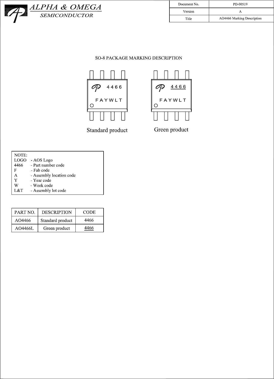
Product Summary
VDS (V) = 30V
ID= 10A (VGS = 10V)
RDS(ON) < 23mΩ (VGS = 10V)
RDS(ON) < 35mΩ (VGS = 4.5V)
100% UIS Tested
100% Rg Tested
AO4466
30V N-Channel MOSFET
General Description
The AO4466 uses advanced trench technology to
provide excellent RDS(ON) and low gate charge. This
device is suitable for use as a load switch or in PWM
applications. The source leads are separated to allow
a Kelvin connection to the source, which may be
used to bypass the source inductance.
* RoHS and Halogen-Free Compliant
SOIC-8
Top View Bottom View
D
D
DD
S
SGG
D
S
Symbol
V
DS
V
GS
I
DM
I
AR
E
AR
T
J
, T
STG
Symbol
Typ
Max
36 40
62 75
R
θJL
18 24
Repetitive avalanche energy 0.1mH
B, G
Junction and Storage Temperature Range
P
D
T
A
=70°C
Pulsed Drain Current
B
Avalanche Current
B, G
°C
3.1
7mJ
2
-55 to 150
12 A
Continuous Drain
Current
AF
Maximum UnitsParameter
Gate-Source Voltage
Drain-Source Voltage
10
7
30
T
A
=25°C
T
A
=70°C
±20
Absolute Maximum Ratings T
A
=25°C unless otherwise noted
V
V
Maximum Junction-to-Lead
C
Steady-State °C/W
Thermal Characteristics
Parameter Units
Maximum Junction-to-Ambient
A
Steady-State
t ≤ 10s R
θJA
°C/W
°C/W
Maximum Junction-to-Ambient
A
I
D
Power Dissipation
T
A
=25°C W
A
64
S
S
Rev.10.0: July 2013 www.aosmd.com Page 1 of 6
AO4466
Symbol Min Typ Max Units
BV
DSS
30 V
1
T
J
=55°C 5
I
GSS
100 nA
V
GS(th)
1.5 2.1 2.6 V
I
D(ON)
64 A
16.7 23
T
J
=125°C 24.3 30
23.7 35 mΩ
g
FS
17 S
V
SD
0.75 1 V
I
S
2.4 A
C
iss
298 373 448 pF
C
oss
46 67 88 pF
C
rss
24 41 58 pF
R
g
0.6 1.8 2.8 Ω
Q
g
(10V) 5.7 7.1 8.6 nC
Q
g
(4.5V) 2.7 3.5 4.2 nC
Q
gs
1.2 nC
Q
gd
1.6 nC
t
D(on)
4.3
ns
Gate Source Charge V
GS
=10V, V
DS
=15V, I
D
=10A
Total Gate Charge
Gate Drain Charge
Total Gate Charge
Turn-On DelayTime
DYNAMIC PARAMETERS
V
GS
=0V, V
DS
=15V, f=1MHz
SWITCHING PARAMETERS
Gate resistance V
GS
=0V, V
DS
=0V, f=1MHz
R
DS(ON)
Static Drain-Source On-Resistance
Forward Transconductance
Diode Forward Voltage
mΩ
V
GS
=4.5V, I
D
=5A
I
S
=1A,V
GS
=0V
V
DS
=5V, I
D
=10A
V
GS
=10V, I
D
=10A
Electrical Characteristics (T
J
=25°C unless otherwise noted)
STATIC PARAMETERS
Parameter Conditions
I
DSS
µA
V
DS
=30 V
GS
=0V
Zero Gate Voltage Drain Current
On state drain current
I
D
=250µA, V
GS
=0V
V
GS
=4.5V, V
DS
=5V
Gate Threshold Voltage V
DS
=V
GS
I
D
=250µA
V
DS
=0V, V
GS
= ±20V
Gate-Body leakage current
Drain-Source Breakdown Voltage
Reverse Transfer Capacitance
Maximum Body-Diode Continuous Current
Input Capacitance
Output Capacitance
Rev.10.0: July 2013 www.aosmd.com Page 2 of 6
t
D(on)
4.3
ns
t
r
2.8 ns
t
D(off)
15.8 ns
t
f
3 ns
t
rr
8.4 10.5 12.6 ns
Q
rr
3.6 4.5 5.4 nC
t
rr
4.7 6.0 7.2 ns
Q
rr
5.3 6.6 8 nC
THIS PRODUCT HAS BEEN DESIGNED AND QUALIFIED FOR THE CONSUMER MARKET. APPLICATIONS OR USES AS CRITICAL
COMPONENTS IN LIFE SUPPORT DEVICES OR SYSTEMS ARE NOT AUTHORIZED. AOS DOES NOT ASSUME ANY LIABILITY ARISING
OUT OF SUCH APPLICATIONS OR USES OF ITS PRODUCTS. AOS RESERVES THE RIGHT TO IMPROVE PRODUCT DESIGN,
FUNCTIONS AND RELIABILITY WITHOUT NOTICE.
Turn-Off DelayTime
V
GS
=10V, V
DS
=15V, R
L
=1.5Ω,
R
GEN
=3Ω
Turn-Off Fall Time
Turn-On DelayTime
Body Diode Reverse Recovery Charge I
F
=10A, dI/dt=500A/µs
I
F
=10A, dI/dt=500A/µs
Turn-On Rise Time
Body Diode Reverse Recovery Time I
F
=10A, dI/dt=100A/µs
Body Diode Reverse Recovery Charge I
F
=10A, dI/dt=100A/µs
Body Diode Reverse Recovery Time
A: The value of R θJA is measured with the device mounted on 1in 2 FR-4 board with 2oz. Copper, in a still air environment with
T A=25°C. The value in any given application depends on the user's specific board design.
B: Repetitive rating, pulse width limited by junction temperature.
C. The RθJA is the sum of the thermal impedence from junction to lead RθJL and lead to ambient.
D. The static characteristics in Figures 1 to 6 are obtained using <300 µs pulses, duty cycle 0.5% max.
E. These tests are performed with the device mounted on 1 in 2 FR-4 board with 2oz. Copper, in a still air environment with T A=25°C. The SOA
curve provides a single pulse rating.
F. The current rating is based on the t≤10s junction to ambient thermal resistance rating.
G: L=100uH, VDD=0V, RG=0Ω, rated VDS=30V and VGS=10V
Rev 9: May. 2012
Rev.10.0: July 2013 www.aosmd.com Page 2 of 6
AO4466
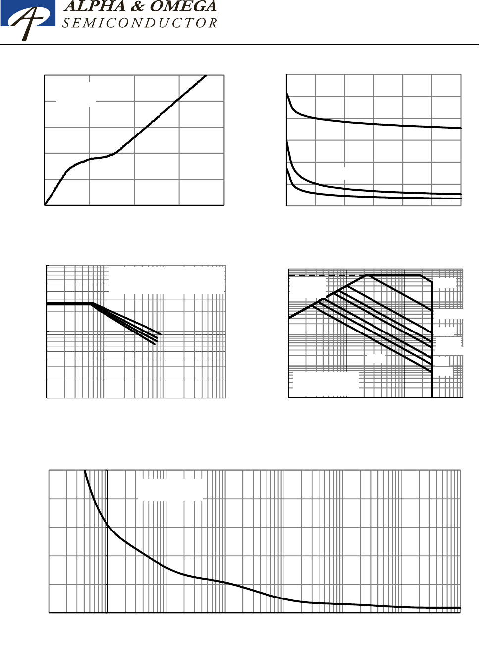
TYPICAL ELECTRICAL AND THERMAL CHARACTERISTICS
0
10
20
30
40
50
60
012345
ID(A)
VDS (Volts)
Fig 1: On-Region Characteristics
V
GS
=3.5V
4.5V
6V
10V
0
3
6
9
12
15
1.5 2 2.5 3 3.5 4 4.5
ID(A)
VGS(Volts)
Figure 2: Transfer Characteristics
10
15
20
25
30
35
40
0
5
10
15
20
RDS(ON) (mΩ
Ω
Ω
Ω)
0.8
1
1.2
1.4
1.6
1.8
0
25
50
75
100
125
150
175
Normalized On-Resistance
V
GS
=10V
VGS=4.5V
25°C
125°C
V
DS
=5V
V
GS
=4.5V
V
GS
=10V
Rev.10.0: July 2013 www.aosmd.com Page 3 of 6
THIS PRODUCT HAS BEEN DESIGNED AND QUALIFIED FOR THE CONSUMER MARKET. APPLICATIONS OR USES AS CRITICAL
COMPONENTS IN LIFE SUPPORT DEVICES OR SYSTEMS ARE NOT AUTHORIZED. AOS DOES NOT ASSUME ANY LIABILITY ARISING
OUT OF SUCH APPLICATIONS OR USES OF ITS PRODUCTS. AOS RESERVES THE RIGHT TO IMPROVE PRODUCT DESIGN,
FUNCTIONS AND RELIABILITY WITHOUT NOTICE.
10
0 5 10 15 20
ID(A)
Figure 3: On-Resistance vs. Drain Current and
Gate Voltage
1.0E-05
1.0E-04
1.0E-03
1.0E-02
1.0E-01
1.0E+00
1.0E+01
0.0 0.2 0.4 0.6 0.8 1.0
IS(A)
VSD (Volts)
Figure 6: Body-Diode Characteristics
25°C
125°C
0.8
0 25 50 75 100 125 150 175
Temperature (°C)
Figure 4: On-Resistance vs. Junction Temperature
10
20
30
40
50
60
2 4 6 8 10
RDS(ON) (mΩ
Ω
Ω
Ω)
VGS (Volts)
Figure 5: On-Resistance vs. Gate-Source Voltage
ID=10A
25
°
C
125°C
Rev.10.0: July 2013 www.aosmd.com Page 3 of 6
AO4466
TYPICAL ELECTRICAL AND THERMAL CHARACTERISTICS
0
2
4
6
8
10
02468
VGS (Volts)
Qg(nC)
Figure 7: Gate-Charge Characteristics
0
100
200
300
400
500
600
0 5 10 15 20 25 30
Capacitance (pF)
VDS (Volts)
Figure 8: Capacitance Characteristics
Ciss
Coss
C
rss
0.0
0.1
1.0
10.0
100.0
0.1 1 10 100
ID(Amps)
V
(Volts)
100
µ
s
10ms
1ms
100ms
1s
10s
DC
RDS(ON)
limited
TJ(Max)=150°C
TA=25°C
VDS=15V
ID=10A
10
µ
s
1.0
10.0
100.0
1
10
100
1000
IA, Peak Avalanche Current (A)
In descending order
TA=25°C, 100°C, 125°C,
Rev.10.0: July 2013 www.aosmd.com Page 4 of 6
0.0
0.1 1 10 100
VDS (Volts)
Figure 10: Maximum Forward Biased Safe
Operating Area (Note E)
T
A
=25
°
C
0
10
20
30
40
50
0.0001 0.01 1 100
Power (W)
Pulse Width (s)
Figure 11: Single Pulse Power Rating Junction-to-Ambient (Note E)
TJ(Max)=150°C
TA=25°C
1.0
1 10 100 1000
IA
, Peak Avalanche Current (A)
Time in Avalache, tA(ms)
Figure 9: Single Pulse Avalanche Capability
Rev.10.0: July 2013 www.aosmd.com Page 4 of 6
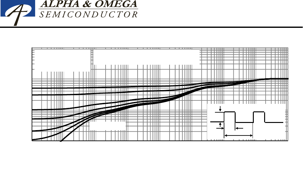
AO4466
TYPICAL ELECTRICAL AND THERMAL CHARACTERISTICS
0.01
0.1
1
10
1E-05 0.0001 0.001 0.01 0.1 1 10 100 1000
Zθ
θ
θ
θJA Normalized Transient
Thermal Resistance
Pulse Width (s)
Figure 12: Normalized Maximum Transient Thermal Impedance
Single Pulse
D=Ton/T
TJ,PK=TA+PDM.ZθJA.RθJA
RθJA=75°C/W
Ton T
P
D
In descending order
D=0.5, 0.3, 0.1, 0.05, 0.02, 0.01, single pulse
Rev.10.0: July 2013 www.aosmd.com Page 5 of 6 Rev.10.0: July 2013 www.aosmd.com Page 5 of 6
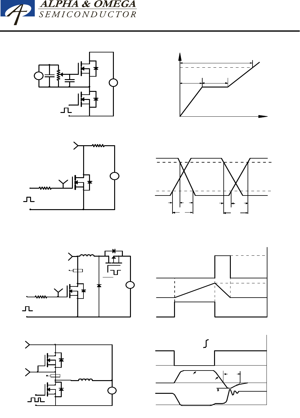
AO4466
-
+
VDC
Ig
Vds
DUT
-
+
VDC
Vgs
Vgs
10V
Qg
Qgs Qgd
Charge
Gate Charge Test Circuit & Waveform
-
+
VDC
DUT Vdd
Vgs
Vds
Vgs
RL
Rg
Vgs
Vds
10%
90%
Resistive Switching Test Circuit & Waveforms
t t
r
d(on)
t
on
t
d(off)
t
f
t
off
L
BV
Unclamped Inductive Switching (UIS) Test Circuit & Waveforms
Vds
DSS
2
E = 1/2 LI
AR
AR
Rev.10.0: July 2013 www.aosmd.com Page 6 of 6
Vdd
Vgs
Id
Vgs
Rg
DUT
-
+
VDC
L
Vgs
Vds
Id
Vgs
BV
I
Ig
Vgs
-
+
VDC
DUT
L
Vds
Vgs
Vds
Isd
Isd
Diode Recovery Test Circuit & Waveforms
Vds -
Vds +
I
F
AR
DSS
2
E = 1/2 LI
dI/dt
I
RM
rr
Vdd
Vdd
Q = - Idt
t
rr
AR
AR
Rev.10.0: July 2013 www.aosmd.com Page 6 of 6