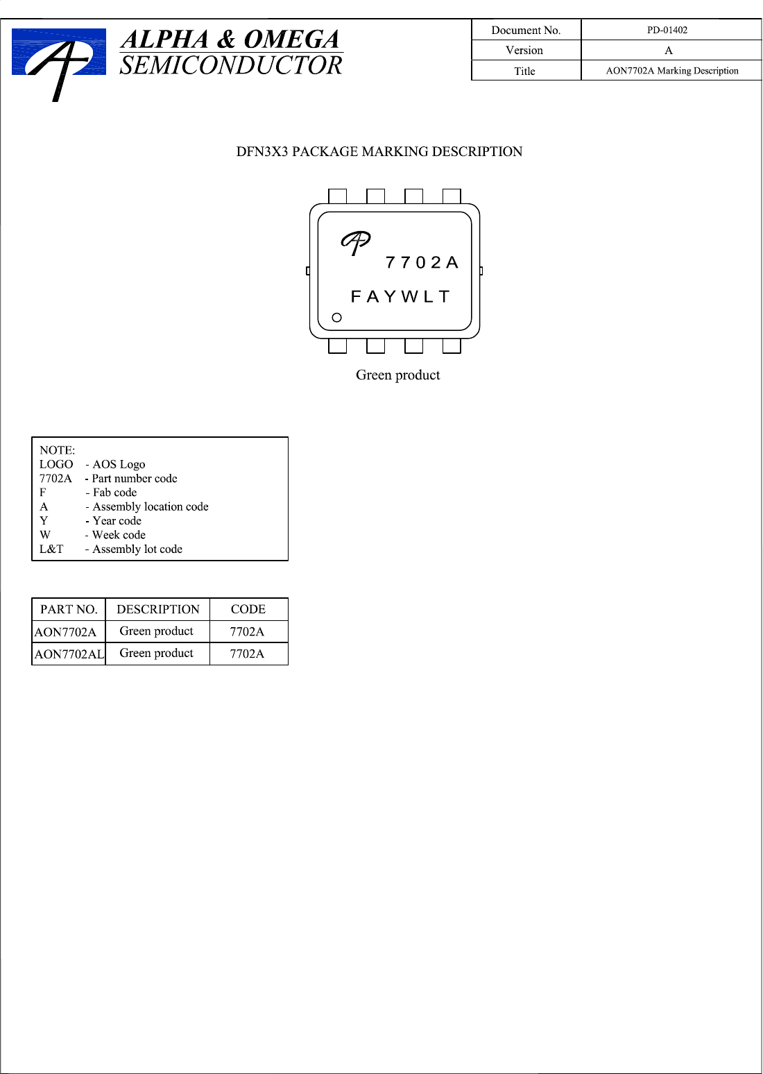
AON7702A Datasheet. Www.s Manuals.com. R1 Ao
User Manual: Marking of electronic components, SMD Codes 7702A, 7716A. Datasheets AON7702A, Si7716ADN.
Open the PDF directly: View PDF ![]() .
.
Page Count: 8
AON7702A
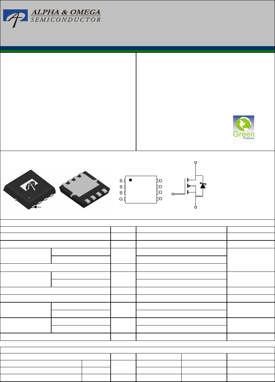
30V N-Channel MOSFET
General Description Product Summary
V
DS
I
D
(at V
GS
=10V) 36A
R
DS(ON)
(at V
GS
=10V) < 10mΩ
R
DS(ON)
(at V
GS
= 4.5V) < 13mΩ
100% UIS Tested
100% R
g
Tested
Symbol
V
DS
V
GS
I
DM
I
AS
, I
AR
E
AS
, E
AR
T
J
, T
STG
Symbol
t ≤ 10s
Steady-State
Steady-State
R
θJC
Typ Max
T
C
=25°C
3.1
9
T
C
=100°C
Junction and Storage Temperature Range -55 to 150 °C
Thermal Characteristics
Units
Maximum Junction-to-Ambient
A
°C/W
R
θJA
30
60
40
Parameter
V±12Gate-Source Voltage
Drain-Source Voltage 30
mJ
Avalanche Current
C
11
A
SRFET
TM
AON7702A uses advanced trench technology
with a monolithically integrated Schottky diode to provide
excellent R
DS(ON)
,and low gate charge. This device is
suitable for use as a low side FET in SMPS, load
switching and general purpose applications.
V
Maximum UnitsParameter
Absolute Maximum Ratings T
A
=25°C unless otherwise noted
30V
A
T
A
=25°C I
DSM
A
T
A
=70°C
80Pulsed Drain Current
C
Continuous Drain
Current I
D
36
22
T
C
=25°C
T
C
=100°C
Power Dissipation
B
P
D
Continuous Drain
Current
11
13.5
15
Avalanche energy L=0.1mH
C
W
Power Dissipation
A
P
DSM
W
T
A
=70°C
23
2
T
A
=25°C
Maximum Junction-to-Case °C/W
°C/W
Maximum Junction-to-Ambient
A D
4.5
75
5.4
Top View
1
2
3
4
8
7
6
5
DFN 3x3A
Top View Bottom View
Pin 1
G
D
S
SRFET
TM
Soft Recovery MOSFET:
Integrated Schottky Diode
SRFET
TM
Rev 1: Feb. 2011 www.aosmd.com Page 1 of 6
Symbol Min Typ Max Units
BV
DSS
30 V
V
DS
=30V, V
GS
=0V 0.5
T
J
=125°C 100
I
GSS
100 nA
V
GS(th)
Gate Threshold Voltage 1.2 1.65 2.1 V
I
D(ON)
80 A
8.2 10
T
J
=125°C 12.5 15
9.9 13 mΩ
g
FS
80 S
V
SD
0.4 0.7 V
I
S
30 A
C
iss
930 1170 1400 pF
C
oss
90 128 170 pF
C
rss
45 89 125 pF
R
g
0.7 1.4 2.1 Ω
Q
g
(10V) 16 20 24 nC
Q
g
(4.5V) 7 8.7 10.5 nC
Q
gs
3.2 nC
Q
gd
3 nC
t
D(on)
6 ns
t
r
2.4 ns
t
D(off)
23 ns
t
f
4 ns
t
rr
5.5 7 8.5 ns
Q
rr
56.5 8 nC
THIS PRODUCT HAS BEEN DESIGNED AND QUALIFIED FOR THE CONSUMER MARKET. APPLICATIONS OR USES AS CRITICAL
COMPONENTS IN LIFE SUPPORT DEVICES OR SYSTEMS ARE NOT AUTHORIZED. AOS DOES NOT ASSUME ANY LIABILITY ARISING
OUT OF SUCH APPLICATIONS OR USES OF ITS PRODUCTS. AOS RESERVES THE RIGHT TO IMPROVE PRODUCT DESIGN,
FUNCTIONS AND RELIABILITY WITHOUT NOTICE.
Maximum Body-Diode Continuous Current
Input Capacitance
Output Capacitance
Turn-On DelayTime
DYNAMIC PARAMETERS
V
GS
=10V, V
DS
=15V, I
D
=13A
Body Diode Reverse Recovery Charge I
F
=13A, dI/dt=500A/µs
Turn-Off DelayTime
V
GS
=10V, V
DS
=15V, R
L
=1.2Ω,
R
GEN
=3Ω
Turn-Off Fall Time
Body Diode Reverse Recovery Time I
F
=13A, dI/dt=500A/µs
Turn-On Rise Time
V
GS
=0V, V
DS
=0V, f=1MHz
Total Gate Charge
Reverse Transfer Capacitance
V
GS
=0V, V
DS
=15V, f=1MHz
SWITCHING PARAMETERS
Gate Source Charge
Gate Drain Charge
Total Gate Charge
Gate resistance
V
GS
=4.5V, I
D
=11A
Forward Transconductance
Diode Forward Voltage I
S
=1A,V
GS
=0V
V
DS
=5V, I
D
=13A
Static Drain-Source On-Resistance
I
DSS
mA
V
DS
=V
GS
I
D
=250µA
V
DS
=0V, V
GS
= ±12V
Zero Gate Voltage Drain Current
Gate-Body leakage current
mΩ
On state drain current
Electrical Characteristics (T
J
=25°C unless otherwise noted)
STATIC PARAMETERS
Parameter Conditions
Drain-Source Breakdown Voltage I
D
=250µA, V
GS
=0V
V
GS
=10V, V
DS
=5V
V
GS
=10V, I
D
=13A
R
DS(ON)
A. The value of R
θJA
is measured with the device mounted on 1in
2
FR-4 board with 2oz. Copper, in a still air environment with T
A
=25°C. The
Power dissipation P
DSM
is based on R
θJA
t ≤ 10s value and the maximum allowed junction temperature of 150°C. The value in any given
application depends on the user's specific board design, and the maximum temperature of 150°C may be u sed if the PCB allows it.
B. The power dissipation P
D
is based on T
J(MAX)
=150°C, using junction-to-case thermal resistance, and is more useful in setting the upper
dissipation limit for cases where additional heatsinking is used.
C. Repetitive rating, pulse width limited by junction temperature T
J(MAX)
=150°C. Ratings are based on low frequency and duty cycles to keep
initial T
J
=25°C.
D. The R
θJA
is the sum of the thermal impedence from junction to case R
θJC
and case to ambient.
E. The static characteristics in Figures 1 to 6 are obtained using <300µs pulses, duty cycle 0.5% max.
F. These curves are based on the junction-to-case thermal impedence which is measured with the device mounted to a large heatsink,
assuming a maximum junction temperature of T
J(MAX)
=150°C. The SOA curve provides a single pulse ratin g.
G. The maximum current rating is package limited.
H. These tests are performed with the device mounted on 1 in
2
FR-4 board with 2oz. Copper, in a still air environment with T
A
=25°C.
Rev 1: Feb. 2011 www.aosmd.com Page 2 of 6
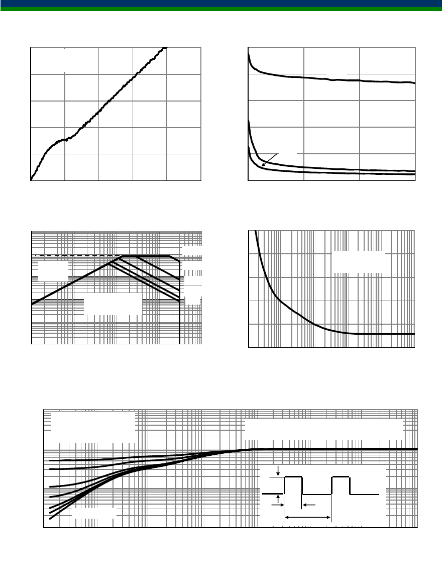
TYPICAL ELECTRICAL AND THERMAL CHARACTERISTICS
40
0
5
10
15
20
25
30
35
1.5 1.75 2 2.25 2.5 2.75 3
V
GS
(Volts)
Figure 2: Transfer Characteristics (Note E)
I
D
(A)
6
7
8
9
10
11
12
1 6 11 16 21 26
I
D
(A)
Figure 3: On-Resistance vs. Drain Current and
Gate Voltage (Note E)
R
DS(ON)
(mΩ
Ω
Ω
Ω)
1.0E-04
1.0E-03
1.0E-02
1.0E-01
1.0E+00
1.0E+01
1.0E+02
0.0 0.2 0.4 0.6 0.8 1.0
V
SD
(Volts)
Figure 6: Body-Diode Characteristics (Note E)
I
S
(A)
25°C
125°C
0.8
1
1.2
1.4
1.6
1.8
2
0 25 50 75 100 125 150 175 200
Temperature (°C)
Figure 4: On-Resistance vs. Junction Temperature
(Note E)
Normalized On-Resistance
V
GS
=4.5V
I
D
=11A
V
GS
=10V
I
D
=13A
5
10
15
20
25
2 4 6 8 10
V
GS
(Volts)
Figure 5: On-Resistance vs. Gate-Source Voltage
(Note E)
R
DS(ON)
(mΩ
Ω
Ω
Ω)
25°C
125°C
V
DS
=5V
V
GS
=4.5V
V
GS
=10V
I
D
=13A
25°C
125°C
0
5
10
15
20
25
30
35
012345
V
DS
(Volts)
Fig 1: On-Region Characteristics (Note E)
I
D
(A)
V
GS
=2.25V
2.5V
3V
10V
2.75V
Rev 1: Feb. 2011 www.aosmd.com Page 3 of 6
TYPICAL ELECTRICAL AND THERMAL CHARACTERISTICS
17
5
2
10
0
18
40
0
2
4
6
8
10
0 5 10 15 20 25
Q
g
(nC)
Figure 7: Gate-Charge Characteristics
V
GS
(Volts)
0
300
600
900
1200
1500
0 10 20 30
V
DS
(Volts)
Figure 8: Capacitance Characteristics
Capacitance (pF)
C
iss
0
40
80
120
160
200
0.0001 0.001 0.01 0.1 1 10
Pulse Width (s)
Figure 10: Single Pulse Power Rating Junction-to-
Case (Note F)
Power (W)
0.01
0.1
1
10
0.00001 0.0001 0.001 0.01 0.1 1 10 100
Pulse Width (s)
Figure 11: Normalized Maximum Transient Thermal Impedance (Note F)
Z
θ
θ
θ
θJC
Normalized Transient
Thermal Resistance
C
oss
C
rss
V
DS
=15V
I
D
=13A
Single Pulse
D=T
on
/T
T
J,PK
=T
C
+P
DM
.Z
θJC
.R
θJC
T
on
T
P
D
In descending order
D=0.5, 0.3, 0.1, 0.05, 0.02, 0.01, single pulse
T
J(Max)
=150°C
T
C
=25°C
10
µ
s
0.0
0.1
1.0
10.0
100.0
1000.0
0.01 0.1 1 10 100
V
DS
(Volts)
I
D
(Amps)
Figure 9: Maximum Forward Biased
Safe Operating Area (Note F)
10
µ
s
10ms
1ms
DC
R
DS(ON)
limited
T
J(Max)
=150°C
T
C
=25°C
100
µ
s
R
θJC
=5.4°C/W
Rev 1: Feb. 2011 www.aosmd.com Page 4 of 6
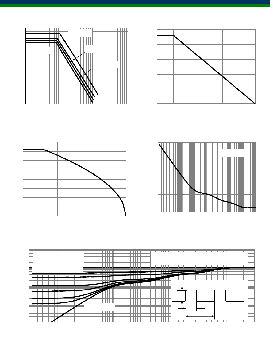
TYPICAL ELECTRICAL AND THERMAL CHARACTERISTICS
17
5
2
10
0
18
40
0.001
0.01
0.1
1
10
0.00001 0.0001 0.001 0.01 0.1 1 10 100 1000
Pulse Width (s)
Figure 16: Normalized Maximum Transient Thermal Impedance (Note H)
Z
θ
θ
θ
θJA
Normalized Transient
Thermal Resistance
Single Pulse
D=T
on
/T
T
J,PK
=T
A
+P
DM
.Z
θJA
.R
θJA
T
on
T
P
D
In descending order
D=0.5, 0.3, 0.1, 0.05, 0.02, 0.01, single pulse
0
5
10
15
20
25
0 25 50 75 100 125 150
T
CASE
(°C)
Figure 13: Power De-rating (Note F)
Power Dissipation (W)
0
5
10
15
20
25
30
35
40
0 25 50 75 100 125 150
T
CASE
(°C)
Figure 14: Current De-rating (Note F)
Current rating I
D
(A)
1
10
100
1000
10000
0.00001 0.001 0.1 10 1000
Pulse Width (s)
Figure 15: Single Pulse Power Rating Junction-to-
Ambient (Note H)
Power (W)
T
A
=25°C
R
θJA
=75°C/W
10.0
100.0
1 10 100 1000
Time in avalanche, t
A
(µ
µµ
µs)
Figure 12: Single Pulse Avalanche capability (Note
C)
I
AR
(A) Peak Avalanche Current
T
A
=25°C
T
A
=150°C T
A
=100°C
T
A
=125°C
Rev 1: Feb. 2011 www.aosmd.com Page 5 of 6
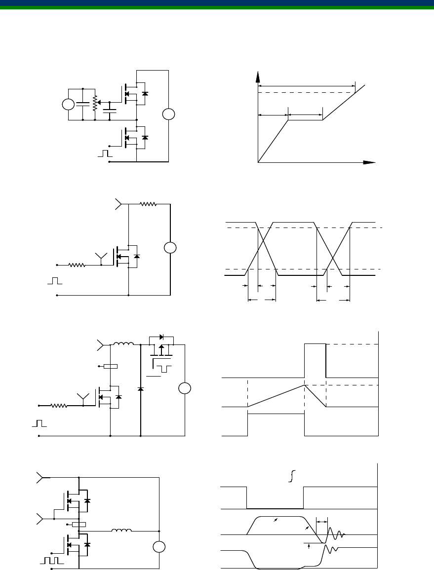
-
+
VDC
Ig
Vds
DUT
-
+
VDC
Vgs
Vgs
10V
Qg
Qgs Qgd
Charge
Gate Charge Test Circuit & Waveform
-
+
VDC
DUT Vdd
Vgs
Vds
Vgs
RL
Rg
Vgs
Vds
10%
90%
Resistive Switching Test Circuit & Waveforms
t t
r
d(on)
t
on
t
d(off)
t
f
t
off
Vdd
Vgs
Id
Vgs
Rg
DUT
-
+
VDC
L
Vgs
Vds
Id
Vgs
BV
I
Unclamped Inductive Switching (UIS) Test Circuit & Waveforms
Ig
Vgs
-
+
VDC
DUT
L
Vds
Vgs
Vds
Isd
Isd
Diode Recovery Test Circuit & Waveforms
Vds -
Vds +
I
F
AR
DSS
2
E = 1/2 LI
dI/dt
I
RM
rr
Vdd
Vdd
Q = - Idt
AR
AR
t
rr
Rev 1: Feb. 2011 www.aosmd.com Page 6 of 6