AP40T03GP HF 3, AP40T03GS 3 Datasheet. Www.s Manuals.com. 20050331 Apec
User Manual: Datasheets AP40T03GH, AP40T03GH-HF, AP40T03GJ, AP40T03GJ-HF, AP40T03GP, AP40T03GP-HF-3, AP40T03GS, AP40T03GS-HF-3, AP40T03H, AP40T03J.
Open the PDF directly: View PDF ![]() .
.
Page Count: 7
200503313-3
Advanced Power
Electronics Corp.
1/6
AP40T03GP/S-HF-3
©2010 Advanced Power Electronics Corp. USA
www.a-powerusa.com
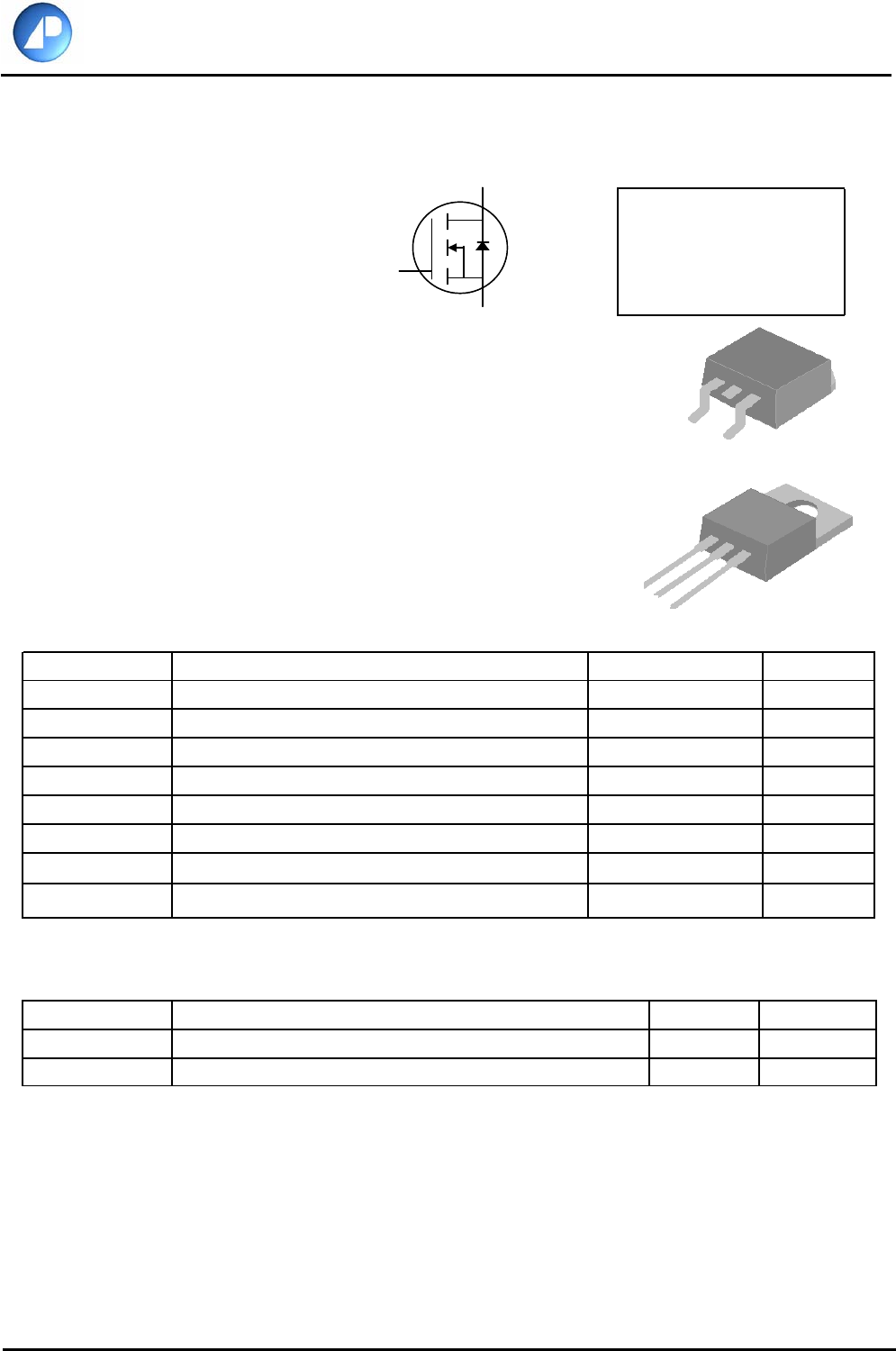
N-channel Enhancement-mode Power MOSFET
DSS
DS(ON)
D
Description
Absolute Maximum Ratings
Thermal Data
A
dvanced Power MOSFETs from APEC provide the designer with the best
combination of fast switching, low on-resistance and cost-effectiveness.
The AP40T03GS-HF-3 is in the TO-263 package, which is widely used
BV 30V
Fast Switching Performance R 25mΩ
Simple Drive Requirement
Low Gate Charge
RoHS-compliant, halogen-free I 28A
for commercial and industrial surface-mount applications, and is well
suited for low voltage applications such as DC/DC converters.
The AP40T03GP-HF-3 is in the TO-220 through-hole package which is
used where a low PCB footprint or an attached heatsink is required.
GDSTO-263 (S)
GDSTO-220 (P)
Ordering Information
AP40T03GS-HF-3TR RoHS-compliant, halogen-free TO-263, shipped on tape and reel (800 pcs/reel)
AP40T03GP-HF-3TB RoHS-compliant, halogen-free TO-220, shipped in tubes
Symbol Units
VDS
VGS
ID at TC=25°C
ID at TC=100°C
IDM
PD at TC=25°C
TSTG
TJ
Symbol Value Units
Rthj-c Maximum Thermal Resistance, Junction-case 4 °C/W
Rthj-a Maximum Thermal Resistance, Junction-ambient 62 °C/W
-55 to 150 °C
Drain-Source Voltage 30 V
Parameter Rating
Gate-Source Voltage ±25 V
Continuous Drain Current 28 A
Continuous Drain Current 24 A
Pulsed Drain Current1 95 A
Total Power Dissipation 31.25 W
Parameter
Storage Temperature Range
Operating Junction Temperature Range -55 to 150 °C
G
D
S
G
D
S
Advanced Power
Electronics Corp.
2/6
AP40T03GP/S-HF-3
©2010 Advanced Power Electronics Corp. USA
www.a-powerusa.com
Electrical Specifications
at Tj=25°C (unless otherwise specified)
Source-Drain Diode
THIS PRODUCT IS SENSITIVE TO ELECTROSTATIC DISCHARGE, PLEASE HANDLE WITH CAUTION.
USE OF THIS PRODUCT AS A CRITICAL COMPONENT IN LIFE SUPPORT OR OTHER SIMILAR SYSTEMS IS NOT AUTHORIZED.
APEC DOES NOT ASSUME ANY LIABILITY ARISING OUT OF THE APPLICATION OR USE OF ANY PRODUCT OR CIRCUIT DESCRIBED
HEREIN; NEITHER DOES IT CONVEY ANY LICENSE UNDER ITS PATENT RIGHTS, NOR THE RIGHTS OF OTHERS.
APEC RESERVES THE RIGHT TO MAKE CHANGES WITHOUT FURTHER NOTICE TO ANY PRODUCTS HEREIN TO IMPROVE
RELIABILITY, FUNCTION OR DESIGN.
Symbol Parameter Test Conditions Min. Typ. Max. Units
BVDSS Drain-Source Breakdown Voltage VGS=0V, ID=250uA 30 - - V
∆BVDSS/∆Tj Breakdown Voltage Temperature Coefficient Reference to 25°C, ID=1mA - 0.032 - V/°C
RDS(ON)
Static Drain-Source On-Resistance VGS=10V, ID=18A - - 25 mΩ
VGS=4.5V, ID=14A - - 45 mΩ
VGS(th) Gate Threshold Voltage VDS=VGS, ID=250uA 1 - 3 V
gfs Forward Transconductance VDS=10V, ID=18A - 15 - S
IDSS Drain-Source Leakage Current (Tj=25oC) VDS=30V, VGS=0V - - 1 uA
Drain-Source Leakage Current (Tj=150oC) VDS=24V ,VGS=0V - - 25 uA
IGSS Gate-Source Leakage VGS= ±25V - - ±100 nA
QgTotal Gate Charge2ID=18A - 8.8 - nC
Qgs Gate-Source Charge VDS=20V - 2.5 - nC
Qgd Gate-Drain ("Miller") Charge VGS=4.5V - 5.8 - nC
td(on) Turn-on Delay Time2VDS=15V - 6 - ns
trRise Time ID=18A - 62 - ns
td(off)
Turn-off Delay Time RG=3.3Ω, VGS=10V - 16 -
ns
tf
Fall Time RD=0.83Ω - 4.4 -
ns
Ciss Input Capacitance VGS=0V - 655 - pF
Coss Output Capacitance VDS=25V - 145 - pF
Crss Reverse Transfer Capacitance f=1.0MHz - 95 - pF
Symbol Parameter Test Conditions Min. Typ. Max. Units
ISContinuous Source Current ( Body Diode ) VD=VG=0V , VS=1.3V - - 28 A
ISM Pulsed Source Current ( Body Diode )1--95
A
VSD
Forward On Voltage2
Tj=25°C, IS=28A, VGS=0V - - 1.3 V
Notes:
1.Pulse width limited by safe operating area.
2.Pulse width <300us , duty cycle <2%.
Advanced Power
Electronics Corp.
3/6
AP40T03GP/S-HF-3
©2010 Advanced Power Electronics Corp. USA
www.a-powerusa.com
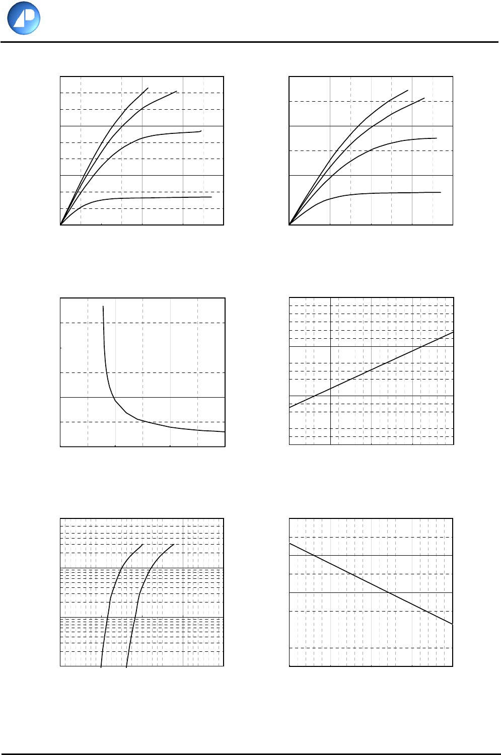
Fig 1. Typical Output Characteristics Fig 2. Typical Output Characteristics
Fig 3. On-Resistance vs. Gate Voltage Fig 4. Normalized On-Resistance
vs. Junction Temperature
Fig 5. Forward Characteristic of Fig 6. Gate Threshold Voltage vs.
Reverse Diode Junction Temperature
Typical Electrical Characteristics
0
25
50
75
0.0 1.0 2.0 3.0 4.0
VDS , Drain-to-Source Voltage (V)
ID , Drain Current (A)
TC=150 oC 10V
8.0V
6.0V
VG=4.0V
0
30
60
90
0.0 1.0 2.0 3.0 4.0
VDS , Drain-to-Source Voltage (V)
ID , Drain Current (A)
TC=25 oC 10V
8.0V
6.0V
VG=4.0V
0.2
0.8
1.4
2.0
-50 0 50 100 150
Tj , Junction Temperature ( oC)
Normalized RDS(ON)
I D=18A
VG=10V
10
30
50
70
0 5 10 15
VGS , Gate-to-Source Voltage (V)
RDS(ON) (mΩ)
I D=14A
T C
=25°C
0.1
1
10
100
0 0.4 0.8 1.2 1.6
VSD , Source-to-Drain Voltage (V)
IS(A)
Tj=25 oC
Tj=150 oC
0.5
1.0
1.5
2.0
2.5
-50 0 50 100 150
Tj , Junction Temperature ( oC )
VGS(th) (V)
Advanced Power
Electronics Corp.
4/6
AP40T03GP/S-HF-3
©2010 Advanced Power Electronics Corp. USA
www.a-powerusa.com
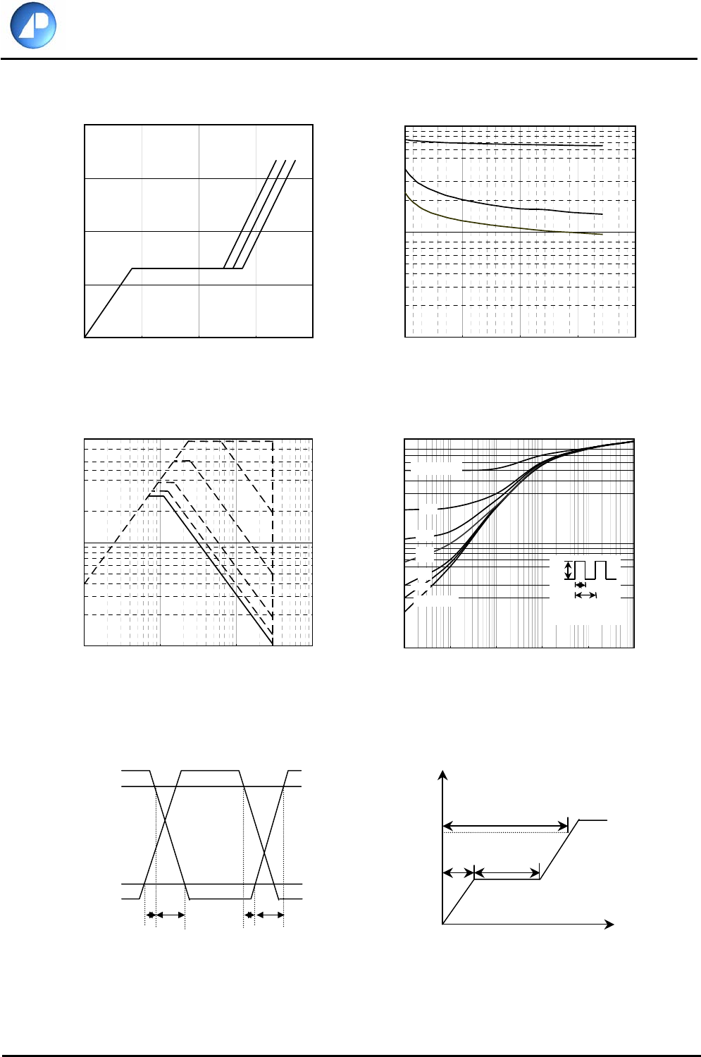
Fig 7. Gate Charge Characteristics Fig 8. Typical Capacitance Characteristics
Fig 9. Maximum Safe Operating Area Fig 10. Effective Transient Thermal Impedance
Fig 11. Switching Time Waveforms Fig 12. Gate Charge Waveform
Typical Electrical Characteristics (cont.)
td(on) trtd(off) tf
VDS
VGS
10%
90%
Q
VG
10V
QGS QGD
QG
Charge
1
10
100
0.1 1 10 100
VDS ,Drain-to-Source Voltage (V)
ID (A)
T C=25 oC
S
in
g
le Puls
e
100us
1ms
10ms
100ms
DC
0.01
0.1
1
0.00001 0.0001 0.001 0.01 0.1 1
t , Pulse Width (s)
Normalized Thermal Response (Rthjc)
PDM
Duty Factor = t/T
Peak Tj = PDM x Rthjc + TC
t
T
0.02
0.01
0.05
0.1
0.2
Duty factor = 0.5
Single Pulse
0
3
6
9
12
036912
QG , Total Gate Charge (nC)
VGS , Gate to Source Voltage (V)
I D=18A
VDS =10V
VDS =15V
VDS =20V
10
100
1000
1 8 15 22 29
VDS ,Drain-to-Source Voltage (V)
C (pF)
f=1.0MHz
Ciss
Coss
Crss

Advanced Power
Electronics Corp.
5/6
AP40T03GP/S-HF-3
©2010 Advanced Power Electronics Corp. USA
www.a-powerusa.com
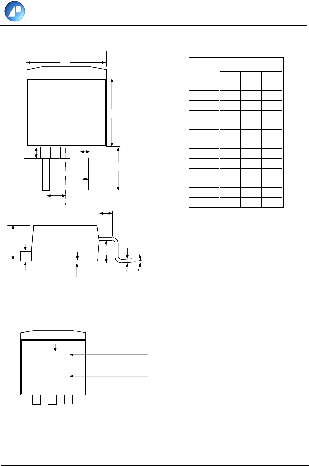
Package Dimensions: TO-220
Marking Information: TO-220
Product: AP40T03
GP = RoHS-compliant halogen-free TO-220
Date/lot code (YWWSSS)
Y: Last digit of the year
WW: Work week
SSS: Lot code sequence
Package code
Millimeters
MIN NOM MAX
A 4.40 4.60 4.80
b0.76 0.88 1.00
D8.60 8.80 9.00
c0.36 0.43 0.50
E9.80 10.10 10.40
L4 14.70 15.00 15.30
L5 6.20 6.40 6.60
D1
c1 1.25 1.35 1.45
b1 1.17 1.32 1.47
L 13.25 13.75 14.25
e
L1 2.60 2.75 2.89
φ 3.71 3.84 3.96
E1
1.All Dimensions Are in Millimeters.
2.Dimension Does Not Include Mold Protrusions.
2.54 REF.
7.4 REF,
SYMBOLS
5.10 REF.
E1
b
b1
e
DL4
L1
A
c1
c
L
40T03GP
YWWSSS
φ
L5
E
D1
Advanced Power
Electronics Corp.
6/6
AP40T03GP/S-HF-3
©2010 Advanced Power Electronics Corp. USA
www.a-powerusa.com
Package Dimensions: TO-263
Marking Information: TO-263
Product: AP40T03
Package code:
Date Code (YWWSSS)
Y: Last digit of the year
WW: Work week
SSS: Lot code sequence
GS = RoHS-compliant halogen-free TO-263
Millimeters
MIN NOM MAX
A 4.25 4.75 5.20
A1 0.00 0.15 0.30
A2 2.20 2.45 2.70
b 0.70 0.90 1.10
b1 1.07 1.27 1.47
c 0.30 0.45 0.60
c1 1.15 1.30 1.45
D 8.30 8.90 9.40
E 9.70 10.10 10.50
e 2.04 2.54 3.04
L2 ----- 1.50 -----
L3 4.50 4.90 5.30
L4 ----- 1.50 ----
1. All dimensions are in millimeters.
2. Dimensions do not include mold protrusions.
SYMBOLS
E
b
b1
e
D
L2
L3
c1
A
.
A1
L4
c
YWWSSS
40T03GS
YWWSSS
E
b
b1
e
D
L2
L3
c1
A
φ
A1
L4
c