APL3512 Datatsheet. Www.s Manuals.com. Ra.6 Anpec
User Manual: Marking of electronic components, SMD Codes L2, L2 *, L2-***, L20, L21B, L24, L2902, L2902K, L2904, L2904AV, L2904V, L2A*, L2B, L2B*. Datasheets ADP3330ART-2.75, APL3512AB, APL3512BB, BAS40-06, BZX384-B6V2, DTD114GK, EML20, LM2902KDB, LM2902KPW, LM2902PW, LM2904AVQDR, LM2904AVQPWR, LM2904PSR, LM2904PW, LM2904VQDR, LM2904VQPWR, LP2980IM5-3.8, NZL6V8AXV3T1, RT9819E-24PV, SL24T1, SST502, UDZS9.1B, UML2N, mESD5.0DT5G.
Open the PDF directly: View PDF ![]() .
.
Page Count: 22
Copyright ANPEC Electronics Corp.
Rev. A.6 - Aug., 2012
APL3512
www.anpec.com.tw1
ANPEC reserves the right to make changes to improve reliability or manufacturability without notice, and
advise customers to obtain the latest version of relevant information to verify before placing orders.
Power-Distribution Switches with Soft Start
•90mΩ High Side MOSFET
•2A Continuous Current
•Soft-Start Time Programmable by External
Capacitor
•Wide Supply Voltage Range: 2.7V to 5.5V
•Current-Limit and Short-Circuit Protections
•Under-Voltage Lockout Protection
•Reverse Current Blocking when Switch Disabled
•Over-Temperature Protection
•Logic Level Enable Input
APL3512A: Active High
APL3512B: Active Low
•Lead Free and Green Devices Available
(RoHS Compliant)
FeaturesGeneral Description
Applications
•TFT LCD Modules
•Notebook and Desktop Computers
•USB Ports
•High-Side Power Protection Switches
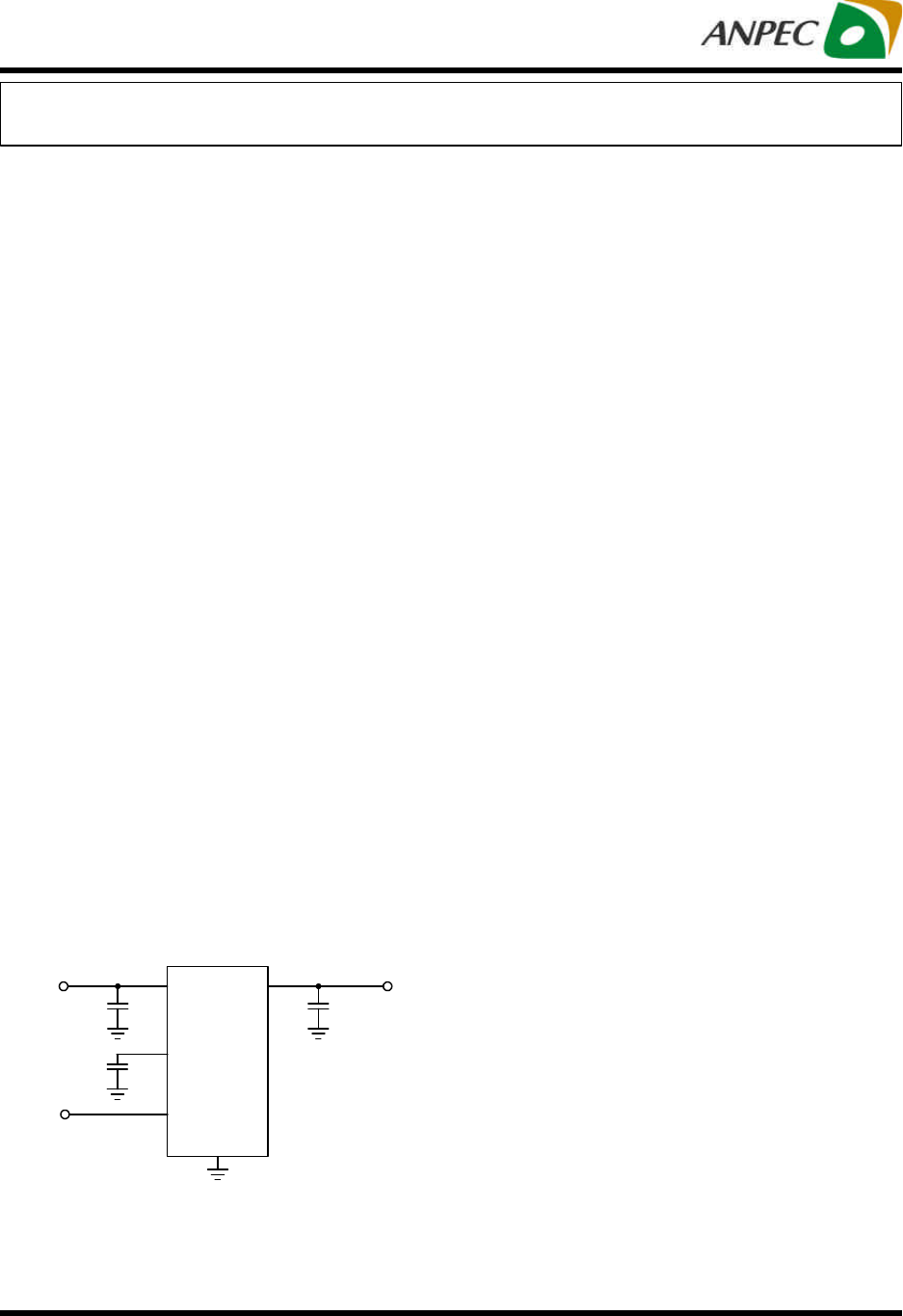
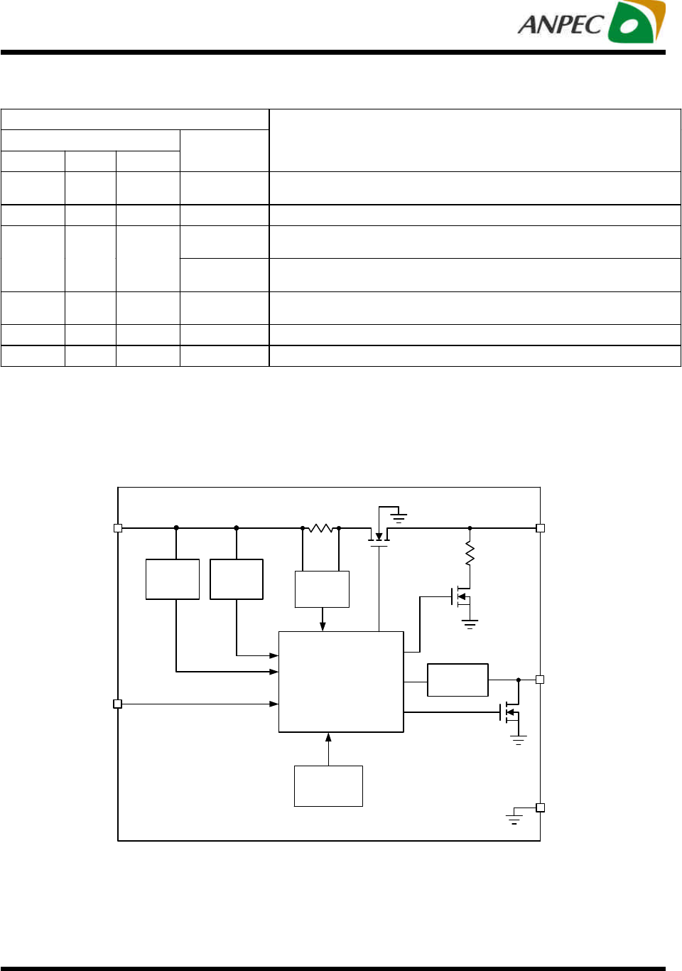
Simplified Application Circuit
The APL3512A/B is a power-distribution switch with some
protection functions that can deliver current up to 2A. The
device incorporates a 90mΩ N-channel MOSFET power
switch that is controlled by an enable logic pin and has a
SS pin dedicated to soft-start ramp-up rate control that
can be used in application where the inrush current is
concerned.
The device integrates some protection features, includ-
ing current-limit protection, short-circuit protection, over-
temperature protection, and UVLO. The current-limit and
short-circuit protection can protect down-stream devices
from catastrophic failure by limiting the output current at
current-limit threshold during over-load or short-circuit
events. When VOUT drops below VIN-1.5V the devices limit
the current to a lower and safe level. The over-tempera-
ture protection function shuts down the N-channel
MOSFET power switch when the junction temperature
rises beyond 140oC and will automatically turns on the
power switch when the temperature drops by 20oC. The
UVLO function keeps the power switch in off state until
there is a valid input voltage present.
The device is available in lead free SOT-23-5, TDFN2x2-
6 and SOP-8 packages with enable active-high(EN) and
active-low(ENB) versions.
VIN VOUT
GND
APL3512A/B
SS
EN/ENB
VIN VOUT
EN
Control
Copyright ANPEC Electronics Corp.
Rev. A.6 - Aug., 2012
APL3512
www.anpec.com.tw2
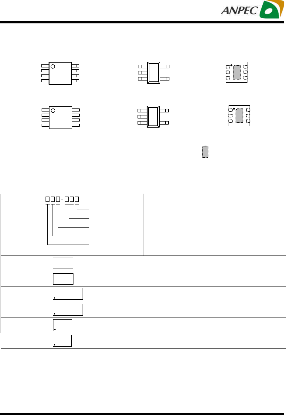
Pin Configuration
GND 2
5 VIN
ENB 3 4 SS
VOUT 1
SOT-23-5
APL3512B
GND 2
5 VIN
EN 3 4 SS
VOUT 1
SOT-23-5
APL3512A
SS 27 NC
GND 3
NC 46 ENB
5 NC
8 VOUT
VIN 1
SOP-8
APL3512B
SS 27 NC
GND 3
NC 46 EN
5 NC
8 VOUT
VIN 1
SOP-8
APL3512A
GND 3
6 VOUT
VIN 1
SS 25 NC
4 EN
TDFN2x2-6
APL3512A
GND 3
6 VOUT
VIN 1
SS 25 NC
4 ENB
TDFN2x2-6
APL3512B
Exposed Pad, connect to large
ground plane for heat dissipation
Ordering and Marking Information
Note : ANPEC lead-free products contain molding compounds/die attach materials and 100% matte tin plate termination finish; which
are fully compliant with RoHS. ANPEC lead-free products meet or exceed the lead-free requirements of IPC/JEDEC J-STD-020D for
MSL classification at lead-free peak reflow temperature. ANPEC defines “Green” to mean lead-free (RoHS compliant)and halogen
free (Br or Cl does not exceed 900ppm by weight in homogeneous material and total of Br and Cl does not exceed 1500ppm by
weight).
APL3512 Package Code
B : SOT-23-5 K : SOP-8 QB : TDFN2x2-6
Operating Ambient Temperature Range
I : -40 to 85 oC
Handling Code
TR : Tape & Reel
EN Function
A : Active High B : Active Low
Assembly Material
G : Halogen and Lead Free Device
Handling Code
Temperature Range
Package Code
Assembly Material
APL3512A B:L2AX X - Date Code
APL3512B B:L2BX X - Date Code
EN Function
APL3512A K:APL3512A
XXXXX XXXXX - Date Code
APL3512B K:XXXXX - Date Code
APL3512B
XXXXX
APL3512A QB:X - Date Code
L12A
X
APL3512B QB:X - Date Code
L12B
X
Copyright ANPEC Electronics Corp.
Rev. A.6 - Aug., 2012
APL3512
www.anpec.com.tw3
Absolute Maximum Ratings (Note 1)
Symbol Parameter Rating Unit
VIN VIN to GND Voltage -0.3 ~ 6 V
VOUT VOUT to GND Voltage -0.3 ~ 6 V
VENB, VEN EN, ENB to GND Voltage -0.3 ~ 6 V
VSS SS to GND Voltage -0.3 ~ 6 V
IOUT Continuous Output Current Internally Limited A
TJ Maximum Junction Temperature -40 ~ 150 oC
TSTG Storage Temperature -65 ~ 150 oC
TSDR Maximum Lead Soldering Temperature, 10 Seconds 260 oC
Note1: Stresses beyond those listed under "absolute maximum ratings" may cause permanent damage to the device. These are
stress ratings only and functional operation of the device at these or any other conditions beyond those indicated under "recom-
mended operating conditions" is not implied. Exposure to absolute maximum rating conditions for extended periods may affect device
reliability.
Thermal Characteristics
Symbol Parameter Typical Value Unit
θJA
Junction-to-Ambient Resistance in Free Air (Note 2) SOT-23-5
SOP-8
TDFN2x2-6
250
160
225
oC/W
Note 2: θJA is measured with the component mounted on a high effective thermal conductivity test board in free air.
Symbol
Parameter Range Unit
VIN VIN Input Voltage 2.7 ~ 5.5 V
IOUT OUT Output Current 0 ~2 A
CSS SS Pin Soft-Start Capacitor (Note 4) 0.3 ~470 nF
TA Ambient Temperature -40 ~ 85 oC
TJ Junction Temperature -40 ~ 125 oC
Recommended Operating Conditions (Note 3)
Note 3: Refer to the typical application circuit.
Note 4: Attaching a capacitor on SS pin can adjust the VOUT soft-start rate. If the CSS is out of the recommended range, the soft-start
rate could become internally controlled as if no CSS.

Copyright ANPEC Electronics Corp.
Rev. A.6 - Aug., 2012
APL3512
www.anpec.com.tw4
Electrical Characteristics
Unless otherwise specified, these specifications apply over VIN=5V, VEN=5V or VENB=0V and TA=-40~85oC. Typical values are at
TA=25oC.
APL3512A/B
Symbol
Parameter Test Conditions Min. Typ. Max.
Unit
SUPPLY CURRENT
No load, VEN=0V or VENB=5V - - 1 µA
VIN Supply Current No load, VEN=5V or VENB=0V - 60 100 µA
Leakage Current VOUT=GND, VEN=0V or VENB=5V - - 1 µA
Reverse Leakage Current VIN=GND, VOUT=5V, VEN=0V or VENB=5V - - 1 µA
POWER SWITCH
IOUT=1.5A, TA=25oC - 90 110 mΩ
RDS(ON)
Power Switch On Resistance IOUT=1.5A, TA=-40~85oC - 90 140 mΩ
UNDER-VOLTAGE LOCKOUT
VIN UVLO Threshold Voltage VIN rising, TA=-40~85oC 2.3 - 2.65 V
VIN UVLO Hysteresis - 0.2 - V
CURRENT-LIMIT AND SHORT-CIRCUIT PROTECTIONS
ILIM Current-Limit Threshold VIN=2.7V to 5.5V, TA=-40~85oC 2.5 3.1 4.22 A
ISHORT
Short-Circuit Output Current VIN=2.7V to 5.5V - 0.8 - A
SOFT-START CONTROL PIN
SS Current VIN=5V, TA=-40~85oC 1 2 3 µA
VIN=5V, No load, COUT=1µF, CSS=10nF,
TA=-40~85oC - 10 - ms
VIN=3.3V, No load, COUT=1µF, CSS=10nF,
TA=-40~85oC - 6.6 - ms
tSS Soft-Start Time
VIN=3.3V, No load, COUT=1µF, No CSS
or SS
tied to VIN, TA=-40~85oC 1 2 3 ms
EN OR ENB INPUT PIN
VIH Input Logic HIGH VIN=2.7V to 5V 2 - - V
VIL Input Logic LOW VIN=2.7V to 5V - - 0.8 V
Input Current - - 1 µA
VOUT Discharge Resistance VEN=0V or VENB=5V - 150 - Ω
OVER-TEMPERATURE PROTECTION (OTP)
TOTP Over-Temperature Threshold TJ rising - 140 - °C
Over-Temperature Hysteresis - 20 - °C
Copyright ANPEC Electronics Corp.
Rev. A.6 - Aug., 2012
APL3512
www.anpec.com.tw5
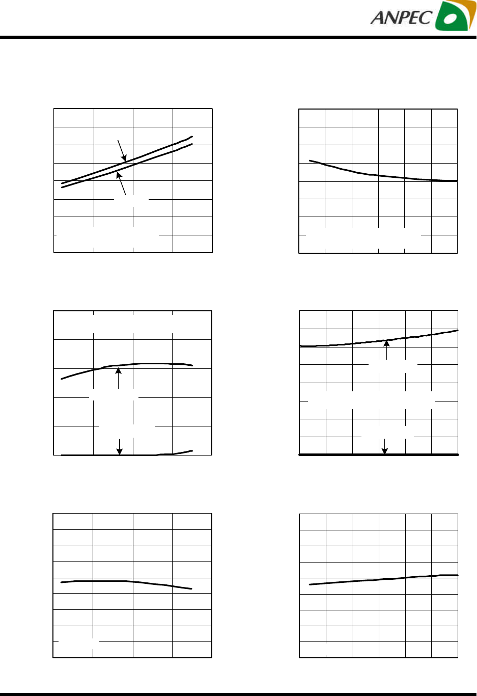
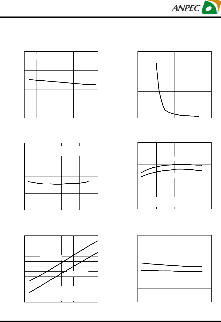
Typical Operating Characteristics
Supply Current vs. Junction
Temperature
Supply Current, ICC (µA)
-50 0 50 100 150
Junction Temperature (oC)
VIN =5V, RLOAD = Open,
CIN =COUT =33µF/Electrolytic
IC Enabled
IC Disabled
0
20
40
60
80
100
Switch On Resistance vs. Input
Voltage
Switch On Resistance, RDS(on) (mΩ)
Input Voltage (V)
IOUT=1.5A,CIN =1µF/X7R,
COUT =1µF/X7R, TA=25oC
2.5 3.0 3.5 4.0 4.5 5.0 5.5
60
80
90
100
110
120
130
70
50
Switch On Resistance , RDS(on) (mΩ)
Switch On Resistance vs. Junction
Temperature
VIN=3.3V
Junction Temperature (oC)
VIN=5V
IOUT=1.5A, CIN =1µF/X7R,
COUT =10µF/X7R
40
60
80
100
120
140
160
20
0-50 0 50 100 150
Supply Current vs. Input Voltage
Input Voltage (V)
2.5 3.0 3.5 4.0 4.5 5.0 5.5
Supply Current, ICC (µA)
00
10
20
30
40
50
60
70
80
RLOAD = Open,
CIN =COUT =1µF/X7R, TA=25oC
IC Disabled
IC Enabled
Current-Limit Threshold vs.
Junction Temperature
Current-Limit Threshold, ILIM (A)
-50 0 50 100 150
Junction Temperature (oC)
2.0
2.8
3.0
3.2
3.4
3.6
3.8
VIN =5V
2.6
2.4
2.2
Input Voltage (V)
Current-Limit Threshold, ILIM (A)
Current-Limit Threshold vs.
Input Voltage
TA =25oC
2.0
2.2
2.4
2.6
2.8
3.0
3.2
3.4
3.6
3.8
2.5 3.0 3.5 4.0 4.5 5.0 5.5
Copyright ANPEC Electronics Corp.
Rev. A.6 - Aug., 2012
APL3512
www.anpec.com.tw6
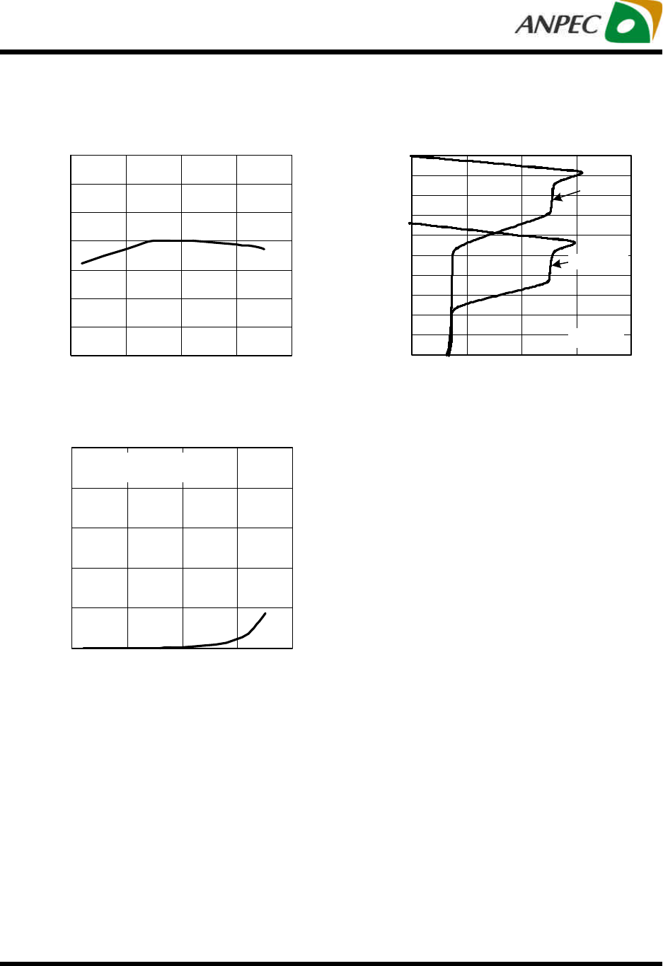
Typical Operating Characteristics (Cont.)
EN Pin Threshold Voltage vs.
Junction Temperature
EN Pin Threshold Voltage, VEN (V)
EN Falling
EN Rising
Junction Temperature (oC)
VIN =5V, RLOAD =50Ω,
CIN = COUT =33µF/Elctrolytic
-50 0 50 100 150
0.5
1.0
1.5
2.0
2.5
3.0
Turn-On Rising Time vs. Junction
Temperature
Turn-On Rising Time, tF (ms)
Junction Temperature (oC)
VIN = 5V, RLOAD =30Ω,
CIN = 1µF/X7R, COUT =33µF/Electrolytic
1.0
1.5
2.0
0.5
0.0-50 0 50 100 150
EN Pin Threshold Voltage vs.
Input Voltage
Input Voltage (V)
EN Pin Threshold Voltage, VEN (V)
EN Falling
EN Rising
RLOAD =50Ω,
CIN = COUT =33µF/
Elctrolytic, TA=25oC
1.3
1.4
1.5
1.6
1.7
1.8
1.9
2.0
2.1
0.8
0.9
1.0
1.1
1.2
2.5 3.0 3.5 4.0 4.5 5.0 5.5
VIN UVLO Threshold Voltage vs.
Junction Temperature
VIN UVLO Threshold Voltage, VVLOC (V)
Junction Temperature (oC)
IOUT =15mA,
CIN = 1µF/X7R, COUT =33µF/Electrolytic
1.2
1.6
2.0
2.4
2.8
3.2
0.8 -50 0 50 100 150
UVLO Rising
UVLO Falling
Short-Circuit Output Current vs.
Input Voltage
Input Voltage (V)
2.5 3.0 3.5 4.0 4.5 5.0 5.5
Short-Circuit Output Current, ISHORT (A)
0.0
0.2
0.4
0.6
0.8
1.0
1.2
1.4
TA=25oC
Current-Limit Response vs.
Output Peak Current
Current-Limit Response (µs)
0
50
100
150
200
250
Output Peak Current (A)
VIN =5V, TA=25oC
0 2 4 6 8 10 12
Copyright ANPEC Electronics Corp.
Rev. A.6 - Aug., 2012
APL3512
www.anpec.com.tw7
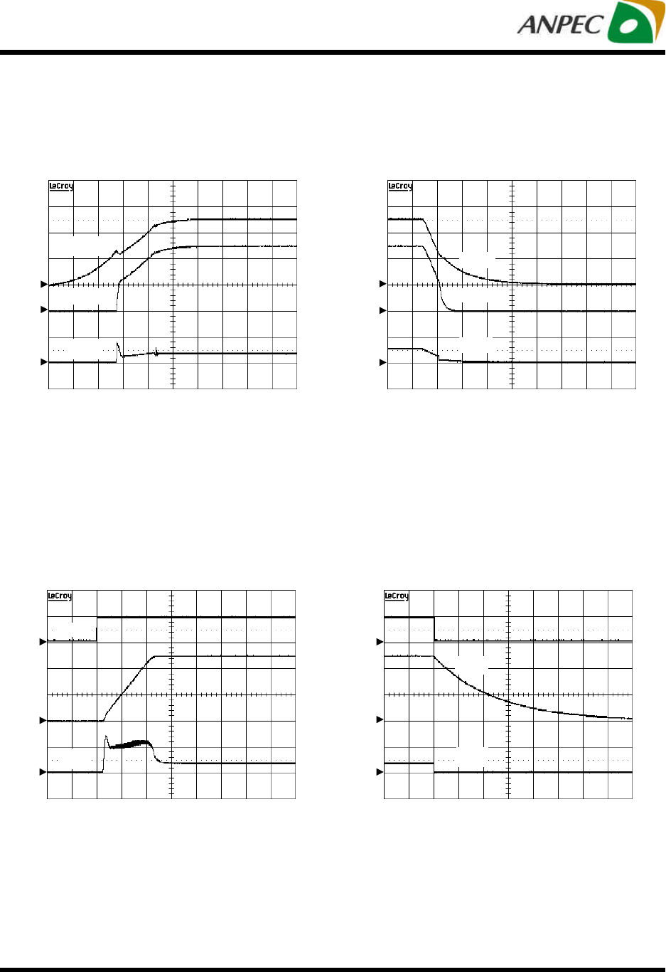
Typical Operating Characteristics (Cont.)
Output Voltage, VOUT (V)
Output Current (A)
Output Voltage vs. Output Current
VIN=5V
TA=25oC
0.0
2.5
3.0
3.5
4.0
4.5
5.0
2.0
1.5
1.0
0.5
0 1 2 3 4
VIN=3.3V
Turn Off Leakage Current vs.
Junction Temperature
Turn Off Leakage Current, ILEAK(µA)
Junction Temperature (oC)
VIN = 5V, RLOAD = 0Ω,
CIN = COUT =1µF/X7R
0
2
4
6
8
10
-50 0 50 100 150
SS Current vs. Junction Temperature
SS Current, ISS (µA)
Junction Temperature (oC)
VIN =5V
0.4
1.2
2.0
2.4
2.8
3.2
1.6
0.8
-50 0 50 100 150
Copyright ANPEC Electronics Corp.
Rev. A.6 - Aug., 2012
APL3512
www.anpec.com.tw8
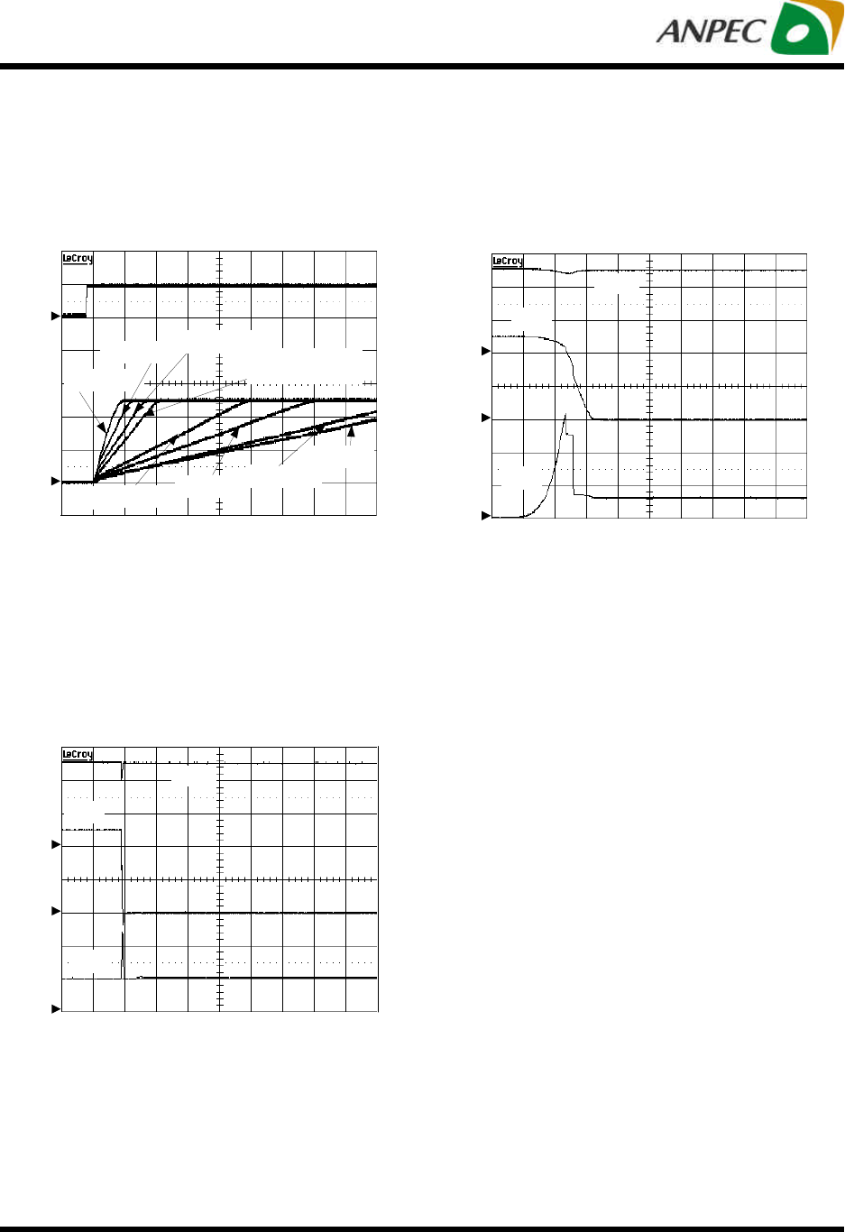
Operating Waveforms
The test condition is VIN=5V, TA= 25oC unless otherwise specified.
Power OnPower Off
1
2
VIN
VOUT
3
IOUT
Turn On Response Turn Off Response
VIN
1
2
VOUT
3
IOUT
VOUT
VEN
1
2
3
IOUT
1VOUT
VIN
IOUT
2
3
TIME:5ms/Div
VIN =5V, RLOAD =30Ω,CIN =1µF/MLCC,
COUT =100µF/Electrolytic, SS open
CH1: VIN, 2V/Div, DC
CH2: VOUT, 2V/Div, DC
CH3: IOUT, 0.5A/Div, DC
TIME:20ms/Div
VIN =5V, RLOAD =30Ω,CIN =1µF/MLCC,
COUT =100µF/Electrolytic, SS open
CH1: VIN, 2V/Div, DC
CH2: VOUT, 2V/Div, DC
CH3: IOUT, 0.5A/Div, DC
TIME:0.5ms/Div
VIN =5V, RLOAD =30Ω,CIN =1µF/MLCC,
COUT =100µF/Electrolytic, SS open
CH1: VEN, 5V/Div, DC
CH2: VOUT, 2V/Div, DC
CH3: IOUT, 0.5A/Div, DC
TIME:1ms/Div
VIN =5V, RLOAD =30Ω,CIN =1µF/MLCC,
COUT =100µF/Electrolytic, SS open
CH1: VEN, 5V/Div, DC
CH2: VOUT, 2V/Div, DC
CH3: IOUT, 0.5A/Div, DC
Copyright ANPEC Electronics Corp.
Rev. A.6 - Aug., 2012
APL3512
www.anpec.com.tw9
Operating Waveforms (Cont.)
The test condition is VIN=5V, TA= 25oC unless otherwise specified.
Soft Start Ramp-up ControlCurrent Limit Response
CH1: VEN, 5V/Div, DC
CH2: VOUT, 2V/Div, DC
TIME: 0.5ms/Div
VIN =5V, RLOAD =30Ω, CIN =1µF/MLCC,
COUT=33µF/Electrolytic
Short Circuit Protection
CH1: VIN, 2V/Div, DC
TIME: 100µs/Div
VIN =5V, VOUT short to ground,
CIN =1µF/MLCC, COUT=33µF/Electrolytic
CH2: VOUT, 2V/Div, DC
CH3: IOUT, 20A/Div, DC
VEN
1
2
VOUT
CSS
=330pF
CSS
=560pF CSS
=unconnected
or SS tied to V IN
CSS
=2.2nF CSS
=3.3nF CSS
=4.4nF
CSS
=5.6nF
CSS
=820pF
1
2
3
VIN
VOUT
IOUT
1
2
3
VIN
VOUT
IOUT
CH1: VIN, 2V/Div, DC
CH2: VOUT, 2V/Div, DC
TIME: 2ms/Div
VIN =5V, CIN =1µF/MLCC,
COUT=33µF/Electrolytic
CH3: IOUT, 1A/Div, DC
Copyright ANPEC Electronics Corp.
Rev. A.6 - Aug., 2012
APL3512
www.anpec.com.tw10
Pin Description
PIN
NO.
SOT-23-5
SOP-8
TDFN2x2-6
NAME FUNCTION
1 8 6 VOUT Output Voltage Pin. The output voltage follows the input voltage. When ENB is
high or EN is low the output voltage is discharged by an internal resistor.
2 3 3 GND Ground
EN
(APL3512A) Enable Input. Pull this pin to high to enable the device and pull this pin to low to
disable device. The EN pin cannot be left floating.
3 6 4 ENB
(APL3512B) Enable Input. Pull this pin to high to disable the device and pull this pin to low to
enable device. The ENB pin cannot be left floating.
4 2 2 SS Soft-Start Control Pin. Connect a capacitor to GND to control the soft-
tart rate. If
the SS pin is left floating or tied to VIN the soft-tart time is 2ms when VIN=5V.
5 1 1 VIN Power Supply Input. Connect this pin to external DC supply.
- 4, 5, 7
5 NC Internally not connected.
Block Diagram
Gate Driver and
Control Logic
UVLO
VIN VOUT
Charge
Pump
SS
EN/
ENB
OTP
GND
Current
-Limit
Soft-Start
Copyright ANPEC Electronics Corp.
Rev. A.6 - Aug., 2012
APL3512
www.anpec.com.tw11
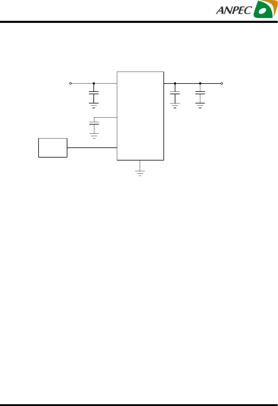
Typical Application Circuit
VIN VOUT
GND
APL3512A/B
SS
EN/ENB
Controller
1µF10µF
10nF
VIN VOUT
0.1µF
COUT
CIN
CSS
CBY

Copyright ANPEC Electronics Corp.
Rev. A.6 - Aug., 2012
APL3512
www.anpec.com.tw12
Function Description
VIN Under-Voltage Lockout (UVLO)
The APL3512A/B power switch is built-in an under-volt-
age lockout circuit to keep the output shut off until internal
circuitry is operating properly. The UVLO circuit has hys-
teresis and a de-glitch feature so that it will typically ig-
nore undershoot transients on the input. When input volt-
age exceeds the UVLO threshold, the output voltage starts
a soft-start to reduce the inrush current.
Power Switch
The power switch is an N-channel MOSFET with a low
RDS(ON). The internal power MOSFET does not have the
body diode. When IC is off, the MOSFET prevents a cur-
rent flowing from the VOUT back to VIN and VIN to VOUT.
Current-Limit Protection
The APL3512A/B power switch provides the current-limit
protection function. During current-limit, the devices limit
output current at current-limit threshold. For reliable
operation, the device should not be operated in current-
limit for extended period.
Short-Circuit Protection
When the output voltage drops below VIN-1.5V, which is
caused by the over load or short-circuit, the devices limit
the output current down to a safe level. The short circuit
current-limit is used to reduce the power dissipation dur-
ing short-circuit condition. If the junction temperature is
over the thermal shutdown temperature, the device will
enter the thermal shutdown.
Soft-Start
The APLA3512A/B provides an adjustable soft-start cir-
cuitry to control rise rate of the output voltage and limit the
current surge during start-up. The soft-start ramp-up rate
is controlled by a capacitor from SS pin to the ground.
Under a specific VIN being applied to the APL3512A/B, the
soft start time can be calculated by the following equation:
tSS = 0.2 x CSS x VIN
where,
tSS is soft-start time of VOUT rising from 0 to 100%, of which
unit is second.
CSS is the value of the capacitor connected from SS pin to
GND, of which unit is micro-Farad.
VIN is the amplitude of input voltage applied to this device,
of which unit is volt.
If the CSS is not connected or SS pin is tied to VIN, the soft-
start time is 2ms when VIN=5V.
Enable/Disable
Pull the ENB above 2V, or EN below 0.8V to disable the
device and pull ENB pin below 0.8V or EN above 2V to
enable the device. When the IC is disabled, the supply
current is reduced to less than 1µA. The enable input is
compatible with both TTL and CMOS logic levels. The
EN/ENB pins cannot be left floating.
Over-Temperature Protection
When the junction temperature exceeds 140oC, the inter-
nal thermal sense circuit turns off the power FET and
allows the device to cool down. When the device’s junc-
tion temperature cools by 20oC, the internal thermal
sense circuit will enable the device, resulting in a pulsed
output during continuous thermal protection. Thermal
protection is designed to protect the IC in the event of
over-temperature conditions. For normal operation, the
junction temperature cannot exceed TJ=+125oC.
Copyright ANPEC Electronics Corp.
Rev. A.6 - Aug., 2012
APL3512
www.anpec.com.tw13
Application Information
Input Capacitor
A 1µF ceramic bypass capacitor from VIN to GND, located
near the APL3512, is strongly recommended to suppress
the ringing during short-circuit fault event. Without the by-
pass capacitor, the output short may cause sufficient ring-
ing on the input (from supply lead inductance) to damage
internal control circuitry.
Output Capacitor
A low-ESR 10µF MLCC, aluminum electrolytic or tanta-
lum between VOUT and GND is strongly recommended
to reduce the voltage droop during hot-attachment of
downstream peripheral. Higher-value output capacitor is
better when the output load is heavy. Additionally, bypass-
ing the output with a 0.1µF ceramic capacitor improves
the immunity of the device to short-circuit transients.
Layout Consideration
The PCB layout should be carefully performed to maxi-
mize thermal dissipation and to minimize voltage drop,
droop and EMI. The following guidelines must be
considered:
1. Please place the input capacitors near the VIN pin as
close as possible.
2. Output decoupling capacitors for load must be placed
near the load as close as possible for decoupling high-
frequency ripples.
3. Locate APL3512 and output capacitors near the load to
reduce parasitic resistance and inductance for excel-
lent load transient performance.
4. The negative pins of the input and output capacitors
and the GND pin must be connected to the ground plane
of the load.
5. Keep VIN and VOUT traces as wide and short as possible.
During soft-start process, the output bulk capacitor draws
inrush current from VIN. If the inrush current reaches
foldback current-limit threshold, namely 0.8A, the output
current will be clamped in 0.8A level. It will take longer to
complete the soft-start process since the soft-start rate
is controlled neither by internal soft-start nor by external
soft-start circuitry. When the COUT meets the following
formula, the soft-start will be controlled by foldback cur-
rent-limiting:
COUT > (0.8xtSS)/VIN
Where,
tSS is 1ms when SS is open or tied to VIN, or obtained by
the tss equation, described in the paragraph of Soft-Start
in Functional Description section when CSS is used.
If the soft-start rate is controlled by the foldback current-
limiting, the soft-start time can be got by the following
equation:
tSS_Foldback = (COUT x VIN)/0.8
Soft-Start Capacitor
The APL3512 has a built-in adjustable soft-start control
for user to set an optimum soft-start time for the app-
lication. The soft-start time can be calculated by the
equation, described in the paragraph of Soft-Start in Func-
tional Description section. Please note that there are mini-
mum and maximum limitations of soft-start capacitor. If
the value of soft-start capacitor is less than the minimum
limitation or higher than the maximum limitation (please
refer to the Recommended Operating Conditions), the
soft-start time will become internally controlled as if there
is no CSS, tSS=2ms when VIN=5V, for example. If a soft-
start capacitor is used, please make sure the CSS is in the
recommeded operating range.
0.05
0.02
0.1
0.037
0.075
Unit : Inch
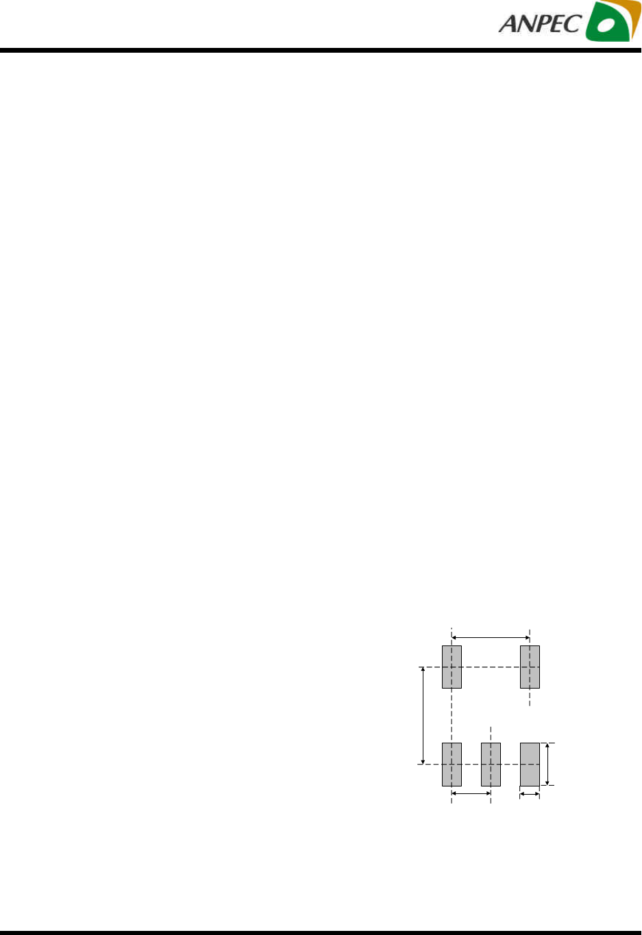
Recommended Minimum Footprint
SOT-23-5
Copyright ANPEC Electronics Corp.
Rev. A.6 - Aug., 2012
APL3512
www.anpec.com.tw14
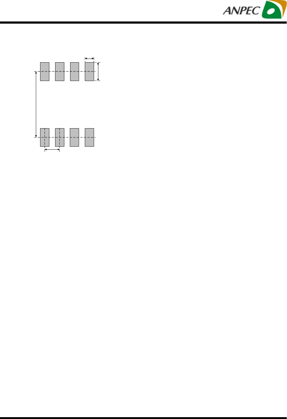
Recommended Minimum Footprint
SOP-8
6.0
1.3
1.27
0.5
1234
8765
Unit : mm
Copyright ANPEC Electronics Corp.
Rev. A.6 - Aug., 2012
APL3512
www.anpec.com.tw15
Package Information
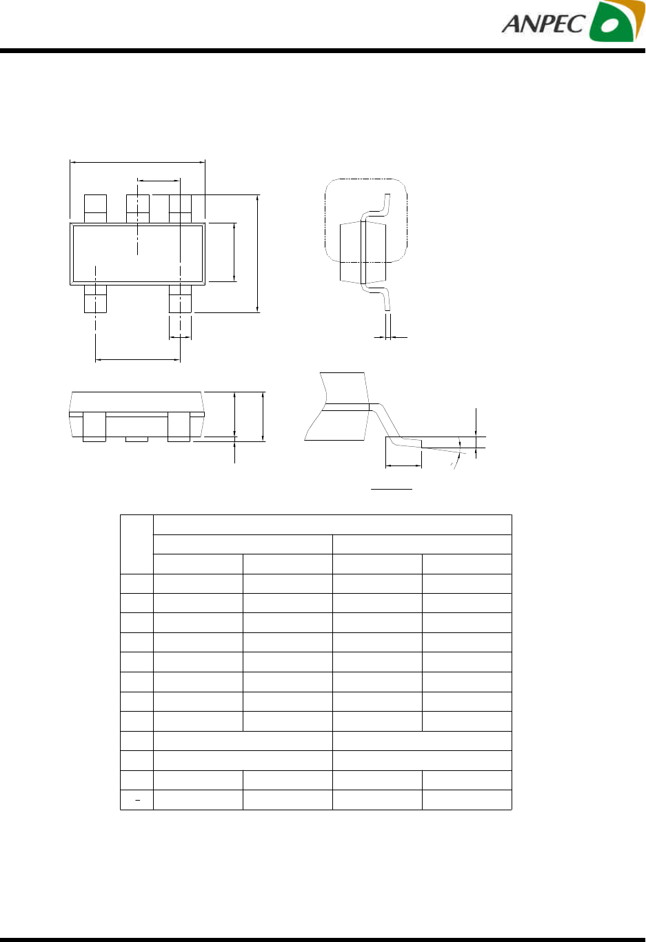
SOT-23-5
MAX.
0.057
0.051
0.024
0.006
0.009
0.0200.012
L0.30
0
e
e1
E1
E
D
c
b
0.08
0.30
0.60 0.012
0.95 BSC
1.90 BSC
0.22
0.50
0.037 BSC
0.075 BSC
0.003
MIN.
MILLIMETERS
S
Y
M
B
O
L
A1
A2
A
0.00
0.90
SOT-23-5
MAX.
1.45
0.15
1.30
MIN.
0.000
0.035
INCHES
°
8
°
0
°
8
°
0
bc
e1
0
L
VIEW A
0.25
GAUGE PLANE
SEATING PLANE
A
A2A1
e
D
E
E1
SEE
VIEW A
1.40
2.60
1.80
3.00
2.70 3.10 0.122
0.071
0.1180.102
0.055
0.106
Note : 1. Follow JEDEC TO-178 AA.
2. Dimension D and E1 do not include mold flash, protrusions or gate
burrs. Mold flash, protrusion or gate burrs shall not exceed 10 mil
per side.
Copyright ANPEC Electronics Corp.
Rev. A.6 - Aug., 2012
APL3512
www.anpec.com.tw16
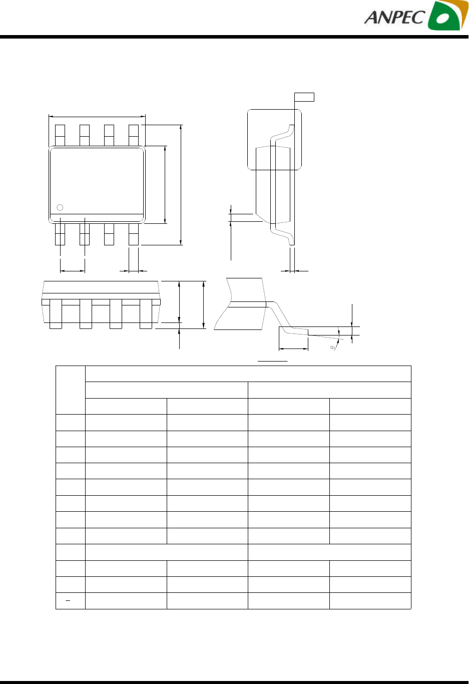
Package Information
SOP-8
A
A1A2
L
VIEW A
0.25
SEATING PLANE
GAUGE PLANE
Note: 1. Follow JEDEC MS-012 AA.
2. Dimension “D” does not include mold flash, protrusions or gate burrs.
Mold flash, protrusion or gate burrs shall not exceed 6 mil per side.
3. Dimension “E” does not include inter-lead flash or protrusions.
Inter-lead flash and protrusions shall not exceed 10 mil per side.
S
Y
M
B
O
LMIN. MAX.
1.75
0.10
0.17 0.25
0.25
A
A1
c
D
E
E1
e
h
L
MILLIMETERS
b0.31 0.51
SOP-8
0.25 0.50
0.40 1.27
MIN. MAX.
INCHES
0.069
0.004
0.012 0.020
0.007 0.010
0.010 0.020
0.016 0.050
0
0.010
1.27 BSC 0.050 BSC
A2 1.25 0.049
0
°
8
°
0
°
8
°
3.80
5.80
4.80
4.00
6.20
5.00 0.189 0.197
0.228 0.244
0.150 0.157
D
e
E
E1
SEE VIEW A
cb
h X 45
°
SEATING PLANE < 4 mils-T-
Copyright ANPEC Electronics Corp.
Rev. A.6 - Aug., 2012
APL3512
www.anpec.com.tw17
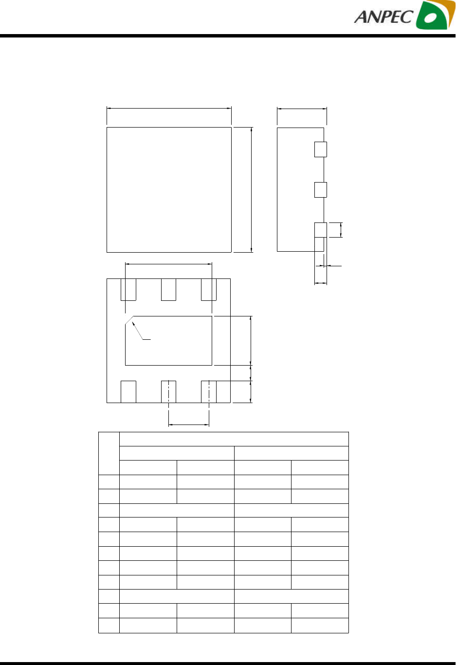
Package Information
TDFN2x2-6
S
Y
M
B
O
LMIN. MAX.
0.80
0.00
0.18 0.30
1.00 1.60
0.05
0.60
A
A1
b
D
D2
E
E2
e
L
MILLIMETERS
A3 0.20 REF
TDFN2x2-6
0.30 0.45
1.00
0.008 REF
MIN. MAX.
INCHES
0.031
0.000
0.007 0.012
0.039 0.063
0.024
0.012 0.018
1.90 2.10 0.075 0.083
1.90 2.10 0.075 0.083
0.20K0.008
0.70
0.039
0.028
0.002
0.65 BSC 0.026 BSC
Note : 1. Followed from JEDEC MO-229 WCCC.
e
LKE2
Pin 1 Corner
D2
A3
A1
b
AD
E
Copyright ANPEC Electronics Corp.
Rev. A.6 - Aug., 2012
APL3512
www.anpec.com.tw18
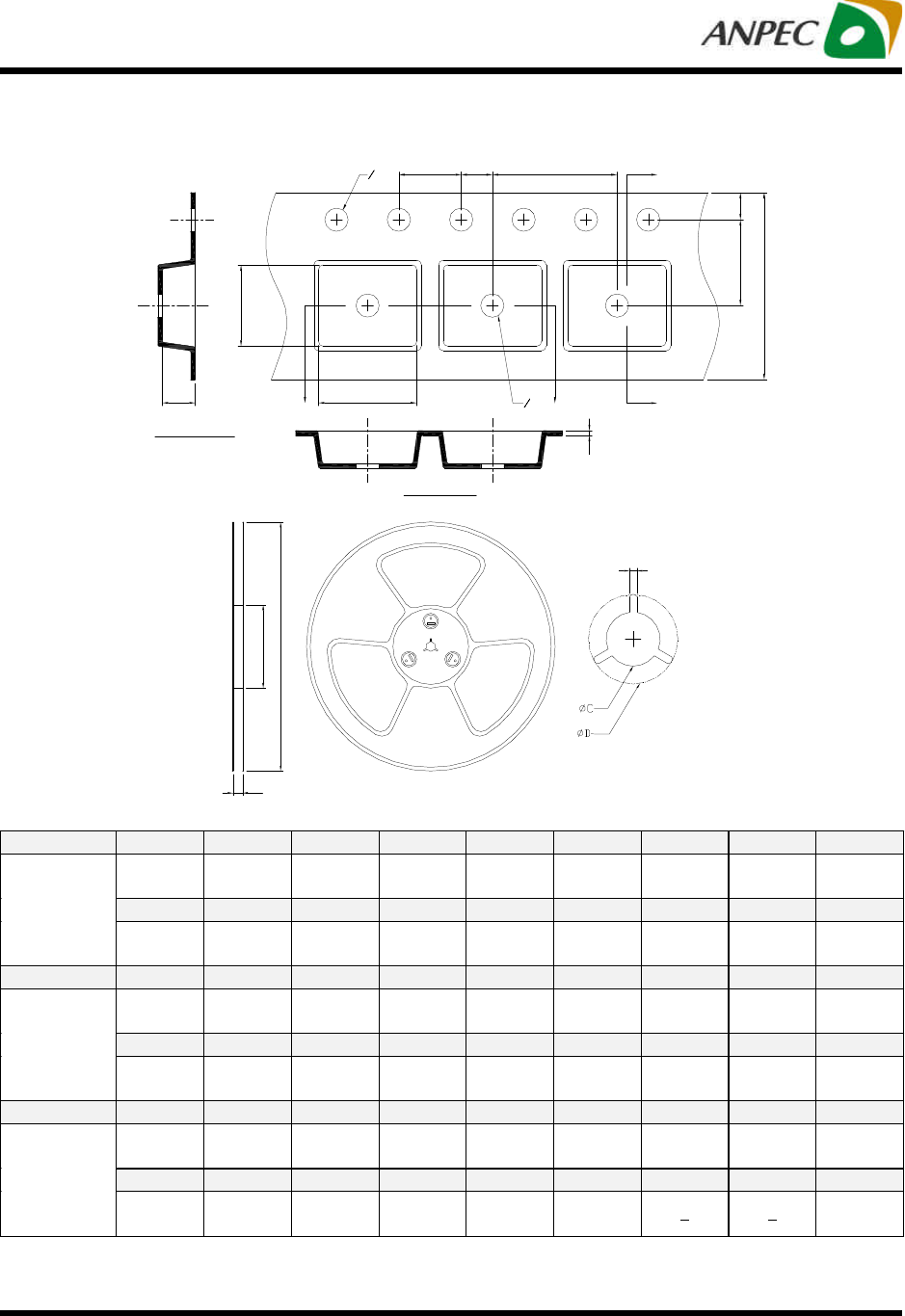
Carrier Tape & Reel Dimensions
A
E1
A
B
W
F
T
P0
OD0
BA0
P2
K0
B0
SECTION B-B
SECTION A-A
OD1
P1
H
T1
A
d
Application
A H T1 C d D W E1 F
178.0±2.00
50 MIN.
8.4+2.00
-0.00
13.0+0.50
-0.20
1.5 MIN.
20.2 MIN.
8.0±0.30
1.75±0.10
3.5±0.05
P0 P1 P2 D0 D1 T A0 B0 K0
SOT-23-5
4.0±0.10
4.0±0.10
2.0±0.05
1.5+0.10
-0.00
1.0 MIN.
0.6+0.00
-0.40
3.20±0.20
3.10±0.20
1.50±0.20
Application
A H T1 C d D W E1 F
330.0±2.00
50 MIN.
12.4+2.00
-0.00
13.0+0.50
-0.20
1.5 MIN.
20.2 MIN.
12.0±0.30
1.75±0.10
5.5±0.05
P0 P1 P2 D0 D1 T A0 B0 K0
SOP-8
4.0±0.10
8.0±0.10
2.0±0.05
1.5+0.10
-0.00
1.5 MIN.
0.6+0.00
-0.40
6.40±0.20
5.20±0.20
2.10±0.20
Application
A H T1 C d D W E1 F
178.0±2.00
50 MIN.
8.4+2.00
-0.00
13.0+0.50
-0.20
1.5 MIN.
20.2 MIN.
12.0±0.30
1.75±0.10
5.5±0.05
P0 P1 P2 D0 D1 T A0 B0 K0
TDFN2x2-6
4.0±0.10
4.0±0.10
2.0±0.05
1.5+0.10
-0.00
1.5 MIN.
0.6+0.00
-0.40 2.35+0.20
2.35+0.20
1.30±0.20
(mm)
Copyright ANPEC Electronics Corp.
Rev. A.6 - Aug., 2012
APL3512
www.anpec.com.tw19
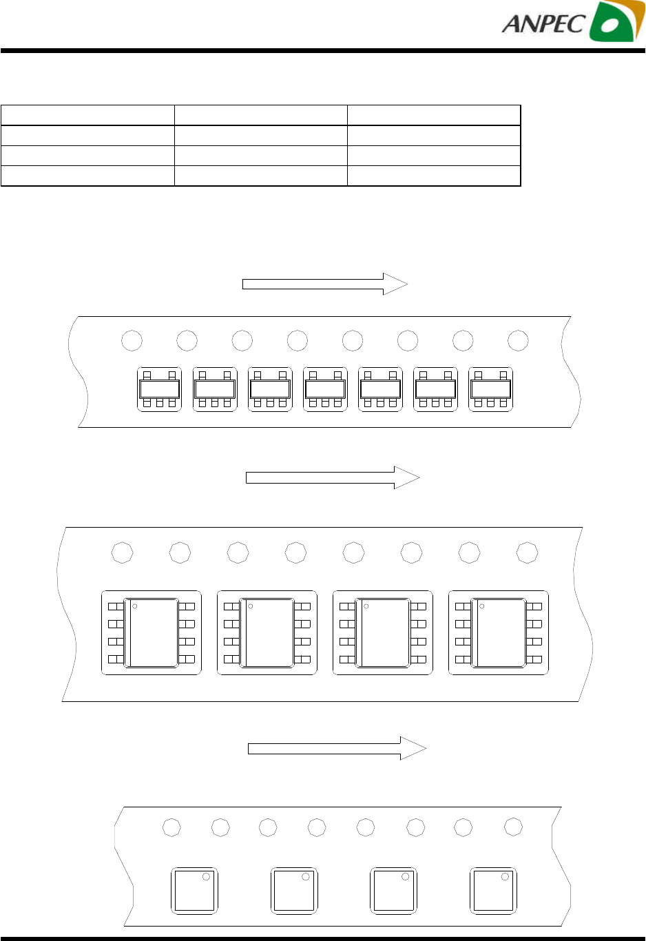
Taping Direction Information
SOT-23-5
USER DIRECTION OF FEED
SOP-8
USER DIRECTION OF FEED
Devices Per Unit
Package Type Unit Quantity
SOT-23-5 Tape & Reel 3000
SOP-8 Tape & Reel 2500
TQFN2x2-6 Tape & Reel 3000
TDFN2x2-6
USER DIRECTION OF FEED
Copyright ANPEC Electronics Corp.
Rev. A.6 - Aug., 2012
APL3512
www.anpec.com.tw20
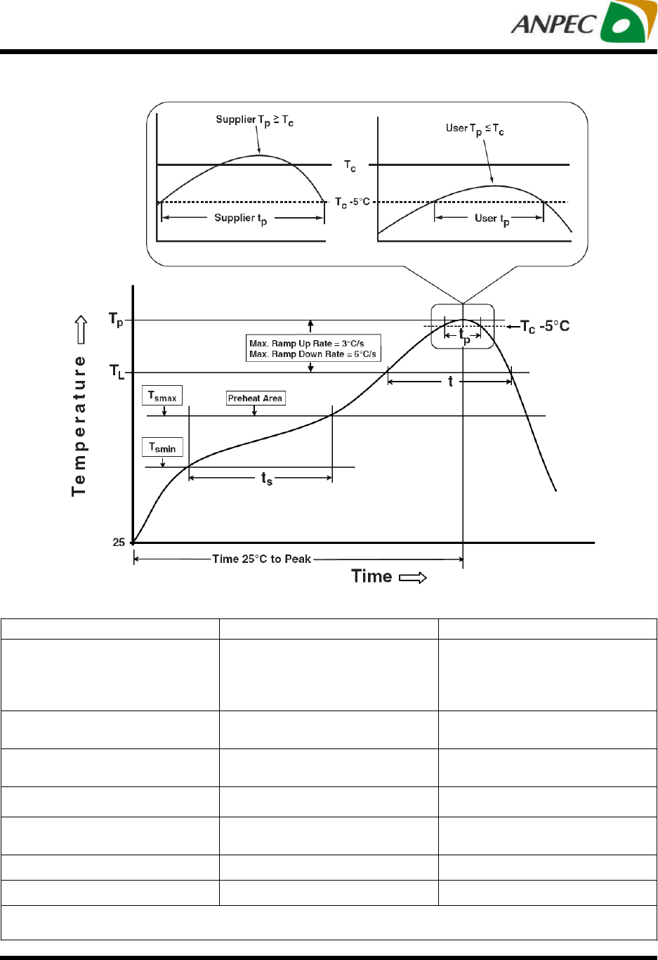
Classification Reflow Profiles
Profile Feature Sn-Pb Eutectic Assembly Pb-Free Assembly
Preheat & Soak
Temperature min (Tsmin)
Temperature max (Tsmax)
Time (Tsmin to Tsmax) (ts)
100 °C
150 °C
60-120 seconds
150 °C
200 °C
60-120 seconds
Average ramp-up rate
(Tsmax to TP) 3 °C/second max. 3°C/second max.
Liquidous temperature (TL)
Time at liquidous (tL) 183 °C
60-150 seconds 217 °C
60-150 seconds
Peak package body Temperature
(Tp)* See Classification Temp in table 1 See Classification Temp in table 2
Time (tP)** within 5°C of the specified
classification temperature (Tc) 20** seconds 30** seconds
Average ramp-down rate (Tp to Tsmax)
6 °C/second max. 6 °C/second max.
Time 25°C to peak temperature 6 minutes max. 8 minutes max.
* Tolerance for peak profile Temperature (Tp) is defined as a supplier minimum and a user maximum.
** Tolerance for time at peak profile temperature (tp) is defined as a supplier minimum and a user maximum.
Classification Profile
Copyright ANPEC Electronics Corp.
Rev. A.6 - Aug., 2012
APL3512
www.anpec.com.tw21
Customer Service
Anpec Electronics Corp.
Head Office :
No.6, Dusing 1st Road, SBIP,
Hsin-Chu, Taiwan, R.O.C.
Tel : 886-3-5642000
Fax : 886-3-5642050
Taipei Branch :
2F, No. 11, Lane 218, Sec 2 Jhongsing Rd.,
Sindian City, Taipei County 23146, Taiwan
Tel : 886-2-2910-3838
Fax : 886-2-2917-3838
Table 1. SnPb Eutectic Process – Classification Temperatures (Tc)
Package
Thickness
Volume mm3
<350
Volume mm3
≥350
<2.5 mm 235 °C 220 °C
≥2.5 mm 220 °C 220 °C
Table 2. Pb-free Process – Classification Temperatures (Tc)
Package
Thickness
Volume mm3
<350
Volume mm3
350-2000
Volume mm3
>2000
<1.6 mm 260 °C 260 °C 260 °C
1.6 mm – 2.5 mm 260 °C 250 °C 245 °C
≥2.5 mm 250 °C 245 °C 245 °C
Reliability Test Program
Test item Method Description
SOLDERABILITY JESD-22, B102 5 Sec, 245°C
HOLT JESD-22, A108 1000 Hrs, Bias @ Tj=125°C
PCT JESD-22, A102 168 Hrs, 100%RH, 2atm, 121°C
TCT JESD-22, A104 500 Cycles, -65°C~150°C
HBM MIL-STD-883-3015.7 VHBM≧2KV
MM JESD-22, A115 VMM≧200V
Latch-Up JESD 78 10ms, 1tr≧100mA
Classification Reflow Profiles (Cont.)

