Appendix A Appxa
User Manual: Appendix A DL305 Analog Manual
Open the PDF directly: View PDF ![]() .
.
Page Count: 19

1A
DL305
Data Types and
Memory Map
In This Chapter. . . .
Ċ DL330 Memory Map
Ċ DL330P Memory Map
Ċ DL340 Memory Map
Ċ I/O Point Bit Map
Ċ Control Relay Bit Map
Ċ Special Relays
Ċ Data Registers
Appendix A
Data Types & Mem. Map
Appendix E
DL305 Memory Map
A–2 DL305 Data Types and Memory Map
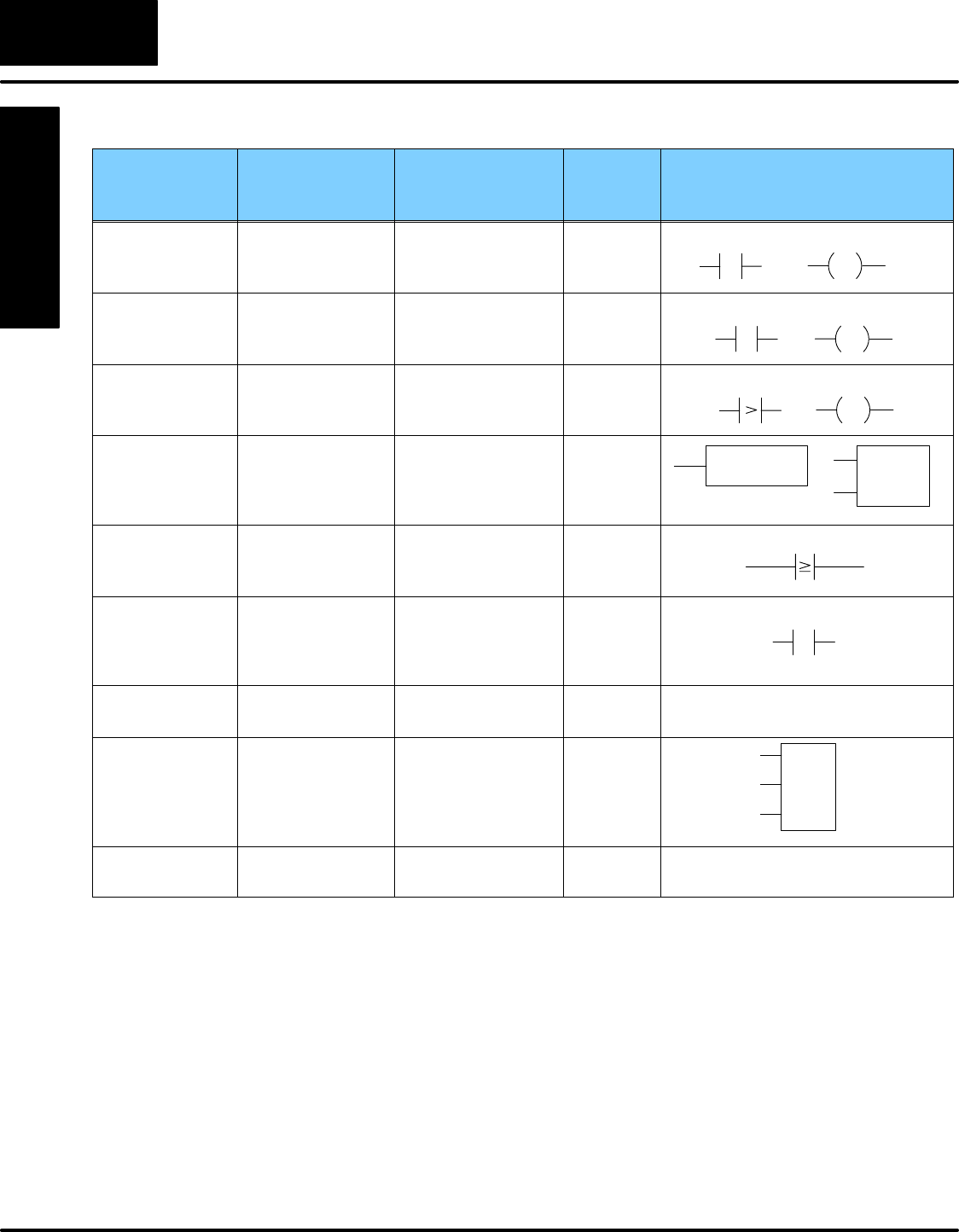
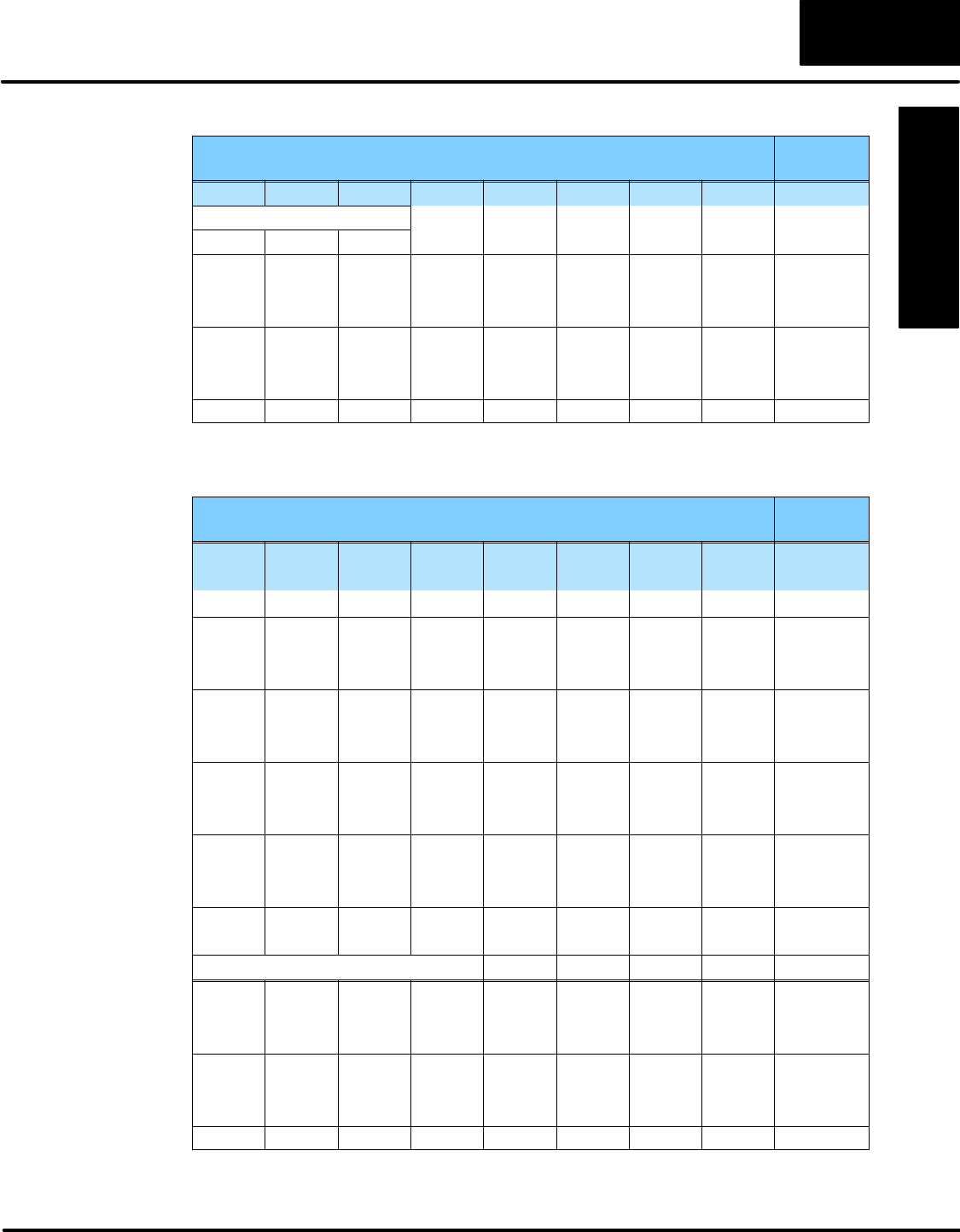
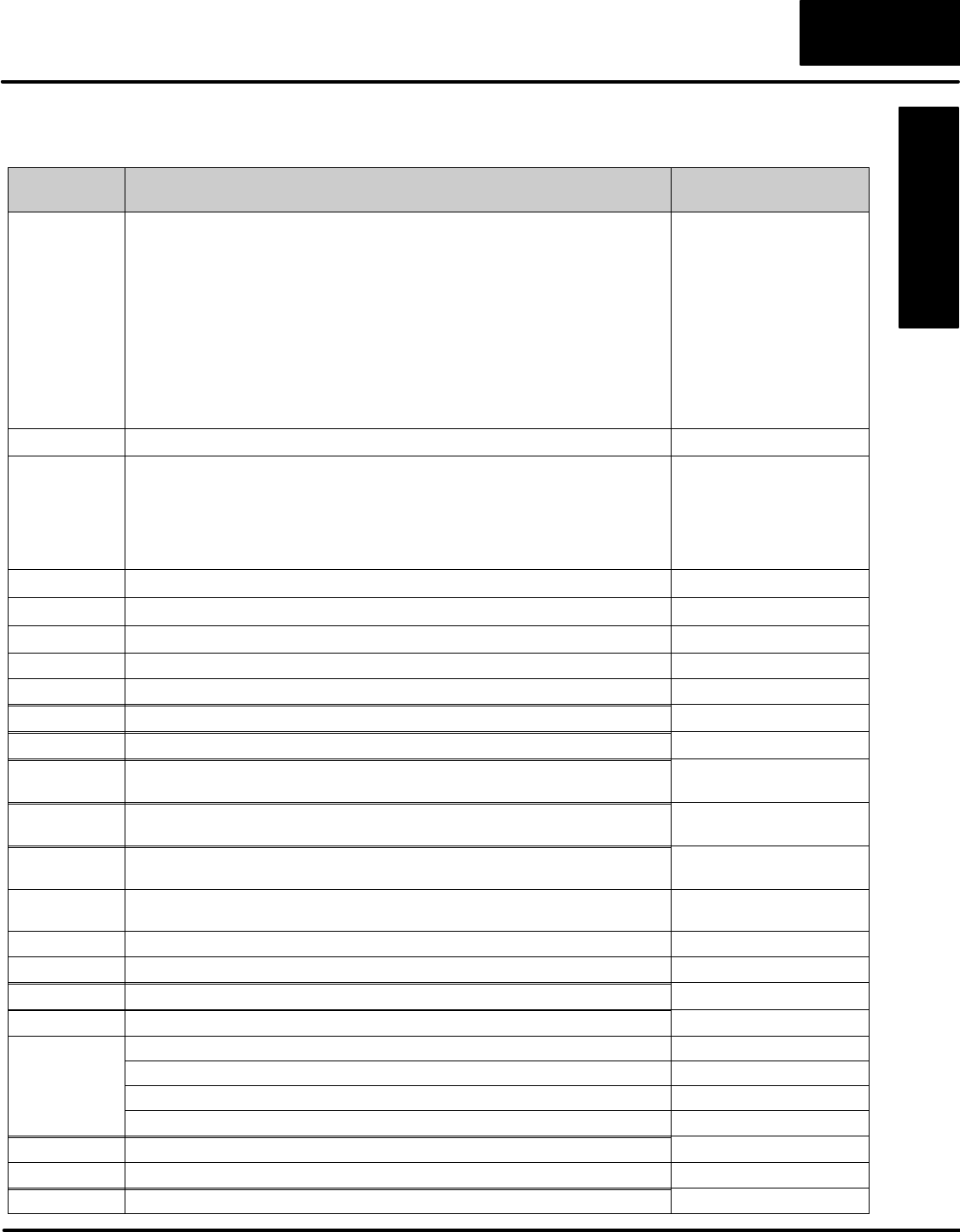
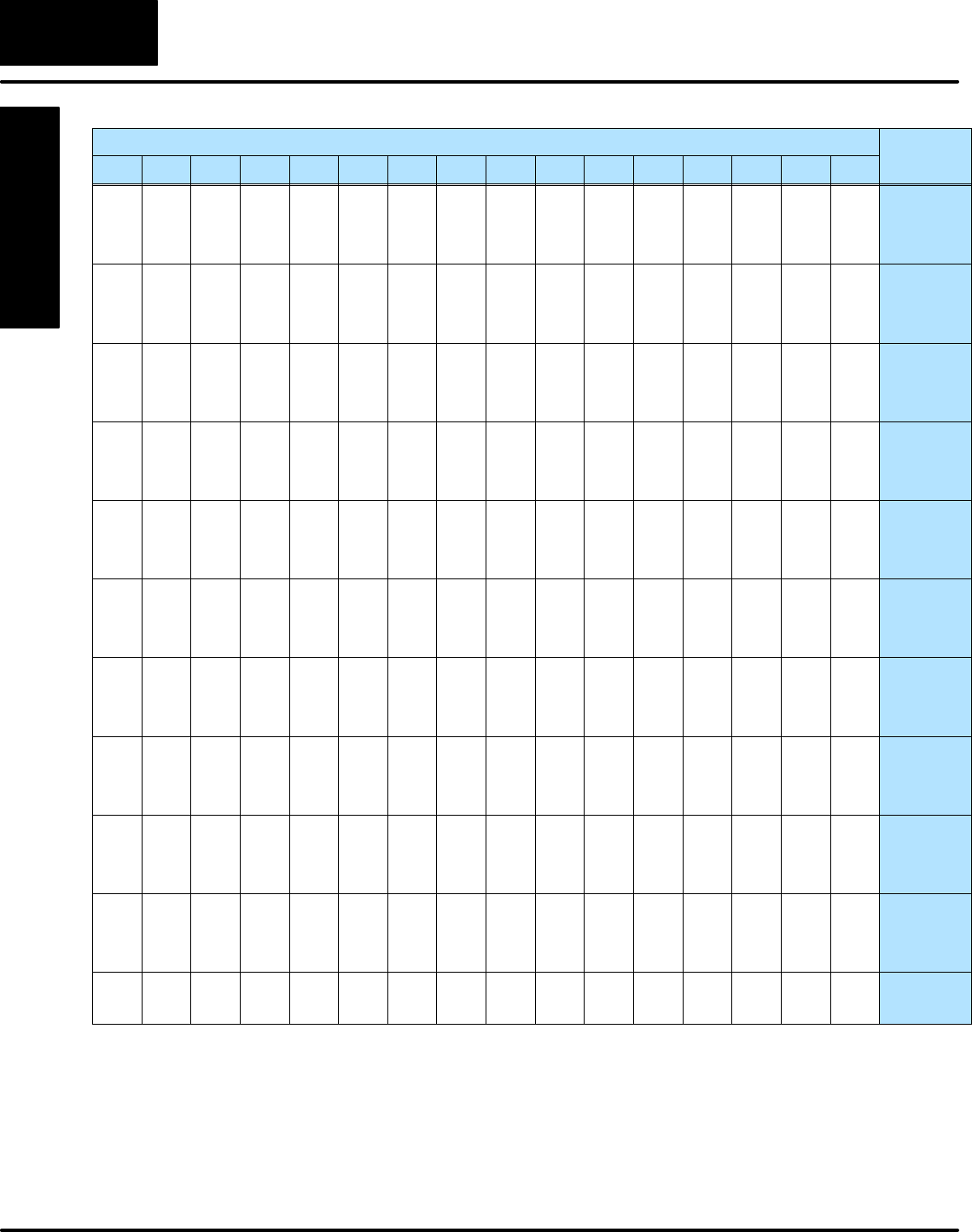
DL330 Memory Map
Memory Type Discrete Memory
Reference
(octal)
Register Memory
Reference
(octal)
Qty.
Decimal Symbol
Input / Output
Points 000 – 157
700 – 767 R000 – R015
R070 – R076 168 Total
Control Relays 160 – 373 R016 – R037 140
Special Relays 374 – 377
770 – 777 R037
R077 12
Timers /
Counters 600 – 673
674 – 677* None 64
Timer / Counter
Current Values None R600 – R673
R674 – R677* 64
Timer / Counter
Status Bits T600 – T673
T674 – T677* None 64
Data Words None R400 – R563 116 None specific, used with many
instructions
Shift Registers 400 – 577 None 128
Special
Registers None R574 – R577 4R574 – R575 used with FAULT
R576 – R577 Auxiliary Accumulator
* T/ C Setpoint Unit Only. Can be used as data registers if the Timer/Counter Setpoint Unit or Thumbwheel Interface Module is not used. R564 – R573 contain the preset value used with the Timer /
Counter Setpoint Unit. R674 – R677 contain the current values for these timers or counters.
000 010
C0C0
772 376
TMR T600
K100 CNT C600
K10
R600 K100
T600
SR
400
417
Appendix A
Data Types & Mem. Map Appendix E
DL305 Memory Map
A–3
DL305 Data Types and Memory Map
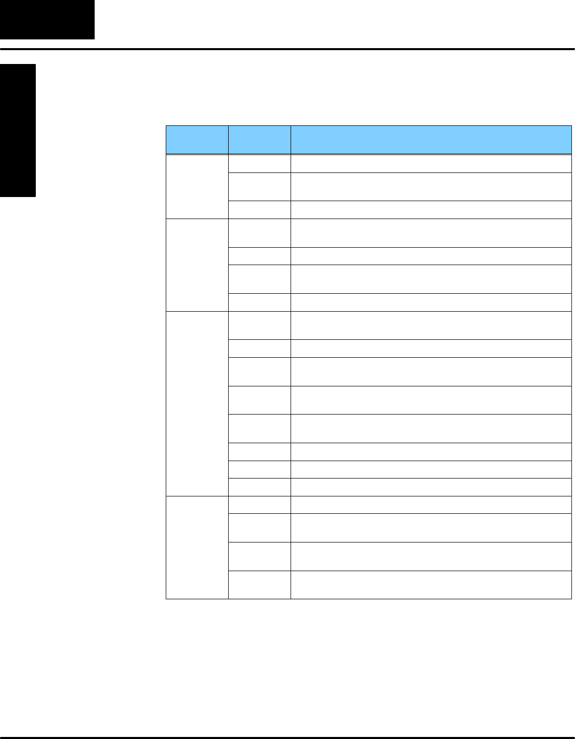
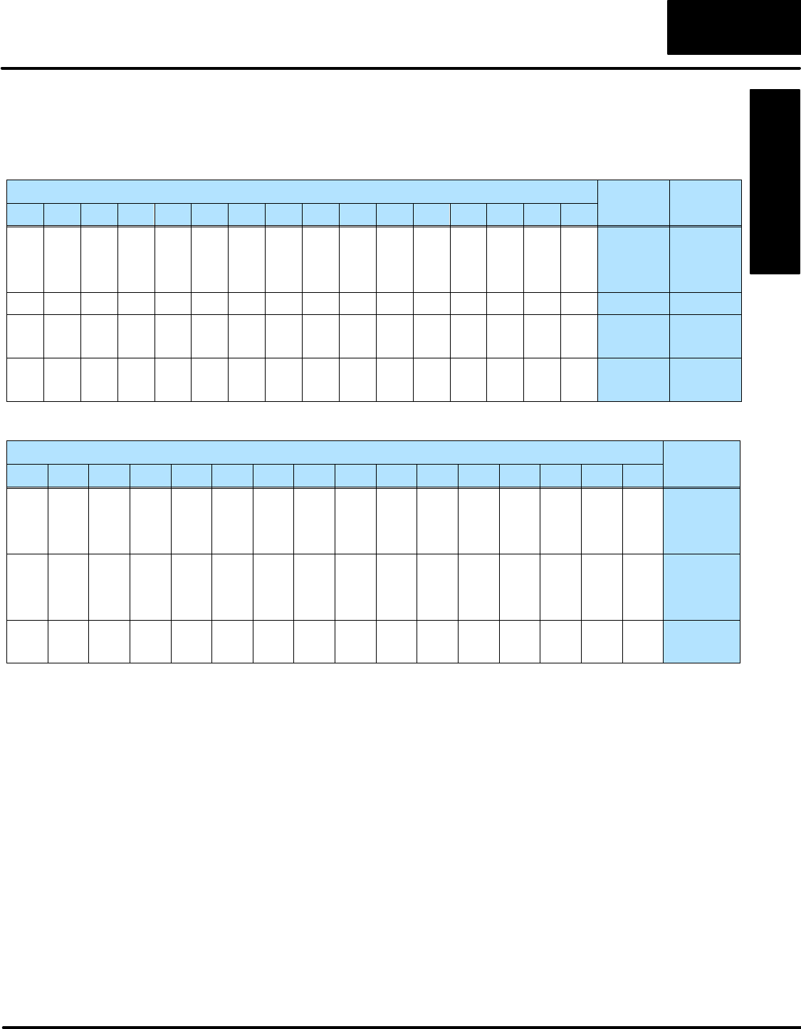
DL330P Memory Map
Memory Type Discrete Memory
Reference
(octal)
Register Memory
Reference
(octal)
Qty.
Decimal Symbol
Input / Output
Points 000 – 157
700 – 767 R000 – R015
R070 – R076 168 Total
Control Relays 160 – 174
200 – 277 R016 – R017
R020 – R027 77
Special Relays 175 – 177
770 – 777 R017
R077 11
Timers /
Counters 600 – 673
674 – 677* None 64
Timer / Counter
Current Values None R600 – R673
R674 – R677* 64
Timer / Counter
Status Bits T600 – T673
T674 – T677* None 64
Data Words None R400 – R563 116 None specific, used with many
instructions
Stages S0 – S177 R100 – R117 128
Special
Registers None R574 – R577 4R574 – R575 used with FAULT
R576 – R577 Auxiliary Accumulator
* T/ C Setpoint Unit Only. Can be used as data registers if the Timer/Counter Setpoint Unit or Thumbwheel Interface Module is not used, which provides a total of 128 data registers.
R564 – R573 contain the preset value used with the Timer / Counter Setpoint Unit. R674 – R677 contain the current values for these timers or counters.
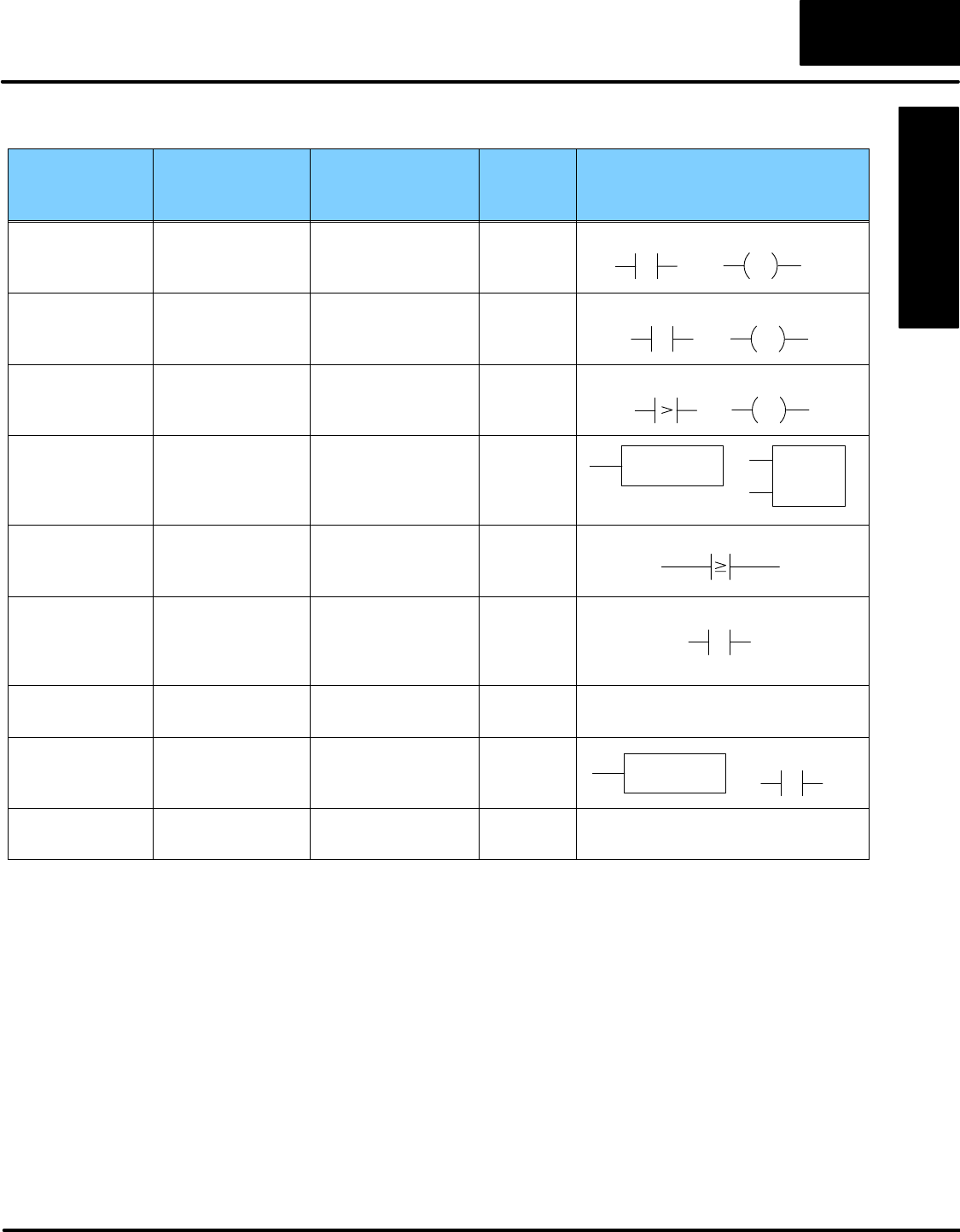
000 010
C0C0
772 176
TMR T600
K100 CNT C600
K10
R600 K100
T600
SG S 001
S1

Appendix A
Data Types & Mem. Map
Appendix E
DL305 Memory Map
A–4 DL305 Data Types and Memory Map
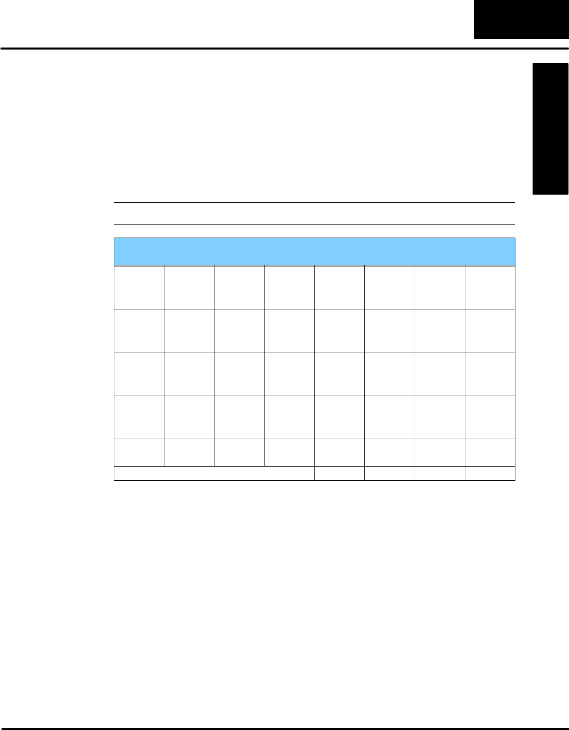
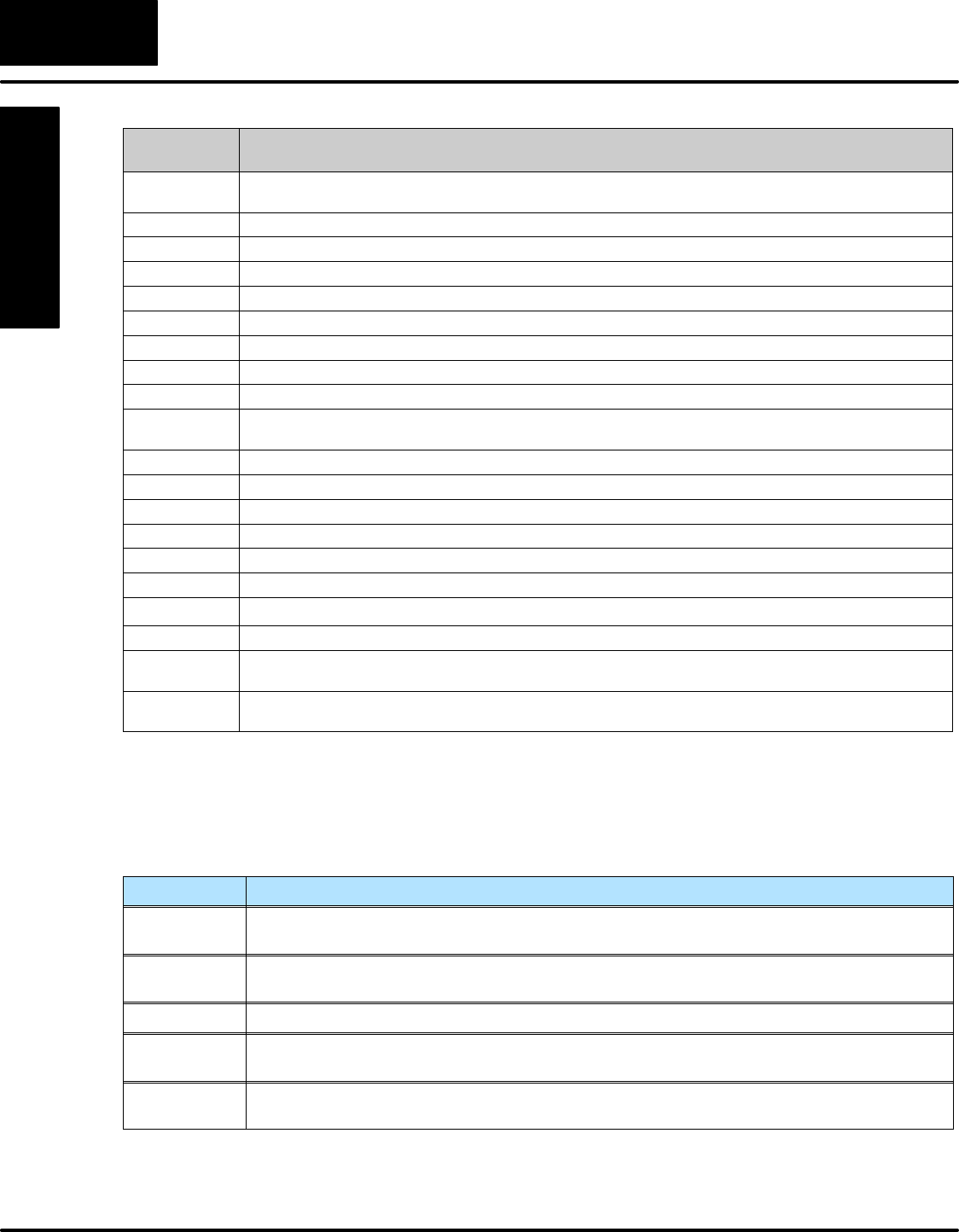
DL340 Memory Map
Memory Type Discrete Memory
Reference
(octal)
Register Memory
Reference
(octal)
Qty.
Decimal Symbol
Input / Output
Points 000 – 157
700 – 767 R000 – R015
R070 – R076 168 Total
Control Relays 160 – 373
1000 – 1067 R016 – R037
R100 – R106 180
Special Relays 374 – 377
770 – 777
1070 – 1077
R037
R077
R107
20
Timers /
Counters 600 – 673
674 – 677* None 64
Timer / Counter
Current Values None R600 – R673
R674 – R677* 64
Timer / Counter
Status Bits T600 – T673
T674 – T677* None 64
Data Words None R400 – R563
R700 – R767 172 None specific, used with many
instructions
Shift Registers 400 – 577 None 128
Special
Registers None R574 – R577
R770 – R777 12 R574–R575 used with FAULT
R576–R577 Auxiliary Accumulator
R770–R777 Communications Setup
* T/ C Setpoint Unit Only. Can be used as data registers if the Timer/Counter Setpoint Unit or Thumbwheel Interface Module is not used. R564 – R573 contain the preset value used with the Timer /
Counter Setpoint Unit. R674 – R677 contain the current values for these timers or counters.
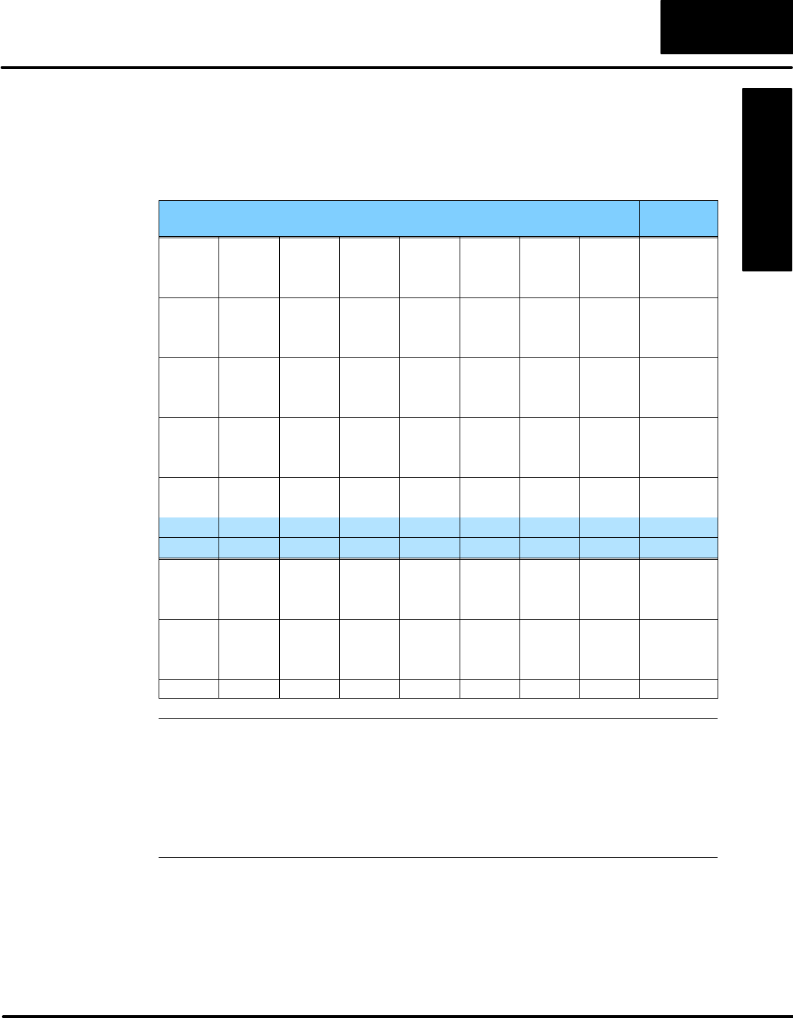
000 010
C0C0
772 376
TMR T600
K100 CNT C600
K10
R600 K100
T600
SR
400
417
Appendix A
Data Types & Mem. Map Appendix E
DL305 Memory Map
A–5
DL305 Data Types and Memory Map
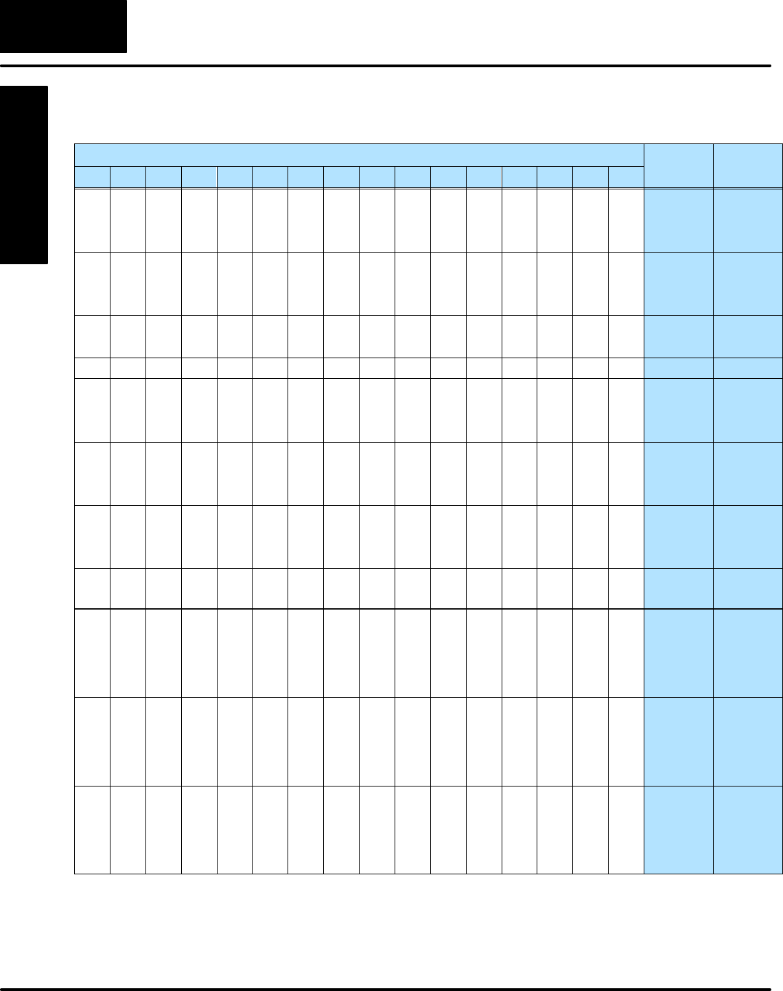
I/O Point Bit Map
These tables provide a listing of the individual Input points associated with each
register location for the DL330, DL330P, and DL340 CPUs.
MSB I/O References LSB Register
Number
007 006 005 004 003 002 001 000 R0
017 016 015 014 013 012 011 010 R1
027 026 025 024 023 022 021 020 R2
037 036 035 034 033 032 031 030 R3
047 046 045 044 043 042 041 040 R4
057 056 055 054 053 052 051 050 R5
067 066 065 064 063 062 061 060 R6
077 076 075 074 073 072 071 070 R7
107 106 105 104 103 102 101 100 R10
117 116 115 114 113 112 111 110 R11
127 126 125 124 123 122 121 120 R12
137 136 135 134 133 132 131 130 R13
147 146 145 144 143 142 141 140 R14
157 156 155 154 153 152 151 150 R15
167 166 165 164 163 162 161 160 n/a
177 176 175 174 173 172 171 170 n/a
707 706 705 704 703 702 701 700 R70
717 716 715 714 713 712 711 710 R71
727 726 725 724 723 722 721 720 R72
737 736 735 734 733 732 731 730 R73
747 746 745 744 743 742 741 740 R74
757 756 755 754 753 752 751 750 R75
767 766 765 764 763 762 761 760 R76
NOTE: 160 – 167 can be used as I/O in a DL330 or DL330P CPU under certain
conditions. 160 – 177 can be used as I/O in a DL340 CPU under certain conditions.
You should consult the DL305 User Manual to determine which configurations allow
the use of these points.
These points are normally used as control relays. You cannot use them as both
control relays and as I/O points. Also, if you use these points as I/O, you cannot
access these I/O points as a Data Register reference.
Appendix A
Data Types & Mem. Map
Appendix E
DL305 Memory Map
A–6 DL305 Data Types and Memory Map
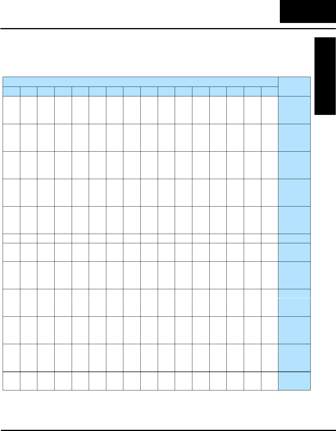
Control Relay Bit Map
The following tables provide a listing of the individual control relays associated with
each register location for the DL305 CPUs.
NOTE: 160 – 167 can be used as I/O in a DL330 or DL330P CPU under certain
conditions. 160 – 177 can be used as I/O in a DL340 CPU under certain conditions.
You should consult the DL305 User Manual to determine which configurations allow
the use of these points.
You cannot use them as both control relays and as I/O points. Also, if you use these
points as I/O, you cannot access these I/O points as a Data Register reference.
MSB DL330
Control Relay References LSB Register
Number
167 166 165 164 163 162 161 160 R16
177 176 175 174 173 172 171 170 R17
207 206 205 204 203 202 201 200 R20
217 216 215 214 213 212 211 210 R21
227 226 225 224 223 222 221 220 R22
237 236 235 234 233 232 231 230 R23
247 246 245 244 243 242 241 240 R24
257 256 255 254 253 252 251 250 R25
267 266 265 264 263 262 261 260 R26
277 276 275 274 273 272 271 270 R27
307 306 305 304 303 302 301 300 R30
317 316 315 314 313 312 311 310 R31
327 326 325 324 323 322 321 320 R32
337 336 335 334 333 332 331 330 R33
347 346 345 344 343 342 341 340 R34
357 356 355 354 353 352 351 350 R35
367 366 365 364 363 362 361 360 R36
373 372 371 370 R37
* Control relays 340 – 373 can be made retentive by setting a CPU dipswitch. See the DL305 User Manual for details
on setting CPU dipswitches.
Appendix A
Data Types & Mem. Map Appendix E
DL305 Memory Map
A–7
DL305 Data Types and Memory Map
MSB DL330P
Control Relay References LSB Register
Number
167 166 165 164 163 162 161 160 R16
174 173 172 171 170 R17
207 206 205 204 203 202 201 200* R20
217 216 215 214 213 212 211 210 R21
227 226 225 224 223 222 221 220 R22
237 236 235 234 233 232 231 230 R23
247 246 245 244 243 242 241 240 R24
257 256 255 254 253 252 251 250 R25
267 266 265 264 263 262 261 260 R26
277* 276 275 274 273 272 271 270 R27
* Control relays 200 – 277 can be made retentive by setting a CPU dipswitch. See the DL305 User Manual for details on setting CPU dipswitches.
MSB DL340
Control Relay References LSB Register
Number
167 166 165 164 163 162 161 160 R16
177 176 175 174 173 172 171 170 R17
207 206 205 204 203 202 201 200 R20
217 216 215 214 213 212 211 210 R21
227 226 225 224 223 222 221 220 R22
237 236 235 234 233 232 231 230 R23
247 246 245 244 243 242 241 240 R24
257 256 255 254 253 252 251 250 R25
267 266 265 264 263 262 261 260 R26
277 276 275 274 273 272 271 270 R27
307 306 305 304 303 302 301 300 R30
317 316 315 314 313 312 311 310 R31
327 326 325 324 323 322 321 320 R32
337 336 335 334 333 332 331 330 R33
347 346 345 344 343 342 341 340* R34
357 356 355 354 353 352 351 350 R35
367 366 365 364 363 362 361 360 R36
373* 372 371 370 R37
1007 1006 1005 1004 1003 1002 1001 1000 R100
1017 1016 1015 1014 1013 1012 1011 1010 R101
1027 1026 1025 1024 1023 1022 1021 1020 R102
1037 1036 1035 1034 1033 1032 1031 1030 R103
1047 1046 1045 1044 1043 1042 1041 1040 R104
1057 1056 1055 1054 1053 1052 1051 1050 R105
1067 1066 1065 1064 1063 1062 1061 1060 R106
* Control relays 340 – 373 can be made retentive by setting a CPU dipswitch. See the DL305 User Manual for details
on setting CPU dipswitches.
Appendix A
Data Types & Mem. Map
Appendix E
DL305 Memory Map
A–8 DL305 Data Types and Memory Map
Special Relays
The following table shows the Special Relays used with the DL305 CPUs.
CPUs Special
Relay Description of Contents
175 100 ms clock, on for 50 ms and off for 50 ms.
DL330P 176 Disables all outputs except for those entered with the SET
OUT instruction.
177 Battery voltage is low.
374 On for the first scan cycle after the CPU is switched to Run
Mode.
DL330 375 100 ms clock, on for 50 ms and off for 50 ms.
DL330
DL340 376 Disables all outputs except for those entered with the SET
OUT instruction.
377 Battery voltage is low.
770 Changes timers to 0.01 second intervals. Timers are
normally 0.1 second time intervals.
771 The external diagnostics FAULT instruction (F20) is in use.
772 The data in the accumulator is greater than the comparison
value.
DL330
DL330P
DL340
773 The data in the accumulator is equal to the comparison
value.
DL
340 774 The data in the accumulator is less than the comparison
value.
775 An accumulator carry or borrow condition has occurred.
776 The accumulator value is zero.
777 The accumulator has an overflow condition.
1074 The RX or WX instruction is active.
1075 An error occurred during communications with the RX or
WX instructions.
DL340 1076 Port 2 communications mode: on = ASCII mode, off = HEX
mode
1077 Port 1 communications mode: on = ASCII mode, off = HEX
mode
Appendix A
Data Types & Mem. Map Appendix E
DL305 Memory Map
A–9
DL305 Data Types and Memory Map
Data Registers
The following 8-bit data registers are primarily used with data instructions to store
various types of application data. For example, you could use a register to hold a
timer or counter preset value.
Some data instructions call for two bytes, which will correspond to two consecutive
8-bit data registers such as R401 and R400. The LSB (Least Significant Bit) will be in
register R400 as bit0 and the MSB (Most Significant Bit) will be in register R401 as
bit17.
NOTE: Data Registers are retentive.
DL330 / DL330P
8-Bit Data Registers
407 406 405 404 403 402 401 400
417 416 415 414 413 412 411 410
427 426 425 424 423 422 421 420
437 436 435 434 433 432 431 430
447 446 445 444 443 442 441 440
457 456 455 454 453 452 451 450
467 466 465 464 463 462 461 460
477 476 475 474 473 472 471 470
507 506 505 504 503 502 501 500
517 516 515 514 513 512 511 510
527 526 525 524 523 522 521 520
537 536 535 534 533 532 531 530
547 546 545 544 543 542 541 540
557 556 555 554 553 552 551 550
563 562 561 560
Appendix A
Data Types & Mem. Map
Appendix E
DL305 Memory Map
A–10 DL305 Data Types and Memory Map
DL340
8-Bit Data Registers
407 406 405 404 403 402 401 400
417 416 415 414 413 412 411 410
427 426 425 424 423 422 421 420
437 436 435 434 433 432 431 430
447 446 445 444 443 442 441 440
457 456 455 454 453 452 451 450
467 466 465 464 463 462 461 460
477 476 475 474 473 472 471 470
507 506 505 504 503 502 501 500
517 516 515 514 513 512 511 510
527 526 525 524 523 522 521 520
537 536 535 534 533 532 531 530
547 546 545 544 543 542 541 540
557 556 555 554 553 552 551 550
563 562 561 560
707 706 705 704 703 702 701 700
717 716 715 714 713 712 711 710
727 726 725 724 723 722 721 720
737 736 735 734 733 732 731 730
747 746 745 744 743 742 741 740
757 756 755 754 753 752 751 750
767 766 765 764 763 762 761 760
Appendix A
Data Types & Mem. Map Appendix E
DL305 Memory Map
A–11
DL305 Data Types and Memory Map
DL350 System V-memory
System
V-memory Description of Contents Default Values / Ranges
V7620–V7627
V7620
V7621
V7622
V7623
V7624
V7625
V7626
V7627
Locations for DV–1000 operator interface parameters
Sets the V-memory location that contains the value.
Sets the V-memory location that contains the message.
Sets the total number (1 – 16) of V-memory locations to be displayed.
Sets the V-memory location that contains the numbers to be displayed.
Sets the V-memory location that contains the character code to be displayed.
Contains the function number that can be assigned to each key.
Reserved
Reserved
V0 – V3777
V0 – V3777
1 – 16
V0 – V3777
V0 – V3777
V-memory for X, Y, or C
0,1,2,3,12
Default=0000
V7630–V7632 Reserved –
V7633 User defined timer interrupt/operation of battery/Binary instruction sign flag*
Bit 0–7 40H Setting Interrupt
Bit 12 ON with battery sign flag. ON use sign flag –
OFF no sign flag
Bit 15 Binary instruction sign flag. ON use sign flag –
OFF no sign flag
V7634 User defined timer interrupt
V7640 Loop Table Beginning address V1400–V7340
V7641 Number of Loops Enabled 1–4
V7642 Error Code – V–memory Error Location for Loop Table
V7643–V7647 Reserved
V7650 Port 2 End–code setting Setting (A55A), Nonprocedure communications start.
V7651 Port 2 Data format –Non–procedure communications format setting.
V7652 Port 2 Format Type setting – Non–procedure communications type code
setting.
V7653 Port 2 Terminate–code setting – Non–procedure communications Termination
code setting.
V7654 Port 2 Store V–mem address – Non–procedure communication data store
V–Memory address.
V7655 Port 2 Setup area –0–7 Comm protocol (flag 0) 8–15 Comm time
out/response delay time (flag 1)
V7656 Port 2 setup area – 0–15 Communication (flag2, flag 3)
V7657 Port 2 setup area – Bit to select use of parameter
V7660–V7707 Set–up Information
V7710–V7717 Reserved
V7720–V7722 Locations for DV–1000 operator interface parameters.
V7720 Titled Timer preset value pointer
V7721 Title Counter preset value pointer
V7722 HiByte-Titled Timer preset block size, LoByte-Titled Counter preset block size
V7730–V7737 For slot 0 to 7 D3–DCM
V7747 Location contains a 10ms counter. This location increments once every 10ms.
V7750 Reserved
Appendix A
Data Types & Mem. Map
Appendix E
DL305 Memory Map
A–12 DL305 Data Types and Memory Map
System
V-memory Description of Contents
V7751 Fault Message Error Code — stores the 4-digit code used with the FAULT instruction when the
instruction is executed.
V7752 Reserved
V7753 Reserved
V7754 Reserved
V7755 Error code — stores the fatal error code.
V7756 Error code — stores the major error code.
V7757 Error code — stores the minor error code.
V7760–V7762 Reserved
V7763–V7764 Location for syntax error information.
V7765 Scan — stores the total number of scan cycles that have occurred since the last Program Mode to Run
Mode transition.
V7766 Contains the number of seconds on the clock. (00 to 59).
V7767 Contains the number of minutes on the clock. (00 to 59).
V7770 Contains the number of hours on the clock. (00 to 23).
V7771 Contains the day of the week. (Mon, Tue, etc.).
V7772 Contains the day of the month (1st, 2nd, etc.).
V7773 Contains the month. (01 to 12)
V7774 Contains the year. (00 to 99)
V7775 Scan — stores the current scan time (milliseconds).
V7776 Scan — stores the minimum scan time that has occurred since the last Program Mode to Run Mode
transition (milliseconds).
V7777 Scan — stores the maximum scan time that has occurred since the last Program Mode to Run Mode
transition (milliseconds).
DL350 Comm Port 2 Control Relays
The following system control relays are valid only for D3–350 CPU remote I/O setup
on Communications Port 2.
System CRs Description of Contents
C740 Completion of setups – ladder logic must turn this relay on when it has finished writing to
the Remote I/O setup table
C741 Erase received data – turning on this flag will erase the received data during a communica-
tion error.
C743 Re-start – Turning on this relay will resume after a communications hang-up on an error.
C750 to C757 Setup Error – The corresponding relay will be ON if the setup table contains an error (C750
= master, C751 = slave 1... C757=slave 7
C760 to C767 Communications Ready – The corresponding relay will be ON if the setup table data is valid
(C760 = master, C761 = slave 1... C767=slave 7

Appendix A
Data Types & Mem. Map Appendix E
DL305 Memory Map
A–13
DL305 Data Types and Memory Map
DL350 Memory Map
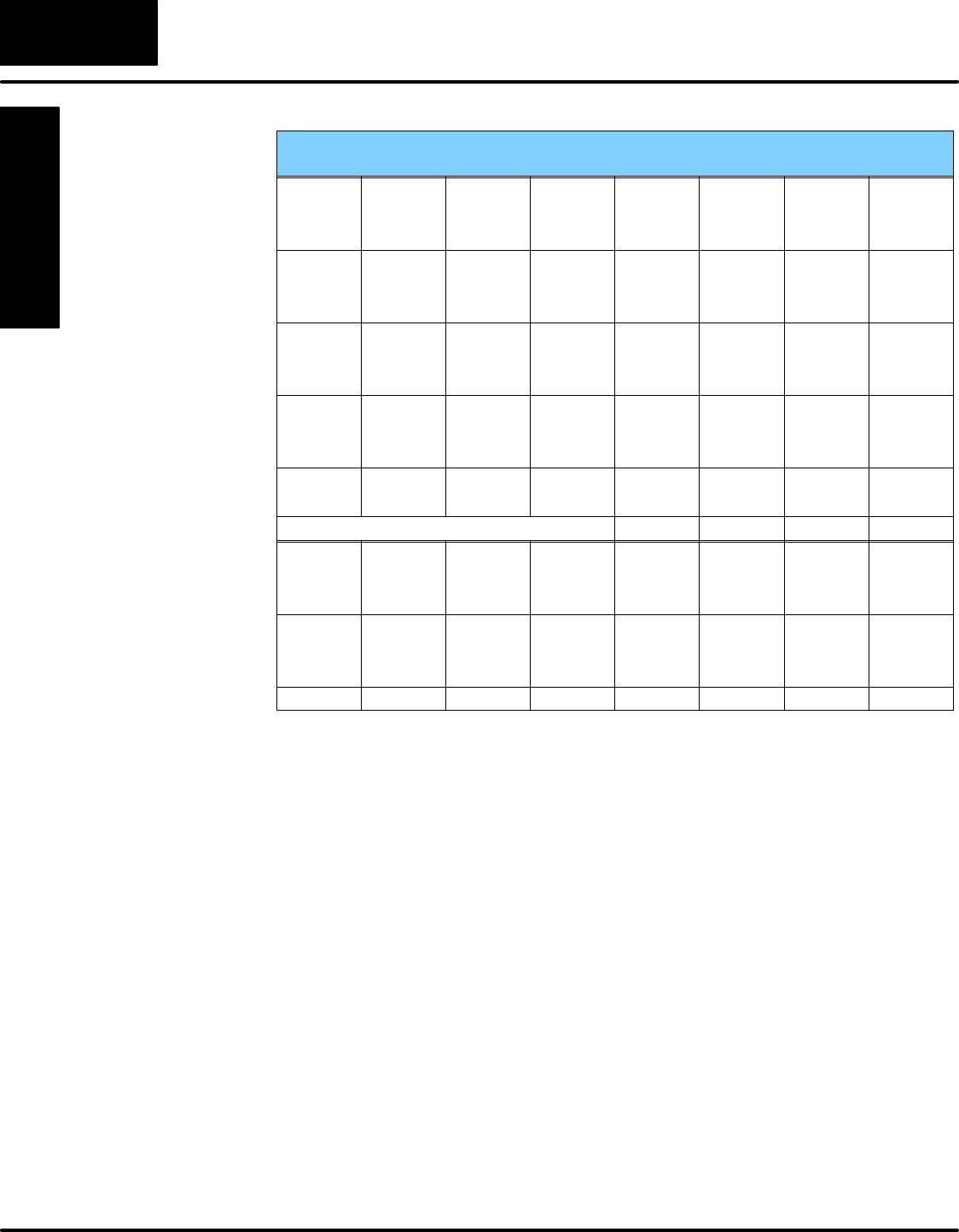
Memory Type Discrete Memory
Reference
(octal)
Word Memory
Reference
(octal)
Qty.
Decimal Symbol
Input Points X0 – X777 V40400 – V40437 512
Output Points Y0 – Y777 V40500 – V40537 512
Control Relays C0 – C1777 V40600 – V40677 1024
Special Relays SP0 – SP777 V41200 – V41237 512
Timer Current
Values None V0 – V377 256
Timer Status Bits T0 – T377 V41100 – V41117 256
Counter
Current Values None V1000 – V1177 128
Counter Status
Bits CT0 – CT177 V41140 – V41147 128
Data Words none V1400 – V7377
V10000–V17777
3072
4096 None specific, used with many
instructions
Stages S0 – S1777 V41000 – V41077 1024
System
parameters None V7400–V7777 256 System specific, used for various
purposes
X0
Y0
C0C0
SP0
V0 K100
T0
V1000 K100
CT0
SG S 001
S0
Appendix A
Data Types & Mem. Map
Appendix E
DL305 Memory Map
A–14 DL305 Data Types and Memory Map
DL 350 X Input / Y Output Bit Map
This table provides a listing of the individual Input points associated with each V-memory address bit.
MSB DL350 Input (X) and Output (Y) Points LSB X Input Y Output
17 16 15 14 13 12 11 10 7 6 5 4 3 2 1 0
X Input
Address
Y Output
Address
017 016 015 014 013 012 011 010 007 006 005 004 003 002 001 000 V40400 V40500
037 036 035 034 033 032 031 030 027 026 025 024 023 022 021 020 V40401 V40501
057 056 055 054 053 052 051 050 047 046 045 044 043 042 041 040 V40402 V40502
077 076 075 074 073 072 071 070 067 066 065 064 063 062 061 060 V40403 V40503
117 116 115 114 113 112 111 110 107 106 105 104 103 102 101 100 V40404 V40504
137 136 135 134 133 132 131 130 127 126 125 124 123 122 121 120 V40405 V40505
157 156 155 154 153 152 151 150 147 146 145 144 143 142 141 140 V40406 V40506
177 176 175 174 173 172 171 170 167 166 165 164 163 162 161 160 V40407 V40507
217 216 215 214 213 212 211 210 207 206 205 204 203 202 201 200 V40410 V40510
237 236 235 234 233 232 231 230 227 226 225 224 223 222 221 220 V40411 V40511
257 256 255 254 253 252 251 250 247 246 245 244 243 242 241 240 V40412 V40512
277 276 275 274 273 272 271 270 267 266 265 264 263 262 261 260 V40413 V40513
317 316 315 314 313 312 311 310 307 306 305 304 303 302 301 300 V40414 V40514
337 336 335 334 333 332 331 330 327 326 325 324 323 322 321 320 V40415 V40515
357 356 355 354 353 352 351 350 347 346 345 344 343 342 341 340 V40416 V40516
377 376 375 374 373 372 371 370 367 366 365 364 363 362 361 360 V40417 V40517
417 416 415 414 413 412 411 410 407 406 405 404 403 402 401 400 V40420 V40520
437 436 435 434 433 432 431 430 427 426 425 424 423 422 421 420 V40421 V40521
457 456 455 454 453 452 451 450 447 446 445 444 443 442 441 440 V40422 V40522
477 476 475 474 473 472 471 470 467 466 465 464 463 462 461 460 V40423 V40523
517 516 515 514 513 512 511 510 507 506 505 504 503 502 501 500 V40424 V40524
537 536 535 534 533 532 531 530 527 526 525 524 523 522 521 520 V40425 V40525
557 556 555 554 553 552 551 550 547 546 545 544 543 542 541 540 V40426 V40526
577 576 575 574 573 572 571 570 567 566 565 564 563 562 561 560 V40427 V40527
617 616 615 614 613 612 611 610 607 606 605 604 603 602 601 600 V40430 V40530
637 636 635 634 633 632 631 630 627 626 625 624 623 622 621 620 V40431 V40531
657 656 655 654 653 652 651 650 647 646 645 644 643 642 641 640 V40432 V40532
677 676 675 674 673 672 671 670 667 666 665 664 663 662 661 660 V40433 V40533
717 716 715 714 713 712 711 710 707 706 705 704 703 702 701 700 V40434 V40534
737 736 735 734 733 732 731 730 727 726 725 724 723 722 721 720 V40435 V40535
757 756 755 754 753 752 751 750 747 746 745 744 743 742 741 740 V40436 V40536
777 776 775 774 773 772 771 770 767 766 765 764 763 762 761 760 V40437 V40537
Appendix A
Data Types & Mem. Map Appendix E
DL305 Memory Map
A–15
DL305 Data Types and Memory Map
DL350 Control Relay Bit Map
This table provides a listing of the individual control relays associated with each V-memory address bit.
MSB DL350 Control Relays (C) LSB
Address
17 16 15 14 13 12 11 10 7 6 5 4 3 2 1 0
Add
ress
017 016 015 014 013 012 011 010 007 006 005 004 003 002 001 000 V40600
037 036 035 034 033 032 031 030 027 026 025 024 023 022 021 020 V40601
057 056 055 054 053 052 051 050 047 046 045 044 043 042 041 040 V40602
077 076 075 074 073 072 071 070 067 066 065 064 063 062 061 060 V40603
117 116 115 114 113 112 111 110 107 106 105 104 103 102 101 100 V40604
137 136 135 134 133 132 131 130 127 126 125 124 123 122 121 120 V40605
157 156 155 154 153 152 151 150 147 146 145 144 143 142 141 140 V40606
177 176 175 174 173 172 171 170 167 166 165 164 163 162 161 160 V40607
217 216 215 214 213 212 211 210 207 206 205 204 203 202 201 200 V40610
237 236 235 234 233 232 231 230 227 226 225 224 223 222 221 220 V40611
257 256 255 254 253 252 251 250 247 246 245 244 243 242 241 240 V40612
277 276 275 274 273 272 271 270 267 266 265 264 263 262 261 260 V40613
317 316 315 314 313 312 311 310 307 306 305 304 303 302 301 300 V40614
337 336 335 334 333 332 331 330 327 326 325 324 323 322 321 320 V40615
357 356 355 354 353 352 351 350 347 346 345 344 343 342 341 340 V40616
377 376 375 374 373 372 371 370 367 366 365 364 363 362 361 360 V40617
417 416 415 414 413 412 411 410 407 406 405 404 403 402 401 400 V40620
437 436 435 434 433 432 431 430 427 426 425 424 423 422 421 420 V40621
457 456 455 454 453 452 451 450 447 446 445 444 443 442 441 440 V40622
477 476 475 474 473 472 471 470 467 466 465 464 463 462 461 460 V40623
517 516 515 514 513 512 511 510 507 506 505 504 503 502 501 500 V40624
537 536 535 534 533 532 531 530 527 526 525 524 523 522 521 520 V40625
557 556 555 554 553 552 551 550 547 546 545 544 543 542 541 540 V40626
577 576 575 574 573 572 571 570 567 566 565 564 563 562 561 560 V40627
617 616 615 614 613 612 611 610 607 606 605 604 603 602 601 600 V40630
637 636 635 634 633 632 631 630 627 626 625 624 623 622 621 620 V40631
657 656 655 654 653 652 651 650 647 646 645 644 643 642 641 640 V40632
677 676 675 674 673 672 671 670 667 666 665 664 663 662 661 660 V40633
717 716 715 714 713 712 711 710 707 706 705 704 703 702 701 700 V40634
737 736 735 734 733 732 731 730 727 726 725 724 723 722 721 720 V40635
757 756 755 754 753 752 751 750 747 746 745 744 743 742 741 740 V40636
777 776 775 774 773 772 771 770 767 766 765 764 763 762 761 760 V40637

Appendix A
Data Types & Mem. Map
Appendix E
DL305 Memory Map
A–16 DL305 Data Types and Memory Map
MSB Additional DL350 Control Relays (C) LSB
Address
17 16 15 14 13 12 11 10 7 6 5 4 3 2 1 0
Add
ress
1017 1016 1015 1014 1013 1012 1011 1010 1007 1006 1005 1004 1003 1002 1001 1000 V40640
1037 1036 1035 1034 1033 1032 1031 1030 1027 1026 1025 1024 1023 1022 1021 1020 V40641
1057 1056 1055 1054 1053 1052 1051 1050 1047 1046 1045 1044 1043 1042 1041 1040 V40642
1077 1076 1075 1074 1073 1072 1071 1070 1067 1066 1065 1064 1063 1062 1061 1060 V40643
1117 1116 1115 1114 1113 1112 1111 1110 1107 1106 1105 1104 1103 1102 1101 1100 V40644
1137 1136 1135 1134 1133 1132 1131 1130 1127 1126 1125 1124 1123 1122 1121 1120 V40645
1157 1156 1155 1154 1153 1152 1151 1150 1147 1146 1145 1144 1143 1142 1141 1140 V40646
1177 1176 1175 1174 1173 1172 1171 1170 1167 1166 1165 1164 1163 1162 1161 1160 V40647
1217 1216 1215 1214 1213 1212 1211 1210 1207 1206 1205 1204 1203 1202 1201 1200 V40650
1237 1236 1235 1234 1233 1232 1231 1230 1227 1226 1225 1224 1223 1222 1221 1220 V40651
1257 1256 1255 1254 1253 1252 1251 1250 1247 1246 1245 1244 1243 1242 1241 1240 V40652
1277 1276 1275 1274 1273 1272 1271 1270 1267 1266 1265 1264 1263 1262 1261 1260 V40653
1317 1316 1315 1314 1313 1312 1311 1310 1307 1306 1305 1304 1303 1302 1301 1300 V40654
1337 1336 1335 1334 1333 1332 1331 1330 1327 1326 1325 1324 1323 1322 1321 1320 V40655
1357 1356 1355 1354 1353 1352 1351 1350 1347 1346 1345 1344 1343 1342 1341 1340 V40656
1377 1376 1375 1374 1373 1372 1371 1370 1367 1366 1365 1364 1363 1362 1361 1360 V40657
1417 1416 1415 1414 1413 1412 1411 1410 1407 1406 1405 1404 1403 1402 1401 1400 V40660
1437 1436 1435 1434 1433 1432 1431 1430 1427 1426 1425 1424 1423 1422 1421 1420 V40661
1457 1456 1455 1454 1453 1452 1451 1450 1447 1446 1445 1444 1443 1442 1441 1440 V40662
1477 1476 1475 1474 1473 1472 1471 1470 1467 1466 1465 1464 1463 1462 1461 1460 V40663
1517 1516 1515 1514 1513 1512 1511 1510 1507 1506 1505 1504 1503 1502 1501 1500 V40664
1537 1536 1535 1534 1533 1532 1531 1530 1527 1526 1525 1524 1523 1522 1521 1520 V40665
1557 1556 1555 1554 1553 1552 1551 1550 1547 1546 1545 1544 1543 1542 1541 1540 V40666
1577 1576 1575 1574 1573 1572 1571 1570 1567 1566 1565 1564 1563 1562 1561 1560 V40667
1617 1616 1615 1614 1613 1612 1611 1610 1607 1606 1605 1604 1603 1602 1601 1600 V40670
1637 1636 1635 1634 1633 1632 1631 1630 1627 1626 1625 1624 1623 1622 1621 1620 V40671
1657 1656 1655 1654 1653 1652 1651 1650 1647 1646 1645 1644 1643 1642 1641 1640 V40672
1677 1676 1675 1674 1673 1672 1671 1670 1667 1666 1665 1664 1663 1662 1661 1660 V40673
1717 1716 1715 1714 1713 1712 1711 1710 1707 1706 1705 1704 1703 1702 1701 1700 V40674
1737 1736 1735 1734 1733 1732 1731 1730 1727 1726 1725 1724 1723 1722 1721 1720 V40675
1757 1756 1755 1754 1753 1752 1751 1750 1747 1746 1745 1744 1743 1742 1741 1740 V40676
1777 1776 1775 1774 1773 1772 1771 1770 1767 1766 1765 1764 1763 1762 1761 1760 V40677

Appendix A
Data Types & Mem. Map Appendix E
DL305 Memory Map
A–17
DL305 Data Types and Memory Map
DL350 Staget Control / Status Bit Map
This table provides a listing of the individual Staget control bits associated with each V-memory address.
MSB DL350 Stage (S) Control Bits LSB
Address
17 16 15 14 13 12 11 10 7 6 5 4 3 2 1 0
Add
ress
017 016 015 014 013 012 011 010 007 006 005 004 003 002 001 000 V41000
037 036 035 034 033 032 031 030 027 026 025 024 023 022 021 020 V41001
057 056 055 054 053 052 051 050 047 046 045 044 043 042 041 040 V41002
077 076 075 074 073 072 071 070 067 066 065 064 063 062 061 060 V41003
117 116 115 114 113 112 111 110 107 106 105 104 103 102 101 100 V41004
137 136 135 134 133 132 131 130 127 126 125 124 123 122 121 120 V41005
157 156 155 154 153 152 151 150 147 146 145 144 143 142 141 140 V41006
177 176 175 174 173 172 171 170 167 166 165 164 163 162 161 160 V41007
217 216 215 214 213 212 211 210 207 206 205 204 203 202 201 200 V41010
237 236 235 234 233 232 231 230 227 226 225 224 223 222 221 220 V41011
257 256 255 254 253 252 251 250 247 246 245 244 243 242 241 240 V41012
277 276 275 274 273 272 271 270 267 266 265 264 263 262 261 260 V41013
317 316 315 314 313 312 311 310 307 306 305 304 303 302 301 300 V41014
337 336 335 334 333 332 331 330 327 326 325 324 323 322 321 320 V41015
357 356 355 354 353 352 351 350 347 346 345 344 343 342 341 340 V41016
377 376 375 374 373 372 371 370 367 366 365 364 363 362 361 360 V41017
417 416 415 414 413 412 411 410 407 406 405 404 403 402 401 400 V41020
437 436 435 434 433 432 431 430 427 426 425 424 423 422 421 420 V41021
457 456 455 454 453 452 451 450 447 446 445 444 443 442 441 440 V41022
477 476 475 474 473 472 471 470 467 466 465 464 463 462 461 460 V41023
517 516 515 514 513 512 511 510 507 506 505 504 503 502 501 500 V41024
537 536 535 534 533 532 531 530 527 526 525 524 523 522 521 520 V41025
557 556 555 554 553 552 551 550 547 546 545 544 543 542 541 540 V41026
577 576 575 574 573 572 571 570 567 566 565 564 563 562 561 560 V41027
617 616 615 614 613 612 611 610 607 606 605 604 603 602 601 600 V41030
637 636 635 634 633 632 631 630 627 626 625 624 623 622 621 620 V41031
657 656 655 654 653 652 651 650 647 646 645 644 643 642 641 640 V41032
677 676 675 674 673 672 671 670 667 666 665 664 663 662 661 660 V41033
717 716 715 714 713 712 711 710 707 706 705 704 703 702 701 700 V41034
737 736 735 734 733 732 731 730 727 726 725 724 723 722 721 720 V41035
757 756 755 754 753 752 751 750 747 746 745 744 743 742 741 740 V41036
777 776 775 774 773 772 771 770 767 766 765 764 763 762 761 760 V41037
Appendix A
Data Types & Mem. Map
Appendix E
DL305 Memory Map
A–18 DL305 Data Types and Memory Map
MSB DL350 Additional Stage (S) Control Bits (continued) LSB
Address
17 16 15 14 13 12 11 10 7 6 5 4 3 2 1 0
Add
ress
1017 1016 1015 1014 1013 1012 1011 1010 1007 1006 1005 1004 1003 1002 1001 1000 V41040
1037 1036 1035 1034 1033 1032 1031 1030 1027 1026 1025 1024 1023 1022 1021 1020 V41041
1057 1056 1055 1054 1053 1052 1051 1050 1047 1046 1045 1044 1043 1042 1041 1040 V41042
1077 1076 1075 1074 1073 1072 1071 1070 1067 1066 1065 1064 1063 1062 1061 1060 V41043
1117 1116 1115 1114 1113 1112 1111 1110 1107 1106 1105 1104 1103 1102 1101 1100 V41044
1137 1136 1135 1134 1133 1132 1131 1130 1127 1126 1125 1124 1123 1122 1121 1120 V41045
1157 1156 1155 1154 1153 1152 1151 1150 1147 1146 1145 1144 1143 1142 1141 1140 V41046
1177 1176 1175 1174 1173 1172 1171 1170 1167 1166 1165 1164 1163 1162 1161 1160 V41047
1217 1216 1215 1214 1213 1212 1211 1210 1207 1206 1205 1204 1203 1202 1201 1200 V41050
1237 1236 1235 1234 1233 1232 1231 1230 1227 1226 1225 1224 1223 1222 1221 1220 V41051
1257 1256 1255 1254 1253 1252 1251 1250 1247 1246 1245 1244 1243 1242 1241 1240 V41052
1277 1276 1275 1274 1273 1272 1271 1270 1267 1266 1265 1264 1263 1262 1261 1260 V41053
1317 1316 1315 1314 1313 1312 1311 1310 1307 1306 1305 1304 1303 1302 1301 1300 V41054
1337 1336 1335 1334 1333 1332 1331 1330 1327 1326 1325 1324 1323 1322 1321 1320 V41055
1357 1356 1355 1354 1353 1352 1351 1350 1347 1346 1345 1344 1343 1342 1341 1340 V41056
1377 1376 1375 1374 1373 1372 1371 1370 1367 1366 1365 1364 1363 1362 1361 1360 V41057
1417 1416 1415 1414 1413 1412 1411 1410 1407 1406 1405 1404 1403 1402 1401 1400 V41060
1437 1436 1435 1434 1433 1432 1431 1430 1427 1426 1425 1424 1423 1422 1421 1420 V41061
1457 1456 1455 1454 1453 1452 1451 1450 1447 1446 1445 1444 1443 1442 1441 1440 V41062
1477 1476 1475 1474 1473 1472 1471 1470 1467 1466 1465 1464 1463 1462 1461 1460 V41063
1517 1516 1515 1514 1513 1512 1511 1510 1507 1506 1505 1504 1503 1502 1501 1500 V41064
1537 1536 1535 1534 1533 1532 1531 1530 1527 1526 1525 1524 1523 1522 1521 1520 V41065
1557 1556 1555 1554 1553 1552 1551 1550 1547 1546 1545 1544 1543 1542 1541 1540 V41066
1577 1576 1575 1574 1573 1572 1571 1570 1567 1566 1565 1564 1563 1562 1561 1560 V41067
1617 1616 1615 1614 1613 1612 1611 1610 1607 1606 1605 1604 1603 1602 1601 1600 V41070
1637 1636 1635 1634 1633 1632 1631 1630 1627 1626 1625 1624 1623 1622 1621 1620 V41071
1657 1656 1655 1654 1653 1652 1651 1650 1647 1646 1645 1644 1643 1642 1641 1640 V41072
1677 1676 1675 1674 1673 1672 1671 1670 1667 1666 1665 1664 1663 1662 1661 1660 V41073
1717 1716 1715 1714 1713 1712 1711 1710 1707 1706 1705 1704 1703 1702 1701 1700 V41074
1737 1736 1735 1734 1733 1732 1731 1730 1727 1726 1725 1724 1723 1722 1721 1720 V41075
1757 1756 1755 1754 1753 1752 1751 1750 1747 1746 1745 1744 1743 1742 1741 1740 V41076
1777 1776 1775 1774 1773 1772 1771 1770 1767 1766 1765 1764 1763 1762 1761 1760 V41077
Appendix A
Data Types & Mem. Map Appendix E
DL305 Memory Map
A–19
DL305 Data Types and Memory Map
DL350 Timer and Counter Status Bit Maps
This table provides a listing of the individual timer and counter contacts associated with each V-memory
address bit.
MSB DL350 Timer (T) and Counter (CT) Contacts LSB Timer Counter
17 16 15 14 13 12 11 10 7 6 5 4 3 2 1 0
Timer
Address
Counter
Address
017 016 015 014 013 012 011 010 007 006 005 004 003 002 001 000 V41100 V41140
037 036 035 034 033 032 031 030 027 026 025 024 023 022 021 020 V41101 V41141
057 056 055 054 053 052 051 050 047 046 045 044 043 042 041 040 V41102 V41142
077 076 075 074 073 072 071 070 067 066 065 064 063 062 061 060 V41103 V41143
117 116 115 114 113 112 111 110 107 106 105 104 103 102 101 100 V41104 V41144
137 136 135 134 133 132 131 130 127 126 125 124 123 122 121 120 V41105 V41145
157 156 155 154 153 152 151 150 147 146 145 144 143 142 141 140 V41106 V41146
177 176 175 174 173 172 171 170 167 166 165 164 163 162 161 160 V41107 V41147
This portion of the table shows additional Timer contacts available with the DL350.
MSB DL350 Additional Timer (T) Contacts LSB Timer
17 16 15 14 13 12 11 10 7 6 5 4 3 2 1 0
Timer
Address
217 216 215 214 213 212 211 210 207 206 205 204 203 202 201 200 V41110
237 236 235 234 233 232 231 230 227 226 225 224 223 222 221 220 V41111
257 256 255 254 253 252 251 250 247 246 245 244 243 242 241 240 V41112
277 276 275 274 273 272 271 270 267 266 265 264 263 262 261 260 V41113
317 316 315 314 313 312 311 310 307 306 305 304 303 302 301 300 V41114
337 336 335 334 333 332 331 330 327 326 325 324 323 322 321 320 V41115
357 356 355 354 353 352 351 350 347 346 345 344 343 342 341 340 V41116
377 376 375 374 373 372 371 370 367 366 365 364 363 362 361 360 V41117
