BFP540 Datasheet. Www.s Manuals.com. Infineon
User Manual: Marking of electronic components, SMD Codes AT, AT*, AT****, AT-**, AT-***, AT1, AT2, AT=**, AT=***, ATC**, ATF**, ATI**, ATP, ATZ**, ATs. Datasheets BAT18-06 , BFP540, BST39, BST40, KB4312A-GRE, MIC803-46D3VC3, MIC803-46D3VM3, OPA2374AIDCN, RT8805GQV, RT8805PQV, RT9011-JMPQV, RT9014-GSPQV, RT9198-2HPU5, RT9198A-44GY, RT9198A-44PY, RT9818C-27GU3, SMAJ8.5A, SMBJ8.5A, SMBJ8.5CA, TS1909CX527, TS1909CX530, TS1909CX533, TS1909CX550.
Open the PDF directly: View PDF ![]() .
.
Page Count: 9
SIEGET 45 BFP540
Aug-09-20011
NPN Silicon RF Transistor
Preliminary data
For highest gain low noise amplifier
at 1.8 GHz
Outstanding Gms = 21 dB
Noise Figure F = 0.9 dB
Gold metallization for high reliability
SIEGET 45 - Line
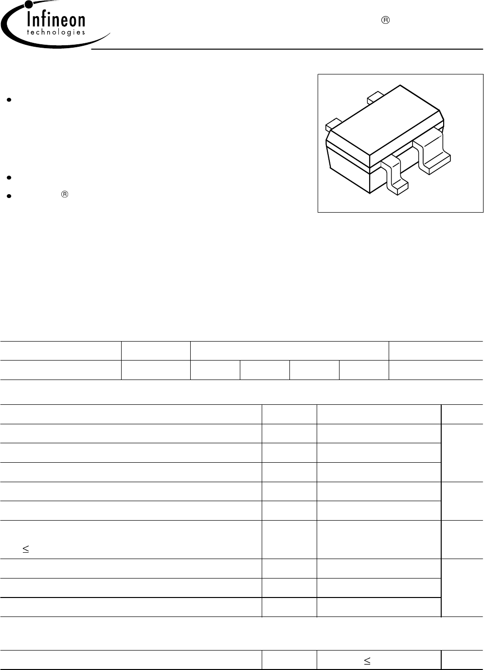
VPS05605
4
2
1
3
ESD: Electrostatic discharge sensitive device, observe handling precaution!
Type Marking Pin Configuration Package
BFP540 ATs 1 = B 2 = E 3 = C 4 = E SOT343
Maximum Ratings
Parameter Symbol Value Unit
Collector-emitter voltage VCEO 4.5 V
Collector-base voltage VCBO 14
Emitter-base voltage VEBO 1
Collector current IC80 mA
Base current IB8
Total power dissipation
TS 77°C 1)
Ptot 250 mW
Junction temperature Tj150 °C
Ambient temperature TA-65 ... 150
Storage temperature Tstg -65 ... 150
Thermal Resistance
Junction - soldering point2) RthJS 290 K/W
1TS is measured on the emitter lead at the soldering point to the pcb
2For calculation of RthJA please refer to Application Note Thermal Resistance

SIEGET 45 BFP540
Aug-09-20012
Electrical Characteristics at TA = 25°C, unless otherwise specified.
Parameter Symbol Values Unit
min. typ. max.
DC characteristics
Collector-emitter breakdown voltage
IC = 1 mA, IB = 0
V(BR)CEO 4.5 5 6.5 V
Collector-base cutoff current
VCB = 5 V, IE = 0
ICBO - - 200 nA
Emitter-base cutoff current
VEB = 1 V, IC = 0
IEBO - - 70 µA
DC current gain
IC = 20 mA, VCE = 3.5 V
hFE 50 110 200 -
AC Characteristics (verified by random sampling)
Collector-base capacitance
VCB = 2 V, f = 1 MHz
Ccb - 0.14 0.24 pF
Collector-emitter capacitance
VCE = 2 V, f = 1 MHz
Cce - 0.33 -
Emitter-base capacitance
VEB = 0.5 V, f = 1 MHz
Ceb - 0.65 -
Noise figure
IC = 5 mA, VCE = 2 V, ZS = ZSopt ,
f = 1.8 GHz
F- 0.9 1.4 dB
Power gain, maximum stable 1)
IC = 20 mA, VCE = 2 V, ZS = ZSopt, ZL = ZLopt ,
f = 1.8 GHz
Gms - 21 -
Insertion power gain
IC = 20 mA, VCE = 2 V, f = 1.8 GHz,
ZS = ZL = 50
|S21|216 18.5 -
Third order intercept point at output
VCE = 2 V, f = 1.8 GHz, ZS=ZSopt, ZL=ZLopt ,
IC = 20 mA
IC = 7 mA
IP3
-
-
24
20
-
-
dBm
1dB compression point
VCE = 2 V, f = 1.8 GHz, ZS=ZSopt, ZL=ZLopt ,
IC = 20 mA
IC = 7 mA
P-1dB
-
-
12
4
-
-
1Gms = |S21 / S12|
SIEGET 45 BFP540
Aug-09-20013
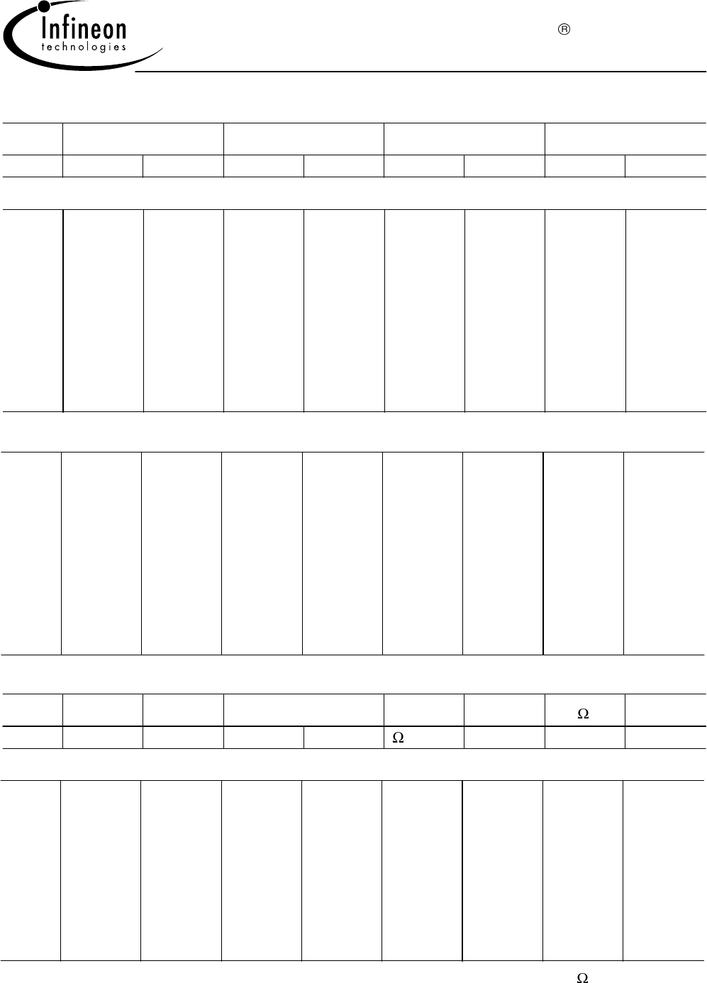
Common Emitter S-Parameters
fS11 S21 S12 S22
GHz MAG ANG MAG ANG MAG ANG MAG ANG
VCE = 2 V, IC = 20 mA
0.01
0.1
0.5
1
2
3
4
5
6
0.5903
0.5827
0.4721
0.4148
0.413
0.4426
0.5064
0.5623
0.5989
-2.2
-22.1
-91.8
-137.4
178
153
133.2
119.5
109.6
42.176
40.33
26.564
15.46
7.897
5.257
3.895
3.027
2.471
179
165.1
121.2
96.5
72.9
56.5
41.6
28.1
16.2
0.0008
0.0068
0.0263
0.0397
0.0646
0.0892
0.1126
0.1313
0.1525
99.2
82.2
62.1
56.4
52.3
46.5
38.1
29.9
22.9
0.9567
0.9499
0.6533
0.3959
0.1912
0.0982
0.1022
0.1445
0.1764
-0.6
-12.1
-48.1
-68.2
-90.7
-117.9
180
147
121.8
VCE = 2V, IC = 5 mA
0.01
0.1
0.5
1
2
3
4
5
6
0.9394
0.937
0.904
0.823
0.68
0.6308
0.6442
0.6757
0.7029
-0.7
-7.6
-37.9
-73.1
-130
-170.9
156.4
134.7
119.7
7.05
6.922
6.567
5.687
3.983
2.913
2.251
1.765
1.439
-179.5
174.7
152.3
128
92.3
67
45.6
27.5
12.7
0.001
0.0087
0.0435
0.0782
0.1073
0.1111
0.1076
0.1028
0.1065
67.1
87.3
70.9
52
25.7
12.3
4.9
3.7
7.1
0.9961
0.9976
0.9485
0.8283
0.5958
0.4471
0.3504
0.2987
0.2491
-0.4
-3.7
-18
-33.3
-52.6
-63.7
-78.9
-96.5
-114.9
Common Emitter Noise Parameters
fFmin 1) Ga 1)
Γ
opt RNrnF50 2) |S21|2 2)
GHz dB dB MAG ANG - dB dB
VCE = 2 V, IC = 5 mA
0.9
1.8
2.4
3
4
5
6
0.69
0.9
1.06
1.2
1.47
1.78
2.11
22.7
17.6
15.2
13.6
11.5
10
8.4
0.29
0.13
0.14
0.22
0.33
0.5
0.55
34
86
127
163
-153
-126
-107
8
6.5
6.5
5.5
6
9
18
0.16
0.13
0.13
0.11
0.12
0.18
0.36
0.86
0.93
1.13
1.31
1.67
2.17
2.98
21.5
17
14.1
11.9
9.5
7.9
5.6
1) Input matched for minimum noise figure, output for maximum gain 2) ZS = ZL = 50
For more and detailed S- and Noise-parameters please contact your local Infineon Technologies
distributor or sales office to obtain a Infineon Technologies Application Notes CD-ROM or see Internet:
http://www.infineon.com/silicondiscretes
SIEGET 45 BFP540
Aug-09-20014
SPICE Parameters (Gummel-Poon Model, Berkley-SPICE 2G.6 Syntax) :
Transistor Chip Data
IS = 82.84 aA
VAF = 28.383 V
NE = 3.19 -
VAR = 19.705 V
NC = 1.172 -
RBM = 1.3
CJE = 1.8063 fF
TF = 6.76 ps
ITF = 1mA
VJC = 0.81969 V
TR = 2.324 ns
MJS = 0-
XTI = 3 -
BF = 107.5 -
IKF = 0.48731 A
BR = 5.5 -
IKR = 0.02 A
RB = 5.4
RE = 0.31111
VJE = 0.8051 V
XTF = 0.4219 -
PTF = 0 deg
MJC = 0.30232 -
CJS = 0fF
XTB = 0-
FC = 0.73234 -
NF = 1 -
ISE = 11.15 pA
NR = 1-
ISC = 19.237 aA
IRB = 0.72983 mA
RC = 4
MJE = 0.46576 -
VTF = 0.23794 V
CJC = 234 fF
XCJC = 0.3 -
VJS = 0.75 V
EG = 1.11 eV
TNOM 300 K
All parameters are ready to use, no scaling is necessary
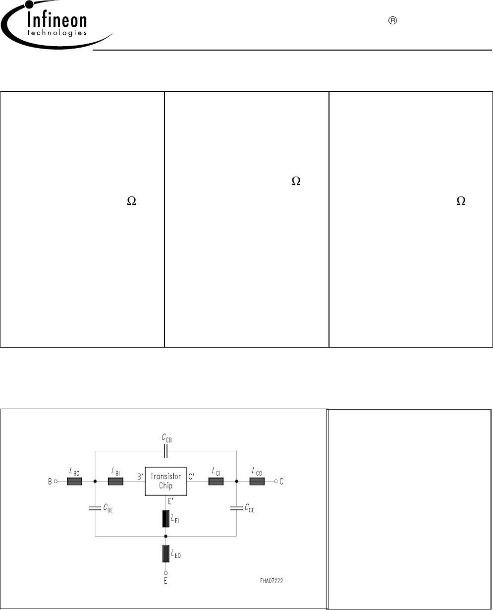
Package Equivalent Circuit:
LBI = 0.47 nH
LBO = 0.53 nH
LEI = 0.23 nH
LEO = 0.05 nH
LCI = 0.56 nH
LCO = 0.58 nH
CBE = 136 fF
CCB = 6.9 fF
CCE = 134 fF
Valid up to 6GHz
The SOT-343 package has two emitter leads. To avoid high complexity of the package equivalent circuit,
both leads are combined in one electrical connection.
For examples and ready to use parameters please contact your local Infineon Technologies
distributor or sales office to obtain a Infineon Technologies CD-ROM or see Internet:
http://www.infineon.com/silicondiscretes

SIEGET 45 BFP540
Aug-09-20015
For non-linear simulation:
Use transistor chip parameters in Berkeley SPICE 2G.6 syntax for all simulators.
Simulation of the package is not necessary for frequencies < 100MHz.
For higher frequencies please add the wiring of the package equivalent circuit
around the non-linear transistor.
Advantages of the common emitter configuration:
Higher gain because of lower emitter inductance.
Power is dissipated via the grounded emitter leads, because the chip is mounted
on the copper emitter leadframe.
Please note, that the broadest lead is the emitter lead.
SIEGET 45 BFP540
Aug-09-20016
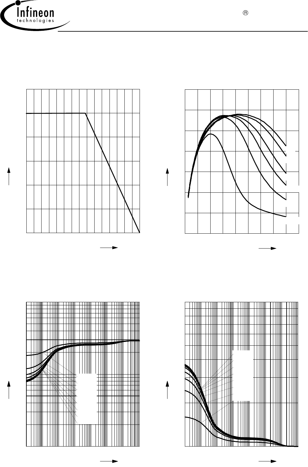
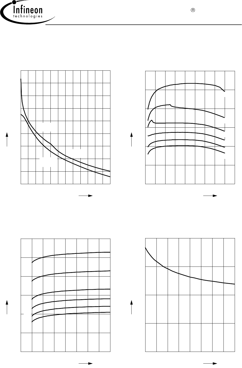
Total power dissipation Ptot = f (TS)
0 20 40 60 80 100 120 °C 150
TS
0
50
100
150
200
mW
300
P
tot
Transition frequency fT = f (IC)
f = 1 GHz
VCE = parameter in V
0 10 20 30 40 50 60 70 mA 90
IC
0
5
10
15
20
25
GHz
35
f
T
0.5
1
1.5
2
3
4
Permissible Pulse Load RthJS = f (tp)
10 -7 10 -6 10 -5 10 -4 10 -3 10 -2 10 0
s
tp
1
10
2
10
3
10
K/W
R
thJS
0.5
0.2
0.1
0.05
0.02
0.01
0.005
D = 0
Permissible Pulse Load
Ptotmax/PtotDC = f (tp)
10 -7 10 -6 10 -5 10 -4 10 -3 10 -2 10 0
s
tp
0
10
1
10
-
P
totmax
/ P
totDC
D = 0
0.005
0.01
0.02
0.05
0.1
0.2
0.5
SIEGET 45 BFP540
Aug-09-20017
Power gain Gma, Gms = f (IC)
VCE = 2V
f = parameter in GHz
0 10 20 30 40 50 60 70 mA 90
IC
0
5
10
15
20
dB
30
G
1
2
3
4
5
6
Power gain Gma, Gms, |S21|2 = f ( f )
VCE = 2V, IC = 20 mA
0.0 1.0 2.0 3.0 4.0 GHz 6.0
f
5
10
15
20
25
30
35
40
dB
50
G
|S21|2
Gms
Gma
Collector-base capacitance Ccb = f (VCB)
f = 1MHz
0.0 0.5 1.0 1.5 2.0 2.5 3.0 V4.0
VCB
0.00
0.05
0.10
pF
0.20
C
cb
Power gain Gma, Gms = f (VCE)
IC = 20 mA
f = parameter in GHz
0.0 0.5 1.0 1.5 2.0 2.5 3.0 V4.0
VCE
0
5
10
15
20
dB
30
G
1
2
3
4
5
6
SIEGET 45 BFP540
Aug-09-20018
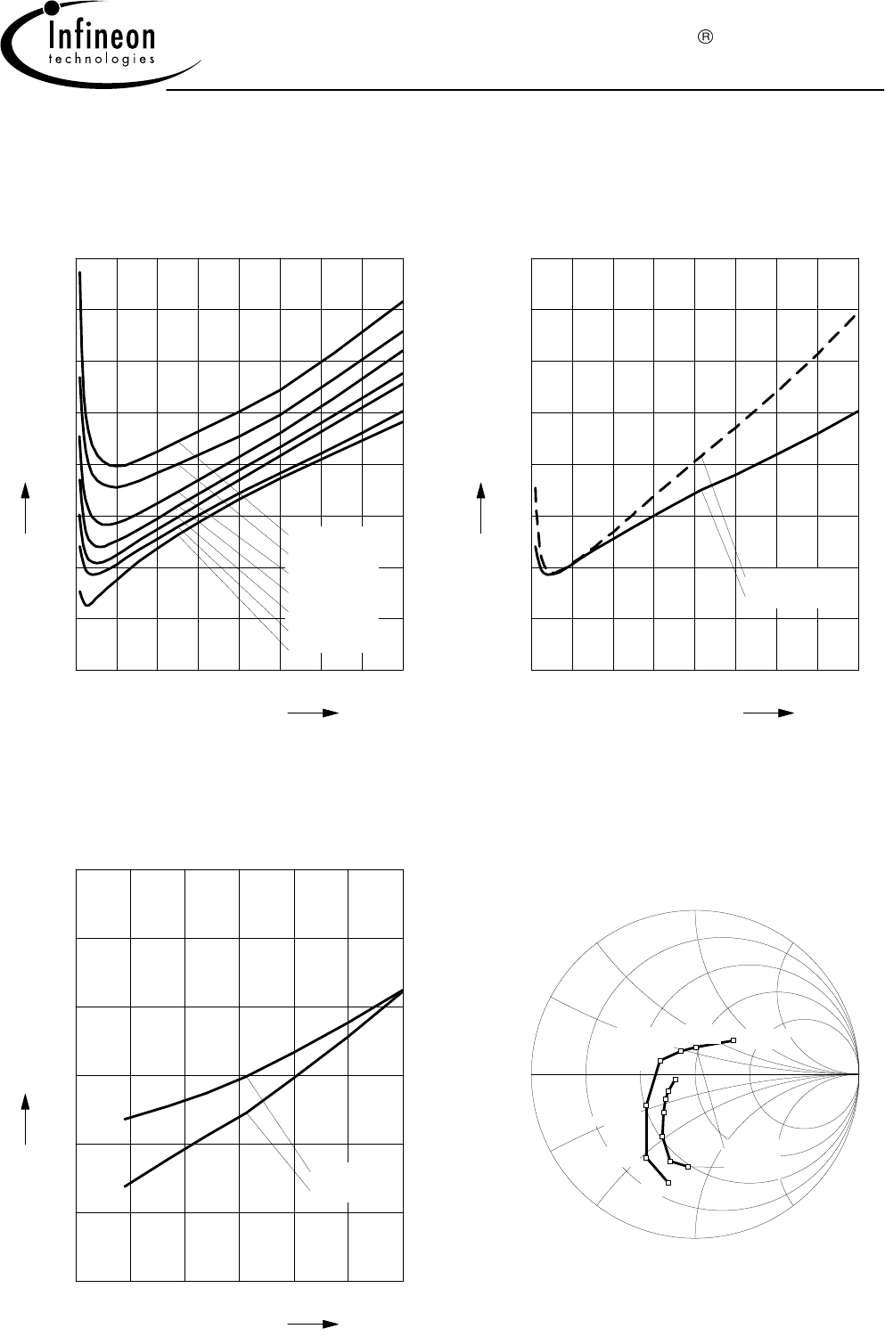
Noise figure F = f (IC)
VCE = 2 V, ZS = ZSopt
0 10 20 30 40 50 60 mA 80
IC
0.0
0.5
1.0
1.5
2.0
2.5
3.0
dB
4.0
F
f = 6GHz
f = 5GHz
f = 4GHz
f = 3GHz
f = 2.4GHz
f = 1.8GHz
f = 0.9GHz
Noise figure F = f (IC)
VCE = 2 V, f = 1.8 GHz
0 10 20 30 40 50 60 mA 80
IC
0.0
0.5
1.0
1.5
2.0
2.5
3.0
dB
4.0
F
ZS = 50Ohm
ZS = Zsopt
Noise figure F = f ( f )
VCE = 2 V, ZS = ZSopt
01234GHz 6
f
0.0
0.5
1.0
1.5
2.0
dB
3.0
F
IC = 20mA
IC = 5mA
Source impedance for min.
noise figure vs. Frequency
VCE = 2 V, IC = 5 mA / 20 mA
100
+j10
-j10
50
+j25
-j25
25
+j50
-j50
10
+j100
-j100
0
0.9GHz
1.8GHz
2.4GHz
3GHz
4GHz
5GHz
6GHz
5mA
20mA
