BFR182 Datasheet. Www.s Manuals.com. Infineon
User Manual: Marking of electronic components, SMD Codes RG, RG***, RG-, RG-***, RG=***, RGW, RGp, RGs, RGt, Rg. Datasheets 1SMA13AT3G, BD53E49G, BFR182, BZB84-B62, PZU5.6B1A/DG, RP130K181A, RT9170-28GB, RT9170-28PB, SMAJ58A, TS19705CX6.
Open the PDF directly: View PDF ![]() .
.
Page Count: 8
BFR182
Aug-09-20011
NPN Silicon RF Transistor
For low noise, high-gain broadband amplifiers at
collector currents from 1 mA to 20 mA
fT = 8 GHz
F = 1.2 dB at 900 MHz
1
2
3
VPS05161
ESD: Electrostatic discharge sensitive device, observe handling precaution!
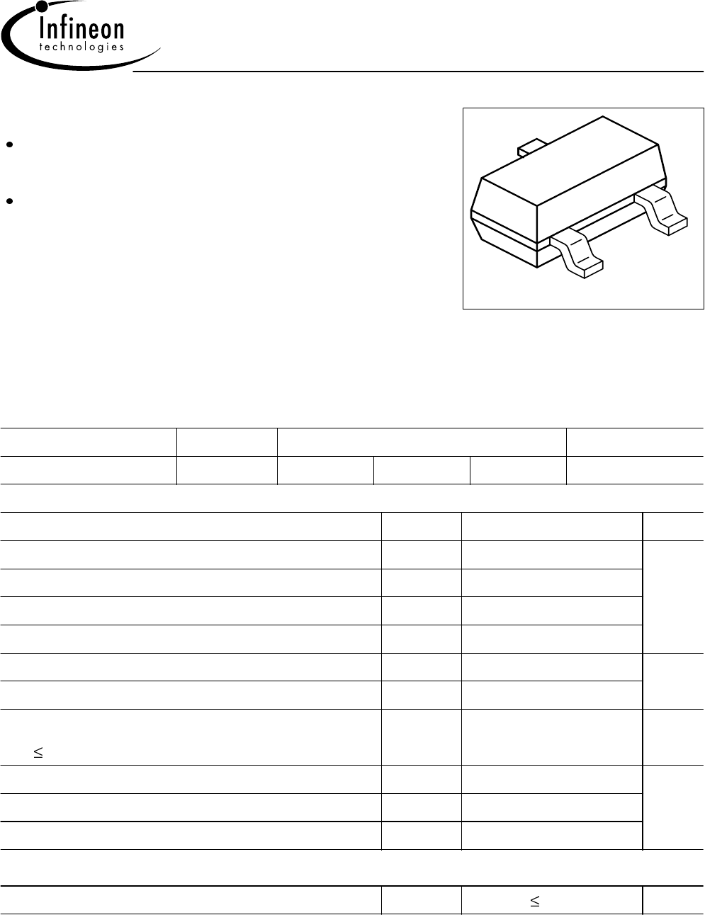
Type Marking Pin Configuration Package
BFR182 RGs 1 = B 2 = E 3 = C SOT23
Maximum Ratings
Parameter Symbol Value Unit
Collector-emitter voltage VCEO 12 V
Collector-emitter voltage VCES 20
Collector-base voltage VCBO 20
Emitter-base voltage VEBO 2
Collector current IC35 mA
Base current IB4
Total power dissipation
TS 93 °C 1)
Ptot 250 mW
Junction temperature Tj150 °C
Ambient temperature TA-65 ... 150
Storage temperature Tst
g
-65 ... 150
Thermal Resistance
Junction - soldering point2) RthJS 230 K/W
1TS is measured on the collector lead at the soldering point to the pcb
2For calculation of RthJA please refer to Application Note Thermal Resistance

BFR182
Aug-09-20012
Electrical Characteristics at TA = 25°C, unless otherwise specified.
Parameter Symbol Values Unit
min. typ. max.
DC characteristics
Collector-emitter breakdown voltage
IC = 1 mA, IB = 0
V(BR)CEO 12 - - V
Collector-emitter cutoff current
VCE = 20 V, VBE = 0
ICES - - 100 µA
Collector-base cutoff current
VCB = 10 V, IE = 0
ICBO - - 100 nA
Emitter-base cutoff current
VEB = 1 V, IC = 0
IEBO - - 1 µA
DC current gain
IC = 10 mA, VCE = 8 V
hFE 50 100 200 -
BFR182
Aug-09-20013
Electrical Characteristics at TA = 25°C, unless otherwise specified.
Parameter Symbol Values Unit
min. typ. max.
AC characteristics (verified by random sampling)
Transition frequency
IC = 15 mA, VCE = 8 V, f = 500 MHz
fT6 8 - GHz
Collector-base capacitance
VCB = 10 V, f = 1 MHz
Ccb - 0.33 0.5 pF
Collector-emitter capacitance
VCE = 10 V, f = 1 MHz
Cce - 0.2 -
Emitter-base capacitance
VEB = 0.5 V, f = 1 MHz
Ceb - 0.6 -
Noise figure
IC = 3 mA, VCE = 8 V, ZS = ZSopt ,
f = 900 MHz
f = 1.8 GHz
F
-
-
1.2
1.9
-
-
dB
Power gain, maximum available 1)
IC = 10 mA, VCE = 8 V, ZS = ZSopt, ZL = ZLopt ,
f = 900 MHz
f = 1.8 GHz
Gma
-
-
17.5
11.5
-
-
Transducer gain
IC = 10 mA, VCE = 8 V, ZS = ZL = 50 ,
f = 900 MHz
f = 1.8 GHz
|S21e|2
-
-
14.5
9
-
-
1Gma = |S21 / S12| (k-(k2-1)1/2)
BFR182
Aug-09-20014
SPICE Parameters (Gummel-Poon Model, Berkley-SPICE 2G.6 Syntax) :
Transistor Chip Data
IS = 4.8499 fA
VAF = 21.742 V
NE = 0.91624 -
VAR = 2.2595 V
NC = 0.5641 -
RBM = 2.8263
CJE = 8.8619 fF
TF = 22.72 ps
ITF = 6.5523 mA
VJC = 1.0132 V
TR = 1.7541 ns
MJS = 0-
XTI = 3 -
BF = 84.113 -
IKF = 0.14414 A
BR = 10.004 -
IKR = 0.03978 A
RB = 3.4217
RE = 2.1858
VJE = 1.0378 V
XTF = 0.43147 -
PTF = 0 deg
MJC = 0.31068 -
CJS = 0fF
XTB = 0-
FC = 0.64175 -
NF = 0.56639 -
ISE = 8.4254 fA
NR = 0.54818 -
ISC = 5.9438 fA
IRB = 0.071955 mA
RC = 1.8159
MJE = 0.40796 -
VTF = 0.34608 V
CJC = 490.25 fF
XCJC = 0.19281 -
VJS = 0.75 V
EG = 1.11 eV
TNOM 300 K
All parameters are ready to use, no scalling is necessary.
Extracted on behalf of Infineon Technologies AG by:
Institut für Mobil-und Satellitentechnik (IMST)
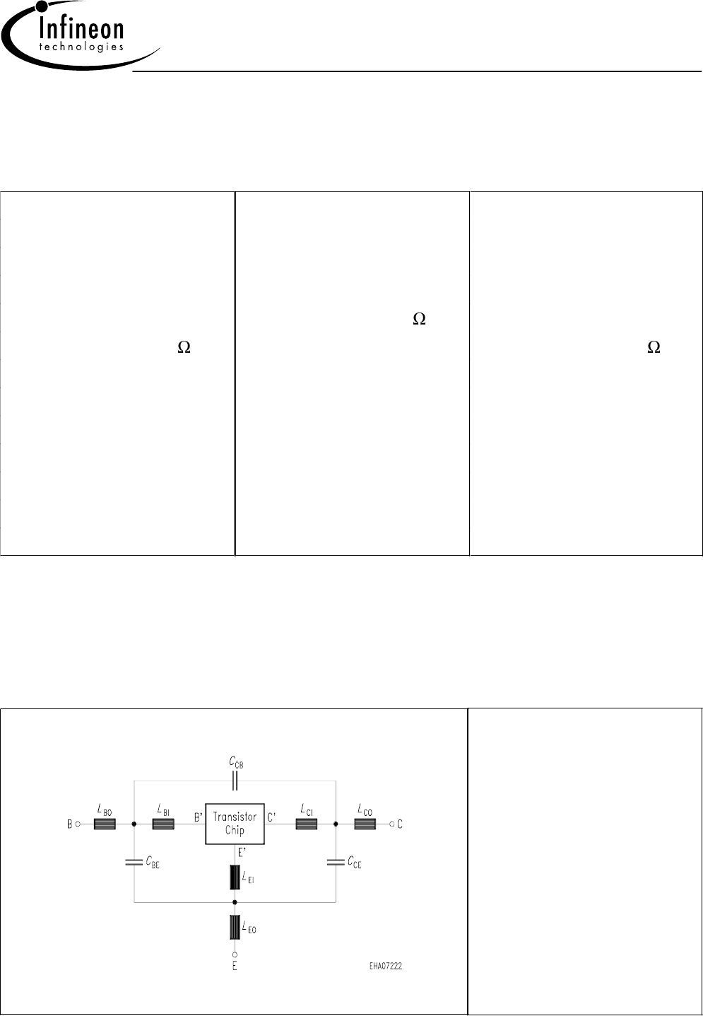
Package Equivalent Circuit:
LBI = 0.85 nH
LBO = 0.51 nH
LEI = 0.69 nH
LEO = 0.61 nH
LCI = 0nH
LCO = 0.49 nH
CBE = 73 fF
CCB = 84 fF
CCE = 165 fF
Valid up to 6GHz
For examples and ready to use parameters please contact your local Infineon Technologies distributor or sales
office to obtain a Infineon Technologies CD-ROM or see Internet: http://www.infineon.com/silicondiscretes
BFR182
Aug-09-20015
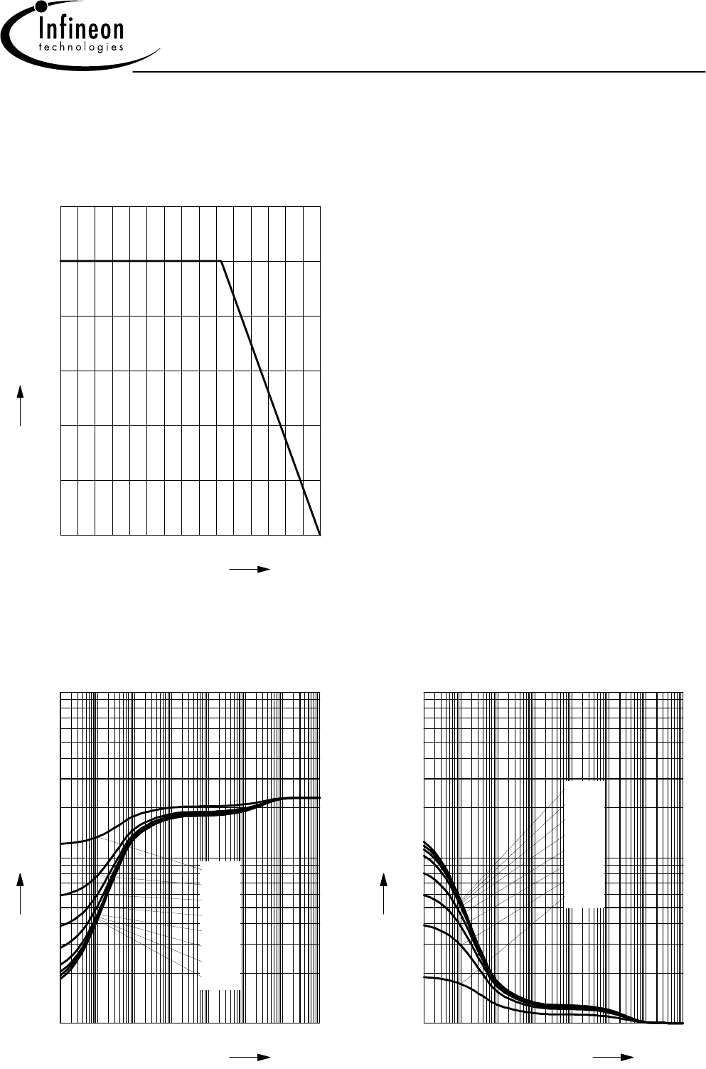
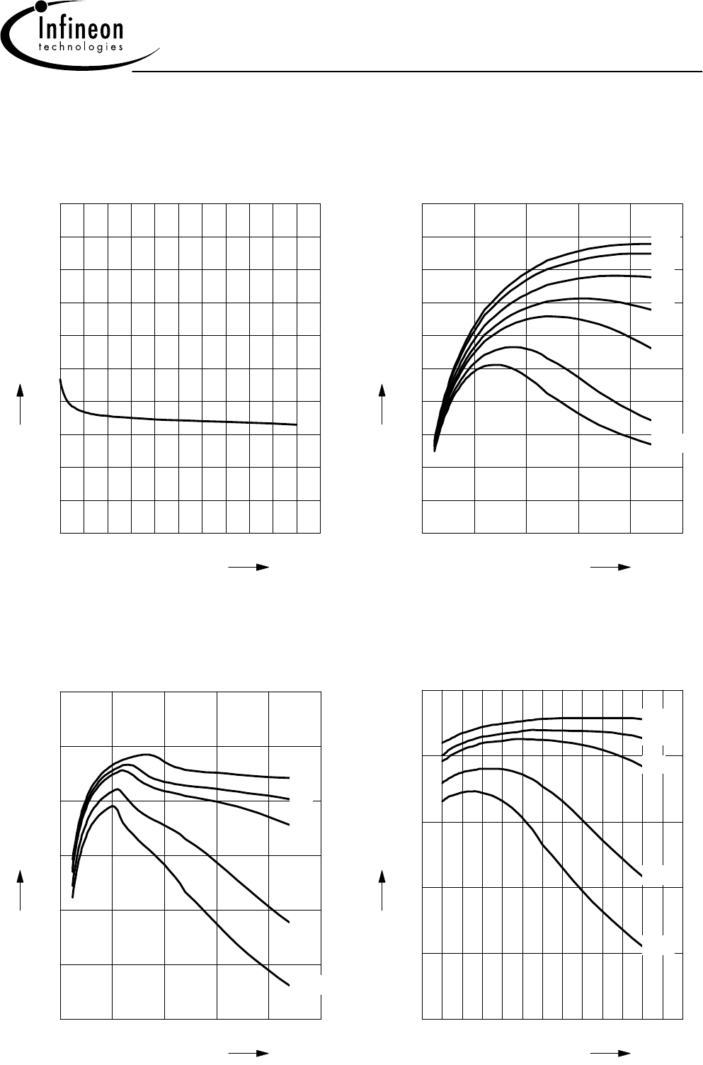
Total power dissipation Ptot = f (TS)
0 20 40 60 80 100 120 °C 150
TS
0
50
100
150
200
mW
300
P
tot
Permissible Pulse Load RthJS = f (tp)
10 -7 10 -6 10 -5 10 -4 10 -3 10 -2 10 0
s
tp
1
10
2
10
3
10
K/W
R
thJS
0.5
0.2
0.1
0.05
0.02
0.01
0.005
D = 0
Permissible Pulse Load
Ptotmax/PtotDC = f (tp)
10 -7 10 -6 10 -5 10 -4 10 -3 10 -2 10 0
s
tp
0
10
1
10
2
10
-
P
totmax
/ P
totDC
D = 0
0.005
0.01
0.02
0.05
0.1
0.2
0.5
BFR182
Aug-09-20016
Collector-base capacitance Ccb = f (VCB)
f = 1MHz
0 4 8 12 16 V22
VCB
0.0
0.1
0.2
0.3
0.4
0.5
0.6
0.7
0.8
pF
1.0
C
cb
0 4 8 12 16 V22
VCB
0.0
0.1
0.2
0.3
0.4
0.5
0.6
0.7
0.8
pF
1.0
C
cb
Transition frequency fT = f (IC)
VCE = Parameter
0 5 10 15 mA 25
IC
0
1
2
3
4
5
6
7
8
GHz
10
f
T
10V
8V
5V
3V
2V
1V
0.7V
Power Gain Gma, Gms = f(IC)
f = 0.9GHz
VCE = Parameter
0 5 10 15 mA 25
IC
8
10
12
14
16
dB
20
G
10V
3V
2V
1V
0.7V
Power Gain Gma, Gms = f(IC)
f = 1.8GHz
VCE = Parameter
0 4 8 12 16 20 mA 26
IC
2
4
6
8
dB
12
G
10V
3V
2V
1V
0.7V
BFR182
Aug-09-20017
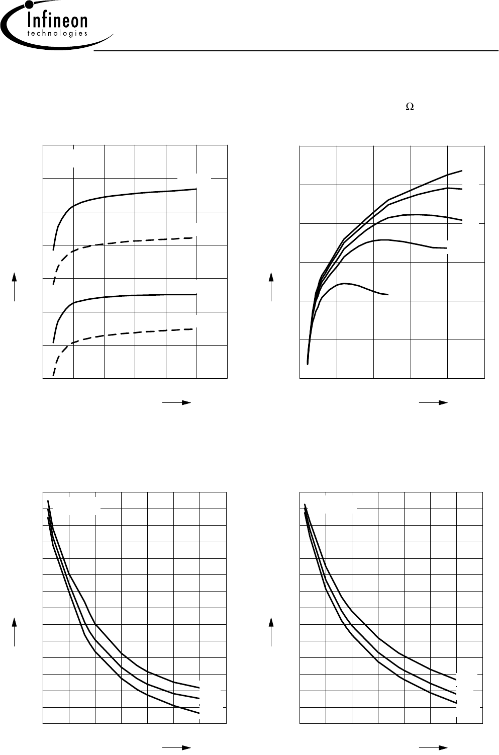
Intermodulation Intercept Point IP3=f(IC)
(3rd order, Output, ZS=ZL=50 )
VCE = Parameter, f = 900MHz
0 5 10 15 V25
IC
0
5
10
15
20
dBm
30
IP
3
8V
5V
3V
2V
1V
Power Gain Gma, Gms = f(VCE):_____
|S21|2 = f(VCE):---------
f = Parameter
02468V12
VCE
6
8
10
12
14
16
dB
20
G
0.9GHz
1.8GHz
0.9GHz
1.8GHz
IC=10mA
Power Gain |S21|2= f(f)
VCE = Parameter
0.0 0.5 1.0 1.5 2.0 2.5 GHz 3.5
f
0
2
4
6
8
10
12
14
16
18
20
22
24
dB
28
S
21
10V
1V
0.7V
IC=10mA
Power Gain Gma, Gms = f(f)
VCE = Parameter
0.0 0.5 1.0 1.5 2.0 2.5 GHz 3.5
f
4
6
8
10
12
14
16
18
20
22
24
26
28
dB
32
G
10V
1V
0.7V
IC=10mA