Bq24740 Datasheet. Www.s Manuals.com. Ti
User Manual: Datasheets bq24740.
Open the PDF directly: View PDF ![]() .
.
Page Count: 34
- FEATURES
- APPLICATIONS
- DESCRIPTION
- DESCRIPTION (continued)
- PACKAGE THERMAL DATA
- ABSOLUTE MAXIMUM RATINGS
- RECOMMENDED OPERATING CONDITIONS
- ELECTRICAL CHARACTERISTICS
- TYPICAL CHARACTERISTICS
- DETAILED DESCRIPTION
- BATTERY VOLTAGE REGULATION
- BATTERY CURRENT REGULATION
- INPUT ADAPTER CURRENT REGULATION
- ADAPTER DETECT AND POWER UP
- ENABLE AND DISABLE CHARGING
- AUTOMATIC INTERNAL SOFT-START CHARGER CURRENT
- CONVERTER OPERATION
- SYNCHRONOUS AND NON-SYNCHRONOUS OPERATION
- ISYNSET CONTROL (SYN and NON-SYN MODE SETTING)
- HIGH ACCURACY IADAPT USING CURRENT SENSE AMPLIFIER (CSA)
- INPUT OVERVOLTAGE PROTECTION (ACOV)
- INPUT UNDERVOLTAGE LOCK OUT (UVLO)
- INPUT CURRENT LOW-POWER MODE DETECTION
- BATTERY OVERVOLTAGE PROTECTION
- CHARGE OVERCURRENT PROTECTION
- THERMAL SHUTDOWN PROTECTION
- Status Outputs (EXTPWR, LPMD, DPMDET pin)
- APPLICATION INFORMATION
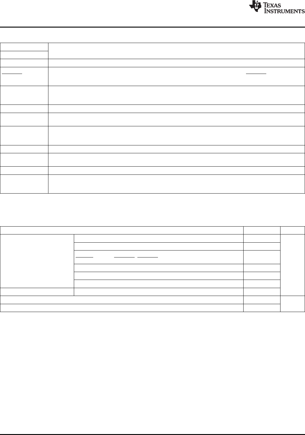
1
FEATURES APPLICATIONS
DESCRIPTION
LPREF
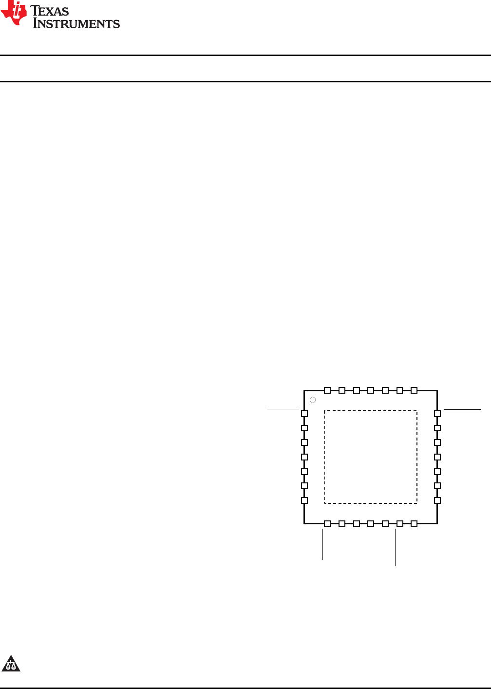
bq24740
28LDQFN
TOP VIEW
DPMDET
SRN
BAT
CELLS
SRP
SRSET
IADAPT
LPMD
ACSET
CHGEN
ACN
ACP
ACDET
PVCC
BTST
HIDRV
REGN
PH
LODRV
PGND
IADSLP
AGND
VREF
VADJ
VDAC
EXTPWR
ISYNSET
1
2
3
4
5
6
7
8 9 10 11 12 13 14
15
16
17
18
19
20
21
22232425262728
bq24740
www.ti.com
............................................................................................................................................... SLUS736C – DECEMBER 2006 – REVISED MARCH 2009
Host-Controlled Multi-Chemistry Battery Charger With Low Input Power Detect
•Notebook and Ultra-Mobile Computers2
•NMOS-NMOS Synchronous Buck Converterwith 300 kHz Frequency and >95% Efficiency
•Portable Data-Capture Terminals
•Portable Printers•30-ns Minimum Driver Dead-time and 99.5%Maximum Effective Duty Cycle
•Medical Diagnostics Equipment
•Battery Bay Chargers•High-Accuracy Voltage and Current Regulation
•Battery Back-up Systems– ± 0.5% Charge Voltage Accuracy
– ± 3% Charge Current Accuracy
– ± 3% Adapter Current Accuracy
The bq24740 is a high-efficiency, synchronous– ± 2% Input Current Sense Amp Accuracy
battery charger with integrated compensation,•Integration
offering low component count for space-constrained– Internal Loop Compensation
multi-chemistry battery charging applications.Ratiometric charge current and voltage programming– Internal Soft Start
allows high regulation accuracies, and can be either•Safety
hardwired with resistors or programmed by the– Input Overvoltage Protection (OVP)
system power-management microcontroller using aDAC or GPIOs.– Dynamic Power Management (DPM) withStatus Indicator
The bq24740 charges two, three, or four series Li+cells, supporting up to 10 A of charge current, and is•Supports Two, Three, or Four Li+ Cells
available in a 28-pin, 5x5-mm thin QFN package.•5 – 24 V AC/DC-Adapter Operating Range
•Analog Inputs with Ratiometric Programmingvia Resistors or DAC/GPIO Host Control
– Charge Voltage (4-4.512 V/Cell)
– Charge Current (up to 10 A, with 10-m Ω
Sense Resistor)
– Adapter Current Limit (DPM)
•Status and Monitoring Outputs
– AC/DC Adapter Present with ProgrammableVoltage Threshold
– Low Input-Power Detect with AdjustableThreshold and Hysteresis
– DPM Loop Active
– Current Drawn from Input Source
•Battery Discharge Current Sense with NoAdapter, or Selectable Low-Iq mode
•Supports Any Battery Chemistry: Li+, NiCd,NiMH, Lead Acid, etc.
•Charge Enable
•10- µA Off-State Current
•28-pin, 5x5-mm QFN package
1
Please be aware that an important notice concerning availability, standard warranty, and use in critical applications of TexasInstruments semiconductor products and disclaimers thereto appears at the end of this data sheet.
2PowerPad is a trademark of Texas Instruments.
PRODUCTION DATA information is current as of publication date.
Copyright © 2006 – 2009, Texas Instruments IncorporatedProducts conform to specifications per the terms of the TexasInstruments standard warranty. Production processing does notnecessarily include testing of all parameters.
DESCRIPTION (CONTINUED)
VREF
RAC
0.010 Ω
.( 1 ) Pull - uprailcouldbeeitherVREForothersystemrail
( 2 ) SRSET / ACSET couldcomefromeitherDACorresistordividers .
Q1 (ACFET)
SI4435
Q3(BATFET )
SI4435
Controlledby
HOST
N
PP
ACN
ACP
ACDET
EXTPWR
SRSET
ACSET
VREF
DAC
CELLS
CHGEN
VDAC
VADJ
DAC
ADC IADAPT
HOST
PVCC
HIDRV
N
PH
BTST
REGN
LODRV
PGND
SRP
SRN
P
PACK+
PACK-
SYSTEM
ADAPTER+
ADAPTER-
EXTPWR
AGND
bq24740
432 kΩ
1%
66.5 kΩ
1%
R1
R2
R3
C4
C2 C3
C5
C8
Q4
FDS6680A
Q5
FDS 6680 A
C9 L1
D1 BAT 54
C10
BAT
IADSLP
ISYNSET
R6
24 kΩ
DPMDET
R4
LPMD
VREF
LPREF
R7
200 kΩ
R8
24.9 kΩ
R9
1.8 MΩ
Q2 (ACFET )
SI4435
Controlledby
HOST
C6
C15
0.1 µF
R5
C1
2 Ω
R10
2.2 µF
0.1 µF0.1 µF
1µF
10k Ω 10k Ω
10k Ω
100 pF
C14
0.1 µF
C13
0.1 µF
0.1 µF
1µF
C11
10 µF
8.2 µH
RSR
0.010 Ω
0.1 µF
10 µF
C7
10 µF
C12
10 µF
PowerPad
D2
BAT54
bq24740
SLUS736C – DECEMBER 2006 – REVISED MARCH 2009 ...............................................................................................................................................
www.ti.com
These devices have limited built-in ESD protection. The leads should be shorted together or the device placed in conductive foamduring storage or handling to prevent electrostatic damage to the MOS gates.
The bq24740 features Dynamic Power Management (DPM) and input power limiting. These features reducebattery charge current when the input power limit is reached to avoid overloading the ac adapter when supplyingthe load and the battery charger simultaneously. A current-sense amplifier enables precise measurement of inputcurrent from the ac adapter to monitor the overall system power. If the adapter current is above the programmedlow-power threshold, a signal is sent to host so that the system optimizes its power performance according towhat is available from the adapter.
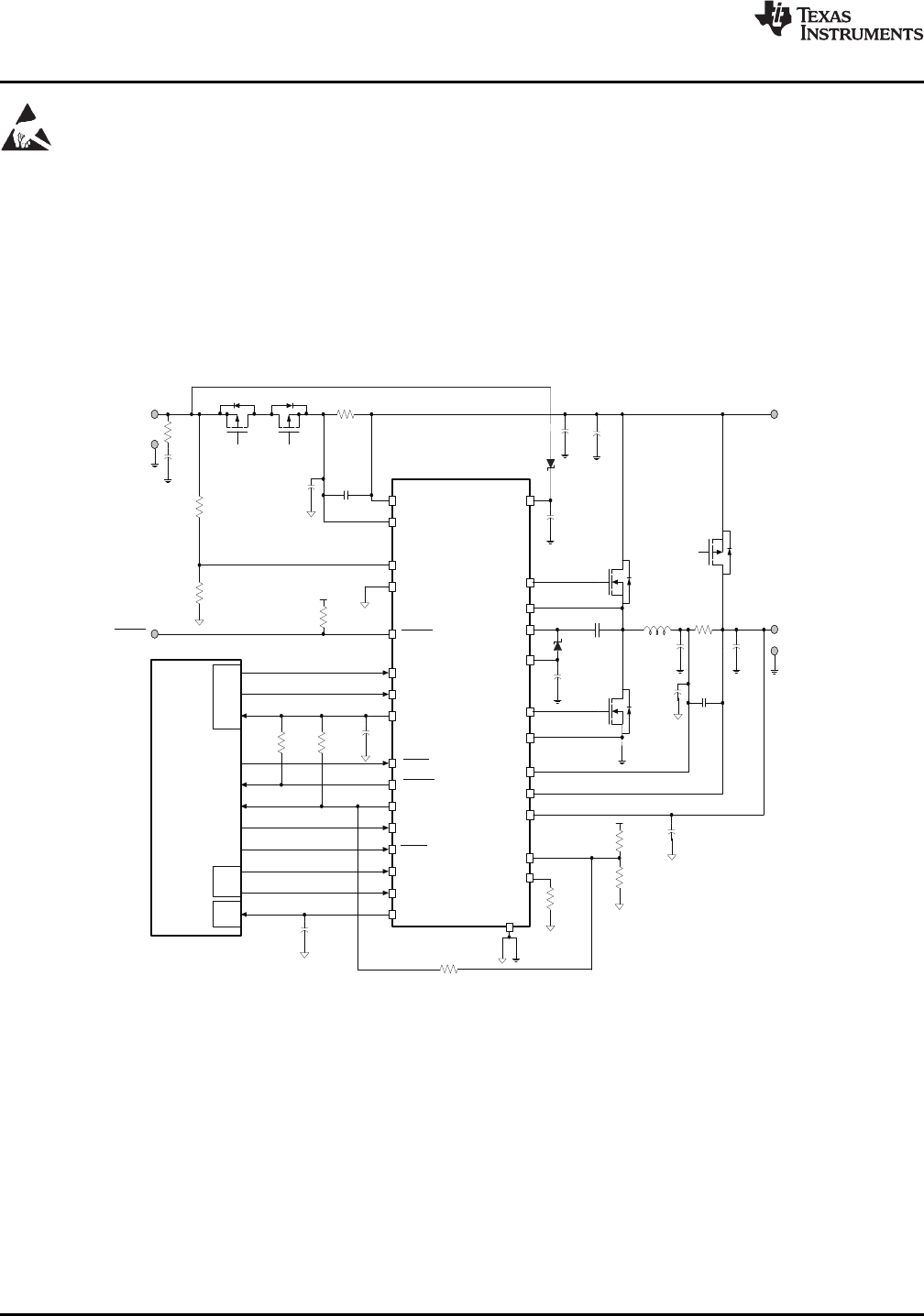
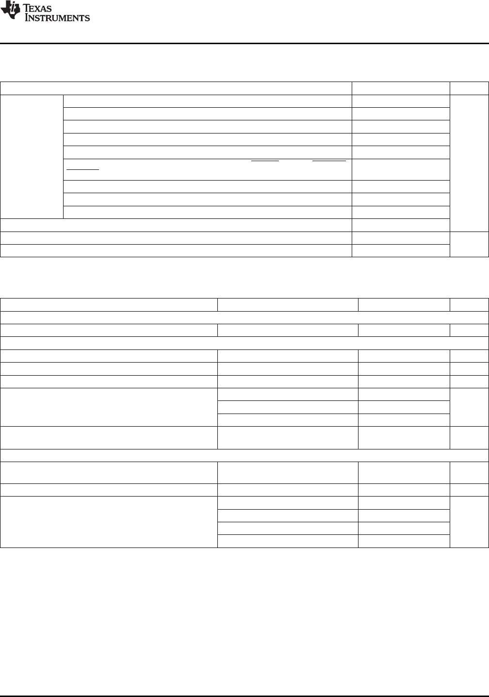
TYPICAL APPLICATION
V
IN
= 20 V, V
BAT
= 3-cell Li-Ion, I
CHARGE
= 3 A, I
ADAPTER_LIMIT
= 4 A
Figure 1. Typical System Schematic, Voltage and Current Programmed by DAC
2Submit Documentation Feedback Copyright © 2006 – 2009, Texas Instruments Incorporated
Product Folder Link(s) :bq24740
VREF
100 kΩ
R 11
66.5 k Ω
R 12
100 kΩ
R 13
43 k Ω
R 14
VREF
R AC
0 .010 Ω
( 1 ) Pull- uprailcouldbeeitherVREForothersystemrail.
( 2 ) SRSET / ACSET couldcomefromeitherDACorresistordividers.
Q 1 ( ACFET )
SI 4435
Q 3 (BATFET )
SI 4435
Controlledby
HOST
N
PP
ACN
ACP
ACDET
EXTPWR
SRSET
ACSET
VREF
GPIO
CELLS
CHGEN
VDAC
VADJ
ADC IADAPT
HOST
PVCC
HIDRV
N
PH
BTST
REGN
LODRV
PGND
SRP
SRN
P
PACK+
PACK-
SYSTEMADAPTER+
ADAPTER-
EXTPWR
AGND
432 k Ω
1 %
66 . 5 k Ω
1 %
R 1
R 2
R 3
C 4
C 2 C 3
C 5
C 8
Q 4
FDS 6680 A
Q 5
FDS 6680 A
C 9
L 1
D 1 BAT 54
C 10
BAT
IADSLP
ISYNSET
R 6
24 k Ω
DPMDET
R 4
LPMD
VREF
LPREF
R 7
200 k Ω
R 8
24.9 k Ω
R 9
1 .8 M Ω
Q 2 (ACFET)
SI4435
Controlledby
HOST
C 6
C 15
0. 1 µF
R 5
C 1
2 Ω
R 10
2. 2 µF
0. 1 µF0 . 1 µF
1µF
10 k Ω 10 kΩ
10 k Ω
100 pF
C 14
0 .1 µF
C 13
0 .1 µF
0. 1 µF
1µF
C 11
10 µF
8. 2 µH
RSR
0 .010 Ω
0. 1 µF
10 µF
C 7
10 µF
C 12
10 µF
PowerPad
VREF
REGN
D2
BAT54
bq24740
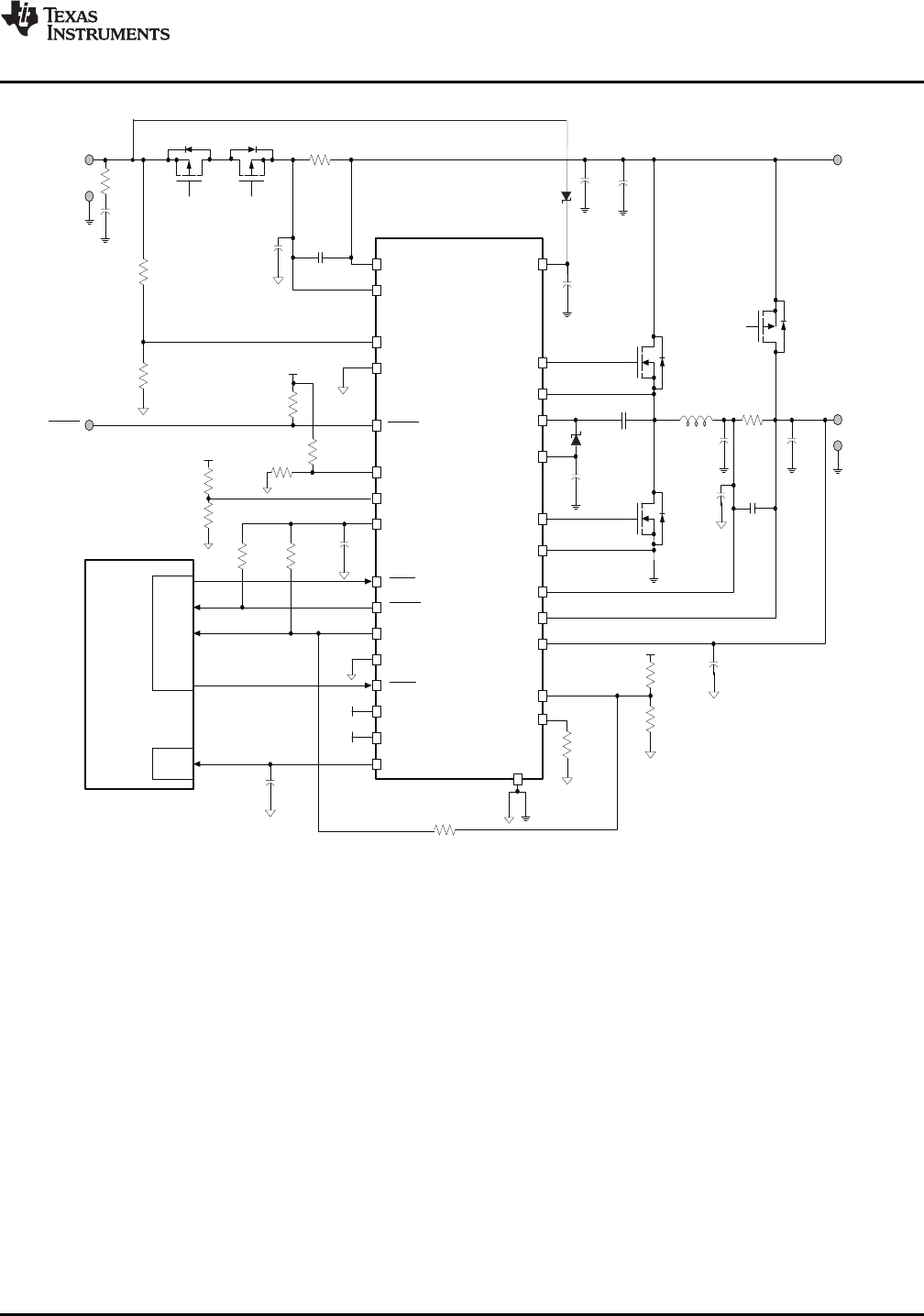
bq24740
www.ti.com
............................................................................................................................................... SLUS736C – DECEMBER 2006 – REVISED MARCH 2009
A. V
IN
= 20 V, V
BAT
= 3-cell Li-Ion, I
CHARGE
= 3 A, I
ADAPTER_LIMIT
= 4 A
Figure 2. Typical System Schematic, Voltage and Current Programmed by Resistor
Copyright © 2006 – 2009, Texas Instruments Incorporated Submit Documentation Feedback 3
Product Folder Link(s) :bq24740
VREF
R AC
0 .010 Ω
( 1 ) Pull - uprailcouldbeeitherVREForothersystemrail .
( 2 ) SRSET / ACSET couldcomefromeitherDACorresistordividers .
Q1 (ACFET )
SI4435
Q3 (BATFET)
SI4435
Controlledby
HOST
N
PP
ACN
ACP
ACDET
EXTPWR
SRSET
ACSET
VREF
DAC
CELLS
CHGEN
VDAC
VADJ
DAC
ADC IADAPT
HOST
PVCC
HIDRV
N
PH
BTST
REGN
LODRV
PGND
SRP
SRN
P
PACK+
PACK-
SYSTEMADAPTER+
ADAPTER-
/EXTPWR
AGND
bq 24740
432 kΩ
1 %
66.5 kΩ
1 %
R1
R2
R 3
C 4
C 2 C 3
C 5
C 8
Q4
FDS 6680 A
Q 5
FDS6680A
C 9 L 1
D 1 BAT 54
C10
BAT
IADSLP
ISYNSET
R 6
24 kΩ
DPMDET
R 4
LPMD
VREF
LPREF
R 7
200 kΩ
R 8
24.9 kΩ
R 9
1.8 M Ω
Q 2 (ACFET )
SI 4435
Controlledby
HOST
C 6
C 15
0 .1 µF
R 5
C 1
2 Ω
R10
2.2 µF
0.1 µF0.1 µF
1µF
10 k Ω 10 k Ω
10 kΩ
100 pF
C 14
0 .1 µF
C 13
0 .1 µF
0.1 µF
1µF
C 11
10 µF
8.2 µH
RSR
0 .010 Ω
0.1 µF
10 µFC7
10 µF
C 12
10 µF
PowerPad
D2
BAT54C
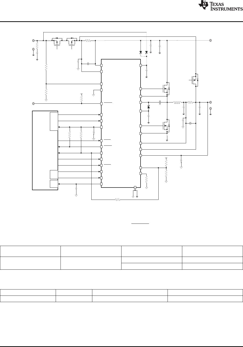
PACKAGE THERMAL DATA
bq24740
SLUS736C – DECEMBER 2006 – REVISED MARCH 2009 ...............................................................................................................................................
www.ti.com
V
IN
= 20 V, V
BAT
= 3-cell Li-Ion, I
CHARGE
= 3 A, I
ADAPTER_LIMIT
= 4 A
Figure 3. Typical System Schematic: Sensing Battery Discharge Current,When Adapter Removed. (Set IADSLP at logic high)
ORDERING INFORMATION
Ordering NumberPart number Package Quantity(Tape and Reel)
bq24740RHDR 3000bq24740 28-PIN 5 x 5 mm QFN
bq24740RHDT 250
PACKAGE θ
JA
T
A
= 70 ° C POWER RATING DERATING FACTOR ABOVE T
A
= 25 ° C
QFN – RHD
(1) (2)
39 ° C/W 2.36 W 0.028 W/ ° C
(1) For the most current package and ordering information, see the Package Option Addendum at the end of this document, or see the TIWeb site at www.ti.com .(2) This data is based on using the JEDEC High-K board and the exposed die pad is connected to a Cu pad on the board. This isconnected to the ground plane by a 2x3 via matrix.
4Submit Documentation Feedback Copyright © 2006 – 2009, Texas Instruments Incorporated
Product Folder Link(s) :bq24740

bq24740
www.ti.com
............................................................................................................................................... SLUS736C – DECEMBER 2006 – REVISED MARCH 2009
Table 1. TERMINAL FUNCTIONS – 28-PIN QFN
TERMINAL
DESCRIPTIONNAME NO.
CHGEN 1 Charge enable active-low logic input. LO enables charge. HI disables charge.
Adapter current sense resistor, negative input. A 0.1- µF ceramic capacitor is placed from ACN pin to AGND forACN 2
common-mode filtering. A 0.1- µF ceramic capacitor is placed from ACN to ACP to provide differential-mode filtering.
Adapter current sense resistor, positive input. A 0.1- µF ceramic capacitor is placed from ACN to ACP to provideACP 3
differential-mode filtering. A 0.1- µF ceramic capacitor is placed from ACP pin to AGND for common-mode filtering.
Low power mode detect active-high open-drain logic output. Place a 10-k Ωpullup resistor from LPMD pin to thepullup-voltage rail. Place a positive-feedback resistor from LPMD pin to LPREF pin for programming hysteresis (seeLPMD 4
the design example for calculation). The output is HI when I
ADAPT
pin voltage is lower than LPREF pin voltage. Theoutput is LO when IADAPT pin voltage is higher than LPREF pin voltage.
Adapter detected voltage set input. Program the adapter detect threshold by connecting a resistor divider fromadapter input to ACDET pin to AGND pin. Adapter voltage is detected if ACDET-pin voltage is greater than 2.4 V.ACDET 5 The I
ADAPT
current sense amplifier is active when the ACDET pin voltage is greater than 0.6 V. ACOV is inputovervoltage protection; it disables charge when ACDET > 3.1 V. ACOV does not latch, and normal operationresumes when ACDET < 3.1 V.
Adapter current set input. The voltage ratio of ACSET voltage versus VDAC voltage programs the input currentregulation set-point during Dynamic Power Management (DPM). Program by connecting a resistor divider from VDACACSET 6
to ACSET to AGND; or by connecting the output of an external DAC to the ACSET pin and connect the DAC supplyto the VDAC pin.
Low power voltage set input. Connect a resistor divider from VREF to LPREF and AGND to program the referencefor the LOPWR comparator. The LPREF-pin voltage is compared to the IADAPT-pin voltage and the logic output isLPREF 7
given on the LPMD open-drain pin. Connecting a positive-feedback resistor from LPREF pin to LPMD pin programsthe hysteresis.
Enable IADAPT to enter sleep mode; active-low logic input. Allows low I
q
sleep mode when adapter not detected.Logic low turns off the Input Current Sense Amplifier (IADAPT) when adapter is not detected and ACDET pin is < 0.6IADSLP 8
V - allows lower battery discharge current. Logic high keeps IADAPT current-sense amplifier on when adapter is notdetected and ACDET pin is < 0.6 V - this allows measuring battery discharge current.
Analog ground. Ground connection for low-current sensitive analog and digital signals. On PCB layout, connect to theAGND 9
analog ground plane, and only connect to PGND through the PowerPad underneath the IC.
3.3-V regulated voltage output. Place a 1- µF ceramic capacitor from VREF to AGND pin close to the IC. This voltageVREF 10 could be used for ratiometric programming of voltage and current regulation. VREF is the source for the internalcircuit.
Charge voltage set reference input. Connect the VREF or external DAC voltage source to the VDAC pin. Batteryvoltage, charge current, and input current are programmed as a ratio of the VDAC pin voltage versus the VADJ,VDAC 11 SRSET, and ACSET pin voltages, respectively. Place resistor dividers from VDAC to VADJ, SRSET, and ACSETpins to AGND for programming. A DAC could be used by connecting the DAC supply to VDAC and connecting theoutput to VADJ, SRSET, or ACSET.
Charge voltage set input. The voltage ratio of VADJ voltage versus VDAC voltage programs the battery voltageregulation set-point. Program by connecting a resistor divider from VDAC to VADJ, to AGND; or, by connecting theVADJ 12
output of an external DAC to VADJ, and connect the DAC supply to VDAC. VADJ connected to REGN programs thedefault of 4.2 V per cell.
Valid adapter active-low detect logic open-drain output. Pulled low when input voltage is above ACDET programmedEXTPWR 13 threshold, OR input current is greater than 1.25 A with 10-m Ωsense resistor. Connect a 10-k Ωpullup resistor fromEXTPWR pin to pullup supply rail.
Synchronous mode current set input. Place a resistor from ISYNSET to AGND to program the charge undercurrentISYNSET 14 threshold to force non-synchronous converter operation at low output current, and to prevent negative inductorcurrent. Threshold should be set at greater than half of the maximum inductor ripple current (50% duty cycle).
Adapter current sense amplifier output. IADAPT voltage is 20 times the differential voltage across ACP-ACN. Place aIADAPT 15
100-pF or less ceramic decoupling capacitor from IADAPT to AGND.
Charge current set input. The voltage ratio of SRSET voltage versus VDAC voltage programs the charge currentSRSET 16 regulation set-point. Program by connecting a resistor divider from VDAC to SRSET to AGND; or by connecting theoutput of an external DAC to SRSET pin and connect the DAC supply to VDAC pin.
Battery voltage remote sense. Directly connect a kelvin sense trace from the battery pack positive terminal to theBAT 17 BAT pin to accurately sense the battery pack voltage. Place a 0.1- µF capacitor from BAT to AGND close to the IC tofilter high-frequency noise.
Charge current sense resistor, negative input. A 0.1- µF ceramic capacitor is placed from SRN to SRP to provideSRN 18 differential-mode filtering. An optional 0.1- µF ceramic capacitor is placed from SRN pin to AGND for common-modefiltering.
Charge current sense resistor, positive input. A 0.1- µF ceramic capacitor is placed from SRN to SRP to provideSRP 19
differential-mode filtering. A 0.1- µF ceramic capacitor is placed from SRP pin to AGND for common-mode filtering.
Copyright © 2006 – 2009, Texas Instruments Incorporated Submit Documentation Feedback 5
Product Folder Link(s) :bq24740
ABSOLUTE MAXIMUM RATINGS
bq24740
SLUS736C – DECEMBER 2006 – REVISED MARCH 2009 ...............................................................................................................................................
www.ti.com
Table 1. TERMINAL FUNCTIONS – 28-PIN QFN (continued)
TERMINAL
DESCRIPTIONNAME NO.
CELLS 20 2, 3 or 4 cells selection logic input. Logic low programs 3 cell. Logic high programs 4 cell. Floating programs 2 cell.
Dynamic power management (DPM) input current loop active, open-drain output status. Logic low indicates inputDPMDET 21 current is being limited by reducing the charge current. Connect 10-k Ωpullup resistor from DPMDET to VREF or adifferent pullup-supply rail.
Power ground. Ground connection for high-current power converter node. On PCB layout, connect directly to sourcePGND 22 of low-side power MOSFET, to ground connection of in put and output capacitors of the charger. Only connect toAGND through the PowerPad underneath the IC.
LODRV 23 PWM low side driver output. Connect to the gate of the low-side power MOSFET with a short trace.
PWM low side driver positive 6-V supply output. Connect a 1- µF ceramic capacitor from REGN to PGND, close to theREGN 24
IC. Use for high-side driver bootstrap voltage by connecting a small-signal Schottky diode from REGN to BTST.
PWM high side driver negative supply. Connect to the phase switching node (junction of the low-side powerPH 25 MOSFET drain, high-side power MOSFET source, and output inductor). Connect the 0.1- µF bootstrap capacitor fromfrom PH to BTST.
HIDRV 26 PWM high side driver output. Connect to the gate of the high-side power MOSFET with a short trace.
PWM high side driver positive supply. Connect a 0.1- µF bootstrap ceramic capacitor from BTST to PH. Connect aBTST 27
small bootstrap Schottky diode from REGN to BTST.
PVCC 28 IC power positive supply. Place a 0.1- µF ceramic capacitor from PVCC to PGND pin close to the IC.
Exposed pad beneath the IC. AGND and PGND star-connected only at the PowerPad plane. Always solderPowerPad™ PowerPad to the board, and have vias on the PowerPad plane connecting to AGND and PGND planes. It also servesas a thermal pad to dissipate the heat.
over operating free-air temperature range (unless otherwise noted)
(1) (2)
VALUE UNIT
PVCC, ACP, ACN, SRP, SRN, BAT – 0.3 to 30
PH – 1 to 30
REGN, LODRV, VADJ, ACSET, SRSET, ACDET, ISYNSET, LPMD, LPREF,
– 0.3 to 7CHGEN, CELLS, EXTPWR, DPMDETVoltage range
VVDAC – 0.3 to 5.5
VREF – 0.3 to 3.6
BTST, HIDRV with respect to AGND and PGND, IADAPT – 0.3 to 36
Maximum difference voltage ACP – ACN, SRP – SRN, AGND – PGND – 0.5 to 0.5
Junction temperature range – 40 to 155
° CStorage temperature range – 55 to 155
(1) Stresses beyond those listed under absolute maximum ratings may cause permanent damage to the device. These are stress ratingsonly, and functional operation of the device at these or any other conditions beyond those indicated under recommended operatingconditions is not implied. Exposure to absolute-maximum-rated conditions for extended periods may affect device reliability.(2) All voltages are with respect to GND if not specified. Currents are positive into, negative out of the specified terminal. Consult PackagingSection of the data book for thermal limitations and considerations of packages.
6Submit Documentation Feedback Copyright © 2006 – 2009, Texas Instruments Incorporated
Product Folder Link(s) :bq24740
RECOMMENDED OPERATING CONDITIONS
ELECTRICAL CHARACTERISTICS
bq24740
www.ti.com
............................................................................................................................................... SLUS736C – DECEMBER 2006 – REVISED MARCH 2009
over operating free-air temperature range (unless otherwise noted)
MIN NOM MAX UNIT
PH – 1 24
PVCC, ACP, ACN, SRP, SRN, BAT 0 24
REGN, LODRV 0 6.5
VREF 0 3.3
VDAC, IADAPT 0 3.6Voltage range
VACSET, SRSET, ACDET, ISYNSET, LPMD, LPREF, CHGEN, CELLS, EXTPWR, 0 5.5DPMDET
VADJ 0 6.5
BTST, HIDRV with respect to AGND and PGND 0 30
AGND, PGND – 0.3 0.3
Maximum difference voltage: ACP – ACN, SRP – SRN – 0.3 0.3
Junction temperature range – 40 125
° CStorage temperature range – 55 150
7 V ≤V
PVCC
≤24 V, 0 ° C < T
J
< 125 ° C, typical values are at T
A
= 25 ° C, with respect to AGND (unless otherwise noted)
PARAMETER TEST CONDITIONS MIN TYP MAX UNIT
OPERATING CONDITIONS
V
PVCC_OP
PVCC Input voltage operating range 5 24 V
CHARGE VOLTAGE REGULATION
V
BAT_REG_RNG
BAT voltage regulation range 4V-4.512V per cell, times 2,3,4 cell 8 18 V
V
VDAC_OP
VDAC reference voltage range 2.6 3.6 V
V
ADJ_OP
VADJ voltage range 0 REGN V
8 V, 8.4 V, 9.024 V – 0.5% 0.5%
Charge voltage regulation accuracy 12 V, 12.6 V, 13.536 V – 0.5% 0.5%
16 V, 16.8 V, 18.048 V – 0.5% 0.5%
VADJ connected to REGN, 8.4 V,Charge voltage regulation set to default to
– 0.5% 0.5%4.2 V per cell
12.6 V, 16.8 V
CHARGE CURRENT REGULATION
Charge current regulation differentialV
IREG_CHG
V
IREG_CHG
= V
SRP
– V
SRN
0 100 mVvoltage range
V
SRSET_OP
SRSET voltage range 0 VDAC V
V
IREG_CHG
= 40 – 100 mV – 3 3
V
IREG_CHG
= 20 mV – 5 5Charge current regulation accuracy %V
IREG_CHG
= 5 mV – 25 25
V
IREG_CHG
= 1.5 mV (V
BAT
≥4 V) – 33 33
Copyright © 2006 – 2009, Texas Instruments Incorporated Submit Documentation Feedback 7
Product Folder Link(s) :bq24740

bq24740
SLUS736C – DECEMBER 2006 – REVISED MARCH 2009 ...............................................................................................................................................
www.ti.com
ELECTRICAL CHARACTERISTICS (continued)
7 V ≤V
PVCC
≤24 V, 0 ° C < T
J
< 125 ° C, typical values are at T
A
= 25 ° C, with respect to AGND (unless otherwise noted)
PARAMETER TEST CONDITIONS MIN TYP MAX UNIT
INPUT CURRENT REGULATION
Adapter current regulation differentialV
IREG_DPM
V
IREG_DPM
= V
ACP
– V
ACN
0 100 mVvoltage range
V
ACSET_OP
ACSET voltage range 0 VDAC V
V
IREG_DPM
= 40 – 100 mV – 3% 3%
V
IREG_DPM
= 20 mV – 5% 5%Input current regulation accuracy
V
IREG_DPM
= 5 mV – 25% 25%
V
IREG_DPM
= 1.5 mV – 33% 33%
VREF REGULATOR
V
VREF_REG
VREF regulator voltage V
ACDET
> 0.6 V, 0-30 mA 3.267 3.3 3.333 V
I
VREF_LIM
VREF current limit V
VREF
= 0 V, V
ACDET
> 0.6 V 35 75 mA
REGN REGULATOR
V
ACDET
> 0.6 V, 0-75 mA, PVCC > 10V
REGN_REG
REGN regulator voltage 5.6 5.9 6.2 VV
I
REGN_LIM
REGN current limit V
REGN
= 0 V, V
ACDET
> 0.6 V 90 135 mA
ADAPTER CURRENT SENSE AMPLIFIER
V
ACP/N_OP
Input common mode range Voltage on ACP/SRN 0 24 V
V
IADAPT
IADAPT output voltage range 0 2 V
I
IADAPT
IADAPT output current 0 1 mA
A
IADAPT
Current sense amplifier voltage gain A
IADAPT
= V
IADAPT
/ V
IREG_DPM
20 V/V
V
IREG_DPM
= 40 – 100 mV – 2% 2%
V
IREG_DPM
= 20 mV – 3% 3%Adapter current sense accuracy
V
IREG_DPM
= 5 mV – 25% 25%
V
IREG_DPM
= 1.5 mV – 30% 30%
I
IADAPT_LIM
Output current limit V
IADAPT
= 0 V 1 mA
C
IADAPT_MAX
Maximum output load capacitance For stability with 0 mA to 1 mA load 100 pF
ACDET COMPARATOR
V
PVCC-BAT_OP
Differential Voltage from PVCC to BAT – 20 24 V
Min voltage to enable charging,V
ACDET_CHG
ACDET adapter-detect rising threshold 2.376 2.40 2.424 VV
ACDET
rising
V
ACDET_CHG_HYS
ACDET falling hysteresis V
ACDET
falling 40 mV
ACDET rising deglitch
(1)
VACDET rising 518 700 908 ms
ACDET falling deglitch VACDET falling 7 9 11 ms
Min voltage to enable all bias, V
ACDETV
ACDET_BIAS
ACDET enable-bias rising threshold 0.56 0.62 0.68 Vrising
V
ACDET_BIAS_HYS
Adapter present falling hysteresis V
ACDET
falling 20 mV
ACDET rising deglitch
(1)
V
ACDET
rising 10
µsACDET falling deglitch V
ACDET
falling 10
INPUT OVERVOLTAGE COMPARATOR (ACOV)
AC Over-voltage rising threshold onV
ACOV
ACDET (See ACDET in Terminal 3.007 3.1 3.193 VFunctions )
AC Overvoltage rising deglitch 1.3V
ACOV_HYS
msAC Overvoltage falling deglitch 1.3
(1) Specified by design.
8Submit Documentation Feedback Copyright © 2006 – 2009, Texas Instruments Incorporated
Product Folder Link(s) :bq24740

bq24740
www.ti.com
............................................................................................................................................... SLUS736C – DECEMBER 2006 – REVISED MARCH 2009
ELECTRICAL CHARACTERISTICS (continued)
7 V ≤V
PVCC
≤24 V, 0 ° C < T
J
< 125 ° C, typical values are at T
A
= 25 ° C, with respect to AGND (unless otherwise noted)
PARAMETER TEST CONDITIONS MIN TYP MAX UNIT
AC CURRENT DETECT COMPARATOR (INPUT UNDERCURRENT)
V
ACIDET
Adapter current detect rising threshold V
ACI
= I
AC
× R
AC
× 20, falling edge 200 250 300 mV
V
ACIDET_HYS
Adapter current detect hysteresis Rising edge 50 mV
PVCC / BAT COMPARATOR
V
PVCC-BAT_FALL
PVCC to BAT falling threshold V
PVCC
– V
BAT
to disable charger 140 185 240 mV
V
PVCC-BAT__HYS
PVCC to BAT hysteresis 50 mV
PVCC to BAT Rising Deglitch V
PVCC
– V
BAT
> V
PVCC-BAT_RISE
7 9 11 ms
PVCC to BAT Falling Deglitch V
PVCC
– V
BAT
< V
PVCC-BAT_FALL
10 µs
INPUT UNDERVOLTAGE LOCK-OUT COMPARATOR (UVLO)
UVLO AC Undervoltage rising threshold Measure on PVCC 3.5 4 4.5 V
UVLO_HYS AC Undervoltage hysteresis, falling 260 mV
BAT OVERVOLTAGE COMPARATOR
V
OV_RISE
Overvoltage rising threshold
(2)
104%As percentage of V
BAT_REGV
OV_FALL
Overvoltage falling threshold
(2)
102%
CHARGE OVERCURRENT COMPARATOR
V
OC
Charge overcurrent falling threshold As percentage of I
REG_CHG
145%
Minimum Current Limit (SRP-SRN) 50 mV
INPUT CURRENT LOW-POWER MODE COMPARATOR
V
ACLP_HYS
AC low power hysteresis 2.8
mVV
ACLP_OFFSET
AC low power rising threshold 1
THERMAL SHUTDOWN COMPARATOR
T
SHUT
Thermal shutdown rising temperature Temperature Increasing 155
° CT
SHUT_HYS
Thermal shutdown hysteresis, falling 20
PWM HIGH SIDE DRIVER (HIDRV)
R
DS(on)_HI
High side driver turn-on resistance V
BTST
– V
PH
= 5.5 V, tested at 100 mA 3 6
ΩR
DS(off)_HI
High side driver turn-off resistance V
BTST
– V
PH
= 5.5 V, tested at 100 mA 0.7 1.4
Bootstrap refresh comparator threshold V
BTST
– V
PH
when low side refreshV
BTST_REFRESH
4 Vvoltage pulse is requested
PWM LOW SIDE DRIVER (LODRV)
R
DS(on)_HI
Low side driver turn-on resistance REGN = 6 V, tested at 100 mA 3 6
ΩR
DS(off)_LO
Low side driver turn-off resistance REGN = 6 V, tested at 100 mA 0.6 1.2
PWM DRIVERS TIMING
Driver Dead Time — Dead time whenswitching between LODRV and HIDRV. No 30 nsload at LODRV and HIDRV
PWM OSCILLATOR
F
SW
PWM switching frequency 240 360 kHz
V
RAMP_HEIGHT
PWM ramp height As percentage of PVCC 6.6 %PVCC
(2) Specified by design.
Copyright © 2006 – 2009, Texas Instruments Incorporated Submit Documentation Feedback 9
Product Folder Link(s) :bq24740
bq24740
SLUS736C – DECEMBER 2006 – REVISED MARCH 2009 ...............................................................................................................................................
www.ti.com
ELECTRICAL CHARACTERISTICS (continued)
7 V ≤V
PVCC
≤24 V, 0 ° C < T
J
< 125 ° C, typical values are at T
A
= 25 ° C, with respect to AGND (unless otherwise noted)
PARAMETER TEST CONDITIONS MIN TYP MAX UNIT
QUIESCENT CURRENT
V
BAT
= 16.8 V, V
ACDET
< 0.6 V,
7 10Total off-state quiescent current into pins
V
PVCC
> 5 V, T
J
= 85 ° CI
OFF_STATE
SRP, SRN, BAT, BTST, PH, PVCC, ACP,
V
BAT
= 16.8 V, V
ACDET
< 0.6 V,ACN
7 11 µAV
PVCC
> 5 V, T
J
= 125 ° C
Total quiescent current into pins SRP, Adapter present, VACDET > 2.4V,I
BATQ_CD
100 200SRN, BAT, BTST, PH charge disabled
I
AC
Adapter quiescent current V
PVCC
= 20 V, charge disabled 2.8 4 mA
INTERNAL SOFT START (8 steps to regulation current)
Soft start steps 8 step
Soft start step time 1.7 ms
CHARGER SECTION POWER-UP SEQUENCING
Delay from when adapter is detectedCharge-enable delay after power-up to when the charger is allowed to turn 518 700 908 mson
ISYNSET AMPLIFIER AND COMPARATOR (SYNCHRONOUS TO NON-SYNCHRONOUS TRANSITION)
I
SYN
Accuracy V
(SRP-SRN)
= 5 mV – 20% 20%
ISYNSET pin voltage 1 V
V
ISYNSET
ISYNSET rising deglitch 20 µs
ISYNSET falling deglitch 640 µs
LOGIC IO PIN CHARACTERISTICS ( CHGEN, IADSLP )
V
IN_LO
Input low threshold voltage 0.8 V
V
IN_HI
Input high threshold voltage 2.1
I
BIAS
Input bias current V
CHGEN
= 0 to V
REGN
1µA
LOGIC INPUT PIN CHARACTERISTICS (CELLS)
V
IN_LO
Input low threshold voltage, 3 cells CELLS voltage falling edge 0.5
CELLS voltage rising for MIN,V
IN_MID
Input mid threshold voltage, 2 cells 0.8 1.8 VCELLS voltage falling for MAX
V
IN_HI
Input high threshold voltage, 4 cells CELLS voltage rising 2.5
I
BIAS_FLOAT
Input bias float current for 2-cell selection V = 0 to V – 1 1 µA
OPEN-DRAIN LOGIC OUTPUT PIN CHARACTERISTICS ( EXTPWR)
V
OUT_LO
Output low saturation voltage Sink Current = 4 mA 0.5 V
Delay, EXTPWR falling 518 700 908 ms
Delay, EXTPWR rising 7 9 11 ms
OPEN-DRAIN LOGIC OUTPUT PIN CHARACTERISTICS ( DPMDET, LPMD)
V
OUT_LO
Output low saturation voltage Sink Current = 5 mA 0.5 V
Delay, rising/falling 10 ms
10 Submit Documentation Feedback Copyright © 2006 – 2009, Texas Instruments Incorporated
Product Folder Link(s) :bq24740
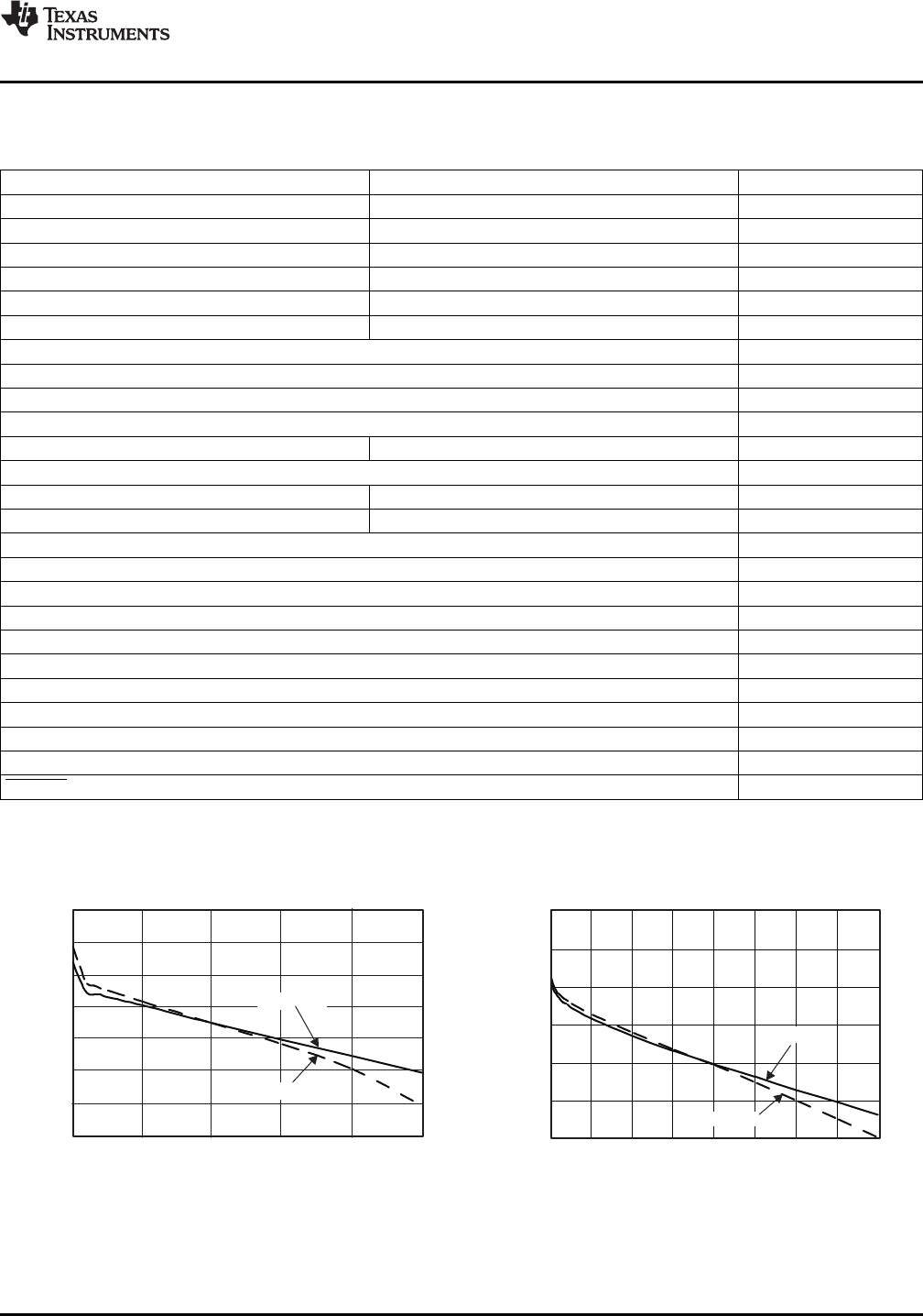
TYPICAL CHARACTERISTICS
-0.20
-0.10
0
0.10
0.20
0.30
0.40
0.50
0 10 20 30 40 50
VREF-LoadCurrent-mA
RegulationError-%
PVCC=10V
PVCC=20V
-3
-2.50
-2
-1.50
-1
-0.50
0
0 10 20 30 40 50 60 70 80
REGN-LoadCurrent-mA
RegulationError-%
PVCC=10V
PVCC=20V
bq24740
www.ti.com
............................................................................................................................................... SLUS736C – DECEMBER 2006 – REVISED MARCH 2009
Table of Graphs
Y X Figure
VREF Load and Line Regulation vs Load Current Figure 4
REGN Load and Line Regulation vs Load Current Figure 5
BAT Voltage vs VADJ/VDAC Ratio Figure 6
Charge Current vs SRSET/VDAC Ratio Figure 7
Input Current vs ACSET/VDAC Ratio Figure 8
BAT Voltage Regulation Accuracy vs Charge Current Figure 9
BAT Voltage Regulation Accuracy Figure 10
Charge Current Regulation Accuracy Figure 11
Input Current Regulation (DPM) Accuracy Figure 12
V
IADAPT
Input Current Sense Amplifier Accuracy Figure 13
Input Regulation Current (DPM), and Charge Current vs System Current Figure 14
Transient System Load (DPM) Response Figure 15
Charge Current Regulation vs BAT Voltage Figure 16
Efficiency vs Battery Charge Current Figure 17
Battery Removal (from Constant Current Mode) Figure 18
REF and REGN Startup Figure 19
Charger on Adapter Removal Figure 20
Charge Enable / Disable and Current Soft-Start Figure 21
Nonsynchronous to Synchronous Transition Figure 22
Synchronous to Nonsynchronous Transition Figure 23
Near 100% Duty Cycle Bootstrap Recharge Pulse Figure 24
Battery Shorted Charger Response, Over Current Protection (OCP) and Charge Current Regulation Figure 25
Continuous Conduction Mode (CCM) Switching Waveforms Figure 26
Discontinuous Conduction Mode (DCM) Switching Waveforms Figure 27
DPMDET Response With Transient System Load Figure 28
VREF LOAD AND LINE REGULATION REGN LOAD AND LINE REGULATIONvs vsLOAD CURRENT LOAD CURRENT
Figure 4. Figure 5.
Copyright © 2006 – 2009, Texas Instruments Incorporated Submit Documentation Feedback 11
Product Folder Link(s) :bq24740
0
1
2
3
4
5
6
7
8
9
10
0 0.1 0.2 0.3 0.4 0.5 0.6 0.7 0.8 0.9 1
SRSET/VDACRatio
ChargeCurrentRegulation- A
SRSET Varied,
4-Cell,
Vbat=16V
16
16.2
16.4
16.6
16.8
17
17.2
17.4
17.6
17.8
18
18.2
0 0.1 0.2 0.3 0.4 0.5 0.6 0.7 0.8 0.9 1
VADJ/VDACRatio
VoltageRegulation-V
VADJ=0-VDAC,
4-Cell,
NoLoad
V =16.8V
reg
-0.2
-0.1
0
0.1
0.2
02000 4000 6000 8000
ChargeCurrent-mA
RegulationError-%
0
1
2
3
4
6
7
8
9
10
0 0.1 0.2 0.3 0.4 0.5 0.6 0.7 0.8 0.9 1
ACSET/VDACRatio
InputCurrentRegulation- A
ACSET Varied,
4-Cell,
Vbat=16V
5
SRSET Varied
-10
-9
-8
-7
-6
-5
-4
-3
-2
-1
0
1
2
0 2 4 6 8
I Setpoint- A
(CHRG) -
RegulationError-%
4-Cell,VBAT =16V
VADJ=0-VDAC
-0.10
-0.08
-0.06
-0.04
-0.02
0
0.02
0.04
0.06
0.08
0.10
16.5 17 17.5 18 18.5 19
V -Setpoint-V
(BAT)
RegulationError-%
4-Cell,noload
bq24740
SLUS736C – DECEMBER 2006 – REVISED MARCH 2009 ...............................................................................................................................................
www.ti.com
BAT VOLTAGE CHARGE CURRENTvs vsVADJ/VDAC RATIO SRSET/VDAC RATIO
Figure 6. Figure 7.
INPUT CURRENT BAT VOLTAGE REGULATION ACCURACYvs vsACSET/VDAC RATIO CHARGE CURRENT
Figure 8. Figure 9.
BAT VOLTAGE REGULATION ACCURACY CHARGE CURRENT REGULATION ACCURACY
Figure 10. Figure 11.
12 Submit Documentation Feedback Copyright © 2006 – 2009, Texas Instruments Incorporated
Product Folder Link(s) :bq24740
ACSET Varied
-2
-1
0
1
2
3
4
5
6
7
8
9
10
0 1 2 3 4 5 6
InputCurrentRegulationSetpoint- A
RegulationError-%
4-Cell,VBAT =16V
Iadapt AmplifierGain
-25
-20
-15
-10
-5
0
5
0 1 2 3 4 5 6 7 8 9 10
I - A
(ACPWR)
PercentError
V =20V,CHG=EN
I
V =20V,CHG=DIS
I
V =20V,
4-Cell,
V =16V
I
bat
0
1
2
3
4
5
0 1 2 3 4
SystemCurrent- A
IchrgandIin- A
SystemCurrent ChargeCurrent
InputCurrent
0
1
2
3
4
5
0 2 4 6 8 10 12 14 16 18
BatteryVoltage-V
ChargeCurrent- A
Ichrg_set=4 A
70
80
90
100
02000 4000 6000 8000
BatteryChargeCurrent-mA
Efficiency-%
V =12.6V
reg
V =16.8V
(BAT)
V =8.4V
reg
bq24740
www.ti.com
............................................................................................................................................... SLUS736C – DECEMBER 2006 – REVISED MARCH 2009
INPUT CURRENT REGULATION (DPM) ACCURACY V
IADAPT
INPUT CURRENT SENSE AMPLIFIER ACCURACY
Figure 12. Figure 13.
INPUT REGULATION CURRENT (DPM), AND CHARGECURRENT
vsSYSTEM CURRENT TRANSIENT SYSTEM LOAD (DPM) RESPONSE
Figure 14. Figure 15.
CHARGE CURRENT REGULATION EFFICIENCYvs vsBAT VOLTAGE BATTERY CHARGE CURRENT
Figure 16. Figure 17.
Copyright © 2006 – 2009, Texas Instruments Incorporated Submit Documentation Feedback 13
Product Folder Link(s) :bq24740
Ch2
20 V/div
t − Time=5ms/div
Ch4
12.3 V
Ch4
1V/div
Ch3
5 A/div
IBAT
VPH
VBAT
Ch1
2 V/div
Ch2
2 V/div
Ch3
5 V/div
t − Time=2ms/div
VREF
VREGN
VACDET
Ch3
2 A/div
t − Time=4ms/div
Ch1
10 V/div
Ch1
1.8 V
Ch4
1 V/div
VCHGEN
VPH
IBAT
Ch2
20 V/div
VBAT
Ch3
2 A/div
VBAT
t − Time=200 s/divm
VIN
IL
Ch1
5 V/div
Ch4
5 V/div
Ch3
2 A/div
t − Time=2 s/divm
Ch2
10 V/div
VPH
VLODRV
IL
Ch4
5 V/div
Ch4
5 V/div
t − Time=4 s/divm
VHIDRV
VPH
VLDDRV
IL
Ch1
10 V/div
Ch2
10 V/div
Ch3
2 A/div
bq24740
SLUS736C – DECEMBER 2006 – REVISED MARCH 2009 ...............................................................................................................................................
www.ti.com
BATTERY REMOVAL REF AND REGN STARTUP
Figure 18. Figure 19.
CHARGE ENABLE / DISABLE AND CURRENTCHARGER ON ADAPTER REMOVAL SOFT-START
Figure 20. Figure 21.
NONSYNCHRONOUS TO SYNCHRONOUS TRANSITION SYNCHRONOUS TO NONSYNCHRONOUS TRANSITION
Figure 22. Figure 23.
14 Submit Documentation Feedback Copyright © 2006 – 2009, Texas Instruments Incorporated
Product Folder Link(s) :bq24740
Ch4
2 A/div
t − Time=4ms/div
Ch1
20 V/div
Ch2
20 V/div
VPH
VLODRV
IL
Ch3
5 V/div
VHIDRV
Ch3
2 A/div
t − Time=400 s/divm
Ch4
10 V/div
VBAT
IL
Ch4
5 A/div
t − Time=1 s/divm
Ch1
20 V/div
Ch2
20 V/div
VPH
VLODRV
IL
Ch3
5 V/div
VHIDRV
Ch4
2 A/div
t − Time=1 s/divm
Ch1
20 V/div
Ch2
20 V/div
VPH
VLODRV
IL
Ch3
5 V/div
VHIDRV
Ch1
2V/div
Ch2
5A/div
Ch3
5A/div
Ch4
5A/div
t-Time=20ms/div
DPMDET
IBAT
Isys
IIN
bq24740
www.ti.com
............................................................................................................................................... SLUS736C – DECEMBER 2006 – REVISED MARCH 2009
BATTERY SHORTED CHARGER RESPONSE,NEAR 100% DUTY CYCLE BOOTSTRAP RECHARGE OVERCURRENT PROTECTION (OCP) AND CHARGEPULSE CURRENT REGULATION
Figure 24. Figure 25.
CONTINUOUS CONDUCTION MODE (CCM) SWITCHING DISCONTINUOUS CONDUCTION MODE (DCM)WAVEFORMS SWITCHING WAVEFORMS
Figure 26. Figure 27.
DPMDET RESPONSE WITH TRANSIENT SYSTEM LOAD
Figure 28.
Copyright © 2006 – 2009, Texas Instruments Incorporated Submit Documentation Feedback 15
Product Folder Link(s) :bq24740
bq24740
IADAPT
BTST
HIDRV
PH
REGN
LODRV
PGND
ACP
ACN
BAT
6 VLDO
V(ACP-ACN)
+
-COMP
ERROR
AMPLIFIER
V(IADAPT)
+
-20x
ACP
ACN
ENA_BIAS
20 µA
IIN_ER
BAT_ER
ICH_ER
1V
20 µA
IIN_REG
VBAT _REG
DC-DC
CONVERTER
PWMLOGIC
PVCC
PH
4 V +
_
BTST REFRESH
CBTST
CHGEN
155°C
ICTj TSHUT
LEVEL
SHIFTER
+
-
+
-
+
-
+
-
+
-
+
-
PVCC_BAT
SYNCH
V(SRP-SRN)
CHG_OCP
+
-
145% XIBAT_REG
SRSET
VADJ
VDAC
ACSET
VBAT _REG
IBAT _REG
IIN_REG
VBATSET
IBATSET
IINSET
RATIO
PROGRAM
BAT
BAT_OVP
+
-
104% XVBAT_REG
ACDET ACOV
+
-
+
-
3.1 V
VREF 3.3 V
LDO
UVLO
DPMDET
DPM_LOOP_ON
EXTPWR
UVLO
+
-
PVCC
+
-
4 V
LPREF -
+V(IADAPT)
LPMD
AGND
PVCC
CHGEN
ACDET
AC_IGOOD
+
-
V(IADAPT)
SYNCH
+
-
ISYNSET
+
-
250 mV
PGND
FBO
EAI EAO
0.6 V
+
-
VREFGOOD
ENA_BIAS_CMP
AC_VGOOD
2.4 V
+
-
IADSLP IADSLP
CELLS
Rising
Delay
700 ms
AC_VGOOD_DG
AC_VGOOD_DG
+
–20x
3.5mA
3.5mA
CHRG_ON
V(SRP-SRN)
V(SRP-SRN)
IBAT_REG
PVCC_BAT
+
–
PVCC
+
–
BAT
185mV
SRP
SRN
20x
VREFGOOD
bq24740
SLUS736C – DECEMBER 2006 – REVISED MARCH 2009 ...............................................................................................................................................
www.ti.com
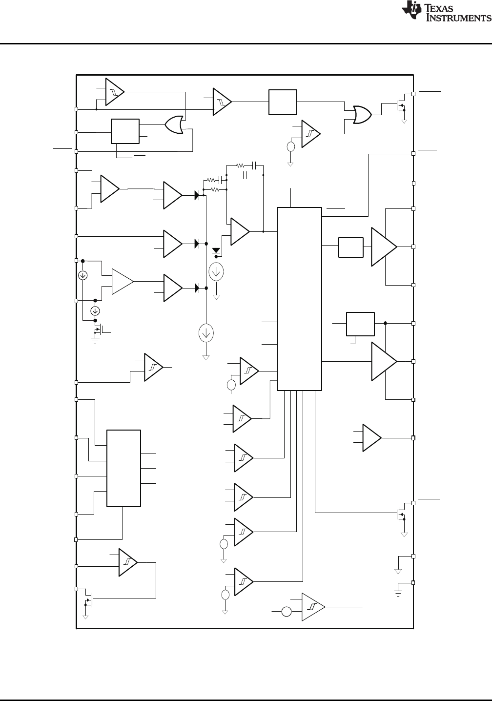
FUNCTIONAL BLOCK DIAGRAM
16 Submit Documentation Feedback Copyright © 2006 – 2009, Texas Instruments Incorporated
Product Folder Link(s) :bq24740
DETAILED DESCRIPTION
BATTERY VOLTAGE REGULATION
x x VADJ
BAT
VDAC
V
V = cell count 4V + 0.512 V
é ù
æ ö
÷
ç
ê ú
÷
ç÷
ê ú
ç÷
ç
è ø
ê ú
ë û
(1)
BATTERY CURRENT REGULATION
ICHARGE +VSRSET
VVDAC 0.10
RSR
(2)
INPUT ADAPTER CURRENT REGULATION
bq24740
www.ti.com
............................................................................................................................................... SLUS736C – DECEMBER 2006 – REVISED MARCH 2009
The bq24740 uses a high-accuracy voltage regulator for charging voltage. Internal default battery voltage settingV
BATT
= 4.2 V × cell count. The regulation voltage is ratio-metric with respect to VADC. The ratio of VADJ andVDAC provides extra 12.5% adjust range on V
BATT
regulation voltage. By limiting the adjust range to 12.5% ofthe regulation voltage, the external resistor mismatch error is reduced from ± 1% to ± 0.1%. Therefore, an overallvoltage accuracy as good as 0.5% is maintained, while using 1% mis-match resistors. Ratio-metric conversionalso allows compatibility with D/As or microcontrollers ( µC). The battery voltage is programmed through VADJand VDAC using Equation 1 .
The input voltage range of VDAC is between 2.6 V and 3.6 V. VADJ is set between 0 and VDAC. V
BATT
defaultsto 4.2 V × cell count when VADJ is connected to REGN.
CELLS pin is the logic input for selecting cell count. Connect CELLS to charge 2, 3, or 4 Li+ cells. Whencharging other cell chemistries, use CELLS to select an output voltage range for the charger.
CELLS CELL COUNT
Float 2
AGND 3
VREF 4
The per-cell battery termination voltage is function of the battery chemistry. Consult the battery manufacturer todetermine this voltage.
The BAT pin is used to sense the battery voltage for voltage regulation and should be connected as close to thebattery as possible, or directly on the output capacitor. A 0.1- µF ceramic capacitor from BAT to AGND isrecommended to be as close to the BAT pin as possible to decouple high frequency noise.
The SRSET input sets the maximum charging current. Battery current is sensed by resistor R
SR
connectedbetween SRP and SRN. The full-scale differential voltage between SRP and SRN is 100 mV. Thus, for a 0.010 Ω
sense resistor, the maximum charging current is 10 A. SRSET is ratio-metric with respect to VDAC usingEquation 2 :
The input voltage range of SRSET is between 0 and V
DAC
, up to 3.6 V.
The SRP and SRN pins are used to sense across R
SR
with default value of 10 m Ω. However, resistors of othervalues can also be used. For a larger the sense resistor, you get a larger sense voltage, and a higher regulationaccuracy; but, at the expense of higher conduction loss.
The total input from an AC adapter or other DC sources is a function of the system supply current and the batterycharging current. System current normally fluctuates as portions of the systems are powered up or down. WithoutDynamic Power Management (DPM), the source must be able to supply the maximum system current and themaximum charger input current simultaneously. By using DPM, the input current regulator reduces the chargingcurrent when the input current exceeds the input current limit set by ACSET. The current capability of the ACadapter can be lowered, reducing system cost.
Similar to setting battery regulation current, adapter current is sensed by resistor R
AC
connected between ACPand ACN. Its maximum value is set ACSET, which is ratio-metric with respect to VDAC, using Equation 3 .
Copyright © 2006 – 2009, Texas Instruments Incorporated Submit Documentation Feedback 17
Product Folder Link(s) :bq24740

IADAPTER +VACSET
VVDAC 0.10
RAC
(3)
ADAPTER DETECT AND POWER UP
ENABLE AND DISABLE CHARGING
AUTOMATIC INTERNAL SOFT-START CHARGER CURRENT
bq24740
SLUS736C – DECEMBER 2006 – REVISED MARCH 2009 ...............................................................................................................................................
www.ti.com
The input voltage range of ACSET is between 0 and V
DAC
, up to 3.6 V.
The ACP and ACN pins are used to sense R
AC
with default value of 10m Ω. However, resistors of other valuescan also be used. For a larger the sense resistor, you get a larger sense voltage, and a higher regulationaccuracy; but, at the expense of higher conduction loss.
An external resistor voltage divider attenuates the adapter voltage before it goes to ACDET. The adapter detectthreshold should typically be programmed to a value greater than the maximum battery voltage and lower thanthe minimum allowed adapter voltage. The ACDET divider should be placed before the ACFET in order to sensethe true adapter input voltage whether the ACFET is on or off.
If PVCC is below 4 V, the device is disabled.
If ACDET is below 0.6 V but PVCC is above 4 V, part of the bias is enabled, including a crude bandgapreference. IADAPT is disabled and pulled down to GND. The total quiescent current is less than 10 µA.
Once ACDET rises above 0.6 V and PVCC is above 4 V, all the bias circuits are enabled and REGN output goesto 6 V and VREF goes to 3.3 V. IADAPT becomes valid to proportionally reflect the adapter current. The totalquiescent current is about 1 mA.
When ACDET keeps rising and passes 2.4 V, a valid ac adapter is present. 700ms later, the following occurs:
•EXTPWR becomes low through external pull-up resistor to the host digital voltage rail.
•Charging begins if all the conditions are satisfied, see the ENABLE AND DISABLE CHARGING section.
The following conditions have to be valid before charge is enabled:
•CHGEN is LOW;
•PVCC > UVLO;
•Adapter is detected;
•Adapter is higher than PVCC-BAT threshold;
•Adapter is not overvoltage;
•700 ms delay is complete after adapter detected;
•REGNGOOD and VREFGOOD are valid;
•Thermal Shut (TSHUT) is not valid;
One of the following conditions will stop on-going charging:
•CHGEN is HIGH;
•PVCC < UVLO;
•Adapter is removed;
•Adapter is less than 185 mV above battery;
•Adapter is overvoltage;
•Adapter is overcurrent;
•TSHUT IC temperature threshold is reached (155 ° C on rising-edge with 20 ° C hysteresis).
The charger automatically soft-starts the charger regulation current every time the charger is enabled to ensurethere is no overshoot or stress on the output capacitors or the power converter. The soft-start consists ofstepping-up the charge regulation current into 8 evenly divided steps up to the programmed charge current. Eachstep lasts around 1.7 ms, for a typical rise time of 13.6 ms. No external components are needed for this function.
18 Submit Documentation Feedback Copyright © 2006 – 2009, Texas Instruments Incorporated
Product Folder Link(s) :bq24740

CONVERTER OPERATION
fo+1
2pLoCo
Ǹ
(4)
SYNCHRONOUS AND NON-SYNCHRONOUS OPERATION
bq24740
www.ti.com
............................................................................................................................................... SLUS736C – DECEMBER 2006 – REVISED MARCH 2009
The synchronous buck PWM converter uses a fixed frequency (300 kHz) voltage mode with feed-forward controlscheme. A type III compensation network allows using ceramic capacitors at the output of the converter. Thecompensation input stage is connected internally between the feedback output (FBO) and the error amplifierinput (EAI). The feedback compensation stage is connected between the error amplifier input (EAI) and erroramplifier output (EAO). The LC output filter is selected to give a resonant frequency of 8 – 12.5 kHz nominal.
Where resonant frequency, f
o
, is given by:
where (from Figure 1 schematic)
•C
O
= C11 + C12
•L
O
= L1
An internal saw-tooth ramp is compared to the internal EAO error control signal to vary the duty-cycle of theconverter. The ramp height is one-fifteenth of the input adapter voltage making it always directly proportional tothe input adapter voltage. This cancels out any loop gain variation due to a change in input voltage, andsimplifies the loop compensation. The ramp is offset by 200 mV in order to allow zero percent duty-cycle, whenthe EAO signal is below the ramp. The EAO signal is also allowed to exceed the saw-tooth ramp signal in orderto get a 100% duty-cycle PWM request. Internal gate drive logic allows achieving 99.98% duty-cycle whileensuring the N-channel upper device always has enough voltage to stay fully on. If the BTST pin to PH pinvoltage falls below 4 V for more than 3 cycles, then the high-side n-channel power MOSFET is turned off and thelow-side n-channel power MOSFET is turned on to pull the PH node down and recharge the BTST capacitor.Then the high-side driver returns to 100% duty-cycle operation until the (BTST-PH) voltage is detected to fall lowagain due to leakage current discharging the BTST capacitor below the 4 V, and the reset pulse is reissued.
The 300 kHz fixed frequency oscillator keeps tight control of the switching frequency under all conditions of inputvoltage, battery voltage, charge current, and temperature, simplifying output filter design and keeping it out of theaudible noise region. The charge current sense resistor R
SR
should be placed with at least half or more of thetotal output capacitance placed before the sense resistor contacting both sense resistor and the output inductor;and the other half or remaining capacitance placed after the sense resistor. The output capacitance should bedivided and placed onto both sides of the charge current sense resistor. A ratio of 50:50 percent gives the bestperformance; but the node in which the output inductor and sense resistor connect should have a minimum of50% of the total capacitance. This capacitance provides sufficient filtering to remove the switching noise and givebetter current sense accuracy. The type III compensation provides phase boost near the cross-over frequency,giving sufficient phase margin.
The charger operates in non-synchronous mode when the sensed charge current is below the ISYNSET value.Otherwise, the charger operates in synchronous mode.
During synchronous mode, the low-side n-channel power MOSFET is on, when the high-side n-channel powerMOSFET is off. The internal gate drive logic ensures there is break-before-make switching to preventshoot-through currents. During the 30ns dead time where both FETs are off, the back-diode of the low-sidepower MOSFET conducts the inductor current. Having the low-side FET turn-on keeps the power dissipation low,and allows safe charging at high currents. During synchronous mode the inductor current is always flowing andoperates in Continuous Conduction Mode (CCM), creating a fixed two-pole system.
During non-synchronous operation, after the high-side n-channel power MOSFET turns off, and after thebreak-before-make dead-time, the low-side n-channel power MOSFET turns on for around 80ns, then thelow-side power MOSFET turns off and stays off until the beginning of the next cycle, where the high-side powerMOSFET is turned on again. The 80ns low-side MOSFET on time is required to ensure the bootstrap capacitor isalways recharged and able to keep the high-side power MOSFET on during the next cycle. This is important forbattery chargers; where, unlike regular dc-dc converters, there is a battery load that maintains a voltage and canboth source and sink current. The 80-ns low-side pulse pulls the PH node (connection between high and low-sideMOSFET) down, allowing the bootstrap capacitor to recharge up to the REGN LDO value. After the 80ns, thelow-side MOSFET is kept off to prevent negative inductor current from occurring. The inductor current is blockedby the off low-side MOSFET, and the inductor current will become discontinuous. This mode is calledDiscontinuous Conduction Mode (DCM).
Copyright © 2006 – 2009, Texas Instruments Incorporated Submit Documentation Feedback 19
Product Folder Link(s) :bq24740

ISYNSET CONTROL (SYN and NON-SYN MODE SETTING)
max_
max_
2rippleSYN
ripple II
I££
L
f
DDV
L
fV
V
VV
Is
in
sin
bat
batin
ripple
1
)1(
1
)( ´´-´
=
´´-
=
and
(5)
bq24740
SLUS736C – DECEMBER 2006 – REVISED MARCH 2009 ...............................................................................................................................................
www.ti.com
During the DCM mode the loop response automatically changes and has a single pole system at which the poleis proportional to the load current, because the converter does not sink current, and only the load provides acurrent sink. This means at very low currents the loop response is slower, as there is less sinking currentavailable to discharge the output voltage. At low currents during non-synchronous operation, there may be asmall amount of negative inductor current during the 80 ns recharge pulse. The charge should be low enough tobe absorbed by the input capacitance.
When BTST – PH < 4 V, the 80-ns recharge pulse occurs on LODRV, the high-side MOSFET does not turn on,and the low-side MOSFET does not turn on (only 80-ns recharge pulse).
The ISYNSET pin is used to program the charge current threshold at which the charger changes fromsynchronous operation into non-synchronous operation. The low side driver turns on for only 80 ns to charge theboost cap. This is important to prevent negative inductor current, which may cause a boost effect in which theinput voltage increases as power is transferred from the battery to the input capacitors. This boost effect can leadto an overvoltage on the PVCC node and potentially cause some damage to the system. This programmablevalue allows setting the current threshold for any inductor current ripple, and avoiding negative inductor current.The minimum synchronous threshold should be set from =of the inductor current ripple to the full ripple current,where the inductor current ripple is given by:
where
V
IN
: adapter voltage
V
BAT
: BAT voltage
f
S
: switching frequency
L: output inductor
D: duty cycle
I
RIPPLE_MAX
occurs when the duty cycle, D is mostly near to 0.5 at given Vin, fs and L. The ISYNSET comparator,or charge undercurrent comparator, compares the voltage between SRP-SNR and the threshold set by anexternal resistor R
ISYNSET
, which can be calculated by:
20 Submit Documentation Feedback Copyright © 2006 – 2009, Texas Instruments Incorporated
Product Folder Link(s) :bq24740
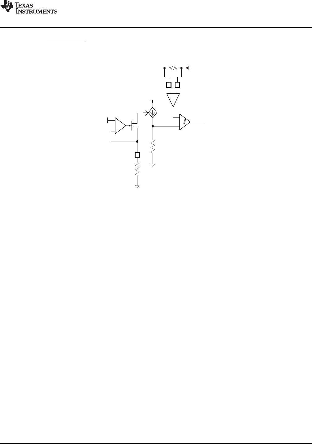
ISYNSET
SYN SENSE
250 V
R = I x R W
(6)
ISYNSET
-
+
SRP
SRN
+
-
+
-
3.3 V
1 V
RSENSE
5 kΩ
20X
SYNCH
R_ ISYNSET
UCP
I =1V/R_ ISYNSET
ISYN
HIGH ACCURACY IADAPT USING CURRENT SENSE AMPLIFIER (CSA)
INPUT OVERVOLTAGE PROTECTION (ACOV)
INPUT UNDERVOLTAGE LOCK OUT (UVLO)
INPUT CURRENT LOW-POWER MODE DETECTION
bq24740
www.ti.com
............................................................................................................................................... SLUS736C – DECEMBER 2006 – REVISED MARCH 2009
Figure 29. Charge Undercurrent Comparator, ISYNSET Comparator Block
An industry standard, high accuracy current sense amplifier (CSA) is used to monitor the input current by thehost or some discrete logic through the analog voltage output of the IADAPT pin. The CSA amplifies the inputsensed voltage of ACP – ACN by 20x through the IADAPT pin. The IADAPT output is a voltage source 20 timesthe input differential voltage. Once PVCC is above 5 V and ACDET is above 0.6V, IADAPT no longer stays atground, but becomes active. If the user wants to lower the voltage, they could use a resistor divider from IOUT toAGND, and still achieve accuracy over temperature as the resistors can be matched their thermal coefficients.
A 100-pF capacitor connected on the output is recommended for decoupling high-frequency noise. An additionalRC filter is optional, after the 100-pF capacitor, if additional filtering is desired. Note that adding filtering alsoadds additional response delay.
ACOV provides protection to prevent system damage due to high input voltage. The controller enters ACOVwhen ACDET > 3.1 V and charge is disabled. ACOV is not latched — normal operation resumes when the ACDETvoltage returns below 3.1 V. ACOV threshold is 130% of the adapter-detect threshold.
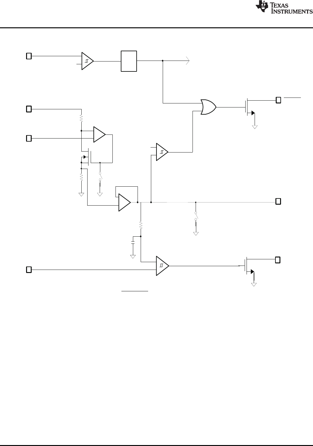
The system must have a minimum 4 V PVCC voltage to allow proper operation. This PVCC voltage could comefrom either input adapter or battery, using a diode-OR input. When the PVCC voltage is below 4 V the biascircuits REGN and VREF stay inactive, even with ACDET above 0.6 V.
To optimize the system performance, the HOST monitors the adapter current. Once the adapter current is abovethreshold set via LPREF, LPMD pin sends signal to HOST. The signal alarms the host that input power hasexceeded the programmed limit, allowing the host to throttle back system power by reducing clock frequency,lowering rail voltages, or disabling certain parts of the system. The LPMD pin is an open-drain output. Connect apull-up resistor to LPMD. The output is logic HI when the IADAPT output voltage (I
ADAPT
= 20 × V
ACP-ACN
) is lowerthan the LPREF input voltage. The LPREF threshold is set by an external resistor divider using VREF. Ahysteresis can be programmed by a positive feedback resistor from LPMD pin to the LPREF pin.
Copyright © 2006 – 2009, Texas Instruments Incorporated Submit Documentation Feedback 21
Product Folder Link(s) :bq24740
1 kΩ
Adaptor
CurrentSense
Amplifier
IADAPT
Error
Amplifier
Disable
+
-
ACVDET
Comparator
AC_VGOOD
2.4 V
t_dg
rising
700 ms
AC_VGOOD_DG
ACDET +
-
LPMD
Comparator
LOPWR_DET+
-
IADAPT
LPREF
LPMD
+
-
ACP
ACN
EXT_PWR_DG EXTPWR
ACIDET
Comparator
AC_IGOOD
+
-
250 mV
(1.25 A)
ToControlLogic
ProgramHysteresisofcomparatorexternally
byputtingaresistorinfeedbackfromLPMDpintoLPREFpin.
IADAPT
Disable
IADAPT
OUTPUT
BUFFER
20 xV(ACP-ACN)
20 kΩ
BATTERY OVERVOLTAGE PROTECTION
CHARGE OVERCURRENT PROTECTION
THERMAL SHUTDOWN PROTECTION
bq24740
SLUS736C – DECEMBER 2006 – REVISED MARCH 2009 ...............................................................................................................................................
www.ti.com
Figure 30. EXTPWR, LPREF and LPMD Logic
The converter stops switching when BAT voltage goes above 104% of the regulation voltage. The converter willnot allow the high-side FET to turn on until the BAT voltage goes below 102% of the regulation voltage. Thisallows one-cycle response to an overvoltage condition, such as when the load is removed or the battery isdisconnected. A 10-mA current sink from BAT to PGND is on only during charge, and allows discharging thestored output-inductor energy into the output capacitors.
The charger has a secondary overcurrent protection. It monitors the charge current, and prevents the currentfrom exceeding 145% of regulated charge current. The high-side gate drive turns off when the overcurrent isdetected, and automatically resumes when the current falls below the over-current threshold.
The QFN package has low thermal impedance, which provides good thermal conduction from the silicon to theambient, to keep junctions temperatures low. As added level of protection, the charger converter turns off andself-protects whenever the junction temperature exceeds the TSHUT threshold of 155 ° C. The charger stays offuntil the junction temperature falls below 135 ° C.
22 Submit Documentation Feedback Copyright © 2006 – 2009, Texas Instruments Incorporated
Product Folder Link(s) :bq24740

Status Outputs ( EXTPWR, LPMD, DPMDET pin)
bq24740
www.ti.com
............................................................................................................................................... SLUS736C – DECEMBER 2006 – REVISED MARCH 2009
Four status outputs are available, and they all, except for LPMD, require external pull up resistors to pull the pinsto system digital rail for a high level.
EXTPWR open-drain output goes low under either of the two conditions:
1. ACDET is above 2.4 V
2. Adapter current is above 1.25 A using a 10-m Ωsense resistor (IADAPT voltage above 250 mV). Internally,the AC current detect comparator looks between IADAPT and an internal 250-mV threshold. It indicates agood adapter is connected because of valid voltage or current.
LPMD open-drain output goes low when the input current is higher than the programmed threshold via LPREFpin. Hysteresis can be programmed by putting a resistor from LPREF pin to LPMD pin.
DPMDET open-drain output goes low when the DPM loop is active to reduce the battery charge current (after a10-ms delay).
Table 2. Component List for Typical System Circuit of Figure 1
PART DESIGNATOR QTY DESCRIPTION
Q1, Q2, Q3 3 P-channel MOSFET, – 30V,-6A, SO-8, Vishay-Siliconix, Si4435
Q4, Q5 2 N-channel MOSFET, 30V, 12.5A, SO-8, Fairchild, FDS6680A
D1, D2 2 Diode, Dual Schottky, 30V, 200mA, SOT23, Fairchild, BAT54C
R
AC
, R
SR
2 Sense Resistor, 10 m Ω, 1%, 1W, 2010, Vishay-Dale, WSL2010R0100F
L1 1 Inductor, 8.2 µH, 24.8m Ω, Vishay-Dale, IHLP5050CE-01
C6, C7, C11, C12 4 Capacitor, Ceramic, 10 µF, 35V, 20%, X5R, 1206, Panasonic, ECJ-3YB1E106M
C4, C10 2 Capacitor, Ceramic, 1 µF, 25V, 10%, X7R, 2012, TDK, C2012X7R1E105K
C2, C3, C8, C9, C13, C14, C15 7 Capacitor, Ceramic, 0.1 µF, 50V, 10%, X7R, 0805, Kemet, C0805C104K5RACTU
C1 1 Capacitor, Ceramic, 2.2 µF, 25V, 2%, X5R, 1206, Panasonic, ECJ3YB1E225M
C5 1 Capacitor, Ceramic, 100pF, 50V, 10%, X7R, 0805, Kemet, C0805C101K5RACTU
R3, R4, R5 3 Resistor, Chip, 10 k Ω, 1/16W, 5%, 0402
R1 1 Resistor, Chip, 432 k Ω, 1/16W, 1%, 0402
R2 1 Resistor, Chip, 66.5 k Ω, 1/16W, 1%, 0402
R6 1 Resistor, Chip, 24k Ω, 1/16W, 1%, 0402
R7 1 Resistor, Chip, 200 k Ω, 1/16W, 1%, 0402
R8 1 Resistor, Chip, 24.9 k Ω, 1/16W, 1%, 0402
R9 1 Resistor, Chip, 1.8 M Ω, 1/16W, 1%, 0402
R10 1 Resistor, Chip, 2 Ω, 1W, 5%, 2012
Copyright © 2006 – 2009, Texas Instruments Incorporated Submit Documentation Feedback 23
Product Folder Link(s) :bq24740
APPLICATION INFORMATION
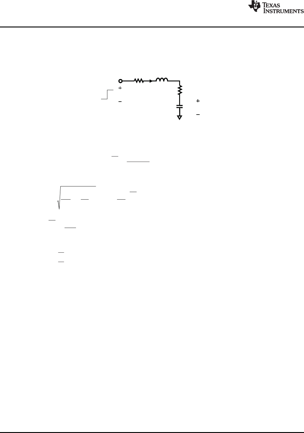
During the adapter hot plug-in, the ACFET has not been turned on. The AC switch is off and the simplified
Ci
Ri Li
Vi
VIN
IIN
Rc
Vc
Ci
Ri Li
Vi
VIN
IIN
Rc
Vc
Ri
2Lit
VIN(t) +IIN(t) RC)VCi(t) +VieƪRi*RC
wLisin wt)cos wtƫ
(7)
2
R V
1 2L
tii
R = R + R = - I (t) = sin
ti IN
CL C 2L L
i i i i
Rit
e tw w
w
æ ö
ç ÷
è ø
(8)
2Li
V (t) = V - V s in t + cos t
i i
Ci 2 Li
RttRt
ew w
w
æ ö
ç ÷
è ø
(9)
Ri)Rcu2Li
Ci
Ǹ
(10)
bq24740
SLUS736C – DECEMBER 2006 – REVISED MARCH 2009 ...............................................................................................................................................
www.ti.com
equivalent circuit of the input is shown in Figure 31
Figure 31. Simplified Equivalent Circuit During Adapter Insertion
The voltage on the charger input side V
IN
is given by:
in which,
The damping condition is:
24 Submit Documentation Feedback Copyright © 2006 – 2009, Texas Instruments Incorporated
Product Folder Link(s) :bq24740
0 0.5 1 1.5 2 2.5 3 3.5 4 4.5 5
0
5
10
15
20
25
30
35
InputCapacitor Voltage-V
Time-ms
R =0.15
iWL =9.3
C =40 F
i
i
mH
m
(a)V withvariousC values
c i
(b)V withvariousL values
c i
(c)V withvariousR values
c i
0 0.5 1 1.5 2 2.5 3 3.5 4 4.5 5
0
5
10
15
20
25
30
35
InputCapacitor Voltage-V
Time-ms
C =20 F
im
C =40 F
im
R =0.21
L =9.3 H
i
i
W
m
0 0.5 1 1.5 2 2.5 3 3.5 4 4.5 5
0
5
10
15
20
25
30
35
InputCapacitor Voltage-V
Time-ms
L =5 H
im
L =12 H
im
R =0.15
C =40 F
i
i
W
m
R =0.5
iW
Rext
C1 C2
2
(0.5W,1210anti-surge)
W
2.2 F
(25V,1210)
m0.1 F
(50V,0805,veryclosetoPVCC)
m
VIN VPVCC
bq24740
www.ti.com
............................................................................................................................................... SLUS736C – DECEMBER 2006 – REVISED MARCH 2009
Figure 32 (a) demonstrates a higher Ci helps dampen the voltage spike. Figure 32 (b) demonstrates the effect ofthe input stray inductance Li upon the input voltage spike. Figure 32 (c) shows how increased resistance helps tosuppress the input voltage spike.
Figure 32. Parametric Study Of The Input Voltage
As shown in Figure 32 , minimizing the input stray inductance, increasing the input capacitance, and addingresistance (including using higher ESR capacitors) helps suppress the input voltage spike. However, a user oftencannot control input stray inductance and increasing capacitance can increase costs. Therefore, the mostefficient and cost-effective approach is to add an external resistor.
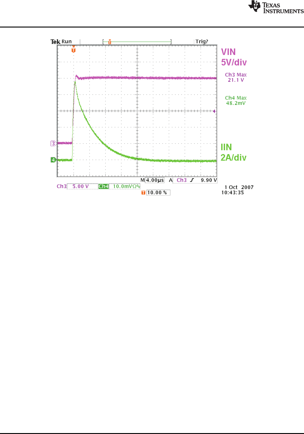
Figure 33 depicts the recommended input filter design. The measured input voltage and current waveforms areshown in Figure 34 . The input voltage spike has been well damped by adding a 2- Ωresistor, while keeping thecapacitance low.
Figure 33. Recommended Input Filter Design
Copyright © 2006 – 2009, Texas Instruments Incorporated Submit Documentation Feedback 25
Product Folder Link(s) :bq24740
bq24740
SLUS736C – DECEMBER 2006 – REVISED MARCH 2009 ...............................................................................................................................................
www.ti.com
Figure 34. Adapter DC Side Hot Plug-In Test Waveforms
26 Submit Documentation Feedback Copyright © 2006 – 2009, Texas Instruments Incorporated
Product Folder Link(s) :bq24740
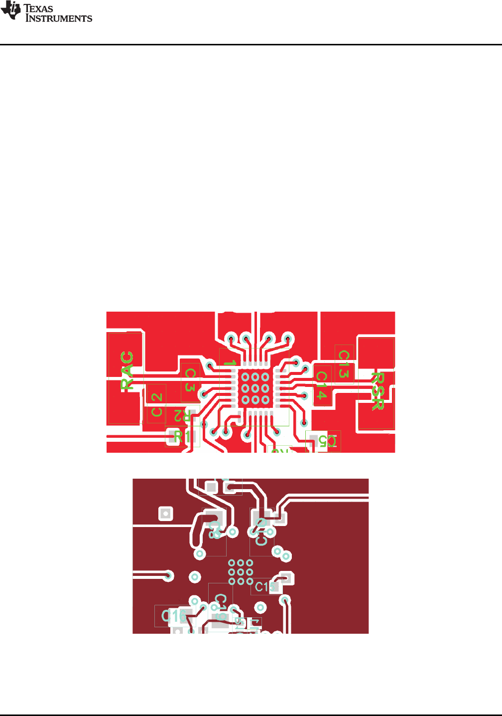
PCB Layout Design Guideline
(a)TopLayer
(b)BottomLayer
bq24740
www.ti.com
............................................................................................................................................... SLUS736C – DECEMBER 2006 – REVISED MARCH 2009
1. It is critical that the exposed power pad on the backside of the IC package be soldered to the PCB ground.Ensure that there are sufficient thermal vias directly under the IC, connecting to the ground plane on theother layers.
2. The control stage and the power stage should be routed separately. At each layer, the signal ground and thepower ground are connected only at the power pad.
3. The AC current-sense resistor must be connected to ACP (pin 3) and ACN (pin 2) with a Kelvin contact. Thearea of this loop must be minimized. An additional 0.1 µF decoupling capacitor for ACN is required to furtherreduce the noise. The decoupling capacitors for these pins should be placed as close to the IC as possible.
4. The charge-current sense resistor must be connected to SRP (pin 19), SRN (pin 18) with a Kelvin contact.The area of this loop must be minimized. An additional 0.1 µF decoupling capacitor for SRN is required tofurther reduce the noise. The decoupling capacitors for these pins should be placed as close to the IC aspossible.
5. Decoupling capacitors for PVCC (pin 28), VREF (pin 10), REGN (pin 24) should be placed underneath the IC(on the bottom layer) with the interconnections to the IC as short as possible.
6. Decoupling capacitors for BAT (pin 17), IADAPT (pin 15) must be placed close to the corresponding IC pinswith the interconnections to the IC as short as possible.
7. Decoupling capacitor CX for the charger input must be placed close to the Q4 drain and Q5 source.
Figure 35 shows the recommended component placement with trace and via locations. For the QFN information,see the SCBA017 and SLUA271 documents.
Figure 35. Layout Example
Copyright © 2006 – 2009, Texas Instruments Incorporated Submit Documentation Feedback 27
Product Folder Link(s) :bq24740
PACKAGE OPTION ADDENDUM
www.ti.com 11-Apr-2013
Addendum-Page 1
PACKAGING INFORMATION
Orderable Device Status
(1)
Package Type Package
Drawing Pins Package
Qty Eco Plan
(2)
Lead/Ball Finish MSL Peak Temp
(3)
Op Temp (°C) Top-Side Markings
(4)
Samples
BQ24740RHDR PREVIEW VQFN RHD 28 Green (RoHS
& no Sb/Br)
CU NIPDAU Level-2-260C-1 YEAR -40 to 85 BQ
24740
BQ24740RHDRG4 PREVIEW VQFN RHD 28 Green (RoHS
& no Sb/Br)
CU NIPDAU Level-2-260C-1 YEAR -40 to 85 BQ
24740
BQ24740RHDT PREVIEW VQFN RHD 28 Green (RoHS
& no Sb/Br)
CU NIPDAU Level-2-260C-1 YEAR -40 to 85 BQ
24740
BQ24740RHDTG4 PREVIEW VQFN RHD 28 Green (RoHS
& no Sb/Br)
CU NIPDAU Level-2-260C-1 YEAR -40 to 85 BQ
24740
(1) The marketing status values are defined as follows:
ACTIVE: Product device recommended for new designs.
LIFEBUY: TI has announced that the device will be discontinued, and a lifetime-buy period is in effect.
NRND: Not recommended for new designs. Device is in production to support existing customers, but TI does not recommend using this part in a new design.
PREVIEW: Device has been announced but is not in production. Samples may or may not be available.
OBSOLETE: TI has discontinued the production of the device.
(2) Eco Plan - The planned eco-friendly classification: Pb-Free (RoHS), Pb-Free (RoHS Exempt), or Green (RoHS & no Sb/Br) - please check http://www.ti.com/productcontent for the latest availability
information and additional product content details.
TBD: The Pb-Free/Green conversion plan has not been defined.
Pb-Free (RoHS): TI's terms "Lead-Free" or "Pb-Free" mean semiconductor products that are compatible with the current RoHS requirements for all 6 substances, including the requirement that
lead not exceed 0.1% by weight in homogeneous materials. Where designed to be soldered at high temperatures, TI Pb-Free products are suitable for use in specified lead-free processes.
Pb-Free (RoHS Exempt): This component has a RoHS exemption for either 1) lead-based flip-chip solder bumps used between the die and package, or 2) lead-based die adhesive used between
the die and leadframe. The component is otherwise considered Pb-Free (RoHS compatible) as defined above.
Green (RoHS & no Sb/Br): TI defines "Green" to mean Pb-Free (RoHS compatible), and free of Bromine (Br) and Antimony (Sb) based flame retardants (Br or Sb do not exceed 0.1% by weight
in homogeneous material)
(3) MSL, Peak Temp. -- The Moisture Sensitivity Level rating according to the JEDEC industry standard classifications, and peak solder temperature.
(4) Multiple Top-Side Markings will be inside parentheses. Only one Top-Side Marking contained in parentheses and separated by a "~" will appear on a device. If a line is indented then it is a
continuation of the previous line and the two combined represent the entire Top-Side Marking for that device.
Important Information and Disclaimer:The information provided on this page represents TI's knowledge and belief as of the date that it is provided. TI bases its knowledge and belief on information
provided by third parties, and makes no representation or warranty as to the accuracy of such information. Efforts are underway to better integrate information from third parties. TI has taken and
continues to take reasonable steps to provide representative and accurate information but may not have conducted destructive testing or chemical analysis on incoming materials and chemicals.
TI and TI suppliers consider certain information to be proprietary, and thus CAS numbers and other limited information may not be available for release.
In no event shall TI's liability arising out of such information exceed the total purchase price of the TI part(s) at issue in this document sold by TI to Customer on an annual basis.

PACKAGE OPTION ADDENDUM
www.ti.com 11-Apr-2013
Addendum-Page 2
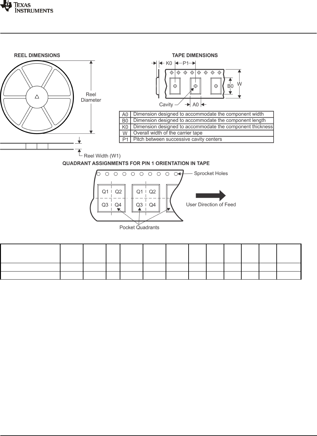
TAPE AND REEL INFORMATION
*All dimensions are nominal
Device Package
Type Package
Drawing Pins SPQ Reel
Diameter
(mm)
Reel
Width
W1 (mm)
A0
(mm) B0
(mm) K0
(mm) P1
(mm) W
(mm) Pin1
Quadrant
BQ24740RHDR VQFN RHD 28 0 330.0 12.4 5.3 5.3 1.5 8.0 12.0 Q2
BQ24740RHDT VQFN RHD 28 0 180.0 12.4 5.3 5.3 1.5 8.0 12.0 Q2
PACKAGE MATERIALS INFORMATION
www.ti.com 24-Apr-2013
Pack Materials-Page 1
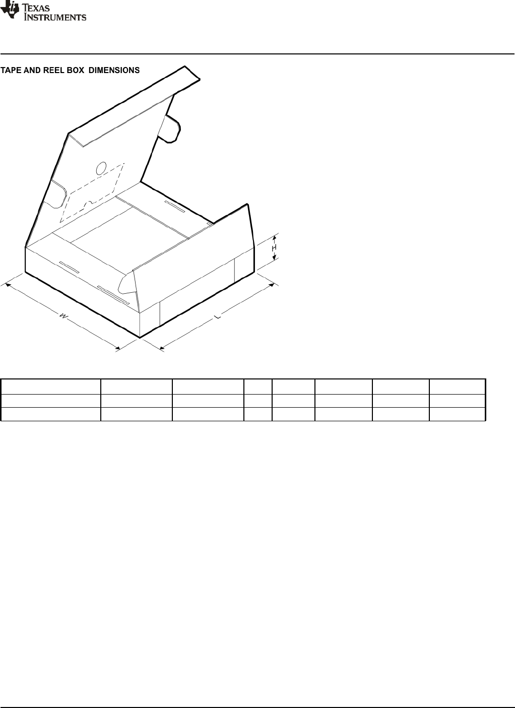
*All dimensions are nominal
Device Package Type Package Drawing Pins SPQ Length (mm) Width (mm) Height (mm)
BQ24740RHDR VQFN RHD 28 0 367.0 367.0 35.0
BQ24740RHDT VQFN RHD 28 0 210.0 185.0 35.0
PACKAGE MATERIALS INFORMATION
www.ti.com 24-Apr-2013
Pack Materials-Page 2
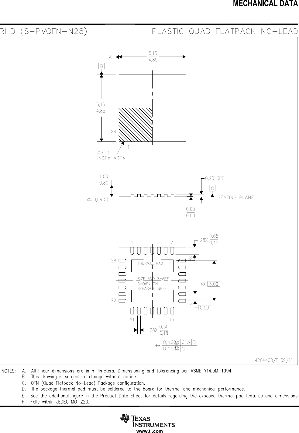

IMPORTANT NOTICE
Texas Instruments Incorporated and its subsidiaries (TI) reserve the right to make corrections, enhancements, improvements and other
changes to its semiconductor products and services per JESD46, latest issue, and to discontinue any product or service per JESD48, latest
issue. Buyers should obtain the latest relevant information before placing orders and should verify that such information is current and
complete. All semiconductor products (also referred to herein as “components”) are sold subject to TI’s terms and conditions of sale
supplied at the time of order acknowledgment.
TI warrants performance of its components to the specifications applicable at the time of sale, in accordance with the warranty in TI’s terms
and conditions of sale of semiconductor products. Testing and other quality control techniques are used to the extent TI deems necessary
to support this warranty. Except where mandated by applicable law, testing of all parameters of each component is not necessarily
performed.
TI assumes no liability for applications assistance or the design of Buyers’ products. Buyers are responsible for their products and
applications using TI components. To minimize the risks associated with Buyers’ products and applications, Buyers should provide
adequate design and operating safeguards.
TI does not warrant or represent that any license, either express or implied, is granted under any patent right, copyright, mask work right, or
other intellectual property right relating to any combination, machine, or process in which TI components or services are used. Information
published by TI regarding third-party products or services does not constitute a license to use such products or services or a warranty or
endorsement thereof. Use of such information may require a license from a third party under the patents or other intellectual property of the
third party, or a license from TI under the patents or other intellectual property of TI.
Reproduction of significant portions of TI information in TI data books or data sheets is permissible only if reproduction is without alteration
and is accompanied by all associated warranties, conditions, limitations, and notices. TI is not responsible or liable for such altered
documentation. Information of third parties may be subject to additional restrictions.
Resale of TI components or services with statements different from or beyond the parameters stated by TI for that component or service
voids all express and any implied warranties for the associated TI component or service and is an unfair and deceptive business practice.
TI is not responsible or liable for any such statements.
Buyer acknowledges and agrees that it is solely responsible for compliance with all legal, regulatory and safety-related requirements
concerning its products, and any use of TI components in its applications, notwithstanding any applications-related information or support
that may be provided by TI. Buyer represents and agrees that it has all the necessary expertise to create and implement safeguards which
anticipate dangerous consequences of failures, monitor failures and their consequences, lessen the likelihood of failures that might cause
harm and take appropriate remedial actions. Buyer will fully indemnify TI and its representatives against any damages arising out of the use
of any TI components in safety-critical applications.
In some cases, TI components may be promoted specifically to facilitate safety-related applications. With such components, TI’s goal is to
help enable customers to design and create their own end-product solutions that meet applicable functional safety standards and
requirements. Nonetheless, such components are subject to these terms.
No TI components are authorized for use in FDA Class III (or similar life-critical medical equipment) unless authorized officers of the parties
have executed a special agreement specifically governing such use.
Only those TI components which TI has specifically designated as military grade or “enhanced plastic” are designed and intended for use in
military/aerospace applications or environments. Buyer acknowledges and agrees that any military or aerospace use of TI components
which have not been so designated is solely at the Buyer's risk, and that Buyer is solely responsible for compliance with all legal and
regulatory requirements in connection with such use.
TI has specifically designated certain components as meeting ISO/TS16949 requirements, mainly for automotive use. In any case of use of
non-designated products, TI will not be responsible for any failure to meet ISO/TS16949.
Products Applications
Audio www.ti.com/audio Automotive and Transportation www.ti.com/automotive
Amplifiers amplifier.ti.com Communications and Telecom www.ti.com/communications
Data Converters dataconverter.ti.com Computers and Peripherals www.ti.com/computers
DLP® Products www.dlp.com Consumer Electronics www.ti.com/consumer-apps
DSP dsp.ti.com Energy and Lighting www.ti.com/energy
Clocks and Timers www.ti.com/clocks Industrial www.ti.com/industrial
Interface interface.ti.com Medical www.ti.com/medical
Logic logic.ti.com Security www.ti.com/security
Power Mgmt power.ti.com Space, Avionics and Defense www.ti.com/space-avionics-defense
Microcontrollers microcontroller.ti.com Video and Imaging www.ti.com/video
RFID www.ti-rfid.com
OMAP Applications Processors www.ti.com/omap TI E2E Community e2e.ti.com
Wireless Connectivity www.ti.com/wirelessconnectivity
Mailing Address: Texas Instruments, Post Office Box 655303, Dallas, Texas 75265
Copyright © 2013, Texas Instruments Incorporated