Cover Bsimsoi3p1 Manual
User Manual:
Open the PDF directly: View PDF ![]() .
.
Page Count: 93
BSIMSOI3.1 MOSFET MODEL
Users’ Manual
BSIM GROUP
February 2003
Department of Electrical Engineering and Computer Sciences
University of California, Berkeley, CA 94720
Copyright 2003
The Regents of the University of California
All Rights Reserved

BSIMSOI Developers:
n Dr. Pin Su
n Mr. Hui Wan
n Dr. Samuel Fung
n Prof. Mansun Chan
n Prof. Ali Niknejad
n Prof. Chenming Hu
Previous BSIMSOI/BSIMPD Developers:
n Dr. Samuel Fung
n Dr. Dennis Sinitsky
n Dr. Stephen Tang
n Dr. Pin Su
n Dr. Weidong Liu
n Dr. Robert Tu
n Prof. Mansun Chan
n Prof. Ping K. Ko
n Prof. Chenming Hu
How to get a copy of this manual and source code for the model:
http://www-device.eecs.berkeley.edu/~bsimsoi

Table of Contents
1. Introduction
2. MOS I-V Model
2.1. Floating Body Operation and Effective Body Potential
2.2. Threshold Voltage in the High Vbs Regime
2.2.1. Linear Extrapolation for the Square-Root Expression
2.2.2. Width Dependence of the Body Effect
2.3. Bulk Charge Effect in the High Vbs Regime
2.4. Single Drain Current Equation
3. Body Currents Model
3.1. Diode and Parasitic BJT Currents
3.2. New Impact Ionization Current Equation
3.3. Gate Induced Drain Leakage Current
3.4. Oxide Tunneling Current
3.5. Body Contact Current
3.6. Body Contact Parasitics
4. MOS C-V Model
4.1. Charge Conservation
4.2. Intrinsic Charges
4.3. Source/Drain Junction Charges
4.4. Extrinsic Capacitances
4.5. Body Contact Parasitics

Table of Content
5. Temperature Dependence and Self-Heating
5.1. Temperature Dependence
5.2. Self-Heating Implementation
6. BSIMSOI - A Unified Model for PD and FD SOI MOSFETs
6.1. BSIMSOI Framework and Built-In Potential Lowering Model
6.2. Verification
7. BSIMSOI RF Model
8. References
9. Appendix A: Model Instance Syntax
10. Appendix B: Model Parameter List
11. Appendix C: Equation List
12. Appendix D: Parameter Extraction
13. Appendix E: Model Parameter Binning

Chapter 1: Introduction
BSIMSOI is an international standard model for SOI (Silicon-On-Insulator) circuit design [20,
21]. This model is formulated on top of the BSIM3v3 framework [1]. It shares the same basic
equations with the bulk model so that the physical nature and smoothness of BSIM3v3 are
retained. Most parameters related to general MOSFET operation (non-SOI specific) are directly
imported from BSIM3v3 to ensure parameter compatibility.
BSIMPD [18] is the Partial-Depletion (PD) mode of BSIMSOI. Many enhanced features are
included in BSIMPD through the joint effort of the BSIM Team at UC Berkeley and IBM
Semiconductor Research and Development Center (SRDC) at East Fishkill. In particular, the
model has been tested extensively within IBM on its state-of-the-art high speed SOI technology.
BSIMPD, a derivative of BSIM3SOIv1.3 [2], has the following features and enhancements:
• Real floating body simulation in both I-V and C-V. The body potential is determined by
the balance of all the body current components.
• An improved parasitic bipolar current model. This includes enhancements in the various
diode leakage components, second order effects (high-level injection and Early effect),
diffusion charge equation, and temperature dependence of the diode junction capacitance.
• An improved impact-ionization current model. The contribution from BJT current is also
modeled by the parameter Fbjtii.
• A gate-to-body tunneling current model, which is important to thin-oxide SOI
technologies.
• Enhancements in the threshold voltage and bulk charge formulation of the high positive
body bias regime.
• Instance parameters (Pdbcp, Psbcp, Agbcp, Aebcp, Nbc) are provided to model the
parasitics of devices with various body-contact and isolation structures [17].

BSIMSOI3.1 Manual Copyright © 2003, UC Berkeley
• An external body node (the 6th node) and other improvements are introduced to facilitate
the modeling of distributed body-resistance [17].
• Self heating. An external temperature node (the 7th node) is supported to facilitate the
simulation of thermal coupling among neighboring devices.
• A unique SOI low frequency noise model, including a new excess noise resulting from the
floating body effect [3].
• Width dependence of the body effect is modeled by parameters (K1, K1w1, K1w2).
• Improved history dependence of the body charges with two new parameters, (Fbody,
DLCB).
• An instance parameter Vbsusr is provided for users to set the transient initial condition of
the body potential.
• The new charge-thickness capacitance model introduced in BSIM3v3.2 [4], capMod=3, is
included.
BSIMSOI3.1 Manual Copyright © 2003, UC Berkeley 2-1
Chapter 2: MOS I-V Model
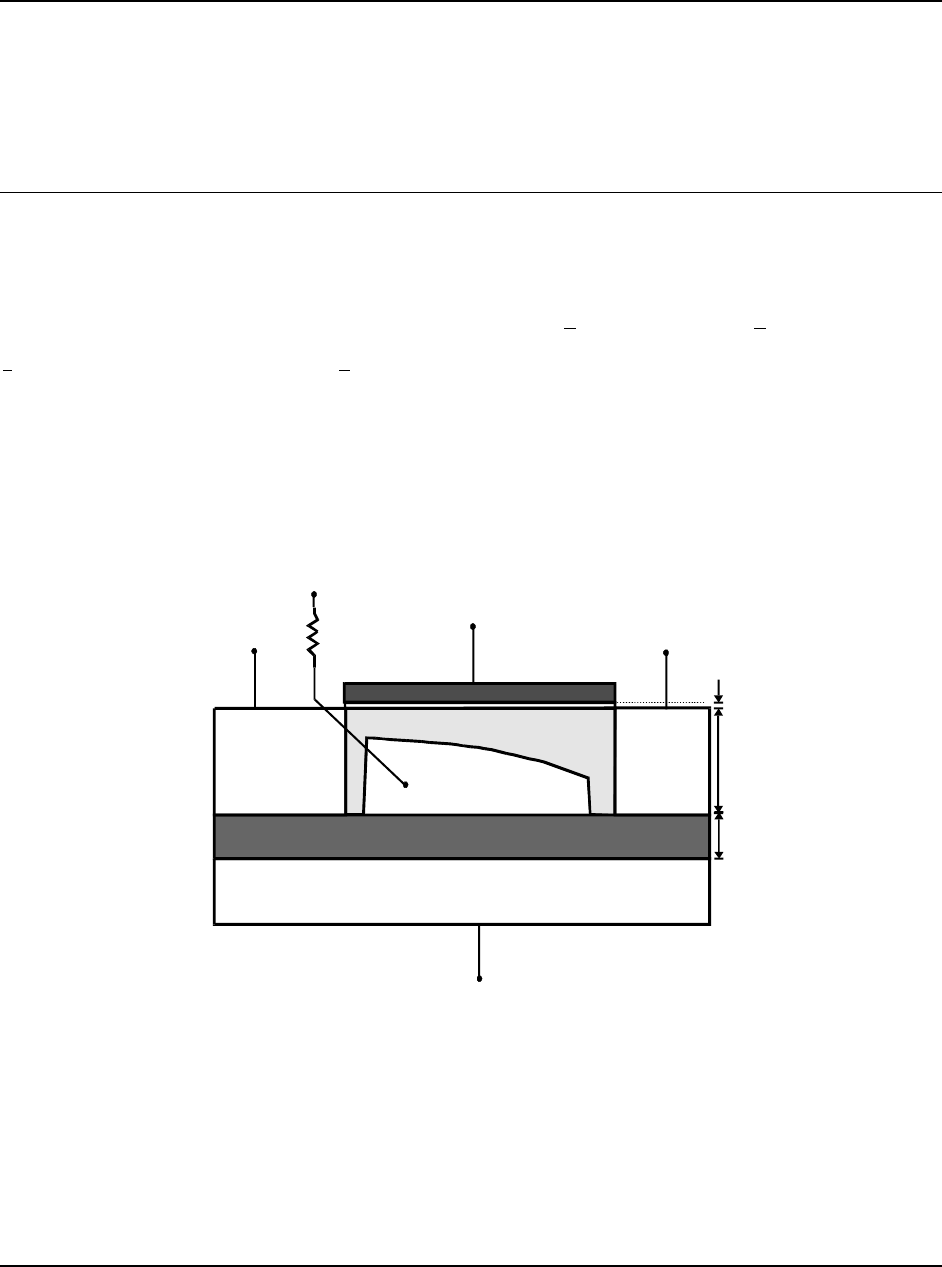
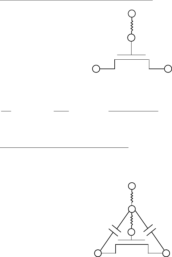
A typical PD SOI MOSFET structure is shown in Fig. 2.1. The device is formed on a thin SOI
film of thickness Tsi on top of a layer of buried oxide with thickness Tbox. In the floating body
configuration, there are four external biases which are gate voltage (Vg), drain voltage (Vd),
source voltage (Vs) and substrate bias (Ve). The body potential (Vb) is iterated in circuit
simulation. If a body contact is applied, there will be one more external bias, the body contact
voltage (Vp).
SOURCE
EXTERNAL BODY BIAS
BODY
SUBSTRATE
GATE
DRAIN
V
V
V
VVV
b
e
p
s
g
d
Tox
Tsi
T
box
Fig. 2.1 Schematic of a typical PD SOI MOSFET.
MOS I-V Model
BSIMSOI3.1 Manual Copyright © 2003, UC Berkeley 2-2
Since the backgate (Ve) effect is decoupled by the neutral body, PD SOI MOSFETs have
similar characteristics as bulk devices. Hence most PD SOI models reported [5, 6] were
developed by adding some SOI specific effects onto a bulk model. These effects include parasitic
bipolar current, self-heating and body contact resistance.
BSIMPD is formulated on top of the BSIM3v3 framework. In this way, a lot of physical
effects which are common in bulk and SOI devices can be shared. These effects are reverse short
channel effect, poly depletion, velocity saturation, DIBL in subthreshold and output resistance,
short channel effect, mobility degradation, narrow width effect and source/drain series resistance
[1, 4].
2.1. Floating Body Operation and Effective Body Potential
In BSIMPD, the floating body voltage is iterated by the SPICE engine. The result of iteration
is determined by the body currents [7, 18]. In the case of DC, body currents include diode
current, impact ionization, gate-induced drain leakage (GIDL), oxide tunneling and body contact
current. For AC or transient simulations, the displacement currents originated from the capacitive
coupling are also contributive.
To ensure a good model behavior during simulations, the iterated body potential Vbs is
bounded by the following smoothing function
(( ))
−−−−−−++−−−−++== bscbscbsbscbsbsc VVVVV.VTδδδδδδ 450 2
1, V V
bsc
=
−
5 (2.1)
(( ))
++−−−−++−−−−−−== 1
2
11111 450 TTT.Vsssbsh δδδδφφδδφφφφ , V
s5.1
1=φ (2.2)
Here the body potential Vbsh is equal to the Vbs bounded between (Vbsc, φs1), and is used in the
threshold voltage and bulk charge calculation. To validate the popular square root expression
bshsV−φ in the MOSFET model, Vbsh is further limited to 0.95φs to give the following effective
body potential
( )
V V V V
bseff s s bsh sbsh bsh
= − − − + − − +
φ φ δφδ δ
0 0 0
2
0 5 4.,
φ
φ
s s0095
=
. (2.3)
MOS I-V Model
BSIMSOI3.1 Manual Copyright © 2003, UC Berkeley 2-3
2.2. Threshold Voltage in the High Vbs Regime
2.2.1. Linear Extrapolation for the Square-Root Epression
Using the Vbseff which is clamped to the surface potential φs, the square-root dependence
bseffsV−φof the threshold voltage is ensured to behave properly during simulations [20].
However the real body potential may be larger than the surface potential in state-of-the-art PD
SOI technologies. To accurately count the body effect in such a high body bias regime, we extend
the square-root expression by
(
)
bseffbshbseffsVVsVtsqrtPhisEx −+−= φ, s
s s
= − −
1
20
φ φ (2.4)
where a linear extrapolation is employed for sbsh
Vφ95.0≥. Notice that bseffsVtsqrtPhisEx −= φ
for sbsh
Vφ95.0≤.
2.2.2. Width Dependence of the Body Effect
In BSIMPD, the body effect coefficient K1 is replaced by
+
+=
21
'
11
11 1
w
w
eff KW
K
KK
eff (2.5)
to model the width dependence of the body effect. Notice that K1eff approaches K1 asymptotically
as the effective channel width W’eff increases. While the body effect coefficient will be determined
by the parameters (K1w1, K1w2 ) when W’eff becomes small so that the contribution from the
channel-stop doping should be taken into account.
The complete equation of the threshold voltage Vth can be found in the Appendix C.
MOS I-V Model
BSIMSOI3.1 Manual Copyright © 2003, UC Berkeley 2-4
2.3. Bulk Charge Effect in the High Vbs Regime
The bulk charge factor in BSIMPD is modified from BSIM3v3 as
+
+
+
−
+
⋅+
−+
+=
1
'
0
2
01
2
1
2
1
)(2
1BW
B
XTL
L
VA
XTL
LA
VKeta
V
Ketas
K
A
eff
depsieff
eff
gsteffgs
depsieff
eff
bsh
bsh
s
eff
bulk
φ
(2.6)
to accommodate the model behavior in the high body bias regime, which is important in PD SOI.
The parameter Ketas acts like an effective increment of the surface potential, which can be used to
adjust the Abulk rollup with the body potential Vbsh. While the other parameter Keta is used to tune
the rate of rollup with Vbsh. By using this new expression, the non-physical drain current roll-off
due to the dramatic Abulk rollup at high body bias can be avoided [20].
2.4. Single Drain Current Equation
After improving the Vth and Abulk behavior in the high body bias regime, we can describe the
MOSFET drain current by the same equation as BSIM3v3. The effective drain voltage Vdseff and
effective gate overdrive voltage Vgsteff introduced in BSIM3v3 [1] are employed to link
subthreshold, linear and saturation operation regions into a single expression as
)1(
1
0
,
A
dseffds
dseff
dsods
ds
MOSFETds V
VV
V
IR
I
I−
+
+
=
βµ=eff ox
eff
eff
CW
L
( )
I
V A V
VvV
V
EL
dso
gsteff bulk
dseff
gsteff t
dseff
dseff
sat eff
=
−+
+
β12 2
1
(2.7)

MOS I-V Model
BSIMSOI3.1 Manual Copyright © 2003, UC Berkeley 2-5
where Rds is the source/drain series resistance, µeff is the mobility, Esat is the critical electrical field
at which the carrier velocity becomes saturated and VA accounts for channel length modulation
(CLM) and DIBL as in BSIM3v3. The substrate current body effect (SCBE) [8, 9] on VA is not
included because it has been taken into account explicitly by the real floating body simulation
determined by the body currents, which will be detailed in the next chapter.
BSIMSOI3.1 Manual Copyright © 2003, UC Berkeley 3-1
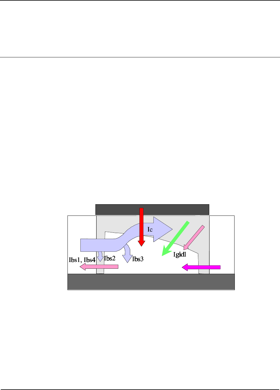
Chapter 3: Body Currents Model
Body currents determine the body potential and therefore the drain current through the body
effect. Beside the impact ionization current considered in BSIM3v3, diode (bipolar) current,
GIDL, oxide tunneling and body contact current are all included in the BSIMPD model [Fig. 3.1]
to give an accurate body-potential prediction in the floating body simulation [18].
3.1. Diode and Parasitic BJT Currents
In this section we describe various current components originated from Body-to-Source/Drain
(B-S/D) injection, recombination in the B-S/D junction depletion region, Source/Drain-to-Body
(S/D-B) injection, recombination current in the neutral body, and diode tunneling current.
Fig. 3.1 Various current components inside the body.
Iii Idiode
Igb
Iii Idiode
Igb

Body Currents Model
BSIMSOI3.1 Manual Copyright © 2003, UC Berkeley 3-2
The backward injection current in the B-S/D diode can be expressed as
−
=
−
=
1exp
1exp
1
1
tdio
bd
sdifsidiodbd
tdio
bs
sdifsidiosbs
Vn
V
jTWI
Vn
V
jTWI
(3.1)
Here dioddiossdifdio WWjn,,, are the non-ideality factor, the saturation current, the effective B-S
diode width and the B-D diode width, respectively.
The carrier recombination and trap-assisted tunneling current in the space-charge region is
modeled by
+
−
=
+
−
=
dbrec
rec
recr
db
recf
bd
srecsidiodbd
sbrec
rec
recr
sb
recf
bs
srecsidiosbs
VV
V
n
V
n
V
jTWI
VV
V
n
V
n
V
jTWI
0
0
2
0
0
2
026.0
exp
026.0
exp
026.0
exp
026.0
exp
(3.2)
Here srecrecrrecf jnn ,, are non-ideality factors for forward bias and reverse bias, the saturation
current, respectively. Note that the parameter 0rec
V is provided to model the current roll-off in the
high reverse bias regime.
The reverse bias tunneling current, which may be significant in junctions with high doping
concentration, can be expressed as
++
−−==
++
−−==
dbtun
tun
tun
db
stunsidiodbd
sbtun
tun
tun
sb
stunsidiosbs
VV
V
n.
V
expjTWI
VV
V
n.
V
expjTWI
0
0
4
0
0
4
0260
1
0260
1
(3.3)
where stun
j is the saturation current. The parameters tun
n and 0tun
V are provided to better fit the
data.
Body Currents Model
BSIMSOI3.1 Manual Copyright © 2003, UC Berkeley 3-3
The recombination current in the neutral body can be described by
( )
( )
−=
−
=
−
=
+=
+
−
−=
+
−
−=
2
_
_
0
'
3
3
5.0exp
1exp
1exp
11
1
1
1exp1
1
1
1exp1
n
eff
bjt
tdio
bd
effhlihlid
tdio
bs
effhlihlis
N
neff
bjtsbjtsieffen
hlid
tdio
bd
enbjtbd
hlis
tdio
bs
enbjtbs
L
L
Vn
V
AE
Vn
V
AE
LL
LjTWI
E
Vn
V
II
E
Vn
V
II
bjt
α
α
α
(3.4)
Here bjt
α is the bipolar transport factor, whose value depends on the ratio of the effective channel
length eff
L and the minority carrier diffusion length n
L. sbjt
j is the saturation current, while the
parameters 0bjt
L and bjt
N are provided to better fit the forward injection characteristics. Notice
that hlis
E and hlid
E, determined by the parameter hli
A, stand for the high level injection effect in
the B-S/D diode, respectively.
The parasitic bipolar transistor current is important in transient body discharge, especially in
pass-gate floating body SOI designs [7]. The BJT collector current is modeled as
I I V
nV
V
nV E
EE E E
EV V
V A L
E E E
cbjt en bs
dio t
bd
dio tnd
nd
ely ely hli
ely bs bd
Abjt ely eff
hli hlis hlid
=
−
=+ +
= + +
+
= +
αexp exp 1
4
2
1
2
2
2
(3.5)
Body Currents Model
BSIMSOI3.1 Manual Copyright © 2003, UC Berkeley 3-4
where nd
E2 is composed of the Early effect ely
E and the high level injection roll-off hli
E. Note
that elynd EE →
2 as hliely EE >> . While hlind EE →
2 as elyhli EE >> , in which case the Early
voltage effelyAbjt LAV+ is high.
To sum up, the total B-S current is ∑
=
=4
1i
bsibs II , and the total B-D current is ∑
=
=4
1i
bdibd II .
The total drain current including the BJT component can then be expressed as
cMOSFETdstotalds III += ,, (3.6)
3.2. New Impact Ionization Current Equation
An accurate impact ionization current equation is crucial to the PD SOI model since it may
affect the transistor output characteristics through the body effect [11]. Hence in BSIMPD we use
a more decent expression [22] to formulate the impact ionization current Iii as
++
+= 2
012
,0exp)(
diffdiff
diff
cbjtiiMOSFETdsii VV
V
IFII βββ
α
V V V
diff ds dsatii
=
−
+
+
+
+
=
−
−++=
dsiid
gstii
ii
gsteffiieffsatii
effsatii
eff
ii
nom
iidsatiidsatii
VS
VS
S
VSLE
LE
VgsStep
L
L
T
T
TVVgsStepV
11
1
1
11
0
2
1
0
(3.7)
Here the cbjtii IF term represents the contribution from the parasitic bipolar current. Notice that
the classical impact ionization current model [12] adopted in BSIM3v3 is actually a special case
of Eqn. (3.6) when
(
)
(
)
0,0,1,, 210 −=βββ . However, the dependence of )log( dsii II on the drain
overdrive voltage diff
V is quite linear [22] for state-of-the-art SOI technologies due to thermally
assisted impact ionization [23]. In this case,
(
)
(
)
1,0,0,, 210 ≅βββ .

Body Currents Model
BSIMSOI3.1 Manual Copyright © 2003, UC Berkeley 3-5
The extracted saturation drain voltage dsatii
V depends on the gate overdrive voltage gst
V and
eff
L. One can first extract the parameters
(
)
iidsatii LV,
0 by the dsatii
V-eff
L characteristics at 0=
gst
V.
All the other parameters ),,,,(021 iidiiiiiisatii SSSSE can then be determined by the plot of dsatii
V
versus gs
V for different eff
L. Notice that a linear temperature dependence of 0
dsatii
V with the
parameter ii
T is also included.
3.3. Gate Induced Drain Leakage Current
GIDL can be important in PD SOI because it can affect the body potential in the low Vgs and
high Vds regime. The formula for GIDL current is:
−⋅⋅=
s
gidl
sgidldgidl E
EIβ
αexp , EV V
T
s
ds gs
ox
=
−
−
⋅
χ
3 (3.8)
Here χ is the fitting parameter with a default value 1.2, which is the correct value for uniformly
doped substrates with no LDD or fully overlapped LDD. However, in general χ can be different
from 1.2, depending on the doping profile at the drain edge [13]. For the sake of symmetry, GIDL
current is accounted for both at the drain and source side )( sgidl
I.
3.4. Oxide Tunneling Current
For thin oxide (below 20Å), oxide tunneling is important in the determination of floatin-body
potential [20]. In BSIMPD the following equations are used to calculate the tunneling current
density Jgb:
Body Currents Model
BSIMSOI3.1 Manual Copyright © 2003, UC Berkeley 3-6
In inversion,
(( ))
0
23
3
EVB
g
EVB
gb1
gb1gb1
N
oxref
2
30
24
3
28
8
V
1V
V1
Ttox
m.m
eV.
hq
m
B
h
q
A
V
explnV
V
TVB
exp
T
T
VV
AJ
ox
b
b
ox
b
ox
aux
ox
oxox
oxqm
ox
auxgb
gb
==
==
==
==
−−
++==
−−
−−−−
==
φφ
φφππ
φφππ
ö
âá
(3.9)
In accumulation,
(( ))
0
23
3
ECB
ECB
gb2
gb2gb2
N
oxref
2
40
13
3
28
8
V
1V
V1
Ttox
m.m
eV.
hq
m
B
h
q
A
VV
explnVV
V
TVB
exp
T
T
VV
AJ
ox
b
b
ox
b
fbgb
taux
ox
oxox
oxqm
ox
auxgb
gb
==
==
==
==
−−
−−++==
−−
−−−−
==
φφ
φφππ
φφππ
âá
(3.10)
Please see Appendix B for model parameter descriptions.
3.5. Body Contact Current
In BSIMPD, a body resistor is connected between the body (B node) and the body contact (P
node) if the transistor has a body-tie. The body resistance is modeled by
rbbshbodyext
'
halo
eff
'
bodybp NRR,
W
R||
L
W
RR effeff ==
== 2 (3.11)

Body Currents Model
BSIMSOI3.1 Manual Copyright © 2003, UC Berkeley 3-7
Here bp
R and bodyext
R represent the intrinsic and extrinsic body resistance respectively. body
R is the
intrinsic body sheet resistance, Rhalo accounts for the effect of halo implant, Nrb is the number of
square from the body contact to the device edge and Rbsh is the sheet resistance of the body
contact diffusion.
The body contact current bp
I is defined as the current flowing through the body resistor:
bodyextbp
bp
bp RR
V
I+
= (3.12)
where bp
V is the voltage across the B node and P node. Notice that 0=
bp
I if the transistor has a
floating body.
3.6. Body Contact Parasitics [17]
The effective channel width may change due to the body contact. Hence the following
equations are used:
sbcpeffdios
dbcpeffdiod
bcbcbcdrawneff
bcbcbcdrawneff
PWW
PWW
dWNdWNWW
dWNdWNWW
+=
+=
−−−=
−
−
−
=
'
'
'
')2(
)2(
(3.13)
Here bc
dW is the width offset for the body contact isolation edge. bc
N is the number of body
contact isolation edge. For example: 0=
bc
N for floating body devices, 1=
bc
N for T-gate
structures and 2=
bc
N for H-gate structures. dbcp
P/sbcp
P represents the parasitic perimeter length
for body contact at drain/source side. The body contact parasitics may affect the I-V significantly
for narrow width devices [20].
After introducing all the mechanisms that contribute the body current, we can express the
nodal equation (KCL) for the body node as
(( ))
(( ))
0==−−++−−−−++++ gbsgidldgidliibpbdbs IIIIIII (3.14)

Body Currents Model
BSIMSOI3.1 Manual Copyright © 2003, UC Berkeley 3-8
Eqn. (3.14) is important since it determines the body potential through the balance of various
body current components. The I-V characteristics can then be correctly predicted after this critical
body potential can be well anchored.

BSIMSOI3.1 Manual Copyright © 2003, UC Berkeley 4-1
Chapter 4: MOS C-V Model
BSIMPD approaches capacitance modeling by adding SOI-specific capacitive effect to the
C-V model of BSIM3v3. Similar to the I-V case, the body charges belonged to the floating body
node will be our emphasis. The model incorporates features listed below with the SOI-specific
features bold-faced and italicized.
• Separate effective channel length and width for IV and CV models.
• The CV model is not piece-wise (i.e. divided into inversion, depletion, and
accumulation). Instead, a single equation is used for each nodal charge covering all
regions of operation. This ensures continuity of all derivatives and enhances convergence
properties. Just like in BSIM3v3, the inversion and body capacitances are continuous at
the threshold voltage.
• Threshold voltage formulation is consistent with the IV model. Body effect and DIBL are
automatically incorporated in the capacitance model.
• Intrinsic capacitance model has two options. The capMod = 2 option yields capacitance
model based on BSIM3v3 short channel capacitance model. The capMod = 3 option is
the new charge-thickness model from BSIM3v3.2 [4].
• Front gate overlap capacitance is comprised of two parts: 1) a bias independent part
which models the effective overlap capacitance between the gate and the heavily doped
source/drain, and 2) a gate bias dependent part between the gate and the LDD region.
• Bias independent fringing capacitances are added between the gate and source as well as
the gate and drain. A sidewall source/drain to substrate (under the buried oxide)
fringing capacitance is added.
• A source/drain-buried oxide-Si substrate parasitic MOS capacitor is added.
• Body-to-back-gate coupling is added.
MOS C-V Model
BSIMSOI3.1 Manual Copyright © 2003, UC Berkeley 4-2
A good intrinsic charge model is important in bulk MOSFETs because intrinsic capacitance
comprises a sizable portion of the overall capacitance, and because a well behaved charge model
is required for robust large circuit simulation convergence. In analog applications there are
devices biased near the threshold voltage. Thus, a good charge model must be well-behaved in
transition regions as well. To ensure proper behavior, both the I-V and C-V model equations
should be developed from an identical set of charge equations so that Cij/Id is well behaved.
A good physical charge model of SOI MOSFETs is even more important than in bulk. This is
because transient behavior of the floating body depends on capacitive currents [18]. Also, due to
the floating body node, convergence issues in PD SOI are more volatile than in bulk, so that
charge smoothness and robustness are important. An example is that a large negative guess of
body potential by SPICE during iterations can force the transistor into depletion, and a smooth
transition between depletion and inversion is required. Therefore the gate/source/drain/backgate
to body capacitive coupling is important in PD SOI.
4.1. Charge Conservation
Fig. 4.1 Intrinsic charge components in BSIMPD CV model

MOS C-V Model
BSIMSOI3.1 Manual Copyright © 2003, UC Berkeley 4-3
To ensure charge conservation, terminal charges instead of terminal voltages are used as state
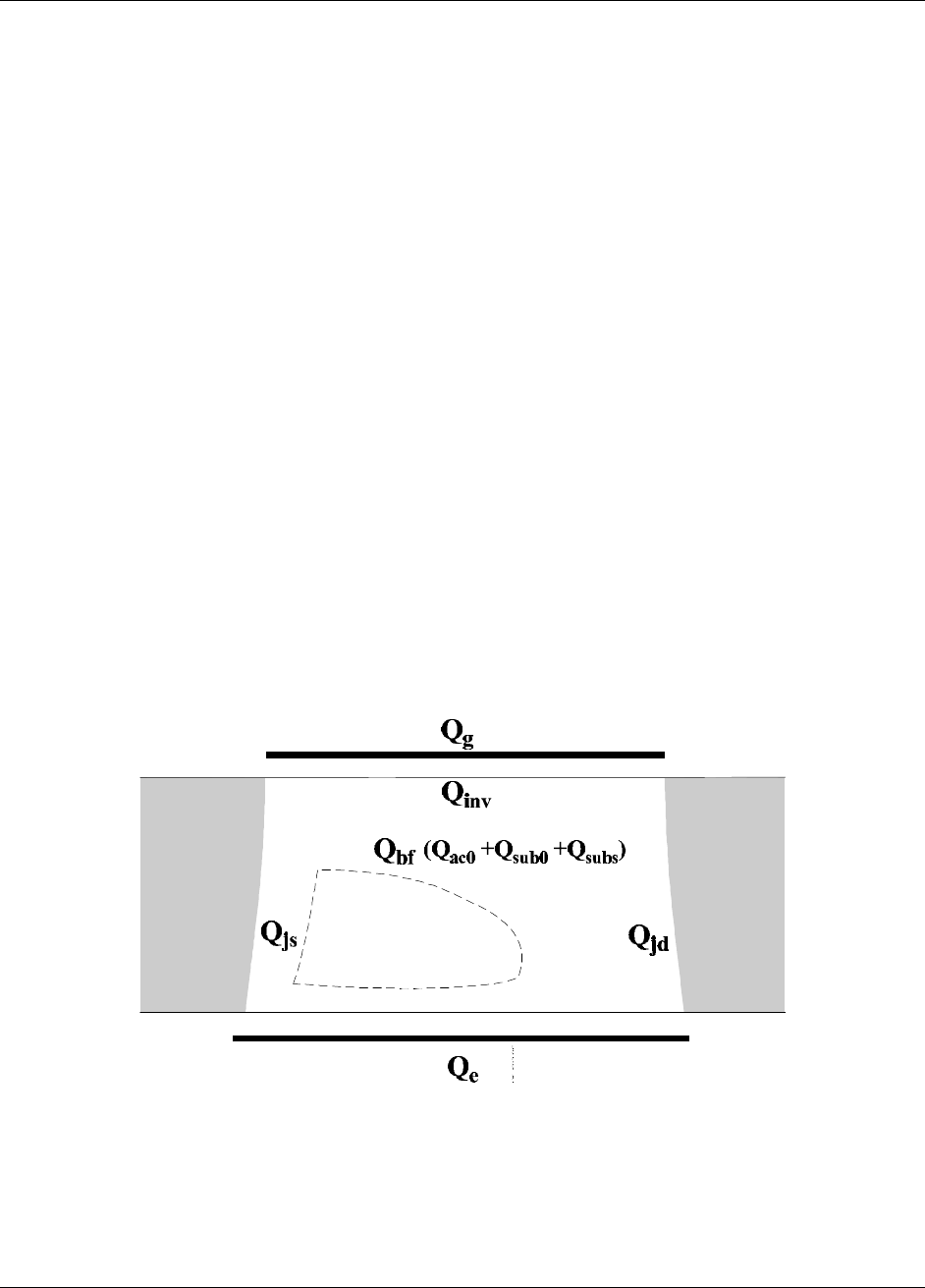
variables. The terminal charges Qg, Qd, Qs, Qb, and Qe are the charges associated with the gate,
drain, source, body, and substrate respectively. These charges can be expressed in terms of
inversion charge (Qinv), front gate body charge (QBf), source junction charge (Qjs) and drain
junction charge (Qjd). The intrinsic charges are distributed between the nodes as shown in Fig.
4.1. The charge conservation equations are:
Q Q Q Q
Bf ac sub subs
=
+
+
0 0
Q Q Q
inv inv sinv d
=
+
, ,
(
)
BfinvgQQQ +−=
jdjseBfbQQQQQ ++−= (4.1)
Q Q Q
sinv sjs
=
−
,
Q Q Q
dinv djd
=
−
,
Q Q Q Q Q
gebsd
+
+
+
+
=
0
The front gate body charge (QBf) is composed of the accumulation charge (Qac0) and the bulk
charge ( 0sub
Q and subs
Q), which may be divided further into two components: the bulk charge at
Vds=0 (Qsub0), and the bulk charge induced by the drain bias (Qsubs) (similar to δQsub in
BSIM3v3).
All capacitances are derived from the charges to ensure charge conservation. Since there are
5 charge nodes, there are 25 (as compared to 16 in BSIM3v3) components. For each component:
CdQ
dV
ij i
j
=, where i and j denote transistor nodes. In addition, C C
ij ij
ji
= =
∑
∑
0.

MOS C-V Model
BSIMSOI3.1 Manual Copyright © 2003, UC Berkeley 4-4
4.2. Intrinsic Charges
BSIMPD uses similar expressions to BSIM3v3 for inv
Q and Bf
Q. First, the bulk charge
constant AbulkCV is defined as
+=
CLE
active
bulkbulkCV L
CLC
AA 1
0 (4.2)
where
(
)
0
0== gsteffbulkbulk VAA (4.3)
This is done in order to empirically fit VdsatCV to channel length. Experimentally,
V V V V
A
dsatIV dsatCV dsatIV L
gsteffCV
bulk
< < =
→∞ (4.4)
The effective CV Vgst is defined as
Vnv V V
nv
gsteffCV t
gs th
t
= + −
ln exp1 (4.5)
Then we can calculate the CV saturation drain voltage
V V A
dsatCV gsteffCV bulkCV
=/. (4.6)
Define effective CV Vds as
)4)((
2
12
dsatCVdsdsatCVdsdsatCVdsatCVdsCV VVVVVVV δδδ +−−+−−−= (4.7)
Then the inversion charge can be expressed as
−
+
−−=
dsCV
bulkCV
gsteffCV
dsCVbulkCV
dsCV
bulkCV
gsteffCVoxactiveactiveinv
V
A
V
VA
V
A
VCLWQ
2
12
22
22 (4.8)
where active
W and active
L are the effective channel width and length in CV, respectively. The
channel partition can be set by the Xpart parameter. The exact evaluation of source and drain
charges for each partition option is presented in Appendix C.
MOS C-V Model
BSIMSOI3.1 Manual Copyright © 2003, UC Berkeley 4-5
A parameter VFBeff is used to smooth the transition between accumulation and depletion
regions. The expression for VFBeff is:
( ) ( )
V V V V V V
FBeff fb fb gb fb gb
= − − − + − − +
05 22
.δ δ δ (4.9)
where V V V
gb gs bseff
=
−
, bseffseffsthfb VKVV −−−= φφ 1.
The physical meaning of the function is the following: it is equal to Vgb for Vgb<VFB, and
equal to VFB for Vgb>VFB. Using VFBeff, the accumulation charge can be calculated as
)(
0fbFBeffoxactiveBactivebodyac VVCLWFQ−−= (4.10)
where DLCBLL activeactiveB −= . Notice that the parameters body
F and DLCB are provided to give
a better fit for the SOI-specific history dependence of the body charge [14].
The gate-induced depletion charge and drain-induced depletion charge can be expressed as
−−−
++−−= 2
1
2
1
0
)(4
11
2eff
bseffgsteffCVFBeffgseff
oxactiveBactivebodysub K
VVVVK
CLWFQ (4.11)
( )
( )
−
−−= 2122
1
2
1
dsCVbulkCVgsteffCV
dsCVbulkCVdsCV
bulkCVoxeffactiveBactivebodysubs VAV
VAV
ACKLWFQ (4.12)
respectively.
Finally, the back gate body charge can be modeled by
(
)
bsefffbbesboxactiveBGactivebodyeVVVCLWFQ−−= (4.13)
where bgactiveBactiveBG LLL δ2+= . The parameter bg
Lδ is provided to count the difference of activeB
L
and activeBG
L due to the source/drain extension in the front channel.
For capMod=3, the flat band voltage is calculated from the bias-independent threshold
voltage, which is different from capMod=2. For the finite thickness formulation, refer to Chapter
4 of BSIM3v3.2 Users’ Manual.
MOS C-V Model
BSIMSOI3.1 Manual Copyright © 2003, UC Berkeley 4-6
4.3. Source/Drain Junction Charges
Beside the junction depletion capacitance considered in BSIM3v3, the diffusion capacitance,
which is important in the forward body-bias regime [20], is also included in BSIMPD. The
source/drain junction charges jdwgjswg QQ / can therefore be expressed as
bddifbddepjdwg
bsdifbsdepjswg
QQQ
QQQ
+=
+
=
(4.14)
The depletion charges bddepbsdep QQ / have similar expressions as in BSIM3v3 [Appendix C].
While the diffusion charges bddifbsdif QQ / can be modeled by
1
1
1exp
11
1'
1
1
1exp
11
1'
00
00
+
−
++=
+
−
++=
hlid
tdio
bd
N
neff
bjtdifsbjtsieffbddif
hlis
tdio
bs
N
neff
bjtdifsbjtsieffbsdif
E
Vn
V
LL
LLJTWQ
E
Vn
V
LL
LLJTWQ
dif
dif
τ
τ
(4.15)
The parameter
τ
represents the transit time of the injected minority carriers in the body. The
parameters 0dif
L and dif
N are provided to better fit the data.
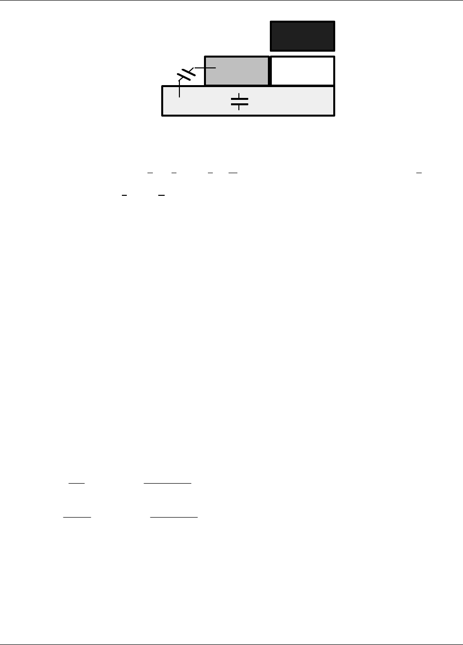
4.4. Extrinsic Capacitances
Expressions for extrinsic (parasitic) capacitances that are common in bulk and SOI
MOSFETs are taken directly from BSIM3v3. They are source/drain-to-gate overlap capacitance
and source/drain-to-gate fringing capacitance. Additional SOI-specific parasitics added are
substrate-to-source sidewall capacitance Cessw, and substrate-to-drain sidewall capacitance Cedsw,
substrate-to-source bottom capacitance (Cesb) and substrate-to-drain bottom capacitance (Cedb)
[Fig. 4.2].
MOS C-V Model
BSIMSOI3.1 Manual Copyright © 2003, UC Berkeley 4-7
Cessw
Cesb
Fig. 4.2 SOI MOSFET extrinsic charge components. Cessw is the
substrate-to-source sidewall capacitance. Cesb is the substrate-
to-source bottom capacitance.
In SOI, there is a parasitic source/drain-buried oxide-Si substrate parasitic MOS structure
with a bias dependent capacitance. If Vs,d=0, this MOS structure might be in accumulation.
However, if Vs,d=Vdd, the MOS structure is in depletion with a much smaller capacitance,
because the Si substrate is lightly doped. The bias dependence of this capacitance is similar to
high frequency MOS depletion capacitance as shown in Fig. 4.3. It might be substantial in
devices with large source/drain diffusion areas. BSIMPD models it by piece-wise expressions,
with accurately chosen parameters to achieve smoothness of capacitance and continuity to the
second derivative of charge. The substrate-to-source bottom capacitance (per unit source/drain
area) Cesb is:
( )
( )
( )
C
Cif V V
CAC C V V
V V elseif V V A V V
CAC C V V
V V elseif V V
Celse
esb
box se sdfb
box sd box se sdfb
sdth sdfb se sdfb sd sdth sdfb
sd box se sdth
sdth sdfb se sdth
=
<
− − −
−
< + −
+−−−
−
<
1
1
1
2
2
min
min min
min
(4.16)
Physical parameters Vsdfb (flat-band voltage of the MOS structure) and Vsdth (threshold voltage of
the MOS structure) can be easily extracted from measurement. Cmin should also be extracted
from measurement, and it can account for deep depletion as well. Asd is a smoothing parameter.
MOS C-V Model
BSIMSOI3.1 Manual Copyright © 2003, UC Berkeley 4-8
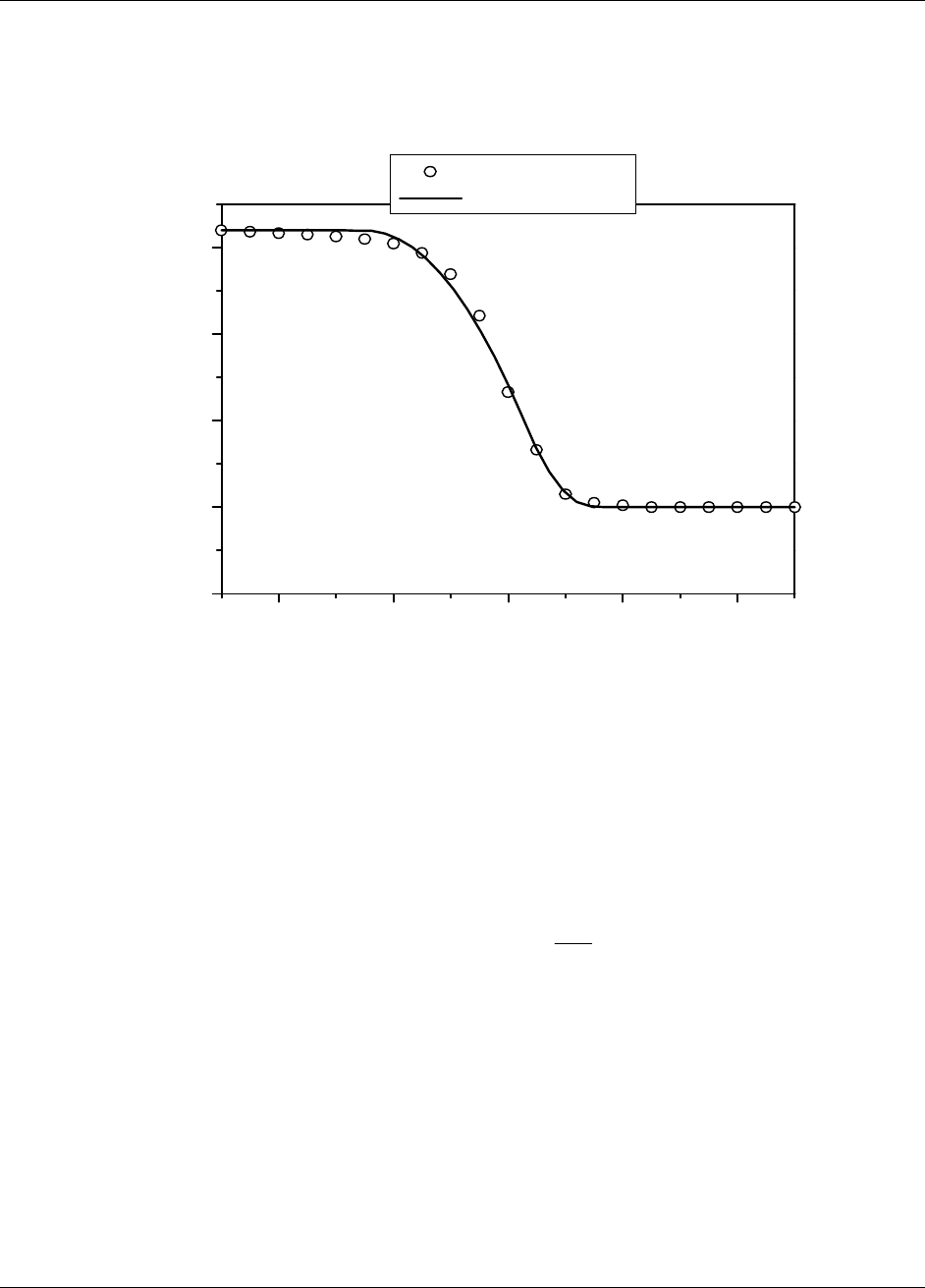
The expression for Cedb is similar to Cesb. Fig. 4.3 shows the comparison of the model and
measured Cesb.
-4 -2 0 2 4
80
100
120
140
160
measured data
model fit
Capacitance (fF)
Vs/d,e
Fig. 4.3 Bottom source/drain to substrate capacitance for a PD SOI
MOSFET.
Finally, the sidewall source/drain to substrate capacitance (per unit source/drain perimeter
length) can be expressed by
+=
box
si
sdesweswdsT
T
CC 1log
,/ (4.17)
which depends on the silicon film thickness si
T and the buried oxide thickness box
T. The
parameter sdesw
C represents the fringing capacitance per unit length.
4.5. Body Contact Parasitics
The parasitic capacitive coupling due to the body contact is considered in BSIMPD. The

MOS C-V Model
BSIMSOI3.1 Manual Copyright © 2003, UC Berkeley 4-9
instance parameter gbcp
A represents the parasitic gate-to-body overlap area due to the body
contact, and ebcp
A represents the parasitic substrate-to-body overlap area. The effect may be
significant for small area devices [CV part in Appendix C].

BSIMSOI3.1 Manual Copyright © 2003, UC Berkeley 5-1
Chapter 5: Temperature Dependence and Self-Heating
Self-heating in SOI is more important than in bulk since the thermal conductivity of silicon
dioxide is about two orders of magnitude lower than that of silicon [15]. It may degrade the
carrier mobility, increase the junction leakage [20], enhance the impact ionization rate[24], and
therefore affect the output characteristics [16] of floating-body SOI devices.
5.1. Temperature Dependence
The temperature dependence of threshold voltage, mobility, saturation velocity and series
resistance in BSIMPD is identical to BSIM3v3. However a different temperature dependence of
diode characteristics is adopted in BSIMPD:
−
−
=
nom
bjt
tdio
g
sbjtsbjt T
T
X
Vn
KE
jj 1
)300(
exp
0
−
−
=
nom
dif
tdio
g
sdifsdif T
T
X
Vn
KE
jj 1
)300(
exp
0
−
−
=
nom
rec
trecf
g
srecsrec T
T
X
Vn
KE
jj 1
)300(
exp
0
0
j j XT
T
stun stun tun
nom
= −
01exp (5.1)
−−++==
−−++==
11
11
0
0
nom
recrrecrrecr
nom
recfrecfrecf
T
T
ntnn
T
T
ntnn
The parameters 0000 ,,, stunsrecsdifsbjt jjjj are diode saturation currents at the nominal temperature
nom
T, and the parameters tunrecdifbjt XXXX ,,, are provided to model the temperature dependence.
Temperature Dependence and Self-Heating
BSIMSOI3.1 Manual Copyright © 2003, UC Berkeley 5-2
Notice that the non-ideality factors recrrecf nn , are also temperature dependent.
5.2. Self-Heating Implementation
BSIMPD models the self-heating by an auxiliary ththCR circuit as shown in Fig. 5.1 [18]. The
temperature node (T node) will be created in SPICE simulation if the self-heating selector shMod
is ON and the thermal resistance is non-zero. The T node is treated as a voltage node and is
connected to ground through a thermal resistance Rth and a thermal capacitance Cth:
0
0
th
'
eff
th
th WW
R
R++
== , )WW(CC th
'
effthth 00 ++== (5.2)
where 0th
R and 0th
C are normalized thermal resistance and capacitance, respectively. Wth0 is the
minimum width for thermal resistance calculation [19]. Notice that the current source is driving a
current equal to the power dissipated in the device.
PIV
ds ds
= × (5.3)
To save computation time, the turn-on surface potential φs (Phi) is taken to be a constant
within each timepoint because a lot of parameters (e.g. Xdep) are function of φs. Each timepoint
will use a φs calculated with the temperature iterated in the previous timepoint. However this
approximation may induce error in DC, transient and AC simulation. Therefore, it is a tradeoff
between accuracy and speed. The error in DC or transient is minimal if the sweeping step or time
step is sufficiently small.
IdVdRth Cth
Fig. 5.1 Equivalent circuit for self-heating simulation.

BSIMSOI3.1 Manual Copyright © 2003, UC Berkeley 6-1
Chapter 6: BSIMSOI –
A Unified Model for PD and FD SOI MOSFETs
Using BSIMPD as a foundation, we have developed a unified model for both PD and FD SOI
circuit designs based on the concept of body-source built-in potential lowering [20, 25].
6.1. BSIMSOI Framework and Built-In Potential Lowering Model
As described in [20], we construct BSIMSOI based on the concept of body-source built-in
potential lowering, ∆Vbi. There are three modes (soiMod = 0, 1, 2) in BSIMSOI: BSIMPD
(soiMod = 0) can be used to model the PD SOI device, where the body potential is independent
on ∆Vbi (VBS > ∆Vbi). Therefore the calculation of ∆Vbi is skipped in this mode. On the other
hand, the ideal FD model (soiMod = 2) is for the FD device with body potential equal to ∆Vbi.
Hence the calculation of body current/charge, which is essential to the PD model, is skipped. For
the unified SOI model (soiMod = 1), however, both ∆Vbi and body current/charge are calculated
to capture the floating-body behavior exhibited in FD devices. As shown in Figure 6.1, this unified
model covers both BSIMPD and the ideal FD model.
BSIMSOI – A Unified Model for PD and FD SOI MOSFETs
BSIMSOI3.1 Manual Copyright © 2003, UC Berkeley 6-2
Fig. 6.1 The body potential in the unified model approaches the VBS solved in BSIMPD for PD
devices, while returns to ∆Vbi for ideal FD devices [20].
This unified model shares the same floating-body module as BSIMPD, with a generalized
diode current model considering the body-source built-in potential lowering effect (IBS ∝ exp(-
q∆Vbi/kT)). Therefore, an accurate and efficient ∆Vbi model is crucial. The following formulation
for ∆Vbi is mainly based on the Poisson equation and the physical characterization for ∆Vbi, as
presented in [25].
For a given surface band bending φ (source reference), ∆Vbi can be formulated by applying the
Poisson equation in the vertical direction and continuity of normal displacement at the back
interface:
0.0 0.5 1.0 1.5 2.0
0.0
0.1
0.2
0.3
0.4
0.5
0.6
0.7
∆∆Vbi
VGS=0.5V
L=0.5µµm
TSi=40nm
soiMod=0 (BSIMPD)
soiMod=1 (Unified Model)
soiMod=2 (Ideal FD)
VBS (V)
VDS (V)

BSIMSOI – A Unified Model for PD and FD SOI MOSFETs
BSIMSOI3.1 Manual Copyright © 2003, UC Berkeley 6-3
(( ))
(( ))
(( ))
OX
OX
OX
BOX
OX
BOX
Si
Si
Si
FBbbGS
BOXSi
BOX
effeDIBLSi
Si
ch
BOXSi
Si
bi
T
C,
T
C,
T
C
VV
CC
C
LVT
qN
CC
C
V
εεεεεε
ηη
εε
φφφφ
======
−−⋅⋅
++
++
∆∆++⋅⋅−−⋅⋅
++
==∆∆
2
2
(6-1).
The first term of Equation (6-1) represents the frontgate coupling. TSi is the SOI thickness. Nch
accounts for the effective channel doping, which may vary with channel length due to the non-
uniform lateral doping effect. The second term of Equation (6-1) represents the backgate coupling
(VbGS). VFBb is the backgate flatband voltage. Equation (6-1) shows that the impact of frontgate on
∆Vbi reaches maximum when the buried oxide thickness, TBOX, approaches infinity.
In Equation (6-1), ∆VDIBL represents the short channel effect on ∆Vbi,
(( ))
Bbi
eff
vbd
eff
vbdvbdDIBL V
l
L
Dexp
l
L
DexpDVΦΦ−−⋅⋅
−−++
−−==∆∆ 22
2110 (6-2),
as addressed in [25]. Here l is the characteristic length for the short-channel-effect calculation.
Dvbd0 and Dvbd1 are model parameters. Similarly, the following equation
(( ))
−−++
−−⋅⋅−−== l
L
Dexp
l
L
DexpKKLeff
bk
eff
bkbbeffe2221 2
2
ηη (6-3)
is used to account for the short channel effect on the backgate coupling, as described in [25].
DK1b, DK2b, K1b (default 1) and K2b (default 0) are model parameters.
The surface band bending, φ, is determined by the frontgate VGS and may be approximated by
BSIMSOI – A Unified Model for PD and FD SOI MOSFETs
BSIMSOI3.1 Manual Copyright © 2003, UC Berkeley 6-4
{{
(( ))
(( ))
TGSGST
BOXSiOX
OX
ON
TGSON
VVVV
CCC
C
VV
≤≤−−⋅⋅
++++
−−ΦΦ
==
≥≥ΦΦ
−−
−−−− for
for
1
11
φφ (6-4).
To improve the simulation convergency, the following single continuous function from
subthreshold to strong inversion is used:
(( ))
−−−−
++⋅⋅⋅⋅
++++
−−ΦΦ== −−
−−−− tFD,OFF
FD,OFFeff_gsFD,T
tFD,OFF
BOXSiOX
OX
ON VN
VVV
explnVN
CCC
C1
1
11
φφ (6-5).
Here Vgs_eff is the effective gate bias considering the poly-depletion effect. VT,FD is the threshold
voltage at VBS = ∆Vbi(φ=2ΦB). NOFF,FD (default 1) and VOFF,FD (default 0) are model parameters
introduced to improve the transition between subthreshold and strong inversion. Vt is the thermal
voltage. Notice that the frontgate coupling ratio in the subthreshold regime approaches 1 as TBOX
approaches infinity.
To accurately model ∆Vbi and thus the device output characteristics, the surface band bending
at strong inversion, ΦON, is not pinned at 2ΦB. Instead, the following equation
(( ))
⋅⋅⋅⋅
ΦΦ++
++++ΦΦ==ΦΦ 2
1
212
12
t
BFD,gsteffFD.gsteff
tBON VKmoin
KVV
lnV (6-6)
is used to account for the surface potential increment with gate bias in the strong inversion regime
[4]. Here moin is a model parameter. K1 is the body effect coefficient. Notice that a single
continuous function,
−−−−
++⋅⋅==
tFD,OFF
FD,OFFFD,Teff_gs
tFD,OFFFD,gsteff VN
VVV
explnVNV1 (6-7),
BSIMSOI – A Unified Model for PD and FD SOI MOSFETs
BSIMSOI3.1 Manual Copyright © 2003, UC Berkeley 6-5
has been used to represent the gate overdrive in Equation (6-6).
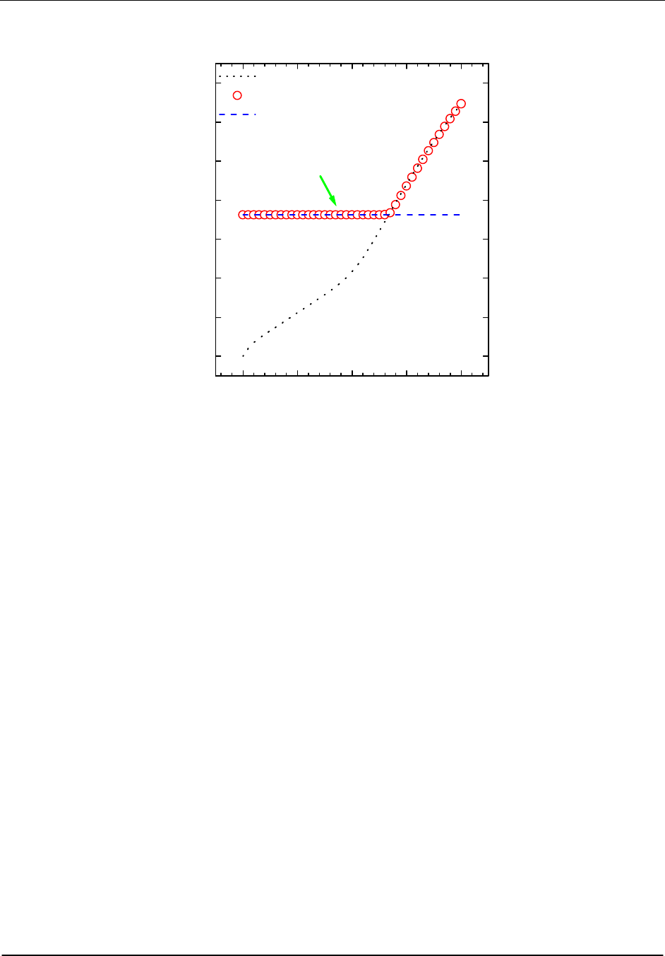
6.2. Verification
The BSIMPD parameter extraction methodology presented in [20] may still be used under the
unified BSIMSOI framework, provided that the link between PD and FD, ∆Vbi, can be accurately
extracted. As described in [25], a direct probe of ∆Vbi can be achieved by finding the onset of the
external body bias (through a body contact) after which the threshold voltage and hence the
channel current of the FD SOI device is modulated. When the body contact is not available,
nevertheless, model parameters related to ∆Vbi should be extracted based on the subthreshold
characteristics of the floating-body device. As shown in Figure 6.2, the reduction of ∆Vbi with
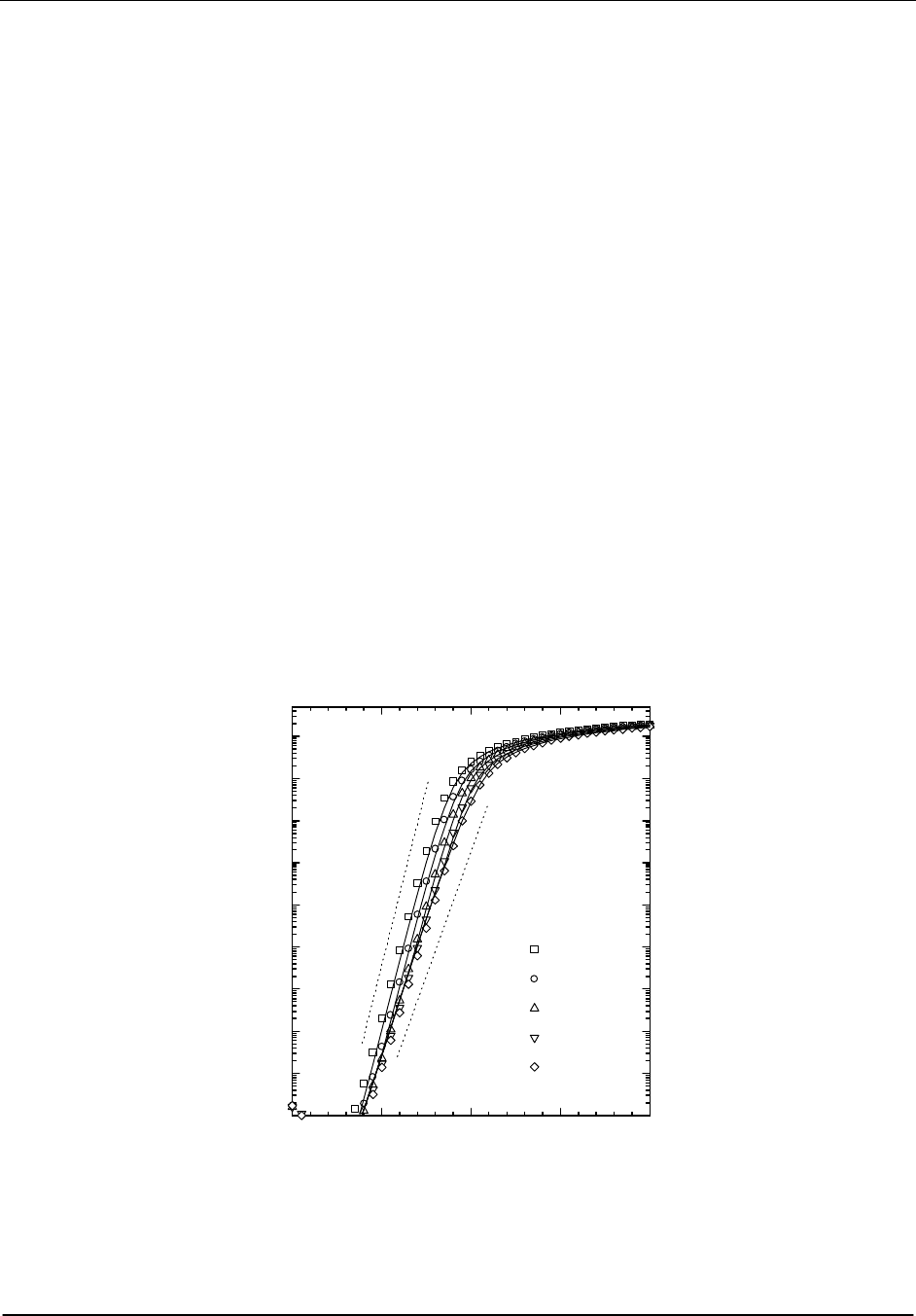
backgate bias is responsible for the transition from the ideal subthreshold swing (~ 60 mV/dec. at
room temperature) to the non-ideal one.
Fig. 6.2 The PD/FD transition can be captured by modeling ∆Vbi [20].
-0.5 0.0 0.5 1.0 1.5
10-13
10-12
10-11
10-10
10-9
10-8
10-7
10-6
10-5
10-4
~102mV/dec.
~67mV/dec.
LG=0.5µµm
VDS=0.05V
T=27oC
VbGS=4V
2V
0V
-2V
-4V
line: model
ID (A)
VGS (V)
BSIMSOI – A Unified Model for PD and FD SOI MOSFETs
BSIMSOI3.1 Manual Copyright © 2003, UC Berkeley 6-6
Figure 6.2 clearly shows that the PD/FD transition can be captured by the ∆Vbi approach. In
other words, ∆Vbi is indeed an index of the degree of full depletion, as pointed out in [20, 25]. As
shown in Figure 6.3, larger floating-body effect can be observed for negative backgate bias due to
smaller ∆Vbi. In case the ∆Vbi value is raised by charge sharing as described in [25], it can be
predicted that the short-channel device should exhibit less floating-body effect than the long-
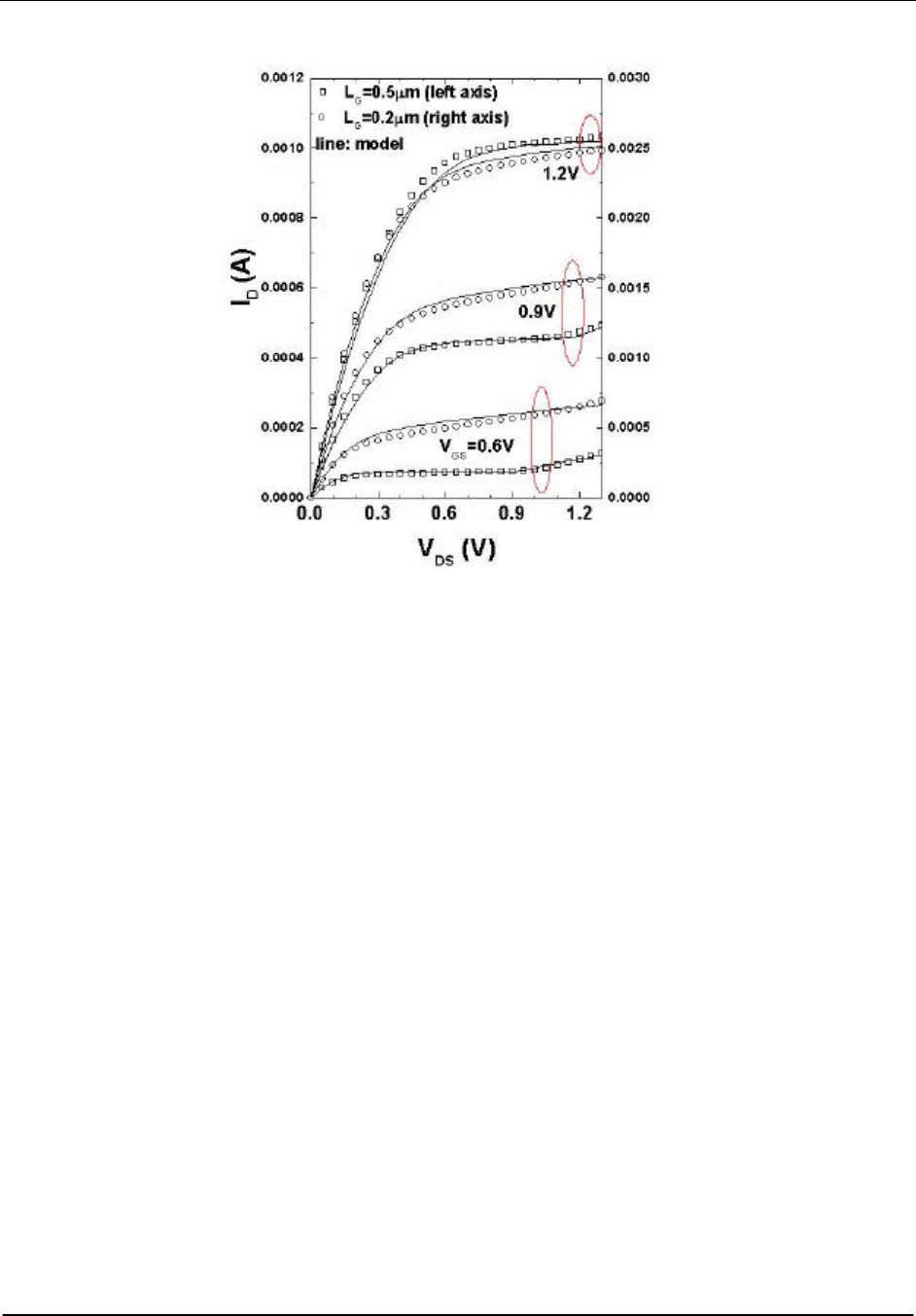
channel one due to larger ∆Vbi, as verified in Figure 6.4.
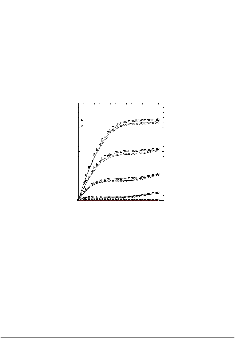
Fig. 6.3 Larger floating-body effect can be seen for the negative backgate bias (source reference)
due to smaller ∆Vbi [20].
0.0 0.3 0.6 0.9 1.2 1.5
0.0000
0.0005
0.0010
0.0015
0.0020
0.6V
0.9V
1.2V
VGS=1.5V
LG=0.5µµm
line: model
VbGS=0V
VbGS=-1.5V
ID (A)
VDS (V)
BSIMSOI – A Unified Model for PD and FD SOI MOSFETs
BSIMSOI3.1 Manual Copyright © 2003, UC Berkeley 6-7
Fig. 6.4 Less floating-body effect can be seen for the short-channel device due to larger ∆Vbi [20].
Chapter 7: BSIMSOI RF model
RF Model in BSIMSOIv3.1
BSIMSOI3.1 provides the gate resistance model for devices used in RF application.
Users have four options for modeling gate electrode resistance (bias independent) and
intrinsic-input resistance (Rii, bias-dependent) by choosing model choice parameter
rgateMod.
RgateMod = 0 (zero-resistance):
In this case, no gate resistance is generated.
RgateMod = 1 (constant-resistance):
In this case, only the electrode gate resistance (bias-independent) is generated by adding
an internal gate node. The electrode gate resistance Rgeltd is given by
( )
XGLLNGCON
NSEGNGCON
W
XGWRSHG
Rgeltd
drawn
eff
−⋅
⋅⋅
+⋅
=3
Rgeltd
RgateMod = 2 (RII model with variable resistance):
In this case, the gate resistance is the sum of the electrode gate resistance and the
intrinsic-input resistance Rii as given by
⋅+⋅=
eff
Boxeffeffeff
dseff
ds
qL
TkCW
XRCRG
V
I
XRCRG
Rii
µ
21
1
An internal gate node will be generated.
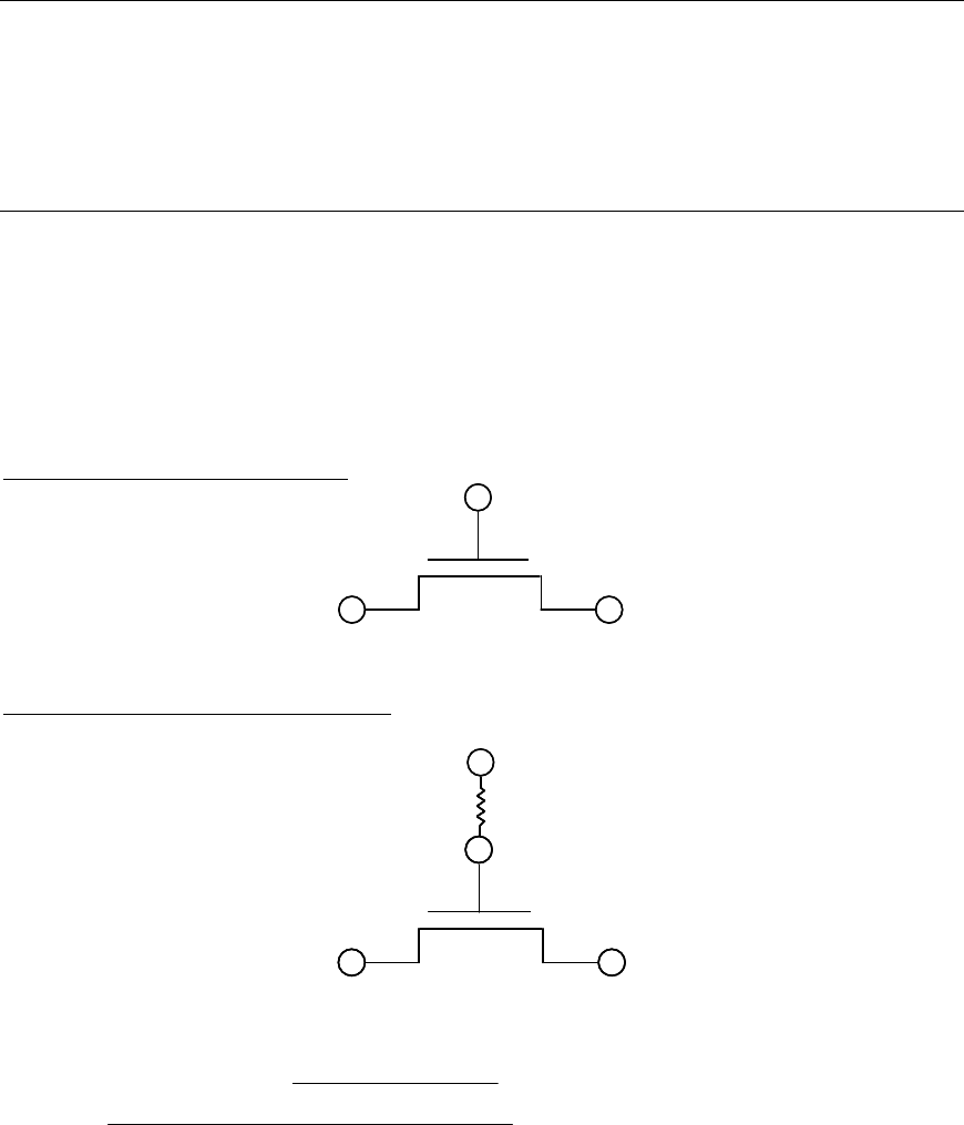
RgateMod = 3 (RII model with two nodes):
In this case, the gate electrode resistance is in series with the intrinsic-input resistance Rii
through two internal gate nodes, so that the overlap capacitance current will not pass
through the intrinsic-input resistance.
Rgeltd+
Rii
Rgeltd
Rii Cgdo
Cgso

References
[1] Y. Cheng, M. C. Jeng, Z. H. Liu, J. Huang M. Chan, P. K. Ko, and C. Hu, “A Physical
and Scalable I-V Model in BSIM3v3 for Analog/Digital Circuit Simulation”, IEEE Trans.
On Elec. Dev., vol. 42, p. 2, Feb 1997.
[2] BSIM3SOIv1.3 Users’ Manual, UC Berkeley, Department of EECS.
[3] W. Jin, P. C. H. Chan, S. K. H. Fung, P. K. Ko, “A Physically-Based Low-Frequency
Noise Model for NFD SOI MOSFET’s”, IEEE Intl. SOI conf., pp. 23-24, 1998.
[4] BSIM3v3.2 Users’ Manual, UC Berkeley, Department of EECS.
[5] D. Suh, J. G. Fossum, “A physical charge-based model for non-fully depleted SOI
MOSFET’s and its use in assessing floating-body effects in SOI CMOS circuits”, IEEE
Tran. on Electron Devices, vol. 42, no. 4, pp. 728-37, April 1995.
[6] M. S. L. Lee, W. Redman-White, B. M. Tenbroek, M. Robinson, “Modelling of thin film
SOI devices for circuit simulation including per-instance dynamic self-heating effects”,
IEEE Intl. SOI conf., pp. 150-151, 1993.
[7] D. Sinitsky, S. Tang, A. Jangity, F. Assaderaghi, G. Shahidi, C. Hu, “Simulation of SOI
Devices and Circuits using BSIM3SOI”, IEEE Electron Device Letters, vol. 19, no. 9,
pp. 323-325, September 1998.
[8] G. S. Gildenblat, VLSI Electronics: Microstructure Science, p. 11, vol. 18, 1989.

BSIMSOI3.1 Manual Copyright © 2003, UC Berkeley
[9] M. C. Jeng, “Design and Modeling of Deep-Submicrometer MOSFETs”, Ph. D.
Dissertation, UC Berkeley.
[10] D. Sinitsky, S. Fung, S. Tang, P. Su, M. Chan, P. Ko, C. Hu, “A Dynamic Depletion SOI
MOSFET Model for SPICE”, in Dig. Tech. Papers, Symp. VLSI Technology, 1998.
[11] D. Sinitsky, R. Tu, C. Liang, M. Chan, J. Bokor and C. Hu, “AC output conductance of
SOI MOSFETs and impact on analog applications”, IEEE Electron Device Letters,
vol.18, no.2, pp. 36-38, Feb 1997.
[12] T. Y. Chan, P. K. Ko and C. Hu, “A Simple Method to Characterize Substrate Current in
MOSFETs”, IEEE Electron Dev. Letts., EDL-5, Dec 1984, p. 505.
[13] S. A. Parke, J. E. Moon, H. C. Wann, P. K. Ko and C. Hu, “Design for suppression of
gate-induced drain leakage in LDD MOSFETs using a quasi-two-dimensional analytical
model”, IEEE Trans. On Electron Device, vol. 39, no. 7, pp. 1697-703, July 1992.
[14] J. Gautier and J. Y.-C. Sun, “On the transient operation of partially depleted SOI
NMOSFET’s”, IEEE Electron device letters, vol.16, no.11, pp. 497-499, Nov 1995.
[15] L. T. Su, D. A. Antoniadis, M. I. Flik, J. E. Chung, “Measurement and modeling of self-
heating effects in SOI nMOSFETs”, IEDM tech. Digest, pp. 357-360, 1994.
[16] R. H. Tu, C. Wann, J. C. King, P. K. Ko, C. Hu, “An AC Conductance Technique for
Measuring Self-Heating in SOI MOSFET’s”, IEEE Electron device letters, vol.16, no.2,
pp. 67-69, Feb. 1995.
[17] P. Su, S. K. H. Fung, F. Assaderaghi, C. Hu, “A Body-Contact SOI MOSFET Model for
Circuit Simulation”, Proceedings of the 1999 IEEE Intl. SOI Conference, pp.50-51.

BSIMSOI3.1 Manual Copyright © 2003, UC Berkeley
[18] P. Su, S. K. H. Fung, S. Tang, F. Assaderaghi and C. Hu, "BSIMPD: A Partial-Depletion
SOI MOSFET Model for Deep-Submicron CMOS Designs", Proceedings of the IEEE
2000 Custom Integrated Circuits Conference, pp.197-200.
[19] H. Nakayama, P. Su , C. Hu, M. Nakamura, H. Komatsu, K. Takeshita, Y. Komatsu,
“Methodology of Self-Heating Free Parameter Extraction and Circuit Simulation for SOI
CMOS”, Proceedings of the IEEE 2001 Custom Integrated Circuits Conference, pp.381-
384.
[20] P. Su, “An International Standard Model for SOI Circuit Design,” Ph. D. Dissertation,
Department of EECS, University of California at Berkeley, December 2002.
(http://www.eecs.berkeley.edu/~pinsu)
[21] http://www.eigroup.org/cmc
[22] P. Su, S. Fung, H. Wan, A. Niknejad, M. Chan and C. Hu, "An impact ionization model
for SOI circuit simulation," 2002 IEEE International SOI Conference Proceedings,
Williamsburg, VA, Oct. 2002, pp. 201-202.
[23] P. Su, K. Goto, T. Sugii and C. Hu, "A thermal activation view of low voltage impact
ionization in MOSFETs," IEEE Electron Device Letters, vol. 23, no. 9, September 2002.
[24] P. Su, K. Goto, T. Sugii and C. Hu, "Enhanced substrate current in SOI MOSFETs,"
IEEE Electron Device Letters, vol. 23, no. 5, pp. 282-284, May 2002.
[25] P. Su, S. Fung, P. Wyatt, H. Wan, A. Niknejad, M. Chan and C. Hu , “On the body-
source built-in potential lowering of SOI MOSFETs,” IEEE Electron Device Letters, vol.
24, no. 2, February 2003.

BSIMSOI3.1 Manual Copyright © 2003, UC Berkeley

BSIMSOI3.1 Manual Copyright © 2003, UC Berkeley A-1
Appendix A: Model Instance Syntax
Mname <D node> <G node> <S node> <E node> [P node]
[B node] [T node] <model>
[L=<val>] [W=<val>]
[AD=<val>] [AS=<val>] [PD=<val>] [PS=<val>]
[NRS=<val>] [NRD=<val>] [NRB=<val>]
[OFF][BJTOFF=<val>]
[IC=<val>,<val>,<val>,<val>,<val>]
[RTH0=<val>] [CTH0=<val>]
[DEBUG=<val>]
[NBC=<val>] [NSEG=<val>] [PDBCP=<val>] [PSBCP=<val>]
[AGBCP=<val>][AEBCP=<val>][VBSUSR=<val>][TNODEOUT]
[FRBODY=<val>]
A.1. Description
<D node> Drain node
<G node> Gate node
<S node> Source node
<E node> Substrate node
[P node] (Optional) external body contact node
[B node] (Optional) internal body node
[T node] (Optional) temperature node
<model> Level 9 BSIM3SOI model name
[L] Channel length
[W] Channel width
[AD] Drain diffusion area
[AS] Source diffusion area
[PD] Drain diffusion perimeter length

BSIMSOI3.1 Manual Copyright © 2003, UC Berkeley A-2
[PS] Source diffusion perimeter length
[NRS] Number of squares in source series resistance
[NRD] Number of squares in drain series resistance
[NRB] Number of squares in body series resistance
[OFF] Device simulation off
[BJTOFF] Turn off BJT current if equal to 1
[IC] Initial guess in the order of (Vds, Vgs, Vbs, Ves, Vps). (Vps will be
ignored in the case of 4-terminal device)
[RTH0] Thermal resistance per unit width
n if not specified, RTH0 is extracted from model card.
n if specified, it will override the one in model card.
[CTH0] Thermal capacitance per unit width
n if not specified, CTH0 is extracted from model card.
n if specified, it will over-ride the one in model card.
[DEBUG] Please see the debugging notes
[NBC] Number of body contact isolation edge
[NSEG] Number of segments for channel width partitioning [17]
[PDBCP] Parasitic perimeter length for body contact at drain side
[PSBCP] Parasitic perimeter length for body contact at source side
[AGBCP] Parasitic gate-to-body overlap area for body contact
[AEBCP] Parasitic body-to-substate overlap area for body contact
[VBSUSR] Optional initial value of Vbs specified by user for transient analysis
[TNODEOUT] Temperature node flag indicating the usage of T node
[FRBODY] Layout-dependent body resistance coefficient

BSIMSOI3.1 Manual Copyright © 2003, UC Berkeley A-3
A.2. About Optional Nodes
There are three optional nodes, P, B and T nodes. P and B nodes are used for body
contact devices. Let us consider the case when TNODEOUT is not set. If user specifies four
nodes, this element is a 4-terminal device, i.e., floating body. If user specifies five nodes, the
fifth node represents the external body contact node (P). There is a body resistance between
internal body node and P node. In these two cases, an internal body node is created but it is not
accessible in the circuit deck. If user specifies six nodes, the fifth node represents the P node and
the sixth node represents the internal body node (B). This configuration is useful for distributed
body resistance simulation.
If TNODEOUT flag is set, the last node is interpreted as the temperature node. In this
case, if user specifies five nodes, it is a floating body case. If user specifies six nodes, it is a
body-contacted case. Finally, if user specifies seven nodes, it is a body-contacted case with an
accessible internal body node. The temperature node is useful for thermal coupling simulation.
A.3. Notes on Debugging
The instance parameter <DEBUG> allows users to turn on debugging information
selectively. Internal parameters (e.g. par) for an instance (e.g. m1) can be plotted by this
command:
plot m1#par
By default, <DEBUG> is set to zero and two internal parameters will be available for
plotting:
#body Vb value iterated by SPICE
#temp Device temperature with self-heating mode turned on
If <DEBUG> is set to one or minus one, more internal parameters are available for
plotting. This serves debugging purposes when there is a convergence problem. This can also
help the user to understand the model more. For <DEBUG> set to minus one, there will be
charge calculation even if the user is running DC simulation. Here is the list of internal
parameters:

BSIMSOI3.1 Manual Copyright © 2003, UC Berkeley A-4
#Vbs Real Vbs value used by the IV calculation
#Vgsteff Effective gate-overdrive voltage
#Vth Threshold voltage
#Ids MOS drain current
#Ic BJT current
#Ibs Body to source diode current
#Ibd Body to drain diode current
#Iii Impact ionization current
#Igidl GIDL current
#Itun Tunneling current
#Ibp Body contact current
#Gds Output conductance
#Gm Transconductance
#Gmb Drain current derivative wrt Vbs
These parameters are valid only if charge computation is required
#Cbb Body charge derivative wrt Vbs
#Cbd Body charge derivative wrt Vds
#Cbe Body charge derivative wrt Ves
#Cbg Body charge derivative wrt Vgs
#Qbody Total body charge
#Qgate Gate charge
#Qac0 Accumulation charge
#Qsub Bulk charge
#Qsub0 Bulk charge at zero drain bias
#Qbf Channel depletion charge
#Qjd Parasitic drain junction charge
#Qjs Parasitic source junction charge

BSIMSOI3.1 Manual Copyright © 2003, UC Berkeley A-5

BSIMSOI3.1 Manual Copyright © 2003, UC Berkeley B-1
Appendix B: Model Parameter List
All model parameters additional to BSIM3v3 will be shown with bold cases.
B.0. BSIMSOI Built-In Potential Lowering (∆∆Vbi) Model Parameters
Symbol
used in
equation
Symbol used
in SPICE Description Unit Default
SoiMod soiMod SOI model selector.
SoiMod=0: BSIMPD.
SoiMod=1: unified model for PD&FD.
SoiMod=2: ideal FD.
- 0
Vnonideal vbsa Offset voltage due to non-idealities V 0
NOFF,FD nofffd Smoothing parameter in FD module - 1
VOFF,FD vofffd Smoothing parameter in FD module V 0
K1b K1b First backgate body effect parameter - 1
K2b K2b Second backgate body effect parameter
for short channel effect - 0
Dk2b dk2b Third backgate body effect parameter
for short channel effect - 0
Dvbd0 dvbd0 First short channel effect parameter in
FD module - 0
Dvbd1 dvbd1 Second short channel effect parameter
in FD module - 0
MoinFD moinfd Gate bias dependence coefficient of
surface potential in FD module - 1e3

BSIMSOI3.1 Manual Copyright © 2003, UC Berkeley B-2
B.1. BSIMPD Model Control Parameters
Symbol
used in
equation
Symbol
used in
SPICE
Description
Unit
Default
Notes (below
the table)
None level Level 9 for BSIM3SOI - 9 -
Shmod shMod Flag for self-heating
0 - no self-heating,
1 - self-heating
- 0
Mobmod mobmod Mobility model selector - 1 -
Capmod capmod Flag for the short channel capacitance model - 2 nI-1
Noimod noimod Flag for Noise model - 1 -
RgateMod
rgateMod
Gate resistance model selector - 0 -

BSIMSOI3.1 Manual Copyright © 2003, UC Berkeley B-3
B.2. Process Parameters
Symbol
used in
equation
Symbol
used in
SPICE
Description
Unit
Default
Notes
(below the table)
tsi Tsi Silicon film thickness m 10-7 -
tbox Tbox Buried oxide thickness m 3x10⁻⁷ -
tox Tox Gate oxide thickness m 1x10⁻⁸ -
Xj Xj S/D junction depth m nI-2 -
nch Nch Channel doping concentration 1/cm3
1.7x10¹⁷
-
nsub Nsub Substrate doping concentration 1/cm3
6x10¹⁶ nI-3
Ngate ngate poly gate doping concentration 1/cm3
0 -
B.3. DC Parameters
Symbol
used in
equation
Symbol
used in
SPICE
Description
Unit
Default
Notes (below the
table)
Vth0 vth0 Threshold voltage @Vbs=0 for long and
wide device
- 0.7 -
K1 k1 First order body effect coefficient V1/2 0.6 -
K1w1 k1w1 First body effect width dependent
parameter
m 0 -
K1w2 k1w2 Second body effect width dependent
parameter
m 0 -
K2 k2 Second order body effect coefficient - 0 -
K3 k3 Narrow width coefficient - 0 -
K3b k3b Body effect coefficient of k3 1/V 0 -
Kb1 Kb1 Backgate body charge coefficient - 1 -

BSIMSOI3.1 Manual Copyright © 2003, UC Berkeley B-4
W0 w0 Narrow width parameter m 0 -
NLX nlx Lateral non-uniform doping parameter m 1.74e-7 -
Dvt0 Dvt0 first coefficient of short-channel effect
on Vth
- 2.2 -
Dvt1 dvt1 Second coefficient of short-channel
effect on Vth
- 0.53 -
Dvt2 dvt2 Body-bias coefficient of short-channel
effect on Vth
1/V -0.032 -
Dvt0w dvt0w first coefficient of narrow width effect
on Vth for small channel length
- 0 -
Dvt1w dvt1w Second coefficient of narrow width
effect on Vth for small channel length
- 5.3e6 -
Dvt2w dvt2w Body-bias coefficient of narrow width
effect on Vth for small channel length
1/V -0.032 -
µ0 u0 Mobility at Temp = Tnom
NMOSFET
PMOSFET
cm2/(
V-sec)
670
250
-
Ua ua First-order mobility degradation
coefficient
m/V 2.25e-9 -
Ub ub Second-order mobility degradation
coefficient
(m/V)
2
5.9e-19 -
Uc uc Body-effect of mobility degradation
coefficient
1/V -.0465 -
vsat vsat Saturation velocity at Temp=Tnom m/sec
8e4 -
A0 a0 Bulk charge effect coefficient for
channel length
- 1.0 -
Ags ags Gate bias coefficient of Abulk 1/V 0.0 -
B0 b0 Bulk charge effect coefficient for
channel width
m 0.0 -

BSIMSOI3.1 Manual Copyright © 2003, UC Berkeley B-5
B1 b1 Bulk charge effect width offset m 0.0 -
Keta keta Body-bias coefficient of bulk charge
effect
V-1 0 -
Ketas Ketas Surface potential adjustment for bulk
charge effect
V 0 -
A1 A1 First non-saturation effect parameter 1/V 0.0 -
A2 A2 Second non-saturation effect parameter 0 1.0 -
Rdsw rdsw Parasitic resistance per unit width Ω-
µmWr
100 -
Prwb prwb Body effect coefficient of Rdsw 1/V 0 -
Prwg prwg Gate bias effect coefficient of Rdsw 1/V1/2
0 -
Wr wr Width offset from Weff for Rds
calculation
- 1 -
Nfactor nfactor Subthreshold swing factor - 1 -
Wint wint Width offset fitting parameter from I-V
without bias
m 0.0 -
Lint lint Length offset fitting parameter from I-V
without bias
m 0.0 -
DWg dwg Coefficient of Weff’s gate dependence m/V 0.0
DWb dwb Coefficient of Weff’s substrate body bias
dependence
m/V1/2
0.0
DWbc Dwbc Width offset for body contact isolation
edge
m 0.0
Voff voff Offset voltage in the subthreshold region
for large W and L
V -0.08 -
Eta0 eta0 DIBL coefficient in subthreshold region - 0.08 -
Etab etab Body-bias coefficient for the
subthreshold DIBL effect
1/V -0.07 -
Dsub dsub DIBL coefficient exponent - 0.56 -

BSIMSOI3.1 Manual Copyright © 2003, UC Berkeley B-6
Cit cit Interface trap capacitance F/m2 0.0 -
Cdsc cdsc Drain/Source to channel coupling
capacitance
F/m2 2.4e-4 -
Cdscb cdscb Body-bias sensitivty of Cdsc F/m2 0 -
Cdscd cdscd Drain-bias sensitivty of Cdsc F/m2 0 -
Pclm pclm Channel length modulation parameter - 1.3 -
Pdibl1 pdibl1 First output resistance DIBL effect
correction parameter
- .39 -
Pdibl2 pdibl2 Second output resistance DIBL effect
correction parameter
- 0.086 -
Drout drout L dependence coefficient of the DIBL
correction parameter in Rout
- 0.56 -
Pvag pvag Gate dependence of Early voltage - 0.0 -
δ delta Effective Vds parameter - 0.01 -
α0 alpha0 The first parameter of impact ionization
current
m/V 0.0 -
Fbjtii fbjtii Fraction of bipolar current affecting
the impact ionization
- 0.0 -
ββ0 beta0 First Vds dependent parameter of
impact ionization current
V-1 0 -
ββ1 beta1 Second Vds dependent parameter of
impact ionization current
- 0 -
ββ2 beta2 Third Vds dependent parameter of
impact ionization current
V 0.1 -
Vdsatii0 vdsatii0 Nominal drain saturation voltage at
threshold for impact ionization
current
V 0.9 -
Tii tii Temperature dependent parameter
for impact ionization current
- 0 -

BSIMSOI3.1 Manual Copyright © 2003, UC Berkeley B-7
Lii lii Channel length dependent parameter
at threshold for impact ionization
current
- 0 -
Esatii esatii Saturation channel electric field for
impact ionization current
V/m 1e7 -
Sii0 sii0 First Vgs dependent parameter for
impact ionization current
V-1 0.5 -
Sii1 sii1 Second Vgs dependent parameter for
impact ionization current
V-1 0.1 -
Sii2 sii2 Third Vgs dependent parameter for
impact ionization current
- 0 -
Siid siid Vds dependent parameter of drain
saturation voltage for impact
ionization current
V-1 0 -
ααgidl Agidl GIDL constant 1−
Ω
0.0 -
ββgidl Bgidl GIDL exponential coefficient V/m 0.0 -
χχ Ngidl GIDL Vds enhancement coefficient V 1.2 -
ntun Ntun Reverse tunneling non-ideality factor - 10.0 -
ndiode Ndio Diode non-ideality factor - 1.0 -
nrecf0 Nrecf0 Recombination non-ideality factor at
forward bias
- 2.0 -
nrecr0 Nrecr0 Recombination non-ideality factor at
reversed bias
- 10 -
isbjt Isbjt BJT injection saturation current A/m2 1e-6 -
isdif Isdif Body to source/drain injection
saturation current
A/m2 1e-7 -
isrec Isrec Recombination in depletion saturation
current
A/m2 1e-5 -
istun Istun Reverse tunneling saturation current A/m2 0.0 -

BSIMSOI3.1 Manual Copyright © 2003, UC Berkeley B-8
Ln Ln Electron/hole diffusion length m 2e-6 -
Vrec0 Vrec0 Voltage dependent parameter for
recombination current
V 0 -
Vtun0 Vtun0 Voltage dependent parameter for
tunneling current
V 0 -
Nbjt Nbjt Power coefficient of channel length
dependency for bipolar current
- 1 -
Lbjt0 Lbjt0 Reference channel length for bipolar
current
m 0.20e-6 -
Vabjt Vabjt Early voltage for bipolar current V 10 -
Aely Aely Channel length dependency of early
voltage for bipolar current
V/m 0 -
Ahli Ahli High level injection parameter for
bipolar current
- 0 -
Rbody Rbody Intrinsic body contact sheet resistance
ohm/s
quare
0.0 -
Rbsh Rbsh Extrinsic body contact sheet resistance
ohm/s
quare
0.0 -
Rsh rsh Source drain sheet resistance in ohm per
square
ohm/s
quare
0.0 -
Rhalo rhalo Body halo sheet resistance ohm/
m
1e15 -

BSIMSOI3.1 Manual Copyright © 2003, UC Berkeley B-9
B.4. Gate-to-body tunneling parameters
Symbol
used in
equation
Symbol used
in SPICE Description Unit Default
IgMod igMod Gate current model selector - 0
Toxqm toxqm Oxide thickness for Igb calculation m Tox
Ntox ntox Power term of gate current - 1
Toxref toxref Target oxide thickness m 2.5e-9
ϕg ebg Effective bandgap in gate current
calculation V 1.2
αgb1 alphaGB1 First Vox dependent parameter for gate
current in inversion 1/V .35
βgb1 betaGB1 Second Vox dependent parameter for
gate current in inversion 1/V2 .03
Vgb1 vgb1 Third Vox dependent parameter for
gate current in inversion V 300
VEVB vevb Vaux parameter for valence band
electron tunneling - 0.075
αgb2 alphaGB2 First Vox dependent parameter for gate
current in accumulation 1/V .43
βgb2 betaGB2 Second Vox dependent parameter for
gate current in accumulation 1/V2 .05
Vgb2 vgb2 ThirdVox dependent parameter for gate
current in accumulation V 17
VECB vecb Vaux parameter for conduction band
electron tunneling - .026

BSIMSOI3.1 Manual Copyright © 2003, UC Berkeley B-10
B.5. AC and Capacitance Parameters
Symbol
used in
equation
Symbol
used in
SPICE
Description
Unit
Default
Notes (below
the table)
Xpart xpart Charge partitioning rate flag - 0
CGS0 cgso Non LDD region source-gate overlap
capacitance per channel length
F/m calcu-
lated
nC-1
CGD0 cgdo Non LDD region drain-gate overlap
capacitance per channel length
F/m calcu-
lated
nC-2
CGEO cgeo Gate substrate overlap capacitance per
unit channel length
F/m 0.0 -
Cjswg cjswg Source/Drain (gate side) sidewall junction
capacitance per unit width (normalized to
100nm Tsi)
F/m2
1e-10
-
Pbswg pbswg Source/Drain (gate side) sidewall junction
capacitance buit in potential
V .7 -
Mjswg mjswg Source/Drain (gate side) sidewall junction
capacitance grading coefficient
V 0.5 -
tt tt Diffusion capacitance transit time
coefficient
second
1e-12 -
Ndif Ndif Power coefficient of channel length
dependency for diffusion capacitance
- -1 -
Ldif0 Ldif0 Channel-length dependency coefficient
of diffusion cap.
- 1 -
Vsdfb vsdfb Source/drain bottom diffusion
capacitance flatband voltage
V calcu-
lated
nC-3
Vsdth vsdth Source/drain bottom diffusion V calcu-nC-4

BSIMSOI3.1 Manual Copyright © 2003, UC Berkeley B-11
capacitance threshold voltage lated
Csdmin csdmin Source/drain bottom diffusion
minimum capacitance
V calcu-
lated
nC-5
Asd asd Source/drain bottom diffusion
smoothing parameter
- 0.3 -
Csdesw csdesw Source/drain sidewall fringing
capacitance per unit length
F/m 0.0 -
CGSl cgsl Light doped source-gate region overlap
capacitance
F/m 0.0 -
CGDl cgdl Light doped drain-gate region overlap
capacitance
F/m 0.0 -
CKAPPA ckappa Coefficient for lightly doped region
overlap capacitance fringing field
capacitance
F/m 0.6 -
Cf cf Gate to source/drain fringing field
capacitance
F/m calcu-
lated
nC-6
CLC clc Constant term for the short channel model m 0.1x10⁻⁷ -
CLE cle Exponential term for the short channel
model
none 0.0 -
DLC dlc Length offset fitting parameter for gate
charge
m lint -
DLCB dlcb Length offset fitting parameter for body
charge
m 0 -
DLBG dlbg Length offset fitting parameter for
backgate charge
m 0.0 -
DWC dwc Width offset fitting parameter from C-V m wint -
DelVt delvt Threshold voltage adjust for C-V V 0.0 -
Fbody fbody Scaling factor for body charge - 1.0 -
acde acde Exponential coefficient for charge m/V 1.0 -

BSIMSOI3.1 Manual Copyright © 2003, UC Berkeley B-12
thickness in capMod=3 for
accumulation and depletion regions.
moin moin Coefficient for the gate-bias dependent
surface potential.
V1/2 15.0 -
B.6. Temperature Parameters
Symbol
used in
equation
Symbol
used in
SPICE
Description
Unit
Defaul
t
Note
Tnom tnom Temperature at which parameters are expected ºC 27 -
µte ute Mobility temperature exponent none -1.5 -
Kt1 kt1 Temperature coefficient for threshold voltage V -0.11 -
Kt11 kt11 Channel length dependence of the temperature
coefficient for threshold voltage
V*m 0.0
Kt2 kt2 Body-bias coefficient of the Vth temperature
effect
none 0.022 -
Ua1 ua1 Temperature coefficient for Ua m/V 4.31e-9
-
Ub2 ub1 Temperature coefficient for Ub (m/V)2 -7.61e-
18
-
Uc1 uc1 Temperature coefficient for Uc 1/V -.056 nT-1
At at Temperature coefficient for saturation velocity m/sec 3.3e4 -
Tcijswg tcjswg Temperature coefficient of Cjswg 1/K 0 -
Tpbswg tpbswg Temperature coefficient of Pbswg V/K 0 -
Cth0 cth0 Normalized thermal capacity (W*sec)
/ mºC
1e-5 -
Prt prt Temperature coefficient for Rdsw Ω-µm 0 -
Rth0 rth0 Normalized thermal resistance mºC/W
0 -
Ntrecf Ntrecf Temperature coefficient for Nrecf - 0 -
Ntrecr Ntrecr Temperature coefficient for Nrecr - 0 -

BSIMSOI3.1 Manual Copyright © 2003, UC Berkeley B-13
Xbjt xbjt Power dependence of jbjt on temperature - 1 -
Xdif xdif Power dependence of jdif on temperature - Xbjt -
Xrec xrec Power dependence of jrec on temperature - 1 -
Xtun xtun Power dependence of jtun on temperature - 0 -
Wth0 Wth0 Minimum width for thermal resistance
calculation
m 0 -
B.7. RF Model Parameters
Symbol
used in
equation
Symbol used
in SPICE Description Unit Default
RgateMod rgateMod Gate resistance model selector
rgateMod = 0 No gate resistance
rgateMod = 1 Constant gate resistance
rgateMod = 2 Rii model with variable
resistance
rgateMod = 3 Rii model with two
nodes
- 0
XRCRG1 xrcrg1 Parameter for distributed channel-
resistance effect for intrinsic input
resistance
- 12.0
XRCRG2 xrcrg2 Parameter to account for the excess
channel diffusion resistance for
intrinsic input resistance
- 1.0
NGCON ngcon Number of gate contacts - 1
XGW xgw Distance from the gate contact to the
channel edge m 0.0
XGL xgl Offset of the gate length due to
variations in patterning m 0.0
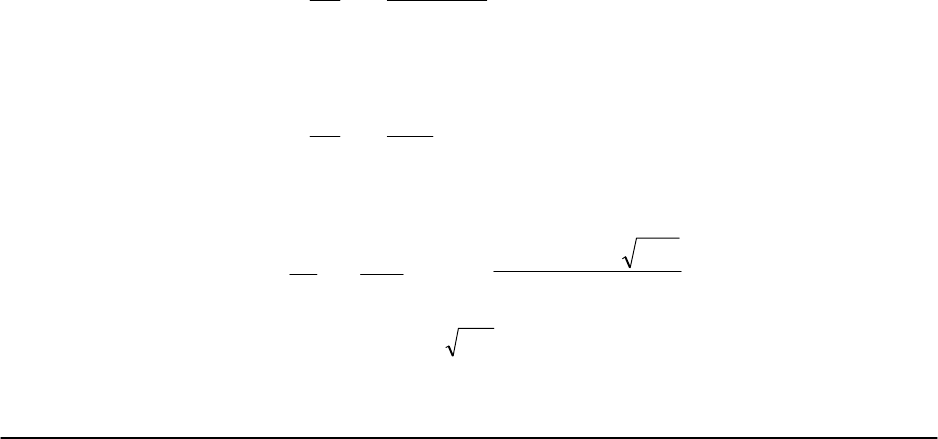
BSIMSOI3.1 Manual Copyright © 2003, UC Berkeley B-14
B.8. Model Parameter Notes
nI-1. BSIMSOI supports capmod=2 and 3 only. Capmod=0 and 1 are not supported.
nI-2. In modern SOI technology, source/drain extension or LDD are commonly used.
As a result, the source/drain junction depth (Xj) can be different from the silicon
film thickness (Tsi). By default, if Xj is not given, it is set to Tsi. Xj is not allowed
to be greater than Tsi.
nI-3. BSIMSOI refers substrate to the silicon below buried oxide, not the well region in
BSIM3. It is used to calculate backgate flatband voltage (Vfbb) and parameters
related to source/drain diffusion bottom capacitance (Vsdth, Vsdfb, Csdmin). Positive
nsub means the same type of doping as the body and negative nsub means opposite
type of doping.
nC-1. If cgso is not given then it is calculated using:
if (dlc is given and is greater 0) then,
cgso = p1 = (dlc*cox) - cgs1
if (the previously calculated cgso <0), then
cgso = 0
else cgso = 0.6 * Tsi * cox
nC-2. Cgdo is calculated in a way similar to Csdo
nC-3. If (nsub is positive)
VkT
q
n
n n
sdfb sub
i i
= − ⋅
⋅
−log .
10 03
20
else
VkT
q n
sdfb sub
= −
+log .
10 03
20
nC-4. If (nsub is positive)
φsd sub
i
kT
q
n
n
=
2log , γsd sub
box
n
C
=×−
5753 10 12
.
V V
sdth sdfb sd sd sd
= + +φγφ
BSIMSOI3.1 Manual Copyright © 2003, UC Berkeley B-15
else
φsd sub
i
kT
q
n
n
= −
2log , γsd sub
box
n
C
=× −
−
5753 10 12
.
V V
sdth sdfb sd sd sd
= − −φγφ
nC-5. Xq n
sddep si sd
sub
=⋅
2
106
εφ, CX
sddep si
sddep
=ε, CC C
C C
sd sddep box
sddep box
min =+
nC-6. If cf is not given then it is calculated using
CF T
ox
ox
= + ×
−
214 10 7
ε
πln
nT-1. For mobmod=1 and 2, the unit is m/V2. Default is -5.6E-11. For mobmod=3,
unit is 1/V and default is -0.056.
BSIMSOI3.1 Manual Copyright © 2003, UC Berkeley C-1
Appendix C: Equation List
Equation List for BSIMSOI Built-In Potential Lowering
Calculation
If SoiMod=0 (default), the model equation is identical to BSIMPD equation.
If SoiMod=1 (unified model for PD&FD) or SoiMod=2 (ideal FD), the following equations (FD
module) are added on top of BSIMPD.
(( ))
(( ))
Bbi
eff
vbd
eff
vbdvbdDIBL
OX
OX
OX
BOX
OX
BOX
Si
Si
Si
FBbes
BOXSi
BOX
eDIBLnonidealSi
Si
ch
BOXSi
Si
bs
V
l
L
Dexp
l
L
DexpDV
T
C,
T
C,
T
C
VV
CC
C
VVT
qN
phi
CC
C
V
ΦΦ−−⋅⋅
−−++
−−==∆∆
======
−−⋅⋅
++
++
∆∆++++⋅⋅−−⋅⋅
++
==
22
2
where
2
110
2
0
εεεεεε
ηη
εε
−−++
−−⋅⋅−−== l
L
Dexp
l
L
DexpKK eff
bk
eff
bkbbe2221 2
2
ηη
(( ))
−−−−
++⋅⋅⋅⋅
++++
−−== −−
−−−− tFD,OFF
FD,OFFeff_gsFD,th
tFD,OFF
BOXSiOX
OX
ON VN
VVV
explnVN
CCC
C
phiphi 1
1
11
(( ))
⋅⋅⋅⋅
ΦΦ++
++++ΦΦ== 2
1
212
12
t
BFD,gsteffFD.gsteff
tBON VKMoinFD
KVV
lnVphi ,
−−−−
++⋅⋅==
tFD,OFF
FD,OFFFD,theff_gs
tFD,OFFFD,gsteff VN
VVV
explnVNV1

BSIMSOI3.1 Manual Copyright © 2003, UC Berkeley C-2
Here Nch is the channel doping concentration. VFBb is the backgate flatband voltage.
Vth,FD is the threshold voltage at Vbs=Vbs0(phi=2ΦB). Vt is thermal voltage. K1 is the body effect
coefficient.
If SoiMod=1, the lower bound of Vbs (SPICE solution) is set to Vbs0. If SoiMod=2, Vbs is pinned
at Vbs0. Notice that there is no body node and body leakage/charge calculation in SoiMod=2.
The zero field body potential that will determine the transistor threshold voltage, Vbsmos, is then
calculated by
(( ))(( )) (( ))
else
if
2
0
2
0
bs
OXbsbsbsOXbs
Sich
Si
bsbsmos
V
TVVVTV
TqN
C
VV
==
∞∞→→≤≤−−∞∞→→−−==
The subsequent clamping of Vbsmos will use the same equation that utilized in BSIMPD.
BSIMSOI3.1 Manual Copyright © 2003, UC Berkeley C-3
Equation List for BSIMSOI IV
Body Voltages
Vbsh is equal to the Vbs bounded between (Vbsc,
φ
s1). Vbsh is used in Vth and
Abulk calculation
(( ))
−−−−−−++−−−−++== bscbscbsbscbsbsc VVVVV.VTδδδδδδ 450 2
1, V V
bsc
=
−
5
(( ))
++−−−−++−−−−−−== 1
2
11111 450 TTT.Vsssbsh δδδδφφδδφφφφ ,
φ
sV
115
=
.
Vbsh is further limited to 0 95.
φ
s to give Vbseff.
( )
V V V V
bseff s s bsh sbsh bsh
= − − − + − − +
φ φ δφδ δ
0 0 0
2
0 5 4.,
φ
φ
s s0095
=
.
Effective Channel Length and Width
( )
dW W
W
L
W
W
W
LW
dW dW dW VdW V
l
Ww
Wwl
W W
ggsteff bsbseff s
wn wn
'
int
'
ln ln
= + + +
= + + − −Φ Φ
dL L
L
L
L
W
L
LW
l
L
w
L
wl
L L
wn wn
= + + +
int ln ln
L L dL
eff drawn
=
−
2
BSIMSOI3.1 Manual Copyright © 2003, UC Berkeley C-4
W W NdW NdW
W W NdW NdW
WW
NP
WW
NP
eff drawn bc bc bc
eff drawn bc bc bc
diod
eff
seg
dbcp
dios
eff
seg
sbcp
=
−
−
−
= − − −
= +
= +
( )
( )
''
'
'
2
2
Threshold Voltage
)1(/
)))(exp(2)
2
(exp(
)))(exp(2)
2
(exp(
)))(exp(2)
2
(exp(
)()11(
)(
2
110
'
1
'
10
'
331
21
bseffVToxdepsit
dsbsefftabtao
to
eff
sub
to
eff
sub
sbi
t
eff
VT
t
eff
VTVT
sbi
tw
effeff
wVT
tw
effeff
wVTwVT
s
oeff
ox
bseffbs
eff
LX
eff
bseffs
eff
thoth
VDCXl
VVEE
l
L
D
l
L
D
V
l
L
D
l
L
DD
V
l
LW
D
l
LW
DD
WW
T
VKK
L
N
K
VKtsqrtPhisExKVV
+=
+−+−−
Φ−−+−−
Φ−−+−−
Φ
+
++Φ−++
−Φ−+=
ε
(
)
sqrtPhisExtVsV V
sbseff bsh bseff
= − + −φ, s
s s
= − −
1
20
φ φ
K K K
WK
eff w
w
eff
111 1
1 2
1= + +
'
lXCDV
tw si dep ox VT wbseff
= +
ε( )12 lXC
to si dep ox
=ε0/
XV
qN
dep
si sbseff
ch
=−2ε( )Φ XqN
dep si s
ch
0
2
=εΦ
VvN N
n
bi tch DS
i
=ln( )
2
BSIMSOI3.1 Manual Copyright © 2003, UC Berkeley C-5
Poly depletion effect
V X E qN X
poly poly poly
gate poly
si
+ =
1
2 2
2
ε
ε ε ε
ox ox si poly si gate poly
E E qNV= = 2
V V V V
gs FB xpoly ox
−
−
=
+
φ
aV V V V
gs FB spoly poly
( )− − − − =φ20
aqNT
ox
si gate ox
=ε
ε
2
2
2
V V qNTV V
qNT
gs eff FB s
si gate ox
ox
ox gs FB s
si gate ox
_
( )
= + + + − − −
φε
ε
εφ
ε
2
2
2
2
121
Effective Vgst for all region (with Polysilicon Depletion Effect)
V
nv V V
nv
nC qN
V V V
nv
gsteff
t
gs eff th
t
ox s
si ch
gs eff th off
t
=
+−
+ − − −
2 1 2
1 2 22
2
ln exp( )
exp
_
_
Φ
ε
nNX
C
C C VCVDL
lDL
l
C
C
C
factor
si dep
ox
dsc dscd ds dscb bseff VT
eff
t
VT
eff
t
ox
it
ox
= + +
+ + − + −
+122
1 1
ε/( ) exp( )exp( )
Effective Bulk Charge Factor
( )
0
2
1
2
1
)(2
1
0
1
'
0
2
01
==
+
+
+
−
+
⋅+
−+
+=
gsteffbulkbulk
eff
depsieff
eff
gsteffgs
depsieff
eff
bsh
bsh
s
eff
bulk
VAA
BW
B
XTL
L
VA
XTL
LA
VKeta
V
Ketas
K
A
φ
BSIMSOI3.1 Manual Copyright © 2003, UC Berkeley C-6
Mobility and Saturation Velocity
For Mobmod=1
µ
µ
eff o
acbseff
gsteff th
ox
b
gsteff th
ox
U U VV V
TUV V
T
=
+ + +++
12 2 2
()( ) ( )
For Mobmod=2
µ
µ
eff o
acbseff
gsteff
ox
b
gsteff
ox
U U VV
TUV
T
=+ + +12
()( ) ( )
For Mobmod=3
µ
µ
eff
a
gstef th
ox
b
gsteff th
ox
cbseff
UV V
TUV V
TUV
=
+++++
0
2
12 2 1[( ) ( ) ]( )
Drain Saturation Voltage
For Rds>0 or λ≠1:
Vb b ac
a
dsat =− − −
24
2
aAWCR A
bulk eff sat ox ds bulk
= + −
2
1
1νλ
( )
bV A E LA V WCR
gsteff tbulk sat eff bulk gsteff teff sat ox ds
= − + − + + +
()( ) ( )221 3 2νλν ν
cV E LVWCR
gsteff tsat eff gsteff teff sat ox ds
= + + +( ) ( )2 2 2 2
ν ν ν
λ
=
+
AV A
gsteff1 2
For Rds=0, λ=1:
BSIMSOI3.1 Manual Copyright © 2003, UC Berkeley C-7
VELV
A E LV
dsat
sat eff gsteff t
bulk sat eff gsteff t
=
+
+ +
( )
( )
2
2
ν
ν
Esat sat
eff
=2ν
µ
Vdseff
[
]
V V V V V V V
dseff dsat dsat ds dsat ds dsat
= − − − + − − +
1
24
2
δ δ δ( )
Drain current expression
IN
IV
RIV
V
V V
V
ds MOSFET
seg
ds dseff
ds dso dseff
dseff
ds dseff
A
,
( )
( ) ( )
=++
−
1
1
1
0
βµ=eff ox
eff
eff
CW
L
( )
I
V A V
VvV
V
EL
dso
gsteff bulk
dseff
gsteff t
dseff
dseff
sat eff
=
−+
+
β12 2
1
V V P V
ELV V
AAsat
vag gsteff
sat eff ACLM ADIBLC
= + +
+−
11 1 1
( )
BSIMSOI3.1 Manual Copyright © 2003, UC Berkeley C-8
VA E LV
P A E litl V V
VV
P V
A V
A V
PDL
lDL
lP
ACLM
bulk sat eff gsteff
clm bulk sat
ds dseff
ADIBLC
gsteff t
rout DIBLCB bseff
bulk dsat
bulk dsat t
rout DIBLC ROUT
eff
t
ROUT
eff
t
DIBLC
=
+
−
=+
+−+
= − + − +
( )
( )
( ) ( )
[exp( exp( )]
2
112
22
1
0 0
2
ν
θ ν
θ
V
ELV R CWVA V
V
RCWA
Asat
sat eff dsat ds sat ox eff gsteff bulk dsat
gsteff t
ds sat ox eff bulk
=
+ + − +
− +
2 1 2 2
2 1
νν
λν
[( )]
/
litl T T
si ox Si
ox
=ε
ε
Drain/Source Resistance
(
)
( )
Wr
eff
sbseffsrwbgsteffrwg
dswds W
VPVP
RR '6
10
1φφ −−++
=
Impact Ionization Current
I I FIV
V V
ii ds MOSFET bjtii c
diff
diff diff
= + + +
αβ β β
0
2 1 0 2
( )exp
,
V V V
diff ds dsatii
=
−
+
+
+
+
=
−
−++=
dsiid
gstii
ii
gsteffiieffsatii
effsatii
eff
ii
nom
iidsatiidsatii
VS
VS
S
VSLE
LE
VgsStep
L
L
T
T
TVVgsStepV
11
1
1
11
0
2
1
0
BSIMSOI3.1 Manual Copyright © 2003, UC Berkeley C-9
Gate-Induced-Drain-Leakage (GIDL)
At drain,
−=
s
gidl
sgidldioddgidl E
EWIβ
αexp , EV V
T
s
ds gs
ox
=
−
−
χ
3
At source,
−=
s
gidl
sgidldiossgidl E
EWIβ
αexp , EV
T
s
gs
ox
=
−
−
χ
3
If Es is negative, Igidl is set to zero for both drain and source.
Oxide tunneling current
In inversion,
(( ))
0
23
3
EVB
g
EVB
gb1
gb1gb1
N
oxref
2
30
24
3
28
8
V
1V
V1
Ttox
m.m
eV.
hq
m
B
h
q
A
V
explnV
V
TVB
exp
T
T
VV
AJ
ox
b
b
ox
b
ox
aux
ox
oxox
oxqm
ox
auxgb
gb
==
==
==
==
−−
++==
−−
−−−−
==
φφ
φφππ
φφππ
ö
âá
In accumulation,
(( ))
0
23
3
ECB
ECB
gb2
gb2gb2
N
oxref
2
40
13
3
28
8
V
1V
V1
Ttox
m.m
eV.
hq
m
B
h
q
A
VV
explnVV
V
TVB
exp
T
T
VV
AJ
ox
b
b
ox
b
fbgb
taux
ox
oxox
oxqm
ox
auxgb
gb
==
==
==
==
−−
−−++==
−−
−−−−
==
φφ
φφππ
φφππ
âá
BSIMSOI3.1 Manual Copyright © 2003, UC Berkeley C-10
Body contact current
== 2
seg
'
eff
halo
eff
seg
'
eff
bodybp
NW
R||
L
NW
RR , R R N
bodyext bsh rb
=
For 4-T device, Ibp
=
0
For 5-T device,
IV
R R
bp bp
bp bodyext
=+
Diode and BJT currents
Bipolar Transport Factor
αbjt
eff
n
L
L
= −
exp .0 5
2
Body-to-Source/drain diffusion
−
=
−
=
1exp
1exp
1
1
tdio
bd
sdifsidiodbd
tdio
bs
sdifsidiosbs
Vn
V
jTWI
Vn
V
jTWI
Recombination/trap-assisted tunneling current in depletion region
+
−
=
+
−
=
dbrec
rec
recr
db
recf
bd
srecsidiodbd
sbrec
rec
recr
sb
recf
bs
srecsidiosbs
VV
V
n
V
n
V
jTWI
VV
V
n
V
n
V
jTWI
0
0
2
0
0
2
026.0
exp
026.0
exp
026.0
exp
026.0
exp
BSIMSOI3.1 Manual Copyright © 2003, UC Berkeley C-11
Reversed bias tunneling leakage
++
−−==
++
−−==
dbtun
tun
tun
db
stunsidiodbd
sbtun
tun
tun
sb
stunsidiosbs
VV
V
n.
V
expjTWI
VV
V
n.
V
expjTWI
0
0
4
0
0
4
0260
1
0260
1
Recombination current in neutral body
( )
( )
( )
−
−
=
−
=
−
=
+=
+
−
−=
+
−
−=
nom
bjt
tdio
g
hlieffhli
tdio
bd
effhlihlid
tdio
bs
effhlihlis
N
neff
bjtsbjtsi
seg
eff
en
hlid
tdio
bd
enbjtbd
hlis
tdio
bs
enbjtbs
T
T
X
Vn
KE
AA
Vn
V
AE
Vn
V
AE
LL
LjT
N
W
I
E
Vn
V
II
E
Vn
V
II
bjt
1
300
exp
1exp
1exp
11
1
1
1exp1
1
1
1exp1
_
_
_
0
'
3
3
α
α
BSIMSOI3.1 Manual Copyright © 2003, UC Berkeley C-12
BJT collector current
I I V
nV
V
nV E
EE E E
EV V
V A L
E E E
cbjt en bs
dio t
bd
dio tnd
nd
ely ely hli
ely bs bd
Abjt ely eff
hli hlis hlid
=
−
=+ +
= + +
+
= +
αexp exp 1
4
2
1
2
2
2
Total body-source/drain current
I I I I I
bs bs bs bs bs
=
+
+
+
1 2 3 4
I I I I I
bd bd bd bd bd
=
+
+
+
1 2 3 4
Total body current
Iii + Idgidl + Isgidl + Igb - Ibs - Ibd - Ibp = 0
Temperature effects
V V K K LKVT T
th Tth Tnom Tt l eff Tbseff nom
( ) ( ) (/)( /)
=
+
+
+
−
1121
µ µ µ
oToTnom
nom
te
T
T
( ) ( ) ( )=,
ν
ν
sat Tsat Tnom Tnom
AT T
( ) ( ) (/)
=
−
−
1
R R TP
T
T
dsw Tdsw nom rt
nom
( ) ( ) ( )= + −1
U U U T T
aTaTnom anom( ) ( ) (/)
=
+
−
11
U U U T T
bTbTnom bnom( ) ( ) (/)
=
+
−
11
U U U T T
cTcTnom cnom( ) ( ) (/)
=
+
−
11
BSIMSOI3.1 Manual Copyright © 2003, UC Berkeley C-13
(( ))
segth
'
eff
th
th NWW
R
R
0
0
++
== ,
seg
th
'
eff
thth N
WW
CC 0
0
++
==
−
−
=
nom
bjt
tdio
g
sbjtsbjt T
T
X
Vn
KE
jj 1
)300(
exp
0
−
−
=
nom
dif
tdio
g
sdifsdif T
T
X
Vn
KE
jj 1
)300(
exp
0
−
−
=
nom
rec
trecf
g
srecsrec T
T
X
Vn
KE
jj 1
)300(
exp
0
0
j j XT
T
stun stun tun
nom
= −
01exp
−−++==
−−++==
11
11
0
0
nom
recrrecrrecr
nom
recfrecfrecf
T
T
ntnn
T
T
ntnn
Eg is the energy gap energy.
Gate-to-channel current (Igc) and gate-to-S/D current (Igs and Igd)
Igc –gate to channel tunneling current
(
)
(
)
[
]
oxdepinvoxdepinvoxqmauxeffgsoxRatioeffeff VcigcVbigcaigcTBVVTALWIgc ⋅+⋅⋅−⋅−⋅⋅⋅⋅⋅=1exp
_
Note here Igc is the gate to channel current with Vds=0
⋅
−
+⋅⋅=
tm
theffgs
maux Vnigc
VV
VnigcV0_
exp1log
BSIMSOI3.1 Manual Copyright © 2003, UC Berkeley C-14
2
1
oxqm
ntox
oxqm
oxref
oxRatio T
T
T
T⋅
=
Igs and Igd –gate tunneling current between the gate and the source/drain diffusion
region
(
)
(
)
[
]
gsgsoxqmgsgsoxRatioEdgeff VcigsdVbigsdaigsdPoxedgeTBVVTADlcigWIgs
′
⋅+⋅
′
⋅−⋅⋅⋅−⋅
′
⋅⋅⋅⋅=1exp
(
)
(
)
[
]
gdgdoxqmgdgdoxRatioEdgeff VcigsdVbigsdaigsdPoxedgeTBVVTADlcigWIgd
′
⋅+⋅
′
⋅−⋅⋅⋅−⋅
′
⋅⋅⋅⋅=1exp
( )
2
1
PoxedgeT
PoxedgeT
T
T
oxqm
ntox
oxqm
oxref
eoxRatioEdg ⋅
⋅
⋅
=
(
)
40.1
2−+−=
′eVVV fbsdgsgs ,
(
)
40.1
2−+−=
′eVVV fbsdgdgd .
Partition of Igc
gcdIIgcsIgc
+
=
(
)
40.2gcd
40.11gcdexpgcd
22 −+⋅
−
+
−
⋅
−
+
⋅
⋅=eVpi
eVpiVpi
IgcIgcs
ds
dsds
(
)
(
)
40.2gcd
40.1gcdexp1gcd1
gcd 22 −+⋅
−
+
⋅
−
⋅
+
⋅
−
⋅=eVpi
eVpiVpi
IgcI
ds
dsds

BSIMSOI3.1 Manual Copyright © 2003, UC Berkeley C-15
Equation List for BSIMSOI CV
Dimension Dependence
δWDWC
W
L
W
W
W
LW
eff lc
W
wc
W
wlc
W W
wn wn
= + + +
ln ln
δLDLC
L
L
L
W
L
LW
eff lc
L
wc
L
wlc
L L
wn wn
= + + +
ln ln
bgactiveBactiveBG
activeactiveB
effdrawnactive
LLL
DLCBLL
LLL
δ
δ
2
2
+=
−=
−
=
dbcp
seg
active
diodCV
sbcp
seg
active
diosCV
effbcbcbcdrawnactive
P
N
W
W
P
N
W
W
WNdWNWW
+=
+=
−
−
−
=
δ
)2(
Charge Conservation
Q Q Q Q
Bf acc sub subs
=
+
+
0
Q Q Q
inv inv sinv d
=
+
, ,
(
)
Q Q Q
ginv Bf
= − +
Q Q Q Q Q
bBf ejs jd
=
−
+
+
Q Q Q
sinv sjs
=
−
,
Q Q Q
dinv djd
=
−
,
Q Q Q Q Q
gebsd
+
+
+
+
=
0
BSIMSOI3.1 Manual Copyright © 2003, UC Berkeley C-16
Intrinsic Charges
(1) capMod = 2
Front Gate Body Charge
Accumulation Charge
( ) ( )
V V V V V V
FBeff fb fb gb fb gb
= − − − + − − +
05 22
.δ δ δ
where V V V
gb gs bseff
=
−
delvtVKVV bseffseffsthfb +−−−= φφ 1
−⋅
−
+=
tt
thgs
tgsteffCV nv
delvt
nv
VV
nvVexpexp1ln
QFWL
NACV V
acc body active activeB
seg
gbcp ox FBeff fb
= − +
−( )
Gate Induced Depletion Charge
−−−
++−
+−= 2
1
2
1
0
)(4
11
2eff
bseffgsteffCVFBeffgseff
oxgbcp
seg
activeBactive
bodysub K
VVVVK
CA
N
LW
FQ
Drain Induced Depletion Charge
V V A
dsatCV gsteffCV bulkCV
=/, A A CLC
L
bulkCV bulk
activeB
CLE
= +
01
V V V V V V V
dsCV dsatCV dsatCV ds dsatCV ds dsatCV
= − − − + − − +
1
2
4
2
( ( ) )δ δ δ
BSIMSOI3.1 Manual Copyright © 2003, UC Berkeley C-17
( )
( )
−
−−
+= 2122
1
2
dsCVbulkCVgsteffCV
dsCVbulkCVdsCV
bulkCVoxgbcp
seg
activeBactive
bodysubs VAV
VAV
ACA
N
LW
FQ
Back Gate Body Charge
( )
bsefffbbesboxebcp
seg
activeBGactive
bodybeVVVCA
N
LW
FkQ−−
+= 1
Inversion Charge
(
)
−
+
−
+−=
=−−=++−=
cveff
bulkCV
gsteffCV
cveffbulkCV
cveff
bulkCV
gsteffCVoxgbcp
seg
activeactive
inv
dsCVdsatCVdsatCVdsatcveff
V
A
V
VA
V
A
VCA
N
LW
Q
VVwhereVVVVVV
2
12
2
02.0;45.0
22
44,4,4
2
44, δδδ
50/50 Charge Partition
Q Q Q
inv sinv dinv, ,. .
=
=
0 5
40/60 Charge Partition
( ) ( ) ( )
Q
WL
NAC
VAV
V V A V V A V A V
inv s
active active
seg
gbcp ox
gsteffCV bulkCV cvefff
gsteffCV gsteffCV bulkCV cveff gsteff bulkCV cveff bulkCV cveff,= −
+
−
− + −
22
4
3
2
3
2
15
2
3 2 2 3
( ) ( ) ( )
Q
WL
NAC
VAV
V V A V V A V A V
inv d
active active
seg
gbcp ox
gsteffCV bulkCV cvefff
gsteffCV gsteffCV bulkCV cveff gsteff bulkCV cveff bulkCV cveff,= −
+
−
− + −
22
5
3
1
5
2
3 2 2 3
BSIMSOI3.1 Manual Copyright © 2003, UC Berkeley C-18
0/100 Charge Partition
( )
−
−+
+
−=
cveff
bulkCV
gsteffCV
cveffbulkCVcveffbulkCVgsteffCV
ox
seg
gbcpactiveactive
sinv
V
A
V
VAVAV
C
N
ALW
Q
2
24
42
2
,
( )
−
+−
+
−=
cveff
bulkCV
gsteffCV
cveffbulkCVcveffbulkCVgsteffCV
ox
seg
gbcpactiveactive
dinv
V
A
V
VAVAV
C
N
ALW
Q
2
8
4
3
2
2
,
(2) capMod = 3 (Charge-Thickness Model)
capMod = 3 only supports zero-bias flat band voltage, which is calculated from bias-
independent threshold voltage. This is different from capMod = 2. For the finite thickness
(DC
X) formulation, refer to Chapter 4 of BSIM3v3.2 Users’s Manual.
Front Gate Body Charge
Accumulation Charge
( ) ( )
V V V V V V
FBeff fb fb gb fb gb
= − − − + − − +
05 22
.δ δ δ
where V V V
gb gs bseff
=
−
V V KV
fb th seff sbseff
= − − −φ φ
1
BSIMSOI3.1 Manual Copyright © 2003, UC Berkeley C-19
( )
DCSicen
cenox
cenox
oxeff
gsbsefffb
fbgbacc
gbaccoxeffgbcp
seg
activeBactive
bodyacc
XC
CC
CC
C
VVVV
VVVV
VCA
N
LW
FQ
ε
δ
δ
=
+
=
−−+=
++=
+−=
0
2
00 45.0
Gate Induced Depletion Charge
−−−
++−
+−= 2
1
2
1
0
)(4
11
2eff
bseffgsteffCVFBeffgseff
oxeffgbcp
seg
activeBactive
bodysub K
VVVVK
CA
N
LW
FQ
Drain Induced Depletion Charge
(
)
bulkCVgsteffCVdsatCV AVV /
δ
Φ−=
(
)
Φ+
+=Φ−Φ=Φ2
1
122
1ln2
teff
BeffgstefCVgsteffCV
tBsvmoinK
KVV
v
δ
V V V V V V V
dsCV dsatCV dsatCV ds dsatCV ds dsatCV
= − − − + − − +
1
2
4
2
( ( ) )δ δ δ
( )
( )
−Φ−
−−
+= 2122
1
2
dsCVbulkCVgsteffCV
dsCVbulkCVdsCV
bulkCVoxeffgbcp
seg
activeBactive
bodysubs VAV
VAV
ACA
N
LW
FQ
δ

BSIMSOI3.1 Manual Copyright © 2003, UC Berkeley C-20
Back Gate Body Charge
( )
bsefffbbesboxebcp
seg
activeBGactive
bodybeVVVCA
N
LW
FkQ−−
+= 1
Inversion Charge
(
)
−Φ−
+
−Φ−
+−=
=−−=++−=
cveff
bulkCV
gsteffCV
cveffbulkCV
cveff
bulkCV
gsteffCVoxeffgbcp
seg
activeactive
inv
dsCVdsatCVdsatCVdsatcveff
V
A
V
VA
V
A
VCA
N
LW
Q
VVwhereVVVVVV
2
12
2
02.0;45.0
22
44,4,4
2
44,
δ
δ
δδδ
50/50 Charge Partition
Q Q Q
inv sinv dinv, ,. .
=
=
0 5
40/60 Charge Partition
( ) ( ) ( ) ( )( ) (
−Φ−+Φ−−Φ−
−Φ−
+
−= 223
2
,15
2
3
2
3
4
2
2
cveffbulkCVcveffbulkCVgsteffcveffbulkCVgsteffCVgsteffCV
cvefff
bulkCV
gsteffCV
oxeffgbcp
seg
activeactive
sinv VAVAVVAVV
V
A
V
CA
N
LW
Q
δδδ
δ
( ) ( ) ( ) ( )( ) ( )
−Φ−+Φ−−Φ−
−Φ−
+
−= 3223
2
,5
1
3
5
2
2
cveffbulkCVcveffbulkCVgstefCVfcveffbulkCVgsteffCVgsteffCV
cvefff
bulkCV
gsteffCV
oxefgbcp
seg
activeactive
dinv VAVAVVAVV
V
A
V
CA
N
LW
Q
δδδ
δ
BSIMSOI3.1 Manual Copyright © 2003, UC Berkeley C-21
0/100 Charge Partition
( )
−Φ−
−+
Φ−+
−=
cveff
bulkCV
gsteffCV
cveffbulkCVcveffbulkCVgsteffCV
oxeff
seg
gbcpactiveactive
sinv
V
A
V
VAVAV
C
N
ALW
Q
2
24
42
2
,
δ
δ
( )
−Φ−
+−
Φ−+
−=
cveff
bulkCV
gsteffCV
cveffbulkCVcveffbulkCVgsteffCV
oxeff
seg
gbcpactiveactive
dinv
V
A
V
VAVAV
C
N
ALW
Q
2
8
4
3
2
2
,
δ
δ
Overlap Capacitance
Source Overlap Charge
( ) ( )
V V V
gs overlap gs gs
_= + + + +
1
24
2
δ δ δ
++−+−+⋅=CKAPPA
V
CKAPPA
VVCGSVCGS
W
Qoverlapgs
overlapgsgsgs
diosCV
soverlap _
_
,4
11
2
10
Drain Overlap Charge
( ) ( )
V V V
gd overlap gd gd_= + + + +
1
24
2
δ δ δ
++−+−+⋅=CKAPPA
V
CKAPPA
VVCGDVCGD
W
Qoverlapgd
overlapgdgdgd
diodCV
doverlap _
_
,4
11
2
10
Gate Overlap Charge
(
)
Q Q Q
overlap goverlap soverlap d, , ,
= − +
BSIMSOI3.1 Manual Copyright © 2003, UC Berkeley C-22
Source/Drain Junction Charge
For Vbs < s
φ95.0
bsdifbsdepjswg QQQ +=
else
(
)
bsdifsbssbsdepjswg QVCQ+−= φφ 95.0)95.0(
For Vbd < s
φ95.0
bddifbddepjdwg QQQ +=
else
(
)
(
)
bddifsbdsbddepjdwg QVCQ+−= φφ 95.095.0
where
(( ))
[[ ]]
(( ))
nompbswgbswgbswg
nomcjswgjswgjswg
hlid
tdio
bd
N
neff
bjdifsbjtsi
seg
eff
bddif
hlis
tdio
bs
N
neff
bjdifsbjtsi
seg
eff
bsdif
M
bswg
bd
swg
bswg
si
jswgdiodCVbddep
M
bswg
bs
swg
bswg
si
jswgdiosCVbsdep
TTtPP
TTtCC
E
Vn
V
exp
LL
LLJT
N
'W
Q
E
Vn
V
exp
LL
LLJT
N
'W
Q
P
V
Mj
P
T
CWQ
P
V
Mj
P
T
CWQ
dif
dif
jswg
jswg
−−−−==
−−++==
++
−−
++++==
++
−−
++++==
−−−−
−−
==
−−−−
−−
==
−−
−−
−−
−−
0
0
00
00
1
7
1
7
1
1
1
1
11
1
1
1
1
11
1
11
1
10
11
1
10
ττ
ττ

BSIMSOI3.1 Manual Copyright © 2003, UC Berkeley C-23
Extrinsic Capacitance
Bottom S/D to Substrate Capacitance (per unit area)
(( ))
(( ))
(( ))
<<
−−
−−
−−
−−
++
−−++<<
−−
−−
−−−−
<<
==
elseC
VVelseif
VV
VV
CC
A
C
VVAVVelseif
VV
VV
CC
A
C
VVifC
C
min
sdthe,d/s
sdfbsdth
sdthe,d/s
minbox
sd
min
sdfbsdthsdsdfbe,d/s
sdfbsdth
sdfbe,d/s
minbox
sd
box
sdfbe,d/sbox
esb 2
2
1
1
1
Sidewall S/D to Substrate Capacitance (per unit length)
+=
box
si
sdesweswdsT
T
CC 1log
,/

BSIMSOI3.1 Manual Copyright © 2003, UC Berkeley D-1
Appendix D: Parameter Extraction
D.1. Extraction Strategy
The complicated physics in SOI MOSFETs makes parameter extraction quite involved [20].
It is always preferable to have more measurements so that the parameters extracted can have
more valid physical meaning. Similar to conventional bulk devices, two basic extraction
strategies can be used: single device extraction, and group device extraction. The group device
extraction is more popular because of several reasons. In analog circuit, channel length and
width scalability is very important. In digital circuit, statistical modeling is often used to predict
the circuit performance due to process variation. Hence channel length scalability is also
important. Besides, model parameters extracted from group device extraction have better
physical meaning than that from single device extraction. In this work, we shall emphasize on
group device extraction.
Parameter extraction using body contact devices is highly recommended because parameters
related to body effect, impact ionization and leakage currents can be directly extracted [18, 19].
This yields less ambiguity in extracting technology parameters for I-V fitting purposes. In the
followings, we suggest a set of measurement suitable for PD devices.

Parameter Extraction
BSIMSOI3.1 Manual Copyright © 2003, UC Berkeley D-2
D.2. Suggested I-V Measurement
Measurement set A is used to extract basic MOS I-V parameters. For each body-contacted
device :
(A1) Ids vs. Vgs @ small Vds with different Vbs, Ves=0V.
(A2) Ids vs. Vgs @ Vds=Vdd with different Vbs, Ves=0V.
(A3) Ids vs. Vds with different Vgs and different Vbs, Ves=0V.
Parameters extracted include threshold voltage, body coefficient, delta L and W, series
resistance, mobility, short channel effect, and subthreshold swing. (A2) is used to extract DIBL
parameters at subthreshold. (A3) is used to extract saturation velocity, body charge effect, output
resistance, body contact resistance and self-heating parameters.
Measurement set C is used to extract impact ionization current parameters. For each body-
contacted device :
(C1) Ib vs. Vgs @ different Vds, Vbs=0V, Ves=0V.
(C2) Ib vs. Vds @ different Vgs, Vbs=0V, Ves=0V.
Measurement set D is used to extract MOS temperature dependent parameter. For a long
channel body-contacted device:
(D1) Ids vs. Vgs @ small Vds, Vbs=0V, Ves=0V, repeat with several temperatures.
(D2) Ids vs. Vds @ different Vgs, Vbs=0V, Ves=0V, repeat with several temperatures.
Notice that the self-heating parameters have to be extracted from set A.
Measurement set E is used to extract diode parameters. For a long channel body-contacted
device or gated diode :
(E1) Idiode vs. Vbs @ Vgs=-1V, Ves=0V, repeat with several temperature
Measurement set F is used to extract BJT parameters. For each body-contacted device:
(F1) Ids vs. Ib @ Vgs=-1V, Ves=0V, Vds=1V.
Measurement set G is used to verify the floating body device data. For each floating-body
device :
(G1) Ids vs. Vgs @ small Vds.
(G2) Ids vs. Vgs @ Vds=Vdd.
(G3) Ids vs. Vds @ different Vgs.

Appendix E: Model Parameter Binning
Below is the information on parameter binning regarding which model parameters can or
cannot be binned. All those parameters which can be binned follow this implementation:
effeff
P
eff
W
eff
L
WL
P
W
P
L
P
PP ×
+++= 0
For example, for the parameter k1: P0 = k1, PL = lk1, PW = wk1, PP = pk1. binUnit is a
bining unit selector. If binUnit = 1, the units of Leff and Weff used in the binning equation
above have the units of microns; therwise in meters.
For example, for a device with Leff = 0.5µm and Weff = 10µm. If binUnit = 1, the parameter
values for vsat are 1e5, 1e4, 2e4, and 3e4 for vsat, lvsat, wvsat, and pvsat, respectively.
Therefore, the effective value of vsat for this device is
vsat = 1e5 + 1e4/0.5 + 2e4/10 + 3e4/(0.5*10) = 1.28e5
To get the same effective value of vsat for binUnit = 0, the values of vsat, lvsat, wvsat,
and pvsat would be 1e5, 1e-2, 2e-2, 3e-8, respectively. Thus,
vsat = 1e5 + 1e-2/0.5e6 + 2e-2/10e-6 + 3e-8/(0.5e-6 * 10e-6) = 1.28e5

Model parameters that have been binned in BSIMPD2.1 are listed as follows:
E.1. DC Parameters
Symbol
used in
equation
Symbol
used in
SPICE
Description
Vth0 vth0 Threshold voltage @Vbs=0 for long and wide device
K1 k1 First order body effect coefficient
K1w1 k1w1 First body effect width dependent parameter
K1w2 k1w2 Second body effect width dependent parameter
K2 k2 Second order body effect coefficient
K3 k3 Narrow width coefficient
K3b k3b Body effect coefficient of k3
Kb1 Kb1 Backgate body charge coefficient
W0 w0 Narrow width parameter
NLX nlx Lateral non-uniform doping parameter
Dvt0 Dvt0 first coefficient of short-channel effect on Vth
Dvt1 dvt1 Second coefficient of short-channel effect on Vth
Dvt2 dvt2 Body-bias coefficient of short-channel effect on Vth
Dvt0w dvt0w first coefficient of narrow width effect on Vth for small channel length
Dvt1w dvt1w Second coefficient of narrow width effect on Vth for small channel
length
Dvt2w dvt2w Body-bias coefficient of narrow width effect on Vth for small channel
length
µ0 u0 Mobility at Temp = Tnom
Ua ua First-order mobility degradation coefficient
Ub ub Second-order mobility degradation coefficient
Uc uc Body-effect of mobility degradation coefficient
vsat vsat Saturation velocity at Temp=Tnom
A0 a0 Bulk charge effect coefficient for channel length

Ags ags Gate bias coefficient of Abulk
B0 b0 Bulk charge effect coefficient for channel width
B1 b1 Bulk charge effect width offset
Keta keta Body-bias coefficient of bulk charge effect
Ketas Ketas Surface potential adjustment for bulk charge effect
A1 A1 First non-saturation effect parameter
A2 A2 Second non-saturation effect parameter
Rdsw rdsw Parasitic resistance per unit width
Prwb prwb Body effect coefficient of Rdsw
Prwg prwg Gate bias effect coefficient of Rdsw
Wr wr Width offset from Weff for Rds calculation
Nfactor nfactor Subthreshold swing factor
Wint wint Width offset fitting parameter from I-V without bias
Lint lint Length offset fitting parameter from I-V without bias
DWg dwg Coefficient of Weff’s gate dependence
DWb dwb Coefficient of Weff’s substrate body bias dependence
Voff voff Offset voltage in the subthreshold region for large W and L
Eta0 eta0 DIBL coefficient in subthreshold region
Etab etab Body-bias coefficient for the subthreshold DIBL effect
Dsub dsub DIBL coefficient exponent
Cit cit Interface trap capacitance
Cdsc cdsc Drain/Source to channel coupling capacitance
Cdscb cdscb Body-bias sensitivty of Cdsc
Cdscd cdscd Drain-bias sensitivty of Cdsc
Pclm pclm Channel length modulation parameter
Pdibl1 pdibl1 First output resistance DIBL effect correction parameter
Pdibl2 pdibl2 Second output resistance DIBL effect correction parameter
Drout drout L dependence coefficient of the DIBL correction parameter in Rout
Pvag pvag Gate dependence of Early voltage

δ delta Effective Vds parameter
α0 alpha0 The first parameter of impact ionization current
Fbjtii fbjtii Fraction of bipolar current affecting the impact ionization
ββ0 beta0 First Vds dependent parameter of impact ionization current
ββ1 beta1 Second Vds dependent parameter of impact ionization current
ββ2 beta2 Third Vds dependent parameter of impact ionization current
Vdsatii0 vdsatii0
Nominal drain saturation voltage at threshold for impact
ionization current
Tii tii Temperature dependent parameter for impact ionization current
Lii lii Channel length dependent parameter at threshold for impact
ionization current
Esatii esatii Saturation channel electric field for impact ionization current
Sii0 sii0 First Vgs dependent parameter for impact ionization current
Sii1 sii1 Second Vgs dependent parameter for impact ionization current
Sii2 sii2 Third Vgs dependent parameter for impact ionization current
Siid siid Vds dependent parameter of drain saturation voltage for impact
ionization current
ααgidl Agidl GIDL constant
ββgidl Bgidl GIDL exponential coefficient
χχ Ngidl GIDL Vds enhancement coefficient
ntun Ntun Reverse tunneling non-ideality factor
ndiode Ndiode Diode non-ideality factor
nrecf0 Nrecf0 Recombination non-ideality factor at forward bias
nrecr0 Nrecr0 Recombination non-ideality factor at reversed bias
isbjt Isbjt BJT injection saturation current
isdif Isdif Body to source/drain injection saturation current
isrec Isrec Recombination in depletion saturation current
istun Istun Reverse tunneling saturation current
Vrec0 Vrec0 Voltage dependent parameter for recombination current

Vtun0 Vtun0 Voltage dependent parameter for tunneling current
Nbjt Nbjt Power coefficient of channel length dependency for bipolar current
Lbjt0 Lbjt0 Reference channel length for bipolar current
Vabjt Vabjt Early voltage for bipolar current
Aely Aely Channel length dependency of early voltage for bipolar current
Ahli Ahli High level injection parameter for bipolar current
E.2. AC and Capacitance Parameters
Symbol
used in
equation
Symbol
used in
SPICE
Description
Vsdfb vsdfb Source/drain bottom diffusion capacitance flatband voltage
Vsdth vsdth Source/drain bottom diffusion capacitance threshold voltage
DelVt delvt Threshold voltage adjust for C-V
acde acde Exponential coefficient for charge thickness in capMod=3 for
accumulation and depletion regions.
moin moin Coefficient for the gate-bias dependent surface potential.
