Clevo M660SR, M665SR Service Manual. Www.s Manuals.com. Manual
User Manual: Notebook Clevo M665SR - Service manuals and Schematics, Disassembly / Assembly. Free.
Open the PDF directly: View PDF ![]() .
.
Page Count: 93
- Manual
- Preface
- Chapter 1: Introduction
- Overview
- System Specifications
- External Locator - Top View with LCD Panel Open
- External Locator - Front & Rear Views
- External Locator - Left & Right Side Views
- External Locator - Bottom View
- Mainboard Overview - Top (Key Parts)
- Mainboard Overview - Bottom (Key Parts)
- Mainboard Overview - Top (Connectors)
- Mainboard Overview - Bottom (Connectors)
- Chapter 2: Disassembly
- Overview
- Maintenance Tools
- Connections
- Maintenance Precautions
- Removing the Battery
- Removing the Hard Disk Drive
- Removing the System Memory (RAM)
- Removing the Processor
- Removing the Wireless LAN Module
- Removing the Modem
- Removing the Bluetooth Module
- Removing the Optical (CD/DVD) Device
- Removing the Keyboard
- Appendix A: Part Lists
- Appendix B: Schematic Diagrams
- SYSTEM BLOCK DIAGRAM
- CLOCK GENERATOR
- CPU-1
- CPU-2
- VN896-1
- VN896-2
- VN896-3
- VN896-4
- DDR2-1
- DDR2-2
- VGA G72M-1
- VGA G72M-2
- VGA G72M-3
- VGA G72M-4
- VT8237A-1
- VT8237A-2
- VT8237A-3
- HDD & CDROM
- CARD READER
- NEW CARD SOCKET
- LAN
- USB & CCD
- KBC-IT8512E
- CRT & LVDS
- FAN CONTROL, LPC ROM
- MINI-PCI & BLUETOOTH
- AUDIO VT1708A/ALC883
- LED, VS POWER
- CHARGER, DC IN
- 1.5V, 1.05VS
- VCORE
- 1.8V, 0.9VS
- VDD3, VDD5
- EXT GPU 1.0VS/1.2VS
- HOTKEY LT BOARD
- PWR HOT BOARD
- AUDIO & MODEM BOARD
- CLICK BOARD
- USB BOARD
- FINGERPRINT BOARD


Preface
I
Preface
Notebook Computer
M660SR/M665SR
Service Manual

Preface
II
Preface
Notice
The company reserves the right to revise this publication or to change its contents without notice. Information contained
herein is for reference only and does not constitute a commitment on the part of the manufacturer or any subsequent ven-
dor. They assume no responsibility or liability for any errors or inaccuracies that may appear in this publication nor are
they in anyway responsible for any loss or damage resulting from the use (or misuse) of this publication.
This publication and any accompanying software may not, in whole or in part, be reproduced, translated, transmitted or
reduced to any machine readable form without prior consent from the vendor, manufacturer or creators of this publica-
tion, except for copies kept by the user for backup purposes.
Brand and product names mentioned in this publication may or may not be copyrights and/or registered trademarks of
their respective companies. They are mentioned for identification purposes only and are not intended as an endorsement
of that product or its manufacturer.
Version 1.0
November 2007
Trademarks
Intel, Celeron, and Intel Core are trademarks/registered trademarks of Intel Corporation.
Windows® is a registered trademark of Microsoft Corporation.
Other brand and product names are trademarks and./or registered trademarks of their respective companies.

Preface
III
Preface
About this Manual
This manual is intended for service personnel who have completed sufficient training to undertake the maintenance and
inspection of personal computers.
It is organized to allow you to look up basic information for servicing and/or upgrading components of the M660SR/
M665SR series notebook PC.
The following information is included:
Chapter 1, Introduction, provides general information about the location of system elements and their specifications.
Chapter 2, Disassembly, provides step-by-step instructions for disassembling parts and subsystems and how to upgrade
elements of the system.
Appendix A, Part Lists
Appendix B, Schematic Diagrams

Preface
IV
Preface
IMPORTANT SAFETY INSTRUCTIONS
Follow basic safety precautions, including those listed below, to reduce the risk of fire, electric shock and injury to per-
sons when using any electrical equipment:
1. Do not use this product near water, for example near a bath tub, wash bowl, kitchen sink or laundry tub, in a wet
basement or near a swimming pool.
2. Avoid using a telephone (other than a cordless type) during an electrical storm. There may be a remote risk of elec-
trical shock from lightning.
3. Do not use the telephone to report a gas leak in the vicinity of the leak.
4. Use only the power cord and batteries indicated in this manual. Do not dispose of batteries in a fire. They may
explode. Check with local codes for possible special disposal instructions.
5. This product is intended to be supplied by a Listed Power Unit (DC Output 19V, 3.42A or 18.5V, 3.5A AC/DC Adapter).
CAUTION
Always disconnect all telephone lines from the wall outlet before servicing or disassembling this equipment.
TO REDUCE THE RISK OF FIRE, USE ONLY NO. 26 AWG OR LARGER,
TELECOMMUNICATION LINE CORD
This Computer’s Optical Device is a Laser Class 1 Product

Preface
V
Preface
Instructions for Care and Operation
The notebook computer is quite rugged, but it can be damaged. To prevent this, follow these suggestions:
1. Don’t drop it, or expose it to shock. If the computer falls, the case and the components could be damaged.
2. Keep it dry, and don’t overheat it. Keep the computer and power supply away from any kind of heating element. This
is an electrical appliance. If water or any other liquid gets into it, the computer could be badly damaged.
3. Follow the proper working procedures for the computer. Shut the computer down properly and don’t forget to save
your work. Remember to periodically save your data as data may be lost if the battery is depleted.
Do not expose the computer
to any shock or vibration.
Do not place it on an unstable
surface.
Do not place anything heavy
on the computer.
Do not expose it to excessive
heat or direct sunlight.
Do not leave it in a place
where foreign matter or mois-
ture may affect the system.
Don’t use or store the com-
puter in a humid environment.
Do not place the computer on
any surface which will block
the vents.
Do not turn off the power
until you properly shut down
all programs.
Do not turn off any peripheral
devices when the computer is
on.
Do not disassemble the com-
puter by yourself.
Perform routine maintenance
on your computer.

Preface
VI
Preface
4. Avoid interference. Keep the computer away from high capacity transformers, electric motors, and other strong mag-
netic fields. These can hinder proper performance and damage your data.
5. Take care when using peripheral devices.
Power Safety
The computer has specific power requirements:
• Only use a power adapter approved for use with this computer.
• Your AC adapter may be designed for international travel but it still requires a steady, uninterrupted power supply. If you are
unsure of your local power specifications, consult your service representative or local power company.
• The power adapter may have either a 2-prong or a 3-prong grounded plug. The third prong is an important safety feature; do
not defeat its purpose. If you do not have access to a compatible outlet, have a qualified electrician install one.
• When you want to unplug the power cord, be sure to disconnect it by the plug head, not by its wire.
• Make sure the socket and any extension cord(s) you use can support the total current load of all the connected devices.
• Before cleaning the computer, make sure it is disconnected from any external power supplies.
Use only approved brands of
peripherals.
Unplug the power cord before
attaching peripheral devices.
Do not plug in the power
cord if you are wet.
Do not use the power cord if
it is broken.
Do not place heavy objects
on the power cord.
Power Safety
Warning
Before you undertake
any upgrade proce-
dures, make sure that
you have turned off the
power, and discon-
nected all peripherals
and cables (including
telephone lines). It is
advisable to also re-
move your battery in
order to prevent acci-
dentally turning the
machine on.

Preface
VII
Preface
Battery Precautions
• Only use batteries designed for this computer. The wrong battery type may explode, leak or damage the computer.
• Do not remove any batteries from the computer while it is powered on.
• Do not continue to use a battery that has been dropped, or that appears damaged (e.g. bent or twisted) in any way. Even if the
computer continues to work with a damaged battery in place, it may cause circuit damage, which may possibly result in fire.
• Recharge the batteries using the notebook’s system. Incorrect recharging may make the battery explode.
• Do not try to repair a battery pack. Refer any battery pack repair or replacement to your service representative or qualified service
personnel.
• Keep children away from, and promptly dispose of a damaged battery. Always dispose of batteries carefully. Batteries may explode
or leak if exposed to fire, or improperly handled or discarded.
• Keep the battery away from metal appliances.
• Affix tape to the battery contacts before disposing of the battery.
• Do not touch the battery contacts with your hands or metal objects.
Battery Disposal
The product that you have purchased contains a rechargeable battery. The battery is recyclable. At the end of
its useful life, under various state and local laws, it may be illegal to dispose of this battery into the municipal
waste stream. Check with your local solid waste officials for details in your area for recycling options or proper
disposal.
Caution
Danger of explosion if battery is incorrectly replaced. Replace only with the same or equivalent type recommend-
ed by the manufacturer. Discard used battery according to the manufacturer’s instructions.

Preface
VIII
Preface
Related Documents
You may also need to consult the following manual for additional information:
User’s Manual on CD
This describes the notebook PC’s features and the procedures for operating the computer and its ROM-based setup pro-
gram. It also describes the installation and operation of the utility programs provided with the notebook PC.

Preface
IX
Preface
Contents
Introduction ..............................................1-1
Overview .........................................................................................1-1
System Specifications .....................................................................1-2
External Locator - Top View with LCD Panel Open ......................1-5
External Locator - Front & Rear Views ..........................................1-6
External Locator - Left & Right Side Views ...................................1-7
External Locator - Bottom View .....................................................1-8
Mainboard Overview - Top (Key Parts) .........................................1-9
Mainboard Overview - Bottom (Key Parts) ..................................1-10
Mainboard Overview - Top (Connectors) .....................................1-11
Mainboard Overview - Bottom (Connectors) ...............................1-12
Disassembly ...............................................2-1
Overview .........................................................................................2-1
Maintenance Tools ..........................................................................2-2
Connections .....................................................................................2-2
Maintenance Precautions .................................................................2-3
Removing the Battery ......................................................................2-5
Removing the Hard Disk Drive .......................................................2-6
Removing the System Memory (RAM) ..........................................2-8
Removing the Processor ................................................................2-10
Removing the Wireless LAN Module ...........................................2-12
Removing the Modem ...................................................................2-13
Removing the Bluetooth Module ..................................................2-14
Removing the Optical (CD/DVD) Device ....................................2-15
Removing the Keyboard ................................................................2-16
Part Lists ..................................................A-1
Part List Illustration Location ........................................................A-2
Top with Fingerprint (M660SR) ....................................................A-3
Top without Fingerprint (M660SRU) ............................................A-4
Top with Fingerprint (M665SRU) ................................................. A-5
Top without Fingerprint (M665SRU) ............................................ A-6
Bottom (M660SRU/M665SRU) .................................................... A-7
LCD (M660SRU/M665SRU) ........................................................ A-8
Combo (M660SRU/M665SRU) .................................................... A-9
DVD-Dual RW (M660SRU/M665SRU) ..................................... A-10
Schematic Diagrams................................. B-1
SYSTEM BLOCK DIAGRAM ......................................................B-2
CLOCK GENERATOR ..................................................................B-3
CPU-1 .............................................................................................B-4
CPU-2 .............................................................................................B-5
VN896-1 .........................................................................................B-6
VN896-2 .........................................................................................B-7
VN896-3 .........................................................................................B-8
VN896-4 .........................................................................................B-9
DDR2-1 .........................................................................................B-10
DDR2-2 .........................................................................................B-11
VGA G72M-1 ...............................................................................B-12
VGA G72M-2 ...............................................................................B-13
VGA G72M-3 ...............................................................................B-14
VGA G72M-4 ...............................................................................B-15
VT8237A-1 ...................................................................................B-16
VT8237A-2 ...................................................................................B-17
VT8237A-3 ...................................................................................B-18
HDD & CDROM ..........................................................................B-19
CARD READER ..........................................................................B-20
NEW CARD SOCKET .................................................................B-21
LAN ..............................................................................................B-22
USB & CCD .................................................................................B-23
KBC-IT8512E ...............................................................................B-24

Preface
X
Preface
CRT & LVDS ............................................................................... B-25
FAN CONTROL, LPC ROM ....................................................... B-26
MINI-PCI & BLUETOOTH ........................................................ B-27
AUDIO VT1708A/ALC883 ........................................................ B-28
LED, VS POWER ........................................................................ B-29
CHARGER, DC IN ...................................................................... B-30
1.5V, 1.05VS ................................................................................ B-31
VCORE ........................................................................................ B-32
1.8V, 0.9VS .................................................................................. B-33
VDD3, VDD5 ............................................................................... B-34
EXT GPU 1.0VS/1.2VS ............................................................... B-35
HOTKEY LT BOARD ................................................................. B-36
PWR HOT BOARD ..................................................................... B-37
AUDIO & MODEM BOARD ...................................................... B-38
CLICK BOARD ........................................................................... B-39
USB BOARD ............................................................................... B-40
FINGERPRINT BOARD ............................................................. B-41

Introduction
Overview 1 - 1
1.Introduction
Chapter 1: Introduction
Overview
This manual covers the information you need to service or upgrade the M660SR/M665SR series notebook computer.
Information about operating the computer (e.g. getting started, and the Setup utility) is in the User’s Manual. Information
about drivers (e.g. VGA & audio) is also found in User’s Manual. That manual is shipped with the computer.
Operating systems (e.g. Windows XP, Windows Vista, etc.) have their own manuals as do application software (e.g. word
processing and database programs). If you have questions about those programs, you should consult those manuals.
The M660SR/M665SR series notebook is designed to be upgradeable. See “Disassembly” on page 2 - 1 for a detailed
description of the upgrade procedures for each specific component. Please note the warning and safety information indi-
cated by the “” symbol.
The balance of this chapter reviews the computer’s technical specifications and features.

Introduction
1 - 2 System Specifications
1.Introduction
System Specifications
Feature Specification
Processor Intel® Core™2 Duo Processor
(478-pin) Micro-FC-PGA Package, Socket P
T7300/ T7500/ T7700
65nm (65 Nanometer) Process Technology
4MB On-die L2 Cache & 800MHz FSB
2.0/ 2.2/ 2.4 GHz
Intel® Core™2 Duo Processor
(478-pin) Micro-FC-PGA Package, Socket P
T7100
65nm (65 Nanometer) Process Technology
2MB On-die L2 Cache & 800MHz FSB
1.8 GHz
Intel® Celeron® M Processor
(478-pin) Micro-FCPGA Package
530/ 540/ 550
65nm (65 Nanometer) Process Technology
1MB On-die L2 Cache & 533MHz FSB
1.73/ 1.86/ 2.0 GHz
Core Logic VIA VN896CE + VT8237A Chipset
Memory Two 200 Pin SO-DIMM Sockets Supporting DDRII (DDR2) 533/667 MHz
64-bit Wide DDRII (DDR2) Data Per Channel
Memory Expandable up to 2GB (256/ 512/ 1024 MB DDRII Modules)
LCD 15.4" WXGA (1280 * 800) TFT LCD
OR
15.4‘” WXGA+ (1440 * 900) TFT LCD
Latest Specification Information
The specifications listed in this Appendix are correct at the time of going to press. Certain items (particularly processor types/speeds and
CD/DVD device types) may be changed, delayed or updated due to the manufacturer's release schedule. Check with your service center
for details.

Introduction
System Specifications 1 - 3
1.Introduction
Video Adapter VIA VN896CE Integrated Video System
(Internal On Chip)
Chrome 9HC™ 3D/2D Graphics
Integrated 128bit 2D/3D Graphic Engine and Clock up to 250MHz
Supports CRT Resolutions up to 2048 * 1536 at 75Hz
Supports Microsoft DirectX 9.0
Security Security (Kensington® Type) Lock Slot BIOS Password
BIOS One 8Mb SPI Flash ROM Phoenix™ BIOS
Storage One Changeable 12.7mm(h) Optical Device (CD/DVD) Type Drive (see “Optional” on page 1 - 4 for drive options)
Easy Changeable 2.5" 9.5 mm (h) SATA (Serial) HDD
Audio Integrated AZALIA Compliant Interface (HDA)
3D Stereo Enhanced Sound System
Sound-Blaster PRO™ Compatible
2 * Built-In Speakers
Built-In Microphone
Keyboard &
Pointing Device
Winkey Keyboard Built-In TouchPad with Scrolling Function
Interface Three USB 2.0 Ports
One RJ-11 Modem Jack
One RJ-45 LAN Jack
One DC-in Jack
One External Monitor Port
One Headphone-Out Jack
One Microphone-In Jack
One Recording Line-In Jack
One S/PDIF Out Jack
Card Reader Embedded 7-in-1 Card Reader (MS/ MS Pro/ SD/ Mini SD/ MMC/ RS MMC/ MS Duo)
Note: MS Duo/ Mini SD/ RS MMC Cards require a PC adapter
ExpressCard Slot One ExpressCard/34(54) Slot
Communication AZALIA 56K Plug & Play Fax/Modem V.90/92 Compliant
10M/100Mb Base-TX Ethernet LAN
802.11 b/g USB Wireless LAN Module (Option)
Bluetooth 2.0 + EDR (Enhanced Data Rate) Module (Factory Option)
1.3M or 2.0M Pixel USB PC Camera Module (Factory Option)
Feature Specification
Introduction
1 - 4 System Specifications
1.Introduction
Power
Management
Supports ACPI 2.0 and PCI Bus Power Management 1.1
Compliant
Battery Low Suspend
Supports Wake on LAN
Power Full Range AC/DC Adapter AC input 100 - 240V, 50 - 60Hz, DC Output 19V, 3.42A (65 Watts) OR 18.5V, 3.5A (65
Watts)
Battery 6 Cell Smart Lithium-Ion Battery Pack, 4000mAH
Environmental
Spec
Temperature
Operating: 5°C ~ 35°C
Non-Operating: -20°C ~ 60°C
Relative Humidity
Operating: 20% ~ 80%
Non-Operating: 10% ~ 90%
Dimensions
& Weight
360mm (w) * 267mm (d) * 25.4-34mm (h)
2.6 kg With 6 Cell Battery
Optional Optical Drive Module Options:
DVD/CD-RW Combo Drive Module
DVD-Dual Drive Module (Super Multi)
802.11 b/g USB Wireless LAN Module
1.3M or 2.0M Pixel USB PC Camera Module (Factory
Option)
Bluetooth 2.0 + EDR (Enhanced Data Rate) Module
(Factory Option)
Feature Specification
Introduction
External Locator - Top View with LCD Panel Open 1 - 5
1.Introduction
External Locator - Top View with LCD Panel Open
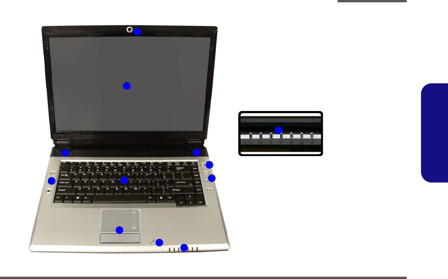
Figure 1
Top View
1. Optional Built-In
PC Camera
2. LCD
3. Speakers
4. Power Button
5. Hot Key Buttons
6. Keyboard
7. TouchPad and
Buttons
8. Built-In
Microphone
9. LED Indicators
2
5
1
7
8
4
6
9
33
5
9

Introduction
1 - 6 External Locator - Front & Rear Views
1.Introduction
External Locator - Front & Rear Views
Figure 2
Front Views
1. LED Indicators
Figure 3
Rear Views
1. 1 * USB Port
2. DC-In Jack
3. Battery
1
1
3
2
1

Introduction
External Locator - Left & Right Side Views 1 - 7
1.Introduction
External Locator - Left & Right Side Views
4
1235 6 7
Figure 4
Left Side View
1. Security Lock Slot
2. Optical Device
Drive Bay
3. RJ-11 Modem
Jack
4. S/PDIF-Out Jack
5. Microphone-In
Jack
6. Headphone-Out
Jack
7. Line-In Jack
Figure 5
Right Side View
1. ExpressCard Slot
2. 7-in-1 Card
Reader
3. 2 * USB 2.0 Ports
4. RJ-45 LAN Jack
5. External Monitor
Port
1
23
345
Introduction
1 - 8 External Locator - Bottom View
1.Introduction
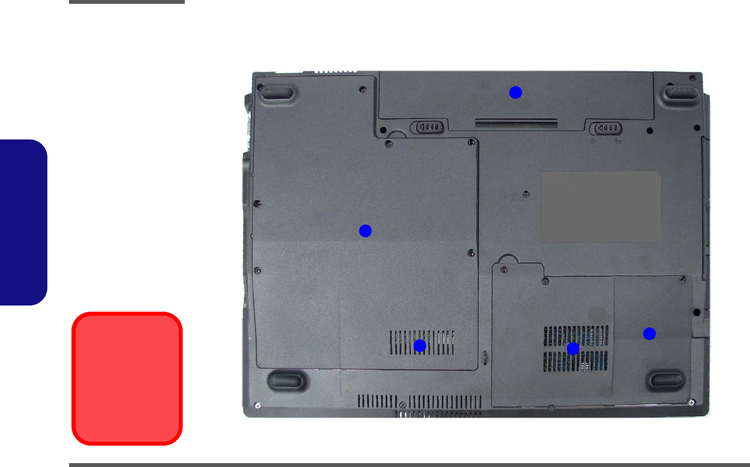
External Locator - Bottom View
Figure 6
Bottom View
1. Vent/Fan Intake
2. Battery
3. Hard Disk Bay
Cover
4. CPU/RAM Bay
Cover
Overheating
To prevent your com-
puter from overheating
make sure nothing
blocks the vent/fan in-
takes while the com-
puter is in use.
2
4
1
3
1
Introduction
Mainboard Overview - Top (Key Parts) 1 - 9
1.Introduction
Mainboard Overview - Top (Key Parts)
Figure 7
Mainboard Top
Key Parts
1. Audio Codec
VT1613
2. Audio Amp
3. Hitachi H8
4. Card Reader
Control
5. ExpressCard
Assembly
2
3
1
4
5
Introduction
1 - 10 Mainboard Overview - Bottom (Key Parts)
1.Introduction
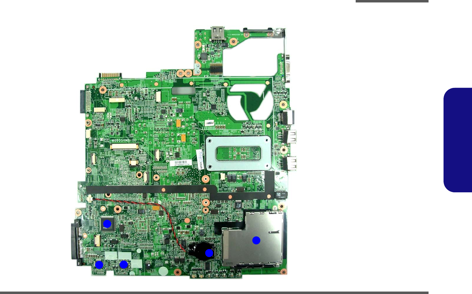
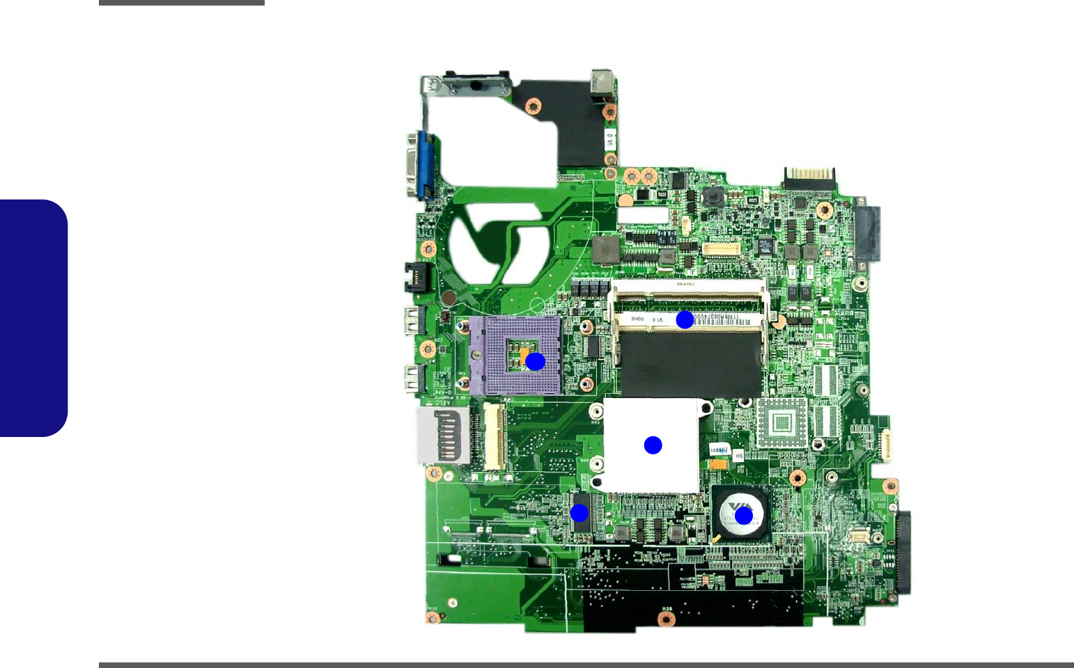
Mainboard Overview - Bottom (Key Parts)
Figure 8
Mainboard Bottom
Key Parts
1. CPU Socket (no
CPU installed)
2. Memory Slots
DDRII So-DIMM
3. Northbridge-
VN896
4. ICS Clock
Generator
5. Southbridge-
VT8237A
2
3
1
45

Introduction
Mainboard Overview - Top (Connectors) 1 - 11
1.Introduction
Mainboard Overview - Top (Connectors)
Figure 9
Mainboard Top
Connectors
1. External Monitor
Port
2. RJ-45 LAN Jack
3. USB Port
4. HDD Connector
5. Hotkey Cable
Connector
6. Power Hotkey
Cable Connector
7. Touch Pad Cable
Connector
8. Keyboard Cable
Connector
9. Speaker Cable
Connector
10. Inverter Cable
Connector
11. CCD Cable
Connector
3
8
11
10
93
3
1
2
4
5
6
7

Introduction
1 - 12 Mainboard Overview - Bottom (Connectors)
1.Introduction
Mainboard Overview - Bottom (Connectors)
Figure 10
Mainboard Bottom
Connectors
1. DC-In Jack
2. Fan Cable
Connector
3. LCD Cable
Connector
4. Batterry
Connector
5. Optical Device
Drive Connector
6. Bluetooth Cable
Connector
7. Card Reader
2
6
3
1
5
4
7

Disassembly
Overview 2 - 1
2.Disassembly
Chapter 2: Disassembly
Overview
This chapter provides step-by-step instructions for disassembling the M660SR/M665SR series notebook’s parts and sub-
systems. When it comes to reassembly, reverse the procedures (unless otherwise indicated).
We suggest you completely review any procedure before you take the computer apart.
Procedures such as upgrading/replacing the RAM, CD device and hard disk are included in the User’s Manual but are
repeated here for your convenience.
To make the disassembly process easier each section may have a box in the page margin. Information contained under
the figure # will give a synopsis of the sequence of procedures involved in the disassembly procedure. A box with a
lists the relevant parts you will have after the disassembly process is complete. Note: The parts listed will be for the dis-
assembly procedure listed ONLY, and not any previous disassembly step(s) required. Refer to the part list for the previ-
ous disassembly procedure. The amount of screws you should be left with will be listed here also.
A box with a will also provide any possible helpful information. A box with a contains warnings.
An example of these types of boxes are shown in the sidebar.
Information
Warning

Disassembly
2-2Overview
2.Disassembly
NOTE: All disassembly procedures assume that the system is turned OFF, and disconnected from any power supply (the
battery is removed too).
Maintenance Tools
The following tools are recommended when working on the notebook PC:
• M3 Philips-head screwdriver
• M2.5 Philips-head screwdriver (magnetized)
• M2 Philips-head screwdriver
• Small flat-head screwdriver
• Pair of needle-nose pliers
• Anti-static wrist-strap
Connections
Connections within the computer are one of four types:
Locking collar sockets for ribbon connectors To release these connectors, use a small flat-head screwdriver to
gently pry the locking collar away from its base. When replac-
ing the connection, make sure the connector is oriented in the
same way. The pin1 side is usually not indicated.
Pressure sockets for multi-wire connectors To release this connector type, grasp it at its head and gently
rock it from side to side as you pull it out. Do not pull on the
wires themselves. When replacing the connection, do not try to
force it. The socket only fits one way.
Pressure sockets for ribbon connectors To release these connectors, use a small pair of needle-nose pli-
ers to gently lift the connector away from its socket. When re-
placing the connection, make sure the connector is oriented in
the same way. The pin1 side is usually not indicated.
Board-to-board or multi-pin sockets To separate the boards, gently rock them from side to side as
you pull them apart. If the connection is very tight, use a small
flat-head screwdriver - use just enough force to start.

Disassembly
Overview 2 - 3
2.Disassembly
Maintenance Precautions
The following precautions are a reminder. To avoid personal injury or damage to the computer while performing a re-
moval and/or replacement job, take the following precautions:
1. Don't drop it. Perform your repairs and/or upgrades on a stable surface. If the computer falls, the case and other
components could be damaged.
2. Don't overheat it. Note the proximity of any heating elements. Keep the computer out of direct sunlight.
3. Avoid interference. Note the proximity of any high capacity transformers, electric motors, and other strong mag-
netic fields. These can hinder proper performance and damage components and/or data. You should also monitor
the position of magnetized tools (i.e. screwdrivers).
4. Keep it dry. This is an electrical appliance. If water or any other liquid gets into it, the computer could be badly
damaged.
5. Be careful with power. Avoid accidental shocks, discharges or explosions.
•Before removing or servicing any part from the computer, turn the computer off and detach any power supplies.
•When you want to unplug the power cord or any cable/wire, be sure to disconnect it by the plug head. Do not pull on the wire.
6. Peripherals – Turn off and detach any peripherals.
7. Beware of static discharge. ICs, such as the CPU and main support chips, are vulnerable to static electricity.
Before handling any part in the computer, discharge any static electricity inside the computer. When handling a
printed circuit board, do not use gloves or other materials which allow static electricity buildup. We suggest that
you use an anti-static wrist strap instead.
8. Beware of corrosion. As you perform your job, avoid touching any connector leads. Even the cleanest hands pro-
duce oils which can attract corrosive elements.
9. Keep your work environment clean. Tobacco smoke, dust or other air-born particulate matter is often attracted
to charged surfaces, reducing performance.
10. Keep track of the components. When removing or replacing any part, be careful not to leave small parts, such as
screws, loose inside the computer.
Cleaning
Do not apply cleaner directly to the computer, use a soft clean cloth.
Do not use volatile (petroleum distillates) or abrasive cleaners on any part of the computer.
Power Safety
Warning
Before you undertake
any upgrade proce-
dures, make sure that
you have turned off the
power, and discon-
nected all peripherals
and cables (including
telephone lines). It is
advisable to also re-
move your battery in
order to prevent acci-
dentally turning the
machine on.

Disassembly
2-4Overview
2.Disassembly
Disassembly Steps
The following table lists the disassembly steps, and on which page to find the related information. PLEASE PERFORM
THE DISASSEMBLY STEPS IN THE ORDER INDICATED.
To remove the Battery:
1. Remove the battery page 2 - 5
To remove the HDD:
1. Remove the battery page 2 - 5
2. Remove the HDD page 2 - 6
To remove the System Memory:
1. Remove the battery page 2 - 5
2. Remove the system memory page 2 - 8
To remove the Processor:
1. Remove the battery page 2 - 5
2. Remove the processor page 2 - 10
To remove the Wireless LAN Module:
1. Remove the battery page 2 - 5
2. Remove the wireless LAN page 2 - 12
To remove the Modem :
1. Remove the battery page 2 - 5
2. Remove the modem page 2 - 13
To remove the Bluetooth:
1. Remove the battery page 2 - 5
2. Remove the bluetooth page 2 - 14
To remove the Optical Device:
1. Remove the battery page 2 - 5
2. Remove the Optical device page 2 - 15
To remove the Keyboard:
1. Remove the battery page 2 - 5
2. Remove the keyboard page 2 - 16
Disassembly
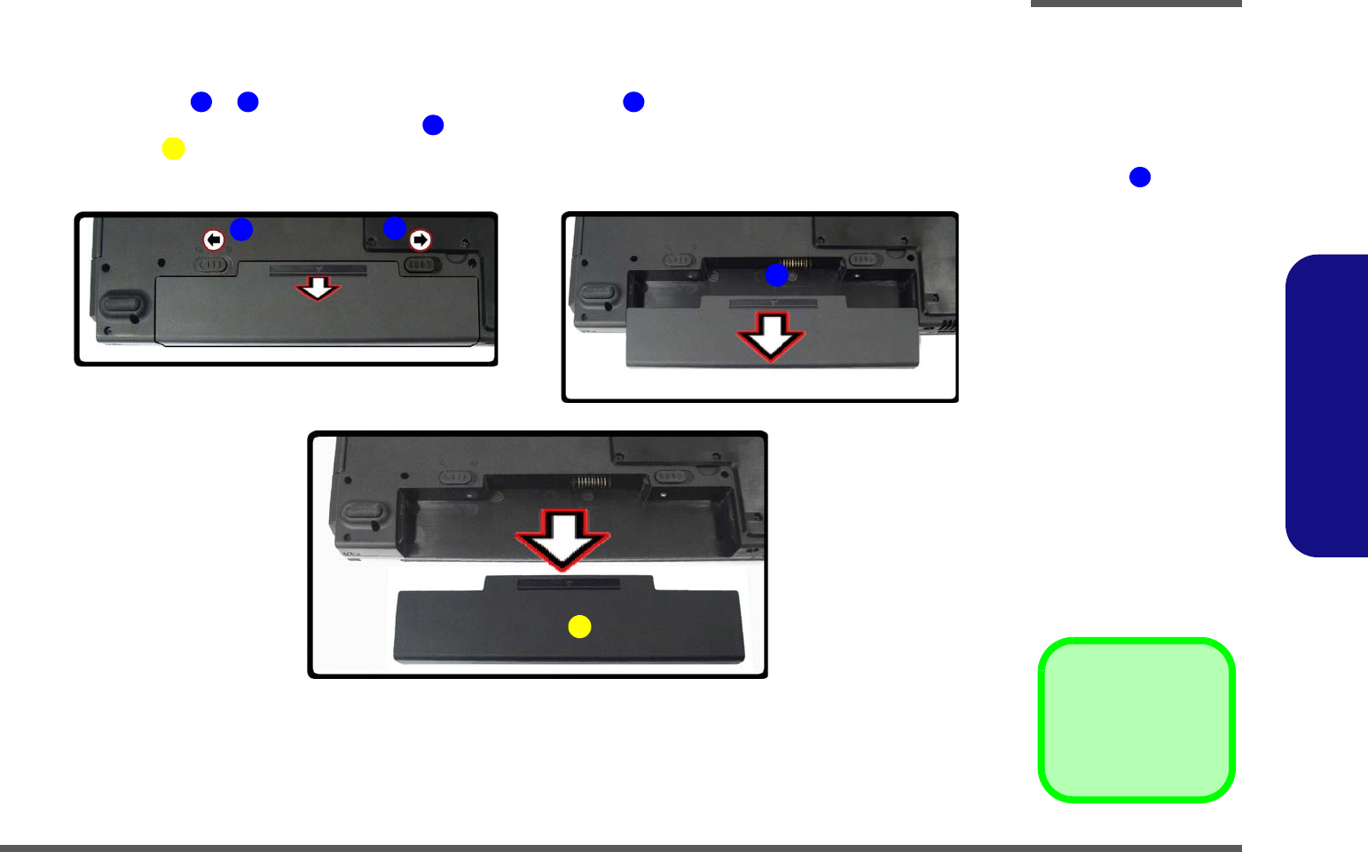
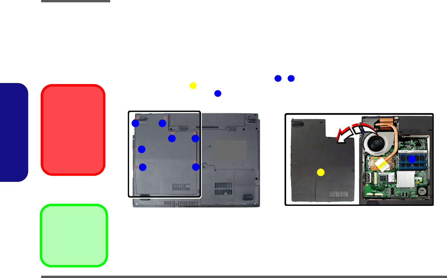
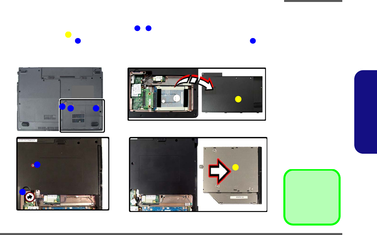
Removing the Battery 2 - 5
2.Disassembly
Removing the Battery
1. Turn the computer off, and turn it over.
2. Slide the latches ( & ) the direction of the arrow, and hold latch in place.
3. Slide the battery in the direction of the arrow .
4. Lift the battery out.
4. Battery
1
2
2
3
6
4
1
a. b.
c.
2
3
4
Figure 1
Battery Removal
a. Slide the 2 latches and
hold latch in place.
b. Slide the battery in the di-
rection of the arrow.
c. Lift the battery out.
2
Disassembly
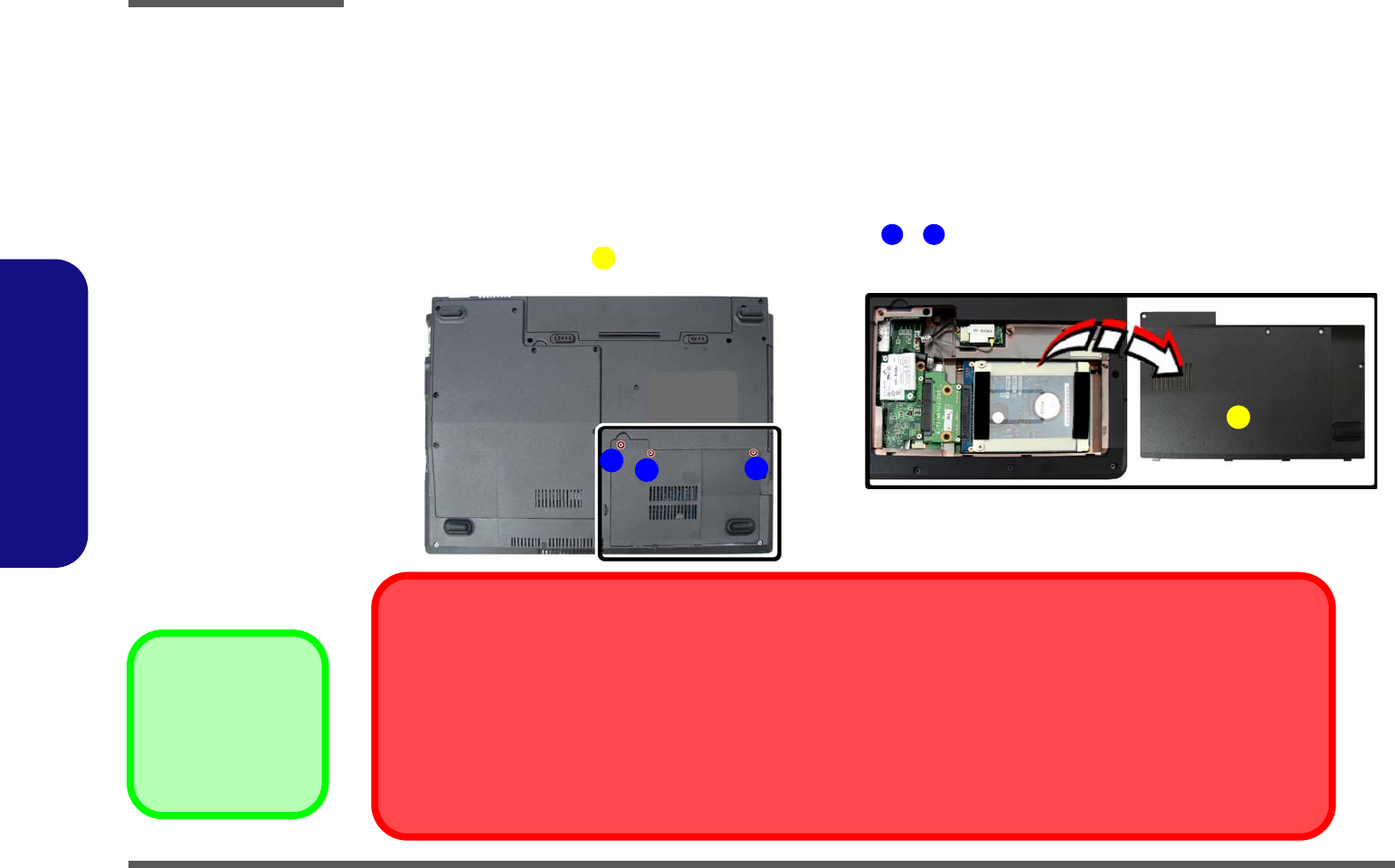
2 - 6 Removing the Hard Disk Drive
2.Disassembly
Removing the Hard Disk Drive
The hard disk drive can be taken out to accommodate other 2.5" serial (SATA) hard disk drives with a height of 9.5mm
(h). Follow your operating system’s installation instructions, and install all necessary drivers and utilities (as outlined in
Chapter 4 of the User’s Manual) when setting up a new hard disk.
Hard Disk Upgrade Processl
1. Turn off the computer, and remove the battery (page 2 - 5).
2. Locate the hard disk bay cover and remove the screws ( - ).
3. Remove the bay cover .
Figure 2
HDD Assembly
Removal
a. Locate the HDD bay cov-
er and remove the
screws.
b. Remove the bay cover.
4. HDD Bay Cover
•3 Screw
1
3
6
4
a.
13
2
HDD System Warning
New HDD’s are blank. Before you begin make sure:
You have backed up any data you want to keep from your old HDD.
You have all the CD-ROMs and FDDs required to install your operating system and programs.
If you have access to the internet, download the latest application and hardware driver updates for the operating system you plan
to install. Copy these to a removable medium.
4
b.
Disassembly
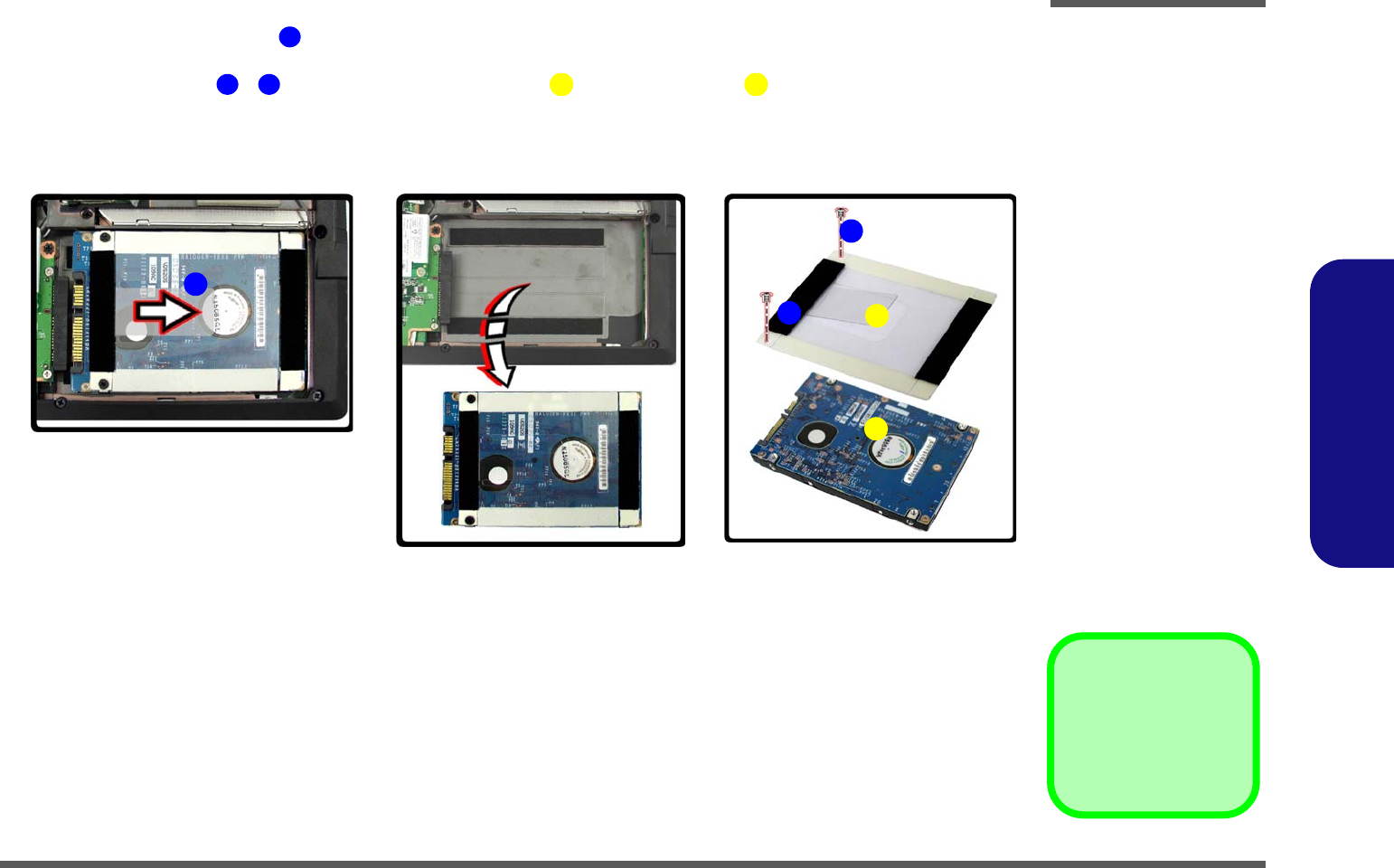
Removing the Hard Disk Drive 2 - 7
2.Disassembly
4. Carefully grip the mylar tab and slide the hard disk in the direction of arrow.
5. Lift the hard disk up (Figure d) in the direction of arrow.
6. Remove the screws - and separate the mylar cover from the hard disk .
7. Reverse the process to install any new hard disk.
5
Figure 3
HDD Assembly
Removal Sequence
c. Slide the HDD in the di-
rection of the arrow.
d. Lift the HDD out of the
bay.
e. Remove the screws and
separate the mylar cover
from the HDD.
6
7
6
8
6
9
8. Mylar Cover
9. HDD
c. d.
5
e.
7
6
9
8
Disassembly
2 - 8 Removing the System Memory (RAM)
2.Disassembly
Removing the System Memory (RAM)
The computer has two memory sockets for 200 pin Small Outline Dual In-line Memory Modules (SO-DIMM) supporting
DDRII 533/667MHz. The main memory can be expanded up to 2GB. The SO-DIMM modules supported are 256MB,
512MB and 1024MB DDRII Modules. The total memory size is automatically detected by the POST routine once you
turn on your computer.
Memory Upgrade Process
1. Turn off the computer, remove the battery (page 2 - 5).
2. Locate the CPU/RAM bay cover, and remove screws - .
3. Remove the bay cover .
4. The RAM will be visible at point on the mainboard.
Figure 4
RAM Module
Removal
a. Remove the screws.
b. Remove the cover.
Contact Warning
Be careful not to touch
the metal pins on the
module’s connecting
edge. Even the clean-
est hands have oils
which can attract parti-
cles, and degrade the
module’s perfor-
mance.
1
7
8
8. CPU/RAM Bay Cover
•7 Screws
9
a.
3 4
1
56
78
b.
2
9

Disassembly
Removing the System Memory (RAM) 2 - 9
2.Disassembly
5. Gently push the two release latches ( & ) on the sides of the memory socket in the direction indicated by the
arrows (Figure c).
6. The RAM module(s) will pop-up (Figure d), and you can then remove it.
7. Push the latches to release the second module if necessary.
8. Insert a new module holding it at about a 30° angle and fit the connectors firmly into the memory slot.
9. The module will only fit one way as defined by its pin alignment. Make sure the module is seated as far into the slot
as it will go. DO NOT FORCE IT; it should fit without much pressure.
10. Press the module down towards the mainboard until the slot levers click into place to secure the module.
11. Replace the bay cover and the screws (see page 2 - 8).
12. Restart the computer to allow the BIOS to register the new memory configuration as it starts up.
10
11
12
Figure 5
Memory Removal
Sequence
c. Push the release
latch(es).
d. Remove the module(s).
10
c. d.
12
11
10 11
12 RAM Module(s)
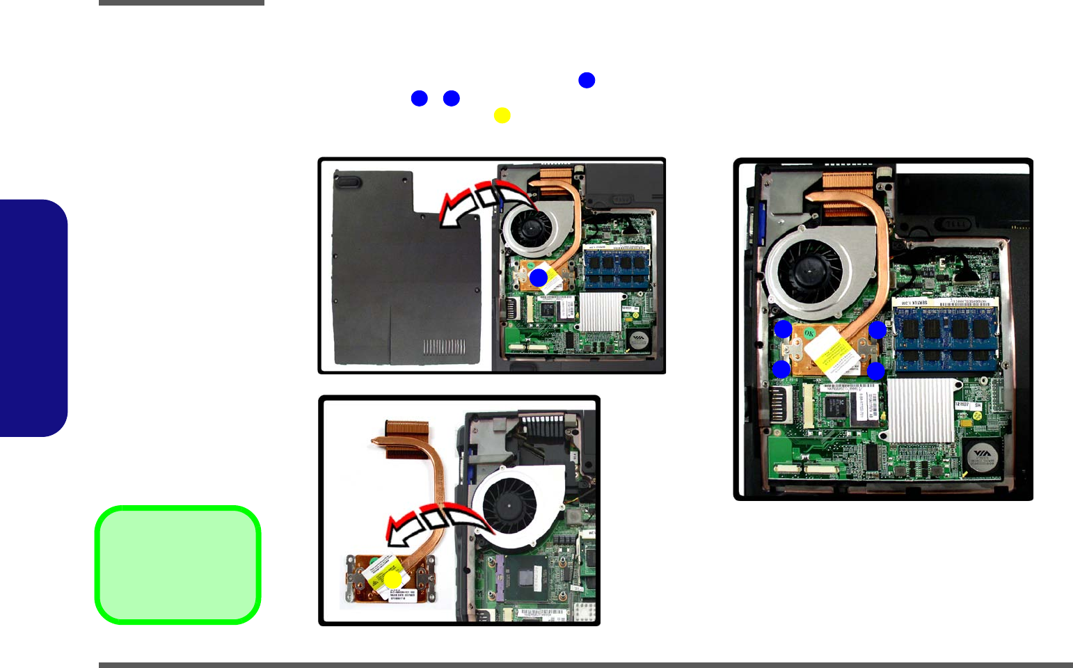
Disassembly
2 - 10 Removing the Processor
2.Disassembly
Removing the Processor
1. Turn off the computer, and remove the battery (page 2 - 5) and the CPU/RAM bay cover (page 2 - 8).
2. The CPU heat sink will be visible at point on the mainboard.
3. Remove screws - from the heat sink in the order indicated.
4. Carefully lift up the heat sink (Figure c) off the computer.
1
2
5
6
Figure 6
Processor Removal
a. Remove the cover and
Iocate the heat sink.
b. Remove the 4 screws in
the order indicated.
c. Remove the heat sink.
6. Heat Sink
•4 Screws
b.
6
1
5
4
a.
c.
3
2

Disassembly
Removing the Processor 2 - 11
2.Disassembly
5. Turn the release latch towards the unlock symbol , to release the CPU (Figure d).
6. Carefully (it may be hot) lift the CPU up out of the socket (Figure e).
7. Reverse the process to install a new CPU.
8. When re-inserting the CPU, pay careful attention to the pin alignment, it will fit only one way (DO NOT FORCE IT!).
7
8
Figure 7
Processor Removal
(cont’d)
d. Turn the release latch to
unlock the CPU.
e. Lift the CPU out of the
socket.
d.
8
e.
Caution
The heat sink, and CPU area in
general, contains parts which are
subject to high temperatures. Allow
the area time to cool before remov-
ing these parts.
Unlock Lock
7
7
8. CPU
Disassembly
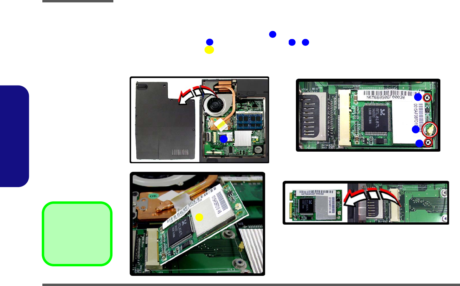
2 - 12 Removing the Wireless LAN Module
2.Disassembly
Removing the Wireless LAN Module
1. Turn off the computer, remove the battery (page 2 - 5) and the module bay cover (page 2 - 8).
1. The Wireless LAN module will be visible at point on the mainboard.
2. Carefully disconnect cable , then remove the screws - from the module socket.
3. The wireless LAN module will pop-up.
4. Lift the wireless LAN module (Figure d) up and off the computer.
Figure 8
Wireless LAN
Module Removal
a. Remove the cover and
Iocate the heat sink.
b. Disconnect the cable
and remove the 2
screws.
c. The WLAN module will
pop up.
d. Remove the WLAN
module.
Note: Make sure you
reconnect the antenna
cable to the “Main”
socket (Figure b).
1
2
3
4
5
1
2
4
c.
a.
5
3
b.
d.
5. WLAN Module
•2 Screws

Disassembly
Removing the Modem 2 - 13
2.Disassembly
Removing the Modem
1. Turn off the computer, remove the battery (page 2 - 5), and remove the hard disk bay cover (page 2 - 6).
2. The modem will be visible at point on the mainboard.
3. Remove screws - from the modem module.
4. Lift the modem up off the socket and separate the modem from the connector .
5. Lift the modem up and off the computer.
1
2
3
4
5
6
Figure 9
Modem Removal
a. Remove the cover and
locate the modem.
b. Remove the screws.
c. Lift the modem up off the
socket and disconnect
the connector.
d. Lift the modem out.
a.
c.
b.
34
1
2
d.
6
5
6. Modem
•2 Screws

Disassembly
2 - 14 Removing the Bluetooth Module
2.Disassembly
Removing the Bluetooth Module
1. Turn off the computer, remove the battery (page 2 - 5) and remove the hard disk bay cover (page 2 - 6).
2. The Bluetooth module will be visible at point on the mainboard.
3. Carefully separate the module from the connector and disconnect the cable .
4. Lift the Bluetooth module (Figure c) up and off the computer.
Figure 10
Bluetooth Removal
a. Remove the cover and
locate the Bluetooth
module.
b. Separate the the mod-
ule from connector and
disconnect the cable.
c. Remove Bluetooth mod-
ule.
1
2
3
4
a. c.
b.
3
1
2
4
4. Bluetooth Module
Disassembly
Removing the Optical (CD/DVD) Device 2 - 15
2.Disassembly
Removing the Optical (CD/DVD) Device
1. Turn off the computer, remove the battery (page 2 - 5).
2. Locate the hard disk bay cover and remove screws ( - ).
3. Remove the bay cover .
4. Remove the screw at point , and use a screwdriver to carefully push out the optical device at point .
5. Insert the new device and carefully slide it into the computer (the device only fits one way. DO NOT FORCE IT; The
screw holes should line up.
6. Restart the computer to allow it to automatically detect the new device.
Figure 11
Optical Device
Removal
a. Remove the screws.
b. Remove the cover.
c. Remove the screw and
push the optical device
out off the computer at
point 6.
d. Remove the optical de-
vice.
1
3
6
4
5
6
4 HDD Bay Cover
7 Optical Device
•4 Screws
32
1
a.
4
b.
c. d.
5
6
7
Disassembly
2 - 16 Removing the Keyboard
2.Disassembly
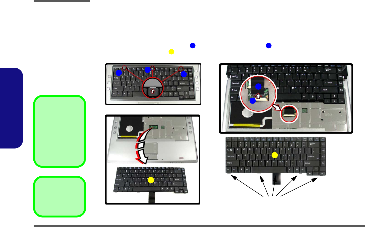
Removing the Keyboard
1. Turn off the computer, and remove the battery (page 2 - 5).
2. Press the three keyboard latches at the top of the keyboard to elevate the keyboard from its normal position (you
may need to use a small screwdriver to do this).
3. Carefully lift the keyboard up, being careful not to bend the keyboard ribbon cable (Figure b).
4. Disconnect the keyboard ribbon cable from the locking collar socket .
5. Carefully lift up the keyboard (Figure c) off the computer.
4
5
Figure 12
Keyboard Removal
a. Press the three latches
to release the keyboard.
b. Lift the keyboard up and
disconnect the cable
from the locking collar.
c. Remove the keyboard.
Re-Inserting the Key-
board
When re-inserting the
keyboard firstly align
the five keyboard tabs
at the bottom of the
keyboard with the slots
in the case.
6
a. b.
123
4
5
Keyboard Tabs
6
c.
6
6. Keyboard

Part Lists
A-1
A.Part Lists
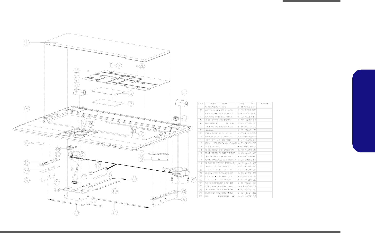
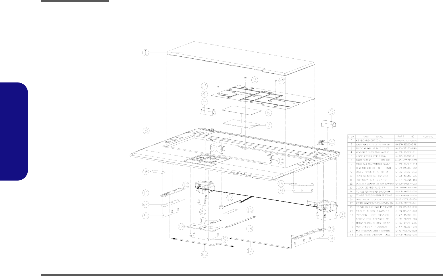
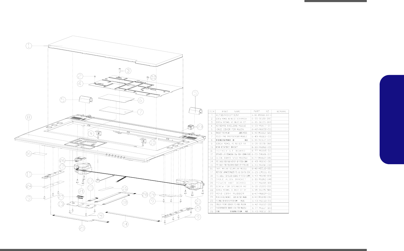
Appendix A:Part Lists
This appendix breaks down the M660SR/M665SR series notebook’s construction into a series of illustrations. The com-
ponent part numbers are indicated in the tables opposite the drawings.
Note: This section indicates the manufacturer’s part numbers. Your organization may use a different system, so be sure
to cross-check any relevant documentation.
Note: Some assemblies may have parts in common (especially screws). However, the part lists DO NOT indicate the
total number of duplicated parts used.
Note: Be sure to check any update notices. The parts shown in these illustrations are appropriate for the system at the
time of publication. Over the product life, some parts may be improved or re-configured, resulting in new part numbers.
Part Lists
A - 2 Part List Illustration Location
A.Part Lists
Part List Illustration Location
The following table indicates where to find the appropriate part list illustration.
Table A - 1
Part List Illustration
Location Part Pages#
Top with Fingerprint - (M660SR) page A - 3
Top without Fingerprint - (M660SR) page A - 4
Top with Fingerprint - (M665SR) page A - 5
Top without Fingerprint - (M665SR) page A - 6
Bottom - (M660SR/M665SR) page A - 7
LCD - (M660SR/M665SR) page A - 8
Combo - (M660SR/M665SR) page A - 9
DVD-Dual RW - (M660SR/M665SR) page A - 10
Part Lists
Top with Fingerprint (M660SR) A - 3
A.Part Lists
Top with Fingerprint (M660SR)
Figure A - 1
Top
with Fingerprint
(M660SR)
無鉛
無鉛
鴻富
無鉛
無鉛
無鉛
無鉛
無鉛
無鉛
無鉛
無鉛
(太乙加邊框) 無鉛
改用NATURE 料及PALMREST內部貼鋁箔 M660SU 無鉛
鴻富 無鉛
無鉛
無鉛
增加 2 個轉折) 無鉛 鴻富
無鉛
無鉛
無鉛
Part Lists
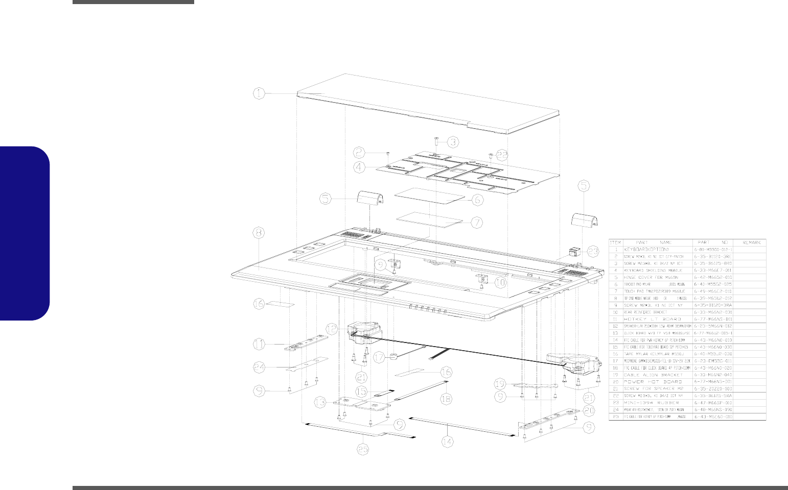
A - 4 Top without Fingerprint (M660SR)
A.Part Lists
Top without Fingerprint (M660SR)
無鉛
無鉛
無鉛
無鉛
無鉛
無鉛
無鉛
無鉛
鴻富
無鉛
無鉛
無鉛
無鉛
(太乙加邊框) 無鉛
鴻富 無鉛
料 位置 尺寸改窄 無鉛
無鉛
Figure A - 2
Top without
Fingerprint
(M660SR)
Part Lists
Top with Fingerprint (M665SR) A - 5
A.Part Lists
Top with Fingerprint (M665SR)
Figure A - 3
Top
with Fingerprint
(M665SR)
無鉛
無鉛
無鉛
無鉛
(太乙加邊框) 無鉛
無鉛
(折角96度)(無鉛)
鴻富
無鉛
無鉛
無鉛
料 位置CR尺寸改窄 無鉛
增加 2 個轉折) 無鉛 鴻富
無鉛
無鉛
被 無鉛
無鉛
無鉛
無鉛
鴻富 無鉛
Part Lists
A - 6 Top without Fingerprint (M665SR)
A.Part Lists
Top without Fingerprint (M665SR)
無鉛
料 位置 尺寸改窄 無鉛
無鉛
無鉛
(太乙加邊框) 無鉛
無鉛
(折角96度)(無鉛)
鴻富
無鉛
無鉛
無鉛
無鉛
無鉛
無鉛
被 無鉛
無鉛
鴻富 無鉛
Figure A - 4
Top without
Fingerprint
(M665SR)
Part Lists
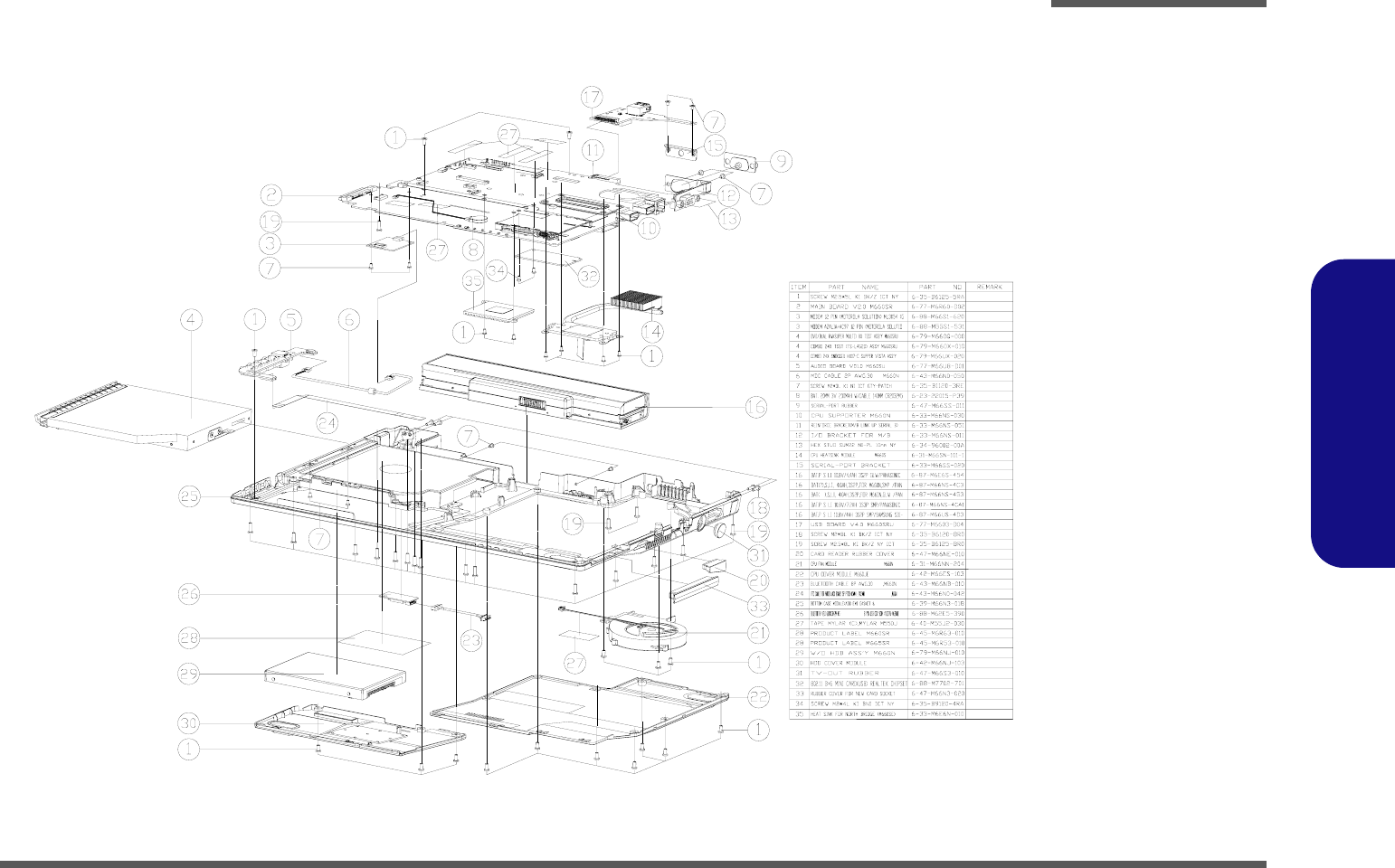
Bottom (M660SR/M665SR) A - 7
A.Part Lists
Bottom (M660SR/M665SR)
Figure A - 5
Bottom (M660SR/
M665SR)
無鉛
無鉛
(中間加肉 0.8MM)(無鉛)
無鉛
(螺絲孔位置加厚度補強) 無鉛
無鉛
無鉛
無鉛
華力
無鉛
無鉛
華力 無鉛
無鉛
無鉛
無鉛
無鉛
無鉛
無鉛
無鉛
無鉛
無鉛
(高度8.0MM)無鉛
無鉛
無鉛
無鉛
無鉛
無鉛
(無散熱片) (先進)無鉛
前緣氣孔)黑色(無鉛)
黑色(高度8.0MM)無鉛
無鉛
外
無鉛
無鉛
藍天2 互億 無鉛
(加背膠) 鴻富 無鉛
Part Lists
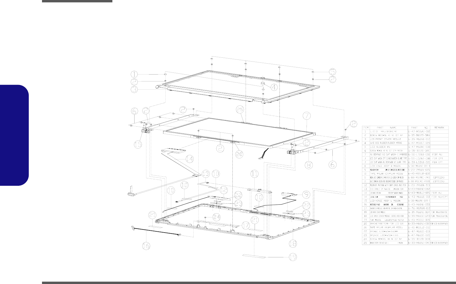
A - 8 LCD (M660SR/M665SR)
A.Part Lists
LCD (M660SR/M665SR)
Figure A - 6
LCD (M660SR/
M665SR)
無鉛
無鉛
含背膠)(無鉛)
含背膠)(無鉛)
華力 端 改為 無鉛
無鉛
無鉛
無鉛
無鉛
加開避位口 無鉛
無鉛
膠帶加長 無鉛
鐵氟龍線 華力 無鉛
無鉛
無鉛
(剛毅)無鉛
華力 無鉛
無鉛(公模面增加兩個理線BOSS)
無鉛
中性
鐵氟龍線 無鉛
(剛毅)無鉛
無鉛
無鉛
無鉛
無鉛
無鉛

Part Lists
Combo (M660SR/M665SR) A - 9
A.Part Lists
Combo (M660SR/M665SR)
減膠
Figure A - 7
Combo (M660SR/
M665SR)

Part Lists
A - 10 DVD-Dual RW (M660SR/M665SR)
A.Part Lists
DVD-Dual RW (M660SR/M665SR)
Figure A - 8
DVD-Dual RW
(M660SR/M665SR)
Schematic Diagrams
B-1
B.Schematic Diagrams
Appendix B:Schematic Diagrams
This appendix has circuit diagrams of the M660SR/M665SR notebook’s PCB’s. The following table indicates where to
find the appropriate schematic diagram.
Diagram - Page Diagram - Page Diagram - Page
SYSTEM BLOCK DIAGRAM - Page B - 2 VT8237A-1 - Page B - 16 CHARGER, DC IN - Page B - 30
CLOCK GENERATOR - Page B - 3 VT8237A-2 - Page B - 17 1.5V, 1.05VS - Page B - 31
CPU-1 - Page B - 4 VT8237A-3 - Page B - 18 VCORE - Page B - 32
CPU-2 - Page B - 5 HDD & CDROM - Page B - 19 1.8V, 0.9VS - Page B - 33
VN896-1 - Page B - 6 CARD READER - Page B - 20 VDD3, VDD5 - Page B - 34
VN896-2 - Page B - 7 NEW CARD SOCKET - Page B - 21 EXT GPU 1.0VS/1.2VS - Page B - 35
VN896-3 - Page B - 8 LAN - Page B - 22 HOTKEY LT BOARD - Page B - 36
VN896-4 - Page B - 9 USB & CCD - Page B - 23 PWR HOT BOARD - Page B - 37
DDR2-1 - Page B - 10 KBC-IT8512E - Page B - 24 AUDIO & MODEM BOARD - Page B - 38
DDR2-2 - Page B - 11 CRT & LVDS - Page B - 25 CLICK BOARD - Page B - 39
VGA G72M-1 - Page B - 12 FAN CONTROL, LPC ROM - Page B - 26 USB BOARD - Page B - 40
VGA G72M-2 - Page B - 13 MINI-PCI & BLUETOOTH - Page B - 27 FINGERPRINT BOARD - Page B - 41
VGA G72M-3 - Page B - 14 AUDIO VT1708A/ALC883 - Page B - 28
VGA G72M-4 - Page B - 15 LED, VS POWER - Page B - 29
Table B - 1
Schematic
Diagrams
Version Note
The schematic dia-
grams in this chapter
are based upon ver-
sion 6-7P-M6607-003.
If your mainboard (or
other boards) are a lat-
er version, please
check with the Service
Center for updated di-
agrams (if required).
Schematic Diagrams
B - 2 SYSTEM BLOCK DIAGRAM
B.Schematic Diagrams
SYSTEM BLOCK DIAGRAM
Sheet 1 of 40
SYSTEM BLOCK
DIAGRAM
SATA
HDD
DEBUGB
PORT
LAN
PWR_HOT BOARD
USB Port 2
X4 DMI
Interface
VT8237A
CRT
NORT H B RI DGE
FSB667
IMVP-6 VR
SOCKET P
LINE IN
SOU TH BRI DGE
SATA
CLOCK GEN
VGA
NB8M/G72M
KBC
IT8512E
VN896CE
CD-ROM
(IDE)
CARD READER
ENE MR510
Touch PAD
SPK. OUT
HOT KEY LT
BOARD
USB BOARD
SP EAK ER x2
DDR2
SO-DIMM
x2
USB Port 1
MDC or
MBC
ICS953009AF+ICS9P936AF
FWH
ULTRA-DMA33/66/100
Blue Tooth
Keyboard
AUD IO& MOD EM
BOAR D
M660SRU BLOCK DIAGRAM
AC97
MIC. IN
USB 2.0
BATT.X1
SANTAROSA
478
VRAM
LAN
VT6103L
SPDIF
MASTER
PORT PRT
Audio Codec
VT1708/ALC
883
CCD Camera
FAN X 1
LPC
CL IC K BO AR D
LCD
USB Port 3
LPC
PCI
Schematic Diagrams
CLOCK GENERATOR B - 3
B.Schematic Diagrams
CLOCK GENERATOR
Sheet 2 of 40
CLOCK
GENERATOR
1.5VS
3V66_0
Z020 8
R N24 22_4P2R _041
2 3
4
C 747 *33P_50V_06R 804 1K_06
R 280 51.1_1%_04
C 753 .1U _16V_04
U3 3
ICS953009AFLF-T
48
10
17
6
11
18
28
32
30
2
21
22
29
26
25
7
9
27
40
3
39
12
13
14
15
16
19
20
1
45
56
55
52
49
23
24
4
5
8
44
43
42
41
38
37
36
35
34
33
31
54
53
51
50
47
46
SDATA
VDD PCI_ 1
PC ICL K4
X1
** FSL2/PC ICLK_F0
PC ICL K5
* *FS4/3V66_1
GN DPCIEX
GN D3 V 66
GN D
Re s et#
VDD 48
3V66_0
VDD 3V6 6
GN D4 8
X2
VttPW R_GD /PD#
** ITP _EN /3V6 6_2F_2X
GN DPCIEX
VDD REF
VDD PCIEX_ 1
* *FS3/PCIC LK1_2X
**TB_EN/PC ICLK2
PC ICL K3
GN DPCI
VDD PCI_ 2
GN DPCI
PCIC LK6/*Turbo#
VDD A
VDD PCIEX_ 2
GN D
IREF
GN DC P U
VDD CPU
**Mode0/48MHz
*Sel24_48#/24_48M HZ
**F S L0 / R E F 0
FSL1/R EF1
GN DR E F
PCIEXT1
PC IEXC 1
PCIEXT2
PC IEXC 2
PCIEXT3
PC IEXC 3
PC IEXT 4 /PEREQ 1# *
PC IEXC4/PEREQ 2# *
PCIEXT5/CPU_STOP#*
PCIEXC5 /PC I_PC IEX_ ST OP# *
SCLK
C P U C LK T 0 _F
CPUC L KC0 _F
CPU CL KT 1
CPUCLKC1
CPU CLKT2_ITP/PCIEXT0
CPUC LK C2 _IT P/PC IEXC 0
M_ CL K_ DD R1 1 0
Z0218
GCLK_NB
Z022 9
C 754 .1U _16V_04
NB_ P EXCL K
-C P U_ S T OP
Z020 2
C 762 22P_50V_04
C PU_ BSEL 03
Z0210
C 757 .1U _16V_04
Q1 9
2N 70 0 2W
G
DS
R 298 * 10K_04
1. 8 V B F R
DK3 +
BSEL2
R657 0_06
R661 0_06
R N25 22_4P2R _041
2 3
4
CLKEN#31
FS4
C4 3 7
.01U_16V_04
R572 0_04
R653 10K_04
SMB_SBCLK9, 1 0 , 1 1, 1 6
RN 18 22_4P2R_04
1
2 3
4
PCI
3.3VCLK
R556 1K_04
1
DK1 -
Z02 27
R 802 10K_04
3.3VS
Z0222
3. 3 V C LK
0
1.5VS
R 1 13 0_ 0 4
C4 44
.01U_16V_04
C605
.01U _16V_04
R274 475_1%_06
C116
*5 P _5 0 V _ 06
R549 22_04
M_ CL K_ DD R3 9
M_ CL K_ DD R0 1 0
Z0216
KBCPC LK
DK2 -
R304 51.1_1% _04
VGA_PEXCLK 1 1
33
NB_PEXCLK#
C6 1 0
.01U_16V_04
PCLKM PCI
HC PUCL K-
C614
4 . 7U _6 . 3 V _ 06
DK2 +
C6 9 9
*22P_50V_06
133
CLK_ PW RGD
Z0209
DK0 + RN 16 22_4P2R_04
1
2 3
4
SIO_ OS C16
RN 17 22_4P2R_04
1
23
4
PCLKPCM 19
CLK_ PCIE_ NC
R542 22_04
CL K_ US B4 815
VGA_ PEXCLK
C 744 *33P_50V_06
FS2
1. 8 V
SMB_SBDA TA9, 1 0 , 1 1, 1 6
Z02 03
PCIC LKX4
R5 6 6 10 K_ 0 4
0
VG A_PEXC LK
FB17
H CB2012KF-121T30_08
PM _STPC PU#16
FS1
C3 9 8
27P_N PO_50V_06
3.3VS
R N23 22_4P2R _041
23
4
Z02 28
R319 22_04
-P CI_ S T OP
C472
.01U_16V_04
C 759 .1U _16V_04 3. 3 V S
1
PCLKMPC I 26
GCL K _ NB 7
3. 3 V C LK
MCLKIT6
Z02 06
R 473 0_04
C603
1U_10V_06 M_ CL K_ DD R# 3 9
VG A_PEXC LK#
HC PUCL K+
R299 51.1_1% _04
Y1
14.318MH Z
12
R658 0_06GC LK _ N B
3. 3 V C LK
FS3
R N21 33_4P2R _041
2 3
4
Q1 8
2N 3904
B
E C
M_ CL K_ DD R# 2 9
BSEL0
SEL24_48
C1 07
.01U_16V_04
U2 9
IC S9P9 5 6 F LF -T
10
21
27
1
9
28
2
16
15
3
12
5
7
13
18
20
24
6
8
14
17
19
23
11
26
25
4
22
VD D2 .5/ 1.8-0
VD D2 .5/ 1.8-1
VD D2 .5/ 1.8-2
AVD D2 .5-0
GND
GND
AG ND
SD ATA
SC LK
BU F_IN T
FB_OUTC
DD RT0
DD RT1
DD RT2
DD RT3
DD RT4
DD RT5
D DRC 0
D DRC 1
D DRC 2
D DRC 3
D DRC 4
D DRC 5
FB _O UTT
AVD D2 .5-1
AG ND
BU F_IN C
GND
33
CL K_ RE SET
3. 3 V C LK
R 287 51.1_1% _04
CPU_ C LK - 3
3. 3 V C LK
D2 1 *R B 75 1 V
AC
KBC_PCLK 23
VCLK_SB
3. 3 V C LK
R 290 1K_04
FS3
Q4 9
2N 39 0 4
B
E C
Z021 3
Z0217
Q1 7
*2 N3 9 04
B
E C
CPU
PCIC LKX2
3. 3 V C LK
0
R 268 1K_06
Z02 31
MODE
Z02 23
FB22
HC B2012KF-121T30_08
HC LK-_
3. 3 V C LK
HC LK+ _
PC LK_TPM
R 283 10K_04
C3 9 7
27P_N PO_50V_06
CL K_P CIE_ NC 20
C L K_PC IE_N C#
C 755 .1U _16V_04
R 539 0_04
Z0219
R315 51.1_1% _04
R5 6 8 10 K_ 0 4
200
3.3VS
1.5VS
CLK_ PCIE_ NC #
C7 03
2 2 U _ 10 V _ 12
R 803 1K_04
266
FS0
Z021 2
C PU_ BSEL 13
SM B_SBDATA9,10,11,16
CLK_P CIE_NC# 20
R310 51.1_1% _04
C L K_PC IE_N C
FS2
R 301 10K_04
3.3VS
Z020 1
R 579 10K_04
C599
. 0 1U _1 6 V _ 04
Z0211
1
Z020 7
R 475 0_04
Z0221
Z0220
VCLK_ SB 17
CL K_M CH _B C L K 5
Z02 05
VGA_PEXCLK# 11
SM B_SBCLK9,10,11,16
Z023 0
C595
4. 7 U _6 . 3 V _0 6
R N27 22_4P2R _041
2 3
4
NB_ P EXCL K # 7
R540 22_04
PC LKMPCI
BSEL2
D2 0 *R B 75 1 V
AC
C 758 .1U _16V_04
DK1 +
RN26
22_4P2R_04
1
23
4
NC_CLKREQ# 20
C410
.01U_16V_04
Z0215
R 291 1K_06
-PC I _S TO P
M9 608 06
C4 8 2
1U_10V_06
C 761 .1U _16V_04
CL K_M CH _B C L K # 5
NB_ P EXCL K 7
FS1
DK0 -
C700
10U_10V_08
C611
.01U _16V_04
CPU_ C LK + 3
C4 0 1
.01U_16V_04
3. 3 V C LK
BSEL1
Z0214
FS4
-CP U _S T O P
3.3VS
3. 3 V C LK
C478
1U _10V_06
R N22 33_4P2R _041
2 3
4
FB18
HC B2012KF-121T30_08
R576 22_04
M_ CL K_ DD R# 0 10
C589
10U _10V_08
R 292 51.1_1% _04
GUIC K8
R 5 47 10 K _ 04
DK3 -
C5 9 0
10 U _ 1 0 V _0 8
330
R 294 51.1_1% _04
C458
. 01 U _1 6 V _0 4
MODE
RN 19 22_4P2R_04
1
2 3
4
R571 22_04
C 743 *33P_50V_06
MC LK I T P
R 7 11 0_ 0 4
R302 51.1_1% _04
R118 100_04
C 760 .1U _16V_04
NB_PEXCLK
Z02 24
NB_ P EXCL K#
R 289 10K_04
M_ CL K_ DD R# 1 10
R681 22_04
R314 1K_04
FS0
SPCLK 1 7
BSE L1
Z02 04
FS2
R321 10K _04
R 284 1K_04
R703 22_04
R561 *1K_04
R 805 0_04
C PU_ BSEL 23
FS0
R 541 0_04
MCLKOC6
R546 0_04
R577 22_04
166
FS 1
C 756 .1U _16V_04
1.8V
VGA_ PEXCLK#
C617
.1U _50V_06
C422
.01U _16V_04
BSEL 0
R307 51.1_1% _04
PM _STPPC I#16
3. 3 V C LK
C1 1 5
* 5P_50V_06
1
33
M_ CL K_ DD R2 9
MCLKOT6
C612
. 01U_16V_04
C431
.01U _16V_04
C7 0 1
10U _10V_08

Schematic Diagrams
B - 4 CPU-1
B.Schematic Diagrams
CPU-1
Sheet 3 of 40
CPU-1
ALL_PWRO K 15,17,24
H_ CPU SL P #
H_ A# 12
H_ D# 3 5
1.05VS
H_ D# 1 8
H_ D# 4 7
TH M _ V D D
CPU _ TES T 1
R466
150_1%_04
Z0319
H_ D# 3 6
R 155 220_06
R 93 1 5 0 _1 % _ 04
R131 27.4_1% _06
H_ DIN V#15
CPU _ DP RS TP #
H_ A# 6
Z0314
XD P_ PREQ#
H_ INT R17
H_ D STB P# 3 5
XD P _ TD O
H_ RS #[2 :0 ]
R 74 51.1_04
THE RMTR IP# 33
H_ L OC K # 5
H _AD STB#05
H_ D# [6 3 :0]5
H_ A# 21
H_ D# 2 5
H_ D# 1
H_ D# 4 5
DATA GRP 0 DATA GRP 1
DA TA G R P 2DA T A G R P 3
MISC
JSKT1B
Me ro m Ba ll -o ut R e v 1a
R2 6
U2 6
AA1
Y1
E22
F24
J24
J23
H2 2
F26
K22
H2 3
N2 2
K25
P26
R2 3
E26
L23
M2 4
L22
M2 3
P25
P23
P22
T24
R2 4
L25
G2 2
T25
N2 5
Y22
AB24
V24
V26
V23
T22
U2 5
U2 3
F23
Y25
W22
Y23
W24
W25
AA23
AA24
AB25
AE24
AD24
G2 5
AA21
AB22
AB21
AC26
AD20
AE22
AF2 3
AC25
AE21
AD21
E25
AC22
AD23
AF2 2
AC23
E23
K24
G2 4
AF1
H2 5
N2 4
U2 2
AC20
E5
B5
D2 4
J26
L26
Y26
AE25
H2 6
M2 6
AA26
AF2 4
AD26
AE6
D6
D7
C2 4
B22
B23
C2 1
D2 5
AF2 6
A26
C2 3 COM P[ 0 ]
COM P [1 ]
COM P [2 ]
COM P [3 ]
D[0 ]#
D[1 ]#
D[1 0 ]#
D[1 1 ]#
D[1 2 ]#
D[1 3 ]#
D[1 4 ]#
D[1 5 ]#
D[1 6 ]#
D[1 7 ]#
D[1 8 ]#
D[1 9 ]#
D[2 ]#
D[2 0 ]#
D[2 1 ]#
D[2 2 ]#
D[2 3 ]#
D[2 4 ]#
D[2 5 ]#
D[2 6 ]#
D[2 7 ]#
D[2 8 ]#
D[2 9 ]#
D[3 ]#
D[3 0 ]#
D[3 1 ]#
D[3 2 ]#
D[3 3 ]#
D[3 4 ]#
D[3 5 ]#
D[3 6 ]#
D[3 7 ]#
D[3 8 ]#
D[3 9 ]#
D[4 ]#
D[4 0 ]#
D[4 1 ]#
D[4 2 ]#
D[4 3 ]#
D[4 4 ]#
D[4 5 ]#
D[4 6 ]#
D[4 7 ]#
D[4 8 ]#
D[4 9 ]#
D[5 ]#
D[5 0 ]#
D[5 1 ]#
D[5 2 ]#
D[5 3 ]#
D[5 4 ]#
D[5 5 ]#
D[5 6 ]#
D[5 7 ]#
D[5 8 ]#
D[5 9 ]#
D[6 ]#
D[6 0 ]#
D[6 1 ]#
D[6 2 ]#
D[6 3 ]#
D[7 ]#
D[8 ]#
D[9 ]#
TE S T5
DIN V[0]#
DIN V[1]#
D INV[2 ]#
D INV[3 ]#
DPRSTP#
DPSLP#
DPW R#
DST BN[0 ]#
DST BN[1 ]#
DSTBN[2]#
DSTBN[3]#
DSTBP[0 ]#
DSTBP[1 ]#
DSTBP[2]#
DSTBP[3]#
GT L R EF
PSI#
PW RGO OD
SLP#
TE S T3
BSEL [0]
BSEL [1]
BSEL [2]
TE S T2
TE S T4
TE S T6
TE S T1
M960808
Z0311
10 MILE
COM P3
PM_THRMTRIP# should
connect to ICH7 and GMCH
without T-ing(No STUB)
H_ HIT M # 5
R 154 75_06
5/14
H_ IN IT#
H_ IGN NE #
H_ INI T# 1 7
H_D PSLP #
XD P _ TD I
H_ A# 30
XD P _ B P M # 0
XDP_T MS
R 120 220_06 R 15 1 5 4 . 9 _1 % _ 06
H_ T RD Y # 5
H_ TH ERM DC
H_ REQ # 3
H_ A# 28
XD P _ B P M # 3
Z0318
H_ D# 1 4
Z0303
C836
2. 2u_6.3V_06
R7 3 1 K_ 06 PM_D PRSLPVR 15,17,31
Z 0310
H_ D# 3 3
H_ D# 3
H_ D# 6
R 14 9 5 4 . 9 _1 % _ 06
VCORE
H _F E RR# 1 7
H_ RS# 2
R135 54.9_1% _06
R 15 7 5 4 . 9 _1 % _ 06
R 94 1 5 0 _1 % _ 04
XD P _ D B R E S E T# R81
680_1%_04
H_ A# 26
H_ D# 2 7
H_ D# 8
3.3V
H_DPWR# 5
H_ A# 5
R469 10K_04
C5 8 6 1000P_50V _06
H_ A# [3 1:3 ]5
H_ D# 5 7
R 4 68 0_ 0 4
H_ AD S# 5
H_ D STB P#05
H_ A# 23
Z0305
XDP_T DI
10 MILE
1. 05 V S
H_ A# 9
H_ D# 4 6
C258
10U _10V_08
R464
4.7K_04
H_ RS# 1
H_ RS# 0
CPU _ CL K - 2
H_ D# 3 1
Comp0,2 connect with Zo=27.4ohm,make
trace length shorter than 0.5"
H_ D# 5 0
H_ D# 4 2
CPU _F E RR#
H_ A# 24
H_ A# 31
H_ A# 34
H_ D# 5 4
Layout:Connect test
point TP3F1 with no
atub
VD D3
XDP_PRE Q#
COM P2
R474 *1K_06
AD D R
GROUP 0 ADDR GROUP
1
CONTROLXDP/ITP SIGNALS
H CL K
THER MA L
RESERVED
ICH
JSKT1A
Me ro m Bal l -ou t R ev 1a
N3
P5
P2
L2
P4
P1
R1
Y2
U5
R3
W6
U4
Y5
U1
R4
T5
T3
W2
W5
Y4
J4
U2
V4
M4
N5
T2
V3
B2
C3
D2
D2 2
L5
L4
K5
M3
N2
J1
A6
H1
M1
V1
D3
A22
A21
E2
AD4
AD3
AD1
AC4
G5
F1
C2 0
E1
H5
F21
A5
G6
E4
D2 0
C4
B3
C6
B4
H4
AC2
AC1
D2 1
K3
H2
K2
J3
L1
C1
F3
F4
G3
A3
D5
AC5
AA6
AB3
C7
A24
B25
AB5
G2
AB6
W3
AA4
AB2
AA3
F6
A[10 ]#
A[11 ]#
A[12 ]#
A[13 ]#
A[14 ]#
A[15 ]#
A[16 ]#
A[17 ]#
A[18 ]#
A[19 ]#
A[20 ]#
A[21 ]#
A[22 ]#
A[23 ]#
A[24 ]#
A[25 ]#
A[26 ]#
A[27 ]#
A[28 ]#
A[29 ]#
A[3]#
A[30 ]#
A[31 ]#
RSV D [01 ]
RSV D [02 ]
RSV D [03 ]
RSV D [04 ]
RSV D [05 ]
RSV D [06 ]
RSV D [07 ]
RSV D [08 ]
A[4]#
A[5]#
A[6]#
A[7]#
A[8]#
A[9]#
A20 M #
AD S#
ADSTB[0 ]#
ADSTB[1 ]#
RSV D [09 ]
BCLK[0]
BCLK[1]
BNR #
BPM[0]#
BPM[1]#
BPM[2]#
BPM[3]#
BPR I#
BR0#
DBR #
DBSY #
DEF ER #
D RDY #
FERR #
HIT #
HITM#
IERR #
IGNN E#
INIT #
LI N T0
LI N T1
LOC K#
PRDY #
PREQ #
PRO CH OT#
REQ[ 0]#
REQ[ 1]#
REQ[ 2]#
REQ[ 3]#
REQ[ 4]#
R ESET#
RS[0 ]#
RS[1 ]#
RS[2 ]#
SMI#
STPC LK#
TCK
TD I
TDO
TH E R M TR I P #
THER MDA
TH E R M D C
TMS
T RDY #
TRST#
A[32 ]#
A[33 ]#
A[34 ]#
A[35 ]#
RSV D [10 ]
R 158 220_06
Layout note:
Zo=55 ohm, 0.5"max for GTLREF
1.05VS
COM P0
R 85 51_1% _06
H_ DST BN# 15
XD P _ TC K
H_ D STB P# 2 5
H_ D# 3 2
H_ D# 3 8
H_ D# 4 0
H_ HIT # 5
PSI#
R472 *1K_06
R465
4.7K_04
10 mils
H_ C PUSL P#
H_ D# 2 1
H_ D# 1 0
H_ D# 5 6
H_ IN TR
H_ D# [6 3 :0]
R 114 * 150_1% _04
H_ REQ # 0
+
C587
* 220U_6.3V _D
12
XD P _ B P M # 1
XDP_PRD Y#
H_ D# 5 3
H_ D# 7
R 15 2 5 4 . 9 _1 % _ 06
H_ DB SY # 5
H_ BR EQ# 0
H_ D# 2 8
H_ PRO CHO T #
H_ IERR #
R 148 649_1% _06
Near to
ADM1032
H_ A# 25
H_ D# 5 9
H_ INIT #
R 80 1 5 0 _1 % _ 04
R 801 150_1% _04
Q1 3
2N3904
B
E C
R 84 1 5 0 _1 % _ 04
H_ REQ #[4 :0 ]5
H_A20M#
H_ D# 4
H_ D# 0
R467 51.1_04
SMC_THERM 23
H_ A# 29
XD P_ P RDY #
H_ D# 4 4H_ D# 1 2
R 98 1 5 0 _1 % _ 04
H_ A# 20
H_ A# 32
H_ SM I#
COM P1
H_ D# 5 5
H_ BN R# 5
1.05VS
H_ A# 14
H_ D# 6 1
C 835 *.1u_X7R_04
NO_STUFF
H_DPSLP# 17
H_ A# [31 :3 ]
Z0315
Z0306
H_ST PCLK#
XD P _ B P M # 2
H_ BRE Q #0
H_ D INV# 05
H_ D# 6 0
H_PWRGD 17
H_ PW RG D
H_ A# 18
H_ D# 4 3
1. 05 V S
H_ D INV# 3 5
CPU_GTLREF
U2 8
ADM 1 03 2 ARM
8
7
6
54
3
2
1SC LK
SD ATA
ALE RT#
GNDTH E R M #
D-
D+
VDD
R462
100K_04
SMD_THERM 23
H_ SM I#17
H_ C PURS T#
XDP_T CK
CPU _ TES T 2
H_ D# 2 6
Q10
2N 3 90 4
B
E C
CP U_BSEL 1
H_ D STB N # 3 5
H_ BR E Q# 0 5
H_ SMI#
CP U_BSEL 0
R 150 220_06
H_ N MI
H_ D# 2 2
H _ CPUS LP # 5 ,1 7
H_ D# [6 3:0 ] 5
H_ TH ERM DA
R 92 1 5 0 _1 % _ 04
H_ D# 4 1
3.3VS
H_ A# 17
H_ D# 1 3
CP U_ DPR S TP#
R133 27.4_1% _06
TH E R M _R S T #23
H_ D# 6 3
H_ D# 5
H_ IGN NE #17
H_RS#[2:0] 5
H_ CPU RST #
H_ NM I
H_ D# 2 4
H_ D# 2 3
R 91 1 5 0 _1 % _ 04
Comp1,3 connect with Zo=55ohm,make
trace length shorter than 0.5"
H_ D# 3 0
H_ A# 7
IN-T a rge t Prob e
H_ D INV# 2 5
H_ A# 10
H_ D# 2
Place Series
Resistor on
H_PWRGD_XDP Without
stub
XDP_TRST#
H_ A# [31 :3 ]
R4 84
1K_1% _06
C PU_ BSEL 02
XDP_BPM #1
H_ REQ # 1
Z0308
R 88 1 5 0 _1 % _ 04
H_ D# 1 5
Q1 1
2N3904
B
E C
PM_ THRM TR IP#
Q12
2N3904
B
E C
1.05VS
CPU _ TES T 4
R4 83
2K _ 1 % _0 6
H_AD STB# 15
H_ D# 3 7
R86
150_06
XDP_BPM #3
H_ A# 4
H_ D# [6 3:0 ] 5
H_ PR OCH OT #
Z03 12
Z0317
D10 RB751V-40
A C
TH ERM_ ALER T# 2 3
H_ RE Q# [4: 0]
H_ A# 8
H_ D# 5 8
R7 9
10K_06
La y o ut N o te :
Ro u t e H _ T HE R M DA a nd
H_THERMDC on same layer.
10 mil trace on 10 mil
sp a c in g .
H_ A2 0M #
H_ A# 13
H_ A# 33
R 89 1 5 0 _1 % _ 04
H_ NM I17
H_ ST PCL K #
H_ D# 5 2
H_BPR I# 5
H_ DST BP # 15
H_D#[63:0]
H_ A# 19
H_ D# 1 7
H_ D# 1 1
R461 10K_04
H_ A# 16
H_ D# 3 9
THM _VD D
VD D3
H_ DE F ER # 5
H_ A# [3 1:3 ]5
H_ DPS L P#
H_ D# 5 1
R82
680_1% _04
C3 6 -> 100 0P
H_ TH ERM DA
H_ TH ERM DC
H_ INT R
H_ D# [6 3 :0]
R 95 1 5 0 _1 % _ 04
CP U_ F ERR #
H_ D# 9
CPU _ CL K + 2
C PU_ BSEL 22
H_ A# 3
H_ A# 11
XDP_T DO
CP U_BSEL 2
H_ IG NNE #
Z0309
H_ D STB N# 05
H_ A# 15
C PU_ F ERR #
R 83 1 5 0 _1 % _ 04
R 96 1 5 0 _1 % _ 04
CPU _D PRST P#
H_ REQ # 4
Z0307
H_ A# 35
Z0304
Layout note:
H_ DR DY # 5
XDP_BPM #2
Z03 02
H_ D# 4 8
C6 2
22U _6.3V_08
C PU_ BSEL 12
H_ D# 4 9
C837
. 1U _10V_X7R _04
Z0316
1.05VS
H_ D# 2 0
R 153 220_06
20 MILE
XDP_BPM #0
H_ D# 2 9
H_ TR DY #
Z 0313
XD P_ TR ST#
H_ DPW R #
H_ REQ # 2
H_ A# 27
H_D#[63:0]5
H_ D# 3 4
H_A20M#17
H_ D# [6 3 :0]
PSI#
R130 54.9_1% _06
R4 70 *0 _ 0 4
TP3F1
H_ CP URST # 5
H_ D STB N # 2 5
H_ D# 1 6
R 15 6 5 4 . 9 _1 % _ 06
R 90 75_1% _04
H_ A# 22
H_ D# 6 2
R4 7 1 0 _ 06
H_ST PCLK#17
XD P _ TM S
H_ D# 1 9
R 75 10K_06

Schematic Diagrams
CPU-2 B - 5
B.Schematic Diagrams
CPU-2
C601
22U_10V_12
C592
.01U _50V_06 VCORE
S1 6
S1
2 1
M960726
C600
22U_10V_12
PLEASE NEAR CPU
H_VID1 31
S1 7
S1
2 1
Route VCC SENSE and VSSSENSE trace
at 27.4 o hms with 50mil spac ing.
JSKT1D
Mer om Bal l -ou t Rev 1a
.
P6
AE11
A8
A1 1
A1 4
A1 6
A1 9
A2 3
AF2
B6
B8
B1 1
B1 3
B1 6
B1 9
B2 1
B2 4
C5
C8
C11
C14
C16
C19
C2
C22
C25
D1
D4
D8
D11
D13
D16
D19
D23
D26
E3
E6
E8
E1 1
E1 4
E1 6
E1 9
E2 1
E2 4
F5
F8
F11
F13
F16
F19
F2
F22
F25
G4
G1
G23
G26
H3
H6
H21
H24
J2
J5
J22
J25
K1
K4
K2 3
K2 6
L3
L6
L21
L24
M2
M5
M22
M25
N1
N4
N23
N26
P3 A25
AF2 1
AF1 9
AF1 6
AF1 3
AF1 1
AF8
AF6
A2
AE26
AE23
AE19
P21
P24
R2
R5
R22
R25
T1
T4
T23
T26
U3
U6
U21
U24
V2
V5
V22
V25
W1
W4
W23
W26
Y3
Y21
Y24
AA2
AA5
AA8
AA11
AA14
AA16
AA19
AA22
AA25
AB1
AB4
AB8
AB11
AB13
AB16
AB19
AB23
AB26
AC 3
AC 6
AC 8
AC 1 1
AC 1 4
AC 1 6
AC 1 9
AC 2 1
AC 2 4
AD 2
AD 5
AD 8
AD 1 1
AD 1 3
AD 1 6
AD 1 9
AD 2 2
AD 2 5
AE1
AE4
Y6
A4
AE14
AE16
AE8
AF2 5
VSS [082]
VSS [148]
VSS[002]
VSS[003]
VSS[004]
VSS[005]
VSS[006]
VSS[007]
VSS[008]
VSS[009]
VSS[010]
VSS[011]
VSS[012]
VSS[013]
VSS[014]
VSS[015]
VSS[016]
VSS[017]
VSS[018]
VSS[019]
VSS[020]
VSS[021]
VSS[022]
VSS[023]
VSS[024]
VSS[025]
VSS[026]
VSS[027]
VSS[028]
VSS[029]
VSS[030]
VSS[031]
VSS[032]
VSS[033]
VSS[034]
VSS[035]
VSS[036]
VSS[037]
VSS[038]
VSS[039]
VSS[040]
VSS[041]
VSS[042]
VSS[043]
VSS[044]
VSS[045]
VSS[046]
VSS[047]
VSS[048]
VSS[049]
VSS[050]
VSS[051]
VSS[052]
VSS[053]
VSS[054]
VSS[055]
VSS[056]
VSS[057]
VSS[058]
VSS[059]
VSS[060]
VSS[061]
VSS[062]
VSS[063]
VSS[064]
VSS[065]
VSS[066]
VSS[067]
VSS[068]
VSS[069]
VSS[070]
VSS[071]
VSS[072]
VSS[073]
VSS[074]
VSS[075]
VSS[076]
VSS[077]
VSS[078]
VSS[079]
VSS[080]
VS S[ 0 8 1 ] VSS [ 1 6 2 ]
VSS [161]
VSS [160]
VSS [159]
VSS [158]
VSS [157]
VSS [156]
VSS [155]
VSS [154]
VSS [153]
VSS [152]
VSS [151]
VSS [083]
VSS [084]
VSS [085]
VSS [086]
VSS [087]
VSS [088]
VSS [089]
VSS [090]
VSS [091]
VSS [092]
VSS [093]
VSS [094]
VSS [095]
VSS [096]
VSS [097]
VSS [098]
VSS [099]
VSS [100]
VSS [101]
VSS [102]
VSS [103]
VSS [104]
VSS [105]
VSS [107]
VSS [108]
VSS [109]
VSS [110]
VSS [111]
VSS [112]
VSS [113]
VSS [114]
VSS [115]
VSS [116]
VSS [117]
VSS [118]
VSS [119]
VSS [120]
VSS [121]
VSS [122]
VSS [123]
VSS [124]
VSS [125]
VSS [126]
VSS [127]
VSS [128]
VSS [129]
VSS [130]
VSS [131]
VSS [132]
VSS [133]
VSS [134]
VSS [135]
VSS [136]
VSS [137]
VSS [138]
VSS [139]
VSS [140]
VSS [141]
VSS [142]
VSS [143]
VSS [144]
VSS [145]
VSS [146]
VSS [106]
VSS[001]
VSS [149]
VSS [150]
VSS [147]
VSS [163]
H_VID3 31
C61
22U_10V_12
H_VID5 31
C109
22U _10V_12
C59
22U_10V _12
C621
22U_10V_12
JSKT1C
Mer om Bal l-out Rev 1a
.
A7
A9
A1 0
A1 2
A1 3
A1 5
A1 7
A1 8
A2 0
B7
B9
B1 0
B1 2
B1 4
B1 5
B1 7
B1 8
B2 0
C9
C10
C12
C13
C15
C17
C18
D9
D10
D12
D14
D15
D17
D18
E7
E9
E1 0
E1 2
E1 3
E1 5
E1 7
E1 8
E2 0
F7
F9
F10
F12
F14
F15
F17
F18
F20
AA7
AA9
AA1 0
AA1 2
AA1 3
AA1 5
AA1 7
AA1 8
AA2 0
AB9
AC 1 0
AB1 0
AB1 2
AB1 4
AB1 5
AB1 7
AB1 8
AB20
AB7
AC7
AC9
AC12
AC13
AC15
AC17
AC18
AD7
AD9
AD10
AD12
AD14
AD15
AD17
AD18
AE9
AE10
AE12
AE13
AE15
AE17
AE18
AE20
AF9
AF10
AF12
AF14
AF15
AF17
AF18
AF20
B26
J6
K6
M6
J21
K21
M21
N21
N6
R21
R6
T21
T6
V21
W21
AF7
AD6
AF5
AE5
AF4
AE3
AF3
AE2
AE7
C26
G21
V6
VC C[001]
VC C[002]
VC C[003]
VC C[004]
VC C[005]
VC C[006]
VC C[007]
VC C[008]
VC C[009]
VC C[010]
VC C[011]
VC C[012]
VC C[013]
VC C[014]
VC C[015]
VC C[016]
VC C[017]
VC C[018]
VC C[019]
VC C[020]
VC C[021]
VC C[022]
VC C[023]
VC C[024]
VC C[025]
VC C[026]
VC C[027]
VC C[028]
VC C[029]
VC C[030]
VC C[031]
VC C[032]
VC C[033]
VC C[034]
VC C[035]
VC C[036]
VC C[037]
VC C[038]
VC C[039]
VC C[040]
VC C[041]
VC C[042]
VC C[043]
VC C[044]
VC C[045]
VC C[046]
VC C[047]
VC C[048]
VC C[049]
VC C[050]
VC C[051]
VC C[052]
VC C[053]
VC C[054]
VC C[055]
VC C[056]
VC C[057]
VC C[058]
VC C[059]
VC C[060]
VC C[061]
VC C[062]
VC C[063]
VC C[064]
VC C[065]
VC C[066]
VC C[067]
VC C[068]
VC C[069]
VC C[070]
VC C[071]
VC C[072]
VC C[073]
VC C[074]
VC C[075]
VC C[076]
VC C[077]
VC C[078]
VC C[079]
VC C[080]
VC C[081]
VC C[082]
VC C[083]
VC C[084]
VC C[085]
VC C[086]
VC C[087]
VC C[088]
VC C[089]
VC C[090]
VC C[091]
VC C[092]
VC C[093]
VC C[094]
VC C[095]
VC C[096]
VC C[097]
VC C[098]
VC C[099]
VC C[100]
VCCA[01]
VCCP[03]
VCCP[04]
VCCP[05]
VCCP[06]
VCCP[07]
VCCP[08]
VCCP[09]
VCCP[10]
VCCP[11]
VCCP[12]
VCCP[13]
VCCP[14]
VCCP[15]
VCCP[16]
VCCSENSE
VI D[0]
VI D[1]
VI D[2]
VI D[3]
VI D[4]
VI D[5]
VI D[6]
VSS SEN SE
VCCA[02]
VCCP[01]
VCCP[02]
VC O R E
C60
22U_10V_12
+
C868
330U_2.5V _D
12
C130
22U_10V _12
C112
.1U_50V_06
C602
22U_10V_12
1.5V S
VC C SE NSE 31
C129
22U_10V_12
C118
.1U _50V_06
C583
22U_10V_12
C131
22U_10V_12
+
C180
* 10U_10V _12
C588
10U_10V_08
+
C867
330U_2. 5V_D
12
PLEASE NEAR CPU
1.05VS
C594
*10U_10V _08
C181
22U_10V_12
Layout No te:
C113
.1U _50V_06
H_VID0 31
+
C608
330U_3V_D
C584
22U_10V_12
VC O RE
VC O RE
H_VID6 31
1.05VS
H_VID2 31
C585
22U_10V_12
+
C624
*10U_10V_08
C132
.1U_50V _06
L50
HCB1608K F-121T25_06
Z0401
C58
22U_10V_12
H_VID4 31
C620
22U_10V_12
C133
.1U_50V_06
C110
22U_10V_12
C117
.1U_50V_06
C619
22U_10V_12
place PU and PD wi nthin 1 in ch of CPU
VS SSE N SE 31
C108
22U_10V _12
Sheet 4 of 40
CPU-2

Schematic Diagrams
B - 6 VN896-1
B.Schematic Diagrams
VN896-1
Sheet 5 of 40
VN896-1
H_A#8
H_A#30
1. 05V S
H_D#48
H_REQ#1
C229
.01U_ 50V _06
H_RS #[2 :0]3
H_D#0
H_D#23
H_DST BN# 0
C219
.01U_50V_06
H_D#44
H_D#30
GTLCOMPN
Z0501
H_REQ#[4 :0]
H_D#46
H_A#3
C6 43
.1 U_50V_06
H_D#33
R1 66 4 9.9_1 %_06
CLK_MCH_BCLK2
H_DST BP#2
H_D#16
H_DST BN# 3
H_BNR#3
H_DI NV#[ 3:0]
H_D#56
P4 M890_ Rev1. 9->rem ove h a32,h a33
P4 M900_ Rev0. 2
P4 M900 only -->
P4 M890 =>HA3 2,HA3 3
BG A 5 A
P4M 9 0 0
B35
A36
C33
C32
E31
B34
B33
A34
D30
A30
B31
B30
E30
C29
B29
C30
D36
F36
G36
H34
H35
F35
G35
C36
D35
F34
F33
G34
G33
E33
H32
G32
E28
E29
D28
D27
C28
H28
G28
F28
E27
D26
D25
E25
F25
G25
H26
H25
B23
B25
E23
B27
B28
A28
B24
B26
A26
C23
C22
A23
G23
A24
B22
E22
AC 2 9
A32
C35
G26
C24
B32
C34
E26
C25
M3 3
N3 4
R3 3
T3 3
R3 4
P3 6
P3 4
N3 5
R3 6
U3 6
U3 4
U3 5
T3 0
U3 2
W3 5
V3 2
V3 6
V3 4
W3 6
W3 4
AA3 6
V3 3
AA3 4
Y3 5
Y3 3
AA3 2
W3 2
V3 1
W3 1
R3 5
W3 3
L3 5
K3 5
J3 2
M3 4
K3 2
J3 3
K3 3
L3 6
L3 4
J3 4
M3 5
T3 2
T3 1
R3 2
M3 2
M3 1
J3 5
N3 6
J3 6
C3 1
E3 5
G2 7
D2 2
F2 2
AC 3 0
A17
A18
A19
A20
A21
B17
B1 8
B19
B20
B21
C1 7
C18
C19
C20
C21
D17
D18
D19
D2 0
D21
E17
E18
E19
E20
E21
U3 0
J2 5
F17
F18
F1 9
F20
F21
G17
G1 8
G19
G20
G21
T35
A1
A2
A8
A10
A22
A25
A2 7
A29
A31
A33
A35
B2
B3
B4
B3 6
C2
C3
C4
C5
E6
C26
C27
D3
L31
D4
D5
D6
D8
D1 1
D23
D24
D29
D31
D3 2
D34
E2
E4
E5
G2 2
H2 2
A3
AB32
HD00 #
HD01 #
HD02 #
HD03 #
HD04 #
HD05 #
HD06 #
HD07 #
HD08 #
HD09 #
HD10 #
HD11 #
HD12 #
HD13 #
HD14 #
HD15 #
HD16 #
HD17 #
HD18 #
HD19 #
HD20 #
HD21 #
HD22 #
HD23 #
HD24 #
HD25 #
HD26 #
HD27 #
HD28 #
HD29 #
HD30 #
HD31 #
HD32 #
HD33 #
HD34 #
HD35 #
HD36 #
HD37 #
HD38 #
HD39 #
HD40 #
HD41 #
HD42 #
HD43 #
HD44 #
HD45 #
HD46 #
HD47 #
HD48 #
HD49 #
HD50 #
HD51 #
HD52 #
HD53 #
HD54 #
HD55 #
HD56 #
HD57 #
HD58 #
HD59 #
HD60 #
HD61 #
HD62 #
HD63 #
HCLK+
HDSTB0P#
HDSTB1P#
HDSTB2P#
HDSTB3P#
HDSTB0 N#
HDSTB1 N#
HDSTB2 N#
HDSTB3 N#
HA03#
HA04#
HA05#
HA06#
HA07#
HA08#
HA09#
HA10#
HA11#
HA12#
HA13#
HA14#
HA15#
HA16#
HA17#
HA18#
HA19#
HA20#
HA21#
HA22#
HA23#
HA24#
HA25#
HA26#
HA27#
HA28#
HA29#
HA30#
HA31#
HADST B0P#
HADST B1#
ADS#
BNR#
BPRI #
BREQ0#
DBSY #
DEFER#
DRDY#
HIT#
HITM#
HLOCK #
HTRDY #
HREQ0#
HREQ1#
HREQ2#
HREQ3#
HREQ4#
RS0#
RS1#
RS2#
HDBI0#
HDBI1#
HDBI2#
HDBI3#
CPURST #
HCLK-
VTT
VT T
VTT
VTT
VT T
VTT
VTT
VT T
VTT
VT T
VTT
VTT
VT T
VTT
VTT
VT T
VTT
VT T
VTT
VTT
VT T
VTT
VT T
VTT
VTT
GTLVR E F0
GTLVR E F1
VT T
VTT
VTT
VT T
VTT
VT T
VTT
VTT
VT T
VTT
HADS TB0 N#
GND
GND
GND
GND
GND
GND
GND
GND
GND
GND
GND
GND
GND
GND
GND
GND
GND
GND
GND
GND
GN D
GND
GND
DPWR#
GND
GND
GND
GND
GND
GN D
GND
GND
GND
GND
GND
GND
GND
GND
GTLCO MPP
GTLCO MPN
GND
CPUSL PI N#
H_DST BN# 1
H_D#59
H_D#14
H_D#47
H_A#9
C28 1
.1U_5 0V_06
H_REQ#4
H_DI NV# 1
H_A#16
R1 84 180_ 1%_0 6
H_DEFE R#3
H_D#45
C674
10U_10 V_1 2
H_D#8
H_D#31
H_A#27
H_D#1
H_DI NV# 0
H_A#4
H_A#13
C2 49
100 0P_ 50V _06
H_A#11
H_D#38
H_D#13
H_A#7
AS TB 0
H_D#36
H_D#57
H_A#25
H_D#43
1.05 VS
H_BPRI #3
H_D#15
H_D#27
H_A#24
H_D#6
H_D#21
H_HI T#3
H_D#37
H_D#51
H_A#10
GTLCOMPP
C6 45
100 0P_ 50V _06
H_REQ#[ 4:0]3
H_D#29
H_A#18
H_RS#0
H_D#9
H_RS#2
H_D#4
H_D#3
H_RS#[2 :0]
C263
.1U_50V_06
H_DRDY#3
H_A#15
H_D#60
R8 77 0_ 06
H_DST BP#0
H_D#25
H_A#23
H_DI NV# [3:0 ]3
H_D#35
H_REQ#0
H_ADST B#03
H_ADST B#13
H_ A# [31: 3]3
C250
.1U_50V_06
H_A#22
C67 3
10U_1 0V_ 12
H_BREQ #03
H_D#10
H_D#7
GTLVREF _NB
H_A#21
H_D#17
H_D#50
H_A#19
H_D#5
H_A#31
H_D#[ 63:0 ]
H_REQ#2
H_D#54
H_D#61
CLK_MCH_BCLK#2
GTLVREF _NB
H_DST BN# [3:0 ]
H_LOCK#3
C646
.1 U_50V_06
H_D#22
H_D#26
H_D STBN#[ 3:0] 3
H_D#42
H_TRDY #3
C248
.1U_5 0V_ 06
C2 73
.1U _50V_06
H_D#2
H_A#6
H_RS#1
H_DBSY #3
H_D STBP#[3: 0] 3
GTLVREF_ NB
C69 7
1U_10 V_0 6
H_D#19
H_ADS#3
H_D#32
H_D#34
H_D#63
1. 05VS
H_A#5
H_HI TM#3
H_D#11
H_A#29
H_A#17
H_D#62
H_DST BN# 2
H_DI NV# 3
H_D#28
H_A #[3 1:3]
C407
10U_10 V_1 2
H_D#20
H_D#18
C220
.01U_50V_06
H_D#12
H_DST BP#[3 :0]
H_D#39
H_REQ#3
H_A#26
H_A#28
H_D#58
H_D#53
H_D#49
C210
.1U_50 V_0 6
H_A#12
H_DST BP#1
H_D#24
C256
.1U_50V_06
H_D #[63: 0] 3
H_ CPURST#3
R167
100_ 1%_0 6
1. 05VS
H_D#41
R1 83 360_ 1%_0 6
H_DST BP#3
C2 47
.0 1U _50V _06
C40 6
10U_1 0V_ 12
H_D#40
H_DI NV# 2
H_D#55
H_DPWR# 3
H_ CPUSLP# 3,17
H_A#14
H_A#20
H_D#52

Schematic Diagrams
VN896-2 B - 7
B.Schematic Diagrams
VN896-2
Sheet 6 of 40
VN896-2
MD _4
M_ D Q S -0
M_ C S 2 #
MA A 0
C159 5P_50V_06
MD _57
M_DM5
C143 5P_50V_06
MD _1
M_DM2
C175
.1 U _ 50 V _ 0 6
MD _19
MVREF_NB
M _BA1
MC L K OC 2
MD _39
MD _21
MD _27
MA A 3
M _BA0
M_ C AS#
MA A 0
C147 5P_50V_06
MA A 1
M _BA2
C255
.1U _50V _06
0: DD R1
MD _3
C 630 5P_50V_06
C267
.1 U_ 5 0 V_ 0 6
MD _30
M V RE F_ NB
MD _17
MA A 8
MD _31
M _O D T3 9,10
MA A 13
MA A 6
MCLKO+/- as short as passable
M_ D Q S -3
1.8V
M_RAS#
MD _46
MA A 2
MD _48
MA A 3
M_ D Q S -1
Z0601
MA A 10
M_DM7
C1 7 4
.1U _50V_06
M_ D Q S + 4
MD _8
1.8V
M AA[0:13] 9,10
M_ D Q S + 6
MD _42
C2 0 5
.1 U _5 0 V _ 0 6
M_CAS#
MD _26
M_CKE1 10
MC LK IT = DC LK x + 2 "
M_ C S 0 #
M_WE#
MD _59
R173
150_1% _06
MA A 9
M_ D Q S -6
MD _0
ME MD E T
C 162 5P_50V_06
MD _18
C 150 5P_50V_06
BGA5B
P4 M 9 00
AF35
AG 3 4
AJ 3 6
AK35
AF34
AG 3 5
AJ 3 4
AK34
AG 3 2
AF32
AH 3 0
AJ 3 1
AF31
AH 3 2
AH 3 1
AJ 3 2
AK33
AL3 6
AP35
AL3 4
AL3 5
AM 3 5
AT3 6
AM 3 4
AK24
AL2 3
AM 2 4
AJ 2 2
AK23
AN 2 4
AM 2 3
AM 2 2
AK20
AK19
AM 1 9
AR 1 8
AL2 0
AM 2 0
AL1 8
AM 1 8
AR 1 7
AT1 6
AN 1 6
AN 1 5
AM 1 7
AP17
AM 1 6
AM 1 5
AN 2 2
AN 2 1
AP19
AT1 8
AT2 1
AR 2 1
AT1 9
AR 1 9
AR 1 4
AM 1 4
AP13
AR 1 1
AP14
AN 1 4
AT1 2
AP12
AB34
AB36
AH 3 6
AF30
AN 3 6
AN 2 3
AN 2 0
AT1 5
AP21
AT1 3
AT27
AP27
AT24
AP26
AH35
AH34
AP36
AP23
AC 24
AD17
AD19
AD 21
AT3 5
AJ 2 8
AK25
AK27
AK29
AL2 6
AL28
AL3 0
AM 25
AM 29
AM 31
AN 26
AN 27
AN31
AN 33
AG2 9
AJ 18
AP30
AR26
AA24
AB24
AR 33
AN18
AR15
AR20
AR13
AM 27
AT2 5
AT 28
AT3 1
AR30
AR29
AT30
AN30
AP31
AR31
AT32
AP32
AN32
AN29
AR32
AT33
AR25
AR28
AN28
AR27
AP28
AT34
AP34
AR34
AN34
AP29
AT29
AM3 3
AF3 6
AB35
AT26
AP25
AR24
AN25
E7
E34
E36
F1
F2
F4
F5
F6
F7
F10
F14
F23
F26
F27
F29
F30
F32
G1
G2
G4
G7
G1 1
G29
H2
H4
H7
H2 3
H24
H27
H3 1
H36
J2
J4
J5
J6
J7
E9
F24
H33
AJ 35
AH33
AR36
AR22
AP18
AP15
AP20
AR12
AD 23
AD 24
AJ 26
AP33
AD22
AD20
AD16
AD 18
MD 0 0
MD 0 1
MD 0 2
MD 0 3
MD 0 4
MD 0 5
MD 0 6
MD 0 7
MD 0 8
MD 0 9
MD 1 0
MD 1 1
MD 1 2
MD 1 3
MD 1 4
MD 1 5
MD 1 6
MD 1 7
MD 1 8
MD 1 9
MD 2 0
MD 2 1
MD 2 2
MD 2 3
MD 2 4
MD 2 5
MD 2 6
MD 2 7
MD 2 8
MD 2 9
MD 3 0
MD 3 1
MD 3 2
MD 3 3
MD 3 4
MD 3 5
MD 3 6
MD 3 7
MD 3 8
MD 3 9
MD 4 0
MD 4 1
MD 4 2
MD 4 3
MD 4 4
MD 4 5
MD 4 6
MD 4 7
MD 4 8
MD 4 9
MD 5 0
MD 5 1
MD 5 2
MD 5 3
MD 5 4
MD 5 5
MD 5 6
MD 5 7
MD 5 8
MD 5 9
MD 6 0
MD 6 1
MD 6 2
MD 6 3
MCLKI
MC LK O-
DQ M0 #
DQ M1 #
DQ M2 #
DQ M3 #
DQ M4 #
DQ M5 #
DQ M6 #
DQ M7 #
CS 0#
CS 1#
CS 2#
CS 3#
DQS0-
DQS1-
DQS2-
DQS3-
VCCMEM
VCC M EM
VC CM EM
VC CM E M
VCC M EM
VCCMEM
VC CM EM
VCC M EM
VCCMEM
VC CM EM
VCC M EM
VC CM E M
VC CM EM
VC CM EM
VCC M EM
VCCMEM
VC CM EM
VCC M EM
VCCMEM
MEMV REF0
MEMV REF1
VC CM EM
VCC M EM
VC CM EM
VCC M EM
VC CM E M
DQS4-
DQS5-
DQS6-
DQS7-
VCCMEM
VC CM EM
VCCMEM
VC CM EM
MA 01
MA 02
MA 03
MA 04
MA 05
MA 06
MA 07
MA 08
MA 09
MA 10
MA 11
MA 12
MA 13
BA0
S RAS#
S CAS#
SW E#
CKE0
CKE1
CKE2
CKE3
BA1
MA 00
DMCOMP
MEMDET
MC L K O +
OD T0
OD T1
OD T2
OD T3
GND
GND
GND
GN D
GND
GN D
GN D
GND
GN D
GN D
GND
GN D
GND
GN D
GND
GND
GN D
GND
GN D
GN D
GND
GN D
GND
GND
GN D
GND
GND
GN D
GND
GN D
GND
GN D
GND
GND
GN D
GND
GN D
GND
GN D
DQS 0+
DQS 1+
DQS 2+
DQS 3+
DQS 4+
DQS 5+
DQS 6+
DQS 7+
VCCMEM
VC CM EM
VCC M EM
BA2
VC CM EM
VCC M EM
VC CM EM
VCCMEM
MD _13
1.8V
M _C S1# 10
M_ W E #
M_DM0
C 151 5P_50V_06
MD _56
MD _41
MD _44
C160 5P_50V_06
MD _55
M_ D Q S + 5
MA A 10
MD _23
C280
1000P_50V _06
C200
.1U_50V_06
M_B A2 9,10
MD _45
MA A 6
C145 5P_50V_06
MD _54
M_ D Q S -2
C227
1000P_50V_06
MEMDET
M_ C LK O-
M_ D QS+ [0 ..7 ]
MD _61
M_ BA0
M_ D Q S -4
C 152 5P_50V_06
MD _28
MD _15
MD _16
R493 *4.7K _04
C2 3 4
.1U_50V_06
M_ BA1
MA A 11
M_DM1
M _O D T2 9,10
MD _50
M _C S2# 9,10
MCLKIT 2
MD _5
R491 22_04
C2 8 7
1U_10V_06
MD _20
MD _53
C262
.1U_50V_06
MD _62
MA A 8
MD _29
M_ C LK O+
MA A 7
M_DM3
R176
150_1% _06
MA A 9
MD _7
MA A 13
C158 5P_50V_06
C2 9 5
.1U _50V_06
M _C S0# 10
MD _6
M_ C S 3 #
MA A [ 0 : 13 ]
M_ D Q S + 7
MA A 11
C157 5P_50V_06
MD _25
M_ D Q S + 1
M_ D Q S + 0
MD _24
M_DM6
MD _33
MD _52
M_DM4
MD _2
C233
.1 U _ 50 V _ 0 6
C279
1000P_50V_06
R490 22_04
MD _36
M_ D Q S + 2
C146 5P_50V_06
M_ D QS - [ 0. . 7] 9 , 10
MA A 4
MA A 5
C 163 5P_50V_06
M _C S3# 9,10
C282
.1U _50V _06
C2 2 1
1000P_50V_06
1.8V
M_ D Q S -5
M_ D Q S + 3
MD _10
MD _37
R 492 4.7K_04
M_W E# 9,10
MA A 7
M _C KE3 9,10
MD _60
C149 5P_50V_06
M_OD T0 10
M D _[ 63 : 0 ]9,10
M_OD T1 10
MD _63
MD _38
MA A 12
MA A 1
MD _14
M_D M[ 0.. 7]
C142 5P_50V_06
1: DD R2
1.8V
MC L K OT 2
MD _32
M_B A0 9,10
M_ D QS+ [0 ..7 ] 9 ,1 0
MD _49
R494 301_1% _04
M D _[ 63 : 0 ]
MA A 5
MD _12
MA A 12
MD _40
MC L K I T
MA A 4
MD _34
M_ D QS -[ 0. . 7]
C277
1U _ 1 0V _0 6
M_ DM [0 ..7 ]9,10
M_CKE0 10
M_ D Q S -7
MEMDET SEL:
M_B A1 9,10
M _C AS# 9,10
MD _43
C148 5P_50V_06
C161 5P_50V_06
MA A 2
MD _47
M_ C S 1 #
M_ BA2
MD _22
C164 5P_50V_06
C2 6 6
.1U_50V_06
M _C KE2 9,10
MD _51
C144 5P_50V_06M_ R AS#
C2 5 9
.1U_50V_06
*
MD _11
M _R AS# 9,10
MD _35
MD _58
MD _9
Schematic Diagrams
B - 8 VN896-3
B.Schematic Diagrams
VN896-3
Sheet 7 of 40
VN896-3
PE0RX6# 11
PE 0T X2 #
PE0RX2
C 77 3 * 4 7 P _ 5 0V _0 4
PE 0T X7 1 1
PE 0T X6 #
PE0 RX0
C 327 2.2U_6.3V_06
1.5VS
PE 0TX1 1 # 1 1
VLAD6
C 772 *47P_50V_04
C 77 9 * 4 7 P _ 5 0V _0 4
PE0 R X1 0
PE 0T X4
FB15
HC B2012K F-121T30_08
C683 .1U_10V_04
C167
1000P _50V_06
UPSTB#17
PEXRE XT1
GN DA PEX0
PE XM ESC I# 1 6
TX 0 2 +
C677 .1U_10V_04
PE 0TX1 # 1 1
G ND APEX1
PE0RX6 #
R214
1K_1% _06
R671 4.7K_06
PE 0TX1 3 # 1 1
R230 10K_06
PE 0T X8 1 1
PE 0T X9 1 1
PE 0T X5 1 1
PE0RX12#
PE0RX10#
TX 1 1 +
PE0 RX1#
C 778 *47P_50V_04
BG A5 C
P4 M9 0 0
D1
H1
E1
J1
AL 4
B1
C1
AP 1
AN 3
AT3
AR 4
AN 2
AN 1
AP 5
AN 4
AT2
AR 3
AR 1
AT1
AR 5
AP 4
AL 6
AL 5
W13
Y13
AA13
AB13
AC 13
AJ 1
AJ 2
AJ 3
AJ 4
AJ5
AJ 6
AN 5
T13
U13
V13
AC 3 2
AD 2 9
AD 3 1
AD 1 4
AD 1 3
AD 3 5
AE36
AD 3 6
AD 3 4
R13
M23
M24
N12
N25
P1 2
P2 5
R12
T12
T25
U12
U25
V1 2
W12
W25
Y12
Y25
AA12
AB12
AC 3 1
AD 3 0
AB25
AC 1 2
AC 2 5
AD 1 2
AJ 7
N13
N1 4
P13
AK3
AK4
AK1
AK 2
K1
L1
L4
M4
M1
N1
N4
P4
P1
R1
T1
U1
U4
V4
V1
W1
W4
AA 1
AB 1
AC 1
AC 4
AD 4
AD 1
AE 1
Y4
E3
D2
F3
G3
H3
J3
K3
L3
K6
L6
M3
N3
M6
N6
P3
R3
T3
U3
T6
U6
V3
W3
W6
V6
Y3
AA 3
AA 6
AB 6
AB 3
AC 3
AD 3
AE 3
Y1
AG 1
AF 1
AF 4
AE 4
B5
AC 3 4
AG 6
AF 6
G6
AE 6
AH 5
H6
AE 7
AH 6
AH 3
AH 4
B6
K5
K7
K3 1
K3 4
K3 6
L2
L7
L32
L3 3
M5
M7
M36
N2
N5
N7
P2
P7
P14
P1 5
P1 6
P17
P1 8
P1 9
M13
M14
M15
M16
M20
M21
M22
K4
L5
M2
P5
P6
AK5
M12
AM 5
P20
AF 7
H5
AD 7
G5
AD 6
AH 1
AH 2
AC 3 6
AC 3 3
D7
K2
AD 1 5
AK6
AK7
PEXTX01+
PEXTX02+
PE XTX01-
PE XTX02-
VC LK
PEXTX00+
PE XTX00-
VD 00
VD 01
VD 02
VD 03
VD 04
VD 05
VD 06
VBE#
UP ST B +
UP ST B -
DN ST B +
DN ST B -
UP CM D
DN C MD
VL VR EF
VL CO M PN
VC C3 3 PEX
VCC33PEX
VC C3 3 PEX
VCC 3 3 PE X
VCC33PEX
VC C3 3 PEX
VCC 3 3 PE X
VCC33PEX
VC C3 3 PEX
VCC 3 3 PE X
VCC33PEX
VD 07
VC C3 3 PEX
VCC33PEX
VC C3 3 PEX
GN D A HC K
GN D A MC K
VSU S1 5
VC C1 5 VL
VC C1 5 VL
SU SST#
TESTIN #
RE SET#
PW R OK
VC C3 3 PE X
VC C15
VC C15
VC C15
VC C15
VC C15
VC C15
VC C15
VC C15
VC C15
VC C15
VC C15
VC C15
VC C15
VC C15
VC C15
VC C15
VC C15
VC C15
VC CA3 3 H CK
VC CA3 3 M CK
VC C15
VC C15
VC C15
VC C15
VC C3 3 PEX
VC C3 3 PE X
VC C3 3 PEX
VCC33PEX
VC C3 3 PEX
VCC 3 3 PE X
VCC 3 3 PE X
VCC33PEX
PEXTX03+
PE XTX03-
PEXTX04+
PE XTX04-
PEXTX05+
PE XTX05-
PEXTX06+
PE XTX06-
PEXTX07+
PE XTX07-
PEXTX08+
PE XTX08-
PEXTX09+
PE XTX09-
PEXTX10+
PE XTX10-
PEXTX11+
PE XTX12-
PEXTX13+
PE XTX13-
PEXTX14+
PE XTX14-
PEXTX15+
PE XTX15-
PE XTX11-
PEXRX0 0+ /DV P0 D1 1
P EXRX00 -/DV P0 D10
PEXRX0 1+ /DV P0 D0 9
P EXRX01 -/DV P0 D08
PEXRX0 2+ /DV P0 D0 7
P EXRX02 -/DV P0 D06
PE XR X0 3 +/D VP0C L K
PE XR X03 -/DVP TV CLKR
PEXRX0 4+ /DV P0 D0 5
P EXRX04 -/DV P0 D04
PEXRX0 5+ /DV P0 D0 3
P EXRX05 -/DV P0 D02
PEXRX0 6+ /DV P0 D0 1
P EXRX06 -/DV P0 D00
PEXR X0 7+/D VP0D E
PEXR X0 7 -/D VP0H S
PEXRX0 8+ /DV P1 D1 1
P EXRX08 -/DV P1 D10
PEXRX0 9+ /DV P1 D0 9
P EXRX09 -/DV P1 D08
PEXRX1 0+ /DV P1 D0 7
P EXRX10 -/DV P1 D06
PE XR X1 1 +/D VP1C L K
P EXRX11 -/DV P1 D05
PEXRX1 2+ /DV P1 D0 4
P EXRX12 -/DV P1 D03
PEXRX1 3+ /DV P1 D0 2
P EXRX13 -/DV P1 D01
PEXRX1 4+ /DV P1 D0 0
PEXR X1 4 -/D VP1D E
PEXR X1 5+/D VP1H S
PE XR X1 5- /DVP 1V S
PEXTX12+
PEXTX16+
PE XTX16-
PEXR X1 6 +
PEXRX16-
PEXD ET
PEXW A KE#
PE XC LK+
PEXC L K-
VC CA33PEX0
VC CA33PEX1
VC CA33 PEXC K
GN D APEX0
GN D APEX1
GN D APEXCK
VC CA33PEX2
GN D APEX2
IN TR #
GN D
GND
GND
GN D
GND
GND
GND
GND
GN D
GND
GN D
GND
GND
GN D
GND
GND
GND
GN D
GND
GN D
GN D
GND
GN D
VC C15
VC C15
VC C15
VC C15
VC C15
VC C15
VC C15
GND
GN D
GND
GN D
GND
VC C 33 PE X
VC C15
VL CO M PP
GN D
VSU S1 5 PEX
PEXC OM P0
PEXC OM P1
P EXREXT0
P EXREXT1
PEXC OM P2
P EXREXT2
PE XH PSC I#
PEXPM ESC I#
TC SEN #
GN D
VC C1 5 VL
VC C3 3 PEX
VCC 3 3 PE X
Dec oupli ng ca pacit ors
UPCMD17
PE 0T X3
GN DA MC K
TX 1 5 -
VC CA33 PE X1
C654 .1U_10V_04
C352
10 0 0 P_ 50 V_ 0 6
PE0RX7 # PE0 R X9
R536 10.7K _1%_06
1.5VS
PE0 RX14 # 1 1
PE 0TX7 # 1 1
PE 0T X1 2
TX 0 6 -
C664 .1U_10V_04
C 76 4 * 4 7 P _ 5 0V _0 4
NEAR NB(VN800)
VC CA 33 PE X0
TX 1 0 +
PE0RX5
PE0 R X1 2
FB2
HC B2012K F-121T30_08
R495 0_04
S2 S1
21
C408
1U _10V_06
R220 10.7K _1%_06
under NB( solder side)
1.5VS
PE 0TX1 3 1 1
PE 0T X4 1 1
PE0 RX8#
C682 .1U_10V_04
C656 .1U_10V_04
C290
.1 U _5 0 V_ 0 6
PE 0TX3 # 1 1
PE0RX1 3
PE0RX4 #
PE 0T X1 5
PE0 RX0#
TX 0 0 -
C294 .1U_50V_06
R242 10.7K _1%_06
PE 0T X6 1 1
TX 0 4 +
PE0 R X1 4 #
C 264 2.2U_6.3V_06
3.3VS
DNSTB#17
GN DA MC K
LVRE F_NB
PE 0T X1 0
UP ST B
PE0 R X1 1
PE0 RX11 # 1 1
Z07 02
PE0 R X1 3
C 830 *47P_50V_04
1.5VS
VLAD0
C 78 3 * 4 7 P _ 5 0V _0 4
C 76 6 * 4 7 P _ 5 0V _0 4
PEXCO M P0
PE0 RX2
C666 .1U_10V_04
C 396 4.7U_10V_08
C 76 3 * 4 7 P _ 5 0V _0 4
M960806
TX 0 4 -
GN DA PEX2
C 316 2.2U_6.3V_06
PE 0TX1 5 # 1 1
PE 0T X2 1 1
VC CA 33 PE X1
TX 1 1 -
C 828 *47P_50V_04
S12 S1
21
PE0RX7
PE0RX3# 11
PE0 RX5
PE0 RX1
C 356 4.7U_10V_08
C246
.1 U_ 5 0 V_ 0 6
C168
22U _10V_12
C665 .1U_10V_04
VLAD7
PE0RX5 #
VLAD1
TX 0 7 +
PE 0T X0 #
TESTIN_N B
C 782 *47P_50V_04
C690 .1U_10V_04
C 676 4.7U_10V_08
TX 1 2 -
AVD D2
C655 .1U_10V_04
C170
22U _10V_12
S13 S1
21
TX 1 2 +
TX 1 0 -
PE0 RX5 1 1
PCIE _T XP2 _ NC 2 0
PE0 RX13 # 1 1
PE0 RX6#
C 319 2.2U_6.3V_06
3.3VS
VB E#17
C667 .068U_16V_04
C657 .1U_10V_04 PE 0T X5 # 1 1
PE0 RX8
1.5V
PE 0T X1 1 1
C 834 *47P_50V_04
C2 8 4
.1 U _5 0 V_ 0 6
S3 S1
21
PE0RX11 11
PEXCO M P1
PE0 R X1 5 #
C 76 8 * 4 7 P _ 5 0V _0 4
R215 249_1% _06
PE 0TX0 # 1 1
VL A D [0 ..7 ]17
PE0 RX2# PE0 R X1 1 #
C692 .1U_10V_04
C651 .1U_10V_04
C659 .1U_10V_04
3.3VS
PE0 RX12 # 1 1
TX 0 2 -
GN DA PEX1
C662 .1U_10V_04
PE 0TX1 3 #
PE0RX15#
DN CM D
R241 249_1% _06
1.5V
PE0RX15 11
VC CA3 3 PEX2
C171
1000P _50V_06
PCIE _TXN 2_ N C 20
PE0 RX7 1 1
PE0RX0# 11
PEXME SCI#
C 320 2.2U_6.3V_06
PE0 RX3 1 1
TX 0 9 +
C 402 4.7U_10V_08
PM_SUS_STAT#16
GC LK_NB2
PE0RX0 #
PE0RX1 5
GN DA HC K
TX 1 3 +
C663 .1U_10V_04
R213
1.4K_1% _06
PE 0TX1 0 #
AVD D1
D ecoup ling capac itors
PE0RX1# 11
SB_ PW RO K16
TX 0 1 -
PE0RX9
PE0 RX2 1 1
PC I_ IN TH # 1 5
GN DA PEXCK
PE 0T X2
PE0RX8 #
1.5VS
PE 0TX1 1 1 1
PE 0TX9 # 1 1
PE 0TX1 1 #
PE 0T X1 3
C668 .068U_16V_04
PE 0T X3 1 1
PE0 RX15 # 1 1
PE0RX8
Z07 01
C409
1U _10V_06
C 776 *47P_50V_04
C684 .1U_10V_04
PE 0T X9
TX 0 3 -
PE0 RX6
PE0 R X1 5
PE0RX8# 11
PE0RX5# 11
PE0 RX0 1 1
PE0 R X1 0 #
PE0RX3 #
PE0RX3
PE 0T X8 #
PE0 R X1 2 #
PE0 R X1 3 #
PCIE _R XN2_ N C 2 0
FB11
HC B2012K F-121T30_08
3.3VS
1.5VS
PEXDE T
PEXRE XT2
PEXHP SCI#
PE0RX1
C 354 4.7U_10V_08
PE0RX7# 11
PCIE _R XP2_ NC 2 0
TX 1 5 +
C 370 4.7U_10V_08
C658 .1U_10V_04
C 669 4.7U_10V_08
C272
.1 U _5 0 V_ 0 6
PE 0TX8 # 1 1
PE0RX0
C 774 *47P_50V_04
UPSTB17
PE0RX9 #
PE0 RX5#
TX 0 3 +
PE 0TX6 # 1 1
PE 0TX1 2 #
AVD D1
PE0RX1 4
PE0RX1 #
C 355 4.7U_10V_08
TX 1 4 -
PE0RX2 #
DN ST B #
DN ST B
UP CM D
PE 0TX2 # 1 1
GN DA PEX0
PE0RX14#
C681 .1U_10V_04
FB9
H CB2012KF-121T30_08
C 77 1 * 4 7 P _ 5 0V _0 4
C685 .1U_10V_04
C 413 4.7U_10V_08
C686 .1U_10V_04
C678 .1U_10V_04
+
CA2
330U _6.3V_D
3.3VS
VLAD3
TX 0 5 +
DNCMD17
C 318 2.2U_6.3V_06
DNSTB17
PE 0TX1 2 # 1 1
PE0RX13 11
GN DA H C K
AVD D2
C688 .1U_10V_04
+
CA1
* 330U _6.3V_D
PE0RX1 0
C691 .1U_10V_04
R496 1K_04
PE 0TX1 4 # 1 1
PE 0TX1 5 #
PE0RX1 2
PE 0T X8
PE0 R X1 4
C 77 5 * 4 7 P _ 5 0V _0 4
TX 1 3 -
C 321 2.2U_6.3V_06
C 358 4.7U_10V_08
S10 S1
21
FB16
HC B2012KF -121T30_08
C 225 2.2U_6.3V_06
PE0RX1 1
PEXRE XT0
C 831 *47P_50V_04
UP ST B #
GN DA PEX2
PE 0T X9 #
C680 .1U_10V_04
PE0 RX6 1 1
PE 0TX1 4 1 1
TX 1 4 +
C 827 *47P_50V_04
C 77 7 * 4 7 P _ 5 0V _0 4
C653 .1U_10V_04
1.5VS
PE 0TX1 0 # 1 1
C 261 2.2U_6.3V_06
3. 3V S
PE0RX2# 11
PEXCO M P2
PE0 RX7#
C 359 4.7U_10V_08
PE 0TX4 # 1 1
Z0704
C 77 0 * 4 7 P _ 5 0V _0 4
C 317 2.2U_6.3V_06
S8 S1
21
WA KE 16
PE0 RX10 # 1 1
PE 0T X5 #
PE0 RX9 1 1
PE 0T X7 #
GN DA PEXCK
L38
H CB1608KF-121T25_06
C393
1U _10V_06
C3 6 6
1U _10V _06
+
C 379
330U_6.3V_D
TX 0 8 -
VC CA 33 PE X2
C4 1 5
1000P_50V_06
FB3
HC B2012K F-121T30_08
C652 .1U_10V_04
3. 3 V S
NB_ P E XC L K # 2
Z0703
BU F_PLT_R ST#15,20,23,26
PE0RX4
TX 0 0 +
C3 9 0
1000P _50V_06
C 780 *47P_50V_04
PE 0TX1 5 1 1
PE 0T X5
C 357 4.7U_10V_08
PE0RX10 11
PE0RX9# 11
PE0RX13#
PE 0T X1 1
C 78 1 * 4 7 P _ 5 0V _0 4
R543 249_1% _06
C687 .1U_10V_04
C371
.1U _50V _06
C660 .1U_10V_04
C 76 5 * 4 7 P _ 5 0V _0 4
PE0 RX8 1 1
TX 0 5 -
PE 0T X6
PE 0T X0
VLAD5
LCO MPN
C661 .1U_10V_04
L VREF_ NB => VT82 37R p lus = 0.625
L VREF_ NB => VT82 37A = 0.45
PE0RX4# 11
PE 0TX1 2 1 1
LCO MPP
PE 0T X1 4
TC S E N #
PE 0T X1
PE0RX11#
C 829 *47P_50V_04
PE 0T X0 1 1
PE0 R X9 #
C2 7 5
1000P _50V_06
C 322 2.2U_6.3V_06
C 76 9 * 4 7 P _ 5 0V _0 4
PE 0T X4 #
PE 0T X1 #
PE0 RX4 1 1
TX 0 9 -
VLAD[0..7]
TX 0 6 +
C 672 4.7U_10V_08
TX 0 1 +VLAD2
VCCA33PEXCK
R651 4.7K_06
R 229 270_1% _06
NB_ P E XC L K 2
PE 0TX1 0 1 1
VLAD4
C689 .1U_10V_04
PE 0T X7
PE 0TX1 4 #
PE 0T X3 #
VC CA 33 PE XC K
C 216 4.7U_10V_08
C679 .1U_10V_04
C 832 *47P_50V_04
R 225 340_1% _06
3.3VS
PE0RX12 11
TX 0 8 +
C 76 7 * 4 7 P _ 5 0V _0 4
3.3VS
PE0RX14 11
TX 0 7 -
C 241 2.2U_6.3V_06
C 833 *47P_50V_04
PE0RX6
PE0 RX7
C4 1 4
1000P _50V_06
PE0 RX1 1 1
VC CA3 3 PEX0
PE0 RX3
LVRE F_NB
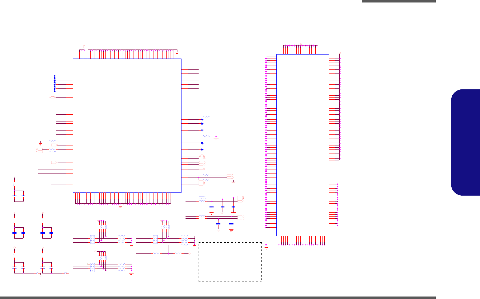
Schematic Diagrams
VN896-4 B - 9
B.Schematic Diagrams
VN896-4
Sheet 8 of 40
VN896-4
3.3VS
DU AL24
R 235 0_06
DVP 2D 0 2
VD08
FD[ 0:1:2: 3:8:9:1 1] R es er ve d
SW1_4 FD7 =>GFX Clock Se lec t( VCK/LCDCK/ECK)
C329
1 0 0 0P_ 50 V_ 0 6
DV P2 D0 4
VD14
DV P2 D0 3
3.3VS
DA CG ND
C2 8 3
1U _10V_06
BGA5E
P4M 90 0
T24
R24
AE14
AJ 10
AJ 12
AK10
AK11
AJ 11
AJ 23
AJ 2 0
AJ 1 9
AG36
AG33
AG31
AG30
AG 5
AG 4
AG 2
Y5
Y6
Y7
Y14
Y15
Y16
Y17
Y18
Y19
Y20
Y21
Y22
Y23
Y30
Y32
Y34
AA2
AA4
AA5
AA7
AA1 4
AA1 5
AA1 6
AA1 7
AA1 8
AA1 9
AA2 0
AA2 1
AA2 2
AA2 3
AA3 1
AA3 3
AA3 5
AB2
AB4
AB5
AB7
AB1 4
AB1 5
AB1 6
AB1 7
AB1 8
AB1 9
AB2 0
AB2 2
AB2 1
AC 2
AC 5
AC 6
AC 7
AC14
AC15
AC16
AC17
AC18
AC19
AC20
AC21
AC22
AC23
AD 2
AD 5
AD32
AE2
AE5
AE3 2
AE3 4
AF2
AF3
AF5
AB2 3
AJ 13
AJ 14
AK9
AK12
AK13
AK15
AL8
AL9
AL10
AL11
AL12
AL14
AM7
AM8
AM9
AM1 0
AM1 1
AG 3
Y36
N2 2
N23
N24
P24
M1 7
M18
M19
N18
N19
N2 0
N21
AJ 3 3
AK1 7
AK18
AK2 2
AK3 2
U2 4
V24
W24
Y24
AM1 2
AM1 3
AN19
AN17
AN 1 3
AN12
AM 3 6
AL 3 3
AL 2 4
AL22
AL 1 9
AL17
AL 1 6
AL 1 5
AK 36
AN35
AP2
AP16
AP22
AP24
AR16
AR23
AR35
AT4
AT17
AT20
AT22
AT23
AT11
AT14
AN8
AN9
AN10
AN11
AP8
AP9
AP10
AP11
AR7
AR8
AR9
AR10
AT7
AT8
AT9
AT10
AL3
AL7
AM2
AP3
AP6
AR2
AR6
AN7
AP7
AE16
AE18
AE20
AE21
AE22
VTT
VTT
VCC15
VCC15
VCC15
VCC15
VCC15
VCC15
GN D
GND
GND
GND
GND
GND
GND
GND
GND
GND
GND
GND
GND
GND
GND
GND
GND
GND
GND
GND
GND
GND
GND
GND
GND
GND
GND
GND
GND
GND
GND
GND
GND
GND
GND
GND
GND
GND
GND
GND
GND
GND
GND
GND
GND
GND
GND
GND
GND
GND
GND
GND
GND
GND
GND
GND
GND
GND
GND
GND
GND
GND
GND
GND
GND
GND
GND
GND
GND
GND
GND
GND
GND
GND
GND
GND
GND
GND
GND
GND
GND
VCC15
VCC15
VCC15
VCC15
VCC15
VCC15
VCC15
VCC15
VCC15
VCC15
VCC15
VCC15
VCC15
VCC15
VCC15
VCC15
VCC15
GND
GND
VTT
VTT
VT T
VTT
VTT
VT T
VTT
VTT
VT T
VTT
VTT
GND
GN D
GN D
GND
GN D
VTT
VTT
VTT
VTT
VCC15
VCC15
GN D
GN D
GND
GN D
GND
GND
GND
GN D
GND
GN D
GN D
GND
GND
GN D
GN D
GN D
GN D
GN D
GN D
GN D
GN D
GN D
GN D
GN D
GN D
GN D
GN D
GN D
VCC15
VCC15
VCC15
VCC15
VCC15
VCC15
VCC15
VCC15
VCC15
VCC15
VCC15
VCC15
VCC15
VCC15
VCC15
VCC15
GND
GN D
GN D
GN D
GN D
GN D
GN D
VCC15
VCC15
VCC15
VCC15
VCC15
VCC15
VCC15
DV P2 D0 7
L34 HC B1608K F-121T25_06
Z08 07
PC I_ INT A#15,19
VD13
D ISPCLKO
C288
2 2 P_ 50 V_ 0 6
DV P2 D0 9
AG
D ACG ND
RN4
1K _8 P 4 R _ 06
1
2
3
4 5
6
7
8
NB_ B L U E 2 4
SW 1_5 F D10 =>CPUCK/M CK Cl ock Se le ct
1. 5V S
AGP_BU SY # 17
L35 HC B1608K F-121T25_06
R 876 0_04
Z0816
R1 9 1 0 _ 04
DVP 2D 0 1
AR
VC CPLL2
VC CP LL 1
C2 6 5
1U _10V_06
0: F rom NB(D efault )
1: F rom External
D ACG ND
PD VP1 CL K
Z0803
L36 HC B1608K F-121T25_06
NB_L VD SDA TA 24
VD11
VC CPLL3
P4M 9 00
H1 1
D1 0
C1 1
C1 0
E10
G1 0
F11
C9
E8
B7
F9
C7
C6
A5
B9
D9
A9
E11
B10
C8
G1 3
A7
E13
A13
A12
A16
A15
A14
B16
B15
B14
B13
B12
C14
D14
E14
E12
F12
H1 2
G1 2
A11
B11
AC35
C13
H13
B8
A6
D12
N15
N16
N1 7
P21
P22
P35
U1 8
U19
U20
U2 1
U22
U2 3
U3 1
U33
V2
V5
V7
V14
V15
V16
V17
V18
V19
V20
V22
V21
V23
V30
V35
W2
W5
W7
W14
W15
W16
W17
W18
W19
W20
W21
W22
W23
Y2
R5
R6
R7
R14
R1 5
R1 6
R17
R1 8
R19
R20
R2 1
R2 3
R3 0
R31
T2
T4
T5
T7
T14
T15
T16
T17
T18
T19
T20
T21
T22
T23
T34
T36
U2
U5
U7
U1 4
U15
U1 6
U17
R2
R4
P23
R22
P33
AM 1
AM 3
AT5
AM 6
AL2
AL1
AN 6
AT6
AM 4
D1 3
F13
C12
D VP2D 00
D VP2D 01
D VP2D 02
D VP2D 03
D VP2D 04
D VP2D 05
D VP2D 06
D VP2D 07
D VP2D 08
D VP2D 09
D VP2D 10
D VP2D 11
DV PDET
D VP0 VS
D VP2CLK
DV P2 DE
D VP2DET
DV P2 HS
D VP2 VS
SPCLK1
SPCLK2
SPD1
SPD2
VC CA3 3 D AC1
VC CA3 3 D AC2
VC CA33PLL1
VC CA33PLL2
VC CA33PLL3
GN D APLL
GN D APLL
GN D APLL
GNDADAC
GNDADAC
AR
AG
AB
HS YN C
VSY NC
D ISPC LKO
DISP CL K I
ENB LT
EN VD D
BU SY#
RS ET
IN TA #
GP O0
GP OU T
XIN
VCC 33G F X
VC C3 3 G F X
VCC 3 3 GFX
GND
GN D
GN D
GND
GN D
GND
GN D
GND
GND
GN D
GND
GN D
GN D
GND
GN D
GND
GND
GN D
GND
GN D
GN D
GN D
GND
GND
GND
GN D
GND
GN D
GND
GND
GN D
GND
GN D
GN D
GND
GN D
GND
GND
GN D
GND
GN D
GND
GN D
GND
GND
GN D
GND
GN D
GN D
GND
GN D
GND
GN D
GND
GN D
GN D
GND
GN D
GND
GND
GN D
GND
GN D
GND
GND
GN D
GND
GN D
GN D
GND
GN D
GND
GND
GN D
GND
GN D
GN D
GND
GND
GN D
GND
GND
VD 08
VD 09
VD 10
VD 11
VD 12
VD 13
VD 14
VD 15
VPAR
GN D
GN D
GND
DVP 2D 1 1
VD10
VSY NC
GUIC K2
R1 9 0 0 _ 04
0 : R e fe r In te rn a l PL L(D e fa u lt)
1: F rom External
0: Two 12-bit DVI interf ace
1: O ne 24-bit Panel
in te rfac e
PD VP1DE
FB7
H CB2012KF-121T30_08
R 217 * 1K_04
DISP CLKO 2 4
PD VP1HS
VSYNC
GN D P LL
FB5
H CB2012KF-121T30_08
Z0801
DV P2 D0 0
AB
AB
Z08 09
VC CD AC 1
GNDPLL
RN2
*1K_8P4R _06
1
2
3
4 5
6
7
8
R 875 0_04
SW 1_2 F D5 = >De dic ate d DV I P or t Co nf igu r atio n
NB_D DC _CLK 24
C332
1U _10V _06
RN5
10K _8P4R _06
1
2
3
4 5
6
7
8
NB_VS YN C 24
VC CD AC 1
DV P0VS
C276
1000P_50V_06
DVP 2D 0 9
C291
1 0 0 0P_ 50 V_ 0 6
GFX power up strapping setting:
VC CPLL1
C293
22P_50V_06
3.3VS
L_ BK LTEN 24
VC CP LL 3
Z0804
Z08 10
R2 0 0 0 _ 04
R221 0_04
HS YN C
DVP 2D 0 3
3. 3V S
NB_G REE N 24
Z08 08
C285
1000P_50V_06
SW 1_1 F D4 = >Po r t M ux ing
SW 1_3 F D6 = >De dic ate d DV I P or t Sel ect ion
S7 S1
2 1
DV P2 D1 0
D VP2 D 10
AR
D ISPCLKI
DVP 2D 0 5
HSYNC
3.3VS
1.05V S
GNDPLL
VD09
R206
80.6_1% _06
0: D isable
1: E nable
NB_L VD SCLK 24
DVP 2D 0 4
VC CD AC 2
C325
1U _10V _06
Z08 12
VC CD AC 2
3.3VS
Z08 11
DV P2 DE T
C 278
22P _50V_06
R1 9 3 0 _ 04
DV P2 D0 5
VD12
C271
22P _50V_06
DV P2 D1 1
R218 10K_04
DVP 2D 0 0
GND
GNDPLL
R 209 22_04
3.3VS
PD VP1VS
DVP 2D 0 8
Z0813
C289
1000P_50V_06
R1 9 2 0 _ 04
GNDPLL
R2 0 1 0 _ 04
C3 2 6
22P_50V_06
FB8
H CB2012KF-121T30_08
RN7
10K _8P4R _06
1
2
3
4 5
6
7
8
RN6
10K _8P4R _06
1
2
3
4 5
6
7
8
VD15
FB6
H CB2012KF-121T30_08
R197 0_04
DV P2 D0 6
E NAVE E24
Z08 06
3.3VS
DACGND Z0814
L39 HC B1608K F-121T25_06
R1 9 8 0 _ 04
FB10
H CB2012KF-121T30_08
S9 S1
2 1
R199 *0_04
GND
Z08 05
NB_D DC _DATA 24
VP AR17
DVP 2D 0 6
R 210 4.7K_04
R 874 0_04
Z0802
L37 HC B1608K F-121T25_06
3.3VS
NB_H SYN C 24
AG
R196 0_04
DV P2 D0 2
NB_ R ED 24
GNDPLL
R194 0_04
DISP CLKI 2 4
DV P2 D0 1
DV P2 D0 8
RN3
1K _8 P 4 R _0 6
1
2
3
4 5
6
7
8
NB_EN AVD D 2 4
3.3VS
VC CP LL 2
R195 0_04
DVP 2D 0 7
Z0815
0: TM DS
1: TV
E ncoder
Z0817
C2 8 6
1U _10V_06
DV PDE T
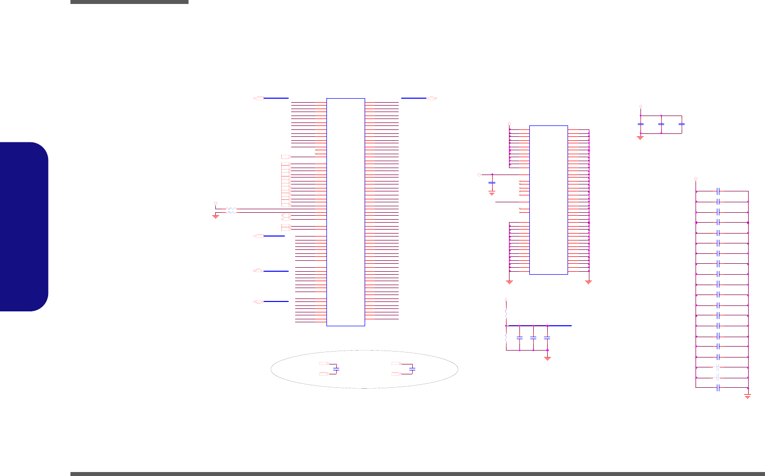
Schematic Diagrams
B - 10 DDR2-1
B.Schematic Diagrams
DDR2-1
Sheet 9 of 40
DDR2-1
M_CLK_DDR32
MD_[0:63]
MD_35
M AA5
M_BA0
C76 .1U _16V_06
M961011
M_CLK_DD R#32
MD_25
M_CS3#
M_DQS -6
C63 .1U _16V_06
M AA0
M_DQS +3
M_DQS +0
M AA3
1.8V
M_ R A S #6,10
SDR EFD
M_DQS -2
M AA13
M_ODT3
M_RAS#
M_CAS#
MD_30
M_DM3
MD_6
MD_56
MD_49
M_CLK_DDR22
MD_45
MD_38
MD_11
MD_3
C32 .1U _16V_04
+
C43
330U_6.3V _D
1 2
MD_13
M_DQS -0
M_DM2
C3 3
.1 U_ 1 6 V_ 04
M_CLK_DDR22
R72 10K_06
M_ DQ S + [0 ..7]6,10 M_DQS +2
MD_58
C65 .1U _16V_04
MD_33
M_DQS -4
R70
75_1% _06
M_ C K E 26,10
M_DM1
M_ D QS+ [0 ..7 ]
C78 .1U _16V_06
MD_51
C36 .1U _16V_04
C7 0
2.2U_6.3V _06
1.8V
MD _[0 :6 3 ] 6 , 1 0
DDRVRE F GE N. & DECOUP LI NG
3.3V S
MD_52
MD_5
C83 .1U _16V_04
MD_37
Z0902
M_DQS -1
1.8V
MD_59
M_DM7
C69
.1 U_ 5 0 V _ 06
M AA8
M_DM6
M_DQS -3
Trace Width 12 Mil
Space 20 Mil
M_ C A S #6,10
M_DM5
MD_16
M_CKE2
MD_17
M AA1
M_CLK_DDR#32
M_ C S 2 #6,10
Z0901
JD IMM 1B
C A0145-200N02
11 2
11 1
11 7
96
95
11 8
81
82
87
10 3
88
10 4
19 9
83
12 0
50
69
16 3
1
20 1
20 2
47
13 3
18 3
77
12
48
18 4
78
71
72
12 1
12 2
19 6
19 3
8
18
24
41
53
42
54
59
65
60
66
127
139
128
145
165
171
172
177
187
178
190
9
21
33
155
34
132
144
156
168
2
3
15
27
39
149
161
28
40
138
150
162
VD D1
VD D2
VD D3
VD D4
VD D5
VD D6
VD D7
VD D8
VD D9
VD D1 0
VD D1 1
VD D1 2
VD DSP D
NC1
NC2
NC3
NC4
NCTEST
VR EF
GND0
GND1
VS S1
VS S2
VS S3
VS S4
VS S5
VS S6
VS S7
VS S8
VS S9
VS S10
VS S11
VS S12
VS S13
VS S14
VS S15
VSS16
VSS17
VSS18
VSS19
VSS20
VSS21
VSS22
VSS23
VSS24
VSS25
VSS26
VSS27
VSS28
VSS29
VSS30
VSS31
VSS32
VSS33
VSS34
VSS35
VSS36
VSS37
VSS38
VSS39
VSS40
VSS41
VSS42
VSS43
VSS44
VSS45
VSS46
VSS47
VSS48
VSS49
VSS50
VSS51
VSS52
VSS53
VSS54
VSS55
VSS56
VSS57
M_ B A 06,10
M_ D QS-[0 ..7 ]
MD_50
M_DQS -7
MD_63
M_ D M[0 ..7 ]6,10
M_BA1
MD_26
M AA10
C48 10U_10V_08
M_ODT2
MD_48
1. 8 V
MD_62
MD_15
MD_4
C30 .1U _16V_06
M_ W E #6,10
MD_20
MD_31R65 10K_06
C67 .1U _16V_04
M AA6
M_ OD T 36,10
MD_34
JD I M M 1 A
CA0145-200N02
102
101
100
99
98
97
94
92
93
91
105
90
89
116
86
84
85
5
7
17
19
4
6
14
16
23
25
35
37
20
22
36
38
43
45
55
57
44
46
56
58
61
63
73
75
62
64
74
76
123
125
135
137
124
126
134
136
141
143
151
153
140
142
152
154
157
159
173
175
158
160
174
176
179
181
189
191
180
182
192
194
107
106
108
109
113
110
115
79
80
30
32
164
166
195
197
200
198
10
26
52
67
130
147
170
185
13
31
51
70
131
148
169
188
11
29
49
68
129
146
167
186
114
119
A0
A1
A2
A3
A4
A5
A6
A7
A8
A9
A10/AP
A1 1
A1 2
A1 3
A1 4
A1 5
A16_BA2
DQ0
DQ1
DQ2
DQ3
DQ4
DQ5
DQ6
DQ7
DQ8
DQ9
DQ10
DQ11
DQ12
DQ13
DQ14
DQ15
DQ16
DQ17
DQ18
DQ19
DQ20
DQ21
DQ22
DQ23
DQ24
DQ25
DQ26
DQ27
DQ28
DQ29
DQ30
DQ31
DQ32
DQ33
DQ34
DQ35
DQ36
DQ37
DQ38
DQ39
DQ40
DQ41
DQ42
DQ43
DQ44
DQ45
DQ46
DQ47
DQ48
DQ49
DQ50
DQ51
DQ52
DQ53
DQ54
DQ55
DQ56
DQ57
DQ58
DQ59
DQ60
DQ61
DQ62
DQ63
BA 0
BA 1
RAS#
WE#
CAS#
S0 #
S1 #
CKE0
CKE1
CK0
CK0#
CK1
CK1#
SD A
SC L
SA 1
SA 0
DM0
DM1
DM2
DM3
DM4
DM5
DM6
DM7
DQS0
DQS1
DQS2
DQS3
DQS4
DQS5
DQS6
DQS7
DQS0#
DQS1#
DQS2#
DQS3#
DQS4#
DQS5#
DQS6#
DQS7#
ODT0
ODT1
MD_23
M AA4
MD_46
MD_8
M_DQS +7
M AA7
MD_61
M_BA 26, 1 0
MD_36
M_ OD T 26,10
MD_47
MD_57
MD_10
MD_27
3.3VS
M_DQS +6
C8 7 7
*10P_50V_06
M_ C S 3 #6,10
M_CLK_DDR#22
MD_12
MD_29
MD_54
MD_7
MD_60
C72 10U_10V_08
M_DM4
MD_28
R71
75_1% _06
MD_19
C35 .1U _16V_04
MD_55
M_DQS -5
M_CKE3
MD_0
MD_39
MD_1
C29 10U_10V_08
C3 4
.1 U _1 6 V _ 0 4
MD_32
C68
.1 U_ 1 6V _0 4
M AA12
C77 .1U _16V_06
SM B_SBDATA2,10,11,16
M_DQS +4
M_CLK_DDR#22
M_DM0
C75 .1U _16V_06
MAA[0:13]6,10
C8 7 6
*10P_50V_06
M AA9
MD_44
C81 10U_10V_08
M_DM[0. .7]
M_ D QS-[0 ..7 ]6, 1 0
MD_24
MD_43
C49 10U_10V_08
M_DQS +1
MD_41
MD_14
MD_2
M_DQS +5
M_ C K E 36,10
MD_40
MD_53
MAA[0:13]
MD_21
M AA2
MD_22
M_WE#
M AA11
+
C44
* 330U_6.3V_D
1 2
SDR EFD
C7 1
2.2U_6.3V_06
MD_9
M_ B A 16,10
MD_18
C64 .1U _16V_06
MD_42
M_CS2#
SM B_ SBCL K2, 1 0 , 1 1, 16
M_CLK_DD R32
C66
.1 U_ 1 6V _0 4
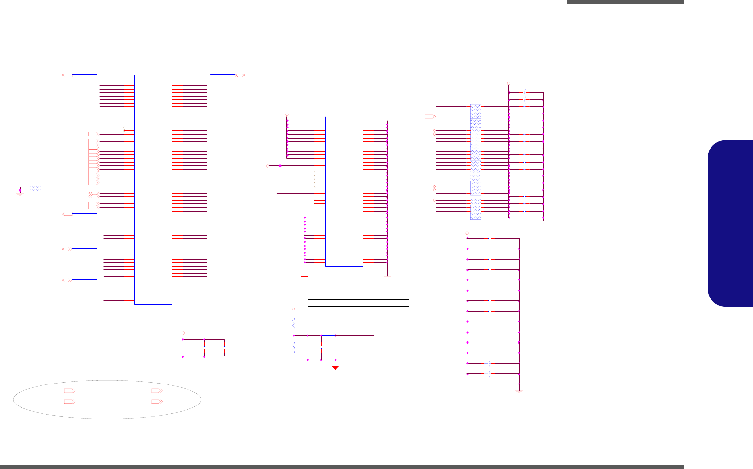
Schematic Diagrams
DDR2-2 B - 11
B.Schematic Diagrams
DDR2-2
M_ O D T 16
MA A 13
R103 47_04 C 51 .1U _16V_04
MD_28
MD_49
MD_50
M_BA 16,9
MA A 0
C87 .1U _16V_06
M _R AS#6,9
MD_6
MD_21 MA A 10
M_OD T0
M_ C S 1#
MD_54
S MB_ SBC L K
RP6 47_8P4R_0481
72
6
5
3
4
MD_36
SDREFC
M AA5
MD_40
MD_30
M_ BA26,9
MD_48
MD_37
MD_3
M_DQ S+3
MD_12
C 38 .1U _16V_04
C 40 .1U _16V_04
M AA1 1
MD_17
MA A 5
M AA1 3
C 84 .1U _16V_04
C102
.1U _16V_04
M_DM1
C79 10U_10V_08
M_ C KE2
SM B_SBC LK2,9,11, 16
M_ DQ S+ [0 ..7 ]
+
C31 *150U_4V_B
MD_20
M_WE#
M _D QS +[0 ..7 ]6,9
C 91 .1U _16V_04
MD_52
M_CAS#
M_C S1#6
RP5 47_8P4R_0481
72
6
5
3
4
M_C LK_DD R#02
M_ C KE1MD_25
MA A 1
M _C KE06
+
C4 7 1 50 U _4 V _ B
M_DM7
MA A 6
C103
.1U_16V_04
JD I M M 2 B
CA0115-200N02
112
111
117
96
95
118
81
82
87
103
88
104
199
83
120
50
69
163
1
201
202
47
133
183
77
12
48
184
78
71
72
121
122
196
193
8
18
24
41
53
42
54
59
65
60
66
12 7
13 9
12 8
14 5
16 5
17 1
17 2
17 7
18 7
17 8
19 0
9
21
33
15 5
34
13 2
14 4
15 6
16 8
2
3
15
27
39
14 9
16 1
28
40
13 8
15 0
16 2
VDD1
VDD2
VDD3
VDD4
VDD5
VDD6
VDD7
VDD8
VDD9
VDD10
VDD11
VDD12
VDDSPD
NC1
NC2
NC3
NC4
NCTES T
VREF
GND0
GND1
V SS1
V SS2
V SS3
V SS4
V SS5
V SS6
V SS7
V SS8
V SS9
V SS10
V SS11
V SS12
V SS13
V SS14
V SS15
VS S16
VS S17
VS S18
VS S19
VS S20
VS S21
VS S22
VS S23
VS S24
VS S25
VS S26
VS S27
VS S28
VS S29
VS S30
VS S31
VS S32
VS S33
VS S34
VS S35
VS S36
VS S37
VS S38
VS S39
VS S40
VS S41
VS S42
VS S43
VS S44
VS S45
VS S46
VS S47
VS S48
VS S49
VS S50
VS S51
VS S52
VS S53
VS S54
VS S55
VS S56
VS S57
M AA1
M_C LK_DD R12
M_CLK_DDR#02
MD_55
RP3 47_8P4R_048 1
7 2
6
5
3
4
M D_[0:63] 6, 9
M _ CL K _ DD R# 12
MD_31
M_ B A 1
M_BA0
M AA6
MD_15
MD_60
C 52 .1U _16V_04
RP4 47_8P4R_0481
72
6
5
3
4
C 85 .1U _16V_04
C80 10U_10V_08
M_ O D T 36,9
MD_41
C 37 .1U _16V_04
C 874
* 1 0P _5 0 V _ 0 6
0. 9V S
R78 47_04
M _ DM [0.. 7]6,9
MD_22
M_DQ S-1
MA A 2
M_DQ S-0
MD_51
MD_63
C 50 .1U _16V_04
MD_10
M_DQ S+2
R99 10K_06
C 54 .1U _16V_04
C99 .1U _16V_06
M_ C S 2#
SMB _SB DATA2,9,11,16
M_DQ S+1
MA A 7
+
C88
*330U _6.3V_D
1 2
MD_58
MD_27
M_ C S 3#
M_CS1#
C 42 .1U _16V_04
C104 .1U _16V_06
Z 1002
MD_46
M_ O D T 2
M_DM0
C 55 .1U _16V_04
M AA7
MD_14
MD_11
R670 47_04
R100 47_04
R104
75_1% _06
M_ C KE0
MA A 8
MA A 9
C96
.1U_16V_06
M_DM2
RP2 47_8P4R_048 1
7 2
6
5
3
4
M_ O D T 26,9
M AA2
M_BA1
MD_39
M_C S0#6
M_ C S 3 #6,9
M_DQ S-7
M_OD T1
M_ C KE26,9
M_ O D T 1
MD_1
C8 2
.1U_16V_04
La yo ut N ot e: Pl ac e th es e Ca ps n ea r So -D im m0
1.8V
M_BA 06,9
M_CKE1
MD_24
C105 .1U _16V_06
MA A 3
+
C89
330U_6.3V_D
1 2
MD_42
M_RAS#
SD REF C
M_ O D T 3
M961011
M AA4
M_ C S 0#
M_DQ S+5
1.8V
MD_8
MD_32
MA A 4
C73 10U_10V_08
M AA1 2
MD_13
MD_43
MD_18
M_DQ S-3
R106 47_04
JDIM M2A
CA 0115-200N 02
102
101
100
99
98
97
94
92
93
91
105
90
89
116
86
84
85
5
7
17
19
4
6
14
16
23
25
35
37
20
22
36
38
43
45
55
57
44
46
56
58
61
63
73
75
62
64
74
76
123
125
135
137
124
126
134
136
141
143
151
153
140
142
152
154
157
159
173
175
158
160
174
176
179
181
189
191
180
182
192
194
107
106
108
109
113
110
115
79
80
30
32
164
166
195
197
200
198
10
26
52
67
130
147
170
185
13
31
51
70
131
148
169
188
11
29
49
68
129
146
167
186
114
119
A0
A1
A2
A3
A4
A5
A6
A7
A8
A9
A10/ AP
A11
A12
A13
A14
A15
A1 6_ BA 2
DQ 0
DQ 1
DQ 2
DQ 3
DQ 4
DQ 5
DQ 6
DQ 7
DQ 8
DQ 9
DQ 1 0
DQ 1 1
DQ 1 2
DQ 1 3
DQ 1 4
DQ 1 5
DQ 1 6
DQ 1 7
DQ 1 8
DQ 1 9
DQ 2 0
DQ 2 1
DQ 2 2
DQ 2 3
DQ 2 4
DQ 2 5
DQ 2 6
DQ 2 7
DQ 2 8
DQ 2 9
DQ 3 0
DQ 3 1
DQ 3 2
DQ 3 3
DQ 3 4
DQ 3 5
DQ 3 6
DQ 3 7
DQ 3 8
DQ 3 9
DQ 4 0
DQ 4 1
DQ 4 2
DQ 4 3
DQ 4 4
DQ 4 5
DQ 4 6
DQ 4 7
DQ 4 8
DQ 4 9
DQ 5 0
DQ 5 1
DQ 5 2
DQ 5 3
DQ 5 4
DQ 5 5
DQ 5 6
DQ 5 7
DQ 5 8
DQ 5 9
DQ 6 0
DQ 6 1
DQ 6 2
DQ 6 3
BA0
BA1
RAS #
WE#
CAS #
S0#
S1#
CKE 0
CKE 1
CK0
CK0 #
CK1
CK1 #
SDA
SCL
SA1
SA0
DM 0
DM 1
DM 2
DM 3
DM 4
DM 5
DM 6
DM 7
DQ S0
DQ S1
DQ S2
DQ S3
DQ S4
DQ S5
DQ S6
DQ S7
DQ S 0 #
DQ S 1 #
DQ S 2 #
DQ S 3 #
DQ S 4 #
DQ S 5 #
DQ S 6 #
DQ S 7 #
OD T 0
OD T 1
R101 47_04
C875
* 1 0 P _ 5 0V _0 6
MAA[ 0:13 ]6,9
MD_44
M_CS0#
S MB_ SBD ATA
C 41 .1U _16V_04
MD_2
M_DM5
M AA[0:1 3]
C93 10U_10V_08
C591
.1U_16V_06
R107 47_04
3.3VS
MD_33
R105
75_1% _06
C97
2.2U _6.3V_06
MD_35
M_W E#6,9
M_ C AS#
M_BA2
M_ B A 2
C 92 .1U _16V_04
Trace Width 12 Mil
Space 20 Mil
MD_23
M_ B A 0
MD_34
M AA3
M_D M[ 0..7]
MD_16
M_C LK_DD R02
M_C LK_DD R#12
M_CLK_DDR02
MA A 11
DDRVRE F GEN. & DECOUPLING
1.8V
M _C AS#6,9
M _ DQ S-[0 ..7 ]6, 9
MD_56
R102 47_04
MD_61
RP1 47_8P4R_048 1
7 2
6
5
3
4M_ R AS#
M _C KE16
M_DM4
M _ CL K _ DD R12
R97 10K_06
MD_59
M_DQ S+0
C90 10U_10V_08
M_ C KE3
M_ W E #
MD_38
M_ C KE36,9
MD_45
MD_19
M_DQ S-5
M_ O D T 0
MA A 12
M_CKE0
C 56 .1U _16V_04
C 53 .1U _16V_04
Z 1001
MD_57
M_DQ S+4
MD_26
C74 .1U _16V_06
M_ DQ S-[0 ..7 ]
M_DQ S+7
C101 .1U _16V_06
MD_4
M AA1 0
M_DM6
M_DQ S-2
M_DM3
M_DQ S+6
MD_0M AA0
M D _ [ 0: 63 ]
MD_5
C 39 .1U _16V_04
MD_53
1.8V
M_ C S 2 #6,9
M_ O D T 06
MD_9
MD_29
MD_47
MD_7
C95 .1U _16V_06
M_DQ S-6
MD_62
C9 8
2.2U_6.3V_06
M_DQ S-4
M AA9
M AA8
C100 .1U _16V_06
Sheet 10 of 40
DDR2-2
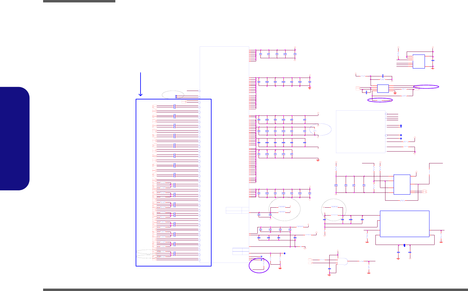
Schematic Diagrams
B - 12 VGA G72M-1
B.Schematic Diagrams
VGA G72M-1
Sheet 11 of 40
VGA G72M-1
VGA_3 .3VS
C2 45
.47U_10V_04
PE 0 TX 87
PEX_RX13 #
Z1101
C23 5
. 47 U _1 0V _0 4
BATT SM BUS->VGA
THERM SM BUS
PEX_RX12
C310 .1U_10V_04
PE 0 R X1 47
BUFRST
R 5 16 * 2 2_0 4
R 1 62 10 K_ 04
C24 4
. 47 U _1 0V _0 4
C2 51
.01U_50V_06
R47 6
4. 7 _0 6
C339 .1U_10V_04
HS AND VS SWAP
F/09/27/07
PE 0 TX 1#7
SSOUT
C60 9
. 1U _ 50 V_ 06
C350 .1U_10V_04
C338 .1U_10V_04
1. 2V S
DVP1 D0924
PEX_RX4#
R 5 29 * 2 2_0 4
1. 2V S
ROM_S CK
PEX_RX12 #
C304 .1U_10V_04
7/ 12 MISC2
BG A 4 D
PBG A53 3- 08MM
COMMON
GND
TE ST M ODE
SWAPRDY
STEREO
BUFRST
I2C H _SD A
I2CH_SCL
ROM_SCLK
ROM_S O
ROM_ SI
ROM_CS
AC8
D7
A7
F7
A6
B7
C7
D2
D3
F3
D1
C23 2
. 1U _ 50 V_ 06
VGA_ SCLK 23
C2 52
1 U _1 0V _0 6
R4 77
10K_04
C336 .1U_10V_04
C300 .1U_10V_04
PE 0 R X57
PEX_RX6
ROMCS#
S1 5
S1
2 1
DVP1 DE24
ROM_ SC K
R 5 19 * 2 2_0 4
R 5 13 * 2 2_0 4
C302 .1U_10V_04
PE 0 R X97
PE 0 TX 07
PEX_RX7
ROM_ SI
PE 0 TX 97
PE 0 TX 10#7
Z1 11 5
I2CH_ SCL
C3 28
.1U_50V_06
C5 21
4.7U_6.3V_06
C51 9
. 1U _ 50 V_ 06
R15 9
* 1 0K _0 6
1.0VS
VGA_THERMDC12
DVP1 D0824
C23 1
1U_10V_06
PE 0 R X1 #7
C2 06
.1U_50V_06
PE 0 TX 4#7
PE 0 TX 157
I2CH_ SDA
PE 0 TX 67
PE 0 TX 2#7
R8 73
0_ 06
R21 2
0_0 6
VGA_3 .3VS
DVP1 HS24
PEX_RX0#
PEX_RX14
Z1 11 3
C305 .1U_10V_04
PE 0 R X1 27
XTALOUTBUFF
VG A _ SC L K
Z1 10 9
R 6 72 0_ 04
PE 0 TX 11#7
PEX_RX15
C341 .1U_10V_04
L2 6 * H C B 16 08 K F- 1 21 T25 _0 61 2
U30
I C S 917 30 A M LF T
2
4
5
3 6
7
1
8
VDD
CL KOUT/FS _ IN0
REF OUT/F S_ IN1
GND S D A TA
SCLK
CL KIN
PD
PE 0 R X1 5#7
DVP1 CLK24
ROM_ SO
L407
H C B 16 08 KF - 12 1T 25 _0 6
1 2
PE 0 R X1 37
DVP1 D1124
DVP1 VS24
ROM_S O
R 4 08 0_ 06
U4
*AT25F512
4
87
1
3
5
2
6GND
VCCHOLD
CS
WP
SI
SO
SCK
ROMCS#
Z1 10 3
L3 2
H C B1 60 8K F - 121 T2 5_ 06
1 2
PE 0 R X67
PE 0 R X2 #7
Z1147
R 5 24 * 2 2_0 4
10 /12 X TAL _PLL
BGA4E
PBGA533-08M M
COMMON
XT AL _ S S_ IN
PLL GND
PLL VD D
XTAL_OUT
XTA L_O U T_B U F
XT AL _ I N
C1
H5
H4
C2
C3
B1
PE 0 R X8 #7
PE 0 R X7 #7
C2 36
.47U_10V_04
C19 7
. 47 U _1 0V _0 4
2.2K->* C960531
PE 0 R X1 4#7
BXTALOUT
ROM_S I
C25 3
.1U_ 50 V_ 06
PE 0 TX 12#7
PE 0 R X0 #7
PE 0 R X1 2#7
R729 0_06
Z1 10 2
VG A _ AL E R T# 1 2
C2 28
.01U_50V_06
NV46
G 72/ 73 NV4x
NV44
NV_PL LAVDD
1/ 12 PCI_E XP RESS
BG A 4 A
COMMON
PBG A5 3 3- 08MM
PEX_RX15
PEX_RX15
PEX_TX15
PEX_TX15
PEX_RX14
PEX_RX14
PEX_TX14
PEX_TX14
PEX_RX13
PEX_RX13
PEX_TX13
PEX_TX13
PEX_RX12
PEX_RX12
PEX_TX12
PEX_TX12
PEX_RX11
PEX_RX11
PEX_TX11
PEX_TX11
PEX_RX10
PEX_RX10
PEX_TX10
PEX_TX10
PEX_RX9
PEX_RX9
PEX_TX9
PEX_TX9
PEX_RX8
PEX_RX8
PEX_TX8
PEX_TX8
PEX_RX7
PEX_RX7
PEX_TX7
PEX_TX7
PEX_RX6
PEX_RX6
PEX_TX6
PEX_TX6
PEX_RX5
PEX_RX5
PEX_TX5
PEX_TX5
PEX_RX4
PEX_RX4
PEX_TX4
PEX_TX4
PEX_RX3
PEX_RX3
PEX_TX3
PEX_TX3
PEX_RX2
PEX_RX2
PEX_TX2
PEX_TX2
PEX_RX1
PEX_RX1
PEX_TX1
PEX_TX1
PEX_RX0
PEX_RX0
PEX_TX0
PEX_TX0
PEX_REFCLK
PEX_REFCLK
P EX _TS TC LK _OUT
P EX _TS TC LK _OUT
PEX_RST
NC
NC
NC
SP DIF NC
PE X_ PL LG N D
PEX _P LLD VD D
PE X_P L L A VD D
VD D
VDD33
VDD33
VDD33
VDD33
VDD33
VDD33
VD D _LP
VD D _LP
VD D _LP
VD D _LP
VD D
VD D
VD D
VD D
VD D
VD D
VD D
VD D
VD D
VD D
VD D
VD D
VD D
VD D
VD D
VD D
VD D
VD D
VD D
VD D
VD D
VD D
VD D
VD D
VD D
VD D
VD D
VD D
VD D
VD D
VD D
VD D
VD D
VD D
VD D
PE X_ IOVDDQ
PE X_ IOVDDQ
PE X_ IOVDDQ
PE X_ IOVDDQ
PE X_ IOVDDQ
PE X_ IOVDDQ
PE X_ IOVDDQ
PE X_ IOVDDQ
PE X_ IOVDDQ
PE X_ IOVDDQ
PE X_ IOVDDQ
PE X_ IOVDDQ
PE X_ IOVDDQ
PE X_ IOVDDQ
PE X_ IOVDDQ
PE X_ IOVDDQ
PE X_ IOVDDQ
PE X_ IOVDDQ
PE X_ IOVDDQ
PE X_ I O VD D
PE X_ I O VD D
PE X_ I O VD D
PE X_ I O VD D
PE X_ I O VD D
PE X_ I O VD D
PE X_ I O VD D
PE X_ I O VD D
AF 27
AG26
AD24
AE 24
AG25
AG24
AE 25
AF 25
AF 23
AF 22
AD23
AD22
AG22
AG21
AE 22
AE 21
AF 20
AF 19
AD21
AC21
AG19
AG18
AE 19
AE 18
AF 17
AF 16
AD18
AC18
AG16
AG15
AE 16
AE 15
AG13
AG12
AD15
AC15
AF 11
AF 10
AC13
AD13
AG10
AG 9
AE 13
AE 12
AF8
AF7
AC10
AD10
AG 7
AG 6
AE 10
AE9
AF5
AF4
AC 7
AD 7
AG 4
AG 3
AE7
AE6
AG 2
AF1
AD 6
AD 5
AE4
AE3
AF 14
AF 13
AC 6
C1 3
F12
E12
D1 2
AA6
AA5
Y6
N9
J1 6
J1 5
F14
J1 3
F13
J1 2
W12
W11
W10
W9
T1 7
R1 7
N1 7
M1 7
W16
U1 6
T1 6
M1 6
L1 6
W15
U1 5
T1 5
M1 5
L1 5
T1 4
M1 4
W13
U1 3
T1 3
M1 3
L1 3
U1 2
T1 2
M1 2
L1 2
T1 1
R1 1
N1 1
M1 1
J1 1
J1 0
T9
R9
M9
J9
AC20
AC19
AB19
AB18
AC17
AB17
AC16
AB16
AB13
AC12
AB12
AC11
AC9
AB9
AB8
AB7
AB6
AB5
AA4
AB21
AB20
W18
W17
AB15
AB14
AB11
AB10
C23 9
. 1U _ 50V _ 06
PE 0 R X1 3#7
PE 0 R X77
GPO016
PE 0 R X3 #7
PE 0 TX 5#7
PE 0 TX 15#7
PE 0 R X1 0#7
PEX_RX8#
C303 .1U_10V_04
U3
AD M 1 03 2A R M
8
7
6
54
3
2
1SCLK
SD A T A
AL ER T #
GNDTH E R M #
D-
D+
VDD
R 730 1 00K _ 04
VGA_THERMDA12
DVP1 D0424
C5 96
.1U_50V_06
C1 96
.47U_10V_04
C18 2
. 47 U _1 0V _0 4
PE 0 TX 17
PEX_RST
R1 37
10K_06
1.2VS
C36 8
.1U_ 50 V_ 06
C1 93
.4 7U _ 10 V_ 04
R 5 14 * 2 2_0 4
G72 M-V/NB8M
SRU DEL->R ADD->C
SR DEL->C ADD->R
PE 0 R X1 57
VGA_PEXCLK2
C61 3
1U_10V_06
PE 0 R X5 #7
PEX_RX14 #
C345 .1U_10V_04
U6
7 4A HC1G0 8GW
2
14
3
5
SMB_SBCLK 2,9,10,16
PEX_PLL GND
R 5 31 * 2 2_0 4
R119 *2.2K_04
DVP1 D0524
PE 0 R X37
Z1112
+
C8 66
3 30U _ 2. 5 V_ D
12
C1 40
.1U_50V_06
C1 85
.1 U _5 0V _0 6
VG A _ 3. 3V S
R1 46
22_04
PE 0 TX 27
SMB_SBDATA 2,9,1 0,16
PE 0 TX 77
PEX_RX6#
VG A _ SD A T A
C21 2
1U_10V_06
C6 15
.1U_50V_06
PE 0 TX 47
PE 0 R X17
Z1111
PEX_RX13
Z1110
PEX_RX3#
C6 04
.1U_50V_06
1. 2V S
PE 0 TX 117
PE 0 R X6 #7R14 7
22 _04
R 4 89 10 K_ 04
C 631
4. 7U _ 6. 3 V_ 06
TP->VGA_SCLK C960531
PEX_RX8
R 5 15 * 2 2_0 4
for NB8M
PE 0 R X1 17
C3 31
1U _1 0V _ 06
PEX_RST
R 5 20 * 2 2_0 4
R20 8
10 K _0 6
C348 .1U_10V_04
R 5 30 * 2 2_0 4
C6 07
.1U_50V_06
VG A _ 3. 3V S
Z1 10 8
C59 8
47 0P _5 0V _ 04
C5 20
.1U_50V_06
PE 0 TX 6#7
PE 0 TX 127
PEX_RX2
PEX_RX3
PE 0 TX 7#7
PEX_RX11 #
R 5 23 * 2 2_0 4
S6 S1
21
SSO UT
C335 .1U_10V_04
C19 2
. 47 U _1 0V _0 4
G72 M-V/NB8M
SWAPRDY _A
PEX_RX10
Z1148
C2 54
4.7U_6.3V_06
PE 0 TX 8#7
C337 .1U_10V_04
PE 0 TX 37
C24 2
1U _10 V _0 6
C240
4. 7U _ 6. 3 V_ 06
R 5 12 * 2 2_0 4
SS_VDD
Z1116
C6 25
.1U_50V_06
C5 93
.1U_50V_06
PE 0 TX 14#7
PEX_RX4
L31
* H C B 16 08 K F- 1 21T 25 _0 6
1 2
C347 .1U_10V_04
1. 2V S
PEX_RX2#
R 6 49 * 0 _04
PEX_RX9#
C3 23
.1 U_5 0V _0 6
C2 38
. 0 1U _ 50V _ 06
C21 5
. 47 U _1 0V _0 4
C311 .1U_10V_04
PE 0 TX 9#7
PEX_RX15 #
L30
H C B 16 08 KF - 12 1T 25 _0 6
1 2
C301 .1U_10V_04
C18 6
. 1U _ 50 V_ 06
C306 .1U_10V_04
C346 .1U_10V_04
for G7 2MV
PE 0 R X07
R121 *47_04
C309 .1U_10V_04
C18 8
4. 7 U _6 . 3V _0 6
for G72MV
1.2VS
PE 0 TX 137
PEX_RX9
PEX_RX1#
R47 8
10 K_ 04
Y3
27 M H Z
1 2
NV sug ges tio n 4 /20
VGA_PEXCLK#2
PEX_RX11
VG A _ SC L K
C343 .1U_10V_04
C6 23
.1U_50V_06
2. 5V S
Z1107->I2CS_SCL
C960604
R 5 21 * 2 2_0 4
C3 80
1 U _1 0V _0 6
C20 1
. 47 U _1 0V _0 4
C307 .1U_10V_04
C6 28
18P_50V_04
VG A _ 3. 3V S
PE 0 TX 0#7
Z1146
C308 .1U_10V_04
DVP1 D0324
PE 0 TX 13#7
C344 .1U_10V_04
R 5 17 * 2 2_0 4
STEREO
C6 18
.1U_50V_06
PE 0 R X1 1#7
DVP1 D0124
PEX_RX7#
BXTALOUT
for NB8M
GND
C1 84
1 U _1 0V _0 6
V G A_ S D AT A 1 2, 2 3
VGAPL LGND
C61 6
. 1U _ 50 V_ 06
C349 .1U_10V_04
75OHM
C6 22
.1U_50V_06
L4 05 H C B 16 08 KF - 12 1T 25 _0 61 2
PE 0 R X27
C1 19
2200P_50V_06
C340 .1U_10V_04
R 5 32 * 2 2_0 4
PE 0 R X4 #7
PE 0 TX 147
C20 9
4. 7U _ 6. 3 V_ 06
VG A _ 3 . 3 V S
DVP1 D1024
PL T_ R ST #15,26
Z 111 4
C2 43
4.7U_6.3V_06
R4 85
*0 _0 6
PE 0 R X1 07
C2 37
1 U _1 0V _0 6
C1 78
.1U_50V_06
C299 .1U_10V_04
PE 0 R X47
PE 0 TX 57
DVP1 D0624
DVP1 D0024
PEX_RX0
PEX_RX10 #
DVP1 D0224
C296 .1U_10V_04 Z1 10 5
Z1 10 6
SS_REF
R 5 22 * 2 2_0 4
C36 0
. 1U _ 50 V_ 06
3. 3 V
C59 7
4. 7 U _6 .3V_06
R65 0
*60_06
C297 .1U_10V_04
PE 0 TX 107
PE 0 R X9 #7
SS_OUT
C2 14
.47U_10V_04
C21 3
. 1U _ 50 V_ 06
VGA_ 3.3VS
PEX_RX1
C806 1 0U_ 10V_ 08
VGA_3 .3VS
R48 2
75 _1% _0 4
1. 0V S
PEX_RX5
C342 .1U_10V_04
DVP1 D0724
C1 89
4700P_50V_04
VGA_3 .3VS
PE 0 R X87
PE 0 TX 3#7
C6 06
.1U_50V_06
C298 .1U_10V_04
I2CS_SCL
M960726
PEX_RX5#
C2 24
.47U_10V_04
C 629
18P _ 50 V_ 04
G7 2M-V /NB8M
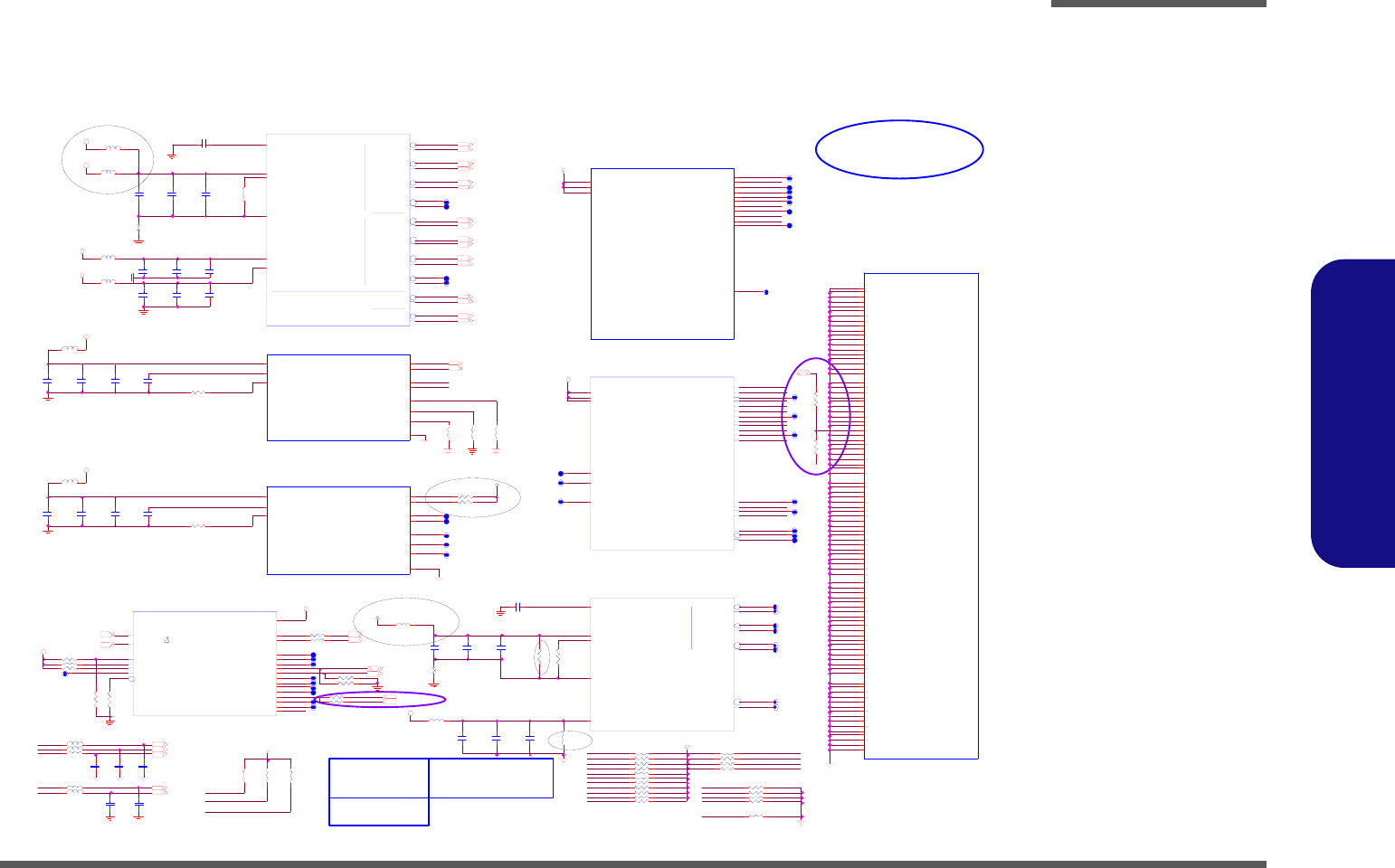
Schematic Diagrams
VGA G72M-2 B - 13
B.Schematic Diagrams
VGA G72M-2
Sheet 12 of 40
VGA G72M-2
3 GIO_PADCF G3
3/ 12 DAC_A
BGA4F
COMMON
PBGA5 3 3-08MM
DAC_A_RSE T
DAC_A_VREF
DAC_A_VDD
DAC_A_ IDUMP
DAC_A_BLUE
DAC_A_GREEN
DAC_A_RED
DAC_A_VSYNC
DAC_A_HSYNC
I2C A_S DA
I2C A _SC L
AD3
AB 4
AE 2
U9
AD2
AD1
AE1
AC4
AD4
E10
D1 0
R66 6 *10 K_04
Z1 29 7
LVDS-L0 P
K4 J553 23QG -BC1 4(8MX 32)( 700M hz)
K4 J523 24QE -BC1 4(16M X32) (700 Mhz)
V G A_ 3. 3V S
RAM_CF G1
C63 6
4. 7 U _6. 3 V_ 06
Z1 22 4
C218
47 00P _5 0V _0 4
VGA_3.3VS
L VD S - U 2N 24
VGA_ ENAVDD 24
I2CC_SCL
Z1 21 2
R766 10K_04
G72M-V/NB8M
Z1 29 5
Z1229
C12 0
22P_5 0V_06
G7 2M-V /NB 8 M
R64 6 2K_0 4
R1 23
2.2K_1%_04
AC_DET
Z1211
Z1 296
TP->VGA_SDATA
C960531
LVDS-L0 N
RAM_CF G3
L20 HCB1608KF-121T25_06
C6 42
4 70P _5 0V _0 4
R51 8
10 K _04
L VDS-LCLK N 24
VG R E E N
C63 4
4 7 0 0 P_ 5 0 V_ 04
L24 HCB1608KF-121T25_06
3GIO_ PA DC F G3
C12 1
22 P _50 V_ 06
Z1 288
PCI_DEVID3
C640
4. 7U _ 6. 3V _0 6
for G72MV
Z1275
L2 5
HCB1608KF-121T25_06
PXE_ MODE
Z1208
SUB_VENDOR
2. 5V S L VD S - L1N 24
VGA_ALERT# 1 1
L VDS-UCLKP 24
LVDS-UCLK N
C26 8
4. 7U _ 6. 3V _0 6
R66 7 *10 K_04
ADD EC_VGA_ALERT#
C960531
PCI_DEVID1
C641
47 00P _5 0V _0 4
I2CC_S DA 2 4
C63 7
4. 7U _ 6. 3V _ 06
3G I O _P AD C F G 2
SUB_V ENDOR
LVDS-L1 N
LVDS-U1P
R 8 72 * 0 _04
9/ 12 M IO_B
BGA4L
PBGA5 3 3 -08MM
COMMON
MIO _ B_ VR EF
MIO_B_ CAL_PU_GND
MIO_B_ CAL_PD_VDDQ
MIO_B_ VDDQ
MIO_B_ VDDQ
MIO_B_ VDDQ
MIO_B_CLKIN
MIO_B _C LKO UT
MIO_B _C LKO UT
MIO_B_C T L3
MIO_B_DE
MIO_B _H SYN C
MIO _B_V SYN C
MI O_B _D 11
MI O_B _D 10
MIO_B _D 9
MIO_B _D 8
MIO_B _D 7
MIO_B _D 6
MIO_B _D 5
MIO_B _D 4
MIO_B _D 3
MIO_B _D 2
MIO_B _D 1
MIO_B _D 0
J4
M3
J5
L6
K6
K5
R2
K3
K2
F2
G1
G4
F1
R3
N3
N2
N1
M1
M2
K1
K4
J1
J2
G3
G2
R66 3 10 K_ 04
R14 1
*150_04
VG A _ 3 . 3V S
E C _V G A _A LE R T# 2 3
VRED
R6 48
10K_1%_04
G7 2M-V/NB 8M
VGA_ 3.3V S
11/12 _G ND_
BG A4 C
COMMON
PBGA53 3 -08MM
GND
GND
GND
GND
GND
GND
GND
GND
GND
GND
GND
GND
GND
GND
GND
GND
GND
GND
GND
GND
GND
GND
GND
GND
GND
GND
GND
GND
GND
GND
GND
GND
GND
GND
GND
GND
GND
GND
GND
GND
GND
GND
GND
GND
GN
D
GND
GND
GND
GND
GND
GND
GND
GND
GND
GND
GND
GND
GND
GND
GND
GND
GND
GND
GND
GND
GND
GND
GND
GND
GND
GND
GND
GND
GND
GND
GND
GND
GND
GND
GND
GND
GND
GND
GND
GND
GND
GND
GND
GND
GND
GND
GND
GND
GND
AF 26
AC26
Y26
U26
P26
L26
H26
E26
B26
AF 24
AC23
Y23
U23
P23
L23
H23
E23
B23
AF 21
AD20
E20
B20
AD19
V19
P19
K19
AF 18
AD17
U17
P17
L17
E17
B17
AD16
R16
P16
N16
AF 15
R15
P15
N15
AD14
AC14
W14
U14
R14
P14
N14
L14
J14
E14
B14
R13
P13
N13
AF 12
AD12
R12
P12
N12
AD11
U11
P11
L11
F11
E11
B11
AF9
AD 9
V9
P9
K9
AD 8
E8
B8
AF6
H6
AC 5
Y5
U5
P5
L5
E5
B5
AF3
AF2
AC 2
Y2
U2
P2
L2
H2
E2
B2
V G A_ 3. 3V S
RAM_CF G3
L29
HCB16 08KF -121T25_06
R 67 7 2K _0 4
L VD S - U 0N 24
LVDS-U0P
C6 38
470P_50V_04
VR E D
4/ 12 DAC_B
BGA4G
PBGA5 3 3-08MM
COMMON
DAC_B_RSE T
DAC_B_VREF
DAC_B_VDD
DAC_B_ IDUMP
DAC_B_BLUE
DAC_B_GREEN
DAC_B_RED
DAC_B_VSYNC
DAC_B_HSYNC
I2C B_S DA
I2C B _SC L
D6
E7
F8
L9
D5
E4
F4
F5
E6
F10
F9
VGA_ 3.3V S
V_HSY
I2CC_SDA
RAM_CF G0
C16 6
4. 7U _ 6. 3V _0 6
R 8 71 0 _04
R 14 4 33 _1 %_0 4
G72 M-V/NB8M
Z1 225
R69 0 *2K_ 04
G7 2M-V /NB 8 M
C635
470P_50V_04
1. 8V S
VGA_G 24
VGA_ THERMDC11
V_ VS Y
Z1 20 4
Z1209
C2 70
470P_50V_04
3G I O _P AD C F G 0
S4
S1
2 1
M660SR AL L DEL
AC_DET
Z1282
RAM_CF G2
L28
* H C B1 608 K F- 12 1T 25_ 06
Z1 289
Z1 20 2
Z1 26 1
G72M-V/NB8M
Z1 292
C 22 3 . 01 U _1 6V _04
for NB8M
1. 8V S
Z1 26 3
Z1280
VGA_ 3.3VS
L VD S - L1P 24
LVDS-U2P 24
R67 5 *2K_ 04
R 1 34 1 24_ 1%_ 04
PCI_DEVID4
8/ 12 M IO_A
BGA4J
PBGA5 3 3 -08MM
COMMON
MIO_A_ VDDQ
MIO_A_ VDDQ
MIO_A_ VDDQ
MIO_A _H SYN C
MI O_A _D 10
MIO_A _D 9
MIO_A _D 8
MIO_A _D 7
MIO_A _D 6
MIO_A _D 5
MIO_A _D 4
MIO_A _D 3
MIO_A _D 2
MIO_A _D 1
MIO_A _D 0
J6
G6
F6
C4
V4
G5
C6
P4
B6
B4
A4
D4
A3
B3
A2
Z1 217
R67 3 *2K_ 04
R76 8
10K _0 4
R67 6 2K _0 4
L3 3
HCB1608KF-121T25_06
G7 2M-V /NB 8 M
Z1 29 9
Z1 219
Z1 293
Z1249
VGA_ BKL TEN 2 4
Z1 25 8
R767 10K_04
R505
1K _1 % _0 4
R66 9 10 K_ 04
VGA_SDATA11,23
Z1 294
3G I O _P AD C F G 1
Z1272
VGA_R 24
LVDS-L2 N
Z1276
LVDS-L1 P
L VD S - L0N 24
Z1 25 5
Z1 290
R 7 71 * 2 K_ 04
PCI_DEVID1
PXE_ MODE
Z1 25 6
R647
27 0_0 4
C2 57
. 0 1U _1 6V _0 4
VG A _ A L ER T #
RAM_CF G0
Z1 20 5
Z1214->I2CS_SDA
C960604
R66 4 10 K_ 04
LVDS-U0N
Z1 220
LVDS-LCL KN
R64 4 10 K_ 04
Z1 25 4
Z1 26 4
R13 9
*150_04
Z1 22 6
Z1 25 7
C222
4. 7U _ 6. 3V _0 6
5/ 12 IFP_AB
B
B
A
A
CLOCK
DATA
BGA4H
COMMON
PBGA5 3 3-08MM
IF P_B _IO_V DD
IF P_A _IO_V DD
IFP_AB_PLL_GND
IFP_AB_RSET
IFP_AB_PLL_VDD
IFP_AB_VPROBE
IFP _B_T XC
IFP _B_T XC
IFP _A_T XC
IFP _A_T XC
IFP _B_T XD7
IFP _B_T XD7
IFP _B_T XD6
IFP _B_T XD6
IFP _B_T XD5
IFP _B_T XD5
IFP _B_T XD4
IFP _B_T XD4
IFP _A_T XD3
IFP _A_T XD3
IFP _A_T XD2
IFP _A_T XD2
IFP _A_T XD1
IFP _A_T XD1
IFP _A_T XD0
IFP _A_T XD0
Y4
W4
V6
U6
V5
N6
W5
W6
T4
U4
AB3
AB2
AB1
AA1
AA2
AA3
W3
W2
R6
P6
T5
T6
R5
R4
N4
N5
C1 79
. 0 1U _1 6V _0 4
RAM_CF G2
R 1 45 1 24_ 1%_ 04
C123
22 P_ 50 V_ 06
PCI_DEVID4
Z1265
VG A _ A L ER T #
R 7 72 * 2 K_ 04
???
Z1 20 1
RAM_CF G3
L21 HCB1608KF-121T25_06
Z1 26 2
Z1279
Z1285
Z1230
S5
S1
2 1
R1 74
1K_1%_04
VGA_ THERMDA11
3GIO_ PA DC F G2
R 7 69 * 2 K_ 04
Z1 20 7
Z1 20 6
PCI_DEVID0
NV suggestion 4/20
VGA_DDCDATA 2 4
Z1 287
LVDS-LCL KP
VG A _ 3 . 3V S
C63 9
47 00 P_ 50V _0 4
LVDS-L2 P
C2 17
4 70P _5 0V _0 4
3GIO_ PA DC F G0
R665 *10K_04
LVDS-U1N
NV suggestion 4/20
Z1 20 3
L VDS-LCLK P 2 4
LVDS-U1P 24
Z1284
RAM_CF G1
Z1238
C124
22 P_ 5 0 V_ 0 6
L VD S - L0P 24
RAM_CF G2
Z1 22 7
LOW from SYST EM B IOS
VBLUE
LVDS-UCLK P
R66 8 *10 K_04
PCI_DEVID3
R64 5 2K_0 4
R67 4 *2K_ 04
VGREEN
Z1 215
Z1271
Z1228
R 64 2 18 0_0 4
Z1283
VB L U E
C2 04
470P_50V_04
C17 3
47 00P _ 50V _0 4
R69 1 *2K_ 04
LVDS-U0P 24
Z1231
PCI_DEVID0
Z1 218
R 7 70 * 2 K_ 04
VGA_HSY 24
Z1234
V_VSY
R6 89
*0 _0 4
L52
HCB16 08KF -121T25_06
R64 3 10 K_ 04
G72M-V/NB8M
VGA_3 .3VS
C20 8 .01U_16V_04
I2CC_S CL 2 4
Z1244
R1 28
10K_04
1. 8V S
VGA_VSY 24
L VD S - L2P 24
Z1213
6/ 12 MISC1
BGA4K
PBG A533-08MM
COMMON
JTA G_T RST
JTA G_T DO
JTA G_T DI
JTA G_T M S
JTA G_T CK
TH ER M DP
TH ER M DN
GPI O12
GPI O11
GPI O10
GPI O9
GPI O8
GPI O7
GPI O6
GPI O5
GPI O4
GPI O3
GPI O2
GPI O1
GPI O0
I2CC_S DA
I2CC_S C L
5 V_C LAM P
AD25
AE26
AD27
AD26
AE27
B9
C9
B16
A15
B15
B13
A13
A12
B12
C12
C10
B10
A10
D9
A9
D8
E9
D11
L22 HCB1608KF-121T25_06
RAM_CF G1
Z1278
Z1 291
C26 9
47 00P _ 50V _0 4
R66 2 10 K_ 04
Z1274
LVDS-U2N
R694 *10K_04
C122
22 P_ 50 V_ 06
L VD S - L2N 24
C1 77
470P_50V_04
Z1 222
LVDS-U2P
Z1270
VGA_DDCCLK 24
Z1210
Z1250
Z1242
C19 4
4.7U_6.3V_06
R13 8
*15 0_ 04
R 14 3 33 _1 %_0 4
for NB8M
NO STUFF
L23 HCB1608KF-121T25_06
SAMS UNG 1 6M X 16- ->101 0
SAMS UNG 3 2M X 16- ->110 1
SAMS UNG 8M X 32- ->011 1
SAMS UNG 1 6M X 32- ->001 1
1. 8 VS
Z1 29 8
PCI_DEVID2
Z1248
3GIO_ PA DC F G1
R1 29
2. 2K _1 %_0 4
L VDS-UCLKN 2 4
L VD S - U 1N 24
C20 3
47 00P _ 50V _0 4
VGA_B 2 4
V_ H SY
Z1 22 3
L 51 * H C B 16 08 KF - 12 1_0 6
R8 70
0_04
L2 7
*HCB1608KF-121_06
L4 06
HCB1608KF-121T25_06
VGA_3 .3VS
PCI_DEVID2
MIO_ B_ DE
I2 CS_ SDA
RAM_CF G0
12/ 12 IFPC
DATA
CLOCK
BGA4I
COMMON
PBGA5 3 3 -08MM
IFPC_IO_VDD
IFPC_PLL _GND
IF PC_RSET
IF PC _ PL L _VD D
IFPC_VPROBE
IFP C_T XC
IFP C_T XC
IFPC_T XD2
IFPC_T XD2
IFPC_T XD1
IFPC_T XD1
IFPC_T XD0
IFPC_T XD0
L4
M6
J3
M4
M5
V1
W1
V2
V3
T3
T2
T1
R1
DEVI CE ID :G72 MV - ->011 1
NB 8M-G S - ->??? ??
NB 8M-S E - ->010 00
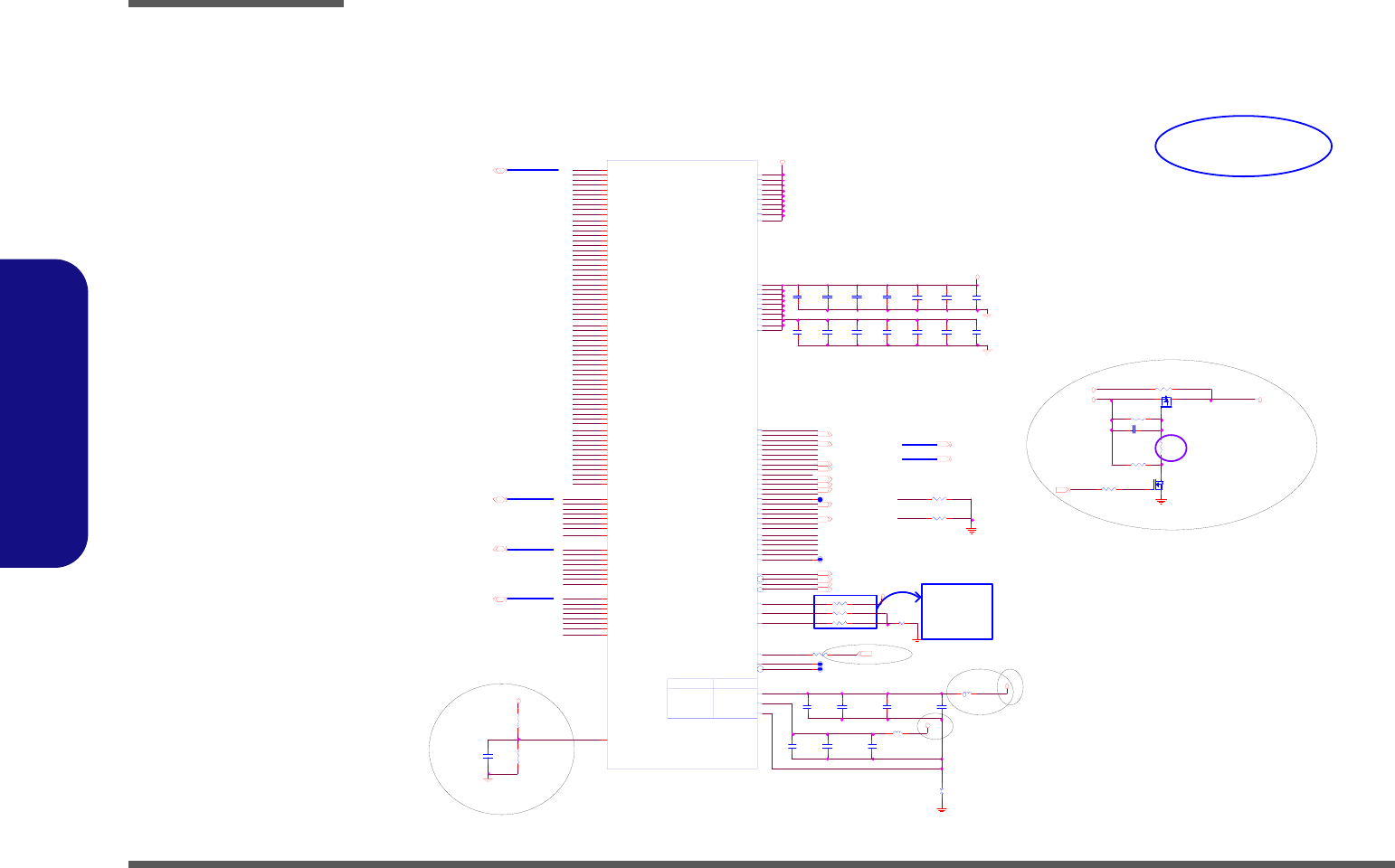
Schematic Diagrams
B - 14 VGA G72M-3
B.Schematic Diagrams
VGA G72M-3
Sheet 13 of 40
VGA G72M-3
FBA_ BA1 14
FBAD19
FBA_A11
FBA_ CLK0 1 4
FBAD38
C13 8
.1U_16V_04
C1 95
.1U_ 16 V _0 4
FBAD34
FBAD10
FBAD46
FBA_BA2_SC1# 14
R7 32
10K_04
1. 2 V S
FBA_A3
C16 5
4. 7 U _6 . 3V _ 06
FBB_A4
FBAD47
FBAD QS_W P2
FBAD13
FBB_A5
FBA_A[0 ..11 ]
FBAD49
Z1305
FBAD55
R753 0_04
FB ADQM[0 ..7]14
S14 S1
2 1
FBAD QS_RN3
R751 20K->22K
FOR VGA TIME
C960604
C1 99
.47U_10V_04
M660SR ALL DEL
FBA_ RST 14
Z130 4
FBAD QS_RN0
FBAD29
R136 40.2%_04
FBA_ BA0 14
FBAD58
1. 8 V S
FBA_A10
FBADQS_WP[0..7 ]
3. 3 V
SUSB#15,16,20,23,27,28,34
FBA_ CKE
FBAD15
R480 24.9_1%_04
FBAD17
FBAD44
FBA_ CLK1 1 4
FBADQM[0 ..7]
FBA_A2
FBAD QS_W P7
FBAD QM6
FBA_A6
FBA_C KE
NC
NV46
2/12 FRAME_BUFF ER
NV44
FB_ PLL GND
FB_ PLL AVDD
BGA4 B
COMMON
PBGA533- 08MM
FB_VREF
FB_DQS_ RN7
FB_DQS_ RN6
FB_DQS_ RN5
FB_DQS_ RN4
FB_DQS_ RN3
FB_DQS_ RN2
FB_DQS_ RN1
FB_DQS_ RN0
FB_DQS_ WP7
FB_DQS_ WP6
FB_DQS_ WP5
FB_DQS_ WP4
FB_DQS_ WP3
FB_DQS_ WP2
FB_DQS_ WP1
FB_DQS_ WP0
FB_DQM7
FB_DQM6
FB_DQM5
FB_DQM4
FB_DQM3
FB_DQM2
FB_DQM1
FB_DQM0
FB_DQ63
FB_DQ62
FB_DQ61
FB_DQ60
FB_DQ59
FB_DQ58
FB_DQ57
FB_DQ56
FB_DQ55
FB_DQ54
FB_DQ53
FB_DQ52
FB_DQ51
FB_DQ50
FB_DQ49
FB_DQ48
FB_DQ47
FB_DQ46
FB_DQ45
FB_DQ44
FB_DQ43
FB_DQ42
FB_DQ41
FB_DQ40
FB_DQ39
FB_DQ38
FB_DQ37
FB_DQ36
FB_DQ35
FB_DQ34
FB_DQ33
FB_DQ32
FB_DQ31
FB_DQ30
FB_DQ29
FB_DQ28
FB_DQ27
FB_DQ26
FB_DQ25
FB_DQ24
FB_DQ23
FB_DQ22
FB_DQ21
FB_DQ20
FB_DQ19
FB_DQ18
FB_DQ17
FB_DQ16
FB_DQ15
FB_DQ14
FB_DQ13
FB_DQ12
FB_DQ11
FB_DQ10
FB_DQ9
FB_DQ8
FB_DQ7
FB_DQ6
FB_DQ5
FB_DQ4
FB_DQ3
FB_DQ2
FB_DQ1
FB_DQ0
FB _P LLG N D
FB _PL LAV D D
F B_P LLV D D
FB _R EF C LK
FB _R EF C LK
FB _D EB U G
FB _C AL _ TE R M _G N D
F B_ C AL_P U _G N D
FB _C A L_PD _ VD D Q
F B _C LK1
F B _C LK1
F B _C LK0
F B _C LK0
F B_C M D 26
F B_C M D 25
F B_C M D 24
F B_C M D 23
F B_C M D 22
F B_C M D 21
F B_C M D 20
F B_C M D 19
F B_C M D 18
F B_C M D 17
F B_C M D 16
F B_C M D 15
F B_C M D 14
F B_C M D 13
F B_C M D 12
F B_C M D 11
F B_C M D 10
FB_ CMD9
FB_ CMD8
FB_ CMD7
FB_ CMD6
FB_ CMD5
FB_ CMD4
FB_ CMD3
FB_ CMD2
FB_ CMD1
FB_ CMD0
FB_ VDDQ
FB_ VDDQ
FB_ VDDQ
FB_ VDDQ
FB_ VDDQ
FB_ VDDQ
FB_ VDDQ
FB_ VDDQ
FB_ VDDQ
FB_ VDDQ
FB _V TT
FB _V TT
FB _V TT
FB _V TT
FB _V TT
FB _V TT
FB _V TT
FB _V TT
FB _V TT
FB _V TT
A16
W2 7
V23
W2 3
V26
B21
F21
E22
A22
W2 6
U2 4
W2 4
V25
C2 1
E21
D2 2
B22
V24
V22
W2 2
V27
A21
F20
F22
D2 1
W2 5
AA 2 5
AB 2 7
AB 2 6
AB 2 5
AA 2 6
AA 2 7
AA 2 4
P24
N2 3
T2 2
R2 2
R2 3
R2 4
T2 3
T2 4
AA 2 2
AA 2 3
AC22
AC24
AB 2 2
AB 2 4
Y24
AB 2 3
T2 6
T2 7
T2 5
R2 7
R2 6
R2 5
N2 5
N2 6
C1 8
C1 6
C1 9
D1 8
B19
A19
B18
A18
D1 9
D2 0
E18
E19
F18
D1 7
E16
D1 6
H2 4
G2 3
F24
J2 4
F23
E24
J2 3
G2 2
D2 3
B25
A25
C2 2
A24
B24
C2 4
A26
C1 5
D1 3
D1 4
M2 4
M2 3
K22
H2 2
E13
D1 5
N2 2
M2 2
K23
L24
N2 4
B27
G2 6
K27
F27
K24
K25
K26
D2 7
D2 6
M2 5
C2 6
M2 7
J26
G2 4
N2 7
D2 4
C2 5
C2 7
M2 6
J27
J25
G2 5
F25
F26
D2 5
G2 7
Y22
U2 2
P22
L22
J22
T19
M1 9
J19
F19
F17
W19
U1 9
R1 9
N1 9
L19
J18
J17
F16
F15
E15
F BB _ A[2..5] 1 4
Z131 0
FBCAL_TER M
FBAD45
FBAD28
FBAD9
FB 4
HCB2012KF-121T30_08
FBA_A7
FBAD52
FBAD[0..63]14
R75 1
22 K_ 1% _0 4
FBAD20
FBAD QS_W P0
R4 86 G 72- ->
N B8- -> 45 .3
R4 80 G 72- ->
N B8- -> 24 .9
R1 36 G 72- ->
N B8- -> 40 .2
FBA_ CLK1 # 14
FBAD8
FBAD1
FBA_A4
FBA_C LK0#
FBAD35
Z1309
FBA_ WE# 1 4
FBA_A5
FBAD QS_W P1
FBAD QS_RN7
C21 1
4. 7U _6 . 3V _0 6
C19 0
.1U_16V_04
for NB8M
1.8VS
FBA_RAS# 14
FBAD7
FBAD56
FBAD27
Q44
AO 34 09
G
DS
FBAD0
FBA_C LK1#
FBAD40
FBAD51
FBAD33
VREF = .4*VDD Q
FBCAL_PD
FBAD37
FBAD60
FBA_C LK0
GND
FBA_C LK1
FBAD12
FBA_ CS0# 1 4
FBAD3
FBAD23
FBAD30
4MS
FBAD61
FBA_A0
FBA_A9
FBAD41
GND
FBAD57
FBAD62
1. 2 V S
FBCAL_PU
FBAD QM1
FBAD2
FBAD32
FBAD5
FBAD54
FBAD42
FBAD QS_W P5
G72 M-V/ NB 8M
FBA_ RAS# 14
Z130 8
C 8 17 1 U _1 0V _ 06
FBB_A[2 ..5]
FBAD6
VG A_ 3 . 3 V S
FBA_C MD28
C17 6
47 0P _5 0 V_ 04
SUSB#
C6 27
* . 1 U _1 6V _ 04
3. 3 VS
FBADQS_RN[0..7 ]14
FBAD53
R486 45.3_1%_04
FBAD QS_RN2
FBAD QM7
FBAD18
C2 07
.47U_10V_04
C1 37
.1 U_1 6V _ 04
FBA_A1
FB1
HC B2012KF-121T30_08
FBAD4
FBAD63
Z1301
C13 4
.1U_16V_04
FBA_A12
C1 72
47 00 P _5 0V _ 04
S1
S1
2 1
FBADQS_RN[0..7]
FBA_A13
FBAD39
1.8VS
FBAD31
FBAD36
FBAD24
FBAD43
FBAD59
VGA_3.3VS
C1 35
.1 U_1 6V _ 04
FBAD QM2
FBA_C MD27
FBAD14
C15 5
47 0P _ 50 V _0 4
FBA_ CAS# 14
FBAD QS_W P4
Z1302
NV su ggestion 4/20
F BA _ A[0..11 ] 14
1.8VS
FBAD QM4
FBA_ CLK0 # 14
FBAD QS_RN5
FBAD QS_W P3
C23 0
4. 7U _6 . 3V _0 6
FBAD QM5
FBAD QM3
FBAD11
FBAD26
R48 7
*2.4K_1%_04
FBADQS_WP[0..7 ]14
Z131 1 C1 56
4.7U_6.3V_06
C1 83
. 4 7U _ 10 V _0 4
R 7 50 * 1 M _ 04
FBAD QM0
R752 100K_04
R48 8
* 1K _ 1% _0 4
Z1303
C1 91
. 4 7U _ 10 V _0 4
FBAD QS_RN6
FBA_ RST
FBB_A3
FBAD22
R1 68
10K_04
Q45
2N7002
G
DS
FBAD16
C1 39
.1U_ 16 V _0 4
C169
4.7U_6.3V_06
FBAD QS_RN4
R14 2 *0 _0 4
FBA_ CKE 1 4
C13 6
.1U_16V_04
C1 54
4700P_50V_04
FBAD25
R749 *0_06
F BAD [0..63 ]
FBAD48
FBAD21
FBAD QS_W P6
FBAD50
FBB_A2
FBA_A8
FBAD QS_RN1
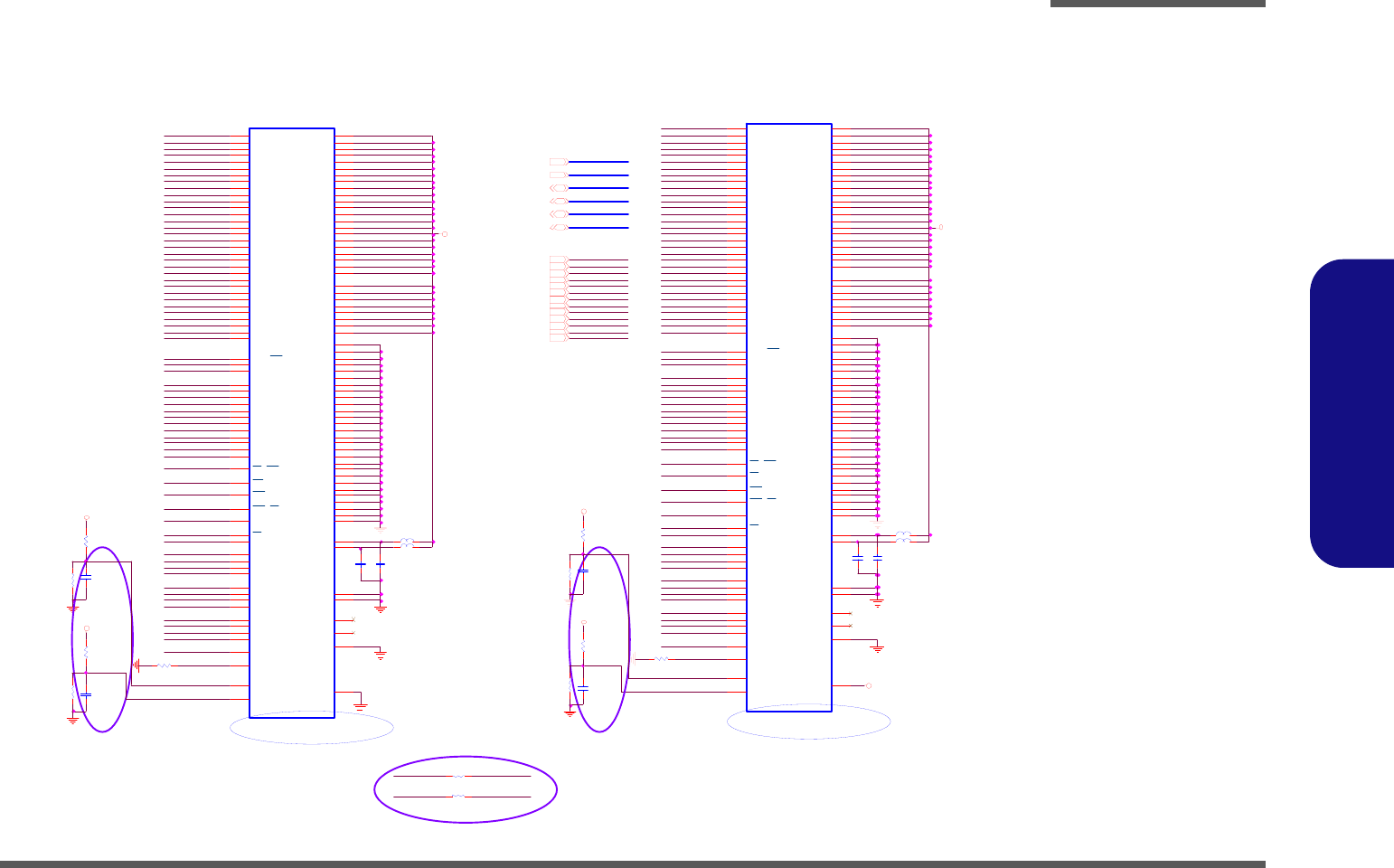
Schematic Diagrams
VGA G72M-4 B - 15
B.Schematic Diagrams
VGA G72M-4
Sheet 14 of 40
VGA G72M-4
F BAD 3 7
R742
2.4K_1%_04
Z1405
FBA_BA2_SC1#
F BAD 3 0
F BAD 4 4
LOW-->NORMAL
HIGH-->MIRROR
F BAD QS_WP5
R746 243_1%_04
FBA_A[0..11]
FB A_BA0
F BAD 5 5
R734
1K_1%_04
F BAD 6 2
.1U->.01U
FOR NV C960604
1.8VS
FB A_CLK1
F BA_A7
F BAD 1 3
F BAD 3 9
1.8VS
F BAD QS_RN1
F BAD 4 0
F BAD 3 6
F BA_WE#
F BAD QS_RN6
GND | VDD
U40
128MB
H1
E3
N3
N10
E10
T3
T2
R3
R2
M3
N2
L3
M2
T10
T11
R10
R11
M10
N11
L10
M11
G10
F11
F10
E11
C10
C11
B10
B11
G3
F2
F3
E2
C3
C2
B3
B2
G9
G4
L4
K2
M9
K11
L9
K10
H11
K9
M4
K4
H2
K3
V9
H3
H4
A4
F9
H12
F4
J11
J10
H9
A1
A12
C1
C4
C9
C12
E1
E4
E9
B1
B4
B9
B12
D1
D4
D9
D12
G2
G11
L2
L11
P1
P4
P9
P12
T1
T4
T9
T12
A3
A10
G1
G12
L1
L12
V3
V10
J2
J3
D3
D10
P10
P3
D2
D11
P11
P2
E12
J4
J9
N1
N4
N9
N12
A2
A11
F1
F12
M1
M12
V2
V11
H10
R1
R4
R9
R12
V1
V12
J1
J12
K1
K12
A9
V4
VR EF
DM0 | DM1
DM3 | DM2
DM2 | DM3
DM1 | DM0
DQ31 | DQ23
DQ30 | DQ22
DQ29 | DQ21
DQ28 | DQ20
DQ27 | DQ19
DQ26 | DQ18
DQ25 | DQ17
DQ24 | DQ16
DQ23 | DQ31
DQ22 | DQ30
DQ21 | DQ29
DQ20 | DQ28
DQ19 | DQ27
DQ18 | DQ26
DQ17 | DQ25
DQ16 | DQ24
DQ15 | DQ7
DQ14 | DQ6
DQ13 | DQ5
DQ12 | DQ4
DQ11 | DQ3
DQ10 | DQ2
DQ9 | DQ1
DQ8 | DQ0
DQ7 | DQ15
DQ6 | DQ14
DQ5 | DQ13
DQ4 | DQ12
DQ3 | DQ11
DQ2 | DQ10
DQ1 | DQ9
DQ0 | DQ8
BA1 | BA0
BA0 | BA1
A11 | A 7
A10 | A 8
A9 | A 3
A8/ AP | A10
A7 | A 11
A6 | A 2
A5 | A 1
A4 | A 0
A3 | A 9
A0 | A 4
A1 | A 5
A2 | A 6
R ESET
R AS | B A2
C KE | W E
ZQ
CS | CAS
VR EF# H 1 2
C AS | C S
CK
CK
WE | CKE
VD DQ
VDDQ#A12
VDDQ#C1
VDDQ#C4
VDDQ#C9
VD DQ#C12
VD DQ#E1
VD DQ#E4
VD DQ#E9
VSSQ
VSSQ # B4
VSSQ # B9
VSS Q#B12
V SSQ# D1
V SSQ# D4
V SSQ# D9
V SSQ # D12
V SSQ# G2
V SSQ # G11
VS SQ#L2
VS SQ#L11
VSSQ # P1
VSSQ # P4
VSSQ # P9
VSS Q#P12
VS SQ#T1
VS SQ#T4
VS SQ#T9
VS SQ#T12
VSS
V SS#A1 0
VSS #G1
VS S#G12
VSS# L 1
VSS #L12
VSS#V3
V SS#V1 0
RFU1
RFU2
RDQS0 | RDQS1
RDQS1 | RDQS0
RDQS2 | RDQS3
RDQS3 | RDQS2
WDQS0 | WDQS1
WDQS1 | WDQS0
WDQS2 | WDQS3
WDQS3 | WDQS2
VDDQ#E12
VDDQ
#J4
VDDQ#J9
VDDQ#N1
VDDQ#N4
VDDQ#N9
VD DQ#N12
VDD
VD D#A11
VDD#F1
VD D#F12
VD D # M1
VDD#M12
VDD#V2
VD D#V11
BA2 | RAS
VDDQ#R1
VDDQ#R4
VDDQ#R9
VD DQ#R12
VD DQ#V1
VDDQ#V12
VS SA
VSSA #J12
VDDA
VDDA#K12
MF
RFU0
R736
2.4K_1%_04
F BAD 9
1.8VS
F BA_A6
F BAD 3 5
Z1407
F BA_A8
F BAD QS_WP7
.1U->.01U
FOR NV C960604
FB A_RST
FB A_BA1
F BAD QS_WP1
F BA_A4
F BAD 5 3
F BAD QS_RN4
L408
HCB1608K F-121T25_06
F BAD QS_WP3
FB A_CLK0
FBADQM[0..7]13
F BA_ R ST
F BA_ C LK0 #
F BA_A9
FB A_RST13
Z1404
F BAD 1
F BAD 4 5
F BAD QS_RN7
F BAD 3 8
F BAD 7
F BAD 1 6
R740 243_1%_04
F BA_A0
R745 243_1%_04
1.8VS
Z1409
F BA_A7
PLACE VREF DIVIDER
COMPONENTS AS
CL O SE TO ME MO R Y A S
POSSIBLE
F BAD 4
F BA_ C LK013
F BAD QM3
R733
1K_1%_04
FBAD[0..63]13
F BAD 5 6
Z1406
F BA_ C KE13
F BA_ C AS#
FB A_CLK0
F BAD QS_RN2
F BAD 2 2
VREF = .7*VDDQ
F BA_A2
FB A_RAS#
F BA_ C AS#
F BAD 2 0
FBA_ A[ 0..11]13
F BAD QS_RN0
F BAD QS_WP4
F BAD 2 1
F BAD 3
F BAD QM0
F BA_ R ST
F BAD 6
FB A_CLK1
Z1410
F BB_A4
1.8V S
F BA_ R AS#
F BAD 2 4
R737
1K_1%_04
C814
.01U_16V_04
C810
.1U_10V_04
F BA_ C KE
Z1402
F BAD 5 0
L411 HCB1608KF-121T25_06
FOR NV C960604
FBB_ A[ 2..5]13
FB A_WE#
F BA_A6
F BAD 2 8
F BA_ C S0#
F BA_ C LK0
F BAD 1 7
FBB_A[2..5]
VREF = .7*VDDQ
FB A_CS0#
F BAD 2 5 FB ADQM[0..7]
F BAD 5 1
C812
.01U_16V_04
F BA_A5
F BAD QM2
F BA_A1
F BAD 3 4
1.8VS
F BA_A1 0
F BAD 5 4
F BB_A2
F BAD QM6
R741
2.4K_1%_04
LOW-->NORMAL
HIGH-->MIRROR
F BAD 1 8
FB A_CKE
FB ADQS_WP[0..7]
VR EF = . 7* VD D Q
FB A_ BA013
F BAD 1 4
F BAD 6 0
F BA_ A1 1
F BA_ BA 2_S C1#
F BAD 1 1
F BAD 2 7
F BAD 8
FBA_ C L K0#
F BA_A1 1
F BA_ BA 0
FB A_CLK1#
1.8VS
FBA_ W E#13
F BAD 1 9
F BAD 6 1
C808
.1U_10V_04
M660SR ALL DEL
FBA _BA2_SC1#13
F BA_ C LK113
F BA_A1
F BAD QM5
FBA DQS_WP[0..7]13
F BA_A3
F BAD 4 6
F BAD QS_WP6
F BA_ C KE
Z1403
C807
.1U_10V_04
F BAD 2 3
F BA_ A1 0
K4J55323QG-BC14
F BAD 1 2
FBAD[0..63]
F BA_ C LK0#13
F BAD 4 1
F BAD QM1
M960731
L409
HCB1608KF-121T25_06
F BA_WE#
F BA_A0
F BA_ C LK1#
K4J55323QG-BC14
F BA_ C LK1#13
F BAD 2 9
F BAD 2
F BAD 5 8
R738
1K_1%_04
F BA_BA0
F BAD QS_WP2
F BAD 4 9
F BAD QS_WP0
Z1401
C813
.01U_16V_04
F BAD QM4
F BAD 6 3
F BAD 5
F BA_ R AS#
FBA_ C L K1#
F BA_ C S0 #
M960731
F BA_ BA2 _ S C1#
L410HCB1608K F-121T25_06
F BAD 4 7
F BA_ C LK1
FBA_ R AS#13
F BAD 5 9
F BAD 5 2
PLACE VREF DIVIDER
COMPONENTS AS
CLOSE TO MEMORY AS
P O SS IB L E
FB ADQS_RN[0..7]
FB A_CAS#
GND | VDD
U39
128MB
H1
E3
N3
N10
E10
T3
T2
R3
R2
M3
N2
L3
M2
T10
T11
R10
R11
M10
N11
L10
M11
G10
F11
F10
E11
C10
C11
B10
B11
G3
F2
F3
E2
C3
C2
B3
B2
G9
G4
L4
K2
M9
K11
L9
K10
H11
K9
M4
K4
H2
K3
V9
H3
H4
A4
F9
H12
F4
J11
J10
H9
A1
A12
C1
C4
C9
C12
E1
E4
E9
B1
B4
B9
B12
D1
D4
D9
D12
G2
G11
L2
L11
P1
P4
P9
P12
T1
T4
T9
T12
A3
A10
G1
G12
L1
L12
V3
V10
J2
J3
D3
D10
P10
P3
D2
D11
P11
P2
E12
J4
J9
N1
N4
N9
N12
A2
A11
F1
F12
M1
M12
V2
V11
H10
R1
R4
R9
R12
V1
V12
J1
J12
K1
K12
A9
V4
VR EF
DM0 | DM1
DM3 | DM2
DM2 | DM3
DM1 | DM0
DQ31 | DQ23
DQ30 | DQ22
DQ29 | DQ21
DQ28 | DQ20
DQ27 | DQ19
DQ26 | DQ18
DQ25 | DQ17
DQ24 | DQ16
DQ23 | DQ31
DQ22 | DQ30
DQ21 | DQ29
DQ20 | DQ28
DQ19 | DQ27
DQ18 | DQ26
DQ17 | DQ25
DQ16 | DQ24
DQ15 | DQ7
DQ14 | DQ6
DQ13 | DQ5
DQ12 | DQ4
DQ11 | DQ3
DQ10 | DQ2
DQ9 | DQ1
DQ8 | DQ0
DQ7 | DQ15
DQ6 | DQ14
DQ5 | DQ13
DQ4 | DQ12
DQ3 | DQ11
DQ2 | DQ10
DQ1 | DQ9
DQ0 | DQ8
BA1 | BA0
BA0 | BA1
A11 | A7
A10 | A8
A9 | A 3
A8/ AP | A10
A7 | A 11
A6 | A 2
A5 | A 1
A4 | A 0
A3 | A 9
A0 | A 4
A1 | A 5
A2 | A 6
RE SET
RAS | BA2
CKE | WE
ZQ
CS | CAS
VR EF# H 1 2
CAS | CS
CK
CK
WE | CKE
VD DQ
VD DQ#A12
VDDQ#C1
VDDQ#C4
VDDQ#C9
VDDQ#C12
VD DQ#E1
VD DQ#E4
VD DQ#E9
VSSQ
VSSQ# B4
VSSQ# B9
VSSQ # B1 2
VS SQ#D1
VS SQ#D4
VS SQ#D9
V SSQ# D12
VS SQ#G2
V SSQ# G11
VSS Q#L2
VS SQ#L11
VSSQ# P1
VSSQ# P4
VSSQ# P9
VSSQ # P1 2
VSS Q#T1
VSS Q#T4
VSS Q#T9
VS SQ#T12
VS S
V SS# A1 0
VSS #G1
VSS #G12
VSS# L 1
VSS# L 1 2
VS S#V3
V SS# V1 0
RFU 1
RFU 2
RDQS0 | RDQS1
RDQS1 | RDQS0
RDQS2 | RDQS3
RDQS3 | RDQS2
WDQS0 | WDQS1
WDQS1 | WDQS0
WDQS2 | WDQS3
WDQS3 | WDQS2
VD DQ#E12
VDDQ#J 4
VDDQ#J 9
VDDQ#N1
VDDQ#N4
VDDQ#N9
VDDQ#N12
VDD
VDD#A11
VDD#F1
VDD#F12
VDD#M1
VDD#M12
VDD#V2
VDD#V11
BA2 | RAS
VDDQ#R1
VDDQ#R4
VDDQ#R9
VDDQ#R12
VD DQ#V1
VD DQ#V12
VSS A
V SSA# J 1 2
VD D A
VDDA#K12
MF
RFU 0
F BAD 1 0
F BAD 4 3
FBA_ C AS#13
F BAD QS_RN3
FB A_CLK0#
FBA_ C S0 #13
F BAD QS_RN5
F BAD 4 2
F BAD 2 6
C811
.01U_16V_04
F BA_BA1
R735
2.4K_1%_04
F BB_A3
C809
.1U_10V_04
F BAD 3 1
F BA_A8
F BAD 3 3
FB A_ BA113
FBA DQS_RN[0..7]13
F BAD 3 2
F BAD 0
F BA_ BA 1
F BAD QM7
F BB_A5
F BA_A9
Z1408
F BAD 1 5
VR EF = . 7* VD D Q
F BAD 5 7
F BAD 4 8
R739 243_1%_04
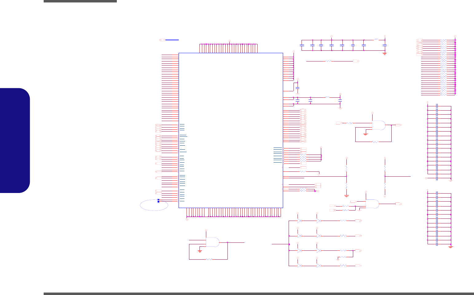
Schematic Diagrams
B - 16 VT8237A-1
B.Schematic Diagrams
VT8237A-1
Z1517
CLK_USB48 2
PCI_REQ#0
GPIO12
U SB1-
C 441 .1U_50V_06
R421 22_06
GPIO12
3VUS B
PC I_AD 29
PCI_ G NT# 1
PCI_GNT#3
PC I_INTD #
U SB3-
PC I_INTH #
FLASH#
6.2K->6.04K
C960530
USB1+ 29
PCI_GNT#2
PC I_AD 24
FB20
HC B3216K F-800T30_12
R 612 8.2K _06
R427 22_06
U19B
74AHC04
3 4
14
3.3VS
BGA 6A
VT8237A-BG A541
G2
J4
J3
H3
F1
G1
H4
F2
E1
G3
E3
D1
G4
D2
D3
F3
K3
L3
K2
K1
M4
L2
N4
L1
M2
M1
P4
N3
N2
N1
P1
P2
E2
C1
L4
M3
J1
H2
J2
H1
K4
C2
F4
E20
D20
A20
B20
E8
F25
H2 3
A4
B4
B5
C4
A5
B6
C5
D5
P3
A6
D6
C6
E5
R4
E18
D18
A18
B18
D16
E16
A16
B16
C25
A24
C26
D24
B26
W3
V1
W1
W2
H9
H10
H1 2
J8
K8
L8
M8
N8
P8
R8
R1 9
J21
C3
R3
R2
R1
T8
T19
U19
V8
V1 9
D22
E22
F22
J13
J14
J15
J16
E23
B25
J25
B2
A17
A19
A21
B13
B15
B17
B19
B21
C1 3
C14
C15
C1 6
C17
C1 8
C1 9
C20
C2 1
D1 3
D15
D1 7
D19
D21
E13
E15
B24
C24
A23
B23
D23
C23
A22
B22
C22
J17
E17
E19
E21
A15
A13
D4
E4
A3
B3
D14
E14
A14
B14
A26
A25
D26
D25
U8
J18
H1 1
V2 1
W9
W10
W11
W17
W18
W19
W21
Y21
H13
H15
H16
H18
H1 4
H1 7
A1
A2
B1
W8
AD00
AD01
AD02
AD03
AD04
AD05
AD06
AD07
AD08
AD09
AD10
AD11
AD12
AD13
AD14
AD15
AD16
AD17
AD18
AD19
AD20
AD21
AD22
AD23
AD24
AD25
AD26
AD27
AD28
AD29
AD30
AD31
CBE0
CBE1
CBE2
CBE3
FRAM E
DEVS EL
IRD Y
TR D Y
STOP
SERR
PAR
USBP0+
USB P 0 -
USBP1+
USB P 1 -
GND
GND
GN D
INT A
INT B
INT C
INT D
REQ 0
REQ 1
REQ 2
REQ 3
REQ 4
GN T0
GN T1
GN T2
GN T3
GN T4
USBP2+
USB P 2 -
USBP3+
USB P 3 -
USBP4+
USB P 4 -
USBP5+
USB P 5 -
US BOC 3
US BOC 5
US BOC 0
US BOC 1
US BOC 2
KBC K/KA20 G ,KBC K
KBDT/K BRC ,KBD T
MSC K
MS D T
VC C3 3 -1
VCC33-2
VCC 3 3 -4
VCC33-5
VC C3 3 -6
VCC 3 3 -7
VC C 33 -8
VC C3 3 -9
VCC 3 3 -10
VC C 33-11
VC C33-12
GND
PERR
REQ 5 /GP I7
GN T5 /G P O 7
PCIR ST
VCC 3 3 -13
VC C 33-14
VCC 3 3- 16
VC C33-17
VC C33-18
USB VCC 4
USB VCC 5
USB VCC 6
USB VCC 7
USB VCC 8
USB VCC 9
US BVC C1 0
U SBC LK
U SBR EXT
GND
GN D
USB GN D3
USBGND4
USBGND5
USB GN D6
USBGND7
US B GN D 8
USB G N D9
USBGND10
US BGN D1 1
USB G N D1 2
USBGND13
US BGN D1 4
USBGND15
USBGND16
USB GN D1 7
USBGND18
USBGND19
USB GN D2 0
USBGND21
USBGND22
USB GN D2 3
USBGND24
US B GN D 25
USB GN D2 6
US BOC 4
VSU SUS B
VC C UPLL 1
VC C UPLL 2
GN D UPLL1
GN D UPLL2
USB VCC 1
USB VCC 2
USB VCC 3
US BVC C1 1
USBGND27
US BGN D2 8
USB G N D2 9
USBGND2
USBGND1
INT E/G P I1 2 /GP O1 2
INT F/ G P I1 3 /GP O1 3
INT G /GPI 14 /G PO 14
INT H /GPI 15 /G P O 15
USBP6+
USB P 6 -
USBP7+
USB P 7 -
US BOC 6
US BOC 7
GPI9/UD PWR,GPI9
GPO9/UDPWREN,GPO9
VC C33-15
US BVC C1 2
VC C3 3 -3
VCC33-19
VC C33-20
VCC 33-21
VCC33-22
VC C33-23
VCC 33-24
V CC 33-25
VC C33-26
VCC 33-27
USBGND30
USBGND32
USBGND33
USBGND35
US BGN D3 1
US BGN D3 4
GN D
GN D
GND
VC C 33-28
PC I_AD 0
R405 22_06
R 699 0_04
USB5- 22
SU SB#13,16,20,23,27,28,34
Z1507
R 591 8.2K _06
PCI_REQ#2
Z1510
R 374 8.2K _06
R 382 8.2K _06
GPI9,GPIO12
Board ID
PC I_ SER R#19,26
R423 * 0_0 6
R609 2.2K_04
2.5VS
3VU SB
U SB0-
R 878 * 0_04
PC I_F R AME #19,26
U20A
74A HC 04
1 2
14
R 534 6.04K_1%_06
PC I_INTC #
C 416 1U_10V_06
PWRGD_VCORE23, 31
PC I_AD 5
C 333 .1U_50V_06
PCI_ G NT#126
PC I_AD 16
PC I_AD 20
3.3V
KBC_RST#
R 370 8.2K _06
C675
.1U_50V_06
PCI_SERR#19, 26
R 726
*10K _06
U20F
74AHC04
13 12
14
R2 5 4
10K _06
P CI_ IN T A#8, 19
USB6- 26
-P CIR ST_GATE
FLAS H#
U20B
74AHC04
3 4
14
USB2- 22
PCI_INTC#
U SB2+
USB0+ 22
C 466 .01U_50V_06
PCI_ R EQ# 2
C4 1 7
1U _10V_06
3.3V
Z1511
PC I_A D[31:0]
C 455 .01U_50V_06
U20E
74A HC 04
11 10
14
PC I_ D E VSEL #19,26
IDE_PA TD ET #
C 459
.1U_50V_06
AL L _ PW R OK
U SB0+
C 460 1U_10V_06
R7 2 5
*10K_06
R678 *0_06
3.3V
PCI_TRDY#19, 26
PC I_AD 27
U SB1+
AL L_ PW RO K
C6 9 3
1U _10V_06
PM _DPR SLPVR 3,17,31
U SB3+
R379 2.2K_04
NEW _ CAR D_ R S T# 2 0
PC I_ REQ #019
H_A20GATE 23
PCI_INTB#
U19A
74A HC 04
1 2
14
3.3VS
Z1516
PC I_AD 3
PCI _A D[3 1:0]19,26
USB0- 22
R 592 8.2K _06
3.3V
PC I_AD 30
U SB2-
R 613 8.2K _06
ID ER ST# 18
3. 3 V S
Z1515
PC I_AD 21
C 470 .1U_50V_06
R 372 8.2K _06
KBC _RST# 23
P CI_C /BE3 #19, 26
PCI_REQ#4
PCI_INTA#
IDE_SA TD ET #
GP O0 416
PC I_AD 12
C 450 .1U_50V_06
P CI_ IN T B#19
USB2+ 22
PCI_PERR#
I DE_PAT D ET#
FB 19
HC B2012KF-121T30_08
PC I_AD 19
DPRSLPVR2
PC I_ STO P#19,26
-P CIR ST_GATE
R 589 8.2K _06
U SB7- USB7+ 26
P CI_D EVSEL #19, 26
U SB4-
3.3V
PCI_ IN TH#7
PC I_AD 1
PC I_AD 7
PC I_AD 4
C6 7 1
10 U _ 10 V _1 2
USB1- 29
USB5+ 22
R 617 8.2K _06
R 384 8.2K _06
R 369 8.2K _06
P CI_FR AM E#
C 436 1U_10V_06
3.3V
FWH _TBL#
Z1512
PC I_AD 23
FWH_TBL#
Z1506
U SB6-
C423
4. 7U _ 1 0V _0 8
C 428 1U_10V_06
P CI_FR AM E#19, 26
C 399 1U_10V_06
3.3V
3VU SB
Z1514
R407 *51_1% _06
P M_ D PRSL P VR
R 252 10K _06
C 451 .1U_50V_06
C 421 1U_10V_06
3.3V
PCI_ G NT# 2
PCI_INTH#
R 593 8.2K _06
R 385 8.2K _06
R 380 8.2K _06
U20C
74A HC 04
5 6
14
C438
1U _10V_06
3. 3V S
Z1504
C 463 .1U_50V_06
3. 3V
PCI_SERR#
C 465 1U_10V_06
C670
.1U_50V_06
PCI_ R EQ# 4
C 426 1U_10V_06
R 590 8.2K _06
PCI_STOP#19, 26
PCI_GNT#1
PCI_REQ#1
DPR SL PV R 2
R697 0_04
PCI_ G NT#019
C 442 .1U_50V_06
2.5V
OC7# 20
P LT_ R ST# 11,26
PC I_AD 28
2.5VS
PCI_PAR19, 26
H _ A2 0 GATE
PCI_REQ#5
PC I_ TRD Y#19,26
R 698 *0_04
KBC_PW RG D23
PCI_ R EQ# 0 GPIO 1 2
C 427 .01U_50V_06
R 616 8.2K _06
C 435 .1U_50V_06
3.3V
P CI_C /BE0 #19, 26
C 464 .1U_50V_06
C6 9 4
10U_10V_08
OC1# 22
PCI_REQ#3
C 361 .01U_50V_06
C420
.1U_50V_06
OC2# 29
AL L_ P W RO K 3 ,1 7 ,24
C 411 1U_10V_06
R 511 8.2K _06
3.3V
USB4+ 20
PC I_AD 17
I DE_SAT D ET#
R 594 8.2K _06
PC IR ST#
GPI9
USB3+ 22
PCI_ R EQ# 3
PCI_TRDY#
PC I_AD 15
PC I_AD 11
R 253 10K _06
R406 22_06
R 383 8.2K _06
Z1505
R 573 8.2K _06
M960806
USB7- 26
PC I_ PER R#19,26
PCI_GNT#0
C 429 .01U_50V_06
C 425 .1U_50V_06
P CI_C /BE1 #19, 26
Z1503
U SB7+
C 367 1U_10V_06
PCI_ R EQ# 5
C430
. 1U _50V _06
USB6+ 26
R 251 10K _06
3.3V
P CI_ IR DY #19, 26
U SB4+
U1 0
74A HC 1G 08GW
2
1
4
3
5
C476
.1U_50V_06
PC IRS T#
PC I_AD 10
PC I_AD 2
PCI_STOP#
PC I_AD 26
R 386 8.2K _06
C 461 1U_10V_06
Z1518 B UF_PLT_RST# 7,20,23,26
PCI_IRDY#
U3 7
74AHC1G08GW
2
1
4
3
5
3.3V
PCI_ R EQ# 1
2.5VS
USB3- 22
PC I_AD 25
R 727
10K_06
U SB6+
R 373 8.2K _06
R 611 8.2K _06
Z1521
PC I_AD 8
R 614 8.2K _06
C 467 .01U_50V_06
R 615 8.2K _06
PCI_PERR#19, 26
P CI_D EVSEL #
PCI_ G NT# 0
PC I_AD 31
PC I_AD 6
USB4- 20
U SB5-
PC I_AD 14
R 250 10K _06
PC I_ IR DY #19,26
Z1513
Z1520
U23
74AHC 1G08G W
2
1
4
3
5
C 424 .01U_50V_06
PCI_ IN TD#26
PCI_ G NT# 3
Z1519
PCI_INTD#
PC I_AD 13
PC I_AD 9
U SB5+
PC I_AD 22
3.3V
P CI_C /BE2 #19, 26
PC I_AD 18
Z1501
C 383 1U_10V_06
C 454 .1U_50V_06
R 371 8.2K _06
PC I_ REQ # 126
PCIR ST#
C 462 .1U_50V_06
3.3V
OC0# 22
PCIRSTC# 19
U20D
74AHC04
9 8
14
Sheet 15 of 40
VT8237A-1
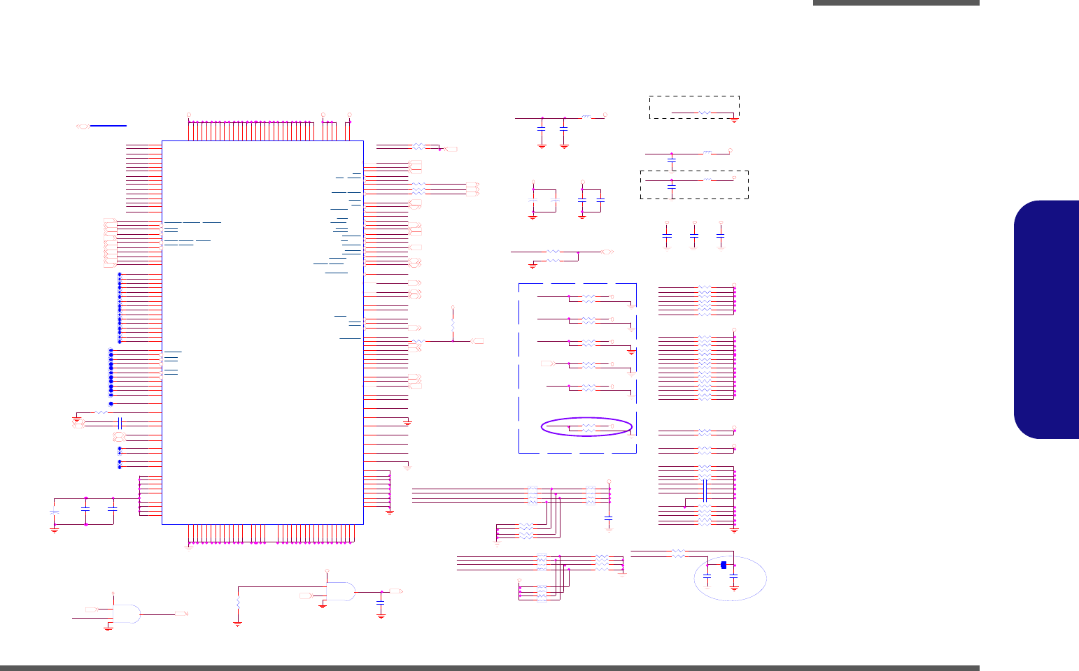
Schematic Diagrams
VT8237A-2 B - 17
B.Schematic Diagrams
VT8237A-2
Sheet 16 of 40
VT8237A-2
IDE_ P DD 0
SATATXP0
INT _ IRQ 15
PM_ STPCPU#
3.3VS
3.3V
823 7 _SU SB#
GP O1
R 3 48 10 K _ 0 6
GPIO D
R 323 1K_06
3. 3 V
ID E _ PDCS3 #
GPO 04
1:Vlink Compensation(Manual setting)
SUS B# 1 3, 15 ,2 0,2 3 ,27 ,2 8 ,34
SM I# 23
IDE_ S DD 0
SUSA#
1:VKCOMP for Vlink at 4X mode 0.9V
ID E_PD A0
TPO
IDE_ S DD 8
SU SA#
IDE_ P DD 7
C373
1U_10V_06
R 2 86 0_ 0 6
R316 0_06
ID E_SI ORD Y
PEXMESCI#
SU SC# 2 3
SATA5 0 COM P
FB 13
H CB2012KF-121T30_08
AZ _BITCLK 2 7
ID E_ SIORD Y
FB 21
H CB2012KF-121T30_08
R 2 76 0_ 0 6
IDE_ P DD 13
CL KR UN#
R 361 * 0_04
R 603 0_06
C493 22P_50V_06
GPIO C,A 1,1:Auto Mode
3.3VS
ID E_SD DR EQ
VT8237R plus => 4.7K
VT8237A => 6.12K
AP339A
ID E_SD CS1#
AZ_ SDIN 0
IDE_ S DD 3
AZ _ SDIN1
IDE_ P DD 8
R 565 4.7K_06
R 6 56 1 0 K _ 06
3.3VS
IDE_ IRQ18
ID E_PD A1
R 360 0_04
GPO04 15
VDD A0
ID E_PDA0
ID E_SD IOR #
R 5 44 1 0 K _ 06
WA KE ON L AN
C9 60 525
R 554 4.7K_06
R 351 0_06
U35
74AHC1G08GW
2
1
4
3
5
R 620 4.7K_06
3.3V S
GPIO C
AZ_ SDIN 1
CPU MISS
AZ _ S DO UT
FB14
HC B3216KF-800T30_12
0:V4-lite support(Disable)
AZ_ SY NC
AC_SPKR
GP I04
IDE_ S DD 9
R 2 69 0_ 0 6
R 6 29 1 M _0 6
VCC RT C
SMB_ SBDATA
IDE_SDD REQ
AZ_R ST# 27
SER IRQ
SD IN3
C7 08
* 10U_10V_08
Z1610
Z1615
R 623 1K_06
Z1613
IDE_ S DD 11
IDE_ P DD 12
+
C3 8 9
470U_4V_D
SCI# 23
SD IN2
IDE_ PDD 7
25M HZXI_S
RN 29
1K_8P4R_06
1
2
3
4 5
6
7
8
GPIO D 0:AGTL+ pullup Enable
ID E_PDA2
3. 3 V
SATATXP018
R 624 4.7K_06
R586 *2.2K_06
R311 0_06
PM _STPPC I# 2
W AKE
PM_ STPPCI#
AZ_ SDOU T
SM B_SBDATA 2 ,9,10 ,11
WAKE
IDE_ P DD 15
C456
15 P_ 50 V_ 06
R 535 4.7K_06
2.5VS
VDDA0
IDE_ P DD 6
CL KRU N#
R 353 * 0_06
SE RIRQ 19 ,2 3
ID E_SD A1
GPO 1
R 6 28 1 M _0 6
GPIO B 0:IOQ Depth 8 Level
PE XM ESCI# 7
PM_ BATLO W #
0/1:Enable/disable Auto Reboot
A Z _S D I N 1 27
IDE_ P DD 10
INT _ IRQ
R 350 2.2K_06
R 574 4.7K_06
R 355 * 0_06
CPU MISS
R 362 1K_06
R 5 81 1 0 K _ 06
8237_PWR OK
8237_PWRO K
IDE_ S DD 15
R868 0_06
R 2 62 1 0 K _ 06
R363 *2.2K_06
WAKE 7
SB_ PW R OK
PM_ BATLO W #
AZ_ RST #
IDE_ P DD 4
R 598 4.7K_06
SMI#
IDE_ P DD 9
R324 *2.2K_06
R 308 6.19K_1% _06
C434
1U_10V_06
3.3VS
2.5V
IDE_ P DD 2
R 575 4.7K_06
0/1:Enable/disable100Mhz VLink clock(Reserved)
SUSB#
AC_SPKR
SEEDI17
PME#
TPO
2.5VS
3.3VS
IDE_PDD REQ18
3.3VS
IDE_ S DD 2
GPI0
SB_ PW ROK
AZ_ BITC LK
ID E_SD A2
R 618 22_06
R 631 4.7K_06
IDE_PIOR DY18
Z1617
SID EVREF
R 366 4.7K_06
Z1604
R 357 * 1K_06
ID E_PDA1
SUSC #
IN T_ IR Q
2.5VSATA
0\1:P4/V4 Bus \ C3 Bus
GP I0
ID E_SD A0
ID E_PD IOR #
GPIO C
GPO0 11
GPIO A
R 597 4.7K_06
R869 *0_06
ID E_PD CS1#
SATATXN018
25MHZ XI_S
Z1607
C960531
ID E_PD D[0..15]18
GPO1 27
RIN G
IDE_ S DD 1
C487 22P_50V_06
PM _C LK R UN#
823 7 TEST
IDE_ P DD 5
PM_ SUS_STAT#
R 595 22_06
ID E_PD DAC K#
GPIO D
SMB_ AL ERT #
BGA6B
VT8 2 37 A-BG A54 1
AA22
Y24
AA26
AA25
AB26
AC26
AC23
AD25
AD26
AC24
AC25
AB24
AB23
AA24
Y26
AA23
W23
V25
W24
Y23
V24
W26
Y25
Y22
V22
V23
T1
U3
V2
U1
V3
T2
U2
T3
AD24
AE26
AC20
AB20
AC21
AE18
AF1 8
AD18
AD19
AF1 9
AE20
AF2 0
AD20
AE21
AF2 1
AD21
AD22
AF2 2
AD17
AD23
AF2 3
AE23
AF1 7
AF2 5
AF2 6
AF2 4
AC22
AE24
AD2
Y2
AA1
W4
AC1
V4
Y3
AB3
AA2
AD3
AF2
AB1
AC4
AB2
AC2
AA3
AE2
AE5
AF5
AC6
AD5
AB7
AC7
AD6
AA4
AB4
AB5
AB6
J9
J10
J1 1
AF1 4
L13
L14
AE9
AF1
L1 5
K9
L9
J12
L18
M9
AB14
AC 14
AD12
AD13
AD 14
AD15
AD 16
AE12
AE14
AE16
AF1 2
L16
M11
AC11
AC17
AB13
AC13
AE15
AF1 5
AB15
AC15
AF16
L11
L1 2
T4
U4
AD9
AF8
AB8
AC3
AD1
AE1
Y4
AF9
Y1
AE3
AE13
AF1 3
AC10
AB10
AE11
AF1 1
AD11
AE10
AF1 0
AC19
AB21
AB11
AB17
W12
W13
W14
W15
W16
M18
N9
N1 8
P9
P18
R9
R18
T9
T18
U9
U1 8
V9
V10
V1 1
V12
V1 3
V1 4
V15
V1 6
V17
V1 8
AC 16
AC12
AB16
AB12
M12
M13
M1 4
M15
M1 6
N1 1
N1 2
N1 3
N1 4
N1 5
N1 6
F6
F7
J5
K5
P5
R5
W5
V5
K18
Y5
PDD0 0
PDD0 1
PDD0 2
PDD0 3
PDD0 4
PDD0 5
PDD0 6
PDD0 7
PDD0 8
PDD0 9
PDD1 0
PDD1 1
PDD1 2
PDD1 3
PDD1 4
PDD1 5
PDA0/PDA0*
PDA1/PDA1*
PDA2/PDA2*
PDDR Q
PDDAC K/PDD ACK*,PD DAC K
PDIOR/PHDMARDY/PHSTROBE
PDIOW /PS TO P
PDRD Y/PD DMAR DY/P DSTROBE
PDCS1 /P D CS1 *,PDC S1
PDCS3 /PD CS3*
ACBIT CLK,AZBITCLK
AC SDIN 0,AZSD IN0
AC SDIN 1,AZSD IN1
AC SDIN2,AZSD IN2/GPI20 /GPO20 /PCS0
AC SDIN 3,AZSD IN3/GPI21 /GPO21 /PCS1/SLPBTN
AC SYNC ,AZSYN C/ACSY NC *
ACS DOU T,AZSD OU T/AC SDO UT*
AC RST,AZRST
IRQ1 4
IRQ1 5
SDD0 0
SDD0 1
SDD0 2
SDD0 3
SDD0 4
SDD0 5
SDD0 6
SDD0 7
SDD0 8
SDD0 9
SDD1 0
SDD1 1
SDD1 2
SDD1 3
SDD1 4
SDD1 5
SDDR Q
SDDAC K
SDIOR/SHDMARDY/SHSTROBE
SDIOW /SS TO P
SDRD Y/SD DMAR DY/S DSTROBE
SDCS1
SDCS3
SDA0
SDA1
SDA2
PW R BTN
RIN G/GP I03
EXTSMI/GP I02
PME
LID/GP I04
BATL OW /GP I05
SUSST1/GPO 03
SU SCLK/GPO 04
SU SA/GPO 02
SU SB
SU SC
SMBAL RT
SM BCK1
SMBD T1
GPI01,GPI01/THRMTRIP
GPO 00
GP I00
S trap _ VD1 *,G PIOA*/PC REQ A*
S trap _ VD0 *,G PIOC* /PCGN TA*
S trap _ VD3 *,G PIOD* /PCGN TB*
S trap _ VD2 *,G PIOB*/PC REQ B*
PC KRU N
CPUSTP/GPO05
PCISTP/PC ISTP* /GPO 06
VSUS33-1
VSU S33 -2
VSUS33-3
VSUS33-4
VCC 25 -1
VC C2 5-2
VCC25-3
G NDAT S1 1
GN D
GND
TEST
PW R OK
GND
V CC2 5 -5
VCC 25 -6
VCC 2 5-4
VC C2 5-7
VCC25-8
GN DA T S 0
G NDAT S 1
GND A T S 2
GN DA T S 3
GNDATS4
GN DA T S 5
G NDAT S 6
GND A T S 7
GN DA T S 8
GNDATS9
GN DA T S 1 0
GND
GND
VCCAS2
VCCAS1
STXP1
STXN1
SRXP2
SRXN2
STXP2
STXN2
GND A T S 1 2
GND
GND
VSUS25-1
VSU S25 -2
SERIR Q
SPKR/SPKR *
OSC
SM BCK2 /GPI2 7 /GPO 27
SMBD T2 /GPI2 6 /GPO 26
IN TRUD ER/GP I16
AOL GPI/T HR M/GP I18
TPO
CPU MISS/GP I17
GPO 01
SRXP1
SRXN1
VCC AO
GNDAO
VCC A33 ,N C
GND A 33 , N C
SR EXT
SXO
SXI
SVREF ,NC
SCOM PP,NC
VCCAS4
VCCAS3
VDDAT S-1
VDDAT S-2
VDDAT S-3
VDDAT S-4
VDDAT S-5
VCC 2 5-9
VC C25-10
VCC 25 -11
VC C25-12
VCC25-13
VCC 25-14
VC C25-15
VCC 25 -16
VC C25-17
VCC25-18
VCC 25 -19
VC C25-20
VCC 25 -21
VC C25-22
VCC25-23
VCC 25 -24
VC C25-25
VCC 25 -26
VC C25-27
VCC25-28
VCC 25 -29
GNDAS1
GN DAS2
G NDAS3
GND AS4
GN D
GND
GND
GN D
GN D
GN D
GN D
GN D
GN D
GN D
GN D
GN D
GND
GND
GN D
GND
GN D
GN D
GN D
GND
NC , W AKE
R 296 5.6K_06
R 381 4.7K_06
0/1:Enable/disable LPC FWH command
SM B_SBCLK 2 ,9,10 ,11
GPIO B
PM_ STPPCI#
R 552 4.7K_06
5VS
PM _CLKRUN # 23
ID E_SD DAC K#
C695
.1U_50V_06
SMB_ SBCLK
PM _STPCPU #
SM BCK2
Z1616
C452
15P_50V_06
0/1:Disable/Enable LAN shadow EEPROM
SI O_ OSC 2
SATA RX N0
R 545 4.7K_06
+
C3 6 2
*3 30 U _ 6 . 3 V _D
C457
4.7U _10V_08
IDE_PDC S3#18
IDE_PDA118
SERIR Q
SIO_ OS C
R 622 4.7K_06
X3
25M Hz
1 2
SW I# 2 3
ID E_PD IOW #
SM I#
ID E_PD A2
SM BDT2
C488 22P_50V_06
IDE_PDIO R#18
ID E_PI ORD Y
IDE_ S DD 13
Z1614
1: V 4 s u pp o r t
2.5VS
VDD A33
GPI0 4
AZ_ SDIN 0
C492 22P_50V_06
IDE_ S DD 5
25MHZ XO _S
0/1:Enable/disable CPU FREQ strapping
2. 5 V S
SDIN 3
SMBC K2
GPIO A
25M HZXO_S
IDE_ P DD 1
R 364 4.7K_06
R583
100_08
SDIN 2
RIN G
R 596 22_06
3.3V
AC _SPKR 2 7
SM B_SBD ATA
SM_INTRU DER #
IDE_ S DD 4
IDE_PDD [0..15 ]
Z1602
AZ_SDOUT27
ID E_SD IOW #
2.5VS
PM _SUS_STAT# 7
R 601 4.7K_06
0:MOBILE MODE
AZ_ SYN C
RN9
1K_8P4R_06
1
2
3
45
6
7
8
C381
4.7U_10V_08
ACSD O
823 7 TEST
RN 28
2.2K_8P4R_06
1
2
3
45
6
7
8
C4 9 0
4.7U_10V_08
IDE_PDIO W #18
ACSY NC
GP O0
C449
.1 U_ 5 0 V_0 6
C696
.1U_50V_06
GPIO B
GPO 0
VDDA33
ID E_PD CS3#
R 358 4.7K_06
R 2 93 * 0 _0 6
R 3 65 1 0 K _ 06
3.3V
AZ_SY NC 27
IDE_PDC S1#18
8237_SU SB#
Z1611
2. 5 V S
PM _STPC PU# 2
IDE_PDD ACK#18
IDE_ S DD 7
SATA RXP0
R 5 99 1 0 K _ 06
R 6 21 1 0 K _ 06
PM E# 19 ,23,26
IDE_PDA218
IDE_PDA018
IDE_ P DD 14
R 354 * 1K_06
R368 *2.2K_06
1:DESKTOP MODE
3.3V
Z1606
SATATXN 0
RN20
2.2K_8P4R_06
1
2
3
45
6
7
8
R633 *2.2K_06
R 347 0_06
RSMRST#17 , 2 3
Z1612
PW R_ BTN # 23
3.3VS
IN T_ IR Q1 5
R 627 4.7K_06
R626
10K_06
2.5VS
A Z _S D I N 0 27
AZ_ SD OUT
ID E_SD CS3#
IDE_ S DD 6
C440
.1U_50V_06
SATARXP018
AZ_ RST #
AZ_ SYN C
+
C8 0 5
100U_6.3V_B
12
R 604 4.7K_06
VKCOMP for Vlink at 4X mode
SMB_ AL ERT#
GPI0 4
Power Up Strapping for VT8237A
2.5VSATA
SREXT
SM B_SBC LK
R285
360_1%_06
IDE_ S DD 14
Z1609
IDE_ S DD 12
R 600 4.7K_06
R 619 4.7K_06
R 264 4.7K_06
IDE_ S DD 10
SB_ PW RO K 7
AZ _ SDIN0
PW R_ BT N#
PM_CLKRUN#
M960807
SREXT
C4 46
1U_10V_06
3.3VS
IDE_ P DD 11
C698
.1U_50V_06
RSM RST #17,23
Z1605
Z1618
C4 32
4.7U_10V_08
C4 4 7
.1U _50V_06
SATARXN018
Z1603
IDE_ SDD 7
R 632 1K_06
PEXMESCI#
Z1608
C443
.1U_50V_06
1 :V 4 -li t e s up p ort
Z1601
IDE_ P DD 3
U34
74AHC1G08GW
2
1
4
3
5
R 6 25 1 0 K _ 06
0:V4 support(Disable)
3.3V
SM_ INT RU DER#
ID E_PD DR EQ
SMBD T2
LAN PHY RESET:
PM_SUS_STAT#

Schematic Diagrams
B - 18 VT8237A-3
B.Schematic Diagrams
VT8237A-3
Sheet 17 of 40
VT8237A-3
GHI
TXEN 2 1
VC CR TC
C405
.1U _50V_06
LP C _ A D [ 3 : 0]23
2.5VS
VLAD2
SATA_ L ED# 2 8
APIC D 0
RXD2 2 1
MD IO
R 555 33_1% _06
R281
4 . 7K _0 6
Z 1709
R 558 4.7K_04
VBE#7
Z 1704VLAD5
LVR EF_SB
SEE DI
PM_D PRS LP VR 3,15,31
LVREF _S B
EEPROM
2.5VS
H_ PW R G D 3
TXD 0 21
DNSTB7
R 587 33_1% _06
H_ IN TR 3
LPC _AD0
Z 1707
H_ NM I 3
UPCMD7
S EEC S
C479
5P_50V_06
3.3V
Z 1708
Near to
South
Bridge
R 563 33_1% _06 TXD 2 21
MD IO
32KH ZX2
VLAD4
C481
.1U _50V_06
LPC _AD1
SEE CLK
BGA 6C
VT8237A -BGA 541
H25
G26
K26
J23
F26
G25
K22
K24
A11
B11
B9
B10
A10
C1 1
C1 0
A9
A7
B7
C7
B8
D8
C9
D1 0
A8
D1 1
B12
A12
C1 2
E7
T22
U2 2
E24
G23
L26
L25
E26
E25
L24
M26
H22
K23
K25
J26
J24
H26
H24
J22
E6
E11
E9
E10
AF 4
L22
D9
P11
P12
P13
P14
P15
P16
R11
R1 5
R14
R13
R1 2
R16
R21
T11
T12
T16
T15
T14
T13
M2 4
N21
N22
N2 3
N24
N25
N2 6
P22
P23
P24
P25
P26
M21
M22
M23
AE 4
AF 3
AE 6
AF 6
C8
D1 2
E12
L21
K21
AD 8
AF 7
AE 7
AD 7
G24
F24
AE 8
D7
AC 5
AD 4
U2 4
U2 6
T24
R2 6
T25
T26
U2 5
R2 4
V26
R2 2
P21
R2 3
U2 3
R2 5
T23
AC 9
AC 8
AB9
AD 10
M25
L2 3
L19
M1 9
N19
P19AA21
AB19
AB22
AB25
AC18
AE17
W22
W25
AE19
AE22
AE25
AA9
T21
AA10
AB 18
K19
F23
G22
F8
VAD 00
VAD 01
VAD 02
VAD 03
VAD 04
VAD 05
VAD 06
VAD 07
MC RS
MCO L
MTXD 2
MTXD 1
MTXD 0
M TXENA
MT X C LK
MTXD 3
MD CK
MD IO
MRXD 3
MRXD 1
MR X D V
MRXC LK
M RXER R
MRXD 2
EECS
EED O
EED I/EED I*
EECK
LANVC C
PLLVCC
PLLGN D
VAD 08
VAD 09
VAD 10
VAD 11
VAD 12
VAD 13
VAD 14
VAD 15
VLVR EF
UP CM D
DN CM D
UP ST B +
UP ST B -
DN ST B +
DN ST B -
VLCO MP
LAN GN D
MII VCC 4
MIIVC C 2
MIIVC C3
VBAT
VC LK
MII VCC 1
GND
GND
GN D
GND
GND
GN D
GND
GN D
GND
GN D
GN D
GN D
GND
GN D
GND
GND
GND
GN D
GND
VCC VK1 8
VCC VK4
VCCVK5
VC CVK 6
VCC VK7
VC C VK8
VC CVK 9
VCC VK1 0
VC C VK11
VC CVK 12
VCC VK1 3
VC CV K14
VC CVK1 5
V CC VK16
VC CV K17
RTC X1
RTC X2
LREQ 0
LFRM
MRXD 0
M IIV C C2 5 -1
MI IVCC 25-2
VC CV K3
VCCVK2
LAD0
LAD1
LAD2
LAD3
VBE
VPAR
LREQ 1
PHY R ST
PW R GD
RS MR ST
FER R
A20M
IGN NE
IN IT
INTR
NMI
SMI
STPC LK
SLP
GH I/G PI 2 2 /GPO 2 2
D PSL P/G PI23 /GPO 2 3
PC IC LK
A PICC L K ,G P I1 9
API CD 0/ GPIO 1 0
API CD 1/ GPIO 1 1
V GATE/G PIO 8
G PI28 /GPO 28 /VID SEL /SATAL ED ,GP I28/G PO 28/ VIDS EL
VR D PSLP/G PI2 9 /GPO 2 9
AGP BZ/G PI06
V CC VK19
VCC VK1
VC CV K20
VCC VK2 1
V CC VK22
VC CVK 23GND
GN D
GND
GN D
GN D
GND
GN D
GND
GN D
GN D
GND
GN D
GND
GN D
GND
GND
NC 1
NC 2
NC ,PH YP W RD N
G N D_SBP LL
S EED I
C702
10U_10V_08
M960808
2.5VS
Z1701
G ND _S BPLL
N C_CP PE#
DPRSLPVR1
C448
.1U_50V_06
2.5VS BPLL
Z 1703
C484
5P_50V_06
R630 1K_06
VGA TE
APIC D 1
ALL_PW R OK
Z 1712
R277
*33_06
C469
1U _10V_06
H_ SM I# 3
VLAD0
2.5VS
1.05VS
R275 1K_06
VCO M PP
R340
10K_06
2.5VSBP LL
H _ CP US L P# 3 ,5
R564 4.7K_06
Z1717
SATA_ L ED #
M960803
U PSTB#7
SPCLK 2
Z1714
DPRSLP VR1
VDD3
TXE N
D37
R B751V
A C
C475
1U_10V_06
V PAR8
C 706
10U _10V_08
R 588 33_1% _06
J BAT1
C ON 2_ BAT
1
21
2
VLAD1
S EEC LK
AG P_BUS Y#
SPC LK
C468
.1U _50V_06
SEED I 1 6
VLAD6
G N D_ SBPL L
2.5VS
R 570 * 4.7K _04
C445
.1U_50V_06
MDC 21
R318 10K_06
R717
1K _0 6
H_ IG NN E# 3
AGP_BU SY # 8
32KHZX2
S EED O
LPC _DR Q #0
3.3VS
CR S 2 1
2.5VS
TXD 1 21
LPC _ F RAM E#
APIC D1
3.3VS
-PHY R S T 21
CO L 21
LPC _DR Q #1
R 832 0_06
D39
R B751V
A C
2.5V
SEE DO
R325 2.2_08
Q21
2N3904
B
E C
APIC D0
R279
1.05K_1%_06
C439
4.7U_10V_08
NC _C PPE # 20
MDI O 21
S11 S121
LPC _F RAM E#23
LPC _AD2
SPC LK
Z1713
C404
.1U _50V_06
R716 470_06
2.5VS
RXD1 2 1
Z 1705
LPC _AD[3:0]
Z1715
L V RE F_ SB = 0. 3 V FO R VT 8 23 7R p lu s
L V RE F_ SB =0 .4 5 V FO R VT 8 23 7A
R 578 4.7K_04
H_ ST PC LK # 3
H_ DP SL P # 3
H_ A2 0 M# 3
VPA R
A GP_BU SY #
U PSTB7
R267 360_1%_06
VLAD3
40mil
RSMRST#16, 23
H_ IN IT# 3 VC CR TC
R282 360_1%_06
R 551 33_1% _06
H_ F ER R# 3
R580
* 100K_04
Z1718
Q20
D TC114EUA
CE
B
DPRSLPVR1 FOR VIA
C960604
R559 * ->0 C960615
VG ATE
C 374
4.7U_10V_08
32KH ZX1
SEE CS
LPC _DR Q#1
R 559 0_04
2.5VS
DPRSLPVR1
Z 1706
U1 1
CAT93C 46S-26490T
3
2
1
4
8
5
6 7
DI
SK
CS
DO
VCC
GND
NC 1 N C2
32KHZX1
DEL GHL PULL UP RESISTER
40mil
3.3V
2.5VSBPL L
3.3VS
C403
.1U _50V_06
R359
1K_06
TXD 3 21
VC OM PP
C377
1U_10V_06
DNCMD7
A LL_PW RO K3,15, 24
R 263 4.7K_06
2.5V
VLAD[0..7]
FB12
HC B2012KF-121T30_08
Must use +3.3VSUS if it want to wake
o n LA N f ro m re su m e fu nc ti on we ll .
R261 360_1%_06
R610
1.5K_04
C489
.1U _16V_04
V LA D[0 ..7 ]7
C419
*10P_50V_06
-PHY P W R DN 2 1
R 313 33_1% _06
RXD0 2 1
GH I
J1
JOP EN
21
R 567 4.7K_04
RXER 21
VC CR TC
Z1716
Y2
32.768K HZ
1
3
2
4
ADD GND SHIELD
VC CR TC
RXD3 2 1
Z1710
RXCL K 21
Z1711
V CLK_SB2
LPC _AD3
LPC _DR Q#0
VLAD7
VT8237R plus=> 10PF
VT8237A => 12PF
AP339A
TXC LK 2 1
ALL_PW R OK3,15,24
PM _DP RSLPVR
Z1702
3.3V
D NSTB#7
RXDV 2 1
R 569 33_1% _06
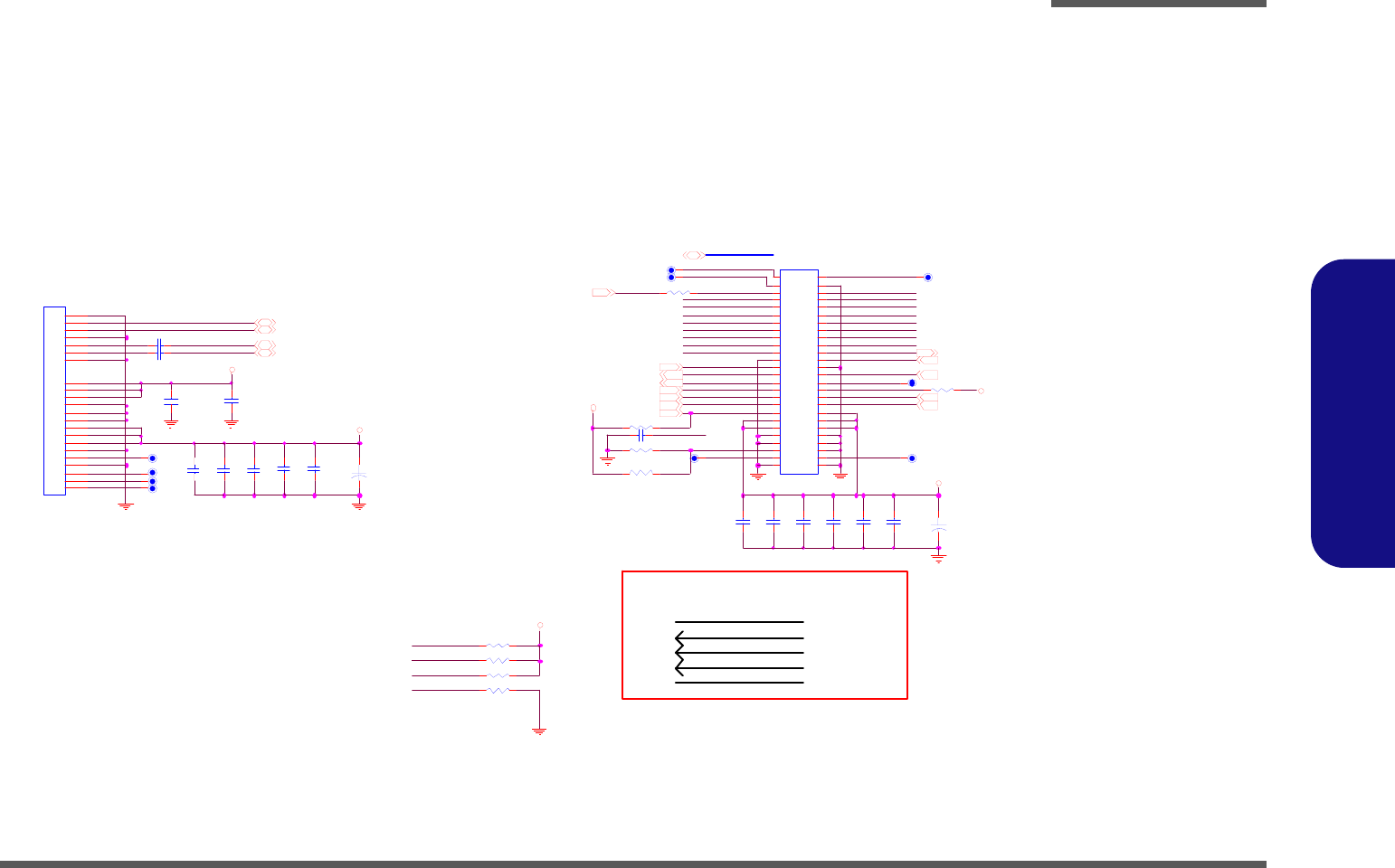
Schematic Diagrams
HDD & CDROM B - 19
B.Schematic Diagrams
HDD & CDROM
Sheet 18 of 40
HDD & CDROM
IDE_PDD5
IDE_PDDACK#
IDE_PDCS1#
C721
.1U_10V _04
IDE_PDA2 16
IDE_PI ORDY R451 4.7 K_06
CD_L
IDE_PDD7
CD_CABSEL
IDE_PDD1
IDE_PDD10
IDE_PDI OW#
Z 1804
IDE_PDIOW#
Z18 0 9
IDE _P DCS3# 16
IDE_PDDI AG#
3.3V S
CD_L
C564 *. 01U_50V _04
IDE_PDD14
C719
.1U _10V _04
C572
.1U _10 V_04
CD_DASP#
Si gn al: Sp ace = 1: 2
C570
.1U _10 V_04
C715
10U_10V_08
Si gn al: Sp ace = 1: 1
C714
1U_16V_06
3.3V S
Z18 0 8
R449 4.7 K_06
PIN G ND1~2=GND
R448 4.7 K_06
I D E_ PD A 016
SATARXP0 16
SATARXN0
I D E_ PD I OW #16
IDE_PDA2
C720
.1U_10V _04
5VS
S ATA TXN 0
SATARXP0
Z 1801
From
CD-ROM
To
AUDIO
CODEC
C569
.1U_10 V_04
IDE_PDD[ 15:0]
IDE_PDD4
IDE_IRQ16
J_HDD1
SAT- 22RE1 GA
S1
S2
S3
S4
S5
S6
S7
P1
P2
P3
P4
P5
P6
P7
P8
P9
P10
P11
P12
P13
P14
P15
CD-ROM
IDE_PDDREQ
CD_RESET#
R457 10K _04
IDE_PDD6
5VS
C710
10U_10V_08
IDE_IRQ
Other Signal
IDE_PDA0
R445 33_0 4
IDE_PDDREQ 16
IDE_PDD2
R459 0_04
IDE_PDCS3#
CD_G
+
C17
*10 0U_6.3V _B
12
IDE_PDD15
Z 1806
SATARXN0 16
CD_R & CD_G & CD_L must parallel
routing to Audio Codec. The wide is
12mils and space must be equal.
La yo ut no te:
IDE_PDI OR#
Z 1805
IDE_PDD8
CD_DASP#
IDE_PDIOR# 16
IDERST#
CD_R
IDE_PDI OR#
Si gn al: Sp ace = 1: 2
Z 1803
IDE_PDD12
C709
3900 P_50 V_04
Si gn al: Sp ace = 1: 1
SATA HDD
R452 10K _04
S ATA TXP 0 1 6
IDE_PIORDY
C12
10U_10V_08
IDE _PDD[ 15:0]16
C471 . 01U_50V _04
+
C713
100U_ 6.3V _B
12
S ATA TXP 0
IDE_PDA1
IDE_PDD0
Z180 7
CD_G
C571
.1U_10 V_04
I D E_ PD A 116
S ATA TXN 0 16
Z 1802
CD_DASP#28
CD_R
C474 . 01U_50V _04
R450 4.7 K_06
J_ODD1
CDR-50 DD2
12
34
56
78
910
11 12
13 14
15 16
17 18
19 20
21 22
23 24
25 26
27 28
29 30
31 32
33 34
35 36
37 38
39 40
41 42
43 44
45 46
47 48
49 50
5251
IDE_PIORDY16
CD_RESET #
IDE_PDD13
IDE_PDD3
5VS
IDE_PDDACK# 16
C574
1U_16V_06
3.3 VS
I D E_ PD C S 1 #16
Other Signal
IDE_PDD9
IDERST#15
IDE_PDD11
R458 * 4.7K_04
IDE_PDDREQ
C175: .01U_50V_04 for Nvidia platform
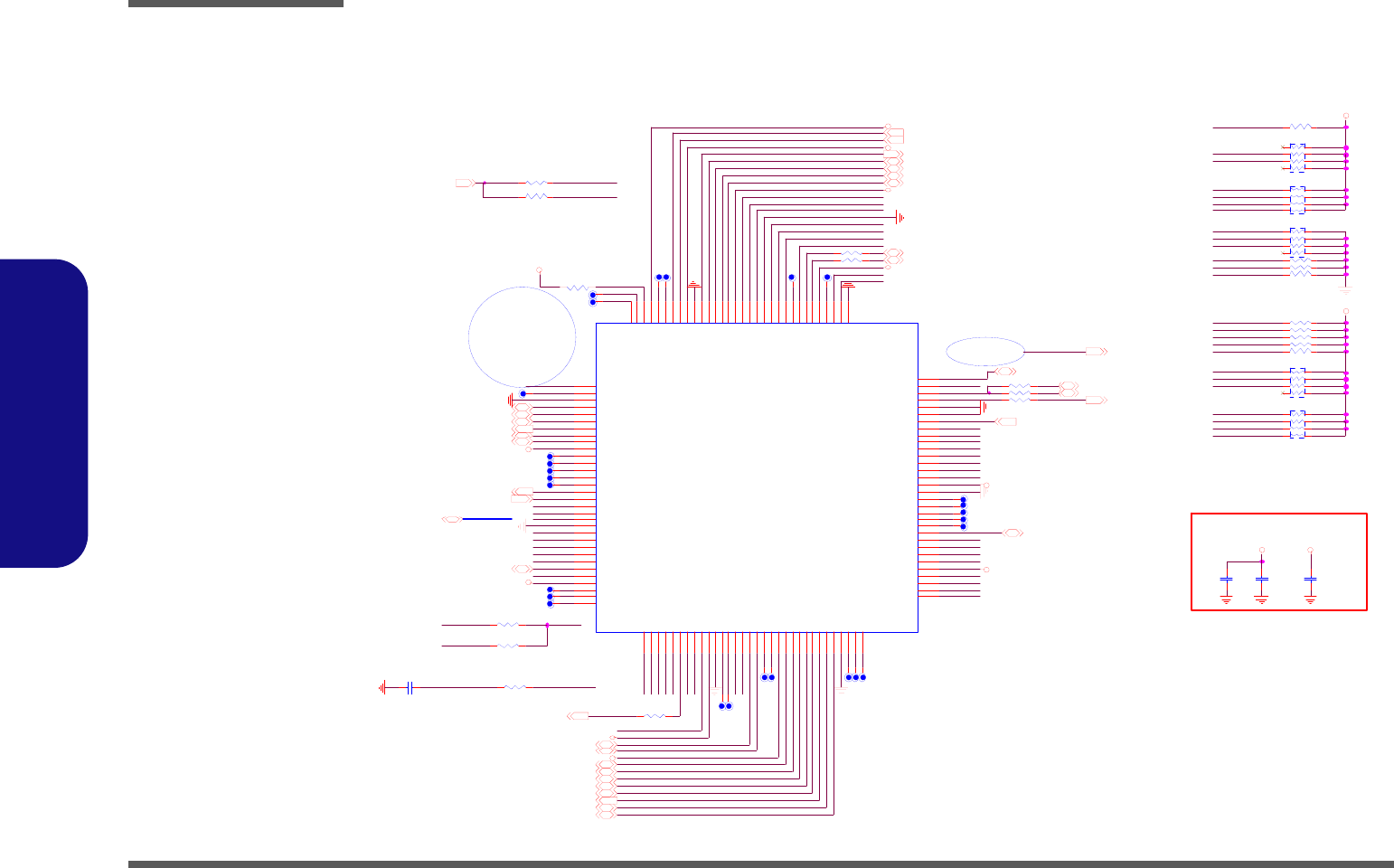
Schematic Diagrams
B - 20 CARD READER
B.Schematic Diagrams
CARD READER
SD_CD#
PC I _ AD 29
PCM_ R ST#
MS_BS 20
Z1921
R352 47K _04
P C I _ FR AM E#15,26
CL OSE TO C HIP
VCC_CARD
SD_D220
PC I _ AD 2
PC I _ STO P#15,26
PC I _ AD 7
MS_BS
PC M_I DSEL
PC M_MF5
RN14 47K _8P4R_061
2
3
4 5
6
7
8
Z 1912
Z1903
3.3V S
PC I _ AD 26
SD _ W P
PC I _ AD 24
PC I _ PA R15, 26
SD _ CMD20
R378 47K _04
PC I _ AD 4
G_RST#
Z 1907
Z 1909
Z1924
PCLKPCM
Z1923
SD _ CLK IN
PME# 16,23,26
PC I _ A D19
R707 100_04
SD _ CD#
SD _ D2
MS_D1
PC I _ PE R R#15, 26
xD_CD#
R344 47K _04
Z 1915
PC I _ AD 12
Z1930
PCI_AD20
MS_CLK 20
PCI_IRDY#15,26
Z 1914
xD_B SY#
PCM_ SU SP EN D #
Z1929
PC I _ AD 9
Z1931
Z 1906
Z1919
PC I _ AD 15
R387 47K _04
C518
.1U_16V_04
xD_CD#
Z1920
PC I _ AD 27
CARD_P WREN#
PC I _ AD 13
PC I _ AD 25
xDWP#
F951202
Z1922
SD _ D3
3.3VS
CARD_PWREN#
SD _ CLK
MS_D1 20
MS_INS# 20
SD _ D0
Z1916
3.3VS
PC I _ GNT#015
PC I _ AD 3
Z1926
C711
.1U_16V_04
C496
.1U_16V_04
M9 60808
PC L KP CM2
MS_CLK
PC L KP CM
PCI _AD[31:0]15,26
PCM_MF7
3.3V S
PCM_MF5
PC I _ AD 8
Z 1913
PC I _ AD 5
R607 0_06
SD_D020
R416 47K _04
C532 * 10P_50V_06
xDWP#
PCI_AD23
PC M_I DSEL
SD_D120
Z1933
SD _ D2
MS_D3
RN12 47K _8P4R_061
2
3
4 5
6
7
8
Z1927
3.3V S
CARD_PWREN# 20
PC I _ C / B E3 #15,26
R706 *0_04
PC I _ AD 11
MS_D0 20
PCI_TRDY#15, 26
SD _ D1
RN11 47K _8P4R_061
2
3
4 5
6
7
8
PC I _ R EQ# 015
MS_IN S#
SD _ CMD
Z1935
PCI_AD22
R343 47K _04
MS_D2 20
VCC_CARDPC I _ I N TB# 1 5
PC I _ SE R R#15, 26
PC I _ AD 0
SD _ CLK
Z1918
SE R I RQ16,23
PCI_AD21
PC I _ AD 14
Z1901
PC I _ AD 20
PC I _ AD 31
MS_CLK
R417 *0_06
3.3VS
MS_INS#
R606 * 0_04
3.3V S
XMDAT4B
R397 *100_04
MS_D3 20
PC I _ AD 6
RN10 47K _8P4R_061
2
3
4 5
6
7
8
3.3VS
Z1905
PCI_C/BE2#15,26
SD _ WP
Z1928
MS_D0
Z 1910
PCM_MF6
PC M_MF7
MS_D2
SD _ CMD
PC I _ AD 1
R700 *0_04
R342 47K _04
PCI_AD[31:0]
MS_BS
VC C _ CARD
PC I _ C/ BE0# 15,26
x D _ BSY #
SD _ CLK IN
CARD_P WREN#
R345 47K _04
PC I _ AD 10
PC I _ AD 18
Z 1917
R705 *0_04
VCC_CARD
3.3VS
R415 0_04
R376 0_06
PC I _ AD 25
XMD AT 4B
R608 0_06
xDSMCE#
Z 1911
U13
MR510
1
2
3
4
5
6
7
8
9
10
11
12
13
14
15
16
17
18
19
20
21
22
23
24
25
26
27
28
29
30
31
32
33
34
35
36
37
38
39
40
41
42
43
44
45
46
47
48
49
50
51
52
53
54
55
56
57
58
59
60
61
62
63
64
65
66
67
68
69
70
71
72
73
74
75
76
77
78
79
80
81
82
83
84
85
86
87
88
89
90
91
92
93
94
95
96
97
98
99
100
101
102
103
104
105
106
107
108
109
110
111
112
113
114
115
116
117
118
119
120
121
122
123
124
125
126
127
128
XSD PW R 3 3OZ
NC
GND_SD
SDDAT2SMCLE
SDDAT3SMDAT4
SDCMDSMALE
SD C L KSMW EO Z
SDDAT0SMDAT7
SDDAT1SMDAT0
VCC_SD
NC
NC
NC
NC
NC
PC I R EQ OZ
PC I G N TI Z
PC I A D31
PC I A D30
PC I A D29
VS S
PC I A D28
PC I A D27
PC I A D26
PC I A D25
PC I A D24
PC I C BE 3 Z
PC I I D SE L I
VC C
NC
NC
NC
PC I AD 2 3
PC I AD 2 2
PC I AD 2 1
PC I AD 2 0
PCIRSTIZ
PCICLK I
PCIAD19
PCIAD18
SDCLKI
VC C
VS S
NC
NC
PC I AD 1 7
PC I AD 1 6
PC I C BE2 Z
PC I FR AM E Z
NC
NC
VCC
PCII RDYZ
PC I T RDYZ
PC I D EV SEL Z
PC I S T OPZ
PC I PE R RZ
PC I SE RROZ
PC I PA R
PC I C BE1 Z
VSS
NC
NC
NC
PC I A D15
PC I A D14
PC I A D13
PC I A D12
VCC
PC I A D11
PC I A D10
PC I A D9
PC I A D8
PCICBE0Z
NC
NC
NC
NC
NC
VSS
VCC
PC I A D7
PC I A D6
PC I A D5
PC I A D4
PC I A D3
PC I A D2
PC I A D1
SMCDIZ
MSI NSIZ
PC I A D0
VSS
RIOUTZ _PMEOZ
MFUNC0
MS_S MPWROZ
MSBSOSMDAT1
VSS
XMD AT7 B SMC EO Z
XMD AT 4B
XMF UNC1B
VC C
XMF UNC2B
XMF U NC3B
XG R ST I Z
XM FU NC4B
XMFUNC5B
XMFUNC6B
X SU SPE N DIZ
GND _SD
XMF U N C 7B
XMD AT 6B SMB SYI Z
XMD AT 5 BSM W PO Z
VC C _ SD
XMS DAT1BSMDAT6B
XMS D AT0 B SMD AT2 B
XM SD AT2 B SMD AT 5B
XM SD AT3 B SMD AT 3 B
X M SC LKO SMR EO Z
VSS
VCC
XSDWPISMWPDIZ
XSD C DIZ
NC
NC
XPM PWR_VCC
XP MPW R_O
XP M PW R_E NIZ
NC
SD _ C D#20
SD_D320
PC M_S USPEND#
3.3VS
PC I _ AD 30
Z1932
SD _ WP20
Z1925
PCI_AD16
PCM_R ST #
PC I _ AD 28
xDSMCE#
M960808
PC I _ D EV SEL #15,26
SD _ D3
PCI_I NTB # 1 5
G_RST#
VCC_CARD
Z1902
PCI_AD17
SD _ D1
R356 *0_06
SD _ D0
C LOSE TO CARD SO CKET
SD_CLK20
PCIRSTC#15
PC I _ I N TA# 8 , 15
Z 1908
Z1934
RN13 47K _8P4R_061
2
3
4 5
6
7
8
R605 47K _04
PC I _ C / B E1 #15,26
PC M_MF6
Sheet 19 of 40
CARD READER
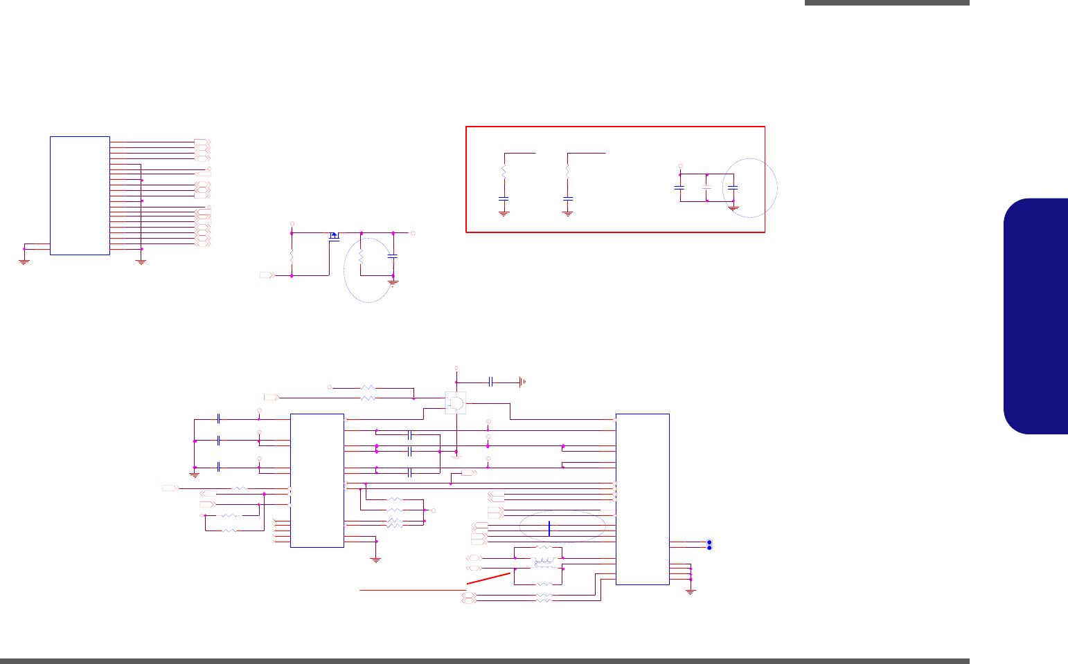
Schematic Diagrams
NEW CARD SOCKET B - 21
B.Schematic Diagrams
NEW CARD SOCKET
Sheet 20 of 40
NEW CARD
SOCKET
Z2011
1.5VS
C516
*3.3U_10V_08
MS_D219
3.3V
PCIE_RXN2_NC
R389
100K_04
Card Reader Power
R188
* 0_04
3.3V
SD _ CD# 19
4 8 mil
BUF_PLT_R ST#7,15,23,26
USB4-15
NEW_CARD_RST#15
Z2007
C486 .068U_16V _04
J_CR1
MDR019-X0-0X10(Rever se)
2
21
3
4
5
6
7
8
9
10
11
12
13
14
15
16
17
18
19
20
1
23
22
DAT2_SD
VS S_MS
CD/DAT3_SD
CMD_SD
VS S_SD
VDD_SD
C L K_SD
VS S_SD
DAT0_SD
DAT1_SD
WP_SD
VS S_MS
VCC_MS
SCLK_MS
DAT3_MS
INS_MS
DAT2_MS
SDIO/DAT0_MS
DAT1_MS
BS_MS
CD_SD
GND
GND
OC7#15
Z2008
SD _ D 1
NC_3.3V
OC7#
NC_CPUSB#
NC_3. 3VAUX
3.3V
MS_CLK
R425 *10K_04
MS_BS 19
MS_D319
SMB_ICHCLK26
Z2014
MS_INS# 19
PCIE_TXN2_N C
SU SB#
PCI E_RXP2_NC7
U SB4 +15
3.3V
USB4-
CLK_PCIE_NC
SD _ CLK 19
C549 .1U_10V _04
3 IN 1 SOCKET SD/MMC/MS(Pro)
VCC_CARD
3.3VS
C543 .1U_10V _04
SD _ D 3
R409 0_06
PCIE_RXN2_N C7
SD _ CMD 19
SD _ D019
PCIE_RXP2_NC
PM_ WAKE#26
>>>Near to S.B. for Intel platform
PM_ WAKE#
Z2010
Z2016
NC_RST#
J_NEW1
130801-1
17
1
10
26
20
23
4
19
18
22
21
25
24
14
15
12
9
13
11
8
7
16
5
6
3
2
CPPE#
GND
+1.5V
GND
GND
GND
CPUSB #
REF CLK +
REF CLK -
PERp0
PERn0
PETp0
PETn0
+3.3V
+3.3V
+3. 3V AUX
+1.5V
PERST#
W AKE #
SMB_DATA
SMB_CLK
CLKREQ#
RESERVED
RESERVED
USB_D+
USB_D-
SMB_ I CHCLK
M960813
R680 0_04
SD_CLK
3.3V S
MS_IN S#
MS_D3
C274
* 10PF_04
C146, C147:
NC_1. 5V
PCIE_TXP2_NC7
SU SB#13,15,16, 23,27,28,34
R428 *100K_04
M960813
CLK_PCIE_NC#
VC C_CARD
SD _ D319
PC I E _ TXN2_NC7
Clo se to soc ket
C531 .1U_10V _04
MS_CLK 19
SMB _ICHDATA26
U21
74AHC1G08GW
1
2
5
4
3
R429 *100K_04
C501
.1U_16V_04
R420 10K _04
Z2012
C511
.1U_16V_04
VC C_CARD
C544 .1U_10V _04
MS_BS
>>>Near to J_NEW1 for Nvidia platform
Z2004
L42
* PLW3216S 161SQ2
1
4
2
3
Z2009
NC_CLKREQ#
NC_C PPE# 17
R403 0_04
3.3V
10mil
R426 * 10K_04 CLK_PCIE_NC#2
NEW CARD
M960806
SD_CLK
R679 * 10K_04
Z2001 Z 2002
SD _ WP19
SD _ C MD
NC_CPPE#
NEW_CARD_RST#
U25
P2231THLFC1
2
3
4
6
5 8
7
9
1
11
14
15
16
17
18
19
20
21
22
23
10
12
13
24 25
SYSRST#
SH DN#
STB Y#
3.3V I N
3.3V I N 3.3V OUT
3.3V OUT
PER ST#
NC
GND
CPUSB#
CPPE#
1.5V OUT
1.5V OUT
1.5V I N
1.5V I N
AU XOUT
AU XI N
RCLKEN
OC#
NC
NC
NC
NC GND
R169
*0_04
Co-lay C ommon Cho ke? 0 O
? ? , ? ? Cost
_Down? ?
MS_D119
N C _ PER ST#
Z 2015
C547 .1U_10V _04
Z2013
MS_D0
ENE P2231 pin3,4,15,22
has internally
pulled high (170Kohm)
CARD_P WREN#19
BUF _PLT_R ST#
C506
.1U_16V _04
NC_CLK REQ#2
3 6 mil
SD _ D 0
MS_CLK
R412 0_06
CLK_PCIE_NC2
C540 .1U_10V_04
4 8 mil
R388
1K_04
Z2003
MS_D019
MS_D1
USB4+
R396 0_04
C546 .1U_10V _04
SD _ D 2
C485 .068U_16V _04
SD _ W P
SD_CD#
MS_D2
VC C_CARD
R719
0_04
C226
*10PF _04
Q23
AO3409
G
DS
SD _ D219
SMB_ I CHDATA
R424 *10K_04
SD _ D119
PCIE_TXP 2_NC

Schematic Diagrams
B - 22 LAN
B.Schematic Diagrams
LAN
Sheet 21 of 40
LAN
RXD1#
For VIA platform
TD-
C260
2.2U_16V_08
-PHYPWRDN 17
C57
1000P_2KV_12
Z2102
RXDV
LAN_CLKO
RN15
* 0_08_8P 4R
81
72
6
5
3
4
Z2105
RXCLK
Co-lay Common Choke? 0O
??,??Cost_Down? ?
RXD2#
C312
.1U_10V_04
C315
.1U_10V_04
TX-
MDIO#
MDC
CRS
RXD 3
C314
6.8P_50V_04
RXC L K#
TXD 3
R66 75_1%_04
TXCLK
RN8
33_8P4R_04
81
72
6
5
3
4
R180 * 0_04
RXCLK 17
C372
.01U_50V _04
PH YP WRDN
R232
49.9_1%_04
VT6103L
U7
VT6103_G
25
26
27
28
29
30
31
32
33
34
35
36
37
38
39
40
41
42
43
44
45
46
47
48
1
2
3
4
5
6
7
8
9
10
11
12
13
14
15
16
17
18
19
20
21
22
23
24
VDDRX
RX-
RX+
FXSD
GNDRX
GNDPLL
REXT
VDDPLL
GNDTXC
TX-
TX+
VDDTX
GNDTX
GNDOSC
XO
XI
VD DOSC
RST
MDI O
MDC
RXD3
RXD2
RXD1
RXD0
VD D1
GND1
RXD V
RXC
RXE R
GNDC
VDDC
TXE R
TXC
TXE N
TXD0
TXD1
TXD2
TXD3
COL
CRS
GND2
VDD2
INT
LED0
LED1
LED2
LED3
PD
C382
.1U_10V_04
RD-
R207 33_04
Z2107
LAN_CLKI
R177
75_1%_04
3. 3VL AN PH
MDC 17
CRS 17
TXD217
PH YP WRDN
R178
75_1%_04
R271 10K _04
-PHYRST 17
C378
.01U_50V _04
RN1 33_8P4R_04
81
72
6
5
3
4
Z2109
RXD0 17
TXD017
RXE R#RXER
R257 33_04
TXCLK#
3.3V
RXD2 17
C365
.1U_10V _04
Z2103
RD-
Z2104
TD+
R237
49.9_1%_04
MDIO
TXCLK 17
R228
6.49K_1%_04
DUPLEX
L41HCB2012K F-121T30_08
1 2
RXD V 17
CMX4 -
R259 10K _04
R258 10K _04
R222
49.9_1%_04
3.3VLANPH
CMX4 +
CMX3 +
TD-
DUPLEX
R260 10K _04
RX+
C364
.01U_16V _04
JLAN1
PJ S - 2 8VL3
1
2
3
4
5
6
7
8
GND1
GND2
DA+
DA-
DB+
DC+
DC-
DB-
DD+
DD-
GND
GND
MDI O 17
CRS#
C313
6. 8P_50V_04
Z2106
RXD0#
R272 10K _04
CMX4+
C395
10U_10V_08
TXD317
TXD 2
SPE ED
NWAY
TXE N
3.3V
3.3VLANPH
NWAY
CMX3-
Z2108
RX-
RXD V#
RXD2
RXD 1
COL 17
SPEED
CMX3 -
C384
.1U_10V _04
M960803
TXEN 17
CMX4-
RXD 0
LINK
RXE R 1 7
Z2101
TX+
RXD3#
LN1 B4W
1
2
3
4 5
6
7
8
RD+
TXD117
COL
REXT
CMX3+
R256 33_04
C394
.1U_10V_04
LINK
TD+
C363
.1U_10V_04
3. 3V
RXD1 17
TXD 1
R62 75_1%_04
RD+
TXD 0
COL#
LAN_CLKO
X1
25MHz
12
RXD3 17
R219
49.9_1%_04
R273 33_04
C351
.1U_16V _04
T10
LF-H80P-1
1
2
16
15
314
412
5
6
7
13
9 8
11
10
RD+
RD-
RX+
RX-
RD_C TRX_CT
NCNC
NC
TD_CT
TD+
NC
TX- TD-
TX_CT
TX+
C369
.1U_10V_04
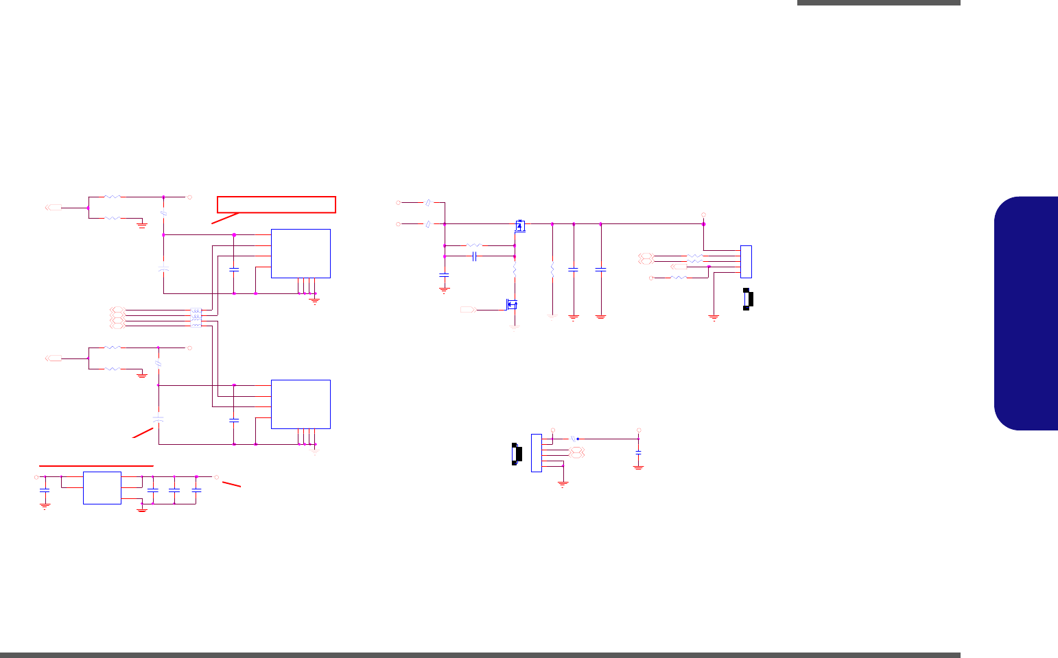
Schematic Diagrams
USB & CCD B - 23
B.Schematic Diagrams
USB & CCD
Sheet 22 of 40
USB & CCD
USB3- 15
60 mil
60 mil
J_FP1
CON6_F P
1
2
3
4
5
6
Z 2211
USB2+15
USB5+
R112 68K_04
5V
USB3+ 15
From H8 de fault HI
EM I sol ution ,whe n pla cemen t
ne ar to USB Port ?
R31
100K_04
C128
10U_10V_08
J_USB1
USB_4P
1
2
3
4
GND1
GND2
GND3
GND4
V+
DATA_L
DATA_H
GND
GND1
GND2
GND3
GND4
CCD_DET#23
U2
RT9701-CPL
1
2
3
4
5
VO U T
GND
VI N
VI N
VO U T
3.3V_F P
C748
.1U_16V_04
1
FP CONN
Q36
2N7002W
G
DS
R6 330K_1%_04
USB0+
L18
HCB3216KF-800T30_12
1 2
C568
.1U _10V_04
Z 2210
C114
.1U_10V _04
6
L19
HCB3216KF-800T30_12
1 2
USB0+15
+
C86
100U_6.3V_B
12
US BVCC? ? ? ? ? 5V
~ 5.2 5V? ? ,? ? ? ?
4.9V,???????
De vice? E ye Pa ttern Test
fail??????
OC1#15
USB0-
3.3V S
OC0#
USBVCC
5V
6-19-91001-001
R132 82K_04
USB5+15
USB2+
1
C111
.1U_10V_0 4
L6
*HCB2012K F-500T40_08
1 2
LP1
CM-4M3216-181JT
1
2
3
4
6
5
7
8
USB5-
J_CCD1
88266-05001
1
2
3
4
5
CCD_E N23
J_FP1
USB0-15
Z2207
Q4
AO3409
G
DS
USB2-
R10
68K_1%_04
L7
HCB 201 2KF- 500T40_08
1 2
? ? U SB_P ort? ? ? ? 1 00U
? ? , ? ? ? ? ? Devi ce? ?
? Resta rt? ?
Z2209
Z 2201
R110 82K_04
C94
.1U _10V _04
USB2-15
Z 2205
J_USB2
USB_4P
1
2
3
4
GND1
GND2
GND3
GND4
V+
DATA_L
DATA_H
GND
GND1
GND2
GND3
GND4
5VS
OC0#15
Z 2203
C153
.1U _10V _04
C11 1U_16 V_06
L404 HCB 1608KF -121T25
5
USB PORT
VDD3
USB5-15
R18 0_06
60 mil
48 mil
Z 2202
OC1#
60 mil
USBVCC
Z2208
R13 0_06
5VS_CCD
C9
10U_10V _08
Z 2204
C106
10U_10V_08
R122 68K_04 USBVCC
J_CCD1
+
C141
100U_6.3V_B
12
R11 10K_0 4
C567
10U_10V_08
Z 2206
CCD
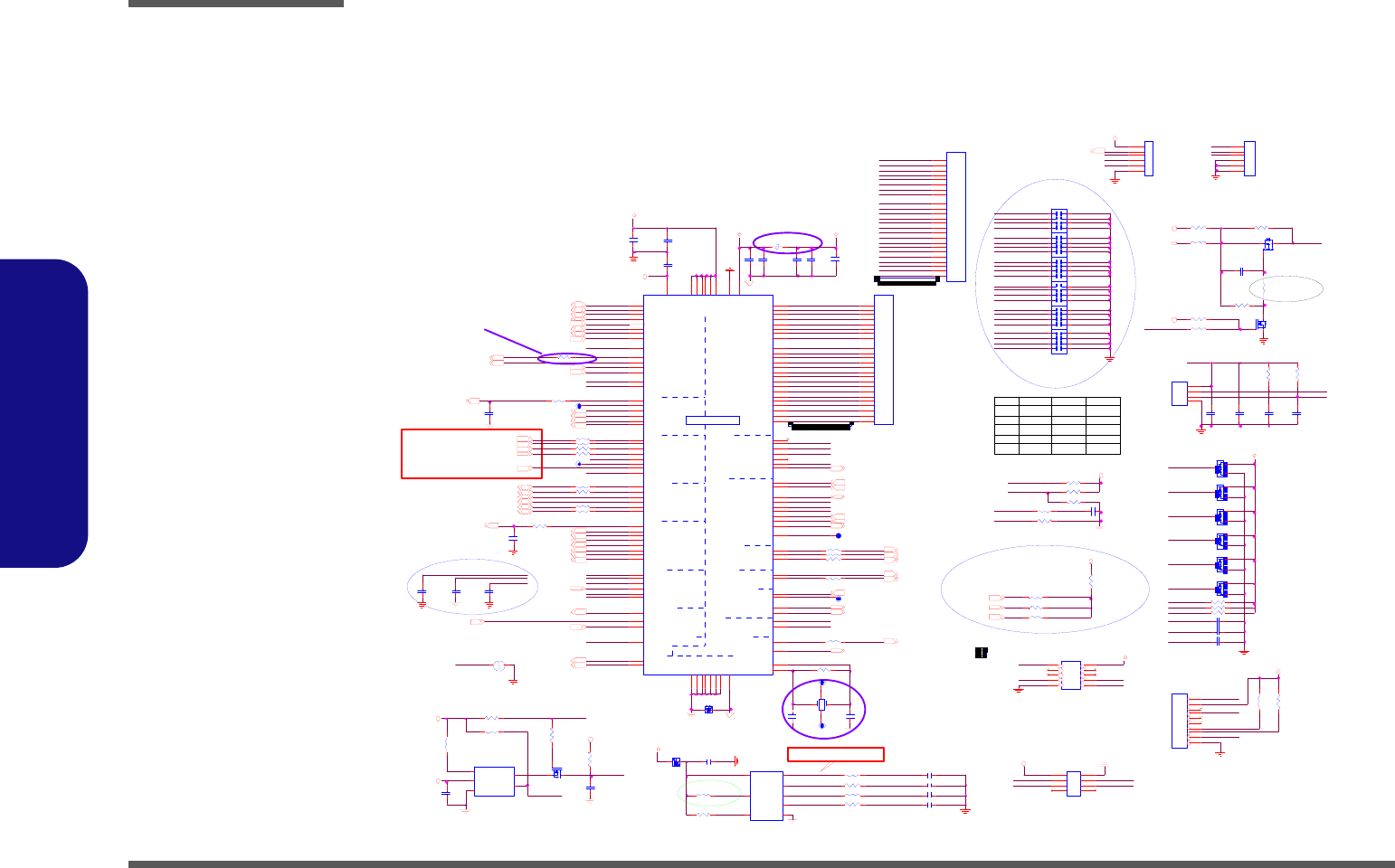
Schematic Diagrams
B - 24 KBC-IT8512E
B.Schematic Diagrams
KBC-IT8512E
Sheet 23 of 40
KBC-IT8512E
EC _ R C IN#
24
LP C _A D 317
EC_P69
Z2 30 7
BRIGHTNESS
R3 38 1 0K_04
KB - S O 15
KBC_RESET#
E C _V G A _A LE R T#
WDT_EN
R75 6 *0_ 04
R79 9 47 _04
M960806
CK3 2K
KB - S I2
KB C _S P I _S I_R
BAT1_DET
C 8 25 * 33 P_ 50V _0 4
R863 0_0 6
J HOTKEY2
CON6_ HOTKE Y
1
2
3
4
5
6
R7 58
47K_04
KBC_ AGND
KB - S O 10
TP _ D A TA
R 7 55 * 0 _04
R5 60 1 00 _04
3.3V
WEB1#->HWEB2#->E-MAIL
LED_BAT_FULL#
WEB0#
R3 49
10K_04
LPC_AD2
L ED_ SCROLL#
3G_SET#
VCORE_PG
24
EC _ SC I #
WDT_EN
J_TP1
85201-04051
1
2
3
4
1
2
3
4
D1 1
BAV99
A
C
AC
KB - S I1
WLAN_EN
BT_ EN
D1 9
BAV99
A
C
AC
C 81 8 1 U _1 0V _06
BU F _P L T _R S T #7, 15 , 20, 2 6
SUSC#
80CLK
SERIRQ
SPI_ VDD
+5VTP
SMD_BAT1
C650
.1 U _10 V _04
L ED_ CAP #
KB - S O14
KB - S O 7
KB - S O 1
J_ KB 2
* 8 52 01- 2 405 1
24
23
22
14
12
11
21
8
20
19
6
5
18
4
17
10
9
7
3
2
1
16
15
13
KB - S O 7
80 D ET #
BT _ D E T#
CCD_DET#
HIGH
17.4K
KB - S O 13
J_KB1
8 520 1- 24 05 1
24
23
22
14
12
11
21
8
20
19
6
5
18
4
17
10
9
7
3
2
1
16
15
13
1
KB - S O13
L ED_ BAT _CHG#
SYS_F AN
KBC_ PW RGD 1 5
KBC_ RST #
LE D _A C I N#
C392 1U_10V_06
R53 7 10 K_ 04
D3 5
BAV99
A
C
AC
VCORE_ON31
CCD_DET#
Z231 4
80DET#
VD D 3
T H ER M _ AL ER T #
WEB2#
KB - S I1
R865 0_0 6
C4 53
15P_50V_04
CHG_ CURSEN
X2
32.768KHZ
1
3
2
4
R 3 36 * 1 0K _0 4
VOLTAGE
KB - S O 12
SM D _ BA T1
SMD_BAT1
KB C _S P I _C E #
KB - S I4
HIGH
RSMRST# 1 6,17
SMD_BAT1
80 C LK
KB - S I1
WD T _E N
R800 4.7K_04
R79 6 15 _1% _04
LE D _A C IN#28 KB - S O3
R79 8 15 _1% _04
C477
.1U_1 0V_0 4
5V S
VD D 3
RSMRS T #
KB - S I0
KBC_BEEP27
SM C _ TH E R M
R30 6 *10 M_0 6
C3 76
. 1 U _10 V _04
R5 38 1 00 _04
C412
10U _ 10 V_ 08
1. 05 V_ PG30
KB - S I7
KBC_BEEP
KB - S O10
WE B3 #
R2 31 1 00 _04
KBC_SPI_SCLK_R
CCD_EN
LPC_AD1
WD _ DISA BL E
H_A20GATE
Z2301
R80 7
10 0K _04
J _IT ED BG
AC _ I N #29
KB - S O 11
KB - S I5
SMC_BAT129
PW R _B TN # 1 6
R240 120K_04
SUSC# 16
R3 29 1 0K_04
SMC_BAT1
WE B5 #
KB - S O 11
TOTAL_ CUR
KB - S I0
45K
TH E R M _R S T#3
CPU_F AN25
H_A20 GAT E15
KB - S O 6
KBC_SPI_SCLK
EC _ PB #
WE B 4#
KB - S O 5
R867 0_0 6
PIN 68->CHG_CURSEN ,PIN 70->X
PIN 71->3G_DET# ,PIN 48->SYS_FANSEN
PIN 94->ITE_SUSB# ,PIN 95->WEB3#
PIN 108->BT_EN ,PIN 109->BKL_EN
PIN 79->WLAN_EN ,PIN 93->CLKRUN#
PIN 100->X ,PIN 104->X
PIN 107->3G_EN ,PIN 119->WEB4#
PIN 23->WEB0# ,PIN 15->WEB1#
PIN 33->WEB2# ,PIN 123->WEB5#
PIN 80->EC_VGA_ALERT#
C960531
KB C _A V D D
CHG_CURSE N29
KB - S I3
J_ KB
2
LP C _A D 217
BAT 1_ DET29
EC_P68
R 8 62 0 _04
3.0V
PWR_BT N#
C82 2 .1U_ 16 V_ 04
KB - S O 1
SY S _ F A N SE N
WE B 3#
KB - S O 2
KB - S O5
C8 69
* 3 0P _5 0V _0 4
KB - S I4
KBC_SPI_SCLK
LO W(SR U)
KB - S O 2
SM C _ BA T1
KB - S O6
CK3 2K E
C48 0
.1U_1 0V_0 4
KB - S O8
WEB2#
D3 6
BAV99
A
C
AC
C400 1U_10V_06
100K
BL K_ EN24
EC_P69
D3 4
BAV99
A
C
AC
V4.0
AC_IN#
KB - S I3
Z2 30 3
VOL_ MUTE#
KBC_ SPI_CE#_ R
KB - S O 4
KB - S O 14
KB - S O 3
C8 71
* 30P _5 0V _0 4
KB - S O 3
KBC_SPI_SI
SM C _ TH E R M3
S U SB # 13 , 15, 1 6, 20 , 27, 2 8, 34
Z 230 2
EC _ SW I #
LID_SW#
SMC_BAT1
BUF_PLT _RST#
SMD_BAT129
KB C _ S P I _ C E # _ R
R5 50 1 00 _04
M960726
DD_ON 29 ,33
R864 0_0 6
J_ I TE D BG 1
SPUFZ -10 S3-B-0-B
12
34
56
78 910
5V
THERM_ AL E R T#3
R4 9
10K _0 6
CP4
*8P 4 CX15 0PF
1
2
3
45
6
7
8
WDT_EN
L5 3 F C M 20 12V - 12 1_ 08
1 2
K/ B MA TRIX
FL ASH
LPC
SMB US
PS/ 2
PWM
UAR T
DAC
CLO CK
IT8512E
CI R
ADC
WAK E UP
PW M/CO UNTE R
LP C/WA KE U P
EX T GP IO
GP INTER RUPT
WA KE U P
GP IO
U9
I T8 512 E /EX
14
13
10
9
8
7
6
17
5
15
23
12 6
4
58
59
60
61
62
63
64
65
36
37
38
39
40
41
42
43
44
45
46
51
52
53
54
55
11
26
50
92
114
127
121
3
74
85
86
87
120
124
22
35
12 5
18
21
112
10 9
10 8
123
88
89
90
47
48
24
25
28
29
30
31
32
34
66
67
68
69
70
71
72
73
1
12
27
49
12 2
113
75
2
128
79
78
77
76
83
84
82
33
20
91
81
80
16
119
56
57
93
94
95
96
97
98
99
107
11 0
11 1
11 5
11 6
11 7
11 8
100
101
102
103
104
105
106
19
WRST#
LPCCL K
LAD0
LAD1
LAD2
LAD3
LFRAME#
( PD )LPCP D #/WUI6 /GP E 6
SERIRQ
ECSMI#/GPD4( PU )
ECSCI#/GPD3( PU )
GA20 / GPB 5
KBRST#/GPB6 ( PU )
KS I 0/ S TB #
KSI1 /AFD#
KSI2/INIT #
KS I3/SL IN#
KSI4
KSI5
KSI6
KSI7
KS O 0 / P D 0
KS O 1 / P D 1
KS O 2 / P D 2
KS O 3 / P D 3
KS O 4 / P D 4
KS O 5 / P D 5
KS O 6 / P D 6
KS O 7 / P D 7
KSO8/ACK#
KSO9/BUSY
KS O 1 0 / PE
KSO11/ERR#
KS O 1 2 / SL C T
KSO13
KSO14
KSO15
VCC
VST BY
VS T BY
VSTBY
VSTBY
VST BY
VST BY
VBAT
AV C C
PS2CLK0/GP F 0( P U )
PS2DAT0 /GP F 1( P U )
PS2CLK1/GP F 2( P U )
( PD )T MRI0 /WUI2/GPC4
( PD )T MRI1 /WUI3/GPC6
LPCRS T #/WUI4/GPD2( PU )
( PD )WUI5 /GPE 5
PW RSW /GPE4( PU )
RI1 #/WUI0 /GPD0( P U )
RI2 #/WUI1 /GPD1( P U )
( P D )RING#/PWRF AIL#/LPCRST#/GP B 7
TXD/GPB1( PU )
RXD/GPB0( PU )
( PD )CTX/GP B 2
PS2DAT1 /GP F 3( P U )
PS2CLK2/GP F 4( P U )
PS2DAT2 /GP F 5( P U ) ( PD )TACH0/GPD6
( PD )TACH1/GPD7
PW M0/GPA0 ( PU )
PW M1/GPA1 ( PU )
PW M2/GPA2 ( PU )
PW M3/GPA3 ( PU )
PW M4/GPA4 ( PU )
PW M5/GPA5 ( PU )
PW M6/GPA6 ( PU )
PW M7/GPA7 ( PU )
ADC0/GPI0
ADC1/GPI1
ADC2/GPI2
ADC3/GPI3
ADC4/GPI4
ADC5/GPI5
ADC6/GPI6
ADC7/GPI7
VSS
VS S
VSS
VSS
VS S
VSS
AVSS
CK32 KE
C K 32K
DAC3/GPJ3
DAC2/GPJ2
DAC1/GPJ1
DAC0/GPJ0
( PD )E GCS#/GPE 2
( PD )E GCLK/GP E 3
( PD )E GA D/GP E1
GIN T /GP D5( P U )
L80LLAT/GPE 7( PU )
VSS
DAC5/GPJ5
DAC4/GPJ4
PW UREQ# /GP C7( P U )
( PD )CRX/GPC0
( PD )K S O16/GPC3
( PD )K S O17/GPC5
( PD )ID0/ GP H0
( PD )ID1/ GP H1
( PD )ID2/ GP H2
( PD )ID3/ GP H3
( PD )ID4/ GP H4
( PD )ID5/ GP H5
( PD )ID6/ GP H6
( PD )ID7/ GP G1
SMCLK0/GPB 3
SMDAT0 /GP B 4
SMCLK1/GPC1
SMDAT1 /GP C 2
SMCLK2/GPF 6( PU )
SMDAT2 /GP F 7( PU )
FLFRAME#/GPG2
FLAD0/SCE#
FL AD 1 / SI
FL AD 2 /SO
F LA D3/ GPG6
FLCLK/SCK
( PD )F LRST# /W UI7/TM/GP G0
( PD )L8 0HLA T /GP E 0
PW RGD_VCORE15,31
KB - S I3
BAT1_ VOLT
M_B TN #
EC _ SM I #
3IN1
HIGH
VDD3
KBC_PCLK2
DD_ON
3G _E N
WEB1#
KB - S I7
EC_P67
2.4V
SMI#
KBC_SPI_SI_R
CP3
*8P 4 CX15 0PF
1
2
3
45
6
7
8
KBC_ AGND
3. 3V S
SPI_ VDD
BT _ E N26,28
P M _C LK R U N # 16
CPU_ FA NSEN
SCI#
CPUF AN
WE B 5#
ITE_SUSB#
KB - S O 15
PW R _ S W #
KBC_ SPI_SO_R
R 75 4 0_ 04
CCD_E N 2 2
Z23 09
KBC_SPI_CE#
CHG_CURSEN
KB - S I6
R866 0_0 6
26.7K
V2.0
LPC_FRAME#17
KB - S O 5
SMC_BAT1
KB - S I6
KB - S O 8
BA T 1 _V O L T
Z23 16
D1 4
BAV99
A
C
AC
C 8 23 * 33 P_ 50V _0 4
R76 1 *0_ 04
C4 83
10U_10V_08
KBC_ SPI_ *_R = 0.1 "~0. 5"
WEB0#
Z2308
R4 8
10K_06
JHOTKEY1
CON 6 _H OT KE Y
1
2
3
4
5
6
HIGH
L CD_B RIGHTNESS24
TO TA L_ C U R
80DET#
C 8 24 * 33 P_ 50V _0 4
C7 52
10U_10V_08
PME#
KB - S O 6
Q46
AO 3 4 0 9
G
DS
10
* DEL C960705
BAT1_VOLT29
LED_SCROL L#28
KB - S O 13
LPC_AD0
KB - S O 9
C87 0
*30P_50V_04
R797 1K_04
VER.
WE B4 #
LED_PWR#
KB C _ P W RGD
PME#16,19,26
KB - S O15
WD _ D I SA B LE NC2 NC_04
2.1V
PM_ CLK RUN#
R759 1M_04
2.7V
U1 2
A AT 35 10I G V
3
5
2
1
4
MR #
VC C
GND
RESET#
WD I
LED_NUM#28
SP I _V D D
R88 3 0_ 04
KB - S O 0
KB - S O1
????????Pull
High to VDD3
VDD3
VGA_SDATA11, 1 2
BLK_EN
KB - S O 14
R12 6
10 K_ 04
LID_SW#24,29
Z2 30 4
KBC_SPI_SO
+5VTP
R88 2 0_ 04
C388 1U_10V_06
C4 73
.1U_1 0V _0 4
X
F or M 670SR U EM I So lutio n
R88 1 0_ 04
C12 6
47 P_ 50 V_ 04
TO T AL _C U R29
KB - S O7
Q4 7
2N7002
G
DS
R76 0 10 K_ 04
R 127
10 K_ 04
CHG_E N
LPC_FRAME#
R79 5 47 _04
NC1 NC_0 4NM
LP C _A D 117
KB - S O 0
CP6
*8P 4 CX15 0PF
1
2
3
45
6
7
8
R715 * 10K_06
V3.0
MODEL_ID
R 8 79 0 _06
HI (SR )
SC I # 1 6
KBC_PCLK
3I N 1
Z231 3
KB - S I7
3I N 1
KBC_SPI_SO
CP2
*8P 4 CX15 0PF
1
2
3
45
6
7
8
LED_CAP#28
CHG_EN 2 9
KB - S O 9
KB - S I6
EC_P68
KB - S O 12
J_ SP I 1
S P N Z- 0 8S 3- B - C-0 -P
1 2
3 4
5 6
7 8
C49 1
1U_10V_06
V1.0
M960806
1. 5V _P G30
BA T1 _D E T
KB C _ S P I _ S C L K _R
WEB1#
C1 25
1U_10V_06
???
E C _V G A _A LE R T#12
TP_CLK
KB - S O9
THERM_ RST#
KBC_ RESE T#
80CLK
CP5
*8P 4 CX15 0PF
1
2
3
45
6
7
8
VDD3
I T E_ W L AN _ PW R26
KBC_ FL ASH
EC_GA20
KB - S O0
KB - S I0
LED_PWR#28
KB - S I5
Z231 1
BAT1_ DET
W L AN _ D ET #
KB - S O 8
1
HIGH
BAT1_ DET
MOD E L_ I D
M_ BT N #29
VDD3
SM I # 1 6
CPU_F ANSE N 2 5
KB - S O11
U41
SS T2 5V F0 80 B
1
2
3
4
5
6
7
8
CE#
SO
WP #
VS S
SI
SCK
HOLD#
VDD
C64 9
.1U_1 0V _0 4
C3 91
.1 U_10 V_ 04
V5.0
SW I # 16
KBC_SPI_SI
C 8 26 * 33 P_ 50V _0 4
ITE DEBU G POR T
KB - S O12
Z2 30 6
L E D _B AT _F U LL#28
WLAN_EN26,28
TP_DATA
EC_P66
SERIRQ16 ,19
CCD_DET#22
KB - S I2
SUSB#
KB - S O4
KB - S O 4
C43 3
15 P_ 50 V_ 04
RX
BT_DET# 2 6
R37 5
100K_04
VDD3
VOL_MUTE#27
R2 46 1 00 _04
C82 1
.1U_1 0V_0 4
M960 803
R2 95 1 0_ 04
Q22
2N 70 02 W
G
DS
9
M9 6080 6
KB C _R S T# 1 5
C8 65
* 1U _ 10 V_ 04
WEB0#->HWEB1#->APPLICATION
3. 3 VS
PW R _ S W #29
Z2 31 0
L ED_ NUM#
KB - S O2
KB - S O 10
R2 65 1 00 _04
JD E BU G 1
HEADER 10_R
1
2
3
4
5
6
7
8
9
10
R3 39 0 _0 4
1
VD D 3
VG A _ S C LK11
VC ORE _ON
LPC_AD3
R88 0
10K_04
WDT_EN
R55 3 4.7 K_ 04
VDD3
SM D _ TH E R M3
R3 30 1 0K _0 4
LP C _A D 017
WL A N_DET# 26
SWI#
KBC_PCLK
I T E_ W L AN _ PW R
VDD5
VD D 3
EC_P67
C4 18 1 0P _5 0V_0 4
WEB2#->HWEB0#->WWW
? ? J_KB2? ?
LED_BAT_CHG#28
RSMRST#
KB - S I4
3IN1
CP7
*8P 4 CX15 0PF
1
2
3
45
6
7
8
R3 46 0 _0 4
KBC_SPI_SO_R
V C O R E_ PG
KB - S I5
KB - S I2
PJ 14
20mil
1 2
R54 8 4.7 K_ 04
J_KB
5V
MOD EL _ID
Z23 15
SM D _ TH E R M
R3 77 1 0K _0 4
C 127
47 P_ 50V _0 4
I T E_ SU S B #
TP_CLK
8Mbit
SCS751V->0 OHM
C960705

Schematic Diagrams
CRT & LVDS B - 25
B.Schematic Diagrams
CRT & LVDS
Sheet 24 of 40
CRT & LVDS
VGADDCCLK
R
LVDS-U1N
L 4 F C M160 8K - 121 T0 6_0 61 2
R14 *0_04
LVDSUP0
Z2 44 3
LVDS-L0P
Z2 42 0
Z 2 427
C58 0
*.01U_50V_06
5V
3. 3V S
PL LV C C
Z243 1
C5 63
1 00 0 P_ 5 0 V_ 0 4
C79 5
* . 1U _ 16V _0 4
C5
10 00P _ 50V _0 4
R7 82 *0 _0 4
2
? : D14,D15,D16? ? ? ? ? ? ? ? CHIP_SET
? ? ? ? ? ,? :Intel? 945GM? 2.5VS
3. 3V S
VGADDCCLK
LVDSLN0
LVDSLP0
VGA_ G 1 2
NB_DDC_ CLK 8
DVP1D1011
B
LVDSLN2
R23 6 *0_0 4
R7 6
*2 . 2K_06
LV D S G N D
DVP1DE11
LB_DATAN2
Z 2 446
Q1 4
*B S S1 38 _NL
G
DS
R10 8
*1 00 K_ 06
LV D S- L C LK N 1 2
C8
22 P _50 V_ 04
C847 *10PF_04
LV D SV C C
VGA_ B 12
L VDS_P D#
L5 FCM1608K-121T06_061 2
C 7 99 * . 1U _1 6V _0 4
L1 FCM1608K-121T06_061 2
Q40
2N 7 002 W
G
S D
VGA_ENAVDD 12
VSY
Z 2 447
R52
10 0_ 08
LVDSLCLKP
Z 2 445
C5 75
.1 U _5 0V _06
R7 76 *0 _0 4
R4 55 *0 _0 4
1-4 ON SINGLE
2-3 X >.<!
D4 1 RB751 V
A C
R41
1 00_ 08
R 10 9 * 0 _06
C848 *10PF_04
2. 5V S
Z2414
LA_DATAP0
LVDS-U0P
C8 72
22 U _6 .3V_ 08
NB (SR)
R6 4
* 1 0K _0 6
C21
.1U_ 50 V_ 06
D3
BAV99
A
C
AC
L VDSUN0
R5 3 0 _04
29
V GA (S UR)
3. 3 VS
3.3VS
Z2410
LVDS-LCLKP
R7 80 *0 _0 4
R36 *4.7K_06
R830 22_ 04
3. 3V S
Z2441
R63
82K _0 6
NB_ LV DSCL K 8
R2 26 *0_ 04
R 17 2 2. 2K _0 6
Ra
PWR
LV D SL P2
LB_CLKP
R 4 4. 7K _0 4
R79 0
*2 .4K_1%
Z2439
ED G E
L VDSUN 1
LA_DATAP1
R2 27 *0_ 04
R4 3 0 _04
R73 1
4. 7K _ 04
24 m il
Z 2 426
D8 RB7 51V
AC
VGA_ DDCDATA 12
Z2 438
Z2407
C5 76
4 . 7U _1 0V _0 8
CRT PORT
VGA_ VSY 1 2
SR1
Z2 403
CRT_VSYNC
LVDSLP2
L VDSUN1
C18
.1U_5 0V_0 6
R70 2
*4.7 K_ 04
LV D S- L 0P 1 2
LVDS-L2P
C852 *10PF_04
R4 4 0 _04
LVDSGND
LVDSLN2
L VDSCLK
NB (SR)
66SR 4.7K
DVP1D0211
Z2 40 9
LVDSLP1
LVDSLN0
R5 4 0 _04
R 2 3 0 _06
C5 77
. 1 U _50 V_ 06
C1 9
* . 1U _5 0V _ 0 6
C838 *10PF_04
NB_HSY NC 8
NB_ ENA VDD 8
LVDSDATA
LB_DATAP1
Rb
EDGE
L4 8
HCB3216KF-800T30_12
1 2
LI D _ SW #23 , 29
LV D S- L 0N 12
Z2405 DDCDATA
LB_DATAN0
LVDS-U0N
C 25 * . 1U _ 50V _ 06
R7 79 0 _04
1
5VS
Z2 402
LVDSUP2
Z 2 444
C15
* 1 U _10 V_ 06
R2 4 *0_0 6
5VS
LVDSVCC
LV D S- L 1P 1 2
DVP1D0311
R28 *0_04
C 28 . 1U _ 50V _0 6
Q5
*2 N390 4
B
E C
Rc
I2CC_SDA 1 2
DVP1D0011
Z 242 9
L4 7 F C M 16 08K - 12 1T0 6_ 061 2
R829 22_ 04
DVDD
NB_RED 8
LB_DATAN1
LA_DATAN0
J_C R T 1
D Z1 1A 91- N D 2 08- 4 F
8
7
6
5
4
3
2
1
9
10
11
12
13
14
15
GND2
GND1
R71 3
*4.7 K_ 04
LVDS-L0N
C851 *10PF_04
R5 6 0 _04
R 69 *10 K_ 04
R 44 4 4. 7K _0 4
R7 04
10K_06
R4 56 *0 _0 4
R7 77 0 _04
R29 *0_04
2. 5V S
NB_VS Y NC 8
LVDS-U2P
U27
*V T 163 7
1
29
5
13
22
27
35
10
14
19
26
36
37
38
39
40
41
43
44
45
46
47
48
33
2
31
34
28
25
32
30
42 24
23
21
20
18
17
12
11
9
8
7
6
16
15
4
3
VC C 2 5
VCC25
VCCLVDS
VCCL VDS
VCCLVDS
VCCPL L
GND
GNDLV DS
GNDLV DS
GNDLV DS
GNDPLL
D[0]
D[1]
D[2]
D[3]
D[4]
D[5]
D[6]
D[7]
D[8]
D[9]
D[10]
D[11]
DE
DUAL
HSYNC
PD B
R_F B
VS W ING
VR E F
VS Y N G
XC L K A 0 -
A0+
A1-
A1+
A2-
A2+
A3-
A3+
A4-
A4+
A5-
A5+
CLK1-
CLK1+
CLK2-
CLK2+
R7 81 0 _04
RP1 3
8P 4 RX22 _04
8 1
7 2
6
5
3
4
R17 *0_04
C843 *10PF_04
INVERTER CONNECTOR
DVDD
R2 11 4 .7K_04
R26
*4 .7 K _06
SR0
L VDSUP 2
LA_CLKP
LB_CLKN
LV D S- U 1 P 12
LA_DATAN2
FR E D
JI N V 1
CON6_ INV
1
2
3
4
5
6
R 2 0 0 _06
C844 *10PF_04
R23 9
*0_ 04
2.5VS
DVP1D1111
Z2 41 3
L VDS_PD#
C840 *10PF_04
R2 5
*1 K_ 1%_ 06
R7 7 0 _0 6
Q 1 2 N 70 02 W
G
DS
R7 84 *0 _0 4
VGA_BKL TEN12
LV D S- U C LK N 12
L VDSUP2
R 2 2 0 _06
PLL GND
D2
BAV99
A
C
AC
R61 *0_04
R3 8 *0_0 6
2. 5V S
LCD_B RIGHTNE SS23
LVDSLCLKP
LVDS-L1P
Q7
AO 3 4 0
G
D S
L1 5 H C B 20 12 KF - 12 1T3 0_0 81 2
If Ext VGA
USE 3.3VS
30
3. 3V S
P LLG N D
L VDSUP0
R2 33 *0_ 04
5V S
HSY
LVDSLCLKN
U8
* P 20 40C
1
2
3
4 5
6
7
8
5V S
LB_DATAN1
L1 3 FCM1608K-121T06_06
1 2
R22 4 *0_0 4
C7
22 P_ 50 V_ 04
DVP1D0711
B
Z 2 425
Z 2 448
C1
100 0P _5 0 V _04
C 7 98 * . 1U _1 6V _0 4
5VS
R3
4.7K_04
C82 0
*1 0PF
R 4 46 * 0 _0 6
D4 0 RB751 V
A C
3.3VS
DVP1D0811
Z2404
WAITTING FOR EMI
SOLUTION
Z2408
L VDSUN 0
LVDS-U2N
R5 5 0 _04
R7 75 0 _04
NB (SR)
Ra, Rb, Rc(?????75O)??
Intel So lution? , ? ? ? NB ? ?
Connector?????150O??
VSY
D32
BAV99
A
C
AC
EN A V D D
C2 2
* . 01U _ 50V _ 06
R27 *0_04
L9
*HCB2012KF-121T30_08
1 2
R4 43
4.7K_04
3.3VS
LA_CLKN
R30 *0_04
+
C45
10U_2 5V_12
R7 83 0 _04
PL L V C C
LVDSCL K
Z2406
CL KINP
LVDS-UCLKP
R7 86 *0 _0 4
P LEA SE CLO SE TO CON NEC TOR
5V S
DVP1D0511
R223 *10K_04
C 27 * . 1U _ 50V _ 06
LV D S- U 0 N 1 2
LA_CLKN
LVDSLN1
Z2 42 3
DUAL
R4 0
* 2 . 2K _04
2. 5 VS
LV D S- L 1N 12
LVDSLCLKN
LVDSLN1
Q3 4
2 N 700 2W
G
DS
3. 3V S
SR1
Z 2 433
LVDSDAT A
LA_DATAP2
LB_DATAN0
R 238 * 22_ 04
C845 *10PF_04
L4 9
* H C B 201 2K F -121T30_08
1 2
R
DUAL
C846 *10PF_04
R7 74 *0 _0 4
VGA (SRU)
F1 001LC D?
VI N
VGADDCDATA
DDCDATA
LA_CLKP
R 3 9 0 _06
R6 7
1 0K _06
R828 22_ 04
2.5VS
DVP1D0411
L VDSUN2
R 442 * 1K _0 4
R3 2 *0_0 6
L 2 F C M160 8K - 121 T0 6_0 61 2
HSY
L VDSUP1
C58 1
* . 1 U _50 V_ 06
R 111
1 0K _06
R2 1 *0_0 6
VGADDCDATA
L VDSUN 2
LVDS-LCLKN
R5 8
100K_06
R16 *0_04
C 8 01 * . 1U _1 6V _0 4
R15 *0_04
LV D S- L 2N 12
LA_DATAP2
L VDSDATA
L 3 F C M160 8K - 121 T0 6_0 61 2
LB_DATAP1
R3 4 *0_0 6
C46
. 1U _ 50V _0 6
R4 5 0 _04
R17 1 * 2.2K_0 6
5V
DVP1D0111
LB_DATAP0
L1 1
* H C B 20 12 KF - 121 T3 0_0 8
1 2
C853 *10PF_04
ENAVEE8
Z2417
Z 2 449
C2
10P_50V_04
C 796
* . 1U _1 6V _0 4
DVP1D0911
SR0
PLL GND
L VDS UCLKP
DDCL K
R3 5
*1 K_ 1%_ 06
NB_BL UE 8
CRT_HSYNC
Z241 6
LA_DATAN1
R7
75_ 1%_ 04
C3
10P _5 0 V _0 4
LV D S- L 2P 1 2
LVDSLCLKN
C850 *10PF_04
L4 6 F C M 16 08K - 12 1T0 6_ 061 2
R831 22_ 04
C14
* . 1U _ 50V _ 06
LV D S- U 2 P 12
L VDSUCLK N
C2 0
*.01U_50V_06
C842 *10PF_04
R 3 7 0 _06
C 8 00 * . 1U _1 6V _0 4
3. 3 VS
CRT_ VS YNC
LVDSLN0
Z2442
LB_DATAP2
R7 85 0 _04
R7 87 0 _04
C4
1 0P _50 V _04
C 385
* . 1U _1 6V _0 4
A LL_ P WR O K3, 15 , 17
DVP1HS11
FG R N
Z2435
LVDSLP0
Z2 42 2
LB_CLKP
C566
* 1U _ 10V _0 6
C841 *10PF_04
R4 2 0 _04
LVDSLP1
LV D SL N 2
C5 73
*.1 U _50 V _06
R4 6 0 _04
R8
75_1%_04
C839 *10PF_04
2. 5V S
NB_GREEN 8
LV D S- U 2 N 1 2
MRA
LA_DATAN1
C819 *.1U_50V_06
R9
7 5_1 %_0 4
3. 3V S
DISP CLKI8
L VDSUC LK N
Q2
2N 7 00 2W
G
DS
D5
BA V 99
A
C
AC
Q8
2N7002W
G
DS
LV D S- U C LK P 1 2
LV D S- U 0 P 12
G
R7 88 *0 _0 4
PL V DD
2. 5 VS
I 2C C _S C L 12
Z243 4
LB_DATAN2
C5 79
*1U_10V_06
Q6
* 2 N 700 2W
G
S D
L1 4 F C M 16 08 K- 12 1T 06_ 061 2
C13
* . 01 U _50 V_ 06
R59
10 K_ 06
FB LU
LA_DATAP0
R2 16 4 .7K_04
L16
HCB20 12K F -1 21 T30 _0 8
1 2
5VS
L VDSUP 1
LVDSLP1
R45 4 *1K _0 4
C6
2 2P _50 V_ 04
Q35
2N 70 02W
G
DS
5V S
D7
BA V 99
A
C
AC
NB_ LV DSDATA 8
Z2401
VG A(*SR U)
DVP1D0611
L VDS UCLKN
LVDSCLK
LVDS-L2N
R45 3
*1 K_ 04
D31
*SC S 75 1
AC
C562
100 0P _ 5 0V _04
RP15
8P 4R X 22_ 04
81
72
6
5
3
4
12
ON
SW 1
NHDS-0 2-T
3
4
1
2
DVP1CLK11
Z2428
R 3 3 0 _06
VGA_ R 12
Z 243 0
RP14
8P 4R X 22_ 04
81
72
6
5
3
4
LVDSLN1
Z 2 424
C79 7
* . 1U _ 16V _0 4
NB_DDC_ DA T A 8
LB_DATAP2
ENAVDD
Q9
DTC114 E UA
CE
B
LV D S GND
L_B K LT EN8
DDCLK
L10
*HCB2012KF-121T30_08
1 2
LA_DATAP1
Z241 5
LV R EF
Q37
2N 70 02 W
G
DS
J_ LC D1
OUT
L VDS UN1
Z 2 432
LVREF
R 4 47 0 _06
DUAL8
D3 P
D9 RB7 31 U
1
2
3 4
5
6
+
+
+-
-
-
LV D S- U 1 N 1 2
L VDS UP1
Z2 42 1
LB_CLKN
L VDSUCLK P
5V S
Z243 6
LVDSUN0
C 26 * . 1U F _5 0V _0 6
C849 *10PF_04
LA_DATAN0
Z2440
LVDSLP0
C 873
22U_6.3V_08
5V S
1.5VS
CRT_ HSYNC
L VDSUC LK P
J_ LC D 1
CON30 A
1 2
3 4
5 6
7 8
910
11 12
13 14
15 16
17 18
19 20
21 22
23 24
25 26
27 28
29 30
12
34
56
78
910
11 1 2
13 1 4
15 1 6
17 1 8
19 2 0
21 2 2
23 2 4
25 2 6
27 2 8
29 3 0
R1 9 *0_0 6
R6 0 0 _04
PL V DD
LV D S- L C LK P 12
MRA
LVDSLP2
R7 78 *0 _0 4
Place D17, R349 for PR100
LVDS-L1N
LVDS-U1P
R4 7 0 _04
D4
BAV99
A
C
AC
C58 2
* . 01 U _50 V _06
PANEL INTERFACE
F1001 LCD?
D33
BAV9 9
A
C
AC
C1 6
4 . 7U _1 0V _0 8
INVERTER
3.3VS
VGA_ DDCCLK 1 2
DVP1VS11
LB_DATAP0
R23 4 *0_0 4
BLK_EN23
DISPCL KO8
LVDSUN2
G
LA_DATAN2
LVDSLCLKP
R71 2
4. 7 K_ 04
Z243 7
L VDSUP 0
For M660SR USE
VGA_ HSY 12
LVDS-UCLKN
Q41
2N 7 002 W
G
S D
R7 89 0 _04
L1 2
* H C B 20 12 KF - 121 T3 0_0 8
1 2
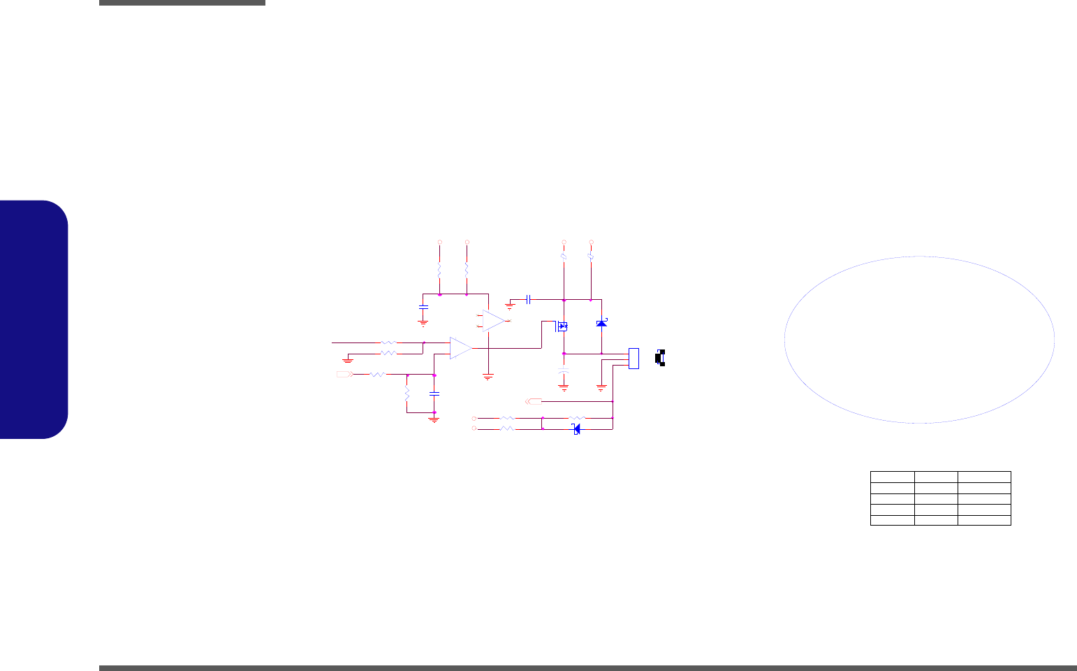
Schematic Diagrams
B - 26 FAN CONTROL, LPC ROM
B.Schematic Diagrams
FAN CONTROL, LPC ROM
Sheet 25 of 40
FAN CONTROL,
LPC ROM
R762
0_04
High
R5 4. 7K_04
40MIL
M960806
R763
*0_ 04
R12 4.99K_1%_06
R764 * 0_04
3.3V S
J_FAN1
85205- 0300
1
2
3
Block 1~7
R51
*2.2M_04
R57 10K_04
1
High
Z 2502
CPU_F AN23
C10
10U _10V _08
40MIL
D6
SCS551V-30
A C
C23
.1U_16V_04
Flash Mode
R765 0_04
FAN CONTROL
Protec ted
Low
VD D 3
D1 SCS551V -30
AC
+
-
U1B
LM358L
5
6
7
Block 0~7
L17
*HCB2012KF-500T40_08
1 2
F WH_TBL #
Q3
NDS352AP_NL
G
D S
JFAN
L8
HCB2012K F-500T40_08
1 2
Low
VDD5
Block 0
5VS
Z2503
C24
.1U_10V _04
FA N _DC_VOL
Z2514
Low
5VS VDD5
Z 2501
CPU_FANSEN23
3
High
Z 2515
FA N_DC_VOL
R50 120K_04
+
C565
100U_6.3V_B
12
FWH _WP#
High
Z2504
DEL SOCKET PLCC32
+
-
U1A
LM358L
3
2
1
84
Normal Low
Low

Schematic Diagrams
MINI-PCI & BLUETOOTH B - 27
B.Schematic Diagrams
MINI-PCI & BLUETOOTH
Sheet 26 of 40
MINI-PCI &
BLUETOOTH
PC I _ PAR15,19
PC I _ GNT#115
Z2625
50mil
R203 0_06
PCI_STOP#15,19
SMB_ I C H DATA
Z2617
U SB7 -
PC I _ AD 2 4
PC I _ AD 2 3
JBT
Z2612
PC I _ AD 4
Bluetooth
3.3VS
Q15
2N7002W G
DS
>>>Near to JMINI1 for Nvidia platform
Z2610
Z2629
R720 * 0_ 12
PC I E_ R XN1_WLA N
Z2627
R861 0_12
C802 1U_16V_06
PC I _ TR DY#15,19
>>>High level ( ON ); Low level ( OFF )
PC I _ AD 2 4
PLT_R ST#
WLAN_DET#
PLT_R ST#11,15
USB6+
WLAN_EN 23,28
PCI_AD[31:0]15,19
US B6- 15
PC I _ AD 1 6
PC I _ AD 1 2
Z2623
PC I _ AD 1 8
R204 0_04
3.3VS
USB7-15
PC I _ AD 2 2
PM_ WAK E#20
>>>WLAN_EN: Connect to H8
PC L KMPC I2
WLAN_EN23,28
PCI_AD[31:0]
Z2626
1
PCI_C/BE3#15,19
PC I _ AD 9
BT_ D ET#
PC I _ AD 2 6
JDFFC2
87151-35
3
5
7
9
11
13
1
15
23
25
21
27
31
29
17
19
20
18
16
14
2
12
10
8
6
4
22
24
26
28
30
32
33
35
34
PCI_AD0
PCI_AD2
PCI_AD4
PCI_AD6
PCI_AD8
PCI_AD9
GND1
PCI_AD11
PCI_CBE#3
PCI_IRDY#
PCI_CBE#1
PCI_TR D Y#
GND5
PCICLK
PCI_AD13
PCI_AD15
PCI_CBE#0
PCI_AD14
PCI_AD12
PCI_AD10
GND2
PCI_RST#
PCI_AD7
PCI_AD5
PCI_AD3
PCI_AD1
PCI_CBE#2
PCI_FRAME#
PCI_STOP#
GND3
GND4
VDD5-1
VDD5-2
VDD5-4
VDD5-3
1.5VS
PC I _ I R DY#15,19
Z2619
BUF_PLT_RST# 7,15,20, 23
PC I _ AD 2 1
C324
10U_10V_08
MINI-PCIE CARD
PC I _ AD 7
Z2605
Z2608
3.3V
C148, C155:
C187
10U_10V_08
US B6+ 15
R164 10K_04
MINI FFC CONN
BT_EN 23,28
Z2621
Z2602
BT_CLK
Z2606
BU F_ P L T_RST#
SMB_ I C H CLK
Z2609
R721
100K_04
USB7+15
PCI_FRAME#15,19
Z2618
JDFFC1
*87151-25
3
5
7
9
11
13
1
15
23
25
21
17
19
20
18
16
14
2
12
10
8
6
4
22
24
GNT2#
IDSEL
SERR#
D EV SEL #
PCI_AD17
PCI_AD19
PIRQB#
PCI_AD21
PCI_AD29
PCI_AD31
PCI_AD27
PCI_AD23
PCI_AD25
PCI_AD26
PCI_AD24
PCI_AD22
PCI_AD20
REQ2#
PCI_AD18
PCI_AD16
PERR#
PAR
PME#
PCI_AD28
PCI_AD30
C292
.1U_10V _04
KE Y
JMINI1
88911-5204
3
5
7
9
11
13
1
15
23
25
21
27
31
33
29
17
19
20
37
39
41
43
45
47
49
51
44
42
18
16
14
2
12
10
8
6
4
22
24
26
28
30
32
34
36
38
40
46
48
50
52
35
BT_ D AT A
BT_ C HCLK
C L KR EQ#
GND0
REFCLK-
REFCLK+
WA KE#
GND1
PE Tn0
PE Tp0
GND2
GND3
PE Rn0
PE Rp0
GND4
NC3
NC4
W_DISABLE#
NC6
NC7
NC8
NC9
NC10
NC11
NC12
NC13
LED_WLAN#
NC(LED_WWAN#)
GND6
UIM_VPP
UIM_RESE T
3. 3V_0
UIM_CLK
UIM_DATA
UIM_PWR
1. 5V_0
GND5
PER SE T #
3.3V AUX
GND7
1. 5V_1
NC(S MB_CLK)
NC ( SMB_ D ATA)
GND8
NC(U SB_D-)
NC(USB_D+)
GND9
NC(LED_WPAN#)
1. 5
V_2
GND10
3. 3V_1
GND11
R723 100K_04
SMB_ I C HDATA 20
Z2620
BT_ EN #
C705
.1U_16V_04
C704
.1U _16V_04
PME#16, 19,23
PC I _ DEVSEL#15,19
PC I _ AD 1 9
Z2611
PM_ WAK E#
R189 0_06
R202 *0_04
3.3V
USB6-
C330
.1U_10V_04
PC I _ AD 1 0
Z2601
+
C648
* 220U _6.3V_D2
12
Z2614
R205 0_04
BT_ D ET#23
PC I _ AD 8
PC I _ AD 1 3
Q43
2N7002
G
DS
R185
10K_04
VD D3
Z2633
PCIE_TXP1_WLAN
Z2628
C202
10U_10V_08
U SB7 +
Z2630
Z2604
R773 0_06
C803
.1U _10V_04
J_BT1
85205-08001
1
2
3
4
5
6
7
8
+3.3v
GND
USB-
USB+
DETECT#
CH_DATA
CH_CLK
BT_ O N#
PC I _ AD 3
Z2631
R165 * 0_04
PCI_SERR#15, 19
PC I _ AD 1
From SB GPIO Pin default HI
Power Plane:Suspend
S3:Defined
PC I _ AD 2 9
PC I _ AD 2 0
R860 *0_12
PC I _ C/BE0#15,19
48 mil
C353
.1U_10V_04
Z2615
PC I _ AD 6
PC I _ AD 1 4
PC I _ C/ BE2 #15,19
3.3V S
>>>Near to S.B. for Intel platform
PCI_REQ#115
PC I _ AD 1 1
WLAN_PWR Sign al default HI for WLAN
1.BIOS Setup HI for Intel PCIE WLAN
2.USB WLAN BI OS Setup LOW for
Fn+F10
8
3.3VS
PC I _ AD 1 7
WLAN3.3V S
R186 100K_04
WLAN_E N
WLAN3.3VS
PC I _ AD 2 7
R181 10K_04
PC I _ AD 0
C804
10U_10V_08 R722
20K_04
5VS
Z2632
PCI_C/BE1#15,19
1.5VS
SMB_ I C HCLK 20
PC I _ AD 2 5
L40
HCB2012KF- 500T40_08
1 2
R724 *0_06
Z2603
+
C647
* 220U_6. 3V_D 2
12
3V S_ BT
PC I _ AD 2
R187 *0_04
PCI_INTD#15
Z2613
PC I _ AD 3 0
Q42
AO3409
G
DS
PC I _ AD 15PC I E_ TXN1_WLAN
PCI_PERR#15, 19
ITE_WLA N_PW R23
WLAN3.3VS
BT_DAT
PC I _ AD 5
Z2624
PC I _ AD 2 8
Z2607
PCIE_RXP1_WLAN
Z2622
Z2616
WLAN_DET#23
PC I _ AD 3 1
BT_ EN
3G card used: Place the C908, C909
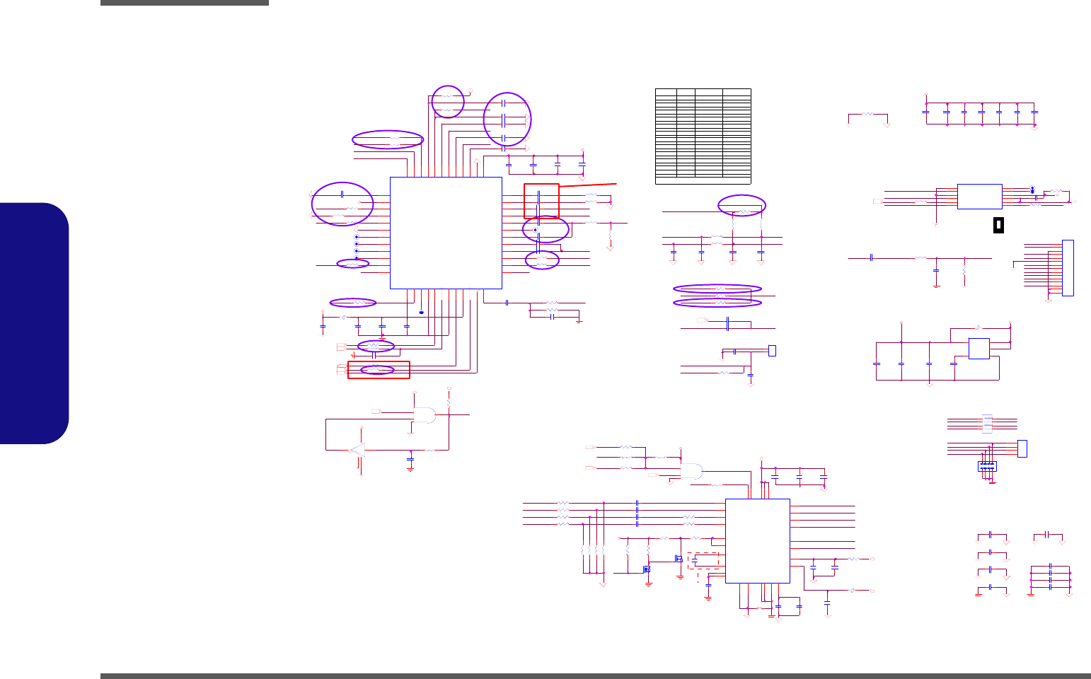
Schematic Diagrams
B - 28 AUDIO VT1708A/ALC883
B.Schematic Diagrams
AUDIO VT1708A/ALC883
AUDG
AUDG
Z2 724
SDATA-IN Max: 0.5inch
AUDG
Z2 736
MUTE IN
Z2 722
R 414
4. 7K _04
Q51
2N 700 2
G
DS
AUDG
AZ _ S DOUT16
Z2 751
C 73 2 1 00P _50 V_0 4
C859
1U _10V _0 6
*10K
20K
PIN
BEEP
C 723 4 .7U_ 10V _08
C7 24 . 1U _16 V_0 4
JSP K1
CO N 4_S PK
1
2
3
4
1
2
3
4
39.2K
PIN 32
Z 271 9
Z 277 2
C 53 6 2 70P _10V _06
*10UF
INTMIC
LI N E- L
R82 0 *0_0 4
C717
* . 1U _16 V_0 4
R636*->10K
C960615
Z2 737
GPO1
R 40 2 0_0 4
C857 4.7U_6.3V_06
R 58 4 * 220 _04
ALC883
0 OHM
5VS _A UD
R 856 *10 K_0 4
L44
HCB 160 8KF - 121T 25_0 6
12
L5 4
H C B20 12K F- 500 T40_ 08
12
C 55 5 . 1U _16V _04
*39.2K
*0 OHM
R 84 5 8. 2K _04
Z 270 6
Z 2743
HP_ L
C49 4
. 1u _16V _04
C 535
.1U_1 6V_ 04
R 69 5 * 0_0 4
*39.2K
PIN 31
AU D G
EA PD
Z 270 3
FRONT-R
R437
100_ 04
10UF
PREHP_R
Z2 752
Z 277 3
Z 2742
C5 58 . 1U _16 V_0 4
0 OHM
R817 ->*
C960615
C854 1U_10V_06
U36
*G924
1
23
4 5
SHDN#
GNDBY P
OUTVIN
0 OHM
MIC-V REF O-R
SPKOUT L+
C 55 4 . 1U _16V _04
C 722 4 .7U_ 10V _08
R410 1M_04
R714 0_06
C 55 9 . 01U _50 V_0 4
AUDG
AC_SPKR16
Z 2714
R 557 0_04
R 367 * 0_04
R82 1 *0_0 4
C 524 4 .7U_ 10V _08
270PF
0 OHM
AUDG
HP_SENSE
Z 275 8
3.3VS
INT-MIC-VREFO
SPKR+
R833
PIN 29
AU D G
MIC L
Z 270 9
C855 1U_10V_06
C736
AUDG
AU D G
SPKR-
Z 276 4
Z2 727
R 85 9 0_0 6
R 41 9 2. 2K _04
C7 16
10U_10V_08
*0 OHM
R 84 4 33 -> 0
C960615
R844
SPKOUTR-
BE EP
R175 *10K_04
C85 8
1U_ 10V _06
R 710 * 0_04
*270PF
5.1K
C53 0
3 30P _50V _04
AUDG
MIC R
R411
10K _04
APA2 056A
U42
AP A20 56A
6
4
19
11
26
13
17
18
15
9
27
25
8
21
22
3
12
14
16
24
5
28
1
20
10
2
7
23
29
L_I N _H P
R_IN_HP
HPVDD
CPVDD
SD#
CPGND
R_HP_ OUT
L_H P_ OUT
CPVSS
L_OUT-
AM P_ EN #
BYPASS
L_O U T+
R_OUT-
R_OUT+
R_IN_AMP
CP+
CP-
HPVSS
HP_EN
L_I N _AM P
BE EP
VD D
PVDD
PV DD
GND
PGND
PGND
GND
1
PIN 20
PIN 47
PREHP_R
FRONT-L
R 638 1 0K_ 1% _04
2
*4.7UF
JD _S EN S E
Z27 44
Z 270 4
Power Pla ne
R841
5VS
VREFO-C_L
R 322 0_06
C 51 7 1 0U _10V _08
5V S
U16
74 AH C 1G 08GW
2
1
4
3
5
C 525 4 .7U_ 10V _08
Z275 4
C856 4.7U_6.3V_06
C863
1U _10V _06
0 OHM
3. 3V S
Z 270 8
Z2 723
C 750
10U _1 0V_ 08
MDC MODEM
1108
AU D G
Z 2734
EXT-MIC-VREFO
PL EASE PLA CE C LOSE COD EC &
AM P TH E PO WER INPU T PI NS
PIN 41
AZ _ S DIN1
Z2 729
R 692 1K_ 04
AU D G
C495
10U _10 V_0 8
R 855 *10 K_0 4
0 OHM
SPKL-
R 826 0 _04
C 862
. 1U _16V _04
AU D G
5V S_A U D
AUDG
SD O
Q52
2N 700 2
G
DS
R857
100K _04
R 398 100K _04
0 OHM
R821
EC_BEEP
C 707 . 1U _1 6V_ 04
R 853 *10 K_0 4
AZ _ S YN C
SP DIF
EXT-MICL
Z27 16
R 413
4. 7K _04
C739
PIN 40
C560 270P_10V_06
R63 9 10K _0 4
C 512
10U _10 V_1 2
LINE _SE NSE
Z 271 8
C 725 1U _10 V_ 06
VT1708
U22
1
13
2
4
5
6
7
8
9
10
11
12
34
14
15
16
17
18
19
20
21
22
23
24
25
26
37
31
33
3
29
30
28
32
35
36
27
38
39
41
40
42
43
44
46
45
47
48
DVDD_CORE
SENSE_A
NC
DVSS
SDO
BITCLK
DVSS
SDI
DVDD_CORE
SYNC
RESE TN
PCBEEP
SENSE_B
PO R T- E_ L
PORT-E _R
PO R T- F _L
PORT-F _R
CD-L
AFILT4
CD-R
PO R T- B_ L
PORT-B _R
PORT-C_L
PO R T- C _ R
AVDD1
AVSS1
AF I L T 3
CAP1
AFILT 2
NC
VREFOUT-C_L
VREFOUT-F_L
VREFOUT-B_L
AFILT 1
PORT-D_L
PORT-D_R
VREF FILT
AV D D2
PO R T- A_ L
PO R T- A_ R
JDREF
AV SS 2
PO R T - G _ L
PO R T - G _ R
PO R T- H _ R
PO R T- H _ L
S/ P DIF RX / EAPD
S/ P DIF TX
*0 OHM
PIN 18
AUDG
EX T - MICL
Z 275 6
C51 0
*.01 U_ X7R _04
*4.7UF
MIC _SE N SE
SPKOUTL +
Z2 710
CP1
8P 4C X1 80P F
1
2
3
45
6
7
8
EC _B EE P
R 64 1 33_ 04
*0 OHM
*0 OHM
PIN 13
AUDG
SPKOUT R-
BEEP
LINE -R
LP2
F C A32 16K F4- 12 1
1
2
3
45
6
7
8
C734
.1U_ 16V _04
*0 OHM
PIN 39
AUDG
SPDIF
R58 5 0_0 6
SPKOUTR+
Z27 02
R 85 0 39K _04
C503
10 U_ 10V _08
TJ MDC3
R814
PIN 15
DEFAULT VT1708
AUDG
EA PD
LI N E- R
Z 270 1
R 637 2 0K_ 1% _04
C 526 4 .7U_ 10V _08
4.7UF
AUDG
Z 271 5
R 84 2 0_0 4
C 727
. 1U _16V _04
MDC
R827
270PF
PIN 10
KB C _ BE EP
R 84 3 0_0 4
5VS_AUD
5VS_AUD
AUDG
Z 2757
EAPD
SPD_IFO
R812
PIN 37
Z27 17
R 84 6 8. 2K _04
? ? 6 , ? ? D E PO P? ? ?
???? ,?? ????
PIN 14
R 82 5 0_0 4
U18
74A H C1G14GW
24
53
1
11
4.7UF
AUDG
PREHP_ L
PIN 2
C 73 9 2 70P _10V _06
R 81 2 0- >1 0K
C960705
BE EP
R 40 1 0_0 4
10K
AUDG
Z 2740
AZ _ S DOUT
AZ_ BITCLK
Z 276 0
Z 2712
C 498
470 P_ 50V _06
PIN 13
AUDG
AZ _ S DIN016
LINE -L
C722
AUDG
5V S_ AU D
Z2 741
INT-MIC-VREFO
C50 9
*.01 U_ X7R _04
PLEA SE P LACE CLO SE C ODEC &
AMP THE POWE R IN PUT PINS
*270PF
LINE _SENSE
HP_SENSE
MIC-VRE FO-R
SPKL+
Z2 725
R 43 0 5. 1K _1% _0 4
C561
100P _50 V_0 4
R825
AUDG
AZ _R ST #
C534
. 1U _16 V_ 04
R 833 * 3 9. 2K_ 1% _0 4
PIN 6
Z2 732
Z27 05
Z2 731
JMDC1
CON12_AM P
1
3
5
7
9
11 12
10
8
6
4
2
GND
Aza li a_S DO
GND
Aza li a_S YN C
Aza li a_S DI
Aza li a_R ST # Azal ia _BC LK
GND
GND
3. 3V Ma in/ au x
RESERVED
RESERVED
C86 1
1U_ 10V _06
C864
.1U_ 16V _04
J AUDIO1
CON15
1
2
3
4
5
6
7
8
9
10
11
12
13
14
15
R 82 7 * 0_0 4
R826
*270PF
KBC_BEEP23
5VS_AUD
24 mil
PIN 34
V O L_M U TE#23
Z2 735
Z2 733
C740
. 1U _16 V_0 4
C 72 9 . 1U _16V _04
C723
SPD_IFOZ 276 3
Z27 65
R 84 1 0_ 04
C7 35 . 1U _16 V_0 4
R 824 0 _04
C 497
47 0P_ 50V _06
3. 3VS
EXT-MIC-V REFO
Z2 726
HP_ R
R 854 *10 K_0 4
S18
SH O RT
2 1
C5 57 . 1U _16 V_0 4
0 OHM
R85 2
10K_04
C504
*.1U_ 16V _04
22PF
AZ_ SYNC16
R 814 * 0_04
C560
HP_L
Z 275 9
Z27 21
R 6 36 39 .2 K_1 %_04
SPKR+
R85 1
1 00K _04
PIN 34
R 84 8 39K _04
R 812 * 10K _04
R 431 200_ 04
*0 OHM
270PF
AZ _ B ITCLK16
EXT-MICR
C 198 330 P_ 50V _04
C556
. 1U _16 V_0 4
L41 2
HCB 201 2KF - 500T 40_0 8
12
C 522 1 U_ 10V _06
C 731
.1U_ 16V _04
R 8 17 * 10 K_1 %_04
C55 0
1 0U _10V _08
*0 OHM
AUDG
Z27 38
10PF
3. 3V S
3. 3VS
MIC_SENSE
HP_R
JD_SENSE
Z 276 1
C 73 8 22P _5 0V_ 04
C 726 . 1U _1 6V_ 04
R636
3. 3V
AU D G
HPSE L
FRONT-L
R 64 0 1K _04
C53 8
. 1U _16V _04
4.7uf
? REALTEK
FAE? ?
?? ?1uf
Power Plane
SUSB#1 3, 15, 16, 20 ,2 3, 28, 34
MICL
R824
PIN 33
SUSB#
BI TC L K
VT1708
*0 OHM
C536
LI N E_S EN S E
INTMIC
Z2 728
Z 270 7
Z2 730
C738
SPKL+
C 73 3 . 1U _16V _04
C 523 1 U_ 10V _06
*10K
MICR
FRONT-R
3.3VS
10K
PIN 33
5V S_A U D
GPO116
Z271 1
SY N C
SPKR-
R 84 9 0_ 04
0 OHM
*10UF
AZ_ RST#16
Z 2713
HPSEL
C71 8
10 U _10V _08
R 399 100K _04
12
C 502
10U _10 V_1 2
C 73 0 1U _10 V_0 6
C 527 4 .7U_ 10V _08
AU D G
SPKL-
39.2K
R430
C near CP+ and CP-
AU D G
AUDG
AUDG
AFILT 4
C 73 7 1 0U _10V _08
C 728 1U _10 V_ 06
10K
PIN 32
AZ_ SDIN116
C 860
. 1U _16V _04
0 OHM
10UF
SD AT A- I N
Z 276 2
Z 275 3
AUDG
PREHP_L
C 73 6 1 0U _10V _08
C529
22 00P _50V _04
C52 8
.1U_1 6V_ 04
R695 ->*
C960615
SPKOUTL -
R817
R820
Value
HP_ SE NSE
R 84 7 0_ 04
C 505
. 1U _16 V_0 4
ADD C960528
SPKOUT L-
C50 7
* . 1U _1 6V_ 04
R693
* 1K _04
R 858
100 K_0 4
R638
PIN 32
AUDG
EX T - MICR
PREHP_L
PREHP_ R
R 84 4 0_0 4
U17
74A H C1G08GW
2
1
4
3
5
C737
SPKOUT R+
Z 272 0
JI N TMIC1
ACES/CON2
1
2
1
2
Sheet 27 of 40
AUDIO VT1708A/
alc883
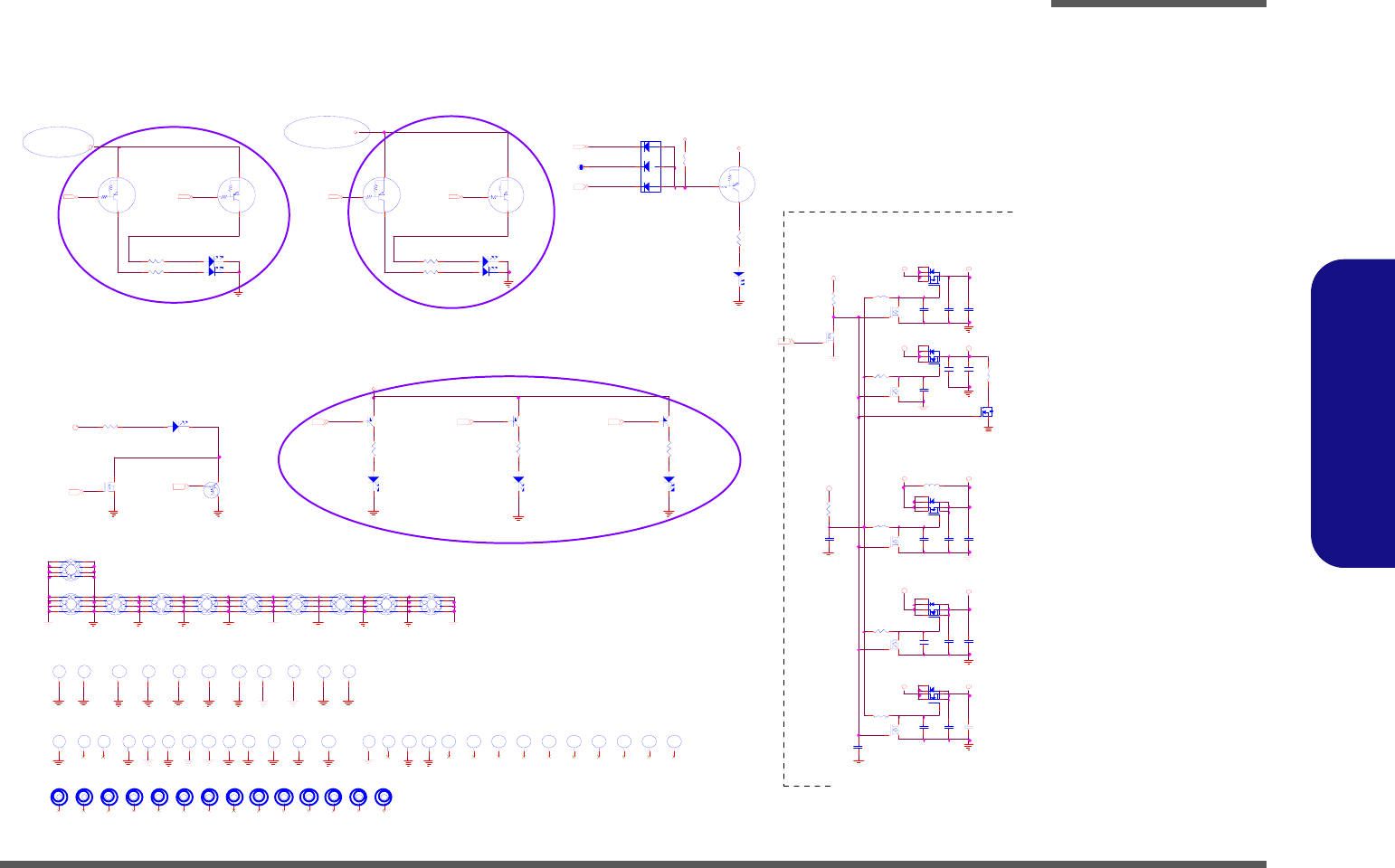
Schematic Diagrams
LED, VS POWER B - 29
B.Schematic Diagrams
LED, VS POWER
Sheet 28 of 40
LED, VS POWER
VDD3
Z28 08
PQ52
2N7002W
G
S D
Q50
2 N 700 2
G
DS
1. 8V S
LED_P WR#23
D29
LE D
AC
Z 2 802
PC62
22 00P _ 50V _0 4
Z2 82 3
MR1
100_06
Q32
2N 39 06
B
EC
MD1
LED
AC
R 4 35 1 00_ 06R 433 100 _0 6
VS POWER
GR EEN
OR ANG E
D2 6 DLE D
34
12 R 4 36 1 00_ 06
1
H1 7
M T H 8_0 D 2_8
2
3
4
5 6
7
8
9
M5
M-MA R K1
PQ 1 1
2N 70 02 W
G
S D
M3
M-MA R K1
CD_DASP#18
Z2825
H30
C15 8
H8
C79D79
GREEN LED
L ED_ CAP #23
PQ16
SI480 0BDY
4
6 2
5
7 3
1
8
1
H3 9
M TH 8 _0 D 2_8
2
3
4
5 6
7
8
9
PC70
10 U _1 0V _08
M960725
H40
C15 8D1 58
CD_DASP#
H45
C 315 D 14 6
H28
C 256 D 14 6
H27
C158
3. 3V S
LE D _A C IN#23
Z2 81 0
H2 3
H6 _5D4 _2
1
H32
MT H 8_ 0D 2_ 8
2
3
4
5 6
7
8
9
Z2 80 9
WIRELESS LAN /BT
LED
H3
C15 8D1 58
SUSB#13,15,16,20,23,27,34
ACIN
PWR/SUS
SCR LOCK
2.5V
PR 1 6 0
0_0 4
H2 2
H 6 _5 D 4_2
H41
C15 8D15 8
1
H3 8
M TH 8 _0D 2 _8
2
3
4
5 6
7
8
9
Z 280 5
M1 0
M-MA R K1
Z 281 6
D2 5
LE D
A C
H13
C 158
Z 281 4
M2
M-MA RK1
PC177
10 U _1 0V _08
Z2 81 3
M1
M-MA R K1
BATT/E mail
CHARGE FULL
GREEN LED
GREEN
O RA NGE
D27 DLED
34
12
M6
M-MAR K 1
L ED_ SCROL L#23
PL1
* H C B 32 16 K- 8 00T 30
H48
C25 6D14 6
PC63
.1 U _1 6V _06
PR 8 4
10K _ 04
H29
C 158
H15
C15 8
PR 8 7
100K_04
R441
100 _06
D3 0
LED
AC
M1 1
M-MA R K1
Z 2 826
PQ 1 0
2N7002W
G
S D
H5
C 1 58D 1 58
GREEN LED
1.5V
1
H21
M T H 8_0 D 2_ 8
2
3
4
5 6
7
8
9
PR85
1M _ 04
PQ15
NTGS41 41 NT1G
3
2 4
1
5
6
VDD3
Q29
DTC1 14 EUA
CE
B
47 K
47K
MQ1
DTA 114 EUA
C
B
E
H19
H6_5D4_2
H14
C15 8
R 434 100 _0 6
HDD/PD LED
P C 175
.1 U _1 6V _06
M960803
Z2 81 2
PC66
.1U_ 16 V_ 04
Z 281 5
D28
LE D
AC
Z2 81 1
H2 6
C1 58
Z2 81 9
PC 6 1
* . 1U _5 0V _0 6
M1 2
M-MA R K1
PQ 1 3
2N7002W
G
S D
VDD5
GREEN LED
SATA_L ED#17
CAPS LOCK LED
SA T A_ L E D #
EN_15 VS
H7
H6 _0 D2_3
PR88
300 K _1% _04
R440
10 0_0 6
5V S
PR 1 5 1
0_0 4
PQ58
2N7002W
G
S D
H44
C256D146
PC65
.1 U _1 6V _04
Z28 07
VDD5
LE D _N U M #23
Z2820
1
H1 6
MTH8 _0 D2_8
2
3
4
5 6
7
8
9
H3 4
C 7 9D 79
H18
C15 8
M960725
H1 2
C1 58
DTA114EUA->2N3906
H4 7
H 5 _5D 2 _7
R7 18
100_08
47K
47 K
Q2 7
D T A1 14 EU A
C
B
E
H1 1
C1 58
Z2 80 3
M14
M-MAR K 1
2. 5V S
Q30
2N 3 906
B
EC
PR 8 6
100K_04
Q31
2N 3 906
B
EC
PQ51
SI4800 BDY
4
6 2
5
7 3
1
8
SUSB#
LED_B AT _CHG#23
Z2821
PC82
.1U_ 16 V_ 04
1.8V
H37
C15 8D1 58
M4
M-MA R K1
H2 0
H 6 _5 D 4_2
5V S
3. 3V S
WLAN_EN23,26
H49
H5_ 5D2_ 7
P C 176
.1U_ 16 V_ 04
R43 2
4.7K_06
H4
C 1 58D 1 58
M9
M-MAR K 1
M7
M-MAR K 1
Z2822
Z 281 7
M13
M-MAR K 1
H1
C15 8D15 8
H3 5
C2 17
H3 6
C 1 58D 1 58
R 439
10 0_0 6
PC64
.1 U _1 6V _04
1
H31
MTH8_0D2_8
2
3
4
5 6
7
8
9
H2
C15 8D1 58
47K
47 K
Q2 6
DT A1 14 EUA
C
B
E
NUM LOCK LED
VDD3
PC67
.1U_ 16 V_ 04
PC83
10 U _1 0V _08
M960 801
Z2824
PC74
.1U_ 16 V_ 04
H4 2
H7 _7 D4_5
Z2 80 4
3.3VS
LE D _B A T_ FU L L#23
Z2 81 8
H4 6
C3 15 D146
1
H1 0
M TH 8 _0D 2 _8
2
3
4
5 6
7
8
9
Q33
2N 7 002 W
G
S D
3. 3V S
Z 2 801
1. 5V S
47K
47 K
Q2 5
D T A1 1 4 EU A
C
B
E
M8
M-MA R K1
Z 280 6
P C 165
.1 U _1 6V _04
PQ57
SI 4 8 0 0 BD Y
4
6 2
5
7 3
1
8
1
H9
M TH 8 _0D 2 _8
2
3
4
5 6
7
8
9
PQ12
2N 70 02 W
G
S D
P D _LE D #
M96 0801
H6
C158D158
BT_EN23 ,26
47K
47 K
Q2 8
DT A1 14E UA
C
B
E
R4 38 1 00 _06
D3P
D24
IMN 1 0
1
2
3 4
5
6
+
+
+-
-
-
H2 4
C2 56 D146
SYS1 5V
PQ14
NTGS41 41 NT1G
3
2 4
1
5
6
1
H3 3
MTH8_ 0D2 _8
2
3
4
5 6
7
8
9
PC73
10 U _1 0V _08
PC71
10U_10V_08
H4 3
H 6 _0D 3 _7
3A
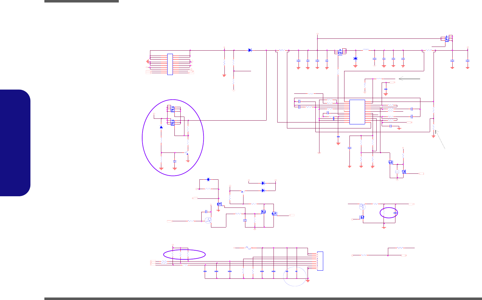
Schematic Diagrams
B - 30 CHARGER, DC IN
B.Schematic Diagrams
CHARGER, DC IN
OC2 #15
MB39A126
PU5
MB 39 A 12 6
1
2
3
4
5
6
7
8
9
10
11
12
24
13
14
15
16
17
18
19
20
21
22
23
-INC2
OUT C 2
+INE2
-INE 2
AC OK
VREF
ACIN
-INE 1
+INE1
OUT C 1
OU TD/SEL
-INC1
+I N C 2
+I N C 1
CTL
FB123
-INE 3
RT
XA C O K
VH
OUT
VCC
CS
GND
Hi:16 .8V
DD_ ON 2 3,3 3
Z2937
PL2
15U_10*10* 4
PR15 0_06
PQ28
2S B 1 19 8K R
B
E C
PC6 6800P_50V_06
Z2912
Z2902
PD15
FM0540-N
AC
PR6
33K_06
VB
Z2927
PR11 9
.0 2_ 1% _ 25
PC12
.1 U_2 5V_ 06
PC128 10U _25V_12
PR 8 1 00 K_0 4
4A 160 mil
USB 1 + 1 5
PR31
100K_04
Z2 9 05
Z2 9 08
VB
PQ6 2
* 2N3904
B
E C
PR9
3 0K _ 1% _0 6
PR161 1 0_ 06
Z2 9 40
PC119
30P_ 50 V_0 6
SYS5V
PR 17 6
*100K_06
DD_O N
PD14
FM5822
A C
PD17 FM0540-N
A C
PQ2 5
2N7002W
G
DS
PC 1 . 0 1 U _ 5 0 V _0 6
PR 23
0_06
# BA T_ SE L H :1 6. 8V ; L : 12 .6 V
PC178.1U_50V_06
PQ 27
2N7002W
G
DS
PQ6
2N7002W
G
DS
PR118
*10K_06
PR 10 6
0_ 06
PC109 .1U_25V_06
VB
Z2 9 21
PR29 10 K_06
PC142
.1 U_ 25 V_0 6
PR32
100K_04
M_ B TN #23
PR 11 2
20K_1%_06
Z293 8
PR109
0_04
PC 11122P_50V_04
PC 12 0
30 P _5 0V _ 06
PR 13 10K_ 06
VIN
CHG_ CUR SEN 2 3
PW R_SW #
Z2933
From H8
VD D 3
Z2 9 25
PR12 * 0_04
PF1
7A
VI N
PC112 10U_25V_12
PR108
*2 .2M_ 0 4
# CU RS EN : Vc ur se n= 0. 02 5 X 20 X I ch g
BAT1 _ VO LT 23
PR 17 4
*10 K _0 6
AC_IN# 23
OC2 #
PR130
100K_04
PC7 6800P_50V_06
# TO TA L PO WE R = 60 W
VA
Z2 9 11
M_BTN#
PC126
10U_25V_12
PC124 10U_25V_12
PR43 0_ 06
PR 13 1
6. 0 4K _ 1% _0 6
PR 3 0
200K_06
USB1-
Z2936
PC138 10U_25V_12
PR2
10K_1% _06
Z2 9 09
PJ 2
3m m
12
PR 40 1 0K _ 04
PW R_SW #23
PQ24
DTA114EU A
CE
B
PR34 10 K_0 6
To H8
PR22
*10K_06
PR16 0_ 06
PR11
*1 0K _ 04
PC118 10U_25V_12
6. 8K->6.0 4K C9607 05
5V
Z2 9 04
PR21 100_06
VIN
JU S B1
CON20AF
1 2
3 4
5 6
7 8
910
11 12
13 14
15 16
17 18
19 20
PR 7 1 0K_ 06
# TO TA L_ CU R : Vt ot al _c ur =0 .0 20 X 2 0 X Ic hg
Z2932
Z2923
JBATTA1
CON _BAT
1
2
3
4
5
6
7
8
9
PC191
.1U _5 0V_ 06
Z2917
3A 120mil
Z2915
PQ23
SI4835BD Y
4
62
5
73
1
8
USB1-15
SM D_BAT123
Z2 9 10
ACOK
PQ1
DT A11 4EUA
C E
B
PC 1 9 3
.1 U_ 25 V_0 6
PR3 30K_ 06
VA -
AC_IN#
Z2929
PR173
*510K_06
PC 2
1000P_50V_06
P C 1 33 . 1U _5 0V _ 06
? ? pull H I C96070 5
Z2934
PR5
1 0K _ 1% _0 6
LI D _ S W #
ACOK
PR 11 1
2 2 0K _ 1% _0 6
CTL
Z2914
VA-
BAT1_ DET23
PQ61
*S I 4 83 5BD Y
4
6 2
5
7 3
1
8
LID_SW # 23,24
PR24
0_ 06
VA
BAT1_ VOLT
VIN1
SM C_BAT123
5V
T_CU R_C ONT
CHG_EN
PC 123 10U_25V_12
PR4
30K_1% _06
PD16 FM0540-N
A C
VIN
PR11 0 *100 K_0 4
PQ30
2N7002W
G
DS
? Ada pter ? ? 90 W? ? ,? ? ? MOSFET? ? ?
SYS5V
PC125
10U_25V_12
PQ5
2N7002W
G
DS
TOTAL_C UR 23
CHG _E N 2 3
PQ60
*S I 4 83 5BD Y
4
6 2
5
7 3
1
8
P C 4 . 1U _ 2 5V _ 06
Z2 9 06
Z2935
Z2928
PR116
*1 0K _ 06
VA
CUR _CO NT
Z2919
PC 5
2200P_50V_04
PC108 10U_25V_12
PR115 100_06
PR128
30K_1%_06
PC122 10U_25V_12
Z2922
VREF
VREF
Z2903
Z2913
M960806
Z2 9 07
VA
AC I N
PC110
.01U_50V_06
Z2916
PQ 26
2N7002W
G
DS
# MA X CH AR GE C UR RE NT = 2 .5 A
Z2939
VD D 3
Z2920
PC19 2
.1U_ 50 V _0 6
PC3 .22U_16V_06
ADJ C.V POINT
USB1+
PR117 100_06
PC10
.1U_25V_06
4A 160mil
PR10
10 K _0 8
PR122
.0 25 _1 %_ 2 5
Z2901
Z2918
VD D 3
P R 14 1 00 K _0 4
Z2931
PC18 0
30P_ 50 V_0 6
PR 10 7 0_0 6
PD7
FM1040-T1
A C
AC IN
PR175
*200K_06
VA
PQ 21
SI4835BD Y
4
62
5
73
1
8
VDD3
Z2930
PD 28
*UDZ 1 6B
A C
PR133 10K_06
Low:1 2.6V
Sheet 29 of 40
CHARGER, DC IN
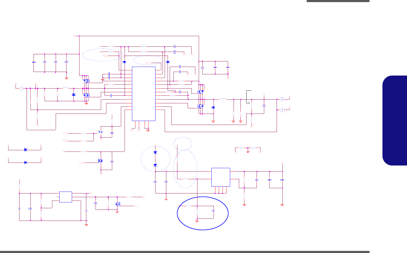
Schematic Diagrams
1.5V, 1.05VS B - 31
B.Schematic Diagrams
1.5V, 1.05VS
Sheet 30 of 40
1.5V, 1.05VS
PR91 0_06
Vout = 0.5V ( 1 + Ra / Rb )
DD _ ON#
PR17 0
2.37K_ 1% _04
PC 17 0
.1U_16V_04
PD6
FM0540-N
AC
+
PC89
2 2 0U _4 V _ D
12
PQ 59
2N 7002W
G
DS
DD_ON# 32,33
M960804
PC78
10U_10V _08
R1
Z30 07
PJ 1 5
OPEN-5mm
1 2
1.58V
5V
3A
Vout = 0.5V ( 1 + Ra / Rb )
+
PC16 6
*2 2 0 U_ 4V _ D
12
Z30 23
PR15 5 1 M _0 4
PR 17 1
100K_04
M960804
2. 5 V S
+
PC167 *220U_4V_D
12
SGND2
PR10 0
11K_1% _06
PD24
FM5822
A C
PC18 9
10 U _ 1 0 V _0 8
PR10 2
0_06
Power Plane
2. 5 A
070529
PU 3 AME8816
1
6
3
5
4
2
7
8
EN
GND
VO UT
GND
ADJ
VIN
GND
GND
SGN D1
PR17 2
10K_1%_04
SG ND 2
Z3008
Z3021
PD 5
FM 0540-N
AC
VD D3
1.05V_PG23
PR 94
22K_1% _06
PC84
* 10U_25V_12
PC101 1U_10V_06
Ra
2A
DD_ON#
PR92 10_06
PR 97 0_04
PD 3
FM 5822
A C
PQ 17
2N 7002W
G
DS
PQ 56
SI4800BD Y
4
62
5
73
1
8
PC 18 7
.1 U_ 1 6V _ 0 4
Rb
VREF=1.215V
1.5V_PG23
M960804
3.3V
SGN D1
Z30 04
PR 16 2
0_06
Rb
PR 168
*0_08
40mil
Z3001
Z3022
PL8 2.5U_7*7*3.5
PQ 53
SI4800BD Y
4
62
5
73
1
8
Z302 0
40mil
VO=VREF(R1+R2)/R2
Z301 6
SGN D2
PC86
* 10U_25V_12
PC96
.1U _2 5 V _ 06
1A
VDD 5
SGND1
Z30 03 PR1 52 7 5 0 K_0 4
Z301 7
Rb
PC19 0
.1 U_ 16 _ 0 4
1.5V
PQ 54
SI4800BD Y
4
62
5
73
1
8
PC17 9
0.01U_16V _06
PQ 55
SI4800BD Y
4
62
5
73
1
8
PR99
10K_1%_06
Z301 8
PC81
10U _10V_08
PQ 18
2N 7002W
G
DS
PD27
*F M 40 0 2
AC
Ra
1A
Z3027
PR 101 *1 0K_0 4
M96081 3
1.5V_PG
PU9
AME8 8 04
1
2
34
5
6VIN
GN D
ENPG
AD J
VO UT
Z30 05
PD25
FM5822
A C
PC 188
.1 U_ 16 V _ 0 4
PR 16 7 0_ 0 6
SGN D1
+
P C 90 2 2 0U _ 4V _ D
12
PC92
.1 U_ 50 V _ 0 6
PC95
22 P_ 50V_ 0 4
Max output current is 1A
DD _O N#32,33
P C93 1U _10V_06
VIN
2. 5V
PC94 1U_10V _06
PC79
10U_10V_08
SGN D2
5V
Z3010
P C 1 6 8 10 0 0P _5 0 V _0 4
Ra
Z3025
PJ 1 3
OPEN-5mm
1 2
PL9
2.5U _7* 7* 3. 5
1 2
PR 16 5
64. 9K_1%_06
PD4
FM5822
A C
SC413
PU4
1
2
3
4
5
6
7
8
9
10
11
12
13
14
15
16
17
18
19
20
21
22
23
24
25
26
27
28
PG ND 1
DL1
VD DP1
IL IM1
LX1
DH1
BST1
EN /PSV2
TON 2
VO UT2
VCC A2
FBK2
PG OOD 2
AGN D2
PG ND2
DL 2
VD DP2
ILIM 2
LX2
DH 2
BST2
EN /PSV1
TON 1
VO UT1
VCC A1
FBK1
PG OO D1
AG ND1
Z301 2
3.3V
Z30 02
SGN D2
PR16 4
36K_1% _06
SGND1
1.05VS
Z30 06
Z3026
PR 95
9.53K_1% _06
2. 5 V
1.05V_PG
PR163 * 0_06
PR90
953_1%_06
PC 91
.1U_50V_06
PC98 1000P _50V_04
SU SB+32,34
Z301 9
PR96 10K_1%_06
PJ 12
OPEN-3mm
1 2
PC 16 9
.1U_16V_04
5V
R2
PR89
1K_1%_06
V1 .05
PC80
10U _10V_08
C4 9 9
1U_10V_06
Z301 4
PC87
10U_25V_12
5V
M960813
3.3VS
1.5VS
SU SB+32,34 SGN D1
PR 15 3
47K _04
1.5V
Power Plane
PC 88
10U_25V_12
3.3V
PD26
*F M 40 0 2
AC
V1.5
PR169 47K_04
Z301 3
Z3011
Z300 9
070529
PR 93
0_06
2A
Z301 5
M960813
SGN D2
Z30 28
NORMAL OPEN
PR 15 4
47K_04
PR 98
10K_1% _06
Vo ut = 1. 24V ( 1 + Ra / Rb )
5V
PR103 10_06
PC85
10U _25V_12
PC1001U_10V _06
PR 16 6 * 0_ 0 6
PC 99 100P_50V_04
PC 97
.1 U_ 2 5 V_0 6
Z30 24
Schematic Diagrams
B - 32 VCORE
B.Schematic Diagrams
VCORE
BST
PC 23 10U_25V_12
GND _SIGNAL
PC26
*10P_50V_06
+
PC77
470U_2.5V_D
12
PC186 .1U_50V_06
PR37
28K_1% _06
PC25
*1 0 0P _ 50 V_ 0 4
PR63 0_ 06
H_VID24
PC29
*68P_50V_04
PR73
130K_1%_06
PR53 0_06
H_VID14
EN _ V C O R E
3. 3 VS
Z3115
PR74
130K_1%_06
PC183 .1U_50V_06
PR41
*0_04
CLK EN#2
CS+
PQ2
2N 70 02 W
G
DS
PR62
10_06
PW RGD_VCORE 15,2 3
Z3113
H_VID04
Z3108
SS
PR38
*0_ 0 4
VCORE
HYS
PD20
FM5822
A C
GN D_S I GN A L
PQ8
2N3904
B
E C
PR80
10 K _0 4
GND _ S IGNA L
H_VID64
Z3102
PTH2
*100K
12
PR48 1 2.4K_1 %_ 06
H_VID44
PR36
27 . 4K _1 % _0 6
P C 18 2 . 1U _ 5 0V _0 6
PC30 10 00 P_5 0V_ 04
PR79
0_04
PJ 1
3m m
1 2
ERROUT
PR82
1K_04
VC C A
Z3103
Z3 10 9
PC41 1U _1 0V _ 06
PQ 4 0
SI4856D Y
4
62
73
8
5
1
PQ3 7
SI485 6D Y
4
62
73
8
5
1
PR71
*10 K _0 4
PC44
18 0P _ 50 V _0 4
PC 2 4
*100P_50V_04
GND_SIGNAL
DRN
BG
GND _ S I GNA L
PR44
10 K _0 4
+
PC146 15U_25V_D
12
PR69
100K_04
5V
Z3101
PD1
FM0540-N
AC
+
PC76
470U_2.5V_D
12
GND _ S IGNA L
VIN
Z3105
TT R I P
PC28 . 0 1U _ X 7R _ 50 V _0 6
1.05VS
DRP_L 1
Z3106
PC47
10 0P _ 50 V _0 4
PQ4
2N 7 0 02 W
G
DS
PR67
0_ 06
DAC
PR33 0_04
VC C A
CS-
H_VID54
DRN
PR35
0_04
PR54
1K _ 04
VC O R E _ O N23
PC20
*10 0 P_ 5 0V _0 4
+
PC 69
47 0U _ 2. 5 V _D
12
PR49 0_ 06
P C 51 * 1 00 P_ 5 0V _ 04
H_VID34
PR45
10 0_ 0 4
Z3107
TG
PR77
130K_1%_06
+
PC147 15U_25V_D
12
VR_ON
3. 3 V S
PQ 41
SI485 6D Y
4
62
73
8
5
1
CS1 N
Z3 11 4
GND_ SIG NAL
3.3VS
Z3104
P C 18 5 . 1U _5 0V _ 06
DRN
+
PC68
47 0U _2 . 5V _ D
12
VC C S E N S E 4
GND _S I GN A L
Z3 1 12
PR51
* 10K_04
PC174
* .001U_50V_08
PC181 .1U_50V_06
VCCA
DRN
PC31 *1 0 0P_ 50 V_ 0 4
PC22 10 U _ 25 V _1 2
EN_VC ORE
+
PC75
33 0U _2 . 5V _ D
12
PQ 4 2
SI485 6D Y
4
62
73
8
5
1
CS1N
PR50
10 K _0 4
PU1
SC454
1
2
3
4
5
6
7
8
9
10
11
15
16
17
18
19
20
21
22
23
24
25
26
27
28
29
30
31
32
14
13
12
33
VID6
VID5
VID4
VID3
VID2
VID1
VID0
DPRSTP#
HYS
CL SE T
VREF
DAC
SS
FB-
FB+
CS-
CS+
TT R I P
DPRS L
RAMP
EN
PW R G D
CLKE N#
V5
BG
DR N
TG
BST
VRTT#
ERR OUT
VCC A
AGND
GND
PC14
*3300P_50V_04
VCORE FOR YUNA AND NAPA CPU
PM_ DPRSLPVR 3,15,1 7
PR47
0_ 06
PC42
1U_10V_06
5V
PL3 .6U_13*13*4
PR76
*0 _0 4
VSSSENSE 4
VREFVC
PC21 .022U _50V_06
32 A
PC 1 8 4 .1U_50V_06
PC46
1U_10V_06
CS+
PQ36
SI4856DY
4
62
73
8
5
1
PR56
68 0_ 1% _0 6
PR55
88 7_ 1 %_ 06
CS-
VREFVC
PR72
*0 _0 6
PR52 10 K_0 4
GND_SIGNAL
PR46
10 0_ 0 4
PR15 9
* 10_08
CL SET
PC27 1000P_50V_04
PTH1
100K_06
12
PM_ DPRSLPVR3, 1 5, 1 7
PC43
10 00 P _5 0V _ 04
Sheet 31 of 40
VCORE
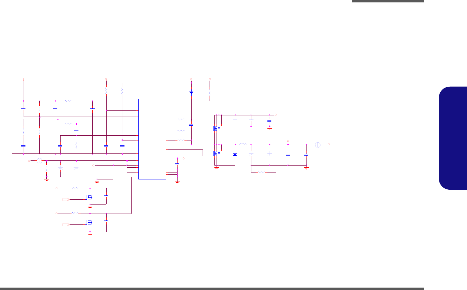
Schematic Diagrams
1.8V, 0.9VS B - 33
B.Schematic Diagrams
1.8V, 0.9VS
Sheet 32 of 40
1.8V, 0.9VS
PL6
2. 5U_7* 7*3. 5
PC145
.1U_50V _06
VIN
PQ4 3
SI4800B DY
4
62
5
73
1
8
V TTEN
PD2
F M0540-N
AC
+
PC 4 8
220U_4V_D
12
PC 5 0
.068U_50V_06
PC 3 9
.01U_50V _06
Z3204
1.8V
PC 3 5
1U_10V _06
3.3V
Rb
Vout = 1.5V ( 1 + Ra / Rb )
1 . 8 VEN
PR60
2.2K_1%_06
PC 3 4
.1U_16V_04
PC36
1U_10V_06
5V
SU SB+30,34
3A
PR 5 9
1.5M_04
PC 5 6
1U_10V_06
5V
PC 3 7
1U_10V_06
V1.8
DD_ON#
PD21
FM5822
A C
Z3211
PR83
0_06
Z3209
Z3208
PR142
10_06
PQ7
2N7002W
G
DS
PQ3 8
SI4800B DY
4
62
5
73
1
8
PC 1 4 3
10U_25V_12
PR65
* 100K_04
Z3203
PR145
20K_1%_06
+
PC 5 7
* 220U_4V _D
12
5V
Z3210
PC 4 5
.1U_16V _04
PR81 47K _04
7A
Z3213
PC 1 4 4
10U_25V _12
DD_ON #30, 33
Z3214
PR58 10_06
PQ9
2N7002W
G
DS
PJ3
OPE N-3mm
12
VIN
Z3205
PR 7 5
0_06
PC 5 5
1U_10V_06
PC 4 9
.1U_25V _06
Z3206
PR57
10K_1% _06
5V
Z3216
0. 9VS
PC 3 2
100P_50V_04
PC 4 0
* 10U_10V_08
+
PC154
* 150U_4V_B2
12
VS SA
PJ7
OPEN-8mm
1 2
PR 6 6
10_06
PR61
10_06
PU 2
SC486
11
2
3
4
5
6
7
8
9
10
1
12
13
14
15
16
17
18
19
20
21
22
23
24
25
VTT E N
TON
VD D QS
VS SA
VC C A
FB
PGD
REF
COMP
VTT S
EN / P SV
VD D P2
VD D P2
VTT
VTT
PGND1
PGND2
PGND1
DL
VDDP1
ILIM
LX
DH
BST
GND
+
PC 5 9
150U_4V_B
12
PR70
0_06
VSS A
PR 6 8
10_06
PC 3 3
1000P_50V_04
PC52
* .1U _25V_06
PR64 47K _04
Z3201
V1 . 8
V1 . 8
Z3217
PC 5 3
.1U_16V _04
PR 7 8
18K_1%_06
Z3202
Z3215
PC38
1U_10V_06
Ra
Z3207 Z3212

Schematic Diagrams
B - 34 VDD3, VDD5
B.Schematic Diagrams
VDD3, VDD5
Sheet 33 of 40
VDD3, VDD5
I NTVCC2
PC114 * 30P_50 V_0 4
DD_ON#
RUN_SS2
VIN2
PD13
FM0540-N
AC
P D10 F M054 0-N
A C
5A
Z3323
PR134
10K_04
P D12 F M054 0-N
AC
Z3312
PR 1 4 8
0_04
PR144
.01 0_1%_25
TH E RMTR I P # 3
PR121 10_0 4
PC13 9
.1U_ 25V_06
SGND4
PC 116 . 01U_1 6V_ 04
PR120 10_04
PQ33
SI4800 BDY
4
6 2
5
7 3
1
8
VI N 2
Ra
Z 3313
PC130
100 0P_ 50V _04
Z3 301
RUN_SS1
5V
Z3320
PR149
100K_0 4
Z3314
DD_ON# 30, 32
PU6
LTC37 28LXCUH
28
30
31
1
2
3
4
5
6
15
17
14
19
20
21
22
23
24
27
187
8
9
11
12 13
25
26
32
29
10
16
RUN/ SS1
SENSE1+
SENSE1-
VOSENSE1
PLLFLTR
PLLI N
FCB
ITH1
SGND
SW 2
BOOS T2
TG2
PG N D
INT VCC
EXT VC C
BG1
VIN
BOOS T1
PGOOD
BG23. 3VOUT
ITH2
VOSENSE2
SENSE2-
SENSE2+ RU N/SS2
SW 1
TG1
NC
NC
NC
NC
SGND4
PR2 8 105K _1% _06
DD_ON23, 29
PJ8
OPEN- 5mm
1 2
PC1 17 * 180P_50 V_0 4
PR 1 2 7
10K_04
PR 1 7 * 0_04
Po we r Pl an e
PR123 10_04
PR129 0_06
PR 1 4 6
270K_04
PR 14 7
1M_0 4
VDD5
PC 1 6 3
* .01U _25V _04
PQ46
SI4800BDY
4
6 2
5
7 3
1
8
Ra
PQ 50
2N70 02W
G
DS
PC13 1 .02 2U_25 V_0 6
EN _15V
PC 1 3 2
0.01U_50V_06
PR13 2 10_0 6
SGND4
P D8 F M054 0-N
A C
SYS5V
Z3324
PC 1 3
.1 U_50V _06
PR27
63.4 K_1 %_0 6
PR113 1 5K_ 04 PC113 22 0P_ 50V_04
Z3302
VI N 1
VDD5
PC137
.1U_16V_04
5A
Z3303
Z3316
PR 1 9
*0 _04
5A
Z3306
+
PC155
150 U_6.3 V_D
12
VDD3
P D9 F M054 0-N
AC
Vout = 0.8V ( 1 + Ra / R b )
PC8 22 0P_ 50V_04
Power Plane
PJ9
OP EN -5m m
1 2
INTVCC2
Z3322
PL4
4.7 U _7* 7* 3.5
1 2
SYS5V
PQ 2 9
2N70 02W
G
DS
Rb
SY S5V
Z3305
PC157
.1 U_16V _04
PQ49
2 N7002 W
G
DS
PQ34
SI4800BDY
4
6 2
5
7 3
1
8
PR150
10K_04
SY S1 5 V
PC161
.1U_25V_06
INTVCC2
PL5
4. 7U _7* 7* 3. 5
1 2
PC135
.1U_2 5V_06
Z3307
Z3325
3. 3V
PC 1 6 4
.1U_ 16V_04
SYS3V
PR 1 4 3
. 010_1 %_2 5
Rb
Z3330
Z 3309
+
PC156
150U_ 6.3V _D
12
PC136
.0 1U_50V _X 7R_06
VIN
PQ32
SI480 0BD Y
4
62
5
73
1
8
SGND4
SGND4
PC 1 6
10 U_25V _12
PJ10
OPEN-3mm
12
PC17
4 .7U_1 0V _08
Z3311
Z3317
PC121 * 30P_50 V_0 4
PC141
.1 U_25V _06
PD18
F M5822
AC
0V:220KHz
5V:640KHz
PC 1 8
10U _25V_12
PD11 FM05 40-N
AC
5V
DD_ON#
5V
SY S1 5 V
PD19
F M5822
A C
5A
Z3319
VIN2
Z3304
PQ 47
SI 4800 BDY
4
6 2
5
7 3
1
8
INTVCC2
Z3318
RUN_SS1
PQ31
2N7 002W
G
DS
PR 18
0_0 4
SGND4
Z3326
Z3327
PC15
10U_25V_12
PQ48
2 N7002W
G
DS
PC19
10U_25V_12
SY S1 0 V
PJ6
SH O R T- 3m m
21
5A
PC 1 1
2200P_50 V_0 6
5V
PC127
* 1000P_5 0V_ 04
PC11 5
. 01U_1 6V_ 04
PC162
2200 P_5 0V _04
PR124 10_0 4
PC134
.0 1U_50V _X 7R_06
PR20 1 5K_ 04
Z3321
PQ22
2N 7002W
G
DS
Z 3308
Z3315
Z3310
PQ35
SI4800 BDY
4
62
5
73
1
8
5A
DD_ON
Z33 28
DD_ ON#
PR 1 2 6 1 M_ 0 4
PR25 20K_1%_06
PR 1 1 4 0 _ 0 4
VDD3
EN_15 V
PC140
1U_10 V_0 6
PR12 5
1M_04
PC 9
2200P_50 V_0 6
3.3V RE F
PC129
1000 P_5 0V_ 04
PR26 20K_1%_06
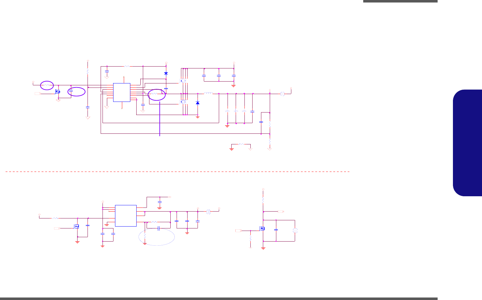
Schematic Diagrams
EXT GPU 1.0VS/1.2VS B - 35
B.Schematic Diagrams
EXT GPU 1.0VS/1.2VS
PQ1 9
2N 70 0 2 W
G
DS
PD 23
FM 5822
A C
PC 150 1000P_50V_04
1.0V_EN
PU8
APL5913
1
6
3
5
4
2
7
8
9
GND
VCNTL
VO UT
VIN
VO UT
VFB
PO K
EN
VIN
PR139
1 . 5M _0 4
2A
5V
PR13 5
7.5K_1% _06
5V
SYS5 V
PR1 41 3K -> 4.3 K 1.0 VS ? OC P?
???11.8A C960724
SG ND3
VIN
PC 10 7
30P_50V_04
Z3402
Z3407
PR13 7
0_ 0 6
Vo ut = 0.8 V ( 1 + Ra / Rb )
SUSB+
PC 54
10U_25V_12
PJ1 1
OP E N-8 m m
1 2
PC 58
10U_25V_12
PR105
10K_04
PC153
1U _10V_06
PC103
.1U _16V_04
PC149 30P_50V_04
PC158 .1U_16V_04
PR140
10 0 K _1 % _ 04
PD 2 2
FM 0540-N
AC
PR 88 15 0K- >1 00K
PC 151 . 1U- >1 U
FO R V GA TI ME
C9 606 04
PQ2 0
2N7002W
G
DS
+
P C 15 9 * 22 0 U _ 4V _ D
12
PR 104
100K_04
PC 106
1 0U _ 10 V _ 08
PC 172 82P_50V_04
PR 157
26.7K_1% _06
1.2VS
Ra
5V
Z3401
Z34 04
PC151
1U_10V_06_X7R
PC 1 04
10U_10V_08
SUSB+30 , 3 2
SGND 3
1.0VS
V1.0
SGN D3
Vo ut = 0 .5 V ( 1 + Ra / Rb )
PC148
1U_10V_06
R1 35= 7. 5K- -> 1.1 67 V
R1 35= 7. 87- -> 1.1 35 V
SGN D3
PJ5
OP E N -3m m
12
PR13 8
10K_1%_06
1. 5A
PC60
.1U _25V_06
5V
SU SB+ 30,32
8A
Rb
SG ND3
PQ 39
2N7002W
G
DS
Z3409
Z3408
Z34 03
SUSB#13,15,16,20,23,27,28 SUSB#
Z34 05
PR13 6
10_06
PC 102
.1U _16V_04
PR158 220K_04
PC105
1 0U _ 10 V _ 08
PL7 2.5U_7*7*3.51 2
Rb
PC171
1U_10V_06
+
PC160 220U_4V_D
12
SUS B+30,32
PC173
.1U _16V_06
PR 14 1
4.3K_06
PC 1 52
.1U_25V_06
V1.2VS
PQ 4 4
SI4856D Y
4
62
73
8
5
1
SG ND 3
Z34 06
M960813
PR156 15K_1% _06
V1.5
PU 7
SC411
15
16
1
2
3
4
17
7
8
9
10
11
12
13
5
14
6
EN/PSV
TO N
VOU T
VCC A
FBK
PGO OD
M1
PG ND
DL
VDD P
IL IM
LX
DH
BST
NC
NC
VSSA
Ra
VIN
SG ND3
PJ4
OP E N-3 m m
1 2
Z3410
+
PC72 470U_2.5V_D
12
PQ 4 5
SI4856DY
4
62
73
8
5
1
Sheet 34 of 40
EXT GPU 1.0VS/
1.2VS
Schematic Diagrams
B - 36 HOTKEY LT BOARD
B.Schematic Diagrams
HOTKEY LT BOARD
HGND
HH5
C237D 91
HWEB2#
PIN5,6=HGND
HWEB2#-->WEB1-->E-MAIL
HWEB0#
HJHO TKEY 1
CON6A
1
2
3
4
5
6
HWEB1#-->WEB2-->APPLICATION
HH1
C67D67
PIN5,6=HGND
E-MAIL AP
HGND
HWEB1#
HWEB0#-->WEB0-->WWW
HGND
HGN D
HSW1
HCH STS-05
3
14
2
HSW3
HCH STS- 05
3
14
2
WWW
HWEB2#
HGND
PIN5,6=HGND
HH 4
C237D91
HSW2
HCH STS-05
3
14
2
HGND
HH2
C67D67
HWEB0#
HWEB1#
HH3
C237D91
HGND
Sheet 35 of 40
HOTKEY LT
BOARD
Schematic Diagrams
PWR HOT BOARD B - 37
B.Schematic Diagrams
PWR HOT BOARD
PPGND
PPGND
PPR1
221_06
PPH2
C237D91
PPWEB4#
PWR LED
PPGND
PPH4
C237D91
PPSW1
HCH STS-05
3
14
2
PIN5,6=PPGND
PPWEB5#
PIN5,6=PPGND
PP+5VS
PPH5
C67D67
PIN5,6=PPGND
PPH3
C237D91
PPWEB4#
PPH1
C67D67
Z3601
PPSW2
HCH STS-05
3
14
2
PPGN D
PPM_BTN#
PPH6
C237D91
PPGND
PP+5VS
PPD1
LED_12
AC
PPGND
PPGND
PPJHOTKEY1
CON6A_HOTKEY
1
2
3
4
5
6
PPWEB3#
PPWEB5#
PIN5,6=PPGND
PPGND
PPSW4
HCH STS-05
3
14
2
PPGND
PPGND
PPWEB3#
PPM_BTN#
PPSW3
HCH STS-05
3
14
2
Sheet 36 of 40
PWR HOT BOARD
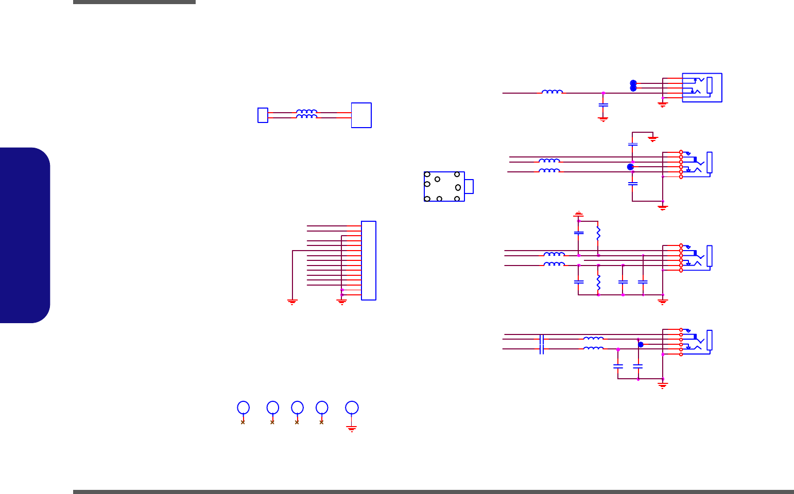
Schematic Diagrams
B - 38 AUDIO & MODEM BOARD
B.Schematic Diagrams
AUDIO & MODEM BOARD
Z3706
AC13 1U_10V_06
AL7 HCB1608KF-121T25_06
AL9
HK2125 R10J-T_08
ASPDI F
AH2
C1 11 D1 1 1
CONN.? ? ? ? ?
Z3707
AHP_L
AR 1
1K_06
Li ne In
/REAL
Surround Out
Z3703
Z3712
AH5
C7 9D 79
ALI NE1-R
ALI NE_SEN SE
AGND
AH 4
C315D110
Z3714
AJSPD IF1
AUDIO JACK
3
5
4
2
1
3
5
4
2
1
SOLDE R SIDE VIEW
AMI CL
AJ AUD IO1
CON15_R
1
2
3
4
5
6
7
8
9
10
11
12
13
14
15
ASPD_IF O
AJLIN EIN 1
2S J -S3 51 -S 0 5
2
6
5
3
1
4
AH MD CC 1
PJ S
1
2TI P
RI NG
AMI CSEN SE
AHP_R Z3710
AC 7
.1U_50V_06
Z3716
ALI NE_SENS E
AR 2
1K_06
AGND
AL8 HCB1608KF-121T25_06
AGN D
Z3702
AMI CR
ALI NE1 -L
SPDIF OUT
/Side Surronnd
OUT
AHP_R
AHP_L
Z3704
ASPD _I FO
AL6 HCB1608KF-121T25_06
1 2
AL3 HCB1608KF-121T25_06
1 2
AGN D
Z3713
Mi c In
/Cen/LEF Out
AMI CSEN SE
AL2 F C M1 60 8K- 12 1T 06 _0 6
1 2
HEADPHONE
AMI CR
AC11 1U_10V_06
AHP_SENS E
AC5
1000P_50V_06
AC 12
2200P_50V_06
2
AC 2
1000P_50V_06
J LINEIN
AGN D
4
AL4 HCB1608KF-121T25_06
1 2
AL5 HCB1608KF-121T25_06
1 2
Z3715
AL1 0
HK2125 R10J-T_08
ALI NE1-L
AHPSEL
AC10
22 00 P_5 0V _ 06
AGND
AGN D
AH PSEL
Z3705
AGN D
AHP_SEN SE
ALI NE1 -R
AC 8
2200P _50V_06
PI N GN D1=AG ND
AH3
C2 56 D2 56
Z3701
1
AC 9
1U_50V_06
AH1
C7 9D 79
Z3711
AC6
22 00 P_5 0V _ 06
Z3709
AC3
680P_50V_06
AJMIC 1
2S J -S3 51 -S 0 1
2
6
5
3
1
4
AGN D
5
6
AG ND
AMI CL
Z3708
AJH P1
2S J -S3 51 -S 0 3
2
6
5
3
1
4
3
AJMOD EM1
85 20 4- 2
1
2
1
2
Sheet 37 of 40
AUDIO & MODEM
BOARD
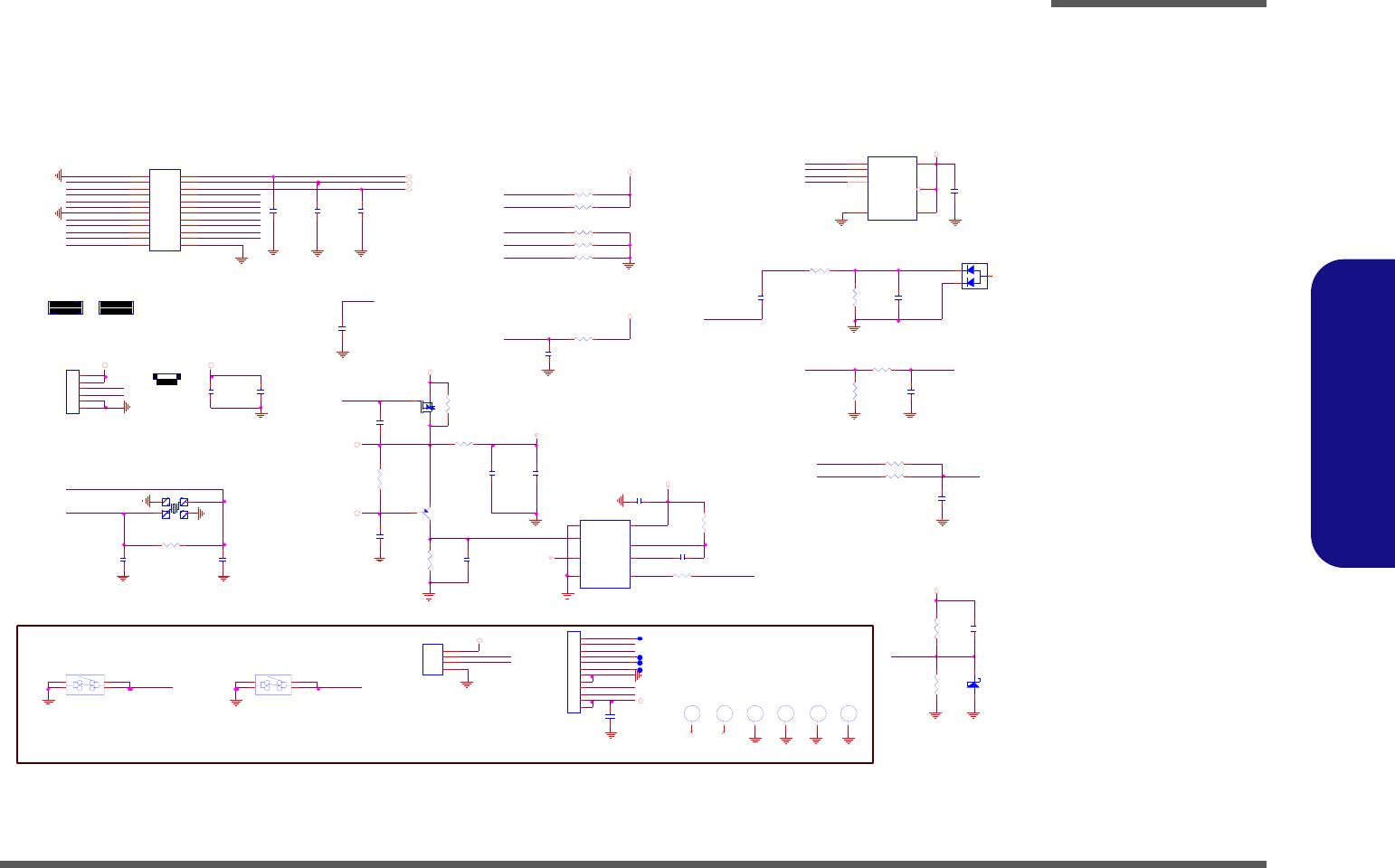
Schematic Diagrams
CLICK BOARD B - 39
B.Schematic Diagrams
CLICK BOARD
TR18
100K_04
TC22
1U_10V_06
TGN D
TMCS
TGPIO 0/IN T
23
TMU XO UT
TUSB_PN3_R
TH3
C237D91
TR 9
33_06
T G RID0 /SE N S E
TJTP 2
CON4
1
2
3
4
1
2
3
4
TGND
TR15 100_04
TPBUTTON _R
TC 1 7
18P_50V _06
TGND
24
TGN D
TG N D
TMISO /MO DE3
TQ1
ND S3 52 AP
G
D S
TG ND
TPBUTTON _L
TC 4
1U _10V_06
TC18
.1 U_ 16 V_ 0 4
TG N D
TG ND
TP B U T T O N _ R
TMOS I
TC16
18P_50V_06
TX1
HS X531S_12MH z
12
34
TGND
TQ2
2SB1198K
B
EC
TTP_C LK
TD A T A 2
TD1
*S C S 5 5 1V
A C
Z3802
TTC_VDD
TTC_VDD
TM O S I
TG ND
TGN D
TH 2
C6 7D 6 7
TC 13
4 7 P_ 50 V_ 0 4
TR23
0_04
TMCS
23
TG ND
TMCLK
TGND
TTP_CLK
TUSB_ PP3
TR24 47K_04
BOTTON VIEW
TG ND
TJ _ F P 2
CON 2 4A
1 2
3 4
5 6
7 8
910
11 12
13 14
15 16
17 18
19 20
2221
23 24
TG N D
TUSB_ PN3_ R
TR11
330K_04
TG N D TU 4
RC lam p0502B
1
2
3
1
TGN D
TTC _VDD
Z3803
TGPIO 0/IN T
TG ND
TP B U T TO N _ L
TUSB _PP3
TGND
TM C L K
TG N D
Z3808
TE S D _ R I N G
TR4 330K_04
TR13 10K_04
TC23
1U_6.3V _04
TGND
TTP_DATA
2
TGN D
TM ISO/M ODE3
TD ATA2
TMUXO UT
TC7
.1 U_ 2 5V _0 6
TG N D
TR3 47K_04
TGN D
TG N D
TTP_D ATA
TG PIO1
TGN D
T+5V
TU 2
M9 51 2 8 W MN 6T P
1
2
3
4
5
6
7
8
CS#
Q
WP#
VSS
S
SC K
HO LD #
VDD
TC 24
1U _10V_06
TU3
74LVC 1G 123
8
7
6
54
3
2
1VC C
Rx /Cx
Cx
QGN D
CL R#
B
A#
PIN5,6=T GND
T3.3V
Z3801
TC21 2.2U_6.3V_06
TGND
TC 20
1U _10V_06
TR21
330K _04
TR 2 2
*0 _0 6
TR16
330K_04
PIN5,6=T GND
TGPIO 1
TDATA0
TGN D
TC15
.1U_16V_04
TN RESET
TX O U T
TP D _ R E G
TC 12
.022U_16V_04
T3.3V
TGN D
TGND
TH6
C237D91
TXO UT
TS W 1
HCH STS-05
3
14
2
TG _ F E T
TJ_FP1
CON6_CLICK
1
2
3
4
5
6
TC 8
* 18P_50V_06
TJ_FP1
24
TD ATA1
TOP VIEW
TDVD D1
TH4
C2 3 7 D9 1
TUSB_PP3_R
T3.3V
T PD_ RE G
TC 1 9
47P_50V _04
TG N D
TUSB_ PP3 _ R
TMISO /MO DE3
TH 1
C2 37 D 91
TR1 47K_04
TG_FET
TG N D
T+5V
TDATA1
TSW2
HCH STS-05
3
14
2
TESD_ RI NG
TN R E S E T
TC 2
.1U _ 16 V _ 0 4
J_FP1
TGRI D0/SENSE
TR5 47K_04
TTC_VDD
TGN D
Z38 09
TU SB_ PN3
TXIN
TC 5
.1U _1 6 V _ 04
TR 1 7 2 7 . 4 _1 % _ 04
TJ TP1
87151-1207G
1
2
3
4
5
6
7
8
9
10
11
12
TC 2 5
1U _10V_06
TUS B_PN 3
TC1
0.1U F_04
TG ND
TD ATA0
TC27
.1U_25V_06
1
TAVDD
TR 20 2 7 . 4 _1 % _ 04
TTC_VDD
TAVDD
TDVD D1
TC 2 8
33 P _ 5 0V _ 0 6
TR6 15_06
6
Z3805
Z3807
TR12
100K_04
T3.3V
Z3804
TR 19 1.5K_04
T3.3V
TGN D
TR2 47K_04
2
TC14
1U_10V_06
TC26
1U_10V_06
1
TG ND
Z3806
TX I N
TR14 *47K_04
T3.3V
TH5
C67D67
TGND
Sheet 38 of 40
CLICK BOARD

Schematic Diagrams
B - 40 USB BOARD
B.Schematic Diagrams
USB BOARD
UC9
1U_10V_06
+
UC1
100U_10V_D
UUSBVCC? ? ? ? ? 5V
~5.25V??,????
4.9V, ? ? ? ? ? ? ?
Device? Eye Pattern Test
fail??????
UGN D
UUSB_PN1
U+VDD3
U+5V
UGND
UPL1
EMI_CHOKE
32
1 4
UL2
HCB 3216K F -800T30_12
UGND
UGN D
UGND
UH2
C237D91
UU SB_PN1Z3901
UH7
H6_0D2_3
UG ND
UR 1 68K_06
UJUSB1
USB_1
1
2
3
4
GND1
GND2
VCC
DATA-
DATA+
GND
S
S
UGND
Z 3904
UL3
WC M3216F2S-161T03
1
4
2
3
UC3
.1U_50V_06
1
UH5
MTH8_0D 2_8
2
3
4
5 6
7
8
9
UPC1
.1U_50V _08
U PR1 * 0_12
UC2
.1U_50V _06
UGND
U+5V
UPF1
5A
UD1
*B AV 99
C
AC
A
UH1
C79D79
UH6
H6_0D2_3
UU 2
R T9701-CP L
1
2
3
4
5
VOUT
GND
VIN
VIN
VOUT
UG ND
ULID_RSUM#
UGND
Z3905
UR 2 82K_06
UPC2
.1U_50V_08
UJAC1
ACIN_CON
1
2
GND1
GND2
1
2
3
4
ULID_RSUM#
UGND
UU SB_OC2#
1
UH4
MTH8_0D2_8
2
3
4
5 6
7
8
9
UU1
TLE4917DS
1
2
3
46
5
VS
GND
Q
GNDPR G
GND
UUSB_PP1
U+VDD3
UC4
.01U_50V _06
UGND
UGND
UC6
.1U _10V_04
UUSBVCC
UGND
U+VDD3
UJUSB2
CON20A
1 2
3 4
5 6
7 8
910
11 12
13 14
15 16
17 18
19 20
Z 3902
UGND
960522
UVA++
+
UC5
100U_6.3V _B
12
UG ND
UUSB_PP1
UC 8
10U_10V_08
UR3 2.7K _06
Z 3903
UH3
C79D79
U+5V
UVA+
PIN GND3~4 =UGND
UGN D
UGND
UGN D
UGND
LID SWITCH
U PR2 * 0_12
UUSB_OC2#
UC7
.1U_10V _04
UPC3
.1U_50V_08
Sheet 39 of 40
USB BOARD
Schematic Diagrams
FINGERPRINT BOARD B - 41
B.Schematic Diagrams
FINGERPRINT BOARD
FJ1
FDATA0
FESD_RING
FDATA0
FTC_VDD
FDATA1
FMUXOUT
FGRID0/SENSE
FNRESET
24
23
24
FGPIO1
FGND
FNRESET
FGND
FJ1
CON24
1 2
3 4
5 6
7 8
910
11 12
13 14
15 16
17 18
19 20
2221
23 24
FUSB_ PN7_R
FGPIO0/INT FXIN
FESD_RI NG
FAVDD
2
FESD_RING
FMOSI
FGND
FGND
FP D_ RE G
FMCLK
FMCS
FMISO/ MODE3
FDVDD1
FPD_REG
FMUXOUT
TO P V IE W
FDVDD1
FMISO/MODE 3
FU1
TCS4B
A1
B1
C1
D1
E1
F1
G1
H1
J1
A2
B2
C2
D2
E2
F2
G2
H2
J2
A3
B3
C3
D3
E3
F3
G3
H3
J3
EXT_RING2
CR I D O
RING
MUXOUT
AVDD
MCS
PAD_VDD1B
MISO
DVDD
GPI O1
AGN D
DATA0
DATA1
GPI O0
MC L K
USB_DN
USB_DP
MOSI
PD_REG
NRESET
DGN D
DATA2
EXT_RING1
PVDD
XTA L I N
PGN D
XTAL OUT
F AVDD
FDATA2
1
BOTTON VIEW
FMOSI
FGND
FGPIO0/ INT
2
FGND
FXOUT
FUSB_PP7_R
FGRID 0/SENSE
23
FGND
FGPIO1
1
FTC_VDD
FUSB_ PP7_R
FDATA1
FMCS
FDATA2
FUSB_PN7_R
FMCLK
FXIN
FTC_VDD
FXOUT
Sheet 40 of 40
FINGERPRINT
BOARD

Schematic Diagrams
B - 42
B.Schematic Diagrams