Clevo W270BUQ Service Manual. Www.s Manuals.com. Manual
User Manual: Notebook Clevo W270BUQ - Service manuals and Schematics, Disassembly / Assembly. Free.
Open the PDF directly: View PDF ![]() .
.
Page Count: 76
- Service Manual
- Notice
- System Startup
- Introduction 1-1
- Disassembly 2-1
- Chapter 1: Introduction
- Overview
- Specifications
- External Locator - Top View with LCD Panel Open
- External Locator - Front & Right Side Views
- External Locator - Left Side & Rear View
- External Locator - Bottom View
- Mainboard Overview - Top (Key Parts)
- Mainboard Overview - Bottom (Key Parts)
- Mainboard Overview - Top (Connectors)
- Mainboard Overview - Bottom (Connectors)
- Chapter 2: Disassembly
- Overview
- Maintenance Tools
- Connections
- Maintenance Precautions
- Disassembly Steps
- Removing the Battery
- Removing the Hard Disk Drive
- Removing the Optical (CD/DVD) Device
- Removing the System Memory (RAM)
- Removing the Wireless LAN Module
- Removing the Keyboard
- Top
- Bottom (9W)
- Bottom (18W)
- SATA-DVD-DUAL
- LCD
- Appendix B: Schematic Diagrams
- System Block Diagram
- ONTARIO MEM & PCIE I/F, AP
- ONTARIO DISPLAY/ CLK/ MISC
- ONTARIO POWER & DECOUPLING
- INAGUA DDR3 SO-DIMMS A
- INAGUA DDR3 SO-DIMMS B
- HUDSON PCIE/ PCI/ CLOCK/ FCH
- HUDSON GPIO/ USB/ STRAP
- HUDSON SATA/ DEBUG IO/ SPI
- HUDSON POWER DECOUPLING
- POWERGOOD/ TPM
- ANX3110 ASIC
- LVDS/ INVERTER
- HDMI/ CRT
- CCD/ 3G
- CARD READER/ LAN JMC261C
- MINI PCIE/ SATA HDD/ ODD
- AUDIO CODEC ALC269
- USB 3.0 VL800
- KBC-ITE IT8518
- LED/ MDC/ BT
- USB/ FAN/ TP/ MULTI CON
- 5VS/ 3.3VS/ 1.8VS/ 1.5VS/ 1.1VS
- POWER VDD3/ VDD5
- POWER 1.5V/ 0.75V
- POWER 1.1V/ 1VS
- POWER 1.8VS
- APU CORE/ NB CORE
- Appendix C: Updating the FLASH ROM BIOS

W270BUQ Series

Preface
I
Preface
Notebook Computer
W270BUQ
Service Manual

Preface
II
Preface
Notice
The company reserves the right to revise this publication or to change its contents without notice. Information contained
herein is for reference only and does not constitute a commitment on the part of the manufacturer or any subsequent ven-
dor. They assume no responsibility or liability for any errors or inaccuracies that may appear in this publication nor are
they in anyway responsible for any loss or damage resulting from the use (or misuse) of this publication.
This publication and any accompanying software may not, in whole or in part, be reproduced, translated, transmitted or
reduced to any machine readable form without prior consent from the vendor, manufacturer or creators of this publica-
tion, except for copies kept by the user for backup purposes.
Brand and product names mentioned in this publication may or may not be copyrights and/or registered trademarks of
their respective companies. They are mentioned for identification purposes only and are not intended as an endorsement
of that product or its manufacturer.
Version 1.0
July 2011
Trademarks
AMD® is a registered trademark of Advanced Micro Devices, Inc.
Windows® is a registered trademark of Microsoft Corporation.
Other brand and product names are trademarks and /or registered trademarks of their respective companies.

Preface
III
Preface
About this Manual
This manual is intended for service personnel who have completed sufficient training to undertake the maintenance and
inspection of personal computers.
It is organized to allow you to look up basic information for servicing and/or upgrading components of the W270BUQ
series notebook PC.
The following information is included:
Chapter 1, Introduction, provides general information about the location of system elements and their specifications.
Chapter 2, Disassembly, provides step-by-step instructions for disassembling parts and subsystems and how to upgrade
elements of the system.
Appendix A, Part Lists
Appendix B, Schematic Diagrams
Appendix C, Updating the FLASH ROM BIOS

Preface
IV
Preface
IMPORTANT SAFETY INSTRUCTIONS
Follow basic safety precautions, including those listed below, to reduce the risk of fire, electric shock and injury to per-
sons when using any electrical equipment:
1. Do not use this product near water, for example near a bath tub, wash bowl, kitchen sink or laundry tub, in a wet
basement or near a swimming pool.
2. Avoid using a telephone (other than a cordless type) during an electrical storm. There may be a remote risk of elec-
trical shock from lightning.
3. Do not use the telephone to report a gas leak in the vicinity of the leak.
4. Use only the power cord and batteries indicated in this manual. Do not dispose of batteries in a fire. They may
explode. Check with local codes for possible special disposal instructions.
5. This product is intended to be supplied by a Listed Power Unit with an AC Input of 100 - 240V, 50 - 60Hz, DC Output
of 19V, 3.42A or 18.5V, 3.5A (65W) minimum AC/DC Adapter.
CAUTION
This Computer’s Optical Device is a Laser Class 1 Product
FCC Statement
This device complies with Part 15 of the FCC Rules. Operation is subject to the following two conditions:
This device may not cause harmful interference.
This device must accept any interference received, including interference that may cause undesired operation.
Preface
V
Preface
Instructions for Care and Operation
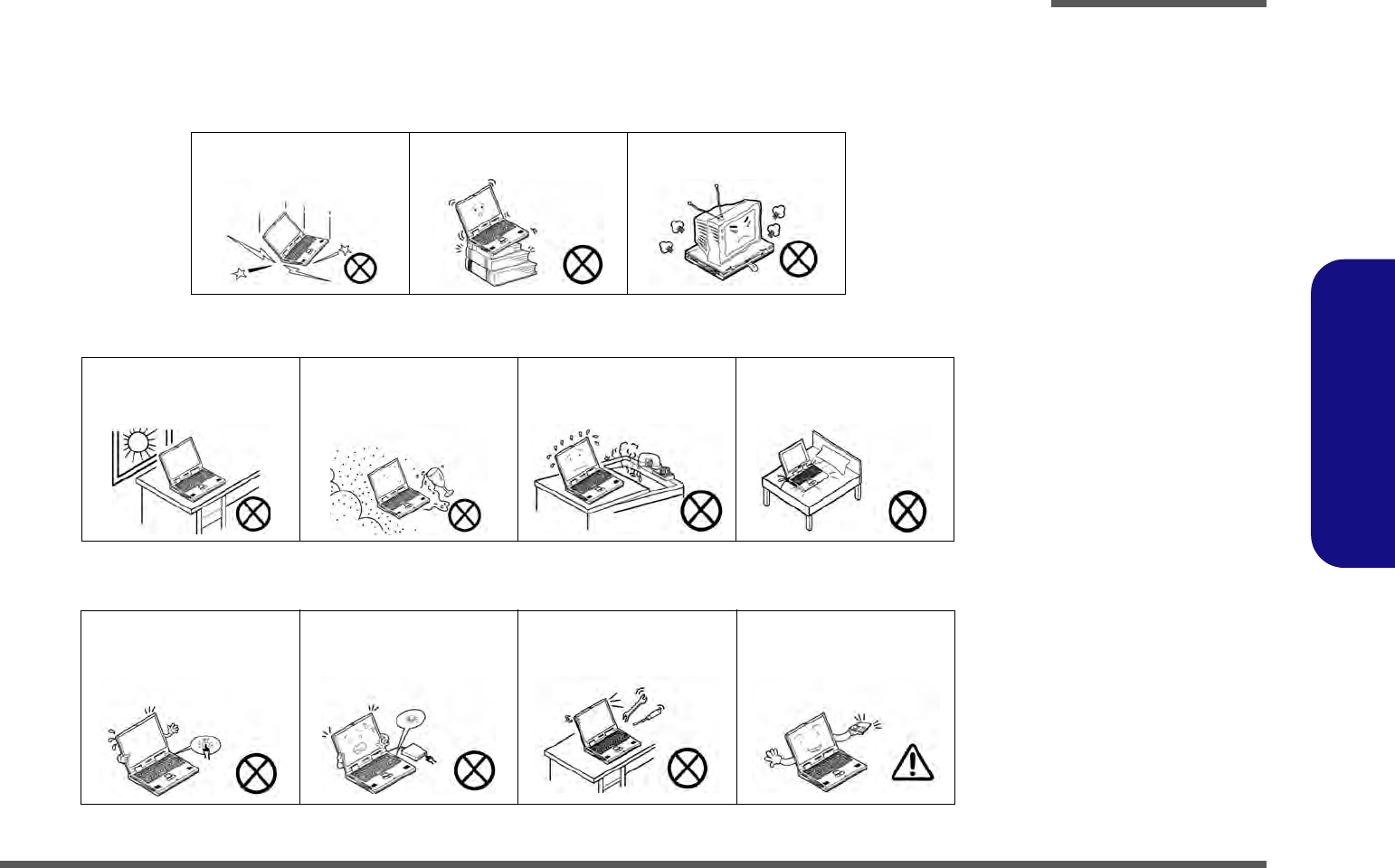
The notebook computer is quite rugged, but it can be damaged. To prevent this, follow these suggestions:
1. Don’t drop it, or expose it to shock. If the computer falls, the case and the components could be damaged.
2. Keep it dry, and don’t overheat it. Keep the computer and power supply away from any kind of heating element. This
is an electrical appliance. If water or any other liquid gets into it, the computer could be badly damaged.
3. Follow the proper working procedures for the computer. Shut the computer down properly and don’t forget to save
your work. Remember to periodically save your data as data may be lost if the battery is depleted.
Do not expose the computer
to any shock or vibration. Do not place it on an unstable
surface. Do not place anything heavy
on the computer.
Do not expose it to excessive
heat or direct sunlight. Do not leave it in a place
where foreign matter or mois-
ture may affect the system.
Don’t use or store the com-
puter in a humid environment. Do not place the computer on
any surface which will block
the vents.
Do not turn off the power
until you properly shut down
all programs.
Do not turn off any peripheral
devices when the computer is
on.
Do not disassemble the com-
puter by yourself. Perform routine maintenance
on your computer.
Preface
VI
Preface
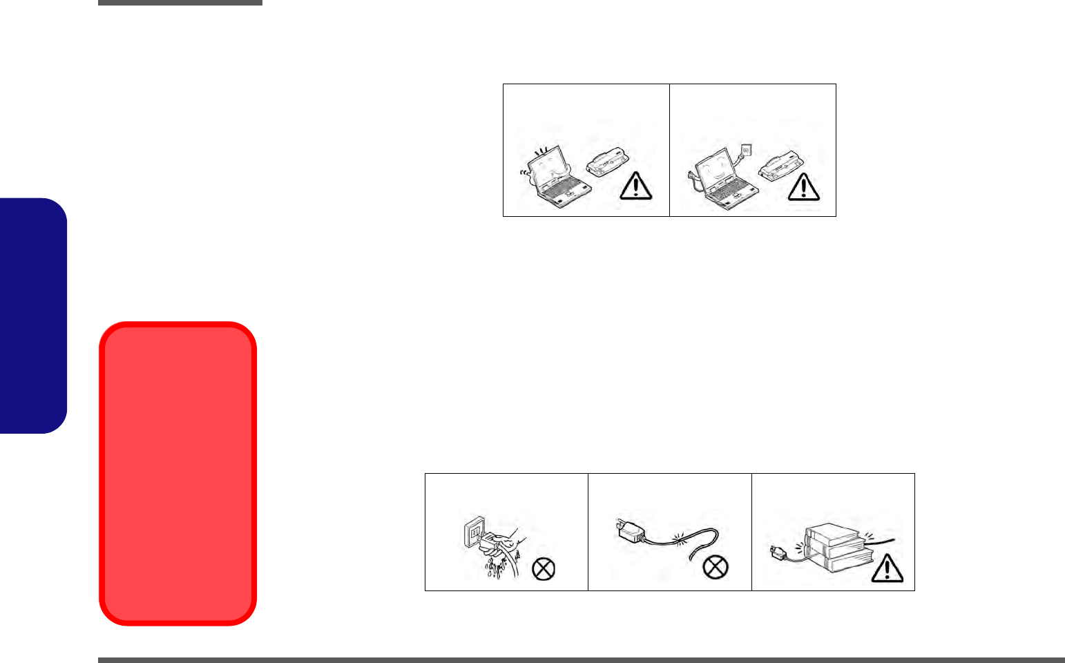
4. Avoid interference. Keep the computer away from high capacity transformers, electric motors, and other strong mag-
netic fields. These can hinder proper performance and damage your data.
5. Take care when using peripheral devices.
Power Safety
The computer has specific power requirements:
• Only use a power adapter approved for use with this computer.
• Your AC adapter may be designed for international travel but it still requires a steady, uninterrupted power supply. If you are
unsure of your local power specifications, consult your service representative or local power company.
• The power adapter may have either a 2-prong or a 3-prong grounded plug. The third prong is an important safety feature; do
not defeat its purpose. If you do not have access to a compatible outlet, have a qualified electrician install one.
• When you want to unplug the power cord, be sure to disconnect it by the plug head, not by its wire.
• Make sure the socket and any extension cord(s) you use can support the total current load of all the connected devices.
• Before cleaning the computer, make sure it is disconnected from any external power supplies.
Use only approved brands of
peripherals. Unplug the power cord before
attaching peripheral devices.
Do not plug in the power
cord if you are wet. Do not use the power cord if
it is broken. Do not place heavy objects
on the power cord.
Power Safety
Warning
Before you undertake
any upgrade proce-
dures, make sure that
you have turned off the
power, and discon-
nected all peripherals
and cables (including
telephone lines). It is
advisable to also re-
move your battery in
order to prevent acci-
dentally turning the
machine on.

Preface
VII
Preface
Battery Precautions
• Only use batteries designed for this computer. The wrong battery type may explode, leak or damage the computer.
• Do not continue to use a battery that has been dropped, or that appears damaged (e.g. bent or twisted) in any way. Even if the
computer continues to work with a damaged battery in place, it may cause circuit damage, which may possibly result in fire.
• Recharge the batteries using the notebook’s system. Incorrect recharging may make the battery explode.
• Do not try to repair a battery pack. Refer any battery pack repair or replacement to your service representative or qualified service
personnel.
• Keep children away from, and promptly dispose of a damaged battery. Always dispose of batteries carefully. Batteries may explode
or leak if exposed to fire, or improperly handled or discarded.
• Keep the battery away from metal appliances.
• Affix tape to the battery contacts before disposing of the battery.
• Do not touch the battery contacts with your hands or metal objects.
Battery Guidelines
The following can also apply to any backup batteries you may have.
• If you do not use the battery for an extended period, then remove the battery from the computer for storage.
• Before removing the battery for storage charge it to 60% - 70%.
• Check stored batteries at least every 3 months and charge them to 60% - 70%.
Battery Disposal
The product that you have purchased contains a rechargeable battery. The battery is recyclable. At the end of its useful life, under var-
ious state and local laws, it may be illegal to dispose of this battery into the municipal waste stream. Check with your local solid waste
officials for details in your area for recycling options or proper disposal.
Caution
Danger of explosion if battery is incorrectly replaced. Replace only with the same or equivalent type recommended by the manufacturer.
Discard used battery according to the manufacturer’s instructions.
Battery Level
Click the battery icon in the taskbar to see the current battery level and charge status. A battery that drops below a level of 10%
will not allow the computer to boot up. Make sure that any battery that drops below 10% is recharged within one week.

Preface
VIII
Preface
Related Documents
You may also need to consult the following manual for additional information:
User’s Manual on CD/DVD
This describes the notebook PC’s features and the procedures for operating the computer and its ROM-based setup pro-
gram. It also describes the installation and operation of the utility programs provided with the notebook PC.
System Startup
1. Remove all packing materials.
2. Place the computer on a stable surface.
3. Insert the battery and make sure it is locked in position.
4. Securely attach any peripherals you want to use with the computer
(e.g. keyboard and mouse) to their ports.
5. Attach the AC/DC adapter to the DC-In jack at the left of the
computer, then plug the AC power cord into an outlet, and connect
the AC power cord to the AC/DC adapter.
6. Use one hand to raise the
lid/LCD to a comfortable viewing angle
(do
not exceed 130 degrees)
;
use the other hand (as illustrated in
Figure 1) to support the base of the computer (Note: Never lift the
computer by the lid/LCD).
7. Press the power button to turn the computer “on”.
Shut Down
Note that you should al-
ways shut your com-
puter down by
choosing Shut Down
from the Start Menu.
This will help prevent
hard disk or system
problems.
130 ゚
Figure 1
Opening the Lid/LCD/
Computer with AC/DC
Adapter Plugged-In

Preface
IX
Preface
Contents
....................................................................................................1-VIII
System Startup ............................................................................1-VIII
Introduction ..............................................1-1
Overview .........................................................................................1-1
Specifications ..................................................................................1-2
External Locator - Top View with LCD Panel Open ......................1-4
External Locator - Front & Right Side Views .................................1-5
External Locator - Left Side & Rear View .....................................1-6
External Locator - Bottom View .....................................................1-7
Mainboard Overview - Top (Key Parts) .........................................1-8
Mainboard Overview - Bottom (Key Parts) ....................................1-9
Mainboard Overview - Top (Connectors) .....................................1-10
Mainboard Overview - Bottom (Connectors) ...............................1-11
Disassembly ...............................................2-1
Overview .........................................................................................2-1
Maintenance Tools ..........................................................................2-2
Connections .....................................................................................2-2
Maintenance Precautions .................................................................2-3
Disassembly Steps ...........................................................................2-4
Removing the Battery ......................................................................2-5
Removing the Hard Disk Drive .......................................................2-6
Removing the Optical (CD/DVD) Device ......................................2-8
Removing the System Memory (RAM) ..........................................2-9
Removing the Wireless LAN Module ...........................................2-11
Removing the Keyboard/CCD ......................................................2-12
Part Lists ..................................................A-1
Part List Illustration Location ........................................................A-2
Top .................................................................................................A-3
Bottom (9W) ..................................................................................A-4
Bottom (18W) ................................................................................ A-5
SATA-DVD-DUAL ....................................................................... A-6
LCD ............................................................................................... A-7
Schematic Diagrams.................................B-1
System Block Diagram ...................................................................B-2
ONTARIO MEM & PCIE I/F, AP .................................................B-3
ONTARIO DISPLAY/ CLK/ MISC ..............................................B-4
ONTARIO POWER & DECOUPLING .........................................B-5
INAGUA DDR3 SO-DIMMS A ....................................................B-6
INAGUA DDR3 SO-DIMMS B ....................................................B-7
HUDSON PCIE/ PCI/ CLOCK/ FCH ............................................B-8
HUDSON GPIO/ USB/ STRAP .....................................................B-9
HUDSON SATA/ DEBUG IO/ SPI .............................................B-10
HUDSON POWER DECOUPLING ............................................B-11
POWERGOOD/ TPM ..................................................................B-12
ANX3110 ASIC ............................................................................B-13
LVDS/ INVERTER ......................................................................B-14
HDMI/ CRT ..................................................................................B-15
CCD/ 3G .......................................................................................B-16
CARD READER/ LAN JMC261C ..............................................B-17
MINI PCIE/ SATA HDD/ ODD ...................................................B-18
AUDIO CODEC ALC269 ............................................................B-19
USB 3.0 VL800 ............................................................................B-20
KBC-ITE IT8518 ..........................................................................B-21
LED/ MDC/ BT ............................................................................B-22
USB/ FAN/ TP/ MULTI CON .....................................................B-23
5VS/ 3.3VS/ 1.8VS/ 1.5VS/ 1.1VS ..............................................B-24
POWER VDD3/ VDD5 ................................................................B-25
POWER 1.5V/ 0.75V ...................................................................B-26
POWER 1.1V/ 1VS ......................................................................B-27

Preface
X
Preface
POWER 1.8VS ............................................................................. B-28
APU CORE/ NB CORE ............................................................... B-29
Updating the FLASH ROM BIOS......... C-1
To update the FLASH ROM BIOS you must: C-1
Download the BIOS ....................................................................... C-1
Unzip the downloaded files to a bootable CD/DVD/ or USB Flash
drive ................................................................................................ C-1
Set the computer to boot from the external drive ........................... C-1
Use the flash tools to update the BIOS ..........................................C-2
Restart the computer (booting from the HDD) .............................. C-2

Introduction
Overview 1 - 1
1.Introduction
Chapter 1: Introduction
Overview
This manual covers the information you need to service or upgrade the W270BUQ series notebook computer. Informa-
tion about operating the computer (e.g. getting started, and the Setup utility) is in the User’s Manual. Information about
dri-vers (e.g. VGA & audio) is also found in the User’s Manual. The manual is shipped with the computer.
Operating systems (e.g. Window 7, etc.) have their own manuals as do application softwares (e.g. word processing and
database programs). If you have questions about those programs, you should consult those manuals.
The W270BUQ series notebook is designed to be upgradeable. See Disassembly on page 2 - 1 for a detailed description
of the upgrade procedures for each specific component. Please take note of the warning and safety information indicated
by the “” symbol.
The balance of this chapter reviews the computer’s technical specifications and features.

Introduction
1 - 2 Specifications
1.Introduction
Specifications
Latest Specification Information
The specifications listed here are correct at the
time of sending them to the press. Certain items
(particularly processor types/speeds) may be
changed, delayed or updated due to the manu-
facturer's release schedule. Check with your
service center for more details.
CPU
The CPU is not a user serviceable part. Ac-
cessing the CPU in any way may violate your
warranty.
Processor Options
AMD-C Series (Dual-Core) Accelerated Processing Unit -
C-50 2C (1.0GHz)
1MB L2 Cache, 40nm, DDR3-1066MHz, TDP 9W
AMD-E Series (Dual-Core) Accelerated Processing Unit -
E-350 (1.6GHz)
1MB L2 Cache, 40nm, DDR3-1066MHz, TDP 18W
Core Logic
AMD A50M FCH
LCD
17.3" (43.94cm) HD+ / FHD TFT LCD
Memory
Two 204 Pin SO-DIMM Sockets Supporting DDR3 1066/
1333MHz Memory
Memory Expandable up to 8GB
Storage
(Factory Option) One Changeable 12.7mm(h) Super Multi
Optical Device Drive
One Changeable 2.5" 9.5 mm (h) SATA HDD
Video Adapter
AMD Radeon™ HD 6250 (E-350 APU Integrated)
Shared Memory Architecture of up to 1469MB (under Win-
dows 7 32 Bit with 4GB Memory)
Microsoft® DirectX 11 Compatible
AMD Radeon™ HD 6310 (C-50 APU Integrated)
Shared Memory Architecture of up to 1469MB (under Win-
dows 7 32 Bit with 4GB Memory)
Microsoft® DirectX 11 Compatible
BIOS
One 16Mb SPI Flash ROM
AMI BIOS
Audio
High Definition Audio Compliant Interface
2 * Built-In Speakers
Built-In Microphone
Security
Security (Kensington® Type) Lock Slot
BIOS Password
Keyboard
Full-size “WinKey” keyboard (with numeric keypad)
Pointing Device
Built-in Touchpad
Communication
Built-In 10Mb/100Mb Ethernet LAN
(Factory Option) 300K/1.3M Pixel USB PC Camera Module
WLAN/ Bluetooth Half Mini-Card Modules:
(Factory Option) Wireless LAN (802.11b/g/n)
(Factory Option) Wireless LAN (802.11b/g/n) + Bluetooth 3.0

Introduction
Specifications 1 - 3
1.Introduction
Interface
Three USB 2.0 Ports
One HDMI-Out Port
One Headphone-Out Jack
One Microphone-In Jack
One RJ-45 LAN Jack
One DC-in Jack
One External Monitor Port
Card Reader
Embedded Multi-In-1 Card Reader
MMC (MultiMedia Card) / RS MMC
SD (Secure Digital) / Mini SD / SDHC/ SDXC
MS (Memory Stick) / MS Pro / MS Duo
Mini Card Slots
Slot 1 for WLAN Module or WLAN and Bluetooth Combo
Module
Environmental Spec
Temperature
Operating: 5°C - 35°C
Non-Operating: -20°C - 60°C
Relative Humidity
Operating: 20% - 80%
Non-Operating: 10% - 90%
Power
6 Cell Smart Lithium-Ion Battery Pack, 48.84WH
(Factory Option) 6 Cell Smart Lithium-Ion Battery Pack,
62.16WH
Full Range AC/DC Adapter
AC Input: 100 - 240V, 50 - 60Hz
DC Output: 19V, 3.42A or 18.5V, 3.5A (65W)
Dimensions & Weight
413mm (w) * 270mm (d) * 14 - 40.5mm (h)
2.9 kg (with 48.84WH Battery and ODD)
Introduction
1 - 4 External Locator - Top View with LCD Panel Open
1.Introduction
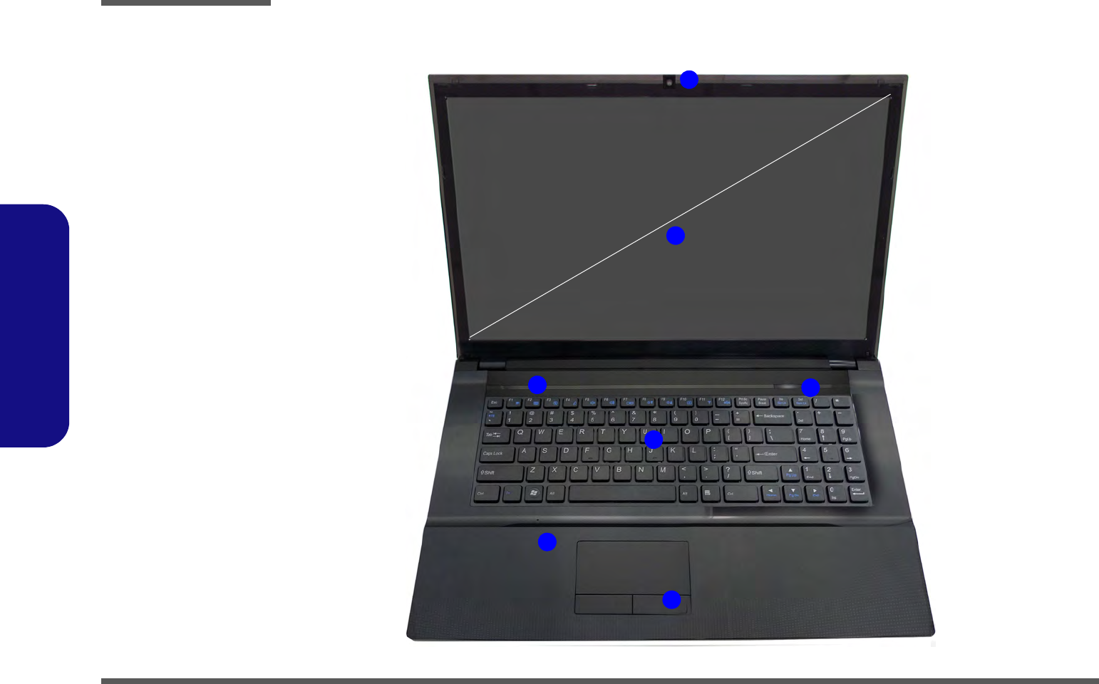
External Locator - Top View with LCD Panel Open
Figure 1
Top View
1. PC Camera
(Optional)
2. LCD
3. Power Button
4. LED Status
Indicators
5. Keyboard
6. Built-In
Microphone
7. Touchpad &
Buttons
4
6
3
5
7
1
2
17.3” (43.94cm)
Introduction
External Locator - Front & Right Side Views 1 - 5
1.Introduction
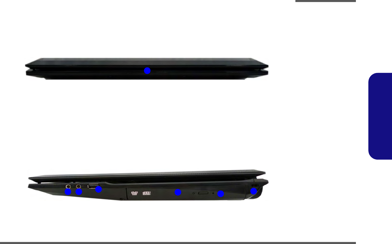
External Locator - Front & Right Side Views
Figure 2
Front View
1. LED Power
Indicators
Figure 3
Right Side View
1. Microphone-In
Jack
2. Headphone-Out
Jack
3. USB 2.0 Port
4. Optical Device
Drive Bay
5. Emergency Eject
Hole
6. Security Lock
Slot
FRONT VIEW
1
RIGHT SIDE VIEW
1 2 35
46
Introduction
1 - 6 External Locator - Left Side & Rear View
1.Introduction
External Locator - Left Side & Rear View
/
Figure 4
Left Side View
1. DC-In Jack
2. External Monitor
Port
3. RJ-45 LAN Jack
4. HDMI-Out Port
5. USB 2.0 Port
6. Vent
7. Multi-in-1 Card
Reader
LEFT SIDE VIEW
12345657
Figure 5
Rear View
1. Battery
REAR VIEW
1
Introduction
External Locator - Bottom View 1 - 7
1.Introduction
External Locator - Bottom View
Figure 6
Bottom View
1. Battery
2. Component Bay
Cover
3. Vent
4. Hard Disk Bay
Cover
5. Speakers
Overheating
To prevent your com-
puter from overhea-
ting, make sure no-
thing blocks any vent
while the computer is
in use.
2
3
1
43
5
5
3
3
3
3
Introduction
1 - 8 Mainboard Overview - Top (Key Parts)
1.Introduction
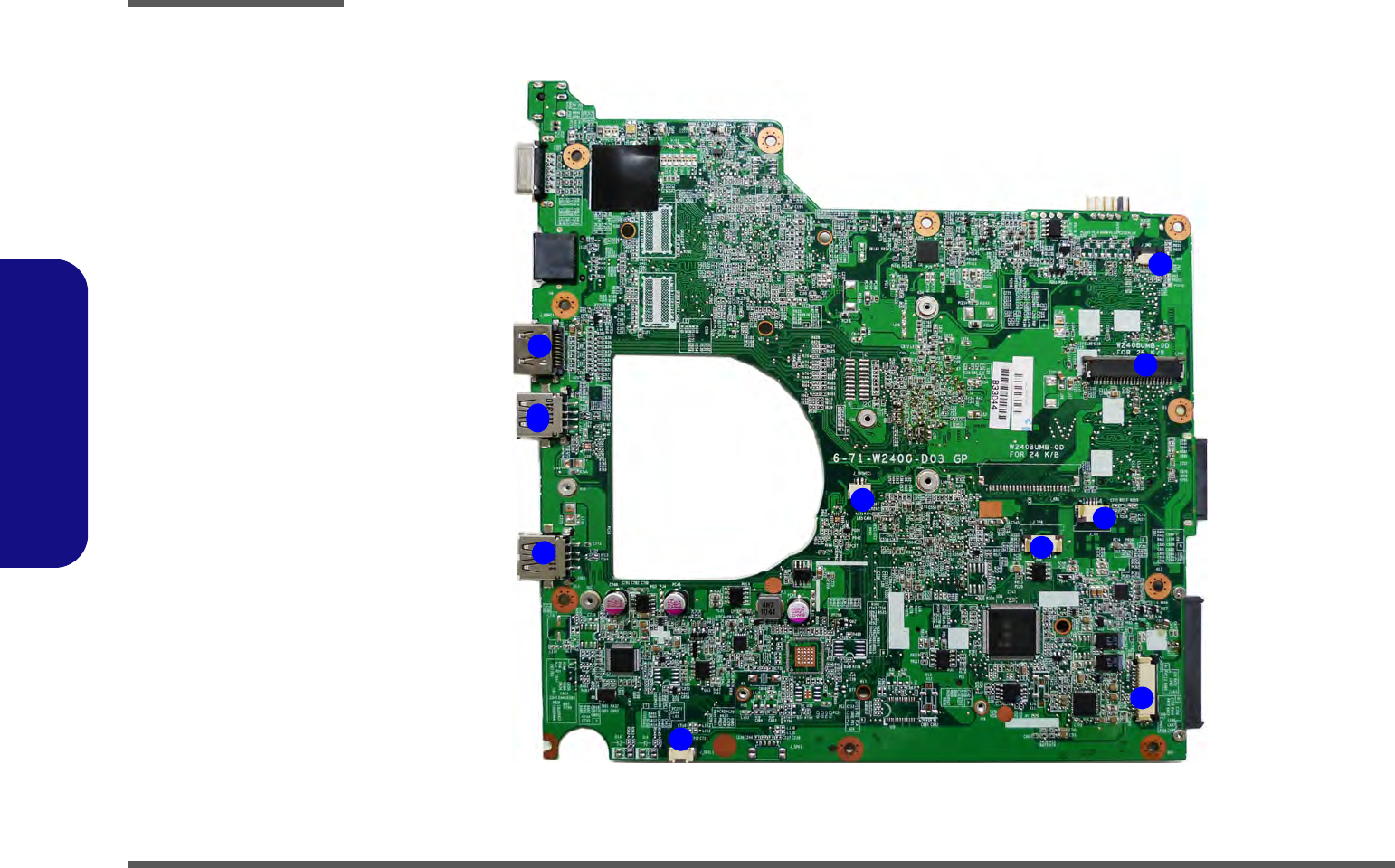
Mainboard Overview - Top (Key Parts)
Figure 7
Mainboard Top
Key Parts
1. JMC261C
2. ITE T858
3. AZALIA Codec
REALTEK
ALC269
3
2
1
Introduction
Mainboard Overview - Bottom (Key Parts) 1 - 9
1.Introduction
Mainboard Overview - Bottom (Key Parts)
1
2
3
456
Figure 8
Mainboard Bottom
Key Parts
1. Memory Slots
DDR3 SO-DIMM
2. Accelerated
Processing Unit
3. AMD Hudson M1
FCH
4. Mini-Card
Connector (WLAN
Module)
5. CMOS Battery
6. Card Reader
Socket
Introduction
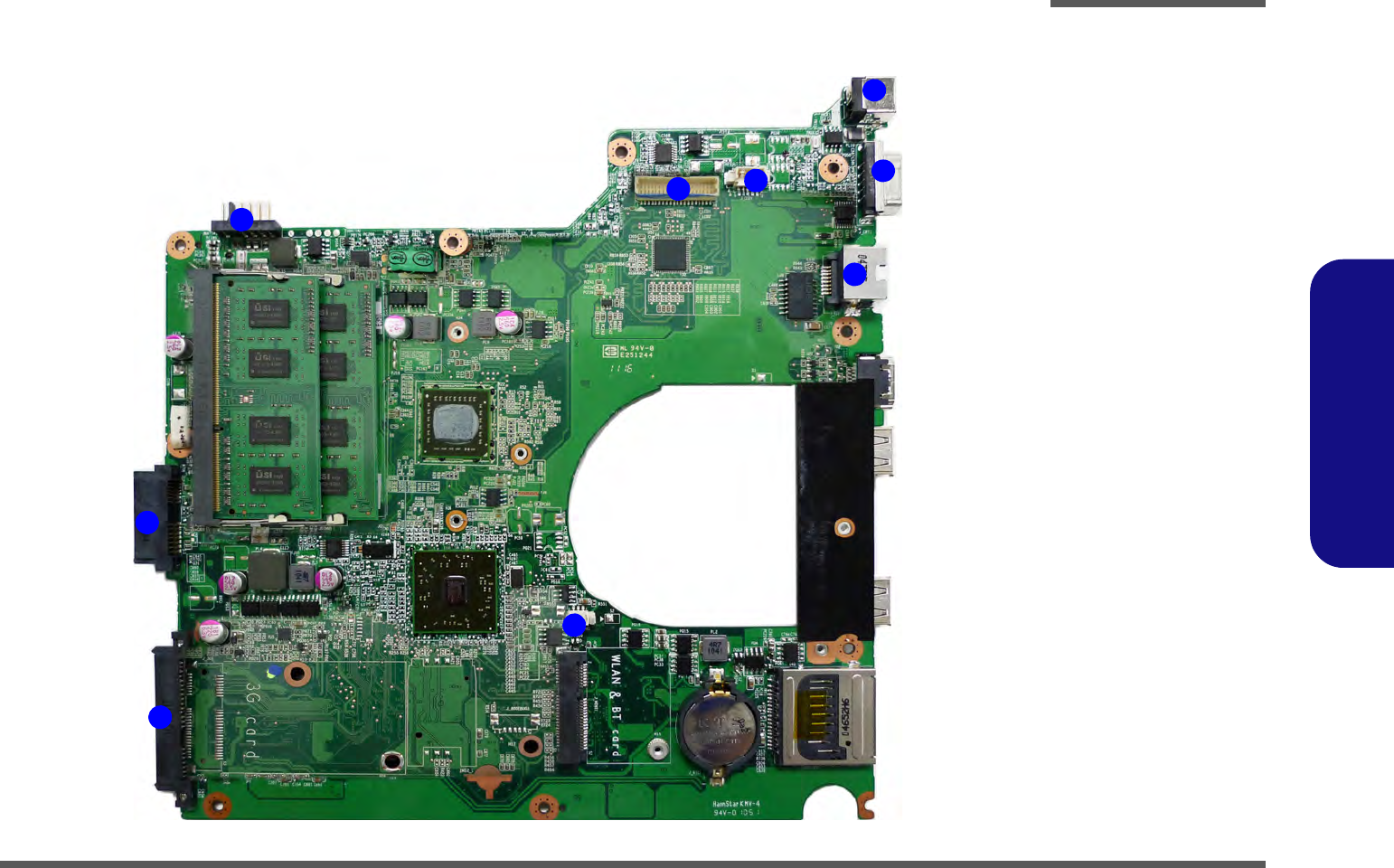
1 - 10 Mainboard Overview - Top (Connectors)
1.Introduction
Mainboard Overview - Top (Connectors)
Figure 9
Mainboard Top
Connectors
1. HDMI-Out Port
2. USB Port 2.0
3. Speaker Cable
Connector
4. Microphone
Cable Connector
5. Audio Board
Connector
6. TouchPad Cable
Connector 2
7. TouchPad Cable
Connector 1
8. Keyboard Cable
Connector
9. Switch Board
Cable Connector
1
2
8
2
3
46
7
5
9
Introduction
Mainboard Overview - Bottom (Connectors) 1 - 11
1.Introduction
Mainboard Overview - Bottom (Connectors)
Figure 10
Mainboard Bottom
Connectors
1. Battery
Connector
2. ODD Connector
3. HDD Connector
4. CPU Fan Cable
Connector
5. RJ-45 LAN Jack
6. External Monitor
Port
7. DC-In Jack
8. CCD Cable
Connector
9. LCD Cable
Connector
1
2
4
5
6
7
8
9
3

Introduction
1 - 12 Mainboard Overview - Bottom (Connectors)
1.Introduction

Disassembly
Overview 2 - 1
2.Disassembly
Chapter 2: Disassembly
Overview
This chapter provides step-by-step instructions for disassembling the W270BUQ series notebook’s parts and subsystems.
When it comes to reassembly, reverse the procedures (unless otherwise indicated).
We suggest you completely review any procedure before you take the computer apart.
Procedures such as upgrading/replacing the RAM, optical device and hard disk are included in the User’s Manual but are
repeated here for your convenience.
To make the disassembly process easier each section may have a box in the page margin. Information contained under
the figure # will give a synopsis of the sequence of procedures involved in the disassembly procedure. A box with a
lists the relevant parts you will have after the disassembly process is complete. Note: The parts listed will be for the dis-
assembly procedure listed ONLY, and not any previous disassembly step(s) required. Refer to the part list for the previ-
ous disassembly procedure. The amount of screws you should be left with will be listed here also.
A box with a will also provide any possible helpful information. A box with a contains warnings.
An example of these types of boxes are shown in the sidebar.
Information
Warning

Disassembly
2 - 2 Overview
2.Disassembly
NOTE: All disassembly procedures assume that the system is turned OFF, and disconnected from any power supply (the
battery is removed too).
Maintenance Tools
The following tools are recommended when working on the notebook PC:
• M3 Philips-head screwdriver
• M2.5 Philips-head screwdriver (magnetized)
• M2 Philips-head screwdriver
• Small flat-head screwdriver
• Pair of needle-nose pliers
• Anti-static wrist-strap
Connections
Connections within the computer are one of four types:
Locking collar sockets for ribbon connectors To release these connectors, use a small flat-head screwdriver to
gently pry the locking collar away from its base. When replac-
ing the connection, make sure the connector is oriented in the
same way. The pin1 side is usually not indicated.
Pressure sockets for multi-wire connectors To release this connector type, grasp it at its head and gently
rock it from side to side as you pull it out. Do not pull on the
wires themselves. When replacing the connection, do not try to
force it. The socket only fits one way.
Pressure sockets for ribbon connectors To release these connectors, use a small pair of needle-nose pli-
ers to gently lift the connector away from its socket. When re-
placing the connection, make sure the connector is oriented in
the same way. The pin1 side is usually not indicated.
Board-to-board or multi-pin sockets To separate the boards, gently rock them from side to side as
you pull them apart. If the connection is very tight, use a small
flat-head screwdriver - use just enough force to start.

Disassembly
Overview 2 - 3
2.Disassembly
Maintenance Precautions
The following precautions are a reminder. To avoid personal injury or damage to the computer while performing a re-
moval and/or replacement job, take the following precautions:
1. Don't drop it. Perform your repairs and/or upgrades on a stable surface. If the computer falls, the case and other
components could be damaged.
2. Don't overheat it. Note the proximity of any heating elements. Keep the computer out of direct sunlight.
3. Avoid interference. Note the proximity of any high capacity transformers, electric motors, and other strong mag-
netic fields. These can hinder proper performance and damage components and/or data. You should also monitor
the position of magnetized tools (i.e. screwdrivers).
4. Keep it dry. This is an electrical appliance. If water or any other liquid gets into it, the computer could be badly
damaged.
5. Be careful with power. Avoid accidental shocks, discharges or explosions.
•Before removing or servicing any part from the computer, turn the computer off and detach any power supplies.
•When you want to unplug the power cord or any cable/wire, be sure to disconnect it by the plug head. Do not pull on the wire.
6. Peripherals – Turn off and detach any peripherals.
7. Beware of static discharge. ICs, such as the CPU and main support chips, are vulnerable to static electricity.
Before handling any part in the computer, discharge any static electricity inside the computer. When handling a
printed circuit board, do not use gloves or other materials which allow static electricity buildup. We suggest that
you use an anti-static wrist strap instead.
8. Beware of corrosion. As you perform your job, avoid touching any connector leads. Even the cleanest hands pro-
duce oils which can attract corrosive elements.
9. Keep your work environment clean. Tobacco smoke, dust or other air-born particulate matter is often attracted
to charged surfaces, reducing performance.
10. Keep track of the components. When removing or replacing any part, be careful not to leave small parts, such as
screws, loose inside the computer.
Cleaning
Do not apply cleaner directly to the computer, use a soft clean cloth.
Do not use volatile (petroleum distillates) or abrasive cleaners on any part of the computer.
Power Safety
Warning
Before you undertake
any upgrade proce-
dures, make sure that
you have turned off the
power, and discon-
nected all peripherals
and cables (including
telephone lines). It is
advisable to also re-
move your battery in
order to prevent acci-
dentally turning the
machine on.

Disassembly
2 - 4 Disassembly Steps
2.Disassembly
Disassembly Steps
The following table lists the disassembly steps, and on which page to find the related information. PLEASE PERFORM
THE DISASSEMBLY STEPS IN THE ORDER INDICATED.
To remove the Battery:
1. Remove the battery page 2 - 5
To remove the HDD:
1. Remove the battery page 2 - 5
2. Remove the HDD page 2 - 6
To remove the Optical Device:
1. Remove the battery page 2 - 5
2. Remove the Optical device page 2 - 8
To remove the System Memory:
1. Remove the battery page 2 - 5
2. Remove the system memory page 2 - 9
To remove the Wireless LAN Module:
1. Remove the battery page 2 - 5
2. Remove the WLAN module page 2 - 11
To remove the Keyboard:
1. Remove the battery page 2 - 5
2. Remove the keyboard page 2 - 12
Disassembly
Removing the Battery 2 - 5
2.Disassembly
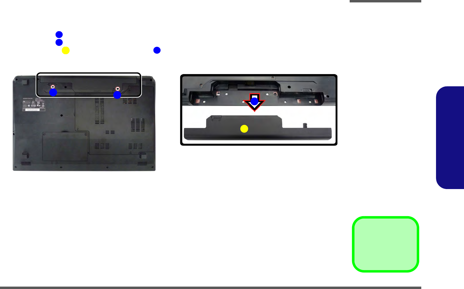
Removing the Battery
1. Turn the computer off, and turn it over.
2. Slide the latch in the direction of the arrow (Figure 1a).
3. Slide the latch in the direction of the arrow, and hold it in place (Figure 1a).
4. Slide the battery in the direction of the arrow (Figure 1b).
3. Battery
1
2
6
3
4
Figure 1
Battery Removal
a. Slide the latch and hold it
in place.
b. Slide the battery in the di-
rection of the arrow.
1
a. b.
3
2
4
Disassembly
2 - 6 Removing the Hard Disk Drive
2.Disassembly
Removing the Hard Disk Drive
The hard disk drive can be taken out to accommodate other 2.5" serial (SATA) hard disk drives with a height of 9.5mm
(h). Follow your operating system’s installation instructions, and install all necessary drivers and utilities (as outlined in
Chapter 4 of the User’s Manual) when setting up a new hard disk.
Hard Disk Upgrade Process
1. Turn off the computer, and remove the battery (page 2 - 5).
2. Locate the hard disk bay cover and remove screws & (Figure 2a).
Figure 2
HDD Assembly
Removal
a. Locate the HDD bay cover
and remove the screws.
•2 Screws
1
2
2
1
a.
HDD System Warning
New HDD’s are blank. Before you
begin make sure:
You have backed up any data
you want to keep from your old
HDD.
You have all the CD-ROMs and
FDDs required to install your op-
erating system and programs.
If you have access to the internet,
download the latest application
and hardware driver updates for
the operating system you plan to
install. Copy these to a remov-
able medium.
Disassembly
Removing the Hard Disk Drive 2 - 7
2.Disassembly
3. Remove the hard disk bay cover (Figure 3b).
4. Grip the tab and slide the hard disk in the direction of arrow (Figure 3c).
5. Lift the hard disk assembly out of the bay (Figure 3d).
6. Remove the screw - and the mylar cover from the hard disk (Figure 3e).
7. Reverse the process to install a new hard disk (do not forget to replace all the screws and covers).
6
3
4
6
5
6
7
10
11
12
4
b.
c.
9
d.
3
e.
11
8
7
12
5
10
6
3. HDD Bay Cover
5. HDD Assembly
11. Mylar Cover
12. HDD
•4 Screws
Figure 3
HDD Assembly
Removal (cont’d.)
b. Remove the HDD bay
cover.
c. Grip the tab and slide the
HDD assembly in the di-
rection of the arrow.
d. Lift the HDD assembly
out of the bay.
e. Remove the screws and
mylar cover.
Disassembly
2 - 8 Removing the Optical (CD/DVD) Device
2.Disassembly
Removing the Optical (CD/DVD) Device
1. Turn off the computer, remove the battery (page 2 - 5) and hard disk (page 2 - 6).
2. Remove the screw at point (Figure 4a).
3. Use a screwdriver to carefully push out the optical device at point (Figure 4b).
4. Insert the new device and carefully slide it into the computer (the device only fits one way. DO NOT FORCE IT; The
screw holes should line up).
5. Restart the computer to allow it to automatically detect the new device.
Figure 4
Optical Device
Removal
a. Remove the screw at
point .
b. Use a screwdriver to
carefully push out the
optical device at point
.
1
2
1
3
2
3. Optical Device
•1 Screw
1
b.
3
a.
2
Disassembly
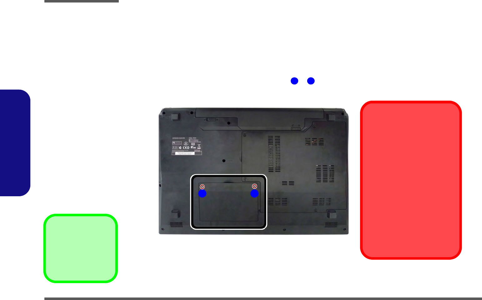
Removing the System Memory (RAM) 2 - 9
2.Disassembly
Removing the System Memory (RAM)
The computer has two memory sockets for 204 pin Small Outline Dual In-line Memory Modules (SO-DIMM) supporting
DDRIII (DDR3) Up to 1066/1333 MHz. The main memory can be expanded up to 8GB. The SO-DIMM modules sup-
ported are 1024MB and 2048MB DDRIII Modules. The total memory size is automatically detected by the POST rou-
tine once you turn on your computer.
Memory Upgrade Process
1. Turn off the computer, turn it over and remove the battery (page 2 - 5).
2. Remove screws - from the component bay cover (Figure 5a).
3. Carefully (a fan and cable are attached to the under side of the cover) lift up the bay cover.
4. Carefully disconnect the fan cable , and remove the cover (note that you need to raise the bottom cover up to
an angle of around 30° angle).
5. The RAM modules will be visible at point on the mainboard (Figure 5b).
Figure 5
RAM Module
Removal
a. Remove the screws.
b. The RAM modules will
be visible at point
on the mainboard.
7
6. Component Bay Cov-
er
•4 Screws
1
4
5
6
7
a.
1
2
3
46
30 ゚
5
76
b.
Disassembly
2 - 10 Removing the System Memory (RAM)
2.Disassembly
6. Gently pull the two release latches ( & ) on the sides of the memory socket in the direction indicated by the
arrows (Figure 5c). The RAM module will pop-up (Figure 5d), and you can then remove it.
7. Pull the latches to release the second module if necessary.
8. Insert a new module holding it at about a 30° angle and fit the connectors firmly into the memory slot.
9. The module will only fit one way as defined by its pin alignment. Make sure the module is seated as far into the slot
as it will go. DO NOT FORCE IT; it should fit without much pressure.
10. Press the module in and down towards the mainboard until the slot levers click into place to secure the module.
11. Replace the component bay cover and the screws (Figure 6e).
12. Restart the computer to allow the BIOS to register the new memory configuration as it starts up.
Figure 6
RAM Module
Removal (cont’d)
c. Pull the release lat-
ches.
d. Remove the module.
Contact Warning
Be careful not to touch
the metal pins on the
module’s connecting
edge. Even the cleanest
hands have oils which
can attract particles, and
degrade the module’s
performance.
10. RAM Module
8
9
10
d.
c.
8
10
9
e.
30 ゚
Note:
The component bay cover has four
cover pins, and these need to be
aligned with the slots in the case to in-
sure a proper cover fit. Make sure also
that the cover is raised at a 30 degree
angle during removal and installation.
Disassembly
Removing the Wireless LAN Module 2 - 11
2.Disassembly
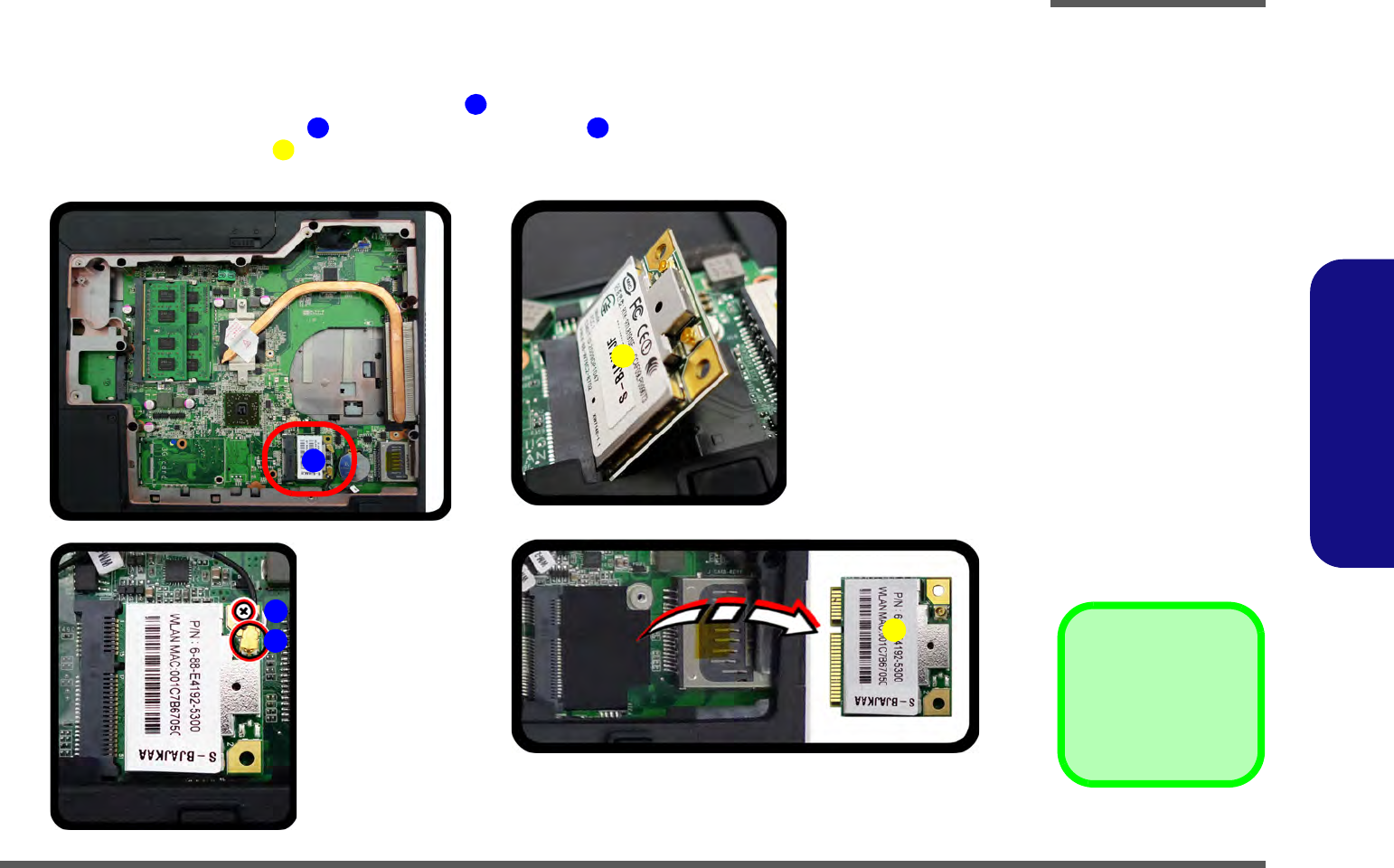
Removing the Wireless LAN Module
1. Turn off the computer, turn it over, and remove the battery (page 2 - 5) and the component bay cover (page 2 - 9).
2. The Wireless LAN module will be visible at point on the mainboard (Figure 11a).
3. Carefully disconnect the cable , and then remove the screw (Figure 11b).
4. The Wireless LAN module (Figure 11c) will pop-up, and you can remove it from the computer (Figure 11d).
Figure 7
Wireless LAN
Module Removal
a. Locate the WLAN.
b. Disconnect the cable
and remove the screw.
c. The WLAN module will
pop up.
d. Remove the Wireless
LAN module.
Note: Make sure you
reconnect the antenna
cable to the “1 + 2”
socket (Figure 11b).
1
2
3
4
b.
c.
a.
2
3
d.
4
4
1
4.Wireless LAN Module
•1 Screw
Disassembly
2 - 12 Removing the Keyboard
2.Disassembly
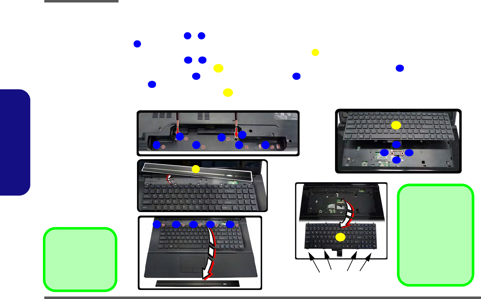
Removing the Keyboard
1. Turn off the computer, and remove the battery (page 2 - 5) and the component bay cover (page 2 - 9).
2. Remove screws - from the bottom of the computer (inside the battery compartment), and then press at point
to unsnap the LED cover module (use the eject pin tool provided to do this Figure 8a).
3. Turn the computer over, unsnap up the LED cover module from the center of the computer (Figure 8b).
4. Remove screws - from the keyboard (Figure 8c).
5. Carefully lift the keyboard up, being careful not to bend the keyboard ribbon cable . Disconnect the key-
board ribbon cable from the locking collar socket by using a flat-head screwdriver to pry the locking collar
pins away from the base (Figure 8d).
6. Carefully lift up the keyboard (Figure 8e) off the computer.
Figure 8
Keyboard Removal
a. Remove screws from the
bottom of the computer.
b. Turn the computer over,
unsnap up the LED cov-
er module from the cent-
er of the computer.
c. Remove screws from
the keyboard.
d. Carefully lift the key-
board up and disconnect
the keyboard ribbon ca-
ble from the locking col-
lar socket by using a flat-
head screwdriver to pry
the locking collar pins
away from the base.
e. Remove the keyboard.
1
6
7
8
9
13
14
15
15
16
17
14
8. LED Cover Module
14. Keyboard
11 Screws
a.
b.
13
2
5
7
6
d.
c. 9
14
10 11 12
4
14
15
17 17
Keyboard Tabs
e.
8
13
16
Re-Inserting the
Keyboard
When re-inserting the
keyboard firstly align the
four keyboard tabs at
the bottom (Figure 8e)
at the bottom of the key-
board with the slots in
the case.

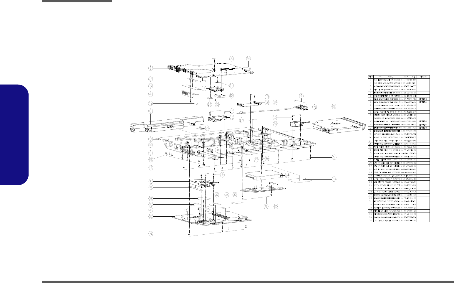
A - 1
A.Part Lists
Appendix A:Part Lists
This appendix breaks down the W270BUQ series notebook’s construction into a series of illustrations. The component
part numbers are indicated in the tables opposite the drawings.
Note: This section indicates the manufacturer’s part numbers. Your organization may use a different system, so be sure
to cross-check any relevant documentation.
Note: Some assemblies may have parts in common (especially screws). However, the part lists DO NOT indicate the
total number of duplicated parts used.
Note: Be sure to check any update notices. The parts shown in these illustrations are appropriate for the system at the
time of publication. Over the product life, some parts may be improved or re-configured, resulting in new part numbers.
A - 2
A.Part Lists
Part List Illustration Location
The following table indicates where to find the appropriate part list illustration.
Table A - 1
Part List Illustration
Location Part W270BUQ
Top page A - 3
Bottom (9W) page A - 5
Bottom (18W) page A - 5
SATA BLU-RAY COMBO page A - 6
SATA DVD DUAL page A - 7
LCD page A - 7
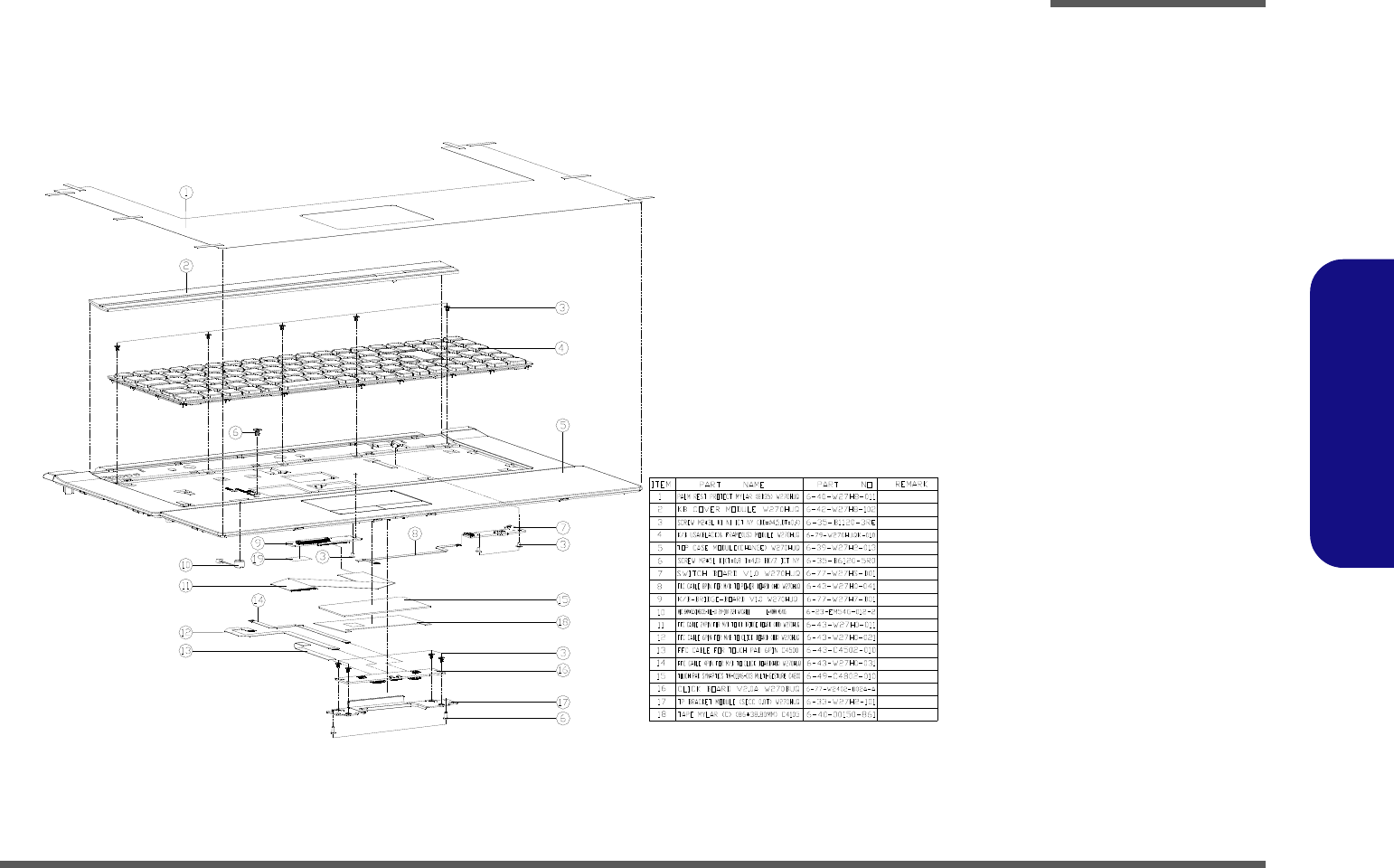
Top A - 3
A.Part Lists
Top
(灰色) (尚盟)
Figure A - 1
Top
A - 4 Bottom (9W)
A.Part Lists
Bottom (9W)
Figure A - 2
Bottom
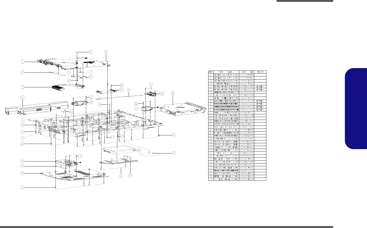
Bottom (18W) A - 5
A.Part Lists
Bottom (18W)
Figure A - 3
Bottom
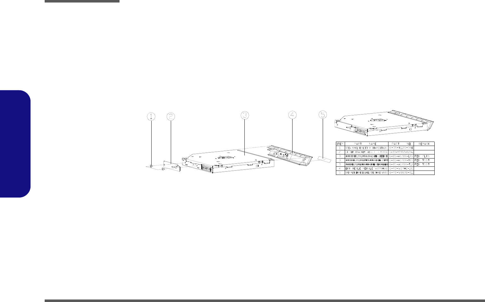
A - 6 SATA-DVD-DUAL
A.Part Lists
SATA-DVD-DUAL
志精
Figure 4
SATA-DVD-DUAL
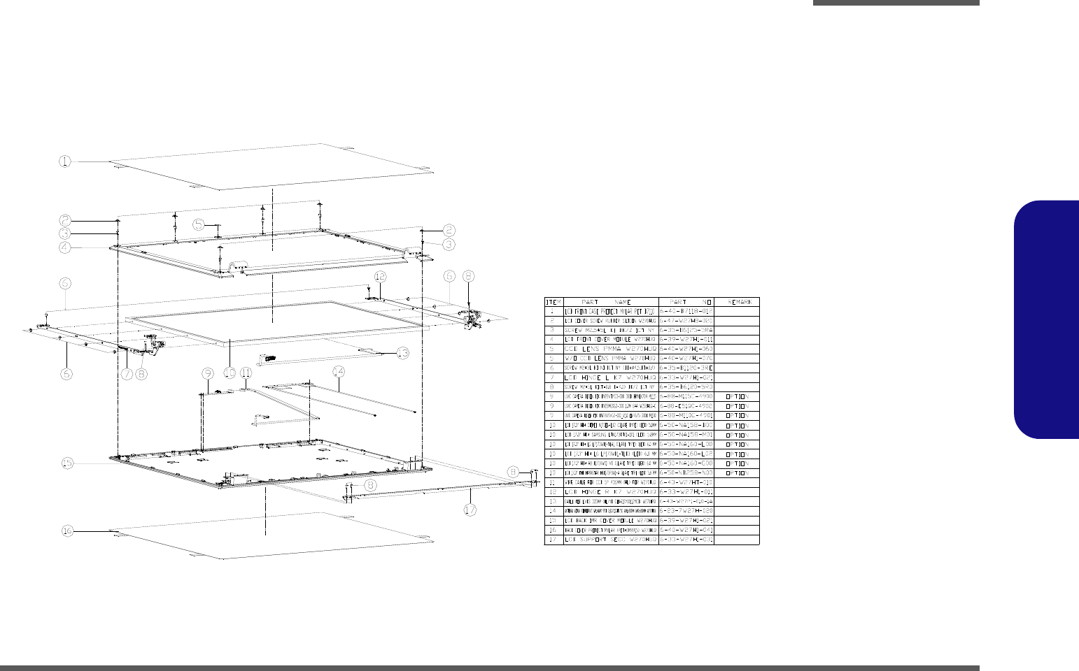
LCD A - 7
A.Part Lists
LCD
Figure A - 5
LCD

A - 8 LCD
A.Part Lists
Schematic Diagrams
B - 1
B.Schematic Diagrams
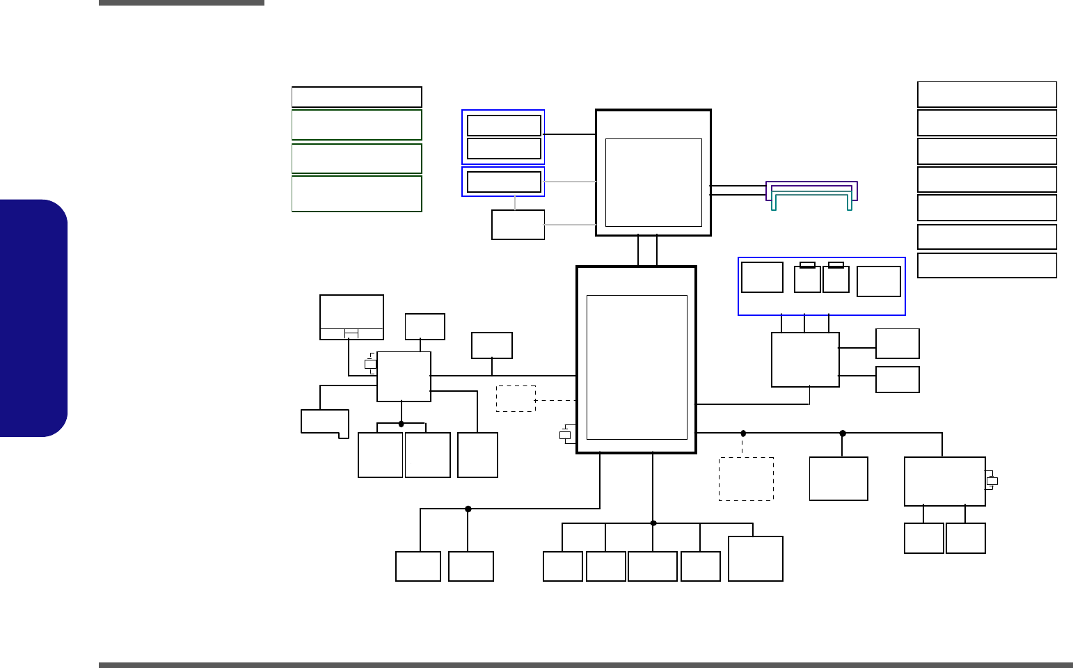
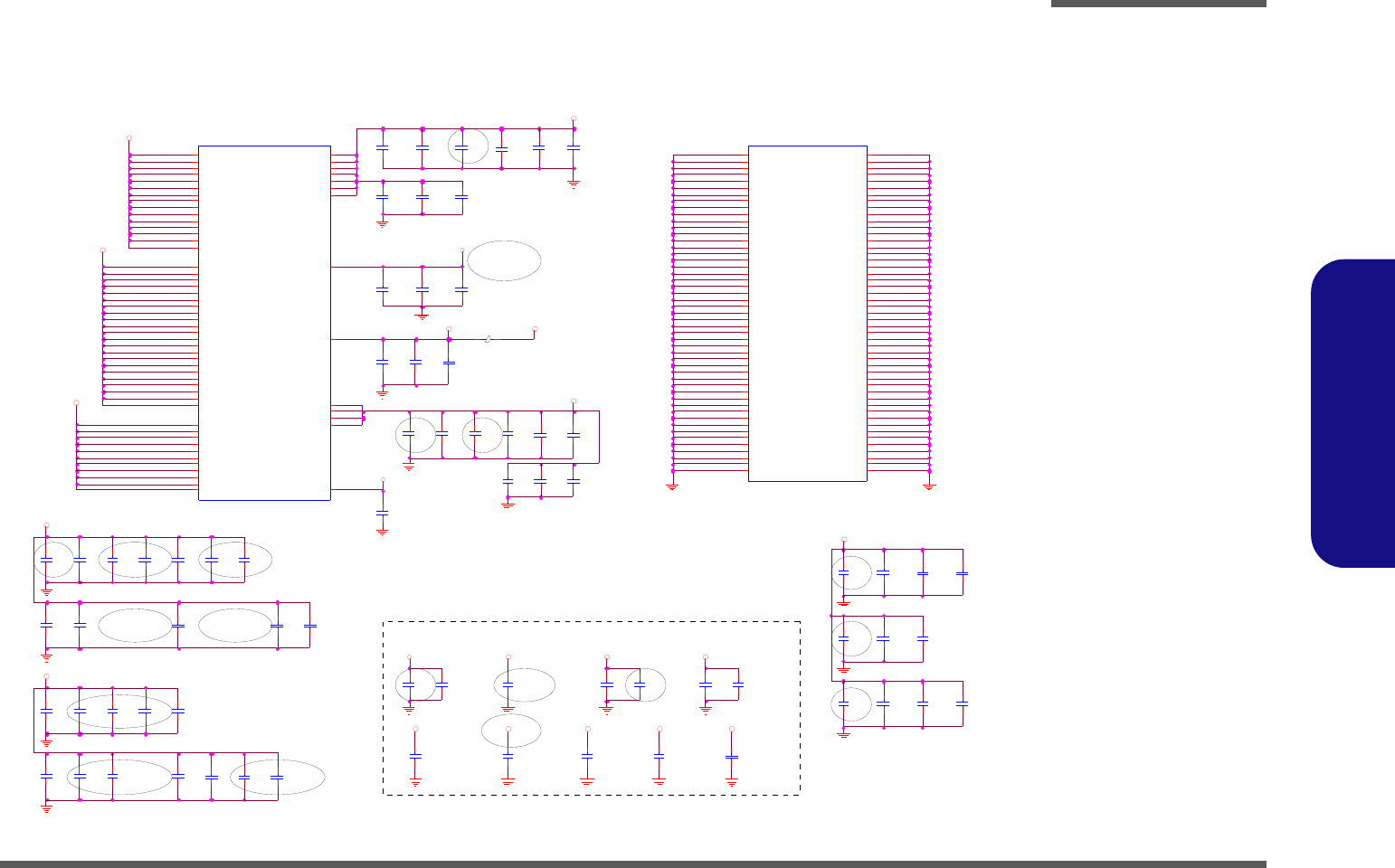
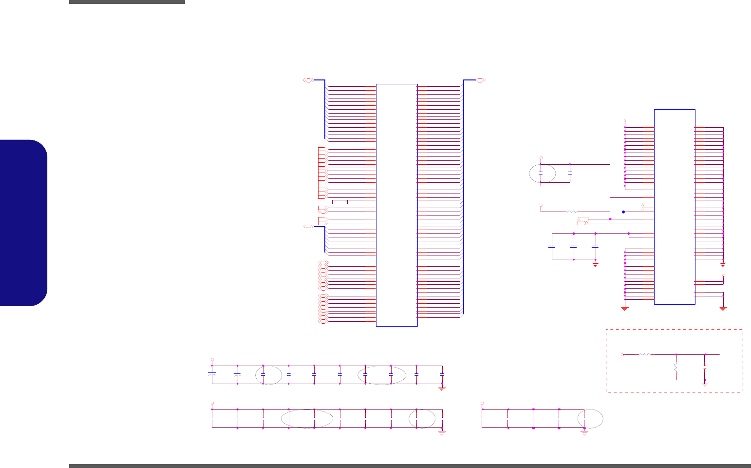
Appendix B: Schematic Diagrams
This appendix has circuit diagrams of the W270BUQ notebook’s PCB’s. The following table indicates where to find the
appropriate schematic diagram.
Diagram - Page Diagram - Page
System Block Diagram - Page B - 2 AUDIO CODEC ALC269 - Page B - 19
ONTARIO MEM & PCIE I/F, AP - Page B - 3 USB 3.0 VL800 - Page B - 20
ONTARIO DISPLAY/ CLK/ MISC - Page B - 4 KBC-ITE IT8518 - Page B - 21
ONTARIO POWER & DECOUPLING - Page B - 5 LED/ MDC/ BT - Page B - 22
INAGUA DDR3 SO-DIMMS A - Page B - 6 USB/ FAN/ TP/ MULTI CON - Page B - 23
INAGUA DDR3 SO-DIMMS B - Page B - 7 5VS/ 3.3VS/ 1.8VS/ 1.5VS/ 1.1VS - Page B - 24
HUDSON PCIE/ PCI/ CLOCK/ FCH - Page B - 8 POWER VDD3/ VDD5 - Page B - 25
HUDSON GPIO/ USB/ STRAP - Page B - 9 POWER 1.5V/ 0.75V - Page B - 26
HUDSON SATA/ DEBUG IO/ SPI - Page B - 10 POWER 1.1V/ 1VS - Page B - 27
HUDSON POWER DECOUPLING - Page B - 11 POWER 1.8VS - Page B - 28
POWERGOOD/ TPM - Page B - 12 APU CORE/ NB CORE - Page B - 29
ANX3110 ASIC - Page B - 13
LVDS/ INVERTER - Page B - 14
HDMI/ CRT - Page B - 15
CCD/ 3G - Page B - 16
CARD READER/ LAN JMC261C - Page B - 17
MINI PCIE/ SATA HDD/ ODD - Page B - 18
Table B - 1
SCHEMATIC
DIAGRAMS
Version Note
The schematic dia-
grams in this chapter
are based upon ver-
sion 6-7P-W24H5-002.
If your mainboard (or
other boards) are a lat-
er version, please
check with the Service
Center for updated di-
agrams (if required).
Schematic Diagrams
B - 2 System Block Diagram
B.Schematic Diagrams
System Block Diagram
Sheet 1 of 43
System Block
Diagram
(USB2)
TO UC H PA D
LPC
CARD
READER
SO-DIMM1
HP
OU T INT SPK R
CLICK BOARD
SOCKET
PCIE
480 Mbps
DDRIII
Mi ni P CI E
SPI
DDRIII
INT MIC
25
MH z
L C D Co nn ec to r
AMD FUSION APU
C R T Co nn ec to r
HDMI Connector
24 MHz
MI C
IN
128pins LQFP
SO-DIMM2
32.768KHz
(USB6)
Bl ue to ot h
1.1V, 1VS
EC SMBUS
US B PO RT
AZALIA LINK
(U SB 0) (USB1)
USB PORT
SATA ODDSA TA H DD
BIOS
SPI
LAN
ITE 85 18
IN T. K /B
Azalia Codec
EC
(Reserve W240BU/W251BUQ) 5V,3V,5VS,3.3VS
1.5V,0.75VS
USB2.0
AN X3 11 0
VDD3,VDD5
UMI*4
G711ST9U
32.768 KHz
JM IC RO
APU_CORE,NB_CORE
SATA I/II 3.0Gb/s
1066MHz
DDR3 / 1.5V
(Reserve)
TP M
CC D
(USB5)
REALTEK
ALC269
33 M H z
TH ER MA L
SE NS OR
100 MHz
14 *1 4* 1 .6m m
SM A RT
FA N
SM AR T
BA TT ER Y
AC -I N
JMC261C
W270BUQ System Block Diagram
SHEET 31
RJ -4 5 7 IN 1
SO CK ET
INT SPKER
POWE R SW IT CH +HOT KE Y X 3
6- 71 -E 51 QS -D 02
CLICK BOARD
EX T. O DD
EXTERNAL ODD BOARD
6- 71 -W 24 02 -D 02
POWER SWITCH BOARD
US B+ EA RP HO NE +E XT .M IC
AUDIO BOARD
6- 71 -E 51 QN -D 01
(Reserve)
6- 71 -W 24 08 -D 03
(USB4)
US B PO RT
Ontario FT1
41 3-BALL
19 mmX19mm BGA
VGA DAC
D I SP LA Y P OR T X 2
4 X 1 P C IE GE N 2 G P P
1 X4 UMI-L INK GEN1
SINGLE CHANNEL DDR3
D X 11 IG P
AMD HUDSON-M1
23mmX23mm BGA
HW MONITOR
GB MAC
605-BALL
AZALIA HD AUDIO
S PI I/F
INT. CLKGEN
USB2.0(12) + 1.1 (2)
P C IE G E N 1 I/F ( 4 x 1 )
LPC I/F
SATAII (3 PORTS)
CHARGER,DC IN
US B 3 .0
3G CA RD
(U S B9 )
(Optional)
WLAN
1.8VS
1.5VS,1.1VS
(U SB 3 )
Schematic Diagrams
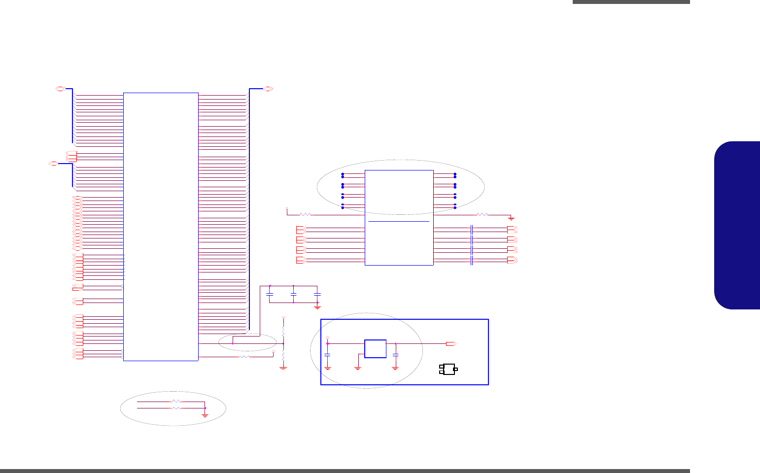
ONTARIO MEM & PCIE I/F, AP B - 3
B.Schematic Diagrams
ONTARIO MEM & PCIE I/F, AP
Sheet 2 of 43
ONTARIO MEM &
PCIE I/F, AP
MEM_DATA63
C 10 0.1u_10V_X7R_04
MEM_DATA4
C 11 0.1u_10V_X7R_04
C 12 0.1u_10V_X7R_04
MEM_DATA35
C 13 0.1u_10V_X7R_04
C _ UM I_ P_ RX07
C 14 0.1u_10V_X7R_04
C_UMI_N_RX07
MEM_DATA5
C _ UM I_ P_ RX17
C_UMI_N_RX17
C_UMI_N_RX27
C _ UM I_ P_ RX27
C 15 0.1u_10V_X7R_04
C _ UM I_ P_ RX37
C_UMI_N_RX37C 16 0.1u_10V_X7R_04
MEM_DATA36
C842
1 0 u _ 6 . 3V _X 5 R _0 6
C_ U MI_ P_ TX 0 7
C_ U MI_ N _T X0 7
C_ U MI_ N _T X1 7
C_ U MI_ P_ TX 1 7
C_ U MI_ N _T X2 7
C_ U MI_ P_ TX 2 7
C_ U MI_ N _T X3 7
C_ U MI_ P_ TX 3 7
MEM_DATA6
R 1 1.27K_1%_04
MEM_DATA37
MEM_DATA7
ME M_ DQ S _ H 05,6
M EM_EV ENT#5,6
MEM_AD D R[15:0]5,6
MEM_DATA39
MEM_CLK_H05
MEM_DATA8
MEM_DATA38
MEM_DATA9
ME M _ B A N K 15, 6
ME M _ B A N K 25, 6
MEM_DATA40
MEM_DATA10
ONT AR IO (2.0)
PA RT 1 OF 5
MEM ORY I/F
U1E
ON TARIO _APU
V17
M_WE_L
V19
M_CA S_L
U18
M_RA S_L
V16
M 1_C S_L1
U17
M 1_C S_L0
W16
M 0_C S_L1
T17
M 0_C S_L0
W15
M 1_O DT 1
U19
M 1_O DT 0
V15
M 0_O DT 1
W19
M 0_O DT 0
E15
M_CK E1
F15
M_CK E0
N17
M _EV EN T_L
L23
M_RE SE T_L
L17
M_C LK_ L3
L18
M_C LK_ H3
N19
M_C LK_ L2
N18
M_C LK_ H2
M18
M_C LK_ L1
M19
M_C LK_ H1
M16
M_C LK_ L0
M17
M_C LK_ H0
AC 16
M_DQ S _L7
AB 16
M _ DQ S _ H7
AC 21
M_DQ S _L6
AC 20
M _ DQ S _ H6
V22
M_DQ S _L5
W22
M _ DQ S _ H5
P22
M_DQ S _L4
R22
M _ DQ S _ H4
J23
M_DQ S _L3
J22
M _ DQ S _ H3
E22
M_DQ S _L2
E23
M _ DQ S _ H2
A20
M_DQ S _L1
B20
M _ DQ S _ H1
B16
M_DQ S _L0
A16
M _ DQ S _ H0
AA 16
M_DM7
AB 20
M_DM6
V23
M_DM5
P23
M_DM4
H22
M_DM3
D21
M_DM2
B19
M_DM1
D15
M_DM0
F16
M_BA NK 2
T18
M_BA NK 1
R18
M_BA NK 0
G15
M_ADD15
E16
M_ADD14
W17
M_ADD13
E18
M_ADD12
F17
M_ADD11
T19
M_ADD10
E19
M_ADD9
F19
M_ADD8
G18
M_ADD7
H15
M_ADD6
G17
M_ADD5
H17
M_ADD4
H18
M_ADD3
J17
M_ADD2
H19
M_ADD1
R17
M_ADD0
M2 2
M_ZVD DIO_MEM_S
M2 3
M_VR EF
AC15
M_ DAT A63
AB1 5
M_ DAT A62
AB1 8
M_ DAT A61
AC18
M_ DAT A60
AC14
M_ DAT A59
AB1 4
M_ DAT A58
Y16
M_ DAT A57
AC17
M_ DAT A56
Y18
M_ DAT A55
AB1 9
M_ DAT A54
AA2 0
M_ DAT A53
AA2 3
M_ DAT A52
AA1 8
M_ DAT A51
AC19
M_ DAT A50
AB2 2
M_ DAT A49
Y20
M_ DAT A48
Y21
M_ DAT A47
W23
M_ DAT A46
U2 3
M_ DAT A45
T21
M_ DAT A44
Y22
M_ DAT A43
Y23
M_ DAT A42
V21
M_ DAT A41
V20
M_ DAT A40
T22
M_ DAT A39
R2 3
M_ DAT A38
P20
M_ DAT A37
M2 0
M_ DAT A36
T23
M_ DAT A35
T20
M_ DAT A34
P21
M_ DAT A33
N2 3
M_ DAT A32
K23
M_ DAT A31
K20
M_ DAT A30
H2 0
M_ DAT A29
G2 3
M_ DAT A28
K21
M_ DAT A27
K22
M_ DAT A26
H2 3
M_ DAT A25
H2 1
M_ DAT A24
F21
M_ DAT A23
F20
M_ DAT A22
D2 2
M_ DAT A21
C2 2
M_ DAT A20
F22
M_ DAT A19
F23
M_ DAT A18
D2 3
M_ DAT A17
C2 3
M_ DAT A16
C2 0
M_ DAT A15
A21
M_ DAT A14
B18
M_ DAT A13
A18
M_ DAT A12
D2 0
M_ DAT A11
B21
M_ DAT A10
A19
M_DAT A9
C1 8
M_DAT A8
D1 6
M_DAT A7
C1 6
M_DAT A6
C1 4
M_DAT A5
A14
M_DAT A4
D1 8
M_DAT A3
A17
M_DAT A2
A15
M_DAT A1
B14
M_DAT A0
MEM_CLK_L15
MEM_CLK_L26
MEM_CLK_H26
MEM_CLK_L36
MEM_CLK_H36
MEM_DATA41
MEM_DATA11
be directly to the plane without a long trace
R6 co nn e ct ion t o 1. 5V sh ou ld
De l ? ? VGA 3 /8
MEM_DATA12
MEM_DATA42
ME M_ CK E 15,6 ME M_ CK E05,6
ONTARIO (2.0)
PA RT 2 O F 5
UMI I/F PCI E I/F
U1A
ON T A R I O_ A PU
AB7
P_U M I_R XN 3
AC 7
P_U M I_R XP 3
AC 10
P_U M I_R XN 2
AB10
P_U M I_R XP 2
Y10
P_U M I_R XN 1
AA10
P_U M I_R XP 1
Y12
P_U M I_R XN 0
AA12
P_U M I_R XP 0
Y14
P_Z VD D_10
Y3
P_G P P_ R XN 3
Y4
P_G P P_R XP 3
AA2
P_G P P_ R XN 2
AA1
P_G P P_R XP 2
AC 4
P_G P P_ R XN 1
AB4
P_G P P_R XP 1
Y6
P_G P P_ R XN 0
AA6
P_G P P_R XP 0
AC 8
P_U M I_TXN3
AB 8
P_U M I_TXP3
Y8
P_U M I_TXN2
AA 8
P_U M I_TXP2
AB 11
P_U M I_TXN1
AC 11
P_U M I_TXP1
AC 12
P_U M I_TXN0
AB 12
P_U M I_TXP0
AA 14
P_Z VS S
V4
P _ G PP_ TXN 3
V3
P_GPP_TXP3
Y2
P _ G PP_ TXN 2
Y1
P_GPP_TXP2
AC 3
P _ G PP_ TXN 1
AB 3
P_GPP_TXP1
AC 6
P _ G PP_ TXN 0
AB 6
P_GPP_TXP0
C8 4 4
0.1u_10V_X7R_04
R 82 *68_1%_04
R 81 *68_1%_04
Res erve 3 /1 1
ME M _ C K E 1
ME M _ C K E 0
MEM_DATA13
MEM_DATA43
DIMM0_ODT15DIMM0_ODT05
DIMM1_ODT16
DIMM1_ODT06
MEM_CLK_L05
DIMM0_CS#15
DIMM0_CS#05
DIMM1_CS#16
DIMM1_CS#06
MEM_DATA14
MEM_DATA44
PLACE NEAR U1
Analog Thermal Sensor
3
2
1
C364
*0.1u_10V_X5R _04
Q15
*G 7 11 S T 9 U
OUT 1
VC C
2
GN D
3
C365
*0 .1 u _ 10 V _ X5 R_ 0 4
1:2 (4mils:8mils)
THER M_ VO L T 20
3.3V
MEM_DATA15
MEM_DATA45
1.5V
MEM_DATA16
MEM_DATA46
MEM_DATA17
MEM_DATA47
ON _Z VSSON_ZVDD
RO UTE A-LINK DIFF PAIR @ 85 OH M +/- 1 0%
ME M_ RA S #5,6
ME M_ W E #5,6 ME M_ CA S#5,6
MEM_DATA18
1VS
MEM_DATA48
MEM_DATA19
MEM_DATA49
MEM_DATA20
ME M _ A D D R 0
ME M _ A D D R 1 0
ME M _ A D D R 1 2
ME M _ A D D R 1 1
ME M _ A D D R 1 3
ME M _ A D D R 1 4
Close to APU
ME M _ A D D R 2
ME M _ A D D R 3
ME M _ A D D R 5
ME M _ A D D R 1 5
ME M _ A D D R 4
ME M _ A D D R 1
ME M _ A D D R 8
ME M _ A D D R 7
ME M _ A D D R 9
ME M _ A D D R 6
MEM_DATA50
M EM_R ESET#5,6
ME M _ DM 1
ME M _ DM 3
ME M _ DM 0
ME M _ DM 2
C843
1000p_50V _X7R _04
ME M _ DM 7
ME M _ DM 5
ME M _ DM 6
ME M _ DM 4
R2 2K _1 % _ 0 4
MEM_DATA21
ME M_ Z V D D I O
MEM_DATA51
R6 7 8
1K _1 % _ 0 4
ME M_ DQ S _ H 15,6
ME M_ DQ S _ L 05,6
ME M_ DQ S _ L 25,6
ME M_ DQ S _ H 25,6
ME M_ DQ S _ L 15,6
ME M_ DQ S _ H 45,6
ME M_ DQ S _ L 35,6
ME M_ DQ S _ H 35,6
ME M_ DQ S _ H 55,6
ME M_ DQ S _ L 45,6
ME M_ DQ S _ L 65,6
ME M_ DQ S _ H 65,6 ME M_ D Q S _ L 55,6
ME M_ DQ S _ L 75,6
ME M_ DQ S _ H 75,6
MEM_DATA22
MEM_DM[7:0]5,6
ME M _ B A N K 05, 6
ME M_DA TA [63:0] 5,6
MEM_DATA52
MEM_DATA23
ONTARIO MEM & PCIE I/F, AP
Del R680 3/7
MEM_DATA53
MEM_DATA24
MEM_DATA55
MEM_DATA25
MEM_DATA54
MEM_DATA26
R6 39.2_1%_04
MEM_CLK_H15
R6 8 1
1K _1 % _ 0 4
MEM_DATA56
MEM_DATA27
MEM_DATA28
MEM_DATA0
MEM_DATA57
MEM_DATA29
MEM_DATA58
MEM_DATA30
MEM_DATA59
MEM_DATA31
MEM_DATA60
MEM_DATA1
MEM_DATA32
MEM_DATA61
MEM_DATA2
MEM_DATA33
CD 3/8
MEM_DATA62
MEM_DATA3
1.5V
C 9 0.1u_10V_X7R_04
MEM_DATA34
Schematic Diagrams
B - 4 ONTARIO DISPLAY/ CLK/ MISC
B.Schematic Diagrams
ONTARIO DISPLAY/ CLK/ MISC
1.8VS
R5 1
1K_04
CPU _SVD
APU _P W R GD
R 593 100K_04
R 54 *1K_04
R 53 *1K_04
R3 5 * 1 0 m il _ s h or t_ 04
R3 6 * 1 0 m il _ s h or t_ 04
R71 *0_04J108_P LLTST1 APU _TEST18_PLLTE ST1
APU _TEST19_PLLTE ST0J108_P LLTST0 R70 *0_04
R 42 51_04
R 43 51_04
DBREQ# R 69 300_1%_04
R 50 0_04
DBRDY
De l R35, R36 , R 38 3/7
3.3V S
ONTARIO DISPLAY/CLK/MISC
APU _TEST36
De l R16 , R5 98 3/7
R40 510_1%_04
CPU_THERMTRIP#8
APU _CLK P7
CP U_ SV D28
CPU_SVC28
H D T+ H EAD ER / PL AC E O N TOP
PORTC_HPD 14
APU _CLK N7
1.8V S
R 33 *10m il_short_04
R 34 *10m il_short_04
R 31 *0_04
R 32 *0_04
1.8VS
De l R33, R34 3/7
1.8VS
APU _SID
AP U_ PW RG D7,28
LDT_R ST#7
R65 *0_04
R5 9
1K_04
LD T _ R S T#
R6 6 *1 0 K_ 0 4
R41 510_1%_04
R4 4 * 1K _ 04
APU_TALERT#9,20
R 591 100K_04
AL LO W _ LD TST P 7
R58 1K_04
1.8VS
R 598 *10m il_s hort_04
R 16 *10m il_s hort_04
1.8VS
C 23 0.1u_16V_Y 5V_04
C 24 0.1u_16V_Y 5V_04
1.8VS
LDT_R ST#
J1
*H DR 1 0 X2 - BLUE - VER TIC AL PLUG
1
CPU_VDDIO
2
CP U_ T CK
3
GND
4
CPU_TMS
5
GND
6
CPU_TDI
7
GND
8
CPU_TDO
9
CPU_TRST_L
10
CP U_ P W R O K_B UF
11
CPU_DBRDY3
12
CP U_ R S T _ L _ B UF
13
CPU_DBRDY2
14
CPU_DBRDY0
15
CPU_DBRDY1
16
C PU_ DB RE Q_L
17
GND
18
CPU_PLL TE ST0
19
CPU_VDDIO
20
CPU_PLL TE ST1
APU _SID8
APU _SIC8
ONTARIO (2.0)
PART 3 OF 5
TEST VGA DAC
JTAG CTRL SER
CL K
DP MISC
DISPL AYPORT 0DISPLAYPORT 1
ANAL OG/DI SPLAY/ MISC
U1 B
ONTARIO_APU
V5
RSVD_3
W11
RSVD_2
B4
RSVD_1
F1
VSS_SENSE
F3
VDDIO_MEM_S_SENSE
G1
VDDCR_CPU_SENSE
F4
VDDCR_NB_SENSE
M1
DBREQ_L
M3
DBRDY
M4
TRST_L
P2
TMS
P1
TC K
N1
TDO
N2
TDI
T2
ALERT_L
U2
THERMTRIP_L
U1
PROCHOT_ L
T4
PWROK
T3
RESET_L
P4
SID
P3
SI C
J2
SVD
J1
SV C
D1
DI SP _C LKI N_ L
D2
DI SP _C LKI N_ H
V1
CL K I N_ L
V2
CL K I N_ H
C8
LT DP 0_T XN 3
D8
LT DP 0_T XP 3
B6
LT DP 0_T XN 2
A6
LT DP 0_T XP 2
C6
LT DP 0_T XN 1
D6
LT DP 0_T XP 1
A5
LT DP 0_T XN 0
B5
LT DP 0_T XP 0
B10
T DP 1_TX N3
A10
T DP 1_TX P3
C10
T DP 1_TX N2
D10
T DP 1_TX P2
A9
T DP 1_TX N1
B9
T DP 1_TX P1
B8
T DP 1_TX N0
A8
T DP 1_TX P0
T1
DM AA CT I VE _ L
K3
TE ST 38
R5
TE ST 37
N5
TE ST 36
H4
TE ST 35
T15
T ES T34 _L
U1 5
T EST 34 _ H
J19
T ES T33 _L
J18
T EST 33 _ H
M2 1
TE ST 31
M5
T ES T28 _L
L5
T EST 28 _ H
K2
T ES T25 _L
K1
T EST 25 _ H
M2
TE ST 19
L2
TE ST 18
L1
TE ST 17
K4
TE ST 16
E4
TE ST 15
T5
TE ST 14
R6
TE ST 6
R2
TE ST 5
R1
TE ST 4
D1 2
DAC_ZVSS
D4
DA C_ S DA
F2
DA C_ S CL
E2
DA C_ V SY NC
E1
DA C_ H SY NC
B13
DAC_BLUEB
A13
DA C_ B L UE
B12
DA C_ GREENB
A12
DAC_GREEN
D1 3
DAC_REDB
C1 2
DA C_ R E D
D3
LTDP0_HPD
B3
LT DP 0_AU XN
A3
LT DP 0_AU XP
C1
TD P1 _H PD
C2
TDP1_AUXN
B2
TDP1_AUXP
H1
D P_V AR Y_ B L
H2
DP_DIGON
G2
DP _ BL O N
H3
DP _ ZV S S
ON _ V AR Y 1 2
DAC_HSYNC 14
D AC_VS YN C 14
DAC_DDCADATA 14
DAC_DDCACLK 14
AP U_TR ST#
APU _SIC
R 19 1K_04
R15 *1K_04
3.3VS
APU _THE RM TRIP #
APU _SIC
APU _SID
3.3V
APU _TAL ER T#
R 22 1K_04
R 24 1K_04
R 20 1K_04
R 17 1K_04
PROCHOT#
ON_VARY
ON_DIGON
ON_BLON
HD MI _D D C_C LK 14
HDMI_DDC_DATA 14
HD M I_DD C_D ATA
HD M I_DD C_C LK
R6 7 *1 0 K_ 0 4
R6 8 *1 0 K_ 0 4
R5 6
1K_04
C22
* 150pF _N PO _50V _0402
C21
* 150pF_N PO _50V _0402
R52
1K_04
LD TRS T_R
LD TPWR G D_R
R3 7 1K _ 04
Reserve
R25 0_04
R 61 1K_04
AP U_TC K
1.8VS
AP U_TDI
AP U_TMS
AP U_TCK
AP U_TDO
AP U_TRS T#
R 63 1K_04AP U_TM S
R 64 1K_04
APU_SIC
APU_SID
AP U_TD I
R3 8
* 10m il_shor t_04
AP U_TD O
R30 499_1%_04
DBRDY
DBREQ#
For ANX3110 3/10
DP _H P D 1 2
SB_PR OC H OT#9
CPU_VDDNB_RUN_FB_H28
PR O CH OT#
APU _BP1_TSTUP D_U SCLK 1
APU _PW R GD
APU _TEST1 8 _P LLTES T1
APU _TEST25_L_BY PAS SCLK
APU _TEST1 9 _P LLTES T0
APU _TEST25_H _BY PASS CLK
APU _TEST33_L_M _CLKTST_L
APU _TEST33_H _M_ C LKTST_ H
APU _TEST35
APU _THER M DA
R62 100K_04
APU _THER M DC
AP U_ THE RM TRIP #
CP U_ VD DN B_ R UN _ F B_ L28
CP U_ V D D0 _ R UN _ F B_ L28
LVDS _D D C_D ATA 12,13
LVDS _D D C_C LK 12,13
LVDS _DD C_D ATA
LVDS _DD C_C LK
DA C_ R SE T
LD TR ST_R
LD TP WR GD _R
ON_DIGON
LDT_RS T#
ON_VARY
ON_BLON
PR O CH OT#
ONDP_CALR
ON_DMAACTIV E#
VDDCR_CPU_SENSE
VD D IO_SU S_ SEN SE
VDDCR_NB_SENSE
VS S_ SEN SE
R3 9 1K _ 04
R 21 150_1%_04R1 2 1K _0 4
R 592 100K_04
R14 300_1%_04
R 60 *100K_04
3/21
PR O CH OT#7
R1 1 1K _0 4
AP U_ PW RG D
HD MIB _D 2 BP14
LV D S - LC L K P13 LV D S - LC L K N13
HD MIB _D 1 BP14 HD MIB _D 1 BN14
HD MIB _D 2 BN14
HD M IB_CLKB N14
HD MIB _D 0 BP14
HD MIB _D 0 BN14
LVD S-L2P12,13
LVD S-L2N12,13
HD M IB_CLKB P14
LVD S-L0N13 LVD S-L0P13
LVD S-L1N12,13
LVD S-L1P12,13
LV DS
HDMI
U 44 *74AH C1G 08G W
1
2
5
4
3
LD T_RS T#_BU F
AP U_ PW RG D_ B UF
LD T_R ST#_BU F
1.8VS
NB_ENAVDD 13
R13
300_1%_04 SMC _ CP U_ T HE RM 8 ,9 ,2 0
SMD _ CP U_ T HE RM 8 ,9 ,2 0
R4 5 * 1 0 m il _ s h or t_ 04
CP U_ V D D0 _ R UN _ F B_ H28
C840
0.1u_16V_Y 5V_04
BLO N 1 3
R4 6 * 1 0 m il _ s h or t_ 04
CPU _SVC
HD T_TR ST#
For ANX3110 3 /10
DAC_RED 14
DAC_BLUE 14
DAC_GREEN 14
R27 150_1% _04
R28 150_1% _04
R4 8 * 1 0 m il _ s h or t_ 04
R29 150_1% _04
APU _P W R GD _BUF
D ISP_C LK N7
D ISP_C LK P7
R4 9 * 1 0 m il _ s h or t_ 04
U 45 *74AH C1G 08G W
1
2
5
4
3
1.8VS
Sheet 3 of 43
ONTARIO
DISPLAY/ CLK/
MISC
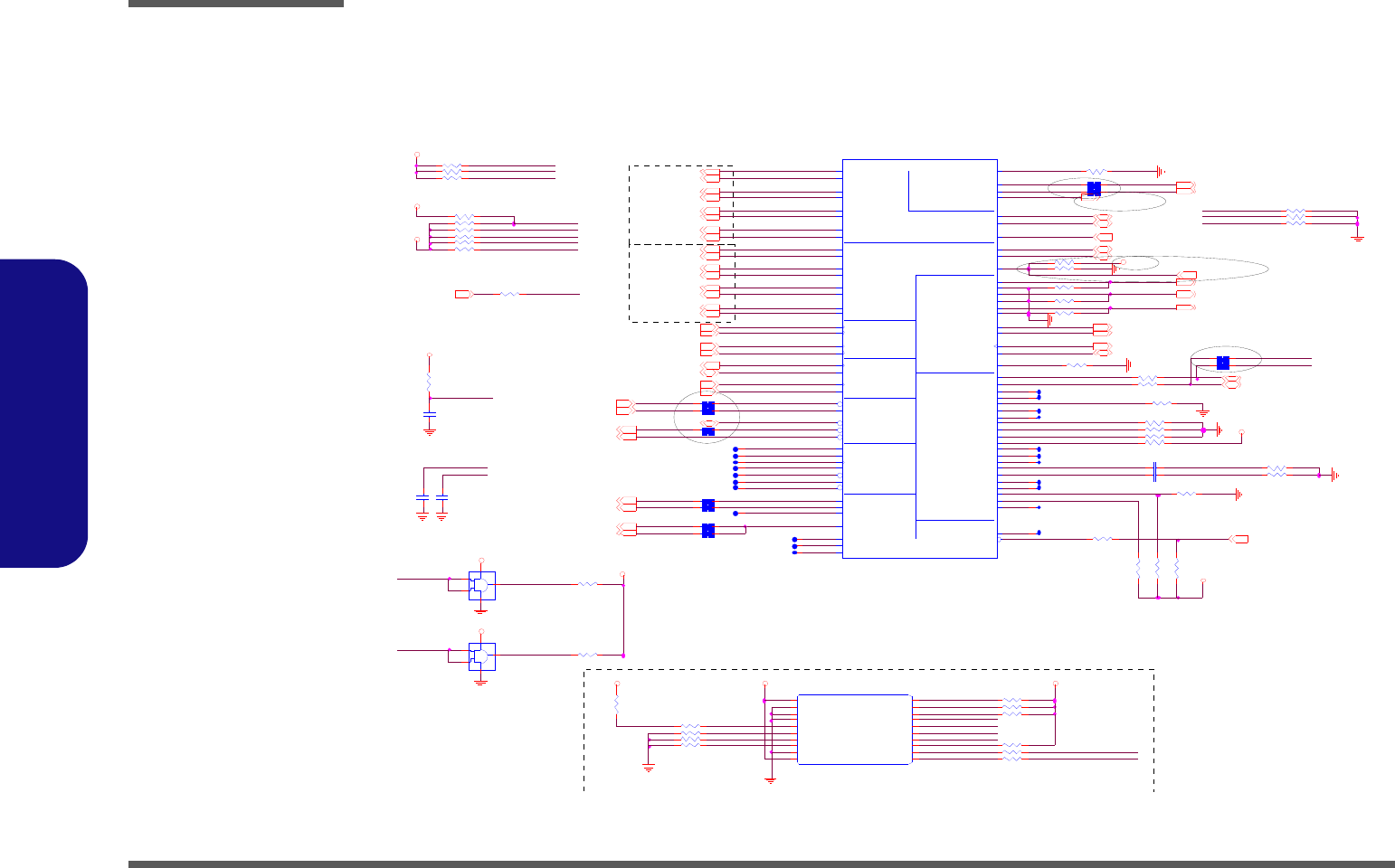
Schematic Diagrams
ONTARIO POWER & DECOUPLING B - 5
B.Schematic Diagrams
ONTARIO POWER & DECOUPLING
1.8VS
C84
180P_50V_N PO _04
C77
*10u_6.3V_X5R_06
C76
*10u_6.3V_X5R _06
C78
*10u_6.3V_X5R _06
C79
10u_6.3V_X5R_06
VD DC R _C PU
C85
180P_50V _NPO _04
C30
10u_6.3V_X5R_06
CD 3/8
C89
1u_6.3V_X5R_04
C46
*10u_6.3V_X5R_06
C45
10u_6.3V_X5R _06
C96
0.1u_10V_X5R _04
C47
*10u_6.3V_X5R _06
C94
0.1u_10V_X5R _04
C48
10u_6.3V_X5R_06
C50
*10u_6.3V_X5R_06
C49
*10u_6.3V_X5R _06
C95
*0.1u_10V_X5R_04
C91
1u_6. 3V _X5R _04
CD 3/ 8
C68
180P_50V_N PO _04
C8 6
180P_50V _NPO _04
VD DC R _ CPU
3.3VS
C87
180P_50V_NP O_04
1.5V
C37
*10u_6.3V_X5R _06
C38
10u_6.3V_X5R_06
C70
180P _50V_N PO _04
C39
*1u_6.3V_X5R _04
C41
0.1u_10V_X5R _04
C40
1u_6.3V_X5R_04
C42
0.1u_10V_X5R_04
.
L63
HC B1608KF-121T25
C43
1u_6.3V_X5R_04
C55
1u_6.3V_X5R_04
C59
0. 1u_10V_X5R_04
C88
0.1u_10V_X5R_04
C63
0. 1u_10V_X5R_04
C62
0.1u_10V_X5R _04
EMC CAPS
CD 3/8
1.5V
VDD PL_ 10 1V S
1VS
ONTA RIO (2.0)
PART 5 OF 5
GR O U N D
U1D
ONTARIO_APU
N1 1
VSS_49
N8
VSS_48
N6
VSS_47
N4
VSS_46
M7
VSS_45
L22
VSS_44
L20
VSS_43
L13
VSS_42
L11
VSS_41
L8
VSS_40
L6
VSS_39
L4
VSS_38
K14
VSS_37
K10
VSS_36
J20
VSS_35
J7
VSS_34
J5
VSS_33
J4
VSS_32
H1 3
VSS_31
H1 1
VSS_30
H6
VSS_29
G2 2
VSS_28
G2 0
VSS_27
G1 2
VSS_26
G9
VSS_25
G7
VSS_24
G5
VSS_23
G4
VSS_22
F13
VSS_21
F11
VSS_20
F8
VSS_19
E20
VSS_18
E12
VSS_17
E9
VSS_16
E7
VSS_15
D1 9
VSS_14
D1 7
VSS_13
B15
VSS_12
D1 4
VSS_11
D1 1
VSS_10
D9
VSS_9
D7
VSS_8
D5
VSS_7
C4
VSS_6
B22
VSS_5
B17
VSS_4
B11
VSS_3
B7
VSS_2
A7
VSS_1
A11
VSSBG_DAC
AC 13
VS S_97
AC 9
VS S_96
AC 5
VS S_95
AB21
VS S_94
AB17
VS S_93
AB13
VS S_92
AB9
VS S_91
AB5
VS S_90
AB2
VS S_89
AA22
VS S_88
AA4
VS S_87
Y19
VS S_86
Y17
VS S_85
Y15
VS S_84
Y13
VS S_83
Y11
VS S_82
Y9
VS S_81
Y7
VS S_80
Y5
VS S_79
W20
VS S_78
W12
VS S_77
W7
VS S_76
W5
VS S_75
W4
VS S_74
W2
VS S_73
W1
VS S_72
V13
VS S_71
V11
VS S_70
V9
VS S_69
V8
VS S_68
U22
VS S_67
U20
VS S_66
U12
VS S_65
U7
VS S_64
U5
VS S_63
U4
VS S_62
T13
VS S_61
T11
VS S_60
T9
VS S_59
T6
VS S_58
R20
VS S_57
R7
VS S_56
R4
VS S_55
P14
VS S_54
P10
VS S_53
N22
VS S_52
N20
VS S_51
N13
VS S_50
ONTA RIO (2.0)
PART 4 OF 5
POWER
U1C
ONTARIO_APU
U1 6
VDDIO_MEM_S_11
W18
VDDIO_MEM_S_10
R1 9
VDDIO_MEM_S_9
R1 6
VDDIO_MEM_S_8
N1 6
VDDIO_MEM_S_7
L19
VDDIO_MEM_S_6
L16
VDDIO_MEM_S_5
J16
VDDIO_MEM_S_4
E17
VDDIO_MEM_S_3
G1 9
VDDIO_MEM_S_2
G1 6
VDDIO_MEM_S_1
P13
VDDCR_NB_22
P11
VDDCR_NB_21
N1 4
VDDCR_NB_20
N1 2
VDDCR_NB_19
N1 0
VDDCR_NB_18
M1 3
VDDCR_NB_17
M1 2
VDDCR_NB_16
M1 1
VDDCR_NB_15
L14
VDDCR_NB_14
L12
VDDCR_NB_13
L10
VDDCR_NB_12
K13
VDDCR_NB_11
K11
VDDCR_NB_10
H1 2
VDDCR_NB_9
H9
VDDCR_NB_8
G1 3
VDDCR_NB_7
G1 1
VDDCR_NB_6
F12
VDDCR_NB_5
F9
VDDCR_NB_4
E13
VDDCR_NB_3
E11
VDDCR_NB_2
E8
VDDCR_NB_1
R8
VDDCR_CPU_15
N7
VDDCR_CPU_14
M8
VDDCR_CPU_13
M6
VDDCR_CPU_12
L7
VDDCR_CPU_11
J8
VDDCR_CPU_10
J6
VDDCR_CPU_9
H7
VDDCR_CPU_8
H5
VDDCR_CPU_7
G8
VDDCR_CPU_6
G6
VDDCR_CPU_5
F7
VDDCR_CPU_4
F5
VDDCR_CPU_3
E6
VDDCR_CPU_2
E5
VDDCR_CPU_1
A4
V DD _33
T12
VD D_1 0_4
V12
VD D_1 0_3
W13
VD D_1 0_2
U13
VD D_1 0_1
U11
V DD PL _10
W9
V DD _18_D AC
V7
VD D_1 8_7
T7
VD D_1 8_6
W6
VD D_1 8_5
U9
VD D_1 8_4
U6
VD D_1 8_3
W8
VD D_1 8_2
U8
VD D_1 8_1
De l C 69 3/17
CD 3/8
C93
1u_6.3V_X5R_04
CD 3/8
C56
1u_6.3V_X5R_04
C8 7 3
*10u_6.3V_X5R_06
C27
* 1 u _ 6. 3V _ X5 R _ 0 4
VDDCR_CPU
VDDCR_NB
C71
180P_50V_NP O_04
C72
*18 0P_ 5 0V_ N PO_04
3. 3V S
VDDPL_10
C874
*1 0 u_ 6 .3 V_X5R _ 06
1VS
1.8VS
C29
1u_6.3V_ X5 R _04
C5 1
*1 0 u _ 6. 3V _ X5 R _ 0 6
C6 4
* 0.1u_10V_X5 R _04
C8 0
*1u_6.3V_X5R_04
C875
*10u_6.3V _X5R _06
C53
*22u_6.3V_X5R_08
C44
*10u_6.3V _X5R _06
1. 5V
C52
10u_6.3V_X5R_06
C73
0.1u_10V_X5R_04
C54
*22u_6.3V_X5R _08
C28
*1u_6.3V _X5R _04
1.8VS
C872
*10u_6.3V_X5R _06
C75
10u_6.3V_X5R_06
VDDCR_NB
De l R 73 3/7
C871
* 10u_6 .3V_ X5 R _06
C869
*10u_6.3V_X5R _06
C870
*10u_6.3V_X5R _06
C7 4
*0.1u_10V_X7R_04
C35
1u_6. 3V _X5R _04
C34
10u_6.3V_X5R _06
C36
0.1u_10V_X5R_04
VDDCR_NB
C26
1u_6.3V_X5R _04
Del C57, C58, C60, C61 3/17
ONTARIO POWER & DECOUPLING
1.5V
1.8VS
C90
*1u_6.3V_X5R _04
C3 1
0. 1u_10V_X5R_04
C67
*180P_50V_NP O_04
CD and Del C92, C97 3/17
C65
0.1u_10V_X5R_04
C66
*0.1u_10V_X7R _04
C81
1u_6.3V _X5R _04
C82
1u_6. 3V _X5R _04
C32
10u_6.3V_X5R _06
C33
1u_6.3V_X5R_04
C83
*1u_6.3V_X5R_04
Sheet 4 of 43
ONTARIO POWER
& DECOUPLING
Schematic Diagrams
B - 6 INAGUA DDR3 SO-DIMMS A
B.Schematic Diagrams
INAGUA DDR3 SO-DIMMS A
+
C104
*150u_4V_B_A
CD 3 /8
MEM_ADDR[15:0]2,6
CD 3/8
INAGUA DDR3 SO-DIMMS A
SO-DIMM A
CD 3/8
MEM_DATA3
MEM_DATA2
MEM_DATA1
MEM_DATA32
MEM_DATA31
MEM_DATA30
MEM_DATA29
MEM_DATA4
MEM_DATA39
MEM_DATA37
MEM_DATA36
MEM_DATA35
MEM_DATA34
MEM_DATA33
MEM_DATA44
MEM_DATA43
MEM_DATA42
MEM_DATA41
MEM_DATA40
MEM_DATA49
MEM_DATA38
MEM_DATA47
MEM_DATA46
MEM_DATA45
MEM_DATA54
MEM_DATA53
MEM_DATA52
MEM_DATA51
MEM_DATA28
MEM_DATA50
MEM_DATA56
MEM_DATA6
MEM_DATA5
MEM_DATA48
MEM_DATA55
MEM_DATA62
MEM_DATA61
MEM_DATA60
MEM_DATA58
MEM_DATA57
MEM_DATA11
MEM_DATA9
MEM_DATA8
MEM_DATA7
MEM_DATA59
MEM_DATA63
MEM_DATA16
MEM_DATA15
MEM_DATA14
MEM_DATA13
MEM_DATA12
MEM_DATA21
MEM_DATA10
MEM_DATA19
MEM_DATA18
MEM_DATA17
MEM_DATA26
MEM_DATA25
MEM_DATA24
MEM_DATA23
MEM_DATA0
MEM_DATA22
MEM_DATA20
MEM_DATA27
MEM_BA NK02,6
MEM_BA NK22,6
MEM_BA NK12,6
C117
*0 . 1 u_ 1 6V_ Y 5 V_ 0 4
+
C105
*220u_4V_V_A
C123
0.1u_16V_Y5V_04
C111
*1u_6.3V_X5R_04
C120
0.1u_16V_Y5V_04
C112
1u_6.3V_X5R_04
C107
10u_10V_Y5V_08
C110
*1u_6.3V_X5R_04
C116
0.1u_16V_Y5V_04
C121
0.1u_16V_Y5V_04
C114
0.1u_16V_Y5V_04
C109
1u_6. 3V_X5R_04
C126
1u_6.3V_X5R_04
C119
0.1u_16V_Y5V_04
C99
0.1u_16V_Y5V_04
C106
*10u_10V_Y5V_08
C127
1u_6.3V_X5R_04
R75 1K_04
C124
10u_10V_Y5V_08
C108
10u_10V_Y5V_08
JDIMM1A
DDRRK -20401- TR4B
A0
98
A1
97
A2
96
A3
95
A4
92
A5
91
A6
90
A7
86
A8
89
A9
85
A10/AP
107
A11
84
A12/BC#
83
A13
119
A14
80
A15
78
DQ0 5
DQ1 7
DQ2 15
DQ3
17
DQ4 4
DQ5 6
DQ6 16
DQ7 18
DQ8 21
DQ9 23
DQ10
33
DQ11 35
DQ12 22
DQ13 24
DQ14 34
DQ15 36
DQ16 39
DQ17 41
DQ18
51
DQ19 53
DQ20 40
DQ21 42
DQ22 50
DQ23 52
DQ24 57
DQ25 59
DQ26
67
DQ27 69
DQ28 56
DQ29 58
DQ30 68
DQ31 70
DQ32 129
DQ33 131
DQ34 141
DQ35 143
DQ36 130
DQ37 132
DQ38 140
DQ39 142
DQ40 147
DQ41
149
DQ42 157
DQ43 159
DQ44 146
DQ45 148
DQ46 158
DQ47 160
DQ48 163
DQ49
165
DQ50 175
DQ51 177
DQ52 164
DQ53 166
DQ54 174
DQ55 176
DQ56 181
DQ57 183
DQ58 191
DQ59 193
DQ60 180
DQ61 182
DQ62 192
DQ63 194
BA0
109
BA1
108
RAS#
110
WE#
113
CAS#
115
S0#
114
S1#
121
CKE0
73
CKE1
74
CK0
101
CK0#
103
CK1
102
CK1#
104
SDA
200 SCL
202 SA1
201 SA0
197
DM0
11
DM1
28
DM2
46
DM3
63
DM4
136
DM5
153
DM6
170
DM7
187
DQS0
12
DQS1
29
DQS2
47
DQS3
64
DQS4
137
DQS5
154
DQS6
171
DQS7
188
DQS0#
10
DQS1#
27
DQS2#
45
DQS3#
62
DQS4#
135
DQS5#
152
DQS6#
169
DQS7#
186
ODT0
116
ODT1
120
BA2
79
C113
1u_6. 3 V_ X5R_04
C128
*1u_6. 3V_X5R_04
C98
*1u_6. 3V_X5R_04
C115
0.1u_16V_Y5V_04
C118
*0.1u_16V_Y5V_04
C125
1 u_ 6 . 3 V_X5 R _ 0 4
JDIMM1B
DDRRK-20401- TR4B
VDD1
75
VDD2
76
VDD3
81
VDD4
82
VDD5
87
VDD6
88
VDD7
93
VDD8
94
VDD9
99
VDD10
100
VDD11
105
VDD12
106
VDDSPD
199
NC1
77
NC2
122
NCTEST
125
VREF_DQ
1
V SS1
2
V SS2
3
V SS3
8
V SS4
9
V SS5
13
V SS6
14
V SS7
19
V SS8
20
V SS9
25
V SS10
26
V SS11
31
V SS12
32
V SS13
37
V SS14
38
V SS15
43
VSS16 44
VSS17 48
VSS18 49
VSS19 54
VSS20 55
VSS21 60
VSS22 61
VSS23
65
VSS24 66
VSS25 71
VSS26 72
VSS27 127
VSS28 128
VSS29 133
VSS30 134
VSS31
138
VSS32 139
VSS33 144
VSS34 145
VSS35 150
VSS36 151
VSS37 155
VSS38 156
VSS39 161
VSS40 162
VSS41 167
VSS42 168
VSS43 172
VSS44 173
VSS45 178
VSS46
179
VSS47 184
VSS48 185
VSS49 189
VSS50 190
VSS51 195
VSS52 196
G2 GND2
G1 GND1
VTT2 204
VTT1 203
VREF_CA
126
RESET#
30 E VEN T #
198
VDD13
111
VDD14
112
VDD16
118 VDD15
117
VDD17
123
VDD18
124
C122
*0.1u_16V_Y5V_04
3.3VS
1.5V
1.5V
1.5V
VTT_MEM
VTT_ MEM
1.5V
MEM_RAS #2,6
MEM_CLK_H12
MEM_R ESE T#2,6DIMM0_ODT12
MEM_WE#2,6
MEM_CAS #2,6
MEM_CLK_L12
DIMM0_ODT02
MEM_C KE02,6
MEM_CLK_H02
MEM_DATA[63:0] 2,6
MEM_C KE12,6
MEM_EV ENT#2,6
MEM_CLK_L02
SD ATA06,8
MEM_DM[7:0]2,6
20mils
CD 3 /8
MEM_ADDR1
R76 1K _1%_04
R77
1K_1%_04
CLOSE TO SO-DIMM A
C103
0.1u_10V_X5R_04
1.5V MVREF_DIMM0
(REV)4.0mm
MEM_DQS _L02,6
MEM_DQS _L72,6
MEM_DQS _H72,6
MEM_DQS _L52,6
MEM_DQS _L12,6
MEM_DQS _H12,6
MEM_DQS _H22,6
MEM_DQS _H62,6
MEM_DQS _L22,6
MEM_DQS _H42,6
MEM_DQS _H52,6
MEM_DQS _L62,6
MEM_DQS _L32,6
MEM_DQS _H02,6
MEM_DQS _H32,6
MEM_DQS _L42,6
MEM_ADDR2
MEM_ADDR3
MEM_ADDR4
MEM_ADDR5
DIMM0_CS#12
DIMM0_CS#02
MEM_ADDR6
MEM_ADDR7
MEM_ADDR8
MEM_ADDR9
MEM_ADDR10
MEM_ADDR11
MEM_ADDR12
MEM_ADDR13
MEM_ADDR14
SC L K06,8
MEM_ADDR15
MEM_DM5
MEM_DM6
MEM_DM7
MEM_DM0
MEM_DM2
MEM_DM1
MEM_DM3
MEM_DM4
CD 3 /8
MVREF_DIMM0
CD 3/8
MEM_ADDR0
C100
1 u_ 6 . 3V_ X5 R _0 4
C101
0.1u_10V_X7R_04
C102
1000p_50V_X7R_04
Sheet 5 of 43
INAGUA DDR3 SO-
DIMMS A
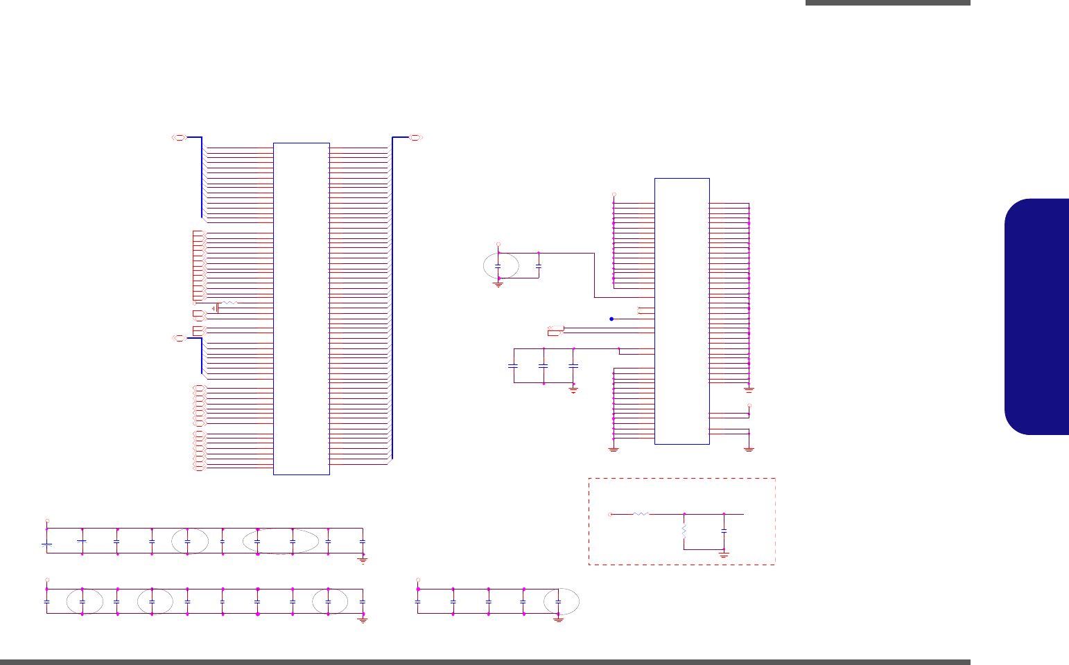
Schematic Diagrams
INAGUA DDR3 SO-DIMMS B B - 7
B.Schematic Diagrams
INAGUA DDR3 SO-DIMMS B
CD 3/9
MEM_D AT A34
MEM_D AT A33
MEM_D AT A32
MEM_D AT A31
MEM_D AT A30
MEM_D AT A29
MEM_D AT A4
MEM_D AT A3
MEM_D AT A2
MEM_D AT A1
MEM_D AT A28
MEM_D AT A50
MEM_D AT A49
MEM_D AT A38
MEM_D AT A47
MEM_D AT A46
MEM_D AT A45
MEM_D AT A44
MEM_D AT A43
MEM_D AT A42
MEM_D AT A41
MEM_D AT A40
MEM_D AT A39
MEM_D AT A37
MEM_D AT A36
MEM_D AT A35
MEM_D AT A59
MEM_D AT A63
MEM_D AT A62
MEM_D AT A61
MEM_D AT A60
MEM_D AT A58
MEM_D AT A57
MEM_D AT A56
MEM_D AT A6
MEM_D AT A5
MEM_D AT A48
MEM_D AT A55
MEM_D AT A54
MEM_D AT A53
MEM_D AT A52
MEM_D AT A51
MEM_D AT A0
MEM_D AT A22
MEM_D AT A21
MEM_D AT A10
MEM_D AT A19
MEM_D AT A18
MEM_D AT A17
MEM_D AT A16
MEM_D AT A15
MEM_D AT A14
MEM_D AT A13
MEM_D AT A12
MEM_D AT A11
MEM_D AT A9
MEM_D AT A8
MEM_D AT A7
MEM_DM0
MEM_DM2
MEM_DM1
MEM_DM3
MEM_DM4
MEM_DM5
MEM_DM6
MEM_DM7
MEM_D AT A20
MEM_D AT A27
MEM_D AT A26
MEM_D AT A25
MEM_D AT A24
MEM_D AT A23
MEM_ADDR0
MEM_ADDR4
MEM_ADDR3
MEM_ADDR2
MEM_ADDR1
MEM_ADDR15
MEM_ADDR14
MEM_ADDR13
MEM_ADDR12
MEM_ADDR11
MEM_ADDR10
MEM_ADDR9
MEM_ADDR8
MEM_ADDR7
MEM_ADDR6
MEM_ADDR5
MVREF_DIMM1
MVREF_DIMM1
R80
1K_1%_04
C156
1u_6. 3V_X5R_04
C134
0.1u_10V _X5R_04
C158
1u_6.3V_X5R_04
C142
*1u_6.3V_X5R_04
C137
10u_10V_Y5V_08
C138
10u_10V_Y5V_08
JDIMM2B
DDRRK- 2 0401-TP8D
VDD1
75
VDD2
76
VDD3
81
VDD4
82
VDD5
87
VDD6
88
VDD7
93
VDD8
94
VDD9
99
VDD10
100
VDD11
105
VDD12
106
VDDSPD
199
NC1
77
NC2
122
NCTEST
125
VREF_DQ
1
VSS1
2
VSS2
3
VSS3
8
VSS4
9
VSS5
13
VSS6
14
VSS7
19
VSS8
20
VSS9
25
VSS10
26
VSS11
31
VSS12
32
VSS13
37
VSS14
38
VSS15
43
VSS 16 44
VSS 17 48
VSS 18 49
VSS 19 54
VSS 20 55
VSS 21 60
VSS 22 61
VSS 23 65
VSS 24 66
VSS 25 71
VSS 26 72
VSS 27 127
VSS 28 128
VSS 29 133
VSS 30 134
VSS 31 138
VSS 32
139
VSS 33 144
VSS 34 145
VSS 35 150
VSS 36 151
VSS 37 155
VSS 38 156
VSS 39 161
VSS 40 162
VSS 41 167
VSS 42 168
VSS 43
172
VSS 44 173
VSS 45 178
VSS 46 179
VSS 47 184
VSS 48 185
VSS 49 189
VSS 50 190
VSS 51 195
VSS 52 196
G2 GND2
G1 GND1
VTT2 204
VTT1 203
VREF_CA
126
RESET#
30 EVENT#
198
VDD13
111
VDD14
112
VDD16
118 VDD15
117
VDD17
123
VDD18
124
C133
1000p_50V_X7 R _ 04
C148
*0.1u_16V_Y5V_04
C144
1 u_ 6 . 3V_ X5 R_04
JDI MM2A
DDRRK-20401-TP8D
A0
98
A1
97
A2
96
A3
95
A4
92
A5
91
A6
90
A7
86
A8
89
A9
85
A1 0/ AP
107
A11
84
A1 2/ BC #
83
A13
119
A14
80
A15
78
DQ0 5
DQ1 7
DQ2 15
DQ3 17
DQ4 4
DQ5 6
DQ6 16
DQ7 18
DQ8 21
DQ9 23
DQ10
33
DQ11 35
DQ12 22
DQ13 24
DQ14 34
DQ15 36
DQ16 39
DQ17 41
DQ18 51
DQ19 53
DQ20 40
DQ21 42
DQ22 50
DQ23 52
DQ24 57
DQ25 59
DQ26 67
DQ27
69
DQ28 56
DQ29 58
DQ30 68
DQ31 70
DQ32 129
DQ33 131
DQ34 141
DQ35 143
DQ36 130
DQ37 132
DQ38
140
DQ39 142
DQ40 147
DQ41 149
DQ42 157
DQ43 159
DQ44 146
DQ45 148
DQ46 158
DQ47 160
DQ48 163
DQ49 165
DQ50 175
DQ51 177
DQ52 164
DQ53 166
DQ54 174
DQ55 176
DQ56 181
DQ57 183
DQ58 191
DQ59 193
DQ60 180
DQ61 182
DQ62 192
DQ63 194
BA0
109
BA1
108
RAS#
110
WE#
113
CAS#
115
S0#
114
S1#
121
CKE0
73
CKE1
74
CK0
101
CK0#
103
CK1
102
CK1#
104
SD A
200 SC L
202 SA1
201 SA0
197
DM0
11
DM1
28
DM2
46
DM3
63
DM4
136
DM5
153
DM6
170
DM7
187
DQS0
12
DQS1
29
DQS2
47
DQS3
64
DQS4
137
DQS5
154
DQS6
171
DQS7
188
DQS0#
10
DQS1#
27
DQS2#
45
DQS3#
62
DQS4#
135
DQS5#
152
DQS6#
169
DQS7#
186
ODT0
116
ODT1
120
BA2
79
C143
1u_6.3V_X5R_04
C131
1u_6.3V_X5R_04
C151
0.1u_16V_Y5V_04
C140
1u_6.3V_X5R_04
C141
*1u_6.3V_X5 R _0 4
C145
0.1u_16V_Y5V_04
+
C136
*220u_4V_V_A
C157
1u_6.3V_X5R_04
C129
* 1u_6.3V_X5R_04
C139
*10u_10V_Y5V_08
C159
*1u_6.3V_X5R_04
C150
0.1u_16V_Y5V_04
C132
0.1u_10V_X7R_04
C154
0.1u_16V_Y5V_04
C155
10u_10V_Y5V_08
C152
0.1u_16V_Y5V_04
C130
0.1u_16V_Y5V_04
C149
0.1u_16V_Y5V_04
C146
*0.1u_16V_Y5V_04
R79 1K_1%_04
C147
0.1u_16V_Y5V_04
C153
* 0.1u_ 16V_Y5V_04
1.5V
3. 3VS
1.5V
VTT_MEM
VTT_MEM
1.5V
1.5V
DIMM1_ODT12
MEM_RAS#2,5
MEM_CLK_H32
MEM_CAS#2,5
MEM_CLK_L32
MEM_RESE T#2,5
MEM_CLK_H22
DIMM1_ODT02
MEM_WE#2,5
MEM_DATA[63:0] 2,5
MEM_CKE12,5
MEM_CKE02,5
SD ATA05,8
MEM_EV ENT#2,5
MEM_CLK_L22
MEM_BA NK02,5
MEM_ADDR[15:0]2,5
MEM_DM[7:0]2,5
DIMM1_CS#12
DIMM1_CS#02MEM_BA NK22,5
MEM_BA NK12,5
MEM_DQS_H72,5
MEM_DQS_H62,5
MEM_DQS_H42,5
MEM_DQS_H22,5
MEM_DQS_L62,5
MEM_DQS_L42,5
MEM_DQS_L22,5
MEM_DQS_H32,5
MEM_DQS_L72,5
MEM_DQS_L02,5
MEM_DQS_L12,5
MEM_DQS_H12,5
MEM_DQS_L52,5
MEM_DQS_H52,5
MEM_DQS_L32,5
MEM_DQS_H02,5
CLOSE TO SO-DIMM B
INAGUA DDR3 SO-DIMMS B
20mils
SO-D IMM B
3.3VS
CD 3 /9
+
C135
560u_2.5V _6. 6*6.6*5. 9
CD 3/ 9
SC L K05,8
R784.7K_04
CD 3/9
(REV)8.0mm
SN:6-86-24204-XXX
Sheet 6 of 43
INAGUA DDR3 SO-
DIMMS B
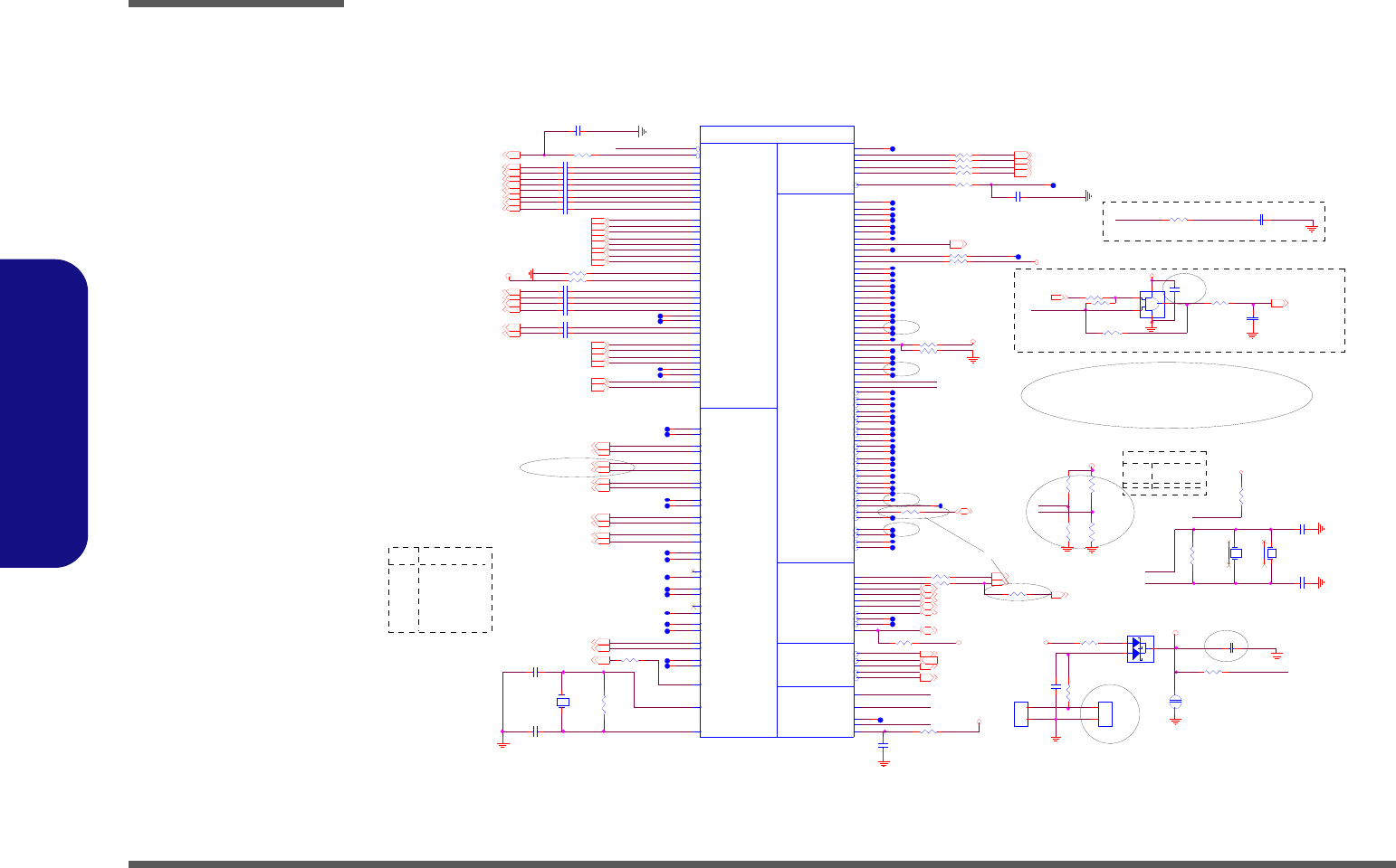
Schematic Diagrams
B - 8 HUDSON PCIE/ PCI/ CLOCK/ FCH
B.Schematic Diagrams
HUDSON PCIE/ PCI/ CLOCK/ FCH
R2 5 5
20K_04
3.3VS
PC I_ CLKRUN # 11
25M _X1
C_ UM I_ N_ RX12C_ UM I_ P_R X12
C_ UM I_ N_ RX02
C_ UM I_ P_R X32C_ UM I_ N_ RX22C_ UM I_ P_R X22
C_ UM I_ N_ RX32
Fo r W270 BUQ 3/1 5
Del ??VGA 3/8
Add R812, R271 for TPM 3/21
C_ U MI_ P_T X 02
GPI O3 1
D ISP_C LK P3
A P U _C LK N3
A P U _C LK P3
D ISP_C LK N3
C LK_PC IE_J MC16
CLK_PCIE_WLAN#17 CLK_PCIE_WLAN17
C LK_PC IE_J MC #16
PCIE_USB30_C LKN19
PCIE_USB30_C LKP19
HU DS ON -1 PA RT 1 O F 5
PCI I/F
PCI EXP RE SS I /F
PCI CLKS
LP C
RTC
CL O CK G EN ERA T O R
CPU
HU DSON M1 A1 3
U19E
L2 7
25M _X2
L2 6
25M _X1
L2 5
14M _25M _48M _OSC
T2 8
GPP _CLK8 N
T2 9
GPP _CLK8 P
N2 7
GPP _CLK7 N
N2 6
GPP _CLK7 P
P28
GPP _CLK6 N
P29
GPP _CLK6 P
M2 5
GPP _CLK5 N
P25
GPP _CLK5 P
L2 3
GPP _CLK4 N
L2 4
GPP _CLK4 P
V25
GPP _CLK3 N
T2 5
GPP _CLK3 P
M2 8
GPP _CLK2 N
M2 9
GPP _CLK2 P
N2 8
GPP _CLK1 N
N2 9
GPP _CLK1 P
L2 8
GPP _CLK0 N
L2 9
GPP _CLK0 P
T2 3
S L T_ G FX_ CL KN
V23
S L T_ G FX_ CL KP
T2 1
CPU_HT_CLKN
V21
CPU_HT_CLKP
T2 7
NB_HT_CLK N
T2 6
NB_HT_CLK P
U2 8
NB_DISP_CLKN
U2 9
NB_DISP_CLKP
P23
PCIE_RCLKN/N B_LNK _CLKN
M2 3
PCIE_RCLKP/N B_LNK _CLKP
W25
GPP _RX3N
W24
GPP _RX3P
V24
GPP _RX2N
W23
GPP _RX2P
AA24
GPP _RX1N
AA25
GPP _RX1P
Y21
GPP _RX0N
AA22
GPP _RX0P
W29
GPP _TX3N
W28
GPP _TX3P
Y27
GPP _TX2N
Y26
GPP _TX2P
Y28
GPP _TX1N
Y29
GPP _TX1P
AA29
GPP _TX0N
AA28
GPP _TX0P
AD28
PCIE_CALRN
AD29
PCIE_CALRP
AB24
UMI_RX3N
AB25
UMI_RX3P
AC25
UMI_RX2N
AC24
UMI_RX2P
AD24
UMI_RX1N
AD25
UMI_RX1P
AE23
UMI_RX0N
AE24
UMI_RX0P
AB27
UMI_TX3N
AB26
UMI_TX3P
AB28
UMI_TX2N
AB29
UMI_TX2P
AC29
UMI_TX1N
AC28
UMI_TX1P
AD27
UMI_TX0N
AD26
UMI_TX0P
L1
A_RST#
P1
PCIE_RST#
B1
VD DBT _ RTC _ G
B2
INTRUDER_ALERT#
D2
RTC CL K
C2
32K_X2
C1
32K_X1
J24
LDT_R ST#
G2 2
LDT_S TP#
K19
LDT_P G
H2 1
PROCHOT#
G2 1
ALLO W_LDT STP / DM A_AC TI VE#
AB19
SERIRQ/GPIO48
AA18
LDR Q1#/ CLK _RE Q6#/ G PI O49
J25
LDR Q0#
G2 8
LF RAM E#
H2 8
LAD3
H2 9
LAD2
J26
LAD1
J27
LAD0
H2 5
LPC CLK1
H2 4
LPC CLK0
AJ 4
INTH#/GPIO35
AG4
INT G#/GPIO34
AG6
INTF#/GPIO33
AJ 6
INTE#/GPIO32
AD7
LO CK#
AB11
CL KR UN#
AB12
G NT3#/ CLK _RE Q7#/ G PI O46
AH6
GN T2#/ GPO45
AJ 5
GN T1#/ GPO44
AD12
GNT0#
AC12
RE Q3 # / CL K _ RE Q5#/ G PI O42
AH4
RE Q2 # / CL K _ RE Q8#/ G PI O41
AH5
RE Q1#/ G PI O40
AE11
RE Q0#
AE4
SE RR#
AE6
PE RR#
AF5
STO P#
AC5
PAR
AE7
TR DY#
AJ 3
IRDY#
AB9
DEV S EL #
AE8
F RAM E#
AA10
CBE3#
AD8
CBE2#
AD5
CBE1#
AA8
CBE0#
AH3
AD31 / G PI O31
AG2
AD30 / G PI O30
AH2
AD29 / G PI O29
AF3
AD28 / G PI O28
AF4
AD27 / G PI O27
AF6
AD26 / G PI O26
AC11
AD25 / G PI O25
AD9
AD24 / G PI O24
AE9
AD23 / G PI O23
AF2
AD22 / G PI O22
AG1
AD21 / G PI O21
AF1
AD20 / G PI O20
AE3
AD19 / G PI O19
AF8
AD18 / G PI O18
AE1
AD17 / G PI O17
AE2
AD16 / G PI O16
AC6
AD15 / G PI O15
AD2
AD14 / G PI O14
AD1
AD13 / G PI O13
AC1
AD12 / G PI O12
AC4
AD11 / G PI O11
AC3
AD10 / G PI O10
AC2
AD9/ G PI O9
AA6
AD8/ G PI O8
AB5
AD7/ G PI O7
AB6
AD6/ G PI O6
AB2
AD5/ G PI O5
AA5
AD4/ G PI O4
AB1
AD3/ G PI O3
AA3
AD2/ G PI O2
AA4
AD1/ G PI O1
AA1
AD0/ G PI O0
V2
PC IRST#
Y1
PC IC LK4/ 14M _OSC/GPO39
W4
PC ICLK3/GPO38
W3
PC ICLK2/GPO37
W1
PC ICLK1/GPO36
W2
PCICLK0
U1 7
* 74AH C1G08G W
1
2
5
4
3
3.3VS
J_RTC1
*85205-02701
1
2
R2 5 7
20K_04
1.8VS
C4 6 6
* 1u_6.3V_X5R _04
CD 3/8
C453 0.1u_10V_X7R_04
PC IE_R XN3 _W L AN17 PC IE_R XP3_ W LAN17
C454 *0.1u_10V_X7R _04
C455 *0.1u_10V_X7R _04
X5
FSX5L_2 5M HZ
12
R2 5 8
*2 0 K _0 4
X3
* MC-146_32.768KHz
14
3 2
5 NA NA
7 USB3 .0 7
2 NA NA
GFX_ CLK NA G
FC H _G P P DEVICE CL KREQ#
1 WLAN 1
8 NA NA
6 NA NA
0 JM C 2 61C 0
4 NA NA
R247 20K_04
25M _X2
De l ? ? VGA 3/8
C_ U MI_ P_T X 22
C_ U MI_ P_T X 12
C_ U MI_ P_T X 32
C_ U MI_ N_ TX02
C_ U MI_ N_ TX22
C_ U MI_ N_ TX12
LPC_AD0 11,20
C_ U MI_ N_ TX32
LPC_AD3 11,20
LPC_AD1 11,20
LPC_AD2 11,20
R 805 * 0_04
Zo= 50O? 5%
GPI O3 0
R242 22_04
R240 22_04
R243 22_04
R244 22_04 PCI_CLK3 8
PCI_CLK2 8
PCLK_ KBC 8
PCI_CLK4 8
R2 6 0
10M_04
C4 6 2
22p_50V_NPO _04
C449 *150pF_NPO_50V_0402
C4 6 3
22p_50V_NPO _04
HUDSON P CIE/PCI/C LOCK/FCH
32K_X1
INT RUD E R_ AL ER T#
PCLK_KBC_RPCLK_ KBC R5 13 *1 0 _0 4 C7 50
*10p_50V_N PO_06
C465 22P_50V_NPO _04
R 595 *10K_04
AN X3110_CLKN12 AN X3110_CLKP12
R263 1K_04
LPC _FR AME# 11, 20
1 0 W 25 1BA Q
0 1 W 27 0BU Q
C444 0.1u_10V_X7R_04
PC LK_TPM 1 1
R687 * 10K_04
R252 0_04
R688 * 10K_04
SERIR Q
Del ??VGA 3/8
R249 590
RTC_VBAT_1
R271 0_043 NA NA
R2 56
* 20K_04
R2 59
20K_04
LDT_ STP#
3.3VS
10mils
20mils 20mils
R 250 2K_1%_04
R806 *0_04
C467 22P_50V_NPO _04
R266
1K_04
Del ? ? VGA 3/8
Re se rve
1. 1 V S
X4
1T J S 1 25 D J 4 A 4 20 P _ 32 . 7 6 8K H z
14
3 2
PCI _R ST#
R265
*1M_04
32 K _ X1
C822 0.1u_10V_X7R_04
32 K _ X2
C823 0.1u_10V_X7R_04
PCIE_ RXP0_J MC16
PCIE_RXN0_ JM C16
A_RST#_C
PCIE_USB 30_NB_RXN19
PCIE_USB 30_NB_RXP19
PCIE_RST# _G ATE8
C 4 64 * 1 u_ 6 . 3 V _Y 5V _ 0 4
C445 0.1u_10V_X7R_04
BT_ON 17,21
FCH _G PPTXN 3
FCH _G PPTXN 0
FCH _G PPTXN 1
FCH _G PPTXP0
VDD 3
A_VBAT
FCH _G PPTXP3
FCH _G PPTXP1
C443 0.1u_10V_X7R_04
DISP_ CLK : C PU (n on -s prea d )
C446 0.1u_10V_X7R_04
C450 0.1u_10V_X7R_04
C448 0.1u_10V_X7R_04
J_R TC 2
BAT-06 3 -P01
1
2
C451 0.1u_10V_X7R_04
C447 0.1u_10V_X7R_04
GPIO 30
GPIO 31
I NT RUD E R_ AL ERT #
L PCCL K _ 0
LDT_STP#
L PCCL K _ 1
PCIE_ RST# IS F OR PCIE DEVICES ON HU DSON
MXM_ PR ESENT2#
PCIE_RST# _C
Change 3/21
PCIR ST# _ R
PCI_CLK2_R
PCI_CLK1_R
PCI_CLK3_R
PCI_CLK4_R
USB30 _C LKREQ#
PCIE_TXP0 _JM C16
CAL RN
CAL RP
U_ RX0 N_ C
U_ RX1 P _ C
U_ RX2 N_ C
U_ RX0 P _ C
U_ RX1 N_ C
U_ RX3 P _ C
U_ RX3 N_ C
U_ RX2 P _ C
GPI O 3 0
0 0 W 24 0BU
CD 3/8
GPIO 31
3.3V
BOAR D ID
A_VBAT
R268 510_1% _04
R245 *33_04
C457
150pF_N PO_50V_0402
PC IE_R ST#_C
R267
1M _04
PCIE_ RC LK : (Spre ad, FUSION MO DE)
PCIE_ TXN 0_ J MC16
PCIE_NB_USB 30 _ TXN19
PCIE_NB_USB 30 _ TXP19
J OPEN 1
*O PEN_10m il-1M M
12
32K_X2
C468
1u_6.3V _X5R_04
R241 33_04
R812 22_04
C_ UM I_ P_R X02
C441 150pF_N PO_50V_0402
VBAT_ IN
W251BUQ
Fo r AN X31 10 3/11
R 251 33_04 BUF_ PL T_RST# 11,16 ,17,19,20
EC_RST#12,20
R689 22_04
P C I E _T X P 3_ W L A N17
C452 0.1u_10V_X7R_04
P C I E _T X N 3 _ W LA N17
MXM_ PR ESENT1#
3.3V
C460
*0.1u_16V_Y 5V_04
LPC_CLK0 8,20
LPC_CLK1 8
R2 61 2 2 _0 4
R2 62 2 2 _0 4
C
A
A
D4 6
BAT54 C W GH
1
23
Del ??VGA 3/8
JM C_25M _IN16
SERIR Q 1 1,20
PR OCH OT# 3
ALLOW_LDTSTP 3
R686 * 0_04
LDT_RST# 3
APU _PW RGD 3,28
Sheet 7 of 43
HUDSON PCIE/
PCI/ CLOCK/ FCH
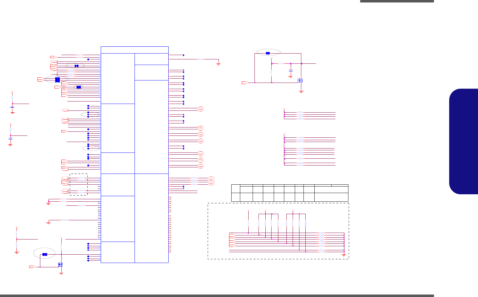
Schematic Diagrams
HUDSON GPIO/ USB/ STRAP B - 9
B.Schematic Diagrams
HUDSON GPIO/ USB/ STRAP
R270 * 10m il_short_04
C4 7 0
*0.1u_16V_Y 5V_04
R2 9 0
10K_04
USB_PP2 17
USB_PN 2 17
De l R696 3/7
U SB_P N6 21
U SB_P P6 21
HD A_S DIN018
R310 10K_04
WLAN_CLKR EQ#17
R312 10K_04
R 2 83 1 0 K _0 4
3.3V
R313 *2.2K_04
R314 *2.2K_04
PC LK_ KBC7
PC I_CLK27
LPC_CLK07,20
PC I_CLK47
LPC_CLK17
PC I_CLK37
R3 84 *2 .2 K _0 4
R 3 82 10 K _ 0 4
R 3 85 2. 2 K _ 0 4
R 3 81 10 K _ 0 4
R 3 83 *1 0K _0 4
R 3 79 10 K _ 0 4
R 3 80 10 K _ 0 4
R 3 77 10 K _ 0 4
R 3 78 *1 0K _0 4
H DA_SD OU T
VD DIO _AZ
R469 33_04
3.3VS
Q8
*MTN 7002ZHS3
G
DS
R695 33_04
R473 33_04
R470 33_04
3.3V
STRAP PINS
R369
10K_04
R371
*10K_04
R3 68
*10K_04
R3 7 2
*10K_04
R3 7 0
*10K_04
R3 7 3
*10K_04
R374
10 K _ 0 4
R376
*1 0 K _0 4
R3 7 5
10K_04
Del R692 3/7
R6 9 0 *0 _ 0 4
MIN IPCI E_SLT2_EN#
EC
Ti merPC IE Gen2
SB_BLON13
PC I_C LK4
H,L = SP I ROM
LPC_C LK0
CLO C K MODE
IGNORE
DEFA ULT
ALLOW
PULL
DEFAULT
PCI_CLK 1 PC I_C LK2
FORCE
JM_D 3M OD E16
STRAP
MINIPCIE_SLT2 _EN#
DEF AULTSTRAP
CLO C K MODE D ISAB LED
USE
DEFAULT
DEFAU L T
AZ_SDOUT
L, H = LPC ROM (DEFAULT)
LPC_C LK1
DEBUG
ENABLED
PCIE Gen1
DEFAULT
MODE
H,H = Reserved
HIGH
Ti mer
Di sabled
GPI O199
DEFAULT
GPIO200non_F usion E CLO W POW E R CLKGEN
U SB_P P9 15
U SB_P N9 15
Ena b l e d
MODE
PULL
MINIPCI E _SLT3_ EN#
PERFORMANCE
R731 *10m il_short_04
DEBUG
LO W
ENABLED
D I SAB L ED
Wat chdog
Wat chdog CLKGENFU SI O N
PCI_CLK 3
L, L = FWH ROM
HUDSON-1
USB OC
A CPI / W AK E UP EVENTS
USB MISC
USB 1. 1
USB 2. 0
GBE LAN
GPIO
EM BE DDE D CT RL
HD AUD IO
PART 4 OF 5
HUDSON M1 A13
U1 9 A
E27
PS2M_C LK/ G PI O19 2
F29
PS2M _D AT/ G PI O 191
F28
PS2K B_C LK/ G PI O190
D2 7
PS2K B_ D AT /GPIO189
G2 9
FC_R ST #/GPO160
F21
SPI_C S2#/GBE_S TA T2/GPIO166
E24
PS2_ CL K/ SC L 4 / GPIO188
E23
PS2_ DAT /SDA4/GP IO 187
V7
GB E_P HY_I N TR
M9
GB E_P HY_R ST #
P4
GB E_P HY_P D
M7
GBE_TXCTL/TXEN
P7
GBE_TXD0
T7
GBE_TXD1
P9
GBE_TXD2
M5
GBE_TXD3
P5
GB E_T XCLK
V5
GBE_RXERR
T5
GBE_RXCTL/RXDV
U2
GBE_RXD0
T2
GBE_RXD1
U3
GBE_RXD2
U1
GBE_RXD3
T9
GB E_R XCLK
L5
GBE_MDIO
L6
GBE_MDCK
T4
GBE_CRS
T1
GBE_COL
P2
AZ_ R ST #
N2
AZ_ S YN C
M4
AZ_S DI N3/ G PI O 170
M1
AZ_S DI N2/ G PI O 169
M2
AZ_S DI N1/ G PI O 168
L2
AZ_S DI N0/ G PI O 167
N1
AZ_S DO UT
M3
AZ_ B I T CLK
F8
USB _OC0#/TRST#/GEV ENT12#
E7
USB _ O C1 # / TD I/ G EV ENT 1 3 #
F7
USB _OC2#/TCK/GEVENT14#
E8
USB_OC3#/AC_PRES/TDO/G EV EN T15#
D4
USB _OC4#/IR_RX0/GEVENT16#
E4
USB _OC5#/IR_TX 0/GEVENT17#
D1
USB _OC6#/IR_TX 1/GEVENT6#
H3
BLI NK /USB_ OC7#/GEVENT18#
AA2 0
CL K_ RE Q G # / GPIO65/OSCIN
K3
GBE_STAT0/GEVENT11#
G5
GB E_LE D2/ G EVE NT 10#
D7
GB E_LE D1/ G EVE NT 9#
D5
GB E_LE D0/ G PI O18 3
H4
DDR 3 _ RS T # / G EV E NT 7 #
AJ21
SM AR T VO L T 2 /SHUTDOWN#/GP IO51
E1
IR _LED #/LLB #/ GPIO184
AB1 8
CL K_ RE Q 1 # / F A NO UT 4 /GPIO61
AH21
CL K_ RE Q 2 # / F A NI N4 / G PI O 6 2
F4
SDA 1 / GPIO228
F5
SCL1 /GPIO227
AE2 2
SDA 0 / GPIO47
AD22
SCL0 /GPIO43
AF1 9
SPK R/ G PI O 6 6
AE1 9
SAT A_ I S5 # / F ANI N3 /GPIO59
AF2 0
SAT A_I S4 #/ F ANO U T3/ GPIO55
AC18
CLK_ REQ 0#/ SA TA_ IS 3#/GP IO60
AB2 1
SM AR T VO L T 1 /S AT A_I S2 #/ G PI O 50
AA1 6
CLK_ REQ 3#/ SA TA_ IS 1#/GP IO63
AD19
CLK_ REQ 4#/ SA TA_ IS 0#/GP IO64
G1
RSM R ST#
AC19
NB_ P W RG D
J6
THR M TRI P# /SMBALERT#/GEV EN T2#
F3
IR_RX1/GEVENT20#
H6
WAK E#/ GEVE NT8#
J1
SYS _RE SET # / GEVENT19#
H2
GEVENT5#
J2 9
LPC_ SM I#/ G EV ENT 23#
K2
LPC_ PM E#/ G EVE NT 3#
AE2 1
KBR ST # /GEVENT1#
AD21
GA 20I N/ GEVENT0#
F6
TES T2
C4
TES T1 / TM S
B3
TES T0
G6
SUS _ST AT#
H5
PW R _ GOOD
F2
PW R _ BTN #
H1
SLP_ S5#
F1
SLP_ S3#
D3
SPI _C S3#/ G BE_S TA T1/ G EVE NT 21#
K1
RI # /GE VENT22#
J2
PCI _P ME#/GE VEN T4#
B22
KSO_17/GPIO226
A22
KSO_16/GPIO225
C2 2
KSO_15/GPIO224
D2 2
KSO_14/GPIO223
A23
KSO_13/GPIO222
B23
KSO_12/GPIO221
C2 4
KSO_11/GPIO220
B24
KSO_10/GPIO219
D2 4
KSO_9/GPIO218
A25
KSO_8/GPIO217
B25
KSO_7/GPIO216
A24
KSO_6/GPIO215
C2 6
KSO_5/GPIO214
A26
KSO_4/GPIO213
D2 6
KSO_3/GPIO212
B27
KSO_2/GPIO211
A27
KSO_1/GPIO210
B28
KSO_0/GPIO209
C2 8
KSI_7/GPIO208
C2 9
KSI_6/GPIO207
D2 8
KSI_5/GPIO206
D2 9
KSI_4/GPIO205
E29
KSI_3/GPIO204
E28
KSI_2/GPIO203
G2 5
KSI_1/GPIO202
G2 4
KSI_0/GPIO201
E21
EC_P W M 3/EC_TIME R3/GPIO200
F22
EC_P W M 2/EC_TIME R2/GPIO199
E22
EC_P W M 1/EC_TIME R1/GPIO198
F25
EC_P W M 0/EC_TIME R0/GPIO197
E26
SDA3_LV/GPIO196
B26
SCL3 _ LV/ GPIO195
F23
SD A2/ GPIO194
D2 5
SC L 2/ GPIO193
B16
USB _ HS D0 N
A16
USB _ HS D0 P
A17
USB _ HS D1 N
B17
USB _ HS D1 P
J1 8
USB _ HS D2 N
J1 6
USB _ HS D2 P
E16
USB _ HS D3 N
E18
USB _ HS D3 P
A14
USB _ HS D4 N
B14
USB _ HS D4 P
C1 6
USB _ HS D5 N
D1 6
USB _ HS D5 P
G1 8
USB _ HS D6 N
G1 6
USB _ HS D6 P
G1 4
USB _ HS D7 N
G1 2
USB _ HS D7 P
C1 3
USB _ HS D8 N
D1 3
USB _ HS D8 P
B13
USB _ HS D9 N
A13
USB _ HS D9 P
J1 4
U SB _HS D10 N
J1 2
U SB _HS D10 P
E12
U SB _HS D11 N
E14
U SB _HS D11 P
E11
U SB _HS D12 N
F11
U SB _HS D12 P
A12
U SB _HS D13 N
B12
U SB _HS D13 P
J8
USB _ FS D0 N
H9
US B_ F SD 0 P / GPIO185
H1 1
USB _ FS D1 N
J1 0
US B_ F SD 1 P / GPIO186
G1 9
USB_RCOMP
A10
U SB CL K/ 14 M_ 25M _48M _O SC
KB C_ RS T#20
GA 2 020
R7 3 0 *0 _0 4
LI D _ S W #13,20,22
Q6
*M T N7 0 02 Z H S 3
G
DS
EC _S MI#19,20
EC _S CI#20
PC IE_ W AKE#1 6 , 1 7, 19
CPU_THERMTRIP#3
SWI #
SUSB#11,12,19,20,23
3.3V S
SUSC #20,23,25
R 276 2.2K_04
MIN IPCI E_SLT3_EN#
R 277 2.2K_04
R 278 4.7K_04
R 279 4.7K_04
APU_SID 3
SUS_STAT#
SDATA0
NB_ PW R GD
SCLK0
3.3V
GB E_P HY_IN TR
R2 8 9
*10K_04
3.3V
WF_RADIO
R 284 2.2K_04
RSM RST_GA TE#20
H DA_SYN C18
R2 7 4
*2 0 K _ 04
SCLK1
SDATA1
PW R _BTN #20
U SB_P P5 15
U SB_P N5 15
9/1 4
Del ??VGA 3/8
R 728 *0_04
R 752 *0_04
R691 *10m il_short_04
Closed to SB.
U SB4 POR T 3
PCIE_RS T#_GATE7U SB9 3 G
U SB0 POR T 0
U SB6 BL UE TO OTH
U SB1 POR T 1
U SB2 MIN I CAR D
U SB5 CC D
SW I#20
HUDSON GPIO/USB/AUDIO/STRAP
3.3V
U SB_P N0 22
U SB_P P0 22
SDATA05,6
SCLK05,6 H DA_SPKR18
SW I#
3.3V
C4 7 1
1u_6 .3V_Y5V_0 4
R2 8 2
10K_04
3.3V
SY S_R ST#
GBE_PH Y_INTR
R 692 *10m il_short_04
HDA_RST#18
OD D_ DA # _ FCH17
P LAC E CL O SE TO SO UTH B RID GE
R291 10K_04
USB_ O CP 0 _ 1#19 , 2 2
R7 4 2 *2 .2 K_0 4
R287 10K_04
SYS_R ST#
R281 *2.2K_04
USB3 0 _P W R_ EN19
HDA _BI TC LK18
Del ? ? VGA 3/8
R 6 9 6 * 1 0m i l _s h o r t _0 4
8/18
R7 4 3 *2 .2 K_0 4
U SB_P P1 22
U SB_P N1 22
Del R691, R27 5, R270, R731 3/7
R7 4 4 *2 .2 K_0 4
EC_SC I#R292 10K_04 EC_SM I#R293 10K_04
3.3V
3.3V
SWI #
R280
*20K_04
R273 *22K_04
C469
* 2.2u_6.3V _X5R_04
S4_ STATE #11
R 693 *0_04
GEVENT0#
GEVENT1#
OD D_ DET EC T#17
M INIPC IE_SLT2_EN#
R 694 *0_04
M INIPC IE_SLT3_EN#
NB_ PW R GD
RSMRST#
RSM RST #
SB_AC_OK
SCLK1
SC LK 2
APU _SIC
SC LK2
SD ATA2
SDATA1
APU _SID
SD ATA2
SUS_STAT#
SY S_RST#
SB_PW R GD11
USB_ R COM P
WF_RAD IO
GBE _C RS
GBE _C OL
R8 1 3 *0 _0 4
U SB_P P4 22
U SB_P N4 22
SY S_RST#11
R272 11K_1%_04
HDA _SD OU T18
R 288 2.2K_04
SMC_CPU_THERM 3,9,20
SMD_CPU_THERM 3,9,20
G BE_RXERR
APU_SIC 3
R275 * 10m il_short_04
R2 8 5 10 K _ 0 4
R2 8 6 10 K _ 0 4
AC _IN #20,22,29
R807
* 1 0K _0 4
Sheet 8 of 43
HUDSON GPIO/
USB/ STRAP
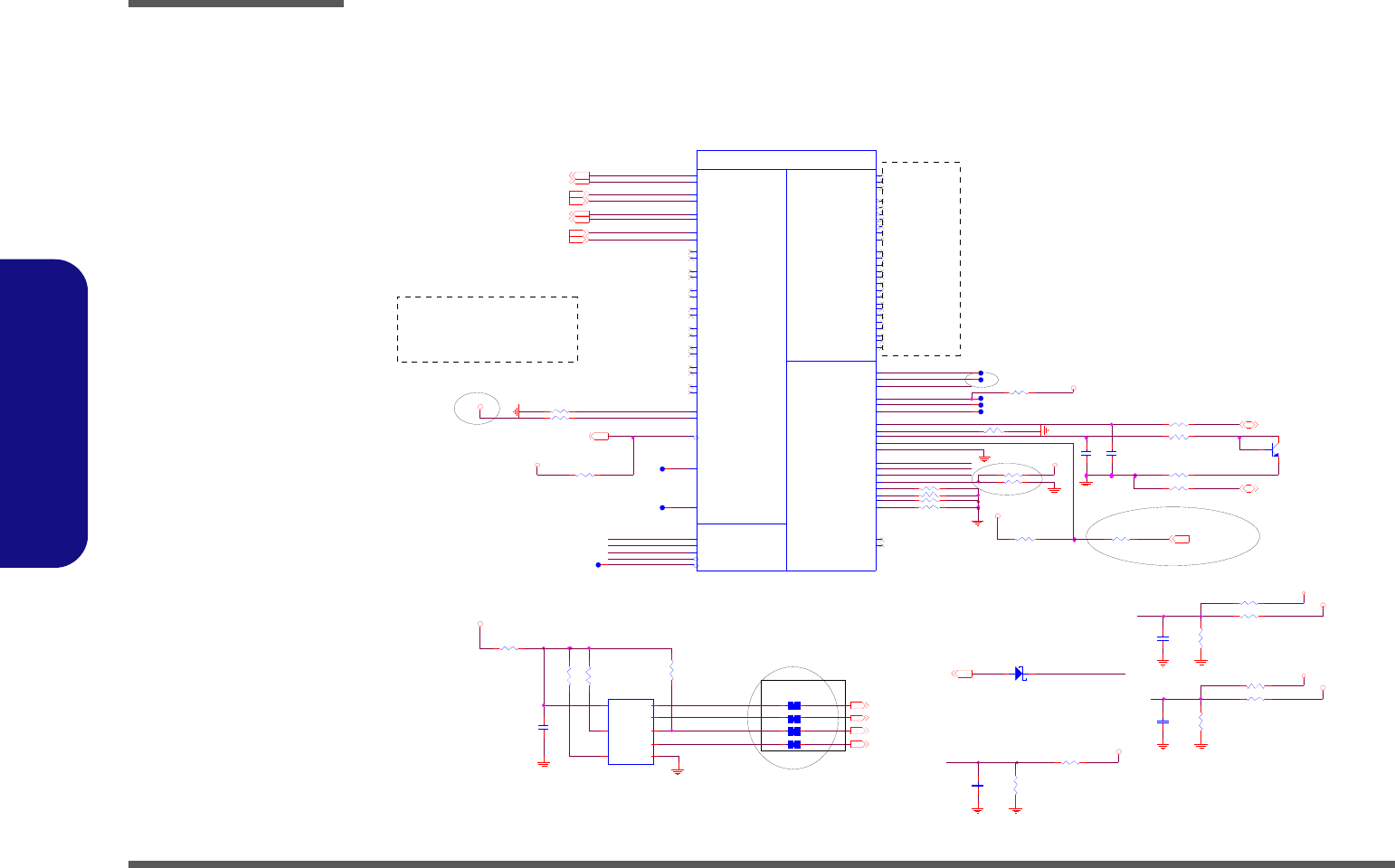
Schematic Diagrams
B - 10 HUDSON SATA/ DEBUG IO/ SPI
B.Schematic Diagrams
HUDSON SATA/ DEBUG IO/ SPI
SATA_ L ED #21
R333 * 0_04
R335 * 0_04
SB_ PR OCHOT#_C
C487
330p_50V _X7R_04
SB_P ROCHOT#3
C486
330p_50V_X7R_04
C488
* 0.1u_16V _Y 5V_04
R340 *11K_1%_04
R336 * 0_04
R337 * 0_04
R341 *10K_04
R576 * 10K _04
AP U_TALERT# 3,20
R810 *10K_04
H SPI _ MSO 20
H SPI _ MSI 20
H SPI _ SC L K 20
H SPI _ C E# 2 0
R799 10K_04
R350
*10K _04
SMD_CPU_THERM 3,8,20
SMC_CPU_THERM 3,8,20
3.3V
3/18
3.3VS
C490
* 0.1u_16V _Y 5V_04
R349
10K_04
SA TARXN 017
HUDSON-1 PA RT 2 OF 5
SPI ROM
GPIOD
SERIAL AT A
HW MONITOR
U19B
HUDSON M1 A13
G2
RO M _ R ST # / GPIO161
K9
SPI_CS 1#/GPIO165
K4
SP I _ CLK / GPIO162
E2
SP I _ DO / G PI O 1 6 3
J5
SPI_DI/GPIO164
AC 1 6
SA TA _ X2
AD 1 6
SA TA _ X1
AD 1 1
SA TA _ AC T# /GPIO67
AA 14
SA TA _ CA L R N
AB 14
SA TA _ CA L R P
AJ 1 9
SA TA _ RX 5 P
AH 1 9
SA TA _ RX 5 N
AH 1 8
SA TA _ TX 5 N
AJ 1 8
SA TA _ TX 5 P
AH 1 7
SA TA _ RX 4 P
AJ 1 7
SA TA _ RX 4 N
AF 17
SA TA _ TX 4 N
AG17
SA TA _ TX 4 P
AF 14
SA TA _ RX 3 P
AG14
SA TA _ RX 3 N
AJ 1 4
SA TA _ TX 3 N
AH 1 4
SA TA _ TX 3 P
AH 1 2
SA TA _ RX 2 P
AJ 1 2
SA TA _ RX 2 N
AF 12
SA TA _ TX 2 N
AG12
SA TA _ TX 2 P
AF 10
SA TA _ RX 1 P
AG10
SA TA _ RX 1 N
AJ 1 0
SA TA _ TX 1 N
AH 1 0
SA TA _ TX 1 P
AH8
SA TA _ RX 0 P
AJ8
SA TA _ RX 0 N
AJ9
SA TA _ TX 0 N
AH9
SA TA _ TX 0 P
Y2
NC
G27
NC
A8
VI N 7/ G BE _LED 3/ G PI O 182
B8
VIN6/GBE_ST AT 3/GPIO181
B7
VIN5/GPIO180
A7
VIN4/GPIO179
C5
VIN3/GPIO178
A4
VIN2/GPIO177
B4
VIN1/GPIO176
A3
VIN0/GPIO175
C7
TEMP_COMM
B5
TE MPIN3/TALERT#/GPIO174
A5
TEMPIN2/GPIO173
A6
TEMPIN1/GPIO172
B6
TEMPIN0/GPIO171
W8
FANIN2/GPIO58
V9
FANIN1/GPIO57
W7
FANIN0/GPIO56
Y9
FA NO UT 2/ G PI O 54
W6
FA NO UT 1/ G PI O 53
W5
FA NO UT 0/ G PI O 52
AH26
F C_A DQ 15/ G P IOD143
AG25
F C_A DQ 14/ G P IOD142
AJ25
F C_A DQ 13/ G P IOD141
AJ24
F C_A DQ 12/ G P IOD140
AF23
F C_A DQ 11/ G P IOD139
AJ23
F C_A DQ 10/ G P IOD138
AH22
F C_A DQ 9/G P IOD 137
AF21
F C_A DQ 8/G P IOD 136
AG21
F C_A DQ 7/G P IOD 135
AJ22
F C_A DQ 6/G P IOD 134
AH23
F C_A DQ 5/G P IOD 133
AG23
F C_A DQ 4/G P IOD 132
AH24
F C_A DQ 3/G P IOD 131
AH25
F C_A DQ 2/G P IOD 130
AJ26
F C_A DQ 1/G P IOD 129
AJ27
F C_A DQ 0/G P IOD 128
AH 2 7
FC_INT2/GPIOD147
AF 29
FC_INT1/GPIOD144
AE 29
FC_CE2#/GPIOD150
AF 27
FC_CE1#/GPIOD149
AG26
FC_WE#/GPIOD148
AG29
FC _AV D#/ G P IOD146
AF 28
FC _ O E#/ G P IOD145
AF 26
FC _FB CLK I N
AG28
FC _F BC LKO U T
AH 2 8
FC _C LK
NEAR U19
3.3V
R351 *10K_04
SPI_CS#_SEL
R800 10K_04
R573 *10mil_short_04
VI N _ VD DCR
R386 *10mil_short_04
R571 *10mil_short_04
AVDD_SATA -> 1.1VS 3/7
R572 *10mil_short_04
HUDSON SATA/DEBUG IO/SPI
De l ? ? VGA 3 /8
C492
* 0.1u_16V _ Y5V_ 04
R352
10K_04
VI N _ VD DIO_SUS
Debug port
R732 *0_04
SA TATXN017
U21
*25VF032B
CE# 1
SO 2
WP#
3
VSS 4
SI 5
SCK6
HOLD#
7
VD D
8
SA TARXP 017
SPI_DATAIN
R330 *10K_04
SA TATXN117 SA TATXP117
SA TARXP 117
SA TARXN 117
R798 10K_04
3.3VS
R801 10K_04
R697 10K_04
R802 10K_04
Q9
*2N 3904
B
E C
R342
10K_04
SA TATXP017
3.3VS
SPI_DATAOUT
R331 1K_1%_04
R332 931_1%_04
R338 * 0_04
CD 3/9
C491
*0.1u_16V_Y5V_04
1.8VS
VDDCR_CPU
VDDCR_NB
1VS
1.1VS
Connect C7 and D8, then go to GND directly.
R346
*1K_04
R347
* 10K_04
R803 10K_04
Re s er ve 3/7
1.5V
to get aff ected wi th 2 vi as. AMD plat f orms are val idat ed
cust omers can use 2v ias with GND via withi n 150mil s of
meet s SATA logo requirement s. Return l oss i s expected
si gnal via as l ong as they can ens ure that their pl atfor m
SATA t r ace shoul d use only 1via on the
trace.
wi th one via only
R344 *4.99K_1%_04
HDD0_PWR
HUDSON_FANOUT0
HUDSON_FANTACH0
R345 *4.99K_1%_04
MB_THRMD A_ SB
MB_THRMDC_SB
HUDSON_ROM_RST#
ODD_PWR
SATA_CALN
SATA_CALP GPI O58
SB_PROCHOT#_C
S B_ TAL ER T#
SPI_CS#_SEL
SPI_CLK
D22 RB751V
A C
SPI_DATAIN
TE MPIN0
SPI_DATAOUT
VIN_VDDCR
VIN_VDDIO_SUS
VIN_VDDNB
VIN_VDDNB
SPI_CLK
Sheet 9 of 43
HUDSON SATA/
DEBUG IO/ SPI
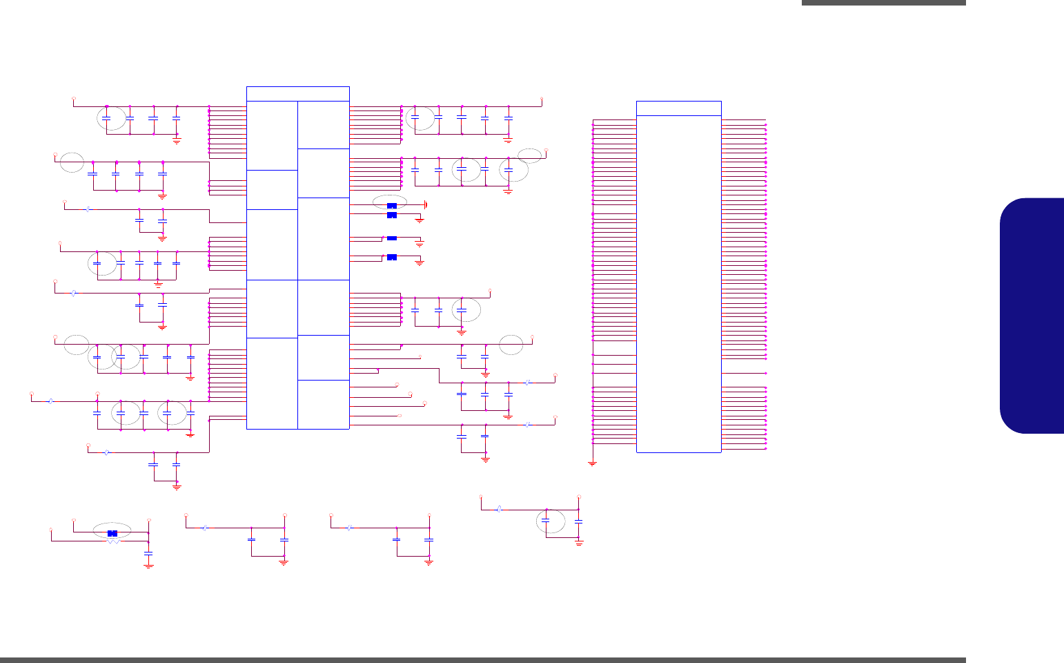
Schematic Diagrams
HUDSON POWER DECOUPLING B - 11
B.Schematic Diagrams
HUDSON POWER DECOUPLING
VD DAN _3.3V_HW M
R 362 * 10m il_s hort
C503
0.1u_10V_X5R _04
600m A
C5 1 2
0.1u_10V_X5R_04
C5 1 1
1u_10V_Y 5V_06
C5 4 3
* 1u_6.3V_X5R_04
658m A
C531
*1u _10V_Y5V_06
C530
1u_10V _Y 5V_06
C529
*0.1u_10V_X7R_04
TBD m A
C504
0.1u_10V_X5R _04
C509
4.7u_6.3V_X5R_06
C5 0 6
0.1u_10V_X5R _04
131m A
.
L96 HC B1005KF-121T20
C497
* 0.1u_10V_X7R_04
C555
1u_10V_Y 5V _06
C556
*0.1u_10V_X7R _04
71mA
43mA
510m A
93mA
TB D m A
567m A
5m A
17m A
47 m A
VD DPL_3.3V_P CIE
V DD PL_3.3V_SATA
V DD XL_3.3VTBD mA
VDD IO_AZ
62m A
32mA
TB D m A
197mA
C557
1u_10V_Y5V_06
CD 3 /8
113mA
CD 3/8
CD 3/8
C5 5 2
0.1u_10V_X5R _04
.
L94 H CB1005KF-121T20
C551
*1u_10V_Y5V_06
CD 3/8
C494
10u_6.3V_X5R _08
C545
*10u_6.3V_X5R _08
C496
0.1u_10V_X5R _04
C495
0.1u_10V_X5R _04
3.3VS
C5 1 9
1u_6.3V_X5R _04
.
L8 8 H C B 1 0 05 K F -1 2 1 T2 0
C5 2 7
*0.1u_10V_X7R_04
C5 2 8
1u_10V_Y5V_06
22u ->10u CD 3/8
CD 3/8
Del R356 3/7
R363 * 0_04
C550
1u_10 V_ Y5 V_06
C549
0.1u_10V_X5R_04
.
L93 HC B1005KF-121T20
.
L95 H CB1005KF -121T20
HUDSON-1
PC I/GPIO I/O
PCI EX PR ESS
GBE LAN
FL ASH I/O
CO R E S5
CORE S0
C L KG EN I/O
3. 3V_S 5 I/O
SE RI AL A TA
PO W ER
PLL
U SB I / O
PA RT 3 O F 5
U19C
HU DS ON M1 A13
D1 1
V DDA N_ 1 1 _ USB _ S
C1 1
V DDA N_ 1 1 _ USB _ S
E19
V DDA N_ 3 3 _ USB _ S
D2 0
V DDA N_ 3 3 _ USB _ S
D1 9
V DDA N_ 3 3 _ USB _ S
D1 8
V DDA N_ 3 3 _ USB _ S
C2 0
V DDA N_ 3 3 _ USB _ S
C1 8
V DDA N_ 3 3 _ USB _ S
B20
V DDA N_ 3 3 _ USB _ S
B19
V DDA N_ 3 3 _ USB _ S
B18
V DDA N_ 3 3 _ USB _ S
A20
V DDA N_ 3 3 _ USB _ S
A19
V DDA N_ 3 3 _ USB _ S
A18
V DDA N_ 3 3 _ USB _ S
AE16
V DDA N_ 1 1 _ SAT A
AD18
V DDA N_ 1 1 _ SAT A
AE18
V DDA N_ 1 1 _ SAT A
AG19
V DDA N_ 1 1 _ SAT A
AH20
V DDA N_ 1 1 _ SAT A
AF1 8
V DDA N_ 1 1 _ SAT A
AJ20
V DDA N_ 1 1 _ SAT A
AD14
V DDP L_33_S ATA
W26
V DDA N_ 1 1 _ PCI E
W22
V DDA N_ 1 1 _ PCI E
V29
V DDA N_ 1 1 _ PCI E
V28
V DDA N_ 1 1 _ PCI E
V27
V DDA N_ 1 1 _ PCI E
V26
V DDA N_ 1 1 _ PCI E
V22
V DDA N_ 1 1 _ PCI E
U2 6
V DDA N_ 1 1 _ PCI E
AE28
V DDP L_33_P CI E
AC22
V DDI O _ 1 8 _ F C
AF2 4
V DDI O _ 1 8 _ F C
AE25
V DDI O _ 1 8 _ F C
AF2 2
V DDI O _ 1 8 _ F C
AA19
V DDI O _ 3 3 _ P CI GP
AF7
V DDI O _ 3 3 _ P CI GP
AA9
V DDI O _ 3 3 _ P CI GP
AA7
V DDI O _ 3 3 _ P CI GP
AC8
V DDI O _ 3 3 _ P CI GP
AB4
V DDI O _ 3 3 _ P CI GP
AA2
V DDI O _ 3 3 _ P CI GP
AC21
V DDI O _ 3 3 _ P CI GP
AE5
V DDI O _ 3 3 _ P CI GP
Y19
V DDI O _ 3 3 _ P CI GP
V6
V DDI O _ 3 3 _ P CI GP
AH1
V DDI O _ 3 3 _ P CI GP
L20
V DD XL_33_S
D6
VDD AN _33_HWM _S
F19
VD DP L_33_USB_S
L22
VD DP L_11_SY S_S
M2 1
VDDPL_33_SYS
B11
VDDCR_11_USB_S
A11
VDDCR_11_USB_S
M8
VDD I O_A Z_S
G2 6
VD DC R_11_S
F26
VD DC R_11_S
T8
VDDIO _33_S
T6
VDDIO _33_S
J9
VDDIO _33_S
L10
VDDIO _33_S
K10
VDDIO _33_S
B21
VDDIO _33_S
D2 1
VDDIO _33_S
A21
VDDIO _33_S
P8
VD DI O _GBE_S
M6
VD DI O _GBE_S
L9
V DD CR_ 1 1 _ GBE_S
L7
V DD CR_ 1 1 _ GBE_S
M1 0
VDD I O_3 3_GBE_S
V1
VDDRF _GBE_S
J22
V DD AN _11_CLK
K21
V DD AN _11_CLK
J20
V DD AN _11_CLK
J21
V DD AN _11_CLK
K26
V DD AN _11_CLK
J28
V DD AN _11_CLK
K29
V DD AN _11_CLK
K28
V DD AN _11_CLK
W18
V DD CR _11
W12
V DD CR _11
V18
V DD CR _11
V12
V DD CR _11
U1 7
V DD CR _11
U1 3
V DD CR _11
N1 7
V DD CR _11
R1 5
V DD CR _11
N1 3
V DD CR _11
C498
10u_6.3V_X5R _08
C5 1 0
1u_6.3V_X5R_04
C508
*1u_6.3V_X5R_04
C507
0.1u_10V_X5R_04
C505
0.1u_10V_X5R _04
HUDSON-1
PAR T 5 OF 5
GROUND
HUDSON M1 A13
U19D
J2 3
V SSI O _ PC IECLK
V20
V SSI O _ PC IECLK
T2 4
V SSI O _ PC IECLK
T2 2
V SSI O _ PC IECLK
T2 0
V SSI O _ PC IECLK
P26
V SSI O _ PC IECLK
P24
V SSI O _ PC IECLK
P22
V SSI O _ PC IECLK
M2 6
V SSI O _ PC IECLK
M2 4
V SSI O _ PC IECLK
M2 2
V SSI O _ PC IECLK
P20
V SSI O _ PC IECLK
P21
V SSI O _ PC IECLK
M1 9
V SSX L
D8
V SSA N_H W M
Y4
EFUSE
H19
V SSI O _ US B
K18
V SSI O _ US B
K16
V SSI O _ US B
K14
V SSI O _ US B
K12
V SSI O _ US B
J1 9
V SSI O _ US B
J1 1
V SSI O _ US B
H18
V SSI O _ US B
H16
V SSI O _ US B
H14
V SSI O _ US B
H12
V SSI O _ US B
D9
V SSI O _ US B
F18
V SSI O _ US B
G1 1
V SSI O _ US B
C9
V SSI O _ US B
F16
V SSI O _ US B
F14
V SSI O _ US B
F12
V SSI O _ US B
F9
V SSI O _ US B
E9
V SSI O _ US B
D17
V SSI O _ US B
D14
V SSI O _ US B
D12
V SSI O _ US B
D10
V SSI O _ US B
B9
V SSI O _ US B
K11
V SSI O _ US B
B10
V SSI O _ US B
A9
V SSI O _ US B
AJ16
V SSI O _ SA TA
AJ13
V SSI O _ SA TA
AJ11
V SSI O _ SA TA
AJ7
V SSI O _ SA TA
AH16
V SSI O _ SA TA
AH13
V SSI O _ SA TA
AH11
V SSI O _ SA TA
AH7
V SSI O _ SA TA
AG8
V SSI O _ SA TA
AF16
V SSI O _ SA TA
AF13
V SSI O _ SA TA
AF11
V SSI O _ SA TA
AF9
V SSI O _ SA TA
AE14
V SSI O _ SA TA
AE12
V SSI O _ SA TA
AC14
V SSI O _ SA TA
AB16
V SSI O _ SA TA
Y16
V SSI O _ SA TA
Y14
V SSI O _ SA TA
K20
VS SI O _ PCI E CL K
L2 1
VS SI O _ PCI E CL K
AE26
VS SI O _ PCI E CL K
W20
VS SI O _ PCI E CL K
W21
VS SI O _ PCI E CL K
Y20
VS SI O _ PCI E CL K
AC26
VS SI O _ PCI E CL K
AA26
VS SI O _ PCI E CL K
AD23
VS SI O _ PCI E CL K
AB23
VS SI O _ PCI E CL K
AA23
VS SI O _ PCI E CL K
AA21
VS SI O _ PCI E CL K
H2 6
VS SI O _ PCI E CL K
H2 3
VS SI O _ PCI E CL K
M2 0
VSSPL_SYS
L8
VSS
L4
VSS
N4
VSS
P6
VSS
V10
VSS
AH29
VSS
H7
VSS
AF2 5
VSS
M1 2
VSS
G9
VSS
G8
VSS
J4
VSS
G4
VSS
AA12
VSS
AA11
VSS
Y11
VSS
Y12
VSS
Y10
VSS
Y18
VSS
U4
VSS
B29
VSS
AJ 28
VSS
W10
VSS
W9
VSS
V8
VSS
AC9
VSS
AB7
VSS
AD4
VSS
AD6
VSS
V4
VSS
P3
VSS
J7
VSS
L1 8
VSS
L1 2
VSS
M1 1
VSS
V19
VSS
M1 8
VSS
U1 5
VSS
V11
VSS
P10
VSS
T1 0
VSS
R1 7
VSS
R1 3
VSS
N1 5
VSS
F24
VSS
E6
VSS
E25
VSS
D2 3
VSS
E5
VSS
A2
VSS
A28
VSS
AJ 2
VSS
C499
*1u_6.3V_X5R _04
VDD PL_3.3V
C501
10u_6.3V_X5R_08
C5 0 2
0.1u_10V_X5R _04
.
L90
HC B1005KF-121T20
AVD D_U SB
V DD PL_1.1V
22u -> 10 u C D 3/8
R771 *10m il_short
VD DAN _1.1V_US B
C534
1u_6.3V _X5R_04
C5 5 3
1u _ 1 0V _Y 5 V _0 6
C554
* 0.1u_10V_X7R_04
22u ->10u CD 3/8
Del L8 9 3 /7
C5 4 0
0.1u_10V_X5R _04
C539
10u_6.3V_X5R_08
Del R 36 1 3 /7
C541
0.1u_10V_X5R _04
C5 2 1
0.1u_10V_X5R _04
.
L91 H CB1005KF -121T20
C542
1u_6.3V_X5R _04
C544
10u_6.3V_X5R _08
C546
0.1u_10V_X5R_04
C4 9 3
0.1u_10V_X5R _04
R356 *10m il_short
R772 *10m il_short
HUDSON POWER DECOUPLING
C518
*1u_6.3V_X5R_04
C520
0.1u_10V_X5R _04
C 517
10u_6.3V_X5R _08
R773 *10m il_short
.
L86 HCB 1005KF-121T20
De l R362 3/7
Del R355 3/7
C5 3 3
* 1u_6.3V_X5R_04
C535
0.1u_10V_X5R _04
C532
10u_6.3V_X5R _08
C500
1u_6.3V_X5R_04
C5 3 8
1u_6.3V_X5R_04
V DD CR _1.1_USB
CD 3 /8
CD 3 /8
C536
0.1u_10V_X5R _04
1.8V S
3.3VS
1.1VS
C537
1u_6.3V _X5R_04
1. 1 V S
3.3V S
3.3V AVDD _USB
1. 1 V
1.5V
VDD IO_AZ3.3V
3.3VS VD DPL_3.3V VD DP L_1.1V1.1V
3. 3 V VD DAN _3.3V_HW M
1.1V
3.3V
.
L92
HC B1005KF-121T20
1.1V
3.3V
C548
1u_10 V_ Y5 V_06
C547
0.1u_10V_X5R_04
1.1VS
22 u -> 10 u C D 3/8
1.1VS
Del L85 3/7
Sheet 10 of 43
HUDSON POWER
DECOUPLING
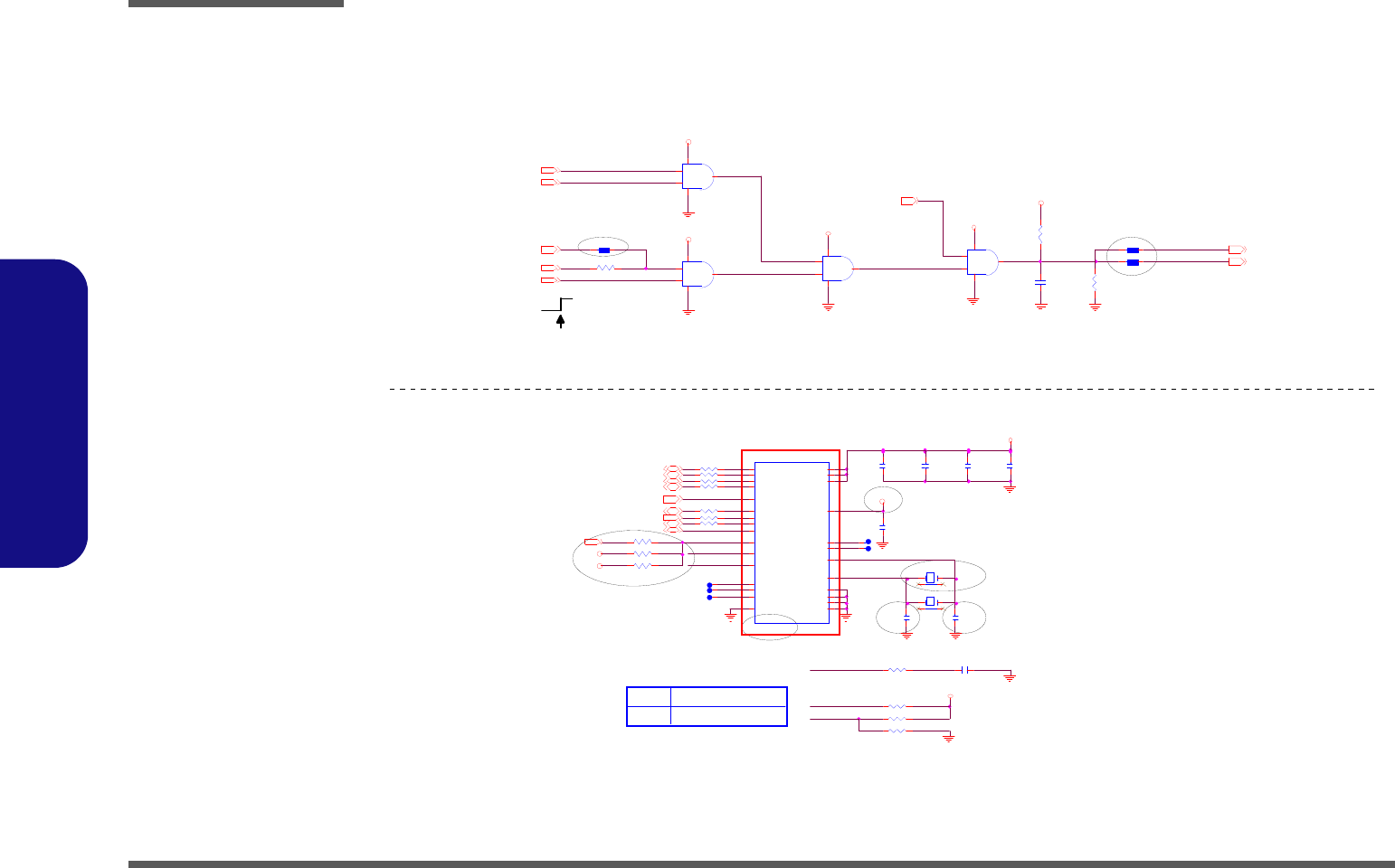
Schematic Diagrams
B - 12 POWERGOOD/ TPM
B.Schematic Diagrams
POWERGOOD/ TPM
Sheet 11 of 43
POWERGOOD/
TPM
R776 *0_04
PW RG D_ VC ORE28
R819 0_04
R248 10K_04
VD D3
De l R3 64, R 36 5 3/7Del R 775 3/7
3.3V
SY S_PW RO K
SB _PW ROK
BUF_PLT_R ST#7,16,17,19,20
LPC_AD37,20
LPC_AD17,20 LPC_AD07,20
PC LK_TPM7
LP C_FRAM E#7,20
LPC_AD27,20
PCI_C LKR UN #7
S4_STATE#8
3/2 1
C841
1u_6.3V_Y 5V_04
3.3VS to VDD3 3/9
R814 0_04
R816 0_04
R817 0_04
R818 0_04
R246 *0_04
Value modify 3/23
1.1V_PWRG D26
18p to 15p 3/9
R239 *10K_04
3.3VS
ON
3.3V
SUSB#8,12,19, 20,23
R7 74
10K_04
R775 *10mil_short R364 *10mil_short
R365 *10mil_short
3.3V
DDR1.5V_PWRGD25,28
R820 0_04
SERIR Q7,20
C8 8 2
15p_50V_N PO_04
XTAL O
X12 M C-306_32.768 KH z
14
3 2
XTAL I
C8 81
15p_50V_NPO _04
R8 24 *1 0 K_ 04
TPM_PP
PCLK_TP M
R823 10K _04
R8 21 *3 3 _ 04
R8 22 *1 0 K_ 04
LPC re se t t i m ing:
TPM 1.2
HI: 4E/ 4F H
LOW: 2E/ 2F H
TP M_P P
TPM_BADD
LPCP D# inac tive to L RST# in act ive 3 2~ 9 6us
Ass er ted b efo re en te ring S3
HI: ACCESS
LOW: NORMAL ( Int ernal PD )
C 883 *10p_50V_04
3.3VS
C8 7 6
0.1u_16V _Y 5V_04
3.3VS
VD D3
C877
0.1u_16V_Y 5V_04
C878
0.1u_16V_Y 5V_04
C879
1u_16V_X5R _06
C8 8 0
0.1u_16V _Y 5V_04
TPM3005
TPM_BAD D
TPM
U50
SLB963 5TT
LAD3
17
LAD0
26
LAD1
23
LAD2
20
VDD 1 10
XTALI 13
VDD 3 24
VDD 2 19
LFRAM E#
22
LCLK
21
LRESE T#
16
SER IRQ
27
CLKRUN#
15
GN D_ 1 4
GN D_ 2 11
GN D_ 3 18
GN D_ 4 25
GPIO 6
GPIO 2 2
XT A L O 14
TESTI
8
TESTBI/BAD D
9
PP
7
NC_1
1
NC_2
3
NC_3
12
LPCPD #
28
VSB 5
TPM3002
TPM3004
TPM_PP
TPM3003
TPM3001
TPM_BAD D
X13 * 32.76 8KHz
14
3 2
U22B
74LVC 08PW
4
5
6
147
3.3V
SYS_RS T#8
R367
*10K_04
U2 2 C
74LVC08PW
9
10 8
147
U22A
74LVC 08PW
1
23
147
Pull hight reserve 3/17
3.3V
SB_ PW R GD 8
ALL_SYS_PWR GD 13,20
U22D
74LVC 08PW
12
13
11
147
R815 0_04
1.8V_PWRG D27
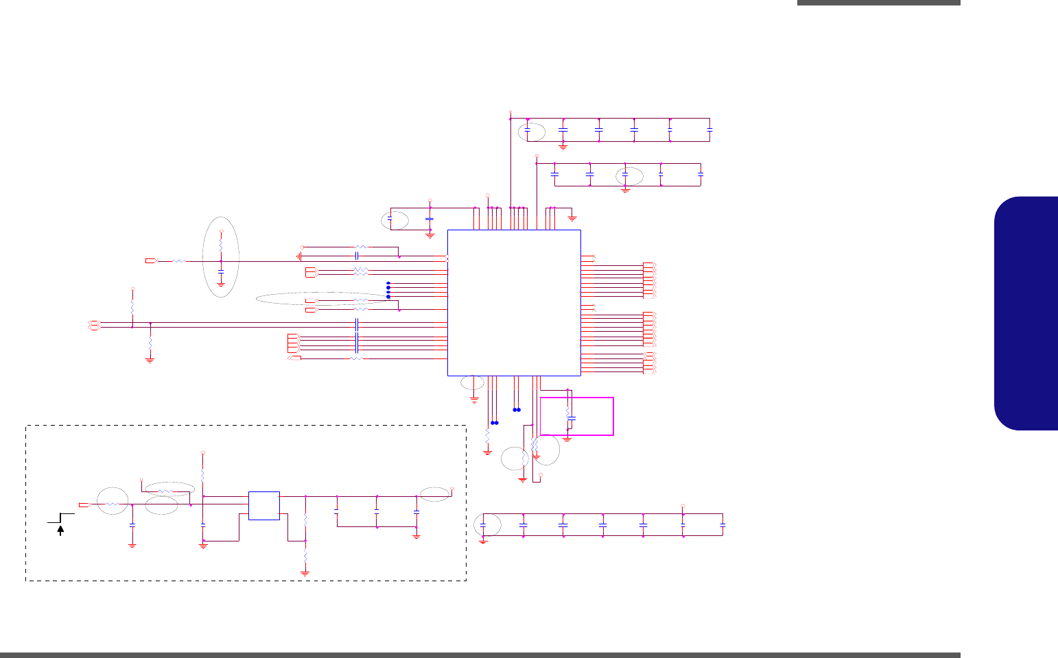
Schematic Diagrams
ANX3110 ASIC B - 13
B.Schematic Diagrams
ANX3110 ASIC
Sheet 12 of 43
ANX3110 ASIC
LVD S-L1P
LVD S-L2P
LVD S-L2N
XLT_BLON _PW M
LVD S-L1N
R854 off 3/22
need to close to chip
1.2VS
ANX3110 ASIC
DP_HPD
R1
Vo =Vr ef *(R 2+ R1) /R2
LVDS-L2P3,13
R2
200mA
Fix ed : P1 OP EN, R 2 s hor t to GN D
ON
LVDS-L2N3,13
LVDS-L1P3,13
RST#
LVDS-L1N3,13
C8 9 5
2.2u_6.3V_X5R_06
P W M_VARY _BL
Mod ify 3/11
R8 59
*10K_04
BRIG HTNESS13,20
Rese rve 3 /22
R842 *0_04
>06 3/11
C8 84
2.2u_6.3V_X5R_06
>06 3/11
GPI O_ 2
C892
2.2u_6.3V_X5R_06
R8 5 6
*100K_04
>0 6 3 /11
De l P J24 3 /22
C8 9 8
* 3. 3u_6.3V_X5R _06
3.3VS
CL K_ SE L
Re ser ve 3/22
LVDS_DD C_DATA3, 1 3 LVDS_DD C_CLK3, 1 3
? ? 3.3V S En able 3/2 2
L V D S _D D C _D A TA
L V D S _D D C _C LK
Del R8 56 3/14
C906
2.2u_6.3V_X5R_06
>0 6 3 /11
PC 239
2.2u_6.3V_X5R _06
C8 9 3
0.01u_16V_X7R_04
R841
*1 M_ 0 4
C891
0. 1 u _1 0 V _ X5 R _ 0 4
C8 8 6
0.1u_10V_X5R_04
PR219
0_06
R 838 0_04
R8 3 6 0 _ 04
R 837 0_04
C 899 0.1u_10V_X5R_04
C911
0.01u_16V_X7R_04
PC 242
* 1u_10V_Y5V_06
R8 5 1
12K_1%_04
C 903 0.1u_10V_X5R_04
PU 13
APL5317-12BI-TRG
VIN
1
GND
2
EN
3
SET 4
VO UT 5
R839
*1M_04
PC 241
0.1u_16V_Y 5V _04
C9 12
0.01u_16V_X7R _04
R854
* 10K_04
R835 1M_04
C887
0. 1 u _1 0 V _ X5 R _ 0 4
C896
0.1u_10V_X5R _04
C 900 0.1u_10V_X5R_04
PR220
*10K_04
C 897 0.1u_10V_X5R_04
C8 8 5
0.1u_10V_X5R_04
C894
0.01u_16V_X7R _04
ANX3110
U5 1
ANX3110
EPAD
65
POR
34
RESET_L
12
OSC _ IN
30
OSC _ OU T
31
TD O
54
TD I
55
TM S
57
TC K
56
CPU_ VA R Y_ BL
48
DPRX_ A UX_ N
60
DPRX_ A UX_ P
61
DPRX_ L0 _ P
3
DPRX_ L0 _ N
4
DPRX_ L1 _ P
6
DPRX_ L1 _ N
7
DPRX_ HPD
58
LV D S _ U 3 _P 45
LVDS_U 3_N 44
LVDS_CLKU _P 43
LVDS_CLKU_N 42
LV D S _ U 2 _P 41
LVDS_U 2_N 40
LV D S _ U 1 _P 38
LVDS_U 1_N 37
LV D S _ U 0 _P 36
LVDS_U 0_N 35
LVDS _L3_P 29
LVDS_L3_N 28
LVDS_CLKL_P 27
LV D S _C L K L_ N 26
LVDS _L2_P 24
LVDS_L2_N 23
LVDS _l1_P 22
LVDS_l1_N 21
LVDS _L0_P 20
LVDS_L0_N 19
DDC_DATA 50
DDC_CLK 49
VAR Y_BL 47
BL_EN 15
DIG ON 14
DVD D 3 3 _1 13
DVDD33_2 53
DVDD12_1 9
DVD D 12 _ 2 32
DVD D 1 2 _3 46
DVDD12_4 59
AVD D33_1 8
AVDD33 _2 25
AVDD 33_ 3 33
AVD D33_4 39
AVDD 33_ 5 63
AVDD12 _1 1
AV SS_1 2
AVSS_2 5
AVSS_3 62
GPIO_0
16
GPIO_ 1
17
GPIO _ 2
18
CF G_ SD A
52
CF G _ S CL
51
CLK_SEL
10
TEST_EN
11
R_ BIA S
64
C 902 0.1u_10V_X5R_04
PC243
1u_10V_Y 5V_06
C9 09
0. 1u _ 10 V _ X5 R _0 4
R853
10K_04
R8 5 2
10K_04
R840 *0_04
C907
0 . 1 u _1 0 V _X 5 R _ 0 4
C910
0 . 1 u _1 0 V _X 5 R _ 0 4
C8 88
0.01u_ 16V_X7R _04
C8 9 0
0.1u_10V_X5R_04
C889
0.01u_16V_X7R_04
C 901 0.1u_10V_X5R_04
PR 222
0_04
C 904 0.1u_10V_X5R_04
R843 0_04
PC240
*1 0 u_ 6 .3V _ X 5 R_ 06
PR 221
*8.2K_1%_04
C9 05
10 0 p_ 5 0 V _N P O _ 0 4
C9 0 8
0.1u_10V_X5R_04
R8 55 0 _0 4
1.2VS
3.3VS
3.3VS
3. 3 V S
1. 2 V S
1. 2 V S
1.5V
1.2VS
3.3VS
3.3VS
TXOU T_U1N 13
TXOU T_U1P 13
3.3VS
TXCLK_LP 13
T XCL K_ UP 1 3
T XCL K_ UN 1 3
SDA 13
TXOU T_L1N 13
TXOU T_L1P 13
T X C L K _ LN 13
XLT_D IGON 13
XLT_BLEN 1 3
SCL 13
AN X3110_ CL KN7ANX3110_C LKP7
DP_HPD3
S USB#8 , 11 , 1 9 , 20 , 2 3
EC_RST#7,20
ON_VARY3
TXOU T_U0P 13
TXOU T_U2N 13
TXOU T_U2P 13
TXOU T_L0P 13
TXOU T_L0N 13
TXOU T_U0N 13
TXOU T_L2P 13
TXOU T_L2N 13
XLT_BLON _PW M 13
TEST_EN
Rese rve 3/1 7
GPIO_1
GPIO _0
OSC_IN
OSC_OUT
POR#
TC K
TM S
TD I
TD O
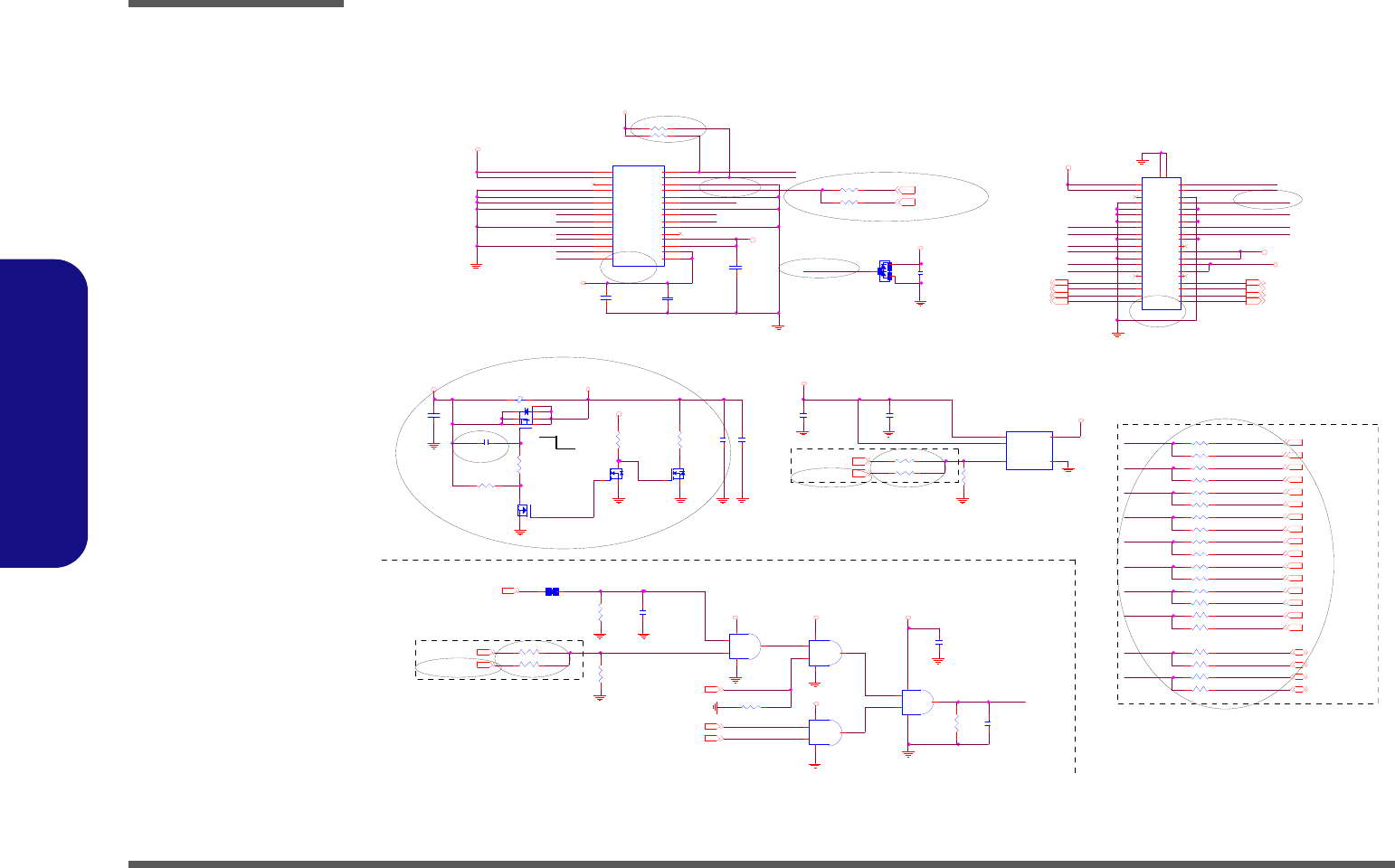
Schematic Diagrams
B - 14 LVDS/ INVERTER
B.Schematic Diagrams
LVDS/ INVERTER
U25C
74LVC08PW
9
10
8
147
R621 0_04
R613 0_04
R390
1 0 0K _0 4
R608 *0_04
R610 *0_04
D23
* BAV 9 9 REC TIFI ER
A
C
AC
C565
0.1u_16V_Y 5V_04
C5 6 6
*0.1u_1 6V_Y5V_ 04
C5 6 7
*0.47u_10V_Y 5V_04
R618 *0_04
R577 4.7K_04
C5 6 3
0.1u_16V_Y5V_04
R616 *0_04
U24
APL3512A
VIN
4
VIN
5
EN
3
VO UT 1
GND 2
3.3V
VIN_ LCD
3.3V
3.3V
3.3V
J_LCD2 Fo r dual ch ann el
J_LCD1 For single channel
3.3VS
PLVDD
3.3VS
PLVDD
3.3VS
3.3V
VIN_ LCD
3. 3 V S
PLVDD
LID _SW #8,20,22
AL L_ SYS_ PW R GD11,20
BRI G HT NE SS 12 ,2 0
BKL_EN20
LV D S - L 1P 3, 1 2
LV D S - L 1N 3 , 1 2
SC L 12
NB_ENAVDD3
TXCLK_LP 12
LV D S - L 0P 3
LV D S - L 0N 3
LV D S - L C L K P 3
LV D S - L 2N 3 , 1 2
TX O U T _L 1 P 1 2
TX O U T _L 0 N 1 2
LV D S - L 2P 3, 1 2
LV D S - L C L K N 3
TX O U T _L 0 P 1 2
TX O U T _L 2 P 1 2
TX O U T _L 2 N 1 2
LVDS_D DC_D ATA 3,12
SD A 12
TX O U T _L 1 N 1 2
TXCLK_LN 12
LVDS_D DC_C LK 3,12
TXOU T_U 0N 12
TXOU T_U 0P 12
TXOU T_U 2N 12
TXOU T_U 2P 12
R LVD S-L2P
C5 590.1u_50V_Y5V_06
C5 6 00.01u_50V_X7R_04
30pin for W24/W25
40pin for W27 3/8
C1 7
0.22u_50V_06
R8 5 8 *0 _ 0 4
2 .2K to 4 .7K 3 /14
R_BRIGHTNESS
R2 3 8
*1 0 K _0 4
S
D
G
Q4 5 B
*M TD N7002ZH S6R
5
34
R2 2 8
*200_1% _04
Q4 9
MTN7002ZH S3 G
DS
S
D
G
Q4 5 A
*MTD N7002ZH S6R
2
61
3. 3 V
Q46
P200 3E VG
4
62
5
73
1
8
.
L1
*0 _ 06
3A
VIN_ LCD
EN AVDD
VIN
1108
LVDS_D ATA
LVDS_C LK
R_BRIGHTNESS
R LVD S-L2N
IN V_B LO N
2A
RLVDS-L1N
RLVDS-L1P
Follow ??? ? 3/7
C18
0.1u_50V_Y5V_06
RLVDS-L0N
RLVDS-L0P
XLT_BL EN12
Default W270BUQ
R9 100K_04
TX O U T _ U 1 N12
TXO UT_U1P12
RLVDS-LCLKP
RLVDS-LCLKN
TXCL K_ UP12
TXCLK_UN12
SB_BLO N8
PANEL CONNECTOR
2A
R LVDS-L 0 P
LV D S _ D A T A
R LVDS-L 1 P
R LVDS-L C LKN RLVD S-L2N
R LVDS-L 1 N
INV_BLON
R LVDS-L 0 N
R LVDS-L C LKP RLVD S-L2 P
LVDS_D DC _D ATA
SD A
R698 *0_04
80mils
LV D S _ D A T A
ED I D Mo d e
L V D S _ D D C _C LK
SC L
LV DS_CLK
LV DS_CLK
ENAVDD
2A
LV D S - L 1 P
TX O U T _L 1 P
G5243A 6-02-05243-9C0
APL3512A 6-02-03512-9C0
PANEL POWER
RL VDS -L1 P
R_ BRI G H TN E SS
TX O U T _L 0 N
XL T _ D I G O N12
LV D S - L 2 N
TX O U T _L 2 N
RL VDS -L2 N
LV D S - L 2 P
TX O U T _L 2 P
LV D S - L 0 N
LV D S - L 0 P
TX O U T _L 0 P
RL VDS -L2 P
RL VDS -L0 P
LV D S - L C L K N
TX C LK _ L N
RL VDS -LC L KN
Mo dify 3/1 1
LV D S - L 1 N
TX O U T _L 1 N
3/10
3/10 3/1 0
RL VDS -L0 N
RL VDS -L1 N
LV D S - L C L K P
TX C LK _ L P
RL VDS -LC L KP
R701 on, R700 off for W270BUQ 3/8
R 699 on , R6 98 o ff fo r W27 0BUQ 3 /8
XL T _ B LO N _ P W M 12
R 699 0_04
R857 0_04
IN V_BLON
BK L_ EN _R
Z1201
BACKLIGHT ENABLE
R5 8 6
1M_04
BLON3R700 *0_04
R 701 0_04
Z1202
Z1203
R611 0_04
R3 9 1 *1 00 K_ 0 4
R602 *0_04
R3 9 2
*1 M_ 0 4
C569
0.1u_16V_Y5V_04
R620 *0_04
U2 5 B
74LVC 08PW
4
5
6
147
R603 0_04
R388 *10mil_short_04
R578 4.7K_04
U2 5 D
74LVC 08PW
12
13 11
147
R606 *0_04
R609 0_04
C564
*0.01u_16V_X7R_04
C5 6 1
0.1u_16V_Y5V_04
R619 0_04
U2 5A
74 L V C 0 8 P W
1
23
147
R387
1 0 0K _0 4
J_LC D1
*87216-3006
1
122
3
344
5
566
7
788
9
910 10
11
11 12 12
13
13 14 14
15
15 16 16
17
17 18 18
19
19 20 20
21
21 22 22
23
23 24 24
25
25 26 26
27
27 28 28
29
29 30 30
C5 6 2
4.7u_6. 3V_X5R_06
R607 0_04
R617 0_04
R615 0_04
R604 *0_04
R614 *0_04
J_ L C D 2
8 72 1 6- 40 0 6
1
3
5
7
9
11
13
15
17
19
21
23
25
27
29
31
33
35
37
39
2
4
6
8
10
12
14
16
18
20
22
24
26
28
30
32
34
36
38
40
Gnd 1 G1
Gn d 2 G2
R389
*100K_04
R605 0_04
F or ANX 31 10 3/10
C568
* 0.1u _16V_ Y5 V_0 4
R612 *0_04
Sheet 13 of 43
LVDS/ INVERTER
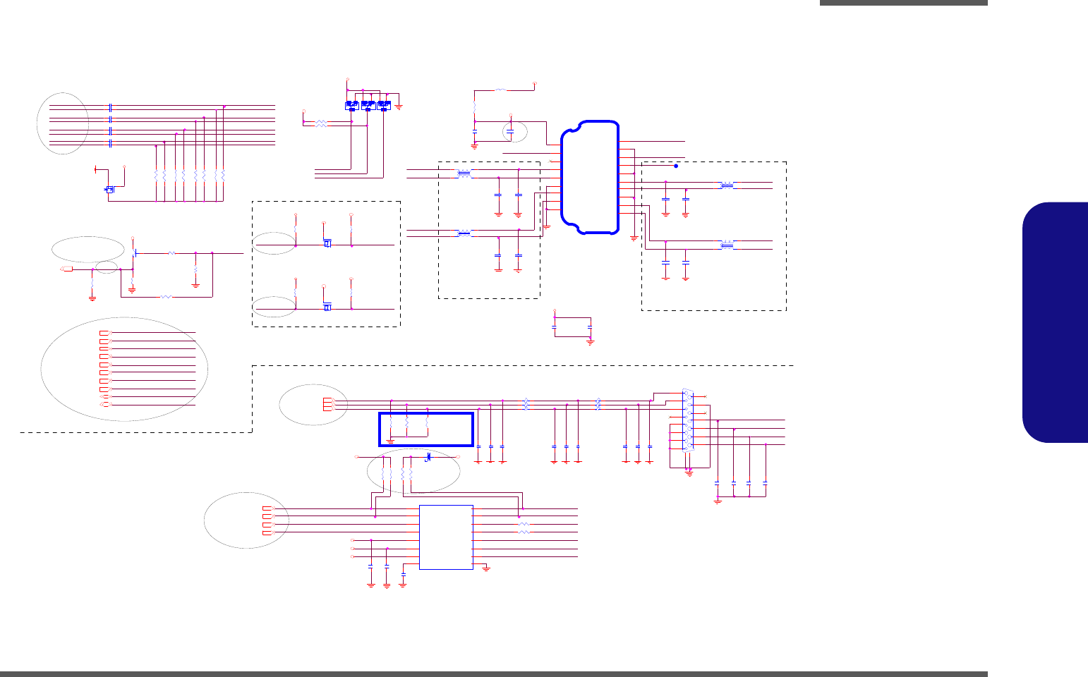
Schematic Diagrams
HDMI/ CRT B - 15
B.Schematic Diagrams
HDMI/ CRT
HDMIB_D2 BP
HDMIB_D2 BN
HDMIB_D1 BN
HDMIB_CL KB N
HDMIB_D0 BP
HDMIB_D1 BP
R7 21 * 0_ 04
HDMIB_CL KB P
CRT PORT
IP4 772 CZ16 6- 02- 477 21- B60
TPD 7S0 19 6-0 2-0 701 9-B 20
DDCL KDAC_ D DCACL K
CRT_ HSY NC
DDCDATA
BLUE
GRN
DAC_ VSY NC
DAC_ H SYNC
VSYNCCRT_ VSYNC
RED
DAC_ D DCADAT A
HSYNC
HDMI_DDC_ DAT A
R720
*100K_04
R65 3 49 9_1 %_ 04
R654 499_1%_04
R4 06
*LV A R 04 02 -24 0E 0R 0 5P - LF
RD1
*BAV99 RECT IFIER
A
C
AC
.
L1 04 F C M 1 00 5MF - 60 0T0 1
C589
0.22u_10V_Y5V_0 4
C 58 2 10 p_ 50 V_ N P O_0 4
Follow ? ? ? ? 3/23
C583 10p_50V_NPO_04
Mo d if y 3 /11
Modify 3/11
Modify 3/11
L10 2
* H D MI 2 01 2F 2S F - 900 T0 4- s ho rt
1
4
2
3
C591
0.2 2u_10V_Y5V_ 04
RD2
* BAV99 RECT IFIER
A
C
AC
R 5 79 2. 2 K_ 04
HDMIB_DATA1P
J_C R T1
10 8A H 15 FS T 04 A1 C C
8
7
6
5
4
3
2
19
10
11
12
13
14
15
GND2
GND1
R 41 5 33 _0 4
R39 8
* LV AR 0 40 2- 2 40 E0 R 05 P- L F
R40 0
* L V AR 0 40 2-2 40E 0 R 05 P- L F
.
L1 03 F C M 1 00 5MF - 60 0T0 1
L9 9
* H D M I 2 01 2F 2S F - 90 0T0 4- s ho r t
1
4
2
3
L1 01
* H D M I 2 01 2F 2S F - 90 0T0 4- s ho r t
1
4
2
3
H D M I B_ E XT 1_S C L
HDMIB_DATA1N
R40 5
* L V AR 0 40 2- 2 40E 0 R 05 P- L F
C57 8
* 0. 1 u_1 6V _ Y 5V _0 4
HDMI PORT
U27
TP D 7S 0 19
VCC_SYNC
1
VCC_VIDEO
2VI D E O _ 1 3
VI D E O _ 2 4
VI D E O _ 3 5
GND 6
VCC_DD C
7
BYP
8
DDC_OUT 1 9
DDC_ IN1
10
DDC_ IN2
11 DDC_OUT 2 12
SYNC_IN1
13 SYNC_OUT 1 14
SYNC_IN2
15 SYNC_OUT 2 16
HDMIB_DATA0P C5 70
10u_10V_Y5V_08
HDMIB_DATA0N
R40 7
* LV AR 0 40 2- 2 40 E0 R 05 P- L F
L10 0
* H D MI 2 012 F 2S F -900T04-short
1
4
2
3
R 41 6 33 _0 4
C586 220p_50V_NPO_04
R3 97
* LV A R 04 02 - 24 0E 0R 0 5P - LF
H D M I B_ E XT 1_ H PD
For ESD
H D M I B_ E XT 1_S D A
C 5 87 22 0p _5 0V _N P O _ 04
R 5 80 2. 2 K_ 04
C 58 5 10 00 p_5 0V _ X7 R _0 4
R4 04
* LV A R 04 02 -240 E 0R 0 5P - LF
.
L1 05 F C M 1 00 5MF - 60 0T0 1
J_HDM I1
C12 81 7-11 9A5 -L
SHIELD2
2
TMDS DATA1+
4
TMDS DATA1-
6
SHIELD0
8TMDS CLOCK+
10 TMDS CLOCK-
12 RESERVED
14
SDA
16
+5 V
18
TMDS DATA2+ 1
TMDS DATA2- 3
SHIELD1 5
TMDS DATA0+ 7
TMDS DATA0- 9
CLK SHIEL D 11
CEC 13
SCL 15
DDC/CEC GND 17
HOT PLUG DETECT 19
L98
1 _04
C571
* 22 u_6 . 3V _X 5R _ 08
C584 10p_50V_NPO_04
C590
0 . 22 u_ 10V _ Y5 V _04
C5 77
0 . 1u _1 6V _Y 5 V_ 04
R3 93
1_04
RD3
* BAV99 RECT IF IER
A
C
AC
R3 95
* LV A R 04 02 - 240 E 0R 0 5P - LF
C 58 8 10 00p _5 0V _X 7 R _0 4
5V S _H D M I
5VS_HDMI
5VS
3.3VS
3.3VS
5V S
3. 3V S
3. 3 V S 5V S
HDMIB_DATA2P
HDMIB_CLOCKP
R 6 47 4 99_ 1% _0 4
HDMIB_DATA2N
HDMIB_CLOCKN
C579 10p_50V_NPO_04
C 58 1 10 p_ 50 V_ N P O_04
R4 14
150_1%_04
C 5 80 1 0p _50 V _N P O _0 4
R41 3
15 0_ 1% _04
R4 12
150_1%_04
DAC_BLU E
DAC_GREEN
DAC_RED
R862 2.2K_04
Modify 3/11
DDCDATA
RED
DDCL K
VSYNC
HSY NC
24 mil
GRN
BLUE
6-20-14X30-015
R860 2 .2K_04
Q2 7
2 N 39 04
B
E C
R658
10K_04
R55 2 00 K _04
R6 57
* 2 00K _ 04
3. 3V S
CLO SE TO HDMI CONN.
HDMI_ DDC_CL K
H D M I B_ E XT 1_S D A
5VS
Q26
MTN 700 2Z H S3
G
DS
R656
2 . 2K _0 4
R65 9
4. 7K _ 04
R65 5
4. 7K _ 04
H D M I B_ E XT 1_S C L
DAC_VSYNC3
3. 3 VS
3. 3 VS
DAC_ HS YNC3
3.3VS
3.3VS
Q28
MTN 700 2Z H S3
G
DS
DAC_BLU E3
DAC _DDCADATA3
5VS
R660
2 . 2K _0 4
DAC_RED3DAC_GREEN3
DAC_ D DCACLK3
HDMI_DDC_ CLK3
HDMIB_ D2BN3
HDMIB_CLKBN3
HDMIB_ D1BN3
HDMIB_ D0BN3
HDMIB_ D2BP3
HDMIB_ D1BP3
HDMIB_CLKBP3
HDMIB_ D0BP3
HD MI_ DDC_DA T A3
HDMIB_ C LKB N
HDMIB_ D 2BN
HDMIB_ D 2BP
HDMIB_ D 1BP
HDMIB_ D 0BN
HDMIB_ C LKB P
HDMIB_ D 1BN
HDMIB_ D 0BP
HDMIB_D0 BN
C865 22p_50V_NPO_04
C 8 67 2 2p_ 50 V _N P O _0 4
C866 22p_50V_NPO_04
C836 0.1u_10V_X7R_04
C829 0.1u_10V_X7R_04
C831 0.1u_10V_X7R_04
C830 0.1u_10V_X7R_04
C833 0.1u_10V_X7R_04
C832 0.1u_10V_X7R_04
C834 0.1u_10V_X7R_04
C835 0.1u_10V_X7R_04
PORT C_HPD3
Modify 3/11
HDMIB_EXT 1_ HPD
3. 3 VS
Q25 MTN7002ZHS3
G
D S
R 64 8 49 9_ 1%_ 04
R 64 9 499 _1 %_ 04
R650 499_1%_04
HDMIB_DA TA0 N
HDMIB_DA TA2 N
FO R EMIFOR EMI
HDMIB_ D ATA1N
HDMIB_EXT 1_ SCL
HD MIB_DATA0P
HDMIB_EX T1 _SDA
HDMIB_EXT 1_ HPD
HDMI_CEC
CD 3/8
HDMIB_ D ATA1P
HDMIB_ C LOCK N
HDMIB_ C LOCK P
HD MIB_DATA2P
5VS_HDMI
R 8 63 2 . 2K _0 4
.
L139 FCM1005MF-600T01
.
L137 FCM1005MF-600T01
.
L138 FCM1005MF-600T01
Del ? ?VGA 3/8
R861 2.2K_04
D el R719 3/11
HDMI_DDC_D ATA
D6 RB 7 51 V
AC
Modify 3/11
R 65 2 49 9_ 1% _04
R 6 51 4 99_ 1% _0 4
HDMI_DDC_ CLK
Sheet 14 of 43
HDMI/ CRT
Schematic Diagrams
B - 16 CCD/ 3G
B.Schematic Diagrams
CCD/ 3G
60 mil s
CCD_EN
Layout Sh ow "3.5G( HSDPA)" Note
From H8 default HI
48 mil
CC D_ DE T#
5
MJ_CCD1
1
CCD
W270BUQ 3G Default Disable
UIM_DATA
M
INI CARD 3G(Port 6)
UIM_VPP
UIM_PWR
UIM_RST
UIM_CLK
Q32
* AO3415
G
DS
C5 9 9
*10u_10V_Y5V_08
S
D
G
Q3 3 A
*R T3K44M
2
61
+
C6 01
*220u_4V_V_B
(T OP VI EW )
LO CK
O PEN
J_SIM1
* C1770661-1
UIM_DATA C7
UIM_VPP C6
UIM_GND C5
UIM_PWR
C1 UIM_RST
C2 UIM_CLK
C3
C5 95
*0.1u_16V_Y 5V_04
C611
0.1u_16V_Y5V_04
C610
1u_6.3V_Y5V_04
C598
*0.1u_16V_Y5V_04
C5 9 2
*0.1u_16V_Y 5V_04
R792
*10_06
C6 02
*22p_50V_N PO_04
R4 2 4
100K_04
C 857 *1u_6.3V_Y5V_04
C6 0 3
*22p_50V _N PO_04
R426 330K_04
C604
* 22p_50V_NPO _04
R4 22
* 1 0m i l _s h or t _0 4
R790 *0_06
L106 *WC M2012F2S-161T03-short
1
4
2
3
J_CCD 1
85205-05001
1
2
3
4
5
+
C593
*220u_4V_V_B
C612
* 1u_6.3V_Y 5V_04
C613
0.1u_16V_Y5V_04
C8 4 6
1u_6.3V_Y 5V_04
R793 * 100K_04
U4 7
*G 5243A
VIN
4
VIN
5
EN
3
VO UT 1
GN D 2
Q1 1
MTN7002ZH S3
G
DS
S
D
G
Q33B
*RT3K44M
5
34
UIM _VPP
R7 8 9 *0_06
C614
1u_ 6.3V_ Y5 V_ 0 4
UIM _C LK UIM _DATA
UIM _ RS T
UIM _ P W R
Q10
MTP3403N 3
G
DS
KEY
J_3G 1
*M P CEC -S 0 0F1 -T P0 0
CO EX1
3
CO EX2
5
CL KREQ #
7
GN D0
9
REFC LK-
11
REFC LK+
13
WAKE#
1
GN D1
15
PETn0
23
PETp0
25
GN D2
21
GN D3
27
PERn0
31
PERp0
33
GN D4
29
Reserved0
17
Reserved1
19
W _D ISABL E# 20
GN D1 2
37
3. 3 V A U X_ 3
39
3. 3 V A U X_ 4
41
GN D1 3
43
Reserved2
45
Reserved3
47
Reserved4
49
Reserved5
51 LE D _ W LA N # 44
LED_WWAN # 42
GND 6 18
UIM _VP P 16
UIM _R ESET 14
3.3VAUX_0 2
UIM _C LK 12
UIM _D A T A 10
UIM_PWR 8
1.5V_0 6
GND 5 4
PERSET# 22
3.3VAUX_1 24
GND 7 26
1.5V_1 28
SM B_C L K 30
SM B_D ATA 32
GND 8 34
USB_D - 36
U SB_D + 38
GND 9 40
L ED_ W PAN # 46
1.5V_2 48
GN D1 0 50
3.3VAUX_2 52
GN D1 1
35
R4 23
100K_04
C605
*22p_50V_NPO_04
C6 0 0
*0.1u_16V_Y5V_04
C596
*10u_10V_Y 5V_08
R4 2 1
*10mil_short_04
C594
*0 .1 u_ 1 6 V _Y 5 V _0 4
R7 9 1
* 2 0 K _1 % _ 04
R 419 *15m il_short_06
R420 *4 .7K _0 4
3G_3.3V
3G_3.3V
3G _ 3. 3 V
5V
3G_3.3V
5V _ C C D
3.3V
3G _3 . 3 V
3.3V_3G
3.3VS
USB_PN 9 8
3G _EN 20
3G _ D E T #20
CCD_DET#20 USB _PP58
USB_ P N58
USB_PP9 8
3G _ P O W E R20
CCD_EN20
SIMLOCK
D avid 8/25
SIM CONN
Layout?
1. SIM????????(10mil)
2. ????????GND
3. SIM hold ? ? ? ? ? GND? ?
4. SIM CONN ? ? MINI CARD
CONN
3A 120mils
From SB GPIO P in default HI
Pow er Plane: Suspend
S3: Defined
AO3409( 90mohm) C hange
to AO3 415(45moh m).
3G POWER
AO3409? ? ?
ADD R128,Q2
So lut ion F or
PD A
BU G-When
Bat te ry
dis char ge to
sh utd ow n,
th e CMOS
so me tim e s
los s.
3 A 12 0 m il s
Valu e m o dify 3/2 3
1A
1A
CCD_EN
60 mils
C868
* 0.1u_16V_Y5V_04
CD 3/8
Sheet 15 of 43
CCD/ 3G
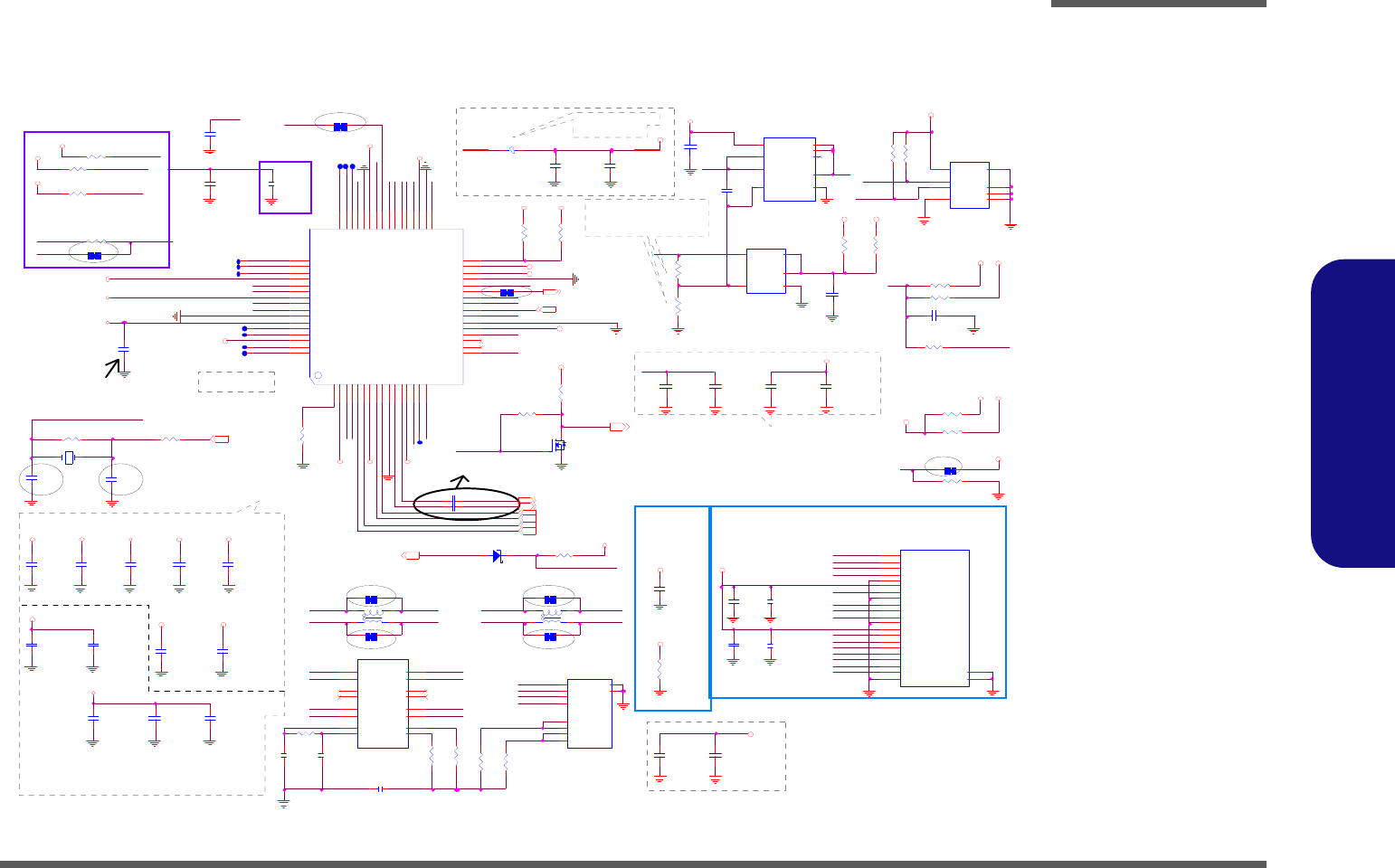
Schematic Diagrams
CARD READER/ LAN JMC261C B - 17
B.Schematic Diagrams
CARD READER/ LAN JMC261C
MLMX0-_R
10 /28 Modify value
SD_CD #
SD_D1
SD_D0
SD_CLK
SD_D2
SD_W P
DVDD
MS _ I N S #
SD_D3
SD_CLK
SD_BS
SD_BS
SD_D3
SD_D1
SD_D0
SD_D2
Ca rd Re ad er
Po we r
4 IN 1 SOCKET SD/MMC/MS/MS Pro
ISON
VD DR EG
Pin#35
SD_D1
6-22-25R00-1B4
6-22-25R00-1B5
near Pin#41
LANXOU T
LANXIN
Pin#52
Pla ce all capacito rs closed t o ch ip.
The su bscript in eac h CAP incica tes t he p in
nu mber of JMC251/JMC261 t hat shou ld b e
closed to.
Pin#55
Pin#43
Pin#62
Pin#43
Pin#21Pin#59 Pin#2
LA N X I N
SD _CLK
LAN _M DIN 2
LAN _M DIN 0
LAN _M DIN 1
LAN _M DIP1
LAN _M DIP0
MDIO8
LAN _M DIP3
LAN _M DIP2
PC Ie D iff er en ti al
Pa ir s = 1 00 O hm
SD _BS
JMC261 C
BU F_P LT_RST#
(>20mil)
MP D
LAN _SC L
CR _ CD1 N
MDIO13
LANX OUT
MDIO7
(>20mil)
ML M X1 +
ML M X1 -MLMX0-
LAN _SD A
LAN _PCIE_W AKE#
MDIO10
Del R 828 3/7
SD_D 0
R 443 * 10m il_short
MPD
SD XC_POW ER
G9141
APL5603-12B(no R201,R198)
LAN_LED1
MDI O1 3
TD_C T
DVD D
MDIO9
MDIO11
REGLX
SD _CD#
REG L X DVDD
S wit ch in g Reg ul at or
c los e to P IN3 3
Pin#33Pin#33
(> 20m il )
(> 20m il )
Fo r J MC 25 1/2 61 o nl y
LDO t ype ? J MC26 1C ,
SD _D 2
MS_INS#
need to close to chip
BU F_PLT_RST#
LAN _M DIN 3
SD XC_POW ER
SD_D3
CR_CD1N
AVDD12_62
RD_CT
De l R58 8 3 /7
LAN _M DIN 0
LAN _M DIP0
ML MX 0 +
ML MX 0 -
DC _N P
DD _N P
ML MX 1 -
ML MX 1 +
W240BU 6-21-B4000-008
RX_ CTRX_ CT
L6 2 NC da vid 8 /25
MLM X1-_R
MLM X0-_R
MLM X0+_R
MLM X1+_R
TX_CT
LAN _M DIN 1
LAN _M DIP1
SD_CLK
Card Reader Pull High/Low
Resistors
LA N _ LE D 0
SD _ W P
SD_CD#
SD _ W P
MS _ I N S # R581
0_06
MLMX0+_R
Pin#13Pin#7
R 4 4 0 * 1 0m i l _s h o r t
SE EDAT
need to close to chip
David 8/27
Pin#32
(> 20m il )
Pin#31
(>20mil)
Pin#32 Pin#31
27 p to 22p 3/9
ML MX 1 -_ R
LA N _ S C L
need to close to chip
P CIE_W AKE#
R643 *1 0m il_short
W251BUQ 6-21-B4040-008
R644 *1 0m il_short
Del R443 3/7
R646 *10m il_short
R645 *10m il_short
VD D_IN
ML MX 1 + _R
Reserved
Pin#7
LA N _ S D A
R8 26 *0 _ 0 4
R825
10K_04
Q7 9
MTN 7002ZHS 3
G
DS
3.3V
JM _D3MO DE 8
JM _D 3 M O D E
R5 8 4
0_06
Pin#59
AP L5 60 3- 12B Ch a nge A X66 10.
MLMX0+
Ra
Vout=0.8(1+Ra/Rb).
Rb
for D3E C991022
CD 3/9
CD 3/9
SEE DAT
De l R44 0 3 /7
R 8 28 *1 0m i l _s h o r t
1.2 V
for AX6 610 , Ra ( 1. 69 K_1 % ) ,
C8 1 6
0.1u_16V_Y5V_04
C800
*0.1u_16V_Y5V_04
R601 *0_04
C489
0.01u_16V_X7R _04
C805
0.1u_16V_Y 5V_04
C8 08
0.1u_16V_Y5 V_04
C8 17
0.1u_16V_Y5V_04
R583 * 0_04
C821
*0.1u_16V_Y5V_04
C8 0 4
10 u _ 10 V _ Y 5 V _ 0 8
L36
P3012
RD+
1
RD-
2RX+ 16
RX- 15
RD_CT
3RX_CT 14
NC
4NC 12
NC
5
TD_C T
6
TD+
7
NC 13
TX- 9
TD-
8
TX_C T 11
TX+ 10
R4 4 7
*0 _ 0 6
(LQFP 64)
JMC261 C
U3 0
JM C 2 6 1 C
REXT
1
AVDD 33
2
XIN
3
XOU T
4
GND
10
LX 33
AVD D12
7
CPPEN 23
CLKN
5
CL KP
6
AVD D12
13
RXP
8
GND 22
TXN
11
TXP
12
PW RCR 30
RSTN 24
WAKEN 27
MP D 28
ISO N 45
LAN_LED2 26
CR_CD1N
16
CR_CD0N 17
RX N
9
MDIO8
51
L AN_ L ED0 47
MDIO7
15
MD IO6 20
GND 44
MDIO5 41
MDIO4 40
MDIO3 39
VD DIO 43
MDIO2 38
MDIO1 37
MDIO0 36
MDIO9
50 MDIO10
49
MD IO1 1 48
MDIO12 19
VD DREG 32
MDIO13
14
MDIO14 18
CR _ LE D 25
TEST 29
V DDIO 21
GND 34
VC C3V 31
FB12 35
LA N _ LE D 1 46
VDDO 42
VD D
52
VIP _1
53
VIN _1
54
AV DD1 2
55
VIP _2
56
VIN _2
57
GND
58
AV DD3 3
59
VIP _3
60
VIN _3
61
AV DD1 2
62
VIP _4
63
VIN _4
64
C647
2.2u_6.3V_X5R _06
C803
*0.1u_16V_Y5V_04
R3 3 4
75_1%_04
C6 4 5
0.1u_16V_Y5V_04
R444 1K_04
R434
*0 _ 06
PJS-08SL3B
J_R J1
DD-
8DD+
7
DB-
6
DC-
5DC+
4
DB+
3DA-
2DA+
1shield GN D1
shield GN D2
U49
AX6 6 10
GN D 1
VC NTL
6
VO UT
3
VIN 5
VO UT
4
VFB
2
POK 7
EN 8
VIN 9
R6 7 7 * 0_ 0 4
C646
* 0.1u_ 16V_Y 5V_04
R4 5 0
*0 _ 04
R4 4 6
*4 .7 K _ 04
C8 5 3
82p_50V_NPO _04
C810
* 10u_6. 3V_X5R_06
R4 3 6 *4 .7 K _0 4
R7 3 6
*7 5_ 1 % _0 4
C6 5 0
10u_10V _Y 5V _08
Rb( 2 .7 K_1 % )
R 433 1K_04
C8 5 2
1u_10V_Y 5V_06
J_C ARD -REV1
MD R019-C 0-1042
DAT 2 _SD
P2
VSS_MS
P21
CD/D AT3_SD
P3
CMD _ SD
P4
VSS_SD
P5
VDD _SD
P6
CL K_ SD
P7
VSS_SD
P8
DAT 0 _SD
P9
DAT 1 _SD
P10
WP_SD
P11
VSS_MS
P12
VCC _M S
P13
SCLK_MS
P14
DAT 3 _M S
P15
INS _ MS
P16
DAT 2 _M S
P17
SDIO /DAT0_M S
P18
DAT 1 _M S
P19
BS_M S
P20
CD_ SD
P1
GND P23
GND P22
R2 69
75_1%_04
C815
0.1u_16V_Y5V_04
C643
*10p_50V_N PO_04
U4 3
*APL5603-12BI-TRG
IN 1
SET
4GN D 2
SHD N# 3
OUT
5
R3 43
75_1%_04
R4 3 2 * 1M _ 04
C652
10u_10V_Y 5V_08
R 588 * 10m il_short
R582 10K_04
C8 0 1
22 p _ 50 V _ N P O _ 04
C 819 0.1u_10V_X7R _04
C813
0.1u_16V_Y5V_04
C854
0.1u_16V_Y5V_04
D4 5
RB7 5 1V
A C
R 438 *10K_04
C812
* 0.1u_10V_X7R _ 04
C820
0.1u_16V_Y5V_04
R 445 10K_04
R3 4 8
75_1%_04
C620 1000p_2KV_X7R_12_H 125
C8 0 7
0.1u_16V_Y 5V_04
C799
*10u_ 10V_Y5V_08
C806
0.1u_16V_Y5V_04
C649 0.1u_16V_Y5V_04
C8 0 9
0 . 1u _ 1 6V _Y 5V _0 4
.
L62
*S W F2520CF-4R7M -M
R 441 *0_06R4 3 5
12K_1%_04
L131
*WC M2012F2S-161T03
1
4
2
3
C8 39
10u_10V_Y5V_08
R4 3 7
*4.7K_04
L132
*WC M2012F2S-161T03
1
4
2
3
C619
*0.01u_16V_X7R _04
C 811 0.1u_10V_X7R _04
C6 5 1
0.1u_16V_Y 5V_04
R5 8 5
2.7K_1%_04
R 729 *0_06
C644
10u_10V_Y5V_08
C814
0.1u_16V_Y5V_04
C6 4 8
1u_6.3V_Y5V_04
R 589 *4.7K_04
C818
0.1u_16V_Y5V_04
R4 4 2
1.69K_1%_04
U31
*A T 2 4C 0 2B N
SCL
6
A0 1
A1 2
A2 3
WP 7
SDA
5
VCC
8
GND
4
X8
FS X5L_25MH Z
12
C802
22 p _ 50 V _ N P O _ 04
DVDD
3. 3 V _ L A N
DVDD
DVD D
3.3V_LA N
3.3V_LAN
DVDD
3.3V_LAN
3.3VS
VC C_CAR D
3.3VS
3.3V_LA N
DVD D
DVD D
DVD D
VCC_CARD
VD D_IN
VDD 3 3.3V
DVD DDVD D
3 . 3V _L A N
3.3V_LAN
VCC _ CARD
3.3V_LAN
VC C_ CAR D
DVDD
3. 3 V S
5V
3.3V_LAN
VD D33.3V
3.3V
3. 3 V S VD D3
3.3V_LAN
VD D3
VDD 3
3.3V_LAN
DV DDDVDD
DVDDDV D D
B U F _P L T _ R S T # 7, 11 , 1 7 , 19 , 2 0
PC IE_ W AKE#8,17,19
VC C_ CAR D
PCIE _TXN0_ JM C 7
PCIE_ RXN 0_ J MC 7
PCIE _TXP0_JMC 7
LAN_PCIE _W AK E# 20
C LK_ PC IE_JM C# 7
CLK_PCIE_JMC 7
PCIE_ RXP0_JM C 7
JMC_25M_I N 7
VD DR EG
10 /21
need to close to chip
Fo r JM C2 51 C
Pin#2Pin#2
ISO N
Sheet 16 of 43
CARD READER/
LAN JMC261C
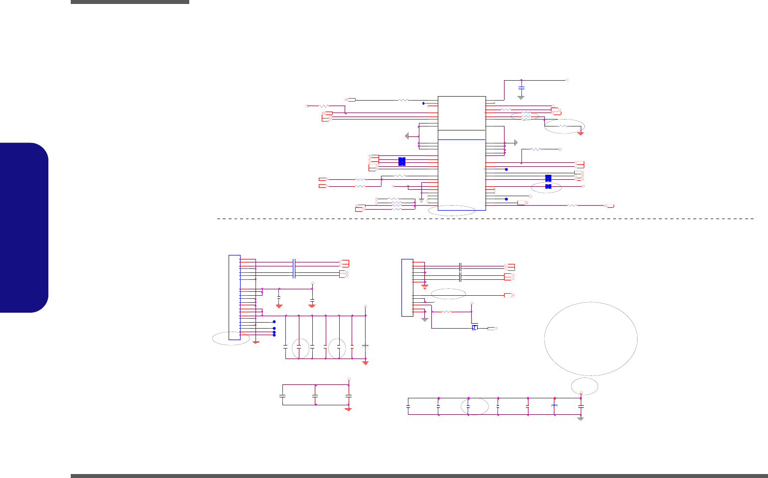
Schematic Diagrams
B - 18 MINI PCIE/ SATA HDD/ ODD
B.Schematic Diagrams
MINI PCIE/ SATA HDD/ ODD
CD 3 /8
ODD _ DE T E CT #
SATA_ TXP0
SATA_ TXN 0
HDD_NC1
HDD_NC2
HDD_NC3
HDD_NC0
SATA HDD
SATA _TXN1
SATA_RXN1
SATA _TXP1
SATA _R XP1
PIN GND1~ 2=GND
SATA ODD
Del R7 02 3/7
W25/W27 6-20-43750-022
Chan ge 3/1 8
CD 3 /8
W24 6-20-43730-122
20 mil
20 mil
Value modify 3/23
SATA_ RXN 0
R7 27
*15mil_ sho rt_06
SATA_ RXP0
WLAN _CLKREQ #
PCIE _W AK E#
3. 3 V A U X_ 1
BUF_PLT_ R ST#
20 mil
Port 2
20 m il
L ayou t Sh ow "WLAN(Wim ax, 80 2.11N) " Not e
R494 * 10K_04
SATATXN0 9
SATATXP0 9
SATARXN0 9
SATARXP0 9
SATATXP1 9
S ATAR XP1 9
SATARXN1 9
SATATXN1 9
3IN1
C655 0.01u_16V_X7R _04
R4 5 2 *0 _ 04
R454 *0_04
C672 *0.1u_16V_Y5V_04
+
C 670 220u_6.3V_6.6*5.7
R456 * 10K_04
J_OD D1
C18553-11305-L
S1
S2
S3
S4
S5
S6
S7
P1
P2
P3
P4
P5
P6
KEY
J_MIN I1
MPCEC-S00F1-TP00
CO EX1
3
CO EX2
5
CLKR EQ#
7
GN D0
9
REF CLK-
11
REF CLK+
13
W AKE#
1
GN D1
15
PETn0
23
PETp0
25
GN D2
21
GN D3
27
PER n0
31
PER p0
33
GN D4
29
Re s erv ed 0
17
Re s erv ed 1
19
W _ DISABL E# 20
GN D1 2
37
3.3V AUX_3
39
3.3V AUX_4
41
GN D1 3
43
Re s erv ed 2
45
Re s erv ed 3
47
Re s erv ed 4
49
Re s erv ed 5
51 LED_WLAN# 44
LE D _W W A N # 42
GN D6 18
U IM_ VPP 16
UIM _RESET 14
3. 3 V A U X_ 0 2
UIM_CLK 12
UIM _ DA TA 10
UIM _PW R 8
1.5V_0 6
GN D5 4
PERSET# 22
3. 3 V A U X_ 1 24
GN D7 26
1.5V_1 28
SM B_CLK 30
SM B_DATA 32
GN D8 34
USB_D- 36
USB_D+ 38
GN D9 40
LED _ W PAN# 46
1.5V_2 48
GND10 50
3. 3 V A U X_ 2 52
GN D1 1
35
C653 0.01u_16V_X7R _04
R7 2 2 *1 00 K _ 0 4
C675 *22u_6.3V_X5R _08
R451 10K_04
C656 0.01u_16V_X7R _04
R4 5 8 0_ 0 4
C 674 1u_6.3V_Y5V_04
C6 6 5
*0.1u_16V_Y 5V_04
Q7* MTN7002 ZH S3
G
DS
C 673 0.1u_16V_Y5V _04
C662
* 10u _ 10V_ Y5 V_ 08
C6 6 6
1u_6.3V_Y 5V_04
J_HD D1
1-162- 100561
S1
S2
S3
S4
S5
S6
S7
P1
P2
P3
P4
P5
P6
P7
P8
P9
P10
P11
P12
P13
P14
P15
C669
* 0. 1u_ 16 V_ Y5 V_ 04
C671 0. 1u_16V_Y5V_04
3/7
C654 0.01u_16V_X7R _04
C677
0.01u_16V_X7R_04
R 723 *10mil_short
R726 *10mil_short
R725 *10mil_short
R 724 *10mil_short
C6 7 8
0.01u_16V_X7R _04
+
C6 6 8 * 2 2 0u _ 6. 3V _ 6 . 6 * 5 . 7
C659 0.01u_16V_X7R _04
C6 63
*0.1u_16V_Y 5V_04
C658 0.01u_16V_X7R _04
C847
0.1u_16V_Y 5V _04
R4 5 7 * 0_ 0 4
C657 0.01u_16V_X7R _04
R453
*10K_04
C661
*0.01u_16V_X7R_04
C667
10u_10V_Y 5V_0 8
R738 *0_04
C679
0.01u_16V_X7R_04
C660 0.01u_16V_X7R _04
C664
0.1u_16V_Y5V_04
C676 22u_6.3V_X5R_08
R706 *10K_04
R 739 *0_04
5VS
5VS
3.3VS
5V S
3. 3 V S
5VS
3.3V
3. 3V
3.3VS
3.3VS
3. 3 V
3.3V
VDD 3
3.3V
ODD_DA#_FCH 8
ODD_DETECT# 8
BT_ EN20,21
BT_O N 7 ,21
WLA N_DET#20
CLK_ PCIE_W L AN#7W L A N _C LK R E Q#8
BT_DET# 20,21
US B_PN 2 8
CLK_ PCIE_W L AN7
WLAN _LED # 20,21
US B_P P 2 8
WLAN_EN 20,21
BU F_PLT_RST# 7,11,16,19,20
PCIE _WAK E#8,16,19
80C LK 20
PCIE_ RXN 3_ W LAN7
PCIE_ TXN 3 _W LAN7
PC IE_ TXP3 _W LA N7
BT_ EN20,21
3IN120
BT_ O N7,21
PC IE_ RXP3 _W L AN7
80CLK 20
3IN1R5 0 8 0_ 0 4
R7 22 off, a dd R 459 pu ll low r es erve 3/22
R4 9 6 0_ 0 4
R 4 55 *1 0 K _0 4
Del R7 05 3/7
0 -> Sh ort 3/22
R509 *0_04
R 459 *20K_04
CD 3 /8
MINI CARD (WLAN,Port 5)
VD D3
Sheet 17 of 43
MINI PCIE/ SATA
HDD/ ODD
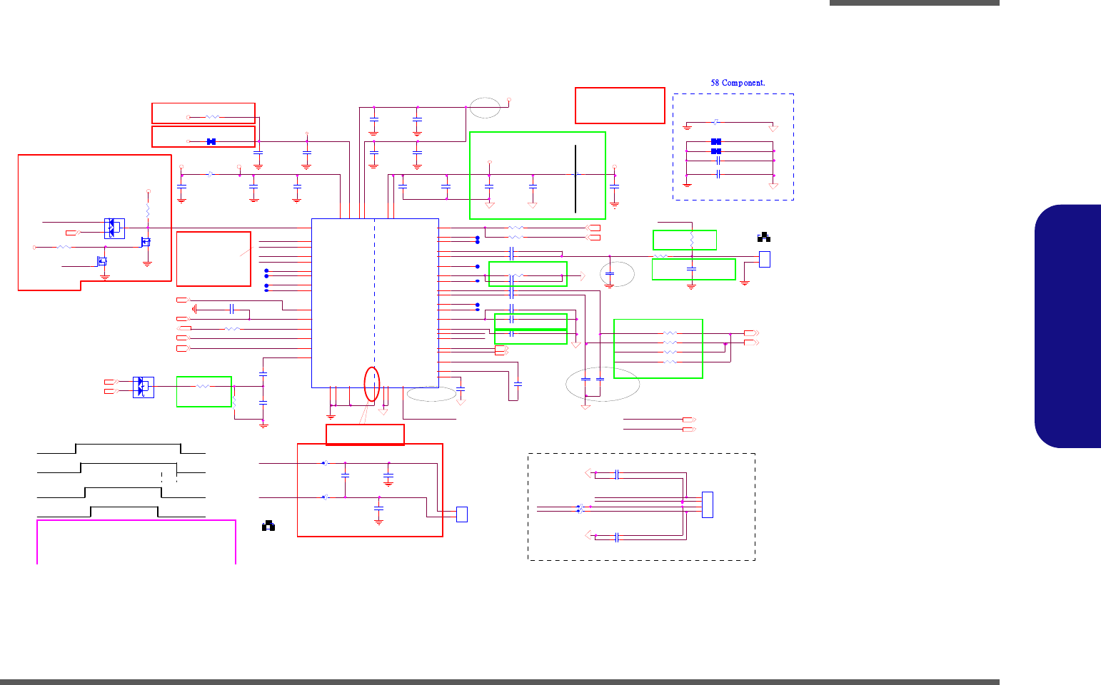
Schematic Diagrams
AUDIO CODEC ALC269 B - 19
B.Schematic Diagrams
AUDIO CODEC ALC269
Sheet 18 of 43
AUDIO CODEC
ALC269
PD#
Add 3/22
AUD G
SPKOU TR-
SPKOU TR+
C785
* 22n_16V_X7R_04
F or Mic n ois e is su e ( Res rve) 3/1 1
L109 *H CB1005KF-121T20
1 2
R464 39.2K_1% _04
C691
0.1u_16V_Y5V_04
R468 20K_1%_04
R461 *10m il_short
C712
*180p_50V_N PO_04
R465
4.7K_04
L111
H CB1005KF -121T20
1 2
R460 * 0_04
C694
10u_10V_Y5V_08
R476 2.2K_04
J _ INT M IC1
88266-02001
PCB F ootprint = 88266-2L
1
2
C692
10u_10V_Y 5V_08
JP1 *10mil_short
C689
10u_10V_Y5V_08
C706
1u_6.3V _Y 5V_04
C704 2.2u_6.3V_X5R _06
C
A
A
D28
BAT5 4 CW G H
1
23
C690
0.1u_16V_Y5V_04
C 686 0. 1u_16V_Y 5V_04
R466 * 100K_04
R463 20K_1%_04
L110
H CB1005K F-121T20
1 2
C710
* 1u_10V _Y 5V_06
R472 1K_04
C685
*0.1u_16V_Y5V_04
C6 8 3
0.1u_16V_Y5V_04
C707
2.2u_6.3V_X5R_06
C696 4.7u_6.3V_X5R _06
R474 1K_04
L112
* FCM 1608K-121T06_short
C697 4.7u_6.3V_X5R _06
R 471 22_04
C711
*180p_50V_N PO_04
Q13
* MTN7002Z HS3
G
DS
C 702 22p_50V_NPO _04
C680
10u_10V_Y5V_08
DIGITAL ANALOG
U32
ALC269Q-VB6
DVD D1 1
GP IO0 -DM IC-D A T
2
GP IO1 -DM IC-C L K
3
PD #
4
SD ATA- OUT
5
BIT-CLK
6
DVS S2
7
SD ATA- IN
8
DVD D-IO 9
SY NC
10
RE SET#
11
PC BEEP
12
S ense A 13
LINE2-L 14
LINE2-R 15
MIC2-L 16
MIC2 -R 17
S ense-B 18
JDR EF 19
MONO-OUT 20
MIC1-L 21
MIC1 -R 22
LINE1-L 23
LINE1-R 24
A VSS1
26
VR EF 27
LD O _ C A P 28
MI C 2- V RE F O 29
M IC 1 -V R E F O-R 30
MIC 1 -V RE F O -L
31
HP-O UT-L 32
AVSS2
37
OPV EE 34
CBN 35
CBP 36
HP -OUT-R 33
PVD D1 39
SPK-L +
40
SPK-L -
41
PVSS1
42
PV SS2
43
SPK-R +
45 SPK-R -
44
PVDD2 46
SPD IFC2/EAPD
47
SPD IFO
48
AVDD2 38
AVD D1 25
GND
49
C688
0.1u_16V _Y 5V_04
C699 * 100p_50V_NPO _04
C698
680p_50V _X7R_04
C 687 0. 1u_16V_Y 5V_04
R478
4.7K_04
R475 2.2K_04
R467 1K_04
C709
100p_50V_NPO _04
C684
* 10u_10V_Y 5V_08
C681
0.1u_16V_Y5V_04
C693
0.1u_16V_Y 5V_04
L113
* FCM 1608K-121T06_short
R 477 47K_04
JP2 *10mil_short
R462
10K_04
C703 0.1u_16V_Y5V_04
C695
1u_6.3V_Y5V_04
C705 10u_10V_Y5V_08
C700 4.7u_6.3V_X5R _06
C701 4.7u_6.3V_X5R _06
C682
10u_10V_Y 5V_08
Q12
*BSS138_N L
G
DS
J_SPKL1
85204-02001
PCB Footprint = 85204-02R
1
2
5V S
DVD D_ IO
5VS
C708
2.2u_6.3V_X5R _06
A UDG
5VS
5VS
A UDG
3.3VS_AU D
AU DG
AU DG
3.3VS_AUD
AU DG
1. 5V S
3.3VS
AU DG
5VS_A UD
AUD G
AUD G
HDA _SP KR8
HEADPHONE-L 22
KBC _M UTE#20
HDA_SYNC8
HD A_R ST#8
HDA _SD IN08
HEADPHONE-R 22
KBC_BEEP20
M IC_SEN SE 2 2
HDA_BITCLK8
HDA_SDOUT8
HP_SEN SE 22
MIC 1-R M 2 2
MIC 1 -L M 2 2
SPKO UTR- 22
SPKO UTR+ 22
Value modify 3/23
C786
* 22n_16V_X7R_04
For 3.3V HDA Li nk.
L135 * FCM 1608K-121T06_short
L136 * FCM 1608K-121T06_short
Sp ea k er 8 o h m- --- -- > 20 m il s
VT1802P 10u
VT1802P
SPKO UT R+, R-, L +, L - Tr a ce wi d th
2
AZ_ RST#
AZ_RST# For 3.3V
HDA Li nk D e-pop
AUDIO CODEC
1
VT1802P
L75,C718 ? ? ?
Layout note:
Sp ea k er 4 o h m- --- -- > 40 m il s
9/8
C92
* 0.022u_16V_X7R _04
For 1.5V HDA Link.
FOR VOLUMN
ADJUST
5VS
20ms
DIG IT AL
EMI Require
GN D a nd AUDG space is
60 mil s ~ 100 mi ls
INT _ MIC _ OU T
Speaker wire length less than 8000mils , It don't need LC Filter.
PD#
MI C 2- V RE F O
PC BEEP
3.3V S_AUD
SPDI FO
CO DEC _ GPIO 0
CO DEC _ GPIO 1
EAPD
ALC269 VB
HDA_RST#
AZ _SD IN0_R
BE EP_R
Thermal Pad place 9
Via hole.
MI C 2- V RE F O
MI C 1- V RE F O - R
SPKOUTL-
SPKO UTL+
CO DEC _C BN
HEAD PHO NE- L
HEAD PHO NE- R
VT1802P NC PIN
LI NE1_L
MIC 1_ R _C
LI NE1_R
MIC 1_L_C
MO NO _O UT
SENS E_B
MIC 1-R
M IC1 -VRE FO-R
M IC1 -VRE FO-L
AN ALOG
LI NE2_R
MIC 2_ L
LI NE2_L
MIC 2_ R
SPKO UTL+_L
MI C_ S ENSE
HP _SE NSE
Please Let LC Filter
together and close to
Codec.IF Speaker
w i re le ngth is le ss
t h an 80 00m ils It d on't
need the LC Filter.
BEEP
J_SPK1
SPKO UTL-
SPKO UT R+
SPKO UTL+
SPKO UT R-
EMI Requ ire
AZ _RST # F or 1. 5V
HDA Link De -pop
PD# Control
VT1802P 5.1K_1%_04
De l R45 9 3 /7
M IC1 -VRE FO-L
AUD G
SPKOU TL-_L
AUD G
PN: 6-20- 43130- 104
C236 *180p_50V_NPO _04
C237 *180p_50V_NPO _04
C239 *180p_50V_NPO _04
C246 *180p_50V_NPO _04
J_SPK1
* 85204-04001
1
2
3
4
SPK OUTR +_R
C
A
A
D3 3
BAT54AW G H
1
23
BEE P_C
CO DEC _V REF
SP KOU TL-_L
HD A_ RS T#
SENS E_A
M IC1-L_M
MIC1-R_M
SPKO UTR+
HDA_RST#
SPK OUTR -_R
SPKOU TL+_L
VT1802P 75_1%_04
VT1802P 4.7K_1%_04
Reserve
LD O _ C A P
JD R E F
12
J_INTMIC1
VT1802P
2.2K_04
VT1802P
330P
INT _ MIC
SPKO UTR-
MIC1-L
CO DEC _C BP
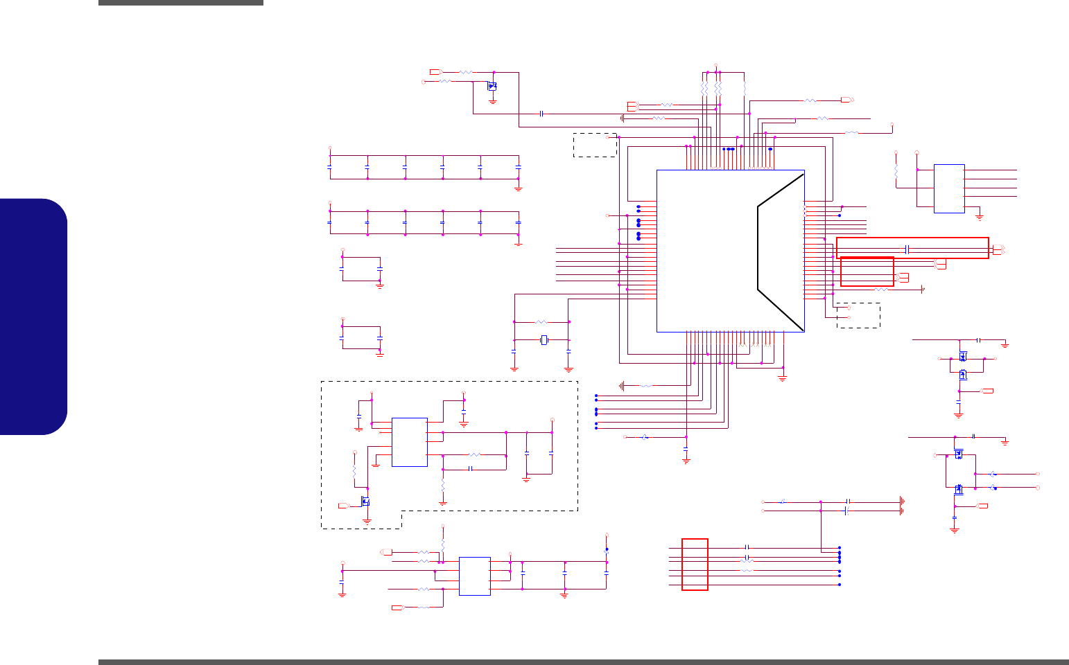
Schematic Diagrams
B - 20 USB 3.0 VL800
B.Schematic Diagrams
USB 3.0 VL800
Sheet 19 of 43
USB 3.0 VL800
Cl os e t o U2Diff. trace 100ohm
( No s tuf fed )
( No s tuf fed )
( No stuffed )
( No stuffed )
1. 5 V
3.3V
Q7 7
*MT N 7 00 2Z H S 3
G
DS
SU SB #8,11,12,20,23
R8 04
*1 0K _ 04
PC5
* 10u_6.3V_X5R_06
VFB
LDO_1.05V
Ra
PN: 6-02-06610-320
PN: 6-13-11311-28C
Core
power
1A
Vout=0.8(1+Ra/Rb)
Rb
P R 1 * 1 K _1 %_ 04
PC3
*0.1u_ 16 V_Y5V_04
PC 1
*1u _1 0 V_ 0 6
U35
*AX6610
GND
1
VCN TL 6
VOUT 3
VIN
5
VOUT 4
VFB 2
POK
7
EN
8
VIN
9
PC2
* 10u_6.3V_X5R_06
PR2
* 3 . 9K _ 1% _0 4
1. 0 5V S
PC4 *82p _50V_NPO_04
3. 3 V
( No stu ffe d )
RXN 0
RXP1
SPISO
SPISI
TX N 0
RXN1
CLK_PCIE_USB#
SSXO
SPISCS#
G_ OC_R
SPISCLK
TXP1
PCIE_N B_ USB30_TXP
G_D P 0
PCIE_N B_ USB30_TXN
G_ OC
SPISCLK
SPISCS#
G_ DP 1
TXP0
SSXI
RXP0
SPISI
GPCIE_R XP2_USB3_R
G_D M0
PCIE_W AKE#
SPISO
TXN1
GPCIE_R XN2 _ US B3 _ R
G_ OC_R
G_ DM1
CLK_PCIE_USB
USB_ON1#
BUF_PLT_ RST#_ R
6-04- 25512- B72
Dif f. trace 100ohm
To EC IT 8518 Pi n84
CPPE#
G_ OC
USB_O N1#
100 MIL
From EC IT8518 Pin83
CPPE#
CPPE#
From EC IT8 518 Pin 83
C861 * 1u_10V_06
R 4 87 * 1 0K _ 04
R48110K_04
Q3 8 *AO3 41 5
G
DS
C714
*0 .1 u _1 6V _ Y 5V _ 04
R4 88
*1 0K _ 04
R4 99 * 0_ 04
R4 93 *0 _0 4
C72 7 * 0.1 u_ 10 V_X 7R _0 4
R4 95
*1 0K _ 1% _0 4
Q3 7 *AO3 41 5
G
DS
R4 84 * 0_ 04
C733
*0.1u_16V_Y5V_04
C7 22
*0 .1u_16V_Y5V_0 4
R7 94 *10 K_0 4
C7 16
*0 .1u_16V_Y5V_0 4
C736
*0.1u_16V_Y5V_04
R4 98 * 0_ 04
R796 *0_04
X9
*X8A025000FG 1H_25MHz
12
C859
*0.1u_16V_Y5V_04
L134 *HCB1608KF-121T25
R4 86 *0 _0 4
R490
*1M_04
VL800 4PORT
VL801 2PORT
U3 4
*V L800 / VL801 QFN88
VS U S U SB
1
SSR EXT
2
VCCA33 SSM
3
SSTX3+
4
SSTX3-
5
VCCA10SSRX3
6
SSRX3+
7
SSRX3-
8
VC CA33SS3
9
USBHP3+
10
USBHP3-
11
VCCA33SS3
12
GND
13
SSTX4+
14
SSTX4-
15
VCC A10SSRX4
16
SSRX4+
17
SS R X 4 -
18
VCCA33 SS4
19
USBHP4+
20
USBHP4-
21
VCCA33SS4
22
VDD 23
VCCA3 3REG2 5 24
P E XR EX T 25
VCCA3 3REG1 2 26
PEXC LK+ 27
PEXCL K- 28
VCC A33 PEXRX 29
PEXRX0 + 30
PEXR X0 - 31
VCCA3 3PEXM 32
P E XT X0 + 33
PEXTX0- 34
VCCA33PEXTX 35
VDD 36
SPICS# 37
SPISCLK 38
SPISI 39
SPISO 40
USB HPE4 # 41
USB HPE3 # 42
USB HPE2 # 43
VSU S3 3 44
SSXO
88 SSXI
87 VC CA10SSM
86 VC CA33SS2
85 USBHP2-
84 USBHP2+
83 VC CA33SS2
82 SSRX2-
81 SSRX2+
80 VC CA10SSR X2
79 SSTX2 -
78 SSTX2 +
77 VC CA33SS1
76 USBHP1-
75 USBHP1+
74 VC CA33SS1
73 SSRX1-
72 SSRX1+
71 VC CA10SSR X1
70 SSTX1 -
69 SSTX1 +
68 VD D
67
VD D 66
VDD 65
VSUS33 64
TESTEN 63
SMD AT 62
SMC LK 61
PEXRST# 60
PEXW AKE# 59
SM I# 58
JT A G T M S 57
JT A G T D O 56
JT A G T D I 55
VSUS33 54
VDD 53
JTAGCK 52
COREPWRDN# 51
USBHOC1# 50
USBH OC2 # 49
USBHOC3 # 48
USBHOC4 # 47
USBHPE1# 46
VSUS33 45
G1
G1
R4 82
*1 0K _ 04
C 8 58 * 1 u_ 10 V _0 6
R4 97 *0_04
C86 4
*1u _ 10 V _0 6
C739
* 1 0u _6 . 3 V_ X 5R _ 06
C731 *0.1u_16V_Y5V_04
U3 6
* R T9 71 5B G S
VOUT1 6
VOUT3 8
VIN2
3
VIN1
2VOUT2 7
GND 1
EN#
4
FLG#
5
C863 *1u_10V_06
C7 24
*0.1u_16V_Y5V_04
C71 3
*0.1u _16V_Y5V_04
C725
*0.1u_16V_Y5V_04
C7 23
*0.1u _16V_Y5 V_04
C7 34 *0 .1u_10V_X7R_04
C72 8 * 0.1 u_ 10 V_X 7R _0 4
C73 0
*20p_50V_NPO_04
U3 3
* M X 25 L 51 2M C - 12 G
CE# 1
SO 2
WP#
3
VS S 4
SI 5
SCK 6
HOLD#
7
VDD
8
R795 *100K_04
C7 35 *0 .1u_10V_X7R_04
R4 9 1 *6 .04 K _1 %_ 04
C8 60
*0.1u _16V_Y5V_04
C7 17
*0.1u _16V_Y5 V_04
R4 8 0*1 0 K_ 0 4 R4 79*1 0K _ 04
Q3 6 *AO3 41 5
G
DS
L133 *HCB1608KF-121T25
R4 89 *3.0 1 K_ 1 %_ 04
.
L114 *HCB 1 60 8K F -1 21 T2 5
+
C 7 32 * 22 0 u_ 6. 3 V _6 . 6* 5 . 7
C71 9
*0.1u _16V_Y5V_04
C737
* 0.1u_16V_Y 5V_04
R48 3
*10 K _0 4
C7 26
*0.1u _16V_Y5V_04
C7 21
*0.1u_16V_Y5V_04
C7 18
*0.1u_16V_Y5V_04
R4 92 *0 _0 4
Q3 4
*AO3415
G
D S
C86 2
* 1 u_ 10 V _0 6
R48 5 * 4.7 K_ 0 4
L115 *HCB 1 60 8K F -1 21 T2 5
C720
*0 .1 u _1 6V _ Y 5V _ 04
C729
* 2 0p _5 0V _ N P O _ 04
C7 15
*0.1u_16V_Y5V_04
R5 00 *0_04
GL1
* HCB1608KF-121T25
C738
*10 u _6 .3V _ X5 R _0 6
Q3 5 *AO3 41 5
G
DS
1.05VS
GN D
3.3V
GND
GND
GND
1.05VD
GN D
GND
3. 3 V S _V L 80 1
3.3VS_VL801
GND
3. 3 V
GND
1. 0 5V A
3. 3 V
3.3V
GND
1. 0 5V D
GND
3.3V
GND
3.3V
GND
GND
5V
G_ US BVC C
1.05VA
3.3VS_VL801
USBVCC
3. 3 V
GN DGND
USBVCC
GND
GND
1. 0 5V S
GND
GND
1. 0 5V A
USBVCC1
GND
1. 0 5V D
3. 3 VS 3.3VS_ VL801
PCIE_NB_USB30_ TXP 7
EC _S M I #8,20
PCIE_WAKE#8, 1 6, 1 7
GND
P C I E _ U S B 30 _C LK N 7
PCIE_USB30_NB_RXP 7
P C I E _ U S B 30 _C LK P 7
BU F_PLT_RST#7, 1 1 ,16,17,20
PCIE_NB_USB30_ TXN 7
PCIE_USB30_NB_RXN 7
USB30_PW R_EN8
USB_OCP0_1#8, 2 2
ICPPE# 20
OCPPE# 2 0
OCPPE# 20
G_D P0 _ 0
RXN0
G_DM 0
RXP0
TX N 0
TX P 0
Port 1+USB 3.0
TX P 0_ R
TX N 0 _R
G_D M0_ 0
( No s tuf fed )
G_DP0
Diff. t race 90ohm
CLO SE TO CONNE CTOR
100mil
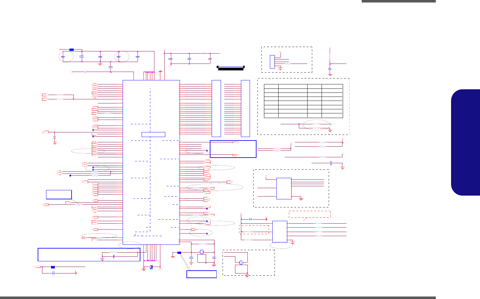
Schematic Diagrams
KBC-ITE IT8518 B - 21
B.Schematic Diagrams
KBC-ITE IT8518
Sheet 20 of 43
KBC-ITE IT8518
W 24 D0 3
Value modify 3/23
K BC_ W RE SET#
3/1 6
Mo dify 3 /17
W 27 D0 1
6-22-32R76-0BG
6-22-32R76-0B2
W 27 D0 1
M odify 3 /16
EC_VCC
WLAN_LED#
W 27 D0 1
60 K / 10K
CK3 2 K
C o- lay ou t X2 , X 3
CK3 2 KE
20K / 1 0K
Mod ify 3/1 7
10K / 2 0K
0. 47 V
Del ? ? VGA 3/8
1. 1V
2. 2V
R808 2.2K_04
For charger 3/17
( BEEP )
F or c har ge r 3 /17
SMD _BAT
SMC _BAT
R506 10K_04
R 507 * 10K_04
.
L118
H C B 1 00 5 K F - 1 2 1T 2 0
R528 1K_04
R502
100K_04
C856
0.1u_16V_Y 5V_04
C7 4 2
10u_10V _Y 5V_08
R532 4.7K_04
C7 54
*12p_50V _N PO_04
R 501 *15m il_short_06
J _ KB1
85201-24051
24
23
22
14
12
11
21
8
20
19
6
5
18
4
17
10
9
7
3
2
1
16
15
13
C753 0.1u_16V_Y 5V_04
R5 3 3 * 0_ 0 4
R 530 47_04
R535 * 10m il_s hort_04
C 751 1u_6.3V_X5R_04
R503 2.49K_1%_04
K/B MATRIX
FLASH
LPC
SMBUS
PS/2
PWM
UART
DAC
CLOCK
IT8518
CIR
ADC
WAKE UP
PWM/COUNTER
LPC/WAKE UP
EXT GPIO
GP INTERRUPT
WAKE UP
GPIO
U38
IT8 5 18E VER :C
WR ST#
14
LPCC LK
13
LAD0
10
LAD1
9
LAD2
8
LAD3
7
LFRAM E#
6
( PD )L PC PD# /W U I6/G PE6 17
SER IRQ
5
EC SMI#/GP D4( PU )
15 EC SCI#/GP D3( PU )
23
G A20/G PB5
12 6
KBR ST#/G PB6( PU )
4
KSI0/STB# 58
KS I1/A F D# 59
KSI2/INIT# 60
KSI3/SLIN# 61
KSI4 62
KSI5 63
KSI6 64
KSI7 65
KSO 0/ PD0 36
KSO 1/ PD1 37
KSO 2/ PD2 38
KSO 3/ PD3 39
KSO 4/ PD4 40
KSO 5/ PD5 41
KSO 6/ PD6 42
KSO 7/ PD7 43
KSO 8/A CK# 44
KSO 9/BUSY 45
K SO10/PE 46
KSO 11/ER R# 51
KSO12 /SL CT 52
KSO13 53
KSO14 54
KSO15 55
VC C 11
VSTBY 26
VST BY 50
VSTBY 92
VST BY 114
VST BY 127
VSTBY 121
VBAT 3
AVCC 74
PS2CLK0/G PF0( PU )
85
PS2DA T0/G PF1( PU )
86
PS2CLK1/G PF2( PU )
87
( PD )TMR I0 /W UI2/G PC4 120
( PD )TMR I1 /W UI3/G PC6 124
L PCR ST#/W UI4 /GPD 2 ( PU )
22
( PD )W U I5/G PE5 35
PWR SW/GP E4( P U )
12 5
R I 1# / W U I 0/ G P D 0 ( P U )
18
R I 2# / W U I 1/ G P D 1 ( P U )
21
( PD )R ING # /PW RFAI L# /L PCR ST#/G PB7 112
TXD/GP B1( PU )
10 9 RXD /GPB0( PU )
10 8
( PD )C T X/G PB2 123
PS2DA T1/G PF3( PU )
88
PS2CLK2/G PF4( PU )
89
PS2DA T2/G PF5( PU )
90
( PD )TAC H0/G PD6 47
( PD )TAC H1/G PD7 48
PWM 0/ GPA0 ( PU )
24
PWM 1/ GPA1 ( PU )
25
PWM 2/ GPA2 ( PU )
28
PWM 3/ GPA3 ( PU )
29
PWM 4/ GPA4 ( PU )
30
PWM 5/ GPA5 ( PU )
31
PWM 6/ GPA6 ( PU )
32
PWM 7/ GPA7 ( PU )
34
AD C0/GPI0
66
AD C1/GPI1
67
AD C2/GPI2
68
AD C3/GPI3
69
AD C4/GPI4
70
AD C5/GPI5
71
AD C6/GPI6
72
AD C7/GPI7
73
VSS
1
VSS
12
VSS
27
VSS
49
VSS
122 VSS
113
AVSS
75
CK32KE 2
CK3 2 K 128
DAC3/GPJ3
79 DAC2/GPJ2
78 GPJ1
77 GPJ0
76
( PD )EGC S#/G PE2 83
( PD )EGC LK/G PE3 84
( PD )EGAD/GPE1 82
G INT/GPD 5( PU )
33
L80LLAT/GPE7( PU )
20
VSS
91
DAC5/GPJ5
81 DAC4/GPJ4
80
PW U REQ #/ GPC7 ( PU )
16
( PD )C RX/G P C0 119
( PD )KSO 16/G PC3 56
( PD )KSO 17/G PC5 57
( PD )GPH 0 /ID0 93
( PD )GPH 1 /ID1 94
( PD )GPH 2 /ID2 95
( PD )GPH 3 /ID3 96
( PD )GPH 4 /ID4 97
( PD )GPH 5 /ID5 98
( PD )GPH 6 /ID6 99
( PD )GPG 1 /ID7 107
SM CLK0/GPB3
11 0
SM DAT0/GPB4
11 1
SM CLK1/GPC 1
11 5
SM DAT1/GPC 2
11 6
SM CLK2/GPF6( PU )
11 7
SM DAT2/GPF7( PU )
11 8
FL FR AME# /G PG2 100
FLAD 0/S CE# 101
FLAD1/SI 102
FLAD2/SO 103
FLAD3/G PG6 104
FL CLK/SC K 105
( PD )F LR ST #/W UI7 /GPG 0 /TM 106
( P D )L 8 0H L AT/G PE0 19
C752
0.1u_16V_Y5V_04
R505 10K_04
X11
*1TJS125DJ4A420P_32.768KHz
1 4
32
C745
*0.1u_16V_Y 5V _04
C7 4 8
0.1u_16V_Y 5V _04
LAN _PCIE_W AKE# 1 6
C743
0.1u_16V_Y5V_04
C749
1u_6.3V_X5R_04
C746
* 0.1u_16V_Y 5V_04
R 529 15_1%_04
C741
*0.1u_16V_Y 5V_04
R531 *10M_04
.
L117
HC B1005KF-121T20
X10
*M C-146_32.768KH z
1 4
32
C744
*0.1u_16V_Y 5V_ 04
R 7 87 1K _ 0 4
C756 *0.1u_16V_Y 5V_04
NC 2 SH OR T
R7 8 5 *0 _0 4
LC D_BRIG HTN ESS
J_KB2
*85201-24051
24
23
22
14
12
11
21
8
20
19
6
5
18
4
17
10
9
7
3
2
1
16
15
13
R 526 47_04
R809 2.2K_04
R 523 *0_04 U3 7
*AT25F512AN
CE # 1
SO 2
WP #
3
VSS 4
SI 5
SCK 6
HOLD#
7
VD D
8
R 527 15_1%_04
C755
*12p_50V_N PO_04
R708 0_04
R504 7.5K_1%_04
U3 9
MX25L1606EM 2I-12G
CE # 1
SO 2
WP #
3
VSS 4
SI 5
SCK 6
HOLD#
7
VD D
8
R7 1 5 * 0 _0 4
R7 8 6 0_ 0 4
C747
0.1u_16V_Y 5V_04
R709 0_04
R710 0_04
C8 5 5
0. 1u_16V_Y 5V_04
VD D3
VD D3
3.3VS
VDD 3
VDD 3
KBC_AGN D
K BC_ A VDD
VDD 3
KBC _A GND
3. 3V S
VDD 3
VD D3
V DD3
WEB_WWW#22
SUSC # 8,23,25
VDD 3
H SPI_CE# 9
3IN 117
SM D_ CPU _T H ERM3, 8 , 9
HSPI_ MS O 9
HSPI_ SC LK 9
HSPI_ MS I 9
CCD_EN 15
PW R_SW #23
BT_EN 17,21
J_80D EBUG 1
*85205-05001
1
2
3
4
5
LED _CAP#21
PW R_BTN #8
LID _SW #8,13,22
SMD _BAT29
KBC_BEEP18
CC D_DET#15
LED_PWR21
BKL_EN 13
LP C _ A D 07,11
LP C _ A D 37,11 LP C _ A D 27,11
3/1 6
3G_PO WER 15
LPC _FR AME#7,11
LP C _ A D 17,11
VCO RE_ON 28
SUSB# 8,11,12,19,23
BU F_P LT_RST#7,11,16,17,19
WLAN_D ET#17
RSM RST_ GATE# 8
W LAN_ LED#17,21
W EB_EMAIL#22
DD _ON 22,23,24
CPU_FANSEN 22
BAT_DET29
KBC_MUTE#18
CPU_FAN22
80PORT
R50 3 / R5 04
0V
LED _SC RO LL#21
EC _R ST#7,12
AP_KEY#22
L ED_ BA T_C HG21
EC MODULE CHOOSE (FOR DIFFERENCE K/B TYPE)
3G_EN15
AC _IN #8,22,29
SW I# 8
BT_ DET#17 , 2 1
10K / X
MO DE L_I D
LED_ACIN21
EC_SCI #8
3G_D ET#15
MO DEL_ID
Valu e m o dify 3/2 3
3. 3VW 24 D0 3
W240BU
THER M_VOLT2
80C LK17
WLAN_EN17,21
V ER. VOLTAGE
SM C_ CPU _T H ERM3, 8 , 9
LED _N UM #21
W251BUQ
TP_DATA22
LED_BAT_FULL21
TP_CLK22
TO TAL_CU R29
LPC_CLK07,8
EC_SMI #8,19
KBC_RST# 8
SER IRQ7,11
GA2 08
SMC _BAT29
ALL _ SYS _PW RGD 11,13
BRIG HT NESS12,13
BAT_VOLT29
BAT_VOLT
W270BUQ(O2)
R514 *10K_04
1. 65 V
CK32KE
CK32K
6- 22 -3 2R 76- 0B 4
2. 5V
W251BAQ
80CLK
3IN1
W 27 D0 1
R 829 *0_04
CD 3 /8
CD 3 /8
KBC_SPI_SI
KBC_SPI_ SO _R KBC_SPI_SO
KB C_HO LD #
KBC_ S PI_ CE #_ R
KBC_SPI_ SI_R
KBC_SPI_ SC LK_ R
KBC_SPI_CE#
KBC_SPI_SCLK
U37 U39 Co-layout
80 D E T#
KB C_FL ASH
???
For 8512E
KBC_SPI_*_R = 0.1"~0.5"
1J_KB1
X / 10K
24
80 D E T#
Pin100 ,104&106 EXT ? ? Pull hi
& P ull L ow .
KBC_SPI_SO
KBC_SPI_C E#
KBC _SPI_SCLK
VC HG _SE L
KBC_SPI_SI
CPU _F AN
VGA_FAN
Del ? ? VGA 3/8
KBC_W R ESET#
3G _ D E T #
CC D_ DET #
USB_PW R _E N# 2 2
KBC _ BEEP
SM D_BAT
CC D_DET #
( SC I# )
( SM I# )
R53 4 For I T85 18BX&
IT8 51 9BX Onl y.
Pin87 3IN1 multi
f unc tion pin
BAT_D ET
3G _ D E T #
( 3G _PWR_EN )
BAT_VO LT
H_PECI
CH G_ EN
FOR W25FOR W24/W27
KB-S I1
KB-S O11
KB-S O6
KB-S I7
KB-S I3
KB-S I0
KB-S O10
KB-S O5
KB-S O15
KB-S O4
KB-S O7
KB-S O0
KB-S O13
KB-S I2
KB-S O2
KB-S O3
KB-S O8
KB-S O14
KB-S O9
KB-S O12
KB-S I4
KB-S O1
KB-SI2
KB-SO1 1
KB-SI3
KB-SO5
KB-S I5
KB-S I6
KB-SO2
KB-SI4
KB-SI7
KB-SO1
KB-SO1 5
KB-SO9
KB-SO1 4
KB-SO1 3
KB-SO1 0
KB-SI0
KB-SI1
KB-SO8
KB-SO1 2
KB-SO3
KB-SO4
KB-SO0
( W EB1# )
KB-SI6
KB-SO7
KB-SI5
KB-SO6
ME _ W E #
( 80PORT_DE T# )
10K / 10K
WLAN_EN
LCD _ BRIG HTNESS
R797 0_04
CELL_C ON TROL
80 C LK
( PM _PW RO K )
( W EB2# )
VG A_FANSEN
( APKEY # )
MO DEL_ID
Mo dify 3/2 2
GA2 0
SM C_BAT
WEB1# ---WEB_ EMAIL#
WEB2# ---WEB_ WWW#
2.49K / 7.5K
0_ 04 FO R IT 851 2C X/ EX
0. 1U_ 04 F OR IT E8 51 2- J(I TE 85 02 -J W /0 C IR)
EC Co st D ow n
EC_VSS
EC_RESE T 2 9
KB C_FLASH
KB C_ HO LD #
U37 U39 Co-layout
KBC_SPI_SO _R
KBC_SPI_SI_R
KBC_SPI_CE #_ R
KBC_SPI_SC LK_R
For 8502E
R 534 *10m il_short
OCP P E# 1 9
ICPPE# 1 9
W240BUQ(O2)
W251BUQ(O2)
APU_TAL ERT#3,9
W 24 D0 3
Reserve
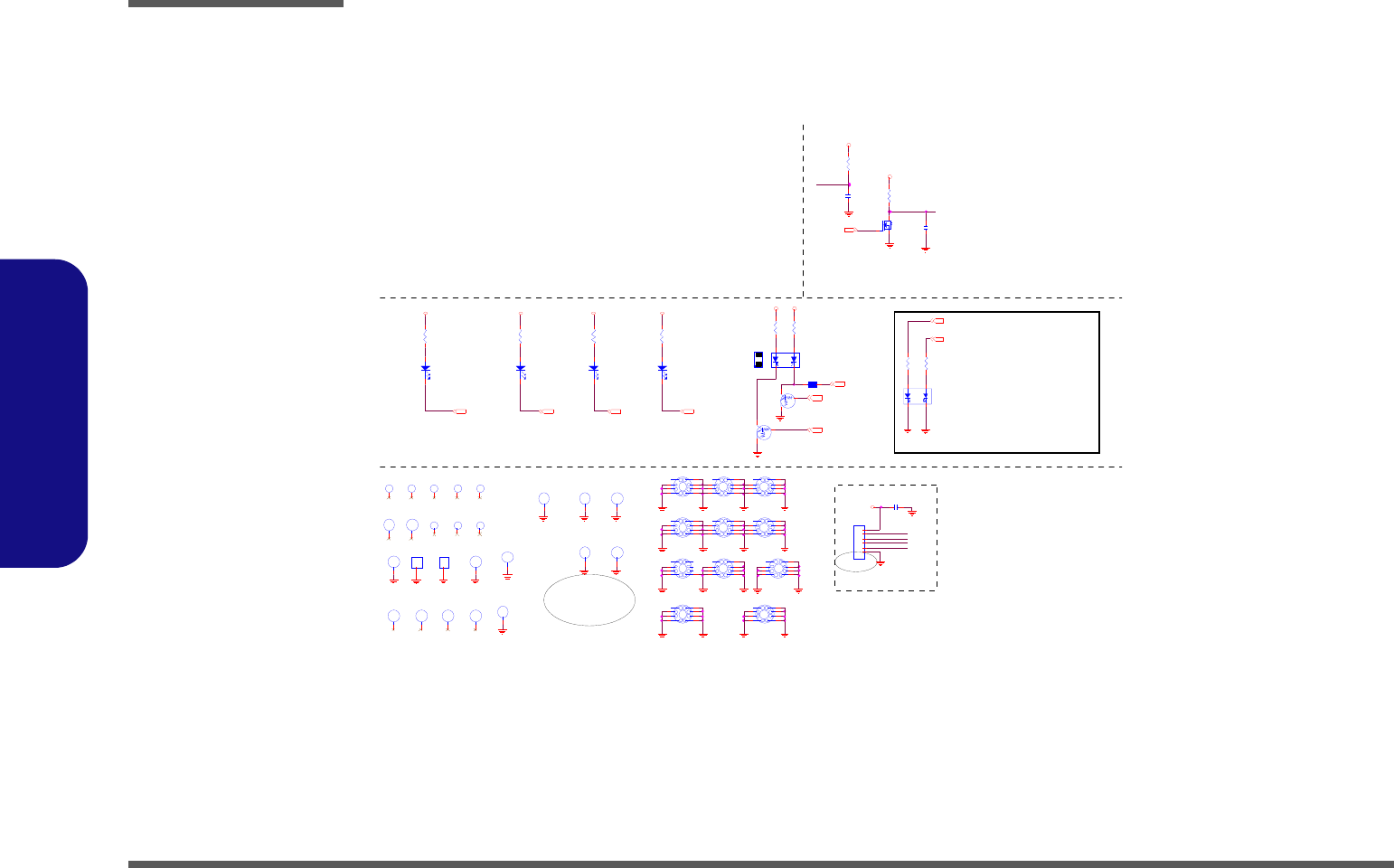
Schematic Diagrams
B - 22 LED/ MDC/ BT
B.Schematic Diagrams
LED/ MDC/ BT
Sheet 21 of 43
LED/ MDC/ BT
LED_BAT_FULL
L ED_ B AT _ CHG
LED_PWR
LED_ACI N
Del H30, H31, H32 3 /8
BT_EN#
1
H2 5
MT H 31 5 D1 1 1
3
4
5 6
7
8
9
M5
M-MAR K1
1
H7
MTH 315D111
3
4
5 6
7
8
9
R5 40
220_04
M2
M-M A R K 1
H3 6
ht6_0b7_0d3_7
M1
M-MARK1 H3 5
HC 6_0d3_7
Q1 7
DTC1 1 4E U A
CE
B
C7 5 7
* 180p_50V_N PO_04
R542
* 220_04
J_ T P 4
85201-06051
1
2
3
4
5
6
H21
C1 10 D1 1 0NP
SG
Y
D1 3
*K P B -3 0 25 Y S GC
1
3
2
4
1
H1 3
MTH315D111
3
4
5 6
7
8
9
1
H2 4
MTH315D111
3
4
5 6
7
8
9
C758
* 180p_ 50V_N PO_04
H3 4
ht6_0b7_0d3_7
R548
22 0 _0 4
Q1 4
*MT N 70 0 2Z H S 3
G
DS
1
H5
MT H 31 5 D1 1 1
3
4
5 6
7
8
9
H15
H 4_7B6_0D3_7
H23
C 67D67
C760
*0.1u_16V_Y5V_04
H2 9
H4_7B6_0D3_7
D2
RY -SP17 0 YG34 -5M
AC
H18
H 6_0D3_7
R5 3 6
47 K _ 0 4
H3 3
HT 6 _0 BS1 D3 _7
R5 49
220_04
H19
H4_0B7_0D3_7
1
H1 1
mt h315d111_3
3
4
5 6
1
H1 4
MTH 315D111
3
4
5 6
7
8
9
1
H3
MTH 315D111
3
4
5 6
7
8
9
R5 38
*1 0K _0 4
D5
RY- SP17 0 YG34 -5M
AC
1
H4
MTH315D111
3
4
5 6
7
8
9
S2
SMD80 X80
1
1
H2
C110D110NP
M7
M-MA RK 1
H20
C110D110NP
M3
M-M A R K 1
M4
M-M A R K 1
R5 4 6
220_04
M8
M-M A R K 1
S1
SMD 80X80
1
1
R5 5 0
* 10m il_short_04
D4
R Y-SP170 YG 34 -5M
AC
R541
220_04
M6
M-MA RK 1
D3
R Y-SP170 YG 34 -5M
AC
H1
C1 10 D 11 0 NP
H17
* H4 _7B6_0D 3 _7
SG
Y
D1
KPB-3025YSG C
1
3
2
4
R543
* 220_04
H6
C67D67
R547
220_04
Q1 6
* DTC114EUA
CE
B
1
H9
MT H 31 5 D1 1 1
3
4
5 6
7
8
9
3.3VS
3.3VS 3.3V S3.3VS3.3VS
3.3VS
3.3V
3.3V
GN D
VD D3
GN D
W24 Of f, W2 5/W27 On
LED_N UM# 20
BT_EN 17,20
WLAN _EN 17,20
LED_CAP# 2 0 LED_SCR OLL# 20SATA_LED # 9
W LAN _LED # 17,20
BT_EN17,20
LED_PWR 20
LE D _A C I N 2 0
1
H2 6
MTH315D111
3
4
5 6
7
8
9
6- 52- 52 001 -0 27 6- 52 -52 00 1- 027 6-5 2- 520 01 -02 7 6-5 2- 520 01 -02 7
Bluetooth
BT_DET#
On 3 /18
NUM
LOCK
LED
2
CA P S
LO C K
LE D
LED
SCROLL
LOCK
LED POWER ON
LED
31
WLAN
LED
24
BT
LED
HDD/ODD
LED
W24 On, W25/W27 Off
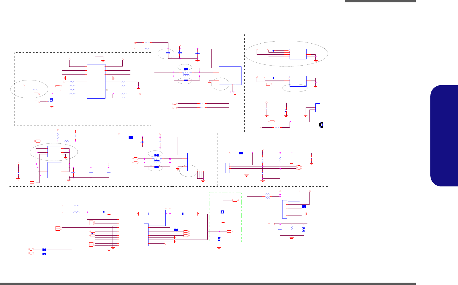
Schematic Diagrams
USB/ FAN/ TP/ MULTI CON B - 23
B.Schematic Diagrams
USB/ FAN/ TP/ MULTI CON
R574 *0_04
R733 0_06
USB PORT Charge
Port 1
80 mil
U52
* AX995 B
VO UT
1
GN D 5
VIN
3FO N#
4
VSET
6GN D 2
3/2 3
3/23
5VS
FON #
5VS_F AN
CPU _F AN
PN:APE8 87 42nd Source
AX 9 95B(SOT23 -6) & APE88 72
Co -L ayou t
USB_PP0 _R
USB_PN0_R
+
C740
220u_6. 3V_6.3*6.3* 4. 2
CTL1 CTL2 CTL3: X 1 0-----> Standard Downstream Port, USB 2.0 Mode.
CT L1 CTL 2 CT L3: 1 1 1----- > C harg ing Do wndtream P ort, BC S pec 1.1
CTL1 CTL2 CTL3: 0 X 1-----> Dedicated Charging Port, Auto-detect
U4
* RT9715BGS
VO UT1 6
VO UT3 8
VIN2
3VIN1
2VO UT2 7
GND 1
EN#
4
FLG#
5
PR 215
* 47K_04
PC23 0
*0.1u_50V_Y 5V_06
100 MIL
VDD 3
R3.3 Modify.
SOP8 & MSOP8 Co-layout 3/9
60 mil
Port 0
R 711 * 10m il_short_04
R832 * 10K_04WEB _WWW #
W24 6-21-B49C0-104
VDD 5
R 712 * 10m il_short_04R737 * 17.8K_1% _04
R745 * 10K_04
R741 * 0_06
PN :AX9 9 5 SA -- 6-0 2 - 99 0 11 -B 20
PN :G99 0-- 6- 02- 99 011 -B 20
PN :APE 887 2- -6- 02 -08 87 2-F C0
2 nd So urce
2 nd So urce
PV1
*V15 AVL C04 02
12
1.1A 60mils
M IC_SENS E
HEAD PHO NE-R
MIC1-R M
H P_SENSE
SPK _H P#
MIC1-L M
HEAD PHO NE-L
SPK OUTR+
SPKO UTR-
U SBP4_R
U SBN4_ R
Audio/B CONN.(Port 2)
U SBP4_R
U SBN4_ R
R714 * 10m il_short_04
R713 * 10m il_short_04
AP_KEY # R831 10K_04
CLICK CONN
R740 0_06
M_ B T N #23
Valu e m o dify 3/2 3
US B_PP08
USB_PN08
USB_O CP0_1#
Change 3/18
C764
* 10u_6.3V_X5R _06
W25/W27 6-21-B4410-004
L120
*W CM2012F2S-161T03
1
4
2
3
+
C7 6 9
*100u_6.3V_B_A
C777
0.01u_16V_X7R_04
+
C772
* 100u_6.3V_B_A
J_FAN1
85205-03701
1
2
3
C766
10u_10V_Y 5V_08
R558 *10m il_short_04
R552
10K_04
L121
* WCM 2012F2S-161T03
1
4
2
3
R560
* 1 0m i l _s h or t _0 4
C768
0.1u_16V_Y5V_04
C778 0.01u_16V_X7R_04
R5 57
10K_04
C7 74
47p_50V_NPO _04
R5 56
10K_04
C761
10u_10V_Y5V_08
3/9
J _ USB2
1-284-800281-1
V+
1
GN D1
GND1
DAT A_ L
2
DAT A_ H
3
GN D
4
GND2
GN D2
GND4
GND 4 GN D3
GND3
U41
AX995SA
VO UT
3
GN D 5
VIN
2FO N
1
VSET
4GN D 6
GN D 7
GN D 8
C770
* 10u_10V_Y5V_08
R561 *10m il_short_04
J_ T P 1
85201-04051
1
2
3
4C762
0.1u_16V_Y 5V_04
R833 * 10K_04
C773
0.1u _1 6 V_Y5V_04
Q18
* MTN7002ZHS3
G
DS
W EB _EM AIL #
C7 65
0.1u_16V_Y5V_04
R 554 * 0_04
C776
0.01u_16V_X7R _04
J_SW1
* 50500- 01041-001L
1
2
3
4
5
6
7
8
9
10
L130
*15mil_short_06
100 mil
USBVC C0
J_AUDIO 1
85201-14051-01
1
2
3
4
5
6
7
8
10
11
12
13
14
9
C7 6 3
0.1u_16V _Y 5V_04
C771
1u_6.3V _Y 5V_04
J _ USB1
1-284-800281-1
V+
1
G ND1
GND1
DA TA_ L
2
DA TA_ H
3
GN D
4
GND 2
GN D2
GND 4
GN D4 G ND3
GND3
R551 4.7K_04
R 555 * 15m il_s hort_06
R553
* 10K_04
J_ S W 2
88 4 8 6- 0 8 01
1
2
3
4
5
6
7
8
C7 75
47 p _ 50 V _ N P O _0 4
R562 *10m il_short_04
U4 0
RT9715BGS
VOU T1 6
VOU T3 8
VIN2
3
VIN1
2VOU T2 7
GN D 1
EN#
4
FLG #
5
5V S
5VS
5V
3.3VS
5VS_FAN
5VS_F AN
5VS_TP
5V S
3.3V3.3VS
VIN
3. 3 V3.3VS
USB VCC0
U SB_VC C2
USB VCC1
3. 3 V3. 3 V
5V
U SB_VCC3
MIC_SEN SE18
SP KOUTR -18 SP KOUTR +18
USBV CC1
MIC1-R M18 MIC1-L M18
H P_SENSE18
H EADPH ON E-R18
USB_PP48
USB_PN48
N/A
CPU _FA NSEN20
CPU _FA N20
H EADPH ON E-L18
TP_C LK 20
TP_D ATA 20
R 1 68 0_ 0 4
A P_KEY # 20
WEB _WWW # 20
LID_SW# 8,13,20
WEB _EM AIL# 20
DD _O N#23,25,26
AP_ON 23
USB_OC P0_ 1 #8,19
USB_PP18
U SB_P N18
R 1 71 0_ 0 4
100 mil
Mo dify 3/1 7
USB PORT*2(Port 0,Port1)
U SB_PN 0
W24 6-21-B49C0-104
FAN CONTROL
W25/W27 6-21-B4410-004
Ch an ge 3/18
FON #
JFAN
3
1
AP_ON
R734 *0_06
R 7 50 * 1 0 K _0 4
USB VCC1
LID_SW#
U10
*TPS2540
CTL1
6
NC 9
DM _IN 11
DM_O
2
DP _IN 10
IN
1
EN /DSC
5
DP_O
3
IL IM_ SE L
4
CTL2
7
CTL3
8
OUT 12
FAU LT# 13
GND 14
IL IM1 15
IL IM0 16
PPAD 17
M_BTN #_R M_ B TN #
AP_KEY#
WEB_WWW#
W EB_ EM AIL#
POWER SWITCH CONN.
20 mi l
CLOSE TO J_SW1
M_ B T N #
W EB_ EMAIL #
LI D _ S W #
WEB_WWW#
AP_KEY#
MB T N
U SB_P P0
U SB_P N0
3/9
20mil
U SB_PP 0
USB_FLG#USB_O CP0_1#
USB_PW R _EN #20
I f sy st em ha s AP ON fu nc ti on , u se s J_ SW1
I f sy st em ha s no A PON f un ct ion , us es J_ SW 2
M_ B T N #
U SB_PN0_R
U SB_PP0_R
PV2
*V15 AVL C0 402
12
R 7 51 * 1 0 K _0 4
USB_FLG#
U SB_P N0_R
R747 * 10K_04
Q7 6
*M TN 7002ZHS3
G
DS
R 7 48 * 1 0 K _0 4
DD_ ON20 , 2 3 , 24
VDD5
AC_IN#8, 20 , 2 9
VD D5
USB VCC1
R 7 49 * 1 0 K _0 4
VDD 3
U SB_P P0_R
R746 *10K_04 V DD3
Sheet 22 of 43
USB/ FAN/ TP/
MULTI CON
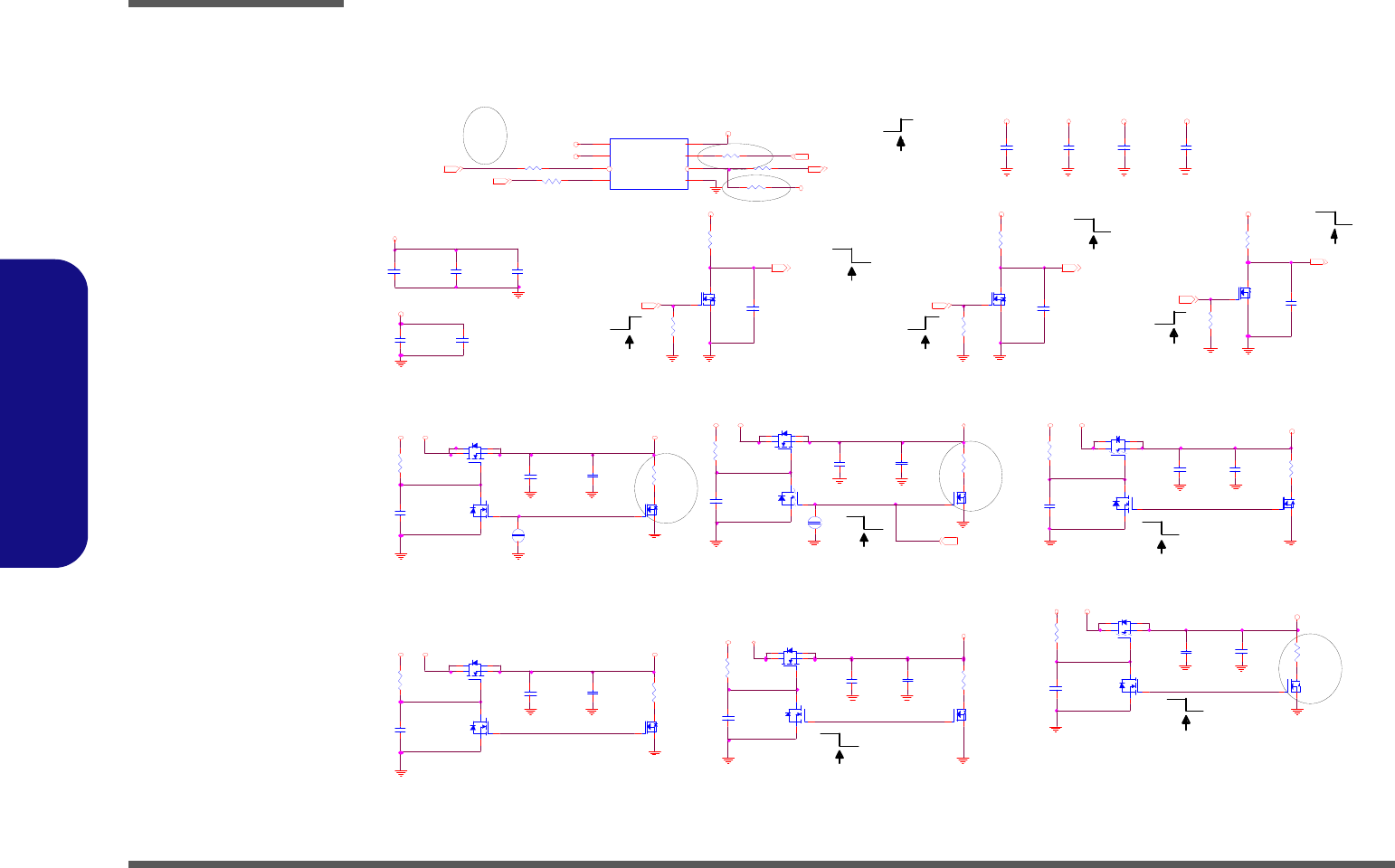
Schematic Diagrams
B - 24 5VS/ 3.3VS/ 1.8VS/ 1.5VS/ 1.1VS
B.Schematic Diagrams
5VS/ 3.3VS/ 1.8VS/ 1.5VS/ 1.1VS
SU SB
ON
Del R810 3/9
Dis ab le PR3 3/9
1 K to 1 00 K 3/9
ON
ON
PC22
10u_10V_Y5V_08
PQ2
MTN7002ZHS3
G
DS
PR20 8
100_1%_04
PR6
10K_04
PR 17
1M_04
PR20 7
*100_1%_04
PJ1
40m il
12
PC 229
10u_10V_Y5V_08
PC 227
10u_10V_Y5V_08
PR 3 *1 00K_0 4
PQ62
MTN7002ZH S3
G
DS
PQ 60
* MTN7002Z HS3
G
DS
PQ 7
*M TN7002ZH S3
G
DS
PQ8B
MTNN 20N 03Q8
6
5
4
PQ 5B
*M TN N20N0 3Q8
6
5
4
PR 15
*100_1%_04
PQ6B
MTNN 20N 03Q8
6
5
4
PR 19
100_1%_04
PQ13
* MTN 7002ZHS3
G
DS
C779
0.01u_16V_X7R _04
PC14
*10u_10V_Y5V_08
PR11
1M_04
PR 4
10K_04
PQ8A
MT NN 20 N 03 Q 8
1
3
7
28
PC 16
10u_10V_Y5V_08
PC 20
0.01u_16V_X7R _04
PC18
470p_50V_X7R_04
PQ9A
MT NN 2 0N 0 3Q 8
1
3
7
28
PR 7
100K _04
PC21
0.1u_16V_Y 5V _04
PC 10
* 0.1u_16V_Y 5V_04
PC19
*0.1u_10V_X7R _04
PR16
1M _ 04
PQ3A
MT NN 20 N 03 Q 8
1
3
728
PR 13
1M_04
PC 226
0.1u_16V_Y 5V_04
PQ 5A
*M T NN 20 N 03 Q 8
1
3
7
28
PC17
470p_50V_X7R_04
PR 211 1K_04
PQ 10
M TN 7002ZH S3
G
DS
PC 8
0.1u_50V_Y5V_06
PC 6
0.1u_50V_Y 5V_06
PC 9
* 0.1u_16V_Y 5V_04
PQ6A
MTNN 20N 03Q8
1
3
7
28
C781
0.01u_16V_X7R _04
PR5
10K_04
PC25
2200p_50V_X7R _04
PR10
1M _ 04
PQ4B
M TN N20N03Q8
6
5
4
PC15
0.1u_16V_Y5V_04
PR12
*1M_04
PC11
* 0.1u_16V_Y 5V_04
C780
0.01u_16V_X7R _04
C784
0.01u_16V _X7R_04
C783
0. 01 u _ 16 V _ X 7 R _ 0 4
PR9
100K_04
PC12
0.1u_16V_Y 5V_04
PQ61
*MTN 7002ZHS3
G
DS
PQ9B
MT NN 2 0N 0 3Q 8
6
5
4
R563 100K_04
PC225
10u_10V _Y 5V_08
PR 8
100K_04
PC 26
2200p_50V_X7R_04
PJ2
40m il
12
S
D
G
PQ1A
M TD N7002Z HS6R
2
61
S
D
G
PQ1B
M TD N7002Z HS6R
5
34
PC 7
0.1u_50V_Y5V_06
PC 228
0.1u_16V_Y 5V_04
PQ3B
MTNN 20N 03Q8
6
5
4
PQ 4A
M TN N20N03Q8
1
3
7
28
C7 8 2
0.01u_16V_X7R_04
PR14
* 100_1% _04
PU 1
P2808B 0
VA
1
VIN
2
M_BTN#
3
IN STA NT-ON
4GND 5
PW R_S W # 6
DD _ON _LATCH 7
VIN1 8
PR 206
* 100_1% _04
PR 210 1 K_ 0 4
PC13
*0.1u_16V_Y5V_04
VDD 5
3. 3 V S
VD D3
CD 3 /8
SYS 15V
SY S15V
5V SSY S15V
SYS 15V VDD 3
VDD 5
VIN 1
VIN
VA
SYS 15V 1.5V
VINVA
1.5V S
SY S5V
VIN 1
5V
3.3V
3. 3 V S
VDD 3
SY S5V
1.1VSY S15 V 1.1VS
SYS 5V
3.3V
5V
PW R_S W # 2 0M_ B T N #22
AP_ON22
D D_O N# 22,25,26
SUSC #8,20,25
SU SB#8,11,12,19,20
SUSB 25,26,27 SUS C 26,28
DD_ON20,22,24
D D_O N 20,22,24
SU SB 25,26,27
SU SB
P R18 1K_04
DD _O N#
NMO S
1.1VS
NMOS
ON
SUS B
1.5VS
3A
3A 3A
3A
Power Plane
Power Plane
3.3VS
5VS
3.3V
5V
ON
DD_ON "L" TO
"H" FROM EC
ON
CD 3 /8
ON
NMO S
NM O S
ON
ON
CD 3 /8
ON
SU SB
DD_ON#
DD_ON#
SUSB
SUSC
ON
Sheet 23 of 43
5VS/ 3.3VS/ 1.8VS/
1.5VS/ 1.1VS
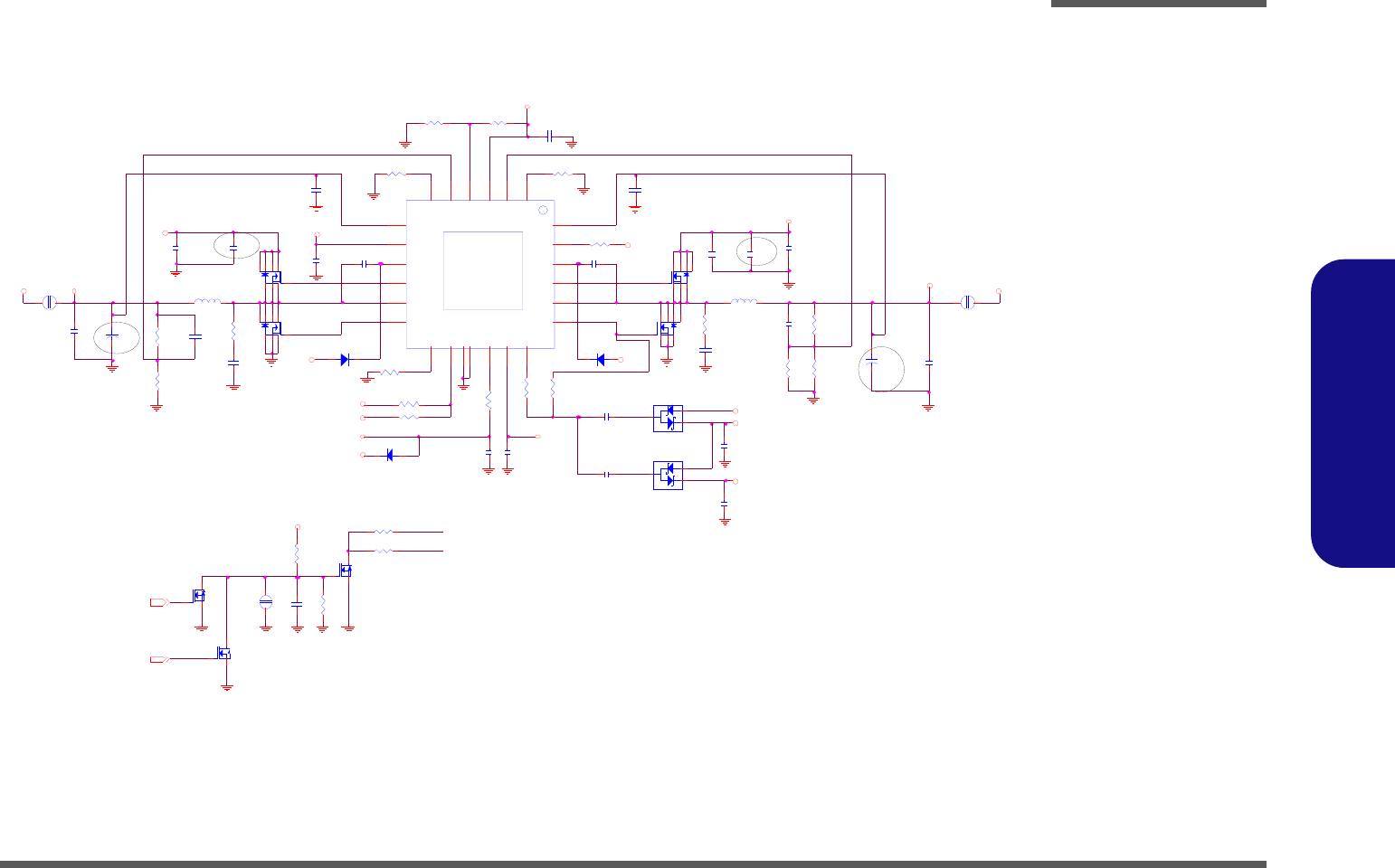
Schematic Diagrams
POWER VDD3/ VDD5 B - 25
B.Schematic Diagrams
POWER VDD3/ VDD5
Ch an ge val u e 3 /2 4
+
PC 40
220u_6.3V_6.3*6.3* 4.2
PC 174
2200p_50V _X7R _04
PR 146
5.1_06
PC28
1u_10V_Y5V_06
W2 7 5 .7 --> 2 20 u_ 6.3 V_ 6. 3* 6.3 * 4.2
5A
EN _ALL
Rb
5A
Ra
EN_3V
EN_5V
PD 3
* RB0540S2
A C
PL2
TMPC 0603H -4R7M-Z 01
1 2
PC 51
2200p_50V_X7R_04
PJ3
*5mm
12
PQ 14
P120 3B V
4
62
5
73
1
8
PR21 * 0_0 4
PU 2
uP6182
VR EF 3
EN1 1
VFB1 2
TO N SEL 4
LDO 5
17
LG ATE1 19
PH ASE1 20
VFB2 5
UGATE2
10
VCLK
18
BOOT2
9
EN2 6
VO2
7
LD O3
8
PHASE2
11
LG ATE2
12
EN0
13
SKIPSEL
14
GND
15
VIN
16
UG ATE1 21
BO OT1 22
PO K 23
VO1 24
GN D P AD
25
PR31
0_04
PC29
1000p_50V_X7R_04
PR24
100K_04 PC 30
1000p_50V_X7R _04
PR33
2.2_06
PQ18
MTN 7002ZHS 3
G
DS
PR36 *0 _0 4
PR216
68 0 K _ 1 % _ 06
PC44
0.1u_16V _Y 5V_04
PQ 19
M TN7002ZHS3
G
DS
+
PC 45
220u_6.3V_6.3 *6.3* 4.2
PL1
TM PC06 03H -4R7 M -Z01
12
PR28
19.1K_1%_06
PJ5
*6 m i l
12
PJ4
*5 m m
1 2
PR 37
10K _04
PR27
13K_1%_06
PR34 0_04
PC34
1u_10V_Y5V_06
PC 38
* 4.7u_25V_X5R _08
PR26
30K_1%_06
PQ 17
P120 3BV
4
62 5
73
1
8
PR39 100K_04
PC36
1u_10V_Y5V_06
PC 55 0.1u_10V_X7R _04
PC39
0.1u_16V_Y5V_04
PC 50
0.01u_50V _X7R _04
PR38 0_04
PC 33
4.7u_25V_X5R _08
PD7
RB0540S2
AC
PC 41
1000p_50V_X7R _04
PR 32
*0 _ 0 4
PC 35
0.1u_10V_X7R_04
PR23
100K_04
C
A
A
PD6
BAT54SW GH
1
2
3
CA
A
PD5
BAT54SW GH
1
2
3
PR22 0_04
PC 32
4.7u_25V_X5R_08
PC 46
0.01u_50V _X7R _04
PC 48
4.7u_25V_X5R_08
PC37
0.1u_50V_Y5V_06
Z2418
PQ 15
P1203BV
4
62
5
73
1
8
PC 42
100p_50V_NPO _04
PR 25 *10K_04
PQ 16
P120 3B V
4
62
5
73
1
8
PC31
*4.7u_25V _X5R_08
PR29
20 K _ 1 % _ 04
PR35 *0 _0 4
PC 49
1u_10V_Y 5V _06
PC 47
2200p_50V_X7R_04
PD 4
* RB0540S2
AC
SY S5V
PR 30
* 680K_1% _04
SY S15 V
VR EF
VD D3
VIN
VD D5
VIN
SYS3V
VREG 3
SY S10 V
VR EG 5
SY S5V
VR EF
VREG5VIN 1
VIN
VR EG 5
VREG5
SYS5V
DD_ON20,22,23
VR EG 5
EN _3V EN _5V
AC IN29
PQ22
*M TN7002Z HS3
G
DS
Z2418
W24/W25 --> 220u_6.3V_6.6*57
CD 3/8
CD 3/8
PR152
5. 1_ 0 6
PC238
2200p_50V_X7R_04
Sheet 24 of 43
POWER VDD3/
VDD5
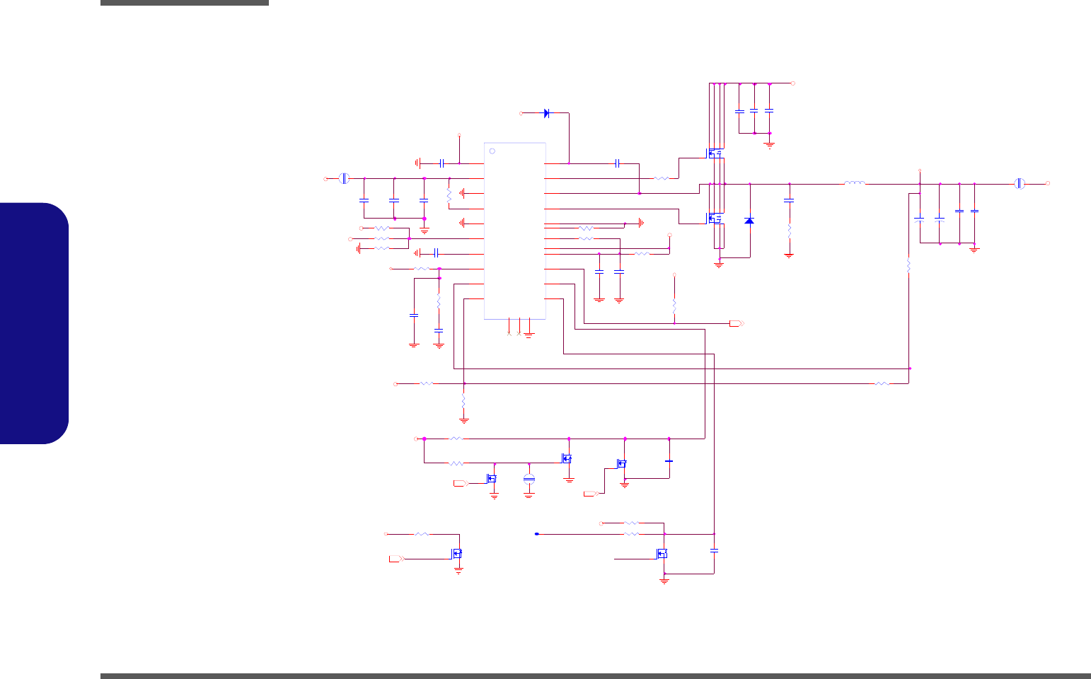
Schematic Diagrams
B - 26 POWER 1.5V/ 0.75V
B.Schematic Diagrams
POWER 1.5V/ 0.75V
PC74
2200p_50V_X7R_06
PR50
5.1_06
Z 2621
PR 64
10K_1%_06
PR60
100K_04
PD 12
RB0540S2
A C
PU 4
uP6163
VTTGN D
1
VLDO IN
23
VTT
24
VTTSNS
2
GN D
3
MO DE
4
VTTREF
5VC C5 14
PGO OD 13
S5 11
S3 10
VD DQ SET
9
VD DQ SNS
8
CO MP
6
CS 16
PG ND 18
DR VL 19
LL 20
DRVH 21
VBST 22
PVC C5 15
CS _G ND 17
NC
7
NC
12
GND
25
PR 68 * 22 _04
PC66 *0.1u_50V_Y5V_06
PJ 7
*OP EN_2A
12
PC68
* 4.7u _25 V_ X5R _0 8
PR62
*1 0 K _ 1 % _ 04
PQ 23
MD S2 6 5 9
4
62 73
8
5
1
PR 52 0_ 0 6
PC86
0. 1u_16V_Y5V_04
PR 57
0_06
PC67 *4.7u_25V_X5R _08
PQ26
*M T N 7 0 0 2 Z H S 3
G
DS
PC 77 0.01u_16V_X7R_04
PC80 0.1u_10V_X7R_04
PC 71
10u_10V _Y 5V_08
P R65 47K _04
PC 75 0.1u_16V_Y5V_04
PQ 24
MD S2 6 5 5
4
62 73
8
5
1
PC 84
*1000p_50V_X7R_04
PR58 0_06
PC 85
0.1u_16V_Y5V_04
PD 13
*SK34SA
A C
PC 73
* 10u_10 V_ Y5V_ 0 8
PQ 28
* MTN 7002ZH S3
G
DS
PL4
1.0U H_10*10*4.5
1 2
PQ 29
MTN 7002Z HS3
G
DS
PJ 8
*OPEN _8A
1 2
PQ25
MTN 7002ZH S3
G
DS
PJ9
*6 m i l
1 2
+
PC79
560u_2.5V_6.6*6.6* 5. 9
+
PC 76
*560u_2.5V_6.6* 6.6* 5.9
PR 67 100K _04
PR 63 10K _1%_06
PC 82
1u_10V_Y5V_06
PR 48
0_06
P R49 0_06
PR 56 2.2_04
PR 69 *100K_04
P R53 *0_04
PC 72
10u_10V_Y 5V_08
PC 70 0.1u_10V_X7R _04
PR 47 0_06
PQ 27
M TN 7002ZH S3
G
DS
PC 83
* 1000p_50V _X 7R _04
PC81
1u_10V_Y5V_06
PR59 *10_04
PC 69
10u_1 0V _ Y5 V_ 08
PR 5 4 1 0K_1 % _06
P R55 *0_04
P R66 100K_04
5V
VD DQ
VD DQ
5V
5V
5V
VIN
5V
VTT_MEM
1.5V
VD DQ
5V
3.3V
VTT_ ME M
5V
SU SC#8,20, 23
DD_ON#22,23, 26
DD R1 .5 V _ PW RG D 1 1 ,2 8
SU SB23,26,27
1.5VEN
+1 .5S_ C PU_ PW RG D
SUSB
VTTEN
SU SB
10A
1.5V
DD R1.5V_ PW RG D
Sheet 25 of 43
POWER 1.5V/ 0.75V
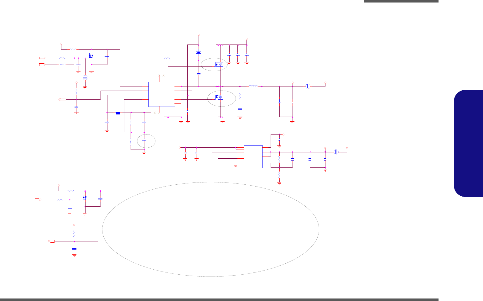
Schematic Diagrams
POWER 1.1V/ 1VS B - 27
B.Schematic Diagrams
POWER 1.1V/ 1VS
1.1VS_VTT=0.75 X (1+PR101 / PR102)
OC P=1 0uA X RIL IM / R dso n
SU SC
5A
1.1V
EN_1.1V
3A
EN _1 VS
1VS_P WRG D
Vout = 0.8V ( 1 + Ra / Rb )
Ra
Rb
3A
SU SB
EN _1VS
10/22 1.0V= >1.054V
1V S_PW R GD
Change value 3/24
PR77
1 0 0K _1 % _ 0 4
PC 96
1u_10V _Y 5V_06
PC 78
2200p_50V_X7R _04
PC91
0.1u_10V_X5R _04
PC97
0.01u_16V _X7R _04
PC 216
10u_6.3V_X5R _06
PC104
0. 1u _ 1 0 V _ X 5 R _ 0 4
PR 72 *62K_1%_04
PC100
0.1u_10V_X7R _04
PJ18
3mm
1 2
PR73
220K_1%_04
PC 21 5
10u_6. 3V _X5R _06
PL5
TMPC 0603H -4R7M -Z01
1 2
PR196
3.24K_1%_04
PD14
RB0540S2
AC
PC 98
* 20p_50V_NP O_04
PC 108
*0.1u_10V_X7R _04
+
PC93
560u_2.5V _6.6* 6.6* 5.9
PU 5
uP6127
LX 1
BS T 2
VC C 3
DL 4
GN D
5
RTN
6
N. C
7
N.C
8
FB
9
VO UT
10
PG D
11
EN
12
ILI M 13
N. C 14
N.C 15
DH 16
PAD 17
PR 75
10K_1%_04
PC 94 0.1u_16V_Y 5V _04
PJ 1 0
5m m
1 2
PJ 2 3
OPEN-1mm
12
PR70
100K_1%_04 PC 9 0
*4.7u_25V_X5R_08
PC214
82p_50V_NPO _04
PQ30
MTN 7002ZH S3
G
DS
P R78 62K_1%_04
PR71 10K_1%_04
PR195
10.2K_1%_04
PC89
0.1u_10V_X7R _04
PR 197 62K_1%_04
PC 87
4.7u_25V _X 5R _08
PQ33
M TN7002ZH S3
G
DS
PC92
0. 1u_10V_X7R_04
PC88
0.1u_50V_Y5V_06
PC 99
300K_1%_04
PC 219
10u_6.3V_X5R_06
PR74
* 10m il_sho rt
PR 80
220K_1%_04
PR 51
5.1_06
PU11
AX6610
GND
1
VC NTL 6
VO UT 3
VIN
5
VO UT 4
VFB 2
POK
7
EN
8
VIN
9
PC95
*0 .1 u _ 10 V _X 7 R _ 04
PR 76
21K_1%_04
PC 21 8
0.1u_16V _Y 5V_04
PQ31
P120 3 BV
4
62 73
8
5
1
PC213
1u_10V_Y5V_06
PQ 32
P1203BV
4
62 73
8
5
1
VIN
1.1V
3.3V
5V
V1.1
5V
3.3V
V1S_REG
5V
5V
1VS
1.5V
SU SB23,25,27
1.1 V_PWRGD11
1V S_ PWRGD28
DD _ O N#22,23,25
SUS C23 , 2 8
3/8
Delete PU6 and relat ed parts.
Sheet 26 of 43
POWER 1.1V/ 1VS
Schematic Diagrams
B - 28 POWER 1.8VS
B.Schematic Diagrams
POWER 1.8VS
EN _ 1. 8 V
3A
3A
Vout = 0.8V ( 1 + Ra / Rb )
Rb
Ra
1.8V_PWRGD
EN _ 1. 8 V
1. 8V_PWRGD
SUSB
1.8VS
OCP=10uA X RILIM / Rdson
4A
PC 22 0
10u_6.3V_X5R_06
PR45
* 14K_1%_04
PL3
*TMP C0603 H-4R7M-Z 01
1 2
PC61
*1u_10V_Y5V_06
PJ6
5mm
1 2
PU3
*uP6127
LX 1
BST 2
VCC 3
DL 4
GND
5
RTN
6N.C
7N.C
8
FB
9
VOUT
10
PGD
11
EN
12
ILIM 13
N.C 14
N.C 15
DH 16
PA D 17
+
PC 5 9
* 560u_2.5V_6. 6*6.6* 5.9
PC63
* 20p_50V_NPO_04
PR46
* 10K_1%_04
PC 6 4
* 0.01u_16V_X7R _04
PU12
AX6610
GND
1
VCNTL 6
VOUT 3
VIN
5
VOUT 4
VF B 2
POK
7
EN
8
VIN
9
PC 5 3
*4. 7u_25V_X5R_08
PR 4 4
* 10mil_shor t
PQ2 1A
*A P69 01GSM
7
8
1
2
PC 58
*0.1u_10V_X7R_04
PQ2 0
MTN7002ZHS3
G
DS
PC 6 2
*0. 1u_10V_X7R_04
PC56
* 0.1u_10V_X7R_04
PD 10
*RB0540S2
AC
PC224
1u_10V_Y 5V_06
PR204
12. 7K_1%_1/ 16W_04
PC 2 23
10u_6.3V_X5R_06
PC 2 21
0.1u_16V_Y5V_04
PR 4 3
220K_1%_04
PC54
*4. 7u_25V_X5R_08
PR205
10K_1%_04
PR41 * 15K_1% _04
PC 22 2
82p_50V_NPO_04
PJ 22
3mm
1 2
PQ21 B
*AP6901GSM
4
3
5
6
PC60
* 0 . 1u _1 6V_ Y 5 V_ 04
PC57
0.01u_16V_X7R_04
PC 21 7
10u_6.3V_X5R_06
PC 52
*. 1u_50V_Y5V _06
PR42 10K_1%_04
PC65
* 20p_50V_NPO_04
PR40
100K_1%_04
VI N
1.8VS
V1.8S
3.3V
5V
5V
V1.8S_REG
5V
1.8VS
3. 3V
SU S B23, 25,26
1.8V_P WRGD11
Sheet 27 of 43
POWER 1.8VS
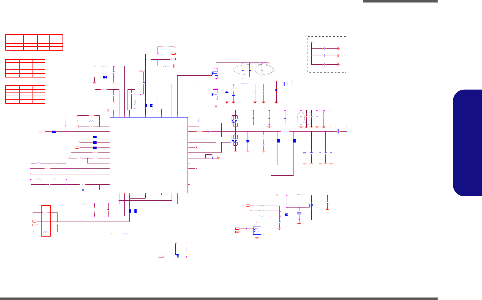
Schematic Diagrams
APU CORE/ NB CORE B - 29
B.Schematic Diagrams
APU CORE/ NB CORE
PR218
5.1_06
PC234
2 20 0p_ 50 V_ X7 R _0 4
PR217
5.1_06
PC158
2200p_50V_X7R_04
APU_PW RGD_R
PC 1 38
* 4.7u_25V_X5R_08
PR 1 20
1_1 % _ 06
PC13 9
*4 .7u_25V_X5R_08
PQ43
MDS 26 55
4
62 73 8
5
1
P R 11 7 * 1 0mi l _s hor t
P C 14 7 3 3p_ 50 V_ N P O _0 4
PC171
*0 .1u _10 V _X7 R _0 4
PR140
4 . 02 K_ 1%_ 04
PR14 1
10 _0 4
P C 14 1 1 00 0p_ 50 V _X 7R _ 04
PR128
* 1 0m il _s h o rt
PR 1 45
10 0K _0 4
P R 12 3 * 10 K_ 06
P C 16 2 0. 0 1u _50 V _X 7R _ 04
P C 168 1 00 0p_ 50 V_ X7 R _0 4
PJ16
OPEN -1 mm
12
C790 *0.01u_16V_X7R_04
P R 13 0 * 10m il _s ho r t
PC 1 59 10u _6 . 3V _X 5R _ 08
PC17 2
0.1u_10V_X7R_04
P C 16 0 0 . 22u _1 0V _Y 5 V_ 04
PR 125
1_ 1% _0 6
PQ45
MDS 26 55
4
62 73 8
5
1
P C 142 10 00 p_5 0V _ X7 R _0 4
PL9
T MPC0 60 3H-R68M-Z 01
1 2
C 79 1 0 . 1u _10 V _X 5R _0 4
PD21
*C S OD 1 40S H
A C
PC157
* 0. 1 u_ 50V _ Y 5V _0 6
P R 11 9 0_0 6
PC15 2
* 4 . 7u_ 25 V_ X 5R _ 08
PR112
* 1 0m i l _s hor t
R682
10K_04
PR11 1
10 _0 4
P R 13 5 1 K _1% _0 4
P R 115
44 . 2K _1 %_0 4
PQ44
MDS 26 59
4
62 73 8
5
1
PC 1 67
18 0p_ 50 V_ N P O _0 4
PC15 0
*4.7 u_ 25V _ X5 R_0 8
C 78 9 0 . 1u _10 V _X 5R _0 4
PR 1 33
62 K_ 1%_ 04
PQ46
M T N 700 2Z H S 3
G
DS
PR137 6.8 K _1% _0 4
PR144 *0_04
PC163
2.2u_6.3V_Y5V_06
Q29MTN 7 00 2Z H S 3
G
DS
P R 14 8 1 0K _1 %_ 04
P R 12 2 * 0_ 06
P C 153
*4.7 u_ 25V _ X5 R_0 8
PR129
* 1 0 m il _s ho rt
PR 1 3 8 7. 5 K_ 1% _ 0 4
PR14 9
10 _0 4
PC 1 51
*4.7u_25V_X5R_08
P R 20 9 0 _0 4
+
PC140
330UF
12
PC15 5
0.22u_16V_06
PR136
54.9K_1%_04
PC145
10u_6.3 V _X 5R _0 8
PQ 4 7
MTN7 002ZHS3
G
DS
PU9
ISL626 5C
PGND_1 28
PGND_NB 40
PHASE_NB 38
UGATE_NB 37
PGND_0 32
RT N_ 1
17
PHASE_0 33
PHASE_1 27
UGATE_0 34
VSEN_1
18
RBIAS
7
ISN_0
14
COMP_0
11
VDIFF_0
9
VW_0
12
OCSET
8
ISP_0
13
VSEN_0
15
ENABLE
6
RTN_ 0
16
SVC
5
PGOOD
2
SVD
4
UGATE_1 26
FB_0
10
LGATE_1 29
OFS/VFIXEN
1
PVCC 30
LGATE_0 31
BOOT_NB 36
BOOT_0 35
GND 49
PWROK
3
VD I F F _1
19
FB_1
20
COMP_1
21
LG A T E_ N B 39
VW _1
22
ISP_1
23
ISN_ 1
24
BOOT_1 25
OCS ET _NB 41
RTN_ NB 42
VSEN_NB 43
FSET_NB 44
COMP_NB 45
FB_NB 46
VCC 47
VI N 48
PR 1 32
54 .9K_1% _04
P R 118 * 10 mi l_ sh or t
PQ42
MDS 26 59
4
62 73 8
5
1
PC149
0. 1 u_ 50V _ Y 5V _0 6
PR10 9
10 _0 4
PC169
0 . 1u _5 0V _Y 5 V_ 06
PR113 22K_1%_04
PR121
10K_04
+
PC14 4
* 3 30 u_2 . 5V _V _ A
P R 12 7 * 10m il _s ho r t
PC146
0.1u_50V_Y5V_06
PR143
*10mil_short
+
PC 1 61 560 u_ 2. 5 V_ 6. 6* 6. 6* 5 . 9
PC166
1000p_50V_X7R_04
PR142
* 1 0m i l _sh or t
+
PC164 *330u_2.5V_V_A
PJ 20
*8mm
1 2
PR134
255_1%_04
PHASE_NB
PR110
10 _0 6
PR139 510K_04
+
PC15 4
* 1 5u _2 5V _6 . 3* 4 .4_C
PC15 6
*0 .1u_50V_Y5V_06
+
P C 143
56 0u_ 2. 5 V_ 6. 6 * 6. 6* 5. 9
O
X
SV I
Z3301
P R 13 1 0 _0 6
PR114
10 _0 6
1
0.9
O
PC137
1 u_1 0V _Y 5V _0 6
PR116
8 . 2K _1 %_0 4
0
SV C
1
1.0
PR147 *0_04
PL8 TMPC0603H-R68M-Z01
1 2
0
1.1
SV D
0
U4 6 *74AHC1G08GW
1
2
5
4
3
PJ19
*8 mm
1 2
O utp ut
PC 1 48
0. 22 u_ 16V _ 06
0
PC165
4700p_50V_X7R_04
VDDCR_ CPU
0.811
PD 2 0
* C S O D 140 S H
A C
EN _ V C O R E
M eta l VI D C ode s
11A
VDDCR_ CPU
5V
SV C
V FIX EN V ID Cod es
NB_VDDCR
0.8
0
SGND5
SGND5
SGND5
O utp ut
SGND5
SGND5
SGND5
1.4
1.0
3. 3V S
SGND5
1.2
1
VIN
1
VIN
5VS
5VS
1
VIN
1
3.3VS
CPU_VDDCR
SV D
0
0
5V S
0
+5V
Pin 49 is GND Pi n
O
VDDCR _NB
CPU_VDDCR
1.8VS
1.5V
NB_VDDCR
3. 3 VS
3. 3V S
LGATE_NB
CPU_ SVC3
CPU_VDD0_ RUN_F B_H3
PWRGD_VCOR E11
CPU_ SVD3
ISP_0
X
CPU_VDD0 _RUN_ FB_ L3
ISP_1
VCORE_ON20
CPU_ VDDNB_ RUN_F B_H 3
CPU_ VDDNB_ RUN_F B_L 3
ISN_0
1VS_PWRGD26
APU_ PW RGD3,7
SUSC23,26
DDR1 .5V_PW RGD11 , 25
ISP_0
APU_ PW RGD_R
O FS/V FIX EN
GND
Of fse t &
Dr oop
PHASE_0
X
ISN_1
O
C los e to
CPU
s ock et
X
PR124 *10mil_short
+3 .3V
VF IX
ISN_ 0
UGAT E_0
X
10 A
LGATE_0
EM I
UGATE_ NB
P R 12 6 * 10m il _s ho r t
EN _ V C O R E
CD 3 /8
Noise issue 3/9
Noise issue 3/9
Cha nge value 3/24
Sheet 28 of 43
APU CORE/ NB
CORE

Schematic Diagrams
B - 30 APU CORE/ NB CORE
B.Schematic Diagrams

BIOS Update
C - 1
C:BIOS Update
Appendix C:Updating the FLASH ROM BIOS
To update the FLASH ROM BIOS you must:
• Download the BIOS update from the web site.
• Unzip the files onto a bootable CD/DVD/USB Flash Drive.
• Reboot your computer from an external CD/DVD/USB Flash Drive.
• Use the flash tools to update the flash BIOS using the commands indicated below.
• Restart the computer booting from the HDD and press F2 at startup enter the BIOS.
• Load setup defaults from the BIOS and save the default settings and exit the BIOS to restart the computer.
• After rebooting the computer you may restart the computer again and make any required changes to the default BIOS
settings.
Download the BIOS
1. Go to www.clevo.com.tw and point to E-Services and click E-Channel.
2. Use your user ID and password to access the appropriate download area (BIOS), and download the latest BIOS files
(the BIOS file will be contained in a batch file that may be run directly once unzipped) for your computer model
(see sidebar for important information on BIOS versions).
Unzip the downloaded files to a bootable CD/DVD/ or USB Flash drive
1. Insert a bootable CD/DVD/USB flash drive into the CD/DVD drive/USB port of the computer containing the
downloaded files.
2. Use a tool such as Winzip or Winrar to unzip all the BIOS files and refresh tools to your bootable CD/DVD/USB
flash drive (you may need to create a bootable CD/DVD with the files using a 3rd party software).
Set the computer to boot from the external drive
1. With the bootable CD/DVD/USB flash drive containing the BIOS files in your CD/DVD drive/USB port, restart the
computer and press F2 (in most cases) to enter the BIOS.
2. Use the arrow keys to highlight the Boot menu.
3. Use the “+” and “-” keys to move boot devices up and down the priority order.
4. Make sure that the CD/DVD drive/USB flash drive is set first in the boot priority of the BIOS.
5. Press F4 to save any changes you have made and exit the BIOS to restart the computer.
BIOS Version
Make sure you down-
load the latest correct
version of the BIOS ap-
propriate for the com-
puter model you are
working on.
You should only
download BIOS ver-
sions that are
V1.00.XX or higher as
appropriate for your
computer model.
Note that BIOS ver-
sions are not backward
compatible and there-
fore you may not
downgrade your
BIOS to an older ver-
sion after upgrading to
a later version (e.g if
you upgrade a BIOS to
ver 1.00.05, you MAY
NOT then go back and
flash the BIOS to ver
1.00.04).

BIOS Update
C - 2
C:BIOS Update
Use the flash tools to update the BIOS
1. Make sure you are not loading any memory management programs such as HIMEM by holding the F8 key as you
see the message “Starting MS-DOS”. You will then be prompted to give “Y” or “N” responses to the programs
being loaded by DOS. Choose “N” for any memory management programs.
2. You should now be at the DOS prompt e.g: DISK C:\> (C is the designated drive letter for the CD/DVD drive/USB
flash drive).
3. Type the following command at the DOS prompt:
C:\> Flash.bat
4. The utility will then proceed to flash the BIOS.
5. You should then be prompted to press any key to restart the system or turn the power off, and then on again but
make sure you remove the CD/DVD/USB flash drive from the CD/DVD drive/USB port before the computer
restarts.
Restart the computer (booting from the HDD)
1. With the CD/DVD/USB flash drive removed from the CD/DVD drive/USB port the computer should restart from
the HDD.
2. Press F2 as the computer restarts to enter the BIOS.
3. Use the arrow keys to highlight the Exit menu.
4. Select Load Setup Defaults (or press F3) and select “Yes” to confirm the selection.
5. Press F4 to save any changes you have made and exit the BIOS to restart the computer.
Your computer is now running normally with the updated BIOS
You may now enter the BIOS and make any changes you require to the default settings.