CP2102 Data Sheet
User Manual:
Open the PDF directly: View PDF ![]() .
.
Page Count: 15
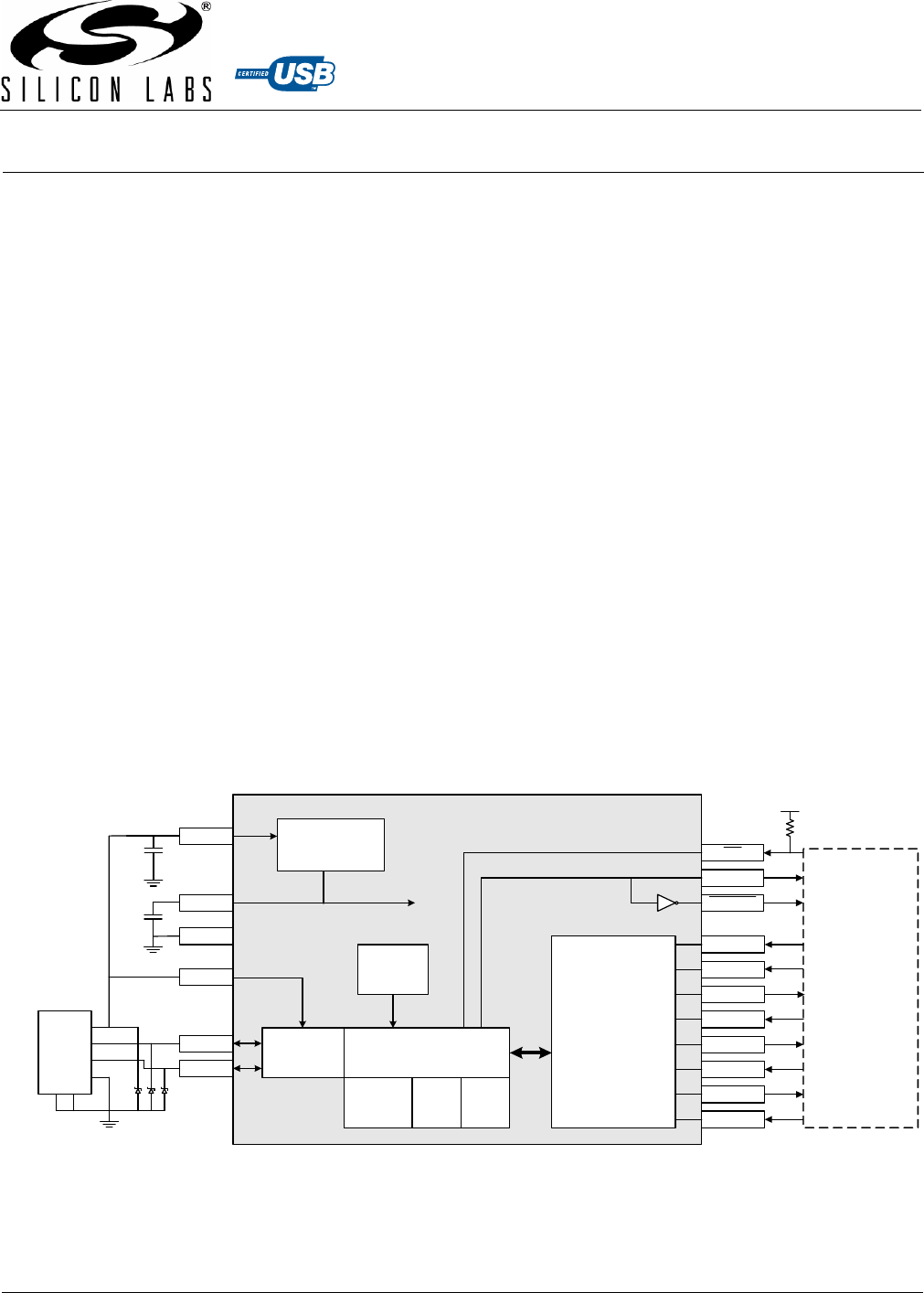
- Figure 1. Example System Diagram
- 1. System Overview
- 2. Electrical Specifications
- 3. Pinout and Package Definitions
- 4. USB Function Controller and Transceiver
- 5. Asynchronous Serial Data Bus (UART) Interface
- 6. Internal EEPROM
- 7. CP2102 Device Drivers
- 8. Voltage Regulator
- 9. Relevant Application Notes
- Document Change List
Rev. 1.4 8/10 Copyright © 2010 by Silicon Laboratories CP2102
CP2102
SINGLE-CHIP USB TO UART BRIDGE
Single-Chip USB to UART Data Transfer
-Integrated USB transceiver; no external resistors
required
-Integrated clock; no external crystal required
-Integrated 1024-Byte EEPROM for vendor ID, product
ID, serial number, power descriptor, release number,
and product description strings
-On-chip power-on reset circuit
-On-chip voltage regulator: 3.3 V output
-100% pin and software compatible with CP2101
USB Function Controller
-USB Specification 2.0 compliant; full-speed (12 Mbps)
-USB suspend states supported via SUSPEND pins
Asynchronous Serial Data BUS (UART)
-All handshaking and modem interface signals
-Data formats supported:
- Data bits: 5, 6, 7, and 8
- Stop bits: 1, 1.5, and 2
- Parity: odd, even, mark, space, no parity
-Baud rates: 300 bps to 1 Mbits
-576 Byte receive buffer; 640 byte transmit buffer
-Hardware or X-On/X-Off handshaking supported
-Event character support
-Line break transmission
Virtual COM Port Device Drivers
-Works with Existing COM Port PC Applications
-Royalty-Free Distribution License
-Windows Vista/XP/Server 2003/2000
-Mac OS-X/OS-9
-Linux
USBXpress™ Direct Driver Support
-Royalty-Free Distribution License
-Windows Vista/XP/Server 2003/2000
-Windows CE
Example Applications
-Upgrade of RS-232 legacy devices to USB
-Cellular phone USB interface cable
-PDA USB interface cable
-USB to RS-232 serial adapter
Supply Voltage
-Self-powered: 3.0 to 3.6 V
-USB bus powered: 4.0 to 5.25 V
Package
-Pb-free 28-pin QFN (5x5 mm)
Ordering Part Number
-CP2102-GM
Temperature Range: –40 to +85 °C
Figure 1. Example System Diagram
CP2102
3.3 V
Voltage
Regulator
48 MHz
Oscillator
IN
OUT
SUSPEND
SUSPEND
11
12
REGIN
7
GND
3
RST 9
D+
4
D-
5
8
UART
RI
DCD
CTS
RTS
RXD
TXD
DSR
DTR
2
27
26
25
24
23
2
3
External RS-232
transceiver or
UART circuitry
(to external circuitry
for USB suspend
states)
VBUS
D-
D+
GND 4
5
6
USB
CONNECTOR
6
1
VDD
VBUS
USB Function
Controller
USB
Transceiver
640B
TX
Buffer
576B
RX
Buffer
1024B
EEPROM
VDD
D1 D2 D3
1
28

CP2102
2 Rev. 1.4

CP2102
Rev. 1.4 3
TABLE OF CONTENTS
Section Page
1. System Overview . . . . . . . . . . . . . . . . . . . . . . . . . . . . . . . . . . . . . . . . . . . . . . . . . . . . . . . . .4
2. Electrical Specifications . . . . . . . . . . . . . . . . . . . . . . . . . . . . . . . . . . . . . . . . . . . . . . . . . . .5
3. Pinout and Package Definitions . . . . . . . . . . . . . . . . . . . . . . . . . . . . . . . . . . . . . . . . . . . . .7
4. USB Function Controller and Transceiver . . . . . . . . . . . . . . . . . . . . . . . . . . . . . . . . . . . .11
5. Asynchronous Serial Data Bus (UART) Interface . . . . . . . . . . . . . . . . . . . . . . . . . . . . . .12
6. Internal EEPROM . . . . . . . . . . . . . . . . . . . . . . . . . . . . . . . . . . . . . . . . . . . . . . . . . . . . . . . .12
7. CP2102 Device Drivers . . . . . . . . . . . . . . . . . . . . . . . . . . . . . . . . . . . . . . . . . . . . . . . . . . .13
7.1. Virtual COM Port Drivers . . . . . . . . . . . . . . . . . . . . . . . . . . . . . . . . . . . . . . . . . . . . . .13
7.2. USBXpress Drivers . . . . . . . . . . . . . . . . . . . . . . . . . . . . . . . . . . . . . . . . . . . . . . . . . .13
7.3. Driver Customization . . . . . . . . . . . . . . . . . . . . . . . . . . . . . . . . . . . . . . . . . . . . . . . . .13
7.4. Driver Certification . . . . . . . . . . . . . . . . . . . . . . . . . . . . . . . . . . . . . . . . . . . . . . . . . . .13
8. Voltage Regulator . . . . . . . . . . . . . . . . . . . . . . . . . . . . . . . . . . . . . . . . . . . . . . . . . . . . . . . .14
9. Relevant Application Notes . . . . . . . . . . . . . . . . . . . . . . . . . . . . . . . . . . . . . . . . . . . . . . . .16
Document Change List . . . . . . . . . . . . . . . . . . . . . . . . . . . . . . . . . . . . . . . . . . . . . . . . . . . . .17
Contact Information . . . . . . . . . . . . . . . . . . . . . . . . . . . . . . . . . . . . . . . . . . . . . . . . . . . . . . . .18

CP2102
4 Rev. 1.4
1. System Overview
The CP2102 is a highly-integrated USB-to-UART Bridge Controller providing a simple solution for updating RS-232
designs to USB using a minimum of components and PCB space. The CP2102 includes a USB 2.0 full-speed
function controller, USB transceiver, oscillator, EEPROM, and asynchronous serial data bus (UART) with full
modem control signals in a compact 5 x 5 mm QFN-28 package. No other external USB components are required.
The on-chip EEPROM may be used to customize the USB Vendor ID, Product ID, Product Description String,
Power Descriptor, Device Release Number, and Device Serial Number as desired for OEM applications. The
EEPROM is programmed on-board via the USB, allowing the programming step to be easily integrated into the
product manufacturing and testing process.
Royalty-free Virtual COM Port (VCP) device drivers provided by Silicon Laboratories allow a CP2102-based
product to appear as a COM port to PC applications. The CP2102 UART interface implements all RS-232 signals,
including control and handshaking signals, so existing system firmware does not need to be modified. In many
existing RS-232 designs, all that is required to update the design from RS-232 to USB is to replace the RS-232
level-translator with the CP2102. Direct access driver support is available through the Silicon Laboratories
USBXpress driver set.
An evaluation kit for the CP2102 (Part Number: CP2102EK) is available. It includes a CP2102-based USB-to-
UART/RS-232 evaluation board, a complete set of VCP device drivers, USB and RS-232 cables, and full
documentation. Contact a Silicon Labs sales representatives or go to www.silabs.com to order the CP2102
Evaluation Kit.
CP2102
Rev. 1.4 5
2. Electrical Specifications
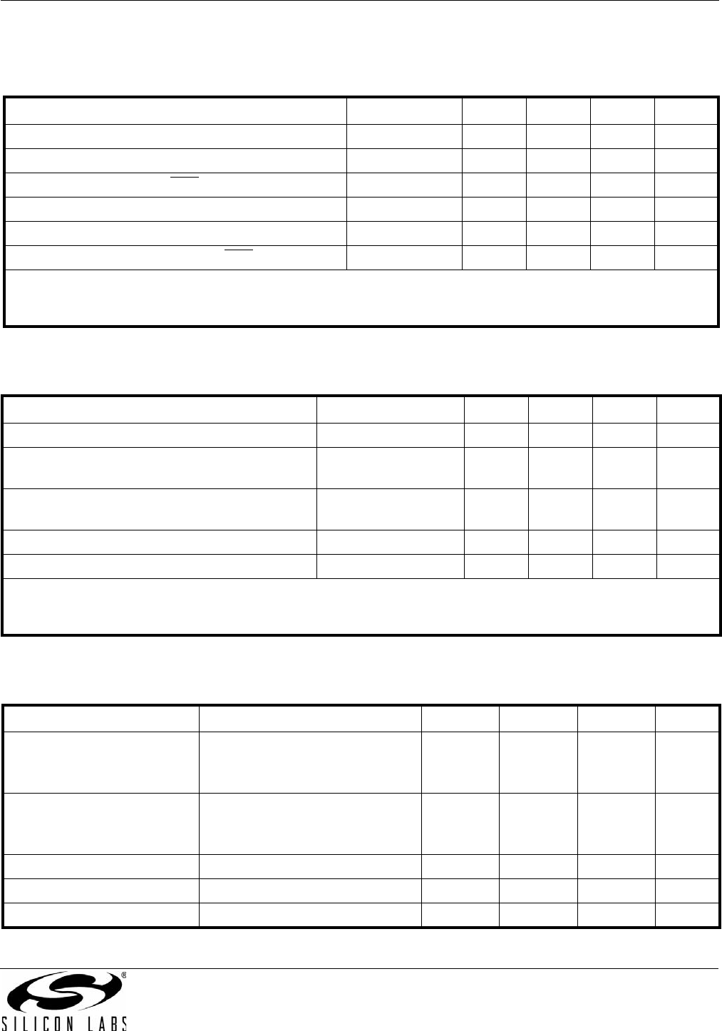
Table 1. Absolute Maximum Ratings
Parameter Conditions Min Typ Max Units
Ambient Temperature under Bias –55 — 125 °C
Storage Temperature –65 — 150 °C
Voltage on any I/O Pin or RST with respect to GND –0.3 — 5.8 V
Voltage on VDD with respect to GND –0.3 — 4.2 V
Maximum Total Current through VDD and GND ——500mA
Maximum Output Current sunk by RST or any I/O pin ——100mA
Note: Stresses above those listed may cause permanent device damage. This is a stress rating only, and functional
operation of the devices at or exceeding the conditions in the operation listings of this specification is not implied.
Exposure to maximum rating conditions for extended periods may affect device reliability.
Table 2. Global DC Electrical Characteristics
VDD = 3.0 to 3.6 V, –40 to +85 °C unless otherwise specified
Parameter Conditions Min Typ Max Units
Supply Voltage 3.0 3.3 3.6 V
Supply Current1Normal Operation;
VREG Enabled —2026mA
Supply Current1Suspended:
VREG Enabled —80100µA
Supply Current - USB Pull-up2—200228µA
Specified Operating Temperature Range –40 — +85 °C
Notes:
1. USB Pull-up Current should be added for total supply current.
2. The USB Pull-up supply current values are calculated values based on USB specifications.
Table 3. UART and Suspend I/O DC Electrical Characteristics
VDD = 3.0 to 3.6 V, –40 to +85 °C unless otherwise specified
Parameters Conditions Min Typ Max UNITS
Output High Voltage IOH =–3mA
IOH =–10µA
IOH =–10mA
VDD –0.7
VDD –0.1
—
—
—
VDD –0.8
—
—
—
V
Output Low Voltage IOL =8.5mA
IOL =10µA
IOL =25mA
—
—
—
—
—
1.0
0.6
0.1
—
V
Input High Voltage 2.0 — — V
Input Low Voltage ——0.8V
Input Leakage Current —2550µA

CP2102
6 Rev. 1.4
Table 4. Reset Electrical Characteristics
–40 to +85 °C unless otherwise specified
Parameter Conditions Min Typ Max Units
RST Input High Voltage 0.7 x VDD ——V
RST Input Low Voltage — — 0.25 x VDD V
Minimum RST Low Time to Gener-
ate a System Reset 15 — — µs
CP2102
Rev. 1.4 7
3. Pinout and Package Definitions
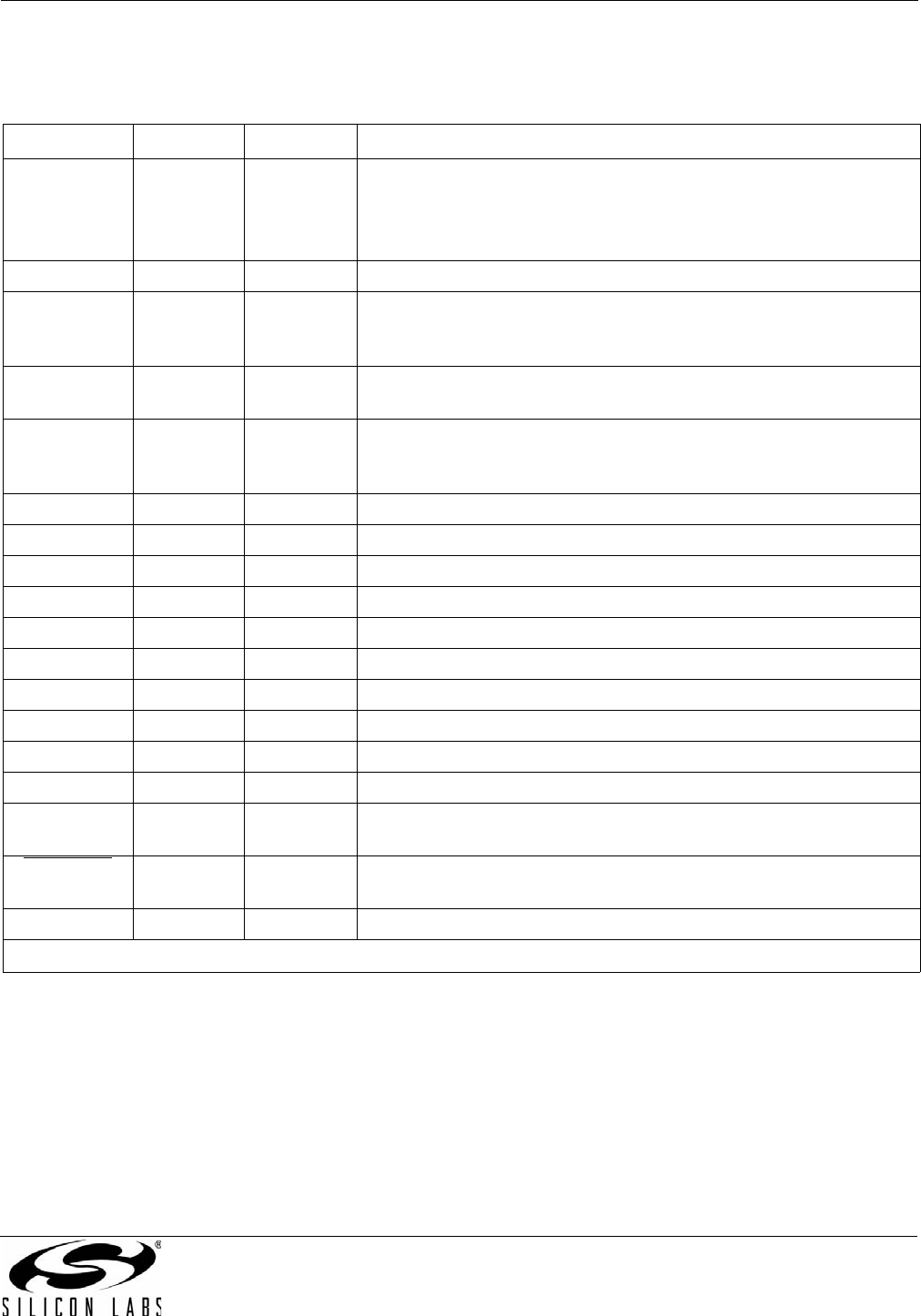
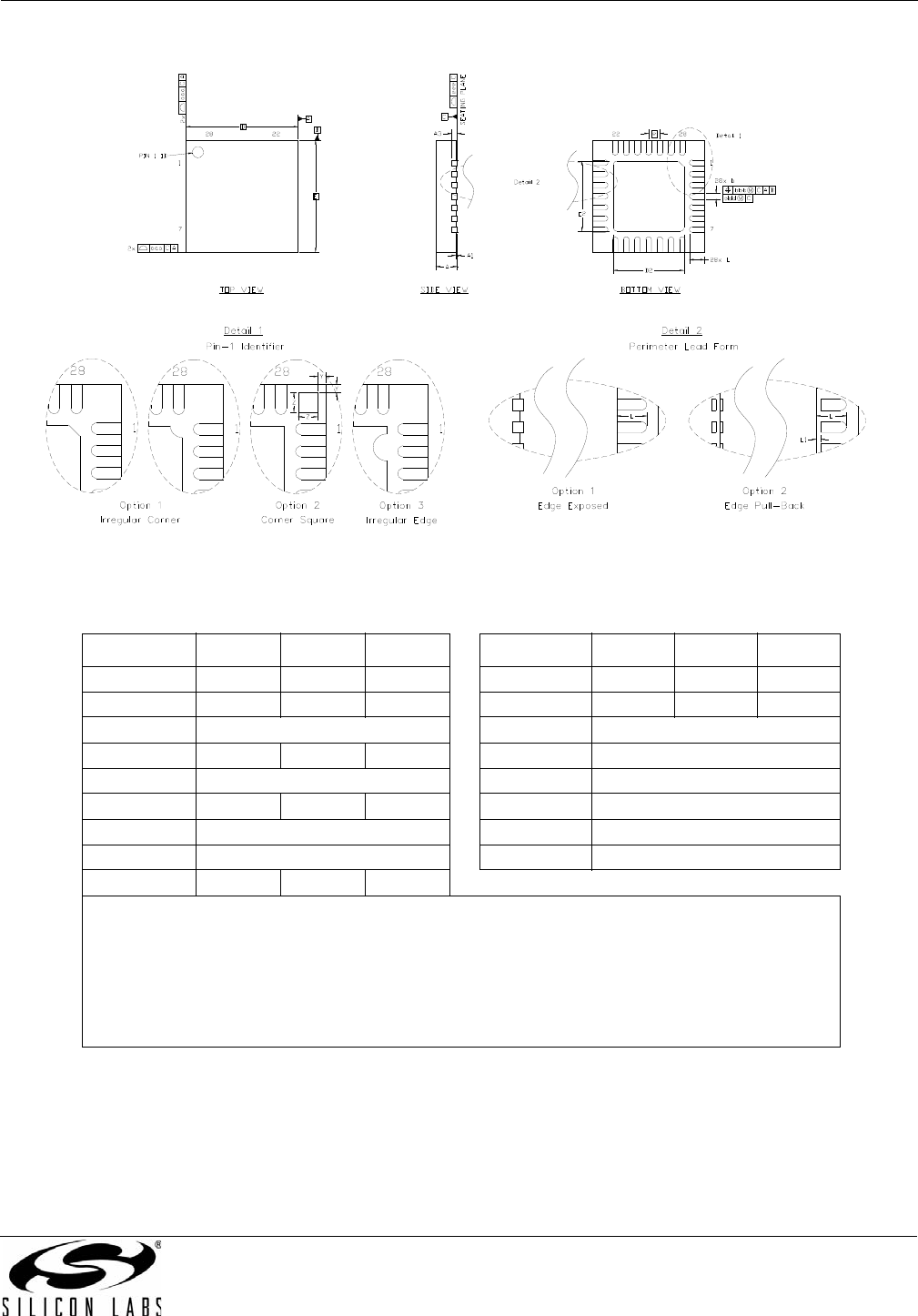
Table 5. CP2102 Pin Definitions
Name Pin # Type Description
VDD 6 Power In
Power Out
3.0–3.6 V Power Supply Voltage Input.
3.3 V Voltage Regulator Output.
See "8. Voltage Regulator" on page 14.
GND 3 Ground
RST 9 D I/O Device Reset. Open-drain output of internal POR or VDD monitor. An
external source can initiate a system reset by driving this pin low for
at least 15 µs.
REGIN 7 Power In 5 V Regulator Input. This pin is the input to the on-chip voltage regu-
lator.
VBUS 8 D In VBUS Sense Input. This pin should be connected to the VBUS signal
of a USB network. A 5 V signal on this pin indicates a USB network
connection.
D+ 4 D I/O USB D+
D– 5 D I/O USB D–
TXD 26 D Out Asynchronous data output (UART Transmit)
RXD 25 D In Asynchronous data input (UART Receive)
CTS 23* D In Clear To Send control input (active low)
RTS 24* D Out Ready to Send control output (active low)
DSR 27* D in Data Set Ready control input (active low)
DTR 28* D Out Data Terminal Ready control output (active low)
DCD 1* D In Data Carrier Detect control input (active low)
RI 2* D In Ring Indicator control input (active low)
SUSPEND 12* D Out This pin is driven high when the CP2102 enters the USB suspend
state.
SUSPEND 11* D Out This pin is driven low when the CP2102 enters the USB suspend
state.
NC 10, 13–22 These pins should be left unconnected or tied to VDD.
*Note: Pins can be left unconnected when not used.
CP2102
8 Rev. 1.4
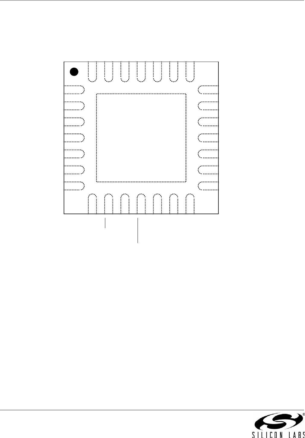
Figure 2. QFN-28 Pinout Diagram (Top View)
4
5
6
7
2
1
3
11
12
13
14
9
8
10
18
17
16
15
20
21
19
25
26
27
28
23
22
24
CP2102
Top View
DCD
RI
GND
D+
D-
VDD
REGIN
VBUS
RST
NC
SUSPEND
SUSPEND
NC
NC
NC
NC
NC
NC
NC
NC
NC
NC
CTS
RTS
RXD
TXD
DSR
DTR
GND
CP2102
Rev. 1.4 9
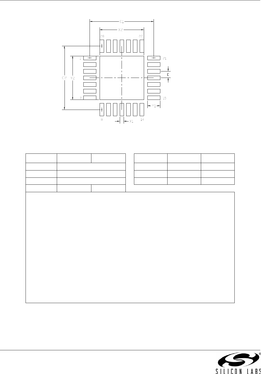
Figure 3. QFN-28 Package Drawing
Table 6. QFN-28 Package Dimensions
Dimension Min Typ Max Dimension Min Typ Max
A 0.80 0.90 1.00 L 0.35 0.55 0.65
A1 0.00 0.02 0.05 L1 0.00 — 0.15
A3 0.25 REF aaa 0.15
b 0.18 0.23 0.30 bbb 0.10
D 5.00 BSC. ddd 0.05
D2 2.90 3.15 3.35 eee 0.08
e 0.50 BSC. Z 0.44
E 5.00 BSC. Y 0.18
E2 2.90 3.15 3.35
Notes:
1. All dimensions shown are in millimeters (mm) unless otherwise noted.
2. Dimensioning and Tolerancing per ANSI Y14.5M-1994.
3. This drawing conforms to the JEDEC Solid State Outline MO-220, variation VHHD except for
custom features D2, E2, Z, Y, and L, which are toleranced per supplier designation.
4. Recommended card reflow profile is per the JEDEC/IPC J-STD-020 specification for Small Body
Components.
CP2102
10 Rev. 1.4
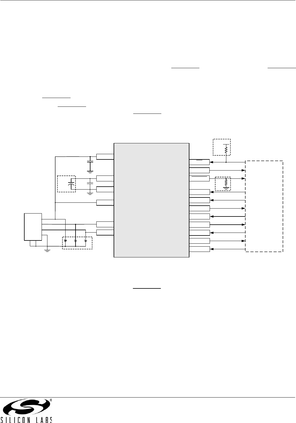
Figure 4. QFN-28 Recommended PCB Land Pattern
Table 7. QFN-28 PCB Land Pattern Dimensions
Dimension Min Max Dimension Min Max
C1 4.80 X2 3.20 3.30
C2 4.80 Y1 0.85 0.95
E 0.50 Y2 3.20 3.30
X1 0.20 0.30
Notes:
General
1. All dimensions shown are in millimeters (mm) unless otherwise noted.
2. Dimensioning and Tolerancing is per the ANSI Y14.5M-1994 specification.
3. This Land Pattern Design is based on the IPC-7351 guidelines.
Solder Mask Design
4. All metal pads are to be non-solder mask defined (NSMD). Clearance between the solder
mask and the metal pad is to be 60 µm minimum, all the way around the pad.
Stencil Design
5. A stainless steel, laser-cut and electro-polished stencil with trapezoidal walls should be used
to assure good solder paste release.
6. The stencil thickness should be 0.125 mm (5 mils).
7. The ratio of stencil aperture to land pad size should be 1:1 for all perimeter pins.
8. A 3x3 array of 0.90 mm openings on a 1.1 mm pitch should be used for the center pad to
assure the proper paste volume (67% Paste Coverage).
Card Assembly
9. A No-Clean, Type-3 solder paste is recommended.
10. The recommended card reflow profile is per the JEDEC/IPC J-STD-020 specification for Small
Body Components.
CP2102
Rev. 1.4 11
4. USB Function Controller and Transceiver
The Universal Serial Bus function controller in the CP2102 is a USB 2.0 compliant full-speed device with integrated
transceiver and on-chip matching and pull-up resistors. The USB function controller manages all data transfers
between the USB and the UART as well as command requests generated by the USB host controller and
commands for controlling the function of the UART.
The USB Suspend and Resume signals are supported for power management of both the CP2102 device as well
as external circuitry. The CP2102 will enter Suspend mode when Suspend signaling is detected on the bus. On
entering Suspend mode, the CP2102 asserts the SUSPEND and SUSPEND signals. SUSPEND and SUSPEND
are also asserted after a CP2102 reset until device configuration during USB Enumeration is complete.
The CP2102 exits the Suspend mode when any of the following occur: (1) Resume signaling is detected or
generated, (2) a USB Reset signal is detected, or (3) a device reset occurs. On exit of Suspend mode, the
SUSPEND and SUSPEND signals are de-asserted.
Both SUSPEND and SUSPEND temporarily float high during a CP2102 reset. If this behavior is undesirable, a
strong pulldown (10 k) can be used to ensure SUSPEND remains low during reset. See Figure 5 for other
recommended options.
Figure 5. Typical Connection Diagram
Option 1: A 4.7 k pull-up resistor can be added to increase noise immunity.
Option 2: A 4.7 µF capacitor can be added if powering other devices from the on-chip regulator.
Option 3: Avalanche transient voltage suppression diodes should be added for ESD protection.
Option 3: Use Littlefuse p/n SP0503BAHT or equivalent.
Option 4: 10 k resistor to ground to hold SUSPEND low on initial power on or device reset.
1
CP2102
SUSPEND
SUSPEND
11
12
REGIN
7
GND
3
RST 9
D+
4
D-
5
8
C2
0.1 F
C1
1 F
RI
DCD
CTS
RTS
RXD
TXD
DSR
DTR
2
1
28
27
26
25
24
23
2
3
External RS-232
transceiver or
UART circuitry
(to external circuitry
for USB suspend
states)
VBUS
D-
D+
GND 4
5
6
USB
CONNECTOR
6VDD
VBUS
VDD
R1
4.7 k
D1 D2 D3
Option 1
R2
10 k
Option 4
Option 3
C4
4.7 F
Option 2

CP2102
12 Rev. 1.4
5. Asynchronous Serial Data Bus (UART) Interface
The CP2102 UART interface consists of the TX (transmit) and RX (receive) data signals as well as the RTS, CTS,
DSR, DTR, DCD, and RI control signals. The UART supports RTS/CTS, DSR/DTR, and X-On/X-Off handshaking.
The UART is programmable to support a variety of data formats and baud rates. If the Virtual COM Port drivers are
used, the data format and baud rate are set during COM port configuration on the PC. If the USBXpress drivers are
used, the CP2102 is configured through the USBXpress API. The data formats and baud rates available are listed
in Table 8.
6. Internal EEPROM
The CP2102 includes an internal EEPROM that may be used to customize the USB Vendor ID (VID), Product ID
(PID), Product Description String, Power Descriptor, Device Release Number and Device Serial Number as
desired for OEM applications. If the EEPROM is not programmed with OEM data, the default configuration data
shown in Table 9 is used.
While customization of the USB configuration data is optional, it is recommended to customize the VID/PID
combination. A unique VID/PID combination will prevent the driver from conflicting with any other USB driver. A
vendor ID can be obtained from http://www.usb.org/ or Silicon Laboratories can provide a free PID for the OEM
product that can be used with the Silicon Laboratories VID. It is also recommended to customize the serial number
if the OEM application is one in which it is possible for multiple CP2102-based devices to be connected to the
same PC.
The internal EEPROM is programmed via the USB. This allows the OEM's USB configuration data and serial
number to be written to the CP2102 on-board during the manufacturing and testing process. A stand-alone utility
for programming the internal EEPROM is available from Silicon Laboratories. A library of routines provided in the
form of a Windows® DLL is also available. This library can be used to integrate the EEPROM programming step
into custom software used by the OEM to streamline testing and serial number management during manufacturing.
The EEPROM has a typical endurance of 100,000 write cycles with a data retention of 100 years.
USB descriptors can be locked to prevent future modification.
Table 8. Data Formats and Baud Rates
Data Bits 5, 6, 7, and 8
Stop Bits 1, 1.51, and 2
Parity Type None, Even, Odd, Mark, Space
Baud Rates2300, 600, 1200, 1800, 2400, 4000, 4800, 7200, 9600, 14400, 16000, 19200, 28800,
38400, 51200, 56000, 57600, 64000, 76800, 115200, 128000, 153600, 230400, 250000,
256000, 460800, 500000, 576000, 9216003
Notes:
1. 5-bit only.
2. Additional baud rates are supported. See “AN205”.
3. 7 or 8 data bits only.
CP2102
14 Rev. 1.4
8. Voltage Regulator
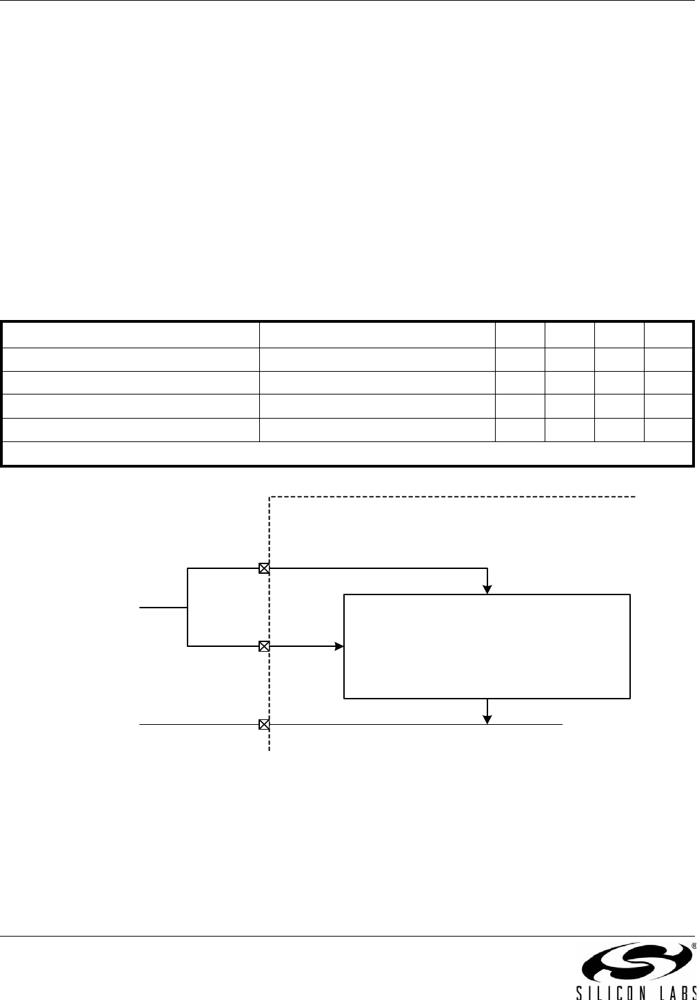
The CP2102 includes an on-chip 5 to 3 V voltage regulator. This allows the CP2102 to be configured as either a
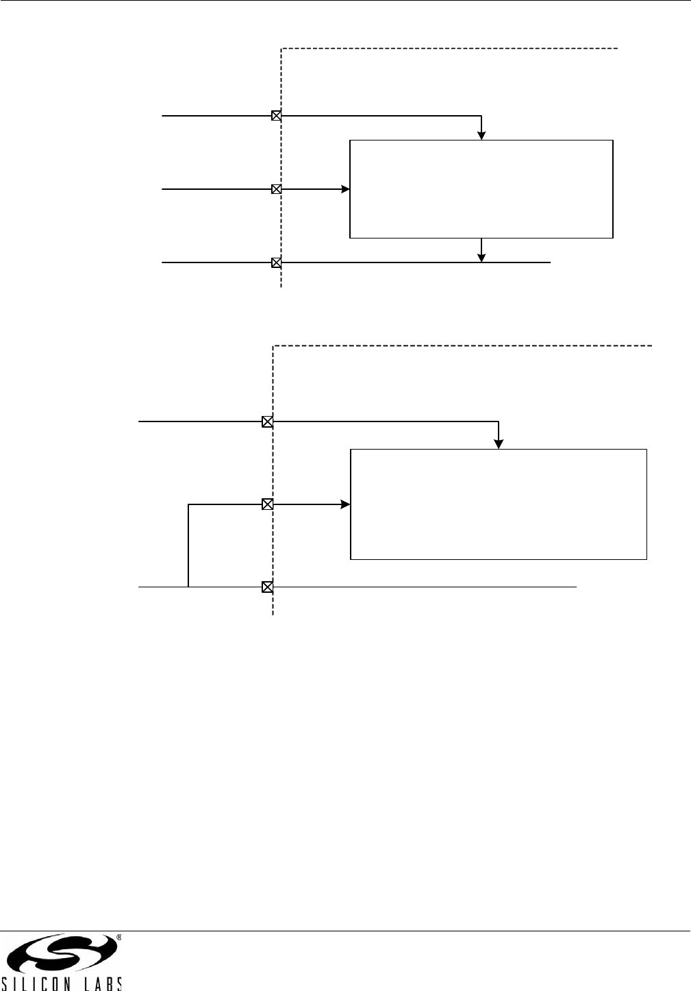
USB bus-powered device or a USB self-powered device. These configurations are shown in Figure 6 and Figure 7.
When enabled, the 3 V voltage regulator output appears on the VDD pin and can be used to power external 3 V
devices. See Table 10 for the voltage regulator electrical characteristics.
Alternatively, if 3 V power is supplied to the VDD pin, the CP2102 can function as a USB self-powered device with
the voltage regulator disabled. For this configuration, it is recommended that the REGIN input be tied to the 3 V net
to disable the voltage regulator. This configuration is shown in Figure 8.
The USB max power and power attributes descriptor must match the device power usage and configuration. See
application note “AN144: CP210x Customization Guide” for information on how to customize USB descriptors for
the CP2102.
Note: It is recommended that additional decoupling capacitance (e.g., 0.1 µF in parallel with 1.0 µF) be provided on the REGIN
input.
Figure 6. Configuration 1: USB Bus-Powered
Table 10. Voltage Regulator Electrical Specifications
–40 to +85 °C unless otherwise specified.
Parameter Conditions Min Typ Max Units
Input Voltage Range 4.0 — 5.25 V
Output Voltage Output Current = 1 to 100 mA* 3.0 3.3 3.6 V
VBUS Detection Input Threshold 1.0 1.8 2.9 V
Bias Current —90—µA
*Note: The maximum regulator supply current is 100 mA.
Voltage Regulator (REG0)5 V In
3 V Out
VBUS Sense
REGIN
VBUS
From VBUS
To 3 V
Power Net Device
Power Net
VDD
CP2102
CP2102
Rev. 1.4 15
Figure 7. Configuration 2: USB Self-Powered
Figure 8. Configuration 3: USB Self-Powered, Regulator Bypassed
Voltage Regulator (REG0)5 V In
3 V Out
VBUS Sense
REGIN
VBUS
To 3V
Power Net Device
Power Net
VDD
CP2102
From 5 V
Power Net
From VBUS
Voltage Regulator (REG0)5 V In
3 V Out
VBUS Sense
REGIN
VBUS
From 3 V
Power Net Device
Power Net
VDD
CP2102
From VBUS

CP2102
Rev. 1.4 17
DOCUMENT CHANGE LIST
Revision 1.0 to Revision 1.1
Updated “Linux 2.40” bullet on page 1.
Changed MLP to QFN throughout.
Revision 1.1 to Revision 1.2
Added additional supported operating systems on
page 1.
Changed VDD conditions of Tables 2 and 3 from a
minimum of 2.7 to 3.0 V.
Updated typical and max Supply Current number in
Table 2.
Removed tantalum requirement in Figure 5.
Consolidated Sections 8 and 9.
Added Section "9. Relevant Application Notes" on
page 16.
Revision 1.2 to Revision 1.3
Updated Figure 1 on page 1.
Updated Figure 5 on page 11.
Updated Maximum VBUS Detection Input Threshold
in Table 10 on page 14.
Revision 1.3 to Revision 1.4
Updated Table 4 RST Input Low Voltage
Updated Table 6, Note 4.
Updated Table 7, Note 10.