IRF2807 Datasheet. Www.s Manuals.com. Irf2708 Irf
User Manual: Datasheets IRF2807.
Open the PDF directly: View PDF ![]() .
.
Page Count: 9
IRF2807
HEXFET® Power MOSFET
3/16/01
Parameter Typ. Max. Units
RθJC Junction-to-Case ––– 0.65
RθCS Case-to-Sink, Flat, Greased Surface 0.50 ––– °C/W
RθJA Junction-to-Ambient ––– 62
Thermal Resistance
www.irf.com 1
VDSS = 75V
RDS(on) = 13mΩ
ID = 82A
S
D
G
TO-220AB
Advanced HEXFET® Power MOSFETs from International
Rectifier utilize advanced processing techniques to achieve
extremely low on-resistance per silicon area. This benefit,
combined with the fast switching speed and ruggedized
device design that HEXFET power MOSFETs are well
known for, provides the designer with an extremely efficient
and reliable device for use in a wide variety of applications.
The TO-220 package is universally preferred for all
commercial-industrial applications at power dissipation
levels to approximately 50 watts. The low thermal
resistance and low package cost of the TO-220 contribute
to its wide acceptance throughout the industry.
lAdvanced Process Technology
lUltra Low On-Resistance
lDynamic dv/dt Rating
l175°C Operating Temperature
lFast Switching
lFully Avalanche Rated
Description
PD - 91517
Absolute Maximum Ratings
Parameter Max. Units
ID @ TC = 25°C Continuous Drain Current, VGS @ 10V 82
ID @ TC = 100°C Continuous Drain Current, VGS @ 10V 58 A
IDM Pulsed Drain Current 280
PD @TC = 25°C Power Dissipation 230 W
Linear Derating Factor 1.5 W/°C
VGS Gate-to-Source Voltage ± 20 V
IAR Avalanche Current43 A
EAR Repetitive Avalanche Energy23 mJ
dv/dt Peak Diode Recovery dv/dt 5.9 V/ns
TJOperating Junction and -55 to + 175
TSTG Storage Temperature Range
Soldering Temperature, for 10 seconds 300 (1.6mm from case )
°C
Mounting torque, 6-32 or M3 srew 10 lbf•in (1.1N•m)
IRF2807
2 www.irf.com
S
D
G
Parameter Min. Typ. Max. Units Conditions
ISContinuous Source Current MOSFET symbol
(Body Diode) ––– ––– showing the
ISM Pulsed Source Current integral reverse
(Body Diode)
––– ––– p-n junction diode.
VSD Diode Forward Voltage ––– ––– 1.2 V TJ = 25°C, IS = 43A, VGS = 0V
trr Reverse Recovery Time ––– 100 150 ns TJ = 25°C, IF = 43A
Qrr Reverse Recovery Charge ––– 410 610 nC di/dt = 100A/µs
ton Forward Turn-On Time Intrinsic turn-on time is negligible (turn-on is dominated by LS+LD)
Source-Drain Ratings and Characteristics
82
280
A
Starting TJ = 25°C, L = 370µH
RG = 25Ω, IAS = 43A, VGS=10V (See Figure 12)
Repetitive rating; pulse width limited by
max. junction temperature. (See fig. 11)
Notes:
ISD ≤ 43A, di/dt ≤ 300A/µs, VDD ≤ V(BR)DSS,
TJ ≤ 175°C
Pulse width ≤ 400µs; duty cycle ≤ 2%.
This is a typical value at device destruction and represents
operation outside rated limits.
This is a calculated value limited to TJ = 175°C .
Calculated continuous current based on maximum allowable
junction temperature. Package limitation current is 75A.
Parameter Min. Typ. Max. Units Conditions
V(BR)DSS Drain-to-Source Breakdown Voltage 75 ––– ––– V VGS = 0V, ID = 250µA
∆V(BR)DSS/∆TJBreakdown Voltage Temp. Coefficient ––– 0.074 ––– V/°C Reference to 25°C, ID = 1mA
RDS(on) Static Drain-to-Source On-Resistance ––– ––– 13 mΩVGS = 10V, ID = 43A
VGS(th) Gate Threshold Voltage 2.0 ––– 4.0 V VDS = VGS, ID = 250µA
gfs Forward Transconductance 38 ––– ––– S VDS = 50V, ID = 43A
––– ––– 25 µA VDS = 75V, VGS = 0V
––– ––– 250 VDS = 60V, VGS = 0V, TJ = 150°C
Gate-to-Source Forward Leakage ––– ––– 100 VGS = 20V
Gate-to-Source Reverse Leakage ––– ––– -100 nA VGS = -20V
QgTotal Gate Charge ––– ––– 160 ID = 43A
Qgs Gate-to-Source Charge ––– ––– 29 nC VDS = 60V
Qgd Gate-to-Drain ("Miller") Charge ––– ––– 55 VGS = 10V, See Fig. 6 and 13
td(on) Turn-On Delay Time ––– 13 ––– VDD = 38V
trRise Time ––– 64 ––– ID = 43A
td(off) Turn-Off Delay Time ––– 49 ––– RG = 2.5Ω
tfFall Time ––– 48 ––– VGS = 10V, See Fig. 10
Between lead,
––– ––– 6mm (0.25in.)
from package
and center of die contact
Ciss Input Capacitance ––– 3820 ––– VGS = 0V
Coss Output Capacitance ––– 610 ––– VDS = 25V
Crss Reverse Transfer Capacitance ––– 130 ––– pF ƒ = 1.0MHz, See Fig. 5
EAS Single Pulse Avalanche Energy––– 1280340mJ IAS = 50A, L = 370µH
nH
Electrical Characteristics @ TJ = 25°C (unless otherwise specified)
LDInternal Drain Inductance
LSInternal Source Inductance ––– –––
S
D
G
IGSS
ns
4.5
7.5
IDSS Drain-to-Source Leakage Current
IRF2807
www.irf.com 3
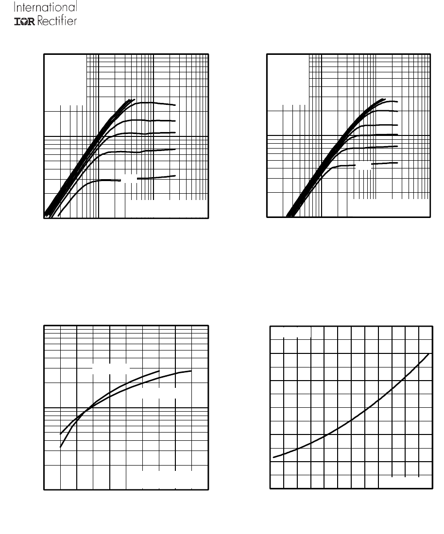
Fig 4. Normalized On-Resistance
Vs. Temperature
Fig 2. Typical Output CharacteristicsFig 1. Typical Output Characteristics
Fig 3. Typical Transfer Characteristics
10
100
1000
0.1 1 10 100
20
µ
s PULSE WIDTH
T = 25 C
J°
TOP
BOTTOM
VGS
15V
10V
8.0V
7.0V
6.0V
5.5V
5.0V
4.5V
V , Drain-to-Source Voltage (V)
I , Drain-to-Source Current (A)
DS
D
4.5V
10
100
1000
0.1 1 10 100
20
µ
s PULSE WIDTH
T = 175 C
J°
TOP
BOTTOM
VGS
15V
10V
8.0V
7.0V
6.0V
5.5V
5.0V
4.5V
V , Drain-to-Source Volta
g
e (V)
I , Drain-to-Source Current (A)
DS
D
4.5V
10
100
1000
4.0 5.0 6.0 7.0 8.0 9.0
V = 25V
20µs PULSE WIDTH
DS
V , Gate-to-Source Voltage (V)
I , Drain-to-Source Current (A)
GS
D
T = 25 C
J°
T = 175 C
J°
-60 -40 -20 0 20 40 60 80 100 120 140 160 180
0.0
0.5
1.0
1.5
2.0
2.5
3.0
T , Junction Temperature ( C)
R , Drain-to-Source On Resistance
(Normalized)
J
DS(on)
°
V =
I =
GS
D
10V
71A
IRF2807
4 www.irf.com
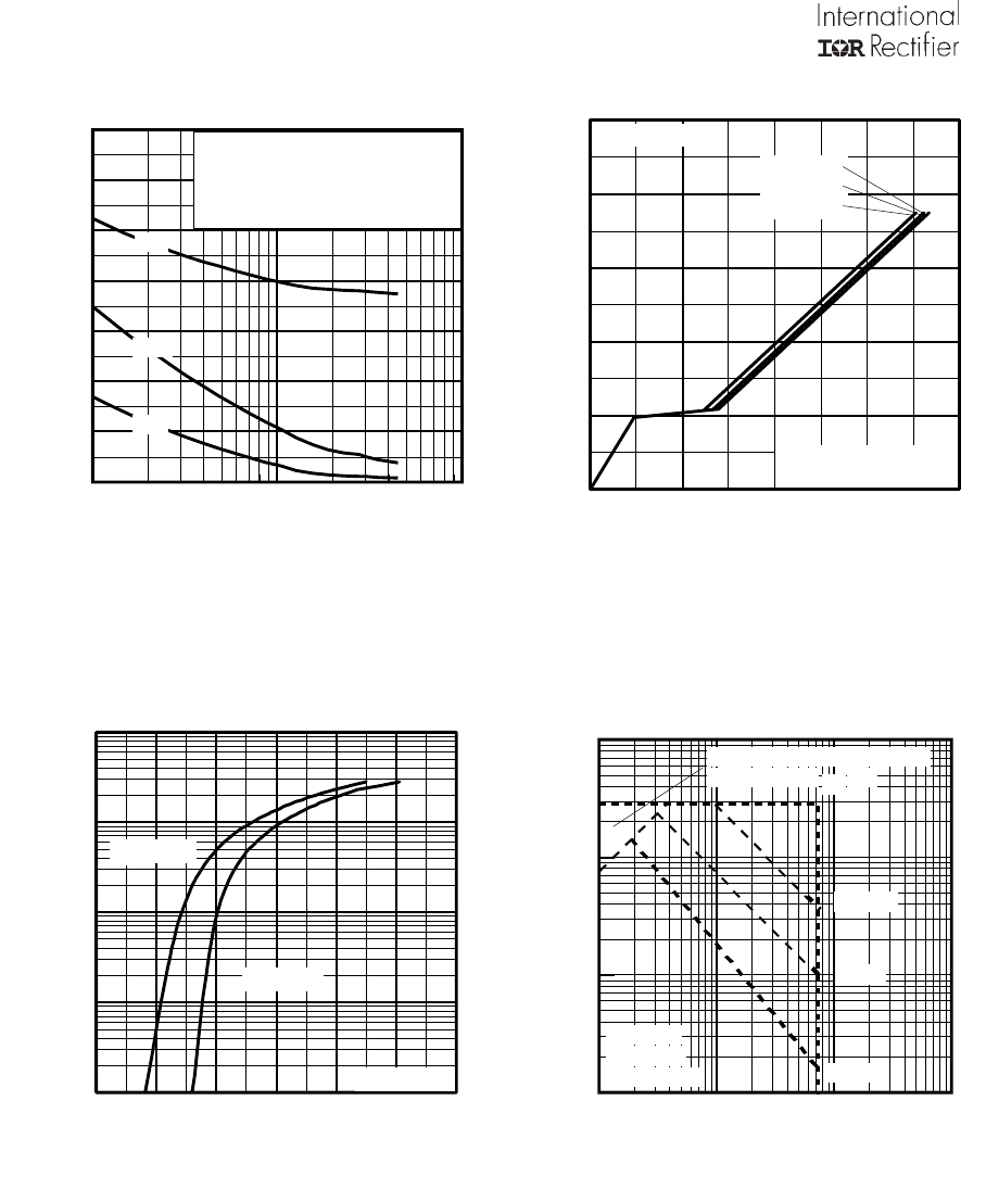
Fig 8. Maximum Safe Operating Area
Fig 6. Typical Gate Charge Vs.
Gate-to-Source Voltage
Fig 5. Typical Capacitance Vs.
Drain-to-Source Voltage
Fig 7. Typical Source-Drain Diode
Forward Voltage
040 80 120 160
0
4
8
12
16
20
Q , Total Gate Charge (nC)
V , Gate-to-Source Voltage (V)
G
GS
FOR TEST CIRCUIT
SEE FIGURE
I =
D
13
43A
V = 15V
DS
V = 37V
DS
V = 60V
DS
0.1
1
10
100
1000
0.0 0.4 0.8 1.2 1.6 2.0 2.4
V ,Source-to-Drain Volta
g
e (V)
I , Reverse Drain Current (A)
SD
SD
V = 0 V
GS
T = 25 C
J°
T = 175 C
J°
110 100
VDS, Drain-to-Source Voltage (V)
0
1000
2000
3000
4000
5000
6000
7000
C, Capacitance(pF)
Coss
Crss
Ciss
VGS
= 0V, f = 1 MHZ
Ciss
= C
gs + C
gd, C
ds SHORTED
Crss
= C
gd
Coss
= C
ds
+ C
gd
1 10 100 1000
VDS , Drain-toSource Voltage (V)
1
10
100
1000
ID, Drain-to-Source Current (A)
Tc = 25°C
Tj = 175°C
Single Pulse
1msec
10msec
OPERATION IN THIS AREA
LIMITED BY R DS(on)
100µsec
IRF2807
www.irf.com 5
Fig 11. Maximum Effective Transient Thermal Impedance, Junction-to-Case
Fig 9. Maximum Drain Current Vs.
Case Temperature
0.01
0.1
1
0.00001 0.0001 0.001 0.01 0.1
Notes:
1. Duty factor D = t / t
2. Peak T =P x Z + T
1 2
JDM thJC C
P
t
t
DM
1
2
t , Rectangular Pulse Duration (sec)
Thermal Response (Z )
1
thJC
0.01
0.02
0.05
0.10
0.20
D = 0.50
SINGLE PULSE
(THERMAL RESPONSE)
25 50 75 100 125 150 175
0
20
40
60
80
100
T , Case Temperature ( C)
I , Drain Current (A)
°
C
D
LIMITED BY PACKAGE
V
DS
90%
10%
V
GS
t
d(on)
t
r
t
d(off)
t
f
VDS
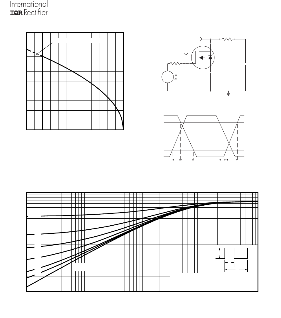
Pulse Width ≤ 1 µs
Duty Factor ≤ 0.1 %
RD
VGS
RG
D.U.T.
VGS
+
-
VDD
Fig 10a. Switching Time Test Circuit
Fig 10b. Switching Time Waveforms
IRF2807
6 www.irf.com
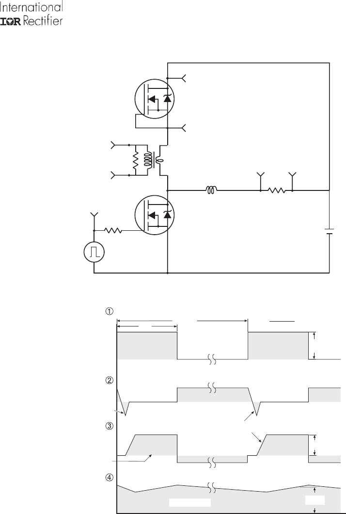
Q
G
Q
GS
Q
GD
V
G
Charge
D.U.T. V
DS
I
D
I
G
3mA
V
GS
.3µF
50KΩ
.2µF
12V
Current Regulator
Same Type as D.U.T.
Current Sampling Resistors
+
-
VGS
Fig 13b. Gate Charge Test Circuit
Fig 13a. Basic Gate Charge Waveform
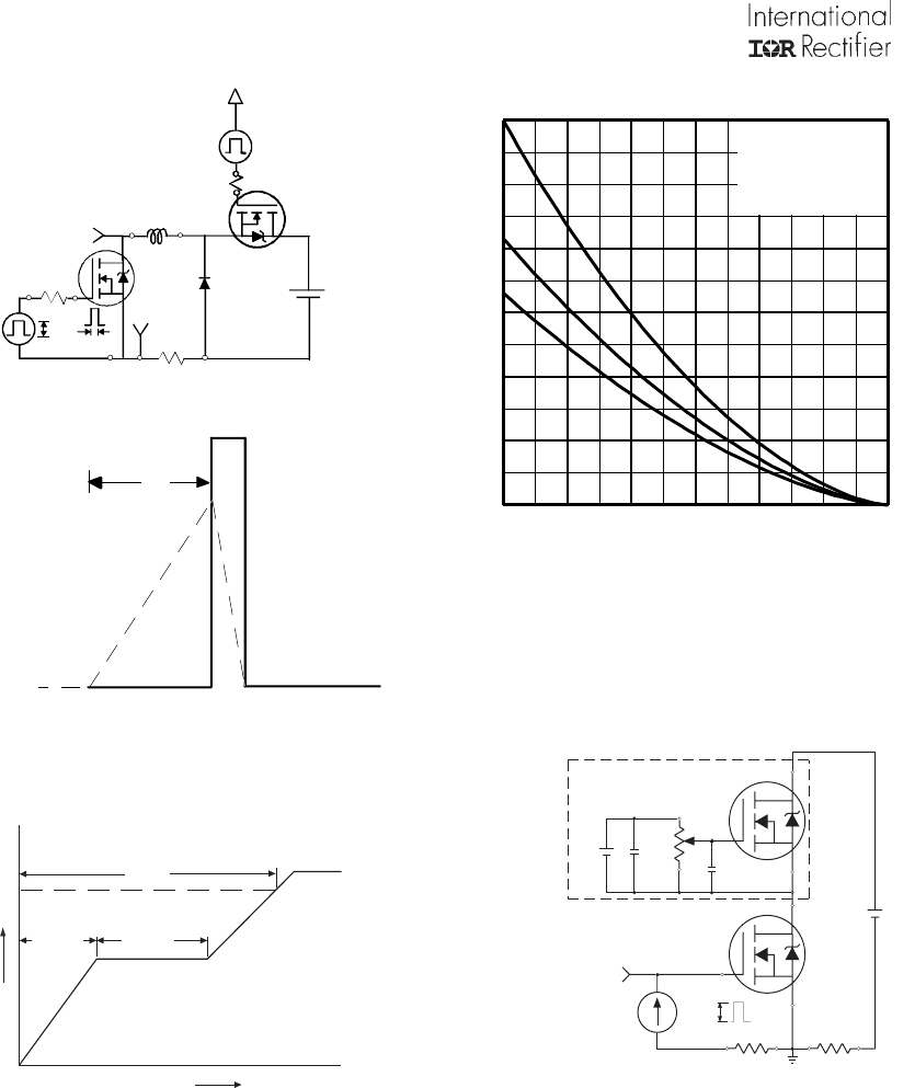
Fig 12b. Unclamped Inductive Waveforms
Fig 12a. Unclamped Inductive Test Circuit
tp
V
(BR)DSS
I
AS
Fig 12c. Maximum Avalanche Energy
Vs. Drain Current
25 50 75 100 125 150 175
0
100
200
300
400
500
600
Starting T , Junction Temperature ( C)
E , Single Pulse Avalanche Energy (mJ)
J
AS
°
ID
TOP
BOTTOM
18A
30A
43A
RG
I
AS
0.01
Ω
t
p
D.U.T
L
VDS
+
-V
DD
DRIVER
A
15V
20V
VGS
IRF2807
www.irf.com 7
Peak Diode Recovery dv/dt Test Circuit
P.W. Period
di/dt
Diode Recovery
dv/dt
Ripple ≤5%
Body Diode Forward Drop
Re-Applied
Voltage
Reverse
Recovery
Current Body Diode Forward
Current
V
GS
=10V
V
DD
I
SD
Driver Gate Drive
D.U.T. I
SD
Waveform
D.U.T. V
DS
Waveform
Inductor Curent
D = P.W.
Period
+
-
+
+
+
-
-
-
RG
VDD
• dv/dt controlled by RG
• ISD controlled by Duty Factor "D"
• D.U.T. - Device Under Test
D.U.T*Circuit Layout Considerations
• Low Stray Inductance
• Ground Plane
• Low Leakage Inductance
Current Transformer
* Reverse Polarity of D.U.T for P-Channel
VGS
[ ]
[ ]
*** VGS = 5.0V for Logic Level and 3V Drive Devices
[ ] ***
Fig 14. For N-channel HEXFET® power MOSFETs
IRF2807
8 www.irf.com
LEAD ASSIGNMENTS
1 - GATE
2 - DRAIN
3 - SOURCE
4 - DRAIN
- B -
1.32 (.052)
1.22 (.048)
3X 0.55 (.022)
0.46 (.018)
2.92 (.115)
2.64 (.104)
4.69 (.185)
4.20 (.165)
3X 0.93 (.037)
0.69 (.027)
4.06 (.160)
3.55 (.140)
1.15 (.045)
M IN
6.47 (.255)
6.10 (.240)
3.78 (.149)
3.54 (.139)
- A -
10.54 (.415)
10.29 (.405)
2.87 (.113)
2.62 (.103)
15.24 (.600)
14.84 (.584)
14.09 (.555)
13.47 (.530)
3X 1.40 (.055)
1.15 (.045)
2.54 (.100)
2X
0.36 (.014) M B A M
4
1 2 3
NOTES:
1 D IM E NSIO N ING & TOL E R ANC ING P E R AN S I Y14.5M, 19 82. 3 OUT LINE C O NFO R MS TO JE D E C O UTLIN E TO -220A B .
2 CONTROLLING DIMENSION : INCH 4 HEATSINK & LEAD MEASUREMENTS DO NOT INCLUDE BURRS.
Part Marking Information
TO-220AB
Package Outline
TO-220AB
Dimensions are shown in millimeters (inches)
PART NUMBER
INTERNATIONAL
RECTIFIER
LOGO
EXAMPLE : THIS IS AN IRF1010
W ITH ASSEMBLY
LOT CODE 9B1M
ASSEMBLY
LOT CODE
DATE CODE
(YYWW)
YY = YEAR
WW = WEEK
9246
IRF1010
9B 1M
A
IR WORLD HEADQUARTERS: 233 Kansas St., El Segundo, California 90245, USA Tel: (310) 252-7105
TAC Fax: (310) 252-7903
Visit us at www.irf.com for sales contact information. 3/01
Data and specifications subject to change without notice.
This product has been designed and qualified for the Automotive [Q101] market.
Qualification Standards can be found on IR’s Web site.