UG086 Xilinx Memory Interface Generator (MIG), User Guide Mig
User Manual:
Open the PDF directly: View PDF ![]() .
.
Page Count: 598 [warning: Documents this large are best viewed by clicking the View PDF Link!]
- Memory Interface Solutions
- Section I: Introduction
- Using MIG
- MIG 3.6 Changes from MIG 3.5
- MIG 3.5 Changes from MIG 3.4
- MIG 3.4 Changes from MIG 3.3
- MIG 3.3 Changes from MIG 3.2
- MIG 3.2 Changes from MIG 3.1
- MIG 3.1 Changes from MIG 3.0
- MIG 3.0 Changes from MIG 2.3
- MIG 2.3 Changes from MIG 2.2
- MIG 2.2 Changes from MIG 2.1
- MIG 2.1 Changes from MIG 2.0
- MIG 2.0 Changes from MIG 1.73
- MIG 1.73 Changes from MIG 1.72
- MIG 1.72 Changes from MIG 1.7
- MIG 1.7 Changes from MIG 1.6
- MIG 1.6 Changes from MIG 1.5
- MIG 1.5 Changes from MIG 1.4
- Tool Features
- Design Tools
- Installation
- Getting Started
- MIG User Interface
- Implementing MIG Designs in ISE GUI Mode
- Using MIG
- Section II: Virtex-4 FPGA to Memory Interfaces
- Implementing DDR SDRAM Controllers
- Implementing DDR2 SDRAM Controllers
- Interface Model
- Direct-Clocking Interface
- Feature Summary
- Architecture
- MIG Tool Design Options for Direct-Clocking Interface
- DDR2 SDRAM Initialization and Calibration
- Direct-Clocking Interface Clocking Scheme
- Global Clock Architecture
- DDR2 SDRAM System and User Interface Signals
- Deep Memory Configurations
- Direct-Clocking DDR2 SDRAM Signal Allocations
- Simulating the DDR2 SDRAM Design
- Supported Devices
- Hardware Tested Configurations
- SerDes Clocking Interface
- Implementing QDRII SRAM Controllers
- Implementing DDRII SRAM Controllers
- Implementing RLDRAM II Controllers
- Section III: Spartan-3/3E/3A/3AN/3A DSP FPGA to Memory Interfaces
- Implementing DDR SDRAM Controllers
- Implementing DDR2 SDRAM Controllers
- Section IV: Virtex-5 FPGA to Memory Interfaces
- Implementing DDR2 SDRAM Controllers
- Implementing QDRII SRAM Controllers
- Implementing DDR SDRAM Controllers
- Implementing DDRII SRAM Controllers
- Feature Summary
- Architecture
- Interface Model
- Hierarchy
- MIG Design Options
- Implemented Features
- Generic Parameters
- DDRII SRAM Memory Controller Modules
- Clocking Scheme
- DDRII SRAM Initialization and Calibration
- DDRII SRAM Controller Interface Signals
- User Interface Accesses
- DDRII SRAM Signal Allocations
- Pinout Considerations
- Supported Devices
- Simulating the DDRII SRAM Design
- Section V: Simulation Guide
- Section VI: Debug Guide
- Section VII: Appendices
- Memory Implementation Guidelines
- Pinout-Related UCF Constraints for Virtex-5 FPGA DDR2 SDRAMs
- WASSO Limit Implementation Guidelines
- SSO for Spartan FPGA Designs
- Debug Port
- Analyzing MIG Designs in the ChipScope Analyzer with CDC
- Low Power Options
- Pin Mapping for x4 RDIMMs

R
Memory Interface
Solutions
User Guide
UG086 (v3.6) September 21, 2010
Memory Interface Solutions User Guide www.xilinx.com UG086 (v3.6) September 21, 2010
Xilinx is disclosing this Document and Intellectual Property (hereinafter “the Design”) to you for use in the development of designs to operate
on, or interface with Xilinx FPGAs. Except as stated herein, none of the Design may be copied, reproduced, distributed, republished,
downloaded, displayed, posted, or transmitted in any form or by any means including, but not limited to, electronic, mechanical,
photocopying, recording, or otherwise, without the prior written consent of Xilinx. Any unauthorized use of the Design may violate copyright
laws, trademark laws, the laws of privacy and publicity, and communications regulations and statutes.
Xilinx does not assume any liability arising out of the application or use of the Design; nor does Xilinx convey any license under its patents,
copyrights, or any rights of others. You are responsible for obtaining any rights you may require for your use or implementation of the Design.
Xilinx reserves the right to make changes, at any time, to the Design as deemed desirable in the sole discretion of Xilinx. Xilinx assumes no
obligation to correct any errors contained herein or to advise you of any correction if such be made. Xilinx will not assume any liability for the
accuracy or correctness of any engineering or technical support or assistance provided to you in connection with the Design.
THE DESIGN IS PROVIDED “AS IS” WITH ALL FAULTS, AND THE ENTIRE RISK AS TO ITS FUNCTION AND IMPLEMENTATION IS
WITH YOU. YOU ACKNOWLEDGE AND AGREE THAT YOU HAVE NOT RELIED ON ANY ORAL OR WRITTEN INFORMATION OR
ADVICE, WHETHER GIVEN BY XILINX, OR ITS AGENTS OR EMPLOYEES. XILINX MAKES NO OTHER WARRANTIES, WHETHER
EXPRESS, IMPLIED, OR STATUTORY, REGARDING THE DESIGN, INCLUDING ANY WARRANTIES OF MERCHANTABILITY, FITNESS
FOR A PARTICULAR PURPOSE, TITLE, AND NONINFRINGEMENT OF THIRD-PARTY RIGHTS.
IN NO EVENT WILL XILINX BE LIABLE FOR ANY CONSEQUENTIAL, INDIRECT, EXEMPLARY, SPECIAL, OR INCIDENTAL DAMAGES,
INCLUDING ANY LOST DATA AND LOST PROFITS, ARISING FROM OR RELATING TO YOUR USE OF THE DESIGN, EVEN IF YOU
HAVE BEEN ADVISED OF THE POSSIBILITY OF SUCH DAMAGES. THE TOTAL CUMULATIVE LIABILITY OF XILINX IN CONNECTION
WITH YOUR USE OF THE DESIGN, WHETHER IN CONTRACT OR TORT OR OTHERWISE, WILL IN NO EVENT EXCEED THE
AMOUNT OF FEES PAID BY YOU TO XILINX HEREUNDER FOR USE OF THE DESIGN. YOU ACKNOWLEDGE THAT THE FEES, IF
ANY, REFLECT THE ALLOCATION OF RISK SET FORTH IN THIS AGREEMENT AND THAT XILINX WOULD NOT MAKE AVAILABLE
THE DESIGN TO YOU WITHOUT THESE LIMITATIONS OF LIABILITY.
The Design is not designed or intended for use in the development of on-line control equipment in hazardous environments requiring fail-
safe controls, such as in the operation of nuclear facilities, aircraft navigation or communications systems, air traffic control, life support, or
weapons systems (“High-Risk Applications”). Xilinx specifically disclaims any express or implied warranties of fitness for such High-Risk
Applications. You represent that use of the Design in such High-Risk Applications is fully at your risk.
© 2004–2010 Xilinx, Inc. All rights reserved. XILINX, the Xilinx logo, and other designated brands included herein are trademarks of Xilinx,
Inc. PowerPC is a trademark of IBM Corp. and is licensed for use. All other trademarks are the property of their respective owners.
Revision History
The following table shows the revision history for this document.
R
Date Version Revision
10/01/04 1.0 Initial MIG 1.0 release.
01/01/05 1.1 MIG 1.1 release.
05/01/05 1.2 MIG 1.2 release.
08/18/05 1.3 MIG 1.3 release.
11/04/05 1.4 MIG 1.4 release.
02/15/06 1.5 MIG 1.5 release.
03/28/06 1.5.1 Updated Table 3-10 and added Table 3-11.
07/28/06 1.6 MIG 1.6 release.
03/21/07 1.7 MIG 1.7 release.

UG086 (v3.6) September 21, 2010 www.xilinx.com Memory Interface Solutions User Guide
04/30/07 1.7.2 MIG 1.72 release. Added support for Spartan-3AN FPGAs.
07/05/07 1.7.3 MIG 1.73 release. Added support for Spartan-3A DSP FPGAs. Corrected minor
typographical errors.
09/18/07 2.0 MAJOR REVISION. MIG Wizard guide added to Chapter 1. Design Frequency
Range and Hardware Tested Configuration tables added in most chapters. Diagram
and table updates throughout.
01/09/08 2.1 MIG 2.1 release. Revisions and added material throughout, including new Chapter
12, Appendix B, and Appendix D.
03/03/08 2.2 MIG 2.2 release. Added Qimonda support. Updated screen captures in Chapter 1.
Added Spartan-3E FPGA support to Chapters 7 and 8. Added footnote to Table 9-1,
page 356. Added “Timing Analysis” in Appendix A. Added information on loading
of address, command, and control signals to “Pin Assignments” in Appendix A.
Replaced Appendix D.
09/19/08 2.3 MIG 2.3 release. Added Chapter 12, “Implementing DDRII SRAM Controllers.”
Updated screen captures in Chapter 1. Added Appendix E, “Debug Port.” Added
support for Virtex®-5 TXT devices. Minor updates throughout.
10/02/08 2.3.1 MIG 2.3 release. Added Appendix G, “Low Power Options.” Additional
miscellaneous typographical edits throughout.
04/24/09 3.0 MIG 3.0 release. Updated screen captures in Chapter 1, “Using MIG.” Added
Chapter 13, “Simulating MIG Designs.” Updated Appendix B, “Pinout-Related
UCF Constraints for Virtex-5 FPGA DDR2 SDRAMs.” Added Appendix D, “SSO for
Spartan FPGA Designs.” Updated content throughout.
06/24/09 3.1 MIG 3.1 release. Updated description and screen captures in Chapter 1, “Using
MIG.” Updated Chapter 13, “Simulating MIG Designs,” and Appendix A,
“Memory Implementation Guidelines.” Minor updates throughout.
09/16/09 3.2 MIG 3.2 release. Updated screen captures in Chapter 1, “Using MIG.” Combined
Verify UCF and Update UCF sections into “Verify UCF and Update Design and
UCF” in Chapter 1. Updated Table 6-2, page 254. Added Table 10-8, page 420.
Replaced “Signals of Interest” section with “Debugging Calibration Failures,” page
538. Updated “Enabling the Debug Port,” page 571. Minor updates throughout.
12/02/09 3.3 MIG 3.3 release. Fixed Pin Out feature description, and updated screen captures in
Chapter 1, “Using MIG.” Removed references to sim.exe in Chapter 13,
“Simulating MIG Designs.” Added Appendix F, “Analyzing MIG Designs in the
ChipScope Analyzer with CDC.” Minor updates throughout.
04/19/10 3.4 MIG 3.4 release. Updated screen captures, removed “Using MIG in Batch Mode,”
and updated “Implementing MIG Designs in ISE GUI Mode” in Chapter 1. Updated
Figure 8-8.
07/23/10 3.5 MIG 3.5 release. Removed wdf_almost_full signal from Figure 2-13. Updated
Table 6-13. Updated “Simulating the RLDRAM II Design” in Chapter 6. Added
“Changing the Refresh Rate” in Chapter 9. Added “Burst Length of Two Design
without FIFO Interface” in Chapter 10. Updated “User Interface Accesses,” “Write
Interface,” and “Read Interface” in Chapter 10. Added “Changing the Refresh Rate”
in Chapter 11. Updated “Design Notes” in Chapter 13. Updated “Memory-Specific
Guidelines” in Appendix A.
Date Version Revision

Memory Interface Solutions User Guide www.xilinx.com 5
UG086 (v3.6) September 21, 2010
Preface: About This Guide
Guide Contents . . . . . . . . . . . . . . . . . . . . . . . . . . . . . . . . . . . . . . . . . . . . . . . . . . . . . . . . . . . . . 19
References . . . . . . . . . . . . . . . . . . . . . . . . . . . . . . . . . . . . . . . . . . . . . . . . . . . . . . . . . . . . . . . . . . 20
Additional Resources . . . . . . . . . . . . . . . . . . . . . . . . . . . . . . . . . . . . . . . . . . . . . . . . . . . . . . . 21
Typographical Conventions . . . . . . . . . . . . . . . . . . . . . . . . . . . . . . . . . . . . . . . . . . . . . . . . . 22
Type Case of Port and Signal Names . . . . . . . . . . . . . . . . . . . . . . . . . . . . . . . . . . . . . . . . 22
SECTION I: INTRODUCTION
Chapter 1: Using MIG
MIG 3.6 Changes from MIG 3.5. . . . . . . . . . . . . . . . . . . . . . . . . . . . . . . . . . . . . . . . . . . . . . 25
MIG 3.5 Changes from MIG 3.4. . . . . . . . . . . . . . . . . . . . . . . . . . . . . . . . . . . . . . . . . . . . . . 25
MIG 3.4 Changes from MIG 3.3. . . . . . . . . . . . . . . . . . . . . . . . . . . . . . . . . . . . . . . . . . . . . . 25
MIG 3.3 Changes from MIG 3.2. . . . . . . . . . . . . . . . . . . . . . . . . . . . . . . . . . . . . . . . . . . . . . 25
MIG 3.2 Changes from MIG 3.1. . . . . . . . . . . . . . . . . . . . . . . . . . . . . . . . . . . . . . . . . . . . . . 26
MIG 3.1 Changes from MIG 3.0. . . . . . . . . . . . . . . . . . . . . . . . . . . . . . . . . . . . . . . . . . . . . . 26
MIG 3.0 Changes from MIG 2.3. . . . . . . . . . . . . . . . . . . . . . . . . . . . . . . . . . . . . . . . . . . . . . 26
MIG 2.3 Changes from MIG 2.2. . . . . . . . . . . . . . . . . . . . . . . . . . . . . . . . . . . . . . . . . . . . . . 26
MIG 2.2 Changes from MIG 2.1. . . . . . . . . . . . . . . . . . . . . . . . . . . . . . . . . . . . . . . . . . . . . . 27
MIG 2.1 Changes from MIG 2.0. . . . . . . . . . . . . . . . . . . . . . . . . . . . . . . . . . . . . . . . . . . . . . 27
MIG 2.0 Changes from MIG 1.73 . . . . . . . . . . . . . . . . . . . . . . . . . . . . . . . . . . . . . . . . . . . . 28
MIG 1.73 Changes from MIG 1.72 . . . . . . . . . . . . . . . . . . . . . . . . . . . . . . . . . . . . . . . . . . . 29
MIG 1.72 Changes from MIG 1.7 . . . . . . . . . . . . . . . . . . . . . . . . . . . . . . . . . . . . . . . . . . . . 29
MIG 1.7 Changes from MIG 1.6. . . . . . . . . . . . . . . . . . . . . . . . . . . . . . . . . . . . . . . . . . . . . . 29
MIG 1.6 Changes from MIG 1.5. . . . . . . . . . . . . . . . . . . . . . . . . . . . . . . . . . . . . . . . . . . . . . 30
MIG 1.5 Changes from MIG 1.4. . . . . . . . . . . . . . . . . . . . . . . . . . . . . . . . . . . . . . . . . . . . . . 30
Tool Features . . . . . . . . . . . . . . . . . . . . . . . . . . . . . . . . . . . . . . . . . . . . . . . . . . . . . . . . . . . . . . . 32
Design Tools. . . . . . . . . . . . . . . . . . . . . . . . . . . . . . . . . . . . . . . . . . . . . . . . . . . . . . . . . . . . . . . . 34
Installation . . . . . . . . . . . . . . . . . . . . . . . . . . . . . . . . . . . . . . . . . . . . . . . . . . . . . . . . . . . . . . . . . 34
Getting Started. . . . . . . . . . . . . . . . . . . . . . . . . . . . . . . . . . . . . . . . . . . . . . . . . . . . . . . . . . . . . . 34
MIG User Interface. . . . . . . . . . . . . . . . . . . . . . . . . . . . . . . . . . . . . . . . . . . . . . . . . . . . . . . . . . 35
Getting Help . . . . . . . . . . . . . . . . . . . . . . . . . . . . . . . . . . . . . . . . . . . . . . . . . . . . . . . . . . . . . 35
Version Information . . . . . . . . . . . . . . . . . . . . . . . . . . . . . . . . . . . . . . . . . . . . . . . . . . . . . . 35
CORE Generator Options . . . . . . . . . . . . . . . . . . . . . . . . . . . . . . . . . . . . . . . . . . . . . . . . . . 35
MIG Output Options . . . . . . . . . . . . . . . . . . . . . . . . . . . . . . . . . . . . . . . . . . . . . . . . . . . . . . 36
Create Design . . . . . . . . . . . . . . . . . . . . . . . . . . . . . . . . . . . . . . . . . . . . . . . . . . . . . . . . . 37
Output Files . . . . . . . . . . . . . . . . . . . . . . . . . . . . . . . . . . . . . . . . . . . . . . . . . . . . . . . . . . 67
Create Design for Xilinx Reference Boards . . . . . . . . . . . . . . . . . . . . . . . . . . . . . . . . . . . 69
Verify UCF and Update Design and UCF. . . . . . . . . . . . . . . . . . . . . . . . . . . . . . . . . . . . 73
Table of Contents

6www.xilinx.com Memory Interface Solutions User Guide
UG086 (v3.6) September 21, 2010
R
Spartan-3A FPGA DDR2 SDRAM 200 MHz Design . . . . . . . . . . . . . . . . . . . . . . . . . . . 87
Implementing MIG Designs in ISE GUI Mode . . . . . . . . . . . . . . . . . . . . . . . . . . . . . . 88
SECTION II: VIRTEX-4 FPGA TO MEMORY INTERFACES
Chapter 2: Implementing DDR SDRAM Controllers
Feature Summary . . . . . . . . . . . . . . . . . . . . . . . . . . . . . . . . . . . . . . . . . . . . . . . . . . . . . . . . . . . 93
Supported Features . . . . . . . . . . . . . . . . . . . . . . . . . . . . . . . . . . . . . . . . . . . . . . . . . . . . . . . 93
Design Frequency Ranges. . . . . . . . . . . . . . . . . . . . . . . . . . . . . . . . . . . . . . . . . . . . . . . . . . 93
Unsupported Features. . . . . . . . . . . . . . . . . . . . . . . . . . . . . . . . . . . . . . . . . . . . . . . . . . . . . 94
Architecture. . . . . . . . . . . . . . . . . . . . . . . . . . . . . . . . . . . . . . . . . . . . . . . . . . . . . . . . . . . . . . . . . 94
Interface Model. . . . . . . . . . . . . . . . . . . . . . . . . . . . . . . . . . . . . . . . . . . . . . . . . . . . . . . . . . . 94
Implemented Features. . . . . . . . . . . . . . . . . . . . . . . . . . . . . . . . . . . . . . . . . . . . . . . . . . . . . 94
Burst Length . . . . . . . . . . . . . . . . . . . . . . . . . . . . . . . . . . . . . . . . . . . . . . . . . . . . . . . . . . 95
CAS Latency . . . . . . . . . . . . . . . . . . . . . . . . . . . . . . . . . . . . . . . . . . . . . . . . . . . . . . . . . . 95
Registered DIMMs . . . . . . . . . . . . . . . . . . . . . . . . . . . . . . . . . . . . . . . . . . . . . . . . . . . . . 95
Unbuffered DIMMs and SODIMMs . . . . . . . . . . . . . . . . . . . . . . . . . . . . . . . . . . . . . . . . 96
Precharge . . . . . . . . . . . . . . . . . . . . . . . . . . . . . . . . . . . . . . . . . . . . . . . . . . . . . . . . . . . . 96
Auto Refresh. . . . . . . . . . . . . . . . . . . . . . . . . . . . . . . . . . . . . . . . . . . . . . . . . . . . . . . . . . 96
Linear Addressing . . . . . . . . . . . . . . . . . . . . . . . . . . . . . . . . . . . . . . . . . . . . . . . . . . . . . 96
Different Memories (Density/Speed) . . . . . . . . . . . . . . . . . . . . . . . . . . . . . . . . . . . . . . . 96
Data Mask. . . . . . . . . . . . . . . . . . . . . . . . . . . . . . . . . . . . . . . . . . . . . . . . . . . . . . . . . . . . 96
System Clock. . . . . . . . . . . . . . . . . . . . . . . . . . . . . . . . . . . . . . . . . . . . . . . . . . . . . . . . . . 97
Hierarchy. . . . . . . . . . . . . . . . . . . . . . . . . . . . . . . . . . . . . . . . . . . . . . . . . . . . . . . . . . . . . . . . 99
MIG Tool Design Options. . . . . . . . . . . . . . . . . . . . . . . . . . . . . . . . . . . . . . . . . . . . . . . . . 100
Controller . . . . . . . . . . . . . . . . . . . . . . . . . . . . . . . . . . . . . . . . . . . . . . . . . . . . . . . . . . . 106
Datapath . . . . . . . . . . . . . . . . . . . . . . . . . . . . . . . . . . . . . . . . . . . . . . . . . . . . . . . . . . . . 106
User Interface . . . . . . . . . . . . . . . . . . . . . . . . . . . . . . . . . . . . . . . . . . . . . . . . . . . . . . . . 106
Test Bench. . . . . . . . . . . . . . . . . . . . . . . . . . . . . . . . . . . . . . . . . . . . . . . . . . . . . . . . . . . 106
Infrastructure . . . . . . . . . . . . . . . . . . . . . . . . . . . . . . . . . . . . . . . . . . . . . . . . . . . . . . . . 107
Idelay_ctrl . . . . . . . . . . . . . . . . . . . . . . . . . . . . . . . . . . . . . . . . . . . . . . . . . . . . . . . . . . . 107
IOBS Module. . . . . . . . . . . . . . . . . . . . . . . . . . . . . . . . . . . . . . . . . . . . . . . . . . . . . . . . . 108
DDR SDRAM Initialization and Calibration. . . . . . . . . . . . . . . . . . . . . . . . . . . . . . . . 108
Clocking Scheme. . . . . . . . . . . . . . . . . . . . . . . . . . . . . . . . . . . . . . . . . . . . . . . . . . . . . . . . . . . 110
Global Clock Architecture . . . . . . . . . . . . . . . . . . . . . . . . . . . . . . . . . . . . . . . . . . . . . . . . 110
DDR SDRAM System and User Interface Signals. . . . . . . . . . . . . . . . . . . . . . . . . . . 112
User Interface Accesses . . . . . . . . . . . . . . . . . . . . . . . . . . . . . . . . . . . . . . . . . . . . . . . . . . . 114
Write Interface . . . . . . . . . . . . . . . . . . . . . . . . . . . . . . . . . . . . . . . . . . . . . . . . . . . . . . . . . . 115
Correlation between the Address and Data FIFOs . . . . . . . . . . . . . . . . . . . . . . . . . . . . 117
Read Interface . . . . . . . . . . . . . . . . . . . . . . . . . . . . . . . . . . . . . . . . . . . . . . . . . . . . . . . . . . . 117
DDR SDRAM Signal Allocations . . . . . . . . . . . . . . . . . . . . . . . . . . . . . . . . . . . . . . . . . . . 119
Simulating the DDR SDRAM Design . . . . . . . . . . . . . . . . . . . . . . . . . . . . . . . . . . . . . . 120
Simulation Violations . . . . . . . . . . . . . . . . . . . . . . . . . . . . . . . . . . . . . . . . . . . . . . . . . . . . 120
Changing the Refresh Rate . . . . . . . . . . . . . . . . . . . . . . . . . . . . . . . . . . . . . . . . . . . . . . . . 120
Supported Devices . . . . . . . . . . . . . . . . . . . . . . . . . . . . . . . . . . . . . . . . . . . . . . . . . . . . . . . . . 121
Hardware Tested Configurations . . . . . . . . . . . . . . . . . . . . . . . . . . . . . . . . . . . . . . . . . . . 122

Memory Interface Solutions User Guide www.xilinx.com 7
UG086 (v3.6) September 21, 2010
R
Chapter 3: Implementing DDR2 SDRAM Controllers
Interface Model . . . . . . . . . . . . . . . . . . . . . . . . . . . . . . . . . . . . . . . . . . . . . . . . . . . . . . . . . . . . 123
Direct-Clocking Interface. . . . . . . . . . . . . . . . . . . . . . . . . . . . . . . . . . . . . . . . . . . . . . . . . . . 124
Feature Summary . . . . . . . . . . . . . . . . . . . . . . . . . . . . . . . . . . . . . . . . . . . . . . . . . . . . . . . . 124
Supported Features. . . . . . . . . . . . . . . . . . . . . . . . . . . . . . . . . . . . . . . . . . . . . . . . . . . . 124
Design Frequency Ranges. . . . . . . . . . . . . . . . . . . . . . . . . . . . . . . . . . . . . . . . . . . . . . . 124
Unsupported Features . . . . . . . . . . . . . . . . . . . . . . . . . . . . . . . . . . . . . . . . . . . . . . . . . 125
Architecture . . . . . . . . . . . . . . . . . . . . . . . . . . . . . . . . . . . . . . . . . . . . . . . . . . . . . . . . . . . . 125
Implemented Features . . . . . . . . . . . . . . . . . . . . . . . . . . . . . . . . . . . . . . . . . . . . . . . . . 125
Hierarchy . . . . . . . . . . . . . . . . . . . . . . . . . . . . . . . . . . . . . . . . . . . . . . . . . . . . . . . . . . . 131
MIG Tool Design Options for Direct-Clocking Interface . . . . . . . . . . . . . . . . . . . . . . . 132
DDR2 Controller Submodules . . . . . . . . . . . . . . . . . . . . . . . . . . . . . . . . . . . . . . . . . . . 137
DDR2 SDRAM Initialization and Calibration . . . . . . . . . . . . . . . . . . . . . . . . . . . . . . . . 139
Direct-Clocking Interface Clocking Scheme. . . . . . . . . . . . . . . . . . . . . . . . . . . . . . . . . . 140
Global Clock Architecture . . . . . . . . . . . . . . . . . . . . . . . . . . . . . . . . . . . . . . . . . . . . . . . . 140
DDR2 SDRAM System and User Interface Signals . . . . . . . . . . . . . . . . . . . . . . . . . . . . 141
User Interface Accesses. . . . . . . . . . . . . . . . . . . . . . . . . . . . . . . . . . . . . . . . . . . . . . . . . 143
Write Interface . . . . . . . . . . . . . . . . . . . . . . . . . . . . . . . . . . . . . . . . . . . . . . . . . . . . . . . 144
Correlation between the Address and Data FIFOs . . . . . . . . . . . . . . . . . . . . . . . . . . . . 147
Read Interface . . . . . . . . . . . . . . . . . . . . . . . . . . . . . . . . . . . . . . . . . . . . . . . . . . . . . . . . 148
User to Controller Interface . . . . . . . . . . . . . . . . . . . . . . . . . . . . . . . . . . . . . . . . . . . . . 150
Dynamic Command Request . . . . . . . . . . . . . . . . . . . . . . . . . . . . . . . . . . . . . . . . . . . . 151
Controller to Physical Layer Interface. . . . . . . . . . . . . . . . . . . . . . . . . . . . . . . . . . . . . . 152
Deep Memory Configurations . . . . . . . . . . . . . . . . . . . . . . . . . . . . . . . . . . . . . . . . . . . . . 154
Components . . . . . . . . . . . . . . . . . . . . . . . . . . . . . . . . . . . . . . . . . . . . . . . . . . . . . . . . . 154
DIMMs . . . . . . . . . . . . . . . . . . . . . . . . . . . . . . . . . . . . . . . . . . . . . . . . . . . . . . . . . . . . . 157
Direct-Clocking DDR2 SDRAM Signal Allocations . . . . . . . . . . . . . . . . . . . . . . . . . . . 158
Simulating the DDR2 SDRAM Design . . . . . . . . . . . . . . . . . . . . . . . . . . . . . . . . . . . . . . 159
Deep-Design Violations . . . . . . . . . . . . . . . . . . . . . . . . . . . . . . . . . . . . . . . . . . . . . . . . 159
Simulation Violations . . . . . . . . . . . . . . . . . . . . . . . . . . . . . . . . . . . . . . . . . . . . . . . . . . 159
Changing the Refresh Rate . . . . . . . . . . . . . . . . . . . . . . . . . . . . . . . . . . . . . . . . . . . . . . 159
Supported Devices . . . . . . . . . . . . . . . . . . . . . . . . . . . . . . . . . . . . . . . . . . . . . . . . . . . . . . . 160
Hardware Tested Configurations . . . . . . . . . . . . . . . . . . . . . . . . . . . . . . . . . . . . . . . . . . 163
SerDes Clocking Interface. . . . . . . . . . . . . . . . . . . . . . . . . . . . . . . . . . . . . . . . . . . . . . . . . . 163
Feature Summary . . . . . . . . . . . . . . . . . . . . . . . . . . . . . . . . . . . . . . . . . . . . . . . . . . . . . . . . 164
Supported Features. . . . . . . . . . . . . . . . . . . . . . . . . . . . . . . . . . . . . . . . . . . . . . . . . . . . 164
Design Frequency Ranges. . . . . . . . . . . . . . . . . . . . . . . . . . . . . . . . . . . . . . . . . . . . . . . 164
Unsupported Features . . . . . . . . . . . . . . . . . . . . . . . . . . . . . . . . . . . . . . . . . . . . . . . . . 164
Architecture . . . . . . . . . . . . . . . . . . . . . . . . . . . . . . . . . . . . . . . . . . . . . . . . . . . . . . . . . . . . 165
Implemented Features . . . . . . . . . . . . . . . . . . . . . . . . . . . . . . . . . . . . . . . . . . . . . . . . . 165
Hierarchy . . . . . . . . . . . . . . . . . . . . . . . . . . . . . . . . . . . . . . . . . . . . . . . . . . . . . . . . . . . 168
MIG Tool Design Options for SerDes Clocking Interface . . . . . . . . . . . . . . . . . . . . . . 169
DDR2 Controller Submodules . . . . . . . . . . . . . . . . . . . . . . . . . . . . . . . . . . . . . . . . . . . 172
DDR2 SDRAM Initialization and Calibration . . . . . . . . . . . . . . . . . . . . . . . . . . . . . . . . 175
DDR2 SDRAM System and User Interface Signals . . . . . . . . . . . . . . . . . . . . . . . . . . . . 176
User Interface Accesses. . . . . . . . . . . . . . . . . . . . . . . . . . . . . . . . . . . . . . . . . . . . . . . . . 178
Write Interface . . . . . . . . . . . . . . . . . . . . . . . . . . . . . . . . . . . . . . . . . . . . . . . . . . . . . . . 178
Correlation between the Address and Data FIFOs . . . . . . . . . . . . . . . . . . . . . . . . . . . . 181
Read Interface . . . . . . . . . . . . . . . . . . . . . . . . . . . . . . . . . . . . . . . . . . . . . . . . . . . . . . . . 182
User to Controller Interface . . . . . . . . . . . . . . . . . . . . . . . . . . . . . . . . . . . . . . . . . . . . . 185
Dynamic Command Request . . . . . . . . . . . . . . . . . . . . . . . . . . . . . . . . . . . . . . . . . . . . 187
Controller to Physical Layer Interface. . . . . . . . . . . . . . . . . . . . . . . . . . . . . . . . . . . . . . 188
SerDes DDR2 SDRAM Signal Allocations . . . . . . . . . . . . . . . . . . . . . . . . . . . . . . . . . . 189

8www.xilinx.com Memory Interface Solutions User Guide
UG086 (v3.6) September 21, 2010
R
Simulating the DDR2 SDRAM Design . . . . . . . . . . . . . . . . . . . . . . . . . . . . . . . . . . . . . . 189
Simulation Violations . . . . . . . . . . . . . . . . . . . . . . . . . . . . . . . . . . . . . . . . . . . . . . . . . . 190
Changing the Refresh Rate . . . . . . . . . . . . . . . . . . . . . . . . . . . . . . . . . . . . . . . . . . . . . . 190
Supported Devices . . . . . . . . . . . . . . . . . . . . . . . . . . . . . . . . . . . . . . . . . . . . . . . . . . . . . . . 190
Hardware Tested Configurations . . . . . . . . . . . . . . . . . . . . . . . . . . . . . . . . . . . . . . . . . . 193
Chapter 4: Implementing QDRII SRAM Controllers
Feature Summary . . . . . . . . . . . . . . . . . . . . . . . . . . . . . . . . . . . . . . . . . . . . . . . . . . . . . . . . . . 195
Design Frequency Range . . . . . . . . . . . . . . . . . . . . . . . . . . . . . . . . . . . . . . . . . . . . . . . . . 195
Limitations . . . . . . . . . . . . . . . . . . . . . . . . . . . . . . . . . . . . . . . . . . . . . . . . . . . . . . . . . . . . . 195
Architecture. . . . . . . . . . . . . . . . . . . . . . . . . . . . . . . . . . . . . . . . . . . . . . . . . . . . . . . . . . . . . . . . 196
Interface Model. . . . . . . . . . . . . . . . . . . . . . . . . . . . . . . . . . . . . . . . . . . . . . . . . . . . . . . . . . 196
Hierarchy. . . . . . . . . . . . . . . . . . . . . . . . . . . . . . . . . . . . . . . . . . . . . . . . . . . . . . . . . . . . . . . 197
QDRII Memory Controller Modules . . . . . . . . . . . . . . . . . . . . . . . . . . . . . . . . . . . . . . . . 204
Controller . . . . . . . . . . . . . . . . . . . . . . . . . . . . . . . . . . . . . . . . . . . . . . . . . . . . . . . . . . . 205
Datapath . . . . . . . . . . . . . . . . . . . . . . . . . . . . . . . . . . . . . . . . . . . . . . . . . . . . . . . . . . . . 206
Infrastructure . . . . . . . . . . . . . . . . . . . . . . . . . . . . . . . . . . . . . . . . . . . . . . . . . . . . . . . . 207
Idelay_ctrl . . . . . . . . . . . . . . . . . . . . . . . . . . . . . . . . . . . . . . . . . . . . . . . . . . . . . . . . . . . 207
IOBS . . . . . . . . . . . . . . . . . . . . . . . . . . . . . . . . . . . . . . . . . . . . . . . . . . . . . . . . . . . . . . . 208
Test Bench. . . . . . . . . . . . . . . . . . . . . . . . . . . . . . . . . . . . . . . . . . . . . . . . . . . . . . . . . . . 208
Clocking Scheme. . . . . . . . . . . . . . . . . . . . . . . . . . . . . . . . . . . . . . . . . . . . . . . . . . . . . . . . . . . 209
Global Clock Architecture . . . . . . . . . . . . . . . . . . . . . . . . . . . . . . . . . . . . . . . . . . . . . . . . 209
QDRII SRAM Initialization and Calibration. . . . . . . . . . . . . . . . . . . . . . . . . . . . . . . . 211
QDRII Controller System and User Interface Signals . . . . . . . . . . . . . . . . . . . . . . . 212
Write Interface . . . . . . . . . . . . . . . . . . . . . . . . . . . . . . . . . . . . . . . . . . . . . . . . . . . . . . . . . . 215
Read Interface . . . . . . . . . . . . . . . . . . . . . . . . . . . . . . . . . . . . . . . . . . . . . . . . . . . . . . . . . . . 218
QDRII SRAM Signal Allocations . . . . . . . . . . . . . . . . . . . . . . . . . . . . . . . . . . . . . . . . . . . 221
Supported Devices . . . . . . . . . . . . . . . . . . . . . . . . . . . . . . . . . . . . . . . . . . . . . . . . . . . . . . . 221
Simulating the QDRII SRAM Design . . . . . . . . . . . . . . . . . . . . . . . . . . . . . . . . . . . . . . 222
Hardware Tested Configurations . . . . . . . . . . . . . . . . . . . . . . . . . . . . . . . . . . . . . . . . . . . 223
Chapter 5: Implementing DDRII SRAM Controllers
Feature Summary . . . . . . . . . . . . . . . . . . . . . . . . . . . . . . . . . . . . . . . . . . . . . . . . . . . . . . . . . . 225
Supported Features . . . . . . . . . . . . . . . . . . . . . . . . . . . . . . . . . . . . . . . . . . . . . . . . . . . . . . 225
Design Frequency Range . . . . . . . . . . . . . . . . . . . . . . . . . . . . . . . . . . . . . . . . . . . . . . . . . 225
Unsupported Features. . . . . . . . . . . . . . . . . . . . . . . . . . . . . . . . . . . . . . . . . . . . . . . . . . . . 225
Architecture. . . . . . . . . . . . . . . . . . . . . . . . . . . . . . . . . . . . . . . . . . . . . . . . . . . . . . . . . . . . . . . . 226
Interface Model. . . . . . . . . . . . . . . . . . . . . . . . . . . . . . . . . . . . . . . . . . . . . . . . . . . . . . . . . . 226
Hierarchy. . . . . . . . . . . . . . . . . . . . . . . . . . . . . . . . . . . . . . . . . . . . . . . . . . . . . . . . . . . . . . . 227
DDRII SRAM Controller Modules . . . . . . . . . . . . . . . . . . . . . . . . . . . . . . . . . . . . . . . . . 233
Controller . . . . . . . . . . . . . . . . . . . . . . . . . . . . . . . . . . . . . . . . . . . . . . . . . . . . . . . . . . . 234
Datapath . . . . . . . . . . . . . . . . . . . . . . . . . . . . . . . . . . . . . . . . . . . . . . . . . . . . . . . . . . . . 234
Infrastructure . . . . . . . . . . . . . . . . . . . . . . . . . . . . . . . . . . . . . . . . . . . . . . . . . . . . . . . . 235
Idelay_ctrl . . . . . . . . . . . . . . . . . . . . . . . . . . . . . . . . . . . . . . . . . . . . . . . . . . . . . . . . . . . 235
IOBS . . . . . . . . . . . . . . . . . . . . . . . . . . . . . . . . . . . . . . . . . . . . . . . . . . . . . . . . . . . . . . . 235
Test Bench. . . . . . . . . . . . . . . . . . . . . . . . . . . . . . . . . . . . . . . . . . . . . . . . . . . . . . . . . . . 235
DDRII SRAM Initialization and Calibration. . . . . . . . . . . . . . . . . . . . . . . . . . . . . . . . 236
Clocking Scheme. . . . . . . . . . . . . . . . . . . . . . . . . . . . . . . . . . . . . . . . . . . . . . . . . . . . . . . . . . . 237
Global Clock Architecture . . . . . . . . . . . . . . . . . . . . . . . . . . . . . . . . . . . . . . . . . . . . . . . . 237

Memory Interface Solutions User Guide www.xilinx.com 9
UG086 (v3.6) September 21, 2010
R
User Interface . . . . . . . . . . . . . . . . . . . . . . . . . . . . . . . . . . . . . . . . . . . . . . . . . . . . . . . . . . . . . . 238
DDRII SRAM Controller Interface Signals . . . . . . . . . . . . . . . . . . . . . . . . . . . . . . . . . 239
Write Interface . . . . . . . . . . . . . . . . . . . . . . . . . . . . . . . . . . . . . . . . . . . . . . . . . . . . . . . . . . 243
Read Interface . . . . . . . . . . . . . . . . . . . . . . . . . . . . . . . . . . . . . . . . . . . . . . . . . . . . . . . . . . . 246
DDRII SRAM Signal Allocations . . . . . . . . . . . . . . . . . . . . . . . . . . . . . . . . . . . . . . . . . . . 249
Supported Devices . . . . . . . . . . . . . . . . . . . . . . . . . . . . . . . . . . . . . . . . . . . . . . . . . . . . . . . 249
Simulating the DDRII SRAM Design . . . . . . . . . . . . . . . . . . . . . . . . . . . . . . . . . . . . . . 251
Hardware Tested Configurations . . . . . . . . . . . . . . . . . . . . . . . . . . . . . . . . . . . . . . . . . . . 251
Chapter 6: Implementing RLDRAM II Controllers
Feature Summary . . . . . . . . . . . . . . . . . . . . . . . . . . . . . . . . . . . . . . . . . . . . . . . . . . . . . . . . . . 253
Supported Features . . . . . . . . . . . . . . . . . . . . . . . . . . . . . . . . . . . . . . . . . . . . . . . . . . . . . . 253
Design Frequency Range . . . . . . . . . . . . . . . . . . . . . . . . . . . . . . . . . . . . . . . . . . . . . . . . . 254
Unsupported Features. . . . . . . . . . . . . . . . . . . . . . . . . . . . . . . . . . . . . . . . . . . . . . . . . . . . 254
Supported RLDRAM II Devices . . . . . . . . . . . . . . . . . . . . . . . . . . . . . . . . . . . . . . . . . . . 254
Architecture. . . . . . . . . . . . . . . . . . . . . . . . . . . . . . . . . . . . . . . . . . . . . . . . . . . . . . . . . . . . . . . . 255
Implemented Features. . . . . . . . . . . . . . . . . . . . . . . . . . . . . . . . . . . . . . . . . . . . . . . . . . . . 261
Address Multiplexing . . . . . . . . . . . . . . . . . . . . . . . . . . . . . . . . . . . . . . . . . . . . . . . . . . 261
CIO/SIO . . . . . . . . . . . . . . . . . . . . . . . . . . . . . . . . . . . . . . . . . . . . . . . . . . . . . . . . . . . . 261
Data Capture Using the Direct-Clocking Technique. . . . . . . . . . . . . . . . . . . . . . . . . . . 262
Memory Initialization . . . . . . . . . . . . . . . . . . . . . . . . . . . . . . . . . . . . . . . . . . . . . . . . . . 263
Block Diagram Description. . . . . . . . . . . . . . . . . . . . . . . . . . . . . . . . . . . . . . . . . . . . . . . . 263
User Interface . . . . . . . . . . . . . . . . . . . . . . . . . . . . . . . . . . . . . . . . . . . . . . . . . . . . . . . . 264
Test Bench. . . . . . . . . . . . . . . . . . . . . . . . . . . . . . . . . . . . . . . . . . . . . . . . . . . . . . . . . . . 264
Address FIFO . . . . . . . . . . . . . . . . . . . . . . . . . . . . . . . . . . . . . . . . . . . . . . . . . . . . . . . . 265
Write Data FIFO . . . . . . . . . . . . . . . . . . . . . . . . . . . . . . . . . . . . . . . . . . . . . . . . . . . . . . 265
Read Data FIFO. . . . . . . . . . . . . . . . . . . . . . . . . . . . . . . . . . . . . . . . . . . . . . . . . . . . . . . 265
Clock Generator . . . . . . . . . . . . . . . . . . . . . . . . . . . . . . . . . . . . . . . . . . . . . . . . . . . . . . 266
Reset Generator. . . . . . . . . . . . . . . . . . . . . . . . . . . . . . . . . . . . . . . . . . . . . . . . . . . . . . . 266
Control Logic . . . . . . . . . . . . . . . . . . . . . . . . . . . . . . . . . . . . . . . . . . . . . . . . . . . . . . . . 266
Clocking Scheme. . . . . . . . . . . . . . . . . . . . . . . . . . . . . . . . . . . . . . . . . . . . . . . . . . . . . . 266
RLDRAM II Control Signal Physical Layer. . . . . . . . . . . . . . . . . . . . . . . . . . . . . . . . . . 267
RLDRAM II Interface Signals . . . . . . . . . . . . . . . . . . . . . . . . . . . . . . . . . . . . . . . . . . . . . . 268
User Command Interface . . . . . . . . . . . . . . . . . . . . . . . . . . . . . . . . . . . . . . . . . . . . . . . . . . . 271
User Interface Accesses . . . . . . . . . . . . . . . . . . . . . . . . . . . . . . . . . . . . . . . . . . . . . . . . . . . 271
Write Interface . . . . . . . . . . . . . . . . . . . . . . . . . . . . . . . . . . . . . . . . . . . . . . . . . . . . . . . . . . 272
Read Interface . . . . . . . . . . . . . . . . . . . . . . . . . . . . . . . . . . . . . . . . . . . . . . . . . . . . . . . . . . . 274
RLDRAM II Signal Allocations. . . . . . . . . . . . . . . . . . . . . . . . . . . . . . . . . . . . . . . . . . . . . 276
Simulating the RLDRAM II Design . . . . . . . . . . . . . . . . . . . . . . . . . . . . . . . . . . . . . . . . 277
Hardware Tested Configurations . . . . . . . . . . . . . . . . . . . . . . . . . . . . . . . . . . . . . . . . . . . 278
SECTION III: SPARTAN-3/3E/3A/3AN/3A DSP FPGA TO MEMORY
INTERFACES
Chapter 7: Implementing DDR SDRAM Controllers
Feature Summary . . . . . . . . . . . . . . . . . . . . . . . . . . . . . . . . . . . . . . . . . . . . . . . . . . . . . . . . . . 281
Supported Features . . . . . . . . . . . . . . . . . . . . . . . . . . . . . . . . . . . . . . . . . . . . . . . . . . . . . . 281

10 www.xilinx.com Memory Interface Solutions User Guide
UG086 (v3.6) September 21, 2010
R
Unsupported Features. . . . . . . . . . . . . . . . . . . . . . . . . . . . . . . . . . . . . . . . . . . . . . . . . . . . 282
Design Frequency Ranges. . . . . . . . . . . . . . . . . . . . . . . . . . . . . . . . . . . . . . . . . . . . . . . . . 282
Controller Architecture. . . . . . . . . . . . . . . . . . . . . . . . . . . . . . . . . . . . . . . . . . . . . . . . . . . . . 282
DDR SDRAM Interface . . . . . . . . . . . . . . . . . . . . . . . . . . . . . . . . . . . . . . . . . . . . . . . . . . . 282
Hierarchy. . . . . . . . . . . . . . . . . . . . . . . . . . . . . . . . . . . . . . . . . . . . . . . . . . . . . . . . . . . . . . . 284
MIG Tool Design Options. . . . . . . . . . . . . . . . . . . . . . . . . . . . . . . . . . . . . . . . . . . . . . . . . 285
Controller . . . . . . . . . . . . . . . . . . . . . . . . . . . . . . . . . . . . . . . . . . . . . . . . . . . . . . . . . . . . . . 290
Datapath . . . . . . . . . . . . . . . . . . . . . . . . . . . . . . . . . . . . . . . . . . . . . . . . . . . . . . . . . . . . . . . 290
Data Read Controller . . . . . . . . . . . . . . . . . . . . . . . . . . . . . . . . . . . . . . . . . . . . . . . . . . . . . 290
Data Read . . . . . . . . . . . . . . . . . . . . . . . . . . . . . . . . . . . . . . . . . . . . . . . . . . . . . . . . . . . . . . 290
Data Write . . . . . . . . . . . . . . . . . . . . . . . . . . . . . . . . . . . . . . . . . . . . . . . . . . . . . . . . . . . . . . 290
infrastructure_top . . . . . . . . . . . . . . . . . . . . . . . . . . . . . . . . . . . . . . . . . . . . . . . . . . . . . . . 291
IOBs . . . . . . . . . . . . . . . . . . . . . . . . . . . . . . . . . . . . . . . . . . . . . . . . . . . . . . . . . . . . . . . . . . . 291
Test Bench . . . . . . . . . . . . . . . . . . . . . . . . . . . . . . . . . . . . . . . . . . . . . . . . . . . . . . . . . . . . . . 291
Clocking Scheme. . . . . . . . . . . . . . . . . . . . . . . . . . . . . . . . . . . . . . . . . . . . . . . . . . . . . . . . . . . 294
Global Clock Architecture . . . . . . . . . . . . . . . . . . . . . . . . . . . . . . . . . . . . . . . . . . . . . . . . 294
Interface Signals . . . . . . . . . . . . . . . . . . . . . . . . . . . . . . . . . . . . . . . . . . . . . . . . . . . . . . . . . . . 295
Resource Utilization. . . . . . . . . . . . . . . . . . . . . . . . . . . . . . . . . . . . . . . . . . . . . . . . . . . . . . . . 299
DDR SDRAM Initialization . . . . . . . . . . . . . . . . . . . . . . . . . . . . . . . . . . . . . . . . . . . . . . . 299
DDR SDRAM Write and Read Operations . . . . . . . . . . . . . . . . . . . . . . . . . . . . . . . . . . 300
Write . . . . . . . . . . . . . . . . . . . . . . . . . . . . . . . . . . . . . . . . . . . . . . . . . . . . . . . . . . . . . . . 300
Read . . . . . . . . . . . . . . . . . . . . . . . . . . . . . . . . . . . . . . . . . . . . . . . . . . . . . . . . . . . . . . . 301
Auto Refresh . . . . . . . . . . . . . . . . . . . . . . . . . . . . . . . . . . . . . . . . . . . . . . . . . . . . . . . . . . . . 303
Changing the Refresh Rate . . . . . . . . . . . . . . . . . . . . . . . . . . . . . . . . . . . . . . . . . . . . . . 304
Load Mode . . . . . . . . . . . . . . . . . . . . . . . . . . . . . . . . . . . . . . . . . . . . . . . . . . . . . . . . . . . . . 304
UCF Constraints . . . . . . . . . . . . . . . . . . . . . . . . . . . . . . . . . . . . . . . . . . . . . . . . . . . . . . . . . 305
Calibration Circuit Constraints . . . . . . . . . . . . . . . . . . . . . . . . . . . . . . . . . . . . . . . . . . . 305
Data and Data Strobe Constraints. . . . . . . . . . . . . . . . . . . . . . . . . . . . . . . . . . . . . . . . . 305
MAXDELAY Constraints . . . . . . . . . . . . . . . . . . . . . . . . . . . . . . . . . . . . . . . . . . . . . . . 305
I/O Banking Rules . . . . . . . . . . . . . . . . . . . . . . . . . . . . . . . . . . . . . . . . . . . . . . . . . . . . . . . . . 306
Design Notes . . . . . . . . . . . . . . . . . . . . . . . . . . . . . . . . . . . . . . . . . . . . . . . . . . . . . . . . . . . . . . 307
Spartan-3/3E/3A/3AN/3A DSP FPGA Pin Allocation Rules . . . . . . . . . . . . . . . . . . 307
Pin Allocation Rules for Left/Right Banks . . . . . . . . . . . . . . . . . . . . . . . . . . . . . . . . . . 307
Pin Allocation Rules for Top/Bottom Banks. . . . . . . . . . . . . . . . . . . . . . . . . . . . . . . . . 307
DDR SDRAM Signal Allocations. . . . . . . . . . . . . . . . . . . . . . . . . . . . . . . . . . . . . . . . . . . 307
Supported Devices . . . . . . . . . . . . . . . . . . . . . . . . . . . . . . . . . . . . . . . . . . . . . . . . . . . . . . . . . 307
Simulating the Spartan-3/3E/3A/3AN/3A DSP FPGA Design . . . . . . . . . . . . . . . . 311
Hardware Tested Configurations . . . . . . . . . . . . . . . . . . . . . . . . . . . . . . . . . . . . . . . . . . . 311
Chapter 8: Implementing DDR2 SDRAM Controllers
Feature Summary . . . . . . . . . . . . . . . . . . . . . . . . . . . . . . . . . . . . . . . . . . . . . . . . . . . . . . . . . . 313
Supported Features . . . . . . . . . . . . . . . . . . . . . . . . . . . . . . . . . . . . . . . . . . . . . . . . . . . . . . 313
Unsupported Features. . . . . . . . . . . . . . . . . . . . . . . . . . . . . . . . . . . . . . . . . . . . . . . . . . . . 314
Design Frequency Ranges. . . . . . . . . . . . . . . . . . . . . . . . . . . . . . . . . . . . . . . . . . . . . . . . . 314
Controller Architecture. . . . . . . . . . . . . . . . . . . . . . . . . . . . . . . . . . . . . . . . . . . . . . . . . . . . . 315
DDR2 SDRAM Interface . . . . . . . . . . . . . . . . . . . . . . . . . . . . . . . . . . . . . . . . . . . . . . . . . . 315
Hierarchy. . . . . . . . . . . . . . . . . . . . . . . . . . . . . . . . . . . . . . . . . . . . . . . . . . . . . . . . . . . . . . . 316
MIG Tool Design Options. . . . . . . . . . . . . . . . . . . . . . . . . . . . . . . . . . . . . . . . . . . . . . . . . 317
Controller . . . . . . . . . . . . . . . . . . . . . . . . . . . . . . . . . . . . . . . . . . . . . . . . . . . . . . . . . . . . . . 322
Datapath . . . . . . . . . . . . . . . . . . . . . . . . . . . . . . . . . . . . . . . . . . . . . . . . . . . . . . . . . . . . . . . 322

Memory Interface Solutions User Guide www.xilinx.com 11
UG086 (v3.6) September 21, 2010
R
Data Read Controller . . . . . . . . . . . . . . . . . . . . . . . . . . . . . . . . . . . . . . . . . . . . . . . . . . . . . 322
Data Read . . . . . . . . . . . . . . . . . . . . . . . . . . . . . . . . . . . . . . . . . . . . . . . . . . . . . . . . . . . . . . 322
Data Write . . . . . . . . . . . . . . . . . . . . . . . . . . . . . . . . . . . . . . . . . . . . . . . . . . . . . . . . . . . . . . 322
Infrastructure_top . . . . . . . . . . . . . . . . . . . . . . . . . . . . . . . . . . . . . . . . . . . . . . . . . . . . . . . 323
IOBs . . . . . . . . . . . . . . . . . . . . . . . . . . . . . . . . . . . . . . . . . . . . . . . . . . . . . . . . . . . . . . . . . . . 323
Test Bench . . . . . . . . . . . . . . . . . . . . . . . . . . . . . . . . . . . . . . . . . . . . . . . . . . . . . . . . . . . . . . 323
Clocking Scheme. . . . . . . . . . . . . . . . . . . . . . . . . . . . . . . . . . . . . . . . . . . . . . . . . . . . . . . . . . . 325
Global Clock Architecture . . . . . . . . . . . . . . . . . . . . . . . . . . . . . . . . . . . . . . . . . . . . . . . . 326
Interface Signals . . . . . . . . . . . . . . . . . . . . . . . . . . . . . . . . . . . . . . . . . . . . . . . . . . . . . . . . . . . 327
Resource Utilization . . . . . . . . . . . . . . . . . . . . . . . . . . . . . . . . . . . . . . . . . . . . . . . . . . . . . 330
DDR2 SDRAM Initialization. . . . . . . . . . . . . . . . . . . . . . . . . . . . . . . . . . . . . . . . . . . . . 330
DDR2 SDRAM Write and Read Operations . . . . . . . . . . . . . . . . . . . . . . . . . . . . . . . . . 331
Write. . . . . . . . . . . . . . . . . . . . . . . . . . . . . . . . . . . . . . . . . . . . . . . . . . . . . . . . . . . . . . . . . . . 332
Read . . . . . . . . . . . . . . . . . . . . . . . . . . . . . . . . . . . . . . . . . . . . . . . . . . . . . . . . . . . . . . . . . . . 333
Auto Refresh . . . . . . . . . . . . . . . . . . . . . . . . . . . . . . . . . . . . . . . . . . . . . . . . . . . . . . . . . . . . 335
Changing the Refresh Rate . . . . . . . . . . . . . . . . . . . . . . . . . . . . . . . . . . . . . . . . . . . . . . 335
Load Mode . . . . . . . . . . . . . . . . . . . . . . . . . . . . . . . . . . . . . . . . . . . . . . . . . . . . . . . . . . . . . 336
UCF Constraints . . . . . . . . . . . . . . . . . . . . . . . . . . . . . . . . . . . . . . . . . . . . . . . . . . . . . . . . . 336
Calibration Circuit Constraints . . . . . . . . . . . . . . . . . . . . . . . . . . . . . . . . . . . . . . . . . . . 336
Data and Data Strobe Constraints. . . . . . . . . . . . . . . . . . . . . . . . . . . . . . . . . . . . . . . . . 336
MAXDELAY Constraints . . . . . . . . . . . . . . . . . . . . . . . . . . . . . . . . . . . . . . . . . . . . . . . 336
I/O Banking Rules . . . . . . . . . . . . . . . . . . . . . . . . . . . . . . . . . . . . . . . . . . . . . . . . . . . . . . . . . 338
Design Notes . . . . . . . . . . . . . . . . . . . . . . . . . . . . . . . . . . . . . . . . . . . . . . . . . . . . . . . . . . . . . . 338
Tool Output. . . . . . . . . . . . . . . . . . . . . . . . . . . . . . . . . . . . . . . . . . . . . . . . . . . . . . . . . . . . . . . . 338
DDR2 SDRAM Signal Allocations . . . . . . . . . . . . . . . . . . . . . . . . . . . . . . . . . . . . . . . . . 339
Supported Devices . . . . . . . . . . . . . . . . . . . . . . . . . . . . . . . . . . . . . . . . . . . . . . . . . . . . . . . . . 339
Maximum Data Widths. . . . . . . . . . . . . . . . . . . . . . . . . . . . . . . . . . . . . . . . . . . . . . . . . . . 345
DIMM Support for Spartan-3 Generation Devices . . . . . . . . . . . . . . . . . . . . . . . . . . . . 349
Design Frequency Range in MHz for Spartan-3 Generation Devices . . . . . . . . . . . . 350
Supported IO Standards . . . . . . . . . . . . . . . . . . . . . . . . . . . . . . . . . . . . . . . . . . . . . . . . . . 350
Hardware Tested Configurations . . . . . . . . . . . . . . . . . . . . . . . . . . . . . . . . . . . . . . . . . . . 352
SECTION IV: VIRTEX-5 FPGA TO MEMORY INTERFACES
Chapter 9: Implementing DDR2 SDRAM Controllers
Interface Model . . . . . . . . . . . . . . . . . . . . . . . . . . . . . . . . . . . . . . . . . . . . . . . . . . . . . . . . . . . . 355
Feature Summary . . . . . . . . . . . . . . . . . . . . . . . . . . . . . . . . . . . . . . . . . . . . . . . . . . . . . . . . . . 356
Supported Features . . . . . . . . . . . . . . . . . . . . . . . . . . . . . . . . . . . . . . . . . . . . . . . . . . . . . . 356
Design Frequency Ranges. . . . . . . . . . . . . . . . . . . . . . . . . . . . . . . . . . . . . . . . . . . . . . . . . 356
Unsupported Features. . . . . . . . . . . . . . . . . . . . . . . . . . . . . . . . . . . . . . . . . . . . . . . . . . . . 357
Architecture. . . . . . . . . . . . . . . . . . . . . . . . . . . . . . . . . . . . . . . . . . . . . . . . . . . . . . . . . . . . . . . . 357
Implemented Features. . . . . . . . . . . . . . . . . . . . . . . . . . . . . . . . . . . . . . . . . . . . . . . . . . . . 357
Burst Length . . . . . . . . . . . . . . . . . . . . . . . . . . . . . . . . . . . . . . . . . . . . . . . . . . . . . . . . . 357
CAS Latency . . . . . . . . . . . . . . . . . . . . . . . . . . . . . . . . . . . . . . . . . . . . . . . . . . . . . . . . . 357
Additive Latency . . . . . . . . . . . . . . . . . . . . . . . . . . . . . . . . . . . . . . . . . . . . . . . . . . . . . 357
Data Masking . . . . . . . . . . . . . . . . . . . . . . . . . . . . . . . . . . . . . . . . . . . . . . . . . . . . . . . . 358
Precharge . . . . . . . . . . . . . . . . . . . . . . . . . . . . . . . . . . . . . . . . . . . . . . . . . . . . . . . . . . . 358
Auto Refresh. . . . . . . . . . . . . . . . . . . . . . . . . . . . . . . . . . . . . . . . . . . . . . . . . . . . . . . . . 358

12 www.xilinx.com Memory Interface Solutions User Guide
UG086 (v3.6) September 21, 2010
R
Bank Management . . . . . . . . . . . . . . . . . . . . . . . . . . . . . . . . . . . . . . . . . . . . . . . . . . . . 358
Linear Addressing . . . . . . . . . . . . . . . . . . . . . . . . . . . . . . . . . . . . . . . . . . . . . . . . . . . . 358
Different Memories (Density/Speed) . . . . . . . . . . . . . . . . . . . . . . . . . . . . . . . . . . . . . . 359
Deep Memories. . . . . . . . . . . . . . . . . . . . . . . . . . . . . . . . . . . . . . . . . . . . . . . . . . . . . . . 359
On-Die Termination . . . . . . . . . . . . . . . . . . . . . . . . . . . . . . . . . . . . . . . . . . . . . . . . . . . 359
Multicontrollers . . . . . . . . . . . . . . . . . . . . . . . . . . . . . . . . . . . . . . . . . . . . . . . . . . . . . . 360
Two Bytes Per Bank . . . . . . . . . . . . . . . . . . . . . . . . . . . . . . . . . . . . . . . . . . . . . . . . . . . 360
System Clock. . . . . . . . . . . . . . . . . . . . . . . . . . . . . . . . . . . . . . . . . . . . . . . . . . . . . . . . . 360
IODELAY Performance Mode . . . . . . . . . . . . . . . . . . . . . . . . . . . . . . . . . . . . . . . . . . . 360
Generic Parameters . . . . . . . . . . . . . . . . . . . . . . . . . . . . . . . . . . . . . . . . . . . . . . . . . . . . . . 361
Hierarchy. . . . . . . . . . . . . . . . . . . . . . . . . . . . . . . . . . . . . . . . . . . . . . . . . . . . . . . . . . . . . . . 365
Constraints . . . . . . . . . . . . . . . . . . . . . . . . . . . . . . . . . . . . . . . . . . . . . . . . . . . . . . . . . . . . . 366
Verifying UCF/HDL Modifications . . . . . . . . . . . . . . . . . . . . . . . . . . . . . . . . . . . . . . . 366
MIG Read Capture Delay and Skew Requirements . . . . . . . . . . . . . . . . . . . . . . . . . . . 366
MIG Tool Design Options. . . . . . . . . . . . . . . . . . . . . . . . . . . . . . . . . . . . . . . . . . . . . . . . . 367
DDR2 Controller Submodules . . . . . . . . . . . . . . . . . . . . . . . . . . . . . . . . . . . . . . . . . . . . . 372
Infrastructure . . . . . . . . . . . . . . . . . . . . . . . . . . . . . . . . . . . . . . . . . . . . . . . . . . . . . . . . 372
Idelay_ctrl . . . . . . . . . . . . . . . . . . . . . . . . . . . . . . . . . . . . . . . . . . . . . . . . . . . . . . . . . . . 373
Ctrl . . . . . . . . . . . . . . . . . . . . . . . . . . . . . . . . . . . . . . . . . . . . . . . . . . . . . . . . . . . . . . . . 373
phy_top. . . . . . . . . . . . . . . . . . . . . . . . . . . . . . . . . . . . . . . . . . . . . . . . . . . . . . . . . . . . . 373
usr_top . . . . . . . . . . . . . . . . . . . . . . . . . . . . . . . . . . . . . . . . . . . . . . . . . . . . . . . . . . . . . 374
Test Bench. . . . . . . . . . . . . . . . . . . . . . . . . . . . . . . . . . . . . . . . . . . . . . . . . . . . . . . . . . . 374
DDR2 SDRAM Initialization . . . . . . . . . . . . . . . . . . . . . . . . . . . . . . . . . . . . . . . . . . . . . . . 375
DDR2 SDRAM Design Calibration. . . . . . . . . . . . . . . . . . . . . . . . . . . . . . . . . . . . . . . . . 375
Clocking Scheme. . . . . . . . . . . . . . . . . . . . . . . . . . . . . . . . . . . . . . . . . . . . . . . . . . . . . . . . . . . 377
Global Clock Architecture . . . . . . . . . . . . . . . . . . . . . . . . . . . . . . . . . . . . . . . . . . . . . . . . 377
DDR2 SDRAM System and User Interface Signals. . . . . . . . . . . . . . . . . . . . . . . . . . 379
User Interface Accesses . . . . . . . . . . . . . . . . . . . . . . . . . . . . . . . . . . . . . . . . . . . . . . . . . . . 381
Write Interface . . . . . . . . . . . . . . . . . . . . . . . . . . . . . . . . . . . . . . . . . . . . . . . . . . . . . . . . . . 382
Read Interface . . . . . . . . . . . . . . . . . . . . . . . . . . . . . . . . . . . . . . . . . . . . . . . . . . . . . . . . . . . 385
DDR2 SDRAM Signal Allocations . . . . . . . . . . . . . . . . . . . . . . . . . . . . . . . . . . . . . . . . . . 387
Simulating the DDR2 SDRAM Design . . . . . . . . . . . . . . . . . . . . . . . . . . . . . . . . . . . . . . 388
Changing the Refresh Rate . . . . . . . . . . . . . . . . . . . . . . . . . . . . . . . . . . . . . . . . . . . . . . 388
Supported Devices . . . . . . . . . . . . . . . . . . . . . . . . . . . . . . . . . . . . . . . . . . . . . . . . . . . . . . . 388
Hardware Tested Configurations . . . . . . . . . . . . . . . . . . . . . . . . . . . . . . . . . . . . . . . . . . . 391
DDR2 PPC440. . . . . . . . . . . . . . . . . . . . . . . . . . . . . . . . . . . . . . . . . . . . . . . . . . . . . . . . . . . . . . 392
Supported Features . . . . . . . . . . . . . . . . . . . . . . . . . . . . . . . . . . . . . . . . . . . . . . . . . . . . . . 392
Unsupported Features. . . . . . . . . . . . . . . . . . . . . . . . . . . . . . . . . . . . . . . . . . . . . . . . . . . . 392
Introduction . . . . . . . . . . . . . . . . . . . . . . . . . . . . . . . . . . . . . . . . . . . . . . . . . . . . . . . . . . . . 393
Compatible FPGAs and UCF . . . . . . . . . . . . . . . . . . . . . . . . . . . . . . . . . . . . . . . . . . . . . . 393
PowerPC Supported FPGA Devices . . . . . . . . . . . . . . . . . . . . . . . . . . . . . . . . . . . . . . . . 393
Chapter 10: Implementing QDRII SRAM Controllers
Feature Summary . . . . . . . . . . . . . . . . . . . . . . . . . . . . . . . . . . . . . . . . . . . . . . . . . . . . . . . . . . 395
Supported Features . . . . . . . . . . . . . . . . . . . . . . . . . . . . . . . . . . . . . . . . . . . . . . . . . . . . . . 395
Design Frequency Ranges. . . . . . . . . . . . . . . . . . . . . . . . . . . . . . . . . . . . . . . . . . . . . . . . . 395
Unsupported Features. . . . . . . . . . . . . . . . . . . . . . . . . . . . . . . . . . . . . . . . . . . . . . . . . . . . 395
Architecture. . . . . . . . . . . . . . . . . . . . . . . . . . . . . . . . . . . . . . . . . . . . . . . . . . . . . . . . . . . . . . . . 396
Interface Model. . . . . . . . . . . . . . . . . . . . . . . . . . . . . . . . . . . . . . . . . . . . . . . . . . . . . . . . . . 396
Hierarchy. . . . . . . . . . . . . . . . . . . . . . . . . . . . . . . . . . . . . . . . . . . . . . . . . . . . . . . . . . . . . . . 397
QDRII Memory Controller Modules . . . . . . . . . . . . . . . . . . . . . . . . . . . . . . . . . . . . . . . . 403

Memory Interface Solutions User Guide www.xilinx.com 13
UG086 (v3.6) September 21, 2010
R
Controller . . . . . . . . . . . . . . . . . . . . . . . . . . . . . . . . . . . . . . . . . . . . . . . . . . . . . . . . . . . 403
Infrastructure . . . . . . . . . . . . . . . . . . . . . . . . . . . . . . . . . . . . . . . . . . . . . . . . . . . . . . . . 405
Idelay_ctrl . . . . . . . . . . . . . . . . . . . . . . . . . . . . . . . . . . . . . . . . . . . . . . . . . . . . . . . . . . . 406
top_phy. . . . . . . . . . . . . . . . . . . . . . . . . . . . . . . . . . . . . . . . . . . . . . . . . . . . . . . . . . . . . 406
IODELAY Performance Mode . . . . . . . . . . . . . . . . . . . . . . . . . . . . . . . . . . . . . . . . . . . 406
Multicontrollers . . . . . . . . . . . . . . . . . . . . . . . . . . . . . . . . . . . . . . . . . . . . . . . . . . . . . . 407
DCI Cascading . . . . . . . . . . . . . . . . . . . . . . . . . . . . . . . . . . . . . . . . . . . . . . . . . . . . . . . 407
CQ/CQ_n Implementation. . . . . . . . . . . . . . . . . . . . . . . . . . . . . . . . . . . . . . . . . . . . . . 408
Pinout Considerations . . . . . . . . . . . . . . . . . . . . . . . . . . . . . . . . . . . . . . . . . . . . . . . . . 409
Test Bench. . . . . . . . . . . . . . . . . . . . . . . . . . . . . . . . . . . . . . . . . . . . . . . . . . . . . . . . . . . 409
QDRII SRAM Initialization and Calibration. . . . . . . . . . . . . . . . . . . . . . . . . . . . . . . . 409
Clocking Scheme. . . . . . . . . . . . . . . . . . . . . . . . . . . . . . . . . . . . . . . . . . . . . . . . . . . . . . . . . . . 410
Global Clock Architecture . . . . . . . . . . . . . . . . . . . . . . . . . . . . . . . . . . . . . . . . . . . . . . . . 410
QDRII Controller Interface Signals. . . . . . . . . . . . . . . . . . . . . . . . . . . . . . . . . . . . . . . . . 413
User Interface Accesses. . . . . . . . . . . . . . . . . . . . . . . . . . . . . . . . . . . . . . . . . . . . . . . . . 415
User Interface . . . . . . . . . . . . . . . . . . . . . . . . . . . . . . . . . . . . . . . . . . . . . . . . . . . . . . . . 416
Write Interface . . . . . . . . . . . . . . . . . . . . . . . . . . . . . . . . . . . . . . . . . . . . . . . . . . . . . . . 418
Read Interface . . . . . . . . . . . . . . . . . . . . . . . . . . . . . . . . . . . . . . . . . . . . . . . . . . . . . . . . 421
QDRII SRAM Signal Allocations . . . . . . . . . . . . . . . . . . . . . . . . . . . . . . . . . . . . . . . . . . . 423
Supported Devices . . . . . . . . . . . . . . . . . . . . . . . . . . . . . . . . . . . . . . . . . . . . . . . . . . . . . . . 424
Simulating the QDRII SRAM Design . . . . . . . . . . . . . . . . . . . . . . . . . . . . . . . . . . . . . . 426
Hardware Tested Configurations . . . . . . . . . . . . . . . . . . . . . . . . . . . . . . . . . . . . . . . . . . . 426
Chapter 11: Implementing DDR SDRAM Controllers
Interface Model . . . . . . . . . . . . . . . . . . . . . . . . . . . . . . . . . . . . . . . . . . . . . . . . . . . . . . . . . . . . 427
Feature Summary . . . . . . . . . . . . . . . . . . . . . . . . . . . . . . . . . . . . . . . . . . . . . . . . . . . . . . . . . . 428
Supported Features . . . . . . . . . . . . . . . . . . . . . . . . . . . . . . . . . . . . . . . . . . . . . . . . . . . . . . 428
Design Frequency Ranges. . . . . . . . . . . . . . . . . . . . . . . . . . . . . . . . . . . . . . . . . . . . . . . . . 428
Unsupported Features. . . . . . . . . . . . . . . . . . . . . . . . . . . . . . . . . . . . . . . . . . . . . . . . . . . . 428
Architecture. . . . . . . . . . . . . . . . . . . . . . . . . . . . . . . . . . . . . . . . . . . . . . . . . . . . . . . . . . . . . . . . 429
Implemented Features. . . . . . . . . . . . . . . . . . . . . . . . . . . . . . . . . . . . . . . . . . . . . . . . . . . . 429
Burst Length . . . . . . . . . . . . . . . . . . . . . . . . . . . . . . . . . . . . . . . . . . . . . . . . . . . . . . . . . 431
CAS Latency . . . . . . . . . . . . . . . . . . . . . . . . . . . . . . . . . . . . . . . . . . . . . . . . . . . . . . . . . 431
Precharge . . . . . . . . . . . . . . . . . . . . . . . . . . . . . . . . . . . . . . . . . . . . . . . . . . . . . . . . . . . 431
Data Masking . . . . . . . . . . . . . . . . . . . . . . . . . . . . . . . . . . . . . . . . . . . . . . . . . . . . . . . . 431
Auto Refresh. . . . . . . . . . . . . . . . . . . . . . . . . . . . . . . . . . . . . . . . . . . . . . . . . . . . . . . . . 431
Bank Management . . . . . . . . . . . . . . . . . . . . . . . . . . . . . . . . . . . . . . . . . . . . . . . . . . . . 431
Linear Addressing . . . . . . . . . . . . . . . . . . . . . . . . . . . . . . . . . . . . . . . . . . . . . . . . . . . . 432
Different Memories (Density/Speed) . . . . . . . . . . . . . . . . . . . . . . . . . . . . . . . . . . . . . . 432
System Clock. . . . . . . . . . . . . . . . . . . . . . . . . . . . . . . . . . . . . . . . . . . . . . . . . . . . . . . . . 432
IODELAY Performance Mode . . . . . . . . . . . . . . . . . . . . . . . . . . . . . . . . . . . . . . . . . . . 432
Hierarchy . . . . . . . . . . . . . . . . . . . . . . . . . . . . . . . . . . . . . . . . . . . . . . . . . . . . . . . . . . . . . . . . . . 433
MIG Design Options. . . . . . . . . . . . . . . . . . . . . . . . . . . . . . . . . . . . . . . . . . . . . . . . . . . . . . . 434
Infrastructure . . . . . . . . . . . . . . . . . . . . . . . . . . . . . . . . . . . . . . . . . . . . . . . . . . . . . . . . 439
idelay_ctrl . . . . . . . . . . . . . . . . . . . . . . . . . . . . . . . . . . . . . . . . . . . . . . . . . . . . . . . . . . . 440
ctrl. . . . . . . . . . . . . . . . . . . . . . . . . . . . . . . . . . . . . . . . . . . . . . . . . . . . . . . . . . . . . . . . . 440
phy_top. . . . . . . . . . . . . . . . . . . . . . . . . . . . . . . . . . . . . . . . . . . . . . . . . . . . . . . . . . . . . 441
usr_top . . . . . . . . . . . . . . . . . . . . . . . . . . . . . . . . . . . . . . . . . . . . . . . . . . . . . . . . . . . . . 441
Test Bench. . . . . . . . . . . . . . . . . . . . . . . . . . . . . . . . . . . . . . . . . . . . . . . . . . . . . . . . . . . 441
Clocking Scheme. . . . . . . . . . . . . . . . . . . . . . . . . . . . . . . . . . . . . . . . . . . . . . . . . . . . . . . . . . . 442

14 www.xilinx.com Memory Interface Solutions User Guide
UG086 (v3.6) September 21, 2010
R
Global Clock Architecture . . . . . . . . . . . . . . . . . . . . . . . . . . . . . . . . . . . . . . . . . . . . . . . . 442
System Interface Signals . . . . . . . . . . . . . . . . . . . . . . . . . . . . . . . . . . . . . . . . . . . . . . . . 446
DDR SDRAM Initialization . . . . . . . . . . . . . . . . . . . . . . . . . . . . . . . . . . . . . . . . . . . . . . . . 447
DDR SDRAM Design Calibration . . . . . . . . . . . . . . . . . . . . . . . . . . . . . . . . . . . . . . . . . . 448
User Interface Accesses. . . . . . . . . . . . . . . . . . . . . . . . . . . . . . . . . . . . . . . . . . . . . . . . . . . . . 449
Write Interface . . . . . . . . . . . . . . . . . . . . . . . . . . . . . . . . . . . . . . . . . . . . . . . . . . . . . . . . . . . . . 450
Read Interface . . . . . . . . . . . . . . . . . . . . . . . . . . . . . . . . . . . . . . . . . . . . . . . . . . . . . . . . . . . . . 453
DDR SDRAM Signal Allocations. . . . . . . . . . . . . . . . . . . . . . . . . . . . . . . . . . . . . . . . . . . 455
Supported Devices . . . . . . . . . . . . . . . . . . . . . . . . . . . . . . . . . . . . . . . . . . . . . . . . . . . . . . . . . 456
Simulating a DDR SDRAM Design . . . . . . . . . . . . . . . . . . . . . . . . . . . . . . . . . . . . . . . . 457
Changing the Refresh Rate . . . . . . . . . . . . . . . . . . . . . . . . . . . . . . . . . . . . . . . . . . . . . . . . 457
Hardware Tested Configurations . . . . . . . . . . . . . . . . . . . . . . . . . . . . . . . . . . . . . . . . . . . 457
Chapter 12: Implementing DDRII SRAM Controllers
Feature Summary . . . . . . . . . . . . . . . . . . . . . . . . . . . . . . . . . . . . . . . . . . . . . . . . . . . . . . . . . . 459
Supported Features . . . . . . . . . . . . . . . . . . . . . . . . . . . . . . . . . . . . . . . . . . . . . . . . . . . . . . 459
Design Frequency Ranges. . . . . . . . . . . . . . . . . . . . . . . . . . . . . . . . . . . . . . . . . . . . . . . . . 459
Architecture. . . . . . . . . . . . . . . . . . . . . . . . . . . . . . . . . . . . . . . . . . . . . . . . . . . . . . . . . . . . . . . . 460
Interface Model . . . . . . . . . . . . . . . . . . . . . . . . . . . . . . . . . . . . . . . . . . . . . . . . . . . . . . . . . . . . 460
Hierarchy . . . . . . . . . . . . . . . . . . . . . . . . . . . . . . . . . . . . . . . . . . . . . . . . . . . . . . . . . . . . . . . . . . 462
MIG Design Options. . . . . . . . . . . . . . . . . . . . . . . . . . . . . . . . . . . . . . . . . . . . . . . . . . . . . . . 463
Implemented Features. . . . . . . . . . . . . . . . . . . . . . . . . . . . . . . . . . . . . . . . . . . . . . . . . . . . . . 468
CIO/SIO . . . . . . . . . . . . . . . . . . . . . . . . . . . . . . . . . . . . . . . . . . . . . . . . . . . . . . . . . . . . . . . 468
Programmable Read-Followed-by-Write Latency . . . . . . . . . . . . . . . . . . . . . . . . . . . . 468
Address Increment. . . . . . . . . . . . . . . . . . . . . . . . . . . . . . . . . . . . . . . . . . . . . . . . . . . . . . . 469
Reset-Active Low . . . . . . . . . . . . . . . . . . . . . . . . . . . . . . . . . . . . . . . . . . . . . . . . . . . . . . . . 469
Debug Port . . . . . . . . . . . . . . . . . . . . . . . . . . . . . . . . . . . . . . . . . . . . . . . . . . . . . . . . . . . . . 469
IODELAY Performance Mode . . . . . . . . . . . . . . . . . . . . . . . . . . . . . . . . . . . . . . . . . . . . . 470
DCI Cascading . . . . . . . . . . . . . . . . . . . . . . . . . . . . . . . . . . . . . . . . . . . . . . . . . . . . . . . . . . 470
CQ/CQ_n Implementation . . . . . . . . . . . . . . . . . . . . . . . . . . . . . . . . . . . . . . . . . . . . . . . 472
Generic Parameters . . . . . . . . . . . . . . . . . . . . . . . . . . . . . . . . . . . . . . . . . . . . . . . . . . . . . . . . 473
DDRII SRAM Memory Controller Modules . . . . . . . . . . . . . . . . . . . . . . . . . . . . . . . . 474
User Interface . . . . . . . . . . . . . . . . . . . . . . . . . . . . . . . . . . . . . . . . . . . . . . . . . . . . . . . . . . . 475
Test Bench . . . . . . . . . . . . . . . . . . . . . . . . . . . . . . . . . . . . . . . . . . . . . . . . . . . . . . . . . . . . . . 475
Memory Controller . . . . . . . . . . . . . . . . . . . . . . . . . . . . . . . . . . . . . . . . . . . . . . . . . . . . . . 476
Physical Interface . . . . . . . . . . . . . . . . . . . . . . . . . . . . . . . . . . . . . . . . . . . . . . . . . . . . . . . . 478
Infrastructure . . . . . . . . . . . . . . . . . . . . . . . . . . . . . . . . . . . . . . . . . . . . . . . . . . . . . . . . . . . 479
PLL/DCM. . . . . . . . . . . . . . . . . . . . . . . . . . . . . . . . . . . . . . . . . . . . . . . . . . . . . . . . . . . 479
Idelay_ctrl . . . . . . . . . . . . . . . . . . . . . . . . . . . . . . . . . . . . . . . . . . . . . . . . . . . . . . . . . . . . . . 479
Clocking Scheme. . . . . . . . . . . . . . . . . . . . . . . . . . . . . . . . . . . . . . . . . . . . . . . . . . . . . . . . . . . 480
Global Clock Architecture . . . . . . . . . . . . . . . . . . . . . . . . . . . . . . . . . . . . . . . . . . . . . . . . 481
DDRII SRAM Initialization and Calibration. . . . . . . . . . . . . . . . . . . . . . . . . . . . . . . . 483
Initialization . . . . . . . . . . . . . . . . . . . . . . . . . . . . . . . . . . . . . . . . . . . . . . . . . . . . . . . . . . . . 483
Delay Calibration . . . . . . . . . . . . . . . . . . . . . . . . . . . . . . . . . . . . . . . . . . . . . . . . . . . . . . . . 483
DDRII SRAM Controller Interface Signals . . . . . . . . . . . . . . . . . . . . . . . . . . . . . . . . . 485
User Interface Accesses. . . . . . . . . . . . . . . . . . . . . . . . . . . . . . . . . . . . . . . . . . . . . . . . . . . . . 489
Write Interface . . . . . . . . . . . . . . . . . . . . . . . . . . . . . . . . . . . . . . . . . . . . . . . . . . . . . . . . . . 490
Read Interface . . . . . . . . . . . . . . . . . . . . . . . . . . . . . . . . . . . . . . . . . . . . . . . . . . . . . . . . . . . 493

Memory Interface Solutions User Guide www.xilinx.com 15
UG086 (v3.6) September 21, 2010
R
DDRII SRAM Signal Allocations. . . . . . . . . . . . . . . . . . . . . . . . . . . . . . . . . . . . . . . . . . . 495
Pinout Considerations. . . . . . . . . . . . . . . . . . . . . . . . . . . . . . . . . . . . . . . . . . . . . . . . . . . . . . 496
Supported Devices . . . . . . . . . . . . . . . . . . . . . . . . . . . . . . . . . . . . . . . . . . . . . . . . . . . . . . . . . 497
Simulating the DDRII SRAM Design . . . . . . . . . . . . . . . . . . . . . . . . . . . . . . . . . . . . . . 498
SECTION V: SIMULATION GUIDE
Chapter 13: Simulating MIG Designs
Introduction . . . . . . . . . . . . . . . . . . . . . . . . . . . . . . . . . . . . . . . . . . . . . . . . . . . . . . . . . . . . . . . 501
Supported Features . . . . . . . . . . . . . . . . . . . . . . . . . . . . . . . . . . . . . . . . . . . . . . . . . . . . . . 502
Unsupported Features. . . . . . . . . . . . . . . . . . . . . . . . . . . . . . . . . . . . . . . . . . . . . . . . . . . . 502
Simulating the Design . . . . . . . . . . . . . . . . . . . . . . . . . . . . . . . . . . . . . . . . . . . . . . . . . . . . . 503
Method 1: Manual Simulation . . . . . . . . . . . . . . . . . . . . . . . . . . . . . . . . . . . . . . . . . . . 503
Method 2: Using the sim.do file . . . . . . . . . . . . . . . . . . . . . . . . . . . . . . . . . . . . . . . . . 503
Files in sim Folder . . . . . . . . . . . . . . . . . . . . . . . . . . . . . . . . . . . . . . . . . . . . . . . . . . . . . . . . . 504
Virtex-5 FPGA Designs . . . . . . . . . . . . . . . . . . . . . . . . . . . . . . . . . . . . . . . . . . . . . . . . . . . 504
DDR2 SDRAM . . . . . . . . . . . . . . . . . . . . . . . . . . . . . . . . . . . . . . . . . . . . . . . . . . . . . . . 504
DDR SDRAM . . . . . . . . . . . . . . . . . . . . . . . . . . . . . . . . . . . . . . . . . . . . . . . . . . . . . . . . 505
QDRII SRAM . . . . . . . . . . . . . . . . . . . . . . . . . . . . . . . . . . . . . . . . . . . . . . . . . . . . . . . . 505
DDRII SRAM . . . . . . . . . . . . . . . . . . . . . . . . . . . . . . . . . . . . . . . . . . . . . . . . . . . . . . . . 506
Multicontroller . . . . . . . . . . . . . . . . . . . . . . . . . . . . . . . . . . . . . . . . . . . . . . . . . . . . . . . 506
Virtex-4 FPGA Designs . . . . . . . . . . . . . . . . . . . . . . . . . . . . . . . . . . . . . . . . . . . . . . . . . . . 508
DDR2 SDRAM Direct Clocking . . . . . . . . . . . . . . . . . . . . . . . . . . . . . . . . . . . . . . . . . . 508
DDR2 SDRAM SerDes . . . . . . . . . . . . . . . . . . . . . . . . . . . . . . . . . . . . . . . . . . . . . . . . . 508
DDR SDRAM . . . . . . . . . . . . . . . . . . . . . . . . . . . . . . . . . . . . . . . . . . . . . . . . . . . . . . . . 509
RLDRAM II. . . . . . . . . . . . . . . . . . . . . . . . . . . . . . . . . . . . . . . . . . . . . . . . . . . . . . . . . . 510
QDRII SRAM . . . . . . . . . . . . . . . . . . . . . . . . . . . . . . . . . . . . . . . . . . . . . . . . . . . . . . . . 511
DDRII SRAM . . . . . . . . . . . . . . . . . . . . . . . . . . . . . . . . . . . . . . . . . . . . . . . . . . . . . . . . 511
Spartan-3 FPGA Designs. . . . . . . . . . . . . . . . . . . . . . . . . . . . . . . . . . . . . . . . . . . . . . . . . . 512
DDR2 SDRAM . . . . . . . . . . . . . . . . . . . . . . . . . . . . . . . . . . . . . . . . . . . . . . . . . . . . . . . 512
DDR SDRAM . . . . . . . . . . . . . . . . . . . . . . . . . . . . . . . . . . . . . . . . . . . . . . . . . . . . . . . . 513
Changing Simulation Run Time . . . . . . . . . . . . . . . . . . . . . . . . . . . . . . . . . . . . . . . . . . . . 513
Changing the Breakpoint Condition . . . . . . . . . . . . . . . . . . . . . . . . . . . . . . . . . . . . . . . . 514
Design Notes . . . . . . . . . . . . . . . . . . . . . . . . . . . . . . . . . . . . . . . . . . . . . . . . . . . . . . . . . . . . . . 514
Known Issues . . . . . . . . . . . . . . . . . . . . . . . . . . . . . . . . . . . . . . . . . . . . . . . . . . . . . . . . . . . 515
Virtex-5 FPGA Designs . . . . . . . . . . . . . . . . . . . . . . . . . . . . . . . . . . . . . . . . . . . . . . . . . 515
Virtex-4 FPGA Designs . . . . . . . . . . . . . . . . . . . . . . . . . . . . . . . . . . . . . . . . . . . . . . . . . 517
Spartan-3 FPGA Designs. . . . . . . . . . . . . . . . . . . . . . . . . . . . . . . . . . . . . . . . . . . . . . . . 519
DDR SDRAM . . . . . . . . . . . . . . . . . . . . . . . . . . . . . . . . . . . . . . . . . . . . . . . . . . . . . . . . 519
SECTION VI: DEBUG GUIDE
Chapter 14: Debugging MIG DDR2 Designs
Introduction . . . . . . . . . . . . . . . . . . . . . . . . . . . . . . . . . . . . . . . . . . . . . . . . . . . . . . . . . . . . . . . 523
Verifying Board Layout . . . . . . . . . . . . . . . . . . . . . . . . . . . . . . . . . . . . . . . . . . . . . . . . . . . . 524

16 www.xilinx.com Memory Interface Solutions User Guide
UG086 (v3.6) September 21, 2010
R
Introduction . . . . . . . . . . . . . . . . . . . . . . . . . . . . . . . . . . . . . . . . . . . . . . . . . . . . . . . . . . . . 524
Memory Implementation Guidelines . . . . . . . . . . . . . . . . . . . . . . . . . . . . . . . . . . . . . . . 524
Calculate WASSO. . . . . . . . . . . . . . . . . . . . . . . . . . . . . . . . . . . . . . . . . . . . . . . . . . . . . . . . 524
Run SI Simulation Using IBIS. . . . . . . . . . . . . . . . . . . . . . . . . . . . . . . . . . . . . . . . . . . . . . 525
Verifying Design Implementation. . . . . . . . . . . . . . . . . . . . . . . . . . . . . . . . . . . . . . . . . . 525
Introduction . . . . . . . . . . . . . . . . . . . . . . . . . . . . . . . . . . . . . . . . . . . . . . . . . . . . . . . . . . . . 525
Behavioral Simulation . . . . . . . . . . . . . . . . . . . . . . . . . . . . . . . . . . . . . . . . . . . . . . . . . . . . 525
Verify Modifications to MIG Output . . . . . . . . . . . . . . . . . . . . . . . . . . . . . . . . . . . . . . . 526
Changing the Pinout Provided in the Output UCF. . . . . . . . . . . . . . . . . . . . . . . . . . . . 526
Changing Design Parameters . . . . . . . . . . . . . . . . . . . . . . . . . . . . . . . . . . . . . . . . . . . . 526
Verify Successful Placement and Routing . . . . . . . . . . . . . . . . . . . . . . . . . . . . . . . . . . . 527
Verify IDELAYCTRL Instantiation for Virtex-4 and Virtex-5 FPGA Designs . . . . . 527
Virtex-5 FPGA Designs . . . . . . . . . . . . . . . . . . . . . . . . . . . . . . . . . . . . . . . . . . . . . . . . . 527
Virtex-4 FPGA Designs . . . . . . . . . . . . . . . . . . . . . . . . . . . . . . . . . . . . . . . . . . . . . . . . . 527
Verify TRACE Timing . . . . . . . . . . . . . . . . . . . . . . . . . . . . . . . . . . . . . . . . . . . . . . . . . . . . 528
Debugging the Spartan-3 FPGA Design . . . . . . . . . . . . . . . . . . . . . . . . . . . . . . . . . . . . 528
Introduction . . . . . . . . . . . . . . . . . . . . . . . . . . . . . . . . . . . . . . . . . . . . . . . . . . . . . . . . . . . . 528
Read Data Capture. . . . . . . . . . . . . . . . . . . . . . . . . . . . . . . . . . . . . . . . . . . . . . . . . . . . . . . 528
Verify Placement and Routing . . . . . . . . . . . . . . . . . . . . . . . . . . . . . . . . . . . . . . . . . . . . . 528
DQ Routing. . . . . . . . . . . . . . . . . . . . . . . . . . . . . . . . . . . . . . . . . . . . . . . . . . . . . . . . . . 529
DQS Routing. . . . . . . . . . . . . . . . . . . . . . . . . . . . . . . . . . . . . . . . . . . . . . . . . . . . . . . . . 530
Debugging Physical Layer in Hardware . . . . . . . . . . . . . . . . . . . . . . . . . . . . . . . . . . . . 532
Loopback Timing . . . . . . . . . . . . . . . . . . . . . . . . . . . . . . . . . . . . . . . . . . . . . . . . . . . . . 533
Incorrect DQS Delay . . . . . . . . . . . . . . . . . . . . . . . . . . . . . . . . . . . . . . . . . . . . . . . . . . . 533
Proceed to General Board-Level Debug . . . . . . . . . . . . . . . . . . . . . . . . . . . . . . . . . . . . . 533
Debugging the Virtex-4 FPGA Direct-Clocking Design . . . . . . . . . . . . . . . . . . . . . 534
Introduction . . . . . . . . . . . . . . . . . . . . . . . . . . . . . . . . . . . . . . . . . . . . . . . . . . . . . . . . . . . . 534
Read Data Capture Timing Calibration . . . . . . . . . . . . . . . . . . . . . . . . . . . . . . . . . . . . . 534
Signals of Interest . . . . . . . . . . . . . . . . . . . . . . . . . . . . . . . . . . . . . . . . . . . . . . . . . . . . . . . . 535
Proceed to General Board-Level Debug . . . . . . . . . . . . . . . . . . . . . . . . . . . . . . . . . . . . . 536
Debugging the Virtex-4 FPGA SerDes Design . . . . . . . . . . . . . . . . . . . . . . . . . . . . . . 536
Introduction . . . . . . . . . . . . . . . . . . . . . . . . . . . . . . . . . . . . . . . . . . . . . . . . . . . . . . . . . . . . 536
Read Data Capture Timing Calibration . . . . . . . . . . . . . . . . . . . . . . . . . . . . . . . . . . . . . 536
Signals of Interest . . . . . . . . . . . . . . . . . . . . . . . . . . . . . . . . . . . . . . . . . . . . . . . . . . . . . . . . 537
Proceed to General Board-Level Debug . . . . . . . . . . . . . . . . . . . . . . . . . . . . . . . . . . . . . 538
Debugging the Virtex-5 FPGA Design . . . . . . . . . . . . . . . . . . . . . . . . . . . . . . . . . . . . . . 538
Introduction . . . . . . . . . . . . . . . . . . . . . . . . . . . . . . . . . . . . . . . . . . . . . . . . . . . . . . . . . . . . 538
Verify Placement and Routing . . . . . . . . . . . . . . . . . . . . . . . . . . . . . . . . . . . . . . . . . . . . . 538
Debugging Calibration Failures. . . . . . . . . . . . . . . . . . . . . . . . . . . . . . . . . . . . . . . . . . . . 538
Physical Layer Debug Port . . . . . . . . . . . . . . . . . . . . . . . . . . . . . . . . . . . . . . . . . . . . . . . . 539
Proceed to General Board-Level Debug . . . . . . . . . . . . . . . . . . . . . . . . . . . . . . . . . . . . . 540
General Board-Level Debug . . . . . . . . . . . . . . . . . . . . . . . . . . . . . . . . . . . . . . . . . . . . . . . . 540
Overall Flow . . . . . . . . . . . . . . . . . . . . . . . . . . . . . . . . . . . . . . . . . . . . . . . . . . . . . . . . . . . . 540
Isolating Bit Errors . . . . . . . . . . . . . . . . . . . . . . . . . . . . . . . . . . . . . . . . . . . . . . . . . . . . . . . 540
Board Measurements . . . . . . . . . . . . . . . . . . . . . . . . . . . . . . . . . . . . . . . . . . . . . . . . . . . . . 541
Supply Voltage Measurements . . . . . . . . . . . . . . . . . . . . . . . . . . . . . . . . . . . . . . . . . . . . 541
Clocking. . . . . . . . . . . . . . . . . . . . . . . . . . . . . . . . . . . . . . . . . . . . . . . . . . . . . . . . . . . . . . . . 542
Synthesizable Testbench . . . . . . . . . . . . . . . . . . . . . . . . . . . . . . . . . . . . . . . . . . . . . . . . . . 542
Varying Read Capture Timing . . . . . . . . . . . . . . . . . . . . . . . . . . . . . . . . . . . . . . . . . . . . . 542

Memory Interface Solutions User Guide www.xilinx.com 17
UG086 (v3.6) September 21, 2010
R
SECTION VII: APPENDICES
Appendix A: Memory Implementation Guidelines
Generic Memory Interface Guidelines . . . . . . . . . . . . . . . . . . . . . . . . . . . . . . . . . . . . . . 545
Timing Analysis . . . . . . . . . . . . . . . . . . . . . . . . . . . . . . . . . . . . . . . . . . . . . . . . . . . . . . . . . 546
Pin Assignments. . . . . . . . . . . . . . . . . . . . . . . . . . . . . . . . . . . . . . . . . . . . . . . . . . . . . . . . . 546
Spartan-3/3E/3A/3A DSP FPGA Memory Implementation Guidelines for DDR/DDR2 SDRAM
Interfaces . . . . . . . . . . . . . . . . . . . . . . . . . . . . . . . . . . . . . . . . . . . . . . . . . . . . . . . . . 546
UCF Generation Rules and Temporary File Data Management . . . . . . . . . . . . . . . . . . 546
Tap Delay Circuit . . . . . . . . . . . . . . . . . . . . . . . . . . . . . . . . . . . . . . . . . . . . . . . . . . . . . 549
Virtex-4 FPGA Direct-Clocking Pins. . . . . . . . . . . . . . . . . . . . . . . . . . . . . . . . . . . . . . . 551
Virtex-4 FPGA SerDes Clocking and Virtex-5 FPGA Pins . . . . . . . . . . . . . . . . . . . . . . 552
Termination. . . . . . . . . . . . . . . . . . . . . . . . . . . . . . . . . . . . . . . . . . . . . . . . . . . . . . . . . . . . . 552
I/O Standards. . . . . . . . . . . . . . . . . . . . . . . . . . . . . . . . . . . . . . . . . . . . . . . . . . . . . . . . 553
Trace Lengths . . . . . . . . . . . . . . . . . . . . . . . . . . . . . . . . . . . . . . . . . . . . . . . . . . . . . . . . . . . 554
Memory-Specific Guidelines . . . . . . . . . . . . . . . . . . . . . . . . . . . . . . . . . . . . . . . . . . . . . . . 554
DDR/DDR2 SDRAM. . . . . . . . . . . . . . . . . . . . . . . . . . . . . . . . . . . . . . . . . . . . . . . . . . . . . 555
Pin Assignments . . . . . . . . . . . . . . . . . . . . . . . . . . . . . . . . . . . . . . . . . . . . . . . . . . . . . . 555
Termination . . . . . . . . . . . . . . . . . . . . . . . . . . . . . . . . . . . . . . . . . . . . . . . . . . . . . . . . . 555
Trace Lengths . . . . . . . . . . . . . . . . . . . . . . . . . . . . . . . . . . . . . . . . . . . . . . . . . . . . . . . . 556
QDRII SRAM . . . . . . . . . . . . . . . . . . . . . . . . . . . . . . . . . . . . . . . . . . . . . . . . . . . . . . . . . . . 556
Pin Assignments . . . . . . . . . . . . . . . . . . . . . . . . . . . . . . . . . . . . . . . . . . . . . . . . . . . . . . 556
Termination . . . . . . . . . . . . . . . . . . . . . . . . . . . . . . . . . . . . . . . . . . . . . . . . . . . . . . . . . 556
I/O Standards. . . . . . . . . . . . . . . . . . . . . . . . . . . . . . . . . . . . . . . . . . . . . . . . . . . . . . . . 557
Trace Lengths . . . . . . . . . . . . . . . . . . . . . . . . . . . . . . . . . . . . . . . . . . . . . . . . . . . . . . . . 557
DDRII SRAM . . . . . . . . . . . . . . . . . . . . . . . . . . . . . . . . . . . . . . . . . . . . . . . . . . . . . . . . . . . 557
Pin Assignments . . . . . . . . . . . . . . . . . . . . . . . . . . . . . . . . . . . . . . . . . . . . . . . . . . . . . . 557
Termination . . . . . . . . . . . . . . . . . . . . . . . . . . . . . . . . . . . . . . . . . . . . . . . . . . . . . . . . . 557
I/O Standards. . . . . . . . . . . . . . . . . . . . . . . . . . . . . . . . . . . . . . . . . . . . . . . . . . . . . . . . 558
Trace Lengths . . . . . . . . . . . . . . . . . . . . . . . . . . . . . . . . . . . . . . . . . . . . . . . . . . . . . . . . 558
RLDRAM II . . . . . . . . . . . . . . . . . . . . . . . . . . . . . . . . . . . . . . . . . . . . . . . . . . . . . . . . . . . . . 558
Pin Assignments . . . . . . . . . . . . . . . . . . . . . . . . . . . . . . . . . . . . . . . . . . . . . . . . . . . . . . 558
Termination . . . . . . . . . . . . . . . . . . . . . . . . . . . . . . . . . . . . . . . . . . . . . . . . . . . . . . . . . 558
I/O Standards. . . . . . . . . . . . . . . . . . . . . . . . . . . . . . . . . . . . . . . . . . . . . . . . . . . . . . . . 558
Trace Lengths . . . . . . . . . . . . . . . . . . . . . . . . . . . . . . . . . . . . . . . . . . . . . . . . . . . . . . . . 559
Appendix B: Pinout-Related UCF Constraints for Virtex-5 FPGA DDR2
SDRAMs
Introduction . . . . . . . . . . . . . . . . . . . . . . . . . . . . . . . . . . . . . . . . . . . . . . . . . . . . . . . . . . . . . . . 561
Read Data Capture Block Diagram . . . . . . . . . . . . . . . . . . . . . . . . . . . . . . . . . . . . . . . . . 561
Pinout-Related UCF Changes Overview . . . . . . . . . . . . . . . . . . . . . . . . . . . . . . . . . . . . 562
Setting UCF Constraints . . . . . . . . . . . . . . . . . . . . . . . . . . . . . . . . . . . . . . . . . . . . . . . . . . 563
Determining FPGA Element Site Locations . . . . . . . . . . . . . . . . . . . . . . . . . . . . . . . . . . 564
Setting DQS Gate Circuit Location Constraints. . . . . . . . . . . . . . . . . . . . . . . . . . . . . . . 564
Verifying UCF/HDL Modifications . . . . . . . . . . . . . . . . . . . . . . . . . . . . . . . . . . . . . . . . 565
Appendix C: WASSO Limit Implementation Guidelines
Overview . . . . . . . . . . . . . . . . . . . . . . . . . . . . . . . . . . . . . . . . . . . . . . . . . . . . . . . . . . . . . . . . . . 567
Pin Allocation Rules with WASSO Limit . . . . . . . . . . . . . . . . . . . . . . . . . . . . . . . . . . . 568

18 www.xilinx.com Memory Interface Solutions User Guide
UG086 (v3.6) September 21, 2010
R
Appendix D: SSO for Spartan FPGA Designs
Overview . . . . . . . . . . . . . . . . . . . . . . . . . . . . . . . . . . . . . . . . . . . . . . . . . . . . . . . . . . . . . . . . . . 569
Requirements . . . . . . . . . . . . . . . . . . . . . . . . . . . . . . . . . . . . . . . . . . . . . . . . . . . . . . . . . . . . . . 569
Appendix E: Debug Port
Overview . . . . . . . . . . . . . . . . . . . . . . . . . . . . . . . . . . . . . . . . . . . . . . . . . . . . . . . . . . . . . . . . . . 571
Enabling the Debug Port . . . . . . . . . . . . . . . . . . . . . . . . . . . . . . . . . . . . . . . . . . . . . . . . . . . 571
Signal Descriptions . . . . . . . . . . . . . . . . . . . . . . . . . . . . . . . . . . . . . . . . . . . . . . . . . . . . . . . . 572
Virtex-5 FPGA: DDR2 SDRAM . . . . . . . . . . . . . . . . . . . . . . . . . . . . . . . . . . . . . . . . . . . . 572
Virtex-5 FPGA: DDR SDRAM . . . . . . . . . . . . . . . . . . . . . . . . . . . . . . . . . . . . . . . . . . . . . 575
Virtex-5 FPGA: QDRII SRAM . . . . . . . . . . . . . . . . . . . . . . . . . . . . . . . . . . . . . . . . . . . . . 578
Virtex-4 FPGA: DDR2 SDRAM Direct Clocking . . . . . . . . . . . . . . . . . . . . . . . . . . . . . . 582
Virtex-4 FPGA: DDR SDRAM . . . . . . . . . . . . . . . . . . . . . . . . . . . . . . . . . . . . . . . . . . . . . 583
Virtex-4 FPGA: DDRII SRAM . . . . . . . . . . . . . . . . . . . . . . . . . . . . . . . . . . . . . . . . . . . . . 584
Virtex-4 FPGA: QDRII SRAM . . . . . . . . . . . . . . . . . . . . . . . . . . . . . . . . . . . . . . . . . . . . . 586
Virtex-4 FPGA: RLDRAM II . . . . . . . . . . . . . . . . . . . . . . . . . . . . . . . . . . . . . . . . . . . . . . . 587
Spartan-3 FPGA: DDR/DDR2 SDRAMs . . . . . . . . . . . . . . . . . . . . . . . . . . . . . . . . . . . . 589
Adjusting the Tap Delays . . . . . . . . . . . . . . . . . . . . . . . . . . . . . . . . . . . . . . . . . . . . . . . . . . 590
Virtex FPGA Designs. . . . . . . . . . . . . . . . . . . . . . . . . . . . . . . . . . . . . . . . . . . . . . . . . . . . . 590
Spartan-3 FPGA Designs. . . . . . . . . . . . . . . . . . . . . . . . . . . . . . . . . . . . . . . . . . . . . . . . . . 591
Sample Control/Monitoring of the Debug Port. . . . . . . . . . . . . . . . . . . . . . . . . . . . . . 592
Appendix F: Analyzing MIG Designs in the ChipScope Analyzer with
CDC
Appendix G: Low Power Options
IODELAY Performance Mode . . . . . . . . . . . . . . . . . . . . . . . . . . . . . . . . . . . . . . . . . . . . . . 595
Appendix H: Pin Mapping for x4 RDIMMs

Memory Interface Solutions User Guide www.xilinx.com 19
UG086 (v3.6) September 21, 2010
R
Preface
About This Guide
The Memory Interface Generator (MIG) generates DDRII SRAM, DDR SDRAM, DDR2
SDRAM, QDRII SRAM, and RLDRAM II interfaces for Virtex®-4 FPGAs and generates
DDR SDRAM, DDR2 SDRAM, QDRII SRAM, and DDRII SRAM interfaces for Virtex-5
FPGAs. It also generates DDR and DDR2 SDRAM interfaces for Spartan®-3, Spartan-3A,
Spartan-3E, and Spartan-3A DSP FPGAs. The tool takes inputs such as the memory
interface type, FPGA family, FPGA devices, frequencies, data width, memory mode
register values, and so forth, from the user through a graphical user interface (GUI). The
tool generates RTL, SDC, UCF, and document files as output. RTL or EDIF (EDIF is created
after running a script file, where the script file is a tool output) files can be integrated with
other design files.
Refer to the Xilinx website for the latest updates to this user guide.
Guide Contents
This manual contains the following chapters:
•Section I: “Introduction”
•Chapter 1, “Using MIG,” shows how to install and use the MIG design tool.
•Section II: “Virtex-4 FPGA to Memory Interfaces”
•Chapter 2, “Implementing DDR SDRAM Controllers,” describes how to
implement DDR SDRAM interfaces that MIG creates for Virtex-4 FPGAs.
•Chapter 3, “Implementing DDR2 SDRAM Controllers,” describes how to
implement DDR2 SDRAM interfaces that MIG creates for Virtex-4 FPGAs.
•Chapter 4, “Implementing QDRII SRAM Controllers,” describes how to
implement QDRII SRAM interfaces that MIG creates for Virtex-4 FPGAs.
•Chapter 5, “Implementing DDRII SRAM Controllers,” describes how to
implement DDRII SRAM interfaces that MIG creates for Virtex-4 FPGAs.
•Chapter 6, “Implementing RLDRAM II Controllers,” describes how to implement
RLDRAM II interfaces that MIG creates for Virtex-4 FPGAs.
•Section III: “Spartan-3/3E/3A/3AN/3A DSP FPGA to Memory Interfaces”
•Chapter 7, “Implementing DDR SDRAM Controllers,” describes how to
implement DDR SDRAM interfaces that MIG creates for Spartan-3 FPGAs.
•Chapter 8, “Implementing DDR2 SDRAM Controllers,” describes how to
implement DDR2 SDRAM interfaces that MIG creates for Spartan-3 FPGAs.
•Section IV: “Virtex-5 FPGA to Memory Interfaces”
•Chapter 9, “Implementing DDR2 SDRAM Controllers,” describes how to
implement DDR2 SDRAM interfaces that MIG creates for Virtex-5 FPGAs.

20 www.xilinx.com Memory Interface Solutions User Guide
UG086 (v3.6) September 21, 2010
Preface: About This Guide
R
•Chapter 10, “Implementing QDRII SRAM Controllers,” describes how to
implement QDRII SRAM interfaces that MIG creates for Virtex-5 FPGAs.
•Chapter 11, “Implementing DDR SDRAM Controllers,” describes how to
implement DDR SDRAM interfaces that MIG creates for Virtex-5 FPGAs.
•Chapter 12, “Implementing DDRII SRAM Controllers,” describes how to
implement DDRII SRAM interfaces that MIG creates for Virtex-5 FPGAs.
•Section V: “Simulation Guide”
•Chapter 13, “Simulating MIG Designs,” provides detailed information about
simulating MIG designs for Virtex-5, Virtex-4, and Spartan-3 FPGAs.
•Section VI: “Debug Guide”
•Chapter 14, “Debugging MIG DDR2 Designs” provides a step-by-step process for
debugging designs that use MIG-generated memory interfaces.
•Section VII: “Appendices”
•Appendix A, “Memory Implementation Guidelines,” provides helpful rules for
reference designs.
•Appendix B, “Pinout-Related UCF Constraints for Virtex-5 FPGA DDR2
SDRAMs,” provides detailed information about modifying pinout-dependent
UCF constraints for Virtex-5 FPGA DDR2 SDRAMs.
•Appendix C, “WASSO Limit Implementation Guidelines,” gives references to
data and tools necessary for ensuring compliance with Simultaneous Switching
Output (SSO) limitations.
•Appendix D, “SSO for Spartan FPGA Designs,” describes SSO requirements for
Spartan FPGA designs.
•Appendix E, “Debug Port” provides information on the Debug port added to all
memory interface designs for MIG 2.2 and later.
•Appendix G, “Low Power Options,” provides information about the low power
option implementation and IODELAY performance modes.
•Appendix G, “Low Power Options,” provides an example of pin mapping for x4
DDR2 RDIMMs between the memory data sheet and the user constraints file.
References
The following documents provide supplementary material useful with this user guide:
1. Samsung Data Sheet k7i321884m_R04
http://www.samsung.com/Products/Semiconductor/SRAM/SyncSRAM/DDRII_CIO_SIO/
36Mbit/K7I321884M/K7I321884M.htm
2. Micron Data Sheet MT47H16M16FG-37E
http://www.micron.com/products/dram/ddr2sdram/partlist.aspx
3. Samsung Data Sheet k7r323684m
http://www.samsung.com/Products/Semiconductor/common/product_list.aspx?family_cd
=SRM020302
4. Micron Data Sheet MT49H16M18FM-25
http://www.micron.com/products/dram/rldram/part.aspx?part=MT49H16M18FM-25
5. Micron Data Sheet MT46V16M16FG-5B
http://www.micron.com/products/dram/ddrsdram/partlist.aspx
6. Xilinx® ChipScope™ Pro analyzer documentation
http://www.xilinx.com/literature/literature-chipscope.htm

Memory Interface Solutions User Guide www.xilinx.com 21
UG086 (v3.6) September 21, 2010
Additional Resources
R
7. UG070, Virtex-4 FPGA User Guide
8. UG072, Virtex-4 FPGA PCB Designer’s Guide
9. UG079, Virtex-4 ML461 Memory Interfaces Development Board User Guide
10. UG190, Virtex-5 FPGA User Guide
11. DS202, Virtex-5 FPGA Data Sheet: DC and Switching Characteristics
12. UG203, Virtex-5 FPGA PCB Designer’s Guide
13. UG195, Virtex-5 FPGA Packaging and Pinout Specification
14. UG199, Virtex-5 FPGA ML561 Memory Interfaces Development Board User Guide
15. XAPP454, DDR2 SDRAM Memory Interface for Spartan-3 FPGAs
16. XAPP458, Implementing DDR2-400 Memory Interfaces in Spartan-3A FPGAs
17. XAPP645, Single Error Correction and Double Error Detection
18. XAPP701, Memory Interfaces Data Capture Using Direct Clocking Technique
19. XAPP702, DDR-2 Controller Using Virtex-4 Devices
20. XAPP703, QDR II SRAM Interface
21. XAPP709, DDR SDRAM Controller Using Virtex-4 FPGA Devices
22. XAPP710, Synthesizable CIO DDR RLDRAM II Controller for Virtex-4 FPGAs
23. XAPP721, High-Performance DDR2 SDRAM Memory Interface Data Capture Using
ISERDES and OSERDES
24. XAPP768c, Interfacing Spartan-3 Devices With 166 MHz or 333 Mb/s DDR SDRAM
Memories (available under click license)
25. XAPP851, DDR SDRAM Controller Using Virtex-5 FPGA Devices
26. XAPP853, QDR II SRAM Interface for Virtex-5 Devices
27. XAPP858, High-Performance DDR2 SDRAM Interface In Virtex-5 Devices
28. DS099, Spartan-3 FPGA Family: Complete Data Sheet
29. DS312, Spartan-3E FPGA Family: Complete Data Sheet
30. DS529, Spartan-3A FPGA Family Data Sheet
31. DS557, Spartan-3AN FPGA Family Data Sheet
32. DS610, Spartan-3A DSP FPGA Family Data Sheet
33. Chapter 6: PARTGen, Development System Reference Guide
34. WASSO Calculator for Virtex-4 devices
https://secure.xilinx.com/webreg/clickthrough.do?cid=30163
35. WASSO Calculator for Virtex-5 devices
https://secure.xilinx.com/webreg/clickthrough.do?cid=30154
36. Micron Technical Note TN-47-01, DDR2-533 Memory Design Guide for Two-DIMM
Unbuffered Systems
http://download.micron.com/pdf/technotes/ddr2/tn_47_01.pdf
37. DS317, FIFO Generator v4.4 Data Sheet
Additional Resources
To search the database of silicon and software questions and answers, or to create a
technical support case in WebCase, see the Xilinx website at:
http://www.xilinx.com/support.
22 www.xilinx.com Memory Interface Solutions User Guide
UG086 (v3.6) September 21, 2010
Preface: About This Guide
R
Typographical Conventions
This document uses the following typographical conventions. An example illustrates each
convention.
Type Case of Port and Signal Names
Some port and signal names given in the figures and tables in this document might appear
in uppercase type, even though those same names are in lowercase type in the designs
themselves. This is strictly a typographical issue in the User Guide, and does not imply
that the port and signal names in the designs need to be changed.
Convention Meaning or Use Example
Italic font
References to other documents See the Virtex-4 Configuration
Guide for more information.
Emphasis in text The address (F) is asserted after
clock event 2.
Underlined Text Indicates a link to a web page. http://www.xilinx.com/virtex4


Memory Interface Solutions User Guide www.xilinx.com 25
UG086 (v3.6) September 21, 2010
R
Chapter 1
Using MIG
MIG is a tool used to generate memory interfaces for Xilinx® FPGAs. MIG generates
Verilog or VHDL RTL design files, user constraints files (UCF), and script files. The script
files are used to run simulations, synthesis, map, and par for the selected configuration.
This chapter describes the user interface details of all memory interfaces supported in
MIG. It provides MIG features, usage, and installation details and describes the output
files. This chapter also summarizes the changes and enhancements made from earlier
versions of MIG.
MIG 3.6 Changes from MIG 3.5
The new features of MIG 3.6 are summarized in this section:
ISE® Design Suite 12.3 software support
MIG 3.5 Changes from MIG 3.4
The new features of MIG 3.5 are summarized in this section:
• ISE Design Suite 12.2 software support
MIG 3.4 Changes from MIG 3.3
The new features of MIG 3.4 are summarized in this section:
• ISE Design Suite 12.1 software support
MIG 3.3 Changes from MIG 3.2
The new features of MIG 3.3 are summarized in this section:
• ISE Design Suite 11.4 software support
• Support of different frequencies for Virtex-5 FPGA multicontroller and
multiple-interface designs
• Frequency selection in GUI changed to Clock Period
• Fixed Pin Out selection feature for Virtex-5 FPGAs in DDR SDRAM, DDR2 SDRAM,
and QDRII SRAM designs.
• CDC support for all MIG-generated Debug enable designs

26 www.xilinx.com Memory Interface Solutions User Guide
UG086 (v3.6) September 21, 2010
Chapter 1: Using MIG
R
MIG 3.2 Changes from MIG 3.1
The new features of MIG 3.2 are summarized in this section:
• ISE Design Suite 11.3 software support
• DDR2 SDRAM twin-die component (4 GB) support for Virtex-5 FPGA designs
• Verify UCF and Update Design options are combined into Verify UCF and Update
Design and UCF
MIG 3.1 Changes from MIG 3.0
The new features of MIG 3.1 are summarized in this section:
• ISE Design Suite 11.2 software support
• DDR2 SDRAM 4 GB memory part support for Virtex®-4 and Virtex-5 FPGA designs
MIG 3.0 Changes from MIG 2.3
The new features of MIG 3.0 are summarized in this section:
• ISE Design Suite 11.1 IP update 1 software support
• 64-bit/32-bit Linux Red Hat Enterprise 5.0 support
• 64-bit Windows Vista support
• 32-bit SUSE 10 support
• Verify UCF and Update Design support for Virtex-5 FPGA multicontroller designs
• Batch mode support for Create Custom Memory Part
• Weighted Average Simultaneously Switching Output (WASSO) support for
Spartan® FPGA designs
• Removed the Preset Configurations option from the GUI
MIG 2.3 Changes from MIG 2.2
The new features of MIG 2.3 are summarized in this section:
• Support for DDRII SRAM for Virtex-5 FPGAs
• Power PC 440 (PPC440) processor compatible pinout support for Virtex-5 FPGA
DDR2 SDRAM
• Support for single-ended versus differential system clock selection in the GUI
• Support for two bytes per bank for data group signals for Virtex-5 FPGA DDR2
SDRAM designs
• Support for high performance mode for IODELAY in the GUI
• FPGA floor plan changed to an architectural view from package view
• Support for multiple interface simulation testbench for Virtex-5 FPGAs
• Separate options for Verify UCF and Update Design in GUI
• Support for Verify UCF and Update Design for Spartan FPGA designs in the GUI
• Support for Virtex-5 TXT FPGA designs
• Support for Debug Port for Virtex-4 FPGA DDR2 SDRAM direct-clocking design

Memory Interface Solutions User Guide www.xilinx.com 27
UG086 (v3.6) September 21, 2010
MIG 2.2 Changes from MIG 2.1
R
MIG 2.2 Changes from MIG 2.1
The new features of MIG 2.2 are summarized in this section:
• Support of Qimonda memory parts for the DDR2 SDRAM interface of all FPGA
families.
• Multiple interface support in Virtex-5 FPGAs for DDR2 SDRAM and QDRII SRAM
designs:
• Provides an option to select DDR2 SDRAM and QDRII SRAM interfaces for
multicontroller designs
• Supports different frequencies for different memory interfaces.
• Provides controller-wise DCI Cascade support
• Creates different UCF files for all the selected compatible FPGAs
• Enhanced support for the Debug port option using VIO
• Updates to Virtex-5 and Virtex-4 FPGA designs:
• Supports updated designs
• Provides an option to browse the old project file (.prj) in the Verify UCF page
• Provides IDELAYCTRL location constraints in the UCF
• Added Debug port to all memory interface designs
MIG 2.1 Changes from MIG 2.0
The new features of MIG 2.1 are summarized in this section:
• Support for 64-bit/32-bit Linux Red Hat Enterprise 4.0
• Support for 64-bit Microsoft Windows XP Professional
• Support for 32-bit Microsoft Vista Business
• Support for 64-bit SUSE 10 Enterprise
• Data mask enable/disable option for DDR and DDR2 SDRAM designs
• Debug signals support
• Real-time pin allocation implemented in the GUI. As the user selects the banks, the
GUI displays the information as the total number of required pin count and the
number of pins allocated for each group of signals.
• Implements the priority bank selection for the data. Priority is given for exclusive
Data banks first, then Data banks with the combination of other groups.
• Creates the RLOC and DQS gate constraints to older versions of UCF files that use the
design from MIG 2.0 or following versions for Virtex-5 FPGA DDR2 SDRAMs. An
option is provided to add or not add the constraints while verifying the UCF.
• Simulations support for custom memory parts
• Reserve Pin banks are changed from list view to hierarchical view
• Implemented the DCI Cascade and Master Bank selection option for QDRII SRAM
Virtex-5 FPGA designs
• Support for Spartan-3A FPGA DDR2 SDRAM 200 MHz design
• 166 MHz frequency support for all possible data widths for Spartan-3E, Spartan-3A,
and Spartan-3A DSP families

28 www.xilinx.com Memory Interface Solutions User Guide
UG086 (v3.6) September 21, 2010
Chapter 1: Using MIG
R
• Uncommon banks are faded out in the Bank Selection page when the user selects
compatible FPGAs, allowing only the common banks for pin allocation
• Attributes X_CORE_INFO and CORE_GENERATION_INFO support for all designs
•Updates to Virtex-5 FPGA designs:
• DDR2 SDRAM
-Changing the MIG 1.73 or prior versions of UCF files compatible to MIG 2.0
or following versions of designs using Verify UCF feature
• QDRII SRAM
-BL2 support
-DCI cascade support
• Updates to Virtex-4 FPGA designs:
• DDR2 SDRAM Direct Clocking
-CAS latency 5 support
-Linear addressing support from the user interface
-Calibration algorithm modified to fix the low-frequency issues
• DDR2 SDRAM SerDes
-Linear addressing support from the user interface
• DDR SDRAM
-Linear addressing support from the user interface
• DDRII SRAM
-Two address FIFOs replaced by a common address FIFO for both write and
read commands
• Updates to Spartan FPGA designs:
• DDR2 SDRAM and DDR SDRAM
-Linear addressing support from the user interface
For MIG 2.1 release notes and a list of specific issues addressed in this release, consult
Xilinx Answer Record 29767.
MIG 2.0 Changes from MIG 1.73
The new features of MIG 2.0 are summarized in this section:
• MIG GUI is changed to WIZARD implementation
• Supports 32-bit Linux Red Hat Enterprise 4.0
• Generates a compatible simulation testbench for the generated design
• Supports Preset Configuration
• Updates to Virtex-5 FPGA designs:
• DDR SDRAM
-Support for DIMMs
• DDR2 SDRAM
-Major physical layer changes: Read capture architecture modified, support
added for read postamble DQS glitch gating, operation of PHY logic at half
clock speed. See XAPP858 for details.

Memory Interface Solutions User Guide www.xilinx.com 29
UG086 (v3.6) September 21, 2010
MIG 1.73 Changes from MIG 1.72
R
-Support for unbuffered DIMMs. Implemented 2T timing to support
unbuffered DIMMs
-72-bit ECC support
• QDRII SRAM
-Partial support for DCI Cascade
-Allocating CQ, CQ# pins
-Allocating K, K# to P and N pairs
-Read data FIFOs removed from the user interface
• Unsupported features:
• Edit signal names
For MIG 2.0 release notes and a list of specific issues addressed in this release, consult
Xilinx Answer Record 29312.
MIG 1.73 Changes from MIG 1.72
The new features of MIG 1.73 are summarized in this section:
• Spartan-3A DSP FPGAs are supported
MIG 1.72 Changes from MIG 1.7
There are no new features added to this release from MIG 1.7.
For MIG 1.72 release notes and a list of specific issues addressed in this release, consult
Xilinx Answer Record 25056.
MIG 1.7 Changes from MIG 1.6
The new features of MIG 1.7 are summarized in this section:
• Supports creating a new memory part by modifying an existing part
• Generates a script file to create an ISE software project
• Updates to Virtex-5 FPGA designs:
• Supports DDR SDRAM Verilog and VHDL
• Supports QDRII SRAM and DDR2 SDRAM VHDL
• Updates to Virtex-4 FPGA designs:
• DDR2 SDRAM
-ECC supported in Pipelined or Unpipelined modes
-Add per-bit deskew for DDR2 direct clocking
-Change SerDes clock scheme
• QDRII SRAM
-No digital clock manager (DCM) support
• DDRII SRAM
-No DCM support
• Updates to Spartan-3 FPGA designs:
• Spartan-3A FPGA support for DDR and DDR2 SDRAMs

30 www.xilinx.com Memory Interface Solutions User Guide
UG086 (v3.6) September 21, 2010
Chapter 1: Using MIG
R
• Pinout compatibility with MIG 1.6 and MIG 1.5 versions for Spartan-3 and
Spartan-3E devices. There are several limitations to this feature. Contact Xilinx
support for more details.
For MIG 1.7 release notes and a list of specific issues addressed in this release, consult
Xilinx Answer Record 25406.
MIG 1.6 Changes from MIG 1.5
The new features of MIG 1.6 are summarized in this section:
• Supports Virtex-5 FPGA interfaces
• Outputs two different folders with and without a testbench for the selected memory
interface. This feature is supported for all interfaces.
• Supports batch mode
• Virtex-4 FPGA GUI changes
• DDR SDRAM
-No DCM support
•RLDRAM II
-No DCM support
•DCI for data
• DCL for address and control
• Spartan-3 FPGA GUI changes
• DDR2 SDRAM
-No DCM support
• Removed Add Testbench button. The tool by default outputs with and without
testbench designs, hence it is not required to have the Add Testbench button.
MIG 1.5 Changes from MIG 1.4
The new features of MIG 1.5 are summarized in this section:
•GUI changes:
• Clock-capable I/Os for strobes and read clocks for direct-clocking method
• Programmable Mode Register options
• Verify my UCF feature
• Programmable pin allocation limit for selected banks
•Reserved Pin list
• Save option to a file
• DDR2 SDRAM direct-clocking (Virtex-4 FPGA interfaces) support:
• Synplicity Synplify 8.2 support
• SODIMM support
• Modified Read Enable implementation
• ISE 8.1.01i tool support (all MIG 1.5 designs support this ISE tool version)
• DDR2 SDRAM SerDes clocking (Virtex-4 FPGA interfaces) support
• DDR SDRAM for Virtex-4 FPGA interfaces:

Memory Interface Solutions User Guide www.xilinx.com 31
UG086 (v3.6) September 21, 2010
MIG 1.5 Changes from MIG 1.4
R
• Synplicity Synplify 8.2 support
• CL = 2, 2.5, and 4
• BL = 2 and 8
• SODIMMs
• Support for more memory devices
• Modified Read Enable implementation
• DDR SDRAM for Spartan-3/Spartan-3E devices:
• CL = 2 and 2.5
• BL = 2 and 8
• Synplicity Synplify 8.2
•Registered DIMMs
• Support for more memory devices
• DDR2 SDRAM for Spartan-3 devices:
• Synplicity Synplify 8.2
•BL=8
•Registered DIMMs
• RLDRAM II:
• Synplicity Synplify 8.2 support
• QDRII and DDRII SRAMs:
• Synplicity Synplify 8.2 support
• Supports skip wait 200 μs delay for Verilog simulations. This feature is not supported
for VHDL cases.
• To skip 200 μs initial delay, users should use the following run-time options for
Verilog in ModelSim.
• For DDR SDRAM for Virtex-4 FPGA interfaces:
vlog +define+simulation modulename_ddr_controller_0.v
Where:
-simulation is the parameter.
-modulename_ddr_controller.v is the file with the parameter
'simulation'. The file modulename_ddr_controller.v must be present in
the sim folder.
• For DDR2 SDRAM for Virtex-4 FPGA interfaces:
vlog +define+simulation modulename_ddr2_controller_0.v
• For Spartan-3 FPGA interfaces:
vlog +define+simulation modulename_ddr_infrastructure_top.v

32 www.xilinx.com Memory Interface Solutions User Guide
UG086 (v3.6) September 21, 2010
Chapter 1: Using MIG
R
Tool Features
The key features of MIG are listed below:
• Supported memory types for Virtex-5 FPGA interfaces:
• DDR2 SDRAM components and single-rank DIMMs
See “Supported Devices” in Chapter 9 for a complete listing of supported devices.
• QDRII SRAM and DDRII SRAM
See “Supported Devices” in Chapter 10 for a complete listing of supported QDRII
devices. See “Supported Devices” in Chapter 12 for a complete listing of
supported DDRII devices.
• DDR SDRAM components and single-rank DIMMs
See “Supported Devices” in Chapter 11 for a complete listing of supported
devices.
Both Verilog and VHDL RTL are generated. Additional devices can be created using
the “Create Custom Part” feature.
• Supported memory types for Virtex-4 FPGA interfaces:
• DDR SDRAM components, registered DIMMs, unbuffered DIMMs, and
SODIMMs.
See “Supported Devices” in Chapter 2 for a complete listing of supported devices.
• DDR2 SDRAM components and single-rank DIMMs. The DDR2 controller
supports deep memory depths from one to four.
See “Supported Devices” in Chapter 3 for a complete listing of supported devices.
• QDRII and DDRII SRAMs
See “Supported Devices” in Chapter 4 for a complete listing of supported QDRII
devices.
See “Supported Devices” in Chapter 5 for a complete listing of supported DDRII
devices.
• RLDRAM II CIO and SIO memories
See “Supported RLDRAM II Devices” in Chapter 6 for a complete listing of
supported devices.
Additional devices can be created using the “Create Custom Part” feature.
• Supported memory types for Spartan-3 FPGA interfaces:
• DDR SDRAM components, registered DIMMs, unbuffered DIMMs, and
SODIMMs.
See “Supported Devices” in Chapter 7 for a complete listing of supported devices.
• DDR2 SDRAM components, registered DIMMs, unbuffered DIMMs, and
SODIMMs.
See “Supported Devices” in Chapter 8 for a complete listing of supported devices.
Additional devices can be created using the “Create New Memory Part” feature.
• Supported memory types for Spartan-3E FPGA interfaces:
• DDR SDRAM components
See “Supported Devices” in Chapter 7 for a complete listing of supported devices.

Memory Interface Solutions User Guide www.xilinx.com 33
UG086 (v3.6) September 21, 2010
Tool Features
R
Additional devices can be created using the “Create New Memory Part” feature.
• Supported memory types for Spartan-3A/3AN FPGA interfaces:
• DDR SDRAM components, registered DIMMs, unbuffered DIMMs, and
SODIMMs.
See “Supported Devices” in Chapter 7 for a complete listing of supported devices.
• DDR2 SDRAM components, registered DIMMs, unbuffered DIMMs, and
SODIMMs.
See “Supported Devices” in Chapter 8 for a complete listing of supported devices.
Additional devices can be created using the “Create New Memory Part” feature.
• Supported memory types for Spartan-3A DSP FPGA interfaces:
• DDR SDRAM components, unbuffered DIMMs, and SODIMMs.
See “Supported Devices” in Chapter 7 for a complete listing of supported devices.
• DDR2 SDRAM components, unbuffered DIMMs, and SODIMMs.
See “Supported Devices” in Chapter 8 for a complete listing of supported devices.
Additional devices can be created using the “Create New Memory Part” feature.
• Supported synthesis and place-and-route tools:
• XST (Xilinx ISE Design Suite 10.1) and Synplify Pro Version 8.8.0.4 are supported
for Virtex-5, Virtex-4, and Spartan-3/3E/3A/3AN/3A DSP FPGA interfaces
• All currently available Virtex-5, Virtex-4, Spartan-3A, Spartan-3AN, Spartan-3A DSP,
Spartan-3E, and Spartan-3 FPGAs are supported.
• DDR2 designs can use either the SerDes or the direct-clocking technique. The
individual bits are deskewed in the direct-clocking technique used in DDR2 designs.
The direct-clocking technique for other memories does not deskew each bit. Details
are explained in the appropriate application notes referenced in this document.
• Direct and SerDes clocking techniques for data capture for Virtex-4 FPGA interfaces.
Direct clocking using per-bit deskew is explained in XAPP701 [Ref 18]. With this
technique, it is not necessary to use clock-capable I/Os for strobes or read clocks.
SerDes clocking is explained in XAPP721 [Ref 23]. The use of clock-capable I/Os for
strobes and read clocks is recommended for maximum flexibility with higher
frequency designs (200 MHz and above).
• Local clocking technique for data capture for all Spartan-3, Spartan-3A/3AN/3A DSP,
and Spartan-3E FPGA interfaces.
The data capture technique using Spartan-3 FPGAs is explained in XAPP768c [Ref 24].
• VHDL and Verilog RTLs are supported for all designs.
• Variable data widths in multiples of 8 up to 144 bits.
The actual width depends upon the selected component. For a 9-bit wide component,
data widths of 9, 18, 36, and 72 are supported.
For DDR2 SDRAM, most of the components support up to a 144-bit data width. 16-bit
or 8-bit wide components can be used to create designs of any data width that is a
multiple of 8.
• User-selectable banks for address, data, system control, and system clock signals.
For QDRII SRAM and RLDRAM II (SIO) memories, the user selects the data banks for
reads and writes separately.

34 www.xilinx.com Memory Interface Solutions User Guide
UG086 (v3.6) September 21, 2010
Chapter 1: Using MIG
R
• Different banks are supported with different I/O standards.
MIG uses different banks for groups of signals whose I/O standards are different. If
the I/O voltages for different groups (such as address, data, and system control) are
different, the user must ensure enough banks are selected for MIG to use. If insufficient
banks are selected, MIG cannot allocate pins.
• Various configurations are supported through changing bits in the Mode and
Extended Mode registers.
• All fields not highlighted in the GUI either are not supported or are not relevant for
that type of memory.
• Only one type of component is supported per interface.
Users cannot mix different components to create an interface.
• Multiple DDR2 interfaces for Virtex-4 FPGA designs.
Users can create up to eight controllers.
• Multiple DDR2 and QDRII interfaces for Virtex-5 FPGA designs and the combination
of both interfaces can be selected.
• Different frequencies can be set for different memory interfaces in Virtex-5 FPGA
designs.
• Pin compatibility.
Users can select multiple devices with the same package to generate compatible
pinouts.
•Update design.
Users can update the old UCF files to be compatible with the latest MIG designs.
Design Tools
All MIG designs have been tested with ISE Design Suite 10.1 and Synplify Pro. MIG is
currently supported on the following operating systems: 64-bit/32-bit Microsoft Windows
XP, 64-bit/32-bit Linux Red Hat Enterprise 4.0, 32-bit Vista Business, and 64-bit SUSE 10
Enterprise.
Installation
MIG provides Xilinx CORE Generator™ tool reference designs and is included in the latest
IP update. IP updates are available through the Xilinx Download Center or WebUpdate.
Visit the Xilinx Download Center for the latest IP update and full documentation on both
installation methods at http://www.xilinx.com/download.
Getting Started
MIG is a self-explanatory tool. This section is intended to help with understanding the
various steps involved in using it.
The following steps launch MIG:
1. The CORE Generator system is launched by selecting Start → Xilinx ISE Design
Suite 12.3 → ISE → Accessories → CORE Generator.
2. Create a CORE Generator project.
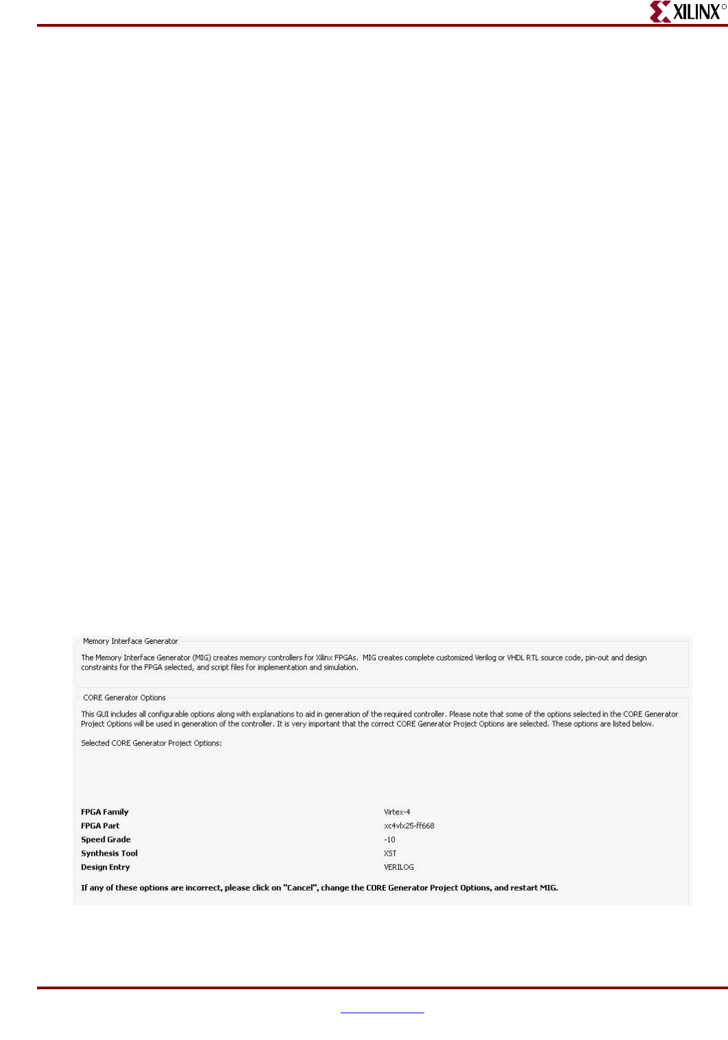
Memory Interface Solutions User Guide www.xilinx.com 35
UG086 (v3.6) September 21, 2010
MIG User Interface
R
3. The Xilinx part must be correctly set because it cannot be changed inside MIG.
Virtex-5, Virtex-4, and Spartan-3/Spartan-3E/Spartan-3A/3AN/3A DSP devices are
supported. Select the part via the part's Project Options menu in the CORE Generator
system. The Generation tab is used to select between Verilog or VHDL by “design
entry” under “flow”. The “flow settings” and “vendor” must be chosen appropriately.
The vendor choices are “Synplicity” for Synplify and “ISE” for XST.
4. Remember the location of the CORE Generator project directory. The “View by
Function” tab to the left shows the available cores organized into folders.
5. MIG is launched by selecting Memories & Storage Elements → Memory Interface
Generator → MIG.
6. The name of the module to be generated is entered in the Component Name text box.
After entering all the parameters in the GUI, click Generate to generate the module
files in a directory with the same name as the component name in the CORE Generator
project directory. After successful generation of the module files, the GUI is closed
automatically.
The “Generated IP” tab to the left lists the generated modules.
MIG User Interface
Getting Help
At any point in time, the MIG user manual can be accessed by clicking the User Guide
button.
Version Information
The Version Info Button gives the information on new features added and the bugs fixed
in the current version. It opens the web browser to display the contents.
CORE Generator Options
Figure 1-1: CORE Generator Options
UG086_c1_04_072008

36 www.xilinx.com Memory Interface Solutions User Guide
UG086 (v3.6) September 21, 2010
Chapter 1: Using MIG
R
The CORE Generator Options screen displays the details of the selected CORE Generator
options that are selected before invoking MIG.
Note: CORE Generator project options are used in the generation of the memory controller.
Correct CORE Generator project options must be selected.
If the displayed CORE Generator Project Options are inaccurate, click the Cancel button
and reselect the CORE Generator Project Options.
Click Next to continue. A new window shows the MIG Output Options page.
MIG Output Options
MIG can have four different output options. They are:
1. Create Design
2. Create Design for Xilinx Reference Boards
3. Verify UCF and Update Design and UCF
4. Spartan-3A FPGA DDR2 SDRAM 200 MHz Design
MIG outputs are generated with the folder name <Component Name>. For Virtex-4 FPGA
and Spartan-3 FPGA designs, the top file (<top_module>) name is same as the
<Component Name> entered in the GUI; all other RTL file names are prepended with
<Component Name>. For example, for a Virtex-4 FPGA DDR2 SDRAM direct-clocking
design with a component name of mig that is entered in the GUI, <design_top> file name
becomes mig.v or mig.vhd, based on the HDL type selected. All other RTL files are
prepended with mig (for example, mig_ddr2_controller). Whereas for Virtex-5 FPGA
designs, the top file (<top_module>) name is the same as <Component Name> entered in
the GUI; all other RTL file names are prepended with the memory interface name. For
example, for a Virtex-5 FPGA DDR2 SDRAM design with a component name of mig that is
entered in the GUI, <design_top> file name becomes mig.v or mig.vhd, based on the HDL
type selected. All other RTL file names are prepended with ddr2_ (such as, ddr2_ctrl).
Note: <Component Name> does not accept special characters. Only alphanumeric characters
can be used to specify a component name. The component name should always start with an
alphabetic character, but can end with an alphanumeric character. If the <Component Name>
entered in the GUI matches with any of the design file names, a pop-up message appears asking
the user to change the <Component Name> to proceed. If the <Component Name> entered in
the GUI matches with the already existing <Component Name> in the project path, MIG prompts
the user to confirm whether to overwrite the files. Upon clicking Yes, MIG overwrites only the
duplicate files.
For multicontroller applications, the number of controllers should be selected at the
Number of Controllers spin box. More than one controller can be selected for DDR2
SDRAM direct-clocking interface for Virtex-4 FPGA designs and for DDR2 SDRAM and
QDRII SRAM designs in Virtex-5 FPGA designs. If more than one controller is selected,
MIG limits the design generation to DDR2 SDRAM for Virtex-4 FPGA designs, and MIG
limits the design generation to DDR2 SDRAM and QDRII SRAM for Virtex-5 FPGA
designs. Select the appropriate number (1-8) in the pull-down menu. The Number of
Controllers selection is enabled only for Virtex-5 and Virtex-4 FPGA families.
Note: The Create Design option can use a multiple number of controllers. For the Create
Design for Xilinx Reference Boards, Verify UCF and Update Design and UCF options, the
number of controllers is limited to one.
Click Back to return to previous page. Click Cancel to quit from the tool. Click Next to
continue. The next page display depends upon the options selected in the current page.
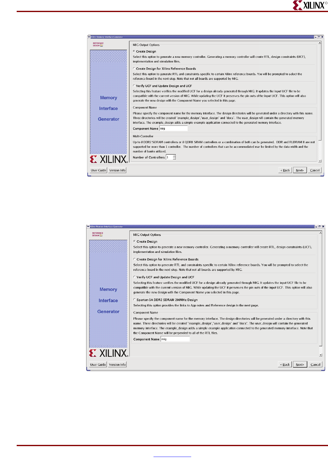
Memory Interface Solutions User Guide www.xilinx.com 37
UG086 (v3.6) September 21, 2010
MIG User Interface
R
The Spartan-3A DDR2 SDRAM 200 MHz Design option appears only for Spartan-3A
FPGA designs (see Figure 1-3).
Create Design
Using the Create Design option, designs can be generated that are supported for that
FPGA family. For example, the Virtex-4 FPGA family supports DDR2 SDRAM, DDR
Figure 1-2: MIG Output Options / Component Name / Number of Controllers
Figure 1-3: MIG Output Options Page of Spartan-3A FPGA Design
UG086_c1_05_030510
UG086_c1_55_030510
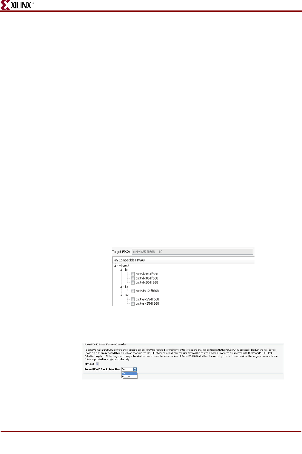
38 www.xilinx.com Memory Interface Solutions User Guide
UG086 (v3.6) September 21, 2010
Chapter 1: Using MIG
R
SDRAM, QDRII SRAM, DDRII SRAM, and RLDRAM II. Here is the flow for creating a
design:
1. Pin Compatible FPGAs
2. Memory Selection
3. Controller Options
4. Memory Options
5. FPGA Options
6. Extended FPGA Options
7. Reserve Pins
8. Bank Selection
9. Summary
10. Memory Model License
11. PCB Information
12. Design Notes
All the options are described in this section.
Pin Compatible FPGAs
FPGAs in the selected family with the same package are listed here. If the generated pinout
from MIG needs to be reusable with any of these other FPGAs, use this option to select the
FPGAs with which the pinout has to be compatible. MIG supports Power PC440
compatible pinout for Virtex-5 FXT devices only for DDR2 SDRAM designs.
Note: The SerDes design is only supported for FPGAs with phase-matched clock drivers
(PMCDs). If the target FPGA or the selected compatible FPGA has no PMCD, the capture
method for DDR2 SDRAM is restricted to direct clocking.
Select any number of compatible FPGAs out of the listed ones. Only the common pins
between target and selected FPGAs are used by MIG. The name in the text box signifies the
Figure 1-4: Pin Compatible FPGAs
Figure 1-5: PPC440 Selection
UG086_c1_06_021109
UG086_c1_66_072008
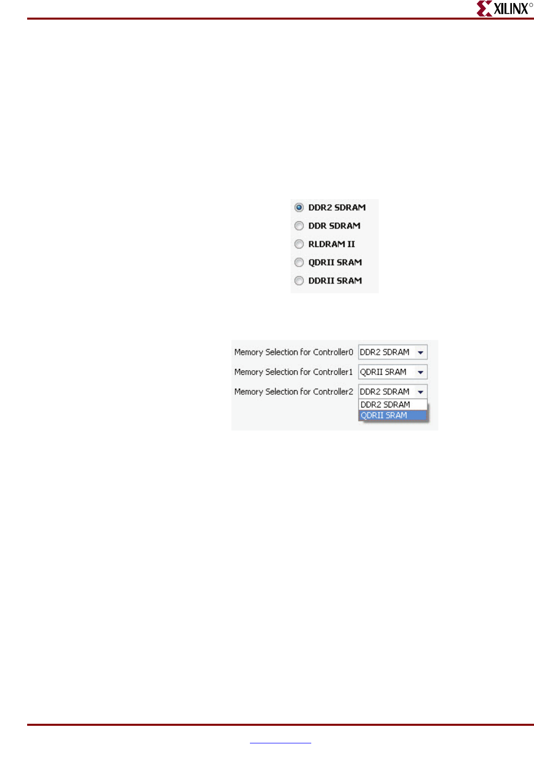
Memory Interface Solutions User Guide www.xilinx.com 39
UG086 (v3.6) September 21, 2010
MIG User Interface
R
Target FPGA selected. When a Virtex-5 FXT device is selected as either compatible or
target, the PPC440 checkbox is enabled. The PPC440 checkbox is enabled only when the
Number of Controllers is selected as 1 in the MIG Output Options page. If the Number of
Controllers is more than 1, then the PPC440 checkbox is disabled and masked, and user can
no longer selected this option. Click Next to continue. The Memory Selection is displayed.
Memory Selection
This page displays all memory types that are supported by the selected FPGA family. An
example is shown in Figure 1-6 for Virtex-4 FPGA designs and in Figure 1-7 for Virtex-5
FPGA designs. In Virtex-5 FPGA designs, the user can select the combination of both
DDR2 SDRAM and QDRII SRAM interfaces for a multicontroller design.
For Virtex-5 FPGA designs, only the DDR2 SDRAM controller is shown when the PPC440
checkbox is enabled in the Pin Compatible FPGAs page. Select the appropriate option, and
then click Next to continue. The Controller Options window is displayed.
Controller Options
This page shows the various controller options that can be selected. If the design has
multiple controllers, this page is repeated for each of the controllers. The page is
partitioned into a maximum of nine sections. The number of partitions depends on the
type of selected memory.
•Capture Method. This feature deals with the data capture method. The DDR2 SDRAM
controller for Virtex-4 devices supports two types of capture method. For other
designs, the capture method is displayed, but it cannot be changed.
Figure 1-6: Memory Selection for Virtex-4 FPGA Designs
Figure 1-7: Memory Selection for Virtex-5 FPGA Designs
UG086_c1_07_072008
UG086_c1_56_072008
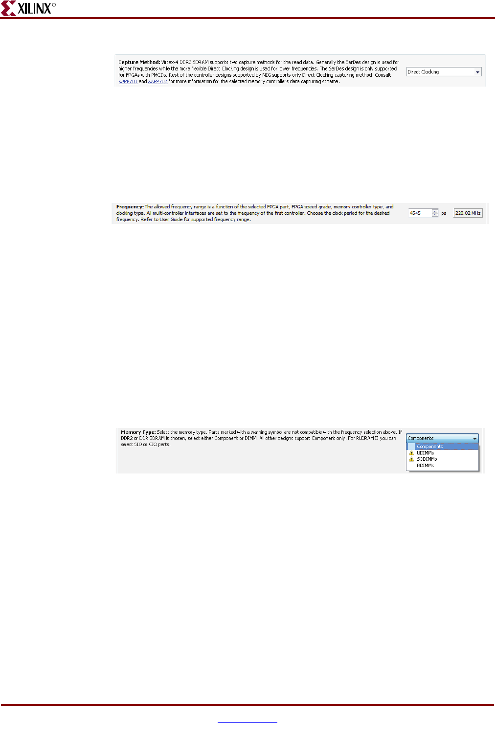
40 www.xilinx.com Memory Interface Solutions User Guide
UG086 (v3.6) September 21, 2010
Chapter 1: Using MIG
R
Click the pull-down menu button and select an option. Certain other options such as
frequency and ECC are restricted based on this selection.
•Frequency. This feature indicates the desired frequency for all the controllers. This
frequency block is limited by factors such as the selected FPGA, device speed grade,
and clocking type.
Vary the clock period as required. Either use the spin box or enter a valid value
through the keyboard. Values entered are restricted based on the minimum and
maximum clock periods supported. The maximum frequency of deep designs is
150 MHz (6,666 ps).
Note: For Virtex-4 FPGA multicontroller designs, the frequency selected for the first controller
is used for all other controllers. For Virtex-5 FPGA multicontroller and multiple-interface designs,
every controller can have a different frequency. The number of controllers that can have different
frequencies is limited by the number of PLLs available in the selected FPGA. Memory parts and
data width are restricted based on the frequency selection.
•Memory Type. For DDR2 SDRAM, MIG categorizes different memory components
and modules available into components, UDIMMs, SODIMMs, and RDIMMs. This
can vary according to the memory selected. Virtex-5 FPGA DDR2 SDRAM controller
supports deep designs only for dual-rank DIMMs.
Click the pull-down menu combo box and select the memory type. Memory type
options marked with a warning symbol are not compatible with the selected
frequency.
•Memory Part. This feature helps the selection of a memory part for the design.
Selection can be made from an existing list, or a new part can be created.
Figure 1-8: Capture Method
Figure 1-9: Frequency
Figure 1-10: Memory Type
UG086_c1_08_020709
UG086_c1_09_102009
UG086_c1_10_072809
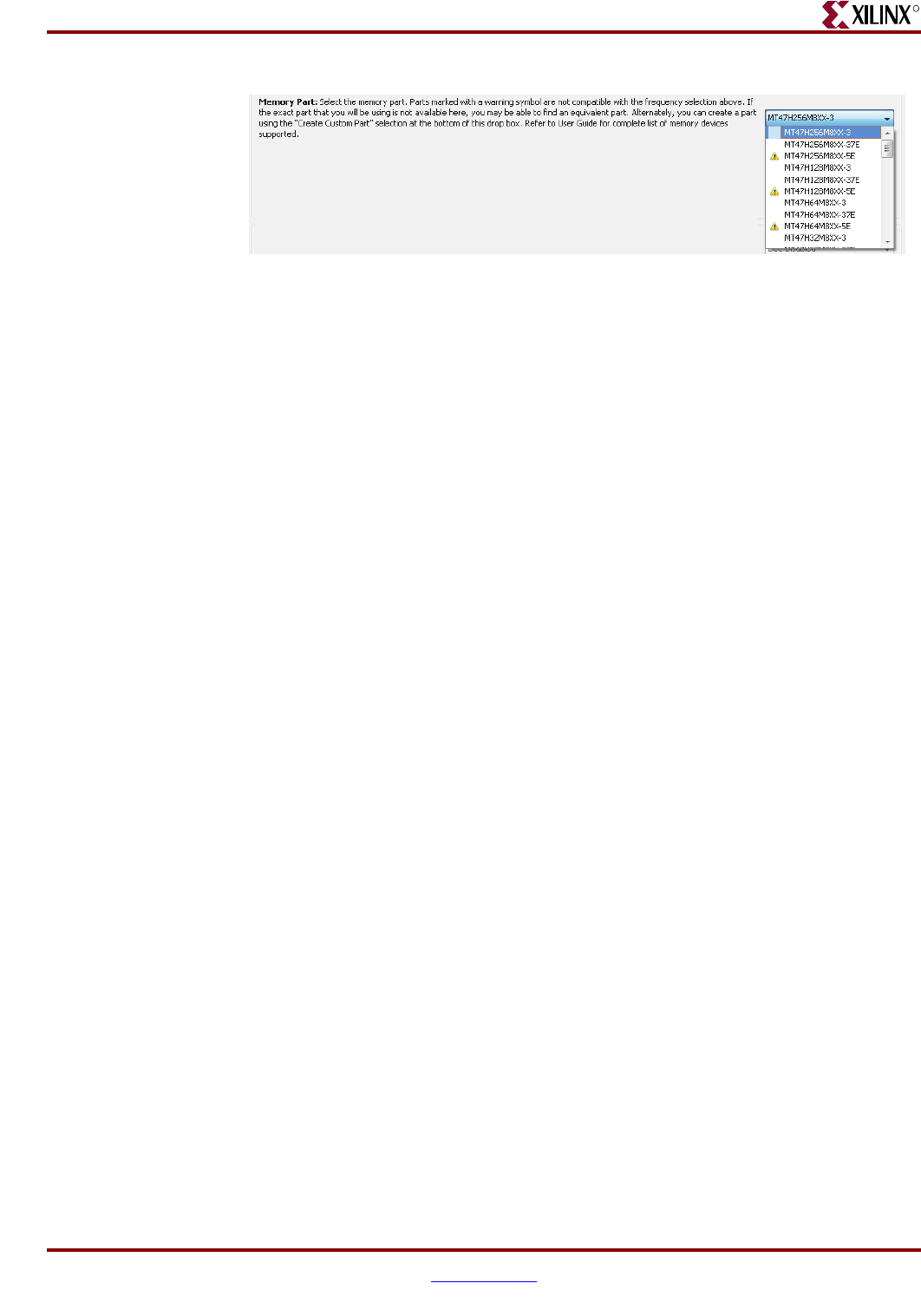
Memory Interface Solutions User Guide www.xilinx.com 41
UG086 (v3.6) September 21, 2010
MIG User Interface
R
Select the appropriate memory part from the list. Select the larger memory parts to get
all address lines in UCF. If the required part or its equivalent is unavailable, a new
memory part can be created. Parts marked with a warning symbol are not compatible
with the selected frequency. To create a custom part, select the Create Custom Part
from the drop down combo box. A new window appears as shown in Figure 1-12.
The window called Create Custom Part includes all the details of the memory
component selected in Select Base Part. Enter the appropriate memory part name in
the text box. Select the suitable base part from the Select base part list. Edit the Value
column as needed. Select the suitable values from the Row, Column, and Bank options
as per the requirements. After editing the required fields, click the Save button. The
new part can be saved with the selected name. This new part is added in the Memory
Parts list as shown in Figure 1-13 and saved into the database for reuse and to produce
the design.
Note: The rank and speed grade of the Create Custom Part is the same as the base part
selected in the GUI. For example, if the base part selected in the GUI is dual-rank, the new part
created is also a dual-rank part.
Figure 1-11: Memory Part
UG086_c1_11_072809
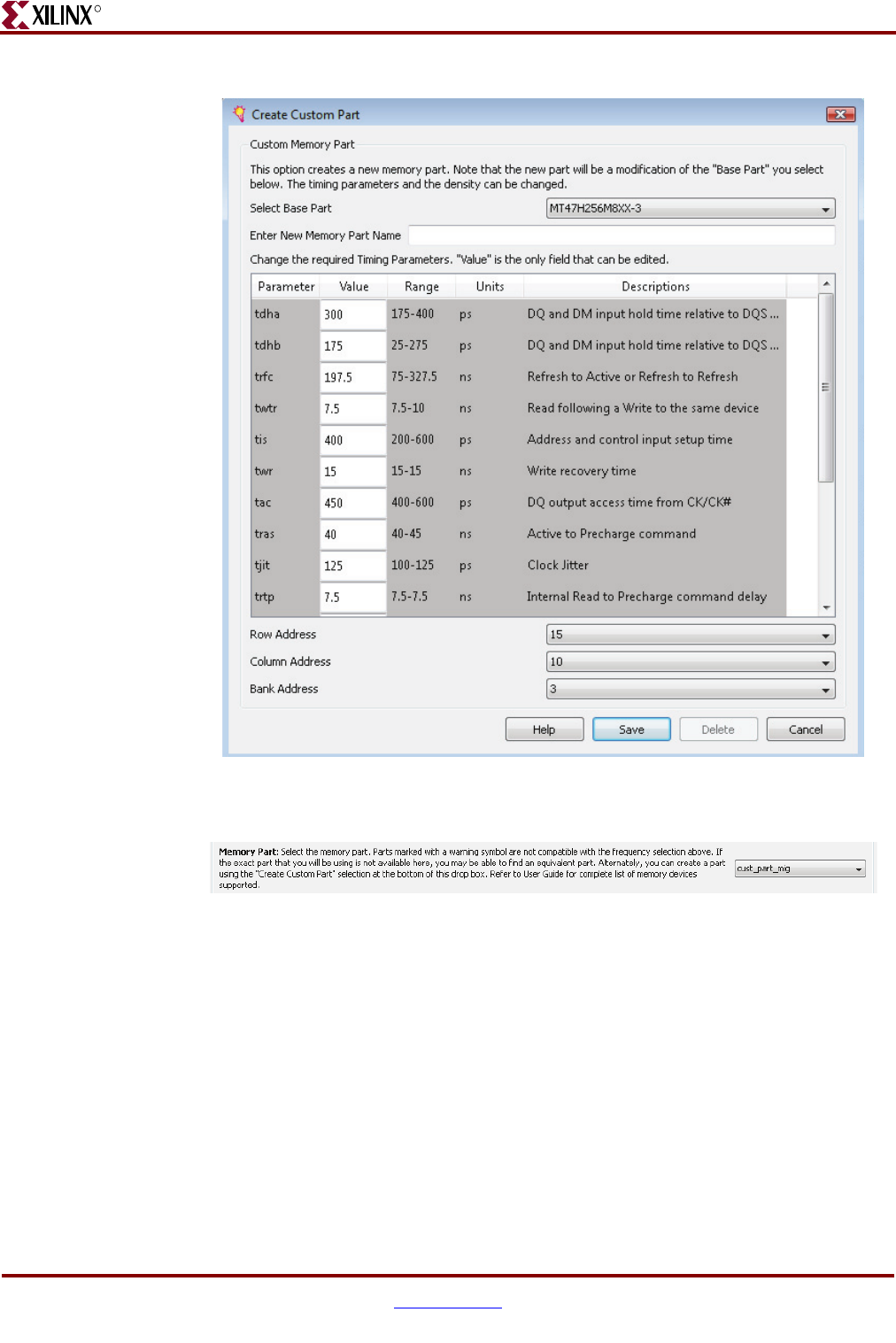
42 www.xilinx.com Memory Interface Solutions User Guide
UG086 (v3.6) September 21, 2010
Chapter 1: Using MIG
R
Note: In order to use the MIG-generated design UCF for different densities of the same
memory type, select the highest memory part from Memory Selection page. For different density
parts, only the number of address bits differ. Hence, if a design is generated selecting the highest
density memory part, the same UCF can be used for the lower density memory part of the same
memory type. For example, if a 128 x 16 DDR2 SDRAM design is generated, its UCF can be
used for 64 x 16 DDR2 SDRAM design by connecting the most-significant address bit to ground.
This scenario works only if the different density memory parts have the same design parameters
(such as data width and other memory parameters).
•Data Width. The data width value can be selected here based on the memory type
selected earlier. The list shows all supported data widths for the selected part. Choose
one of them. These values are generally multiples of the individual device data
Figure 1-12: Create Custom Part
Figure 1-13: Memory Part
UG086_c1_12_072809
UG086_c1_13_072809
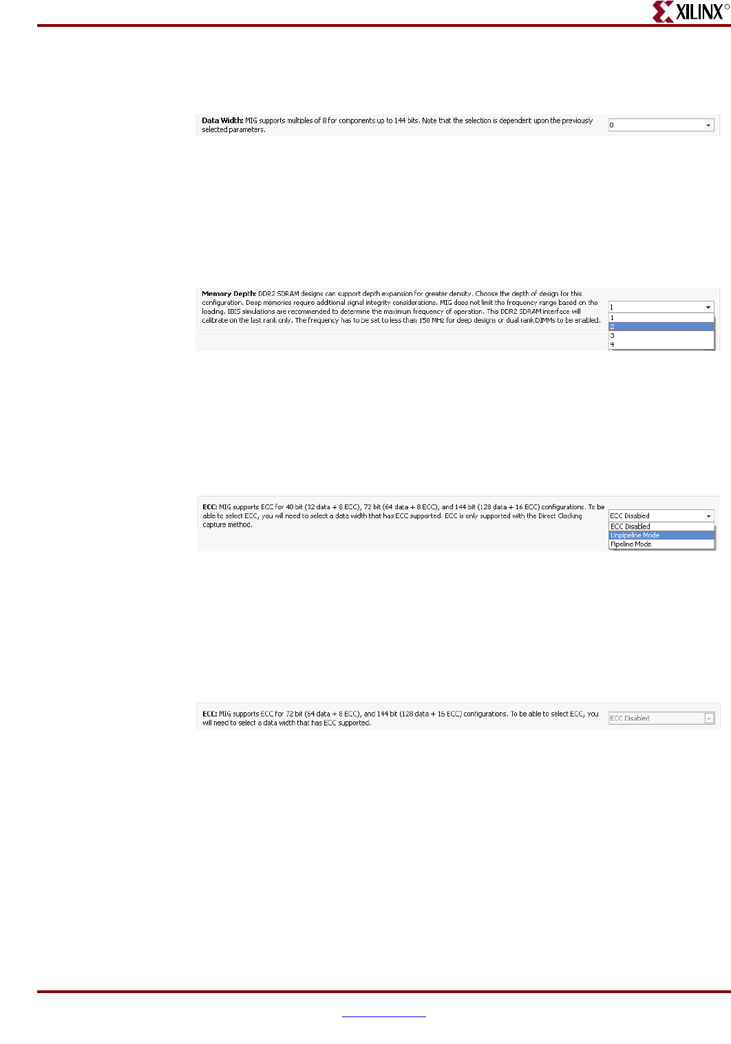
Memory Interface Solutions User Guide www.xilinx.com 43
UG086 (v3.6) September 21, 2010
MIG User Interface
R
widths. In some cases, the width might not be an exact multiple. For example, though
16 bits is the default data width for x16 components, 8 bits is also a valid value.
•Memory Depth. The DDR2 SDRAM Virtex-4 FPGA controller with the direct-clocking
capture method supports a memory depth of one to four. DDR2 SDRAM Virtex-5
FPGA controller supports a memory depth of two only for dual-rank DIMMs. The
maximum frequency supported for deep designs is less than or equal to 150 MHz. For
other designs, this option is unavailable.
Select the appropriate option from the Memory Depth option.
•ECC. ECC stands for Error Correction Code. This feature enables the generation of
ECC along with the code. This section is enabled based on selected data width. This
option is available only for DDR2 SDRAM Virtex-4 and Virtex-5 FPGA designs.
Note that ECC selection is enabled only when the appropriate data width is selected.
DDR2 SDRAM Virtex-4 FPGA design supports three modes: ECC Disabled,
Unpipeline Mode, and Pipeline Mode, as shown in Figure 1-16. Select the appropriate
mode. The Pipeline mode improves frequency performance at the cost of an extra
pipeline stage.
For other Virtex-4 FPGA designs, this window is disabled as shown in Figure 1-17. For
Virtex-5 FPGA DDR2 SDRAM designs, the two options are ECC Enabled and ECC
Disabled.
Figure 1-14: Data Width
Figure 1-15: Memory Depth
Figure 1-16: ECC (a)
Figure 1-17: ECC (b)
UG086_c1_14_020709
UG086_c1_15_020709
UG086_c1_16_020709
UG086_c1_17_020709
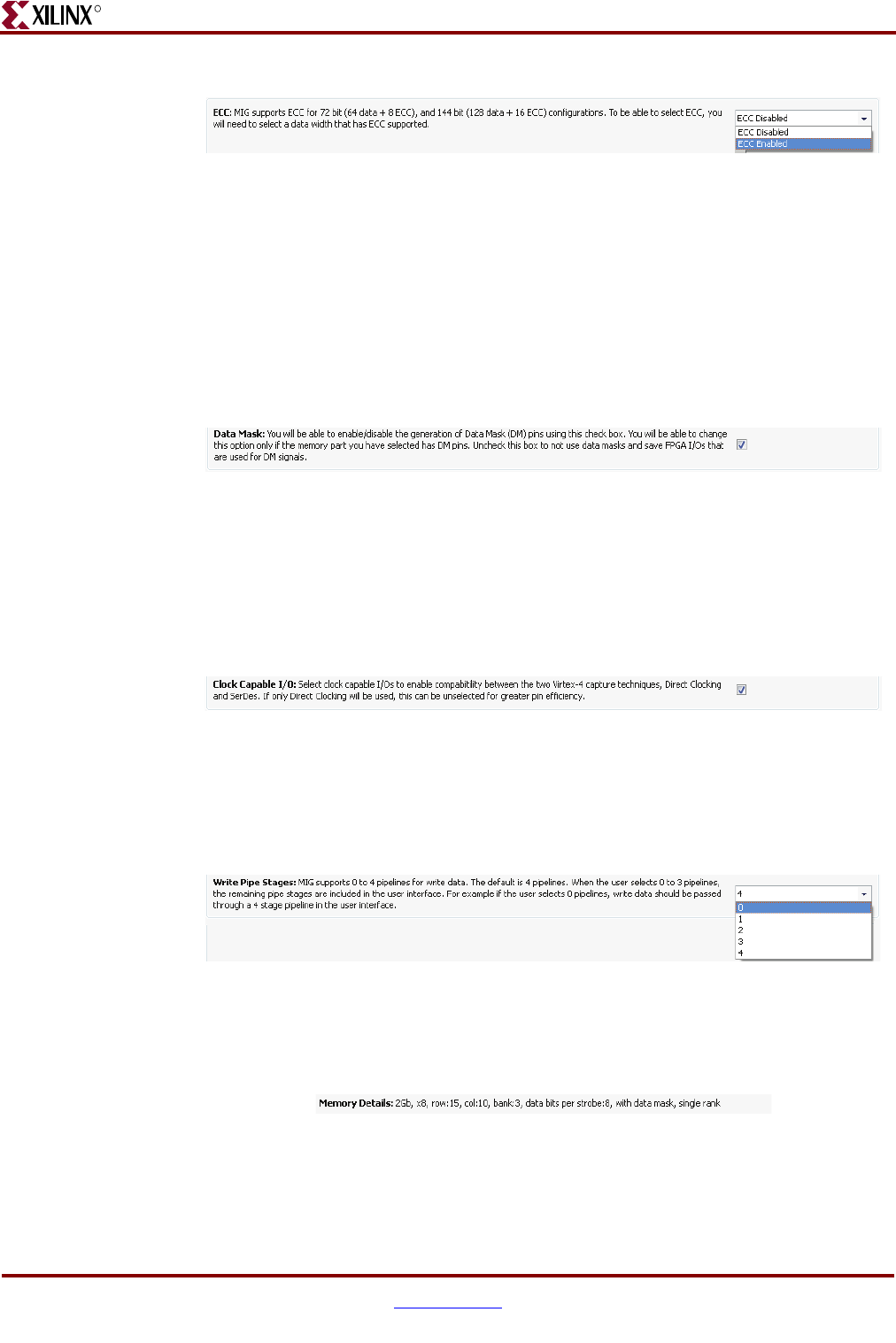
44 www.xilinx.com Memory Interface Solutions User Guide
UG086 (v3.6) September 21, 2010
Chapter 1: Using MIG
R
Figure 1-18 shows the ECC option section for the Virtex-5 FPGA design GUI. For
Virtex-5 devices, ECC is supported for 72-bit or 144-bit DDR2 SDRAM designs.
•Data Mask. When this Data Mask checkbox is marked, the data mask pins are
allocated. When this Data Mask checkbox is not checked, the data mask pins are not
allocated, which increases the pin efficiency. This option is disabled and cannot be
changed for memory parts that do not support data masks. Similarly, this option is
disabled for ECC enabled designs. This option is available only for DDR2 and DDR
SDRAMs.
Select the option as per the requirement.
•Clock Capable I/O. Checking the Clock Capable I/O box makes use of the CC pins
available in Virtex-4 FPGAs for strobes or read clocks. This option is enabled and
cannot be changed for DDR2 SDRAM SerDes designs, but is editable for other
designs.
Select the option as per the requirement.
•Write Pipe Stages. The Write Pipe Stages is supported only for Spartan FPGA designs.
This option allows users to implement the write data pipelines in the user interface.
•Memory Details. This section displays details about the selected memory. For
DIMMs, x4/x8/x16 indicates the memory width of the base device.
The memory details change based on the selected Memory part.
Figure 1-18: ECC (c)
Figure 1-19: Data Mask
Figure 1-20: Clock Capable I/O
Figure 1-21: Write Pipe Stages
Figure 1-22: Memory Details
UG086_c1_18_020709
UG086_c1_43_021009
UG086_c1_19_021009
UG086_c1_57_021009
UG086_c1_20_021009
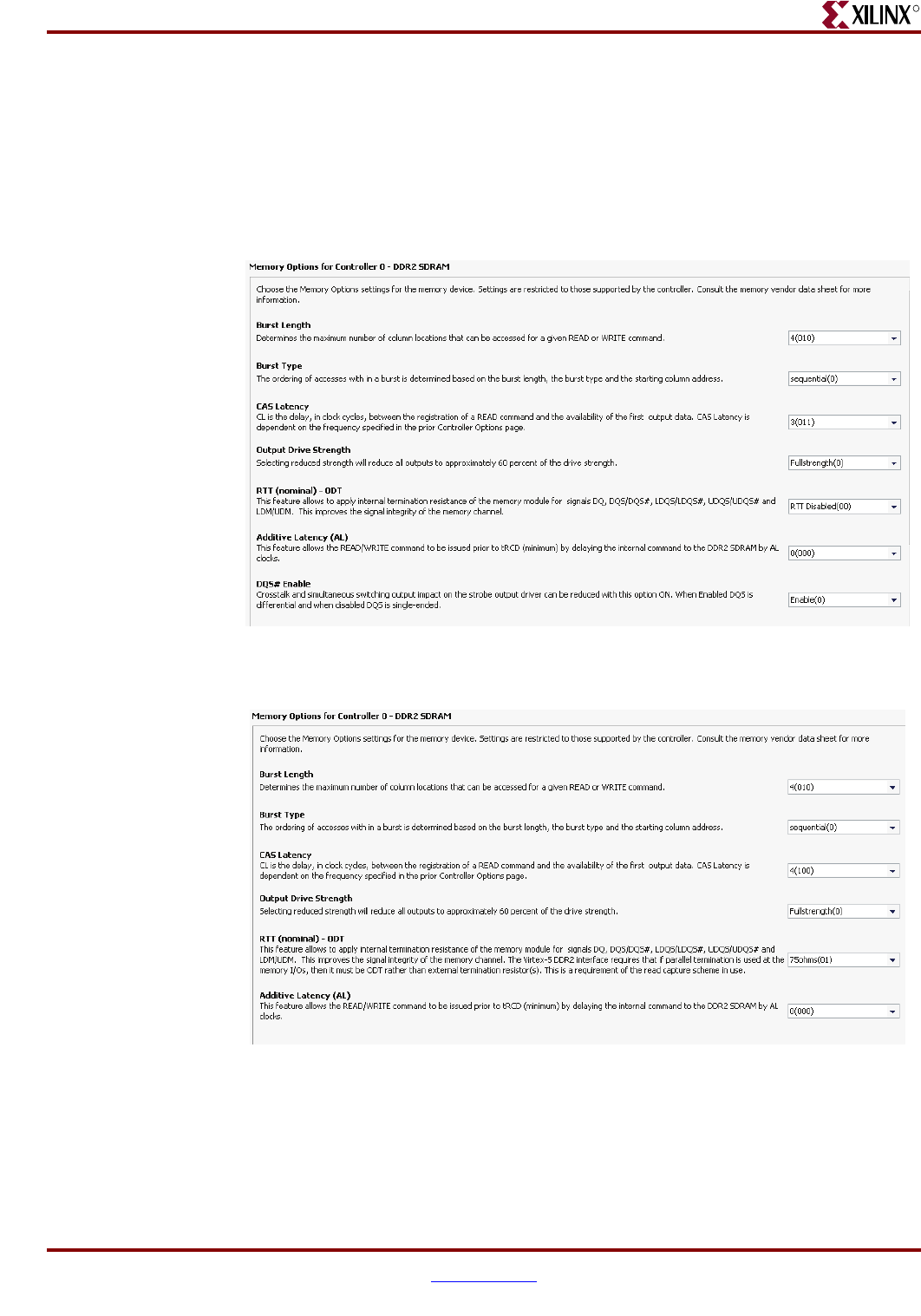
Memory Interface Solutions User Guide www.xilinx.com 45
UG086 (v3.6) September 21, 2010
MIG User Interface
R
Click Next to continue. The Memory Options window is displayed for RLDRAM II,
DDR, and DDR2 SDRAM devices. For other memories, the next window displayed is
FPGA Options.
Memory Options
This feature allows selection of various memory options as supported by the controller
type.
These values are programmed into memory during initialization.
Note: The memory options listed in this GUI are restricted by the frequency and the memory part
selected on the prior page. The memory option value will not be shown in this page if it cannot be
changed. For example, a CAS latency value of 5 is only is supported in a frequency range of 267 MHz
Figure 1-23: Memory Options for Virtex-4 FPGA DDR2 Direct Clocking Design
Figure 1-24: Memory Options for Virtex-5 FPGA DDR2 Design
UG086_c1_21_021009
UG086_c1_22_021009
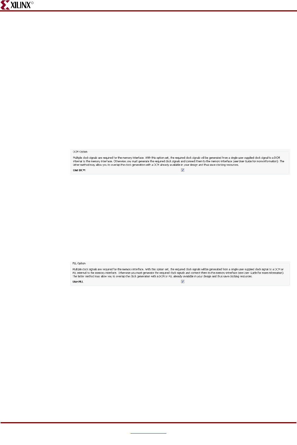
46 www.xilinx.com Memory Interface Solutions User Guide
UG086 (v3.6) September 21, 2010
Chapter 1: Using MIG
R
to 333 MHz. Thus, the CAS latency value is not shown in a frequency range of 267 MHz to 333 MHz,
and the value selected for CAS latency is 5.
Click Next to continue. The FPGA Options window is displayed.
FPGA Options
This feature is partitioned into three or four sections based on the FPGA family selected:
DCM, DCI, SSTL Class, and Debug Signals Control. For Virtex-5 FPGA designs, the DCI
option appears in the Extended FPGA Options page.
•DCM. DCM allows design generation with or without a DCM in the design. This
option appears only for Virtex-4 and Spartan FPGA designs. When a design is
generated with DCM, all the required clocks for the design are generated out of the
DCM using the system clock inputs. When the DCM is disabled, the user must
implement a user clocking scheme to generate the required design clocks. Refer to the
Clocking Scheme section of a design for details about the clocks that the user must
generate when the DCM is not instantiated in the design.
•PLL. PLL allows design generation with or without a phase-locked loop (PLL) in the
design. This option appears only for Virtex-5 FPGA designs. In MIG 3.0 and later,
DCM is replaced with PLL for all Virtex-5 FPGA designs. When a design is generated
with PLL, all the required clocks for the design are generated out of the PLL using the
system clock inputs. When the PLL is disabled, the user must implement a user
clocking scheme to generate the required design clocks. Refer to the Clocking Scheme
section of a design for details about the clocks that the user must generate when the
PLL is not instantiated in the design.
•DCI. This feature indicates whether the Digitally Controlled Impedance is Disabled or
Enabled. This option appears only for Virtex-4 FPGA designs. DCI can be enabled or
disabled for input, bidirectional, or output pins. This option can change according to
the memory selected. They are listed as follows:
DDR2 SDRAM — DCI for DQ/DQS and DCI for Address/Control
DDR SDRAM — DCI for DQ/DQS and DCI for Address/Control
RLDRAM II — DCI for Data, Read Clocks, and Data Valid Signals and DCI for
Address/Control
QDRII SRAM — DCI for Data and Read Clocks
DDRII SRAM — DCI for Data and Read Clocks
Figure 1-25: DCM Option
Figure 1-26: PLL Option
UG086_c1_23_021009
UG086_c1_85_021009
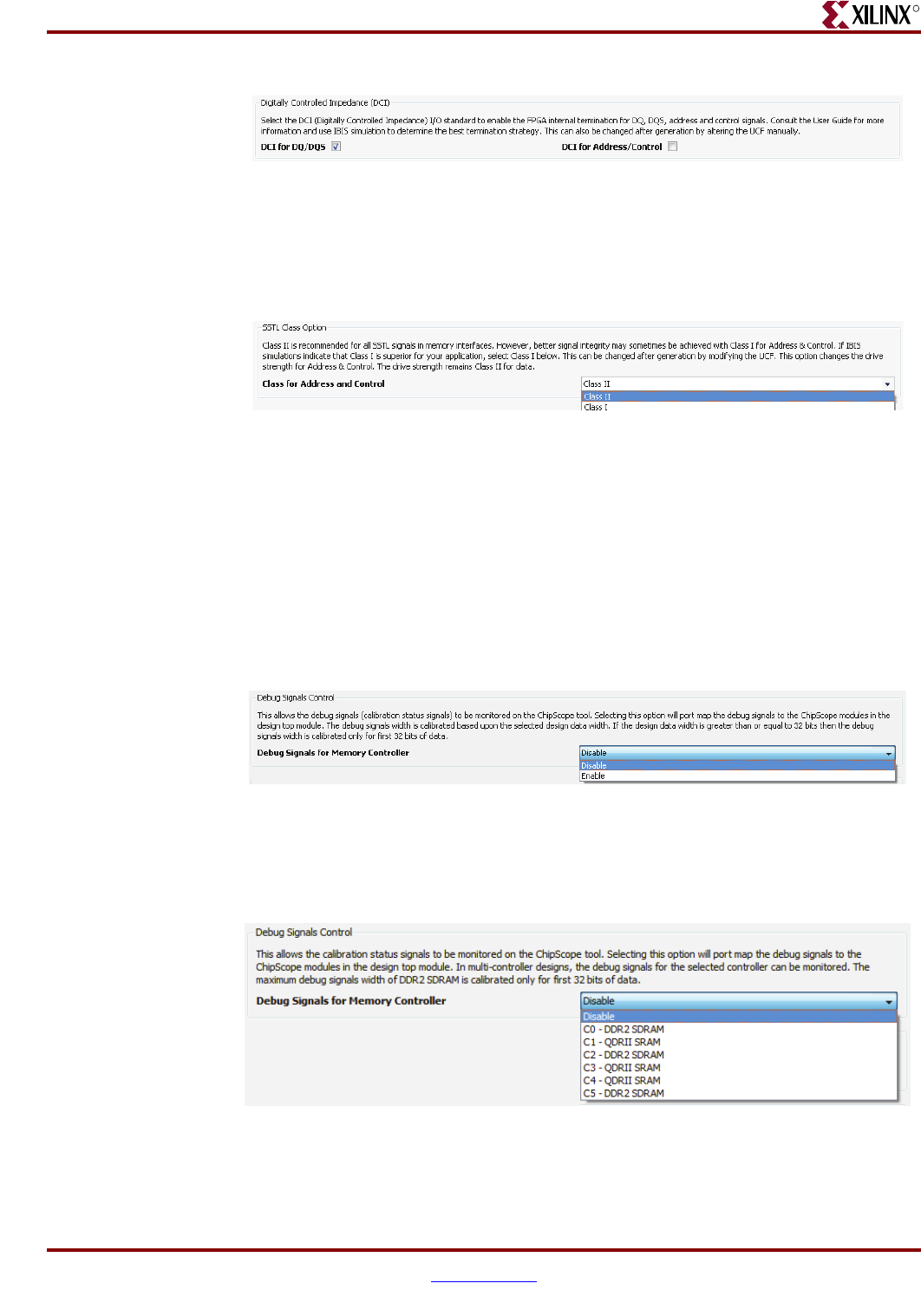
Memory Interface Solutions User Guide www.xilinx.com 47
UG086 (v3.6) September 21, 2010
MIG User Interface
R
•SSTL Class Option. SSTL Class Option determines the I/O standard drive strength in
the UCF of DDR and DDR2 SDRAM. These I/O standards can be changed based on
their application.
•Debug Signals Control. Selecting this option enables the debug signals to be port-
mapped to the ChipScope™ analyzer modules in the design top module. This helps in
monitoring the debug signals on the ChipScope tool. When the generated design is
run in batch mode using ise_flow.bat in the design’s par folder, the CORE
Generator system is called to generate ChipScope analyzer modules (that is, EDIF files
are generated). Deselecting this option leaves the debug signals unconnected in the
design top module, with no ChipScope analyzer modules instantiated in the design
top module or generated by the CORE Generator system. In Virtex-4 FPGA
multicontroller designs, the Debug port is supported for the first controller.
In Virtex-5 FPGA multicontroller and multiple-interface designs, the Debug port is
supported for the selected controller in the GUI.
Figure 1-27: DCI Options (a)
Figure 1-28: SSTL Class Options
Figure 1-29: Debug Signals Control
Figure 1-30: Debug Signals in Virtex-5 FPGA Multiple Interface Designs
UG086_c1_24_021009
UG086_c1_26_021009
UG086_c1_44_072909
UG086_c1_59_102009
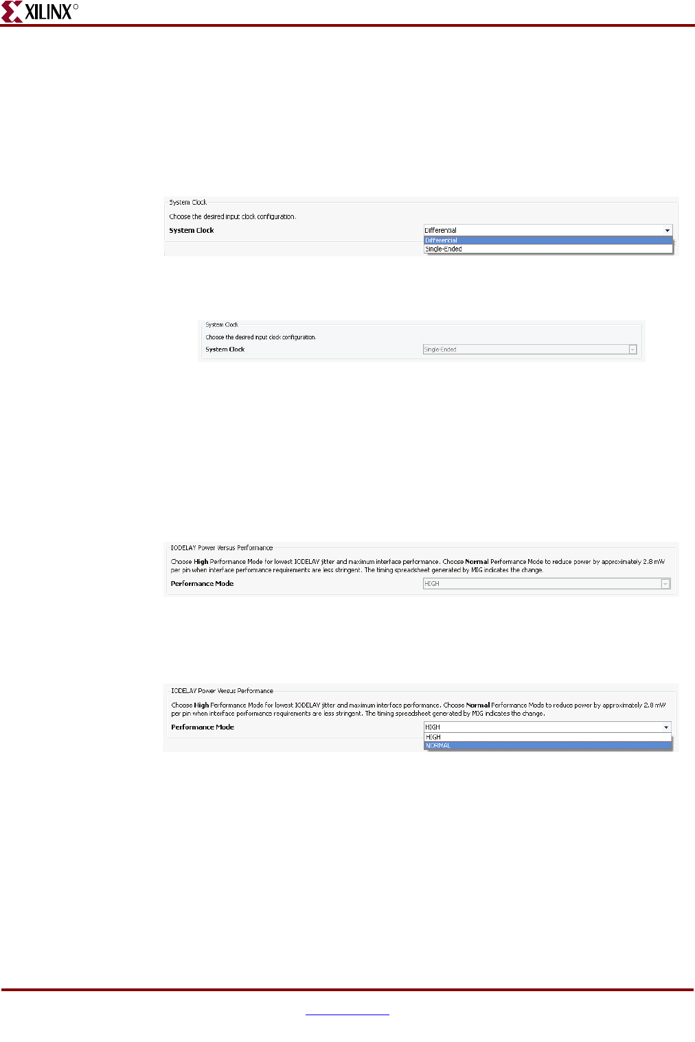
48 www.xilinx.com Memory Interface Solutions User Guide
UG086 (v3.6) September 21, 2010
Chapter 1: Using MIG
R
•System Clock. This option enables users to select the system clock type for the design
to be generated (Figure 1-31). This option is applied on both system clock as well as
IDELAYCTRL clock (200 MHz clock). When Differential is selected, only differential
clock pairs appear in the design top RTL file as well as in the design UCF. When
Single-Ended is selected, only single-ended clock input pins appear in the design top
RTL file as well as in the design UCF. This option is grayed out when PLL/DCM
option is deselected and the clock type remains single-ended (Figure 1-32).
•High Performance Mode. This is the IODELAY element High Performance Mode
selection type for Virtex-5 FPGA designs (Figure 1-33). This option sets the IODELAY
in HIGH power or LOW power mode. This option is enabled for selection only when
the design frequency is less than the false frequency mode. When the frequency set in
the Controller options page is more than the specified false frequency range, then the
High Performance Mode option is not available for selection and is grayed out with
the default value set to TRUE (Figure 1-34).
In Virtex-5 FPGA multicontroller and multiple-interface designs, IODELAY
performance mode can be selected for each controller independently (Figure 1-35).
Figure 1-31: System Clock Type Selection when PLL/DCM Option is Selected
Figure 1-32: System Clock Type Selection when PLL/DCM Option is Deselected
Figure 1-33: High Performance Mode Selection Type for Virtex-5 FPGA
Interface Single Controller Designs
Figure 1-34: High Performance Mode Default: Design Freq > False Freq Range
UG086_c1_77_021009
UG086_c1_78_072108
UG086_c1_79_021009
UG086_c1_80_021009
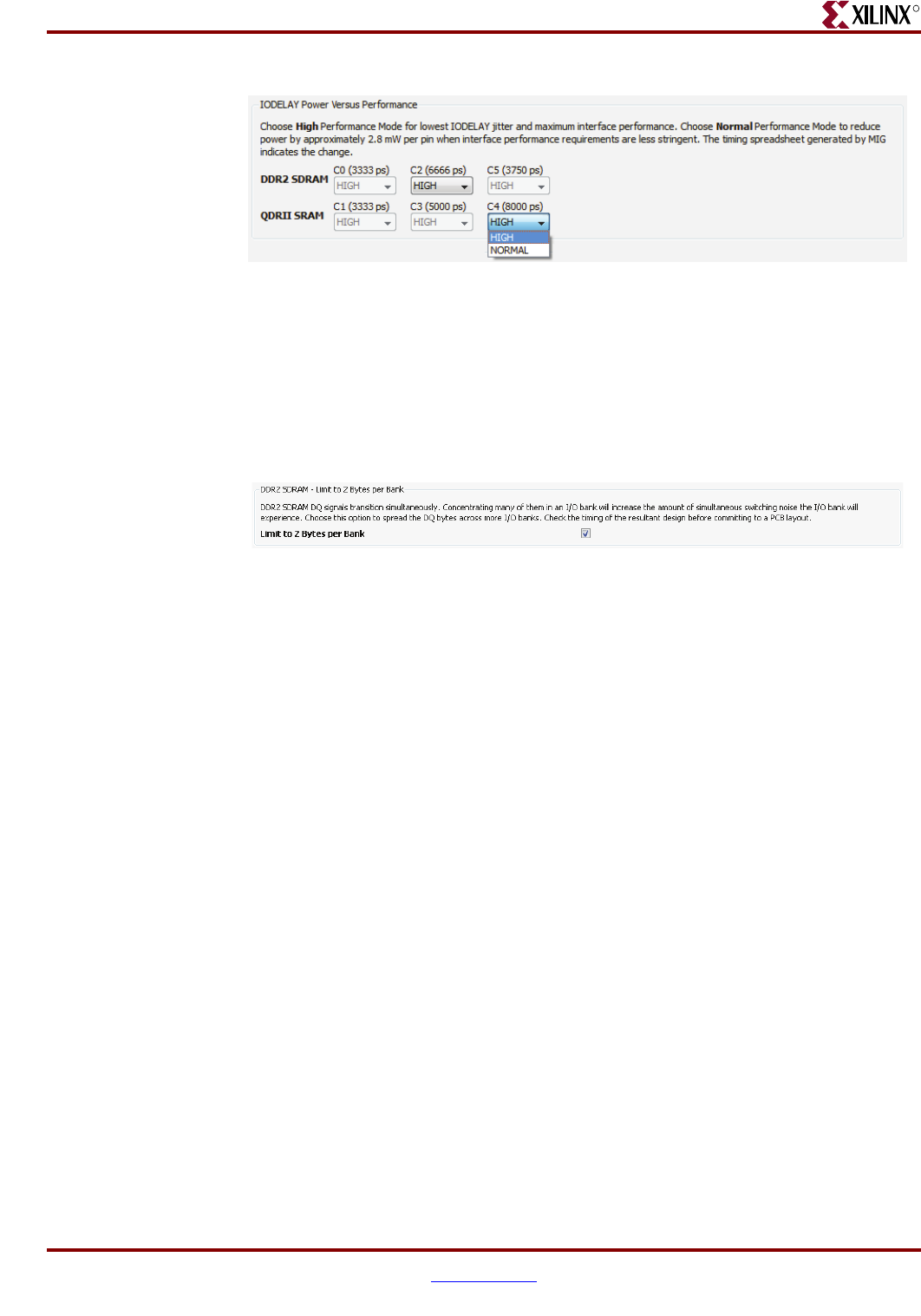
Memory Interface Solutions User Guide www.xilinx.com 49
UG086 (v3.6) September 21, 2010
MIG User Interface
R
Refer to Appendix E, “Debug Port” for more information on False Mode frequency
ranges for all Virtex-5 FPGA memory interface designs.
•Limit to 2 Bytes per Bank. Enabling this option allows only two bytes of data into a
single bank (Figure 1-36). This option is available only for Virtex-5 FPGA DDR2
SDRAM memory interface designs.
Click Next to continue. For Virtex-5 FPGA designs, the Extended FPGA Options
window is displayed, and for other designs, the Reserve Pins window is displayed.
Extended FPGA Options
This feature is partitioned into three sections: DCI, DCI Cascading Information, and SSTL
Class. This page will appear for Virtex-5 FPGA designs only.
•DCI. This feature indicates whether the Digitally Controlled Impedance is Disabled or
Enabled. DCI can be enabled or disabled for input, bidirectional, or output pins. This
option can change according to the memory selected. They are listed as follows:
DDR2 SDRAM — DCI for DQ/DQS and DCI for Address/Control
DDR SDRAM — DCI for DQ/DQS and DCI for Address/Control
QDRII SRAM — DCI for Data and Read Clocks
DDRII SRAM — DCI for Data and Read Clocks
The DCI selection window is shown in Figure 1-27.
For multiple interfaces in Virtex-5 FPGA designs, DCI can be selected for each
interface separately. The Extended FPGA Options page shows the DCI selections for
each interface separately (Figure 1-37).
Figure 1-35: High Performance Mode Selection Type for Virtex-5 FPGA
Multiple Interface Designs
Figure 1-36: Limit to 2 Bytes per Bank in Virtex-5 FPGA DDR2 SDRAM
Interface Designs
UG086_c1_87_102009
UG086_c1_76_021009
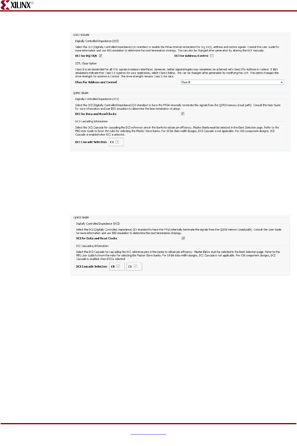
50 www.xilinx.com Memory Interface Solutions User Guide
UG086 (v3.6) September 21, 2010
Chapter 1: Using MIG
R
If DCI is enabled, the pins are characterized by the DCI I/O standards.
•DCI Cascading Information. This option appears only for QDRII Virtex-5 FPGA
designs. This option is necessary for generating 36-bit component designs with DCI
support.
Note: If the DCI Cascading Information option is checked, the Bank Selection window shows
the Master Bank selection box. The user must not reserve VRN/VRP pins in the Reserve Pins
window for the selected master banks.
•SSTL Class Options. SSTL Class Option determines the I/O standard drive strength
in the UCF of DDR and DDR2 SDRAM. These I/O standards can be changed based on
their application.
Click Next to continue. The Reserve Pins page is displayed.
This page is partitioned into two sections:
•Reserve Pins
• Pin/Bank Selection Mode
The Reserve Pins section allows the user to reserve the specific pins of the device. The
Pin/Bank Selection Mode section lets the user select the Pin/Bank selection GUI mode,
based on user requirements. By default, the Next button is disabled. This button is enabled
Figure 1-37: DCI Option for Multiple Interfaces Selected in Virtex-5 FPGA Designs
Figure 1-38: DCI Cascading Information Option
UG086_c1_58_021009
UG086_c1_25_021009
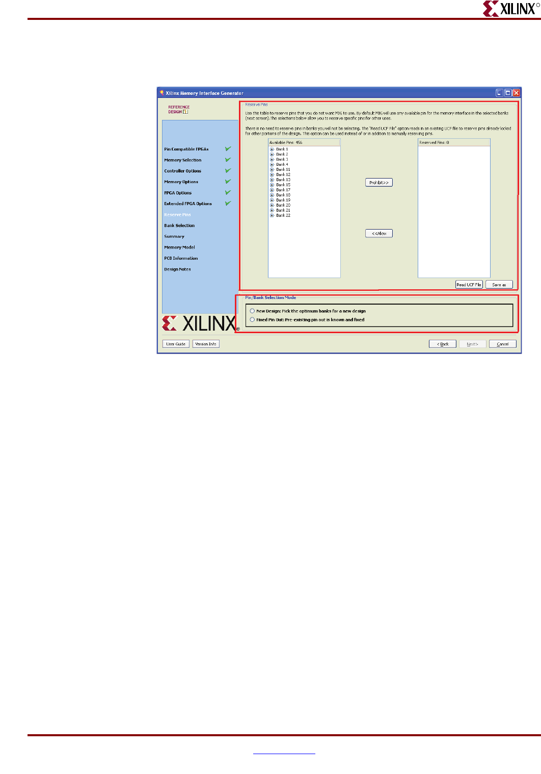
Memory Interface Solutions User Guide www.xilinx.com 51
UG086 (v3.6) September 21, 2010
MIG User Interface
R
after the user chooses the Pin/Bank selection mode. The Pin Selection feature is only
implemented for Virtex-5 FPGA devices in DDR and DDR2 SDRAMs, and QDR II SRAM.
Reserve Pins
This feature allows specific pins to be reserved for other applications. After selecting
suitable pins as necessary, the reserved pins are not used by the MIG tool while generating
the pinout for that particular design.
Figure 1-39: Reserve Pins Page
UG086_c1_88_102709
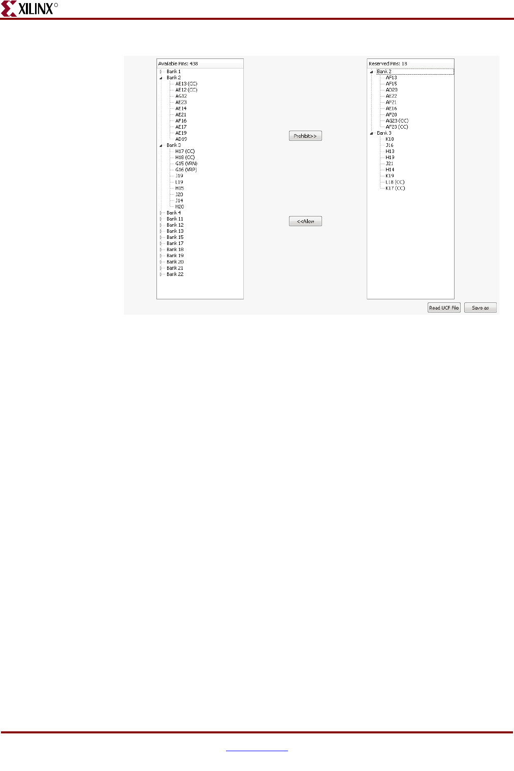
52 www.xilinx.com Memory Interface Solutions User Guide
UG086 (v3.6) September 21, 2010
Chapter 1: Using MIG
R
Select the pins from the Available Pins column, and click the Prohibit button. The
particular pin is transferred to Reserve Pins column along with its bank information. This
signifies that the selected pin has been reserved. To unreserve a reserved pin, click the
appropriate pin that needs to be removed, and then click the Allow button. The number
408 in the Available Pins header signifies the number of pins available for pinout, whereas
the number 16 in the Reserve Pins header signifies the number of pins selected to be
reserved.
The reserved pins information can be saved in a user defined file using the Save as button.
A browser window appears after clicking the Save as button. Set the file location here.
Use the Read UCF File button to read a reserve pins from a UCF. When the Read UCF File
button is clicked, a new window pop ups. Select the UCF to be read. After reserving the
pins, click Next to continue. The Bank Selection window is displayed.
Pin/Bank Selection Mode
This mode has two options based on whether or not a fixed board layout is available
(Figure 1-41):
• New Design: In this option, the user picks the optimum banks for a new design. This
option applies when the user does not already have a board. The pins for various
signals can be automatically selected, based on the optimum bank selection.
• Fixed Pin Out: In this option, a preexisting pinout is known and fixed. This option
applies when the user already has a board. In this case, signals have to be manually
assigned to the pins.
Figure 1-40: Reserve Pins Section
UG086_c1_27_021009
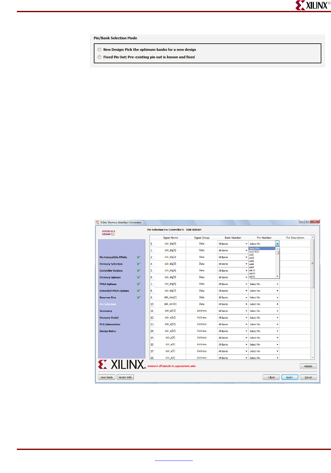
Memory Interface Solutions User Guide www.xilinx.com 53
UG086 (v3.6) September 21, 2010
MIG User Interface
R
After selecting the appropriate option, click the Next button to continue. If the Fixed Pin
out: Pre-existing pin out is known and fixed option is selected, the Pin Selection page is
displayed (“Pin Selection,” page 53). If the New Design: Pick the optimum banks for a
new design option is selected, the Bank Selection page is displayed (“Bank Selection,”
page 54).
Pin Selection
This page allows for the selection of pins for the various signals on the memory interface.
There are five columns in the pin selection table:
•Signal Name
•Signal Group
•Bank Number
•Pin Number
•Pin Name
•Signal Name. This column displays all the required signals for the specific memory
interface. The signal name cannot be edited or changed.
Figure 1-41: Pin/Bank Selection Mode
Figure 1-42: Pin Selection Page
UG086_c1_89_102709
UG086_c1_90_102709
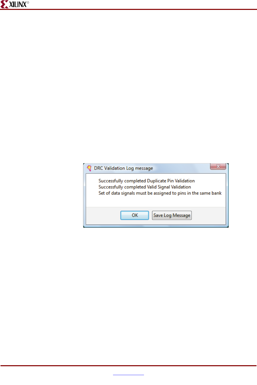
54 www.xilinx.com Memory Interface Solutions User Guide
UG086 (v3.6) September 21, 2010
Chapter 1: Using MIG
R
•Signal Group. This column displays the group name of the corresponding signal
name. The signal name cannot be edited or changed.
•Bank Number. This column displays all the banks available in the FPGA. Each cell of
this column contains a pull-down menu. The entries in the pull-down menu are the
banks of the corresponding FPGA. Select the appropriate banks for specific memory
signals. After the bank is selected in the bank number, the Pin Number pull-down
menu is automatically populated with a list of pins from the corresponding bank.
Note: It is not mandatory to select a bank number. When the pin number is selected, the bank
number pull-down menu is automatically updated with the corresponding bank number.
•Pin Number. This column displays all the pin numbers available in the FPGA. Each
cell of this column contains a pull-down menu that lists all the pins in the FPGA.
Select the appropriate pins for specific memory signals. After the pin number is
selected in the Pin Number menu, the Bank Number menu automatically changes to
the corresponding bank.
•Pin Name. This column displays the pin name (I/O type) of the user selected pin
number. The pin name cannot be edited or changed.
Use the Validate button to verify the design rule of all the assigned pins to memory signals.
After verifying the design rule, a DRC Validation Log message window is displayed with
a list of success and failure messages. This window can be saved using the Save Log
Message button.
After successfully assigning the memory interface signals to the appropriate pin, click the
Next button to continue. If there are no errors, the Summary page is displayed
(“Summary,” page 75).
Bank Selection
This feature allows selection of banks for the Memory interface. Banks can be selected for
different groups of memory signals. The different groups are:
• Address and Control Signals
• Data Signals
• System Control Signals
•System Clock
Figure 1-43: DRC Validation Log Message
UG086_c1_91_102709
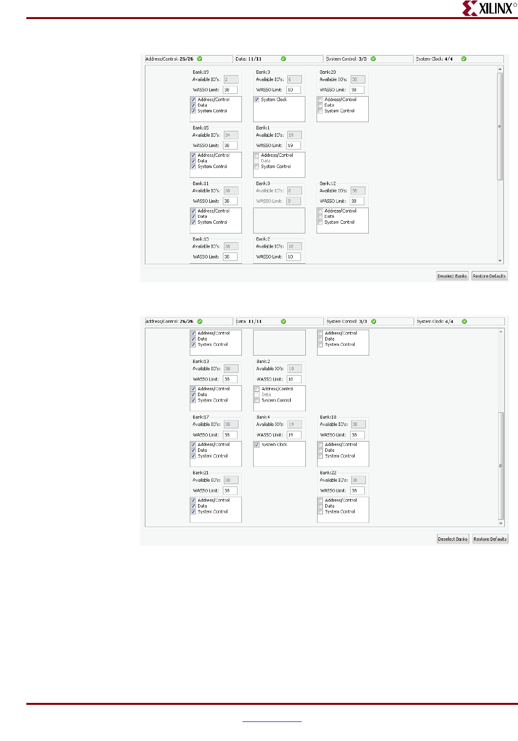
Memory Interface Solutions User Guide www.xilinx.com 55
UG086 (v3.6) September 21, 2010
MIG User Interface
R
Select the appropriate bank and memory signals as required.
The WASSO limit in conjunction with the Reserve pins limits the number of available I/Os
in a bank. For more information on the WASSO limit, refer Appendix C, “WASSO Limit
Implementation Guidelines.”
To unselect the banks that are selected, click the Deselect Banks button. To restore the
defaults, click the Restore Defaults button.
Figure 1-44: Bank Select (a)
Figure 1-45: Bank Select (b)
UG086_c1_28_021009
UG086_c1_29_021009
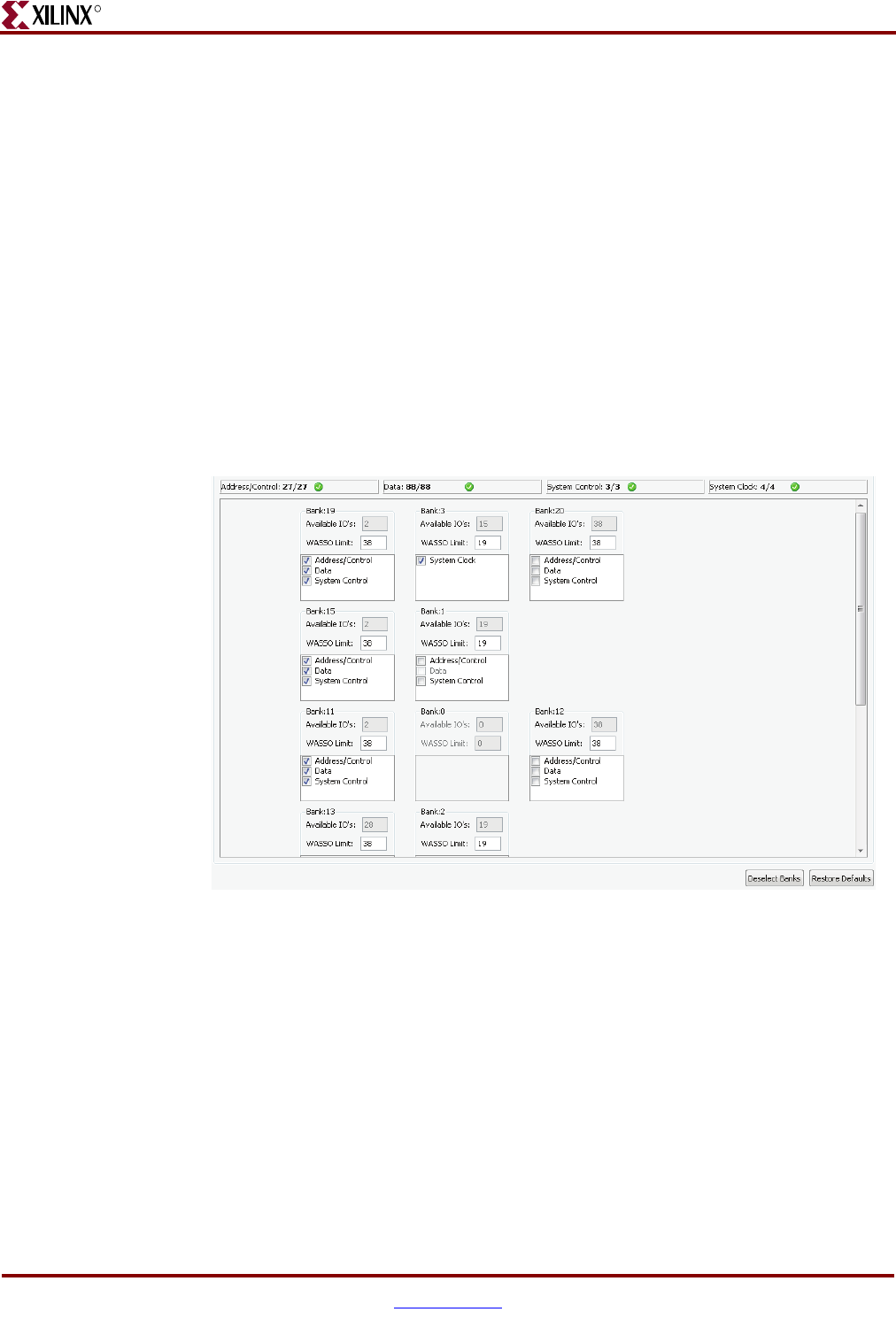
56 www.xilinx.com Memory Interface Solutions User Guide
UG086 (v3.6) September 21, 2010
Chapter 1: Using MIG
R
In certain banks, global clock pins are not allowed for system clock. This is because system
clock signals have different I/O standards as compared to those of any other signals in the
design. In such banks, global clock pins are left unused.
•Real-time pin allocation. As the user selects the banks, pin allocation is done
dynamically, and the number of pins required is updated for each group of signals.
• The red circle with a cross mark at each group indicates that sufficient pins are not
allocated, and additional pins are required for the selected configuration.
• The green circle with a tick mark at each group indicates that sufficient pins are
allocated for the selected configuration.
• The denominator in each group indicates the total number of pins required for
each group.
The user must select banks until the numerator equals the denominator. The user
cannot move to the next page unless sufficient pins are allocated for each group.
Figure 1-46 illustrates the conditions where sufficient banks are selected in order to
successfully generate the design.
Figure 1-47 indicates when sufficient banks are not allocated for each signal group.
Figure 1-46: Real-Time Pin Allocation: Sufficient Banks Selected
UG086_c1_45_021009
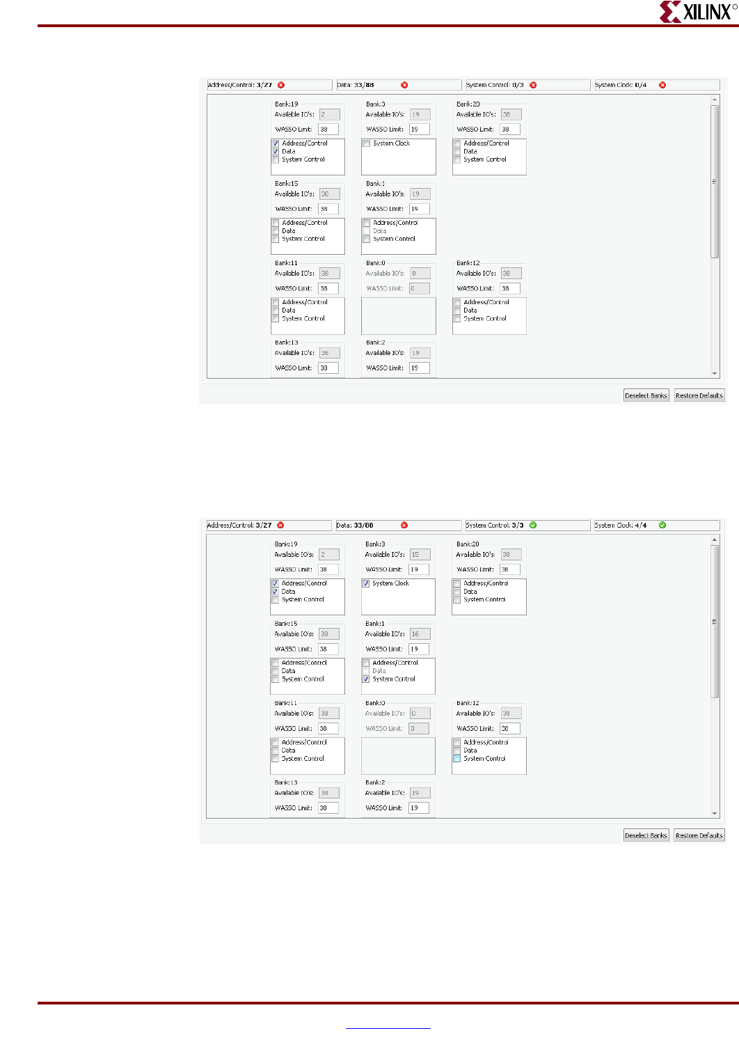
Memory Interface Solutions User Guide www.xilinx.com 57
UG086 (v3.6) September 21, 2010
MIG User Interface
R
Figure 1-48 indicates sufficient pins are allocated for System Control and System Clock
groups, but sufficient pins are not allocated for Data and Address groups.
•Pin Allocation Priority. MIG allocates the pins starting with exclusive data banks
first, followed by data banks that combine with other groups.
Figure 1-47: Real-Time Pin Allocation: Sufficient Banks Not Selected
Figure 1-48: Real-Time Pin Allocation: Insufficient Pins for Data/Address Groups
UG086_c1_46_021009
UG086_c1_47_021009
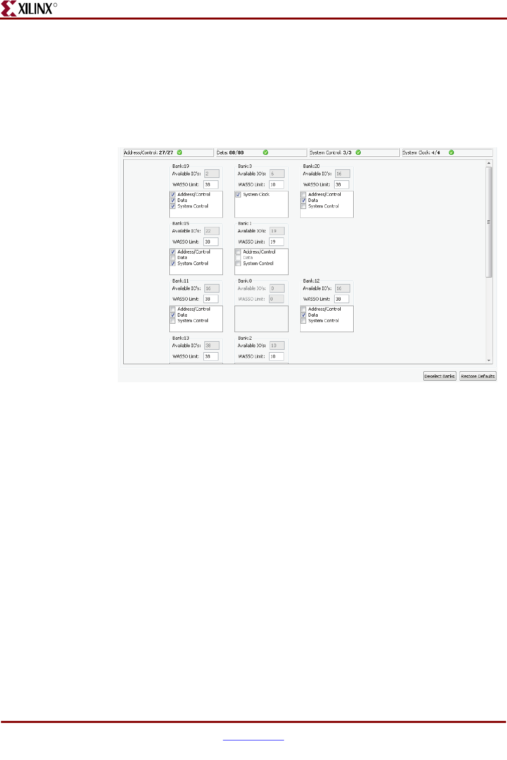
58 www.xilinx.com Memory Interface Solutions User Guide
UG086 (v3.6) September 21, 2010
Chapter 1: Using MIG
R
Figure 1-49 indicates that data banks are selected in bank 11, bank 19, bank 20, and
bank 12. In bank 11, bank 20 and bank 12, only data is selected; in bank 19, data,
address, and system control are selected. Here, data is allocated first in bank 11,
bank 20 and bank 12, and then in bank 19. This Pin Allocation Priority is applicable
only for data group signals in Virtex-4 and Virtex-5 devices.
Note: Data group infers Data group pins in CIO designs and Data Read group pins in SIO
designs.
•Master Bank selection. This is applicable only for QDRII SRAM and DDRII SRAM
Virtex-5 FPGA designs when the DCI Cascading Information option is selected. A
Master bank should be selected in each column when a Data Read is selected in that
particular column. There is an exception for the middle column. The middle column is
divided into two parts: above zero bank and below zero bank. The middle column can
have two Master banks, depending on where the Read Data banks are selected. If the
Read Data bank is selected either above or below the Zero bank, only one Master Bank
is required. If the Read Data banks are selected both above and below Zero bank, two
Master banks are required.
Figure 1-50 shows that the Data Read is selected in both the columns and user needs to
select the Master Banks in both the columns. Master bank selection box lists all the
possible banks that can be selected as Master Bank. MIG does not show the Master
Bank selection box for a column if that column does not have enough pins in the banks.
Figure 1-49: Pin Allocation Priority
UG086_c1_48_021009
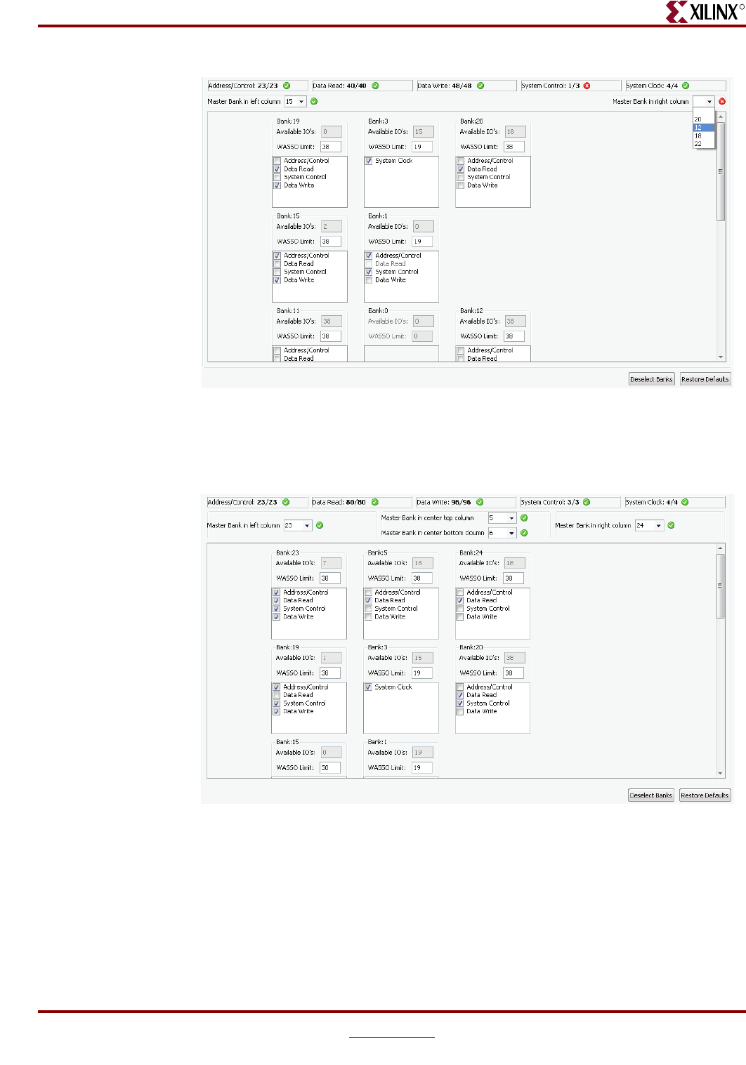
Memory Interface Solutions User Guide www.xilinx.com 59
UG086 (v3.6) September 21, 2010
MIG User Interface
R
Figure 1-51 shows the Master Bank selection in the center column. It uses all the pins
for Read Data from the center column.
Figure 1-50: Master Bank Selection (a)
Figure 1-51: Master Bank Selection (b)
UG086_c1_49_021009
UG086_c1_50_021009
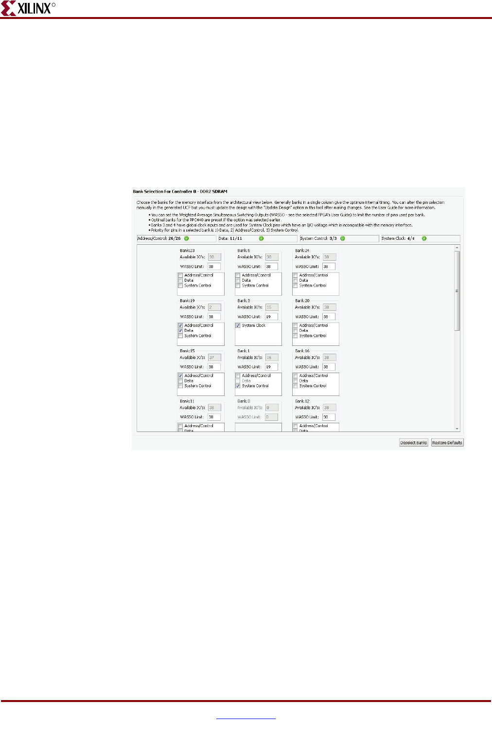
60 www.xilinx.com Memory Interface Solutions User Guide
UG086 (v3.6) September 21, 2010
Chapter 1: Using MIG
R
•Bank Selections for Multiple Memory Interfaces in Virtex-5 FPGA Designs. For a
multiple interface design, a particular group is allowed to select in a bank only for
compatible I/O standards. For example (with the selected FPGA as
XC5VLX220-FF1760), Controller 0 is DDR2 SDRAM (see Figure 1-52) and Controller 1
is QDRII SRAM (see Figure 1-53). In DDR2 SDRAM, bank 19 is selected for Data, bank
19 and bank 15 are selected for Address, and bank 1 is selected for System Control. In
QDRII SRAM, neither bank 19 nor bank 15 are allowed to select Data Read, because
the I/O standard for DDR2 SDRAM Data and Address is SSTL18_II_DCI, and the I/O
standard for QDRII SRAM Data Read is HSTL_I_DCI_18. These two I/O standards
are not compatible. Hence MIG does not allow bank selection for the group of signals
that do not follow the I/O standard compatibility rules.
Figure 1-52: DDR2 SDRAM Bank Selection in a Multiple Interface Design
UG086_c1_60_050409
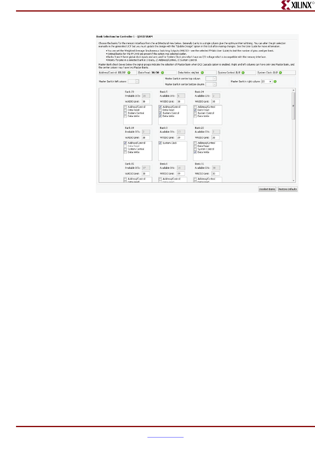
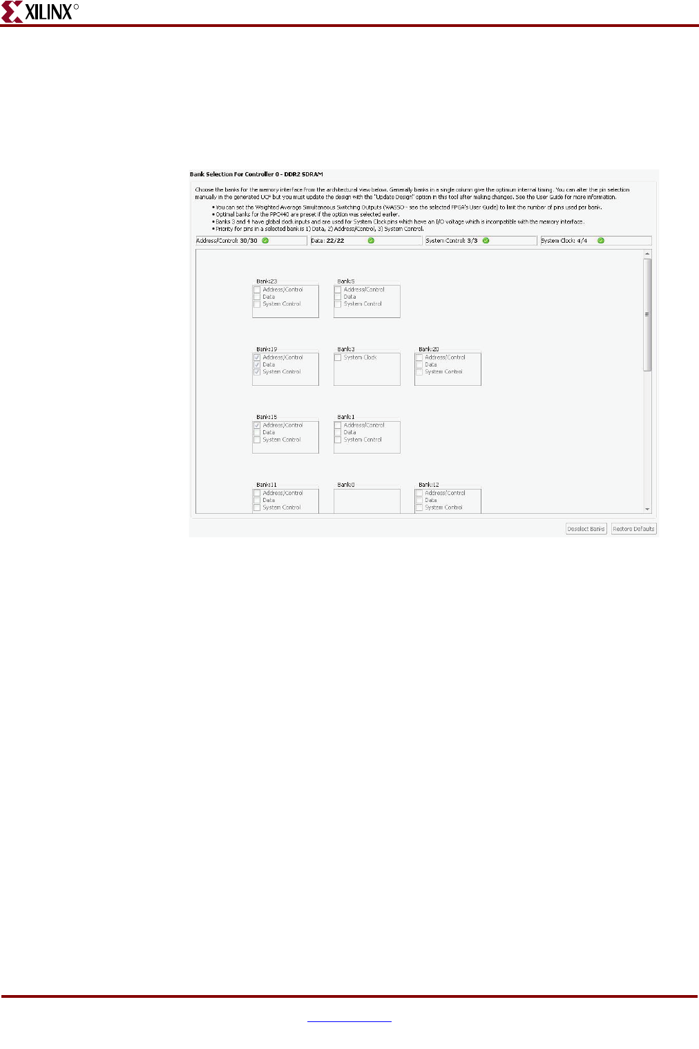
62 www.xilinx.com Memory Interface Solutions User Guide
UG086 (v3.6) September 21, 2010
Chapter 1: Using MIG
R
When PPC440 compatible pinouts are selected, MIG outputs the fixed pinout. The banks
that are checked indicate the banks used for PPC440 pinouts; the user does not have an
option to select the specific banks. For example, bank selection of a 16-bit design with a
XC5VFX100T-FF1136 target device and the PowerPC440 Block Selection value in the Pin
Compatible FPGAs page set to Top is shown in Figure 1-54.
After selecting the banks, click Next to continue. The Summary page window is displayed.
Figure 1-54: PPC Bank Selection Page
UG086_c1_73_050409
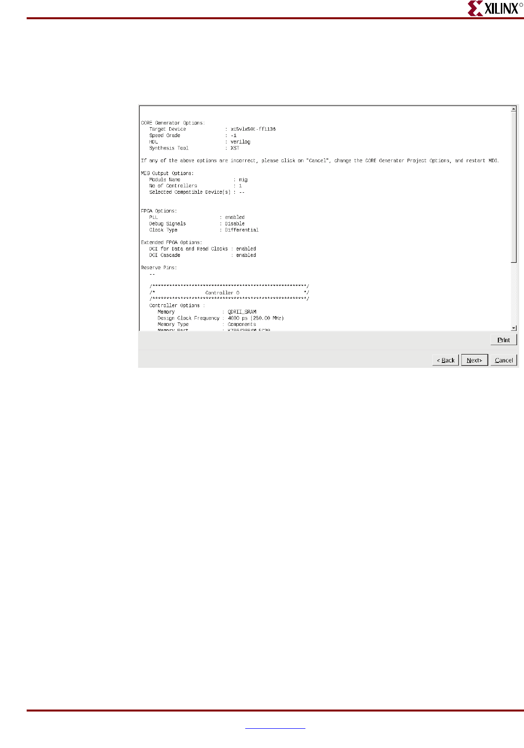
Memory Interface Solutions User Guide www.xilinx.com 63
UG086 (v3.6) September 21, 2010
MIG User Interface
R
Summary
This window provides complete details about the CORE Generator options, Interface
parameters, FPGA options, and Bank selections of the active project (Figure 1-55).
Click Next to move to the License Agreement page of the selected memory of the
Micron/Qimonda memory model only for DDR2 SDRAM, DDR SDRAM, and RLDRAM II
memory interface designs. For other memory interface designs, clicking the Next button
will move to the PCB information page.
Figure 1-55: Summary
UG086_c1_31_030510
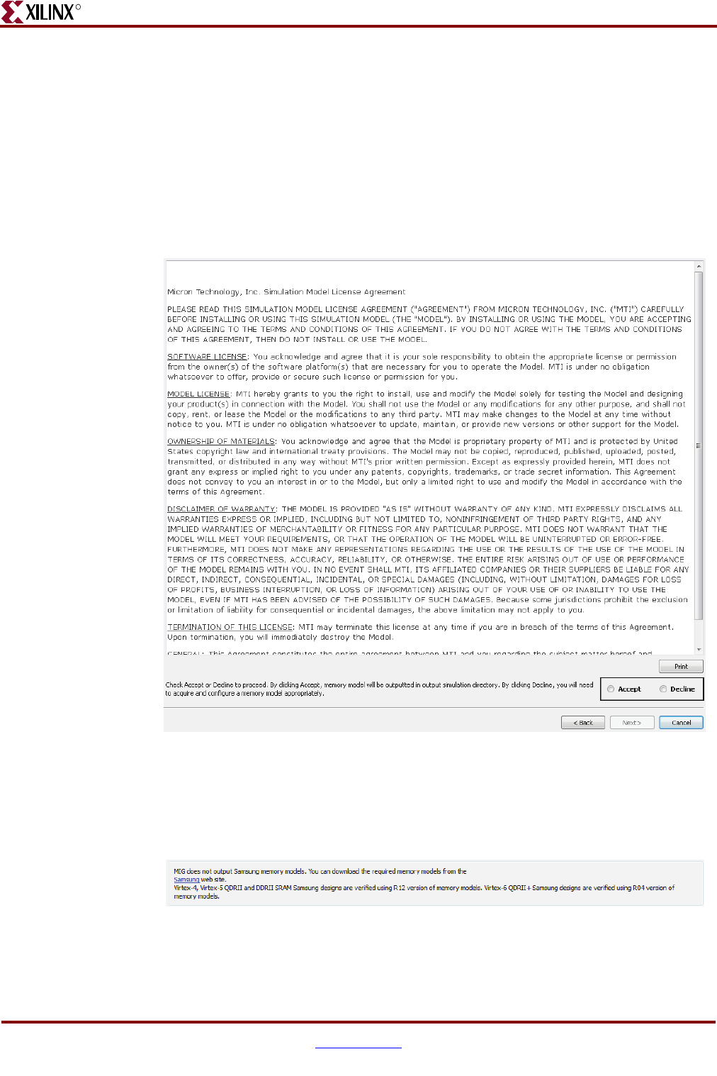
64 www.xilinx.com Memory Interface Solutions User Guide
UG086 (v3.6) September 21, 2010
Chapter 1: Using MIG
R
Memory Model License
MIG outputs a Micron memory model for simulation purposes for memories such as DDR
SDRAM, DDR2 SDRAM, and RLDRAM II, as well as Qimonda memory model for DDR2
SDRAM. Read the license agreement carefully and select the Accept radio button to accept
it (Figure 1-56). Selecting the Accept radio button also causes the models to be output in
the output sim folder.
If the license agreement is not agreed to (i.e., the Decline radio button is selected), the
memory model is not available. The user then needs to get the appropriate memory model
by some other means to simulate the design.
MIG outputs Micron and Qimonda memory models only. MIG does not output Samsung
and Cypress memory models; these should be download from the vendor’s respective
websites (Figure 1-57).
Click the Next button to move to the PCB information page.
Figure 1-56: License Agreement
Figure 1-57: Samsung Memory Models Information
UG086_c1_30_072809
UG086_c1_86_102009
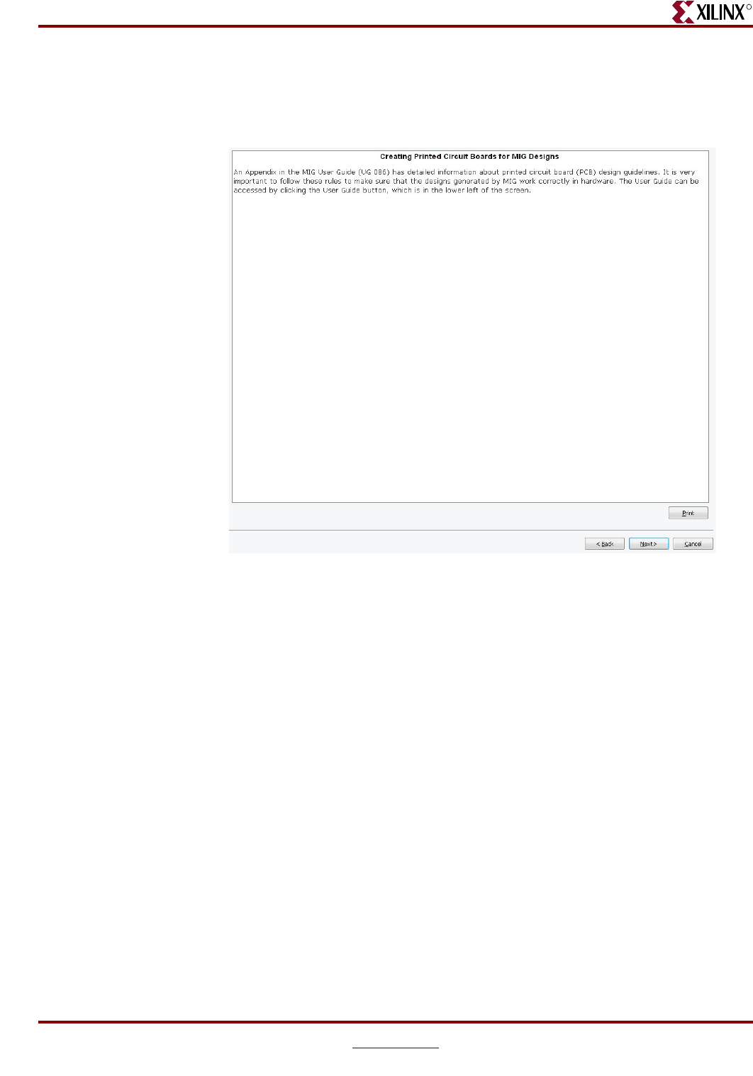
Memory Interface Solutions User Guide www.xilinx.com 65
UG086 (v3.6) September 21, 2010
MIG User Interface
R
PCB Information
This page displays the PCB related information to be considered while designing the board
that uses MIG generated designs (Figure 1-58).
Click Next to go to the Design Notes page.
Figure 1-58: PCB Information
UG086_c1_42_072008
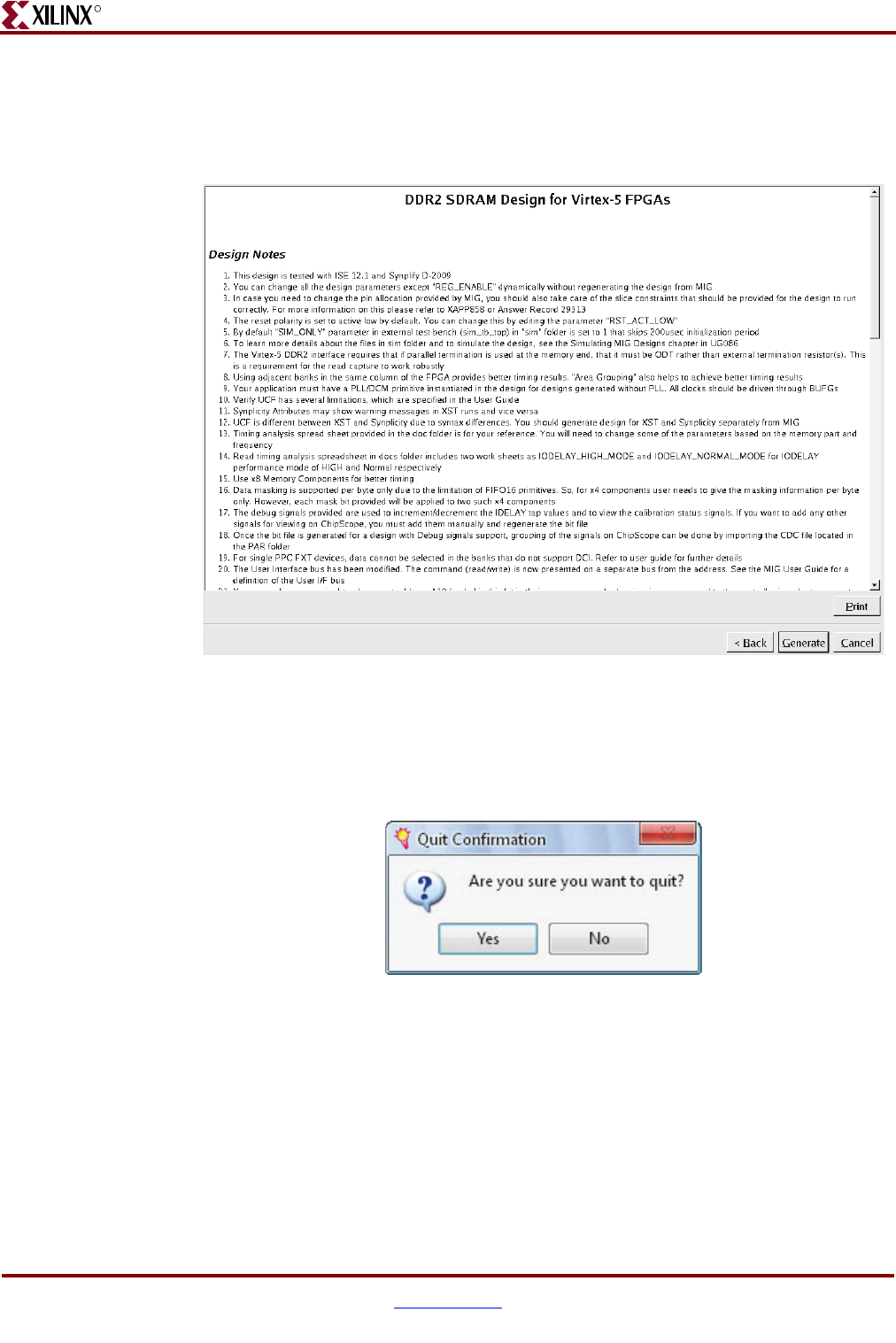
66 www.xilinx.com Memory Interface Solutions User Guide
UG086 (v3.6) September 21, 2010
Chapter 1: Using MIG
R
Design Notes
This page provides the design notes that should be taken into account while using MIG
generated designs (Figure 1-59).
Click Generate to generate the design files. MIG generates three output directories:
example_design, user_design, and docs. After generating the design, the MIG GUI closes.
Click Cancel. A Quit Confirmation window appears, as shown in Figure 1-60.
Click Yes to exit or No to return to the current page.
Figure 1-59: Design Notes
Figure 1-60: Quit Confirmation
UG086_c1_32_030510
UG086_c1_33_072008

Memory Interface Solutions User Guide www.xilinx.com 67
UG086 (v3.6) September 21, 2010
MIG User Interface
R
Output Files
A MIG-generated design has the following output files and directory:
•A <component name>_xmdf.tcl file. This is the interface file between the ISE and
CORE Generator software. The ISE software uses this file to determine the files output
by the CORE Generator software for the core to be integrated into the ISE project.
•A <component name>.vho file, used for the core to be instantiated, created only
when a VHDL design is generated.
•A <component name>.veo file, used for the core to be instantiated, created only
when a Verilog design is generated.
•A <component name>_readme.txt file, includes information about the files
generated and how they are used.
•A <component name> directory.
In the <component name> directory, three folders are created:
•docs
•example_design
•user_design
Any relevant documents, such as application notes, timing analysis spreadsheets, and user
guide are in the docs directory.
The example_design and user_design folders contain several other folders and files.
They are:
•rtl — Contains all the RTL files (either VHDL or Verilog design files). The RTL files
generated for Virtex-5 FPGA designs do not have user design names (component
names) prepended to the RTL file names. MIG generates the same code for both the
XST and Synplicity tools. The generated RTL has separate XST and Synplicity
attributes. While running XST designs, Synplicity attributes might cause warning
messages to appear, and vice versa. The warning messages related to these attributes
can be ignored.
•par — Contains the UCF with constraints for the design, including two scripts files
that are generated (ise_flow.bat and create_ise.bat):
•ise_flow.bat — The user double-clicks the ise_flow.bat script file to run
the design through synthesis, build, map, and par. This script file sets all the
required options. Users should refer to this file for the recommended build
options for the design. This file takes all synthesis options from the
xst_run.txt file located in the par folder. All map, place-and-route, and
Timing Reporter and Circuit Evaluator (TRCE) options are set in the
ise_flow.bat file. BITGEN options are taken from the UT file located in the
par folder. The options that are not listed out in these files (such as Synthesis and
others) are set to their default values. For more information about the allowed
option values, refer to the Development System Reference Guide in the Xilinx ISE
12.3 Design Suite Software Manuals and Help – PDF Collection at
http://www.xilinx.com/support/documentation/index.htm.
•create_ise.bat — The generated MIG design includes a create_ise.bat
script file in both the example_design/par and user_design/par
directories. Running the create_ise.bat script generates an ISE tools project
that incorporates the generated MIG design. If the file is run from the
example_design/par directory, the ISE tools project includes the
example_design. If the file is run from the user_design/par directory, the ISE

68 www.xilinx.com Memory Interface Solutions User Guide
UG086 (v3.6) September 21, 2010
Chapter 1: Using MIG
R
project includes the user_design. The create_ise.bat file calls the
set_ise_prop.tcl file, which is also located in the selected par directory. The
set_ise_prop.tcl file includes standard xtclsh commands that pull the MIG
RTL source files (example_design/rtl or user_design/rtl) into an ISE
tools project and set the required synthesis and implementation build options.
After completion of the create_ise.bat script, a test.ise file is created that
can be opened in the ISE tools. The synthesis and implementation build options
set by create_ise.bat are recommended. No other build options have been
tested and are not supported. For detailed information on the options set by
create_ise.bat, refer to the Development System Reference Guide and the
XST User Guide in the Xilinx ISE 12.3 Design Suite Software Manuals and Help –
PDF Collection at http://www.xilinx.com/support/documentation/index.htm.
•compatible_ucf — This folder is created when the memory interface designs
are generated with compatible FPGAs. This folder contains a compatible UCF of
every compatible FPGA selected.
• CDC file — MIG provides the CDC for debug enable designs. For more
information on how to use this file, refer to Appendix F, “Analyzing MIG Designs
in the ChipScope Analyzer with CDC.”
•synth — Contains the SDC file which has design constraints for Synplify Pro
synthesis tool. This folder also has the script files, which set various tool options.
There is also a project file, through which the RTL files are passed for synthesis.
•sim — Contains the testbench files that are needed to simulate the design. It also has a
.do file. For more information on simulating the design, refer to “Simulation Guide,”
page 499.
For the user_design folder, a synthesizable testbench module is also present in the
sim folder.
Caution! Recommended Build Options. The ise_flow.bat file in the par folder of the
component name directory contains the recommended build options for the design. Failure to follow
the recommended build options could produce unexpected results.
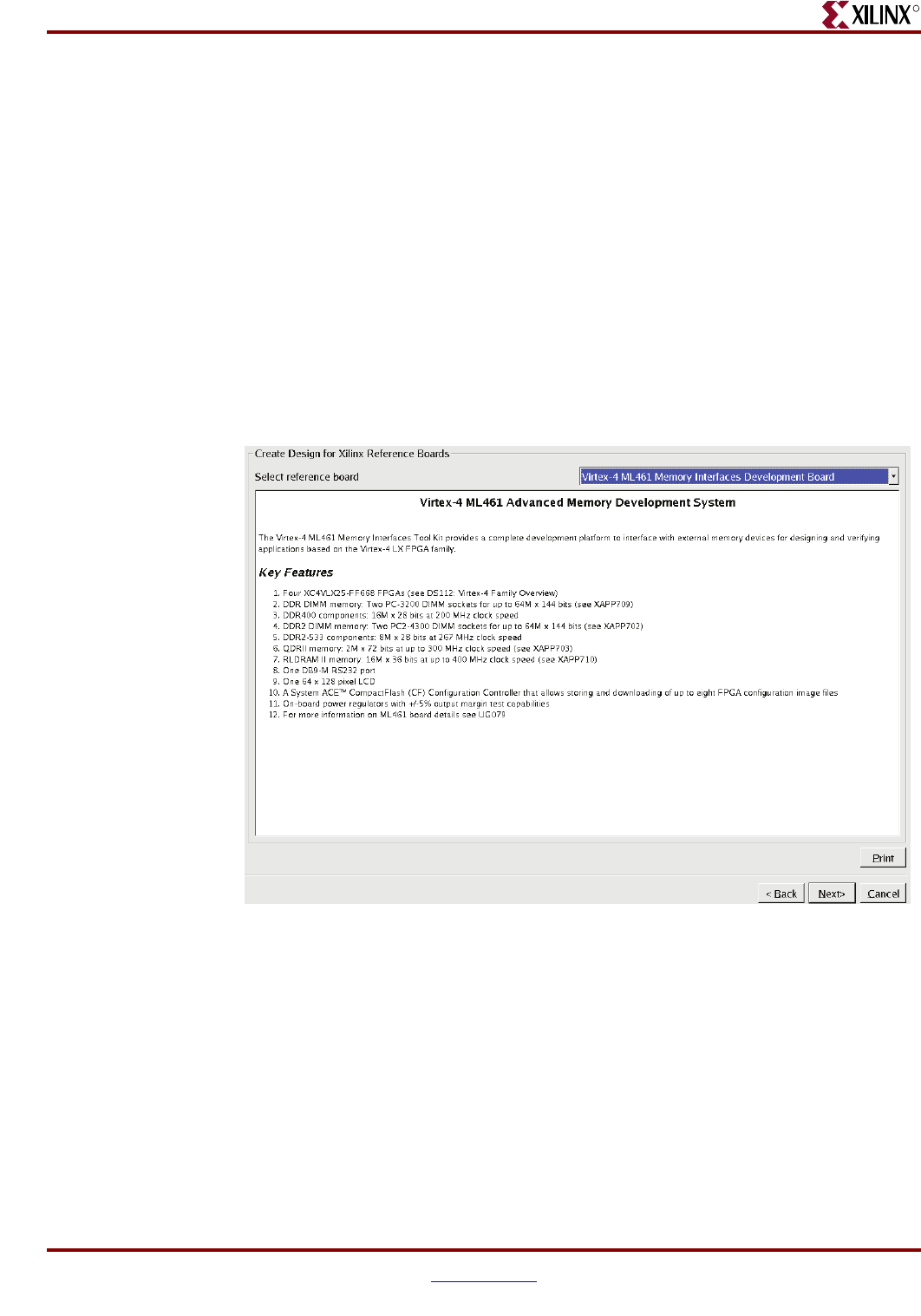
Memory Interface Solutions User Guide www.xilinx.com 69
UG086 (v3.6) September 21, 2010
MIG User Interface
R
Create Design for Xilinx Reference Boards
To create a design for the Xilinx Reference Boards, select Create Design for Xilinx
Reference Boards from the MIG Output Options. It is intended to generate the board files
for various Xilinx Reference Boards. Click Next to continue.
The flow is as follows:
1. Reference Board Designs
2. Memory Model License
3. PCB Information
4. Design Notes
Reference Board Designs
This section allows selection of the board for which the designs are to be generated
(Figure 1-61).
The pull-down menu includes a list of boards. Select the appropriate board. Details about
the particular board are displayed in the pane below. After selecting the board, click Next
to move to next page.
Figure 1-61: Create Design for Xilinx Reference Boards
UG086_c1_34_030510
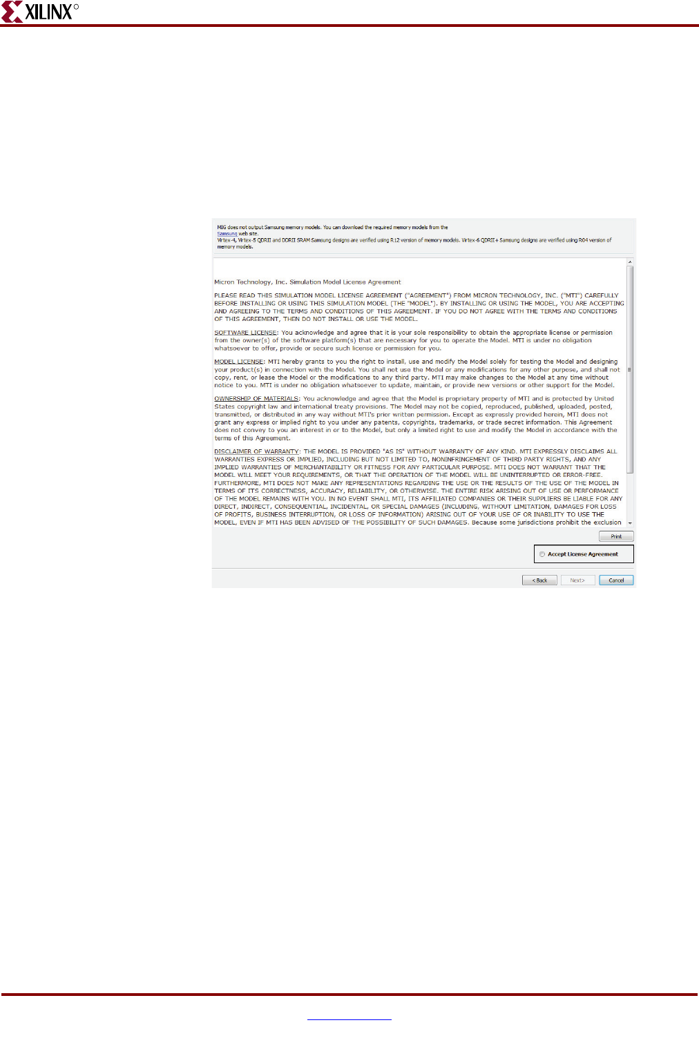
70 www.xilinx.com Memory Interface Solutions User Guide
UG086 (v3.6) September 21, 2010
Chapter 1: Using MIG
R
Memory Model License
MIG outputs a Micron memory model for simulation purpose for memories like DDR
SDRAM, DDR2 SDRAM, and RLDRAM II. To generate the board files for the specified
Xilinx Reference Board, read the license agreement carefully and select the Accept
License Agreement radio button (Figure 1-62).
If the license agreement is not accepted, the user cannot generate board files. The Next
button is disabled unless the license agreement is accepted.
Click Next to go to the PCB Information page.
Figure 1-62: Memory Model License
UG086_c1_54_102009
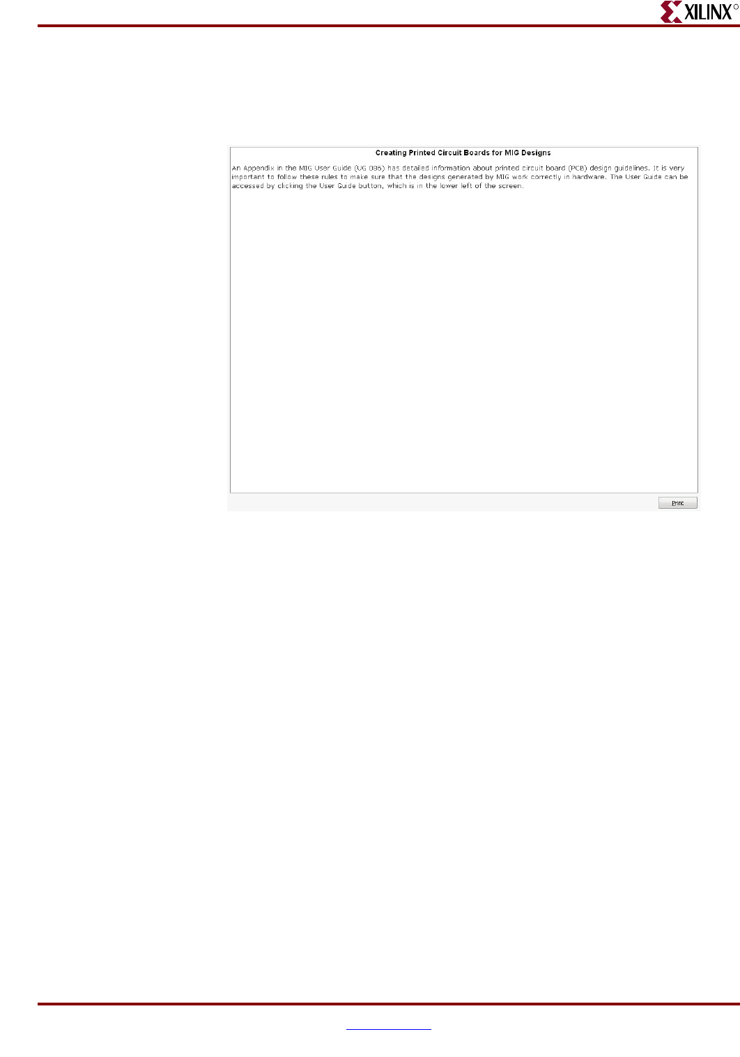
Memory Interface Solutions User Guide www.xilinx.com 71
UG086 (v3.6) September 21, 2010
MIG User Interface
R
PCB Information
This page displays the PCB-related information to be considered while designing the
board that is to use a MIG generated design (Figure 1-63).
Click Next to go to the Design Notes page.
Figure 1-63: PCB Information
UG086_c1_51_072008
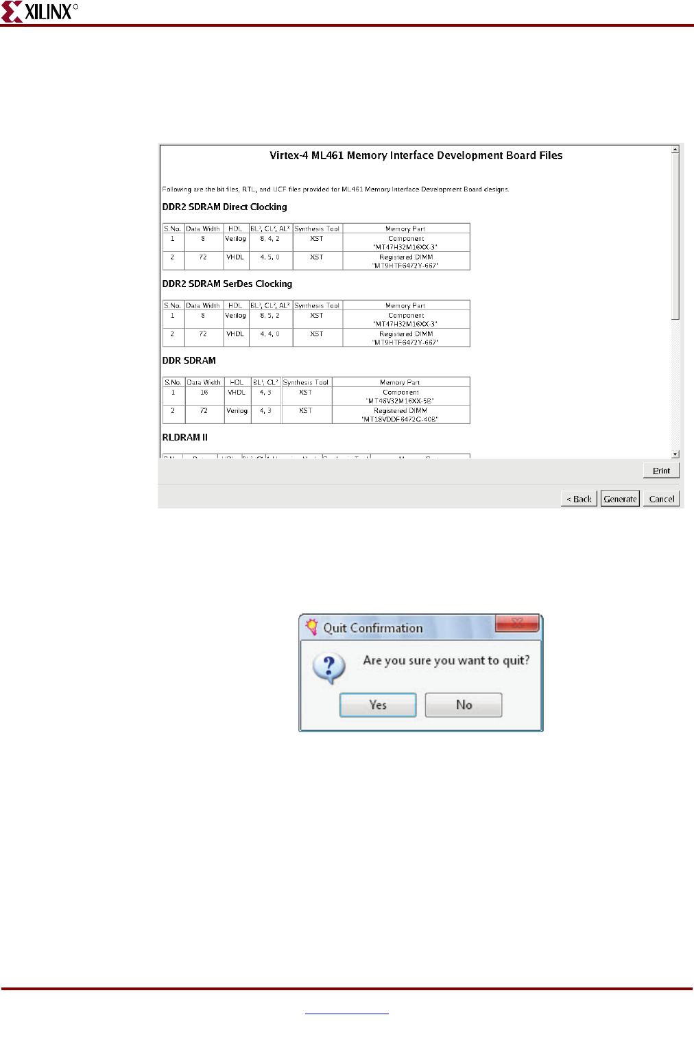
72 www.xilinx.com Memory Interface Solutions User Guide
UG086 (v3.6) September 21, 2010
Chapter 1: Using MIG
R
Design Notes
Click Generate to generate the board files for the specified Xilinx reference board
(Figure 1-64). After successful generation of the board files, the MIG GUI closes.
Click Cancel. A Quit Confirmation window appears, as shown in Figure 1-65. Click Yes to
exit or No to return to the current page.
Figure 1-64: Finish
Figure 1-65: Quit Confirmation
UG086_c1_35_030510
UG086_c1_33_072008

Memory Interface Solutions User Guide www.xilinx.com 73
UG086 (v3.6) September 21, 2010
MIG User Interface
R
Verify UCF and Update Design and UCF
To verify the UCF and update design and UCF, select the third option (Verify UCF and
Update Design and UCF) from the MIG Output Options page. This option verifies that the
input UCF passed and can update the design and UCF for the current version of the MIG
tool. Verify UCF is intended for verification of UCF files that were/are generated from the
MIG tool and later modified. This feature ensures that the pinout still follows the rules
required for the current version of MIG generated designs. For a list of rules associated
with the Verify UCF feature, refer to “Verify UCF and Update Design Rules,” page 80.
The Update Design feature updates the input UCF files to make them compatible with the
current MIG design. The MIG tool verifies the input UCF for the pin allocation rules and
allows the UCF to get updated only if it passes the pin allocation rules. The Update Design
feature is required in the following scenarios:
• A pinout is generated using an older version of MIG and the design is to be revised to
the current version of MIG. In MIG 2.0 and later, the pinout allocation algorithms
have been changed for certain MIG designs.
• A pinout is generated independent of MIG or is modified after the design is
generated. When a design is generated from MIG, the UCF file and HDL code are
generated with the correct constraints.
Caution! This is not recommended. MIG should be used to generate the pinout. If an
independently generated pinout must be used, a UCF should be generated using MIG and used
as a baseline for constraint modifications.
After verification of the UCF is completed and if there are no issues with the input UCF, the
user can update the RTL and UCF for the current version of the MIG tool by proceeding
further. The Update Design feature ensures that the input UCF pinout remains the same.
This option is not supported for Virtex-5 FPGA PPC440 DDR2 designs. Update Design
works for Create Custom Part if the created custom parts exist in the output directory or
project directory. If the created custom part does not exist, the MIG tool cannot update the
design. For a list of rules associated with the Update Design feature, refer to “Verify UCF
and Update Design Rules,” page 80. For more details on Virtex-5 FPGA DDR2 design
constraints, see Appendix B, “Pinout-Related UCF Constraints for Virtex-5 FPGA DDR2
SDRAMs.” For a list of rules associated with the Update UCF feature, refer to “Verify UCF
and Update Design Rules,” page 80.
The Update Design feature updates the UCF constraints and also the RTL design
parameters. RTL design parameters are updated in the corresponding RTL file. For
example, for a Virtex-4 FPGA single controller DDR2 direct-clocking design, the
IDELAYCTRL_NUM parameter is updated in the idelay_ctrl module. These parameters
are updated for both example_design and user_design. In MIG 3.0 and later, DCM is
replaced with PLL for all Virtex-5 FPGA designs. If the Update Design option is used, the
MIG tool uses PLL resources instead of DCM resources. The infrastructure module has
both PLL and DCM codes and the CLK_GENERATOR parameter enables either a PLL or a
DCM in the infrastructure module. The CLK_GENERATOR parameter is set to PLL by
default. For use as a DCM, this parameter should be changed manually to DCM.
MIG generates mig.prj files in the output mig_x/example_design and
mig_x/user_design directories. These files contain the project settings specific to a
generated MIG project for both the example_design and user_design. A mig.prj file is
required to perform the update. This mig.prj file can be from a previous version of MIG
or from the current version.
If a MIG design has not been generated, use the current MIG version to generate the
design. Select the appropriate banks of the desired pinout on the Bank Selection GUI page
74 www.xilinx.com Memory Interface Solutions User Guide
UG086 (v3.6) September 21, 2010
Chapter 1: Using MIG
R
to ensure that the update completes successfully. If a MIG design has already been
generated, locate the mig.prj file in the generated MIG project. Ensure that the banks
selected for this project match the banks of the desired pinout. This is required for the
update to complete successfully.
Open MIG either by invoking a new MIG project or by reopening the previously generated
MIG project. Verify the options displayed on screen one and click Next. On screen two,
provide a component name and select Verify UCF and Update Design and UCF.
Note: Verify UCF and Update Design and UCF verifies that the pinout adheres to the required
pinout rules outlined in Appendix A, “Memory Implementation Guidelines.” The pinout must meet
these guidelines for the tool to complete the Update Design option.
The flow is as follows:
1. Load mig.prj and UCF
2. Summary
3. Verification Report
4. Memory Model License
5. PCB Information
6. Design Notes
Load mig.prj and UCF
Browse to the project file path (mig.prj). If the pinout is an example_design pinout (i.e.,
contains the additional example_design pins such as ERROR), select the mig.prj file
located in the example_design directory. If the pinout does not include the additional
example_design pins, select the mig.prj file located in the user_design directory.
If a MIG provided UCF is being updated from a pre-MIG release, browse to the
MIG-generated UCF. If a UCF is being updated to a user-defined pinout, browse to this
UCF. The UCF only needs to include the desired pin LOCs; however, the pin names must
match the MIG syntax. Provide the input UCF path at the Load UCF File box and input the
mig.prj at the Load Prj File Box, or click the Browse button to enter the UCF and Prj files
through a browser window (Figure 1-66).
Note: Update Design is not supported for the UCF signal names that were modified using the Edit
Signal Names option of MIG 1.73.
Select the appropriate files. After selecting the files, click Next to continue.
Figure 1-66: Prj and UCF Selection Window
UG086_c1_37_072809
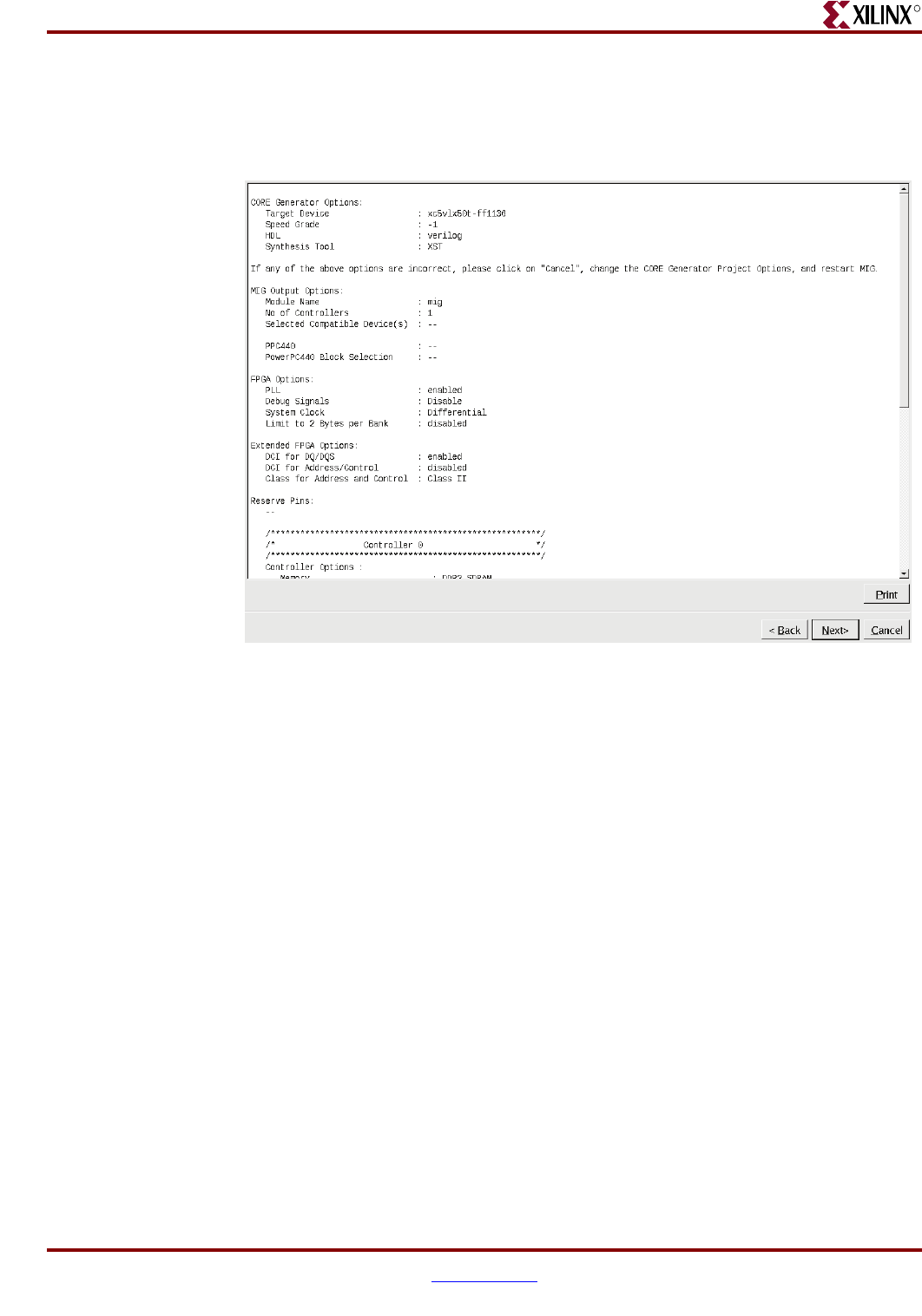
Memory Interface Solutions User Guide www.xilinx.com 75
UG086 (v3.6) September 21, 2010
MIG User Interface
R
Summary
This page provides complete details about the bank selection, Interface parameters, CORE
Generator options and FPGA options of the project for which the UCF is to be verified.
Click Next to move to the Verification Report page.
Figure 1-67: Summary Page
UG086_c1_38_030510
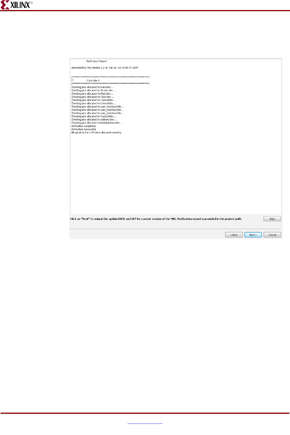
76 www.xilinx.com Memory Interface Solutions User Guide
UG086 (v3.6) September 21, 2010
Chapter 1: Using MIG
R
Verification Report
This window indicates if the input UCF has been verified and provides warning or error
messages if the input UCF does not follow the pin allocation rules.
Figure 1-68: Verification Report Page after Successful Verification
UG086_c1_69_072809
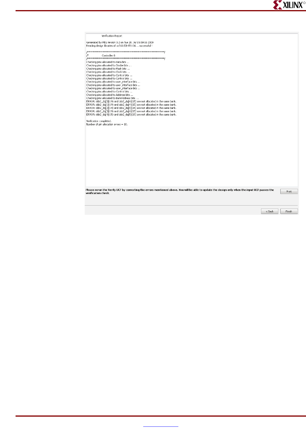
Memory Interface Solutions User Guide www.xilinx.com 77
UG086 (v3.6) September 21, 2010
MIG User Interface
R
Click Next to move to Memory Model License agreement page. If the Verification Report
file has a warning message(s), MIG proceeds with updating the design.
When the input UCF does not follow the MIG pin allocation rules, for example if the
Verification Report file has an error message(s), MIG does not proceed with updating the
design.
Figure 1-69: Verification Report Page after Unsuccessful Verification
UG086_c1_70_072809
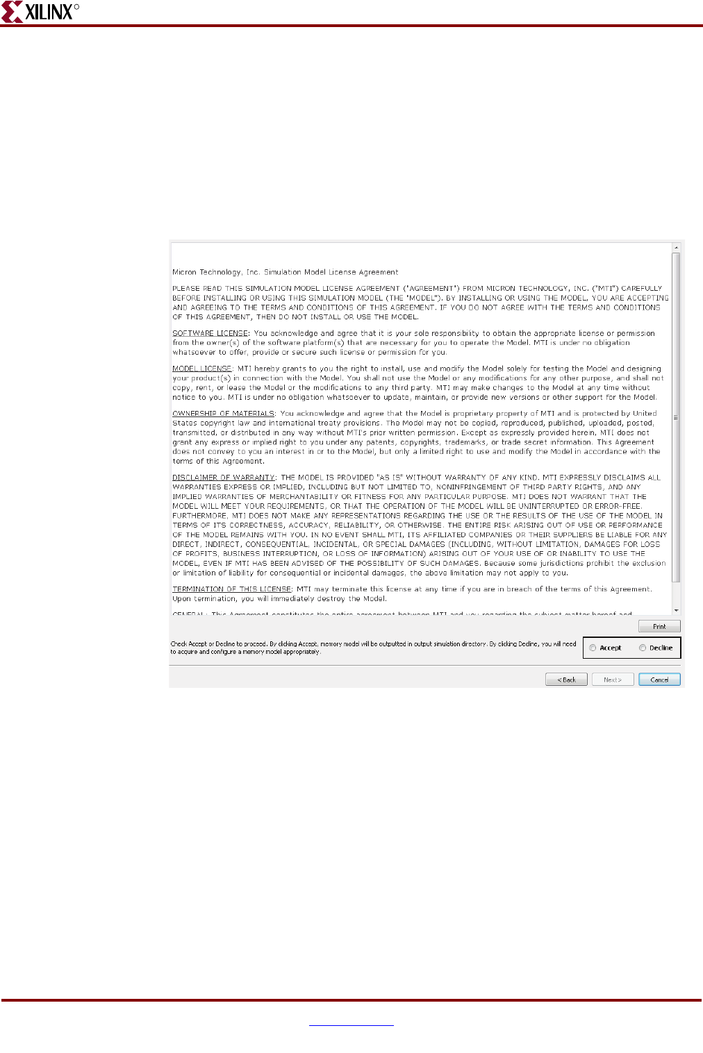
78 www.xilinx.com Memory Interface Solutions User Guide
UG086 (v3.6) September 21, 2010
Chapter 1: Using MIG
R
Memory Model License
MIG outputs Micron memory model for simulation purposes for memories such as DDR2
SDRAM, DDR SDRAM and RLDRAM II and Qimonda memory model for DDR2 SDRAM.
To get the simulation model in the output folder, click the Accept radio button. Read the
license agreement carefully and select the Accept radio button to accept it.
If the license agreement is not agreed to (i.e., the Decline radio button is selected), the
simulation model is not output into the output folder.
Click Next to move to the PCB information page
Figure 1-70: Memory Model License Agreement Page
UG086_c1_71_072809
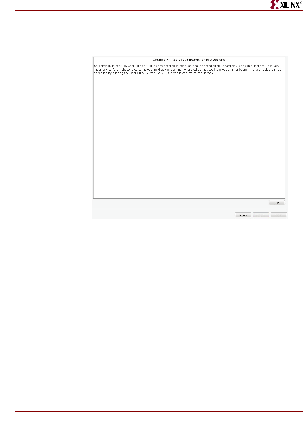
Memory Interface Solutions User Guide www.xilinx.com 79
UG086 (v3.6) September 21, 2010
MIG User Interface
R
PCB Information
This page displays the PCB related information to be considered while designing the board
that uses MIG generated designs. Click Next to go to the Design Notes page.
Design Notes
This page provides the design notes that should be taken into account while using the MIG
generated designs.
Click the Generate button to generate the complete design with the loaded Prj settings and
modified UCF (the UCF is updated without affecting the pin allocation constraints). MIG
generates three output directories example_design, user_design and docs. The UCF files in
the example_design and user_design folders are updated to the input UCF. After
generating the design, the MIG GUI closes.
Click Cancel. A Quit Confirmation window appears, as shown in Figure 1-72. Click Yes to
exit or No to return to the Current page.
Figure 1-71: PCB Information
UG086_c1_72_072208
80 www.xilinx.com Memory Interface Solutions User Guide
UG086 (v3.6) September 21, 2010
Chapter 1: Using MIG
R
Verify UCF and Update Design Rules
Verify UCF and Update Design and UCF verifies the input UCF file for pin allocation
rules and generates warnings or error reports for any issues. It does not verify the input prj
file. This feature is useful to verify any UCF pinout changes after the design is generated
from the MIG tool. The user must pass the MIG generated prj file (the original prj file)
without any modifications. The verification report will not be correct if any of the
parameters in the original prj file are altered. In the CORE Generator tool, the
recustomization option should be selected to reload the project.
The following UCF keywords and syntax elements are supported by Verify UCF and
Update Design:
•KEYWORDs:
•NET
•Net
•net
• NET names (can be lowercase, uppercase, or a mix of lower- and uppercase):
• NET “ddr2_dq[0]”
• NET ddr2_dq[0]
• NET “DDR2_DQ[0]”
• NET “Ddr2_dq[0]”
Figure 1-72: Quit Confirmation
UG086_c1_84_092208

Memory Interface Solutions User Guide www.xilinx.com 81
UG086 (v3.6) September 21, 2010
MIG User Interface
R
•Bus notations:
• NET “ddr2_dq[0]”
• NET “ddr2_dq<0>”
• LOC constraints (supports various syntaxes, such as LOC, PROHIBIT and INHIBIT):
• LOC = “N33”
•LOC = N33
•IOSTANDARD:
• NET “ddr2_dq[*]” IOSTANDARD = SSTL18_II_DCI;
• NET “ddr2_dq[*]” LOC=N33 | IOSTANDARD = SSTL18_II_DCI;
• The MIG output UCF has spaces between the various KEYWORDs. The input UCF
need not have the same number of spaces, but each KEYWORD should be followed
by at least one space:
• NET “ddr2_dq[*]” IOSTANDARD = SSTL18_II_DCI;
• NET “ddr2_dq[*]” IOSTANDARD = SSTL18_II_DCI;
All of the above elements of syntax are treated the same by the MIG tool.
The following rules are verified from the input UCF file.
DDR2 SDRAM/DDR SDRAM Spartan FPGA designs:
1. Verifies the slice location constraints for DQ, DQS delayed col, FIFO write enable and
FIFO write address, and rst_dqs_div signals.
2. Verifies RLOC and BEL constraints for LUT delay calibration chain.
3. Verifies RLOC_ORIGIN constraints for LUT delay calibration chain.
4. Verifies AREA group constraint for calibration logic.
5. Verifies 5 Up/6 Down rule for DQ signals from DQS for left/right banks.
6. Verifies 5 Right rule for DQ signal from DQS for top/bottom banks
7. Verifies the DQ, DQS, DM, memory clocks, and rst_dqs_div (loop back) signals on the
same side of the FPGA.
8. Verifies the rst_dqs_div signal (loopback) should be center of the DQS sets.
9. Verifies system clock signals, whether allocated to the global clock pair of the device.
10. Verifies memory clock signals and differential DQS to be allocated to the differential
I/O pair of the device.
11. Verifies if reserved pins are used in the UCF.
12. Verifies VRN/VRP and VREF pins are not used in the UCF.
13. Verifies if the same tile is used for left/right banks for the following signals:
•DQ and DQS
•DQ and Address
• DQ and rst_dqs_div_out
• DM and DQS
• DM and Address
• DM and rst_dqs_div_out
The above signals cannot be used in the same tile because the two signals are in two
different clock phases.

82 www.xilinx.com Memory Interface Solutions User Guide
UG086 (v3.6) September 21, 2010
Chapter 1: Using MIG
R
14. Verifies all the pins and slice allocation rules if user selects compatible UCF.
DDR2 SDRAM Virtex-4/Virtex-5 FPGA designs:
1. Updates the IDELAYCTRL LOCs and slice constraints in the updated UCF.
2. Verifies the UCF and Updates the design even with the compatible UCF.
3. Verifies the UCF and Updates the design even with the user design UCF.
4. Verifies the UCF for system clocks allocated to global clock pins.
5. Updates the design for Virtex-4 FPGA DDR2 SDRAM multicontroller user design
UCF. If MIG does not find sufficient pins in a bank for allocating ERROR signal, then
user has to manually allocate the LOCs for the ERROR signal in the updated UCF file.
6. In designs containing an x4 memory part, the MIG verifies the UCF only when the DM
is associated with DQ higher nibble.
7. Verifies UCF for differential DQS signals allocated to differential pair pins in DDR2
SDRAM designs.
DDR SDRAM Virtex-4/Virtex-5 FPGA designs:
1. Updates the IDELAYCTRL LOCs and slice constraints in the updated UCF.
2. Verifies the UCF and Updates the design even with the compatible UCF.
3. Verifies the UCF and Updates the design even with the user design UCF.
4. Verifies the UCF for system clocks allocated to global clock pins.
5. Verifies the UCF for DQS to CC_P pin and corresponding DM to the CC_N for a CC
pair in Virtex-5 FPGA designs.
6. For parts with no DM, verifies the UCF for DQS to CC_P pin and the CC_N to any of
the output pins only in Virtex-5 FPGA designs.
7. In designs containing an x4 memory part, the MIG verifies the UCF only when the DM
is associated with DQ higher nibble.
QDRII SRAM/DDRII SRAM Virtex-4/Virtex-5 FPGA designs:
1. Updates the IDELAYCTRL LOCs in the updated UCF.
2. Verifies the UCF and updates the design even with the compatible UCF.
3. Verifies the UCF and Updates the design even with the user design UCF.
4. Verifies the UCF for system clocks allocated to global clock pins.
5. Verifies the UCF for CQ and CQ_n allocation only to P-pins.
6. For DDRII SRAM CIO x36 Virtex-5 FPGA designs, MIG verifies the UCF only when
the K/K_n and C/C_n are associated with the most significant 18 bits of data.
RLDRAMII Virtex-4 FPGA design:
1. Updates the IDELAYCTRL LOCs in the updated UCF.
2. Verifies the UCF and updates the design even with the compatible UCF.
3. Verifies the UCF and updates the design even with the user design UCF.
4. Verifies the UCF for system clocks allocated to global clock pins.
The following rules are not verified from the input UCF file.
DDR2 SDRAM/DDR SDRAM Spartan FPGA designs:
1. MIG does not verify if user changes vector notation of generate statement in the
instance hierarchy path.

Memory Interface Solutions User Guide www.xilinx.com 83
UG086 (v3.6) September 21, 2010
MIG User Interface
R
2. If two pins are allocated to the same signal, MIG is not giving any error or warning
message.
3. MIG does not verify if DQS signal is not present in the UCF and does not report any
message in the report.
4. MIG does not give any message if DIRT strings are missing in the UCF file for
top/bottom banks of XC3S2000, XC3S4000 and XC3S5000 devices.
DDR2 SDRAM Virtex-4/Virtex-5 FPGA designs:
1. Verify UCF for IDELAYCTRL LOCs and slice constraints.
2. Update design for the PPC supported designs.
3. Verify UCF and Update design for Virtex-5 FPGA multicontroller designs.
4. Updated design using the updated UCF. It will result in unknown error messages.
5. Verify UCF for differential system clocks and differential memory signals allocated to
differential pair.
6. Verify UCF for vacant VRN/VRP and VREF pins.
7. Verify UCF when a signal is allocated to two pins.
8. Verify UCF when reserved pins used for pin allocation.
DDR SDRAM Virtex-4/Virtex-5 FPGA designs:
1. Verify UCF for IDELAYCTRL LOCs and slice constraints.
2. Updated design using the updated UCF. It will result in unknown error messages.
3. Verify UCF for differential system clocks and differential memory signals allocated to
differential pair.
4. Verify UCF for vacant VRN/VRP and VREF pins.
5. Verify UCF when a signal is allocated to two pins.
6. Verify UCF when reserved pins used for pin allocation.
QDRII SRAM/DDRII SRAM Virtex-4/Virtex-5 FPGA designs:
1. Verify UCF for IDELAYCTRL LOCs.
2. Updated design using the updated UCF. It will result in unknown error messages.
3. Verify UCF for differential system clocks and differential memory signals allocated to
differential pair.
4. Verify UCF for vacant VRN/VRP and VREF pins.
5. Verify UCF for Master-Slave banks association.
6. Verify UCF when a signal is allocated to two pins.
7. Verify UCF when reserved pins used for pin allocation.
RLDRAMII Virtex-4 FPGA design:
1. Verify UCF for IDELAYCTRL LOCs.
2. Updated design using the updated UCF. It will result in unknown error messages.
3. Verify UCF for differential system clocks and differential memory signals allocated to
differential pair.
4. Verify UCF for vacant VRN/VRP and VREF pins.
5. Verify UCF when a signal is allocated to two pins.
6. Verify UCF when reserved pins used for pin allocation.

84 www.xilinx.com Memory Interface Solutions User Guide
UG086 (v3.6) September 21, 2010
Chapter 1: Using MIG
R
Error Messages
This section describes the different error messages that can be generated when verifying
the UCF.
The reference UCF must follow the MIG naming conventions (refer to the UCF generated
by MIG). For example, the Virtex-4 FPGA DDR2 SDRAM controller 0 should have
cntrl0_ddr2_dq[0] for data bits, and RLDRAM controller 0 should have cntrl0_rld2_dq[0]
for data bits.
•Uniqueness. If two signals are allocated to the same pins in the reference UCF, an error
message is listed in the directed file with a user-assigned name.
The error message format is “<signal_name1> and <I> are allocated to same pins.”
For example, if cntrl0_ddr2_dq[0] and cntrl0_ddr2_dqs[0] are allocated to same pin,
such as:
NET "cntrl0_ddr2_dq[0]" LOC = "D12" ;
NET "cntrl0_ddr2_dqs[0]" LOC = "D12" ;
Then the following error message is printed:
ERROR: cntrl0_ddr2_dq[0] and cntrl0_ddr2_dqs[0] are allocated to the
same pins. Pins are not unique.
•Association. Signals in the same group should be allocated in the same bank,
otherwise MIG reports error messages. For CIO parts (such as DDR2 SDRAM, DDR
SDRAM, RLDRAMII, and DDRII SRAM CIO), this rule is applied on data group pins.
For SIO parts (such as QDRII SRAM, and DDRII SRAM SIO), this rule is applied only
for data read group pins and not for data write group pins.
The error message format is "<signal_name1> and <signal_name2> are not allocated in
the same banks."
For example, DDR2 SDRAM:
NET "cntrl0_ddr2_dq[0]" LOC = "D12" ; #bank 6
NET "cntrl0_ddr2_dq[1]" LOC = "C12" ; #bank 6
NET "cntrl0_ddr2_dq[2]" LOC = "B10" ; #bank 6
NET "cntrl0_ddr2_dq[3]" LOC = "C10" ; #bank 7
Assume cntrl0_ddr2_dq[3] and cntrl0_ddr2_dq[2] are allocated to pins of different
banks, such as bank 7 and bank 6, respectively. The following error messages are
printed:
ERROR: cntrl0_ddr2_dq[0] (6) and cntrl0_ddr2_dq[3] (7) are not
allocated in the same banks
ERROR: cntrl0_ddr2_dq[1] (6) and cntrl0_ddr2_dq[3] (7) are not
allocated in the same banks
ERROR: cntrl0_ddr2_dq[2] (6) and cntrl0_ddr2_dq[3] (7) are not
allocated in the same banks
For example, SIO part - QDRII SRAM:
NET "qdr_q[0]" LOC = "K24" ; #Bank 19
NET "qdr_q[1]" LOC = "L24" ; #Bank 19
NET "qdr_q[2]" LOC = "L25" ; #Bank 19
NET "qdr_q[3]" LOC = "E29" ; #Bank 15
Assume qdr_q[3] and qdr_q[2] are allocated to pins of different banks, such as bank 15
and bank 19, respectively. The following error messages are printed:

Memory Interface Solutions User Guide www.xilinx.com 85
UG086 (v3.6) September 21, 2010
MIG User Interface
R
ERROR: qdr_q[0] (19) and qdr_q[3] (15) are not allocated in the same
banks
ERROR: qdr_q[1] (19) and qdr_q[3] (15) are not allocated in the same
banks
ERROR: qdr_q[2] (19) and qdr_q[3] (15) are not allocated in the same
banks
These types of error messages are reported for each pair of signals of the same group,
but are allocated to different banks.
•Strobes vs. Data allocation for Virtex-4 FPGA DDR2 SDRAM SerDes designs. Data
(DQ) should be allocated within the same or one clock region above or below the
corresponding strobe (DQS) clock region. This rule applies for Virtex-4 FPGA DDR2
SDRAM SerDes designs only. If not, an error message is displayed.
For example, the XC4VLX100-FF1148 Virtex-4 FPGA DDR2 SDRAM SerDes design
has this pinout:
NET "cntrl0_ddr2_dq[0]" LOC = "F20" ; #Bank 1
NET "cntrl0_ddr2_dq[1]" LOC = "A15" ; #Bank 1
NET "cntrl0_ddr2_dq[2]" LOC = "B15" ; #Bank 1
NET "cntrl0_ddr2_dq[3]" LOC = "N19" ; #Bank 1
NET "cntrl0_ddr2_dqs[0]" LOC = "F13" ; #Bank 1
The clock region of cntrl0_ddr2_dq[0], cntrl0_ddr2_dq[1], and cntrl0_ddr2_dq[2] is
CLOCKREGION_X1Y8. The clock region of cntrl0_ddr2_dq[3] is
CLOCKREGION_X1Y5, while the clock region of cntrl0_ddr2_dqs[0] is
CLOCKREGION_X1Y6. The allowed clock regions for dq[0] to dq[7] are X1Y5, X1Y6,
and X1Y7. In this example, the data signals cntrl0_ddr2_dq[0], cntrl0_ddr2_dq[1], and
cntrl0_ddr2_dq[2] violate the rule. The MIG tool outputs the following error messages
for each signal that violates the clock region rule:
ERROR: cntrl0_ddr2_dq[0](1) is not allocated within the clock region
boundary of cntrl0_ddr2_dqs[0](1). (DQ should be in the same or one
above/below clock region of the corresponding DQS clock region).
ERROR: cntrl0_ddr2_dq[1](1) is not allocated within the clock region
boundary of cntrl0_ddr2_dqs[0](1). (DQ should be in the same or one
above/below clock region of the corresponding DQS clock region).
ERROR: cntrl0_ddr2_dq[2](1) is not allocated within the clock region
boundary of cntrl0_ddr2_dqs[0](1). (DQ should be in the same or one
above/below clock region of the corresponding DQS clock region).
•Clock Capable I/Os for strobes/read clock. Check for CC pins if Use CC for direct
clocking is clicked. In this case, the strobe/read_clock signals should be allocated to
the CC pins only. If not, an error message is displayed.
The error message format is “<signal_name> should be allocated to the CC Pins.” For
example, cntrl0_ddr2_dqs[0] is a strobe. Assume it is allocated to the K12 pin, which is
not a clock capable I/O pin. The following error message is printed:
ERROR: cntrl0_ddr2_dqs[0 should be allocated to the CC Pins.
•Absence of signals. If one or more signal-pin pair is missing and/or commented in the
given UCF against the selected inputs, the verification result indicates the absence of
those signal-pin pairs as a warning.
The warning message format is ”<signal_name> is forbidden in the given UCF against
the selected inputs.”

86 www.xilinx.com Memory Interface Solutions User Guide
UG086 (v3.6) September 21, 2010
Chapter 1: Using MIG
R
For example, assume the reference UCF has 8 bits (dq[0:7]), and the data width passed
through PRJ is 16 bits. While checking, MIG verifies only 8 bits and reports the other
expected bits as follows:
WARNING : cntrl0_ddr2_dq[8] is expected, but not present in the UCF.
WARNING : cntrl0_ddr2_dq[9] is expected, but not present in the UCF.
WARNING : cntrl0_ddr2_dq[10] is expected, but not present in the
UCF.
WARNING : cntrl0_ddr2_dq[11] is expected, but not present in the
UCF.
WARNING : cntrl0_ddr2_dq[12] is expected, but not present in the
UCF.
WARNING : cntrl0_ddr2_dq[13] is expected, but not present in the
UCF.
WARNING : cntrl0_ddr2_dq[14] is expected, but not present in the
UCF.
WARNING : cntrl0_ddr2_dq[15] is expected, but not present in the
UCF.
•Bank selection. If one or more banks are not selected and one or more pins from that
(those) bank(s) is (are) used for some purpose, an error message is printed.
The error message format is “<signal_name> (<signal_group>) should not be allocated
to bank <bank_number>. The rule is, it can only be moved within the bank(s)
“<bank_numbers>” specified in the input mig.prj file for the <signal_group> group.”
For example:
NET "cntrl0_ddr2_dqs[0]" LOC = "D12" ;#bank 6
Bank 6 is not selected for Data (as cntrl0_ddr2_dqs[0] from Data). Assume that
cntrl0_ddr2_dqs[0], which belongs to the strobe group, is allocated to a pin belonging
to bank 6. The following error message is printed:
ERROR: cntrl0_ddr2_dqs[0](Strobe) should not be allocated to bank 6.
The rule is, it can only be moved within the bank(s)
"11,13,15,17,19,21" specified in the input mig.prj file for "Data"
group.
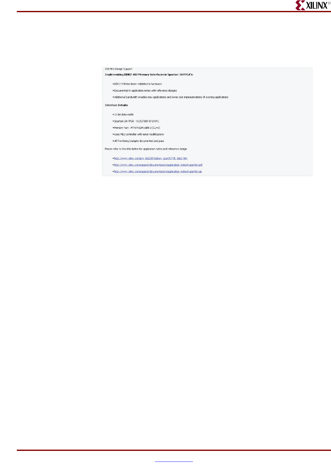
Memory Interface Solutions User Guide www.xilinx.com 87
UG086 (v3.6) September 21, 2010
MIG User Interface
R
Spartan-3A FPGA DDR2 SDRAM 200 MHz Design
This page is displayed only for Spartan-3A FPGA designs. It provides links to XAPP458
[Ref 16] and the Spartan-3A FPGA DDR2 SDRAM 200 MHz reference design.
Figure 1-73: Spartan-3A FPGA 200 MHz Design Support
UG086_c1_53_072108

88 www.xilinx.com Memory Interface Solutions User Guide
UG086 (v3.6) September 21, 2010
Chapter 1: Using MIG
R
Implementing MIG Designs in ISE GUI Mode
The MIG tool can be invoked from the project navigator of the ISE software as follows:
1. Launch the ISE software by selecting Start → Xilinx ISE Design Suite 12.3 → ISE
→ Project Navigator.
2. Create an ISE project:
a. Select File → New Project. The New Project Wizard appears.
b. Type the appropriate name in the Project Name field. Enter a directory path or
browse to a location for the new project. A subdirectory is created with the Project
Name entered automatically.
c. Select HDL for the Top-level Source Type and click Next to move to the device
properties page.
d. The Xilinx part must be correctly set because it cannot be changed inside the MIG
tool. Virtex-5, Virtex-4, and Spartan-3/Spartan-3E/Spartan-3A/3AN/3A DSP
devices are supported. Select the part using Device, Package, and Speed in the
Device Properties menu. Select the HDL using Simulator and
Preferred Language in the Device Properties menu. Leave the default values in
the remaining fields.
e. Click Next to proceed to the Create New Source window in the New Project
Wizard.
f. Create new source as follows:
-Click New Source, select the Source Type as IP (CORE Generator &
Architecture Wizard), and enter the appropriate File Name and Location in
the Select Source Type menu. Click Next.
-The Select IP menu lists out the various IPs that are supported. The View by
Function tab to the left shows the available cores organized into folders.
Choose the MIG tool by selecting Memories & Storage Elements →
Memory Interface Generator → MIG. Click Next.
-In the Summary menu, click Finish. The software returns to the Create New
Source menu.
-Click Finish in the New Project Wizard. The XCO file is created and added to
the project.
Note: New Source can be created in step f) or by creating the project by selecting
Project → New Source.
g. Click Next. Optionally, add existing source files to the project in the Add Existing
Sources page.
h. Click Next to display the Project Summary page.
i. Click Finish to create the project.
j. Upon creating the project, the ISE software invokes the MIG tool. Enter the name
of the module to be generated in the Component Name text box. The component
name provided in the MIG tool should be the same as that used in the Project
Navigation New Source menu. After entering all the parameters in the GUI, click
Generate. This generates the module files in a directory with the same name as the
component name in the ISE project directory.
k. After generating the design, click the Finish button. This closes the MIG tool.

Memory Interface Solutions User Guide www.xilinx.com 89
UG086 (v3.6) September 21, 2010
Implementing MIG Designs in ISE GUI Mode
R
l. The MIG tool generates the example_design and user_design. The
example_design includes the synthesizable test bench, while user_design does not
include any test bench modules.
3. If New Source is not created in the Create New Source menu in step f), new source can
be created by selecting Project → New Source. The steps required to create a new
source are the same as those listed in step f).
4. Upon closing the MIG tool, the XCO file is added to the ISE project. Create a top-level
HDL file (.v or .vhd) that includes the instance of <top_module> of the
MIG-generated user design. After creating the top-level HDL file, add it to an ISE
project by selecting Project → Add Source. Upon adding the top-level HDL file to
the ISE project, the MIG RTL source files (user_design/rtl) are added to the ISE
project. Only user_design files are added to an ISE project.
For example, if a MIG design is generated with the module name entered in the GUI
(such as “test_case”), create a top-level HDL file by including the <top_module> HDL
module (i.e., test_case.v/vhd) instance of user_design. If the top-level HDL file is
called inst_test_case.v/.vhd, add the inst_test_case.v/.vhd module to
the ISE project by selecting Project → Add Source.
5. The UCF file (user_design/par) is also added to the ISE project. The RTL source
files and the UCF file that are added to the project are not shown in the Files Tab
window.
6. Default synthesis and implementation build options are used. These options can be set
as required.
7. Click Process → Implement Top Module. The software runs through synthesis,
MAP, PAR, and TRCE.
If the design is generated using the CORE Generator tool or batch mode, the design can be
run in the ISE software GUI using create_ise.bat. This script file is included in both
the example_design/par and user_design/par directories of the generated MIG
design. Running the create_ise.bat script generates an ISE project that incorporates
the generated MIG design. If the script is run from the example_design/par directory,
the ISE project includes the example_design. If the script is run from the
user_design/par directory, the ISE project includes the user_design. The
create_ise.bat file calls the set_ise_prop.txt file. This file is also located in the
selected par directory. The file includes standard xtclsh commands that pull the MIG RTL
source files (example_design/rtl or user_design/rtl) into an ISE project and set
the required synthesis and implementation build options. After completion of the
create_ise.bat script, a test.ise file is created that can be opened in the ISE
software. The synthesis and implementation build options set by create_ise.bat are
recommended. No other build options have been tested and cannot be supported. For
detailed information on the options set, refer to the Development System Reference Guide
and the XST User Guide in the Xilinx ISE 12.3 Design Suite Software Manuals and Help –
PDF Collection at http://www.xilinx.com/support/documentation/index.htm.


Memory Interface Solutions User Guide www.xilinx.com 91
UG086 (v3.6) September 21, 2010
R
Section II: Virtex-4 FPGA to Memory Interfaces
Chapter 2, “Implementing DDR SDRAM Controllers”
Chapter 3, “Implementing DDR2 SDRAM Controllers”
Chapter 4, “Implementing QDRII SRAM Controllers”
Chapter 5, “Implementing DDRII SRAM Controllers”
Chapter 6, “Implementing RLDRAM II Controllers”

Memory Interface Solutions User Guide www.xilinx.com 93
UG086 (v3.6) September 21, 2010
R
Chapter 2
Implementing DDR SDRAM Controllers
This chapter describes how to implement DDR SDRAM interfaces for Virtex®-4 FPGAs
generated by MIG. This design is based on XAPP709 [Ref 21].
Feature Summary
Supported Features
The DDR SDRAM controller design supports the following:
• Burst lengths of two, four, and eight
• Sequential and interleaved burst types
• CAS latencies of 2, 2.5, and 3
• Precharge based on the row to be accessed or the precharge command given by the
user
• Registered DIMMs, unbuffered DIMMs, and SODIMMs
• Different memories (density/speed)
•Auto refresh
• Linear addressing
• VHDL and Verilog
• With and without a testbench
• With and without a DCM
•Data mask
• System clock, differential and single-ended
The supported features are described in more detail in “Architecture.”
Design Frequency Ranges
Table 2-1: Design Frequency Range in MHz
Memory
FPGA Speed Grade
-10 -11 -12
Min Max Min Max Min Max
Component 77 165 77 170 77 175
DIMM 77 165 77 170 77 175
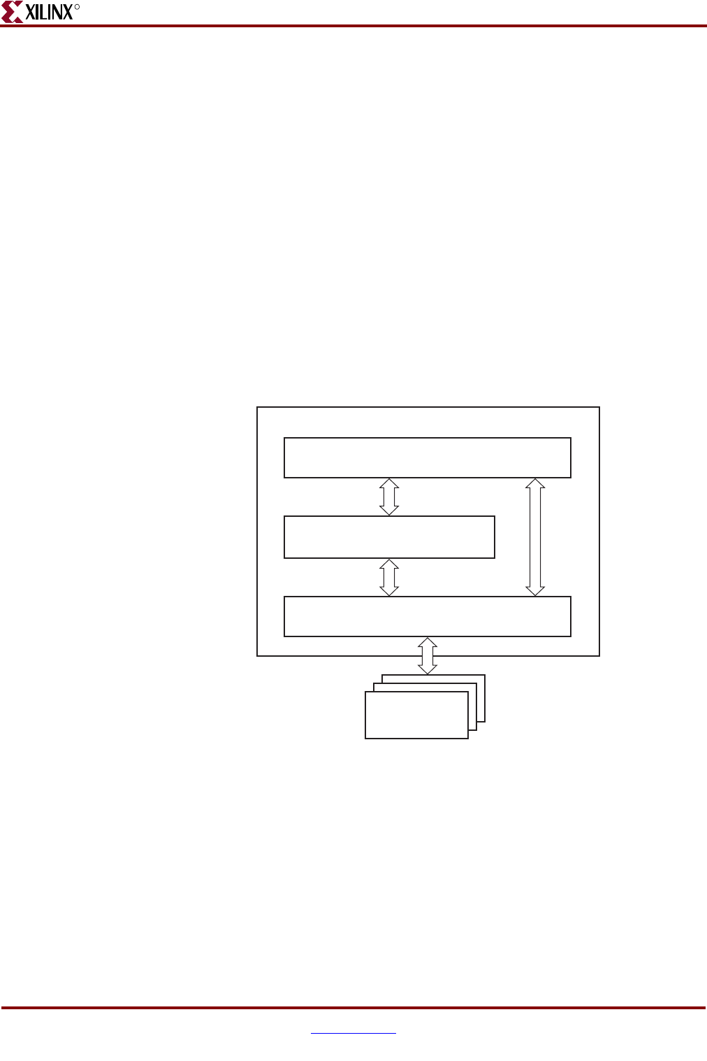
94 www.xilinx.com Memory Interface Solutions User Guide
UG086 (v3.6) September 21, 2010
Chapter 2: Implementing DDR SDRAM Controllers
R
Unsupported Features
•Dual Rank DIMMs
•Deep Memory
•Auto Precharge
• Bank Management
•Multi Controller
Architecture
Interface Model
DDR SDRAM interfaces are source-synchronous and double data rate. They transfer data
on both edges of the clock cycle. A memory interface can be modularly represented as
shown in Figure 2-1. A modular interface has many advantages. It allows designs to be
ported easily and also makes it possible to share parts of the design across different types
of memory interfaces.
Implemented Features
This section provides details on the supported features of the DDR SDRAM controller.
Based on user selection, the tool generates a parameter file, which is used to set various
features of the memory and to generate the control signals accordingly.
The parameter file provides the settings for burst length, CAS latency, sequential or
interleaved addressing, number of row address bits, number of column address bits, bank
address, and the timing parameters based on the frequency and the speed grade selected
from the GUI. The DDR SDRAM controller uses these parameters directly.
Figure 2-1: Modular Memory Interface Representation
Application Interface Layer
Xilinx FPGA
Physical Layer
Control Layer
UG086_c2_01_012507
Memories
Memory Interface Solutions User Guide www.xilinx.com 95
UG086 (v3.6) September 21, 2010
Architecture
R
The user issues a command through the FIFOs (user_interface). The user address (i.e.,
APP_AF_ADDR that is written into the FIFO as shown in Figure 2-11 or Figure 2-13) is
decoded in a sequence. The total width of the Read/Write Address FIFO
(rd_wr_addr_fifo) is 36 bits. The user writes the column address (least-significant bits),
row address, bank address, chip address [31:0], and the command to be issued [34:32]. The
36th bit (APP_AF_ADDR[35]) is reserved by the design to manipulate whether or not the
row to be accessed is same as that of the previous row. The APP_AF_ADDR[35] input is a
don't care for the design. The controller takes the row and column address bits based on
the selected component. The “Write Interface” and “Read Interface” sections provide
further details on how to issue the write and read commands, respectively.
Table 2-2 lists the commands that the user can issue through the User interface. If the user
issues an invalid command, the state of the controller is undefined. The functionality is not
guaranteed when an invalid command is issued.
Burst Length
Bits M0:M3 of the Mode Register define the burst length and burst type. Read and write
accesses to the DDR SDRAM are burst-oriented. The burst length is programmable to
either 2, 4, or 8 from the GUI. It determines the maximum number of column locations
accessed for a given READ or WRITE command.
The DDR SDRAM ddr_controller module implements the user-selected burst length from
MIG.
CAS Latency
Bits M4:M6 of the Mode Register define the CAS latency (CL). CL is the delay in clock
cycles between the registration of a READ command and the availability of the first bit of
output data. CL can be set to 2, 2.5, or 3 clocks from the GUI.
The controller supports CAS latencies of 2, 2.5, and 3.
During read data operations, the generation of the read_en signal varies according to the
CL in the ddr_controller module.
Registered DIMMs
DDR SDRAM supports registered DIMMs. This feature is implemented in the
ddr_controller module. For registered DIMMs, the READ and WRITE commands and
address have one additional clock latency than unbuffered DIMMs. Also for registered
DIMMs, the controller delays the data and the strobe by one clock because the command
has one clock latency due to the register in the DIMM.
Table 2-2: User Commands
Command APP_AF_ADDR[34:32]
READ 101
WRITE 100
REFRESH 001
PRECHARGE 010

96 www.xilinx.com Memory Interface Solutions User Guide
UG086 (v3.6) September 21, 2010
Chapter 2: Implementing DDR SDRAM Controllers
R
Unbuffered DIMMs and SODIMMs
DDR SDRAM design supports unbuffered DIMMs and SODIMMs. Unbuffered DIMMs
are normal DIMMs where a set of components are used to get a particular configuration.
SODIMMs vary from the unbuffered DIMMs only by package type. They are functionally
the same.
Precharge
The PRECHARGE command is issued before the next read or write is issued for a different
row, but not if the read or write is in the same row. The PRECHARGE command checks the
row address, bank address, and chip selects. The DDR Virtex-4 FPGA controller issues a
PRECHARGE command if there is a change in any address where a read or write
command is to be issued. The AUTO PRECHARGE command via the A10 column bit is
not supported.
Auto Refresh
The DDR SDRAM controller issues AUTO REFRESH commands at specified intervals for
the memory to refresh the charge required to retain the data in the memory. The user can
also issue a REFRESH command through the user interface by setting bits 34, 33, and 32 of
the app_af_addr signal in the user_interface module to 3’b001. If there is a refresh request
while during an ongoing read or write burst, the controller issues a REFRESH command
after completing the current read or write burst command.
Linear Addressing
The DDR SDRAM controller supports linear addressing. Linear addressing refers to the
way the user provides the address of the memory to be accessed. For Virtex-4 FPGA DDR
SDRAM controllers, the user provides the address information through the app_af_addr
signal. As the densities of the memory devices vary, the number of column address bits
and row address bits also changes. In any case, the row address bits in the app_af_addr
signal always start from the next-higher bit, where the column address ends. This feature
increases the number of devices that can be supported with the design.
Different Memories (Density/Speed)
This feature supports different memory components and DIMMs. The component
densities can vary from 128 Mb to 1 Gb, and the DIMM densities can vary from 128 MB to
1 GB. Higher densities can be created using the "Create new memory part" feature of MIG.
The maximum supported column address is 13 bits, the maximum row address is 15 bits,
and the maximum bank address is 2 bits. To support this feature, the design can decode
write and read addresses from the user in the DDR SDRAM controller module. The user
address consists of row, column, bank, and chip addresses, and the user command. Apart
from the address decoding, timing parameters vary according to the density and speed
grade.
Data Mask
MIG supports a data mask option. If this option is checked in the GUI, MIG generates a
design with data mask pins. This option can be chosen if the selected part has data
masking.
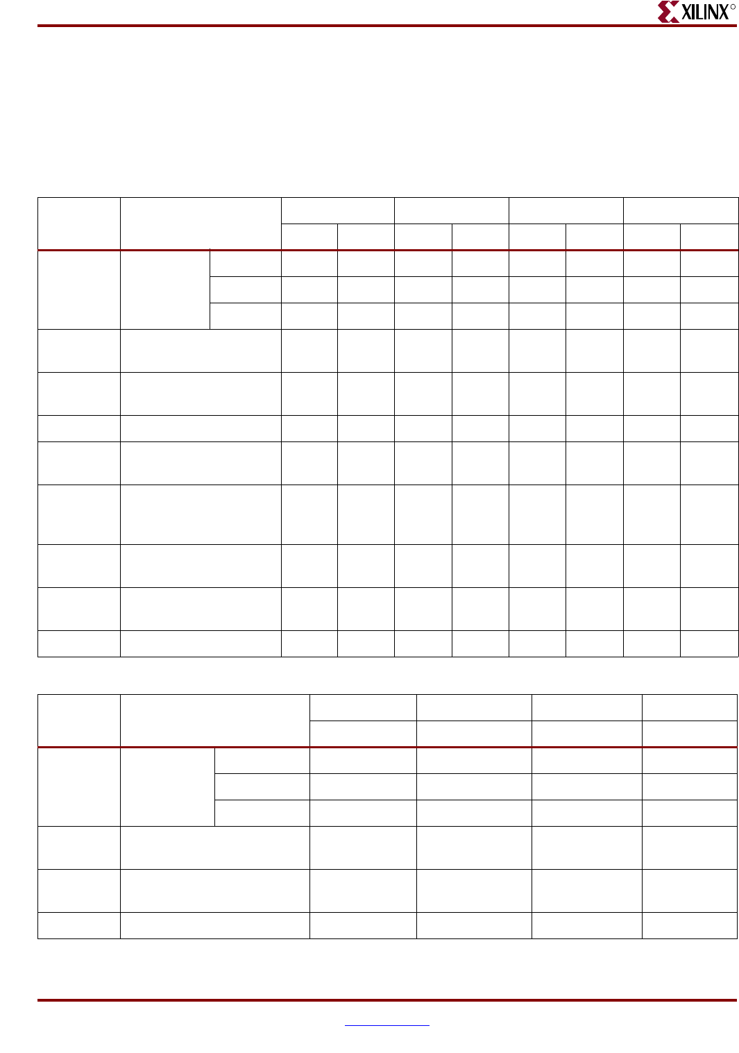
Memory Interface Solutions User Guide www.xilinx.com 97
UG086 (v3.6) September 21, 2010
Architecture
R
System Clock
MIG supports a differential or single-ended system clock option. Based on the selection in
the GUI, input system clocks and IDELAY clocks are differential or single-ended.
Table 2-3 lists the timing parameters for components, and Table 2-4 lists the timing
parameters for DIMMs.
Table 2-3: Timing Parameters for Components
Parameter Description Micron 128 Mb Micron 256 Mb Micron 512 Mb Micron 1 Gb
-5 -75 -5 -75 -5 -75 -5 -75
TCK Clock Cycle
Time
CL = 3 5 ns NA 5 ns NA 5 ns NA 5 ns NA
CL = 2.5 6 ns 7.5 ns 6 ns 7.5 ns 6 ns 7.5 ns 6 ns 7.5 ns
CL = 2 7.5 ns 10 ns 7.5 ns 10 ns 7.5 ns 10 ns 7.5 ns 10 ns
TMRD LOAD MODE
Command Cycle Time
10 ns 15 ns 10 ns 15 ns 10 ns 15 ns 10 ns 15 ns
TRP PRECHARGE
Command Period
15 ns 20 ns 15 ns 20 ns 15 ns 20 ns 15 ns 20 ns
TRFC REFRESH Time 70 ns 75 ns 70 ns 75 ns 70 ns 75 ns 120 ns 120 ns
TRCD ACTIVE to READ or
WRITE Delay
15 ns 20 ns 15 ns 20 ns 15 ns 20 ns 15 ns 20 ns
TRAS ACTIVE to
PRECHARGE
Command
40 ns 40 ns 40 ns 40 ns 40 ns 40 ns 40 ns 40 ns
TRC ACTIVE to ACTIVE
(Same Bank) Command
55 ns 65 ns 55 ns 65 ns 55 ns 65 ns 55 ns 65 ns
TWTR WRITE to READ
Command Delay
2 * TCK 1 * TCK 2 * TCK 1 * TCK 2 * TCK 1 * TCK 2 * TCK 1 * TCK
TWR WRITE Recovery Time 15 ns 15 ns 15 ns 15 ns 15 ns 15 ns 15 ns 15 ns
Table 2-4: Timing Parameters for DIMMs (Unbuffered and Registered)
Parameter Description Micron 128 MB Micron 256 MB Micron 512 MB Micron 1 GB
-40 -40 -40 -40
TCK Clock Cycle
Time
CL = 3 5 ns 5 ns 5 ns 5 ns
CL = 2.5 6 ns 6 ns 6 ns 6 ns
CL = 2 7.5 ns 7.5 ns 7.5 ns 7.5 ns
TMRD LOAD MODE Command
Cycle Time
10 ns 10 ns 10 ns 10 ns
TRP PRECHARGE Command
Period
15 ns 15 ns 15 ns 15 ns
TRFC REFRESH Time 70 ns 70 ns 70 ns 70 ns
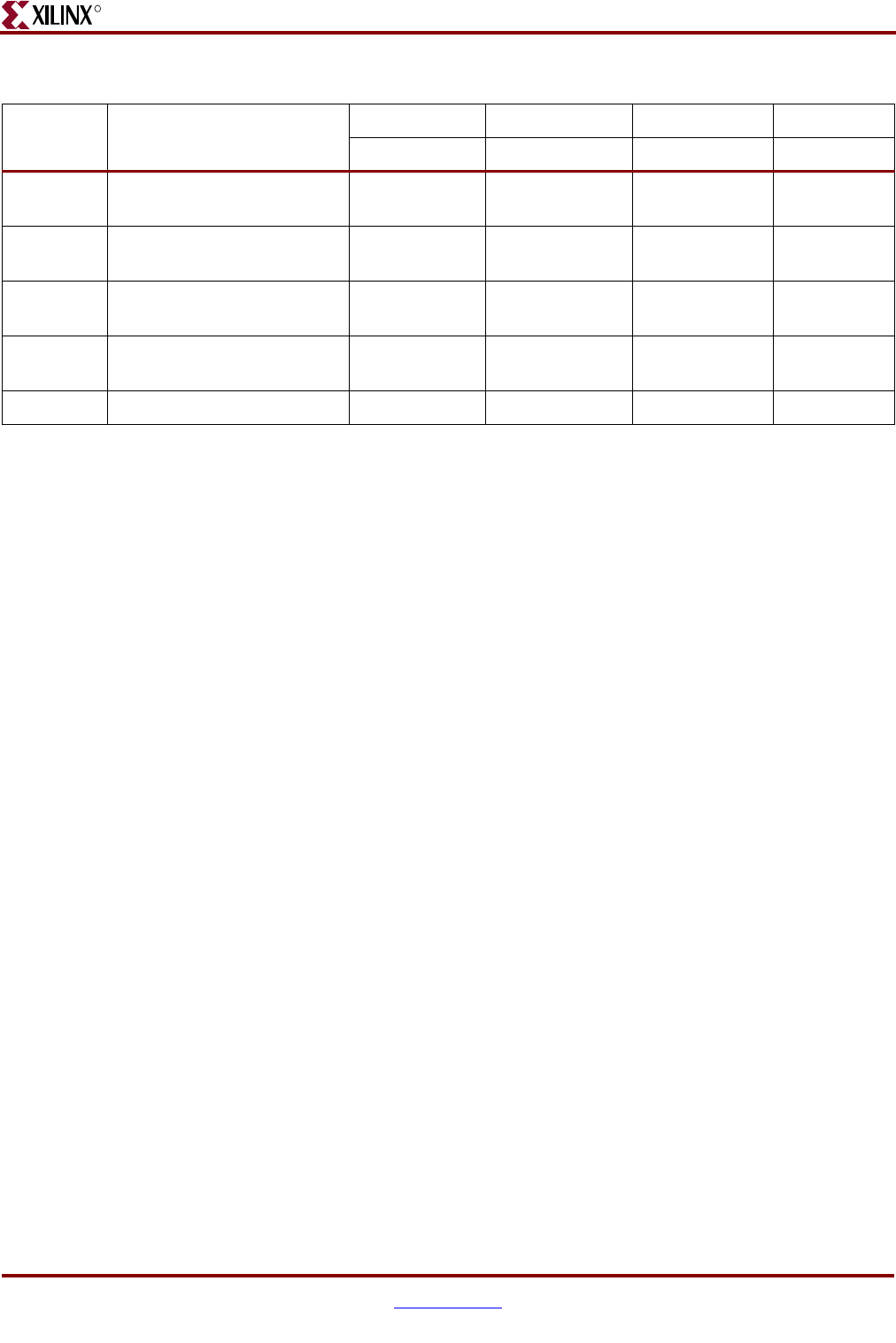
98 www.xilinx.com Memory Interface Solutions User Guide
UG086 (v3.6) September 21, 2010
Chapter 2: Implementing DDR SDRAM Controllers
R
Note: For the latest timing information, refer to the vendor memory data sheets.
TRCD ACTIVE to READ or WRITE
Delay
15 ns 15 ns 15 ns 15 ns
TRAS ACTIVE to PRECHARGE
Command
40 ns 40 ns 40 ns 40 ns
TRC ACTIVE to ACTIVE (Same
Bank) Command
55 ns 55 ns 55 ns 55 ns
TWTR WRITE to READ Command
Delay
2 * TCK 2 * TCK 2 * TCK 2 * TCK
TWR WRITE Recovery Time 15 ns 15 ns 15 ns 15 ns
Table 2-4: Timing Parameters for DIMMs (Unbuffered and Registered) (Cont’d)
Parameter Description Micron 128 MB Micron 256 MB Micron 512 MB Micron 1 GB
-40 -40 -40 -40
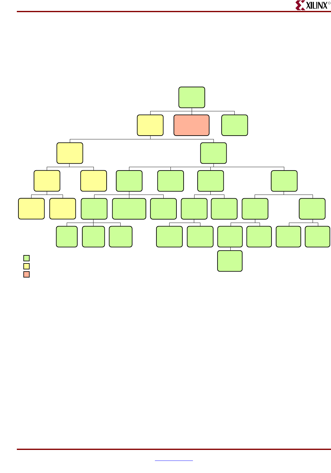
Memory Interface Solutions User Guide www.xilinx.com 99
UG086 (v3.6) September 21, 2010
Architecture
R
Hierarchy
Figure 2-2 shows the hierarchical structure of the DDR SDRAM design generated by MIG
with a testbench and a DCM. The physical and control layers are clearly separated in this
figure. MIG generates the entire DDR SDRAM controller as shown in this hierarchy,
including the testbench. MIG also generates a parameter file where all user input
parameters or some parameters used internally by the design are defined.
The modules are classified as follows:
• Design modules
• Testbench modules
• Clocks and reset generation modules
There is a parameter file generated with the design that has all the user input and design
parameters selected from MIG.
MIG can generate four different DDR SDRAM designs:
• With a testbench and a DCM
• Without a testbench and with a DCM
• With a testbench and without a DCM
• Without a testbench and without a DCM
When the testbench is not generated by MIG, the top-level module has the user interface
signals. The list of user interface signals is provided in Table 2-8.
Figure 2-2: Hierarchical Structure of the Virtex-4 FPGA DDR SDRAM Design
<top_
module>
main* idelayctrl
infrastructure*
iobs*data_
path*
user_
interface*
data_
path_iobs*
controller
_iobs*
infrastructure
_iobs*
ddr_
controller*
v4_dq_
iob
Design Modules
v4_dm_
iob
RAM_D
v4_dqs_
iob
backend
_fifos*
rd_wr_
addr_
fifo*
wr_data
_fifo
rd_data*
rd_data
_fifo*
pattern_
compare
data_
write*
tap_
logic*
tap_
ctrl*
data_
tap_inc*
test_
bench* top*
Te st Bench Modules
Clocks and Reset Generation Modules
UG086_c2_02_091107
Note: A block with a * has a parameter file included.
cmp_rd_
data*
backend
_rom*
data_
gen
addr_
gen

100 www.xilinx.com Memory Interface Solutions User Guide
UG086 (v3.6) September 21, 2010
Chapter 2: Implementing DDR SDRAM Controllers
R
Design clocks and resets are generated in the infrastructure module. The DCM clock is
instantiated in the infrastructure module for designs with a DCM. The inputs to this
module are the differential design clock and a 200 MHz differential clock for the
IDELAYCTRL module. A user reset is also input to this module. Using the input clocks and
reset signals, the system clocks and the system reset are generated in this module, which is
used in the design.
The DCM primitive is not instantiated in this module if the Use DCM option is unchecked.
So, the system operates on the user-provided clocks. The system reset is generated in the
infrastructure module using the dcm_lock input signal.
MIG Tool Design Options
MIG provides various options to generate the design with or without a testbench or with
or without a DCM. This section provides detailed descriptions of the type of design
generated by the user using various options. Figure 2-3, page 101 and Figure 2-4, page 102
represent the system clock of differential. For more information on clocking structure refer
to “Clocking Scheme,” page 110.
MIG outputs both an example_design and a user_design. The MIG-generated
example_design includes the entire memory controller design along with a synthesized
testbench (example user application). This testbench generates sample writes and reads
and then uses comparison logic to verify that the data patterns written are the same as
those received. This example_design can be used to test functionality both in simulation
and in hardware. The user_design includes the memory controller design only. This design
allows users to connect the MIG memory controller design to a user developed testbench
(user application). Refer to Table 2-8, page 112 for user interface signals, the “User Interface
Accesses,” page 114 for timing restriction on user interface signals, and Figure 2-11,
page 116 for write interface timing.
Figure 2-3 shows a DDR SDRAM controller block diagram representation of the top-level
module for a design with a DCM and a testbench. The sys_clk_p and sys_clk_n signals are
differential input system clocks. The DCM clock is instantiated in the infrastructure
module that generates the required design clocks. The differential clk200_p and clk200_n
pair are used for the idelay_ctrl element. The active-Low system reset signal is
sys_reset_in_n. All design resets are gated by the dcm_lock signal. Memory device signals
are prepended with the controller number. For example, ddr_ras_n appears as
cntrl0_ddr_ras_n.
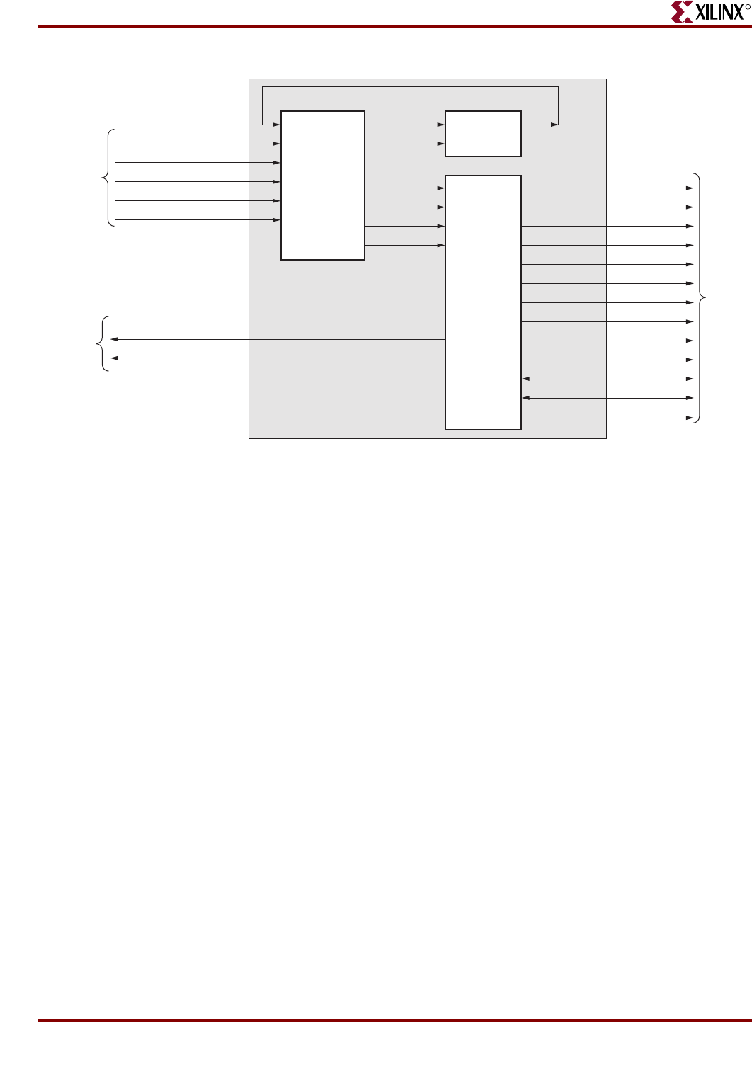
Memory Interface Solutions User Guide www.xilinx.com 101
UG086 (v3.6) September 21, 2010
Architecture
R
The error output signal indicates whether the case passes or fails. The testbench module
does writes and reads, and also compares the read data with the written data. The error
signal is driven High on data mismatches.
The init_done signal indicates the completion of initialization and calibration of the design.
All the signals listed under the Memory Device category do not necessarily appear in the
top-level block port list. The port list varies according to the memory type selected, such as
a component or a registered DIMM. For example, a component does not have the
ddr_reset_n signal.
Figure 2-4 shows a block diagram representation of the top-level module for a design with
a DCM but without a testbench.
Figure 2-3: Top-Level Block Diagram of the DDR SDRAM Design with a DCM and a Testbench
main_0
idelay_ctrl_rdy
clk200
Memory
Device
UG086_c2_03_092908
Status
Signals
System
Clocks
and Reset
idelay_ctrl
Infrastructure
sys_rst_rt
clk_0
clk_90
sys_rst90
clk200_p
clk200_n
sys_clk_p
sys_clk_n
sys_reset_in_n sys_rst
ddr_ras_n
ddr_cas_n
ddr_we_n
ddr_cs_n
ddr_cke
ddr_dm
ddr_ba
ddr_a
ddr_ck
ddr_ck_n
ddr_dq
ddr_dqs
ddr_reset_n
error
init_done
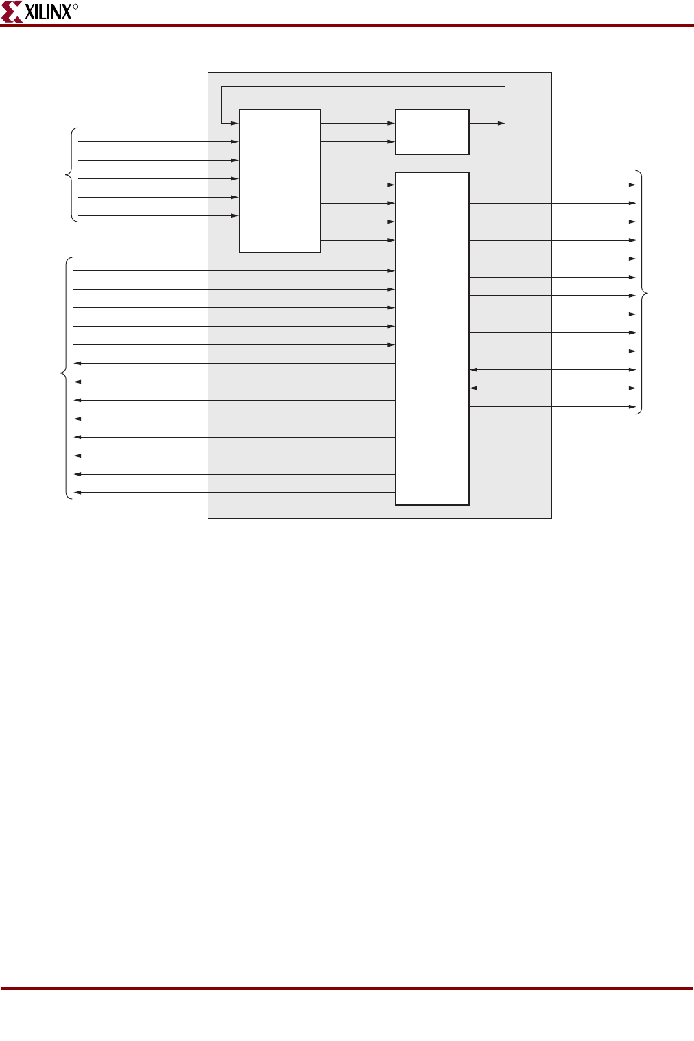
102 www.xilinx.com Memory Interface Solutions User Guide
UG086 (v3.6) September 21, 2010
Chapter 2: Implementing DDR SDRAM Controllers
R
The DCM clock module is instantiated in the infrastructure module. Using the differential
sys_clk_p and sys_clk_n signals, the internal DCM generates all the required clocks for the
design. The differential clk200_p and clk200_n are used by the idelay_ctrl element. The
active-Low system reset signal is sys_reset_in_n. All design resets are generated using the
input reset signal gated by the dcm_lock signal.
The init_done signal indicates the completion of initialization and calibration of the design.
The application’s user interface signals are listed in Figure 2-4. The design provides the
clk_tb and reset_tb signals to the user to synchronize with the design.
Figure 2-4: Top-Level Block Diagram of the DDR SDRAM Design with a DCM but without a Testbench
top_0
idelay_ctrl_rdy
clk200
Memory
Device
UG086_c2_04_091708
User
Application
System
Clocks
and Reset
idelay_ctrl
Infrastructure
sys_rst_rt
clk_0
clk_90
sys_rst90
clk200_p
clk200_n
sys_clk_p
sys_clk_n
sys_reset_in_n
app_af_addr
app_af_wren
app_wdf_data
app_mask_data
app_wdf_wren
wdf_almost_full
af_almost_full
burst_length_div2
read_data_valid
read_data_fifo_out
sys_rst
ddr_ras_n
ddr_cas_n
ddr_we_n
ddr_cs_n
ddr_cke
ddr_dm
ddr_ba
ddr_a
ddr_ck
ddr_ck_n
ddr_dq
ddr_dqs
clk_tb
reset_tb
init_done
ddr_reset_n
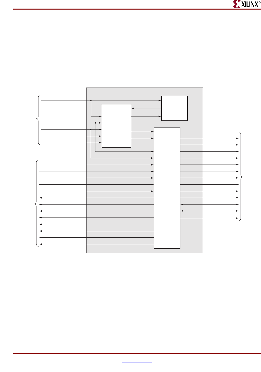
Memory Interface Solutions User Guide www.xilinx.com 103
UG086 (v3.6) September 21, 2010
Architecture
R
Figure 2-5 shows a block diagram representation of the top-level module for a design
without a DCM or a testbench. There is no DCM instantiated in the infrastructure module.
All the clocks and dcm_lock should be given as inputs from the user interface. Resets are
generated using the sys_reset_in_n signal gated by the dcm_lock signal in the
infrastructure module. Clk200 is used by the idelay_ctrl element. All the clocks should be
single-ended. The user application must have a DCM primitive instantiated in the design.
The init_done signal indicates the completion of initialization and calibration of the design.
The user interface signals are also listed in the <top_module> module. The design
provides the clk_tb and reset_tb signals to the user to synchronize with the design.
Figure 2-5: Top-Level Block Diagram of the DDR SDRAM Design without a DCM or a Testbench
top_0
idelay_ctrl_rdy
Memory
Device
UG086_c2_05_091708
System
Reset
and User
DCM
Clocks
idelay_ctrl
Infrastructure
sys_rst_r1
sys_rst
sys_rst90
clk_0
clk_200
clk_90
sys_reset_in_n
dcm_lock
ddr_ras_n
ddr_cas_n
ddr_we_n
ddr_cs_n
ddr_cke
ddr_dm
ddr_ba
ddr_a
ddr_ck
ddr_ck_n
ddr_dq
ddr_dqs
ddr_reset_n
User
Application
app_af_addr
app_af_wren
app_wdf_data
app_mask_data
app_wdf_wren
wdf_almost_full
af_almost_full
burst_length_div2
read_data_valid
read_data_fifo_out
clk_tb
reset_tb
init_done
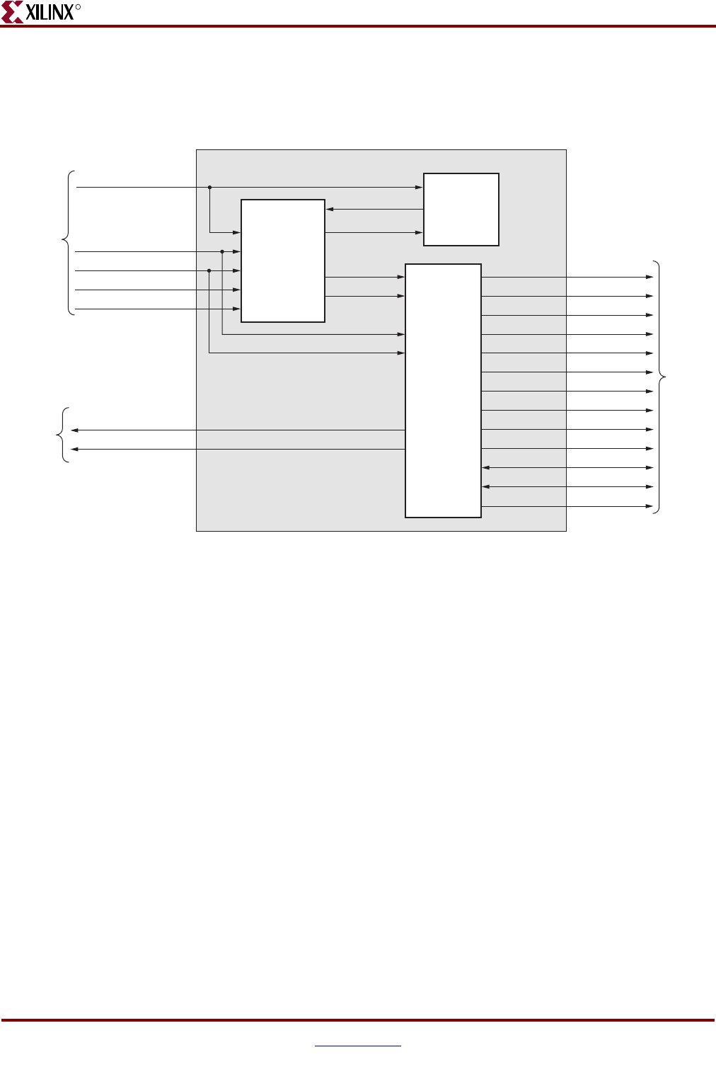
104 www.xilinx.com Memory Interface Solutions User Guide
UG086 (v3.6) September 21, 2010
Chapter 2: Implementing DDR SDRAM Controllers
R
Figure 2-6 shows a block diagram representation of the top-level module for a design with
a testbench but without a DCM. The user should provide all the clocks and the dcm_lock
signal. These clocks should be single-ended. The active-Low system reset signal is
sys_reset_in_n. All design resets are gated by the dcm_lock signal.
The error output signal indicates whether the case passes or fails. The testbench module
does writes and reads, and also compares the read data with the written data. The ERROR
signal is driven High on data mismatches. The init_done signal indicates the completion of
initialization and calibration of the design.
Figure 2-6: Top-Level Block Diagram of the DDR SDRAM Design with a Testbench but without a DCM
main_0
idelay_ctrl_rdy
Memory
Device
UG086_c2_06_091708
Status
Signals
System
Reset
and User
DCM
Clocks
idelay_ctrl
Infrastructure
sys_rst_rt
sys_rst
sys_rst90
clk_0
clk_200
clk_90
sys_reset_in_n
dcm_lock
ddr_ras_n
ddr_cas_n
ddr_we_n
ddr_cs_n
ddr_cke
ddr_dm
ddr_ba
ddr_a
ddr_ck
ddr_ck_n
ddr_dq
ddr_dqs
error
init_done
DDR_RESET_N
ddr_reset_n
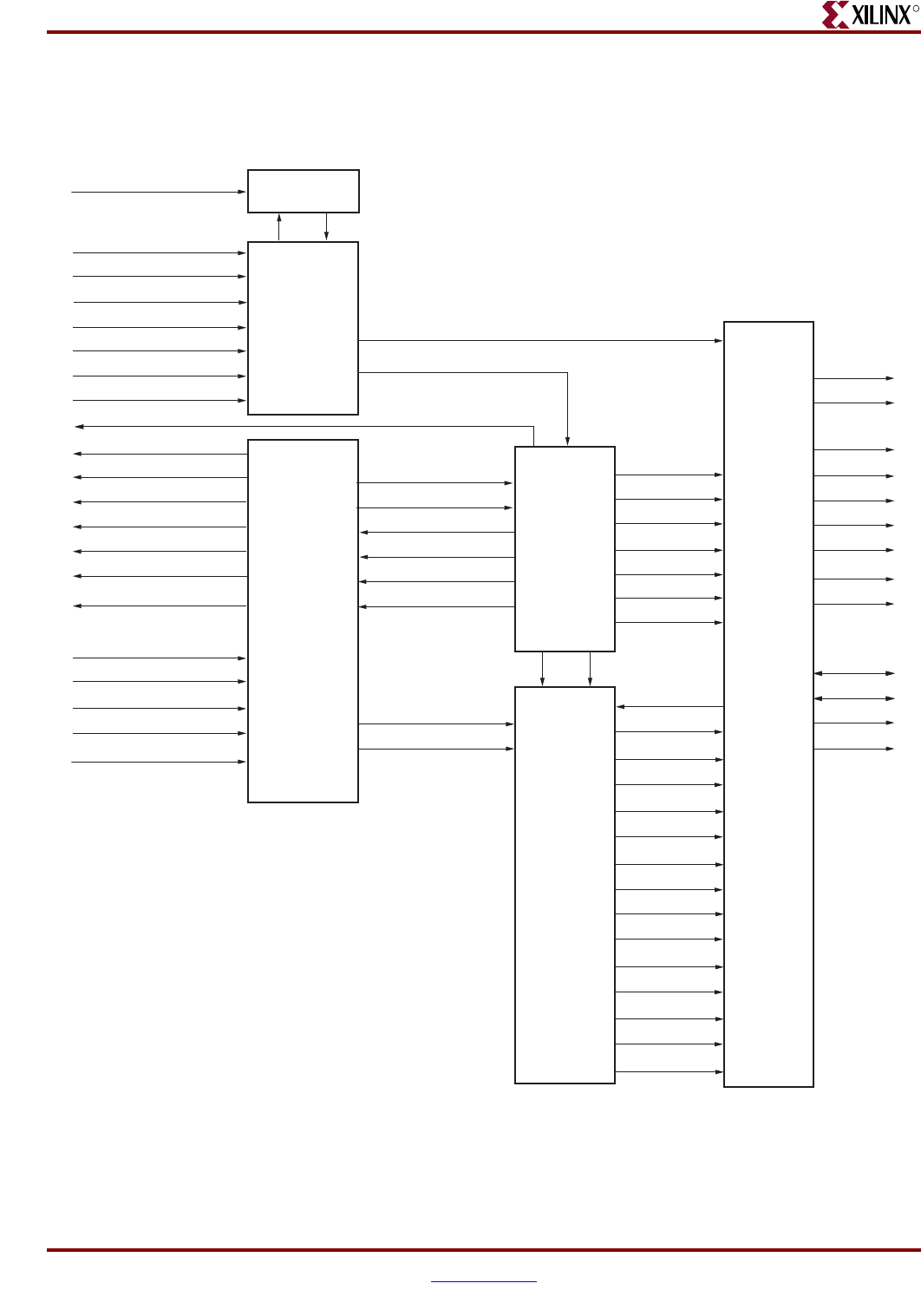
Memory Interface Solutions User Guide www.xilinx.com 105
UG086 (v3.6) September 21, 2010
Architecture
R
Figure 2-7 shows the expanded block diagram of the design. The top module is expanded
to show various internal blocks. The functions of these blocks are explained in the
subsections following the figure.
Figure 2-7: Expanded DDR SDRAM Controller Block Diagram
Infrastructure
Datapath
User Interface
idelay_ctrl
IOBsController
wdf_almost_full
af_almost_full
read_data_valid
app_wdf_data[2n:0]
app_mask_data[2m-1:0]
read_data_fifo_out
af_addr
Clocks and Resets
af_empty
ctrl_af_rden
ctrl_wdf_rden
burst_length_div2
dqs_delayed
data_idelay_inc
mask_data
wdf_data
clk
clk_n
addressctrl_ddr_address
ctrl_ddr_ba ras_n
cas_n
we_n
burst_length_div2[2:0]
clk200_p
clk200_N
idly_clk_200
sys_clk_p
sys_clk_n
sys_clk
sys_reset_in_n
clk_tb
init_done
reset_tb
ctrl_ddr_ras_l
ctrl_ddr_cas_l
ctrl_ddr_we_l
ctrl_ddr_cs_l
ctrl_ddr_cke
dq
dqs
dm
reset_n
cke_n
cs_n
ba
ctrl_rden
idelay_ctrl_rdy
UG086_c2_07_091708
data_idelay_ce
data_idelay_rst
dqs_idelay_inc
dqs_idelay_ce
dqs_idelay_rst
rising_first
dqs_rst
dqs_en
wr_en
wr_data_rise
wr_data_fall
mask_data_rise
mask_data_fall
app_af_addr
app_af_wren
app_wdf_wren
clk_200
reset

106 www.xilinx.com Memory Interface Solutions User Guide
UG086 (v3.6) September 21, 2010
Chapter 2: Implementing DDR SDRAM Controllers
R
Controller
The DDR SDRAM controller initializes the memory, accepts and decodes user commands,
and generates READ, WRITE, and REFRESH commands. The DDR SDRAM controller also
generates signals for other modules. The memory is initialized and powered-up using a
defined process. The controller state machine handles the initialization process upon
power-up. If the AUTO REFRESH command is to be issued between any user read or write
commands, then the read or write command is suspended until the ref_done flag is
deasserted.
Datapath
This module transmits data to the memories. Its major functions include storing the write
data and calculating the tap value for the read datapath. The data_write and
data_path_IOBs modules do the actual write functions. The Idelay_ctrl, tap_ctrl and
data_tap_inc modules do the calibration.
User Interface
This module stores write data in its Write Data FIFO (wr_data_fifo), stores write and read
addresses in its Read/Write Address FIFO (rd_wr_addr_fifo), and stores received read
data from memory in its Read Data FIFO (rd_data_fifo). The width of the Write Data FIFO
is twice the data width and mask width of the memory. For example, for a 16-bit width, the
width of the FIFO is 36 because the data width is 32 and the mask width is 4. The
rd_wr_addr_fifo and wr_data_fifo modules store the data and address in block RAMs. The
rd_data_fifo module captures the data in the LUT-based RAMs.
The FIFOs are built using FIFO16 primitives in the rd_wr_addr_fifo, wr_data_fifo_16, and
wr_data_fifo_8 modules. FIFO16 has two FIFO threshold attributes,
ALMOST_EMPTY_OFFSET and ALMOST_FULL_OFFSET, that are set to 7 and F,
respectively, in the RTL by default. These values can be altered to match the application.
For valid FIFO threshold offset values, refer to UG070 [Ref 7].
The controller also generates user commands, such as READ and WRITE.
The pattern_compare module registers the delay between the command and the data
received from the IOBs. This delay is then applied to the Rden signal generated from the
ddr_controller module during the actual read to register the valid data in the internal
FIFOs.
Test Bench
The MIG tool generates two RTL folders, example_design and user_design. The
example_design folder includes the synthesizable test bench, while user_design does not
include the test bench modules. The MIG test bench performs eight write commands and
eight read commands in an alternating fashion. The number of words in a write command
depends on the burst length. For a burst length of 4, the test bench writes a total of 32 data
words for all eight write commands (16 rise data words and 16 fall data words). For a burst
length of 8, the test bench writes a total of 64 data words. It writes the data pattern of FF,
00, AA, 55, 55 AA, 99, 66 in a sequence of which FF, AA, 55, and 99 are rise data words and
00, 55, AA, and 66 are fall data words for an 8-bit design. The falling edge data is the
complement of the rising edge data. For a burst length of 4, the data sequence for the first
write command is FF, 00, AA, 55, and the data sequence for the second write command is
55, AA, 99, 66. For a burst length of 8, the data pattern for the first write command is FF,
00, AA, 55, 55 AA, 99, 66 and the same pattern is repeated for all the remaining write
commands. This data pattern is repeated in the same order based on the number of data

Memory Interface Solutions User Guide www.xilinx.com 107
UG086 (v3.6) September 21, 2010
Architecture
R
words written. For data widths greater than 8, the same data pattern is concatenated for
the other bits. For a 32-bit design and a burst length of 8, the data pattern for the first write
command is FFFFFFFF, 00000000, AAAAAAAA, 55555555, 55555555, AAAAAAAA,
99999999, 66666666.
Address generation logic generates eight different addresses for eight write commands.
The same eight address locations are repeated for the following eight read commands. The
read commands are performed at the same locations where the data is written. There are
total of 32 different address locations for 32 write commands, and the same address
locations are generated for 32 read commands. Upon completion of a total of 64
commands, including both writes and reads (eight writes and eight reads repeated four
times), address generation rolls back to the first address of the first write command and the
same address locations are repeated. The MIG test bench exercises only a certain memory
area. The address is formed such that all address bits are exercised. During writes, a new
address is generated for every burst operation on the column boundary.
During reads, comparison logic compares the read pattern with the pattern written, i.e., the
FF, 00, AA, 55, 55 AA, 99, 66 pattern. For example, for an 8-bit design of burst length 4, the
data written for a single write command is FF, 00, AA, 55. During reads, the read pattern is
compared with the FF, 00, AA, 55 pattern. Based on a comparison of the data, a status
signal error is generated. If the data read back is the same as the data written, the error
signal is 0, otherwise it is 1.
Infrastructure
The infrastructure module generates the FPGA clock and reset signals. When differential
clocking is used, sys_clk_p, sys_clk_n, clk_200_p, and clk_200_n signals appear. When
single-ended clocking is used, sys_clk and idly_clk_200 signals appear. In addition, clocks
are available for design use and a 200 MHz clock is provided for the idelayctrl primitive.
Differential and single-ended clocks are passed through buffers before connecting to a
DCM. For differential clocking, the output of the sys_clk_p/sys_clk_n buffer is single-
ended and is provided to the DCM input. Likewise, for single-ended clocking, sys_clk is
passed through a buffer and its output is provided to the DCM input. The clock outputs of
the DCM are clk_0 and clk_90. After the DCM is locked, the design is in the reset state for
at least 25 clocks. The infrastructure module also generates all of the reset signals required
for the design.
Idelay_ctrl
This module instantiates the IDELAYCTRL primitive of the Virtex-4 FPGA. The
IDELAYCTRL primitive is used to continuously calibrate the individual delay elements in
its region to reduce the effect of process, temperature, and voltage variations. A 200 MHz
clock has to be fed to this primitive.
The MIG tool instantiates the required number of IDELAYCTRLs in the RTL and uses the
LOC constraints in the UCF file to fix their locations. The number of IDELAYCTRLs is
defined by the IDELAYCTRL_NUM parameter in the idelay_ctrl module. In the RTL,
IDELAY_CTRL_RDY is generated by doing a logical AND of the RDY signals of every
IDELAYCTRL block.
IDELAYCTRL LOC constraints should be checked in the following cases:
• The MIG design is used with other IP cores or user designs that also require the use of
IDELAYCTRL and IDELAYs.

108 www.xilinx.com Memory Interface Solutions User Guide
UG086 (v3.6) September 21, 2010
Chapter 2: Implementing DDR SDRAM Controllers
R
• Previous ISE® software releases 8.2.03i and 9.1i had an issue with IDELAYCTRL block
replication or trimming. When using these revisions of the ISE software, the user must
instantiate and constrain the location of each IDELAYCTRL individually.
See UG070 [Ref 7] for more information on the requirements of IDELAYCTRL placement.
IOBS Module
All DDR SDRAM address, control, and data signals are transmitted and received in the
through the input and output buffers.
DDR SDRAM Initialization and Calibration
DDR memory is initialized through a specified sequence as shown in Figure 2-8. The
controller starts the memory initialization at power up itself. Following the initialization,
the relationship between the data and the FPGA clock is calculated using the tap_logic. The
controller issues a dummy write command and a dummy read command to the memory
and compares read data with the fixed pattern. During dummy reads, the tap_logic
module calibrates and delays the data to center-align with the FPGA clock. The sel_done
port in the tap_logic module indicates the completion of the per-bit calibration. XAPP701
[Ref 18] provides more information about the calibration architecture.
After the per-bit calibration is done, the controller does a read enable calibration. This
calibration is used to determine the delay from read command to read data at rd_data_fifo.
The delay between read command and read data is affected by the CAS latency
parameters, the PCB traces, and the I/O buffer delays. Read enable calibration is used to
generate a write enable to rd_data_fifo so that valid data is registered. Controller writes a
known fixed pattern and reads back the data from memory. The read data is compared
against the known fixed pattern. The comp_done port in rd_data module indicates the
completion of the read enable calibration.
The init_done port indicates the completion of both per-bit calibration and read enable
calibration. After initialization and calibration is done, the controller can start issuing user
commands to the memory.
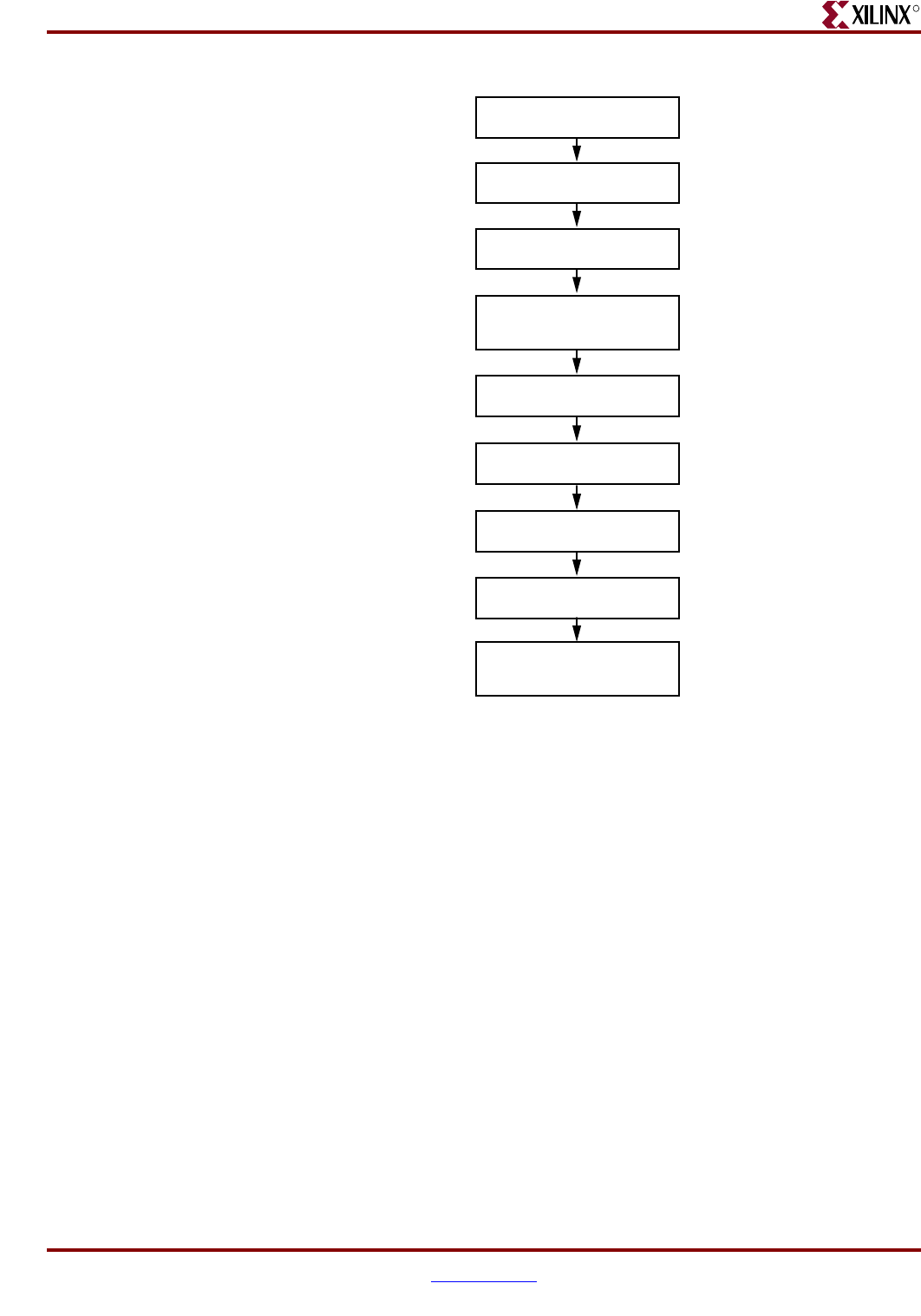
Memory Interface Solutions User Guide www.xilinx.com 109
UG086 (v3.6) September 21, 2010
DDR SDRAM Initialization and Calibration
R
Figure 2-8: DDR Memory Initialization Sequence
Load Mode Register
Command for Extended Mode
Register to enable the DLL
Load Mode Register
Command to reset the DLL
Precharge All Command
Two Auto Refresh Commands
Load Mode Register
Command to deactivate the
DLL Reset
Precharge All Command
200 clock cycles delay
200 μs Delay
Power Up
UG086_c2_08_012507
110 www.xilinx.com Memory Interface Solutions User Guide
UG086 (v3.6) September 21, 2010
Chapter 2: Implementing DDR SDRAM Controllers
R
Clocking Scheme
Figure 2-9, page 111 shows the clocking scheme for this design. Global and local clock
resources are used.
The global clock resources consist of a DCM, two global clock buffers (BUFG) on DCM
output clocks, and one BUFG for clk_200. The local clock resources consist of regional I/O
clock networks (BUFIO). The global clock architecture is discussed in this section.
The MIG tool allows the user to customize the design such that the DCM is not included.
In this case, clk_0, clk_90 and IDELAYCTRL clock clk_200 must be supplied by the user.
Global Clock Architecture
The user must supply two input clocks to the design:
• A system clock running at the target frequency for the memory
• A 200 MHz clock for the IDELAYCTRL blocks.
These clocks can be either single-ended or differential. Users can select the single-ended or
differential clock input option from the MIG GUI. Differential clocks are connected to the
IBUFGDS and the single-ended clock is connected to IBUFG.
The system clock from the output of the IBUFGDS or the IBUFG is connected to the DCM
to generate the various clocks used by the memory interface logic.
The clk200 output of the IBUFGDS or the IBUFG is connected to the BUFG. The output of
the BUFG is used for IDELAY IOB delay blocks for aligning read capture data.
The DCM generates two separate synchronous clocks for use in the design. This is shown
in Table 2-5 and Figure 2-9, page 111. The clock structure is same for both the example
design and the user design. For designs without DCM instantiation, the DCM and the
BUFGs should be instantiated at the user end to generate the required clocks.
Table 2-5: DDR Interface Design Clocks
Clock Description Logic Domain
clk_0
Skew compensated
replica of the input
system clock.
The clock for the controller and the user interface
logic, most of the DDR bus-related I/O flip-flops
(e.g., memory clock, control/address, output DQS
strobe, and DQ input capture). This is used to
register the data, address, and command signals,
and the address and data enables for the user
interface logic(1). This clock is also used to generate
read data, read data valid, and FIFO status signals.
clk_90 90° phase-shifted
version of clk_0
Used in the write data path section of physical layer.
Clocks write path control logic, DDR side of the
Write Data FIFO, and output flip-flops for DQ.
Notes:
1. See “User Interface Accesses,” page 114 for timing requirements and restrictions on the user interface
signals.
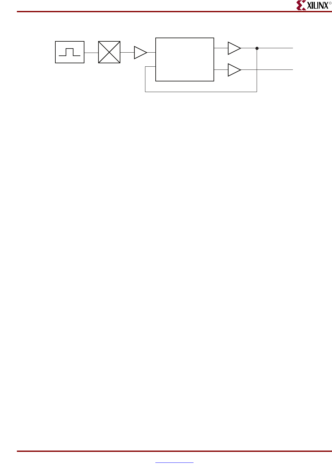
112 www.xilinx.com Memory Interface Solutions User Guide
UG086 (v3.6) September 21, 2010
Chapter 2: Implementing DDR SDRAM Controllers
R
DDR SDRAM System and User Interface Signals
Table 2-6 describes the DDR SDRAM system interface signals for designs with the DCM.
The system interface signals are the clocks and the reset signals provided by the user to the
FPGA. The differential clock signals, sys_clk_p and sys_clk_n, are the two clocks to be
provided to the design. These two clocks must have a phase difference of 180 degrees with
respect to each other. The sys_reset_in_n signal resets all the logic.
Table 2-7 shows the system interface signals for designs without the DCM. The clk_0,
clk_90, and clk_200 signals are the single-ended input clocks. The clk_90 signal must have
a phase difference of 90° with respect to clk_0. The clk_200 signal is the clock used for the
IDELAYCTRL primitives in Virtex-4 FPGAs.
Table 2-8 describes the DDR SDRAM user interface signals for designs without the
testbench.
Table 2-6: DDR SDRAM System Interface Signals for Designs with DCM
Signal Name Direction Description
sys_clk_p, sys_clk_n Input Differential input clock to the DCM. The DDR SDRAM controller
and memory operate on this frequency.
sys_reset_in_n Input Active-Low reset to the DDR SDRAM controller.
clk200_p, clk200_n Input Differential clock used in the idelay_ctrl logic.
Table 2-7: System Interface Signals for Designs without the DCM
Signal Direction Description
clk_0 Input The DDR SDRAM controller and memory operate on this clock.
sys_reset_in_n Input Active-Low reset to the DDR SDRAM controller. This signal is used
to generate a synchronous system reset.
clk_90 Input 90° phase-shifted clock with the same frequency as clk0.
clk_200 Input 200 MHz differential input clock for the IDELAYCTRL primitive of
the Virtex-4 FPGA.
dcm_lock Input The status signal indicating whether the DCM is locked or not. It is
used to generate the synchronous system reset.
Table 2-8: DDR SDRAM User Interface Signals for Designs without the Testbench Case
Signal Name(1) Direction Description
clk_tb Output All user interface signals must be synchronized with respect to
clk_tb.
reset_tb Output Active-High system reset for the user interface.
burst_length_div2[2:0] Output Indicates the number of bursts that can be written to or read from
the memory.
001: burst length = 2
010: burst length = 4
100: burst length = 8

Memory Interface Solutions User Guide www.xilinx.com 113
UG086 (v3.6) September 21, 2010
DDR SDRAM System and User Interface Signals
R
read_data_valid Output Status of the Read Data FIFO. This signal is asserted when read data
is available in the Read Data FIFO.
read_data_fifo_out
[2n–1:0]
Output Read data from memory, where n is the data width of the interface.
The read data is stored into the Read Data FIFO. This data can be
read from the FIFO depending upon the status of the FIFO.
wdf_almost_full Output ALMOST FULL status of the Write Data FIFO. When this signal is
asserted, the user can write 5 more locations into the FIFO in designs
generated with a testbench and 14 more locations in designs without
a testbench.
af_almost_full Output ALMOST FULL status of the Read Address FIFO. The user can issue
eight more locations into the FIFO after AF_ALMOST_FULL is
asserted.
app_af_addr[35:0](2) Input Memory address and command. Bit 35 is used internally by the
controller. The controller ignores this bit from the user interface. Bits
[34:32] are used for dynamic commands as follows:
001: Auto Refresh
010: Precharge
100: Write
101: Read
Bits [31:0] form the memory chip select, bank address, row address,
and column address. The positioning of the chip, bank, row, and
column addresses changes based on the memory configuration.
app_af_wren Input Write-enable signal to the Write Address FIFO. This signal is
synchronized with the write address. The write address is written to
the Write Address FIFO only when this signal is asserted High.
app_mask_data[2m–1:0] Input User mask data, where m indicates the data mask width of the
interface. The mask data is twice the mask width of the interface.
The mask data is written into the Write Data FIFO along with the
write data.
app_wdf_data[2n–1:0] Input User write data to the memory, where n indicates the data width of
the interface. The user write data is twice the data width of the
interface. The most-significant bits contain the rising-edge data, and
the least-significant bits contain the falling-edge data. Memory write
data is written into the Write Data FIFO, and the write address is
written into the Write Address FIFO from the user interface. The
DDR SDRAM controller reads the Write Address FIFO and Write
Data FIFO.
Table 2-8: DDR SDRAM User Interface Signals for Designs without the Testbench Case (Cont’d)
Signal Name(1) Direction Description
114 www.xilinx.com Memory Interface Solutions User Guide
UG086 (v3.6) September 21, 2010
Chapter 2: Implementing DDR SDRAM Controllers
R
Table 2-9 describes the status signals that are available to the user.
User Interface Accesses
The user backend logic communicates with the memory controller through a FIFO-based
user interface. This interface consists of three related buses:
• A Command/Address FIFO bus, which accepts write/read commands as well as the
corresponding memory address from the user
• A Write Data FIFO bus, which accepts the corresponding write data when the user
issues a write command on the Command/Address bus
• A Read bus on which the corresponding read data for an issued read command is
returned
The user interface has the following timing and signaling restriction:
• Commands and write data cannot be written by the user until calibration is complete
(as indicated by init_done). In addition, the following interface signals need to be held
Low until calibration is complete: app_af_wren, app_wdf_wren, app_wdf_data, and
app_mask_data. Failure to hold these signals Low causes errors during calibration.
This restriction arises from the fact that the Write Data FIFO is used during calibration
to hold the training patterns for the various stages of calibration.
• When issuing a write command, the first write data word must be written to the Write
Data FIFO no more than one clock cycle after the write command is issued. This
restriction arises from the fact that the controller assumes write data is available when
it receives the write command from the user.
• clk_tb is connected to clk_0 in the controller. In case that user clock domain is different
from clk_0 / clk_tb of MIG, the user should add FIFOs for all data inputs and outputs
of the controller, in order to synchronize them to the clk_tb.
app_wdf_wren Input Write-enable signal to the Write Data FIFO. This signal is
synchronized with the write data. The write data is written to the
Write Data FIFO only when this signal is asserted High.
Notes:
1. All user interface signal names are prepended with a controller number, for example, cntrl0_APP_WDF_DATA. DDR SDRAM
devices currently support only one controller. See “User Interface Accesses,” page 114 for timing requirements and restrictions on
the user interface signals.
2. Linear addressing is used, i.e., the row address immediately follows the column address bits, and the bank address follows the row
address bits, thus supporting more devices. The number of address bits used depends on the density of the memory part. The
controller ignores the unused bits, which can all be tied High.
Table 2-8: DDR SDRAM User Interface Signals for Designs without the Testbench Case (Cont’d)
Signal Name(1) Direction Description
Table 2-9: DDR SDRAM Design Status Signals
Signal Name Direction Description
init_done Output This signal indicates the completion of initialization and calibration
of the design.
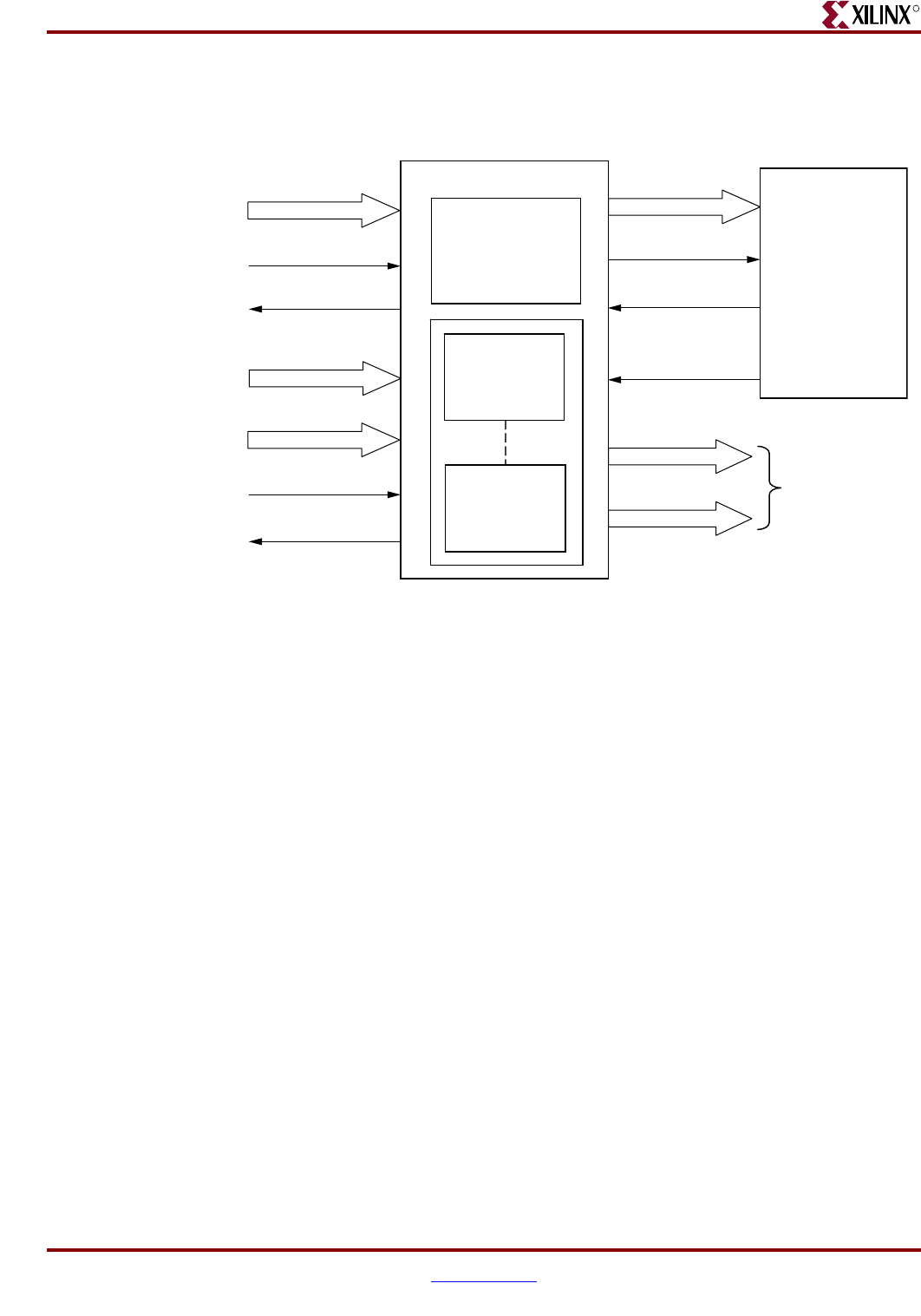
Memory Interface Solutions User Guide www.xilinx.com 115
UG086 (v3.6) September 21, 2010
DDR SDRAM System and User Interface Signals
R
Write Interface
Figure 2-10 shows the user interface block diagram for write operations.
The following steps describe the architecture of the Address and Write Data FIFOs and
show how to perform a write burst operation to DDR SDRAM from the user interface.
1. The user interface consists of an Address FIFO and a Write Data FIFO. These FIFOs are
constructed using Virtex-4 FPGA FIFO16 primitives with a 512 x 36 configuration. The
36-bit architecture comprises one 32-bit port and one 4-bit port. For Write Data FIFOs,
the 32-bit port is used for data bits and the 4-bit port is used for mask bits.
2. The Common Address FIFO is used for both write and read commands, and comprises
a command part and an address part. Command bits discriminate between write and
read commands.
3. User interface data width app_wdf_data is twice that of the memory data width. For
an 8-bit memory width, the user interface is 16 bits consisting of rise data and fall data.
For every 8 bits of data, there is a mask bit. For 72-bit memory data, the user interface
data width app_wdf_data is 144 bits, and the mask data app_mask_data is 18 bits.
4. The minimum configuration of the Write Data FIFO is 512 x 36 for a memory data
width of 8 bits. For an 8-bit memory data width, the least significant 16 bits of the data
port is used for write data. The controller internally pads all zeros for the most-
significant 16 bits.
5. Depending on the memory data width, MIG instantiates multiple FIFO16s to gain the
required width. For designs using 8-bit data width, one FIFO16 is instantiated; for
72-bit data width, a total of five FIFO16s are instantiated. The bit architecture
comprises 16 bits of rising-edge data, 2 bits of rising-edge mask, 16 bits of falling-edge
data, and 2 bits of falling-edge mask, which are all stored in a FIFO16. MIG routes the
app_wdf_data and app_mask_data to FIFO16s accordingly.
6. The user can initiate a write to memory by writing to the Address FIFO and the Write
Data FIFO when the FIFO Full flags are deasserted. Status signal af_almost_full is
Figure 2-10: User Interface Block Diagram for Write Operations
User Interface
Controller
Address FIFO
(FIFO16)
512 x 36
af_addr
af_empty
ctrl_af_rden
ctrl_wdf_rden
app_af_addr
app_af_wren
app_wdf_data
app_mask_data
app_wdf_wren
wdf_data
mask_data
To Phy Layer
wdf_almost_full
af_almost_full
Write Data
FIFO
(FIFO16)
512 x 36
Write Data
FIFO
(FIFO16)
512 x 36
ug086_c2_11_110607
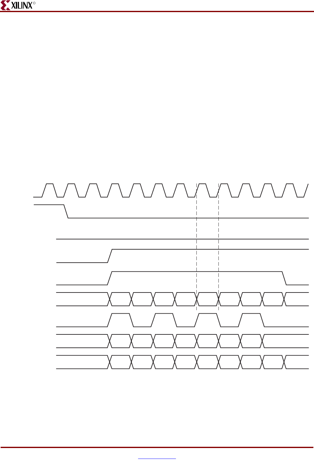
116 www.xilinx.com Memory Interface Solutions User Guide
UG086 (v3.6) September 21, 2010
Chapter 2: Implementing DDR SDRAM Controllers
R
asserted when Address FIFO is full, and similarly wdf_almost_full is asserted when
Write Data FIFO is full.
7. Both the Address FIFO and Write Data FIFO Full flags are deasserted with power-on.
8. The user should assert the Address FIFO write-enable signal app_af_wren along with
address app_af_addr to store the write address and write command into the Address
FIFO.
9. The user should assert the Data FIFO write-enable signal app_wdf_wren along with
write data app_wdf_data and mask data app_mask_data to store the write data and
mask data into the Write Data FIFO. The user should provide both rise and fall data
together for each write to the Data FIFO.
10. The controller reads the Address FIFO by issuing the ctrl_af_rden signal. The
controller reads the Write Data FIFO by issuing the ctrl_wdf_rden signal after the
Address FIFO is read. It decodes the command part after the Address FIFO is read.
11. The write command timing diagram in Figure 2-11 is derived from the MIG-generated
testbench. As shown (burst length of 4), each write to the Address FIFO must be
coupled with two writes to the Data FIFO. Similarly, for a burst length of 8, every write
to the Address FIFO must be coupled with four writes to the Data FIFO. Failure to
follow this rule can cause unpredictable behavior.
Figure 2-11: DDR SDRAM Write Burst for Four Bursts (BL = 4)
clk_tb
reset_tb
wdf_almost_full
app_wdf_wren
app_wdf_data
app_mask_data
app_af_wren
init_done
app_af_addr
D0D1
A0
M0M1 M2M3M4M5 M6M7 M8M9 M10M11 M12M13M14M15
A1 A2 A3
D2D3D4D5 D6D7 D8D9 D10D11 D12D13D14D15
ug086_c2_09_091708
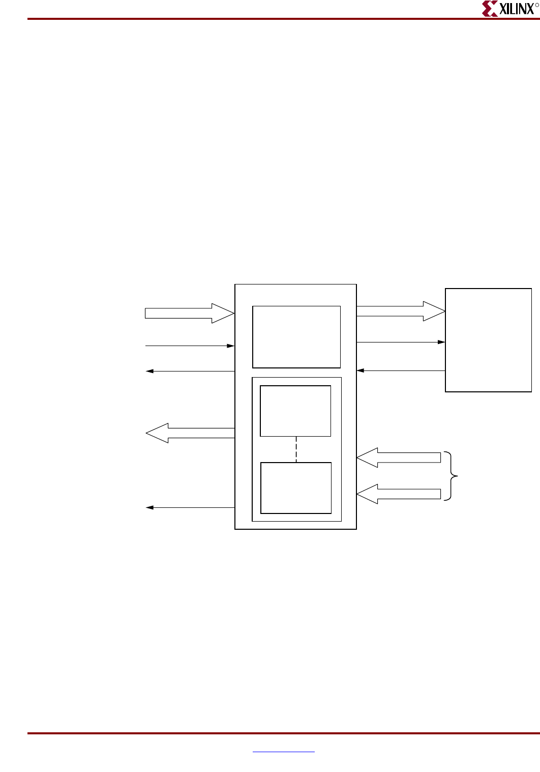
Memory Interface Solutions User Guide www.xilinx.com 117
UG086 (v3.6) September 21, 2010
DDR SDRAM System and User Interface Signals
R
Correlation between the Address and Data FIFOs
There is a worst case two-cycle latency from the time the address is loaded into the address
FIFO on app_af_addr[35:0] to the time the controller decodes the address. Because of this
latency, it is not necessary to provide the address on the last clock where data is entered
into the data FIFO. If the address is written before the last data phase, the overall efficiency
and performance increases because it eliminates or reduces the two-cycle latency.
However, if the address is written before data is input into the data FIFO, a FIFO empty
condition might result because the Data FIFO does not contain valid data.
Based on these considerations, Xilinx recommends entering the address into the address
FIFO between the first data phase and the next-to-last data phase. For a burst of four or
eight, this means the address can be asserted one clock before the first data phase. This
implementation increases efficiency by reducing the one clock latency and guarantees that
valid data is available in the Data FIFO.
Read Interface
Figure 2-12 shows a block diagram of the read interface.
The following steps describe the architecture of the Read Data FIFOs and show how to
perform a burst read operation from DDR SDRAM from the user interface.
1. The read user interface consists of an Address FIFO and a Read Data FIFO. The
Address FIFO is common to both read and write operations. These FIFOs are
constructed using Virtex-4 FPGA Distributed RAMs with a 16 x 1 configuration. MIG
instantiates a number of RAM16Ds depending on the data width. For example, for
8-bit data width, MIG instantiates a total of 16 RAM16Ds, 8 for rising-edge data and 8
for falling-edge data. Similarly, for 72-bit data width, MIG instantiates a total of 144
RAM16Ds, 72 for rising-edge data and 72 for falling-edge data.
2. The user can initiate a read to memory by writing to the Address FIFO when the
FIFO Full flag af_almost_full is deasserted.
Figure 2-12: User Interface Block Diagram for Read Operation
User Interface
Controller
Address FIFO
(FIFO16)
512 x 36
af_addr
af_empty
ctrl_af_rden
app_af_addr
app_af_wren
read_data_fifo_out
read_data_rise
read_data_fall From Phy Layer
read_data_valid
af_almost_full
Read Data
FIFO
RAM16 x 1D
Read Data
FIFO
RAM16 x 1D
ug086_c2_12_110607
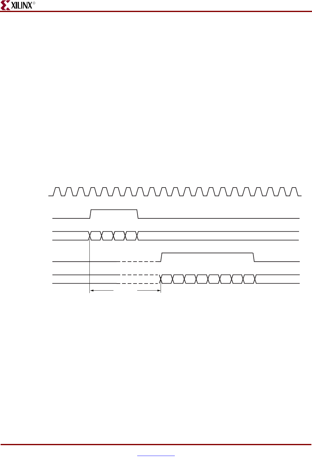
118 www.xilinx.com Memory Interface Solutions User Guide
UG086 (v3.6) September 21, 2010
Chapter 2: Implementing DDR SDRAM Controllers
R
3. To write the read address and read command into the Address FIFO, the user should
issue the Address FIFO write-enable signal app_af_wren along with read address
app_af_addr.
4. The controller reads the Address FIFO containing the address and command. After
decoding the command, the controller generates the appropriate control signals to
memory.
5. Prior to the actual read and write commands, the design calibrates the latency (number
of clock cycles) from the time the read command is issued to the time data is received.
Using this pre-calibrated delay information, the controller generates the write-enable
signals to the Read Data FIFOs.
6. The read_data_valid signal is asserted when data is available in the Read Data FIFOs.
7. Figure 2-13 shows a user interface timing diagram for a burst length of 4, CAS latency
of 3 at 175 MHz, and a Trcd value of the memory part at 20 ns. The read latency is
calculated from the point when the Read command is given by the user to the point
when the data is available with the read_data_valid signal. The minimum latency in
this case is 26 clocks, where no precharge is required, no auto-refresh request is
pending, the user commands are issued after initialization is completed, and the first
command issued is a Read command. The controller executes the commands only
after initialization is done as indicated by the init_done signal.
8. After the address and command are loaded into the Address FIFO, it takes 26 clock
cycles minimum for CL = 3 at a frequency of 175 MHz for the controller to assert the
read_data_valid signal.
9. Read data is available only when the read_data_valid signal is asserted. The user
should access the read data on every positive edge of the read_data_valid signal.
The read latency for the case where (1) CL = 3, (2) the read is written to an empty
address/command FIFO, (3) the read targets an unopened bank/row, and (4) the
frequency is 175 MHz, is broken down as indicated in Table 2-10.
Figure 2-13: DDR SDRAM Read Burst for Four Bursts (BL = 4)
CLK_TB
A0 A1
app_af_wren
app_af_addr
read_data_valid
read_data_fifo_out
UG086_c2_10_050610
A2 A3
D0D1
D2D3
D4D5
D6D7
D8D9
D10D11
D12D13
D14D15
26 clocks
Memory Interface Solutions User Guide www.xilinx.com 119
UG086 (v3.6) September 21, 2010
DDR SDRAM System and User Interface Signals
R
In general, read latency varies based on the following parameters:
• Number of commands already in the FIFO pipeline before the read command is
issued
• Whether an ACTIVATE command needs to be issued to open the new bank/row
• Whether a PRECHARGE command needs to be issued to close a previously opened
bank
• Specific timing parameters for the memory, such as TRAS and TRCD in conjunction
with the bus clock frequency
• Commands can be interrupted, and banks/rows can forcibly be closed when the
periodic AUTO REFRESH command is issued
•CAS latency
• If the user issues the commands before initialization is complete, the latency cannot be
determined.
• Board-level and chip-level (for both memory and FPGA) propagation delays
DDR SDRAM Signal Allocations
The MIG tool allows selection of banks for different classes of memory signals. Table 2-11
shows the list of signals allocated in a group from bank selection checkboxes.
Note: Timing has been verified for most of the MIG generated configurations. For the best timing
results, adjacent banks in the same column of the FPGA should be used. Banks that are separated
by unbonded banks should be avoided because these can cause timing violations.
Table 2-10: Read Command to Read Data Clock Cycles
Parameter Number of Clock Cycles
Read Command to Empty Signal Deassertion 7 clocks
Empty to Active Command 5.5 clocks
Active to Read Command 4 clocks
Memory Read to Valid 9.5 clocks
Total: 26 clocks
Table 2-11: DDR SDRAM Signal Allocations
Bank Selected Signals Allocated in the Group
Address Memory address, memory control, and memory clock signals
Data Data, data mask, and data strobes
System Control System reset from the user interface and status signals
System Clock System clocks from the user interface

120 www.xilinx.com Memory Interface Solutions User Guide
UG086 (v3.6) September 21, 2010
Chapter 2: Implementing DDR SDRAM Controllers
R
Simulating the DDR SDRAM Design
After generating the design, MIG creates a sim folder in the specified path. This folder
contains simulation files for a particular design. The sim folder contains the external
testbench, memory model, and do file to simulate the generated design. The memory
model files are currently generated in Verilog only. To learn more about the files in the sim
folder and to simulate the design, refer to “Simulation Guide,” page 499.
For single-rank DIMMs, MIG outputs only the base part memory model. In the simulation
testbench (sim_tb_top in the sim folder), MIG instantiates the required number of
memory models. For example, a 1 GB single-rank DIMM with the base part is 1 Gb, and
MIG instantiates the base model eight times. If the MIG generated memory model is to be
used with the user’s test bench, multiple instances that are based on the selected
configuration should be used.
The MIG output memory model considers the part_mem_bits parameter by default for
memory range allocation. This covers only a partial memory range, i.e., 2part_mem_bits. To
allocate the full memory range, the FULL_MEM parameter should be set in the memory
model, which in turn sets the full_mem_bits parameter for memory allocation. Allocating
the full memory range might exceed the memory of the operating system, thus causing
memory allocation failure in simulations.
Simulation Violations
There might be simulation violations for frequencies such as 150 MHz where the clock
period is not an integer value. At 150 MHz, the clock period value in the simulation
testbench is 6.66 ns and the MIG tool rounds it to 6.67 ns. Consider a memory TRCD value
of 20 ns. MIG calculates the TRCD count value based on the clock period,
RCD_COUNT_VALUE = 20/6.67 = 2.998 = 3 (after rounding off) in the design parameter
file. The TRCD value for 3 clock cycles is 3 × 6.66 = 19.98, which causes timing violations by
20 ps. The difference between the clock period in the external simulation testbench versus
the MIG tool causes timing violations. This is only one example case. There might be more
such scenarios. These are only simulation warnings. Functionally, there should be no
issues. To remove these warnings, the related count value can be increased by one.
Changing the Refresh Rate
Change the global `define (for Verilog) or constant (for VHDL) variable MAX_REF_CNT in
mymodule_parameters_0.v (or .vhd) so that MAX_REF_CNT = (refresh interval in
clock periods) = (refresh interval) / (clock period). For example, for a refresh rate of 3.9 µs
with a memory bus running at 200 MHz:
MAX_REF_CNT = 3.9 µs / (clock period) = 3.9 µs / 5 ns = 780 (decimal) = 0x30C
If the above value exceeds 2MAX_REF_WIDTH – 1, the value of MAX_REF_WIDTH must be
increased accordingly in parameters_0.v (or .vhd) to increase the width of the counter
used to track the refresh interval.
Memory Interface Solutions User Guide www.xilinx.com 121
UG086 (v3.6) September 21, 2010
Supported Devices
R
Supported Devices
The design generated out of MIG is independent of the memory package, hence the
package part of the memory component is replaced with XX or XXX, where XX or XXX to
indicate a don't care condition. The tables below list the components (Table 2-12) and
DIMMs (Table 2-13 through Table 2-15) supported by MIG for DDR SDRAM. In supported
devices, XX in the memory component column denotes either single or two alphanumeric
characters. For example, MT46V32M4XX-75 can be either MT46V32M4P-75 or
MT46V32M4BN-75. An X in the DIMM columns (for Unbuffered, Registered, and SO
DIMMs) denotes a single alphanumeric character. For example, MT9VDDF3272X-40B can
be either MT9VDDF3272G-40B or MT9VDDF3272Y-40B. Similarly MT4VDDT1664AX-40B
can be either MT4VDDT1664AG-40B or MT4VDDT1664AY-40B. Pin mapping for x4
RDIMMs is provided in Appendix G, “Low Power Options.”
Table 2-12: Supported Components for DDR SDRAM
Components Packages (XX) Components Packages (XX)
MT46V32M4XX-75 P,TG MT46V32M4XX-5B -
MT46V64M4XX-75 FG,P,TG MT46V64M4XX-5B BG,FG,P,TG
MT46V128M4XX-75 BN,FN,P,TG MT46V128M4XX-5B BN,FN,P,TG
MT46V256M4XX-75 P,TG MT46V256M4XX-5B P,TG
MT46V16M8XX-75 P,TG MT46V16M8XX-5B TG,P
MT46V32M8XX-75 FG,P,TG MT46V32M8XX-5B BG,FG,P,TG
MT46V64M8XX-75 BN,FN,P,TG MT46V64M8XX-5B BN,FN,P,TG
MT46V128M8XX-75 P,TG MT46V128M8XX-5B -
MT46V8M16XX-75 P,TG MT46V8M16XX-5B TG,P
MT46V16M16XX-75 BG,FG,P,TG MT46V16M16XX-5B BG,FG,P,TG
MT46V32M16XX-75 - MT46V32M16XX-5B BN,FN,P,TG
MT46V64M16XX-75 P,TG MT46V64M16XX-5B -
Table 2-13: Supported Unbuffered DIMMs for DDR SDRAM
Unbuffered DIMMs Packages (X) Unbuffered DIMMs Packages (X)
MT4VDDT1664AX-40B G,Y MT8VDDT3264AX-40B G,Y
MT4VDDT3264AX-40B G,Y MT9VDDT3272AX-40B Y
Table 2-14: Supported Registered DIMMs for DDR SDRAM
Registered DIMMs Packages (X) Registered DIMMs Packages (X)
MT9VDDF3272X-40B G,Y MT18VDDF6472X-40B G,Y
MT9VDDF6472X-40B G,Y MT18VDDF12872X-40B G,Y
Table 2-15: Supported SODIMMs for DDR SDRAM
SODIMMs Packages (X) SODIMMs Packages (X)
MT4VDDT3264HX-40B G,Y MT9VDDT3272HX-40B -
MT4VDDT1664HX-40B Y MT9VDDT6472HX-40B G,Y
122 www.xilinx.com Memory Interface Solutions User Guide
UG086 (v3.6) September 21, 2010
Chapter 2: Implementing DDR SDRAM Controllers
R
Hardware Tested Configurations
The frequencies shown in Table 2-16 were achieved on the Virtex-4 FPGA ML461 Memory
Interfaces Development Board under nominal conditions. This frequency should not be
used to determine the maximum design frequency. The maximum design frequency
supported in the MIG wizard is based on a combination of the TRCE results for fabric
timing on multiple device/package combinations and I/O timing analysis using FPGA
and memory timing parameters for a 64-bit wide interface.
MT8VDDT3264HX-40B - MT9VDDT12872HX-40B -
MT8VDDT6464HX-40B G,Y
Table 2-15: Supported SODIMMs for DDR SDRAM (Cont’d)
SODIMMs Packages (X) SODIMMs Packages (X)
Table 2-16: Hardware Tested Configurations
Synthesis Tools XST and Synplicity
HDL Verilog and VHDL
FPGA Device XC4VLX25-FF668-11
Burst Lengths 2, 4, 8
CAS Latency (CL) 2, 2.5, 3
16-bit Design Tested on 16-bit Component “MT46V32M16XX-5B”
72-bit Design Tested on 72-bit RDIMM “MT18VDDF6472G-40B”
CL = 2
Achieved Frequency
Range for Component 110 MHz to 180 MHz
Achieved Frequency
Range for DIMM 110 MHz to 160 MHz
CL = 2.5
Achieved Frequency
Range for Component 110 MHz to 220 MHz
Achieved Frequency
Range for DIMM 110 MHz to 200 MHz
CL = 3
Achieved Frequency
Range for Component 110 MHz to 240 MHz
Achieved Frequency
Range for DIMM 110 MHz to 240 MHz
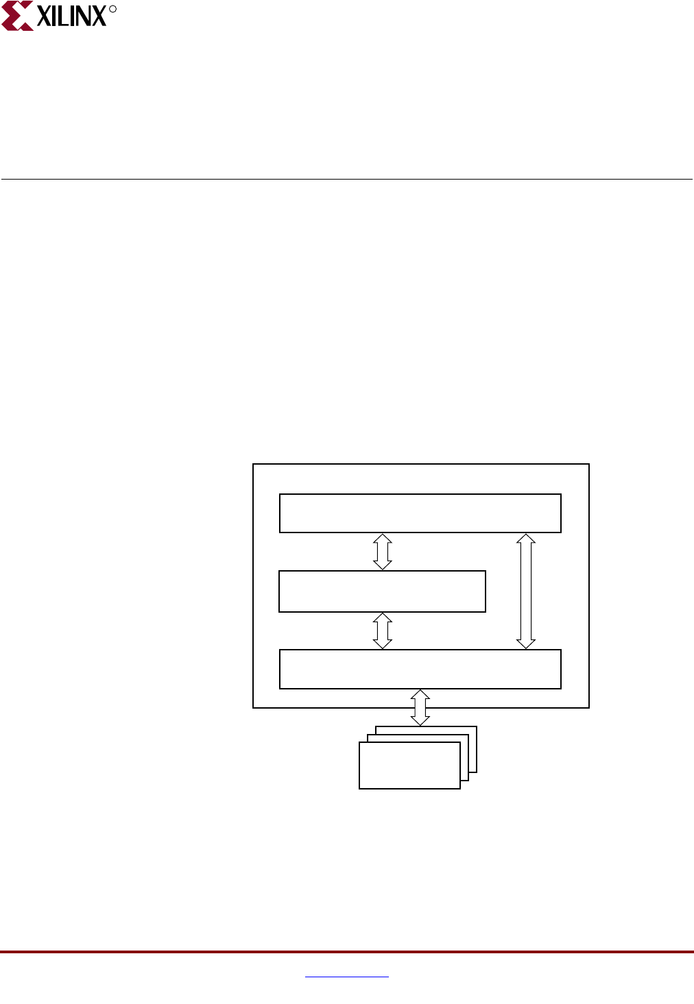
Memory Interface Solutions User Guide www.xilinx.com 123
UG086 (v3.6) September 21, 2010
R
Chapter 3
Implementing DDR2 SDRAM Controllers
This chapter describes how to implement DDR2 SDRAM interfaces for Virtex®-4 FPGAs
generated by MIG. MIG supports two implementations of DDR2 SDRAM interfaces: direct
clocking and SerDes clocking. The direct-clocking interface supports frequencies up to
240 MHz. This design is based on XAPP702 [Ref 19]. The SerDes clocking design supports
frequencies up to 300 MHz and is based on XAPP721 [Ref 23].
Interface Model
DDR2 SDRAM interfaces are source-synchronous and double data rate. They transfer data
on both edges of the clock cycle. A memory interface can be modularly represented as
shown in Figure 3-1. A modular interface has many advantages. It allows designs to be
ported easily and also makes it possible to share parts of the design across different types
of memory interfaces.
Figure 3-1: Modular Memory Interface Representation
Application Interface Layer
Xilinx FPGA
Physical Layer
Control Layer
UG086_c3_01_033105
Memories
124 www.xilinx.com Memory Interface Solutions User Guide
UG086 (v3.6) September 21, 2010
Chapter 3: Implementing DDR2 SDRAM Controllers
R
Direct-Clocking Interface
Feature Summary
This section summarizes the supported and unsupported features of the direct-clocking
DDR2 SDRAM controller design.
Supported Features
The DDR2 SDRAM controller design supports the following:
• Burst lengths of four and eight
• Sequential and interleaved burst types
• CAS latencies of 3, 4, and 5
• Additive latencies of 0, 1, and 2
• Differential and single-ended DQS
• On-Die Termination (ODT)
• Up to four deep memories
• Memory components
• Registered DIMMs (up to 240 MHz)
• Unbuffered DIMMs (up to 200 MHz)
• Unbuffered SODIMMs (up to 200 MHz)
• Different memories (density/speed)
• Byte-wise data masking
• Precharge and auto refresh
• Linear addressing
• ECC support
•Verilog and VHDL
• With and without a testbench
• With and without a DCM
• Multicontrollers (up to eight)
•Data Mask
• System clock, differential and single-ended
The supported features are described in more detail in “Architecture.”
Design Frequency Ranges
Table 3-1: Design Frequency Range in MHz
Memory
FPGA Speed Grade
-10 -11 -12
Min Max Min Max Min Max
Component 125 220 125 230 125 240
UDIMM/SODIMM 125 200 125 200 125 200
Memory Interface Solutions User Guide www.xilinx.com 125
UG086 (v3.6) September 21, 2010
Direct-Clocking Interface
R
Unsupported Features
The DDR2 SDRAM controller design does not support:
• Additive latencies of 3 and 4
• Redundant DQS (RDQS)
• Unbuffered DIMMs (greater than 200 MHz)
• Unbuffered SODIMMs (greater than 200 MHz)
Architecture
Implemented Features
This section provides details on the supported features of the DDR2 SDRAM controller.
Burst Length
The DDR2 SDRAM controller supports burst lengths of four and eight. The burst length
can be selected through the Set mode register(s) option from the GUI. For a design
without a testbench (user design), the user has to provide bursts of the input data based on
the chosen burst length. Bits M2:M0 of the Mode Register define the burst length, and bit
M3 indicates the burst type (see the Micron data sheet). Read and write accesses to the
DDR2 SDRAM are burst-oriented. It determines the maximum number of column
locations accessed for a given READ or WRITE command.
CAS Latency
The DDR2 SDRAM controller supports CAS latencies (CLs) of three and four. CL can be
selected in the Set mode register(s) option from the GUI. The CAS latency is
implemented in the ddr2_controller module. During data write operations, the generation
of the ctrl_Dqs_En and ctrl_Dqs_Rst signals varies according to the CL in the
ddr2_controller module. During data read operations, the generation of the ctrl_RdEn
signal varies according to the CL in the ddr2_controller module. Bits M4:M6 of the Mode
Register define the CL (see the Micron data sheet). CL is the delay in clock cycles between
the registration of a READ command and the availability of the first bit of output data.
Additive Latency
DDR2 SDRAM devices support a feature called posted CAS additive latency (AL). The
DDR2 SDRAM supports additive latencies of 0, 1, and 2. AL can be selected in the Set
mode register(s) option from the GUI. Additive latency is implemented in the
ddr2_controller module. The ddr2_controller module issues READ/WRITE commands
prior to tRCD (minimum) depending on the user-selected AL value in the Extended Mode
Register. This feature allows the READ command to be issued prior to tRCD (minimum) by
delaying the internal command to the DDR2 SDRAM by AL clocks. Posted CAS AL makes
RDIMM 125 220 125 230 125 240
Deep Memory /
Dual Rank DIMM 125 150 125 150 125 150
Table 3-1: Design Frequency Range in MHz
Memory
FPGA Speed Grade
-10 -11 -12
Min Max Min Max Min Max
126 www.xilinx.com Memory Interface Solutions User Guide
UG086 (v3.6) September 21, 2010
Chapter 3: Implementing DDR2 SDRAM Controllers
R
the command and data bus efficient for sustainable bandwidths in DDR2 SDRAM. Bits
E3:E5 of the Extended Mode Register define the value of AL (see the Micron data sheet).
Registered DIMMs
DDR2 SDRAM supports registered DIMMs. This feature is implemented in the
ddr2_controller module. For registered DIMMs, the READ and WRITE commands and
address have one additional clock latency than unbuffered DIMMs.
Unbuffered DIMMs and SODIMMs
The DDR2 SDRAM design supports unbuffered DIMMs and SODIMMs. Unbuffered
DIMMs are normal DIMMs, where a set of components are used to get a particular
configuration. SODIMMs differ from the unbuffered DIMMs only by the package type.
Otherwise they are functionally the same.
Multicontrollers
MIG supports multicontrollers for DDR2 SDRAMs. A maximum of eight controllers can be
selected by the user from the tool. In multicontroller designs, MIG supports the same
frequency for all the controllers.
Different Memories (Density/Speed)
The DDR2 SDRAM controller supports different densities. For DDR2 components shown
in MIG, densities vary from 256 Mb to 2 Gb, and DIMM densities vary from 128 Mb to
4 Gb. Higher densities can be created using the “Create new memory part” feature of MIG.
The supported maximum column address is 13, the maximum row address is 15, and the
maximum bank address is 3. The design can decode write and read addresses from the
user in the DDR2 SDRAM controller module. The user address consists of column, row,
bank, chip address, and user command.
Table 3-2 and Table 3-3 list sample timing sheets for Micron components and DIMMs,
respectively.
Table 3-2: Timing Parameters for Components
Parameter Description
Micron 256 Mb Micron 512 Mb Micron 1 Gb
-37E -5E -37E -5E -37E -5E
TMRD LOAD MODE command cycle time 2 2 2 2 2 2
TRP PRECHARGE command period 15 15 15 15 15 15
TRFC REFRESH to ACTIVE or REFRESH to
REFRESH command interval
75 75 105 105 127.5 127.5
TRCD ACTIVE to READ or WRITE delay 15 15 15 15 15 15
TRAS ACTIVE to PRECHARGE command 40 40 40 40 40 40
TRC ACTIVE to ACTIVE (same bank) command 55 55 55 55 55 55
TRTP READ to PRECHARGE command delay 7.5 7.5 7.5 7.5 7.5 7.5
TWTR WRITE to READ command delay 7.5 10 7.5 10 7.5 10
TWR WRITE Recovery time 15 15 15 15 15 15
Memory Interface Solutions User Guide www.xilinx.com 127
UG086 (v3.6) September 21, 2010
Direct-Clocking Interface
R
Note: For the latest timing information, refer to the vendor memory data sheets.
Data Masking
The DDR2 SDRAM design supports data masking per byte. Masking per nibble is not
supported due to the limitation of the internal block RAM based FIFOs. So, the masking of
data can be done on a per byte basis. The mask data is stored in the Data FIFO along with
the actual data.
MIG supports a data mask option. If this option is checked in the GUI, MIG generates a
design with data mask pins. This option can be chosen if the selected part has data
masking. DDR2 SDRAM designs do not support read-modify-write operations in ECC
mode. The mask bits to the SDRAM should never be asserted while in the ECC mode.
Thus, when ECC is selected, the data masking selection is disabled in the GUI.
Precharge
The PRECHARGE command is used to close the open row in a bank if there is a command
to be issued in the same bank. The PRECHARGE command checks the row address, bank
address, and chip address, and the Virtex-4 FPGA DDR2 controller issues a PRECHARGE
command if there is a change in any of the addresses where a read or write command is to
be issued. The auto precharge function is not supported.
Auto Refresh
The DDR2 SDRAM controller issues AUTO REFRESH commands at specified intervals for
the memory to refresh the charge required to retain the data in the memory. The user can
Table 3-3: Timing Parameters for DIMMs
Parameter Description
MT4HTF MT8HTF MT16HTF MT9HTF MT18HTF
-53E -40E -53E -40E -53E -40E -53E -40E -53E -40E
TMRD LOAD MODE command
cycle time
2222222222
TRP PRECHARGE command
period
15 15 15 15 15 15 15 15 15 15
TRFC REFRESH to ACTIVE or
REFRESH to REFRESH
command interval
128 MB
75
75 256 MB
75
75 512 MB
75
75 256 MB
75
75 512 MB
75
75
256 MB
105
105 512 MB
105
105 1 GB
105
105 512 MB
105
105 1 GB
105
105
512 MB
127.5
127.5 1 GB
127.5
127.5 2 GB
127.5
127.5 1 GB
127.5
127.5 2 GB
127.5
127.5
TRCD ACTIVE to READ or
WRITE delay
15 15 15 15 15 15 15 15 15 15
TRAS ACTIVE to
PRECHARGE command
40 40 40 40 40 40 40 40 40 40
TRC ACTIVE to ACTIVE
(same bank) command
55 55 55 55 55 55 55 55 55 55
TRTP READ to PRECHARGE
command delay
7.5 7.5 7.5 7.5 7.5 7.5 7.5 7.5 7.5 7.5
TWTR WRITE to READ
command delay
7.5 10 7.5 10 7.5 10 7.5 10 7.5 10
TWR WRITE recovery time 15 15 15 15 15 15 15 15 15 15

128 www.xilinx.com Memory Interface Solutions User Guide
UG086 (v3.6) September 21, 2010
Chapter 3: Implementing DDR2 SDRAM Controllers
R
also issue a REFRESH command through the user interface by setting bits 34, 33, and 32 of
the app_af_addr signal in the user_interface module to 3’b001. If there is a refresh request
while there is an ongoing read or write burst, the controller issues a refresh command after
completing the current read or write burst command.
Linear Addressing
The DDR2 SDRAM controller supports linear addressing. Linear addressing refers to the
way the user provides the address of the memory to be accessed. For Virtex-4 FPGA DDR2
SDRAM controllers, the user provides address information through the app_af_addr bus.
As the densities of the memory devices vary, the number of column address bits and row
address bits also change. In any case, the row address bits in the app_af_addr bus always
start from the next higher bit, where the column address ends. This feature increases the
number of devices that can be supported with the design.
On-Die Termination
The DDR2 SDRAM controller supports on-die termination (ODT). Through the Set mode
register(s) option from the GUI, the user can disable ODT or can choose 75, 150, or 50.
ODT can turn the termination on and off as needed to improve signal integrity in the
system. Because DDR2 supports the deep memory maximum of four, a maximum of four
ODTs is supported. Several examples follow:
1. Four single-rank DIMMs or components populated in four different slots. If the user selects
deep memory = 4, the memory component sequence is 0, 1, 2, and 3. During write
operations, the ODT is enabled for component 3 when writing into 0, 1, or 2, otherwise
it is enabled for component 2 when writing into component 3. During read operations,
the ODT is enabled for component 3 when reading from 0, 1, or 2, otherwise it is
enabled for component 2 for reading from component 3.
Two dual-rank DIMMs populated in two different slots. Rank 1 and rank 2 of slot 1 are
referred to as CS0 and CS1. Rank 1 and rank 2 of slot 2 are referred to as CS2 and CS3.
ODT is enabled for CS0 when writing into CS2 or CS3 and enabled for CS2 when
writing into CS0 or CS1. ODT is enabled for CS0 when reading from CS2 or CS3 and
enabled for CS2 when reading from CS0 or CS1. ODT0, ODT1, ODT2, and ODT3
should be connected to the ODT signals of CS0, CS1, CS2, and CS3, respectively.
2. Three single-rank DIMMs or components populated in three different slots. If the user selects
deep memory = 3, the memory component sequence is 0, 1, and 2. During write
operations, the ODT is enabled for component 2 when writing into 0 or 1, otherwise it
is enabled for component 1 when writing into component 2. During read operations,
the ODT is enabled for component 2 when reading from 0 or 1, otherwise it is enabled
for component 1 for reading from component 2. ODT0, ODT1, and ODT2 should be
connected to the ODT signals of CS0, CS1, and CS2, respectively.
3. Two single-rank DIMMs or components populated in two different slots. If the user selects
deep memory = 2, the memory component sequence is 0 and 1. During write
operations, the ODT is enabled for component 1 when writing into 0, otherwise it is
enabled for component 0 when writing into component 1. During read operations, the
ODT is enabled for component 1 when reading from 0, otherwise it is enabled for
component 0 for reading from component 1.
One single dual-rank DIMM is populated in single slot. Rank 1 and rank 2 of slot 1 are
referred as CS0 and CS1. ODT is enabled for CS0 when writing into CS0 or CS1. During
read operations, the ODT is disabled. ODT0 and ODT1 should be connected to the
ODT signals of CS0 and CS1, respectively.
Memory Interface Solutions User Guide www.xilinx.com 129
UG086 (v3.6) September 21, 2010
Direct-Clocking Interface
R
4. If the user selects deep memory = 1, the memory component sequence is 0. During
write operations, the ODT is enabled for component 0 when writing into 0. During
read operations, the ODT is disabled. ODT0 should be connected to the ODT signal of
CS0.
Table 3-4 shows ODT control during write operations.
Table 3-5 shows ODT control during read operations.
Table 3-4: ODT Control During Writes
Configuration Write To DRAM at Slot 1 (ODT On/Off) DRAM at Slot 1 (ODT On/Off)
Slot 1 Slot 2 Rank 1 Rank 2 Rank 1 Rank 2
DR(1) DR Slot 1 Off Off On Off
Slot 2 On Off Off Off
DR Empty Slot 1 On Off N/A N/A
Empty DR Slot 2 N/A N/A On Off
SR(2) SR Slot 1 Off N/A On N/A
Slot 2 On N/A Off N/A
SR Empty Slot 1 On N/A N/A N/A
Empty SR Slot 2 N/A N/A On N/A
Notes:
1. Dual rank.
2. Single rank.
Table 3-5: ODT Control During Reads
Configuration Read From DRAM at Slot 1 (ODT On/Off) DRAM at Slot 1 (ODT On/Off)
Slot 1 Slot 2 Rank 1 Rank 2 Rank 1 Rank 2
DR(1) DR Slot 1 Off Off On Off
Slot 2 On Off Off Off
DR Empty Slot 1 Off Off N/A N/A
Empty DR Slot 2 N/A N/A Off Off
SR(2) SR Slot 1 Off N/A On N/A
Slot 2 On N/A Off N/A
SR Empty Slot 1 Off N/A N/A N/A
Empty SR Slot 2 N/A N/A Off N/A
Notes:
1. Dual rank.
2. Single rank.

130 www.xilinx.com Memory Interface Solutions User Guide
UG086 (v3.6) September 21, 2010
Chapter 3: Implementing DDR2 SDRAM Controllers
R
Deep Memories
The MIG DDR2 SDRAM controller supports depths up to 4. Through the Depth option, the
user can select various deep values. For deep memory implementations, MIG generates
chip selects, CKE signals, and ODT signals for each memory. The clock widths (ck and
ck_n) are a multiple factor of the deep configuration chosen in MIG. This feature increases
the depth of the memory. For example, if the user selects a 256 Mb component and deep
memory = 4 from MIG, the tool generates a memory interface for a 1 Gb design.
Deep memory logic is implemented in the ddr2_ controller module. With deep memories,
DDR2 SDRAMs are initialized one after the other to avoid loading the address and control
buses, and the calibration is done on the last memory. Apart from initialization, the DDR2
SDRAM controller module also demultiplexes the column, row, and bank addresses from
the user address. The module also decodes the chip selects and rank addresses for
components and DIMMs.
The formats of user read/write addresses for a 256 Mb component and 2 GB and 4 GB
DIMMs are given in “Deep Memory Configurations.”
ECC Support
The DDR2 SDRAM controller supports ECC. ECC is supported for the following data
widths:
• 40-bit (32-bit data and a 0 prepended to 7-bit parity)
• 72-bit (64-bit data and 8-bit parity)
• 144-bit (128-bit data and 16-bit parity)
The user can completely disable the ECC or can generate the design for the above data
widths by choosing either the Unpipeline mode or the Pipeline mode from the GUI.
ECC is based on XAPP645 [Ref 17]. The design can detect and correct all single bit errors,
and it can detect double bit errors in the data. This design utilizes Hamming code for the
ECC operations. The Pipeline mode improves the frequency performance at the cost of an
extra pipeline stage.
System Clock
MIG supports differential and single-ended system clocks. Based on the selection in the
GUI, input system clocks and IDELAY clocks are differential or single-ended.
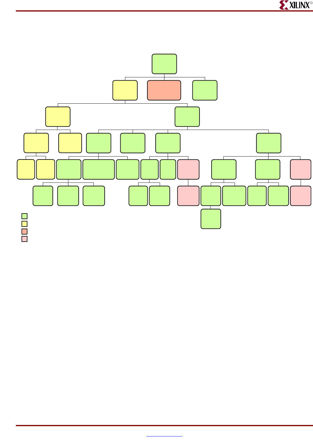
Memory Interface Solutions User Guide www.xilinx.com 131
UG086 (v3.6) September 21, 2010
Direct-Clocking Interface
R
Hierarchy
Figure 3-2 shows the hierarchical structure of the DDR2 SDRAM controller.
Figure 3-2 shows the hierarchical structure of the DDR2 SDRAM design generated by MIG
with a testbench and a DCM. The modules are classified as follows:
• Design modules
• Testbench modules
• Clocks and reset generation modules
There is a parameter file generated with the design that has all the user input and design
parameters selected from MIG.
MIG can generate four different DDR2 SDRAM designs:
• With a testbench and a DCM
• Without a testbench and with a DCM
• With a testbench and without a DCM
• Without a testbench and without a DCM
A design without a testbench (user_design) does not have testbench modules. The
<top_module> module has the user interface signals for designs without a testbench. The
list of user interface signals is provided in Table 3-9, page 142.
Figure 3-2: Hierarchical Structure of the DDR2 Design (Direct Clocking)
<top_
module>
main* idelayctrl
infrastructure*
iobs*data_
path*
user_
interface*
data_
path_iobs*
controller
_iobs*
infrastructure
_iobs*
ddr2_
controller*
decoder
_32/64
encoder
_32/64
v4_dq_
iob
Design Modules
v4_dm_
iob
RAM_D
v4_dqs_
iob
decoder*
backend
_fifos*
rd_wr_
addr_
fifo*
wr_data
_fifo
tap_
ctrl*
data_
tap_inc*
rd_data*
rd_data
_fifo*
pattern_
compare
encoder*
tap_
logic*
test_
bench* top*
Te st Bench Modules
DCM and Reset Generation Modules
ECC Modules
UG086_c3_03_091107
Note: A block with a * has a parameter file included.
cmp_rd_
data*
backend
_rom*
data_
gen
addr_
gen
data_
write*

132 www.xilinx.com Memory Interface Solutions User Guide
UG086 (v3.6) September 21, 2010
Chapter 3: Implementing DDR2 SDRAM Controllers
R
Design clocks and resets are generated in the infrastructure module. The DCM clock is
instantiated in the infrastructure module for designs with a DCM. The inputs to this
module are the differential design clock and a 200 MHz differential clock for the
IDELAYCTRL module. A user reset is also input to this module. Using the input clocks and
reset signals, the system clocks and the system reset are generated in this module, which is
used in the design.
The DCM primitive is not instantiated in this module if the Use DCM option is unchecked.
So, the system operates on the user-provided clocks. The system reset is generated in the
infrastructure module using the dcm_lock input signal.
For ECC enabled designs, the corresponding pink shaded modules are present in the
design. ECC data is generated from these modules.
MIG Tool Design Options for Direct-Clocking Interface
MIG provides various options to generate the design with or without a testbench or with
or without a DCM. This section provides detailed descriptions of the type of design
generated by the user using various options. Figure 3-3, page 133 and Figure 3-4, page 134
show the differential system clock. For more information on the clocking structure, refer to
“Direct-Clocking Interface Clocking Scheme,” page 140.
MIG outputs both an example_design and a user_design. The MIG-generated
example_design includes the entire memory controller design along with a synthesized
testbench (example user application). This testbench generates sample writes and reads
and then uses comparison logic to verify that the data patterns written are the same as
those received. This example_design can be used to test functionality both in simulation
and in hardware. The user_design includes the memory controller design only. This design
allows users to connect the MIG memory controller design to a user developed testbench
(user application). Refer to Table 3-9, page 142 for user interface signals, the “User
Interface Accesses,” page 143 for timing restriction on user interface signals, and
Figure 3-10, page 146 and Figure 3-11, page 147 for write interface timing.
Figure 3-3, page 133 shows a top-level block diagram of a DDR2 SDRAM design with a
DCM and a testbench. The sys_clk_p and sys_clk_n signals are differential input system
clocks. The DCM is instantiated in the infrastructure module that generates the required
design clocks. The differential clk200_p and clk200_n signals are used for the idelay_ctrl
element. The sys_reset_in_n is the active-Low system reset signal. All design resets are
gated by the dcm_lock signal. The error output signal indicates whether the case passes or
fails. The testbench module does writes and reads, and also compares the read data with
the written data. The error signal is driven High on data mismatches. The init_done signal
indicates the completion of initialization and calibration of the design. Memory device
signals are prepended with the controller number. For example, for a single controller
design, the ddr2_ras_n signal appears as cntrl0_ddr2_ras_n. Similarly, for a four-controller
design with controllers 0, 1, 2, and 3, the controller 3 ddr2_ras_n signal appears as
cntrl3_ddr2_ras_n.
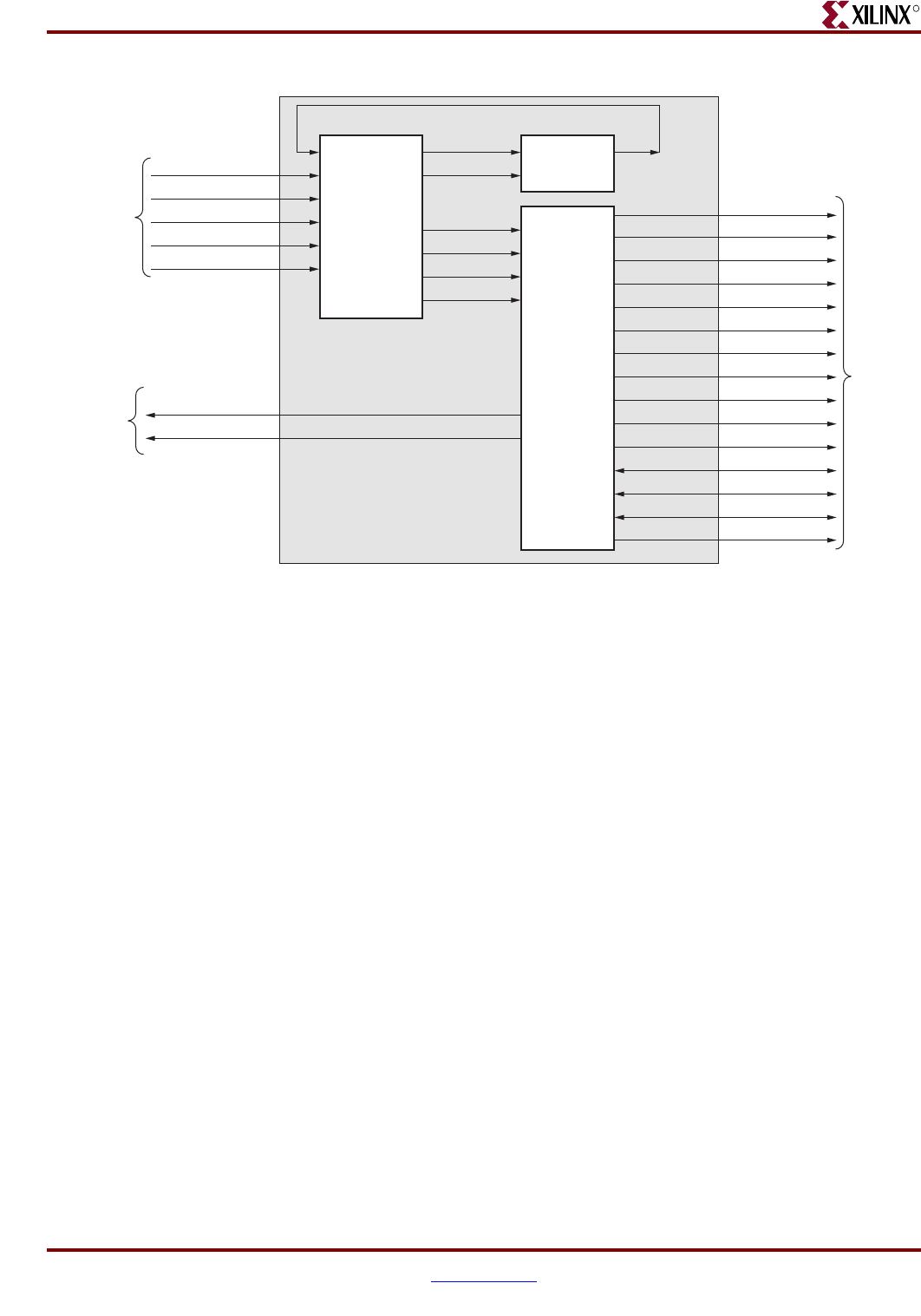
Memory Interface Solutions User Guide www.xilinx.com 133
UG086 (v3.6) September 21, 2010
Direct-Clocking Interface
R
All Memory Device ports do not necessarily appear for all MIG-generated designs. For
example, port ddr2_reset_n appears in the port list for Registered DIMM designs only.
Similarly, ddr2_dqs_n does not appear for single-ended DQS designs. Port DDR2_DM
appears only for parts that contain a data mask; a few RDIMMs have no data mask, and
DDR2_DM does not appear in the port list for them.
Figure 3-4 shows a top-level block diagram of a DDR2 SDRAM design with a DCM but
without a testbench. The sys_clk_p and sys_clk_n pair are differential input system clocks.
A DCM is instantiated in the infrastructure module that generates the required design
clocks. The differential clk200_p and clk200_n are used for the idelay_ctrl element. The
active-Low system reset signal is sys_reset_in_n. All design resets are gated by the
dcm_lock signal. The user has to drive the user application signals. The design provides
the CLK_TB and RESET_TB signals to the user to synchronize with the design. The
INIT_DONE signal indicates the completion of initialization and calibration of the design.
Figure 3-3: Top-Level Block Diagram of the DDR2 SDRAM Design with a DCM and a Testbench
main_0
idelay_ctrl_rdy
clk200
Memory
Device
UG086_c3_03_091508
Status
Signals
System
Clocks
and Reset
idelay_ctrl
Infrastructure
sys_rst200
clk_0
clk_90
sys_rst90
clk200_p
clk200_n
sys_clk_p
sys_clk_n
sys_reset_in_n sys_rst
ddr2_ras_n
ddr2_cas_n
ddr2_we_n
ddr2_cs_n
ddr2_odt
ddr2_cke
ddr2_dm
ddr2_ba
ddr2_a
ddr2_ck
ddr2_ck_n
ddr2_dq
ddr2_dqs
ddr2_reset_n
ddr2_dqs_n
error
init_done
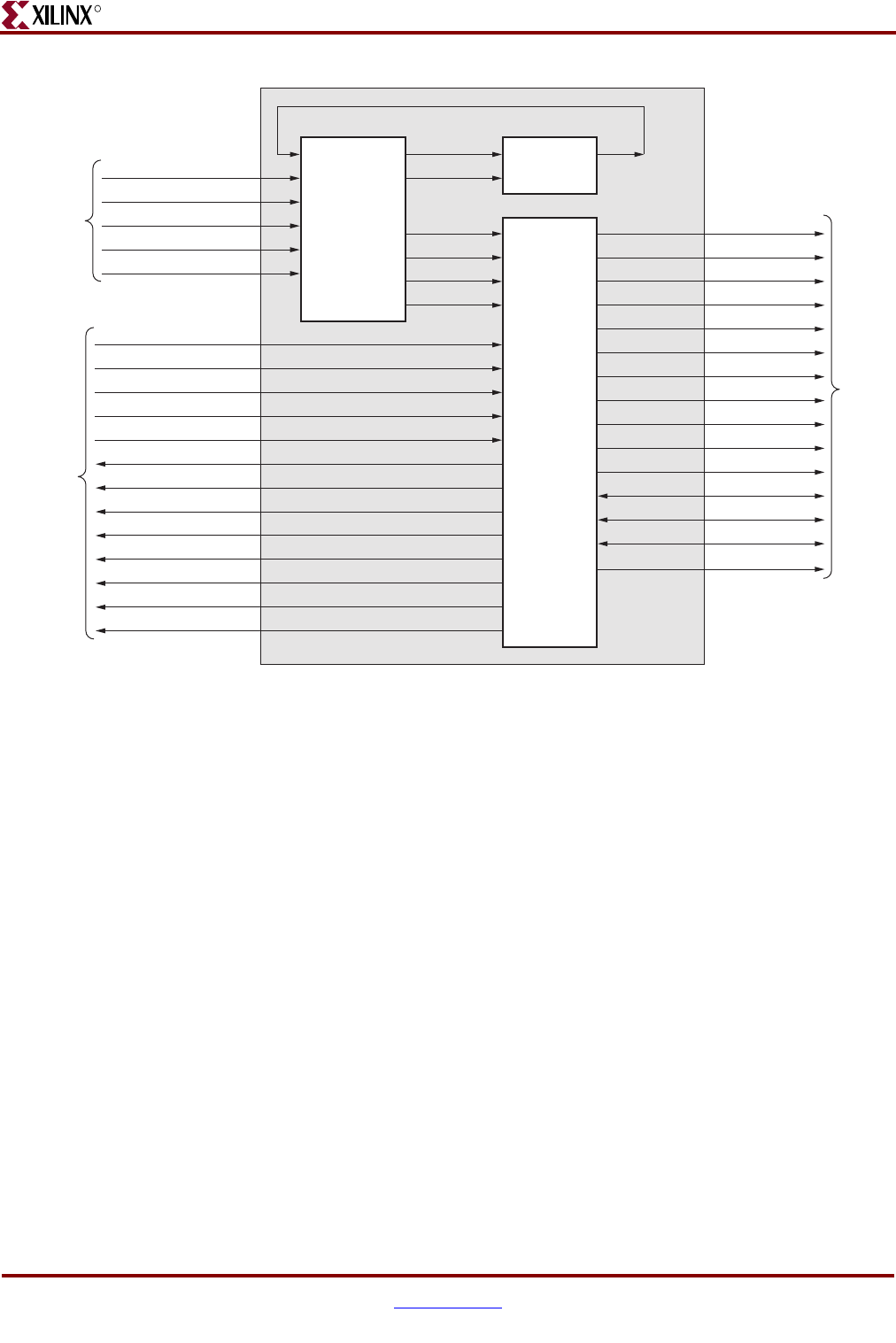
134 www.xilinx.com Memory Interface Solutions User Guide
UG086 (v3.6) September 21, 2010
Chapter 3: Implementing DDR2 SDRAM Controllers
R
Figure 3-4: Top-Level Block Diagram of the DDR2 SDRAM Design with a DCM but without a Testbench
top_0
idelay_ctrl_rdy
CLK200
Memory
Device
UG086_c3_04_091508
User
Application
System
Clocks
and Reset
idelay_ctrl
Infrastructure
sys_rst200
clk_0
clk_90
sys_rst90
clk200_p
clk200_n
sys_clk_p
sys_clk_n
sys_reset_in_n
app_af_addr
app_af_wren
app_wdf_data
app_mask_data
app_wdf_wren
wdf_almost_full
af_almost_full
burst_length_div2
read_data_valid
read_data_fifo_out
sys_rst
ddr2_ras_n
ddr2_cas_n
ddr2_we_n
ddr2_cs_n
ddr2_cke
ddr2_dm
ddr2_ba
ddr2_a
ddr2_ck
ddr2_ck_n
ddr2_dq
ddr2_dqs
ddr2_odt
ddr2_reset_n
ddr2_dqs_n
clk_tb
reset_tb
init_done
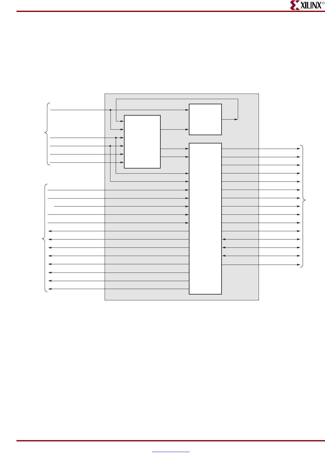
Memory Interface Solutions User Guide www.xilinx.com 135
UG086 (v3.6) September 21, 2010
Direct-Clocking Interface
R
Figure 3-5 shows a top-level block diagram of a DDR2 SDRAM design without a DCM or
a testbench. The user should provide all the clocks and the dcm_lock signal. These clocks
should be single-ended. The active-Low system reset signal is sys_reset_in_n. All design
resets are gated by the dcm_lock signal. The user application must have a DCM primitive
instantiated in the design. All user clocks should be driven through BUFGs. The user has to
drive the user application signals. The design provides the CLK_TB and RESET_TB signals
to the user to synchronize with the design. The INIT_DONE signal indicates the
completion of initialization and calibration of the design.
Figure 3-5: Top-Level Block Diagram of the DDR2 SDRAM Design without a DCM or a Testbench
top_0
idelay_ctrl_rdy
Memory
Device
UG086_c3_05_091508
System
Reset
and User
DCM
Clocks
idelay_ctrl
Infrastructure
sys_rst200
sys_rst
sys_rst90
clk_0
clk_200
clk_90
sys_reset_in_n
dcm_lock
ddr2_ras_n
ddr2_cas_n
ddr2_we_n
ddr2_cs_n
ddr2_odt
ddr2_cke
ddr2_dm
ddr2_ba
ddr2_a
ddr2_ck
ddr2_ck_n
ddr2_dq
ddr2_dqs
ddr2_dqs_n
ddr2_reset_n
User
Application
app_af_addr
app_af_wren
app_wdf_data
app_mask_data
app_wdf_wren
wdf_almost_full
af_almost_full
burst_length_div2
read_data_valid
read_data_fifo_out
clk_tb
reset_tb
init_done
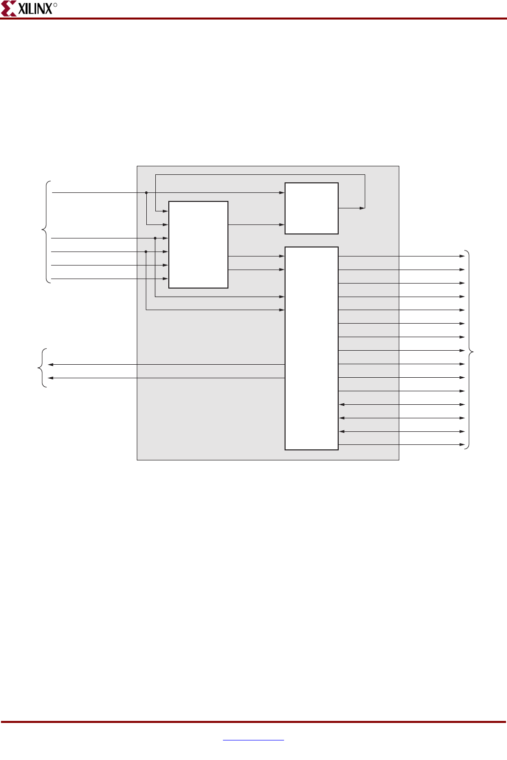
136 www.xilinx.com Memory Interface Solutions User Guide
UG086 (v3.6) September 21, 2010
Chapter 3: Implementing DDR2 SDRAM Controllers
R
Figure 3-6 shows a top-level block diagram of a DDR2 SDRAM design with a testbench but
without a DCM. The user should provide all the clocks and the dcm_lock signal. These
clocks should be single-ended. The active-Low system reset signal is sys_reset_in_n. All
design resets are gated by the dcm_lock signal. The user application must have a DCM
primitive instantiated in the design. All user clocks should be driven through BUFGs. The
ERROR output signal indicates whether the case passes or fails. The testbench module
does writes and reads, and also compares the read data with the written data. The ERROR
signal is driven High on data mismatches. The INIT_DONE signal indicates the
completion of initialization and calibration of the design.
Figure 3-6: Top-Level Block Diagram of the DDR2 SDRAM Design with a Testbench but without a DCM
main_0
idelay_ctrl_rdy
Memory
Device
UG086_c3_06_091508
Status
Signals
System
Reset
and User
DCM
Clocks
idelay_ctrl
Infrastructure
sys_rst200
sys_rst
sys_rst90
clk_0
clk_200
clk_90
sys_reset_in_n
dcm_lock
ddr2_ras_n
ddr2_cas_n
ddr2_we_n
ddr2_cs_n
ddr2_odt
ddr2_cke
ddr2_dm
ddr2_ba
ddr2_a
ddr2_ck
ddr2_ck_n
ddr2_dq
ddr2_dqs
ddr2_dqs_n
ddr2_reset_n
error
init_done
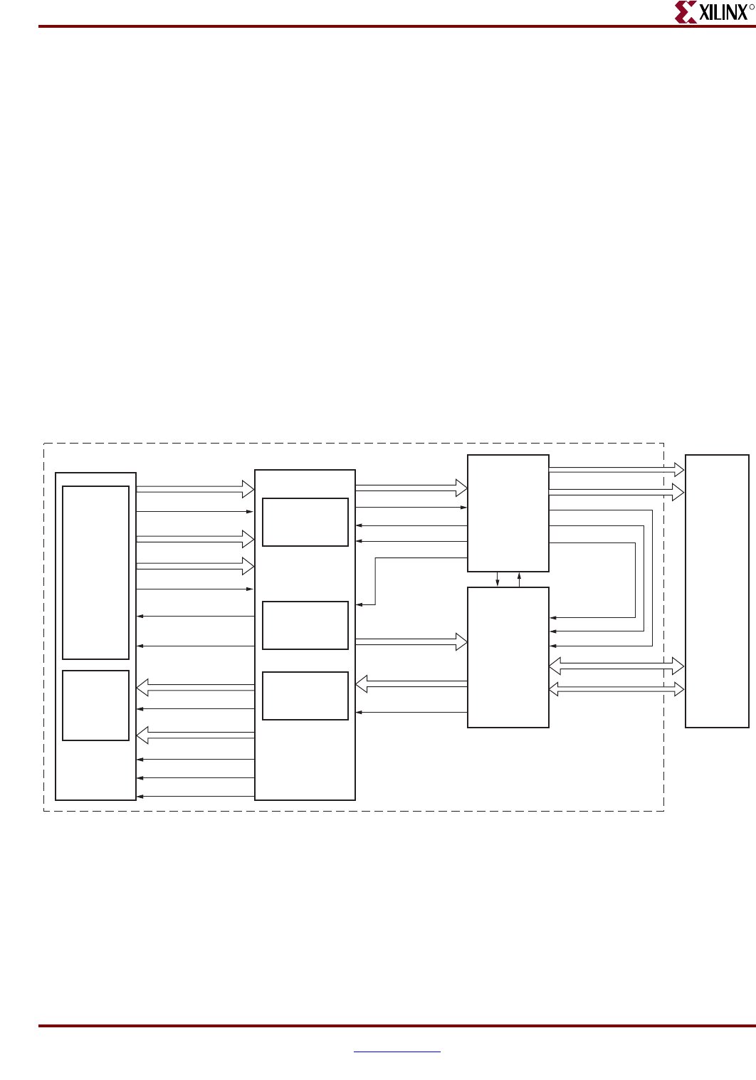
Memory Interface Solutions User Guide www.xilinx.com 137
UG086 (v3.6) September 21, 2010
Direct-Clocking Interface
R
DDR2 Controller Submodules
Infrastructure
The infrastructure module generates the FPGA clock and reset signals. When differential
clocking is used, sys_clk_p, sys_clk_n, clk_200_p, and clk_200_n signals appear. When
single-ended clocking is used, sys_clk and idly_clk_200 signals appear. In addition, clocks
are available for design use and a 200 MHz clock is provided for the IDELAYCTRL
primitive. Differential and single-ended clocks are passed through global clock buffers
before connecting to a DCM. For differential clocking, the output of the
sys_clk_p/sys_clk_n buffer is single-ended and is provided to the DCM input. Likewise,
for single-ended clocking, sys_clk is passed through a buffer and its output is provided to
the DCM input. The outputs of the DCM are clk_0 (0° phase-shifted version of the input
clock) and clk_90 (90° phase-shifted version of the input clock). After the DCM is locked,
the design is in the reset state for at least 25 clocks. The infrastructure module also
generates all of the reset signals required for the design.
Figure 3-7 is a detailed block diagram of the DDR2 SDRAM controller. The five blocks
shown are the subblocks of the top module. User backend signals are provided by the tool
for designs with a testbench. The user has to drive these signals for designs without a
testbench. The functions of these blocks are explained in the subsections following the
figure.
I
Controller
The DDR2 SDRAM ddr2_controller accepts and decodes user commands and generates
read, write, and refresh commands. The DDR2 SDRAM controller also generates signals
for other modules. The memory is initialized and powered-up using a defined process. The
controller state machine handles the initialization process upon power-up. After memory
initialization, the controller issues dummy read commands. During dummy reads, the
Figure 3-7: DDR2 Memory Controller Block Diagram
DDR2
SDRAM
Controller
Physical
Layer
Virtex-4 FPGA
DDR2
SDRAM
User Backend User Interface
Backend FIFOs
rd_en_delayed_rise/fall
ctrl_dummyread_start
af_empty
af_addr
app_af_addr
app_af_wren
wdf_data
UG086_c3_07_091508
ck/ck_n
dq
dqs
Read/Write
Address FIFO
Write Data
FIFOs
Read Data
FIFOs
Address
and Data
Generation
Read
Data
Compare
Module
af_almost_full
read_data_fifo_out
burst_length_div2
wdf_almost_full
read_data_valid
init_done
clk_tb
reset_tb
ctrl_waf_rden
ctrl_rden
phy_dly_slct_done
ctrl_wdf_rden
read_data_rise/fall
app_wdf_data
app_mask_data
app_wdf_wren
address/controls
ctrl_dqs_rst
ctrl_dqs_en
ctrl_wren

138 www.xilinx.com Memory Interface Solutions User Guide
UG086 (v3.6) September 21, 2010
Chapter 3: Implementing DDR2 SDRAM Controllers
R
tap_logic module calibrates and delays the data to center-align with the FPGA clock. After
the calibration is done, the controller issues a dummy write and pattern read commands to
get the delay between the read command and IOB output data.
The delay, calculated in number of clocks, is used as a write-enable signal to the read data
FIFOs. For deep designs, the DQ calibration and pattern calibration are done only on the
last memory. For example, for four deep designs, the fourth memory is used for
calibration. There is no reason to use the fourth memory because the controller retains the
last chip select during initialization of memory. Thus the same chip select is used for
calibration. XAPP701 [Ref 18] provides more details about the calibration architecture.
User Interface
This module stores write data, write addresses, and read addresses in FIFOs and receives
read data from the memory. The rd_data and rd_data_fifos modules capture the data in the
LUT-based RAMs. The rd_wr_addr_fifo and wr_data_fifo modules store the data and
address in block RAMs. The FIFOs are built using FIFO16 primitives in rd_wr_addr_fifo,
wr_data_fifo_16, and wr_data_fifo_8 modules. Each FIFO has two FIFO threshold
attributes, ALMOST_EMPTY_OFFSET and ALMOST_FULL_OFFSET, that are set to 7 and
F, respectively, in the RTL by default. These values can be changed as needed. For valid
FIFO threshold offset values, refer to UG070 [Ref 7].
Once the calibration is done, the controller issues a pattern_write command with a known
pattern (0xAA559966) to the memory. Then the controller issues a pattern_read command
from the same location and compares the read data with the known pattern in the
pattern_compare8 or the pattern_compare4 module. During the pattern_read command,
the controller generates the ctrl_rden signal, which is delayed in the pattern_compare
module to synchronize with the read data. This delay is applied to the ctrl_rden signal
generated from the ddr2_controller module during a normal read to register the valid data
in the internal FIFOs.
The FIRST_RISING logic is implemented in the pattern_compare module. FIRST_RISING
is asserted when the first data is captured with respect to the falling edge of FPGA clock.
This signal is used in rd_data_fifo to swap rise and fall data. In addition to the ODDR used
to register output data (DQ) in each I/O, a second ODDR in the IOB controls the 3-state
enable for the I/O. This is used to enable the write data output one-half clock cycle before
the first data word and disable the write data one-half clock cycle after the last data word.
Test Bench
The MIG tool generates two RTL folders, example_design and user_design. The
example_design folder includes the synthesizable test bench, while user_design does not
include the test bench modules. The MIG test bench performs eight write commands and
eight read commands in an alternating fashion. The number of words in a write command
depends on the burst length. For a burst length of 4, the test bench writes a total of 32 data
words for all eight write commands (16 rise data words and 16 fall data words). For a burst
length of 8, the test bench writes a total of 64 data words. It writes the data pattern of FF,
00, AA, 55, 55 AA, 99, 66 in a sequence of which FF, AA, 55, and 99 are rise data words and
00, 55, AA, and 66 are fall data words for an 8-bit design. The falling edge data is the
complement of the rising edge data. For a burst length of 4, the data sequence for the first
write command is FF, 00, AA, 55, and the data sequence for the second write command is
55, AA, 99, 66. For a burst length of 8, the data pattern for the first write command is FF,
00, AA, 55, 55 AA, 99, 66 and the same pattern is repeated for all the remaining write
commands. This data pattern is repeated in the same order based on the number of data
words written. For data widths greater than 8, the same data pattern is concatenated for
the other bits. For a 32-bit design and a burst length of 8, the data pattern for the first write

Memory Interface Solutions User Guide www.xilinx.com 139
UG086 (v3.6) September 21, 2010
Direct-Clocking Interface
R
command is FFFFFFFF, 00000000, AAAAAAAA, 55555555, 55555555, AAAAAAAA,
99999999, 66666666.
Address generation logic generates eight different addresses for eight write commands.
The same eight address locations are repeated for the following eight read commands. The
read commands are performed at the same locations where the data is written. There are
total of 32 different address locations for 32 write commands, and the same address
locations are generated for 32 read commands. Upon completion of a total of 64
commands, including both writes and reads (eight writes and eight reads repeated four
times), address generation rolls back to the first address of the first write command and the
same address locations are repeated. The MIG test bench exercises only a certain memory
area. The address is formed such that all address bits are exercised. During writes, a new
address is generated for every burst operation on the column boundary.
During reads, comparison logic compares the read pattern with the pattern written, i.e., the
FF, 00, AA, 55, 55 AA, 99, 66 pattern. For example, for an 8-bit design of burst length 4, the
data written for a single write command is FF, 00, AA, 55. During reads, the read pattern is
compared with the FF, 00, AA, 55 pattern. Based on a comparison of the data, a status
signal error is generated. If the data read back is the same as the data written, the error
signal is 0, otherwise it is 1. Comparison logic only compares the data bits and not the ECC
data pattern. For example, for a 72-bit ECC design, comparison logic only compares
64 bits. The 8 MSBs (ECC bits) are not compared.
Infrastructure
The infrastructure module generates the FPGA clock and reset signals. When differential
clocking is used, sys_clk_p, sys_clk_n, clk_200_p, and clk_200_n signals appear. When
single-ended clocking is used, sys_clk and idly_clk_200 signals appear. In addition, clocks
are available for design use and a 200 MHz clock is provided for the IDELAYCTRL
primitive. Differential and single-ended clocks are passed through global clock buffers
before connecting to a DCM. For differential clocking, the output of the
sys_clk_p/sys_clk_n buffer is single-ended and is provided to the DCM input. Likewise,
for single-ended clocking, sys_clk is passed through a buffer and its output is provided to
the DCM input. The outputs of the DCM are clk_0 (0° phase-shifted version of the input
clock) and clk_90 (90° phase-shifted version of the input clock). After the DCM is locked,
the design is in the reset state for at least 25 clocks. The infrastructure module also
generates all of the reset signals required for the design.
Idelay_ctrl
This module instantiates the IDELAYCTRL primitive of the Virtex-4 FPGA. The
IDELAYCTRL primitive is used to continuously calibrate the individual delay elements in
its region to reduce the effect of process, temperature, and voltage variations. A 200 MHz
clock has to be fed to this primitive. For more information on IDELAYCTRLs, refer to
“Verify IDELAYCTRL Instantiation for Virtex-4 and Virtex-5 FPGA Designs” in Chapter
14.
DDR2 SDRAM Initialization and Calibration
DDR2 memory is initialized through a specified sequence as per both Micron and JEDEC
specifications. The controller starts the memory initialization at power-up. Following the
initialization, the relationship between the data and the FPGA clock is calculated using the
tap_logic. The controller issues a dummy write command and a dummy read command to
the memory and compares read data with the fixed pattern. During dummy reads, the
tap_logic module calibrates and delays the data to center-align with the FPGA clock.
XAPP701 [Ref 18] provides more details about the calibration architecture.

140 www.xilinx.com Memory Interface Solutions User Guide
UG086 (v3.6) September 21, 2010
Chapter 3: Implementing DDR2 SDRAM Controllers
R
The sel_done port in the tap_logic module indicates the completion of the per-bit
calibration. After the per-bit calibration is done, the controller does a read enable
calibration. This calibration is used to determine the delay from read command to read
data at rd_data_fifo. The delay between read command and read data is affected by the
CAS latency and additive latency parameters, the PCB traces, and the I/O buffer delays.
This in turn is used to generate a write enable to rd_data_fifo so that valid data is
registered. The controller writes a known fixed pattern and reads back the data. The read
data is compared against the known fixed pattern. The comp_done port in the rd_data
module indicates the completion of the read enable calibration.
The init_done port indicates the completion of both per-bit calibration and read enable
calibration. After initialization and calibration is done, the controller can start issuing user
commands to the memory.
Direct-Clocking Interface Clocking Scheme
Figure 3-8, page 141 shows the clocking scheme for this design. Global and local clock
resources are used.
The global clock resources consist of a DCM, two BUFGs on DCM output clocks, and one
BUFG for clk_200. The local clock resources consist of regional I/O clock networks
(BUFIO). The global clock architecture is discussed in this section.
The MIG tool allows the user to customize the design such that the DCM is not included.
In this case clk_0, clk_90 and IDELAYCTRL clock clk_200 must be supplied by the user.
Global Clock Architecture
The user must supply two input clocks to the design:
• A system clock running at the target frequency for the memory
• A 200 MHz clock for the IDELAYCTRL blocks
These clocks can be either single ended or differential. User can select single-ended or
differential clock input option from MIG GUI. Differential clocks are connected to the
IBUFGDS and single ended clock is connected to IBUFG.
The system clock from the output of the IBUFGDS or the IBUFG is connected to the DCM
to generate the various clocks used by the memory interface logic.
The clk_200 output of the IBUFGDS or the IBUFG is connected to the BUFG. The output of
the BUFG is used for IDELAY IOB delay blocks for aligning read capture data.
The DCM generates two separate synchronous clocks for use in the design. This is shown
in Table 3-6, page 141 and Figure 3-8, page 141. The clock structure is same for both
example design and user design. For designs with out DCM instantiation, DCM and the
BUFGs should be instantiated at user end to generate the required clocks.
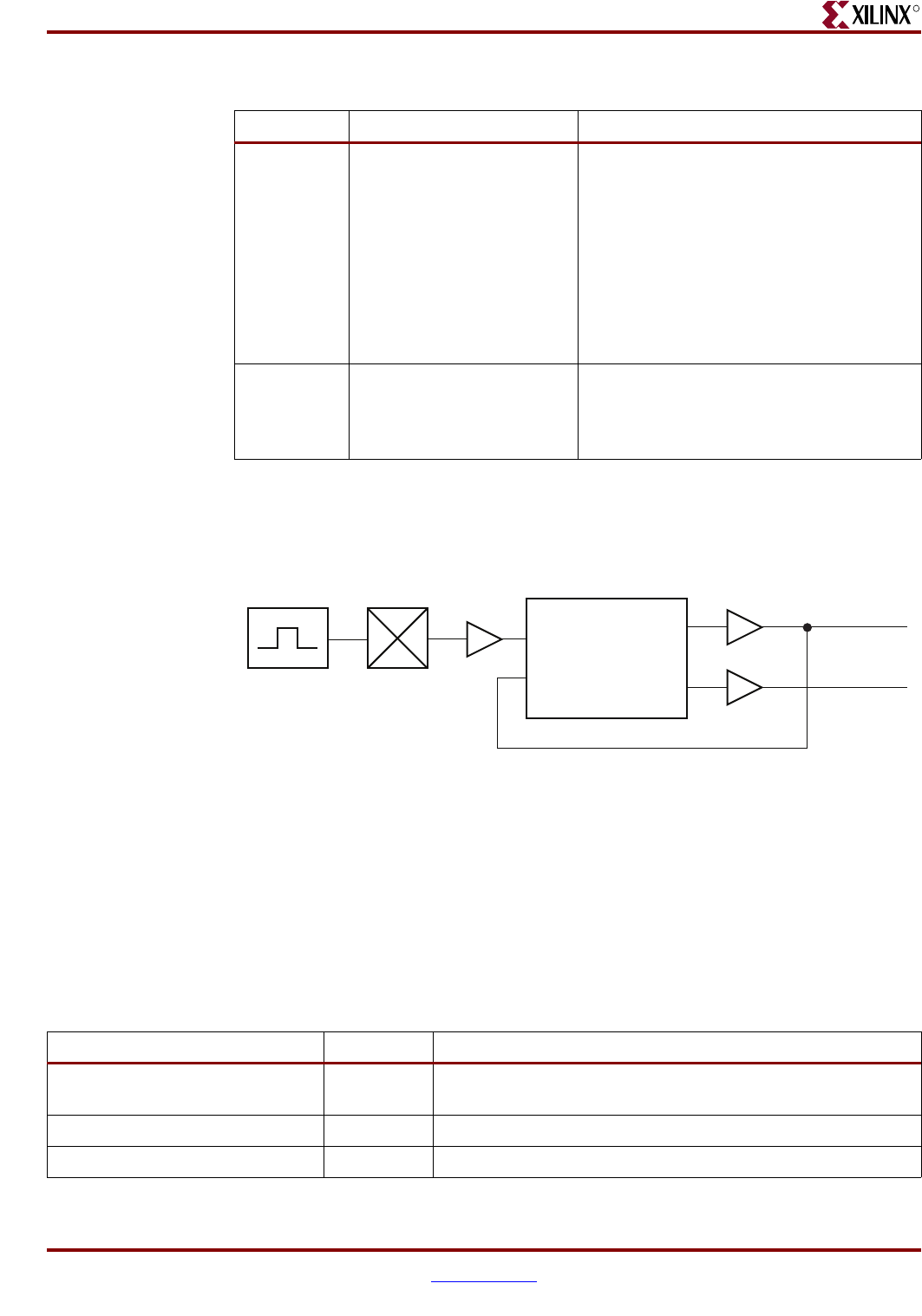
Memory Interface Solutions User Guide www.xilinx.com 141
UG086 (v3.6) September 21, 2010
Direct-Clocking Interface
R
DDR2 SDRAM System and User Interface Signals
Table 3-7 describes the DDR2 SDRAM system interface signals. The system interface
signals are the clocks and the reset signals given by the user to the FPGA. The sys_clk_p
and sys_clk_n pair are the two clocks provided to the design. They must have a phase
difference of 180° with respect to each other. Similarly, clk200_p and clk_200N are 200 MHz
differential clocks for the IDELAYCTRL module. The sys_reset_in_n signal resets all the
logic.
Table 3-6: DDR2 Interface Design Clocks
Clock Description Logic Domain
clk_0 Skew compensated replica
of the input system clock.
The clock for the controller and the user
interface logic, most of the DDR2 bus-
related I/O flip-flops (e.g., memory clock,
control/address, output DQS strobe, and
DQ input capture). This is used to register
the data, address, and command signals,
and the address and data enables for the
user interface logic(1). This clock is also
used to generate read data, read data valid,
and FIFO status signals.
clk90_0 90° phase-shifted version of
CLK0.
Used in the write data path section of
physical layer. Clocks write path control
logic, DDR2 side of the Write Data FIFO,
and output flip-flops for DQ.
Notes:
1. See “User Interface Accesses,” page 143 for timing requirements and restrictions on the user interface
signals.
Figure 3-8: Clocking Scheme for DDR2 Interface Logic
ug086_c3_13_072108
DCM
System Clock GC I/O
CLK0
CLK_IN
CLK_FB
BUFG
BUFG
CLK90
clk_0
clk_90
Table 3-7: DDR2 SDRAM Controller System Interface Signals (with a DCM)
Signal Name Direction Description
sys_clk_p, sys_clk_n Input Differential input clock to the DCM. The DDR2 controller and
memory operate at this frequency.
clk200_p, clk200_n Input Differential clock used in the idelay_ctrl logic.
sys_reset_in_n Input Active-Low reset to the DDR2 controller.
142 www.xilinx.com Memory Interface Solutions User Guide
UG086 (v3.6) September 21, 2010
Chapter 3: Implementing DDR2 SDRAM Controllers
R
Table 3-8 shows the system interface signals for designs without a DCM. clk_0, clk_90, and
clk_200 are single-ended input clocks. The clk_90 signal must have a phase difference of
90° with respect to clk_0. The clk_200 signal is the clock used for the IDELAYCTRL
primitives in Virtex-4 FPGAs.
Table 3-9 describes the DDR2 SDRAM user interface signals.
Table 3-8: DDR2 SDRAM Controller System Interface Signals (without a DCM)
Signal Direction Description
clk_0 Input The DDR2 SDRAM controller and memory operates on this clock.
sys_reset_in_n Input Active-Low reset to the DDR2 SDRAM controller. This signal is used to
generate the synchronous system reset.
clk_90 Input 90° phase-shifted clock with the same frequency as clk0.
clk_200 Input 200 MHz differential input clock for the IDELAYCTRL primitive of Virtex-4
FPGAs.
dcm_lock Input This status signal indicates whether the DCM is locked or not. It is used to
generate the synchronous system reset.
Table 3-9: DDR2 SDRAM Controller User Interface Signals
Signal Name(1) Direction Description
CLK_TB Output All user interface signals must be synchronized with respect to
CLK_TB.
RESET_TB Output Reset signal for the User Interface.
BURST_LENGTH_DIV2[2:0] Output This signal determines the data burst length for each write
address.
010: burst length = 4
100: burst length = 8
WDF_ALMOST_FULL Output This signal indicates the ALMOST_FULL status of the Write
Data FIFO. When this signal is asserted, the user can write
5 more locations into the FIFO in designs generated with a
testbench and 14 more locations in designs without a testbench.
APP_WDF_DATA[2n-1:0] Input User write data to the memory, where n indicates the data width
of the interface. The user data is twice the data width of the
interface. The most-significant bits contain the rising-edge data
and the least-significant bits contain the falling-edge data.
APP_MASK_DATA[2m-1:0] Input User mask data to the memory, where m indicates the data mask
width of the interface. The mask data is twice the mask width of
the interface. The most-significant bits contain the rising-edge
mask data and the least-significant bits contain the falling-edge
mask data. These signals are not present when the memory part
does not have mask support (for example, certain Registered
DIMMs) or when the data mask option is not selected in the
MIG GUI.
APP_WDF_WREN Input Write Enable signal to the Write Data FIFO.
AF_ALMOST_FULL Output This signal indicates the ALMOST_FULL status of the Address
FIFO. The user can issue eight more locations into the FIFO after
AF_ALMOST_FULL is asserted.
Memory Interface Solutions User Guide www.xilinx.com 143
UG086 (v3.6) September 21, 2010
Direct-Clocking Interface
R
User Interface Accesses
The user backend logic communicates with the memory controller through a FIFO-based
user interface. This interface consists of three related buses:
• A Command/Address FIFO bus, which accepts write/read commands as well as the
corresponding memory address from the user
• A Write Data FIFO bus, which accepts the corresponding write data when the user
issues a write command on the Command/Address bus
• A Read bus on which the corresponding read data for an issued read command is
returned
The user interface has the following timing and signaling restrictions:
• Commands and write data cannot be written by the user until calibration is complete
(as indicated by INIT_DONE). In addition, the following interface signals need to be
held Low until calibration is complete: APP_AF_WREN, APP_WDF_WREN,
APP_WDF_DATA, and APP_MASK_DATA. Failure to hold these signals Low causes
errors during calibration. This restriction arises from the fact that the Write Data FIFO
APP_AF_ADDR[35:0](2) Input The user address consists of a memory address and dynamic
commands. Bits [31:0] are the memory read/write address. Bits
[31:0] form the memory chip select, bank address, row address,
and column address.
Bit 35 is reserved for internal use of the controller. Bits [34:32]
represent the following dynamic commands:
001: Auto Refresh
010: Precharge
100: Write
101: Read
Other combinations are invalid. Functionality of the controller is
unpredictable for unimplemented commands.
APP_AF_WREN Input Write Enable signal to the Address FIFO.
READ_DATA_FIFO_OUT[2n-1:0] Output Read data from the memory, where n indicates the data width of
the interface. The most-significant bits of the read data consist of
the rising-edge data and the least-significant bits consist of the
falling-edge data.
READ_DATA_VALID Output This signal is asserted to indicate the read data is available to the
user.
INIT_DONE Output This signal indicates the completion of initialization and
calibration of the design.
Notes:
1. All user interface signal names are prepended with a controller number. DDR2 SDRAM devices support multicontroller operation,
where a maximum of eight controllers can be selected by the user from MIG. For example, when the user selects eight controllers,
the signal names have the following format: cntrl0_user_signal, cntrl1_user_signal, cntrl2_user_signal, cntrl3_user_signal,
cntrl4_user_signal, cntrl5_user_signal, cntrl6_user_signal, and cntrl7_user_signal. See “User Interface Accesses” for timing
requirements and restrictions on the user interface signals.
2. Linear addressing is used, i.e., the row address immediately follows the column address bits, and the bank address follows the row
address bits, thus supporting more devices. The number of address bits used depends on the density of the memory part. The
controller ignores the unused bits, which can all be tied High.
Table 3-9: DDR2 SDRAM Controller User Interface Signals (Cont’d)
Signal Name(1) Direction Description
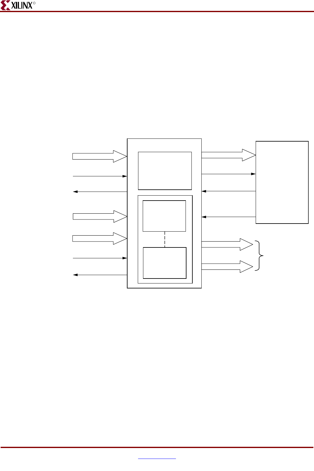
144 www.xilinx.com Memory Interface Solutions User Guide
UG086 (v3.6) September 21, 2010
Chapter 3: Implementing DDR2 SDRAM Controllers
R
is used during calibration to hold the training patterns for the various stages of
calibration.
• When issuing a write command, the first write data word must be written to the Write
Data FIFO no more than two clock cycles after the write command is issued. This
restriction arises from the fact that the controller assumes write data is available when
it receives the write command from the user.
• The clk_tb signal is connected to clk_0 in the controller. If the user clock domain is
different from clk_0 / clk_tb of the MIG, the user should add FIFOs for all data inputs
and outputs of the controller in order to synchronize them to the clk_tb.
Write Interface
Figure 3-9 shows the user interface block diagram for write operations.
The following steps describe the architecture of the Address and Write Data FIFOs and
show how to perform a write burst operation to DDR2 SDRAM from the user interface.
1. The user interface consists of an Address FIFO and a Write Data FIFO. These FIFOs are
constructed using Virtex-4 FPGA FIFO16 primitives with a 512 x 36 configuration. The
36-bit architecture comprises one 32-bit port and one 4-bit port. For Write Data FIFOs,
the 32-bit port is used for data bits and the 4-bit port is used for mask bits. Mask bits
are available only when supported by the memory part and when data mask is enabled
in the MIG GUI. Some memory parts, such as Registered DIMMs of x4 parts, do not
support mask bits.
2. The Common Address FIFO is used for both write and read commands, and comprises
a command part and an address part. Command bits discriminate between write and
read commands.
3. User interface data width app_wdf_data is twice that of the memory data width. For
an 8-bit memory width, the user interface is 16 bits consisting of rise data and fall data.
Figure 3-9: User Interface Block Diagram for Write Operations
User Interface
Controller
Address FIFO
(FIFO16)
512 x 36
af_addr
af_empty
ctrl_af_rden
ctrl_wdf_rden
app_af_addr
app_af_wren
app_wdf_data
app_mask_data
app_wdf_wren
wdf_data
mask_data
To Phy Layer
wdf_almost_full
af_almost_full
Write Data
FIFO
(FIFO16)
512 x 36
Write Data
FIFO
(FIFO16)
512 x 36
ug086_c3_26_110707

Memory Interface Solutions User Guide www.xilinx.com 145
UG086 (v3.6) September 21, 2010
Direct-Clocking Interface
R
For every 8 bits of data, there is a mask bit. For 72-bit memory data, the user interface
data width app_wdf_data is 144 bits, and the mask data app_mask_data is 18 bits.
4. The minimum configuration of the Write Data FIFO is 512 x 36 for a memory data
width of 8 bits. For an 8-bit memory data width, the least-significant 16 bits of the data
port are used for write data and the least-significant two bits of the 4-bit port are used
for mask bits. The controller internally pads all zeros for the most-significant 16 bits of
the 32-bit port and the most-significant two bits of the 4-bit port.
5. Depending on the memory data width, MIG instantiates multiple FIFO16s to gain the
required width. For designs using 8-bit data width, one FIFO16 is instantiated; for
72-bit data width, a total of five FIFO16s are instantiated. The bit architecture
comprises 16 bits of rising-edge data, 2 bits of rising-edge mask, 16 bits of falling-edge
data, and 2 bits of falling-edge mask, which are all stored in a FIFO16. MIG routes the
app_wdf_data and app_mask_data to FIFO16s accordingly.
6. The user can initiate a write to memory by writing to the Address FIFO and the Write
Data FIFO when the FIFO Full flags are deasserted and after the init_done signal is
asserted. Status signal af_almost_full is asserted when Address FIFO is full, and
similarly wdf_almost_full is asserted when Write Data FIFO is full.
7. Both the Address FIFO and Write Data FIFO Full flags are deasserted with power-on.
8. The user should assert the Address FIFO write-enable signal app_af_wren along with
address app_af_addr to store the write address and write command into the Address
FIFO.
9. The user should assert the Data FIFO write-enable signal app_wdf_wren along with
write data app_wdf_data and mask data app_mask_data to store the write data and
mask data into the Write Data FIFO. The user should provide both rise and fall data
together for each write to the Data FIFO.
10. The controller reads the Address FIFO by issuing the ctrl_af_rden signal. The
controller reads the Write Data FIFO by issuing the ctrl_wdf_rden signal after the
Address FIFO is read. It decodes the command part after the Address FIFO is read.
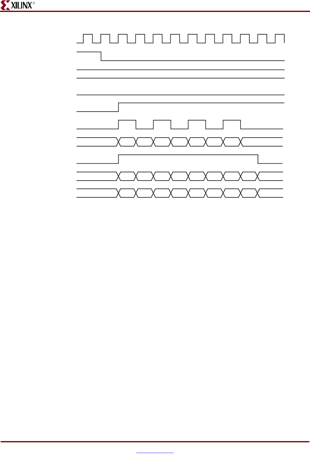
146 www.xilinx.com Memory Interface Solutions User Guide
UG086 (v3.6) September 21, 2010
Chapter 3: Implementing DDR2 SDRAM Controllers
R
11. The write command timing diagram in Figure 3-10 is derived from the MIG-generated
testbench. As shown (burst length of 4), each write to the Address FIFO must be
coupled with two writes to the Data FIFO. Similarly, for a burst length of 8, every write
to the Address FIFO must be coupled with four writes to the Data FIFO. Failure to
follow this rule can cause unpredictable behavior.
Note: The user can start filling the Write Data FIFO two clocks after the Address FIFO is
written, because there is a two-clock latency between the command fetch and reading the Data
FIFO. Using the terms shown in Figure 3-11, therefore, the user can assert the A0 address two
clocks before D0D1.
Figure 3-10: DDR2 SDRAM Write Burst (BL = 4) for Four Bursts
init_done
clk_tb
reset_tb
wdf_almost_full
burst_length_div2[2:0] 3’b010 (BL = 4)
app_af_wren
app_af_addr[35:0]
app_wdf_wren
A
0
app_wdf_data[2n-1:0] D
0
D
1
D
2
D
3
D
4
D
5
D
6
D
7
D
8
D
9
D
10
D
11
D
12
D
13
D
14
D
15
app_mask_data[2m-1:0] M
0
M
1
M
2
M
3
M
4
M
5
M
6
M
7
M
8
M
9
M
10
M
11
M
12
M
13
M
14
M
15
A
1
A
2
A
3
UG086_c3_08_091508
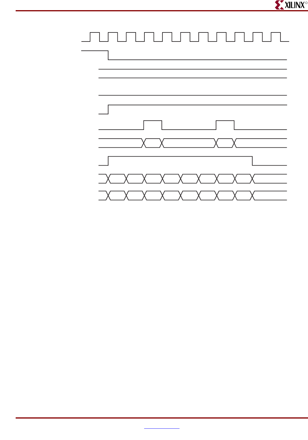
Memory Interface Solutions User Guide www.xilinx.com 147
UG086 (v3.6) September 21, 2010
Direct-Clocking Interface
R
12. The write command timing diagram in Figure 3-11 is derived from the MIG-generated
testbench. As shown (burst length of 8), each write to the Address FIFO must be
coupled with four writes to the Data FIFO. Because the controller first reads the
address and command together, the address need not coincide with the last data. After
the command is analyzed (nearly two clocks later for a worst-case timing scenario), the
controller sequentially reads the data in four clocks. Thus, there are six clocks from the
time the address is read to the time the last data is read.
Correlation between the Address and Data FIFOs
There is a worst-case two-cycle latency from the time the address is loaded into the address
FIFO on APP_AF_ADDR[35:0] to the time the controller decodes the address. Because of
this latency, it is not necessary to provide the address on the last clock where data is
entered into the data FIFO. If the address is written before the last data phase, the overall
efficiency and performance increases because it eliminates or reduces the two-cycle
latency. However, if the address is written before data is input into the data FIFO, a FIFO
empty condition might result because the Data FIFO does not contain valid data.
Based on these considerations, Xilinx recommends entering the address into the address
FIFO between the first data phase and the next-to-last data phase. For a burst of four or
eight, this means the Address can be asserted two clocks before the first data phase. This
implementation increases efficiency by reducing the two clock latency and guarantees that
valid data is available in the Data FIFO.
Figure 3-11: DDR2 SDRAM Write Burst (BL = 8) for Two Bursts
clk_tb
reset_tb
wdf_almost_full
burst_length_div2[2:0] 3’b100 (BL = 8)
app_af_wren
app_af_addr[35:0]
app_wdf_wren
init_done
A0
D0D1D2D3D4D5D6D7D8D9D10D11 D12D13D14D15
app_mask_data[2m-1:0]
app_wdf_data[2n-1:0]
M
0M
1M
2M
3M
4M
5M
6M
7M
8M
9M
10M
11 M
12M
13M
14M
15
A1
UG086_c3_09_091508
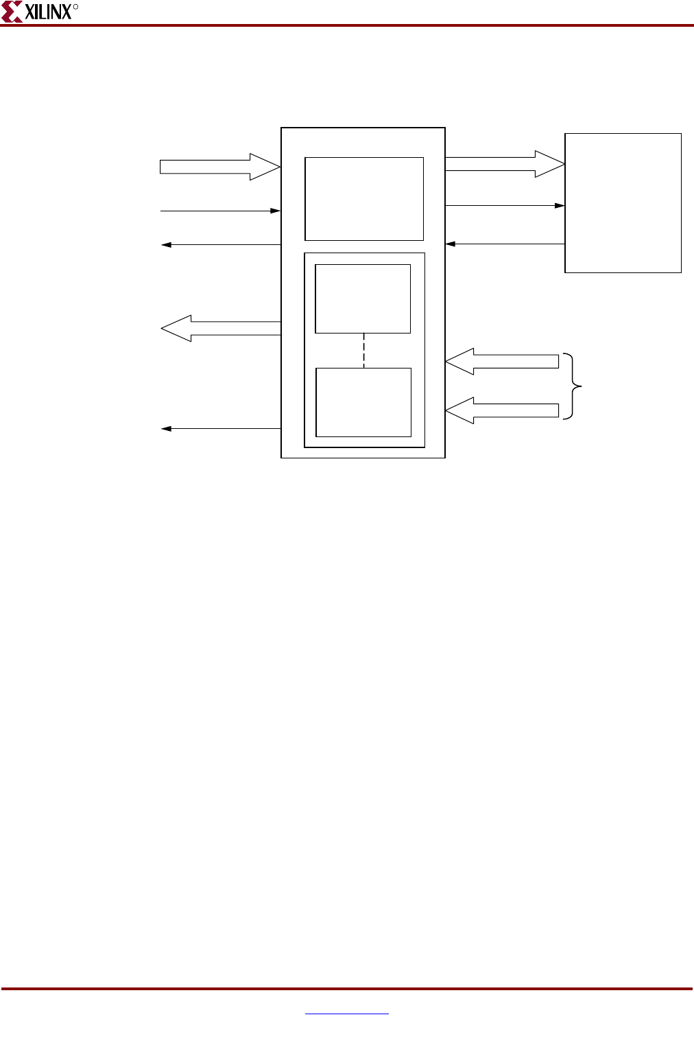
148 www.xilinx.com Memory Interface Solutions User Guide
UG086 (v3.6) September 21, 2010
Chapter 3: Implementing DDR2 SDRAM Controllers
R
Read Interface
Figure 3-12 shows a block diagram of the read interface.
The following steps describe the architecture of the Read Data FIFOs and show how to
perform a burst read operation from DDR SDRAM from the user interface.
1. The read user interface consists of an Address FIFO and a Read Data FIFO. The
Address FIFO is common to both read and write operations. The Read Data FIFOs are
constructed using Virtex-4 FPGA Distributed RAMs with a 16 x 1 configuration. MIG
instantiates a number of RAM16Ds depending on the data width. For example, for
8-bit data width, MIG instantiates a total of 16 RAM16Ds, 8 for rising-edge data and 8
for falling-edge data. Similarly, for 72-bit data width, MIG instantiates a total of 144
RAM16Ds, 72 for rising-edge data and 72 for falling-edge data.
2. The user can initiate a read to memory by writing to the Address FIFO when the
FIFO Full flag af_almost_full is deasserted and after init_done is asserted.
3. To write the read address and read command into the Address FIFO, the user should
issue the Address FIFO write-enable signal app_af_wren along with read address
app_af_addr.
4. The controller reads the Address FIFO containing the address and command. After
decoding the command, the controller generates the appropriate control signals to
memory.
5. Prior to the actual read and write commands, the design calibrates the latency (number
of clock cycles) from the time the read command is issued to the time data is received.
Using this pre-calibrated delay information, the controller generates the write-enable
signals to the Read Data FIFOs.
6. The read_data_valid signal is asserted when data is available in the Read Data FIFOs.
Figure 3-12: User Interface Block Diagram for Read Operation
User Interface
Controller
Address FIFO
(FIFO16)
512 x 36
af_addr
af_empty
ctrl_af_rden
app_af_addr
app_af_wren
read_data_fifo_out
read_data_rise
read_data_fall From Phy Layer
read_data_valid
af_almost_full
Read Data
FIFO
RAM16 x 1D
Read Data
FIFO
RAM16 x 1D
ug086_c3_27_110607
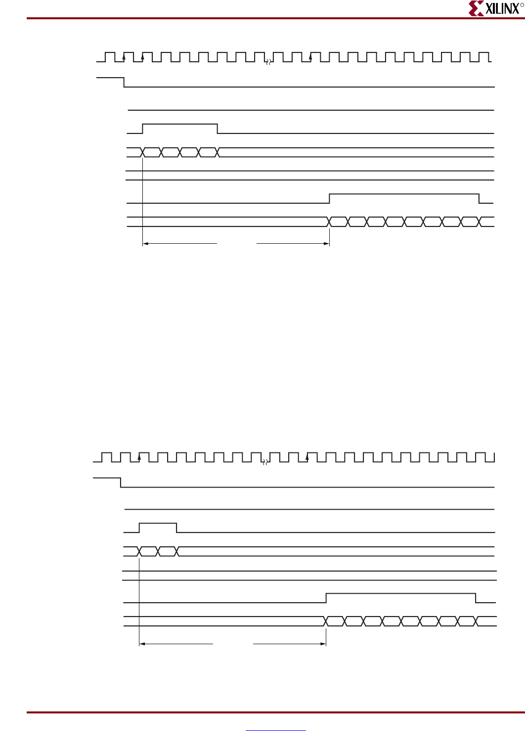
Memory Interface Solutions User Guide www.xilinx.com 149
UG086 (v3.6) September 21, 2010
Direct-Clocking Interface
R
7. Figure 3-13 shows the user interface timing diagram for a burst length of 4, and
Figure 3-14 shows the user interface timing diagram for a burst length of 8. Both the
cases shown here are for a CAS latency of 3 at 200 MHz. The read latency is calculated
from the point when the read command is given by the user to the point when the data
is available with the read_data_valid signal. The minimum latency in this case is
25 clocks, where no precharge is required, no auto-refresh request is pending, the user
commands are issued after initialization is completed, and the first command issued is
a Read command. Controller executes the commands only after initialization is done
as indicated by the init_done signal.
8. After the address and command are loaded into the Address FIFO, it takes 25 clock
cycles minimum for the controller to assert the read_data_valid signal.
9. Read data is available only when the read_data_valid signal is asserted. The user
should access the read data on every positive edge of the read_data_valid signal.
Figure 3-13: DDR2 SDRAM Read Burst (BL = 4) for Four Bursts
clk_tb
af_almost_full
app_af_wren
reset_tb
app_af_addr[35:0]
burst_length_div2[2:0]
read_data_valid
read_data_fifo_out[2n-1:0]
25 clocks
D0D1D2D3D4D5D6D7D8D9D10D11 D12D13D14D15
UG086_c3_10_091508
A0A1A
3’b010 (BL = 4)
2A3
Figure 3-14: DDR2 SDRAM Read Burst (BL = 8) for Two Bursts
read_data_valid
read_data_fifo_out[2n-1:0]
UG086_c3_11_091508
A0A1
af_almost_full
app_af_wren
app_af_addr [35:0]
D
0
D
1 D
2
D
3 D
4
D
5 D
6
D
7 D
8
D
9 D
10
D
1 1 D
1 2
D
13 D
14
D
15
clk_tb
reset_tb
burst_length_div2 [2:0]
25 clocks
3’b100 (BL = 8)
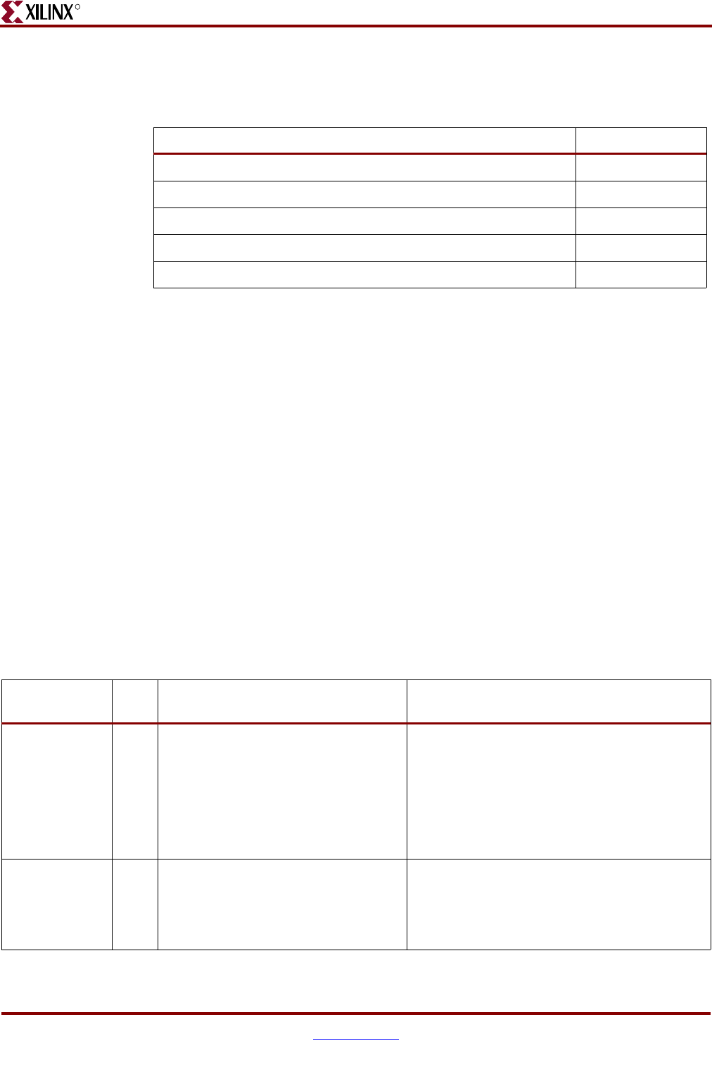
150 www.xilinx.com Memory Interface Solutions User Guide
UG086 (v3.6) September 21, 2010
Chapter 3: Implementing DDR2 SDRAM Controllers
R
The 25 clocks from the read command to the read data, as shown in Figure 3-13 and
Figure 3-14, are broken up as indicated in Table 3-10.
In general, read latency varies based on the following parameters:
• CAS latency (CL) and additive latency (AL)
• The number of commands already in the FIFO pipeline before the read command is
issued
• Whether an ACTIVATE command needs to be issued to open the new bank/row
• Whether a PRECHARGE command needs to be issued to close a previously opened
bank
• Specific timing parameters for the memory, such as TRAS, and TRCD in conjunction
with the bus clock frequency
• Commands might be interrupted, and banks/rows might be forcibly closed when the
periodic AUTO REFRESH command is issued
• If the user issues the commands before initialization is complete, the latency cannot be
determined
• Board-level and chip-level (for both memory and FPGA) propagation delays
User to Controller Interface
Table 3-11 lists the signals between the User interface and the controller.
Table 3-10: Read Command to Read Data Clock Cycles
Parameter Number of Clocks
Read Address to Empty Deassert 7 clocks
Empty to Active Command 5.5 clocks
Active to Read Command 3 clocks
Memory Read Command to Read Data Valid 9.5 clocks
Tot al : 25 clocks
Table 3-11: Signals between User Interface and Controller
Port Name Port
Width Port Description Notes
af_addr 36 Output of the Address FIFO in the user
interface. The mapping of these address
bits is:
[31:0]: Memory Address (CS, Bank,
Row, Column)
[34:32]: Dynamic Command Request
[35]: Reserved
Monitor FIFO-full status flag to write address into
the Address FIFO
af_empty 1 The user interface Address FIFO empty
status flag output. The user application
can write to the Address FIFO when this
signal is asserted until the write data
FIFO-full status flag is asserted.
FIFO16 Almost Empty flag
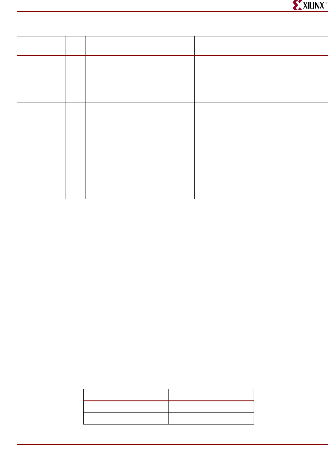
Memory Interface Solutions User Guide www.xilinx.com 151
UG086 (v3.6) September 21, 2010
Direct-Clocking Interface
R
The memory address (af_addr) includes the column address, row address, bank address,
and chip-select width for deep memory interfaces.
Column Address
[column_address – 1:0]
Row Address
[column_address + row_address – 1:column_address]
Bank Address
[column_address + row_address + bank_address – 1:column_address +
row_address]
Chip Select
[column_address + row_address + bank_address + chip_address – 1:
column_address + row_address + bank_address]
Dynamic Command Request
Table 3-12 lists commands not required for normal operation of the controller. The user has
the option of requesting these commands if the commands are required by their
application.
ctrl_af_RdEn 1 Read Enable input to Address FIFO in
the user interface.
This signal is asserted for one clock cycle when
the controller state is write, read, Precharge All, or
Auto Refresh resulting from dynamic command
requests. Figure 3-16 shows the timing waveform
for burst length of eight with four back-to-back
writes followed by four back-to-back reads.
ctrl_Wdf_RdEn 1 Read Enable input to Write Data FIFO in
the user interface.
The controller asserts this signal two clock cycles
after the first write state. This signal remains
asserted for two clock cycles for a burst length of
four and four clock cycles for a burst length of
eight. Figure 3-16 shows the timing waveform.
Sufficient data must be available in Write Data
FIFO associated with a write address for the
required burst length before issuing a write
command. For example, for a 64-bit data bus and
a burst length of four, the user should input two
128-bit data words in the Write Data FIFO for
every write address before issuing the write
command.
Table 3-11: Signals between User Interface and Controller (Cont’d)
Port Name Port
Width Port Description Notes
Table 3-12: Optional Commands
Command Description
001 Auto Refresh
010 Precharge
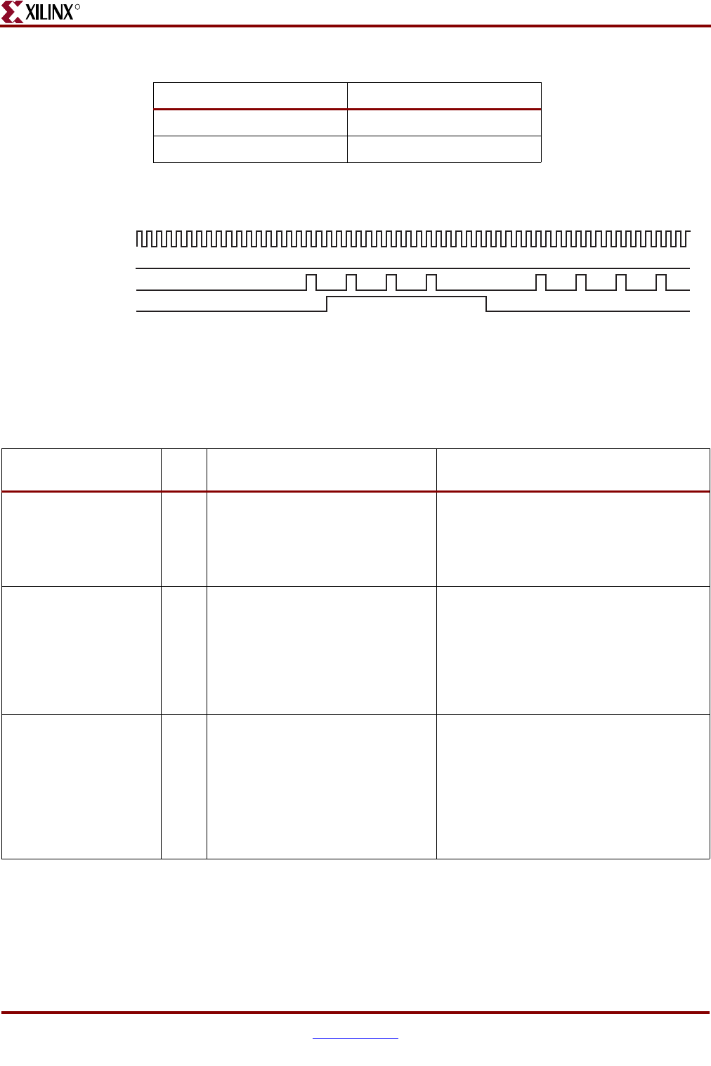
152 www.xilinx.com Memory Interface Solutions User Guide
UG086 (v3.6) September 21, 2010
Chapter 3: Implementing DDR2 SDRAM Controllers
R
Figure 3-15 describes four consecutive writes followed by four consecutive reads with a
burst length of 8.
Controller to Physical Layer Interface
Table 3-13 lists the signals between the controller and the physical layer.
100 Write
101 Read
Table 3-12: Optional Commands (Cont’d)
Command Description
Figure 3-15: Consecutive Writes Followed by Consecutive Reads with Burst Length of 8
UG086_c3_12_042507
top_00/clk_0
top_00/af_empty_w
top_00/ctrl_af_rden
top_00/ctrl_wr_df_rden
Table 3-13: Signals between the Controller and Physical Layer
Port Name Port
Width Port Description Notes
ctrl_Dummyread_Start 1 Output from the controller to the
physical layer. When asserted, the
physical layer begins strobe and
data calibration after memory
initialization.
This signal is asserted after read strobe
begins to toggle in the dummy read state.
This signal is deasserted when the
phy_Dly_Slct_Done signal is asserted.
phy_Dly_Slct_Done 1 Output from the physical layer to
the controller indicating
calibration is complete.
This signal is asserted after data bits have
been delayed to center align with respect
to the FPGA global clock. The
ctrl_Dummyread_Start signal is
deasserted when the phy_Dly_Slct_Done
signal is asserted. Normal operation
begins after this signal is asserted.
ctrl_Dqs_Rst 1 Output from the controller to the
physical layer for the write strobe
preamble.
This signal is asserted for one clock cycle
during a write. The CAS latency and AL
values determine how many clock cycles
after the first write state this signal is
asserted. Figure 3-16 shows the timing
waveform for this signal with CAS latency
of 3 and AL of 0 for four back-to-back
writes with a burst length of 8.
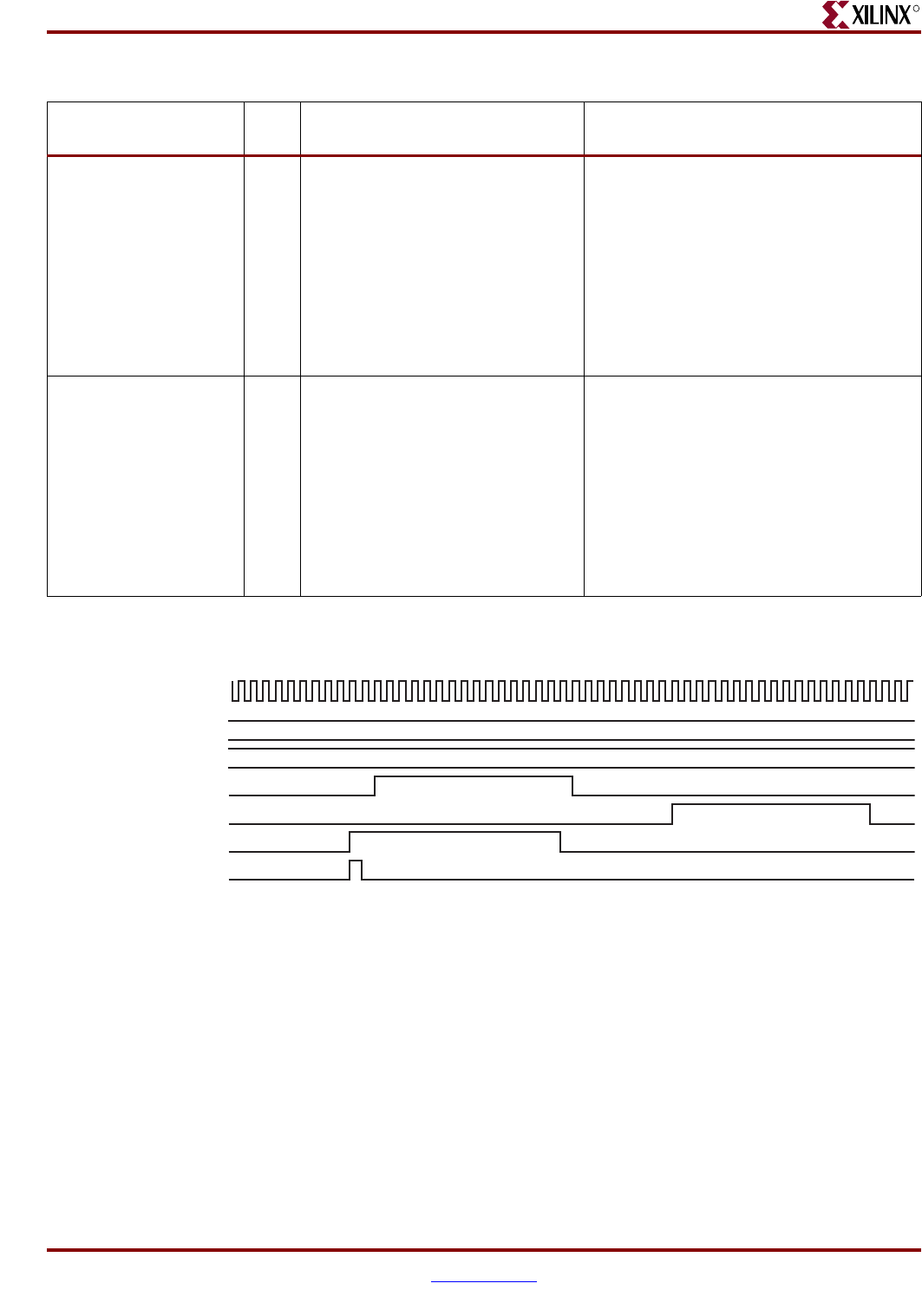
Memory Interface Solutions User Guide www.xilinx.com 153
UG086 (v3.6) September 21, 2010
Direct-Clocking Interface
R
Figure 3-16 describes the timing waveform for control signals from the controller to the
physical layer.
ctrl_Dqs_En 1 Output from the controller to the
physical layer for a write strobe.
This signal is asserted for three clock
cycles during a write with a burst length
of four and five clock cycles with a burst
length of 8. The CAS latency and AL
values determine how many clock cycles
after the first write or burst write state this
signal is asserted. Figure 3-16 shows the
timing waveform for this signal with CAS
latency of 3 and AL of 0 for four back-to-
back writes with a burst length of 8.
ctrl_WrEn 1 Output from the controller to the
physical layer for write data three-
state control.
This signal is asserted for two clock cycles
during a write with a burst length of 4 and
for four clock cycles with a burst length of
8. The CAS latency and AL values
determine how many clock cycles after
the first write or burst write state this
signal is asserted. Figure 3-16 shows the
timing waveform for this signal with CAS
latency of 3 and AL of 0 for four back-to-
back writes with a burst length of 8.
Table 3-13: Signals between the Controller and Physical Layer (Cont’d)
Port Name Port
Width Port Description Notes
Figure 3-16: Timing Waveform for Control Signals from the Controller to the Physical Layer
UG086_c3_13_042507
top_00/clk_0
Additive Latency
CAS Latency
top_00/ctrl_wr_en
top_00/ctrl_rden
top_00/ctrl_dqs_enable
top_00/ctrl_dqs_reset
0
3
154 www.xilinx.com Memory Interface Solutions User Guide
UG086 (v3.6) September 21, 2010
Chapter 3: Implementing DDR2 SDRAM Controllers
R
Deep Memory Configurations
The following examples provide user address formats for different densities of
components and DIMMs in deep memory designs. These are examples only, not associated
with any specific memory part number from memory data sheets.
Components
Case 1: 256 Mb (x4 component)
Write Address/Read Address:
Density 256 Mb (256 Mb x 4 = 1 Gb)
Depth 4
Row address 13
Column address 11
Bank address 2
Rank/chip + deep address 2
35 32 31 29 28 27 26 25 24 12 11 10 9 0
A10-A0 Column address
A23-A11 Row address
A25-A24 Bank address
A27 -A26 Rank + deep address
A31-A28 Assigned to all zeros
A34-A32 Dynamic commands
A35 Reserved for internal use

Memory Interface Solutions User Guide www.xilinx.com 155
UG086 (v3.6) September 21, 2010
Direct-Clocking Interface
R
Case 2: 256 Mb (x8 component)
Write Address/Read Address:
Density 256 Mb (256 Mb x 3 = 768 Mb)
Depth 3
Row address 13
Column address 10
Bank address 2
Rank/chip + deep address 2
35 32 31 28 27 26 25 24 23 11 10 9 0
A9-A0 Column address
A22-A10 Row address
A24-A23 Bank address
A26-A25 Rank + deep address
A31-A27 Assigned to all zeros
A34-A32 Dynamic commands
A35 Reserved for internal use
156 www.xilinx.com Memory Interface Solutions User Guide
UG086 (v3.6) September 21, 2010
Chapter 3: Implementing DDR2 SDRAM Controllers
R
Case 3: 256 Mb (x16 component)
Write Address/Read Address:
Density 256 Mb (256 Mb x 2 = 512 Mb)
Depth 2
Row address 13
Column address 9
Bank address 2
Rank/chip + deep address 1
35 32 31 30 29 28 27 25 24 11 10 9 0
A8-A0 Column address
A21-A9 Row address
A23-A22 Bank address
A24 Rank + deep address
A31-A25 Assigned to all zeros
A34-A32 Dynamic commands
A35 Reserved for internal use
Memory Interface Solutions User Guide www.xilinx.com 157
UG086 (v3.6) September 21, 2010
Direct-Clocking Interface
R
DIMMs
Case 1: 2 GB
Write Address/Read Address:
Density 1 GB (1 x 2 = 2 GB)
Depth 2
Row address 14
Column address 10
Bank address 3
Rank/chip + deep address 2
35 32 31 30 29 28 27 25 24 11 10 9 0
A9-A0 Column address
A23-A10 Row address
A26-A24 Bank address
A28-A27 Rank + deep address
A31-A29 Assigned to all zeros
A34-A32 Dynamic commands
A35 Reserved for internal use
158 www.xilinx.com Memory Interface Solutions User Guide
UG086 (v3.6) September 21, 2010
Chapter 3: Implementing DDR2 SDRAM Controllers
R
Case 2: (8 GB)
Write Address/Read Address:
Direct-Clocking DDR2 SDRAM Signal Allocations
MIG allows banks to be selected for different classes of memory signals.
Table 3-14 shows the list of signals allocated in a group from bank selection checkboxes.
Note: Timing has been verified for most of the MIG generated configurations. For the best timing
results, adjacent banks in the same column of the FPGA should be used. Banks that are separated
by unbonded banks should be avoided because these can cause timing violations.
Density 4 GB (4 x 2 = 8 GB)
Depth 2
Row address 14
Column address 11
Bank address 3
Rank/chip + deep address 2
35 32 31 30 29 28 26 25 12 11 10 9 0
A10-A0 Column address
A24-A11 Row address
A27-A25 Bank address
A29-A28 Rank + deep address
A31-A30 Assigned to zeros
A34 - A32 Dynamic commands
A35 Reserved for internal use
Table 3-14: Direct-Clocking DDR2 SDRAM Signal Allocations
Bank Selected Signals Allocated in the Group
Address Memory address, memory control, and memory clock signals
Data Data, data mask, and data strobes
System Control System reset from user interface and status signals
System Clock System clocks from the user interface

Memory Interface Solutions User Guide www.xilinx.com 159
UG086 (v3.6) September 21, 2010
Direct-Clocking Interface
R
Simulating the DDR2 SDRAM Design
After generating the design, MIG creates a sim folder in the specified path. This folder
contains simulation files for a particular design. The sim folder contains the external
testbench, memory model, and .do file to simulate the generated design. The memory
model files are currently generated in Verilog only. To learn more details about the files in
the sim folder and to simulate the design, refer to “Simulation Guide,” page 499.
For both single- and dual-rank DIMMs, MIG outputs only the base part memory model. In
the simulation testbench (sim_tb_top in the sim folder), MIG instantiates the required
number of memory models. For example, a 1 GB single-rank DIMM with the base part is
1 Gb, and MIG instantiates the base model eight times. A dual-rank part (2 GB capacity)
with the base part is 1 Gb. MIG instantiates a 1 Gb model 16 times (the first 8 instances
correspond to CS0, and the remaining 8 instances correspond to CS1). If the MIG generated
memory model is to be used with the user’s test bench, multiple instances that are based
on the selected configuration should be used.
The MIG output memory model considers the MEM_BITS parameter by default for
memory range allocation. This covers only a partial memory range, i.e., 2MEM_BITS. To
allocate the full memory range, the MAX_MEM parameter should be set in the memory
model. Allocating the full memory range might exceed the memory of the operating
system, thus causing memory allocation failure in simulations.
Deep-Design Violations
Simulation violations occur for a depth of 4 at frequencies less than and equal to 127 MHz.
An auto-refresh command is issued during memory initialization. The next auto-refresh
command is issued upon the auto-refresh request after completing calibration
(INIT_DONE asserted). Because the controller issues the refresh command to the memory
only after calibration is completed, even though there is a pending auto-refresh request, a
MAX TRFC violation occurs for CS0 for a depth of 4 and at frequencies between 125 MHz to
127 MHz. These violations can be ignored because there are no read and write commands
issued to the memory, i.e., CS0.
Simulation Violations
There might be simulation violations for frequencies such as 150 MHz where the clock
period is not an integer value. At 150 MHz, the clock period value in the simulation
testbench is 6.66 ns and the MIG tool rounds it to 6.67 ns. Consider a memory TRCD value
of 20 ns. MIG calculates the TRCD count value based on the clock period,
RCD_COUNT_VALUE = 20/6.67 = 2.998 = 3 (after rounding off) in the design parameter
file. The TRCD value for 3 clock cycles is 3 × 6.66 = 19.98, which causes timing violations by
20 ps. The difference between the clock period in the external simulation testbench versus
the MIG tool causes timing violations. This is only one example case. There might be more
such scenarios. These are only simulation warnings. Functionally, there should be no
issues. To remove these warnings, the related count value can be increased by one.
Changing the Refresh Rate
Change the global `define (for Verilog) or constant (for VHDL) variable MAX_REF_CNT in
mymodule_parameters_0.v (or .vhd) so that MAX_REF_CNT = (refresh interval in
clock periods) = (refresh interval) / (clock period). For example, for a refresh rate of 3.9 µs
with a memory bus running at 200 MHz:
MAX_REF_CNT = 3.9 µs / (clock period) = 3.9 µs / 5 ns = 780 (decimal) = 0x30C
160 www.xilinx.com Memory Interface Solutions User Guide
UG086 (v3.6) September 21, 2010
Chapter 3: Implementing DDR2 SDRAM Controllers
R
If the above value exceeds 2MAX_REF_WIDTH – 1, the value of MAX_REF_WIDTH must be
increased accordingly in parameters_0.v (or .vhd) to increase the width of the counter
used to track the refresh interval.
Supported Devices
The design generated out of MIG is independent of memory package, hence the package
part of the memory component is replaced with XX or XXX, where XX or XXX indicates a
don't care condition. The tables below list the components (Table 3-15) and DIMMs
(Table 3-16 through Table 3-18) supported by the tool for DDR2 direct-clocking designs. In
supported devices, an X in the components column (for Components and Unbuffered
DIMMs) denotes a single alphanumeric character. For example MT47H128M4XX-3 can be
either MT47H128M4BP-3 or MT47H128M4B6-3. Similarly MT16HTF25664AX-40E can be
either MT16HTF25664AY-40E or MT16HTF25664AG-40E. An XX for Registered DIMMs
denotes a single or two alphanumeric characters. For example, MT9HTF3272XX-667 can be
either MT9HTF3272Y-667 or MT9HTF3272DY-667. An XXX for Registered DIMMs denotes
two or three alphanumeric characters. For example, MT18HTF12872XXX-667 can be either
MT18HTF12872DY-667 or MT18HTF12872PDY-667. Pin mapping for x4 RDIMMs is
provided in Appendix G, “Low Power Options.”
Table 3-15: Supported Components for DDR2 SDRAM
Components Packages (XX) Components Packages (XX)
MT47H64M4XX-3 BP MT47H16M16XX-3 BG
MT47H64M4XX-37E BP MT47H16M16XX-37E BG
MT47H64M4XX-5E BP MT47H16M16XX-5E BG
MT47H128M4XX-3 B6,CB,GB MT47H32M16XX-3 BN,CC,FN,GC
MT47H128M4XX-37E B6,CB,GB MT47H32M16XX-37E BN,CC,FN,GC
MT47H128M4XX-5E B6,CB,GB MT47H32M16XX-5E BN,CC,FN,GC
MT47H256M4XX-3 BT,HQ MT47H64M16XX-3 BT,HR
MT47H256M4XX-37E BT,HQ MT47H64M16XX-37E BT,HR
MT47H256M4XX-5E BT,HQ MT47H64M16XX-5E BT,HR
MT47H512M4XX-3 HG MT47H128M16XX-3 HG
MT47H512M4XX-37E HG MT47H128M16XX-37E HG
MT47H512M4XX-5E HG MT47H128M16XX-5E --
MT47H32M8XX-3 BP HYB18T1G800XXXX-3S C2F,C2FL
MT47H32M8XX-37E BP HYB18T1G800XXXX-37 C2F,C2FL
MT47H32M8XX-5E BP HYB18T1G160XXXX-3S C2F,C2FL
MT47H64M8XX-3 B6,CB,F6,GB HYB18T1G160XXXX-37 C2F,C2FL
MT47H64M8XX-37E B6,CB,F6,GB HYB18T1G400XXXX-3S C2F,C2FL
MT47H64M8XX-5E B6,CB,F6,GB HYB18T1G400XXXX-37 C2F,C2FL
MT47H128M8XX-3 BT,HQ HYB18T512800XXXX-3S B2F,B2FL
MT47H128M8XX-37E BT,HQ HYB18T512800XXXX-37 B2F,B2FL
MT47H128M8XX-5E BT,HQ HYB18T512160XXXX-3S B2F,B2FL
MT47H256M8XX-3 HG HYB18T512160XXXX-37 B2F,B2FL
Memory Interface Solutions User Guide www.xilinx.com 161
UG086 (v3.6) September 21, 2010
Direct-Clocking Interface
R
MT47H256M8XX-37E HG HYB18T512400XXXX-3S B2F,B2FL
MT47H256M8XX-5E HG HYB18T512400XXXX-37 B2F,B2FL
Table 3-16: Supported Registered DIMMs for DDR2 SDRAM
Registered DIMMs Registered DIMMs
MT9HTF3272Y-667 MT18HTF12872Y-40E
MT9HTF3272PY-667 MT18HTF12872PY-40E
MT9HTF3272Y-53E MT18HTF25672Y-667
MT9HTF3272PY-53E MT18HTF25672PY-667
MT9HTF3272Y-40E MT18HTF25672Y-53E
MT9HTF3272PY-40E MT18HTF25672PY-53E
MT9HTF6472Y-667 MT18HTF25672Y-40E
MT9HTF6472PY-667 MT18HTF25672PY-40E
MT9HTF6472Y-53E MT18HTF6472DY-667
MT9HTF6472PY-53E MT18HTF6472PDY-667
MT9HTF6472Y-40E MT18HTF6472DY-53E
MT9HTF6472PY-40E MT18HTF6472PDY-53E
MT9HTF12872Y-667 MT18HTF6472DY-40E
MT9HTF12872PY-667 MT18HTF6472PDY-40E
MT9HTF12872Y-53E MT18HTF12872DY-667
MT9HTF12872PY-53E MT18HTF12872PDY-667
MT9HTF12872Y-40E MT18HTF12872DY-53E
MT9HTF12872PY-40E MT18HTF12872PDY-53E
MT18HTF6472G-53E MT18HTF12872DY-40E
MT18HTF6472Y-667 MT18HTF12872PDY-40E
MT18HTF6472PY-667 MT18HTF25672DY-667
MT18HTF6472Y-53E MT18HTF25672PDY-667
MT18HTF6472PY-53E MT18HTF25672DY-53E
MT18HTF6472Y-40E MT18HTF25672PDY-53E
MT18HTF6472PY-40E MT18HTF25672DY-40E
MT18HTF12872Y-667 MT18HTF25672PDY-40E
MT18HTF12872PY-667 MT36HTJ51272Y-667
MT18HTF12872Y-53E MT36HTJ51272Y-53E
Table 3-15: Supported Components for DDR2 SDRAM (Cont’d)
Components Packages (XX) Components Packages (XX)
162 www.xilinx.com Memory Interface Solutions User Guide
UG086 (v3.6) September 21, 2010
Chapter 3: Implementing DDR2 SDRAM Controllers
R
MT18HTF12872PY-53E MT36HTJ51272Y-40E
MT36HTF51272Y-667 MT36HTF51272Y-53E
MT36HTF51272Y-40E --
Table 3-17: Supported Unbuffered DIMMs for DDR2 SDRAM
Unbuffered DIMMs Unbuffered DIMMs
MT4HTF1664AY-667 MT9HTF3272AY-40E
MT4HTF1664AY-53E MT9HTF6472AY-667
MT4HTF1664AY-40E MT9HTF6472AY-53E
MT4HTF3264AY-53E MT9HTF6472AY-40E
MT4HTF3264AY-667 MT16HTF25664AX-667
MT4HTF3264AY-40E MT16HTF25664AX-53E
MT4HTF6464AY-667 MT16HTF25664AX-40E
MT16HTF51264AY-667 MT16HTF51264AY-53E
MT4HTF6464AY-53E MT18HTF6472AY-667
MT4HTF6464AY-40E MT18HTF6472AY-53E
MT8HTF6464AY-667 MT18HTF6472AY-40E
MT8HTF6464AY-53E MT18HTF12872AY-667
MT8HTF6464AY-40E MT18HTF12872AY-53E
MT8HTF12864AY-667 MT18HTF12872AY-40E
MT8HTF12864AY-53E MT18HTF25672AY-667
MT8HTF12864AY-40E MT18HTF25672AY-53E
MT9HTF3272AY-53E MT18HTF25672AY-40E
MT9HTF3272AY-667 MT18HTF51272AY-53E
MT18HTF51272AY-667 MT18HTF51272AY-40E
Table 3-18: Supported SODIMMs for DDR2 SDRAM
SODIMMs SODIMMs
MT4HTF1664HY-667 MT8HTF6464HY-40E
MT4HTF1664HY-53E MT8HTF3264HDY-667
MT4HTF1664HY-40E MT8HTF3264HDY-53E
MT4HTF3264HY-667 MT8HTF3264HDY-40E
MT4HTF3264HY-53E MT8HTF6464HDY-667
MT4HTF3264HY-40E MT8HTF6464HDY-53E
MT8HTF3264HY-667 MT8HTF6464HDY-40E
MT8HTF3264HY-53E MT16HTF25664HY-667
MT8HTF3264HY-40E MT16HTF25664HY-53E
Table 3-16: Supported Registered DIMMs for DDR2 SDRAM (Cont’d)
Registered DIMMs Registered DIMMs
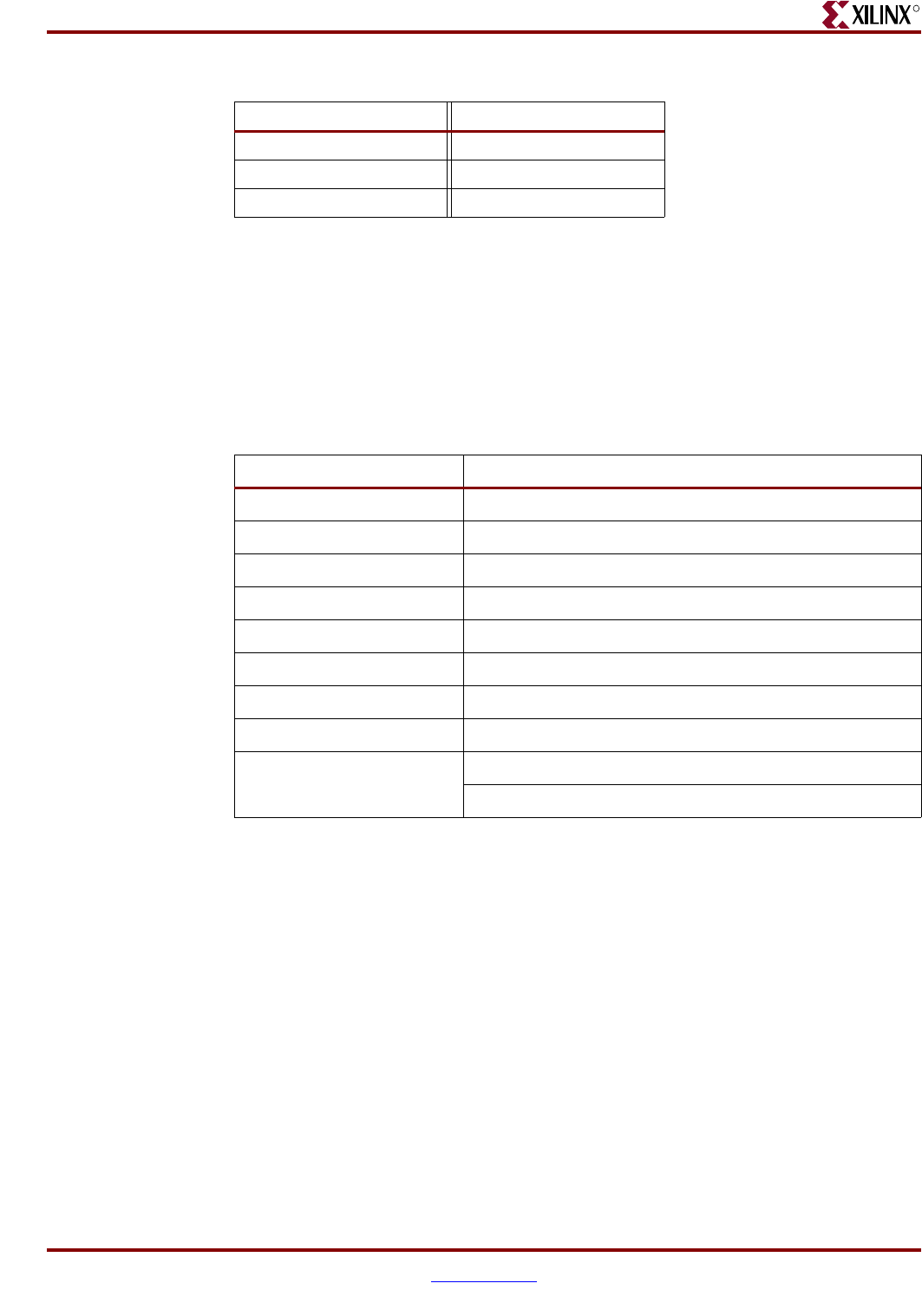
Memory Interface Solutions User Guide www.xilinx.com 163
UG086 (v3.6) September 21, 2010
SerDes Clocking Interface
R
Hardware Tested Configurations
The frequencies shown in Table 3-19 were achieved on the Virtex-4 FPGA ML461 Memory
Interfaces Development Board under nominal conditions. This frequency should not be
used to determine the maximum design frequency. The maximum design frequency
supported in the MIG wizard is based on a combination of the TRCE results for fabric
timing on multiple device/package combinations and I/O timing analysis using FPGA
and memory timing parameters for a 64-bit wide interface.
SerDes Clocking Interface
This technique uses the Input Serializer/Deserializer (ISERDES) and Output
Serializer/Deserializer (OSERDES) features available in every Virtex-4 FPGA I/O. A
DDR2 SDRAM interface is source-synchronous, where the read data and read data strobe
are transmitted edge-aligned. To capture this transmitted data using Virtex-4 FPGAs,
either the strobe or the data can be delayed. In this design, the read data is captured in the
delayed strobe domain and recaptured in the FPGA clock domain in the ISERDES. The
received signal, double data rate (DDR) read data, is converted to 4-bit parallel single data
rate (SDR) data at the frequency of the interface using the ISERDES. The write data and
strobe transmitted by the FPGA use the OSERDES. The OSERDEDS converts 4-bit parallel
data at half the frequency of the interface to DDR data at the interface frequency.
MT8HTF6464HY-667 MT16HTF25664HY-40E
MT8HTF6464HY-53E MT16HTS51264HY-667
MT16HTS51264HY-53E --
Table 3-18: Supported SODIMMs for DDR2 SDRAM (Cont’d)
SODIMMs SODIMMs
Table 3-19: Hardware Tested Configurations
Synthesis Tools XST and Synplicity
HDL Verilog and VHDL
FPGA Device XC4VLX25-FF668-11
Burst Lengths 4, 8
CAS Latency (CL) 3, 4
Additive Latency 0, 1, 2
8-bit Design Tested on 16-bit Component “MT47H32M16XX-3”
72-bit Design Tested on 72-bit RDIMM “MT9HTF6472Y-667”
ECC with Pipelined Mode 72-bit Registered DIMM design
Frequency Range 110 MHz to 270 MHz for CL = 3
110 MHz to 300 MHz for CL = 4 or 5
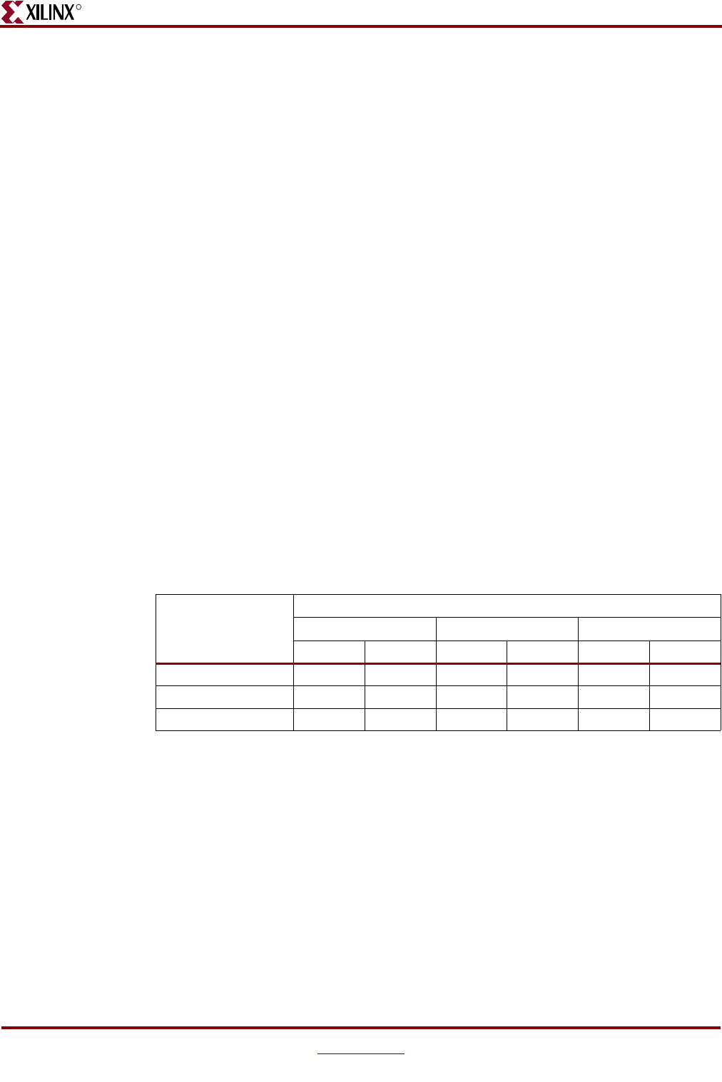
164 www.xilinx.com Memory Interface Solutions User Guide
UG086 (v3.6) September 21, 2010
Chapter 3: Implementing DDR2 SDRAM Controllers
R
Feature Summary
This section summarizes the supported and unsupported features of the SerDes clocking
DDR2 SDRAM controller design.
Supported Features
The DDR2 SDRAM controller design supports:
• Burst lengths of four and eight
• Sequential and Interleaved burst types
• CAS latencies of 4 and 5
• Different memories (density/speed)
• Components
• Additive latencies 0, 1, and 2
•Verilog and VHDL
• Differential and single-ended DQS
• Linear addressing
• Without a testbench
• On Die Termination (ODT)
• DIMMs (registered DIMMs up to 300 MHz and unbuffered DIMMs up to 266 MHz)
•Data mask
• System clock, differential and single-ended
The supported features are described in more detail in “Architecture.”
Design Frequency Ranges
Unsupported Features
The DDR2 SDRAM controller design does not support:
•CAS latency of 3
• Additive latencies of 3 and 4
• Redundant DQS (RDQS)
•Auto precharge
• Deep memories
• ECC support
•Without a DCM
•Multicontroller
Table 3-20: Design Frequency Range in MHz
Memory
FPGA Speed Grade
-10 -11 -12
Min Max Min Max Min Max
Component 200 230 200 266 200 300
Registered DIMM 200 230 200 266 200 300
UDIMM/SODIMM 200 230 200 266 200 266

Memory Interface Solutions User Guide www.xilinx.com 165
UG086 (v3.6) September 21, 2010
SerDes Clocking Interface
R
Architecture
Implemented Features
This section provides details on the supported features of the DDR2 SDRAM controller.
Burst Length
The DDR2 SDRAM controller supports burst lengths of four and eight. The burst length
can be selected through the Set mode register(s) option in MIG. For a design without a
testbench (user design), the user has to provide bursts of the input data based on the
chosen burst length. Bits M2:M0 of the Mode Register define the burst length, and bit M3
indicates the burst type (see the Micron data sheet). Read and write accesses to the DDR2
SDRAM are burst-oriented. It determines the maximum number of column locations
accessed for a given READ or WRITE command.
CAS Latency
The DDR2 SDRAM controller supports CAS latencies (CLs) of four and five. CL can be
selected in the Set mode register(s) option from the GUI. The CAS latency is
implemented in the ddr2_controller module. During data write operations, the generation
of the ctrl_WrEn, ctrl_WrEn_Dis, and ctrl_Odd_Latency signals varies according to the CL
in the ddr2_controller module. During data read operations, the generation of the
ctrl_RdEn_div0 signal varies according to the CL in the ddr2_controller module. Bits
M4:M6 of the Mode Register define the CL (see the Micron data sheet). CL is the delay in
clock cycles between the registration of a READ command and the availability of the first
bit of output data.
Additive Latency
DDR2 SDRAM devices support a feature called posted CAS additive latency (AL). The
DDR2 SDRAM supports additive latencies of 0, 1, and 2. AL can be selected in the Set
mode register(s) option. Additive latency is implemented in the ddr2_controller module.
The ddr2_controller module issues READ/WRITE commands prior to tRCD (minimum)
depending on the user-selected AL value in the Extended Mode Register. This feature
allows the READ command to be issued prior to tRCD (minimum) by delaying the internal
command to the DDR2 SDRAM by AL clocks. Posted CAS AL makes the command and
data bus efficient for sustainable bandwidths in DDR2 SDRAM. Bits E3:E5 of the Extended
Mode Register define the value of AL (see the Micron data sheet).
Registered DIMMs
DDR2 SDRAM supports registered DIMMs. This feature is implemented in the
ddr2_controller module. For registered DIMMs, the address and command signals are
registered at the DIMM and therefore have one additional clock latency than unbuffered
DIMMs.
Unbuffered DIMMs and SODIMMs
The DDR2 SDRAM design supports unbuffered DIMMs and SODIMMs. Unbuffered
DIMMs do not have registers at the DIMM for address and command signals. SODIMMs
differ from the unbuffered DIMMs only by the package type; otherwise they are
functionally the same.
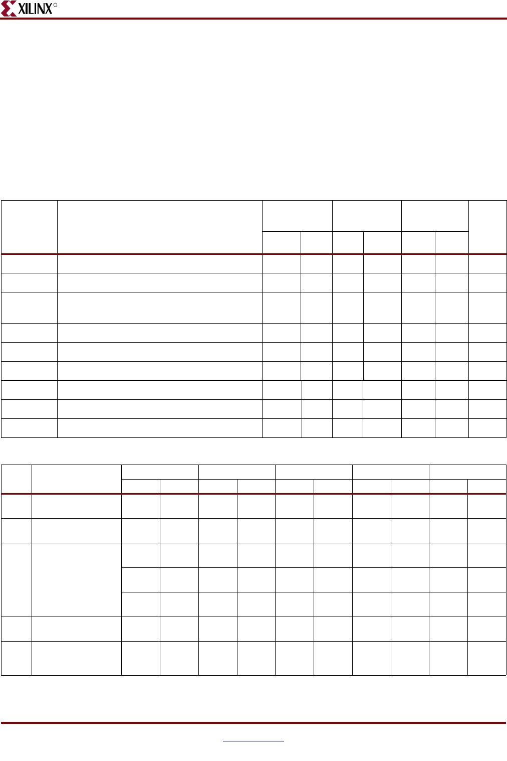
166 www.xilinx.com Memory Interface Solutions User Guide
UG086 (v3.6) September 21, 2010
Chapter 3: Implementing DDR2 SDRAM Controllers
R
Different Memories (Density/Speed)
The DDR2 SDRAM controller supports different densities. For DDR2 components shown
in MIG, densities vary from 256 Mb to 2 Gb, and DIMM densities vary from 128 Mb to
4 Gb. The user can select various configurations using the “Create new memory part”
feature of MIG. The supported maximum column address is 13, the maximum row address
is 15, and the maximum bank address is 3. The design can decode write and read addresses
from the user in the DDR2 SDRAM controller module. The user address consists of
column, row, bank, chip address, and user command.
Table 3-21 and Table 3-22 list sample timing sheets for Micron components and DIMMs,
respectively.
Table 3-21: Timing Parameters for Components
Parameter Description
Micron
256 Mb
Micron
512 Mb Micron 1 Gb
Units
-37E -3 -37E -3 -37E -3
TMRD LOAD MODE command cycle time 2 2 2 2 2 2 TCK
TRP PRECHARGE command period 15 15 15 15 15 15 ns
TRFC REFRESH to ACTIVE or REFRESH to
REFRESH command interval
75 75 105 105 127.5 127.5 ns
TRCD ACTIVE to READ or WRITE delay 15 15 15 15 15 15 ns
TRAS ACTIVE to PRECHARGE command 40 40 40 40 40 40 ns
TRC ACTIVE to ACTIVE (same bank) command 55 55 55 55 55 55 ns
TRTP READ to PRECHARGE command delay 7.5 7.5 7.5 7.5 7.5 7.5 ns
TWTR WRITE to READ command delay 7.5 7.5 7.5 7.5 7.5 7.5 ns
TWR WRITE recovery time 15 15 15 15 15 15 ns
Table 3-22: Timing Parameters for DIMMs
Para-
meter Description MT4HTF MT8HTF MT16HTF MT9HTF MT18HTF
-53E -40E -53E -40E -53E -40E -53E -40E -53E -40E
TMRD LOAD MODE
command cycle time 2ns 2ns 2ns 2ns 2ns 2ns 2ns 2ns 2ns 2ns
TRP PRECHARGE
command period 15 ns 15 ns 15 ns 15 ns 15 ns 15 ns 15 ns 15 ns 15 ns 15 ns
TRFC REFRESH time
128 MB
75 ns 75 ns 256 MB
75 ns 75 ns 512 MB
75 ns 75 ns 256 MB
75 ns 75 ns 512 MB
75 ns 75 ns
256 MB
105 ns 105 ns 512 MB
105 ns 105 ns 1GB
105 ns 105 ns 512 MB
105 ns 105 ns 1GB
105 ns 105 ns
512 MB
127.5 ns 127.5 ns 1GB
127.5 ns 127.5 ns 2GB
127.5 ns 127.5 ns 1GB
127.5 ns 127.5 ns 2GB
127.5 ns 127.5 ns
TRCD ACTIVE to READ or
WRITE delay 15 ns 15 ns 15 ns 15 ns 15 ns 15 ns 15 ns 15 ns 15 ns 15 ns
TRAS
ACTIVE to
PRECHARGE
command
40 ns 40 ns 40 ns 40 ns 40 ns 40 ns 40 ns 40 ns 40 ns 40 ns
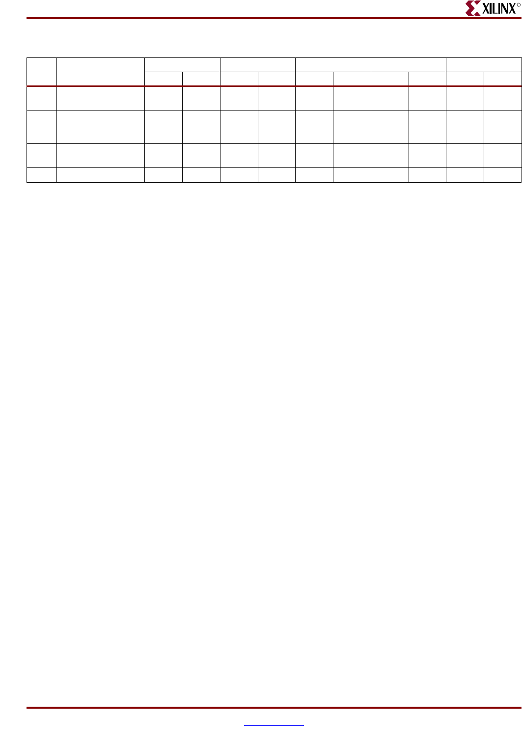
Memory Interface Solutions User Guide www.xilinx.com 167
UG086 (v3.6) September 21, 2010
SerDes Clocking Interface
R
Data Masking
The DDR2 SDRAM design supports data masking per byte. Masking per nibble is not
supported due to the limitation of the internal block RAM based FIFOs. So, the masking of
data can be done on per byte basis. The mask data is stored in the Data FIFO along with the
actual data.
MIG supports a data mask option. If this option is checked in the GUI, MIG generates
design with data mask pins. This option can be chosen if the selected part has data
masking.
Precharge
The PRECHARGE command is used to close the open row in a bank if there is a command
to be issued to a different row in the same bank. The PRECHARGE command checks the
row address, bank address, and chip address, and the Virtex-4 FPGA DDR2 controller
issues a PRECHARGE command if there is a change in any address where a read or write
command is to be issued. The auto-precharge function is not supported.
Auto Refresh
The DDR2 SDRAM controller issues AUTO REFRESH commands at specified intervals for
the memory to refresh the charge required to retain the data in the memory. The user can
also issue a REFRESH command through the user interface by setting bits 34, 33, and 32 of
the app_af_addr signal in the user_interface module to 3’b001. If there is a refresh request
while there is an ongoing read or write burst, the controller issues a REFRESH command
after completing the current read or write burst command.
Linear Addressing
The DDR2 SDRAM controller supports linear addressing. Linear addressing refers to the
way the user provides the address of the memory to be accessed. For Virtex-4 FPGA DDR2
SDRAM controllers, the user provides the address information through the app_af_addr
signal. As the densities of the memory devices vary, the number of column address bits
and row address bits also change. In any case, the row address bits in the app_af_addr
signal always start from the next higher bit, where the column address ends. This feature
increases the number of devices that can be supported with the design.
On-Die Termination
The DDR2 SDRAM controller supports on-die termination (ODT). Through the Set mode
register(s) option from the GUI, the user can disable ODT or can choose 75, 150, or 50.
TRC ACTIVE to ACTIVE
command (same bank) 55 ns 55 ns 55 ns 55 ns 55 ns 55 ns 55 ns 55 ns 55 ns 55 ns
TRTP
READ to
PRECHARGE
command delay
7.5ns 7.5ns 7.5ns 7.5ns 7.5ns 7.5ns 7.5ns 7.5ns 7.5ns 7.5ns
TWTR WRITE to READ
command delay 7.5ns 10ns 7.5ns 10ns 7.5ns 10ns 7.5ns 10ns 7.5ns 10ns
TWR WRITE recovery time 15 ns 15 ns 15 ns 15 ns 15 ns 15 ns 15 ns 15 ns 15 ns 15 ns
Notes:
1. For the latest timing information, refer to the vendor memory data sheets.
Table 3-22: Timing Parameters for DIMMs (Cont’d)
Para-
meter Description MT4HTF MT8HTF MT16HTF MT9HTF MT18HTF
-53E -40E -53E -40E -53E -40E -53E -40E -53E -40E
168 www.xilinx.com Memory Interface Solutions User Guide
UG086 (v3.6) September 21, 2010
Chapter 3: Implementing DDR2 SDRAM Controllers
R
ODT can turn the termination on and off as needed to improve the signal integrity in the
system. ODT is only enabled on writes to DDR2 memory. It is disabled on read operations.
System Clock
MIG supports differential and single-ended system clocks. Based on the selection in the
GUI, input system clocks and IDELAY clocks are differential or single-ended.
Hierarchy
Figure 3-17 shows the hierarchical structure of the DDR2 SDRAM controller.
Figure 3-17 shows the hierarchical structure of the DDR2 SDRAM design generated by
MIG with a testbench and a DCM. The modules are classified as follows:
• Design modules
• Testbench modules
• Clocks and reset generation modules
There is a parameter file generated with the design that has all the user input and design
parameters selected from MIG.
MIG can generate two different DDR2 SDRAM designs:
• With a testbench and a DCM
• Without a testbench and with a DCM
Figure 3-17: Hierarchical Structure of the DDR2 SDRAM Design (SerDes Clocking)
<top_
module>
main* idelayctrl
infrastructure*
iobs*data_
path*
user_
interface*
data_
path_iobs*
controller
_iobs*
infrastructure
_iobs*
ddr2_
controller*
rd_data
_fifo*
RAM_D
v4_dq_
iob
Design Modules
v4_dm_
iob
idelay_
rd_en_
io
v4_dqs_
iob
cmp_rd_
data*
backend
_rom*
data_
gen
addr_
gen rd_data*
backend
_fifos*
rd_wr_
addr_
fifo*
wr_data
_fifo
data_
write*
tap_
logic*
tap_
ctrl*
data_
tap_inc*
UG086_c3_14_091207
test_
bench* top*
Te st Bench Modules
Clocks and Reset Generation Modules
Note: A block with a * has a parameter file included.

Memory Interface Solutions User Guide www.xilinx.com 169
UG086 (v3.6) September 21, 2010
SerDes Clocking Interface
R
A design without a testbench (user_design) does not have testbench modules. The
<top_module> module has the user interface signals for designs without a testbench. The
list of user interface signals is provided in Table 3-24.
Design clocks and resets are generated by using the DCM in the infrastructure module.
The inputs to this module are the differential design clock and a 200 MHz differential clock
for the IDELAYCTRL module. A user reset is also input to this module. Using the input
clocks and reset signals, the system clocks and the system reset are generated in this
module, which is used in the design.
MIG Tool Design Options for SerDes Clocking Interface
MIG provides various options to generate the design with or without a testbench or with
or without a DCM. This section provides detailed descriptions of the type of design
generated by the user using various options. Figure 3-18 and Figure 3-19, page 171 show
the differential system clock.
MIG outputs both an example_design and a user_design. The MIG-generated
example_design includes the entire memory controller design along with a synthesized
testbench (example user application). This testbench generates sample writes and reads
and then uses comparison logic to verify that the data patterns written are the same as
those received. This example_design can be used to test functionality both in simulation
and in hardware. The user_design includes the memory controller design only. This design
allows users to connect the MIG memory controller design to a user developed testbench
(user application). Refer to Table 3-24, page 176 for user interface signals, the “User
Interface Accesses,” page 178 for timing restriction on user interface signals, and
Figure 3-24, page 180 and Figure 3-25, page 181 for write interface timing.
Figure 3-18 shows a top-level block diagram of a DDR2 SDRAM design with a DCM and a
testbench. The sys_clk_p and sys_clk_n signals are differential input system clocks. The
DCM is instantiated in the infrastructure module that generates the required design clocks.
The differential clk200_p and clk200_n signals are used for the idelay_ctrl element. The
sys_reset_in_n is an active-Low system reset signal. All design resets are gated by the
dcm_lock signal. The error output signal indicates whether a read passes or fails. The
testbench module issues writes and reads, and also compares the read data with the
written data. The error signal is driven High on data mismatches. The init_complete signal
indicates the completion of initialization and calibration of the design. Memory device
signals are prepended with the controller number. For example, the ddr2_ras_n signal
appears as cntrl0_ddr2_ras_n.
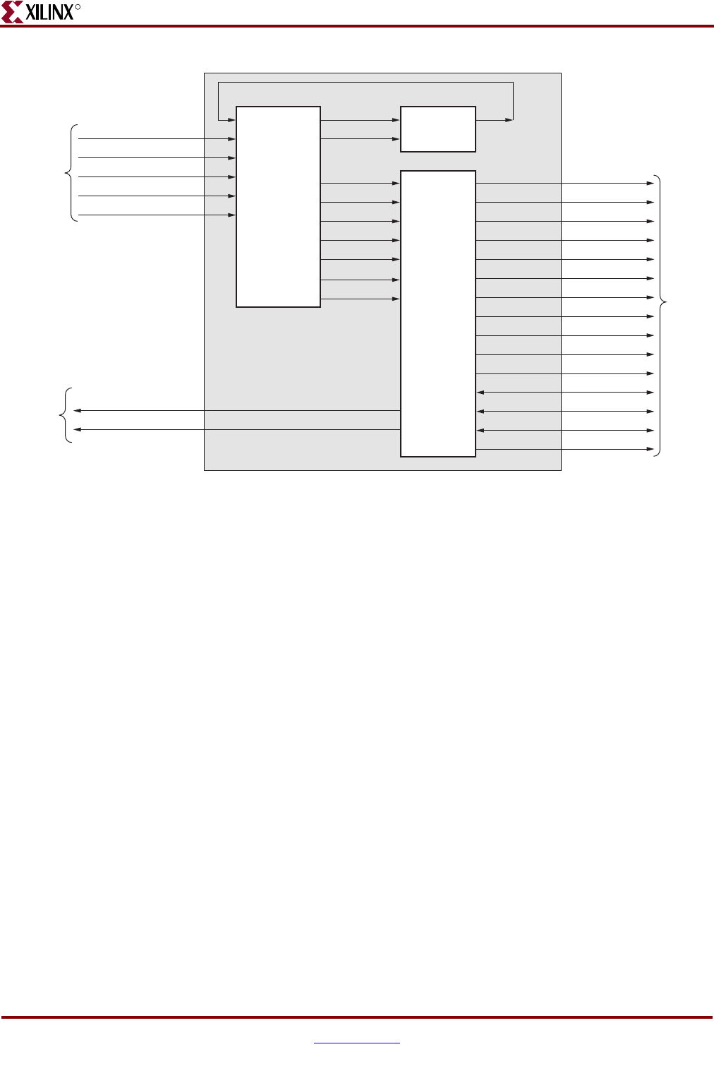
170 www.xilinx.com Memory Interface Solutions User Guide
UG086 (v3.6) September 21, 2010
Chapter 3: Implementing DDR2 SDRAM Controllers
R
All Memory Device ports do not necessarily appear for all MIG-generated designs. For
example, port ddr2_reset_n appears in the port list for registered DIMM designs only.
Similarly, ddr2_dqs_n does not appear for single-ended DQS designs. Port DDR2_DM
appears only for parts that contain a data mask; a few RDIMMs have no data mask, and
DDR2_DM does not appear in the port list for them.
Figure 3-19 shows a top-level block diagram of a DDR2 SDRAM design with a DCM but
without a testbench. The sys_clk_p and sys_clk_n pair are differential input system clocks.
The DCM is instantiated in the infrastructure module that generates the required design
clocks. The differential clk200_p and clk200_n pair are used for the idelay_ctrl element. The
active-Low system reset signal is sys_reset_in_n. All design resets are gated by the
dcm_lock signal. The user has to drive the user application signals. The design provides
the clk_tb and reset_tb signals to the user to synchronize with the design. The
init_complete signal indicates the completion of initialization and calibration of the design.
Figure 3-18: Top-Level Block Diagram of the DDR2 SDRAM Design with a DCM and a Testbench
main_0
idelay_ctrl_rdy
clk200
Memory
Device
UG086_c3_15_091508
Status
Signals
System
Clocks
and Reset
idelay_ctrl
Infrastructure
rst200
clk
clk90
sys_rst_270
sys_rst_90
clk200_p
clk200_n
sys_clk_p
sys_clk_n
sys_reset_in_n
sys_rst
ddr2_ras_n
ddr2_cas_n
ddr2_we_n
ddr2_cs_n
ddr2_odt
ddr2_cke
ddr2_dm
ddr2_ba
ddr2_a
ddr2_ck
ddr2_ck_n
ddr2_dq
ddr2_dqs
ddr2_dqs_n
clkdiv_0
clkdiv_90
ddr2_reset_n
error
init_complete
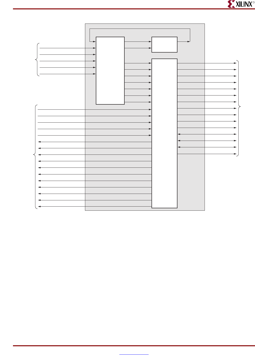
Memory Interface Solutions User Guide www.xilinx.com 171
UG086 (v3.6) September 21, 2010
SerDes Clocking Interface
R
Figure 3-19: Top-Level Block Diagram of the DDR2 SDRAM Design with a DCM but without a Testbench
top_0
idelay_ctrl_rdy
clk200
Memory
Device
UG086_c3_16_091508
User
Application
System
Clocks
and Reset
idelay_ctrl
Infrastructure
rst200
clk
clk90
sys_rst_270
sys_rst_90
clk200_p
clk200_n
sys_clk_p
sys_clk_n
sys_reset_in_n
app_af_addr
app_af_wren
app_wdf_data
app_mask_data
app_wdf_wren
wdf_almost_full
af_almost_full
burst_length_div2
read_data_valid
read_data0_fifo_out
sys_rst
ddr2_ras_n
ddr2_cas_n
ddr2_we_n
ddr2_cs_n
ddr2_odt
ddr2_cke
ddr2_dm
ddr2_ba
ddr2_a
ddr2_ck
ddr2_ck_n
ddr2_dq
ddr2_dqs
ddr2_dqs_n
ddr2_reset_n
read_data1_fifo_out
read_data2_fifo_out
read_data3_fifo_out
clk_tb
reset_tb
init_complete
clkdiv_0
clkdiv_90
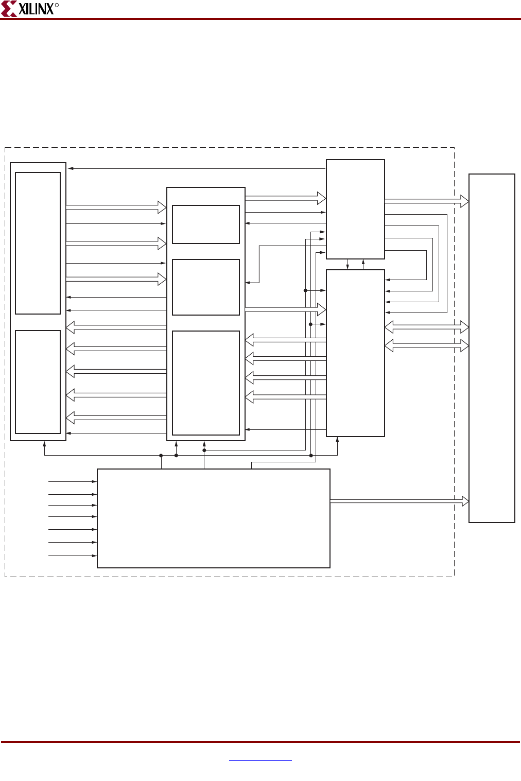
172 www.xilinx.com Memory Interface Solutions User Guide
UG086 (v3.6) September 21, 2010
Chapter 3: Implementing DDR2 SDRAM Controllers
R
DDR2 Controller Submodules
Figure 3-20 is a detailed block diagram of the DDR2 SDRAM controller. The five blocks
shown are the subblocks of the top module. The user backend signals are provided by the
tool for designs with a testbench. The user has to drive these signals for designs without a
testbench. The functions of these blocks are explained in the subsections following
Figure 3-20.
I
Controller
The DDR2 SDRAM ddr2_controller accepts and decodes user commands and generates
read, write, and refresh commands. The DDR2 SDRAM controller also generates signals
for other modules. The memory is initialized and powered up using a defined process. The
controller state machine handles the initialization process upon power-up. When the
initialization is over, the controller starts doing a dummy write and continuous dummy
reads. During these dummy reads, the tap_logic module calibrates DQ and DQS by
Figure 3-20: DDR2 Memory Controller Block Diagram (SerDes Clocking)
DDR2
SDRAM
Controller
Physical
Layer
Virtex-4 FPGA
DDR2
SDRAM
User Backend
User Interface
Backend FIFOs
ctrl_rden_valid
cntl_dummyread_start
af_almost_empty
af_addr
app_af_addr
init_complete
app_af_wren
wdf_data
UG086_c3_17_091608
ck/ck_n
dq
dqs
Read/Write
Address FIFO
Write Data
FIFOs
Read Data
FIFOs
Infrastructure
Address
and Data
Generation
Read Data
Compare
Module
af_almost_full
read_data0_fifo_out
burst_length_div2
read_data1_fifo_out
read_data2_fifo_out
read_data3_fifo_out
wdf_almost_full
read_data_valid
clkdiv_0 CLK_90 clkdiv_90
ctrl_waf_rden
dp_dly_sel_done
ctrl_wdf_rden
read_data0
read_data1
read_data2
read_data3
app_wdf_data
app_mask_data
app_wdf_wren
sys_clk_p
sys_clk_n
clk200_p
sys_clk
clk200_n
idly_clk_200
sys_reset_in_n
address/controls
ctrl_wr_dis
ctrl_odd_latency
ctrl_rden
ctrl_wren
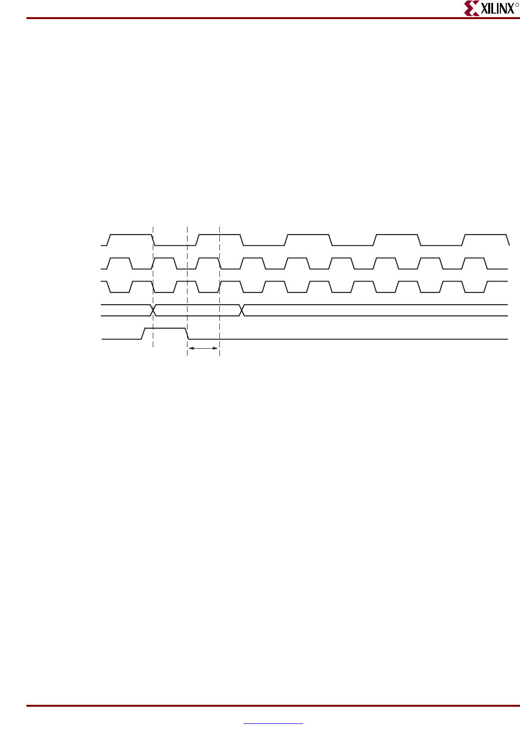
Memory Interface Solutions User Guide www.xilinx.com 173
UG086 (v3.6) September 21, 2010
SerDes Clocking Interface
R
varying the delay to center-align the data with the FPGA clock. Then the tap_logic module
asserts the dp_dqs_dq_calib_done signal. After this assertion, the controller does one more
write and read to the memory for read-enable calibration to determine the delay between
the read command and data. Then dp_dly_slct_done is asserted to start writing to and
reading from the memory.
The ddr2_controller is clocked at half the frequency of the interface using CLKDIV_0 and
CLKDIV_90 and CLK_90. Therefore the address and bank address are driven and the
command signals (RAS_L, CAS_L, and WE_L) are asserted for two clock cycles of the fast
memory interface clock. The control signals (CS_L, CKE, and ODT) are DDR of the half
frequency clock CLKDIV_0, ensuring that the control signals are asserted for just one clock
cycle of the fast memory interface clock. Figure 3-21 shows the command and control
timing diagram for unbuffered DIMMs and components in which CS_L is deasserted 3/4T
earlier when the write command is at the positive edge of the device clock to the memory.
For registered DIMMs, CS_L is deasserted T/2 earlier only.
Physical Layer
This module transmits data to and receives data from the memories. Its major functions
include processing the data in the write datapath, and calibrating the data in the read
datapath. The write datapath function is implemented in the data_write module and the
read datapath function is implemented in the tap_ctrl, data_tap_inc, and idelay_rd_en_io
modules.
To start calibration in the read datapath, the write datapath first generates the training
pattern (known data) and writes it to the memory during dummy writes. Calibration is
done during the dummy reads. The read datapath expects the training pattern. When the
received training pattern is correct, then DQ and DQS are aligned with the FPGA clock to
capture the data without errors during actual writes and reads. After this calibration is
finished, dp_dqs_dq_calib_done is asserted to start read-enable calibration to find the
delay between the read command and data at the input of the Read Data FIFO. So the read
enable generated from the controller with the read command is delayed by the same
amount and is used as the write enable to the Read Data FIFO for normal reads. Once this
read-enable calibration is complete, dp_dly_slct_done is asserted, which initiates writes
and reads to the memory.
User Interface
This module stores write data and write addresses, writes the data into a location specified
by the write address, stores read addresses used to read from a specific location, and also
stores data read from the memory in FIFOs. The rd_data and rd_data_fifos modules store
Figure 3-21: Command and Control Timing from Controller to DDR2 Memory
clkdiv_0
Memory Device
Clock
Command WRITE IDLE
Control (cs_l)
clk
3/4T UG086_c3_18_091508

174 www.xilinx.com Memory Interface Solutions User Guide
UG086 (v3.6) September 21, 2010
Chapter 3: Implementing DDR2 SDRAM Controllers
R
the data in LUT-based RAMs. The rd_wr_addr_fifo and wr_data_fifo modules store the
data and address in block RAMs.
The FIFOs are built using FIFO16 primitives in the rd_wr_addr_fifo and wr_data_fifo_16
modules. Each FIFO has a threshold attribute called ALMOST_FULL_OFFSET, whose
value is set to 7, by default, in the RTL. This value can be changed as needed. For valid
FIFO threshold offset values, refer to UG070 [Ref 7].
The width of the data stored by the wr_data_fifo module is four times the interface data
width, because the data corresponding to four edges is given in one clock cycle.
Test Bench
The MIG tool generates two RTL folders, example_design and user_design. The
example_design folder includes the synthesizable test bench, while user_design does not
include the test bench modules. The MIG test bench performs eight write commands and
eight read commands in an alternating fashion. The number of words in a write command
depends on the burst length. For a burst length of 4, the test bench writes a total of 32 data
words for all eight write commands (16 rise data words and 16 fall data words). For a burst
length of 8, the test bench writes a total of 64 data words. It writes the data pattern of FF,
00, AA, 55, 55 AA, 99, 66 in a sequence of which FF, AA, 55, and 99 are rise data words and
00, 55, AA, and 66 are fall data words for an 8-bit design. The falling edge data is the
complement of the rising edge data. For a burst length of 4, the data sequence for the first
write command is FF, 00, AA, 55, and the data sequence for the second write command is
55, AA, 99, 66. For a burst length of 8, the data pattern for the first write command is FF,
00, AA, 55, 55 AA, 99, 66 and the same pattern is repeated for all the remaining write
commands. This data pattern is repeated in the same order based on the number of data
words written. For data widths greater than 8, the same data pattern is concatenated for
the other bits. For a 32-bit design and a burst length of 8, the data pattern for the first write
command is FFFFFFFF, 00000000, AAAAAAAA, 55555555, 55555555, AAAAAAAA,
99999999, 66666666.
Address generation logic generates eight different addresses for eight write commands.
The same eight address locations are repeated for the following eight read commands. The
read commands are performed at the same locations where the data is written. There are
total of 32 different address locations for 32 write commands, and the same address
locations are generated for 32 read commands. Upon completion of a total of 64
commands, including both writes and reads (eight writes and eight reads repeated four
times), address generation rolls back to the first address of the first write command and the
same address locations are repeated. The MIG test bench exercises only a certain memory
area. The address is formed such that all address bits are exercised. During writes, a new
address is generated for every burst operation on the column boundary.
During reads, comparison logic compares the read pattern with the pattern written, i.e., the
FF, 00, AA, 55, 55 AA, 99, 66 pattern. For example, for an 8-bit design of burst length 4, the
data written for a single write command is FF, 00, AA, 55. During reads, the read pattern is
compared with the FF, 00, AA, 55 pattern. Based on a comparison of the data, a status
signal error is generated. If the data read back is the same as the data written, the error
signal is 0, otherwise it is 1.
Infrastructure Module
The infrastructure module generates the necessary FPGA clock and reset signals. The
clocking scheme used for this design includes one DCM and one PMCD, as shown in
Figure 3-22. When differential clocking is used, sys_clk_p, sys_clk_n, clk_200_p, and
clk_200_n signals appear. When single-ended clocking is used, sys_clk and idly_clk_200
signals appear. In addition, clocks are available for design use and a 200 MHz clock is
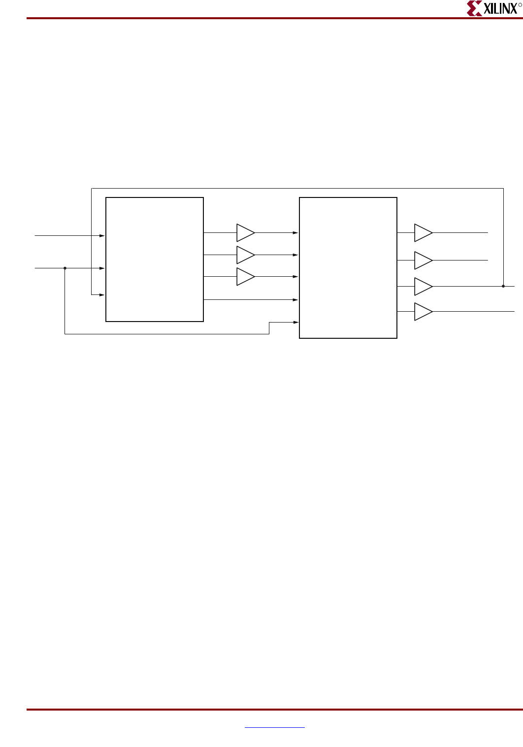
Memory Interface Solutions User Guide www.xilinx.com 175
UG086 (v3.6) September 21, 2010
SerDes Clocking Interface
R
provided for the IDELAYCTRL primitive. Differential and single-ended clocks are passed
through global clock buffers before connecting to a DCM. For differential clocking, the
output of the sys_clk_p/sys_clk_n buffer is single-ended and is provided to the DCM
input. Likewise, for single-ended clocking, sys_clk is passed through a buffer and its
output is provided to the DCM input. The clock outputs of the DCM are passed through
the PMCD. The outputs of the PMCD are clk (0° phase-shifted version of the input clock),
clk_90 (90° phase-shifted version of the input clock), clkdiv_0 (half the frequency of the
input clock and phase-aligned with clk), and clkdiv_90 (half the frequency of the input
clock and phase-aligned with clk_90). The clock outputs of the DCM are passed through
PMCD. After the DCM is locked, the design is in the reset state for at least 25 clocks. The
infrastructure module also generates all of the reset signals required for the design.
Note: SerDes design is not supported for FPGAs that do not have PMCDs. Unsupported FPGAs for
SerDes design are:
Idelay_ctrl
This module instantiates the IDELAYCTRL primitive of the Virtex-4 FPGA. The
IDELAYCTRL primitive is used to continuously calibrate the individual delay elements in
its region to reduce the effect of process, temperature, and voltage variations. A 200 MHz
clock has to be fed to this primitive. For more information on IDELAYCTRLs, refer to
“Verify IDELAYCTRL Instantiation for Virtex-4 and Virtex-5 FPGA Designs” in Chapter
14.
DDR2 SDRAM Initialization and Calibration
DDR2 memory is initialized through a specified sequence as per both Micron and JEDEC
specifications. The controller starts the memory initialization at power-up. Following the
initialization, the relationship between the data and the FPGA clock is calculated using the
tap_logic. The controller issues a dummy write command and dummy read command to
the memory and compares read data with the fixed pattern. During dummy reads, the
tap_logic module calibrates and delays the DQ and DQS to center-align with the FPGA
clock. The dqs_dq_calib_done port in the tap_logic module indicates the completion of
DQS to FPGA clock calibration and per bit calibration.
Figure 3-22: Clocking Scheme for the High-Performance Memory Interface Design
sys_clk_in
sys_reset
CLKIN
RS
T
C
LKFB LOCKED
CLK90
CLKDV
CLK0
DCM PMCD
CLKB
RST
REL
C
LKA1
CLKA1D2
clk_90
clkdiv_90
CLKB1
clk
CLKC1
clkdiv_0
UG086_c3_19_091508
CLKA
CLKC
XC4VLX15-FF668 XC4VFX12-FF668 XC4VSX25-FF668
XC4VLX15-FF676 XC4VFX12-SF363 XC4VSX25-FF676
XC4VLX15-SF363 XC4VFX20-FF672
176 www.xilinx.com Memory Interface Solutions User Guide
UG086 (v3.6) September 21, 2010
Chapter 3: Implementing DDR2 SDRAM Controllers
R
After the per-bit calibration is done, the controller does a read enable calibration. This
calibration is used to determine the delay from read command to read data at rd_data_fifo.
The delay between read command and read data is affected by the CAS latency and
additive latency parameters, the PCB traces, and the I/O buffer delays. This in turn is used
to generate a write enable to rd_data_fifo so that valid data is registered. The controller
issues a dummy read command and compares the read data with a fixed known pattern.
The training_done port in the tap_logic module indicates the completion of the read enable
calibration.
The init_complete port indicates the completion of DQS to FPGA clock calibration, per-bit
calibration, and read enable calibration. After initialization and calibration are done, the
controller can start issuing user commands to the memory.
DDR2 SDRAM System and User Interface Signals
Table 3-23 lists the system signals that are required for the design. The system interface
signals are the clocks and the reset signals given by the user to the FPGA. The sys_clk_p
and sys_clk_n signals comprise the differential clock pair provided to the design. Similarly,
clk200_p and clk_200N comprise the 200 MHz differential clock pair for the IDELAYCTRL
module. The sys_reset_in_n signal resets all the logic.
Table 3-24 describes the DDR2 SDRAM user interface signals.
Table 3-23: DDR2 SDRAM System Signals
Signal Name Direction Description
sys_clk_p, sys_clk_n Input This differential clock pair generates the single-ended clock to the
input of the DCM. Memory operates at this frequency, but the
ddr2_controller, data_path, and user_interface modules, and all
other FPGA slice logic are clocked at half of this frequency.
clk200_p, clk200_n Input Differential clock used in the idelay_ctrl logic.
sys_reset_in_n Input Active-Low reset to the design.
Table 3-24: DDR2 SDRAM Controller User Interface Signals
Signal Name(1) Direction Description
clk_tb Output All user interface signals must be synchronized with respect to the
negative edge of CLKDIV_0.
reset_tb Output Reset signal for the User Interface.
burst_length_div2[2:0] Output This signal determines the data burst length for each write address.
010: burst length = 4
100: burst length = 8
wdf_almost_full Output This signal indicates the ALMOST_FULL status of the Write Data
FIFO. When this signal is asserted, the user can write 5 more data
words into the FIFO for the with testbench case and 14 more data
words for the without testbench case.
app_wdf_data[4n-1:0] Input User write data to the memory, where n indicates the data width of
the interface. The user data width is four times the data width of the
interface. This bus has the data for two rising edges and two falling
edges. The most-significant bits contain the second falling-edge data,
and the least-significant bits contain the first rising-edge data.
Memory Interface Solutions User Guide www.xilinx.com 177
UG086 (v3.6) September 21, 2010
SerDes Clocking Interface
R
app_mask_data[4m-1:0] Input User mask data to the memory, where m indicates the data mask
width of the interface. The mask data width is four times the mask
width of the interface. This bus also has the mask data for four edges.
The most-significant bits contain the mask data for the second falling
edge, and the least-significant bits contain the mask data for the first
rising edge. These signals are not present when the memory part
does not have mask support (for example, certain Registered
DIMMs) or when the data mask option is not selected in the MIG
GUI.
app_wdf_wren Input Write Enable signal to the Write Data FIFO.
af_almost_full Output This signal indicates the ALMOST_FULL status of the Address FIFO.
When this signal is asserted, the user can issue eight more
commands/addresses to the FIFO.
app_af_addr[35:0](2) Input The user address consists of a memory address and dynamic
commands. The address width [31:0] is the memory read/write
address, which includes the column, row, bank, and chip address.
The address width [35:32] represents dynamic commands.
001: Auto Refresh
010: Precharge All
100: Write
101: Read
app_af_wren Input Write Enable signal to the Address FIFO.
read_data0_fifo_out[n-1:0]
read_data1_fifo_out[n-1:0]
read_data2_fifo_out[n-1:0]
read_data3_fifo_out[n-1:0]
Output The read data captured from the memory is four parallel n-bit data
buses, each at half the frequency of the interface, where n indicates
the data width of the interface. READ_DATA0_FIFO_OUT is the first
rising-edge data, READ_DATA1_FIFO_OUT is the second rising-
edge data, READ_DATA2_FIFO_OUT is the first falling-edge data,
and READ_DATA3_FIFO_OUT is the second falling-edge data.
read_data_valid Output This signal is asserted to indicate the read data is available to the user.
init_complete Output This signal indicates the completion of initialization to the memory
and calibration in the design.
Notes:
1. All user interface signal names are prepended with a controller number for the without testbench case, because SerDes clocking
supports only a single controller. See “User Interface Accesses,” page 143 for timing requirements and restrictions on the user
interface signals.
2. Linear addressing is used, i.e., the row address immediately follows the column address bits, and the bank address follows the row
address bits, thus supporting more devices. The number of address bits used depends on the density of the memory part. The
controller ignores the unused bits, which can all be tied High.
Table 3-24: DDR2 SDRAM Controller User Interface Signals (Cont’d)
Signal Name(1) Direction Description
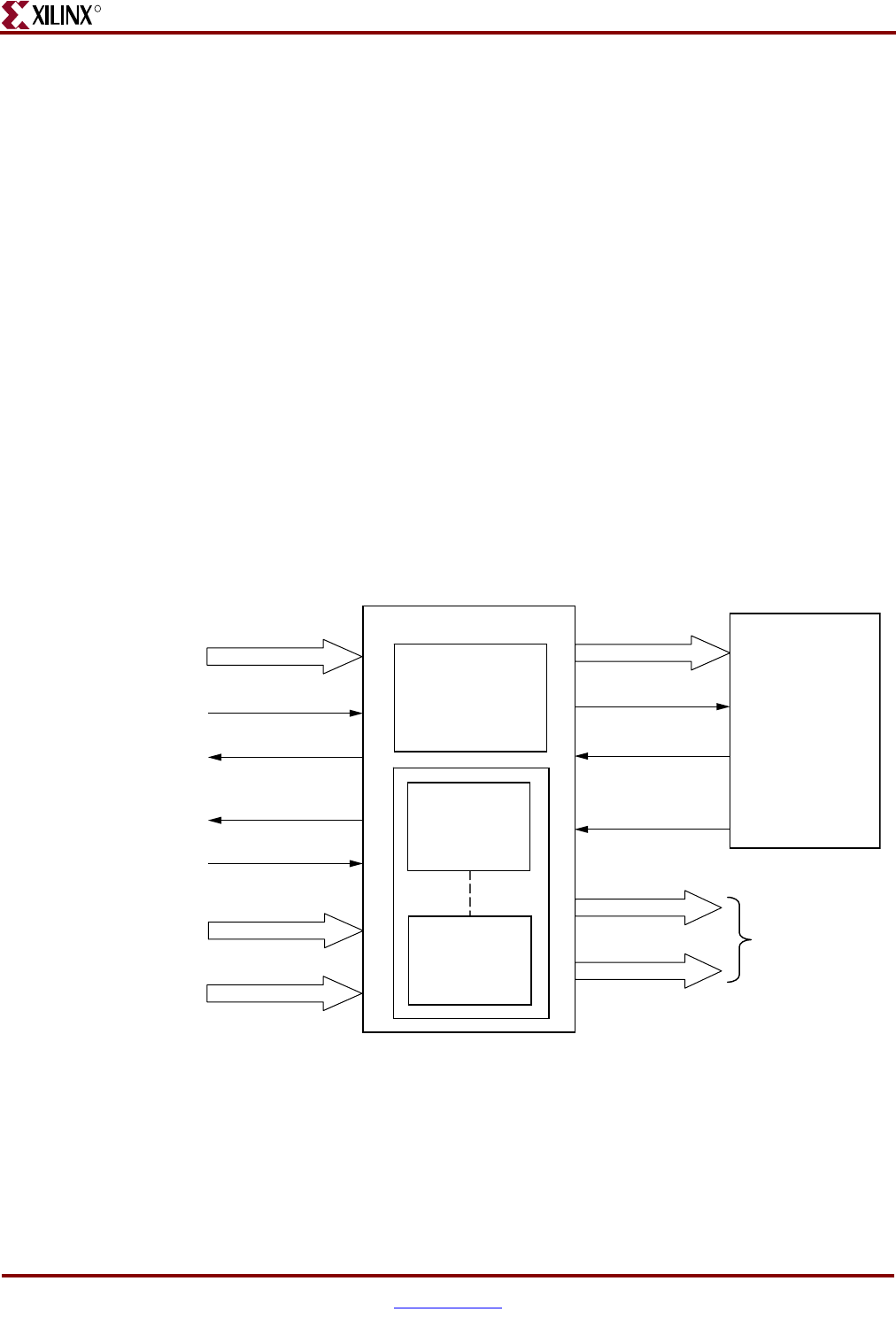
178 www.xilinx.com Memory Interface Solutions User Guide
UG086 (v3.6) September 21, 2010
Chapter 3: Implementing DDR2 SDRAM Controllers
R
User Interface Accesses
The user backend logic communicates with the memory controller through a FIFO-based
user interface. This interface consists of three related buses:
• A Command/Address FIFO bus, which accepts write/read commands as well as the
corresponding memory address from the user
• A Write Data FIFO bus, which accepts the corresponding write data when the user
issues a write command on the Command/Address bus
• A Read bus on which the corresponding read data for an issued read command is
returned
The user interface has the following timing and signaling restriction: When issuing a write
command, the first write data word must be written to the Write Data FIFO no more than
two clock cycles after the write command is issued. This restriction arises from the fact that
the controller assumes write data is available when it receives the write command from the
user.
The clk_tb signal is connected to clkdiv_0 in the controller. If the user clock domain is
different from clkdiv_0 / clk_tb of the MIG, the user should add FIFOs for all data inputs
and outputs of the controller in order to synchronize them to the clk_tb.
Write Interface
Figure 3-23 shows the user interface block diagram for write operations.
The following steps describe the architecture of the Address and Write Data FIFOs and
show how to perform a write burst operation to DDR2 SDRAM from the user interface.
1. The user interface consists of an Address FIFO and a Write Data FIFO. These FIFOs are
constructed using Virtex-4 FPGA FIFO16 primitives with a 512 x 36 configuration. The
36-bit architecture comprises one 32-bit port and one 4-bit port. For Write Data FIFOs,
the 32-bit port is used for data bits and the 4-bit port is used for mask bits. Mask bits
Figure 3-23: User Interface Block Diagram for Write Operations
User Interface
Controller
Address FIFO
(FIFO16)
512 x 36
af_addr
af_empty
ctrl_af_rden
ctrl_wdf_rden
app_af_addr
app_af_wren
app_wdf_data
app_mask_data
app_wdf_wren
wdf_data
mask_data
To Phy Layer
wdf_almost_full
af_almost_full
Write Data
FIFO
(FIFO16)
512 x 36
Write Data
FIFO
(FIFO16)
512 x 36
ug086_c3_28_110707

Memory Interface Solutions User Guide www.xilinx.com 179
UG086 (v3.6) September 21, 2010
SerDes Clocking Interface
R
are available only when supported by the memory part and when the data mask
option is enabled in the MIG GUI. Some memory parts, such as Registered DIMMs of
x4 parts, do not support mask bits.
2. The Common Address FIFO is used for both write and read commands, and comprises
a command part and an address part. Command bits discriminate between write and
read commands.
3. User interface data width app_wdf_data is four times that of the memory data width.
For an 8-bit memory width, the user interface is 32 bits consisting of two rising-edge
data and two falling-edge data. For every 8 bits of data, there is a mask bit. For 72-bit
memory data, the user interface data width app_wdf_data is 288 bits, and the mask
data app_mask_data is 36 bits.
4. The minimum configuration of the Write Data FIFO is 512 x 36 for a memory data
width of 8 bits.
5. Depending on the memory data width, MIG instantiates multiple FIFO16s to gain the
required width. For designs using 8-bit data width, one FIFO16 is instantiated; for
72-bit data width, a total of nine FIFO16s are instantiated. The bit architecture
comprises 16 bits of rising-edge data, 2 bits of rising-edge mask, 16 bits of falling-edge
data, and 2 bits of falling-edge mask, which are all stored in a FIFO16. MIG routes the
app_wdf_data and app_mask_data to FIFO16s accordingly.
6. The user can initiate a write to memory by writing to the Address FIFO and the Write
Data FIFO when the FIFO Full flags are deasserted. Status signal af_almost_full is
asserted when Address FIFO is full, and similarly wdf_almost_full is asserted when
Write Data FIFO is full.
7. Both the Address FIFO and Write Data FIFO Full flags are deasserted with power-on.
8. The user should assert the Address FIFO write-enable signal app_af_wren along with
address app_af_addr to store the write address and write command into the Address
FIFO.
9. The user should assert the Data FIFO write-enable signal app_wdf_wren along with
write data app_wdf_data and mask data app_mask_data to store the write data and
mask data into the Write Data FIFO. The user should provide two rising-edge and two
falling-edge data together for each write to the Data FIFO.
10. The controller reads the Address FIFO by issuing the ctrl_af_rden signal. The
controller reads the Write Data FIFO by issuing the ctrl_wdf_rden signal after the
Address FIFO is read. It decodes the command part after the Address FIFO is read.
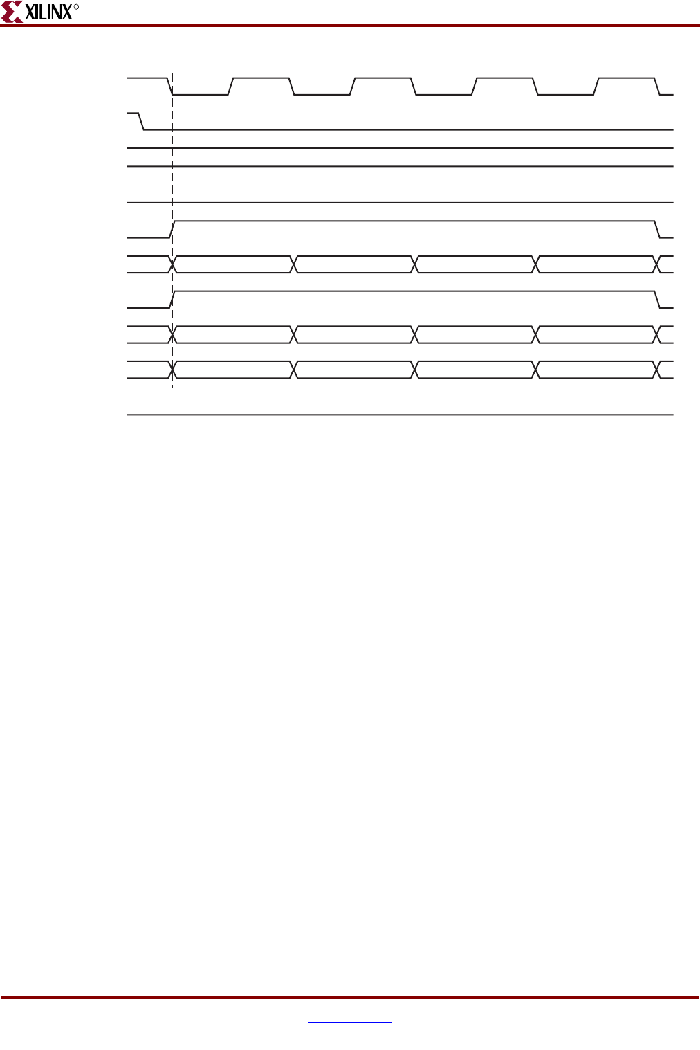
180 www.xilinx.com Memory Interface Solutions User Guide
UG086 (v3.6) September 21, 2010
Chapter 3: Implementing DDR2 SDRAM Controllers
R
11. The write command timing diagram in Figure 3-24 is derived from the MIG-generated
testbench. As shown (burst length of 4), each write to the Address FIFO must be
coupled with one write to the Data FIFO.
Note: The user can start filling the Write Data FIFO two clocks after the Address FIFO is
written, because there is a two-clock latency between the command fetch and reading the Data
FIFO. Using the terms shown in Figure 3-24 and Figure 3-25, therefore, the user can assert the
A1 address two clocks before D0D1D2D3. Similarly, A2, A3, and A4 can be advanced by two
clocks.
Figure 3-24: DDR2 SDRAM Write Burst (BL = 4) for Four Bursts
A1
D0 D1 D2 D3
M0 M1 M2 M3M0 M1 M2 M3M0 M1 M2 M3M0 M1 M2 M3
D0 D1 D2 D3D0 D1 D2 D3D0 D1 D2 D3
clkdiv_0
reset0
burst_length_div2[2:0]
af_almost_full
app_af_wren
app_af_addr[35:0]
app_wdf_wren
app_wdf_data[4n-1:0]
app_mask_data[4m-1:0]
wdf_almost_full
A2
3’b010 (BL = 4)
A3A4
UG086_c3_20_091508
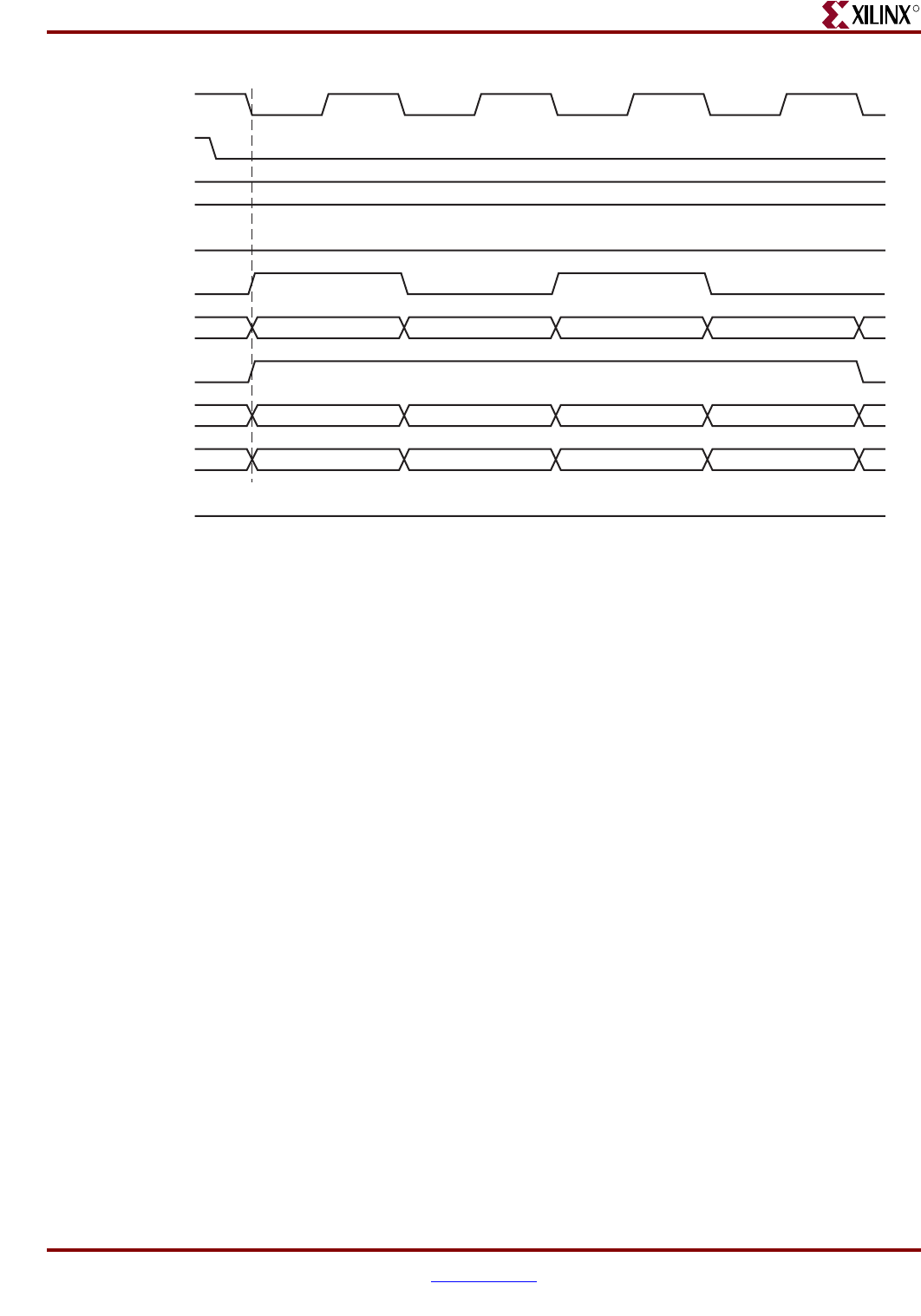
Memory Interface Solutions User Guide www.xilinx.com 181
UG086 (v3.6) September 21, 2010
SerDes Clocking Interface
R
12. The write command timing diagram in Figure 3-25 is derived from the MIG-generated
testbench. As shown (burst length of 8), each write to the Address FIFO must be
coupled with two writes to the Data FIFO. Because the controller first reads the address
and command together, the address need not coincide with the last data. After the
command is analyzed (nearly two clocks later for a worst-case timing scenario), the
controller sequentially reads the data in four clocks. Thus, there are six clocks from the
time the address is read to the time the last data is read.
Correlation between the Address and Data FIFOs
There is a worst case two-cycle latency from the time the address is loaded into the address
FIFO on APP_AF_ADDR[35:0] to the time the controller decodes the address. Because of
this latency, it is not necessary to provide the address on the last clock where data is
entered into the data FIFO. If the address is written before the last data phase, the overall
efficiency and performance increases because it eliminates or reduces the two-cycle
latency. However, if the address is written before data is input into the data FIFO, a FIFO
empty condition might result because the Data FIFO does not contain valid data.
Based on these considerations, Xilinx recommends entering the address into the address
FIFO between the first data phase and the next-to-last data phase. For a burst of four or
eight, this means the Address can be asserted two clocks before the first data phase. This
implementation increases efficiency by reducing the two clock latency and guarantees that
valid data is available in the Data FIFO.
Figure 3-25: DDR2 SDRAM Write Burst (BL = 8) for Two Bursts
A1
D0 D1 D2 D3
M0 M1 M2 M3M4 M5 M6 M7 M0 M1 M2 M3M4 M5 M6 M7
D4 D5 D6 D7 D0 D1 D2 D3D4 D5 D6 D7
clkdiv_0
reset0
burst_length_div2[2:0]
af_almost_full
app_af_wren
app_af_addr[35:0]
app_wdf_wren
app_wdf_data[4n-1:0]
app_mask_data[m-1:0]
wdf_almost_full
0
3’b100 (BL = 8)
A2 0
UG086_c3_21_091508
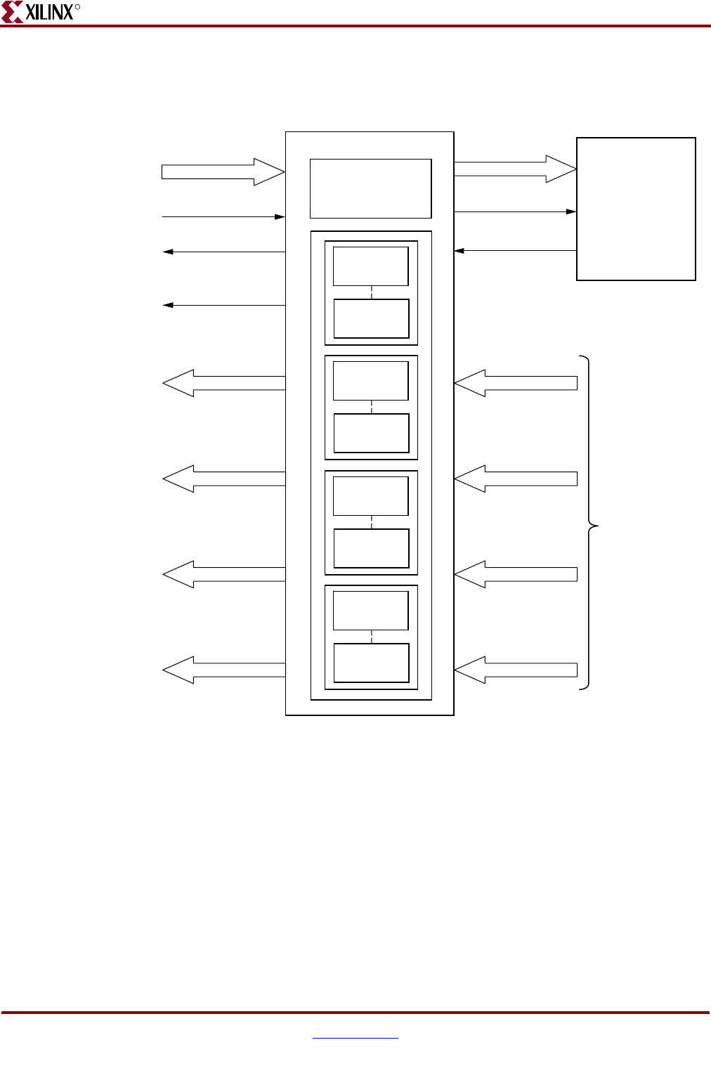
182 www.xilinx.com Memory Interface Solutions User Guide
UG086 (v3.6) September 21, 2010
Chapter 3: Implementing DDR2 SDRAM Controllers
R
Read Interface
Figure 3-26 shows a block diagram of the read interface.
The following steps describe the architecture of the Read Data FIFOs and show how to
perform a burst read operation from DDR SDRAM from the user interface.
1. The read user interface consists of an Address FIFO and a Read Data FIFO. The
Address FIFO is common to both read and write operations. These FIFOs are
constructed using Virtex-4 FPGA Distributed RAMs with a 16 x 1 configuration. MIG
instantiates a number of RAM16Ds depending on the data width. For example, for
8-bit data width, MIG instantiates a total of 32 RAM16Ds, 16 for first and second
rising-edge data and 16 for first and second falling-edge data. Similarly, for 72-bit data
width, MIG instantiates a total of 288 RAM16Ds, 144 for first and second rising-edge
data and 144 for first and second falling-edge data.
Figure 3-26: User Interface Block Diagram for Read Operation
User Interface
Controller
Address FIFO
(FIFO16)
512 x 36
af_addr
af_empty
ctrl_af_rden
app_af_addr
app_af_wren
read_data0_fifo_out
read_data1_fifo_out
read_data2_fifo_out
read_data3_fifo_out
read_data0_fifo_out
read_data1_fifo_out
read_data2_fifo_out
read_data3_fifo_out
From Phy Layer
read_data_valid
af_almost_full
Read Data
FIFO 0
RAM16 x 1D
Read Data
FIFO 0
RAM16 x 1D
Read Data
FIFO 1
RAM16 x 1D
Read Data
FIFO 1
RAM16 x 1D
Read Data
FIFO 2
RAM16 x 1D
Read Data
FIFO 2
RAM16 x 1D
Read Data
FIFO 3
RAM16 x 1D
Read Data
FIFO 3
RAM16 x 1D
ug086_c3_29_110607
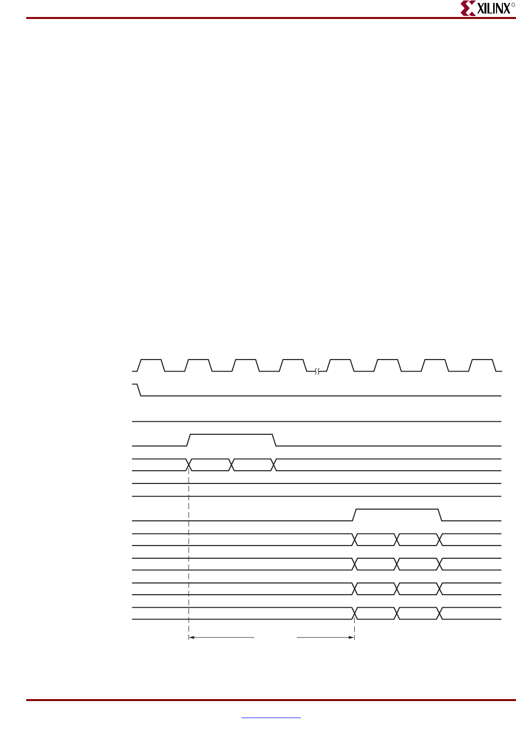
Memory Interface Solutions User Guide www.xilinx.com 183
UG086 (v3.6) September 21, 2010
SerDes Clocking Interface
R
2. The user can initiate a read to memory by writing to the Address FIFO when the
FIFO Full flag af_almost_full is deasserted.
3. To write the read address and read command into the Address FIFO, the user should
issue the Address FIFO write-enable signal app_af_wren along with read address
app_af_addr.
4. The controller reads the Address FIFO containing the address and command. After
decoding the command, the controller generates the appropriate control signals to
memory.
5. Prior to the actual read and write commands, the design calibrates the latency (number
of clock cycles) from the time the read command is issued to the time data is received.
Using this pre-calibrated delay information, the controller generates the write-enable
signals to the Read Data FIFOs.
After the power-up calibration is done, dummy reads are executed to set up the delay
between the read command and read data from the memory. During the time these
dummy reads are in progress, the read enable is generated with each read command
and is delayed until the read data matches the write data. This delay includes CAS
latency, trace delay, and path delay. This precalculated delay is used for asserting the
read-enable signals that latch the data into the Read Data FIFOs. The delays are
calculated on a per-DQS basis. For example, if a bank has two DQS signals, there are
two read enables used to latch the read data to the FIFOs. The strobe (DQS), data (DQ),
and clock (CK/CK) signals should be matched in trace length from the FPGA to the
memory device. MIG ensures that a DQS and its corresponding DQ signals do not
cross a bank boundary.
6. The read_data_valid signal is asserted when data is available in the Read Data FIFOs.
Figure 3-27: DDR2 SDRAM Read Burst (BL = 4) for Two Bursts
clkdiv_0
reset0
af_almost_full
app_af_wren
app_af_addr[35:0]
burst_length_div2[2:0]
read_data_valid
read_data0_fifo_out[n-1:0]
read_data1_fifo_out[n-1:0]
read_data2_fifo_out[n-1:0]
read_data3_fifo_out[n-1:0]
UG086_c3_22_091508
A1 A2
D0 D0
D1 D1
D2 D2
D3D3
3’b010 (BL=4)
25 Clocks
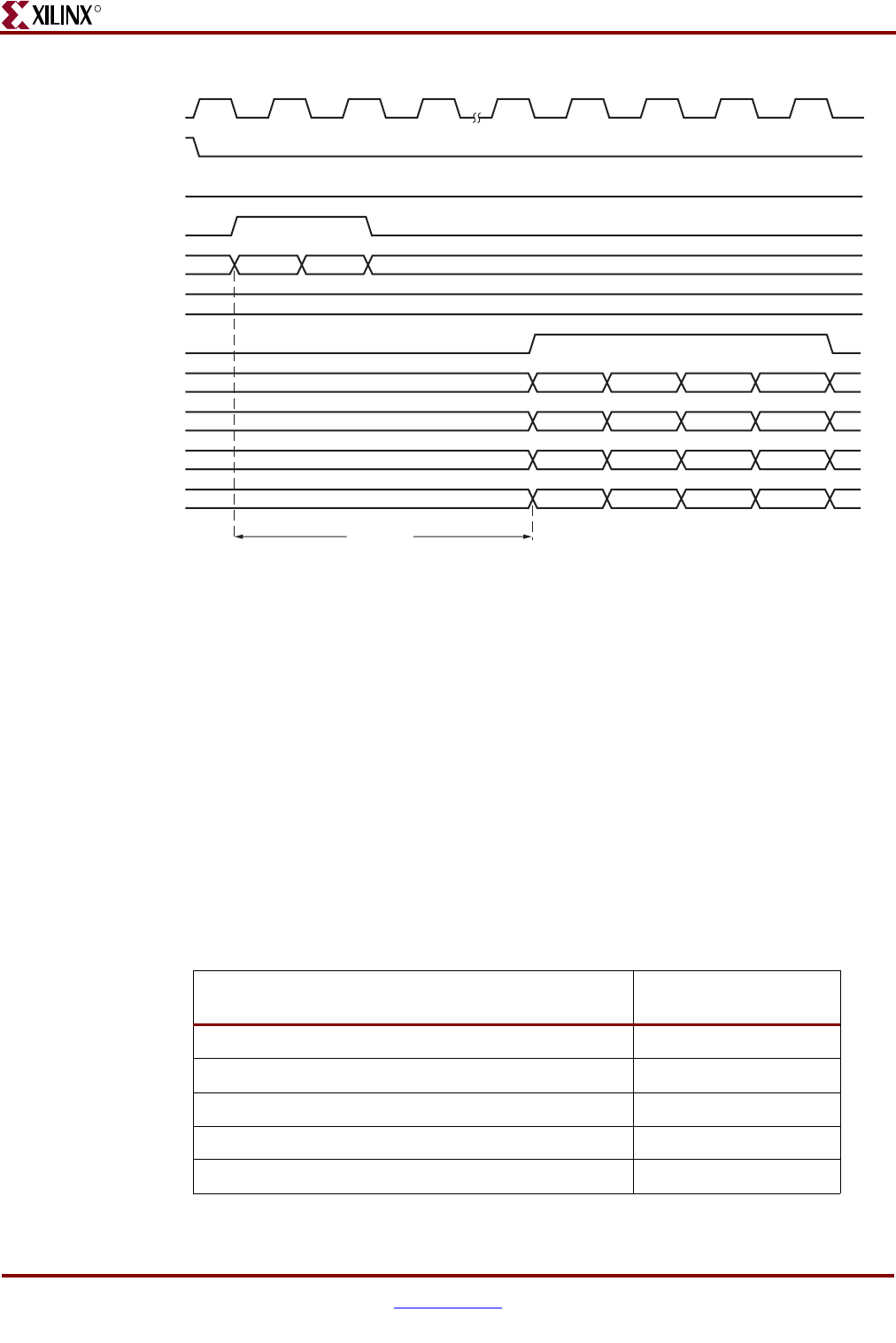
184 www.xilinx.com Memory Interface Solutions User Guide
UG086 (v3.6) September 21, 2010
Chapter 3: Implementing DDR2 SDRAM Controllers
R
7. Figure 3-27 shows the user interface timing diagram for a burst length of 4, and
Figure 3-28 shows user interface timing diagram for a burst length of 8. Both the cases
shown here are for a CAS latency of 4 at 200 MHz. The read latency is calculated from
the point when the read command is given by the user to the point when the data is
available with the read_data_valid signal. The minimum latency in this case is 25
clocks, where no precharge is required, no auto-refresh request is pending, the user
commands are issued after initialization is completed, and the first command issued is
a Read command. Controller executes the commands only after initialization is done
as indicated by the init_done signal.
8. After the address and command are loaded into the Address FIFO, it takes 25 clock
cycles minimum for the controller to assert the read_data_valid signal.
9. Read data is available only when the read_data_valid signal is asserted. The user
should access the read data on every positive edge of the read_data_valid signal.
Table 3-25 shows how the 25 clocks from the read command to the read data are broken up.
Figure 3-28: DDR2 SDRAM Read Burst (BL = 8) for Two Bursts
clkdiv_0
reset0
af_almost_full
app_af_wren
app_af_addr[35:0]
burst_length_div2[2:0]
read_data_valid
read_data0_fifo_out[n-1:0]
read_data1_fifo_out[n-1:0]
read_data2_fifo_out[n-1:0]
read_data3_fifo_out[n-1:0]
UG086_c3_23_091508
A1 A2
D0 D4
D1 D5
D2 D6
D3D7
3’b100 (BL=8)
25 Clocks
D0 D4
D1 D5
D2 D6
D3D7
Table 3-25: Read Command to Read Data Clock Cycles
Parameter Number of Clocks
(CLKDIV_0)
Read Command to Empty Signal Deassertion 7 Clocks
Empty to Active Command 5.5 Clocks
Active to Read Command 3 Clocks
Memory Read Command to Read Data Valid 9.5 Clocks
Tot al : 25 Clocks
Memory Interface Solutions User Guide www.xilinx.com 185
UG086 (v3.6) September 21, 2010
SerDes Clocking Interface
R
In general, read latency varies based on the following parameters:
• CAS latency (CL) and additive latency (AL)
• The number of commands already in the FIFO pipeline before the read command is
issued
• Whether an ACTIVATE command needs to be issued to open the new bank/row
• Whether a PRECHARGE command needs to be issued to close a previously opened
bank
• Specific timing parameters for the memory, such as TRAS, and TRCD in conjunction
with the bus clock frequency
• Possible interruption of commands and/or forced closure of banks/rows when the
periodic AUTO REFRESH command is issued
• Commands issued by the user before initialization is complete, causing latency to be
indeterminate
• Board-level and chip-level (for both memory and FPGA) propagation delays
User to Controller Interface
Table 3-26 lists the signals between the user interface and the controller.
Table 3-26: Signals between User Interface and Controller
Port Name Port
Width Port Description Notes
waf_addr 36 Output of the Address FIFO in the user interface.
Mapping of these address bits:
Memory Address (CS, Bank, Row, Column): [31:0]
Dynamic Command Request: [34:32]
Reserved: [35]
Monitor FIFO-full status flag to
write address into the Address
FIFO
af_almost_empty 1 The user interface Address FIFO empty status flag
output. The user application can write to the
Address FIFO when this signal is asserted until the
write data FIFO-full status flag is asserted.
FIFO16 Almost Empty Flag
ctrl_waf_RdEn 1 Read Enable input to Address FIFO in the user
interface
This signal is asserted for one
CLKDIV_0 clock cycle when the
controller state is write, read,
Load Mode register, Precharge
All, Auto Refresh, or Active
resulting from dynamic
command requests. Figure 3-29
shows the timing waveform for a
burst length of 8 with two back-
to-back writes followed by two
back-to-back reads.
186 www.xilinx.com Memory Interface Solutions User Guide
UG086 (v3.6) September 21, 2010
Chapter 3: Implementing DDR2 SDRAM Controllers
R
The memory address (Waf_addr) includes the column address, row address, bank address,
and chip-select width for deep memory interfaces.
Column Address
[‘column_address - 1:0]
Row Address
[(‘row_address + ‘column_address) - 1:‘column_address]
Bank Address
[(‘bank_address + ‘row_address + ‘column_address) -
1:(‘column_address + ‘row_address)]
Chip Select
[‘cs_width + ‘bank_address + ‘row_address + ‘column_address -
1:‘bank_address + ‘row_address + ‘column_address]
ctrl_wdf_Rden 1 Read Enable input to Write Data FIFO in the user
interface
The controller asserts this signal
one CLKDIV_0 clock cycle after
the first write state. This signal
remains asserted for one clock
cycle for a burst length of 4 and
two clock cycles for a burst
length of 8. Figure 3-29 shows the
timing waveform. Sufficient data
must be available in the Write
Data FIFO associated with a
write address for the required
burst length before issuing a
write command. For example,
for a 64-bit data bus and a burst
length of 4, the user should input
four 64-bit data words in the
Write Data FIFO for every write
address before issuing the write
command.
Table 3-26: Signals between User Interface and Controller (Cont’d)
Port Name Port
Width Port Description Notes
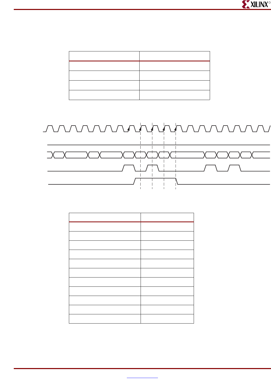
Memory Interface Solutions User Guide www.xilinx.com 187
UG086 (v3.6) September 21, 2010
SerDes Clocking Interface
R
Dynamic Command Request
Table 3-27 lists the commands supported from user interface.
Figure 3-29 describes two consecutive writes followed by two consecutive reads with a
burst length of 8. Table 3-28 lists the state signal values for Figure 3-29.
Table 3-27: User Interface Commands
Command Description
001 Auto Refresh
010 Precharge All
100 Write
101 Read
Figure 3-29: Controller Read of Command and Data from User Interface FIFOs for a Burst Length of 8
af_almost_empty
ctrl_waf_rden
ctrl_wdf_rden
addr_controller/
state
clkdiv_0
0304 07 080C 16 09 0B 0A 0B
UG086_c3_24_091508
0C 0C0D
Table 3-28: State Signal Values for Figure 3-29
State Signal Value (hex) Description
03 precharge
04 precharge_wait
07 active
08 active_wait
09 first_read
0A burst_read
0B read_wait
0C first_write
0D burst_write
0E write_wait
16 write_read

188 www.xilinx.com Memory Interface Solutions User Guide
UG086 (v3.6) September 21, 2010
Chapter 3: Implementing DDR2 SDRAM Controllers
R
Controller to Physical Layer Interface
Table 3-29 lists the signals between the controller and the physical layer.
Table 3-29: Signals between the Controller and Physical Layer
Signal Name Signal
Width Signal Description Notes
ctrl_wren 1 Output from the controller to the
write datapath.
Write DQS and DQ generation
begins when this signal is
asserted.
Asserted for two CLKDIV_0 cycles for a
burst length of 4 and three CLKDIV_0
cycles for burst length of 8.
Asserted one CLKDIV_0 cycle earlier
than the WRITE command for CAS
latency values of 4 and 5.
ctrl_wr_dis 1 Output from the controller to the
write datapath.
Write DQS and DQ generation
ends when this signal is asserted.
Asserted for one CLKDIV_0 cycle for a
burst length of 4 and two CLKDIV_0
cycles for burst length of 8.
Asserted one CLKDIV_0 cycle earlier
than the WRITE command for CAS
latency values of 4 and 5.
ctrl_odd_latency 1 Output from the controller to the
write datapath.
Asserted when the selected CAS
latency is an odd number.
Required for generation of write
DQS and DQ after the correct
latency (CAS latency – 1).
ctrl_RdEn_div0 1 Output from the controller to the
datapath generated with each
read command. This is delayed
by the precalculated amount and
is used as a write enable to the
read data capture FIFOs.
This signal is asserted for one CLKDIV_0
clock cycle for a burst length of 4 and two
clock cycles for a burst length of 8.
ctrl_dummyread_start 1 Output from the controller to the
write datapath. When this signal
is asserted, the strobe and data
calibration begin.
This signal must be asserted when valid
read data is available on the read data
bus.
This signal is deasserted when the
dp_dly_slct_done signal is asserted.
dp_dly_slct_done 1 Output from the read datapath
to the controller indicating the
strobe and data calibration are
complete.
This signal is asserted when the data and
strobe are calibrated.
Normal operation begins after this signal
is asserted.
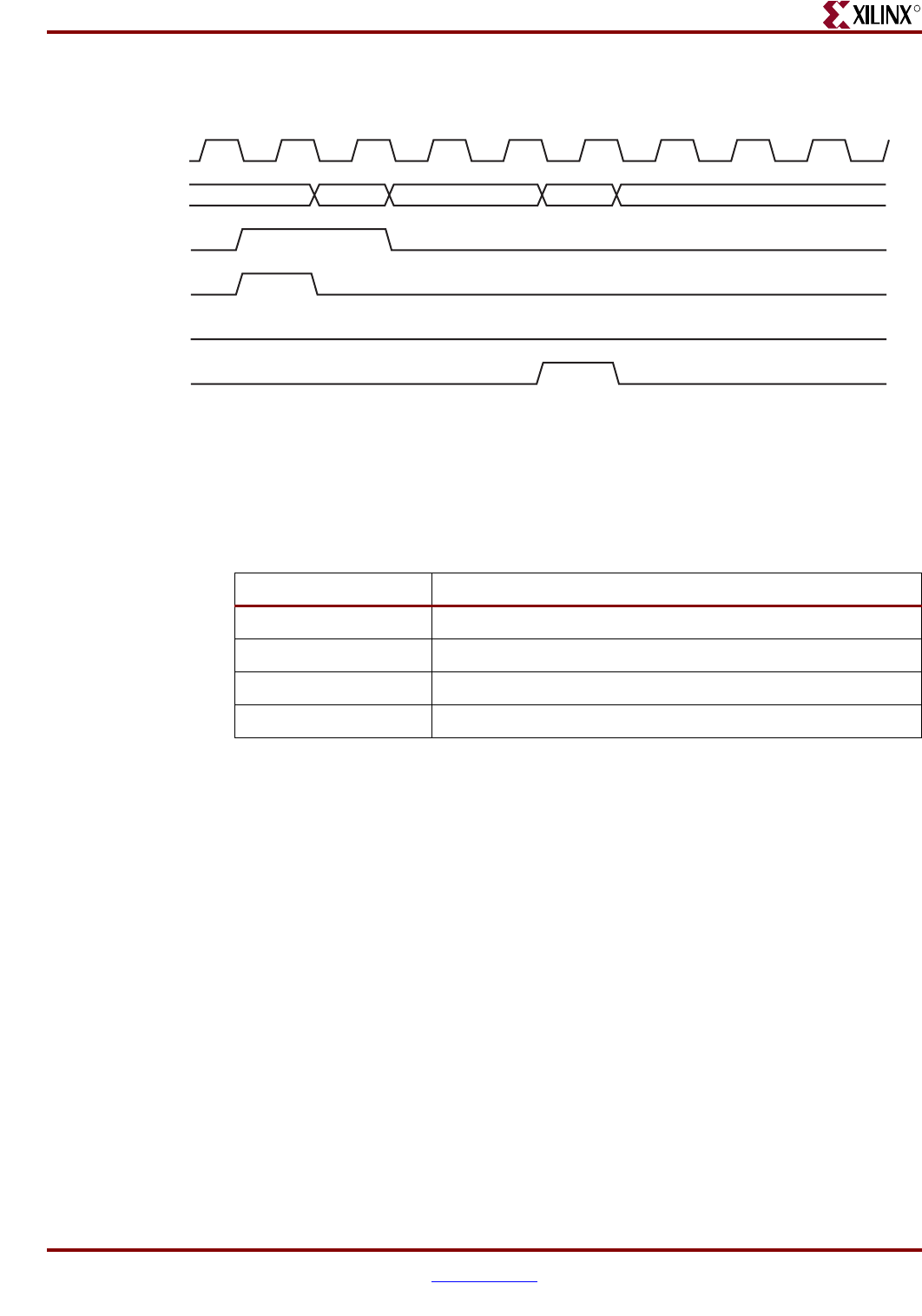
Memory Interface Solutions User Guide www.xilinx.com 189
UG086 (v3.6) September 21, 2010
SerDes Clocking Interface
R
Figure 3-30 describes the timing waveform for control signals from the controller to the
physical layer with a CAS latency of 4 and an additive latency of 0.
SerDes DDR2 SDRAM Signal Allocations
MIG allows bank selection for different classes of memory signals. Table 3-30 shows the list
of signals allocated in a group from bank selection checkboxes.
Note: Timing has been verified for most of the MIG generated configurations. For the best timing
results, adjacent banks in the same column of the FPGA should be used. Banks that are separated
by unbonded banks should be avoided because these can cause timing violations.
Simulating the DDR2 SDRAM Design
After generating the design, MIG creates a sim folder in the specified path. This folder
contains simulation files for a particular design. The sim folder contains the external
testbench, memory model, and .do file to simulate the generated design. The memory
model files are currently generated in Verilog only. To learn more details about the files in
the sim folder and to simulate the design, refer to “Simulation Guide,” page 499.
For single-rank DIMMs, MIG outputs only the base part memory model. In the simulation
testbench (sim_tb_top in the sim folder), MIG instantiates the required number of
memory models. For example, a 1 GB single-rank DIMM with the base part is 1 Gb, and
MIG instantiates the base model eight times. If the MIG generated memory model is to be
used with the user’s test bench, multiple instances should be used based on the selected
configuration.
The MIG output memory model considers the MEM_BITS parameter by default for
memory range allocation. This covers only a partial memory range, i.e., 2MEM_BITS. To
allocate the full memory range, the MAX_MEM parameter should be set in the memory
Figure 3-30: Timing Waveform for Control Signals from the Controller to the Physical Layer
Command WRITE IDLE IDLEREAD
ctrl_wren
ctrl_wr_disable
ctrl_odd_latency
ctrl_rden_div0
clkdiv_0
UG086_c3_25_091508
Table 3-30: SerDes DDR2 SDRAM Signal Allocations
Bank Selected Signals Allocated in the Group
Address Memory address, memory control, and memory clock signals
Data Data, data mask, and data strobes
System Control System reset from user interface and status signals
System Clock System clocks from user interface
190 www.xilinx.com Memory Interface Solutions User Guide
UG086 (v3.6) September 21, 2010
Chapter 3: Implementing DDR2 SDRAM Controllers
R
model. Allocating the full memory range might exceed the memory of the operating
system, thus causing memory allocation failure in simulations.
Simulation Violations
There might be simulation violations for frequencies such as 150 MHz where the clock
period is not an integer value. At 150 MHz, the clock period value in the simulation
testbench is 6.66 ns and the MIG tool rounds it to 6.67 ns. Consider a memory TRCD value
of 20 ns. MIG calculates the TRCD count value based on the clock period,
RCD_COUNT_VALUE = 20/6.67 = 2.998 = 3 (after rounding off) in the design parameter
file. The TRCD value for 3 clock cycles is 3 × 6.66 = 19.98, which causes timing violations by
20 ps. The difference between the clock period in the external simulation testbench versus
the MIG tool causes timing violations. This is only one example case. There might be more
such scenarios. These are only simulation warnings. Functionally, there should be no
issues. To remove these warnings, the related count value can be increased by one.
Changing the Refresh Rate
The formula is similar to the Virtex-4 FPGA DDR2 direct-clocking case. However, since the
refresh logic in the controller is running at half the memory bus rate, the formula is
MAX_REF_CNT = (refresh interval) / (2 * clock period). For example, for a refresh rate of
3.9 µs with a memory bus running at 267 MHz:
MAX_REF_CNT = 3.9 µs / (2 * clock period) = 3.9 µs / 7.49 ns = 521 (decimal) = 0x209
If the above value exceeds 2MAX_REF_WIDTH – 1, the value of MAX_REF_WIDTH must be
increased accordingly in parameters_0.v (or .vhd) to increase the width of the counter
used to track the refresh interval.
Supported Devices
The design generated out of MIG is independent of memory package, hence the package
part of the memory component is replaced with XX, where XX indicates a don't care
condition. The tables below list the components (Table 3-31) and DIMMs (Table 3-32
through Table 3-34) supported by the tool for DDR2 SerDes clocking designs.
In supported devices, an X in the component column denotes a single alphanumeric
character. For example MT47H128M4XX-3 can be either MT47H128M4BP-3 or
MT47H128M4B6-3. An XX for Registered DIMMs denotes a single or two alphanumeric
characters. For example, MT9HTF3272XX-667 can be either MT9HTF3272Y-667 or
MT9HTF3272DY-667. Pin mapping for x4 RDIMMs is provided in Appendix G, “Low
Power Options.”
Table 3-31: Supported Components for DDR2 SDRAM
Components Packages (XX) Components Packages (XX)
MT47H64M4XX-3 BP MT47H16M16XX-3 BG
MT47H64M4XX-37E BP MT47H16M16XX-37E BG
MT47H64M4XX-5E BP MT47H16M16XX-5E BG
MT47H128M4XX-3 B6,CB,GB MT47H32M16XX-3 BN,CC,FN,GC
MT47H128M4XX-37E B6,CB,GB MT47H32M16XX-37E BN,CC,FN,GC
MT47H128M4XX-5E B6,CB,GB MT47H32M16XX-5E BN,CC,FN,GC
MT47H256M4XX-3 BT,HQ MT47H64M16XX-3 BT,HR
Memory Interface Solutions User Guide www.xilinx.com 191
UG086 (v3.6) September 21, 2010
SerDes Clocking Interface
R
MT47H256M4XX-37E BT,HQ MT47H64M16XX-37E BT,HR
MT47H256M4XX-5E BT,HQ MT47H64M16XX-5E BT,HR
MT47H512M4XX-3 HG MT47H128M16XX-3 HG
MT47H512M4XX-37E HG MT47H128M16XX-37E HG
MT47H512M4XX-5E HG MT47H128M16XX-5E --
MT47H32M8XX-3 BP HYB18T1G800XXXX-3S C2F,C2FL
MT47H32M8XX-37E BP HYB18T1G800XXXX-37 C2F,C2FL
MT47H32M8XX-5E BP HYB18T1G160XXXX-3S C2F,C2FL
MT47H64M8XX-3 B6,CB,F6,GB HYB18T1G160XXXX-37 C2F,C2FL
MT47H64M8XX-37E B6,CB,F6,GB HYB18T1G400XXXX-3S C2F,C2FL
MT47H64M8XX-5E B6,CB,F6,GB HYB18T1G400XXXX-37 C2F,C2FL
MT47H128M8XX-3 BT,HQ HYB18T512800XXXX-3S B2F,B2FL
MT47H128M8XX-37E BT,HQ HYB18T512800XXXX-37 B2F,B2FL
MT47H128M8XX-5E BT,HQ HYB18T512160XXXX-3S B2F,B2FL
MT47H256M8XX-3 HG HYB18T512160XXXX-37 B2F,B2FL
MT47H256M8XX-37E HG HYB18T512400XXXX-3S B2F,B2FL
MT47H256M8XX-5E HG HYB18T512400XXXX-37 B2F,B2FL
Table 3-32: Supported Registered DIMMs for DDR2 SDRAM
Registered DIMMs Registered DIMMs
MT9HTF3272Y-667 MT18HTF6472Y-667
MT9HTF3272PY-667 MT18HTF6472PY-667
MT9HTF3272Y-53E MT18HTF6472Y-53E
MT9HTF3272PY-53E MT18HTF6472PY-53E
MT9HTF3272Y-40E MT18HTF6472Y-40E
MT9HTF3272PY-40E MT18HTF6472PY-40E
MT9HTF6472Y-667 MT18HTF12872Y-667
MT9HTF6472PY-667 MT18HTF12872PY-667
MT9HTF6472Y-53E MT18HTF12872Y-53E
MT9HTF6472PY-53E MT18HTF12872PY-53E
MT9HTF6472Y-40E MT18HTF12872Y-40E
MT9HTF6472PY-40E MT18HTF12872PY-40E
MT9HTF12872Y-667 MT18HTF25672Y-667
MT9HTF12872PY-667 MT18HTF25672PY-667
Table 3-31: Supported Components for DDR2 SDRAM (Cont’d)
Components Packages (XX) Components Packages (XX)
192 www.xilinx.com Memory Interface Solutions User Guide
UG086 (v3.6) September 21, 2010
Chapter 3: Implementing DDR2 SDRAM Controllers
R
MT9HTF12872Y-53E MT18HTF25672Y-53E
MT9HTF12872PY-53E MT18HTF25672PY-53E
MT9HTF12872Y-40E MT18HTF25672Y-40E
MT9HTF12872PY-40E MT18HTF25672PY-40E
MT18HTF6472G-53E --
Table 3-33: Supported Unbuffered DIMMs for DDR2 SDRAM
Unbuffered DIMMs Unbuffered DIMMs
MT4HTF1664AY-667 MT8HTF6464AY-40E
MT4HTF1664AY-53E MT8HTF12864AY-667
MT4HTF1664AY-40E MT8HTF12864AY-53E
MT4HTF3264AY-667 MT8HTF12864AY-40E
MT4HTF3264AY-53E MT9HTF3272AY-667
MT4HTF3264AY-40E MT9HTF3272AY-53E
MT4HTF6464AY-667 MT9HTF3272AY-40E
MT4HTF6464AY-53E MT9HTF6472AY-667
MT4HTF6464AY-40E MT9HTF6472AY-53E
MT8HTF6464AY-667 MT9HTF6472AY-40E
MT8HTF6464AY-53E --
Table 3-34: Supported SODIMMs for DDR2 SDRAM
SODIMMs SODIMMs
MT4HTF1664HY-667 MT8HTF3264HY-667
MT4HTF1664HY-53E MT8HTF3264HY-53E
MT4HTF1664HY-40E MT8HTF3264HY-40E
MT4HTF3264HY-667 MT8HTF6464HY-667
MT4HTF3264HY-53E MT8HTF6464HY-53E
MT4HTF3264HY-40E MT8HTF6464HY-40E
Table 3-32: Supported Registered DIMMs for DDR2 SDRAM (Cont’d)
Registered DIMMs Registered DIMMs
Memory Interface Solutions User Guide www.xilinx.com 193
UG086 (v3.6) September 21, 2010
SerDes Clocking Interface
R
Hardware Tested Configurations
The frequencies shown in Table 3-35 were achieved on the Virtex-4 FPGA ML461 Memory
Interfaces Development Board under nominal conditions. This frequency should not be
used to determine the maximum design frequency. The maximum design frequency
supported in the MIG wizard is based on a combination of the TRCE results for fabric
timing on multiple device/package combinations and I/O timing analysis using FPGA
and memory timing parameters for a 64-bit wide interface.
Table 3-35: Hardware Tested Configurations
Synthesis Tools XST and Synplicity
HDL Verilog and VHDL
FPGA Device XC4VLX25-FF668-11
Burst Lengths 4, 8
CAS Latency 4, 5
Additive Latency 0, 1, 2
8-bit Design Tested on 16-bit Component “MT47H32M16XX-3”
64-bit Design Tested on 64-bit UDIMM “MT8HTF6464AY-667”
72-bit Design Tested on 72-bit RDIMM “MT9HTF6472Y-667”
Frequency Range 140 MHz to 400 MHz for component and Registered DIMMs
140 MHz to 290 MHz for Unbuffered DIMMs

Memory Interface Solutions User Guide www.xilinx.com 195
UG086 (v3.6) September 21, 2010
R
Chapter 4
Implementing QDRII SRAM Controllers
This chapter describes how to implement QDRII SRAM interfaces for Virtex®-4 FPGAs
generated with MIG. This design is based on XAPP703 [Ref 20].
Feature Summary
The QDRII controller design supports the following:
• A maximum frequency of 250 MHz
• 9-bit, 18-bit, 36-bit, and 72-bit data widths
• Burst lengths of two and four
• Implementation using different Virtex-4 devices
• Operation with any 9-bit, 18-bit, and 36-bit memory component
•Verilog and VHDL
• With and without a testbench
• With and without a DCM
Design Frequency Range
Limitations
Four different FIFOs are accessible from the user interface: the Read Address FIFO, Read
Data FIFO, Write Address FIFO, and Write Data FIFO. The Read Address FIFO is used to
store the read command and read address. The Write Address FIFO is used to store the
write command and write address. The Write Data FIFO is used to store the write data
from the user interface. The controller stores the read data from the memory to the Read
Data FIFO. The controller executes read commands only when the Read Address FIFO is
not empty and the Read Data FIFO is not full. Similarly, the controller executes write
commands only when the Write Address FIFO are Write Data FIFO are not empty. The
sequence of commands executed by the controller might not be the same as the sequence of
commands that are stored in the Read Address and Write Address FIFOs. The controller
executes write and read commands alternately when it finds valid write and read
Table 4-1: Design Frequency Range in MHz
Memory
FPGA Speed Grade
-10 -11 -12
Min Max Min Max Min Max
Component 120 200 120 240 120 250
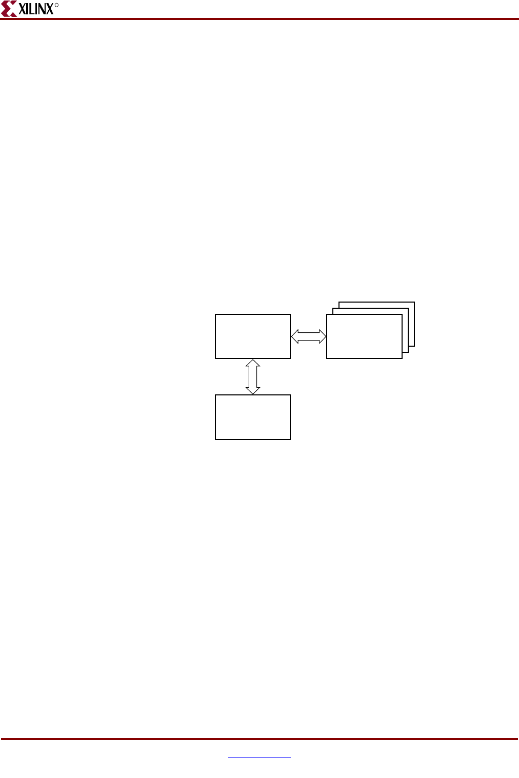
196 www.xilinx.com Memory Interface Solutions User Guide
UG086 (v3.6) September 21, 2010
Chapter 4: Implementing QDRII SRAM Controllers
R
commands, irrespective of the sequence of commands that are written to the FIFOs from
the user interface. Consider an example in which 10 write commands followed by 10 read
commands are issued from the user interface, but the controller executes write, read, write,
read… and so on. If the Read Address FIFO is empty or the Read Data FIFO is full, and the
Write Address FIFO is not empty, the controller executes all write commands sequentially.
Similarly, if the Write Address FIFO is empty, the Read Address FIFO is not empty, and the
Read Data FIFO is not full, the controller executes all read commands sequentially.
The controller remains in the IDLE state when the Write Address FIFO is empty, and either
the Read Address FIFO is empty or the Read Data FIFO is full.
Architecture
Figure 4-1 shows a top-level block diagram of the QDRII memory controller. One side of
the QDRII memory controller connects to the user interface denoted as Block Application.
The other side of the controller interfaces to QDRII memory. The memory interface data
width is selectable.
Data is double-pumped to QDRII SRAM on both the positive and the negative clock edges.
The HSTL_18 Class I I/O standard is used for the data, address, and control signals.
QDRII SRAM interfaces are source-synchronous and double data rate like DDR SDRAM
interfaces.
The key advantage to QDRII devices is they have separate data buses for reads and writes
to SRAM.
Interface Model
The memory interface is layered to simplify the design and make the design modular.
Figure 4-2 shows the layered memory interface in the QDRII memory controller. The three
layers are the application layer, the implementation layer, and the physical layer.
Figure 4-1: QDRII Memory Controller
QDRII
Memory
Controller
Block
Application
UG086_c4_01_042205
QDRII
Memory
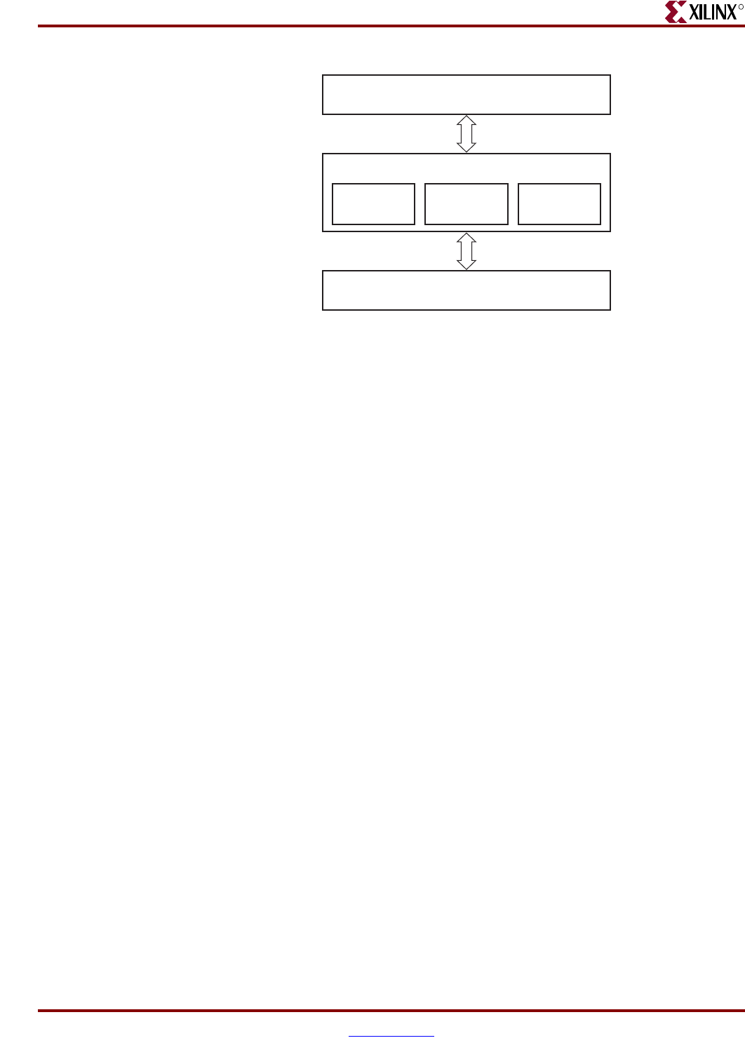
Memory Interface Solutions User Guide www.xilinx.com 197
UG086 (v3.6) September 21, 2010
Architecture
R
The application layer comprises the user interface, which initiates memory writes and
reads by writing data and memory addresses to the User Interface FIFOs. The
implementation layer comprises the infrastructure, datapath, and control logic.
• The infrastructure logic consists of the DCM and reset logic generation circuitry.
• The datapath logic consists of the calibration logic by which the data from the
memory component is captured using the FPGA clock.
• The control logic determines the type of data transfer, that is, read/write with the
memory component, depending on the User Interface FIFO’s status signals.
The physical layer comprises the I/O elements of the FPGA. The controller communicates
with the memory component using this layer. The I/ O elements (such as IDDRs, ODDRs,
and IDELAY elements) are associated with this layer.
Hierarchy
Figure 4-3 shows the QDRII SRAM controller hierarchy.
Figure 4-2: Interface Layering Model
User Interface
Physical Layer
Implementation Layer
UG086_c4_02_012507
Infrastructure Datapath Control
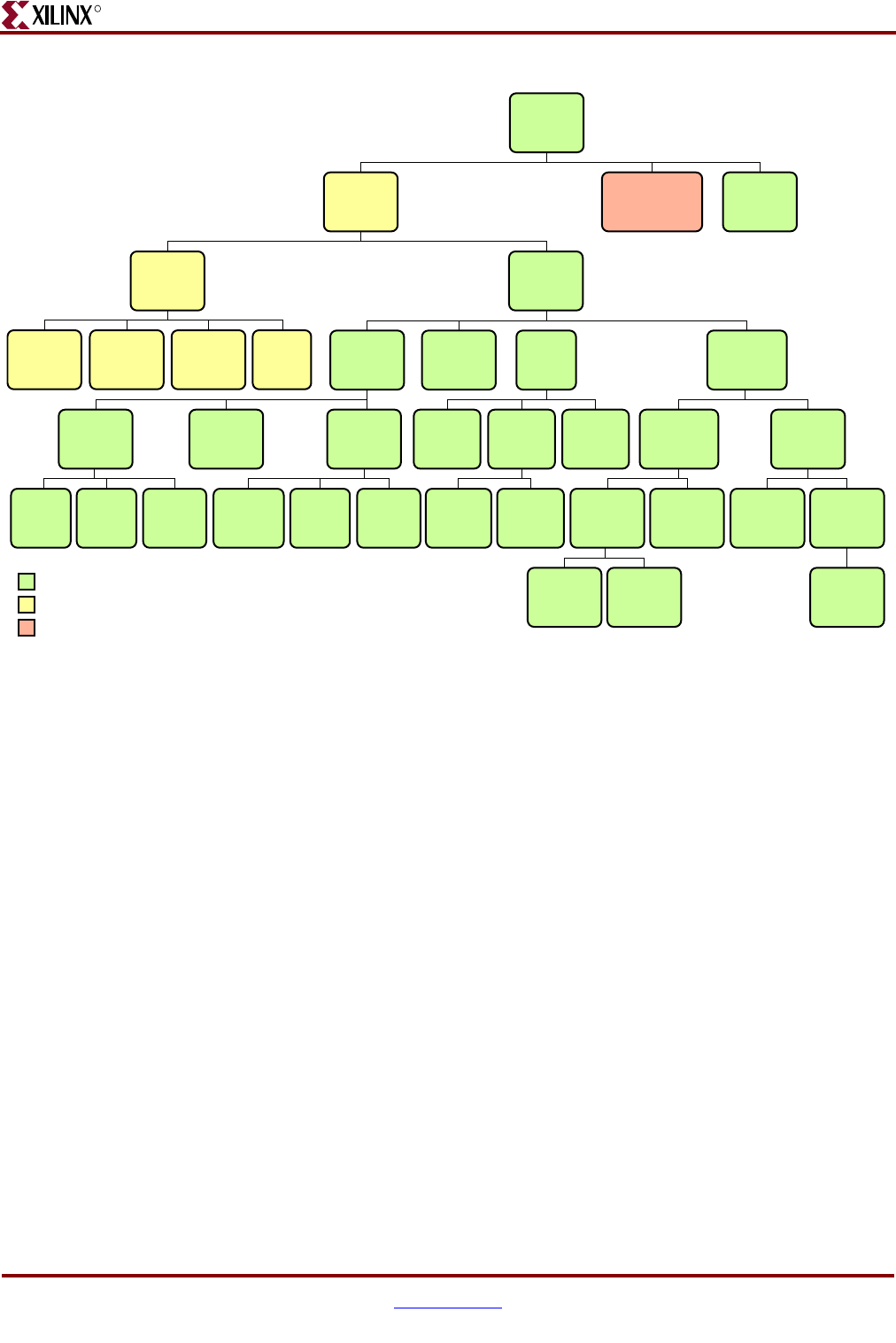
198 www.xilinx.com Memory Interface Solutions User Guide
UG086 (v3.6) September 21, 2010
Chapter 4: Implementing QDRII SRAM Controllers
R
Figure 4-3 shows the hierarchical structure of the QDRII SRAM design generated by MIG
with a testbench and a DCM. The modules are classified as follows:
• Design modules
• Testbench modules
• Clocks and reset generation modules
There is a parameter file generated with the design that has all the user input and design
parameters selected from MIG.
MIG can generate QDRII SRAM designs in four different ways:
• With a testbench and a DCM
• Without a testbench and with a DCM
• With a testbench and without a DCM
• Without a testbench and without a DCM
MIG outputs both an example_design and a user_design. The MIG-generated
example_design includes the entire memory controller design along with a synthesized
testbench (example user application). This testbench generates sample writes and reads
and then uses comparison logic to verify that the data patterns written are the same as
those received. This example_design can be used to test functionality both in simulation
and in hardware. The user_design includes the memory controller design only. This design
allows users to connect the MIG memory controller design to a user developed testbench
(user application). Refer to Table 4-5, page 213 for user interface signals and to “Write
Figure 4-3: QDRII SRAM Controller Hierarchy
<top_
module>
main* infrastructure_
top*
iobs*data_
path*
user_
interface*
data_path
_iobs*ctrl_iobs*
clock_
forward*
qdr_mem
_sm*
address_
burst*
Design Modules
bw_
burst*
qdr_rd_
enable*
read_
ctrl*
write_
burst*
tap_
logic*
wr_rd_
sm* q_sm* addr_
gen*
data_
gen*
qdr_q_
iob*
qdr_d_
iob*
qdr_cq_
iob*
wr_user_
interface*
rd_user_
interface*
rd_addr_
interface*
rd_data_
interface*
wr_data_
fifo*
data_bw
_fifo*
data_fifo
_mem*
wr_data_
interface*
dly_cal_
sm
data_
tap_inc
UG086_c4_03_091207
test_
bench* top*
idelay_
ctrl
Te st Bench Modules
DCM and Reset Generation Modules
Note: A block with a * has a parameter file included.
wr_addr_
interface*

Memory Interface Solutions User Guide www.xilinx.com 199
UG086 (v3.6) September 21, 2010
Architecture
R
Interface,” page 215 and “Read Interface,” page 218 for timing restrictions on user interface
signals.
Design clocks and resets are generated in the infrastructure_top module. When the
Use DCM option is checked in MIG, a DCM primitive and the necessary clock buffers are
instantiated in the infrastructure_top module. The inputs to this module are the
differential design clock and a 200 MHz differential clock required for the IDELAYCTRL
module. A user reset is also input to this module. Using the input clocks and reset signals,
the system clocks and the system resets used in the design are generated in this module.
When the Use DCM option is unchecked in MIG, the infrastructure_top module does not
have the DCM and the corresponding clock buffer instantiations; therefore, the system
operates on the user-provided clocks. The system reset is generated in the
infrastructure_top module using the dcm_lock signal and the ready signal of the
IDELAYCTRL element. For more information on the clocking structure, refer to “Clocking
Scheme,” page 209.
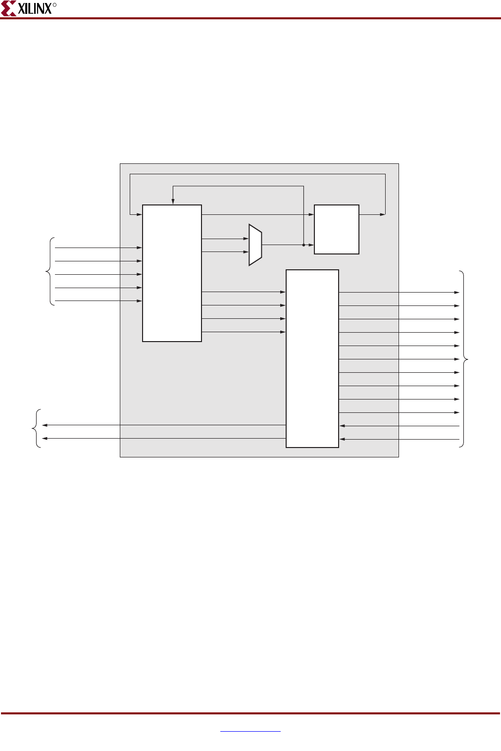
200 www.xilinx.com Memory Interface Solutions User Guide
UG086 (v3.6) September 21, 2010
Chapter 4: Implementing QDRII SRAM Controllers
R
Figure 4-4 shows a top-level block diagram of a QDRII SRAM design with a DCM and a
testbench. Inputs to the design are referenced to a differential clock pair (refclk_p and
refclk_n) for the controller design, a 200 MHz differential clock pair (dly_clk_200_p and
dly_clk_200_n) for the IDELAYCTRL element, and the system reset signal, sys_rst_n. All
design resets are generated using the dcm_locked signal, the sys_rst_n signal, and the
dly_ready signal of the IDELAYCTRL element. The compare_error output signal indicates
whether the design passes or fails. The dly_cal_done signal indicates the completion of
initialization and calibration of the design. Because the DCM is instantiated in the
infrastructure module, it generates the required clocks and reset signals for the design.
Figure 4-4: Top-Level Block Diagram of the QDRII SRAM Design with a DCM and a Testbench
main0
dly_ready
user_reset200
Memory
Device
UG086_c4_04_071808
Status
Signals
Reference
Clocks
and Reset
idelay_ctrl
infrastructure
_top
clk_200
IBUFGDS
clk_200_n
clk_0
clk_200_p
clk_270
user_reset
refclk_p
refclk_n
dly_clk_200_p
dly_clk_200_n
sys_rst_n
user_reset270
qdr_dll_off_n
qdr_w_n
qdr_r_n
qdr_k
qdr_k_n
qdr_c
qdr_c_n
qdr_sa
qdr_bw_n
qdr_d
qdr_q
qdr_cq
compare_error
dly_cal_done
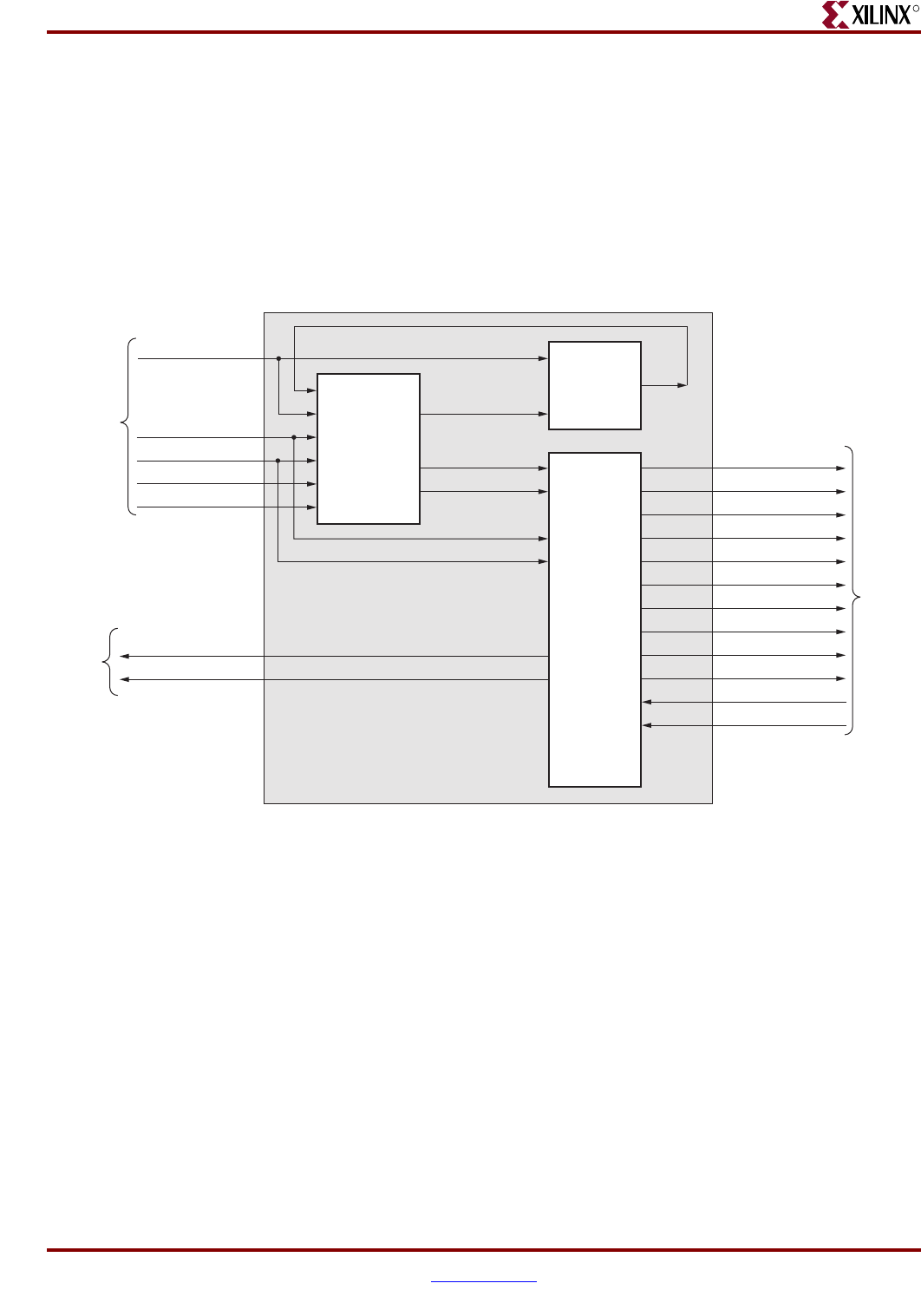
Memory Interface Solutions User Guide www.xilinx.com 201
UG086 (v3.6) September 21, 2010
Architecture
R
Figure 4-5 shows a top-level block diagram of a QDRII SRAM design without a DCM but
with a testbench. The user should provide all the clocks and the dcm_locked signal. These
clocks should be single-ended. sys_rst_n is the system reset signal. All design resets are
generated using the dcm_locked signal, the sys_rst_n signal, and the dly_ready signal of
the IDELAYCTRL element. The user application must have a DCM primitive instantiated
in the design, and all user clocks should be driven through BUFGs. The compare_error
signal, which is the output of the design, indicates whether the design passes or fails. The
testbench module does writes and reads, and also compares the read data with written
data. The compare_error signal is set High on data mismatches. The dly_cal_done signal
indicates the completion of initialization and calibration of the design.
Figure 4-5: Top-Level Block Diagram of the QDRII SRAM Design with a Testbench but without a DCM
main0
dly_ready
Memory
Device
UG086_c4_05_071808
Status
Signals
User
DCM
Clocks
and
Reset
idelay_ctrl
Infrastructure
_top
user_reset200
user_reset270
user_reset
clk_0
clk_200
clk_270
dcm_locked
sys_rst_n
qdr_dll_off_n
qdr_w_n
qdr_r_n
qdr_k
qdr_k_n
qdr_c
qdr_c_n
qdr_sa
qdr_bw_n
qdr_d
qdr_q
qdr_cq
compare_error
dly_cal_done
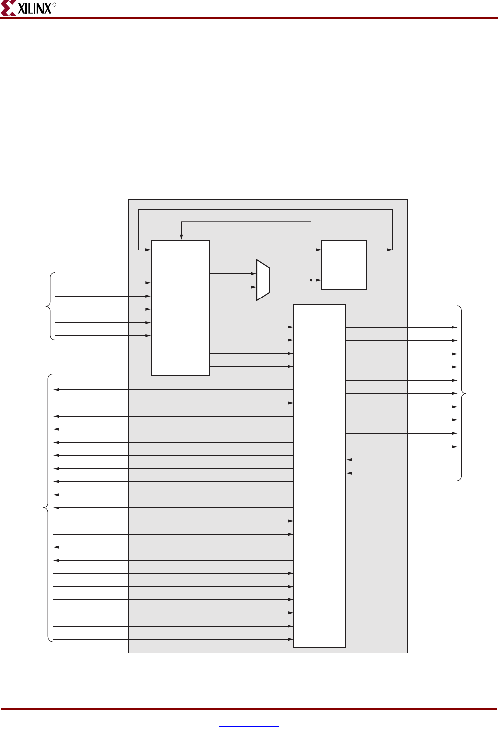
202 www.xilinx.com Memory Interface Solutions User Guide
UG086 (v3.6) September 21, 2010
Chapter 4: Implementing QDRII SRAM Controllers
R
Figure 4-6 shows a top-level block diagram of a QDRII SRAM design with a DCM but
without a testbench. refclk_p and refclk_n are differential input reference clocks. The DCM
is instantiated in the infrastructure module that generates the required design clocks.
dly_clk_200_p and dly_clk_200_n are used for the IDELAYCTRL element. sys_rst_n is the
system reset signal. All design resets are generated using the dcm_locked signal, the
sys_rst_n signal, and the dly_ready signal of IDELAYCTRL element. The user has to drive
the user application signals. The design provides the user_clk and user_rst signals to the
user to synchronize the user application signals with the design. The signal user_clk is
connected to clk0 clock signal in the controller. If the user clock domain is different from
clk0/user_clk, the user should add FIFOs for all the inputs and output of the controller
(user application signals), in order to synchronize them to user_clk clock. The
dly_cal_done signal indicates the completion of initialization and calibration of the design.
Figure 4-6: Top-Level Block Diagram of the QDRII SRAM Design with a DCM but without a Testbench
main0
dly_ready
user_reset200
Memory
Device
UG086_c4_06_071808
User
Application
Reference
Clocks
and Reset
idelay_ctrl
infrastructure
_top
clk_200
IBUFGDS
clk_200_n
clk_0
clk_200_p
clk_270
user_reset
refclk_p
refclk_n
dly_clk_200_p
dly_clk_200_n
sys_rst_n
user_reset270
qdr_dll_off_n
qdr_w_n
qdr_r_n
qdr_k
qdr_k_n
qdr_c
qdr_c_n
qdr_sa
qdr_bw_n
qdr_d
qdr_q
qdr_cq
dly_cal_done
user_wr_full
user_rd_full
user_qr_empty
user_wr_err
user_rd_err
user_qr_err
user_clk
user_rst
user_dwl
user_dwh
user_qrl
user_qrh
user_bwl_n
user_bwh_n
user_ad_wr
user_ad_rd
user_qen_n
user_r_n
user_w_n
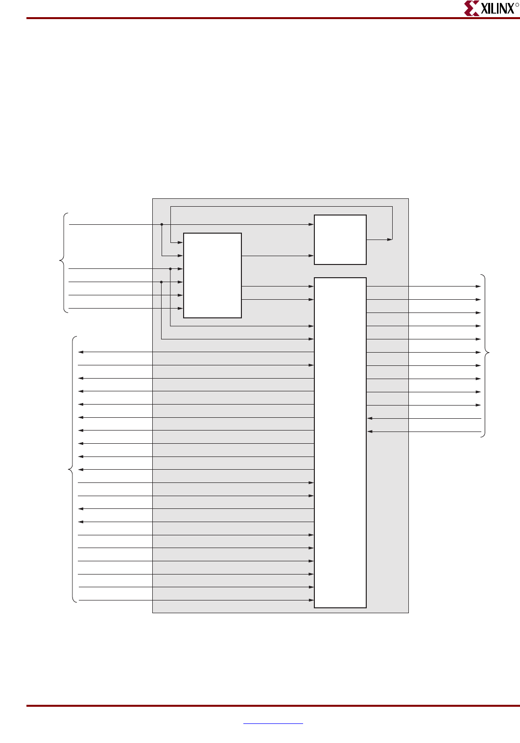
Memory Interface Solutions User Guide www.xilinx.com 203
UG086 (v3.6) September 21, 2010
Architecture
R
Figure 4-7 shows a top-level block diagram of a QDRII SRAM design without a DCM or a
testbench. The user should provide all the clocks and the dcm_locked signal. These clocks
should be single-ended. sys_rst_n is the system reset signal. All design resets are generated
using the dcm_locked signal, the sys_rst_n signal, and the dly_ready signal of the
IDELAYCTRL element. The user application must have a DCM primitive instantiated in
the design, and all user clocks should be driven through BUFGs. The user has to drive the
user application signals. The design provides the user_clk and user_rst signals to the user
to synchronize the user application signals with the design. The signal user_clk is
connected to clk0 clock in the controller. If the user clock domain is different from
clk0/user_clk, the user should add FIFOs for all the inputs and output of the controller
(user application signals), in order to synchronize them to user_clk clock. The
dly_cal_done signal indicates the completion of initialization and calibration of the design.
Figure 4-7: Top-Level Block Diagram of the QDRII SRAM Design without a DCM or a Testbench
main0
dly_ready
Memory
Device
UG086_c4_07_071808
User
DCM
Clocks
and
Reset
idelay_ctrl
infrastructure
_top
user_reset200
user_reset270
user_reset
clk_0
clk_200
clk_270
sys_reset_in_n
dcm_lock
qdr_dll_off_n
qdr_w_n
qdr_r_n
qdr_k
qdr_k_n
qdr_c
qdr_c_n
qdr_sa
qdr_bw_n
qdr_d
qdr_q
qdr_cq
User
Application
dly_cal_done
user_wr_full
user_rd_full
user_qr_empty
user_wr_err
user_rd_err
user_qr_err
user_clk
user_rst
user_dwl
user_dwh
user_qrl
user_qrh
user_bwl_n
user_bwh_n
user_ad_wr
user_ad_rd
user_qen_n
user_r_n
user_w_n
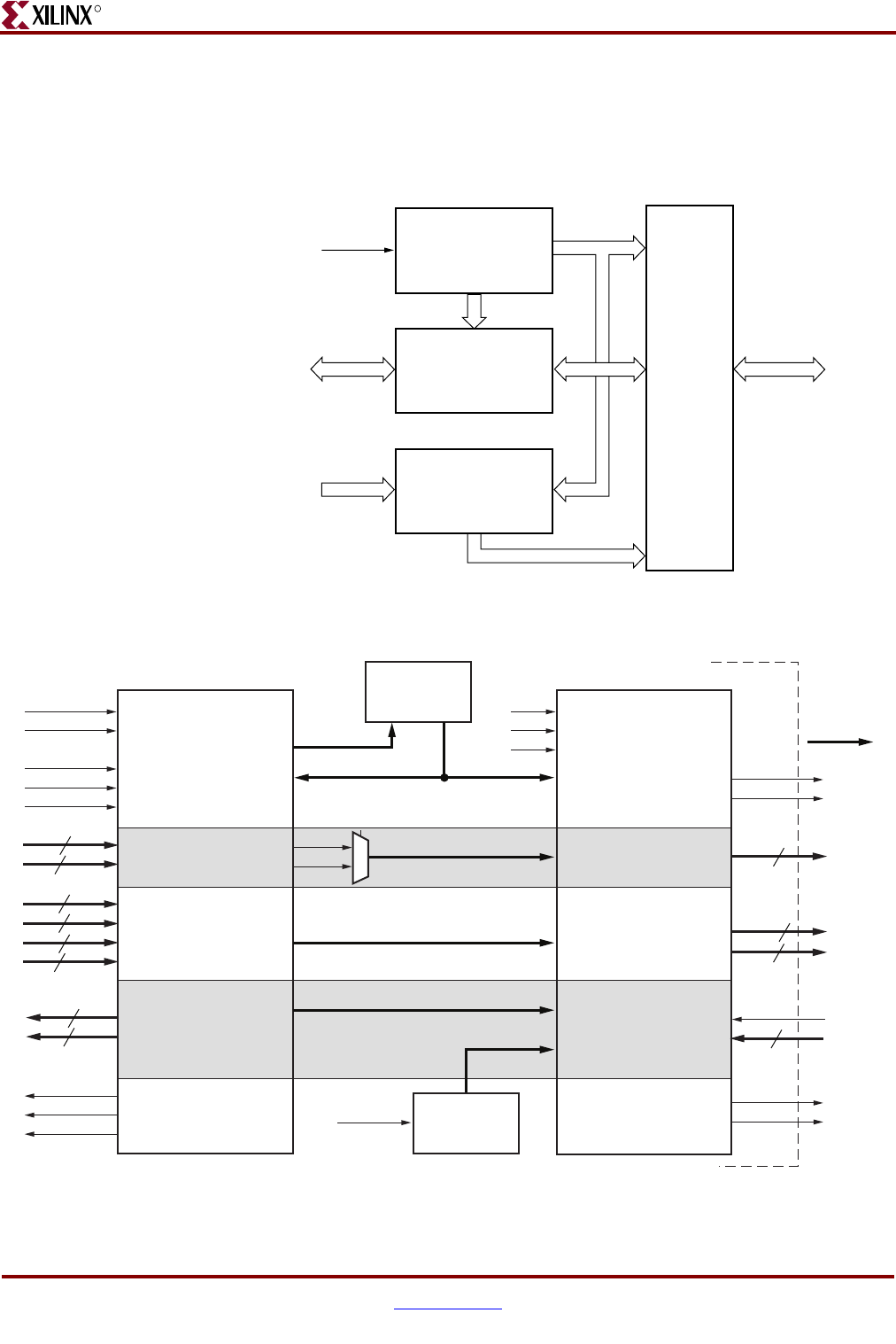
204 www.xilinx.com Memory Interface Solutions User Guide
UG086 (v3.6) September 21, 2010
Chapter 4: Implementing QDRII SRAM Controllers
R
QDRII Memory Controller Modules
Figure 4-8 shows a detailed block diagram of the QDRII memory controller. The four
blocks shown are subblocks of the top module. The functionalities of these blocks are
explained in the subsections following the figure.
Figure 4-9 shows the QDRII memory controller modules with a 36-bit interface.
Figure 4-8: QDRII Memory Controller Modules
Infrastructure_top
IOBSQDRII
Interface
Data_pathUser_data
User_clk
User_fifo_status
QDRII
Memory
Controller
UG086_c4_08_090607
Figure 4-9: QDRII Memory Controller Modules
User Interface Physical Interface
Read / Write
State Machine
Read / Write Control
Address Path
FIFO Status
QDRII
Memory
Device
user_clk
user_reset
user_w_n
user_r_n
user_qen_n
user_ad_wr
user_ad_rd
user_bwh_n
user_bwl_n
user_dwl
user_dwh
USER_QRL
USER_QRH
USER_WR_FULL
USER_RD_FULL
USER_QR_EMPTY
qdr_w_n
qdr_r_n
qdr_sa
qdr_bw_n
qdr_d
qdr_cq
qdr_q
qdr_k
qdr_k_n
user_clk
user_clk270
user_reset
Write Path
Read Path
clk_0 Delay
Calibration
State Machine
UG086_c4_09_071808
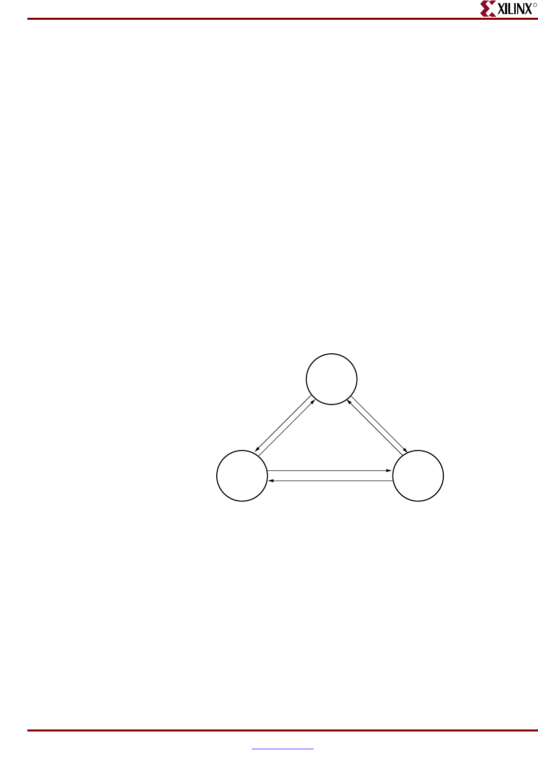
Memory Interface Solutions User Guide www.xilinx.com 205
UG086 (v3.6) September 21, 2010
Architecture
R
Controller
The QDRII memory controller initiates alternate Write and Read commands to the
memory as long as the User Write Data FIFOs, the User Write Address FIFO, and the User
Read Address FIFO are not empty, and the User Read Data FIFOs are not full.
The user writes the write data and the write address into the User Write Data FIFOs and
the User Write Address FIFO, respectively. When neither the User Write Data FIFOs nor
the User Write Address FIFO is empty, the QDRII controller generates a write-enable signal
to the memory. When the write enable is asserted, the write data and the write address are
transferred to memory from the User Write Data FIFOs and the User Write Address FIFO,
respectively.
The read address from where the data is to be read from memory is stored by the user in
the User Read Address FIFO. The QDRII memory controller generates a read-enable signal
to the memory when the User Read Address FIFO is not empty and the User Read Data
FIFOs are not full. When the read enable is asserted, the read address from the Read
Address FIFO is transferred to memory. The captured read data from the memory
corresponding to the read address is stored in the User Read Data FIFOs. The user can
access the data read from memory by reading the User Read Data FIFOs.
Figure 4-10 shows the QDRII memory controller state machine for burst lengths of four.
The controller state machine is in the IDLE state when the calibration is complete. When
the User Write Data FIFO and the User Write Address FIFO are not empty (that is, when
there are user-written write data and write address bits in the corresponding FIFOs), the
state machine goes to the WRITE state, initiating a memory write of one complete burst.
When the User Read Address FIFO is not empty (that is, the user has written read address
bits into the User Read Address FIFO) and either Read Data FIFO is not full, the state
machine goes to the READ state, initiating a memory read of one burst.
From the IDLE state, the QDRII memory controller can go to either the WRITE or the
READ state depending on the not empty status of the Write Address FIFO and the Write
Data FIFOs or the Read Address FIFO, and not full status of the Read Data FIFOs,
respectively. Writes are given priority. In the WRITE state, a memory write is initiated, and
the User Read Address Not Empty and User Read Data FIFOs full status are checked to
transfer into the READ state. When the User Read Address FIFO is empty, or the User Read
Data FIFOs are full, the state machine goes to the IDLE state.
In the READ state, a memory read is initiated, and the User Write Data and the User Write
Address FIFO Not Empty status is checked before going to the WRITE state. If the FIFOs
are empty, the state machine goes to the IDLE state.
Figure 4-10: QDRII Memory Controller State Machine with Burst Lengths of 4
IDLE
RD
RD
WR
WR WRITE
R_n=1
W_n=0
READ
R_n=0
W_n=1
UG086_c4_10_012507
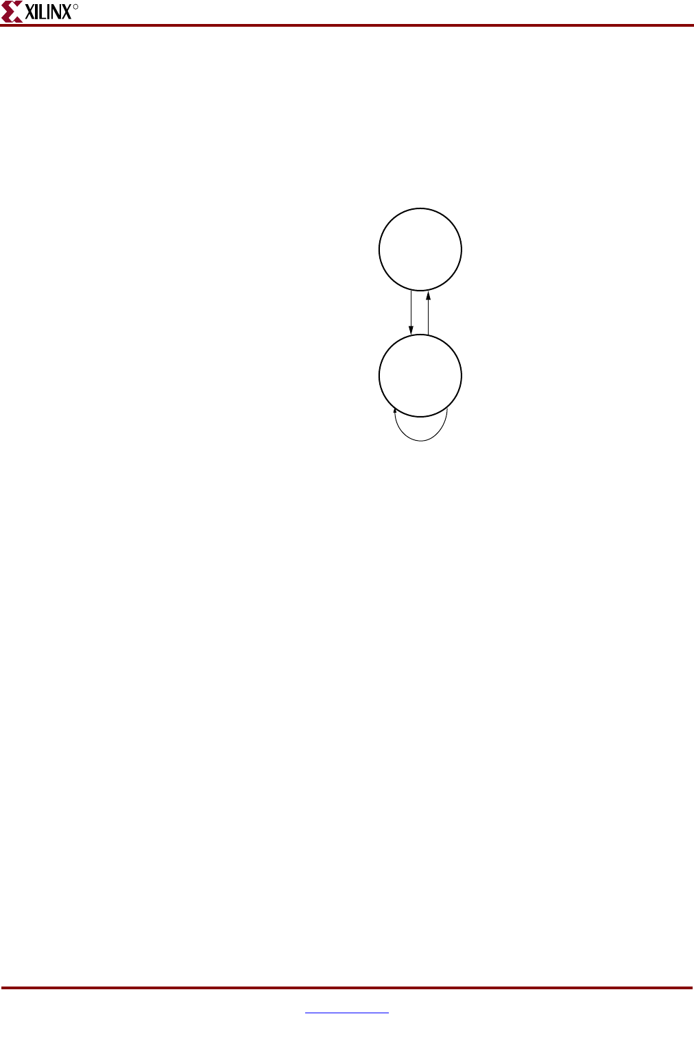
206 www.xilinx.com Memory Interface Solutions User Guide
UG086 (v3.6) September 21, 2010
Chapter 4: Implementing QDRII SRAM Controllers
R
Figure 4-11 shows a state machine of the QDR II memory controller for burst lengths of
two. When calibration is complete, the state machine is in the IDLE state. When the User
Write Data FIFO or Write Address FIFO is not empty (that is, when there are user-written
write data and write address bits in the corresponding FIFOs), the state machine goes to
the READ_WRITE state, initiating a memory write of one complete burst, or when the
User Read Address FIFO is not empty, that is, the user has written read address bits into
the User Read Address FIFO, and the User Read Data FIFOs are not full, the state machine
goes to the READ_WRITE state, initiating a memory read of one complete burst.
From the IDLE state, the QDR II memory controller goes to READ_WRITE state if either:
• the User Write Address FIFO and the User Write Data FIFO are not empty or,
• the User Read Address FIFO is not empty and the User Read Data FIFOs are not full
In the READ_WRITE state, the User Read Address Not Empty and User Read Data FIFOs
Not Full status are checked to initiate a memory read. To initiate a memory write in the
READ_WRITE state, the User Write Data FIFOs and the User Write Address FIFO Not
Empty status are checked. If both the User Write Data FIFOs and User Write Address FIFO
are empty, and the User Read Address FIFO is empty, or the User Read Data FIFOs are full,
the state machine goes to the IDLE state. If the User Write Data FIFO and User Write
Address FIFO are not empty, or the User Read Address FIFO is not empty and the User
Read Data FIFO is not full, the state machine remains in the READ_WRITE state to issue
memory writes or reads. The FIFOs are built using FIFO16 primitives in the data_bw_fifo,
data_fifo_mem, rd_addr_interface, wr_addr_interface, and wr_data_fifo modules. Each
FIFO has a threshold attribute called ALMOST_FULL_OFFSET whose value is set to F, by
default, in the RTL. This value can be changed as needed. For valid FIFO threshold offset
values, refer to UG070 [Ref 7].
Refer to XAPP703 [Ref 20] for detailed design and timing analysis of the QDRII memory
controller module.
Datapath
The Datapath module transmits and receives data to and from the memories. Its major
functions are listed below:
• Asserts a write-enable signal for memories with burst lengths of two or four
• Asserts a read-enable signal to memory and a write-enable signal to the User Read
Data FIFO
Figure 4-11: QDRII Memory Controller State Machine with Burst Lengths of 2
IDLE
READ_
WRITE
R_n=0
W_n=0
UG086_c4_11_090607

Memory Interface Solutions User Guide www.xilinx.com 207
UG086 (v3.6) September 21, 2010
Architecture
R
• Generates increment/decrement signals (tap count) for IDELAY elements in the IOBS
• Center-aligns the data window to the FPGA clock
Refer to XAPP703 [Ref 20] for techniques on data writes to memory and data captures from
memory. For burst lengths of two, the write-enable signal to memory is asserted at the
same time that write data is driven. For burst lengths of four, the write-enable signal is
asserted one clock before the write data is driven on the memory bus. The data is driven on
both edges of the clock. The address to memory is driven for one full clock cycle for burst
lengths of 4 and on both the edges of the clock cycle for burst lengths of 2.
Memory read data is edge-aligned with the source-synchronous clock, CQ. The QDRII
memory clock, to which data is synchronized, is a free-running strobe. The free-running
strobe from the memory CQ is captured using the FPGA clock. Thus the relation between
the CQ strobe and the FPGA clock is found, and the strobe CQ is center-aligned with the
FPGA clock. The same logic is applied to the read data Q window, which is center-aligned
with the same FPGA clock. This in turn means that the same amount of tap delays are
applied to both Q and CQ through IDELAY elements to center-align the Q and CQ
windows with respect to the FPGA clock. By center-aligning the Read Data window Q
with respect to the FPGA clock, the data capturing logic is complete.
The delay calibration circuit generates the delay reset, delay select, and delay increment
values for IDELAY elements used in delaying strobes and data read from memory. The
strobe is center-aligned with the FPGA clock, which results in the data window falling to
the center of the FPGA clock. Refer to XAPP703 [Ref 20] for details about the delay
calibration.
Infrastructure
The infrastructure (infrastructure_top) module generates the FPGA clock and reset signals.
When differential clocking is used, refclk_p, refclk_n, dly_clk_200_p, and dly_clk_200_n
signals appear. When single-ended clocking is used, refclk and idly_clk_200 signals
appear. In addition, clocks are available for design use and a 200 MHz clock is provided for
the IDELAYCTRL primitive. Differential and single-ended clocks are passed through
global clock buffers before connecting to a DCM. For differential clocking, the output of the
refclk_p/refclk_n buffer is single-ended and is provided to the DCM input. Likewise, for
single-ended clocking, refclk is passed through a buffer and its output is provided to the
DCM input. The outputs of the DCM are 0° and 270° phase-shifted versions of the input
clock. After the DCM is locked, the design is in the reset state for at least 25 clocks. The
infrastructure module also generates all of the reset signals required for the design.
Idelay_ctrl
This module instantiates the IDELAYCTRL primitive of the Virtex-4 FPGA. The
IDELAYCTRL primitive is used to continuously calibrate the individual delay elements in
its region to reduce the effect of process, temperature, and voltage variations. A 200 MHz
clock has to be fed to this primitive.
The MIG tool instantiates the required number of IDELAYCTRLs in the RTL and uses the
LOC constraints in the UCF file to fix their locations. The number of IDELAYCTRLs is
defined by the IDELAYCTRL_NUM parameter in the idelay_ctrl module. In the RTL,
DLY_READY is generated by doing a logical AND of the RDY signals of every
IDELAYCTRL block.
IDELAYCTRL LOC constraints should be checked in the following cases:
• The MIG design is used with other IP cores or user designs that also require the use of
IDELAYCTRL and IDELAYs.

208 www.xilinx.com Memory Interface Solutions User Guide
UG086 (v3.6) September 21, 2010
Chapter 4: Implementing QDRII SRAM Controllers
R
• Previous ISE® software releases 8.2.03i and 9.1i had an issue with IDELAYCTRL block
replication or trimming. When using these revisions of the ISE software, the user must
instantiate and constrain the location of each IDELAYCTRL individually.
See UG070 [Ref 7] for more information on the requirements of IDELAYCTRL placement.
IOBS
All the input and output signals of the QDRII SRAM controller are implemented in the
IOBS module. All address and byte enable signals are registered in the IOBs and driven
out.
The IDELAY elements for the read strobe and data read from memory are implemented in
the IOBS. The IOBS also implement bidirectional buffers for write and read data. It
registers the output data (ODDR) before driving it out and registers the input data (IDDR).
Test Bench
The MIG tool generates two RTL folders, example_design and user_design. The
example_design folder includes the synthesizable test bench, while user_design does not
include the test bench modules. The MIG test bench performs one write command
followed by one read command in an alternating manner for designs with a burst length of
4. For a burst length of 2, the test bench performs one write command and one read
command in the same clock and repeats one write and one read command continuously.
The number of words in a write command depends on the burst length. For a burst length
of 4, the test bench writes a total of 4 data words for a single write command (2 rise data
words and 2 fall data words). For a burst length of 2, the test bench writes a total of 2 data
words. On every write command, the data pattern is incremented by one, and this is
repeated with each subsequent write command. The initial data pattern for the first write
command is 000. The test bench writes the 000, 001, 002, 003 data pattern in a sequence
in which 000 and 002 are rise data words and 001 and 003 are fall data words for a 9-bit
design. The falling edge data is always rising edge data plus one. For a burst length of 2,
the data sequence for the first write command is 000, 001. The data sequence for the
second write command is 002, 003. The pattern is then incremented for the next write
command. For data widths greater than 9, the same data pattern is concatenated for the
other bits. For a 36-bit design and a burst length of 4, the data pattern for the first write
command is 000000000, 008040201, 010080402, 0180C0603.
Address generation logic generates the address in an incremental pattern for each write
command. The same address location is repeated for the next read command. In Samsung
components, the burst address increments are done by the memory, so the address is
generated by the test bench in a linear incremental pattern. In Cypress parts, the MIG test
bench increments the address for burst operation. After the address reaches the maximum
value, it rolls back to the initial address, i.e., 00000.
During reads, comparison logic compares the read pattern with the pattern written, i.e., the
000, 001, 002, 003 pattern. For example, for a 9-bit design of burst length 4, the data
written for a single write command is 000, 001, 002, and 003. During reads, the read
pattern is compared with the 000, 001, 002, 003pattern. Based on a comparison of the
data, a status signal error is generated. If the data read back is the same as the data written,
the error signal is 0, otherwise it is 1.
Memory Interface Solutions User Guide www.xilinx.com 209
UG086 (v3.6) September 21, 2010
Clocking Scheme
R
Clocking Scheme
Figure 4-12 shows the clocking scheme for this design. Global and local clock resources are
used.
The global clock resources consist of a DCM, two BUFGs on DCM output clocks, and one
BUFG for clk_200. The local clock resources consist of regional I/O clock networks
(BUFIO). The global clock architecture is discussed in this section.
The MIG tool allows the user to customize the design such that the DCM is not included.
In this case, clk_0 and clk_270 must be supplied by the user.
Global Clock Architecture
The user must supply two input clocks to the design:
• A system clock running at the target frequency for the memory
• A 200 MHz clock for the IDELAYCTRL blocks.
These clocks can be either single-ended or differential. User can select single-ended or
differential clock input option from MIG GUI. Differential clocks are connected to the
IBUFGDS and single-ended clock is connected to IBUFG.
The system clock from the output of the IBUFGDS or the IBUFG is connected to the DCM
to generate the various clocks used by the memory interface logic.
The clk_200 output of the IBUFGDS or the IBUFG is connected to the BUFG. The output of
the BUFG is used for IDELAY IOB delay blocks for aligning read capture data.
The DCM generates two separate synchronous clocks for use in the design. This is shown
in Table 4-2 and Figure 4-12. The clock structure is same for both example design and user
design. For designs with out DCM instantiation, DCM and the BUFGs should be
instantiated at user end to generate the required clocks.
Table 4-2: QDRII Interface Design Clocks
Clock Description Logic Domain
clk_0 Skew compensated replica
of the input system clock.
The clock for the controller and the user
interface logic. The QDRII bus-related
I/O flip-flops (e.g., memory clocks).
This clock is used to register the data,
address, and command signals, and the
address and data enables for the user
interface logic(1). This clock is also used
to generate the read data and read data
valid signals.
clk_270 270° phase-shifted version
of clk_0
Used in the write data path section of
physical layer. Clocks write path control
logic, QDRII side of the Write Data
FIFO, and output flip-flops for D and
memory control and address signals.
This clock is also used to generate FIFO
status signals.
Notes:
1. See “QDRII Controller System and User Interface Signals,” page 212 for timing requirements and
restrictions on the user interface signals.
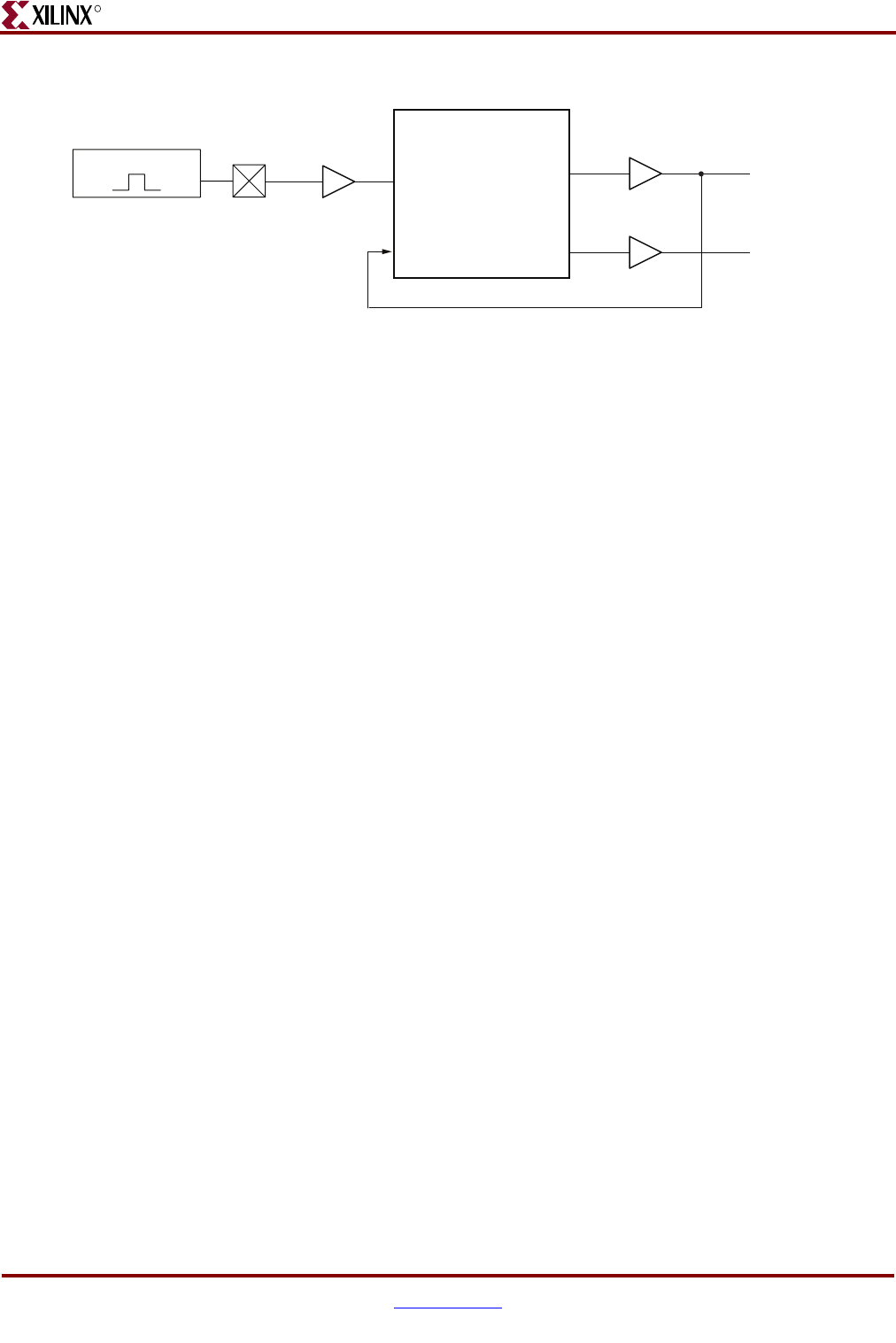

Memory Interface Solutions User Guide www.xilinx.com 211
UG086 (v3.6) September 21, 2010
QDRII SRAM Initialization and Calibration
R
QDRII SRAM Initialization and Calibration
QDRII memory is initialized through a specified sequence. The QDRII device requires
2048 clock cycles of clock input after its DLL has been enabled. After the DCM clocks are
stable, the controller waits for a specified amount of time before asserting the
qdr_dll_off_n signal to the memory. This signal can also be pulled up to a High on the
memory device without being driven from the FPGA.
Any command can be issued to the memory only after the 2048 clock cycle wait time. After
2048 clock cycles, the INIT_DONE signal is asserted indicating the completion of the
initialization sequence. Following initialization, the relationship between the data and the
FPGA clock is calculated using the TAP logic. The memory strobe CQ is a free-running
clock from the memory component. Because the read data Q and the memory strobe CQ
are edge-aligned, the strobe is passed through the IDELAY elements of the Virtex-4 device
and the taps are adjusted to center-align the strobe pulse with respect to the FPGA clock.
The same number of taps are applied to the data window's IDELAY element to center-align
the data window with respect to the FPGA clock. XAPP701 [Ref 18] provides more
information about the calibration architecture.
Calibration is done in two stages:
1. In the first stage of calibration, the read strobe CQ is center-aligned with respect to the
FPGA clock. CQ is a free-running clock from QDRII memory. The read data Q is edge-
aligned with the read strobe CQ. The first and second edges of the CQ strobe are
detected using the FPGA clock to determine the center of the CQ window.
Once the CQ window is center-aligned with the FPGA clock, the same amount of delay
(tap counts) is applied to the read data windows Q through the IDELAY element, so
that the Q window is center-aligned with the FPGA clock.
Port cq_q_cal_done in the data_path module indicates the status of the first stage
calibration. When cq_q_cal_done is asserted High, it indicates the completion of first
stage calibration. After the first stage calibration is complete, the second stage
calibration starts.
2. In the second stage of calibration, the write enable signal for the Read Data FIFO is
determined by delaying the controller-issued read command. This delay is calibrated
based on the delay between the read command and the corresponding read data at the
Read Data FIFO. For this delay calibration, the controller writes a known fixed pattern
of data into a memory location and reads back from the same location. This read data
is compared against the known fixed pattern. The delay between the read command
and the correct pattern read data comparison is the delay calibration.
The final_dly_cal_done port in the data_path module indicates the status of the second
stage calibration. When final_dly_cal_done is asserted High, it indicates the
completion of second stage calibration, which implies the completion of the whole
initialization and calibration process. After the initialization and calibration is done
(i.e., the dly_cal_done signal in design_top is asserted High), the controller can start
issuing user commands to the memory.
In the second stage calibration, when the pattern read data does not match with the
pattern write data, the controller does not issue any further pattern read commands,
and the controller gets stuck in the calibration state. The design must be restarted for
the calibration to start from the beginning.
212 www.xilinx.com Memory Interface Solutions User Guide
UG086 (v3.6) September 21, 2010
Chapter 4: Implementing QDRII SRAM Controllers
R
QDRII Controller System and User Interface Signals
Table 4-3 through Table 4-4 describe the QDRII controller system interface signals with and
without a DCM, respectively. Table 4-5 describes the QDRII user interface signals without
a testbench. Table 4-6 describes the QDRII memory interface signals. In these tables, all
signal directions are with respect to the QDRII memory controller.
Table 4-3: QDRII SRAM System Interface Signals (with a DCM)
Signal Name Direction Description
refclk_p, refclk_n Input Reference clock input made up of differential clock pairs. This clock
pair goes to a differential input buffer. The differential buffer output
goes to the DCM input. The DCM generates the required clocks for the
design.
refclk Input Single-ended system clock input. This clock is an input to IBUFG. The
IBUFG output is connected to the DCM clock input. The DCM
generates the required clocks for the design. This input system clock is
present only when the SINGLE_ENDED clocks option is selected in
MIG FPGA options.
When the DCM option is deselected, both differential or single-ended
input system clocks are not present.
dly_clk_200_p,
dly_clk_200_n
Input 200 MHz differential clock used in the idelay_ctrl logic.
sys_rst_n Input Reset to the QDRII memory controller.
compare_error Output This signal represents the status of the comparison between the read
data and the corresponding write data.
dly_cal_done Output This signal is asserted when the design initialization and calibration is
complete.
Table 4-4: QDRII SRAM System Interface Signals (without a DCM)
Signal Name Direction Description
clk_0 Input Input clock
clk_270 Input Input clock with a 270° phase difference.
clk_200 Input 200 MHz clock for the IDELAYCTRL primitives.
dcm_locked Input This active-High signal indicates whether the user DCM is locked or
not.
sys_rst_n Input Reset to the QDRII memory controller.
compare_error Output This signal represents the status of the comparison between the read
data and the corresponding write data.
dly_cal_done Output This signal is asserted when the design initialization and calibration is
complete.
Memory Interface Solutions User Guide www.xilinx.com 213
UG086 (v3.6) September 21, 2010
QDRII Controller System and User Interface Signals
R
Table 4-5: QDRII SRAM User Interface Signals (without a Testbench)
Signal Name(1) Direction Description
user_wr_full Output This signal indicates the User Write FIFO status. It is asserted
when either the User Write Address FIFO or the User Write
Data FIFO is full. When this signal is asserted, any writes to
the User Write Address FIFO and the User Write Data FIFO
are invalid, possibly leading to controller malfunction.
user_rd_full Output This signal indicates the User Read Address FIFO status. It is
asserted when the User Read Address FIFO is full. When this
signal is asserted, all writes to the User Read Address FIFO
are ignored.
user_qr_empty Output This signal indicates the User Read Data FIFO status. This
signal is asserted when the User Read Data FIFO is empty.
When this signal is asserted, all reads to the User Read Data
FIFO are invalid.
user_wr_err Output This signal is asserted when an error occurs while writing to
the User Write Data FIFO or the User Write Address FIFO.
user_rd_err Output This signal is asserted when an error occurs while writing to
the User Read Address FIFO.
user_qr_err Output This signal is asserted when an error occurs while reading
the User Read Data FIFO.
dly_cal_done Output This signal is asserted to indicate that the calibration is done.
user_clk(2) Output All user interface signals are to be synchronized to this clock.
The user_clk is sourced from clk_0 in the controller.
user_rst Output This reset is active until the DCM is not locked.
user_dwl [(data_width-1):0] Input Positive-edge data for memory writes. This data bus is valid
when user_w_ n is asserted.
user_dwh [(data_width-1):0] Input Negative-edge data for memory writes. This data bus is valid
when user_w_ n is asserted.
user_qrl [(data_width-1):0] Output Positive-edge data read from memory. This data is output
when user_qen_n is asserted.
user_qrh [(data_width-1):0] Output Negative-edge data read from memory. This data is output
when user_qen_n is asserted.
user_bwl_n [(BW_width-1):0] Input Byte enables for QDRII memory positive-edge write data.
These byte enables are valid when user_w_n is asserted.
user_bwh_n [(BW_width-1):0] Input Byte enables for QDRII memory negative-edge write data.
These byte enables are valid when user_w_n is asserted.
user_ad_wr [(addr_width-1):0](3) Input QDRII memory address for write data. This bus is valid
when user_w_n is asserted.
user_ad_rd [(addr_width-1):0](3) Input QDRII memory address for read data. This bus is valid when
user_r_n is asserted.
214 www.xilinx.com Memory Interface Solutions User Guide
UG086 (v3.6) September 21, 2010
Chapter 4: Implementing QDRII SRAM Controllers
R
user_qen_n Input This active-Low signal is the read enable for the User Read
Data FIFOs. The QDRII memory controller captures the data
read from memory and stores it in the Read Data FIFOs. The
user can access these FIFOs to get the data read from
memory.
user_w_n Input This active-Low signal is the write enable for the User Write
Data and User Write Address FIFOs. The user asserts this
signal to write new data to the FIFOs. The QDRII memory
controller reads the data from the User Write Data FIFO and
writes to memory at the address located in the User Write
Address FIFO.
user_r_n Input This active-Low signal is the write enable for the User Read
Address FIFO. The user asserts this signal to read new data
from memory. The QDRII memory controller reads the
address from the Read Address FIFO and does a memory
read to the corresponding memory address.
Notes:
1. All user interface signal names are prepended with a controller number, for example, cntrl0_QDR_Q. QDRII SRAM devices
currently support only one controller.
2. The user_clk is connected to clk_0 in the controller. If the user clock domain is different from clk_0 / user_clk of MIG, the user
should add FIFOs for all data inputs and outputs of the controller, in order to synchronize them to the user_clk.
3. The number of address bits used depends on the density of the memory part. The controller ignores the unused bits, which can all
be tied High.
Table 4-5: QDRII SRAM User Interface Signals (without a Testbench) (Cont’d)
Signal Name(1) Direction Description
Table 4-6: QDRII SRAM Interface Signals
Signal Name Direction Description
qdr_d Output During WRITE commands, the data is sampled on both edges of K.
qdr_q Input During READ commands, the data is sampled on both edges of the
FPGA clk.
qdr_bw_n Output Byte enables for QDRII memory write data. The byte enables are valid
when user_w_n is asserted
qdr_sa Output Address for READ and WRITE operations.
qdr_w_n Output This signal represents the WRITE command.
qdr_r_n Output This signal represents the READ command.
qdr_cq Input This read data clock transmitted by the QDRII SRAM is edge-aligned
with the read data.
k, k_n Output Differential write data clocks.
c, c_n Output Input clock for output data.
qdr_dll_off_n Output The DLL is disabled when this signal is Low.
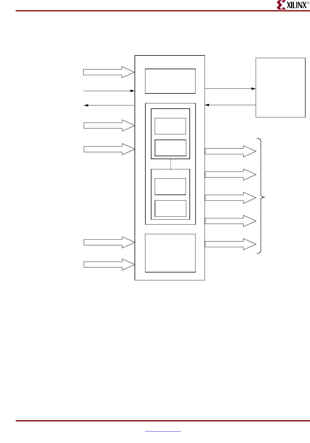
Memory Interface Solutions User Guide www.xilinx.com 215
UG086 (v3.6) September 21, 2010
QDRII Controller System and User Interface Signals
R
Write Interface
Figure 4-13 illustrates the user interface block diagram for write operations.
The following steps describe the architecture of Address and Write Data FIFOs and how to
perform a write burst operation to QDRII memory from user interface.
1. The user interface consists of an Address FIFO, Data FIFOs and a byte write FIFO.
These FIFOs are built out of Virtex-4 FPGA FIFO16 primitives of configuration 512x 36.
2. The Address FIFO stores the QDRII memory address where the data is to be written
from the user interface. A single instantiation of a FIFO16 constitutes the Address
FIFO.
3. Two separate sets of Data FIFOs store the rising-edge and falling-edge data to be
written to QDRII memory from the user interface. For 9-bit, 18-bit, and 36-bit data
widths, two FIFO16s are required for storing rising-edge and falling-edge data. For a
72-bit data width, two FIFO16s are required for storing rising-edge data and two
FIFO16s for storing falling-edge data. MIG instantiates the required number of FIFOs
depending on the memory data width selected. For 9-bit and 18-bit configurations, the
controller pads the extra bits of the Data FIFO with 0s.
Figure 4-13: Write User Interface Block Diagram
User Interface
Controller
Address FIFO
(FIFO16)
512 x 36
Byte Write FIFO
(FIFO16)
512 x 36
fifo_wr_empty
wr_init_n
user_ad_wr
user_w_n
user_dwl
user_dwh
user_bwl_n
user_bwh_n
fifo_dwl
fifo_ad_wr
fifo_dwh
fifo_bwl_n
fifo_bwh_n
To IOBS
user_wr_full
Rise Data FIFO
(FIFO16)
512 x 36
Fall Data FIFO
(FIFO16)
512 x 36
Rise Data FIFO
(FIFO16)
512 x 36
Fall Data FIFO
(FIFO16)
512 x 36
Data FIFOs
Data FIFOs
ug086_c4_15_111507
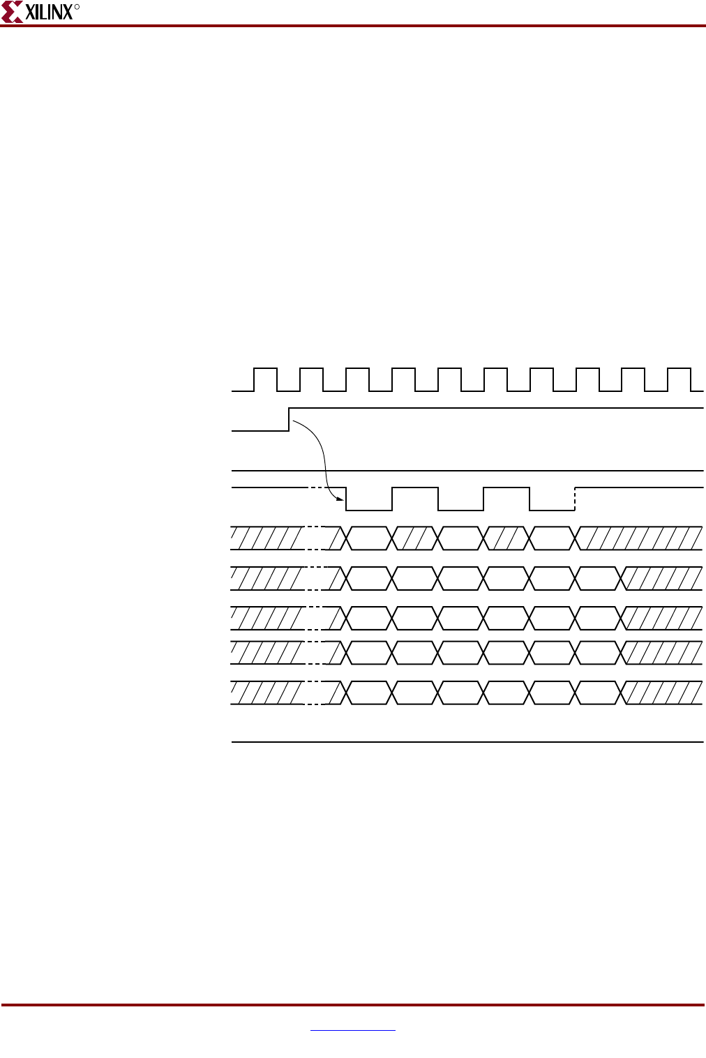
216 www.xilinx.com Memory Interface Solutions User Guide
UG086 (v3.6) September 21, 2010
Chapter 4: Implementing QDRII SRAM Controllers
R
4. The Byte Write FIFO stores the Byte Write signals to QDRII memory from the user
interface. Extra bits are padded with zeros.
5. The user can initiate a write command to memory by writing to the Address FIFO,
Data FIFOs, and Byte Write FIFOs when FIFO Full flags are deasserted and after the
calibration done signal dly_cal_done is asserted. Users should not access any of these
FIFOs until dly_cal_done is asserted. The dly_cal_done signal assures that the clocks
are stable, the reset process is completed, and the controller is ready to accept
commands. Status signal user_wr_full is asserted when the Address FIFO, Data FIFOs,
or Byte Write FIFOs are full.
6. When user_w_n is asserted, user_ad_wr is stored in the Address FIFO, user_dwl and
user_dwh are stored in the Data FIFO, and user_bwl and user_bwh are stored in the
Byte Write FIFOs. A common write-enable signal is used to store the data into all three
FIFOs.
7. The controller reads the Address, Data, and Byte Write FIFOs when they are not empty
by issuing the wr_init_n signal. A QDRII memory write command is generated from
the wr_init_n signal by properly timing it.
8. Figure 4-14 shows the timing diagram for a write command of BL = 4. The address
must be asserted for one clock cycle as shown. For burst lengths of four, each write to
the Address FIFO must have two writes to the Data FIFO consisting of two rising edge
data and two falling edge data.
9. Figure 4-15 shows the timing diagram for a write command of BL = 2. For a burst
length of two, each write to the Address FIFO is coupled to one write to the Data FIFO,
consisting of one rising edge data and one falling edge data. For BL = 2, commands can
be given in every clock.
Figure 4-14: Write User Interface Timing Diagram for BL = 4
user_clk
dly_cal_done
user_wr_full
user_wr_err
user_w_n
user_ad_wr
user_dwl
user_dwh
DWL-00 DWL-01 DWL-10 DWL-11 DWL-20 DWL-21
DWH-00 DWH-01 DWH-10 DWH-11 DWH-20 DWH-21
A0 A1 A2
user_bwl_n
iser_bwh_n
BWL-00 BWL-01 BWL-10 BWL-11 BWL-20 BWL-21
BWH-00 BWH-01 BWH-10 BWH-11 BWH-20 BWH-21
UG086_c4_16_111507
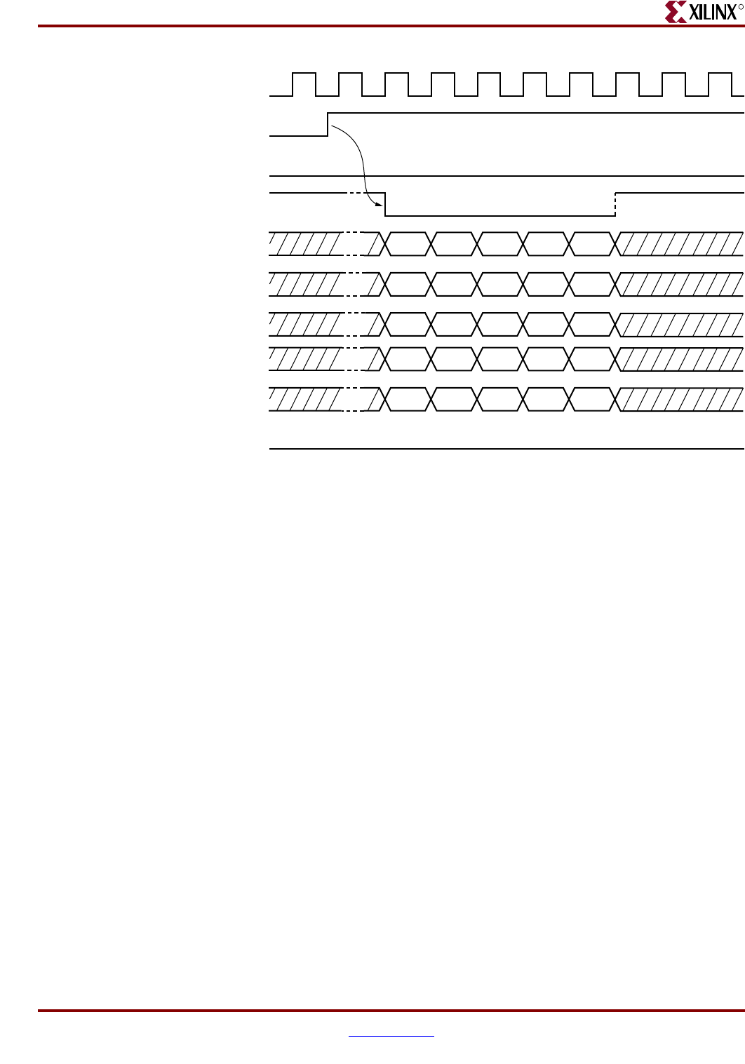
Memory Interface Solutions User Guide www.xilinx.com 217
UG086 (v3.6) September 21, 2010
QDRII Controller System and User Interface Signals
R
Figure 4-15: Write User Interface Timing Diagram for BL = 2
user_clk
dly_cal_done
user_wr_full
user_wr_err
user_w_n
user_ad_wr
user_dwl
user_dwh
DWL-0 DWL-1 DWL-2 DWL-3DWL-4
DWH-0 DWH-1 DWH-2 DWH-3DWH-4
A0 A1 A3A2 A4
user_bwl_n
iser_bwh_n
BWL-0 BWL-1 BWL-2 BWL-3BWL-4
BWH-0 BWH-1 BWH-2 BWH-3BWH-4
UG086_c4_17_010108
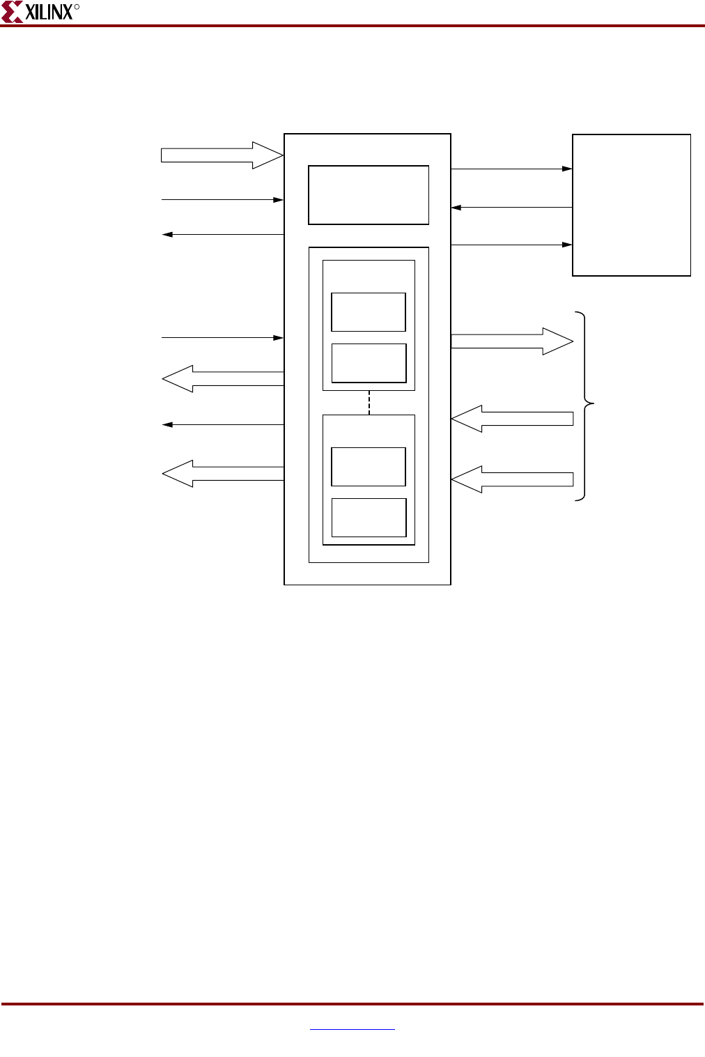
218 www.xilinx.com Memory Interface Solutions User Guide
UG086 (v3.6) September 21, 2010
Chapter 4: Implementing QDRII SRAM Controllers
R
Read Interface
Figure 4-16 shows a block diagram for the read interface.
The following steps describe the architecture of the Read Data FIFOs and show how to
perform a QDRII SRAM burst read operation from the user interface.
1. The read user interface consists of an Address FIFO and a Read Data FIFO. The
Address FIFO and Read Data FIFO are built from Virtex-4 FPGA FIFO16s of
configuration 512 x 36.
2. The size of the Address FIFO is always of 512 x 16.
3. The number of Read Data FIFOs required depends on the number of QDRII
components being used. Using 9-bit components for 36-bit data width, a total of eight
FIFOs are required, four for rising-edge data and four for falling-edge data. Although
each FIFO can accommodate 36-bit data, the requirement of having one FIFO per
component arises from CQ pattern calibration, where an internal pattern calibration is
done per CQ. The controller generates the Read Data FIFO write-enable signal for each
FIFO separately depending on the CQ pattern calibration.
4. To initiate a QDRII read command, the user must write the Address FIFO when the
FIFO full flag user_rd_full is deasserted and the calibration done signal dly_cal_done
is asserted. Writing to the Address FIFO indicates to the controller that it is a Read
command. The dly_cal_done signal assures that the controller clocks are stable, the
internal reset process is completed, and the controller is ready to accept commands.
Figure 4-16: Read User Interface Block Diagram
Controller
fifo_rd_empty
rd_init_n
user_ad_rd
user_r_n
user_qrl
user_qrh
fifo_ad_rd
fifo_drl
fifo_drh
To/From IOBS
user_rd_full fifo_qr_full
user_qen_n
user_qr_empty
ug086_c4_18_111507
User Interface
Address FIFO
(FIFO16)
512 x 36
Rise Data FIFO
(FIFO16)
512 x 36
Fall Data FIFO
(FIFO16)
512 x 36
Rise Data FIFO
(FIFO16)
512 x 36
Fall Data FIFO
(FIFO16)
512 x 36
Data FIFOs
Component 0
Component (n–1)
Data FIFOs
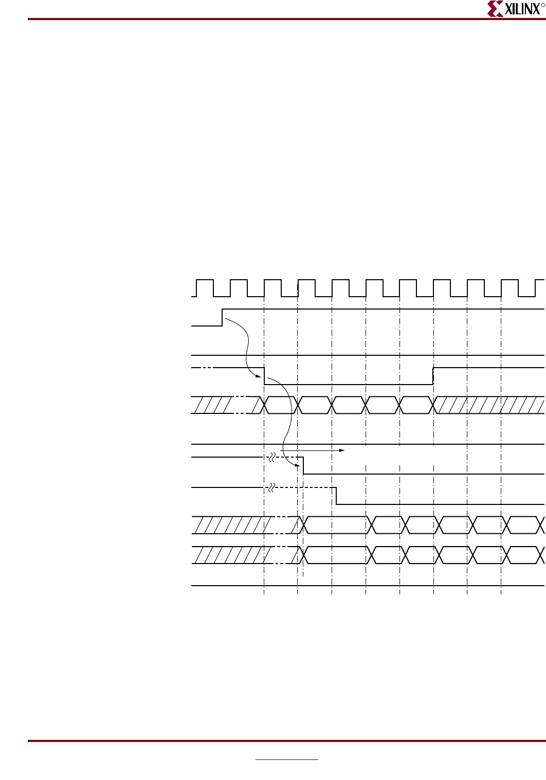
Memory Interface Solutions User Guide www.xilinx.com 219
UG086 (v3.6) September 21, 2010
QDRII Controller System and User Interface Signals
R
5. The user must issue an Address FIFO write-enable signal user_r_n along with the read
address user_ad_rd to write the read address to the Address FIFO.
6. The controller reads the Address FIFO when status signal fifo_rd_empty is deasserted
and generates the appropriate control signals to QDRII memory required for a read
command.
7. Prior to the actual read and write commands, the design calibrates the latency (number
of clock cycles) from when the read command is issued to when the data is received.
Using this precalibrated delay information, the controller generates the write-enable
signals to the Read Data FIFOs. The delay calibration is done per QDRII component.
8. The Low state of user_qr_empty indicates read data is available. Asserting user_qen_n
reads rising-edge data and falling-edge data simultaneously on every rising edge of
the clock.
9. Figure 4-17 and Figure 4-18 show the user interface timing diagrams for BL = 4 and
BL = 2.
10. After the address is loaded into the Address FIFO, it can take 18 clock cycles (worst
case) for the controller to write the Data FIFOs.
Figure 4-17: Read User Interface Timing Diagram for BL = 4
user_clk
dly_cal_done
user_rd_full
user_qr_err
user_rd_err
user_qr_empty
user_qen_n
user_r_n
user_ad_rd
user_qrl
user_qrh
q00 q02 q10 q12 q20 q22
A0 A1 A3A2 A4
q01 q03q11 q13q21 q23
UG086_c4_19_111907
18 Tck between user read command
and user read data
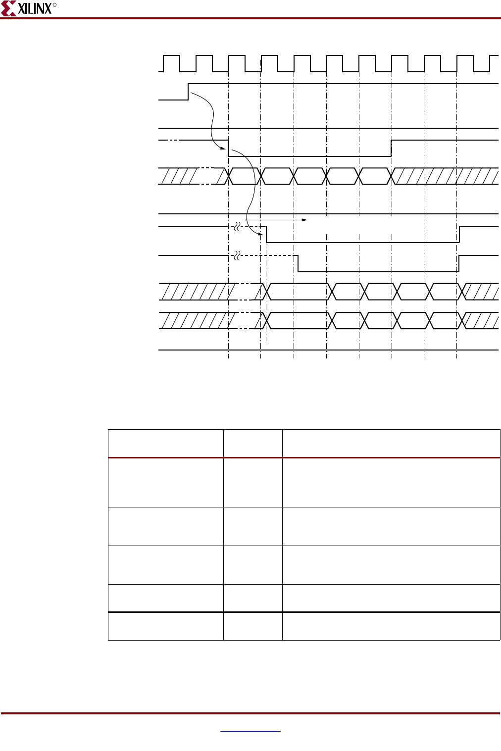
220 www.xilinx.com Memory Interface Solutions User Guide
UG086 (v3.6) September 21, 2010
Chapter 4: Implementing QDRII SRAM Controllers
R
Table 4-7 shows the maximum read latency of the controller.
Figure 4-18: Read User Interface Timing Diagram for BL = 2
Table 4-7: Maximum Read Latency
Parameter Number of
Clocks Description
User command to
address FIFO empty
flag
5 (2 + 3) Two clocks for the two-stage pipeline before the
FIFO input. An empty FIFO takes three clocks to
deassert the empty status signal after the FIFO is
written with the first data.
Command from
controller state machine
to QDR memory
3 One clock cycle to read the FIFO and two clocks
for decoding and passing the command to QDR
memory.
QDR command to FIFO
input data
6 Two clocks for QDRII memory latency, two
clocks for calibration delay, and two clocks for
the input pipeline.
FIFO input to FIFO
output
4 Four clocks to deassert the empty status signal
in fall-through mode.
Total Latency 18 Total latency from read command issued to
Address FIFO, to data input to user interface.
user_clk
dly_cal_done
user_rd_full
user_qr_err
user_rd_err
user_qr_empty
user_qen_n
user_r_n
user_ad_rd
user_qrl
user_qrh
q00 q10 q20 q30q40
A0 A1 A3A2 A4
q01 q11 q21 q31q41
UG086_c4_20_010208
18 Tck between user read command
and user read data
Memory Interface Solutions User Guide www.xilinx.com 221
UG086 (v3.6) September 21, 2010
QDRII Controller System and User Interface Signals
R
QDRII SRAM Signal Allocations
Table 4-8 shows the list of signals for a QDRII SRAM design allocated in a group from bank
selection checkboxes in MIG.
When the Address box is checked in a bank, the address, qdr_w_n, qdr_r_n, and
qdr_dll_off_n bits are assigned to that particular bank.
When the Data Write box is checked in a bank, the memory data write and memory byte
write are assigned to that particular bank.
When the Data Read box is checked in a bank, the memory data read, memory read clocks,
memory write clocks, and memory input clock for the output data are assigned to that
particular bank.
When the System Control box is checked in a bank, the sys_rst_n, compare_error, and
dly_cal_done bits are assigned to that particular bank.
When the System Clock box is checked in a bank, the refclk_p, refclk_n, dly_clk_200_p,
and dly_clk_200_n bits are assigned to that particular bank.
For special cases, such as without a testbench and without a DCM, the corresponding
input and output ports are not assigned to any FPGA pins in the design UCF because the
user can connect these ports to the FPGA pins or can connect to some logic internal to the
same FPGA.
Note: Timing has been verified for most of the MIG generated configurations. For the best timing
results, adjacent banks in the same column of the FPGA should be used. Banks that are separated
by unbonded banks should be avoided because these can cause timing violations.
Supported Devices
The design generated out of MIG is independent of the memory package, hence the
package part of the memory component is replaced with X, where X indicates a don't care
condition. Table 4-9 shows the list of components supported by MIG.
Table 4-8: QDRII Signal Allocations
Bank Selected Signals Allocated in the Group
Address Memory address and memory control
Data Write Memory write data and memory byte write
Data Read Memory read data, memory CQ, and K and C clocks
System Control System reset from the user interface and status signals
System Clock System clocks from the user interface
Table 4-9: Supported Devices for QDRII SRAM
Virtex-4 FPGAs (Verilog and VHDL)
Components Make Configuration
CY7C1314BV18-167BZXC Cypress x36
CY7C1315BV18-250BZC Cypress x36
CY7C1426AV18-250BZC Cypress x9
222 www.xilinx.com Memory Interface Solutions User Guide
UG086 (v3.6) September 21, 2010
Chapter 4: Implementing QDRII SRAM Controllers
R
Simulating the QDRII SRAM Design
After generating the design, MIG creates a sim folder in the specified path. This folder
contains simulation files for a particular design. The sim folder contains an external
testbench and a .do file to simulate the generated design. To learn more details about the
files in the sim folder and to simulate the design, refer to “Simulation Guide,” page 499.
CY7C1526V18-250BZC Cypress x9
CY7C1911BV18-250BZC Cypress x9
CY7C1515V18-250BZC Cypress x36
K7R160982B-FC25 Samsung x9
K7R161882B-FC25 Samsung x18
K7R161884B-FC25 Samsung x18
K7R163682B-FC25 Samsung x36
K7R163684B-FC25 Samsung x36
K7R320982C-FC20 Samsung x9
K7R320982M-FC20 Samsung x9
K7R321882C-FC20 Samsung x18
K7R321882M-FC20 Samsung x18
K7R321884C-FC25 Samsung x18
K7R321884M-FC25 Samsung x18
K7R323682C-FC20 Samsung x36
K7R323682M-FC20 Samsung x36
K7R323684C-FC25 Samsung x36
K7R323684M-FC25 Samsung x36
K7R640982M-FC25 Samsung x9
K7R641882M-FC25 Samsung x18
K7R641884M-FC25 Samsung x18
K7R643682M-FC25 Samsung x36
K7R643684M-FC30 Samsung x36
Table 4-9: Supported Devices for QDRII SRAM (Cont’d)
Virtex-4 FPGAs (Verilog and VHDL)
Components Make Configuration
Memory Interface Solutions User Guide www.xilinx.com 223
UG086 (v3.6) September 21, 2010
Hardware Tested Configurations
R
Hardware Tested Configurations
The frequencies shown in Table 4-10 were achieved on the Virtex-4 FPGA ML461 Memory
Interfaces Development Board under nominal conditions. This frequency should not be
used to determine the maximum design frequency. The maximum design frequency
supported in the MIG wizard is based on a combination of the TRCE results for fabric
timing on multiple device/package combinations and I/O timing analysis using FPGA
and memory timing parameters for a 72-bit wide interface.
Table 4-10: Hardware Tested Configurations
Synthesis Tools XST and Synplicity
HDL Verilog and VHDL
FPGA Device XC4VLX25-FF668-11
Memory Component K7R163684B-FC25
Burst Length 4
Data Widths 36, 72
36-bit Frequency Range 110 to 350 MHz
72-bit Frequency Range 110 to 320 MHz

Memory Interface Solutions User Guide www.xilinx.com 225
UG086 (v3.6) September 21, 2010
R
Chapter 5
Implementing DDRII SRAM Controllers
This chapter describes how to implement DDRII SRAM interfaces for Virtex®-4 FPGAs
generated by MIG.
Feature Summary
This section summarizes the supported and unsupported features of the DDRII SRAM
controller design.
Supported Features
The DDRII SRAM controller design supports:
• A maximum frequency of 250 MHz
• Data widths of 9, 18, 36, and 72 bits
• Burst lengths of two and four
• Implementation using different Virtex-4 devices
• Operation with any 9-bit, 18-bit, and 36-bit memory component
•Verilog and VHDL
• With and without a testbench
• With and without a DCM
Design Frequency Range
Unsupported Features
The DDRII SRAM controller design does not support:
• DDR SIO memory
Table 5-1: Design Frequency Range in MHz
Memory
FPGA Speed Grade
-10 -11 -12
MinMaxMinMaxMinMax
Component 120 200 120 240 120 250
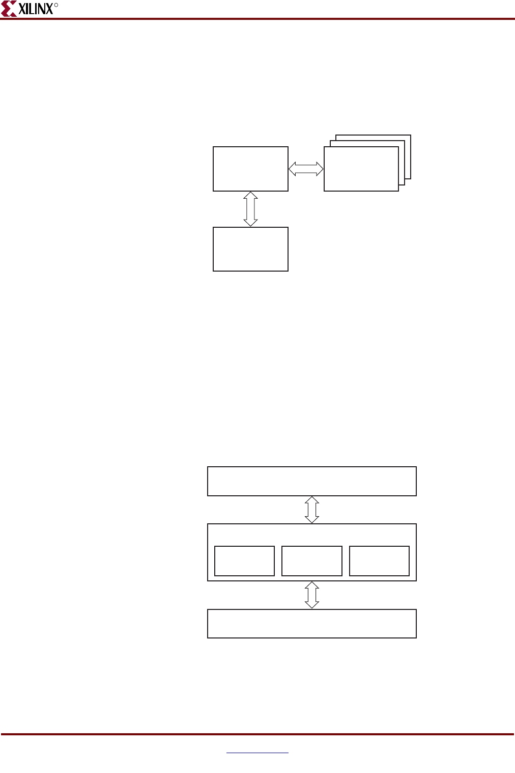
226 www.xilinx.com Memory Interface Solutions User Guide
UG086 (v3.6) September 21, 2010
Chapter 5: Implementing DDRII SRAM Controllers
R
Architecture
Figure 5-1 shows a top-level block diagram of the DDRII SRAM controller interface. One
side of the DDRII SRAM controller connects to the user interface denoted as Block
Application. The other side of the controller interfaces to DDRII memory. The memory
interface data width is selectable.
Data is double-pumped to DDRII memory on both the positive and the negative edges of
the clock. The HSTL_18 Class II I/O standard is used for data, and the HSTL_18 Class I
I/O standard is used for address, control, and memory clock signals.
DDRII memory interfaces are source-synchronous and double data rate like DDR SDRAM
interfaces.
Interface Model
The Memory interface is layered to simplify the design and make the design modular.
Figure 5-2 shows the layered memory interface used in the DDRII SRAM controller. The
three layers are the application layer, the implementation layer, and the physical layer.
Figure 5-1: DDRII SRAM Controller Interface
DDRII SRAM
Controller
Block
Application
UG086_c5_01_012507
DDRII
Memory
Figure 5-2: Interface Layering Model
User Interface
Physical Layer
Implementation Layer
UG086_c5_02_012507
Infrastructure Data Path Control
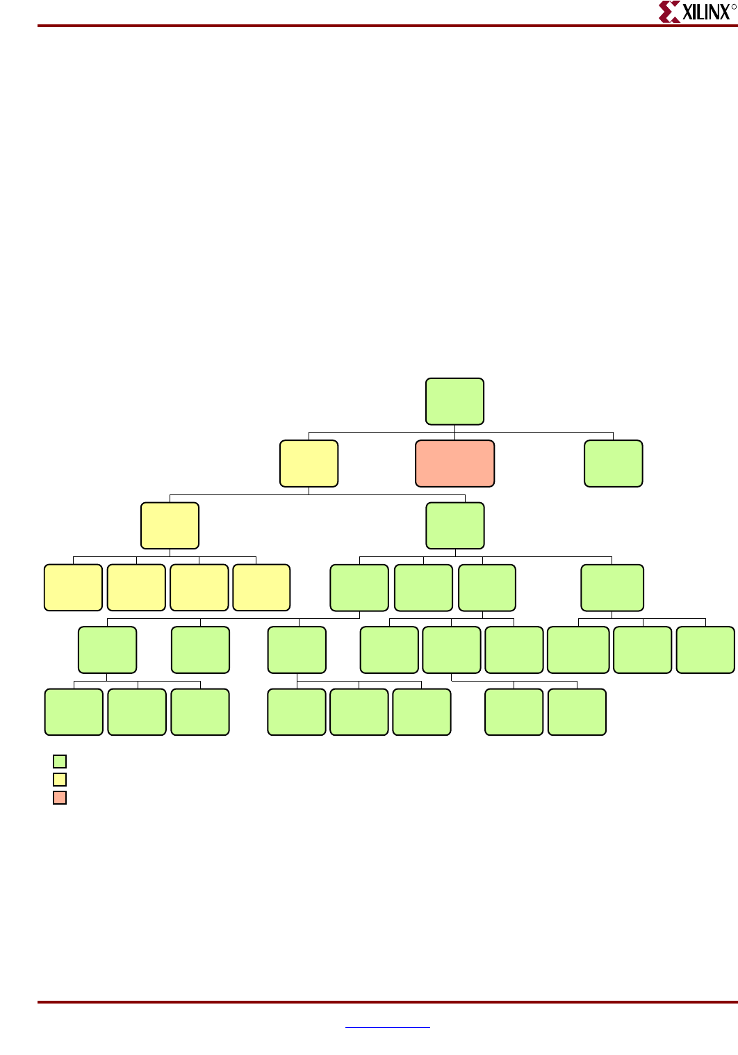
Memory Interface Solutions User Guide www.xilinx.com 227
UG086 (v3.6) September 21, 2010
Architecture
R
The application layer comprises the user interface, which initiates memory writes and
reads by writing data and memory addresses to the User Interface FIFOs. The
implementation layer comprises the infrastructure, datapath, and control logic.
• The infrastructure logic consists of the DCM and reset logic generation circuitry.
• The datapath logic consists of the calibration logic by which the data from the
memory component is captured using the FPGA clock.
• The control logic determines the type of data transfer, that is, read/write with the
memory component, depending on the User Interface FIFO’s status signals.
The physical layer comprises the I/O elements of the FPGA. The controller communicates
with the memory component using this layer. I/ O elements (such as IDDRs, ODDRs,
IDELAY, and OFLOPs) are associated with this layer.
Hierarchy
Figure 5-3 shows the hierarchical structure of the DDRII SRAM design generated by MIG
with a testbench and a DCM.
The modules are classified as follows:
• Design modules
• Testbench modules
• Clocks and reset generation modules
Figure 5-3: DDRII SRAM Controller Hierarchy
<top_
module>
main* infrastructure_
top*
iobs*data_
path*
user_
interface*
data_path
_iobs*ctrl_iobs*
clock_
forward*
ddr_mem
_sm*
address_
burst*
Design Modules
bw_
burst*
ddr_rd_
enable*
read_
ctrl*
write_
burst*
tap_
logic*
wr_rd_
sm* d_sm* addr_
gen*
data_
gen*
ddr_d_
iob*
ddr_cq_
iob*
ddr_q_
iob*
wr_data_
interface*
rd_data_
interface*
rd_wr_
addr_
interface*
dly_cal_
sm
data_
tap_inc
UG086_c5_03_112907
test_
bench* top*
idelay_
ctrl
Te st Bench Modules
DCM and Reset Generation Modules
Note: A block with a * has a parameter file included.

228 www.xilinx.com Memory Interface Solutions User Guide
UG086 (v3.6) September 21, 2010
Chapter 5: Implementing DDRII SRAM Controllers
R
There is a parameter file generated with the design that has all the user input and design
parameters selected from MIG.
MIG can generate DDRII SRAM designs in four different ways:
• With a testbench and a DCM
• Without a testbench and with a DCM
• With a testbench and without a DCM
• Without a testbench and without a DCM
MIG outputs both an example_design and a user_design. The MIG-generated
example_design includes the entire memory controller design along with a synthesized
testbench (example user application). This testbench generates sample writes and reads
and then uses comparison logic to verify that the data patterns written are the same as
those received. This example_design can be used to test functionality both in simulation
and in hardware. The user_design includes the memory controller design only. This design
allows users to connect the MIG memory controller design to a user developed testbench
(user application). Refer to Table 5-5 for user interface signals, “Write Interface,” page 243
and “Read Interface,” page 246 for timing restrictions on user interface signals, and
Figure 5-12, page 244 and Figure 5-13, page 245 for write interface timing.
Design clocks and resets are generated in the infrastructure_top module. When Use DCM
option is checked in MIG, a DCM primitive and the necessary clock buffers are instantiated
in the infrastructure_top module. The inputs to this module are the differential design
clock and a 200 MHz differential clock required for the IDELAYCTRL module. A user reset
is also input to this module. Using the input clocks and reset signals, the system clocks and
system resets used in the design are generated in this module.
When the Use DCM option is unchecked in MIG, the infrastructure_top module does not
have the DCM and the corresponding clock buffer instantiations. Therefore, the system
operates on the user-provided clocks. The system reset is generated in the
infrastructure_top module using the dcm_lock signal and the ready signal of the
IDELAYCTRL element. For more information on the clocking structure, refer to “Clocking
Scheme,” page 237.
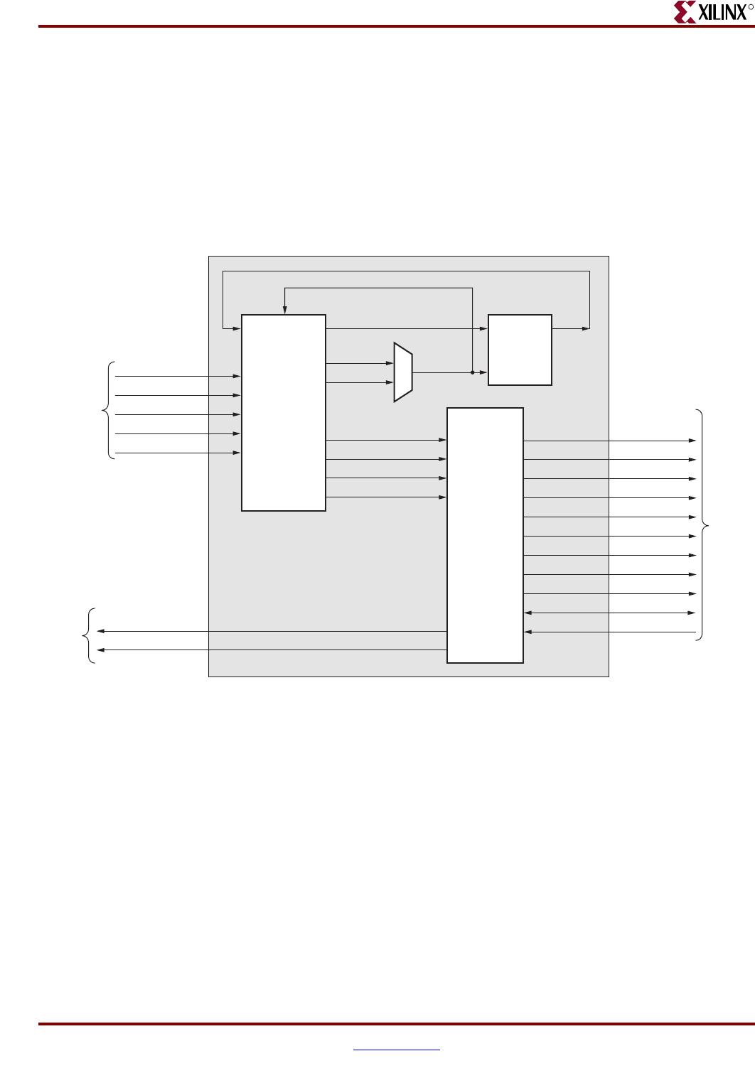
Memory Interface Solutions User Guide www.xilinx.com 229
UG086 (v3.6) September 21, 2010
Architecture
R
Figure 5-4 shows a top-level block diagram of a DDRII SRAM design with a DCM and a
testbench. refclk_p and refclk_n are differential input reference clocks. The DCM is
instantiated in the infrastructure module that generates the required design clocks.
dly_clk_200_p and dly_clk_200_n are used for the IDELAYCTRL element. sys_rst_n is the
system reset signal. All design resets are generated using the dcm_locked signal, the
sys_rst_n signal, and the dly_ready signal of the IDELAYCTRL element. The
compare_error output signal indicates whether the design passes or fails. The
dly_cal_done signal indicates the completion of initialization and calibration of the design.
Because the DCM is instantiated in the infrastructure module, it generates the required
clocks and resets signals for the design.
Figure 5-4: Top-Level Block Diagram of the DDRII SRAM Design with a DCM and a Testbench
main0
dly_ready
user_reset200
Memory
Device
UG086_c5_04_071808
Status
Signals
Reference
Clocks
and Reset
idelay_ctrl
infrastructure
_top
clk_200
IBUFGDS
clk_200_n
clk_0
clk_200_p
clk_270
user_reset
refclk_p
refclk_n
dly_clk_200_p
dly_clk_200_n
sys_rst_n
user_reset270
ddr_dll_off_n
ddr_ld_n
ddr_rw_n
ddr_k
ddr_k_n
ddr_c
ddr_c_n
ddr_sa
ddr_bw_n
compare_error
dly_cal_done
ddr_cq
ddr_dq
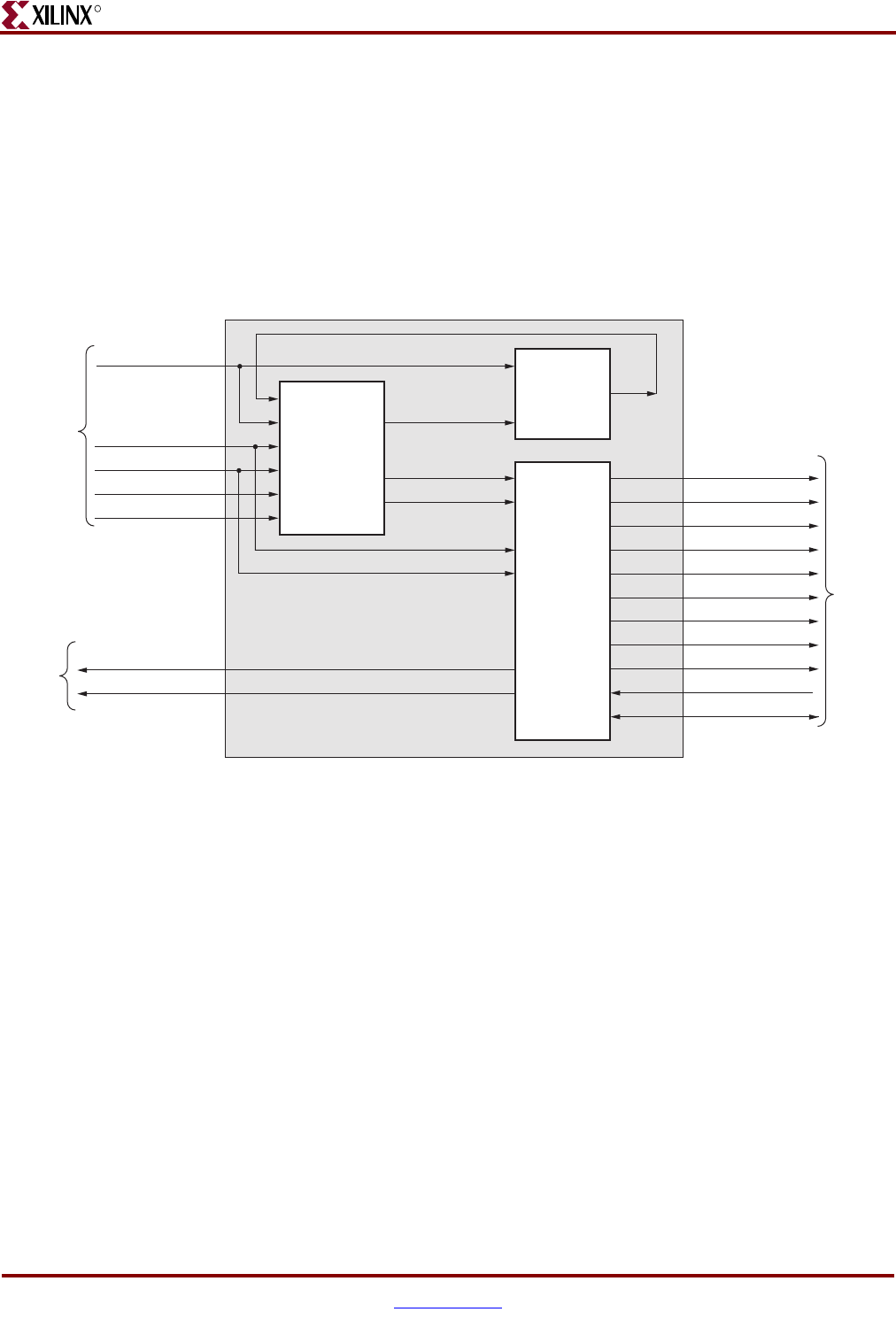
230 www.xilinx.com Memory Interface Solutions User Guide
UG086 (v3.6) September 21, 2010
Chapter 5: Implementing DDRII SRAM Controllers
R
Figure 5-5 shows a top-level block diagram of a DDRII SRAM design with a testbench but
without a DCM. The user should provide all the clocks and the dcm_locked signal. These
clocks should be single-ended. sys_rst_n is the system reset signal. All design resets are
generated using the dcm_locked signal, the sys_rst_n signal, and the dly_ready signal of
the IDELAYCTRL element. The user application must have a DCM primitive instantiated
in the design, and all user clocks should be driven through BUFGs. The compare_error
output signal indicates whether the design passes or fails. The testbench module does
writes and reads, and also compares the read data with the written data. The
compare_error signal is driven High on data mismatches. The dly_cal_done signal
indicates the completion of initialization and calibration of the design.
Figure 5-6, page 231 shows a top-level block diagram of a DDRII SRAM design with a
DCM but without a testbench. refclk_p and refclk_n are differential input reference clocks.
The DCM is instantiated in the infrastructure module that generates the required design
clocks. dly_clk_200_p and dly_clk_200_n are used for the IDELAYCTRL element.
sys_rst_n is the system reset signal. All design resets are generated using the dcm_locked
signal, the sys_rst_n signal, and the dly_ready signal of the IDELAYCTRL element. The
user has to drive the user application signals. The design provides the user_clk and
user_rst signals to the user to synchronize the user application signals with the design. The
signal user_clk is connected to clk0 clock signal in the controller. If the user clock domain
is different from clk0/user_clk, the user should add FIFOs for all the inputs and output of
the controller (user application signals), in order to synchronize them to user_clk clock.
The dly_cal_done signal indicates the completion of initialization and calibration of the
design.
Figure 5-5: Top-Level Block Diagram of the DDRII SRAM Design without a DCM but with a Testbench
main0
dly_ready
Memory
Device
UG086_c5_05_071808
Status
Signals
User
DCM
Clocks
and
Reset
idelay_ctrl
infrastructure
_top
user_reset200
user_reset270
user_reset
clk_0
clk_200
clk_270
dcm_locked
sys_rst_n
ddr_dll_off_n
ddr_dl_n
ddr_rw_n
ddr_k
ddr_k_n
ddr_c
ddr_c_n
ddr_sa
ddr_bw_n
ddr_dq
ddr_cq
compare_error
dly_cal_done
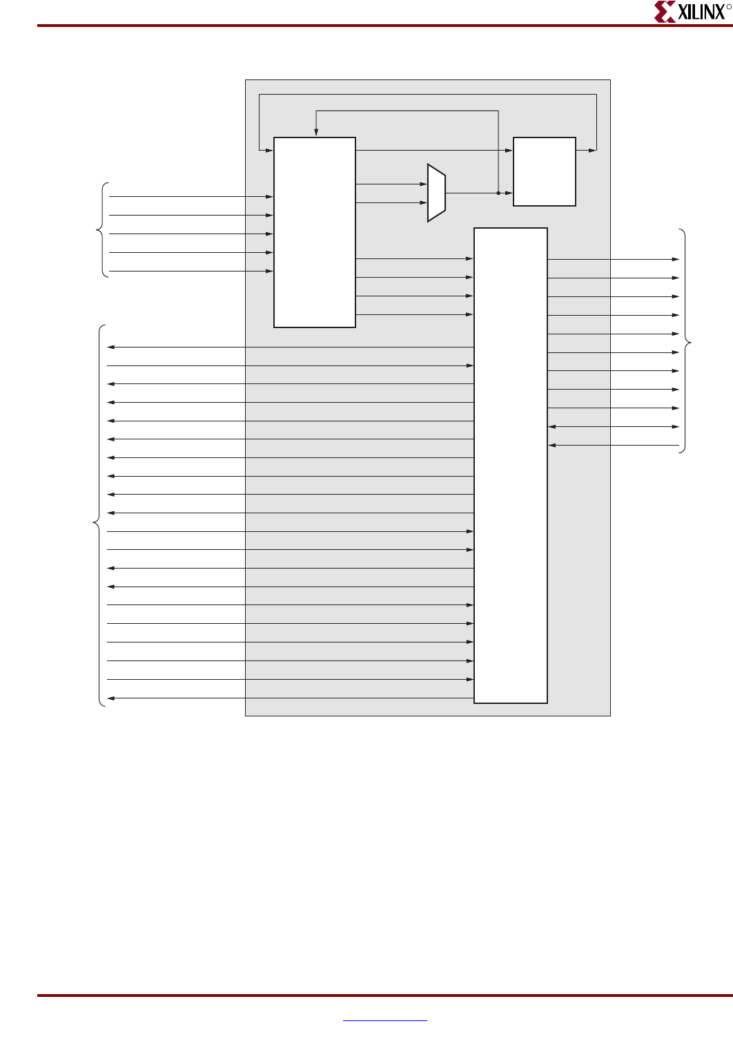
Memory Interface Solutions User Guide www.xilinx.com 231
UG086 (v3.6) September 21, 2010
Architecture
R
Figure 5-7 shows a top-level block diagram of a DDRII SRAM design without a DCM or a
testbench. The user should provide all the clocks and the dcm_locked signal. These clocks
should be single-ended. sys_rst_n is the system reset signal. All design resets are generated
using the dcm_locked signal, the sys_rst_n signal, and the dly_ready signal of the
IDELAYCTRL element. The user application must have a DCM primitive instantiated in
the design, and all user clocks should be driven through BUFGs. The user has to drive the
user application signals. The design provides the user_clk and user_rst signals to the user
to synchronize the user application signals with the design. The signal user_clk is
connected to clk0 clock signal in the controller. If the user clock domain is different from
clk0/user_clk, the user should add FIFOs for all the inputs and output of the controller
(user application signals), in order to synchronize them to user_clk clock.
Figure 5-6: Top-Level Block Diagram of the DDRII SRAM Design with a DCM but without a Testbench
main0
dly_ready
user_reset200
Memory
Device
UG086_c5_06_071808
User
Application
Reference
Clocks
and Reset
idelay_ctrl
infrastructure
_top
clk_200
IBUFGDS
clk_200_n
clk_0
clk_200_p
clk_270
user_reset
refclk_p
refclk_n
dly_clk_200_p
dly_clk_200_n
sys_rst_n
user_reset270
ddr_dll_off_n
ddr_ld_n
ddr_rw_n
ddr_k
ddr_k_n
ddr_c
ddr_c_n
ddr_sa
ddr_bw_n
ddr_dq
dly_cal_done
wr_data_full
addr_full
rd_data_valid
wr_data_wrerr
addr_wrerr
rd_data_rderr
user_clk
user_rst
user_dwl
user_dwh
user_qrl
user_qrh
user_bwl_n
user_bwh_n
user_addr_cmd
user_data_wr_ena_n
user_addr_wr_ena_n
rd_data_empty
user_qen_n
ddr_cq
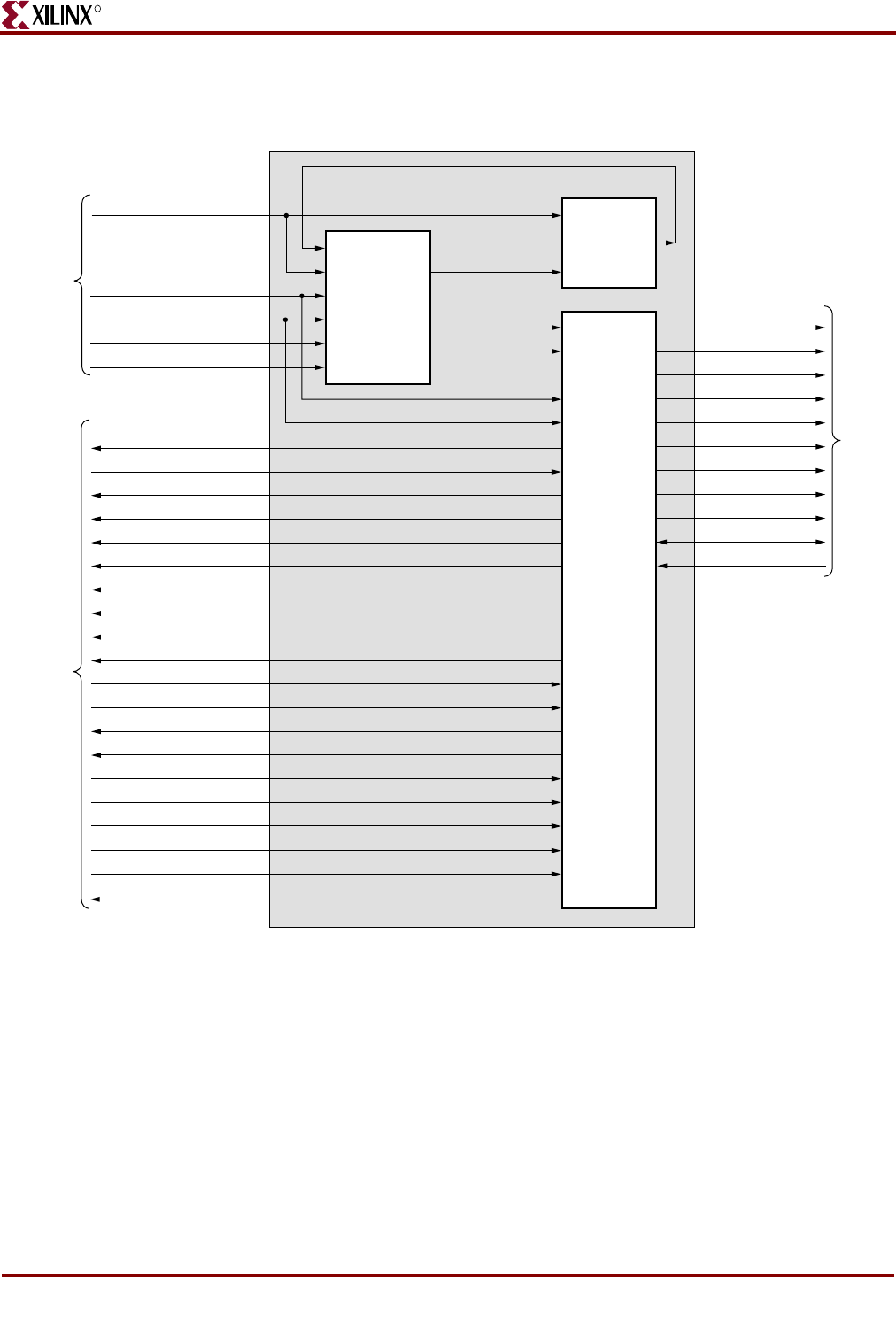
232 www.xilinx.com Memory Interface Solutions User Guide
UG086 (v3.6) September 21, 2010
Chapter 5: Implementing DDRII SRAM Controllers
R
The dly_cal_done signal indicates the completion of initialization and calibration of the
design.
Figure 5-7: Top-Level Block Diagram of the DDRII SRAM Design without a DCM or a Testbench
main0
dly_ready
Memory
Device
UG086_c5_07_121907
User
DCM
Clocks
and
Reset
idelay_ctrl
Infrastructure
_top
USER_RESET200
USER_RESET270
USER_RESET
CLK_0
CLK_200
CLK_270
DCM_LOCKED
SYS_RST_N
DDR_DLL_OFF_n
DDR_LD_N
DDR_RW_N
DDR_K
DDR_K_N
DDR_C
DDR_C_N
DDR_SA
DDR_BW_N
DDR_DQ
DDR_CQ
User
Application
DLY_CAL_DONE
WR_DATA_FULL
ADDR_FULL
RD_DATA_VALID
WR_DATA_WRERR
ADDR_WRERR
RD_DATA_RDERR
USER_CLK
USER_RST
USER_DWL
USER_DWH
USER_QRL
USER_QRH
USER_BWL_n
USER_BWH_n
USER_ADDR_CMD
USER_DATA_WR_ENA_n
USER_ADDR_WR_ENA_n
USER_QEN_n
RD_DATA_EMPTY
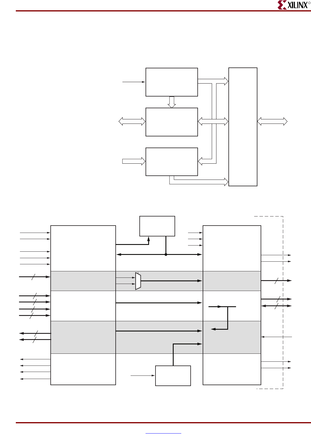
Memory Interface Solutions User Guide www.xilinx.com 233
UG086 (v3.6) September 21, 2010
Architecture
R
DDRII SRAM Controller Modules
Figure 5-8 shows a detailed block diagram of the DDRII SRAM controller. The four blocks
shown are subblocks of the top module. The functionalities of these blocks are explained in
the subsections following the figure.
Figure 5-9 shows the DDRII SRAM controller modules with a 36-bit interface.
Figure 5-8: DDRII SRAM Controller Modules
infrastructure_top
IOBS
DDRII
SRAM
Interface
data_path
user_data
user_clk
user_fifo_status DDRII SRAM
Controller
UG086_c5_08_071808
Figure 5-9: DDRII SRAM Controller Modules with Interface Signals
User Interface Physical Interface
Read / Write
State Machine
Read / Write Control
Address Path
FIFO Status
DDRII
Memory
Device
user_clk
user_reset
user_data_wr_ena_n
user_addr_wr_ena_n
user_qen_n
user_addr_cmd
user_bwl_n
user_dwl
user_dwh
user_qrl
user_qrh
wr_data_full
addr_full
rd_data_valid
ddr_ld_n
ddr_rw_n
ddr_sa
ddr_bw_n
ddr_dq
ddr_cq
ddr_k
ddr_k_n
user_clk
user_clk270
user_reset
rd_data_empty
Write Path
Read Path
clk_0
user_bwh_n
Delay
Calibration
State Machine
UG086_c5_09_071808

234 www.xilinx.com Memory Interface Solutions User Guide
UG086 (v3.6) September 21, 2010
Chapter 5: Implementing DDRII SRAM Controllers
R
Controller
The DDRII SRAM controller initializes the memory, accepts and decodes the user
commands, and generates the READ and WRITE commands. It also generates control
signals for other modules. After power on it starts the calibration, after the calibration is
completed it process the READ or WRITE commands.
Datapath
The Datapath module transmits and receives data to and from the memories. Its major
functions are listed below:
• Asserts a write-enable signal for memories with burst lengths of two or four
• Asserts a read-enable signal to memory and a write-enable signal to the User Read
Data FIFO
• Generates increment/decrement signals (tap count) for IDELAY elements in the IOBS
• Center-aligns the data window to the FPGA clock
Refer to XAPP703 [Ref 20] for techniques on data writes to memory and data captures from
memory. For burst lengths of four and two, the write-enable signal is asserted one clock
before the write data is driven on the memory bus. The data is driven on both edges of the
clock. The address to memory is driven for one full clock cycle.
Memory read data is edge-aligned with the source-synchronous clock, CQ. The DDRII
clock, CQ, to which read data is synchronized, is a free-running strobe. The free-running
strobe from the memory CQ is captured using the FPGA clock. Thus the relation between
the CQ strobe and FPGA clock is found, and the strobe CQ is center-aligned with the FPGA
clock by delaying the CQ strobe in the IDELAY element. The same logic is applied to the
read data window. The read data window is center-aligned with the same FPGA clock.
This in turn means that the same amount of tap delays are applied on both the read data
window and the strobe CQ through the IDELAY elements to center-align the read data and
strobe CQ windows with respect to the FPGA clock. Center-aligning the read data window
with respect to the FPGA clock completes the data capturing logic.
The delay calibration circuit generates the delay reset, delay select, and delay increment
values for IDELAY elements used in delaying strobes and data read from memory. The
strobe is center-aligned with the FPGA clock, which results in the data window falling to
the center of the FPGA clock. Refer to XAPP703 [Ref 20] for details about the delay
calibration.

Memory Interface Solutions User Guide www.xilinx.com 235
UG086 (v3.6) September 21, 2010
Architecture
R
Infrastructure
The infrastructure (infrastructure_top) module generates the FPGA clock and reset signals.
When differential clocking is used, refclk_p, refclk_n, dly_clk_200_p, and dly_clk_200_n
signals appear. When single-ended clocking is used, refclk and idly_clk_200 signals
appear. In addition, clocks are available for design use and a 200 MHz clock is provided for
the IDELAYCTRL primitive. Differential and single-ended clocks are passed through
global clock buffers before connecting to a DCM. For differential clocking, the output of the
refclk_p/refclk_n buffer is single-ended and is provided to the DCM input. Likewise, for
single-ended clocking, refclk is passed through a buffer and its output is provided to the
DCM input. The outputs of the DCM are 0° and 270° phase-shifted versions of the input
clock. After the DCM is locked, the design is in the reset state for at least 25 clocks. The
infrastructure module also generates all of the reset signals required for the design.
Idelay_ctrl
This module instantiates the IDELAYCTRL primitive of the Virtex-4 FPGA. The
IDELAYCTRL primitive is used to continuously calibrate the individual delay elements in
its region to reduce the effect of process, temperature, and voltage variations. A 200 MHz
clock has to be fed to this primitive.
The MIG tool instantiates the required number of IDELAYCTRLs in the RTL and uses the
LOC constraints in the UCF file to fix their locations. The number of IDELAYCTRLs is
defined by the IDELAYCTRL_NUM parameter in the idelay_ctrl module. In the RTL,
DLY_READY is generated by doing a logical AND of the RDY signals of every
IDELAYCTRL block.
IDELAYCTRL LOC constraints should be checked in the following cases:
• The MIG design is used with other IP cores or user designs that also require the use of
IDELAYCTRL and IDELAYs.
• Previous ISE® software releases 8.2.03i and 9.1i had an issue with IDELAYCTRL block
replication or trimming. When using these revisions of the ISE software, the user must
instantiate and constrain the location of each IDELAYCTRL individually.
See UG070 [Ref 7] for more information on the requirements of IDELAYCTRL placement.
IOBS
All the input and output signals of the DDRII SRAM controller are implemented in the
IOBS module. All address and byte enable signals are registered in the IOBs and driven
out.
The IDELAY elements for the read strobe and data read from memory are implemented in
the IOBS. The IOBS also implements bidirectional buffers for write and read data. The
IOBS registers the output data (ODDR) before driving it out and also registers the input
data (IDDR).
Test Bench
The MIG tool generates two RTL folders, example_design and user_design. The
example_design folder includes the synthesizable test bench, while user_design does not
include the test bench modules. The MIG test bench performs one write command
followed by one read command in an alternating manner. The number of words in a write
command depends on the burst length. For a burst length of 4, the test bench writes a total
of 4 data words for a single write command (2 rise data words and 2 fall data words). For
a burst length of 2, the test bench writes a total of 2 data words. On every write command,

236 www.xilinx.com Memory Interface Solutions User Guide
UG086 (v3.6) September 21, 2010
Chapter 5: Implementing DDRII SRAM Controllers
R
the data pattern is incremented by one, and this is repeated with each subsequent write
command. The initial data pattern for the first write command is 000. The test bench
writes the 000, 001, 002, 003 data pattern in a sequence in which 000 and 002 are rise
data words and 001 and 003 are fall data words for a 9-bit design. The falling edge data is
always rising edge data plus one. For a burst length of 2, the data sequence for the first
write command is 000, 001. The data sequence for the second write command is 002, 003.
The pattern is then incremented for the next write command. For data widths greater than
9, the same data pattern is concatenated for the other bits. For a 36-bit design and burst
length of 4, the data pattern for the first write command is 000000000, 008040201,
010080402, 0180C0603.
Address generation logic generates the address in an incremental pattern for each write
command. The same address location is repeated for the next read command. In Samsung
components, the burst address increments are done by the memory, so the address is
generated by the test bench in a linear incremental pattern. In Cypress parts, the MIG test
bench increments the address for burst operation. After the address reaches the maximum
value, it rolls back to the initial address, i.e., 00000.
During reads, comparison logic compares the read pattern with the pattern written, i.e., the
000, 001, 002, 003 pattern. For example, for a 9-bit design of burst length 4, the data
written for a single write command is 000, 001, 002, and 003. During reads, the read
pattern is compared with the 000, 001, 002, 003pattern. Based on a comparison of the
data, a status signal error is generated. If the data read back is the same as the data written,
the error signal is 0, otherwise it is 1.
DDRII SRAM Initialization and Calibration
DDRII SRAM is initialized through a specified sequence. Following the initialization, the
relationship between the read data and the FPGA clock is calculated using the TAP logic.
After the DCM clocks are stable, the controller waits for a specified amount of time before
asserting the DDR_DLL_OFF_n signal to the memory. This signal can also be pulled up to
a High on the memory device without being driven from the FPGA.
The memory strobe CQ is a free-running clock from the memory component. Because the
read data and the memory strobe CQ are edge-aligned, the strobe is passed through the
IDELAY elements of the Virtex-4 device and the taps are adjusted to center-align the strobe
pulse with respect to the FPGA clock. The same number of taps are applied to the data
window's IDELAY element to center-align the data window with respect to the FPGA
clock. XAPP701 [Ref 18] provides more information about the calibration architecture.
Calibration is done in two stages:
1. In the first stage of calibration, the read strobe CQ is center-aligned with respect to the
FPGA clock. CQ is a free-running clock from DDRII SRAM. The read data window is
edge-aligned with the read strobe CQ. The first and second edges of the CQ strobe are
detected using the FPGA clock to determine the center of the CQ window.
Once the CQ window is center-aligned with the FPGA clock, the same amount of delay
(tap counts) is applied to the read data window through the IDELAY element, so that
the read data window is center-aligned with the FPGA clock.
Port cq_q_cal_done in the data_path module indicates the status of the first stage
calibration. When cq_q_cal_done is asserted High, it indicates the completion of first
stage calibration. After the first stage calibration is complete, the second stage
calibration starts.

Memory Interface Solutions User Guide www.xilinx.com 237
UG086 (v3.6) September 21, 2010
Clocking Scheme
R
2. In the second stage of calibration, the write enable signal for the Read Data FIFO is
determined by delaying the controller-issued read command. This delay is calibrated
based on the delay between the read command and the corresponding read data at the
Read Data FIFO. For this delay calibration, the controller writes a known fixed pattern
of data into a memory location and reads back from the same location. This read data
is compared against the known fixed pattern. The delay between the read command
and the correct pattern read data comparison is the delay calibration.
The final_dly_cal_done port in the data_path module indicates the status of the second
stage calibration. When final_dly_cal_done is asserted High, it indicates the
completion of second stage calibration, which implies the completion of the whole
initialization and calibration process. After the initialization and calibration is done
(i.e., the dly_cal_done signal in design_top is asserted High), the controller can start
issuing user commands to the memory.
In the second stage calibration, when the pattern read data does not match with the
pattern write data, the controller does not issue any further pattern read commands
and the controller gets stuck in the calibration state. The design must be restarted for
the calibration to start from the beginning.
Clocking Scheme
Figure 5-10, page 238 shows the clocking scheme for this design. Global and local clock
resources are used.
The global clock resources consist of a DCM, two BUFGs on DCM output clocks, and one
BUFG for clk_200.The local clock resources consist of regional I/O clock networks
(BUFIO). The global clock architecture is discussed in this section.
The MIG tool allows the user to customize the design such that the DCM is not included.
In this case, clk_0 and clk_270 must be supplied by the user.
Global Clock Architecture
The user must supply two input clocks to the design:
• A system clock running at the target frequency for the memory
• A 200 MHz clock for the IDELAYCTRL blocks.
These clocks can be either single-ended or differential. User can select single-ended or
differential clock input option from MIG GUI. Differential clocks are connected to the
IBUFGDS and single-ended clock is connected to IBUFG.
The system clock from the output of the IBUFGDS or the IBUFG is connected to the DCM
to generate the various clocks used by the memory interface logic.
The clk_200 output of the IBUFGDS or the IBUFG is connected to the BUFG. The output of
the BUFG is used for IDELAY IOB delay blocks for aligning read capture data.
The DCM generates three separate synchronous clocks for use in the design. This is shown
in Table 5-2 and Figure 5-10, page 238. The clock structure is same for both example design
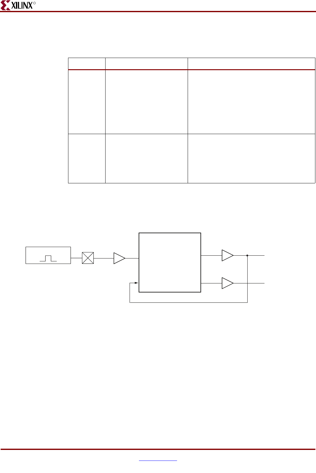
238 www.xilinx.com Memory Interface Solutions User Guide
UG086 (v3.6) September 21, 2010
Chapter 5: Implementing DDRII SRAM Controllers
R
and user design. For designs with out DCM instantiation, DCM and the BUFGs should be
instantiated at user end to generate the required clocks.
User Interface
The user interface consists of seven FIFOs. The User Write interface has four FIFOs: one
FIFO is used for the memory address, two FIFOs contain positive-edge and negative-edge
data for memory, and the remaining FIFO is used for Byte Writes. The DDRII SRAM
controller checks the not empty status of these FIFOs and initiates a memory write. The
user interface is single data rate (SDR). The controller handles the conversion from the SDR
user interface to the DDR Memory interface and vice versa.
The User Read interface has three FIFOs, where one FIFO is used for the memory address
and the remaining two FIFOs contain positive-edge and negative-edge data read from
memory. The user writes to the User Read Address FIFO the memory address from which
data is to be read. The DDRII SRAM controller checks the status of this FIFO and initiates
Table 5-2: DDRII Interface Design Clocks
Clock Description Logic Domain
clk_0 Skew compensated replica
of the input system clock.
The clock for the controller and the user
interface logic. The DDRII bus-related I/O
flip-flops (e.g., memory clocks). This clock is
used to register the data, address, and
command signals, and the address and data
enables for the user interface logic(1). This
clock is also used to generate the read data
and read data valid signals.
clk_270 270° phase-shifted version
of clk_0
Used in the write data path section of
physical layer. Clocks write path control
logic, DDRII side of the Write Data FIFO,
and output flip-flops for DQ and memory
control and address signals. This clock is
also used to generate FIFO status signals.
Notes:
1. See “DDRII SRAM Controller Interface Signals,” page 239 for timing requirements and restrictions on
the user interface signals.
Figure 5-10: Clocking Scheme for DDRII Interface Logic
CLKIN
C
LKFB CLK270
CLK0
clk_270
clk_0
DCM BUFG
GC I/O
SYSTEM CLK
UG086_c5_21_071808
Memory Interface Solutions User Guide www.xilinx.com 239
UG086 (v3.6) September 21, 2010
DDRII SRAM Controller Interface Signals
R
a memory read burst. The data read is stored in the User Read Data FIFOs. The user reads
these FIFOs to access the data read from memory. The FIFOs are built using FIFO16
primitives in the rd_data_interface, rd_wr_addr_interface, and wr_data_interface
modules. Each FIFO has a threshold attribute called ALMOST_FULL_OFFSET whose
value is set to F, by default, in the RTL. This value can be changed as needed. For valid
FIFO threshold offset values, refer to UG070 [Ref 7].
Refer to Table 5-3 for how the user can access these FIFOs.
DDRII SRAM Controller Interface Signals
Table 5-3 through Table 5-4 describe the DDRII controller system interface signals.
Table 5-5 describes the DDRII SRAM user interface signals. Table 5-6 describes the DDRII
memory interface signals. In these tables, all signal directions are with respect to the DDRII
memory controller.
Table 5-3: DDRII SRAM System Interface Signals (with a DCM)
Signal Name Direction Description
refclk_p, refclk_n Input Reference clock input made up of differential clock pairs. This clock
pair goes to a differential input buffer. The differential buffer output
goes to the DCM input. The DCM generates the required clocks for the
design. This input system clock pair is present only when the
DIFFERENTIAL clock option is selected in the MIG FPGA options
page.
refclk Input Single-ended system clock input. This clock is an input to IBUFG. The
IBUFG output is connected to the DCM clock input. The DCM
generates the required clocks for the design. This input system clock is
present only when the SINGLE_ENDED clocks option is selected in
MIG FPGA options page.
When DCM option is deselected, both differential or single-ended
input system clocks are not present.
dly_clk_200_p,
dly_clk_200_n
Input 200 MHz differential clock used in the IDELAY_CTRL logic. This input
clock pair is present only when the DIFFERENTIAL clocks options is
selected in the MIG FPGA options page.
idly_clk_200 Input Single-ended 200 MHz IDELAYCTRL clock input. This clock is
connected to an IBUFG. The IBUFG output is connected to input of
BUFG. The output of this BUFG acts as IDELAYCTRL clock input. This
input system clock is present only when the SINGLE_ENDED clocks
option is selected in the MIG FPGA options page.
When the DCM option is deselected, both differential and single-
ended input system clocks are not present.
sys_rst_n Input Reset to the DDRII memory controller
compare_error Output This signal indicates the status of the comparison between the read
data with the corresponding write data
dly_cal_done Output This signal is asserted when the design initialization and calibration is
complete
240 www.xilinx.com Memory Interface Solutions User Guide
UG086 (v3.6) September 21, 2010
Chapter 5: Implementing DDRII SRAM Controllers
R
Table 5-4: DDRII SRAM System Interface Signals (without a DCM)
Signal Name Direction Description
clk_0 Input Input clock
clk_270 Input Input clock with 270° phase difference
clk_200 Input 200 MHz clock for IDELAYCTRL primitives
dcm_locked Input This active-High signal indicates whether the user DCM is locked or
not
sys_rst_n Input Reset to the DDRII memory controller
compare_error Output This signal indicates the status of the comparison between the read
data with the corresponding write data
dly_cal_done Output This signal is asserted when the design initialization and calibration is
complete
Table 5-5: DDRII SRAM User Interface Signals (without a Testbench)
Signal Name(1) Direction Description
wr_data_full Output This signal indicates the User Write FIFOs status. It is
asserted when the User Write Data FIFOs are full. When
this signal is asserted, any writes to the User Write Data
FIFO are invalid, possibly leading to controller
malfunction.
addr_full Output This signal indicates the User Read Write Address FIFO
status. It is asserted when the User Read Write Address
FIFO is full. When this signal is asserted, any writes to the
User Read Write Address FIFO are ignored.
rd_data_valid Output This signal indicate to the user that data available at read
data FIFOs.
wr_data_wrerr Output This signal is asserted when an error occurs while writing
to the User Write Data FIFOs.
addr_wrerr Output This signal is asserted when an error occurs while writing
to the User Read Write Address FIFO.
rd_data_rderr Output This signal is asserted when an error occurs while reading
the User Read Data FIFO
dly_cal_done Output This signal is asserted to indicate that the calibration is done
user_clk(2) Output All user interface signals are to be synchronized to this
clock. The user_clk is sourced from the clk_0 in the
controller.
user_rst Output This reset is active until the DCM is not locked
user_dwl [(data_width–1):0] Input Positive-edge data for memory writes. The data bus is valid
when the WRITE command (DDR_LD_N=0 &&
DDR_RW_N=0) is asserted.

Memory Interface Solutions User Guide www.xilinx.com 241
UG086 (v3.6) September 21, 2010
DDRII SRAM Controller Interface Signals
R
user_dwh [(data_width–1):0] Input Negative-edge data for memory writes. The data bus is
valid when the WRITE command (DDR_LD_N=0 &&
DDR_RW_N=0) is asserted.
user_qrl [(data_width–1):0] Output Positive-edge data read from memory. This data is output
when user_qen_n is asserted.
user_qrh [(data_width–1):0] Output Negative-edge data read from memory. This data is output
when user_qen_n is asserted.
user_bwl_n [(bw_width–1):0] Input Byte enables for DDRII memory positive-edge write data.
The byte enables are valid when the WRITE command
(DDR_LD_N=0 && DDR_RW_N=0) is asserted.
user_bwh_n[(bw_width–1):0] Input Byte enables for DDRII memory negative-edge write data.
The byte enables are valid when the WRITE command
(DDR_LD_N=0 && DDR_RW_N=0) is asserted.
usr_addr_cmd[addr_width:0](3) Input DDRII memory address for read or write operation. This
address is valid when USER_DATA_WR_ENA_n is
asserted. An extra bit is driven by the user to represent the
command.
user_qen_n Input This active-Low signal is the read enable for the User Read
Data FIFOs. The DDRII memory controller captures the
data read from memory and stores it in the Read Data
FIFOs. The user can access these FIFOs to get the data read
from memory.
user_data_wr_ena_n Input This active-Low signal is the write enable for the User Write
Data FIFOs. The user asserts this signal to write new data to
the FIFOs. The DDRII SRAM controller reads the data from
the User Write Data FIFO and writes to memory.
user_addr_wr_ena_n Input This active-Low signal is the write enable for the User Read
Write Address FIFO. The user asserts this signal to write
write/read address and command in to user read write
address FIFO.
Notes:
1. All user interface signal names are prepended with a controller number, for example, cntrl0_ddr_dq. DDRII SRAM devices
currently support only one controller.
2. The user_clk signal is connected to clk_0 in the controller. If the user clock domain is different from clk_0 / user_clk of the MIG, the
user should add FIFOs for all data inputs and outputs of the controller in order to synchronize them to the user_clk.
3. The number of address bits used depends on the density of the memory part. The controller ignores the unused bits, which can all
be tied High.
Table 5-5: DDRII SRAM User Interface Signals (without a Testbench) (Cont’d)
Signal Name(1) Direction Description
242 www.xilinx.com Memory Interface Solutions User Guide
UG086 (v3.6) September 21, 2010
Chapter 5: Implementing DDRII SRAM Controllers
R
Table 5-6: DDRII SRAM Interface Signals
Signal Name Direction Description
ddr_dq Input/
Output
Bidirectional data bus. During READ commands, the data is sampled
on both edges of the FPGA clk. During WRITE commands, the data is
sampled on both edges of the K clk.
ddr_bw_n Output Byte enables for DDRII memory write data. The byte enables are valid
when the WRITE command (DDR_LD_N=0 && DDR_RW_N=0) is
asserted.
ddr_sa Output Address for READ and WRITE operations
ddr_ld_n Output Synchronous load pin. The bus cycle sequence is to be defined when
this signal is Low.
ddr_rw_n Output Read/Write control pin. Read is active when High.
ddr_cq Input This read data clock, transmitted by DDRII SRAM, is edge-aligned
with read data
k, k_n Output Differential write data clocks
c, c_n Output Input clock for output data
ddr_dll_off_n Output The DLL is disabled when this signal is Low
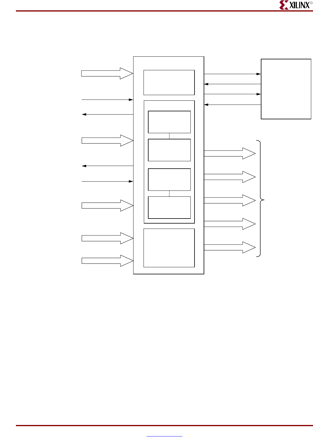
Memory Interface Solutions User Guide www.xilinx.com 243
UG086 (v3.6) September 21, 2010
DDRII SRAM Controller Interface Signals
R
Write Interface
Figure 5-11 shows the user interface block diagram for write operations.
The following steps describe the architecture of the Address and Write Data FIFOs and
show how to perform a write burst operation to DDRII memory from the user interface.
1. The user interface consists of an Address FIFO, Data FIFOs, and a Byte Write FIFO.
These FIFOs are constructed using Virtex-4 FPGA FIFO16 primitives with a 512 x 36
configuration.
2. The common Address FIFO is used for both write and read commands, and comprises
a command part and an address part. The command bit (bit 0 of the Address FIFO)
discriminates between write and read commands; the address starts at bit 1. The
command bit should be set to 0 for writes and to 1 for reads.
3. Two separate sets of Data FIFOs are used for storing the rising-edge and falling-edge
data to be written to DDRII memory from the user interface. For 9-bit, 18-bit, and 36-bit
data widths, two FIFO16s are required for storing rising-edge and falling-edge data.
For 72-bit data width, two FIFO16s are required for rising-edge data and two for
falling-edge data. MIG instantiates the required number of FIFOs to gain the required
Figure 5-11: Write User Interface Block Diagram
User Interface
Controller
Address FIFO
(FIFO16)
512 x 36
Byte Write FIFO
(FIFO16)
512 x 36
user_add_cmd
user_addr_wr_ena_n
user_dwl
user_dwh
user_bwl_n
user_bwh_n
fifo_dwl
fifo_rd_addr
fifo_dwh
fifo_bwl
fifo_bwh
To IOBS
addr_full
Rise Data FIFO
(FIFO16)
512 x 36
Rise Data FIFO
(FIFO16)
512 x 36
Fall Data FIFO
(FIFO16)
512 x 36
Fall Data FIFO
(FIFO16)
512 x 36
Data FIFOs
addr_empty
wr_rd_cmd
fifo_addr_rd_ena_n
wr_init_n
user_data_wr_ena_n
wr_data_full
ug086_c5_15_010208
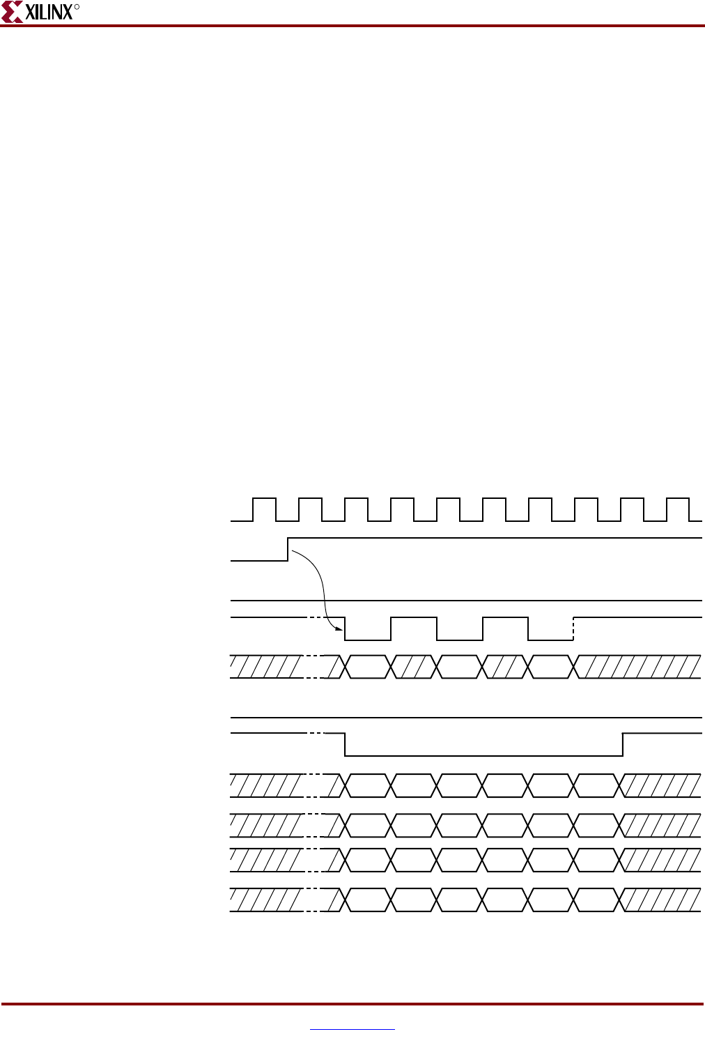
244 www.xilinx.com Memory Interface Solutions User Guide
UG086 (v3.6) September 21, 2010
Chapter 5: Implementing DDRII SRAM Controllers
R
data width. For 9-bit and 18-bit configurations, the controller pads the extra bits of the
Data FIFO with 0s.
4. The Byte Write FIFO is used to store the Byte Write signals to DDRII memory from the
user interface. The controller internally pads all zeros for the unused bits.
5. The user can initiate a write to memory by writing to the Address FIFO, Data FIFOs,
and Byte Write FIFO when the FIFO full flags are deasserted and after dly_cal_done is
asserted. The user should not access any of these FIFOs until dly_cal_done is asserted.
The dly_cal_done signal assures that the clocks are stable, the reset process is
completed, and the controller is ready to accept commands. Status signals addr_full
and wr_data_full are asserted when the Address FIFO and Data FIFOs or Byte Write
FIFO are full.
6. When user_addr_wr_ena_n is asserted, the user address is stored in the Address FIFO.
Similarly, when user_data_wr_ena_n is asserted, user_dwl, user_dwh, user_bwl, and
user_bwh are stored into corresponding FIFOs. A common write-enable signal is used
to enable both the Data FIFO and the Byte Write FIFO.
7. The controller reads the address and decodes the command bit. The write command
wr_init_n is issued if the command bit is 0 when the Address FIFO is not empty. This
command acts as a read-enable to the Data and Byte Write FIFOs. The DDRII memory
write command is generated from the wr_init_n signal by properly timing it.
8. Figure 5-12 shows the timing diagram for a write command of BL = 4. The address
should be asserted for one clock cycle as shown. For burst lengths of four, each write to
the Address FIFO should have two writes to the Data FIFO consisting of two rising-
edge data and two falling-edge data.
Figure 5-12: Write User Interface Timing diagram for BL = 4
user_clk
dly_cal_done
addr_full
addr_wrerr
wr_data_wrerr
user_addr_wr_ena_n
user_data_wr_ena__n
user_add_cmd
user_dwl
user_dwh
DWL-00 DWL-01 DWL-10 DWL-11 DWL-20 DWL-21
DWH-00 DWH-01 DWH-10 DWH-11 DWH-20 DWH-21
A0, W A1, W A2, W
user_bwl_n
user_bwh_n
BWL-00 BWL-01 BWL-10 BWL-11 BWL-20 BWL-21
BWH-00 BWH-01 BWH-10 BWH-11 BWH-20 BWH-21
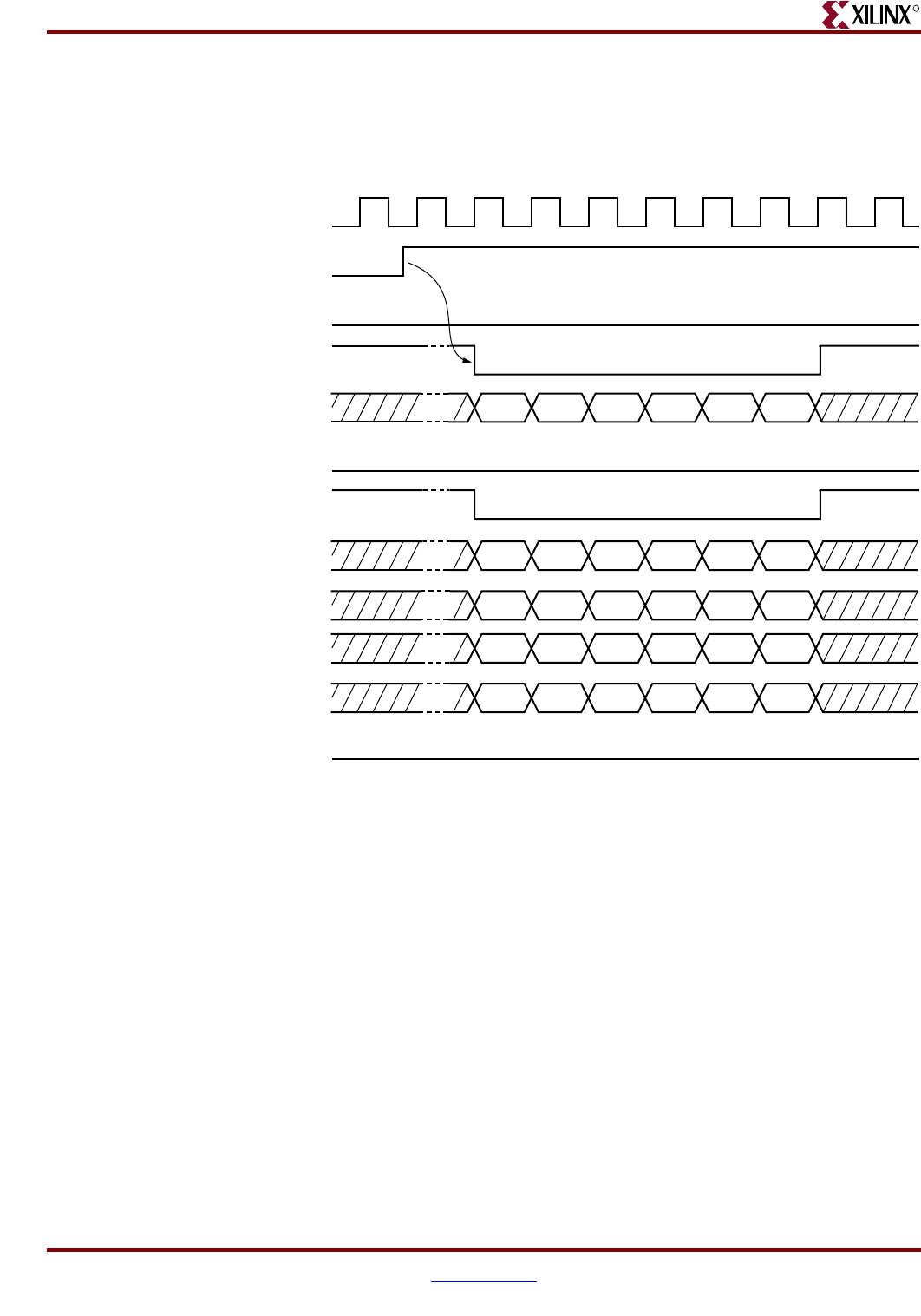
Memory Interface Solutions User Guide www.xilinx.com 245
UG086 (v3.6) September 21, 2010
DDRII SRAM Controller Interface Signals
R
9. Figure 5-13 shows the timing diagram for a write command of BL = 2. For burst length
of two, each write to Address FIFO has one write to Data FIFO, consisting of one
rising-edge data and one falling-edge data. For burst length of two, commands can be
given in every clock.
Figure 5-13: Write User Interface Timing diagram for BL = 2
user_clk
dly_cal_done
addr_full
addr_wrerr
wr_data_wrerr
user_addr_wr_ena_n
user_data_wr_ena__n
user_add_cmd
user_dwl
user_dwh
DWL-00 DWL-10 DWL-20 DWL-30 DWL-40 DWL-50
DWH-00 DWH-10 DWH-20 DWH-30 DWH-40 DWH-50
A0, W A2, W A4, WA1, W A3, W A5, W
user_bwl_n
user_bwh_n
BWL-00 BWL-10 BWL-20 BWL-30 BWL-40 BWL-50
BWH-00 BWH-10 BWH-20 BWH-30 BWH-40 BWH-50
UG086_c5_17_112907
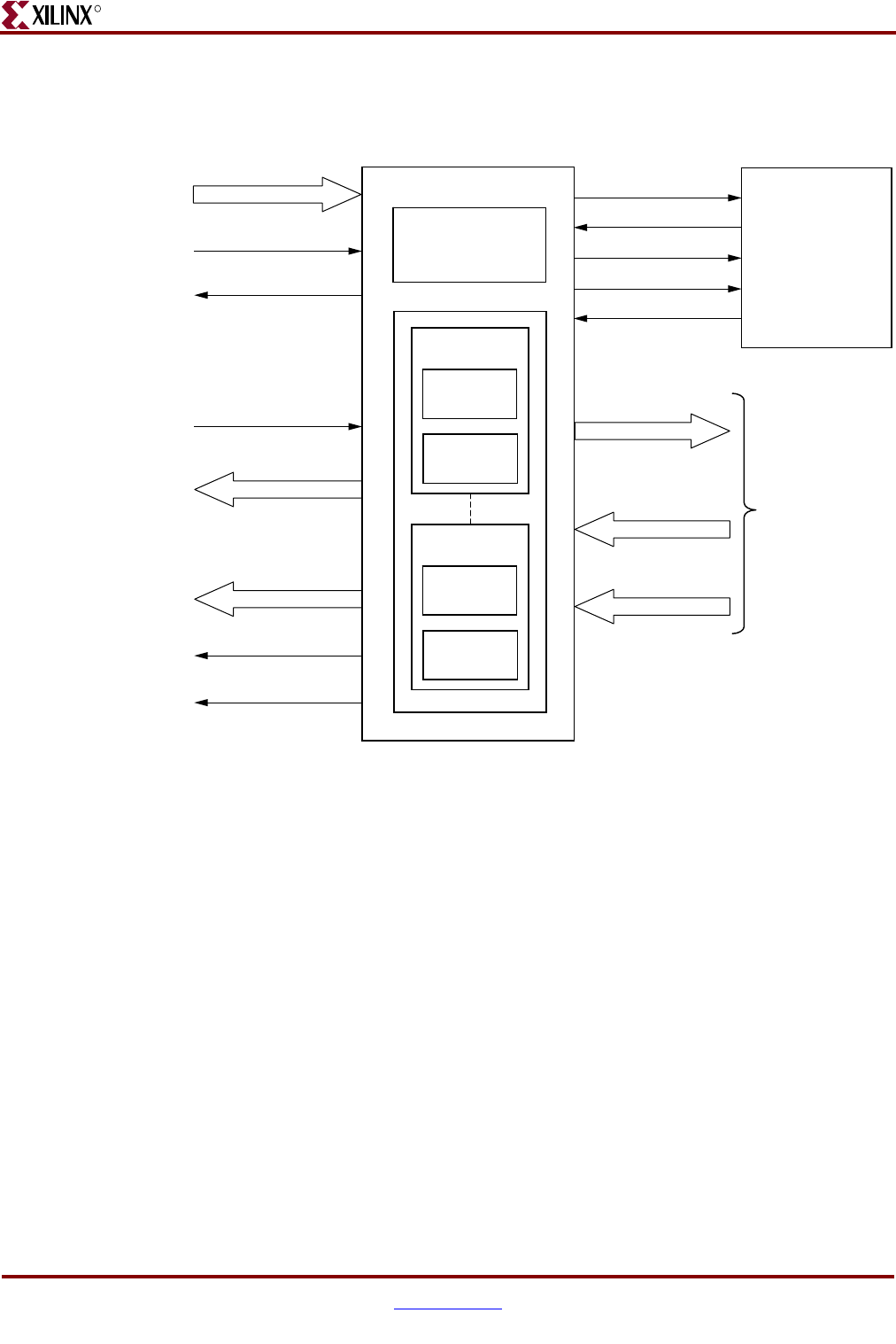
246 www.xilinx.com Memory Interface Solutions User Guide
UG086 (v3.6) September 21, 2010
Chapter 5: Implementing DDRII SRAM Controllers
R
Read Interface
Figure 5-14 shows the user interface block diagram for read operations.
The following steps describe the architecture of Read Data FIFOs and show how to
perform a burst read operation from DDRII SRAM from the user interface.
1. The read user interface consists of a common Address FIFO and a Read Data FIFO. The
Address FIFO and Read Data FIFO are constructed using FIFO16s with a 512 x 16
configuration.
2. The number of Read Data FIFOs required depends on the number of DDRII
components used. Using 9-bit components for 36-bit data width, a total of eight FIFOs
are required, four FIFOs for rising-edge data and four FIFOs for falling-edge data.
Though each FIFO can accommodate 36-bit data, the requirement of having one FIFO
per component arises from the CQ pattern calibration. Internal pattern calibration is
done per CQ. Controller generates the Read Data FIFO write-enable signal for each
FIFO separately, depending on the CQ pattern calibration.
3. To initiate a DDRII read command, the user should write the Address FIFO with the
command bit set to logic 1 when the FIFO addr_full flag is deasserted and the
dly_cal_done signal is asserted. The dly_cal_done signal assures the controller clocks
are stable, the internal reset process is completed, and the controller is ready to accept
commands.
Figure 5-14: Read User Interface Block Diagram
Controller
user_addr_cmd
user_addr_wr_ena_n
user_qrl
user_qrh
fifo_rd_addr
fifo_drl
fifo_drh
To/From IOBS
addr_full
addr_empty
wr_rd_cmd
rd_data_full
user_qen_n
fifo_addr_rd_ena_n
wr_init_n
rd_data_valid
rd_data_empty
ug086_c5_18_010108
User Interface
Address FIFO
(FIFO16)
512 x 36
Rise Data FIFO
(FIFO16)
512 x 36
Fall Data FIFO
(FIFO16)
512 x 36
Rise Data FIFO
(FIFO16)
512 x 36
Fall Data FIFO
(FIFO16)
512 x 36
Data FIFOs
Component 0
Component (n–1)
Data FIFOs
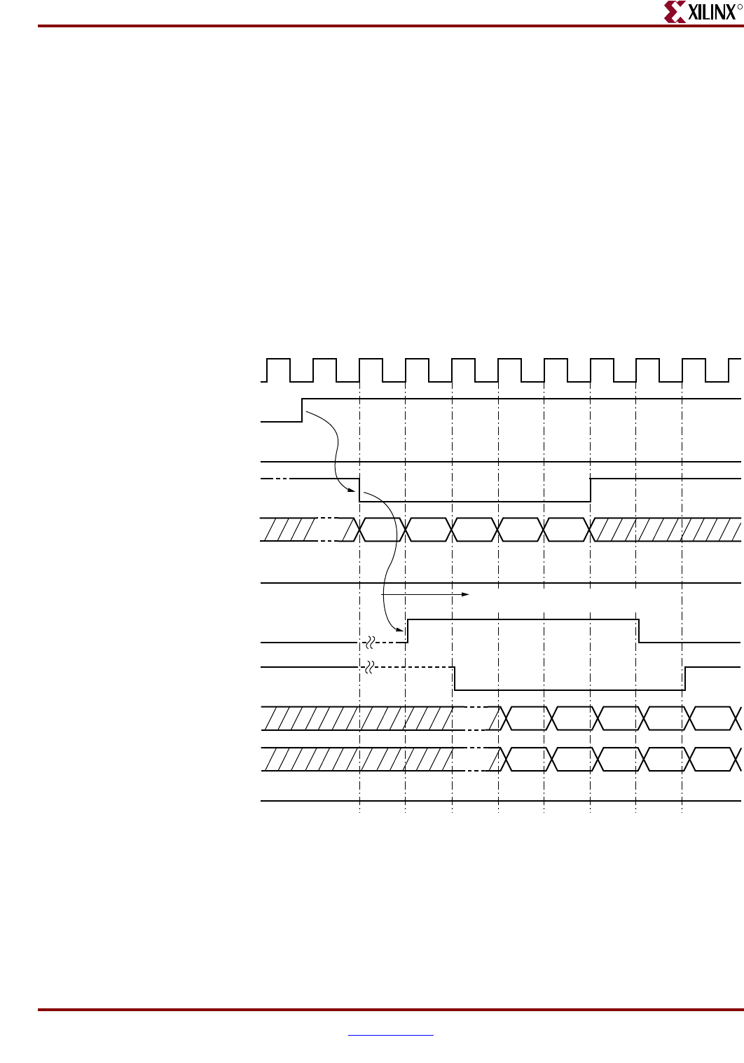
Memory Interface Solutions User Guide www.xilinx.com 247
UG086 (v3.6) September 21, 2010
DDRII SRAM Controller Interface Signals
R
4. The user should issue the Address FIFO write enable signal user_addr_wr_ena_n
along with user_addr_cmd to write the address to the Address FIFO.
5. When status signal addr_empty is deasserted, the controller reads the Address FIFO.
If the command bit is 1 when the Read Data FIFO is not full, the appropriate control
signal required for a read command is sent to the DDRII memory.
6. Prior to the actual read and write commands, the design calibrates the latency from the
time the read command is issued to the time data is received in terms of the number of
clock cycles. Using the precalibrated delay information between the read commands to
read data, the controller generates the write-enable signals to the Read Data FIFOs.The
delay calibration is done per DDRII component.
7. The Low state of rd_data_empty indicates read data is available. Asserting user_qen_n
reads rising-edge data and falling-edge data simultaneously on every rising edge of
the clock.
8. Figure 5-15 and Figure 5-16 shows the user interface timing diagrams for BL = 2 and
BL = 4.
Figure 5-15: Read User Interface Timing Diagram for BL = 2
user_clk
dly_cal_done
user_rd_full
user_rd_err
addr_wrerr
rd_data_valid
user_qen_n
user_addr_wr_ena_n
user_ad_rd
user_qrl
user_qrh
q00 q10 q20 q30q40
A0 A1 A3A2 A4
q01 q11 q21 q31q41
UG086_c5_19_121907
19 clocks between user read command
and user read data
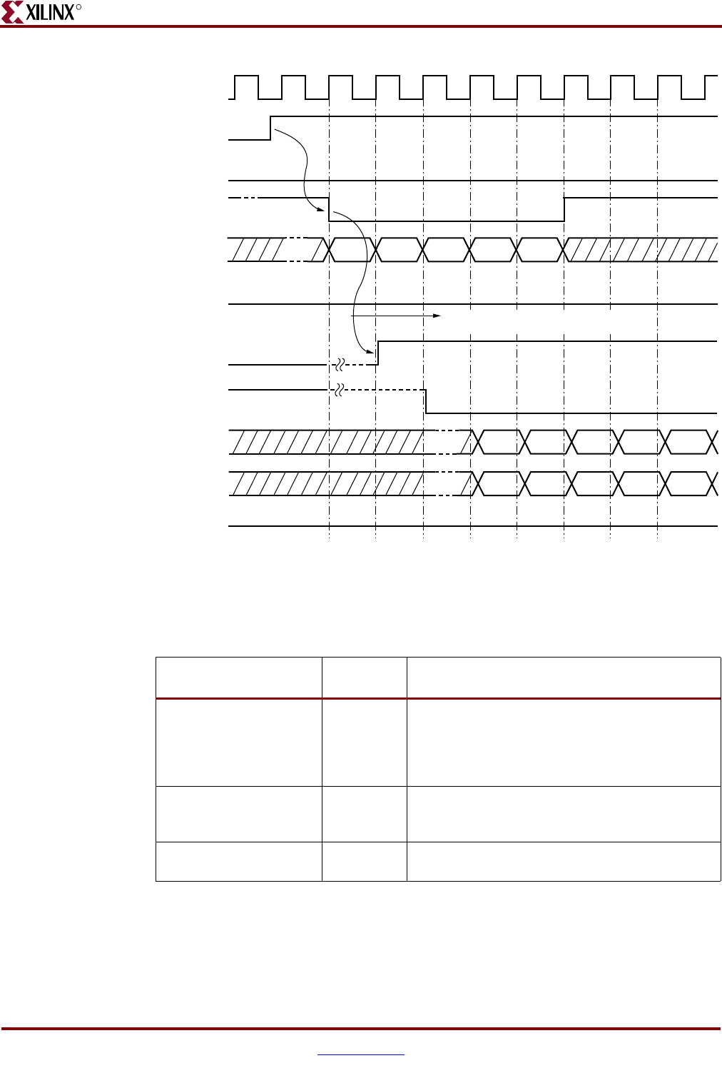
248 www.xilinx.com Memory Interface Solutions User Guide
UG086 (v3.6) September 21, 2010
Chapter 5: Implementing DDRII SRAM Controllers
R
Table 5-7 shows the maximum read latency of the controller. Maximum latency occurs
when the read command is given to an empty FIFO.
Figure 5-16: Read User Interface Timing Diagram for BL = 4
Table 5-7: Maximum Read Latency
Parameter Number of
Clocks Description
User command to
address FIFO empty
flag
6 (2 + 4) Two clocks for the two-stage pipeline before the
FIFO input. An empty FIFO takes four clocks to
deassert the empty status signal after the FIFO is
written with the first data in first-word
fall-through (FWFT) mode.
Command from
controller state machine
to DDR memory
3 Decoding and passing the command to DDR
memory.
DDR command to FIFO
input data
4 Two clocks for DDRII memory latency, two
clocks for calibration delay.
user_clk
dly_cal_done
user_rd_full
user_rd_err
addr_wrerr
rd_data_valid
user_qen_n
user_addr_wr_ena_n
user_ad_rd
user_qrl
user_qrh
q00 q02 q10 q12 q20
A0 A1 A3A2 A4
q01 q03q11 q13q21
UG086_c5_20_010208
19 Tck between user read command
and user read data
Memory Interface Solutions User Guide www.xilinx.com 249
UG086 (v3.6) September 21, 2010
DDRII SRAM Controller Interface Signals
R
DDRII SRAM Signal Allocations
Table 5-8 shows the list of signals for a DDRII SRAM design allocated in a group from bank
selection checkboxes in MIG.
When the Address box is checked in a bank, the address, ddr_ld_n, ddr_rw_n,
ddr_dll_off_n bits are assigned to that particular bank.
When the Data box is checked in a particular bank, the memory data, the memory byte
write, the memory read clocks, the memory write clocks, and the memory input clock for
the output data are assigned to that particular bank.
When the System Control box is checked in a bank, the sys_rst_n, compare_error, and
dly_cal_done bits are assigned to that particular bank.
When the System Clock box is checked in a bank, the refclk_p, refclk_n, dly_clk_200_p,
and dly_clk_200_n bits are assigned to that particular bank.
For special cases, such as without a testbench and without a DCM, the corresponding
input and output ports are not assigned to any pins of the FPGA in the design UCF because
the user can connect these ports to the FPGA pins or can connect to some logic internal to
the same FPGA.
Note: Timing has been verified for most of the MIG generated configurations. For the best timing
results, adjacent banks in the same column of the FPGA should be used. Banks that are separated
by unbonded banks should be avoided because these can cause timing violations.
Supported Devices
The design generated out of MIG is independent of the memory package, hence the
package part of the memory component is replaced with X, where X indicates a don't care
condition. Table 5-9 shows the list of components supported by MIG.
FIFO input to FIFO
output
6 Pipelines the write enable six clock cycles
(two-stage pipeline at the FIFO and one reg for
calibration, and four clocks for deassertion of
read data fifo empty).
Total Latency 19 Total latency from read command issued to
Address FIFO, to data input to user interface.
Table 5-7: Maximum Read Latency (Cont’d)
Parameter Number of
Clocks Description
Table 5-8: DDRII Signal Allocations
Bank Selected Signals Allocated in the Group
Address Memory address and memory control
Data Memory data and memory byte read/write
System Control System reset from the user interface and status signals
System Clock System clocks from the user interface
250 www.xilinx.com Memory Interface Solutions User Guide
UG086 (v3.6) September 21, 2010
Chapter 5: Implementing DDRII SRAM Controllers
R
Table 5-9: Supported Devices for DDRII SRAM
Virtex-4 FPGAs (Verilog and VHDL)
Components Make Configuration
CY7C1319BV18-250BZC Cypress x18
CY7C1318BV18-250BZC Cypress x18
CY7C1320BV18-200BZC Cypress x36
CY7C1320BV18-250BZC Cypress x36
CY7C1321AV18-250BZC Cypress x36
CY7C1321BV18-250BZC Cypress x36
CY7C1419AV18-250BZC Cypress x18
CY7C1420AV18-250BZC Cypress x36
CY7C1421AV18-250BZC Cypress x36
CY7C1427AV18-250BZC Cypress x9
CY7C1428AV18-250BZC Cypress x9
CY7C1518V18-250BZC Cypress x18
CY7C1520V18-250BZC Cypress x36
CY7C1916BV18-250BZC Cypress x9
CY7C1917BV18-250BZC Cypress x9
K7I161882B-FC25 Samsung x18
K7I161884B-FC25 Samsung x18
K7I163682B-FC25 Samsung x36
K7I163684B-FC25 Samsung x36
K7I321884C-FC25 Samsung x18
K7I321884M-FC25 Samsung x18
K7I323684C-FC25 Samsung x36
K7I323684M-FC25 Samsung x36
K7I641882M-FC25 Samsung x18

Memory Interface Solutions User Guide www.xilinx.com 251
UG086 (v3.6) September 21, 2010
Simulating the DDRII SRAM Design
R
Simulating the DDRII SRAM Design
After generating the design, MIG creates a sim folder in the specified path. This folder
contains simulation files for a particular design. The sim folder contains an external
testbench and a .do file to simulate the generated design. To learn more details about the
files in the sim folder and to simulate the design, refer to “Simulation Guide,” page 499.
Hardware Tested Configurations
This design is not hardware verified.


Memory Interface Solutions User Guide www.xilinx.com 253
UG086 (v3.6) September 21, 2010
R
Chapter 6
Implementing RLDRAM II Controllers
Reduced Latency DRAM (RLDRAM II) devices address high bandwidth memory
requirements. The RLDRAM II utilizes an eight-bank architecture optimized for high-
speed operation and a double data rate I/O for increased bandwidth. This chapter
describes how to implement RLDRAM II interfaces for Virtex®-4 FPGAs generated with
MIG. This design is based on XAPP710 [Ref 22].
Feature Summary
This section summarizes the supported and unsupported features of the RLDRAM II
controller design.
Supported Features
The RLDRAM II controller design supports the following:
• A maximum frequency of 250 MHz
• Both SIO and CIO memories
• Multiplexed and non-multiplexed addresses
• All configurations (Config1, Config2, and Config3)
• x9, x18, and x36 components
• Data widths of 9, 18, 36, and 72 bits
• Back-to-back read and write operations
• Write followed by read operations
• Read followed by write operations
• All combinations of the Mode Register
• XST and Synplicity synthesis tools
•Verilog and VHDL
• With and without a testbench
• With or without a DCM
254 www.xilinx.com Memory Interface Solutions User Guide
UG086 (v3.6) September 21, 2010
Chapter 6: Implementing RLDRAM II Controllers
R
Design Frequency Range
Unsupported Features
The RLDRAM II controller design does not support:
• Commands in successive clocks with a burst length of 2. The controller processes
these commands with one extra clock latency. For example, a READ or WRITE
sequence of commands, BL = 2, Configuration = Any, CIO/SIO.
Supported RLDRAM II Devices
The RLDRAM II controller design supports the RLDRAM II devices from Micron indicated
in Table 6-2. MIG generates the designs for the list of components mentioned in Table 6-2 in
both VHDL and Verilog. The design generated out of MIG is independent of memory
package, hence the package part of the memory component is replaced with XX, where XX
indicates any package.
Table 6-1: Design Frequency Range in MHz
Memory
FPGA Speed Grade
-10 -11 -12
Min Max Min Max Min Max
Component (SIO/CIO) 175 200 175 230 175 250
Table 6-2: Supported RLDRAM II Devices
Device Make CIO/SIO Configuration Speed Grade Supported Data
Widths (in bits) Packages
MT49H32M9XX Micron CIO x9 (-5), (-25), (-33) 9, 18, 36, 72 BM, FM
MT49H16M18XX Micron CIO x18 (-5), (-25), (-33) 18, 36, 72 BM, FM
MT49H8M36XX Micron CIO x36 (-5), (-25), (-33) 36, 72 BM, FM
MT49H32M9CXX Micron SIO x9 (-5), (-25), (-33) 9, 18, 36, 72 BM, FM
MT49H16M18CXX Micron SIO x18 (-5), (-25), (-33) 18, 36, 72 BM, FM
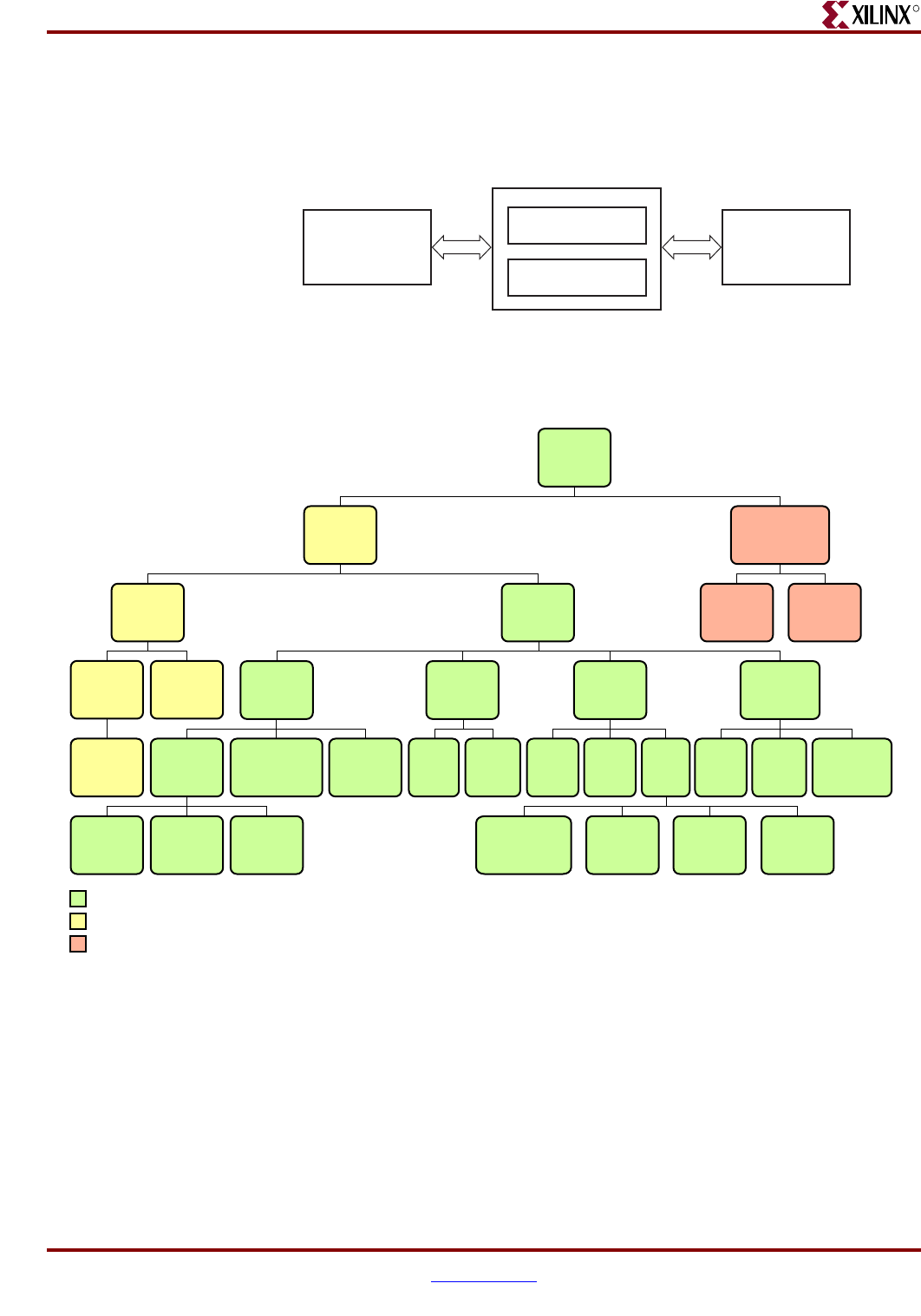
Memory Interface Solutions User Guide www.xilinx.com 255
UG086 (v3.6) September 21, 2010
Architecture
R
Architecture
Figure 6-1 shows a top-level block diagram of the RLDRAM II memory controller.
Figure 6-2 shows the hierarchical structure of the RLDRAM II design generated by MIG
with a testbench and a DCM.
The modules are classified as follows:
• Design modules
• Testbench modules
• Clocks and reset generation modules
There is a parameter file generated with the design that has all the user input and design
parameters selected from MIG.
Figure 6-1: RLDRAM II Memory Controller Block Diagram
User
Application
RLDRAM II
CIO/SIO
Memory
UG086_c6_01_012007
Memory Controller
Infrastructure_top
To p
Figure 6-2: RLDRAM II Memory Controller Hierarchy
<top_
module>
main* infrastructure_
top*
iobs*
infrastructure
_iobs*
data_
path_
iobs*
controller
_iobs*
byte_
compare
controller data_
path*
tap_
logic*
data_
read*
data_
write*
user_
interface*
rld_
mergedfifo
rld_
rdfifo*
rld_
wdfifo*
rld_
conf* rld_ctl*
Design Modules
cmp_rd
_data*
backend
_rom*
v4_dm_
iob
v4_dq_
iob
d4_dqs
_iob
UG086_c6_02_091307
clk_
module rld_rst*
test_
bench* top*
Te st Bench Modules
Clock Module and Reset Generation Module
Note: A block with a * has a parameter file included.
IDELAYCTRL tap_ctrl data_
tap_inc
idelay_rd
_en

256 www.xilinx.com Memory Interface Solutions User Guide
UG086 (v3.6) September 21, 2010
Chapter 6: Implementing RLDRAM II Controllers
R
MIG can generate four different RLDRAM II designs:
• With a testbench and a DCM
• Without a testbench and with a DCM
• With a testbench and without a DCM
• Without a testbench and without a DCM
MIG outputs both an example_design and a user_design. The MIG-generated
example_design includes the entire memory controller design along with a synthesized
testbench (example user application). This testbench generates sample writes and reads
and then uses comparison logic to verify that the data patterns written are the same as
those received. This example_design can be used to test functionality both in simulation
and in hardware. The user_design includes the memory controller design only. This design
allows users to connect the MIG memory controller design to a user developed testbench
(user application). Refer to Table 6-10, page 269 for user interface signals, the “User
Interface Accesses,” page 271 for timing restriction on user interface signals, and
Figure 6-10, page 273 and Figure 6-11, page 274 for write interface timing.
Design clocks and resets are generated in the infrastructure_top module, which comprises
clk_module and rld_rst modules. The DCM clock is instantiated in the clk_module module
for designs with a DCM. The differential design clock is an input to this module, which
generates the system clocks. A user reset is input to the rld_rst module, which generates
the system resets. A 200 MHz differential clock for the IDELAYCTRL module is derived
from 200 MHz differential clocks. This clock is present in the top-level module.
The clk_module is not instantiated in the infrastructure_top module if the DCM option is
not checked in MIG. So, the system operates on the user-provided clocks. The system reset
is generated in the rld_rst module using the dcm_lock signal and the ready signal of the
IDELAYCTRL element. For more information on the clocking structure, refer to “Clocking
Scheme,” page 266.
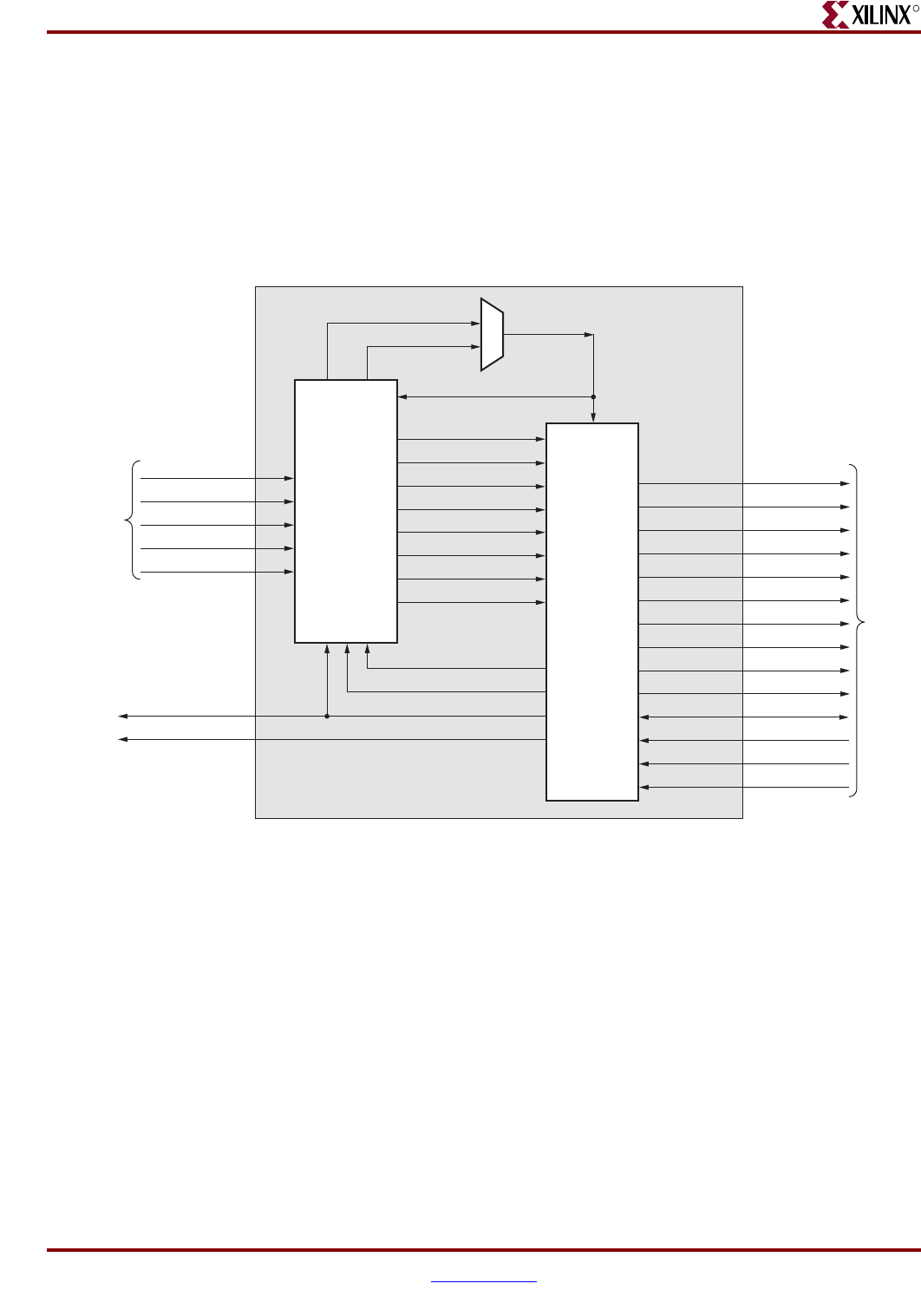
Memory Interface Solutions User Guide www.xilinx.com 257
UG086 (v3.6) September 21, 2010
Architecture
R
Figure 6-3 shows a block diagram representation of an RLDRAM II design with a DCM
and a testbench. The design inputs are the system clocks and the user reset. sysreset_n is
the system reset signal. All design resets are generated using the dcm_locked signal, the
sysreset_n signal, and the idelay_ctrl_rdy signal of the IDELAYCTRL element. The
pass_fail output signal indicates whether the design passes or fails. The init_done signal
indicates the completion of initialization and calibration of the design. Required clocks and
reset signals for the design are generated from the clk_module and the rld_rst modules,
respectively. The clk_module instantiates the DCM primitive. The infrastructure_top
module instantiates the clk_module and the rld_rst modules.
Figure 6-3: Top-Level Block Diagram of the RLDRAM II Design with a DCM and a Testbench
main_0
Memory
Device
UG086_c6_03_071808
System
Clocks
and Reset
infrastructure
_top
clk200_in
clk_200_n
rsthard_180
idelay_ctrl_rdy
calibration_done
clk_200_p
rsthard_270
rstconfig
clk200_p
clk200_n
sysclk_p
sysclk_n
sysreset_n
rst_init
rld2_we_n
rld2_ref_n
rld2_cs_n
rld2_ba
rld2_a
rld2_ck
rld2_ck_n
rld2_dk
rld2_dm
clk90
clkglob
rsthard_clk200
rsthard
rld2_dk_n
pass_fail
init_done rld2_qvld
rld2_dq
rld2_qk
rld2_qk_n
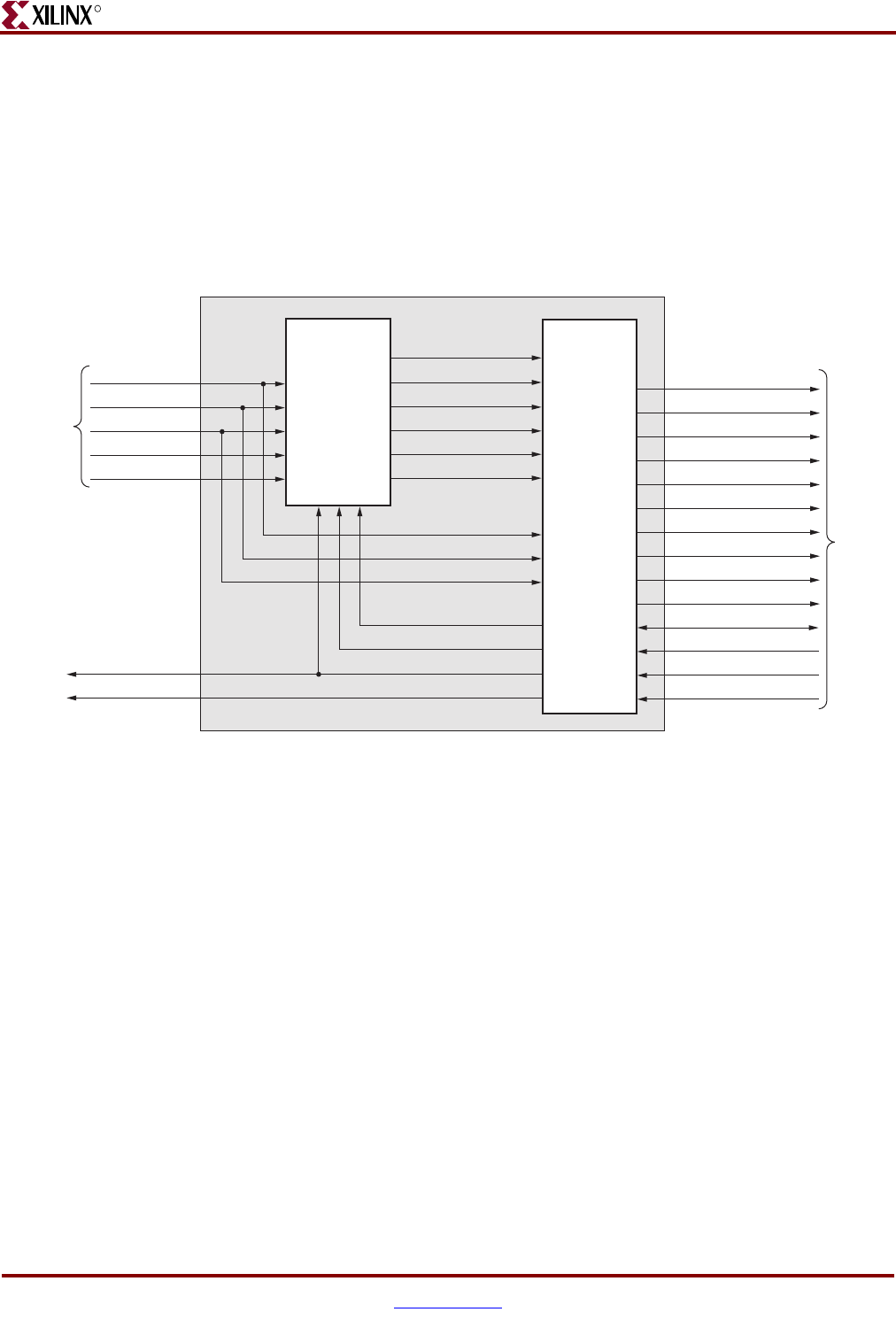
258 www.xilinx.com Memory Interface Solutions User Guide
UG086 (v3.6) September 21, 2010
Chapter 6: Implementing RLDRAM II Controllers
R
Figure 6-4 shows a block diagram representation of the top-level RLDRAM II module
without a DCM but with a testbench. Design inputs are the user clocks and the user reset.
sysreset_n is the system reset signal. All design resets are generated using the dcm_locked
signal, the sysreset_n signal, and the idelay_ctrl_rdy signal of the IDELAYCTRL element.
The design uses the user input clocks. These clocks should be single-ended. The user
application must have a DCM primitive instantiated in the design, and all user clocks
should be driven through BUFGs. The pass_fail output signal indicates whether the design
passes or fails. The init_done signal indicates the completion of initialization and
calibration of the design.
Figure 6-5, page 259 shows a block diagram representation of the top-level RLDRAM II
module with a DCM but without a testbench. Design inputs are the system clocks and
reset. sysreset_n is the system reset signal. All design resets are generated using the
dcm_locked signal, the sysreset_n signal, and the idelay_ctrl_rdy signal of the
IDELAYCTRL element. User must drive the user application signals. The design provides
the clkglob_tb and rsthard_tb signals to the user to synchronize the user application
signals with the design. The signal clkglob_tb is connected to clkglob clock signal in the
controller. If the user clock domain is different from clkglob/clkglob_tb, the user should
add FIFOs for all the inputs and output of the controller (user application signals), in order
to synchronize them to clkglob_tb clock. The required design clocks and design reset
signals for the design are generated from the clk_module and the rld_rst modules,
respectively. The clk_module instantiates the DCM primitive. The infrastructure_top
module instantiates the clk_module and rld_rst modules. The init_done signal indicates
the completion of initialization and calibration of the design.
Figure 6-4: Top-Level Block Diagram of the RLDRAM II Design without a DCM but with a Testbench
main_0
Memory
Device
UG086_c6_04_071808
System
Reset
and User
DCM
Clocks
infrastructure
_top rsthard_180
idelay_ctrl_rdy
calibration_done
rsthard_270
rstconfig
clk_200
clkglob
clk90
sysreset_n
dcm_locked rst_init
rld2_we_n
rld2_ref_n
rld2_cs_n
rld2_ba
rld2_a
rld2_ck
rld2_ck_n
rld2_dk
rld2_dm
rsthard_clk200
rsthard
rld2_dk_n
pass_fail
Init_done
rld2_qvld
rld2_dq
rld2_qk
rld2_qk_n
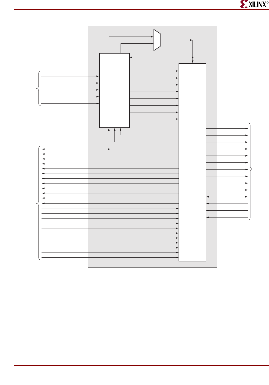
Memory Interface Solutions User Guide www.xilinx.com 259
UG086 (v3.6) September 21, 2010
Architecture
R
Figure 6-6 shows a block diagram representation of the top-level RLDRAM II module
without a DCM or a testbench. Design inputs are the user clocks and the user reset.
sysreset_n is the system reset signal. All design resets are generated using the dcm_locked
signal, the sysreset_n signal, and the idelay_ctrl_rdy signal of the IDELAYCTRL. The
design uses the user input clocks, which should be single-ended. The user application
must have a DCM primitive instantiated in the design, and all user clocks should be driven
through BUFGs. User must drive the user application signals. The design provides the
glob and rsthard_tb signals to the user to synchronize the user application signals with the
design. The signal clkglob_tb is connected to clkglob clock signal in the controller. If the
user clock domain is different from clkglob/clkglob_tb, the user should add FIFOs for all
the inputs and output of the controller (user application signals), in order to synchronize
Figure 6-5: Top-Level Block Diagram of the RLDRAM II Design with a DCM but without a Testbench
top_0 Memory
Device
UG086_c6_05_071808
System
clocks
and reset
Infrastructure
_top
clk200_in
clk_200_n
rsthard_180
idelay_ctrl_rdy
calibration_done
clk_200_p
rsthard_270
rstconfig
clk200_p
clk200_n
sysclk_p
sysclk_n
sysreset_n
rst_init
rld2_we_n
rld2_ref_n
rld2_cs_n
rld2_ba
rld2_a
rld2_ck
rld2_ck_n
rld2_dk
rld2_dm
clk90
clkglob
rsthard_clK200
rsthard
rld2_dk_n
User
Application
rld2_qvld
rld2_dq
rld2_qk
rld2_qk_n
init_done
rlwdfull
rlaffull
rlafempty
rlrdfempty
rlwdfempty
apconfrd
burstlength
rldreaddata
clkglob_tb
rsthard_tb
init_done_tb
apaddr
apvalid
apwritedvalid
apconfa
apconfwrd
apconfrd
apconfwr
aprdrden
apwritedata
apwritedm
issuemrs_tb
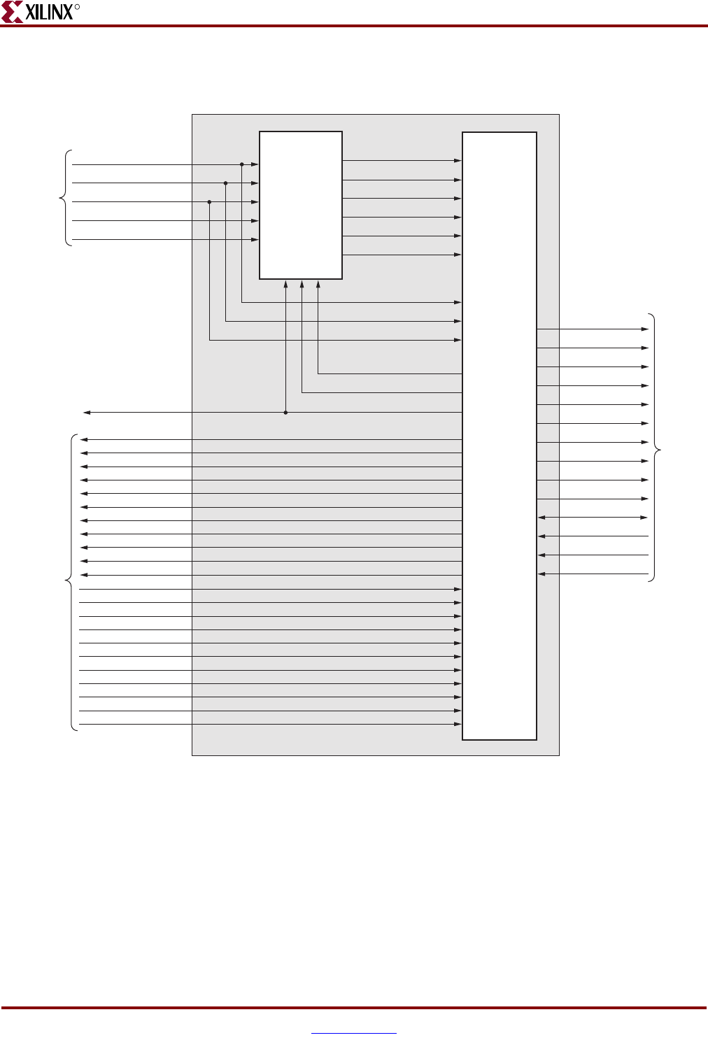
260 www.xilinx.com Memory Interface Solutions User Guide
UG086 (v3.6) September 21, 2010
Chapter 6: Implementing RLDRAM II Controllers
R
them to clkglob_tb clock. The Init_done signal indicates the completion of initialization
and calibration of the design.
Figure 6-6: Top-Level Block Diagram of the RLDRAM II Design without a DCM or a Testbench
top_0 Memory
Device
UG086_c6_06_071808
System
Reset
and User
DCM
Clocks
infrastructure
_top
rsthard_180
idelay_ctrl_rdy
calibration_done
rsthard_270
rstconfig
clk_200
clkglob
clk90
sysreset_n
dcm_locked
rst_init
rld2_we_n
rld2_ref_n
rld2_cs_n
rld2_ba
rld2_a
rld2_ck
rld2_ck_n
rld2_dk
rld2_dm
rsthard_clk200
rsthard
rld2_dk_n
init_done
rld2_qvld
rld2_dq
rld2_qk
rld2_qk_n
User
Application
rlwdfull
rlaffull
rlafempty
rlrdfempty
rlwdfempty
apConfrd
burstlength
rldreaddata
clkglob_tb
rsthard_tb
init_done_tb
apaddr
apvalid
apwritedvalid
apConfa
apConfwrd
apConfrd
apConfwr
aprdrden
apwritedata
apwritedm
issuemrs_tb
Memory Interface Solutions User Guide www.xilinx.com 261
UG086 (v3.6) September 21, 2010
Architecture
R
The RLDRAM II memory controller processes the user commands to generate the
RLDRAM II interface signals. The RLDRAM II memory controller has a built-in
synthesizable testbench to generate all the RLDRAM commands. The built-in testbench
enables simulation and validation of the design in hardware. To interface with the user
application, the RLDRAM II memory controller must be separated from the built-in
testbench. MIG generates designs with and without a testbench. The following parameters
are selectable through the GUI: the type of the RLDRAM (SIO or CIO), the data width, the
burst length, multiplexed or non-multiplexed address, memory component, and other
configuration values.
The design can use any selected banks of the Virtex-4 FPGAs. It can use different banks or
the same banks for data, address, and control signals.
The HSTL_II_18 I/O standard is used for address, control, and data signals, and the
DIFF_HSTL_II_DCI_18 I/O standard is used for clock signals.
Similar to other DRAM architectures, the RLDRAM II requires its entire content to be
refreshed periodically. The AREF command initiates a refresh for the device and must be
used each time a refresh is required. The RLDRAM II memory controller has an option to
enable the execution of auto-refresh commands periodically. If this option is OFF, the user
has to provide the auto-refresh commands at regular intervals.
Implemented Features
This section provides details on the supported features of the RLDRAM II controller.
Address Multiplexing
The RLDRAM II memory controller supports multiplexed and non-multiplexed address
modes. Bit A5 of the Mode Register determines whether the address mode is multiplexed
(A5 = 1) or non-multiplexed (A5 = 0). In multiplexed address mode, the address is
provided to the RLDRAM II memory in two cycles, which are latched into the memory on
two consecutive rising clock edges. The advantage of this approach is a maximum of 11
address bits are required to control the RLDRAM II memory.
In multiplexed address mode, the controller outputs an 11-bit address. The user has to
properly connect the addresses to the RLDRAM II devices. Table 6-3 provides the address
mapping between the controller and the RLDRAM II devices for the multiplexed address
mode.
CIO/SIO
The RLDRAM II memory controller supports both CIO and SIO memory components. The
GUI provides an option to select the required memory components. The separate
RLDRAM I/O interface transfers two 18-bit or 9-bit data words per clock cycle at the I/O
balls. The read port has dedicated data outputs to support read operations, while the write
port has dedicated input balls to support write operations. Output data is referenced to the
Table 6-3: Address Mapping in Multiplexed Address Mode
Address Address Mapping
Output
Address A0 A1 A2 A3 A4 A5 A6 A7 A8 A9 A10
RLDRAM II
Address A0 A3 A4 A5 A8 A9 A10 A13 A14 A17 A18

262 www.xilinx.com Memory Interface Solutions User Guide
UG086 (v3.6) September 21, 2010
Chapter 6: Implementing RLDRAM II Controllers
R
free-running output data clock. This architecture eliminates the need for high-speed bus
turnarounds.
Data Capture Using the Direct-Clocking Technique
The read data from the RLDRAM II is captured using the direct-clocking technique. In this
technique, data is delayed and center-aligned with respect to the internal FPGA clock. In
this scheme, the internal FPGA clock captures the read data. The clock/strobe transmitted
from the memory determines the delay value for the associated data bits. As a result, there
are no restrictions on the number of data bits associated with a strobe. Because the strobe
does not need to be distributed to the associated data bits, no additional clocking resources
are required. Refer to XAPP701 [Ref 18] for details on this technique.
Calibration is done in two stages:
1. In the first stage of calibration, QK is center-aligned with respect to the FPGA clock.
QK is a free-running clock from RLDRAM II. The DQ data is edge-aligned with the QK
read strobe, and the QVLD read data valid signal is edge-aligned with the QK read
strobe. The first and second edges of the QK strobe are detected using the FPGA clock
to determine the center of the QK window.
Once the QK window is center-aligned with the FPGA clock, the same amount of delay
(tap counts) is applied to the DQ through the IDELAY element, so that the DQ window
is center-aligned with the FPGA clock. Signal qk_tap_sel_done in the tap_logic
module indicates the status of the first stage calibration. When qk_tap_sel_done is
asserted High, it indicates the completion of first stage calibration. After the first stage
calibration is complete, the second stage calibration starts.
2. In the second stage of calibration, the write-enable signal for the read data FIFO is
determined in order to store the read data from memory into the Read Data FIFO.
QVLD from RLDRAM II is delayed such that it exactly aligns with the delayed DQ
window. This delayed QVLD signal is used as the write-enable signal for the Read
Data FIFO.
The sel_done port in the data_path module indicates the status of the second stage
calibration. When sel_done is asserted High, it indicates the completion of second
stage calibration, which implies the completion of the whole initialization and
calibration process. After the initialization and calibration is done (i.e., the init_done
signal in design_top is asserted High), the controller can start issuing user commands
to the memory.
When calibration is complete, the calibration_done signal is asserted High.
The tap_logic module instantiates the IDELAYCTRL primitive of the Virtex-4 FPGA. The
IDELAYCTRL primitive is used to continuously calibrate the individual delay elements in
its region to reduce the effect of process, temperature, and voltage variations. A 200 MHz
clock has to be fed to this primitive. The MIG tool instantiates the required number of
IDELAYCTRLs in the RTL and uses the LOC constraints in the UCF file to fix their
locations. The number of IDELAYCTRLs is defined by the IDELAYCTRL_NUM parameter
in the idelay_ctrl module. In the RTL, IDELAY_CTRL_RDY is generated by doing a logical
AND of the RDY signals of every IDELAYCTRL block.
IDELAYCTRL LOC constraints should be checked in the following cases:
• The MIG design is used with other IP cores or user designs that also require the use of
IDELAYCTRL and IDELAYs.
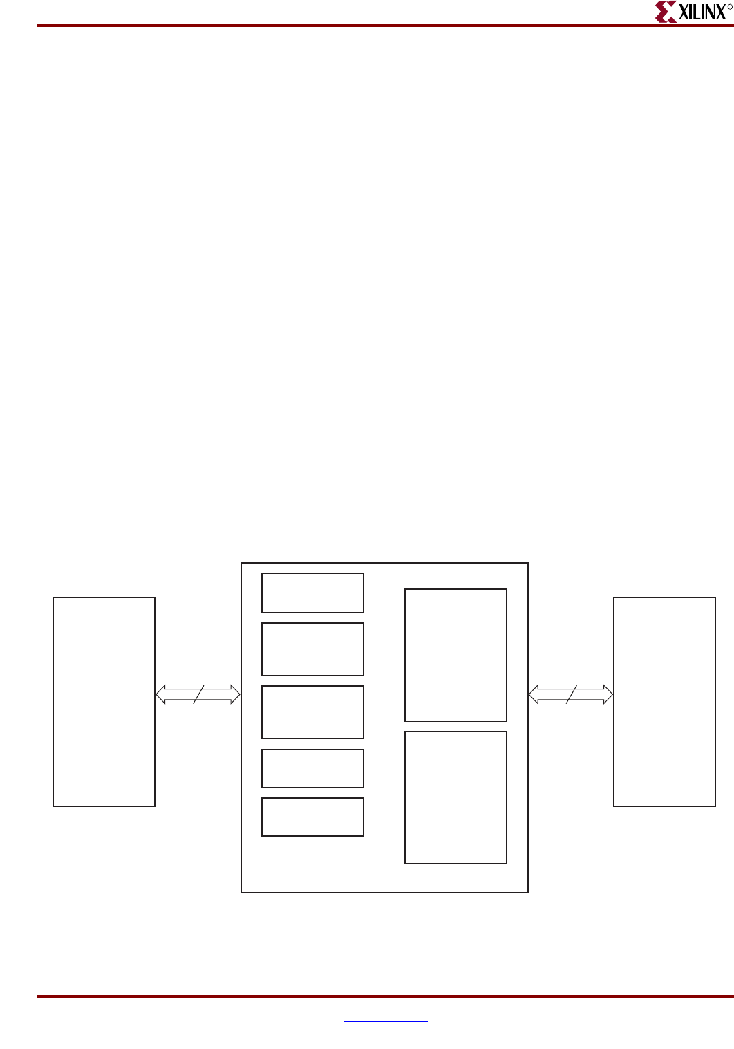
Memory Interface Solutions User Guide www.xilinx.com 263
UG086 (v3.6) September 21, 2010
Architecture
R
• Previous ISE® software releases 8.2.03i and 9.1i had an issue with IDELAYCTRL block
replication or trimming. When using these revisions of the ISE software, the user must
instantiate and constrain the location of each IDELAYCTRL individually.
See UG070 [Ref 7] for more information on the requirements of IDELAYCTRL placement.
Memory Initialization
The RLDRAM II device must be powered up and initialized in a predefined manner. The
controller handles the initialization sequence as described in this section.
After all power supply and reference voltages are stable and the master clock (rld_ck and
rld_ck_n) is stable, the RLDRAM II device requires a 200 μs (minimum) delay prior to
applying an executable command. After the 200 μs (minimum) delay has passed, three
MODE REGISTER SET (MRS) commands are issued. For non-multiplexed addressing, two
dummy commands and one valid MRS command are issued. For multiplexed addressing,
four MODE REGISTER SET (MRS) commands are issued, consisting of two dummy
commands and two valid MRS commands.
Six clock cycles (tMRSC) after the valid MRS commands, eight AUTO REFRESH commands
are issued, one on each bank, separated by 2048 cycles.
Initialization is complete after tRC. The number of clock cycles (tRC) after auto refresh
depends on the Mode Register configuration parameter. The RLDRAM II memory
controller takes care of the tRC value for different configurations. The device is ready for
normal operation as indicated by the init_done outputs to the application.
Block Diagram Description
Figure 6-7 shows a detailed block diagram of the RLDRAM II memory controller. The
major blocks of the controller are described following the figure.
Figure 6-7: Detailed Block Diagram of the RLDRAM II Memory Controller
User
Application
(Synthesizable
Test bench)
Address,
Data,
and
Control RLDRAM II
SIO/CIO
Memory
Device
UG086_c6_09_092608
RLDRAM II
Control and
Data Signals
(Physical Layer)
Address
FIFO
Control
Logic
Write
Data
FIFO
Read
Data
FIFO
Reset
Generator
Clock
Generator
Address,
Data,
and
Control

264 www.xilinx.com Memory Interface Solutions User Guide
UG086 (v3.6) September 21, 2010
Chapter 6: Implementing RLDRAM II Controllers
R
User Interface
The user interface of the RLDRAM II memory controller is a FIFO-based implementation.
Three FIFOs are used: an Address FIFO, a Write Data FIFO, and a Read Data FIFO.
FIFO generator v4.2 is used in this design. It can be generated using XCO files located in
the par folder or by using the FIFO generator tool of CORE Generator™ software. FIFO
generator v4.2 is used in the rld_mergedfifo, rld_rdfifo, and rld_wrfifo modules. The FIFO
has various threshold attributes whose offset values can be changed based on the
requirement in the XCO files provided in the par folder. Alternatively, the FIFO generator
can be regenerated using the FIFO generator tool of CORE Generator software with
various threshold offset values. For valid FIFO threshold offset values, refer to
DS317 [Ref 37].
Test Bench
The MIG tool generates two different RTL folders, example_design and user_design. The
example_design includes the synthesizable test bench, while user_design does not include
the test bench modules. The MIG test bench performs eight write commands and eight
read commands in an alternating fashion. The number of words in a write command
depends on the burst length. For a burst length of 4, the test bench writes a total of 32 data
words for all eight write commands (16 rise data words and 16 fall data words). For a burst
length of 8, the test bench writes a total of 64 data words. It writes the data pattern of 1EE,
011, 1AA, 055 in a sequence in which 1EE and 1AA are rise data words and 011 and 055
are fall data words for a 9-bit design. The falling edge data is the complement of the rising
edge data. For a burst length of 2, the data sequence for the first write command is 1EE,
011 and the data sequence for the second write command is 1AA, 055. For a burst length
of 4, the data pattern for the first write command is 1EE, 011, 1AA, 055, and the same
pattern is repeated for all the remaining write commands. For a burst length of 8, the data
pattern for the first write command is 1EE, 011, 1AA, 055, 1EE, 011, 1AA, 055, and the
same pattern is repeated for all the remaining write commands. This data pattern is
repeated in the same order based on the number of data words written. For data widths
greater than 9, the same data pattern is concatenated for the other bits. For a 36-bit design
and burst length of 4, the data pattern for the first write command is F77BBDDEE,
088442211, D56AB55AA, 2A954AA55.
Address generation logic generates eight different addresses for eight write commands.
The same eight address locations are repeated for the following eight read commands. The
read commands are performed at the same locations where the data is written. There are a
total of 16 different address locations for 16 write commands, and the same address
locations are generated for 16 read commands. Upon completion of a total of 32
commands, including both writes and reads (8 writes, 8 reads, 8 writes, 8 reads), address
generation rolls back to the first address of the first write command, and the same address
locations are repeated. The MIG test bench exercises only a certain memory area. The
address is formed such that all address bits are exercised. During writes, a new address is
generated for every burst operation on the column boundary.
During reads, comparison logic compares the read pattern with the pattern written, i.e., the
1EE, 011, 1AA, 055 pattern. For example, for a 9-bit design of burst length 4, the data
written for a single write command is 1EE, 011, 1AA, 055. During reads, the read pattern
is compared with the 1EE, 011, 1AA, 055 pattern. Based on a comparison of the data, a
PASS_FAIL status signal is generated. If the data read back is the same as the data written,
the PASS_FAIL signal value is 010, otherwise it is 100. A PASS_FAIL signal value of 001
indicates that the calibration process is not yet complete.
Memory Interface Solutions User Guide www.xilinx.com 265
UG086 (v3.6) September 21, 2010
Architecture
R
Address FIFO
This FIFO serves as the buffer for the user interface to store addresses corresponding to the
read and write data as well as the user-controlled refreshes. All reads, writes, and user
refreshes are scheduled in this FIFO. This synchronous FIFO is 26 bits wide and 16 words
deep. Table 6-4 defines the configuration of the 26 bits.
Write Data FIFO
The Write Data FIFO serves as a buffer for the user interface to store data to be written into
memory. This synchronous FIFO is two times the memory data width plus the data mask
(DM) width and is 15 words deep. For a burst length of two, each location in the Write Data
FIFO comprises the required data. For a burst length of four, two locations in the Write
Data FIFO comprise the required data. For a burst length of eight, four locations in the
Write Data FIFO comprise the required data.
Table 6-5 defines the FIFO configuration for 36-bit data width using x36 memory
components.
Read Data FIFO
The Read Data FIFO serves as a buffer for the RLDRAM II memory controller to store data
it has read from the memory. This synchronous FIFO is two times the width of the memory
data width and 16 words deep. For x18 memory components, an 18-bit wide Base FIFO is
used, and for x36 memory components, a 36-bit wide Base FIFO is used. Multiple Base
FIFO instances are used to match the two times memory data width. For x18 components
with a 36-bit data width, the Base Read FIFO width is 18 bits. Four Read FIFO instances are
used to get two times the memory data width. For a burst length of two, each location in
the Read Data FIFO constitutes the data read from the memory. For a burst length of four,
two locations in the Read Data FIFO constitute the data read from the memory. For a burst
length of eight, four locations in the Read Data FIFO constitute the data read from the
memory.
Table 6-6 defines the configuration of the Read Data FIFO for the selected memory data
width of 36 bits.
Table 6-4: Address FIFO Bit Configuration
Bit Configuration Description
25 User Refresh
24 Read/Write
[23:3] Memory Address bits A[20:0]
[2:0] Memory Bank Address bits BA[2:0]
Table 6-5: Write Data FIFO Bit Configuration for 36-bit Data Width
Bit Configuration Description
[73:72] Write Data Mask
[71:0] Write Data
266 www.xilinx.com Memory Interface Solutions User Guide
UG086 (v3.6) September 21, 2010
Chapter 6: Implementing RLDRAM II Controllers
R
Clock Generator
The clock generator module generates the FPGA clock and reset signals. When differential
clocking is used, sysclk_p, sysclk_n, clk200_p, and clk200_n signals appear. When single-
ended clocking is used, sysclk and idly_clk_200 signals appear. In addition, clocks are
available for design use and a 200 MHz clock is provided for the IDELAYCTRL primitive.
Differential and single-ended clocks are passed through global clock buffers before
connecting to a DCM. For differential clocking, the output of the sysclk_p/sysclk_n buffer
is single-ended and is provided to the DCM input. Likewise, for single-ended clocking,
sysclk is passed through a buffer and its output is provided to the DCM input. The outputs
of the DCM are clkglob (0° phase-shifted version of the input clock) and clk90 (90° phase-
shifted version of the input clock). After the DCM is locked, the design is in the reset state
for at least 25 clocks. The RLDRAM II controller works using these clocks.
Reset Generator
This block generates different reset signals. It also performs the initialization and
configuration (MRS) of the RLDRAM II memories.
Control Logic
The logic in this block controls NOP, READ, WRITE, and USER REFRESH operations with
the memories. The RLDRAM II memory controller is triggered with data in the Address
FIFO. Bit 24 of the Address FIFO discriminates between read and write commands. Bit 25
is the USER REFRESH command. If the auto refresh bit is ON, the controller generates the
AUTO REFRESH command periodically. The controller issues a read or a write grant only
when there is no user refresh request command or no pending internal refresh request. If
there is a pending refresh request, the RLDRAM II memory controller issues the read or the
write grant after the refresh is done.
Clocking Scheme
Figure 6-8, page 267 shows the clocking scheme for this design. Global and local clock
resources are used.
The global clock resources consist of a DCM, two BUFGs on DCM output clocks, and one
BUFG for clk_200. The local clock resources consist of regional I/O clock networks
(BUFIO). The global clock architecture is discussed in this section.
The MIG tool allows the user to customize the design such that the DCM is not included.
In this case, clkglob and clk90 must be supplied by the user.
Global Clock Architecture
The user must supply two input clocks to the design:
• A system clock running at the target frequency for the memory
• A 200 MHz clock for the IDELAYCTRL blocks.
Table 6-6: Read Data FIFO Bit Configuration for a 36-bit Data Width
Bit Configuration Description
[71:0] Read Data
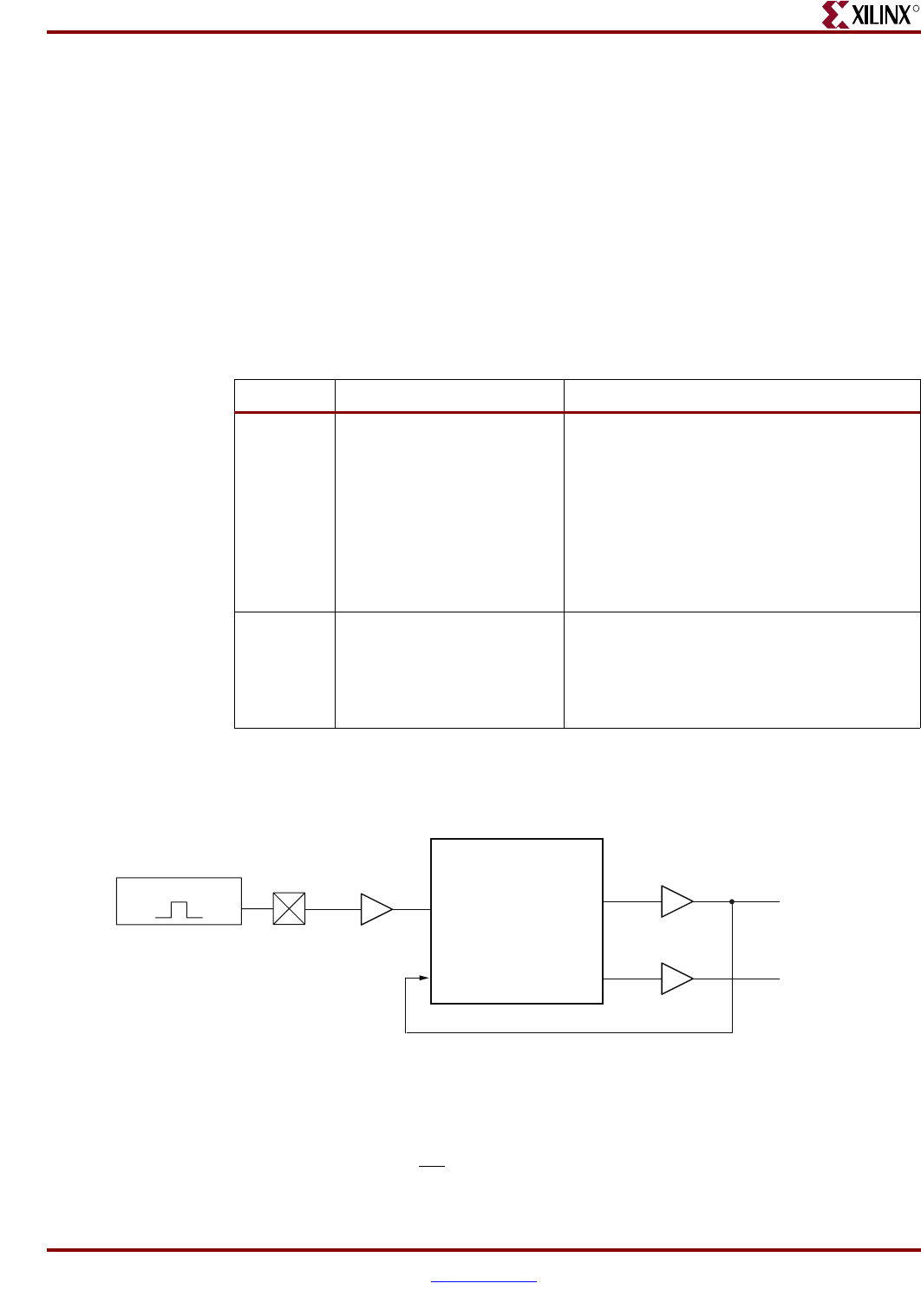
Memory Interface Solutions User Guide www.xilinx.com 267
UG086 (v3.6) September 21, 2010
Architecture
R
These clocks can be either single ended or differential. User can select single ended or
differential clock input option from MIG GUI. Differential clocks are connected to the
IBUFGDS and single ended clock is connected to IBUFG.
The system clock from the output of the IBUFGDS or the IBUFG is connected to the DCM
to generate the various clocks used by the memory interface logic.
The clk_200 output of the IBUFGDS or the IBUFG is connected to the BUFG. The output of
the BUFG is used for IDELAY IOB delay blocks for aligning read capture data.
The DCM generates three separate synchronous clocks for use in the design. This is shown
in Table 6-7 and Figure 6-8, page 267. The clock structure is same for both example design
and user design. For designs with out DCM instantiation, DCM and the BUFGs should be
instantiated at user end to generate the required clocks.
RLDRAM II Control Signal Physical Layer
This block has the pads that interface with the RLDRAM II data signals. A calibration
circuit samples the QK/QK signals using the ChipSync™ technology feature of the
Table 6-7: RLDRAM II Interface Design Clocks
Clock Description Logic Domain
clkglob Skew compensated replica
of the input system clock.
The clock for the controller and the user
interface logic. The RLDRAM II bus-related
I/O flip-flops (e.g., memory clocks). This
clock is used to register the data, address,
and command signals, and the address and
data enables for the user interface logic(1).
This clock is also used to generate the read
data, read data valid, and FIFO status
signals.
clk90 90° phase-shifted version of
clkglob
Used in the write data path section of
physical layer. Clocks write path control
logic, RLDRAM II side of the Write Data
FIFO, and output flip-flops for D and
memory control and address signals.
Notes:
1. See “User Interface Accesses,” page 271 for timing requirements and restrictions on the user interface
signals.
Figure 6-8: Clocking Scheme for RLDRAM II Interface Logic
CLKIN
C
LKFB CLK90
CLK0
clk90
clkglob
DCM BUFG
GC I/O
SYSTEM CLK
UG086_c6_15_071808
268 www.xilinx.com Memory Interface Solutions User Guide
UG086 (v3.6) September 21, 2010
Chapter 6: Implementing RLDRAM II Controllers
R
Virtex-4 FPGA. The FPGA clock samples both the data and clock (for calibration) and the
data itself to capture it in the same clock domain. Refer to XAPP701 [Ref 18] for more
details.
RLDRAM II Interface Signals
Table 6-8 and Table 6-9 define the RLDRAM II system interface signals with and without a
DCM, respectively.
Table 6-8: RLDRAM II System Interface Signals (with a DCM)
Signal Name Direction Description
sysclk_p, sysclk_n Input System clock input made up of differential clock pairs. This clock pair goes
to a differential input buffer. The differential buffer output goes to the
DCM input. The DCM generates the required clocks for the design. This
input system clock pair is present only when the DIFFERENTIAL clocks
option is selected in the MIG FPGA options page.
sysclk Input Single-ended system clock input. This clock is an input to IBUFG. The
IBUFG output is connected to the DCM clock input. The DCM generates
the required clocks for the design. This input system clock is present only
when the SINGLE_ENDED clocks option is selected in the MIG FPGA
options page.
When the DCM option is deselected, both differential or single-ended
input system clocks are not present.
clk200_p, clk200_n Input Differential clock used in the idelay_ctrl logic. This input clock pair is
present only when the DIFFERENTIAL clocks option is selected in the MIG
FPGA options page.
idly_clk_200 Input Single-ended 200 MHz IDELAYCTRL clock input. This clock is
connected to an IBUFG. The IBUFG output is connected to input of
BUFG. The output of this BUFG acts as IDELAYCTRL clock input. This
input system clock is present only when the SINGLE_ENDED clocks
option is selected in the MIG FPGA options page.
When the DCM option is deselected, both differential and single-ended
input system clocks are not present.
sysreset_n Input Active-Low reset to the RLDRAM II controller.
pass_fail[2:0] Output This signal bus indicates the status the comparison between the read data
compared with the corresponding write data.
001: INITIALIZATION STATE
010: PASS
100: FAIL
init_done Output This signal is asserted when the design initialization and calibration is
complete.
Table 6-9: RLDRAM II System Interface Signals (without a DCM)
Signal Name Direction Description
clkglob Input Input clock
clk90 Input Input clock with a 90° phase difference
Memory Interface Solutions User Guide www.xilinx.com 269
UG086 (v3.6) September 21, 2010
RLDRAM II Interface Signals
R
Table 6-10 describes the RLDRAM II user interface signals.
clk_200 Input 200 MHz clock for Idelayctrl primitives
dcm_locked Input This active-High signal indicates whether the user DCM is locked or not
sysreset_n Input Active-Low reset to the RLDRAM II controller
pass_fail[2:0] Output This signal bus indicates the status the comparison between the read data
compared with the corresponding write data.
001: INITIALIZATION STATE
010: PASS
100: FAIL
init_done Output This signal is asserted when the design initialization and calibration is
complete
Table 6-9: RLDRAM II System Interface Signals (without a DCM) (Cont’d)
Signal Name Direction Description
Table 6-10: RLDRAM II User Interface Signals (without a Testbench)
Signal Name(1) Direction Description
rlwdffull Output Almost full status signal for the Write Data FIFO. When this signal is asserted,
the user can write three more data words into the FIFO.
rlaffull Output Almost full status signal for the Address FIFO. When this signal is asserted, the
user can write two more data words into the FIFO.
rlafempty Output Empty status signal for the Address FIFO
rlrdfempty Output Empty status signal for the Read Data FIFO
rlwdfempty Output Empty status signal for the Write Data FIFO
apaddr[25:0](2) Input Address FIFO data input. This bus consists of the user-defined bank address, the
address, the WRITE/READ command, and the user-defined REFRESH
command.
apvalid Input Address FIFO write-enable signal
apwritedvalid Input Write Data FIFO write-enable signal
aprdfrden Input Read enable for the Read Data FIFO
burstlength[1:0] Output Indicates the number of bursts that can be written to or read from the memory:
00: Burst length = 2
01: Burst length = 4
10: Burst length = 8
rldreaddata[(2*n)-1:0] Output Read data from the memory, where n is the data width of the design. This read
data is stored in the Read Data FIFOs and can be read from the FIFOs depending
upon the status of the FIFOs.
apwritedata[(2*n)-1:0] Input Write data to be written into the memory, where n is the data width of the design.
This data is stored in the Write Data FIFO and is written into the memory
depending upon the controller status (write command).
apwritedm[m-1:0] Input Data mask of the write data, where m is the number of data mask bits associated
with the write data width.
clkglob_tb Output clkglob clock input. All the corresponding signals must be synchronized with
clkglob_tb. The clkglob_tb clock is sourced from clkglob clock in the controller.
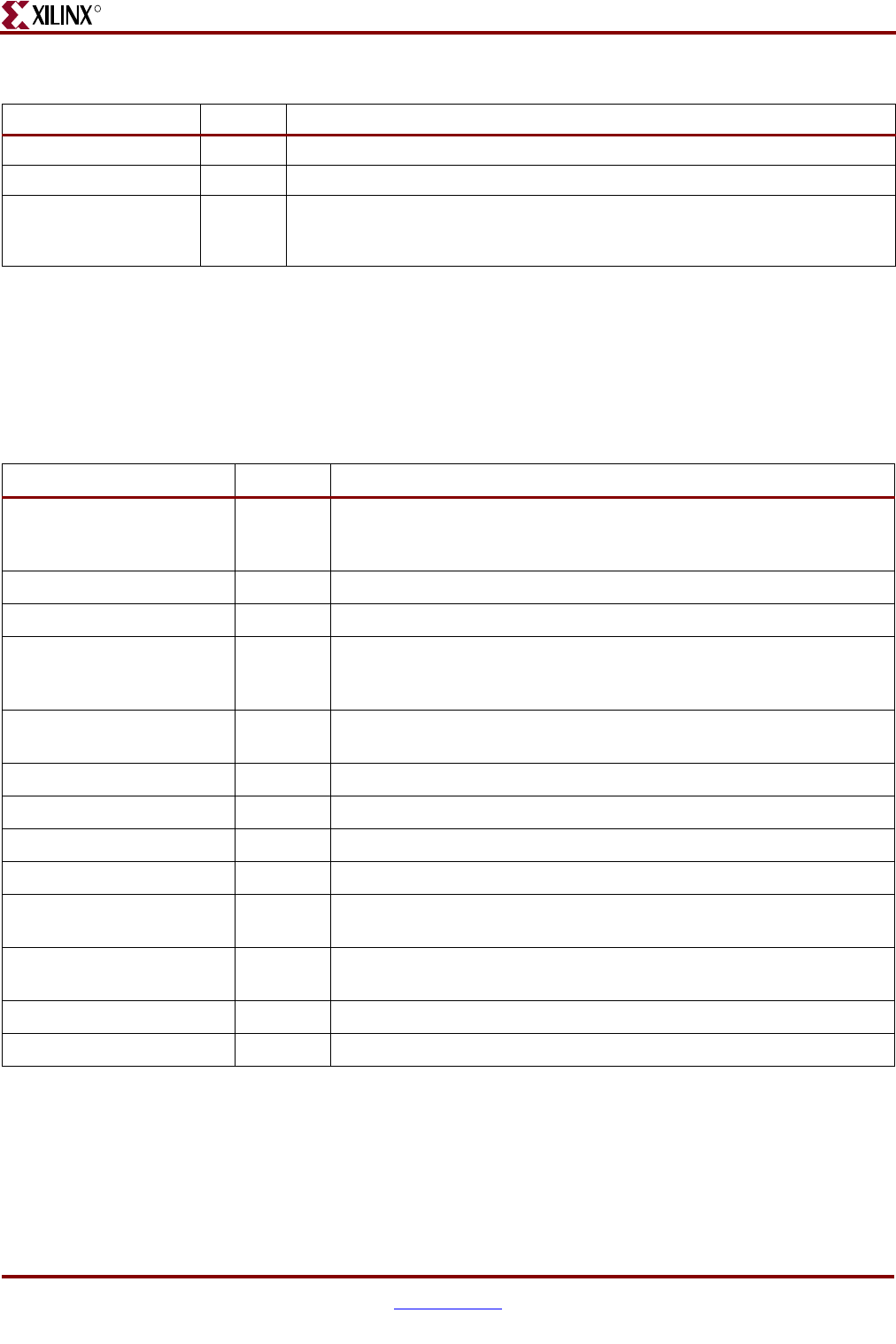
270 www.xilinx.com Memory Interface Solutions User Guide
UG086 (v3.6) September 21, 2010
Chapter 6: Implementing RLDRAM II Controllers
R
Table 6-11 describes the RLDRAM II memory interface signals.
rsthard_tb Output Active-Low system reset for the user interface, synchronous with clkglob_tb.
init_done_tb Output When asserted, this signal indicates that memory initialization is complete.
issuemrs_tb Input A pulse on this input makes the controller program the Mode Register into the
memory. This signal is synchronous with clkglob. (At power-up, MRS is done as
part of the initialization.)
Notes:
1. All user interface signal names are prepended with a controller number, for example, cntrl0_apWriteData. RLDRAM II devices
currently support only one controller. See “User Interface Accesses” for timing requirements and restrictions on the user interface
signals.
2. The number of address bits used depends on the density of the memory part. The controller ignores the unused bits, which can all
be tied High.
Table 6-10: RLDRAM II User Interface Signals (without a Testbench) (Cont’d)
Signal Name(1) Direction Description
Table 6-11: RLDRAM II Memory Interface Signals
Signal Name Direction Description
rld2_dq (cio) Input/
Output
Data input/outputs. During READ commands, the data is captured using
the FPGA clock. During WRITE commands, the data is sampled on both
edges of DK.
rld2_d (sio) Output Write data
rld2_q (sio) Input Read data
rld2_a Output Row and column addresses for READ and WRITE operations. During a
MODE REGISTER SET command, the address inputs define the register
settings.
rld2_ba Output These bank addresses select the internal bank to which to apply
commands.
rld2_we_n Output Write-enable command
rld2_ref_n Output REFRESH command
rld2_cs_n Output Chip-select command
rld2_dm Output Data mask signals for the write data
rld2_qvld Input Data valid signals transmitted by the RLDRAM II devices. They indicate
valid read data.
rld2_qk, rld2_qk_n Input Differential read data clocks. These clocks are transmitted by the
RLDRAM II devices and are edge-aligned with the read data.
rld2_dk, rld2_dk_n Output Differential write data clocks.
rld2_ck, rld2_ck_n Output Master differential clocks for addresses and commands.

Memory Interface Solutions User Guide www.xilinx.com 271
UG086 (v3.6) September 21, 2010
User Command Interface
R
User Command Interface
The current implementation supports commands that come in successive clocks with one
extra clock latency.
User Interface Accesses
The user backend logic communicates with the memory controller through a FIFO-based
user interface. This interface consists of three related buses:
• A Command/Address FIFO bus accepts write/read commands as well as the
corresponding memory address from the user
• A Write Data FIFO bus accepts the corresponding write data when the user issues a
write command on the command/address bus
• A Read bus on which the corresponding read data for an issued read command is
returned
The user interface has the following timing and signaling restrictions:
• Commands and write data cannot be written by the user until calibration is complete
(as indicated by init_done). In addition, the apvalid and app_wdf_wren interface
signals need to be held Low until calibration is complete.
• When issuing a write command, the first write data word must be written to the Write
Data FIFO either prior to or on the same clock cycle as the write command is issued.
In addition, the write data must be written by the user over consecutive clock cycles;
there cannot be a break between words. These restrictions arise from the fact that the
controller assumes write data is available when it receives the write command from
the user.
• The clkglob_tb signal is connected to clkglob in the controller. If the user clock domain
is different from clkglob / clkglob_tb of MIG, the user should add FIFOs for all data
inputs and outputs of the controller in order to synchronize them to the clkglob_tb.
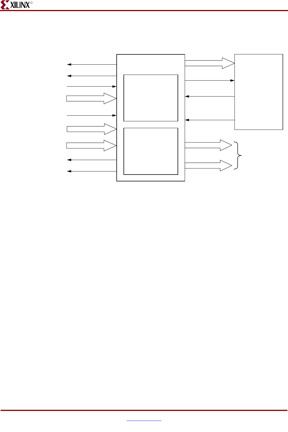
272 www.xilinx.com Memory Interface Solutions User Guide
UG086 (v3.6) September 21, 2010
Chapter 6: Implementing RLDRAM II Controllers
R
Write Interface
Figure 6-9 shows the user interface block diagram for write operations.
The following steps describe the architecture of the Address and Write Data FIFOs and
show how to perform a write burst operation to RLDRAM II from the user interface.
1. The user interface consists of an Address FIFO and a Write Data FIFO. These FIFOs are
constructed using the FIFO generator module of the CORE Generator software.
Address FIFO is a distributed RAM with 16 x 26 configuration. Data FIFO is a block
RAM, with a depth of 16 locations and width equal to two times the data width and
data mask width together.
2. The Common Address FIFO is used for both write and read commands, and comprises
a command part and an address part. Command bits discriminate between write and
read commands.
3. User interface data width apwritedata is twice that of the memory data width. For
every memory component there is a mask bit. For 9-bit memory width, the user
interface is 20 bits consisting of rising-edge data, falling-edge data, rising-edge mask
bit, and falling-edge mask bit.
4. For a 9-bit memory component with 72-bit data, the user interface data width
apwritedata is 144 bits, and the mask data apwritedm is 8 bits.
5. The user can initiate a write to memory by writing to the Address FIFO and the Write
Data FIFO when the FIFO Full flags are deasserted and after the init_done signal is
asserted. Status signal rlaffull is asserted when Address FIFO is full, and similarly
rlwdffull is asserted when Write Data FIFO is full.
6. Both the Address FIFO and Write Data FIFO Full flags are deasserted with power-on.
7. The user should assert the Address FIFO write-enable signal apvalid along with
address apaddr to store the write address and write command into the Address FIFO.
8. The user should assert the Data FIFO write-enable signal apwritedvalid along with
write data apwritedata and mask data apwritedm to store the write data and mask
Figure 6-9: User Interface Block Diagram for Write Operations
User Interface
Controller
Address FIFO
(Distributed RAM)
16 x 26
ctlafrden
afa
rlafempty
ctlwdfrden
apaddr
apvalid
apwritedata
apwritedm
apwritevalid
wdfd
wdfd
To Phy Layer
rlafempty
rlaffull
Write Data FIFO
(Block RAM)
16 x (2 * [Data Width +
Data Mask Width])
rlwdfempty
rlwdffull
ug086_c6_13_120407
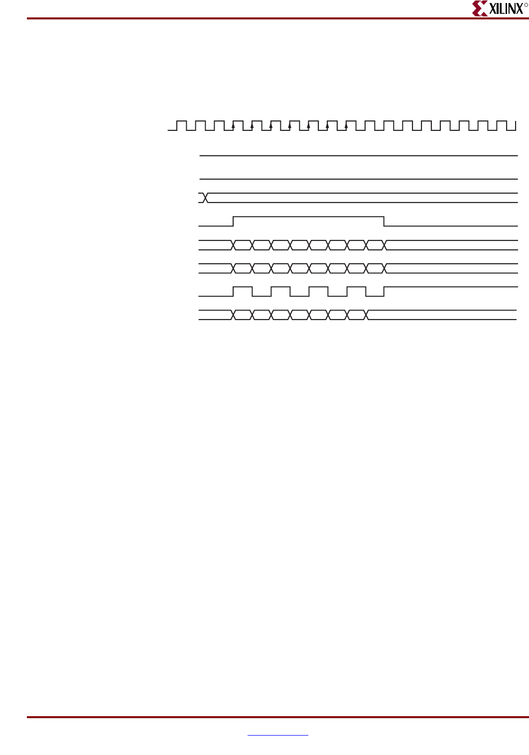
Memory Interface Solutions User Guide www.xilinx.com 273
UG086 (v3.6) September 21, 2010
User Command Interface
R
data into the Write Data FIFO. The user should provide both rise and fall data together
for each write to the Data FIFO.
9. The controller reads the Address FIFO by issuing the ctlafrden signal. The controller
reads the Write Data FIFO by issuing the ctlwdfrden signal after the Address FIFO is
read. It decodes the command part after the Address FIFO is read.
10. The write command timing diagram in Figure 6-10 is derived from the MIG-generated
testbench. As shown (burst length of 4), each write to the Address FIFO must be
coupled with two writes to the Data FIFO. Similarly, for a burst length of 8, every write
to the Address FIFO must be coupled with four writes to the Data FIFO. Failure to
follow this rule can cause unpredictable behavior.
Note: The user can start filling the Write Data FIFO two clocks after the Address FIFO is
written, because there is a two-clock latency between the command fetch and reading the Data
FIFO. Using the terms shown in Figure 6-9, therefore, the user can assert the A0 address two
clocks before D0D1.
11. The write command timing diagram in Figure 6-11, page 274 is derived from the MIG-
generated testbench. As shown (burst length of 8), each write to the Address FIFO
must be coupled with four writes to the Data FIFO. Because the controller first reads
the address and command together, the address need not coincide with the last data.
After the command is analyzed (nearly two clocks later for a worst-case timing
scenario), the controller sequentially reads the data in four clocks. Thus, there are six
clocks from the time the address is read to the time the last data is read.
Figure 6-10: RLDRAM II Write Burst Timing Diagram (BL = 4), Four Bursts
CLK
rlafFull
BurstLength
apWriteDValid
apWriteData
rlWdfFull
ApAddr
UG086_c6_10_012807
2’b01 (burst length = 4)
D0D1D2D3D4D5D6D7D8D9D10D11 D12D13 D14D15
apWriteDM
apValid
DM0,1 DM2,3 DM4,5 DM6,7 DM8,9 DM10,11 DM12,13 DM14,15
A0A1A2A3
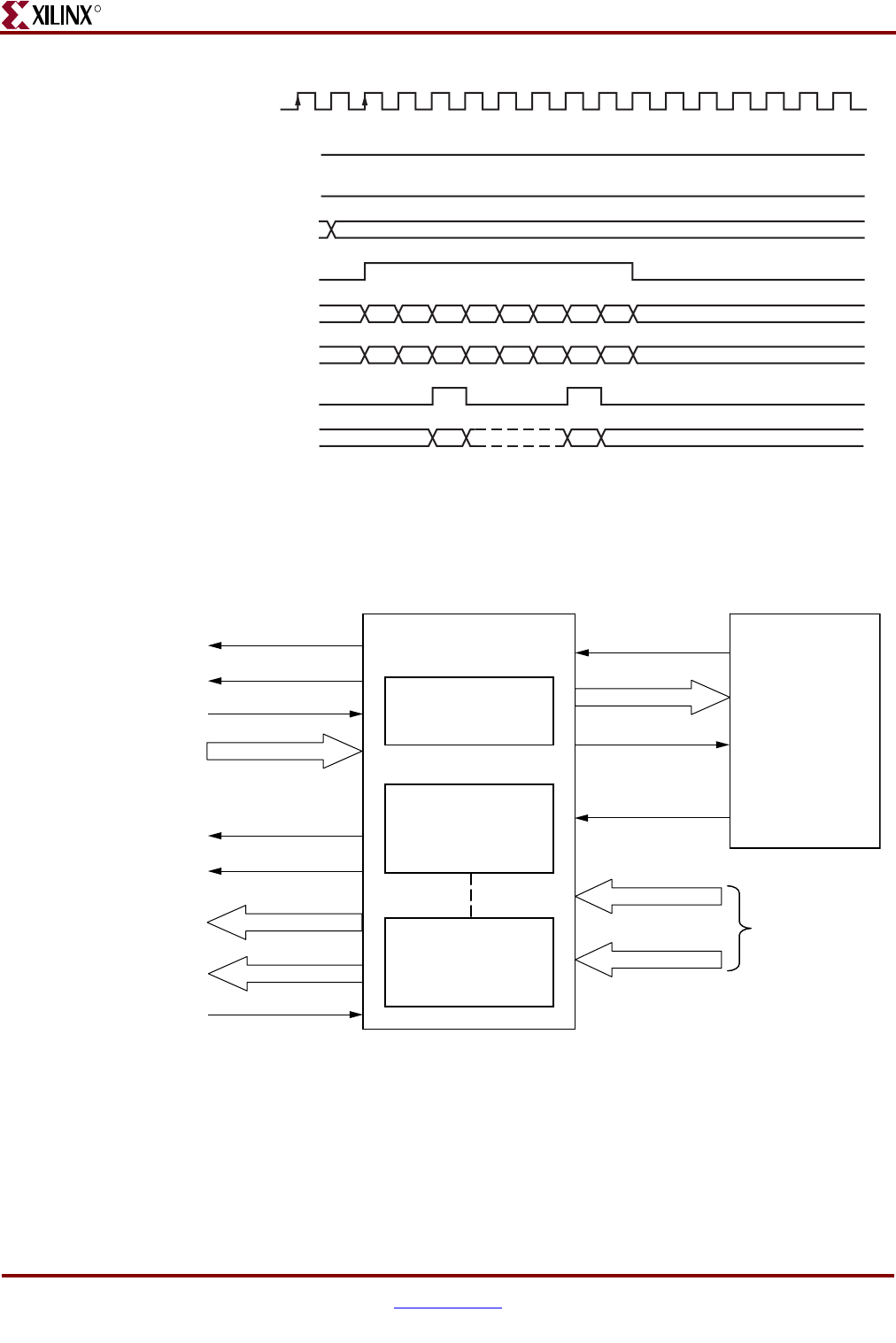
274 www.xilinx.com Memory Interface Solutions User Guide
UG086 (v3.6) September 21, 2010
Chapter 6: Implementing RLDRAM II Controllers
R
Read Interface
Figure 6-12 shows a block diagram of the read interface.
The following steps describe the architecture of the Read Data FIFOs and show how to
perform a burst read operation from RLDRAM II from the user interface.
1. The read user interface consists of an Address FIFO and a Read Data FIFO. The
Address FIFO is common to both read and write operations. The Read Data FIFOs are
constructed using the CORE Generator FIFO generator module. The Read Data FIFO is
a Distributed RAM with depth of 16 locations and width equal to two times the
Figure 6-11: RLDRAM II Write Burst Timing Diagram (BL = 8), Two Bursts
CLK
UG086_c6_11_012807
2’b10 (burst length = 8)
D0D1D2D3D4D5D6D7D8D9D10D11 D12D13 D14D15
DM0,1 DM2,3 DM4,5 DM6,7 DM8,9 DM10,11 DM12,13 DM14,15
A0A1
rlafFull
BurstLength
apWriteDValid
apWriteData
rlWdfFull
ApAddr
apWriteDM
apValid
Figure 6-12: User Interface Block Diagram for Read Operations
User Interface
Controller
Address FIFO
(Distributed RAM)
16 x 26
ctlafrden
afa
rlafempty
wren_rdfifo
apaddr
apvalid
dprddata_higher
dprddata_lower
aprdfrden
rldreaddata_higher
rldreaddata_lower From Phy Layer
rlafempty
rlaffull
Read Data FIFO
(Distributed RAM)
16 x (2 * Memory Width)
Read Data FIFO
(Distributed RAM)
16 x (2 * Memory Width)
rlrdfempty
rlrdffull
ug086_c6_14_121907
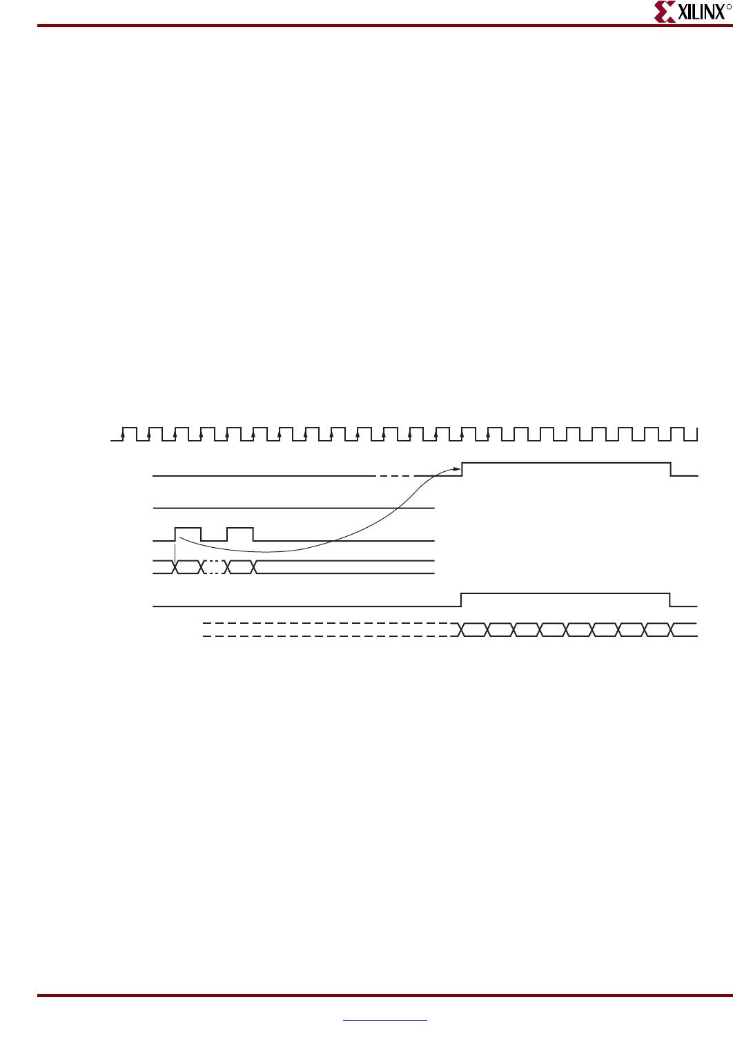
Memory Interface Solutions User Guide www.xilinx.com 275
UG086 (v3.6) September 21, 2010
User Command Interface
R
memory device width, consisting of rising-edge data and falling-edge data. For
example, for a 9-bit memory component, the Read Data FIFO configuration is 16 x 18.
MIG instantiates a number of Read Data FIFO modules depending on the QK signal
width of the design. For example, for 9-bit memory component and 72-bit data width
designs, MIG instantiates a total of nine Read Data FIFO modules.
2. The user can initiate a read to memory by writing to the Address FIFO when the FIFO
Full flag rlaffull is deasserted and after init_done is asserted.
3. To write the read address and read command into the Address FIFO, the user should
issue the Address FIFO write-enable signal apvalid along with read address apaddr.
4. The controller reads the Address FIFO containing the address and command. After
decoding the command, the controller generates the appropriate control signals to
memory.
5. Prior to the actual read and write commands, the design calibrates the latency (number
of clock cycles) from the time the read command is issued to the time data is received.
Using this pre-calibrated delay information, the controller generates the write-enable
signals to the Read Data FIFOs.
6. The rlrdfempty signal is deasserted when data is available in the Read Data FIFOs.
7. The user can read the read data from the Read Data FIFOs by asserting aprdfrden to
High.
8. Figure 6-13 shows the user interface timing diagram for a burst length of 8. The read
latency is calculated from the point when the read command is given by the user to the
point when the rlrdfempty signal is deasserted. The minimum latency in this case is
21 clocks. Where no auto-refresh request is pending, the user commands are issued
after initialization is completed, and the first command issued is a Read command.
The controller executes the commands only after initialization is done, as indicated by
the init_done signal.
9. After the address and command are loaded into the Address FIFO, it takes 21 clock
cycles minimum for the controller to deassert the rlrdfempty signal.
10. Read data is available only when the rlrdfempty signal is deasserted. The user can
access the read data by asserting the aprdfrden signal, a read enable signal to the Read
Data FIFOs, to High.
Note: The RLDRAM controller does not check the status of the Read Data FIFO, and can issue
read commands even when the Read Data FIFO is full. The user must make this determination and
ensure that read commands are not issued by the controller when the Read Data FIFO is full.
Figure 6-13: RLDRAM II Read Burst Timing Diagram (BL = 8), Two Bursts
UG086_c6_12_012807
CLK
rlRdfEmpty
rlafEmpty
apValid
apAddr
apRdfRdEn
A0A1
rldRead_Data D0,D1
D2,D3 D4,D5 D6,D7 D8,D9
D10,D11 D12,D13 D14,D15
276 www.xilinx.com Memory Interface Solutions User Guide
UG086 (v3.6) September 21, 2010
Chapter 6: Implementing RLDRAM II Controllers
R
In general, read latency varies based on the following parameters:
• Configuration
• The number of commands already in the FIFO pipeline before the read command is
issued
• Whether commands are interrupted when the periodic AUTO REFRESH command is
issued
• Whether the user issues the commands before initialization is complete (if so, the
latency cannot be determined)
• Board-level and chip-level propagation delays for both memory and FPGA
RLDRAM II Signal Allocations
MIG shows the checkboxes listed in Table 6-13 when a bank is selected for an RLDRAM II
design.
Table 6-12: Read Command Latency
Parameter Number of
Clocks Description
User command to deassertion
of the Address FIFO empty flag 1
When the read command is given to an
empty FIFO, it takes one clock time to
deassert the empty flag
Controller command reading
and decoding time 3
The FIFO outputs the data one clock after
the read command. Two clocks for
decoding the command.
Command from the controller
to the controller IOB’s output 3 Three-stage pipeline
RLDRAM II command to read
data latency (max) 8 RLDRAM II worst-case latency
Read data from the IOB to
dq_iob 2 Two-stage pipeline from IOB to dq_iob
dq_iob output to Read Data
FIFO input 2 Two-stage pipeline
Read Data FIFO input to Read
Data FIFO output 2One clock for deassertion of empty signal,
and one clock for outputting the data
Total Latency 21 Total of all latencies
Table 6-13: RLDRAM II Signal Allocation
Bank Selected by
Checkbox Signals Allocated in the Group
Address Memory address, memory control, and memory clocks
Data (CIO) Memory data and memory data mask
Data_Write (SIO) Memory write data, memory data mask, and memory write clocks
Data_Read (SIO) Memory read data, memory QVLD, and memory read clocks
Memory Interface Solutions User Guide www.xilinx.com 277
UG086 (v3.6) September 21, 2010
Simulating the RLDRAM II Design
R
When the Address box is checked in a particular bank, the bank address, the address, the
WE_N, the REF_N, and the CS_N bits are assigned to that particular bank.
When the Data box is checked in a particular bank for a CIO design, the memory data, the
memory data mask, the memory data valid (QVLD), the memory read clock, the memory
write clock, the memory address, and the command clock bits are assigned to that
particular bank.
When the Data_Write box is checked in a particular bank for an SIO design, the memory
data write, the memory data mask, and the memory write clock bits are assigned to that
particular bank.
When the Data_Read box is checked in a particular bank for an SIO design, the memory
data read, the memory data valid (QVLD), the memory read clock, the memory address,
and the command clock bits are assigned to that particular bank.
When the System Control box is checked in a particular bank, the sysreset_n, the pass_fail,
and the Init_done bits are assigned to that particular bank.
When the System Clock box is checked in a particular bank, the sysclk_p, sysclk_n,
CLK200_p, and CLK200_n bits are assigned to that particular bank.
For special cases, such as without a testbench and without a DCM, the corresponding
input and output ports are not assigned to any FPGA pins in the design UCF because the
user can connect these ports to the FPGA pins or can connect to some logic internal to the
same FPGA.
Note: Timing has been verified for most of the MIG generated configurations. For the best timing
results, adjacent banks in the same column of the FPGA should be used. Banks that are separated
by unbonded banks should be avoided because these can cause timing violations.
Simulating the RLDRAM II Design
After generating the design, MIG creates a sim folder in the specified path. This folder
contains simulation files for a particular design. The sim folder contains the external
testbench, memory model, and .do file to simulate the generated design. The memory
model files are currently generated in Verilog only. To learn more details about the files in
the sim folder and to simulate the design, refer to “Simulation Guide,” page 499.
While simulating VHDL designs, the XilinxCoreLib library needs to be mapped. This is
used by the fifo_generator_v5_3.vhd module present in the sim directory. An
example mapping is shown here for reference:
vmap xilinxcorelib
/proj/xbuilds/clibs/M.53c.0/modelsim/6.5c/lin64/lib/xilinxcorelib
System Control System reset from the user interface and status signals
System Clock System clocks from the user interface
Table 6-13: RLDRAM II Signal Allocation (Cont’d)
Bank Selected by
Checkbox Signals Allocated in the Group
278 www.xilinx.com Memory Interface Solutions User Guide
UG086 (v3.6) September 21, 2010
Chapter 6: Implementing RLDRAM II Controllers
R
Hardware Tested Configurations
The frequencies shown in Table 6-14 were achieved on the Virtex-4 FPGA ML461 Memory
Interfaces Development Board under nominal conditions. This frequency should not be
used to determine the maximum design frequency. The maximum design frequency
supported in the MIG wizard is based on a combination of the TRCE results for fabric
timing on multiple device/package combinations and I/O timing analysis using FPGA
and memory timing parameters for a 72-bit wide interface.
Table 6-14: Hardware Tested Configurations
FPGA Device XC4VLX25-FF668-11
Memory Component MT49H16M18XX-25
Data Bus Options CIO
Data Width 36
Configuration 1, 2, 3
Burst Length 2, 4, 8
Addressing Mode Multiplexing and Non-Multiplexing Addressing mode
Frequency 120 MHz to 330 MHz
Flow Vendors Synplicity and XST
Design Entry VHDL and Verilog


Memory Interface Solutions User Guide www.xilinx.com 281
UG086 (v3.6) September 21, 2010
R
Chapter 7
Implementing DDR SDRAM Controllers
This chapter describes how to implement DDR SDRAM interfaces for Spartan®-3,
Spartan-3E, Spartan-3A, Spartan-3AN, and Spartan-3A DSP FPGAs. The designs are based
on XAPP768c [Ref 24].
Feature Summary
This section summarizes the supported and unsupported features of the DDR SDRAM
controller design.
Supported Features
The DDR SDRAM controller design supports the following:
• Burst lengths of two, four, and eight
• CAS latencies of 2, 2.5, and 3
• Sequential and interleaved burst types
•Auto refresh
• Data mask enable/disable option
• System clock, differential and single-ended
• Linear addressing
• Spartan-3 FPGA maximum frequency:
• 133 MHz with a -4 speed grade device
• 166 MHz with a -5 speed grade device
• Spartan-3E FPGA maximum frequency:
• 133 MHz with a -4 speed grade device
• 166 MHz with a -5 speed grade device
• Spartan-3A, Spartan-3AN, and Spartan-3A DSP FPGA maximum frequency:
• 133 MHz with a -4 speed grade device
• 166 MHz with a -5 speed grade device
• Components, unbuffered DIMMs, registered DIMMs, and SODIMMs
• With and without a testbench
• With or without a DCM
• All Spartan-3, Spartan-3E, Spartan-3A, Spartan-3AN, and Spartan-3A DSP FPGAs
•Verilog and VHDL
• XST and Synplicity synthesis tools
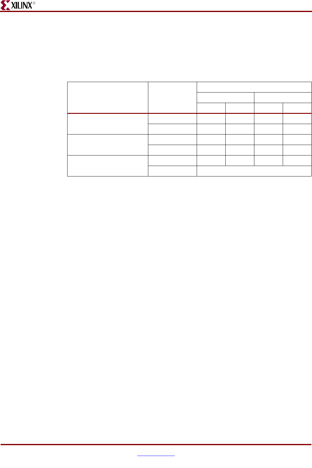
282 www.xilinx.com Memory Interface Solutions User Guide
UG086 (v3.6) September 21, 2010
Chapter 7: Implementing DDR SDRAM Controllers
R
Unsupported Features
Single burst of burst length two.
Design Frequency Ranges
Controller Architecture
DDR SDRAM Interface
High-speed memory interfaces are source-synchronous and double data rate. They
transfer data on both edges of the clock cycle. A memory interface can be modularly
represented as shown in Figure 7-1. Creating a modular interface has many advantages. It
allows designs to be ported easily, and it also makes sharing parts of the design across
different types of memory interfaces possible.
Table 7-1: Design Frequency Range in MHz
FPGA Family Memory
FPGA Speed Grade
-4 -5
Min Max Min Max
Spartan-3 Component 77 133 77 166(1)
DIMM 77 133 77 133
Spartan-3A/3AN/3A DSP Component 77 133 77 166
DIMM 77 133 77 166
Spartan-3E Component 77 133 77 166
DIMM (Not supported)
Notes:
1. Spartan-3 devices support 133 MHz for data widths greater than 32 bits.
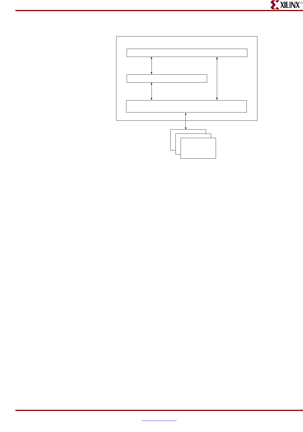

284 www.xilinx.com Memory Interface Solutions User Guide
UG086 (v3.6) September 21, 2010
Chapter 7: Implementing DDR SDRAM Controllers
R
Hierarchy
Figure 7-2 shows the hierarchical structure of the DDR SDRAM design generated by MIG
with a testbench and a DCM. In the figure, the physical and control layers are clearly
separated. MIG generates the entire controller, as shown in this hierarchy, including the
testbench. The user can replace the testbench with a design that makes use of the DDR
SDRAM interface.
The modules are classified as follows:
• Design modules
• Testbench modules
• Clocks, reset generation, and calibration modules
There is a parameter file generated with the design that has all the user input and design
parameters selected from MIG.
MIG can generate four different DDR SDRAM designs:
• With a testbench and a DCM
• Without a testbench and with a DCM
• With a testbench and without a DCM
• Without a testbench and without a DCM
Figure 7-2: Hierarchical Structure of the DDR SDRAM Design with a Testbench
<top_
module>
main* infrastructure_
top*
controller* infrastructure iobs*
data_
read*
data_
read_
controller*
data_
write*
data_
path*
controller_
iobs*
dqs_
delay
Design Modules
fifo_0_
wr_en
wr_gray_
cntr
fifo_1_
wr_en
addr_
gen* cmd_fsmdata_
gen*
cmp_
data*
rd_gray_
cntr ram8d*
infrastructure
_iobs*
data_
path_
iobs*
s3_dq_
iob
s3_dm_
iob
s3_dqs_
iob
UG086_c7_02_010108
clk_dcm cal_top
test_
bench* top*
tap_dly cal_ctl
Te st Bench Modules
Clocks, Reset Generation, and Calibration Modules
Note: A block with a * has a parameter file included.

Memory Interface Solutions User Guide www.xilinx.com 285
UG086 (v3.6) September 21, 2010
Controller Architecture
R
For designs generated without a testbench, the testbench modules in Figure 7-2 are not
present in the design. In this case, the user interface signals appear in the <top_module>
module. The list of user interface signals is in Table 7-9.
The infrastructure_top module has the clock and the reset generation module of the
design. It instantiates a DCM in the module when selected by MIG. The differential design
clock is an input to this module. A user reset is also input to this module. Using the input
clocks and reset signals, system clocks and system reset are generated in this module
which is used in the design. Infrastructure_top also consists of calibration logic.
The DCM primitive is not instantiated in the infrastructure_top module if the Use DCM
option is unchecked. Therefore, the system operates on the user-provided clocks. The
system reset is generated in the infrastructure module using the dcm_lock input signal.
MIG Tool Design Options
MIG provides various options to generate the design with or without a testbench or with
or without a DCM. This section provides detailed descriptions of the type of design
generated by the user using various options. Figure 7-3, page 286 and Figure 7-4, page 287
show the differential system clock. For more information on the clocking structure, refer to
“Clocking Scheme,” page 294.
MIG outputs example_design and user_design. The MIG-generated example_design
includes the memory controller and synthesized testbench. The example_design can be
used to simulate the design and to test its functionality. Whereas the user_design includes
the memory controller design only. Users should develop a testbench (user application)
and should interface with the MIG memory controller design. Refer to Table 7-9, page 297
for user interface signals and “DDR SDRAM Write and Read Operations,” page 300 for
write and read timing shown in Figure 7-10, page 301 and Figure 7-11, page 302.
Figure 7-3, page 286 shows a block diagram representation of the top-level module of a
DDR SDRAM design with a DCM and a testbench. “Clocking Scheme,” page 294 describes
how various clocks are generated using the DCM. The input clocks can be differential or
single-ended based on the system clock selection in GUI.
For differential, differential clocks sys_clk and sys_clkb appear as input ports, whereas for
single-ended sys_clk_in appears as input port. The DCM clock is instantiated in the
infrastructure_top module that generates the required design clocks. The reset_in_n signal
is the active-Low system reset signal. All design resets are gated by the dcm_lock signal.
The cntrl0_led_error_output1 output signal indicates whether the test passes or fails.
When set, this signal indicates that the test has failed. The testbench module does writes
and reads, and also compares the read data with the written data. The
cntrl0_data_valid_out signal indicates whether the read data is valid or not.
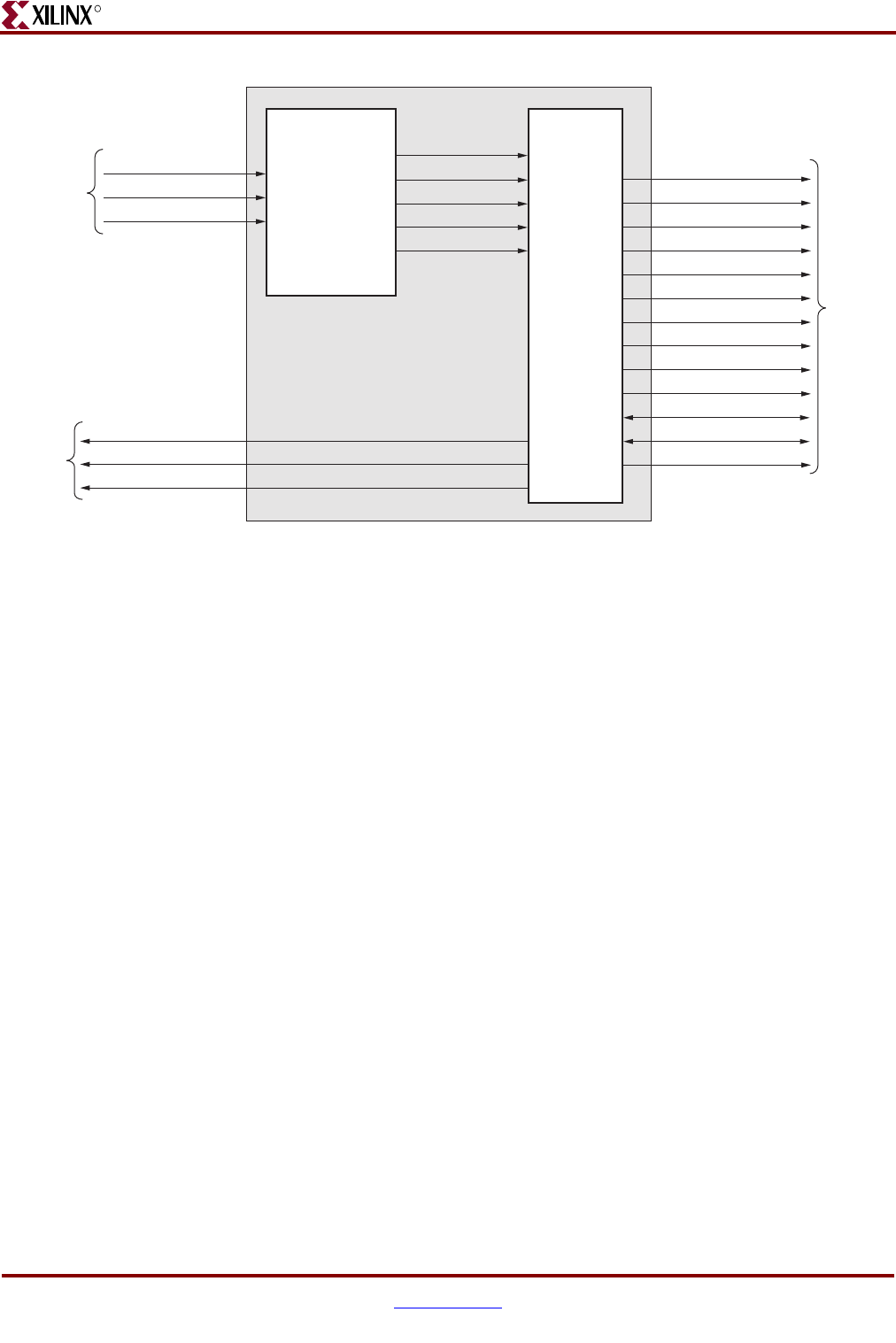
286 www.xilinx.com Memory Interface Solutions User Guide
UG086 (v3.6) September 21, 2010
Chapter 7: Implementing DDR SDRAM Controllers
R
Figure 7-3: MIG Output of the DDR SDRAM Controller Design with a DCM and a Testbench
main_0 Memory
Device
UG086_c7_03_071608
System
Clocks
and Reset
Status
Signals
infrastructure_top
clk90_0
clk_0
sys_clk
sys_clkb
reset_in_n
cntrl0_ddr_ras_n
cntrl0_ddr_cas_n
cntrl0_ddr_we_n
cntrl0_ddr_cs_n
cntrl0_ddr_cke
cntrl0_ddr_dm
cntrl0_ddr_ba
cntrl0_ddr_a
cntrl0_ddr_ck_n
sys_rst
sys_rst90
sys_rst180
cntrl0_ddr_reset_n
cntrl0_ddr_ck
cntrl0_led_error_output1
cntrl0_init_done
cntrl0_data_valid_out
cntrl0_ddr_dq
cntrl0_ddr_dqs
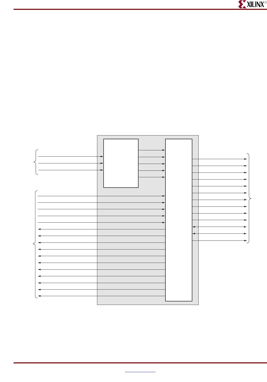
Memory Interface Solutions User Guide www.xilinx.com 287
UG086 (v3.6) September 21, 2010
Controller Architecture
R
Figure 7-4 shows a block diagram representation of the top-level module for a DDR
SDRAM design with a DCM but without a testbench. “Clocking Scheme,” page 294
describes how various clocks are generated using the DCM. The input clocks can be
differential or single-ended based on system clock selection in GUI.
For differential, differential clocks sys_clk and sys_clkb appear as input ports, whereas for
single-ended sys_clk_in appears as input port.
The DCM clock is instantiated in the infrastructure_top module that generates the required
design clocks. reset_in_n is the active-Low system reset signal. All design resets are gated
by the dcm_lock signal.
The user interface signals are listed in Figure 7-4. The design provides the clk_tb, clk90_tb,
sys_rst_tb, sys_rst90_tb, and sys_rst180_tb signals to the user in order to synchronize with
the design. The signals clk_tb, clk90_tb, sys_rst_tb, sys_rst90_tb, and sys_rst180_tb are
connected to clocks clk_0 and clk90_0 and reset signals sys_rst, sys_rst90, and sys_rst180,
respectively, in the controller. If the user clock domain is different from clk_tb/clk90_tb,
then the user should add FIFOs for all the inputs and outputs of the controller (user
application signals) in order to synchronize them to clk_tb/clk90_tb.
Figure 7-4: MIG Output of the DDR SDRAM Controller Design with a DCM but without a Testbench
top_0 Memory
Device
UG086_c7_04_071608
System
Clocks
and Reset
User
Interface
Signals
infrastructure_top
clk90_0
clk_0
sys_clk
sys_clkb
reset_in_n
sys_rst
sys_rst90
sys_rst180
cntrl0_burst_done
cntrl0_user_command_register
cntrl0_user_data_mask
cntrl0_user_input_data
cntrl0_user_input_address
cntrl0_init_done
cntrl0_ar_done
cntrl0_auto_ref_req
cntrl0_user_cmd_ack
cntrl0_clk_tb
cntrl0_clk90_tb
cntrl0_sys_rst_tb
cntrl0_sys_rst90_tb
cntrl0_sys_rst180_tb
cntrl0_user_output_data
cntrl0_user_data_valid
cntrl0_ddr_ras_n
cntrl0_ddr_cas_n
cntrl0_ddr_we_n
cntrl0_ddr_cs_n
cntrl0_ddr_cke
cntrl0_ddr_dm
cntrl0_ddr_ba
cntrl0_ddr_a
cntrl0_ddr_ck_n
cntrl0_ddr_reset_n
cntrl0_ddr_ck
cntrl0_ddr_dq
cntrl0_ddr_dqs
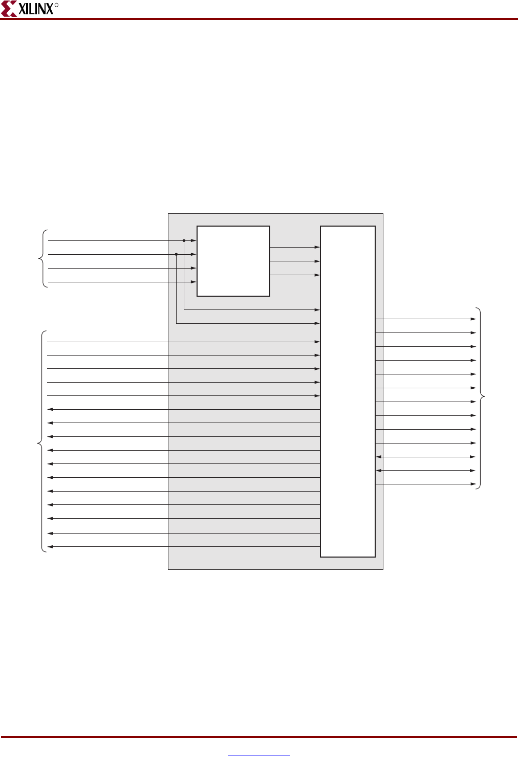
288 www.xilinx.com Memory Interface Solutions User Guide
UG086 (v3.6) September 21, 2010
Chapter 7: Implementing DDR SDRAM Controllers
R
Figure 7-5 shows a block diagram representation of the top-level module for a DDR
SDRAM design without a DCM or a testbench. “Clocking Scheme,” page 294 describes
how various clocks are generated using the DCM. The user should provide all the clocks
and the dcm_lock signal. These clocks should be single-ended. reset_in_n is the active-Low
system reset signal. All design resets are gated by the dcm_lock signal.
The user interface signals are listed in Figure 7-5. The design provides the clk_tb, clk90_tb,
sys_rst_tb, sys_rst90_tb, and sys_rst180_tb signals to the user in order to synchronize with
the design. The signals clk_tb, clk90_tb, sys_rst_tb, sys_rst90_tb, and sys_rst180_tb are
connected to clocks clk_0 and clk90_0 and reset signals sys_rst, sys_rst90, and sys_rst180,
respectively, in the controller. If the user clock domain is different from clk_tb/clk90_tb,
then the user should add FIFOs for all the inputs and outputs of the controller (user
application signals) in order to synchronize them to clk_tb/clk90_tb.
Figure 7-5: MIG Output of the DDR SDRAM Controller Design without a DCM or a Testbench
top_0 Memory
Device
UG086_c7_05_071608
System
Reset
and User
DCM
Clocks
User
Interface
Signals
infrastructure_top
clk90_int
dcm_lock
clk_int
reset_in_n
cntrl0_ddr_ras_n
cntrl0_ddr_cas_n
cntrl0_ddr_we_n
cntrl0_ddr_cs_n
cntrl0_ddr_cke
cntrl0_ddr_dm
cntrl0_ddr_ba
cntrl0_ddr_a
cntrl0_ddr_ck_n
sys_rst
sys_rst90
sys_rst180
cntrl0_burst_done
cntrl0_user_command_register
cntrl0_user_data_mask
cntrl0_user_input_data
cntrl0_user_input_address
cntrl0_ddr_ck
cntrl0_init_done
cntrl0_ar_done
cntrl0_auto_ref_req
cntrl0_user_cmd_ack
cntrl0_clk_tb
cntrl0_clk90_tb
cntrl0_sys_rst_tb
cntrl0_sys_rst90_tb
cntrl0_sys_rst180_tb
cntrl0_user_data_valid
cntrl0_user_output_data
cntrl0_ddr_dq
cntrl0_ddr_dqs
cntrl0_ddr_reset_n
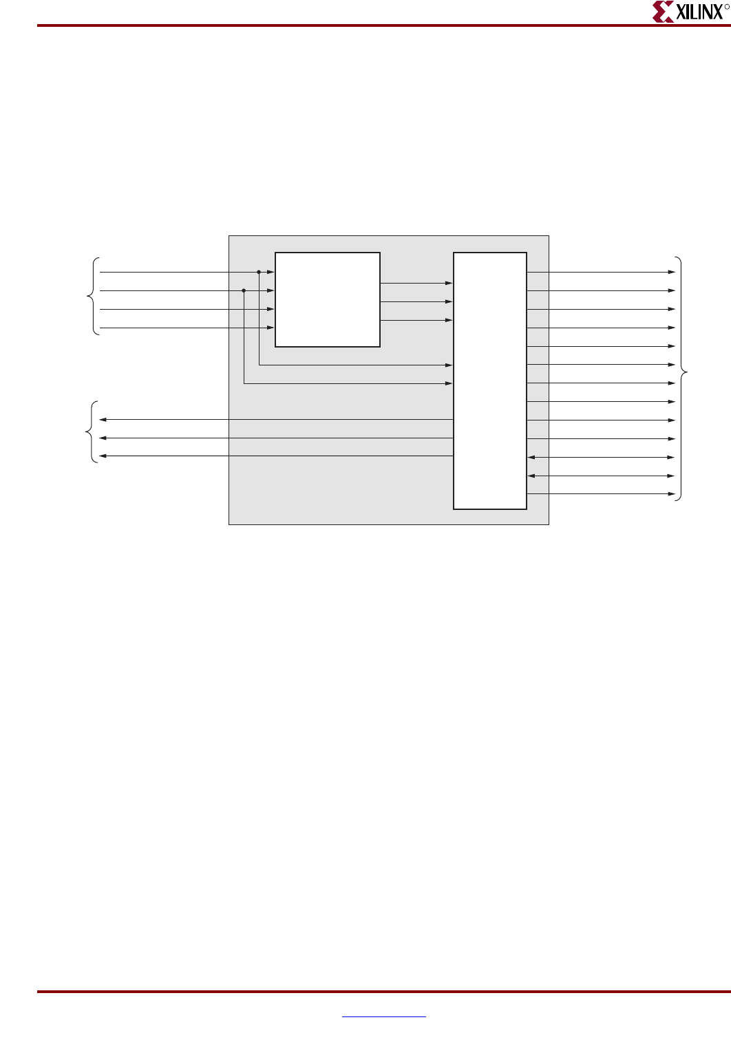
Memory Interface Solutions User Guide www.xilinx.com 289
UG086 (v3.6) September 21, 2010
Controller Architecture
R
Figure 7-6 shows a block diagram representation of the top-level module of a DDR
SDRAM design without a DCM but with a testbench. “Clocking Scheme,” page 294
describes how various clocks are generated using the DCM. The user should provide all
the clocks and the dcm_lock signal. These clocks should be single-ended. reset_in_n is the
active-Low system reset signal. All design resets are gated by the dcm_lock signal.
The cntrl0_led_error_output1 output signal indicates whether the test passes or fails. The
testbench module does writes and reads, and also compares the read data with the written
data. The cntrl0_led_error_output1 signal is driven High on data mismatches. The
cntrl0_data_valid_out signal indicates whether the read data is valid or not.
All the memory device interface signals shown in Figure 7-3 through Figure 7-6 might not
necessarily appear for all designs generated from MIG. For example, the
cntrl0_ddr_reset_n port appears in the port list for Registered DIMM designs only.
Similarly, cntrl0_ddr_dm appears only for parts that have data mask signals. A few
RDIMMs do not have data mask, and cntrl0_ddr_dm does not appear in the port list for
these parts.
Figure 7-6: MIG Output of the DDR SDRAM Controller Design without a DCM but with a Testbench
main_0 Memory
Device
UG086_c7_06_071608
System
Reset
and User
DCM
Clocks
Status
Signals
infrastructure_top
cntrl0_ddr_ras_n
cntrl0_ddr_cas_n
cntrl0_ddr_we_n
cntrl0_ddr_cs_n
cntrl0_ddr_cke
cntrl0_ddr_dm
cntrl0_ddr_ba
cntrl0_ddr_a
cntrl0_ddr_ck_n
sys_rst
sys_rst90
sys_rst180
cntrl0_ddr_reset_n
cntrl0_ddr_ck
cntrl0_led_error_output1
cntrl0_data_valid_out
cntrl0_init_done
cntrl0_ddr_dq
cntrl0_ddr_dqs
clk90_int
dcm_lock
clk_int
reset_in_n
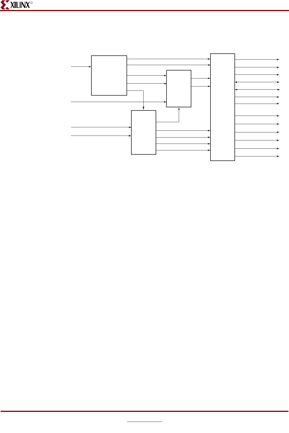
290 www.xilinx.com Memory Interface Solutions User Guide
UG086 (v3.6) September 21, 2010
Chapter 7: Implementing DDR SDRAM Controllers
R
Figure 7-7 shows a detailed block diagram of the DDR SDRAM controller. All four blocks
shown are subblocks of the ddr1_top module. The functionality of these blocks is
explained in following sections.
Controller
The controller module accepts and decodes user commands and generates read, write, and
memory initialization commands. The controller also generates signals for other modules.
The memory is initialized and powered up using a defined process. The controller state
machine handles the initialization process upon receiving an initialization command.
Datapath
This module transmits and receives data to and from the memories. Major functions
include storing the read data and transferring write data and write enable to the IOBS
module. The data_read, data_write, data_path_IOBs, and data_read_controller modules
perform the actual read and write functions. For more information, refer to XAPP768c
[Ref 24].
Data Read Controller
This module generates all control signals that are used for data_read.
Data Read
The data_read module contains the read datapaths for the DDR SDRAM interface. Details
for this module are described in XAPP768c [Ref 24].
Data Write
This module contains the write datapath for the DDR SDRAM interface. The write data
and write enable signals are forwarded together to the DDR SDRAM through IOB flip-
flops. The IOBs are implemented in the data_path_iobs module.
Figure 7-7: Memory Controller Block Diagram
UG086_c7_07_071608
user_command_register
Controller
Datapath
Infrastructure_top
IOBs
cntrl0_ddr_ck
cntrl0_ddr_ck_n
cntrl0_ddr_cke
cntrl0_ddr_dm
cntrl0_ddr_cs_n
cntrl0_ddr_dqs
cntrl0_ddr_cas_n
cntrl0_ddr_we_n
cntrl0_ddr_reset_n
cntrl0_ddr_dq
cntrl0_ddr_a
cntrl0_ddr_ba
cntrl0_ddr_ras_n
user_clk
user_data
user_address
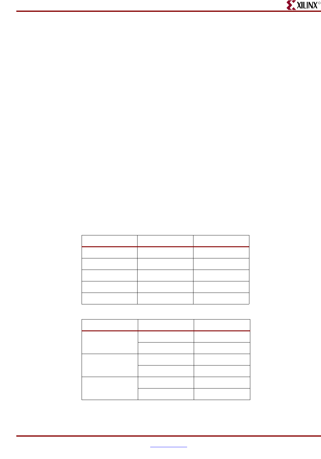
Memory Interface Solutions User Guide www.xilinx.com 291
UG086 (v3.6) September 21, 2010
Controller Architecture
R
infrastructure_top
The infrastructure module generates the FPGA clock and reset signals. For differential
clocking, sys_clk and syc_clkb ports are used as inputs to the IBUFGDS_LVDS_25 buffer
and the output of the buffer is driven to the DCM input. For single-ended clocking, the
sys_clk_in port is used as an input to the IBUFG buffer; the output of the buffer is driven to
the DCM input. A DCM generates the clock and its inverted version. The infrastructure
module also generates all of the reset signals required for the design.
The calibration circuit is also implemented in this module. If there is no DCM, the clocks
are driven from the user interface.
IOBs
All input and output signals of the FPGA are implemented in the IOB registers.
Te st B en c h
MIG generates two different RTL folders, example_design and user_design. The
example_design includes the synthesizable test bench, while user_design does not include
the test bench modules. The MIG test bench performs five write commands and five read
commands in an alternating fashion. The number of words in a write command depends
on the burst length. For a burst length of 4, every write command writes four data words.
For all five write commands, the test bench writes a total of 20 data words (10 rise data
words and 10 fall data words). For a burst length of 8, the test bench writes a total of 40 data
words. The pattern data is shown in Table 7-2, Table 7-3, and Table 7-4 for burst lengths of
2, 4, and 8, respectively.
Table 7-2: Data Pattern for Burst Length of 2
Burst Rise Fall
196 69
22C D3
358 A7
4B1 4E
563 9C
Table 7-3: Data Pattern for Burst Length of 4
Burst Rise Fall
196 69
2C D3
258 A7
B1 4E
363 9C
C6 39
292 www.xilinx.com Memory Interface Solutions User Guide
UG086 (v3.6) September 21, 2010
Chapter 7: Implementing DDR SDRAM Controllers
R
The falling edge data is the complement of the rising edge data. The data pattern is
repeated for the next set of five burst write commands based on the selected burst length,
as shown in Table 7-2, Table 7-3, and Table 7-4. This data pattern is repeated in the same
order based on the number of data words written. For data widths greater than 8, the same
data pattern is concatenated for the other bits. For a 32-bit design and a burst length of 8,
the data pattern for the first write command is 96969696, 69696969, 2C2C2C2C,
D3D3D3D3, 58585858, A7A7A7A7, B1B1B1B1, 4E4E4E4E.
48C 73
18 E7
531 CE
62 9D
Table 7-4: Data Pattern for Burst Length of 8
Burst Rise Fall
196 69
2C D3
58 A7
B1 4E
263 9C
C6 39
8C 73
18 E7
331 CE
62 9D
C4 3B
88 77
410 EF
21 DE
42 BD
85 7A
50A F5
15 EA
2B D4
56 A9
Table 7-3: Data Pattern for Burst Length of 4 (Cont’d)
Burst Rise Fall

Memory Interface Solutions User Guide www.xilinx.com 293
UG086 (v3.6) September 21, 2010
Controller Architecture
R
For all five write commands, five different address locations are generated, as shown in
Table 7-5. Read commands read the data from the same locations where writes are
performed. The column address is incremented based on the burst length from one write
command to the next write command. The row address is the same for all five write
commands. For the next five write commands, the row address is incremented by 2, and
this continues for each subsequent group of five write commands. Only five bits are used
for row address generation. The row address rolls back to the initial value on reaching the
terminal value. The bank address is the same for all five write commands, but it gets
incremented for the next five write commands. This continues until the terminal count
value is reached, depending on whether the selected memory part has a 4- or 8-bank
architecture. The MIG test bench exercises only a certain memory area. Table 7-5 provides
the details of how the bank, row, and column address are incremented in the test bench.
Table 7-5: Address Generation in Test Bench
Address Address for First Five
Writes/Reads
Address for Second Five
Writes/Reads Description
Bank 0 1 The bank address increments by
1. For a 2-bit bank address, the
sequence is 0, 1, 2, 3.
For a 3-bit bank address, the
sequence is 0, 1, 2, 3, 4, 5, 6, 7.
The bank address rolls back to
the initial address 0 when it
reaches the maximum value.
Row 2 4 The row address increments by 2
and starts with 2. Only five bits
are used to generate the row
address. 2, 4, 6, 8, 10, 12, 14, 16,
18, 20, 22, 24, 26, 28, 30
(5'b00010 to 5'b11110).
The row address rolls back to the
initial value of 2, when it reaches
the maximum value.
Column 0, 8, 16, 24, 32 0, 8, 16, 24, 32 The column address increments
in multiples of the burst length.
For BL = 8, the address sequence
for the first set of five write/read
commands is 0, 8, 16, 24, 32.
For BL = 4, the address sequence
for the first set of five write/read
commands is 0, 4, 8, 12, 16.
For BL = 2, the address sequence
for the first set of five write/read
commands is 0, 2, 4, 8, 10.
The same column address is
repeated for the next set of
commands.
294 www.xilinx.com Memory Interface Solutions User Guide
UG086 (v3.6) September 21, 2010
Chapter 7: Implementing DDR SDRAM Controllers
R
During reads, the read data is compared with the pattern written. For example, for an 8-bit
data width and a burst length of 4, the write data for a single write command is 96, 69, 2C,
D3. During reads, the read pattern is compared with the 96, 69, 2C, D3 pattern. If the data
read back matches with the data written, the led_error_output1 signal is set to 0,
otherwise, it is set to 1 to indicate an error condition.
Clocking Scheme
Figure 7-8, page 295 shows the clocking scheme for this design. Global and local clock
resources are used.
The global clock resources consist of a DCM and two BUFGs. The local clock resources
consist of regional I/O clock networks (BUFIO). The global clock architecture is discussed
in this section.
The MIG tool allows the user to customize the design such that the DCM is not included.
In this case, clk_0 and clk90_0 must be supplied by the user.
Global Clock Architecture
The user must supply a system clock running at the target frequency for the memory.
This clock can be either single-ended or differential. User can select single-ended or
differential clock input option from MIG GUI. Differential clocks are connected to the
IBUFGDS and single-ended clock is connected to IBUFG.
The system clock from the output of the IBUFGDS or the IBUFG is connected to the DCM
to generate the various clocks used by the memory interface logic.
The DCM generates two separate synchronous clocks for use in the design. This is shown
in Table 7-6 and Figure 7-8, page 295. The clock structure is the same for both example
design and user design. For designs without DCM instantiation, DCM and the BUFGs
should be instantiated at user end to generate the required clocks.
Table 7-6: DDR Interface Design Clocks
Clock Description Logic Domain
clk_0 Skew compensated replica
of the input system clock.
The clock for the controller and the user
interface logic, most of the DDR bus-
related I/O flip-flops (e.g., memory clock,
control/address, output DQS strobe). This
is also used to register the address and
command signals from the user interface.
clk90_0 90° phase-shifted version of
CLK0.
Used in the user interface logic, the write
data path section of physical layer, write
path control logic and output flip-flops for
DQ and DM. This is also used to register
data from the user interface and generate
the read data and read data valid signals
for the user interface logic.
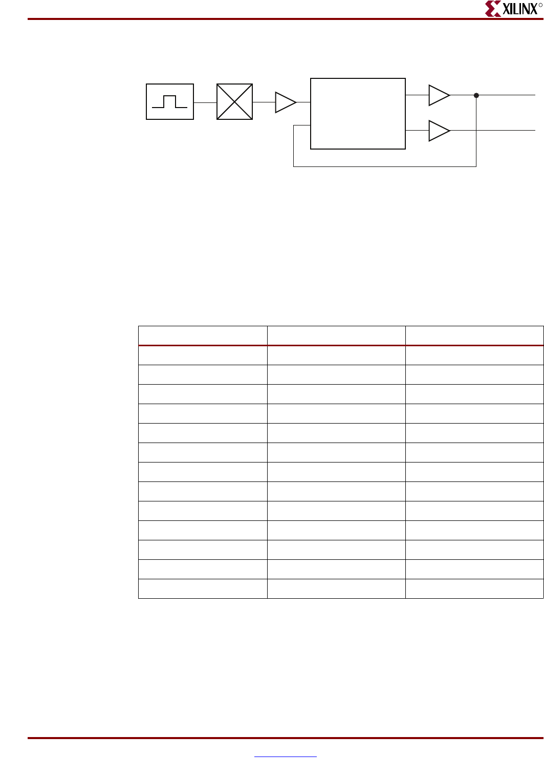
Memory Interface Solutions User Guide www.xilinx.com 295
UG086 (v3.6) September 21, 2010
Interface Signals
R
Interface Signals
Table 7-7 lists the DDR SDRAM interface signals, directions, and descriptions to and from
DDR SDRAM controller. The signal direction is with respect to the DDR SDRAM
controller. Active-Low polarity is indicated with _n appended to the signal name. Table 7-7
is common for designs with and without testbenches. The signal cntrl0_ddr_reset_n is
present only for registered DIMMs.
Table 7-8 lists the DDR SDRAM clock, reset, and status signals for designs with and
without testbenches. Except for the contrl0_led_error_ouput1 signal, all other signals in
Table 7-8 are present in designs either with or without testbenches. The
contrl0_led_error_ouput1 signal is present only in designs with a testbench.
Figure 7-8: Clocking Scheme for DDR Interface Logic
ug086_c7_11_071608
DCM
System Clock GC I/O
CLK0
CLK_IN
CLK_FB
BUFG
BUFG
CLK90
clk_0
clk_90
Table 7-7: DDR SDRAM Interface Signal Descriptions
Signal Name Signal Direction Description
cntrl0_ddr_a Output Address
cntrl0_ddr_dq Input/Output Data
cntrl0_ddr_dqs Input/Output Data Strobe
cntrl0_ddr_ras_n Output Command
cntrl0_ddr_cas_n Output Command
cntrl0_ddr_we_n Output Command
cntrl0_ddr_ba Output Bank Address
cntrl0_ddr_ck Output Clock
cntrl0_ddr_ck_n Output Inverted Clock
cntrl0_ddr_cs_n Output Chip Select
cntrl0_ddr_cke Output Clock Enable
cntrl0_ddr_dm Output Data Mask
cntrl0_ddr_reset_n Output Reset
296 www.xilinx.com Memory Interface Solutions User Guide
UG086 (v3.6) September 21, 2010
Chapter 7: Implementing DDR SDRAM Controllers
R
Table 7-9 describes the DDR SDRAM controller user interface signals used between the
ddr1_top (design top-level module) and user application modules in designs without a
testbench. These signals are buried one level down the hierarchy from memory interface
top for with testbench design.
Table 7-8: DDR SDRAM Clock, Reset, and Status Signals
Signal Name Direction Description
sys_clk and sys_clkb Input These signals are the system clock differential signals. They are
driven from the user application for designs with DCMs. These two
signals are given to a differential buffer, and the output of the
differential buffer is connected to a clock’s DCM. The DCM
generates the required clocks to the design modules. These signals
are not present when the design is generated without a DCM. When
there is no DCM, the user application should drive the required
clocks to the design.
clk_int and clk90_int Input These signals are the design clocks used in all modules. These clocks
are to be driven from the user application only when the DDR
SDRAM controller is generated without a DCM. These two clocks
should be generated from the same source (DCM output) with a 90°
phase shift.
reset_in_n Input This signal is the system reset signal. By default, this signal is active
Low. The parameter file contains a parameter called
RESET_ACTIVE_LOW. An active-High reset input can be selected
by changing this parameter to 0.
cntrl0_led_error_ouput1 Output This signal is asserted when there is a read data mismatch with the
write data. This signal is usually used to connect the LED on the
hardware to indicate a data error.
cntrl0_data_valid_out Output This signal is asserted when there is valid read data in the read FIFO.
The signal LED error output is generated when this signal is High
and there is a data mismatch. This signal can be driven to a status
LED on the hardware.
cntrl0_rst_dqs_div_in Input This loopback signal is connected to the contrl0_rst_dqs_div_out
signal on the board. Refer to XAPP768c [Ref 24] for the functionality
of this signal.
cntrl0_rst_dqs_div_out Output This loopback signal is connected to the cntrl0_rst_dqs_div_in signal
on the board.
dcm_lock Input This signal is present only in designs without a DCM.
cntrl0_init_done Output The DDR SDRAM controller asserts this signal to indicate that the
DDR SDRAM initialization is complete.
Memory Interface Solutions User Guide www.xilinx.com 297
UG086 (v3.6) September 21, 2010
Interface Signals
R
Table 7-9: DDR SDRAM Controller User Interface Signals (without a Testbench)
Signal Names Direction(1) Description
cntrl0_user_input_data[(2n–1):0] Input
This bus is the write data to the DDR SDRAM from the user
interface, where n is the width of the DDR SDRAM data bus.
The DDR SDRAM controller converts single data rate to double
data rate on the physical layer side. The data is valid on the
DDR SDRAM write command. In 2n, the MSB is rising-edge
data and the LSB is falling-edge data.
cntrl0_user_data_mask[(2m–1):0] Input
This bus is the data mask for write data. Like user_input_data,
it is twice the size of the data mask bus at memory, where m is
the size of the data mask at the memory interface. In 2m, the
MSB applies to rising-edge data and the LSB applies to falling-
edge data.
cntrl0_user_input_address
[(ROW_ADDRESS +
COLUMN_ADDRESS +
BANK_ADDRESS –1):0](2)
Input
This bus is the DDR SDRAM row, column, and bank address.
This bus is the combination of row, column, and bank addresses
for DDR SDRAM writes and reads. For example, for a given
memory if row_address = 13, column_address = 11,
bank_address = 2, and the user_input_address = 26, then:
• Bank Address from the user interface = A[1:0]
• Column Address from the user interface = A[12:2]
• Row Address part from the user interface = A[25:13]
cntrl0_user_command_register
[2:0] Input
Supported user commands for the DDR SDRAM controller:
cntrl0_burst_done Input
This signal is used to terminate a read or write command. This
signal must be asserted after the last address for one clock for
BL=2, two clocks for BL=4, and four clocks for BL =8. The DDR
SDRAM controller supports write burst or read burst capability
for a single row. The user must terminate the transfer on a
column boundary and must re-initialize the controller for the
next row of transactions on a column boundary.
cntrl0_user_output_data
[(2n–1):0] Output
This is the read data from the DDR SDRAM. The DDR SDRAM
controller converts the DDR data from the DDR SDRAM to
SDR data. As the DDR data is converted to SDR data, the width
of this bus is 2n, where n is data width of the DDR SDRAM data
bus.
cntrl0_user_data_valid Output When asserted, this signal indicates
cntrl0_user_output_data[(2n–1):0] is valid.
user_command[2:0] User Command Description
000 NOP
010 Memory (DDR SDRAM) initialization
100 Write
110 Read
Others Reserved
298 www.xilinx.com Memory Interface Solutions User Guide
UG086 (v3.6) September 21, 2010
Chapter 7: Implementing DDR SDRAM Controllers
R
cntrl0_user_cmd_ack Output
This is the acknowledgement signal for a user read or write
command. It is asserted by the DDR SDRAM controller during
a write or read to/from the DDR SDRAM. The user should not
issue any new commands to the controller until this signal is
deasserted.
cntrl0_init_done Output The DDR SDRAM controller asserts this signal to indicate that
the DDR SDRAM initialization is complete.
cntrl0_auto_ref_req(3) Output
This signal is asserted based on the frequency. For example, for
a frequency of 166 MHz, the signal is asserted every ~7.6 µs
until the controller issues an auto-refresh command to the
memory. Upon seeing this signal, the user should terminate
any ongoing command after completion of the current burst
cycle by asserting the cntrl0_burst_done signal. To ensure
reliable operation, users should terminate the current
command within 15 to 20 clock cycles after cntrl0_auto_ref_req
is asserted. The frequency with which this signal is asserted is
determined by the MAX_REF_CNT value in the parameter file.
The MAX_REF_CNT value is set in the parameter file based on
the frequency selected from the tool.
cntrl0_ar_done(3) Output
This indicates that the auto-refresh command was completed to
DDR SDRAM. The DDR SDRAM controller asserts this signal
for one clock after giving an auto-refresh command to the DDR
SDRAM and completion of TRFC time. The TRFC time is
determined by the rfc_count_value in the parameter file. TRFC
is the minimum time required for the DDR SDRAM to
complete the refresh command. The Refresh command is
completed only after the assertion of the cntrl0_ar_done signal.
The user can assert the next command any time after the
assertion of the cntrl0_ar_done signal.
Notes:
1. All of the signal directions are with respect to the DDR SDRAM controller.
2. Linear addressing is used, i.e., the row address immediately follows the column address bits, and the bank address follows the row
address bits, thus supporting more devices. The number of address bits used depends on the density of the memory part. The
controller ignores the unused bits, which can all be tied High.
3. For more information on auto refresh refer to “Auto Refresh,” page 303.
Table 7-9: DDR SDRAM Controller User Interface Signals (without a Testbench) (Cont’d)
Signal Names Direction(1) Description
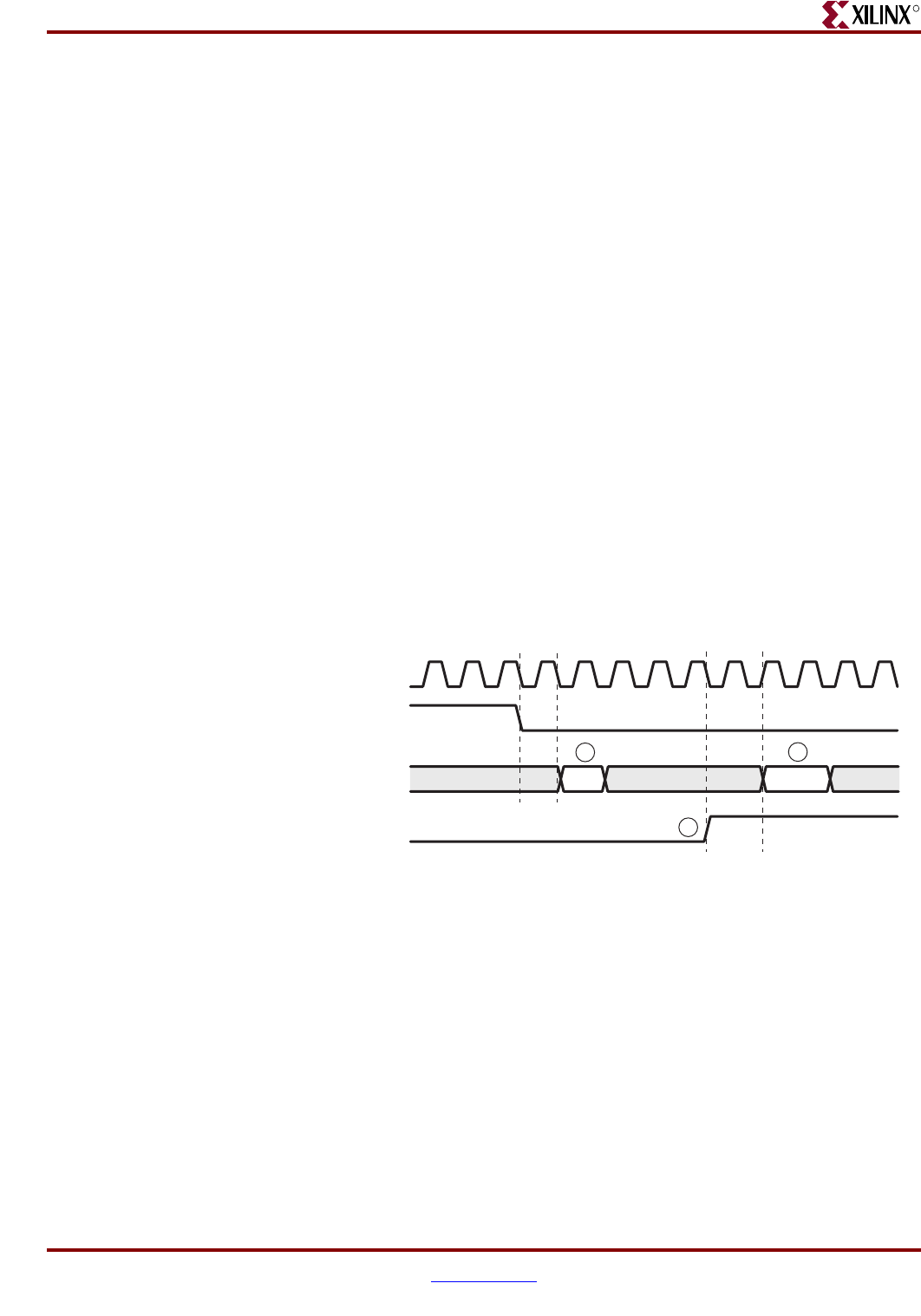
Memory Interface Solutions User Guide www.xilinx.com 299
UG086 (v3.6) September 21, 2010
Resource Utilization
R
Resource Utilization
A local inversion clocking technique is used in this design. The DCM generates only clk0
and clk90. One DCM and two BUFGMUXs are used. The Spartan-3 generation FPGA
designs operate at 166 MHz and below.
DDR SDRAM Initialization
Before issuing the memory read and write commands, the controller initializes the DDR
SDRAM using the memory initialization command. The user can give the initialization
command only after all reset signals are deactivated. The controller is in the reset state for
200 µs after power up. For design optimization, a 200 µs timer is generated from the refresh
counter. The refresh timer is a function of frequency. Therefore, at lower frequencies, the
200 µs timer waits more than 200 µs. Because wait200 happens only during the power-up
sequence, design performance is not degraded. All resets are asserted for 200 µs because
DDR SDRAM requires a 200 µs delay prior to applying an executable command after all
power supply and reference voltages are stable. The controller asserts the clock enable to
memory after 200 µs.
All the load mode register parameters are taken from the Mode Register values in the
parameter file. The user has to enter the load mode parameters from the GUI while
generating the design from MIG. When the Init command is received from the user
interface, the controller starts DDR SDRAM initialization. The controller then writes this
data into the Load Mode Register. Once the DDR SDRAM is initialized, the DDR SDRAM
controller asserts the init_done signal.
Figure 7-9 shows the timing for the memory initialization command.
1. When the 200 μs timer expires, all the system resets (sys_rst, sys_rst90, and sys_rst180)
go down. After sys_rst180 is deasserted, the user can place the initialization command
on user_command_register[2:0] on a falling edge of clk0 for one clock cycle. This starts
the initialization sequence.
2. The DDR SDRAM controller indicates that the initialization is complete by asserting
the init_done signal on a falling edge of clk0. The init_done signal is asserted
throughout the period.
3. After init_done is asserted, the user can pass the next command at any time.
I
Figure 7-9: DDR SDRAM Initialization
clk0
010 Cmd
UG086_c7_08_080409
2
13
sys_rst180
user_command_register
init_done

300 www.xilinx.com Memory Interface Solutions User Guide
UG086 (v3.6) September 21, 2010
Chapter 7: Implementing DDR SDRAM Controllers
R
DDR SDRAM Write and Read Operations
In Spartan-3 generation FPGA designs, prior to issuing a read or write operation, the user
must assert the first address and command simultaneously and wait for a command
acknowledge signal. The assertion time of the command acknowledge varies depending
on the controller status. After the command acknowledge is asserted, the user waits for
three clock cycles before sending the next address. This three clock cycle time is the Active
to Command (tRCD) delay for a read or write command as defined in the memory
specification. Subsequent addresses are sent once every two clock cycles for a burst length
of four.
If the user clock domain is different from clk0 and clk90 of the MIG, then the user must
synchronize all the user interface signals to the clk0 and clk90 that are shown in Figure 7-10
and Figure 7-11, page 302.
Write
Figure 7-10 shows the timing diagram for a write to DDR SDRAM with a burst length of
four. The user initiates the write command by sending a Write command to the DDR
SDRAM controller. To terminate a write burst, the user asserts the burst_done signal for
two clocks after the last user_input_address. For a burst length of two, the burst_done
signal should be asserted for one clock. For a burst length of four, the burst_done signal
should be asserted for two clocks. For a burst length of eight, the burst_done signal should
be asserted for four clock cycles.
The write command is asserted on the falling edge of clk0. In response to a write
command, the DDR SDRAM controller acknowledges with the usr_cmd_ack signal on a
falling edge of clk0. The usr_cmd_ack signal is generated in the next clock after the write
command is asserted, if the controller is not busy. If there is an ongoing refresh command,
the usr_cmd_ack signal is asserted after completion of the refresh command. The user
asserts the first address (row + column + bank address) with the write command and
keeps it asserted for three clocks after usr_cmd_ack assertion. Any subsequent write
addresses are asserted on an alternate falling edge of clk0 after deasserting the first
memory address. For a burst length of two, subsequent addresses are asserted on each
clock cycle, and for a burst length of eight, subsequent addresses are asserted once every
four clock cycles. The first user data is asserted on a rising edge of clk90 after usr_cmd_ack
is asserted. As the SDR data is converted to DDR data, the width of this bus is 2n, where n
is data width of DDR SDRAM data bus.
For a burst length of four, only two data words (each of 2n) are given to the DDR SDRAM
controller for each user address. For a burst length of two, one data word is passed for each
burst. For a burst length of eight, four data words are passed for each burst. Internally, for
Burst Length = 4, the DDR SDRAM controller converts into four data words, each of n bits.
To terminate the write burst, the user asserts burst_done on a falling edge of clk0 for two
clocks. The burst_done signal is asserted after the last memory address. Any further
commands to the DDR SDRAM controller are given only after the usr_cmd_ack signal is
deasserted. After burst_done is asserted, the controller terminates the burst and issues a
precharge to the memory. The usr_cmd_ack signal is deasserted after completion of the
precharge.
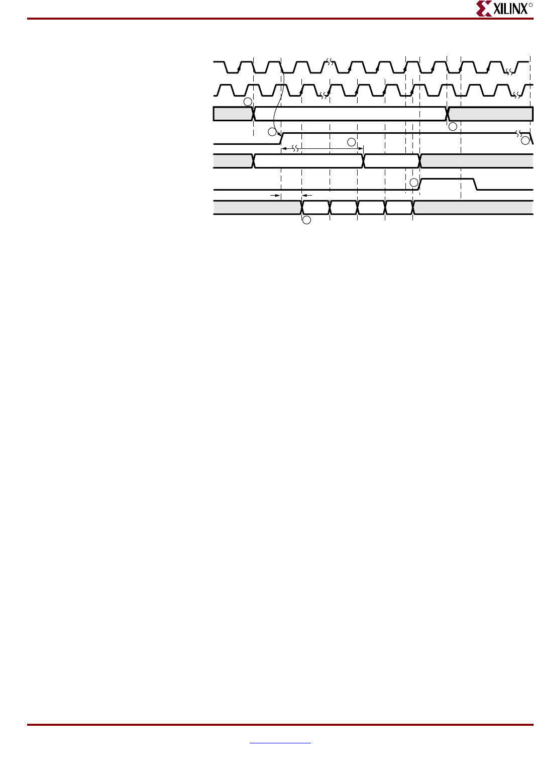
Memory Interface Solutions User Guide www.xilinx.com 301
UG086 (v3.6) September 21, 2010
Resource Utilization
R
1. A memory write is initiated by issuing a write command to the DDR SDRAM
controller. The write command must be asserted on a falling edge of clk0.
2. The DDR SDRAM controller acknowledges the write command by asserting the
user_cmd_ack signal on a falling edge of clk0. The earliest this signal is asserted is one
clock after the command. The maximum number of clock cycles it takes to assert
cmd_ack signal depends on the refresh period.
3. The first user_input_address must be placed along with the command. The input data
is asserted with the clk90 signal after the user_cmd_ack signal is asserted.
4. The user asserts the first address (row + column + bank address) with the write
command and keeps it asserted for three clocks after usr_cmd_ack assertion. The
user_input_address signal is asserted on a falling edge of clk0. All subsequent
addresses are asserted on alternate falling edges of clk0 for burst lengths of four, on
each clock for burst lengths of two, and once in four clocks for burst lengths of eight.
5. To terminate the write burst, burst_done is asserted after the last user_input_address.
The burst_done signal is asserted for two clock cycles with respect to the falling edge
of clk0 for burst lengths of four.
6. The user command is deasserted after burst_done is asserted.
7. The controller deasserts the user_cmd_ack signal after completion of precharge to the
memory. The next command must be given only after user_cmd_ack is deasserted.
Back-to-back write operations are supported only within the same bank and row.
Read
The user initiates a memory read with a read command to the DDR SDRAM controller.
Figure 7-11 shows the memory read timing diagram for a burst length of four.
Figure 7-10: DDR SDRAM Write Burst, Burst Lengths of Four and Two Bursts
clk0
clk90
user_command_register
user_cmd_ack
user_input_address
burst_done
user_input_data
UG086_c7_09_010108
D0, D1
Write Command (3’b100)
D2, D3D4, D5 D6, D7
Add1 Add2
0.75 Clks(clk90)
1
2
3
4
6
7
3 Clks
5
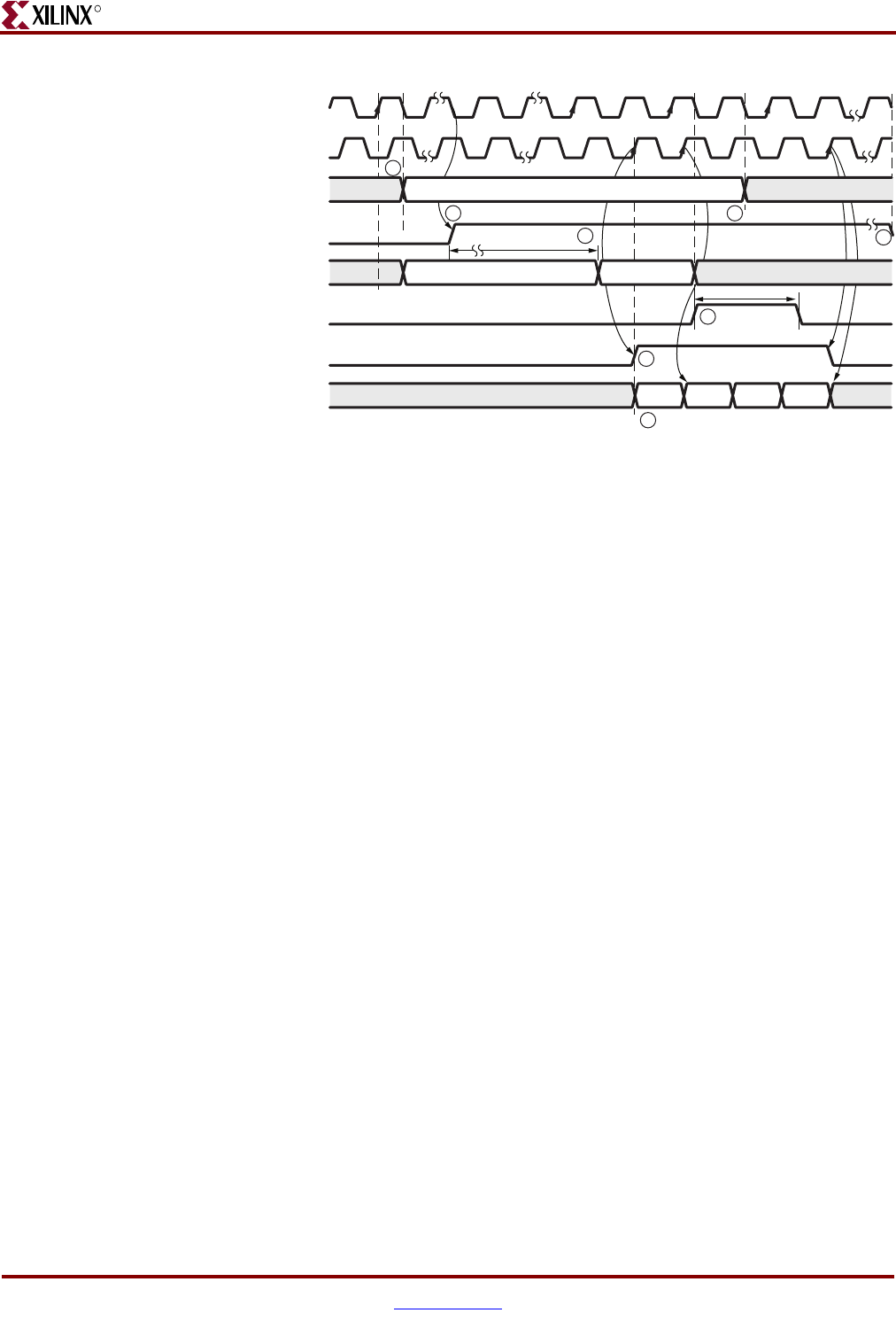
302 www.xilinx.com Memory Interface Solutions User Guide
UG086 (v3.6) September 21, 2010
Chapter 7: Implementing DDR SDRAM Controllers
R
The user provides the first memory address with the read command, and subsequent
memory addresses upon receiving the usr_cmd_ack signal. Data is available on the user
data bus with the user_data_valid signal. To terminate read burst, the user asserts the
burst_done signal on a falling edge of clk0 for two clocks with the deassertion of the last
user_input_address. The burst_done signal is asserted for one clock for burst lengths of
two, two clocks for burst lengths of four, and four clocks for burst lengths of eight. The
controller does not support single burst read operation for burst length of two.
The read command flow is similar to the write command flow.
1. A memory read is initiated by issuing a read command to the DDR SDRAM controller.
The read command is accepted on a falling edge of clk0.
2. The first read address must be placed along with the read command. In response to the
read command, the DDR SDRAM controller asserts the user_cmd_ack signal on a
falling edge of clk0. The usr_cmd_ack signal is asserted a minimum of one clock cycle
after the read command is asserted. This signal is delayed if there is an ongoing refresh
cycle, in which case it is asserted after the current refresh command completes.
3. The user asserts the first address (row + column + bank address) with the read
command and keeps it asserted for three clocks after usr_cmd_ack is asserted. The
user_input_address signal is then accepted on the falling edge of clk0. All subsequent
memory read addresses are asserted on alternate falling edges of clk0 for burst lengths
of four. The subsequent addresses are changed on every clock for burst lengths of two,
on alternate clocks for burst lengths of four, and once in four clocks for burst lengths of
eight.
4. The data on user_output_data is valid only when the user_data_valid signal is
asserted.
5. The data read from the DDR SDRAM is available on user_output_data, which is
asserted with clk90. Because the DDR SDRAM data is converted to SDR data, the
width of this bus is 2n, where n is the data width of the DDR SDRAMs. For a read burst
length of four, the DDR SDRAM controller outputs only two data words with each
user address. For a burst length of two, the controller outputs one data word, and for
a burst length of eight, the controller outputs four data words.
6. To terminate the read burst, burst_done is asserted for two clocks on the falling edge of
clk0. The burst_done signal is asserted after the last memory address.
Figure 7-11: DDR SDRAM Read, Burst Lengths of Four and Two Bursts
clk0
clk90
user_command_register
user_cmd_ack
user_input_address
burst_done
user_data_valid
user_output_data
UG086_c7_10_022108
D0, D1 D2, D3D4, D5 D6, D7
3 Clks
2 Clks
Read Command (3’b110)
1
2
3
4
5
6
7
8
Add2Add1
Memory Interface Solutions User Guide www.xilinx.com 303
UG086 (v3.6) September 21, 2010
Resource Utilization
R
7. The user command is deasserted after burst_done is asserted.
8. The controller deasserts the user_cmd_ack signal after completion of precharge to the
memory. Any further commands to the DDR SDRAM controller should be given after
user_cmd_ack is deasserted. Back-to-back read operations are supported only within
the same bank and row. Approximately 17 clock cycles pass between the time a read
command is asserted on the user interface and the time data becomes available on the
user interface.
Table 7-10 shows the read latency for CL = 3.
In general, read latency varies based on the following parameters
•CAS latency
• If the user issues the commands before initialization is complete, the latency cannot be
determined
Auto Refresh
The DDR SDRAM controller does a memory refresh at intervals determined by the
frequency. For example, for a frequency of 166 MHz, an auto-refresh request is raised every
~7.6 µs. The user must terminate any ongoing commands within 20 clock cycles, when
auto_ref_req flag is asserted. The user must assert the burst_done signal at the end of the
current burst transaction when sensing the auto_ref_req flag for terminating the current
transaction. The auto_ref_req flag is asserted until the controller issues a refresh command
to the memory. The user must wait for completion of the auto-refresh command before
giving any commands to the controller when auto_ref_req is asserted.
The ar_done signal is asserted by the controller on completion of the auto-refresh
command—i.e., after TRFC time. The ar_done signal is asserted with clk180 for one clock
cycle.
The controller sets the MAX_REF_CNT value in the parameter file according to the
frequency selected for a refresh interval (7.7 µs). The rfc_count_value value in the
parameter file defines TRFC, the time between the refresh command to Active or another
refresh command.
After completion of the auto-refresh command, the next command can be given any time
after ar_done is asserted.
The current testbench generates five consecutive write bursts followed by five read burst
commands. For every group of five write/read commands, the controller issues an active
command followed by five write/read commands, and then a precharge command to the
memory. All five burst commands take up a maximum of 20 clock cycles. After every
precharge command, the controller state machine goes to an idle state and checks for an
Table 7-10: Read Command to Read Data Latency
Parameter Number of Clocks
User Read command to command ack 1
Command ack to Active command 3
Active to Read command 3
Memory Read command to data valid 10
Tot al c l o c k s 17

304 www.xilinx.com Memory Interface Solutions User Guide
UG086 (v3.6) September 21, 2010
Chapter 7: Implementing DDR SDRAM Controllers
R
auto_ref_req. When an auto_ref_req is asserted, the controller issues an auto refresh
command to the memory if it is in an idle state. In the worst case, the controller takes
20 clocks to go from burst_done to the auto refresh command and to the memory. The
controller issues auto refresh commands to the memory within 40 clock cycles after
auto_ref_req is asserted. Because the delay from auto_ref_req to the refresh command to
the memory is within the specified number of clocks even in the worst case scenario, the
testbench does not need to terminate the write or read transaction on the auto_ref_req
signal.
For example, at 77 MHz, an auto_ref_req is generated every 7.292 µs, and at 166 MHz, it is
generated every 7.572 µs. The MAX_REF_CNT parameter is set to the following values at
77 MHz and 166 MHz frequencies to allow 40 clock cycles of delay from auto_ref_req to
the refresh command:
Average periodic refresh = 7.8125 µs
MAX_REF_CNT = (7812.5 ns – 40 × clk_period)/clk_period
At 77 MHz (13 ns): MAX_REF_CNT = (7812.5 ns – 40 × 13)/13 = 7292.5/13 = 560
At 166 MHz (6 ns): MAX_REF_CNT = (7812.5ns – 40 × 6)/6 = 7572.5/6 = 1262
User transactions should be terminated within 20 clock cycles of the auto_ref_req signal
being asserted. The ar_done signal is asserted for one clock period by the controller on
completion of an auto refresh command (i.e., after TRFC time). Normal read and write
commands can be issued to the controller any time after ar_done is asserted.
Changing the Refresh Rate
Change the global `define (for Verilog) or constant (for VHDL) variable MAX_REF_CNT in
mymodule_parameters_0.v (or .vhd) so that MAX_REF_CNT = (refresh interval in
clock periods) = (refresh interval) / (clock period). For example, for a refresh rate of 7.7 µs
with a memory bus running at 133 MHz:
MAX_REF_CNT = 7.7 µs / (clock period) = 7.7 µs / 7.5 ns = 1026 (decimal) = 0x402
If the above value exceeds 2MAX_REF_WIDTH – 1, the value of MAX_REF_WIDTH must be
increased accordingly in parameters_0.v (or .vhd) to increase the width of the counter
used to track the refresh interval.
Load Mode
MIG does not support the user LOAD MODE command. The mode register values from
the parameter file are loaded into the Load Mode register during initialization.

Memory Interface Solutions User Guide www.xilinx.com 305
UG086 (v3.6) September 21, 2010
Resource Utilization
R
UCF Constraints
Some constraints are required to successfully create the design. The following examples
explain the different constraints in the UCF.
Calibration Circuit Constraints
All LUTs in the matched delay circuits are constrained to specific locations in the device.
For example:
INST "infrastructure_top0/cal_top0/tap_dly0/l0" RLOC=X0Y6;
INST "infrastructure_top0/cal_top0/tap_dly0/l0" U_SET =
delay_calibration_chain;
INST "infrastructure_top0/cal_top0/tap_dly0/gen_tap1[0].r" RLOC=X0Y6;
INST "infrastructure_top0/cal_top0/tap_dly0/gen_tap1[0].r" U_SET =
delay_calibration_chain;
INST "infrastructure_top0/cal_top0/tap_dly0/gen_tap1[1].r" RLOC=X0Y6;
INST "infrastructure_top0/cal_top0/tap_dly0/gen_tap1[1].r" U_SET =
delay_calibration_chain;
Data and Data Strobe Constraints
Data and data strobe signals are assigned to specific pins in the device; placement
constraints related to the dqs_delay circuit and the FIFOs used for the data_read module
are specified.
Example:
NET "cntrl0_DDR_DQS[0]" LOC = Y6;
INST "ddr1_top0/data_path0/data_read_controller0/gen_delay[0].dqs_delay_col0/one"
LOC = SLICE_X0Y110;
INST "ddr1_top0/data_path0/data_read_controller0/gen_delay[0].dqs_delay_col0/one"
BEL = F;
NET "cntrl0_DDR_DQ[0]" LOC = Y4;
INST "ddr1_top0/data_path0/data_read0/gen_strobe[0].strobe/fifo0_bit0" LOC =
SLICE_X2Y111;
The I/O standards for all the memory interface signals are required to be specified.
MAXDELAY Constraints
The MAXDELAY constraints define the maximum allowable delay on the net. Following
are the list of MAXDELAY constraints used in Spartan FPGA designs in the UCF on
different nets. The values provided here vary depending on FPGA family and the device
type. Some values are dependent on frequency. The constraints shown here are from
example_design. The hierarchy paths of the nets are different between
example_design and user_design.
NET "infrastructure_top0/cal_top0/tap_dly0/tap[7]" MAXDELAY = 350ps;
NET "infrastructure_top0/cal_top0/tap_dly0/tap[15]" MAXDELAY = 350ps;
NET "infrastructure_top0/cal_top0/tap_dly0/tap[23]" MAXDELAY = 350ps;
These constraints are used to minimize the tap delay inverter connection wire length. This
delay should be minimized to calibrate the delay of a tap (LUT element) accurately. These
values are independent of frequency and vary from family to family and device to device.
Without these constraints, the tool might synthesize longer routes between the tap
connections. Inappropriate delays in this circuit could cause the design to fail in hardware.
NET "main_00/top0/dqs_int_delay_in*" MAXDELAY = 675ps;

306 www.xilinx.com Memory Interface Solutions User Guide
UG086 (v3.6) September 21, 2010
Chapter 7: Implementing DDR SDRAM Controllers
R
This constraint is used for the DQS nets from the I/O pad to the input of the LUT delay
chain. Without this constraint, the nets take unpredictable delays that affect the Data Valid
window. In Spartan-3 generation FPGA designs, data is latched using the DQS signal. In
order to latch the correct data, DQS is delayed using LUT delay elements to center-align
with respect to the input read data. Incorrect data could be latched if the delays on this net
are unpredictable. Unpredictable delays might also cause the design to have intermittent
failures, which are difficult to debug in hardware.
NET "main_00/top0/dqs_div_rst" MAXDELAY = 460ps;
The net dqs_div_rst is the loopback signal. This signal is used as an enable for read data
FIFOs and FIFO write pointers after it is delayed using the LUT delay elements. The
overall delay on this net should be comparable with the delay on the DQS signal. This net
is constrained to control the overall delay. Both the dqs_div_rst and DQS signals take
similar paths. If the delay on the dqs_div_rst signal is higher, the first read data from
memory might be missed.
NET
"main_00/top0/data_path0/data_read_controller0/gen_delay*dqs_delay_col
*/delay*" MAXDELAY = 140ps;
NET
"main_00/top0/data_path0/data_read_controller0/rst_dqs_div_delayed/
delay*" MAXDELAY = 140 ps;
These constraints are required to minimize the wire delays between the LUT elements of a
LUT delay chain that is used to delay the DQS and rst_dqs_div loopback signal. Higher
wire delays between LUT delay elements can shift the data valid window, which in turn
can cause incorrect data to be latched. Therefore, the MAXDELAY constraint is required for
these nets.
NET "main_00/top0/data_path0/data_read_controller0/rst_dqs_div"
MAXDELAY = 3383 ps;
NET "main_00/top0/data_path0/data_read0/fifo*_wr_en*"
MAXDELAY = 3007ps;
These constraints are required because these paths are not constrained otherwise. The total
delay on the rst_dqs_div and fifo_wr_en nets must not exceed the clock period. The total
delay on both the nets is set to 85% of the clock period, leaving 15% as margin. These
delays vary with frequency.
NET "main_00/top0/data_path0/data_read0/fifo*_wr_addr[*]"
MAXDELAY = 5610ps;
The MAXDELAY constraint is required on FIFO write address because this path is not
constrained otherwise. This is a single clock cycle path. It is set to 80% of the clock period,
leaving 20% as margin because this net generally meets the required constraint.
I/O Banking Rules
There are I/O banking rules to be followed for I/O pin allocations, stating that the I/O
signals allocated in a bank should adhere to compatible I/O standards. Refer to the “Rules
Concerning Banks” section for additional information regarding I/O banking rules in
DS099 [Ref 28] and DS312 [Ref 29].
Memory Interface Solutions User Guide www.xilinx.com 307
UG086 (v3.6) September 21, 2010
Design Notes
R
Design Notes
Spartan-3/3E/3A/3AN/3A DSP FPGA Pin Allocation Rules
The pin allocation rules are different for top/bottom and left/right banks because of the
local clock structure of Spartan FPGAs.
Pin Allocation Rules for Left/Right Banks
1. When a DQS is allocated, its associated DQ bits should be allocated within five tiles
above and six tiles below the DQS tile.
2. The DQ bits should not be allocated in the DQS tile.
3. The rst_dqs_div signal should be placed in the center of the data bank.
Pin Allocation Rules for Top/Bottom Banks
1. All DQ bits corresponding to DQS are required to be placed to the right of its DQS tile.
2. All DQ bits corresponding to the DQS should be within five I/O tiles of the DQS tile.
3. A DQ bit should not be allocated in the same I/O tile where DQS is allocated.
Top/Bottom Bank Support
MIG does not support top/bottom banks for Spartan 3E/3A/3AN/3A DSP devices. For
some I/O pads, the fabric slices are not located next to the IOBs. These I/O pads cannot be
used for pin allocation. By excluding these I/O pins, there are not enough pins to allocate
DQ and DQS signals according to the pin allocation rules.
DDR SDRAM Signal Allocations
MIG allows banks to be selected for different classes of memory signals. Table 7-11 shows
the list of signals allocated in a group from bank selection checkboxes.
Supported Devices
This section provides tables for the memory components supported by Spartan-3,
Spartan-3A, Spartan-3AN, Spartan-3A DSP, and Spartan-3E devices.
The design generated out of MIG is independent of memory speed grade, hence the
package part of the memory component is replaced with X, where X indicates a don't care
condition. Pin mapping for x4 RDIMMs is provided in Appendix G, “Low Power
Options.”
Table 7-11: DDR SDRAM Signal Allocations
Bank Selected Signals Allocated in the Group
Address Memory address and memory control
Data Data, data mask, data strobes, and memory clock signals
System Control System reset from the user interface and status signals
System Clock System clocks from the user interface
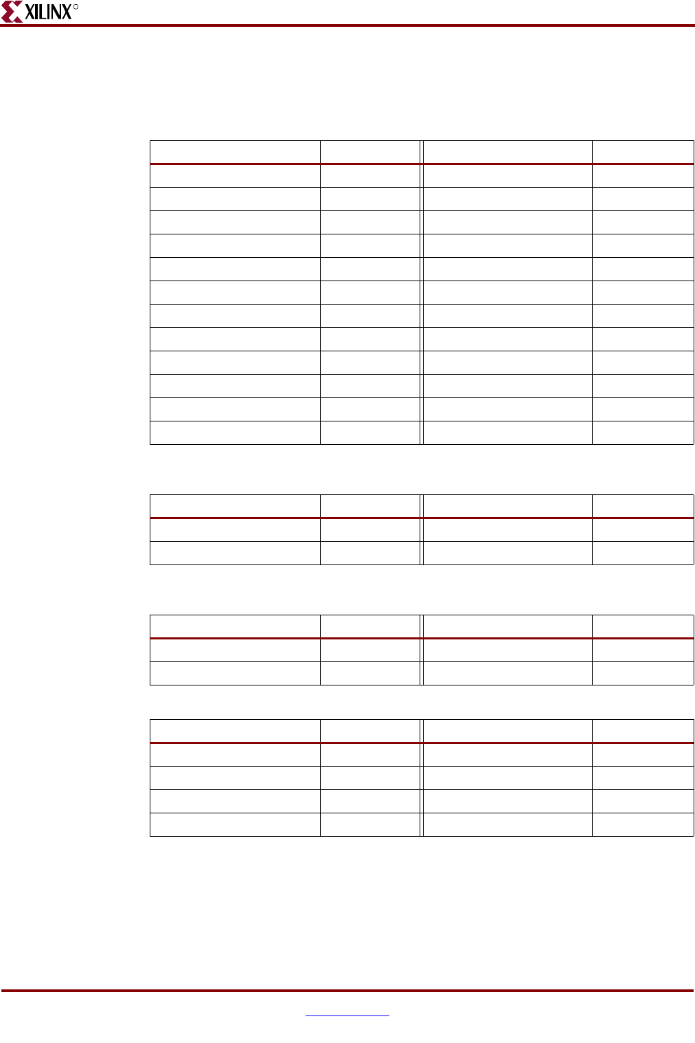
308 www.xilinx.com Memory Interface Solutions User Guide
UG086 (v3.6) September 21, 2010
Chapter 7: Implementing DDR SDRAM Controllers
R
The tables below list the components (Table 7-12) and DIMMs (Table 7-13 through
Table 7-15) supported by the tool for Spartan-3 FPGA DDR local clocking designs.
The tables below list the components (Table 7-16) and DIMMs (Table 7-17 through
Table 7-19, page 309) supported by the tool for Spartan-3A/3AN FPGA DDR local clocking
designs.
Table 7-12: Supported Components for DDR SDRAM Local Clocking
(Spartan-3 FPGAs)
Components Packages (XX) Components Packages (XX)
MT46V32M4XX-5B - MT46V32M4XX-75 P,TG
MT46V64M4XX-5B BG,FG,P,TG MT46V64M4XX-75 FG,P,TG
MT46V128M4XX-5B BN,FN,P,TG MT46V128M4XX-75 BN,FN,P,TG
MT46V256M4XX-5B P,TG MT46V256M4XX-75 P,TG
MT46V16M8XX-5B TG,P MT46V16M8XX-75 P,TG
MT46V32M8XX-5B BG,FG,P,TG MT46V32M8XX-75 FG,P,TG
MT46V64M8XX-5B BN,FN,P,TG MT46V64M8XX-75 BN,FN,P,TG
MT46V128M8XX-5B - MT46V128M8XX-75 P,TG
MT46V8M16XX-5B TG,P MT46V8M16XX-75 P,TG
MT46V16M16XX-5B BG,FG,P,TG MT46V16M16XX-75 BG,FG,P,TG
MT46V32M16XX-5B BN,FN,P,TG MT46V32M16XX-75 -
MT46V64M16XX-5B - MT46V64M16XX-75 P,TG
Table 7-13: Supported Unbuffered DIMMs for DDR SDRAM Local Clocking
(Spartan-3 FPGAs)
Unbuffered DIMMs Packages (X) Unbuffered DIMMs Packages (X)
MT4VDDT1664AX-40B G,Y MT8VDDT3264AX-40B G,Y
MT4VDDT3264AX-40B G,Y MT9VDDT3272AX-40B Y
Table 7-14: Supported Registered DIMMs for DDR SDRAM Local Clocking
(Spartan-3 FPGAs)
Registered DIMMs Packages (X) Registered DIMMs Packages (X)
MT9VDDF3272X-40B G,Y MT18VDDF3272X-40B G,Y
MT9VDDF3272X-40B G,Y MT18VDDF12872X-40B G,Y
Table 7-15: Supported SODIMMs for DDR SDRAM Local Clocking (Spartan-3 FPGAs)
SODIMMs Packages (X) SODIMMs Packages (X)
MT4VDDT3264HX-40B G,Y MT9VDDT3272HX-40B
MT4VDDT1664HX-40B Y MT9VDDT6472HX-40B G,Y
MT8VDDT3264HX-40B - MT9VDDT12872HX-40B -
MT8VDDT6464HX-40B G,Y
Memory Interface Solutions User Guide www.xilinx.com 309
UG086 (v3.6) September 21, 2010
Supported Devices
R
The tables below list the components (Table 7-20) and DIMMs (Table 7-21 and Table 7-22)
supported by the tool for Spartan-3A DSP FPGA DDR local clocking designs.
Table 7-16: Supported Components for DDR SDRAM Local Clocking
(Spartan-3A/3AN FPGAs)
Components Packages (XX) Components Packages (XX)
MT46V32M4XX-5B - MT46V32M4XX-75 P,TG
MT46V64M4XX-5B BG,FG,P,TG MT46V64M4XX-75 FG,P,TG
MT46V128M4XX-5B BN,FN,P,TG MT46V128M4XX-75 BN,FN,P,TG
MT46V256M4XX-5B P,TG MT46V256M4XX-75 P,TG
MT46V16M8XX-5B TG,P MT46V16M8XX-75 P,TG
MT46V32M8XX-5B BG,FG,P,TG MT46V32M8XX-75 FG,P,TG
MT46V64M8XX-5B BN,FN,P,TG MT46V64M8XX-75 BN,FN,P,TG
MT46V128M8XX-5B - MT46V128M8XX-75 P,TG
MT46V8M16XX-5B TG,P MT46V8M16XX-75 P,TG
MT46V16M16XX-5B BG,FG,P,TG MT46V16M16XX-75 BG,FG,P,TG
MT46V32M16XX-5B BN,FN,P,TG MT46V32M16XX-75 -
MT46V64M16XX-5B - MT46V64M16XX-75 P,TG
Table 7-17: Supported Unbuffered DIMMs for DDR SDRAM Local Clocking
(Spartan-3A/3AN FPGAs)
Unbuffered DIMMs Packages (X) Unbuffered DIMMs Packages (X)
MT4VDDT1664AX-40B G,Y MT8VDDT3264AX-40B G,Y
MT4VDDT3264AX-40B G,Y MT9VDDT3272AX-40B Y
Table 7-18: Supported Registered DIMMs for DDR SDRAM Local Clocking
(Spartan-3A/3AN FPGAs)
Registered DIMMs Packages (X) Registered DIMMs Packages (X)
MT9VDDF3272X-40B G,Y MT9VDDF3272X-40B G,Y
Table 7-19: Supported SODIMMs for DDR SDRAM Local Clocking
(Spartan-3A/3AN FPGAs)
SODIMMs Packages (X) SODIMMs Packages (X)
MT4VDDT3264HX-40B G,Y MT9VDDT3272HX-40B --
MT4VDDT1664HX-40B Y MT9VDDT6472HX-40B G,Y
MT8VDDT3264HX-40B - MT9VDDT12872HX-40B --
MT8VDDT6464HX-40B G,Y -- --
Table 7-20: Supported Components for DDR SDRAM Local Clocking
(Spartan-3A DSP FPGAs)
Components Packages (XX) Components Packages (XX)
MT46V32M4XX-5B - MT46V32M4XX-75 P,TG
MT46V64M4XX-5B BG,FG,P,TG MT46V64M4XX-75 FG,P,TG
310 www.xilinx.com Memory Interface Solutions User Guide
UG086 (v3.6) September 21, 2010
Chapter 7: Implementing DDR SDRAM Controllers
R
Table 7-23 lists the components supported by the tool for Spartan-3E FPGA DDR local
clocking designs.
MT46V128M4XX-5B BN,FN,P,TG MT46V128M4XX-75 BN,FN,P,TG
MT46V256M4XX-5B P,TG MT46V256M4XX-75 P,TG
MT46V16M8XX-5B TG,P MT46V16M8XX-75 P,TG
MT46V32M8XX-5B BG,FG,P,TG MT46V32M8XX-75 FG,P,TG
MT46V64M8XX-5B BN,FN,P,TG MT46V64M8XX-75 BN,FN,P,TG
MT46V128M8XX-5B - MT46V128M8XX-75 P,TG
MT46V8M16XX-5B TG,P MT46V8M16XX-75 P,TG
MT46V16M16XX-5B BG,FG,P,TG MT46V16M16XX-75 BG,FG,P,TG
MT46V32M16XX-5B BN,FN,P,TG MT46V32M16XX-75 -
MT46V64M16XX-5B - MT46V64M16XX-75 P,TG
Table 7-21: Supported Unbuffered DIMMs for DDR SDRAM Local Clocking
(Spartan-3A DSP FPGAs)
Unbuffered DIMMs Packages (X) Unbuffered DIMMs Packages (X)
MT4VDDT1664AX-40B G,Y MT8VDDT3264AX-40B G,Y
MT4VDDT3264AX-40B G,Y
Table 7-22: Supported SODIMMs for DDR SDRAM Local Clocking
(Spartan-3A DSP FPGAs)
SODIMMs Packages (X) SODIMMs Packages (X)
MT4VDDT3264HX-40B G,Y MT8VDDT3264HX-40B -
MT4VDDT1664HX-40B Y MT8VDDT6464HX-40B G,Y
Table 7-23: Supported Components for DDR SDRAM Local Clocking
(Spartan-3E FPGAs)
Components Packages (XX) Components Packages (XX)
MT46V32M4XX-5B - MT46V32M4XX-75 P,TG
MT46V64M4XX-5B BG,FG,P,TG MT46V64M4XX-75 FG,P,TG
MT46V128M4XX-5B BN,FN,P,TG MT46V128M4XX-75 BN,FN,P,TG
MT46V256M4XX-5B P,TG MT46V256M4XX-75 P,TG
MT46V16M8XX-5B TG,P MT46V16M8XX-75 P,TG
MT46V32M8XX-5B BG,FG,P,TG MT46V32M8XX-75 FG,P,TG
MT46V64M8XX-5B BN,FN,P,TG MT46V64M8XX-75 BN,FN,P,TG
MT46V128M8XX-5B - MT46V128M8XX-75 P,TG
MT46V8M16XX-5B TG,P MT46V8M16XX-75 P,TG
MT46V16M16XX-5B BG,FG,P,TG MT46V16M16XX-75 BG,FG,P,TG
Table 7-20: Supported Components for DDR SDRAM Local Clocking
(Spartan-3A DSP FPGAs) (Cont’d)
Components Packages (XX) Components Packages (XX)
Memory Interface Solutions User Guide www.xilinx.com 311
UG086 (v3.6) September 21, 2010
Simulating the Spartan-3/3E/3A/3AN/3A DSP FPGA Design
R
Simulating the Spartan-3/3E/3A/3AN/3A DSP FPGA Design
After generating the design, MIG creates a sim folder in the specified path. This folder
contains simulation files for the generated design. The sim folder contains the external
testbench, memory model, and .do file to simulate the generated design. The memory
model files are currently generated in Verilog only. To learn more details about the files in
the sim folder and to simulate the design, refer to “Simulation Guide,” page 499.
For single-rank DIMMs, MIG outputs only the base part memory model. In the simulation
testbench (sim_tb_top in the sim folder), MIG instantiates the required number of
memory models. For example, a 1 GB single-rank DIMM with the base part is 1 Gb, and
MIG instantiates the base model eight times. If the MIG generated memory model is to be
used with the user’s test bench, multiple instances should be used based on the selected
configuration.
The MIG output memory model considers the part_mem_bits parameter by default for
memory range allocation. This covers only a partial memory range, i.e., 2part_mem_bits. To
allocate the full memory range, the FULL_MEM parameter should be set in the memory
model, which in turn sets the full_mem_bits parameter for memory allocation. Allocating
the full memory range might exceed the memory of the operating system, thus causing
memory allocation failure in simulations.
Hardware Tested Configurations
The frequencies shown in Table 7-24 and Table 7-25 were achieved on the Spartan-3 FPGA
Memory Interface Board and Spartan-3E FPGA Starter Kit, respectively, under nominal
conditions. This frequency should not be used to determine the maximum design
frequency. The maximum design frequency supported in the MIG wizard is based on a
combination of the TRCE results for fabric timing on multiple device/package
combinations and I/O timing analysis using FPGA and memory timing parameters for a
64-bit wide interface.
MT46V32M16XX-5B BN,FN,P,TG MT46V32M16XX-75 -
MT46V64M16XX-5B - MT46V64M16XX-75 P,TG
Table 7-23: Supported Components for DDR SDRAM Local Clocking
(Spartan-3E FPGAs)
Components Packages (XX) Components Packages (XX)
Table 7-24: Hardware Tested Configurations for Spartan-3 FPGA DDR SDRAM
Designs
Synthesis Tools XST
HDL Verilog and VHDL
FPGA Device XC3S1500FG676-5
Burst Lengths 2 and 8
CAS Latency (CL) 2 and 2.5
64-bit Design Tested on 16-bit Component “MT46V16M16XX-75”
64-bit DIMM “MT4VDDT3264AX”
312 www.xilinx.com Memory Interface Solutions User Guide
UG086 (v3.6) September 21, 2010
Chapter 7: Implementing DDR SDRAM Controllers
R
Frequency Range 67 MHz to 170 MHz for CL = 2
40 MHz to 190 MHz for CL = 2.5
Table 7-25: Hardware Tested Configurations for Spartan-3E FPGA DDR SDRAM
Designs
Synthesis Tools XST
HDL Verilog and VHDL
FPGA Device XC3S500EFG320-4
Burst Lengths 2 and 4
CAS Latency (CL) 2 and 2.5
16-bit Design Tested on 16-bit Component “MT46V32M16XX-6T”
Frequency Range 80 MHz to 170 MHz for CL = 2
80 MHz to 170 MHz for CL = 2.5
Table 7-24: Hardware Tested Configurations for Spartan-3 FPGA DDR SDRAM
Designs
Synthesis Tools XST

Memory Interface Solutions User Guide www.xilinx.com 313
UG086 (v3.6) September 21, 2010
R
Chapter 8
Implementing DDR2 SDRAM Controllers
This chapter describes how to implement DDR2 SDRAM interfaces for Spartan®-3,
Spartan-3A, Spartan-3AN, and Spartan-3A DSP FPGAs generated by MIG. This design is
based on XAPP768c [Ref 24].
Feature Summary
This section summarizes the supported and unsupported features of the DDR2 SDRAM
controller design.
Supported Features
The DDR2 SDRAM controller design supports the following:
• Burst lengths of four and eight
• Sequential and interleaved burst types
•CAS latency of 3
•Auto refresh
• Data mask enable/disable option
• System clock, differential and single-ended
• Linear addressing
• Spartan-3 FPGA maximum frequency:
• 133 MHz with a -4 speed grade device
• 166 MHz with a -5 speed grade device
• Spartan-3A, Spartan-3AN, and Spartan-3A DSP FPGA maximum frequency:
• 133 MHz with a -4 speed grade device
• 166 MHz with a -5 speed grade device
• Components, unbuffered DIMMs, and registered DIMMs
•Verilog and VHDL
• XST and Synplicity synthesis tools
• With and without a testbench
• With or without a DCM
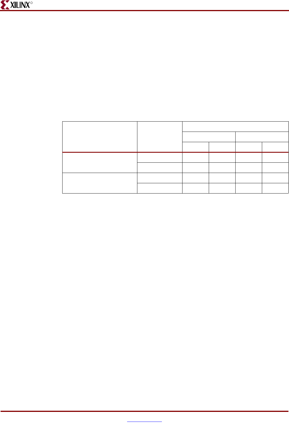
314 www.xilinx.com Memory Interface Solutions User Guide
UG086 (v3.6) September 21, 2010
Chapter 8: Implementing DDR2 SDRAM Controllers
R
Unsupported Features
The DDR2 SDRAM controller design does not support:
• CAS Latencies of 4 and 5
• Additive latencies of 1, 2, 3 and 4
•Auto Precharge
• Redundant DQS (RDQS)
• Dual rank DIMMs and Deep design
Design Frequency Ranges
Table 8-1: Design Frequency Range in MHz
FPGA Family Memory
FPGA Speed Grade
-4 -5
Min Max Min Max
Spartan-3 Component 125 133 125 166(1)
DIMM 125 133 125 133
Spartan-3A/3AN/3A DSP Component 125 133 125 166
DIMM 125 133 125 166
Notes:
1. Spartan-3 devices support 133 MHz for data widths greater than 32 bits.
Memory Interface Solutions User Guide www.xilinx.com 315
UG086 (v3.6) September 21, 2010
Controller Architecture
R
Controller Architecture
DDR2 SDRAM Interface
High-speed memory interfaces are source-synchronous and double data rate. They
transfer data on both edges of the clock cycle. A memory interface can be modularly
represented as shown in Figure 8-1. Creating a modular interface has many advantages. It
allows designs to be ported easily, and it also makes sharing parts of the design across
different types of memory interfaces possible.
Figure 8-1: Modular Memory Interface Representation
ug086_c8_01_012907
Application Interface Layer
Control Layer
Physical Layer
Xilinx FPGA
Memories
316 www.xilinx.com Memory Interface Solutions User Guide
UG086 (v3.6) September 21, 2010
Chapter 8: Implementing DDR2 SDRAM Controllers
R
Hierarchy
Figure 8-2 shows the hierarchical structure of the DDR2 SDRAM design generated by MIG
with a testbench and a DCM. In the figure, the physical and control layers are clearly
separated. MIG generates the entire controller, as shown in this hierarchy, including the
testbench. The user can replace the testbench with a design that makes use of the DDR2
SDRAM interface.
The modules are classified as follows:
• Design modules
• Testbench modules
• Clocks, reset generation, and calibration modules
There is a parameter file generated with the design that has all the user input and design
parameters selected from MIG.
MIG can generate four different DDR2 SDRAM designs:
• With a testbench and a DCM
• Without a testbench and with a DCM
• With a testbench and without a DCM
• Without a testbench and without a DCM
Figure 8-2: Hierarchical Structure of the Design
<top_
module>
main* infrastructure_
top*
controller* infrastructure iobs*
data_
read*
data_
read_
controller*
data_
write*
data_
path*
controller_
iobs*
dqs_
delay
Design Modules
fifo_0_
wr_en
wr_gray_
cntr
fifo_1_
wr_en
addr_
gen* cmd_fsmdata_
gen*
cmp_
data*
rd_gray_
cntr ram8d*
infrastructure
_iobs*
data_
path_
iobs*
s2_dq_
iob
s3_dm_
iob
s3_dqs_
iob
UG086_c8_02_010108
clk_dcm cal_top
test_
bench* top*
tap_dly cal_ctl
Te st Bench Modules
Clocks, Reset Generation, and Calibration Modules
Note: A block with a * has a parameter file included.

Memory Interface Solutions User Guide www.xilinx.com 317
UG086 (v3.6) September 21, 2010
Controller Architecture
R
For a design without a testbench (user_design), the yellow shaded modules in Figure 8-2
are not present in the design. The <top_module> module has the user interface signals for
designs without a testbench. The list of user interface signals is provided in Table 8-8.
The infrastructure_top module comprises the clock and the reset generation module of the
design. It instantiates a DCM in the module when selected by MIG. The differential design
clock is an input to this module. A user reset is also input to this module. Using the input
clocks and reset signals, system clocks and system reset are generated in this module
which is used in the design. Infrastructure_top also consists of calibration logic.
The DCM primitive is not instantiated in this module if the Use DCM option is unchecked.
Therefore, the system operates on the user-provided clocks. The system reset is generated
in the infrastructure_top module using the dcm_lock input signal. Figure 8-3 and
Figure 8-4, page 319 represent the system clock for differential only.
MIG Tool Design Options
MIG provides various options to generate the design with or without a testbench or with
or without a DCM. This section provides detailed descriptions of the type of design
generated by the user using various options. Figure 8-3, page 318 and Figure 8-4, page 319
represent the system clock for differential only. For more information on the clocking
structure, refer to “Clocking Scheme,” page 325.
MIG outputs example_design and user_design. MIG generated example_design includes
the memory controller and synthesized testbench. In order to simulate design and to test
the functionality of the design example_design can be used. Where as user_design
includes the memory controller design only. User should develop test bench (User
application) and should interface with MIG memory controller design. Refer to Table 8-8,
page 329 for user interface signals and “DDR2 SDRAM Write and Read operations” section
for write and read timing shown in Figure 8-8, page 326 and Figure 8-11, page 333.
Figure 8-3, page 318 shows a block diagram representation of the top-level module for a
DDR2 SDRAM design with a DCM and a testbench. “Clocking Scheme,” page 325
describes how various clocks are generated using the DCM. The input clocks can be
differential or single-ended based on the system clock selection in the GUI. For differential,
differential clocks sys_clk and sys_clkb appear as input ports, whereas for single-ended
sys_clk_in appears as the input port. The DCM clock is instantiated in the
infrastructure_top module that generates the required design clocks. reset_in_n is the
active-Low system reset signal. All design resets are gated by the dcm_lock signal.
The cntrl0_led_error_output1 output signal indicates whether the case passes or fails. The
testbench module does writes and reads, and also compares the read data with written
data. The cntrl0_led_error_output1 signal is driven High on data mismatches. The
cntrl0_data_valid_out signal indicates whether the read data is valid or not.
318 www.xilinx.com Memory Interface Solutions User Guide
UG086 (v3.6) September 21, 2010
Chapter 8: Implementing DDR2 SDRAM Controllers
R
Figure 8-3: MIG Output of the DDR2 SDRAM Controller Design with a DCM and a Testbench
main_0 Memory
Device
UG086_c8_03_090208
System
Clocks
and Reset
Status
Signals
infrastructure_top clk90_0
clk0_0
sys_clk
sys_clkb
reset_in_n
sys_rst
sys_rst90
sys_rst180
cntrl0_led_error_output1
cntrl0_init_done
cntrl0_data_valid_out
cntrl0_ddr2_ras_n
cntrl0_ddr2_cas_n
cntrl0_ddr2_we_n
cntrl0_ddr2_cs_n
cntrl0_ddr2_cke
cntrl0_ddr2_dm
cntrl0_ddr2_ba
cntrl0_ddr2_a
cntrl0_ddr2_ck_n
cntrl0_ddr2_odt
cntrl0_ddr2_ck
cntrl0_ddr2_dq
cntrl0_ddr2_dqs
cntrl0_ddr2_reset_n
cntrl0_ddr2_dqs_n
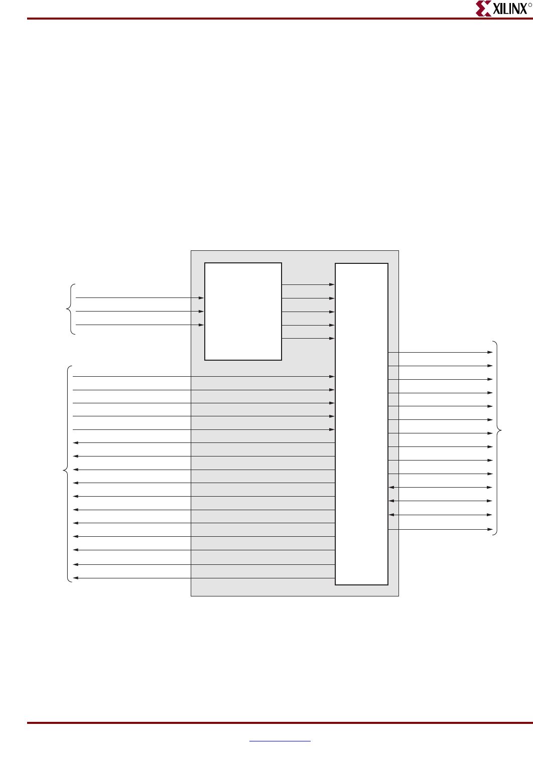
Memory Interface Solutions User Guide www.xilinx.com 319
UG086 (v3.6) September 21, 2010
Controller Architecture
R
Figure 8-4 shows a block diagram representation of the top-level module for a DDR2
SDRAM design with a DCM but without a testbench. “Clocking Scheme,” page 325
describes how various clocks are generated using the DCM. The input clocks can be
differential or single-ended based on the System Clock selection in the GUI.
For differential, differential clocks sys_clk and sys_clkb appear as input ports, whereas for
single-ended sys_clk_in appears as the input port. The DCM clock is instantiated in the
infrastructure_top module that generates the required design clocks. reset_in_n is the
active-Low system reset signal. All design resets are gated by the dcm_lock signal.
The user interface signals are listed in Figure 8-4. The design provides the clk_tb, clk90_tb,
sys_rst_tb, sys_rst90_tb, and sys_rst180_tb signals to the user in order to synchronize with
the design. The signals clk_tb, clk90_tb, sys_rst_tb, sys_rst90_tb, and sys_rst180_tb are
connected to clocks clk_0 and clk90_0 and reset signals sys_rst, sys_rst90, and sys_rst180,
respectively, in the controller. If the user clock domain is different from clk_tb/clk90_tb,
then the user should add FIFOs for all the inputs and outputs of the controller (user
application signals) in order to synchronize them to clk_tb/clk90_tb.
Figure 8-4: MIG Output of the DDR2 SDRAM Controller Design with a DCM but without a Testbench
top_0 Memory
Device
UG086_c8_04_071708
System
Clocks
and Reset
User
Interface
Signals
infrastructure_top
clk90_0
clk_0
sys_clk
sys_clkb
reset_in_n
sys_rst
sys_rst90
sys_rst180
cntrl0_burst_done
cntrl0_user_command_register
cntrl0_user_data_mask
cntrl0_user_input_data
cntrl0_user_input_address
cntrl0_init_done
cntrl0_ar_done
cntrl0_auto_ref_req
cntrl0_user_cmd_ack
cntrl0_clk_tb
cntrl0_clk90_tb
cntrl0_sys_rst_tb
cntrl0_sys_rst90_tb
cntrl0_sys_rst180_tb
cntrl0_user_data_valid
cntrl0_user_output_data
cntrl0_ddr2_ras_n
cntrl0_ddr2_cas_n
cntrl0_ddr2_we_n
cntrl0_ddr2_cs_n
cntrl0_ddr2_cke
cntrl0_ddr2_dm
cntrl0_ddr2_ba
cntrl0_ddr2_a
cntrl0_ddr2_ck_n
cntrl0_ddr2_ck
cntrl0_ddr2_dq
cntrl0_ddr2_dqs
cntrl0_ddr2_reset_n
cntrl0_ddr2_dqs_n
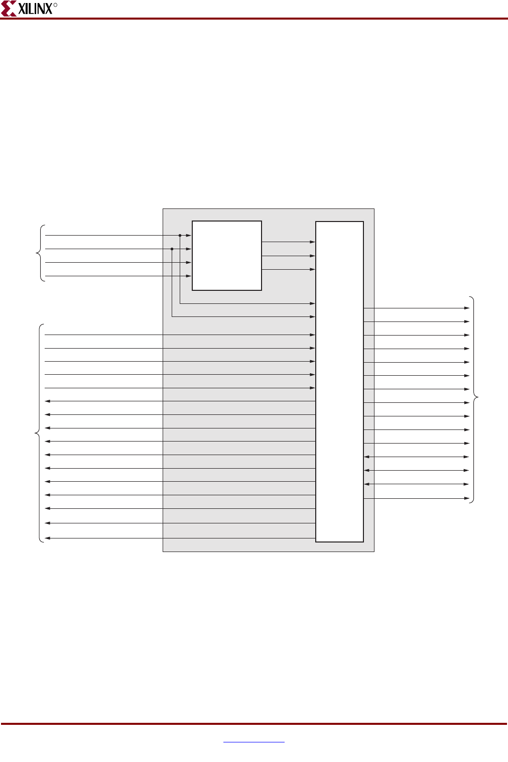
320 www.xilinx.com Memory Interface Solutions User Guide
UG086 (v3.6) September 21, 2010
Chapter 8: Implementing DDR2 SDRAM Controllers
R
Figure 8-5 shows a block diagram representation of the top-level module for a DDR2
SDRAM design without a DCM or a testbench. “Clocking Scheme,” page 325 describes
how various clocks are generated using the DCM. The user should provide all the clocks
and the dcm_lock signal. These clocks should be single-ended. reset_in_n is the active-Low
system reset signal. All design resets are gated by the dcm_lock signal.
The user interface signals are listed in Figure 8-5. The design provides the clk_tb, clk90_tb,
sys_rst_tb, sys_rst90_tb, and sys_rst180_tb signals to the user in order to synchronize with
the design. The signals clk_tb, clk90_tb, sys_rst_tb, sys_rst90_tb, and sys_rst180_tb are
connected to clocks clk_0 and clk90_0 and reset signals sys_rst, sys_rst90, and sys_rst180,
respectively, in the controller. If the user clock domain is different from clk_tb/clk90_tb,
then user should add FIFOs for all the inputs and outputs of the controller (user
application signals) in order to synchronize them to clk_tb/clk90_tb.
Figure 8-5: MIG Output of the DDR2 SDRAM Controller Design without a DCM or a Testbench
top_0
Memory
Device
UG086_c8_05_071708
System
Reset
and User
DCM
Clocks
User
Interface
Signals
infrastructure_top
clk90_int
dcm_lock
clk_int
reset_in_n
sys_rst
sys_rst90
sys_rst180
cntrl0_burst_done
cntrl0_user_command_register
cntrl0_user_data_mask
cntrl0_user_input_data
cntrl0_user_input_address
cntrl0_init_done
cntrl0_ar_done
cntrl0_auto_ref_req
cntrl0_user_cmd_ack
cntrl0_clk_tb
cntrl0_clk90_tb
cntrl0_sys_rst_tb
cntrl0_sys_rst90_tb
cntrl0_sys_rst180_tb
cntrl0_user_data_valid
cntrl0_user_output_data
cntrl0_ddr2_ras_n
cntrl0_ddr2_cas_n
cntrl0_ddr2_we_n
cntrl0_ddr2_cs_n
cntrl0_ddr2_cke
cntrl0_ddr2_dm
cntrl0_ddr2_ba
cntrl0_ddr2_a
cntrl0_ddr2_ck_n
cntrl0_ddr2_odt
cntrl0_ddr2_ck
cntrl0_ddr2_dq
cntrl0_ddr2_dqs
cntrl0_ddr2_reset_n
cntrl0_ddr2_dqs_n
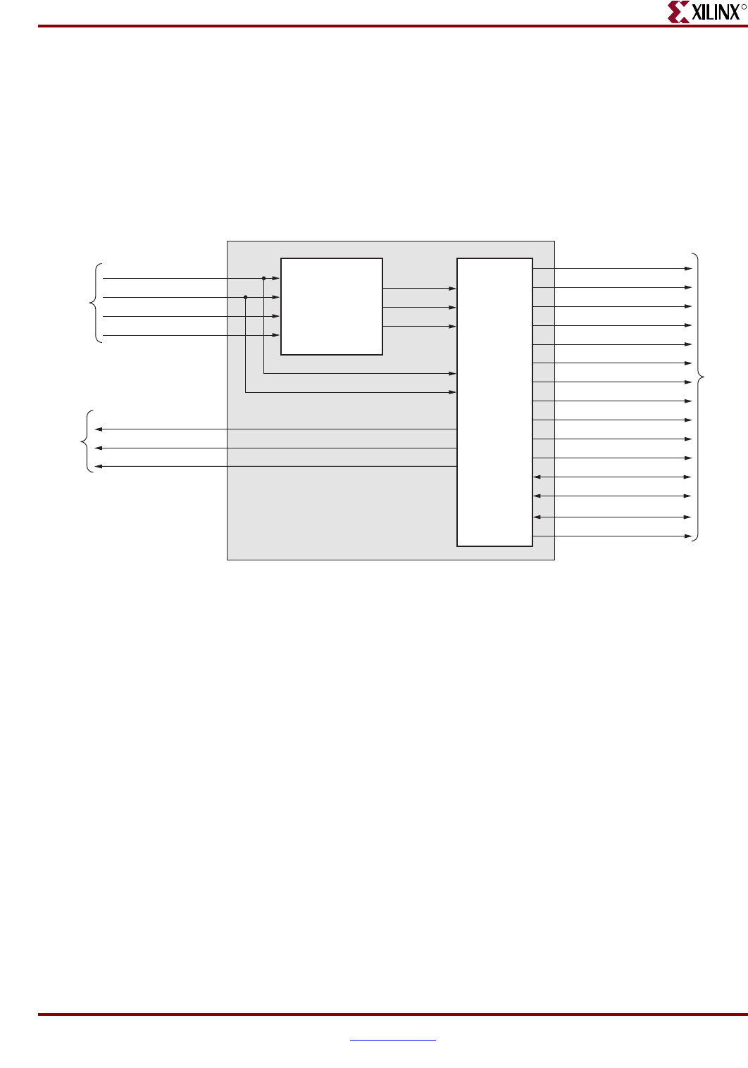
Memory Interface Solutions User Guide www.xilinx.com 321
UG086 (v3.6) September 21, 2010
Controller Architecture
R
Figure 8-6 shows a block diagram representation of the top-level module for a DDR2
SDRAM design without a DCM but with a testbench. “Clocking Scheme,” page 325
describes how various clocks are generated using the DCM. The user should provide all
the clocks and the dcm_lock signal. These clocks should be single-ended. reset_in_n is the
active-Low system reset signal. All design resets are gated by the dcm_lock signal.
The cntrl0_led_error_output1 output signal indicates whether the case passes or fails. The
testbench module does writes and reads, and also compares the read data with the written
data. The cntrl0_led_error_output1 signal is driven High on data mismatches. The
cntrl0_data_valid_out signal indicates whether the read data is valid or not.
All the Memory Device interface signals that are shown in Figure 8-3 through Figure 8-6
do not necessarily appear for all designs that are generated from MIG. For example, port
cntrl0_ddr2_reset_n appears in the port list only for Registered DIMM designs. Similarly,
cntrl0_ddr2_DQS_N does not appear for single-ended DQS designs. Port cntrl0_ddr2_dm
appears only for the parts that contain a data mask. A few RDIMMs do not have a data
mask, and cntrl0_ddr2_dm does not appear in the port list for these parts.
Figure 8-6: MIG Output of the DDR2 SDRAM Controller Design without a DCM but with a Testbench
main_0
Memory
Device
UG086_c8_06_071708
System
Reset
and User
DCM
Clocks
Status
Signals
infrastructure_top
cntrl0_ddr2_ras_n
cntrl0_ddr2_cas_n
cntrl0_ddr2_we_n
cntrl0_ddr2_cs_n
cntrl0_ddr2_cke
cntrl0_ddr2_dm
cntrl0_ddr2_ba
cntrl0_ddr2_a
cntrl0_ddr2_ck_n
sys_rst
sys_rst90
sys_rst180
cntrl0_ddr2_odt
cntrl0_ddr2_ck
cntrl0_led_error_output1
cntrl0_data_valid_out
cntrl0_init_done cntrl0_ddr2_dq
cntrl0_ddr2_dqs
cntrl0_ddr2_reset_n
cntrl0_ddr2_dqs_n
clk90_int
dcm_lock
clk_int
reset_in_n
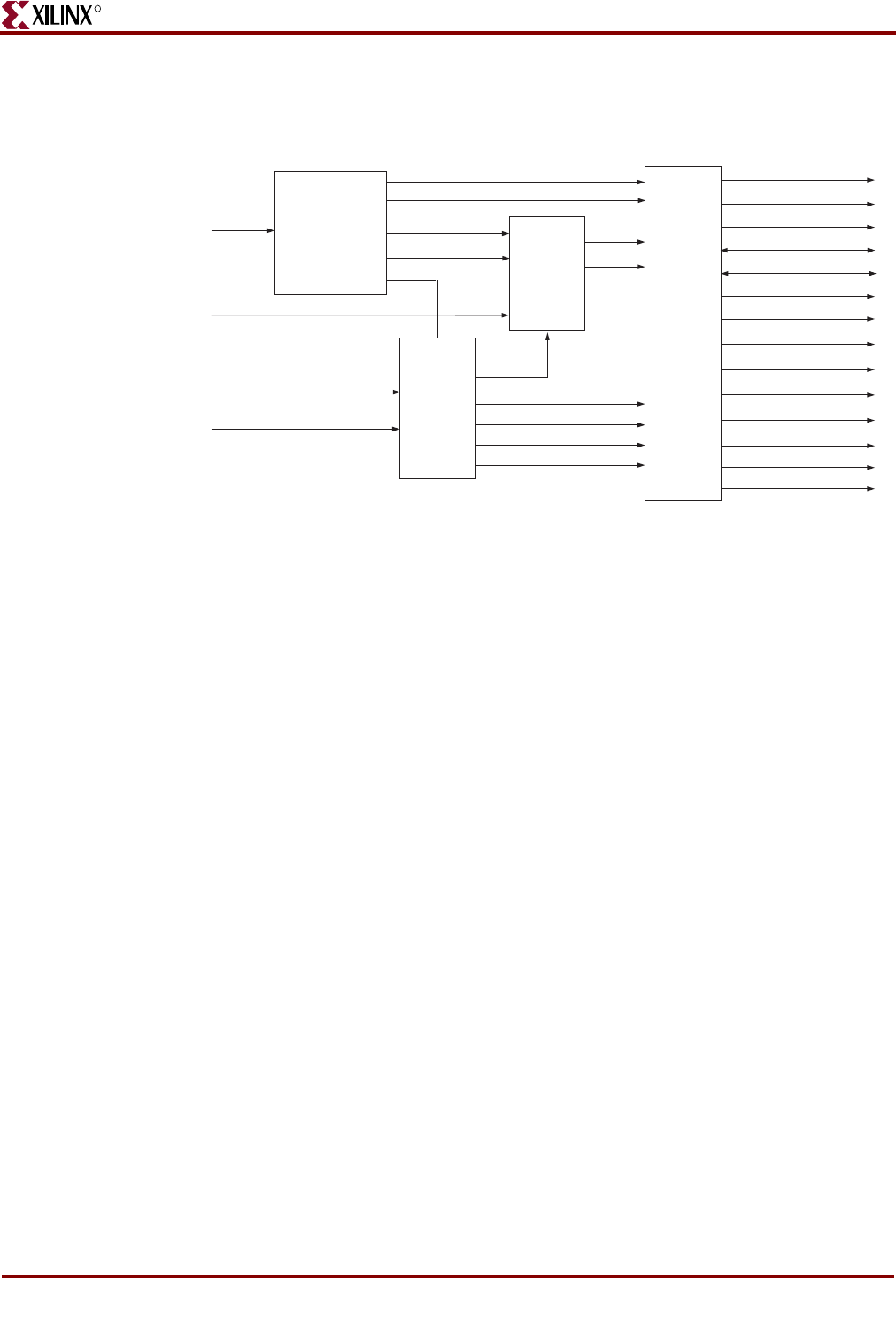
322 www.xilinx.com Memory Interface Solutions User Guide
UG086 (v3.6) September 21, 2010
Chapter 8: Implementing DDR2 SDRAM Controllers
R
Figure 8-7 shows a detailed block diagram of the DDR2 SDRAM controller. All four blocks
shown are subblocks of the ddr2_top module. The functionality of these blocks is
explained in following sections.
Controller
The controller module accepts and decodes user commands and generates read, write,
memory initialization, and load mode commands. The controller also generates signals for
other modules.
The memory is initialized and powered up using a defined process. The controller state
machine handles the initialization process upon receiving an initialization command.
Datapath
This module transmits and receives data to and from the memories. Major functions
include storing the read data and transferring write data and write enable to the IOBS
module. The data_read, data_write, data_path_IOBs, and data_read_controller modules
perform the actual read and write functions. For more information, refer to XAPP768c
[Ref 24].
Data Read Controller
This module generates all control signals that are used for the data_read module.
Data Read
The data_read module contains the read datapaths for the DDR2 SDRAM interface. Details
for this module are described in XAPP768c [Ref 24].
Data Write
This module contains the write datapath for the DDR2 SDRAM interface. The write data
and write enable signals are forwarded together to the DDR2 SDRAM through IOB flip-
flops. The IOBs are implemented in the datapath_IOBs module.
Figure 8-7: Memory Controller Block Diagram
UG086_c8_07_071708
user_command_register
Controller
Datapath
infrastructure_top
IOBs
cntrl0_ddr2_ck
cntrl0_ddr2_ck_n
cntrl0_ddr2_cke
cntrl0_ddr2_dm
cntrl0_ddr2_cs_n
cntrl0_ddr2_dqs
cntrl0_ddr2_cas_n
cntrl0_ddr2_we_n
cntrl0_ddr2_odt
cntrl0_ddr2_reset_n
cntrl0_ddr2_dq
cntrl0_ddr2_a
cntrl0_ddr2_ba
cntrl0_ddr2_ras_n
user_clk
user_data
user_address
Memory Interface Solutions User Guide www.xilinx.com 323
UG086 (v3.6) September 21, 2010
Controller Architecture
R
Infrastructure_top
The infrastructure module generates the FPGA clock and reset signals. For differential
clocking, sys_clk and syc_clkb ports are used as inputs to the IBUFGDS_LVDS_25 buffer
and the output of the buffer is driven to the DCM input. For single-ended clocking, the
sys_clk_in port is used as an input to the IBUFG buffer; the output of the buffer is driven to
the DCM input. A DCM generates the clock and its inverted version. The infrastructure
module also generates all of the reset signals required for the design.
IOBs
All input and output signals of the FPGA are implemented in the IOBs.
Te st B en c h
MIG generates two different RTL folders, example_design and user_design. The
example_design includes the synthesizable test bench, while user_design does not include
the test bench modules. The MIG test bench performs five write commands and five read
commands in an alternating fashion. The number of words in a write command depends
on the burst length. For a burst length of 4, every write command writes four data words.
For all five write commands, the test bench writes a total of 20 data words (10 rise data
words and 10 fall data words). For a burst length of 8, the test bench writes a total of 40 data
words. The pattern data is shown in Table 8-2 and Table 8-3 for burst lengths of 4 and 8,
respectively.
Table 8-2: Data Pattern for Burst Length of 4
Burst Rise Fall
196 69
2C D3
258 A7
B1 4E
363 9C
C6 39
48C 73
18 E7
531 CE
62 9D
Table 8-3: Data Pattern for Burst Length of 8
Burst Rise Fall
196 69
2C D3
58 A7
B1 4E
324 www.xilinx.com Memory Interface Solutions User Guide
UG086 (v3.6) September 21, 2010
Chapter 8: Implementing DDR2 SDRAM Controllers
R
The falling edge data is the complement of the rising edge data. The data pattern is
repeated for the next set of five burst write commands based on the selected burst length,
as given in Table 8-2 and Table 8-3. This data pattern is repeated in the same order based on
the number of data words written. For data widths greater than 8, the same data pattern is
concatenated for the other bits. For a 32-bit design and a burst length of 8, the data pattern
for the first write command is 96969696, 69696969, 2C2C2C2C, D3D3D3D3, 58585858,
A7A7A7A7, B1B1B1B1, 4E4E4E4E.
For all five write commands, five different address locations are generated, as shown in
Table 8-4. Read commands read the data from the same locations where writes are
performed. The column address is incremented based on the burst length from one write
command to the next write command. The row address is the same for all five write
commands. For the next five write commands, the row address is incremented by 2, and
this continues for each subsequent group of five write commands. Only five bits are used
for row address generation. The row address rolls back to the initial value on reaching the
terminal value. The bank address is the same for all five write commands, but it gets
incremented for the next five write commands. This continues until the terminal count
value is reached, depending on whether the selected memory part has a 4- or 8-bank
architecture. The MIG test bench exercises only a certain memory area. Table 8-4 provides
the details of how the bank, row, and column address are incremented in the test bench.
263 9C
C6 39
8C 73
18 E7
331 CE
62 9D
C4 3B
88 77
410 EF
21 DE
42 BD
85 7A
50A F5
15 EA
2B D4
56 A9
Table 8-3: Data Pattern for Burst Length of 8 (Cont’d)
Burst Rise Fall

Memory Interface Solutions User Guide www.xilinx.com 325
UG086 (v3.6) September 21, 2010
Clocking Scheme
R
During reads, the read data is compared with the pattern written. For example, for an 8-bit
data width and a burst length of 4, the write data for a single write command is 96, 69, 2C,
D3. During reads, the read pattern is compared with the 96, 69, 2C, D3 pattern. If the data
read back matches with the data written, the led_error_output1 signal is set to 0,
otherwise, it is set to 1 to indicate an error condition.
Clocking Scheme
Figure 8-8 shows the clocking scheme for this design. Global and local clock resources are
used.
The global clock resources consist of a DCM and several BUFGs. The local clock resources
consist of regional I/O clock networks (BUFIO). The global clock architecture is discussed
in this section.
The MIG tool allows the user to customize the design such that the DCM is not included.
In this case, clk_0 and clk90_0 must be supplied by the user.
Table 8-4: Address Generation in Test Bench
Address Address for First Five
Writes/Reads
Address for Second Five
Writes/Reads Description
Bank 0 1 The bank address increments by
1. For a 2-bit bank address, the
sequence is 0, 1, 2, 3.
For a 3-bit bank address, the
sequence is 0, 1, 2, 3, 4, 5, 6, 7.
The bank address rolls back to
the initial address 0 when it
reaches the maximum value.
Row 2 4 The row address increments by 2
and starts with 2. Only five bits
are used to generate the row
address. 2, 4, 6, 8, 10, 12, 14, 16,
18, 20, 22, 24, 26, 28, 30
(5'b00010 to 5'b11110).
The row address rolls back to the
initial value of 2, when it reaches
the maximum value.
Column 0, 8, 16, 24, 32 0, 8, 16, 24, 32 The column address increments
in multiples of the burst length.
For BL = 8, the address sequence
for the first set of five write/read
commands is 0, 8, 16, 24, 32.
For BL = 4, the address sequence
for the first set of five write/read
commands is 0, 4, 8, 12, 16.
The same column address is
repeated for the next set of
commands.
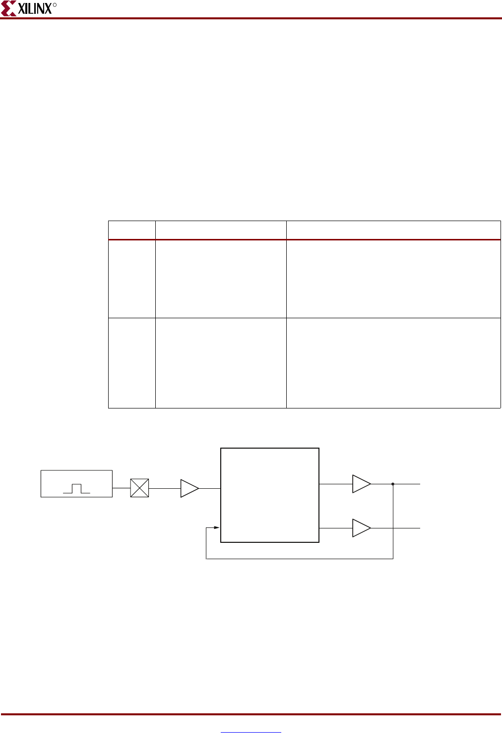
326 www.xilinx.com Memory Interface Solutions User Guide
UG086 (v3.6) September 21, 2010
Chapter 8: Implementing DDR2 SDRAM Controllers
R
Global Clock Architecture
The user must supply a system clock running at the target frequency for the memory. This
clock can be either single-ended or differential. User can select single-ended or differential
clock input option from MIG GUI. Differential clocks are connected to the IBUFGDS and
the single-ended clock is connected to IBUFG.
The system clock from the output of the IBUFGDS or the IBUFG is connected to the DCM
to generate the various clocks used by the memory interface logic.
The DCM generates two separate synchronous clocks for use in the design, as shown in
Table 8-5 and Figure 8-8. The clock structure is same for both the example design and the
user design. For designs with out DCM instantiation, the DCM and the BUFGs should be
instantiated at the user end to generate the required clocks.
Table 8-5: DDR2 Interface Design Clocks
Clock Description Logic Domain
clk0 Skew compensated replica
of the input system clock.
The clock for the controller and the user
interface logic, most of the DDR2 bus-related
I/O flip-flops (e.g., memory clock,
control/address). This is also used to register
the address and command signals from the
user interface.
clk90 90° phase-shifted version of
clk0
Used in the user interface logic, the write data
path section of physical layer, write path
control logic and output flip-flops for DQ and
DM. This is also used to register data from the
user interface and generate the read data and
read data valid signals for the user interface
logic.
Figure 8-8: Clocking Scheme for DDR2 Interface Logic
CLKIN
C
LKFB CLK90
CLK0
clk_90
clk_0
DCM BUFG
GC I/O
SYSTEM CLK
UG086_c8_11_071608
Memory Interface Solutions User Guide www.xilinx.com 327
UG086 (v3.6) September 21, 2010
Interface Signals
R
Interface Signals
Table 8-6 shows the DDR2 SDRAM interface signals, directions, and descriptions. The
signal direction is with respect to the DDR2 SDRAM controller. The cntrl0_ddr2_reset_n
signal is present only for registered DIMMs, and the cntrl0_ddr2_dqs_n signal is present
when DQS# Enable is selected in the Extended Mode register.
Table 8-6: DDR2 SDRAM Interface Signal Descriptions
Signal Name Signal Direction Description
cntrl0_DDR2_A Output Address
cntrl0_DDR2_DQ Input/Output Data
cntrl0_DDR2_DQS Input/Output Data Strobe
cntrl0_ddr2_dqs_n Input/Output Data Strobe
cntrl0_DDR2_RAS_N Output Command
cntrl0_DDR2_CAS_N Output Command
cntrl0_DDR2_WE_N Output Command
cntrl0_DDR2_BA Output Bank Address
cntrl0_DDR2_CK Output Clock
cntrl0_DDR2_CK_N Output Inverted Clock
cntrl0_DDR2_CS_N Output Chip Select
cntrl0_DDR2_CKE Output Clock Enable
cntrl0_DDR2_DM Output Data Mask
cntrl0_DDR2_ODT Output On-Die Termination
cntrl0_ddr2_reset_n Output Reset
328 www.xilinx.com Memory Interface Solutions User Guide
UG086 (v3.6) September 21, 2010
Chapter 8: Implementing DDR2 SDRAM Controllers
R
Table 8-7 describes the DDR2 SDRAM controller system interface signals. Except for the
cntlr0_led_error_ouput1 signal, all other signals in Table 8-7 are present in designs either
with or without testbenches. The cntrl0_led_error_ouput1 signal is present only in designs
with a testbench.
Table 8-7: DDR2 SDRAM Controller System Interface Signals
Signal Names Direction Description
sys_clk and sys_clkb Input
These signals are the system clock differential
signals. They are driven from the user
application for designs with DCMs. These two
signals are given to a differential buffer, and the
output of the differential buffer is connected to
a clock’s DCM. The DCM generates the required
clocks to the design modules. These signals are
not present when the design is generated
without a DCM. When there is no DCM, the
user application should drive the required
clocks to the design.
reset_in_n Input
This is the system reset signal. By default, this
signal is active Low. The parameter file contains
a parameter called RESET_ACTIVE_LOW. An
active-High reset input can be selected by
changing this parameter to 0.
cntrl0_led_error_ouput1 Output This signal is asserted when there is a read data
mismatch with the write data. This signal is
usually used to connect the LED on the
hardware to indicate a data error.
cntrl0_data_valid_out Output This signal is asserted when there is valid read
data in the read FIFO. The signal LED error
output is generated when this signal is High
and there is a data mismatch. This signal can be
driven to a status LED on the hardware.
cntrl0_rst_dqs_div_in Input This loopback signal is connected to the
contrl0_rst_dqs_div_out signal on the board.
Refer to XAPP768c [Ref 24] for the functionality
of this signal.
cntrl0_rst_dqs_div_out Output This loopback signal is connected to the
cntrl0_rst_dqs_div_in signal on the board.
dcm_lock Input This signal is present only in designs without a
DCM.
cntrl0_init_done Output The DDR2 SDRAM controller asserts this signal
to indicate that the DDR2 SDRAM initialization
is complete.
Memory Interface Solutions User Guide www.xilinx.com 329
UG086 (v3.6) September 21, 2010
Interface Signals
R
Table 8-8 describes the DDR2 SDRAM controller system interface signals in designs
without a testbench.
Table 8-8: DDR2 SDRAM Controller User Interface Signals (without a Testbench)
Signal Names Direction(1) Description
cntrl0_user_input_data[(2n–1):0] Input
This bus is the write data to the DDR2 SDRAM from the user
interface, where n is the width of the DDR2 SDRAM data bus.
The DDR2 SDRAM controller converts single data rate to
double data rate on the physical layer side. The data is valid
on the DDR2 SDRAM write command. In 2n, the MSB is
rising-edge data and the LSB is falling-edge data.
cntrl0_user_data_mask[(2m–1):0] Input
This bus is the data mask for write data. Like user_input_data,
it is twice the size of the data mask bus at memory, where m is
the size of the data mask at the memory interface. In 2m, the
MSB applies to rising-edge data and the LSB applies to falling-
edge data.
cntrl0_user_input_address
[(ROW_ADDRESS +
COLUMN_ADDRESS +
BANK_ADDRESS – 1):0](2)
Input
This bus consists of the row address, the column address, and
the bank address for DDR2 SDRAM writes and reads. The
address sequence starting from the LSB is bank address,
column address, and row address.
cntrl0_user_command_register[2:0] Input
Supported user commands for the DDR2 SDRAM controller:
cntrl0_burst_done Input
This signal is used to terminate read or write command. This
signal must be asserted after the last address for two clocks for
BL=4 and for four clocks for BL =8. The DDR2 SDRAM
controller supports write burst or read burst capability for a
single row. The user must terminate the transfer on a column
boundary and must re-initialize the controller for the next row
of transactions on a column boundary.
cntrl0_user_output_data[(2n–1):0] Output
This is the read data from the DDR2 SDRAM. The DDR2
SDRAM controller converts the DDR data from the DDR2
SDRAM to SDR data. As the DDR data is converted to SDR
data, the width of this bus is 2n, where n is data width of the
DDR2 SDRAM data bus.
cntrl0_user_data_valid Output When asserted, this signal indicates user_output_data[(2n–
1):0] is valid.
user_command[2:0] User Command Description
000 NOP
010 Initialize memory
100 Write Request
110 Read Request
Others Reserved
330 www.xilinx.com Memory Interface Solutions User Guide
UG086 (v3.6) September 21, 2010
Chapter 8: Implementing DDR2 SDRAM Controllers
R
Resource Utilization
A local inversion clocking technique is used in this design. The DCM generates only clk0
and clk90. One DCM and two BUFGMUXs are used. The Spartan-3 generation FPGA
designs operate at 166 MHz and below.
DDR2 SDRAM Initialization
Before issuing the memory read and write commands, the controller initializes the DDR2
SDRAM using the memory initialization command. The user can give the initialization
command only after all reset signals are deactivated. The controller is in the reset state for
200 µs after power up. For design optimization, a 200 µs timer is generated from the refresh
counter. The refresh timer is a function of frequency. Therefore, at lower frequencies, the
200 µs timer waits more than 200 µs. Because wait200 happens only during the power-up
sequence, design performance is not degraded. All resets are asserted for 200 µs because
DDR2 SDRAM requires a 200 µs delay prior to applying an executable command after all
cntrl0_user_cmd_ack Output
This is the acknowledgement signal for a user read or write
command. It is asserted by the DDR2 SDRAM controller
during a write or read to/from the DDR2 SDRAM. The user
should not issue any new commands to the controller until
this signal is deasserted.
cntrl0_init_done Output The DDR2 SDRAM controller asserts this signal to indicate
that the DDR2 SDRAM initialization is complete.
cntrl0_auto_ref_req(3) Output
This signal is asserted based on the frequency. For example,
for a frequency of 166 MHz, the signal is asserted every
~7.6 µs. It is asserted until the controller issues an auto-refresh
command to the memory. Upon seeing this signal, the user
should terminate any ongoing command after the current
burst transaction by asserting the cntrl0_burst_done signal.
The frequency with which this signal is asserted is determined
by the MAX_REF_CNT value in parameter file.
cntrl0_auto_ref_req indicates the refresh request to the
memory, and cntrl0_ar_done indicates completion of the auto-
refresh command.
cntrl0_ar_done(3) Output
This indicates that the auto-refresh command was completed
to DDR2 SDRAM. The DDR2 SDRAM controller asserts this
signal for one clock after giving an auto-refresh command to
the DDR2 SDRAM and completion of TRFC time. The TRFC
time is determined by the rfc_count_value value in the
parameter file. The user can assert the next command any time
after the assertion of the cntrl0_ar_done signal.
Notes:
1. All of the signal directions are with respect to the DDR2 SDRAM controller.
2. Linear addressing is used, i.e., the row address immediately follows the column address bits, and the bank address follows the row
address bits, thus supporting more devices. The number of address bits used depends on the density of the memory part. The
controller ignores the unused bits, which can all be tied High.
3. For more information on auto refresh, refer to “Auto Refresh,” page 335.
Table 8-8: DDR2 SDRAM Controller User Interface Signals (without a Testbench) (Cont’d)
Signal Names Direction(1) Description
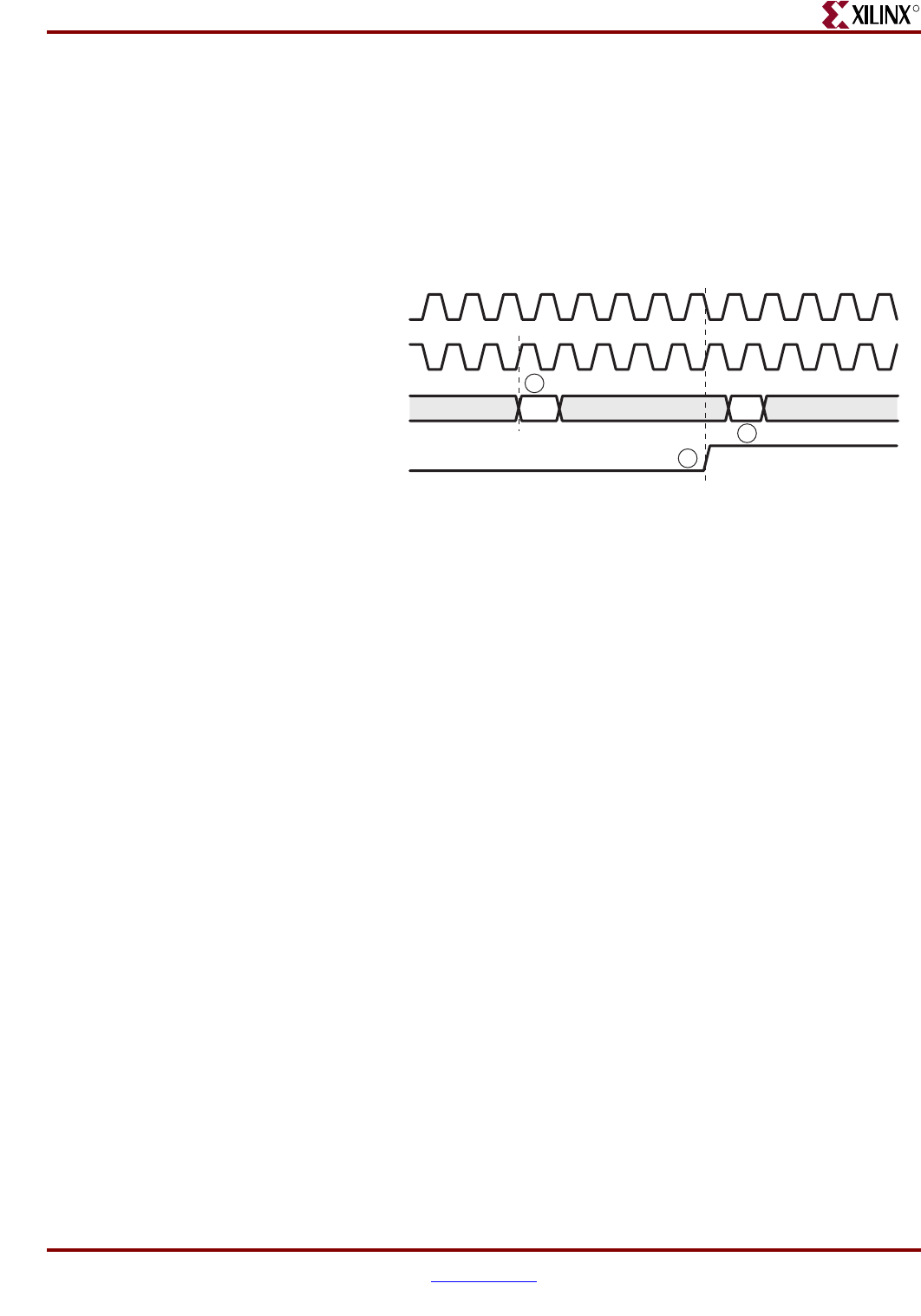
Memory Interface Solutions User Guide www.xilinx.com 331
UG086 (v3.6) September 21, 2010
Interface Signals
R
power supply and reference voltages are stable. The controller asserts clock-enable to
memory after 200 µs.
Load mode parameters are to be selected from the GUI while generating the design. These
parameters are updated by MIG in the parameter file. When the INIT command is
executed, the DDR2 SDRAM controller passes these values to the Memory Load Mode
register. When the DDR2 SDRAM is initialized, the DDR2 SDRAM controller asserts the
init_done signal.
Figure 8-9 shows the timing for the memory initialization command.
1. The user places the initialization command on user_command_register[2:0] on a
falling edge of clk0 for one clock cycle. This starts the initialization sequence.
2. The DDR2 SDRAM controller indicates that the initialization is complete by asserting
the init_done signal on a falling edge of clk0. The init_done signal is asserted
throughout the period.
3. After init_done is asserted, the user can pass the next command at any time.
DDR2 SDRAM Write and Read Operations
In Spartan FPGA designs, prior to issuing a read or write operation, the user must assert
the first address and command simultaneously and wait for a command acknowledge
signal. The assertion time of the command acknowledge varies depending on the
controller status. After the command acknowledge is asserted, the user waits for three
clock cycles before sending the next address. This three clock cycle time is the Active-to-
Command (tRCD) delay for a read or write command as defined in the memory
specification. Subsequent addresses are sent once every two clock cycles for a burst length
of four.
If user clock domain is different from clk0 and clk90 of MIG, then user has to synchronize
all the user interface signals to the clk0 and clk90 that are shown in Figure 8-10, page 332
and Figure 8-11, page 333.
I
Figure 8-9: DDR2 SDRAM Initialization
clk0
clk180
user_command_register
init_done
010 Cmd
UG086_c8_08_091007
2
1
3
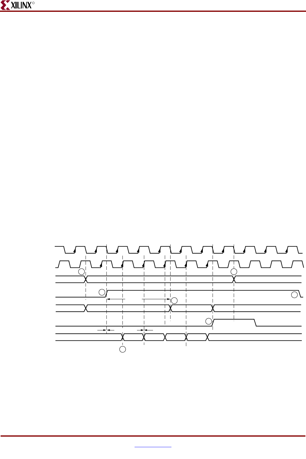
332 www.xilinx.com Memory Interface Solutions User Guide
UG086 (v3.6) September 21, 2010
Chapter 8: Implementing DDR2 SDRAM Controllers
R
Write
Figure 8-10 shows the timing diagram for a write to DDR2 SDRAM for a burst length of
four. The user initiates the write command by sending a Write instruction to the DDR2
SDRAM controller. To terminate a write burst, the user asserts the burst_done signal for
two clocks after the last user_input_address. The burst_done signal should be asserted for
two clocks for burst lengths of four and four clocks for burst lengths of eight.
The write command is asserted on the falling edge of clk0. In response to a write
command, the DDR2 SDRAM controller acknowledges with the usr_cmd_ack signal on a
falling edge of clk0. If the controller is busy with a refresh, the usr_cmd_ack signal is not
asserted until after the refresh command cycle completes. The user asserts the first address
(row + column + bank address) with the write command and keeps it asserted for three
clocks after usr_cmd_ack assertion. Any subsequent write addresses are asserted on
alternate falling edges of clk0 after deasserting the first memory address for a burst length
of four, and it is asserted once in four clocks for a burst length of eight. The first user data
is asserted on a rising edge of clk90 after usr_cmd_ack is asserted. As the SDR data is
converted to DDR data, the width of this bus is 2n, where n is data width of DDR2 SDRAM
data bus.
For a burst length of four, only two data words (each of 2n) are given to the DDR2 SDRAM
controller for each user address, and four data words are given for a burst length of eight.
Internally, the DDR2 SDRAM controller converts into four data words for a burst length of
four and eight data words for a burst length of eight, each of n bits. To terminate the write
burst, the user asserts burst_done on a rising edge of clk180 for two clocks for a burst
length of four and four clocks for a burst length of eight. The burst_done signal is asserted
after the last memory address. Any further commands to the DDR2 SDRAM controller are
given only after the usr_cmd_ack signal is deasserted. After burst_done is asserted, the
controller terminates the burst and issues a precharge to the memory. The usr_cmd_ack
signal is deasserted after completion of the precharge.
1. A memory write is initiated by issuing a write command to the DDR2 SDRAM
controller. The write command must be asserted on a falling edge of clk0.
2. The DDR2 SDRAM controller acknowledges the write command by asserting the
user_cmd_ack signal on a falling edge of clk0. The user_cmd_ack signal is asserted a
minimum of one clock cycle after the write command is asserted. If the controller is
Figure 8-10: DDR2 SDRAM Write Burst, Burst Lengths of Four and Two Bursts
clk90
WRITE Command (3’b100)
Addr1
3 CLKs
Addr2
D0,D1 D2,D3D4,D5 D6,D7
user_command_register
burst_done
user_input_data
user_cmd_ack
user_input_address
clk0
UG086_c8_09_010108
3
5
6
7
4
2
1
(CLK180) (CLK90)1.75 CLKs
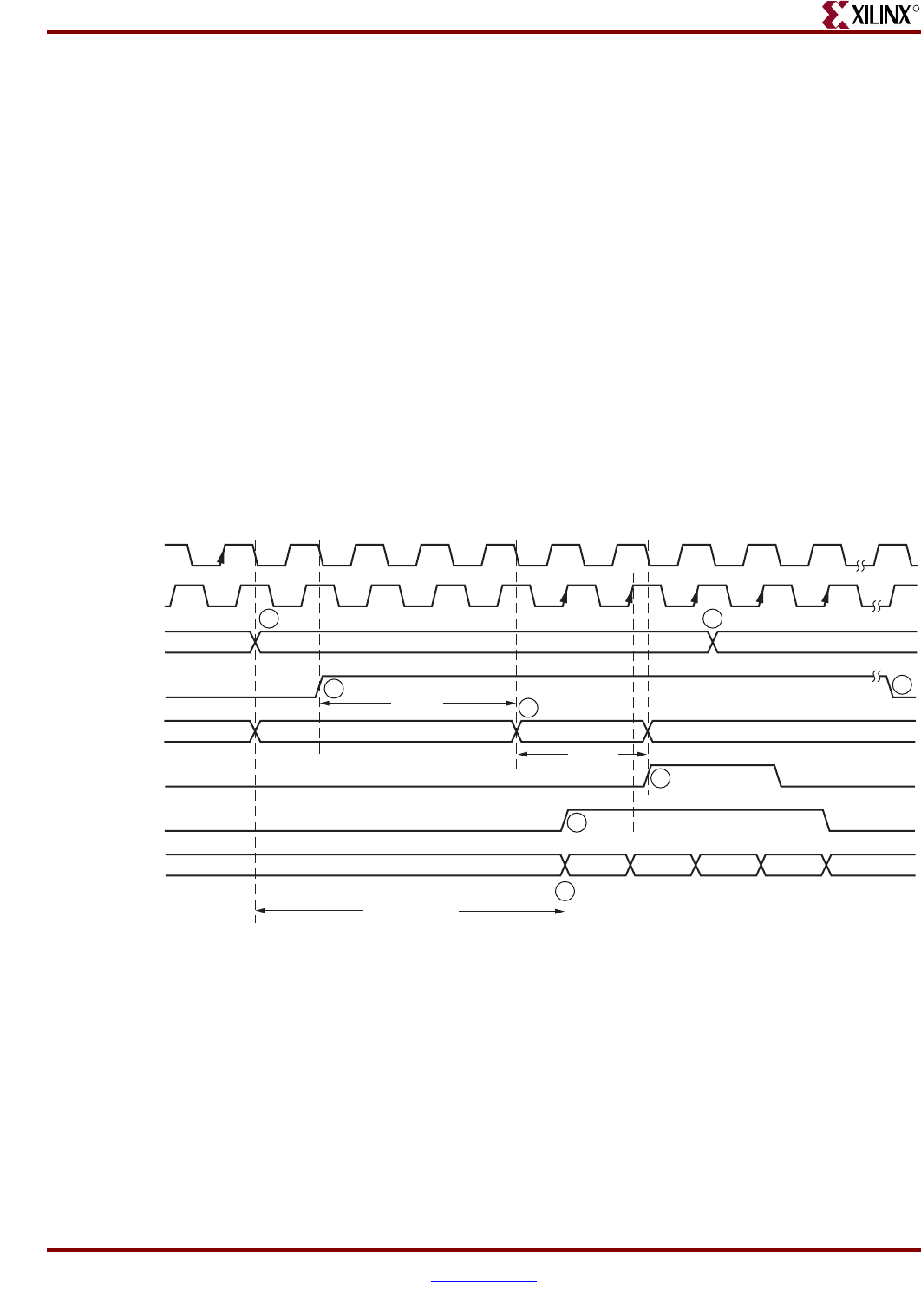
Memory Interface Solutions User Guide www.xilinx.com 333
UG086 (v3.6) September 21, 2010
Interface Signals
R
busy with a refresh, the usr_cmd_ack signal is not asserted until after the refresh
command cycle completes.
3. The first user_input_address must be placed along with the command. The input data
is asserted with the clk90 signal after the user_cmd_ack signal is asserted.
4. The user asserts the first address (row + column +bank address) with the write
command and keeps it asserted for three clocks after usr_cmd_ack assertion. The
user_input_address signal is asserted on a falling edge of clk0. All subsequent
addresses are asserted on alternate falling edges of clk0.
5. To terminate the write burst, burst_done is asserted after the last user_input_address.
The burst_done signal is asserted for two clock cycles.
6. The user command is deasserted after burst_done is asserted.
7. The controller deasserts the user_cmd_ack signal after completion of precharge to the
memory. The next command must be given only after user_cmd_ack is deasserted.
Back-to-back write operations are supported only within the same bank and row.
Read
The user initiates a memory read with a read command to the DDR2 SDRAM controller.
Figure 8-11 shows the memory read timing diagram for a burst length of four.
The user provides the first memory address with the read command, and subsequent
memory addresses upon receiving the usr_cmd_ack signal. Data is available on the user
data bus with the user_data_valid signal. To terminate read burst, the user asserts the
burst_done signal on a falling edge of clk0 for two clocks with the deassertion of the last
user_input_address. All subsequent addresses are asserted on alternate clocks for burst
lengths of four, and subsequent addresses are asserted once every four clock cycles for
burst lengths of eight.
For burst lengths of four, the burst_done signal is asserted for two clocks after the last
address and for four clocks for burst lengths of eight.
Figure 8-11: DDR2 SDRAM Read, Burst Lengths of Four and Two Bursts
clk90
Read Command
Addr1
3 CLKs
Addr2
2 CLKs
D0,D1 D2,D3D4,D5 D6,D7
user_command_
register
burst_done
user_data_valid
user_output_data
user_cmd_ack
user_input_
address
clk0
UG086_c8_10_030510
4
5
6
7
8
3
2
1
Read Latency
334 www.xilinx.com Memory Interface Solutions User Guide
UG086 (v3.6) September 21, 2010
Chapter 8: Implementing DDR2 SDRAM Controllers
R
The read command flow is similar to the write command flow.
1. A memory read is initiated by issuing a read command to the DDR2 SDRAM
controller. The read command is accepted on a falling edge of clk0.
2. The first read address must be placed along with the read command. In response to the
read command, the DDR2 SDRAM controller asserts the user_cmd_ack signal on a
falling edge of clk0. The user_cmd_ack signal is asserted a minimum of one clock cycle
after the read command is asserted. If the controller is busy with a refresh, the
usr_cmd_ack signal is not asserted until after the refresh command cycle completes.
3. The user asserts the first address (row + column + bank address) with the read
command and keeps it asserted for three clocks after usr_cmd_ack is asserted. The
user_input_address signal is then accepted on the falling edge of clk0. All subsequent
memory read addresses are asserted on alternate falling edges of clk0.
4. The data on user_output_data is valid only when the user_data_valid signal is
asserted.
5. The data read from the DDR2 SDRAM is available on user_output_data, which is
asserted with clk90. Because the DDR2 SDRAM data is converted to SDR data, the
width of this bus is 2n, where n is the data width of the DDR2 SDRAMs. For a read
burst length of four, the DDR2 SDRAM controller outputs only two data words with
each user address.
6. To terminate the read burst, burst_done is asserted for two clocks on the falling edge of
clk0. The burst_done signal is asserted after the last memory address.
7. The user command is deasserted after burst_done is asserted.
8. The controller deasserts the user_cmd_ack signal after completion of precharge to the
memory. Any further commands to the DDR2 SDRAM controller should be given after
user_cmd_ack is deasserted. Back-to-back read operations are supported only within
the same bank and row. Approximately 17 clock cycles pass between the time a read
command is asserted on the user interface and the time data becomes available on the
user interface.
Table 8-9 shows the read latency for CL = 3.
In general, read latency varies based on the following parameters:
•CAS latency
• If the user issue the commands before initialization is complete, the latency cannot be
determined
Table 8-9: Read Command to Read Data Latency
Parameter Number of Clocks
User read command to command ack 1
Command ack to active command 3
Active to read command 3
Memory read command to data valid 10
Tot al c l o c k s 17

Memory Interface Solutions User Guide www.xilinx.com 335
UG086 (v3.6) September 21, 2010
Interface Signals
R
Auto Refresh
The DDR2 SDRAM controller does a memory refresh at intervals determined by the
frequency. For example, for a frequency of 166 MHz, an auto-refresh request is raised every
~7.6 µs. The user must terminate any ongoing commands when auto_ref_req flag is
asserted after the current burst transaction by asserting the burst_done signal. The
auto_ref_req flag is asserted until the controller issues a refresh command to the memory.
The user must wait for completion of the auto-refresh command before giving any
commands to the controller when auto_ref_req is asserted.
The ar_done signal is asserted by the DDR2 SDRAM controller upon completion of the
auto-refresh command—i.e., after TRFC time. The ar_done signal is asserted on the falling
edge of clk0 for one clock cycle.
The controller sets the MAX_REF_CNT value in the parameter file according to the
frequency and selected memory component for a refresh interval (7.7 µs). The
rfc_count_value setting in the parameter file defines TRFC, the time between the refresh
command to Active or another refresh command.
After completion of the auto-refresh command, the next command can be given any time
after ar_done is asserted.
The current testbench generates five consecutive write bursts followed by five read burst
commands. For every group of five write/read commands, the controller issues an active
command followed by five write/read commands, and then a precharge command to the
memory. All five burst commands take up a maximum of 20 clock cycles. After every
precharge command, the controller state machine goes to an idle state and checks for an
auto_ref_req. When an auto_ref_req is asserted, the controller issues an auto refresh
command to the memory if it is in an idle state. In the worst case, the controller takes
20 clocks to go from burst_done to the auto refresh command and to the memory. The
controller issues auto refresh commands to the memory within 40 clock cycles after
auto_ref_req is asserted. Because the delay from auto_ref_req to the refresh command to
the memory is within the specified number of clocks even in the worst case scenario, the
testbench does not need to terminate the write or read transaction on the auto_ref_req
signal.
For example, at 77 MHz, an auto_ref_req is generated every 7.292 µs, and at 166 MHz, it is
generated every 7.572 µs. The MAX_REF_CNT parameter is set to the following values at
77 MHz and 166 MHz frequencies to allow 40 clock cycles of delay from auto_ref_req to
the refresh command:
Average periodic refresh = 7.8125 µs
MAX_REF_CNT = (7812.5 ns – 40 × clk_period)/clk_period
At 77 MHz (13 ns): MAX_REF_CNT = (7812.5 ns – 40 × 13)/13 = 7292.5/13 = 560
At 166 MHz (6 ns): MAX_REF_CNT = (7812.5ns – 40 × 6)/6 = 7572.5/6 = 1262
User transactions should be terminated within 20 clock cycles of the auto_ref_req signal
being asserted. The ar_done signal is asserted for one clock period by the controller on
completion of an auto refresh command (i.e., after TRFC time). Normal read and write
commands can be issued to the controller any time after ar_done is asserted.
Changing the Refresh Rate
Change the global `define (for Verilog) or constant (for VHDL) variable MAX_REF_CNT in
mymodule_parameters_0.v (or .vhd) so that MAX_REF_CNT = (refresh interval in

336 www.xilinx.com Memory Interface Solutions User Guide
UG086 (v3.6) September 21, 2010
Chapter 8: Implementing DDR2 SDRAM Controllers
R
clock periods) = (refresh interval) / (clock period). For example, for a refresh rate of 7.7 µs
with a memory bus running at 133 MHz:
MAX_REF_CNT = 7.7 µs / (clock period) = 7.7 µs / 7.5 ns = 1026 (decimal) = 0x402
If the above value exceeds 2MAX_REF_WIDTH – 1, the value of MAX_REF_WIDTH must be
increased accordingly in parameters_0.v (or .vhd) to increase the width of the counter
used to track the refresh interval.
Load Mode
MIG does not support the LOAD MODE command.
UCF Constraints
Some constraints are required to successfully create the design. The following examples
explain the different constraints in the UCF for XST.
Calibration Circuit Constraints
All LUTs in the matched delay circuits are constrained to specific locations in the device.
Example:
INST "infrastructure_top0/cal_top0/tap_dly0/l0" RLOC=X0Y6;
INST "infrastructure_top0/cal_top0/tap_dly0/l0" U_SET =
delay_calibration_chain;
INST "infrastructure_top0/cal_top0/tap_dly0/gen_tap1[0].r" RLOC=X0Y6;
INST "infrastructure_top0/cal_top0/tap_dly0/gen_tap1[0].r" U_SET =
delay_calibration_chain;
INST "infrastructure_top0/cal_top0/tap_dly0/gen_tap1[1].r" RLOC=X0Y6;
INST "infrastructure_top0/cal_top0/tap_dly0/gen_tap1[1].r" U_SET =
delay_calibration_chain;
Data and Data Strobe Constraints
Data and data strobe signals are assigned to specific pins in the device; placement
constraints related to the dqs_delay circuit and the FIFOs used for the data_read module
are specified.
Example:
NET "cntrl0_DDR2_DQS[0]" LOC = Y6;
INST "ddr2_top0/data_path0/data_read_controller0/gen_delay[0].dqs_delay_col0/
one" LOC = SLICE_X0Y110;
INST "ddr2_top0/data_path0/data_read_controller0/gen_delay[0].dqs_delay_col0/
one" BEL = F;
NET "cntrl0_DDR2_DQ[0]" LOC = Y5;
INST "ddr2_top0/data_path0/data_read0/gen_strobe[0].strobe/fifo0_bit0" LOC =
SLICE_X2Y111;
MAXDELAY Constraints
The MAXDELAY constraints define the maximum allowable delay on the net. Following
are the list of MAXDELAY constraints used in Spartan FPGA designs in the UCF on
different nets. The values provided here vary depending on FPGA family and the device
type. Some values are dependent on frequency. The constraints shown here are from
example_design. The hierarchy paths of the nets are different between
example_design and user_design.

Memory Interface Solutions User Guide www.xilinx.com 337
UG086 (v3.6) September 21, 2010
Interface Signals
R
NET "infrastructure_top0/cal_top0/tap_dly0/tap[7]" MAXDELAY = 350ps;
NET "infrastructure_top0/cal_top0/tap_dly0/tap[15]" MAXDELAY = 350ps;
NET "infrastructure_top0/cal_top0/tap_dly0/tap[23]" MAXDELAY = 350ps;
These constraints are used to minimize the tap delay inverter connection wire length. This
delay should be minimized to calibrate the delay of a tap (LUT element) accurately. These
values are independent of frequency and vary from family to family and device to device.
Without these constraints, the tool might synthesize longer routes between the tap
connections. Inappropriate delays in this circuit could cause the design to fail in hardware.
NET "main_00/top0/dqs_int_delay_in*" MAXDELAY = 675ps;
This constraint is used for the DQS nets from the I/O pad to the input of the LUT delay
chain. Without this constraint, the nets take unpredictable delays that affect the Data Valid
window. In Spartan-3 generation FPGA designs, data is latched using the DQS signal. In
order to latch the correct data, DQS is delayed using LUT delay elements to center-align
with respect to the input read data. Incorrect data could be latched if the delays on this net
are unpredictable. Unpredictable delays might also cause the design to have intermittent
failures, which are difficult to debug in hardware.
NET "main_00/top0/dqs_div_rst" MAXDELAY = 460ps;
The net dqs_div_rst is the loopback signal. This signal is used as an enable for read data
FIFOs and FIFO write pointers after it is delayed using the LUT delay elements. The
overall delay on this net should be comparable with the delay on the DQS signal. This net
is constrained to control the overall delay. Both the dqs_div_rst and DQS signals take
similar paths. If the delay on the dqs_div_rst signal is higher, the first read data from
memory might be missed.
NET
"main_00/top0/data_path0/data_read_controller0/gen_delay*dqs_delay_col
*/delay*" MAXDELAY = 140ps;
NET
"main_00/top0/data_path0/data_read_controller0/rst_dqs_div_delayed/
delay*" MAXDELAY = 140 ps;
These constraints are required to minimize the wire delays between the LUT elements of a
LUT delay chain that is used to delay the DQS and rst_dqs_div loopback signal. Higher
wire delays between LUT delay elements can shift the data valid window, which in turn
can cause incorrect data to be latched. Therefore, the MAXDELAY constraint is required for
these nets.
NET "main_00/top0/data_path0/data_read_controller0/rst_dqs_div"
MAXDELAY = 3383 ps;
NET "main_00/top0/data_path0/data_read0/fifo*_wr_en*"
MAXDELAY = 3007ps;
These constraints are required because these paths are not constrained otherwise. The total
delay on the rst_dqs_div and fifo_wr_en nets must not exceed the clock period. The total
delay on both the nets is set to 85% of the clock period, leaving 15% as margin. These
delays vary with frequency.
NET "main_00/top0/data_path0/data_read0/fifo*_wr_addr[*]"
MAXDELAY = 5610ps;
The MAXDELAY constraint is required on FIFO write address because this path is not
constrained otherwise. This is a single clock cycle path. It is set to 80% of the clock period,
leaving 20% as margin because this net generally meets the required constraint.

338 www.xilinx.com Memory Interface Solutions User Guide
UG086 (v3.6) September 21, 2010
Chapter 8: Implementing DDR2 SDRAM Controllers
R
The FROM-TO constraints are:
NET "infrastructure_top0/clk_dcm0/clk" TNM_NET = "clk0";
NET "main_00/top0/data_path0/dqs_delayed_col*" TNM_NET = "dqs_clk";
TIMESPEC "TS_CLK" = FROM "clk0" TO "dqs_clk" 18 ns DATAPATHONLY;
NET "infrastructure_top0/clk_dcm0/clk90" TNM_NET = "clk90";
TIMESPEC "TS_CLK90" = FROM "dqs_clk" TO "clk90" 18 ns DATAPATHONLY;
NET "main_00/top0/data_path0/data_read_controller0/gen_wr_en*
fifo*_wr_en_inst/clk"
TNM_NET = "fifo_we_clk";
TIMESPEC "TS_WE_CLK" = FROM "dqs_clk" TO "fifo_we_clk" 5 ns
DATAPATHONLY;
NET "main_00/top0/data_path0/data_read_controller0/gen_wr_addr*fifo*
_wr_addr_inst/clk" TNM_NET = "fifo_waddr_clk";
TIMESPEC "TS_WADDR_CLK" = FROM "dqs_clk" TO "fifo_waddr_clk" 5 ns
DATAPATHONLY;
These paths are not the real timing paths in the design context. To get rid of unconstrained
paths, FROM-TO constraints are used. The values used here are not related to the design
clock period, but are chosen such that no violations are reported. There is no restriction on
these values, and the constraints can always be relaxed if there are any timing violations.
I/O Banking Rules
There are I/O banking rules to be followed for I/O pin allocations, stating that the I/O
signals allocated in a bank should adhere to compatible I/O standards. Refer to the “Rules
Concerning Banks” section for additional information regarding I/O banking rules in
DS099 [Ref 28].
Design Notes
The DDR2 SDRAM design is not validated on hardware. The MAXDELAY constraints in
the UCF are set based on the selected frequency.
Calibration circuit details and data capture techniques are covered in XAPP768c [Ref 24].
Tool Output
When the design is generated from the tool, it outputs docs, example_design, and
user_design folders. The example_design consists of the design with test_bench,
and user_design consists of the design without test_bench. Each folder contains
rtl,par, synth, and sim folders. The sim folder contains simulation files for the
generated design. The sim folder contains the external testbench, memory model, and .do
file to simulate the generated design. The memory model files are currently generated in
Verilog only. To learn more details about the files in the sim folder and to simulate the
design, refer to “Simulation Guide,” page 499.
For single-rank DIMMs, MIG outputs only the base part memory model. In the simulation
testbench (sim_tb_top in the sim folder), MIG instantiates the required number of
memory models. For example, a 1 GB single-rank DIMM with the base part is 1 Gb, and
MIG instantiates the base model eight times. If the MIG generated memory model is to be
used with the user’s test bench, multiple instances should be used based on the selected
configuration.
The MIG output memory model considers the MEM_BITS parameter by default for
memory range allocation. This covers only a partial memory range, i.e., 2MEM_BITS. To
Memory Interface Solutions User Guide www.xilinx.com 339
UG086 (v3.6) September 21, 2010
DDR2 SDRAM Signal Allocations
R
allocate the full memory range, the MAX_MEM parameter should be set in the memory
model, which in turn sets the full_mem_bits parameter for memory allocation. Allocating
the full memory range might exceed the memory of the operating system, thus causing
memory allocation failure in simulations.
DDR2 SDRAM Signal Allocations
MIG allows banks to be selected for different classes of memory signals. Table 8-10 shows
the list of signals allocated in a group from bank selection checkboxes.
Supported Devices
The design generated out of MIG is independent of memory speed grade, hence the
package part of the memory component is replaced with X, where X indicates a don't care
condition. See Appendix G, “Low Power Options.”
The tables below list the components (Table 8-11) and DIMMs (Table 8-12 through
Table 8-14) supported by the tool for Spartan-3 FPGA DDR2 local clocking designs.
Table 8-10: DDR2 SDRAM Signal Allocations
Bank Selected Signals Allocated in the Group
Address Memory address and memory control
Data Data, data mask, data strobes and memory clock signals
System Control System reset from user interface and status signals
System Clock System clocks from the user interface
Table 8-11: Supported Components for DDR2 SDRAM Local Clocking
(Spartan-3 FPGAs)
Components Packages (XX) Components Packages (XX)
MT47H64M4XX-3 BP MT47H16M16XX-3 BG
MT47H64M4XX-37E BP MT47H16M16XX-37E BG
MT47H64M4XX-5E BP MT47H16M16XX-5E BG
MT47H128M4XX-3 B6,CB,GB MT47H32M16XX-3 BN,CC,FN,GC
MT47H128M4XX-37E B6,CB,GB MT47H32M16XX-37E BN,CC,FN,GC
MT47H128M4XX-5E B6,CB,GB MT47H32M16XX-5E BN,CC,FN,GC
MT47H256M4XX-3 BT,HQ MT47H64M16XX-3 BT,HR
MT47H256M4XX-37E BT,HQ MT47H64M16XX-37E BT,HR
MT47H256M4XX-5E BT,HQ MT47H64M16XX-5E BT,HR
MT47H512M4XX-3 HG MT47H128M16XX-3 HG
MT47H512M4XX-37E HG MT47H128M16XX-37E HG
MT47H512M4XX-5E HG MT47H128M16XX-5E --
MT47H32M8XX-3 BP HYB18T1G800XXXX-3S BF,BFL,BC
MT47H32M8XX-37E BP HYB18T1G800XXXX-37 BF,BFL,BC
MT47H32M8XX-5E BP HYB18T1G160XXXX-3S BF,BFV,BFL,BC
340 www.xilinx.com Memory Interface Solutions User Guide
UG086 (v3.6) September 21, 2010
Chapter 8: Implementing DDR2 SDRAM Controllers
R
MT47H64M8XX-3 B6,CB,F6,GB HYB18T1G160XXXX-37 BF,BFV,BFL,BC
MT47H64M8XX-37E B6,CB,F6,GB HYB18T1G400XXXX-3S BF,BFL,BC
MT47H64M8XX-5E B6,CB,F6,GB HYB18T1G400XXXX-37 BF,BFL,BC
MT47H128M8XX-3 BT,HQ HYB18T512800XXXX-3S B2F,B2C,B2FL
MT47H128M8XX-37E BT,HQ HYB18T512800XXXX-37 B2F,B2C,B2FL
MT47H128M8XX-5E BT,HQ HYB18T512160XXXX-3S B2F,B2C,B2FL
MT47H256M8XX-3 HG HYB18T512160XXXX-37 B2F,B2C,B2FL
MT47H256M8XX-37E HG HYB18T512400XXXX-3S B2F,B2C,B2FL
MT47H256M8XX-5E HG HYB18T512400XXXX-37 B2F,B2C,B2FL
Table 8-12: Supported Unbuffered DIMMs for DDR2 SDRAM Local Clocking
(Spartan-3 FPGAs)
Unbuffered DIMMs
MT4HTF1664AY-667 MT8HTF6464AY-40E
MT4HTF1664AY-40E MT8HTF12864AY-667
MT4HTF1664AY-53E MT8HTF12864AY-40E
MT4HTF3264AY-667 MT8HTF12864AY-53E
MT4HTF3264AY-40E MT9HTF3272AY-667
MT4HTF3264AY-53E MT9HTF3272AY-40E
MT4HTF6464AY-667 MT9HTF3272AY-53E
MT4HTF6464AY-40E MT9HTF6472AY-667
MT4HTF6464AY-53E MT9HTF6472AY-53E
MT8HTF6464AY-667 MT9HTF6472AY-40E
MT8HTF6464AY-53E --
Table 8-13: Supported Registered DIMMs for DDR2 SDRAM Local Clocking
(Spartan-3 FPGAs)
Registered DIMMs
MT9HTF3272Y-53E MT18HTF6472Y-53E
MT9HTF3272PY-53E MT18HTF6472PY-53E
MT9HTF3272Y-40E MT18HTF6472Y-40E
MT9HTF3272PY-40E MT18HTF6472PY-40E
MT9HTF6472Y-53E MT18HTF12872Y-53E
MT9HTF6472PY-53E MT18HTF12872PY-53E
MT9HTF6472Y-40E MT18HTF12872Y-40E
MT9HTF6472PY-40E MT18HTF12872PY-40E
MT9HTF12872Y-53E MT18HTF25672Y-53E
Table 8-11: Supported Components for DDR2 SDRAM Local Clocking
(Spartan-3 FPGAs) (Cont’d)
Components Packages (XX) Components Packages (XX)
Memory Interface Solutions User Guide www.xilinx.com 341
UG086 (v3.6) September 21, 2010
Supported Devices
R
The tables below list the components (Table 8-15) and DIMMs (Table 8-16 through
Table 8-18) supported by the tool for Spartan-3A/AN FPGA DDR2 local clocking designs.
MT9HTF12872PY-53E MT18HTF25672PY-53E
MT9HTF12872Y-40E MT18HTF25672Y-40E
MT9HTF12872PY-40E MT18HTF25672PY-40E
MT18HTF6472G-53E --
Table 8-14: Supported SODIMMs for DDR2 SDRAM Local Clocking
(Spartan-3 FPGAs)
SODIMMs
MT4HTF1664HY-667 MT8HTF3264HY-53E
MT4HTF1664HY-53E MT8HTF3264HY-40E
MT4HTF1664HY-40E MT8HTF6464HY-667
MT4HTF3264HY-667 MT8HTF6464HY-53E
MT4HTF3264HY-53E MT8HTF6464HY-40E
MT4HTF3264HY-40E MT9HTF12872CHY-667
MT8HTF3264HY-667 MT9HTF12872CHY-53E
Table 8-15: Supported Components for DDR2 SDRAM Local Clocking
(Spartan-3A/AN FPGAs)
Components Packages (XX) Components Packages (XX)
MT47H64M4XX-3 BP MT47H16M16XX-3 BG
MT47H64M4XX-37E BP MT47H16M16XX-37E BG
MT47H64M4XX-5E BP MT47H16M16XX-5E BG
MT47H128M4XX-3 B6,CB,GB MT47H32M16XX-3 BN,CC,FN,GC
MT47H128M4XX-37E B6,CB,GB MT47H32M16XX-37E BN,CC,FN,GC
MT47H128M4XX-5E B6,CB,GB MT47H32M16XX-5E BN,CC,FN,GC
MT47H256M4XX-3 BT,HQ MT47H64M16XX-3 BT,HR
MT47H256M4XX-37E BT,HQ MT47H64M16XX-37E BT,HR
MT47H256M4XX-5E BT,HQ MT47H64M16XX-5E BT,HR
MT47H512M4XX-3 HG MT47H128M16XX-3 HG
MT47H512M4XX-37E HG MT47H128M16XX-37E HG
MT47H512M4XX-5E HG MT47H128M16XX-5E --
MT47H32M8XX-3 BP HYB18T1G800XXXX-3S BF,BFL,BC
MT47H32M8XX-37E BP HYB18T1G800XXXX-37 BF,BFL,BC
MT47H32M8XX-5E BP HYB18T1G160XXXX-3S BF,BFV,BFL,BC
MT47H64M8XX-3 B6,CB,F6,GB HYB18T1G160XXXX-37 BF,BFV,BFL,BC
Table 8-13: Supported Registered DIMMs for DDR2 SDRAM Local Clocking
(Spartan-3 FPGAs) (Cont’d)
Registered DIMMs
342 www.xilinx.com Memory Interface Solutions User Guide
UG086 (v3.6) September 21, 2010
Chapter 8: Implementing DDR2 SDRAM Controllers
R
MT47H64M8XX-37E B6,CB,F6,GB HYB18T1G400XXXX-3S BF,BFL,BC
MT47H64M8XX-5E B6,CB,F6,GB HYB18T1G400XXXX-37 BF,BFL,BC
MT47H128M8XX-3 BT,HQ HYB18T512800XXXX-3S B2F,B2C,B2FL
MT47H128M8XX-37E BT,HQ HYB18T512800XXXX-37 B2F,B2C,B2FL
MT47H128M8XX-5E BT,HQ HYB18T512160XXXX-3S B2F,B2C,B2FL
MT47H256M8XX-3 HG HYB18T512160XXXX-37 B2F,B2C,B2FL
MT47H256M8XX-37E HG HYB18T512400XXXX-3S B2F,B2C,B2FL
MT47H256M8XX-5E HG HYB18T512400XXXX-37 B2F,B2C,B2FL
Table 8-16: Supported Unbuffered DIMMs for DDR2
SDRAM Local Clocking (Spartan-3A/AN FPGAs)
Unbuffered DIMMs
MT4HTF1664AY-667 MT8HTF6464AY-40E
MT4HTF1664AY-40E MT8HTF12864AY-667
MT4HTF1664AY-53E MT8HTF12864AY-40E
MT4HTF3264AY-667 MT8HTF12864AY-53E
MT4HTF3264AY-40E MT9HTF3272AY-667
MT4HTF3264AY-53E MT9HTF3272AY-53E
MT4HTF6464AY-667 MT9HTF3272AY-40E
MT4HTF6464AY-40E MT9HTF6472AY-667
MT4HTF6464AY-53E MT9HTF6472AY-53E
MT8HTF6464AY-667 MT9HTF6472AY-40E
MT8HTF6464AY-53E --
Table 8-17: Supported Registered DIMMs for DDR2 SDRAM Local Clocking
(Spartan-3A/AN FPGAs)
Registered DIMMs
MT9HTF3272Y-53E MT9HTF6472Y-40E
MT9HTF3272PY-53E MT9HTF6472PY-40E
MT9HTF3272Y-40E MT9HTF12872Y-53E
MT9HTF3272PY-40E MT9HTF12872PY-53E
MT9HTF6472Y-53E MT9HTF12872Y-40E
MT9HTF6472PY-53E MT9HTF12872PY-40E
Table 8-15: Supported Components for DDR2 SDRAM Local Clocking
(Spartan-3A/AN FPGAs)
Components Packages (XX) Components Packages (XX)

Memory Interface Solutions User Guide www.xilinx.com 343
UG086 (v3.6) September 21, 2010
Supported Devices
R
Table 8-18: Supported SODIMMs for DDR2 SDRAM
Local Clocking (Spartan-3A/AN FPGAs)
SODIMMs
MT4HTF1664HY-667 MT8HTF3264HY-53E
MT4HTF1664HY-53E MT8HTF3264HY-40E
MT4HTF1664HY-40E MT8HTF6464HY-667
MT4HTF3264HY-667 MT8HTF6464HY-53E
MT4HTF3264HY-53E MT8HTF6464HY-40E
MT4HTF3264HY-40E MT9HTF12872CHY-667
MT8HTF3264HY-667 MT9HTF12872CHY-53E
344 www.xilinx.com Memory Interface Solutions User Guide
UG086 (v3.6) September 21, 2010
Chapter 8: Implementing DDR2 SDRAM Controllers
R
The tables that follow list the components (Table 8-19) and DIMMs (Table 8-20 and
Table 8-21) supported by the tool for Spartan-3A DSP FPGA DDR2 local clocking designs.
Table 8-19: Supported Components for DDR2 SDRAM Local Clocking
(Spartan-3A DSP FPGAs)
Components Packages (XX) Components Packages (XX)
MT47H64M4XX-3 BP MT47H16M16XX-3 BG
MT47H64M4XX-37E BP MT47H16M16XX-37E BG
MT47H64M4XX-5E BP MT47H16M16XX-5E BG
MT47H128M4XX-3 B6,CB,GB MT47H32M16XX-3 BN,CC,FN,GC
MT47H128M4XX-37E B6,CB,GB MT47H32M16XX-37E BN,CC,FN,GC
MT47H128M4XX-5E B6,CB,GB MT47H32M16XX-5E BN,CC,FN,GC
MT47H256M4XX-3 BT,HQ MT47H64M16XX-3 BT,HR
MT47H256M4XX-37E BT,HQ MT47H64M16XX-37E BT,HR
MT47H256M4XX-5E BT,HQ MT47H64M16XX-5E BT,HR
MT47H512M4XX-3 HG MT47H128M16XX-3 HG
MT47H512M4XX-37E HG MT47H128M16XX-37E HG
MT47H512M4XX-5E HG MT47H128M16XX-5E --
MT47H32M8XX-3 BP HYB18T1G800XXXX-3S BF,BFL,BC
MT47H32M8XX-37E BP HYB18T1G800XXXX-37 BF,BFL,BC
MT47H32M8XX-5E BP HYB18T1G160XXXX-3S BF,BFV,BFL,BC
MT47H64M8XX-3 B6,CB,F6,GB HYB18T1G160XXXX-37 BF,BFV,BFL,BC
MT47H64M8XX-37E B6,CB,F6,GB HYB18T1G400XXXX-3S BF,BFL,BC
MT47H64M8XX-5E B6,CB,F6,GB HYB18T1G400XXXX-37 BF,BFL,BC
MT47H128M8XX-3 BT,HQ HYB18T512800XXXX-3S B2F,B2C,B2FL
MT47H128M8XX-37E BT,HQ HYB18T512800XXXX-37 B2F,B2C,B2FL
MT47H128M8XX-5E BT,HQ HYB18T512160XXXX-3S B2F,B2C,B2FL
MT47H256M8XX-3 HG HYB18T512160XXXX-37 B2F,B2C,B2FL
MT47H256M8XX-37E HG HYB18T512400XXXX-3S B2F,B2C,B2FL
MT47H256M8XX-5E HG HYB18T512400XXXX-37 B2F,B2C,B2FL
Table 8-20: Supported Unbuffered DIMMs for DDR2
SDRAM Local Clocking (Spartan-3A DSP FPGAs)
Unbuffered DIMMs
MT4HTF1664AY-667 MT4HTF6464AY-40E
MT4HTF1664AY-40E MT4HTF6464AY-53E
MT4HTF1664AY-53E MT8HTF6464AY-667
MT4HTF3264AY-667 MT8HTF6464AY-53E
MT4HTF3264AY-40E MT8HTF6464AY-40E
MT4HTF3264AY-53E MT8HTF12864AY-667
MT4HTF6464AY-667 --
Memory Interface Solutions User Guide www.xilinx.com 345
UG086 (v3.6) September 21, 2010
Supported Devices
R
Maximum Data Widths
Table 8-22 provides the maximum data widths for Spartan-3 FPGAs. Table 8-23 provides
the maximum data widths for Spartan-3E FPGAs. Table 8-24 provides the maximum data
widths for single-ended DQS Spartan-3A FPGAs (differential DQS is disabled). Table 8-25
provides the maximum data widths for differential DQS Spartan-3A FPGAs (differential
DQS is enabled). Table 8-26 provides the maximum data widths for differential DQS
Spartan-3AN FPGAs (single/differential DQS is enabled). Table 8-27 provides the
maximum data widths for differential DQS Spartan-3A DSP FPGAs (single/differential
DQS is enabled). All the supported data width tables have the Mask Enable option
enabled.
Table 8-21: Supported SODIMMs for DDR2 SDRAM
Local Clocking (Spartan-3A DSP FPGAs)
SODIMMs
MT4HTF1664HY-667 MT8HTF3264HY-53E
MT4HTF1664HY-53E MT8HTF3264HY-40E
MT4HTF1664HY-40E MT8HTF6464HY-667
MT4HTF3264HY-667 MT8HTF6464HY-53E
MT4HTF3264HY-53E MT8HTF6464HY-40E
MT4HTF3264HY-40E --
MT8HTF3264HY-667 --
Table 8-22: Spartan-3 FPGA Maximum Data Width for DDR and DDR2 Memories
Serial
Number FPGA
Maximum Data Width when Data, Address, and Control are Allocated in...
...Different Banks ...the Same Bank
Bank
2
Bank
3
Bank
6
Bank
7Left Right Bank
2
Bank
3
Banks
6/7 Left Right
1XC3S50CP132 0000880 0 0 0 0
2 XC3S50PQ208 0 0 0 0 8 8 0 0 0 0 0
3 XC3S50TQ144 0 0 0 0 8 8 0 0 0 0 0
4 XC3S200FT256 8 8 8 8 16 16 0 0 0 8 8
5 XC3S200PQ208 0 8 0 0 16 16 0 0 0 0 0
6 XC3S200TQ144 0 0 0 0 8 8 0 0 0 0 0
7 XC3S400FG320 8 8 8 8 24 24 0 0 0 16 16
8 XC3S400FG456 16 8 16 8 32 24 0 0 0 16 16
9 XC3S400FT256 8 8 8 8 16 16 0 0 0 8 8
10 XC3S400PQ208 0 0 0 0 8 8 0 0 0 0 0
11 XC3S400TQ144 0 0 0 0 8 8 0 0 0 0 0
12 XC3S1000FG320 8 8 8 8 24 24 0 0 0 16 16
13 XC3S1000FG456 16 16 16 16 48 48 8 8 8 32 32
14 XC3S1000FG676 24 24 24 24 48 48 8 8 8 32 32
346 www.xilinx.com Memory Interface Solutions User Guide
UG086 (v3.6) September 21, 2010
Chapter 8: Implementing DDR2 SDRAM Controllers
R
15 XC3S1000FT256 8 8 8 8 16 16 0 0 0 8 8
16 XC3S1500FG320 8 8 8 8 24 24 0 0 0 16 16
17 XC3S1500FG456 16 16 16 16 48 48 8 8 8 40 40
18 XC3S1500FG676 32 32 32 32 72 72 16 16 16 48 48
19 XC3S2000FG456 16 16 16 16 48 48 8 8 8 32 32
20 XC3S2000FG676 32 32 32 32 72 72 16 16 16 56 56
21 XC3S2000FG900 32 32 32 40 72 72 24 24 24 64 64
22 XC3S4000FG676 24 32 32 32 72 72 16 16 16 56 48
23 XC3S4000FG900 40 40 40 40 72 72 32 32 32 72 72
24 XC3S4000FG1156 48 48 48 48 72 72 32 32 32 72 72
25 XC3S5000FG676 24 24 24 32 64 64 16 16 16 48 48
26 XC3S5000FGG676 24 24 24 32 64 64 16 16 16 48 48
27 XC3S5000FG900 40 40 40 40 72 72 32 32 32 72 72
28 XC3S5000FG1156 56 56 48 56 72 72 40 40 40 72 72
Table 8-22: Spartan-3 FPGA Maximum Data Width for DDR and DDR2 Memories (Cont’d)
Serial
Number FPGA
Maximum Data Width when Data, Address, and Control are Allocated in...
...Different Banks ...the Same Bank
Bank
2
Bank
3
Bank
6
Bank
7Left Right Bank
2
Bank
3
Banks
6/7 Left Right
Table 8-23: Spartan-3E FPGA Maximum Data Width for DDR SDRAMs
Serial
Number FPGA
Maximum Data Width when Data, Address, and
Control are Allocated in...
...Different Banks ...the Same Bank
Left Right Left/Right
1 XC3S100ECP132 8 8 0
2 XC3S100ETQ144 8 8 0
3 XC3S250ECP132 8 0 0
4 XC3S250EFT256 16 16 0
5 XC3S250EPQ208 16 16 0
6 XC3S250ETQ144 8 8 0
7 XC3S500ECP132 8 0 0
8 XC3S500EFG320 24 24 8
9 XC3S500EFT256 16 16 8
10 XC3S500EPQ208 8 8 0
11 XC3S1200EFG320 16 16 16
12 XC3S1200EFG400 32 32 16
13 XC3S1200EFT256 16 8 8
14 XC3S1600EFG320 16 16 8
Memory Interface Solutions User Guide www.xilinx.com 347
UG086 (v3.6) September 21, 2010
Supported Devices
R
15 XC3S1600EFG400 24 32 16
16 XC3S1600EFG484 48 40 32
Table 8-24: Spartan-3A FPGA Single-Ended DQS Maximum Data Width
(Differential DQS Disabled)
Serial
Number FPGA
Maximum Data Width when Data, Address, and
Control are Allocated in...
...Different Banks ...the Same Bank
Left/Right Left Right
1 XC3S50ATQ144 8 0 0
2XC3S50AFT256 8 0 0
3 XC3S200AFT256 16 8 8
4 XC3S200AFG320 16 16 16
5 XC3S400AFT256 16 8 8
6 XC3S400AFG320 24 8 16
7 XC3S400AFG400 32 16 16
8 XC3S700AFT256 16/8 0 0
9 XC3S700AFG400 32 16 16
10 XC3S700AFG484 40 24 32
11 XC3S1400AFT256 16/8 0 0
12 XC3S1400AFG484 40 24 32
13 XC3S1400AFG676 72 48 48
Table 8-25: Spartan-3A FPGA Differential DQS Maximum Data Width
(Differential DQS Enabled)
Serial
Number FPGA
Maximum Data Width when Data, Address, and
Control are Allocated in...
...Different Banks ...the Same Bank
Left Right Left Right
1XC3S50ATQ1448800
2 XC3S200AFG320 24 24 8 16
3 XC3S200AFT256 16 24 8 8
4 XC3S400AFG320 24 24 8 16
5 XC3S400AFG400 32 32 16 16
6 XC3S400AFT256 16 16 8 8
Table 8-23: Spartan-3E FPGA Maximum Data Width for DDR SDRAMs (Cont’d)
Serial
Number FPGA
Maximum Data Width when Data, Address, and
Control are Allocated in...
...Different Banks ...the Same Bank
Left Right Left/Right
348 www.xilinx.com Memory Interface Solutions User Guide
UG086 (v3.6) September 21, 2010
Chapter 8: Implementing DDR2 SDRAM Controllers
R
7 XC3S700AFG400 24 32 16 16
8 XC3S700AFG484 40 40 24 32
9 XC3S1400AFG484 40 40 24 32
10 XC3S1400AFG676 64 64 48 48
11 XC3S50AFT256 8 8 0 0
12 XC3S700AFT256 16 8 0 0
13 XC3S1400AFT256 16 8 0 0
Table 8-26: Spartan-3AN FPGA DQS Maximum Data Width
(Single/Differential DQS Enabled)
Serial
Number FPGA
Maximum Data Width when Data, Address, and
Control are Allocated in...
...Different Banks ...the Same Bank
Left Right Left Right
1XC3S50ANTQG1448800
2 XC3S50ANFTG256 8 8 0 0
3 XC3S200ANFTG256 16 24 8 8
4 XC3S400ANFGG400 32 32 16 16
5 XC3S700ANFGG484 40 40 24 32
6 XC3S1400ANFGG676(1) 64 64 48 48
Notes:
1. For the XC3S1400ANFGG676 part, MIG can generate 72-bit single-ended DQS RDIMM with address
and data on different banks.
Table 8-27: Spartan-3A DSP FPGA DQS Maximum Data Width (Single/Differential
DQS Enabled)
Serial
Number FPGA
Maximum Data Width when Data, Address, and
Control are Allocated in...
...Different Banks ...the Same Bank
Left Right Left Right
1 XC3SD1800A-CS484 32 32 16 16
2 XC3SD3400A-CS484 32 32 16 16
3 XC3SD1800A-FG676 64 64 48 48
4 XC3SD3400A-FG676 64 64 48 48
Table 8-25: Spartan-3A FPGA Differential DQS Maximum Data Width
(Differential DQS Enabled) (Cont’d)
Serial
Number FPGA
Maximum Data Width when Data, Address, and
Control are Allocated in...
...Different Banks ...the Same Bank
Left Right Left Right
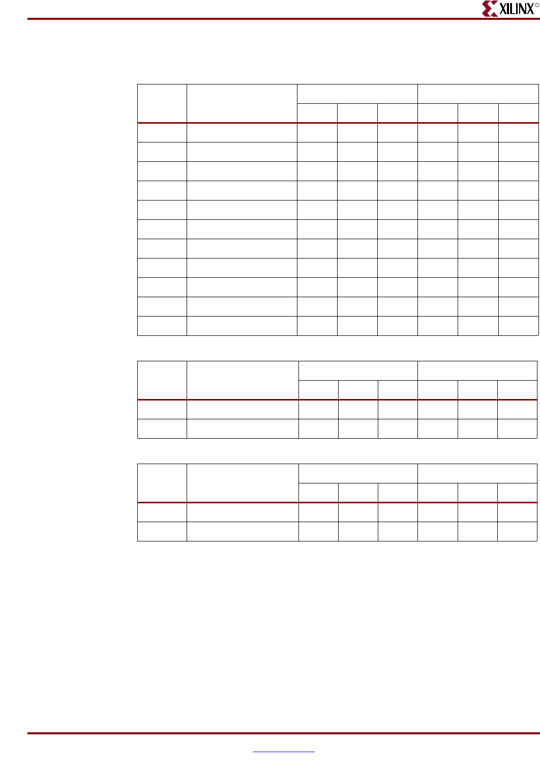
Memory Interface Solutions User Guide www.xilinx.com 349
UG086 (v3.6) September 21, 2010
Supported Devices
R
DIMM Support for Spartan-3 Generation Devices
Note: Spartan-3E devices do not support 64-bit or 72-bit DIMMs.
Table 8-28: DIMM Support for Spartan-3 Devices
Serial
Number FPGA 64-bit DIMM 72-bit DIMM
x4 x8 x16 x4 x8 x16
1 XC3S1500FG676 No Yes Yes No Yes Yes
2 XC3S2000FG676 No Yes Yes No Yes Yes
3 XC3S4000FG676 No Yes Yes No Yes Yes
4 XC3S5000FG676 No Yes Yes No No No
5 XC3S2000FG900 Yes Yes Yes Yes Yes Yes
6 XC3S4000FG900 Yes Yes Yes Yes Yes Yes
7 XC3S5000FG900 Yes Yes Yes Yes Yes Yes
8 XC3S4000FG1156 Yes Yes Yes Yes Yes Yes
9 XC3S5000FG1156 Yes Yes Yes Yes Yes Yes
10 XC3S1500LFG676 No Yes Yes No Yes Yes
11 XC3S4000LFG900 Yes Yes Yes Yes Yes Yes
Table 8-29: DIMM Support for Spartan-3A and Spartan-3AN Devices
Serial
Number FPGA
64-bit DIMM 72-bit DIMM
x4 x8 x16 x4 x8 x16
1 XC3S1400AFG676 No Yes Yes No Yes Yes
2 XC3S1400ANFGG676 No Yes Yes No Yes Yes
Table 8-30: DIMM Support for Spartan-3A DSP Devices
Serial
Number FPGA 64-bit DIMM 72-bit RDIMM
x4 x8 x16 x4 x8 x16
1 XC3SD1800AFG676 No Yes Yes No No No
2 XC3SD3400AFG676 No Yes Yes No No No
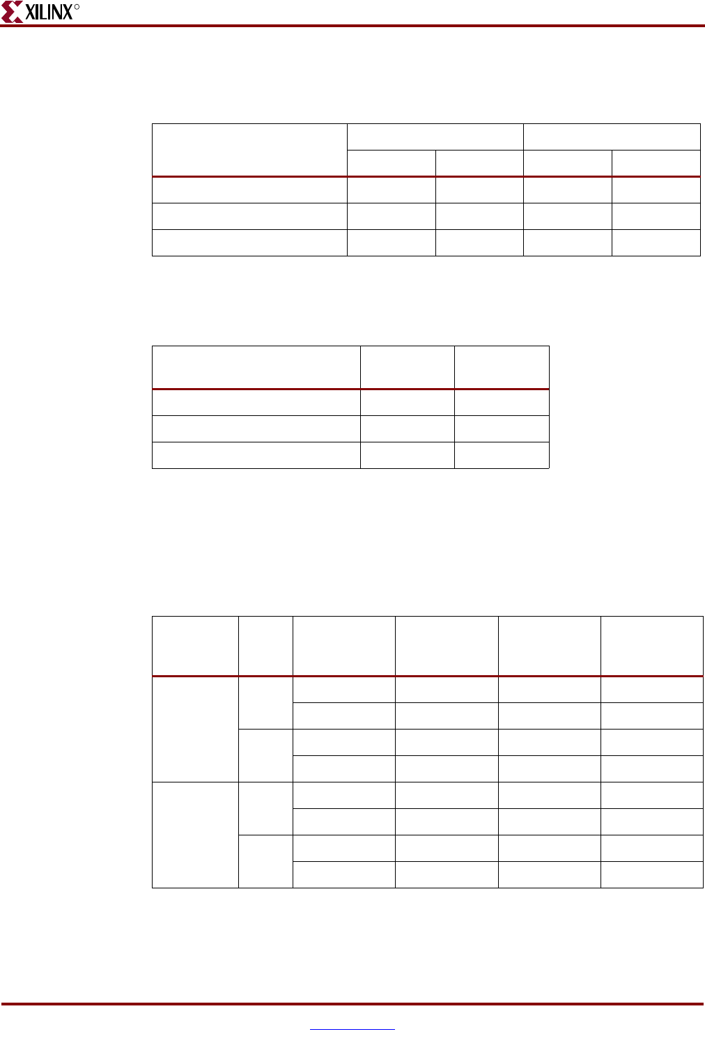
350 www.xilinx.com Memory Interface Solutions User Guide
UG086 (v3.6) September 21, 2010
Chapter 8: Implementing DDR2 SDRAM Controllers
R
Design Frequency Range in MHz for Spartan-3 Generation Devices
Supported IO Standards
Table 8-33 shows the I/O standards supported for MIG generated Spartan FPGA families.
Table 8-31: Spartan-3 Generation FPGA Component Controllers
FPGA Family DDR SDRAM DDR2 SDRAM
≤32-bit > 32-bit ≤32-bit >32-bit
Spartan-3A/3AN/3A DSP 166 166 166 166
Spartan-3E 166 166 NS NS
Spartan-3 166 133 166 133
Notes:
NS = not supported.
Table 8-32: Spartan-3 Generation FPGA DIMM Controllers
FPGA Family DDR SDRAM DDR2
SDRAM
Spartan-3A/3AN/3A DSP 166 166
Spartan-3E NS NS
Spartan-3 133 133
Notes:
1. NS = not supported.
Table 8-33: Supported I/O Standards for MIG-Generated Spartan FPGA Families
Standard Vcco Drive/Class
Spartan-
3A/3AN/3A
DSP
Spartan-3E Spartan-3
LVCMOS
1.8V 8MA All Banks All Banks All Banks
16MA Banks 1/3 All Banks All Banks
2.5V 12MA All Banks All Banks All Banks
24MA Banks 1/3 All Banks All Banks
SSTL
1.8V I All Banks All Banks All Banks
II All Banks (1) - All Banks
2.5V I All Banks All Banks All Banks
II All Banks (1) - All Banks
Memory Interface Solutions User Guide www.xilinx.com 351
UG086 (v3.6) September 21, 2010
Supported Devices
R
DIFF_SSTL
1.8V I All Banks All Banks -
II All Banks (2) - -
2.5V I All Banks All Banks -
II All Banks (2) - All Banks
LVDS 2.5V - All Banks (3) All Banks All Banks
Notes:
1. Outputs are restricted to banks 1 and 3. Inputs are unrestricted.
2. These high-drive outputs are restricted to banks 1 and 3. Inputs are unrestricted.
3. These differential outputs are restricted to banks 0 and 2. Inputs are unrestricted.
Table 8-33: Supported I/O Standards for MIG-Generated Spartan FPGA Families
Standard Vcco Drive/Class
Spartan-
3A/3AN/3A
DSP
Spartan-3E Spartan-3
352 www.xilinx.com Memory Interface Solutions User Guide
UG086 (v3.6) September 21, 2010
Chapter 8: Implementing DDR2 SDRAM Controllers
R
Hardware Tested Configurations
The frequencies shown in Table 8-34 were achieved on the Spartan-3A FPGA Starter Kit
under nominal conditions. This frequency should not be used to determine the maximum
design frequency. The maximum design frequency supported in the MIG wizard is based
on a combination of the TRCE results for fabric timing on multiple device/package
combinations and I/O timing analysis using FPGA and memory timing parameters for a
64-bit interface.
The frequency shown in Table 8-35 was achieved on the Spartan-3A DSP FPGA 3400A
Development Board under nominal conditions. This frequency should not be used to
determine the design frequency. The maximum design frequency supported in the MIG
wizard is based a combination of the TRCE results for fabric timing on multiple
device/package combinations and I/O timing analysis using FPGA and memory timing
parameters for a 64-bit interface.
Table 8-34: Hardware Tested Configurations for Spartan-3A FPGA DDR2 SDRAM
Designs
Synthesis Tools XST
HDL Verilog and VHDL
FPGA Device XC3S700AFG484-4
Burst Lengths 4 and 8
CAS Latency (CL) 3
16-bit Design Tested on 16-bit Component “MT47H32M16XX-5E”
Frequency Range 25 MHz to 225 MHz
Table 8-35:
Hardware Tested Configurations for Spartan-3A DSP FPGA DDR2 SDRAM
Designs
Synthesis Tools XST
HDL Verilog and VHDL
FPGA Device XC3SD3400AFG676-4
Burst Lengths 4 and 8
CAS Latency (CL) 3
32-bit Design Tested on 64-bit SO DIMM “MT4HTF6464HY-667”
Frequency 133 MHz

Memory Interface Solutions User Guide www.xilinx.com 353
UG086 (v3.6) September 21, 2010
R
Section IV: Virtex-5 FPGA to Memory Interfaces
Chapter 9, “Implementing DDR2 SDRAM Controllers”
Chapter 10, “Implementing QDRII SRAM Controllers”
Chapter 11, “Implementing DDR SDRAM Controllers”
Chapter 12, “Implementing DDRII SRAM Controllers”

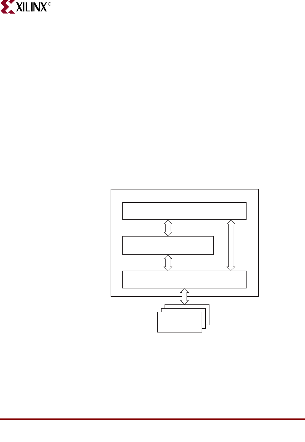
Memory Interface Solutions User Guide www.xilinx.com 355
UG086 (v3.6) September 21, 2010
R
Chapter 9
Implementing DDR2 SDRAM Controllers
This chapter describes how to implement DDR2 SDRAM interfaces for Virtex®-5 FPGAs
generated by MIG. The DDR2 SDRAM design supports frequencies up to 333 MHz. This
design is based on XAPP858 [Ref 27].
Interface Model
DDR2 SDRAM interfaces are source-synchronous and double data rate. They transfer data
on both edges of the clock cycle. A memory interface can be modularly represented as
shown in Figure 9-1. A modular interface has many advantages. It allows designs to be
ported easily and also makes it possible to share parts of the design across different types
of memory interfaces.
Figure 9-1: Modular Memory Interface Representation
Application Interface Layer
Xilinx FPGA
Physical Layer
Control Layer
UG086_c9_01_061606
Memories
356 www.xilinx.com Memory Interface Solutions User Guide
UG086 (v3.6) September 21, 2010
Chapter 9: Implementing DDR2 SDRAM Controllers
R
Feature Summary
This section summarizes the supported and unsupported features of the DDR2 SDRAM
controller design.
Supported Features
The DDR2 SDRAM controller design supports:
• Burst lengths of four and eight
• Sequential and interleaved burst types
• CAS latencies of 3, 4, and 5
• Additive latencies of 0, 1, 2, 3, and 4
• Differential DQS
•ODT
•Verilog and VHDL
• Byte wise data masking
• Precharge and auto refresh
• Bank management
• Linear addressing
•ECC
• Different memories (density/speed)
• Memory components, registered DIMMs, unbuffered DIMMs, and SODIMMs
• Deep support for Dual Rank DIMMs of value 2
• With and without a testbench
• With and without a PLL
• Multicontroller (DDR2) and Multiple Interfaces (DDR2 and QDRII)
• PPC440 pinout
•Data mask
• Two bytes per bank
• System clock, differential and single-ended
The supported features are described in more detail in “Architecture.”
Design Frequency Ranges
Table 9-1: Design Frequency Range in MHz
Memory
FPGA Speed Grade
-1 -2 -3
MinMaxMinMaxMinMax
Component 125 266 125 300 125 333
RDIMM 125 266 125 300 125 333
UDIMM or SODIMM(1) 125 266 125 266 125 266
Memory Interface Solutions User Guide www.xilinx.com 357
UG086 (v3.6) September 21, 2010
Architecture
R
Unsupported Features
The DDR2 SDRAM controller design does not support:
• Single-ended DQS
• Redundant DQS (RDQS)
• Deep support for components, single-rank DIMMs and deep value of 4
Architecture
Implemented Features
This section provides details on the supported features of the DDR2 SDRAM controller.
Burst Length
The DDR2 SDRAM controller supports burst lengths of four and eight. Through the “Set
mode register(s)” option, the burst length can be selected. For a design without a testbench
(user_design), the user has to provide bursts of the input data based on the chosen burst
length. Bits M2:M0 of the Mode Register define the burst length, and bit M3 indicates the
burst type (see the Micron data sheet). Read and write accesses to the DDR2 SDRAM are
burst-oriented. It determines the maximum number of column locations accessed for a
given READ or WRITE command.
CAS Latency
The DDR2 SDRAM controller supports CAS latencies of 3, 4, and 5. The CAS latency (CL)
can be selected in the “Set mode register(s)” option. CL is implemented in the phy_write
module. During data write operations, the generation of the dqs_oe_n and dqs_rst_n
signals varies according to the CL in the phy_write module. During read data operations,
the generation of the ctrl_rden signal varies according to the CL in the ctrl module. Bits
M4:M6 of the Mode Register define the CL (see the Micron data sheet). CL is the delay in
clock cycles between the registration of a READ command and the availability of the first
bit of output data.
Additive Latency
DDR2 SDRAM devices support a feature called posted CAS additive latency (AL). The
DDR2 SDRAM supports ALs of 0, 1, 2, 3, and 4. AL can be selected in the “Set mode
Deep Memory/Dual
Rank DIMM/Twin Die
Components
125 150 125 150 125 150
Notes:
1. It is possible to go faster than 266 MHz, but it requires care and IBIS simulations and possibly using
the parameter to send the CS out earlier depending on the load. For more details, see XAPP858
[Ref 27].
Table 9-1: Design Frequency Range in MHz (Cont’d)
Memory
FPGA Speed Grade
-1 -2 -3
MinMaxMinMaxMinMax

358 www.xilinx.com Memory Interface Solutions User Guide
UG086 (v3.6) September 21, 2010
Chapter 9: Implementing DDR2 SDRAM Controllers
R
register(s)” option. AL is implemented in the DDR2 SDRAM ctrl module. The ctrl module
issues READ/WRITE commands prior to tRCD (minimum) depending on the user-selected
AL value in the Extended Mode Register. This feature allows the READ command to be
issued prior to tRCD (minimum) by delaying the internal command to the DDR2 SDRAM
by AL clocks. Posted CAS AL makes the command and data bus efficient for sustainable
bandwidths in DDR2 SDRAM. Bits E3:E5 of the Extended Mode Register define the value
of AL (see the Micron data sheet).
Data Masking
DDR2 SDRAM design supports data masking per byte. Masking per nibble is not
supported due to the limitation of the internal block RAM based FIFOs. So, the masking of
data can be done on per byte basis. The mask data is stored in the Data FIFO along with the
actual data.
MIG supports a data mask option. If this option is checked in the GUI, MIG generates a
design with data mask pins. This option can be chosen if the selected part has data
masking. DDR2 SDRAM designs do not support read-modify-write operations in ECC
mode. The mask bits to the SDRAM should never be asserted while in the ECC mode.
Thus, when ECC is selected, the data masking selection is disabled in the GUI.
Precharge
The PRECHARGE command is used to close the open row in a bank if there is a command
to be issued in the same bank. The Virtex-5 FPGA DDR2 controller issues a PRECHARGE
command only if there is already an open row in the particular bank where a read or write
command is to be issued, thus increasing the efficiency of the design. The auto precharge
function is not supported in this design. The design ties the A10 bit Low during normal
reads and writes.
Auto Refresh
The auto refresh command is issued to the memory at specified intervals of time. The
memory issues an auto refresh command to refresh the charge to retain the data.
Bank Management
A Virtex-5 FPGA DDR2 SDRAM controller design supports bank management that
increases the efficiency of the design. The controller keeps track of whether the bank being
accessed already has an open row or not and also decides whether a PRECHARGE
command should be issued or not to that bank. When bank management is enabled via the
MULTI_BANK_EN parameter, a maximum of four banks/rows can open at any one time.
A least recently used (LRU) algorithm is employed to keep the three most recently used
banks and to close the least recently used bank when a new bank/row location needs to be
accessed. The bank management feature can also be disabled by clearing
MULTI_BANK_EN. For more information on Bank Management, refer to application note
XAPP858 [Ref 27].
Linear Addressing
The DDR2 SDRAM controller supports linear addressing. Linear addressing refers to the
way the user provides the address of the memory to be accessed. For Virtex-5 FPGA DDR2
SDRAM controllers, the user provides the address information through the app_af_addr
signal. As the densities of the memory devices vary, the number of column address bits
and row address bits also change. In any case, the row address bits in the app_af_addr
Memory Interface Solutions User Guide www.xilinx.com 359
UG086 (v3.6) September 21, 2010
Architecture
R
signal always start from the next higher bit, where the column address ends. This feature
increases the number of devices that can be supported with the design.
Different Memories (Density/Speed)
The DDR2 SDRAM controller supports different densities. For DDR2 components shown
in MIG, densities vary from 256 Mb to 2 Gb, and the DIMM densities vary from 256 Mb to
2 Gb. The user can select the various configurations from the “Create new memory part”
option. The supported maximum column address is 13, the maximum row address is 15,
and the maximum bank address is 3. The design can decode write and read addresses from
the user in the DDR2 SDRAM ctrl module. The user address consists of column, row, and
bank addresses.
Deep Memories
The MIG DDR2 SDRAM controller supports Dual Rank DIMMs with depth of 2. For deep
memory implementations, MIG generates chip selects, CKE signals, and ODT signals for
each memory. The clock widths (CK and CK_N) are a multiple factor of the deep
configuration chosen in MIG.
For deep memories, DDR2 SDRAMs are initialized one after the other to avoid loading the
address and control buses, and the calibration is done on the last memory. Apart from
initialization, the DDR2 SDRAM controller module also demultiplexes the column, row,
and bank addresses from the user address. The module also decodes the chip selects and
rank addresses for DIMMs.
On-Die Termination
The DDR2 SDRAM controller supports on-die termination (ODT). Through the “Set mode
register(s)” option from the GUI, the user can disable ODT or can choose 75, 150, or 50.
ODT can turn the termination on and off as needed to improves signal integrity in the
system.
ODT is only enabled on writes to DDR2 memory. It is disabled on read operations. One
single dual-rank DIMM is populated in a single slot. Rank 1 and Rank 2 of slot 1 or slot 2
are referred to as CS0 and CS1. ODT0 should be connected to the ODT signal of CS0 and
ODT1 should be connected to the ODT signal of CS1. ODT0 is enabled when writing to
CS0 or CS1. During read operations, the ODT is disabled. In this configuration, ODT for
CS1 is always off. Table 9-2 shows ODT control during write operations, and Table 9-3
shows ODT control during read operations.
Table 9-2: ODT Control during Writes
Configuration Write to DRAM at Slot 1 (ODT On/Off) DRAM at Slot 1 (ODT On/Off)
Slot 1 Slot 2 Rank 1 Rank 2 Rank 1 Rank 2
DR Empty Slot 1 On Off N/A N/A
Empty DR Slot 2 N/A N/A On Off
SR Empty Slot 1 On N/A N/A N/A
Empty SR Slot 2 N/A N/A On N/A
360 www.xilinx.com Memory Interface Solutions User Guide
UG086 (v3.6) September 21, 2010
Chapter 9: Implementing DDR2 SDRAM Controllers
R
Note: The Virtex-5 FPGA DDR2 interface requires that if parallel termination is used at the
memory end, it must be ODT rather than external termination resistor(s). This is a requirement of
the read capture scheme used. For more information on the need for ODT, refer to
XAPP858 [Ref 27].
Multicontrollers
MIG supports multicontrollers for DDR2 SDRAMs and multiple interfaces for
DDR2 SDRAMs and QDRII SRAMs. Up to eight controllers are supported. In
multicontroller and multiple interface designs, every controller can have a different
frequency. The number of controllers that can have different frequencies is limited by the
number of PLLs available in the selected FPGA. For example, a total of six PLL resources
are available for the XC5VLX50 device, so a maximum of six controllers can have different
frequencies. Even though the number of controllers selected in the GUI is eight, a
maximum of six controllers can have different frequencies. Thus, for the remaining two
controllers, the user should select one of the already selected frequencies. Refer to the
Virtex-5 FPGA User Guide [Ref 10] for PLL resources available for various devices.
For a single controller design, all memory and user interface signals appear as shown in
Figure 9-7 and Table 9-6 based on the selected part. For a multicontroller design, all
memory and user interface signal names are prepended with the controller number. For
example, for a two controller design (two DDR2 controllers), the ddr2_dq port appears as
c0_ ddr2_dq and c1_ ddr2_dq. A similar naming convention is followed for the parameters
provided in Table 9-2. Some parameters, such as HIGH_PERFORMANCE_MODE,
CLK_TYPE and RST_ACT_LOW, are common for all the controllers and do not have the
controller number prepended.
Two Bytes Per Bank
MIG supports Two Byte per bank option. If this option is checked in GUI, MIG allocates
only 2 bytes of Data in each bank. By default this option is unchecked and MIG allocated 3
bytes of Data in each bank.
System Clock
MIG supports differential and single-ended system clocks. Based on the selection in the
GUI, input system clocks and IDELAY clocks are differential or single-ended.
IODELAY Performance Mode
In Virtex-5 family devices, the power dissipation of the IODELAY elements can be
controlled using the HIGH_PERPORMANCE_MODE parameter. The values of this
parameter can be either TRUE or FALSE.
Table 9-3: ODT Control during Reads
Configuration
Read from
DRAM at Slot 1 (ODT On/Off) DRAM at Slot 2 (ODT On/Off)
Slot 1 Slot 2 Rank 1 Rank 2 Rank 1 Rank 2
DR Empty Slot 1 Off Off N/A N/A
Empty DR Slot 2 N/A N/A Off Off
SR Empty Slot 1 Off N/A N/A N/A
Empty SR Slot 2 N/A N/A Off N/A

Memory Interface Solutions User Guide www.xilinx.com 361
UG086 (v3.6) September 21, 2010
Architecture
R
When this parameter value is set to TRUE, the IODELAY jitter valuer per tap is reduced.
This reduction results in a slight increase in power dissipation from the IODELAY element.
When this parameter value is set to FALSE, the IODELAY power dissipation is reduced,
but with an increase in the jitter value per tap.
The value of this parameter can be selected from the MIG FPGA options page. Users can
also manually set this parameter value to TRUE or FALSE in the design top-level block
HDL module.
Refer to Appendix E, “Debug Port” for more information on the IODELAY Performance
Mode.
Generic Parameters
The DDR2 SDRAM design is a generic design that works for most of the features
mentioned above. User input parameters are defined as parameters for Verilog and
generics in VHDL in the design modules and are passed down the hierarchy. For example,
if the user selects a burst length of 4, then it is defined as follows in the <top_module>
module:
parameter BURST_LEN = 4, // burst length (in doublewords)
The user can change this parameter in <top_module> for various burst lengths to get the
desired output. The same concept applies to most of the other parameters listed in the
<top_module> module. The user cannot change REG_ENABLE and CLK_TYPE to reflect
those changes directly. The user should manually edit <top_module> for port connections
and other logical changes. Table 9-4 lists the details of all parameters.
362 www.xilinx.com Memory Interface Solutions User Guide
UG086 (v3.6) September 21, 2010
Chapter 9: Implementing DDR2 SDRAM Controllers
R
Table 9-4: Parameterization of DDR2 SDRAM Virtex-5 FPGA Design
Category Parameter Name Description Other Notes Value Restrictions
Memory
Width
BANK_WIDTH Number of memory bank
address bits
CKE_WIDTH Number of memory clock
enable outputs
CLK_WIDTH Number of differential
clock outputs
Determined by the number of
components/modules (one pair
per component)
COL_WIDTH Number of memory
column bits
CS_BITS log2(CS_NUM)
Used for chip-select related
address decode. See notes for
CS_NUM and CS_WIDTH.
CS_NUM Number of separate chip
selects
Different from CS_WIDTH. For
example, for a 32-bit data bus
consisting of 2 x16 parts, CS_NUM
= 1, but CS_WIDTH = 2 (that is, a
single chip select drives two
separate outputs, one for each
component)
CS_WIDTH /
CS_NUM = integer
CS_WIDTH Number of memory chip
selects
Determined by the number of
components/modules (one per
component)
CS_WIDTH /
CS_NUM = integer
DM_WIDTH Number of data mask bits
Can be different value than
DQS_WIDTH if x4 components
are used
(DQS_WIDTH *
DQ_PER_DQS)/8
DQ_BITS log2(DQS_WIDTH*DQ_P
ER_DQS)
Used for data bus calibration
decode
(DQ_WIDTH)/
Number of data bits
DQ_WIDTH Number of data bits
Must set to DQS_WIDTH *
DQ_PER_DQS. Equal to total
number of data bits, including
ECC bits.
DQS_WIDTH *
DQ_PER_DQS
DQ_PER_DQS Number of memory DQ
data bits per strobe
DQS_BITS log2(DQS_WIDTH)
DQS_WIDTH Number of memory DQS
strobes
ODT_WIDTH Number of ODT control
outputs
Determined by the number of
components/modules (one per
component)
ROW_WIDTH Number of memory
address bits
APPDATA_WIDTH Number of data bits at
user backend interface
If ECC Disabled:
2*(DQ_WIDTH)
If ECC Enabled:
2*(DQ_WIDTH –
8*(DQ_WIDTH/72))
Memory Interface Solutions User Guide www.xilinx.com 363
UG086 (v3.6) September 21, 2010
Architecture
R
Memory
Options
ADDITIVE_LAT Additive latency (0,1,2,3,4)
BURST_LEN Burst length (4,8) for DDR2,
(2,4,8) for DDR
BURST_TYPE burst type (0: sequential, 1:
interleaved) (0,1)
CAS_LAT CAS latency (equal to 6 for
CL = 2.5)
(3,4,5) for DDR2,
(2,3,6) for DDR
ECC_ENABLE Enable ECC Set to 0
MULTI_BANK_EN Bank management enable
If enabled, up to 4 banks are kept
open; otherwise, one bank is kept
open
(0,1)
ODT_TYPE ODT termination value
0: ODT disabled
1: 75 Ω
2: 150 Ω
3: 50 Ω)
(0,1,2,3)
REDUCE_DRV
Reduced strength memory
I/O enable. Set (1) for
reduced I/O drive
strength.
Not supported for all DDR/DDR2
widths (0,1)
REG_ENABLE Set for registered memory
module
Accounts for an extra clock cycle
delay on address/control for
registered module
(0,1)
TWO_T_TIME_EN Enable “2T” timing for
control/address signals
0: Disable 2T timing
1: Enable 2T timing (0,1)
Memory
Timing
TREFI_NS Auto refresh interval (in
ns)
Take directly from memory
datasheet
TRAS Active to precharge delay
(in ps)
Take directly from memory
datasheet
TRCD Active to read/write delay
(in ps)
Take directly from memory
datasheet
TRFC Refresh to refresh, refresh
to active delay (in ps)
Take directly from memory
datasheet
TRP Precharge to command
delay (in ps)
Take directly from memory
datasheet
TRTP Read to precharge delay
(in ps)
Take directly from memory
datasheet
TWR Used to determine write to
precharge (in ps)
Take directly from memory
datasheet
TWTR Write to read (in ps) Take directly from memory
datasheet
Table 9-4: Parameterization of DDR2 SDRAM Virtex-5 FPGA Design (Cont’d)
Category Parameter Name Description Other Notes Value Restrictions
364 www.xilinx.com Memory Interface Solutions User Guide
UG086 (v3.6) September 21, 2010
Chapter 9: Implementing DDR2 SDRAM Controllers
R
Miscellan-
eous
CLK_PERIOD Memory clock period (in
ps)
Used for PHY calibration and
PLL/DCM (if applicable) setting
CLK_TYPE Input Clock Type
Determined by system clock
selection in GUI.
(“DIFFERENTIAL_
ENDED”,
“SINGLE_ENDED”)
DLL_FREQ_MODE DCM Frequency Mode
Determined by CLK_PERIOD.
Needed only if the DCM option is
selected.
(“LOW”, “HIGH”)
DDR2_TYPE Select either DDR or DDR2
interface
0: DDR
1: DDR2
Provided from the mem_if_top
level and below
(0,1)
SIM_ONLY
Enable to bypass initial
200 μs power-on delay.
Abbreviated calibration
sequence (only one bit for
Stage 1, one strobe for
Stages 2–4).
(0,1)
RST_ACT_LOW
Indicates the polarity of
input reset signal
(sys_rst_n)
1: Reset is active Low.
0: Reset is active High. (0,1)
DEBUG_EN Enable Calibration Debug
Port See Appendix E for details (0,1)
HIGH_PERFORMANCE_MODE
IODELAY High
Performance Mode
Parameter value
This parameter value represents
HIGH_PERFOR MANCE_MODE
of IODELAY as TRUE or FALSE.
This will result in the higher or
lower power dissipation at the
output of IODLEAY element.
Verilog : String.
"TRUE", "FALSE".
VHDL : Boolean :
TRUE, FALSE.
Table 9-4: Parameterization of DDR2 SDRAM Virtex-5 FPGA Design (Cont’d)
Category Parameter Name Description Other Notes Value Restrictions
Memory Interface Solutions User Guide www.xilinx.com 365
UG086 (v3.6) September 21, 2010
Architecture
R
Hierarchy
Figure 9-2 shows the hierarchical structure of the DDR2 SDRAM design generated by MIG
with a testbench and a PLL.
The modules are classified as follows:
• Design modules
• Testbench modules
• Clocks and reset generation modules
MIG can generate four different DDR2 SDRAM designs:
• With a testbench and a PLL
• Without a testbench and with a PLL
• With a testbench and without a PLL
• Without a testbench and without a PLL
For a design without a testbench (user_design), the yellow shaded modules in Figure 9-2
are not present in the design. The <top_module> module has the user interface signals for
designs without a testbench. The list of user interface signals is provided in Table 9-8.
Design clocks and resets are generated in the infrastructure module. The PLL/DCM is
instantiated in infrastructure module when selected by MIG. The inputs to this module are
the differential design clock and a 200 MHz differential clock for the IDELAYCTRL
module. A user reset is also input to this module. Using the input clocks and reset signals,
system clocks and system reset are generated in this module which is used in the design.
The PLL/DCM primitive is not instantiated in this module if the No PLL option is
selected. So, the system operates on the user-provided clocks. The system reset is
generated in the infrastructure module using the locked input signal.
Figure 9-2: Hierarchical Structure of the Virtex-5 FPGA DDR2 Design
<top_
module>
ddr2_
top
ddr2_
idelay_
ctrl
ddr2_
tb_top
ddr2_
mem_if_
top
ddr2_
phy_top ddr2_ctrl ddr2_
usr_top
ddr2_
infrastructure
ddr2_
phy_ctl_
io
ddr2_
phy_io
ddr2_
phy_
write
ddr2_
phy_init
ddr2_
phy_calib
Design Modules
ddr2_
phy_dqs_
iob
ddr2_
phy_dm_
iob
ddr2_
phy_dq_
iob
ddr2_
usr_rd
ddr2_
usr_wr
ddr2_
usr_addr_
fifo
UG086_c9_02_012609
ddr2_
tb_test_
gen
ddr2_
tb_test_
cmp
ddr2_
tb_test_
addr_gen
ddr2_
tb_test_
data_gen
Te st Bench Modules
Clocks and Reset Generation Modules

366 www.xilinx.com Memory Interface Solutions User Guide
UG086 (v3.6) September 21, 2010
Chapter 9: Implementing DDR2 SDRAM Controllers
R
Constraints
The Virtex-5 FPGA DDR2 design uses a combination of the IOB flop (IDDR) and fabric-
based flops for read data capture. This requires the use of pinout-dependent location
constraints. For more details, see Appendix B, “Pinout-Related UCF Constraints for Virtex-
5 FPGA DDR2 SDRAMs.”
In Virtex-5 FPGA DDR2 designs containing single PPC440 processors (FX30T-FF65, FX70T-
FF665, and FX70T-FF1136), data cannot be allocated to non-DCI banks (Bank 1 and Bank 2).
Because PPC440 processor blocks are closer to the I/O pads, location constraints for DQ
read-data capture flip-flops (for second # stage capture) will not find slices closer to I/Os.
Therefore, a Virtex-5 FPGA DDR2 design cannot generate squelch constraints for Bank 1
and Bank 2 and these two non-DCI banks are not selectable in the GUI.
Verifying UCF/HDL Modifications
The user should perform the following checks to ensure that the timing is met:
• All UCF timing constraints (PERIOD, MAXDELAY, FROM-TO) must be met.
• Additional delay and skew requirements specific to the MIG Virtex-5 FPGA DDR2
interface and specified through the use of attributes embedded in the RTL source code
must be met.
MIG Read Capture Delay and Skew Requirements
The Virtex-5 FPGA DDR2 interface requires that certain routes between the IDDR and
fabric flip-flops be tightly constrained to limit their total net delay and their skew with
respect to each other. This is required to meet the timing requirements for DDR2 read data
capture. The place and route (PAR) report must be examined to confirm that these
requirements were met. The read capture circuit is explained in more detail in XAPP858
[Ref 27].
The ISE® software places the fabric flip-flops and routes the nets from the IDDR to these
fabric flip-flops according to delay and inter-net skew requirements. The paths are not
covered by UCF timing constraints. The delay and inter-net skew requirements are
specified using the XIL_PAR_DELAY and XIL_PAR_SKEW attributes, respectively, within
the MIG HDL source code. The MIG tool determines and sets these attributes based on
user performance requirements. The design should always be regenerated using the MIG
tool if any of the design parameters are changed. Similarly, the values of these attributes
should not be modified without using MIG to regenerate the design.
The user can verify that these delay and skew requirements were met by checking the
output of the PAR report. If these requirements are met, the PAR report displays:
INFO:PAR:### - <X> number of MIG cores have been detected in your design
and have been successfully placed and routed. All appropriate timing
requirements have been met.
If any of the requirements have not been met, either MAP or PAR issues one of two
possible errors.
If MAP is unable to place the fabric flip-flops close to their corresponding IDDR due to a
conflict with other logic that has been specifically constrained in those locations, MAP
issues the following error:
ERROR: Place: 1240 - Placement has failed for the IP core generated by
MIG because non-related components have been locked to slice locations
required for the MIG core. Please change or remove the location
constraints for these non-related components so that they don't

Memory Interface Solutions User Guide www.xilinx.com 367
UG086 (v3.6) September 21, 2010
Architecture
R
conflict with MIG placement. Below is a list of the slice locations,
the component that is currently locked to this location, and the MIG
component that needs to be placed in the same location:
Slice Location Currently Locked Component MIG Component
-------------- ---------------- -------------------
SLICE_X0Y119
u_ddr2_tb_top_0/u_tb_test_cmp/gen_rd_data[4].ff_rd_data_r1
u_ddr2_top_0/u_mem_if_top/u_phy_top/u_phy_io/gen_dq[0].u_iob_dq/stg2b_
out_fall
If PAR is unable to meet any of the read capture delay or skew requirements, PAR issues
the following error message and lists the failing nets:
ERROR: Route:537 - A core generated by the Memory Interface Generator
(MIG) has been detected in this design but PAR is unable to route the
critical signals of this core to meet the necessary skew and delay
requirements. Please ensure that there are no location constraints or
Directed Routing constraints on the MIG core logic/routes that could
conflict with automatic placement and routing. To generate an NCD that
can be used for debugging in FPGA Editor, please re-run PAR with the
environment variable XIL_PAR_DISABLE_MIG_ANALYSIS 1. Note that if this
NCD is used, the design can fail in hardware. Below is the list of nets
in which PAR had problems routing optimally:
Sig:
u_ddr2_top_0/u_mem_if_top/u_phy_top/u_phy_io/gen_dq[0].u_iob_dq/stg1_o
ut_rise_sg3
Sig:
u_ddr2_top_0/u_mem_if_top/u_phy_top/u_phy_io/gen_dq[1].u_iob_dq/stg1_o
ut_rise_sg3
MIG Tool Design Options
MIG provides various options to generate the design with or without a testbench or with
or without a PLL. This section provides detailed descriptions of the type of design
generated by the user using various options. Figure 9-3 and Figure 9-4 represent the
system clock for differential only. For more information on the clocking structure, refer to
“Clocking Scheme,” page 377.
MIG outputs both an example_design and a user_design. The MIG-generated
example_design includes the entire memory controller design along with a synthesized
testbench (example user application). This testbench generates sample writes and reads
and then uses comparison logic to verify that the data patterns written are the same as
those received. This example_design can be used to test functionality both in simulation
and in hardware. The user_design includes the memory controller design only. This design
allows users to connect the MIG memory controller design to a user developed testbench
(user application). Refer to Table 9-5, page 378 for user interface signals, the “User
Interface Accesses,” page 381 for timing restriction on user interface signals, and
Figure 9-12, page 384 for write interface timing.
Figure 9-3 shows a top-level block diagram of a DDR2 SDRAM design with a PLL and a
testbench. The sys_clk_p and sys_clk_n pair are differential input system clocks. “Clocking
Scheme,” page 377 describes how various clocks are generated using the PLL. The PLL is
instantiated in the infrastructure module that generates the required design clocks.
clk200_p and clk200_n are used for the idelay_ctrl element. Sys_rst_n is an active-Low
system reset signal. All design resets are generated using it. The error output signal
indicates whether the case passes or fails. The testbench module does writes and reads,
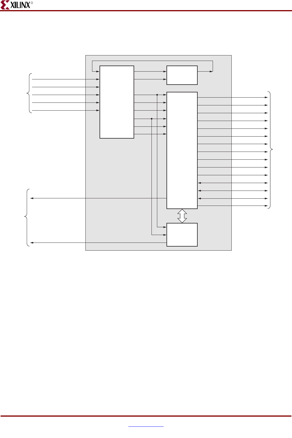
368 www.xilinx.com Memory Interface Solutions User Guide
UG086 (v3.6) September 21, 2010
Chapter 9: Implementing DDR2 SDRAM Controllers
R
and also compares the read data with written data. The error signal is driven High on data
mismatches. The phy_init_done signal indicates the completion of initialization and
calibration of the design.
Figure 9-3: Top-Level Block Diagram of the DDR2 SDRAM Design with a PLL and a Testbench
ddr2_top
tb_top
idelay_ctrl_rdy
clk200
Memory
Device
UG086_c9_03_070808
Status
Signals
System
Clocks
and Reset
idelay_ctrl
Infrastructure
rst200
clk90
clkdiv0
clk0
rst90
rstdiv0
clk200_p
clk200_n
sys_clk_p
sys_clk_n
sys_rst_n
rst0
ddr2_ras_n
ddr2_cas_n
ddr2_we_n
ddr2_cs_n
ddr2_cke
ddr2_dm
ddr2_ba
ddr2_a
ddr2_ck
ddr2_ck_n
ddr2_dq
ddr2_dqs
ddr2_odt
ddr2_reset_n
ddr2_dqs_n
phy_init_done
error
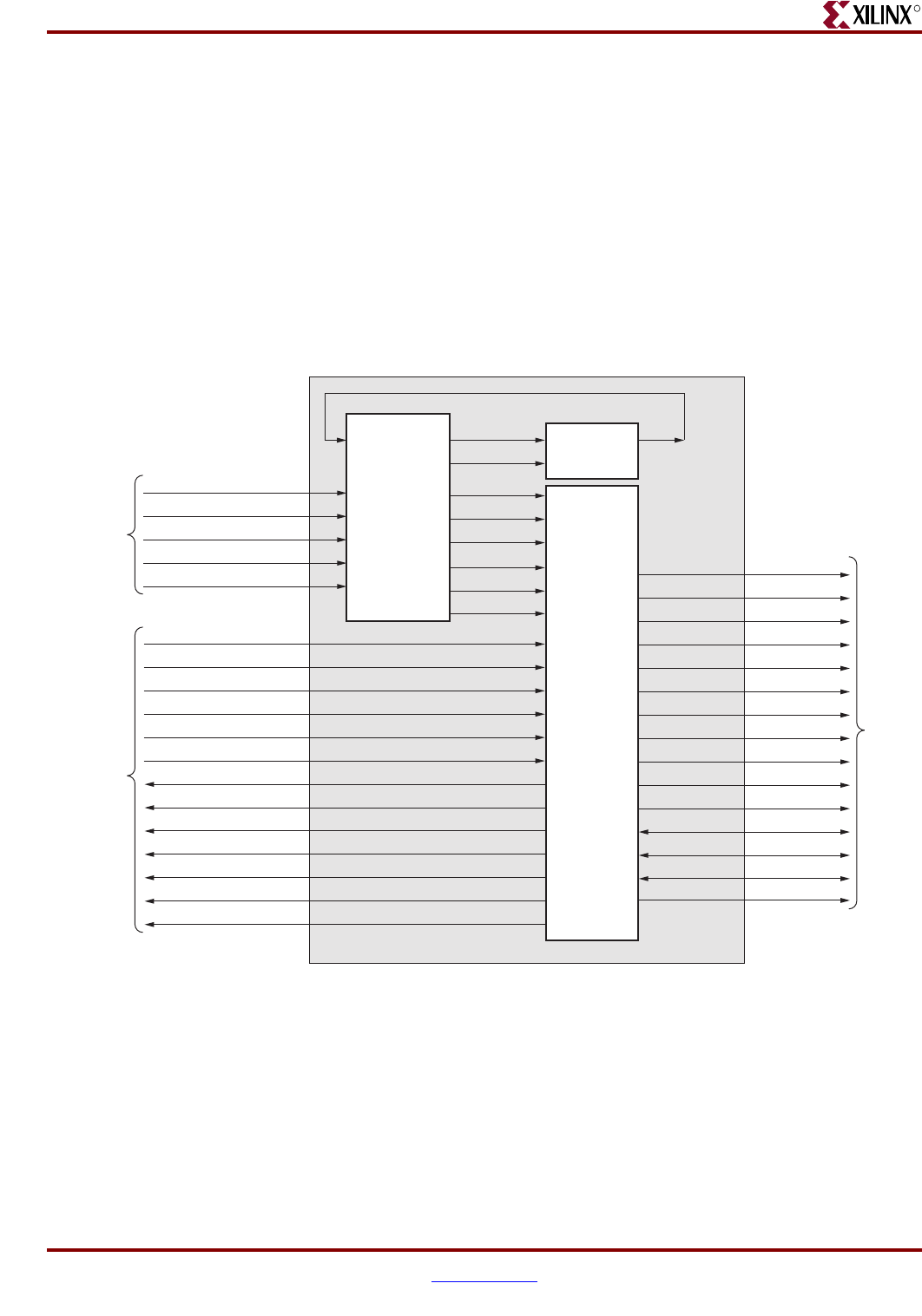
Memory Interface Solutions User Guide www.xilinx.com 369
UG086 (v3.6) September 21, 2010
Architecture
R
Figure 9-4 shows a top-level block diagram of a DDR2 SDRAM design with a PLL but
without a testbench. The sys_clk_p and sys_clk_n signals are differential input system
clocks. “Clocking Scheme,” page 377 describes how various clocks are generated using the
PLL. The PLL is instantiated in the infrastructure module that generates the required
design clocks. The clk200_p and clk200_n signals are used for the idelay_ctrl element. The
sys_rst_n signal is the active-Low system reset signal. All design resets are gated by the
locked signal. The user has to drive the user application signals. The design provides the
clk_tb and reset_tb signals to the user in order to synchronize with the design. The clk0_tb
signal is connected to clk0 in the controller. If the user clock domain is different from
clk0/clk0_tb, the user should add FIFOs for all the inputs and outputs of the controller
(user application signals) in order to synchronize them to the clk0_tb clock. The
phy_init_done signal indicates the completion of initialization and calibration of the
design.
Figure 9-4: Top-Level Block Diagram of the DDR2 SDRAM Design with a PLL but without a Testbench
ddr2_top
idelay_ctrl_rdy
clk200
Memory
Device
UG086_c9_04_070808
User
Application
System
Clocks
and Reset
idelay_ctrl
rst200
clk200_p
clk200_n
sys_clk_p
sys_clk_n
sys_rst_n
app_af_addr
app_af_wren
app_wdf_data
app_wdf_mask_data
app_wdf_wren
app_wdf_afull
app_af_afull
rd_data_valid
rd_data_fifo_out
clk0_tb
ddr2_ras_n
ddr2_cas_n
ddr2_we_n
ddr2_cs_n
ddr2_odt
ddr2_dm
ddr2_ba
ddr2_a
ddr2_ck
ddr2_ck_n
ddr2_dq
ddr2_dqs
ddr2_cke
ddr2_reset_n
ddr2_dqs_n
app_af_cmd
rst0_tb
phy_init_done
clk90
clkdiv0
clk0
rst90
rstdiv0
rst0
Infrastructure
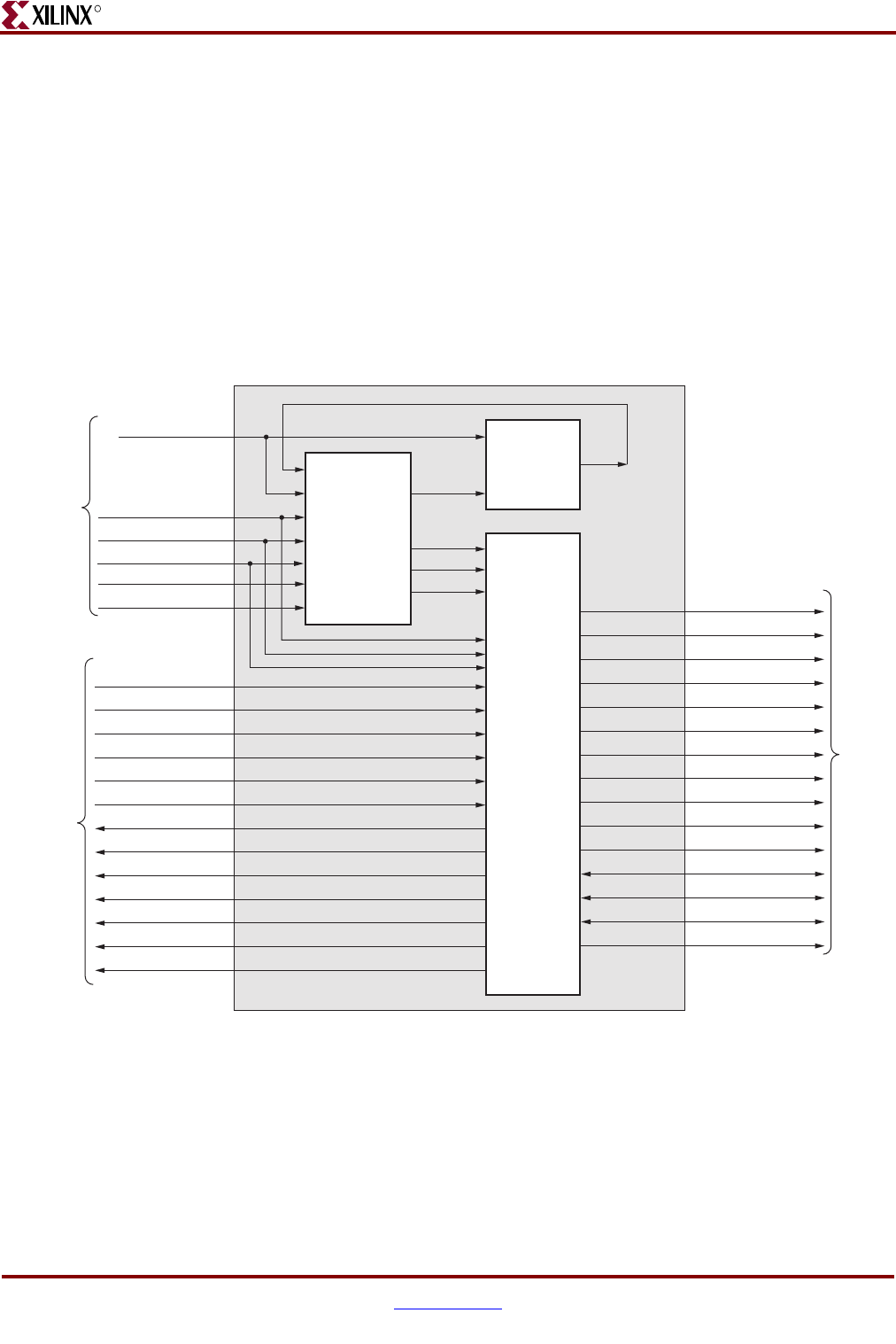
370 www.xilinx.com Memory Interface Solutions User Guide
UG086 (v3.6) September 21, 2010
Chapter 9: Implementing DDR2 SDRAM Controllers
R
Figure 9-5 shows a top-level block diagram of a DDR2 SDRAM design without a PLL or a
testbench. The user should provide all the design clocks and the locked signal. “Clocking
Scheme,” page 377 explains the details of how to generate the design clocks from the user
interface. These clocks should be single-ended. The sys_rst_n signal is the active-Low
system reset signal. All design resets are gated by the locked signal. The user application
must have a PLL/DCM primitive instantiated in the design, and all user clocks should be
driven through BUFGs. The user has to drive the user application signals. The design
provides the clk_tb and reset_tb signals to the user in order to synchronize with the design.
The clk0_tb signal is connected to clk0 in the controller. If the user clock domain is different
from clk0/clk0_tb, the user should add FIFOs for all the inputs and outputs of the
controller (user application signals) in order to synchronize them to the clk0_tb clock. The
phy_init_done signal indicates the completion of initialization and calibration of the
design.
Figure 9-5: Top-Level Block Diagram of the DDR2 SDRAM Design without a PLL or a Testbench
ddr2_top
idelay_ctrl_rdy
Memory
Device
UG086_c9_05_012609
System
Reset
and
User PLL/
DCM
idelay_ctrl
Infrastructure
rst200
rst0
rstdiv0
rst90
clk_0
clk_200
clk_90
sys_rst_n
locked ddr2_ras_n
ddr2_cas_n
ddr2_we_n
ddr2_cs_n
ddr2_cke
ddr2_odt
ddr2_dm
ddr2_ba
ddr2_a
ddr2_ck
ddr2_ck_n
ddr2_reset_n
ddr2_dq
ddr2_dqs
ddr2_dqs_n
clkdiv0
User
Application
app_af_addr
app_af_wren
app_wdf_data
app_wdf_mask_data
app_wdf_wren
app_wdf_afull
app_af_afull
rd_data_valid
rd_data_fifo_out
clk0_tb
rst0_tb
phy_init_done
app_af_cmd
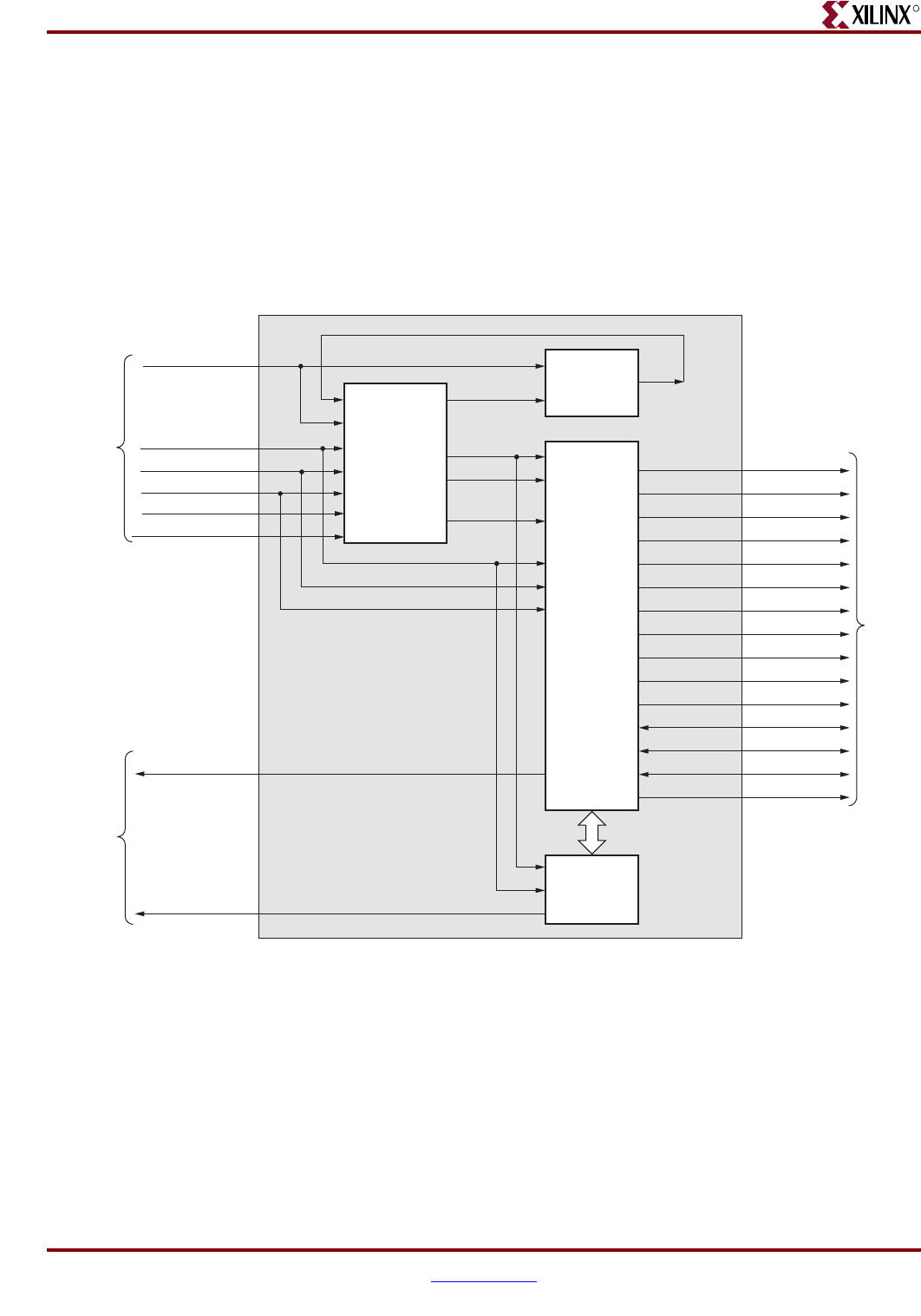
Memory Interface Solutions User Guide www.xilinx.com 371
UG086 (v3.6) September 21, 2010
Architecture
R
Figure 9-6 shows a top-level block diagram of a DDR2 SDRAM design without a PLL but
with a testbench. The user should provide all the clocks and the locked signal. “Clocking
Scheme,” page 377 explains the details of how to generate the design clocks from the user
interface. These clocks should be single-ended. sys_rst_n is the active-Low system reset
signal. All design resets are gated by the locked signal. The user application must have a
PLL/DCM primitive instantiated in the design, and all user clocks should be driven
through BUFGs. The error output signal indicates whether the case passes or fails. The
testbench module does writes and reads, and also compares the read data with the written
data. The error signal is driven High on data mismatches. The phy_init_done signal
indicates the completion of initialization and calibration of the design.
Figure 9-6: Top-Level Block Diagram of the DDR2 SDRAM Design without a PLL but with a Testbench
ddr2_top
tb_top
idelay_ctrl_rdy
clk200
Memory
Device
UG086_c9_06_012609
Status
Signals
System
Clocks
and Reset
idelay_ctrl
Infrastructure
rst200
rst90
clk200
clk0
clk90
rst0 ddr2_ras_n
ddr2_cas_n
ddr2_we_n
ddr2_cs_n
ddr2_cke
ddr2_dm
ddr2_ba
ddr2_a
ddr2_ck
ddr2_ck_n
ddr2_dq
ddr2_dqs
ddr2_odt
ddr2_reset_n
ddr2_dqs_n
phy_init_done
error
rstdiv0
sys_rst_n
locked
clkdiv0
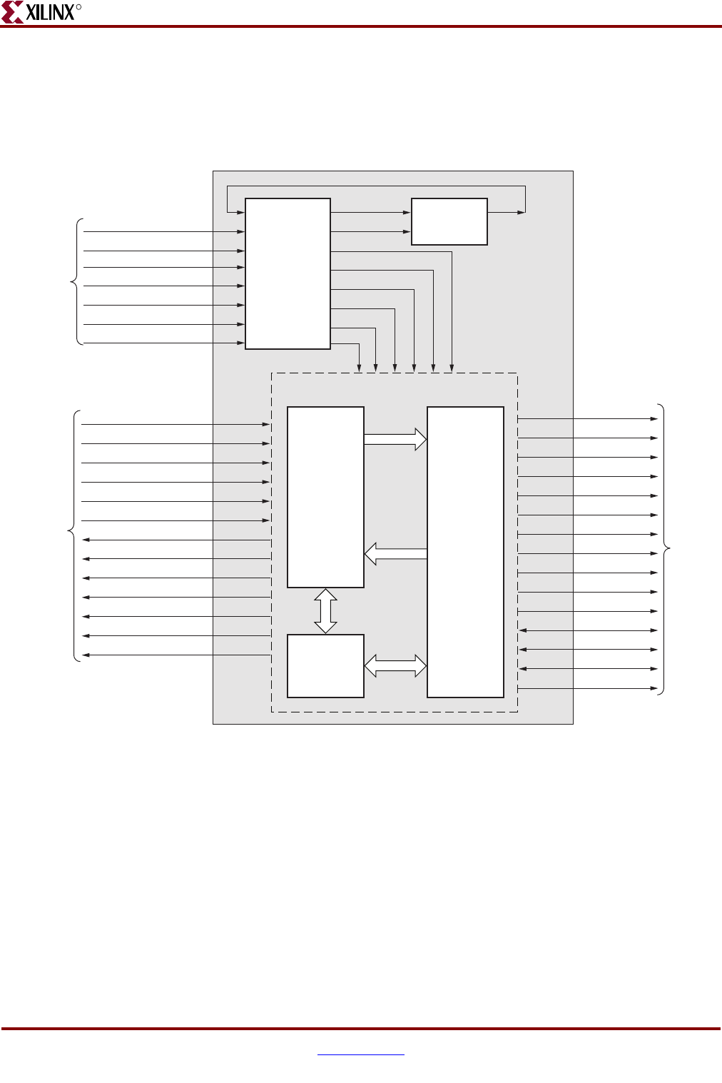
372 www.xilinx.com Memory Interface Solutions User Guide
UG086 (v3.6) September 21, 2010
Chapter 9: Implementing DDR2 SDRAM Controllers
R
DDR2 Controller Submodules
Figure 9-7 is a detailed block diagram of the DDR2 SDRAM controller. The design top
module is expanded to show various internal blocks. The functions of these blocks are
explained in the subsections following the figure.
Infrastructure
The infrastructure module generates the design clocks and reset signals. When differential
clocking is used, sys_clk_p, sys_clk_n, clk_200_p, and clk_200_n signals appear. When
single-ended clocking is used, sys_clk and idly_clk_200 signals appear. In addition, clocks
are available for design use and a 200 MHz clock is provided for the IDELAYCTRL
primitive. Differential and single-ended clocks are passed through global clock buffers
before connecting to a PLL/DCM. For differential clocking, the output of the
sys_clk_p/sys_clk_n buffer is single-ended and is provided to the PLL/DCM input.
Likewise, for single-ended clocking, sys_clk is passed through a buffer and its output is
provided to the PLL/DCM input. The outputs of the PLL/DCM are clk0 (0° phase-shifted
version of the input clock) clk90 (90° phase-shifted version of the input clock), and clkdiv0
Figure 9-7: DDR2 Memory Controller Block Diagram
ctrl
Control
Signals
write_data
ddr2_top/mem_if_top
read_data
Control
Signals
idelay_ctrl_rdy
clk200
Memory
Device
UG086_c9_07_070808
System
Clocks
and Reset
idelay_ctrl
Infrastructure
rst200
clk90
clkdiv0
clk0
rst0
rst90
rstdiv0
clk200_p
clk200_n
sys_clk_p
idly_clk_200
sys_clk_n
sys_clk
sys_rst_n
ddr2_ras_n
ddr2_cas_n
ddr2_we_n
ddr2_cs_n
ddr2_cke
ddr2_dm
ddr2_ba
ddr2_a
ddr2_ck
ddr2_ck_n
ddr2_dq
ddr2_dqs
ddr2_odt
ddr2_reset_n
ddr2_dqs_n
User
Application
app_af_addr
app_af_wren
app_wdf_data
app_wdf_mask_data
app_wdf_wren
app_wdf_afull
app_af_afull
rd_data_valid
rd_data_fifo_out
clk0_tb
app_af_cmd
rst0_tb
phy_init_done
usr_top
phy_top

Memory Interface Solutions User Guide www.xilinx.com 373
UG086 (v3.6) September 21, 2010
Architecture
R
(half the frequency of the input clock and phase aligned with clk0). After the PLL/DCM is
locked, the design is in the reset state for at least 25 clocks. The infrastructure module also
generates all of the reset signals required for the design.
PLL/DCM
In MIG 3.0 and later, the DCM is replaced with a PLL for all Virtex-5 FPGA designs. If the
user selects a design with a PLL in the GUI, the infrastructure module will have both PLL
and DCM codes. The CLK_GENERATOR parameter enables either a PLL or a DCM in the
infrastructure module. The CLK_GENERATOR parameter is set to PLL by default. If the
user wants to use DCM, this parameter should be changed manually to DCM.
For designs without a PLL, the user application must have a PLL/DCM primitive
instantiated in the design, and all user clocks should be driven through BUFGs.
Idelay_ctrl
This module instantiates the IDELAYCTRL primitive of the Virtex-5 FPGA. The
IDELAYCTRL primitive is used to continuously calibrate the individual delay elements in
its region to reduce the effect of process, temperature, and voltage variations. A 200 MHz
clock has to be fed to this primitive. For more information on IDELAYCTRLs, refer to
section “Verify IDELAYCTRL Instantiation for Virtex-4 and Virtex-5 FPGA Designs” in
Chapter 14.
Ctrl
The ctrl module is the main controller of the Virtex-5 FPGA DDR2 SDRAM controller
design. It generates all the control signals required for the DDR2 memory interface and the
user interface. During the normal operation, this module toggles the memory address and
control signals.
The ctrl module decodes the user command and issues the specified command to the
memory. The app_af_cmd signal is decoded as a write command when it equals 3’b000,
and app_af_cmd is decoded as a read command when it equals 3’b001. The commands and
control signals are generated based on the input burst length and CAS latency. The
controller state machine issues the commands in the correct sequence while determining
the timing requirements of the memory.
In the multi-bank mode (MULTIBANK_EN = 1), the controller has the ability to keep four
banks open at a time. The banks are opened in the order of the commands that are
presented to the controller. In the event that four banks are already opened and an access
arrives to the fifth bank, the least recently used bank is closed and the new bank is opened.
All the banks are closed during auto refresh and are opened as commands are presented to
the controller. Depending on the traffic pattern, the multi-bank enable mode can increase
the efficiency of the design.
In the single-bank mode (MULTIBANK_EN = 0), the controller keeps one bank open at a
time. When there is an access to a different bank or to a different row in the current bank,
the controller closes the current row and bank and opens the new row and bank.
phy_top
The phy_top module is the top level of the physical interface of the design. The physical
layer includes the input/output blocks (IOBs) and other primitives used to read and write
the double data rate signals to and from the memory, such as IDDR and ODDR. This
module also includes the IODELAY elements of the Virtex-5 FPGA. These IODELAY

374 www.xilinx.com Memory Interface Solutions User Guide
UG086 (v3.6) September 21, 2010
Chapter 9: Implementing DDR2 SDRAM Controllers
R
elements are used to delay the data signals to capture the valid data into the Read Data
FIFO.
The memory control signals, such as RAS_N, CAS_N, and WE_N, are driven from the
buffers in the IOBs. All the input and output signals to and from the memory are
referenced from the IOB to compensate for the routing delays inside the FPGA.
The phy_init module, which is instantiated in the phy_top module, is used to initialize the
DDR2 memory in a predefined sequence according to the JEDEC standard for DDR2
SDRAM.
The phy_calib module calibrates the design to align the strobe signal such that it always
captures the valid data in the FIFO. This calibration is needed to compensate for the trace
delays between the memory and the FPGA devices.
The phy_write module splits the user data into rise data and fall data to be sent to the
memory as a double data rate signal using ODDR. Similarly, while reading the data from
memory, the data from IDDR is combined to get a single vector that is written into the read
FIFO.
usr_top
The usr_top module is the user interface block of the design. It receives and stores the user
data, command, and address information in respective FIFOs. The ctrl module generates
the required control signals for this module. During a write operation, the data stored in
the usr_wr_fifo is read and given to the physical layer to output to the memory. Similarly,
during a read operation, the data from the memory is read via IDDR and written into the
FIFOs. This data is given to the user with a valid signal (rd_data_valid), which indicates
valid data on the rd_data_fifo_out signal. Table 9-6 lists the user interface signals.
The FIFO36 and FIFO36_72 primitives are used for loading address and data from the user
interface. The FIFO36 primitive is used in the ddr2_usr_addr_fifo module. The FIFO36_72
primitive is used in the ddr2_usr_wr and ddr2_usr_rd modules. Every FIFO has two FIFO
threshold attributes, ALMOST_EMPTY_OFFSET and ALMOST_FULL_OFFSET, that are
set to 7 and F, respectively, in the RTL by default. These values can be changed as needed.
For valid FIFO threshold offset values, refer to UG190 [Ref 10].
Test Bench
The MIG tool generates two RTL folders, example_design and user_design. The
example_design folder includes the synthesizable test bench, while user_design does not
include the test bench modules. The MIG test bench performs eight write commands and
eight read commands in an alternating fashion. The number of words in a write command
depends on the burst length. For a burst length of 4, the test bench writes a total of 32 data
words for all eight write commands (16 rise data words and 16 fall data words). For a burst
length of 8, the test bench writes a total of 64 data words. It writes the data pattern of FF,
00, AA, 55, 55 AA, 99, 66 in a sequence of which FF, AA, 55, and 99 are rise data words and
00, 55, AA, and 66 are fall data words for an 8-bit design. The falling edge data is the
complement of the rising edge data. For a burst length of 4, the data sequence for the first
write command is FF, 00, AA, 55, and the data sequence for the second write command is
55, AA, 99, 66. For a burst length of 8, the data pattern for the first write command is FF,
00, AA, 55, 55 AA, 99, 66 and the same pattern is repeated for all the remaining write
commands. This data pattern is repeated in the same order based on the number of data
words written. For data widths greater than 8, the same data pattern is concatenated for
the other bits. For a 32-bit design and a burst length of 8, the data pattern for the first write
command is FFFFFFFF, 00000000, AAAAAAAA, 55555555, 55555555, AAAAAAAA,
99999999, 66666666.

Memory Interface Solutions User Guide www.xilinx.com 375
UG086 (v3.6) September 21, 2010
DDR2 SDRAM Initialization
R
Address generation logic generates eight different addresses for eight write commands.
The same eight address locations are repeated for the following eight read commands. The
read commands are performed at the same locations where the data is written. There are
total of 32 different address locations for 32 write commands, and the same address
locations are generated for 32 read commands. Upon completion of a total of 64
commands, including both writes and reads (eight writes and eight reads repeated four
times), address generation rolls back to the first address of the first write command and the
same address locations are repeated. The MIG test bench exercises only a certain memory
area. The address is formed such that all address bits are exercised. During writes, a new
address is generated for every burst operation on the column boundary.
During reads, comparison logic compares the read pattern with the pattern written, i.e., the
FF, 00, AA, 55, 55 AA, 99, 66 pattern. For example, for an 8-bit design of burst length 4, the
data written for a single write command is FF, 00, AA, 55. During reads, the read pattern is
compared with the FF, 00, AA, 55 pattern. Based on a comparison of the data, a status
signal error is generated. If the data read back is the same as the data written, the error
signal is 0, otherwise it is 1. Comparison logic only compares the DATA bits and not the
ECC data pattern. For example, for a 72-bit ECC design, comparison logic only compares
64 bits. The 8 MSBs (ECC bits) are not compared.
DDR2 SDRAM Initialization
DDR2 memory is initialized through a specified sequence as per both Micron and JEDEC
specifications. Initialization logic is implemented in the physical layer.
DDR2 SDRAM Design Calibration
Before issuing user read and write commands, the read datapath is calibrated to ensure
that correct data is captured into the CLK0 domain of the FPGA. Calibration logic is
implemented in the physical layer of the design. Figure 9-8 shows overall calibration
sequence.
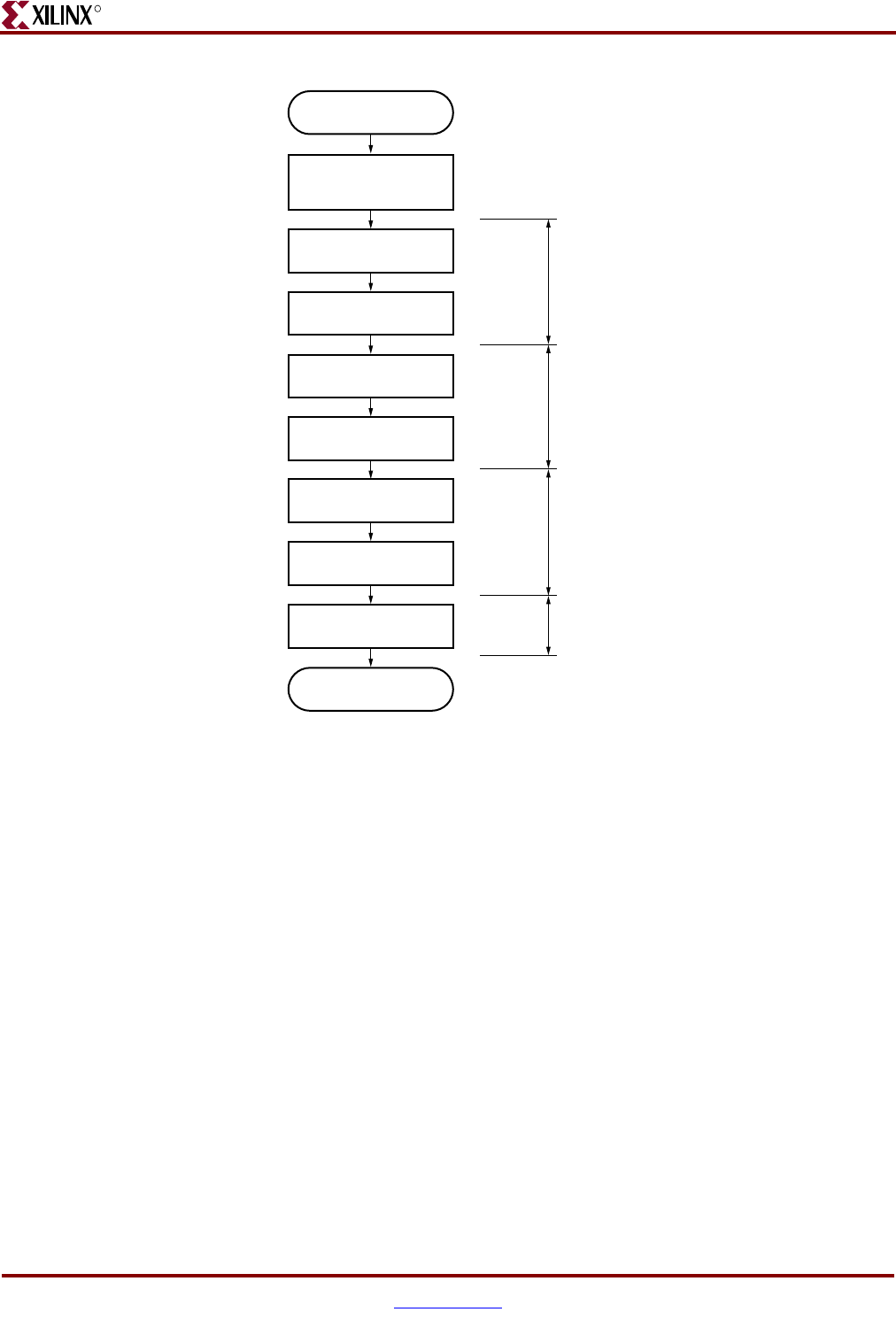
376 www.xilinx.com Memory Interface Solutions User Guide
UG086 (v3.6) September 21, 2010
Chapter 9: Implementing DDR2 SDRAM Controllers
R
The first calibration stage is used to position the DQS in the DQ valid window. This
synchronizes the capture of DQ using DQS in the IDDR flop. A training pattern of 1 for rise
and 0 for fall data is written into the memory and is continuously read back. The DQ and
IDELAYs are adjusted depending upon the DQ to DQS relationship. Per-bit deskew is
performed on the DQ bits.
The second calibration stage is between the DQS and the FPGA clock. This synchronizes
the transfer of data between the IDDR flop and flip-flops located in the FPGA fabric. The
DQ and DQS IDELAY taps are incremented together to align to the FPGA clock domain.
The third calibration stage is the read-enable calibration, which is used to generate a read
valid signal. The memory devices do not provide a signal indicating when the read data is
valid. The read data is delayed by CAS latency, additive latency, the PCB trace, and the I/O
buffer delays. The read-enable calibration is used to determine the delay between issuing
a read command and the arrival of the read data.
The fourth calibration stage is used to align the DQS Gate signal from the controller to the
falling edge of DQS. The DQS Gate controls the clock enable to the DQ IDDRs. It is used to
prevent clocking of invalid data into the IDDR after the read postamble. This can happen
because the DQS is 3-stated by the memory at the end of a read. The DQS can then go into
an indeterminate value, causing false clocking of the IDDR.
Figure 9-8: Overall Design Calibration Sequence
UG086_c9_08_091707
Write all callibration training
patterns to fixed locations
in memory
Write callibration patterns required
for stage 1, stage 2, and stage 3/4
calibration to memory.
Stage 1:
DQ-DQS per-bit calibration
Adjust DQ delay
Perform once per DQ bit
Stage 4:
DQS gate control calibration
Adjust IDELAY for DQS gate control
Perform once per DQS group
Continuous read back of
stage 1 training pattern
Continuous read back of
stage 2 training pattern
Calibrate all DQ
Calibrate all DQS
Continuous read back of
stage 3/4 training pattern
Read Data Valid calibration
all DQS
Calibration Done
DQS Gate Control
calibration for all DQS
Power-up init sequence
complete
Stage 3:
Read data valid calibration
(once per DQS group)
Adjust number of clock cycles to wait
after issuing read command before valid
data arrives in FPGA_CLK domain
Perform once per DQS group
Stage 2:
DQS-FPGA CLK calibration
Use DQ[8*x] to calibrate DQS[x]
Adjust DQ/DQS IDELAY
Perform once per DQS group

Memory Interface Solutions User Guide www.xilinx.com 377
UG086 (v3.6) September 21, 2010
Clocking Scheme
R
After initialization and calibration is done, the controller is signaled to start normal
operation of the design. Now, the controller can start issuing user write and read
commands to the memory.
Clocking Scheme
Figure 9-10, page 378 shows the clocking scheme for this design. Global and local clock
resources are used.
The global clock resources consist of a PLL or a DCM, three BUFGs on PLL/DCM output
clocks, and one BUFG for clk200. The local clock resources consist of regional I/O clock
networks (BUFIO). The global clock architecture is discussed in this section.
The MIG tool allows the user to customize the design such that the PLL/DCM is not
included. In this case, clk0, clk90, clkdiv0 and IDELAYCTRL clock clk200 must be supplied
by the user.
Global Clock Architecture
The user must supply two input clocks to the design:
• A system clock running at the target frequency for the memory
• A 200 MHz clock for the IDELAYCTRL blocks.
These clocks can be either single-ended or differential. User can select single-ended or
differential clock input option from MIG GUI. Differential clocks are connected to the
IBUFGDS and single-ended clock is connected to IBUFG.
The system clock from the output of the IBUFGDS or the IBUFG is connected to the
PLL/DCM to generate the various clocks used by the memory interface logic.
The clk200 output of the IBUFGDS or the IBUFG is connected to the BUFG. The output of
the BUFG is used for IDELAY IOB delay blocks for aligning read capture data.
The PLL/DCM generates three separate synchronous clocks for use in the design. This is
shown in Table 9-5, page 378, Figure 9-9, page 378, and Figure 9-10, page 378. The clock
structure is the same for both example design and user design. For designs without PLL
instantiation, PLL/DCM and the BUFGs should be instantiated at user end to generate the
required clocks.

378 www.xilinx.com Memory Interface Solutions User Guide
UG086 (v3.6) September 21, 2010
Chapter 9: Implementing DDR2 SDRAM Controllers
R
Table 9-5: DDR2 Interface Design Clocks
Clock Description Logic Domain
clk0 Skew compensated replica
of the input system clock.
The clock for the controller and the user
interface logic, most of the DDR2 bus-related
I/O flip-flops (e.g., memory clock,
control/address, output DQS strobe, and DQ
input capture). This clock is used to register the
data, address, and command signals, and the
address and data enables for the user interface
logic(1). This clock is also used to generate the
read data, read data valid, and FIFO status
signals.
clk90 90° phase-shifted version of
clk0
Used in the write data path section of physical
layer. Clocks write path control logic, DDR2
side of the Write Data FIFO, and output flip-
flops for DQ.
clkdiv0 Divided-by-2 and edge-
aligned version of clk0
Clocks the memory initialization and read
capture timing calibration state machines in
the PHY layer.
Notes:
1. See “User Interface Accesses,” page 381 for timing requirements and restrictions on the user interface
signals.
Figure 9-9: Clocking Scheme for DDR2 Interface Logic Using PLL
CLKIN
CLKFBIN
CLKOUT1
CLKOUT2
CLKOUT0
CLK90
CLKDIV0
CLK0
PLL BUFG
GC I/O
SYSTEM CLK
UG086_c9_14_012709
CLKFBOUT
Figure 9-10: Clocking Scheme for DDR2 Interface Logic Using DCM
CLKIN
C
LKFB
CLK90
CLKDV (+2)
CLK0
CLK90
CLKDIV0
CLK0
DCM BUFG
GC I/O
SYSTEM CLK
UG086_c9_13_071008
Memory Interface Solutions User Guide www.xilinx.com 379
UG086 (v3.6) September 21, 2010
DDR2 SDRAM System and User Interface Signals
R
DDR2 SDRAM System and User Interface Signals
Table 9-6 and Table 9-7 describe the system interface signals for designs generated with
and without a PLL, respectively.
Table 9-6: DDR2 SDRAM Controller System Interface Signals (with a PLL)
Signal Name Direction Description
sys_clk_p, sys_clk_n Input Differential input clock to the PLL/DCM. The DDR2 controller
and memory operate at this frequency. This differential input
clock pair is present only when the DIFFERENTIAL clocks
option is selected in MIG FPGA options page.
sys_clk Input Single-ended input clock to the PLL/DCM. The DDR2 controller
and memory operate at this frequency. This input clock is
present only when the SINGLE_ENDED clocks option is
selected in the MIG FPGA options page.
clk200_p, clk200_n Input 200 MHz differential input clock for the IDELAYCTRL primitive
of Virtex-5 FPGAs. This differential input clock pair is present
only when the DIFFERENTIAL clocks option is selected in
MIG FPGA options page.
idly_clk_200 Input 200 MHz single-ended input clock for the IDELAYCTRL
primitive of Virtex-5 FPGAs. This input clock is present only
when the SINGLE_ENDED clocks option is selected in the
MIG FPGA options page.
sys_rst_n Input Active-Low reset to the DDR2 controller.
Table 9-7: DDR2 SDRAM Controller System Interface Signals (without a PLL)
Signal Direction Description
clk0 Input The DDR2 SDRAM controller and memory operate on this clock.
clk90 Input 90° phase-shifted clock with the same frequency as clk0.
clkdiv0 Input Clocks the memory initialization and read capture timing
calibration state machines in the PHY layer.
clk200 Input 200 MHz differential input clock for the IDELAYCTRL primitive
of Virtex-5 FPGAs.
sys_rst_n Input Active-Low reset to the DDR2 SDRAM controller. This signal is
used to generate the synchronous system reset.
locked Input The status signal indicating whether the PLL is locked or not.
This signal is used to generate the synchronous system reset.
380 www.xilinx.com Memory Interface Solutions User Guide
UG086 (v3.6) September 21, 2010
Chapter 9: Implementing DDR2 SDRAM Controllers
R
Table 9-8 describes the user interface signals.
Table 9-8: DDR2 SDRAM Controller User Interface Signals
Signal Direction(1) Description
app_af_cmd[2:0] Input 3-bit command to the Virtex-5 FPGA DDR2 SDRAM design.
app_af_cmd = 3’b000 for write command
app_af_cmd = 3’b001 for read command
Other combinations are invalid. Functionality of the controller is
unpredictable for unimplemented commands.
app_af_addr[30:0](2) Input Gives information about the address of the memory location to be
accessed. This bus contains the bank address, the row address, and
the column address.
Column address = app_af_addr[COL_WIDTH-1: 0]
Row address = app_af_addr[ROW_WIDTH+COL_WIDTH–1:
COL_WIDTH]
Bank address =
app_af_addr[BANK_WIDTH+ROW_WIDTH+COL_WIDTH–1:
ROW_WIDTH+COL_WIDTH]
Chip select(3)=
app_af_addr[BANK_WIDTH+ROW_WIDTH+COL_WIDTH]
app_af_wren Input Write enable to the User Address FIFO. This signal should be
synchronized with the app_af_addr and app_af_cmd signals.
app_wdf_data[2*DQ_WIDTH–1:0] Input User input data. It should contain the fall data and the rise data.
Rise data = app_wdf_data[DQ_WIDTH–1: 0]
Fall data = app_wdf_data[2*DQ_WIDTH–1: DQ_WIDTH]
app_wdf_mask_data[2*DM_WIDTH–1: 0] Input User mask data. It should contain the masking information for both
rise and fall data.
Rise mask data = app_wdf_mask_data[DM_WIDTH–1: 0]
Fall mask data = app_wdf_mask_data[2*DM_WIDTH–1:
DM_WIDTH]
app_wdf_wren Input Write enable for the User Write FIFO. This signal should be
synchronized with the app_wdf_data and app_wdf_mask_data
signals.
app_af_afull Output Almost Full status of the Address FIFO. When this signal is asserted,
the user can write 12 more locations into the FIFO.
app_wdf_afull Output Almost Full status of the User Write FIFO. When this signal is
asserted, the user can write 12 more locations into the FIFO.
rd_data_valid Output Status signal indicating read data is valid on the read data bus.
rd_data_fifo_out[2*DQ_WIDTH–1: 0] Output Read data from the memory.
phy_init_done Output Indicates the completion of initialization and calibration of the
design.
clk0_tb Output Clock output to the user. All user interface signals must be
synchronized with this clock. This signal is sourced from clk0 in the
controller.
Memory Interface Solutions User Guide www.xilinx.com 381
UG086 (v3.6) September 21, 2010
DDR2 SDRAM System and User Interface Signals
R
Table 9-9 lists the signals between the user interface and the controller.
User Interface Accesses
The user backend logic communicates with the memory controller through a FIFO-based
user interface. This interface consists of three related buses: (1) a command/address FIFO
bus accepts write/read commands as well as the corresponding memory address from the
user, (2) a write data FIFO bus accepts the corresponding write data when the user issues
a write command on the command/address bus, and (3) a read bus on which the
corresponding read data for an issued read command is returned.
The user interface has the following timing and signaling restrictions:
1. When issuing a write command, the first write data word must be written to the Write
Data FIFO either prior to or on the same clock cycle as the when the write command is
issued. In addition, the write data must be written by the user over consecutive clock
cycles; there cannot be a break between words. These restrictions arise from the fact
rst0_tb Output Active-High reset for the user interface.
Notes:
1. Direction indicated in the table is referenced from the design perspective. For example, input here indicates that the signal is input to the
design.
2. Addressing in Virtex-5 FPGAs is linear addressing (i.e., the row address immediately follows the column address bits, and the bank address
follows the row address bits, thus supporting more devices). The number of address bits used depends on the density of the memory part.
The controller ignores the unused bits, which can all be tied High.
3. For single-rank devices, Chip Select is not taken from the user address (i.e., app_af_addr). Hence, the controller always selects all of
the existing devices. For dual-rank devices, the corresponding device is selected based on the Chip Select value. In other words, for
dual-rank devices, the Chip Select is taken from the user address (i.e., app_af_addr). CS0 is selected for a Chip Select value of 0, and
CS1 is selected for a Chip Select value of 1.
Table 9-8: DDR2 SDRAM Controller User Interface Signals (Cont’d)
Signal Direction(1) Description
Table 9-9: Signals between User Interface and Controller
Port Name Port Width Port Description
af_cmd 3
Output of the Address FIFO in the user interface.
Monitors the FIFO full status flag to the write address
into the Address FIFO.
af_addr 31
Output of the Address FIFO in the user interface. The
mapping of these address bits is [30:0]: Memory
Address (CS, Bank, Row, Column). Monitors the
FIFO full status flag to the write address into the
Address FIFO.
af_empty 1
The user interface Address FIFO empty status flag
output. The user application can write to the Address
FIFO when this signal is asserted until the write data
FIFO full status flag is asserted. FIFO36 Almost
Empty flag.
ctrl_af_rden 1
Read Enable input to Address FIFO in the user
interface. This signal is asserted for one clock cycle
when the controller state is write or read resulting
from dynamic command requests.
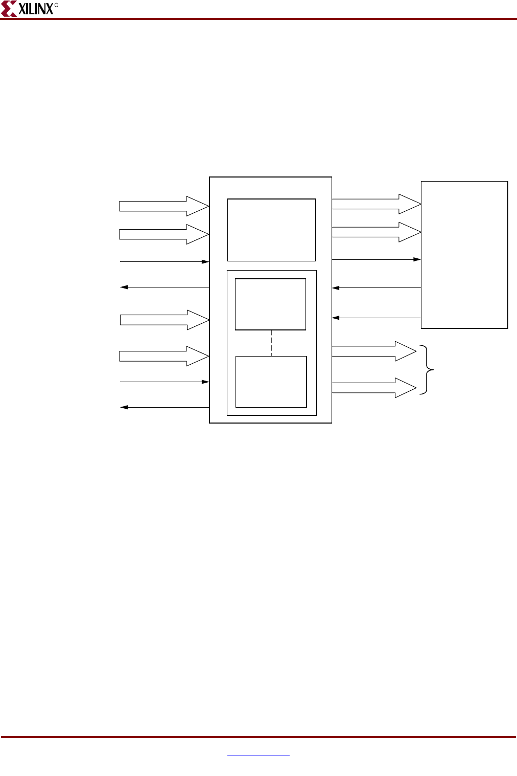
382 www.xilinx.com Memory Interface Solutions User Guide
UG086 (v3.6) September 21, 2010
Chapter 9: Implementing DDR2 SDRAM Controllers
R
that the controller assumes write data is available when it receives the write command
from the user.
2. The clk0_tb signal is connected to clk0 in the controller. If the user clock domain is
different from clk0 / clk0_tb of MIG, the user should add FIFOs for all data inputs and
outputs of the controller in order to synchronize them to the clk0_tb.
Write Interface
Figure 9-11 shows the user interface block diagram for write operations.
The following steps describe the architecture of the Address and Write Data FIFOs and
show how to perform a write burst operation to DDR2 SDRAM from the user interface.
1. The user interface consists of an Address FIFO and a Write Data FIFO. The Write Data
FIFO is constructed using the Virtex-5 FPGA FIFO36_72 primitive with a 512 x 72
configuration. The 72-bit architecture comprises one 64-bit port and one 8-bit port. For
Write Data FIFOs, the 64-bit port is used for data bits and the 8-bit port is used for
mask bits for ECC-disabled designs. Mask bits are available only when supported by
the memory part and when data mask is enabled in the MIG GUI. Some memory parts,
such as Registered DIMMs of x4 parts, do not support mask bits.
2. In ECC-enabled designs, the 64-bit port is used for data bits and the 8-bit port is used
for ECC data. The attributes passed to the Virtex-5 FPGA FIFO36_72 primitive are
different for ECC-enabled designs; attribute EN_ECC_WRITE is set to TRUE for ECC-
enabled designs to enable the generation of ECC data.
3. The Address FIFO is constructed using the Virtex-5 FPGA FIFO36 primitive with a
1024 x 36 configuration. The 36-bit architecture comprises one 32-bit port and one 4-bit
port. The 32-bit port is used for the address (app_af_addr) and the 4-bit port is used for
the command (app_af_cmd).
Figure 9-11: User Interface Block Diagram for Write Operation
User Interface
Controller
Address FIFO
(FIFO36)
1024 x 36
af_addr
af_cmd
af_empty
ctrl_af_rden
wdf_rden
app_af_addr
app_af_cmd
app_af_wren
app_wdf_data
app_wdf_mask_data
app_wdf_wren
wdf_data
wdf_mask_data
To Phy Layer
app_wdf_afull
app_af_afull
Write Data
FIFO
(FIFO36_72)
512 x 72
Write Data
FIFO
(FIFO36_72)
512 x 72
ug086_c9_11_122007

Memory Interface Solutions User Guide www.xilinx.com 383
UG086 (v3.6) September 21, 2010
DDR2 SDRAM System and User Interface Signals
R
4. The Address FIFO is common for both Write and Read commands. It comprises an
address part and a command part. Command bits discriminate between write and
read commands.
5. User interface data width app_wdf_data is twice that of the memory data width. For
an 8-bit memory width, the user interface is 16 bits consisting of rising-edge data and
falling-edge data. There is a mask bit for every 8 bits of data. For 72-bit memory data,
the user interface data width app_wdf_data is 144 bits, and the mask data
app_wdf_mask_data is 18 bits.
6. The minimum configuration of the Write Data FIFO is 512 x 72 for a memory data
width of 8 bits. For an 8-bit memory data width, the least-significant 16 bits of the data
port are used for write data and the least-significant two bits of the 8-bit port are used
for mask bits. The controller internally pads all zeros for the most-significant 48 bits of
the 64-bit port and the most-significant 6 bits of the 8-bit port.
7. Depending on the memory data width, MIG instantiates multiple FIFO36_72s to gain
the required width. For designs using 8-bit to 32-bit data width, one FIFO36_72 is
instantiated; for 72-bit data width, a total of three FIFO36_72s are instantiated. The bit
architecture comprises 32 bits of rising-edge data, 4 bits of rising-edge mask, 32 bits of
falling-edge data, and 4 bits of falling-edge mask, which are all stored in a FIFO36_72.
MIG routes app_wdf_data and app_wdf_mask_data to FIFO36_72s accordingly.
8. The user can initiate a write to memory by writing to the Address FIFO and the Write
Data FIFO when the FIFO full flags are deasserted. Status signal app_af_afull is
asserted when the Address FIFO is full; similarly, app_wdf_afull is asserted when the
Write Data FIFO is full.
9. At power on, both the Address FIFO and Write Data FIFO full flags are deasserted.
10. The user should assert Address FIFO write-enable signal app_af_wren along with
address app_af_addr and command app_af_cmd to store the address and command
into Address FIFO.
11. The user data should be synchronized to the clk_tb clock. The user should assert the
Data FIFO write-enable signal app_wdf_wren along with write data app_wdf_data
and mask data app_wdf_mask_data to store the write data and mask data into the
Write Data FIFOs. The user should provide both rising-edge and falling-edge data
together for each write to the Data FIFO. The Virtex-5 FPGA DDR2 SDRAM controller
design supports byte-wise masking of data only.
12. The write command should be given by keeping app_af_cmd = 3'b000 and asserting
app_af_wren. Address information is given on the app_af_addr signal. Address and
command information is written into the User Address FIFO.
13. After the completion of the initialization and calibration process and when the User
Address FIFO empty signal is deasserted, the controller reads the Command and
Address FIFO and issues a write command to the DDR2 SDRAM.
14. The write timing diagram in Figure 9-12 is derived from the MIG-generated testbench
for a burst length of 4. As shown, each write to the Address FIFO should have two
writes to the Data FIFO. The phy_init_done signal indicates memory initialization and
calibration completion.
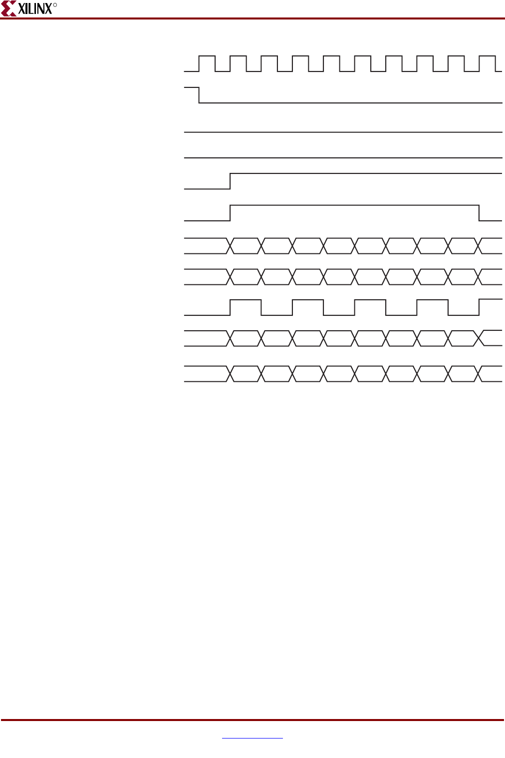
384 www.xilinx.com Memory Interface Solutions User Guide
UG086 (v3.6) September 21, 2010
Chapter 9: Implementing DDR2 SDRAM Controllers
R
Figure 9-12: DDR2 SDRAM Write Burst for Four Bursts (BL = 4)
clk_tb
reset_tb
app_wdf_afull
app_af_afull
app_af_wren
app_af_addr
phy_init_done
app_wdf_wren
A0
app_af_cmd 000 000 000 000
app_wdf_dataD1D0D3D2D5D4D7D6D9D8D11D10 D13D12 D15D14
app_mask_dataM1M0M3M2M5M4M7M6M9M8M
11M
10 M
13M
12 M
15M
14
A1A2A3
UG086_c9_09_071808
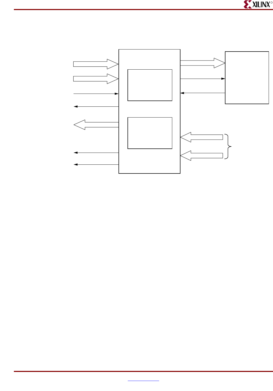
Memory Interface Solutions User Guide www.xilinx.com 385
UG086 (v3.6) September 21, 2010
DDR2 SDRAM System and User Interface Signals
R
Read Interface
Figure 9-13 shows the block diagram of the read interface.
The following steps describe the architecture of the Read Data FIFO and show how to
perform a read burst operation from DDR2 SDRAM from user interface.
1. The Read Data FIFOs are constructed using the Virtex-5 FPGA FIFO36_72 primitive
with a 512 x 72 configuration for ECC-enabled designs. For non-ECC designs, read
data is latched using the flops.
2. In ECC-enabled designs, the 64-bit port is used for data bits and the 8-bit port is used
for ECC data. The Virtex-5 FPGA FIFO36_72 performs ECC comparison when the
attribute EN_ECC_READ is set during read operation. MIG instantiates the FIFOs
appropriately for ECC or non-ECC designs.
3. The user can initiate a read to memory by writing to the Address FIFO when the FIFO
full flag app_af_afull is deasserted.
4. To write the read address and read command into the Address FIFO, the user should
issue the Address FIFO write-enable signal app_af_wren along with read address
app_af_addr and app_af_cmd is the command (set to 001 for a read command).
5. The controller reads the Address FIFO and generates the appropriate control signals to
memory. After decoding app_af_cmd, the controller issues a read command to the
memory at the specified address.
6. Prior to the actual read and write commands, the design calibrates the latency in
number of clock cycles from the time the read command is issued to the time the data
is received. Using this precalibrated delay information, the controller stores the read
data in the Read Data FIFOs.
7. The read_data_valid signal is asserted when data is available in the Read Data FIFOs.
8. When the calibration is completed, the controller generates the control signals to
capture the read data from the FIFO according to the CAS latency selected by the user.
Figure 9-13: User Interface Block Diagram for Read Operation
User Interface
Controller
Address FIFO
(FIFO16)
1024 x 36
af_addr
af_empty
ctrl_af_rden
rd_data_out_rise
rd_data_out_fall From Phy Layer
Read Data
FIFO
ug086_c9_12_122007
app_af_addr
app_af_cmd
app_af_wren
rd_data_fifo_out
rd_data_valid
app_af_afull
wdf_almost_full
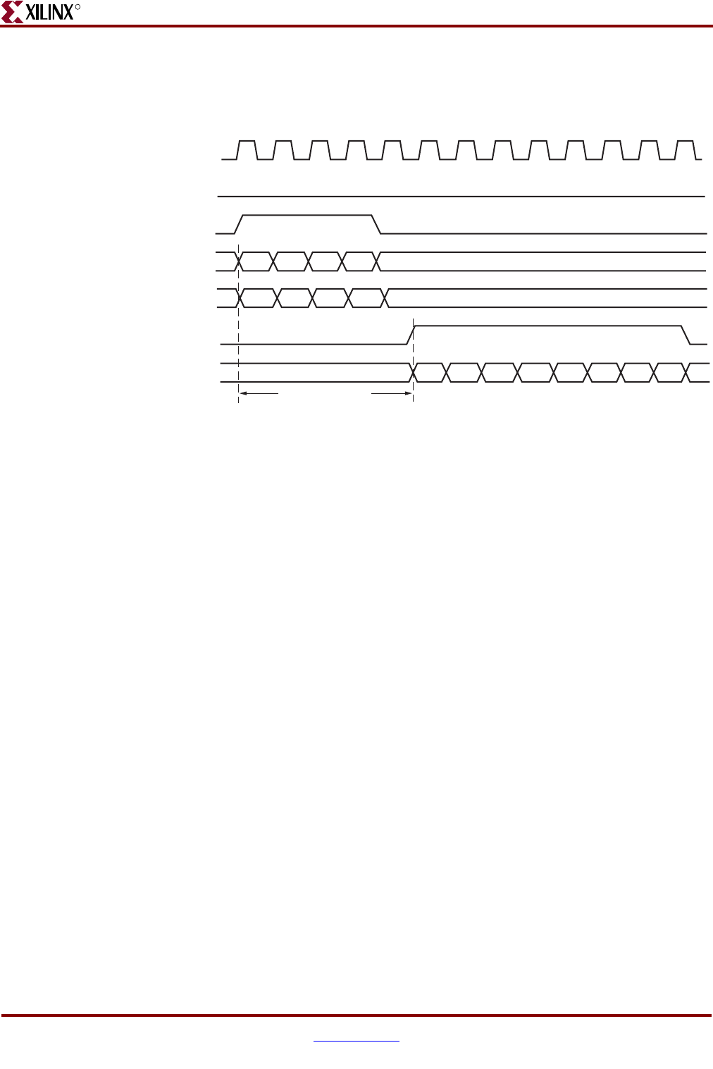
386 www.xilinx.com Memory Interface Solutions User Guide
UG086 (v3.6) September 21, 2010
Chapter 9: Implementing DDR2 SDRAM Controllers
R
The rd_data_valid signal is asserted when the read data is available to the user, and
rd_data_fifo_out is the read data from the memory to the user.
9. Figure 9-14 shows the user interface timing diagram for burst length of four.
Read latency is defined as the time between when the read command is written to the user
interface bus until when the corresponding first piece of data is available on the user
interface bus (see Figure 9-14).
When benchmarking read latencies, it is important to specify the exact conditions under
which the measurement occurs.
Read latency varies based on the following parameters:
• Number of commands already in the FIFO pipeline before the read command is
issued
• Whether an ACTIVATE command needs to be issued to open the new bank/row
• Whether a PRECHARGE command needs to be issued to close a previously opened
bank
• Specific timing parameters for the memory, such as TRAS and TRCD in conjunction
with the bus clock frequency
• Commands can be interrupted, and banks/rows can forcibly be closed when the
periodic AUTO REFRESH command is issued
•CAS latency
• Board-level and chip-level (for both memory and FPGA) propagation delays
Table 9-10 and Table 9-11 show read latencies for the Virtex-5 FPGA DDR2 interface for
two different conditions. Table 9-10 shows the case where a row activate is not required
prior to issuing a read command on the DDR bus. This situation is possible, for example,
when bank management is enabled, and the read targets an already opened bank.
Table 9-11 shows the case when a read results in a bank/row conflict. In this case, a
precharge of the previous row must be followed by an activation of the new row, which
increases read latency. Other specific conditions are noted in the footnotes for each table.
Figure 9-14: DDR2 SDRAM Read Burst (BL = 4) for Four Bursts
clk_tb
app_af_afull
app_af_wren
app_af_addr
app_af_cmd
rd_data_valid
rd_data_fifo_out
UG086_c9_10_071808
D15D14D11D10D7D6D3D2 D13D12D9D8D5D4D1D0
A0 A1 A2 A3
001 001 001 001
Read Latency
Memory Interface Solutions User Guide www.xilinx.com 387
UG086 (v3.6) September 21, 2010
DDR2 SDRAM System and User Interface Signals
R
DDR2 SDRAM Signal Allocations
MIG allows banks to be selected for different classes of memory signals. Table 9-12 shows
the list of signals allocated in a group from bank selection checkboxes.
Table 9-10: Read Latency without Precharge and Activate
Parameter Number of Clocks
User READ command to empty signal deassertion (using FIFO36) 1 clock
Empty signal to READ command on DDR2 bus 8.5 clocks
READ command to read valid assertion 8.5 clocks
Tot al 18 clocks
Notes:
1. Test conditions: Clock frequency = 333 MHz, CAS latency = 5, DDR2 -3E speed grade device.
2. Access conditions: Read to an already open bank/row is issued to an empty control/address FIFO.
3. Some entries have fractional clock cycles because the inverted version of CLK0 is used to drive the
DDR2 memory.
4. The Virtex-5 FPGA DDR2 interface uses a FIFO36 for the address/control FIFO. It is possible to
shorten the READ command to empty signal deassertion latency by implementing the FIFO as a
distributed RAM FIFO or removing the FIFO altogether, as the application requires.
Table 9-11: Read Latency with Precharge and Activate
Parameter Number of Clocks
User READ command to empty signal deassertion (using FIFO36) 1 clock
Empty signal to PRECHARGE command on DDR2 bus 8.5 clocks
PRECHARGE to ACTIVE command to DDR2 memory 4 clocks
ACTIVE to READ command to DDR2 memory 4 clocks
READ command to read valid assertion 8.5 clocks
Tot al 26 clocks
Notes:
1. Test conditions: Clock frequency = 333 MHz, CAS latency = 5, DDR2 -3E speed grade device.
2. Access conditions: Read that results in a bank/row conflict is issued to an empty control/address
FIFO. This requires that the previous bank/row be closed first.
3. Some entries have fractional clock cycles because the inverted version of CLK0 is used to drive the
DDR2 memory.
4. The Virtex-5 FPGA DDR2 interface uses a FIFO36 for the address/control FIFO. It is possible to
shorten the READ command to empty signal deassertion latency by implementing the FIFO as a
distributed RAM FIFO or removing the FIFO altogether, as the application requires.
Table 9-12: DDR2 SDRAM Signal Allocations
Bank Selected Signals Allocated in the Group
Address Memory address, memory control, and memory clock signals
Data Data, data mask, and data strobes
System Control System reset from user interface and status signals
System Clock System clocks from the user interface

388 www.xilinx.com Memory Interface Solutions User Guide
UG086 (v3.6) September 21, 2010
Chapter 9: Implementing DDR2 SDRAM Controllers
R
Note: Timing has been verified for most of the MIG generated configurations. For the best timing
results, adjacent banks in the same column of the FPGA should be used. Banks that are separated
by unbonded banks should be avoided because these can cause timing violations.
Simulating the DDR2 SDRAM Design
After generating the design, MIG creates a sim folder in the specified path. This folder
contains simulation files for a particular design. The sim folder contains the external
testbench, memory model, and .do file to simulate the generated design. The memory
model files are currently generated in Verilog only. To learn more details about the files in
the sim folder and to simulate the design, refer to “Simulation Guide,” page 499.
For both single- and dual-rank DIMMs, MIG outputs only the base part memory model. In
the simulation testbench (sim_tb_top in the sim folder), MIG instantiates the required
number of memory models. For example, a 1 GB single-rank DIMM with the base part is
1 Gb, and MIG instantiates the base model eight times. A dual-rank part (2 GB capacity)
with the base part is 1 Gb. MIG instantiates a 1 Gb model 16 times (the first 8 instances
correspond to CS0, and the remaining 8 instances correspond to CS1). If the MIG generated
memory model is to be used with the user’s test bench, multiple instances should be used
based on the selected configuration.
The MIG output memory model considers the MEM_BITS parameter by default for
memory range allocation. This covers only a partial memory range, i.e., 2MEM_BITS. To
allocate the full memory range, the MAX_MEM parameter should be set in the memory
model. Allocating the full memory range might exceed the memory of the operating
system, thus causing memory allocation failure in simulations.
Changing the Refresh Rate
The top-level parameter TREFI_NS should be changed to the selected refresh interval in
ns. For example, to change the refresh rate to 3.9 μs, set TREFI_NS to 3900. The controller
issues a refresh approximately every (TREFI_NS ×1000)/CLK_PERIOD clock cycles,
where CLK_PERIOD is the top-level parameter defining the clock period in ps. If the value
in the formula exceeds 4095, the width signal refi_cnt_r in the CTRL module must be
manually increased beyond 12 bits.
The CKE counter is a down-counter that is used to set the refresh interval, and its value is
initialized to all ones during reset. To change TREFI_NS, cke_200us_cnt_r in the
ddr2_phy_init HDL file must also be modified. This ensures that the 200 μs initialization
time is preserved. Bits must be added or removed based on the change made to the refresh
interval.
Supported Devices
The design generated out of MIG is independent of memory package, hence the package
part of the memory component is replaced with XX or XXX, where XX or XXX indicates a
don't care condition. The tables below list the components (Table 9-8) and DIMMs
(Table 9-11) supported by the tool for the DDR2 design. In supported devices, X in the
components column denotes a single alphanumeric character. For example,
MT47H128M4XX-3 can be either MT47H128M4BP-3 or MT47H128M4B6-3. XX for
Registered DIMMs denotes a single or two alphanumeric characters. For example,
MT9HTF3272XX-667 can be either MT9HTF3272Y-667 or MT9HTF3272DY-667. See
Appendix G, “Low Power Options.”
Memory Interface Solutions User Guide www.xilinx.com 389
UG086 (v3.6) September 21, 2010
DDR2 SDRAM System and User Interface Signals
R
Table 9-13: Supported Components for DDR2 SDRAM (Virtex-5 FPGAs)
Components Packages (XX) Components Packages (XX)
MT47H64M4XX-3 BP MT47H16M16XX-3 BG
MT47H64M4XX-37E BP MT47H16M16XX-37E BG
MT47H64M4XX-5E BP MT47H16M16XX-5E BG
MT47H128M4XX-3 B6,CB,GB MT47H32M16XX-3 BN,CC,FN,GC
MT47H128M4XX-37E B6,CB,GB MT47H32M16XX-37E BN,CC,FN,GC
MT47H128M4XX-5E B6,CB,GB MT47H32M16XX-5E BN,CC,FN,GC
MT47H256M4XX-3 BT,HQ MT47H64M16XX-3 BT,HR
MT47H256M4XX-37E BT,HQ MT47H64M16XX-37E BT,HR
MT47H256M4XX-5E BT,HQ MT47H64M16XX-5E BT,HR
MT47H512M4XX-3 HG MT47H128M16XX-3 HG
MT47H512M4XX-37E HG MT47H128M16XX-37E HG
MT47H512M4XX-5E HG MT47H128M16XX-5E --
MT47H512M8XXX-25 THM MT47H1G4XXX-3 THM
MT47H512M8XXX-3 THM MT47H1G4XXX-37E THM
MT47H512M8XXX-37E THM HYB18T1G800XXXX-37 C2F,C2FL
MT47H32M8XX-3 BP HYB18T1G160XXXX-3S C2F,C2FL
MT47H32M8XX-37E BP HYB18T1G160XXXX-37 C2F,C2FL
MT47H32M8XX-5E BP HYB18T1G400XXXX-3S C2F,C2FL
MT47H64M8XX-3 B6,CB,F6,GB HYB18T1G400XXXX-37 C2F,C2FL
MT47H64M8XX-37E B6,CB,F6,GB HYB18T512800XXXX-3S B2F,B2FL
MT47H64M8XX-5E B6,CB,F6,GB HYB18T512800XXXX-37 B2F,B2FL
MT47H128M8XX-3 BT,HQ HYB18T512160XXXX-3S B2F,B2FL
MT47H128M8XX-37E BT,HQ HYB18T512160XXXX-37 B2F,B2FL
MT47H128M8XX-5E BT,HQ HYB18T512400XXXX-3S B2F,B2FL
MT47H256M8XX-3 HG HYB18T512400XXXX-37 B2F,B2FL
MT47H256M8XX-37E HG MT47H256M8XX-5E HG
Table 9-14: Supported Registered DIMMs for DDR2 SDRAM (Virtex-5 FPGAs)
MT9HTF3272Y-667 MT18HTF12872Y-40E
MT9HTF3272PY-667 MT18HTF12872PY-40E
MT9HTF3272Y-53E MT18HTF25672Y-667
MT9HTF3272PY-53E MT18HTF25672PY-667
MT9HTF3272Y-40E MT18HTF25672Y-53E
MT9HTF3272PY-40E MT18HTF25672PY-53E
MT9HTF6472Y-667 MT18HTF25672Y-40E
390 www.xilinx.com Memory Interface Solutions User Guide
UG086 (v3.6) September 21, 2010
Chapter 9: Implementing DDR2 SDRAM Controllers
R
MT9HTF6472PY-667 MT18HTF25672PY-40E
MT9HTF6472Y-53E MT18HTF6472DY-667
MT9HTF6472PY-53E MT18HTF6472PDY-667
MT9HTF6472Y-40E MT18HTF6472DY-53E
MT9HTF6472PY-40E MT18HTF6472PDY-53E
MT9HTF12872Y-667 MT18HTF6472DY-40E
MT9HTF12872PY-667 MT18HTF6472PDY-40E
MT9HTF12872Y-53E MT18HTF12872DY-667
MT9HTF12872PY-53E MT18HTF12872PDY-667
MT9HTF12872Y-40E MT18HTF12872DY-53E
MT9HTF12872PY-40E MT18HTF12872PDY-53E
MT18HTF6472G-53E MT18HTF12872DY-40E
MT18HTF6472Y-667 MT18HTF12872PDY-40E
MT18HTF6472PY-667 MT18HTF25672DY-667
MT18HTF6472Y-53E MT18HTF25672PDY-667
MT18HTF6472PY-53E MT18HTF25672DY-53E
MT18HTF6472Y-40E MT18HTF25672PDY-53E
MT18HTF6472PY-40E MT18HTF25672DY-40E
MT18HTF12872Y-667 MT18HTF25672PDY-40E
MT18HTF12872PY-667 MT36HTJ51272Y-667
MT18HTF12872Y-53E MT36HTJ51272Y-53E
MT18HTF12872PY-53E MT36HTJ51272Y-40E
MT36HTF51272Y-667 MT36HTF51272Y-53E
MT36HTF51272Y-40E --
Table 9-15: Supported UDIMMs for DDR2 SDRAM (Virtex-5 FPGAs)
MT4HTF1664AY-667 MT9HTF3272AY-40E
MT4HTF1664AY-53E MT9HTF6472AY-667
MT4HTF1664AY-40E MT9HTF6472AY-53E
MT4HTF3264AY-667 MT9HTF6472AY-40E
MT4HTF3264AY-53E MT16HTF25664AX-667
MT4HTF3264AY-40E MT16HTF25664AX-53E
MT4HTF6464AY-667 MT16HTF25664AX-40E
MT16HTF51264AY-667 MT16HTF51264AY-53E
Table 9-14: Supported Registered DIMMs for DDR2 SDRAM (Virtex-5 FPGAs)
Memory Interface Solutions User Guide www.xilinx.com 391
UG086 (v3.6) September 21, 2010
Hardware Tested Configurations
R
Hardware Tested Configurations
The frequencies shown in Table 9-17 were achieved on the Virtex-5 FPGA ML561 Memory
Interfaces Development Board under nominal conditions. These frequencies should not be
used to determine the maximum design frequency. The maximum design frequency
supported in the MIG wizard is based on a combination of the TRCE results for fabric
timing on multiple device/package combinations and I/O timing analysis using FPGA
and memory timing parameters for a 72-bit wide interface.
MT4HTF6464AY-53E MT18HTF6472AY-667
MT4HTF6464AY-40E MT18HTF6472AY-53E
MT8HTF6464AY-667 MT18HTF6472AY-40E
MT8HTF6464AY-53E MT18HTF12872AY-667
MT8HTF6464AY-40E MT18HTF12872AY-53E
MT8HTF12864AY-667 MT18HTF12872AY-40E
MT8HTF12864AY-53E MT18HTF25672AY-667
MT8HTF12864AY-40E MT18HTF25672AY-53E
MT9HTF3272AY-667 MT18HTF25672AY-40E
MT9HTF3272AY-53E MT18HTF51272AY-667
MT18HTF51272AY-53E MT18HTF51272AY-40E
Table 9-16: Supported SODIMMs for DDR2 SDRAM (Virtex-5 FPGAs)
MT4HTF1664HY-667 MT8HTF6464HY-40E
MT4HTF1664HY-53E MT8HTF3264HDY-667
MT4HTF1664HY-40E MT8HTF3264HDY-53E
MT4HTF3264HY-667 MT8HTF3264HDY-40E
MT4HTF3264HY-53E MT8HTF6464HDY-667
MT4HTF3264HY-40E MT8HTF6464HDY-53E
MT8HTF3264HY-667 MT8HTF6464HDY-40E
MT8HTF3264HY-53E MT16HTF25664HY-667
MT8HTF3264HY-40E MT16HTF25664HY-53E
MT8HTF6464HY-667 MT16HTF25664HY-40E
MT8HTF6464HY-53E MT16HTS51264HY-667
MT16HTS51264HY-53E --
Table 9-15: Supported UDIMMs for DDR2 SDRAM (Virtex-5 FPGAs)
Table 9-17: Hardware Tested Configurations
Synthesis Tools XST and Synplicity
HDL Verilog and VHDL
FPGA Device XC5VLX50T-FF1136-2
Burst Lengths 4, 8
392 www.xilinx.com Memory Interface Solutions User Guide
UG086 (v3.6) September 21, 2010
Chapter 9: Implementing DDR2 SDRAM Controllers
R
DDR2 PPC440
Supported Features
• Supports a maximum performance of 333 MHz in the fastest speed grade
• Supports 16-bit, 32-bit, and 64-bit data widths, and 72-bit data width with ECC
(DQ:DQS = 8:1)
• Supports DDR2 SDRAM single-rank registered DIMMs, SODIMMs, UDIMMs, and
components. RDIMMs support a maximum of 9 loads. SODIMMs and UDIMMs
support a maximum of 4 loads.
• Supports the following DDR2 SDRAM features:
• CAS latencies (3, 4, 5)
• Additive latencies (0, 1, 2, 3, 4)
• On-die termination (ODT)
• Burst lengths (4, 8)
• Supports bank management (up to four banks open)
Unsupported Features
• GUI options
• Verify UCF and Update Design and UCF
•Data mask
• Two bytes per bank
• System clock type
•Dual Rank DIMMs
•Multi controllers
CAS Latency (CL) 3, 4, 5
Additive Latency 0, 1, 2, 3, 4
32-bit Design Tested on 16-bit Component MT47H32M16XX-3
72-bit RDIMM Design Tested on 72-bit DIMM MT9HTF6472Y-667
72-bit UDIMM Design Tested on 72-bit DIMM MT9HTF6472AY-667
ECC verified 72-bit RDIMM and UDIMM design
Component, CL=3, 4, 5 100 MHz to 400 MHz
DIMM, CL=3 100 MHz to 280 MHz
DIMM, CL=4, 5 100 MHz to 400 MHz
Table 9-17: Hardware Tested Configurations
Synthesis Tools XST and Synplicity

Memory Interface Solutions User Guide www.xilinx.com 393
UG086 (v3.6) September 21, 2010
DDR2 PPC440
R
Introduction
By selecting the PPC440 option the MIG tool will output a UCF that is optimal for the
PowerPC440 in the selected Virtex-5 FXT device. This limits the location of the memory
interface to the banks adjacent to the PPC440 hard block. This also limits the supported
memory interface widths to 16-bit, 32-bit, and 64-bit data widths, and 72-bit data width
with ECC. And the only supported DQ:DQS ratio is 8:1.
Compatible FPGAs and UCF
FPGAs LX50T-FF1136, LX85T-FF1136 and SX50T-FF1136 are only compatible with FXT
FPGAs for 16-bit and 32-bit interfaces. The Virtex-5 FX30T and FX70T FPGAs are single-
processor devices whereas the Virtex-5 FX100T, FX130T, and FX200T FPGAs are dual-
processor devices. If the target FXT device is a dual processor device then the top or bottom
processor can be selected using the PowerPC440 Block Selection drop box in the 'Pin
Compatible FPGAs' page. When selecting compatible devices, if the target device and the
compatible device have different processor counts the MIG tool will output a UCF that is
optimal for the device with a single processor and the PowerPC440 Block Selection drop
box will be grayed out. When selecting compatibility between Virtex-5 SXT/LXT and FXT
devices the MIG tool will output a UCF that is optimal for the FXT device.
The DDR2 SDRAM design that is output by MIG cannot be used to interface to the
PowerPC440 Memory Controller Interface (MCI). The EDK tool must be used to generate
the ppc440mc_ddr2 processor core (pcore) that interfaces to the PowerPC440 MCI.
Technical details on the ppc440mc_ddr2 pcore are provided in DS567, DDR2 Memory
Controller for PowerPC 440 Processors Data Sheet. Additional constraints required in the UCF
when using the ppc440mc_ddr2 pcore are: AREA_GROUP, PowerPC440 block location
constraint for dual processor devices, and BRAM location constraints for the write and
read data FIFOs. Uncomment all these constraints in UCF file of MIG generated output.
MIG will not output the AREA group constraints, PPC440 location constraints and
block RAM constraints in the UCF for LX and SX series devices when the FXT Compatible
Devices option is selected.
The following is an example for FX100T-FF1738 device constraints from MIG output:
#INST "u_ddr2_top/*" AREA_GROUP="AREA_DDR2"; AREA_GROUP "AREA_DDR2"
RANGE=SLICE_X0Y0:SLICE_X15Y79;
#INST "mem_ctrl_ppc440" LOC = PPC440_X0Y0;
#INST "*/.gen_rdf[0].u_rdf" LOC = RAMB36_X0Y11;
#INST "*/.gen_rdf[0].u_rdf1" LOC = RAMB36_X0Y10;
#INST "*/.gen_wdf[0].u_usr_wr_fifo/.u_wdf" LOC = RAMB36_X0Y9;
#INST "*/.gen_wdf[1].u_usr_wr_fifo/.u_wdf" LOC = RAMB36_X0Y8;
#INST "*/.gen_rdf[0].u_rmw_data0" LOC = RAMB36_X0Y13;
#INST "*/.gen_rdf[0].u_rmw_data1" LOC = RAMB36_X0Y12;
Uncomment all above constraints in the UCF.
The system reset signal MI_MCRESET is renamed to sys_rst_n.
PowerPC Supported FPGA Devices
PPC440 designs are supported for the following FPGAs:
• XC5VFX30T-FF665
• XC5VFX70T-FF665
• XC5VFX70T-FF1136

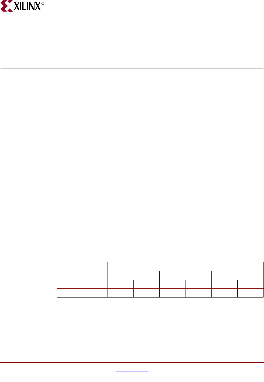
Memory Interface Solutions User Guide www.xilinx.com 395
UG086 (v3.6) September 21, 2010
R
Chapter 10
Implementing QDRII SRAM Controllers
This chapter describes how to implement QDRII SRAM interfaces for Virtex®-5 FPGAs
generated by MIG. This design is based on XAPP853 [Ref 26].
Feature Summary
This section summarizes the supported and unsupported features of the QDRII controller
design.
Supported Features
The QDRII controller design supports the following:
• A maximum frequency of 300 MHz
• 18-bit, 36-bit, and 72-bit data widths
•Burst lengths of four and two
• Implementation using different Virtex-5 devices
• Support for DCI Cascading
• Operation with 18-bit and 36-bit memory components
•Verilog and VHDL
• With and without a testbench
• With and without a PLL
Design Frequency Ranges
Unsupported Features
The QDRII controller design does not support:
• 9-bit data widths
• 9-bit memory components
Table 10-1: Design Frequency Range in MHz
Memory
FPGA Speed Grade
-1 -2 -3
MinMaxMinMaxMinMax
Component 120 250 120 300 120 300
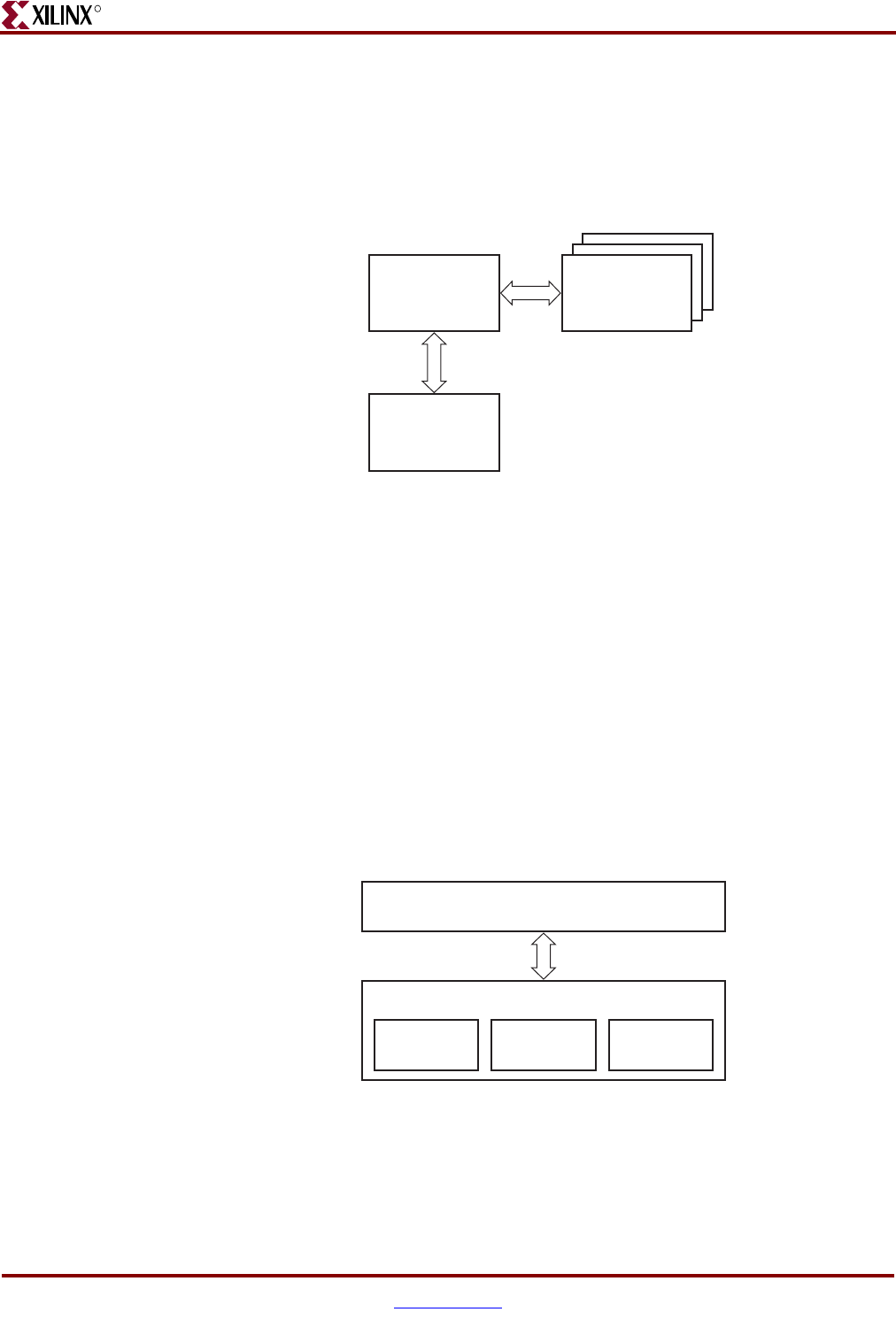
396 www.xilinx.com Memory Interface Solutions User Guide
UG086 (v3.6) September 21, 2010
Chapter 10: Implementing QDRII SRAM Controllers
R
Architecture
Figure 10-1 shows a top-level block diagram of the QDRII memory controller. One side of
the QDRII memory controller connects to the user interface denoted as User Interface. The
other side of the controller interfaces to QDRII memory. The memory interface data width
is selectable from MIG.
The QDR operation can support double data rated read and write operations through
separate data output and input ports with the same cycle. Memory bandwidth is
maximized because data can be transferred into SRAM on every edge of the clock and
transferred out of SRAM on every edge of the read clock. Independent read and write ports
eliminate the need for high-speed bus turnaround.
Read and write addresses are latched on positive edges of the input clock K. A common
address bus is used to access the addresses for both read and write operations. The key
advantage to QDRII devices is they have separate data buses for reads and writes to
SRAM.
Interface Model
The QDRII memory interface is layered to simplify the design and make the design
modular. Figure 10-2 shows the layered memory interface in the QDRII memory controller.
The two layers are the application layer and the implementation and physical layer.
The application layer creates the user interface, which initiates memory writes and reads
by writing data and memory addresses to the User Interface FIFOs.
The implementation and physical layer comprises:
Figure 10-1: QDRII Memory Controller
QDRII
Memory
Controller
User
Interface
Virtex-5 FPGA
UG086_c10_01_070506
QDRII
Memory
Figure 10-2: Interface Layering Model
User Interface
Implementation and Physical Layer
UG086_c10_02_071206
Clocks and
Reset Datapath Control
Memory Interface Solutions User Guide www.xilinx.com 397
UG086 (v3.6) September 21, 2010
Architecture
R
• Clocks and reset generation logic
• Datapath logic
• Control logic
Clocks and reset generation logic constitute a PLL/DCM primitive, which derives
different phase-shifted versions of the user-supplied differential clocks (sys_clk_p and
sys_clk_n). These phase-shifted versions of clocks run throughout the controller design. A
200 MHz user-supplied differential clock is used for the idelay control elements. Reset
signals are generated for different clock domains using the user-supplied reset signal
(sys_rst_n), the locked signal, and idelay control elements ready signal.
The Datapath logic consists of the memory write clocks, the read clocks, the data write
generation logic, and the read data capturing logic.
The Control logic constitutes read/write command generation logic, depending on the
status signals of the User Interface FIFO.
The above mentioned logic interfaces with memory through IDDRs, ODDRs, OFLOPs,
ISERDES elements, etc., which are associated with the physical layer.
Hierarchy
Figure 10-3 shows the hierarchical structure of the QDRII SRAM design generated by MIG
with a testbench and a PLL.
Figure 10-3: Hierarchical Structure of the Virtex-5 FPGA QDRII SRAM Design
<top_
module>
qdrii_
top
qdrii_
idelay_
ctrl
qdrii_
tb_top
qdrii_
top_phy
qdrii_top_
ctrl_sm
qdrii_top_
user_
interface
qdrii_
infrastructure
qdrii_phy_
addr_io
qdrii_phy_
read
qdrii_phy_
clk_io
qdrii_
phy_bw
_io
qdrii_
phy_d_
io
qdrii_
phy_cq
_io
Design Modules
qdrii_
phy_init
_sm
qdrii_
phy_en
qdrii_
phy_q
_io
qdrii_
phy_v5
_q_io
qdrii_
phy_dly
_cal_sm
qdrii_top_
rd_
interface
qdrii_top_
wr_
interface
qdrii_top_
wr_addr_
interface
qdrii_top_
wr_data_
interface
UG086_c10_03_012709
qdrii_top_
wrdata_
fifo
qdrii_top_
wrdata_
bw_fifo
qdrii_top_
rd_addr_
interface
qdrii_test_
wr_rd_sm
qdrii_test_
addr_gen
qdrii_test_
data_gen
Te st Bench Modules
Clocks and Reset Generation Modules
qdrii_test_
cmp_data
qdrii_test_
q_sm
qdrii_phy_
write

398 www.xilinx.com Memory Interface Solutions User Guide
UG086 (v3.6) September 21, 2010
Chapter 10: Implementing QDRII SRAM Controllers
R
The modules are classified as follows:
• Design modules
• Testbench modules
• Clocks and reset generation modules
MIG can generate four different QDRII SRAM designs:
• With a testbench and a PLL
• Without a testbench and with a PLL
• With a testbench and without a PLL
• Without a testbench and without a PLL
MIG outputs both an example_design and a user_design. The MIG-generated
example_design includes the entire memory controller design along with a synthesized
testbench (example user application). This testbench generates sample writes and reads
and then uses comparison logic to verify that the data patterns written are the same as
those received. This example_design can be used to test functionality both in simulation
and in hardware. The user_design only includes the memory controller design. The yellow
shaded modules in Figure 10-3 are not present in the design. This design allows users to
connect the MIG memory controller design to a user developed testbench (user
application). Refer to Table 10-5, page 414 for user interface signals and to “User Interface
Accesses,” page 415 for timing restriction on user interface signals.
Design clocks and resets are generated in the infrastructure module. The PLL/DCM clock
is instantiated in the infrastructure module for designs with a PLL. The inputs to this
module are the differential design clock and a 200 MHz differential clock for the
IDELAYCTRL module. A user reset is also input to this module. Using the input clocks and
reset signal, system clocks and system reset signals are generated in this module, which are
used in the design.
The PLL/DCM primitive is not instantiated in this module if the “No PLL” option is
selected. So, the system operates on the user-provided clocks. The system reset signals are
generated in the infrastructure module using the locked input signal, the input reset signal,
and the idelay control element’s ready signal. For more information on the clocking
structure, refer to “Clocking Scheme,” page 410.
The QDRII design is generated in two configurations with and without a testbench
(example_design and user_design respectively). The top-level module with testbench
(example_design) has the design top, testbench, IDELAY control, and clock and reset
modules. Without a testbench (user_design), the mem_test_bench module is removed
from the top-level module. By default, MIG outputs both designs (example_design and
user_design) in two separate RTL folders, and the user can choose the appropriate design.
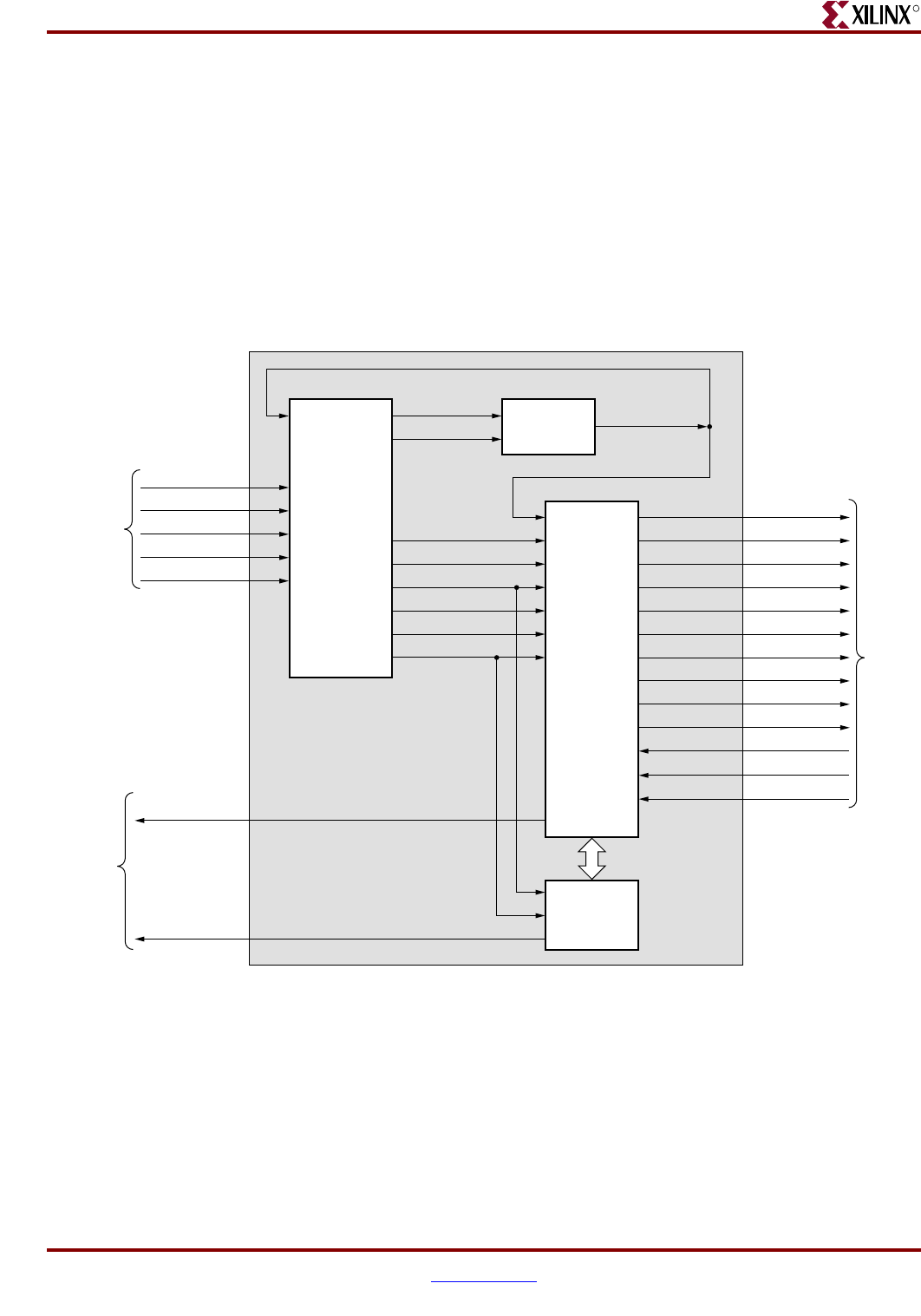
Memory Interface Solutions User Guide www.xilinx.com 399
UG086 (v3.6) September 21, 2010
Architecture
R
Figure 10-4 shows a top-level block diagram of a QDRII SRAM design with a PLL and a
testbench. The sys_clk_p and sys_clk_n pair are differential input system clocks. “Clocking
Scheme,” page 410 describes how various clocks are generated using the PLL. The PLL is
instantiated in the infrastructure module that generates the required design clocks.
dly_clk_200_p and dly_clk_200_n are used for the idelay_ctrl element. Sys_rst_n is an
active-Low system reset signal. All design resets are generated using the sys_rst_n signal,
the locked signal, and the dly_ready signal of the IDELAYCTRL element. The
compare_error output signal indicates whether the design passes or fails. The testbench
module called “tb_top” generates the user interface data, address, and command signals.
The user data bits and address bits are stored in the corresponding User Interface FIFOs.
The compare_error signal is driven High on data mismatches. The cal_done signal
indicates the completion of initialization and calibration of the design.
Figure 10-4: Top-Level Block Diagram of the QDRII SRAM Design with a PLL and a Testbench
qdr2_top
tb_top
idelay_ctrl_rdy
clk200
Memory
Device
UG086_c10_04_091707
Status
Signals
System
Clocks
and Reset
idelay_ctrl
Infrastructure
user_rst_200
clk180
clk270
clk0
user_rst_180
user_rst_0
dly_clk_200_p
dly_clk_200_n
sys_clk_p
sys_clk_n
sys_rst_n
user_rst_270
qdr_r_n
qdr_w_n
qdr_bw_n
qdr_dll_off_n
qdr_sa
qdr_k
qdr_k_n
qdr_c
qdr_c_n
qdr_cq
qdr_q
qdr_d
qdr_cq_n
cal_done
compare_error
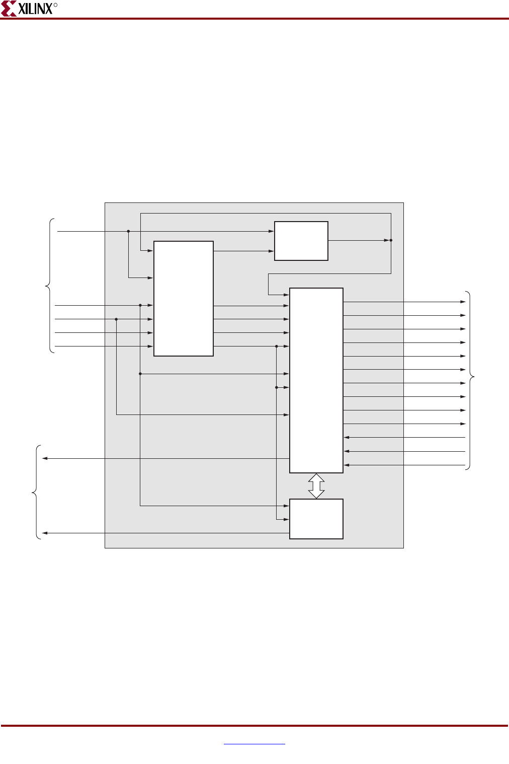
400 www.xilinx.com Memory Interface Solutions User Guide
UG086 (v3.6) September 21, 2010
Chapter 10: Implementing QDRII SRAM Controllers
R
Figure 10-5 shows a top-level block diagram of a QDRII SRAM design without a PLL but
with a testbench. The user should provide all the clocks and the locked signal. “Clocking
Scheme,” page 410 explains how to generate the design clocks from the user interface.
These clocks should be single-ended. sys_rst_n is the active-Low system reset signal. All
design resets are generated using the sys_rst_n signal, the locked signal, and the dly_ready
signal of the IDELAYCTRL element. The user application must have a PLL/DCM
primitive instantiated in the design, and all user clocks should be driven through BUFGs.
The compare_error output signal indicates whether the case passes or fails. The testbench
module called “tb_top” generates the user interface data, address, and command signals.
The user data bits and address bits are stored in the corresponding User Interface FIFOs
The compare_error signal is driven High on data mismatches. The cal_done signal
indicates the completion of initialization and calibration of the design.
Figure 10-6, page 401 shows a top-level block diagram of a QDRII SRAM design with a
PLL but without a testbench. The sys_clk_p and sys_clk_n pair are differential input
system clocks. “Clocking Scheme,” page 410 describes how various clocks are generated
using the PLL. The PLL is instantiated in the infrastructure module that generates the
required design clocks. dly_clk_200_p and dly_clk_200_n are used for the idelay_ctrl
element. Sys_rst_n is an active-Low system reset signal, and all design resets are generated
using the sys_rst_n signal, the locked signal, and the dly_ready signal of the IDELAYCTRL
element. The user has to drive the user application signals. The design provides the clk0_tb
and user_rst_0_tb signals to the user in order to synchronize the user application signals
Figure 10-5: Top-Level Block Diagram of the QDRII SRAM Design without a PLL but with a Testbench
qdr2_top
tb_top
idelay_ctrl_rdy
clk200
Memory
Device
UG086_c10_05_012709
Status
Signals
User
Clocks and
System
Reset
idelay_ctrl
Infrastructure
user_rst_200
user_rst_180
user_rst_0
clk200
clk0 clk180
clk270
locked
sys_rst_n
user_rst_270
qdr_r_n
qdr_w_n
qdr_bw_n
qdr_dll_off_n
qdr_sa
qdr_k
qdr_k_n
qdr_c
qdr_c_n
qdr_cq
qdr_d
qdr_cq_n
qdr_q
cal_done
compare_error
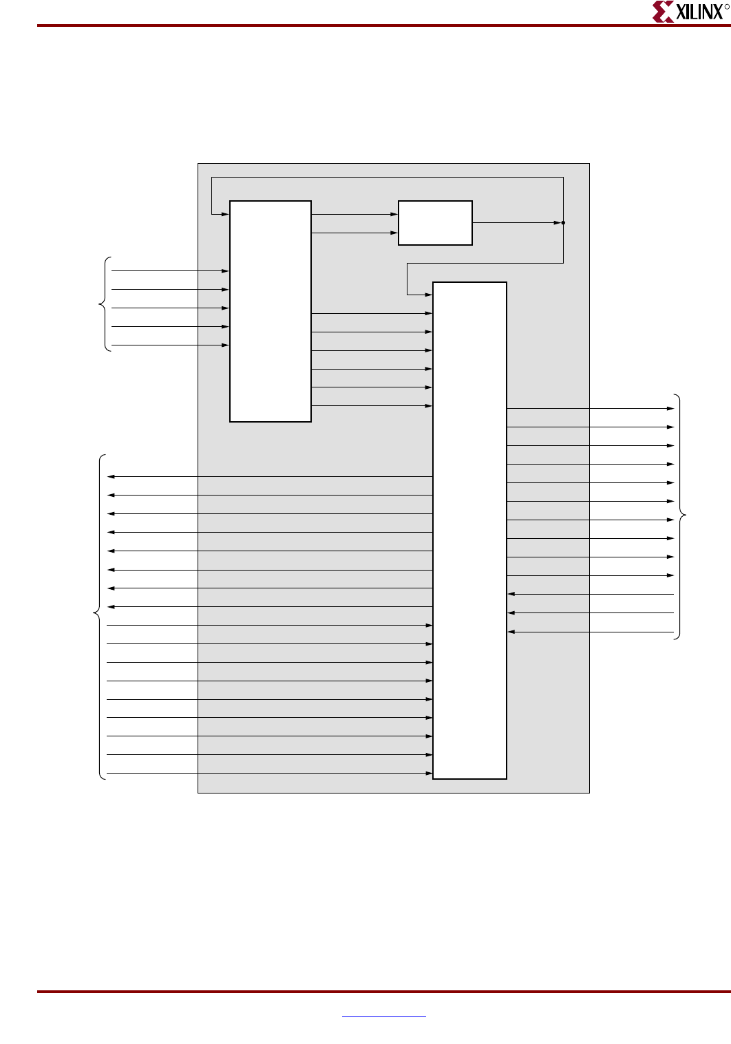
Memory Interface Solutions User Guide www.xilinx.com 401
UG086 (v3.6) September 21, 2010
Architecture
R
with the design. The signal clk0_tb is connected to clock clk0 in the controller. If the user
clock domain is different from clk0/clk0_tb, the user should add FIFOs for all the input
and outputs of the controller (user application signals) in order to synchronize them to
clk0_tb.The cal_done signal indicates the completion of initialization and calibration of the
design.
Figure 10-7, page 402 shows a top-level block diagram of a QDRII SRAM design without a
PLL or a testbench. The user should provide all the clocks and the locked signal. “Clocking
Scheme,” page 410 explains how to generate the design clocks from the user interface.
These clocks should be single-ended. sys_rst_n is the active-Low system reset signal. All
design resets are generated using the sys_rst_n signal, the locked signal, and the dly_ready
signal of the IDELAYCTRL element. The user application must have a PLL/DCM
primitive instantiated in the design, and all user clocks should be driven through BUFGs.
Figure 10-6: Top-Level Block Diagram of the QDRII SRAM Design with a PLL but without a Testbench
qdr2_top
idelay_ctrl_rdy
clk200
Memory
Device
UG086_c10_06_091707
User
Interface
Signals
System
Clocks
and Reset
idelay_ctrl
Infrastructure
user_rst_200
clk180
clk270
clk0
user_rst_180
user_rst_0
dly_clk_200_p
dly_clk_200_n
sys_clk_p
sys_clk_n
sys_rst_n
user_rst_270
qdr_r_n
qdr_w_n
qdr_bw_n
qdr_dll_off_n
qdr_sa
qdr_k
qdr_k_n
qdr_c
qdr_c_n
qdr_cq
qdr_q
qdr_d
qdr_cq_n
clk0_tb
user_rst_0_tb
user_wr_full
user_rd_full
user_qr_valid
user_qrl
user_qrh
cal_done
user_ad_w_n
user_d_w_n
user_r_n
user_dwl
user_dwh
user_bwl_n
user_bwh_n
user_ad_wr
user_ad_rd
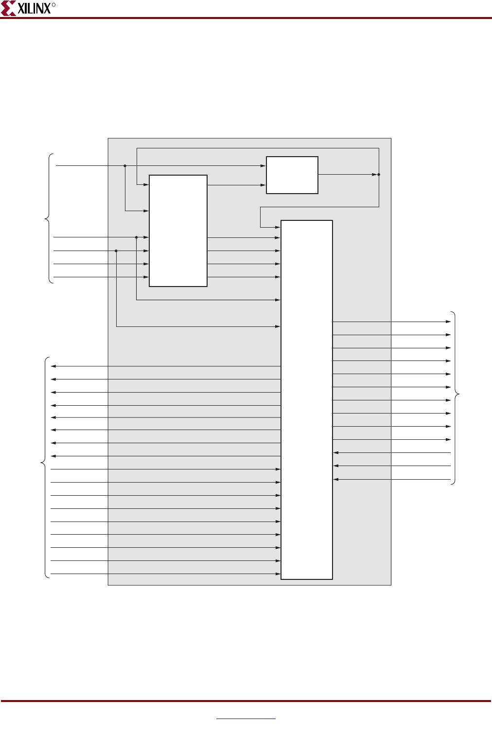
402 www.xilinx.com Memory Interface Solutions User Guide
UG086 (v3.6) September 21, 2010
Chapter 10: Implementing QDRII SRAM Controllers
R
The user has to drive the user application signals. The design provides the clk0_tb and
user_rst_0_tb signals to the user in order to synchronize the user application signals with
the design. The clk0_tb signal is connected to the clk0 clock in the controller. If the user
clock domain is different from clk0/clk0_tb, the user should add FIFOs for all the inputs
and outputs of the controller (user application signals) in order to synchronize them to
clk0_tb. The cal_done signal indicates the completion of initialization and calibration of the
design.
Figure 10-7: Top-Level Block Diagram of the QDRII SRAM Design without a PLL or a Testbench
qdr2_top
idelay_ctrl_rdy
Memory
Device
UG086_c10_07_012709
User
Clocks and
System
Reset
idelay_ctrl
Infrastructure
user_rst_200
user_rst_180
user_rst_0
clk200
clk0 clk180
clk270
locked
sys_rst_n
user_rst_270
qdr_r_n
qdr_w_n
qdr_bw_n
qdr_dll_off_n
qdr_sa
qdr_k
qdr_k_n
qdr_c
qdr_c_n
qdr_cq
qdr_d
qdr_cq_n
qdr_q
User
Interface
Signals
clk0_tb
user_rst_0_tb
user_wr_full
user_rd_full
user_qr_valid
user_qrl
user_qrh
cal_done
user_ad_w_n
user_d_w_n
user_r_n
user_dwl
user_dwh
user_bwl_n
user_bwh_n
user_ad_wr
user_ad_rd
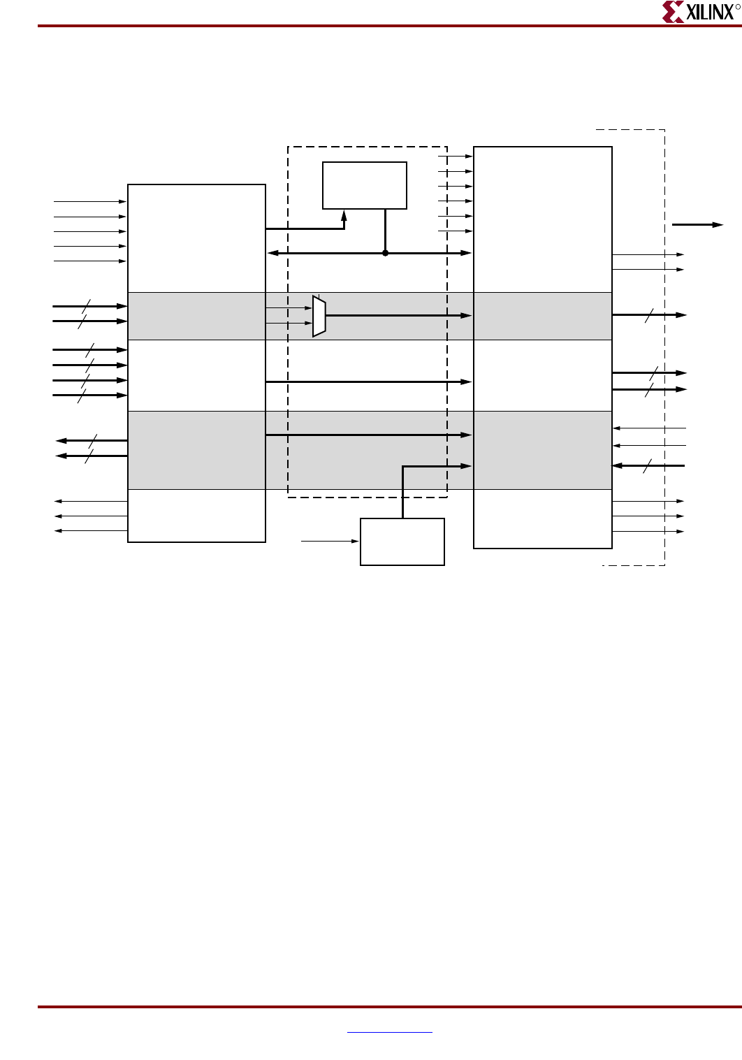
Memory Interface Solutions User Guide www.xilinx.com 403
UG086 (v3.6) September 21, 2010
Architecture
R
QDRII Memory Controller Modules
Figure 10-8 shows a detailed block diagram of the QDRII memory controller.
Controller
The QDRII memory controller initiates alternate WRITE and READ commands to the
memory as long as the User Write Address FIFO and the User Read Address FIFO are not
empty.
The user writes the write data, its corresponding byte write enable, and the Write Address
bits into the User Write Data FIFOs, the User Byte Write FIFO, and the User Write Address
FIFOs, respectively. When the User Write Address FIFO is not empty, the QDRII controller
generates a write-enable signal to the memory. When the write enable is asserted, the write
data, the byte write enable, and the write address bits are transferred to memory from the
User Write Data FIFOs, the User Byte Write FIFO, and the User Write Address FIFO,
respectively.
The read address from where the data is to be read from the memory is stored by the user
in the User Read Address FIFO. The QDRII memory controller generates a read-enable
signal to the memory when the User Read Address FIFO is not empty. When the read
enable is asserted, the read address from the Read Address FIFO is transferred to memory.
When the read data from the memory corresponding to the read address is captured
correctly, a valid user_qr_valid signal is asserted High. The user can access the read data
corresponding to the read address only when the data valid signal user_qr_valid is
asserted High.
Figure 10-8: QDRII Memory Controller Modules using FIFO Interface
User Interface
Physical Interface
Read / Write
State Machine
Read / Write Control
Address Path
FIFO Status
QDRII
Memory
Device
clk0
user_rst_0
user_d_w_n
user_r_n
user_ad_wr
user_ad_rd
user_bwh_n
user_dwl
user_dwh
user_qrl
user_qrh
user_wr_full
user_rd_full
user_qr_valid
qdr_r_n
qdr_w_n
qdr_sa
qdr_bw_n
qdr_d
qdr_cq
qdr_k
qdr_k_n
user_rst_0
user_rst_180
user_rst_270
clk0
clk180
clk270
user_ad_w_n
Write Path
Read Path
clk0 qdr_dll_off_n
user_bwl_n
qdr_cq_n
qdr_q
Delay
Calibration
State Machine
UG086_c10_08_091707
Memory Controller
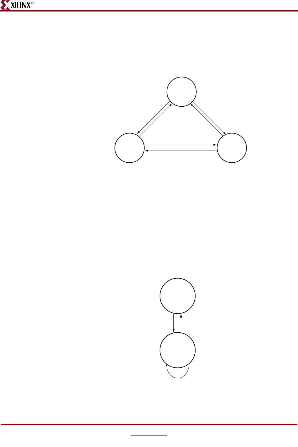
404 www.xilinx.com Memory Interface Solutions User Guide
UG086 (v3.6) September 21, 2010
Chapter 10: Implementing QDRII SRAM Controllers
R
Figure 10-9 shows a state machine of the QDRII memory controller for burst lengths of
four. When calibration is complete (that is, when the cal_done signal is asserted), the state
machine is in the IDLE state. When the User Write Address FIFO is not empty (that is,
when the user has written the write data, the byte write enable, and the write address bits
into their corresponding FIFOs, respectively), the state machine goes to the WRITE state,
initiating a memory write of one burst.
When the User Read Address FIFO is not empty (that is, the user has written read address
bits into the User Read Address FIFO), the state machine goes to the READ state, initiating
a memory read of one burst.
From the IDLE state, the QDRII memory controller can go to either the WRITE or the
READ state depending on the status of the User FIFOs. Writes are given priority. In the
WRITE state, a memory write is initiated, and the User Read Address Not Empty status is
checked in order to transfer into the READ state. When the User Read Address FIFO is
empty, the state machine goes to the IDLE state.
In the READ state, a memory read is initiated, and the User Write Address FIFO Not
Empty status is checked before going to the WRITE state. If the User Address FIFO is
empty, the state machine goes to the IDLE state.
Figure 10-10 shows a state machine of the QDR II memory controller for burst lengths of
two when the FIFO user interface is used. When calibration is complete, the state machine
Figure 10-9: QDRII Memory Controller State Machine with Burst Lengths of 4
Figure 10-10: QDRII Memory Controller State Machine with Burst Lengths of 2
IDLE
RD
RD
WR
WR WRITE
R_n=1
W_n=0
READ
R_n=0
W_n=1
UG086_c10_09_013107
IDLE
WRITE_
READ
W_n=0
R_n=0
UG086_c10_14_122007

Memory Interface Solutions User Guide www.xilinx.com 405
UG086 (v3.6) September 21, 2010
Architecture
R
is in the IDLE state. When the User Write Address FIFO is not empty (that is, when the user
has written the write data, the byte write enable, and the write address bits into their
corresponding FIFOs), the state machine goes to the WRITE_READ state, initiating a
memory write of one complete burst. When the User Read Address FIFO is not empty (that
is, the user has written read address bits into the User Read Address FIFO), the state
machine goes to the READ_WRITE state, initiating a memory read of one complete burst.
From the IDLE state, the QDR II memory controller goes to WRITE_READ state if either:
• the User Write Address FIFO is not empty, or
• the User Read Address FIFO is not empty.
In the WRITE_READ state, the User Read Address Not Empty status is checked to initiate
a memory read. To initiate a memory write in the WRITE_READ state, the User Write
Address FIFO not empty status is checked. If both the User Write Address FIFO and the
User Read Address FIFO are empty, the state machine goes to the IDLE state. If either the
User Write Address FIFO or the User Read Address FIFO is not empty, the state machine
remains in the WRITE_READ state to issue memory writes or reads.
Refer to XAPP853 [Ref 26] for data capture techniques and timing analysis of the QDRII
memory controller module.
Burst Length of Two Design without FIFO Interface
In designs with a burst length of two, user commands can be transferred directly to the
physical layer. This design does not rely on the controller state machine to provide the
write and read commands and instead forwards the commands directly to the physical
layer.
The user can select this option by setting the BURST2_FIFO_INTERFACE parameter in the
design_top file to FALSE. This option can be used when a write address and a read address
need to be issued to the memory on the same cycle, the empty flag status of the Read
Address FIFO and Write Address FIFO can be different, and the command order needs to
be preserved.
Infrastructure
The infrastructure module generates the design clocks and reset signals. When differential
clocking is used, sys_clk_p, sys_clk_n, clk_200_p, and clk_200_n signals appear. When
single-ended clocking is used, sys_clk and idly_clk_200 signals appear. In addition, clocks
are available for design use and a 200 MHz clock is provided for the IDELAYCTRL
primitive. Differential and single-ended clocks are passed through global clock buffers
before connecting to a PLL/DCM. For differential clocking, the output of the
sys_clk_p/sys_clk_n buffer is single-ended and is provided to the PLL/DCM input.
Likewise, for single-ended clocking, sys_clk is passed through a buffer and its output is
provided to the PLL/DCM input. The outputs of the PLL/DCM are 180° and 270° phase-
shifted versions of the input clock. After the PLL/DCM is locked, the design is in the reset
state for at least 25 clocks. The infrastructure module also generates all of the reset signals
required for the design.
PLL/DCM
In MIG 3.0 and later, the DCM is replaced with a PLL for all Virtex-5 FPGA designs. If the
user selects a design with a PLL in the GUI, the infrastructure module will have both PLL
and DCM codes. The CLK_GENERATOR parameter enables either a PLL or a DCM in the
infrastructure module. The CLK_GENERATOR parameter is set to PLL by default. If the
user wants to use DCM, this parameter should be changed manually to DCM.

406 www.xilinx.com Memory Interface Solutions User Guide
UG086 (v3.6) September 21, 2010
Chapter 10: Implementing QDRII SRAM Controllers
R
Idelay_ctrl
This module instantiates the IDELAYCTRL primitive of the Virtex-5 FPGA. The
IDELAYCTRL primitive is used to continuously calibrate the individual delay elements in
its region to reduce the effect of process, temperature, and voltage variations. A 200 MHz
clock has to be fed to this primitive.
MIG uses the “automatic” method for IDELAYCTRL instantiation in which the MIG HDL
only instantiates a single IDELAYCTRL for the entire design. No location (LOC)
constraints are included in the MIG-generated UCF. This method relies on the ISE® tools to
replicate and place as many IDELAYCTRLs as needed (for example, one per clock region
that uses IDELAYs). Replication and placement are handled automatically by the software
tools if IDELAYCTRLs have same refclk, reset, and rdy nets. A new constraint called
IODELAY_GROUP associates a set of IDELAYs with an IDELAYCTRL and allows for
multiple IDELAYCTRLs to be instantiated without LOC constraints specified. ISE software
generates the IDELAY_CTRL_RDY signal by logically ANDing the RDY signals of every
IDELAYCTRL block.
The IODELAY_GROUP name should be checked in the following cases:
• The MIG design is used with other IP cores or user designs that also require the use of
IDELAYCTRL and IDELAYs.
• Previous ISE software releases 8.2.03i and 9.1i had an issue with IDELAYCTRL block
replication and trimming. When using these revisions of the ISE software, the user
must instantiate and constrain the location of each IDELAYCTRL individually.
See UG190 [Ref 10] for more information on the requirements of IDELAYCTRL placement.
top_phy
This module is the interface between the controller and the memory. It consists of the
following:
• Control logic that generates READ/WRITE commands and address signals to the
memory.
• Write Data logic that associates the write data, the byte enable, and the write address
with the WRITE commands and the read address with the READ commands. It also
generates the write data pattern for calibration purposes.
• Read Data logic that comprises the read data capturing scheme and calibration logic.
IODELAY Performance Mode
In Virtex-5 family devices, the power dissipation of the IODELAY elements can be
controlled using the HIGH_PERPORMANCE_MODE parameter. The values of this
parameter can be either TRUE or FALSE.
When this parameter value is set to TRUE, the IODELAY jitter valuer per tap is reduced.
This reduction results in a slight increase in power dissipation from the IODELAY element.
When this parameter value is set to FALSE, the IODELAY power dissipation is reduced,
but with an increase in the jitter value per tap.
The value of this parameter can be selected from the MIG FPGA options page. Users can
also manually set this parameter value to TRUE or FALSE in the design top-level block
HDL module.
Refer to Appendix E, “Debug Port” for more information on the IODELAY Performance
Mode.

Memory Interface Solutions User Guide www.xilinx.com 407
UG086 (v3.6) September 21, 2010
Architecture
R
Multicontrollers
MIG supports multicontrollers for QDRII SRAMs and multiple interfaces for QDRII
SRAMs and DDR2 SDRAMs. Up to eight controllers are supported. In multicontroller and
multiple interface designs, every controller can have a different frequency. The number of
controllers that can have different frequencies is limited by the number of PLLs available in
the selected FPGA. For example, a total of six PLL resources are available for the
XC5VLX50 device, so a maximum of six controllers can have different frequencies. Even
though the number of controllers selected in the GUI is eight, a maximum of six controllers
can have different frequencies. Thus, for the remaining two controllers, the user should
select one of the already selected frequencies. Refer to the Virtex-5 FPGA User Guide
[Ref 10] for PLL resources available for various devices.
For a single controller design, all memory signals and user interface signals appear as
shown in Figure 10-8, page 403 and Table 10-5, page 414 based on the selected part. For a
multicontroller design, all memory signal names and user interface signal names are
prepended with the controller number. For example, for a two controller design (two
QDR2 controllers), the qdr_d port appears as c0_ qdr_d and c1_ qdr_d. A similar naming
convention is followed for the design parameters. Some parameters such as
HIGH_PERFORMANCE_MODE, CLK_TYPE, and RST_ACT_LOW are common for all
the controllers and do not have the controller number prepended.
DCI Cascading
In Virtex-5 family devices, I/O banks that need DCI reference voltage can be cascaded with
other DCI I/O banks. One set of VRN/VRP pins can be used to provide reference voltage
to several I/O banks. With DCI cascading, one bank (the master bank) must have its
VRN/VRP pins connected to external reference resistors. Other banks in the same column
(slave banks) can use DCI standards with the same impedance as the master bank, without
connecting the VRN/VRP pins on these banks to external resistors. DCI impedance control
in cascaded banks is received from the master bank. This results in more usable pins and in
reduced power usage because fewer VR pins and DCI controllers are used.
The syntax for representing the DCI Cascading in the UCF is:
CONFIG DCI_CASCADE = "<master> <slave1> <slave2> ...";
There are certain rules that need to be followed in order to use DCI Cascade option:
1. The master and slave banks must all reside on the same column (left, center, or right)
on the device.
2. Master and slave banks must have the same VCCO and VREF (if applicable) voltages.
This feature enables placing all 36 bits of read data, as well as the CQ and CQ# clocks, in the
same bank when interfacing with 36-bit QDRII components.
MIG supports DCI Cascading. Following are the possibilities for generating the designs
with DCI support using the DCI Cascade option.
• For x36 component designs, the DCI Cascade option is always enabled. This feature
cannot be disabled if DCI support is needed.
• For x18 component designs, DCI Cascade is optional. DCI support for these designs
can be selected with or without the DCI Cascade selection.
• For x18 component with 18-bit data width designs, the DCI Cascade option is
disabled and cannot be utilized.
When DCI Cascade option is selected, MIG displays the master bank selection box for each
column of the FPGA in the bank selection page.

408 www.xilinx.com Memory Interface Solutions User Guide
UG086 (v3.6) September 21, 2010
Chapter 10: Implementing QDRII SRAM Controllers
R
• If an FPGA has no banks or has only non-DCI banks in a particular column, the
master bank selection box for that column is not displayed.
• All the data read banks are treated as slave banks.
• When a data read bank is selected in a particular column, the master bank selection
box for that particular column is activated and the rest of the master bank selection
boxes for other columns are deactivated.
• In a particular column, when a data read bank is selected and there are no DCI banks
left in that column for master banks selection, then the design cannot be generated.
The data read banks must be moved to the other columns in order to select the master
banks.
• The master bank selection box shows all the bank numbers in that particular column
other than the data read banks and non-DCI banks in that column.
• There can be only one master bank selected for each column of banks.
• MIG utilizes VRN/VRP pins in the slave banks for pin allocation.
• For each master, VRN/VRP pins are reserved. When a selected master bank does not
have any data read pins then a dummy input pin called masterbank_sel_pin is
allocated and assigned the HSTL_I_DCI_18 I/O standard.
• The dummy input pin is required to satisfy the requirement of the master bank. Any
master bank should have at least one input pin to program the DCI option, and the
I/O standard of the master and slave banks should be the same.
• When all the banks in a particular column are allocated with data read pins, MIG
chooses only the required banks for data read pins allocation depending upon the
design data width. When there is only one bank allocation for data read pins in a
column of banks of an FPGA, then that particular data read bank should not be
selected as a master bank. Doing so would result in an inappropriate DCI Cascade
syntax in the UCF of the generated design.
The center column banks of all the FPGAs are divided into two sections, top-column banks
and bottom-column banks. Top-column banks are the banks available above the 0th bank,
and the bottom column banks are the banks available below 0th bank. Therefore, there are
two master bank selection boxes for the center column.
The VRN/VRP pins for a master bank do not need to be reserved in the reserve pins page.
Once the design is ready with the valid master and slave bank selection, the same master
and slave bank information (along with the DCI Cascading syntax) is provided in the UCF
when the design is generated.
For more information about DCI Cascade, refer to DCI Cascading in the Virtex-5 FPGA
User Guide [Ref 10] and the Xilinx® Constraints Guide.
CQ/CQ_n Implementation
Controller uses CQ and CQ_n for capturing read data of a 36-bit component. CQ and CQ_n
are placed on the P pins of the clock-capable I/Os. For a 36-bit component, CQ is used to
capture the first 18 bits of the read data, and CQ_n is used to capture the second 18 bits of
the read data. For an 18-bit component, only CQ is used for capturing the read data. CQ_n
is not used, and it is connected to a dummy logic. This dummy logic is used just to retain
CQ_n pin during PAR. Users can use the CQ_n pin if needed.

Memory Interface Solutions User Guide www.xilinx.com 409
UG086 (v3.6) September 21, 2010
QDRII SRAM Initialization and Calibration
R
Pinout Considerations
It is recommended to select banks within the same column in MIG. This helps to avoid the
clock tree skew that the design would incur while crossing from one column to another.
When the Data Read, Data Write, Address, and System Control pins are allocated to
individual banks in a column, then the System Control pins must be allocated in a bank
that is central to the rest of banks allocated. This helps reduce datapath and clock path
skew.
For larger FPGAs (for example, FF1738, FF1760, and similar), it is recommended to place
Data Read, Data Write, Address, and System Control pins in the same column to reduce
datapath and clock path skew.
Test Bench
MIG generates two RTL folders, example_design and user_design. The example_design
includes the synthesizable test bench, while user_design does not include the test bench
modules. The MIG test bench performs one write command followed by one read
command in an alternating manner for designs with a burst length of 4. For a burst length
of 2, the test bench performs one write command and one read command in the same clock
and repeats one write and one read command continuously. The number of words in a
write command depends on the burst length. For a burst length of 4, the test bench writes
a total 4 data words for a single write command (2 rise data words and 2 fall data words).
For a burst length of 2, the test bench writes a total of 2 data words. The data pattern is an
incremental pattern. On every write command, the data pattern is incremented by one, and
this is repeated with each subsequent write command. The initial data pattern for the first
write command is 000. The test bench writes the 000, 001, 002, 003 data pattern in a
sequence in which 000 and 002 are rise data words, and 001 and 003 are fall data words
for a 9-bit design. The falling edge data is always rising edge data plus one. For a burst
length of 2, the data sequence for the first write command is 000, 001. The data sequence
for the second write command is 002, 003. The pattern is then incremented for the next
write command. For data widths greater than 9, the same data pattern is concatenated for
the other bits. For a 36-bit design and a burst length of 4, the data pattern for the first write
command is 000000000, 008040201, 010080402, 0180C0603.
Address generation logic generates the address in an incremental pattern for each write
command. The same address location is repeated for the next read command. In Samsung
components, the burst address increments are done by the memory, so the address is
generated by the test bench in a linear incremental pattern. In Cypress parts, the MIG test
bench increments the address for burst operation. After the address reaches the maximum
value, it rolls back to the initial address, i.e., 00000.
During reads, comparison logic compares the read pattern with the pattern written, i.e., the
000, 001, 002, 003 pattern. For example, for a 9-bit design of burst length 4, the data
written for a single write command is 000, 001, 002, and 003. During reads, the read
pattern is compared with the 000, 001, 002, 003pattern. Based on a comparison of the
data, a status signal error is generated. If the data read back is the same as the data written,
the error signal is 0, otherwise it is 1.
QDRII SRAM Initialization and Calibration
QDRII memory is initialized through a specified sequence. Following initialization, the
relationship between the data and the FPGA clock is calculated using the TAP logic. The
calibration logic is explained briefly as follows.

410 www.xilinx.com Memory Interface Solutions User Guide
UG086 (v3.6) September 21, 2010
Chapter 10: Implementing QDRII SRAM Controllers
R
Calibration is done in three stages:
1. The read strobe CQ is edge-aligned with the read data Q from the memory. The read
strobe is a free-running clock from the memory. In the first stage of calibration, the read
strobe CQ is passed through the BUFIO, which delays the strobe by the amount of
delay in the BUFIO. Now the read strobe CQ is out of synchronization with the read
data Q.
A pattern of four bursts of data (with a value of '1' for rise data and '0' for fall data) is
written into a particular location in memory. Continuous read commands are issued to
the same location of the memory and the read data Q is delayed in the ISERDES, until
it is center-aligned with respect to the delayed read strobe CQ.
The q_init_delay_done signal in the phy_read module indicates the status of the first
stage calibration. When q_init_delay_done is asserted High, it indicates the
completion of first-stage calibration. Now the CQ clocks are centered with respect to
the Read Data Q at the input of the ISERDES.
2. In the second stage of calibration, the read data window is center-aligned with respect
to the FPGA clock. Here another pattern of four bursts of data is written into a
particular memory location. It is read back continuously from the same memory
location, and the read data and the delay clock, CQ, are delayed until the registered
read data is center-aligned with the FPGA clock.
When the registered read data is center-aligned with the FPGA clock, the alignment of
the read data Q with respect to the FPGA clock is complete. The dly_cal_done signal in
the phy_read module indicates the status of second-stage calibration.
3. In the third stage of calibration, the controller issues non-consecutive read commands
to the memory. The internal read command signal generated by the controller is then
delayed through a shift register until the delayed read command signal is aligned with
the ISERDES read data output. Then another level of calibration is done to ensure
alignment between the ISERDES data outputs from all the banks used in the interface.
This finishes the calibration of the read data Q, and the cal_done signal is asserted
High.
XAPP853 [Ref 26] provides more information about the calibration architecture.
The user must strictly follow the pattern data and not modify it. The timing diagrams in
“QDRII Controller Interface Signals” explain the user interface commands until the
calibration is finished.
Clocking Scheme
Figure 10-12, page 412 shows the clocking scheme for this design. Global and local clock
resources are used.
The global clock resources consist of a PLL or a DCM, two BUFGs on PLL/DCM output
clocks, and one BUFG for clk200. The local clock resources consist of regional I/O clock
networks (BUFIO). The global clock architecture is discussed in this section.
The MIG tool allows the user to customize the design such that the PLL/DCM is not
included. In this case, system clocks clk0 and clk270, and IDELAYCTRL clock clk200 must
be supplied by the user.
Global Clock Architecture
The user must supply two input clocks to the design:
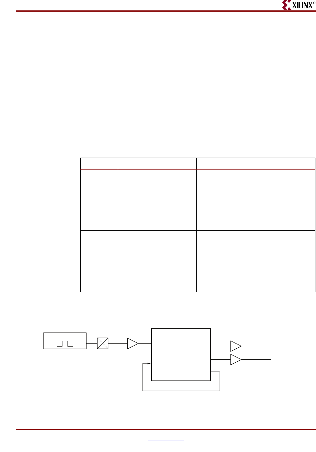
Memory Interface Solutions User Guide www.xilinx.com 411
UG086 (v3.6) September 21, 2010
Clocking Scheme
R
• A system clock running at the target frequency for the memory
• A 200 MHz clock for the IDELAYCTRL blocks.
These clocks can be either single-ended or differential. The user can select a single-ended
or differential clock input option from the MIG GUI. Differential clocks are connected to
the IBUFGDS and the single-ended clock is connected to an IBUFG.
The system clock from the output of the IBUFGDS or the IBUFG is connected to the
PLL/DCM to generate the various clocks used by the memory interface logic.
The clk200 output of the IBUFGDS or the IBUFG is connected to the BUFG. The output of
the BUFG is used for IDELAY IOB delay blocks for aligning read capture data.
The PLL/DCM generates two separate synchronous clocks for use in the design. This is
shown in Table 10-2, Figure 10-11, and Figure 10-12. The clock structure is same for both
example design and user design. For designs without PLL/DCM instantiation, the
PLL/DCM and the BUFGs should be instantiated at user end to generate the required
clocks.
Table 10-2: QDRII Interface Design Clocks
Clock Description Logic Domain
clk0 Skew compensated replica
of the input system clock.
The clock for the controller and the user
interface logic. The QDRII bus-related I/O
flip-flops (e.g., memory clocks). This clock
is used to register the data, address, and
command signals, and the address and
data enables for the user interface logic(1).
This clock is also used to generate the FIFO
status signals.
clk270 270° phase-shifted version
of clk0
Used in the write data path section of
physical layer. Clocks write path control
logic, the QDRII side of the Write Data
FIFO, and output flip-flops for D and
memory control and address signals. This
clock is also used to generate the read data
and read data valid signals for the user
interface logic(1).
Notes:
1. See “User Interface Accesses,” page 415 for timing requirements and restrictions on the user interface
signals.
Figure 10-11: Clocking Scheme for QDRII Interface Logic Using PLL
CLKIN
CLKFBIN CLKOUT1
CLKOUT0
clk270
clk0
PLL BUFG
GC I/O
SYSTEM CLK
UG086_c10_22_012709
CLKFBOUT
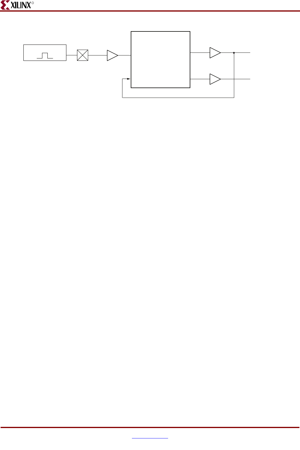
Memory Interface Solutions User Guide www.xilinx.com 413
UG086 (v3.6) September 21, 2010
QDRII Controller Interface Signals
R
QDRII Controller Interface Signals
Table 10-3 through Table 10-4 describe the QDRII controller system interface signals with
and without a PLL, respectively. Table 10-5 describes the QDRII user interface signals.
Table 10-6 describes the QDRII memory interface signals. In these tables, all signal
directions are with respect to the QDRII memory controller.
Table 10-3: QDRII SRAM System Interface Signals (with a PLL)
Signal Name Direction Description
sys_clk_p, sys_clk_n Input System clock input made up of differential clock pairs. This clock
pair goes to a differential input buffer. The differential buffer output
goes to the PLL/DCM input. The PLL/DCM generates the required
clocks for the design. This input system clock pair is present only
when the DIFFERENTIAL clocks option is selected in the MIG
FPGA options page.
sys_clk Input Single-ended system clock input. This clock goes to a IBUFG. The
IBUFG output goes to the PLL/DCM input. The PLL/DCM
generates the required clocks for the design. This input system
clock is present only when the SINGLE_ENDED clocks option is
selected in MIG FPGA options.
When the PLL option is deselected, both differential or single-
ended input system clocks are not present.
dly_clk_200_p, dly_clk_200_n Input 200 MHz differential clock used in the idelay_ctrl logic. This input
clock pair is present only when the DIFFERENTIAL clocks option
is selected in the MIG FPGA options.
idly_clk_200 Input Single-ended 200 MHz IDELAYCTRL clock input. This clock is
connected to an IBUFG. The IBUFG output is connected to input of
BUFG. The output of this BUFG acts as IDELAYCTRL clock input.
This input system clock is present only when the SINGLE_ENDED
clocks option is selected in the MIG FPGA options.
When the PLL option is deselected, both differential or single-
ended input system clocks are not present.
sys_rst_n Input Reset to the QDRII memory controller.
compare_error Output This signal represents the status of comparison of read data when
compared to the corresponding write data.
cal_done Output This signal is asserted when the design initialization and calibration
is complete.
Table 10-4: QDRII SRAM System Interface Signals (without a PLL)
Signal Name Direction Description
clk0 Input Input clock
clk270 Input Input clock with a 270° phase difference
clk200 Input 200 MHz clock for Idelayctrl primitives
locked Input This active-High signal indicates whether the user PLL/DCM is locked
or not.
414 www.xilinx.com Memory Interface Solutions User Guide
UG086 (v3.6) September 21, 2010
Chapter 10: Implementing QDRII SRAM Controllers
R
sys_rst_n Input Reset to the QDRII memory controller
compare_error Output This signal represents the status of the comparison between the read
data with the corresponding write data.
cal_done Output This signal is asserted when the design initialization and calibration is
complete.
Table 10-4: QDRII SRAM System Interface Signals (without a PLL) (Cont’d)
Signal Name Direction Description
Table 10-5: QDRII SRAM User Interface Signals (without a Testbench [user_design])
Signal Name Direction Description
user_wr_full Output This signal indicates the User Write FIFO status. It is asserted
when either the User Write Address FIFO or the User Write
Data FIFO is full. When this signal is asserted, any writes to
the User Write Address FIFO and the User Write Data FIFO
are invalid, possibly leading to controller malfunction.
user_rd_full Output This signal indicates the User Read Address FIFO status. It is
asserted when the User Read Address FIFO is full. When this
signal is asserted, any writes to the User Read Address FIFO
are ignored.
user_qr_valid Output This status signal indicates that data read from the memory
is available to the user.
clk0_tb Output All user interface signals are to be synchronized to this clock.
user_rst_0_tb Output This reset is active until the PLL/DCM is not locked.
user_dwl [(DATA_WIDTH-1):0] Input Positive-edge data for memory writes. This data bus is valid
when user_d_w_n is asserted.
user_dwh [(DATA_WIDTH-1):0] Input Negative-edge data for memory writes. This data bus is valid
when user_d_w_n is asserted.
user_qrl [(DATA_WIDTH-1):0] Output Positive-edge data read from memory. This data is output
when user_qen_n is asserted.
user_qrh [(DATA_WIDTH-1):0] Output Negative-edge data read from memory. This data is output
when user_qen_n is asserted.
user_bwl_n [(BW_WIDTH-1):0] Input Byte enables for QDRII memory positive-edge write data.
The byte enables are valid when user_d_w_n is asserted.
user_bwh_n [(BW_WIDTH-1):0] Input Byte enables for QDRII memory negative-edge write data.
The byte enables are valid when user_d_w_n is asserted.
user_ad_wr [(ADDR_WIDTH-1):0](1) Input QDRII memory address for write data. This address is valid
when user_ad_w_n is asserted.
user_ad_rd [(ADDR_WIDTH-1):0](1) Input QDRII memory address for read data. This address is valid
when user_r_n is asserted.
user_ad_w_n Input This active-Low signal is the write enable for the User Write
Address FIFO.
Memory Interface Solutions User Guide www.xilinx.com 415
UG086 (v3.6) September 21, 2010
QDRII Controller Interface Signals
R
User Interface Accesses
The user backend logic communicates with the memory controller through a FIFO-based
user interface for designs with a burst length of four. This FIFO interface is optional for
designs with a burst length of two.
The following section describes the user backend timing and the FIFO interface. Designs
with a burst length of two that do not use the FIFO use the same timing as that of the FIFO
interface. This FIFO interface consists of four related buses:
• A Write Address FIFO bus accepts memory write address from the user
• A Write Data FIFO bus accepts the write data corresponding to the memory write
address
• A Read Address FIFO bus accepts the memory read address from the user
The user interface has the following timing and signaling restrictions:
• The Write/Read Address and Write Data FIFOs cannot be written by the user until
calibration is complete (as indicated by cal_done). In addition, the user_ad_w_n,
user_d_w_n Input This active-Low signal is the write enable for the User Write
Data FIFO and Byte Write FIFOs.
user_r_n Input This active-Low signal is the write enable for the User Read
Address FIFO.
Notes:
1. The number of address bits used depends on the density of the memory part. The controller ignores the unused bits, which can all
be tied to High.
Table 10-5: QDRII SRAM User Interface Signals (without a Testbench [user_design]) (Cont’d)
Signal Name Direction Description
Table 10-6: QDRII SRAM Interface Signals
Signal Name Direction Description
qdr_d Output During WRITE commands, the data is sampled on both edges of K.
qdr_q Input During READ commands, the data is sampled on both edges of FPGA
clk.
qdr_bw_n Output Byte enables for QDRII memory write data. These enable signals are
sampled on both edges of the K clock.
qdr_sa Output Address for READ and WRITE operations
qdr_w_n Output This signal represents the WRITE command.
qdr_r_n Output This signal represents the READ command.
qdr_cq, qdr_cq_n Input These signals are the read clocks transmitted by the QDRII SRAM.
Both CQ and CQ_n are used for data capture in this design.
qdr_k, qdr_k_n Output Differential write data clocks
qdr_c, qdr_c_n Output Input clock to memory for the output data
qdr_dll_off_n Output Memory DLL disable when Low

416 www.xilinx.com Memory Interface Solutions User Guide
UG086 (v3.6) September 21, 2010
Chapter 10: Implementing QDRII SRAM Controllers
R
user_d_w_n, and user_r_n interface signals need to be held High until calibration is
complete.
• For issuing a write command, the memory write address must be written into the
Read Address FIFO. The first write data word must be written to the Write Data FIFO
on the same clock cycle as the when the write address is written. In addition, the write
data burst must be written over consecutive clock cycles; there cannot be a break
between bursts of data. These restrictions arise from the fact that the controller
assumes write data is available when it receives the write command from the user.
• The clk0_tb signal is connected to clk0 in the controller. If the user clock domain is
different from clk0 / clk0_tb of MIG, the user should add FIFOs for all data inputs and
outputs of the controller in order to synchronize them to the clk0_tb. The timing for
the non-FIFO user interface for controllers with a burst length of two is the same as
that of the FIFO interface. With respect to the user backend, the timing remains the
same for both the FIFO and non-FIFO user interface.
User Interface
The user interface has two interfaces: a Read user interface and a Write user interface.
The Read user interface consists of the Read Address interface modules. The Read Address
interface consists of the Read Address FIFO. The user has to write the read address bits of
the memory into this FIFO.
The Write User interface consists of the Write Data interface and the Write Address
interface. The Write Address interface consists of the Write Address FIFO. The user has to
write the write address bits of the memory into this FIFO.
The Write Data interface consists of the Write Data FIFO and the Byte Write FIFO. The
width of the Write Data FIFO depends upon the data width of the controller design. There
are two Write Data FIFOs for every controller: the LSB Write Data FIFO and the MSB Write
Data FIFO. The outputs of these FIFOs are SDR and are later converted to DDR at the
ODDR primitive before transferring to memory.
The Byte Write enable signals are stored in the Byte Write FIFO by the user.
The controller monitors the status signals of these User FIFOs and issues the
READ/WRITE commands to the memory.
The user must wait until the cal_done signal is asserted by the controller, which indicates
completion of calibration prior to writing the user data to the Write Data FIFOs, Byte Write
FIFO, and Write Address FIFO. Even if the user wants to write any data in to these FIFOs
before the completion of calibration, the data does not get written to these FIFOs. These
Write Data FIFOs and Byte Write FIFOs write enable signals are considered valid only after
the calibration is complete.
Refer to the timing diagrams in “QDRII Controller Interface Signals” for how the user can
access these FIFOs.
The FIFO36 and FIFO36_72 primitives are used for loading address and data from the user
interface. The FIFO36 primitive is used in the qdrii_top_wr_addr_interface,
qdrii_top_rd_addr_interface, and qdrii_top_wrdata_bw_fifo modules. The FIFO36_72
primitive is used in the qdrii_top_wrdata_fifo module. Every FIFO has two FIFO threshold
attributes, ALMOST_EMPTY_OFFSET and ALMOST_FULL_OFFSET, that are both set to
128 in the RTL, by default. These values can be changed as needed. For valid FIFO
threshold offset values, refer to UG190 [Ref 10].
Memory Interface Solutions User Guide www.xilinx.com 417
UG086 (v3.6) September 21, 2010
QDRII Controller Interface Signals
R
Table 10-7 lists the signals between the user interface and the controller.
Table 10-7: Signals between User Interface and Controller
Port Name Port Width Port Description
wr_empty 1
Empty status signal from Write Address FIFO. Monitors the
FIFO empty status flags to issue write commands. If the
Write Address FIFO is empty, the controller stops issuing
write commands.
rd_empty 1
Empty status signal from Read Address FIFO. Monitors the
FIFO empty status flag to issue read commands. If the Read
Address FIFO is empty, the controller stops issuing read
commands.
wr_init_n 1
Active-Low write command from the controller state
machine. This write command is used for generation of the
memory write command and also is used as a read enable
signal to the Write Address FIFO and Write Data FIFO.
rd_init_n 1
Active-Low read command from the controller state
machine. This read command is used for generation of the
memory read command and also is used as a read enable
signal to the read address FIFO.
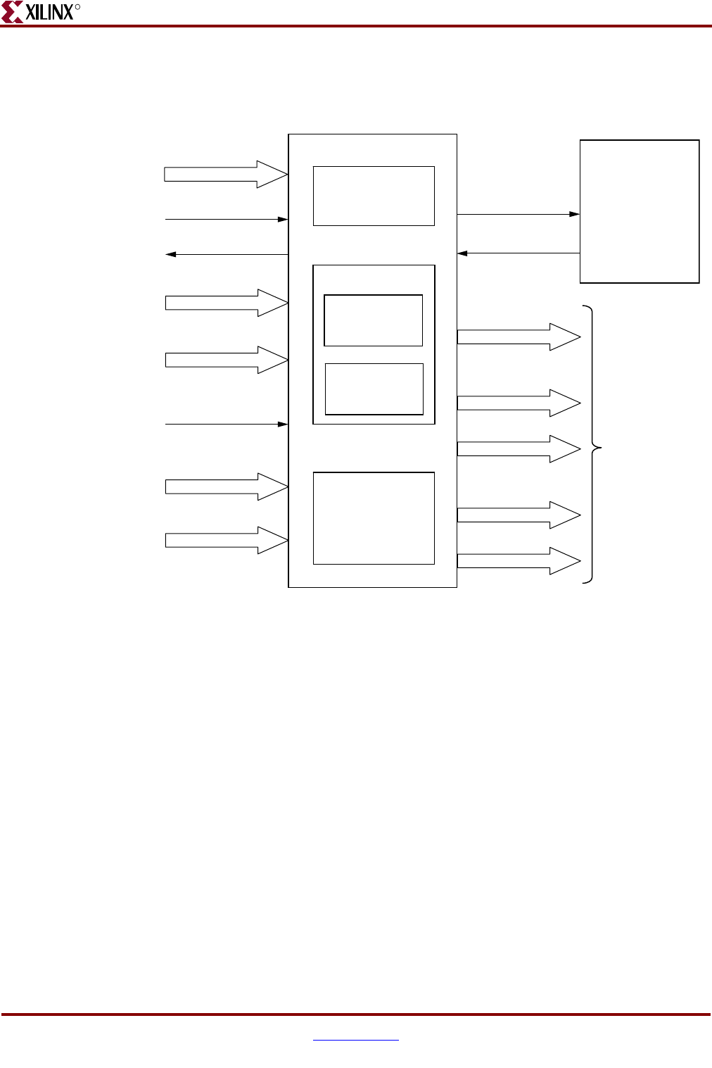
418 www.xilinx.com Memory Interface Solutions User Guide
UG086 (v3.6) September 21, 2010
Chapter 10: Implementing QDRII SRAM Controllers
R
Write Interface
Figure 10-13 illustrates the user interface block diagram for write operations.
The following steps describe the architecture of Address and Write Data FIFOs and how to
perform a write burst operation to QDRII memory from user interface.
1. The user interface consists of an Address FIFO, Data FIFOs, and a Byte Write FIFO.
These FIFOs are built out of Virtex-5 FPGA FIFO primitives. The Address FIFO is a
FIFO36 primitive with 1K x 36 configuration. The Data FIFO is a FIFO36_72 primitive
with 512 x 72 configuration.
2. The Address FIFO is used to store the memory address where the data is to be written
from the user interface. A single instantiation of a FIFO36 constitutes the Address
FIFO.
3. Two separate sets of Data FIFOs are used for storing the rising-edge and falling-edge
data to be written to QDRII memory from the user interface. For 9-bit, 18-bit, and 36-bit
configurations, the controller pads the extra bits of the Data FIFO with 0s.
4. The Byte Write FIFO is used to store the Byte Write signals to QDRII memory from the
user interface. Extra bits are padded with zeros.
5. The user can initiate a write command to memory by writing to the Write Address
FIFO, Write Data FIFO, and Byte Write FIFOs when the FIFO full flags are deasserted
and after the calibration done signal cal_done is asserted. The user should not access
any of these FIFOs until cal_done is asserted. During the calibration process, the
Figure 10-13: Write FIFO User Interface Block Diagram
User Interface
Controller
Address FIFO
(FIFO36)
1024 x 36
Byte Write FIFO
(FIFO36)
1024 x 36
fifo_wr_empty
wr_init_n
user_ad_wr
user_ad_w_n
user_dwl
user_dwh
user_bwl_n
user_bwh_n
fifo_dwl
fifo_ad_wr
fifo_dwh
fifo_bw_l
fifo_bw_h
To top_phy
user_wr_full
Rise Data FIFO
(FIFO36_72)
512 x 72
Fall Data FIFO
(FIFO36_72)
512 x 72
Data FIFOs
user_d_w_n
ug086_c10_15_122007
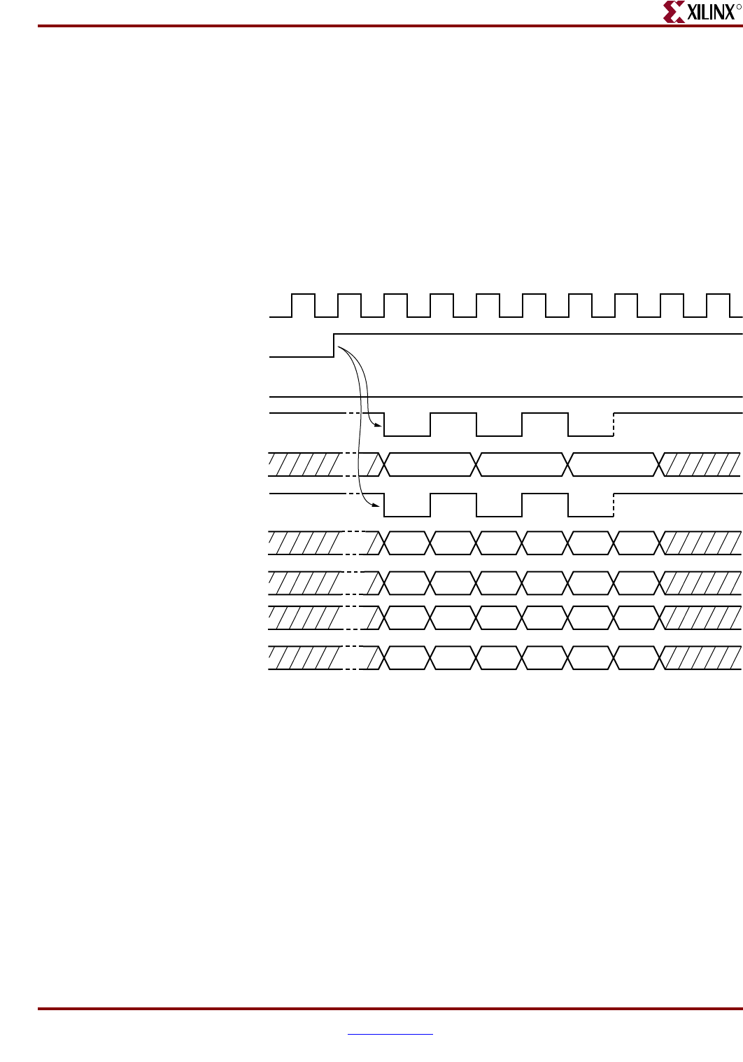
Memory Interface Solutions User Guide www.xilinx.com 419
UG086 (v3.6) September 21, 2010
QDRII Controller Interface Signals
R
controller writes pattern data into the Data FIFOs. The cal_done signal assures that the
clocks are stable, the reset process is completed, and the controller is ready to accept
commands. Status signal user_wr_full is asserted when the Address FIFO, Data FIFOs,
or Byte Write FIFOs are full.
6. When signal user_ad_w_n is asserted, user_ad_wr is stored in the Address FIFO.
When signal user_d_w_n signal is asserted, user_dwl and user_dwh are stored into
the Data FIFO, and user_bwl and user_bwh are stored into the Byte Write FIFOs. For
proper controller functionality, user_ad_w_n and user_d_w_n must be asserted and
deasserted simultaneously.
7. The controller reads the Address, Data, and Byte Write FIFOs when they are not empty
by issuing the wr_init_n signal. The QDRII memory write command is generated from
the wr_init_n signal by properly timing it.
8. Figure 10-14 shows the timing diagram for a write command with a burst length of
four. The address should be asserted for one clock cycle as shown. For BL = 4, each
write to the Address FIFO has two writes to the Data FIFO consisting of two rising-
edge and two falling-edge data.
9. Figure 10-15 shows the timing diagram for a write command with a burst length of
two. For BL = 2, each write to the Address FIFO has one write to Data FIFO, consisting
of one rising-edge and one falling-edge data. Commands can be given in every clock
when BL = 2.
When BURST2_FIFO_INTERFACE is set to FALSE in design_top, the timing shown in
Figure 10-15 must be followed from the user side. Corresponding address and write
data are provided in the same cycle associated with asserting user_ad_w_n and
user_d_w_n. The user_wr_full and user_rd_full signals are tied Low in this case.
Figure 10-14: Write FIFO User Interface Timing Diagram for BL = 4
clk0_tb
cal_done
user_wr_full
user_ad_w_n
user_d_w_n
user_ad_wr
user_dwl
user_dwh
DWL-00 DWL-01 DWL-10 DWL-11 DWL-20 DWL-21
DWH-00 DWH-01 DWH-10 DWH-11 DWH-20 DWH-21
user_bwl_n
iser_bwh_n
BWL-00 BWL-01 BWL-10 BWL-11 BWL-20 BWL-21
BWH-00 BWH-01 BWH-10 BWH-11 BWH-20 BWH-21
UG086_c10_16_122007
A0 A1 A2
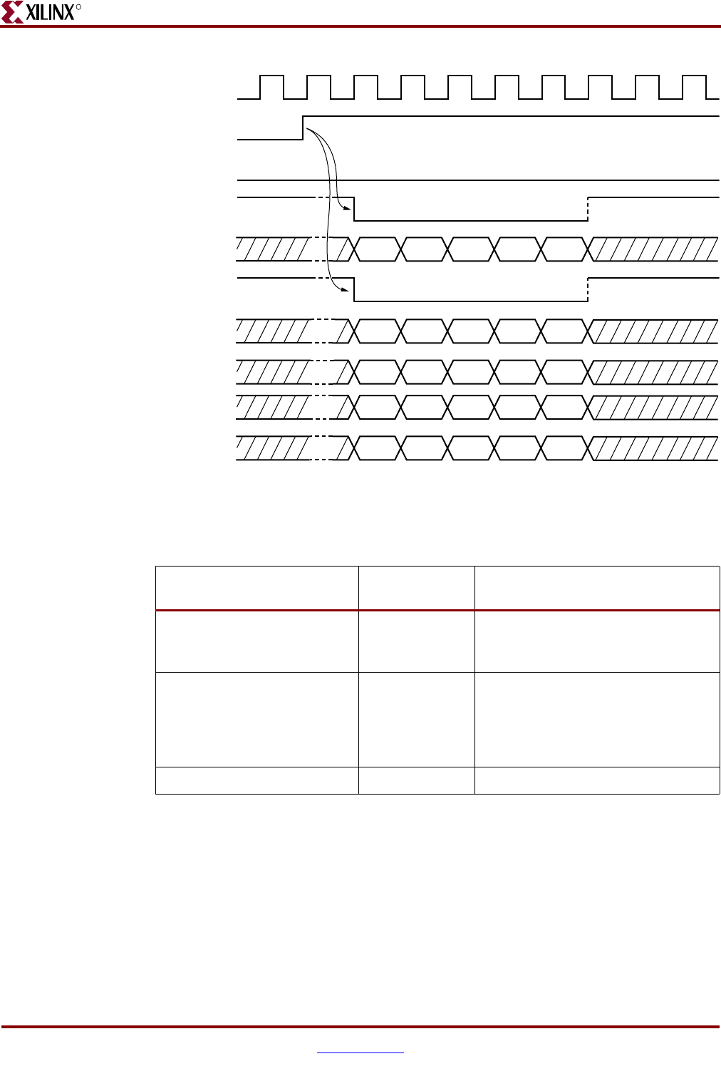
420 www.xilinx.com Memory Interface Solutions User Guide
UG086 (v3.6) September 21, 2010
Chapter 10: Implementing QDRII SRAM Controllers
R
Table 10-8 shows the write latency of the controller.
For a design with a burst length of two without FIFOs, the total write latency becomes 4.5
cycles. This is because the four clock cycle latency of the empty signal deassertion of the
Write Address FIFO does not apply.
Figure 10-15: Write FIFO User Interface Timing Diagram for BL = 2
Table 10-8: Maximum Write Latency
Parameter Number of
Clock Cycles Description
User write command to Write
Address FIFO empty flag
6• 2 clock cycles for register stages
• 4 clock cycles for empty flag
deassertion in the FWFT mode
Read empty flag to command
to the memory
2.5 • 1 clock cycle to generate the write
command in the controller state
machine
• 1.5 cycles to transfer the command
to the memory
Total Latency 8.5
clk0_tb
cal_done
user_wr_full
user_ad_w_n
user_d_w_n
user_ad_wr
user_dwl
user_dwh
DWL-0 DWL-1 DWL-2 DWL-3DWL-4
DWH-0 DWH-1 DWH-2 DWH-3DWH-4
A0 A1 A3A2 A4
user_bwl_n
iser_bwh_n
BWL-0 BWL-1 BWL-2 BWL-3BWL-4
BWH-0 BWH-1 BWH-2 BWH-3BWH-4
UG086_c10_17_122007
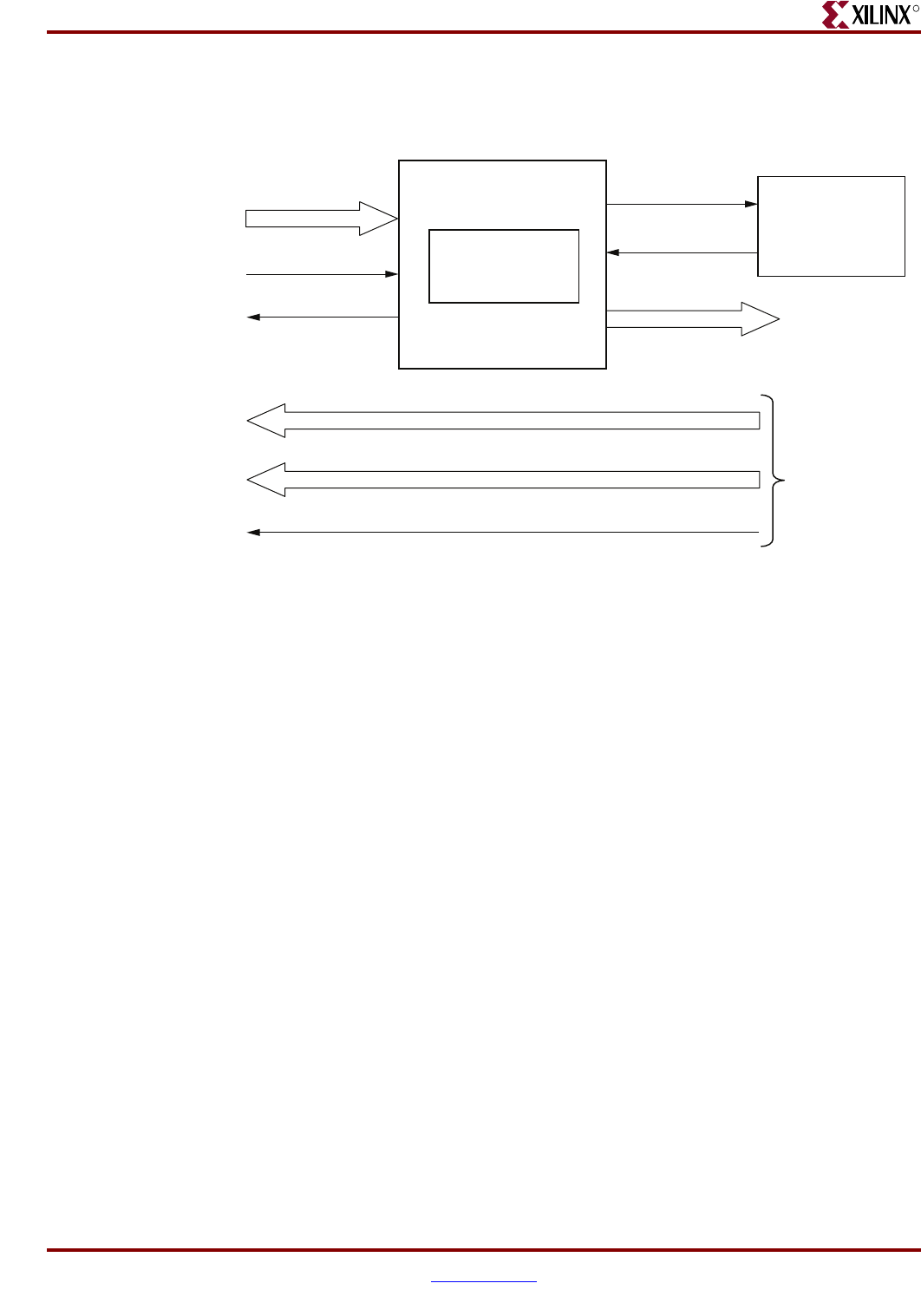
Memory Interface Solutions User Guide www.xilinx.com 421
UG086 (v3.6) September 21, 2010
QDRII Controller Interface Signals
R
Read Interface
Figure 10-16 shows a block diagram for the read interface.
The following steps describe the architecture of the read user interface and how to perform
a QDRII SRAM burst read operation.
1. The read user interface consists of an Address FIFO built out of a Virtex-5 FPGA
FIFO36 of configuration 1K x 16.
2. To initiate a QDRII read command, the user writes the Address FIFO when the FIFO
full flag user_rd_full is deasserted and the calibration done signal cal_done is asserted.
Writing to the Address FIFO is an indication to the controller that it is a Read
command. The cal_done signal assures that the controller clocks are stable, the internal
reset process is completed, and the controller is ready to accept commands.
3. The user should issue the Address FIFO write-enable signal user_r_n along with read
address user_ad_rd to write the read address to the Address FIFO.
4. The controller reads the Address FIFO when status signal fifo_rd_empty is deasserted
and generates the appropriate control signals to QDRII memory required for a read
command.
5. Prior to the actual read and write commands, the design calibrates the latency in
number of clock cycles from the time the read command is issued to the time the data
is received. Using this precalibrated delay information, the controller generates the
user valid signal user_qr_valid.
6. The High state of the user_qr_valid signal indicates that read data is available.
7. The user must access the read data as soon as user_qr_valid is asserted High.
8. Figure 10-17 and Figure 10-18 show the user interface timing diagrams for BL = 4 and
BL = 2.
9. After the read address is loaded into the Read Address FIFO, it can take a maximum of
14 clock cycles, worst case, for the controller to assert user_qr_valid High.
Figure 10-16: Read FIFO User Interface Block Diagram
Controller
fifo_rd_empty
rd_init_n
user_ad_rd
user_r_n
user_qrl
user_qrh
fifo_ad_rd
From top_phy
To top_phy
user_rd_full
user_qr_valid
UG086_c10_18_030308
User Interface
Address FIFO
(FIFO36)
1024 x 36
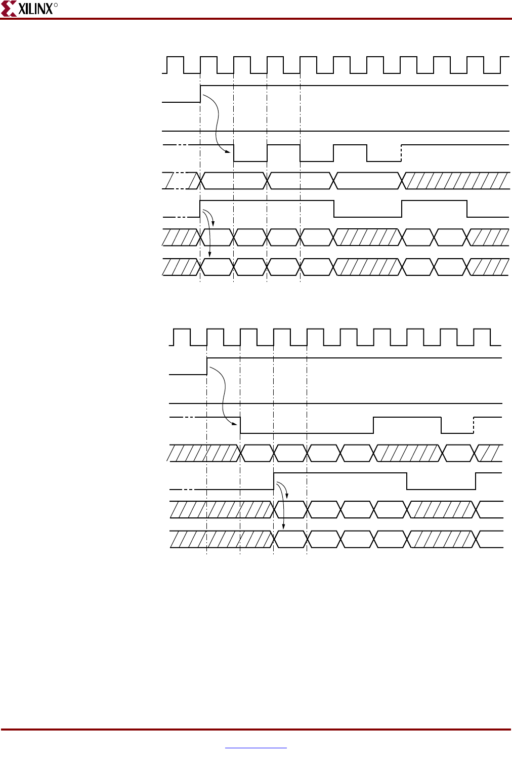
422 www.xilinx.com Memory Interface Solutions User Guide
UG086 (v3.6) September 21, 2010
Chapter 10: Implementing QDRII SRAM Controllers
R
The BL = 2 example without the FIFO user interface uses the same input signal timing on
the address, command, and data as the non-FIFO user interface.
Figure 10-17: Read User Interface Timing Diagram for BL = 4
Figure 10-18: Read User Interface Timing Diagram for BL = 2
clk0_tb
cal_done
user_rd_full
user_r_n
user_ad_rd
user_qrl
user_qrh
user_qr_valid
QRL-00 QRL-01 QRL-10 QRL-11 QRL-20 QRL-21
QRH-00 QRH-01 QRH-10 QRH-11 QRH-20 QRH-21
UG086_c10_19_122007
A0 A1 A2
clk0_tb
cal_done
user_rd_full
user_r_n
user_ad_rd
user_qrl
user_qrh
user_qr_valid
QRL-0 QRL-1 QRL-2 QRL-3QRL-4
QRH-0 QRH-1 QRH-2 QRH-3QRH-4
A0 A1 A2 A3A4
UG086_c10_20_122007
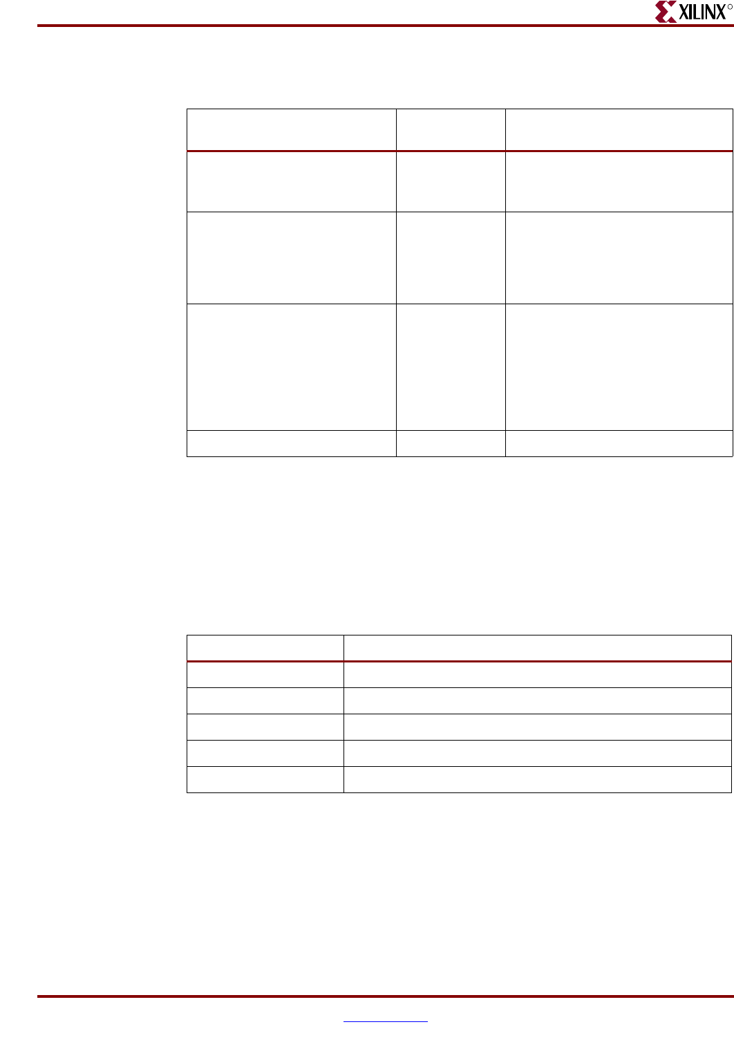
Memory Interface Solutions User Guide www.xilinx.com 423
UG086 (v3.6) September 21, 2010
QDRII Controller Interface Signals
R
Table 10-9 shows the read latency of the controller.
For a design with a burst length of two without FIFOs, the total read latency becomes 4.5
cycles. This is because the four clock cycle latency of the empty signal deassertion of the
Read Address FIFO does not apply.
QDRII SRAM Signal Allocations
Table 10-10 shows the list of signals for a QDRII SRAM design allocated in a group from
bank selection checkboxes in MIG.
MIG shows checkboxes for Address, Data_Write, Data_Read, System Control, and
System_Clock when a bank is selected for a QDRII SRAM design.
When the Address box is checked in a bank, the address, qdr_w_n, qdr_r_n, and
qdr_dll_off_n bits are assigned to that particular bank.
When the Data_Write box is checked in a bank, the memory data write, memory byte write
bits, the memory write clocks, and the memory input clock for the output data are assigned
to that particular bank.
Table 10-9: Maximum Read Latency
Parameter Number of
Clock Cycles Description
User read command to Read
Address FIFO empty flag
6• 2 clock cycles for register stages
• 4 clock cycles for empty flag
deassertion in the FWFT mode
Read empty flag to command to
the memory
2.5 • 1 clock cycle to generate the read
command in the controller state
machine
• 1.5 cycles to transfer the command
to the memory
Memory read command to valid
data available
5.5 • 1.5 clock cycles of memory read
latency
• 3 clock cycles to capture and
transfer read data to the FPGA
clock domain
• 1 clock cycle for aligning all the
read data captured
Total Latency 14
Table 10-10: QDRII Signal Allocations
Bank Selected Signals Allocated in the Group
Address Memory address and memory control
Data_Write Memory write data, memory byte write, and K and C clocks
Data_Read Memory read data and memory CQ
System Control System reset from the user interface and status signals
System Clock System clocks from the user interface
424 www.xilinx.com Memory Interface Solutions User Guide
UG086 (v3.6) September 21, 2010
Chapter 10: Implementing QDRII SRAM Controllers
R
When the Data_Read box is checked in a bank, the memory data read and memory read
clocks are assigned to that particular bank.
When the System Control box is checked in a bank, the sys_rst_n, compare_error, and
cal_done bits are assigned to that particular bank.
When the System Clock box is checked in a bank, the sys_clk_p, sys_clk_n, dly_clk_200_p,
and dly_clk_200_n bits are assigned to that particular bank.
For special cases, such as without a testbench and without a PLL, the corresponding input
and output ports are not assigned to any FPGA pins in the design UCF because the user
can connect these ports to the FPGA pins or can connect to some logic internal to the same
FPGA.
Note: Timing has been verified for most of the MIG generated configurations. For the best timing
results, adjacent banks in the same column of the FPGA should be used. Banks that are separated
by unbonded banks should be avoided because these can cause timing violations.
Supported Devices
The design generated out of MIG is independent of the memory package, hence the
package part of the memory component is replaced with X, where X indicates any package.
Table 10-11 shows the list of components supported by MIG.
Table 10-11: Supported Devices for QDRII SRAM
Virtex-5 FPGA (Verilog and VHDL)
Components Make Configuration
CY7C1314BV18-167BZXC Cypress x36
CY7C1315BV18-250BZC Cypress x36
CY7C1515V18-250BZC Cypress x36
K7R161882B-FC25 Samsung x18
K7R161884B-FC25 Samsung x18
K7R161884B-FC30 Samsung x18
K7R163682B-FC25 Samsung x36
K7R163684B-FC25 Samsung x36
K7R321884M-FC25 Samsung x18
K7R321884C-FC25 Samsung x18
K7R323682C-FC30 Samsung x36
K7R323684M-FC25 Samsung x36
K7R323684C-FC25 Samsung x36
K7R641882M-FC25 Samsung x18
K7R641884M-FC25 Samsung x18
K7R641884M-FC30 Samsung x18
426 www.xilinx.com Memory Interface Solutions User Guide
UG086 (v3.6) September 21, 2010
Chapter 10: Implementing QDRII SRAM Controllers
R
Simulating the QDRII SRAM Design
After generating the design, MIG creates a sim folder in the specified path. This folder
contains simulation files for a particular design. The sim folder contains the external
testbench, memory model, and .do file to simulate the generated design. The memory
model files are currently generated in Verilog only. To learn more details about the files in
the sim folder and to simulate the design, refer to “Simulation Guide,” page 499.
Hardware Tested Configurations
The frequencies shown in Table 10-12 were achieved on the Virtex-5 FPGA ML561 Memory
Interface Development Board under nominal conditions. This frequency should not be
used to determine the maximum design frequency. The maximum design frequency
supported in MIG wizard is based on combination of the TRCE results for fabric timing on
multiple device/package combinations and I/O timing analysis using FPGA and memory
timing parameter for a 72-bit wide interface.
Table 10-12: Hardware Tested Configurations
FPGA Device XC5VLX50TFF1136-2
Memory Component K7R643684M-FC30
Data width 72
Burst Length 4
Frequency 100 MHz to 360 MHz
Flow Vendors Synplicity and XST
Design Entry VHDL and Verilog
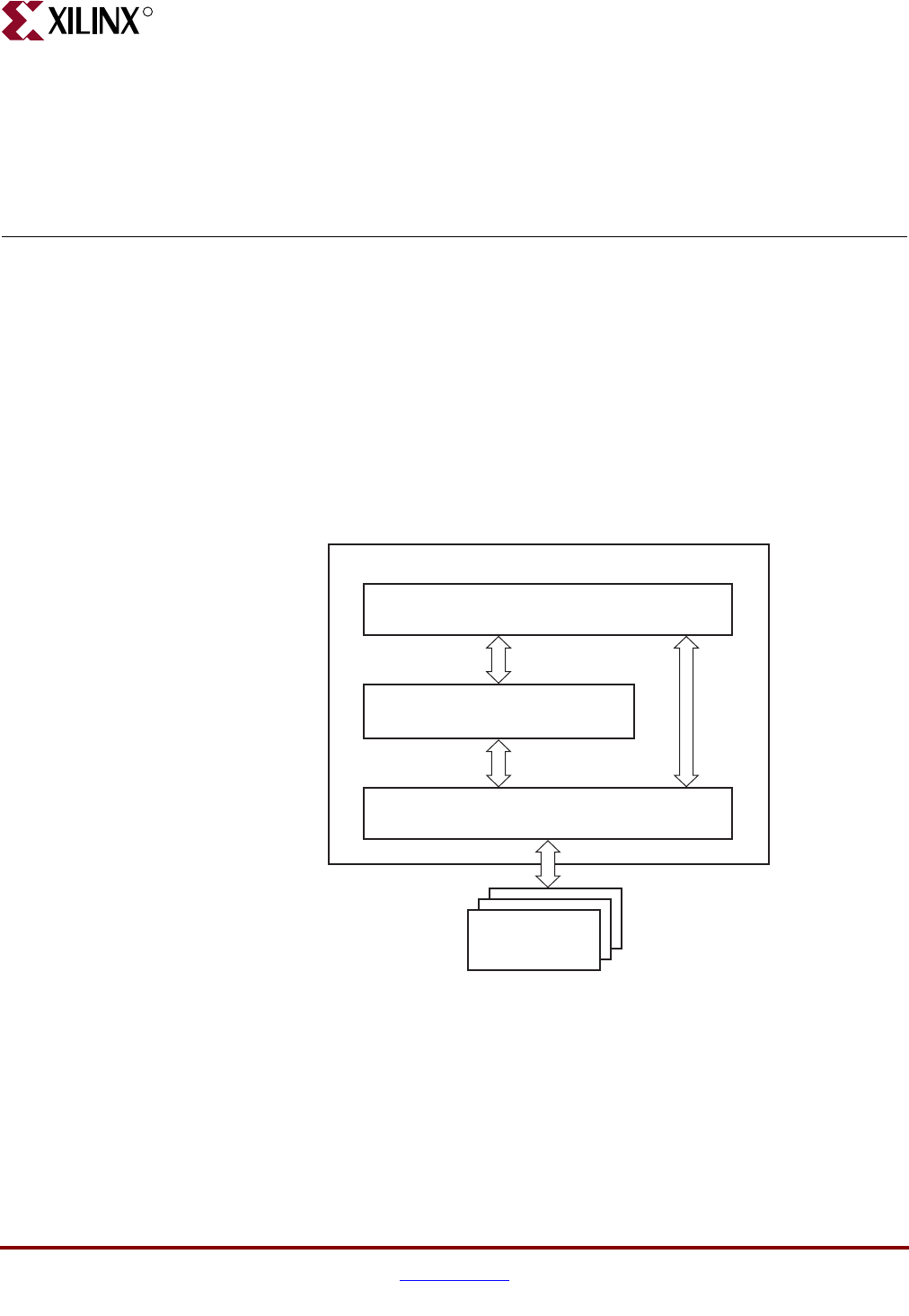
Memory Interface Solutions User Guide www.xilinx.com 427
UG086 (v3.6) September 21, 2010
R
Chapter 11
Implementing DDR SDRAM Controllers
This chapter describes how to implement DDR SDRAM interfaces for Virtex®-5 FPGAs
generated by MIG. This design is based on XAPP851 [Ref 25].
Interface Model
DDR SDRAM interfaces are source-synchronous and double data rate. They transfer data
on both edges of the clock cycle. A memory interface can be modularly represented as
shown in Figure 11-1. A modular interface has many advantages. It allows designs to be
ported easily and also makes it possible to share parts of the design across different types
of memory interfaces.
Figure 11-1: Modular Memory Interface Representation
Application Interface Layer
Xilinx FPGA
Physical Layer
Control Layer
UG086_c11_01_012207
Memories
428 www.xilinx.com Memory Interface Solutions User Guide
UG086 (v3.6) September 21, 2010
Chapter 11: Implementing DDR SDRAM Controllers
R
Feature Summary
This section summarizes the supported and unsupported features of DDR SDRAM
controller design.
Supported Features
The DDR SDRAM controller design supports the following:
• Burst lengths of two, four, and eight
• Sequential and interleaved burst types
• DDR SDRAM components and DIMMs
• CAS latencies of 2, 2.5, and 3
•Verilog and VHDL
• With and without a testbench
• Bank management
• Bytewise data masking
• Linear addressing
• With and without a PLL
• Registered DIMMs, unbuffered DIMMs and SO-DIMMs
•Data mask
• System clock, differential and single-ended
The supported features are described in more detail in “Architecture.”
Design Frequency Ranges
Unsupported Features
The DDR SDRAM controller design does not support:
• Deep memories/dual rank DIMMs
•Multicontrollers
Table 11-1: Design Frequency Range in MHz
Memory
FPGA Speed Grade
-1 -2 -3
MinMaxMinMaxMinMax
Component 77 200 77 200 77 200
DIMM 77 200 77 200 77 200
Memory Interface Solutions User Guide www.xilinx.com 429
UG086 (v3.6) September 21, 2010
Architecture
R
Architecture
Implemented Features
This section provides details on the supported features of the DDR SDRAM controller. The
Virtex-5 FPGA DDR SDRAM design is a generic design that works for most of the features
mentioned above. User input parameters are defined as parameters for Verilog and
generics in VHDL in the design modules and are passed down the hierarchy. For example,
if the user selects a burst length of 4, then it is defined as follows in the <top_module>
module:
parameter BURST_LEN = 4, // burst length (in doublewords)
The user can change this parameter for various burst lengths to get the desired output. The
same concept holds for all the other parameters listed in the <top_module> module.
Table 11-2 lists the details of all parameters.
Table 11-2: Parameterization of DDR SDRAM Virtex-5 FPGA Design
Category Parameter Name Description Other Notes Value Restrictions
Memory
Width
BANK_WIDTH Number of memory bank
address bits
CKE_WIDTH Number of memory clock
enable outputs
CLK_WIDTH Number of differential clock
outputs
Determined by the number
of components/modules
(one pair per component)
COL_WIDTH Number of memory column
bits
CS_BITS log2(CS_NUM)
Used for chip-select related
address decode. See notes
for CS_NUM and
CS_WIDTH.
CS_NUM Number of separate chip
selects
Different from CS_WIDTH.
For example, for a 32-bit
data bus with 2 x16 parts,
CS_NUM = 1, but
CS_WIDTH = 2 (that is, a
single chip select drives two
separate outputs, one for
each component)
CS_WIDTH /
CS_NUM = integer
CS_WIDTH Number of memory chip
selects
Determined by the number
of components/modules
(one per component)
CS_WIDTH /
CS_NUM = integer
DM_WIDTH Number of data mask bits
Can be a different value
from DQS_WIDTH if x4
components are used
(DQ_WIDTH)/8
DQ_BITS log2(DQS_WIDTH*DQ_PER_
DQS)
Used for data bus
calibration decode
(DQ_WIDTH)/
Number of data bits
DQ_WIDTH Number of data bits
DQ_PER_DQS Number of memory DQ data
bits per strobe
DQS_BITS log2(DQS_WIDTH)
DQS_WIDTH Number of memory DQS
strobes
ROW_WIDTH Number of memory address
bits
430 www.xilinx.com Memory Interface Solutions User Guide
UG086 (v3.6) September 21, 2010
Chapter 11: Implementing DDR SDRAM Controllers
R
Memory
Options
BURST_LEN Burst length (2,4,8)
BURST_TYPE Burst type (0: sequential, 1:
interleaved) (0,1)
CAS_LAT CAS latency (equal to 25 for
CL = 2.5) (2,25,3)
MULTI_BANK_EN Bank management enable
If enabled, up to four banks
are kept open; otherwise,
one bank is kept open
(0,1)
REDUCE_DRV
Reduced strength memory
I/O enable. Set (1) for reduced
I/O drive strength.
Not supported for all
DDR/DDR2 widths (0,1)
REG_ENABLE Set (1) for registered memory
module
Accounts for an extra clock
cycle delay on address/
control for a registered
module
(0,1)
Memory
Timing
TREFI_NS Auto refresh interval (in ns) Take directly from memory
data sheet
TRAS Active to precharge delay (in
ps)
Take directly from memory
data sheet
TRCD Active to read/write delay (in
ps)
Take directly from memory
data sheet
TRFC Refresh to refresh, refresh to
active delay (in ps)
Take directly from memory
data sheet
TRP Precharge to command delay
(in ps)
Take directly from memory
data sheet
TWR Used to determine write to
precharge (in ps)
Take directly from memory
data sheet
TWTR Write to read (in ps) Take directly from memory
data sheet
Miscellaneous
CLK_PERIOD Memory clock period (in ps)
Used for PHY calibration
and PLL/DCM (if
applicable) setting
DLL_FREQ_MODE DCM Frequency Mode
Determined by
CLK_PERIOD. Needed
only if the DCM option is
selected.
("LOW", "HIGH")
DDR2_ENABLE Select either DDR or DDR2
interface (equal to 1 for DDR2)
Provided from the
mem_if_top level and
below
(0,1)
SIM_ONLY Enable bypass of 200 μs
power-on delay (0,1)
RST_ACT_LOW Indicates the polarity of the
input reset signal (sys_rst_n)
1: Reset is active Low.
0: Reset is active High. (0,1)
HIGH_PERFORMANCE_MODE IODELAY High Performance
Mode Parameter value
This parameter value
represents HIGH_PERFOR
MANCE_MODE of
IODELAY as TRUE or
FALSE. This will result in
the higher or lower power
dissipation at the output of
IODLEAY element.
Verilog : String.
"TRUE", "FALSE".
VHDL : Boolean :
TRUE, FALSE.
Table 11-2: Parameterization of DDR SDRAM Virtex-5 FPGA Design (Cont’d)
Category Parameter Name Description Other Notes Value Restrictions

Memory Interface Solutions User Guide www.xilinx.com 431
UG086 (v3.6) September 21, 2010
Architecture
R
Burst Length
Bits M0:M3 of the Mode Register define the burst length and burst type. Read and write
accesses to the DDR SDRAM are burst-oriented. The burst length is programmable to
either 2, 4, or 8 through the GUI. The burst length determines the maximum number of
column locations accessed for a given READ or WRITE command. The DDR SDRAM ctrl
module implements a burst length that is programmed.
CAS Latency
Bits M4:M6 of the Mode Register define the CAS latency (CL). CL is the delay in clock
cycles between the registration of a READ command and the availability of the first bit of
output data. CL can be set to 2, 2.5, or 3 clocks through the GUI. CAS latency is
implemented in the ctrl module. For CL = 2.5, the input value is read as “25” in the design.
During read data operations, the generation of the read_en signal varies according to the
CL in the ctrl module.
Precharge
The PRECHARGE command is used to close the open row in a bank if there is a command
to be issued in the same bank. The Virtex-5 FPGA DDR controller issues a PRECHARGE
command only if there is already an open row in the particular bank where a read or write
command is to be issued, thus increasing the efficiency of the design. The auto-precharge
function is not supported in this design. This design ties the A10 bit Low during normal
reads and writes.
Data Masking
Virtex-5 FPGA DDR SDRAM controllers support bytewise data masking of the data bits
during a write operation. For x4 components, data masking cannot be done on a per nibble
basis due to an internal block RAM based FIFO limitation. The mask data is stored into the
FIFOs along with the write data. MIG supports a data mask option. If this option is
checked in the GUI, MIG generates a design with data mask pins. This option can be
chosen if the selected part has data masking.
Auto Refresh
An AUTO REFRESH command is issued to the DDR memory at specified intervals of time
to refresh the charge to retain the data.
Bank Management
Bank management is done by the Virtex-5 FPGA DDR SDRAM controller design to
increase the efficiency of the design. The controller keeps track of whether the bank being
accessed already has an open row or not, and also decides whether a PRECHARGE
command should be issued or not to that bank. When bank management is enabled via the
MULTI_BANK_EN parameter, a maximum of four banks/rows can open at any one time.
A least-recently-used (LRU) algorithm is employed to keep the three banks most recently
used. It closes the bank least recently used when a new bank/row location needs to be
accessed. The bank management feature can also be disabled by clearing
MULTI_BANK_EN. In this case, only one bank is kept open at any one time. For more
information on Bank Management, refer to application note XAPP858 [Ref 27].

432 www.xilinx.com Memory Interface Solutions User Guide
UG086 (v3.6) September 21, 2010
Chapter 11: Implementing DDR SDRAM Controllers
R
Linear Addressing
Linear addressing refers to the way the user provides the address of the memory to be
accessed. For Virtex-5 FPGA DDR SDRAM controllers, the user provides the address
information through the app_af_addr signal. As the densities of the memory devices vary,
the number of column address bits and row address bits also change. In any case, the row
address bits in the app_af_addr signal always start from the next higher bit where the
column address ends. This feature increases the coverage of more devices that can be
supported with the design.
Different Memories (Density/Speed)
The DDR SDRAM controller supports different densities. For DDR components shown in
MIG, densities can vary from 128 Mb to 1 Gb. The user can select the various
configurations from the “Create custom part” option; the supported maximum column
address is 13, the maximum row address is 15, and the maximum bank address is 2. The
design can decode write and read addresses from the user in the DDR SDRAM ctrl
module. The user address consists of column, row, and bank addresses.
System Clock
MIG supports differential and single-ended system clocks. Based on the selection in the
GUI, input system clocks and IDELAY clocks are differential or single-ended.
IODELAY Performance Mode
In Virtex-5 family devices, the power dissipation of the IODELAY elements can be
controlled using the HIGH_PERPORMANCE_MODE parameter. The values of this
parameter can be either TRUE or FALSE.
When this parameter value is set to TRUE, the IODELAY jitter valuer per tap is reduced.
This reduction results in a slight increase in power dissipation from the IODELAY element.
When this parameter value is set to FALSE, the IODELAY power dissipation is reduced,
but with an increase in the jitter value per tap.
The value of this parameter can be selected from the MIG FPGA options page. Users can
also manually set this parameter value to TRUE or FALSE in the design top-level block
HDL module.
Refer to Appendix E, “Debug Port” for more information on the IODELAY Performance
Mode.
Memory Interface Solutions User Guide www.xilinx.com 433
UG086 (v3.6) September 21, 2010
Hierarchy
R
Hierarchy
Figure 11-2 shows the hierarchical structure of the design generated by MIG with a PLL
and a testbench.
The modules are classified in three types:
• Design modules
• Testbench modules
• Clock and reset generation modules
MIG can generate four different DDR SDRAM designs:
• With a testbench and a PLL
• Without a testbench and with a PLL
• With a testbench and without a PLL
• Without a testbench and without a PLL
For designs without a testbench, the correspondingly yellow shaded modules are not
present. In this case, the user interface signals appear in the <top_module> module.
Table 11-4, page 444 provides a list of these signals.
The infrastructure module generates the clock and reset signals for the design. It
instantiates a PLL when MIG generates a design with a PLL. The inputs to this module are
the differential design clock and a 200 MHz differential clock for the IDELAYCTRL
Figure 11-2: Hierarchical Structure of Virtex-5 FPGA DDR SDRAM Design
<top_
module>
ddr_
top
ddr_
idelay_ctrl
ddr_
tb_top
ddr_mem
_if_top
ddr_
phy_top ddr_ctrl ddr_
usr_top
ddr_
infrastructure
ddr_phy_
ctl_io
ddr_
phy_io
ddr_phy_
write
ddr_
phy_init
ddr_phy_
calib
Design Modules
ddr_phy_
dqs_iob
ddr_phy_
dm_iob
ddr_phy_
dq_iob
ddr_
usr_rd
ddr_usr_
backend_
fifo
ddr_usr_
addr_fifo
ddr_usr_
wr_fifo
UG086_c11_02_012809
ddr_tb_
test_gen
ddr_tb_
test_cmp
ddr_tb_
test_
addr_gen
ddr_tb_
test_
data_gen
ddr_usr_
rd_fifo
ddr_usr_
ram_d
Te st Bench Modules
Clocks and Reset Generation Modules

434 www.xilinx.com Memory Interface Solutions User Guide
UG086 (v3.6) September 21, 2010
Chapter 11: Implementing DDR SDRAM Controllers
R
module. A user reset is also input to this module. Using the input clocks and reset signals,
the system clocks and the system reset are generated in this module, which is used in the
design.
If the design has no PLL, the PLL primitive is not instantiated in the module. Instead, the
system operates on the user-provided clocks. A system reset is also generated in the
infrastructure module using the input locked signal.
MIG Design Options
MIG provides various options to generate the design with or without a testbench or with
or without a PLL. This section provides detailed descriptions of the different types of
designs the user can generate using the MIG options. The designs in Figure 11-3 and
Figure 11-5, page 437 use the differential system clocks. For more information on the
clocking structure, refer to “Clocking Scheme,” page 442.
MIG outputs both an example_design and a user_design. The MIG-generated
example_design includes the entire memory controller design along with a synthesized
testbench (example user application). This testbench generates sample writes and reads
and then uses comparison logic to verify that the data patterns written are the same as
those received. This example_design can be used to test functionality both in simulation
and in hardware. The user_design includes the memory controller design only. This design
allows users to connect the MIG memory controller design to a user developed testbench
(user application). Refer to Table 11-4, page 444 for user interface signals, the “User
Interface Accesses,” page 449 for timing restriction on user interface signals, and
Figure 11-13, page 452 for write interface timing.
Figure 11-3 shows a block diagram representation of the top-level module for a design
with a PLL and a testbench. The inputs consist of differential clocks for the design and
Idelayctrl modules and the user reset. “Clocking Scheme,” page 442 describes how various
clocks are generated using the PLL. The error output signal indicates whether the case
passes or fails. The phy_init_done signal indicates the completion of initialization and
calibration of the design. Because the PLL is instantiated in the infrastructure module, it
generates the required clocks and reset signals for the design.
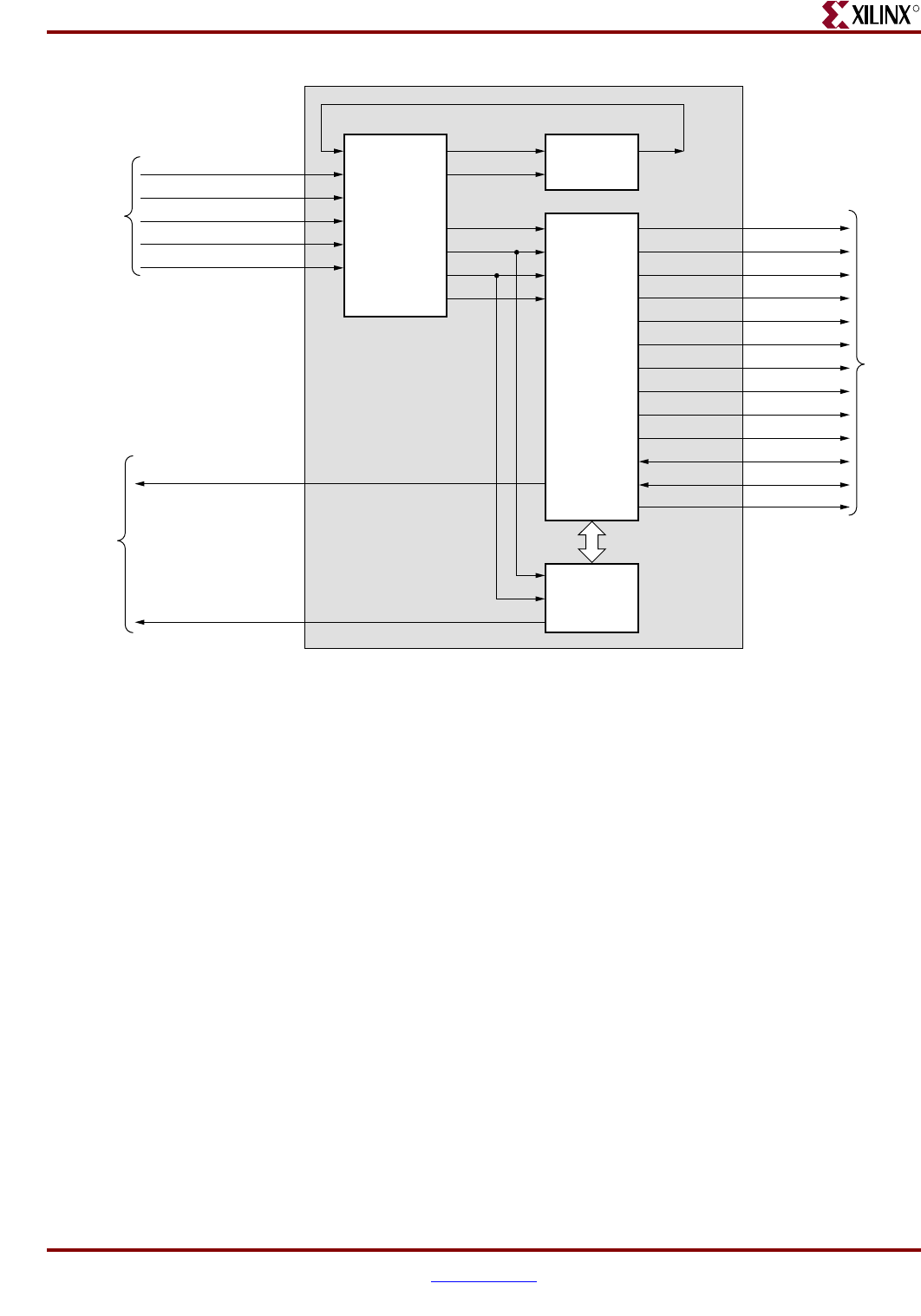
Memory Interface Solutions User Guide www.xilinx.com 435
UG086 (v3.6) September 21, 2010
MIG Design Options
R
Figure 11-3: Top-Level Block Diagram of the DDR SDRAM Design with a PLL and a Testbench
ddr1_top
tb_top
idelay_ctrl_rdy
clk200
Memory
Device
UG086_c11_03_091007
Status
Signals
System
Clocks
and Reset
idelay_ctrl
Infrastructure
rst200
clk90
clk0
rst90
clk200_p
clk200_n
sys_clk_p
sys_clk_n
sys_rst_n rst0
ddr_ras_n
ddr_cas_n
ddr_we_n
ddr_cs_n
ddr_cke
ddr_dm
ddr_ba
ddr_a
ddr_ck
ddr_ck_n
ddr_dq
ddr_dqs
ddr_reset_n
phy_init_done
error
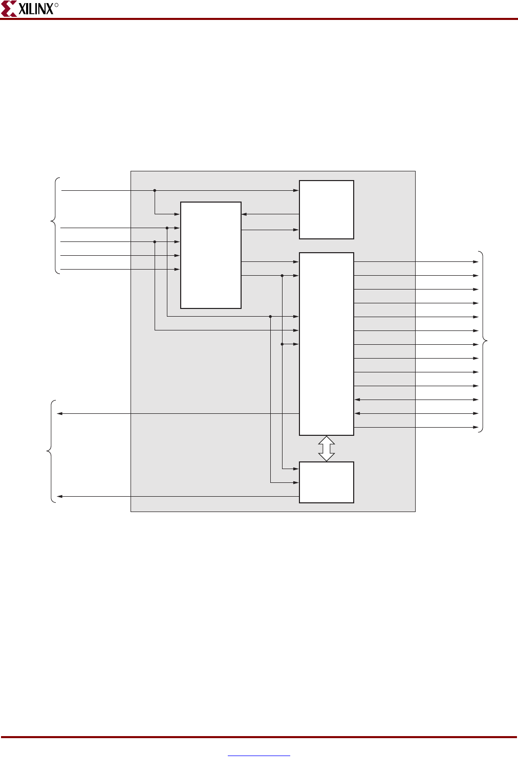
436 www.xilinx.com Memory Interface Solutions User Guide
UG086 (v3.6) September 21, 2010
Chapter 11: Implementing DDR SDRAM Controllers
R
Figure 11-4 shows a block diagram representation of the top-level module for a design
with a testbench but without a PLL. “Clocking Scheme,” page 442 explains how to
generate the design clocks from the user interface. The inputs consist of user clocks for the
design and Idelayctrl modules and the user reset. The design uses the user input clocks.
These clocks should be single-ended. The infrastructure module uses the input reset and
locked signals to reset the design. The user application must have a PLL/DCM primitive
instantiated in the design. The error output signal indicates whether the case passes or
fails. The phy_init_done signal indicates the completion of initialization and calibration of
the design.
Figure 11-4: Top-Level Block Diagram of the DDR SDRAM Design with a Testbench but without a PLL
ddr1_top
tb_top
idelay_ctrl_rdy
Memor
y
Device
UG086_c11_04_01280
9
Status
Signals
System
Reset and
User PLL/
DCM Clocks
idelay_ctrl
Infrastructure
rst200
rst0
clk200
clk0
clk90
sys_rst_n
locked rst90 ddr_ras_n
ddr_cas_n
ddr_we_n
ddr_cs_n
ddr_cke
ddr_dm
ddr_ba
ddr_a
ddr_ck
ddr_ck_n
ddr_dq
ddr_dqs
ddr_reset_n
phy_init_done
error
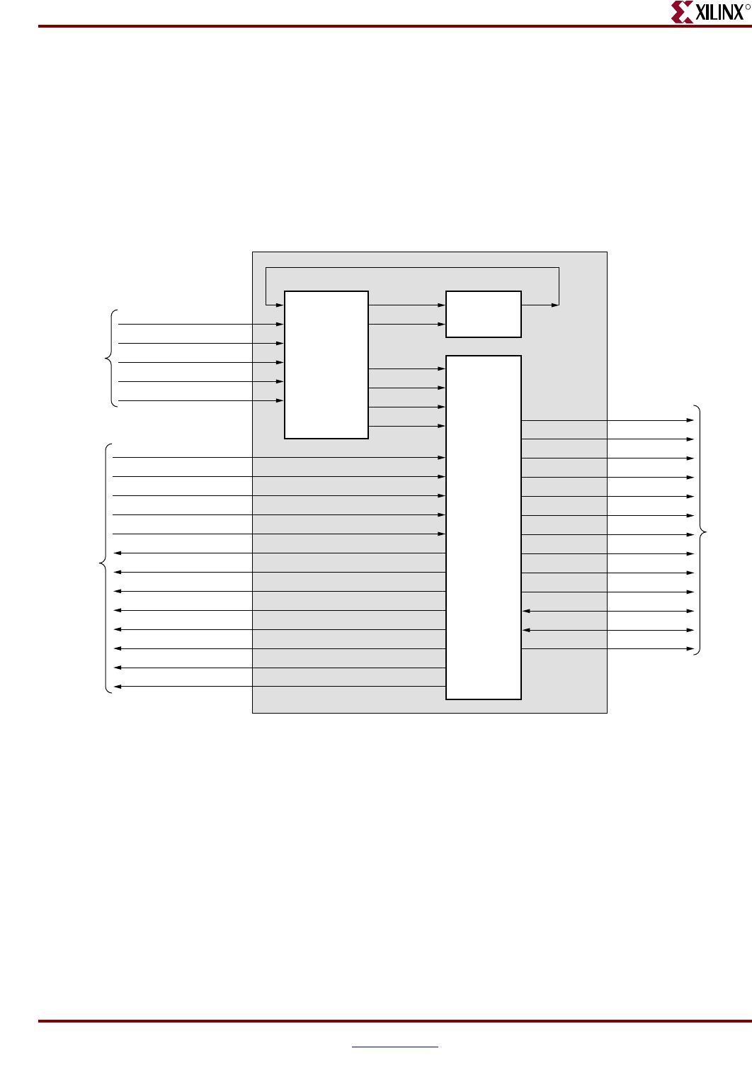
Memory Interface Solutions User Guide www.xilinx.com 437
UG086 (v3.6) September 21, 2010
MIG Design Options
R
Figure 11-5 shows a block diagram representation of the top-level module for a design
with a PLL but without a testbench. “Clocking Scheme,” page 442 describes how various
clocks are generated using the PLL. The phy_init_done signal indicates the completion of
initialization and calibration of the design. The user interface signals are also listed in the
<top_module> module. The design provides the clk0_tb and rst0_tb signals to the user to
synchronize with the design. The clk0_tb signal is connected to clk0 in the controller. If the
user clock domain is different from clk0/clk0_tb, the user should add FIFOs for all the
inputs and outputs of the controller (user application signals) in order to synchronize them
to the clk0_tb clock. Because the PLL is instantiated in the infrastructure module, it
generates the required clock and reset signals for the design.
Figure 11-5: Top-Level Block Diagram of the DDR SDRAM Design with a PLL but without a Testbench
ddr1_top
idelay_ctrl_rdy
clk200
Memory
Device
UG086_c11_05_091007
User
Application
and Status
Signal
System
Clocks
and Reset
idelay_ctrl
Infrastructure
rst200
clk90
clk0
rst0
clk200_p
clk200_n
sys_clk_p
sys_clk_n
sys_rst_n
app_af_addr
app_wdf_data
app_wdf_mask_data
app_wdf_wren
app_wdf_afull
rst90
ddr_ras_n
ddr_cas_n
ddr_we_n
ddr_cs_n
ddr_dm
ddr_ba
ddr_a
ddr_ck
ddr_ck_n
ddr_dq
ddr_dqs
ddr_cke
ddr_reset_n
app_af_wren
app_af_afull
rd_data_valid
rd_data_fifo_out
clk0_tb
app_af_cmd
rst0_tb
phy_init_done
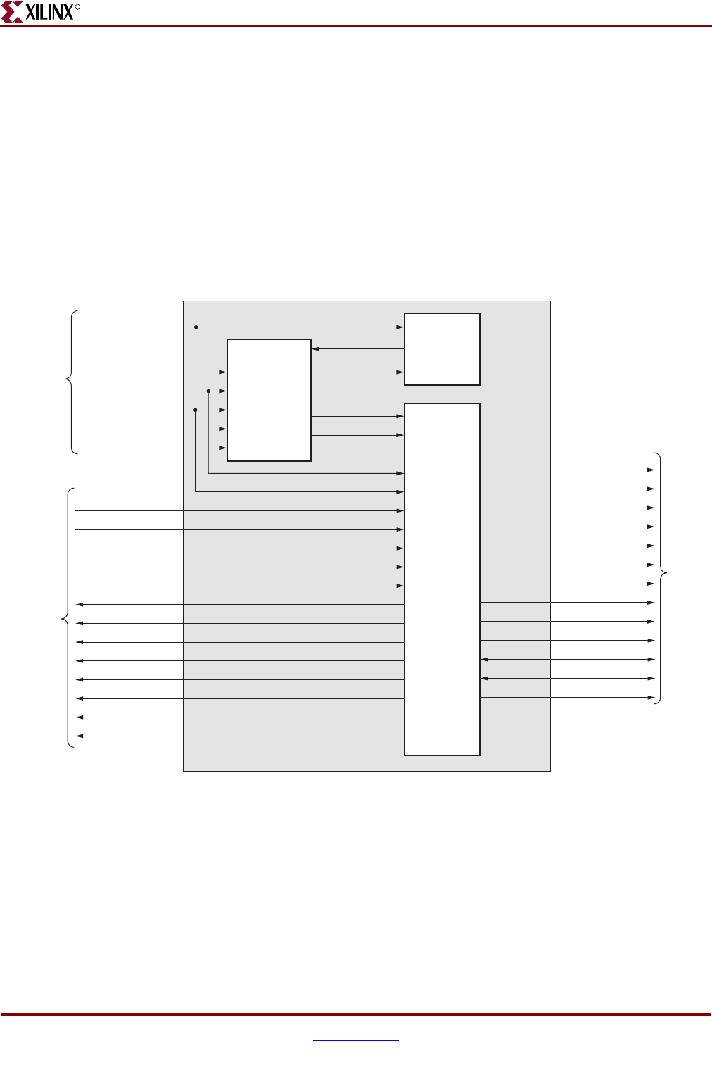
438 www.xilinx.com Memory Interface Solutions User Guide
UG086 (v3.6) September 21, 2010
Chapter 11: Implementing DDR SDRAM Controllers
R
Figure 11-6 shows a block diagram representation of the top-level module for designs
without a PLL or a testbench. The inputs consist of user clocks for the design and Idelayctrl
modules and the user reset. The design uses the user input clocks. “Clocking Scheme,”
page 442 explains how to generate the design clocks from the user interface. These clocks
should be single-ended. To reset the design, the signals are generated using the input reset
and the locked signals in the infrastructure module. The user application must have a
PLL/DCM primitive instantiated in the design. The phy_init_done signal indicates the
completion of initialization and calibration of the design. The user interface signals are also
listed in the <top_module> module. The design provides the clk0_tb and rst0_tb signals to
the user to synchronize with the design. The signal clk0_tb is connected to clock clk0 in the
controller. If the user clock domain is different from clk0/clk0_tb, the user should add
FIFOs for all the inputs and outputs of the controller (user application signals) in order to
synchronize them to clk0_tb clock.
Figure 11-6: Top-Level Block Diagram of the DDR SDRAM Design without a PLL or a Testbench
ddr1_top
idelay_ctrl_rdy
Memory
Device
UG086_c11_06_012809
System
Reset
and User
PLL/DCM
idelay_ctrl
Infrastructure
rst200
rst0
rst90
clk_0
clk_200
clk_90
sys_rst_n
locked
ddr_ras_n
ddr_cas_n
ddr_we_n
ddr_cs_n
ddr_cke
ddr_dm
ddr_ba
ddr_a
ddr_ck
ddr_ck_n
ddr_reset_n
ddr_dq
ddr_dqs
User
Application
and Status
Signal
app_af_addr
app_af_wren
app_wdf_data
app_wdf_mask_data
app_wdf_wren
app_wdf_afull
app_af_cmd
rd_data_valid
rd_data_fifo_out
clk0_tb
rst0_tb
phy_init_done
app_af_afull
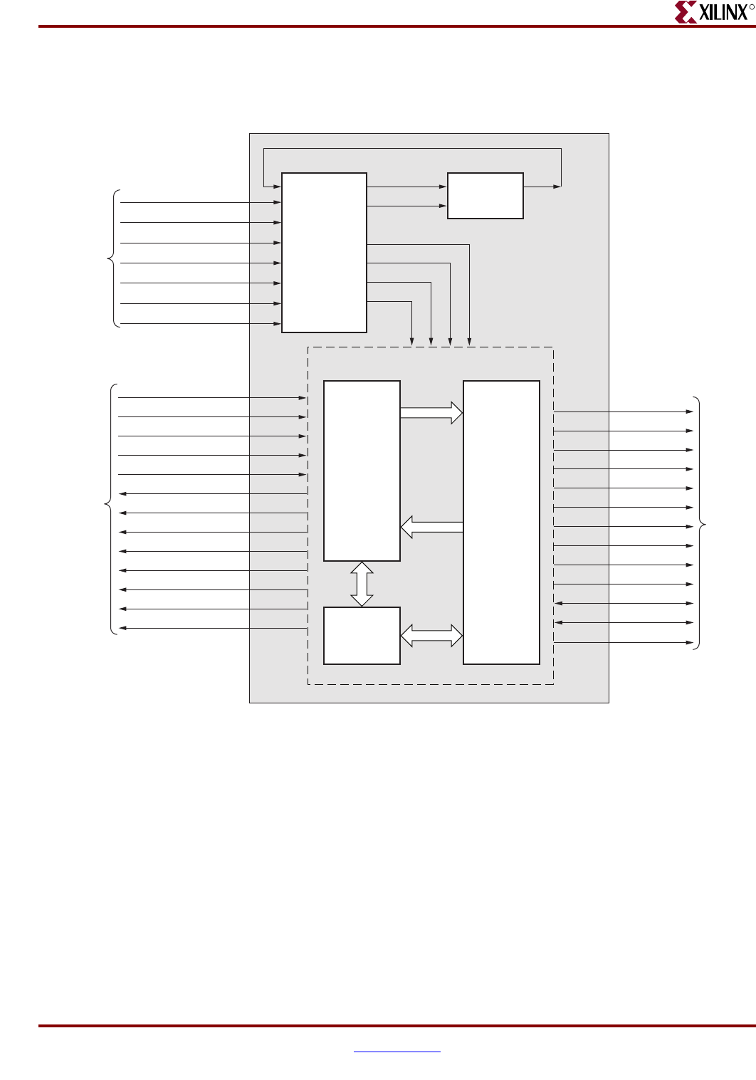
Memory Interface Solutions User Guide www.xilinx.com 439
UG086 (v3.6) September 21, 2010
MIG Design Options
R
Figure 11-7 shows an expanded block diagram of the design. The design’s top module is
expanded to show various internal blocks. The functions of these blocks are explained in
following subsections.
Infrastructure
The infrastructure module generates the FPGA clock and reset signals. When differential
clocking is used, sys_clk_p, sys_clk_n, clk_200_p, and clk_200_n signals appear. When
single-ended clocking is used, sys_clk and idly_clk_200 signals appear. In addition, clocks
are available for design use and a 200 MHz clock is provided for the IDELAYCTRL
primitive. Differential and single-ended clocks are passed through global clock buffers
before connecting to a PLL/DCM. For differential clocking, the output of the
sys_clk_p/sys_clk_n buffer is single-ended and is provided to the PLL/DCM input.
Likewise, for single-ended clocking, sys_clk is passed through a buffer and its output is
provided to the PLL/DCM input. The outputs of the PLL/DCM are clk0 (0° phase-shifted
version of the input clock) and clk90 (90° phase-shifted version of the input clock). After
the PLL/DCM is locked, the design is in the reset state for at least 25 clocks. The
infrastructure module also generates all of the reset signals required for the design.
Figure 11-7: Detailed Block Diagram of the DDR SDRAM Design with a PLL but without a Testbench
ctrl
Control
Signals
write_data
ddr1_top/mem_if_top
read_data
Control
Signals
idelay_ctrl_rdy
clk200
Memory
Device
UG086_c11_07_083108
System
Clocks
and Reset
idelay_ctrl
Infrastructure
rst200
clk90
clk0
rst90
rst0
clk200_p
clk200_n
sys_clk_p
sys_clk_n
idly_clk_200
sys_clk
sys_rst_n
ddr_ras_n
ddr_cas_n
ddr_we_n
ddr_cs_n
ddr_cke
ddr_dm
ddr_ba
ddr_a
ddr_ck
ddr_ck_n
ddr_dq
ddr_dqs
ddr_reset_n
User
Application
and Status
Signal
app_af_addr
app_af_wren
app_wdf_data
app_wdf_mask_data
app_wdf_wren
app_wdf_afull
app_af_afull
rd_data_valid
rd_data_fifo_out
clk0_tb
app_af_cmd
rst0_tb
phy_init_done
usr_top
phy_top

440 www.xilinx.com Memory Interface Solutions User Guide
UG086 (v3.6) September 21, 2010
Chapter 11: Implementing DDR SDRAM Controllers
R
PLL/DCM
In MIG 3.0 and later, the DCM is replaced with a PLL for all Virtex-5 FPGA designs. If the
user selects a design with a PLL in the GUI, the infrastructure module will have both PLL
and DCM codes. The CLK_GENERATOR parameter enables either a PLL or a DCM in the
infrastructure module. The CLK_GENERATOR parameter is set to PLL by default. If the
user wants to use DCM, this parameter should be changed manually to DCM.
When the user chooses the no PLL option in the GUI, the design does not use any
PLL/DCM primitives. Instead it works on the clocks provided by the user. The input
clocks in this case have to be single-ended. The locked status and user input reset signals
are the inputs to the module when there is no PLL. These signals are used to generate the
synchronous system resets for the design.
idelay_ctrl
This module instantiates the IDELAYCTRL primitive of the Virtex-5 FPGA. The
IDELAYCTRL primitive is used to continuously calibrate the individual delay elements in
its region to reduce the effect of process, temperature, and voltage variations. A 200 MHz
clock has to be fed to this primitive.
MIG uses the “automatic” method for IDELAYCTRL instantiation in which the MIG HDL
only instantiates a single IDELAYCTRL for the entire design. No location (LOC)
constraints are included in the MIG-generated UCF. This method relies on the ISE® tools to
replicate and place as many IDELAYCTRLs as needed (for example, one per clock region
that uses IDELAYs). Replication and placement are handled automatically by the software
tools if IDELAYCTRLs have same refclk, reset, and rdy nets. A new constraint called
IODELAY_GROUP associates a set of IDELAYs with an IDELAYCTRL and allows for
multiple IDELAYCTRLs to be instantiated without LOC constraints specified. ISE software
generates the IDELAY_CTRL_RDY signal by logically ANDing the RDY signals of every
IDELAYCTRL block.
The IODELAY_GROUP name should be checked in the following cases:
• The MIG design is used with other IP cores or user designs that also require the use of
IDELAYCTRL and IDELAYs.
• Previous ISE software releases 8.2.03i and 9.1i had an issue with IDELAYCTRL block
replication or trimming. When using these revisions of the ISE software, the user must
instantiate and constrain the location of each IDELAYCTRL individually.
See UG190 [Ref 10] for more information on the requirements of IDELAYCTRL placement.
ctrl
The ctrl module is the main controller of the Virtex-5 FPGA DDR SDRAM controller
design. It generates all the control signals required for the DDR memory interface and the
user interface. This module signals the FIFOs instantiated in the user interface to output
the fed data in it and also signals the physical layer to output the data on the IOBs during
a write operation. During a read operation, the data read from the memory is taken from
the physical layer and written into the user interface FIFOs using the control signals
generated by the ctrl module.
The ctrl module decodes the user command and issues the specified command to the
memory. The app_af_cmd signal is decoded as a write command when it equals 3’b000,
and app_af_cmd is decoded as a read command when it equals 3’b001. The commands
and control signals are generated based on the input burst length and CAS latency. If the
multi-bank option is enabled, the ctrl module also takes care of bank management, so as to

Memory Interface Solutions User Guide www.xilinx.com 441
UG086 (v3.6) September 21, 2010
MIG Design Options
R
increase the efficiency of the design. At a given point of time, a maximum of four banks can
be open. The controller issues a PRECHARGE command to the bank only if there is already
an open row in that bank and the next command is to be issued to a different row. An
ACTIVE command is generated to open the row in that particular bank. Thus the efficiency
is increased.
phy_top
The phy_top module is the top level of the physical interface of the design. The physical
layer includes the input/output blocks (IOBs) and other primitives used to read and write
the double data rate signals to and from the memory, such as IDDR and ODDR. This
module also includes the IODELAY elements of the Virtex-5 FPGA. These IODELAY
elements are used to delay the input strobe and data signals to capture the valid data into
the Read Data FIFO.
The memory control signals, such as RAS_N, CAS_N, and WE_N, are driven from the
buffers in the IOBs. All the input and output signals to and from the memory are
referenced from the IOB to compensate for the routing delays inside the FPGA.
The phy_init module, which is instantiated in the phy_top module, is used to initialize the
DDR memory in a predefined sequence according to the JEDEC standard for DDR
SDRAM.
The phy_calib module calibrates the design to align the strobe signal such that it always
captures the valid data in the FIFO. This calibration is needed to compensate for the trace
delays between the memory and the FPGA devices.
The phy_write module splits the user data into rise data and fall data to be sent to the
memory as a double data rate signal using ODDR. Similarly, while reading the data from
memory, the data from IDDR is combined to get a single vector that is written into the read
FIFO.
usr_top
The usr_top module is the user interface block of the design. It receives and stores the user
data, command, and address information in respective FIFOs. The ctrl module generates
the required control signals for this module. During a write operation, the data stored in
the usr_wr_fifo is read and given to the physical layer to output to the memory. Similarly,
during a read operation, the data from the memory is read via IDDR and written into the
FIFOs. This data is given to the user with a valid signal (rd_data_valid), which indicates
valid data on the rd_data_fifo_out signal. See “User Interface Accesses,” page 449 for
required timing requirements and restrictions for user interface signals.
The FIFO36 and FIFO36_72 primitives are used for loading address and data from the user
interface. The FIFO36 primitive is used in the ddr_usr_addr_fifo module. The FIFO36_72
primitive is used in the ddr_usr_wr module. Every FIFO has two FIFO threshold
attributes, ALMOST_EMPTY_OFFSET and ALMOST_FULL_OFFSET, that are set to 7 and
F, respectively, in the RTL by default. These values can be changed as needed. For valid
FIFO threshold offset values, refer to UG190 [Ref 10].
Test Bench
The MIG tool generates two RTL folders, example_design and user_design. The
example_design folder includes the synthesizable test bench, while user_design does not
include the test bench modules. The MIG test bench performs eight write commands and
eight read commands in an alternating fashion. The number of words in a write command
depends on the burst length. For a burst length of 4, the test bench writes a total of 32 data

442 www.xilinx.com Memory Interface Solutions User Guide
UG086 (v3.6) September 21, 2010
Chapter 11: Implementing DDR SDRAM Controllers
R
words for all eight write commands (16 rise data words and 16 fall data words). For a burst
length of 8, the test bench writes a total of 64 data words. It writes the data pattern of FF,
00, AA, 55, 55 AA, 99, 66 in a sequence of which FF, AA, 55, and 99 are rise data words and
00, 55, AA, and 66 are fall data words for an 8-bit design. The falling edge data is the
complement of the rising edge data. For a burst length of 4, the data sequence for the first
write command is FF, 00, AA, 55, and the data sequence for the second write command is
55, AA, 99, 66. For a burst length of 8, the data pattern for the first write command is FF,
00, AA, 55, 55 AA, 99, 66 and the same pattern is repeated for all the remaining write
commands. This data pattern is repeated in the same order based on the number of data
words written. For data widths greater than 8, the same data pattern is concatenated for
the other bits. For a 32-bit design and a burst length of 8, the data pattern for the first write
command is FFFFFFFF, 00000000, AAAAAAAA, 55555555, 55555555, AAAAAAAA,
99999999, 66666666.
Address generation logic generates eight different addresses for eight write commands.
The same eight address locations are repeated for the following eight read commands. The
read commands are performed at the same locations where the data is written. There are
total of 32 different address locations for 32 write commands, and the same address
locations are generated for 32 read commands. Upon completion of a total of 64
commands, including both writes and reads (eight writes and eight reads repeated four
times), address generation rolls back to the first address of the first write command and the
same address locations are repeated. The MIG test bench exercises only a certain memory
area. The address is formed such that all address bits are exercised. During writes, a new
address is generated for every burst operation on the column boundary.
During reads, comparison logic compares the read pattern with the pattern written, i.e., the
FF, 00, AA, 55, 55 AA, 99, 66 pattern. For example, for an 8-bit design of burst length 4, the
data written for a single write command is FF, 00, AA, 55. During reads, the read pattern is
compared with the FF, 00, AA, 55 pattern. Based on a comparison of the data, a status
signal error is generated. If the data read back is the same as the data written, the error
signal is 0, otherwise it is 1.
Clocking Scheme
Figure 11-9, page 444 shows the clocking scheme for this design. Global and local clock
resources are used.
The global clock resources consist of a PLL or a DCM, two BUFGs on PLL/DCM output
clocks, and one BUFG for clk200. The local clock resources consist of regional I/O clock
networks (BUFIO). The global clock architecture is discussed in this section.
The MIG tool allows the user to customize the design such that the PLL/DCM is not
included. In this case, system clocks clk0 and clk90, and IDELAYCTRL clock clk200 must
be supplied by the user.
Global Clock Architecture
The user must supply two input clocks to the design:
• A system clock running at the target frequency for the memory
• A 200 MHz clock for the IDELAYCTRL blocks.
These clocks can be either single-ended or differential. The user can select a single-ended
or differential clock input option from MIG GUI. Differential clocks are connected to the
IBUFGDS and the single-ended clock is connected to an IBUFG.
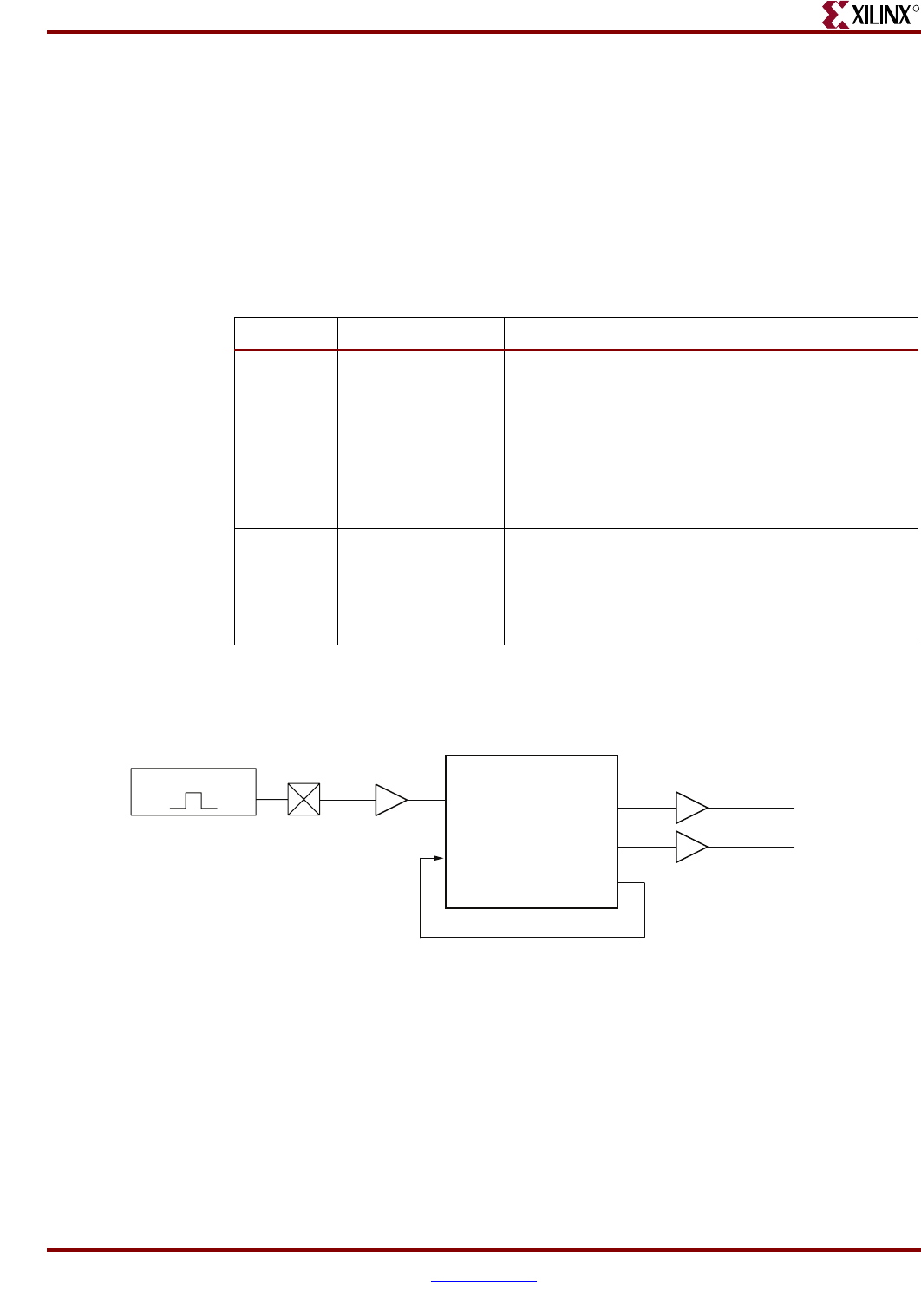
Memory Interface Solutions User Guide www.xilinx.com 443
UG086 (v3.6) September 21, 2010
Clocking Scheme
R
The system clock from the output of the IBUFGDS or the IBUFG is connected to the
PLL/DCM to generate the various clocks used by the memory interface logic.
The clk200 output of the IBUFGDS or the IBUFG is connected to the BUFG. The output of
the BUFG is used for IDELAY IOB delay blocks for aligning read capture data.
The PLL/DCM generates two separate synchronous clocks for use in the design. This is
shown in Table 11-3, Figure 11-8, and Figure 11-9, page 444. The clock structure is the same
for both the example design and the user design. For designs without PLL/DCM
instantiation, PLL/DCM and the BUFGs should be instantiated at the user end to generate
the required clocks.
Table 11-3: DDR Interface Design Clocks
Clock Description Logic Domain
clk0
Skew compensated
replica of the input
system clock.
The clock for the controller and the user interface
logic, most of the DDR bus-related I/O flip-flops
(e.g., memory clock, control/address, output DQS
strobe, and DQ input capture). This clock is used to
register the data, address, and command signals,
and the address and data enables for the user
interface logic(1). This clock is also used to generate
the FIFO status signals.
clk90 90° phase-shifted
version of clk_0
Used in the write data path section of physical layer.
Clocks write path control logic, DDR side of the
Write Data FIFO, and output flip-flops for DQ. This
clock is also used to generate the read data and read
data valid signals for the user interface logic(1).
Notes:
1. See “User Interface Accesses,” page 449 for timing requirements and restrictions on the user interface
signals.
Figure 11-8: Clocking Scheme for QDRII Interface Logic Using PLL
CLKIN
CLKFBIN CLKOUT1
CLKOUT0
clk90
clk0
PLL BUFG
GC I/O
SYSTEM CLK
UG086_c11_15_012809
CLKFBOUT
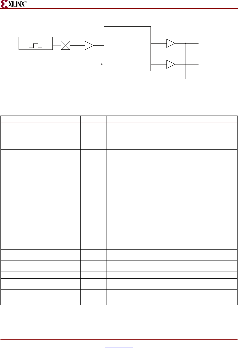
444 www.xilinx.com Memory Interface Solutions User Guide
UG086 (v3.6) September 21, 2010
Chapter 11: Implementing DDR SDRAM Controllers
R
Table 11-4 lists the user interface signals.
Figure 11-9: Clocking Scheme for DDR Interface Logic
CLKIN
C
LKFB CLK90
CLK0
clk90
clk0
DCM BUFG
GC I/O
SYSTEM CLK
UG086_c11_14_092908
Table 11-4: User Interface Signals
Signal Direction(1) Description
app_af_cmd[2:0](2) Input 3-bit command to the Virtex-5 FPGA DDR SDRAM design.
app_af_cmd = 3’b000 for write commands
app_af_cmd = 3’b001 for read commands
Operation is not guaranteed if the user gives values other than the specified
ones.
app_af_addr[30:0](2, 3) Input Provides the address, row address, and column address of the memory
location to be accessed.
Column address = app_af_addr[COL_WIDTH-1: 0]
Row address = app_af_addr[ROW_WIDTH+COL_WIDTH -1:
COL_WIDTH]
Bank address =
app_af_addr[BANK_WIDTH+ROW_WIDTH+COL_WIDTH-1:
ROW_WIDTH+COL_WIDTH]
app_af_wren(2) Input Write enable to the user address FIFO. This signal should be synchronized
with the app_af_addr and app_af_cmd signals.
app_wdf_data[2*DQ_WIDTH-1:0](2) Input User input data. It should have the fall data and the rise data.
Rise data = app_wdf_data[DQ_WIDTH-1: 0]
Fall data = app_wdf_data[2*DQ_WIDTH-1: DQ_WIDTH]
app_wdf_wren(2) Input Write enable for the user write FIFO. This signal should be synchronized
with the app_wdf_data and app_wdf_mask_data signals.
app_wdf_mask_data[2*DM_WIDTH-1: 0](2) Input User mask data. It should contain the masking information for both rise and
fall data.
Rise mask data = app_wdf_mask_data[DM_WIDTH-1: 0]
Fall mask data = app_wdf_mask_data[2*DM_WIDTH-1: DM_WIDTH]
app_af_afull(2) Output Almost Full status of the address FIFO. The user can write 12 more locations
into the FIFO after app_af_afull is asserted.
app_wdf_afull(2) Output Almost Full status of the user write FIFO. The user can write 12 more
locations into the FIFO after app_wdf_afull is asserted.
rd_data_fifo_out[2*DQ_WIDTH-1: 0](2) Output Read data from the memory. Read data is stored in the user write FIFO.
rd_data_valid(2) Output Status signal indicating that data read from the memory is available to the
user.
clk0_tb Output Clock output to the user. All the user input data and commands must be
synchronized with this clock. This signal is sourced from clk0 in the
controller.
Memory Interface Solutions User Guide www.xilinx.com 445
UG086 (v3.6) September 21, 2010
Clocking Scheme
R
Table 11-5 lists the signals between the User interface and the controller.
rst0_tb Output Active-High reset for the user interface.
Notes:
1. The direction indicated in this table is referenced from the design perspective. For example, input indicates that the signal is input to the
design and output for the user.
2. See “User Interface Accesses,” page 449 for required timing requirements and restrictions for the user interface signals.
3. Addressing in the Virtex-5 FPGA is linear. That is, the row address bits immediately follow the column address bits, and the bank address
bits follow the row address bits, thus supporting more devices. The number of address bits used depends on the density of the memory part.
The controller ignores the unused bits, which can all be tied to High.
Table 11-4: User Interface Signals (Cont’d)
Signal Direction(1) Description
Table 11-5: Signals between User Interface and Controller
Port Name Port Width Port Description
af_cmd 3
Output of the Address FIFO in the user interface.
Monitors the FIFO full status flag to the write command
into the Address FIFO.
af_addr 31
Output of the Address FIFO in the user interface. The
mapping of these address bits is: [30:0]: Memory
Address (Bank, Row, Column). Monitors the FIFO full
status flag to the write address into the Address FIFO.
af_empty 1
The user interface Address FIFO empty status flag
output. The user application can write to the Address
FIFO when this signal is asserted until the write data
FIFO full status flag is asserted. FIFO36 Almost Empty
flag.
ctrl_af_rden 1
Read Enable input to Address FIFO in the user interface.
This signal is asserted for one clock cycle when the
controller state is write or read resulting from dynamic
command requests.
Table 11-6: Design Status Signals
Signal Direction Description
phy_init_done Output Indicates the completion of initialization
and calibration of the design.
446 www.xilinx.com Memory Interface Solutions User Guide
UG086 (v3.6) September 21, 2010
Chapter 11: Implementing DDR SDRAM Controllers
R
System Interface Signals
Table 11-7 and Table 11-8 shows the system interface signals for designs with and without
a PLL, respectively.
Table 11-7: System Interface Signals with a PLL
Signal Direction Description
sys_clk_p, sys_clk_n Input Differential input clocks to the PLL/DCM. The
DDR SDRAM controller and memory operate on
this clock. This differential input clock pair is
present only when the DIFFERENTIAL clocks
option is selected in MIG FPGA options page.
sys_clk Input Single-ended input clock to the PLL/DCM. The
DDR controller and memory operate at this
frequency. This input clock is present only when
the SINGLE_ENDED clocks option is selected in
the MIG FPGA options page.
sys_rst_n Input Active-Low reset to the DDR SDRAM controller.
clk200_p, clk200_n Input 200 MHz differential input clock for the
IDELAYCTRL primitive of Virtex-5 FPGA. This
differential input clock pair is present only when
the DIFFERENTIAL clocks option is selected in
MIG FPGA options page.
idly_clk_200 Input 200 MHz single-ended input clock for the
IDELAYCTRL primitive of Virtex-5 FPGAs. This
input clock is present only when the
SINGLE_ENDED clocks option is selected in the
MIG FPGA options page.
Table 11-8: System Interface Signals without a PLL
Signal Direction Description
clk0 Input The DDR SDRAM controller and memory
operate on this clock.
sys_rst_n Input Active-Low reset to the DDR SDRAM controller.
This signal is used to generate a synchronous
system reset.
clk90 Input 90° phase-shifted clock with the same frequency
as clk0.
clk200 Input 200 MHz input differential clock for the
IDELAYCTRL primitive of the Virtex-5 FPGA.
locked Input The status signal indicating whether the
PLL/DCM is locked or not. This signal is used to
generate a synchronous system reset.
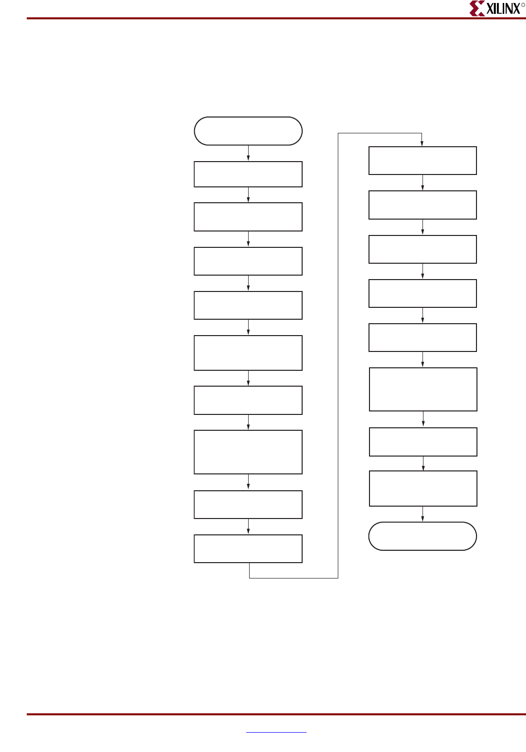
Memory Interface Solutions User Guide www.xilinx.com 447
UG086 (v3.6) September 21, 2010
DDR SDRAM Initialization
R
DDR SDRAM Initialization
DDR memory is initialized through a specified sequence as shown in Figure 11-10. This
initialization sequence is in accordance with JEDEC specifications for DDR SDRAMs. The
initialization logic is implemented in the physical layer.
Figure 11-10: DDR SDRAM Initialization
UG086_c11_08_021307
Wait 200 μs
Wait > 200 clock cycles
Wait 45 clock cycles
Wait 45 clock cycles
Wait 45 clock cycles
Wait 45 clock cycles
Wait 45 clock cycles
Wait 45 clock cycles
Precharge all banks
Wait > 200 clock cycles
(249 clock cycles)
Precharge all banks
Load Mode EMR with
A0 = 0 (enable DLL). Also
select drive strength.
Load Mode MR with
A[12:8] = 0x01 (reset DLL).
Also select other operating
parameters.
Bank Activate at BA = 0x0,
Row = 0x0 (for first
calibration stage)
Load Mode MR with
A[12:8] = 0x00 (deactivate
DLL reset). Also select other
operating parameters.
System Reset
Auto Refresh
Auto Refresh
Initialization complete.
Continue calibration.
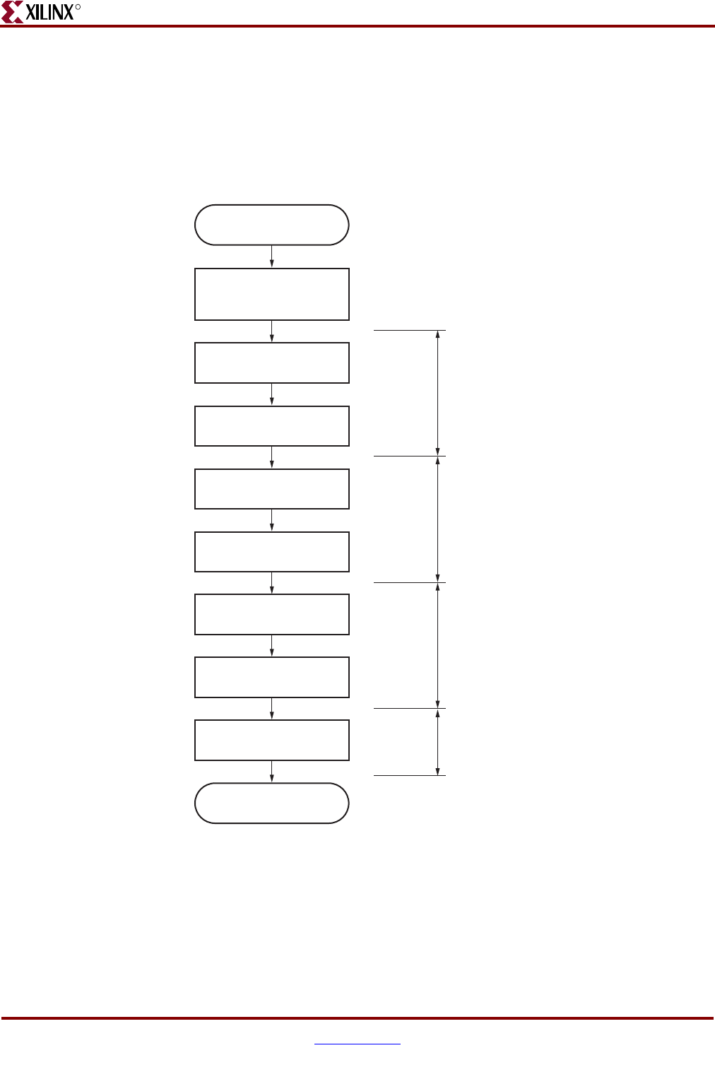
448 www.xilinx.com Memory Interface Solutions User Guide
UG086 (v3.6) September 21, 2010
Chapter 11: Implementing DDR SDRAM Controllers
R
DDR SDRAM Design Calibration
Before issuing user read and write commands, the design is calibrated to ensure that
correct data is captured in the ISERDES primitives of Virtex-5 FPGAs. Calibration logic is
implemented in the physical layer of the design. Figure 11-11 shows the overall calibration
sequence. For more details on the calibration algorithm for the Virtex-5 FPGA DDR
interface, see XAPP851 [Ref 25].
The first calibration stage sets the IDELAY value for each DQ (IDELAY for DQS remains at
0 during this time), and is performed even before a phase relationship between DQS and
FPGA_CLK has been established. A training pattern of “10” (1 = rising, 0 = falling) is used
to calibrate DQ.
The second calibration stage includes calibration between the DQS and the FPGA clock.
Figure 11-11: Overall Design Calibration Sequence
UG086_c9_08_020507
Write all callibration training
patterns to fixed locations
in memory
Write callibration patterns
required for stage 1, stage 2,
and stage 3/4 calibration to memory.
Stage 1:
DQ-DQS per bit calibration.
Adjust DQ IDELAY.
Perform once per DQ bit.
Continuous readback of
stage 1 training pattern
Continuous readback of
stage 2 training pattern
Calibrate all DQ
Calibrate all DQS
Continuous readback of
stage 3/4 training pattern
Read Data Valid calibration
all DQS
Calibration Done
DQS Gate Control
calibration for all DQS
Power-up init sequence
complete
Stage 3:
Read data valid calibration (once per
DQS group).
Adjust number of clock cycles to wait
after issuing read command before valid
data arrives in FPGA_CLK domain.
Perform once per DQS group.
Stage 4:
DQS gate control calibration.
Adjust IDELAY for DQS gate control.
Perform once per DQS group.
Stage 2:
DQS-FPGA CLK calibration (use
DQ [8 * x] to calibrate DQS [x]);
Adjust DQ/DQS IDELAY.
Perform once per DQS group.

Memory Interface Solutions User Guide www.xilinx.com 449
UG086 (v3.6) September 21, 2010
User Interface Accesses
R
The third calibration stage is read-enable calibration, which compensates for the round-
trip delay between when the read command is issued by the controller, and the captured
read data is valid at the outputs of the ISERDES.
The fourth stage includes calibration of a squelch circuit that gates the input DQS to avoid
the glitch that propagates to the second rank of flops in the ISERDES. The glitch occurs
when DQS goes from the Low state to the 3-state level after the last edge of the DQS, which
might cause a “false” rising and/or falling edge on the DQS input to the FPGA. Unless the
DQS glitch is gated after the last DQS falling edge of a read burst, the data registered in the
ISERDES might change prematurely. During calibration, an auto-refresh command is
issued to memory at intervals depending on the stage of calibration.
After initialization and calibration is done, the controller is signaled to start normal
operation of the design. Now, the controller can start issuing user write and read
commands to the memory.
User Interface Accesses
The user backend logic communicates with the memory controller through a synchronous
FIFO-based user interface. This interface consists of three related buses:
• a command/address FIFO bus accepts write/read commands as well as the
corresponding memory address from the user
• a Write Data FIFO bus that accepts the corresponding write data when the user issues
a write command on the command/address bus
• a read bus on which the corresponding read data for an issued read command is
returned
The user interface has the following timing and signaling restrictions:
1. Commands and write data cannot be written by the user until calibration is complete
(as indicated by phy_init_done). In addition, the following interface signals need to be
held Low until calibration is complete: app_af_wren, app_wdf_wren, app_wdf_data[].
app_wdf_mask_data[]. Failure to hold these signals Low causes errors during
calibration. This restriction arises from the fact that the Write Data FIFO is also used
during calibration to hold the training patterns for the various stages of calibration.
2. When issuing a write command, the first write data word must be written to the Write
Data FIFO either prior to, or on the same clock cycle as the when the write command
is issued. In addition, the write data must be written by the user over consecutively
clock cycles, there cannot be a break in between words. These restrictions arise from
the fact that the controller assumes write data is available when it receives the write
command from the user.
3. The output of the Read Data FIFO (specifically, the rd_data_fifo_out and
rd_data_valid signals) are synchronous to clk90, and not to clk0. The user might need
to insert an extra pipeline stage to resynchronize the data to clk0 if place-and-route
timing cannot be met on these 3/4 cycle paths.
4. The clk0_tb signal is connected to clk0 in the controller. If the user clock domain is
different from clk0 / clk0_tb of MIG, the user should add FIFOs for all data inputs and
outputs of the controller in order to synchronize them to the clk0_tb.
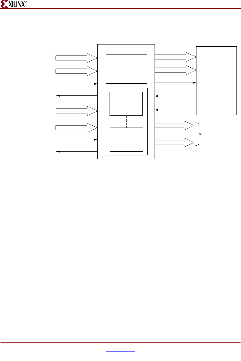
450 www.xilinx.com Memory Interface Solutions User Guide
UG086 (v3.6) September 21, 2010
Chapter 11: Implementing DDR SDRAM Controllers
R
Write Interface
Figure 11-12 shows the user interface block diagram for write operations.
The following steps describe the architecture of the Address and Write Data FIFOs and
show how to perform a write burst operation to DDR SDRAM from the user interface.
1. The user interface consists of an Address FIFO and a Write Data FIFO. The Write Data
FIFO is constructed using Virtex-5 FPGA FIFO36_72 primitive with a 512 x 72
configuration. The 72-bit architecture comprises one 64-bit port and one 8-bit port. For
Write Data FIFOs, the 64-bit port is used for data bits and the 8-bit port is used for
mask bits. Mask bits are available only when supported by the memory part and when
the Data Mask is enabled in the MIG GUI. Some memory parts, such as Registered
DIMMs of x4 parts, do not support mask bits.
2. The Address FIFO is constructed using Virtex-5 FPGA FIFO36 primitive with a
1024 x 36 configuration. The 36-bit architecture comprises one 32-bit port and one 4-bit
port. The 32-bit port is used for addresses (app_af_addr), and the 4-bit port is used for
commands (app_af_cmd).
3. The Address FIFO is common for both Write and Read commands. It comprises an
address part and the command part. Command bits discriminate between write and
read commands.
4. The user interface data width app_wdf_data is twice that of the memory data width.
For an 8-bit memory width, the user interface is 16 bits consisting of rising edge data
and falling edge data. For every 8 bits of data, there is a mask bit. For 72-bit memory
data, the user interface data width app_wdf_data is 144 bits, and the mask data
app_wdf_mask_data is 18 bits.
5. The minimum configuration of the Write Data FIFO is 512 x 72 for a memory data
width of 8 bits. For an 8-bit memory data width, the least-significant 16 bits of the data
port are used for write data and the least-significant two bits of the 8-bit port are used
Figure 11-12: User Interface Block Diagram for Write Operations
User Interface
Controller
Address FIFO
(FIFO36)
1024 x 36
af_addr
af_cmd
af_empty
ctrl_af_rden
wdf_rden
app_af_addr
app_af_cmd
app_af_wren
app_wdf_data
app_wdf_mask_data
app_wdf_wren
wdf_data
wdf_mask_data
To Phy Layer
app_wdf_afull
app_af_afull
Write Data
FIFO
(FIFO36_72)
512 x 72
Write Data
FIFO
(FIFO36_72)
512 x 72
ug086_c11_12_122007

Memory Interface Solutions User Guide www.xilinx.com 451
UG086 (v3.6) September 21, 2010
Write Interface
R
for mask bits. The controller internally pads all zeros for the most-significant 48 bits of
the 64-bit port and the most-significant six bits of the 8-bit port.
6. Depending on the memory data width, MIG instantiates multiple FIFO36_72s to gain
the required width. For designs using 8-bit to 32-bit data width, one FIFO36_72 is
instantiated; for 72-bit data width, a total of three FIFO36_72s are instantiated. The bit
architecture comprises 32 bits of rising-edge data, 4 bits of rising-edge mask, 32 bits of
falling-edge data, and 4 bits of falling-edge mask, which are all stored in a FIFO36_72.
MIG routes the app_wdf_data and app_wdf_mask_data to FIFO36_72s accordingly.
7. The user can initiate a write to memory by writing to the Address FIFO and the Write
Data FIFO when FIFO full flags are deasserted. Status signal app_af_afull is asserted
when the Address FIFO is full; similarly, app_wdf_afull is asserted when Write Data
FIFO is full.
8. At power-on, both Address FIFO and Write Data FIFO full flags are deasserted.
9. The user should assert Address FIFO write enable signal app_af_wren along with
address app_af_addr and command app_af_cmd to store the address and command
into Address FIFO.
10. The user data should be synchronized to the clk_tb clock. Data FIFO write-enable
signal app_wdf_wren should be asserted to store write data app_wdf_data and mask
data app_wdf_mask_data into the Write Data FIFOs. Rising-edge and falling-edge
data should be provided together for each write to the Data FIFO. The Virtex-5 FPGA
DDR SDRAM controller design supports byte-wise masking of data only.
11. The write command should be given by keeping app_af_cmd = 3'b000 and asserting
app_af_wren. Address information is given on the app_af_addr signal. Address and
command information is written into the User Address FIFO.
12. After the completion of the initialization and calibration process and when the User
Address FIFO empty signal is deasserted, the controller reads the command and
address FIFO and issues a write command to the DDR SDRAM.
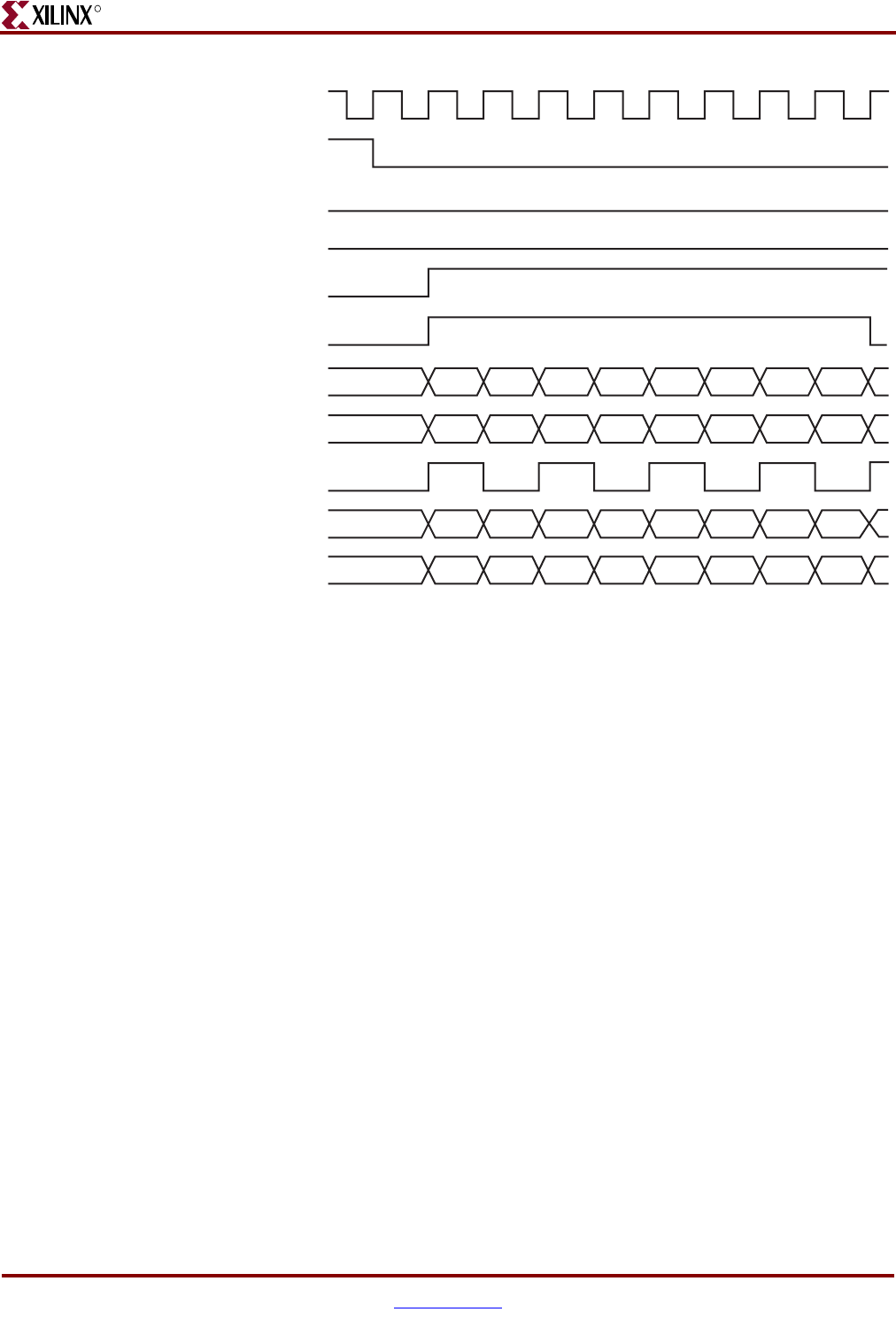
452 www.xilinx.com Memory Interface Solutions User Guide
UG086 (v3.6) September 21, 2010
Chapter 11: Implementing DDR SDRAM Controllers
R
13. The write timing diagram in Figure 11-13 is derived from the MIG-generated testbench
for a burst length of four (BL = 4). As shown, each write to Address FIFO should have
two writes to the Data FIFO. The phy_init_done signal indicates memory initialization
and calibration completion.
Figure 11-13: DDR SDRAM Write Burst for Four Bursts (BL = 4)
clk_tb
reset_tb
app_wdf_afull
app_af_afull
app_af_wren
app_af_addr
phy_init_done
app_wdf_wren
A0
app_af_cmd 000 000 000 000
app_wdf_dataD1D0D3D2D5D4D7D6D9D8D11D10 D13D12 D15D14
app_mask_dataM1M0M3M2M5M4M7M6M9M8M
11M
10 M
13M
12 M
15M
14
A1A2A3
UG086_c11_10_071808
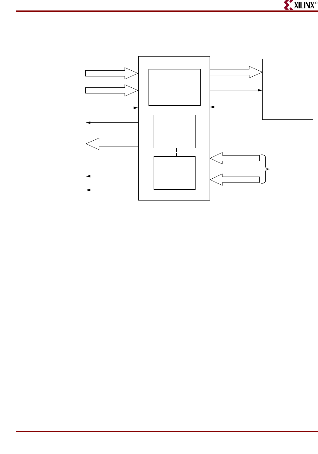
Memory Interface Solutions User Guide www.xilinx.com 453
UG086 (v3.6) September 21, 2010
Read Interface
R
Read Interface
Figure 11-14 shows the block diagram of the read interface.
The following steps describe the architecture of the Read Data FIFO and show how to
perform a read burst operation from DDR SDRAM from the user interface.
1. The read user interface consists of an Address FIFO and a Read Data FIFO. The
Address FIFO is common between reads and writes. The Read Data FIFO is built out of
Distributed RAMs of 16 x 1 configuration. MIG instantiates the number of RAM16Ds
depending on the data width. For example, for 8-bit data width, MIG instantiates a
total of 16 RAM16X1Ds, 8 for rising-edge data and 8 for falling-edge data. Similarly, for
72-bit data width, MIG instantiates a total of 144 RAM16Ds, 72 for rising-edge data
and 72 for falling-edge data.
2. The user can initiate a read to memory by writing to the Address FIFO when the FIFO
full flag app_af_afull is deasserted.
3. To write the read address and read command into the Address FIFO, the Address FIFO
write enable signal app_af_wren should be issued, along with the memory read
address app_af_addr and app_af_cmd commands (set to 001 for a read command).
4. The controller reads the Address FIFO and generates the appropriate control signals to
memory. After decoding app_af_cmd, the controller issues a read command to the
memory at the specified address.
5. Prior to the actual read and write commands, the design calibrates the latency in
number of clock cycles from the time the read command is issued to the time the data
is received. Using this precalibrated delay information, the controller stores the read
data in Read Data FIFOs.
6. The read_data_valid signal is asserted when data is available in the Read Data FIFOs.
7. When calibration is completed, the controller generates the control signals to capture
the read data from the FIFO according to the CAS latency selected by the user. The
Figure 11-14: User Interface Block Diagram for Read Operation
User Interface
Controller
Address FIFO
(FIFO36)
1024 x 36
af_addr
af_empty
ctrl_af_rden
rd_data_out_rise
rd_data_out_fall From Phy Layer
Read Data
FIFO
(RAM 16 x 1D)
Read Data
FIFO
(RAM 16 x 1D)
ug086_c11_13_122007
app_af_addr
app_af_cmd
app_af_wren
rd_data_fifo_out
rd_data_valid
app_af_afull
wdf_almost_full
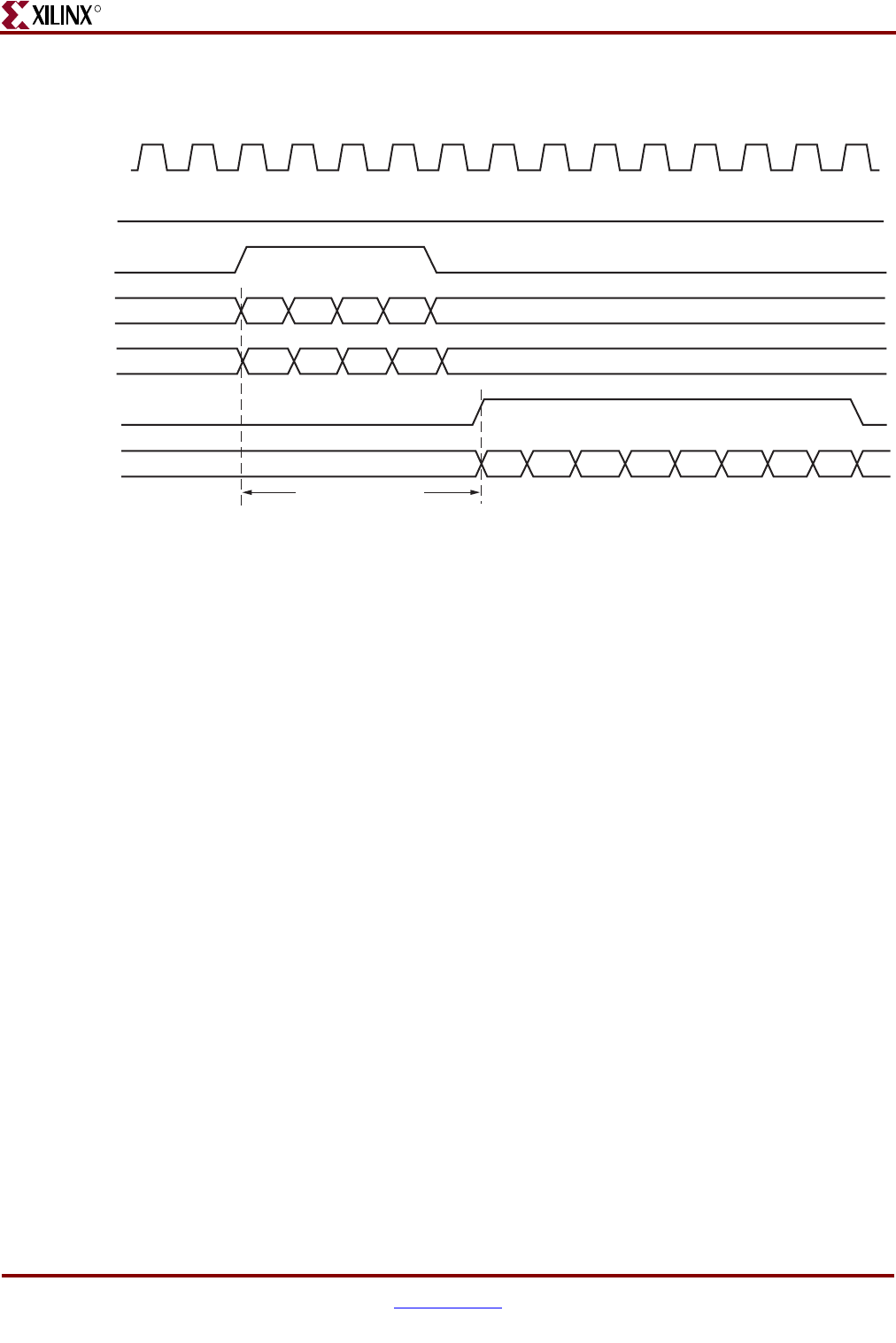
454 www.xilinx.com Memory Interface Solutions User Guide
UG086 (v3.6) September 21, 2010
Chapter 11: Implementing DDR SDRAM Controllers
R
rd_data_valid signal is asserted when the read data is available to the user, and
rd_data_fifo_out is the read data from the memory to the user.
8. Figure 11-15 shows the user interface timing diagram for a read command, burst
length of four.
Read latency is defined as the time between when the read command is written to the user
interface bus until when the corresponding first piece of data is available on the user
interface bus (see Figure 11-15).
When benchmarking read latencies, it is important to specify the exact conditions under
which the measurement occurs.
Read latency varies based on the following parameters:
• Number of commands already in the FIFO pipeline before the read command is
issued
• Whether an ACTIVATE command needs to be issued to open the new bank/row
• Whether a PRECHARGE command needs to be issued to close a previously opened
bank
• Specific timing parameters for the memory, such as TRAS and TRCD in conjunction
with the bus clock frequency
• Commands can be interrupted, and banks/rows can forcibly be closed when the
periodic AUTO REFRESH command is issued
•CAS latency
• Board-level and chip-level (for both memory and FPGA) propagation delays
Table 11-9 and Table 11-10 show read latencies for the Virtex-5 FPGA DDR interface for two
different conditions. Table 11-9 shows the case where a row activate is not required prior to
issuing a read command on the DDR bus. This situation is possible, for example, when
bank management is enabled, and the read targets an already opened bank. Table 11-10
shows the case when a read results in a bank/row conflict. In this case, a precharge of the
previous row must be followed by an activation of the new row, which increases read
latency. Other specific conditions are noted in the footnotes for each table.
Figure 11-15: DDR SDRAM Read Burst for Four Bursts (BL = 4)
clk_tb
app_af_afull
app_af_wren
app_af_addr
app_af_cmd
rd_data_valid
rd_data_fifo_out
UG086_c11_11_071808
D15D14D11D10D7D6D3D2 D13D12D9D8D5D4D1D0
A0 A1 A2 A3
001 001 001 001
Read Latency
Memory Interface Solutions User Guide www.xilinx.com 455
UG086 (v3.6) September 21, 2010
DDR SDRAM Signal Allocations
R
DDR SDRAM Signal Allocations
MIG allows banks to be selected for different classes of memory signals. Table 11-11 shows
the list of signals allocated in a group from bank selection checkboxes.
Table 11-9: Read Latency without Precharge and Activate
Parameter Number of Clock
Cycles
User READ command to empty signal deassertion (using FIFO36) 5 clocks
Empty signal to READ command on DDR bus 4.5 clocks
READ command to read valid assertion 11.5 clocks
Total 21 clocks
Notes:
1. Test conditions: Clock frequency = 200 MHz, CAS latency = 3, DDR -5 speed grade device.
2. Access conditions: Read to an already open bank/row is issued to an empty control/address FIFO.
3. Some entries have fractional clock cycles because the inverted version of CLK0 is used to drive the
DDR memory.
4. The Virtex-5 FPGA DDR interface uses a FIFO36 for the address/control FIFO. It is possible to shorten
the READ command to empty signal deassertion latency by implementing the FIFO as a distributed
RAM FIFO or removing the FIFO altogether, as the application requires.
Table 11-10: Read Latency with Precharge and Activate
Parameter Number of Clock
Cycles
User READ command to empty signal deassertion (using FIFO36) 5 clocks
Empty signal to PRECHARGE command on DDR bus 4.5 clocks
PRECHARGE to ACTIVE command to DDR memory 3 clocks
ACTIVE to READ command to DDR memory 4 clocks
READ command to read valid assertion 11.5 clocks
Total 28 clocks
Notes:
1. Test conditions: Clock frequency = 200 MHz, CAS latency = 3, DDR -5 speed grade device.
2. Access conditions: Read that results in a bank/row conflict is issued to an empty control/address
FIFO. This requires that the previous bank/row be closed first.
3. Some entries have fractional clock cycles because the inverted version of CLK0 is used to drive the
DDR memory.
4. The Virtex-5 DDR interface uses a FIFO36 for the address/control FIFO. It is possible to shorten the
READ command to empty signal deassertion latency by implementing the FIFO as a distributed RAM
FIFO or removing the FIFO altogether, as the application requires.
Table 11-11: DDR SDRAM Signal Allocations
Bank Selected Signals Allocated in the Group
Address Memory address, memory control, and memory clock signals
Data Data, data mask, and data strobes
456 www.xilinx.com Memory Interface Solutions User Guide
UG086 (v3.6) September 21, 2010
Chapter 11: Implementing DDR SDRAM Controllers
R
Note: Timing has been verified for most of the MIG generated configurations. For the best timing
results, adjacent banks in the same column of the FPGA should be used. Banks that are separated
by unbonded banks should be avoided because these can cause timing violations.
Supported Devices
The design generated by MIG is independent of the memory package; therefore, the
package part of the memory component is replaced with XX, where XX indicates a “don't
care” condition. The tables below list the components (Table 11-12) and DIMMs
(Table 11-13 through Table 11-15) supported by MIG for DDR SDRAM. See Appendix G,
“Low Power Options.”
System Control System reset from user interface and status signals
System Clock System clocks from the user interface
Table 11-11: DDR SDRAM Signal Allocations (Cont’d)
Bank Selected Signals Allocated in the Group
Table 11-12: Supported Components for DDR SDRAM (Virtex-5 FPGAs)
Components Packages (XX) Components Packages (XX)
MT46V32M4XX-75 P,TG MT46V32M4XX-5B -
MT46V64M4XX-75 FG,P,TG MT46V64M4XX-5B BG,FG,P,TG
MT46V128M4XX-75 BN,FN,P,TG MT46V128M4XX-5B BN,FN,P,TG
MT46V256M4XX-75 P,TG MT46V256M4XX-5B P,TG
MT46V16M8XX-75 P,TG MT46V16M8XX-5B TG,P
MT46V32M8XX-75 FG,P,TG MT46V32M8XX-5B BG,FG,P,TG
MT46V64M8XX-75 BN,FN,P,TG MT46V64M8XX-5B BN,FN,P,TG
MT46V128M8XX-75 P,TG MT46V128M8XX-5B -
MT46V8M16XX-75 P,TG MT46V8M16XX-5B TG,P
MT46V16M16XX-75 BG,FG,P,TG MT46V16M16XX-5B BG,FG,P,TG
MT46V32M16XX-75 - MT46V32M16XX-5B BN,FN,P,TG
MT46V64M16XX-75 P,TG MT46V64M16XX-5B -
Table 11-13: Supported Unbuffered DIMMs for DDR SDRAM (Virtex-5 FPGAs)
Unbuffered DIMMs Packages (X) Unbuffered DIMMs Packages (X)
MT4VDDT1664AX-40B G,Y MT8VDDT3264AX-40B G,Y
MT4VDDT3264AX-40B G,Y MT9VDDT3272AX-40B Y
Table 11-14: Supported Registered DIMMs for DDR SDRAM (Virtex-5 FPGAs)
Registered DIMMs Packages (X) Registered DIMMs Packages (X)
MT9VDDF3272X-40B G,Y MT18VDDF6472X-40B G,Y
MT9VDDF6472X-40B G,Y MT18VDDF12872X-40B G,Y
Memory Interface Solutions User Guide www.xilinx.com 457
UG086 (v3.6) September 21, 2010
Simulating a DDR SDRAM Design
R
Simulating a DDR SDRAM Design
After generating the design, MIG creates a sim folder in the specified path. This folder
contains simulation files for a particular design. The sim folder contains the external
testbench, memory model, and .do file to simulate the generated design. The memory
model files are currently generated in Verilog only. To learn more details about the files in
the sim folder and to simulate the design, refer to “Simulation Guide,” page 499.
For single-rank DIMMs, MIG outputs only the base part memory model. In the simulation
testbench (sim_tb_top in the sim folder), MIG instantiates the required number of
memory models. For example, a 1 GB single-rank DIMM with the base part is 1 Gb, and
MIG instantiates the base model eight times. If the MIG generated memory model is to be
used with the user’s test bench, multiple instances should be used based on the selected
configuration.
The MIG output memory model considers the part_mem_bits parameter by default for
memory range allocation. This covers only a partial memory range, i.e., 2part_mem_bits. To
allocate the full memory range, the FULL_MEM parameter should be set in the memory
model, which in turn sets the full_mem_bits parameter for memory allocation. Allocating
the full memory range might exceed the memory of the operating system, thus causing
memory allocation failure in simulations.
Changing the Refresh Rate
The top-level parameter TREFI_NS should be changed to the selected refresh interval in
ns. For example, to change the refresh rate to 3.9 μs, TREFI_NS should be set to 3900. The
controller issues a refresh approximately every (TREFI_NS ×1000)/CLK_PERIOD clock
cycles, where CLK_PERIOD is the top-level parameter defining the clock period in terms
of ps. If the value in the formula exceeds 4095, the refi_cnt_r signal in the CTRL module
must be manually increased beyond 12 bits.
The CKE counter is a down-counter that is used to set the refresh interval, and its value is
initialized to all ones during reset. To change TREFI_NS, cke_200us_cnt_r in the
ddr2_phy_init HDL file must also be modified. This ensures that the 200 μs initialization
time is preserved. Bits must be added or removed based on the change made to the refresh
interval.
Hardware Tested Configurations
The frequencies shown in Table 11-16 were achieved on the Virtex-5 FPGA ML561 Memory
Interfaces Development Board under nominal conditions. This frequency should not be
used to determine the maximum design frequency. The maximum design frequency
supported in the MIG wizard is based a combination of the TRCE results for fabric timing
Table 11-15: Supported SODIMMs for DDR SDRAM (Virtex-5 FPGAs)
SODIMMs Packages (X) SODIMMs Packages (X)
MT4VDDT3264HX-40B G,Y MT9VDDT3272HX-40B -
MT4VDDT1664HX-40B Y MT9VDDT6472HX-40B G,Y
MT8VDDT3264HX-40B - MT9VDDT12872HX-40B -
MT8VDDT6464HX-40B G,Y
458 www.xilinx.com Memory Interface Solutions User Guide
UG086 (v3.6) September 21, 2010
Chapter 11: Implementing DDR SDRAM Controllers
R
on multiple device/package combinations and I/O timing analysis using FPGA and
memory timing parameters for a 64-bit wide interface.
Table 11-16: Hardware Tested Configurations
Synthesis Tools XST and Synplicity
HDL Verilog and VHDL
FPGA Device XC5VLX50T-FF1136-2
Burst Lengths 2, 4, 8
CAS Latency (CL) 2, 2.5, 3
32-bit Design Tested on 16-bit Component “MT46V32M16XX-5B”
Component, CL=2 110 MHz to 170 MHz
Component, CL=2.5 110 MHz to 210 MHz
Component, CL=3 110 MHz to 250 MHz
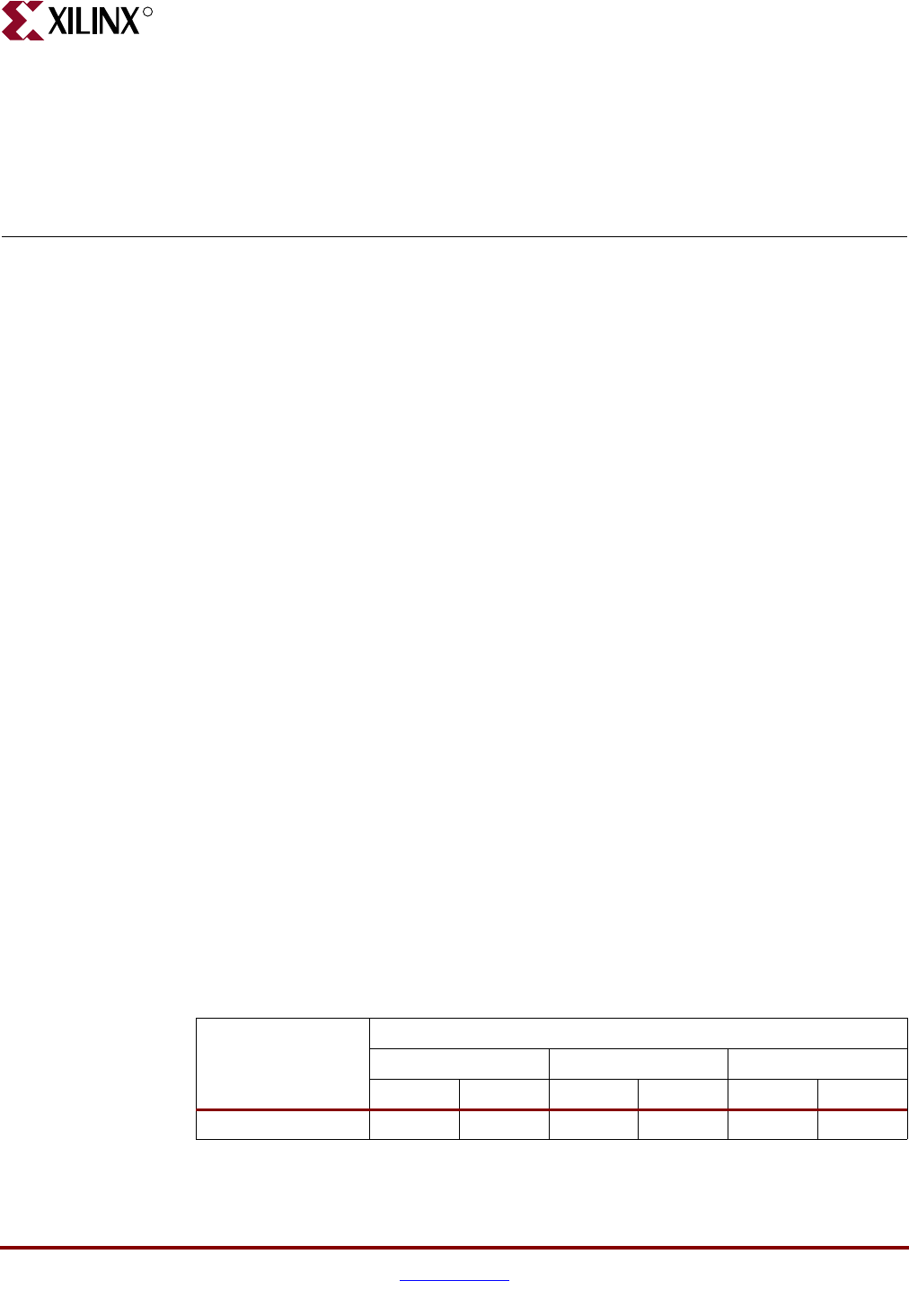
Memory Interface Solutions User Guide www.xilinx.com 459
UG086 (v3.6) September 21, 2010
R
Chapter 12
Implementing DDRII SRAM Controllers
This chapter describes how to implement DDRII SRAM interfaces for Virtex®-5 FPGAs
generated by MIG.
Feature Summary
This section summarizes the supported and unsupported features of DDRII SRAM
controller design.
Supported Features
The DDRII SRAM controller design supports the following:
• A maximum frequency of 300 MHz
• 9-bit, 18-bit, 36-bit, and 72-bit data widths
• CIO and SIO controller designs
• Burst lengths of two and four
• Programmable read-followed-by-write latency
• Linear/burst increment of address bits
• Implemented using different Virtex-5 devices
• Support for DCI cascading
• Support for debug signals
• Operating with 9-bit, 18-bit and 36-bit memory parts
•Verilog and VHDL
• With and without a testbench
• With and without a PLL
Design Frequency Ranges
Table 12-1: Design Frequency Range in MHz
Memory
FPGA Speed Grade
-1 -2 -3
MinMaxMinMaxMinMax
Component 120 250 120 300 120 300
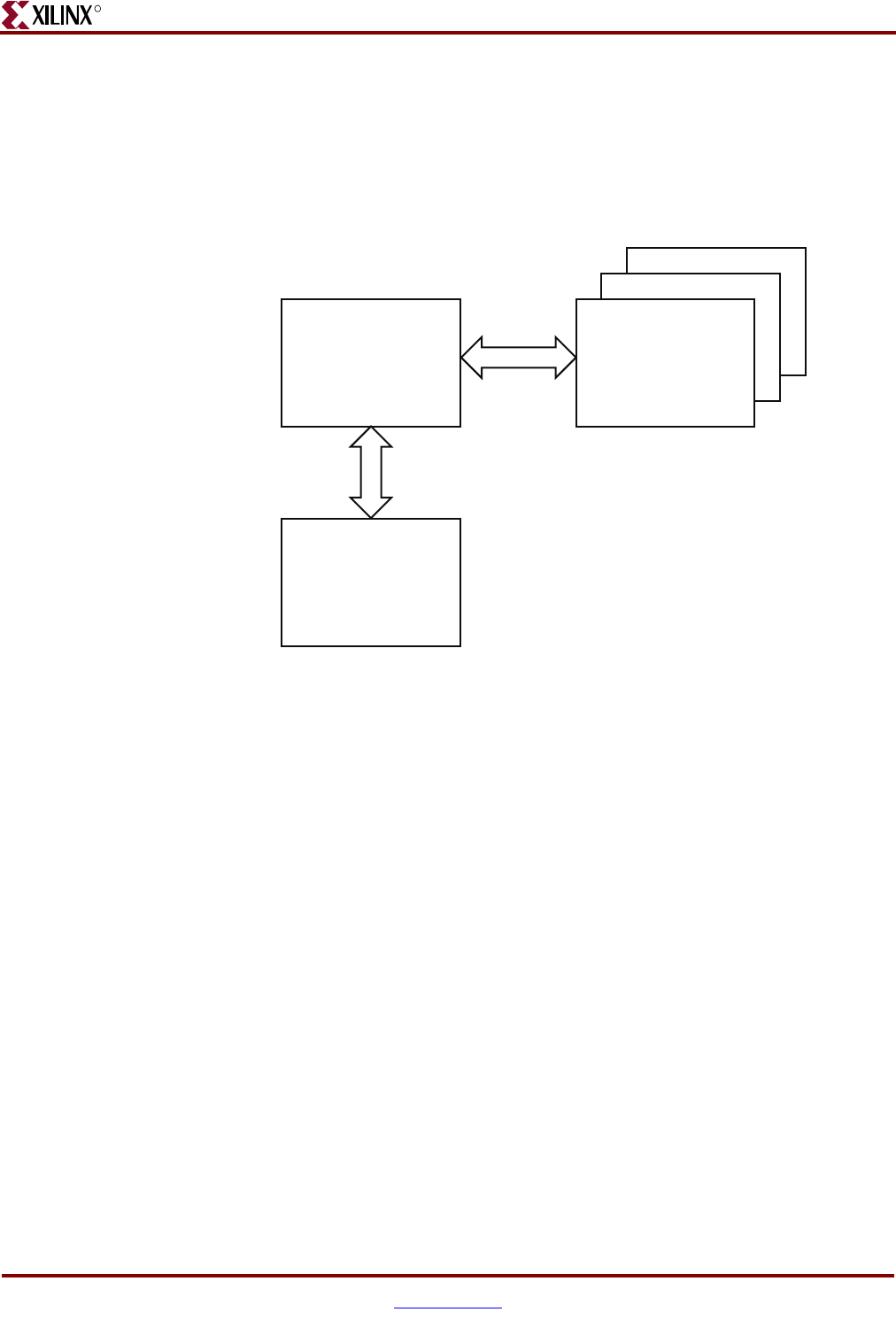
460 www.xilinx.com Memory Interface Solutions User Guide
UG086 (v3.6) September 21, 2010
Chapter 12: Implementing DDRII SRAM Controllers
R
Architecture
Figure 12-1 shows a top-level block diagram of the DDRII SRAM controller. One side of the
DDRII SRAM memory controller connects to the user interface denoted as User Interface.
The other side of the controller interfaces to DDRII SRAM memory. The memory interface
data width is selectable from MIG.
Both common I/O (CIO) and separate I/O (SIO) DDRII SRAM designs are supported by
MIG. SIO designs having independent read and write ports eliminate the need for high-
speed bus turnaround.
Read and write addresses are latched on positive edges of the input clock K. A common
address bus is used to access the addresses for both read and write operations.
Interface Model
DDRII SRAM interfaces are source-synchronous and double data rate. They transfer data
on both edges of the clock cycle. A memory interface has many advantages. It allows
designs to be ported easily and also makes it possible to share parts of the design across
different types of memory interfaces.
Figure 12-1: DDRII SRAM Memory Controller
DDRII SRAM
Memory
Controller
Virtex-5 FPGA
DDRII SRAM
Memory
User
Interface
ug086_c12_01_071508
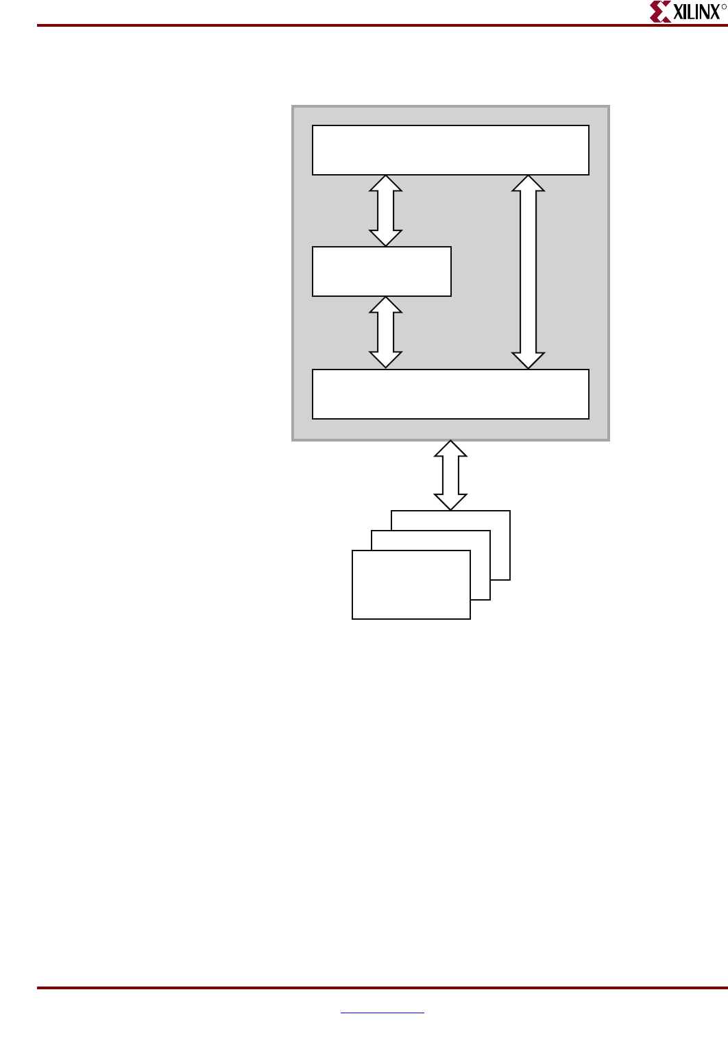
Memory Interface Solutions User Guide www.xilinx.com 461
UG086 (v3.6) September 21, 2010
Interface Model
R
Figure 12-2 shows the modular memory interface representation diagram. The application
interface layer creates the user interface, which initiates memory writes and reads by
writing data and memory addresses to the User Interface FIFOs.
The control layer comprises:
• Clocks and reset generation logic
• Datapath logic
• Control logic
Clocks and reset generation logic constitute a PLL/DCM primitive, which derives
different phase-shifted versions of the user-supplied differential clocks (sys_clk_p and
sys_clk_n). These phase-shifted versions of clocks run throughout the controller design. A
200 MHz user-supplied differential clock is used for the IDELAYCTRL elements. Reset
signals are generated for different clock domains using the user-supplied reset signals
(sys_rst_n), the locked signal, and the IDELAYCTRL ready signal (idelay_ctrl_ready).
Figure 12-2: Modular Memory Interface Representation Diagram
Application Interface Layer
Physical Layer
Control Layer
Xilinx FPGA
ug086_c12_02_071508
Memories
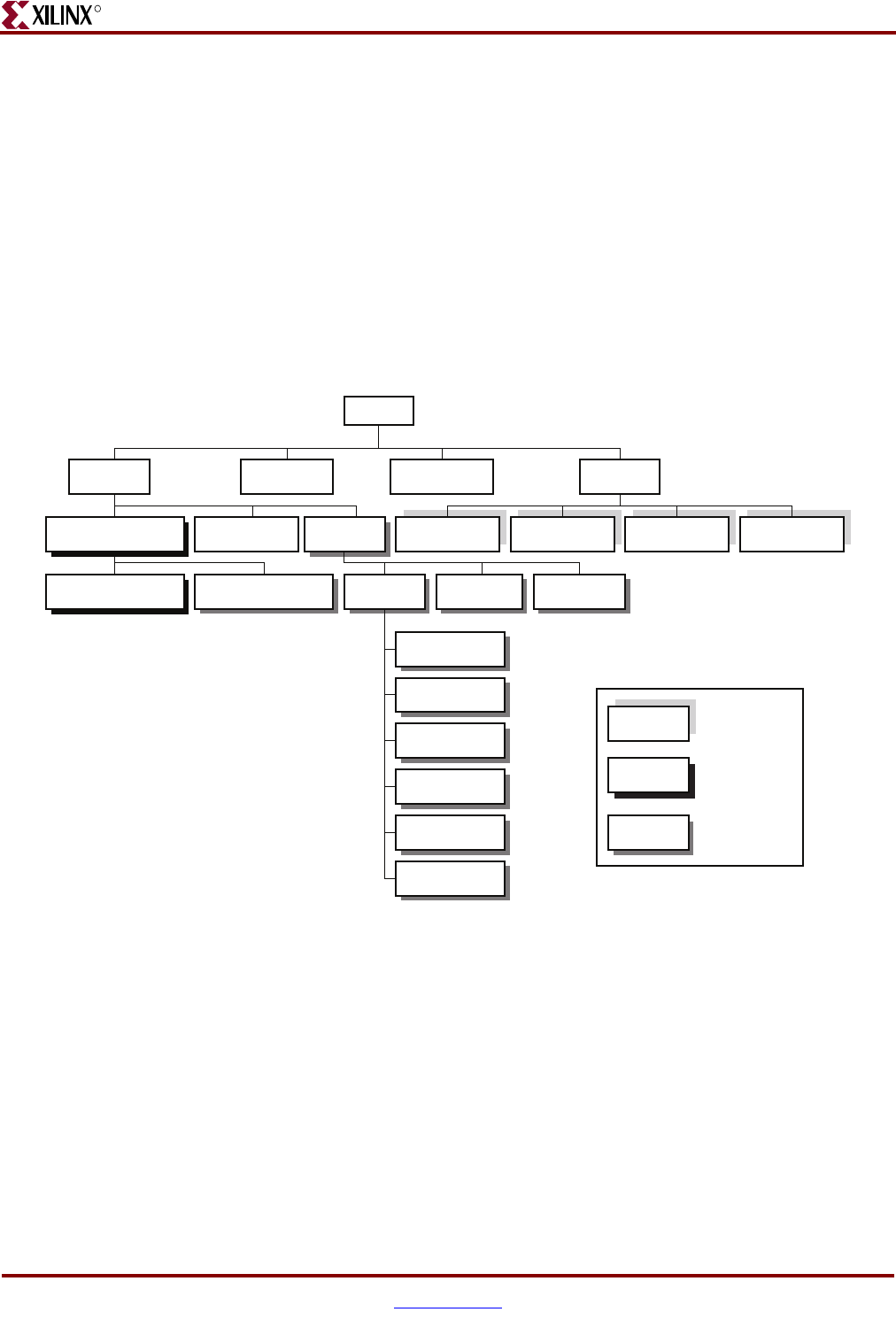
462 www.xilinx.com Memory Interface Solutions User Guide
UG086 (v3.6) September 21, 2010
Chapter 12: Implementing DDRII SRAM Controllers
R
The Datapath logic consists of memory write clocks, the read clocks and the data write
generation logic.
The Control logic constitutes read/write command generation logic, depending on the
status signals of the User Interface FIFO.
The previously mentioned logic interfaces with memory through IDDRs, ODDRs,
OFLOPS, ISERDES elements, and so on, which are associated with the physical layer. The
read data capturing logic is also associated with the physical layer.
Hierarchy
Figure 12-3 shows the hierarchical structure of the DDRII SRAM design generated by MIG
with a testbench and a PLL.
The modules are classified as follows:
• Design modules
• Testbench modules
• Clocks and reset generation modules
MIG can generate four different DDRII SRAM designs:
• With a testbench and a PLL
• Without a testbench and with a PLL
• With a testbench and without a PLL
• Without a testbench and without a PLL
Figure 12-3: Hierarchical Structure of the Virtex-5 FPGA DDRII SRAM
ug086_c12_03_100108
ip_top
ddrii_infrastructure
u_ddrii_infrastructure
arch_ddrii_infrastructure
ddrii_test_wr_rd_sm
u_ddrii_test_wr_rd_sm
arch_ddrii_test_wr_rd_sm
ddrii_test_addr_gen
u_ddrii_test_addr_gen
arch_ddrii_test_addr_gen
ddrii_test_data_gen
u_ddrii_test_data_gen
arch_ddrii_test_data_gen
ddrii_test_data_cmp
u_ddrii_test_data_cmp
arch_ddrii_test_data_cmp
ddrii_idelay_ctrl
u_ddrii_idelay_ctrl
arch_ddrii_idelay_ctrl
ddrii_top
u_ddrii_top
arch_ddrii_top
ddrii_tb_top
u_ddrii_tb_top
arch_ddrii_tb_top
ddrii_top_user_interface
u_ddrii_top_user_interface
arch_ddrii_top_user_interface
ddrii_top_addr_cmd_interface
u_ddrii_top_addr_cmd_interface
arch_ddrii_top_addr_cmd_interface
ddrii_top_wr_data_interface
u_ddrii_top_wr_data_interface
arch_ddrii_top_wr_data_interface
ddrii_top_ctrl_sm
u_ddrii_top_ctrl_sm
arch_ddrii_top_ctrl_sm
ddrii_phy_top
u_ddrii_phy_top
arch_ddrii_phy_top
ddrii_phy_io
u_ddrii_phy_io
arch_ddrii_phy_io
ddrii_phy_write
u_ddrii_phy_write
arch_ddrii_phy_write
ddrii_phy_ctrl_io
u_ddrii_phy_ctrl_io
arch_ddrii_phy_ctrl_io
ddrii_phy_cq_io
u_ddrii_phy_cq_io
arch_ddrii_phy_cq_io
ddrii_phy_dq_io
u_ddrii_phy_dq_io
arch_ddrii_phy_dq_io
ddrii_phy_bw_io
u_ddrii_phy_bw_io
arch_ddrii_phy_bw_io
ddrii_phy_init_sm
u_ddrii_phy_init_sm
arch_ddrii_phy_init_sm
ddrii_phy_dly_cal_sm
u_ddrii_phy_dly_cal_sm
arch_ddrii_phy_dly_cal_sm
ddrii_phy_en
u_ddrii_phy_en
arch_ddrii_phy_en
<module>
<verilog-instance>
<vhdl-instance>
= Testbench
= User Interface
LEGEND
= Physical (PHY) Layer
<module>
<verilog-instance>
<vhdl-instance>
<module>
<verilog-instance>
<vhdl-instance>

Memory Interface Solutions User Guide www.xilinx.com 463
UG086 (v3.6) September 21, 2010
MIG Design Options
R
MIG outputs both an example_design and a user_design. The MIG generated
example_design includes the entire memory controller design along with a synthesized
test bench (example user application). This testbench generates sample writes and reads
and then uses comparison logic to verify the data patterns written are the same received.
This example_design can be used to test functionality both in simulation and in hardware.
The user_design includes the memory controller design only. This design allows users to
connect the MIG memory controller design to a user developed testbench (user
application). Refer to Table 12-4 for user interface signals, the “User Interface Accesses” for
timing restriction on user interface signals.
For designs without a testbench (user_design), testbench modules are not present in the
design. The <top_module> (top level) module has the user interface signals for designs
without a testbench. The list of user interface signals is provided in Table 12-4.
Design clock and resets are generated in the infrastructure module. The PLL/DCM clock is
instantiated in the infrastructure module for designs with a PLL. The inputs to this module
are the differential design clock and a 200 MHz differential clock for the IDELAYCTRL
module. A user reset is also input to this module. Using the input clocks and reset signal,
system clocks and system reset signals are generated in this module, which are used in the
design.
The PLL/DCM primitive is not instantiated in this module if the PLL option is not
selected. So, the system operates on the user-provided clocks. The system reset signals are
generated in the infrastructure module using the locked input signal, the input reset signal,
and the IDELAYCTRL ready signal (idelay_ctrl_ready). For more information on the
clocking structure, refer to “Clocking Scheme,” page 480.
MIG Design Options
MIG provides various options to generate the design with or without a PLL. MIG always
generates two design folders, one with a testbench and the other without a testbench. This
selection provides detailed descriptions of the type of the design generated by the user
using various options.
Figure 12-4 shows a top-level block diagram of a DDRII SRAM design with a PLL and a
testbench. The sys_clk_p and sys_clk_n pair are differential input system clocks. “Clocking
Scheme,” page 480 describes how various clocks are generated using the PLL. The
PLL/DCM is instantiated in the infrastructure module that generates the required design
clocks. dly_clk_200_p and dly_clk_200_n are used for the IDELAYCTRL element.
Sys_rst_n is an active-Low system reset signal. All design resets are generated using this
system reset signal, the locked signal, and the IDELAYCTRL ready signal
(idelay_ctrl_ready). The error output signal compare_error indicates whether the case
passes or fails. The testbench module generates write and read address, write and read
commands, write data to the controller. It also compares the read data with written data.
The error signal is driven high on the data mismatches. The cal_done signal indicates the
completion of initialization and calibration of the design.
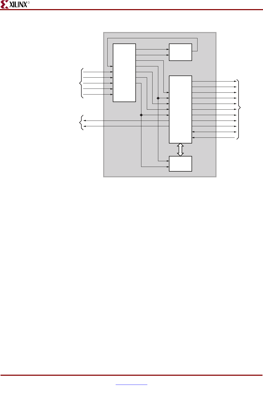
464 www.xilinx.com Memory Interface Solutions User Guide
UG086 (v3.6) September 21, 2010
Chapter 12: Implementing DDRII SRAM Controllers
R
Figure 12-5 shows a top-level block diagram of a DDRII SRAM design with a PLL but
without a testbench. The sys_clk_p and sys_clk_n pair are differential input system clocks.
“Clocking Scheme,” page 480 describes how various clocks are generated using the PLL.
The PLL/DCM is instantiated in the infrastructure module that generates the required
design clocks. dly_clk_200_p and dly_clk_200_n are used for the IDELAYCTRL element.
Sys_rst_n is an active-Low system reset signal. All design resets are generated using this
system reset signal, the locked signal, and the IDELAYCTRL ready signal
(idelay_ctrl_ready). User has to drive the user application signals. The design provides the
clk_0_tb and reset_clk_0_tb signals to the user in order to synchronize with the design. The
signal clk_0_tb is connected to clock clk_0 in the controller. If the user clock domain is
different from clk_0/clk_0_tb, the user should add FIFOs for all the input and outputs of
the controller (user application signals), in order to synchronize them to clk_0_tb clock.
The cal_done signal indicates the completion of initialization and calibration of the design.
Figure 12-4: Top-Level Block Diagram of the DDRII SRAM Design with a PLL and a
Testbench
ddrii_top
Memory
Device
Reference
Clocks and
Reset
ddrii_cq
idelay_ctrl_ready
tb_top
idelay_ctrl
infrastructure
ug086_c12_04_071508
Status
Signals
ddrii_dq
ddrii_bw_n
ddrii_saddrii_sa
ddrii_sa
ddrii_c_n
ddrii_c
ddrii_k_n
ddrii_k
ddrii_rw_n
ddrii_ld_n
ddrii_dll_off_n
reset_clk_200
clk_200
reset_clk_270
reset_clk_0
clk_270
sys_clk_p
sys_clk_n
clk_200_p
clk_200_n
sys_rst_n
compare_error
cal_done
clk_90
clk_0
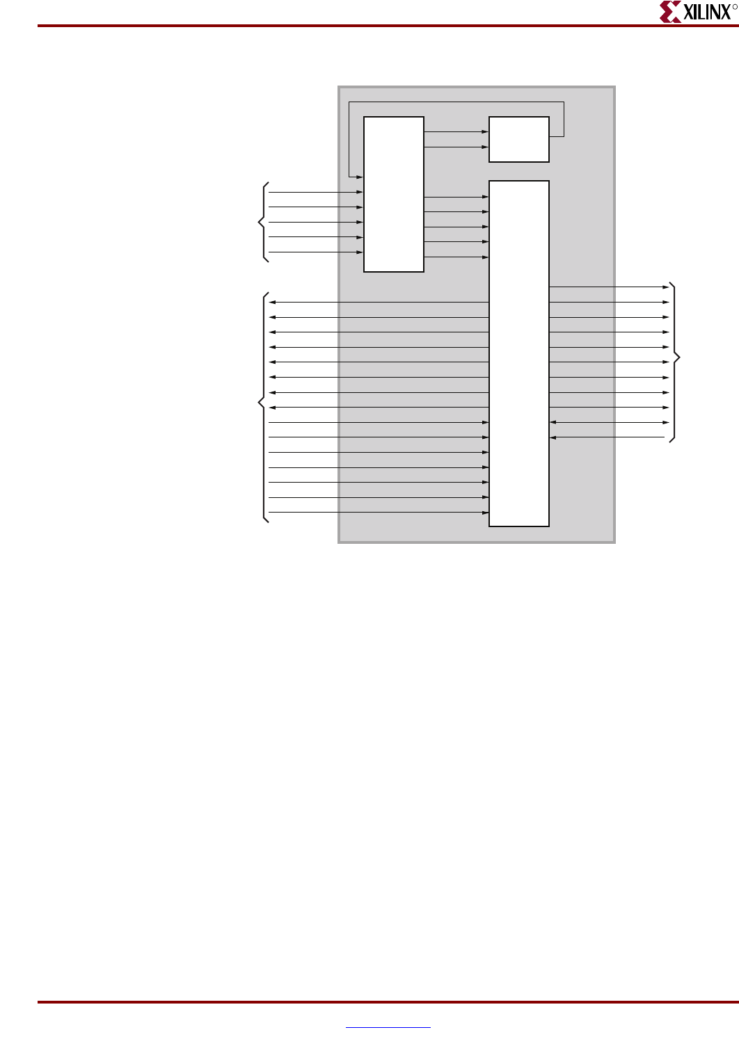
Memory Interface Solutions User Guide www.xilinx.com 465
UG086 (v3.6) September 21, 2010
MIG Design Options
R
Figure 12-5: Top-Level Block Diagram of the DDRII SRAM Design with a PLL and
without a Testbench
ddrii_top
Memory
Device
Reference
Clocks and
Reset
User
Application
ddrii_cq
idelay_ctrl_ready
idelay_ctrl
infrastructure
ug086_c12_05_071508
ddrii_dq
ddrii_bw_n
ddrii_sa
ddrii_c_n
ddrii_c
ddrii_k_n
ddrii_k
ddrii_rw_n
ddrii_ld_n
ddrii_dll_off_n
reset_clk_200
clk_200
clk_0
clk_90
clk_270
reset_clk_0
reset_clk_270
sys_clk_p
sys_clk_n
clk_200_p
clk_200_n
cal_done
clk_0_tb
reset_clk_0_tb
wrdata_fifo_full
addr_fifo_ful
rd_data_valid
user_rd_data_rise
user_rd_data_fall
user_wrdata_wr_en
user_addr_wr_en
user_bw_n_rise
user_bw_n_fall
user_addr_cmd
user_wr_data_rise
user_wr_data_fall
sys_rst_n
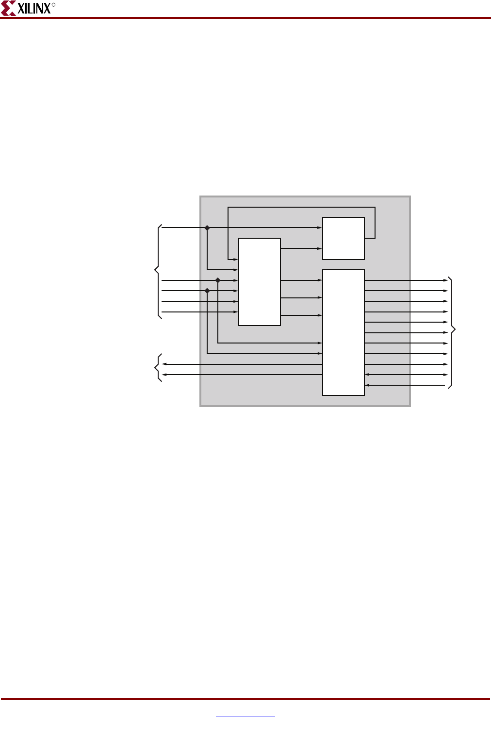
466 www.xilinx.com Memory Interface Solutions User Guide
UG086 (v3.6) September 21, 2010
Chapter 12: Implementing DDRII SRAM Controllers
R
Figure 12-6 shows a top-level block diagram of a DDRII SRAM design without a PLL but
with a testbench. User should provide all the clocks and the locked signal. “Clocking
Scheme,” page 480 describes how to generate the design clocks from the user interface.
These clocks should be single-ended. The sys_rst_n signal is an active-Low system reset.
All design resets are generated using this system reset signal, locked signal, and the
IDELAYCTRL ready signal (idelay_ctrl_ready). The user application must have a
PLL/DCM primitive instantiated in the design, and all user clocks should be driven
through BUFGs. The error output signal compare_error indicates whether the case passes
or fails. The testbench module generates write and read address, write and read
commands, write data to the controller. It also compares the read data with written data.
The error signal is driven high on the data mismatches. The cal_done signal indicates the
completion of initialization and calibration of the design.
Figure 12-6: Top-Level Block Diagram of the DDRII SRAM Design without a PLL but
with a Testbench
ddrii_top Memory
Device
User PLL/DCM
Clocks and
Reset
ddrii_cq
idelay_ctrl_ready
idelay_ctrl
infrastructure
ug086_c12_06_012909
ddrii_dq
ddrii_bw_n
ddrii_sa
ddrii_c_n
ddrii_c
ddrii_k_n
ddrii_k
ddrii_rw_n
ddrii_ld_n
ddrii_dll_off_n
clk_200
reset_clk_200
reset_clk_270
reset_clk_0
clk_90
clk_0
locked
sys_rst_n
clk_270
Status
Signals
compare_error
cal_done
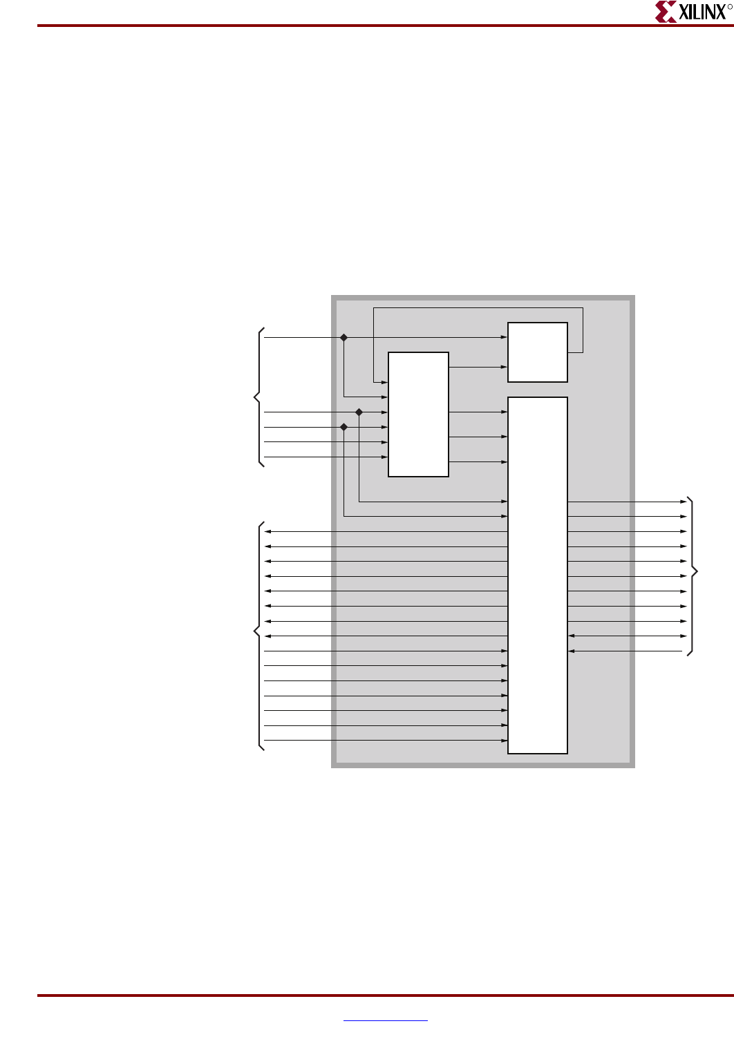
Memory Interface Solutions User Guide www.xilinx.com 467
UG086 (v3.6) September 21, 2010
MIG Design Options
R
Figure 12-7 shows a top-level block diagram of a DDRII SRAM design without a PLL or a
testbench. Users should provide all the clocks and the locked signal. “Clocking Scheme,”
page 480 describes how to generate the design clocks from the user interface. These clocks
should be single-ended. The sys_rst_n signal is an active-Low system reset. All design
resets are generated using this system reset signal, the locked signal, and the IDELAYCTRL
ready signal (idelay_ctrl_ready). The user application must have a PLL/DCM primitive
instantiated in the design, and all user clocks should be driven through BUFGs. The user
has to drive the user application signals. The design provides the clk_0_tb and
reset_clk_0_tb signals to the user in order to synchronize with the design. The signal
clk_0_tb is connected to clock clk_0 in the controller. If the user clock domain is different
from clk_0/clk_0_tb, the user should add FIFOs for all the input and outputs of the
controller (user application signals), in order to synchronize them to clk_0_tb clock.The
cal_done signal indicates the completion of initialization and calibration of the design.
Figure 12-7: Top-Level Block Diagram of the DDRII SRAM Design without a PLL or
a Testbench
ddrii_top Memor
y
Device
User
Application
ddrii_cq
ug086_c12_07_01290
9
ddrii_dq
ddrii_bw_n
ddrii_sa
ddrii_c_n
ddrii_c
ddrii_k_n
ddrii_k
ddrii_rw_n
ddrii_ld_n
ddrii_dll_off_n
cal_done
clk_0_tb
reset_clk_0_tb
wrdata_fifo_full
addr_fifo_ful
rd_data_valid
user_rd_data_rise
user_rd_data_fall
user_wrdata_wr_en
user_addr_wr_en
user_bw_n_rise
user_bw_n_fall
user_addr_cmd
user_wr_data_rise
user_wr_data_fall
User PLL/DCM
Clocks and
Reset
idelay_ctrl_ready
idelay_ctrl
infrastructure
clk_200
reset_clk_200
clk_90
reset_clk_0
reset_clk_270
clk_0
locked
sys_rst_n
clk_270

468 www.xilinx.com Memory Interface Solutions User Guide
UG086 (v3.6) September 21, 2010
Chapter 12: Implementing DDRII SRAM Controllers
R
Implemented Features
This section provides details on the supported features of the DDRII SRAM controller.
CIO/SIO
The DDRII SRAM memory controller supports both Common I/O (CIO) and Separate I/O
(SIO) memory parts. MIG provides an option to select the required memory parts. CIO
memory parts have support for Burst Lengths 2 and 4, whereas SIO memory parts have
support only for Burst Length 2.
The memory type of the design generated using MIG is represented by a parameter
IO_TYPE in the design top RTL module. This parameter value can be either SIO or CIO in
the design top RTL module depending on the type of memory selected in MIG memory
controller options.
DDRII SRAM memory controller design RTL modules are generic, which means to say that
all the ports and logic related to both the memory types i.e., SIO and CIO (namely
ddrii_dq-CIO port and ddrii_d, ddrii_q-SIO ports) are present in all RTL modules all the
way up to the design top RTL module. When design is generated using MIG, depending
on the type of memory selected in the memory controller options, the design top RTL
module contains the parameter IO_TYPE value and the selected memory type ports.
Example: If the selected memory is a CIO part, then the design top RTL module has the
parameter IO_TYPE = CIO and the ddrii_dq port.
User can change the memory type from SIO to CIO and vice-versa, with a considerable
amount of design top RTL module and UCF modifications. Apart from changing the
parameter value IO_TYPE, appropriated memory ports should also be added, and the un-
necessary ports should either be connected to ground or left unconnected.
Example: If the parameter IO_TYPE value is changed from CIO to SIO in the design top
RTL module, then the design top RTL module port list must have the ports ddrii_d and
ddrii_q. The port ddrii_dq should be removed. The ddrii_top module instantiation in the
design top RTL module must have the signals ddrii_d and ddrii_q port mapped. User
must also take care of the UCF file which should be compatible with the modified design
top RTL module.
The parameter IO_TYPE can only have the values CIO or SIO, other values will result in
the controller misbehavior. Instead of modifying the RTL module manually, it is
recommended to generate the appropriated design using MIG. Custom memory part
feature can be utilized if required.
Programmable Read-Followed-by-Write Latency
Whenever there is a situation where in an immediate write command has to be issued after
a read command is issued, one extra clock cycle delay should be introduced before issuing
the write command. According to memory vendor specifications, this will accommodate
for data bus-turnaround period (read data to write data).
User can also increase this clock delay between read and write command. This can be done
with the parameter RD_TO_WR_LATENCY. The value on this parameter infers the
number of clocks controller has to wait between the read and write commands whenever
there is a read followed by a write condition.
Controller introduces a single clock delay between read and write command whenever
there is a read followed by a write condition. The parameter RD_TO_WR_LATENCY value

Memory Interface Solutions User Guide www.xilinx.com 469
UG086 (v3.6) September 21, 2010
Implemented Features
R
adds the delays (in terms of number of clock cycles) to the existing single clock delay
between read and write command.
The parameter RD_TO_WR_LATENCY value should be an integer value between 0 and 3.
Any other value other than from the specified will be considered as value 3.
This parameter is used only for CIO designs. For SIO designs, this parameter is ignored by
the controller. For SIO designs there are separate data buses for read data and write data,
hence there is no need for data bus-turnaround period.
Address Increment
The address generation logic generates an incremental address pattern. The address
pattern can be generated as a linear incremental pattern or as burst incremental pattern.
This depends on the parameter BURST_INC.
For some memory models the address bits for the data bursts are considered internally,
hence a linear incremental address pattern will work. But for some memory models the
address bits for the data bursts are not considered internally, they are included in the
address given to the memory. Hence the address incrementing cannot be linear in this
scenario, only burst increment of address bits should be given to the memory model.
Address generation logic generates a linear incremental pattern of address bits if the
parameter BURST_INC is 0 and generates a burst incremental pattern of address bits if the
parameter BURST_INC is 1. The value of the parameter BURST_INC can be integer and
either 0 or 1.
MIG generates this parameter value depending on the type of the memory selected. User
can even manually edit this value in the generated design top RTL module.
Reset-Active Low
The design reset signal sys_rst_n is an active-Low signal. This active-Low reset input pin is
used to generate the design reset signals which run throughout the design. A parameter
RST_ACT_LOW is provided in the design top module. This parameter indicates whether
the input reset signal is an active-Low or active-High signal.
User can even drive an active-High reset signal as an input reset signal. But the parameter
RST_ACT_LOW should be set to 0. This indicates that the input reset signal is an active-
High signal.
The default value of this parameter is 1. This parameter must be manually modified by the
user in the design top module depending upon the requirement. The value of the
parameter RST_ACT_LOW can be either 0 or 1.
Debug Port
The debug port allows debugging and monitoring of physical layer read timing calibration
logic and timing. This port consists of signals brought to the design top level HDL from the
read calibration module (where the read timing calibration logic resides). These signals
provide information for debugging hardware issues when calibration does not complete or
read data errors are observed in the system even after calibration completes.
Debug port option can be enabled from MIG. By default the option is disabled. By enabling
the option from MIG, the design top-level block parameter DEBUG_EN is set to 1. When
this option is disabled the parameter value is 0. User can even enable/disable this
parameter in the design top-level block HDL module manually.

470 www.xilinx.com Memory Interface Solutions User Guide
UG086 (v3.6) September 21, 2010
Chapter 12: Implementing DDRII SRAM Controllers
R
For further details refer to Appendix E, “Debug Port”.
IODELAY Performance Mode
In Virtex-5 family devices, the power dissipation of the IODELAY elements can be
controlled using the HIGH_PERPORMANCE_MODE parameter. The values of this
parameter can be either TRUE or FALSE.
When this parameter value is set to TRUE, the IODELAY jitter valuer per tap is reduced.
This reduction results in a slight increase in power dissipation from the IODELAY element.
When this parameter value is set to FALSE, the IODELAY power dissipation is reduced,
but with an increase in the jitter value per tap.
The value of this parameter can be selected from the MIG FPGA options page. Users can
also manually set this parameter value to TRUE or FALSE in the design top-level block
HDL module.
Refer to Appendix E, “Debug Port” for more information on the IODELAY Performance
Mode.
DCI Cascading
In Virtex-5 family devices, I/O banks that need DCI reference voltage can be cascaded with
other DCI I/O banks. One set of VRN/VRP pins can be used to provide reference voltage
to several I/O banks in the same column. With DCI cascading, one bank (the master bank)
must have its VRN/VRP pins connected to external reference resistors. Other banks in the
same column (slave banks) can use DCI standards with the same impedance as the master
bank, without connecting the VRN/VRP pins on these banks to external resistors. DCI
impedance control in cascaded banks is received from the master bank. This results in
more usable pins and in reduced power usage because fewer VR pins and DCI controllers
are used.
The syntax for representing the DCI Cascading in the UCF is:
CONFIG DCI_CASCADE = "<master> <slave1> <slave2> . . .";
There are certain rules that need to be followed in order to use DCI Cascade option:
1. The master and slave banks must all reside on the same column (left, centre, or right)
on the device.
2. Master and slave banks must have the same VCCO and VREF (if applicable) voltages.
MIG supports DCI Cascading. This feature enables placing all 36 bits of read data, as well
as the CQ and CQ# clocks, in the same bank when interfacing with 36-bit DDRII SRAM
SIO memory parts. While interfacing the 36 bits of data of a 36-bit DDRII SRAM CIO
memory part, first 18 bits of data and corresponding CQ are placed in one bank and the
remaining 18 bits of data and corresponding CQ# are placed in another bank. This is done
to prevent the WASSO limit from exceeding a given bank.
Following are the possibilities for generating the design with DCI support using the DCI
Cascade option.
• For x36 SIO memory part designs, the DCI Cascade option is always enabled. This
feature cannot be disabled if DCI support is needed.
• For x36 CIO memory part designs, the DCI Cascade is optional. DCI Support for these
designs can be selected with or without the DCI Cascade selection. By default, the
DCI Cascade option is disabled for these designs.

Memory Interface Solutions User Guide www.xilinx.com 471
UG086 (v3.6) September 21, 2010
Implemented Features
R
• For x18 memory part designs, DCI Cascade is optional. DCI support for these designs
can be selected with or without the DCI Cascade selection. By default DCI Cascade
option is disabled for these designs.
• For x18 memory part with 18-bit data width designs, the DCI Cascade option is
disabled and cannot be utilized.
When DCI Cascade option is selected, MIG displays the master bank selection box for each
column for the FPGA in the bank selection page.
• If an FPGA has no banks or has only non-DCI banks in a particular column, the
master bank selection box for that column is not displayed.
• All the data read banks are treated as slave banks.
• When a data read bank is selected in a particular column, the master bank selection
box for that particular column is activated and the rest of the master bank selection
boxed for other columns are deactivated.
• In a particular column, when a data read bank is selected and there are no DCI banks
left in that column for master banks selection, then the design cannot be generated.
The data read banks must be moved to the other columns in order to select the master
banks.
• The master bank selection box shows all the bank numbers in that particular column
other than the data read banks and non-DCI banks in that column.
• There can be only one master bank selected for each column of banks.
• MIG utilizes VRN/VRP pins in the slave banks for pin allocation.
• For each master bank, VRN/VRP pins are reserved. When the selected master bank
does not have at least one input or bidirectional pin of the HSTL_I_DCI_18 I/O
standard, then MIG allocates a dummy input pin masterbank_sel_pin and the I/O
standard of this dummy pin is assigned to HSTL_I_DCI_18. For example, consider an
x18 SIO memory part design where the data read bank is selected as master bank,
MIG reserves the VRN/VRP pins of the bank and the dummy input pin is not
required.
• The dummy input pin is required to satisfy the requirement of the master bank. Any
master bank should have at least one input or bidirectional pin of HSTL_I_DCI_18
I/O standard to program the DCI option.
• When all the banks in a particular column are allocated with data or data read pins,
MIG chooses only the required banks for data or data read pin allocation, depending
upon the design data width. When there is only one bank allocated for data/data read
pins in a column of banks of an FPGA, then that particular data/data read bank
should not be selected as a master bank. Doing so would result in an inappropriate
DCI_Cascade syntax in the UCF of the generated design.
The center column banks of all the FPGAs are divided into two sections, top-column banks
and bottom-column banks. Top-column banks are the banks available above the 0th bank,
and the bottom column banks are the banks available below 0th bank. Therefore, there are
two master bank selection boxes for the center column.
The VRN/VRP pins for a master bank do not need to be reserved in the reserve pins page.
Once the design is ready with the valid master and slave bank selection, the same master
and slave bank information (along with the DCI Cascading syntax) is provided in the UCF
when the design is generated.
For more information about DCI Cascade, refer to DCI Cascading in the Virtex-5 FPGA
User Guide [Ref 10] and the Xilinx® Constraints Guide.

472 www.xilinx.com Memory Interface Solutions User Guide
UG086 (v3.6) September 21, 2010
Chapter 12: Implementing DDRII SRAM Controllers
R
CQ/CQ_n Implementation
For x36 memory part, controller design uses both CQ and CQ_n for capturing the read
data. CQ and CQ_n pins are allocated to P pins of an FPGA by MIG. For x36 memory part
controller designs, first 18 bits of the read data is captured using CQ and the second 18 bits
of the read data is captured using CQ_n.
For x18 memory part controller designs, only CQ is used for capturing the read data. CQ_n
is not used and is connected to a dummy logic. This dummy logic is used just to retain
CQ_n pin during the place and routing of the design.
Memory Interface Solutions User Guide www.xilinx.com 473
UG086 (v3.6) September 21, 2010
Generic Parameters
R
Generic Parameters
The DDRII SRAM design is a generic design that works for all the features that are
mentioned previously. User input parameters are defined as parameters for Verilog and
generics in VHDL in the design modules and are passed down the hierarchy. For example,
if the user selects a burst length of 4, then it is defined as follows in the <top_module>
module:
Parameter BURST_LENGTH = 4, // Burst Length
The user can change this parameter in <top_module> for various burst lengths to get the
desired output. Same concept holds for all the other parameters listed in the
<top_module> module. Table 12-2 lists the details of all parameters.
Table 12-2: Parameterization of DDRII SRAM Virtex-5 FPGA Design
Category Parameter Name Description Other Notes Value Restrictions
Memory
Parameters
BURST_LENGTH Burst length of the design For SIO designs, the value is
only 2. For CIO designs, the
value can be 2 or 4
Integer. 2 or 4
BW_WIDTH Number of Byte Write
signals. One Byte Write
signal for every 9 data (read
data) bits
Integer. 1,2,3,4,5,6,7,8
CLK_WIDTH Number of input clock pairs.
One input clock pair for
every memory part
Number of K/K_n and
C/C_n
Integer. 1,2,3,4.5,6,7,8
CQ_WIDTH Number of echo clock pairs.
One echo clock pair for every
memory part
Number of CQ/CQ_n Integer. 1,2,3,4,5,6,7,8
MEMORY_WIDTH Data width of the memory
part
Integer. 9,18,36
ADDR_WIDTH Address width of the
memory part
Integer.
Design
Parameters
BURST_INC Address increment type.
Linear incremental pattern
or burst incremental pattern
1: Burst incremental pattern
0: Linear incremental pattern
Needed only in the example
design
Integer. 1,0
CLK_FREQ Design clock frequency In MHz Integer.
DATA_WIDTH Data width of the design Integer. 9,18,36,72
IO_TYPE CIO (Common I/O) or SIO
(Separate I/O)
String. "CIO", "SIO"
DLL_FREQ_MODE DCM frequency mode Determined by
CLK_PERIOD. Needed only if
the DCM option is selected.
String. "HIGH",
"LOW"
RD_TO_WR_LATENCY Number of clock cycle
delays controller must insert
between a read command
and an immediate write
command
The value selected can be only
0 or 1 or 2 or 3. Any other
value will be considered as 3
Integer. 0,1,2,3
SIM_ONLY Enable to bypass initial
200µs power-on delay.
Integer. 0,1
474 www.xilinx.com Memory Interface Solutions User Guide
UG086 (v3.6) September 21, 2010
Chapter 12: Implementing DDRII SRAM Controllers
R
DDRII SRAM Memory Controller Modules
Figure 12-8 and Figure 12-9 shows the memory controller modules for both SIO and CIO
memory types.
Miscellan-
eous
DEBUG_EN To enable debug logic and
able to view the debug
signals on the ChipScope™
analyzer
See Appendix E, “Debug
Port” for details
Integer. 1,0
MASTERBANK_PIN_WIDTH Number of Master bank
input pins
Number of master banks
selected and which have
masterbank_sel_pin
Integer.
HIGH_PERFORMANCE_MODE IODELAY High
Performance Mode
Parameter value
This parameter value
represents HIGH_PERFOR
MANCE_MODE of IODELAY
as TRUE or FALSE. This will
result in the Higher or lower
power dissipation at the
output of IODLEAY element.
Verilog : String.
"TRUE", "FALSE".
VHDL : Boolean :
TRUE, FALSE.
Table 12-2: Parameterization of DDRII SRAM Virtex-5 FPGA Design (Cont’d)
Category Parameter Name Description Other Notes Value Restrictions
Figure 12-8: DDRII SRAM SIO Memory Controller Modules
ug086_c12_08_071508
clk_0
reset_clk_0
user_addr_wr_en
addr_fifo_full
FIFOs
read enable
user_wrdata_wr_en
Command bit
Memory Controller
Physical Interface
User Interface
Address path
clk_0
clk_270
clk_90
reset_clk_0
reset_clk_270
ddrii_ld_n
DDRII SRAM SIO
Memory Device
ddrii_rw_n
ddrii_sa
ddrii_d
ddrii_bw_n
ddrii_d
ddrii_cq
ddrii_cq_n
ddrii_k
ddrii_k_n
ddrii_dll_off_n
clk_0
Read/Write
control
Wire path
Read path
user_addr_cmd
user_wr_data_rise
user_wr_data_fall
user_bw_n_rise
user_bw_n_fall
user_rd_data_rise
user_data_fall
rd_data_valid
wrdata_fifo_full
addr_fifo_full
cal_done
Read/Write
State Machine
Delay
Calibration
State Machine
Memory Interface Solutions User Guide www.xilinx.com 475
UG086 (v3.6) September 21, 2010
DDRII SRAM Memory Controller Modules
R
User Interface
User interface module receives and stores the user data, command and address
information in respective FIFOs. The control module generates the required control signals
for this module. During a write operation, the data stored in wr_data_interface is read and
given to the physical layer to output to the memory. Similarly, during a read operation, the
data from the memory is read via IDDR and is given to user with a valid signal
(rd_data_valid). This valid signal indicates valid data on the user_rd_data_rise and
user_rd_data_fall signals. Table 12-4 lists the user interface signals.
The FIFO36, FIFO36_72, and FIFO18 primitives are used for loading address and data from
the user interface. The FIFO36 primitive is used in the ddrii_top_addr_cmd_interface
module, the FIFO36_72 primitive is used in the ddrii_top_wr_data_interface module, and
the FIFO18 primitive is used in the ddrii_top_wr_data_interface module. Every FIFO has
two FIFO threshold attributes, ALMOST_EMPTY_OFFSET and ALMOST_FULL_OFFSET,
that are set to 128 in the RTL. These values can be changed as needed. For valid FIFO
threshold offset values, refer to UG190 [Ref 10].
Te st B en c h
MIG generates two RTL folders, example_design and user_design. The example_design
includes the synthesizable test bench, while user_design does not include the test bench
modules. The MIG test bench performs one write command followed by one read
command in an alternating manner. The number of words in a write command depends on
the burst length. For a burst length of 4, the test bench writes a total 4 data words for a
single write command (2 rise data words and 2 fall data words). For a burst length of 2, the
test bench writes a total of 2 data words. The data pattern is an incremental pattern. On
every write command, the data pattern is incremented by one, and this is repeated with
each subsequent write command. The initial data pattern for the first write command is
Figure 12-9: DDRII SRAM CIO Memory Controller Modules
ug086_c12_09_071508
clk_0
reset_clk_0
user_addr_wr_en
addr_fifo_full
FIFOs
read enable
user_wrdata_wr_en
Command bit
Memory Controller
Physical Interface
User Interface
Address path
clk_0
clk_270
clk_90
reset_clk_0
reset_clk_270
ddrii_ld_n
DDRII SRAM SIO
Memory Device
ddrii_rw_n
ddrii_sa
ddrii_bw_n
ddrii_dq
ddrii_cq
ddrii_cq_n
ddrii_k
ddrii_k_n
ddrii_dll_off_n
clk_0
Read/Write
control
Wire path
Read path
user_addr_cmd
user_wr_data_rise
user_wr_data_fall
user_bw_n_rise
user_bw_n_fall
user_rd_data_rise
user_data_fall
rd_data_valid
wrdata_fifo_full
addr_fifo_full
cal_done
Read/Write
State Machine
Delay
Calibration
State Machine

476 www.xilinx.com Memory Interface Solutions User Guide
UG086 (v3.6) September 21, 2010
Chapter 12: Implementing DDRII SRAM Controllers
R
000. The test bench writes the 000, 001, 002, 003 data pattern in a sequence in which 000
and 002 are rise data words, and 001 and 003 are fall data words for a 9-bit design. The
falling edge data is always rising edge data plus one. For a burst length of 2, the data
sequence for the first write command is 000, 001. The data sequence for the second write
command is 002, 003. The pattern is then incremented for the next write command. For
data widths greater than 9, the same data pattern is concatenated for the other bits. For a
36-bit design and a burst length of 4, the data pattern for the first write command is
000000000, 008040201, 010080402, 0180C0603.
Address generation logic generates the address in an incremental pattern for each write
command. The same address location is repeated for the next read command. In Samsung
components, the burst address increments are done by the memory, so the address is
generated by the test bench in a linear incremental pattern. In Cypress parts, the MIG test
bench increments the address for burst operation. After the address reaches the maximum
value, it rolls back to the initial address, i.e., 00000.
During reads, comparison logic compares the read pattern with the pattern written, i.e., the
000, 001, 002, 003 pattern. For example, for a 9-bit design of burst length 4, the data
written for a single write command is 000, 001, 002, and 003. During reads, the read
pattern is compared with the 000, 001, 002, 003pattern. Based on a comparison of the
data, a status signal error is generated. If the data read back is the same as the data written,
the error signal is 0, otherwise it is 1.
Memory Controller
The DDRII SRAM memory controller can initiate write/read commands for both CIO and
SIO memory parts. These write/read commands are issued as long as the User address-
command FIFO is not empty. CIO designs support both Burst Length 4 and 2 whereas SIO
designs support only Burst Length 2.
DDRII SRAM memory controller module (ddrii_top_ctrl_sm) is completely generic. This
means to say that by just passing the correct parameter to this module, it generates
read/write command signals for CIO/SIO, BL2/BL4 designs.
For CIO designs, controller takes care for the data bus-turnaround condition. When ever
there is a situation where in an immediate write command has to be issued after a read
command is issued, one extra clock cycle delay should be introduced before issuing the
write command. According to memory vendor specifications, this will accommodate for
data bus-turnaround period (read data to write data).
Controller introduces a single clock delay between read and write command whenever
there is a read followed by a write condition. The parameter RD_TO_WR_LATENCY value
adds the delays (in terms of number of clock cycles) to the existing single clock delay
between read and write command.
The parameter RD_TO_WR_LATENCY value should be an integer value between 0 and 3.
Any other value other than the specified will be considered as value 3.
For Separate I/O (SIO) designs there are separate data buses for read data and write data,
so there is no need for data bus-turnaround. For Separate I/O (SIO) designs, controller will
not consider the RD_TO_WR_LATENCY parameter.
Controller module decodes the user command and issues the specified command to the
memory. The command_bit signal is decoded as a write command when it equals logic 0
and command_bit signal is decoded as a read command when it equals logic 1. The
read/write command signals are generated based on the parameters BURST_LENGTH,
IO_TYPE and RD_TO_WR_LATENCY. The controller state machine issues the commands
in the correct sequence while determining the timing requirements of the memory.
Memory Interface Solutions User Guide www.xilinx.com 477
UG086 (v3.6) September 21, 2010
DDRII SRAM Memory Controller Modules
R
Once the calibration is complete, controller issues a read enable to the address-command
FIFO (ddrii_top_addr_cmd_interface module). The command bit is extracted from the
output of the address-command FIFO. This command bit is then decoded to issue
read/write commands. Figure 12-10 shows the controller state machine flow chart.
For Burst Length 4 controller designs, commands (read/write) to the memory are issued
on every alternate clock. In this scenario controller issues read enable to the address-
command FIFO on every alternate clock.
For Burst Length 2 controller designs, commands (read/write) to the memory are issued
on every clock. In this scenario controller issues read enable to the address-command FIFO
on every cock.
When ever the previous decoded command is a read command and the present command
which is decoded is a write command, there is a need for introducing a single clock delay
before the write command is issued to the memory. This single clock delay is for data bus-
turnaround period. This single clock delay is applied on the decoded write command
immediately. The same single clock delay is applied on the address-command FIFO read
enable.
When the parameter RD_TO_WR_LATENCY value is non-zero value (any integer
between 0 and 3), a delay (in number of clock cycles) specified by this parameter in
addition to the single clock cycle delay is applied on the decoded write command before it
is presented on to the command bus of the memory. The same delay is applied on the
address-command FIFO read enable.
Figure 12-10: DDRII SRAM Memory Controller Flow Diagram
u
g
086_c12_10_082908
cal_done
I/O Type
Address FIFO=EMPTY
Programmable
Latency=0
Ye s
No
No
No
SIO
CIO
Ye s
Ye s
No
Ye s
Read from Address
FIFO
Burst Length
BL4
BL2
Read from Address
FIFO
Wait for one clock cycle.
Wait for one clock cycle.
(Previous cmd=READ)
and
(Present cmd=WRITE)
478 www.xilinx.com Memory Interface Solutions User Guide
UG086 (v3.6) September 21, 2010
Chapter 12: Implementing DDRII SRAM Controllers
R
Whenever the address-command FIFO is empty, controller shifts to the FIFO_EMPTY_ST
state. No commands are issued.
Physical Interface
It is the interface between the controller and the memory. It includes the input/output
blocks (IOBs) and other primitives used to read and write the double data rate signals to
and from the memory, such as IDDR and ODDR. This module also includes the IODELAY
elements of the Virtex-5 FPGA. These IODELAY elements are used to delay the data signals
to capture the read data.
The memory control signals, such as ld_n, rw_n and DLLoff_n are driven from the buffers
in the IOBs. All the input and output signals to and from the memory are referenced from
the IOB to compensate for the routing delays inside the FPGA.
Figure 12-11: DDRII SRAM Memory Controller State Diagram
CAL_WAIT_ST
FIFO_EMPTY_ST
BL2 ST BL4 ST
BURST_WAIT_ST
CMD_WAIT_ST
RD_TO_WR_LATENCY_ST
cal_done=0
Address FIFO
Empty
Burst Length=4
Burst Length=2
Address FIFO
Empty
Address FIFO
Empty
Address FIFO
Empty
(CIO) and (Read-
followed by-Write)
(CIO) and (Read-
followed by-Write)
Address FIFO
not-Empty
Address FIFO
not-Empty
(latency=0)and(Burst Length=4)
(latency=0)and(Burst Length=2)
N
on-zero latency
(latency=0)and(Burst Length=4)
(latency=0)and(Burst Length=2)
Address FIFO
Empty
Load Latency
(cal_done = 1) and (Address
FIFO not-empty) and (Burst
Length = 4)
(cal_done = 1) and (Address
FIFO not-empty) and (Burst
Length = 2)
Address FIFO
Empty
ug086_c12_11_071808

Memory Interface Solutions User Guide www.xilinx.com 479
UG086 (v3.6) September 21, 2010
DDRII SRAM Memory Controller Modules
R
The ddrii_phy_init_sm module, which is instantiated in the ddrii_phy_io module, is used
to initialize the DDRII SRAM memory in a predefined sequence according to the memory
vendor specifications.
The ddrii_phy_dly_cal_sm and ddrii_phy_en modules calibrate the design to align the
strobe such that it always captures the read data from the memory. A data valid signal
rd_data_valid is generated to indicate the captured read data is a valid data.
The ddrii_phy_write module splits the user data into rise data and fall data to be sent to
the memory as double data rate signal using ODDR.
Infrastructure
The infrastructure module generates the design clocks and reset signals. When differential
clocking is used, sys_clk_p, sys_clk_n, clk_200_p, and clk_200_n signals appear. When
single-ended clocking is used, sys_clk and idly_clk_200 signals appear. In addition, clocks
are available for design use and a 200 MHz clock is provided for the IDELAYCTRL
primitive. Differential and single-ended clocks are passed through global clock buffers
before connecting to a PLL/DCM. For differential clocking, the output of the
sys_clk_p/sys_clk_n buffer is single-ended and is provided to the PLL/DCM input.
Likewise, for single-ended clocking, sys_clk is passed through a buffer and its output is
provided to the PLL/DCM input. The outputs of the PLL/DCM are 0° and 270°
phase-shifted versions of the input clock). After the PLL/DCM is locked, the design is in
the reset state for at least 25 clocks. The infrastructure module also generates all of the reset
signals required for the design.
PLL/DCM
In MIG 3.0 and later, the DCM is replaced with a PLL for all Virtex-5 FPGA designs. If the
user selects a design with a PLL in the GUI, the infrastructure module will have both PLL
and DCM codes. The CLK_GENERATOR parameter enables either a PLL or a DCM in the
infrastructure module. The CLK_GENERATOR parameter is set to PLL by default. If the
user wants to use DCM, this parameter should be changed manually to DCM.
For designs without a PLL, the user application must have a PLL/DCM primitive
instantiated in the design, and all user clocks should be driven through BUFGs.
Idelay_ctrl
This module instantiates the IDELAYCTRL primitive of the Virtex-5 FPGA. The
IDELAYCTRL primitive is used to continuously calibrate the individual delay elements in
its region to reduce the effect of process, temperature, and voltage variations. A 200 MHz
clock has to be fed to this primitive.
MIG uses the “automatic” method for IDELAYCTRL instantiation in which the MIG HDL
only instantiates a single IDELAYCTRL for the entire design. No location (LOC)
constraints are included in the MIG-generated UCF. This method relies on the ISE® tools to
replicate and place as many IDELAYCTRLs as needed (for example, one per clock region
that uses IDELAYs). Replication and placement are handled automatically by the software
tools if IDELAYCTRLs have same refclk, reset, and rdy nets. A new constraint called
IODELAY_GROUP associates a set of IDELAYs with an IDELAYCTRL and allows for
multiple IDELAYCTRLs to be instantiated without LOC constraints specified. ISE software
generates the IDELAY_CTRL_RDY signal by logically ANDing the RDY signals of every
IDELAYCTRL block.
The IODELAY_GROUP name should be checked in the following cases:

480 www.xilinx.com Memory Interface Solutions User Guide
UG086 (v3.6) September 21, 2010
Chapter 12: Implementing DDRII SRAM Controllers
R
• The MIG design is used with other IP cores or user designs that also require the use of
IDELAYCTRL and IDELAYs.
• Previous ISE software releases 8.2.03i and 9.1i had an issue with IDELAYCTRL block
replication or trimming. When using these revisions of the ISE software, the user must
instantiate and constrain the location of each IDELAYCTRL individually.
See UG190 [Ref 10] for more information on the requirements of IDELAYCTRL placement.
Clocking Scheme
Figure 12-13 shows the clocking scheme for this design. Global and local clock resources
are used. The global clock resources consists of a PLL or a DCM, two BUFGs on PLL/DCM
output clocks, and one BUFG for clk_200. The local clock resources consist of regional I/O
clock networks (BUFIO). The global clock architecture is discussed in this selection.
The MIG tool allows the user to customize the design such that the PLL/DCM is not
included. In this case, system clocks clk_0 and clk_270, and IDELAYCTRL clock clk_200
must be supplied by the user.
Memory Interface Solutions User Guide www.xilinx.com 481
UG086 (v3.6) September 21, 2010
Clocking Scheme
R
Global Clock Architecture
User must supply two input clocks to the design:
• A system clock running at the target frequency for the memory. This clock is used by
the PLL/DCM to generate the various clocks used by the memory interface logic.
• A 200 MHz clock for the IDELAYCTRL block, which in turn are used for the IDELAY
IOB delay blocks for aligning read capture data.
These clocks can be either differential or single-ended. User can select single-ended or
differential ended clock input option from MIG FPGA options page. Differential clocks are
connected to the IBUFGDS and the single-ended clocks are connected to IBUFG.
The system clock from the output of the IBUFGDS or the IBUFG is connected to the
PLL/DCM to generate the various clocks used by the memory interface logic.
The clk_200 output of the IBUFGDS or the IBUFG is connected to BUFG. The output of the
BUFG is used for IDELAY IOB delay blocks for aligning read capture data.
The PLL/DCM generates two separate synchronous clocks for use in the design. This is
shown in Table 12-3, Figure 12-12, page 482, and Figure 12-13, page 482. The clock
structure is same for both example design and user design. For designs without PLL/DCM
instantiation, PLL/DCM and BUFGs should be instantiated at user end to generate the
required clocks.
Table 12-3: DDRII SRAM interface Design Clocks
Clock Description Logic Domain
clk_0 Skew compensated replica
of the input system clock.
The clock for the controller and user
interface logic, the DDRII SRAM bus-
related I/O flip-flops (e.g., input data
capture (DQ/Q), output data (DQ/D) and
input clocks (CQ/CQ#). This clock is used
to register the data, address, and
command signals, and the address and
data enables for the user interface logic(1).
This clock is also used to generate read
data, read data valid, and FIFO status
signals.
clk_270 270° phase-shifted version
of clk_0
The clocks for the DDRII SRAM memory
address and control bus-related I/O flip-
flops.
Notes:
1. See “User Interface Accesses,” page 489 for timing requirements and restrictions on the user interface
signals.
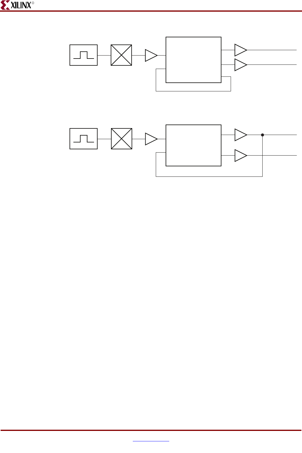
482 www.xilinx.com Memory Interface Solutions User Guide
UG086 (v3.6) September 21, 2010
Chapter 12: Implementing DDRII SRAM Controllers
R
Figure 12-12: Clocking Scheme for QDRII Interface Logic Using PLL
Figure 12-13: Clocking Scheme for DDRII SRAM Memory Interface Logic Using
DCM
u
g
086_c12_19_012909
PLL
System Clock GC I/O
CLKOUT0
CLKIN1
CLKFBIN BUFG
CLKOUT1
CLK_0
CLK_270
CLKFBOUT
BUFG
ug086_c12_12_071508
DCM
System Clock GC I/O
CLK_0
CLK_IN
CLK_FB
BUFG
BUFG
CLK_270
CLK_0
CLK_270

Memory Interface Solutions User Guide www.xilinx.com 483
UG086 (v3.6) September 21, 2010
DDRII SRAM Initialization and Calibration
R
DDRII SRAM Initialization and Calibration
Initialization
DDRII SRAM memory is initialized through a specified sequence.
1. A 200 µs wait period is initiated by the DDRII SRAM controller in order to achieve a
stable power condition for the DDRII SRAM memory part.
2. After the stable power and clock (K,K#), ddrii_dll_off_n is set to high to enable DLL in
DDRII SRAM memory part.
3. The additional wait period of 2048 clock cycles is applied in order to lock the DLL.
4. After this sequence of initialization, DDRII SRAM memory part is ready for
calibration.
Delay Calibration
The delay calibration logic is responsible for providing the required amount of delay on
the Read data and the input clocks (CQ/CQ#) to align the FPGA clock in the data valid
window.
The delay calibration is enabled due to the available IODELAY elements in all the I/Os in
the Virtex-5 device. The IODELAY elements delay the input read data by increments of
75 ps, up to a maximum delay of 5 ns. IDELAYCTRLs, available in every bank in
Virtex-5 devices, and help to maintain the resolution of the IODELAY elements.
Calibration begins when the IDELAYCTRL ready signal has been asserted. Calibration is
done in three stages:
1. First Stage Calibration: Calibration of input clocks (CQ/CQ#) with respect to read data.
2. Second Stage Calibration: Calibration of input clocks (CQ/CQ#) and read data with
respect to the FPGA clock.
3. Third Stage Calibration: Read enable calibration that determines when the read data is
valid. This helps to generate the data valid signal rd_data_valid.
First Stage Calibration: Calibration of input clocks (CQ/CQ#) and read data
This stage of calibration helps to align CQ/CQ# inside the data valid window. CQ/CQ# is
delayed more than the read data by the delay on the BUFIO and the route delay of the
CQ/CQ# before it clocks the read data in the ISERDES. In a case where the data valid
window is considerably reduced, this delay on the BUFIO can move the edge of the CQ or
the CQ# clock outside of the valid window. This calibration stage helps to avoid the de-
synchronization of the clock and data. The calibration stage includes a dummy write to the
memory with a constant rise data pattern of 1s and a constant fall data pattern of 0s
followed by constant read to the same location until the first calibration is complete. The
non-transitioning rise and fall data pattern helps to avoid any metastability caused by the
FPGA clock in the second and third register stages in the ISERDES.
The steps involved in this stage include:
1. Increment CQ/CQ# delay taps to see if CQ/CQ# is within the valid window. If it is,
continue to increment CQ/CQ# delay taps until the hold window range is measured.
2. Reset CQ/CQ# delay taps.
3. Increment read data delay taps to determine the read data setup window with respect
to CQ/CQ#.

484 www.xilinx.com Memory Interface Solutions User Guide
UG086 (v3.6) September 21, 2010
Chapter 12: Implementing DDRII SRAM Controllers
R
4. Reset read data delay taps.
5. If the hold window is greater than the setup, no tap increments are required.
Otherwise, increment read data to the center of the valid window.
Completion of the first stage calibration is indicated with logic 1 on the signal
stg1_cal_done.
Second Stage Calibration: Calibration of CQ/CQ# and read data with FPGA clock
This calibration stage helps to align CQ/CQ# and read data with respect to the FPGA
clock. For reliable data capture and transfer of the data in to the FPGA fabric, the
calibration is require to align the FPGA clock inside of the data capture by CQ/CQ#.
This stage includes a dummy write to the memory. The dummy write includes the
following pattern: FF/00-55/AA, where FF and 55 refer to the rising data pattern during a
four-word burst and 00 and AA refer to the falling data pattern.
The steps involved in this calibration stage are:
1. Increment CQ/CQ# and read data delay taps to delay CQ/CQ# and read data and
determine the valid window range.
2. If this window is insufficient, which indicates that the CQ/CQ# and FPGA clock edge
are aligned very closely to each other, continue to increment CQ/CQ# and read data
delay taps to determine the valid window of CQ/CQ# and read data with respect to
the next FPGA clock edge.
3. The calibration is complete when at least 15 taps of window are available at
frequencies above250 MHz and half the clock period worth of taps are available at
frequencies lower than 250 MHz between CQ/CQ# and the FPGA clock.
Completion of the first stage calibration is indicated with logic 1 on the signal
stg3_cal_done.
Third Stage Calibration: Read Enable Calibration
This stage is required to generate the read data valid signal. This includes non-contiguous
read commands to align the data valid signals to the read data at the output of the
ISERDES.
The calibration logic, built using an SRL16 as a shift register, helps to determine the
number of register stages required by the read command signal to generate the correct read
data valid signal. One read enable signals is generated for data captured by each CQ or
CQ# clock. Based in the count value in the SRL shift register from all the banks, the read
data from all the banks is aligned and presented to the user backend along with read data
valid signal rd_data_valid.
This completes the delay calibration sequence. The completion of calibration is indicated
with logic 1 on the signal cal_done.
Memory Interface Solutions User Guide www.xilinx.com 485
UG086 (v3.6) September 21, 2010
DDRII SRAM Controller Interface Signals
R
DDRII SRAM Controller Interface Signals
Table 12-4 and Table 12-5 describe the DDRII SRAM controller system interface signals
with and without a PLL, respectively. Table 12-6 describes the DDRII SRAM user interface
signals. Table 12-7 describes the DDRII SRAM memory interface signals. In these tables, all
signal directions are with respect to the DDRII SRAM memory controller.
Table 12-4: DDRII SRAM System Interface Signals (with a PLL)
Signal Name Direction Description
sys_clk_p, sys_clk_n Input System clock input made up of differential clock
pairs. This clock pair goes to a differential input
buffer. The differential buffer output goes to the
PLL/DCM input. The PLL/DCM generates the
required clocks for the design. This differential
input clock pair is present only when the
DIFFERENTIAL clocks option is selected in the
MIG FPGA options page.
sys_clk Input Single-ended system clock input. This clock
goes to a IBUFG. The IBUFG output goes to the
PLL/DCM input. The PLL/DCM generates the
required clocks for the design. This input
system clock is present only when the
SINGLE_ENDED clocks option is selected in
the MIG FPGA options.
When PLL option is deselected, both differential
or single-ended input system clocks are not
present.
dly_clk_200_p,
dly_clk_200_n
Input 200 MHz differential clock used in the
ddrii_idelay_ctrl logic. This differential input
clock pair is present only when the
DIFFERENTIAL clock option is selected in the
MIG FPGA options page.
idly_clk_200 Input Single-ended 200 MHz IDELAYCTRL clock
input. This clock is connected to an IBUFG. The
IBUFG output is connected to the input of a
BUFG. The output of this BUFG acts as the
IDELAYCTRL clock input. This input system
clock is present only when the
SINGLE_ENDED clocks option is selected in
the MIG FPGA options.
When the PLL option is deselected, both
differential and single-ended input system
clocks are not present.
sys_rst_n Input Reset to the DDRII SRAM memory controller.
486 www.xilinx.com Memory Interface Solutions User Guide
UG086 (v3.6) September 21, 2010
Chapter 12: Implementing DDRII SRAM Controllers
R
compare_error Output This signal represents the status of the
comparison of read data when compared to the
corresponding write data.
cal_done Output This signal is asserted when the design
initialization and calibration is complete.
Table 12-5: DDRII SRAM System Interface Signals (without a PLL)
Signal Name Direction Description
clk_0 Input A 0° phase-shifted design input clock. This is an
output of user PLL/DCM
clk_270 Input A 270° phase-shifted design input clock. This is
an output of user PLL/DCM.
clk_200 Input 200 MHz clock used in the ddrii_idelay_ctrl
logic.
locked Input This active-High signal indicates whether the
user PLL/DCM is locked or not.
sys_rst_n Input Reset to the DDRII SRAM memory controller
compare_error Output This signal represents the status of the
comparison of read data when compared to the
corresponding write data.
cal_done Output This signal is asserted when the design
initialization and calibration is complete.
Table 12-6: DDRII SRAM User Interface Signals (without a Testbench
[user_design])
Signal Name Direction Description
user_addr_wr_en Input This active-High signal is the write enable for
the user address FIFO
user_wrdata_wr_en Input This active-High signal is the write enable for
the user write data FIFO
user_wr_data_rise Input Positive-edge data for memory write. The
contents of user_wr_data_rise bus are written in
to rise data FIFO only when
user_wrdata_wr_en is asserted.
user_wr_data_fall Input Negative-edge data for memory write. The
contents of user_wr_data_fall bus are written in
to fall data FIFO only when user_wrdata_wr_en
is asserted.
Table 12-4: DDRII SRAM System Interface Signals (with a PLL) (Cont’d)
Signal Name Direction Description
Memory Interface Solutions User Guide www.xilinx.com 487
UG086 (v3.6) September 21, 2010
DDRII SRAM Controller Interface Signals
R
user_bw_n_rise Input Byte write enables for DDRII SRAM memory
positive-edge write data. The contents of
user_bw_n_rise are written in to byte write
FIFO only when user_wrdata_wr_en is
asserted.
user_bw_n_fall Input Byte write enables for DDRII SRAM memory
negative-edge write data. The contents of
user_bw_n_fall are written in to byte write FIFO
only when user_wrdata_wr_en is asserted.
user_addr_cmd[0] Input 1-bit command to the Virtex-5 FPGA DDRII
SRAM design.
user_addr_cmd[0] = logic 0 for write command
user_addr_cmd[0] = logic 1 for read command
The contents of user_addr_cmb bus are written
in to address FIFO only when user_addr_wr_en
is asserted.
user_addr_cmd
[ADDR_WIDTH:1](1)
Input Gives information about the address of the
memory location to be accessed. The contents of
user_addr_cmb bus are written in to address
FIFO only when user_addr_wr_en is asserted.
clk_0_tb Output Clock output to the user. All the user interface
signals must be synchronized with this clock.
This signal is sourced from clock clk_0 in the
controller.
reset_clk_0_tb Output Active high reset for the user interface.
wrdata_fifo_full Output FIFO full status signal of the user write data
FIFOs.
addr_fifo_full Output FIFO full status signal of the user address FIFO
rd_data_valid Output Status signal indicating read data is valid on the
read data bus.
user_rd_data_rise Output Positive-edge data read from memory.
user_rd_data_fall Output Negative-edge data read from memory.
Notes:
1. The number of address bits used depends on the density of the memory part. The controller ignores the
unused bits, which can all be tied to High.
Table 12-6: DDRII SRAM User Interface Signals (without a Testbench
[user_design]) (Cont’d)
Signal Name Direction Description
488 www.xilinx.com Memory Interface Solutions User Guide
UG086 (v3.6) September 21, 2010
Chapter 12: Implementing DDRII SRAM Controllers
R
Table 12-8 lists the signals between the user interface and the controller.
Table 12-7: DDRII SRAM Memory Interface Signals
Signal Name Direction Description
ddrii_dq Bidirectional During write commands, the data is sampled
on both edges of K clock. During read
commands, the data is sampled on both the
edges of FPGA clock. This port will appear only
for CIO designs.
ddrii_d Output During write commands, the data is sampled
on both edges of K clock. This port will appear
only for SIO designs.
ddrii_q Input During read commands, the data is sampled on
both edges of FPGA clock. This port will appear
only for SIO designs.
ddrii_bw_n Output Byte write enables for DDRII SRAM memory
write data. These enable signals are sampled on
both edges of the K clock.
ddrii_sa Output DDRII SRAM memory address for read and
write operations.
ddrii_ld_n Output DDRII SRAM synchronous Load pin, bus cycle
sequence is defined when it is low.
ddrii_rw_n Output DDRII SRAM read/write control pin. Read
command when active-High, write command
when active-Low.
ddrii_dll_off_n Output DDRII SRAM memory DLL Disable when low.
ddrii_cq, ddrii_cq_n Input DDRII SRAM memory output echo clocks.
These are used for capturing the read data from
the memory.
ddrii_k, ddrii_k_n Output DDRII SRAM memory input clocks. Memory
write data is sampled on these clocks
ddrii_c, ddrii_c_n Output DDRII SRAM memory input clocks for output
data. These signals are tied to high.
Table 12-8: Signals between User Interface and Controller
Port Name Port Width Port Description
addr_fifo_empty 1
Empty status signal from the Address FIFO. Monitors
the FIFO empty status flags to issue write and read
commands.
command_bit 1
Output signal from the Address and Command FIFO.
The first bit from the address and command FIFO
output that represents the write/read command.
addr_fifo_rd_en 1 Read enable for the Address and command FIFO

Memory Interface Solutions User Guide www.xilinx.com 489
UG086 (v3.6) September 21, 2010
User Interface Accesses
R
User Interface Accesses
The user backend logic communicates with the memory controller through a FIFO-based
user interface. This interface consists of four related buses:
• A Write Address FIFO bus accepts memory write address from the user
• A Write Data FIFO bus accepts the write data corresponding to the memory write
address
• A Read Address FIFO bus accepts the memory read address from the user
The user interface has the following timing and signaling restrictions:
• The Write/Read Address and Write Data FIFOs cannot be written by the user until
calibration is complete (as indicated by cal_done). In addition, the user_ad_w_n,
user_d_w_n, and user_r_n interface signals need to be held high until calibration is
complete.
• For issuing a write command, the memory write address must be written into the
Read Address FIFO. The first write data word must be written to the Write Data FIFO
on the same clock cycle as the when the write address is written. In addition, the write
data burst must be written over consecutive clock cycles; there cannot be a break
between bursts of data. These restrictions arise from the fact that the controller
assumes write data is available when it receives the write command from the user.
• clk_0_tb is connected to clk_0 in the controller. In case that user clock domain is
different from clk_0 / clk_0_tb of MIG, the user should add FIFOs for all data inputs
and outputs of the controller to synchronize them to the clk_0_tb.
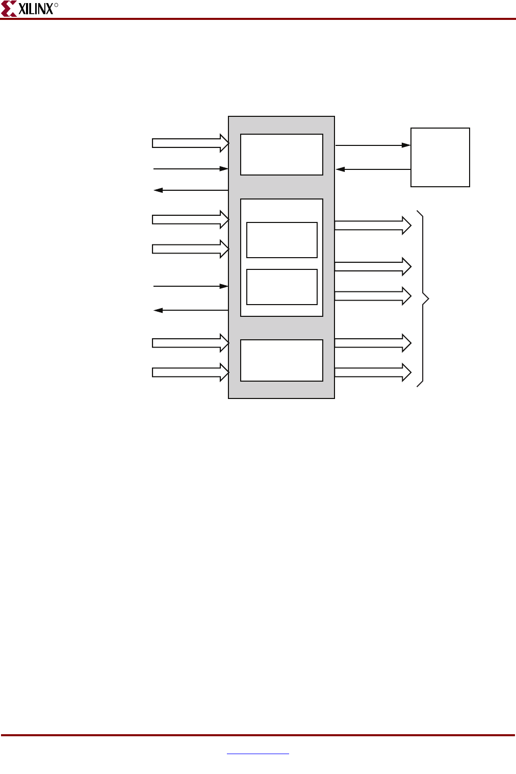
490 www.xilinx.com Memory Interface Solutions User Guide
UG086 (v3.6) September 21, 2010
Chapter 12: Implementing DDRII SRAM Controllers
R
Write Interface
Figure 12-14 illustrates the user interface block diagram for write operations.
The following steps describe the architecture of Address and Write Data FIFOs and how to
perform a write burst operation to DDRII SRAM memory from user interface.
1. The user interface consists of an Address FIFO, Data FIFOs and a byte write FIFO.
These FIFOs are built out of Virtex-5 FPGA FIFO primitives. Address FIFO is FIFO36
primitive with 1K x 36 configuration, Data FIFO is FIFO36_72 primitive with 512 x 72
configuration and Byte Write FIFO is FIFO18 primitive with 1024 x 18 configuration.
2. Address FIFO is common for both write and read commands. It comprises an address
part and a command part. Command bit discriminate between write and read
commands. Single instantiation of FIFO36 constitutes the Address FIFO.
3. Two separate sets of Data FIFOs are being used for storing the rising edge and falling
edge data to be written to DDRII SRAM memory from user interface. For 9bit, 18bit
and 36bit configurations, controller concatenates the extra bits of Data FIFO with 0s.
4. Byte Write FIFO is being used to store the Byte Write signals to DDRII SRAM memory
from user interface. Extra bits are concatenated with zeros
5. User can initiate a write to memory by writing to the address FIFO and the write data
FIFO only when the calibration is complete (cal_done signal is asserted high) and
FIFOs full flags are asserted low. Users should not access any of these FIFOs until the
signal cal_done is asserted. During Calibration process controller writes pattern data
in to the Data FIFOs. Signal cal_done assures that the clocks are stable, reset process is
completed, calibration is complete and the controller is ready to accept the user data
Figure 12-14: Write User Interface Block Diagram
wr_rd_address
wr_data_rise
wr_data_fall
bw_n_rise
bw_n_fall
ug086_c12_13_071508
Address FIFO
(FIFO36)
1024 x 36
User Interface
user_addr_cmd
user_addr_wr_en
addr_fifo_full
user_wr_data_rise
user_wr_data_fall
user_bw_n_rise
user_bw_n_fall
user_wrdata_wr_en
wrdata_fifo_full
addr_fifo_empty
To phy_top
addr_fifo_rd_en
Byte Write FIFO
(FIFO18)
1024 x 36
Rise Data FIFO
(FIFO36_72)
512 x 36
Data FIFOs
Fall Data FIFO
(FIFO36_72)
512 x 36
Controller
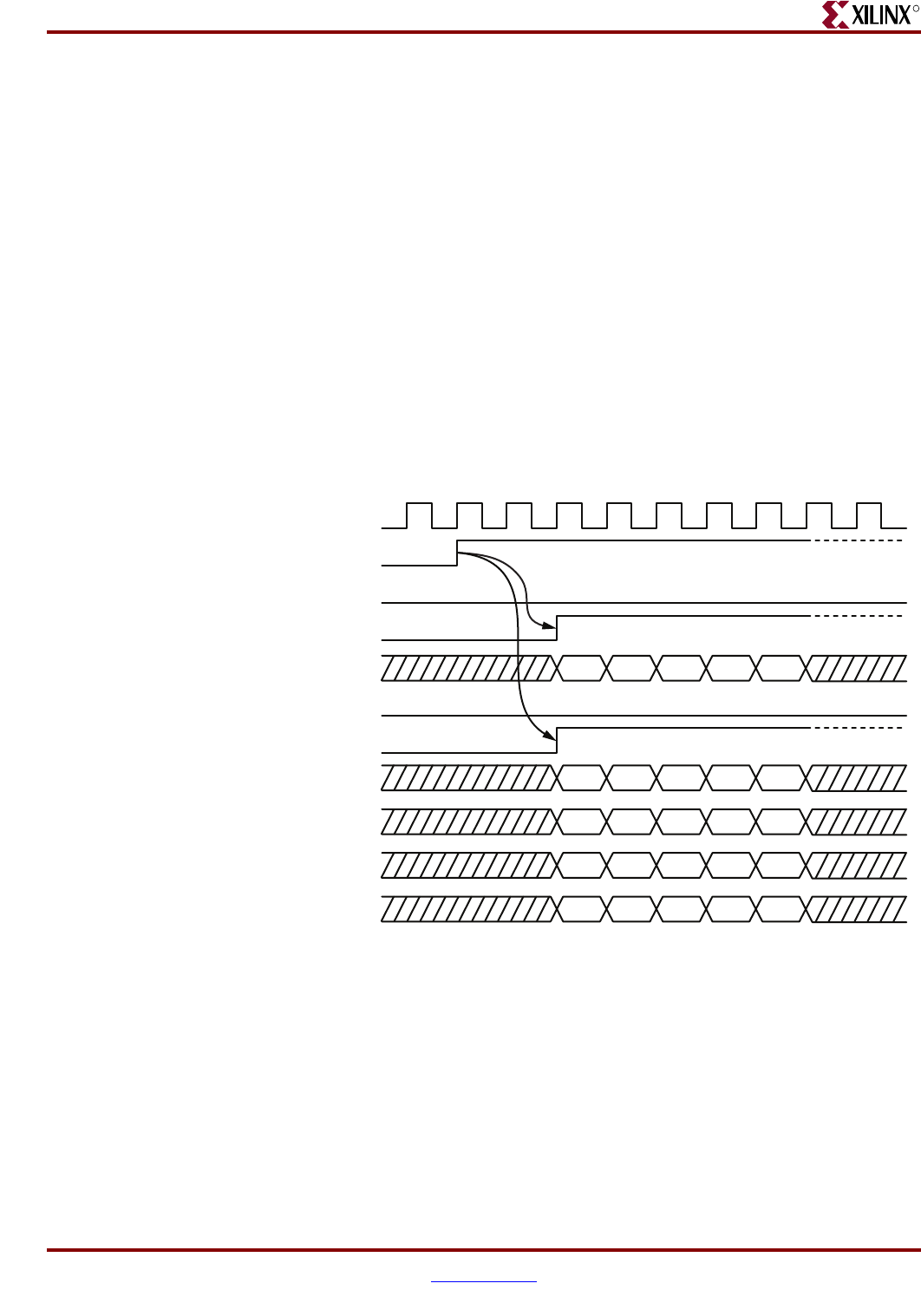
Memory Interface Solutions User Guide www.xilinx.com 491
UG086 (v3.6) September 21, 2010
User Interface Accesses
R
and commands. Status signal addr_fifo_full is asserted high when Address FIFO is full
and status signal wrdata_fifo_full is asserted high or Data FIFOs or Byte Write FIFO
are full.
6. Both the address FIFO and write data FIFO full flags are deasserted with power-on.
7. User should assert the address FIFO write enable signal user_addr_wr_en along with
address bus user_addr_cmd to store the write address and write command in to the
address FIFO.
8. The write command should be given by setting the user_addr_cmd[0] bit as logic 0.
9. User should assert the data FIFO write enable signal user_wrdata_wr_en along with
write data user_wr_data_rise, user_wr_data_fall and user_bw_n_rise, user_bw_n_fall
to store the rise data and fall data in to rise data FIFO and fall data FIFO and byte write
enable for rise data and fall data in to byte write FIFO respectively.
10. Controller reads the Address, Data and Byte Write FIFOs when they are not empty.
Controller reads the address FIFO by issuing the addr_fifo_rd_en signal. Controller
reads the write data FIFO and byte write FIFOs by issuing the wrdata_fifo_rd_en
signal after the address FIFO is read. Controller decodes the command part after the
address FIFO is read.
11. Figure 12-15 shows the timing diagram for a write command with a burst length of
four. As shown in the figure the command bit (user_addr_cmd [0]) is a write command
(command bit is indicated as 'W') which is identified with a logic 0 on that bit. The
address should be asserted for one clock cycle as shown. For burst length of four, each
write to address FIFO has two write to the Data FIFO consisting of two rising-edge and
two falling-edge data.
12. Figure 12-16 shows the timing diagram for a write command with a burst length of
two. As shown in the figure, the command bit (user_addr_cmd [0]) is a write
command (command bit is indicated as W) which is identified with a logic 0 on that
Figure 12-15: Write User Interface Timing Diagram for Burst Length 4
ug086_c12_14_071508
D00 D02 D10 D12 D20
D01 D03D11 D13D21
BW00 BW02 BW10 BW12 BW20
BW01 BW03BW11 BW13BW21
A0,W A1,W
clk_0_tb
cal_done
addr_fifo_full
user_addr_wr_en
user_addr_cmd
wrdata_fifo_full
user_wrdata_wr_en
user_wr_data_rise
user_wr_data_fall
user_bw_n_rise
user_bw_n_fall
A2,W A3,W A4,W
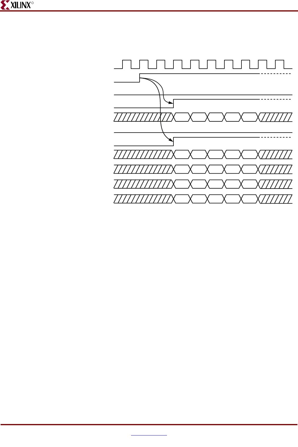
492 www.xilinx.com Memory Interface Solutions User Guide
UG086 (v3.6) September 21, 2010
Chapter 12: Implementing DDRII SRAM Controllers
R
bit. The address should be asserted for one clock cycle as shown. For burst length of
two, each write to address FIFO has a single write to the Data FIFO consisting of a
single rising-edge and single falling-edge data.
13. From the previous user interface timing diagrams, it is clear that writing addresses and
command bits in to address FIFO and write data in to data FIFOs are two different and
independent actions. Users must take complete responsibility for writing bursts of
data bits corresponding to a particular address in to the respective FIFOs at the same
time. If not, the controller will output an undesired data bits which will be written in to
the memory.
Figure 12-16: Write User Interface Timing Diagram for Burst Length 2
ug086_c12_15_071508
D00 D10 D20 D30 D40
D01 D11 D21 D31 D41
BW00 BW10 BW20 BW30BW40
BW01 BW11 BW21 BW31BW41
A0,W A1,W
clk_0_tb
cal_done
addr_fifo_full
user_addr_wr_en
user_addr_cmd
wrdata_fifo_full
user_wrdata_wr_en
user_wr_data_rise
user_wr_data_fall
user_bw_n_rise
user_bw_n_fall
A2,W A3,W A4,W
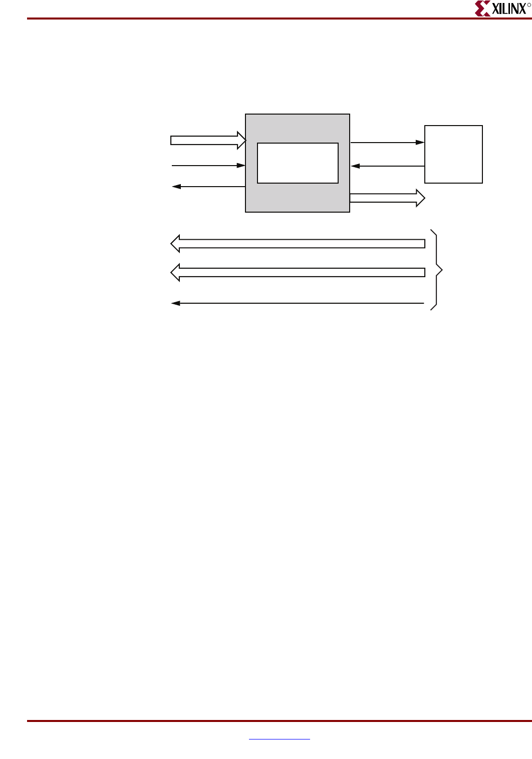
Memory Interface Solutions User Guide www.xilinx.com 493
UG086 (v3.6) September 21, 2010
User Interface Accesses
R
Read Interface
Figure 12-17 illustrates the user interface block diagram for read operations.
The following steps describe the architecture of the read user interface and how to perform
a DDRII SRAM burst read operation
1. The read user interface consists of an Address FIFO built out of a Virtex-5 FPGA
FIFO18 configuration 1024 x 18.
2. User can initiate a read to the memory by writing to the address FIFO only when the
calibration is complete (cal_done signal is asserted high) and FIFOs full flags are
asserted low.
3. User should assert the address FIFO write enable signal user_addr_wr_en along with
address bus user_addr_cmd to store the read address and read command in to the
address FIFO.
4. The read command should be given by setting the user_addr_cmd[0] bit as logic 1.
5. Controller read the address FIFO when it is not empty by issuing the read enable
signal addr_fifo_rd_en. After decoding user_addr_cmd [0] bit, the controller issues a
read command to the memory at the specified address.
6. Prior to the actual read and write command, t he design calibrates the latency in
number of clock cycles from the time the read command is issued to the time the data
is received. Using this pre-calibrated delay information, the controller delays the read
data for required number of clocks.
7. The rd_data_valid signal is asserted high when data is available in the read data
FIFOs.
8. User must access the read data as soon as rd_data_valid signal is asserted high.
Figure 12-17: Read User Interface Block Diagram
wr_rd_address
ug086_c12_16_071508
Address FIFO
(FIFO36)
1024 x 36
User Interface
user_addr_cmd
user_addr_wr_en
addr_fifo_full
user_rd_data_rise
user_rd_data_fall
rd_data_valid
addr_fifo_empty
From phy_top
To phy_top
addr_fifo_rd_en Controller
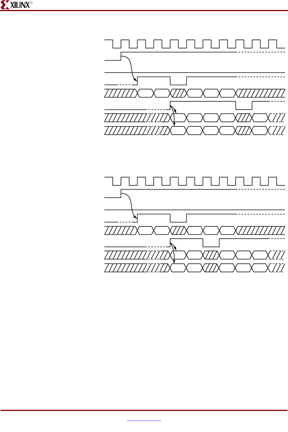
494 www.xilinx.com Memory Interface Solutions User Guide
UG086 (v3.6) September 21, 2010
Chapter 12: Implementing DDRII SRAM Controllers
R
9. Figure 12-18 shows the timing diagram for a read command with a burst length of
four. As shown in the figure the command bit (user_addr_cmd [0]) is a read command
(command bit is indicated as 'R') which is identified with a logic 1 on that bit. The
address should be asserted for one clock cycle as shown. For burst length of four, each
read command is associated with four read data's, two rising-edge and two falling-
edge data. The signal rd_data_valid is asserted high for two clocks for each read
command issued to the memory. The read data captured is a valid data as long as the
signal rd_data_valid is asserted high as shown in the figure.
10. Figure 12-19 shows the timing diagram for a read command with a burst length of two.
As shown in the figure the command bit (user_addr_cmd [0]) is a read command
(command bit is indicated as 'R') which is identified with a logic 1 on that bit. The
address should be asserted for one clock cycle as shown. For burst length of two, each
read command is associated with two read data's, one rising-edge and one falling-edge
Figure 12-18: Read User Interface Timing Diagram for Burst Length 4
Figure 12-19: Read User Interface Timing Diagram for Burst Length 2
ug086_c12_17 _071508
clk_0_tb
cal_done
addr_fifo_full
user_addr_wr_en
user_addr_cmd
rd_data_valid
user_rd_data_rise
user_rd_data_fall
A0,R A1,R A2,R A4,RA3,R
D00 D02 D12 D20D10
D01 D03D13D21D11
ug086_c12_18_071508
clk_0_tb
cal_done
addr_fifo_full
user_addr_wr_en
user_addr_cmd
rd_data_valid
user_rd_data_rise
user_rd_data_fall
A0,R A1,R A2,R A4,RA3,R
D00 D10 D20 D40D30
D01 D11 D21 D41D31
Memory Interface Solutions User Guide www.xilinx.com 495
UG086 (v3.6) September 21, 2010
DDRII SRAM Signal Allocations
R
data. The signal rd_data_valid is asserted high for one clock for each read command
issued to the memory. The read data captured is a valid data as long as the signal
rd_data_valid is asserted high as shown in the figure.
11. After the read command and the corresponding address bits are loaded in to the
address FIFO, it can take a minimum of 14 clock cycles, for the controller to assert
rd_data_valid high.
Table 12-9 shows the read latency of the controller.
DDRII SRAM Signal Allocations
MIG shows checkboxes for Data, Address, System_Control and System_Clock in the bank
selection for DDRII SRAM CIO designs.
Table 12-9: Maximum Read Latency
Parameter Number of Clock Cycles Description
User read command to
address FIFO empty flag
4• 4 clock cycles for empty
flag deassertion in the
FWFT mode
Address empty flag to the
read command on DDRII
SRAM memory bus
5• 2 clock cycle to generate
the read command in the
controller state machine
• 3 clock cycles to transfer
the command to the
memory
DDRII SRAM memory read
command to valid data
available
5• 1.5 clock cycles of the
memory read latency
• 2.5 clock cycles to capture
and transfer read data to
the FPGA clock domain
• 1 clock cycle for aligning
all the read data capture
Total Latency 14
Table 12-10: DDRII SRAM Signal Allocations
Bank Selected Signals Allocated in the Group
Data Memory Data, memory byte write, CQ/CQ#, K/K#, and
C/C# clocks.
Data_Read Memory read data and memory CQ/CQ#.
Data_Write Memory write data, memory byte write, K/K#, and C/C#
clocks.
Address Memory address and memory control.
System_Control System reset and status signals.
System_Clock System clocks.

496 www.xilinx.com Memory Interface Solutions User Guide
UG086 (v3.6) September 21, 2010
Chapter 12: Implementing DDRII SRAM Controllers
R
MIG show checkboxes for Data_Read, Data_Write, System_Control and System_Clock in
the bank selection for DDRII SRAM SIO designs.
For CIO designs, when Data box is checked in a bank, the memory data (DQ), memory
byte write (BW), memory output echo clocks (CQ/CQ#), memory input clocks (K/K#) and
memory input clocks for output data (C/C#) are assigned to that particular bank.
For SIO designs, when Data_Read box is checked in a bank, the memory read data (Q),
memory output echo clocks (CQ/CQ#) are assigned to that particular bank.
For SIO designs, when Data_Write box is checked in a bank, the memory write data (D),
memory byte write (BW), memory input clocks (K/K#) and memory input clocks for
output data (C/C#) are assigned to that particular bank.
When System_Clock box is checked in a bank, the system reset signal sys_rst_n and the
status signals compare_error and cal_done are assigned to that particular bank.
When the System_Clock box is checked in a bank, the design clock signals sys_clk_p,
sys_clk_n, dly_clk_200_p and dly_clk_200_n are assigned to that particular bank.
For special cases, such as without a testbench (user_design), the corresponding input and
output ports are not assigned to any FPGA pins in the design UCF because user can
connect these ports to the FPGA pins or can connect to some logic internal to the same
FPGA.
Note: Timing has been verified for most of the MIG generated configurations. For the best timing
results, adjacent banks in the same column of the FPGA should be used. Banks that are separated
by unbonded banks should be avoided because these can cause timing violations.
Pinout Considerations
It is recommended to select banks within the same column on MIG. This helps to avoid the
clock tree skew that the design would incur while crossing from one column to another.
When the data read, data write, address and system control pins are allocated to individual
banks in a column, then the system control pins must be allocated in a bank that is central
to the rest of banks allocated. This helps reduce datapath and clock path skew.
For larger FPGAs (for example, FF1738, FF1760, and similar), it is recommended to place
data read, data write, address and system control pins in the same column to reduce
datapath and clock path skew.

Memory Interface Solutions User Guide www.xilinx.com 497
UG086 (v3.6) September 21, 2010
Supported Devices
R
Supported Devices
Table 12-11 lists the memory parts supported by MIG for DDRII SRAM design. In the
supported devices, X in the memory part column denotes a single alphanumeric character.
For example, K7I321884X can be either K7I321884C or K7I321884M.
Table 12-11: Supported memory parts for DDRII SRAM (Virtex-5 FPGAs)
Memory Part Speed Grade Density in Mb Memory Width Burst Length IO Type Vendor
K7I643684M FC30 72 36 4 CIO Samsung
K7I643682M FC30 72 36 2 CIO Samsung
K7I641884M FC30 72 18 4 CIO Samsung
K7I641882M FC30, FC25 72 18 2 CIO Samsung
K7I323684X FC30, FC25 36 36 4 CIO Samsung
K7I163682B FC30, FC25 18 36 2 CIO Samsung
K7I161884B FC30, FC25 18 18 4 CIO Samsung
K7I321884X FC25 36 18 4 CIO Samsung
K7I163684B FC25 18 36 4 CIO Samsung
K7I161882B FC25 18 18 2 CIO Samsung
CY7C1419AV18 300BZC, 250BZC 36 18 4 CIO Cypress
CY7C1421AV18 300BZC, 250BZC 36 36 4 CIO Cypress
CY7C1428AV18 300BZC, 250BZC 36 9 4 CIO Cypress
CY7C1518V18 300BZC, 250BZC 72 18 2 CIO Cypress
CY7C1520V18 300BZC, 250BZC 72 36 2 CIO Cypress
CY7C1527V18 300BZC 72 9 2 CIO Cypress
CY7C1420AV18 250BZC 36 36 2 CIO Cypress
CY7C1427AV18 250BZC 36 9 2 CIO Cypress
CY7C1320BV18 250BZC, 200BZC 18 36 2 CIO Cypress
CY7C1321AV18 250BZC 18 36 4 CIO Cypress
CY7C1321BV18 250BZC 18 36 4 CIO Cypress
CY7C1318BV18 250BZC 18 18 2 CIO Cypress
CY7C1319BV18 250BZC 18 18 4 CIO Cypress
CY7C1916BV18 250BZC 18 9 2 CIO Cypress
CY7C1917BV18 250BZC 18 9 4 CIO Cypress
K7J643682M FC30 72 36 2 SIO Samsung
K7J641882M FC30 72 18 2 SIO Samsung
K7J321882M FC30 36 18 2 SIO Samsung
CY7C1393BV18 300BZC 18 18 2 SIO Cypress
CY7C1424BV18 300BZC 36 36 2 SIO Cypress

498 www.xilinx.com Memory Interface Solutions User Guide
UG086 (v3.6) September 21, 2010
Chapter 12: Implementing DDRII SRAM Controllers
R
Simulating the DDRII SRAM Design
After generating the design, MIG creates a sim folder in the specified path. This folder
contains simulation files for a particular design. The sim folder contains the external
testbench, memory model, and .do file to simulate the generated design. The memory
model files are currently generated in Verilog only. To learn more details about the files in
the sim folder and to simulate the design, refer to “Simulation Guide,” page 499.


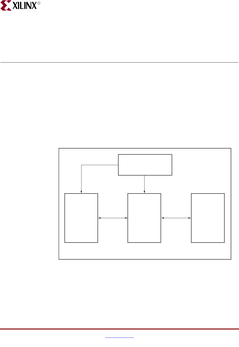
Memory Interface Solutions User Guide www.xilinx.com 501
UG086 (v3.6) September 21, 2010
R
Chapter 13
Simulating MIG Designs
A generic simulation testbench is supported for MIG generated designs. With this
testbench, the user can simulate the design generated from MIG.
Introduction
The sim folder provides a simulation environment for the design generated in the
ModelSim simulator. This folder includes the simulation testbench module (sim_tb_top)
and various other modules to simulate the design properly. The simulation testbench
module also generates system input signals, clocks, and resets to the design.
Figure 13-1 depicts a block diagram of the simulation environment.
The simulation testbench module integrates the complete system through port maps, a
design clock, a clock for the IDELAYCTRL module, and reset generation logic. With clocks
and system reset signals as inputs, the system can be divided into these blocks:
• Optional instances: These function as testbench modules for designs without
testbenches and as DCM/PLL logic for designs without DCMs or PLLs. The testbench
Figure 13-1: Block Diagram of Simulation Environment
System Inputs, such as
Clock and Reset
Design
To p
Memory
Model
Optional
Instances
or
Modules,
such as
Te stbench,
DCM Logic,
Etc.
UG086_c13_12_020609
Simulation Testbench

502 www.xilinx.com Memory Interface Solutions User Guide
UG086 (v3.6) September 21, 2010
Chapter 13: Simulating MIG Designs
R
here refers to a synthesizable test module that provides test inputs such as data,
address, and commands to the design. In designs with a testbench, the testbench is
part of the design top module. Similarly, DCM/PLL logic is part of design top for
designs generated with DCMs or PLLs.
• Design top: In the example design, the design top module connects with the clocks,
reset, memory interface signals, and status signals. In the user design, design top
connects with the user interface signals, clocks, reset, memory interface signals, and
status signals. Design top includes the controller part, an optional testbench, and
DCM/PLL logic.
• Memory model: This is provided with the memory core of the component selected.
MIG provides a memory model in Verilog only. VHDL memory models are not
provided.
The simulation testbench module can be in Verilog or VHDL, depending on the HDL used
in the design.
Supported Features
The MIG simulation environment supports:
•All component widths
• Designs with or without a testbench
• Designs with or without DCM/PLL
• All supported components and DIMMs (UDIMMs, SODIMMs and RDIMMs)
• Deep memories and ECC for Virtex®-4 FPGA DDR2 direct-clocking designs
• Differential and single-ended DQS for Virtex-4 FPGA DDR2 direct-clocking designs
• CIO and SIO for RLDRAM II designs
• CIO and SIO for Virtex-5 FPGA DDRII SRAM designs
•Multicontroller simulation testbenches for the Virtex-5 FPGA (QDRII SRAM and
DDR2 SDRAM)
Unsupported Features
The MIG simulation environment does not support:
• Multicontroller simulation testbenches for Virtex-4 FPGA DDR2 direct-clocking
designs
• VHDL memory models
• Cypress components for all SRAM designs
Note: The simulation testbench is specific to each design that is generated from MIG. Design
parameters should not be changed after generating the design, except for the RESET_ACTIVE_LOW
or RST_ACT_LOW parameters.

Memory Interface Solutions User Guide www.xilinx.com 503
UG086 (v3.6) September 21, 2010
Simulating the Design
R
Simulating the Design
The design can be simulated using the ModelSim GUI either manually or by calling the
sim.do file in ModelSim.
Method 1: Manual Simulation
1. Invoke ModelSim.
2. Create a new project.
3. Add design files to the project from the rtl folder, and add simulation files to the
project from the sim folder. Only .v or .vhd files should be added to the project. Files
with a .vh extension do not need to be added to the sim folder.
4. Map the unisim or unsims_ver libraries. This is needed to compile Xilinx primitives
used in the design.
5. Compile the design. For Virtex-4 and Spartan®-3 FPGA VHDL designs, the design
parameter file from the rtl folder needs to be compiled before other modules are
compiled.
6. Load the design and map the library to it. For example, the following command is used
to load a Virtex-4 FPGA DDR SDRAM design in Verilog:
vsim -t ps +notimingchecks -L unisims_ver work.sim_tb_top glbl
The following command loads the same design in VHDL:
vsim -t ps +notimingchecks -L unisim work.sim_tb_top glbl
7. After loading, run the design for the required amount of time.
Method 2: Using the sim.do file
This method uses the sim.do file to simulate the design. This file contains ModelSim
commands to create a new project, add files to the sim folder, and run the simulation for a
specified period.
The steps involved in simulating a design are:
1. Invoke ModelSim.
2. Create a new project. (Optional.)
3. Change the directory to the working sim folder. (Optional.)
4. If the directory is set to the working directory, execute the following command at the
ModelSim prompt:
do sim.do
If the working directory is not set in ModelSim, execute the following command at the
vsim prompt:
do <working directory>/sim.do
For example:
do E:/simulations/test1/example_design/sim/sim.do
5. The run time depends on completion of calibration or memory initialization. After
completion of calibration or initialization, simulation runs for an additional 50 µs. For
example, if it takes 212 µs for the calibration to complete, the total run time is 212 + 50
= 262 µs. The user can still increase or decrease the run time. For more information on
changing the run time, refer to “Changing Simulation Run Time,” page 513. See also
“Design Notes,” page 514.
504 www.xilinx.com Memory Interface Solutions User Guide
UG086 (v3.6) September 21, 2010
Chapter 13: Simulating MIG Designs
R
Files in sim Folder
MIG generates all the design files in the rtl folder, and the simulation files in the sim
folder.
Virtex-5 FPGA Designs
This section describes the simulation files for various Virtex-5 FPGA designs.
DDR2 SDRAM
Table 13-1 lists the files generated in the sim folder for Virtex-5 FPGA DDR2 SDRAM
designs.
Table 13-1: Virtex-5 FPGA DDR2 SDRAM Simulation Files
File Name Description
sim_tb_top (.v or .vhd) This Verilog or VHDL external testbench file
integrates the system and provides the system
inputs.
wiredly (.v or .vhd) This module is used to insert delay in a Verilog or
VHDL design.
ddr2_model.v This is the Verilog memory model for DDR2 SDRAM
from Micron. This memory model is provided only
in Verilog.
ddr2_model_parameters.vh This parameter file is used by the ddr2_model.v
Micron memory model. It lists all the parameters that
define the memory type and timing parameters.
hyb18t512xx0b2f_0129.v This is the Verilog memory model for the 512 MB
DDR2 SDRAM from Qimonda. This memory model
is provided only in Verilog.
hyx18t1gxx0c2x.v This is the Verilog memory model for the 1 GB DDR2
SDRAM from Qimonda. This memory model is
provided only in Verilog.
set_hold.vh This checks the Setup and Hold Config file for the
Verilog model used by the Qimonda memory model.
qimonda_package.vhd This VHDL package file for Qimonda parts includes
component declarations of all memory models.
glbl.v This file initializes the simulator environment.
sim.do This file lists the ModelSim commands required to
run the test case.
ddr2_tb_test_addr_gen,
ddr2_tb_test_cmp,
ddr2_tb_test_data_gen,
ddr2_tb_test_gen,
tb_top (.v or .vhd)
These optional modules are only included in the sim
folder of designs without testbenches, or in the rtl
folder.
Memory Interface Solutions User Guide www.xilinx.com 505
UG086 (v3.6) September 21, 2010
Files in sim Folder
R
DDR SDRAM
Table 13-2 lists the files generated in the sim folder for Virtex-5 FPGA DDR SDRAM
designs.
QDRII SRAM
Table 13-3 lists the files generated in the sim folder for Virtex-5 FPGA QDRII SRAM
designs. Samsung and Cypress memory models are not available in the sim folder for
simulations when the design is generated by the MIG tool. The appropriate memory
model must be downloaded from the vendor’s web site. MIG designs are functionally
verified with the R12 version of the Samsung memory models.
Table 13-2: Virtex-5 FPGA DDR SDRAM Simulation Files
File Name Description
sim_tb_top (.v or .vhd) This Verilog or VHDL external testbench file
integrates the system and provides the system
inputs.
wiredly (.v or .vhd) This module is used to insert delay in a Verilog or
VHDL design.
ddr_model.v This is the Verilog memory model for DDR SDRAM
from Micron. This memory model is provided only in
Verilog.
ddr_model_parameters.vh This parameter file is used by the ddr_model.v
Micron memory model. It lists all the parameters that
define the memory type and timing parameters.
glbl.v This file initializes the simulator environment.
sim.do This file lists the ModelSim commands required to
run the test case.
ddr_tb_test_addr_gen,
ddr_tb_test_cmp,
ddr_tb_test_data_gen,
ddr_tb_test_gen,
ddr_tb_top (.v or .vhd)
These optional modules are only included in the sim
folder of designs without testbenches, or in the rtl
folder.
Table 13-3: Virtex-5 FPGA QDRII SRAM Simulation Files
File Name Description
sim_tb_top (.v or .vhd) This Verilog or VHDL external testbench file
integrates the system and provides the system inputs.
glbl.v This file initializes the simulator environment.
sim.do This file lists the ModelSim commands required to
run the test case.
506 www.xilinx.com Memory Interface Solutions User Guide
UG086 (v3.6) September 21, 2010
Chapter 13: Simulating MIG Designs
R
DDRII SRAM
Table 13-4 lists the files generated in the sim folder for Virtex-5 FPGA DDRII SRAM
designs. Samsung and Cypress memory models are not available in the sim folder for
simulations when the design is generated by the MIG tool. The appropriate memory
model must be downloaded from the vendor’s web site. MIG designs are functionally
verified with the R12 version of the Samsung memory models.
Multicontroller
Table 13-5 lists the files generated in the sim folder for Virtex-5 FPGA Multicontroller
designs.
qdrii_tb_top,
qdrii_test_addr_gen,
qdrii_test_cmp_data,
qdrii_test_data_gen,
qdrii_test_q_sm,
qdrii_test_wr_rd_sm
(.v or .vhd)
These optional modules are only included in the sim
folder of designs without testbenches, or in the rtl
folder.
Table 13-3: Virtex-5 FPGA QDRII SRAM Simulation Files (Cont’d)
File Name Description
Table 13-4: Virtex-5 FPGA DDRII SRAM Simulation Files
File Name Description
sim_tb_top (.v or .vhd) This Verilog or VHDL external testbench file
integrates the system and provides the system
inputs.
wiredly (.v or .vhd) This module is used to insert delay in a Verilog or
VHDL design.
glbl.v This file initializes the simulator environment.
sim.do This file lists the ModelSim commands required to
run the test case.
ddrii_tb_top,
ddrii_test_addr_gen,
ddrii_test_data_cmp,
ddrii_test_data_gen,
ddrii_test_wr_rd_sm
(.v or .vhd)
These optional modules are only included in the sim
folder of designs without testbenches, or in the rtl
folder.
Table 13-5: Virtex-5 FPGA Multicontroller Simulation Files
File Name Description
sim_tb_top (.v or .vhd) This Verilog or VHDL external testbench file
integrates the system and provides the system
inputs.
Memory Interface Solutions User Guide www.xilinx.com 507
UG086 (v3.6) September 21, 2010
Files in sim Folder
R
wiredly (.v or .vhd) This module is used to insert delay in a Verilog or
VHDL design.
ddr2_model_cX.v This is the Verilog memory model for DDR2
SDRAM from Micron. This memory model is
provided only in Verilog. The cX in the file name
represents the controller number (e.g., c0, c1,
etc.).
ddr2_model_parameters_cX.vh This parameter file is used by the
ddr2_model_cX.v Micron memory model. It
lists all the parameters that define the memory
type and timing parameters. The cX in the file
name represents the controller number (e.g., c0,
c1, etc.)
hyb18t512xx0b2f_0129_cX.v This is the Verilog memory model for the 512 MB
DDR2 SDRAM from Qimonda. This memory
model is provided only in Verilog. The cX in the
file name represents the controller number (e.g.,
c0, c1, etc.)
hyx18t1gxx0c2x_cX.v This is the Verilog memory model for the 1 GB
DDR2 SDRAM from Qimonda. This memory
model is provided only in Verilog. The cX in the
file name represents the controller number (e.g.,
c0, c1, etc.)
set_hold_cX.vh This checks the Setup and Hold Config file for
the Verilog model used by the Qimonda memory
model. The cX in the file name represents the
controller number (e.g., c0, c1, etc.)
glbl.v This file initializes the simulator environment.
sim.do This file lists the ModelSim commands required
to run the test case. It includes memory
parameters to be passed to the memory models
of the respective controllers.
ddr2_tb_test_addr_gen,
ddr2_tb_test_cmp,
ddr2_tb_test_data_gen,
ddr2_tb_test_gen, tb_top,
qdrii_tb_top ,
qdrii_test_addr_gen,
qdrii_test_cmp_data,
qdrii_test_data_gen,
qdrii_test_q_sm,
qdrii_test_wr_rd_sm
(.v or .vhd)
These optional modules are only included in the
sim folder of designs without testbenches, or in
the rtl folder.
Table 13-5: Virtex-5 FPGA Multicontroller Simulation Files (Cont’d)
File Name Description
508 www.xilinx.com Memory Interface Solutions User Guide
UG086 (v3.6) September 21, 2010
Chapter 13: Simulating MIG Designs
R
Virtex-4 FPGA Designs
This section describes the simulation files for various Virtex-4 FPGA designs.
DDR2 SDRAM Direct Clocking
Table 13-6 lists the files generated in the sim folder for Virtex-4 FPGA DDR2 SDRAM
direct-clocking designs.
DDR2 SDRAM SerDes
Table 13-7 lists the files generated in the sim folder for Virtex-4 FPGA DDR2 SDRAM
SerDes designs.
Table 13-6: Virtex-4 FPGA DDR2 SDRAM Direct-Clocking Simulation Files
File Name Description
sim_tb_top (.v or .vhd) This Verilog or VHDL external testbench file
integrates the system and provides the system
inputs.
wiredly (.v or .vhd) This module is used to insert delay in a Verilog or
VHDL design.
ddr2_model.v This is the Verilog memory model for DDR2
SDRAM from Micron. This memory model is
provided only in Verilog.
ddr2_model_parameters.vh This parameter file is used by the ddr2_model.v
Micron memory model. It lists all the parameters
that define the memory type and timing
parameters.
hyb18t512xx0b2f_0129.v This is the Verilog memory model for the 512 MB
DDR2 SDRAM from Qimonda. This memory
model is provided only in Verilog.
hyx18t1gxx0c2x.v This is the Verilog memory model for the 1 GB
DDR2 SDRAM from Qimonda. This memory
model is provided only in Verilog.
set_hold.vh This checks the Setup and Hold Config file for the
Verilog model used by the Qimonda memory
model.
qimonda_package.vhd This VHDL package file for Qimonda parts
includes component declarations of all memory
models.
glbl.v This file initializes the simulator environment.
sim.do This file lists the ModelSim commands required to
run the test case.
addr_gen, backend_rom,
cmp_rd_data, data_gen,
test_bench (.v or .vhd)
These optional modules are only included in the
sim folder of designs without testbenches, or in the
rtl folder.
Memory Interface Solutions User Guide www.xilinx.com 509
UG086 (v3.6) September 21, 2010
Files in sim Folder
R
DDR SDRAM
Table 13-8 lists the files generated in the sim folder for Virtex-4 FPGA DDR SDRAM
designs.
Table 13-7: Virtex-4 FPGA DDR2 SDRAM SerDes Simulation Files
File Name Description
sim_tb_top (.v or .vhd) This Verilog or VHDL external testbench file
integrates the system and provides the system
inputs.
wiredly (.v or .vhd) This module is used to insert delay in a Verilog or
VHDL design.
ddr2_model.v This is the Verilog memory model for DDR2
SDRAM from Micron. This memory model is
provided only in Verilog.
ddr2_model_parameters.vh This parameter file is used by the ddr2_model.v
Micron memory model. It lists all the parameters
that define the memory type and timing parameters.
hyb18t512xx0b2f_0129.v This is the Verilog memory model for the 512 MB
DDR2 SDRAM from Qimonda. This memory model
is provided only in Verilog.
hyx18t1gxx0c2x.v This is the Verilog memory model for the 1 GB
DDR2 SDRAM from Qimonda. This memory model
is provided only in Verilog.
set_hold.vh This checks the Setup and Hold Config file for the
Verilog model used by the Qimonda memory
model.
qimonda_package.vhd This VHDL package file for Qimonda parts includes
component declarations of all memory models.
glbl.v This file initializes the simulator environment.
sim.do This file lists the ModelSim commands required to
run the test case.
addr_gen, backend_rom,
cmp_rd_data, data_gen,
test_bench (.v or .vhd)
These optional modules are only included in the
sim folder of designs without testbenches, or in the
rtl folder.
Table 13-8: Virtex-4 FPGA DDR SDRAM Simulation Files
File Name Description
sim_tb_top (.v or .vhd) This Verilog or VHDL external testbench file
integrates the system and provides the system inputs.
wiredly (.v or .vhd) This module is used to insert delay in a Verilog or
VHDL design.
510 www.xilinx.com Memory Interface Solutions User Guide
UG086 (v3.6) September 21, 2010
Chapter 13: Simulating MIG Designs
R
RLDRAM II
Table 13-9 lists the files generated in the sim folder for Virtex-4 FPGA RLDRAM II designs.
ddr_model.v This is the Verilog memory model for DDR SDRAM
from Micron. This memory model is provided only in
Ver ilog .
ddr_model_parameters.vh This parameter file is used by the ddr_model.v
Micron memory model. It lists all the parameters that
define the memory type and timing parameters.
glbl.v This file initializes the simulator environment.
sim.do This file lists the ModelSim commands required to
run the test case.
addr_gen, backend_rom,
cmp_rd_data, data_gen,
test_bench (.v or .vhd)
These optional modules are only included in the sim
folder of designs without testbenches, or in the rtl
folder.
Table 13-8: Virtex-4 FPGA DDR SDRAM Simulation Files (Cont’d)
File Name Description
Table 13-9: Virtex-4 FPGA RLDRAM II Simulation Files
File Name Description
sim_tb_top (.v or .vhd) This Verilog or VHDL external testbench file
integrates the system and provides the system inputs.
wiredly (.v or .vhd) This module is used to insert delay in a Verilog or
VHDL design.
rldram2_model.v This is the Verilog memory model for RLDRAM II
memory from Micron. This memory model is
provided only in Verilog.
rldram2_model_parameter
s.vh
This parameter file is used by the
rldram2_model.v memory model. It lists all the
parameters that define the memory type and timing
parameters.
fifo_generator_v4_1.v This Verilog FIFO model is used by the design user
interface for Verilog controller designs.
fifo_generator_v4_1.vhd This VHDL FIFO model is used by the design user
interface. This model utilizes the
iputils_conv.vhd, iputils_misc.vhd,
iputils_std_logic_arith.vhd, and
iputils_std_logic_unsigned.vhd modules
for compilation. These modules are used for the
VHDL controller designs.
glbl.v This file initializes the simulator environment.
Memory Interface Solutions User Guide www.xilinx.com 511
UG086 (v3.6) September 21, 2010
Files in sim Folder
R
QDRII SRAM
Table 13-10 lists the files generated in the sim folder for Virtex-4 FPGA QDRII SRAM
designs. Samsung and Cypress memory models are not available in the sim folder for
simulations when the design is generated by the MIG tool. The appropriate memory
model must be downloaded from the vendor’s web site. MIG designs are functionally
verified with the R12 version of the Samsung memory models.
DDRII SRAM
Table 13-11 lists the files generated in the sim folder for Virtex-4 FPGA DDRII SRAM
designs. Samsung and Cypress memory models are not available in the sim folder for
simulations when the design is generated by the MIG tool. The appropriate memory
model must be downloaded from the vendor’s web site. The MIG designs are functionally
verified with the R12 version of the Samsung memory models.
sim.do This file lists the ModelSim commands required to
run the test case.
backend_rom,
byte_compare,
cmp_rd_data, test_bench
(.v or .vhd)
These optional modules are only included in the sim
folder of designs without testbenches, or in the rtl
folder.
Table 13-9: Virtex-4 FPGA RLDRAM II Simulation Files (Cont’d)
File Name Description
Table 13-10: Virtex-4 FPGA QDRII SRAM Simulation Files
File Name Description
sim_tb_top (.v or .vhd) This Verilog or VHDL external testbench file integrates the
system and provides the system inputs.
glbl.v This file initializes the simulator environment.
sim.do This file lists the ModelSim commands required to run the
test case.
addr_gen, data_gen,
q_sm, test_bench,
wr_rd_sm
(.v or .vhd)
These optional modules are only included in the sim
folder of designs without testbenches, or in the rtl folder.
Table 13-11: Virtex-4 FPGA DDRII SRAM Simulation Files
File Name Description
sim_tb_top (.v or .vhd) This Verilog or VHDL external testbench file integrates the
system and provides the system inputs.
wiredly (.v or .vhd) This module is used to insert delay in a Verilog or VHDL
design.
glbl.v This file initializes the simulator environment.
512 www.xilinx.com Memory Interface Solutions User Guide
UG086 (v3.6) September 21, 2010
Chapter 13: Simulating MIG Designs
R
Spartan-3 FPGA Designs
This section describes the simulation files for various Spartan-3 FPGA designs.
DDR2 SDRAM
Table 13-12 lists the files generated in the sim folder for Spartan-3 FPGA DDR2 SDRAM
designs.
sim.do This file lists the ModelSim commands required to run the
test case.
addr_gen, data_gen,
d_sm, test_bench,
wr_rd_sm
(.v or .vhd)
These optional modules are only included in the sim
folder of designs without testbenches, or in the rtl folder.
Table 13-11: Virtex-4 FPGA DDRII SRAM Simulation Files (Cont’d)
File Name Description
Table 13-12: Spartan-3 FPGA DDR2 SDRAM Simulation Files
File Name Description
sim_tb_top (.v or .vhd) This Verilog or VHDL external testbench file
integrates the system and provides the system
inputs.
wiredly (.v or .vhd) This module is used to insert delay in a Verilog or
VHDL design.
ddr2_model.v This is the Verilog memory model for DDR2 SDRAM
from Micron. This memory model is provided only
in Verilog.
ddr2_model_parameters.vh This parameter file is used by the ddr2_model.v
Micron memory model. It lists all the parameters
that define the memory type and timing parameters.
hyb18t512xx0b2f_0129.v This is the Verilog memory model for the 512 MB
DDR2 SDRAM from Qimonda. This memory model
is provided only in Verilog.
hyx18t1gxx0c2x.v This is the Verilog memory model for the 1 GB DDR2
SDRAM from Qimonda. This memory model is
provided only in Verilog.
set_hold.vh This checks the Setup and Hold Config file for the
Verilog model used by the Qimonda memory model.
qimonda_package.vhd This VHDL package file for Qimonda parts includes
component declarations of all memory models.
glbl.v This file initializes the simulator environment.
Memory Interface Solutions User Guide www.xilinx.com 513
UG086 (v3.6) September 21, 2010
Changing Simulation Run Time
R
DDR SDRAM
Table 13-13 lists the files generated in the sim folder for Spartan-3 FPGA DDR SDRAM
designs.
Changing Simulation Run Time
Memory write and read can be performed correctly after calibration of the design at a
given frequency for Virtex-4 and Virtex-5 FPGA designs, and after initialization of the
design at a given frequency for Spartan-3/3E/3A/3AN/3A DSP FPGA designs. Thus, run
time also depends upon the calibration period.
In the sim.do file, the run time is determined by the following example ModelSim
commands:
when {/sim_tb_top/phy_init_done = 1} {
if {[when -label a_100] == ""} {
when -label a_100 { $now = 50 us } {
nowhen a_100..........}}}}
sim.do This file lists the ModelSim commands required to
run the test case.
addr_gen, cmd_fsm,
cmp_data, data_gen,
test_bench (.v or .vhd)
These optional modules are only included in the sim
folder of designs without testbenches, or in the rtl
folder.
Table 13-12: Spartan-3 FPGA DDR2 SDRAM Simulation Files (Cont’d)
File Name Description
Table 13-13: Spartan-3 FPGA DDR SDRAM Simulation Files
File Name Description
sim_tb_top (.v or .vhd) This Verilog or VHDL external testbench file
integrates the system and provides the system inputs.
wiredly (.v or .vhd) This module is used to insert delay in a Verilog or
VHDL design.
ddr_model.v This is the Verilog memory model for DDR SDRAM
from Micron. This memory model is provided only in
Ver ilog .
ddr_model_parameters.vh This parameter file is used by the ddr_model.v
Micron memory model. It lists all the parameters that
define the memory type and timing parameters.
glbl.v This file initializes the simulator environment.
sim.do This file lists the ModelSim commands required to
run the test case.
addr_gen, cmd_fsm,
cmp_data, data_gen,
test_bench (.v or .vhd)
These optional modules are only included in the sim
folder of designs without testbenches, or in the rtl
folder.

514 www.xilinx.com Memory Interface Solutions User Guide
UG086 (v3.6) September 21, 2010
Chapter 13: Simulating MIG Designs
R
The when command checks for completion of calibration and then runs for an additional
50 μs. To increase the run time after completion of calibration, 50 μs should be changed to
some other value, such as 100 μs. There should be a space between the value and the unit:
when {$now = @800 us} {stop}
In the above example, this when command assumes importance if the previous condition
({/sim_tb_top/phy_init_done = 1}) does not become valid up to 800 μs. ModelSim
then pauses in this case and exits from the simulation.
Note: The run time value of the second when command (800 μs) should always be greater than that
of the first when command (50 μs). Otherwise, the simulation result display at the end erroneously
shows that the calibration failed for Virtex-4 and Virtex-5 designs, and initialization failed for
Spartan-3/3E/3A/3AN/3A DSP designs.
Changing the Breakpoint Condition
From the example in “Changing Simulation Run Time,” page 513,
/sim_tb_top/phy_init_done = 1 indicates the signal on which the breakpoint is set.
This condition can be changed by changing the path and the value of the breakpoint. For
more details, refer to the command reference section of the ModelSim reference manual.
Design Notes
This section provides notes on the various designs discussed in this chapter:
•The sim.do file contains commands that suppress Numeric Std package and
Arithmetic operation warnings.
• At the end of simulation, a test result is displayed depending on whether or not the
design generates an error signal. The displayed result does not consider the error or
violations generated by the memory models or the simulator. The transcript file
should be reviewed for any errors or warnings generated.
• If the license agreement is not accepted when generating the design, the memory
model is not generated in the sim folder. In such a case, the memory model might
have to be downloaded from a memory vendor site and then placed in the sim folder.
The files should be renamed accordingly, as described in “Files in sim Folder,” page
504. According to the design generated, the memory model parameters are passed
from the sim.do file. For example, the following command is used for a Micron
DDR2 SDRAM design:
vlog +incdir+. +define+x256Mb +define+sg3 +define+x8 ddr2_model.v
In this case, +define+x256Mb shows the device density. This parameter is not present
in the downloaded memory model and should be ignored. The +define+sg3
segment shows the memory speed grade and +define+x8 shows the device data
width.
• For DIMM designs, MIG uses instantiations of component models.
• In Qimonda parts, DDR2 SDRAM design simulations undergo a memory allocation
failure and the ModelSim GUI closes automatically. This occurs only on certain
systems (based on swap memory in Linux and cache memory in Windows). To avoid
this, the address mapping for the NO_SPARSE_MEM and SPARSE_MEM Qimonda
memory models are modified. The SPARSE_ROW_BITS and SPARSE_COL_BITS
parameter values are modified. Address mapping for the SPARSE_ROW_MAP and
SPARSE_COL_MAP parameters are modified based on the SPARSE_ROW_BITS and

Memory Interface Solutions User Guide www.xilinx.com 515
UG086 (v3.6) September 21, 2010
Design Notes
R
SPARSE_COL_BITS parameter values. Similarly, the assignment statement for the
all_bits parameter is modified in the memory model.
• When simulating designs for Qimonda parts, the simulator displays this error
message:
# QI ERR: CKE has to be low during initial 200us period
The simulator displays this output even though CKE meets the 200 μs period. This
output can be ignored.
• While simulating VHDL designs that are generated using the Debug Signals option
enabled in MIG, the simulator produces these warning messages:
# ** Warning: (vsim-3473) Component instance "ila_inst : ila" is not
bound.
# Time: 0 ps Iteration: 0 Region: /sim_tb_top/u_mem_controller
File: ../rtl/test13_vhd_X0.vhd
# ** Warning: (vsim-3473) Component instance "vio_inst : vio" is not
bound.
# Time: 0 ps Iteration: 0 Region: /sim_tb_top/u_mem_controller
File: ../rtl/test13_vhd_X0.vhd
# ** Warning: (vsim-3473) Component instance "icon_inst : icon" is not
bound.
# Time: 0 ps Iteration: 0 Region: /sim_tb_top/u_mem_controller
File: ../rtl/test13_vhd_X0.vhd
These warning messages can be ignored because ila and icon instances are only useful
for debugging the design in hardware.
• When simulating VHDL designs for Virtex-4 FPGA RLDRAM controllers, the
XilinxCoreLib library needs to be mapped. This is used by the
fifo_generator_v5_3.vhd module present in the sim directory. An example
mapping is shown here for reference:
vmap xilinxcorelib
/proj/xbuilds/clibs/M.53c.0/modelsim/6.5c/lin64/lib/xilinxcorelib
Known Issues
This section discusses some known issues that can occur during simulation.
Virtex-5 FPGA Designs
This section discusses known simulation issues in Virtex-5 FPGA designs.
DDR2 SDRAM
• For VHDL designs, these warning messages might be displayed due to metastable
values during power on:
#Warning:NUMERIC_STD.TO_INTEGER: metavalue detected, returning 0
#Time: 0 ps
Iteration:0
Instance:/ddr2_test_tb/u_mem_controller/u_ddr2_top_0/u_mem_if_top_0/u_
phy_top_0/u_phy_io_0/gen_phy_calib/u_phy_calib_0/gen_chk_cnt__3
These messages are suppressed in the sim.do file and appear only if the design is
simulated without using the sim.do file generated by MIG. These messages can be
ignored.
• In x16 or x8 components with a data width of eight, this warning appears while
compiling the design:

516 www.xilinx.com Memory Interface Solutions User Guide
UG086 (v3.6) September 21, 2010
Chapter 13: Simulating MIG Designs
R
# ** Warning: [3] ../sim/sim_tb_top.vhd(316): Range 0 to -1 is null.
This warning only appears for VHDL designs and can be ignored.
• If the design is rerun without deleting old files that were generated during simulation,
this warning might be displayed:
# ** Warning: (vlib-34) Library already exists at "work".
This warning can be ignored.
• While generating parts using Create Custom Part, proper address values must be
entered. For Qimonda parts, 512 MB and 1 GB models are supported. For custom
parts of bank address value 3, a 1 GB model is output. If the column address entered is
less than or equal to 11, this error message is displayed:
"Address is Reversed"
Thus, the column address entered should be greater than 11.
DDR SDRAM
• For VHDL designs, these warning messages might be displayed due to metastable
values during power on:
#Warning: NUMERIC_STD.TO_INTEGER: metavalue detected, returning 0
#Time: 0 ps
Iteration: 0
Instance:/ddr1_tb/u_mem_controller/u_ddr1_top_0/u_mem_if_top/u_phy_top
/u_phy_io/gen_phy_calib_gate/u_phy_calib
These messages are suppressed in the sim.do file and appear only if the design is
simulated without using the sim.do file generated by MIG. These messages can be
ignored.
• In x16 or x8 components with a data width of eight, this warning appears while
compiling the design:
# ** Warning: [3] ../sim/sim_tb_top.vhd(316): Range 0 to -1 is null.
This warning only appears for VHDL designs and can be ignored.
• If the design is rerun without deleting old files that were generated during simulation,
this warning might be displayed:
# ** Warning: (vlib-34) Library already exists at "work".
This warning can be ignored.
QDRII SRAM
• Due to metastable values during power on, warning messages might be displayed.
These messages are suppressed in the sim.do file and appear only if the design is
simulated without using the sim.do file generated by MIG. These messages can be
ignored.
DDRII SRAM
• Due to metastable values during power on, warning messages might be displayed.
These messages are suppressed in the sim.do file and appear only if the design is
simulated without using the sim.do file generated by MIG. These messages can be
ignored.

Memory Interface Solutions User Guide www.xilinx.com 517
UG086 (v3.6) September 21, 2010
Design Notes
R
Multicontroller
• While simulating multicontroller designs involving DDR2 SDRAM and QDRII SRAM
controllers, the simulator displays these warning messages:
# ** Warning: ../sim/k7rxxxx84x_r12_c1.v(336): [TMREN] - Redefinition
of macro: NUM_DATA.
# ** Warning: ../sim/k7rxxxx84x_r12_c1.v(337): [TMREN] - Redefinition
of macro: NUM_BW.
# ** Warning: ../sim/k7rxxxx84x_r12_c1.v(338): [TMREN] - Redefinition
of macro: SIZE_MEM.
These warnings arise because all the memory models are compiled first, and then each
memory model is recompiled with the parameters set in MIG by the user. These
messages can be ignored.
Virtex-4 FPGA Designs
This section discusses known simulation issues in Virtex-4 FPGA designs.
DDR2 SDRAM Direct Clocking
• Due to metastable values during power on, warning messages might be displayed.
These messages are suppressed in the sim.do file and appear only if the design is
simulated without using the sim.do file generated by MIG. These messages can be
ignored.
• In x16 or x8 components with a data width of eight, this warning appears while
compiling the design:
# ** Warning: [3] ../sim/sim_tb_top.vhd(316): Range 0 to -1 is null.
This warning only appears for VHDL designs and can be ignored.
• If the design is rerun without deleting old files that were generated during simulation,
this warning might be displayed:
# ** Warning: (vlib-34) Library already exists at "work".
This warning can be ignored.
• While generating the parts using Create Custom Part, proper address values must be
entered. For Qimonda parts, 512 MB and 1 GB models are supported. For custom
parts of bank address value 3, a 1 GB model is output. If the column address entered is
less than or equal to 11, this error message is displayed:
"Address is Reversed".
Thus, the column address entered should be greater than 11.
DDR2 SDRAM SerDes
• Due to metastable values during power on, warning messages might be displayed.
These messages are suppressed in the sim.do file and appear only if the design is
simulated without using the sim.do file generated by MIG. These messages can be
ignored.
• In x16 or x8 components with a data width of eight, this warning appears while
compiling the design:
# ** Warning: [3] ../sim/sim_tb_top.vhd(316): Range 0 to -1 is null.
This warning only appears for VHDL designs and can be ignored.
• If the design is rerun without deleting old files that were generated during simulation,
this warning might be displayed:

518 www.xilinx.com Memory Interface Solutions User Guide
UG086 (v3.6) September 21, 2010
Chapter 13: Simulating MIG Designs
R
# ** Warning: (vlib-34) Library already exists at "work".
This warning can be ignored.
• When simulating a design for Qimonda parts, the simulator displays this error
message:
"# QI ERR: Illegal command".
This error arises before memory initialization and can be ignored.
• While generating parts using Create Custom Part, proper address values must be
entered. For Qimonda parts, 512 MB and 1 GB models are supported. For custom
parts of bank address value 3, a 1 GB model is output. If the column address entered is
less than or equal to 11, this error message is displayed:
"Address is Reversed"
Thus, the column address entered should be greater than 11.
DDR SDRAM
• Due to metastable values during power on, warning messages might be displayed.
These messages are suppressed in the sim.do file and appear only if the design is
simulated without using the sim.do file generated by MIG. These messages can be
ignored.
• In x16 or x8 components with a data width of eight, this warning appears while
compiling the design:
# ** Warning: [3] ../sim/sim_tb_top.vhd(316): Range 0 to -1 is null.
This warning only appears for VHDL designs and can be ignored.
• If the design is rerun without deleting old files that were generated during simulation,
this warning might be displayed:
# ** Warning: (vlib-34) Library already exists at "work".
This warning can be ignored.
RLDRAMII
• Although the DLL is not used, the memory model displays this warning message:
"Read prior to DLL locked. Failing to wait for synchronization to occur
may result in violation of tAC or tdkCk parameters"
• For multiplexed addressing mode, the memory model issues displays this error
message:
"Load mode reserved bits must be set to zero"
• Due to metastable values during power on, warning messages might be displayed.
These messages are suppressed in the sim.do file and appear only if the design is
simulated without using the sim.do file generated by MIG. These messages can be
ignored.
QDRII SRAM
• Due to metastable values during power on, warning messages might be displayed.
These messages are suppressed in the sim.do file and appear only if the design is
simulated without using the sim.do file generated by MIG. These messages can be
ignored.

Memory Interface Solutions User Guide www.xilinx.com 519
UG086 (v3.6) September 21, 2010
Design Notes
R
DDRII SRAM
• Due to metastable values during power on, warning messages might be displayed.
These messages are suppressed in the sim.do file and appear only if the design is
simulated without using the sim.do file generated by MIG. These messages can be
ignored.
Spartan-3 FPGA Designs
This section discusses known simulation issues in Spartan-3 FPGA designs.
DDR2 SDRAM
• Due to metastable values during power on, warning messages might be displayed.
These messages are suppressed in the sim.do file and appear only if the design is
simulated without using the sim.do file generated by MIG. These messages can be
ignored.
• In x16 or x8 components with a data width of eight, this warning appears while
compiling the design:
# ** Warning: [3] ../sim/sim_tb_top.vhd(316): Range 0 to -1 is null.
This warning only appears for VHDL designs and can be ignored.
• If the design is rerun without deleting old files that were generated during simulation,
this warning might be displayed:
# ** Warning: (vlib-34) Library already exists at "work".
This warning can be ignored.
• When simulating a design for Qimonda parts, the simulator displays this error
message:
"# QI ERR: Illegal command".
This error arises before memory initialization and can be ignored.
• While generating parts using Create Custom Part, proper address values must be
entered. For Qimonda parts, 512 MB and 1 GB models are supported. For custom
parts of bank address value 3, a 1 GB model is output. If the column address entered is
less than or equal to 11, this error message is displayed:
"Address is Reversed"
Thus, the column address entered should be greater than 11.
DDR SDRAM
• Due to metastable values during power on, warning messages might be displayed.
These messages are suppressed in the sim.do file and appear only if the design is
simulated without using the sim.do file generated by MIG. These messages can be
ignored.
• In x16 or x8 components with a data width of eight, this warning appears while
compiling the design:
# ** Warning: [3] ../sim/sim_tb_top.vhd(316): Range 0 to -1 is null.
This warning only appears for VHDL designs and can be ignored.
• If the design is rerun without deleting old files that were generated during simulation,
this warning might be displayed:
# ** Warning: (vlib-34) Library already exists at "work".
This warning can be ignored.


Memory Interface Solutions User Guide www.xilinx.com 523
UG086 (v3.6) September 21, 2010
R
Chapter 14
Debugging MIG DDR2 Designs
Introduction
Debugging problems encountered during hardware testing of MIG-generated memory
interfaces can be challenging. Because of the complexity involved in designing with
memory interfaces, it is necessary to have a debugging process to narrow down to the root
cause of the problem to then be able to focus on the required resolution.
This chapter provides a step-by-step process for debugging designs that use MIG-
generated memory interfaces. It provides details on board layout verification, design
implementation verification, usage of the physical layer of MIG controllers to debug
board-level issues, and general board-level debug techniques. The information in this
chapter is specific to DDR2 SDRAM designs. However, the techniques covered can be
applied to other memory interfaces. The overall flow for debugging problems encountered
in hardware for MIG-based memory interface designs is shown in Figure 14-1:
The following sections go into detail on each of these important debugging steps to aid in
providing resolution to calibration failures and data corruptions or errors.
Figure 14-1: MIG Debug Flowchart
Symptoms in Hardware
Verify Board Layout Guidelines
- Calibration Failure
- Data Bit/Byte Corruption/Errors
General Software Debug
Physical Layer Debug
General Board Level Debug
UG086_c13_01_122107
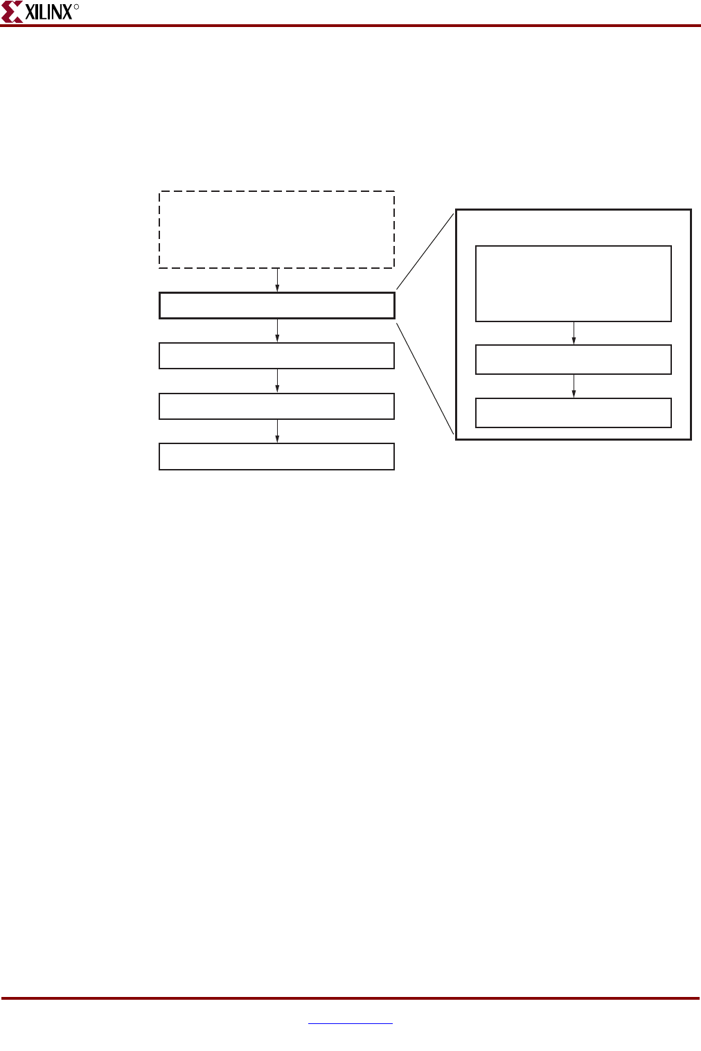
524 www.xilinx.com Memory Interface Solutions User Guide
UG086 (v3.6) September 21, 2010
Chapter 14: Debugging MIG DDR2 Designs
R
Verifying Board Layout
Introduction
There are three main steps in verifying the board layout for a memory interface, as shown
in Figure 14-2.
Memory Implementation Guidelines
See Appendix A, “Memory Implementation Guidelines” for specifications on pinout
guidelines, termination, I/O standards, trace matching, and loading. The guidelines
provided are specific to both memory technologies as well as MIG output designs. It is
very important to verify that these guidelines have been read and considered during
board-layout. Failure to follow these guidelines can result in problematic behavior in
hardware, which is detailed throughout this chapter.
Calculate WASSO
It is important to take into consideration WASSO limits when generating a MIG pinout.
The FPGA data sheets define the SSO limits for each bank. WASSO calculations take this
into account along with design-specific parameters, such as board-level inductance, input
logic-low threshold, input undershoot voltage, and output loading capacitance. WASSO
ensures even distribution of fast/strong drivers across the package, that the number of
simultaneously switching outputs does not exceed the per-bank limit and that the chip
does not generate excessive ground bounce.
WASSO Calculators for Virtex®-4 devices [Ref 34] or Virtex-5 devices [Ref 35] should be
used to find WASSO limits based on board-specific parameters.
These calculations should be run during both pre-board layout and post-board layout. The
results found can then be entered in the Bank Selection page of the MIG GUI. (Refer to
“Bank Selection,” page 54.) MIG follows these WASSO Limits when generating the pinout.
Please see Appendix C, “WASSO Limit Implementation Guidelines” for further
information.
Figure 14-2: Verify Board Layout Guidelines
Symptoms in Hardware
Verify Board Layout Guidelines
- Calibration Failure
- Data Bit/Byte Corruption/Errors
Verify Board Layout Guidelines
General Software Debug
Physical Layer Debug
Calculate WASSO
Verify Memory Implementation
Guidlines Such as Pin-out,
Termination, and Trace Matching
are Properly Followed
Run SI Simulation Using IBIS
General Board Level Debug
UG086_c13_02_122107
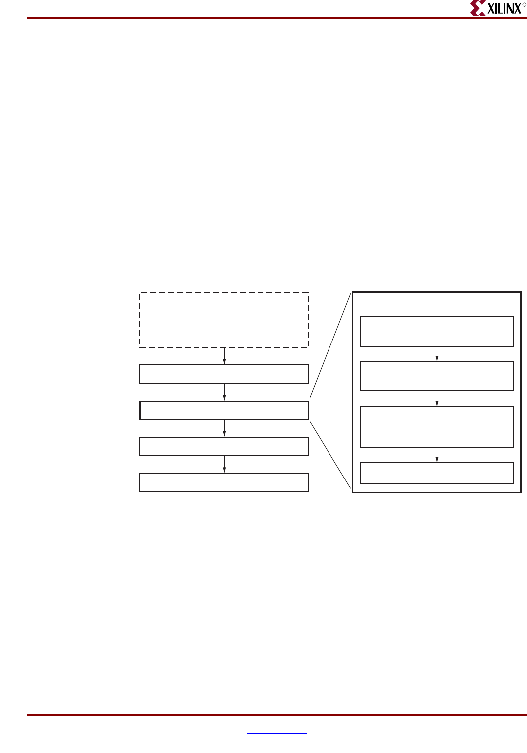
Memory Interface Solutions User Guide www.xilinx.com 525
UG086 (v3.6) September 21, 2010
Verifying Design Implementation
R
Run SI Simulation Using IBIS
The final critical step in verifying board layout guidelines have been followed is to run
signal integrity simulations using IBIS. These simulations should always be run both pre-
board layout and post-board layout. The purpose of running these simulations is to
confirm the signal integrity on the board.
The ML561 Hardware-Simulation Correlation chapter of the ML561 User Guide [Ref 14]
can be used as a guideline. This chapter provides a detailed look at signal integrity
correlation results for the ML561 board and can be used as an example for what to look at
and what is good to see. It also provides steps to create a design specific IBIS model to aid
in setting up the simulations.
Verifying Design Implementation
Introduction
There are four main steps in verifying the design implementation of a MIG output as
shown in Figure 14-3:
Behavioral Simulation
Running behavioral simulation verifies the functionality of the design. Both the
example_design and user_design provided with the MIG DDR2 controllers include a
complete environment which allows the user to simulate the reference design and view the
outputs. Scripts are provided to run behavioral simulation.
• For Virtex-4 family designs, see “Simulating the DDR2 SDRAM Design” in Chapter 3.
• For Spartan®-3/3E/3A/3AN/3A DSP family designs, see “Tool Output” in Chapter 8.
• For Virtex-5 family designs, see “Simulating the DDR2 SDRAM Design” in Chapter 9.
Figure 14-3: Verify Design Implementation
Symptoms in Hardware
Verify Board Layout Guidelines
- Calibration Failure
- Data Bit/Byte Corruption/Errors
Verify Design Implementation
General Software Debug
Physical Layer Debug
Verify Design Successfully
Completes MAP/PAR and Follows
MIG Routing Constraints
Run MIG Design Through
Behavioral Simulation
Verify any Modifications to the
MIG Output
Verify MIG Design Timing in TRACE
General Board Level Debug
UG086_c13_03_122107

526 www.xilinx.com Memory Interface Solutions User Guide
UG086 (v3.6) September 21, 2010
Chapter 14: Debugging MIG DDR2 Designs
R
The Xilinx® UNISIM libraries must be mapped into the simulator. If the UNISIM libraries
are not set up for your environment, go to the COMPXLIB chapter of the Development
Systems Reference Guide section for assistance compiling Xilinx simulation models and
setting up the simulator environment. This guide can be found in the ISE® Software
Manuals.
Verify Modifications to MIG Output
There are two modifications to the MIG output that are commonly made:
1. Changing the pinout in the provided output UCF
2. Changing design parameters defined in the output source code
Both of these changes can cause problems with the implemented design that are not
always visible to the user.
Changing the Pinout Provided in the Output UCF
MIG allows users to select the desired banks rather then the exact pin locations for the
memory interface. This is because specific pin assignment guidelines must be followed.
See Appendix A, “Memory Implementation Guidelines” for detailed pin assignment
guidelines.
Following these pin assignment guidelines when making changes to the output pinout
ensures proper pin placement. However, design implementation problems can still occur.
The Virtex-5 and Spartan-3 FPGA DDR2 designs require specific placement constraints
outside of the pin locations. These constraint values are dependent on the pinout and so
the constraints output with the MIG UCF are not correct if the pin locations are changed.
The Spartan-3 and Virtex-5 FPGA architecture-specific sections of this debug guide
provide detailed information on these constraints and how changes cause problems.
It is always recommended to use the MIG pinout. If specific pins in the selected banks
cannot be used for the memory interface, use the Reserve Pins feature of the MIG tool.
(Refer to section “Reserve Pins” in Chapter 1.) If changes are made to the Virtex-4 or
Virtex-5 FPGA pinout, the Verify UCF and Update Design and UCF feature should always
be used to test the changes against the pin assignment guidelines. (Refer to section “Load
mig.prj and UCF” in Chapter 1.)
Changing Design Parameters
Often users need to change specific design parameters such as address/data widths, DDR2
memory parameters, and clock period after generating the DDR2 design. These
modifications often require multiple changes to the MIG source code that are not always
visible to the user. It is always recommended to re-run MIG when making any design
parameter change.
For Spartan-3 and Virtex-4 family MIG designs, design parameters are defined through
`defines. In some cases, changing one design parameter requires changing multiple
`defines and/or portions of the source code. As an example, when changing the address or
data bus widths, the source code replicates multiple instances that depend on the bus
width. In this case, it is necessary to instantiate additional elements for new bits manually.
Because of required modifications such as this, MIG should always be re-run when a
design parameter change is required.
For Virtex-5 FPGA MIG designs, design parameters are defined using top-level parameters
and generate statements. Changes to the code are no longer necessary. However, it is still
recommended to re-run MIG when making design parameter modifications.

Memory Interface Solutions User Guide www.xilinx.com 527
UG086 (v3.6) September 21, 2010
Verifying Design Implementation
R
Verify Successful Placement and Routing
In order to ensure proper timing of address/control or writes to the memory, specific flip-
flops must be pushed into IOBs. These flip-flops include address, control and data 3-state
output. To ensure proper timing, the flip-flops must be located within the IOBs. The MIG
source code provides attributes to push these flip-flops into their respective IOBs. The
attributes, however, are specific to the synthesis tool selected in the CORE Generator
software project options. If XST is selected, the attributes are specific only to XST. Ensure
the synthesis tool selected in the CORE Generator software project options is used.
Once the design has successfully complete Place and Route, FPGA Editor can then be used
to verify the correct placement of these flip-flops in the IOBs. Search for the address,
control, and data IOBs in the 'List1' window under 'All Components.' Individually open
each of these IOB components to verify the flip-flop is properly packed in the IOB. If the
flops are not properly packed, ensure the synthesis attributes were picked up when
running XST or Synplify Pro.
Verify IDELAYCTRL Instantiation for Virtex-4 and Virtex-5 FPGA Designs
Virtex-4 and Virtex-5 FPGA designs require instantiation of the IDELAYCTRL module in
the HDL to support the use of the IDELAY ChipSync™ technology elements for read data
capture.
Virtex-5 FPGA Designs
MIG uses the “Automatic” method for IDELAYCTRL instantiation: specifically, the MIG
HDL only instantiates a single IDELAYCTRL for the entire design. No (LOC) constraints
are included in the MIG-generated UCF. This method relies on the ISE tools to replicate
and place as many IDELAYCTRLs (for example, one per clock region that use IDELAYs) as
needed. Replication and placement are handled automatically by the software tools if the
IDELAYCTRLs have the same refclk, reset, and rdy nets. A new constraint,
IODELAY_GROUP, is available that associates a set of IDELAYs with an IDELAYCTRL
and allows for multiple IDELAYCTRLs to be instantiated without LOC constraints
specified. The ISE software generates the IDELAY_CTRL_RDY signal by logically ANDing
the RDY signals of every IDELAYCTRL block.
Virtex-4 FPGA Designs
MIG instantiates the required number of IDELAYCTRLs in the RTL, and uses the LOC
constraints in the UCF file to fix their locations. The number of IDELAYCTRLs is defined
by the IDELAYCTRL_NUM parameter in the idelay_ctrl module. In the RTL,
IDELAY_CTRL_RDY is generated by logically ANDing the RDY signals of every
IDELAYCTRL block.
For Virtex-5 or Virtex-4 FPGA designs, the IODELAY_GROUP name and IDELAYCTRL
LOC constraints should be checked in the following cases:
• The MIG design is used with other IP cores or user designs that also require the use of
IDELAYCTRL and IDELAYs.
• Previous ISE software releases 8.2.03i and 9.1i had an issue with IDELAYCTRL block
replication or trimming. When using these revisions of the ISE software, the user must
instantiate and constrain the location of each IDELAYCTRL individually.
See the Virtex-4 FPGA User Guide [Ref 7] and Virtex-5 FPGA User Guide [Ref 10] for more
information on the requirements of IDELAYCTRL placement.
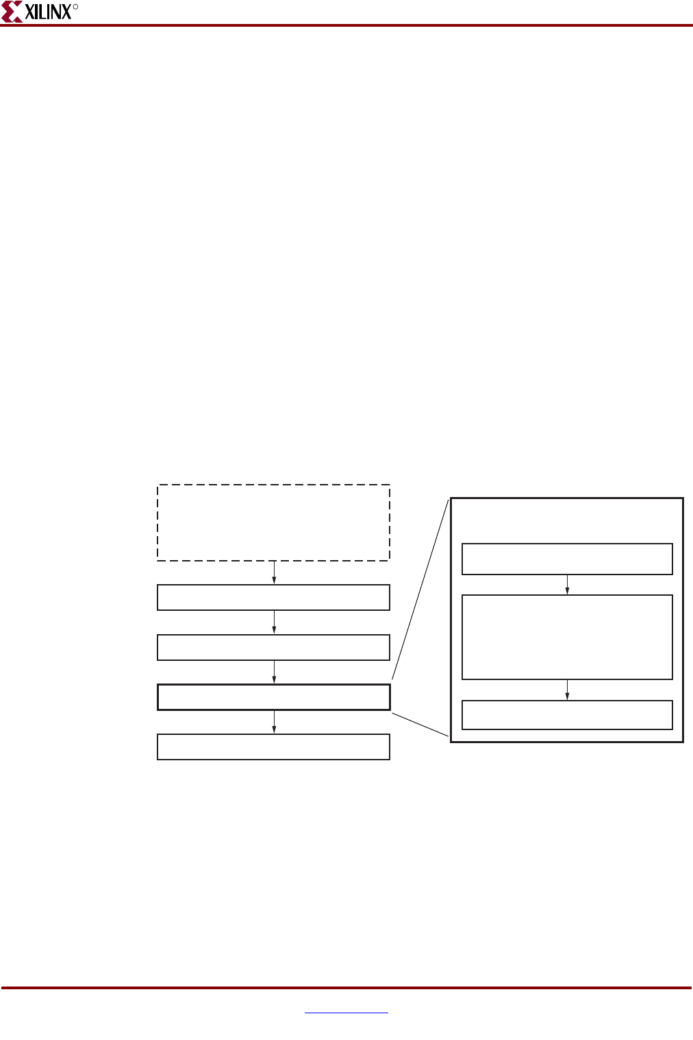
528 www.xilinx.com Memory Interface Solutions User Guide
UG086 (v3.6) September 21, 2010
Chapter 14: Debugging MIG DDR2 Designs
R
Verify TRACE Timing
As a final check of proper software implementation of the MIG design, verify that all MIG
provided timing constraints have completed successfully. There should be no failed timing
paths in the provided MIG constraints. If the design was run in batch mode using the
ise_flow script file, the TRACE output <design_name>.twr file can be opened. If the
design was ran using the ISE tools, select the Analyze Post-Place and Route Static Timing
option located under the Processes tab.
Debugging the Spartan-3 FPGA Design
Introduction
For a detailed discussion of the Spartan-3 FPGA DDR2 interface design, see application
notes XAPP454 [Ref 15] and XAPP768c [Ref 24].
Read Data Capture
Read data capture is executed using LUT based delay circuits to delay the DQS and
loopback signals. The delayed DQS is then used to capture data into LUT RAM based
FIFOs with the delayed loopback used as the write enable.
There are four main steps in debugging this data capture implementation as shown in
Figure 14-4.
Verify Placement and Routing
The proper implementation of the data capture algorithm requires specific pinout and
placement constraints which include PIN, LUT, BEL, and MAXDELAY, as well as usage of
template routes during Place and Route.
MIG creates the appropriate UCF for the banks selected and should always be used. If
changes are made to the pinout, the remaining placement constraints are no longer correct
because these are based on the pin locations. Information on the specific guidelines used in
Figure 14-4: Spartan-3 FPGA Physical Layer Debug
Symptoms in Hardware
Verify Board Layout Guidelines
- Calibration Failure
- Data Bit/Byte Corruption/Errors
- Insert ChipScope
- Add MIG Signals to Isolate Failure
- Vary LUT Taps as Required
Spartan-3 FPGA
Physical Layer Debug
General Software Debug
Physical Layer Debug
Verify Placement and Routing
Debug Physical Layer in Hardware
Proceed to Board-level Debug
General Board Level DebugUG086_c13_04_021709

Memory Interface Solutions User Guide www.xilinx.com 529
UG086 (v3.6) September 21, 2010
Debugging the Spartan-3 FPGA Design
R
creating Spartan-3 generation FPGA UCFs are provided in Appendix A, “Memory
Implementation Guidelines.” If these constraints are not followed, the data capture
algorithm is not implemented properly and the results in hardware might not be as
expected.
When the appropriate UCF is implemented, all related components are placed properly.
This correct placement causes two specific routing algorithms (template routes) to be used
during implementation of the PAR tools:
• Routing DQ bits from a PAD to a Distributed Memory component
• Routing delayed DQS strobe signals using Local Clocking resources
• The PAR tools automatically treats Local Clocks as template routes and locks
down the routes correctly without using the environment variable.
DQ Routing
The template router set through the environment variable ensures the data bits are routed
from a PAD to a Distributed Memory to capture the data in an Asynchronous FIFO using
the Local Clock to write the data, and a Global Clock to read the data. These routes require
a template to guarantee that the delay remains constant between all data bits.
Once the design is implemented, load the resultant .ncd and .pcf files into FPGA Editor
to visually verify the template routes for the data bits, as follows:
1. Open the design in FPGA Editor by selecting Start → Programs → Xilinx ISE 10.1i
→ Accessories → FPGA Editor, or load through the View/Edit Routed Design
(FPGA Editor) option in the Processes tab of an ISE project.
2. In some cases, turning Stub Trimming off provides a better picture of the route. To do
this, select File → Main Properties and turn off Stub Trimming in the General tab.
When Stub Trimming is enabled, FPGA Editor does not display the entire route. If Stub
Trimming is disabled, you can see the entire length of the routing segment. Stub
Trimming is enabled in Figure 14-5 and Figure 14-6.
3. Search within the List1 window for *dq* under the All Nets pull-down. Select all of the
DQ data bit nets (e.g., main_00/top0/dq(0)) within the window and highlight these
nets by clicking the Hilite button in the right-hand column. This allows for visual
inspection of the delay routes. Zoom into the area with the highlighted nets and verify
that the placement looks like Figure 14-5 or Figure 14-6.
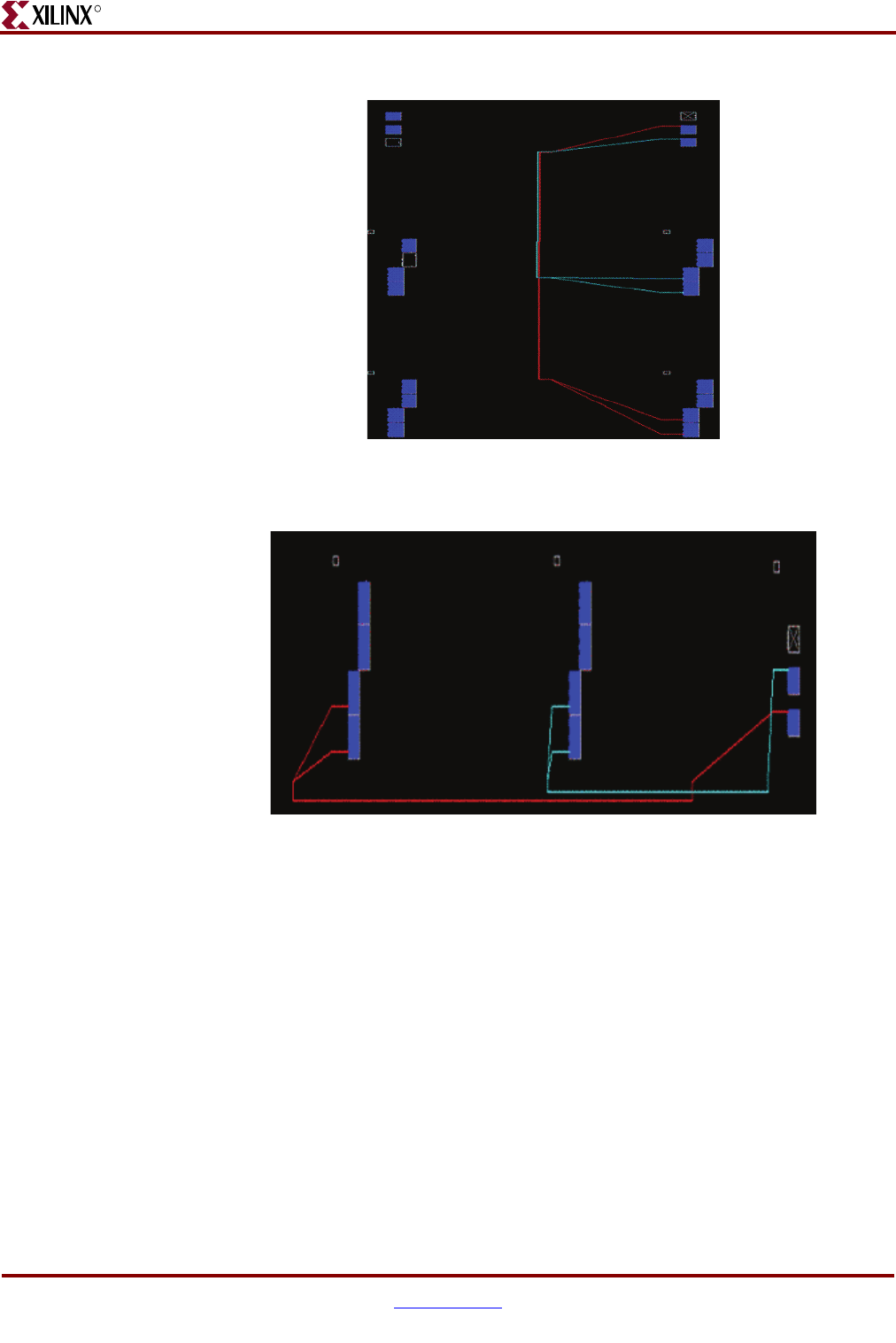
530 www.xilinx.com Memory Interface Solutions User Guide
UG086 (v3.6) September 21, 2010
Chapter 14: Debugging MIG DDR2 Designs
R
4. Next, verify that the delays on the nets are consistent. Again, select all of the DQ data
bit nets in the List1 window. This time click on the Delay button located in the right-
hand column. This lists the worst-case delay for the DQ bits. Using this delay
information, inconsistent routing can be quickly identified. There should be less than
75 ps of skew (ideally less than 50 ps) between the data nets. The delay values depend
on the device speed grade and Top/Bottom versus Left/Right implementation but
have been observed to range between 300–700 ps.
If preferred, export the delay information to view the report in an Excel spreadsheet. Select
File → Export to export the delay information to a .csv file.
DQS Routing
The delayed strobes (dqs*_delayed_col*) need to use the local clocking resources available
in the device for the clock routing. The local routing resources used depend on the pin
placement specified during generation in the MIG tool. Full hex lines that have low skew
Figure 14-5: DQ Placement (Top/Bottom)
Figure 14-6: DQ Placement (Left/Right)
UG086_c13_05_122107
UG086_c13_06_122107
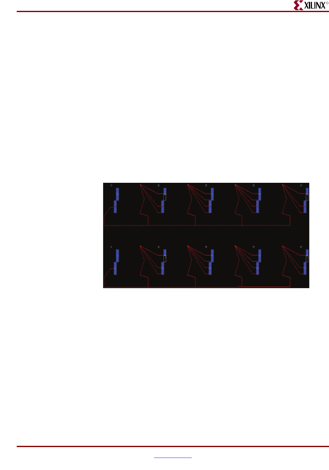
Memory Interface Solutions User Guide www.xilinx.com 531
UG086 (v3.6) September 21, 2010
Debugging the Spartan-3 FPGA Design
R
are located throughout the device. Left and right implementations use Vertical Full Hex
(VFULLHEX) lines for local clock routing. Top and bottom implementations use VLONG,
VFULLHEX, and HFULLHEX lines for local clock routing.
PAR routes from the Local Clock PAD to a series of LUTs to implement the scheme
explained in detail in XAPP768c. From the output of the final LUT delay, the delayed
strobe/Local Clock (dqs*_delayed_col*) routes to all of the FIFO bits.
To verify the pinout and usage of the template router, the net skew and max delay on the
local clock (dqs*_delayed_col*) must be within spec. To verify these values, open the PAR
report (.par file) and scroll to the Clock Report section. For most Spartan-3 platform
devices, the Net Skew is less than 40 ps, and the Max Delay is approximately 550 ps. For
Spartan-3A and Spartan-3A DSP devices, the Net Skew is less than 65 ps, and the Max
Delay is approximately 400 ps.
The FPGA Editor can then be used to view the local clock placement. To view the template
routes for the delayed strobes, search in the List1 window for *dqs*_delayed_col* in the All
Nets pull-down. Select all the nets (e.g., main_00/top0/data_path0/dqs0_delayed_col0)
and select Hilite from the right-hand column. This command highlights the nets of interest.
Then zoom into this range of highlighted signals to view the placement. If local clocking is
used, one of the two structures shown in Figure 14-7 and Figure 14-8 is seen.
Figure 14-7: Local Clock (Top/Bottom) for dqs*_delayed_col* LUT Delay Elements
UG086_c13_07_122107
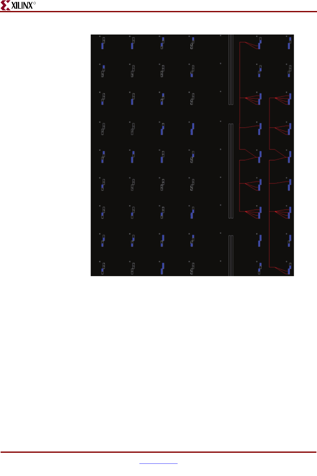
532 www.xilinx.com Memory Interface Solutions User Guide
UG086 (v3.6) September 21, 2010
Chapter 14: Debugging MIG DDR2 Designs
R
If the skew and delays are within spec and the layout for the Local Clock and Data bits
match the previous figures, the template routes for DQS have been properly implemented.
If the DQ or delayed DQS signals do not verify properly, ensure that the UCF follows the
guidelines specified in Appendix A.
Debugging Physical Layer in Hardware
If problems are seen in hardware after verifying the correct implementation of the
Spartan-3 generation FPGA design, there are two common issues that cause problems with
the data capture algorithm:
• Incorrect Loopback timing
• Incorrect delay on DQS for read capture
Figure 14-8: Local Clock (Left/Right) for dqs*_delayed_col* LUT Delay Elements
UG086_c13_08_122107

Memory Interface Solutions User Guide www.xilinx.com 533
UG086 (v3.6) September 21, 2010
Debugging the Spartan-3 FPGA Design
R
Loopback Timing
The timing on the loopback signal is critical to the proper implementation of the data
capture algorithm because the delayed loopback signal generates the write enable for the
read data FIFOs. The causes for incorrect loopback timing are:
• Incorrect route delay on the loopback signal
• The loopback signal must be delayed by the sum of the FPGA forward clock and
the DQS trace length. This is most commonly implemented through a physical
board trace.
• Changes to the MIG pinout after generation
The symptoms of incorrect loopback timing are:
• The first data in a burst is usually corrupted
• Depending on trace delays, only certain bits in the bus exhibit the problem
Incorrect DQS Delay
The appropriate delay on the DQS strobe signals is required for proper implementation of
the Spartan-3 generation FPGA data capture algorithm. Common causes for incorrect DQS
delay are:
• Mismatch in trace lengths for DQ and DQS
• Changes to the MIG pinout after generation
• Frequency changes without reimplementation of the design
If the delay on DQS is incorrect, the following symptoms can be seen in hardware:
• Incorrect data is seen intermittently
• Incorrect data is always seen
To debug either incorrect Loopback timing or incorrect DQS delay, insert a
ChipScope™ Pro analyzer Virtual Input Output (VIO) core into the MIG design. The
tapfordqs1 signal located in the cal_ctl.v/.vhd source file should be added to the
ChipScope tool VIO to view the number of taps in the delay paths. Use the VIO to increase
or decrease the number of LUTs in the delay path while examining the resultant behavior
in hardware. The number of taps increases/decreases for both the Loopback delay path
and the DQS delay path. Once the appropriate number of LUT delays is found so the data
corruption no longer occurs, the number of delays can then be changed within the source
code. Changing the number of LUTs in the delay path can compensate for the incorrect
loopback timing and incorrect DQS delay. See the ChipScope Pro User Guide [Ref 6] for
detailed information on using ChipScope tool VIO.
Proceed to General Board-Level Debug
If the above verification of design implementation and debug of the data capture
algorithm did not resolve the issues seen in hardware, there could be a problem on the
board itself. Proceed to the“General Board-Level Debug” section for further guidance.

534 www.xilinx.com Memory Interface Solutions User Guide
UG086 (v3.6) September 21, 2010
Chapter 14: Debugging MIG DDR2 Designs
R
Debugging the Virtex-4 FPGA Direct-Clocking Design
Introduction
This section discusses internal signals to observe in order to assist in isolating problems
that could occur during read data timing calibration in the Virtex-4 FPGA DDR2
direct-clocking design. For more information on the calibration algorithm used in this
design, refer to application note XAPP702. [Ref 19]
Read Data Capture Timing Calibration
Read data timing calibration is executed over two stages:
• Stage 1: Aligning output of IDDR to internal (FPGA) clock
• Stage 2: Read Data Valid Calibration
The calibration logic is parallel, in that multiple calibration units are instantiated, one for
each DQS group (e.g., each calibration unit handles 4 or 8 DQ bits).
What can break during calibration?
• Stage 2 calibration checks for a specific sequence of data back from the memory
• Data bit issues (e.g., stuck-at-bit, PCB trace open/short) causes calibration to hang
during Stage 2
• Each calibration unit must be checked individually to pinpoint exactly which
bit(s) failed and/or DQS groups failed
The overall calibration state machine flow diagram is shown in Figure 14-9.
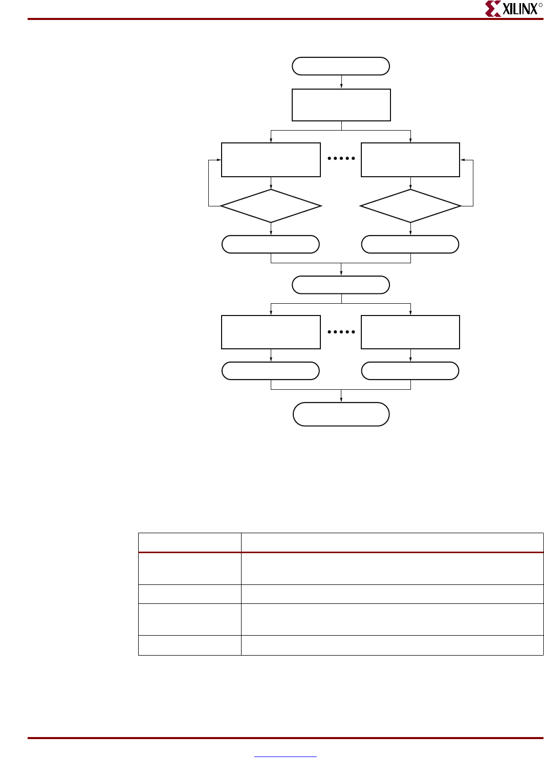
Memory Interface Solutions User Guide www.xilinx.com 535
UG086 (v3.6) September 21, 2010
Debugging the Virtex-4 FPGA Direct-Clocking Design
R
Signals of Interest
The status signals shown in Table 14-1 can be used to help determine where the failure
occurs:
Figure 14-9: Virtex-4 FPGA DDR2 Direct-Clocking Overall Calibration Flowchart
Start Calibration
Write Training Patterns
{0xFF, 0x00}, {0xA5, 0x5A}
to Memory
calib_done_dqs [0] = 1
Stage 1: DQ-to-FPGA
Clock Calibration for
DQS [0] Group
All DQ Bits
Calibrated?
Stage 1: DQ-to-FPGA
Clock Calibration for
DQS [x] Group
Stage 2: Read FIFO Write
Enable Calibration for
DQS[0]
Stage 2: Read FIFO Write
Enable Calibration for
DQS[0]
All DQ Bits
Calibrated?
tap_sel_done = 1
Calibration Done
init_done = 1
calib_done_dqs [x] = 1
comp_done_int [0] = 1 comp_done_int [x] = 1
NN
YY
UG086_c13_09_043009
Table 14-1: Virtex-4 FPGA Direct-Clocking Status Signals
Signal Description
calib_done_dqs[x:0] Asserted when individual Stage 1 calibration units have finished
(one per DQS group)
tap_sel_done Asserted when all Stage 1 calibration units have completed
comp_done_int[x:0] Asserted when individual Stage 2 calibration units have finished
(one per DQS group)
init_done Asserted when all calibration stages successfully completed

536 www.xilinx.com Memory Interface Solutions User Guide
UG086 (v3.6) September 21, 2010
Chapter 14: Debugging MIG DDR2 Designs
R
Proceed to General Board-Level Debug
If the above verification of design implementation and debug of the data capture
algorithm does not resolve the issues seen in hardware, there could be a problem on the
board itself. Proceed to the “General Board-Level Debug” section for further guidance.
Debugging the Virtex-4 FPGA SerDes Design
Introduction
This section discusses internal signals to observe in order to assist in isolating problems
that could occur during read data timing calibration in the Virtex-4 FPGA DDR2 SerDes
design. For more information on the calibration algorithm used in this design, refer to
application note XAPP721. [Ref 23]
Read Data Capture Timing Calibration
Read data timing calibration is executed over three stages:
• Stage 1: Aligning output of the first stage of the ISERDES to the FPGA clock
• Stage 2: Fine adjustment of Data-to-Strobe (DQ-to-DQS) capture timing into first stage
of ISERDES
• Stage 3: Read data valid calibration
The calibration logic is parallel, in that multiple calibration units are instantiated, one for
each DQS group (e.g., each calibration unit handles 4 or 8 DQ bits).
What can break during calibration?
• Calibration can hang at any of the stages. All stages look for a specific training pattern
back from the memory. If it is not received, calibration sticks in an infinite loop
reading back the data.
• Data bit issues (e.g., stuck-at-bit, PCB trace open/short) can cause calibration to hang
• Each calibration unit must be checked individually to pinpoint exactly which
bit(s) failed and/or DQS groups failed
The overall calibration state machine flow diagram is shown in Figure 14-10.
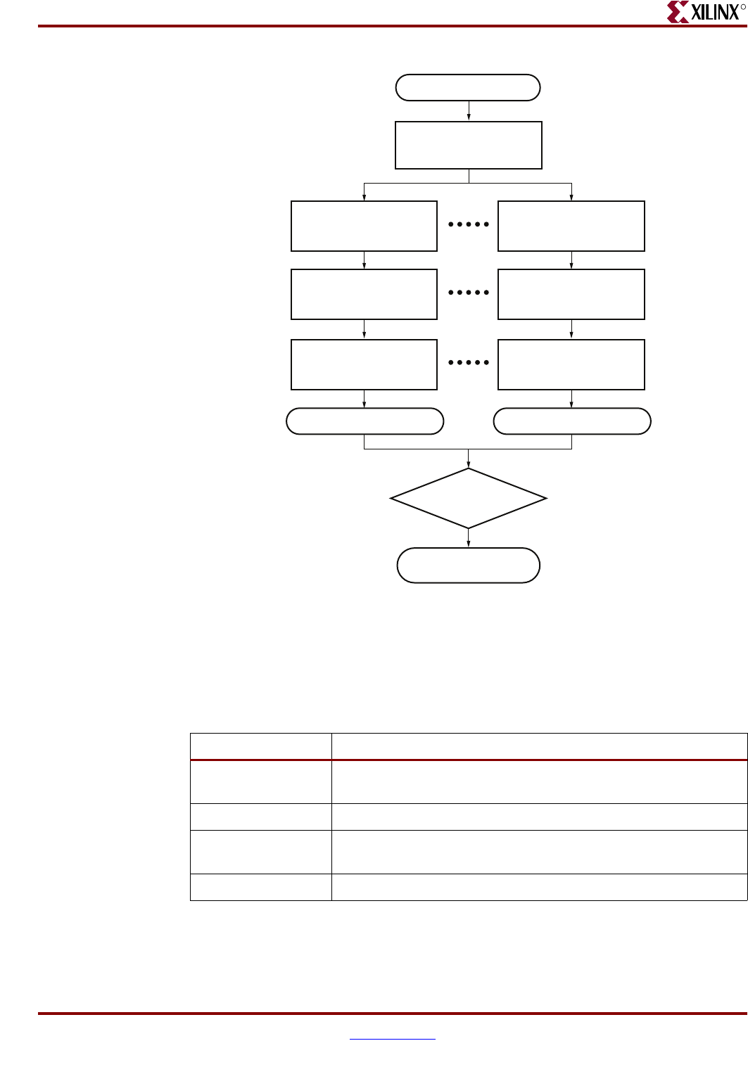
Memory Interface Solutions User Guide www.xilinx.com 537
UG086 (v3.6) September 21, 2010
Debugging the Virtex-4 FPGA SerDes Design
R
Signals of Interest
The status signals shown in Table 14-2 can be used to help determine where the failure
occurs:
Figure 14-10: Virtex-4 FPGA DDR2 SerDes Overall Calibration Flowchart
Start Calibration
Write Training Patterns
0xFF, 0x00, 0xAA, 0x55
to Memory
Stage 1: DQS
[0]-to-FPGA
Clock Calibration
All DQ/DQS Bits
Calibrated?
Stage 1: DQS
[x]-to-FPGA
Clock Calibration
Calibration Done
dp_dly_slct_done =1
UG086_c13_10_122107
Stage 2: DQS
[0]-to-DQ [7:0] Fine
Adjustment Calibration
Stage 2: DQS
[x]-to-DQ Fine
Adjustment Calibration
Stage 3: Read FIFO
Write Enable Calibration
for DQS [0]
Stage 3: Read FIFO
Write Enable Calibration
for DQS [x]
dq 1 to 7_calib_done [0] = 1 dq 1 to 7_calib_done [x] = 1
Table 14-2: Virtex-4 FPGA SerDes Status Signals
Signal Description
calib_done_dqs[x:0] Asserted when individual Stage 1 calibration units have finished
(one per DQS group)
tap_sel_done Asserted when all Stage 1 calibration units have completed
comp_done_int[x:0] Asserted when individual Stage 2 calibration units have finished
(one per DQS group)
init_done Asserted when all calibration stages successfully completed

538 www.xilinx.com Memory Interface Solutions User Guide
UG086 (v3.6) September 21, 2010
Chapter 14: Debugging MIG DDR2 Designs
R
Proceed to General Board-Level Debug
If the above verification of design implementation and debug of the data capture
algorithm did not resolve the issues seen in hardware, there could be a problem on the
board itself. Proceed to the “General Board-Level Debug” section for further guidance.
Debugging the Virtex-5 FPGA Design
Introduction
This section discusses internal signals to observe in order to assist in isolating problems
that could occur during read data timing calibration in the Virtex-5 FPGA DDR2 design.
Additional UCF and other parameter requirements of this design are also discussed. For
more information on this design, refer to application note XAPP858 [Ref 27].
Verify Placement and Routing
Historically, unlike the MIG Spartan-3 FPGA interface designs, most MIG Virtex-4 and
Virtex-5 FPGA designs have had only pin location (LOC) and clock (PERIOD) constraints
in the UCF. In some cases AREA_GROUP constraints were included to assist with meeting
timing. The MIG Virtex-5 FPGA DDR design does require location and internal timing
constraints for specific read data capture related circuits.
The MIG Virtex-5 FPGA DDR2 adds a number of additional constraints to the design. This
design requires properly setting both top-level parameters in HDL and constraints in the
UCF that are pinout-dependent. The additional constraints in the UCF consists of location
constrains for certain fabric-based resources, and internal timing (MAXDELAY)
constraints. These constraints arise from changes to the read-capture path from previous
revisions of MIG Virtex-5 FPGA DDR2 designs.
When creating a design in MIG, MIG automatically generates the proper HDL and UCF
constraint values. However, if it becomes necessary to make changes to the MIG-generated
pinout, these constraints must be manually modified. The procedure for doing so is
discussed in Appendix B, “Pinout-Related UCF Constraints for Virtex-5 FPGA DDR2
SDRAMs.”
In addition, the MIG Virtex-5 FPGA DDR2 design requires that certain logic placement and
routes related to the read data capture be tightly constrained. MAP or PAR issue an error if
any of these requirements cannot be met. For more information on these requirements, see
“Constraints,” page 366.
Debugging Calibration Failures
If the phy_init_done signal is not asserted, calibration has failed. To determine why
calibration has failed, it is best to start debugging using just the MIG generated example
design rather than the full user design. Calibration consists of four stages, as outlined in
“DDR2 SDRAM Design Calibration,” page 375. Although problems can occur in any of the
stages, the calibration state machine always passes through the first two stages of
calibration regardless of whether or not the correct data was returned from the memory.
Because of this, the actual data returned from the memory on rd_data_rise and
rd_data_fall during each stage of calibration should be looked at. The signals listed in
Table 14-3 should be monitored through the ChipScope analyzer during the calibration
stages and compared to the expected data.
Memory Interface Solutions User Guide www.xilinx.com 539
UG086 (v3.6) September 21, 2010
Debugging the Virtex-5 FPGA Design
R
By triggering on the end of each stage of calibration using the calib_done signals and
looking at the read data prior to moving to the next stage, it is possible to determine what
caused calibration to fail. The expected data patterns for each stage can be seen in
Table 14-4.
For further debugging, the calibration state machine can be found in the
PHY_CALIB.V/VHD module and is documented in XAPP858 [Ref 27]. The correct
behavior can be confirmed by running the example simulation provided by the MIG tool.
If calibration fails, it is important to verify that the board layout guidelines have been
followed (see “Verifying Board Layout,” page 524) and to proceed to the “General Board-
Level Debug,” page 540 section.
Physical Layer Debug Port
The Virtex-5 FPGA DDR2 design HDL contains an optional port to allow the user to
observe and control the IDELAY tap values for the DQ, DQS, and DQS Gate signals after
read capture timing calibration. This is described in Appendix E, “Debug Port.”
Table 14-3: Virtex-5 FPGA SerDes Status Signals
Signal Description
phy_init_done Asserted when both initialization of memory and read capture
timing calibration has completed
calib_start[3:0] Pulsed for one clock cycle as each calibration stage is entered
calib_done[3:0] Driven to a static 1 as each calibration stage is finished
rd_data_rise Captured (synchronized) rising edge read data from DDR2
rd_data_fall Captured (synchronized) falling edge read data from DDR2
cal1_dq_count Binary value indicating the current DQ bit being calibrated
during Stage 1
cal2_dq_count Binary value indicate the current DQS group being calibrated
during Stage 2
Table 14-4: Expected Data Patterns
Stage rd_data_rise rd_data_fall
1All 0xF All 0x0
2First word: All 0xF
Second word: All 0x0
First word: All 0xF
Second word: All 0x0
3First word: All 0x1
Second word: All 0xE
First word: All 0xE
Second word: All 0x1
4First word: All 0x1
Second word: All 0xE
First word: All 0xE
Second word: All 0x1
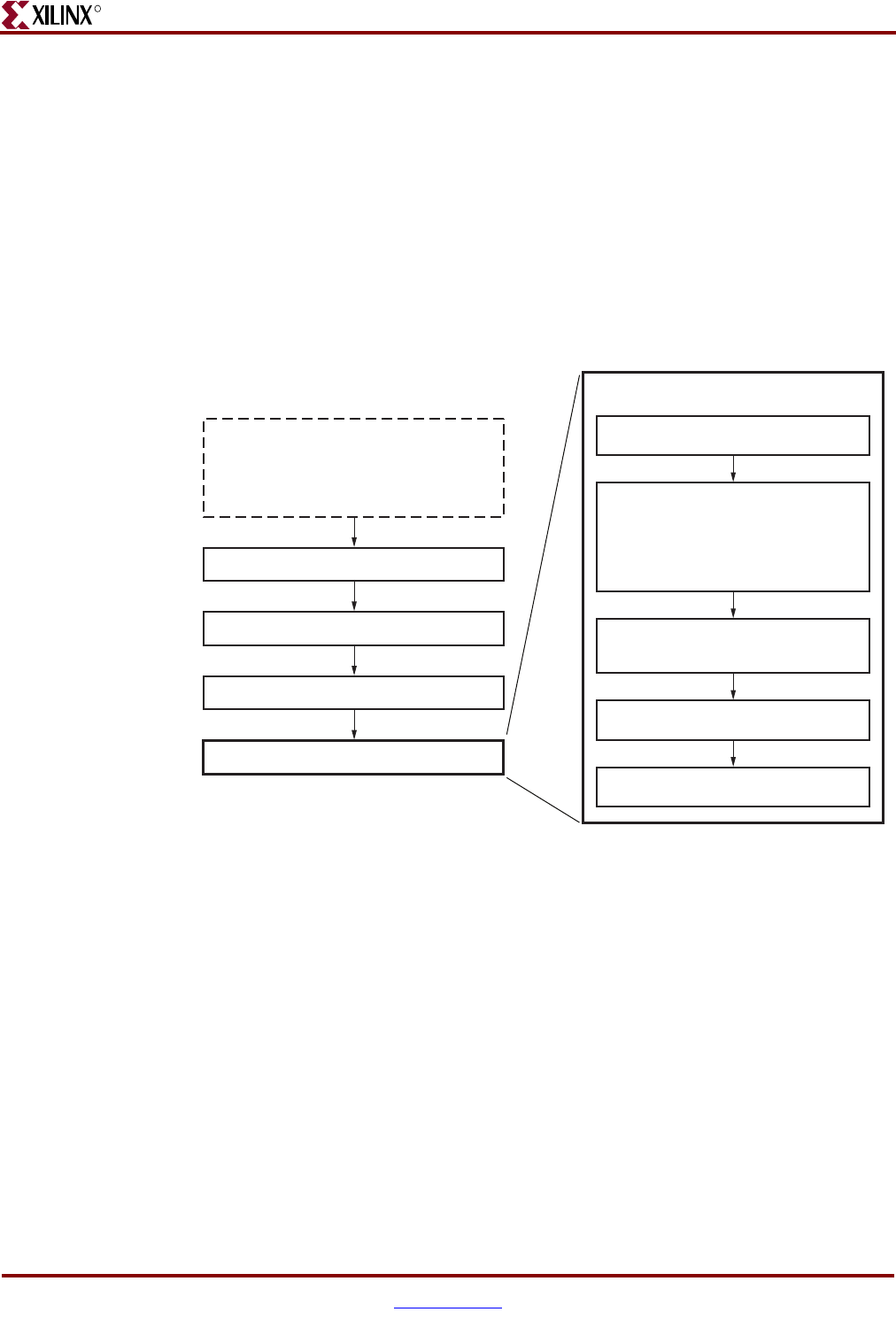
540 www.xilinx.com Memory Interface Solutions User Guide
UG086 (v3.6) September 21, 2010
Chapter 14: Debugging MIG DDR2 Designs
R
Proceed to General Board-Level Debug
If the above verification of design implementation and debug of the data capture
algorithm does not resolve the issues seen in hardware, there could be a problem on the
board itself. Proceed to the “General Board-Level Debug” section for further guidance.
General Board-Level Debug
Overall Flow
The flowchart shown in Figure 14-11 documents recommended steps to try during board-
level debug.
Isolating Bit Errors
In this step, the user stays in the HDL domain and tries to isolate when/where the bit
errors are occurring.
When are the error(s) occurring?
• Data belonging to certain DQS groups?
• On accesses to certain addresses, banks, or ranks of memory?
• For example, on designs that can support multiple varieties of DIMM modules,
make sure to support all possible address and bank bit combinations
• Only occur for certain data patterns or sequences?
• This can indicate a shorted or open connection on the PCB
• This can also indicate an SSO or cross-talk issue
• Does the design use multiple DIMM sockets?
Figure 14-11: General Board-Level Debug Flowchart
Symptoms in Hardware
Verify Board Layout Guidelines
- Calibration Failure
- Data Bit Corruption/Errors
- Measure Signal Integrity
- Measure Supply & Vref Voltages
- Measure Bus Timing
General Board Level Debug
General Software Debug
Physical Layer Debug
Isolate Bit Errors
Run Synthesizable Testbench
Board Measurements
Check Clocking/Run Interface
at Slower Frequency
Vary Taps
General Board Level Debug
UG086_c13_11_122107

Memory Interface Solutions User Guide www.xilinx.com 541
UG086 (v3.6) September 21, 2010
General Board-Level Debug
R
• All MIG designs that support multiple DIMM sockets (“deep” configurations)
calibrate only on the first DIMM socket, and the maximum frequency is reduced
from the maximum achievable if only one rank of memory is used. This was done
to account for both the additional loading and the fact that there are no inherent,
process-related timing differences between the DIMM sockets. Factors that cause
the timing to be different between the DIMMs—for example, PCB trace routing
differences between the FPGA and each of the DIMMs—can result in read failures
on all but the very first DIMM.
It might also be necessary to determine whether the data corruption is due to writes or
reads. This can be difficult to determine because, if the writes are the issue, readback of the
data appears corrupted as well. In addition, issues with control/address timing affect both
writes and reads. Some experiments that can be tried to isolate the issue:
• If the errors are intermittent, have the controller issue a small initial number of writes,
followed by continuous reads from those locations. Do the reads intermittently yield
bad data? If so, this might point to a read problem.
• Check/vary the control and address timing:
• For a heavily loaded control/address bus (as is the case for an unregistered or
SO-DIMM), it might be necessary to use 2T timing to allow for more setup and
hold time for the control/address signals.
• Note that the chip select (CS_N) signal to the memory remains a 1T signal, even
though it can also have a heavy load. In this case, it might be necessary to advance
the assertion of CS_N by a quarter of a clock cycle. This requires changing the
code for the CS_N output flop to use CLK90 instead of CLK0.
• Check/Vary only write timing:
• If on-die termination is used, check that the correct value is enabled in the DDR2
device and that the timing on the ODT signal relative to the write burst is correct.
• For Virtex-5 FPGA designs, it is possible to use ODELAY to vary the phase of DQ
relative to DQS. In addition, a PLL (rather than a DCM) can be used to generate
CLK0 and CLK90 used for the write output timing. The phase outputs of a PLL
can be fine-tuned, and in this way the phase between DQ and DQS can be varied.
• Vary only read timing:
• Vary the LUT or IDELAY taps after calibration for the bits that are returning bad
data. This affects only the read capture timing.
• For Virtex-4 and Virtex-5 FPGA designs, check the IDELAY values after
calibration. (For the Virtex-5 FPGA DDR2 design, the PHY layer debug port can
be used.) Look for variations between IDELAY values. IDELAY values should be
very similar for DQs in the same DQS group.
Board Measurements
Refer to the HW-Simulation Correlation Section in the ML561 User Guide [Ref 14] as a
guide for expected bus signal integrity.
Supply Voltage Measurements
Check the reference voltage levels:
•For I/O:
• 1.8V: VCCO, DDR2 VDDQ

542 www.xilinx.com Memory Interface Solutions User Guide
UG086 (v3.6) September 21, 2010
Chapter 14: Debugging MIG DDR2 Designs
R
• 0.9V: VREF
• 0.9V: VTT Termination
• Internal:
• 1.8V: DDR2 VDD, DDR2 VDDL
• 2.5V: FPGA VCCAUX
• 1.0V or 1.2V: VCCINT
Make sure to check these levels when the bus is active. It is possible these levels are correct
when the bus is idle but droop when the bus is active.
Clocking
If the memory interface is having issues running at the target speed, try running the
interface at a lower speed.
• Unfortunately, not all designs can accommodate this, as it is dependent on the clock
generation scheme used.
• Running at a lower speed increases marginal setup time and/or hold time due to PCB
trace mismatch, poor SI, and excessive loading.
If excessive input/system clock jitter might be an issue, the onboard PLL can be used in
Virtex-5 FPGA designs to filter input clock jitter.
Synthesizable Testbench
MIG provides a “synthesizable testbench” containing a simple state machine. The state
machine takes the place of the user-specific backend logic and issues a simple repeating
write-read memory test. This can be used as an alternative to the user's backend logic to
provide a test of the memory interface during initial hardware bring-up. The advantage of
using the synthesizable testbench is that it rules out any issues with the user's backend
logic interfacing with the MIG User Interface block.
The testbench has limitations. It only checks a limited number of memory locations, and
the data pattern is a repeating pattern. The user can change the testbench code to expand
its capabilities.
Varying Read Capture Timing
For Virtex-4 and Virtex-5 FPGA designs, the IDELAY values for DQ and DQS can be varied
post-calibration. The user can determine the extent of the read valid window in this way.
The customer can also use this feature for margin testing. This feature is supported in HDL
in the Virtex-5 FPGA DDR2 design. In other designs, the user must modify the HDL to add
the hooks to vary the IDELAY taps.
For Spartan-3 FPGA designs, LUTs are used to delay the DQS and the loopback signal. The
user can modify the code to use a different number of LUT delays to change the DQ-DQS
timing. but there is a much larger granularity (approximately 250–600 ps) than with the
IDELAY element of Virtex-4 and Virtex-5 FPGAs.

Memory Interface Solutions User Guide www.xilinx.com 543
UG086 (v3.6) September 21, 2010
R
Section VII: Appendices
Appendix A, “Memory Implementation Guidelines”
Appendix B, “Pinout-Related UCF Constraints for Virtex-5
FPGA DDR2 SDRAMs”
Appendix C, “WASSO Limit Implementation Guidelines”
Appendix D, “SSO for Spartan FPGA Designs”
Appendix E, “Debug Port”
Appendix F, “Analyzing MIG Designs in the ChipScope
Analyzer with CDC”
Appendix G, “Low Power Options”
Appendix G, “Low Power Options”

Memory Interface Solutions User Guide www.xilinx.com 545
UG086 (v3.6) September 21, 2010
R
Appendix A
Memory Implementation Guidelines
This appendix provides rules for designing reference design boards generated by the MIG
tool. It is organized into two sections:
•“Generic Memory Interface Guidelines”
The rules in this section apply to all memory interfaces discussed in this document.
•“Memory-Specific Guidelines”
The rules in this section relate to specific memories:
• DDR/DDR2 SDRAM
• QDRII SRAM
•RLDRAM II
UG079 [Ref 9] and UG199 [Ref 14] provide more detailed analysis. UG072 [Ref 8] and
UG203 [Ref 12] provide additional information on how to obtain maximum performance
for high-speed interfaces.
Generic Memory Interface Guidelines
This section specifies rules common to all memory interfaces. The “Memory-Specific
Guidelines” section provides exceptions or additions to any and all guidelines in this
section.
Figure A-1 illustrates a typical FPGA bank used to capture read data.
Figure A-1: FPGA Bank with Data, Strobes, and PCB Loopback
FPGA
Bank
I/O PCB Loopback(1)
Strobe_P
I/O
I/O
CC I/O P
CC I/O N Strobe_N
Data associated
with strobe
UG086_aA_01_071509
rst_dqs_div_out
rst_dqs_div_in
Notes:
1. Only Spartan FPGA designs require the loopback signal.

546 www.xilinx.com Memory Interface Solutions User Guide
UG086 (v3.6) September 21, 2010
Appendix A: Memory Implementation Guidelines
R
Timing Analysis
MIG generates timing analysis spreadsheets for all designs of the Virtex®-5 and Virtex-4
families, and Spartan® series under the docs folder. Each design has different timing
analysis spreadsheets for read_data_timing, write_data_timing, and addr_cntrl_timing.
Evaluation of the PERIOD constraint by the static timing analyzer is not sufficient to
determine if the memory interface is functional at a particular frequency. The PERIOD
constraint covers the internal timing between synchronous elements. These spreadsheets
cover the concept of timing budgets for the interface between the FPGA and memory
device.
The spreadsheets provide information about the data valid window and the margins
available at the selected frequency. They also provide information about different
uncertainty parameters that are to be considered for timing analysis.
Pin Assignments
MIG generates pin assignments for a memory interface based on certain rules depending
on the design technique, but does not provide the best possible pin assignment for every
board implementation. During layout it might be necessary to swap pin locations
depending on the number of layers available and the interface topology. The best way to
change the pin assignment is to first apply changes on a byte basis then swap bits within a
byte. Calculate the PCB loopback length, if required, after pin swapping and trace
matching. The following rules of thumb are provided to help designers determine how
pins can be swapped.
Any changes to the pin assignments require modifications to the UCF provided by MIG
and might require changes to the source code depending on the changes made.
For all MIG Virtex and Spartan FPGA designs, the address and control pins can be
swapped with each other as needed to avoid crossing of the nets on the printed circuit
board.
Spartan-3/3E/3A/3A DSP FPGA Memory Implementation Guidelines for
DDR/DDR2 SDRAM Interfaces
This section outlines general pin assignment guidelines for DDR/DDR2 SDRAM
implementation. However, additional guidelines should be followed when targeting
Spartan-3/3E/3A/3A DSP devices.
MIG generates a UCF that follows the guidelines listed below. Xilinx recommends using
the pinout created by MIG. Follow the guidelines below if the MIG pinout is modified.
UCF Generation Rules and Temporary File Data Management
The pin allocation rules are different for top/bottom and left/right banks because of the
local clock structure of Spartan FPGAs.
Pin Allocation Rules for Left/Right Banks
1. The IOBs of the DQ bits must be placed five tiles above or six tiles below the IOB tile of
the associated DQS bit. This is necessary because the MIG design uses low-skew
routing resources to route DQS to the data capture FIFOs of its dq bits. The unbonded
tiles (even though they cannot be used) also count toward this +5/-6 guideline.
Consequently, it is possible that a pinout that meets the above requirements for a
specific bus width might not be supported on a different device in the same package

Memory Interface Solutions User Guide www.xilinx.com 547
UG086 (v3.6) September 21, 2010
Generic Memory Interface Guidelines
R
(even though the package is pinout compatible). MIG can be used to generate a design
with the same pinout for multiple devices of a single package. This results in separate
UCF generation for each device because for the same pinout, the associated SLICE
location constraints are different for different FPGA devices.
If a DQS is placed on either the W3 or W4 pins (the two IOBs share a tile) in the
XC3S1500-FG676 device, these +5 tiles can be used for the DQ placement:
W1/W2
U7/V7
V4/V5
V2/V3
U5/U6
These -6 tiles can also be used for the DQ placement:
W5/V6
W6/W7
Y1/Y2
AA1/AA2
Y4/Y5
AA3/AA4
2. MIG designs use two columns of CLBs because the Spartan-3 FPGA architectures have
only two FIFOs per CLB, and because each bit of data requires two FIFOs, one for
rising edge data and the other for falling edge data. Therefore, each bit of data uses one
CLB, and the two pads in an I/O tile use two side-by-side CLBs. Due to restricted
Spartan-3 FPGA routing, the top pad must always be assigned to the first column and
the bottom pad to the second column of CLBs. With this routing implementation, the
DQ lines from both pads have nearly the same route delay. For better convention, one
of the CLB columns is dedicated for the odd-numbered dq bits (dq[1], dq[3]) and the
other is dedicated to the even numbered dq bits (dq[0], dq[2]), depending on the FPGA
family and the side (left or right) on which the data banks reside.
When the data bits are assigned on the left side of a Spartan-3 generation FPGA, the
rule for assigning dq bits differs for the Spartan-3E FPGA. However, on the right side,
it is the same for all Spartan-3 generation FPGAs.
Left side:
• Spartan-3E FPGA: All the even dq signals should be allocated to the bottom pad
and odd dq signals to the top pad in an I/O.
• Others: All the even dq signals should be allocated to the top pad and odd dq
signals to the bottom pad in an I/O.
Right side:
• All the even dq signals should be allocated to the top pad and odd dq signals to
the bottom pad in an I/O.
Figure A-2 shows the DQ bit allocation in an I/O tile of bank 3 (left side) of the
XC3S250E-FT256 Spartan-3E FPGA in accordance to the above rule.
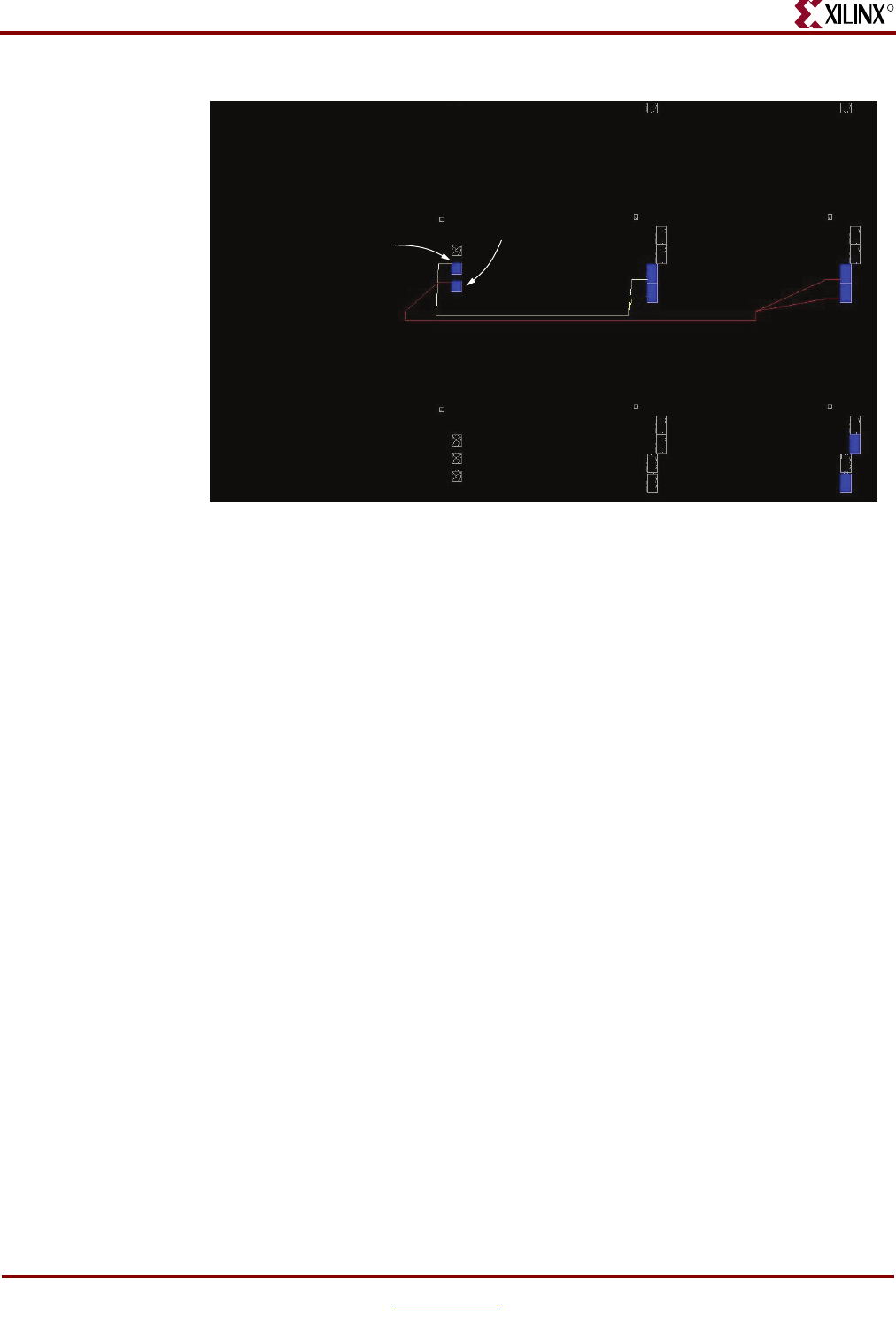
548 www.xilinx.com Memory Interface Solutions User Guide
UG086 (v3.6) September 21, 2010
Appendix A: Memory Implementation Guidelines
R
3. A byte can be swapped with another byte as long as the pin names of all the necessary
signals associated with the byte i.e., DQS, all DQ bits and DM, and the corresponding
slice location of all the signals are exchanged.
4. Within a byte, all the even-numbered DQ bits can be swapped only with the other
even-numbered bits, and odd-numbered bits only with the other odd bits because two
copies of delayed DQS strobes are generated internally for the two columns of CLBs.
One of the DQS strobes is used for the even-numbered bits and the other for the
odd-numbered bits. Each copy is delayed a specific amount of time relative to the
placement of the even (or odd) Read Data FIFOs.
5. The DQ and DQS signals should not be allocated to the IOBs of the same tile.
6. DQS and DQS# should be allocated to a differential pair, such as the pair of IOBs of a
single tile, when differential DQS is selected.
7. Memory clock signals ck and ck# should be allocated to a differential pair.
8. DQ, DQS, DM, the memory clocks, and the loopback signals (rst_dqs_div_in and
rst_dqs_div_out) should be on the same side of the FPGA.
9. The signals generated in different phases of the clocks should not be allocated in the
same I/O tile. The DM and DQ signals are generated on clk90. Thus, these signals
cannot be allocated in the same I/O tile where the address, DQS, or control signals that
are generated on clk are allocated.
10. For memory interfaces that do not provide a signal to indicate when the read data is
valid, a data-valid signal must be provided on the PCB. This loopback is used as a
write-enable signal for the Read Data FIFOs. A strobe is used to latch the data. Two
pins are needed per design: one to output the signal, and one to input the return signal.
The length of the loopback is defined as:
PCB loopback = CLK delay to memory + strobe delay
Figure A-2: I/O Pads Connecting to Two Columns of CLBs
UG086_aA_07_050509
To p p ad, assigned to
odd DQ bit, dq[1]
Bottom pad, assigned
to even DQ bit, dq[0]

Memory Interface Solutions User Guide www.xilinx.com 549
UG086 (v3.6) September 21, 2010
Generic Memory Interface Guidelines
R
11. The rst_dqs_div_in and rst_dqs_div_out signals constitute the loopback pair. To meet
the loopback delay requirement, the rst_dqs_div_in and rst_dqs_div_out signals can
be allocated in the same I/O tile.
12. The rst_dqs_div_in and rst_dqs_div_out signals should be placed at the center of the
data bits. If the number of data bytes is even, allocate them at the center of the data bits.
If it is odd, allocate them immediately either before or after the centered data byte. If
this is not done, the data capture might not be reliable. This is necessary because the
MIG design uses the RST_DQS_DIV feedback loop to generate a write enable to all the
data capture FIFOs.
If the data width is 32, allocate the rst_dqs_div pins between the second and the third
bytes. However, if the data width is 40, the rst pins can be allocated between either the
second and third bytes or the third and fourth bytes. Refer to “Verify Placement and
Routing,” page 528 for details on these verification steps. For more information on the
Spartan-3 FPGA data capture technique, see XAPP768c [Ref 24].
Pin Allocation Rules for Top/Bottom Banks
1. All DQ bits must be placed within five tiles to the right of the associated DQS location.
2. There is no restriction on swapping DQ bits within a DQS group because only one
copy of DQS is used to capture the DQ bits. Even DQ bits can be swapped with odd or
even DQ bits, and vice versa.
3. Rules 5 to 11 from “Pin Allocation Rules for Left/Right Banks,” page 546 also apply to
the top/bottom banks.
Tap Delay Circuit
The Spartan-3/3A/3A DSP FPGA DDR/DDR2 SDRAM and Spartan-3E FPGA
DDR SDRAM MIG designs include a tap delay circuit within the physical layer. See
XAPP454 [Ref 15] for details.
Proper tap delay implementation requires the circuit logic to be placed in one column. To
force the implementation tools to always place the circuit in one column, MIG 2.2 sets the
XIL_PAR_ALIGN_USER_RPMs environment variable. This is set in the ise_flow.bat
script file located in the par directory of the generated MIG output.
Proper placement of the tap_dly circuit in one column can also be implemented with
RLOC_ORIGIN constraints. This method is recommended if the environment variable
causes issues with other parts of the design or if the UCF is being used with an
EDK/MPMC design.
Note: MIG 2.3 and later sets the RLOC_ORIGIN constraints rather than using the
XIL_PAR_ALIGN_USER_RPMS environment variable.
An RLOC_ORIGIN constraint must be created when the XIL_PAR_ALIGN_USER_RPMs
environment variable is not used. The value of this constraint is dependent on the
system_clock bank selection set in the MIG GUI. MIG allows the system_clocks to be
placed in either top or bottom banks. MIG 2.3 and later generates the required
RLOC_ORIGIN constraints in the UCF file for placing the tap_delay circuits.
Note: The tap_dly circuit should be in the same top/bottom location as the BUFG that drives the
memory clock.
These are the guidelines to use the RLOC_ORIGIN constraints for the UCF generated prior
to MIG 2.3:

550 www.xilinx.com Memory Interface Solutions User Guide
UG086 (v3.6) September 21, 2010
Appendix A: Memory Implementation Guidelines
R
Top Bank Selection
The MIG output UCF includes an AREA_GROUP constraint on cal_ctl. The first value in
the RANGE of this constraint is the value in the added RLOC_ORIGIN constraint. An
example AREA_GROUP from a MIG output UCF is:
AREA_GROUP "cal_ctl" RANGE = SLICE_X74Y190:SLICE_X85Y203;
The first value in the range is X74Y190. This is the new RLOC_ORIGIN value. The syntax
for the new constraint to add to the UCF file is:
INST "infrastructure_top0/cal_top0/tap_dly0/l0" RLOC_ORIGIN = X74Y190;
Bottom Bank Selection
The MIG output UCF includes an AREA_GROUP constraint on cal_ctl. To calculate the
RLOC_ORIGIN constraint, take the first value in the AREA_GROUP RANGE and add 10
to the X coordinate. An example AREA_GROUP from a MIG output UCF is:
AREA_GROUP "cal_ctl" RANGE = SLICE_X74Y4:SLICE_X85Y17;
The first value in the range is X74Y4. The new RLOC_ORIGIN value is X84Y4 because 10 is
added to the X coordinate. The syntax for the new constraint to be added to the UCF file is:
INST "infrastructure_top0/cal_top0/tap_dly0/l0" RLOC_ORIGIN = X84Y4;
Verification of Tap Delay Circuit Placement
To verify placement of the tap_dly circuit:
1. Open the post-PAR design.ncd and design.pcf files in FPGA Editor.
2. Select Routed Nets from the List window located at the top left-hand corner. This
shows all the routed net names of the design.
3. Enter *tap_dly*/tap* in the Name Filter window to select the tap_dly chain.
4. Select all the nets displayed, and click the Apply button on the right-hand side of the
Name Filter window.
5. Zoom into the area in the Array window where the selected routes are highlighted.
If properly constrained, the logic is located in a single column in four sequential CLBs. This
indicates that the RLOC_ORIGIN is correct.
The screen capture in Figure A-3 shows an example of the correct placement of the tap_dly
circuits:
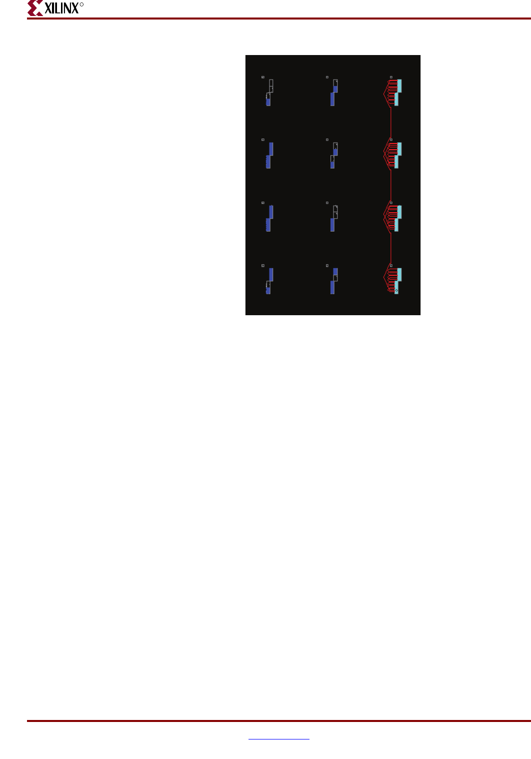
Memory Interface Solutions User Guide www.xilinx.com 551
UG086 (v3.6) September 21, 2010
Generic Memory Interface Guidelines
R
Note: The hierarchy structure and the naming convention shown in Figure A-3 refer to the
MIG generated design. Any change in design hierarchy and naming convention should be taken into
account.
Virtex-4 FPGA Direct-Clocking Pins
1. For flexibility of design techniques, it is recommended that all strobe signals be placed
on clock-capable inputs (such as DQS, CQ, and QK) with P connected to the P side and
N connected to the N side of the pair. If only single-ended strobes are provided, the
signal is placed on the P input of the clock-capable I/O pair.
2. Data lines used to read data from a memory are placed in the same bank as their
associated strobe. Data is captured with an internal FPGA clock. Data is delayed
through the IDELAY element to make it center-aligned with the FPGA clock. The
strobe is used to find the data delay with respect to the FPGA clock.
3. Address and control signals are to be placed together in the same bank (see “Memory-
Specific Guidelines,” page 554 for exceptions) or placed in banks near each other to
minimize the route delays for these signals inside the FPGA.
4. DDRII SRAM ONLY: For memory interfaces that do not provide a data valid signal to
indicate when the read data is valid, a data valid signal is to be provided on the PCB.
This loopback is used as a write-enable signal for the Read Data FIFOs. A strobe is
used to latch the data. Two pins are needed per bank: one to output the signal and one
to input the return signal. The length of the loopback is:
PCB loopback = CLK delay to memory + strobe delay
Virtex-4 FPGA direct-clocking designs that place the strobe on clock-capable I/O should
follow the pin-swapping recommendations for the Virtex-4 SerDes and Virtex-5 FPGA
designs. If the strobe is not placed on clock-capable I/O, an entire DQS group (containing
Figure A-3: Proper Tap Delay Circuit Placement
UG086_aA_06_020109

552 www.xilinx.com Memory Interface Solutions User Guide
UG086 (v3.6) September 21, 2010
Appendix A: Memory Implementation Guidelines
R
data, strobe, and data mask) can be swapped with any other DQS group in same bank. The
initial pinout that MIG selects also affects the amount of calibration logic MIG generates.
MIG generates one calibration unit for each bank that contains data bits. Therefore, a DQS
group cannot be swapped with other byte groups on different banks without appropriate
modification to the source code. Within a DQS group, data bits can be swapped with other
data bits, and the data signals should be placed on pins near the associated DQS strobe.
Virtex-4 FPGA SerDes Clocking and Virtex-5 FPGA Pins
1. All strobe signals must be placed on clock-capable inputs (such as DQS, CQ, and QK)
with P connected to the P side and N connected to the N side of the pair. If only single-
ended strobes are provided, the signal is placed on the P input of the clock-capable I/O
pair.
2. Data lines used to read data from a memory are placed in the same bank as their
associated strobe. Data is captured in the ISERDES block using the strobe signal. The
strobe is passed through the BUFIO to delay it with respect to the data input.
3. Address and control signals are to be placed together in the same bank (see “Memory-
Specific Guidelines,” page 554 for exceptions) or placed in banks near each other to
minimize the route delays for these signals inside the FPGA.
4. DQ signals can transition simultaneously. Concentrating many of them in an I/O bank
increases the amount of simultaneous switching noise the I/O bank will experience.
Under some conditions it may be desirable to spread the DQ bytes across as many I/O
banks as is feasible in the design, back-filling the same banks with address and control
signals. Before committing to a PCB layout, check the timing carefully via a place and
route run, and check the Simultaneously Switching Output limits.
Virtex-4 SerDes clocking and Virtex-5 FPGA designs must place the strobe on clock-
capable I/O with the data for the said strobe placed in the same bank. A byte can be
swapped with another byte as long as all the necessary signals associated with that byte
(strobe, data, and data mask) are located in the same bank. Within a bank, strobes can be
swapped with other strobes while the rest of the pins in a bank can be swapped as needed.
The Virtex-5 FPGA DDR2 design uses a combination of the IOB flop (IDDR) and fabric-
based flops for read data capture. This requires the use of pinout-dependent directed-
routing and location constraints. If pinouts are changed manually, the UCF must be
modified. Refer to Appendix B, “Pinout-Related UCF Constraints for Virtex-5 FPGA DDR2
SDRAMs” for details.
Te r m i n a t i o n
These rules apply to termination:
1. IBIS simulation is highly recommended for all high-speed interfaces.
2. Single-ended signals are to be terminated with a pull-up of 50Ω to VTT at the load (see
Figure A-4). A split 100Ω termination to VCCO and 100Ω termination to GND can be
used (see Figure A-5), but takes more power. For bidirectional signals, the termination
is needed at both ends of the signal (DCI/ODT or external termination).
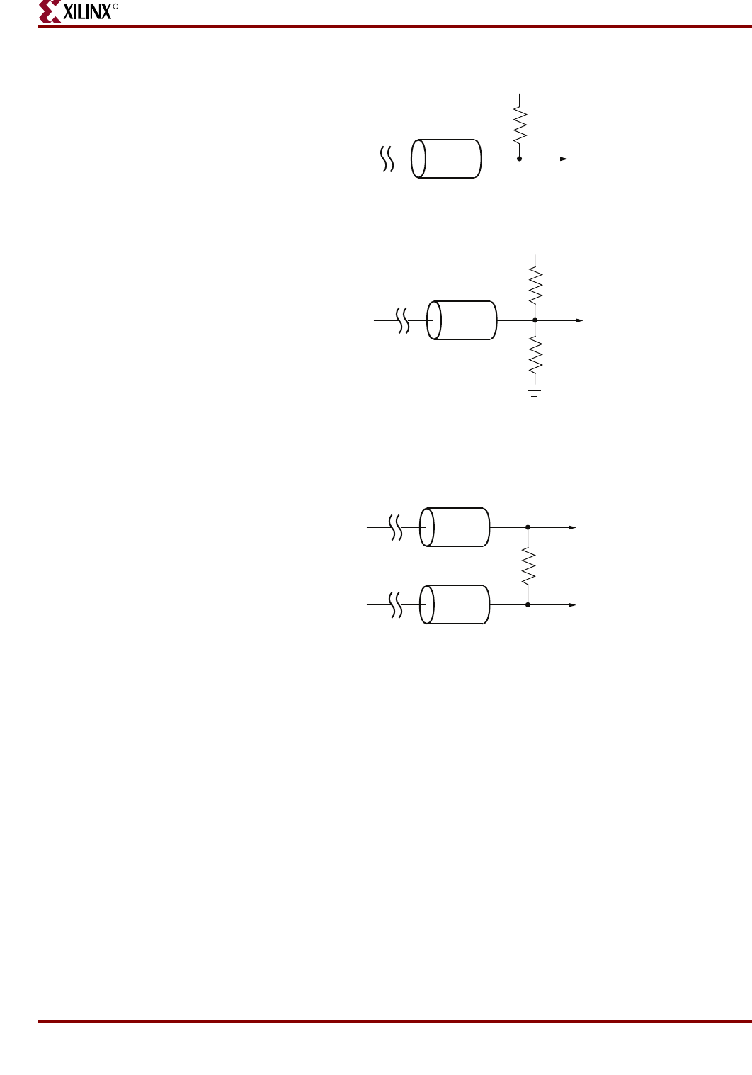
Memory Interface Solutions User Guide www.xilinx.com 553
UG086 (v3.6) September 21, 2010
Generic Memory Interface Guidelines
R
3. Differential signals are to be terminated with a 100Ω differential termination at the
load (see Figure A-6). For bidirectional signals, termination is needed at both ends of
the signal (DCI/ODT or external termination).
4. All termination must be placed as close to the load as possible. The termination can be
placed before or after the load provided that the termination is placed within one inch
of the load pin.
5. DCI can be used at the FPGA as long as the DCI rules are followed (such as
VRN/VRP).
I/O Standards
These rules apply to the I/O standard selection for DDR SDRAMs:
• MIG-generated designs use the SSTL2 CLASS I I/O standard by default for memory
address and control signals, and use the SSTL2 CLASS II I/O standard for memory
data, data-mask, and data-strobe signals. When DCI is selected in MIG, DCI for SSTL2
CLASS I can be applied only to memory interface signals that are inputs to the FPGA.
• The user can select CLASS II or CLASS I I/O standards from MIG. When SSTL2
CLASS II is selected in MIG, it is applied to all the memory interface signals.
• When DCI is selected in MIG, the DCI I/O standard is applied to all the memory
interface signals.
Figure A-4: 50Ω Termination to VTT
Figure A-5: 100Ω Split Termination to VCCO and GND
Figure A-6: 100Ω Differential Termination
UG086_aA_02_022208
ZQ =
50Ω
RT =
50Ω
VTT
LoadSource
UG086_aA_03_022208
ZQ =
50Ω
2 * ZQ =
100Ω
2 * ZQ =
100Ω
V
CCO
LoadSource
UG086_aA_04_020406
ZQ =
50Ω
2 * ZQ =
100Ω
Load_PSource_P
ZQ =
50ΩLoad_NSource_N

554 www.xilinx.com Memory Interface Solutions User Guide
UG086 (v3.6) September 21, 2010
Appendix A: Memory Implementation Guidelines
R
These rules apply to the I/O standard selection for DDR2 SDRAMs:
• MIG-generated designs use the SSTL18 CLASS II I/O standard by default for all
memory interface signals. When DCI is selected in MIG, DCI for SSTL18 CLASS II is
applied on input, output, and in-out memory interface signals.
• CLASS II is recommended for all SSTL signals in memory interfaces. However, better
signal integrity can sometimes be achieved with CLASS I for the address/control
group. The user can select between CLASS II or CLASS I I/O standards from the MIG
tool. Based on the IBIS simulation results, the CLASS should be selected in the GUI.
• Selection of the CLASS option is allowed only for the address/control group in
Virtex-4 and Virtex-5 FPGA designs. Data group signals always use the SSTL18
CLASS II I/O standard. When SSTL18 CLASS I is selected in the MIG tool, the
I/O standard for differential signals (such as memory clocks) remains SSTL18
CLASS II.
• CLASS can be selected for both data and address/control groups in
Spartan-3 FPGA designs. When SSTL18 CLASS I is selected in the MIG tool, the
I/O standard for all signals of the selected group is SSTL18 CLASS I.
• When DCI is selected in MIG for SSTL18 CLASS I, the DCI I/O standard is applied
only to memory interface signals that are outputs to the FPGA.
Trace Lengths
Trace length matching must also include the package delay information. The PARTGen
utility [Ref 33] generates a .pkg file that contains the package trace length in microns for
every pin of the device under consideration.
For example, to obtain the package delay information for a Virtex-5 LX50T-FF1136 device
used on an ML561 board, issue the following command within a DOS command shell:
partgen -v xc5vlx50tff1136
This generates an xc5vlx50tff1136.pkg file in the current directory with package trace
length information for each pin (unit: micron or µm). Use the typical 6.5 fs per micron
(6.5 ps per millimeter) conversion formula to obtain the corresponding electrical
propagation delay. While applying specific trace-matching guidelines for each of the
memory interfaces as described below, consider this additional package delay term for the
overall electrical propagation delay. Note that different die in the same package may have
different delays for the same package pin. If this case is expected, average the values
appropriately.
Calibration factors out PCB trace mismatches during reads, but the trace matching
requirements are needed during writes.
Memory-Specific Guidelines
Each memory interface has three sections:
• Pin assignments
•Termination
•Trace lengths
Trace lengths given are for high-speed operation and can be relaxed depending on the
applications target bandwidth requirements. Be sure to include the package delay when
determining the effective trace length. These internal delays can be found through the
PACE tool.
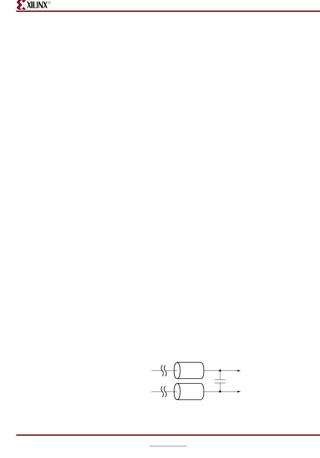
Memory Interface Solutions User Guide www.xilinx.com 555
UG086 (v3.6) September 21, 2010
Memory-Specific Guidelines
R
DDR/DDR2 SDRAM
Pin Assignments
These rules apply to pin assignments for DDR and DDR2 SDRAM:
1. The DQ and DM bits of a byte are to be placed in the same bank as the associated DQS.
The DQ bits must be kept close together for better routing.
2. Address and control signals are to be placed in the same bank or placed in banks near
each other.
If all control signals cannot fit in one bank, CK, ODT, and CKE should be selected first
for placement in another bank.
3. Spartan FPGA designs require a loopback signal. The loopback signal should be
placed at the center of the DQ bits.
If a bank is pin-limited and there is a need to free up a few pins, the following actions are
to be considered:
1. The loopback signals can be eliminated in Virtex-4 FPGA MIG designs because they
are no longer required.
2. The CKE signals can be tied together for multiple devices.
3. For DIMMs, non-critical features need not be implemented, such as
PAR_IN/PAR_OUT and the SPD interface (SA, SPD, SCL).
The loading of address (A, BA), command (RAS_N, CAS_N, WE_N), and control (CS_N,
ODT) signals depends on various factors, such as speed requirements, termination
topology, use of unbuffered DIMMs, and multiple rank DIMMs.
The address and command signals should be implemented with 2T clocking, i.e., asserted
for two cycles, so these signals can handle higher loading without impacting the timing
budget. Virtex-4 FPGA SerDes designs and Virtex-5 FPGA DDR2 designs are implemented
with 2T clocking of address and command signals.
The control signals (CS_N and ODT) have 1T clocking, and so their replication is
recommended when the loading is higher. If the application is pin-limited to implement
lighter loading on critical clock signals going to memory, it might be necessary to use an
external PLL to generate multiple copies of the clock signals.
For descriptions of 1T and 2T clocking, refer to Micron technical note TN-47-01[Ref 36].
Termination
These rules apply to termination for DDR/DDR2 SDRAM:
1. For DIMMs, the CK signals are to be terminated by a 5 pF capacitor between the two
legs of the differential signal instead of the 100Ω resistor termination, because these
signals are already terminated on each DIMM.
Figure A-7: 5 pF Differential Termination on Clocks
UG086_aA_05_020406
ZQ =
50Ω
5 pF
Load_PCK_P
ZQ =
50ΩLoad_NCK_N

556 www.xilinx.com Memory Interface Solutions User Guide
UG086 (v3.6) September 21, 2010
Appendix A: Memory Implementation Guidelines
R
2. The ODT and CKE signals are not terminated. These signals are required to be pulled
down during memory initialization with a 4.7 kΩ resistor connected to GND.
3. ODT, which terminates a signal at the memory, applies to the DQ/DQS/DM signals
only. If ODT is used, the Mode register must be set appropriately in the RTL design.
4. The Virtex-5 FPGA DDR2 interface requires that if parallel termination is used at the
memory end, it must be ODT rather than external termination resistor(s). This is a
requirement of the read capture scheme used.
To save board space, DCI at the FPGA and ODT at the memory can be used to minimize the
number of external resistors on the board.
Trace Lengths
These rules indicate the maximum electrical delays between DDR/DDR2 SDRAM signals
at 333 MHz:
1. ± 25 ps maximum electrical delay between any DQ and its associated DQS/DQS#
2. ± 50 ps maximum electrical delay between any address and control signals and the
corresponding CK/CK#
3. ± 100 ps maximum electrical delay between any DQS/DQS# and CK/CK#
QDRII SRAM
Pin Assignments
These rules apply to pin assignments for Virtex-4 FPGA QDRII SRAM:
1. All CQ signals are placed on clock-capable pins, if the Use CC option is selected;
otherwise any I/O pin is used. CQ is only connected to the P side of the P-N pair.
2. The Q bits of a byte are placed in the same bank as its associated CQ.
The Q bits must be kept close together for optimal routing.
These rules apply to pin assignments for Virtex-5 FPGA QDRII SRAM:
1. All CQ/CQ# signals are placed on clock-capable pins. CQ and CQ# are connected only
to the P side of the CC P-N pair.
2. The Q bits of a byte are placed in the same bank as its associated CQ/CQ#.
The Q bits must be kept close together for optimal routing.
Termination
These rules apply to termination of QDRII SRAM signals:
1. Termination of the qdr_dll_off_n signal should be done based on the recommendation
of the memory vendor. If the vendor requires this signal to be driven by the FPGA, this
signal should be pulled down with a 4.7 kΩ resistor connected to GND. However, if
the vendor requires this signal not to be driven by the FPGA, this signal should be
connected to a pull-up resistor with a value recommended by the SRAM vendor.
2. DCI can also be used on CK for QDRII+ support (QVLD signal from memory to
FPGA).
To save board space, DCI is to be used at the FPGA to minimize the number of external
resistors on the board.

Memory Interface Solutions User Guide www.xilinx.com 557
UG086 (v3.6) September 21, 2010
Memory-Specific Guidelines
R
I/O Standards
These rules apply to the I/O Standard selection for QDRII SRAM.
• MIG-generated designs use the HSTL CLASS I I/O standard by default for all
memory interface signals.
• When DCI is selected in MIG, the DCI standard for HSTL CLASS I is applied only to
memory interface signals that are inputs to FPGA.
Trace Lengths
These rules provide the maximum electrical delays between QDRII SRAM signals:
1. ± 25 ps maximum electrical delay between data and its associated CQ.
2. ± 50 ps maximum electrical delay between address and control signals.
3. ± 100 ps maximum electrical delay between address/control and data.
4. ± 100 ps maximum electrical delay between address/control and K/K# clocks.
5. ± 25 ps maximum electrical delay between data (write port) and K/K# clocks.
6. There is no relation between CQ and the K clocks. K should be matched with D, and
CQ should be matched with Q (read data).
DDRII SRAM
Pin Assignments
These rules apply to pin assignments for Virtex-4 FPGA DDRII SRAM:
1. All CQ signals are placed on clock-capable pins, if the Use CC option is selected;
otherwise, any I/O pin is used. CQ is only connected to the P side of the P-N pair.
2. The Q bits of a byte are placed in the same bank as its associated CQ. The Q bits must
be kept close together for optimal routing.
These rules apply to pin assignments for Virtex-5 FPGA DDRII SRAM:
1. All CQ/CQ# signals are placed on clock-capable pins. CQ and CQ# are connected only
to the P side of the CC P-N pair.
2. The Q bits (SIO designs) or DQ bits (CIO designs) of a byte are placed in the same bank
as its associated CQ/CQ#. The Q bits or DQ bits must be kept close together for
optimal routing.
Termination
These rules apply to termination of DDRII SRAM signals:
1. Termination of the ddr_dll_off_n signal should be done based on the recommendation
of the memory vendor. If the vendor requires this signal to be driven by the FPGA, this
signal should be pulled down with a 4.7 kΩ resistor connected to GND. If the vendor
requires this signal not to be driven by the FPGA, this signal should be connected to a
pull-up resistor with a value recommended by the SRAM vendor.
To save board space, DCI is to be used at the FPGA to minimize the number of external
resistors on the board.

558 www.xilinx.com Memory Interface Solutions User Guide
UG086 (v3.6) September 21, 2010
Appendix A: Memory Implementation Guidelines
R
I/O Standards
These rules apply to the I/O Standard selection for DDRII SRAM:
• MIG-generated designs use the HSTL CLASS I I/O standard by default for all
memory interface signals except the DQ/Q and CQ/CQ# signals.
• When DCI is selected in the MIG tool, the DCI standard for HSTL CLASS I is applied
only to memory interface signals that are inputs to the FPGA, except the CQ/CQ# and
DQ/Q signals where the HSTL CLASS II DCI standard is applied.
Trace Lengths
These rules provide the maximum electrical delays between DDRII SRAM signals:
1. ± 25 ps maximum electrical delay between data and its associated CQ.
2. ± 50 ps maximum electrical delay between address and control signals.
3. ± 100 ps maximum electrical delay between address/control and data.
4. ± 100 ps maximum electrical delay between address/control and K/K# clocks.
5. ± 25 ps maximum electrical delay between data (write port) and K/K# clocks.
6. There is no relation between CQ and the K clocks. K should be matched with D, and
CQ should be matched with Q (read data).
RLDRAM II
Pin Assignments
These rules apply to pin assignments for RLDRAM II:
1. All QK signals are to be placed on Clock-Capable I/O pairs if the Use CC option is
selected in the tool; otherwise normal I/O pins are used. P is connected to the P side
and N is connected to the N side of the pair.
2. The DQ bits of a byte are placed in the same bank as the associated QK.
The DQ bits must be kept as close as possible for optimal routing.
3. The loopback signal is not required because RLDRAM II provides a data valid signal
for capturing the read data.
If the design is pin constrained, only common I/O (CIO) can use a bidirectional DQ data
bus.
Termination
This rule applies to termination of RLDRAM II signals:
1. DCI can be used on DQ/QK at the FPGA provided that DCI rules are followed (such
as VRN/VRP).
To save board space, use DCI at the FPGA and ODT at the memory to minimize the
number of external resistors on the board.
I/O Standards
These rules apply to the I/O Standard selection for RLDRAM II:

Memory Interface Solutions User Guide www.xilinx.com 559
UG086 (v3.6) September 21, 2010
Memory-Specific Guidelines
R
• MIG-generated designs use the HSTL CLASS II I/O standard by default for all
memory interface signals. When DCI is selected in MIG, DCI for HSTL CLASS II is
applied on input, output, and in-out memory interface signals.
• The user can change the I/O standard to HSTL CLASS I. When DCI is selected in
MIG, DCI for HSTL CLASS I is applied only to the memory interface signals that are
inputs to the FPGA.
• To have HSTL CLASS I on the required pins, the user must manually edit the UCF
constraint file for the corresponding design generated.
Trace Lengths
These rules provide the maximum electrical delays between RLDRAM II signals:
1. ± 25 ps maximum electrical delay between data and its associated QK.
2. ± 50 ps maximum electrical delay between address and control signals.
3. ± 100 ps maximum electrical delay between address/control and data.


Memory Interface Solutions User Guide www.xilinx.com 561
UG086 (v3.6) September 21, 2010
R
Appendix B
Pinout-Related UCF Constraints for
Virtex-5 FPGA DDR2 SDRAMs
Introduction
The Virtex®-5 FPGA DDR2 design generated by MIG requires a number of UCF
constraints. The values of these UCF constraints might need to be changed if, after using
MIG to generate the design, the user changes the data strobe (DQS) pin (and, by extension,
the DQ data pin) assignments. In addition, these constraints might need to be changed, or
in some cases, added when updating from an older version of the DDR2 design.
Update Design should always be used to update the design and regenerate the updated
constraint values. This chapter describes the parameters/UCF constraints that are
modified by the Update Design option, and the architectural reasons why the UCF
constraints are required. For more information on Update Design, see “Verify UCF and
Update Design and UCF” in Chapter 1.
Update Design should be used in these situations:
• The user has a DDR2 design generated using an older version of MIG and needs to
upgrade to the latest version of the DDR2 interface
• The user has generated a design using the latest version of MIG and needs to make
modifications to the pinout that affect the location of the strobe (DQS) pins. This
would occur if the user is swapping DDR2 data byte locations to improve PCB
routability.
Historically, additional pinout-related constraints (other than pin number LOC
constraints) were not required for MIG 1.73 or earlier DDR2 designs. Because of changes to
the read data capture circuitry, these constraints were required starting with MIG 2.0
designs. With MIG 3.0, the required pinout-related constraints have been significantly
simplified but not completely eliminated. This section discusses the relevant parameters
and constraints for MIG 3.0 and later.
Read Data Capture Block Diagram
The read capture path used for the MIG Virtex-5 FPGA DDR2 interface consists of these
subblocks:
• DQ is initially captured using DQS in the IOB using the IDELAY and IDDR elements.
• Data is transferred to the FPGA (CLK0) clock domain using a series of flip-flops
located in the fabric. The location of these flip-flops, and the routes between the IDDR
and fabric flip-flops, must be carefully defined and matched. In MIG 2.x designs, the
flip-flop locations and routing are defined using a combination of RPMs and directed
routing constraints. With MIG 3.0, attributes such as XIL_PAR_SKEW and
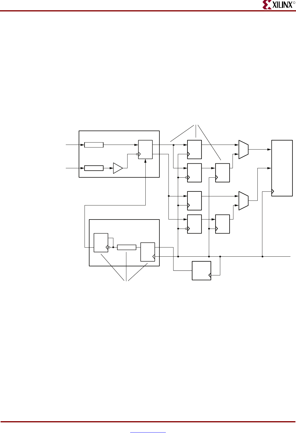
562 www.xilinx.com Memory Interface Solutions User Guide
UG086 (v3.6) September 21, 2010
Appendix B: Pinout-Related UCF Constraints for Virtex-5 FPGA DDR2 SDRAMs
R
XIL_PAR_DELAY are embedded in the RTL to allow the ISE® tools to place and route
this circuit and meet the required net delay and intra-net skew without the use of the
RPM and directed routing constraints.
• For each DQS, a circuit is added to disable the clock enable (CE) pin to each of the
corresponding DQ capture IDDRs at the end of a read burst (“DQS Gate”). The
placement and routing of this circuit is also critical and is defined by a combination of
LOC and MAXDELAY constraints in the UCF.
Figure B-1 shows the read capture path architecture for the MIG Virtex-5 FPGA DDR2
design, as well as the various portions of the capture path that are affected by the
additional UCF constraints.
Pinout-Related UCF Changes Overview
When updating a design whose pinout has been modified, MIG makes specific changes to
the UCF file. For each DQS pin:
• A location constraint pair for an IDELAY (input delay element) and IOB flip-flop must
be specified. These two elements are used in the DQS Gate circuit, of which there is
one per DQS group. The value of the LOC constraint for the IDELAY and IOB flip-flop
are determined by the pin location for the corresponding DQS IOB. The rules for
determining this value are outlined in “Setting UCF Constraints,” page 563.
• A location constraint for a single fabric flip-flop must be specified. This locks the
flip-flop used to drive the DQS Gate signal close to its corresponding IDELAY. This is
required to reduce the total net delay on this route, and therefore the delay
Figure B-1: Virtex-5 FPGA DDR2 Read Capture Path, MIG 3.1 or Later
DQS Gate
QD
QD
Q1
Q2
D
IDDR
CE
QD
QD
QDQD
IDELAY
IDELAY
DQ
DQSBUFIO
Read
Data
Transfer
Logic
DQS Gate
Specify locations for components used for DQS Gate circuit
FPGA Clock
The ISE software places and routes to these fabric flip-flops based on
XIL_PAR_SKEW and XIL_PAR_DELAY attributes embedded in the RTL
IDELAY
D
IOB Flip-Flop
QDQ
PHY
Control
Logic
UG086_aB_01_043009

Memory Interface Solutions User Guide www.xilinx.com 563
UG086 (v3.6) September 21, 2010
Read Data Capture Block Diagram
R
fluctuations on this line due to voltage/temperature. The rules for determining this
value are outlined in “Setting UCF Constraints.”
Setting UCF Constraints
Beyond the typical constraints found in a UCF file (e.g., the PERIOD timing constraint,
pinout LOC, and IOSTANDARD constraints for I/O), the Virtex-5 FPGA DDR2 interface
also requires three other classes of constraints to be added to the UCF file. (These
constraints are updated upon using the Update Design option.) MIG automatically
generates the correct values of these constraints for a new design and updates the values
when Update Design is used. These values are based on the pinout and
speed grade/operating frequency of the design. The three classes of constraints are:
1. Location (LOC) constraints for the IDELAY and IOB flip-flop blocks used for every
DQS Gate circuit. There is one DQS Gate circuit per DQS I/O.
2. MAXDELAY constraints to limit the delay timing-critical paths related to IOB
timing. This is not required to meet any specific cycle-to-cycle timing requirement, but
rather to limit any post-calibration voltage/temperature related changes to the net
delay. Voltage/temperature variations on a particular net increase as the total net delay
increases.
It is critical to reduce the delay on the DQS gate control input. This signal is generated in the
CLK0 clock domain and synchronized via an IDELAY to the DQS domain. The
synchronization between the CLK0 and DQS domains on this control net is established
once during initial calibration. Calibration accounts for the “static” delay component
of these nets. However, post-calibration changes in net delay are not accounted for and
must be minimized.
3. FROM-TO constraints:
a. One FROM-TO constraint limits the DQS Gate path from the IOB flip-flop to the
DQ CE pins to be approximately one-half clock cycle. This ensures that the DQ
clock enables are deasserted before any possible DQS glitch at the end of the read
postamble can arrive at the input to the IDDR. This value is clock-frequency
dependent:
INST "*/gen_dqs*.u_iob_dqs/u_iddr_dq_ce" TNM = "TNM_DQ_CE_IDDR";
INST "*/gen_dq*.u_iob_dq/gen_stg2_*.u_iddr_dq" TNM =
"TNM_DQS_FLOPS";
TIMESPEC "TS_DQ_CE" = FROM "TNM_DQ_CE_IDDR" TO "TNM_DQS_FLOPS"
1.6 ns;
b. Additional FROM-TO constraints define multi-cycle paths in the design. These are
added to help meet internal (fabric) timing at the higher supported frequencies. At
lower frequencies of operation, these multi-cycle path constraints might not be
required and can be removed.
Constraint class (1) is discussed in this section. Classes (2) and (3) are not discussed. Their
values do not need to change if the pinout is modified.

564 www.xilinx.com Memory Interface Solutions User Guide
UG086 (v3.6) September 21, 2010
Appendix B: Pinout-Related UCF Constraints for Virtex-5 FPGA DDR2 SDRAMs
R
Determining FPGA Element Site Locations
Setting the correct location constraint for the IDELAY in a DQS Gate circuit requires that
the site name for the location where the corresponding DQS_N pin is placed be correctly
specified. For example, on an XC5VLX50T-FF1136 device, if DQS_N[0] is located on pin
C13, the site name for this location must be known. In this case, it is “IOB_X2Y216” and the
LOC constraint is set to:
INST "*/gen_dqs[0].u_iob_dqs/u_iodelay_dq_ce" LOC = "IODELAY_X2Y216";
MIG automatically determines the correct site names when generating a new design or
updating an existing design. Site names can also be determined graphically using FPGA
Editor, or by using the PARTGen utility to generate a package file for the appropriate
device/package combination in text format.
Setting DQS Gate Circuit Location Constraints
Each DQS Gate circuit requires the use of an IDELAY and IOB flip-flop in addition to
fabric-based slice resources. The IDELAY and IOB flip-flop for each DQS Gate circuit, as
well as the fabric flip-flop driving the IDELAY must be manually located in the UCF file.
There are three constraints for every DQS in the design.
The IDELAY and IOB flip-flop must be taken from an IOB site where these resources are
available, specifically an IOB site that is used only as an output, or is totally unused. This
can be one of the following:
• The DQS_N negative-side I/O site of the DQS differential I/O pair of the
corresponding DQS group. A differential I/O pair does not use the input-side
resources on the N-side leg of the pair.
• The DM output site for the corresponding DQS group. The DM is an output-only site,
and its input-side resources are available for use by the DQS Gate circuit.
• Any IOB site that is either output-only, or unused.
The best site to use is one that is closest in proximity on the FPGA die to the four or eight
DQ I/O sites in that DQS group. This reduces the routing delay on the clock enable control
from the DQS Gate circuit to its corresponding DQ sites. At higher frequencies, this can
often be the critical timing path, because there is only about half a clock cycle for this path.
MIG always chooses to place the IDELAY and IOB flip-flop on the DQS_N site for the
corresponding DQS group. However, depending on the particular user pinout, a better site
might be available. The user might have to relocate the DQS Gate location(s) to other sites
in order to meet timing.
The IDELAY and IOB flip-flop for a given DQS Gate circuit must be placed at the same site.
They cannot be placed on different sites.
These constraints are used for locating the IDELAY and IOB flip-flop:
INST "*/gen_dqs[<x>].u_iob_dqs/u_iddr_dq_ce" LOC = "ILOGIC_<SITE>";
INST "*/gen_dqs[<x>].u_iob_dqs/u_iodelay_dq_ce" LOC = "IODELAY_<SITE>";
Where <x> denotes the DQS group number, and <SITE> denotes the I/O site name.
For example, on an XC5VLX50T-FF1136 device, if DQS_N[0] is placed on pin K9, and this
site is chosen to locate the IDELAY and IOB flip-flop for the DQS Gate circuit for DQS[0],
the constraints are:
INST "*/gen_dqs[0].u_iob_dqs/u_iddr_dq_ce" LOC = "ILOGIC_X2Y218";
INST "*/gen_dqs[0].u_iob_dqs/u_iodelay_dq_ce" LOC = "IODELAY_X2Y218";

Memory Interface Solutions User Guide www.xilinx.com 565
UG086 (v3.6) September 21, 2010
Read Data Capture Block Diagram
R
The fabric flip-flop driving the IDELAY with the DQS Gate control pulse must also be
location constrained to be near the corresponding IDELAY/IOB flip-flop. The rules for
determining this are:
• Locate the IOB where the corresponding IDELAY and IOB flip-flop are location
constrained.
• Use the appropriate package file to find the “nearest CLB.” Location constraint this
flip-flop to this location.
For example, on an XC5VLX50T-FF1136 device, if DQS_N[0] is placed on pin N30, the
location constraint for the corresponding DQS Gate fabric flip-flop is:
INST "*/gen_dqs[0].u_iob_dqs/u_iodelay_dq_ce" LOC = "IODELAY_X2Y218";
The reason for this requirement is to minimize the net delay from the output of the DQS
Gate fabric flip-flop to the synchronizing IDELAY (see the discussion of why MAXDELAY
constraints are used in this design in “Setting UCF Constraints,” page 563). It is possible to
not constrain this flip-flop to a specific location (or constrain it to a different location) as
long as the corresponding MAXDELAY for this net can be met (i.e., by allowing MAP to
place this flip-flop).
Verifying UCF/HDL Modifications
The user can verify that the modifications to the UCF and HDL top-level files are correct by
verifying that all timing requirements have been met. For more information on verifying
timing constraints for the Virtex-5 FPGA DDR2 design, refer to “Constraints” in Chapter 9.


Memory Interface Solutions User Guide www.xilinx.com 567
UG086 (v3.6) September 21, 2010
R
Appendix C
WASSO Limit Implementation
Guidelines
Overview
This appendix provides information about WASSO (Weighted Average Simultaneous
Switching Output) limit implementation in the bank selection from MIG. It is
recommended to use a WASSO calculator before the number of pins selected in a bank.
MIG limits the number of outputs/inouts allocated in a bank based on the WASSO limit
entered for that bank in bank selection page. WASSO is supported for all FPGA families.
Ground bounce must be controlled to ensure proper operation of high-performance FPGA
devices. Particular attention must be applied to minimizing board-level inductance during
PCB layout.
When multiple output drivers change state at the same time, power supply disturbances
occur. These disturbances can cause undesired transient behavior in output drivers, input
receivers, or in internal logic. These disturbances are often referred to as Simultaneous-
Switching Output (SSO) noise. The SSO limits govern the number and type of I/O output
drivers that can be switched simultaneously while maintaining a safe level of SSO noise.
SSO of an individual bank is calculated by summing the SSO contributions of the
individual I/O standards in the bank. The SSO contribution is the percentage of full
utilization of any one I/O standard in any one bank. WASSO calculation is done by
combining the SSO contributions of all I/Os in a bank into a single figure.
WASSO calculation differs for Virtex®-4 and Virtex-5 devices:
•Virtex-4 FPGA User Guide [Ref 7] provides more information on WASSO calculation
for Virtex-4 devices.
•Virtex-5 FPGA User Guide [Ref 10] provides more information on WASSO calculation
for Virtex-5 devices.
A Microsoft Excel-based spreadsheet entitled “WASSO Calculator” is provided to
automate these calculations. The WASSO calculator uses PCB geometry, such as board
thickness, via diameter, and breakout trace width and length, to determine board
inductance. It determines the smallest undershoot and logic-Low threshold voltage among
all input devices, calculates the average output capacitance, and determines the SSO
allowance by taking into account all of the board-level design parameters mentioned in
this document. In addition, the WASSO calculator performs checks to ensure the overall
design does not exceed the SSO allowance.
The Virtex-4 FPGA WASSO Calculator [Ref 34] and the Virtex-5 FPGA WASSO Calculator
[Ref 35] can be downloaded from the Xilinx® website. A WASSO calculator for
Spartan® devices can be downloaded from
http://www.xilinx.com/bvdocs/appnotes/xapp689.zip.

568 www.xilinx.com Memory Interface Solutions User Guide
UG086 (v3.6) September 21, 2010
Appendix C: WASSO Limit Implementation Guidelines
R
Pin Allocation Rules with WASSO Limit
MIG allocates the pins starting with exclusive data banks for CIO (Common I/O) designs
and exclusive data read banks for SIO (Separate I/O) designs, followed by data (/data
read) banks that combine with other groups. After the data(/data read) groups are filled in
the banks, MIG allocates the rest of the groups (namely data write, address, and system
control).
WASSO can be applied only on output or bidirectional pins. Hence pin allocation rules will
change when the WASSO limit is less than the available pins in the bank.
For SIO designs, data read group consists of all input pins and WASSO is not applicable on
inputs. In a bank where data read group is combined with other groups (which has output
pins), first data read group is allocated. After the data read group is allocated in that bank,
if the left over pins are less than the WASSO limit of that bank then all the pins are allocated
for the other group. If the left over pins are more than the WASSO limit of that bank, then
only the number of pins of other groups equal to the WASSO limit are allocated in that
bank.
For CIO designs, a data group consists of bidirectional, input, and output pins. WASSO is
applicable on output and bidirectional pins only. In a bank where the data group is
combined with other groups (which has output pins), the first data group is allocated. If
the WASSO limit is less than the bank pin count, then only the number of pins equal to the
WASSO limit are allocated. If the WASSO limit is equal to bank pin count, then all the pins
in the bank are allocated for data.
For CIO designs, the number of pins available in a bank or the WASSO limit of the bank
should be sufficient to allocated at least one calibration unit. A calibration unit consists of
a strobe/read clocks, associated data bits, associated data mask pins, associated data valid
signals (if available). If the number of pins available in a bank or the WASSO limit of the
bank is less than the number of pins required to allocate at least on calibration unit, then no
data group pins are allocated in that bank even if the bank is selected for the data group.
Memory Interface Solutions User Guide www.xilinx.com 569
UG086 (v3.6) September 21, 2010
R
Appendix D
SSO for Spartan FPGA Designs
Overview
Simultaneous switching output guidelines limit the number of outputs that can switch
simultaneously for a given I/O standard in a bank while maintaining a safe level of SSO
noise. Pin allocation of signals is required to meet these guidelines to reduce ground
bounce and increase signal integrity. Refer to the Simultaneously Switching Output
Guidelines section of the Spartan-3/3E/3A/3AN/3A DSP data sheets [Ref 28] [Ref 29]
[Ref 30] [Ref 31] [Ref 32] for the recommended maximum number of SSOs and other
details.
Requirements
SSO is not required to be considered in these conditions:
• The SSO value is greater than the available I/O pin count in a bank
• The simultaneously switching signal count is less than the SSO value of the bank for
the given I/O standard
The applicable I/O standards for DDR/DDR2 SDRAM address, control, and data are
SSTL2_I, SSTL2_II, SSTL18_I, and SSTL18_II. For the Spartan®-3 and Spartan-3E
platforms, the SSO limit for these standards is greater than the available pin count. For
Spartan-3A and Spartan-3A DSP devices, although the SSO limit is less than the I/O pin
count, the output signals that switch simultaneously are always less than the SSO count
value. Thus, for all the Spartan devices described here, the SSO limit does not have to be
considered for pin allocation. The DQ, DQS, address, and control signals never switch
simultaneously. During write operations, DQS is center aligned with DQ, and therefore,
they do not switch together. The address and control signals are asserted before enabling
the data.
Table D-1 shows how the number of pins allocated is less than the SSO limit for Bank 3 of
the XC3S1400A-FG676 device in a DDR2 SDRAM design.
Table D -1 : XC3S1400A-FG676 Device in DDR2 SDRAM Design
Parameter Value
Device XC3S1400A-FG676
SSO limit for the SSTL18_II I/O standard for Bank 3 81
Available I/O pin count for Bank 3 103
Memory type DDR2 SDRAM
Memory part MT47H256M8HG-3
570 www.xilinx.com Memory Interface Solutions User Guide
UG086 (v3.6) September 21, 2010
Appendix D: SSO for Spartan FPGA Designs
R
Maximum data width for the DDR2 SDRAM 56-bit
Total number of DQ and DM signals that switch
together
63
Total number of DQS ( differential) 14
Table D -1 : XC3S1400A-FG676 Device in DDR2 SDRAM Design (Cont’d)
Parameter Value

Memory Interface Solutions User Guide www.xilinx.com 571
UG086 (v3.6) September 21, 2010
R
Appendix E
Debug Port
Overview
Starting with MIG 2.2, the memory controller interface design HDL for Virtex®-5, Virtex-4,
and Spartan®-3 FPGAs adds ports to the top-level design file to allow debugging and
monitoring of the physical layer read timing calibration logic and timing. This port
consists of signals brought to the top-level HDL from the Read Calibration module (where
the read timing calibration logic resides). These signals provide information for debugging
hardware issues when calibration does not complete or read timing errors are observed in
the system even after calibration completes. For Virtex FPGA designs, these signals also
allow the user to adjust the read capture timing by adjusting the various IDELAY elements
used for data synchronization. Whereas, for Spartan-3 FPGA designs, these signals allow
the user to adjust the read capture timing by adjusting the delays on data_strobe and
rst_dqs_div signals.
Specifically, the Debug port allows the user to:
• Observe calibration status signals.
• Observe current tap values for IDELAYs used for read data synchronization for Virtex
FPGA designs.
• Observe current tap_delay values for Spartan-3 FPGA designs.
• Dynamically vary these tap values. Possible uses of this functionality include:
• Debug read data corruption issues
• Support periodic readjustment of the read data capture timing by adjusting the
tap values
• Use as a tool during product margining to determine actual timing margin
available on read data captures
Enabling the Debug Port
For Virtex-5 FPGA memory controller designs, the Debug port is enabled by setting the
top-level HDL parameter DEBUG_EN to 1. To disable the Debug port, set DEBUG_EN to
0. This prevents the synthesis of additional logic required to support the Debug port (e.g.,
logic to allow dynamic adjustment of the IDELAY taps).
For Virtex-4 FPGA memory controller designs, the Debug port is enabled by setting the
Debug Signals option in MIG.
If the design is implemented using the batch files (ise_flow.bat/create_ise.bat)
provided by MIG, ChipScope™ tool debug EDIF or NGC files (ILA/ICON/VIO) are
generated automatically by using the XCO files provided in the par folder. If batch files
(ise_flow.bat/create_ise.bat) are not used for implementing the design, the
572 www.xilinx.com Memory Interface Solutions User Guide
UG086 (v3.6) September 21, 2010
Appendix E: Debug Port
R
ChipScope tool debug EDIF or NGC files should be manually generated. Refer to
readme.txt located in the par folder for a set of commands to be executed before
starting synthesis and PAR to generate the EDIF or NGC files.
Signal Descriptions
The tables in this section provide the Debug port signal descriptions for the various
memory and FPGA combinations. All the signal directions are with respect to the RTL
design.
•Table E-1, “DDR2 SDRAM Signal Descriptions (Virtex-5 FPGAs),” page 572
•Table E-2, “DDR SDRAM Signal Descriptions (Virtex-5 FPGAs),” page 575
•Table E-3, “QDRII SRAM Signal Descriptions (Virtex-5 FPGAs),” page 578
•Table E-4, “DDR2 SDRAM Signal Descriptions (Virtex-4 FPGAs),” page 582
•Table E-5, “DDR SDRAM Signal Descriptions (Virtex-4 FPGAs),” page 583
•Table E-6, “DDRII SRAM Signal Descriptions (Virtex-4 FPGAs),” page 584
•Table E-7, “QDRII SRAM Signal Descriptions (Virtex-4 FPGAs),” page 586
•Table E-8, “RLDRAM II Signal Descriptions (Virtex-4 FPGAs),” page 588
•Table E-9, “DDR/DDR2 SDRAM Signal Descriptions (Spartan-3 FPGAs),” page 589
Virtex-5 FPGA: DDR2 SDRAM
All debug ports signals are clocked using the half-frequency clock (clkdiv). Increment and
decrement control signals (e.g., dbg_idel_up_all) must be provided synchronously with
clkdiv. IDELAY select signals, such as dbg_sel_all_idel_dqs and dbg_sel_idel_dqs can
change asynchronous to clkdiv, but must meet setup and hold requirements on clkdiv on
cycles when the corresponding increment/decrement control signal is asserted.
Table E-1: DDR2 SDRAM Signal Descriptions (Virtex-5 FPGAs)
Bus Name I/O Width Description
dbg_calib_done O 4 Each bit is driven to a static 1 as each stage of
calibration is completed. dbg_calib_done[0]
corresponds to Stage 1.
dbg_calib_dq_tap_cnt O 6*DQ_WIDTH 6-bit tap count for each DQ IDELAY.
dbg_calib_dq_tap_cnt[5:0] corresponds to
DQ[0].
dbg_calib_dqs_tap_cnt O 6*DQS_WIDTH 6-bit tap count for each DQS IDELAY.
dbg_calib_dqs_tap_cnt[5:0] corresponds to
DQS[0].
dbg_calib_gate_tap_cnt O 6*DQS_WIDTH 6-bit tap count for each DQS Gate IDELAY.
dbg_calib_gate_tap_cnt[5:0] corresponds to
the DQS Gate for DQS[0].

Memory Interface Solutions User Guide www.xilinx.com 573
UG086 (v3.6) September 21, 2010
Signal Descriptions
R
dbg_calib_rd_data_sel O DQS_WIDTH Each bit indicates which polarity of the FPGA
clock (clk0) is used to synchronize the
captured read data from the DQ IDDR for a
DQS group.
1: The rising edge of clk0 synchronizes
DDR2 rising edge data. The falling edge of
clk0 synchronizes DDR2 falling edge data.
0: The falling edge of clk0 synchronizes
DDR2 rising edge data. The rising edge of
clk0 synchronizes DDR2 falling edge data.
calib_rd_data_sel[0] corresponds to DQS[0].
dbg_calib_rden_dly O 5*DQS_WIDTH 5-bit value indicating the number of clk0
clock cycles of delay between when a read
command is issued by the controller and the
synchronization of valid data in the clk0 clock
domain. Each DQS group has its own distinct
value. dbg_calib_rden_dly[4:0] corresponds
to DQS[0].
dbg_calib_gate_dly O 5*DQS_WIDTH 5-bit value indicating the number of clk0
clock cycles of delay between the end of a
read burst and the assertion of DQS Gate.
Each DQS group has its own distinct value.
dbg_calib_gate_dly[4:0] corresponds to
DQS[0].
dbg_calib_err O 2 Asserted when an error is detected during
calibration during stages 3 and/or 4. This
appears as a 4-bit bus in the HDL. However,
only bits [3:2] are used. dbg_calib_err[2]
corresponds to stage 3, and dbg_calib_err[3]
corresponds to stage 4. Stages 1 and 2 do not
have error signals.
dbg_idel_up_all I 1 Increments the tap value for all IDELAYs
(DQ, DQS, and DQS Gate) used for read data
synchronization. Tap values are incremented
by one for every clkdiv cycle that this signal is
held High.
dbg_idel_down_all I 1 Decrements the tap value for all IDELAYs
(DQ, DQS, and DQS Gate) used for read data
synchronization. Tap values are decremented
by one for every clkdiv cycle that this signal is
held High.
Table E-1: DDR2 SDRAM Signal Descriptions (Virtex-5 FPGAs) (Cont’d)
Bus Name I/O Width Description

574 www.xilinx.com Memory Interface Solutions User Guide
UG086 (v3.6) September 21, 2010
Appendix E: Debug Port
R
dbg_sel_all_idel_dq I 1 Selects the functionality for dbg_idel_up_dq
and dbg_idel_down_dq:
1: All DQ IDELAYs are adjusted.
0: Only the IDELAY for the DQ bit
specified by dbg_sel_idel_dq is adjusted.
If neither dbg_idel_up_dq nor
dbg_idel_down_dq is active in a clkdiv cycle,
this signal is a don’t care.
dbg_sel_idel_dq I log2(DQS_WIDTH*DQ_PER_DQS) When dbg_sel_all_idel_dq = 1, determines
the specific DQ IDELAY to vary using
dbg_idel_up_dq or dbg_idel_down_dq.
If neither dbg_idel_up_dq nor
dbg_idel_down_dq is active in a clkdiv cycle,
this signal is a don’t care.
dbg_idel_up_dq I 1 Increments the tap value for all DQ IDELAYs.
The DQ IDELAY(s) affected are given by
dbg_sel_all_idel_dq and dbg_sel_idel_dq.
Tap value(s) are incremented by one for every
clkdiv cycle that this signal is held High.
dbg_idel_down_dq I 1 Decrements the tap value for all DQ
IDELAYs. The DQ IDELAY(s) affected are
given by dbg_sel_all_idel_dq and
dbg_sel_idel_dq. Tap value(s) are
decremented by one for every clkdiv cycle
that this signal is held High.
dbg_sel_all_idel_dqs I 1 Selects the functionality for dbg_idel_up_dqs
and dbg_idel_down_dqs:
1: All DQS IDELAYs are adjusted.
0: Only the IDELAY for the DQS specified
by dbg_sel_idel_gate is adjusted.
If neither dbg_idel_up_dqs nor
dbg_idel_down_dqs is active in a clkdiv
cycle, this signal is a don’t care.
dbg_sel_idel_dqs I log2(DQS_WIDTH) When dbg_sel_sll_idel_dqs = 1, determines
the specific DQS IDELAY to vary using
dbg_idel_up_dqs or dbg_idel_down_dqs. If
neither dbg_idel_up_dqs nor
dbg_idel_down_dqs is active in a clkdiv
cycle, this signal is a don’t care.
dbg_idel_up_dqs I 1 Increments the tap value for all DQS
IDELAYs. The DQS IDELAY(s) affected are
given by dbg_sel_all_idel_dqs and
dbg_sel_idel_dqs. Tap value(s) are
incremented by one for every clkdiv cycle
that this signal is held High.
Table E-1: DDR2 SDRAM Signal Descriptions (Virtex-5 FPGAs) (Cont’d)
Bus Name I/O Width Description
Memory Interface Solutions User Guide www.xilinx.com 575
UG086 (v3.6) September 21, 2010
Signal Descriptions
R
Virtex-5 FPGA: DDR SDRAM
All debug port signals are clocked using the design clock frequency (clk90). Increment and
decrement control signals (e.g., dbg_idel_up_all) must be provided synchronously with
clk90. IDELAY select signals, such as dbg_sel_all_idel_dqs and dbg_sel_idel_dqs, can
change asynchronous to clk90, but must meet setup and hold requirements on clk90 on
cycles when the corresponding increment/decrement control signal is asserted.
dbg_idel_down_dqs I 1 Decrements the tap value for all DQS
IDELAYs. The DQS IDELAY(s) affected are
given by dbg_sel_all_idel_dqs and
dbg_sel_idel_dqs. Tap value(s) are
decremented by one for every clkdiv cycle
that this signal is held High.
dbg_sel_all_idel_gate I 1 Selects the functionality for
dbg_idel_up_gate and dbg_idel_down_gate:
1: All DQS Gate IDELAYs are adjusted.
0: Only the IDELAY for the DQS Gate
specified by dbg_sel_idel_gate is adjusted.
dbg_sel_idel_gate I log2(DQS_WIDTH) When dbg_sel_all_idel_gate = 1, determines
the specific DQS Gate IDELAY to vary using
dbg_idel_up_gate or dbg_idel_down_gate.
dbg_idel_up_gate I 1 Increments the tap value for all DQS Gate
IDELAYs. The DQS Gate IDELAY(s) affected
are given by dbg_sel_all_idel_gate and
dbg_sel_idel_gate.
Tap value(s) are incremented by one for every
clkdiv cycle that this signal is held High. If
neither dbg_idel_up_gate nor
dbg_idel_down_gate is active in a clkdiv
cycle, this signal is a don’t care.
dbg_idel_down_gate I 1 Decrements the tap value for all DQS Gate
IDELAYs. The DQS IDELAY(s) affected are
given by dbg_sel_all_idel_gate and
dbg_sel_idel_gate.
Tap value(s) are decremented by one for
every clkdiv cycle that this signal is held
High. If neither dbg_idel_up_gate nor
dbg_idel_down_gate is active in a clkdiv
cycle, this signal is a don’t care.
Table E-1: DDR2 SDRAM Signal Descriptions (Virtex-5 FPGAs) (Cont’d)
Bus Name I/O Width Description
Table E-2: DDR SDRAM Signal Descriptions (Virtex-5 FPGAs)
Bus Name I/O Width Description
dbg_calib_done O 4 Each bit is driven to a static 1 as each stage of calibration
is completed. dbg_calib_done[0] corresponds to Stage 1.
dbg_calib_dq_tap_cnt O 6*DQ_WIDTH 6-bit tap count for each DQ IDELAY.
dbg_calib_dq_tap_cnt[5:0] corresponds to DQ[0].
576 www.xilinx.com Memory Interface Solutions User Guide
UG086 (v3.6) September 21, 2010
Appendix E: Debug Port
R
dbg_calib_dqs_tap_cnt O 6*DQS_WIDTH 6-bit tap count for each DQS IDELAY.
dbg_calib_dqs_tap_cnt[5:0] corresponds to DQS[0].
dbg_calib_gate_tap_cnt O 6*DQS_WIDTH 6-bit tap count for each DQS Gate IDELAY.
dbg_calib_gate_tap_cnt[5:0] corresponds to the DQS
Gate for DQS[0].
dbg_calib_rden_dly O 5*DQS_WIDTH 5-bit value indicating the number of clk90 clock cycles of
delay between when a read command is issued by the
controller and the synchronization of valid data in the
clk90 clock domain. Each DQS group has its own distinct
value. dbg_calib_rden_dly[4:0] corresponds to DQS[0].
dbg_calib_gate_dly O 5*DQS_WIDTH 5-bit value indicating the number of clk90 clock cycles of
delay between the end of a read burst and the assertion
of DQS Gate. Each DQS group has its own distinct value.
dbg_calib_gate_dly[4:0] corresponds to DQS[0].
dbg_calib_err O 4 Asserted when an error is detected during calibration
during stages 3 and/or 4. This appears as a 4-bit bus in
the HDL. However, only bits [3:2] are used.
dbg_calib_err[2] corresponds to stage 3, and
dbg_calib_err[3] corresponds to stage 4. Stages 1 and 2
do not have error signals.
dbg_idel_up_all I 1 Increments the tap value for all IDELAYs (DQ, DQS, and
DQS Gate) used for read data synchronization. Tap
values are incremented by one for every clk90 cycle that
this signal is held High.
dbg_idel_down_all I 1 Decrements the tap value for all IDELAYs (DQ, DQS,
and DQS Gate) used for read data synchronization. Tap
values are decremented by one for every clk90 cycle that
this signal is held High.
dbg_sel_all_idel_dq I 1 Selects the functionality for dbg_idel_up_dq and
dbg_idel_down_dq:
1: All DQ IDELAYs are adjusted.
0: Only the IDELAY for the DQ bit specified by
dbg_sel_idel_dq is adjusted.
If neither dbg_idel_up_dq nor dbg_idel_down_dq is
active in a clk90 cycle, this signal is a don’t care.
dbg_sel_idel_dq I log2(DQS_WIDTH*
DQ_PER_DQS)
When dbg_sel_add_idel_dq = 1, determines the specific
DQ IDELAY to vary using dbg_idel_up_dq or
dbg_idel_down_dq.
If neither dbg_idel_up_dq nor dbg_idel_down_dq is
active in a clk90 cycle, this signal is a don’t care.
dbg_idel_down_dq I 1 Increments the tap value for all DQ IDELAYs. The DQ
IDELAY(s) affected are given by dbg_sel_all_idel_dq
and dbg_sel_idel_dq.
Tap value(s) are incremented by one for every clk90
cycle that this signal is held High.
Table E-2: DDR SDRAM Signal Descriptions (Virtex-5 FPGAs) (Cont’d)
Bus Name I/O Width Description

Memory Interface Solutions User Guide www.xilinx.com 577
UG086 (v3.6) September 21, 2010
Signal Descriptions
R
dbg_sel_all_idel_dqs I 1 Decrements the tap value for all DQ IDELAYs. The DQ
IDELAY(s) affected are given by dbg_sel_all_idel_dq
and dbg_sel_idel_dq.
Tap value(s) are decremented by one for every clk90
cycle that this signal is held High.
dbg_sel_idel_dqs I 1 Selects the functionality for dbg_idel_up_dqs and
dbg_idel_down_dqs:
1: All DQS IDELAYs are adjusted.
0: Only the IDELAY for the DQS specified by
dbg_sel_idel_gate is adjusted.
If neither dbg_idel_up_dqs nor dbg_idel_down_dqs is
active in a clk90 cycle, this signal is a don’t care.
dbg_idel_up_dqs I log2(DQS_WIDTH) When dbg_sel_add_idel_dqs = 1, determines the specific
DQS IDELAY to vary using dbg_idel_up_dqs or
dbg_idel_down_dqs.
If neither dbg_idel_up_dqs nor dbg_idel_down_dqs is
active in a clk90 cycle, this signal is a don’t care.
dbg_idel_down_dqs I 1 Increments the tap value for all DQS IDELAYs. The DQS
IDELAY(s) affected are given by dbg_sel_all_idel_dqs
and dbg_sel_idel_dqs.
Tap value(s) are incremented by one for every clk90
cycle that this signal is held High.
dbg_sel_all_idel_gate I 1 Decrements the tap value for all DQS IDELAYs. The
DQS IDELAY(s) affected are given by
dbg_sel_all_idel_dqs and dbg_sel_idel_dqs.
Tap value(s) are decremented by one for every clk90
cycle that this signal is held High.
dbg_sel_idel_gate I 1 Selects the functionality for dbg_idel_up_gate and
dbg_idel_down_gate:
1: All DQS Gate IDELAYs are adjusted.
0: Only the IDELAY for the DQS Gate specified by
dbg_sel_idel_gate is adjusted.
dbg_idel_up_gate I log2(DQS_WIDTH) When dbg_sel_add_idel_gate = 1, determines the
specific DQS Gate IDELAY to vary using
dbg_idel_up_gate or dbg_idel_down_gate.
dbg_idel_down_gate I 1 Increments the tap value for all DQS Gate IDELAYs. The
DQS Gate IDELAY(s) affected are given by
dbg_sel_all_idel_gate and dbg_sel_idel_gate.
Tap value(s) are incremented by one for every clk90
cycle that this signal is held High.
If neither dbg_idel_up_gate nor dbg_idel_down_gate is
active in a clk90 cycle, this signal is a don’t care.
Table E-2: DDR SDRAM Signal Descriptions (Virtex-5 FPGAs) (Cont’d)
Bus Name I/O Width Description
578 www.xilinx.com Memory Interface Solutions User Guide
UG086 (v3.6) September 21, 2010
Appendix E: Debug Port
R
Virtex-5 FPGA: QDRII SRAM
All the debug input port signals are clocked using the design clock frequency (clk0).
Increment and decrement control signals (e.g., dbg_idel_up_all) as well as the IDELAY
select signals must be provided synchronously with clk0.
Note:
1. All Data (Q) in a given calibration group has the same IDELAY tap value.
2. For x36 component designs, calibration group has both CQ and CQ# and their
corresponding Data (Q) calibrated, hence the debug logic is applied to both CQ and
CQ#. For x18 component designs, the calibration group has only CQ and its
corresponding Data (Q) calibrated. Thus the designer must ignore the debug logic
related to CQ# (e.g., dbg_idel_up_cq_n). The synthesis tool prunes the CQ# related
logic anyway.
Table E-3: QDRII SRAM Signal Descriptions (Virtex-5 FPGAs)
Bus Name I/O Width Description
dbg_idel_up_all I 1 Increments the tap value for all IDELAYs (Q, CQ,
CQ#) used for read data synchronization. Tap values
are incremented by one for every clk0 cycle that this
signal is held High.
dbg_idel_down_all I 1 Decrements the tap value for all IDELAYs (Q, CQ,
CQ#) used for read data synchronization. Tap values
are decremented by one for every clk0 cycle that this
signal is held High.
dbg_sel_all_idel_cq I 1 Selects the functionality for dbg_idel_up_cq and
dbg_idel_down_cq:
1: All CQ IDELAYs are adjusted.
0: Only the IDELAY for the CQ specified by
dbg_sel_idel_cq is adjusted.
If neither dbg_idel_up_cq nor dbg_idel_down_cq is
active in the clk0 cycle, this signal is a don’t care.
dbg_sel_idel_cq I CQ_WIDTH When any dbg_sel_idel_cq bit is set to 1, it
determines the specific CQ IDELAY to vary using
dbg_idel_up_cq or dbg_idel_down_cq.
If neither dbg_idel_up_cq nor dbg_idel_down_cq is
active in the clk0 cycle, this signal is a don’t care.
dbg_idel_up_cq I 1 Increments the tap value for all CQ IDELAYs. The
CQ IDELAY(s) affected are given by
dbg_sel_all_idel_cq and dbg_sel_idel_cq.
Tap value(s) are incremented by one for every clk0
cycle that this signal is held High.
dbg_idel_down_cq I 1 Decrements the tap value for all CQ IDELAYs. The
CQ IDELAY(s) affected are given by
dbg_sel_all_idel_cq and dbg_sel_idel_cq.
Tap value(s) are decremented by one for every clk0
cycle that this signal is held High.

Memory Interface Solutions User Guide www.xilinx.com 579
UG086 (v3.6) September 21, 2010
Signal Descriptions
R
dbg_sel_all_idel_cq_n I 1 Selects the functionality for dbg_idel_up_cq_n and
dbg_idel_down_cq_n:
1: All CQ# IDELAYs are adjusted.
0: Only the IDELAY for the CQ# specified by
dbg_sel_idel_cq_n is adjusted.
If neither dbg_idel_up_cq_n nor
dbg_idel_down_cq_n is active in the clk0 cycle, this
signal is a don’t care.
dbg_sel_idel_cq_n I CQ_WIDTH When any dbg_sel_idel_cq_n bit is set to 1, it
determines the specific CQ# IDELAY to vary using
dbg_idel_up_cq_n or dbg_idel_down_cq_n.
If neither dbg_idel_up_cq_n nor
dbg_idel_down_cq_n is active in the clk0 cycle, this
signal is a don’t care.
dbg_idel_up_cq_n I 1 Increments the tap value for all CQ# IDELAYs. The
CQ# IDELAY(s) affected are given by
dbg_sel_all_idel_cq_n and dbg_sel_idel_cq_n.
Tap value(s) are incremented by one for every clk0
cycle that this signal is held High.
dbg_idel_down_cq_n I 1 Decrements the tap value for all CQ# IDELAYs. The
CQ# IDELAY(s) affected are given by
dbg_sel_all_idel_cq_n and dbg_sel_idel_cq_n.
Tap value(s) are decremented by one for every clk0
cycle that this signal is held High.
dbg_sel_all_idel_q_cq I 1 Selects the functionality for dbg_idel_up_q_cq and
dbg_idel_down_q_cq:
1: All Data (Q) IDELAYs are adjusted.
0: Only the IDELAYs for Data (Q) in the
calibration group of CQ specified by
dbg_sel_idel_q_cq are adjusted.
If neither dbg_idel_up_q_cq nor
dbg_idel_down_q_cq is active in the clk0 cycle, this
signal is a don’t care.
dbg_sel_idel_q_cq I CQ_WIDTH When any dbg_sel_idel_q_cq bit is set to 1, it
determines all the Data (Q) IDELAYs in the
calibration group of CQ to vary using
dbg_idel_up_q_cq or dbg_idel_down_q_cq.
If neither dbg_idel_up_q_cq nor
dbg_idel_down_q_cq is active in the clk0 cycle, this
signal is a don’t care.
dbg_idel_up_q_cq I 1 Increments the tap value for all Data (Q) IDELAYs in
the calibration group of CQ. The Data (Q) IDELAYs
in the calibration group that is affected are given by
dbg_sel_all_idel_q_cq and dbg_sel_idel_q_cq.
Tap value(s) are incremented by one for every clk0
cycle that this signal is held High.
Table E-3: QDRII SRAM Signal Descriptions (Virtex-5 FPGAs) (Cont’d)
Bus Name I/O Width Description
580 www.xilinx.com Memory Interface Solutions User Guide
UG086 (v3.6) September 21, 2010
Appendix E: Debug Port
R
dbg_idel_down_q_cq I 1 Decrements the tap value of all Data (Q) IDELAYs in
the calibration group of CQ. The Data (Q) IDELAYs
in the calibration group of CQ that is affected are
given by dbg_sel_all_idel_q_cq and
dbg_sel_idel_q_cq.
Tap value(s) are decremented by one for every clk0
cycle that this signal is held High.
dbg_sel_all_idel_q_cq_n I 1 Selects the functionality for dbg_idel_up_q_cq_n
and dbg_idel_down_q_cq_n:
1: All Data (Q) IDELAYs are adjusted.
0: Only the IDELAYs of all Data (Q) in the
calibration group of CQ# specified by
dbg_sel_idel_q_cq_n are adjusted.
If neither dbg_idel_up_q_cq_n nor
dbg_idel_down_q_cq_n is active in the clk0 cycle,
this signal is a don’t care.
dbg_sel_idel_q_cq_n I CQ_WIDTH When any dbg_sel_idel_q_cq_n bit is set to 1, it
determines all the Data (Q) IDELAYs in the
calibration group of CQ# to vary using
dbg_idel_up_q_cq_n or dbg_idel_down_q_cq_n.
If neither dbg_idel_up_q_cq_n nor
dbg_idel_down_q_cq_n is active in the clk0 cycle,
this signal is a don’t care.
dbg_idel_up_q_cq_n I 1 Increments the tap value of all Data (Q) IDELAYs in
the calibration group of CQ#. The Data (Q) IDELAYs
in the calibration group of CQ# that is affected are
given by dbg_sel_all_idel_q_cq_n and
dbg_sel_idel_q_cq_n.
Tap value(s) are incremented by one for every clk0
cycle that this signal is held High.
dbg_idel_down_q_cq_n I 1 Decrements the tap value of all Data (Q) IDELAYs in
the calibration group of CQ#. The Data (Q) IDELAYs
in the calibration group of CQ# that is affected are
given by dbg_sel_all_idel_q_cq_n and
dbg_sel_idel_q_cq_n.
Tap value(s) are decremented by one for every clk0
cycle that this signal is held High.
dbg_init_count_done O 1 When set to 1, indicates the completion of memory
initialization.
dbg_q_cq_init_delay_done O CQ_WIDTH When set to 1, indicates the completion of the first
stage calibration with respect to CQ.
dbg_q_cq_init_delay_done_tap_count O 6*CQ_WIDTH A 6-bit tap count for each group of Data (Q) bits
IDELAY associated with CQ.
dbg_q_cq_init_delay_done_tap_count[5:0]
corresponds to CQ[0].
Table E-3: QDRII SRAM Signal Descriptions (Virtex-5 FPGAs) (Cont’d)
Bus Name I/O Width Description
Memory Interface Solutions User Guide www.xilinx.com 581
UG086 (v3.6) September 21, 2010
Signal Descriptions
R
dbg_q_cq_n_init_delay_done O CQ_WIDTH When set to 1, indicates the completion of the first
stage calibration with respect to CQ#.
dbg_q_cq_n_init_delay_done_tap_count O 6*CQ_WIDTH A 6-bit tap count for each group of Data (Q) bits
IDELAY associated with CQ#.
dbg_q_cq_n_init_delay_done_tap_count[5:0]
corresponds to CQ#[0].
dbg_cq_cal_done O CQ_WIDTH When set to 1, indicates the completion of the second
stage calibration with respect to CQ.
dbg_cq_cal_tap_count O 6*CQ_WIDTH A 6-bit tap count for each CQ IDELAY.
dbg_cq_cal_tap_count[5:0] corresponds to CQ[0].
dbg_cq_n_cal_done O CQ_WIDTH When set to 1, indicates the completion of the second
stage calibration with respect to CQ#.
dbg_cq_n_cal_tap_count O 6*CQ_WIDTH A 6-bit tap count for each CQ# IDELAY.
dbg_cq_n_cal_tap_count[5:0] corresponds to
CQ#[0].
dbg_we_cal_done_cq O CQ_WIDTH When set to 1, indicates the completion of the read
enable calibration of the Data (Q) in the calibration
group of each CQ.
dbg_we_cal_done_cq_n O CQ_WIDTH When set to 1, indicates the completion of the read
enable calibration of the Data (Q) in the calibration
group of CQ#.
dbg_cq_q_data_valid O CQ_WIDTH When set to 1, indicates the data valid signal for the
Data (Q) in the calibration group of each CQ.
dbg_cq_n_q_data_valid O CQ_WIDTH When set to 1, indicates the data valid signal for the
Data (Q) in the calibration group of each CQ#.
dbg_cal_done O 1 When set to 1, indicates the completion of the Data
(Q) calibration process.
dbg_data_valid O 1 When set to 1, indicates the data valid signal for the
Read Data (Q) after calibration.
Table E-3: QDRII SRAM Signal Descriptions (Virtex-5 FPGAs) (Cont’d)
Bus Name I/O Width Description
582 www.xilinx.com Memory Interface Solutions User Guide
UG086 (v3.6) September 21, 2010
Appendix E: Debug Port
R
Virtex-4 FPGA: DDR2 SDRAM Direct Clocking
All the debug input port signals are clocked using the design clock frequency (clk_0).
Increment and decrement control signals (e.g., dbg_idel_up_all) as well as the IDELAY
select signals must be provided synchronously with clk_0.
Table E-4: DDR2 SDRAM Signal Descriptions (Virtex-4 FPGAs)
Bus Name I/O Width Description
dbg_idel_up_all I 1
Increments tap value for all IDELAYs (DQ) used for read data
synchronization. Tap values are incremented by one for every clk_0
cycle this signal is held High.
dbg_idel_down_all I 1
Decrements tap value for all IDELAYs (DQ) used for read data
synchronization. Tap values are decremented by one for every
clk_0 cycle this signal is held High.
dbg_sel_all_idel_dq I 1
Selects functionality for idel_up_dq and idel_down_dq:
1: All DQ IDELAYs are adjusted
0: Only the IDELAY for the DQ bit specified by sel_idel_dq is
adjusted
If neither idel_up_dq nor idel_down_dq: is active in a clk_0 cycle,
this signal is a "don't care".
dbg_sel_idel_dq I
log2(DATA_STR
OBE_WIDTH *
DATABITSPERS
TROBE)
When sel_all_idel_dq = 1, determines the specific DQ IDELAY to
vary using idel_up_dq or idel_down_dq.
If neither idel_up_dq nor idel_down_dq is active in a clk_0 cycle,
this signal is a "don't care".
dbg_idel_up_dq I 1
Increments tap value for all DQ IDELAYs. The DQ IDELAY(s)
affected are given by sel_all_idel_dq and sel_idel_dq. Tap value(s)
are incremented by one for every clk_0 cycle this signal is held
High.
dbg_idel_down_dq I 1
Decrements tap value for all DQ IDELAYs. The DQ IDELAY(s)
affected are given by sel_all_idel_dq and sel_idel_dq. Tap value(s)
are decremented by one for every clk_0 cycle this signal is held
High.
dbg_calib_dq_tap_cnt O 6*
DATA_WIDTH
6-bit tap count for each DQ IDELAY. calib_dq_tap_cnt [5:0]
corresponds to DQ [0].
dbg_data_tap_inc_done O DATA_STROBE
_WIDTH
Each bit is asserted when per bit calibration is completed for
corresponding byte.
dbg_sel_done O 1 Asserted as per bit calibration (first stage) is completed.
dbg_first_rising O DATA_STROBE
_WIDTH
Asserted for each byte if rise and fall data arrive staggered with
regards to each other.
dbg_cal_first_loop O DATA_STROBE
_WIDTH
Deasserted ('0') for corresponding byte if pattern calibration is not
completed on first pattern read command.
dbg_comp_done O DATA_STROBE
_WIDTH
Each one asserted as pattern calibration (second stage) is
completed for corresponding byte.
dbg_comp_error O DATA_STROBE
_WIDTH
Each one asserted when a calibration error encountered in pattern
stage for corresponding byte.
dbg_init_done O 1 asserted if both per bit and pattern calibration are completed.
Memory Interface Solutions User Guide www.xilinx.com 583
UG086 (v3.6) September 21, 2010
Signal Descriptions
R
Virtex-4 FPGA: DDR SDRAM
All the debug input port signals are clocked using the design clock frequency (clk_0).
Increment and decrement control signals (e.g., dbg_idel_up_all) as well as the IDELAY
select signals must be provided synchronously with clk_0.
Table E-5: DDR SDRAM Signal Descriptions (Virtex-4 FPGAs)
Bus Name I/O Width Description
dbg_idel_up_all I 1
Increments tap value for all IDELAYs (DQ) used for read data
synchronization. Tap values are incremented by one for every clk_0
cycle this signal is held High.
dbg_idel_down_all I 1
Decrements tap value for all IDELAYs (DQ) used for read data
synchronization. Tap values are decremented by one for every
clk_0 cycle this signal is held High.
dbg_sel_all_idel_dq I 1
Selects functionality for idel_up_dq and idel_down_dq:
1: All DQ IDELAYs are adjusted
0: Only the IDELAY for the DQ bit specified by sel_idel_dq is
adjusted
If neither idel_up_dq nor idel_down_dq: is active in a clk_0 cycle,
this signal is a "don't care".
dbg_sel_idel_dq I
log2(DATA_STR
OBE_WIDTH *
DATABITSPERS
TROBE)
When sel_all_idel_dq = 1, determines the specific DQ IDELAY to
vary using idel_up_dq or idel_down_dq.
If neither idel_up_dq nor idel_down_dq is active in a clk_0 cycle,
this signal is a "don't care".
dbg_idel_up_dq I 1
Increments tap value for all DQ IDELAYs. The DQ IDELAY(s)
affected are given by sel_all_idel_dq and sel_idel_dq. Tap value(s)
are incremented by one for every clk_0 cycle this signal is held
High.
dbg_idel_down_dq I 1
Decrements tap value for all DQ IDELAYs. The DQ IDELAY(s)
affected are given by sel_all_idel_dq and sel_idel_dq. Tap value(s)
are decremented by one for every clk_0 cycle this signal is held
High.
dbg_calib_dq_tap_cnt O 6*
DATA_WIDTH
6-bit tap count for each DQ IDELAY. calib_dq_tap_cnt [5:0]
corresponds to DQ [0].
dbg_data_tap_inc_done O DATA_STROBE
_WIDTH
Each bit is asserted when per bit calibration is completed for
corresponding byte.
dbg_sel_done O 1 Asserted as per bit calibration (first stage) is completed.
dbg_first_rising O DATA_STROBE
_WIDTH
Asserted for each byte if rise and fall data arrive staggered with
regards to each other.
dbg_cal_first_loop O DATA_STROBE
_WIDTH
Deasserted ('0') for corresponding byte if pattern calibration is not
completed on first pattern read command.
dbg_comp_done O DATA_STROBE
_WIDTH
Each one asserted as pattern calibration (second stage) is
completed for corresponding byte.
dbg_comp_error O DATA_STROBE
_WIDTH
Each one asserted when a calibration error encountered in pattern
stage for corresponding byte.
dbg_init_done O 1 Asserted if both per bit and pattern calibration are completed.
584 www.xilinx.com Memory Interface Solutions User Guide
UG086 (v3.6) September 21, 2010
Appendix E: Debug Port
R
Virtex-4 FPGA: DDRII SRAM
All the debug input port signals are clocked using the design clock frequency (clk_0).
Increment and decrement control signals (e.g., dbg_idel_up_all) as well as the IDELAY
select signals must be provided synchronously with clk_0.
Note:
1. All Data (DQ) in a given calibration group has the same IDELAY tap value.
2. A calibration group is determined by the number of Data (DQ) associated with each
CQ.
Table E-6: DDRII SRAM Signal Descriptions (Virtex-4 FPGAs)
Bus Name I/O Width Description
dbg_idel_up_all I 1 Increments the tap value for all Read Data (DQ)
IDELAYs used for data synchronization. Tap values are
incremented by one for every clk_0 cycle that this signal
is held High.
dbg_idel_down_all I 1 Decrements the tap value for all Read Data (DQ)
IDELAYs used for data synchronization. Tap values are
decremented by one for every clk_0 cycle that this signal
is held High.
dbg_sel_all_idel_data_cq I 1 Selects the functionality for dbg_idel_up_data_cq and
dbg_idel_down_data_cq:
1: All DQ IDELAYs are adjusted.
0: Only the IDELAY for all the DQ IDELAYs in the
calibration group specified by dbg_sel_idel_data_cq
is adjusted.
If neither dbg_idel_up_data_cq nor
dbg_idel_down_data_cq is active in the clk_0 cycle, this
signal is a don’t care.
dbg_sel_idel_data_cq I CQ_WIDTH When any dbg_sel_idel_data_cq bit is set to 1, it
determines all the Read Data (DQ) IDELAYs in a
calibration group to vary using dbg_idel_up_data_cq or
dbg_idel_down_data_cq.
If neither dbg_idel_up_data_cq nor
dbg_idel_down_data_cq is active in the clk_0 cycle, this
signal is a don’t care.
dbg_idel_up_data_cq I 1 Increments the tap value for all Read Data (DQ)
IDELAYs in a calibration group. The Read Data (DQ)
IDELAYs in a calibration group which are affected are
given by dbg_sel_all_idel_data_cq and
dbg_sel_idel_data_cq.
Tap value(s) are incremented by one for every clk_0
cycle, this signal is held High.

Memory Interface Solutions User Guide www.xilinx.com 585
UG086 (v3.6) September 21, 2010
Signal Descriptions
R
dbg_idel_down_data_cq I 1 Decrements the tap value for all Read Data (DQ)
IDELAYs in a calibration group. The Read Data (DQ)
IDELAYs in a calibration group, which are affected, are
given by dbg_sel_all_idel_data_cq and
dbg_sel_idel_data_cq.
Tap value(s) are decremented by one for every clk_0
cycle, this signal is held High.
dbg_cq_first_edge_detect O CQ_WIDTH When set to 1, indicates the detection of the first edge of
CQ in each calibration group.
dbg_cq_first_edge_tap_count O 6*CQ_WIDTH A 6-bit tap count for CQ IDELAY in each calibration
group. This value determines the number of IDELAY
taps incremented for first edge detection.
dbg_cq_first_edge_tap_count[5:0] corresponds to CQ[0]
dbg_cq_second_edge_detect O CQ_WIDTH When set to 1, indicates the detection of the second edge
of CQ in each calibration group.
dbg_cq_second_edge_tap_count O 6*CQ_WIDTH A 6-bit tap count for CQ IDELAY in each calibration
group. This value determines the number of IDELAY
taps incremented for second edge detection.
dbg_cq_second_edge_tap_count[5:0] corresponds to
CQ[0].
dbg_cq_tap_sel_done O CQ_WIDTH When set to 1, indicates that the calibration process of
the center-aligning CQ with respect to clk_0 in each
calibration group is completed.
dbg_cq_tap_count O 6*CQ_WIDTH A 6-bit tap count for CQ IDELAY in each calibration
group. This value determines the number of IDELAY
taps incremented. The maximum counter value cannot
be more than 64, since the maximum taps that an
IDELAY element can be incremented is only 64 taps.
dbg_data_tap_count O 6*CQ_WIDTH A 6-bit tap count for all Read Data (DQ) IDELAYs in
each calibration group. The counter value indicates the
number of tap delays that are to be applied on all Read
Data (DQ) IDELAYs in each calibration group.
dbg_data_tap_sel_done O CQ_WIDTH When set to 1, indicates the completion of delaying all
the Read Data (DQ) IDELAYs in each calibration group.
The number of taps that are to be delayed is determined
by dbg_data_tap_count.
dbg_first_rising O CQ_WIDTH 1: The first edge detected is rising edge.
0: The first edge detected is falling edge.
dbg_rdcmd2valid_cnt O 5*CQ_WIDTH A 5-bit counter to calculate number of clocks from
controller read command to data valid for group of Read
Data (DQ) associated with specific CQ.
dbg_dly_cal_done O 1 When set to 1, indicates the completion of the Read Data
(DQ) calibration process.
Table E-6: DDRII SRAM Signal Descriptions (Virtex-4 FPGAs) (Cont’d)
Bus Name I/O Width Description
586 www.xilinx.com Memory Interface Solutions User Guide
UG086 (v3.6) September 21, 2010
Appendix E: Debug Port
R
Virtex-4 FPGA: QDRII SRAM
All the debug input port signals are clocked using the design clock frequency (clk_0).
Increment and decrement control signals (e.g., dbg_idel_up_all) as well as the IDELAY
select signals must be provided synchronously with clk_0.
Note:
1. All Data (Q) in a given calibration group has the same IDELAY tap value.
2. A calibration group is determined by the number of Data (Q) associated with each CQ.
Table E-7: QDRII SRAM Signal Descriptions (Virtex-4 FPGAs)
Bus Name I/O Width Description
dbg_idel_up_all I 1 Increments the tap value for all Data (Q) IDELAYs used
for data synchronization. Tap values are incremented by
one for every clk_0 cycle that this signal is held High.
dbg_idel_down_all I 1 Decrements the tap value for all Data (Q) IDELAYs used
for data synchronization. Tap values are decremented by
one for every clk_0 cycle that this signal is held High.
dbg_sel_all_idel_data_cq I 1 Selects the functionality for dbg_idel_up_data_cq and
dbg_idel_down_data_cq:
1: All Q IDELAYs are adjusted.
0: Only the IDELAY for all Data (Q) in the calibration
specified by dbg_sel_idel_data_cq is adjusted.
If neither dbg_idel_up_data_cq nor
dbg_idel_down_data_cq is active in the clk_0 cycle, this
signal is a don’t care.
dbg_sel_idel_data_cq I CQ_WIDTH When any dbg_sel_idel_data_cq bit is set to 1, it
determines all the Data (Q) IDELAYs in the calibration
group to vary using dbg_idel_up_data_cq or
dbg_idel_down_data_cq.
If neither dbg_idel_up_data_cq nor
dbg_idel_down_data_cq is active in the clk_0 cycle, this
signal is a don’t care.
dbg_idel_up_data_cq I 1 Increments the tap value for all Data (Q) IDELAYs in the
calibration group. The Data (Q) IDELAYs in the
calibration group which are affected are given by
dbg_sel_all_idel_data_cq and dbg_sel_idel_data_cq.
Tap value(s) are incremented by one for every clk_0 cycle
that this signal is held High.
dbg_idel_down_data_cq I 1 Decrements the tap value for all Data (Q) IDELAYs in the
calibration group The Data (Q) IDELAYs in the
calibration group, which are affected, are given by
dbg_sel_all_idel_data_cq and dbg_sel_idel_data_cq.
Tap value(s) are decremented by one for every clk_0 cycle
that this signal is held High.
dbg_cq_first_edge_detect O CQ_WIDTH When set to 1, indicates the detection of the first edge of
CQ in each calibration group.
Memory Interface Solutions User Guide www.xilinx.com 587
UG086 (v3.6) September 21, 2010
Signal Descriptions
R
Virtex-4 FPGA: RLDRAM II
All the debug input port signals are clocked using the design clock frequency (clkglob).
Increment and decrement control signals (e.g., dbg_idel_up_all) as well as the IDELAY
select signals must be provided synchronously with clkglob.
Note:
1. All Read Data (DQ) in a given calibration group has the same IDELAY tap value.
2. A calibration group is determined by the number of Read Data (DQ) associated with
each QK.
dbg_cq_first_edge_tap_count O 6*CQ_WIDTH A 6-bit tap count for CQ IDELAY in each calibration
group. This value determines the number of IDELAY taps
incremented for first edge detection.
dbg_cq_first_edge_tap_count[5:0] corresponds to CQ[0].
dbg_cq_second_edge_detect O CQ_WIDTH When set to 1, indicates the detection of the second edge
of CQ in each calibration group.
dbg_cq_second_edge_tap_count O 6*CQ_WIDTH A 6-bit tap count for CQ IDELAY in each calibration
group. This value determines the number of IDELAY taps
incremented for second edge detection.
dbg_cq_second_edge_tap_count[5:0] corresponds to
CQ[0].
dbg_cq_tap_sel_done O CQ_WIDTH When set to 1, indicates that the calibration process of the
center-aligning CQ with respect to clk_0 in each
calibration group.
dbg_cq_tap_count O 6*CQ_WIDTH A 6-bit tap count for CQ IDELAY in each calibration
group. This value determines the number of IDELAY taps
incremented. The maximum counter value cannot be
more than 64; since the maximum taps that an IDELAY
element can be incremented is only 64 taps.
dbg_data_tap_count O 6*CQ_WIDTH A 6-bit tap count for all Data (Q) IDELAYs in each
calibration group. The counter value indicates the
number of tap delays that are to be applied on all Data (Q)
IDELAYs in each calibration group.
dbg_data_tap_sel_done O CQ_WIDTH When set to 1, indicates the completion of delaying all the
Data (Q) IDELAYs in the calibration group. The number
of taps that are to be delayed is determined by
dbg_data_tap_count.
dbg_first_rising O CQ_WIDTH 1: The first edge detected is rising edge.
0: The first edge detected is falling edge.
dbg_rdcmd2valid_cnt O 5*CQ_WIDTH A 5-bit counter to calculate number of clocks from
controller read command to data valid for group of Data
(Q) associated with specific CQ.
dbg_dly_cal_done O 1 When set to 1, indicates the completion of the Data (Q)
calibration process.
Table E-7: QDRII SRAM Signal Descriptions (Virtex-4 FPGAs) (Cont’d)
Bus Name I/O Width Description

588 www.xilinx.com Memory Interface Solutions User Guide
UG086 (v3.6) September 21, 2010
Appendix E: Debug Port
R
Table E-8: RLDRAM II Signal Descriptions (Virtex-4 FPGAs)
Bus Name I/O Width Description
dbg_idel_up_all I 1 Increments the tap value for all Read Data (DQ) IDELAYs
used for read data synchronization. Tap values are
incremented by one for every clkglob cycle that this
signal is held High.
dbg_idel_down_all I 1 Decrements the tap value for all Read Data (DQ)
IDELAYs used for read data synchronization. Tap values
are decremented by one for every clkglob cycle that this
signal is held High.
dbg_sel_all_idel_data_qk I 1 Selects the functionality for dbg_idel_up_data_qk and
dbg_idel_down_data_qk:
1: All Read Data (DQ) IDELAYs are adjusted.
0: Only the IDELAYs for all the Read Data (DQ) in a
calibration group specified by dbg_sel_idel_data_qk
is adjusted.
If neither dbg_idel_up_data_qk nor
dbg_idel_down_data_qk is active in the clkglob cycle,
this signal is a don’t care.
dbg_sel_idel_data_qk I QK_WIDTH When any dbg_sel_idel_data_qk bit is set to 1, it
determines all the Data (DQ) IDELAYs in a calibration
group to vary using dbg_idel_up_data_qk or
dbg_idel_down_data_qk.
If neither dbg_idel_up_data_qk nor
dbg_idel_down_data_qk is active in the clkglob cycle,
this signal is a don’t care.
dbg_idel_up_data_qk I 1 Increments the tap value for all Data (DQ) IDELAYs in a
calibration group. The Data (DQ) IDELAYs in a
calibration group, which are affected, are given by
dbg_sel_all_idel_data_qk and dbg_sel_idel_data_qk.
Tap value(s) are incremented by one for every clkglob
cycle that this signal is held High.
dbg_idel_down_data_qk I 1 Decrements the tap value for all Data (DQ) IDELAYs in a
calibration group. The Data (DQ) IDELAYs in a
calibration group, which are affected, are given by
dbg_sel_all_idel_data_qk and dbg_sel_idel_data_qk.
Tap value(s) are decremented by one for every clkglob
cycle that this signal is held High.
dbg_qk_first_edge O QK_WIDTH When set to 1, indicates the detection of the first edge of
QK in a calibration group.
dbg_qk_first_edge_tap_count O 6*QK_WIDTH A 6-bit tap count for QK IDELAY in each calibration
group. This value determines the number of IDELAY
taps incremented for first edge detection.
dbg_qk_first_edge_tap_count[5:0] corresponds to QK[0].
dbg_qk_second_edge O QK_WIDTH When set to 1, indicates the detection of the second edge
of QK in a calibration group.
Memory Interface Solutions User Guide www.xilinx.com 589
UG086 (v3.6) September 21, 2010
Signal Descriptions
R
Spartan-3 FPGA: DDR/DDR2 SDRAMs
dbg_qk_second_edge_tap_count O 6*QK_WIDTH A 6-bit tap count for QK IDELAY in each calibration
group. This value determines the number of IDELAY
taps incremented for second edge detection.
dbg_qk_second_edge_tap_count[5:0] corresponds to
QK[0].
dbg_qk_tap_count O 6*QK_WIDTH A 6-bit counter for QK IDELAY in each calibration group.
This value determines the number of IDELAY taps
incremented. The maximum counter value cannot be
more than 64, since the maximum taps that an IDELAY
element can be incremented is only 64 taps.
dbg_first_rising O QK_WIDTH 1: Indicates that the first edge detected is rising edge.
0: Indicates that the first edge detected is falling edge.
dbg_qk_tap_sel_done O QK_WIDTH When set to 1, indicates that the calibration process of the
center-aligning clkglob with respect to that particular QK
is complete.
dbg_data_tap_count O 6*QK_WIDTH A 6-bit tap count for all the Read Data (DQ) IDELAYs in
a calibration group. The counter value indicates the
number of tap delays that are to be applied on group of
Read Data (DQ) IDELAYs.
dbg_data_tap_sel_done O QK_WIDTH When set to 1, indicates the completion of delaying the all
the Read Data (DQ) IDELAYs in a calibration group. The
number of taps that are to be delayed is determined by
dbg_data_tap_count.
Table E-8: RLDRAM II Signal Descriptions (Virtex-4 FPGAs) (Cont’d)
Bus Name I/O Width Description
Table E-9: DDR/DDR2 SDRAM Signal Descriptions (Spartan-3 FPGAs)
Signal Name I/O Width Description
dbg_delay_sel O 5 Tap value from the calibration logic used to delay the strobe and rst_dqs_div.
dbg_rst_calib O 1 Used to stop new tap_values from calibration logic to strobe and rst_dqs_div
during memory read operations.
dbg_phase_cnt O 5 Phase count gives the number of LUTs in the clock phase.
dbg_cnt O 6 Counter used in the calibration logic.
dbg_trans_onedtct O 1 Asserted when the first transition is detected.
dbg_trans_twodtct O 1 Asserted when the second transition is detected.
dbg_enb_trans_two_dtct O 1 Enable signal for dbg_trans_twodtct.
vio_out_dqs_en I 1 Enable signal for strobe tap selection.
vio_out_dqs I 5 Used to change the tap values for strobes.
vio_out_rst_dqs_div_en I 1 Enable signal for rst_dqs_div tap selection.
vio_out_rst_dqs_div I 5 Used to change the tap values for rst_dqs_div.

590 www.xilinx.com Memory Interface Solutions User Guide
UG086 (v3.6) September 21, 2010
Appendix E: Debug Port
R
Adjusting the Tap Delays
The Debug port can be used for dynamic adjustment of tap delays. This can be initiated
either through a Xilinx® Virtual I/O (VIO) module or through other custom control logic.
Virtex FPGA Designs
This section describes the procedure for adjusting the IDELAY taps for the DDR2 SDRAM
Virtex-5 FPGA design. This tap adjusting procedure is applicable for DDR2 SDRAM and
DDR SDRAM Virtex-5 FPGA designs only.
1. If all IDELAY taps used in the DDR2 interface (for all DQ, DQS, and DQS Gate) must
be adjusted at once:
a. Assert either dbg_sel_idel_up_all or dbg_sel_idel_down_all. For every clkdiv
cycle where one or the other of these two signals is asserted, the IDELAY taps are
incremented or decremented by 1.
b. To exactly control the amount of adjustment when using VIO to control these
signals, the user should make sure these control signals are set to generate a single
pulse one clock cycle wide when selected.
2. If all DQ IDELAYs must be adjusted at once:
a. Set dbg_sel_all_idel_gate = 1.
b. Use dbg_idel_up_dq or dbg_idel_down_dq to either increment or decrement all
DQ IDELAYs at once. As is the case with dbg_sel_idel_up_all, these control signals
increment or decrement the IDELAY tap count by 1 for every clkdiv cycle they are
asserted.
3. If only a specific DQ IDELAY must be adjusted:
a. Set dbg_sel_all_idel_dq = 0.
b. Set dbg_sel_idel_dq to indicate the specific DQ IDELAY to be adjusted. For
example, for a 32-bit DDR2 interface where DQ[10] must be adjusted, the user sets
dbg_sel_idel_dq[4:0] = 01010.
c. Use dbg_idel_up_dq or dbg_idel_down_dq to either increment or decrement the
specified DQ IDELAY.
4. The procedure for adjusting all or individual DQS or DQS Gate IDELAY tap values is
the same as outlined in step 2 and step 3, except that separate ports are provided for
DQS and DQS Gate IDELAY adjustment.
This next procedure is for the QDRII SRAM Virtex-5 FPGA design:
1. If all IDELAY taps used in the QDRII interface (for all Read Data (Q) and Strobes (CQ,
CQ#)) must be adjusted at once:
a. Assert either dbg_sel_idel_up_all or dbg_sel_idel_down_all. For every clk0 cycle
where one or the other of these two signals is asserted, the IDELAY taps are
incremented or decremented by 1.
b. To exactly control the amount of adjustment when using VIO to control these
signals, the user should make sure these control signals are set to generate a single
pulse one clock cycle wide when selected.
2. If all CQ or CQ# IDELAYs must be adjusted at once:
a. Use dbg_idel_up_cq or dbg_idel_down_cq to either increment or decrement all
CQ IDELAYs at once, when dbg_sel_all_idel_cq is set to 1.
Memory Interface Solutions User Guide www.xilinx.com 591
UG086 (v3.6) September 21, 2010
Adjusting the Tap Delays
R
b. Use dbg_idel_up_cq_n or dbg_idel_down_cq_n to either increment or decrement
all CQ# IDELAYs at once, when dbg_sel_all_idel_cq_n is set to 1.
As is the case with dbg_sel_idel_up_all or dbg_sel_idel_down_all, these control
signals increment or decrement the IDELAY tap count by 1 for every clk0 cycle
they are asserted.
3. If only a specific CQ or CQ# IDELAY must be adjusted:
a. Set dbg_sel_all_idel_cq = 0 and set dbg_sel_idel_cq to indicate the specific CQ
IDELAY to be adjusted. For example, for a x36 QDRII component interface with a
72-bit data width where CQ[1] must be adjusted, the user sets
dbg_sel_idel_cq[1:0] = 10.
b. Set dbg_sel_all_idel_cq_n = 0 and set dbg_sel_idel_cq_n to indicate the specific
CQ# IDELAY to be adjusted. For example, for a x36 QDRII component interface
with a 72-bit data width where CQ#[1] must be adjusted, the user sets
dbg_sel_idel_cq_n[1:0]= 10.
c. Use dbg_idel_up_cq or dbg_idel_down_cq to either increment or decrement the
specified CQ IDELAY.
4. The procedure for adjusting all or calibration group Read Data (Q) IDELAY tap values
is the same as outlined in step 2 and step 3, except that separate ports are provided for
Read Data (Q) IDELAY adjustment.
The above mentioned tap adjustment procedure is applicable for QDRII SRAM Virtex-5
FPGA designs and DDR SDRAM, DDRII SRAM, RLDRAM II, QDRII SRAM Virtex-4
FPGA designs.
Spartan-3 FPGA Designs
The procedure for adjusting the tap delay values is as follows:
1. Adjust the tap delay values for all the strobes (DQS):
a. Set vio_out_dqs_en = 1.
b. Use vio_out_dqs[4:0] to change the tap values (see Table E-10).
2. Adjust the tap delay values for rst_dqs_div (loopback signal):
a. Set vio_out_rst_dqs_div_en = 1.
b. Use vio_out_rst_dqs_div[4:0] to change the tap values (see Table E-11).
Table E -1 0 : Tap Values for Strobes
vio_out_dqs[4:0] Tap Value
01111 (0x0F) Tap 1
10111 (0x17) Tap 2
11011 (0x1B) Tap 3
11101 (0x1D) Tap 4
11110 (0x1E) Tap 5
11111 (0x1F) Tap 6
592 www.xilinx.com Memory Interface Solutions User Guide
UG086 (v3.6) September 21, 2010
Appendix E: Debug Port
R
3. Adjust the tap delay values for all the strobes (DQS) and rst_dqs_div:
a. Set vio_out_dqs_en = 1.
b. Set vio_out_rst_dqs_div_en = 1.
c. Set the tap values for rst_dqs_div and all the strobes from Table E-10 and
Table E-11 by changing vio_out_dqs[4:0] and vio_out_rst_dqs_div[4:0].
Sample Control/Monitoring of the Debug Port
HDL code for the Spartan-3, Virtex-4, and Virtex-5 FPGA Debug ports can be generated
from MIG by selecting the Debug Signals option. Spartan-3 FPGA designs use VIO, ILA,
and ICON cores generated using the ChipScope Pro tool to monitor the calibration signals
and tap values, as well as allow dynamic adjustment of the tap delay values. Virtex-4 and
Virtex-5 FPGA designs use VIO cores generated using the ChipScope Pro tool to monitor
both calibration status and IDELAY tap values, as well as allow dynamic adjustment of the
IDELAY tap values.
Table E -1 1 : Tap Values for Loopback Signal
vio_out_rst_dqs_div[4:0] Tap Value
01111 (0x0F) Tap 1
10111 (0x17) Tap 2
11011 (0x1B) Tap 3
11101 (0x1D) Tap 4
11110 (0x1E) Tap 5
11111 (0x1F) Tap 6

Memory Interface Solutions User Guide www.xilinx.com 593
UG086 (v3.6) September 21, 2010
R
Appendix F
Analyzing MIG Designs in the
ChipScope Analyzer with CDC
Upon implementing MIG designs, a BIT file is generated that can be programmed using
the ChipScope™ analyzer. Programming of the BIT file depends on the board
specifications. At the start of a ChipScope analyzer project, all of the signals in every core
have generic names. Changing the signal names based on the RTL is a hectic task. To avoid
this, the MIG tool provides the CDC file in the par folder for debug enable designs. The
CDC file provided by the MIG tool contains the signal names of all ChipScope analyzer
cores that are used in the design top RTL (<top_module>). The signal names provided in
the CDC file are symmetric with respect to the signals mapped to ChipScope analyzer
cores.
The CDC file can be imported after the BIT file is loaded into the FPGA. Upon importing
the CDC file, the signal names of all ChipScope analyzer cores in the Signal Browser
window are renamed to the names specified in the CDC file. If any changes are made to the
RTL design files after generating the design, similar changes need to be made to the CDC
file, otherwise the CDC file will not be in symmetry with the RTL.
CDC files are provided for all MIG generated debug enable designs and for the Create
Design for Xilinx Reference Boards output option. The signal names provided in the CDC
file for multicontroller and multiple-interface designs in various families are as follows:
• For Virtex-4 FPGA multicontroller designs, signal names provided in the CDC file are
those of the first controller.
• For Virtex-5 FPGA multicontroller and multiple interface designs, the signal names
provided in the CDC file are of the controller that is enabled for debug in the GUI.

Memory Interface Solutions User Guide www.xilinx.com 595
UG086 (v3.6) September 21, 2010
R
Appendix G
Low Power Options
IODELAY Performance Mode
In Virtex®-5 family devices, IODELAY elements can be programmed to consume less
power. The HIGH_PERFORMANCE_MODE parameter associated with the IODELAY
element can be passed with values either TRUE or FALSE.
When the HIGH_PERFORMANCE_MODE parameter is set to TRUE, it reduces the output
jitter of the IODELAY element. This reduction results in a slight increase in power
dissipation from the IODELAY element.
When the HIGH_PERFORMANCE_MODE parameter is set to FALSE, it reduces the
power dissipation at the output of IODELAY, but with an increase in the output jitter of the
IODELAY element.
The jitter value associated with the IODELAY output is related to the maximum design
frequency. A higher jitter value results in reduction in maximum design frequency value.
Table G-1 shows the maximum design frequency that can be attained when the IODELAY
HIGH_PERFORMANCE_MODE parameter value is set to FALSE.
Table G-1: Maximum Design Frequencies for HIGH_PERFORMANCE_MODE
Virtex-5 FPGA
Memory Controller
Designs
Maximum Design Frequency
HIGH_PERFORMANCE_MODE
= TRUE
HIGH_PERFORMANCE_MODE
= FALSE
DDR2 SDRAM 333 MHz 200 MHz
DDR SDRAM 200 MHz 150 MHz
DDRII SRAM 300 MHz 200 MHz
QDRII SRAM 300 MHz 200 MHz
Notes:
1. Maximum design frequencies for HIGH_PERFORMANCE_MODE using a -3 FPGA speed grade.

596 www.xilinx.com Memory Interface Solutions User Guide
UG086 (v3.6) September 21, 2010
Appendix G: Low Power Options
R
The IODELAY HIGH_PERFORMANCE_MODE parameter value can be selected from the
MIG FPGA options page. A FALSE parameter value can only be selected when the
frequency selected in the memory controller options page is less than or equal to the
FALSE mode frequency shown in Table G-1. The maximum design frequency for the
FALSE mode remains the same for all the selected FPGA speed grades. If the frequency
selected is greater than the FALSE mode frequency range, then the FALSE value selection
is not allowed. Instead, the value remains TRUE.
The IODELAY HIGH_PERFORMANCE_MODE parameter appears in the design top RTL
file. This parameter is mapped to the lower level RTL modules all the way up to IOB
modules where the IODELAY primitive is instantiated. In IOB modules, this parameter is
mapped to the IODELAY primitive.
The user can change this parameter value manually in the design top RTL file, if required.
For more information on the IODELAY HIGH_PERFORMANCE_MODE, refer to the
Virtex-5 FPGA User Guide [Ref 10]. For more information on the IODELAY output jitter
values, refer to the Virtex-5 FPGA Data Sheet: DC and Switching Characteristics [Ref 11].
Memory Interface Solutions User Guide www.xilinx.com 597
UG086 (v3.6) September 21, 2010
R
Appendix H
Pin Mapping for x4 RDIMMs
Table H-1 is an example showing the pin mapping for x4 DDR2 registered DIMMs
between the memory data sheet and the user constraints file (UCF).
Table H -1 : Pin Mapping for x4 DDR2 DIMMs
Memory Data Sheet MIG UCF
DQ[63:0] DQ[63:0]
CB3 - CB0 DQ[67:64]
CB7 - CB4 DQ[71:68]
DQS0, DQS0 DQS[0], DQS_N[0]
DQS1, DQS1 DQS[2], DQS_N[2]
DQS2, DQS2 DQS[4], DQS_N[4]
DQS3, DQS3 DQS[6], DQS_N[6]
DQS4, DQS4 DQS[8], DQS_N[8]
DQS5, DQS5 DQS[10], DQS_N[10]
DQS6, DQS6 DQS[12], DQS_N[12]
DQS7, DQS7 DQS[14], DQS_N[14]
DQS8, DQS8 DQS[16], DQS_N[16]
DQS9, DQS9 DQS[1], DQS_N[1]
DQS10, DQS10 DQS[3], DQS_N[3]
DQS11, DQS11 DQS[5], DQS_N[5]
DQS12, DQS12 DQS[7], DQS_N[7]
DQS13, DQS13 DQS[9], DQS_N[9]
DQS14, DQS14 DQS[11], DQS_N[11]
DQS15, DQS15 DQS[13], DQS_N[13]
DQS16, DQS16 DQS[15], DQS_N[15]
DQS17, DQS17 DQS[17], DQS_N[17]
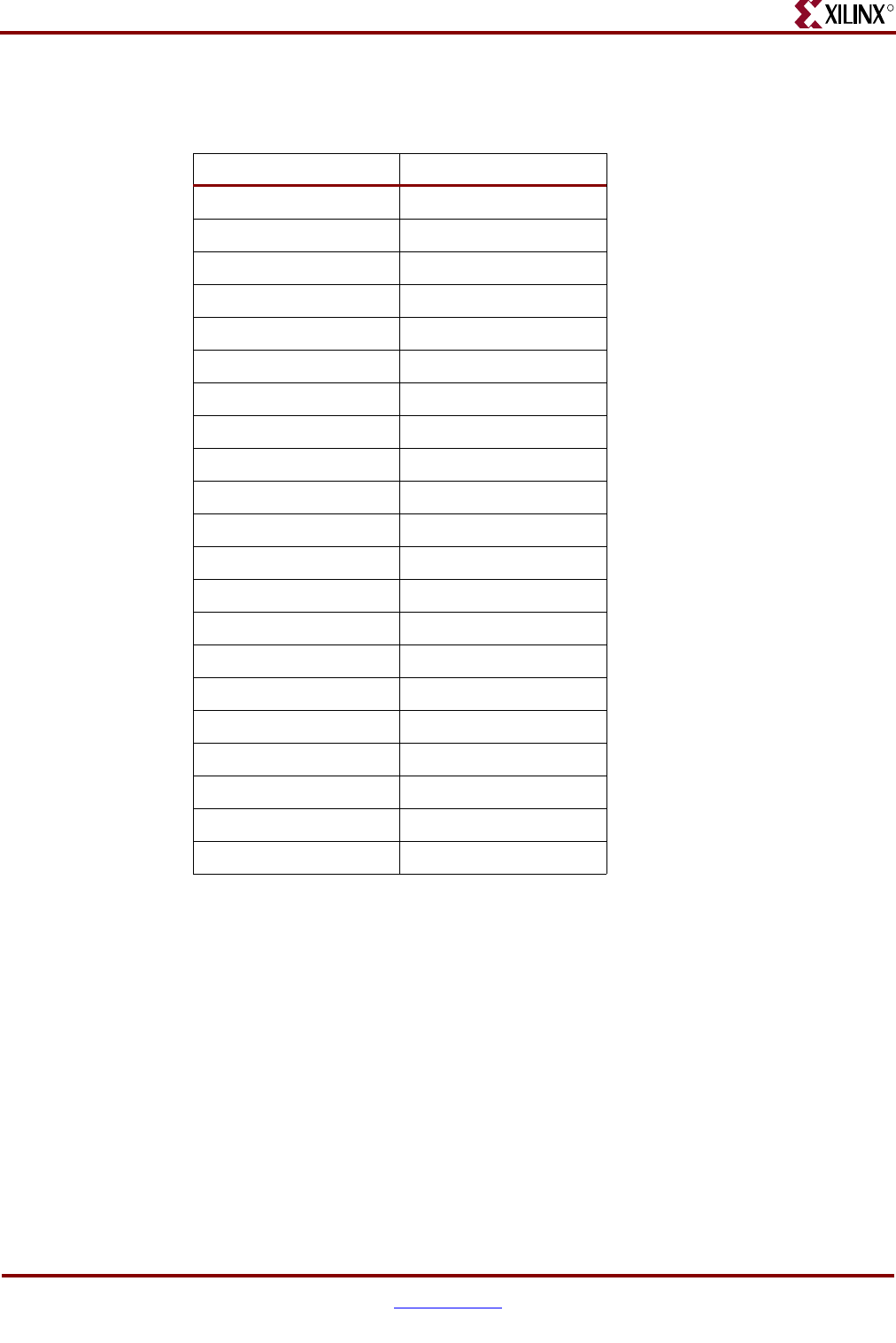
598 www.xilinx.com Memory Interface Solutions User Guide
UG086 (v3.6) September 21, 2010
Appendix H: Pin Mapping for x4 RDIMMs
R
Table H-2 is an example showing the pin mapping for x4 DDR registered DIMMs between
the memory data sheet and the UCF.
Table H -2 : Pin Mapping for x4 DDR DIMMs
Memory Data Sheet MIG UCF
DQ[63:0] DQ[63:0]
CB3 - CB0 DQ[67:64]
CB7 - CB4 DQ[71:68]
DQS0 DQS[0]
DQS1 DQS[2]
DQS2 DQS[4]
DQS3 DQS[6]
DQS4 DQS[8]
DQS5 DQS[10]
DQS6 DQS[12]
DQS7 DQS[14]
DQS8 DQS[16]
DQS9 DQS[1]
DQS10 DQS[3]
DQS11 DQS[5]
DQS12 DQS[7]
DQS13 DQS[9]
DQS14 DQS[11]
DQS15 DQS[13]
DQS16 DQS[15]
DQS17 DQS[17]
