MT3401 Datasheet. Www.s Manuals.com. Mos Tech
User Manual: Marking of electronic components, SMD Codes 03, 03**, 030N03LS, 030N03MS, 030N04NS, 035N04LS, 036N04L, 03C. Datasheets BSC030N03LS G, BSC030N03MS G, BSC030N04NS G, BSC035N04LS G, DTC143TCA, DTC143TEB, IPD036N04L G, MT3401, PDTA114EE, PSOT03, PSOT03C.
Open the PDF directly: View PDF ![]() .
.
Page Count: 9
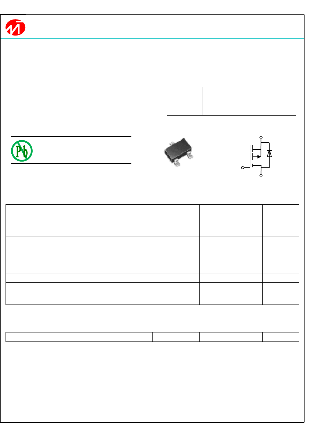
P-Channel Enhancement Mode Field Effect Transistor
D S
S G
G
ABSOLUTE MAXIMUM RATINGS(TA=25℃ unless otherwise noted)
Parameter Sym bol Limit Unit
Drain-Source Voltage VDS -30 V
Gate-Source Voltage VGS ±20 V
Drain Current-Continuousª@Tj=125℃
- Pulse b
d
ID -5.6 A
IDM -25 A
Drain-source Diode Forward Currentª IS -1.5 A
Maximum Power Dissipationª PD 1.5 W
Operating Junction and Storage
Temperature Range TJ,TSTG -55 to 150 °C
THERMAL CHARACTERISTICS
Thermal Resistance, Junction-to Ambientª Rth JA 90 ℃/W
©2009 Mos-Tech Semiconductor 1 http//www.mtsemi.com
FEATURES
● Super high dense cell design for low RDS(ON)
● Rugged and reliable
● Simple drive requirement
● SOT-23 package
PRODUCT SUMMARY
VDSS ID RDS(ON) (mΩ) Typ
-30V -5.6A 45@ VGS=-10V
65 @ VGS=-4.5V
NOTE:The MT3401 is available
in a lead-free package
MT3401
Mos-Tech Semiconductor Co.,LTD
.
茂钿半導體股份有限公司
D
ELECTRICAL CHARACTERISTICS (TA=25℃ unless otherwise noted)
Parameter Sym bol Condition Min Typ Max Unit
OFF CHARACTERISTICS
Drain-Source Breakdown Voltage BVDSS VGS=0V,ID=-250µA -30 V
Zero Gate Voltage Drain Current IDSS VDS=-30V,VGS=0V 1 µA
Gate-Body Leakage IGSS VGS=±10V,VDS=0V ±100 nA
ON CHARACTERITICS
Gate Threshold Voltage VGS(th) V DS=VGS,ID=-250µA -1.2 -2.0 V
Drain-Source On-State Resistance RDS(ON)
VGS=-10V,ID=-4.6A 45 50
mΩ
VGS=-4.5V,ID=-3.0A 65 70
Forward Transconductance ɡFS VGS=-10V,ID=-1.7A 17 S
DAYNAMIC CHARACTERISTICS
Input Capacitance CISS
VDS=-15V,VGS=0V
f=1.0MHZ
1226 pF
Output Capacitance COSS 187 pF
Reverse Transfer Capacitance CRSS 91 pF
SWITCHING CHARACTERISISTICS
Turn-On Delay Time tD(ON) VDD=-15V
ID=-1.0A,
VGEN=-10V
RL=15ohm
RGEN=6ohm
5.9 ns
Rise Time tr 6.9 ns
Turn-Off Delay Time tD(OFF) 48 ns
Fall Time tf 16 ns
Total Gate Charge Qg
VDS=-15V,ID=-1.7A
VGS=-10V
9.8 nC
Gate-Source Charge Qgs 1.8 nC
Gate-Drain Charge Qgd 4.5 nC
©2009 Mos-Tech Semiconductor 2 http//www.mtsemi.com
MT3401
Mos-Tech Semiconductor Co.,LTD
.
茂钿半導體股份有限公司
ELECTRICAL CHARACTERICS (TA=25℃ unless otherwise noted)
Parameter Sym bol Condition Min Typ Max Unit
DRAIN-SOURCE DIODE CHARACTERISTICS
Diode Forward Voltage VSD VGS=0V,IS=-1.25A -0.8 -1.2 V
Notes
a. Surface Mounted on FR4 Board, t≦10sec
b. Pulse Test: Pulse Width≦300Us, Duty Cycle≦2%
c. Guaranteed by design, not subject to production testing.
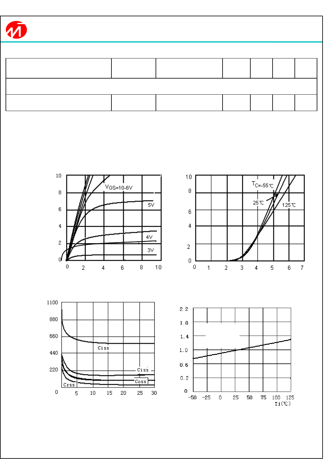
- VDS, Drain-to-Source Voltage (V) -VGS, Gate-to-source Voltage (V)
Figure 1.Output Characteristics Figure 2.Transfer Characteristics
- VGS, Drain-to Source Voltage
Figure3.Capacitance Figure4. On-Resistance Variation with
Temperature
©2009 Mos-Tech Semiconductor 3 http//www.mtsemi.com
-ID, Drain Current (A)
-ID,Drain Current(A)
C,Capacitance(pF)
VGS=-10V
ID=-1.7A
RDS(ON), On-Resistance(mΩ)
MT3401
Mos-Tech Semiconductor Co.,LTD
.
茂钿半導體股份有限公司
--50 -25 0 25 50 75 1 00 12 5
0.5
0.4
0.3
0.2
0.1
0.0
-0.1
-0.2
0.2 0. 4 0. 6 0.8 1. 0 1. 2 1.4 1. 6
21
18
15
12
9
6
3
0
20
10
1
0
0 5 10 15 20 25 30 0.6 0. 8 1. 0 1. 2 1. 4 1. 6
0 1 2 3 4 5 6 7
-
©2009 Mos-Tech Semiconductor 4 http//www.mtsemi.com
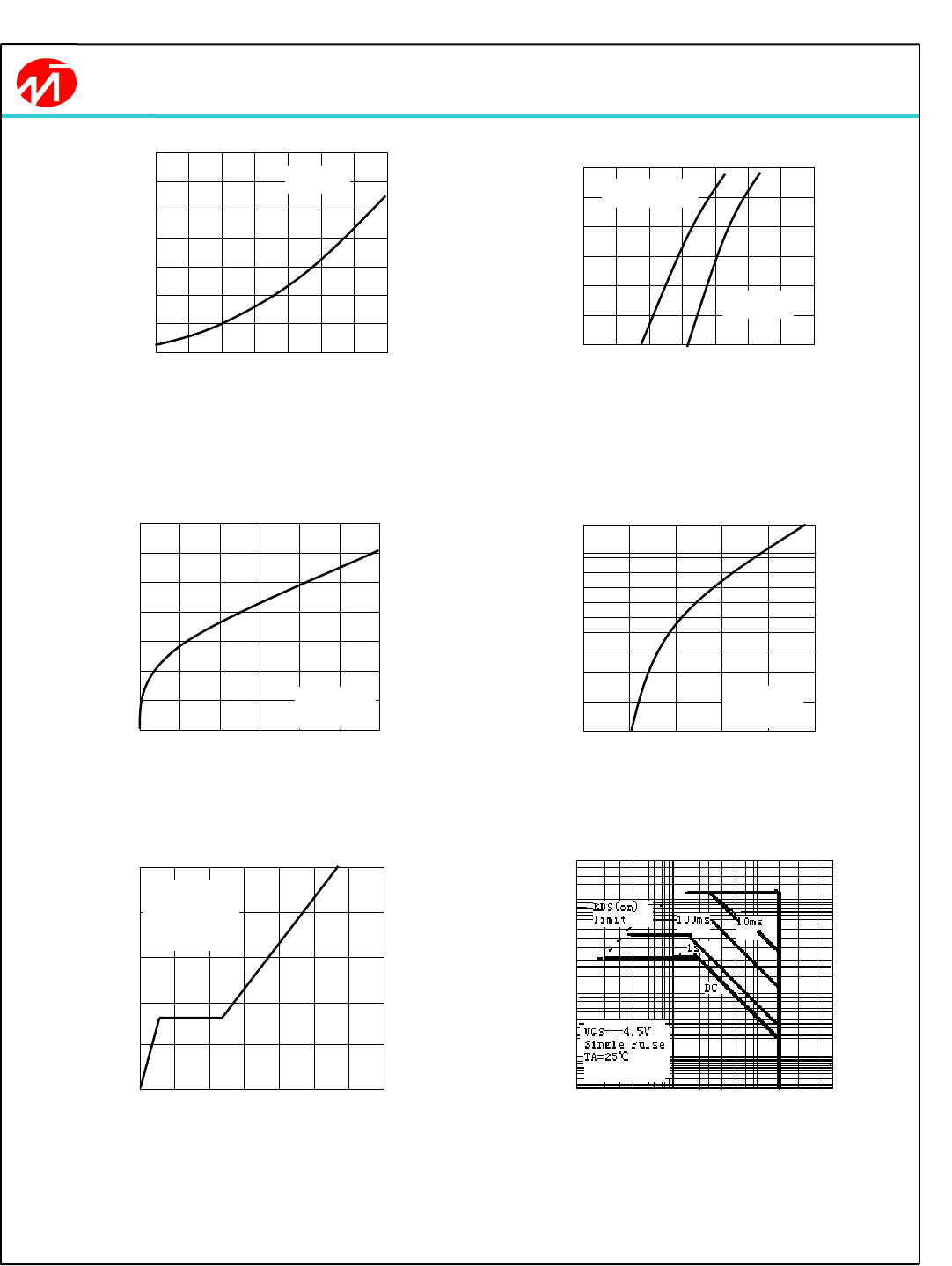
Vth, Normalized
Gate-Source Threshold Voltage
Is-Source Currenti(A)
10
1
Tj,. Junction Temperature(℃)
Figure5.Gate Threshold Variation
With Temperature
VSD-Soures-to-Drain Voltage(V)
ɡFS,Transconductance(S)
-Is,Source-drain current(A)
-IDS, Drain-Source Current (A)
Figure7.Transconductance Variation
With Drain Current
-VGS,Gate to Source Voltage
50
10
1
0.1
0.03
-VSD, Body Diode Forward Voltage
Figure8.Body Diode Forward Voltage
Variation with Source Current
0
2
4
6
8
10
0.1 1 10 20 50
Qɡ, Total Gate Charge(nC)
Figure9. Gate Charge
-VDS, Drain-Source Voltage(V)
Figure10.Maximum Safe Operating Area
-ID,Drain Current(A)
ID=-250uA
TJ=150℃
VGS=-5V Tj=25℃
VDS=-15V
ID=-1.7A
TJ=25℃
MT3401
Mos-Tech Semiconductor Co.,LTD
.
茂钿半導體股份有限公司
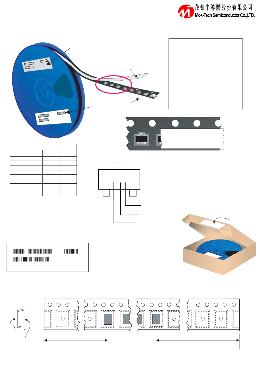
SOT23-3L Packaging
Configuration: F igure 1.0
C omponents Leade r T ape
500mm minimum or
125 em pty pockets
Trailer Ta pe
300mm minimum or
75 em pty pock ets
SOT23-3L Tape Leader and Trailer
Configuration: F igure 2.0
C over T ape
C arrier Tape
Note/Comments
Packaging Option
SOT23-3L Packaging Information
S tandar d
(no flow code) D87Z
Packaging type
Reel Size
TN R
7" D ia
TN R
13"
Qty per Reel/Tube/Bag 3, 000 10, 000
Box Dimension (mm) 193x 183 x80 355x 333 x40
Max qty per Box 15, 000 30, 000
Weight per unit (gm) 0. 0082 0. 0082
Weight per Reel (kg) 0. 1175 0. 4006
SOT23-3L Unit Orientation
ACTR Label
Cus tomized Lab el
E mbosse d
Carri er Tape
Antistatic Cover Tape
Packaging Description:
S OT 23-3L par ts ar e s hipped in tape. T he carrier ta pe is
made from a d issipative (carbon filled) polycarbonate
resin. T he cover tape i s a m ultilayer film (Hea t Activated
Adhes ive in nature) primarily c omposed o f polyes ter film,
adhes ive l ayer, seal ant, and anti-static s prayed ag ent.
T hes e reeled parts i n s tandard option ar e s hipped with
3, 000 units per 7 " or 177mm diameter reel. T he r eels ar e
dark blue in c olor and is made of polystyrene plas tic ( anti-
static coated) . O ther option c omes i n 10,000 units per 13"
or 330c m diameter reel. T his and s ome other options ar e
des cribed in the P ackaging Information table.
T hes e f ull reel s are i ndividually labe led and plac ed inside
a s tandar d immediate box made o f recyclable corrugated
brown paper with a F airchild logo p rinting. O ne box
contains f ive reel s maximum. And thes e immediate boxes
are placed inside a labeled s hipping box which c omes in
different siz es depending on the number of parts s hipped.
XH1 MT3401AACTR
XH2 C97I27K1-038I-K133 M13274
D
SPEC :
QT Y : 3000
D
193m m x 183m m x 80m m
P izza B ox for S tandard O ption
B arc ode
Lab el
B
L
B arcode L abel s ample
MOS-TECH SEMICONDUCTOR LTD (ACTR)
SOT-23 Std Tape and Reel Data
©2009 MOS-TECH Semiconductor Corporation 2009, Rev. D
038I 038I 038I 038I
MARKING DIAGRAM
03 X X
03:PartNO.
X:YearCode
X:MonthCode
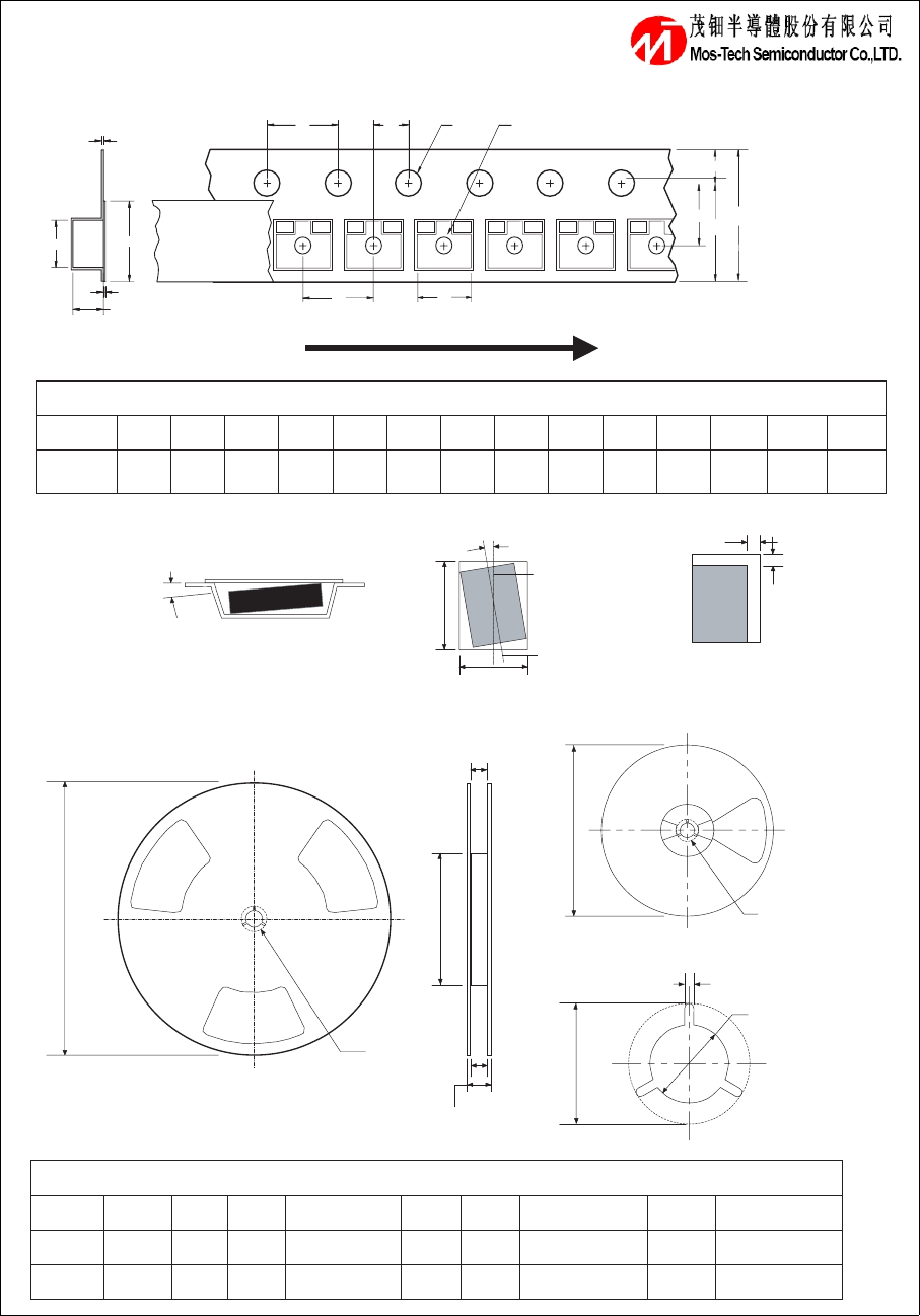
SOT-23 Std Tape and Reel Data, continued
Dimensions are in millimeter
Pkg type
A0 B0 W D0 D1 E1 E2 F P1 P0 K0 T Wc Tc
SOT-23
(8mm)
3.15
+/-0.10
2.77
+/-0.10
8.0
+/-0.3
1.55
+/-0.05
1.125
+/-0.125
1.75
+/-0.10
6.25
min
3.50
+/-0.05
4.0
+/-0.1
4.0
+/-0.1
1.30
+/-0.10
0.228
+/-0.013
5.2
+/-0.3
0.06
+/-0.02
Dimensions are in inches and millimeters
Tape Size Reel
Option Dim A Dim B Dim C Dim D Dim N Dim W1 Dim W2 Dim W3 (LSL-USL)
8mm 7" Dia 7.00
177.8
0.059
1.5
512 +0.020/-0.008
13 +0.5/-0.2
0.795
20.2
2.165
55
0.331 +0.059/-0.000
8.4 +1.5/0
0.567
14.4
0.311 - 0.429
7.9 - 10. 9
8mm 13" Dia 13.00
330
0.059
1.5
512 +0.020/-0.008
13 +0.5/-0.2
0.795
20.2
4.00
100
0.331 +0.059/-0.000
8.4 +1.5/0
0.567
14.4
0.311 - 0.429
7.9 - 10. 9
See detail AA
Dim A
max
13" Diameter Option
7" Diameter Option
Dim A
Max
See detail AA
W3
W2 max Measured at Hub
W1 Measured at Hub
Dim N
Dim D
min
Dim C
B Min
DETAIL AA
Notes: A0, B0, and K0 dimensions are determined with respect to the EIA/Jedec RS-481
rotational and lateral movement requirements (see sketches A, B, and C).
20 deg maximum component rotation
0.5mm
maximum
0.5mm
maximum
Sketch C (Top View)
Component lateral movement
Typical
component
cavity
center line
20 deg maximum
Typical
component
center line
B0
A0
Sketch B (Top View)
Component Rotation
Sketch A (Side or Front Sectional View)
Component Rotation
User Direction of Feed
SOT23-3L Embossed Carrier Tape
Configuration: Figure 3.0
SOT23-3L Reel Configuration: Figure 4.0
P1 A0
D1
FW
E1
E2
Tc
Wc
K0
T
B0
D0P0 P2
October 2005, Rev. D1
1. This document is provided for reference purposes only so that Mos-tech customers may select the appropriate
Mos-tech products for their use. Mos-tech neither makes warranties or representations with respect to the
accuracy or completeness of the information contained in this document nor grants any license to any
intellectual property rights or any other rights of Mos-tech or any third party with respect to the information in
this document.
2. Mos-tech shall have no liability for damages or infringement of any intellectual property or other rights arising
out of the use of any information in this document, including, but not limited to, product data, diagrams, charts,
programs, algorithms, and application circuit examples.
3. You should not use the products or the technology described in this document for the purpose of military
applications such as the development of weapons of mass destruction or for the purpose of any other military
use. When exporting the products or technology described herein, you should follow the applicable export
control laws and regulations, and procedures required by such laws and regulations.
4. All information included in this document such as product data, diagrams, charts, programs, algorithms, and
application circuit examples, is current as of the date this document is issued. Such information, however, is
subject to change without any prior notice. Before purchasing or using any Mos-tech products listed in this
document, please confirm the latest product information with a Mos-tech sales office. Also, please pay regular
and careful attention to additional and different information to be disclosed by Mos-tech such as that disclosed
through our website. (http://www.mtsemi.com )
5. Mos-tech has used reasonable care in compiling the information included in this document, but Mos-tech
assumes no liability whatsoever for any damages incurred as a result of errors or omissions in the information
included in this document.
6. When using or otherwise relying on the information in this document, you should evaluate the information in
light of the total system before deciding about the applicability of such information to the intended application.
Mos-tech makes no representations, warranties or guaranties regarding the suitability of its products for any
particular application and specifically disclaims any liability arising out of the application and use of the
information in this document or Mos-tech products.
7. With the exception of products specified by Mos-tech as suitable for automobile applications, Mos-tech
products are not designed, manufactured or tested for applications or otherwise in systems the failure or
malfunction of which may cause a direct threat to human life or create a risk of human injury or which require
especially high quality and reliability such as safety systems, or equipment or systems for transportation and
traffic, healthcare, combustion control, aerospace and aeronautics, nuclear power, or undersea communication
transmission. If you are considering the use of our products for such purposes, please contact a Mos-tech
sales office beforehand. Mos-tech shall have no liability for damages arising out of the uses set forth above.
8. Notwithstanding the preceding paragraph, you should not use Mos-tech products for the purposes listed below:
(1) artificial life support devices or systems
(2) surgical implantations
(3) healthcare intervention (e.g., excision, administration of medication, etc.)
(4) any other purposes that pose a direct threat to human life
Mos-tech shall have no liability for damages arising out of the uses set forth in the above and purchasers who
elect to use Mos-tech products in any of the foregoing applications shall indemnify and hold harmless Mos-tech
Technology Corp., its affiliated companies and their officers, directors, and employees against any and all
damages arising out of such applications.
9. You should use the products described herein within the range specified by Mos-tech, especially with respect
to the maximum rating, operating supply voltage range, movement power voltage range, heat radiation
characteristics, installation and other product characteristics. Mos-tech shall have no liability for malfunctions or
damages arising out of the use of Mos-tech products beyond such specified ranges.
10. Although Mos-tech endeavors to improve the quality and reliability of its products, IC products have specific
characteristics such as the occurrence of failure at a certain rate and malfunctions under certain use
conditions. Please be sure to implement safety measures to guard against the possibility of physical injury, and
injury or damage caused by fire in the event of the failure of a Mos-tech product, such as safety design for
hardware and software including but not limited to redundancy, fire control and malfunction prevention,
appropriate treatment for aging degradation or any other applicable measures. Among others, since the
evaluation of microcomputer software alone is very difficult, please evaluate the safety of the final products or
system manufactured by you.
11. In case Mos-tech products listed in this document are detached from the products to which the Mos-tech
products are attached or affixed, the risk of accident such as swallowing by infants and small children is very
high. You should implement safety measures so that Mos-tech products may not be easily detached from your
products. Mos-techshall have no liability for damages arising out of such detachment.
12. This document may not be reproduced or duplicated, in any form, in whole or in part, without prior written
approval from Mos-tech.
13. Please contact a Mos-tech sales office if you have any questions regarding the information contained in this
document, Mos-tech semiconductor products, or if you have any other inquiries.
Notes regarding these materials
MOS-TECH Semiconductor Co.,LTD
©2010 MOS-TECH Semiconductor Corporation www.mtsemi.com
1. ᴀ䌘᭭ᰃЎњ䅽⫼᠋ḍ⫼䗨䗝ᢽড়䗖ⱘᴀ݀ৌѻકⱘখ㗗䌘᭭ˈᇍѢᴀ䌘᭭Ё᠔䆄䕑ⱘᡔᴃֵᙃˈᑊ䴲ᛣ
ੇⴔᇍᴀ݀ৌ㗙ϝ㗙ⱘⶹ䆚ѻᴗঞ݊Ҫᴗ߽خߎֱ䆕ᇍᅲᮑᴗ䖯㸠ⱘᡓ䇎DŽ
2. ᇍѢՓ⫼ᴀ䌘᭭᠔䆄䕑ⱘѻક᭄ǃǃ㸼ǃᑣǃㅫ⊩ঞ݊Ҫᑨ⫼⬉䏃՟㗠ᓩ䍋ⱘᤳᆇ㗙ᇍϝ㗙ⱘ
ⶹ䆚ѻᴗঞ݊Ҫᴗ߽䗴៤։⢃ˈᴀ݀ৌϡᡓᢙӏԩ䋷ӏDŽ
3. ϡ㛑ᇚᴀ䌘᭭᠔䆄䕑ⱘѻકᡔᴃ⫼Ѣ㾘⸈ണᗻ℺఼ⱘᓔথㄝⳂⱘǃݯџⳂⱘ݊Ҫⱘݯ䳔⫼䗨ᮍ䴶DŽ
ˈߎষᯊᖙ乏䙉ᅜ中国ⱘlj∛ঞ䌌ᯧ⊩NJঞ݊ҪߎষⱘⳌ݇⊩Ҹᑊሹ㸠䖭ѯ⊩ҸЁ㾘ᅮⱘᖙ㽕
㓁DŽ
4. ᴀ䌘᭭᠔䆄䕑ⱘѻક᭄ǃǃ㸼ǃᑣǃㅫ⊩ҹঞ݊Ҫᑨ⫼⬉䏃՟ㄝ᠔ֵ᳝ᙃഛЎᴀ䌘᭭থ㸠ᯊⱘݙᆍˈ
ᴀ݀ৌ᳝ৃ㛑خџܜ䗮ⶹⱘᚙމϟˈᇍᴀ䌘᭭᠔䆄䕑ⱘѻક㗙ѻક㾘Ḑ䖯㸠ᬍDŽ᠔ҹ䌁фՓ⫼
ᴀ݀ৌⱘञᇐԧѻકПࠡˈ䇋џܜᴀ݀ৌⱘ㧹Ϯにষ⹂䅸᳔ᮄⱘֵᙃᑊ㒣ᐌ⬭ᛣᴀ݀ৌ䗮䖛݀ৌЏ义
(http://www.mtsemi.com)ㄝ݀ᓔⱘ᳔ᮄֵᙃDŽ
5. ᇍѢᴀ䌘᭭Ё᠔䆄䕑ⱘֵᙃˈࠊᯊ៥Ӏሑֱ䆕ߎ⠜ᯊⱘ㊒⹂ᗻˈԚϡᡓᢙᴀ䌘᭭ⱘভ䗄ϡᔧ㗠㟈Փ乒
ᅶ䙁ফᤳ༅ㄝⱘӏԩⳌ݇䋷ӏDŽ
6. Փ⫼ᴀ䌘᭭᠔䆄䕑ⱘѻક᭄ǃǃ㸼ㄝ᠔⼎ⱘᡔᴃݙᆍǃᑣǃㅫ⊩ঞ݊Ҫᑨ⫼⬉䏃՟ᯊˈϡҙ㽕ᇍ᠔
Փ⫼ⱘᡔᴃֵᙃ䖯㸠ऩ⣀䆘Ӌˈ䖬㽕ᇍᭈϾ㋏㒳䖯㸠ܙߚⱘ䆘ӋDŽ䇋乒ᅶ㞾㸠䋳䋷ˈ䖯㸠ᰃ৺䗖⫼ⱘ߸ᮁDŽ
ᴀ݀ৌᇍѢᰃ৺䗖⫼ϡ䋳ӏԩ䋷ӏDŽ
7. ᴀ䌘᭭Ё᠔䆄䕑ⱘѻકᑊ䴲䩜ᇍϛϔߎ⦄ᬙ䱰ᰃ䫭䇃䖤㸠ህӮ࿕㚕ࠄҎⱘ⫳ੑ㒭Ҏԧᏺᴹॅᆇⱘᴎ఼ǃ
㋏㒳བ⾡ᅝܼ㺙㕂㗙䖤䕧Ѹ䗮⫼ⱘǃए⭫ǃ➗⚻ࠊǃ㟾఼ẄǃḌ㛑ǃ⍋ᑩЁ㒻⫼ⱘᴎ఼㋏㒳ㄝ
㗠䆒䅵ࠊ䗴ⱘ⡍߿ᰃᇍѢક䋼ৃ䴴ᗻ㽕∖ᵕ催ⱘᴎ఼㋏㒳ㄝ˄ᇚᴀ݀ৌᣛᅮ⫼Ѣ≑䔺ᮍ䴶ⱘѻક⫼
Ѣ≑䔺ᯊ䰸˅DŽབᵰ㽕⫼ѢϞ䗄ⱘⳂⱘˈ䇋ࡵᖙџܜᴀ݀ৌⱘ㧹Ϯにষ䆶DŽˈᇍѢ⫼ѢϞ䗄Ⳃⱘ
㗠䗴៤ⱘᤳ༅ㄝˈᴀ݀ৌὖϡ䋳䋷DŽ
8. 䰸Ϟ䗄乍ݙᆍˈϡ㛑ᇚᴀ䌘᭭Ё䆄䕑ⱘѻક⫼Ѣҹϟ⫼䗨DŽབᵰ⫼Ѣҹϟ⫼䗨㗠䗴៤ⱘᤳ༅ˈᴀ݀ৌ
ὖϡ䋳䋷DŽ
1˅⫳ੑ㓈ᣕ㺙㕂DŽ
2˅ỡඟѢҎԧՓ⫼ⱘ㺙㕂DŽ
3˅⫼Ѣ⊏⭫˄ߛ䰸ᙷ䚼ǃ㒭㥃ㄝ˅ⱘ㺙㕂DŽ
4˅݊ҪⳈᕅડࠄҎⱘ⫳ੑⱘ㺙㕂DŽ
9. Փ⫼ᴀ䌘᭭᠔䆄䕑ⱘѻકᯊˈᇍѢ᳔乱ᅮؐǃᎹ⬉⑤⬉य़ⱘ㣗ೈǃᬒ⛁⡍ᗻǃᅝ㺙ᴵӊঞ݊Ҫᴵӊ䇋
ᴀ݀ৌ㾘ᅮⱘֱ䆕㣗ೈݙՓ⫼DŽབᵰ䍙ߎњᴀ݀ৌ㾘ᅮⱘֱ䆕㣗ೈՓ⫼ᯊˈᇍѢ⬅ℸ㗠䗴៤ⱘᬙ䱰ߎ⦄
ⱘџᬙˈᴀ݀ৌᇚϡᡓᢙӏԩ䋷ӏDŽ
10.ᴀ݀ৌϔⳈ㟈Ѣᦤ催ѻકⱘ䋼䞣ৃ䴴ᗻˈԚϔ㠀ᴹ䇈ˈञᇐԧѻકᘏӮҹϔᅮⱘὖ⥛থ⫳ᬙ䱰ǃ㗙⬅
ѢՓ⫼ᴵӊϡৠ㗠ߎ⦄䫭䇃䖤㸠ㄝDŽЎњ䙓ܡᴀ݀ৌⱘѻકথ⫳ᬙ䱰㗙䫭䇃䖤㸠㗠ᇐ㟈Ҏ䑿џᬙ☿♒
䗴៤⼒Ӯᗻⱘᤳ༅ˈᏠᳯᅶ᠋㛑㞾㸠䋳䋷䖯㸠ݫԭ䆒䅵ǃ䞛পᓊ⚻ᇍㄪঞ䖯㸠䰆ℶ䫭䇃䖤㸠ㄝⱘᅝܼ䆒䅵
˄ࣙᣀ⹀ӊ䕃ӊϸᮍ䴶ⱘ䆒䅵˅ҹঞ㗕࣪໘⧚ㄝˈ䖭ᰃЎᴎ఼㋏㒳ⱘߎॖֱ䆕DŽ⡍߿ᰃऩ⠛ᴎⱘ䕃ӊˈ
⬅Ѣऩ⣀䖯㸠偠䆕ᕜೄ䲒ˈ᠔ҹ㽕∖乒ᅶࠊ䗴ⱘ᳔㒜ⱘᴎ఼ঞ㋏㒳Ϟ䖯㸠ᅝܼẔ偠ᎹDŽ
11. བᵰᡞᴀ䌘᭭᠔䆄䕑ⱘѻકҢ݊䕑ԧ䆒Ϟौϟˈ᳝ৃ㛑䗴៤၈ܓ䇃৲ⱘॅ䰽DŽ乒ᅶᇚᴀ݀ৌѻકᅝ㺙ࠄ
乒ᅶⱘ䆒Ϟᯊˈ䇋乒ᅶ㞾㸠䋳䋷ᇚᴀ݀ৌѻક䆒㕂Ўϡᆍᯧ࠹㨑ⱘᅝܼ䆒䅵DŽབᵰҢ乒ᅶⱘ䆒Ϟ࠹㨑㗠
䗴៤џᬙᯊˈᴀ݀ৌᇚϡᡓᢙӏԩ䋷ӏDŽ
12.ᕫࠄᴀ݀ৌⱘџܜк䴶䅸ৃᯊˈϡৃᇚᴀ䌘᭭ⱘϔ䚼ߚ㗙ܼ䚼䕀䕑㗙ࠊDŽ
13.བᵰ䳔㽕њ㾷݇Ѣᴀ䌘᭭ⱘ䆺㒚ݙᆍˈ㗙᳝݊Ҫ݇ᖗⱘ䯂乬ˈ䇋ᴀ݀ৌⱘ㧹Ϯにষ䆶DŽ
݇Ѣ߽⫼ᴀ䌘᭭ᯊⱘ⊼ᛣџ乍
⊼ᛣ
ᴀ᭛াᰃখ㗗䆥᭛ˈࠡ义᠔䕑㣅᭛⠜“Cautions”᳝ℷᓣᬜDŽ
©2010 MOS-TECH Semiconductor Corporation www.mtsemi.com
MOS-TECH Semiconductor Co.,LTD
1. MOS-TECH Semiconductor Corp. puts the maximum effort into making semiconductor products better
and more reliable, but there is always the possibility that trouble may occur with them. Trouble with
semiconductors may lead to personal injury, fire or property damage.
Remember to give due consideration to safety when making your circuit designs, with appropriate
measures such as (i) placement of substitutive, auxiliary circuits, (ii) use of nonflammable material or
(iii) prevention against any malfunction or mishap.
Keep safety first in your circuit designs!