MT6228 Datasheet. Www.s Manuals.com. R1.02 Mediatek
User Manual: Datasheets MT6228.
Open the PDF directly: View PDF ![]() .
.
Page Count: 617 [warning: Documents this large are best viewed by clicking the View PDF Link!]

MTK Confidential Release for Konka
MTK Confidential Release for Konka
MT6228 GSM/GPRS Baseband
Processor Data Sheet
Revision 1.02
September 09, 2005

MTK Confidential Release for Konka
MTK Confidential Release for Konka
MT6228 GSM/GPRS Baseband Processor Data Sheet Revision 1.0
2/616
MediaTek Inc. Confidential
Revision History
Revision Date Comments
1.00 Jun 28, 2005 First Release
1.01 Aug 30, 2005
1. Correct typo in “Flow Control” section of Post Resize
2. Change IRQ_STA and IRQ_STA2 registers to RO type in Interrupt-Controller
3. Additional core power ball, VDDK, is added in ball map diagram.
4. Updated package thickness to 1.2 in product description
1.02 Sep 09, 2005 1. Fixed ball count description from 313 to 314 balls.
2. Typo fixed.

MTK Confidential Release for Konka
MTK Confidential Release for Konka
MT6228 GSM/GPRS Baseband Processor Data Sheet Revision 1.0
3/616
MediaTek Inc. Confidential
TABLE OF CONTENTS
Revision History...................................................................................................................................... 2
Preface...................................................................................................................................................... 5
1. System Overview............................................................................................................................... 6
1.1
Platform Features....................................................................................................................................................... 9
1.2
MODEM Features.....................................................................................................................................................11
1.3
Multi-Media Features............................................................................................................................................... 12
1.4
General Description ................................................................................................................................................. 15
2 Product Description........................................................................................................................ 17
2.1
Pin Outs.................................................................................................................................................................... 17
2.2
Top Marking Definition ........................................................................................................................................... 20
2.3
DC Characteristics ................................................................................................................................................... 21
2.4
Pin Description......................................................................................................................................................... 22
2.5
Power Description.................................................................................................................................................... 31
3 Micro-Controller Unit Subsystem ................................................................................................. 37
3.1
Processor Core ......................................................................................................................................................... 38
3.2
Memory Management.............................................................................................................................................. 38
3.3
Bus System............................................................................................................................................................... 41
3.4
Direct Memory Access............................................................................................................................................. 45
3.5
Interrupt Controller .................................................................................................................................................. 61
3.6
Code Cache Controller............................................................................................................................................. 74
3.7
MPU......................................................................................................................................................................... 82
3.8
Data Cache............................................................................................................................................................... 91
3.9
Internal Memory Interface ..................................................................................................................................... 100
3.10
External Memory Interface .................................................................................................................................... 100
4 Microcontroller Peripherals ........................................................................................................ 109
4.1
Pulse-Width Modulation Outputs........................................................................................................................... 109
4.2
Alerter .....................................................................................................................................................................112
4.3
SIM Interface ..........................................................................................................................................................114
4.4
Keypad Scanner ..................................................................................................................................................... 123
4.5
General Purpose Inputs/Outputs ............................................................................................................................ 125
4.6
General Purpose Timer........................................................................................................................................... 139
4.7
UART..................................................................................................................................................................... 142
4.8
IrDA Framer........................................................................................................................................................... 156
4.9
Real Time Clock .................................................................................................................................................... 164
4.10
Auxiliary ADC Unit............................................................................................................................................... 170
4.11
SCCB ..................................................................................................................................................................... 173
4.12
Cipher Hash Engine ............................................................................................................................................... 176
5 Microcontroller Coprocessors ..................................................................................................... 185
5.1
Divider ................................................................................................................................................................... 185
5.2
CSD Accelerator .................................................................................................................................................... 187
5.3
FCS Codec ............................................................................................................................................................. 197
5.4
PPP Framer Coprocessor........................................................................................................................................ 199
6 Multi-Media Subsystem ............................................................................................................... 206
6.1
LCD Interface ........................................................................................................................................................ 206
6.2
NAND FLASH interface ....................................................................................................................................... 226
6.3
USB OTG Controller............................................................................................................................................. 242
6.4
Memory Stick and SD Memory Card Controller ................................................................................................... 259

MTK Confidential Release for Konka
MTK Confidential Release for Konka
MT6228 GSM/GPRS Baseband Processor Data Sheet Revision 1.0
4/616
MediaTek Inc. Confidential
6.5
Graphic Memory Controller................................................................................................................................... 281
6.6
2D acceleration ...................................................................................................................................................... 284
6.7
Capture Resize ....................................................................................................................................................... 305
6.8
Drop Resize............................................................................................................................................................ 313
6.9
Post Resize............................................................................................................................................................. 317
6.10
JPEG Decoder........................................................................................................................................................ 330
6.11
JPEG Encoder........................................................................................................................................................ 340
6.12
GIF Decoder........................................................................................................................................................... 346
6.13
PNG Decoder......................................................................................................................................................... 356
6.14
Camera Interface.................................................................................................................................................... 368
6.15
Image DMA ........................................................................................................................................................... 410
6.16
Image Engine ......................................................................................................................................................... 441
6.17
MPEG-4/H.263 Video CODEC ............................................................................................................................. 458
6.18
TV Controller......................................................................................................................................................... 498
6.19
TV encoder............................................................................................................................................................. 504
7 Audio Front-End........................................................................................................................... 512
7.1
General Description ............................................................................................................................................... 512
7.2
Register Definitions ............................................................................................................................................... 515
7.3
Programming Guide............................................................................................................................................... 519
8 Radio Interface Control ............................................................................................................... 521
8.1
Baseband Serial Interface....................................................................................................................................... 521
8.2
Baseband Parallel Interface.................................................................................................................................... 527
8.3
Automatic Power Control (APC) Unit................................................................................................................... 530
8.4
Automatic Frequency Control (AFC) Unit ............................................................................................................ 536
9 Baseband Front End..................................................................................................................... 540
9.1
Baseband Serial Ports............................................................................................................................................. 541
9.2
Downlink Path (RX Path) ...................................................................................................................................... 543
9.3
Uplink Path (TX Path) ........................................................................................................................................... 549
10 Timing Generator ......................................................................................................................... 552
10.1
TDMA timer........................................................................................................................................................... 552
10.2
Slow Clocking Unit................................................................................................................................................ 559
11 Power, Clocks and Reset .............................................................................................................. 563
11.1
B2PSI..................................................................................................................................................................... 563
11.2
Clocks .................................................................................................................................................................... 565
11.3
Reset Generation Unit (RGU)................................................................................................................................ 571
11.4
Software Power Down Control .............................................................................................................................. 574
12 Analog Front-end & Analog Blocks ............................................................................................ 579
12.1
General Description ............................................................................................................................................... 579
12.2
MCU Register Definitions ..................................................................................................................................... 590
12.3
Programming Guide............................................................................................................................................... 601
13 Digital Pin Electrical Characteristics.......................................................................................... 603

MTK Confidential Release for Konka
MTK Confidential Release for Konka
MT6228 GSM/GPRS Baseband Processor Data Sheet Revision 1.0
5/616
MediaTek Inc. Confidential
Preface
Acronym for Register Type
R/W Capable of both read and write access
RO Read only
RC Read only. After reading the register bank, each bit which is HIGH(1) will be cleared to LOW(0 )
automatically.
WO Write only
W1S Write only. When writing data bits to register bank, each bit which is HIGH(1) will cause the
corresponding bit to be set to 1. Data bits which are LOW(0) has no effect on the corresponding bit.
W1C Write only. When writing data bits to register bank, each bit which is HIGH(1) will cause the
corresponding bit to be cleared to 0. Data bits which are LOW(0) has no effect on the corresponding bit.

MTK Confidential Release for Konka
MTK Confidential Release for Konka
MT6228 GSM/GPRS Baseband Processor Data Sheet Revision 1.0
6/616
MediaTek Inc. Confidential
1. System Overview
MT6228 is a feature-rich and extremely powerful
single-chip solution for high-end GSM/GPRS mobile
phones. Based on the 32-bit ARM7EJ-S
TM
RISC
processor, MT6228’s superb processing power, along with
high bandwidth architecture and dedicated hardware
support, provides an unprecedented platform for high
performance GPRS Class 12 MODEM and leading-edge
multimedia applications. Overall, MT6228 presents a
revolutionary platform for multimedia-centric mobile
devices.
Typical application diagram is shown in Figure 1.
Platform
MT6228 is capable of running the ARM7EJ-S
TM
RISC
processor at up to 104 MHz, thus providing fast data
processing capabilities. In addition to the high clock
frequency, separate CODE and DATA caches are also
added to further improve the overall system efficiency.
For large amounts of data transfer, high performance DMA
(Direct Memory Access) with hardware flow control is
implemented, which greatly enhances the data movement
speed while reducing MCU processing load.
Targeted as a media-rich platform for mobile applications,
MT6228 also provides hardware security digital rights
management for copyright protection. For further
safeguarding, and to protect the manufacturer’s
development investment, hardware flash content protection
is provided to prevent unauthorized porting of the software
load.
Memory
To provide the greatest capacity for expansion and
maximum bandwidth for data intensive applications such
as multimedia features, MT6228 supports up to 4 external
state-of-the-art devices through its 8/16-bit host interface.
High performance devices such as Mobile RAM and
Cellular RAM are supported for maximum bandwidth.
Traditional devices such as burst/page mode flash, page
mode SRAM, and Pseudo SRAM are also supported. For
greatest compatibility, the memory interface can also be
used to connect to legacy devices such as Color/Parallel
LCD, and multi-media companion chips are all supported
through this interface. To minimize power consumption
and ensure low noise, this interface is designed for flexible
I/O voltage and allows lowering of the supply voltage
down to 1.8V. The driving strength is configurable for
signal integrity adjustment. The data bus also employs
retention technology to prevent the bus from floating
during a turn over.
Multi-media
The MT6228 multi-media subsystem provides a
connection to a CMOS image sensor and supports a
resolution up to 3Mpixels. With its advanced image
signal and data processing technology, MT6228 allows
efficient processing of image and video data. Built-in
JPEG CODEC and MPEG-4 CODEC enable real-time
recording and playback of high-quality images and video.
A hardware MPEG4 accelerator supports playback in VGA
mode at 15fps and encoding in CIF at 15fps. Videophone
functionality is also provided. Moreover, a high quality
de-blocking filter is removes blocking artifacts in video
playback. GIF and PNG decoders are implemented for
fast image decoding. MT6228 supports a TV-OUT
capability, allowing the mobile handset to connect to a TV
screen via an NTSC or PAL connection.
In addition to advanced image and video features, MT6228
utilizes high resolution DAC, digital audio, and audio
synthesis technology to provide superior audio features for
all future multi-media needs.
Connectivity and Storage
To take advantage of its incredible multimedia strengths,
MT6228 incorporates myriads of advanced connectivity
and storage options for data storage and communication.
MT6228 supports UART, Fast IrDA, USB 1.1 Full Speed
OTG, SDIO, Bluetooth and WIFI Interface, and
MMC/SD/MS/MS Pro storage systems. These interfaces
provide MT6228 users with the highest degree of
flexibility in implementing solutions suitable for the
targeted application.

MTK Confidential Release for Konka
MTK Confidential Release for Konka
MT6228 GSM/GPRS Baseband Processor Data Sheet Revision 1.0
7/616
MediaTek Inc. Confidential
To achieve a complete user interface, MT6228 also brings
together all the necessary peripheral blocks for a
multi-media GSM/GPRS phone. The peripheral blocks
include the Keypad Scanner with the capability to detect
multiple key presses, SIM Controller, Alerter, Real Time
Clock, PWM, Serial LCD Controller, and General Purpose
Programmable I/Os.
Furthermore, to provide more better configurability and
bandwidth for multi-media products, an additional 18-bit
parallel interface is incorporated. This interface enables
connection to LCD panels as well as NAND flash devices
for additional multi-media data storage.
Audio
Using a highly integrated mixed-signal Audio Front-End,
the MT6228 architecture allows for easy audio interfacing
with direct connection to the audio transducers. The
audio interface integrates D/A and A/D Converters for
Voice band, as well as high resolution Stereo D/A
Converters for Audio band. In addition, MT6228 also
provides Stereo Input and Analog MUX.
MT6228 supports AMR codec to adaptively optimize
speech and audio quality. Moreover, HE-AAC codec is
implemented to deliver CD-quality audio at low bit rates.
On the whole, MT6228’s audio features provide a rich
solution for multi-media applications.
Radio
MT6228 integrates a mixed-signal baseband front-end in
order to provide a well-organized radio interface with
flexibility for efficient customization. The front-end
contains gain and offset calibration mechanisms, and filters
with programmable coefficients for comprehensive
compatibility control on RF modules. This approach
allows the usage of a high resolution D/A Converter for
controlling VCXO or crystal, reducing the need for an
expensive TCVCXO. MT6228 achieves great MODEM
performance by utilizing a 14-bit high resolution A/D
Converter in the RF downlink path. Furthermore, to
reduce the need for extra external current-driving
component, the driving strength of some BPI outputs is
designed to be configurable.
Debug Function
The JTAG interface enables in-circuit debugging of the
software program with the ARM7EJ-S core. With this
standardized debugging interface, MT6228 provides
developers with a wide set of options in choosing ARM
development kits from different third party vendors.
Power Management
The MT6228 offers various low-power features to help
reduce system power consumption. These features
include a Pause Mode of 32 KHz clocking in Standby State,
Power Down Mode for individual peripherals, and
Processor Sleep Mode. MT6228 is also fabricated in an
advanced low leakage CMOS process, hence providing an
overall ultra low leakage solution.
Package
The MT6228 device is offered in a 13mm×13mm, 314-ball,
0.65 mm pitch, TFBGA package.

MTK Confidential Release for Konka
MTK Confidential Release for Konka
MT6228 GSM/GPRS Baseband Processor Data Sheet Revision 1.0
8/616
MediaTek Inc. Confidential
RF
MODULE
MT6228
SPEECH/AUDIO
OUTPUT
SPEECH/AUDIO
INPUT
KEYPAD
SDRAM
CellularRAM
TCVCXO
AFC
APC
TX I/Q
RX I/Q
BPI
BSI
ALERTER
SIM
USIM
SUPPLY
VOLTAGES
JTAG
UART
IRDA
POWER
MANAGEMENT
CIRCUITRY
SERIAL
LCD
SYSCLK
SERIAL
LCD
MMC/SD/MS
MSPRO/SDIO
USB
OTG
B2PSI
AUXADC
123
456
789
*0 #
CMOS
SENSOR
HIFI STEREO
OUTPUT
FM STEREO
RADIO INPUT
DEBUGGER
PWM
NAND
FLASH LCD
18-BIT PARALLEL
INTERFACE
FLASH
SRAM
PSRAM
IMAGE INPUT
TV OUT
CHIP UID
AUDIO
DAC
I2S
Figure 1 Typical application of MT6228

MTK Confidential Release for Konka
MTK Confidential Release for Konka
MT6228 GSM/GPRS Baseband Processor Data Sheet Revision 1.0
9/616
MediaTek Inc. Confidential
1.1 Platform Features
General
Integrated voice-band, audio-band and base-band
analog front ends
TFBGA 13mm×13mm, 314-ball, 0.65 mm pitch
package
MCU Subsystem
ARM7EJ-S 32-bit RISC processor
High performance multi-layer AMBA bus
Java hardware acceleration for fast Java-based
games and applets
Operating frequency: 26/52/104 MHz
Dedicated DMA bus
14 DMA channels
1M bits on-chip SRAM
1M bits MCU dedicated Tightly Coupled memory
256K bits CODE cache
64K bits DATA cache
On-chip boot ROM for Factory Flash
Programming
Watchdog timer for system crash recovery
3 sets of General Purpose Timer
Circuit Switch Data coprocessor
Division coprocessor
PPP Framer coprocessor
External Memory Interface
Supports up to 4 external devices
Supports 8-bit or 16-bit memory components with
maximum size of up to 64M Bytes each
Supports Mobile RAM and Cellular RAM
Supports Flash and SRAM/PSRAM with page
mode or burst mode
Industry standard Parallel LCD interface
Supports multi-media companion chips with 8/16
bits data width
Flexible I/O voltage of 1.8V ~ 2.8V for memory
interface
Configurable driving strength for memory
interface
User Interfaces
6-row × 7-column keypad controller with
hardware scanner
Supports multiple key presses for gaming
SIM/USIM controller with hardware T=0/T=1
protocol control
Real Time Clock (RTC) operating with a separate
power supply
General Purpose I/Os (GPIOs)
2 sets of Pulse Width Modulation (PWM) output
Alerter output with Enhanced PWM or PDM
8 external interrupt lines
Security
Cipher: supports AES, DES/3DES
Hash: supports MD5, SHA-1
Supports security key and 27 bit chip unique ID
Connectivity
3 UARTs with hardware flow control and speeds
up to 921600 bps
IrDA modulator/demodulator with hardware
framer. Supports SIR/MIR/FIR operating speeds.
Full-speed USB 1.1 OTG capability. Supports
device mode, limited host mode, and dual-role
OTG mode.

MTK Confidential Release for Konka
MTK Confidential Release for Konka
MT6228 GSM/GPRS Baseband Processor Data Sheet Revision 1.0
10/616
MediaTek Inc. Confidential
Multi Media Card, Secure Digital Memory Card,
Memory Stick, Memory Stick Pro host controller
with flexible I/O voltage power
Supports SDIO interface for SDIO peripherals as
well as WIFI connectivity
DAI/PCM and I2S interface for Audio application
Power Management
Power Down Mode for analog and digital circuits
Processor Sleep Mode
Pause Mode of 32 KHz clocking in Standby State
7-channel Auxiliary 10-bit A/D Converter for
charger and battery monitoring and photo sensing
Test and Debug
Built-in digital and analog loop back modes for
both Audio and Baseband Front-End
DAI port complying with GSM Rec.11.10
JTAG port for debugging embedded MCU

MTK Confidential Release for Konka
MTK Confidential Release for Konka
MT6228 GSM/GPRS Baseband Processor Data Sheet Revision 1.0
11/616
MediaTek Inc. Confidential
1.2 MODEM Features
Radio Interface and Baseband Front End
GMSK modulator with analog I and Q channel
outputs
10-bit D/A Converter for uplink baseband I and Q
signals
14-bit high resolution A/D Converter for downlink
baseband I and Q signals
Calibration mechanism of offset and gain
mismatch for baseband A/D Converter and D/A
Converter
10-bit D/A Converter for Automatic Power
Control
13-bit high resolution D/A Converter for
Automatic Frequency Control
Programmable Radio RX filter
2 channels Baseband Serial Interface (BSI) with
3-wire control
Bi-directional BSI interface. RF chip register
read access with 3-wire or 4-wire interface.
10-Pin Baseband Parallel Interface (BPI) with
programmable driving strength
Multi-band support
Voice and Modem CODEC
Dial tone generation
Voice memo
Noise reduction
Echo suppression
Advanced sidetone Oscillation Reduction
Digital sidetone generator with programmable
gain
Two programmable acoustic compensation filters
GSM/GPRS quad vocoders for adaptive multirate
(AMR), enhanced full rate (EFR), full rate (FR)
and half rate (HR)
GSM channel coding, equalization and A5/1 and
A5/2 ciphering
GPRS GEA1 and GEA2 ciphering
Programmable GSM/GPRS modem
Packet Switched Data with CS1/CS2/CS3/CS4
coding schemes
GSM Circuit Switch Data
GPRS Class 12
Voice Interface and Voice Front End
Two microphone inputs sharing one low noise
amplifier with programmable gain and automatic
gain control (AGC) mechanisms
Voice power amplifier with programmable gain
2
nd
order Sigma-Delta A/D Converter for voice
uplink path
D/A Converter for voice downlink path
Supports half-duplex hands-free operation
Compliant with GSM 03.50

MTK Confidential Release for Konka
MTK Confidential Release for Konka
MT6228 GSM/GPRS Baseband Processor Data Sheet Revision 1.0
12/616
MediaTek Inc. Confidential
1.3 Multi-Media Features
LCD/NAND Flash Interface
Dedicated Parallel Interface supports 3 external
devices with 8-/16-bit NAND flash interface,
8-/9-/16-/18-bit Parallel interface, and Serial
interface for LCM
Built-in NAND Flash Controller with 1-bit ECC
for mass storage
LCD Controller
Supports simultaneous connection to up to 3
parallel LCD and 2 serial LCD modules
Supports LCM format: RGB332, RGB444,
RGB565, RGB666, RGB888
Supports LCD module with maximum resolution
up to 800x600 at 24bpp
Per pixel alpha channel
True color engine
Supports hardware display rotation
Capable of combining display memories with up to
6 blending layers
Image Signal Processor
8/10 bit Bayer format image input
Capable of processing image of size up to 3M
pixels
Color correction matrix
Gamma correction
Automatic exposure (AE) control
Automatic white balance (AWB) control
Programmable AE/AWB windows
Edge enhancement support
Histogram equalization logic
Horizontal and vertical sync information on
separate pins
Shading compensation
Defect Pixel compensation
Graphic Compression
GIF Decoder
PNG Decoder
JPEG Decoder
ISO/IEC 10918-1 JPEG Baseline and Progressive
modes
Supports all possible YUV formats, including
grayscale format
Supports all DC/AC Huffman table parsing
Supports all quantization table parsing
Supports a restart interval
Supports SOS, DHT, DQT and DRI marker
parsing
IEEE Std 1180-1990 IDCT standards compliance
Supports progressive image processing to
minimize storage space requirement
Supports reload-able DMA for VLD stream
JPEG Encoder
ISO/IEC 10918-1 JPEG baseline mode
ISO/IEC 10918-2 compliance
Supports YUV422 and YUV420 and grayscale
formats
Supports JFIF
Standard DC and AC Huffman tables
Provides 4 levels of encode quality
Supports continuous shooting
Image Data Processing
Supports Digital Zoom

MTK Confidential Release for Konka
MTK Confidential Release for Konka
MT6228 GSM/GPRS Baseband Processor Data Sheet Revision 1.0
13/616
MediaTek Inc. Confidential
Supports RGB888/565, YUV444 image
processing
High throughput hardware scaler. Capable of
tailoring an image to an arbitrary size.
Horizontal scaling in averaging method
Vertical scaling in bilinear method
Simultaneous scaling for MPEG-4 encode and
LCD display
YUV and RGB color space conversion
Pixel format transform
Boundary padding
Pixel processing: hue/saturation/intensity/color
adjustment, Gamma correction and
grayscale/invert/sepia-tone effects
Programmable spatial filtering: linear filter,
non-linear filter and multi-pass artistic effects
Hardware accelerated image editing
Photo frame capability
RGB thumbnail data output
MPEG-4/H.263 CODEC
Hardware Video CODEC
ISO/IEC 14496-2 simple profile:
decode @ level 0/1/2/3
encode @ level 0
ITU-T H.263 profile 0 @ level 10
Max decode speed is VGA @ 15fps
Max encode speed is CIF @ 15fps
Support VGA mode encoding
Horizontal and vertical de-blocking filter in video
playback
Encoder resync marker and HEC
Supported visual tools for decoder: I-VOP, P-VOP,
AC/DC Prediction, 4-MV, Unrestricted MV, Error
Resilience, Short Header
Error Resilience for decoder: Slice
Resynchronization, Data Partitioning, Reversible
VLC
Supported visual tools for encoder: I-VOP, P-VOP,
Half-Pel, DC Prediction, Unrestricted MV,
Reversible VLC, Short Header
Supports encoding motion vector of range up
to –64/+63.5 pixels
HE-AAC decode support
AAC/AMR/WB-AMR audio decode support
AMR/WB-AMR audio encode support
TV-OUT
Supports NTSC/PAL formats (interlaced mode)
10 bit video DAC with 2x oversampling
Supports one composite video output
2D Accelerator
Supports 32-bpp ARGB8888, 24-bpp RGB888,
16-bpp RGB565, and 8-bpp index color modes
Supports SVG Tiny
Rectangle gradient fill
BitBlt: multi-BitBlt with 7 rotation, 16 binary ROP
Alpha blending with 7 rotation
Line drawing: normal line, dotted line,
anti-aliasing
Circle drawing
Bezier curve drawing
Triangle flat fill
Font caching: normal font, italic font
Command queue with max depth of 2047
Audio CODEC
Supports HE-AAC codec decode
Supports AAC codec decode
Wavetable synthesis with up to 64 tones

MTK Confidential Release for Konka
MTK Confidential Release for Konka
MT6228 GSM/GPRS Baseband Processor Data Sheet Revision 1.0
14/616
MediaTek Inc. Confidential
Advanced wavetable synthesizer capable of
generating simulated stereo
Wavetable including GM full set of 128
instruments and 47 sets of percussions
PCM Playback and Record
Digital Audio Playback
Audio Interface and Audio Front End
Supports I2S interface
High resolution D/A Converters for Stereo Audio
playback
Stereo analog input for stereo audio source
Analog multiplexer for stereo audio
Stereo to mono conversion

MTK Confidential Release for Konka
MTK Confidential Release for Konka
MT6228 GSM/GPRS Baseband Processor Data Sheet Revision 1.0
15/616 MediaTek Inc. Confidential
1.4 General Description
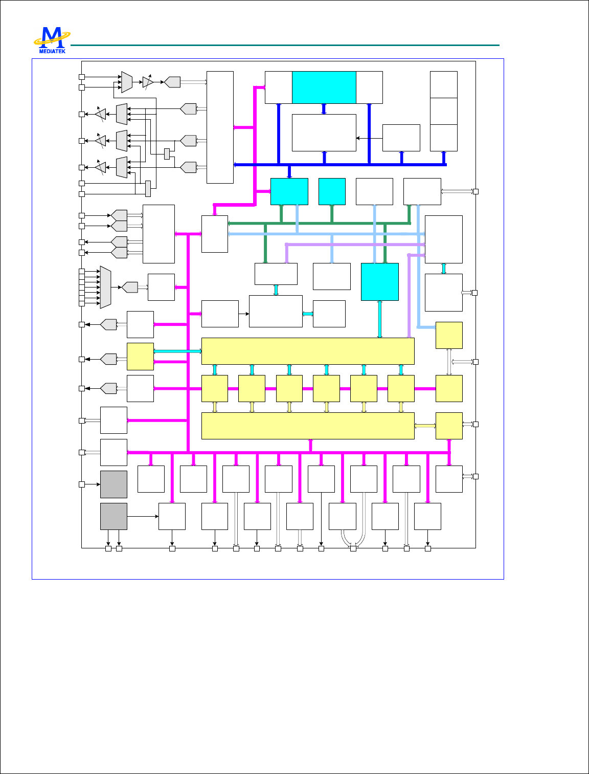
Figure 2 depicts the block diagram of MT6228. Based on a dual-processor architecture, MT6228 integrates both an
ARM7EJ-S core and a digital signal processor core. ARM7EJ-S is the main processor responsible for running
high-level GSM/GPRS protocol software as well as multi-media applications. The digital signal processor manages
the low-level MODEM as well as advanced audio functions. Except for a few mixed-signal circuitries, the other
building blocks in MT6228 are connected to either the microcontroller or the digital signal processor.
MT6228 consists of the following subsystems:
Microcontroller Unit (MCU) Subsystem: includes an ARM7EJ-S RISC processor and its accompanying
memory management and interrupt handling logics;
Digital Signal Processor (DSP) Subsystem: includes a DSP and its accompanying memory, memory controller,
and interrupt controller;
MCU/DSP Interface: the junction at which the MCU and the DSP exchange hardware and software
information;
Microcontroller Peripherals: includes all user interface modules and RF control interface modules;
Microcontroller Coprocessors: runs computing-intensive processes in place of the Microcontroller;
DSP Peripherals: hardware accelerators for GSM/GPRS channel codec;
Multi-media Subsystem: integrates several advanced accelerators to support multi-media applications;
Voice Front End: the data path for converting analog speech to and from digital speech;
Audio Front End: the data path for converting stereo audio from an audio source;
Video Front End: the data path for converting a video signal to NTSL/PAL format;
Baseband Front End: the data path for converting a digital signal to and from an analog signal from the RF
modules;
Timing Generator: generates the control signals related to the TDMA frame timing; and,
Power, Reset and Clock Subsystem: manages the power, reset, and clock distribution inside MT6228.
Details of the individual subsystems and blocks are described in the following chapters.
MTK Confidential Release for Konka
MTK Confidential Release for Konka
MT6228 GSM/GPRS Baseband Processor Data Sheet Revision 1.0
16/616 MediaTek Inc. Confidential
BSI
ARM7EJ-S
DSP INTERRUPT
CONTROL
MCU/DSP
INTERFACE
MEMORY
PATCH
UNIT
TRAP
UNIT
DSP CO-
PROCES
SOR
BOOT
ROM
ON-CHIP
SRAM
DMA
CONTROL
EXTERNAL
MEMORY
INTERFACE
INTERRUPT
CONTROL
TDMA
TIMER
DAC APC
DAC AFC
SIM GPIO
KEYPAD
BPI
WDT
ADC AUX
ADC
CLOCK
GEN
MMC
SD/MS
MS PRO
AUDIO
PATH
BASEBAND
PATH
ADC
USB OTG
ALERTER
MT6228
SERIAL RF
CONTROL
PARALLEL
RF CONTROL
APC
ADC
DAC
DAC
ADC
DAC
DAC
DAC
+
+
BRIDGE
DSP CO-
PROCES
SOR
NAND
FLASH
CON
DSP CO-
PROCES
SOR
AUXADC
AFC
TX-Q
TX-I
RX-I
RX-Q
VOICE
AUDIO-L
AUDIO-R
MIC-0
MIC-1
STEREO-L
STEREO-R
SYSTEM
CLOCK
13/26MHZ
32KHZ
CRYSTAL
SDRAM
CellularRAM
FLASH
SRAM
PSRAM
WAKE UP USER
INTERFACE
RESET
GPT
IMAGE RESIZER
JPEG
CODEC
NAND
LCD
B2PSI IRDA
PWM SERIAL
LCD
RTC
SCCB
CONNECTIVITYSERIAL PORT
GIF/PNG
DECODE
MPEG-4
VIDEO
CODEC
2D
ENGINE
IMAGE
POST
PROC
GRAPHIC MEMORY
CONTROLLER
IMAGE
SIGNAL
PROC
IMAGE
DMA
LCD
CON
32K
OSC
CMOS
SENSOR
USB OTG
UART
CACHE
TCM
TV-OUT
CON
CACHE
DACTVOUT
SECURITY
ENGINE
Figure 2 MT6228 block diagram.

MTK Confidential Release for Konka
MTK Confidential Release for Konka
MT6228 GSM/GPRS Baseband Processor Data Sheet Revision 1.0
17/616 MediaTek Inc. Confidential
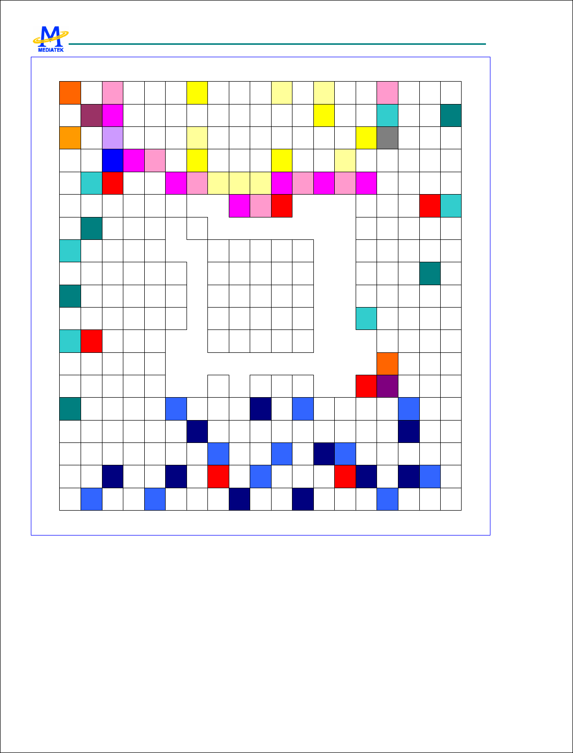
2 Product Description
2.1 Pin Outs
One type of package for this product, TFBGA 13mm*13mm, 314-ball, 0.65 mm pitch Package, is offered.
Pin-outs and the top view are illustrated in Figure 3 for this package. Outline and dimension of package is illustrated in
Figure 4, while the definition of package is shown in Table 1.
MTK Confidential Release for Konka
MTK Confidential Release for Konka
MT6228 GSM/GPRS Baseband Processor Data Sheet Revision 1.0
18/616 MediaTek Inc. Confidential
BBWA
KEUP
AUXA
DIN6
SYSCL
K
VSS33
AVDD_
RTC
AFC
AVDD_
PLL
XIN
VSS33
AFC_B
YP
AVSS_
PLL
XOUT
TESTM
ODE
JTMS
AUX_R
EF
VDDK
JTCKJTDI
BPI_B
US1
JTRST
#
BPI_B
US0
JTDOJRTCK
MT6228 TFBGA Top-View
B
A
C
E
D
F
G
H
J
K
L
M
N
P
14131211106321 87 954
GPIO7
DAIRS
T
DAIPC
MIN
ESDM
_CK
AVDD_
TV
GPIO8GPIO9
GPIO4
DAISY
NC
GPIO6
VDDK
DAICL
K
KROW
1
KROW
2
DAIPC
MOUT
KROW
3
KROW
4
VSS33
KCOL4
KCOL1KCOL2KCOL3
KCOL5KCOL6
IRDA_
PDN
IRDA_
TXD
VDDK
URXD2
IRDA_
RXD
UTXD3URXD3
VSS33
UTXD1
UTXD2
URXD1 URTS1UCTS1
SIMDA
TA
ED6ED7EADV# ERAS#
ECS1#
EWR#
ED15
ECS2#
VSS33
_EMI
VDD33
_EMI
VSS33
_EMI
ED8
ECS3#
VDDKELB# ED12 VDD33
_EMI
VDD33
_EMI
ECS0#
ED9
ECKE
ERD#
VDDK
ED14
EUB#
ED13 ED10
VSS33
_EMI EA6
EA3 VDD33
_EMI
EDCL
K
EA10
EA7
EA4
EA0
ECAS#
EA11
EA8
VSS33
_EMI
EA12
VDD33
_EMI
EA9
EA2
EA5 EA1
ECLK
SIMSE
L
GPIO2
SIMCL
K
GPIO3
VDD33
SIMRS
T
GPIO1
MCINSMCWP
MCPW
RON
MCCK
MCDA
2
MCDA
3
USB_D
M
MCDA
1
USB_D
P
VDD33
_AUX2
VSS33
_EMI
WATC
HDOG
EA25
EA24 EA22
EA13EA21
EA18 EA15
MCDA
0
VDD33
_EMI
EA19
EA20 EA16
VSS33
_EMI
VDD33
_EMI
EA17
EPDN#
1918171615
R
T
U
V
W
BPI_B
US6
BSI_C
S0
LSCE0
#
LRST#
NLD6
KROW
0
VDD33
NLD0
VDD33
MCCM
0
ED11
VSS33
_EMI
BPI_B
US2
BPI_B
US3
BPI_B
US4
BPI_B
US5
BPI_B
US7
BPI_B
US8
VSS33
BPI_B
US9
BSI_D
ATA
BSI_C
LK
LPCE1
#
VDD33 LSCE1
#
LPCE0
#
LSCK
LSDA
LRD#LPA0LWR# NLD7
NLD5VDDK NLD4
NLD2NLD1
NALENWE#
NRNB
NCLE
AU_O
UT1_P
AU_O
UT0_P
AVDD_
AFE
AU_VI
N0_P
AVSS_
AFE
BDLAI
P
AVDD_
RFE
AUXA
DIN1
BUPA
QN
AU_F
MINR
AVDD_
BUF
AU_MI
CBIAS
_N
AGND
_AFE
AU_VI
N1_P
AGND
_RFE
AVSS_
RFE
AUXA
DIN0
BUPA
QP
AU_F
MINL
AU_O
UT0_N
AU_MI
CBIAS
_P
AU_VR
EF_P
AU_VI
N1_N
BDLA
QN
BUPAI
N
APC
AUXA
DIN3
BDLAI
N
AU_M_
BYP
AU_O
UT1_N
BDLA
QP
BUPAI
P
AUXA
DIN2
AUXA
DIN5
AVSS_
GSMR
FTX
AVDD_
GSMR
FTX
AUXA
DIN4
AVSS_
BUF
AU_VR
EF_N
AVSS_
MBUF
AU_M
OUTR
AU_M
OUTL
AVDD_
MBUF
VDD33 VDD33VSS33
AU_VI
N0_N
VDD33 VSS33
VSS33
EWAIT
LSA0
SIMVC
C
NC
EA14
MFIQ
NRE#
NLD3
PWM1VDD33
MIRQ
SRCL
KENA
ED5
SRCL
KENAI
ALERT
ER
SYSRS
T#
SRCL
KENA
N
VSS33
_EMI
VDD33
_EMI
EINT1
EINT0 GPIO0 ED3
EINT3
ED2
ED4
ED1
ED0
VSS33
_EMI
EA23
NCE#
PWM2
EINT2
14131211106321 87 954 1918171615
B
A
C
E
D
F
G
H
J
K
L
M
N
P
R
T
U
V
W
GPIO5
VDD33
VSS33
KCOL0 KROW
5
VDD33VSS33
VSS33
VSS33
PLLOU
T
CMDA
T9
CMDA
T8
CMDA
T7
CMDA
T6
CMRS
T
CMPD
N
CMDA
T0
CMDA
T1
CMHR
EF
CMVR
EF
CMMC
LK
CMPC
LK
CMDA
T3
CMDA
T2
CMDA
T4
CMDA
T5
NLD16
NLD15
NLD13
NLD14 NLD11
NLD9
NLD8NLD10
TVOUT
VDD33
AVSS_
TV
FRES
VSS33
_EMI
VDD33
_EMI
VDD33
_EMI
VSS33
_EMI
VDD33
_AUX1
VDD33 VSS33
NLD17
NLD12
VDDK
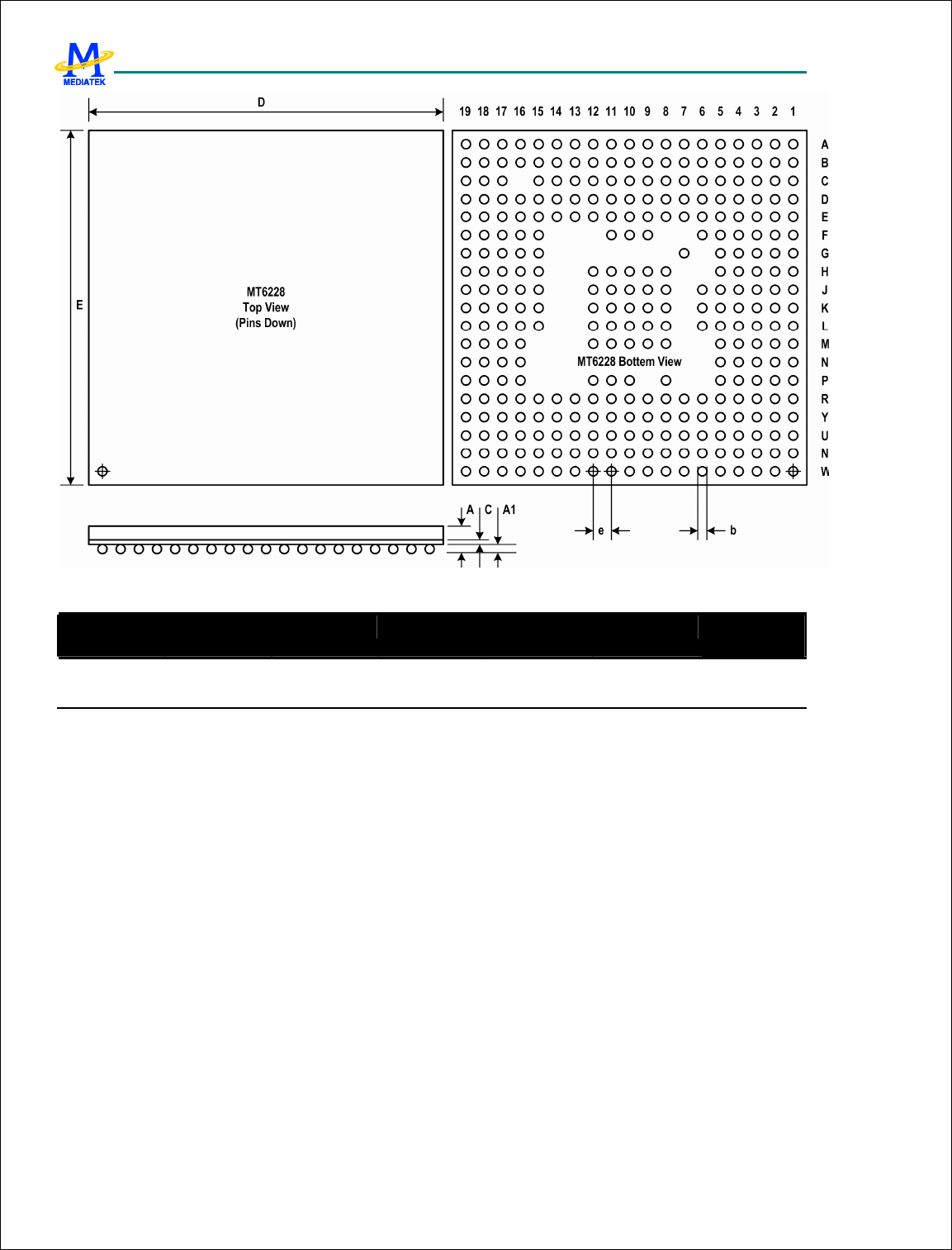
Figure 3 Top View of MT6228 TFBGA 13mm*13mm, 314-ball, 0.65 mm pitch Package
MTK Confidential Release for Konka
MTK Confidential Release for Konka
MT6228 GSM/GPRS Baseband Processor Data Sheet Revision 1.0
19/616 MediaTek Inc. Confidential
Figure 4 Outlines and Dimension of TFBGA 13mm*13mm, 314-ball, 0.65 mm pitch Package
Body Size Ball Count Ball Pitch Ball Dia. Package Thk.
Stand Off Substrate
Thk.
D E N E B A (Max.) A1 C
13 13 314 0.65 0.35 1.2 0.3 0.36
Table 1 Definition of TFBGA 13mm*13mm, 314-ball, 0.65 mm pitch Package (Unit: mm)

MTK Confidential Release for Konka
MTK Confidential Release for Konka
MT6228 GSM/GPRS Baseband Processor Data Sheet Revision 1.0
20/616 MediaTek Inc. Confidential
2.2 Top Marking Definition
S
M T 6 2 2 8T
D D D D - ## #
LLLLL
KKKKK
MT6228T: Part No.
DDDD: Date Code
###: Subcontractor Code
LLLLL: U1 Die Lot No.
KKKKK: U2 Die Lot No.
S: Special Code
MTK Confidential Release for Konka
MTK Confidential Release for Konka
MT6228 GSM/GPRS Baseband Processor Data Sheet Revision 1.0
21/616 MediaTek Inc. Confidential
2.3 DC Characteristics
2.3.1 Absolute Maximum Ratings
Prolonged exposure to absolute maximum ratings may reduce device reliability. Functional operation at these
maximum ratings is not implied.
Item Symbol Min Max Unit
IO power supply VDD33 -0.3 VDD33+0.3 V
I/O input voltage VDD33I -0.3 VDD33+0.3 V
Operating temperature Topr -20 80 Celsius
Storage temperature Tstg -55 125 Celsius
MTK Confidential Release for Konka
MTK Confidential Release for Konka
MT6228 GSM/GPRS Baseband Processor Data Sheet Revision 1.0
22/616 MediaTek Inc. Confidential
2.4 Pin Description
Ball
13X13 Name Dir Description Mode0 Mode1 Mode2 Mode3
PU/
PD
Rese
t
JTAG Port
E4 JTRST# I JTAG test port reset input PD Input
F5 JTCK I JTAG test port clock input PU Input
F4 JTDI I JTAG test port data input PU Input
F3 JTMS I JTAG test port mode switch PU Input
F2 JTDO O JTAG test port data output 0
F1 JRTCK O JTAG test port returned clock output 0
RF Parallel Control Unit
G5 BPI_BUS0 O RF hard-wire control bus 0 0
G4 BPI_BUS1 O RF hard-wire control bus 1 0
G3 BPI_BUS2 O RF hard-wire control bus 2 0
G1 BPI_BUS3 O RF hard-wire control bus 3 0
J6 BPI_BUS4 O RF hard-wire control bus 4 0
H5 BPI_BUS5 O RF hard-wire control bus 5 0
H4 BPI_BUS6 IO RF hard-wire control bus 6 GPIO16 BPI_BUS6 PD Input
H3 BPI_BUS7 IO RF hard-wire control bus 7 GPIO17 BPI_BUS7 13MHz 26MHz PD Input
H2 BPI_BUS8 IO RF hard-wire control bus 4 GPIO18 BPI_BUS8 6.5MHz 32KHz PD Input
J5 BPI_BUS9 IO RF hard-wire control bus 5 GPIO19 BPI_BUS9 BSI_CS1 BFEPRB
O PD Input
RF Serial Control Unit
J4 BSI_CS0 O RF 3-wire interface chip select 0 0
J3 BSI_DATA O RF 3-wire interface data output 0
J2 BSI_CLK O RF 3-wire interface clock output 0
PWM Interface
R4 PWM1 IO Pulse width modulated signal 1 GPIO32 PWM1 TBTXFS DSP_TID
2 PD Input
R3 PWM2 IO Pulse width modulated signal 2 GPIO33 PWM2 TBRXEN DSP_TID
3 PD Input
R2 ALERTER IO Pulse width modulated signal for
buzzer
GPIO34 ALERTER TBRXFS DSP_TID
4 PD Input
Serial LCD/PM IC Interface
J1 LSCK IO Serial display interface data output GPIO20 LSCK TDMA_C
K TBTXEN PU Input
K5 LSA0 IO Serial display interface address
output
GPIO21 LSA0 TDMA_D1 TDTIRQ PU Input
K4 LSDA IO Serial display interface clock output GPIO22 LSDA TDMA_D0 TCTIRQ2 PU Input
K3 LSCE0# IO Serial display interface chip select 0
output
GPIO23 LSCE0# TDMA_FS TCTIRQ1 PU Input
K2 LSCE1# IO Serial display interface chip select 1
output
GPIO24 LSCE1# LPCE2# TEVTVA
L PU Input
Parallel LCD/NAND-Flash
Interface
K6 LPCE1# IO Parallel display interface chip select 1
output
GPIO25 LPCE1# NCE1# DSP_TID
0 PU Input
L5 LPCE0# O Parallel display interface chip select 0
output
1
L4 LRST# O Parallel display interface Reset Signal 1
L3 LRD# O Parallel display interface Read Strobe 1

MTK Confidential Release for Konka
MTK Confidential Release for Konka
MT6228 GSM/GPRS Baseband Processor Data Sheet Revision 1.0
23/616 MediaTek Inc. Confidential
L2 LPA0 O Parallel display interface address
output
1
L1 LWR# O Parallel display interface Write
Strobe
1
G7 NLD17 IO Parallel LCD/NAND-Flash Data 17 GPIO11 NLD17 MCDA4 DSP_TID
1 PD Input
J9 NLD16 IO Parallel LCD/NAND-Flash Data 16 GPIO10 NLD16 MCDA5 DID PD Input
K9 NLD15 IO
Parallel LCD/NAND-Flash Data 15 NLD15 GPIO61 DIMS PD
Input
J10 NLD14 IO Parallel LCD/NAND-Flash Data 14 NLD14 GPIO60 DICK PD Input
L9 NDL13 IO Parallel LCD/NAND-Flash Data 13 NLD13 GPIO59 SWDBGP
KT PD Input
K10 NLD12 IO Parallel LCD/NAND-Flash Data 12 NLD12 GPIO58 SWDBG
WR PD Input
J11 NLD11 IO Parallel LCD/NAND-Flash Data 11 NLD11 GPIO57 SWDBGR
D PD Input
L10 NLD10 IO Parallel LCD/NAND-Flash Data 10 NLD10 GPIO56 SWDBGR
OE PD Input
K11 NLD9 IO Parallel LCD/NAND-Flash Data 9 NLD9 GPIO55 SWDBGA
0 PD Input
L11 NLD8 IO Parallel LCD/NAND-Flash Data 8 NLD8 GPIO54 SWDBGA
1 PD Input
L6 NLD7 IO Parallel LCD/NAND-Flash Data 7 PD Input
M5 NLD6 IO Parallel LCD/NAND-Flash Data 6 PD Input
M4 NLD5 IO Parallel LCD/NAND-Flash Data 5 PD Input
M3 NLD4 IO Parallel LCD/NAND-Flash Data 4 PD Input
N5 NLD3 IO Parallel LCD/NAND-Flash Data 3 PD Input
N4 NLD2 IO Parallel LCD/NAND-Flash Data 2 PD Input
N3 NLD1 IO Parallel LCD/NAND-Flash Data 1 PD Input
N2 NLD0 IO Parallel LCD/NAND-Flash Data 0 PD Input
N1 NRNB IO NAND-Flash Read/Busy Flag NRNB GPIO26 USBSESS
VLD SWDBGD
2 PU
P5 NCLE IO NAND-Flash Command Latch Signal NCLE GPIO27 USBVBUS
VLD SWDBGD
1 PD
P4 NALE IO NAND-Flash Address Latch Signal NALE GPIO28 USBSESS
END SWDBGD
0 PD
P3 NWE# IO NAND-Flash Write Strobe NWE# GPIO29 PU
P2 NRE# IO NAND-Flash Read Strobe NRE# GPIO30 USBVBUS
DSC SWDBGC
K PU
P1 NCE# IO NAND-Flash Chip select output NCE# GPIO31 PU
SIM Card Interface
M19 SIMRST O SIM card reset output 0
L16 SIMCLK O SIM card clock output 0
L17 SIMVCC O SIM card supply power control 0
L18 SIMSEL O SIM card supply power select GPIO48 SIMSEL PD Input
L19 SIMDATA IO SIM card data input/output 0
Dedicated GPIO Interface
U3 GPIO0 IO General purpose input/output 0 GPIO0 CMFLAS
H DSP_TID
5 PD Input
U1 GPIO1 IO General purpose input/output 1 GPIO1 BSI_RFIN PD Input
D17 GPIO2 IO General purpose input/output 2 GPIO2 SCL PU Input
C19 GPIO3 IO General purpose input/output 3 GPIO3 SDA PU Input
C18 GPIO4 IO General purpose input/output 4 GPIO4 EDICK URXD2 SWDBGD
7
C17 GPIO5 IO General purpose input/output 5 GPIO5 EDIWS UTXD2 SWDBGD
6
A19 GPIO6 IO General purpose input/output 6 GPIO6 EDIDAT SWDBGD

MTK Confidential Release for Konka
MTK Confidential Release for Konka
MT6228 GSM/GPRS Baseband Processor Data Sheet Revision 1.0
24/616 MediaTek Inc. Confidential
5
B18 GPIO7 IO General purpose input/output 7 GPIO7 USBVBUS
ON SWDBGD
4
A18 GPIO8 IO General purpose input/output 19 GPIO8 32KHz USBVBUS
CHG SWDBGF
A17 GPIO9 IO General purpose input/output 21 GPIO9 26MHz 13MHz SWDBGE
Miscellaneous
T2 SYSRST# I System reset input active low Input
R16 WATCHDO
G#
O Watchdog reset output 1
T1 SRCLKENA
N
O External TCXO enable output active
low GPO1 SRCLKE
NAN
0
T4 SRCLKENA O External TCXO enable output active
high GPO0 SRCLKE
NA
1
T3 SRCLKENAI IO External TCXO enable input GPIO31 SRCLKEN
AI PD Input
E5 TESTMODE I TESTMODE enable input PD Input
D15 ESDM_CK O Internal Monitor Clock
Keypad Interface
H17 KCOL6 I Keypad column 6 PU Input
H18 KCOL5 I Keypad column 5 PU Input
H19 KCOL4 I Keypad column 4 PU Input
G15 KCOL3 I Keypad column 3 PU Input
G16 KCOL2 I Keypad column 2 PU Input
G17 KCOL1 I Keypad column 1 PU Input
G18 KCOL0 I Keypad column 0 PU Input
G19 KROW5 O Keypad row 5 KROW5 GPIO44 ARM CK TV CK 0
F15 KROW4 O Keypad row 4 KROW4 GPIO45 AHB CK DSP CK 0
F16 KROW3 O Keypad row 3 KROW3 GPIO46 FTV CK SLOW
CK 0
F17 KROW2 O Keypad row 2 KROW2 GPIO47 FMCU CK FUSB CK 0
E16 KROW1 O Keypad row 1 0
E17 KROW0 O Keypad row 0 0
External Interrupt Interface
U2 EINT0 I External interrupt 0 PU Input
V1 EINT1 I External interrupt 1 PU Input
W1 EINT2 I External interrupt 2 PU Input
V2 EINT3 I External interrupt 3 PU Input
U4 MIRQ I Interrupt to MCU GPIO36 MIRQ 6.5MHz 32KHz PU Input
B17 MFIQ I Interrupt to MCU GPIO63 MFIQ USBID SWDBGD
3 PU Input
External Memory Interface
R15 ED0 IO External memory data bus 0 Input
T19 ED1 IO External memory data bus 1 Input
T18 ED2 IO External memory data bus 2 Input
U19 ED3 IO External memory data bus 3 Input
U18 ED4 IO External memory data bus 4 Input
V19 ED5 IO External memory data bus 5 Input
W19 ED6 IO External memory data bus 6 Input
W18 ED7 IO External memory data bus 7 Input
U17 ED8 IO External memory data bus 8 Input
W17 ED9 IO External memory data bus 9 Input
T16 ED10 IO External memory data bus 10 Input
U16 ED11 IO External memory data bus 11 Input

MTK Confidential Release for Konka
MTK Confidential Release for Konka
MT6228 GSM/GPRS Baseband Processor Data Sheet Revision 1.0
25/616 MediaTek Inc. Confidential
V16 ED12 IO External memory data bus 12 Input
T15 ED13 IO External memory data bus 13 Input
U15 ED14 IO External memory data bus 14 Input
W15 ED15 IO External memory data bus 15 Input
P12 ERD# O External memory read strobe 1
T12 EWR# O External memory write strobe 1
U12 ECS0# O External memory chip select 0 1
V12 ECS1# O External memory chip select 1 1
P11 ECS2# O External memory chip select 2 1
R11 ECS3# O External memory chip select 3 1
R14 EWAIT O Flash, PSRAM and CellularRAM
data ready
PU Input
T14 ECAS# O MobileRAM column address 1
W14 ERAS# O MobileRAM row address 1
R13 ECKE O MobileRAM clock enable 1
T13 EDCLK O MobileRAM clock
V13 ELB# O External memory lower byte strobe 1
W13 EUB# O External memory upper byte strobe 1
T11 EPDN# O PSRAM power down control GPO2 EPDN# 26Mhz 13MHz 0
W11 EADV# O Flash, PSRAM and CellularRAM
address valid 1
V11 ECLK O Flash, PSRAM and CellularRAM
clock 0
P10 EA0 O External memory address bus 0 0
T10 EA1 O External memory address bus 1 0
U10 EA2 O External memory address bus 2 0
W10 EA3 O External memory address bus 3 0
R9 EA4 O External memory address bus 4 0
T9 EA5 O External memory address bus 5 0
U9 EA6 O External memory address bus 6 0
V9 EA7 O External memory address bus 7 0
R8 EA8 O External memory address bus 8 0
T8 EA9 O External memory address bus 9 0
W8 EA10 O External memory address bus 10 0
P8 EA11 O External memory address bus 11 0
R7 EA12 O External memory address bus 12 0
U7 EA13 O External memory address bus 13 0
V7 EA14 O External memory address bus 14 0
W7 EA15 O External memory address bus 15 0
T6 EA16 O External memory address bus 16 0
U6 EA17 O External memory address bus 17 0
W6 EA18 O External memory address bus 18 0
R5 EA19 O External memory address bus 19 0
T5 EA20 O External memory address bus 20 0
U5 EA21 O External memory address bus 21 0
V5 EA22 O External memory address bus 22 0
W4 EA23 O External memory address bus 23 0
V4 EA24 O External memory address bus 24 0
W3 EA25 O External memory address bus 25 0
USB Interface
R18 USB_DP IO USB D+ Input/Output
R19 USB_DM IO USB D- Input/Output
Memory Card Interface

MTK Confidential Release for Konka
MTK Confidential Release for Konka
MT6228 GSM/GPRS Baseband Processor Data Sheet Revision 1.0
26/616 MediaTek Inc. Confidential
P17 MCCM0 IO SD Command/MS Bus State Output PU/
PD
P18 MCDA0 IO SD Serial Data IO 0/MS Serial Data
IO PU/
PD
P19 MCDA1 IO SD Serial Data IO 1 PU/
PD
N17 MCDA2 IO SD Serial Data IO 2 PU/
PD
N18 MCDA3 IO SD Serial Data IO 3 PU/
PD
M18 MCCK O SD Serial Clock/MS Serial Clock
Output
N19 MCPWRON O SD Power On Control Output
M16 MCWP I SD Write Protect Input PU/
PD Input
M17 MCINS I SD Card Detect Input PU/
PD Input
UART/IrDA Interface
K15 URXD1 I UART 1 receive data PU Input
K16 UTXD1 O UART 1 transmit data 1
K17 UCTS1 I UART 1 clear to send PU Input
K18 URTS1 O UART 1 request to send 1
K19 URXD2 IO UART 2 receive data GPIO37 URXD2 UCTS3 PU Input
J15 UTXD2 IO UART 2 transmit data GPIO38 UTXD2 URTS3 PU Input
J16 URXD3 IO UART 3 receive data GPIO39 URXD3 PU Input
J17 UTXD3 IO UART 3 transmit data GPIO40 UTXD3 DSP_TID
6 PU Input
J19 IRDA_RXD IO IrDA receive data GPIO41 IRDA_RX
D UCTS2 SWDBGD
15 PU Input
H15 IRDA_TXD IO IrDA transmit data GPIO42 IRDA_TX
D URTS2 SWDBG1
4 PU Input
H16 IRDA_PDN IO IrDA Power Down Control GPIO43 IRDA_PD
N SWDBG1
3 PU Input
Digital Audio Interface
E18 DAICLK IO DAI clock output GPIO49 DAICLK SWDBGD
12 PU Input
E19 DAIPCMOUT IO DAI pcm data out GPIO50 DAIPCMO
UT SWDBGD
11 PD Input
D16 DAIPCMIN IO DAI pcm data input GPIO51 DAIPCMI
N SWDBGD
10 PU Input
D19 DAIRST IO DAI reset signal input GPIO52 DAIRST SWDBG9 PU Input
D18 DAISYNC IO DAI frame synchronization signal
output
GPIO53 DAISYNC SWDBG8 PU Input
CMOS Sensor Interface
J12 CMRST IO CMOS sensor reset signal output GPIO12 CMRST PD Input
K12 CMPDN IO CMOS sensor power down control GPIO13 CMPDN PD Input
H12 CMVREF I Sensor vertical reference signal input PD Input
H11 CMHREF I Sensor horizontal reference signal
input
PD Input
H9 CMPCLK I CMOS sensor pixel clock input PD Input
H10 CMMCLK O CMOS sensor master clock output 0
H8 CMDAT9 I CMOS sensor data input 9 CMDAT
9
GPIO74 PD Input
J8 CMDAT8 I CMOS sensor data input 8 CMDAT
8
GPIO73 PD Input
K8 CMDAT7 I CMOS sensor data input 7 CMDAT GPIO72 PD
Input

MTK Confidential Release for Konka
MTK Confidential Release for Konka
MT6228 GSM/GPRS Baseband Processor Data Sheet Revision 1.0
27/616 MediaTek Inc. Confidential
7
L8 CMDAT6 I CMOS sensor data input 6 CMDAT
6
GPIO71 PD Input
M8 CMDAT5 I CMOS sensor data input 5 CMDAT
5
GPIO70 PD Input
M9 CMDAT4 I CMOS sensor data input 4 CMDAT
4
GPIO69 PD Input
M10 CMDAT3 I CMOS sensor data input 3 CMDAT
3
GPIO68 PD
Input
M11 CMDAT2 I CMOS sensor data input 2 CMDAT
2
GPIO62 PD Input
M12 CMDAT1 IO CMOS sensor data input 1 GPIO50 CMDAT1 PD Input
L12 CMDAT0 IO CMOS sensor data input 0 GPIO51 CMDAT0 PD Input
Analog Interface
B15 AU_MOUL Audio analog output left channel
A15 AU_MOUR Audio analog output right channel
C14 AU_M_BYP Audio DAC bypass pin
B14 AU_FMINL FM radio analog input left channel
A14 AU_FMINR FM radio analog input right channel
D13 AU_OUT1_P Earphone 1 amplifier output (+)
C13 AU_OUT1_N Earphone 1 amplifier output (-)
B12 AU_OUT0_N Earphone 0 amplifier output (-)
A12 AU_OUT0_P Earphone 0 amplifier output (+)
C12 AU_MICBIA
S_P
Microphone bias supply (+)
D12 AU_MICBIA
S_N
Microphone bias supply (-)
C11 AU_VREF_N Audio reference voltage (-)
B11 AU_VREF_P Audio reference voltage (+)
D10 AU_VIN0_P Microphone 0 amplifier input (+)
C10 AU_VIN0_N Microphone 0 amplifier input (-)
B10 AU_VIN1_N Microphone 1 amplifier input (-)
A10 AU_VIN1_P Microphone 1 amplifier input (+)
D9 BDLAQP Quadrature input (Q+) baseband
codec downlink
C9 BDLAQN Quadrature input (Q-) baseband
codec downlink
A9 BDLAIN In-phase input (I+) baseband codec
downlink
B9 BDLAIP In-phase input (I-) baseband codec
downlink
B8 BUPAIP In-phase output (I+) baseband codec
uplink
A8 BUPAIN In-phase output (I-) baseband codec
uplink
C8 BUPAQN Quadrature output (Q+) baseband
codec uplink
D8 BUPAQP Quadrature output (Q-) baseband
codec uplink
B7 APC Automatic power control DAC output
D6 AUXADIN0 Auxiliary ADC input 0
C6 AUXADIN1 Auxiliary ADC input 1
B6 AUXADIN2 Auxiliary ADC input 2
A6 AUXADIN3 Auxiliary ADC input 3
C5 AUXADIN4 Auxiliary ADC input 4
B5 AUXADIN5 Auxiliary ADC input 5

MTK Confidential Release for Konka
MTK Confidential Release for Konka
MT6228 GSM/GPRS Baseband Processor Data Sheet Revision 1.0
28/616 MediaTek Inc. Confidential
A5 AUXADIN6 Auxiliary ADC input 6
C4 AUX_REF Auxiliary ADC reference voltage
input
B4 AFC Automatic frequency control DAC
output
A4 AFC_BYP Automatic frequency control DAC
bypass capacitance
VCXO Interface
B1 SYSCLK 13MHz or 26MHz system clock input
F6 PLLOUT PLL reference voltage output
RTC Interface
D1 XIN 32.768 KHz crystal input
D2 XOUT 32.768 KHz crystal output
E1 BBWAKEUP O Baseband power on/off control 1
TV Interface
A2 TVOUT TV DAC Output
C2 FSRES
Supply Voltages
E3 VDDK Supply voltage of internal logic
M2 VDDK Supply voltage of internal logic
V8 VDDK Supply voltage of internal logic
V14 VDDK Supply voltage of internal logic
F18 VDDK Supply voltage of internal logic
F11 VDDK Supply voltage of internal logic
V3 VDD33_EMI Supply voltage of memory interface
driver
V6 VDD33_EMI Supply voltage of memory interface
driver
T7 VDD33_EMI Supply voltage of memory interface
driver
W9 VDD33_EMI Supply voltage of memory interface
driver
R10 VDD33_EMI Supply voltage of memory interface
driver
W12 VDD33_EMI Supply voltage of memory interface
driver
U13 VDD33_EMI Supply voltage of memory interface
driver
V15 VDD33_EMI Supply voltage of memory interface
driver
T17 VDD33_EMI Supply voltage of memory interface
driver
V17 VDD33_EMI Supply voltage of memory interface
driver
W5 VSS33_EMI Ground of memory interface driver
R6 VSS33_EMI Ground of memory interface driver
U8 VSS33_EMI Ground of memory interface driver
V10 VSS33_EMI Ground of memory interface driver
U11 VSS33_EMI Ground of memory interface driver
R12 VSS33_EMI Ground of memory interface driver
U14 VSS33_EMI Ground of memory interface driver
W16 VSS33_EMI Ground of memory interface driver
R17 VSS33_EMI Ground of memory interface driver
V18 VSS33_EMI Ground of memory interface driver

MTK Confidential Release for Konka
MTK Confidential Release for Konka
MT6228 GSM/GPRS Baseband Processor Data Sheet Revision 1.0
29/616 MediaTek Inc. Confidential
P16 VDD33_AUX
2
Supply voltage of drivers for USB
N16 VDD33_AUX
1
Supply Voltage of MS/MMC/SD
G2 VDD33 Supply voltage of drivers except
memory interface, USB and
MS/MMC/SD
K1 VDD33 Supply voltage of drivers except
memory interface, USB and
MS/MMC/SD
R1 VDD33 Supply voltage of drivers except
memory interface, USB and
MS/MMC/SD
J18 VDD33 Supply voltage of drivers except
memory interface, USB and
MS/MMC/SD
B19 VDD33 Supply voltage of drivers except
memory interface, USB and
MS/MMC/SD
E15 VDD33 Supply voltage of drivers except
memory interface, USB and
MS/MMC/SD
E13 VDD33 Supply voltage of drivers except
memory interface, USB and
MS/MMC/SD
E11 VDD33 Supply voltage of drivers except
memory interface, USB and
MS/MMC/SD
F9 VDD33 Supply voltage of drivers except
memory interface, USB and
MS/MMC/SD
E6 VDD33 Supply voltage of drivers except
memory interface, USB and
MS/MMC/SD
D4 VDD33 Supply voltage of drivers except
memory interface, USB and
MS/MMC/SD
B3 VDD33 Supply voltage of drivers except
memory interface, USB and
MS/MMC/SD
W2 VSS33 Ground of drivers except memory
interface, USB and MS/MMC/SD
E2 VSS33 Ground of drivers except memory
interface, USB and MS/MMC/SD
H1 VSS33 Ground of drivers except memory
interface, USB and MS/MMC/SD
M1 VSS33 Ground of drivers except memory
interface, USB and MS/MMC/SD
L15 VSS33 Ground of drivers except memory
interface, USB and MS/MMC/SD
F19 VSS33 Ground of drivers except memory
interface, USB and MS/MMC/SD
B16 VSS33 Ground of drivers except memory
interface, USB and MS/MMC/SD
A16 VSS33 Ground of drivers except memory
interface, USB and MS/MMC/SD
E14 VSS33 Ground of drivers except memory
interface, USB and MS/MMC/SD
E12 VSS33 Ground of drivers except memory
interface, USB and MS/MMC/SD

MTK Confidential Release for Konka
MTK Confidential Release for Konka
MT6228 GSM/GPRS Baseband Processor Data Sheet Revision 1.0
30/616 MediaTek Inc. Confidential
F10 VSS33 Ground of drivers except memory
interface, USB and MS/MMC/SD
E7 VSS33 Ground of drivers except memory
interface, USB and MS/MMC/SD
D5 VSS33 Ground of drivers except memory
interface, USB and MS/MMC/SD
A3 VSS33 Ground of drivers except memory
interface, USB and MS/MMC/SD
A1 AVDD_PLL Supply voltage for PLL
C1 AVSS_PLL Ground for PLL supply
B2 AVDD_TV Supply voltage for TV out
C3 AVSS_TV Ground for TV out
D3 AVDD_RTC Supply voltage for Real Time Clock
Analog Supplies
C15 AVDD_MBU
F
Supply Voltage for Audio band
section
D14 AVSS_MBUF GND for Audio band section
B13 AVDD_BUF Supply voltage for voice band
transmit section
A13 AVSS_BUF GND for voice band transmit section
D11 AVDD_AFE Supply voltage for voice band receive
section
A11 AGND_AFE GND reference voltage for voice
band section
E10 AVSS_AFE GND for voice band receive section
E9 AGND_RFE GND reference voltage for baseband
section, APC, AFC and AUXADC
E8 AVSS_GSMR
FTX GND for baseband transmit section
D7 AVDD_GSM
RFTX
Supply voltage for baseband transmit
section
C7 AVSS_RFE GND for baseband receive section,
APC, AFC and AUXADC
A7 AVDD_RFE Supply voltage for baseband receive
section, APC, AFC and AUXADC
Table 2 Pin Descriptions (Bolded types are functions at reset)

MTK Confidential Release for Konka
MTK Confidential Release for Konka
MT6228 GSM/GPRS Baseband Processor Data Sheet Revision 1.0
31/616 MediaTek Inc. Confidential
2.5 Power Description
Ball
13X13 Name IO Supply IO GND Core Supply Core GND Remark
A16 VSS33
E15 VDD33 Typ. 2.8V
E14 VSS33
E13 VDD33 Typ. 2.8V
E12 VSS33
E11 VDD33 Typ. 2.8V
F11 VDDK Typ. 1.2V
F10 VSS33
F9 VDD33 Typ. 2.8V
E7 VSS33
E6 VDD33 Typ. 2.8V
D5 VSS33
J12 CMRST VDD33 VSS33 VDDK VSSK
K12 CMPDN VDD33 VSS33 VDDK VSSK
H12 CMVREF VDD33 VSS33 VDDK VSSK
H11 CMHREF VDD33 VSS33 VDDK VSSK
H9 CMPCLK VDD33 VSS33 VDDK VSSK
H10 CMMCLK VDD33 VSS33 VDDK VSSK
D4 VDD33 Typ. 2.8V
H8 CMDAT9 VDD33 VSS33 VDDK VSSK
J8 CMDAT8 VDD33 VSS33 VDDK VSSK
K8 CMDAT7 VDD33 VSS33 VDDK VSSK
L8 CMDAT6 VDD33 VSS33 VDDK VSSK
M8 CMDAT5 VDD33 VSS33 VDDK VSSK
A3 VSS33
M9 CMDAT4 VDD33 VSS33 VDDK VSSK
M10 CMDAT3 VDD33 VSS33 VDDK VSSK
M11 CMDAT2 VDD33 VSS33 VDDK VSSK
M12 CMDAT1 VDD33 VSS33 VDDK VSSK
L12 CMDAT0 VDD33 VSS33 VDDK VSSK
B3 VDD33 Typ. 2.8V
B2 AVDD_TV Typ. 2.8V
A2 TVOUT AVDD_TV AVSS_TV AVDD_TV AVSS_TV
C2 FSRES AVDD_TV AVSS_TV AVDD_TV AVSS_TV
C3 AVSS_TV
A1 AVDD_PLL Typ. 2.8V
B1 SYSCLK AVDD_PLL AVSS_PLL AVDD_PLL AVSS_PLL
F6 PLLOUT AVDD_PLL AVSS_PLL AVDD_PLL AVSS_PLL
C1 AVSS_PLL
D3 AVDD_RTC Typ. 1.2V
D2 XOUT AVDD_RTC VSS33 AVDD_RTC VSS33
D1 XIN AVDD_RTC VSS33 AVDD_RTC VSS33
E1 BBWAKEUP AVDD_RTC VSS33 AVDD_RTC VSS33
E2 VSS33
E5 TESTMODE VDD33 VSS33 VDDK VSSK
E3 VDDK Typ. 1.2V
E4 JTRST# VDD33 VSS33 VDDK VSSK
F5 JTCK VDD33 VSS33 VDDK VSSK

MTK Confidential Release for Konka
MTK Confidential Release for Konka
MT6228 GSM/GPRS Baseband Processor Data Sheet Revision 1.0
32/616 MediaTek Inc. Confidential
F4 JTDI VDD33 VSS33 VDDK VSSK
F3 JTMS VDD33 VSS33 VDDK VSSK
F2 JTDO VDD33 VSS33 VDDK VSSK
F1 JRTCK VDD33 VSS33 VDDK VSSK
G5 BPI_BUS0 VDD33 VSS33 VDDK VSSK
G4 BPI_BUS1 VDD33 VSS33 VDDK VSSK
G2 VDD33 Typ. 2.8V
G3 BPI_BUS2 VDD33 VSS33 VDDK VSSK
G1 BPI_BUS3 VDD33 VSS33 VDDK VSSK
J6 BPI_BUS4 VDD33 VSS33 VDDK VSSK
H5 BPI_BUS5 VDD33 VSS33 VDDK VSSK
H4 BPI_BUS6 VDD33 VSS33 VDDK VSSK
H3 BPI_BUS7 VDD33 VSS33 VDDK VSSK
H2 BPI_BUS8 VDD33 VSS33 VDDK VSSK
H1 VSS33
J5 BPI_BUS9 VDD33 VSS33 VDDK VSSK
J4 BSI_CS0 VDD33 VSS33 VDDK VSSK
J3 BSI_DATA VDD33 VSS33 VDDK VSSK
J2 BSI_CLK VDD33 VSS33 VDDK VSSK
J1 LSCK VDD33 VSS33 VDDK VSSK
K5 LSA0 VDD33 VSS33 VDDK VSSK
K4 LSDA VDD33 VSS33 VDDK VSSK
K3 LSCE0# VDD33 VSS33 VDDK VSSK
K2 LSCE1# VDD33 VSS33 VDDK VSSK
K1 VDD33 Typ. 2.8V
K6 LPCE1# VDD33 VSS33 VDDK VSSK
L5 LPCE0# VDD33 VSS33 VDDK VSSK
L4 LRST# VDD33 VSS33 VDDK VSSK
L3 LRD# VDD33 VSS33 VDDK VSSK
L2 LPA0 VDD33 VSS33 VDDK VSSK
L1 LWR# VDD33 VSS33 VDDK VSSK
L6 NLD7 VDD33 VSS33 VDDK VSSK
M5 NLD6 VDD33 VSS33 VDDK VSSK
M4 NLD5 VDD33 VSS33 VDDK VSSK
M1 VSS33
M2 VDDK Typ. 1.2V
M3 NLD4 VDD33 VSS33 VDDK VSSK
N5 NLD3 VDD33 VSS33 VDDK VSSK
N4 NLD2 VDD33 VSS33 VDDK VSSK
N3 NLD1 VDD33 VSS33 VDDK VSSK
N2 NLD0 VDD33 VSS33 VDDK VSSK
N1 NRNB VDD33 VSS33 VDDK VSSK
P5 NCLE VDD33 VSS33 VDDK VSSK
P4 NALE VDD33 VSS33 VDDK VSSK
P3 NWE# VDD33 VSS33 VDDK VSSK
P2 NRE# VDD33 VSS33 VDDK VSSK
P1 NCE# VDD33 VSS33 VDDK VSSK
R1 VDD33 Typ. 2.8V
R4 PWM1 VDD33 VSS33 VDDK VSSK
R3 PWM2 VDD33 VSS33 VDDK VSSK
R2 ALERTER VDD33 VSS33 VDDK VSSK
T4 SRCLKENA VDD33 VSS33 VDDK VSSK

MTK Confidential Release for Konka
MTK Confidential Release for Konka
MT6228 GSM/GPRS Baseband Processor Data Sheet Revision 1.0
33/616 MediaTek Inc. Confidential
T1 SRCLKENAN VDD33 VSS33 VDDK VSSK
T3 SRCLKENAI VDD33 VSS33 VDDK VSSK
T2 SYSRST# VDD33 VSS33 VDDK VSSK
U3 GPIO0 VDD33 VSS33 VDDK VSSK
U1 GPIO1 VDD33 VSS33 VDDK VSSK
U2 EINT0 VDD33 VSS33 VDDK VSSK
V1 EINT1 VDD33 VSS33 VDDK VSSK
W1 EINT2 VDD33 VSS33 VDDK VSSK
V2 EINT3 VDD33 VSS33 VDDK VSSK
W2 VSS33
V3 VDD33_EMI Typ. 1.8/2.8V
U4 MIRQ VDD33_EMI VSS33_EMI VDDK VSSK
W3 EA25 VDD33_EMI VSS33_EMI VDDK VSSK
V4 EA24 VDD33_EMI VSS33_EMI VDDK VSSK
W4 EA23 VDD33_EMI VSS33_EMI VDDK VSSK
W5 VSS33_EMI
V5 EA22 VDD33_EMI VSS33_EMI VDDK VSSK
U5 EA21 VDD33_EMI VSS33_EMI VDDK VSSK
T5 EA20 VDD33_EMI VSS33_EMI VDDK VSSK
R5 EA19 VDD33_EMI VSS33_EMI VDDK VSSK
V6 VDD33_EMI Typ. 1.8/2.8V
W6 EA18 VDD33_EMI VSS33_EMI VDDK VSSK
U6 EA17 VDD33_EMI VSS33_EMI VDDK VSSK
T6 EA16 VDD33_EMI VSS33_EMI VDDK VSSK
R6 VSS33_EMI
W7 EA15 VDD33_EMI VSS33_EMI VDDK VSSK
V7 EA14 VDD33_EMI VSS33_EMI VDDK VSSK
U7 EA13 VDD33_EMI VSS33_EMI VDDK VSSK
T7 VDD33_EMI Typ. 1.8/2.8V
R7 EA12 VDD33_EMI VSS33_EMI VDDK VSSK
P8 EA11 VDD33_EMI VSS33_EMI VDDK VSSK
W8 EA10 VDD33_EMI VSS33_EMI VDDK VSSK
V8 VDDK Typ. 1.2V
U8 VSS33_EMI
T8 EA9 VDD33_EMI VSS33_EMI VDDK VSSK
R8 EA8 VDD33_EMI VSS33_EMI VDDK VSSK
V9 EA7 VDD33_EMI VSS33_EMI VDDK VSSK
W9 VDD33_EMI Typ. 1.8/2.8V
U9 EA6 VDD33_EMI VSS33_EMI VDDK VSSK
T9 EA5 VDD33_EMI VSS33_EMI VDDK VSSK
R9 EA4 VDD33_EMI VSS33_EMI VDDK VSSK
V10 VSS33_EMI
W10 EA3 VDD33_EMI VSS33_EMI VDDK VSSK
U10 EA2 VDD33_EMI VSS33_EMI VDDK VSSK
T10 EA1 VDD33_EMI VSS33_EMI VDDK VSSK
R10 VDD33_EMI Typ. 1.8/2.8V
P10 EA0 VDD33_EMI VSS33_EMI VDDK VSSK
W11 EADV# VDD33_EMI VSS33_EMI VDDK VSSK
V11 ECLK VDD33_EMI VSS33_EMI VDDK VSSK
U11 VSS33_EMI
T11 EPDN# VDD33_EMI VSS33_EMI VDDK VSSK
R11 ECS3# VDD33_EMI VSS33_EMI VDDK VSSK

MTK Confidential Release for Konka
MTK Confidential Release for Konka
MT6228 GSM/GPRS Baseband Processor Data Sheet Revision 1.0
34/616 MediaTek Inc. Confidential
P11 ECS2# VDD33_EMI VSS33_EMI VDDK VSSK
W12 VDD33_EMI Typ. 1.8/2.8V
V12 ECS1# VDD33_EMI VSS33_EMI VDDK VSSK
U12 ECS0# VDD33_EMI VSS33_EMI VDDK VSSK
T12 EWR# VDD33_EMI VSS33_EMI VDDK VSSK
R12 VSS33_EMI
P12 ERD# VDD33_EMI VSS33_EMI VDDK VSSK
W13 EUB# VDD33_EMI VSS33_EMI VDDK VSSK
V13 ELB# VDD33_EMI VSS33_EMI VDDK VSSK
U13 VDD33_EMI Typ. 1.8/2.8V
T13 EDCLK VDD33_EMI VSS33_EMI VDDK VSSK
R13 ECKE VDD33_EMI VSS33_EMI VDDK VSSK
W14 ERAS# VDD33_EMI VSS33_EMI VDDK VSSK
V14 VDDK Typ. 1.2V
U14 VSS33_EMI
T14 ECAS# VDD33_EMI VSS33_EMI
R14 EWAIT VDD33_EMI VSS33_EMI
W15 ED15 VDD33_EMI VSS33_EMI VDDK VSSK
V15 VDD33_EMI Typ. 1.8/2.8V
U15 ED14 VDD33_EMI VSS33_EMI VDDK VSSK
T15 ED13 VDD33_EMI VSS33_EMI VDDK VSSK
V16 ED12 VDD33_EMI VSS33_EMI VDDK VSSK
W16 VSS33_EMI
U16 ED11 VDD33_EMI VSS33_EMI VDDK VSSK
T16 ED10 VDD33_EMI VSS33_EMI VDDK VSSK
W17 ED9 VDD33_EMI VSS33_EMI VDDK VSSK
V17 VDD33_EMI Typ. 1.8/2.8V
U17 ED8 VDD33_EMI VSS33_EMI VDDK VSSK
W18 ED7 VDD33_EMI VSS33_EMI VDDK VSSK
W19 ED6 VDD33_EMI VSS33_EMI VDDK VSSK
V18 VSS33_EMI
V19 ED5 VDD33_EMI VSS33_EMI VDDK VSSK 1.2V
U18 ED4 VDD33_EMI VSS33_EMI VDDK VSSK
U19 ED3 VDD33_EMI VSS33_EMI VDDK VSSK
T17 VDD33_EMI Typ. 1.8/2.8V
T18 ED2 VDD33_EMI VSS33_EMI VDDK VSSK
T19 ED1 VDD33_EMI VSS33_EMI VDDK VSSK
R15 ED0 VDD33_EMI VSS33_EMI VDDK VSSK
R16 WATCHDOG VDD33_EMI VSS33_EMI VDDK VSSK
R17 VSS33_EMI
R18 USB_DP VDD33_AUX2 VSS33 VDDK VSSK
R19 USB_DM VDD33_AUX2 VSS33 VDDK VSSK
P16 VDD33_AUX2 Typ. 3.3V
N16 VDD33_AUX1 Typ. 3.3V
P17 MCCM0 VDD33_AUX1 VSS33 VDDK VSSK
P18 MCDA0 VDD33_AUX1 VSS33 VDDK VSSK
P19 MCDA1 VDD33_AUX1 VSS33 VDDK VSSK
N17 MCDA2 VDD33_AUX1 VSS33 VDDK VSSK
N18 MCDA3 VDD33_AUX1 VSS33 VDDK VSSK
N19 MCPWRON VDD33_AUX1 VSS33 VDDK VSSK
M16 MCWP VDD33_AUX1 VSS33 VDDK VSSK
M17 MCINS VDD33_AUX1 VSS33 VDDK VSSK
M18 MCCK VDD33_AUX1 VSS33 VDDK VSSK

MTK Confidential Release for Konka
MTK Confidential Release for Konka
MT6228 GSM/GPRS Baseband Processor Data Sheet Revision 1.0
35/616 MediaTek Inc. Confidential
L15 VSS33
M19 SIMRST VDD33 VSS33 VDDK VSSK
L16 SIMCLK VDD33 VSS33 VDDK VSSK
L17 SIMVCC VDD33 VSS33 VDDK VSSK
L18 SIMSEL VDD33 VSS33 VDDK VSSK
L19 SIMDATA VDD33 VSS33 VDDK VSSK
K15 URXD1 VDD33 VSS33 VDDK VSSK
K16 UTXD1 VDD33 VSS33 VDDK VSSK
K17 UCTS1 VDD33 VSS33 VDDK VSSK
K18 URTS1 VDD33 VSS33 VDDK VSSK
K19 URXD2 VDD33 VSS33 VDDK VSSK
J15 UTXD2 VDD33 VSS33 VDDK VSSK
J16 URXD3 VDD33 VSS33 VDDK VSSK
J17 UTXD3 VDD33 VSS33 VDDK VSSK
J18 VDD33 Typ. 2.8V
J19 IRDA_RXD VDD33 VSS33 VDDK VSSK
H15 IRDA_TXD VDD33 VSS33 VDDK VSSK
H16 IRDA_PDN VDD33 VSS33 VDDK VSSK
H17 KCOL6 VDD33 VSS33 VDDK VSSK
H18 KCOL5 VDD33 VSS33 VDDK VSSK
H19 KCOL4 VDD33 VSS33 VDDK VSSK
G15 KCOL3 VDD33 VSS33 VDDK VSSK
G16 KCOL2 VDD33 VSS33 VDDK VSSK
G17 KCOL1 VDD33 VSS33 VDDK VSSK
G18 KCOL0 VDD33 VSS33 VDDK VSSK
G19 KROW5 VDD33 VSS33 VDDK VSSK
F15 KROW4 VDD33 VSS33 VDDK VSSK
F16 KROW3 VDD33 VSS33 VDDK VSSK
F17 KROW2 VDD33 VSS33 VDDK VSSK
F18 VDDK Typ. 1.2V
F19 VSS33
E16 KROW1 VDD33 VSS33 VDDK VSSK
E17 KROW0 VDD33 VSS33 VDDK VSSK
E18 DAICLK VDD33 VSS33 VDDK VSSK
E19 DAIPCMOUT VDD33 VSS33 VDDK VSSK
D16 DAIPCMIN VDD33 VSS33 VDDK VSSK
D19 DAIRST VDD33 VSS33 VDDK VSSK
D18 DAISYNC VDD33 VSS33 VDDK VSSK
D17 GPIO2 VDD33 VSS33 VDDK VSSK
C19 GPIO3 VDD33 VSS33 VDDK VSSK
C18 GPIO4 VDD33 VSS33 VDDK VSSK
B19 VDD33 Typ. 2.8V
C17 GPIO5 VDD33 VSS33 VDDK VSSK
A19 GPIO6 VDD33 VSS33 VDDK VSSK
B18 GPIO7 VDD33 VSS33 VDDK VSSK
B17 MFIQ VDD33 VSS33 VDDK VSSK
A18 GPIO8 VDD33 VSS33 VDDK VSSK
A17 GPIO9 VDD33 VSS33 VDDK VSSK
B16 VSS33
C15 AVDD_MBUF Typ. 2.8V
B15 AU_MOUTL
A15 AU_MOUTR
D14 AVSS_MBUF

MTK Confidential Release for Konka
MTK Confidential Release for Konka
MT6228 GSM/GPRS Baseband Processor Data Sheet Revision 1.0
36/616 MediaTek Inc. Confidential
C14 AU_M_BYP
B14 AU_FMINL
A14 AU_FMINR
D13 AU_OUT1_P
C13 AU_OUT1_N
B12 AU_OUT0_N
B13 AVDD_BUF Typ. 2.8V
A12 AU_OUT0_P
A13 AVSS_BUF
C12 AU_MICBIAS_P
D12 AU_MICBIAS_N
D11 AVDD_AFE Typ. 2.8V
C11 AU_VREF_N
B11 AU_VREF_P
A11 AGND_AFE
D10 AU_VIN0_P
C10 AU_VIN0_N
B10 AU_VIN1_N
A10 AU_VIN1_P
E10 AVSS_AFE
D9 BDLAQP
C9 BDLAQN
E9 AGND_RFE
A9 BDLAIN
B9 BDLAIP
E8 AVSS_GSMRFTX
B8 BUPAIP
A8 BUPAIN
D7 AVDD_GSMRFTX Typ. 2.8V
C8 BUPAQN
D8 BUPAQP
C7 AVSS_RFE
B7 APC
A7 AVDD_RFE Typ. 2.8V
D6 AUXADIN0
C6 AUXADIN1
B6 AUXADIN2
A6 AUXADIN3
C5 AUXADIN4
B5 AUXADIN5
A5 AUXADIN6
C4 AUX_REF
B4 AFC
A4 AFC_BYP
Table 3 Power Descriptions

MTK Confidential Release for Konka
MTK Confidential Release for Konka
MT6228 GSM/GPRS Baseband Processor Data Sheet Revision 1.0
37/616 MediaTek Inc. Confidential
3 Micro-Controller Unit Subsystem
Figure 5 illustrates the block diagram of the Micro-Controller Unit Subsystem in MT6228. The subsystem utilizes a
main 32-bit ARM7EJ-S RISC processor, which plays the role of the main bus master controlling the whole subsystem.
All processor transactions go to code cache first. The code cache controller accesses TCM (128KB memory dedicated
to ARM7EJS core), cache memory, or bus according to the processor’s request address. If the requested content is
found in TCM or in cache, no bus transaction is required. If the code cache hit rate is high enough, bus traffic can be
effectively reduced and processor core performance maximized. In addition to the benefits of reuse of memory
contents, code cache also has a MPU (Memory Protection Unit), which allows cacheable and protection settings of
predefined regions. The contents of code cache are only accessible to MCU, and only MCU instructions are kept in
the cache memory (thus the name “code” cache).
The bus comprises of two-level system buses: Advanced High-Performance Bus (AHB) and Advanced Peripheral Bus
(APB). All bus transactions originate from bus masters, while slaves can only respond to requests from bus masters.
Before data transfer can be established, the bus master must ask for bus ownership, accomplished by request-grant
handshaking protocol between masters and arbiters.
Two levels of bus hierarchy are designed to provide optimum usage for different performance requirements.
Specifically, AHB Bus, the main system bus, is tailored toward high-speed requirements and provides 32-bit data path
with multiplex scheme for bus interconnections. The APB Bus, on the other hand, is designed to reduce interface
complexity for lower data transfer rate, and so it is isolated from high bandwidth AHB Bus by APB Bridge. APB Bus
supports 16-bit addressing and both 16-bit and 32-bit data paths. APB Bus is also optimized for minimal power
consumption by turning off the clock when there is no APB bus activity.
During operation, if the target slave is located on AHB Bus, the transaction is conducted directly on AHB Bus.
However, if the target slave is a peripheral and is attached to the APB bus, then the transaction is conducted between
AHB and APB bus through the use of APB Bridge.
The MT6228 MCU subsystem supports only memory addressing method. Therefore all components are mapped onto
the MCU 32-bit address space. A Memory Management Unit is employed to allow for a central decode scheme.
The MMU generates appropriate selection signals for each memory-addressed module on the AHB Bus.
In order to off-load the processor core, a DMA Controller is designated to act as a master and share the bus resources
on AHB Bus to perform fast data movement between modules. This controller provides fourteen DMA channels.
The Interrupt Controller provides a software interface to manipulate interrupt events; it can handle up to 32 interrupt
sources asserted at the same time. In general, the controller generates 2 levels of interrupt requests, FIQ and IRQ, to
the processor.
A 128K Byte SRAM is provided as system memory for high-speed data access. For factory programming purposes, a
Boot ROM module is also integrated. These two modules use the same Internal Memory Controller to connect to
AHB Bus.
External Memory Interface supports both 8-bit and 16-bit devices. This interface supports both synchronous and
asynchronous components, such as Flash, SRAM and parallel LCD. This interface supports page and burst mode type
of Flash, Cellular RAM, as well as high performance MobileRAM. In order to take advantages of burst- or page-type
devices, a data cache is introduced and placed between AHB Bus and EMI, allowing the data cache to issue burst
requests to EMI whenever possible. Since AHB Bus is 32-bit wide, all data transfers are converted into several 8-bit
or 16-bit cycles depending on the data width of the target device. In contrast to code cache, contents in data cache are
queried when MCU issues data requests, or when other AHB bus masters issue memory requests to EMI.
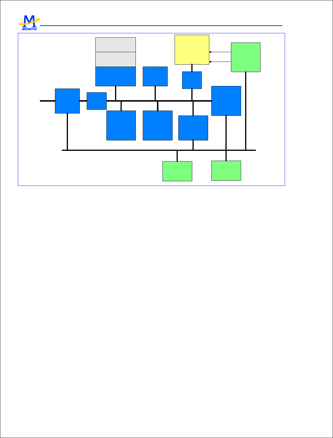
MTK Confidential Release for Konka
MTK Confidential Release for Konka
MT6228 GSM/GPRS Baseband Processor Data Sheet Revision 1.0
38/616 MediaTek Inc. Confidential
MCU-DSP
Interface
ARM7EJ-S
External
Memory
Interface
System RAM
DMA
Controller
APB
Bridge
System ROM
Peripheral
Peripheral
Interrupt
Controller
Internal Memory
Controller Arbiter
AHB Bus
APB Bus
Ext
Bus
USB
code
cache
data
cache
Figure 5 Block Diagram of the Micro-Controller Unit Subsystem in MT6228
3.1 Processor Core
3.1.1 General Description
The Micro-Controller Unit Subsystem in MT6228 uses the 32-bit ARM7EJ-S RISC processor that is based on the Von
Neumann architecture with a single 32-bit data bus carrying both instructions and data. The memory interface of
ARM7EJ-S is totally compliant with the AMBA based bus system, which allows direct connection to the AHB Bus.
3.2 Memory Management
3.2.1 General Description
The processor core of MT6228 supports only a memory addressing method for instruction fetch and data access. The
core manages a 32-bit address space that has addressing capability of up to 4 GB. System RAM, System ROM,
Registers, MCU Peripherals and external components are all mapped onto such 32-bit address space, as depicted in
Figure 6.

MTK Confidential Release for Konka
MTK Confidential Release for Konka
MT6228 GSM/GPRS Baseband Processor Data Sheet Revision 1.0
39/616 MediaTek Inc. Confidential
MCU 32-bit
Addressing
Space
EA[25:0]
Addressing
Space
APB Peripherals
MCU-DSP Interface
Reserved
8FFF_FFFFh
|
8000_0000h
7FFF_FFFFh
|
7000_0000h
6FFF_FFFFh
|
5000_0000h
4FFF_FFFFh
|
4000_0000h
3FFF_FFFFh
|
0000_0000h
External Memroy
Internal Memory
7800_0000h
7000_0000h USB
Virtual FIFO
9FFF_FFFh
|
9000_0000h
9800_0000h
9000_0000h LCD
Reserved
TCM
AFFF_FFFh
|
A000_0000h
Figure 6 The Memory Layout of MT6228
The address space is organized into blocks of 256 MB each. Memory blocks 0-AFFFFFFFh are defined and currently
dedicated to specific functions, while the others are reserved for future usage. The block number is uniquely selected
by address line A31-A28 of the internal system bus.
3.2.1.1 External Access
To allow external access, the MT6228 outputs 26 bits (A25-A0) of address lines along with 4 selection signals that
correspond to associated memory blocks. That is, MT6228 can support up to 4 MCU addressable external
components. The data width of internal system bus is fixed at 32-bit wide, while the data width of the external
components can be either 8- or 16- bit.
Since devices are usually available with varied operating grades, adaptive configurations for different applications are
needed. MT6228 provides software programmable registers to configure their wait-states to adapt to different
operating conditions.
3.2.1.2 Memory Re-mapping Mechanism
To permit more flexible system configuration, a memory re-mapping mechanism is provided. The mechanism allows
software program to swap BANK0 (ECS0#) and BANK1 (ECS1#) dynamically. Whenever the bit value of RM0 in

MTK Confidential Release for Konka
MTK Confidential Release for Konka
MT6228 GSM/GPRS Baseband Processor Data Sheet Revision 1.0
40/616 MediaTek Inc. Confidential
register EMI_REMAP is changed, these two banks are swapped accordingly. Furthermore, it allows system to boot
from System ROM as detailed in 3.2.1.3 Boot Sequence.
3.2.1.3 Boot Sequence
Since the ARM7EJ-S core always starts to fetch instructions from the lowest memory address at 00000000h after
system has been reset, the system is designed to have a dynamic mapping architecture capable of associating Boot Code,
external Flash or external SRAM with the memory block 0000_0000h – 07ff_ffffh.
By default, the Boot Code is mapped onto 0000_0000h – 07ff_ffffh after a system reset. In this special boot mode,
External Memory Controller does not access external memory; instead, the EMI Controller send predefined Boot Code
back to the ARM7EJS-S core, which instructs the processor to execute the program in System ROM. This
configuration can be changed by programming bit value of RM1 in register EMI_REMAP directly.
MT6228 system provides one boot up scheme:
Start up system of running codes from Boot Code for factory programming or NAND flash boot.
Boot Code
The Boot Code is placed together with Memory Re-Mapping Mechanism in External Memory Controller, and
comprises of just two words of instructions as shown below. A jump instruction leads the processor to run the code
starting at address 48000000h where the System ROM is placed.
ADDRESS BINARY CODE ASSEMBLY
00000000h E51FF004h LDR PC, 0x4
00000004h 48000000h (DATA)
Factory Programming
The configuration for factory programming is shown in Figure 7. Usually the Factory Programming Host connects
with MT6228 via the UART interface. The download speed can be up to 921K bps while MCU is running at 26MHz.
After the system has reset, the Boot Code guides the processor to run the Factory Programming software placed in
System ROM. Then, MT6228 starts and polls the UART1 port until valid information is detected. The first
information received on the UART1 is used to configure the chip for factory programming. The Flash downloader
program is then transferred into System RAM or external SRAM.
Further information is detailed in the MT6228 Software Programming Specification.
MT6228
Factory
Programming
Host
FLASH
UART
External
Memory
Interface
Figure 7 System configuration required for factory programming
MTK Confidential Release for Konka
MTK Confidential Release for Konka
MT6228 GSM/GPRS Baseband Processor Data Sheet Revision 1.0
41/616 MediaTek Inc. Confidential
NAND Flash Booting
If MT6228 cannot receive data from UART1 for a certain amount of time, the program in System ROM checks if any
valid boot loader exists in NAND flash. If found, the boot loader code is copied from NAND flash to RAM (internal
or external) and executed to start the real application software. If no valid boot loader can be found in NAND flash,
MT6228 starts executing code in EMI bank0 memory. The whole boot sequence is shown in the following figure.
Boot from
System ROM
Check UART
input
Receive
from UART
Copy loader from
NAND to RAM
Valid loader
on NAND
YN
Y
N
Factory
programming
Boot from
loader in RAM
Boot from
EMI bank 0
Boot from
System ROM
Check UART
input
Receive
from UART
Copy loader from
NAND to RAM
Valid loader
on NAND
YN
Y
N
Factory
programming
Boot from
loader in RAM
Boot from
EMI bank 0
Figure 8 Boot sequence
3.2.1.4 Little Endian Mode
The MT6228 system always treats 32-bit words of memory in Little Endian format. In Little Endian mode, the lowest
numbered byte in a word is stored in the least significant position, and the highest numbered byte in the most
significant position. Byte 0 of the memory system is therefore connected to data lines 7 through 0.
3.3 Bus System
3.3.1 General Description
Two levels of bus hierarchy are employed in the Micro-Controller Unit Subsystem of MT6228. As depicted in Figure
5, AHB Bus and APB Bus serve as system backbone and peripheral buses, while an APB bridge connects these two
buses. Both AHB and APB Buses operate at the same or half the clock rate of processor core.
The APB Bridge is the only bus master residing on the APB bus. All APB slaves are mapped onto memory block
MB8 in the MCU 32-bit addressing space. A central address decoder is implemented inside the bridge to generate
select signals for individual peripherals. In addition, since the base address of each APB slave is associated with
select signals, the address bus on APB contains only the value of offset address.
The maximum address space that can be allocated to a single APB slave is 64 KB, i.e. 16-bit address lines. The width
of the data bus is mainly constrained to 16 bits to minimize the design complexity and power consumption while some
use 32-bit data buses to accommodate more bandwidth. In the case where an APB slave needs large amount of

MTK Confidential Release for Konka
MTK Confidential Release for Konka
MT6228 GSM/GPRS Baseband Processor Data Sheet Revision 1.0
42/616 MediaTek Inc. Confidential
transfers, the device driver can also request DMA channels to conduct a burst of data transfer. The base address and
data width of each peripheral are listed in Table 4.
Base Address Description Data
Width Software Base ID
8000_0000h Configuration Registers
(Clock, Power Down, Version and Reset)
16 CONFG Base
8001_0000h External Memory Interface 32 EMI Base
8002_0000h Interrupt Controller 32 CIRQ Base
8003_0000h DMA Controller 32 DMA Base
8004_0000h Reset Generation Unit 16 RGU Base
8005_0000h Data cache controller 32 DATACACHE Base
8006_0000h GPRS Cipher Unit 32 GCU Base
8007_0000h Software Debug 32 SWDBG Base
8008_0000h Reserved
8009_0000h NAND Flash Interface 32 NFI Base
800a_0000h Serial Camera Control Bus 16 SCCB Base
8010_0000h General Purpose Timer 16 GPT Base
8011_0000h Keypad Scanner 16 KP Base
8012_0000h General Purpose Inputs/Outputs 16 GPIO Base
8013_0000h UART 1 16 UART1 Base
8014_0000h SIM Interface 16 SIM Base
8015_0000h Pulse-Width Modulation Outputs 16 PWM Base
8016_0000h Alerter Interface 16 ALTER Base
8017_0000h Cipher Hash Engine 32 CHE Base
8018_0000h UART 2 16 UART2 Base
8019_0000h PPP Framer 32 PFC Base
801a_0000h IrDA 16 IRDA Base
801b_0000h UART 3 16 UART3 Base
801c_0000h Base-Band to PMIC Serial Interface 16 B2PSI Base
8020_0000h TDMA Timer 32 TDMA Base
8021_0000h Real Time Clock 16 RTC Base
8022_0000h Base-Band Serial Interface 32 BSI Base
8023_0000h Base-Band Parallel Interface 16 BPI Base
8024_0000h Automatic Frequency Control Unit 16 AFC Base
8025_0000h Automatic Power Control Unit 32 APC Base
8026_0000h Frame Check Sequence 16 FCS Base
8027_0000h Auxiliary ADC Unit 16 AUXADC Base
8028_0000h Divider/Modulus Coprocessor 32 DIVIDER Base
8029_0000h CSD Format Conversion Coprocessor 32 CSD_ACC Base
802a_0000h MS/SD Controller 32 MSDC Base
8030_0000h MCU-DSP Shared Register 16 SHARE Base
8031_0000h DSP Patch Unit 16 PATCH Base

MTK Confidential Release for Konka
MTK Confidential Release for Konka
MT6228 GSM/GPRS Baseband Processor Data Sheet Revision 1.0
43/616 MediaTek Inc. Confidential
8040_0000h Audio Front End 16 AFE Base
8041_0000h Base-Band Front End 16 BFE Base
8050_0000h Analog Chip Interface Controller 16 MIXED Base
8060_0000h JPEG Decoder 32 JPEG Base
8061_0000h Post Processing Resizer 32 PRZ Base
8062_0000h Camera Interface 32 CAM Base
8063_0000h Image Engine 32 IMG Base
8064_0000h PNG Decoder 32 PNGDEC Base
8065_0000h GIF Decoder 32 GIFDEC Base
8066_0000h 2D Command Queue 32 GCMQ Base
8067_0000h 2D Accelerator 32 G2D Base
8068_0000h MPEG4 Codec 32 MP4 Base
8069_0000h Image DMA 32 IMGDMA Base
806a_0000h Capture Resizer 32 CRZ Base
806b_0000h Drop Resizer 32 DRZ Base
806c_0000h TV Encoder 32 TVENC Base
806d_0000h TV Controller 32 TVCON Base
806e_0000h Graphics Memory Controller 32 GMC Base
8070_0000h Code cache controller and MPU 32 CODECAHE Base
Table 4 Register Base Addresses for MCU Peripherals
REGISTER ADDRESS
REGISTER NAME SYNONYM
CONFG + 0000h Hardware Version Register HW_VER
CONFG + 0004h Software Version Register SW_VER
CONFG + 0008h Hardware Code Register HW_CODE
CONFG + 0404h APB Bus Control Register APB_CON
Table 5 APB Bridge Register Map
3.3.2 Register Definitions
CONFG+0000
h Hardware Version Register HW_VERSION
Bit 15 14 13 12 11 10 9 8 7 6 5 4 3 2 1 0
Name
EXTP MAJREV MINREV
Type RO RO RO RO
Reset
8 A 0 0
This register is used by software to determine the hardware version of the chip. The register contains a new value
whenever each metal fix or major step is performed. All values are incremented by a step of 1.
MINREV Minor Revision of the chip
MAJREV Major Revision of the chip
EXTP This field shows the existence of Hardware Code Register that presents the Hardware ID while the value is
other than zero.
MTK Confidential Release for Konka
MTK Confidential Release for Konka
MT6228 GSM/GPRS Baseband Processor Data Sheet Revision 1.0
44/616 MediaTek Inc. Confidential
CONFG+0004
h Software Version Register SW_VERSION
Bit 15 14 13 12 11 10 9 8 7 6 5 4 3 2 1 0
Name
EXTP MAJREV MINREV
Type RO RO RO RO
Reset
8 A 0 0
This register is used by software to determine the software version used with this chip. All values are incremented by
a step of 1.
MINREV Minor Revision of the Software
MAJREV Major Revision of the Software
EXTP This field shows the existence of Software Code Register that presents the Software ID when the value is other
than zero.
CONFG+0008
h Hardware Code Register HW_CODE
Bit 15 14 13 12 11 10 9 8 7 6 5 4 3 2 1 0
Name
CODE3 CODE2 CODE1 CODE0
Type RO RO RO RO
Reset
6 2 2 8
This register presents the Hardware ID.
CODE This version of chip is coded as 6228h.
CONFG+0400
h APB Bus Control Register APB_CON
Bit 15 14 13 12 11 10 9 8 7 6 5 4 3 2 1 0
Name
APB
W6 APB
W4
APB
W3
APB
W2
APB
W1
APB
W0 APBR
6 APBR
4
APBR
3
APBR
2
APBR
1
APBR
0
Type R/W R/W R/W R/W R/W R/W R/W R/W R/W R/W R/W R/W
Reset
0 0 0 0 0 0 1 1 1 1 1 1
This register is used to control the timing of Read Cycle and Write Cycle on APB Bus. Note that APB Bridge 5 is
different from other bridges: the access time is varied, and access is not complete until an acknowledge signal from
APB slave is asserted.
APBR0-APBR6 Read Access Time on APB Bus
0 1-Cycle Access
1 2-Cycle Access
APBW0-APBW6 Write Access Time on APB Bus
0 1-Cycle Access
1 2-Cycle Access
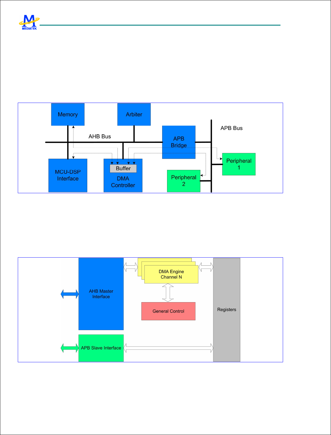
MTK Confidential Release for Konka
MTK Confidential Release for Konka
MT6228 GSM/GPRS Baseband Processor Data Sheet Revision 1.0
45/616 MediaTek Inc. Confidential
3.4 Direct Memory Access
3.4.1 General Description
A generic DMA Controller is placed on Layer 2 AHB Bus to support fast data transfers and to off-load the processor.
With this controller, specific devices on AHB or APB buses can benefit greatly from quick completion of data
movement from or to memory modules such as Internal System RAM or External SRAM. Such Generic DMA
Controller can also be used to connect any two devices other than memory module as long as they can be addressed in
memory space.
Figure 9 Variety Data Paths of DMA Transfers
Up to fourteen channels of simultaneous data transfers are supported. Each channel has a similar set of registers to be
configured to different scheme as desired. If more than fourteen devices are requesting the DMA resources at the
same time, software based arbitration should be employed. Once the service candidate is decided, the responsible
device driver should configure the Generic DMA Controller properly in order to conduct DMA transfers. Both
Interrupt and Polling based schemes in handling the completion event are supported. The block diagram of such
generic DMA Controller is illustrated in Figure 10.
Figure 10 Block Diagram of Direct memory Access Module

MTK Confidential Release for Konka
MTK Confidential Release for Konka
MT6228 GSM/GPRS Baseband Processor Data Sheet Revision 1.0
46/616 MediaTek Inc. Confidential
3.4.1.1 Full-Size & Half-Size DMA Channels
There are three types of DMA channels in the DMA controller. The first one is called a full-size DMA channel, the
second one is called a half-size DMA channel, and the last is Virtual FIFO DMA. Channels 1 through 3 are full-size
DMA channels; channels 4 through 10 are half-size ones; and channels 11 through 14 are Virtual FIFO DMAs. The
difference between the first two types of DMA channels is that both source and destination address are programmable
in full-size DMA channels, but only the address of one side can be programmed in half-size DMA channel. In
half-size channels, only either the source or destination address can be programmed, while the addresses of the other
side is preset. Which preset address is used depends on the setting of MAS in DMA Channel Control Register.
Refer to the Register Definition section for more detail.
3.4.1.2 Ring Buffer & Double Buffer Memory Data Movement
DMA channels 1 through 10 support ring-buffer and double-buffer memory data movement. This can be achieved by
programming DMA_WPPT and DMA_WPTO, as well as setting WPEN in DMA_CON register to enable. Figure 11
illustrates how this function works. Once the transfer counter reaches the value of WPPT, the next address jumps to
the WPTO address after completing the WPPT data transfer. Note that only one side can be configured as ring-buffer
or double-buffer memory, and this is controlled by WPSD in DMA_CON register.
Figure 11 Ring Buffer and Double Buffer Memory Data Movement
3.4.1.3 Unaligned Word Access
The address of word access on AHB bus must be aligned to word boundary, or the 2 LSB is truncated to 00b. If
programmers do not notice this, it may cause an incorrect data fetch. In the case where data is to be moved from
unaligned addresses to aligned addresses, the word is usually first split into four bytes and then moved byte by byte.
This results in four read and four write transfers on the bus.
To improve bus efficiency, unaligned-word access is provided in DMA4~10. While this function is enabled, DMAs
move data from unaligned address to aligned address by executing four continuous byte-read access and one
word-write access, reducing the number of transfers on the bus by three.
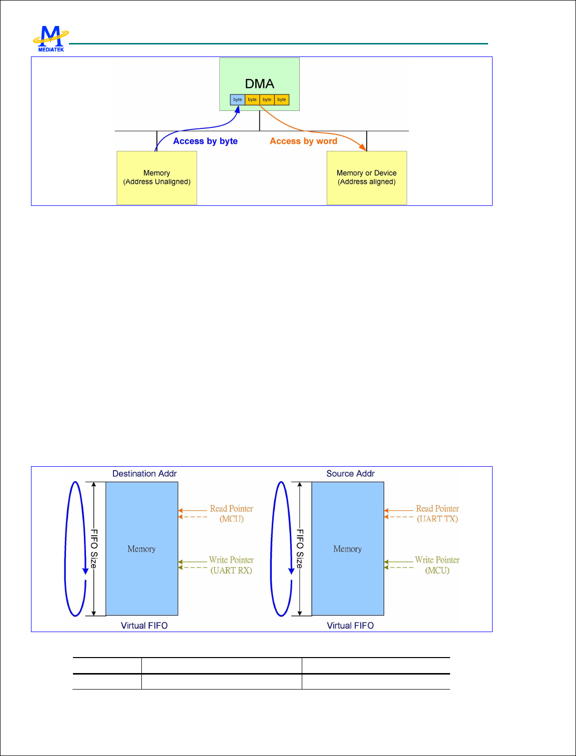
MTK Confidential Release for Konka
MTK Confidential Release for Konka
MT6228 GSM/GPRS Baseband Processor Data Sheet Revision 1.0
47/616 MediaTek Inc. Confidential
Figure 12 Unaligned Word Accesses
3.4.1.4 Virtual FIFO DMA
Virtual FIFO DMA is used to ease UART control. The difference between the Virtual FIFO DMAs and the ordinary
DMAs is that Virtual FIFO DMA contains additional FIFO controller. The read and write pointers are kept in the
Virtual FIFO DMA. During a read from the FIFO, the read pointer points to the address of the next data. During a
write to the FIFO, the write pointer moves to the next address. If the FIFO is empty, a FIFO read is not allowed.
Similarly, data is not written into the FIFO if the FIFO is full. Due to UART flow control requirements, an alert
length is programmed. Once the FIFO Space is less than this value, an alert signal is issued to enable UART flow
control. The type of flow control performed depends on the setting in UART.
Each Virtual FIFO DMA can be programmed as RX or TX FIFO. This depends on the setting of DIR in DMA_CON
register. If DIR is “0”(READ), it means TX FIFO. On the other hand, if DIR is “1”(WRITE), the Virtual FIFO
DMA is specified as a RX FIFO.
Virtual FIFO DMA provides an interrupt to MCU. This interrupt informs MCU that there is data in the FIFO, and the
amount of data is over or under the value defined in DMA_COUNT register. With this, MCU does not need to poll
DMA to know when data must be removed from or put into the FIFO.
Note that Virtual FIFO DMAs cannot be used as generic DMAs, i.e. DMA1~10.
Figure 13 Virtual FIFO DMA
DMA number Address of Virtual FIFO Access Port Associated UART
DMA11 7800_0000h UART1 RX / ALL UART TX
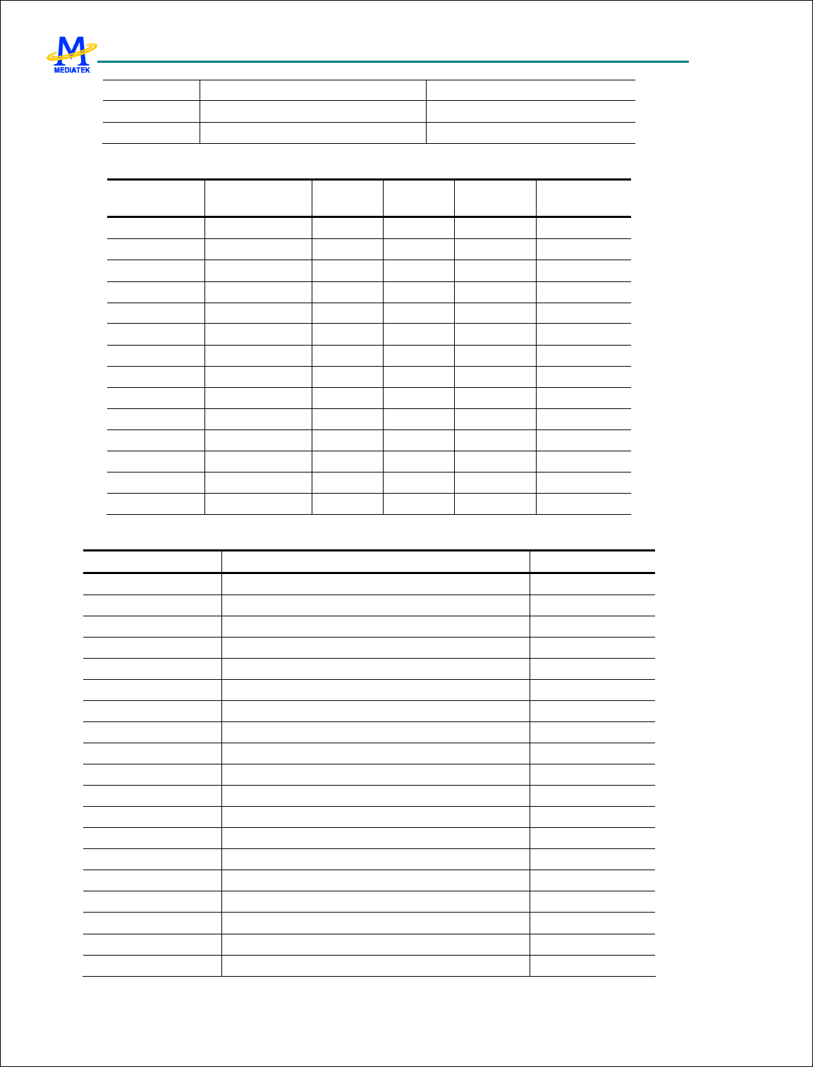
MTK Confidential Release for Konka
MTK Confidential Release for Konka
MT6228 GSM/GPRS Baseband Processor Data Sheet Revision 1.0
48/616 MediaTek Inc. Confidential
DMA12 7800_0100h UART2 RX / ALL UART TX
DMA13 7800_0200h UART3 RX / ALL UART TX
DMA14 7800_0300h ALL UART TX
Table 6 Virtual FIFO Access Port
DMA number
Type Ring Buffer
Two Buffer
Burst Mode
Unaligned Word
Access
DMA1 Full Size
DMA2 Full Size
DMA3 Full Size
DMA4 Half Size
DMA5 Half Size
DMA6 Half Size
DMA7 Half Size
DMA8 Half Size
DMA9 Half Size
DMA10 Half Size
DMA11 Virtual FIFO
DMA12 Virtual FIFO
DMA13 Virtual FIFO
DMA14 Virtual FIFO
Table 7 Function List of DMA channels
REGISTER ADDRESS REGISTER NAME SYNONYM
DMA + 0000h DMA Global Status Register DMA_GLBSTA
DMA + 0028h DMA Global Bandwidth Limiter Register DMA_GLBLIMITER
DMA + 0100h DMA Channel 1 Source Address Register DMA1_SRC
DMA + 0104h DMA Channel 1 Destination Address Register DMA1_DST
DMA + 0108h DMA Channel 1 Wrap Point Address Register DMA1_WPPT
DMA + 010Ch DMA Channel 1 Wrap To Address Register DMA1_WPTO
DMA + 0110h DMA Channel 1 Transfer Count Register DMA1_COUNT
DMA + 0114h DMA Channel 1 Control Register DMA1_CON
DMA + 0118h DMA Channel 1 Start Register DMA1_START
DMA + 011Ch DMA Channel 1 Interrupt Status Register DMA1_INTSTA
DMA + 0120h DMA Channel 1 Interrupt Acknowledge Register DMA1_ACKINT
DMA + 0124h DMA Channel 1 Remaining Length of Current Transfer DMA1_RLCT
DMA + 0128h DMA Channel 1 Bandwidth Limiter Register DMA1_LIMITER
DMA + 0200h DMA Channel 2 Source Address Register DMA2_SRC
DMA + 0204h DMA Channel 2 Destination Address Register DMA2_DST
DMA + 0208h DMA Channel 2 Wrap Point Address Register DMA2_WPPT
DMA + 020Ch DMA Channel 2 Wrap To Address Register DMA2_WPTO
DMA + 0210h DMA Channel 2 Transfer Count Register DMA2_COUNT
DMA + 0214h DMA Channel 2 Control Register DMA2_CON

MTK Confidential Release for Konka
MTK Confidential Release for Konka
MT6228 GSM/GPRS Baseband Processor Data Sheet Revision 1.0
49/616 MediaTek Inc. Confidential
DMA + 0218h DMA Channel 2 Start Register DMA2_START
DMA + 021Ch DMA Channel 2 Interrupt Status Register DMA2_INTSTA
DMA + 0220h DMA Channel 2 Interrupt Acknowledge Register DMA2_ACKINT
DMA + 0224h DMA Channel 2 Remaining Length of Current Transfer DMA2_RLCT
DMA + 0228h DMA Channel 2 Bandwidth Limiter Register DMA2_LIMITER
DMA + 0300h DMA Channel 3 Source Address Register DMA3_SRC
DMA + 0304h DMA Channel 3 Destination Address Register DMA3_DST
DMA + 0308h DMA Channel 3 Wrap Point Address Register DMA3_WPPT
DMA + 030Ch DMA Channel 3 Wrap To Address Register DMA3_WPTO
DMA + 0310h DMA Channel 3 Transfer Count Register DMA3_COUNT
DMA + 0314h DMA Channel 3 Control Register DMA3_CON
DMA + 0318h DMA Channel 3 Start Register DMA3_START
DMA + 031Ch DMA Channel 3 Interrupt Status Register DMA3_INTSTA
DMA + 0320h DMA Channel 3 Interrupt Acknowledge Register DMA3_ACKINT
DMA + 0324h DMA Channel 3 Remaining Length of Current Transfer DMA3_RLCT
DMA + 0328h DMA Channel 3 Bandwidth Limiter Register DMA3_LIMITER
DMA + 0408h DMA Channel 4 Wrap Point Address Register DMA4_WPPT
DMA + 040Ch DMA Channel 4 Wrap To Address Register DMA4_WPTO
DMA + 0410h DMA Channel 4 Transfer Count Register DMA4_COUNT
DMA + 0414h DMA Channel 4 Control Register DMA4_CON
DMA + 0418h DMA Channel 4 Start Register DMA4_START
DMA + 041Ch DMA Channel 4 Interrupt Status Register DMA4_INTSTA
DMA + 0420h DMA Channel 4 Interrupt Acknowledge Register DMA4_ACKINT
DMA + 0424h DMA Channel 4 Remaining Length of Current Transfer DMA4_RLCT
DMA + 0428h DMA Channel 4 Bandwidth Limiter Register DMA4_LIMITER
DMA + 042Ch DMA Channel 4 Programmable Address Register DMA4_PGMADDR
DMA + 0508h DMA Channel 5 Wrap Point Address Register DMA5_WPPT
DMA + 050Ch DMA Channel 5 Wrap To Address Register DMA5_WPTO
DMA + 0510h DMA Channel 5 Transfer Count Register DMA5_COUNT
DMA + 0514h DMA Channel 5 Control Register DMA5_CON
DMA + 0518h DMA Channel 5 Start Register DMA5_START
DMA + 051Ch DMA Channel 5 Interrupt Status Register DMA5_INTSTA
DMA + 0520h DMA Channel 5 Interrupt Acknowledge Register DMA5_ACKINT
DMA + 0524h DMA Channel 5 Remaining Length of Current Transfer DMA5_RLCT
DMA + 0528h DMA Channel 5 Bandwidth Limiter Register DMA5_LIMITER
DMA + 052Ch DMA Channel 5 Programmable Address Register DMA5_PGMADDR
DMA + 0608h DMA Channel 6 Wrap Point Address Register DMA6_WPPT
DMA + 060Ch DMA Channel 6 Wrap To Address Register DMA6_WPTO
DMA + 0610h DMA Channel 6 Transfer Count Register DMA6_COUNT
DMA + 0614h DMA Channel 6 Control Register DMA6_CON
DMA + 0618h DMA Channel 6 Start Register DMA6_START
DMA + 061Ch DMA Channel 6 Interrupt Status Register DMA6_INTSTA

MTK Confidential Release for Konka
MTK Confidential Release for Konka
MT6228 GSM/GPRS Baseband Processor Data Sheet Revision 1.0
50/616 MediaTek Inc. Confidential
DMA + 0620h DMA Channel 6 Interrupt Acknowledge Register DMA6_ACKINT
DMA + 0624h DMA Channel 6 Remaining Length of Current Transfer DMA6_RLCT
DMA + 0628h DMA Channel 6 Bandwidth Limiter Register DMA6_LIMITER
DMA + 062Ch DMA Channel 6 Programmable Address Register DMA6_PGMADDR
DMA + 0708h DMA Channel 7 Wrap Point Address Register DMA7_WPPT
DMA + 070Ch DMA Channel 7 Wrap To Address Register DMA7_WPTO
DMA + 0710h DMA Channel 7 Transfer Count Register DMA7_COUNT
DMA + 0714h DMA Channel 7 Control Register DMA7_CON
DMA + 0718h DMA Channel 7 Start Register DMA7_START
DMA + 071Ch DMA Channel 7 Interrupt Status Register DMA7_INTSTA
DMA + 0720h DMA Channel 7 Interrupt Acknowledge Register DMA7_ACKINT
DMA + 0724h DMA Channel 7 Remaining Length of Current Transfer DMA7_RLCT
DMA + 0728h DMA Channel 7 Bandwidth Limiter Register DMA7_LIMITER
DMA + 072Ch DMA Channel 7 Programmable Address Register DMA7_PGMADDR
DMA + 0808h DMA Channel 8 Wrap Point Address Register DMA8_WPPT
DMA + 080Ch DMA Channel 8 Wrap To Address Register DMA8_WPTO
DMA + 0810h DMA Channel 8 Transfer Count Register DMA8_COUNT
DMA + 0814h DMA Channel 8 Control Register DMA8_CON
DMA + 0818h DMA Channel 8 Start Register DMA8_START
DMA + 081Ch DMA Channel 8 Interrupt Status Register DMA8_INTSTA
DMA + 0820h DMA Channel 8 Interrupt Acknowledge Register DMA8_ACKINT
DMA + 0824h DMA Channel 8 Remaining Length of Current Transfer
DMA8_RLCT
DMA + 0828h DMA Channel 8 Bandwidth Limiter Register DMA8_LIMITER
DMA + 082Ch DMA Channel 8 Programmable Address Register DMA8_PGMADDR
DMA + 0908h DMA Channel 9 Wrap Point Address Register DMA9_WPPT
DMA + 090Ch DMA Channel 9 Wrap To Address Register DMA9_WPTO
DMA + 0910h DMA Channel 9 Transfer Count Register DMA9_COUNT
DMA + 0914h DMA Channel 9 Control Register DMA9_CON
DMA + 0918h DMA Channel 9 Start Register DMA9_START
DMA + 091Ch DMA Channel 9 Interrupt Status Register DMA9_INTSTA
DMA + 0920h DMA Channel 9 Interrupt Acknowledge Register DMA9_ACKINT
DMA + 0924h DMA Channel 9 Remaining Length of Current Transfer
DMA9_RLCT
DMA + 0928h DMA Channel 9 Bandwidth Limiter Register DMA9_LIMITER
DMA + 092Ch DMA Channel 9 Programmable Address Register DMA9_PGMADDR
DMA + 0A08h DMA Channel 10 Wrap Point Address Register DMA10_WPPT
DMA + 0A0Ch DMA Channel 10 Wrap To Address Register DMA10_WPTO
DMA + 0A10h DMA Channel 10 Transfer Count Register DMA10_COUNT
DMA + 0A14h DMA Channel 10 Control Register DMA10_CON
DMA + 0A18h DMA Channel 10 Start Register DMA10_START
DMA + 0A1Ch DMA Channel 10 Interrupt Status Register DMA10_INTSTA
DMA + 0A20h DMA Channel 10 Interrupt Acknowledge Register DMA10_ACKINT
DMA + 0A24h DMA Channel 10 Remaining Length of Current
Transfer DMA10_RLCT

MTK Confidential Release for Konka
MTK Confidential Release for Konka
MT6228 GSM/GPRS Baseband Processor Data Sheet Revision 1.0
51/616 MediaTek Inc. Confidential
DMA + 0A28h DMA Channel 10 Bandwidth Limiter Register DMA10_LIMITER
DMA + 0A2Ch DMA Channel 10 Programmable Address Register DMA10_PGMADDR
DMA + 0B10h DMA Channel 11 Transfer Count Register DMA11_COUNT
DMA + 0B14h DMA Channel 11 Control Register DMA11_CON
DMA + 0B18h DMA Channel 11 Start Register DMA11_START
DMA + 0B1Ch DMA Channel 11 Interrupt Status Register DMA11_INTSTA
DMA + 0B20h DMA Channel 11 Interrupt Acknowledge Register DMA11_ACKINT
DMA + 0B28h DMA Channel 11 Bandwidth Limiter Register DMA11_LIMITER
DMA + 0B2Ch DMA Channel 11 Programmable Address Register DMA11_PGMADDR
DMA + 0B30h DMA Channel 11 Write Pointer DMA11_WRPTR
DMA + 0B34h DMA Channel 11 Read Pointer DMA11_RDPTR
DMA + 0B38h DMA Channel 11 FIFO Count DMA11_FFCNT
DMA + 0B3Ch DMA Channel 11 FIFO Status DMA11_FFSTA
DMA + 0B40h DMA Channel 11 Alert Length DMA11_ALTLEN
DMA + 0B44h DMA Channel 11 FIFO Size DMA11_FFSIZE
DMA + 0C10h DMA Channel 12 Transfer Count Register DMA12_COUNT
DMA + 0C14h DMA Channel 12 Control Register DMA12_CON
DMA + 0C18h DMA Channel 12 Start Register DMA12_START
DMA + 0C1Ch DMA Channel 12 Interrupt Status Register DMA12_INTSTA
DMA + 0C20h DMA Channel 12 Interrupt Acknowledge Register DMA12_ACKINT
DMA + 0C28h DMA Channel 12 Bandwidth Limiter Register DMA12_LIMITER
DMA + 0C2Ch DMA Channel 12 Programmable Address Register DMA12_PGMADDR
DMA + 0C30h DMA Channel 12 Write Pointer DMA12_WRPTR
DMA + 0C34h DMA Channel 12 Read Pointer DMA12_RDPTR
DMA + 0C38h DMA Channel 12 FIFO Count DMA12_FFCNT
DMA + 0C3Ch DMA Channel 12 FIFO Status DMA12_FFSTA
DMA + 0C40h DMA Channel 12 Alert Length DMA12_ALTLEN
DMA + 0C44h DMA Channel 12 FIFO Size DMA12_FFSIZE
DMA + 0D10h DMA Channel 13 Transfer Count Register DMA13_COUNT
DMA + 0D14h DMA Channel 13 Control Register DMA13_CON
DMA + 0D18h DMA Channel 13 Start Register DMA13_START
DMA + 0D1Ch DMA Channel 13 Interrupt Status Register DMA13_INTSTA
DMA + 0D20h DMA Channel 13 Interrupt Acknowledge Register DMA13_ACKINT
DMA + 0D28h DMA Channel 13 Bandwidth Limiter Register DMA13_LIMITER
DMA + 0D2Ch DMA Channel 13 Programmable Address Register DMA13_PGMADDR
DMA + 0D30h DMA Channel 13 Write Pointer DMA13_WRPTR
DMA + 0D34h DMA Channel 13 Read Pointer DMA13_RDPTR
DMA + 0D38h DMA Channel 13 FIFO Count DMA13_FFCNT
DMA + 0D3Ch DMA Channel 13 FIFO Status DMA13_FFSTA
DMA + 0D40h DMA Channel 13 Alert Length DMA13_ALTLEN
DMA + 0D44h DMA Channel 13 FIFO Size DMA13_FFSIZE
DMA + 0E10h DMA Channel 14 Transfer Count Register DMA14_COUNT
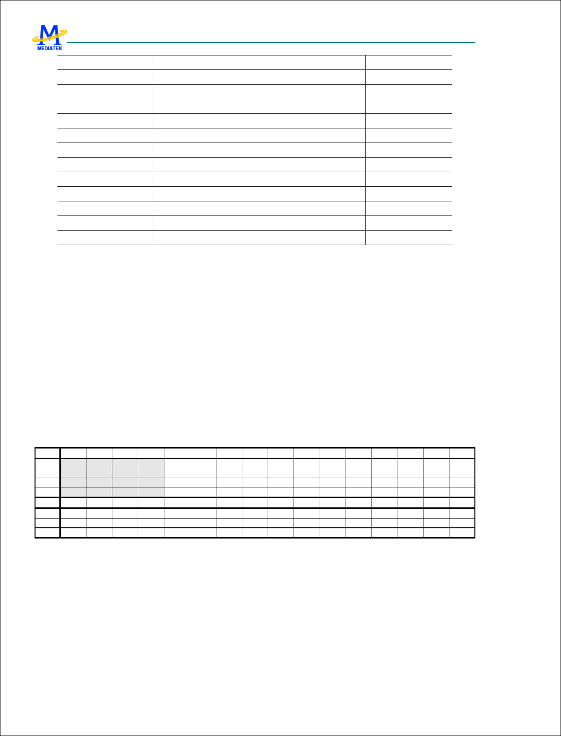
MTK Confidential Release for Konka
MTK Confidential Release for Konka
MT6228 GSM/GPRS Baseband Processor Data Sheet Revision 1.0
52/616 MediaTek Inc. Confidential
DMA + 0E14h DMA Channel 14 Control Register DMA14_CON
DMA + 0E18h DMA Channel 14 Start Register DMA14_START
DMA + 0E1Ch DMA Channel 14 Interrupt Status Register DMA14_INTSTA
DMA + 0E20h DMA Channel 14 Interrupt Acknowledge Register DMA14_ACKINT
DMA + 0E28h DMA Channel 14 Bandwidth Limiter Register DMA14_LIMITER
DMA + 0E2Ch DMA Channel 14 Programmable Address Register DMA14_PGMADDR
DMA + 0E30h DMA Channel 14 Write Pointer DMA14_WRPTR
DMA + 0E34h DMA Channel 14 Read Pointer DMA14_RDPTR
DMA + 0E38h DMA Channel 14 FIFO Count DMA14_FFCNT
DMA + 0E3Ch DMA Channel 14 FIFO Status DMA14_FFSTA
DMA + 0E40h DMA Channel 14 Alert Length DMA14_ALTLEN
DMA + 0E44h DMA Channel 14 FIFO Size DMA14_FFSIZE
Table 8 DMA Controller Register Map
3.4.2 Register Definitions
Register programming tips:
Start registers shall be cleared, when associated channels are being programmed.
PGMADDR, i.e. programmable address, only exists in half-size DMA channels. If DIR in Control Register
is high, PGMADDR represents Destination Address. Conversely, If DIR in Control Register is low,
PGMADDR represents Source Address.
Functions of ring-buffer and double-buffer memory data movement can be activated on either source side or
destination side by programming DMA_WPPT & and DMA_WPTO, as well as setting WPEN in DMA_CON
register high. WPSD in DMA_CON register determines the activated side.
DMA+0000h DMA Global Status Register DMA_GLBSTA
Bit 31 30 29 28 27 26 25 24 23 22 21 20 19 18 17 16
Name
IT14 RUN1
4 IT13 RUN1
3 IT12 RUN1
2 IT11 RUN1
1 IT10 RUN1
0 IT9 RUN9
Type RO RO RO RO RO RO RO RO RO RO RO RO
Reset
0 0 0 0 0 0 0 0 0 0 0 0
Bit 15 14 13 12 11 10 9 8 7 6 5 4 3 2 1 0
Name
IT8 RUN8
IT7 RUN7
IT6 RUN6
IT5 RUN5
IT4 RUN4
IT3 RUN3
IT2 RUN2
IT1 RUN1
Type RO RO RO RO RO RO RO RO RO RO RO RO RO RO RO RO
Reset
0 0 0 0 0 0 0 0 0 0 0 0 0 0 0 0
This register helps software program keep track of the global status of DMA channels.
RUN
N
DMA channel n status
0 Channel n is stopped or has completed the transfer already.
1 Channel n is currently running.
IT
N
Interrupt status for channel n
0 No interrupt is generated.
1 An interrupt is pending and waiting for service.
MTK Confidential Release for Konka
MTK Confidential Release for Konka
MT6228 GSM/GPRS Baseband Processor Data Sheet Revision 1.0
53/616 MediaTek Inc. Confidential
DMA+0028h DMA Global Bandwidth limiter Register DMA_GLBLIMIT
ER
Bit 31 30 29 28 27 26 25 24 23 22 21 20 19 18 17 16
Name
Type
Reset
Bit 15 14 13 12 11 10 9 8 7 6 5 4 3 2 1 0
Name
GLBLIMITER
Type WO
Reset
0
Please refer to the expression in DMAn_LIMITER for detailed note. The value of
DMA_GLBLIMITER is set to all DMA channels, from 1 to 14.
DMA+0n00h DMA Channel n Source Address Register DMAn_SRC
Bit 31 30 29 28 27 26 25 24 23 22 21 20 19 18 17 16
Name
SRC[31:16]
Type R/W
Reset
0
Bit 15 14 13 12 11 10 9 8 7 6 5 4 3 2 1 0
Name
SRC[15:0]
Type R/W
Reset
0
The above registers contain the base or current source address that the DMA channel is currently operating on.
Writing to this register specifies the base address of transfer source for a DMA channel. Before programming these
registers, the software program should make sure that STR in DMAn_START is set to 0; that is, the DMA channel is
stopped and disabled completely. Otherwise, the DMA channel may run out of order. Reading this register returns
the address value from which the DMA is reading.
Note that n is from 1 to 3.
SRC SRC[31:0] specifies the base or current address of transfer source for a DMA channel, i.e. channel 1, 2 or 3.
WRITE Base address of transfer source
READ Address from which DMA is reading
DMA+0n04h DMA Channel n Destination Address Register DMAn_DST
Bit 31 30 29 28 27 26 25 24 23 22 21 20 19 18 17 16
Name
DST[31:16]
Type R/W
Reset
0
Bit 15 14 13 12 11 10 9 8 7 6 5 4 3 2 1 0
Name
DST[15:0]
Type R/W
Reset
0
The above registers contain the base or current destination address that the DMA channel is currently operating on..
Writing to this register specifies the base address of the transfer destination for a DMA channel. Before programming
these registers, the software should make sure that STR in DMAn_START is set to ‘0’; that is, the DMA channel is
stopped and disabled completely. Otherwise, the DMA channel may run out of order. Reading this register returns
the address value to which the DMA is writing.
Note that n is from 1 to 3.
MTK Confidential Release for Konka
MTK Confidential Release for Konka
MT6228 GSM/GPRS Baseband Processor Data Sheet Revision 1.0
54/616 MediaTek Inc. Confidential
DST DST[31:0] specifies the base or current address of transfer destination for a DMA channel, i.e. channel 1, 2 or
3.
WRITE Base address of transfer destination.
READ Address to which DMA is writing.
DMA+0n08h DMA Channel n Wrap Point Count Register DMAn_WPPT
Bit
31 30
29
28
27 26 25
24
23
22 21 20
19
18
17 16
Name
Type
Reset
Bit 15 14 13 12 11 10 9 8 7 6 5 4 3 2 1 0
Name
WPPT[15:0]
Type R/W
Reset
0
The above registers are to specify the transfer count required to perform before the jump point. This can be used to
support ring buffer or double buffer style memory accesses. To enable this function, two control bits, WPEN and
WPSD, in DMA control register must be programmed. See the following register description for more details. If the
transfercounter in the DMA engine matches this value, an address jump occurs, and the next address is the address
specified in DMAn_WPTO. Before programming these registers, the software should make sure that STR in
DMAn_START is set to ‘0’, that is the DMA channel is stopped and disabled completely. Otherwise, the DMA
channel may run out of order. To enable this function, WPEN in DMA_CON is set.
Note that n is from 1 to 10.
WPPT WPPT[15:0] specifies the amount of the transfer count from start to jumping point for a DMA channel, i.e.
channel 1 – 10.
WRITE Address of the jump point.
READ Value set by the programmer.
DMA+0n0Ch DMA Channel n Wrap To Address Register DMAn_WPTO
Bit 31 30 29 28 27 26 25 24 23 22 21 20 19 18 17 16
Name
WPTO[31:16]
Type R/W
Reset
0
Bit 15 14 13 12 11 10 9 8 7 6 5 4 3 2 1 0
Name
WPTO[15:0]
Type R/W
Reset
0
The above registers specify the address of the jump destination of a given DMA transfer to support ring buffer or
double buffer style memory accesses. To enable this function, set the two control bits, WPEN and WPSD, in the
DMA control register . See the following register description for more details. Before programming these registers,
the software should make sure that STR in DMAn_START is set to ‘0’, that is the DMA channel is stopped and
disabled completely. Otherwise, the DMA channel may run out of order. To enable this function, WPEN in
DMA_CON should be set.
Note that n is from 1 to 10.
WPTO WPTO[31:0] specifies the address of the jump point for a DMA channel, i.e. channel 1 – 10.
WRITE Address of the jump destination.
READ Value set by the programmer.
DMA+0n10h DMA Channel n Transfer Count Register DMAn_COUNT
Bit 31 30 29 28 27 26 25 24 23 22 21 20 19 18 17 16
MTK Confidential Release for Konka
MTK Confidential Release for Konka
MT6228 GSM/GPRS Baseband Processor Data Sheet Revision 1.0
55/616 MediaTek Inc. Confidential
Name
Type
Reset
Bit 15 14 13 12 11 10 9 8 7 6 5 4 3 2 1 0
Name
LEN
Type R/W
Reset
0
This register specifies the amount of total transfer count that the DMA channel is required to perform. Upon
completion, the DMA channel generates an interrupt request to the processor while ITEN in DMAn_CON is set as ‘1’.
Note that the total size of data being transferred by a DMA channel is determined by LEN together with the SIZE in
DMAn_CON, i.e. LEN x SIZE.
For virtual FIFO DMA, this register is used to configure the RX threshold and TX threshold. Interrupt is triggered
while FIFO count >= RX threshold in RX path or FIFO count =< TX threshold in TX path. Note that ITEN bit in
DMA_CON register shall be set, or no interrupt is issued.
Note that n is from 1 to 14.
LEN The amount of total transfer count
DMA+0n14h DMA Channel n Control Register DMAn_CON
Bit 31 30 29 28 27 26 25 24 23 22 21 20 19 18 17 16
Name
MAS DIR WPEN
WPS
D
Type R/W R/W R/W R/W
Reset
0 0 0 0
Bit 15 14 13 12 11 10 9 8 7 6 5 4 3 2 1 0
Name
ITEN BURST B2W DRQ DINC SINC SIZE
Type R/W R/W R/W R/W R/W R/W R/W
Reset
0 0 0 0 0 0 0
This register contains all the available control schemes for a DMA channel that is ready for software programmer to
configure. Note that all these fields cannot be changed while DMA transfer is in progress or an unexpected situation
may occur.
Note that n is from 1 to 14.
SIZE Data size within the confine of a bus cycle per transfer.
These bits confines the data transfer size between source and destination to the specified value for individual
bus cycle. The size is in terms of byte and has maximum value of 4 bytes. It is mainly decided by the data
width of a DMA master.
00 Byte transfer/1 byte
01 Half-word transfer/2 bytes
10 Word transfer/4 bytes
11 Reserved
SINC Incremental source address. Source addresses increase every transfer. If the setting of SIZE is Byte, Source
addresses increase by 1 every single transfer. If Half-Word, increase by 2; and if Word, increase by 4.
0 Disable
1 Enable
DINC Incremental destination address. Destination addresses increase every transfer. If the setting of SIZE is
Byte, Destination addresses increase by 1 every single transfer. If Half-Word, increase by 2; and Iif Word,
increase by 4.
0 Disable
1 Enable

MTK Confidential Release for Konka
MTK Confidential Release for Konka
MT6228 GSM/GPRS Baseband Processor Data Sheet Revision 1.0
56/616 MediaTek Inc. Confidential
DREQ Throttle and handshake control for DMA transfer
0 No throttle control during DMA transfer or transfers occurred only between memories
1 Hardware handshake management
The DMA master is able to throttle down the transfer rate by way of request-grant handshake.
B2W Word to Byte or Byte to Word transfer for the applications of transferring non-word-aligned-address data to
word-aligned-address data. Note that BURST is set to 4-beat burst while enabling this function, and the
SIZE is set to Byte.
NO effect on channel 1 – 3 & 11 - 14.
0 Disable
1 Enable
BURST Transfer Type. Burst-type transfers have better bus efficiency. Mass data movement is recommended to
use this kind of transfer. However, note that burst-type transfer does not stop until all of the beats in a burst
are completed or transfer length is reached. FIFO threshold of peripherals must be configured carefully
while being used to move data from/to the peripherals.
What transfer type can be used is restricted by the SIZE. If SIZE is 00b, i.e. byte transfer, all of the four
transfer types can be used. If SIZE is 01b, i.e. half-word transfer, 16-beat incrementing burst cannot be used.
If SIZE is 10b, i.e. byte transfer, only single and 4-beat incrementing burst can be used.
NO effect on channel 11 - 14.
000 Single
001 Reserved
010 4-beat incrementing burst
011 Reserved
100 8-beat incrementing burst
101 Reserved
110 16-beat incrementing burst
111 Reserved
ITEN DMA transfer completion interrupt enable.
0 Disable
1 Enable
WPSD The side using address-wrapping function. Only one side of a DMA channel can activate address-wrapping
function at a time.
NO effect on channel 11 - 14.
0 Address-wrapping on source .
1 Address-wrapping on destination.
WPEN Address-wrapping for ring buffer. The next address of DMA jumps to WRAP TO address when the current
address matches WRAP POINT count.
NO effect on channel 11 - 14.
0 Disable
1 Enable
DIR Directions of DMA transfer for half-size and Virtual FIFO DMA channels, i.e. channels 4~14. The direction
is from the perspective of the DMA masters. WRITE means read from master and then write to the address
specified in DMA_PGMADDR, and vice versa.
NO effect on channel 1 - 3.
0 Read
1 Write
MTK Confidential Release for Konka
MTK Confidential Release for Konka
MT6228 GSM/GPRS Baseband Processor Data Sheet Revision 1.0
57/616 MediaTek Inc. Confidential
MAS Master selection. Specifies which master occupies this DMA channel. Once assigned to certain master, the
corresponding DREQ and DACK are connected. For half-size and Virtual FIFO DMA channels, i.e.
channels 4 ~ 14, a predefined address is assigned as well.
00000 SIM
00001 MSDC
00010 IrDA TX
00011 IrDA RX
00100 USB1 Write
00101 USB1 Read
00110 USB2 Write
00111 USB2 Read
01000 UART1 TX
01001 UART1 RX
01010 UART2 TX
01011 UART2 RX
01100 UART3 TX
01101 UART3 RX
01110 DSP-DMA
01111 NFI TX
10000 NFI RX
OTHERS Reserved
DMA+0n18h DMA Channel n Start Register DMAn_START
Bit 31 30 29 28 27 26 25 24 23 22 21 20 19 18 17 16
Name
Type
Reset
Bit 15 14 13 12 11 10 9 8 7 6 5 4 3 2 1 0
Name
STR
Type R/W
Reset
0
This register controls the activity of a DMA channel. Note that prior to setting STR to “1”, all the configurations
should be done by giving proper value to the registers. Note also that once the STR is set to “1”, the hardware does
not clear it automatically no matter if the DMA channel accomplishes the DMA transfer or not. In other works, the
value of STR stays “1” regardless of the completion of DMA transfer. Therefore, the software program should be
sure to clear STR to “0” before restarting another DMA transfer.
Note that n is from 1 to 14.
STR Start control for a DMA channel.
0 The DMA channel is stopped.
1 The DMA channel is started and running.
DMA+0n1Ch DMA Channel n Interrupt Status Register DMAn_INTSTA
Bit 31 30 29 28 27 26 25 24 23 22 21 20 19 18 17 16
Name
Type
Reset
Bit 15 14 13 12 11 10 9 8 7 6 5 4 3 2 1 0
Name
INT
Type RO
Reset
0
MTK Confidential Release for Konka
MTK Confidential Release for Konka
MT6228 GSM/GPRS Baseband Processor Data Sheet Revision 1.0
58/616 MediaTek Inc. Confidential
This register shows the interrupt status of a DMA channel. It has the same value as DMA_GLBSTA.
Note that n is from 1 to 14.
INT Interrupt Status for DMA Channel
0 No interrupt request is generated.
1 One interrupt request is pending and waiting for service.
DMA+0n20h DMA Channel n Interrupt Acknowledge Register DMAn_ACKINT
Bit 31 30 29 28 27 26 25 24 23 22 21 20 19 18 17 16
Name
Type
Reset
Bit 15 14 13 12 11 10 9 8 7 6 5 4 3 2 1 0
Name
ACK
Type WO
Reset
0
This register is used to acknowledge the current interrupt request associated with the completion event of a DMA
channel by software program. Note that this is a write-only register, and any read to it returns a value of “0”.
Note that n is from 1 to 14.
ACK Interrupt acknowledge for the DMA channel
0 No effect
1 Interrupt request is acknowledged and should be relinquished.
DMA+0n24h DMA Channel n Remaining Length of Current
Transfer DMAn_RLCT
Bit 31 30 29 28 27 26 25 24 23 22 21 20 19 18 17 16
Name
Type
Reset
Bit 15 14 13 12 11 10 9 8 7 6 5 4 3 2 1 0
Name
RLCT
Type RO
Reset
0
This register is to reflect the left amount of the transfer.
Note that n is from 1 to 10.
DMA+0n28h DMA Bandwidth limiter Register DMAn_LIMITER
Bit 31 30 29 28 27 26 25 24 23 22 21 20 19 18 17 16
Name
Type
Reset
Bit 15 14 13 12 11 10 9 8 7 6 5 4 3 2 1 0
Name
LIMITER
Type R/W
Reset
0
This register is to suppress the Bus utilization of the DMA channel. The value is from 0 to 255. 0 means no
limitation, and 255 means totally banned. The value between 0 and 255 means certain DMA can have permission to
use AHB every (4 X n) AHB clock cycles.
MTK Confidential Release for Konka
MTK Confidential Release for Konka
MT6228 GSM/GPRS Baseband Processor Data Sheet Revision 1.0
59/616 MediaTek Inc. Confidential
Note that it is not recommended to limit the Bus utilization of the DMA channels because this increases the latency of
response to the masters, and the transfer rate decreases as well. Before using it, programmer must make sure that the
bus masters have some protective mechanism to avoid entering the wrong states.
Note that n is from 1 to 14.
LIMITER from 0 to 255. 0 means no limitation, 255 means totally banned, and others mean Bus access permission
every (4 X n) AHB clock.
DMA+0n2Ch DMA Channel n Programmable Address Register DMAn_PGMAD
DR
Bit 31 30 29 28 27 26 25 24 23 22 21 20 19 18 17 16
Name
PGMADDR[31:16]
Type R/W
Reset
0
Bit 15 14 13 12 11 10 9 8 7 6 5 4 3 2 1 0
Name
PGMADDR[15:0]
Type R/W
Reset
0
The above registers specify the address for a half-size DMA channel. This address represents a source address if DIR
in DMA_CON is set to 0, and represents a destination address if DIR in DMA_CON is set to 1. Before being able to
program these register, the software should make sure that STR in DMAn_START is set to ‘0’, that is the DMA channel
is stopped and disabled completely. Otherwise, the DMA channel may run out of order.
Note that n is from 4 to 14.
PGMADDR PGMADDR[31:0] specifies the addresses for a half-size or a Virtual FIFO DMA channel, i.e. channel 4 –
14.
WRITE Address of the jump destination.
READ Current address of the transfer.
DMA+0n30h DMA Channel n Virtual FIFO Write Pointer Register DMAn_WRPTR
Bit 31 30 29 28 27 26 25 24 23 22 21 20 19 18 17 16
Name
WRPTR[31:16]
Type RO
Bit 15 14 13 12 11 10 9 8 7 6 5 4 3 2 1 0
Name
WRPTR[15:0]
Type RO
Note that n is from 11 to 14.
WRPTR Virtual FIFO Write Pointer.
DMA+0n34h DMA Channel n Virtual FIFO Read Pointer Register DMAn_RDPTR
Bit 31 30 29 28 27 26 25 24 23 22 21 20 19 18 17 16
Name
RDPTR[31:16]
Type RO
Bit 15 14 13 12 11 10 9 8 7 6 5 4 3 2 1 0
Name
RDPTR[15:0]
Type RO
Note that n is from 11 to 14.
RDPTR Virtual FIFO Read Pointer.
MTK Confidential Release for Konka
MTK Confidential Release for Konka
MT6228 GSM/GPRS Baseband Processor Data Sheet Revision 1.0
60/616 MediaTek Inc. Confidential
DMA+0n38h DMA Channel n Virtual FIFO Data Count Register DMAn_FFCNT
Bit 31 30 29 28 27 26 25 24 23 22 21 20 19 18 17 16
Name
Type
Bit 15 14 13 12 11 10 9 8 7 6 5 4 3 2 1 0
Name
FFCNT
Type RO
Note that n is from 11 to 14.
FFCNT To display the number of data stored in FIFO. 0 means FIFO empty, and FIFO is full if FFCNT is equal to
FFSIZE.
DMA+0n3Ch DMA Channel n Virtual FIFO Status Register DMAn_FFSTA
Bit 31 30 29 28 27 26 25 24 23 22 21 20 19 18 17 16
Name
Type
Reset
Bit 15 14 13 12 11 10 9 8 7 6 5 4 3 2 1 0
Name
ALT EMPT
Y FULL
Type RO RO RO
Reset
0 1 0
Note that n is from 11 to 14.
FULL To indicate FIFO is full.
0 Not Full
1 Full
EMPTY To indicate FIFO is empty.
0 Not Empty
1 Empty
ALT To indicate FIFO Count is larger than ALTLEN. DMA issues an alert signal to UART to enable UART flow
control.
0 Not reach alert region.
1 Reach alert region.
DMA+0n40h DMA Channel n Virtual FIFO Alert Length Register DMAn_ALTLEN
Bit 31 30 29 28 27 26 25 24 23 22 21 20 19 18 17 16
Name
Type
Reset
Bit 15 14 13 12 11 10 9 8 7 6 5 4 3 2 1 0
Name
ALTLEN
Type R/W
Reset
0
Note that n is from 11 to 14.
ALTLEN Specifies the Alert Length of Virtual FIFO DMA. Once the remaining FIFO space is less than ALTLEN,
an alert signal is issued to UART to enable flow control. Normally, ALTLEN shall be larger than 16 for
UART application.
DMA+0n44h DMA Channel n Virtual FIFO Size Register DMAn_FFSIZE
Bit 31 30 29 28 27 26 25 24 23 22 21 20 19 18 17 16
MTK Confidential Release for Konka
MTK Confidential Release for Konka
MT6228 GSM/GPRS Baseband Processor Data Sheet Revision 1.0
61/616 MediaTek Inc. Confidential
Name
Type
Reset
Bit 15 14 13 12 11 10 9 8 7 6 5 4 3 2 1 0
Name
FFSIZE
Type R/W
Reset
0
Note that n is from 11 to 14.
FFSIZE Specifies the FIFO Size of Virtual FIFO DMA.
3.5 Interrupt Controller
3.5.1 General Description
Figure 14 outlines the major functionality of the MCU Interrupt Controller. The interrupt controller processes all
interrupt sources coming from external lines and internal MCU peripherals. Since ARM7EJ-S core supports two
levels of interrupt latency, this controller generates two request signals: FIQ for fast, low latency interrupt request and
IRQ for more general interrupts with lower priority.
Interrupt
Input
Multiplex
IRQ
Controller
IRQn
IRQ0
IRQ1
IRQ2
IRQ31
KP
TDMA
GPT
SIM
UART1
DSP2MCU
RTC
UART2
EINT FIQ
IRQ
FIQ
Controller
Registers
SoftIRQ
APB Bus
Figure 15 Block Diagram of the Interrupt Controller
One and only one of the interrupt sources can be assigned to FIQ Controller and have the highest priority in requesting
timing critical service. All the others share the same IRQ signal by connecting them to IRQ Controller. The IRQ
Controller manages up 32 interrupt lines of IRQ0 to IRQ31 with fixed priority in descending order.
The Interrupt Controller provides a simple software interface by mean of registers to manipulate the interrupt request
shared system. IRQ Selection Registers and FIQ Selection Register determine the source priority and connecting
relation among sources and interrupt lines. IRQ Source Status Register allows software program to identify the source
of interrupt that generates the interrupt request. IRQ Mask Register provides software to mask out undesired sources

MTK Confidential Release for Konka
MTK Confidential Release for Konka
MT6228 GSM/GPRS Baseband Processor Data Sheet Revision 1.0
62/616 MediaTek Inc. Confidential
some time. End of Interrupt Register permits software program to indicate to the controller that a certain interrupt
service routine has been finished.
Binary coded version of IRQ Source Status Register is also made available for software program to helpfully identify
the interrupt source. Note that while taking advantage of this, it should also take the binary coded version of End of
Interrupt Register coincidently.
The essential Interrupt Table of ARM7EJ-S core is shown as Table 9.
Address Description
00000000h System Reset
00000018h IRQ
0000001Ch FIQ
Table 10 Interrupt Table of ARM7EJ-S
Interrupt Source Masking
Interrupt controller provides the function of Interrupt Source Masking by the way of programming MASK register.
Any of them can be masked individually.
However, because of the bus latency, the masking takes effect no earlier than 3 clock cycles later. In this time, the
to-be-masked interrupts could come in and generate an IRQ pulse to MCU, and then disappear immediately. This
IRQ forces MCU going to Interrupt Service Routine and polling Status Register (IRQ_STA or IRQ_STA2), but the
register shows there is no interrupt. This might cause MCU malfunction.
There are two ways for programmer to protect their software.
1. Return from ISR (Interrupt Service Routine) immediately while the Status register shows no interrupt.
2. Set I bit of MCU before doing Interrupt Masking, and then clear it after Interrupt Masking done.
Both avoid the problem, but the first item recommended to have in the ISR.
External Interrupt
This interrupt controller also integrates an External Interrupt Controller that can support up to 4 interrupt requests
coming from external sources, the EINT0~3, and 4 WakeUp interrupt requests, i.e. EINT4~7, coming from peripherals
used to inform system to resume the system clock.
The four external interrupts can be used for different kind of applications, mainly for event detections: detection of
hand free connection, detection of hood opening, detection of battery charger connection.
Since the external event may be unstable in a certain period, a de-bounce mechanism is introduced to ensure the
functionality. The circuitry is mainly used to verify that the input signal remains stable for a programmable number of
periods of the clock. When this condition is satisfied, for the appearance or the disappearance of the input, the output
of the de-bounce logic changes to the desired state. Note that, because it uses the 32 KHz slow clock for performing
the de-bounce process, the parameter of de-bounce period and de-bounce enable takes effect no sooner than one
32 KHz clock cycle (~31.25us) after the software program sets them. However, the polarities of EINTs are clocked
with the system clock. Any changes to them take effect immediately. Note also that this External Interrupt
Controller handles only level sensitive type of interrupt sources.
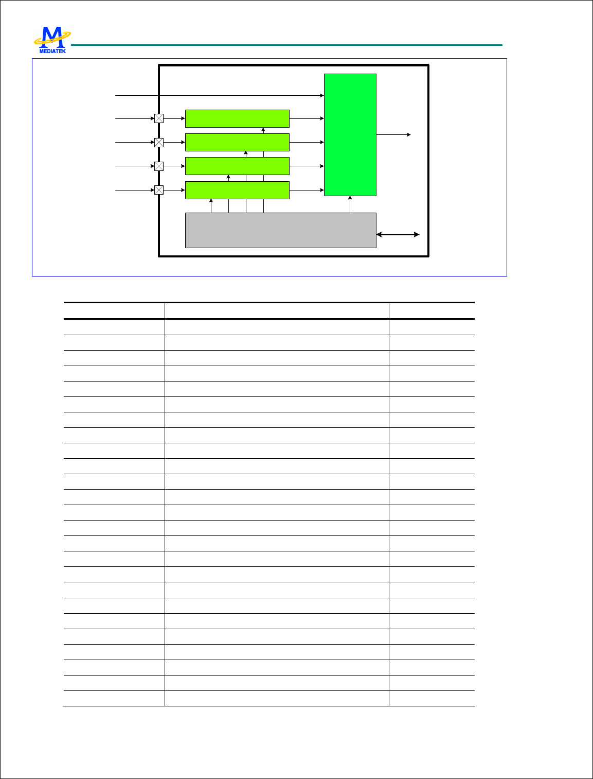
MTK Confidential Release for Konka
MTK Confidential Release for Konka
MT6228 GSM/GPRS Baseband Processor Data Sheet Revision 1.0
63/616 MediaTek Inc. Confidential
Debounce Logic
Debounce Logic
Debounce Logic
Registers
Interrupt
Control
Logic
EINT_IRQ
EINT3
EINT1
EINT2
APB Bus
MT6219
Debounce Logic
EINT0
EINT4-7
Figure 16 Block Diagram of External Interrupt Controller
REGISTER ADDRESS
REGISTER NAME SYNONYM
CIRQ + 0000h IRQ Selection 0 Register IRQ_SEL0
CIRQ + 0004h IRQ Selection 1 Register IRQ_SEL1
CIRQ + 0008h IRQ Selection 2 Register IRQ_SEL2
CIRQ + 000Ch IRQ Selection 3 Register IRQ_SEL3
CIRQ + 0010h IRQ Selection 4 Register IRQ_SEL4
CIRQ + 0014h IRQ Selection 5 Register IRQ_SEL5
CIRQ + 0018h IRQ Selection 6 Register IRQ_SEL6
CIRQ + 001ch IRQ Selection 7 Register IRQ_SEL7
CIRQ + 0034h FIQ Selection Register FIQ_SEL
CIRQ + 0038h IRQ Mask Register (LSB) IRQ_MASKL
CIRQ + 003ch IRQ Mask Register (MSB) IRQ_MASKH
CIRQ + 0040h IRQ Mask Clear Register (LSB) IRQ_MASK_CLRL
CIRQ + 0044h IRQ Mask Clear Register (MSB) IRQ_MASK_CLRH
CIRQ + 0048h IRQ Mask Set Register (LSB) IRQ_MASK_SETL
CIRQ + 004ch IRQ Mask Set Register (MSB) IRQ_MASK_SETH
CIRQ + 0050h IRQ Status Register (LSB) IRQ_STAL
CIRQ + 0054h IRQ Status Register (MSB) IRQ_STAH
CIRQ + 0058h IRQ End of Interrupt Register (LSB) IRQ_EOIL
CIRQ + 005ch IRQ End of Interrupt Register (MSB) IRQ_EOIH
CIRQ + 0060h IRQ Sensitive Register (LSB) IRQ_SENSL
CIRQ + 0064h IRQ Sensitive Register (MSB) IRQ_SENSH
CIRQ + 0068h IRQ Software Interrupt Register (LSB) IRQ_SOFTL
CIRQ + 006ch IRQ Software Interrupt Register (MSB) IRQ_SOFTH
CIRQ + 0070h FIQ Control Register FIQ_CON
CIRQ + 0074h FIQ End of Interrupt Register FIQ_EOI
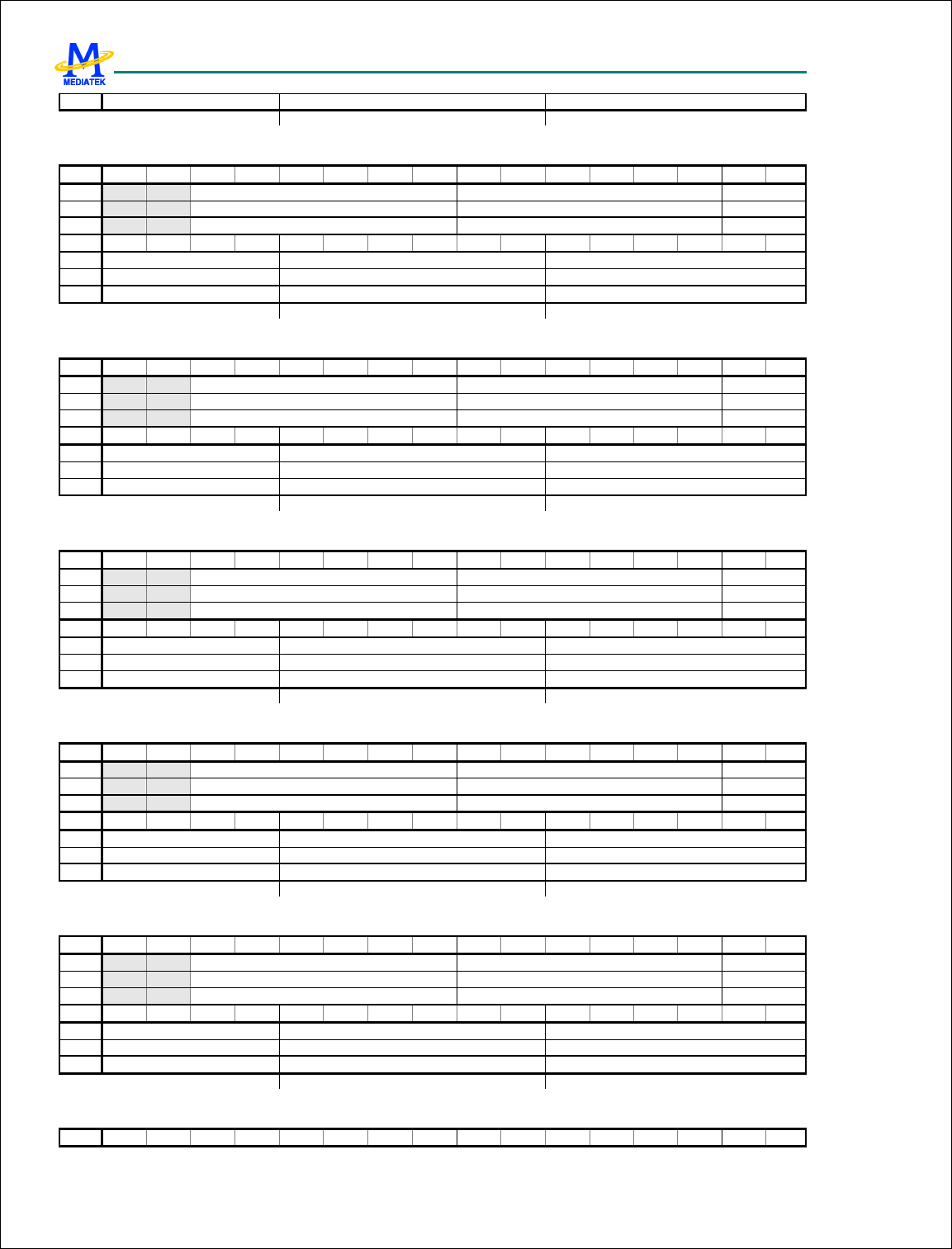
MTK Confidential Release for Konka
MTK Confidential Release for Konka
MT6228 GSM/GPRS Baseband Processor Data Sheet Revision 1.0
65/616 MediaTek Inc. Confidential
Reset
c b a
CIRQ+000ch IRQ Selection 3 Register IRQ_SEL3
Bit 31 30 29 28 27 26 25 24 23 22 21 20 19 18 17 16
Name
IRQ13 IRQ12 IRQ11
Type R/W R/W R/W
Reset
13 12 11
Bit 15 14 13 12 11 10 9 8 7 6 5 4 3 2 1 0
Name
IRQ11 IRQ10 IRQF
Type R/W R/W R/W
Reset
11 10 f
CIRQ+0010h IRQ Selection 4 Register IRQ_SEL4
Bit 31 30 29 28 27 26 25 24 23 22 21 20 19 18 17 16
Name
IRQ18 IRQ17 IRQ16
Type R/W R/W R/W
Reset
18 17 16
Bit 15 14 13 12 11 10 9 8 7 6 5 4 3 2 1 0
Name
IRQ16 IRQ15 IRQ14
Type R/W R/W R/W
Reset
16 15 14
CIRQ+0014h IRQ Selection 5 Register IRQ_SEL5
Bit 31 30 29 28 27 26 25 24 23 22 21 20 19 18 17 16
Name
IRQ1D IRQ1C IRQ1B
Type R/W R/W R/W
Reset
1d 1c 1b
Bit 15 14 13 12 11 10 9 8 7 6 5 4 3 2 1 0
Name
IRQ1B IRQ1A IRQ19
Type R/W R/W R/W
Reset
1b 1a 19
CIRQ+0018h IRQ Selection 6 Register IRQ_SEL6
Bit 31 30 29 28 27 26 25 24 23 22 21 20 19 18 17 16
Name
IRQ22 IRQ21 IRQ20
Type R/W R/W R/W
Reset
22 21 20
Bit 15 14 13 12 11 10 9 8 7 6 5 4 3 2 1 0
Name
IRQ20 IRQ1F IRQ1E
Type R/W R/W R/W
Reset
20 1f 1e
CIRQ+001ch IRQ Selection 7 Register IRQ_SEL7
Bit 31 30 29 28 27 26 25 24 23 22 21 20 19 18 17 16
Name
IRQ27 IRQ26 IRQ25
Type R/W R/W R/W
Reset
27 26 25
Bit 15 14 13 12 11 10 9 8 7 6 5 4 3 2 1 0
Name
IRQ25 IRQ24 IRQ23
Type R/W R/W R/W
Reset
25 24 23
CIRQ+0020h IRQ Selection 8 Register IRQ_SEL8
Bit 31 30 29 28 27 26 25 24 23 22 21 20 19 18 17 16
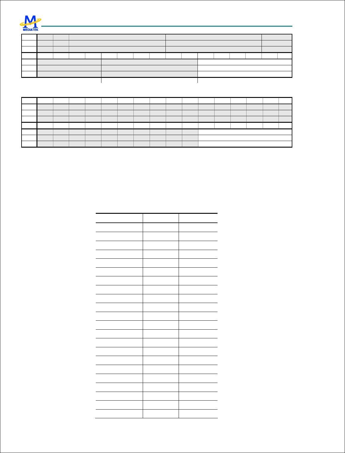
MTK Confidential Release for Konka
MTK Confidential Release for Konka
MT6228 GSM/GPRS Baseband Processor Data Sheet Revision 1.0
66/616 MediaTek Inc. Confidential
Name
Type
Reset
Bit 15 14 13 12 11 10 9 8 7 6 5 4 3 2 1 0
Name
IRQ28
Type R/W
Reset
28
CIRQ+0034h FIQ Selection Register FIQ_SEL
Bit 31 30 29 28 27 26 25 24 23 22 21 20 19 18 17 16
Name
Type
Reset
Bit 15 14 13 12 11 10 9 8 7 6 5 4 3 2 1 0
Name
FIQ
Type R/W
Reset
0
The IRQ/FIQ Selection Registers provide system designers with a flexible routing scheme to make various mappings of
priority among interrupt sources possible. The registers allow the interrupt sources to be mapped onto interrupt
requests of either FIQ or IRQ. While only one interrupt source can be assigned to FIQ, the other ones share IRQs by
mapping them onto IRQ0 to IRQ1F connected to IRQ controller. The priority sequence of IRQ0~IRQ1F is fixed, i.e.
IRQ0 > IRQ1 > IRQ2 > … > IRQ1E > IRQ1F. During the software configuration process, the Interrupt Source Code
of desired interrupt source should be written into source field of the corresponding IRQ_SEL0-IRQ_SEL4/FIQ_SEL.
Five-bit Interrupt Source Codes for all interrupt sources are fixed and defined.
Interrupt Source STA2 (Hex) STAH_STAL
GPI_FIQ 0 000_00000001
TDMA_CTIRQ1 1 000_00000002
TDMA_CTIRQ2 2 000_00000004
DSP2CPU 3 000_00000008
SIM 4 000_00000010
DMA 5 000_00000020
TDMA 6 000_00000040
UART1 7 000_00000080
KeyPad 8 000_00000100
UART2 9 000_00000200
GPTimer a 000_00000400
EINT b 000_00000800
USB c 000_00001000
MSDC d 000_00002000
RTC e 000_00004000
IrDA f 000_00008000
LCD 10 000_00010000
UART3 11 000_00020000
GPI 12 000_00040000
WDT 13 000_00080000
SWDBG 14 000_00100000
CHE 15 000_00200000
MTK Confidential Release for Konka
MTK Confidential Release for Konka
MT6228 GSM/GPRS Baseband Processor Data Sheet Revision 1.0
67/616 MediaTek Inc. Confidential
NFI 16 000_00400000
B2PSI 17 000_00800000
Image DMA 18 000_01000000
GIF 19 000_02000000
PNG 1a 000_04000000
SCCB 1b 000_08000000
G2D 1c 000_10000000
Image Porc 1d 000_20000000
CAM 1e 000_40000000
PFC 1f 000_80000000
MPEG4_DEC 20 001_00000000
MPEG4_ENC 21 002_00000000
JPEG_DEC 22 004_00000000
JPEG_ENC 23 008_00000000
Resizer_crz 24 010_00000000
Resizer_drz 25 020_00000000
Resizer_prz 26 040_00000000
TVE 27 080_00000000
Table 12 Interrupt Source Code for Interrupt Sources
FIQ, IRQ0-26 The 5-bit content of this field corresponds to an Interrupt Source Code shown above.
CIRQ+0038h IRQ Mask Register (LSB) IRQ_MASKL
Bit 31 30 29 28 27 26 25 24 23 22 21 20 19 18 17 16
Name
IRQ1F
IRQ1E
IRQ1
D
IRQ1
C
IRQ1
B
IRQ1
A IRQ19
IRQ18
IRQ17
IRQ16
IRQ15
IRQ14
IRQ13
IRQ12
IRQ11
IRQ10
Type R/W R/W R/W R/W R/W R/W R/W R/W R/W R/W R/W R/W R/W R/W R/W R/W
Reset
1 1 1 1 1 1 1 1 1 1 1 1 1 1 1 1
Bit 15 14 13 12 11 10 9 8 7 6 5 4 3 2 1 0
Name
IRQF
IRQE
IRQD
IRQC
IRQB
IRQA
IRQ9
IRQ8
IRQ7
IRQ6
IRQ5
IRQ4
IRQ3
IRQ2
IRQ1
IRQ0
Type R/W R/W R/W R/W R/W R/W R/W R/W R/W R/W R/W R/W R/W R/W R/W R/W
Reset
1 1 1 1 1 1 1 1 1 1 1 1 1 1 1 1
CIRQ+003ch IRQ Mask Register (MSB) IRQ_MASKH
Bit 31 30 29 28 27 26 25 24 23 22 21 20 19 18 17 16
Name
Type
Reset
Bit 15 14 13 12 11 10 9 8 7 6 5 4 3 2 1 0
Name
IRQ27
IRQ26
IRQ25
IRQ24
IRQ23
IRQ22
IRQ21
IRQ20
Type R/W R/W R/W R/W R/W R/W R/W R/W
Reset
1 1 1 1 1 1 1 1
This register contains a mask bit for each interrupt line in IRQ Controller. The register allows each interrupt source
IRQ0 to IRQ1F to be disabled or masked separately under software control. After a system reset, all bit values are set
to 1 to indicate that interrupt requests are prohibited.
IRQ0-27 Mask control for the associated interrupt source in the IRQ controller
0 Interrupt is enabled.
1 Interrupt is disabled.
MTK Confidential Release for Konka
MTK Confidential Release for Konka
MT6228 GSM/GPRS Baseband Processor Data Sheet Revision 1.0
68/616 MediaTek Inc. Confidential
CIRQ+0040h IRQ Mask Clear Register (LSB) IRQ_MASK_CL
RL
Bit 31 30 29 28 27 26 25 24 23 22 21 20 19 18 17 16
Name
IRQ1F
IRQ1E
IRQ1
D
IRQ1
C
IRQ1
B
IRQ1
A IRQ19
IRQ18
IRQ17
IRQ16
IRQ15
IRQ14
IRQ13
IRQ12
IRQ11
IRQ10
Type W1C W1C W1C W1C W1C W1C W1C W1C W1C W1C W1C W1C W1C W1C W1C W1C
Bit 15 14 13 12 11 10 9 8 7 6 5 4 3 2 1 0
Name
IRQF IRQE IRQD IRQC IRQB IRQA IRQ9 IRQ8 IRQ7 IRQ6 IRQ5 IRQ4 IRQ3 IRQ2 IRQ1 IRQ0
Type W1C W1C W1C W1C W1C W1C W1C W1C W1C W1C W1C W1C W1C W1C W1C W1C
CIRQ+0044h IRQ Mask Clear Register (MSB) IRQ_MASK_CL
RH
Bit 31 30 29 28 27 26 25 24 23 22 21 20 19 18 17 16
Name
Type
Bit 15 14 13 12 11 10 9 8 7 6 5 4 3 2 1 0
Name
IRQ27
IRQ26
IRQ25
IRQ24
IRQ23
IRQ22
IRQ21
IRQ20
Type W1C W1C W1C W1C W1C W1C W1C W1C
This register is used to clear bits in IRQ Mask Register. When writing to this register, the data bits that are HIGH
cause the corresponding bits in IRQ Mask Register to be cleared. Data bits that are LOW have no effect on the
corresponding bits in IRQ Mask Register.
IRQ0-27 Clear corresponding bits in IRQ Mask Register.
0 No effect.
1 Disable the corresponding MASK bit.
CIRQ+0048h IRQ Mask SET Register (LSB) IRQ_MASK_SE
TL
Bit 31 30 29 28 27 26 25 24 23 22 21 20 19 18 17 16
Name
IRQ1F
IRQ1E
IRQ1
D
IRQ1
C
IRQ1
B
IRQ1
A IRQ19
IRQ18
IRQ17
IRQ16
IRQ15
IRQ14
IRQ13
IRQ12
IRQ11
IRQ10
Type W1S W1S W1S W1S W1S W1S W1S W1S W1S W1S W1S W1S W1S W1S W1S W1S
Bit 15 14 13 12 11 10 9 8 7 6 5 4 3 2 1 0
Name
IRQF IRQE IRQD IRQC IRQB IRQA IRQ9 IRQ8 IRQ7 IRQ6 IRQ5 IRQ4 IRQ3 IRQ2 IRQ1 IRQ0
Type W1S W1S W1S W1S W1S W1S W1S W1S W1S W1S W1S W1S W1S W1S W1S W1S
CIRQ+004ch IRQ Mask SET Register (MSB) IRQ_MASK_SE
TH
Bit 31 30 29 28 27 26 25 24 23 22 21 20 19 18 17 16
Name
Type
Bit 15 14 13 12 11 10 9 8 7 6 5 4 3 2 1 0
Name
IRQ27
IRQ26
IRQ25
IRQ24
IRQ23
IRQ22
IRQ21
IRQ20
Type W1S W1S W1S W1S W1S W1S W1S W1S
This register is used to set bits in the IRQ Mask Register. When writing to this register, the data bits that are HIGH
cause the corresponding bits in IRQ Mask Register to be set. Data bits that are LOW have no effect on the
corresponding bits in IRQ Mask Register.
IRQ0-27 Set corresponding bits in IRQ Mask Register.
0 No effect.
1 Enable corresponding MASK bit.
MTK Confidential Release for Konka
MTK Confidential Release for Konka
MT6228 GSM/GPRS Baseband Processor Data Sheet Revision 1.0
69/616 MediaTek Inc. Confidential
CIRQ+0050h IRQ Source Status Register (LSB) IRQ_STAL
Bit 31 30 29 28 27 26 25 24 23 22 21 20 19 18 17 16
Name
IRQ1F
IRQ1E
IRQ1
D
IRQ1
C
IRQ1
B
IRQ1
A IRQ19
IRQ18
IRQ17
IRQ16
IRQ15
IRQ14
IRQ13
IRQ12
IRQ11
IRQ10
Type RO RO RO RO RO RO RO RO RO RO RO RO RO RO RO RO
Reset
0 0 0 0 0 0 0 0 0 0 0 0 0 0 0 0
Bit 15 14 13 12 11 10 9 8 7 6 5 4 3 2 1 0
Name
IRQF
IRQE
IRQD
IRQC
IRQB
IRQA
IRQ9
IRQ8
IRQ7
IRQ6
IRQ5
IRQ4
IRQ3
IRQ2
IRQ1
IRQ0
Type RO RO RO RO RO RO RO RO RO RO RO RO RO RO RO RO
Reset
0 0 0 0 0 0 0 0 0 0 0 0 0 0 0 0
CIRQ+0054h IRQ SouROe Status Register (MSB) IRQ_STAH
Bit 31 30 29 28 27 26 25 24 23 22 21 20 19 18 17 16
Name
Type
Reset
Bit 15 14 13 12 11 10 9 8 7 6 5 4 3 2 1 0
Name
IRQ27
IRQ26
IRQ25
IRQ24
IRQ23
IRQ22
IRQ21
IRQ20
Type RO RO RO RO RO RO RO RO
Reset
0 0 0 0 0 0 0 0
This Register allows software to poll which interrupt line has generated an IRQ interrupt request. A bit set to 1
indicates a corresponding active interrupt line. Only one flag is active at a time. The IRQ_STA is type of read-clear;
write access has no effect on the content.
IRQ0-27 Interrupt indicator for the associated interrupt source.
0 The associated interrupt source is non-active.
1 The associated interrupt source is asserted.
CIRQ+0058h IRQ End of Interrupt Register (LSB) IRQ_EOIL
Bit 31 30 29 28 27 26 25 24 23 22 21 20 19 18 17 16
Name
IRQ1F
IRQ1E
IRQ1
D
IRQ1
C
IRQ1
B
IRQ1
A IRQ19
IRQ18
IRQ17
IRQ16
IRQ15
IRQ14
IRQ13
IRQ12
IRQ11
IRQ10
Type WO WO WO WO WO WO WO WO WO WO WO WO WO WO WO WO
Reset
0 0 0 0 0 0 0 0 0 0 0 0 0 0 0 0
Bit 15 14 13 12 11 10 9 8 7 6 5 4 3 2 1 0
Name
IRQF IRQE IRQD IRQC IRQB IRQA IRQ9 IRQ8 IRQ7 IRQ6 IRQ5 IRQ4 IRQ3 IRQ2 IRQ1 IRQ0
Type WO WO WO WO WO WO WO WO WO WO WO WO WO WO WO WO
Reset
0 0 0 0 0 0 0 0 0 0 0 0 0 0 0 0
CIRQ+005ch IRQ End of Interrupt Register (MSB) IRQ_EOIH
Bit 31 30 29 28 27 26 25 24 23 22 21 20 19 18 17 16
Name
Type
Reset
Bit 15 14 13 12 11 10 9 8 7 6 5 4 3 2 1 0
Name
IRQ27
IRQ26
IRQ25
IRQ24
IRQ23
IRQ22
IRQ21
IRQ20
Type WO WO WO WO WO WO WO WO
Reset
0 0 0 0 0 0 0 0
This register provides a mean for software to relinquish and to refresh the interrupt controller. Writing a 1 to a
specific bit position results in an End of Interrupt command issued internally to the corresponding interrupt line.
IRQ0-27 End of Interrupt command for the associated interrupt line.
0 No service is currently in progress or pending.
1 Interrupt request is in-service.
MTK Confidential Release for Konka
MTK Confidential Release for Konka
MT6228 GSM/GPRS Baseband Processor Data Sheet Revision 1.0
70/616 MediaTek Inc. Confidential
CIRQ+0060h IRQ Sensitive Register (LSB) IRQ_SENSL
Bit 31 30 29 28 27 26 25 24 23 22 21 20 19 18 17 16
Name
IRQ1F
IRQ1E
IRQ1
D
IRQ1
C
IRQ1
B
IRQ1
A IRQ19
IRQ18
IRQ17
IRQ16
IRQ15
IRQ14
IRQ13
IRQ12
IRQ11
IRQ10
Type R/W R/W R/W R/W R/W R/W R/W R/W R/W R/W R/W R/W R/W R/W R/W R/W
Reset
0 0 0 0 0 0 0 0 0 0 0 0 0 0 0 0
Bit 15 14 13 12 11 10 9 8 7 6 5 4 3 2 1 0
Name
IRQF
IRQE
IRQD
IRQC
IRQB
IRQA
IRQ9
IRQ8
IRQ7
IRQ6
IRQ5
IRQ4
IRQ3
IRQ2
IRQ1
IRQ0
Type R/W R/W R/W R/W R/W R/W R/W R/W R/W R/W R/W R/W R/W R/W R/W R/W
Reset
0 0 0 0 0 0 0 0 0 0 0 0 0 0 0 0
CIRQ+0064h IRQ Sensitive Register (MSB) IRQ_SENSH
Bit 31 30 29 28 27 26 25 24 23 22 21 20 19 18 17 16
Name
Type
Reset
Bit 15 14 13 12 11 10 9 8 7 6 5 4 3 2 1 0
Name
IRQ27
IRQ26
IRQ25
IRQ24
IRQ23
IRQ22
IRQ21
IRQ20
Type R/W R/W R/W R/W R/W R/W R/W R/W
Reset
0 0 0 0 0 0 0 0
All interrupt lines of IRQ Controller, IRQ0~IRQ1F can be programmed as either edge or level sensitive. By default,
all the interrupt lines are edge sensitive and should be active LOW. Once a interrupt line is programmed as edge
sensitive, an interrupt request is triggered only at the falling edge of interrupt line, and the next interrupt is not accepted
until the EOI command is given. However, level sensitive interrupts trigger is according to the signal level of the
interrupt line. Once the interrupt line become from HIGH to LOW, an interrupt request is triggered, and another
interrupt request is triggered if the signal level remain LOW after an EOI command. Note that in edge sensitive mode,
even if the signal level remains LOW after EOI command, another interrupt request is not triggered. That is because
edge sensitive interrupt is only triggered at the falling edge.
IRQ0-27 Sensitivity type of the associated Interrupt Source
0 Edge sensitivity with active LOW
1 Level sensitivity with active LOW
CIRQ+0068h IRQ Software Interrupt Register (LSB) IRQ_SOFTL
Bit 31 30 29 28 27 26 25 24 23 22 21 20 19 18 17 16
Name
IRQ1F
IRQ1E
IRQ1
D
IRQ1
C
IRQ1
B
IRQ1
A IRQ19
IRQ18
IRQ17
IRQ16
IRQ15
IRQ14
IRQ13
IRQ12
IRQ11
IRQ10
Type R/W R/W R/W R/W R/W R/W R/W R/W R/W R/W R/W R/W R/W R/W R/W R/W
Reset
0 0 0 0 0 0 0 0 0 0 0 0 0 0 0 0
Bit 15 14 13 12 11 10 9 8 7 6 5 4 3 2 1 0
Name
IRQF IRQE IRQD IRQC IRQB IRQA IRQ9 IRQ8 IRQ7 IRQ6 IRQ5 IRQ4 IRQ3 IRQ2 IRQ1 IRQ0
Type R/W R/W R/W R/W R/W R/W R/W R/W R/W R/W R/W R/W R/W R/W R/W R/W
Reset
0 0 0 0 0 0 0 0 0 0 0 0 0 0 0 0
CIRQ+006ch IRQ Software Interrupt Register (MSB) IRQ_SOFTH
Bit
31 30
29
28
27 26 25
24
23
22 21 20
19
18
17 16
Name
Type
Reset
Bit 15 14 13 12 11 10 9 8 7 6 5 4 3 2 1 0
Name
IRQ27
IRQ26
IRQ25
IRQ24
IRQ23
IRQ22
IRQ21
IRQ20
Type R/W R/W R/W R/W R/W R/W R/W R/W
Reset
0 0 0 0 0 0 0 0

MTK Confidential Release for Konka
MTK Confidential Release for Konka
MT6228 GSM/GPRS Baseband Processor Data Sheet Revision 1.0
71/616 MediaTek Inc. Confidential
Setting “1” to the specific bit position generates a software interrupt for corresponding interrupt line before mask.
This register is used for debug purpose.
IRQ0-IRQ27 Software Interrupt
CIRQ+0070h FIQ Control Register FIQ_CON
Bit 31 30 29 28 27 26 25 24 23 22 21 20 19 18 17 16
Name
Type
Reset
Bit 15 14 13 12 11 10 9 8 7 6 5 4 3 2 1 0
Name
SENS
MAS
K
Type R/W R/W
Reset
0 1
This register provides a means for software program to control the FIQ controller.
MASK Mask control for the FIQ Interrupt Source
0 Interrupt is enabled.
1 Interrupt is disabled.
SENS Sensitivity type of the FIQ Interrupt Source
0 Edge sensitivity with active LOW
1 Level sensitivity with active LOW
CIRQ+0074h FIQ End of Interrupt Register FIQ_EOI
Bit 31 30 29 28 27 26 25 24 23 22 21 20 19 18 17 16
Name
Type
Reset
Bit 15 14 13 12 11 10 9 8 7 6 5 4 3 2 1 0
Name
EOI
Type WO
Reset
0
This register provides a means for software to relinquish and to refresh the FIQ controller. Writing a ‘1’ to the
specific bit position results in an End of Interrupt command issued internally to the corresponding interrupt line.
EOI End of Interrupt command
CIRQ+0078h Binary Coded Value of IRQ_STATUS IRQ_STA2
Bit 31 30 29 28 27 26 25 24 23 22 21 20 19 18 17 16
Name
Type
Reset
Bit 15 14 13 12 11 10 9 8 7 6 5 4 3 2 1 0
Name
NOIR
Q STS
Type RO RO
Reset
0 0
This Register is a binary coded version of IRQ_STA. It is used by the software program to poll which interrupt line
has generated the IRQ interrupt request in a much easier way. Any read to it has the same result as reading IRQ_STA.
The IRQ_STA2 is also read-only; write access has no effect on the content. Note that IRQ_STA2 should be coupled
with IRQ_EOI2 while using it.
STS Binary coded value of IRQ_STA
MTK Confidential Release for Konka
MTK Confidential Release for Konka
MT6228 GSM/GPRS Baseband Processor Data Sheet Revision 1.0
72/616 MediaTek Inc. Confidential
NOIRQ Indicating if there is an IRQ or not. If there is no IRQ, this bit is HIGH, and the value of STS is 00_0000b.
CIRQ+007ch Binary Coded Value of IRQ_EOI IRQ_EOI2
Bit 31 30 29 28 27 26 25 24 23 22 21 20 19 18 17 16
Name
Type
Reset
Bit 15 14 13 12 11 10 9 8 7 6 5 4 3 2 1 0
Name
EOI
Type WO
Reset
0
This register is a binary coded version of IRQ_EOI. It provides an easier way for software program to relinquish and
to refresh the interrupt controller. Writing a specific code results in an End of Interrupt command issued internally to
the corresponding interrupt line. Note that IRQ_EOI2 should be coupled with IRQ_STA2 while using it.
EOI Binary coded value of IRQ_EOI
CIRQ+0080h Binary Coded Value of IRQ_SOFT IRQ_SOFT2
Bit 31 30 29 28 27 26 25 24 23 22 21 20 19 18 17 16
Name
Type
Reset
Bit 15 14 13 12 11 10 9 8 7 6 5 4 3 2 1 0
Name
SOFT
Type WO
Reset
0
This register is a binary coded version of IRQ_SOFT.
SOFT Binary Coded Value of IRQ_SOFT
CIRQ+0100h EINT Interrupt Status Register EINT_STA
Bit 31 30 29 28 27 26 25 24 23 22 21 20 19 18 17 16
Name
Type
Reset
Bit 15 14 13 12 11 10 9 8 7 6 5 4 3 2 1 0
Name
EINT7
EINT6
EINT5
EINT4
EINT3
EINT2
EINT1
EINT0
Type RO RO RO RO RO RO RO RO
Reset
0 0 0 0 0 0 0 0
This register keeps up with current status that which EINT Source generates the interrupt request. If EINT sources are
set to edge sensitivity, EINT_IRQ is de-asserted while this register is read.
EINT0-EINT7 Interrupt status
0 No interrupt request is generated.
1 Interrupt request is pending.
CIRQ+0104h EINT Interrupt Mask Register EINT_MASK
Bit 31 30 29 28 27 26 25 24 23 22 21 20 19 18 17 16
Name
Type
Reset
Bit 15 14 13 12 11 10 9 8 7 6 5 4 3 2 1 0
Name
EINT7
EINT6
EINT5
EINT4
EINT3
EINT2
EINT1
EINT0
Type R/W R/W R/W R/W R/W R/W R/W R/W
Reset
1 1 1 1 1 1 1 1
MTK Confidential Release for Konka
MTK Confidential Release for Konka
MT6228 GSM/GPRS Baseband Processor Data Sheet Revision 1.0
73/616 MediaTek Inc. Confidential
This register controls whether or not EINT Source is allowed to generate an interrupt request. Setting a “1”
to the specific bit position prohibits the external interrupt line from becoming active.
EINT0-EINT7 Interrupt Mask
0 Interrupt request is enabled.
1 Interrupt request is disabled.
CIRQ+0108h EINT Interrupt Mask Clear Register EINT_MASK_C
LR
Bit 31 30 29 28 27 26 25 24 23 22 21 20 19 18 17 16
Name
Type
Bit 15 14 13 12 11 10 9 8 7 6 5 4 3 2 1 0
Name
EINT7
EINT6
EINT5
EINT4
EINT3
EINT2
EINT1
EINT0
Type W1C W1C W1C W1C W1C W1C W1C W1C
This register is used to clear individual mask bits. Only the bits set to 1 are in effect, and interrupt masks for which
the mask bit is set are cleared (set to 0). Otherwise the interrupt mask bit retains its original value.
EINT0-EINT7 Disable mask for the associated external interrupt source.
0 No effect.
1 Disable the corresponding MASK bit.
CIRQ+010Ch EINT Interrupt Mask Set Register EINT_MASK_S
ET
Bit 31 30 29 28 27 26 25 24 23 22 21 20 19 18 17 16
Name
Type
Bit 15 14 13 12 11 10 9 8 7 6 5 4 3 2 1 0
Name
EINT7
EINT6
EINT5
EINT4
EINT3
EINT2
EINT1
EINT0
Type W1S W1S W1S W1S W1S W1S W1S W1S
This register is used to set individual mask bits. Only the bits set to 1 are in effect, and interrupt masks for which the
mask bit is set are set to 1. Otherwise the interrupt mask bit retains its original value.
EINT0-EINT7 Disable mask for the associated external interrupt source.
0 No effect.
1 Enable corresponding MASK bit.
CIRQ+0110h EINT Interrupt Acknowledge Register EINT_INTACK
Bit 31 30 29 28 27 26 25 24 23 22 21 20 19 18 17 16
Name
Type
Reset
Bit 15 14 13 12 11 10 9 8 7 6 5 4 3 2 1 0
Name
EINT7
EINT6
EINT5
EINT4
EINT3
EINT2
EINT1
EINT0
Type WO WO WO WO WO WO WO WO
Reset
0 0 0 0 0 0 0 0
Writing “1” to the specific bit position acknowledge the interrupt request correspondingly to the external interrupt line
source.
EINT0-EINT7 Interrupt acknowledgement
0 No effect
1 Interrupt request is acknowledged.
MTK Confidential Release for Konka
MTK Confidential Release for Konka
MT6228 GSM/GPRS Baseband Processor Data Sheet Revision 1.0
74/616 MediaTek Inc. Confidential
CIRQ+0114h EINT Sensitive Register EINT_SENS
Bit 31 30 29 28 27 26 25 24 23 22 21 20 19 18 17 16
Name
Type
Reset
Bit 15 14 13 12 11 10 9 8 7 6 5 4 3 2 1 0
Name
EINT3
EINT2
EINT1
EINT0
Type R/W R/W R/W R/W
Reset
1 1 1 1
Sensitivity type of external interrupt source. Only EINT0~3 need to be specified. EINT4~7 are always edge
sensitive.
EINT0-3 Sensitivity type of the associated external interrupt source.
0 Edge sensitivity
1 Level sensitivity
CIRQ+01m0h EINTn De-bounce Control Register EINTn_CON
Bit 31 30 29 28 27 26 25 24 23 22 21 20 19 18 17 16
Name
Type
Reset
Bit 15 14 13 12 11 10 9 8 7 6 5 4 3 2 1 0
Name
EN POL CNT
Type R/W R/W R/W
Reset
0 0 0
These registers control the de-bounce logic for external interrupt sources in order to minimize the possibility of false
activations. EINT4~7 have no de-bounce mechanism, therefore only bit POL is used.
Note that n is from 0 to 7, and m is n + 2.
CNT De-bounce duration in terms of number of 32 KHz clock cycles.
POL Activation type of the EINT source
0 Negative polarity
1 Positive polarity
EN De-bounce control circuit
0 Disable
1 Enable
3.6 Code Cache Controller
3.6.1 General Description
A new subsystem consisting of cache and TCM (tightly coupled memory) is implemented in MT6228. This
subsystem is placed between MCU core and AHB bus interface, as shown in Figure 17.
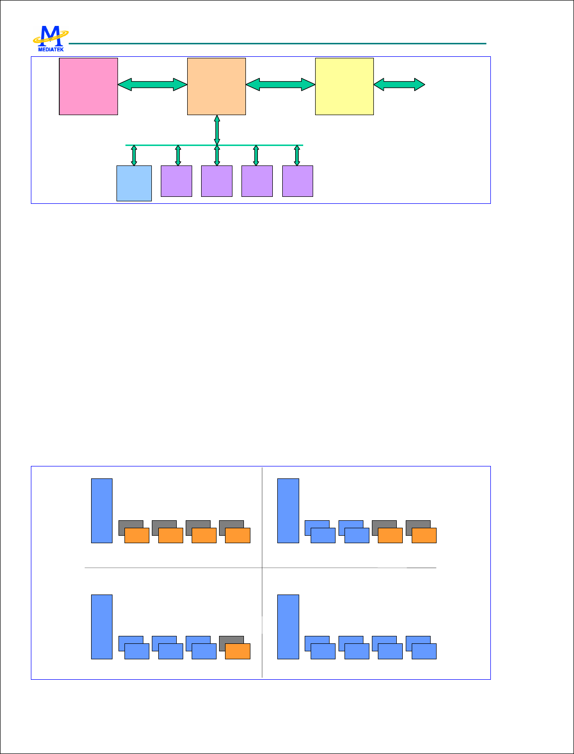
MTK Confidential Release for Konka
MTK Confidential Release for Konka
MT6228 GSM/GPRS Baseband Processor Data Sheet Revision 1.0
75/616 MediaTek Inc. Confidential
ARM7EJ
core
Cache
Controller
& MPU
AHB
bus
interface
TCM
cache
way 0
cache
way 1
cache
way 2
cache
way 3
AHB
Figure 17 Cache and TCM subsystem
TCM is a high-speed (zero wait state) dedicated memory accessed by MCU exclusively. Because MCU can run at
104 MHz and on-chip bus runs at maximum of 52 MHz, latency occurs when MCU accesses memory or peripherals
through the on-chip bus. By moving timing critical code and data into TCM, MCU performance is increased and the
response to particular events can be guaranteed.
Another method to increase MCU performance is the introduction of cache. Cache is a small memory, keeping the
copy of external memory. If MCU reads a portion of cacheable data, the data is copied to cache. If MCU needs the
same data at a later time, it can retrieve the data directly from cache (called cache hit) instead of from external memory,
which takes a long time compared to accessing high-speed (zero wait state) cache memory.
Since a large external memory maps to a small cache, cache can hold only a small portion of external memory. If
MCU accesses data not found in cache (called cache miss), some contents of cache must be dropped (flushed) and the
required data is transferred from external memory (called cache line fill) and stored in cache. On the other hand, TCM
is not a copy of external memory. The best way to use TCM is to put critical code/data in TCM in the memory usage
plan. After power on reset, the boot loader copies TCM contents from external storage (such as flash) to internal
TCM. If necessary, MCU can replace a portion of TCM content with other data on external storage in the runtime to
implement an “overlay” mechanism. TCM is also an ideal place to put stack data.
The sizes of TCM and cache can be set to one of 4 configurations:
128
KB
8
KB
8
KB
8
KB
8
KB
TCM
cache
cache
cache
cache
128
KB
8
KB
8
KB
8
KB
8
KB
TCM
TCM
TCM
cache
cache
128
KB
8
KB
8
KB
8
KB
8
KB
TCM
TCM
TCM
TCM
cache
128
KB
8
KB
8
KB
8
KB
8
KB
TCM
TCM
TCM
TCM
TCM
4
-
way cache
2
-
way cache
1
-
way cache
no cache
Figure 18 Configurations of TCM and cache
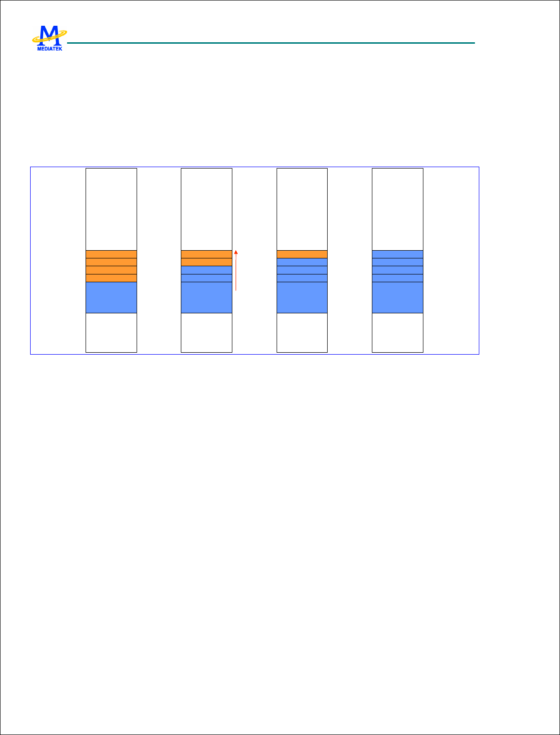
MTK Confidential Release for Konka
MTK Confidential Release for Konka
MT6228 GSM/GPRS Baseband Processor Data Sheet Revision 1.0
76/616 MediaTek Inc. Confidential
128KB TCM, 32KB cache
144KB TCM, 16KB cache
152KB TCM, 8KB cache
160KB TCM, 0KB cache
These configurations provide flexibility for software to adjust for optimum system performance.
The address mapping of these memories is as follows:
cache
cache
TCM TCM TCM
cache
TCM
TCM TCM
TCM TCM
TCM
TCM
TCM
TCM
TCM
cache
cache
cache
cache
128K
8K
8K
8K
8K
Increasingly
adjacent
address.
No memory
holes.
cache
cache
TCM TCM TCM
cache
TCM
TCM TCM
TCM TCM
TCM
TCM
TCM
TCM
TCM
cache
cache
cache
cache
128K
8K
8K
8K
8K
Increasingly
adjacent
address.
No memory
holes.
Figure 19 Memory mapping of TCM and cache
In Figure 19, MCU could only access TCM explicitly. Cache is transparent to MCU.
3.6.2 Organization of Cache
The cache system has the following features:
Write through (no write allocation)
Configurable 1/2/4 way set associative (8K/16K/32K)
Each way has 256 cache lines with 8 word line size (256*8*4=8KB)
19 bit tag address, 1 valid bit, for one cache line.
One way of cache comprises of two memories: tag memory and data memory. Tag memory stores each line’s valid bit,
dirty bit and tag (upper part of address). Data memory stores line data. When MCU accesses memory, the address is
compared to the contents of tag memory. First the line index (address bit [12:5]) is used to locate a line, and then the
tag of the line is compared to upper part of address (bit [31:13]). If two parts match and valid bit is 1, it is a cache hit
and data from that particular way is sent back to MCU. This process is illustrated in the following figure:
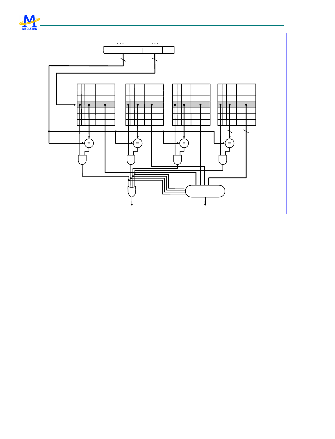
MTK Confidential Release for Konka
MTK Confidential Release for Konka
MT6228 GSM/GPRS Baseband Processor Data Sheet Revision 1.0
77/616 MediaTek Inc. Confidential
Address
19 8
V TagIndex
0
1
2
253
254
255
Data V Tag Data V Tag Data V Tag Data
3219
4-to-1 multiplexor
Hit Data
45121331 0
D D D D
Figure 20 Tag comparison of 4-way cache
If most memory accesses are cache hit, MCU could get data immediately without wait states and the overall system
performance is higher. There are several factors that may affect cache hit rate:
Cache size and the organization
The larger the cache size is, the higher the hit rate is. However the hit rate starts to saturate when cache size
is larger than a threshold size. Normally a cache size of 16KB and above and two or four ways achieve a
good hit rate.
Program behavior
If the system has several tasks that switch data quickly, it may cause cache contents to be flushed frequently.
Each time a new task is run, the cache holds the data. If the next task uses data in memory that occupies the
same cache entries as the previous task, the cache contents are flushed to store the data for the new task.
Interrupts also cause program flow to change dynamically. The interrupt handler code itself and the data it
processes may cause cache to flush some data used by the current task. Thus after exiting the interrupt
handler and returning to the current task, the flushed data may need to be re-cached, resulting performance
degradation.
To help a software engineer tune system performance, the cache controller in MT6228 records the number of cache hits
and cacheable memory accesses. The cache hit rate can be obtained from these two numbers.
The cache sub system also has a module called MPU (memory protection unit). MPU can prevent illegal memory
access and specify which memory region is cacheable or non-cacheable. Two fields in CACHE_CON register control
the enable of MPU functions. MPU has its own registers to define memory region and associated regions. These

MTK Confidential Release for Konka
MTK Confidential Release for Konka
MT6228 GSM/GPRS Baseband Processor Data Sheet Revision 1.0
78/616 MediaTek Inc. Confidential
settings only take effect after the enable bits in CACHE_CON are set to 1. For more details on the settings, refer to
MPU portion of the specification.
3.6.3 Cache Operations
Upon power on, cache memory contains random numbers and cannot be used by MCU. Therefore MCU must have
some means to “clean” cache memory before enabling it. The cache controller provides a register which, when
written, can perform operations on cache memory. These are called cache operations, and include
Invalidate one cache line
The user must give a memory address. If it is found within cache, that particular line is invalidated (valid bit
set to 0). Alternatively, the user can specify which set/way of cache to be invalidated.
Invalidate all cache lines
The user needs not to specify an address. The cache controller hardware automatically clears all valid bits in
each tag memory.
3.6.4 Cache Controller Register Definition
CACHE base address is assumed 0x80700000 (subject to change).
CACHE+00h Cache General Control Register CACHE_CON
Bit 15 14 13 12 11 10 9 8 7 6 5 4 3 2 1 0
Name
CACHESIZE
CNTE
N1
CNTE
N0 MPEN
MCE
N
Type RW RW RW R/W R/W
Reset
00 0 0 0 0
This register determines the cache size, cache hit counter and the enabling of MPU.
CACHESIZE Cache Size Select
00 no cache (128KB TCM)
01 8KB, 1-way cache (120KB TCM)
10 16KB, 2-way cache (112KB TCM)
11 32KB, 4-way cache (96KB TCM)
CNTEN1 Enable cache hit counter 1.
If enabled, cache controller increments a 48-bit counter each time a cache hit occurs. This number can
provide a reference for performance measurement for tuning of application programs. This counter
increments only when the cacheable information is from MPU cacheable regions 4~7.
0 Disable
1 Enable
CNTEN0 Enable cache hit counter 0
If enabled, cache controller increments a 48-bit counter each time a cache hit occurs. This number can
provide a reference for performance measurement for tuning of application programs. This counter
increments only when the cacheable information is from MPU cacheable regions 0~3.
0 Disable
1 Enable
MPEN Enable MPU comparison of read/write permission setting.
If disabled, MCU can access any memory segment without any restriction. If enabled, MPU compares the
address of MCU to its setting. If an address falls into a restricted region, MPU stops this memory access and
sends an “ABORT” signal to MCU. Refer to the MPU portion of the specification for more details.

MTK Confidential Release for Konka
MTK Confidential Release for Konka
MT6228 GSM/GPRS Baseband Processor Data Sheet Revision 1.0
79/616 MediaTek Inc. Confidential
0 Disable
1 Enable
MCEN Enable MPU comparison of cacheable/non-cacheable setting.
If disabled, MCU memory accesses are all non-cacheable, i.e., they go through AHB bus (except for TCM).
If enabled, the setting in MPU takes effect. If MCU accesses a cacheable memory region, the cache
controller returns the data in cache if found in cache, and retrieves the data through the AHB bus only if a
cache miss occurs. Refer to the MPU portion of the specification for more details.
0 Disable
1 Enable
CACHE+04h Cache Operation CACHE_OP
Bit 31 30 29 28 27 26 25 24 23 22 21 20 19 18 17 16
Name
TADDR[31:16]
Type R/W
Reset
0
Bit 15 14 13 12 11 10 9 8 7 6 5 4 3 2 1 0
Name
TADDR[15:5] OP[3:0] EN
Type R/W W W1
Reset
0 0 0
This register defines the address and/or which kind of cache operations to perform. When MCU writes this register,
the pipeline of MCU is stopped for the cache controller to complete the operation. Bit 0 of the register must be
written 1 to enable the command.
TADDR[31:5] Target Address
This field contains the address of invalidation operation. If OP[3:0]=0010, TADDR[31:5] is the address[31:5]
of a memory whose line is invalidated if it exists in the cache. If OP[3:0]=0100, TADDR[12:5] indicates the
set, while TADDR[19:16] indicates which way to clear:
0001 Way #0
0010 Way #1
0100 Way #2
1000 Way #3
OP[3:0] Operation
This field determines which cache operations are performed.
0001 Invalidate all cache lines
0010 Invalidate one cache line using address
0100 Invalidate one cache line using set/way
EN Enable command
This enable bit must be written 1 to enable the command.
0 Disabled
1 Enabled
CACHE+08h Cache Hit Count 0 Lower Part CACHE_HCNT0
L
Bit 31 30 29 28 27 26 25 24 23 22 21 20 19 18 17 16
Name
CHIT_CNT0[31:16]
Type R/W
Reset
0
Bit 15 14 13 12 11 10 9 8 7 6 5 4 3 2 1 0
Name
CHIT_CNT0[15:0]
Type R/W
MTK Confidential Release for Konka
MTK Confidential Release for Konka
MT6228 GSM/GPRS Baseband Processor Data Sheet Revision 1.0
80/616 MediaTek Inc. Confidential
Reset
0
CACHE+0Ch Cache Hit Count 0 Upper Part CACHE_HCNT0
U
Bit 31 30 29 28 27 26 25 24 23 22 21 20 19 18 17 16
Name
RESERVED
Type
Reset
Bit 15 14 13 12 11 10 9 8 7 6 5 4 3 2 1 0
Name
CHIT_CNT0[47:32]
Type R/W
Reset
0
When the CNTEN0 bit in CACHE_CON register is set to 1 (enabled), this register counts each cache hit until it is
disabled. If the value increases over the maximum value (0xffffffffffff), the counter rolls over to 0 and continues
counting. The 48-bit counter provides a recording time of 31 days even if MCU runs at 104 MHz and every cycle is a
cache hit.
Note that before enabling the counter, it is recommended to write the initial value of zero to the counter.
CHIT_CNT0[47:0] Cache Hit Count 0
WRITE Writing any value to CACHE_HCNT0L or CACHE_HCNT0U clears CHIT_CNT0 to all zeros
READ Current counter value
CACHE+10h Cacheable Access Count 0 Lower Part CACHE_CCNT0
L
Bit 31 30 29 28 27 26 25 24 23 22 21 20 19 18 17 16
Name
CACC_CNT0[31:16]
Type R/W
Reset
0
Bit 15 14 13 12 11 10 9 8 7 6 5 4 3 2 1 0
Name
CACC_CNT0[15:0]
Type R/W
Reset
0
CACHE+14h Cacheable Access Count 0 Upper Part CACHE_CCNT0
U
Bit 31 30 29 28 27 26 25 24 23 22 21 20 19 18 17 16
Name
RESERVED
Type
Reset
Bit 15 14 13 12 11 10 9 8 7 6 5 4 3 2 1 0
Name
CACC_CNT0[47:32]
Type R/W
Reset
0
When the CNTEN0 bit in CACHE_CON register is set to 1 (enabled), this register is incremented at each cacheable
memory access (whether a cache hit or cache miss). If the value increases over the maximum value (0xffffffffffff), the
counter rolls over to 0 and continues counting. For 104 MHz MCU speed, if all memory accesses are cacheable and
cache hits, this counter overflows after (2^48) * 9.6ns = 31 days (the shortest time for the counter to overflow). In a
more realistic case, the system encounters cache misses, non-cacheable accesses, and idle mode that delay the counter
overflow.
CACC_CNT0[47:0] Cache Access Count 0
MTK Confidential Release for Konka
MTK Confidential Release for Konka
MT6228 GSM/GPRS Baseband Processor Data Sheet Revision 1.0
81/616 MediaTek Inc. Confidential
WRITE Writing any value to CACHE_CCNT0L or CACHE_CCNT0U clears CACC_CNT0 to all zeros
READ Current counter value
The best way to use CACHE_HCNT0 and CACHE_CCNT0 is to set zero as initial value in both registers, enable both
counters (set CNTEN0 to 1), run a portion of program to be benchmarked, stop the counters and retrieve their values.
During this period,
%100
_
_×=
CCNTCACHE
HCNTCACHE
ratehitCache
.
The cache hit rate value may help tune the performance of an application program.
Note that CHIT_CNT0 and CACC_CNT0 only increment if the cacheable attribute is defined in MPU cacheable
regions 0~3.
CACHE+18h Cache Hit Count 1 Lower Part CACHE_HCNT1
L
Bit 31 30 29 28 27 26 25 24 23 22 21 20 19 18 17 16
Name
CHIT_CNT1[31:16]
Type R/W
Reset
0
Bit 15 14 13 12 11 10 9 8 7 6 5 4 3 2 1 0
Name
CHIT_CNT1[15:0]
Type R/W
Reset
0
CACHE+1Ch Cache Hit Count 1 Upper Part CACHE_HCNT1
U
Bit 31 30 29 28 27 26 25 24 23 22 21 20 19 18 17 16
Name
RESERVED
Type
Reset
Bit 15 14 13 12 11 10 9 8 7 6 5 4 3 2 1 0
Name
CHIT_CNT1[47:32]
Type R/W
Reset
0
When the CNTEN1 bit in CACHE_CON register is set to 1 (enabled), this register counts each cache hit until it is
disabled. If the value increases over the maximum value (0xffffffffffff), the counter rolls over to 0 and continues
counting. The 48-bit counter provides a recording time of 31 days even if MCU runs at 104 MHz and every cycle is a
cache hit.
Note that before enabling the counter, it is recommended to write the initial value of zero to the counter.
CHIT_CNT1[47:0] Cache Hit Count
WRITE Writing any value to CACHE_HCNT1L or CACHE_HCNT1U clears CHIT_CNT1 to all zeros.
READ Current counter value
CACHE+20h Cacheable Access Count 1 Lower Part CACHE_CCNT1
L
Bit 31 30 29 28 27 26 25 24 23 22 21 20 19 18 17 16
Name
CACC_CNT1[31:16]
Type R/W
Reset
0
Bit
15 14
13
12
11 10 9 8 7 6 5 4 3 2 1 0
MTK Confidential Release for Konka
MTK Confidential Release for Konka
MT6228 GSM/GPRS Baseband Processor Data Sheet Revision 1.0
82/616 MediaTek Inc. Confidential
Name
CACC_CNT1[15:0]
Type R/W
Reset
0
CACHE+24h Cacheable Access Count 1 Upper Part CACHE_CCNT1
U
Bit 31 30 29 28 27 26 25 24 23 22 21 20 19 18 17 16
Name
RESERVED
Type
Reset
Bit 15 14 13 12 11 10 9 8 7 6 5 4 3 2 1 0
Name
CACC_CNT1[47:32]
Type R/W
Reset
0
When the CNTEN1 bit in CACHE_CON register is set to 1 (enabled), this register is incremented at each cacheable
memory access (whether a cache hit or a cache miss). If the value increases over the maximum value (0xffffffffffff),
the counter rolls over to 0 and continues counting. For 104 MHz MCU speed, if all memory accesses are cacheable
and cache hits, this counter overflows after (2^48) * 9.6ns = 31 days (the shortest time for the counter to overflow). In
a more realistic case, the system encounters cache misses, non-cacheable accesses, and idle mode that delay the counter
overflow.
CACC_CNT1[47:0] Cache Access Count 1
WRITE Writing any value to CACHE_CCNT1L or CACHE_CCNT1U clears CACC_CNT1 to all zeros
READ Current counter value
The best way to use CACHE_HCNT1 and CACHE_CCNT1 is to set zero as initial value in both registers, enable both
counters (set CNTEN1 to 1), run a portion of program to be benchmarked, stop the counters and retrieve their values.
During this period,
%100
_
_×=
CCNTCACHE
HCNTCACHE
ratehitCache
.
The cache hit rate value may help tune the performance of application program.
Note that CHIT_CNT1 and CACC_CNT1 only increment if the cacheable attribute is defined in MPU cacheable
regions 4~7.
3.7 MPU
3.7.1 General Description
The purpose of MPU is to provide protection mechanism and cacheable indication of memory. The features of MPU
include
8-entry protection settings.
Determine if MCU can read/write a memory region. If the setting does not allow MCU access to a
particular memory address, MPU stops the memory access and issues an “ABORT” signal to MCU, forcing
it to enter “abort” mode. The exception handler must then process the situation.
8-entry cacheable settings.

MTK Confidential Release for Konka
MTK Confidential Release for Konka
MT6228 GSM/GPRS Baseband Processor Data Sheet Revision 1.0
83/616 MediaTek Inc. Confidential
Determine if a memory region is cacheable or not. If cacheable, MCU keeps a small copy in its cache after
read accesses. If MCU requires the same data later, it can retrieve the data from the high-speed local copy,
instead of from low-speed external memory.
Normally the protection and cacheable attributes are combined together for the same address range, as in the example
of ARM946E. For greater flexibility, the MPU in MT6228 provides independent protection and cacheable settings.
That is to say, the memory regions defined for memory protection and for cacheable region are different and
independent of each other.
The 4GB memory space is divided to 16 memory blocks of 256 MB, i.e., MB0~MB15. EMI uses MB0~MB3;
SYSRAM uses MB4; IDMA uses MB5; peripherals and other hardware occupy MB6~MB9; TCM (tightly-coupled
memory used by MCU exclusively) uses MB10. The characteristics of these memory blocks are listed below:
Read/write protection setting
MB5 and above (except MB10) are always readable/writeable.
MB0~MB4 and MB10 are determined by MPU.
Cacheable setting
MB4 and above are always non-cacheable.
MB0~MB3 are determined by MPU.
MTK Confidential Release for Konka
MTK Confidential Release for Konka
MT6228 GSM/GPRS Baseband Processor Data Sheet Revision 1.0
84/616 MediaTek Inc. Confidential
3.7.2 Protection Settings
EMI
SYSRAM
IDMA
Peripheral
MB3
~
MB0
MB4
MB5
MB9
~
MB6
Region 0
Region 1
Region 2
Region 3
Region 0 base address
Region 1 base address
Region 2 base address
Region 3 base address
non-readable/writeable
readable/non-writeable
non-readable/non-writeable
readable/writeable
TCM
MB10
Region 4
Region 4 base address
Figure 21 Protection setting
Figure 21 shows the protection setting in each memory block. Five regions are defined in the figure. Note that each
region can be continuous or non-continuous to each other, and those address ranges not covered by any region are set to
be readable/writeable automatically. One restriction exists: different regions must not overlap.
The user can define maximum 8 regions in MB0~MB4 and MB10. Each region has its own setting defined in a 32-bit
register:
base address
31 0
size EN
10 1 5
prot
7 6
00
Region base address (22 bits)
Region size (5 bits)
Region protection attribute (2 bits)
MTK Confidential Release for Konka
MTK Confidential Release for Konka
MT6228 GSM/GPRS Baseband Processor Data Sheet Revision 1.0
85/616 MediaTek Inc. Confidential
Enable bit (1 bit)
MPU aborts MCU if it accesses MB11~MB15 regions.
3.7.2.1 Region base address
The region base address defines the start of the memory region. The user needs only to specify several upper address
bits. The number of valid address bits depends on the region size. The user must align the base address to a
region-size boundary. For example, if a region size is 8 KB, its base address must be a multiple of 8KB.
3.7.2.2 Region size
The bit encoding of region size and its relationship with base address are listed as follows.
Region size Bit encoding Base address
1KB 00000 Bit [31:10] of region start address
2KB 00001 Bit [31:11] of region start address
4KB 00010 Bit [31:12] of region start address
8KB 00011 Bit [31:13] of region start address
16KB 00100 Bit [31:14] of region start address
32KB 00101 Bit [31:15] of region start address
64KB 00110 Bit [31:16] of region start address
128KB 00111 Bit [31:17] of region start address
256KB 01000 Bit [31:18] of region start address
512KB 01001 Bit [31:19] of region start address
1MB 01010 Bit [31:20] of region start address
2MB 01011 Bit [31:21] of region start address
4MB 01100 Bit [31:22] of region start address
Table 13 Region size and bit encoding
3.7.2.3 Region protection attribute
This attribute has two bits. The MSB determines read access permission, and the LSB write access permission.
Bit encoding Permission
00 non-readable / non-writeable
10 readable / non-writeable
01 non-readable / writeable
11 readable / writeable
Table 14 Region protection attribute bit encoding
Note that bit encoding 11b allows full read/write permission, which is the case when no region is specified. So it is
recommended to only specify regions with protection attribute 00b, 10b or 01b.
MTK Confidential Release for Konka
MTK Confidential Release for Konka
MT6228 GSM/GPRS Baseband Processor Data Sheet Revision 1.0
86/616 MediaTek Inc. Confidential
3.7.3 Cacheable Settings
cacheable
EMI
SYSRAM
IDMA
Peripheral
MB3
~
MB0
MB4
MB5
MB9
~
MB6
Region 0
Region 1
Region 2
Region 0 base address
Region 1 base address
Region 2 base address
uncacheable
TCM
MB10
Figure 22 Cacheable setting
Figure 22 shows the cacheable setting in each memory block. Three regions are defined in the figure. Note that
each region can be continuous or non-continuous to each other, and those address ranges not covered by any region are
set to be non-cacheable automatically. One restriction exists: different regions must not overlap.
The user can define maximum 8 regions in MB0~MB3. Each region has its own setting defined in a 32-bit register:
base address
31 0
size EN
10 1 5
C
6
000
Region base address (22 bits)
Region size (5 bits)
Region cacheable attribute (1 bit)
Enable bit (1 bit)
The region base address and region size bit encoding are the same as those of protection setting. The user must also
align the base address to a region-size boundary. The cacheable attribute has the following meaning.
Bit encoding Attribute
0 uncacheable
1 cacheable
MTK Confidential Release for Konka
MTK Confidential Release for Konka
MT6228 GSM/GPRS Baseband Processor Data Sheet Revision 1.0
87/616 MediaTek Inc. Confidential
Table 15 Region cacheable attribute bit encoding
3.7.4 MPU Register Definition
MPU base address is assumed 0x80701000 (subject to change).
MPU+0000h Protection setting for region 0 MPU_PROT0
Bit 31 30 29 28 27 26 25 24 23 22 21 20 19 18 17 16
Name
BASEADDR[31:16]
Type R W
Reset
Bit 15 14 13 12 11 10 9 8 7 6 5 4 3 2 1 0
Name
BASEADDR[15:10] ATTR[1:0] SIZE[4:0] E N
Type R W R W R W R W
Reset
11 00000 0
This register sets protection attributes for region 0.
BASEADDR Base address of this region
ATTR Protection attribute
00 non-readable / non-writeable
01 non-readable / writeable
10 readable / non-writeable
11 readable / writeable
SIZE Size of this region
00000 1 KB
00001 2 KB
00010 4 KB
00011 8 KB
00100 16 KB
00101 32 KB
00110 64 KB
00111 128 KB
01000 256 KB
01001 512 KB
01010 1 MB
01011 2 MB
01100 4 MB
EN Enable this region
0 Disable
1 Enable
MPU+0004h Protection setting for region 1 MPU_PROT1
Bit 31 30 29 28 27 26 25 24 23 22 21 20 19 18 17 16
Name
BASEADDR[31:16]
Type R W
Reset
Bit 15 14 13 12 11 10 9 8 7 6 5 4 3 2 1 0
Name
BASEADDR[15:10] ATTR[1:0] SIZE[4:0] E N
Type R W R W R W R W
Reset
11 00000 0
MTK Confidential Release for Konka
MTK Confidential Release for Konka
MT6228 GSM/GPRS Baseband Processor Data Sheet Revision 1.0
88/616 MediaTek Inc. Confidential
This register sets protection attributes for region 1.
MPU+0008h Protection setting for region 2 MPU_PROT2
Bit 31 30 29 28 27 26 25 24 23 22 21 20 19 18 17 16
Name
BASEADDR[31:16]
Type R W
Reset
Bit 15 14 13 12 11 10 9 8 7 6 5 4 3 2 1 0
Name
BASEADDR[15:10] ATTR[1:0] SIZE[4:0] E N
Type R W R W R W R W
Reset
11 00000 0
This register sets protection attributes for region 2.
MPU+000Ch Protection setting for region 3 MPU_PROT3
Bit 31 30 29 28 27 26 25 24 23 22 21 20 19 18 17 16
Name
BASEADDR[31:16]
Type R W
Reset
Bit 15 14 13 12 11 10 9 8 7 6 5 4 3 2 1 0
Name
BASEADDR[15:10] ATTR[1:0] SIZE[4:0] E N
Type R W R W R W R W
Reset
11 00000 0
This register sets protection attributes for region 3.
MPU+0010h Protection setting for region 4 MPU_PROT4
Bit 31 30 29 28 27 26 25 24 23 22 21 20 19 18 17 16
Name
BASEADDR[31:16]
Type R W
Reset
Bit 15 14 13 12 11 10 9 8 7 6 5 4 3 2 1 0
Name
BASEADDR[15:10] ATTR[1:0] SIZE[4:0] E N
Type R W R W R W R W
Reset
11 00000 0
This register sets protection attributes for region 4.
MPU+0014h Protection setting for region 5 MPU_PROT5
Bit 31 30 29 28 27 26 25 24 23 22 21 20 19 18 17 16
Name
BASEADDR[31:16]
Type R W
Reset
Bit 15 14 13 12 11 10 9 8 7 6 5 4 3 2 1 0
Name
BASEADDR[15:10] ATTR[1:0] SIZE[4:0] E N
Type R W R W R W R W
Reset
11 00000 0
This register sets protection attributes for region 5.
MPU+0018h Protection setting for region 6 MPU_PROT6
Bit 31 30 29 28 27 26 25 24 23 22 21 20 19 18 17 16
Name
BASEADDR[31:16]
Type R W
Reset
Bit 15 14 13 12 11 10 9 8 7 6 5 4 3 2 1 0

MTK Confidential Release for Konka
MTK Confidential Release for Konka
MT6228 GSM/GPRS Baseband Processor Data Sheet Revision 1.0
89/616 MediaTek Inc. Confidential
Name
BASEADDR[15:10] ATTR[1:0]
SIZE[4:0] E N
Type R W R W R W R W
Reset
11 00000 0
This register sets protection attributes for region 6.
MPU+001Ch Protection setting for region 7 MPU_PROT7
Bit 31 30 29 28 27 26 25 24 23 22 21 20 19 18 17 16
Name
BASEADDR[31:16]
Type R W
Reset
Bit 15 14 13 12 11 10 9 8 7 6 5 4 3 2 1 0
Name
BASEADDR[15:10] ATTR[1:0] SIZE[4:0] E N
Type R W R W R W R W
Reset
11 00000 0
This register sets protection attributes for region 7.
MPU+0040h Cacheable setting for region 0 MPU_CACHE0
Bit 31 30 29 28 27 26 25 24 23 22 21 20 19 18 17 16
Name
BASEADDR[31:16]
Type R W
Reset
Bit 15 14 13 12 11 10 9 8 7 6 5 4 3 2 1 0
Name
BASEADDR[15:10] C SIZE[4:0] E N
Type R W R W R W R W
Reset
0 00000 0
This register sets cacheable attributes for region 0.
BASEADDR Base address of this region
C Cacheable attribute
0 Uncacheable
1 Cacheable
SIZE Size of this region
00000 1 KB
00001 2 KB
00010 4 KB
00011 8 KB
00100 16 KB
00101 32 KB
00110 64 KB
00111 128 KB
01000 256 KB
01001 512 KB
01010 1 MB
01011 2 MB
01100 4 MB
EN Enable this region
0 Disable
1 Enable
MTK Confidential Release for Konka
MTK Confidential Release for Konka
MT6228 GSM/GPRS Baseband Processor Data Sheet Revision 1.0
90/616 MediaTek Inc. Confidential
MPU+0044h Cacheable setting for region 1 MPU_CACHE1
Bit 31 30 29 28 27 26 25 24 23 22 21 20 19 18 17 16
Name
BASEADDR[31:16]
Type R W
Reset
Bit 15 14 13 12 11 10 9 8 7 6 5 4 3 2 1 0
Name
BASEADDR[15:10] C SIZE[4:0] E N
Type R W R W R W R W
Reset
0 00000 0
This register sets cacheable attributes for region 1.
MPU+0048h Cacheable setting for region 2 MPU_CACHE2
Bit 31 30 29 28 27 26 25 24 23 22 21 20 19 18 17 16
Name
BASEADDR[31:16]
Type R W
Reset
Bit 15 14 13 12 11 10 9 8 7 6 5 4 3 2 1 0
Name
BASEADDR[15:10] C SIZE[4:0] E N
Type R W R W R W R W
Reset
0 00000 0
This register sets cacheable attributes for region 2.
MPU+004Ch Cacheable setting for region 3 MPU_CACHE3
Bit 31 30 29 28 27 26 25 24 23 22 21 20 19 18 17 16
Name
BASEADDR[31:16]
Type R W
Reset
Bit 15 14 13 12 11 10 9 8 7 6 5 4 3 2 1 0
Name
BASEADDR[15:10] C SIZE[4:0] E N
Type R W R W R W R W
Reset
0 00000 0
This register sets cacheable attributes for region 3.
MPU+0050h Cacheable setting for region 4 MPU_CACHE4
Bit 31 30 29 28 27 26 25 24 23 22 21 20 19 18 17 16
Name
BASEADDR[31:16]
Type R W
Reset
Bit 15 14 13 12 11 10 9 8 7 6 5 4 3 2 1 0
Name
BASEADDR[15:10] C SIZE[4:0] E N
Type R W R W R W R W
Reset
0 00000 0
This register sets cacheable attributes for region 4.
MPU+0054h Cacheable setting for region 5 MPU_CACHE5
Bit 31 30 29 28 27 26 25 24 23 22 21 20 19 18 17 16
Name
BASEADDR[31:16]
Type R W
Reset
Bit 15 14 13 12 11 10 9 8 7 6 5 4 3 2 1 0
Name
BASEADDR[15:10] C SIZE[4:0] E N
Type R W R W R W R W

MTK Confidential Release for Konka
MTK Confidential Release for Konka
MT6228 GSM/GPRS Baseband Processor Data Sheet Revision 1.0
91/616 MediaTek Inc. Confidential
Reset
0 00000 0
This register sets cacheable attributes for region 5.
MPU+0058h Cacheable setting for region 6 MPU_CACHE6
Bit 31 30 29 28 27 26 25 24 23 22 21 20 19 18 17 16
Name
BASEADDR[31:16]
Type R W
Reset
Bit 15 14 13 12 11 10 9 8 7 6 5 4 3 2 1 0
Name
BASEADDR[15:10] C SIZE[4:0] E N
Type R W R W R W R W
Reset
0 00000 0
This register sets cacheable attributes for region 6.
MPU+005Ch Cacheable setting for region 7 MPU_CACHE7
Bit 31 30 29 28 27 26 25 24 23 22 21 20 19 18 17 16
Name
BASEADDR[31:16]
Type R W
Reset
Bit 15 14 13 12 11 10 9 8 7 6 5 4 3 2 1 0
Name
BASEADDR[15:10] C SIZE[4:0] E N
Type R W R W R W R W
Reset
0 00000 0
This register sets cacheable attributes for region 7.
3.8 Data Cache
3.8.1 General Description
The data cache is an 8-kilobyte, 8-way write-back cache that bridges the multi-layer Advanced High-speed Bus (AHB)
and the External Memory Interface (EMI). Requests from the AHBs are processed by the data cache before being
forwarded to the external bus. The two main objectives of the data cache are to reduce activity on the external bus,
and to maximize the throughput of the external bus.
The data cache contains a copy of part of the external memory. If the required data is in data cache, the data is
returned from the cache without issuing a request to external memory. This intervention on the cache’s part reduces
activity on the external bus without losing data throughput. The data cache converts all types of bus read requests into
a single type of 16-byte burst read request for the EMI. The EMI converts a 16-byte burst read request to a 16-byte
page-mode or 16-byte burst-mode access request on the external bus, depending on the type of memory on the external
bus. Page-mode and burst-mode access are more efficient ways to access external memory. The system can retrieve
more data in the same amount of time, thereby increasing throughput. The simple request types also simplify the
EMI’s design, reducing cost and improving timing.
If the data request is a data cache hit (the requested data is found in the cache), the data is returned from the data cache
in one cycle for the DMA and GMC busses, and in two cycles for an MCU running at 104MHz. These latencies are
much shorter than for an external bus access.
Figure 23 shows an overview of the bus architecture. The data cache serves all of the bus masters and multi-media
engines via the three AHBs.
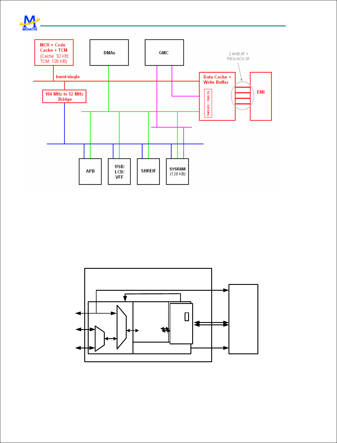
MTK Confidential Release for Konka
MTK Confidential Release for Konka
MT6228 GSM/GPRS Baseband Processor Data Sheet Revision 1.0
92/616 MediaTek Inc. Confidential
Figure 23 Overview of the Bus Architecture
The data cache and EMI are connected by four buses. These four interfaces operate independently of each other;
requests from the interfaces can be issued at the same time. Three of the four buses are standard AHBs for reading
data from external memory, and the other is a request-acknowledgement interface for the write buffer. The EMI can
see the next request while current request is still being processed. With the capability of seeing pending requests, the
EMI can optimize its access schedule to make memory access more efficient.
The data cache comprises four parts: the AHB interface, the main controller, the line filler, and the write buffer (Figure
24).
DATA CACHE
DATA cache
Main Controller
EMI
Write Buffer
MCU BUS
GMC BUS
DMA BUS
MCU burst read
AHB I/F
AHB I/F
ADDR Queue
RDATA FIFO
1-stage ADDR
Queue
REQ/ACK
Line Filler
MCU line filler
DG line filler
Write buffer
AHB I/F
Figure 24 Data Cache Architecture
The AHB interface’s responsibilities are to interface with the AHBs, to prioritize incoming requests from the buses, and
to shake hands with the Line Filler for missed data. Requests from the three buses are prioritized before entering the
main controller of the cache: requests from the MCU bus take precedence over the requests from the DMA and GMC
buses.
MTK Confidential Release for Konka
MTK Confidential Release for Konka
MT6228 GSM/GPRS Baseband Processor Data Sheet Revision 1.0
93/616 MediaTek Inc. Confidential
The main controller is the core of the data cache: its sophisticated state machine is designed to handle the control of
cache TAG memory and DATA memory; hand-shaking with the AHB interface, the write buffer, and line fillers; and
debugging functions. The main controller features a “hit under miss” non-blocking cache: a cache miss from an AHB
does not block the other buses’ access to the cache. When a cache miss occurs, the main controller enters Line Fill
Phase: the replaced cache line is flushed (written to target memory as required), and the main controller issues a line fill
request to the Line Filler. Once the Line Filler accepts the request, the main control becomes available again for
access while the line fill is executed in background. The data cache is still accessible during the line fill.
Two Line Fillers are implemented. They allow two cache lines being replaced concurrently, while leaving the cache
still accessible in the meantime. This feature is especially useful for a system with many bus masters. Missed data is
returned from Line Filler to the AHB interface directly to reduce the latency.
The data cache contains an eight-stage write buffer. Each stage stores up to 32-bit data. The write buffer favors
sequential tags for each buffer stage. Data with sequential tags has the highest priority in the EMI: the EMI can write
data sequentially into the same row of the SDRAM memory, reducing the write time by saving on the time required to
pre-charge and activate a row.
3.8.2 Specification and Main Features
The MT6228 data cache implementation includes the following features:
• 8-kilobyte, 8-way write-back data cache with random cache replacement scheme.
• 64 cache lines for each cache way, and 16 bytes per cache line.
• 2 dirty bits per cache line.
The two dirty bits indicate whether the upper 8-byte and lower 8-byte segment of a cache line have been changed
(Figure 25). Only half of the cache line is flushed before replacement if that half-line has been changed,
shortening the access latency and reducing activity on the external memory bus.
Figure 25 Two Dirty Bits per Cache Line
• Four read/write ports to the EMI.
The EMI sees the next queued memory access request before the current request has been completed, and
pre-schedules the access based on requests from the four access ports. This capability is especially useful for
SDRAM type memory, where pre-charge and row activation for the next request can be executed in advance to
shorten latency.
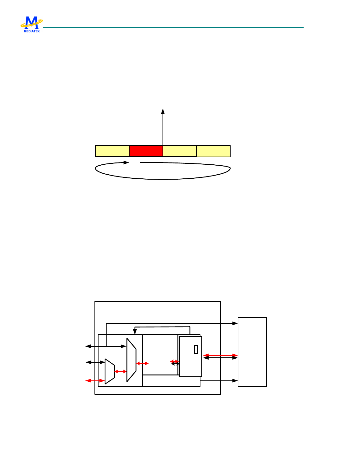
MTK Confidential Release for Konka
MTK Confidential Release for Konka
MT6228 GSM/GPRS Baseband Processor Data Sheet Revision 1.0
94/616 MediaTek Inc. Confidential
• Missed data is returned first.
The data requested during a cache miss is filled by the line filler and returned to the requestor starting at the
missed data.
For example: the MCU requests data at address 0x4, but the request results in a cache miss. The data cache
dispatches a 16-byte burst request starting from 0x4 to the EMI. The data located at address 0x4 is returned first,
followed by that at addresses 0x8, 0xC, then 0x0 (Figure 26). The return of the requested data first shortens the
access latency.
Figure 26 Missed Data Is Returned First
• Background cache line fill.
The data cache has two stand-alone line fillers, each of which can execute a cache line fill upon request from the
main controller individually. Other buses can still access the data cache during the line fill, maximizing
throughput of the data cache.
For example: two sequential requests come from the MCU and the GMC. The MCU request is accepted before
GMC and causes a cache miss. The cache main controller allocates a cache line for the MCU data. If the cache
line is dirty, the main controller flushes the line first, then hands over the line fill request to the Line Filler. The
main controller is now available to accept the next request from the GMC (Figure 27). If the GMC request
results in another cache miss, the line fill request is issued to the second Line Filler. The main controller is still
available to process the next request from a bus. The main controller is blocked only when a third cache miss
occurs before the two previous line fills have been completed.
DATA CACHE
DATA cache
Main Controller
EMI
Write Buffer
MCU BUS
GMC BUS
DMA BUS
MCU burst read
AHB I/F
AHB I/F
ADDR Queue
RDATA FIFO
1-stage ADDR
Queue
REQ/ACK
Line Filler
MCU line filler
DG line filler
Write buffer
AHB I/F
Figure 27 Background Cache Line Fill
MTK Confidential Release for Konka
MTK Confidential Release for Konka
MT6228 GSM/GPRS Baseband Processor Data Sheet Revision 1.0
95/616 MediaTek Inc. Confidential
• Debug support.
The data cache supports a variety of debugging functions and cache tag and data memory read access via the
Advanced Peripheral Bus (APB). The following functions can be executed anywhere and anytime without
restriction:
Invalidate all cache lines.
Invalidate and clean all cache lines.
Invalidate a single cache line by specifying the set/way or address.
Invalidate and clean a single cache line by specifying the set/way or address.
Read a cache tag by specifying the set/way or address.
Read cache data by specifying the set/way or address.
Drain the write buffer.
• Write buffer flushed before MCU burst read (FBBR mode).
The data cache is specially optimized for MCU code execution, thus the user is recommended to set only code and
read-only (RO) data as code cache cacheable (refer to the Code Cache section for the definition of a cacheable
region). For regions of cacheable memory, requests are forwarded directly to the EMI through the “MCU burst
read” path (Figure 24). The requests can be accepted before write buffer is flushed, shortening access latency.
If read-write (RW) data is set as code cache cacheable, data inconsistency may occur. Consider a write request
(WB2) followed by a read request (L1C) with the same memory address, both issued by the MCU (Figure 28 (a)).
The write data (WB2) is queued in the data cache’s write buffer, and the read request is forwarded directly to the
EMI. Because the write buffer queue contains other data ahead of WB2, WB2 is actually written to target
memory after L1C has been executed. Therefore, the MCU receives outdated data, and the consistency problem
occurs.
!"
#
$ %
#
!"
!"
#
$ %
#
!"
(a) (b)
Figure 28 Data Consistency Problem for Cacheable RW
The data cache provides an Flush Buffer Before Read (FBBR) mode that allows RW data to be set as code cache
cacheable without compromising data consistency. When in FBBR mode, MCU read requests are not issued to
the EMI until the write buffer is empty. This suspension of the read request prevents it from being executed
before the write request and solves the data consistency problem. Figure 28(b) shows L1C executed after WB2.
Note that in FBBR mode, more cycles are required to complete a read request because of flush cycles before the
read operation. Thus MCU access latency may increase, and MCU performance may be reduced.
MTK Confidential Release for Konka
MTK Confidential Release for Konka
MT6228 GSM/GPRS Baseband Processor Data Sheet Revision 1.0
96/616 MediaTek Inc. Confidential
$& %'%(# )
$& %'%(# )*
*
'+*
!"
#
$ %
#
! "
Figure 29 Increased Latency of FBBR Mode Due to Write Buffer Flush
• DMA and GMC AHB interfaces allow the clock ratio to switch dynamically between 1:2 and 1:1.
The maximum clock rate of the DMA and GMC buses is 52 MHz; the maximum clock rate of data cache is
104 MHz. A clock ratio bridge is implemented in the AHB interface of the data cache to convert requests and
data to different clock rates. The clock ratio of the DMA or GMC bus and data cache can be either 1:2 or 1:1.
If the data cache clock rate is lower than 52 MHz, the clock rate of DMA or GMC bus must be the same as that of
the data cache and the clock ratio is 1:1. If the data cache clock rate is 104 MHz, the AHB’s clock rate can only
be 52 MHz, and the clock ratio is 1:2. The clock ratio can be switched between 1:2 and 1:1 dynamically without
restriction, reducing the overhead for system clock rate switching software.
3.8.3 NOR flash Programming
When data cache is enabled, an external memory access request may not actually result in physical transaction occuring
on external memory bus. For instance, when MCU issues a read request to external memory, if the request hits data
cache, the data will be returned from data cache directly instead of reading it from external memory. This means no
request took place on the external bus.
Figure 30 illustrates the normal NOR flash programming sequence. These access must be actually executed to the
NOR flash memory interface. However, as mentioned before, an internal bus request may not be reflected on the
external bus when caches are enabled, and will therefore result in MCU not being able to program the NOR flash.
address
data
0x0000aaa
0xaa
write
address
data
0x0000555
0x55
write
address
data
0x0000078
read
address
data
0x0000aaa
0xa0
write
address
data
0x0000078
0x1234
write
address
data
0x0000aaa
0xaa
write
address
data
0x0000555
0x55
write
address
data
0x0000078
read
address
data
0x0000aaa
0xa0
write
address
data
0x0000078
0x1234
write
Figure 30 NOR flash programming sequence
To solve the problem, an IO command mode is designed in data cache. When data cache receive a memory request with
“1” at address bit 26, data cache will treat the request as an IO command. For an IO command, data cache will read or
write the external memory immediately regardless of the hit/miss condition. In addition, data cache will invalidate the
hit cache line for an IO write command. This can prevent data inconsistence between data cache and external memory.
Next read data from the same address will return from external memory, not from data cache.
illustrates the NOR flash programming using IO command. To issue an IO command, software has to OR original
address bit 26 with “1”. In the example, the address to be programmed is 0x0078. To program it with IO command, the
address bit 26 is set to “1”, and the address becomes 0x4000078.

MTK Confidential Release for Konka
MTK Confidential Release for Konka
MT6228 GSM/GPRS Baseband Processor Data Sheet Revision 1.0
97/616 MediaTek Inc. Confidential
address
data
0x4000aaa
0xaa
write
address
data
0x4000555
0x55
write
address
data
0x4000078
read
address
data
0x4000aaa
0xa0
write
address
data
0x4000078
0x1234
write
address
data
0x4000aaa
0xaa
write
address
data
0x4000555
0x55
write
address
data
0x4000078
read
address
data
0x4000aaa
0xa0
write
address
data
0x4000078
0x1234
write
Figure 31 IO command for NOR flash programming
3.8.4 Register Definitions
Table 16 summarizes the registers used by the data cache.
Register Address Register Function Acronym
L2C+0000h Data cache control register L2C_CON
L2C+0004h Data cache target register L2C_TARGET
L2C+0008h Data cache status register L2C_STA
L2C+000Ch Data cache tag register L2C_TAG
L2C+0010h Data cache data register L2C_DATA
L2C+0014h Data cache mode register L2C_MODE
Table 16 Data Cache Registers
L2C+0000h Data Cache Control Register L2C_CON
Bit 31 30 29 28 27 26 25 24 23 22 21 20 19 18 17 16
Name
EN
Type
W
Bit 15 14 13 12 11 10 9 8 7 6 5 4 3 2 1 0
Name
VALUE CMD
Type R/W R/W
CMD Requests an operation on the data cache. Four functions are provided:
0000 Invalidate and clean the data cache.
To invalidate means to clear the valid bit of a cache line. To clean means to write the cache line data to
destination memory if dirty.
VALUE[3:0]
Function
0100 Invalidate a single cache line with the set/way specified in the L2C_TARGET register.
0110 Invalidate and clean a single cache line with the set/way specified in the
L2C_TARGET register.
1100 Invalidate a single cache line with the address specified in the L2C_TARGET register
.
The data cache finds the cache line with the same address and invalidates it.
1110 Invalidate and clean a single cache line with the address specified in the
L2C_TARGET register. The data cache finds the cache line with the same address,
and cleans and invalidates it.
0101 Invalidate all cache lines.
0111 Invalidate and clean all cache lines.
0001 Read the data cache. Either TAG or DATA can be read.
VALUE[1:0]
Function
00 Read a TAG with the set/way specified in the L2C_TARGET register.
01 Read cache data with the set/way specified in the L2C_TARGET register.
10 Read a TAG with address specified in the L2C_TARGET register.
MTK Confidential Release for Konka
MTK Confidential Release for Konka
MT6228 GSM/GPRS Baseband Processor Data Sheet Revision 1.0
98/616 MediaTek Inc. Confidential
11 Read cache data at the address specified in the L2C_TARGET register.
0010 Drain the write buffer.
0011 Configure the MODE bit.
VALUE
Bit 7 6 5 4 3 2 1 0
Name FBBR DIRTYAL
L GATEDG MPEG4 BYPASS
Type W W W W W
Reset 0 0 0 0 1
BYPASS Bypass the data cache. The write buffer is still activated.
MPEG4 MPEG4 mode.
GATEDG Gate DMA and GMC requests. Any requests from the DMA and GMC are suspended.
DIRTYALL Normally only half a cache line is set as dirty when data is written to only half of the
cache line. When this mode is enabled, the entire cache line is set as dirty when data
is written to the line.
FBBR Flush the write buffer before issuing an MCU burst read (L1 cache line fill) to the EMI.
Others Reserved.
VALUE Cooperates with CMD to specify a function.
EN Executes the command specified by CMD and VALUE. While EN is set, the values of CMD and VALUE
are interpreted as a command: the data cache executes the command CMD with the parameter VALUE.
L2C+0004h Data Cache Target Register (SET/WAY) L2C_TARGET
Bit 31 30 29 28 27 26 25 24 23 22 21 20 19 18 17 16
Name
SET
Type R/W
Bit
15 14
13
12
11
10 9 8 7 6 5 4 3 2 1 0
Name
IDX WORD
Type R/W R/W
L2C+0004h Data Cache Target Register (ADDRESS) L2C_TARGET
Bit 31 30 29 28 27 26 25 24 23 22 21 20 19 18 17 16
Name
TAG
Type R/W
Bit 15 14 13 12 11 10 9 8 7 6 5 4 3 2 1 0
Name
IDX WORD
Type R/W R/W R/W
Specifies a SET/WAY or address for a single cache invalidation or TAG/DATA read.
L2C+0008h Data Cache Status Register L2C_STA
Bit 31 30 29 28 27 26 25 24 23 22 21 20 19 18 17 16
Name
Type
Reset
Bit 15 14 13 12 11 10 9 8 7 6 5 4 3 2 1 0
Name
MISS
GATE
DG
BUSY
Type R R R
Reset
0 0 0
BUSY Indicates that the current command is still being processed. The register is cleared when the current
command is finished.
MTK Confidential Release for Konka
MTK Confidential Release for Konka
MT6228 GSM/GPRS Baseband Processor Data Sheet Revision 1.0
99/616 MediaTek Inc. Confidential
GATEDG Indicates that DMA and GMC requests are gated. GATEDG is valid only when the BUSY register is
clear.
MISS Indicates HIT or MISS of the commands for a single cache invalidation or TAG/DATA read. MISS is
valid only when the BUSY register is clear.
L2C+000Ch Data Cache TAG Register L2C_TAG
Bit
31 30
29
28
27 26 25
24
23
22 21 20
19
18
17 16
Name
TAG
Type R
Bit 15 14 13 12 11 10 9 8 7 6 5 4 3 2 1 0
Name
TAG
Type R
When a read TAG command is executed and finished, the TAG can be read from the L2C_TAG register.
L2C+0010h Data Cache DATA Register L2C_DATA
Bit 31 30 29 28 27 26 25 24 23 22 21 20 19 18 17 16
Name
DATA
Type R
Bit 15 14 13 12 11 10 9 8 7 6 5 4 3 2 1 0
Name
DATA
Type R
When a read DATA command is executed and finished, DATA can be read from the L2C_DATA register.
L2C+0014h Data Cache Mode Register L2C_MODE
Bit 31 30 29 28 27 26 25 24 23 22 21 20 19 18 17 16
Name
Type
Reset
Bit 15 14 13 12 11 10 9 8 7 6 5 4 3 2 1 0
Name
FBBR
DIRTY
ALL
GATE
DG
MPEG
4
BYPA
SS
Type R R R R R
Reset
0 0 0 0 1
The L2C_MODE register shows the data cache’s operation mode. The setting can be changed by programming the
L2C_CON register. Refer to the L2C_CON register description for details.
BYPASS Bypass the data cache. The write buffer is still activated.
MPEG4 MPEG4 mode. This mode is valid only when the data cache is enabled (BYPASS = 0).
GATEDG Gate DMA and GMC requests. Any requests from the DMA and GMC are suspended.
DIRTYALL Normally only half of a cache line is set as dirty when data is written to only half of the cache line.
When this mode is enabled, the entire cache line is set as dirty when data is written to the line.
FBBR Flush the write buffer before issuing an MCU burst read (L1 cache line fill) to the EMI.
3.8.5 Initialize and Enable the Data Cache
• Invalidate all cache lines.
Note: DO NOT CLEAN the cache during the first initialization, or the content of the destination memory (external
memory) may be overwritten with unpredictable values.
MTK Confidential Release for Konka
MTK Confidential Release for Konka
MT6228 GSM/GPRS Baseband Processor Data Sheet Revision 1.0
100/616 MediaTek Inc. Confidential
• Set BYPASS to ‘0’ to enable the data cache.
3.9 Internal Memory Interface
3.9.1 System RAM
MT6228 provides one 128 KByte size of on-chip memory modules acting as System RAM for data access with low
latency. Such a module is composed of one high speed synchronous SRAMs with AHB Slave Interface connected to the
system backbone AHB Bus, as shown in Figure 32. The synchronous SRAM operates on the same clock as the AHB
Bus and is organized as 32 bits wide with 4 byte-write signals capable for byte operations. The SRAM macro has
limited repair capability. The yield of SRAM is improved if the defects inside it can be repaired during testing.
3.9.2 System ROM
The System ROM is primarily used to store software program for Factory Programming. However, due to its
advantageous low latency performance, some of the timing critical codes are also placed in System ROM. This
module is composed of high-speed VIA ROM with an AHB Slave Interface connected to a system backbone AHB,
shown in Figure 32. The module operates on the same clock as the AHB and has a 32-bit wide organization.
Bank0 SRAM
Graphsys AHB Bus 0
ROM
DMA AHB Bus
MCU AHB Bus Bank0 SRAM
Graphsys AHB Bus 0
ROM
DMA AHB Bus
MCU AHB Bus
Figure 32: Block Diagram of the Internal Memory Controller
3.10 External Memory Interface
3.10.1 General Description
MT6228 incorporates a powerful and flexible memory controller, External Memory Interface, to connect with a variety
of memory components. This controller provides one generic access scheme for Flash Memory, SRAM, PSRAM and
CellularRAM and another access scheme for MobileRAM. Up to 4 memory banks can be supported simultaneously,
BANK0-BANK3, with a maximum size of 64MB each.
Since most of the Flash Memory, SRAM, PSRAM and CellularRAM have similar AC requirements, a generic
configuration scheme to interface them is desired. This way, the software program can treat different components by
simply specifying certain predefined parameters. All these parameters are based on the cycle time of system clock.
The interface definition based on such a scheme is listed in Table 17. Note that, this interface always works with data
in Little Endian format for all types of access.

MTK Confidential Release for Konka
MTK Confidential Release for Konka
MT6228 GSM/GPRS Baseband Processor Data Sheet Revision 1.0
101/616 MediaTek Inc. Confidential
Signal Name Type Description
EA[25:0] O Address Bus
ED[15:0] I/O Data Bus
EWR# O Write Enable Strobe/MobileRAM Command Input
ERD# O Read Enable Strobe
ELB# O Lower Byte Strobe/MobileRAM Data Input & Output Mask
EUB# O Upper Byte Strobe/MobileRAM Data Input & Output Mask
ECS[3:0]# O BANK0~BANK3 Selection Signal
EPDN O PSRAM Power Down Control Signal
ECLK O Flash, SRAM, PSRAM and CellularRAM Clock Signal
EADV# O Flash, SRAM, PSRAM and CellularRAM Address Valid Signal
EWAIT I Flash, SRAM, PSRAM and CellularRAM Wait Signal Input
EDCLK O MobileRAM Clock Signal
ECKE O MobileRAM Clock Enable Signal
ERAS# O MobileRAM Row Address Signal
ECAS# O MobileRAM Column Address Signal
Table 17 External Memory Interface Signal of MT6228
REGISTER ADDRESS REGISTER NAME SYNONYM
EMI + 0000h EMI Control Register for BANK0 EMI_CONA
EMI + 0008h EMI Control Register for BANK1 EMI_CONB
EMI + 0010h EMI Control Register for BANK2 EMI_CONC
EMI + 0018h EMI Control Register for BANK3 EMI_COND
EMI + 0040h EMI Control Register 0 for MobileRAM EMI_CONI
EMI + 0048h EMI Control Register 1 for MobileRAM EMI_CONJ
EMI + 0050h EMI Control Register 2 for MobileRAM EMI_CONK
EMI + 0058h EMI Control Register 3 for MobileRAM EMI_CONL
EMI + 0060h EMI Remap Control Register EMI_REMAP
EMI + 0068h EMI General Control Register 0 EMI_GENA
EMI + 0070h EMI General Control Register 1 EMI_GENB
Table 18 External Memory Interface Register Map
3.10.2 Register Definitions
EMI+0000h EMI Control Register for BANK 0 EMI_CONA
Bit 31 30 29 28 27 26 25 24 23 22 21 20 19 18 17 16
Name
C2WS C2WH C2RS PRLT CLKE
N
PMO
DE
Type R/W R/W R/W R/W R/W R/W
Reset
0 0 0 0 0 0
Bit 15 14 13 12 11 10 9 8 7 6 5 4 3 2 1 0
Name
DW RBLN
BW WST WAIT PSIZE
RLT
Type R/W R/W R/W R/W R/W R/W R/W
Reset
0 1 0 0 0 0 7
MTK Confidential Release for Konka
MTK Confidential Release for Konka
MT6228 GSM/GPRS Baseband Processor Data Sheet Revision 1.0
102/616 MediaTek Inc. Confidential
EMI+0008h EMI Control Register for BANK 1 EMI_CONB
Bit 31 30 29 28 27 26 25 24 23 22 21 20 19 18 17 16
Name
C2WS C2WH C2RS PRLT CLKE
N
PMO
DE
Type R/W R/W R/W R/W R/W R/W
Reset
0 0 0 0 0 0
Bit 15 14 13 12 11 10 9 8 7 6 5 4 3 2 1 0
Name
DW RBLN
BW WST WAIT PSIZE
RLT
Type R/W R/W R/W R/W R/W R/W R/W
Reset
0 1 0 0 0 0 7
EMI+0010h EMI Control Register for BANK 2 EMI_CONC
Bit 31 30 29 28 27 26 25 24 23 22 21 20 19 18 17 16
Name
C2WS C2WH C2RS PRLT CLKE
N
PMO
DE
Type R/W R/W R/W R/W R/W R/W
Reset
0 0 0 0 0 0
Bit 15 14 13 12 11 10 9 8 7 6 5 4 3 2 1 0
Name
DW RBLN
BW WST WAIT PSIZE
RLT
Type R/W R/W R/W R/W R/W R/W R/W
Reset
0 1 0 0 0 0 7
EMI+0018h EMI Control Register for BANK 3 EMI_COND
Bit 31 30 29 28 27 26 25 24 23 22 21 20 19 18 17 16
Name
C2WS C2WH C2RS PRLT CLKE
N
PMO
DE
Type R/W R/W R/W R/W R/W R/W
Reset
0 0 0 0 0 0
Bit 15 14 13 12 11 10 9 8 7 6 5 4 3 2 1 0
Name
DW RBLN
BW WST WAIT PSIZE
RLT
Type R/W R/W R/W R/W R/W R/W R/W
Reset
0 1 0 0 0 0 7
For each bank (BANK0-BANK3), a dedicated control register is associated with the bank controller. These registers
have timing parameters that help the controller to convert memory access into proper timing waveform. Note that,
except for parameters CLKEN, PMODE, DW, RBLN, BW, WAIT and PSIZE, all the other parameters specified
explicitly are based on system clock speed in terms of cycle count.
RLT Read Latency Time
Specifies the number of wait-states to insert in the bus transfer to the requesting agent. Such a parameter
must be chosen carefully to meet the timing specification requirements for common parameter tACC(address
access time) for asynchronous-read device and tCWT(chip select low to wait valid time) for synchronous-read
device. An example is shown below.
MTK Confidential Release for Konka
MTK Confidential Release for Konka
MT6228 GSM/GPRS Baseband Processor Data Sheet Revision 1.0
103/616 MediaTek Inc. Confidential
Figure 33 Read Wait State Timing Diagram for Asynchronous-Read Memory (CLKEN=0)
Access Time Read Latency Time in 104 MHz unit
65 ns ~ 70 ns 7
85 ns ~ 90 ns 9
110 ns ~ 120 ns 12
Table 19 Reference value of Read Latency Time for Asynchronous-Read memory Devices
Figure 34 Read Wait State Timing Diagram for Synchronous-Read Memory (CLKEN=1)
ECS# Low to EWAIT Valid
Read Latency Time in 104 MHz unit
0 ns ~ 10 ns 1
10 ns ~ 20 ns 2
Table 20 Reference value of Read Latency Time for Synchronous-Read Devices
PSIZE This bit position describes the page size behavior of that the Page Mode enabled device.
0 8 byte, EA[22:3] remains the same
1 16 byte, EA[22:4] remains the same
WAIT Data-valid feedback operation control for Flash memory, PSRAM and CellularRAM.
0 Disable data-valid feedback operation control
1 Enable data-valid feedback operation control
WST Write Wait State
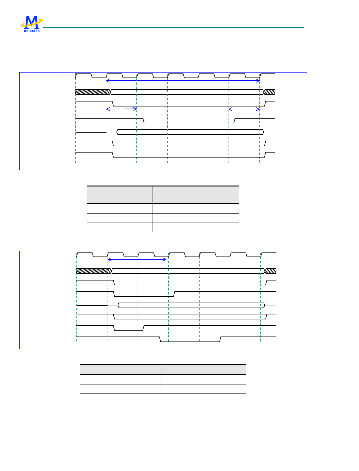
MTK Confidential Release for Konka
MTK Confidential Release for Konka
MT6228 GSM/GPRS Baseband Processor Data Sheet Revision 1.0
104/616 MediaTek Inc. Confidential
Specifies the parameters to extend adequate setup and hold time for target component in write operation.
Such parameter must be chosen carefully to meet the timing specification requirements for common parameter
tWC(write cycle time) for asynchronous-write device and tCWT(chip select low to wait valid time) for
synchronous-write device. An example is shown in Figure 35 and Table 21.
Figure 35 Write Wait State Timing Diagram for Asynchronous-Write Memory (BW=0)
Write Pulse Width
(Write Data Setup Time) Write Wait State in 104 MHz unit
65 ns ~ 70 ns 7
85 ns ~ 90 ns 9
110 ns ~ 120 ns 12
Table 21 Reference value of Write Wait State for Asynchronous-Write Devices
Figure 36 Write Wait State Timing Diagram for Synchronous-Write Memory (CLKEN=1 and BW=1)
ECS# Low to EWAIT Valid Write Wait State in 104 MHz unit
0 ns ~ 10 ns 1
10 ns ~ 20 ns 2
Table 22 Reference value of Write Wait State for Synchronous-Write Devices
BW Burst Mode Write Control
0 Disable burst write operation
MTK Confidential Release for Konka
MTK Confidential Release for Konka
MT6228 GSM/GPRS Baseband Processor Data Sheet Revision 1.0
105/616 MediaTek Inc. Confidential
1 Enable burst write operation
RBLN Read Byte Lane Enable
DW Data Width
0 16 Bit
1 8 Bit
PMODE Page Mode Control
If the target device supports page mode operations, the Page Mode Control can be enabled. Read in Page
Mode is determined by the set of parameters: PRLT and PSIZE.
0 disable page mode operation
1 enable page mode operation
PRLT Read Latency Time within the Same Page
Since page mode operation only helps to eliminate read latency in subsequent access within the same page, the
initial latency does not matter. Thus, the memory controller must still adopt the RLT parameter for the initial
read or reads between different pages, even if PMODE is set to 1.
CLKEN Clock Enable Control
C2RS Chip Select to Read Strobe Setup Time
C2WH Chip Select to Write Strobe Hold Time
C2WS Chip Select to Write Strobe Setup Time
EMI+0040h EMI Control Register 0 for MobileRAM EMI_CONI
Bit 31 30 29 28 27 26 25 24 23 22 21 20 19 18 17 16
Name
PAUS
E_EN
PING
PONG
_EN
DRAM_MOD
E DRAM_SIZE DRAM
_EN DRAM_CS
Type R/W R/W R/W R/W R/W R/W
Reset
0 0 2d 0 0 0
Bit 15 14 13 12 11 10 9 8 7 6 5 4 3 2 1 0
Name
BA1 BA0 A12 A11 A10 A9 A8 A7 A6 A5 A4 A3 A2 A1 A0
Type R/W R/W R/W R/W R/W R/W R/W R/W R/W R/W R/W R/W R/W R/W R/W
Reset
0 0 0 0 0 0 0 0 0 0 0 0 0 0 0
A12-A0 Mode Register Configuration
BA1-B0 Mode Register Configuration
DRAM_CS MobileRAM Controller Chip Select Signal Control
00 Chip Select 0 is used for MobileRAM
01 Chip Select 1 is used for MobileRAM
10 Chip Select 2 is used for MobileRAM
11 Chip Select 3 is used for MobileRAM
DRAM_EN MobileRAM Controller Control
0 MobileRAM controller is disabled
1 MobileRAM controller is enabled
DRAM_SIZE MobileRAM Chip Size
00 64Mbit
01 128Mbit
10 256Mbit
11 512Mbit
DRAM_MODE MobileRAM Scrambling Table Control
00 Mode 1
01 Mode 2
10 Mode 3 (PASR is not allowed)
MTK Confidential Release for Konka
MTK Confidential Release for Konka
MT6228 GSM/GPRS Baseband Processor Data Sheet Revision 1.0
106/616 MediaTek Inc. Confidential
11 Mode 3 (PASR is not allowed)
PINGPONG_EN Ping-pong Operation Control
PAUSE_EN Self-Refresh Mode Control when Baseband is in Pause Mode Operation
EMI+0048h EMI Control Register 1 for MobileRAM EMI_CONJ
Bit 31 30 29 28 27 26 25 24 23 22 21 20 19 18 17 16
Name
PDNS
SRFS
Type R R
Reset
0 0
Bit 15 14 13 12 11 10 9 8 7 6 5 4 3 2 1 0
Name
PDN SRF SETM
AREF
PCA
Type R/W R/W R/W R/W R/W
Reset
0 0 0 0 0
PCA Pre-Charge All Command
AREF Auto-Refresh Command
SETM Set Mode Register Command
SRF Self-Refresh Mode Command
PDN Power-Down Mode Command
SRFS Self-Refresh Mode Status
PDNS Power Down Mode Status
EMI+0050h EMI Control Register 2 for MobileRAM EMI_CONK
Bit 31 30 29 28 27 26 25 24 23 22 21 20 19 18 17 16
Name
WR RAS_MAX
Type R/W R/W
Reset
0 0
Bit 15 14 13 12 11 10 9 8 7 6 5 4 3 2 1 0
Name
RAS_MIN RRD RC RP RCD CAS
Type R/W R/W R/W R/W R/W R/W
Reset
0 0 0 0 0 0
CAS CAS Latency Control
0 CAS Latency = 2
1 CAS Latency = 3
RCD Active to Read or Write Delay
RP Pre-charge Command Period
RC Active Bank A to Active Bank A Period
RRD Active Bank A to Active Bank B Delay
RAS_MIN Minimum Active to Pre-charge Command Delay
RAS_MAX Maximum Active to Pre-charge Command Delay
WR Write Recovery Time
EMI+0058h EMI Control Register 3 for MobileRAM EMI_CONL
Bit 31 30 29 28 27 26 25 24 23 22 21 20 19 18 17 16
Name
ARFE
N HYE REFCNT DIV
Type R/W R/W R/W R/W
Reset
0 0 0 0
Bit 15 14 13 12 11 10 9 8 7 6 5 4 3 2 1 0
Name
ISR MRD XSR RFC
Type R/W R/W R/W R/W
Reset
0 0 0 0
RFC Auto Refresh Period

MTK Confidential Release for Konka
MTK Confidential Release for Konka
MT6228 GSM/GPRS Baseband Processor Data Sheet Revision 1.0
107/616 MediaTek Inc. Confidential
XSR Exit Self Refresh to Active Command Delay
MRD Load Mode Register Command Period
ISR Minimum Period for Self-Refresh Mode
DIV MobileRAM Refresh Period Pre-Divider in units of 32 KHz; this field defines the MobileRAM Refresh
Period.
00 Divide by 1 (32KHz)
01 Divide by 2 (32KHz/2)
10 Divide by 3 (32KHz/3)
11 Divide by 4 (32KHz/4)
REFCNT Number of Auto-Refresh-Command to issue per MobileRAM Refresh Period.
HYE Reserved
ARFEN Auto Refresh Control
EMI+0060h EMI Re-map Control Register EMI_REMAP
Bit 15 14 13 12 11 10 9 8 7 6 5 4 3 2 1 0
Name
RM1 RM0
Type R/W R/W
Reset
0 0
This register accomplishes the Memory Re-mapping Mechanism. The register provides the kernel software program
or system designer with the capability to change memory configuration dynamically. Three kinds of configuration are
permitted.
RM[1:0] Re-mapping control for Boot Code, BANK0 and BANK1, refer to Table 23.
RM[1:0] Address 0000_0000h – 07ff_ffffh Address 0800_0000h – 0fff_ffffh
00 Boot Code BANK1
01 BANK1 BANK0
10 BANK0 BANK1
11 BANk1 BANK0
Table 23 Memory Map Configuration
EMI+0068h EMI General Control Register 0 EMI_GENA
Bit 31 30 29 28 27 26 25 24 23 22 21 20 19 18 17 16
Name
CKE EXT_GUARD
DCKS
R
DCKE
2
DCKE
4
DCKE
8
DCKE
16 DCKE
DCKDLY
Type R/W R/W R/W R/W R/W R/W R/W R/W R/W
Reset
0 0 0 0 0 0 0 0 0
Bit 15 14 13 12 11 10 9 8 7 6 5 4 3 2 1 0
Name
EDA PDNE
WPOL
SCKS
R
SCKE
2
SCKE
4
SCKE
4
SCKE
16 SCKE
SCKDLY
Type R/W R/W R/W R/W R/W R/W R/W R/W R/W R/W
Reset
1 0 0 0 0 0 0 0 0 0
SCKDLY FLASH, SRAM, PSRAM and CellularRAM Clock Delay Control
SCKE FLASH, SRAM, PSRAM and CellularRAM Clock Enable Control
SCKEn FLASH, SRAM, PSRAM and CellularRAM Clock Pad Driving Control (n=2, 4, 8, 16)
SCKSR FLASH, SRAM, PSRAM and CellularRAM Pad Slew-Rate Control
WPOL FLASH, SRAM, PSRAM and CellularRAM Wait Signal Inversion Control
PDNE PSRAM Power Down Control
EDA Data Bus Active Drive Control
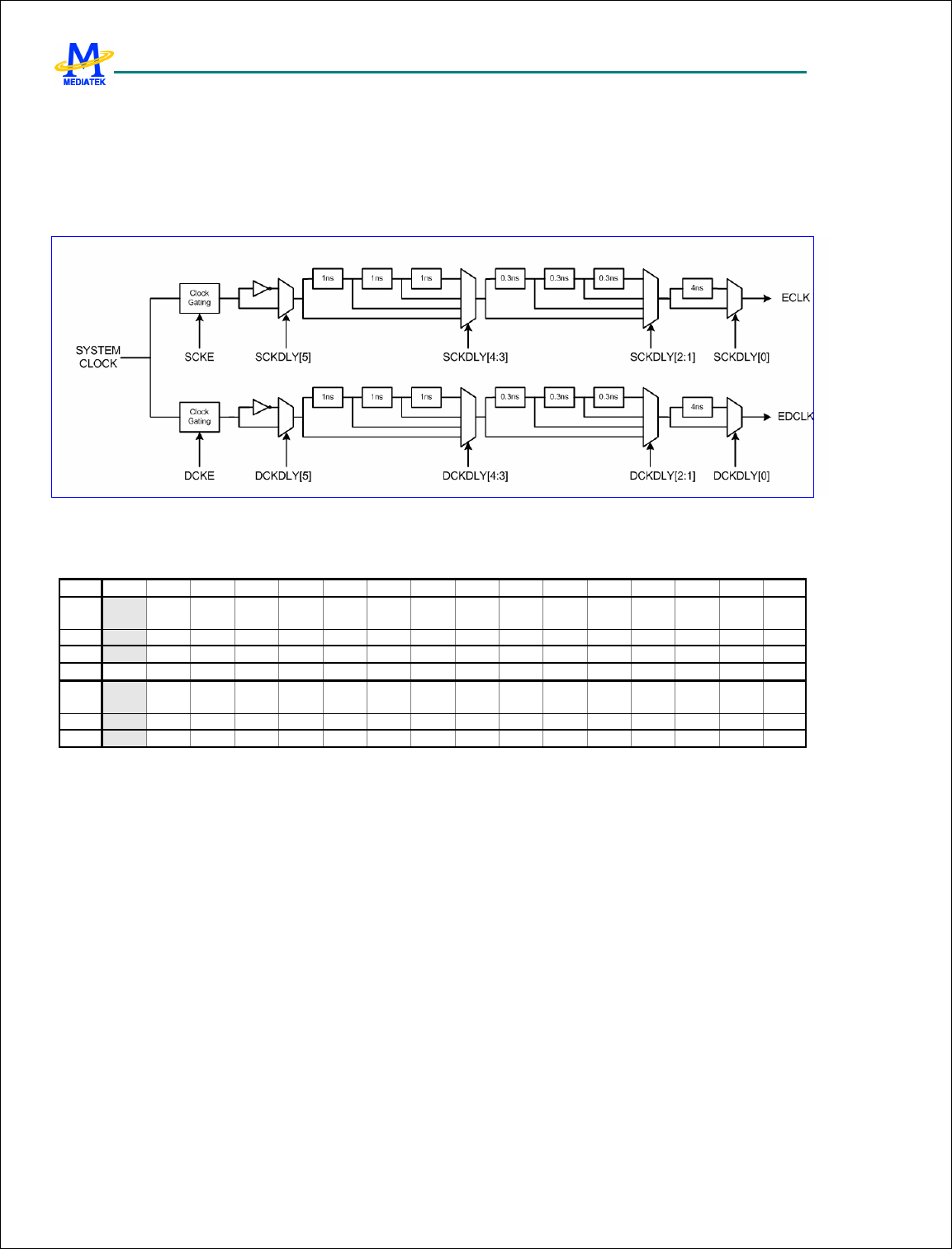
MTK Confidential Release for Konka
MTK Confidential Release for Konka
MT6228 GSM/GPRS Baseband Processor Data Sheet Revision 1.0
108/616 MediaTek Inc. Confidential
DCKDLY MobileRAM Clock Delay Control
DCKE MobileRAM Clock Enable Control
DCKEn MobileRAM Clock Pad Driving Control (n=2, 4, 8, 16)
DCKSR MobileRAM Clock Pad Slew-Rate Control
EXT_GUARD Extra IDLE Time for FLASH, SRAM, PSRAM and CellularRAM
CKE Dynamic MobileRAM Clock Enable Control
Figure 37 Clock Delay Control
EMI+0070h EMI General Control Register 1 EMI_GENB
Bit 31 30 29 28 27 26 25 24 23 22 21 20 19 18 17 16
Name
EASR
EAE2 EAE4 EAE8
EAE1
6 EDSR
EDE2
EDE4
EDE8
EDE1
6
ECSS
R
ECSE
2
ECSE
4
ECSE
8
ECSE
16
Type R/W R/W R/W R/W R/W R/W R/W R/W R/W R/W R/W R/W R/W R/W R/W
Reset
1 1 0 0 0 1 1 0 0 0 1 1 0 0 0
Bit 15 14 13 12 11 10 9 8 7 6 5 4 3 2 1 0
Name
ERWS
R
ERWE
2
ERWE
4
ERWE
8
ERWE
16
EADV
SR
EADV
E2
EADV
E4
EADV
E8
EADV
E16
ERCS
R
ERCE
2
ERCE
4
ERCE
8
ERCE
16
Type R/W R/W R/W R/W R/W R/W R/W R/W R/W R/W R/W R/W R/W R/W R/W
Reset
1 1 0 0 0 1 1 0 0 0 1 1 0 0 0
ERCEn RAS and CAS Pad Driving Control (n=2, 4, 8, 16)
ERCSR RAS and CAS Pad Slew-Rate Control
EADVEn EADV Pad Driving Control (n=2, 4, 8, 16)
EADVSR EADV Pad Slew-Rate Control
ERWEn ERD, EWR, EUB and ELB Pad Driving Control (n=2, 4, 8, 16)
ERWSR ERD, EWR, EUB and ELB Pad Slew-Rate Control
ECSEn ECS[3:0] Pad Driving Control (n=2, 4, 8, 16)
ECSSR ECS[3:0] Pad Slew-Rate Control
EDEn ED[15:0] Pad Driving Control (n=2, 4, 8, 16)
EDSR ED[15:0] Pad Slew-Rate Control
EAEn EA[25:0] Pad Driving Control (n=2, 4, 8, 16)
EASR EA[25:0] Pad Slew-Rate Control
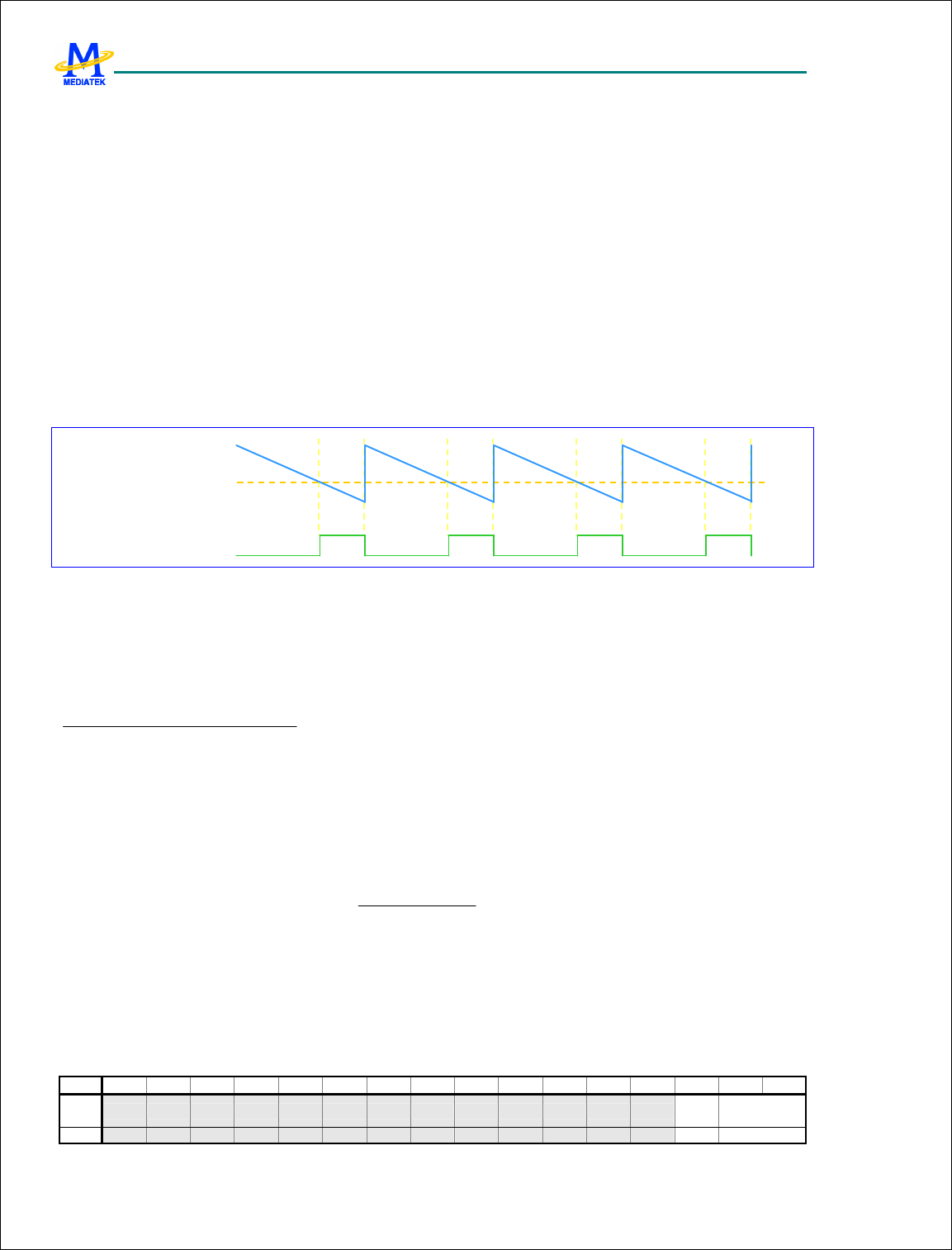
MTK Confidential Release for Konka
MTK Confidential Release for Konka
MT6228 GSM/GPRS Baseband Processor Data Sheet Revision 1.0
109/616 MediaTek Inc. Confidential
4 Microcontroller Peripherals
Microcontroller (MCU) Peripherals are devices that are under direct control of the Microcontroller. Most of the
devices are attached to the Advanced Peripheral Bus (APB) of the MCU subsystem, and serve as APB slaves. Each
MCU peripheral must be accessed as a memory-mapped I/O device; that is, the MCU or the DMA bus master reads
from or writes to the specific peripheral by issuing memory-addressed transactions.
4.1 Pulse-Width Modulation Outputs
4.1.1 General Description
Two generic pulse-width modulators are implemented to generate pulse sequences with programmable frequency and
duty cycle for LCD backlight or charging purpose. The duration of the PWM output signal is LOW as long as the
internal counter value is greater than or equal to the threshold value. The waveform is shown in Figure 38.
Internal counter
Threshold
PWM Signal
Figure 38 PWM waveform
The frequency and volume of PWM output signal are determined by these registers: PWM_COUNT, PWM_THRES,
PWM_CON. The POWERDOWN (pdn_pwm) signal is applied to power-down the PWM module. When PWM is
deactivated (POWERDOWN=1), the output is in LOW state.
The output PWM frequency is determined by:
132000,0CLKSEL when 13000000CLK
)1_(_ ====
+× whenCLKSELCLK
COUNTPWMDIVCLOCK
CLK
CLOCK_DIV = 1, when CLK[1:0] = 00b
CLOCK_DIV = 2, when CLK[1:0] = 01b
CLOCK_DIV = 4, when CLK[1:0] = 10b
CLOCK_DIV = 8, when CLK[1:0] = 11b
The output PWM duty cycle is determined by:
1_
_
+COUNTPWM
THRESPWM
Note that PWM_THRES should be less than the PWM_COUNT: if this condition is not satisfied, the output pulse of
the PWM is always HIGH.
4.1.2 Register Definitions
PWM+0000h PWM1 Control register PWM1_CON
Bit 15 14 13 12 11 10 9 8 7 6 5 4 3 2 1 0
Name
CLKS
EL
CLK [1:0]
Type
R/W
R/W
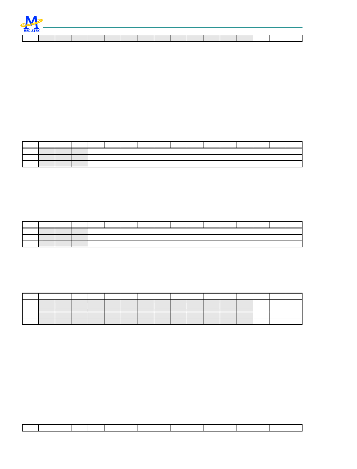
MTK Confidential Release for Konka
MTK Confidential Release for Konka
MT6228 GSM/GPRS Baseband Processor Data Sheet Revision 1.0
110/616 MediaTek Inc. Confidential
Reset
0 0
CLK Select PWM1 clock prescaler scale.
00 CLK Hz
01 CLK/2 Hz
10 CLK/4 Hz
11 CLK/8 Hz
Note: When PWM1 module is disabled, its output should be kept in the LOW state.
CLKSEL Select PWM1 clock
0 CLK=13M Hz
1 CLK=32K Hz
PWM+0004h PWM1 max counter value register PWM1_COUNT
Bit 15 14 13 12 11 10 9 8 7 6 5 4 3 2 1 0
Name
PWM1_COUNT [12:0]
Type R/W
Reset
1FFFh
PWM1_COUNT PWM1 max counter value. This value is the initial value for the internal counter. Regardless of
the operation mode, if PWM1_COUNT is written while the internal counter is counting backwards,
the new initial value does not take effect until the internal counter counts down to zero, i.e. a
complete period.
PWM+0008h PWM1 Threshold Value register PWM1_THRES
Bit 15 14 13 12 11 10 9 8 7 6 5 4 3 2 1 0
Name
PWM1_THRES [12:0]
Type R/W
Reset
0
PWM1_THRES Threshold value. When the internal counter value is greater than or equal to PWM1_THRES, the
PWM1 output signal is 0; when the internal counter is less than PWM1_THRES, the PWM1 output
signal is 1.
PWM+000Ch PWM2 Control register PWM2_CON
Bit 15 14 13 12 11 10 9 8 7 6 5 4 3 2 1 0
Name
CLKS
EL
CLK [1:0]
Type R/W R/W
Reset
0 0
CLK Select PWM2 clock prescaler scale.
00 CLK Hz
01 CLK/2 Hz
10 CLK/4 Hz
11 CLK/8 Hz
Note: When PWM2 module is disabled, its output should be kept in the LOW state.
CLKSEL Select PWM2 clock
0 CLK=13M Hz
1 CLK=32K Hz
PWM+0010h PWM2 max counter value register PWM2_COUNT
Bit 15 14 13 12 11 10 9 8 7 6 5 4 3 2 1 0

MTK Confidential Release for Konka
MTK Confidential Release for Konka
MT6228 GSM/GPRS Baseband Processor Data Sheet Revision 1.0
111/616 MediaTek Inc. Confidential
Name
PWM2_COUNT [12:0]
Type R/W
Reset
1FFFh
PWM2_COUNT PWM2 max counter value. This value is the initial value for the internal counter. Regardless of
the operation mode, if PWM2_COUNT is written while the internal counter is counting backwards,
the new initial value does not take effect until the internal counter counts down to zero, i.e. a
complete period.
PWM+0014h PWM2 Threshold Value register PWM2_THRES
Bit 15 14 13 12 11 10 9 8 7 6 5 4 3 2 1 0
Name
PWM2_THRES [12:0]
Type R/W
Reset
0
PWM2_THRES Threshold value. When the internal counter value is greater than or equal to PWM2_THRES, the
PWM1 output signal is 0; when the internal counter is less than PWM2_THRES, the PWM2 output
signal is 1.
Figure 39 shows the PWM waveform with the indicated register values.
PWM_COUNT = 5
PWM_THRES = 1
PWM_CON = 0b
13MHz
Figure 39 PWM waveform with register values
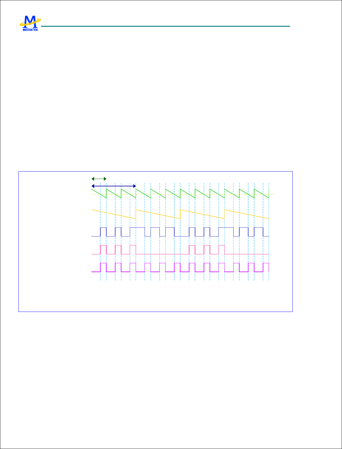
MTK Confidential Release for Konka
MTK Confidential Release for Konka
MT6228 GSM/GPRS Baseband Processor Data Sheet Revision 1.0
112/616 MediaTek Inc. Confidential
4.2 Alerter
4.2.1 General Description
The output of the Alerter has two sources: one is the enhanced PWM output signal, implemented within the Alerter
module; the other is the PDM signal that comes from the DSP domain directly. The output source can be selected via
the register ALERTER_CON.
The enhanced PWM has three modes of operation and can generate a signal with programmable frequency and tone
volume. The frequency and volume are determined by four registers: ALERTER_CNT1, ALERTER_THRES,
ALERTER_CNT2, and ALERTER_CON. ALERTER_CNT1 and ALERTER_CNT2 are the initial counting values
for the internal counters counter1 and counter2, respectively.
POWERDOWN signal is applied to power down the Alerter module. When Alerter is deactivated
(POWERDOWN=1), the output is in a low state. The waveform of Alerter from the enhanced PWM source in
different modes is shown in Figure 40.
ALERTER_THRES
enhance pwm out (mode 1)
enhance pwm out (mode 2)
enhanced pwm out (mode 3)
T2
Internal counter1
T1 = ALERTER_CNT1
*
1/13MHz
*(
ALERTER_CON[1:0]+1)
T2 = T1 *( ALERTER_CNT2+1)
T1
Internal counter2
Figure 40 Alerter Waveform
In Mode 1, the polarity of the Alerter output signal, given the relationship between internal counter1 and the
programmed threshold, is inverted each time internal counter2 reaches zero.
In Mode 2, each time the internal counter2 reaches zero, the Alerter output signal toggles between the normal PWM
signal (i.e. the signal is low for an internal counter1 value greater than or equals to ALERTER_THRES; high when the
internal counter1 value is less than ALERTER_THRES) and low state.
In Mode 3, the value of internal counter2 has no effect on output signal. That is, the alerter output signal is low as
long as the internal counter 1 value is above the programmed threshold, and is high when the internal counter1 is less
than ALERTER_THRES, regardless of internal counter2’s value.
The output signal frequency is given by:

MTK Confidential Release for Konka
MTK Confidential Release for Konka
MT6228 GSM/GPRS Baseband Processor Data Sheet Revision 1.0
113/616 MediaTek Inc. Confidential
3 modeor
])0:1[_()11_(
13000000
2 mode and 1 modeor
)12_()11_()1]0:1[_(2
13000000
×+
+×+×+×
f
CONALERTERCNTALERTER
f
CNTALERTERCNTALERTERCONALERTER
.
The volume of the output signal is given by:
11_
_
+CNTALERTER
THRESALERTER
.
4.2.2 Register Definitions
ALTER+0000h
Alerter counter1 value register
ALERTER_CNT1
Bit 15 14 13 12 11 10 9 8 7 6 5 4 3 2 1 0
Name
ALERTER_CNT1 [15:0]
Type R/W
Reset
FFFFh
ALERTER_CNT1 Alerter max counter’s value. Initial value of internal counter1. In any mode, if
ALERTER_CNT1 is written when the internal counter1 is counting, the new start value does not take effect
until the next countdown period; i.e. after internal counter1 reaches zero.
ALTER+0004h
Alerter threshold value register ALERTER_THR
ES
Bit 15 14 13 12 11 10 9 8 7 6 5 4 3 2 1 0
Name
ALERTER_THRES [15:0]
Type R/W
Reset
0
ALERTER_THRES Threshold value. When the internal counter1 value is greater than or equals to
ALERTER_THRES, the Alerter output signal is low; when counter1 is less than ALERTER_THRES,
the Alerter output signal is high.
ALTER+0008h
Alerter counter2 value register
ALERTER_CNT2
Bit 15 14 13 12 11 10 9 8 7 6 5 4 3 2 1 0
Name
ALERTER_CNT2 [ 5:0]
Type R/W
Reset
111111b
ALERTER_CNT2 Initial value for internal counter2. The internal counter2 decreases by one each time the
internal counter1 counts down to zero; internal counter1 is a nested counter.
ALTER+000Ch
Alerter control register ALERTER_CON
Bit 15 14 13 12 11 10 9 8 7 6 5 4 3 2 1 0
Name
TYPE
MODE CLK [1:0]
Type R/W R/W R/W
Reset
0 0 0
CLK Select the PWM Waveform clock.
00 13 MHz
01 13/2 MHz
10 13/4 MHz
11 13/8 MHz
MODE Select the Alerter mode.
00 Mode 1 selected
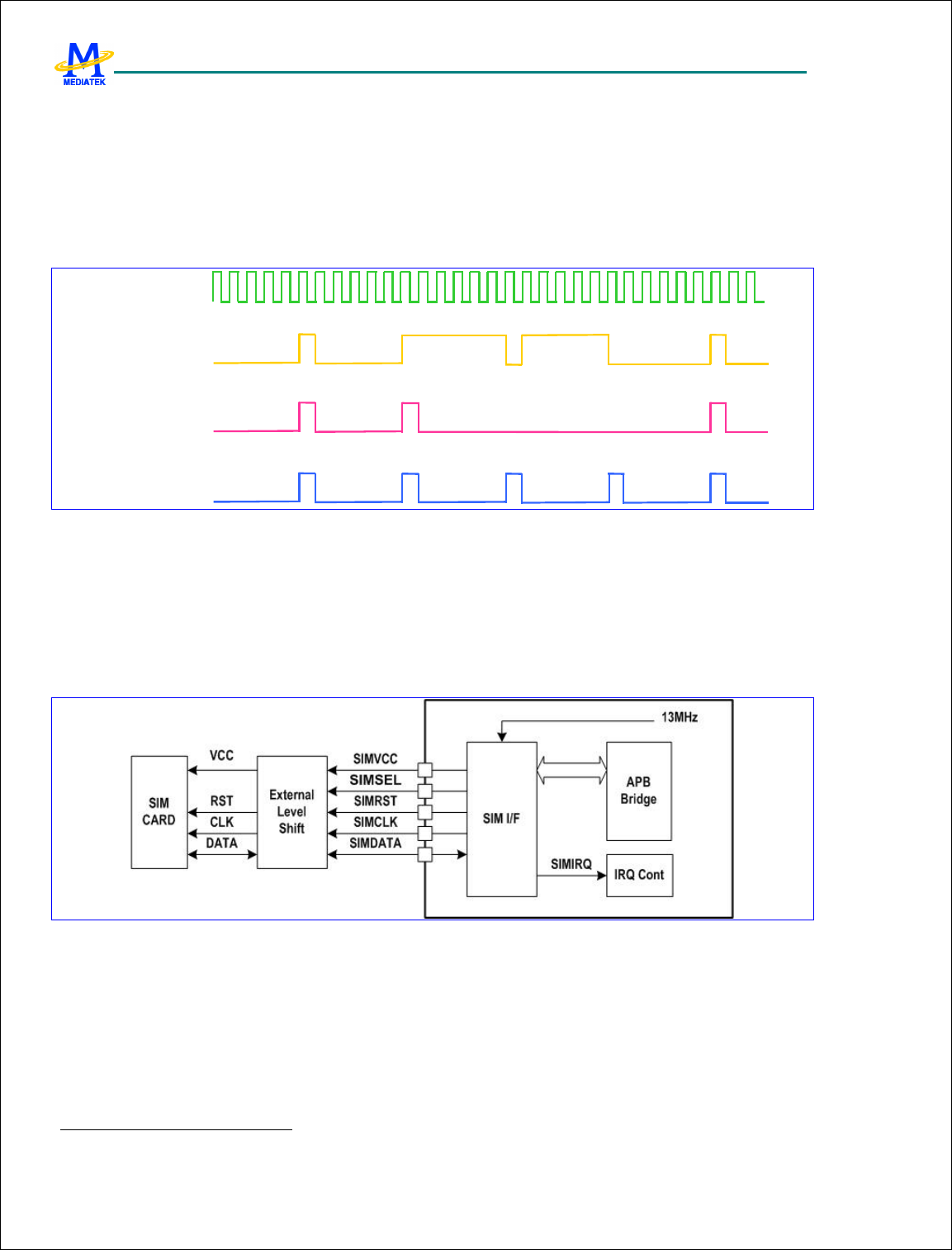
MTK Confidential Release for Konka
MTK Confidential Release for Konka
MT6228 GSM/GPRS Baseband Processor Data Sheet Revision 1.0
114/616 MediaTek Inc. Confidential
01 Mode 2 selected
10 Mode 3 selected
TYPE Select the ALERTER output source from PWM or PDM.
0 Output generated from PWM path.
1 Output generated from PDM path.
Note: When the Alerter module is powered down, its output must be kept in low state.
Figure 41 shows the Alerter waveform with the register values.
ALERTER_CNT1 = 5
ALERTER_CNT2 = 1
ALERTER_THRESH = 1
ALERTER_CON = 01000b
ALERTER_CNT1 = 5
ALERTER_CNT2 = 1
ALERTER_THRESH = 1
ALERTER_CON = 00100b
ALERTER_CNT1 = 5
ALERTER_CNT2 = 1
ALERTER_THRESH = 1
ALERTER_CON =00000b
13MHz
Figure 41 Alerter Output Signal from Enhanced PWM with Register Value Present
4.3 SIM Interface
The MT6228 contains a dedicated smart card interface to allow the MCU access to the SIM card. It can operate via 5
terminals, using SIMVCC, SIMSEL, SIMRST, SIMCLK and SIMDATA.
Figure 42 SIM Interface Block Diagram
The SIMVCC is used to control the external voltage supply to the SIM card and SIMSEL determines the regulated
smart card supply voltage. SIMRST is used as the SIM card reset signal. SIMDATA and SIMCLK are used for data
exchange purpose.
The SIM interface acts as a half duplex asynchronous communication port and its data format is composed of ten
consecutive bits: a start bit in state Low, eight information bits, and a tenth bit used for parity checking. The data format
can be divided into two modes as follows:
Direct Mode (ODD=SDIR=SINV=0)
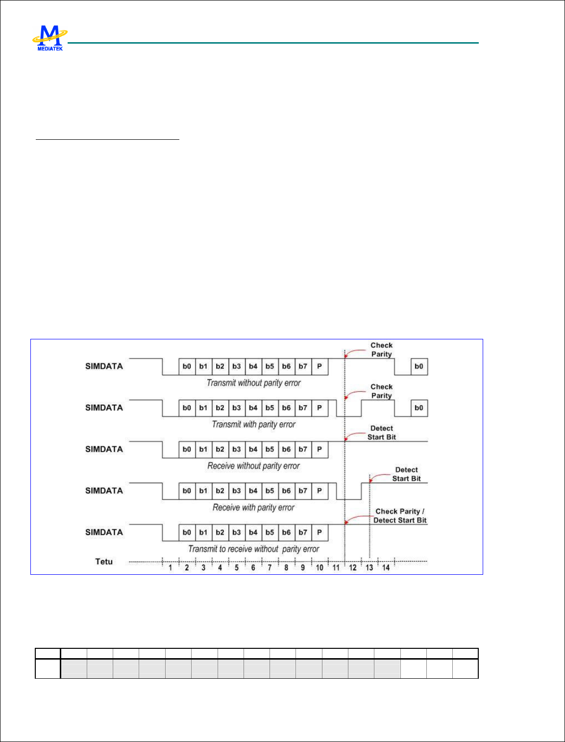
MTK Confidential Release for Konka
MTK Confidential Release for Konka
MT6228 GSM/GPRS Baseband Processor Data Sheet Revision 1.0
115/616 MediaTek Inc. Confidential
SB D0 D1 D2 D3 D4 D5 D6 D7 PB
SB: Start Bit (in state Low)
Dx: Data Byte (LSB is first and logic level ONE is High)
PB: Even Parity Check Bit
Indirect Mode (ODD=SDIR=SINV=1)
SB N7 N6 N5 N4 N3 N2 N1 N0 PB
SB: Start Bit (in state Low)
Nx: Data Byte (MSB is first and logic level ONE is Low)
PB: Odd Parity Check Bit
If the receiver gets a wrong parity bit, it will respond by pulling the SIMDATA Low to inform the transmitter and the
transmitter will retransmit the character.
When the receiver is a SIM Card, the error response starts 0.5 bits after the PB and it may last for 1~2 bit periods.
When the receiver is the SIM interface, the error response starts 0.5 bits after the PB and lasts for 1.5 bit period.
When the SIM interface is the transmitter, it will take a total of 14 bits guard period for the error response to appear. If
the receiver shows the error response, the SIM interface will retransmit the previous character again, otherwise it will
transmit the next character.
Figure 43 SIM Interface Timing Diagram
4.3.1 Register Definitions
SIM+0000h SIM module control register SIM_CON
Bit 15 14 13 12 11 10 9 8 7 6 5 4 3 2 1 0
Name
WRST
CSTO
P
SIMO
N

MTK Confidential Release for Konka
MTK Confidential Release for Konka
MT6228 GSM/GPRS Baseband Processor Data Sheet Revision 1.0
116/616 MediaTek Inc. Confidential
Type
W R/W
R/W
Reset
0 0 0
SIMON SIM card power-up/power-down control
0 Initiate the card deactivation sequence
1 Initiate the card activation sequence
CSTOP Enable clock stop mode. Together with CPOL in SIM_CNF register, it determines the polarity of the SIMCLK
in this mode.
0 Enable the SIMCLK output.
1 Disable the SIMCLK output
WRST SIM card warm reset control
SIM+0004h SIM module configuration register SIM_CNF
Bit 15 14 13 12 11 10 9 8 7 6 5 4 3 2 1 0
Name
HFEN
T0EN T1EN TOUT
SIMS
EL ODD SDIR SINV CPOL
TXAC
K
RXAC
K
Type R/W R/W R/W R/W R/W R/W R/W R/W R/W R/W R/W
Reset
0 0 0 0 0 0 0 0 0 0 0
RXACK SIM card reception error handshake control
0 Disable character receipt handshaking
1 Enable character receipt handshaking
TXACK SIM card transmission error handshake control
0 Disable character transmission handshaking
1 Enable character transmission handshaking
CPOL SIMCLK polarity control in clock stop mode
0 Make SIMCLK stop in LOW level
1 Make SIMCLK stop in HIGH level
SINV Data Inverter.
0 Not invert the transmitted and received data
1 Invert the transmitted and received data
SDIR Data Transfer Direction
0 LSB is transmitted and received first
1 MSB is transmitted and received first
ODD Select odd or even parity
0 Even parity
1 Odd parity
SIMSEL SIM card supply voltage select
0 SIMSEL pin is set to LOW level
1 SIMSEL pin is set to HIGH level
TOUT SIM work waiting time counter control
0 Disable Time-Out counter
1 Enable Time-Out counter
T1EN T=1 protocol controller control
0 Disable T=1 protocol controller
1 Enable T=1 protocol controller
T0EN T=0 protocol controller control
0 Disable T=0 protocol controller
1 Enable T=0 protocol controller
HFEN Hardware flow control

MTK Confidential Release for Konka
MTK Confidential Release for Konka
MT6228 GSM/GPRS Baseband Processor Data Sheet Revision 1.0
117/616 MediaTek Inc. Confidential
0 Disable hardware flow control
1 Enable hardware flow control
SIM +0008h SIM Baud Rate Register SIM_BRR
Bit 15 14 13 12 11 10 9 8 7 6 5 4 3 2 1 0
Name
BAUD[8:0] SIMCLK[1:0]
Type R/W R/W
Reset
372d 01
SIMCLK Set SIMCLK frequency
00 13/2 MHz
01 13/4 MHz
10 13/8 MHz
11 13/12 MHz
BAUD Determines the baud rate as a division of SIMCLK (SIMCLK/BAUD[8:0])
SIM +0010h SIM interrupt enable register SIM_IRQEN
Bit 15 14 13 12 11 10 9 8 7 6 5 4 3 2 1 0
Name
EDCE
RR
T1EN
D
RXER
R
T0EN
D
SIMO
FF
ATRER
R
TXER
R
TOU
T
OVRU
N
RXTID
E
TXTID
E
Type R/W R/W R/W R/W R/W R/W R/W R/W R/W R/W R/W
Reset
0 0 0 0 0 0 0 0 0 0 0
For all these bits
0 Interrupt is disabled
1 Interrupt is enabled
SIM +0014h SIM module status register SIM_STA
Bit 15 14 13 12 11 10 9 8 7 6 5 4 3 2 1 0
Name
EDCE
RR
T1EN
D
RXER
R
T0EN
D
SIMO
FF
ATRER
R
TXER
R
TOU
T
OVRU
N
RXTID
E
TXTID
E
Type RC RC RC RC RC RC RC RC RC RO RO
Reset
TXTIDE Transmit FIFO tide mark reached interrupt occurred
RXTIDE Receive FIFO tide mark reached interrupt occurred
OVRUN Transmit/Receive FIFO overrun interrupt occurred
TOUT Between character timeout interrupt occurred
TXERR Character transmission error interrupt occurred
ATRERR ATR start time-out interrupt occurred
SIMOFF Card deactivation complete interrupt occurred
T0END Data Transfer handled by T=0 Controller completed interrupt occurred
RXERR Character reception error interrupt occurred
T1END Data Transfer handled by T=1 Controller completed interrupt occurred
EDCERR T=1 Controller CRC error occurred
SIM +0020h SIM retry limit register SIM_RETRY
Bit 15 14 13 12 11 10 9 8 7 6 5 4 3 2 1 0
Name
TXRETRY RXRETRY
Type R/W R/W
Reset
3h 3h
RXRETRY Specify the max. numbers of receive retries that are allowed when parity error has occurred.
TXRETRY Specify the max. numbers of transmit retries that are allowed when parity error has occurred.

MTK Confidential Release for Konka
MTK Confidential Release for Konka
MT6228 GSM/GPRS Baseband Processor Data Sheet Revision 1.0
118/616 MediaTek Inc. Confidential
SIM +0024h SIM FIFO tide mark register SIM_TIDE
Bit 15 14 13 12 11 10 9 8 7 6 5 4 3 2 1 0
Name
TXTIDE[3:0] RXTIDE[3:0]
Type R/W R/W
Reset
0h 0h
RXTIDE Trigger point for RXTIDE interrupt
TXTIDE Trigger point for TXTIDE interrupt
SIM +0030h Data register used as Tx/Rx Data Register SIM_DATA
Bit 15 14 13 12 11 10 9 8 7 6 5 4 3 2 1 0
Name
DATA[7:0]
Type R/W
Reset
DATA Eight data digits. These correspond to the character being read or written
SIM +0034h SIM FIFO count register SIM_COUNT
Bit 15 14 13 12 11 10 9 8 7 6 5 4 3 2 1 0
Name
COUNT[4:0]
Type R/W
Reset
0h
COUNT The number of characters in the SIM FIFO when read, and flushes when written.
SIM +0040h SIM activation time register SIM_ATIME
Bit 15 14 13 12 11 10 9 8 7 6 5 4 3 2 1 0
Name
ATIME[15:0]
Type R/W
Reset
AFC7h
ATIME The register defines the duration, in SIM clock cycles, of the time taken for each of the three stages of the
card activation process
SIM +0044h SIM deactivation time register SIM_DTIME
Bit 15 14 13 12 11 10 9 8 7 6 5 4 3 2 1 0
Name
DTIME[11:0]
Type R/W
Reset
3E7h
DTIME The register defines the duration, in 13MHz clock cycles, of the time taken for each of the three stages of
the card deactivation sequence
SIM +0048h Character to character waiting time register SIM_WTIME
Bit 15 14 13 12 11 10 9 8 7 6 5 4 3 2 1 0
Name
WTIME[15:0]
Type R/W
Reset
983h
WTIME Maximum interval between the leading edge of two consecutive characters in 4 ETU unit
SIM +004Ch Block to block guard time register SIM_GTIME
Bit 15 14 13 12 11 10 9 8 7 6 5 4 3 2 1 0
Name
GTIME
Type R/W
Reset
10d
MTK Confidential Release for Konka
MTK Confidential Release for Konka
MT6228 GSM/GPRS Baseband Processor Data Sheet Revision 1.0
119/616 MediaTek Inc. Confidential
GTIME Minimum interval between the leading edge of two consecutive characters sent in opposite directions in ETU
unit
SIM +0050h Transmit error detection register SIM_ETIME
Bit 15 14 13 12 11 10 9 8 7 6 5 4 3 2 1 0
Name
ETIME
Type R/W
Reset
15d
ETIME The register define the position for transmit error detection in ETU/16 unit
SIM +0060h SIM command header register: INS SIM_INS
Bit 15 14 13 12 11 10 9 8 7 6 5 4 3 2 1 0
Name
INSD
SIMINS[7:0]
Type R/W R/W
Reset
0h 0h
SIMINS This field should be identical to the INS instruction code. When writing to this register, the T=0 controller will
be activated and data transfer will be initiated.
INSD [Description for this register field]
0 T=0 controller receives data from the SIM card
1 T=0 controller sends data to the SIM card
SIM +0064h SIM command header register: P3 SIM_P3(ICC_LE
N)
Bit 15 14 13 12 11 10 9 8 7 6 5 4 3 2 1 0
Name
SIMP3[8:0]
Type R/W
Reset
0h
SIMP3 This field should be identical to the P3 instruction code. It should be written prior to the SIM_INS register.
While the data transfer is going on, this field shows the no. of the remaining data to be sent or to be received
SIM +0068h SIM procedure byte register: SW1 SIM_SW1(ICC_
LEN)
Bit 15 14 13 12 11 10 9 8 7 6 5 4 3 2 1 0
Name
SIMSW1[7:0]
Type RO
Reset
0h
SIMSW1 This field holds the last received procedure byte for debug purpose. When the T0END interrupt occurred,
it keeps the SW1 procedure byte.
SIM +006Ch SIM procedure byte register: SW2 SIM_SW2(ICC_
EDC)
Bit 15 14 13 12 11 10 9 8 7 6 5 4 3 2 1 0
Name
SIMSW2[7:0]
Type RO
Reset
0h
SIMSW2 This field holds the SW2 procedure byte

MTK Confidential Release for Konka
MTK Confidential Release for Konka
MT6228 GSM/GPRS Baseband Processor Data Sheet Revision 1.0
120/616 MediaTek Inc. Confidential
4.3.2 SIM Card Insertion and Removal
The detection of physical connection to the SIM card and card removal is done by the external interrupt controller or by
GPIO.
4.3.3 Card Activation and Deactivation
The card activation and deactivation sequence are both controlled by hardware. The MCU initiates the activation
sequence by writing a “1” to bit 0 of the SIM_CON register, and then the interface performs the following activation
sequence:
Assert SIMRST LOW
Set SIMVCC at HIGH level and SIMDATA in reception mode
Enable SIMCLK clock
De-assert SIMRST HIGH (required if it belongs to active low reset SIM card)
The final step in a typical card session is contact deactivation in order to prevent the card from being electrically
damaged. The deactivation sequence is initiated by writing a “0” to bit 0 of the SIM_CON register, and then the
interface performs the following deactivation sequence:
Assert SIMRST LOW
Set SCIMCLK at LOW level
Set SIMDATA at LOW level
Set SIMVCC at LOW level
4.3.4 Answer to Reset Sequence
After card activation, a reset operation results in an answer from the card consisting of the initial character TS, followed
by at most 32 characters. The initial character TS provides a bit synchronization sequence and defines the conventions
to interpret data bytes in all subsequent characters.
On reception of the first character, TS, MCU should read this character, establish the respective required convention
and reprogram the related registers. These processes should be completed prior to the completion of reception of the
next character. And then, the remainder of the ATR sequence is received, read via the SIM_DATA in the selected
convention and interpreted by the software.
The timing requirement and procedures for ATR sequence are handled by hardware and shall meet the requirement of
ISO 7816-3 as shown in Figure 44.
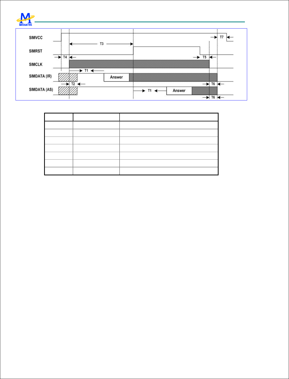
MTK Confidential Release for Konka
MTK Confidential Release for Konka
MT6228 GSM/GPRS Baseband Processor Data Sheet Revision 1.0
121/616 MediaTek Inc. Confidential
Figure 44 Answer to Reset Sequence
Time Value Comment
T1 > 400 SIMCLK SIMCLK start to ATR appear
T2 < 200 SIMCLK SIMCLK start to SIMDATA in reception mode
T3 > 40000 SIMCLK SIMCLK start to SIMRST High
T4 — SIMVCC High to SIMCLK start
T5 — SIMRST Low to SIMCLK stop
T6 — SIMCLK stop to SIMDATA Low
T7 — SIMDATA Low to SIMVCC Low
Table 24 Answer to Reset Sequence Time-Out Condition
4.3.5 SIM Data Transfer
Two transfer modes are provided, either in software controlled byte-by-byte fashion or in a block fashion using T=0
controller and DMA controller. In both modes, the time-out counter can be enabled to monitor the elapsed time between
two consecutive bytes.
4.3.5.1 Byte Transfer Mode
This mode is used during ATR and PPS procedure. In this mode, the SIM interface only ensures error free character
transmission and reception.
Receiving Character
Upon detection of the start-bit sent by SIM card, the interface transforms into reception mode and the following bits are
shifted into an internal register. If no parity error is detected or character-receive handshaking is disabled, the
received-character is written into the SIM FIFO and the SIM_CNT register is increased by one. Otherwise, the
SIMDATA line is held low for 0.5 ETU after detecting the parity error for 1.5 ETU, and the character is re-received. If a
character fails to be received correctly for the RXRETRY times, the receive-handshaking is aborted and the
last-received character is written into the SIM FIFO, the SIM_CNT is increased by one and the RXERR interrupt is
generated
When the number of characters held in the receive FIFO exceeds the level defined in the SIM_TIDE register, a
RXTIDE interrupt is generated. The number of characters held in the SIM FIFO can be determined by reading the
SIM_CNT register and writing to this register will flush the SIM FIFO.
Sending Character

MTK Confidential Release for Konka
MTK Confidential Release for Konka
MT6228 GSM/GPRS Baseband Processor Data Sheet Revision 1.0
122/616 MediaTek Inc. Confidential
Characters that are to be sent to the card are first written into the SIM FIFO and then automatically transmitted to the
card at timed intervals. If character-transmit handshaking is enabled, the SIMDATA line is sampled at 1 ETU after the
parity bit. If the card indicates that it did not receive the character correctly, the character is retransmitted a maximum
of TXRETRY times before a TXERR interrupt is generated and the transmission is aborted. Otherwise, the succeeding
byte in the SIM FIFO is transmitted.
If a character fails to be transmitted and a TXERR interrupt is generated, the interface needs to be reset by flushing the
SIM FIFO before any subsequent transmit or receive operation.
When the number of characters held in the SIM FIFO falls below the level defined in the SIM_TIDE register, a
TXTIDE interrupt is generated. The number of characters held in the SIM FIFO can be determined by reading the
SIM_CNT register and writing to this register will flush the SIM FIFO.
4.3.5.2 Block Transfer Mode
Basically, the SIM interface is designed to work in conjunction with the T=0 protocol controller and the DMA
controller during non-ATR and non-PPS phase; although it is still possible for software to service the data transfer
manually as in byte transfer mode if necessary, and thus the T=0 protocol should be controlled by software.
The T=0 controller is accessed via four registers representing the instruction header bytes INS and P3, and the
procedure bytes SW1 and SW2. These registers are:
SIM_INS, SIM_P3
SIM_SW1, SIM_SW2
During characters transfer, SIM_P3 holds the number of characters to be sent or to be received and SIM_SW1 holds the
last received procedure byte including NULL, ACK, NACK and SW1 for debug purpose.
Data Receive Instruction
Data Receive Instructions receive data from the SIM card. It is instantiated as the following procedure.
1. Enable the T=0 protocol controller by setting the T0EN bit to 1 in SIM_CNF register
2. Program the SIM_TIDE register to 0x0000 (TXTIDE = 0, RXTIDE = 0)
3. Program the SIM_IRQEN to 0x019C (Enable RXERR, TXERR, T0END, TOUT and OVRUN interrupts)
4. Write CLA, INS, P1, P2 and P3 into SIM FIFO
5. Program the DMA controller :
DMAn_MSBSRC and DMAn_LSBSRC : address of SIM_DATA register
DMAn_MSBDST and DMAn_LSBDST : memory address reserved to store the received characters
DMAn_COUNT : identical to P3 or 256 (if P3 == 0)
DMAn_CON : 0x0078
6. Write P3 into SIM_P3 register and then INS into SIM_INS register (Data Transfer is initiated
now)
7. Enable the Time-out counter by setting the TOUT bit to 1 in SIM_CNF register
8. Start the DMA controller by writing 0x8000 into the DMAn_START register to
Upon completion of the Data Receive Instruction, T0END interrupt will be generated and then the Time-out counter
should be disabled by setting the TOUT bit back to 0 in SIM_CNF register.
If error occurs during data transfer (RXERR, TXERR, OVRUN or TOUT interrupt is generated), the SIM card should
be deactivated first and then activated prior subsequent operations.
Data Send Instruction
Data Send Instructions send data to the SIM card. It is instantiated as the following procedure.
1. Enable the T=0 protocol controller by setting the T0EN bit to 1 in SIM_CNF register

MTK Confidential Release for Konka
MTK Confidential Release for Konka
MT6228 GSM/GPRS Baseband Processor Data Sheet Revision 1.0
123/616 MediaTek Inc. Confidential
2. Program the SIM_TIDE register to 0x0100 (TXTIDE = 1, RXTIDE = 0)
3. Program the SIM_IRQEN to 0x019C (Enable RXERR, TXERR, T0END, TOUT and OVRUN interrupts)
4. Write CLA, INS, P1, P2 and P3 into SIM FIFO
5. Program the DMA controller :
DMAn_MSBSRC and DMAn_LSBSRC : memory address reserved to store the transmitted characters
DMAn_MSBDST and DMAn_LSBDST : address of SIM_DATA register
DMAn_COUNT : identical to P3
DMAn_CON : 0x0074
6. Write P3 into SIM_P3 register and then (0x0100 | INS) into SIM_INS register (Data Transfer
is initiated now)
7. Enable the Time-out counter by setting the TOUT bit to 1 in SIM_CNF register
8. Start the DMA controller by writing 0x8000 into the DMAn_START register
Upon completion of the Data Send Instruction, T0END interrupt will be generated and then the Time-out counter
should be disabled by setting the TOUT bit back to 0 in SIM_CNF register.
If error occurs during data transfer (RXERR, TXERR, OVRUN or TOUT interrupt is generated), the SIM card should
be deactivated first and then activated prior to subsequent operations.
4.4 Keypad Scanner
4.4.1 General Description
The keypad can be divided into two parts: one is the keypad interface including 7 columns and 6 rows; the other is the
key detection block which provides key pressed, key released and de-bounce mechanisms. Each time the key is
pressed or released, i.e. something different in the 7 x 6 matrix, the key detection block senses the change and
recognizes if a key has been pressed or released. Whenever the key status changes and is stable, a KEYPAD IRQ is
issued. The MCU can then read the key(s) pressed directly in KP_HI_KEY, KP_MID_KEY and KP_LOW_KEY
registers. To ensure that the key pressed information is not missed, the status register in keypad is not read-cleared by
APB read command. The status register can only be changed by the key-pressed detection FSM.
This keypad can detect one or two key-pressed simultaneously with any combination. Figure 45 shows one key
pressed condition. Figure 46(a) and Figure 46(b) illustrate two keys pressed cases. Since the key press detection
depends on the HIGH or LOW level of the external keypad interface, if keys are pressed at the same time and there
exists a key that is on the same column and the same row with the other keys, the pressed key cannot be correctly
decoded. For example, if there are three key presses: key1 = (x1, y1), key2 = (x2, y2), and key3 = (x1, y2), then both
key3 and key4 = (x2, y1) are detected, and therefore they cannot be distinguished correctly. Hence, the keypad can
detect only one or two keys pressed simultaneously at any combination. More than two keys pressed simultaneously
in a specific pattern retrieves the wrong information. If these specific patterns are excluded, the keypad-scanning
block can detect 11 keys at the same time, shown in Figure 47.
Key-pressed Status
De-bounce time De-bounce time
Key Pressed
KP_IRQ
KEY_PRESS_IRQ KEY_RELEASE_IRQ
Figure 45 One key pressed with de-bounce mechanism denoted
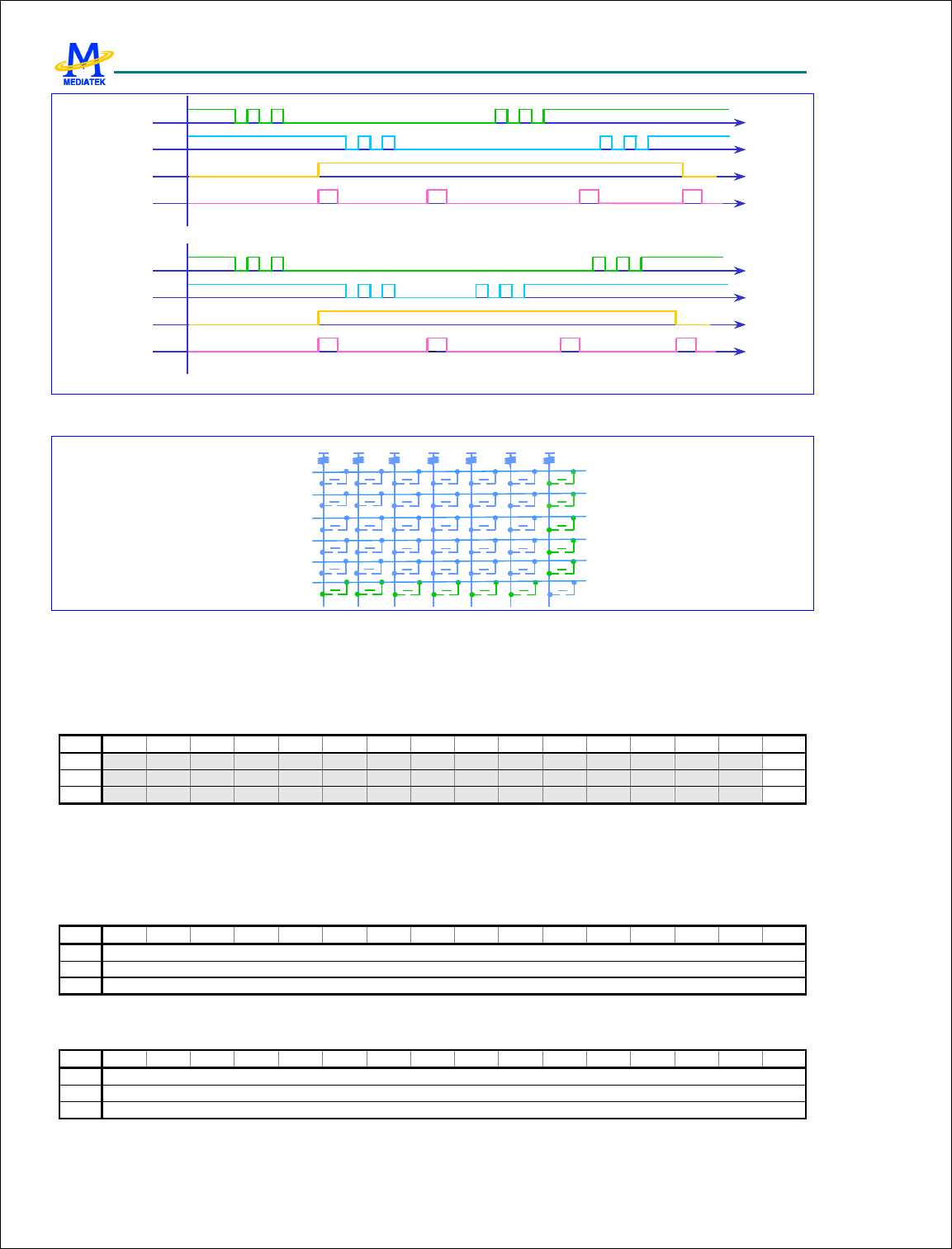
MTK Confidential Release for Konka
MTK Confidential Release for Konka
MT6228 GSM/GPRS Baseband Processor Data Sheet Revision 1.0
124/616 MediaTek Inc. Confidential
Key 1 pr essed
Key 2 pr essed
S t a t us
IRQ
Key 1 pr essed Key2 pr essed K ey1 relea sed Key 2 r ele ased
Key 1 pr essed
Key 2 pr essed
S t a t us
IRQ
Key 1 pr essed Key2 pr essed K ey2 relea sed Key 1 r ele ased
Key 1 pr essed
Key 2 pr essed
S t a t us
IRQ
Key 1 pr essed Key2 pr essed K ey1 relea sed Key 2 r ele ased
Key 1 pr essed
Key 2 pr essed
S t a t us
IRQ
Key 1 pr essed Key2 pr essed K ey2 relea sed Key 1 r ele ased
Figure 46 (a) Two keys pressed, case 1 (b) Two keys pressed, case 2
COL4 COL3 COL2 COL1 COL0
COL5
ROW0
ROW1
ROW2
ROW3
ROW4
ROW5
COL6
Figure 47 11 keys are detected at the same time
4.4.2 Register Definitions
KP +0000h Keypad status KP_STA
Bit 15 14 13 12 11 10 9 8 7 6 5 4 3 2 1 0
Name
STA
Type RO
Reset
0
STA This register indicates the keypad status. The register is not cleared by the read operation.
0 No key pressed
1 Key pressed
KP +0004h Keypad scanning output, the lower 16 keys KP_LOW_KEY
Bit 15 14 13 12 11 10 9 8 7 6 5 4 3 2 1 0
Name
KEYS [15:0]
Type RO
Reset
FFFFh
KP +0008h Keypad scanning output, the medium 16 keys KP_MID_KEY
Bit 15 14 13 12 11 10 9 8 7 6 5 4 3 2 1 0
Name
KEYS [31:16]
Type RO
Reset
FFFFh
MTK Confidential Release for Konka
MTK Confidential Release for Konka
MT6228 GSM/GPRS Baseband Processor Data Sheet Revision 1.0
125/616 MediaTek Inc. Confidential
KP+000Ch Keypad scanning output, the higher 4 keys KP_HIGH_KEY
Bit 15 14 13 12 11 10 9 8 7 6 5 4 3 2 1 0
Name
KEYS[41:32]
Type RO
Reset
3FF’h
These two registers list the status of 42 keys on the keypad. When the MCU receives the KEYPAD IRQ, both two
registers must be read. If any key is pressed, the relative bit is set to 0.
KEYS Status list of the 42 keys.
KP +00010h De-bounce period setting KP_DEBOUNC
E
Bit 15 14 13 12 11 10 9 8 7 6 5 4 3 2 1 0
Name
DEBOUNCE [13:0]
Type R/W
Reset
400h
This register defines the waiting period before key press or release events are considered stale.
DEBOUNCE De-bounce time = KP_DEBOUNCE/32 ms.
4.5 General Purpose Inputs/Outputs
MT6228 offers 71 general-purpose I/O pins and 3 general-purpose output pins. By setting the control registers, MCU
software can control the direction, the output value, and read the input values on these pins. These GPIOs and GPOs
are multiplexed with other functionalities to reduce the pin count.
Figure 48 GPIO Block Diagram
GPIOs at RESET
Upon a hardware reset (SYSRST#), GPIOs are all configured as inputs and the following alternate usages of the GPIO
pins are enabled.
These GPIOs are used to latch the inputs upon reset to memorize the desired configuration to ensure that the system
restarts or boots up in the right mode.
Multiplexing of Signals on GPIO
The GPIO pins can be multiplexed with other signals.
DAICLK, DAIPCMIN, DAIPCMOUT, DAIRST: digital audio interface for FTA
BPI_BUS6, BPI_BUS7, BPI_BUS8, BPI_BUS9: radio hardwired control
MTK Confidential Release for Konka
MTK Confidential Release for Konka
MT6228 GSM/GPRS Baseband Processor Data Sheet Revision 1.0
126/616 MediaTek Inc. Confidential
BSI_CS1: additional chip select signal for radio 3-wire interface
LSCK, LSA0, LSDA, LSCE0#, LSCE1#: serial display interface
LPCE1#: parallel display interface chip select signal
NRNB, NCLE, NALE, NWEB, NREB, NCEB: NAND flash control signals
PWM1, PWM2: pulse width modulation signal
ALERTER: pulse width modulation signal for buzzer
IRDA_RXD, IRDA_TXD, IRDA_PDN: IrDA control signals
URXD2, UTXD2, UCTS2, URTS2: data and flow control signals for UART2
URXD3, UTXD3, UCTS3, URTS3: data and flow control signals for UART3
CMRST, CMPDN, CMDAT9, CMDAT8, CMDAT7, CMDAT6, CMDAT5, CMDAT4, CMDAT3, CMDAT2,
CMDAT1, CMDAT0: sensor interface
SRCLKENAI: external power on signal of the external VCXO LDO
NLD8, NLD9, NLD10, NLD11, NLD12, NLD13, NLD14, NLD15, NLD16, NLD17: NAND FLASH and
Parallel LCD data signals
MFIQ, MIRQ: external interrupt
MCDA4, MCDA5, MCDA6, MCDA7: MMC4.0 data signals
Multiplexed of Signals on GPO
SRCLKENA, SRCLKENAN: power on signal of the external VCXO LDO
EPDN: external memory interface power down controls
4.5.1 Register Definitions
GPIO+0000h GPIO direction control register 1 GPIO_DIR1
Bit 15 14 13 12 11 10 9 8 7 6 5 4 3 2 1 0
Name
GPIO
15
GPIO
14
GPIO
13
GPIO
12
GPIO
11
GPIO
10
GPIO
9
GPIO
8
GPIO
7
GPIO
6
GPIO
5
GPIO
4
GPIO
3
GPIO
2
GPIO
1
GPIO
0
Type R/W R/W R/W R/W R/W R/W R/W R/W R/W R/W R/W R/W R/W R/W R/W R/W
Reset
0 0 0 0 0 0 0 0 0 0 0 0 0 0 0 0
GPIO +0010h GPIO direction control register 2 GPIO_DIR2
Bit 15 14 13 12 11 10 9 8 7 6 5 4 3 2 1 0
Name
GPIO
31
GPIO
30
GPIO
29
GPIO
28
GPIO
27
GPIO
26
GPIO
25
GPIO
24
GPIO
23
GPIO
22
GPIO
21
PGIO
20
GPIO
19
GPIO
18
GPIO
17
GPIO
16
Type R/W R/W R/W R/W R/W R/W R/W R/W R/W R/W R/W R/W R/W R/W R/W R/W
Reset
0 0 0 0 0 0 0 0 0 0 0 0 0 0 0 0
GPIO+0020h GPIO direction control register 3 GPIO_DIR3
Bit 15 14 13 12 11 10 9 8 7 6 5 4 3 2 1 0
Name
GPIO
47
GPIO
46
GPIO
45
GPIO
44
GPIO
43
GPIO
42
GPIO
41
GPIO
40
GPIO
39
GPIO
38
GPIO
37
GPIO
36
GPIO
35
GPIO
34
GPIO
33
GPIO
32
Type R/W R/W R/W R/W R/W R/W R/W R/W R/W R/W R/W R/W R/W R/W R/W R/W
Reset
0 0 0 0 0 0 0 0 0 0 0 0 0 0 0 0

MTK Confidential Release for Konka
MTK Confidential Release for Konka
MT6228 GSM/GPRS Baseband Processor Data Sheet Revision 1.0
127/616 MediaTek Inc. Confidential
GPIO+0030h GPIO direction control register 4 GPIO_DIR4
Bit 15 14 13 12 11 10 9 8 7 6 5 4 3 2 1 0
Name
GPIO
63
GPIO
62
GPIO
61
GPIO
60
GPIO
59
GPIO
58
GPIO
57
GPIO
56
GPIO
55
GPIO
54
GPIO
53
GPIO
52
GPIO
51
GPIO
50
GPIO
49
GPIO
48
Type R/W R/W R/W R/W R/W R/W R/W R/W R/W R/W R/W R/W R/W R/W R/W R/W
Reset
0 0 0 0 0 0 0 0 0 0 0 0 0 0 0 0
GPIO+0040h GPIO direction control register 5 GPIO_DIR5
Bit 15 14 13 12 11 10 9 8 7 6 5 4 3 2 1 0
Name
GPIO
74
GPIO
73
GPIO
72
GPIO
71
GPIO
70
GPIO
69
GPIO
68
Type R/W R/W R/W R/W R/W R/W R/W
Reset
0 0 0 0 0 0 0
GPIOn GPIO direction control
0 GPIOs are configured as input
1 GPIOs are configured as output
GPIO +0050h GPIO pull-up/pull-down enable register 1 GPIO_PULLEN
1
Bit 15 14 13 12 11 10 9 8 7 6 5 4 3 2 1 0
Name
GPIO
15
GPIO
14
GPIO
13
GPIO
12
GPIO
11
GPIO
10
GPIO
9
GPIO
8
GPIO
7
GPIO
6
GPIO
5
GPIO
4
GPIO
3
GPIO
2
GPIO
1
GPIO
0
Type R/W R/W R/W R/W R/W R/W R/W R/W R/W R/W R/W R/W R/W R/W R/W R/W
Reset
1 1 1 1 1 1 1 1 1 1 1 1 1 1 1 1
Note PD PD PD PD PD PD High-
Z
High-
Z
High-
Z
High-
Z
High-
Z HIzhZ
PU PU PD PD
GPIO +0060h GPIO pull-up/pull-down enable register 2 GPIO_PULLEN
2
Bit 15 14 13 12 11 10 9 8 7 6 5 4 3 2 1 0
Name
GPIO
31
GPIO
30
GPIO
29
GPIO
28
GPIO
27
GPIO
26
GPIO
25
GPIO
24
GPIO
23
GPIO
22
GPIO
21
PGIO
20
GPIO
19
GPIO
18
GPIO
17
GPIO
16
Type R/W R/W R/W R/W R/W R/W R/W R/W R/W R/W R/W R/W R/W R/W R/W R/W
Reset
1 1 1 1 1 1 1 1 1 1 1 1 1 1 1 1
Note PU PU PU PD PD PU PU PU PU PU PU PU PD PD PD PD
GPIO+0070h GPIO pull-up/pull-down enable register 3 GPIO_PULLEN
3
Bit 15 14 13 12 11 10 9 8 7 6 5 4 3 2 1 0
Name
GPIO
47
GPIO
46
GPIO
45
GPIO
44
GPIO
43
GPIO
42
GPIO
41
GPIO
40
GPIO
39
GPIO
38
GPIO
37
GPIO
36
GPIO
35
GPIO
34
GPIO
33
GPIO
32
Type R/W R/W R/W R/W R/W R/W R/W R/W R/W R/W R/W R/W R/W R/W R/W R/W
Reset
1 1 1 1 1 1 1 1 1 1 1 1 1 1 1 1
Note High-Z
High-Z
High-
Z
High-
Z PU PU PU PU PU PU PU PU PD PD PD PD
GPIO+0080h GPIO pull-up/pull-down enable register 4 GPIO_PULLEN4
Bit 15 14 13 12 11 10 9 8 7 6 5 4 3 2 1 0
Name
GPIO
63
GPIO
62
GPIO
61
GPIO
60
GPIO
59
GPIO
58
GPIO
57
GPIO
56
GPIO
55
GPIO
54
GPIO
53
GPIO
52
GPIO
51
GPIO
50
GPIO
49
GPIO
48
Type R/W R/W R/W R/W R/W R/W R/W R/W R/W R/W R/W R/W R/W R/W R/W R/W
Reset
1 1 1 1 1 1 1 1 1 1 1 1 1 1 1 1
Note PU PD PD PD PD PD PD PD PD PD PU PU PU PD PU PD
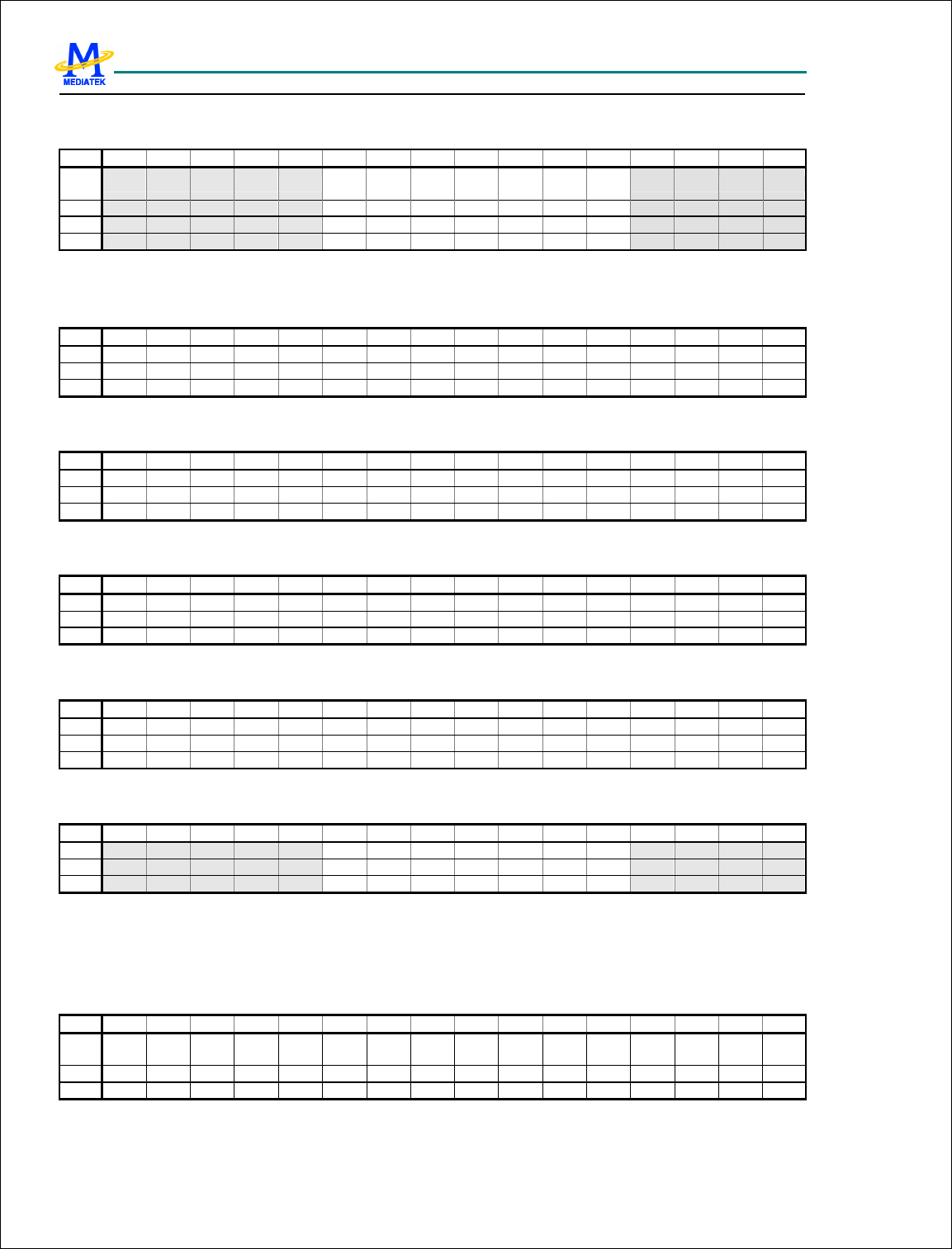
MTK Confidential Release for Konka
MTK Confidential Release for Konka
MT6228 GSM/GPRS Baseband Processor Data Sheet Revision 1.0
128/616 MediaTek Inc. Confidential
GPIO+0090h GPIO pull-up/pull-down enable register 5 GPIO_PULLEN5
Bit 15 14 13 12 11 10 9 8 7 6 5 4 3 2 1 0
Name
GPIO
74
GPIO
73
GPIO
72
GPIO
71
GPIO
70
GPIO
69
GPIO
68
Type R/W R/W R/W R/W R/W R/W R/W
Reset
1 1 1 1 1 1 1
Note PD PD PD PD PD PD PD
GPIOn GPIO pull-up/pull-down control
GPIO +00A0h GPIO data inversion control register 1 GPIO_DINV1
Bit 15 14 13 12 11 10 9 8 7 6 5 4 3 2 1 0
Name
INV15
INV14
INV13
INV12
INV11
INV10
INV9 INV8 INV7 INV6 INV5 INV4 INV3 INV2 INV1 INV0
Type R/W R/W R/W R/W R/W R/W R/W R/W R/W R/W R/W R/W R/W R/W R/W R/W
Reset
0 0 0 0 0 0 0 0 0 0 0 0 0 0 0 0
GPIO +00B0h GPIO data inversion control register 2 GPIO_DINV2
Bit 15 14 13 12 11 10 9 8 7 6 5 4 3 2 1 0
Name
INV31
INV30
INV29
INV28
INV27
INV26
INV25
INV24
INV23
INV22
INV21
INV20
INV19
IVN18
INV17
INV16
Type R/W R/W R/W R/W R/W R/W R/W R/W R/W R/W R/W R/W R/W R/W R/W R/W
Reset
0 0 0 0 0 0 0 0 0 0 0 0 0 0 0 0
GPIO +00C0h GPIO data inversion control register 3 GPIO_DINV3
Bit 15 14 13 12 11 10 9 8 7 6 5 4 3 2 1 0
Name
INV47
INV46
INV45
INV44
INV43
INV42
INV41
INV40
INV39
INV38
INV37
INV36
INV35
INV34
INV33
INV32
Type
R/W
R/W
R/W
R/W
R/W
R/W
R/W
R/W
R/W
R/W
R/W
R/W
R/W
R/W
R/W
R/W
Reset
0 0 0 0 0 0 0 0 0 0 0 0 0 0 0 0
GPIO+00D0h GPIO data inversion control register 4 GPIO_DINV4
Bit 15 14 13 12 11 10 9 8 7 6 5 4 3 2 1 0
Name
INV63
INV62
INV61
INV60
INV59
INV58
INV57
INV56
INV55
INV54
INV53
INV52
INV51
INV50
INV49
INV48
Type R/W R/W R/W R/W R/W R/W R/W R/W R/W R/W R/W R/W R/W R/W R/W R/W
Reset
0 0 0 0 0 0 0 0 0 0 0 0 0 0 0 0
GPIO+00E0h GPIO data inversion control register 5 GPIO_DINV5
Bit 15 14 13 12 11 10 9 8 7 6 5 4 3 2 1 0
Name
INV74
INV73
INV73
INV71
INV70
INV69
INV68
Type R/W R/W R/W R/W R/W R/W R/W
Reset
0 0 0 0 0 0 0
INVn GPIO inversion control
0 GPIOs data inversion disable
1 GPIOs data inversion enable
GPIO +00F0h GPIO data output register 1 GPIO_DOUT1
Bit 15 14 13 12 11 10 9 8 7 6 5 4 3 2 1 0
Name
GPIO
15
GPIO
14
GPIO
13
GPIO
12
GPIO
11
GPIO
10
GPIO
9
GPIO
8
GPIO
7
GPIO
6
GPIO
5
GPIO
4
GPIO
3
GPIO
2
GPIO
1
GPIO
0
Type R/W R/W R/W R/W R/W R/W R/W R/W R/W R/W R/W R/W R/W R/W R/W R/W
Reset
0 0 0 0 0 0 0 0 0 0 0 0 0 0 0 0
MTK Confidential Release for Konka
MTK Confidential Release for Konka
MT6228 GSM/GPRS Baseband Processor Data Sheet Revision 1.0
129/616 MediaTek Inc. Confidential
GPIO +0100h GPIO data output register 2 GPIO_DOUT2
Bit 15 14 13 12 11 10 9 8 7 6 5 4 3 2 1 0
Name
GPIO
31
GPIO
30
GPIO
29
GPIO
28
GPIO
27
GPIO
26
GPIO
25
GPIO
24
GPIO
23
GPIO
22
GPIO
21
PGIO
20
GPIO
19
GPIO
18
GPIO
17
GPIO
16
Type R/W R/W R/W R/W R/W R/W R/W R/W R/W R/W R/W R/W R/W R/W R/W R/W
Reset
0 0 0 0 0 0 0 0 0 0 0 0 0 0 0 0
GPIO +0110h GPIO data output register 3 GPIO_DOUT3
Bit 15 14 13 12 11 10 9 8 7 6 5 4 3 2 1 0
Name
GPIO
47
GPIO
46
GPIO
45
GPIO
44
GPIO
43
GPIO
42
GPIO
41
GPIO
40
GPIO
39
GPIO
38
GPIO
37
GPIO
36
GPIO
35
GPIO
34
GPIO
33
GPIO
32
Type R/W R/W R/W R/W R/W R/W R/W R/W R/W R/W R/W R/W R/W R/W R/W R/W
Reset
0 0 0 0 0 0 0 0 0 0 0 0 0 0 0 0
GPIO+0120h GPIO data output register 4 GPIO_DOUT4
Bit 15 14 13 12 11 10 9 8 7 6 5 4 3 2 1 0
Name
GPIO
63
GPIO
62
GPIO
61
GPIO
60
GPIO
59
GPIO
58
GPIO
57
GPIO
56
GPIO
55
GPIO
54
GPIO
53
GPIO
52
GPIO
51
GPIO
50
GPIO
49
GPIO
48
Type R/W R/W R/W R/W R/W R/W R/W R/W R/W R/W R/W R/W R/W R/W R/W R/W
Reset
0 0 0 0 0 0 0 0 0 0 0 0 0 0 0 0
GPIO+0130h GPIO data output register 5 GPIO_DOUT5
Bit 15 14 13 12 11 10 9 8 7 6 5 4 3 2 1 0
Name
GPIO
74
GPIO
73
GPIO
72
GPIO
71
GPIO
70
GPIO
69
GPIO
68
Type R/W R/W R/W R/W R/W R/W R/W
Reset
0 0 0 0 0 0 0
GPIOn GPIO data output control
0 GPIOs data output 0
1 GPIOs data output 1
GPIO +0140h GPIO data Input register 1 GPIO_DIN1
Bit 15 14 13 12 11 10 9 8 7 6 5 4 3 2 1 0
Name
GPIO
15
GPIO
14
GPIO
13
GPIO
12
GPIO
11
GPIO
10
GPIO
9
GPIO
8
GPIO
7
GPIO
6
GPIO
5
GPIO
4
GPIO
3
GPIO
2
GPIO
1
GPIO
0
Type RO RO RO RO RO RO RO RO RO RO RO RO RO RO RO RO
Reset
X X X X X X X X X X X X X X X X
GPIO +0150h GPIO data Input register 2 GPIO_DIN2
Bit 15 14 13 12 11 10 9 8 7 6 5 4 3 2 1 0
Name
GPIO
31
GPIO
30
GPIO
29
GPIO
28
GPIO
27
GPIO
26
GPIO
25
GPIO
24
GPIO
23
GPIO
22
GPIO
21
PGIO
20
GPIO
19
GPIO
18
GPIO
17
GPIO
16
Type RO RO RO RO RO RO RO RO RO RO RO RO RO RO RO RO
Reset
X X X X X X X X X X X X X X X X
GPIO +0160h GPIO data Input register 3 GPIO_DIN3
Bit 15 14 13 12 11 10 9 8 7 6 5 4 3 2 1 0
Name
GPIO
47
GPIO
46
GPIO
45
GPIO
44
GPIO
43
GPIO
42
GPIO
41
GPIO
40
GPIO
39
GPIO
38
GPIO
37
GPIO
36
GPIO
35
GPIO
34
GPIO
33
GPIO
32
Type RO RO RO RO RO RO RO RO RO RO RO RO RO RO RO RO
Reset
X X X X X X X X X X X X X X X X
MTK Confidential Release for Konka
MTK Confidential Release for Konka
MT6228 GSM/GPRS Baseband Processor Data Sheet Revision 1.0
130/616 MediaTek Inc. Confidential
GPIO+0170h GPIO data input register 4 GPIO_DIN4
Bit 15 14 13 12 11 10 9 8 7 6 5 4 3 2 1 0
Name
GPIO
63
GPIO
62
GPIO
61
GPIO
60
GPIO
59
GPIO
58
GPIO
57
GPIO
56
GPIO
55
GPIO
54
GPIO
53
GPIO
52
GPIO
51
GPIO
50
GPIO
49
GPIO
48
Type RO RO RO RO RO RO RO RO RO RO RO RO RO RO RO RO
Reset
X X X X X X X X X X X X X X X X
GPIO+0180h GPIO data input register 5 GPIO_DIN5
Bit 15 14 13 12 11 10 9 8 7 6 5 4 3 2 1 0
Name
GPIO
74
GPIO
73
GPIO
72
GPIO
71
GPIO
70
GPIO
69
GPIO
68
Type RO RO RO RO RO RO RO
Reset
X X X X X X X
GPIOn GPIOs data input
GPIO +0190h GPO data output register GPO_DOUT
Bit 15 14 13 12 11 10 9 8 7 6 5 4 3 2 1 0
Name
GPO2
GPO1
GPO0
Type R/W R/W R/W
Reset
0 0 0
GPOn GPOs data output
GPIO +01A0h GPIO mode control register 1 GPIO_MODE1
Bit 15 14 13 12 11 10 9 8 7 6 5 4 3 2 1 0
Name
GPIO7_M GPIO6_M GPIO5_M GPIO4_M GPIO3_M GPIO2_M GPIO1_M GPIO0_M
Type R/W R/W R/W R/W R/W R/W R/W R/W
Reset
00 00 00 00 00 00 00 00
GPIO0_M GPIO mode selection
00 Configured as GPIO function
01 CMOS Sensor Flash Control Output
10 Reserved
11 DSP Task ID5
GPIO1_M GPIO mode selection
00 Configured as GPIO function
01 BSI Auxiliary input
10 Reserved
11 Reserved
GPIO2_M GPIO mode selection
00 Configured as GPIO function
01 SCCB Clock
10 Reserved
11 Reserved
GPIO3_M GPIO mode selection
00 Configured as GPIO function
01 SCCB Data
10 Reserved
11 Reserved
GPIO4_M GPO mode selection
00 Configured as GPIO function
MTK Confidential Release for Konka
MTK Confidential Release for Konka
MT6228 GSM/GPRS Baseband Processor Data Sheet Revision 1.0
131/616 MediaTek Inc. Confidential
01 EDI (I2S) Clock Output
10 UART2 RXD Signal
11 Software Debug Interface Data Bit 7
GPIO5_M GPIO mode selection
00 Configured as GPIO function
01 EDI (I2S) Word Synchronization Output
10 UART2 TXD Signal
11 Software Debug Interface Data Bit 6
GPIO6_M GPIO mode selection
00 Configured as GPIO function
01 EDI (I2S) Data Signal
10 Reserved
11 Software Debug Interface Data Bit 5
GPIO7_M GPIO mode selection
00 Configured as GPIO function
01 Reserved
10 USB-OTG Bus Power On Control
11 Software Debug Interface Data Bit 4
GPIO +01B0h GPIO mode control register 2 GPIO_MODE2
Bit 15 14 13 12 11 10 9 8 7 6 5 4 3 2 1 0
Name
GPIO15_M GPIO14_M GPIO13_M GPIO12_M GPIO11_M GPIO10_M GPIO9_M GPIO8_M
Type R/W R/W R/W R/W R/W R/W R/W R/W
Reset
00 00 00 00 00 00 00 00
GPIO8_M GPIO mode selection
00 Configured as GPIO function
01 32KHz Clock
10 USB-OTG Bus Charging Enable Control
11 Software Debug Interface Full Signal
GPIO9_M GPIO mode selection
00 Configured as GPIO function
01 26MHz Clock
10 13MHz Clock
11 Software Debug Interface Empty Signal
GPIO10_M GPIO mode selection
00 Configured as GPIO function
01 Parallel NAND FLASH/LCD Interface Data Bit 16
10 MMC4.0 Data Bit 4
11 DID (DSP ICE Data Signal)
GPIO11_M GPIO mode selection
00 Configured as GPIO function
01 Parallel NAND FLASH/LCD Interface Data Bit 17
10 MMC4.0 Data Bit 5
11 DSP Task ID 1
GPIO12_M GPIO mode selection
00 Configured as GPIO function
01 Sensor Reset Signal Output
10 Reserved

MTK Confidential Release for Konka
MTK Confidential Release for Konka
MT6228 GSM/GPRS Baseband Processor Data Sheet Revision 1.0
132/616 MediaTek Inc. Confidential
11 Reserved
GPIO13_M GPIO mode selection
00 Configured as GPIO function
01 Sensor Power Down Signal Output
10 Reserved
11 Reserved
GPIO14_M GPIO mode selection
00 Configured as GPIO function
01 Sensor Data Input 1
10 MMC4.0 Data Bit 6
11 Reserved
GPIO15_M GPIO mode selection
00 Configured as GPIO function
01 Sensor Data Input 0
10 MMC4.0 Data Bit 7
11 Reserved
GPIO +01C0h GPIO mode control register 3 GPIO_MODE3
Bit 15 14 13 12 11 10 9 8 7 6 5 4 3 2 1 0
Name
GPIO23_M GPIO22_M GPIO21_M GPIO20_M GPIO19_M GPIO18_M GPIO17_M GPIO16_M
Type R/W R/W R/W R/W R/W R/W R/W R/W
Reset
00 00 00 00 00 00 00 00
GPIO16_M GPIO mode selection
00 Configured as GPIO function
01 BPI_BUS6
10 Reserved
11 Reserved
GPIO17_M GPIO mode selection
00 Configured as GPIO function
01 BPI_BUS7
10 13MHz Clock
11 26MHz Clock
GPIO18_M GPIO mode selection
00 Configured as GPIO function
01 BPI_BUS8
10 6.5MHz Clock
11 32KHz Clock
GPIO19_M GPIO mode selection
00 Configured as GPIO function
01 BPI_BUS9
10 BSI_CS1
11 BFE Debug Signal Output
GPIO20_M GPIO mode selection
00 Configured as GPIO function
01 Serial LCD Interface/PM IC Interface Clock Signal
10 TDMA Timer Debug Port Clock Output
11 TDMA Timer Uplink Frame Enable Signal
GPIO21_M GPIO mode selection

MTK Confidential Release for Konka
MTK Confidential Release for Konka
MT6228 GSM/GPRS Baseband Processor Data Sheet Revision 1.0
133/616 MediaTek Inc. Confidential
00 Configured as GPIO function
01 Serial LCD Interface Address/Data Signal
10 TDMA Timer Debug Port Data Output 1
11 TDMA Timer DIRQ Signal
GPIO22_M GPIO mode selection
00 Configured as GPIO function
01 Serial LCD Interface Data/PM IC Interface Data Signal
10 TDMA Timer Debug Port Data Output 0
11 TDMA Timer CTIRQ2 Signal
GPIO23_M GPIO mode selection
00 Configured as GPIO function
01 Serial LCD Interface/PM IC Interface Chip Select Signal 0
10 TDMA Timer Debug Port Frame Sync Signal
11 TDMA Timer CTIRQ1 Signal
GPIO +01D0h GPIO mode control register 4 GPIO_MODE4
Bit 15 14 13 12 11 10 9 8 7 6 5 4 3 2 1 0
Name
GPIO31_M GPIO30_M GPIO29_M GPIO28_M GPIO27_M GPIO26_M GPIO25_M GPIO24_M
Type
R/W R/W R/W R/W R/W R/W R/W R/W
Reset
00 00 00 00 00 00 00 00
GPIO24_M GPIO mode selection
00 Configured as GPIO function
01 Serial LCD Interface Chip Select Signal 1
10 Parallel LCD Interface Chip Select Signal 2
11 TDMA Timer Event Validate Signal
GPIO25_M GPIO mode selection
00 Configured as GPIO function
01 Parallel LCD Interface Chip Select Signal 1
10 NAND FLASH Interface Chip Select Signal 1
11 DSP Task ID 0
GPIO26_M GPIO mode selection
00 NAND FLASH Interface Ready/Busy Signal
01 Configured as GPIO function
10 USB-OTG Session Valid Signal
11 Software Debug Interface Data Bit 2
GPIO27_M GPIO mode selection
00 NAND FLASH Interface Command Latch Signal
01 Configured as GPIO function
10 USB-OTG VBus Valid Signal
11 Software Debug Interface Data Bit 1
GPIO28_M GPIO mode selection
00 NAND FLASH Interface Address Latch Signal
01 Configured as GPIO function
10 USB-OTG Session End Signal
11 Software Debug Interface Data Bit 0
GPIO29_M GPIO mode selection
00 NAND FLASH Interface Write Strobe Signal
01 Configured as GPIO function
MTK Confidential Release for Konka
MTK Confidential Release for Konka
MT6228 GSM/GPRS Baseband Processor Data Sheet Revision 1.0
134/616 MediaTek Inc. Confidential
10 Reserved
11 Reserved
GPIO30_M GPIO mode selection
00 NAND FLASH Interface Read Strobe Signal
01 Configured as GPIO function
10 USB-OTG Bus Power Discharging Control Signal
11 Software Debug Interface Clock Output Signal
GPIO31_M GPIO mode selection
00 NAND FLASH Interface Chip Select Signal 0
01 Configured as GPIO function
10 Reserved
11 Reserved
GPIO +01E0h GPIO mode control register 5 GPIO_MODE5
Bit 15 14 13 12 11 10 9 8 7 6 5 4 3 2 1 0
Name
GPIO39_M GPIO38_M GPIO37_M GPIO36_M GPIO35_M GPIO34_M GPIO33_M GPIO32_M
Type R/W R/W R/W R/W R/W R/W R/W R/W
Reset
00 00 00 00 00 00 00 00
GPIO32_M GPIO mode selection
00 Configured as GPIO function
01 PWM1
10 TDMA Timer Uplink Frame Sync Signal
11 DSP Task ID2
GPIO33_M GPIO mode selection
00 Configured as GPIO function
01 PWM2
10 TDMA Timer Downlink Frame Enable Signal
11 DSP Task ID3
GPIO34_M GPIO mode selection
00 Configured as GPIO function
01 Alerter
10 TDMA Timer Downlink Frame Sync Signal
11 DSP Task ID4
GPIO35_M GPIO mode selection
00 Configured as GPIO function
01 VCXO Enable Signal Input
10 Reserved
11 Reserved
GPIO36_M GPIO mode selection
00 Configured as GPIO function
01 MIRQ Signal
10 6.5 MHz Clock Signal
11 32 KHz Clock Signal
GPIO37_M GPIO mode selection
00 Configured as GPIO function
01 UART2 RXD Signal
10 UART3 CTS Signal
11 Reserved

MTK Confidential Release for Konka
MTK Confidential Release for Konka
MT6228 GSM/GPRS Baseband Processor Data Sheet Revision 1.0
135/616 MediaTek Inc. Confidential
GPIO38_M GPIO mode selection
00 Configured as GPIO function
01 UART2 TXD Signal
10 UART3 RTS Signal
11 Reserved
GPIO39_M GPIO mode selection
00 Configured as GPIO function
01 UART3 RXD Signal
10 Reserved
11 Reserved
GPIO +01F0h GPIO mode control register 6 GPIO_MODE6
Bit 15 14 13 12 11 10 9 8 7 6 5 4 3 2 1 0
Name
GPIO47_M GPIO46_M GPIO45_M GPIO44_M GPIO43_M GPIO42_M GPIO41_M GPIO40_M
Type R/W R/W R/W R/W R/W R/W R/W R/W
Reset
00 00 00 00 00 00 00 00
GPIO40_M GPIO mode selection
00 Configured as GPIO function
01 UART3 TXD Signal
10 Reserved
11 DSP Task ID5
GPIO41_M GPIO mode selection
00 Configured as GPIO function
01 IrDA RXD Signal
10 UART2 CTS Signal
11 Software Debug Interface Data 15
GPIO42_M GPIO mode selection
00 Configured as GPIO function
01 IrDA TXD Signal
10 UART2 RTS Signal
11 Software Debug Interface Data 14
GPIO43_M GPIO mode selection
00 Configured as GPIO function
01 IrDA Power Down Control Signal
10 Reserved
11 Software Debug Interface Data 13
GPIO44_M GPIO mode selection
00 Keypad Row 5 Scan Signal
01 Configured as GPIO function
10 ARM Clock Output
11 TV_CK Clock Output
GPIO45_M GPIO mode selection
00 Keypad Row 4 Scan Signal
01 Configured as GPIO function
10 Internal AHB Bus Clock Output
11 DSP Clock Output
GPIO46_M GPIO mode selection
00 Keypad Row 3 Scan Signal
MTK Confidential Release for Konka
MTK Confidential Release for Konka
MT6228 GSM/GPRS Baseband Processor Data Sheet Revision 1.0
136/616 MediaTek Inc. Confidential
01 Configured as GPIO function
10 TPLL Clock Output
11 SLOW_CK Clock Output
GPIO47_M GPIO mode selection
00 Keypad Row 2 Scan Signal
01 Configured as GPIO function
10 MCU/DSP PLL Clock Output
11 UPLL Clock Output
GPIO +0200h GPIO mode control register 7 GPIO_MODE7
Bit 15 14 13 12 11 10 9 8 7 6 5 4 3 2 1 0
Name
GPIO55 GPIO54 GPIO53 GPIO52 GPIO51 GPIO50 GPIO49 GPIO48
Type R/W R/W R/W R/W R/W R/W R/W R/W
Reset
0 0 0 0 0 0 0 0
GPIO48_M GPIO mode selection
00 Configured as GPIO function
01 SIM Interface Voltage Select Signal
10 Reserved
11 Reserved
GPIO49_M GPIO mode selection
00 Configured as GPIO function
01 Digital Audio Interface Clock Output
10 Reserved
11 Software Debug Interface Data Bit 12
GPIO50_M GPIO mode selection
00 Configured as GPIO function
01 Digital Audio Interface PCM Data Output
10 Reserved
11 Software Debug Interface Data Bit 11
GPIO51_M GPIO mode selection
00 Configured as GPIO function
01 Digital Audio Interface PCM Data Input
10 Reserved
11 Software Debug Interface Data Bit 10
GPIO52_M GPIO mode selection
00 Configured as GPIO function
01 Digital Audio Interface Reset Signal Output
10 Reserved
11 Software Debug Interface Data Bit 9
GPIO53_M GPIO mode selection
00 Configured as GPIO function
01 Digital Audio Interface Synchronization Signal Input
10 Reserved
11 Software Debug Interface Data Bit 8
GPIO54_M GPIO mode selection
00 NAND FLASH/Parallel LCD Interface Data Bit 8
01 Configured as GPIO function
10 Reserved
MTK Confidential Release for Konka
MTK Confidential Release for Konka
MT6228 GSM/GPRS Baseband Processor Data Sheet Revision 1.0
137/616 MediaTek Inc. Confidential
11 Software Debug Interface Address Bit 1
GPIO55_M GPIO mode selection
00 NAND FLASH/Parallel LCD Interface Data Bit 9
01 Configured as GPIO function
10 Reserved
11 Software Debug Interface Address Bit 0
GPIO +0210h GPIO mode control register 8 GPIO_MODE8
Bit 15 14 13 12 11 10 9 8 7 6 5 4 3 2 1 0
Name
GPIO63 GPIO62 GPIO61 GPIO60 GPIO59 GPIO58 GPIO57 GPIO56
Type R/W R/W R/W R/W R/W R/W R/W R/W
Reset
0 0 0 0 0 0 0 0
GPIO56_M GPIO mode selection
00 NAND FLASH/Parallel LCD Interface Data Bit 10
01 Configured as GPIO function
10 Reserved
11 Software Debug Interface Read Output Enable Control
GPIO57_M GPIO mode selection
00 NAND FLASH/Parallel LCD Interface Data Bit 11
01 Configured as GPIO function
10 Reserved
11 Software Debug Interface Read Strobe Control
GPIO58_M GPIO mode selection
00 NAND FLASH/Parallel LCD Interface Data Bit 12
01 Configured as GPIO function
10 Reserved
11 Software Debug Interface Write Strobe Control
GPIO59_M GPIO mode selection
00 NAND FLASH/Parallel LCD Interface Data Bit 13
01 Configured as GPIO function
10 Reserved
11 Software Debug Interface Packet End Strobe Control
GPIO60_M GPIO mode selection
00 NAND FLASH/Parallel LCD Interface Data Bit 14
01 Configured as GPIO function
10 Reserved
11 DICK (DSP ICE Clock Input)
GPIO61_M GPIO mode selection
00 NAND FLASH/Parallel LCD Interface Data Bit 15
01 Configured as GPIO function
10 Reserved
11 DIMS (DSP ICE Mode Select)
GPIO62_M GPIO mode selection
00 Sensor Input Data Bit 2
01 Configured as GPIO function
10 Reserved
11 Reserved
GPIO63_M GPIO mode selection
MTK Confidential Release for Konka
MTK Confidential Release for Konka
MT6228 GSM/GPRS Baseband Processor Data Sheet Revision 1.0
138/616 MediaTek Inc. Confidential
00 Configured as GPIO function
01 MFIQ Signal
10 USB-OTG ID
11 Software Debug Interface Data Bit 3
GPIO +0220h GPIO mode control register 9 GPIO_MODE9
Bit
15 14
13
12
11 10 9 8 7 6 5 4 3 2 1 0
Name
GPIO71 GPIO70 GPIO69 GPIO68
Type R/W R/W R/W R/W
Reset
0 0 0 0
GPIO68_M GPIO mode selection
00 Sensor Input Data Bit 3
01 Configured as GPIO function
10 Reserved
11 Reserved
GPIO69_M GPIO mode selection
00 Sensor Input Data Bit 4
01 Configured as GPIO function
10 Reserved
11 Reserved
GPIO70_M GPIO mode selection
00 Sensor Input Data Bit 5
01 Configured as GPIO function
10 Reserved
11 Reserved
GPIO71_M GPIO mode selection
00 Sensor Input Data Bit 6
01 Configured as GPIO function
10 Reserved
11 Reserved
GPIO +0230h GPIO mode control register 10 GPIO_MODE10
Bit 15 14 13 12 11 10 9 8 7 6 5 4 3 2 1 0
Name
GPIO74 GPIO73 GPIO72
Type R/W R/W R/W
Reset
0 0 0
GPIO72_M GPIO mode selection
00 Sensor Input Data Bit 7
01 Configured as GPIO function
10 Reserved
11 Reserved
GPIO73_M GPIO mode selection
00 Sensor Input Data Bit 8
01 Configured as GPIO function
10 Reserved
11 Reserved
GPIO74_M GPIO mode selection
00 Sensor Input Data Bit 9

MTK Confidential Release for Konka
MTK Confidential Release for Konka
MT6228 GSM/GPRS Baseband Processor Data Sheet Revision 1.0
139/616 MediaTek Inc. Confidential
01 Configured as GPIO function
10 Reserved
11 Reserved
GPIO +0240h GPO mode control register 1 GPO_MODE1
Bit 15 14 13 12 11 10 9 8 7 6 5 4 3 2 1 0
Name
GPO2_M GPO1_M GPO0_M
Type R/W R/W R/W
Reset
01 01 01
GPO0_M GPO mode selection
00 Configured as GPO function
01 VCXO Enable Signal Output Active High
10 Reserved
11 Reserved
GPO1_M GPO mode selection
00 Configured as GPO function
01 VCXO Enable Signal Output Active Low
10 Reserved
11 Reserved
GPO2_M GPO mode selection
00 Configured as GPO function
01 External Memory Interface Power Down Control for Pseudo SRAM
10 Reserved
11 Reserved
GPIO+xxx4h GPIO xxx register SET GPIO_XXX_SET
For all registers addresses listed above, writing to the +4h addresse offset will perform a bit-wise OR function between
the 16bit written value and the 16bit register value already existing in the corresponding GPIO_xxx registers.
Eg.
If GPIO_DIR1 (GPIO+0000h) = 16’h0F0F,
writing GPIO_DIR1_SET (GPIO+0004h) = 16’F0F0 will result in GPIO_DIR1 = 16’hFFFF.
GPIO+xxx8h GPIO xxx register CLR GPIO_XXX_CLR
For all registers addresses listed above, writing to the +8h addresse offset will perform a bit-wise AND-NOT function
between the 16bit written value and the 16bit register value already existing in the corresponding GPIO_xxx registers.
Eg.
If GPIO_DIR1 (GPIO+0000h) = 16’h0F0F,
writing GPIO_DIR1_CLR (GPIO+0008h) = 16’0F0F will result in GPIO_DIR1 = 16’h0000.
4.6 General Purpose Timer
4.6.1 General Description
Three general-purpose timers are provided. The timers are 16 bits long and run independently of each other, although
they share the same clock source. Two timers can operate in one of two modes: one-shot mode and auto-repeat mode;
the other is a free running timer. In one-shot mode, when the timer counts down and reaches zero, it is halted. In
auto-repeat mode, when the timer reaches zero, it simply resets to countdown initial value and repeats the countdown to
zero; this loop repeats until the disable signal is set to 1. Regardless of the timer’s mode, if the countdown initial
MTK Confidential Release for Konka
MTK Confidential Release for Konka
MT6228 GSM/GPRS Baseband Processor Data Sheet Revision 1.0
140/616 MediaTek Inc. Confidential
value (i.e. GPTIMER1_DAT for GPT1 or GPTIMER_DAT2 for GPT2) is written when the timer is running, the new
initial value does not take effect until the next time the timer is restarted. In auto-repeat mode, the new countdown
start value is used on the next countdown iteration. Therefore, before enabling the gptimer, the desired values for
GPTIMER_DAT and the GPTIMER_PRESCALER registers must first be set.
4.6.2 Register Definitions
GPT +0000h GPT1 Control register GPTIMER1_CO
N
Bit 15 14 13 12 11 10 9 8 7 6 5 4 3 2 1 0
Name
EN MODE
Type R/W R/W
Reset
0 0
MODE This register controls GPT1 to count repeatedly (in a loop) or just one-shot.
0 One-shot mode is selected.
1 Auto-repeat mode is selected.
EN This register controls GPT1 to start counting or to stop.
0 GPT1 is disabled.
1 GPT1 is enabled.
GPT +0004h GPT1 Time-Out Interval register GPTIMER1_DA
T
Bit 15 14 13 12 11 10 9 8 7 6 5 4 3 2 1 0
Name
CNT [15:0]
Type R/W
Reset
FFFFh
CNT [15:0] Initial counting value. GPT1 counts down from GPTIMER1_DAT. When GPT1 counts down to zero,
a GPT1 interrupt is generated.
GPT +0008h GPT2 Control register GPTIMER2_CO
N
Bit 15 14 13 12 11 10 9 8 7 6 5 4 3 2 1 0
Name
EN MODE
Type R/W R/W
Reset
0 0
MODE This register controls GPT2 to count repeatedly (in a loop) or just one-shot.
0 One-shot mode is selected
1 Auto-repeat mode is selected
EN This register controls GPT2 to start counting or to stop.
0 GPT2 is disabled.
1 GPT2 is enabled.
GPT +000Ch GPT2 Time-Out Interval register GPTIMER2_DA
T
Bit 15 14 13 12 11 10 9 8 7 6 5 4 3 2 1 0
Name
CNT [15:0]
Type R/W
Reset
FFFFh

MTK Confidential Release for Konka
MTK Confidential Release for Konka
MT6228 GSM/GPRS Baseband Processor Data Sheet Revision 1.0
141/616 MediaTek Inc. Confidential
CNT [15:0] Initial counting value. GPT2 counts down from GPTIMER2_DAT. When GPT2 counts down to zero,
a GPT2 interrupt is generated.
GPT +0010h GPT Status register GPTIMER_STA
Bit 15 14 13 12 11 10 9 8 7 6 5 4 3 2 1 0
Name
GPT2
GPT1
Type RC RC
Reset
0 0
This register illustrates the gptimer timeout status. Each flag is set when the corresponding timer countdown
completes, and can be cleared when the CPU reads the status register.
GPT +0014h GPT1 Prescaler register GPTIMER1_PRES
CALER
Bit 15 14 13 12 11 10 9 8 7 6 5 4 3 2 1 0
Name
PRESCALER [2:0]
Type R/W
Reset
100b
PRESCALER This register controls the counting clock for gptimer1.
000 16 KHz
001 8 KHz
010 4 KHz
011 2 KHz
100 1 KHz
101 500 Hz
110 250 Hz
111 125 Hz
GPT +0018h GPT2 Prescaler register GPTIMER2_PRES
CALER
Bit 15 14 13 12 11 10 9 8 7 6 5 4 3 2 1 0
Name
PRESCALER [2:0]
Type R/W
Reset
100b
PRESCALER This register controls the counting clock for gptimer2.
000 16 KHz
001 8 KHz
010 4 KHz
011 2 KHz
100 1 KHz
101 500 Hz
110 250 Hz
111 125 Hz
GPT+001Ch GPT3 Control register GPTIMER3_CO
N
Bit 15 14 13 12 11 10 9 8 7 6 5 4 3 2 1 0
Name
EN
Type R/W
Reset
0

MTK Confidential Release for Konka
MTK Confidential Release for Konka
MT6228 GSM/GPRS Baseband Processor Data Sheet Revision 1.0
142/616 MediaTek Inc. Confidential
EN This register controls GPT3 to start counting or to stop.
0 GPT3 is disabled.
1 GPT3 is enabled.
GPT+0020h GPT3 Time-Out Interval register GPTIMER3_DA
T
Bit 15 14 13 12 11 10 9 8 7 6 5 4 3 2 1 0
Name
CNT[15:0]
Type RO
Reset
0
CNT [15:0] If EN=1, GPT3 is a free running timer . Software reads this register for the countdown start value for
GPT3.
GPT+0024h GPT3 Prescaler register GPTIMER3_PRES
CALER
Bit 15 14 13 12 11 10 9 8 7 6 5 4 3 2 1 0
Name
PRESCALER [2:0]
Type R/W
Reset
100b
PRESCALER This register controls the counting clock for gptimer3.
000 16 KHz
001 8 KHz
010 4 KHz
011 2 KHz
100 1 KHz
101 500 Hz
110 250 Hz
112 125 Hz
4.7 UART
4.7.1 General Description
MT6228 houses three UARTs. The UARTs provide full duplex serial communication channels between the MT6228
and external devices.
The UART has M16C450 and M16550A modes of operation, which are compatible with a range of standard software
drivers. The extensions have been designed to be broadly software compatible with 16550A variants, but certain areas
offer no consensus.
In common with the M16550A, the UART supports word lengths from five to eight bits, an optional parity bit and one
or two stop bits, and is fully programmable by an 8-bit CPU interface. A 16-bit programmable baud rate generator
and an 8-bit scratch register are included, together with separate transmit and receive FIFOs. Eight modem control
lines and a diagnostic loop-back mode are provided. The UART also includes two DMA handshake lines, used to
indicate when the FIFOs are ready to transfer data to the CPU. Interrupts can be generated from any of the 10
sources.
Note: The UART has been designed so that all internal operations are synchronized by the CLK signal. This
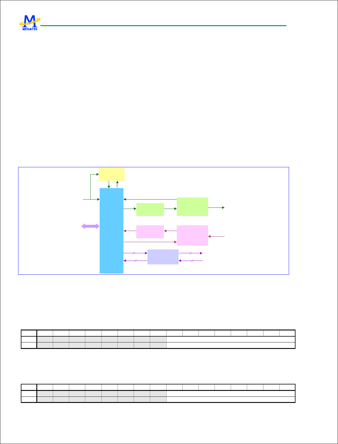
MTK Confidential Release for Konka
MTK Confidential Release for Konka
MT6228 GSM/GPRS Baseband Processor Data Sheet Revision 1.0
143/616 MediaTek Inc. Confidential
synchronization results in minor timing differences between the UART and the industry standard 16550A device, which
means that the core is not clock for clock identical to the original device.
After a hardware reset, the UART is in M16C450 mode. Its FIFOs can be enabled and the UART can then enter
M16550A mode. The UART adds further functionality beyond M16550A mode. Each of the extended functions can
be selected individually under software control.
The UART provides more powerful enhancements than the industry-standard 16550:
Hardware flow control. This feature is very useful when the ISR latency is hard to predict and control in the
embedded applications. The MCU is relieved of having to fetch the received data within a fixed amount of
time.
Output of an IR-compatible electrical pulse with a width 3/16 of that of a regular bit period.
Note: In order to enable any of the enhancements, the Enhanced Mode bit, EFR[4], must be set. If EFR[4] is not set,
IER[7:5], FCR[5:4], ISR[5:4] and MCR[7:6] cannot be written. The Enhanced Mode bit ensures that the UART is
backward compatible with software that has been written for 16C450 and 16550A devices.
Figure 49 shows the block diagram of the MT6228 UART device.
APB
BUS
I/F
Baud Rate
Generator
TX FIFO
TX Machine
RX FIFO
Modem
Control
RX Machine
Modem Outputs
Modem Inputs
APB Bus
clock
divisor
uart_tx_data
uart_rx_data
baud
Figure 49 Block Diagram of UART
4.7.2 Register Definitions
n = 1, 2, 3; for uart1, uart2 and uart3 respectively.
UARTn+0000h RX Buffer Register UARTn_RBR
Bit 15 14 13 12 11 10 9 8 7 6 5 4 3 2 1 0
Name
RBR[7:0]
Type RO
RBR RX Buffer Register. Read-only register. The received data can be read by accessing this register.
Modified when LCR[7] = 0.
UARTn+0000h TX Holding Register UARTn_THR
Bit 15 14 13 12 11 10 9 8 7 6 5 4 3 2 1 0
Name
THR[7:0]
Type WO
MTK Confidential Release for Konka
MTK Confidential Release for Konka
MT6228 GSM/GPRS Baseband Processor Data Sheet Revision 1.0
144/616 MediaTek Inc. Confidential
THR TX Holding Register. Write-only register. The data to be transmitted is written to this register, and then
sent to the PC via serial communication.
Modified when LCR[7] = 0.
UARTn+0004h Interrupt Enable Register UARTn_IER
Bit 15 14 13 12 11 10 9 8 7 6 5 4 3 2 1 0
Name
CTSI RTSI XOFFI
X EDSSI
ELSI ETBEI
ERBFI
Type R/W
Reset
0
IER By storing a ‘1’ to a specific bit position, the interrupt associated with that bit is enabled. Otherwise, the
interrupt is disabled.
IER[3:0] are modified when LCR[7] = 0.
IER[7:4] are modified when LCR[7] = 0 & EFR[4] = 1.
CTSI Masks an interrupt that is generated when a rising edge is detected on the CTS modem control line.
Note: This interrupt is only enabled when hardware flow control is enabled.
0 Unmask an interrupt that is generated when a rising edge is detected on the CTS modem control line.
1 Mask an interrupt that is generated when a rising edge is detected on the CTS modem control line.
RTSI Masks an interrupt that is generated when a rising edge is detected on the RTS modem control line.
Note: This interrupt is only enabled when hardware flow control is enabled.
0 Unmask an interrupt that is generated when a rising edge is detected on the RTS modem control line.
1 Mask an interrupt that is generated when a rising edge is detected on the RTS modem control line.
XOFFI Masks an interrupt that is generated when an XOFF character is received.
Note: This interrupt is only enabled when software flow control is enabled.
0 Unmask an interrupt that is generated when an XOFF character is received.
1 Mask an interrupt that is generated when an XOFF character is received.
EDSSI When set ("1"), an interrupt is generated if DDCD, TERI, DDSR or DCTS (MSR[4:1]) becomes set.
0 No interrupt is generated if DDCD, TERI, DDSR or DCTS (MSR[4:1]) becomes set.
1 An interrupt is generated if DDCD, TERI, DDSR or DCTS (MSR[4:1]) becomes set.
ELSI When set ("1"), an interrupt is generated if BI, FE, PE or OE (LSR[4:1]) becomes set.
0 No interrupt is generated if BI, FE, PE or OE (LSR[4:1]) becomes set.
1 An interrupt is generated if BI, FE, PE or OE (LSR[4:1]) becomes set.
ETBEI When set ("1"), an interrupt is generated if the TX Holding Register is empty or the contents of the TX FIFO
have been reduced to its Trigger Level.
0 No interrupt is generated if the TX Holding Register is empty or the contents of the TX FIFO have been
reduced to its Trigger Level.
1 An interrupt is generated if the TX Holding Register is empty or the contents of the TX FIFO have been
reduced to its Trigger Level
ERBFI When set ("1"), an interrupt is generated if the RX Buffer contains data.
0 No interrupt is generated if the RX Buffer contains data.
1 An interrupt is generated if the RX Buffer contains data.
UARTn+0008h Interrupt Identification Register UARTn_IIR
Bit 15 14 13 12 11 10 9 8 7 6 5 4 3 2 1 0
Name
FIFOE ID4 ID3 ID2 ID1 ID0 NINT
Type RO
Reset
0 0 0 0 0 0 0 1
IIR Identify if there are pending interrupts; ID4 and ID3 are presented only when EFR[4] = 1.
The following table gives the IIR[5:0] codes associated with the possible interrupts:

MTK Confidential Release for Konka
MTK Confidential Release for Konka
MT6228 GSM/GPRS Baseband Processor Data Sheet Revision 1.0
145/616 MediaTek Inc. Confidential
IIR[5:0]
Priority
Level
Interrupt Source
000001 - No interrupt pending
000110 1 Line Status Interrupt BI, FE, PE or OE set in LSR
000100 2 RX Data Received RX Data received or RX Trigger Level reached.
001100 2 RX Data Timeout Timeout on character in RX FIFO.
000010
3 TX Holding Register Empty
TX Holding Register empty or TX FIFO Trigger Level reached.
000000 4 Modem Status change DDCD, TERI, DDSR or DCTS set in MSR
010000 5 Software Flow Control XOFF Character received
100000 6 Hardware Flow Control CTS or RTS Rising Edge
Table 25 The IIR[5:0] codes associated with the possible interrupts
Line Status Interrupt: A RX Line Status Interrupt (IIR[5:0`] == 000110b) is generated if ELSI (IER[2]) is set and any of
BI, FE, PE or OE (LSR[4:1]) becomes set. The interrupt is cleared by reading the Line Status Register.
RX Data Received Interrupt: A RX Received interrupt (IER[5:0] == 000100b) is generated if EFRBI (IER[0]) is set and
either RX Data is placed in the RX Buffer Register or the RX Trigger Level is reached. The interrupt is cleared by
reading the RX Buffer Register or the RX FIFO (if enabled).
RX Data Timeout Interrupt:
When virtual FIFO mode is disabled, RX Data Timeout Interrupt is generated if all of the following apply:
1. FIFO contains at least one character;
2. The most recent character was received longer than four character periods ago (including all start, parity and stop
bits);
3. The most recent CPU read of the FIFO was longer than four character periods ago.
The timeout timer is restarted on receipt of a new byte from the RX Shift Register, or on a CPU read from the RX
FIFO.
The RX Data Timeout Interrupt is enabled by setting EFRBI (IER[0]) to 1, and is cleared by reading RX FIFO.
When virtual FIFO mode is enabled, RX Data Timeout Interrupt is generated if all of the following apply:
1. FIFO is empty;
2. The most recent character was received longer than four character periods ago (including all start, parity and stop
bits);
3. The most recent CPU read of the FIFO was longer than four character periods ago.
The timeout timer is restarted on receipt of a new byte from the RX Shift Register.
RX Holding Register Empty Interrupt: A TX Holding Register Empty Interrupt (IIR[5:0] = 000010b) is generated if
ETRBI (IER[1]) is set and either the TX Holding Register or, if FIFOs are enabled, the TX FIFO becomes empty. The
interrupt is cleared by writing to the TX Holding Register or TX FIFO if FIFO enabled.
Modem Status Change Interrupt: A Modem Status Change Interrupt (IIR[5:0] = 000000b) is generated if EDSSI
(IER[3]) is set and either DDCD, TERI, DDSR or DCTS (MSR[3:0]) becomes set. The interrupt is cleared by reading
the Modem Status Register.

MTK Confidential Release for Konka
MTK Confidential Release for Konka
MT6228 GSM/GPRS Baseband Processor Data Sheet Revision 1.0
146/616 MediaTek Inc. Confidential
Software Flow Control Interrupt: A Software Flow Control Interrupt (IIR[5:0] = 010000b) is generated if Software
Flow Control is enabled and XOFFI (IER[5]) becomes set, indicating that an XOFF character has been received. The
interrupt is cleared by reading the Interrupt Identification Register.
Hardware Flow Control Interrupt: A Hardware Flow Control Interrupt (IER[5:0] = 100000b) is generated if Hardware
Flow Control is enabled and either RTSI (IER[6]) or CTSI (IER[7]) becomes set indicating that a rising edge has been
detected on either the RTS/CTS Modem Control line. The interrupt is cleared by reading the Interrupt Identification
Register.
UARTn+0008h FIFO Control Register UARTn_FCR
Bit 15 14 13 12 11 10 9 8 7 6 5 4 3 2 1 0
Name
RFTL1
RFTL0
TFTL1
TFTL0
DMA1
CLRT
CLRR
FIFOE
Type WO
FCR FCR is used to control the trigger levels of the FIFOs, or flush the FIFOs.
FCR[7:6] is modified when LCR != BFh
FCR[5:4] is modified when LCR != BFh & EFR[4] = 1
FCR[4:0] is modified when LCR != BFh
FCR[7:6] RX FIFO trigger threshold
0 1
0 6
1 12
2 22
FCR[5:4] TX FIFO trigger threshold
0 1
1 4
2 8
3 14
DMA1 This bit determines the DMA mode, which the TXRDY and RXRDY pins support. TXRDY and RXRDY act
to support single-byte transfers between the UART and memory (DMA mode 0) or multiple byte transfers
(DMA mode1). Note that this bit has no effect unless the FIFOE bit is set as well
0 The device operates in DMA Mode 0.
1 The device operates in DMA Mode 1.
TXRDY – mode0: Goes active (low) when the TX FIFO or the TX Holding Register is empty. Becomes
inactive when a byte is written to the Transmit channel.
TXRDY – mode1: Goes active (low) when there are no characters in the TX FIFO. Becomes inactive when
the TX FIFO is full.
RXRDY – mode0: Becomes active (low) when at least one character is in the RX FIFO or the RX Buffer
Register is full. Becomes inactive when there are no more characters in the RX FIFO or RX Buffer
register.
RXRDY – mode1: Becomes active (low) when the RX FIFO Trigger Level is reached or an RX FIFO
Character Timeout occurs. Goes inactive when the RX FIFO is empty.
CLRT Clear Transmit FIFO. This bit is self-clearing.
0 Leave TX FIFO intact.
1 Clear all the bytes in the TX FIFO.
CLRR Clear Receive FIFO. This bit is self-clearing.
0 Leave RX FIFO intact.
1 Clear all the bytes in the RX FIFO.
FIFOE FIFO Enabled. This bit must be set to 1 for any of the other bits in the registers to have any effect.

MTK Confidential Release for Konka
MTK Confidential Release for Konka
MT6228 GSM/GPRS Baseband Processor Data Sheet Revision 1.0
147/616 MediaTek Inc. Confidential
0 Disable both the RX and TX FIFOs.
1 Enable both the RX and TX FIFOs.
UARTn+000Ch
Line Control Register UARTn_LCR
Bit 15 14 13 12 11 10 9 8 7 6 5 4 3 2 1 0
Name
DLAB
SB SP EPS PEN STB WLS1
WLS0
Type R/W
Reset
0 0 0 0 0 0 0 0
LCR Line Control Register. Determines characteristics of serial communication signals.
Modified when LCR[7] = 0.
DLAB Divisor Latch Access Bit.
0 The RX and TX Registers are read/written at Address 0 and the IER register is read/written at Address 4.
1 The Divisor Latch LS is read/written at Address 0 and the Divisor Latch MS is read/written at Address 4.
SB Set Break
0 No effect
1 SOUT signal is forced into the “0” state.
SP Stick Parity
0 No effect.
1 The Parity bit is forced into a defined state, depending on the states of EPS and PEN:
If EPS=1 & PEN=1, the Parity bit is set and checked = 0.
If EPS=0 & PEN=1, the Parity bit is set and checked = 1.
EPS Even Parity Select
0 When EPS=0, an odd number of ones is sent and checked.
1 When EPS=1, an even number of ones is sent and checked.
PEN Parity Enable
0 The Parity is neither transmitted nor checked.
1 The Parity is transmitted and checked.
STB Number of STOP bits
0 One STOP bit is always added.
1 Two STOP bits are added after each character is sent; unless the character length is 5 when 1 STOP bit is
added.
WLS1, 0 Word Length Select.
0 5 bits
1 6 bits
2 7 bits
3 8 bits
UARTn+0010h Modem Control Register UARTn_MCR
Bit 15 14 13 12 11 10 9 8 7 6 5 4 3 2 1 0
Name
XOFF
STAT
US
IR
ENAB
LE
X LOOP
OUT2 OUT1 RTS DTR
Type R/W
Reset
0 0 0 0 0 0 0 0
MCR Modem Control Register. Control interface signals of the UART.
MCR[4:0] are modified when LCR[7] = 0,
MCR[7:6] are modified when LCR[7] = 0 & EFR[4] = 1.
XOFF Status This is a read-only bit.
0 When an XON character is received.

MTK Confidential Release for Konka
MTK Confidential Release for Konka
MT6228 GSM/GPRS Baseband Processor Data Sheet Revision 1.0
148/616 MediaTek Inc. Confidential
1 When an XOFF character is received.
IR Enable Enable IrDA modulation/demodulation.
0 Disable IrDA modulation/demodulation.
1 Enable IrDA modulation/demodulation.
LOOP Loop-back control bit.
0 No loop-back is enabled.
1 Loop-back mode is enabled.
OUT2 Controls the state of the output NOUT2, even in loop mode.
0 NOUT2=1.
1 NOUT2=0.
OUT1 Controls the state of the output NOUT1, even in loop mode.
0 NOUT1=1.
1 NOUT1=0.
RTS Controls the state of the output NRTS, even in loop mode.
0 NRTS=1.
1 NRTS=0.
DTR Control the state of the output NDTR, even in loop mode.
0 NDTR=1.
1 NDTR=0.
UARTn+0014h Line Status Register UARTn_LSR
Bit 15 14 13 12 11 10 9 8 7 6 5 4 3 2 1 0
Name
FIFOE
RR TEMT
THRE
BI FE PE OE DR
Type R/W
Reset
0 1 1 0 0 0 0 0
LSR Line Status Register.
Modified when LCR[7] = 0.
FIFOERR RX FIFO Error Indicator.
0 No PE, FE, BI set in the RX FIFO.
1 Set to 1 when there is at least one PE, FE or BI in the RX FIFO.
TEMT TX Holding Register (or TX FIFO) and the TX Shift Register are empty.
0 Empty conditions below are not met.
1 If FIFOs are enabled, the bit is set whenever the TX FIFO and the TX Shift Register are empty. If FIFOs
are disabled, the bit is set whenever TX Holding Register and TX Shift Register are empty.
THRE Indicates if there is room for TX Holding Register or TX FIFO is reduced to its Trigger Level.
0 When at least one byte is written to the TX FIFO or the TX Shift Register.
1 Set whenever the contents of the TX FIFO are reduced to its Trigger Level (FIFOs are enabled), or
whenever TX Holding Register is empty and ready to accept new data (FIFOs are disabled).
BI Break Interrupt.
0 Reset by the CPU reading this register
1 If the FIFOs are disabled, this bit is set whenever the SIN is held in the 0 state for more than one
transmission time (START bit + DATA bits + PARITY + STOP bits).
If the FIFOs are enabled, this error is associated with a corresponding character in the FIFO and is flagged
when this byte is at the top of the FIFO. When a break occurs, only one zero character is loaded into the
FIFO: the next character transfer is enabled when SIN goes into the marking state and receives the next
valid start bit.
FE Framing Error.

MTK Confidential Release for Konka
MTK Confidential Release for Konka
MT6228 GSM/GPRS Baseband Processor Data Sheet Revision 1.0
149/616 MediaTek Inc. Confidential
0 Reset by the CPU reading this register
1 If the FIFOs are disabled, this bit is set if the received data did not have a valid STOP bit. If the FIFOs
are enabled, the state of this bit is revealed when the byte it refers to is the next to be read.
PE Parity Error
0 Reset by the CPU reading this register
1 If the FIFOs are disabled, this bit is set if the received data did not have a valid parity bit. If the FIFOs
are enabled, the state of this bit is revealed when the referred byte is the next to be read.
OE Overrun Error.
0 Reset by the CPU reading this register.
1 If the FIFOs are disabled, this bit is set if the RX Buffer was not read by the CPU before new data from
the RX Shift Register overwrote the previous contents.
If the FIFOs are enabled, an overrun error occurs when the RX FIFO is full and the RX Shift Register
becomes full. OE is set as soon as this happens. The character in the Shift Register is then overwritten,
but not transferred to the FIFO.
DR Data Ready.
0 Cleared by the CPU reading the RX Buffer or by reading all the FIFO bytes.
1 Set by the RX Buffer becoming full or by a byte being transferred into the FIFO.
UARTn+0018h
Modem Status Register UARTn_MSR
Bit 15 14 13 12 11 10 9 8 7 6 5 4 3 2 1 0
Name
DCD RI DSR CTS DDCD
TERI DDSR
DCTS
Type R/W R/W R/W R/W R/W R/W R/W R/W
Reset
Input Input Input Input 0 0 0 0
Note: After a reset, D4-D7 are inputs. A modem status interrupt can be cleared by writing ‘0’ or set by writing ‘1’ to
this register. D0-D3 can be written to.
Modified when LCR[7] = 0.
MSR Modem Status Register
DCD Data Carry Detect.
When Loop = "0", this value is the complement of the NDCD input signal.
When Loop = "1", this value is equal to the OUT2 bit in the Modem Control Register.
RI Ring Indicator.
When Loop = "0", this value is the complement of the NRI input signal.
When Loop = "1", this value is equal to the OUT1 bit in the Modem Control Register.
DSR Data Set Ready
When Loop = "0", this value is the complement of the NDSR input signal.
When Loop = "1", this value is equal to the DTR bit in the Modem Control Register.
CTS Clear To Send.
When Loop = "0", this value is the complement of the NCTS input signal.
When Loop = "1", this value is equal to the RTS bit in the Modem Control Register.
DDCD Delta Data Carry Detect.
0 The state of DCD has not changed since the Modem Status Register was last read
1 Set if the state of DCD has changed since the Modem Status Register was last read.
TERI Trailing Edge Ring Indicator
0 The NRI input does not change since this register was last read.
1 Set if the NRI input changes from “0” to “1” since this register was last read.
MTK Confidential Release for Konka
MTK Confidential Release for Konka
MT6228 GSM/GPRS Baseband Processor Data Sheet Revision 1.0
150/616 MediaTek Inc. Confidential
DDSR Delta Data Set Ready
0 Cleared if the state of DSR has not changed since this register was last read.
1 Set if the state of DSR has changed since this register was last read.
DCTS Delta Clear To Send
0 Cleared if the state of CTS has not changed since this register was last read.
1 Set if the state of CTS has changed since this register was last read.
UARTn+001Ch
Scratch Register UARTn_SCR
Bit 15 14 13 12 11 10 9 8 7 6 5 4 3 2 1 0
Name
SCR[7:0]
Type R/W
A general purpose read/write register. After reset, its value is un-defined.
Modified when LCR[7] = 0.
UARTn+0000h Divisor Latch (LS) UARTn_DLL
Bit 15 14 13 12 11 10 9 8 7 6 5 4 3 2 1 0
Name
DLL[7:0]
Type R/W
Reset
1
UARTn+0004h Divisor Latch (MS) UARTn_DLM
Bit 15 14 13 12 11 10 9 8 7 6 5 4 3 2 1 0
Name
DLL[7:0]
Type R/W
Reset
0
Note: DLL & DLM can only be updated if DLAB is set (“1”).. Note too that division by 1 generates a BAUD signal
that is constantly high.
Modified when LCR[7] = 1.
The table below shows the divisor needed to generate a given baud rate from CLK inputs of 13, 26 MHz and 52 MHz.
The effective clock enable generated is 16 x the required baud rate.
BAUD 13MHz 26MHz 52MHz
110 7386 14773 29545
300 2708 5417 10833
1200 677 1354 2708
2400 338 677 1354
4800 169 339 677
9600 85 169 339
19200 42 85 169
38400 21 42 85
57600 14 28 56
115200 6 14 28
Table 26 Divisor needed to generate a given baud rate
UARTn+0008h
Enhanced Feature Register UARTn_EFR
Bit 15 14 13 12 11 10 9 8 7 6 5 4 3 2 1 0

MTK Confidential Release for Konka
MTK Confidential Release for Konka
MT6228 GSM/GPRS Baseband Processor Data Sheet Revision 1.0
151/616 MediaTek Inc. Confidential
Name
AUTO
CTS
AUTO
RTS D5
ENAB
LE -E
SW FLOW CONT[3:0]
Type R/W R/W R/W R/W R/W
Reset
0 0 0 0 0
*NOTE: Only when LCR=BF’h
Auto CTS Enables hardware transmission flow control
0 Disabled.
1 Enabled.
Auto RTS Enables hardware reception flow control
0 Disabled.
1 Enabled.
Enable-E Enable enhancement features.
0 Disabled.
1 Enabled.
CONT[3:0] Software flow control bits.
00xx No TX Flow Control
10xx Transmit XON1/XOFF1 as flow control bytes
01xx Transmit XON2/XOFF2 as flow control bytes
11xx Transmit XON1 & XON2 and XOFF1 & XOFF2 as flow control words
xx00 No RX Flow Control
xx10 Receive XON1/XOFF1 as flow control bytes
xx01 Receive XON2/XOFF2 as flow control bytes
xx11 Receive XON1 & XON2 and XOFF1 & XOFF2 as flow control words
UARTn+0010h
XON1 UARTn_XON1
Bit 15 14 13 12 11 10 9 8 7 6 5 4 3 2 1 0
Name
XON1[7:0]
Type R/W
Reset
0
UARTn+0014h
XON2 UARTn_XON2
Bit 15 14 13 12 11 10 9 8 7 6 5 4 3 2 1 0
Name
XON2[7:0]
Type R/W
Reset
0
UARTn+0018h
XOFF1 UARTn_XOFF1
Bit 15 14 13 12 11 10 9 8 7 6 5 4 3 2 1 0
Name
XOFF1[7:0]
Type R/W
Reset
0
UARTn+001Ch
XOFF2 UARTn_XOFF2
Bit 15 14 13 12 11 10 9 8 7 6 5 4 3 2 1 0
Name
XOFF2[7:0]
Type R/W
Reset
0
*Note: XON1, XON2, XOFF1, XOFF2 are valid only when LCR=BFh.

MTK Confidential Release for Konka
MTK Confidential Release for Konka
MT6228 GSM/GPRS Baseband Processor Data Sheet Revision 1.0
152/616 MediaTek Inc. Confidential
UARTn+0020h
AUTOBAUD_EN UARTn_AUTOBAU
D_EN
Bit 15 14 13 12 11 10 9 8 7 6 5 4 3 2 1 0
Name
AUTO
_EN
Type R/W
Reset
0
AUTOBAUD_EN Auto-baud enable signal
0 Auto-baud function disable
1 Auto-baud function enable
UARTn+0024h
HIGH SPEED UART UARTn_HIGHSPEED
Bit 15 14 13 12 11 10 9 8 7 6 5 4 3 2 1 0
Name
SPEED [1:0]
Type R/W
Reset
0
SPEED UART sample counter base
0 based on 16*baud_pulse, baud_rate = system clock frequency/16/{DLH, DLL}
1 based on 8*baud_pulse, baud_rate = system clock frequency/8/{DLH, DLL}
2 based on 4*baud_pulse, baud_rate = system clock frequency/4/{DLH, DLL}
3 based on sampe_count * baud_pulse, baud_rate = system clock frequency / sampe_count
The table below shows the divisor needed to generate a given baud rate from CLK inputs of 13M Hz based on different
HIGHSPEED value.
BAUD
HIGHSPEED = 0
HIGHSPEED = 1
HIGHSPEED = 2
110 7386 14773 29545
300 2708 7386 14773
1200 677 2708 7386
2400 338 677 2708
4800 169 338 677
9600 85 169 338
19200 42 85 169
38400 21 42 85
57600 14 21 42
115200
7 14 21
230400 * 7 14
460800 * * 7
921600 * * *
Table 27 Divisor needed to generate a given baud rate from 13MHz based on different HIGHSPEED value
The table below shows the divisor needed to generate a given baud rate from CLK inputs of 26 MHz based on different
HIGHSPEED value.
BAUD HIGHSPEED = 0 HIGHSPEED = 1 HIGHSPEED = 2
110 14773 29545 59091

MTK Confidential Release for Konka
MTK Confidential Release for Konka
MT6228 GSM/GPRS Baseband Processor Data Sheet Revision 1.0
153/616 MediaTek Inc. Confidential
300 5417 14773 29545
1200 1354 5417 14773
2400 677 1354 5417
4800 339 677 1354
9600 169 339 667
19200 85 169 339
38400 42 85 169
57600 28 42 85
115200 14 28 42
230400 7 14 28
460800
* 7 14
921600 * * 7
Table 28 Divisor needed to generate a given baud rate from 26 MHz based on different HIGHSPEED value
The table below shows the divisor needed to generate a given baud rate from CLK inputs of 52MHz based on different
HIGHSPEED value.
BAUD HIGHSPEED = 0 HIGHSPEED = 1 HIGHSPEED = 2
110 29545 59091 118182
300 10833 29545 59091
1200 2708 10833 29545
2400 1354 2708 10833
4800 677 1354 2708
9600 339 677 1354
19200 169 339 677
38400 85 169 339
57600 56 85 169
115200 28 56 85
230400 14 28 56
460800 7 14 28
921600
* 7 14
Table 29 Divisor needed to generate a given baud rate from 52 MHz based on different HIGHSPEED value
UARTn+0028h
SAMPLE_COUNT UARTn_SAMPLE_COUN
T
Bit
15 14
13
12
11 10 9 8 7 6 5 4 3 2 1 0
Name
SAMPLECOUNT [7:0]
Type R/W
Reset
0
When HIGHSPEED=3, the sample_count is the threshold value for UART sample counter (sample_num).
MTK Confidential Release for Konka
MTK Confidential Release for Konka
MT6228 GSM/GPRS Baseband Processor Data Sheet Revision 1.0
154/616 MediaTek Inc. Confidential
UARTn+002C
h SAMPLE_POINT UARTn_SAMPLE_POIN
T
Bit 15 14 13 12 11 10 9 8 7 6 5 4 3 2 1 0
Name
SAMPLEPOINT [7:0]
Type R/W
Reset
ffh
When HIGHSPEED=3, UART gets the input data when sample_count=sample_num.
e.g. system clock = 13MHz, 921600 = 13000000 / 14
sample_count = 14 and sample point = 7 (sample the central point to decrease the inaccuracy)
UARTn+0030h
AUTOBAUD_REG UARTn_AUTOBAUD_RE
G
Bit 15 14 13 12 11 10 9 8 7 6 5 4 3 2 1 0
Name
BAUD_STAT[3:0] BAUDRATE[3:0]
Type RO RO
Reset
0 0
BAUD_RATE Autobaud baud rate
0 115200
1 57600
2 38400
3 19200
4 9600
5 4800
6 2400
7 1200
8 300
9 110
BAUDSTAT Autobaud format
0 Autobaud is detecting
1 AT_7N1
2 AT_7O1
3 AT_7E1
4 AT_8N1
5 AT_8O1
6 AT_8E1
7 at_7N1
8 at_7E1
9 at_7O1
10 at_8N1
11 at_8E1
12 at_8O1
13 Autobaud detection fails
UARTn+0038h
AUTOBAUDSAMPLE UARTn_AUTOBAUDSA
MPLE
Bit 15 14 13 12 11 10 9 8 7 6 5 4 3 2 1 0
Name
AUTOBAUDSAMPLE
Type R/W R/W R/W R/W R/W R/W R/W
MTK Confidential Release for Konka
MTK Confidential Release for Konka
MT6228 GSM/GPRS Baseband Processor Data Sheet Revision 1.0
155/616 MediaTek Inc. Confidential
Reset
dh
Since the system clock may change, autobaud sample duration should change as system clock changes. When system
clock = 13MHz, autobaudsample = 6; when system clock = 26MHz, autobaudsample = 13.
UARTn+003C
h Guard time added register UARTn_GUARD
Bit 15 14 13 12 11 10 9 8 7 6 5 4 3 2 1 0
Name
GUARD_
EN
GUARD_CNT[3:0]
Type R/W R/W R/W R/W R/W
Reset
0 0 0 0 0
GUARD_CNT Guard interval count value. Guard interval = (1/(system clock / 16 / div )) * GUARD_CNT.
GUARD_EN Guard interval add enable signal.
0 No guard interval added.
1 Add guard interval after stop bit.
UARTn+0040h
Escape character register UARTn_ESCAPE_DAT
Bit 15 14 13 12 11 10 9 8 7 6 5 4 3 2 1 0
Name
ESCAPE_DAT[7:0]
Type R/W
Reset
FFh
ESCAPE_DAT Escape character added before software flow control data and escape character, i.e. if tx data is xon
(31h), with esc_en =1, uart transmits data as esc + CEh (~xon).
UARTn+0044h
Escape enable register UARTn_ESCAPE_EN
Bit 15 14 13 12 11 10 9 8 7 6 5 4 3 2 1 0
Name
ESC_E
N
Type R/W
Reset
0
ESC_EN Add escape character in transmitter and remove escape character in receiver by UART.
0 Do not deal with the escape character.
1 Add escape character in transmitter and remove escape character in receiver.
UARTn+0048h
Sleep enable register UARTn_SLEEP_EN
Bit 15 14 13 12 11 10 9 8 7 6 5 4 3 2 1 0
Name
SELL
P_EN
Type R/W
Reset
0
SLEEP_EN For sleep mode issue
0 Do not deal with sleep mode indicate signal
1 To activate hardware flow control or software control according to software initial setting when chip
enters sleep mode. Releasing hardware flow when chip wakes up; but for software control, uart sends
xon when awaken and when FIFO does not reach threshold level.
UARTn+004C
h Virtual FIFO enable register UARTn_VFIFO_EN
Bit 15 14 13 12 11 10 9 8 7 6 5 4 3 2 1 0
MTK Confidential Release for Konka
MTK Confidential Release for Konka
MT6228 GSM/GPRS Baseband Processor Data Sheet Revision 1.0
156/616 MediaTek Inc. Confidential
Name
VFIF
O_EN
Type R/W
Reset
0
VFIFO_EN Virtual FIFO mechanism enable signal.
0 Disable VFIFO mode.
1 Enable VFIFO mode. When virtual mode is enabled, the flow control is based on the DMA threshold,
and generates a timeout interrupt for DMA.
4.8 IrDA Framer
4.8.1 General Description
IrDA framer is implemented to reduce the CPU loading for IrDA transmissions by performing all the physical level
protocol framing in hardware. From a software perspective, the framer need only prepare and process the raw data for
transmission and reception. Generic DMA is required to move the data between IrDA framer’s internal FIFO and
software-designated memory. The IrDA framer supports IrDA SIR, MIR, and FIR modes of operation. SIR mode
includes operation from 9600bps ~ 115200bps, MIR includes operation at 567000bps or 1152000bps, and FIR mode
includes operation at 4Mbps.
4.8.2 Register Definitions
IRDA+0000h TX BUF and RX BUF BUF
Bit 15 14 13 12 11 10 9 8 7 6 5 4 3 2 1 0
Name
BUF[7:0]
Type R/W
Reset
0
BUF IrDA Framer transmit or receive data.
A write to this register writes into the internal TX FIFO.
A read from this register reads from the internal RX FIFO.
IRDA+0004h TX BUF and RX BUF clear signal BUF_CLEAR
Bit 15 14 13 12 11 10 9 8 7 6 5 4 3 2 1 0
Name
CLEAR
Type R/W
Reset
0
CLEAR SIR mode only. When CLEAR=1, both the TX and RX FIFO are cleared. This is used primarily for debug
purpose. Normal operation does not require this. This control signaled can only be issued under SIR mode.
IRDA+0008h Maximum Turn Around Time MAX_T
Bit 15 14 13 12 11 10 9 8 7 6 5 4 3 2 1 0
Name
MAX_T [13:0]
Type R/W
Reset
3E80h
MAX_T The maximum time that a station can hold the P/F bit. This parameter along with the baud rate parameter
dictates the maximum number of bytes that a station can transmit before passing the line to another station by
transmitting a frame with the P/F bit. This parameter is used by one station to indicate the maximum time the
other station can send before it must turn the link around. For baud rates less than 115200 kbps, 500 ms is
the only valid value. The default value is 500 ms.

MTK Confidential Release for Konka
MTK Confidential Release for Konka
MT6228 GSM/GPRS Baseband Processor Data Sheet Revision 1.0
157/616 MediaTek Inc. Confidential
IRDA+000Ch Minimum Turn Around Time MIN_T
Bit 15 14 13 12 11 10 9 8 7 6 5 4 3 2 1 0
Name
MIN_T [15:0]
Type R/W
Reset
FDE8h
MIN_T Minimum turn around time, the default value is 10 ms. The minimum turn around time parameter deals with
the time needed for a receiver to recover following saturation by transmission from the same device. This
parameter corresponds to the required time delay between the last byte of the last frame sent by a station and
the point at which it is ready to receive the first byte of a frame from another station, i.e. the latency for a
transmit to complete and be ready to receive.
IRDA+0010h Number of additional BOFs prefixed to the beginning
of a frame BOFS
Bit 15 14 13 12 11 10 9 8 7 6 5 4 3 2 1 0
Name
TYPE
BOFS [6:0]
Type R/W R/W
Reset
0 1011b
BOFs For SIR mode: the additional BOFs parameter indicates the number of additional flags needed at the beginning
of every frame. The main purpose for the additional BOFs is to provide a delay at the beginning of each frame
for devices with a long interrupt latency.
For MIR mode: This parameter indicates the number of double STA’s to transmit in the beginning. This value
should be set to 0 (for default 2 STA’s) for MIR mode, unless more are required.
For FIR mode: This parameter has no effect.
TYPE SIR mode only. Additional BOFs type.
1 BOF = C0h
0 BOF = FFh
IRDA+0014h Baud rate divisor DIV
Bit 15 14 13 12 11 10 9 8 7 6 5 4 3 2 1 0
Name
DIV[15:0]
Type R/W
Reset
55h
DIV Transmit or receive rate divider. Rate = System clock frequency / DIV/ 16. The default value is 55h when
in contention mode. This divisor is also used to determine the RX FIFO timeout threshold.
IRDA+0018h Transmit frame size TX_FRAME_SIZ
E
Bit 15 14 13 12 11 10 9 8 7 6 5 4 3 2 1 0
Name
TX_FRAME_SIZE[11:0]
Type R/W
Reset
40h
TX_FRAME_SIZE Transmit frame size; the default value is 64 when in contention mode.
IRDA+001Ch Receiving frame1 size RX_FRAME1_SI
ZE
Bit 15 14 13 12 11 10 9 8 7 6 5 4 3 2 1 0
Name
RX_FRAME1_SIZE[11:0]
Type RO
Reset
0

MTK Confidential Release for Konka
MTK Confidential Release for Konka
MT6228 GSM/GPRS Baseband Processor Data Sheet Revision 1.0
158/616 MediaTek Inc. Confidential
RX_FRAME1_SIZE Reports the number of byte received. Includes only the A+C+I fields.
IRDA+0020h Transmit abort indication ABORT
Bit 15 14 13 12 11 10 9 8 7 6 5 4 3 2 1 0
Name
ABO
RT
Type
R/W
Reset
0
ABORT SIR mode only. When set 1, the framer transmits an abort sequence and closes the frame without an FCS field
or an ending flag.
Note: Tx abort can be achieved in MIR and FIR by simply disabling the tx_en signal.
IRDA+0024h IrDA framer transmit enable signal TX_EN
Bit 15 14 13 12 11 10 9 8 7 6 5 4 3 2 1 0
Name
TX_ON
E
TXINVE
RT
MODE
TX_E
N
Type R/W R/W R/W R/W
Reset
0 0 0 0
TX_EN Transmit enable.
MODE SIR mode only. Modulation type selection.
0 3/16 modulation
1 1.61us
TXINVERT Invert the transmit signal.
0 Transmit signal is not inverted.
1 Transmit signal is inverted.
TX_ONE: Controls the transmit enable signal is one or not.
0 tx_en is not de-asserted until software programs a so.1 tx_en is de-asserted (i.e. transmit disabled)
automatically after one frame has been sent.
IRDA+0028h IrDA framer receive enable signal RX_EN
Bit 15 14 13 12 11 10 9 8 7 6 5 4 3 2 1 0
Name
RX_ON
E
RXINVE
RT
RX_E
N
Type R/W R/W R/W
Reset
0 0 0
RX_EN Receive enable.
RXINVERT Invert the receive signal.
0 Receive signal is not inverted.
1 Receive signal is inverted.
RX_ONE Disable receive when get one frame.
0 rx_en is not de-asserted until software programs so.
1 rx_en is de-asserted (i.e. transmit disabled) automatically after one frame has been sent.
IRDA+002Ch FIFO trigger level indication TRIGGER
Bit 15 14 13 12 11 10 9 8 7 6 5 4 3 2 1 0
Name
RX_TRIG[ TX_TRIG
Type R/W R/W
Reset
0 0
MTK Confidential Release for Konka
MTK Confidential Release for Konka
MT6228 GSM/GPRS Baseband Processor Data Sheet Revision 1.0
159/616 MediaTek Inc. Confidential
TX_TRIG TX FIFO interrupt trigger threshold. When the amount of data in the TX FIFO is less than the specified
amount, dma req is asserted. (When TX_TRIG = 03, dma req is always asserted as long as FIFO is not full.)
00 0 byte
01 1 byte
02 8 byte
03 16 byte
RX_TRIG RX FIFO interrupt trigger threshold. When the amount of data in RX FIFO is above the specified
amount, dma req is asserted.
00 1 byte
01 2 byte
02 3 byte
IRDA+0030h IRQ enable signal IRQ_ENABLE
Bit 15 14 13 12 11 10 9 8 7 6 5 4 3 2 1 0
Name
2NDR
X_CO
MP
RXRE
START
THRE
SHTIM
EOUT
FIFOTI
MEOU
T
TXABO
RT
RXABO
RT
MAXTI
MEOU
T
MINTI
MEOU
T
RXCO
MPLET
E
TXCO
MPLET
E
ERRO
R
RXTH
RES
TXTH
RES
Type R/W R/W R/W R/W R/W R/W R/W R/W R/W R/W R/W R/W
Reset
0 0 0 0 0 0 0 0 0 0 0 0
TXRES Transmit data reaches the threshold level. (For debug only. Should be set to 0.)
0 No interrupt is generated.
1 Interrupt is generated when transmit FIFO size reaches threshold.
RXRES Receive data reaches the threshold level. (For debug only. Should be set to 0.)
0 No interrupt is generated.
1 Interrupt is generated when receive FIFO size reaches threshold.
ERROR Error status interrupt enable.
0 No interrupt is generated.
1 Interrupt is generated when one of the error statuses occurs.
TXCOMPLETE Transmit one frame completely.
0 No interrupt is generated.
1 Interrupt is generated when transmitting one frame completely.
RXCOMPLETE Receive one frame completely.
0 No interrupt is generated.
1 Interrupt is generated when receiving one frame completely.
MINTIMEOUT Minimum time timeout.
0 No interrupt is generated.
1 Interrupt is generated when minimum timer is timed out.
MAXTIMEOUT Maximum time timeout.
0 No interrupt is generated.
1 Interrupt is generated when maximum timer is timed out.
RXABORT Receiving aborting frame.
0 No interrupt is generated.
1 Interrupt is generated when receiving aborting frame.
TXABORT SIR mode only. Transmitting aborting frame.
0 No interrupt is generated.
1 Interrupt is generated when transmitting aborting frame.
FIFOTIMEOUT FIFO timeout.
0 No interrupt is generated.

MTK Confidential Release for Konka
MTK Confidential Release for Konka
MT6228 GSM/GPRS Baseband Processor Data Sheet Revision 1.0
160/616 MediaTek Inc. Confidential
1 Interrupt is generated when FIFO timeout.
THRESHTIMEOUT Threshold time timeout.
0 No interrupt is generated.
1 Interrupt is generated when threshold timer is timed out.
RXRESTART SIR mode only. Receiving a new frame before one frame is received completely.
0 No interrupt is generated.
1 Interrupt is generated when receiving a new frame before one frame is received completely.
2NDRX_COMP Receiving second frame and get P/F bit.
0 No interrupt is generated.
1 Interrupt is generated when receiving second frame and get P/F bit completely.
IRDA+0034h Interrupt Status IRQ_STA
Bit 15 14 13 12 11 10 9 8 7 6 5 4 3 2 1 0
Name
2NDR
X_CO
MP
RXRE
START
THRE
SHTIM
EOUT
FIFOTI
MEOU
T
TXABO
RT
RXABO
RT
MAXTI
MEOU
T
MINTI
MEOU
T
RXCO
MPLET
E
TXCO
MPLET
E
ERRO
R
RXTR
ES
TXTRE
S
Type RC RC RC RC RC RC RC RC RC RC RC RC RC
Reset
0 0 0 0 0 0 0 0 0 0 0 0 0
TXFIFO Transmit FIFO reaches threshold. (For debug only. Not recommended for normal usage.)
RXFIFO Receive FIFO reaches threshold. (For debug only. Not recommended for normal usage.)
ERROR Generated when any of status in Error Status register occurs.
Once the source of an interrupt is determined to be caused by an error (bit 2), the error status register should
be read. Once read, both the error status register and the interrupt source are read-cleared. If the error
status register indicates either a frame 1 or frame 2 error, the corresponding frame status register should be
read.
TXCOMPLETE Transmitting one frame completely.
RXCOMPLETE Receiving one frame completely.
MINTIMEOUT Minimum turn around time timeout.
MAXTIMEOUT Maximum turn around time timeout.
RXABORT Receiving aborting frame.
TXABORT Transmitting aborting frame.
FIFOTIMEOUT FIFO is timeout.
THRESHTIMEOUT Threshold time timeout.
RXRESTART Receiving a new frame before one frame is received completely.
2NDRX_COMP Receiving second frame and get P/F bit completely.
IRDA+0038h ERROR STATUS register ERR_STATUS
Bit 15 14 13 12 11 10 9 8 7 6 5 4 3 2 1 0
Name
TX FIFO
UNDERR
UN
FRAME
2 DATA
ERR
FRAME
1 DATA
ERR
RESER
VED2
RESER
VED
OVER
RUN
RXSIZ
E
Type R/W R/W R/W R/W R/W R/W R/W
Reset
0 0 0 0 0 0 0
RXSIZE Receive frame size error.
OVERRUN Frame overrun.
RESERVED Reserved for future use.
RESERVED2 Reserved for future use.
FRAME1 DATA ERR Indicates that an error condition occurred in RX frame1. Must check the RX frame1 status.
FRAME2 DATA ERR Indicates that an error condition occurred in RX frame2. Must check the RX frame2 status.
MTK Confidential Release for Konka
MTK Confidential Release for Konka
MT6228 GSM/GPRS Baseband Processor Data Sheet Revision 1.0
161/616 MediaTek Inc. Confidential
TX FIFO UNDERRUN MIR and FIR mode only.
TX FIFO underrun has occurred. Data transmission is aborted. Software must reset the tx_en
signal.
IRDA+003Ch Transceiver power on/off control. Transceiver mode
select.
TRANSCEIVER
_PDN
Bit 15 14 13 12 11 10 9 8 7 6 5 4 3 2 1 0
Name
TXCVR
CONFIG
TX
MANUAL
TRANS_
PDN
Type R/W R/W R/W
Reset
0 0 0
TRANSCEIVER_PDN Used for power on/off control for external IrDA transceiver.
TX_MANUAL When txcvr config is set to 1, this bit can be used to select the operation mode of the external IrDA
transceiver (some transceivers require selection between high speed and low speed operating modes), by
software programming the desired sequence to transmit through the irda_txd pin.
TXCVR CONFIG
0 Irda_txd comes from core logic.
1 Irda_txd depends on tx_manual value.
IRDA+0040h Maximum number of receiving frame size RX_FRAME_MA
X
Bit 15 14 13 12 11 10 9 8 7 6 5 4 3 2 1 0
Name
MAX_RX_FRAME_SIZE_
Type R/W
Reset
0
RX_FRAME_MAX Receive frame I field max size, when actual receiving frame size is larger than rx_frame_max,
RXSIZE is asserted. The maximum allowed I field size is 2048.
IRDA+0044h Threshold Time THRESH_T
Bit 15 14 13 12 11 10 9 8 7 6 5 4 3 2 1 0
Name
DISCONNECT_TIME[15:0]
Type R/W
Reset
bb8h
THRESHOLD TIME Threshold time; used to control the time a station waits without receiving a valid frame before
disconnecting the link. Associated with this is the time a station waits without receiving a valid
frame before sending a status indication to the service user layer.
IRDA+0048h Counter enable signal COUNT_ENABL
E
Bit 15 14 13 12 11 10 9 8 7 6 5 4 3 2 1 0
Name
THRESH
_EN
MIN_E
N
MAX_
EN
Type R/W R/W R/W
Reset
0 0 0
COUNT_ENABLE Counter enable signals.
IRDA+004Ch Indication of system clock rate CLOCK_RATE
Bit 15 14 13 12 11 10 9 8 7 6 5 4 3 2 1 0
Name
CLOCK_RA
TE
MTK Confidential Release for Konka
MTK Confidential Release for Konka
MT6228 GSM/GPRS Baseband Processor Data Sheet Revision 1.0
162/616 MediaTek Inc. Confidential
Type
R/W
Reset
0
CLOCK_RATE SIR mode only Indication of the system clock rate.
0 26 MHz
1 52 MHz
2 13 MHz
IRDA+0050h System Clock Rate Fix RATE_FIX
Bit 15 14 13 12 11 10 9 8 7 6 5 4 3 2 1 0
Name
CRC
REPOR
T
SIR
FRAMI
NG SET
RATE_
FIX
Type R/W R/W R/W
Reset
0 0 0
RATE_FIX SIR mode only Fix the IrDA framer sample base clock rate as 13 MHz.
0 Clock rate based on clock_rate selection.
1 Clock rate fixed at 13 MHz.
SIR FRAMING SET SIR mode only. Framing error check condition.
0 Ignore the STOP bit of the last byte of a frame.
1 Check the STOP bit of the last byte of a frame.
CRC REPORT When set to 1, CRC error is reported via error status register and error interrupt.
IRDA+0054h RX Frame1 Status FRAME1_STAT
US
Bit
15 14
13
12
11 10 9 8 7 6 5 4 3 2 1 0
Name
FIR
STO
ERR
FIR
4PPM
ERR
MIR
HDLC
ERR
UNKNO
W_ERRO
R
PF_DET
ECT
CRC_FAI
L
FRAME_
ERROR
Type R/W R/W R/W R/W R/W R/W R/W
Reset
0 0 0 0 0 0 0
FRAME_ERROR SIR mode only. Framing error, i.e. STOP bit = 0.
0 No framing error
1 Framing error occurred
CRC_FAIL CRC check fail
2 CRC check successfully
3 CRC check fail
PF_DETECT P/F bit detect
0 Not a P/F bit frame
1 Detected P/F bit in this frame
UNKNOWN_ERROR SIR mode only. Receiving error data, i.e. escape character is followed by a character that is
not an ESC, BOF, or EOF character.
0 Data received correctly.
1 Unknown error occurred.
MIR HDLC ERR MIR mode only. MIR HDLC encoding error
0 No error
1 Error
FIR 4PPM ERR FIR mode only. FIR 4ppm encoding error
0 No error
1 Error

MTK Confidential Release for Konka
MTK Confidential Release for Konka
MT6228 GSM/GPRS Baseband Processor Data Sheet Revision 1.0
163/616 MediaTek Inc. Confidential
FIR STO ERR FIR mode only. FIR STO sequence error
0 No error
1 Error
IRDA+0058h RX Frame2 Status FRAME2_STAT
US
Bit 15 14 13 12 11 10 9 8 7 6 5 4 3 2 1 0
Name
FIR
STO
ERR
FIR
4PPM
ERR
MIR
HDLC
ERR
UNKNO
W_ERRO
R
PF_DET
ECT
CRC_FAI
L
FRAME_
ERROR
Type R/W R/W R/W R/W R/W R/W R/W
Reset
0 0 0 0 0 0 0
FRAME_ERROR SIR mode only. Framing error, i.e. STOP bit = 0
0 No framing error.
1 Framing error occurred.
CRC_FAIL CRC check fail.
0 CRC check successfully.
1 CRC check fail.
PF_DETECT P/F bit detect.
0 Not a P/F bit frame.
1 Detected P/F bit in this frame.
UNKNOWN_ERROR SIR mode only. Receiving error data, i.e. escape character is followed by a character that is
not an ESC, BOF, or EOF character.
0 Data receiving correctly.
1 Unknown error occurred.
MIR HDLC ERR MIR mode only. MIR HDLC encoding error.
0 No error
1 Error
FIR 4PPM ERR FIR mode only.FIR 4ppm encoding error
0 No error
1 Error
FIR STO ERR FIR mode only.FIR STO sequence error
0 No error
1 Error
IRDA+005Ch Receiving frame2 size RX_FRAME2_SI
ZE
Bit 15 14 13 12 11 10 9 8 7 6 5 4 3 2 1 0
Name
RX_FRAME2_SIZE[11:0]
Type RO
Reset
0
RX_FRAME2_SIZE Reports the number of byte received. Includes only the A+C+I fields.
IRDA+0060h Irda Mode Select IRDA_MODE
Bit 15 14 13 12 11 10 9 8 7 6 5 4 3 2 1 0
Name
MIR
SPEED IRDA MODE
Type R/W R/W
Reset
0 00

MTK Confidential Release for Konka
MTK Confidential Release for Konka
MT6228 GSM/GPRS Baseband Processor Data Sheet Revision 1.0
164/616 MediaTek Inc. Confidential
IRDA MODE Selects the IrDA operating mode. NOTE: this mode selection cannot be issued while transmitting
or receiving.
00 IR mode
01 MIR mode
10 FIR mode
MIR SPEED Select the MIR speed.
0 0.576 Mbps
1 1.152 Mbps
IRDA+0064h Fifo Status FIFO_STAT
Bit 15 14 13 12 11 10 9 8 7 6 5 4 3 2 1 0
Name
RX
FIFO
HOLD
TX FIFO
WR FULL
TX FIFO
RD
EMPTY
RX FIFO
WR FULL
RX FIFO
RD
EMPTY
Type RO RO RO RO RO
Reset
0 0 1 0 1
This register indicates the real time FIFO status, for monitoring purposes.
4.9 Real Time Clock
4.9.1 General Description
The Real Time Clock (RTC) module provides time and data information. The clock is based on a 32.768KHz
oscillator with an independent power supply. When the mobile handset is powered off, a dedicated regulator supplies
the RTC block. If the main battery is not present, a backup supply such as a small mercury cell battery or a large
capacitor is used. In addition to providing timing data, an alarm interrupt is generated and can be used to power up
the baseband core via the BBWAKEUP pin. Regulator interrupts corresponding to seconds, minutes, hours and days
can be generated whenever the time counter value reaches a maximum value (e.g., 59 for seconds and minutes, 23 for
hours, etc.). The year span is supported up to 2127. The maximum day-of-month values, which depend on the leap
year condition, are stored in the RTC block.
4.9.2 Register Definitions
RTC+0000h Baseband power up RTC_BBPU
Bit 15 14 13 12 11 10 9 8 7 6 5 4 3 2 1 0
Name
KEY_BBPU AUTO
BBPU
WRITE_E
N
PWRE
N
Type W R/W R/W R/W R/W
KEY_BBPU A bus write is acceptable only when KEY_BBPU=0x43.
AUTO Controls if BBWAKEUP is automatically in the low state when SYSRST# transitions from high to low.
0 BBWAKEUP is not automatically in the low state when SYSRST# transitions from high to low.
1 BBWAKEUP is automatically in the low state when SYSRST# transitions from high to low.
BBPU Controls the power of PMIC. If powerkey1=A357h and powerkey2=67D2h, PMIC takes on the value
programmed by software; otherwise PMIC is low.
0 Power down
1 Power on
WRITE_EN When WRITE_EN is set to 0 by the software program, the RTC write interface is disabled until another
system power on.

MTK Confidential Release for Konka
MTK Confidential Release for Konka
MT6228 GSM/GPRS Baseband Processor Data Sheet Revision 1.0
165/616 MediaTek Inc. Confidential
PWREN
0 RTC alarm has no action on power switch.
1 When an RTC alarm occurs, BBPU is set to 1, and the system powers on by RTC alarm wakeup.
RTC+0004h RTC IRQ status RTC_IRQ_STA
Bit 15 14 13 12 11 10 9 8 7 6 5 4 3 2 1 0
Name
TCST
A
ALST
A
Type R/C R/C
ALSTA This register indicates the IRQ status and whether or not the alarm condition has been met.
0 No IRQ occurred; the alarm condition has not been met.
1 IRQ occurred; the alarm condition has been met.
TCSTA This register indicates the IRQ status and whether or not the tick condition has been met.
0 No IRQ occurred; the tick condition has not been met.
1 IRQ occurred; the tick condition has been met.
RTC+0008h RTC IRQ enable RTC_IRQ_EN
Bit 15 14 13 12 11 10 9 8 7 6 5 4 3 2 1 0
Name
WING
ONESH
OT
TC_E
N
AL_E
N
Type R/O R/W R/W R/W
ONESHOT Controls automatic reset of AL_EN and TC_EN.
AL_EN This register enables the control bit for IRQ generation if the alarm condition has been met.
0 Disable IRQ generation.
1 Enable the alarm time match interrupt. Clear the interrupt when ONESHOT is high upon generation of
the corresponding IRQ.
TC_EN This register enables the control bit for IRQ generation if the tick condition has been met.
0 Disable IRQ generation.
1 Enable the tick time match interrupt. Clear the interrupt when ONESHOT is high upon generation of the
corresponding IRQ.
WING This bit indicates that RTC is still writing to this register.
RTC+000Ch Counter increment IRQ enable RTC_CII_EN
Bit 15 14 13 12 11 10 9 8 7 6 5 4 3 2 1 0
Name
WING
1/8SEC
CII
1/4SEC
CII
1/2SEC
CII
YEAC
II
MTHC
II
DOW
CII
DOM
CII
HOUC
II
MINCI
I
SECC
II
Type R/O R/W R/W R/W R/W R/W R/W R/W R/W R/W R/W
This register activates or de-activates the IRQ generation when the TC counter reaches its maximum value.
SECCII Set this bit to 1 to activate the IRQ at each second update.
MINCII Set the bit to 1 to activate the IRQ at each minute update.
HOUCII Set the bit to 1 to activate the IRQ at each hour update.
DOMCII Set the bit to 1 to activate the IRQ at each day-of-month update.
DOWCII Set the bit to 1 to activate the IRQ at each day-of-week update.
MTHCII Set the bit to 1 to activate the IRQ at each month update.
YEACII Set the bit to 1 to activate the IRQ at each year update.
1/2SECCII Set the bit to 1 to activate the IRQ at each one-half of a second update.
1/4SECCII Set the bit to 1 to activate the IRQ at each one-fourth of a second update.
1/8SECCII Set the bit to 1 to activate the IRQ at each one-eighth of a second update.

MTK Confidential Release for Konka
MTK Confidential Release for Konka
MT6228 GSM/GPRS Baseband Processor Data Sheet Revision 1.0
166/616 MediaTek Inc. Confidential
WING This bit indicates RTC is still writing to this register.
RTC+0010h RTC alarm mask RTC_AL_MASK
Bit 15 14 13 12 11 10 9 8 7 6 5 4 3 2 1 0
Name
WING
YEA_M
SK
MTH_M
SK
DOW_M
SK
DOM_M
SK
HOU_M
SK
MIN_M
SK
SEC_M
SK
Type R/O R/W R/W R/W R/W R/W R/W R/W
The alarm condition for alarm IRQ generation depends on whether or not the corresponding bit in this register is
masked.
SEC_MSK
0 Condition (RTC_TC_SEC = RTC_AL_SEC) is checked to generate the alarm signal.
1 Condition (RTC_TC_SEC = RTC_AL_SEC) is masked, i.e. the value of RTC_TC_SEC does not affect
the alarm IRQ generation.
MIN_MSK
0 Condition (RTC_TC_MIN = RTC_AL_MIN) is checked to generate the alarm signal.
1 Condition (RTC_TC_MIN = RTC_AL_MIN) is masked, i.e. the value of RTC_TC_MIN does not affect
the alarm IRQ generation.
HOU_MSK
0 Condition (RTC_TC_HOU = RTC_AL_HOU) is checked to generate the alarm signal.
1 Condition (RTC_TC_HOU = RTC_AL_HOU) is masked, i.e. the value of RTC_TC_HOU does not affect
the alarm IRQ generation.
DOM_MSK
0 Condition (RTC_TC_DOM = RTC_AL_DOM) is checked to generate the alarm signal.
1 Condition (RTC_TC_DOM = RTC_AL_DOM) is masked, i.e. the value of RTC_TC_DOM does not
affect the alarm IRQ generation.
DOW_MSK
0 Condition (RTC_TC_DOW = RTC_AL_DOW) is checked to generate the alarm signal.
1 Condition (RTC_TC_DOW = RTC_AL_DOW) is masked, i.e. the value of RTC_TC_DOW does not
affect the alarm IRQ generation.
MTH_MSK
0 Condition (RTC_TC_MTH = RTC_AL_MTH) is checked to generate the alarm signal.
1 Condition (RTC_TC_MTH = RTC_AL_MTH) is masked, i.e. the value of RTC_TC_MTH does not affect
the alarm IRQ generation.
YEA_MSK
0 Condition (RTC_TC_YEA = RTC_AL_YEA) is checked to generate the alarm signal.
1 Condition (RTC_TC_YEA = RTC_AL_YEA) is masked, i.e. the value of RTC_TC_YEA does
not affect the alarm IRQ generation.
WING This bit indicates RTC is still writing to this register.
RTC+0014h RTC seconds time counter register RTC_TC_SEC
Bit 15 14 13 12 11 10 9 8 7 6 5 4 3 2 1 0
Name
WING
TC_SECOND
Type R/O R/W
TC_SECOND The second initial value for the time counter. The range of its value is: 0-59.
WING This bit indicates RTC is still writing to this register.
RTC+0018h RTC minutes time counter register RTC_TC_MIN
Bit 15 14 13 12 11 10 9 8 7 6 5 4 3 2 1 0

MTK Confidential Release for Konka
MTK Confidential Release for Konka
MT6228 GSM/GPRS Baseband Processor Data Sheet Revision 1.0
167/616 MediaTek Inc. Confidential
Name
WING
TC_MINUTE
Type R/O R/W
TC_MINUTE The minute initial value for the time counter. The range of its value is: 0-59.
WING This bit indicates RTC is still writing to this register.
RTC+001Ch RTC hours time counter register RTC_TC_HOU
Bit 15 14 13 12 11 10 9 8 7 6 5 4 3 2 1 0
Name
WING
TC_HOUR
Type R/O R/W
TC_HOUR The hour initial value for the time counter. The range of its value is: 0-23.
WING This bit indicates RTC is still writing to this register.
RTC+0x0020 RTC day-of-month time counter register RTC_TC_DOM
Bit 15 14 13 12 11 10 9 8 7 6 5 4 3 2 1 0
Name
WING
TC_DOM
Type R/O R/W
TC_DOM The day-of-month initial value for the time counter. The day-of-month maximum value depends on the
leap year condition, i.e. 2 LSB of year time counter are zeros.
WING This bit indicates RTC is still writing to this register.
RTC+0x0024 RTC day-of-week time counter register RTC_TC_DOW
Bit 15 14 13 12 11 10 9 8 7 6 5 4 3 2 1 0
Name
WING
TC_DOW
Type R/O R/W
TC_DOW The day-of-week initial value for the time counter. The range of its value is: 1-7.
WING This bit indicates RTC is still writing to this register.
RTC+0x0028 RTC month time counter register RTC_TC_MTH
Bit 15 14 13 12 11 10 9 8 7 6 5 4 3 2 1 0
Name
WING
TC_MONTH
Type R/O R/W
TC_MONTH The month initial value for the time counter. The range of its value is: 1-12.
WING This bit indicates RTC is still writing to this register.
RTC+0x002C RTC year time counter register RTC_TC_YEA
Bit 15 14 13 12 11 10 9 8 7 6 5 4 3 2 1 0
Name
WING
AL_SECOND
Type R/O R/W
TC_YEAR The year initial value for the time counter. The range of its value is: 0-127. (2000-2127)
WING This bit indicates RTC is still writing to this register.
RTC+0x0030 RTC second alarm setting register RTC_AL_SEC
Bit 15 14 13 12 11 10 9 8 7 6 5 4 3 2 1 0
Name
WING
AL_SECOND
Type R/O R/W
AL_SECOND The second value of the alarm counter setting. The range of its value is: 0-59.
WING This bit indicates RTC is still writing to this register.
MTK Confidential Release for Konka
MTK Confidential Release for Konka
MT6228 GSM/GPRS Baseband Processor Data Sheet Revision 1.0
168/616 MediaTek Inc. Confidential
RTC+0x0034 RTC minute alarm setting register RTC_AL_MIN
Bit 15 14 13 12 11 10 9 8 7 6 5 4 3 2 1 0
Name
WING
AL_MINUTE
Type R/O R/W
AL_MINUTE The minute value of the alarm counter setting. The range of its value is: 0-59.
WING This bit indicates RTC is still writing to this register.
RTC+0x0038 RTC hour alarm setting register RTC_AL_HOU
Bit 15 14 13 12 11 10 9 8 7 6 5 4 3 2 1 0
Name
WING
AL_HOUR
Type R/O R/W
AL_HOUR The hour value of the alarm counter setting. The range of its value is: 0-23.
WING This bit indicates RTC is still writing to this register.
RTC+0x003C RTC day-of-month alarm setting register RTC_AL_DOM
Bit 15 14 13 12 11 10 9 8 7 6 5 4 3 2 1 0
Name
WING
AL_DOM
Type R/O R/W
AL_DOM The day-of-month value of the alarm counter setting. The day-of-month maximum value depends on
the leap year condition, i.e. 2 LSB of year time counter are zeros.
WING This bit indicates RTC is still writing to this register.
RTC+0x0040 RTC day-of-week alarm setting register RTC_AL_DOW
Bit 15 14 13 12 11 10 9 8 7 6 5 4 3 2 1 0
Name
WING
AL_DOW
Type R/O R/W
AL_DOW The day-of-week value of the alarm counter setting. The range of its value is: 1-7.
WING This bit indicates RTC is still writing to this register.
RTC+0x0044 RTC month alarm setting register RTC_AL_MTH
Bit 15 14 13 12 11 10 9 8 7 6 5 4 3 2 1 0
Name
WING
AL_MONTH
Type R/O R/W
AL_MONTH The month value of the alarm counter setting. The range of its value is: 1-12.
WING This bit indicates RTC is still writing to this register.
RTC+0x0048 RTC year alarm setting register RTC_AL_YEA
Bit 15 14 13 12 11 10 9 8 7 6 5 4 3 2 1 0
Name
WING
AL_YEAR
Type R/O R/W
AL_YEAR The year value of the alarm counter setting. The range of its value is: 0-127. (2000-2127)
WING This bit indicates RTC is still writing to this register.
RTC+0x004C XOSC bias current control register RTC_XOSCCAL
I
Bit 15 14 13 12 11 10 9 8 7 6 5 4 3 2 1 0
Name
WING
XOSCCALI
Type
R/O
WO
MTK Confidential Release for Konka
MTK Confidential Release for Konka
MT6228 GSM/GPRS Baseband Processor Data Sheet Revision 1.0
169/616 MediaTek Inc. Confidential
XOSCCALI This register controls the XOSC32 bias current. Before the first program by software, the
XOSCCALI value is 11111b.
WING This bit indicates RTC is still writing to this register.
RTC+0050h RTC_POWERKEY1 register RTC_POWERK
EY1
Bit 15 14 13 12 11 10 9 8 7 6 5 4 3 2 1 0
Name
RTC_POWERKEY1
Type R/W
RTC+0054h RTC_POWERKEY2 register RTC_POWERK
EY2
Bit 15 14 13 12 11 10 9 8 7 6 5 4 3 2 1 0
Name
RTC_POWERKEY2
Type R/W
These register sets are used to determine if the real time clock has been programmed by software; i.e. the time value in
real time clock is correct. When the real time clock is first powered on, the register contents are all undefined,
therefore the time values shown are incorrect. Software needs to know if the real time clock has been programmed.
Hence, these two registers are defined to solve this power-on issue. After software programs the correct value, these
two register sets do not need to be updated. In addition to programming the correct time value, when the contents of
these register sets are wrong, the interrupt is not generated. Therefore, the real time clock does not generate the
interrupts before the software programs the registers; unwanted interrupt due to wrong time value do not occur. The
correct values of these two register sets are:
RTC_POWERKEY1 A357h
RTC_POWERKEY2 67D2h
RTC+0058h PDN1 RTC_PDN1
Bit 15 14 13 12 11 10 9 8 7 6 5 4 3 2 1 0
Name
WING
DBIN
G RTC_PDN1[7:0]
Type R/O R/O R/W
RTC_PDN1[3:1] is for reset de-bounce mechanism.
0 4ms
1 16ms
2 64ms
3 256ms
4 512ms
5 1024ms
6 2048ms
7 4096ms
RTC_PDN1[7:4] & RTC_PDN1[0] is the spare register for software to keep power on and power off state
information.
DBING This bit indicates RTC is still de-bouncing.
WING This bit indicates RTC is still writing to this register.
RTC+005Ch PDN2 RTC_PDN2
Bit
15 14
13
12
11 10 9 8 7 6 5 4 3 2 1 0

MTK Confidential Release for Konka
MTK Confidential Release for Konka
MT6228 GSM/GPRS Baseband Processor Data Sheet Revision 1.0
170/616 MediaTek Inc. Confidential
Name
WING
RTC_PDN2[7:0]
Type R/O R/W
RTC_PDN2 The spare register for software to keep power on and power off state information.
WING This bit indicates RTC is still writing to this register.
RTC+0060h RTC writing completed flag RTC_WOK
Bit 15 14 13 12 11 10 9 8 7 6 5 4 3 2 1 0
Name
WING
3
WING
2
WING
1
Type R/O R/O R/O
WING1 This bit indicates RTC is still writing POWERKEY1.
WING2 This bit indicates RTC is still writing POWERKEY2.
WING3 This bit indicates RTC is still writing BBPU.
4.10 Auxiliary ADC Unit
The auxiliary ADC unit is used to monitor the status of the battery and charger, to identify the plugged peripheral, and
to perform temperature measurement. Seven input channels allow diverse applications in this unit.
Each channel can operate in one of two modes: immediate mode and timer-triggered mode. The mode of each
channel can be individually selected through register AUXADC_CON0. For example, if the flag SYN0 in the register
AUXADC_CON0 is set, the channel 0 is set in timer-triggered mode. Otherwise, the channel operates in immediate
mode.
In immediate mode, the A/D converter samples the value once only when the flag in the AUXADC_CON1 register has
been set. For example, if the flag IMM0 in AUXADC_CON1 is set, the A/D converter samples the data for channel 0.
The IMM flags must be cleared and set again to initialize another sampling.
The value sampled for channel 0 is stored in register AUXADC_DAT0, the value for channel 1 is stored in register
AUXADC_DAT1, etc.
If the AUTOSET flag in the register AUXADC_CON3 is set, the auto-sample function is enabled. The A/D converter
samples the data for the channel in which the corresponding data register has been read. For example, in the case
where the SYN1 flag is not set, the AUTOSET flag is set, when the data register AUXADC_DAT0 has been read, the
A/D converter samples the next value for channel 1 immediately.
If multiple channels are selected at the same time, the task is performed sequentially on every selected channel. For
example, if AUXADC_CON1 is set to 0x7f, that is, all 7 channels are selected, the state machine in the unit starts
sampling from channel 6 to channel 0, and saves the values of each input channel in the respective registers. The
same process also applies in timer-triggered mode.
In timer-triggered mode, the A/D converter samples the value for the channels in which the corresponding SYN flags
are set when the TDMA timer counts to the value specified in the register TDMA_AUXEV1, which is placed in the
TDMA timer. For example, if AUXADC_CON0 is set to 0x7f, all 7 channels are selected to be in timer-triggered
mode. The state machine samples all 7 channels sequentially and save the values in registers from AUXADC_DAT0
to AUXADC_DAT6, as it does in immediate mode.
There is a dedicated timer-triggered scheme for channel 0. This scheme is enabled by setting the SYN7 flag in the
register AUXADC_CON2. The timing offset for this event is stored in the register TDMA_AUXEV0 in the TDMA
timer. The sampled data triggered by this specific event is stored in the register AUXADC_DAT7. It is used to
separate the results of two individual software routines that perform actions on the auxiliary ADC unit.
MTK Confidential Release for Konka
MTK Confidential Release for Konka
MT6228 GSM/GPRS Baseband Processor Data Sheet Revision 1.0
171/616 MediaTek Inc. Confidential
The AUTOCLRn in the register AUXADC_CON3 is set when it is intended to sample only once after setting
timer-triggered mode. If AUTOCLR1 flag has been set, after the data for the channels in timer-triggered mode has
been stored, the SYNn flags in the register AUXADC_CON0 are cleared. If AUTOCLR0 flag has been set, after the
data for the channel 0 has been stored in the register AUXADC_DAT7, the SYN7 flag in the register AUXADC_CON2
is cleared.
The usage of the immediate mode and timer-triggered mode are mutually exclusive in terms of individual channels.
The PUWAIT_EN bit in the registers AUXADC_CON3 is used to power up the analog port in advance. This ensures
that the power has ramped up to the stable state before A/D converter starts the conversion. The analog part is
automatically powered down after the conversion is completed.
4.10.1 Register Definitions
AUXADC+000
0h Auxiliary ADC control register 0 AUXADC_CON0
Bit 15 14 13 12 11 10 9 8 7 6 5 4 3 2 1 0
Name
SYN6
SYN5
SYN4
SYN3
SYN2
SYN1
SYN0
Type R/W R/W R/W R/W R/W R/W R/W
Reset
0 0 0 0 0 0 0
SYNn These 7 bits define whether the corresponding channel is sampled or not in timer-triggered mode. It is
associated with timing offset register TDMA_AUXEV1. It supports multiple flags. The flags can be
automatically cleared after those channel have been sampled if AUTOCLR1 in the register AUXADC_CON3
is set.
0 The channel is not selected.
1 The channel is selected.
AUXADC+000
4h Auxiliary ADC control register 1 AUXADC_CON1
Bit 15 14 13 12 11 10 9 8 7 6 5 4 3 2 1 0
Name
IMM6 IMM5 IMM4 IMM3 IMM2 IMM1 IMM0
Type R/W R/W R/W R/W R/W R/W R/W
Reset
0 0 0 0 0 0 0
IMMn These 7 bits are set individually to sample the data for the corresponding channel. It supports multiple flags.
0 The channel is not selected.
1 The channel is selected.
AUXADC+000
8h Auxiliary ADC control register 2 AUXADC_CON2
Bit 15 14 13 12 11 10 9 8 7 6 5 4 3 2 1 0
Name
SYN7
Type R/W
Reset
0
SYN7 This bit is used only for channel 0 and is to be associated with timing offset register TDMA_AUXEV0 in the
TDMA timer in timer-triggered mode. The flag can be automatically cleared after channel 0 has been
sampled if AUTOCLR0 in the register AUXADC_CON3 is set.
0 The channel is not selected.
1 The channel is selected.
MTK Confidential Release for Konka
MTK Confidential Release for Konka
MT6228 GSM/GPRS Baseband Processor Data Sheet Revision 1.0
172/616 MediaTek Inc. Confidential
AUXADC+000
Ch Auxiliary ADC control register 3 AUXADC_CON3
Bit 15 14 13 12 11 10 9 8 7 6 5 4 3 2 1 0
Name
AUTO
SET
PUW
AIT_E
N
AUTO
CLR1
AUTO
CLR0
STA
Type
R/W
R/W
R/W
R/W
RO
Reset
0 0 0 0 0
AUTOSET This field defines the auto-sample mode of the module. In auto-sample mode, each channel with its
sample register being read can start sampling immediately without configuring the control register
AUXADC_CON1 again.
PUWAIT_EN Thus field enables the power warm-up period to ensure power stability before the SAR process takes
place. It is recommended to activate this field.
0 The mode is not enabled.
1 The mode is enabled.
AUTOCLR1 The field defines the auto-clear mode of the module for event 1. In auto-clear mode, each
timer-triggered channel gets samples of the specified channels once the SYNn bit in the register
AUXADC_CON0 has been set. The SYNn bits are automatically cleared and the channel is not enabled
again by the timer event except when the SYNn flags are set again.
0 The automatic clear mode is not enabled.
1 The automatic clear mode is enabled.
AUTOCLR0 The field defines the auto-clear mode of the module for event 0. In auto-clear mode, the
timer-triggered channel 0 gets the sample once the SYN7 bit in the register AUXADC_CON2 has been set.
The SYN7 bit is automatically cleared and the channel is not enabled again by the timer event 0 except when
the SYN7 flag is set again.
0 The automatic clear mode is not enabled.
1 The automatic clear mode is enabled.
STA The field defines the state of the module.
0 This module is idle.
1 This module is busy.
AUXADC+001
0h Auxiliary ADC channel 0 register AUXADC_DAT0
Bit 15 14 13 12 11 10 9 8 7 6 5 4 3 2 1 0
Name
DAT
Type RO
Reset
0
The register stores the sampled data for the channel 0. There are 8 registers of the same type for the corresponding
channel . The overall register definition is listed in Table 30.
Register Address Register Function Acronym
AUXADC+0010h Auxiliary ADC channel 0 data register AUXADC_DAT0
AUXADC+0014h Auxiliary ADC channel 1 data register AUXADC_DAT1
AUXADC+0018h Auxiliary ADC channel 2 data register AUXADC_DAT2
AUXADC+001Ch Auxiliary ADC channel 3 data register AUXADC_DAT3
AUXADC+0020h Auxiliary ADC channel 4 data register AUXADC_DAT4
AUXADC+0024h Auxiliary ADC channel 5 data register AUXADC_DAT5

MTK Confidential Release for Konka
MTK Confidential Release for Konka
MT6228 GSM/GPRS Baseband Processor Data Sheet Revision 1.0
173/616 MediaTek Inc. Confidential
AUXADC+0028h Auxiliary ADC channel 6 data register AUXADC_DAT6
AUXADC+002Ch Auxiliary ADC channel 0 data register for TDMA event 0 AUXADC_DAT7
Table 30 Auxiliary ADC data register list
4.11 SCCB
4.11.1 General Description
SCCB (Serial Camera Control Bus) is a two-wire serial interface for camera control usage. The two signals are
SIO_CK and SIO_DAT. SIO_CK is a single-direction, active-high clock signal that must be driven by the master.
SIO_DAT is a bi-directional data signal that can be driven by either the master or the slave.
Within the transmission, two situations are defined as the START and STOP conditions. A HIGH to LOW transition
on the SIO_DAT line while SIO_CK is high indicates a START condition. A LOW to HIGH transition on the
SIO_DAT line while SIO_CK is high indicates a STOP condition. The master generates START and STOP conditions
when it initiates or terminates a transmission.
For SCCB, there are 3 kinds of transmissions: 3-phase write transmission, 2-phase write transmission, and 2-phase read
transmission cycle. A phase contains 9 bits: an 8-bit sequential data transmission followed by a 9
th
bit. The 9
th
bit is
a Do not-Care bit or an NA bit, depending on whether the transmission is a write or read phase. The 3-phase write
transmission cycle is a full write cycle and the master can write one byte of data to a specific slave. The content of a
3-phase write transmission cycle is displayed in Figure 50. The ID address indicates the specific slave that the master
wants to access. The sub address is the location of the destination register. The purpose of a 2-phase write
transmission cycle is to identify the sub-address of the specific slave the master intends to access; it is always followed
by a 2-phase read transmission cycle, which has no ability to identify the sub-address. The structure of 2-phase write
transmission cycle and 2-phase read transmission cycle are depicted in Figure 51 and Figure 52, respectively.
ID Address Sub-address Write Data
Figure 50 SCCB 3-phase write transmission cycle
ID Address Sub-address
Phase 1 Phase 2
Figure 51 SCCB 2-phase write transmission cycle
ID Address Read Data
Phase 1 Phase 2
Figure 52 SCCB 2-phase read transmission cycle
4.11.2 Register Definitions
SCCB+0000h SCCB Control Register CTRL
Bit 15 14 13 12 11 10 9 8 7 6 5 4 3 2 1 0
MTK Confidential Release for Konka
MTK Confidential Release for Konka
MT6228 GSM/GPRS Baseband Processor Data Sheet Revision 1.0
174/616 MediaTek Inc. Confidential
Name
SCCB
_EN
Type R/W
Reset
0
SCCB_EN This bit is used to enable SCCB. The bit must be accessed when SCCB wants to communicate with the
slave, i.e. generates write or read transmission cycles.
SCCB+0008h
SCCB Data Length Register DAT_LEN
Bit 15 14 13 12 11 10 9 8 7 6 5 4 3 2 1 0
Name
DAT_LEN
Type R/W
Reset
0
DAT_LEN This field indicates the transmission length minus 1, i.e. to set DAT_LEN = 1 for 2-phase transmission
and to sets DAT_LEN = 2 for 3-phase transmission.
SCCB+000Ch SCCB Buffer Time Register TBUF
Bit 15 14 13 12 11 10 9 8 7 6 5 4 3 2 1 0
Name
TBUF
Type R/W
Reset
3Eh
TBUF For SCCB, the master initiates transmission with a START condition, and ends the transmission by sending a
STOP condition. TBUF indicates the bus free time between a STOP and START condition, i.e. the interval
of the STOP and START conditions. Based on a 13 MHz clock frequency, the SCCB buffer time = (TBUF /
13000000), and the default setting is ~4.7us.
SCCB+0010h
SCCB Start Hold Time THDSTA
Bit 15 14 13 12 11 10 9 8 7 6 5 4 3 2 1 0
Name
THDSTA
Type R/W
Reset
34h
THDSTA START condition occurs when there is a HIGH to LOW transition on the SIO_DAT line while SIO_CK is
HIGH. The START hold time indicates that SIO_CK should be HIGH at least THDSTA length of time after
SIO_DAT becomes LOW. Based on a 13 MHz frequency, the SCCB start hold time = (THDSTA /
13000000), and the default setting is ~4us.
SCCB+0014h SCCB Data Hold Time THDDAT
Bit 15 14 13 12 11 10 9 8 7 6 5 4 3 2 1 0
Name
THDDAT
Type R/W
Reset
27h
THDDAT Since SCCB data can be changed only when SIO_CK is LOW, a data hold time is defined to indicate the
time interval that data cannot be changed after SIO_CK becomes LOW. Based on 13 MHz frequency, SCCB
data hold time = (THDDAT / 13000000), and the default setting is ~3us.
SCCB+0018h SCCB TLOW TLOW
Bit 15 14 13 12 11 10 9 8 7 6 5 4 3 2 1 0
Name
TLOW
Type R/W
Reset
46h
MTK Confidential Release for Konka
MTK Confidential Release for Konka
MT6228 GSM/GPRS Baseband Processor Data Sheet Revision 1.0
175/616 MediaTek Inc. Confidential
TLOW This field indicates the low period of serial clock. Combined with THIGH, the SIO_CK duty is adjustable.
Based on a 13MHz frequency, the SIO_CK low period = (TLOW / 13000000), and the default setting is
~5.3us.
SCCB+001Ch SCCB THIGH THIGH
Bit 15 14 13 12 11 10 9 8 7 6 5 4 3 2 1 0
Name
THIGH
Type R/W
Reset
3Ch
THIGH This field indicates the high period of serial clock. Combined with TLOW, the SIO_CK duty is adjustable.
Based on a 13 MHz frequency, the SIO_CK high period = (THIGH / 13000000), and the default setting is
~4.6us.
SCCB+0020h
SCCB Data Register DATA
Bit 15 14 13 12 11 10 9 8 7 6 5 4 3 2 1 0
Name
DATA
Type R/W
Reset
0
DATA SCCB write data. DATA[8] indicates whether or not the following 8bits is an ID address. If the word is an
ID address, the write or read information is hidden in DATA[0].
DATA[8] 0 The following 8-bits is a sub address or pure data.
1 The following 8-bits is an ID address field.
DATA[0]
0 When DATA [8] = 1, the data is an ID address.
DATA [0] = 0, a write cycle
DATA [0] = 1, a read cycle
1 When DATA [8] = 0, the data is not an ID address; it may be a sub address or pure data.
SCCB+0028h SCCB STOP Setup Time TSUSTO
Bit 15 14 13 12 11 10 9 8 7 6 5 4 3 2 1 0
Name
TSUSTO
Type R/W
Reset
34h
TSUSTO A LOW to HIGH transition on the SIO_DAT line while SIO_CK is high indicates a STOP condition.
For a STOP condition, the LOW to HIGH transition on the SIO_DAT can be generated after SCCB STOP
setup time while SIO_CK must be HIGH. Based on a 13 MHz frequency, SCCB STOP setup time =
(TSUSTOP / 13000000), and the default setting is ~4us.
SCCB+0038h SCCB MODE MODE
Bit 15 14 13 12 11 10 9 8 7 6 5 4 3 2 1 0
Name
MOD
E
Type R/W
Reset
0
MODE This bit indicates the SCCB operating mode
0 To operate as Slave
1 To operate as Master
SCCB+003Ch SCCB Buf Clear BUF_CLEAR
Bit 15 14 13 12 11 10 9 8 7 6 5 4 3 2 1 0
MTK Confidential Release for Konka
MTK Confidential Release for Konka
MT6228 GSM/GPRS Baseband Processor Data Sheet Revision 1.0
176/616 MediaTek Inc. Confidential
Name
BUF_
CLEA
R
Type R/W
Reset
0
BUF_CLEAR Buffer clear bit. Set this bit to clear the SCCB FIFO.
0 Buffer is not cleared.
1 Clear the buffer.
SCCB+0040h SCCB Status Register STA
Bit 15 14 13 12 11 10 9 8 7 6 5 4 3 2 1 0
Name
WRIT
E READ
Type R/W R/W
Reset
0 0
READ Indicates the read is complete.
0 Read command is not finished.
1 Read command is finished.
WRITE Indicates the write is complete.
0 Write command is not finished.
1 Write command is finished.
SCCB+0044h SCCB Read Data Register READ_DATA
Bit 15 14 13 12 11 10 9 8 7 6 5 4 3 2 1 0
Name
READ_DATA
Type RO
Reset
0
READ_DATA The returned read data from slave.
4.12 Cipher Hash Engine
4.12.1 General Description
The Cipher and Hash Engine (CHE) and Secure Booting module is responsible for security functions in the MT6228
that are essential for applications such as M-Payment, WAP, WIM, banking communication, and Digital Rights
Management. The hardware support allows for lower complexity and higher efficiency. The architecture is based on
Direct Memory Access (DMA) without a word-alignment constraint, increasing its flexibility for users.
For the cipher and decipher functions, CHE supports Advanced Encryption Standard (AES), Data Encryption Standard
(DES), and Triple-DES (Figure 53). These standards are used for both Electronic Codebook mode (Figure 54) and
Cipher Block Chaining mode (Figure 55). The cipher and decipher functions are symmetric functions: the same key
is used for both encryption and decryption. They are block-based algorithms: AES operates on a block size of 16
bytes and 3DES/DES on a block size of 8 bytes. The lengths of the cipher text and the plain text are typically the
same if the original length is a multiple of the block size. CHE supports all AES key lengths: 128, 192, 256 bits.
Under certain conditions, the decoding speed can be comparable to encoding speed. Write-only key registers are
given higher security level for use. The user can keep the cipher-text of raw keys and discard original keys to prevent
peepers.
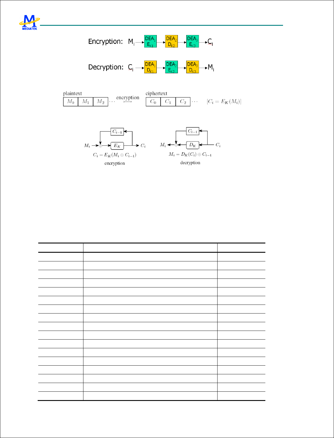
MTK Confidential Release for Konka
MTK Confidential Release for Konka
MT6228 GSM/GPRS Baseband Processor Data Sheet Revision 1.0
177/616 MediaTek Inc. Confidential
Figure 53 3DES Function
Figure 54 ECB Mode
Figure 55 CBC Mode
For the hash function, CHE supports both Message Digest 5 (MD5 in RFC 1321) and US Secure Hash Algorithm 1
(SHA-1 in RFC 3174). The hash function is a one-way function: a message is converted into a fixed-length string of
digits. MD5 is a 128-bit message digest, and SHA-1 is 160-bit. They are very similar functions such that resources
sharing can be applied in CHE.
A new Save and Resume feature is implemented in CHE. Because only one task can be applied on CHE at any given
time, unfinished jobs can be saved to the assigned memory addresses until the source data is ready again.
Register Definitions
Register Address Register Function Acronym
CHE + 0000h CHE start register CHE_START
CHE + 0004h CHE control register CHE_CON
CHE + 0008h CHE key0/key4/initial vector 0/source memory address CHE_IN0
CHE + 000ch CHE key1/key5/initial vector 1/destination memory address CHE_IN1
CHE + 0010h CHE key2/key6/initial vector 2/data length CHE_IN2
CHE + 0014h CHE key3/key7/initial vector 3/state memory address CHE_IN3
CHE + 0018h CHE slow down rate CHE_SDRAT
CHE + 001ch CHE pad count CHE_PCNT
CHE + 0020h CHE status CHE_STAT
CHE + 0024h CHE current destination address CHE_CDES
CHE + 0028h CHE interrupt status CHE_INTSTA
CHE + 002ch CHE interrupt enable CHE_INTEN
CHE + 00c0h CHE Secure Booting control CHE_BCON
CHE + 00c4h CHE Secure Booting source data CHE_BSRC
CHE + 00c8h CHE Secure Booting seed data CHE_BSEED
CHE + 00cch CHE Secure Booting encrypted data CHE_BENC
CHE + 00d0h CHE Secure Booting decrypted data CHE_BDEC

MTK Confidential Release for Konka
MTK Confidential Release for Konka
MT6228 GSM/GPRS Baseband Processor Data Sheet Revision 1.0
178/616 MediaTek Inc. Confidential
Table 31 CHE Registers
CHE+0000h CHE start register CHE_START
Bit 15 14 13 12 11 10 9 8 7 6 5 4 3 2 1 0
Name
UPK67
UPK45
UPK23
UPK01
UPIV2
3
UPIV0
1 RKEY WKEY
UPDE
S
CLEA
R RSTAT
WSTAT
LAST ST/UD
Type R/W R/W R/W R/W R/W R/W R/W R/W R/W R/W R/W R/W R/W R/W
Reset
0 0 0 0 0 0 0 0 0 0 0 0 0 0
Start register for CHE.
ST/UD This bit means Start (1) / !Update (0).
When the ST/UD bit is asserted, CHE enters NORMAL mode and performs the job pre-defined according to
the bit settings of LAST, WSTAT, RSTAT, UPDES, WKEY, RKEY and register CHE_CON. This bit must be
de-asserted after the current operation finished. Note: CHE only starts when the CHE_CON control
register ATYPE is 111 (Reserved); otherwise, CHE ends immediately and returns an error.
When ST/UD is de-asserted, CHE enters UPDATE mode. It depends on the UPIV01, UPIV23, UPK01,
UPK23, UPK45 and UPK67 to update the corresponding Initial Vectors (IV0~3) and cipher or decipher keys
0~7 in symmetric ciphering or deciphering mode. It’s suggested that writing 0x0000 into START immediately
before other operations.
LAST This bit indicates the last section for this process. If this bit is asserted, CHE finishes the current process and
resets to the initial state.
In ciphering mode, CHE outputs the last result (including padding process operation).
In deciphering mode, CHE outputs the last result and updates CHE_PCNT.
In hashing mode, CHE pads and outputs the digest.
WSTAT Write CHE states after this operation completed. CHE needs 120 bytes of space for each state to write to
address CHE_SADDR (CHE_IN3). The state can be read back by asserting RSTAT.
RSTAT Read states before the start of the operation. CHE reads 120 bytes back from address CHE_SADDR
(CHE_IN3). The states can be written beforehand by asserting WSTAT.
CLEAR Reset all states and return to the initial state. To perform a clear operation, write 0x0010 to CHE_START,
then write 0x0000 to CHE_START immediately (in the next instruction cycle) to return to the idle mode.
The clear operation has the highest priority of all. If this operation starts with RSTAT disabled, the
user is recommended to clear CHE. The user is highly recommended to clear CHE if this operation
starts without RSTAT enabled.
UPDES Force an update for CHE_DES (CHE_IN1). CHE automatically updates CHE_DES under two conditions
only: the first operation after a reset or a last operation. The user can force CHE to update the destination
address by asserting UPDES. When this bit is enabled, CHE does not update the destination address when
RSTAT is enabled.
WKEY Write key values into encrypted form. To encrypt the key after writing CHE_KEY0~ 7 (CHE_IN0~3), write
0x0041 to CHE_START. Wait for the OK state before writing 0x0000 to CHE_START to return to idle
mode. The keys are stored in encrypted form; the user cannot recover the plain text key, only restore the
encrypted key to CHE by asserting RKEY.
This operation needs 36 bytes of buffer space and uses SADDR as a target address. The WKEY process does
not affect the contents of the KEY registers in CHE. WKEY and RKEY override the NORMAL mode
operation for CHE; WKEY has higher priority than RKEY.
RKEY Restore the key values back to CHE. To retrieve a previously stored key (36 bytes), write 0x0081 to
CHE_START. Wait for the OK state before writing 0x0000 to CHE_START to return to the idle mode.
The keys can be stored by asserting WKEY.
UPIV01 Update CHE_IV0 from CHE_IN0 and CHE_IV1 from CHE_IN1 in UPDATE mode.
UPIV23 Update CHE_IV2 from CHE_IN2 and CHE_IV3 from CHE_IN3 in UPDATE mode.

MTK Confidential Release for Konka
MTK Confidential Release for Konka
MT6228 GSM/GPRS Baseband Processor Data Sheet Revision 1.0
179/616 MediaTek Inc. Confidential
UPK01 Update CHE_KEY0&1 from CHE_IN0 and CHE_IV1 in UPDATE mode.
UPK23 Update CHE_KEY2&3 from CHE_IN2 and CHE_IV3 in UPDATE mode.
UPK45 Update CHE_KEY4&5 from CHE_IN0 and CHE_IV1 in UPDATE mode.
UPK67 Update CHE_KEY6&7 from CHE_IN2 and CHE_IV3 in UPDATE mode.
CHE+0004h CHE control register CHE_CON
Bit
15 14
13
12
11 10 9 8 7 6 5 4 3 2 1 0
Name
SMOD
E
CIPH
ER ATYPE
Type R/W R/W R/W
Reset
0 0 000
Control register for CHE.
ATYPE Cipher Hash algorithm type: 000=MD5, 001=SHA-1, 010=DES, 011=3-DES, 100=AES-128, 101=AES-192,
110=AES-256. 111=Reserved.
CIPHER 0=Decipher mode, 1=Cipher mode.
SMODE 0=ECB mode, 1=CBC mode. For CBC mode, load the initialization vectors (IV) beforehand.
CHE+0008h CHE key0/key4/initial vector 0/source address CHE_IN0
Bit 31 30 29 28 27 26 25 24 23 22 21 20 19 18 17 16
Name
IN0[31:16]
Type R/W
Reset
0
Bit 15 14 13 12 11 10 9 8 7 6 5 4 3 2 1 0
Name
IN0[15:0]
Type R/W
Reset
0
IN0 Temporary buffer to load the CHE internal registers: KEY0, KEY4, IV0 and SRC. Which registers are loaded
depends on CHE_START: in UPDATE mode, KEY0, KEY4, IV0 are loaded; in NORMAL mode, SRC is
loaded.
KEY0 When CHE is in UPDATE mode and the UPK01 bit is enabled, the content of IN0 is copied into the internal
KEY0 registers. CHE stores 8 KEYs, KEY0~KEY7. Different algorithms use different KEYs. AES-128:
[0,1,2,3]; AES-192: [0,1,2,3,4,5]; AES-256: [0,1,2,3,4,5,6,7]; DES: [0,1]; 3-DES encryption:
[0,1][2,3][4,5]; and 3-DES decryption: [4,5][2,3][0,1].
KEY4 When CHE is in UPDATE mode and UPK45 is enabled, the content of IN0 is copied into the internal KEY4
registers.
IV0 When CHE is in UPDATE mode and UPIV01 is enabled, the content of IN0 is copied into the internal IV0
registers. DES/3DES uses a 64-bit initial vector [IV0,IV1] in CBC mode. AES uses a 128-bit initial vector
[IV0,IV1,IV2,IV3] in CBC mode.
SRC When CHE is in NORMAL mode, the content of IN0 is copied into internal SRC registers. SRC is the source
address for CHE operation.
CHE+000ch CHE key1/key5/initial vector 1/destination address CHE_IN1
Bit 31 30 29 28 27 26 25 24 23 22 21 20 19 18 17 16
Name
IN1[31:16]
Type R/W
Reset
0
Bit 15 14 13 12 11 10 9 8 7 6 5 4 3 2 1 0
Name
IN1[15:0]
Type R/W
Reset
0
MTK Confidential Release for Konka
MTK Confidential Release for Konka
MT6228 GSM/GPRS Baseband Processor Data Sheet Revision 1.0
180/616 MediaTek Inc. Confidential
IN1 Temporary buffer to load the CHE internal registers: KEY1, KEY5, IV1 and DES. Which registers are loaded
depends on CHE_START: in UPDATE mode, KEY1, KEY5, IV1 are loaded; in NORMAL mode, DES is
loaded.
KEY1 When CHE is in UPDATE mode and UPK01 is enabled, the content of IN1 is copied into the internal KEY1
registers.
KEY5 When CHE is in UPDATE mode and UPK45 is enabled, the content of IN1 is copied into the internal KEY5
registers.
IV1 When CHE is in UPDATE mode and UPIV01 is enabled, the content of IN1 is copied into the internal IV1
registers.
DES When CHE is in NORMAL mode, the content of IN1 is copied into internal DES if UPDES is asserted or if this
operation immediately follows a reset or a last operation. DES is the destination address for a CHE operation.
Info: About the destination buffer length:
In ciphering mode, the destination buffer length must be larger than the source data length.
len_des
cipher
= len_src
cipher
+ BLOCK_SIZE – (len_src
cipher
% BLOCK_SIZE)
In deciphering mode, the destination data length is the same as the source data length, a multiple of
BLOCK_SIZE.
In hash mode, the destination buffer length is 16 bytes in MD5 mode and 20 bytes in SHA-1 mode.
BLOCK_SIZE is 8 bytes in DES (3-DES) mode and 16 bytes in AES mode.
CHE+0010h CHE key2/key6/initial vector 2/operation length CHE_IN2
Bit 31 30 29 28 27 26 25 24 23 22 21 20 19 18 17 16
Name
IN2[31:16]
Type R/W
Reset
0
Bit 15 14 13 12 11 10 9 8 7 6 5 4 3 2 1 0
Name
IN2[15:0]
Type R/W
Reset
0
IN2 Temporary buffer to load the CHE internal registers: KEY2, KEY6, IV2 and LEN. Which registers are loaded
in depends on CHE_START: in UPDATE mode, KEY2, KEY6, IV2 are loaded; in NORMAL move, LEN is
loaded.
KEY2 When CHE is in UPDATE mode and UPK23 is enabled, the content of IN2 is copied into the internal KEY2
registers.
KEY6 When CHE is in UPDATE mode and UPK67 is enabled, the content of IN2 is copied into the internal KEY6
registers.
IV2 When CHE is in UPDATE mode and UPIV23 is enabled, the content of IN2 is copied into the internal IV2
registers.
LEN When CHE is in NORMAL mode, the content of IN2 is copied into the internal LEN registers. LEN is the
length for the CHE operation. A zero length is allowed only in a last operation (LAST asserted); avoid using a
zero length if possible. If a zero-length setting is unavoidable, clear the CHE after this operation. If a zero
length is used in ciphering mode, the corresponding padded cipher text would be output. In deciphering mode,
CHE resets. Both of them are regardless of previous ciphering or deciphering operations.
In hash mode, if there are previous hash operations, CHE resets. Otherwise, the digest of zero length is output.
I.e., MD5 outputs “d41d8cd98f00b204e9800998ecf8427e” and SHA1 outputs
“da39a3ee5e6b4b0d3255bfef95601890afd80709".
MTK Confidential Release for Konka
MTK Confidential Release for Konka
MT6228 GSM/GPRS Baseband Processor Data Sheet Revision 1.0
181/616 MediaTek Inc. Confidential
CHE+0014h CHE key3/key7/initial vector 3/state address CHE_IN3
Bit 31 30 29 28 27 26 25 24 23 22 21 20 19 18 17 16
Name
IN3[31:16]
Type R/W
Reset
0
Bit 15 14 13 12 11 10 9 8 7 6 5 4 3 2 1 0
Name
IN3[15:0]
Type R/W
Reset
0
IN3 Temporary buffer to load the CHE internal registers: KEY3, KEY7, IV3 and SADDR. Which registers are
loaded depends on CHE_START: in UPDATE mode, KEY3, KEY7, IV3 are loaded; in NORMAL mode,
SADDR is loaded.
KEY3 When CHE is in UPDATE mode and UPK23 is enabled, the content of IN3 is copied into internal KEY3
registers.
KEY7 When CHE is in UPDATE mode and UPK67 is enabled, the content of IN3 is copied into internal KEY7
registers.
IV3 When CHE is in UPDATE mode and UPIV23 is enabled, the content of IN3 is copied into internal IV3
registers.
SADDR When CHE is in NORMAL mode, the content of IN3 is copied into the internal SADDR registers.
SADDR is the state/KEY address for the CHE operation. If RSTAT or WSTAT is asserted, CHE treats SADDR
as a state address, and reads or writes 120 bytes from or to this address. If RKEY or WKEY is asserted, CHE
reads or stores 36-byte KEYs from or to SADDR. Note: SADDR must 4-byte aligned.
CHE+0018h CHE slow down rate CHE_SDRAT
Bit 15 14 13 12 11 10 9 8 7 6 5 4 3 2 1 0
Name
SDRAT
Type R/W
Reset
0
SDRAT Slow down CHE to prevent too many requests for AHB resources. Each unit increment translates into a
4-cycle delay for each bus access (read or write). The range of SDRAT is from 0 (no delay) to 255
(255*4=1020 cycles’ delay).
CHE+001ch CHE pad count CHE_PCNT
Bit 15 14 13 12 11 10 9 8 7 6 5 4 3 2 1 0
Name
PCNT
Type RO
Reset
0
PCNT When performing symmetric deciphering, this register indicates the padding length.
CHE+0020h CHE return status CHE_STAT
Bit 15 14 13 12 11 10 9 8 7 6 5 4 3 2 1 0
Name
STAT
Type RO
Reset
0
STAT STAT represents the current state of CHE. 000b: OK. 001b: control field setting error. 010b: zero length
for a non-last operation, or a last operation that is not hash nor ciphering (a last operation that is deciphering).
011b: resume state, wait for the next last or non-last operation. 100b: BUSY. 101b: RKEY and WKEY at the
same time.
CHE+0024h CHE current destination address CHE_CDES
Bit 31 30 29 28 27 26 25 24 23 22 21 20 19 18 17 16
Name
CDES[31:16]
MTK Confidential Release for Konka
MTK Confidential Release for Konka
MT6228 GSM/GPRS Baseband Processor Data Sheet Revision 1.0
182/616 MediaTek Inc. Confidential
Type
RO
Reset
0
Bit 15 14 13 12 11 10 9 8 7 6 5 4 3 2 1 0
Name
CDES[15:0]
Type RO
Reset
0
CDES CDES is the current destination address in CHE.
CHE+0028h CHE interrupt status CHE_INTSTA
Bit 15 14 13 12 11 10 9 8 7 6 5 4 3 2 1 0
Name
INTSTA
Type RC
Reset
0
INTSTA Interrupt status. Bit 0 indicates CHE finished in the OK or RESUME state. Bit 1 indicates CHE
returned a failure. Further information can be obtained from CHE_STAT.
CHE+002ch CHE interrupt enable CHE_INTEN
Bit 15 14 13 12 11 10 9 8 7 6 5 4 3 2 1 0
Name
INTEN
Type R/W
Reset
0
INTEN Interrupt enable control register. When bit 0 is enabled, an interrupt occurs when CHE finishes in the OK or
RESUME state. If bit 1 is enabled, CHE interrupts if an error occurs.
CHE+00c0h CHE Secure Booting control CHE_BCON
Bit 15 14 13 12 11 10 9 8 7 6 5 4 3 2 1 0
Name
PAR3
PAR2
PAR1
DIS
Type R/W R/W R/W R/W
Reset
0 0 0 0
DIS Disable Secure Booting function. When DIS is asserted, the data read from CHE_BENC and CHE_BDEC is
the same as CHE_BSRC.
PAR1 Use inner information parameter 1 (SK) to strengthen security.
PAR2 Use inner information parameter 2 (RS) to strengthen security.
PAR3 Use inner information parameter 3 (MR) to strengthen security.
CHE+00c4h CHE Secure Booting source data CHE_BSRC
Bit 31 30 29 28 27 26 25 24 23 22 21 20 19 18 17 16
Name
BSRC[31:16]
Type WO
Reset
0
Bit 15 14 13 12 11 10 9 8 7 6 5 4 3 2 1 0
Name
BSRC[15:0]
Type WO
Reset
0
BSRC Source data for Secure Booting to be encrypted (obtained from CHE_BENC) or decrypted (obtained from
CHE_BDEC).
CHE+00c8h CHE Secure Booting seed value CHE_BSEED
Bit 31 30 29 28 27 26 25 24 23 22 21 20 19 18 17 16
Name
BSEED[31:16]
Type WO
Reset
0
Bit 15 14 13 12 11 10 9 8 7 6 5 4 3 2 1 0
Name
BSEED[15:0]
Type WO
Reset
0
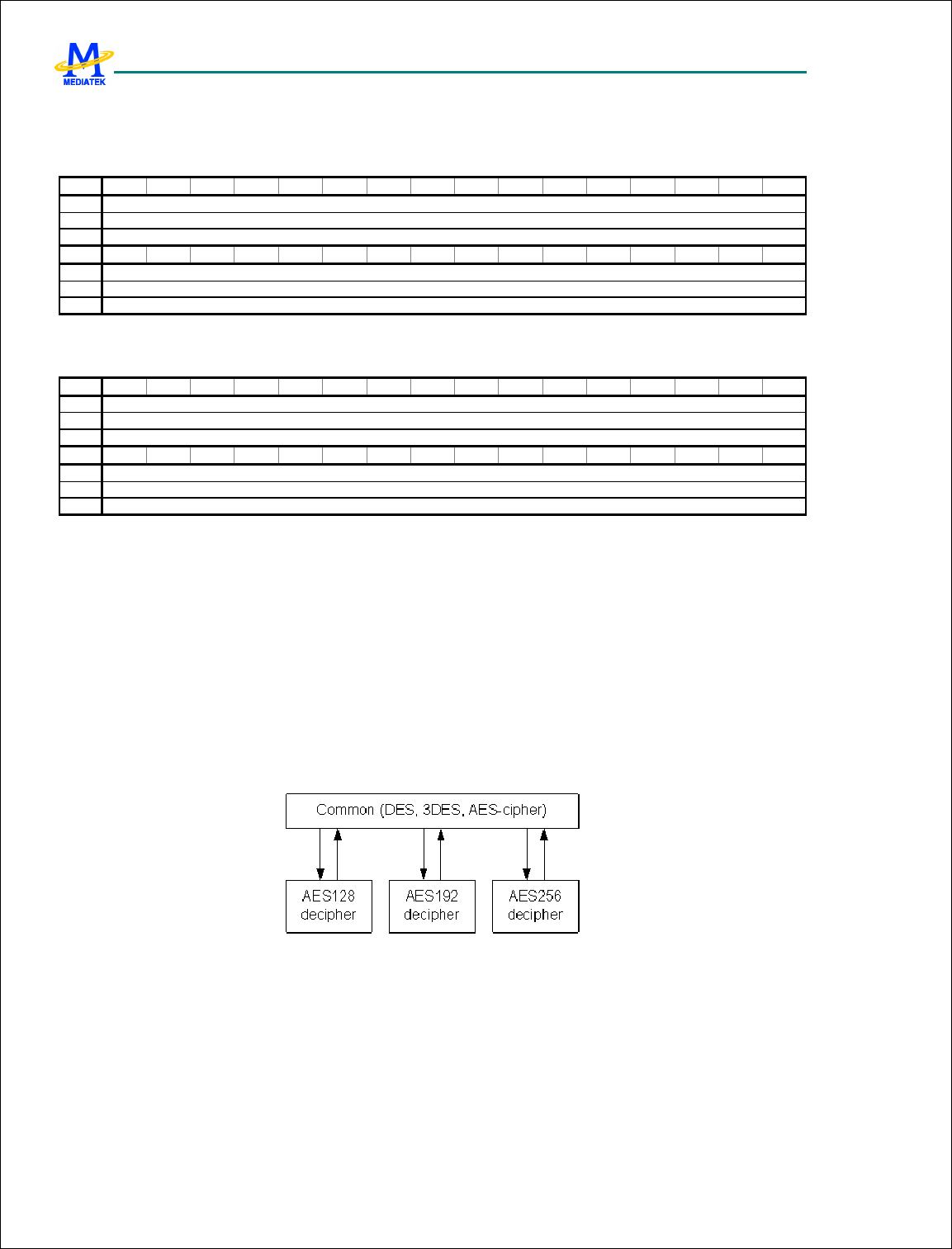
MTK Confidential Release for Konka
MTK Confidential Release for Konka
MT6228 GSM/GPRS Baseband Processor Data Sheet Revision 1.0
183/616 MediaTek Inc. Confidential
BSEED Seed data needed to increase security of the Boot Secure function. Set the seed value before performing
Boot Secure the first time.
CHE+00cch CHE Secure Booting encrypted data CHE_BENC
Bit 31 30 29 28 27 26 25 24 23 22 21 20 19 18 17 16
Name
BENC[31:16]
Type RO
Reset
0
Bit 15 14 13 12 11 10 9 8 7 6 5 4 3 2 1 0
Name
BENC[15:0]
Type RO
Reset
0
BENC Encrypted data from CHE_BSRC.
CHE+00d0h CHE Secure Booting decrypted data CHE_BDEC
Bit 31 30 29 28 27 26 25 24 23 22 21 20 19 18 17 16
Name
BDEC[31:16]
Type RO
Reset
0
Bit 15 14 13 12 11 10 9 8 7 6 5 4 3 2 1 0
Name
BDEC[15:0]
Type
RO
Reset
0
BDEC Decrypted data from CHE_BSRC.
4.12.2 CHE KEY Phase Transient
In CHE, all cipher and decipher functions need a KEY, i.e., AES, DES, 3DES. However, due to the cost and
performance concern, all the keys are put together in a KEY buffer with four phases (Figure 56).
1. Phase 1: AES128 decipher phase.
2. Phase 2: AES192 decipher phase
3. Phase 3: AES256 decipher phase.
4. Phase 4: Common phase, other functions which exclude the AES decipher. I.e., DES (cipher and decipher),
3DES (cipher and decipher), AES128, AES192, AES256 cipher.
Figure 56 Key Phase Transient GraphPhases 1 through 3 are internal phases, unknown to the user. When the user
first enters the key data, the key phase is reset to the Common Phase. Transition among phases is limited to the
arrows shown in Figure 56. For example, if currently performing a 3DES cipher function, any cipher or decipher
function may follow. If currently using a AES192 decipher function, only the AES192 decipher function or the
Common Phase algorithms may be used next; otherwise an error occurs.
For security reasons and convenience, the key phase can be saved with key contents by WKEY or WSTAT. The user
is highly recommended to convert raw key data into CKEY data format (using WKEY), discard the original key data,
and to use CKEY by RKEY.

MTK Confidential Release for Konka
MTK Confidential Release for Konka
MT6228 GSM/GPRS Baseband Processor Data Sheet Revision 1.0
184/616 MediaTek Inc. Confidential
4.12.3 Secure Booting Procedure
Secure Booting is a feature of CHE that protects the program contents on flash memory from modification, skip or hard
copy. With a secure process and a unique chip ID (UID), CHE can encrypt or decrypt a segment of instruction data in
order.
Encryption procedure:
1. Activate the eFuse module.
2. Write the seed value into BSEED. The seed value can be any 32-bit value. The same seed value is
necessary in the decryption procedure.
3. Write the control value into BCON.
4. Write source data (instruction) into BSRC and read the cipher text from BENC.
5. Repeat step 4 until all instructions are encrypted.
Decryption procedure:
1. Activate the eFuse module.
2. Write the seed value into BSEED. The seed value must be the same one used in the encryption procedure.
3. Write the control value into BCON. The control value must be the same one used in the encryption
procedure.
4. Write the source data (instruction) into BSRC and read the plain text from BDEC.
5. Repeat step 4 until all instructions are decrypted.
Notes:
1. A bit length equal or less than 32 bits is acceptable for Secure Boot. E.g.: a 16-bit data 0x1234 is treated as
0x12340000 32-bit data and decrypted in the same manner.
2. For security reasons, access times to be encrypted or decrypted should not be the multiples of 4.
3. The internal states of Secure Booting function change under the following conditions, such that redundant
register access is forbidden.
Write data into BSRC
Write data into BSEED
Read data from BENC or BDEC
As an example of the encryption and decryption of 16-bit data, consider the value 0xabcd:
Encryption:
1. The data is padded with zeros to obtain a 32-bit value: 0xabcd0000.
2. The encryption operation produces a value 0x12345678.
Decryption:
1. Only the most significant 16 bits 0x1234000 are considered and decrypted as 0xabcd7893.
2. The first 16 bits 0xabcd are retained, and 0x00007893 is ignored.

MTK Confidential Release for Konka
MTK Confidential Release for Konka
MT6228 GSM/GPRS Baseband Processor Data Sheet Revision 1.0
185/616 MediaTek Inc. Confidential
5 Microcontroller Coprocessors
Microcontroller Coprocessors are designed to run computing-intensive processes in place of the Microcontroller
(MCU). These coprocessors especially target timing critical GSM/GPRS Modem processes that require fast response
and large data movement. Controls to the coprocessors are all through memory access via the APB.
5.1 Divider
To ease the processing load of the MCU, a divider is employed. The divider can perform signed and unsigned
32bit/32bit division, as well as modulus. The processing time of the divider is from 1 clock cycle to 33 clock cycles,
depending on the magnitude of the dividend. Detailed processing times are listed below in Table 32. Table 32
shows two processing times (except for when the dividend is zero) for each range of dividends, depending on whether
or not restoration is required during the last step of the division operation.
Table 32 Processing Time for Different Dividend Values
Signed Division Unsigned Division
Dividend Clock Cycles Dividend Clock Cycles
0000_0000h 1 0000_0000h 1
0000_00ffh –
(-0000_0100h), excluding
0x0000_0000
8 or 9 0000_0001h - 0000_00ffh 8 or 9
0000_ffffh – (-0001_0000h)
16 or 17 0000_0100h - 0000_ffffh 16 or 17
00ff_ffffh – (-0100_0000h)
24 or 25 0001_0000h - 00ff_ffffh 24 or 25
7fff_ffffh – (-8000_0000h)
32 or 33 0100_0000h - ffff_ffffh 32 or 33
Table 33 Processing Time for Different Dividend Values
When the divider is started by setting the Divider Control Register START bit to 1, DIV_RDY becomes 0; this bit is
asserted when the division process is complete. MCU detects this status bit by polling it to know the correct access
timing. To simplify polling, only the value of register DIV_RDY is visible while Divider Control Register is being
read. Hence, MCU does not need to mask other bits to extract the value of DIV_RDY.
In a GSM/GPRS system, many divisions are executed with constant divisors. Therefore, oft-used constants are stored
in the divider to speed up the process. By controlling control bits IS_CNST and CNST_IDX in Divider Control
register, a division can be performed without providing a divisor. This omission of a step saves on the time for writing
a divisor in and on the instruction fetch time, thus making the process more efficient.
5.1.1 Register Definitions
DIVIDER+000
0h Divider Control Register DIV_CON
Bit 31 30 29 28 27 26 25 24 23 22 21 20 19 18 17 16
Name
CNST_IDX
Type WO
Reset
0
Bit 15 14 13 12 11 10 9 8 7 6 5 4 3 2 1 0
Name
IN_CNS
T SIGN
DIV_RD
Y
STAR
T

MTK Confidential Release for Konka
MTK Confidential Release for Konka
MT6228 GSM/GPRS Baseband Processor Data Sheet Revision 1.0
186/616 MediaTek Inc. Confidential
Type
WO
WO
RO
WO
Reset
0 1 1 0
START Starts a division operation. Returns to 0 after the division has started.
DIV_RDY Current status of the divider. Note that when DIV_CON register is read, only the value of DIV_RDY
appears; the program does not need to mask other parts of the register to extract the information in
DIV_RDY.
0 Division is in progress.
1 Division is finished
SIGN Indicates a signed or unsigned division operation.
0 Unsigned division
1 Signed division
IS_CNST Specifies that an internal constant value should be used as a divisor. If IS_CNST is enabled, the divisor
value need not be written, and divider automatically uses the internal constant value instead. The
internal constant value used depends on the value of CNST_IDX.
0 Normal division. Divisor is written in via APB.
1 Using internal constant divisor instead.
CNST_IDX Index of constant divisor.
0 divisor = 13
1 divisor = 26
2 divisor = 51
3 divisor = 52
4 divisor = 102
5 divisor = 104
DIVIDER
+0004h Divider Dividend register DIV_DIVIDEND
Bit 31 30 29 28 27 26 25 24 23 22 21 20 19 18 17 16
Name
DIVIDEND[31:16]
Type WO
Reset
0
Bit 15 14 13 12 11 10 9 8 7 6 5 4 3 2 1 0
Name
DIVIDEND[15:0]
Type WO
Reset
0
Dividend.
DIVIDER
+0008h Divider Divisor register DIV_DIVISOR
Bit 31 30 29 28 27 26 25 24 23 22 21 20 19 18 17 16
Name
DIVISOR[31:16]
Type WO
Reset
0
Bit 15 14 13 12 11 10 9 8 7 6 5 4 3 2 1 0
Name
DIVISOR[15:0]
Type WO
Reset
0
Divisor.
MTK Confidential Release for Konka
MTK Confidential Release for Konka
MT6228 GSM/GPRS Baseband Processor Data Sheet Revision 1.0
187/616 MediaTek Inc. Confidential
DIVIDER
+000Ch Divider Quotient register DIV_QUOTIENT
Bit 31 30 29 28 27 26 25 24 23 22 21 20 19 18 17 16
Name
QUOTIENT[31:16]
Type RO
Reset
0
Bit 15 14 13 12 11 10 9 8 7 6 5 4 3 2 1 0
Name
QUOTIENT[15:0]
Type RO
Reset
0
Quotient.
DIVIDER
+0010h Divider Remainder register DIV_REMAINDE
R
Bit 31 30 29 28 27 26 25 24 23 22 21 20 19 18 17 16
Name
REMAINDER[31:16]
Type RO
Reset
0
Bit 15 14 13 12 11 10 9 8 7 6 5 4 3 2 1 0
Name
REMAINDER[15:0]
Type RO
Reset
0
Remainder.
5.2 CSD Accelerator
5.2.1 General Description
This unit performs the data format conversion of RA0, RA1, and FAX in CSD service. CSD service consists of two
major functions: data flow throttling and data format conversion. The data format conversion is a bit-wise operation
and requires several instructions to complete a conversion, thus making it inefficient for the MCU to perform itself. A
coprocessor, CSD accelerator, is designed to reduce the computing power needed to perform this function.
The CSD accelerator helps in converting data format only; the data flow throttling function is still implemented by the
MCU. CSD accelerator performs three types of data format conversion: RA0, RA1, and FAX.
For RA0 conversion, too many case scenarios for the downlink path conversion greatly increase the hardware area cost,
thus only uplink RA0 data format conversion is provided. Uplink RA0 conversion consists of inserting a start bit
before and a stop bit after each a byte, for a duration of 16 bytes. illustrates the detailed conversion table.
MTK Confidential Release for Konka
MTK Confidential Release for Konka
MT6228 GSM/GPRS Baseband Processor Data Sheet Revision 1.0
188/616 MediaTek Inc. Confidential
Figure 57 Data Format Conversion of RA0
The RA0 converter processes data state by state. Therefore, before filling in new data, software must ensure that
converted data of in a state is withdrawn, otherwise the converted data is replaced by new data. For example, if 32
bits of data are written, the state pointer increments from state 0 to state 1, and word ready of state 0 is asserted.
Before writing the next 32-bit data, the word of state 0 must be withdrawn first, or the data is lost when the next
conversion is performed.
RA0 records the number of written bytes, the state pointer, and a ready state word. This information helps the
software to perform flow control. See Register Definition for more detail.
For RA1 conversion, both downlink and uplink directions are supported. The data formats vary for different data rate.
Detailed conversion tables are shown in and . The yellow part is the payload data, and the blue part is the status bit.
Figure 58 Data Format Conversion for 6k/12k RA1
MTK Confidential Release for Konka
MTK Confidential Release for Konka
MT6228 GSM/GPRS Baseband Processor Data Sheet Revision 1.0
189/616 MediaTek Inc. Confidential
Figure 59 Data Format Conversion for 3.6k RA1
For FAX, two types of bit-reversal functions are provided. Type 1 reversal is a bit-wise reversal (), and Type 2 is a
byte-wise reversal ().
Figure 60 Type 1 Bit Reversal
Figure 61 Type 2 Bit Reversal
Register Address Register Function Acronym
CSD + 0000h CSD RA0 Control Register CSD_RA0_CON
CSD + 0004h CSD RA0 Status Register CSD_RA0_STA
CSD + 0008h CSD RA0 Input Data Register CSD_RA0_DI
CSD + 000Ch CSD RA0 Output Data Register CSD_RA0_DO
CSD + 0100h CSD RA1 6K/12K Uplink Input Data Register 0 CSD_RA1_6_12K_ULDI0
CSD + 0104h CSD RA1 6K/12K Uplink Input Data Register 1 CSD_RA1_6_12K_ULDI1
CSD + 0108h CSD RA1 6K/12K Uplink Status Data Register CSD_RA1_6_12K_ULSTUS
CSD + 010Ch CSD RA1 6K/12K Uplink Output Data Register 0 CSD_RA1_6_12K_ULDO0

MTK Confidential Release for Konka
MTK Confidential Release for Konka
MT6228 GSM/GPRS Baseband Processor Data Sheet Revision 1.0
190/616 MediaTek Inc. Confidential
CSD + 0110h CSD RA1 6K/12K Uplink Output Data Register 1 CSD_RA1_6_12K_ULDO1
CSD + 0200h CSD RA1 6K/12K Downlink Input Data Register 0 CSD_RA1_6_12K_DLDI0
CSD + 0204h CSD RA1 6K/12K Downlink Input Data Register 1 CSD_RA1_6_12K_DLDI1
CSD + 0208h CSD RA1 6K/12K Downlink Output Data Register 0 CSD_RA1_6_12K_DLDO0
CSD + 020Ch CSD RA1 6K/12K Downlink Output Data Register 1 CSD_RA1_6_12K_DLDO1
CSD + 0210h CSD RA1 6K/12K Downlink Status Data Register CSD_RA1_6_12K_DLSTUS
CSD + 0300h CSD RA13.6K Uplink Input Data Register 0 CSD_RA1_3P6K_ULDI0
CSD + 0304h CSD RA13.6K Uplink Status Data Register CSD_RA1_3P6K_ULSTUS
CSD + 0308h CSD RA13.6K Uplink Output Data Register 0 CSD_RA1_3P6K_ULDO0
CSD + 030Ch CSD RA13.6K Uplink Output Data Register 1 CSD_RA1_3P6K_ULDO1
CSD + 0400h CSD RA1 3.6K Downlink Input Data Register 0 CSD_RA1_3P6K_DLDI0
CSD + 0404h CSD RA1 3.6K Downlink Input Data Register 1 CSD_RA1_3P6K_DLDI1
CSD + 0408h CSD RA1 3.6K Downlink Output Data Register 0 CSD_RA1_3P6K_DLDO0
CSD + 040Ch CSD RA1 3.6K Downlink Status Data Register CSD_RA1_3P6K_DLSTUS
CSD + 0500h CSD FAX Bit Reverse Type 1 Input Data Register CSD_FAX_BR1_DI
CSD + 0504h CSD FAX Bit Reverse Type 1 Output Data Register CSD_FAX_BR1_DO
CSD + 0510h CSD FAX Bit Reverse Type 2 Input Data Register CSD_FAX_BR2_DI
CSD + 0514h CSD FAX Bit Reverse Type 2 Output Data Register CSD_FAX_BR2_DO
Table 34 CSD Accelerator Registers
5.2.2 Register Definitions
CSD+0000h CSD RA0 Control Register CSD_RA0_CON
Bit 31 30 29 28 27 26 25 24 23 22 21 20 19 18 17 16
Name
Type
Reset
Bit
15 14
13
12
11 10 9 8 7 6 5 4 3 2 1 0
Name
RST BTS0 VLD_BYTE
Type WO WO WO
Reset
0 0 100
VLD_BYTE Specifies the number of valid bytes in the current input data. This value must be specified before filling
data.
BTS0 Back to state 0. Forces RA0 converter return back to state 0. Incomplete words are padded with stop bits.
For example, consider a back-to-state0 command that is issued after 8 bytes of data are filled in. All bits
after the 8
th
byte are padded with stop bits, and the second ready word byte RDYWD2 is asserted (Figure 62).
After removing state word 2, the state pointer goes back to state 0. Note that new data filling should take
place after removing state word 2, or the state pointer may be out of order.
MTK Confidential Release for Konka
MTK Confidential Release for Konka
MT6228 GSM/GPRS Baseband Processor Data Sheet Revision 1.0
191/616 MediaTek Inc. Confidential
Figure 62 Example of Back to State 0
RST Resets the RA0 converter. If an erroneous operation disorders the data, this bit restores all states to their
original state.
CSD+0004h CSD RA0 Status Register CSD_RA0_STA
Bit 31 30 29 28 27 26 25 24 23 22 21 20 19 18 17 16
Name
Type
Reset
Bit 15 14 13 12 11 10 9 8 7 6 5 4 3 2 1 0
Name
BYTECNT CRTSTA RDYWD
Type RO RO RC
Reset
0 0 0
RDYWD0~4 Ready words. Indicates which state words are ready for withdrawal. If any bits asserted, data
must be withdrawn before new data is filled into CSD_RA0_DI, to avoid data loss.
0 Not ready
1 Ready
CRTSTA Current state. State0 ~ State4. Indicates which state word software is currently filling.
BYTECNT Total number of bytes being filled.
CSD+0008h CSD RA0 Input Data Register CSD_RA0_DI
Bit 31 30 29 28 27 26 25 24 23 22 21 20 19 18 17 16
Name
DIN
Type WO
Reset
0
Bit
15 14
13
12
11 10 9 8 7 6 5 4 3 2 1 0
Name
DIN
Type WO
Reset
0
DIN The RA0 conversion input data. The ready word indicator is checked before filling in data; if any words are
ready, they are withdrawn first, otherwise the ready data in RA0 converter is replaced.
CSD+000Ch CSD RA0 Output Data Register CSD_RA0_DO
Bit 31 30 29 28 27 26 25 24 23 22 21 20 19 18 17 16
Name
DOUT
Type RO
Reset
0
Bit 15 14 13 12 11 10 9 8 7 6 5 4 3 2 1 0
Name
DOUT
Type RO
MTK Confidential Release for Konka
MTK Confidential Release for Konka
MT6228 GSM/GPRS Baseband Processor Data Sheet Revision 1.0
192/616 MediaTek Inc. Confidential
Reset
0
DOUT RA0 converted data. The return data corresponds to the ready word indicator defined in CSD_RA0_STA
register. The five bits of RDYWD map to state0 ~ state 4 respectively. When CSD_RA0_DO is read, the
asserted state word is returned. If two state words asserted at the same time, the lower one is returned.
CSD+0100h CSD RA1 6K/12K Uplink Input Data Register 0 CSD_RA1_6_12
K_ULDI0
Bit 31 30 29 28 27 26 25 24 23 22 21 20 19 18 17 16
Name
DIN
Type WO
Reset
0
Bit 15 14 13 12 11 10 9 8 7 6 5 4 3 2 1 0
Name
DIN
Type WO
Reset
0
DIN D1 to D32 of the RA1 uplink data.
CSD+0104h CSD RA1 6K/12K Uplink Input Data Register 1 CSD_RA1_6_12
K_ULDI1
Bit 31 30 29 28 27 26 25 24 23 22 21 20 19 18 17 16
Name
Type
Reset
Bit 15 14 13 12 11 10 9 8 7 6 5 4 3 2 1 0
Name
DIN
Type WO
Reset
0
DIN D33 to D48 of the RA1 uplink data.
CSD+0108h CSD RA1 6K/12K Uplink Status Data Register CSD_RA1_6_12
K_ULSTUS
Bit
31 30
29
28
27 26 25
24
23
22 21 20
19
18
17 16
Name
Type
Reset
Bit 15 14 13 12 11 10 9 8 7 6 5 4 3 2 1 0
Name
E7 E6 E5 E4 X SB SA
Type WO WO WO WO WO WO WO
Reset
0 0 0 0 0 0 0
SA Represents S1, S3, S6, and S8 of the status bits.
SB Represents S4 and S9 of the status bits.
X Represents X of the status bits.
E4 Represents E4 of the status bits.
E5 Represents E5 of the status bits.
E6 Represents E6 of the status bits.
E7 Represents E7 of the status bits.
CSD+010Ch CSD RA1 6K/12K Uplink Output Data Register 0 CSD_RA1_6_12
K_ULDO0
Bit 31 30 29 28 27 26 25 24 23 22 21 20 19 18 17 16
Name
DOUT

MTK Confidential Release for Konka
MTK Confidential Release for Konka
MT6228 GSM/GPRS Baseband Processor Data Sheet Revision 1.0
193/616 MediaTek Inc. Confidential
Type
RO
Reset
0
Bit 15 14 13 12 11 10 9 8 7 6 5 4 3 2 1 0
Name
DOU
Type RO
Reset
0
DOUT Bit 0 to bit 31 of the RA1 6K/12K uplink frame.
CSD+0110h CSD RA1 6K/12K Uplink Output Data Register 1 CSD_RA1_6_12
K_ULDO1
Bit 31 30 29 28 27 26 25 24 23 22 21 20 19 18 17 16
Name
DOUT
Type RO
Reset
0
Bit 15 14 13 12 11 10 9 8 7 6 5 4 3 2 1 0
Name
DOUT
Type RO
Reset
0
DOUT Bit 32 to bit 59 of the RA1 6K/12K uplink frame.
CSD+0200h CSD RA1 6K/12K Downlink Input Data Register 0 CSD_RA1_6_12
K_DLDI0
Bit 31 30 29 28 27 26 25 24 23 22 21 20 19 18 17 16
Name
DIN
Type WO
Reset
0
Bit 15 14 13 12 11 10 9 8 7 6 5 4 3 2 1 0
Name
DIN
Type WO
Reset
0
DIN Bit 0 to bit 31 of the RA1 6K/12K downlink frame.
CSD+0204h CSD RA1 6K/12K Downlink Input Data Register 1 CSD_RA1_6_12
K_DLDI1
Bit 31 30 29 28 27 26 25 24 23 22 21 20 19 18 17 16
Name
DIN
Type WO
Reset
0
Bit 15 14 13 12 11 10 9 8 7 6 5 4 3 2 1 0
Name
DIN
Type WO
Reset
0
DIN Bit 32 to bit 59 of the RA1 6K/12K downlink frame.
CSD+0208h CSD RA1 6K/12K Downlink Output Data Register 0 CSD_RA1_6_12
K_DLDO0
Bit 31 30 29 28 27 26 25 24 23 22 21 20 19 18 17 16
Name
DOUT
Type RO
Reset
0
Bit 15 14 13 12 11 10 9 8 7 6 5 4 3 2 1 0
Name
DOUT
Type RO
Reset
0
MTK Confidential Release for Konka
MTK Confidential Release for Konka
MT6228 GSM/GPRS Baseband Processor Data Sheet Revision 1.0
194/616 MediaTek Inc. Confidential
DOUT D1 to D32 of the RA1 downlink data.
CSD+020Ch CSD RA1 6K/12K Downlink Output Data Register 1 CSD_RA1_6_12
K_DLDO1
Bit 31 30 29 28 27 26 25 24 23 22 21 20 19 18 17 16
Name
Type
Reset
Bit 15 14 13 12 11 10 9 8 7 6 5 4 3 2 1 0
Name
DOUT
Type RO
Reset
0
DOUT D33 to D48 of the RA1 downlink data.
CSD+0210h CSD RA1 6K/12K Downlink Status Data Register CSD_RA1_6_12
K_DLSTUS
Bit 31 30 29 28 27 26 25 24 23 22 21 20 19 18 17 16
Name
Type
Reset
Bit 15 14 13 12 11 10 9 8 7 6 5 4 3 2 1 0
Name
E7 E6 E5 E4 X SB SA
Type RO RO RO RO RO RO RO
Reset
0 0 0 0 0 0 0
SA The majority vote of the S1, S3, S6 and S8 status bits. If the vote is split, SA=0.
SB The majority vote of the S4 and S9 status bits. If the vote is split, SB=0.
X The majority vote of the two X bits in downlink frame. If the vote is split, X=0.
E4 Represents E4 of the status bits.
E5 Represents E5 of the status bits.
E6 Represents E6 of the status bits.
E7 Represents E7 of the status bits.
CSD+0300h CSD RA1 3.6K Uplink Input Data Register 0 CSD_RA1_3P6
K_ULDI0
Bit 31 30 29 28 27 26 25 24 23 22 21 20 19 18 17 16
Name
DIN
Type WO
Reset
0
Bit 15 14 13 12 11 10 9 8 7 6 5 4 3 2 1 0
Name
DIN
Type WO
Reset
0
DIN D1 to D24 of the RA1 3.6K uplink data.
CSD+0304h CSD RA1 3.6K Uplink Status Data Register CSD_RA1_3P6
K_ULSTUS
Bit 31 30 29 28 27 26 25 24 23 22 21 20 19 18 17 16
Name
Type
Reset
Bit 15 14 13 12 11 10 9 8 7 6 5 4 3 2 1 0
Name
E7
E6
E5
E4
X SB
SA
MTK Confidential Release for Konka
MTK Confidential Release for Konka
MT6228 GSM/GPRS Baseband Processor Data Sheet Revision 1.0
195/616 MediaTek Inc. Confidential
Type
WO
WO
WO
WO
WO
WO
WO
Reset
0 0 0 0 0 0 0
SA Represents S1, S3, S6, and S8 of the status bits.
SB Represents S4 and S9 of the status bits.
X Represents X of the status bits.
E4 Represents E4 of the status bits.
E5 Represents E5 of the status bits.
E6 Represents E6 of the status bits.
E7 Represents E7 of the status bits.
CSD+0308h CSD RA1 3.6K Uplink Output Data Register 0 CSD_RA1_3P6
K_ULDO0
Bit 31 30 29 28 27 26 25 24 23 22 21 20 19 18 17 16
Name
DOUT
Type RO
Reset
0
Bit 15 14 13 12 11 10 9 8 7 6 5 4 3 2 1 0
Name
DOUT
Type RO
Reset
0
DOUT Bit 0 to bit 31 of the RA1 3.6K uplink frame.
CSD+030Ch CSD RA1 3.6K Uplink Output Data Register 1 CSD_RA1_3P6
K_ULDO1
Bit 31 30 29 28 27 26 25 24 23 22 21 20 19 18 17 16
Name
Type
Reset
Bit 15 14 13 12 11 10 9 8 7 6 5 4 3 2 1 0
Name
DOUT
Type RO
Reset
0
DOUT Bit 32 to bit 35 of the RA1 3.6K uplink frame.
CSD+0400h CSD RA1 3.6K Downlink Input Data Register 0 CSD_RA1_3P6
K_DLDI0
Bit 31 30 29 28 27 26 25 24 23 22 21 20 19 18 17 16
Name
DIN
Type WO
Reset
0
Bit 15 14 13 12 11 10 9 8 7 6 5 4 3 2 1 0
Name
DIN
Type WO
Reset
0
DIN Bit 0 to bit 31 of the RA1 3.6K downlink frame.
CSD+0404h CSD RA1 3.6K Downlink Input Data Register 1 CSD_RA1_3P6
K_DLDI1
Bit 31 30 29 28 27 26 25 24 23 22 21 20 19 18 17 16
Name
Type
Reset

MTK Confidential Release for Konka
MTK Confidential Release for Konka
MT6228 GSM/GPRS Baseband Processor Data Sheet Revision 1.0
196/616 MediaTek Inc. Confidential
Bit 15 14 13 12 11 10 9 8 7 6 5 4 3 2 1 0
Name
DIN
Type WO
Reset
0
DIN Bit 32 to bit 35 of the RA1 3.6K downlink frame.
CSD+0408h CSD RA1 3.6K Downlink Output Data Register 0 CSD_RA1_3P6
K_DLDO0
Bit 31 30 29 28 27 26 25 24 23 22 21 20 19 18 17 16
Name
DOUT
Type RO
Reset
0
Bit 15 14 13 12 11 10 9 8 7 6 5 4 3 2 1 0
Name
DOUT
Type RP
Reset
0
DIN D1 to D24 of the RA1 3.6K downlink data.
CSD+040Ch CSD RA1 3.6K Downlink Status Data Register CSD_RA1_3P6
K_DLSTUS
Bit 31 30 29 28 27 26 25 24 23 22 21 20 19 18 17 16
Name
Type
Reset
Bit 15 14 13 12 11 10 9 8 7 6 5 4 3 2 1 0
Name
E7 E6 E5 E4 X SB SA
Type
RO
RO
RO
RO
RO
RO
RO
Reset
0 0 0 0 0 0 0
SA The majority vote of the S1, S3, S6 and S8 status bits. If the vote is split, SA=0.
SB The majority vote of the S4 and S9 status bits. If the vote is split, SB=0.
X The majority vote of the two X bits in downlink frame. If the vote is split, X=0.
E4 Represents E4 of status bits.
E5 Represents E5 of status bits.
E6 Represents E6 of status bits.
E7 Represents E7 of status bits.
CSD+0500h CSD FAX Bit Reverse Type 1 Input Data Register CSD_FAX_BR1
_DI
Bit 31 30 29 28 27 26 25 24 23 22 21 20 19 18 17 16
Name
DIN
Type WO
Reset
0
Bit 15 14 13 12 11 10 9 8 7 6 5 4 3 2 1 0
Name
DIN
Type WO
Reset
0
DIN 32-bit input data for a Type 1 bit reversal of the FAX data. A Type 1 bit reversal reverses the data bit by bit.
CSD+0504h CSD FAX Bit Reverse Type 1 Output Data Register CSD_FAX_BR1
_DO
Bit 31 30 29 28 27 26 25 24 23 22 21 20 19 18 17 16
Name
DOUT

MTK Confidential Release for Konka
MTK Confidential Release for Konka
MT6228 GSM/GPRS Baseband Processor Data Sheet Revision 1.0
197/616 MediaTek Inc. Confidential
Type
RO
Reset
0
Bit 15 14 13 12 11 10 9 8 7 6 5 4 3 2 1 0
Name
DOUT
Type RO
Reset
0
DOUT 32-bit result data for a Type 1 bit reversal of the FAX data.
CSD+0510h CSD FAX Bit Reverse Type 2 Input Data Register CSD_FAX_BR2
_DI
Bit 31 30 29 28 27 26 25 24 23 22 21 20 19 18 17 16
Name
DIN
Type WO
Reset
0
Bit 15 14 13 12 11 10 9 8 7 6 5 4 3 2 1 0
Name
DIN
Type WO
Reset
0
DIN 32-bit input data for a Type 2 bit reversal of the FAX data. A Type 2 bit reversal reverses the data byte by
byte.
CSD+0514h CSD FAX Bit Reverse Type 2 Output Data Register CSD_FAX_BR2
_DO
Bit 31 30 29 28 27 26 25 24 23 22 21 20 19 18 17 16
Name
DOUT
Type RO
Reset
0
Bit 15 14 13 12 11 10 9 8 7 6 5 4 3 2 1 0
Name
DOUT
Type RO
Reset
0
DOUT 32-bit result data for a Type 2 bit reversal of the FAX data.
5.3 FCS Codec
5.3.1 General Description
The Frame Check Sequence (FCS) serves to detect errors in the following information bits:
RLP-frame of CSD services in GSM: The frame length is fixed at 240 or 576 bits including the 24-bit FCS
field.
LLC-frame of GPRS service: The frame length is determined by the information field, and length of the
FCS field is 24 bits.
Generation of the FCS is very similar to CRC coding in baseband signal processing. ETSI GSM specifications 04.22
and 04.64 both define the coding rules as:
1. The CRC is the one’s complement of the modulo-2 sum of the following additives:
•
the remainder of x
k
(x
23
+ x
22
+ x
21
+ … + x
2
+ x + 1) modulo-2 divided by the generator polynomial, where k
is the number of bits of the dividend (i.e. fill the shift registers with all ones initially before feeding data); and,

MTK Confidential Release for Konka
MTK Confidential Release for Konka
MT6228 GSM/GPRS Baseband Processor Data Sheet Revision 1.0
198/616 MediaTek Inc. Confidential
•
the remainder of the modulo-2 division by the generator polynomial of the product of x
24
by the dividend,
which are the information bits.
2. The CRC-24 generator polynomial is:
G(x) = x
24
+ x
23
+ x
21
+ x
20
+ x
19
+ x
17
+ x
16
+ x
15
+ x
13
+ x
8
+ x
7
+ x
5
+ x
4
+ x
2
+ 1
3. The 24-bit CRC is appended to the data bits in the MSB-first manner.Decoding is identical to encoding except that
data fed into the syndrome circuit is 24 bits longer than the information bits at encoding. The dividend is also
multiplied by x
24
. If no error occurs, the remainder satisfies:
R(x) = x
22
+ x
21
+ x
19
+ x
18
+ x
16
+ x
15
+ x
11
+ x
8
+ x
5
+ x
4
(0x6d8930)
The parity output word is 0x9276cf.
In contrast to conventional CRC, this special coding scheme makes the encoder identical to the decoder and simplifies
the hardware design.
5.3.2 Register Definitions
FCS+0000h FCS input data register FCS_DATA
Bit 15 14 13 12 11 10 9 8 7 6 5 4 3 2 1 0
Name
D15 D14 D13 D12 D11 D10 D9 D8 D7 D6 D5 D4 D3 D2 D1 D0
Type WO WO WO WO WO WO WO WO WO WO WO WO WO WO WO WO
The data bits input. First write of this register is the starting point of the encode or decode process.
D0~15 The input format is D15·x
n
+ D14·x
n-1
+ D13·x
n-2
+ … + Dk·x
k
+ …, thus D15 is the first bit pushed into the
shift register. If the last data word is less than 16 bits, the remaining bits are neglected.
FCS+0004h Input data length indication register FCS_DLEN
Bit 15 14 13 12 11 10 9 8 7 6 5 4 3 2 1 0
Name
LEN
Type WO
The MCU specifies the total data length (in bits) to be encoded or decoded.
LEN Data length. The length must be a multiple of 8 bits.
FCS+0x0008h FCS parity output register 1, MSB part FCS_PAR1
Bit 15 14 13 12 11 10 9 8 7 6 5 4 3 2 1 0
Name
P15 P14 P13 P12 P11 P10 P9 P8 P7 P6 P5 P4 P3 P2 P1 P0
Type RC RC RC RC RC RC RC RC RC RC RC RC RC RC RC RC
Reset
0 0 0 0 0 0 0 0 0 0 0 0 0 0 0 0
FCS+000Ch FCS parity output register 2, LSB part FCS_PAR2
Bit 15 14 13 12 11 10 9 8 7 6 5 4 3 2 1 0
Name
P23 P22 P21 P20 P19 P18 P17 P16
Type RC RC RC RC RC RC RC RC
Reset
0 0 0 0 0 0 0 0
Parity bits output. For FCS_PAR2, bit 8 to bit 15 are filled with zeros when reading.
P0~23 The output format is P23·D
23
+ P22·D
22
+ P21·D
21
+ … + Pk·D
k
+ …+P1·D
1
+P0, thus P23 is the first bit
being popped out from the shift register and the first appended to the information bits. In other words,
{FCS_PAR2[7:0], FCS_PAR1[15:8], FCS_PAR1[7:0] } is the order of the parity bits appended to the data.
FCS+0010h FCS codec status register FCS_STAT
Bit 15 14 13 12 11 10 9 8 7 6 5 4 3 2 1 0
MTK Confidential Release for Konka
MTK Confidential Release for Konka
MT6228 GSM/GPRS Baseband Processor Data Sheet Revision 1.0
199/616 MediaTek Inc. Confidential
Name
BUSY
FER
RDY
Type RC RC RC
Reset
0 1 0
BUSY Indicates whether or not the current data work is available for writing. The codec works in a serial manner
and the data word is input in a parallel manner. BUSY=1 indicates that the current data word is being
processed and a write to FCS_DATA is invalid: the operation is permitted but the data may not be consistent.
BUSY=0 allows a write of FCS_DATA during an encoding or decoding process.
FER Frame error indication, for decode mode only. FER=0 means no error has occurred; FER=1 indicates the
parity check has failed. Writing to FCS_RST.RST or the first write to FCS_DATA resets this bit to 0.
RDY When RDY=1, verify that the encode or decode process has been finished. For an encode, the parity data in
FCS_PAR1 and FCS_PAR2 are available and consistent. For a decode, FCS_STAT.FER indication is
valid. A write of FCS_RST.RST or the first write of FCS_DATA resets this bit to 0.
FCS+0014h FCS codec reset register FCS_RST
Bit 15 14 13 12 11 10 9 8 7 6 5 4 3 2 1 0
Name
EN_D
E PAR BIT RST
Type WO WO WO WO
RST RST=0 resets the CRC coprocessor. Before setup of the FCS codec, the MCU needs to set RST=0 to flush
the shift register content before encode or decode.
BIT BIT=0 signifies not to invert the bit order in a data word byte when the codec is running. BIT=1 signifies to
reverse the bit order in a byte written in FCS_DATA.
PAR PAR=0 means not to invert the bit order in a byte of parity words when the codec is running, including
reading FCS_PAR1 and FCS_PAR2. PAR=1 means the bit order of the parity words should be reversed,
in encoding or decoding .
EN_DE EN_DE=0 indicates an encode operation; EN_DE=1 indicates a decode operation.
5.4 PPP Framer Coprocessor
5.4.1 General Description
The PPP Framer Coprocessor (PFC) is an accelerator for PPP frame parsing; it helps pack and unpack the PPP frame
while performing:
1. Flag sequence (0x7e) recognition,
2. Byte stuffing handling, and
3. 16- or 32-bit frame check sequence (FCS) handling.
The PFC architecture is based on Direct Memory Access (DMA). All PPP framer parameters are configurable, such
as Address and Control Field Compression (ACFC), Protocol Field Compression (PFC), 16- or 32-bit FCS, and
Asynchronous Control Character Map (ACCM).
5.4.2 Register Definitions
Register Address Register Function Acronym
PFC + 0000h PFC start register PFC_START
PFC + 0004h PFC control register PFC_CON
PFC + 0008h PFC encoding protocol PFC_EPTC

MTK Confidential Release for Konka
MTK Confidential Release for Konka
MT6228 GSM/GPRS Baseband Processor Data Sheet Revision 1.0
200/616 MediaTek Inc. Confidential
PFC + 000ch PFC initial byte stuffing configuration for encoding PFC_EACCM
PFC + 0010h PFC destination/source address PFC_D/SRC
PFC + 0014h PFC destination buffer/source operation length PFC_D/SLEN
PFC + 0018h PFC slow down rate PFC_SDRAT
PFC + 001ch PFC status PFC_STAT
PFC + 0020h PFC current source address in decoding mode PFC_DCSRC
PFC + 0024h PFC current source address in encoding mode PFC_ECSRC
PFC + 0028h PFC current destination address in decoding mode PFC_DCDES
PFC + 002ch PFC current destination address in encoding mode PFC_ECDES
PFC + 0030h PFC unread source data length in decoding mode PFC_DUSLEN
PFC + 0034h PFC unread source data length in encoding mode PFC_EUSLEN
PFC + 0038h PFC unused write buffer length in decoding mode PFC_DUDLEN
PFC + 003ch PFC unused write buffer length in encoding mode PFC_EUDLEN
PFC + 0040h PFC decoding protocol PFC_DPTC
PFC + 0044h PFC interrupt status PFC_INTSTA
PFC + 0048h PFC interrupt enable PFC_INTEN
Table 35 PFC Registers
PFC+0000h PFC start register PFC_START
Bit 15 14 13 12 11 10 9 8 7 6 5 4 3 2 1 0
Name
ELAS
TD
ELAS
TS
DSET
7E
DF7E EUPD
EL
DUPD
EL
ECLR
DCLR
EUPS
RL
DUPS
RL
NADD
R
DEL/
ST
Type R/W R/W R/W R/W R/W R/W R/W R/W R/W R/W R/W R/W
Reset
0 0 0 0 0 0 0 0 0 0 0 0
Start register for PPP framer coprocessor.
DEL/ST When this bit is enabled, the PFC is started up; otherwise, the DES and DLEN statuses are updated.
NADDR When NADDR is asserted, PFC updates only DSLEN and bypasses DSRC when updating source or
destination information.
DUPSRL Force an update of the decoding register set for SRC and SLEN. This bit only takes effect when
DEL/ST is enabled. If this bit is disabled, the operation uses the old settings, i.e., CSRC and USLEN.
EUPSRL Force an update of the encoding register set for SRC and SLEN. This bit only takes effect when
DEL/ST is enabled. If this bit is disabled, the operation uses the old settings, i.e., CSRC and USLEN.
DCLR Reset all decoding states and return to the initial state.
ECLR Reset all encoding states and return to the initial state.
DUPDEL Force an update of the decoding register set for DES and DLEN. This bit only takes effect when
DEL/ST is disabled. After asserting this bit, a de-assert should follow immediately (in the next instruction
cycle). Note: The result depends on the ENC bit. Only one of the encoder and decoder parts changes.
EUPDEL Force an update of the encoding register set for DES and DLEN. This bit only takes effect when
DEL/ST is disabled. After asserting this bit, a de-assert should follow immediately (in the next instruction
cycle). Note: The result depends on the ENC bit. Only one of the encoder and decoder parts changes.
DF7E In decoding mode, if PFC starts with DF7E enabled, PFC does nothing until a 0x7e byte is found.
DSET7E In decoding mode, set 0x7e-found mode.
ELASTS End the process (append the FCS and flag sequence on last) after source data has run out.
MTK Confidential Release for Konka
MTK Confidential Release for Konka
MT6228 GSM/GPRS Baseband Processor Data Sheet Revision 1.0
201/616 MediaTek Inc. Confidential
ELASTD End the process (append the FCS and flag sequence on last) after the destination buffer is full. The
buffer may have a 0- to 4-byte space, depending on byte-stuffing conditions of FCS and the last encoded
character.
PFC+0004h PFC control register PFC_CON
Bit 15 14 13 12 11 10 9 8 7 6 5 4 3 2 1 0
Name
EDEL
DF32
DPFC
DACF
C EF32
EPFC
EACF
C ENC
Type R/W R/W R/W R/W R/W R/W R/W R/W
Reset
1 0 0 0 0 0 0 0
Control register for PPP framer coprocessor.
ENC Encode bit. If enabled, this operation is encoding; otherwise the operation is decoding.
EACFC Address and Control Field Compression in encoding mode. This Configuration Option provides a method to
negotiate the compression of the Data Link Layer Address and Control fields. By default, all
implementations MUST transmit frames with Address and Control fields appropriate to the link framing.
When the Address and Control fields are compressed, the Data Link Layer FCS field is calculated based on the
compressed frame, not the original uncompressed frame.
EPFC Protocol Field Compression in encoding mode. PPP Protocol field numbers are chosen such that some
values may be compressed into a single octet form that is clearly distinguishable from the two-octet form.
This Configuration Option is sent to inform the peer that the implementation can receive such single octet
Protocol fields. When a Protocol field is compressed, the Data Link Layer FCS field is calculated on the
compressed frame, not the original uncompressed frame.
EF32 Use FCS32 in encoding mode.
DACFC Use Address and Control Field Compression in decoding mode.
DPFC Use Protocol Field Compression in decoding mode.
DF32 Use FCS32 in decoding mode.
EDEL Escape DEL(0x7f) in encoding mode.
PFC+0008h PFC encoding protocol PFC_EPTC
Bit 15 14 13 12 11 10 9 8 7 6 5 4 3 2 1 0
Name
EPTC[15:0]
Type R/W
Reset
0
EPTC Encoding protocol. This register contains the protocol field value for encoding a frame. Writing 8 or 16
bits depends on the EPFC bit. An 8-bit protocol uses LSB.
PFC+000ch PFC byte stuffing configuration for encoding PFC_EACCM
Bit
31 30
29
28
27 26 25
24
23
22 21 20
19
18
17 16
Name
EACCM[31:16]
Type R/W
Reset
0xffff
Bit 15 14 13 12 11 10 9 8 7 6 5 4 3 2 1 0
Name
EACCM[15:0]
Type R/W
Reset
0xffff
EACCM This byte stuffing control register is for encoding. Each bit of the 32-bit byte stuffing
configuration indicates whether or not to enable the byte stuffing option if that byte value is encountered
during encoding or decoding.
For example, if bit 7 is set to 1 (enabled), then each byte 0x7 encountered is encoded as {0x7d, 0x27}, i.e.
a 0x7d byte followed by the byte (here, 0x7) XOR’ed with 0x20. Similarly, if bit 0 is enabled, {0x7d,
0x20} is decoded into 0x00 by ignoring 0x7d and obtaining 0x20 XOR 0x20 = 0x0.
MTK Confidential Release for Konka
MTK Confidential Release for Konka
MT6228 GSM/GPRS Baseband Processor Data Sheet Revision 1.0
202/616 MediaTek Inc. Confidential
PFC+0010h PFC destination/source address PFC_D/SRC
Bit 31 30 29 28 27 26 25 24 23 22 21 20 19 18 17 16
Name
D/SRC[31:16]
Type R/W
Reset
0
Bit 15 14 13 12 11 10 9 8 7 6 5 4 3 2 1 0
Name
D/SRC[15:0]
Type R/W
Reset
0
D/SRC When DEL/ST is disabled, D/SRC is the destination address to load when UPDEL is enabled.
When DEL/ST is enabled, D/SRC is the source address for PFC operation.
PFC+0014h PFC destination/source operation length PFC_D/SLEN
Bit 15 14 13 12 11 10 9 8 7 6 5 4 3 2 1 0
Name
D/SLEN[15:0]
Type R/W
Reset
0
D/SLEN When DEL/ST is disabled, D/SLEN is the destination buffer length. When DEL/ST is
enabled, D/SLEN is the source length for the PFC operation. Note: Zero length is not allowed in
decoding mode. A zero length when encoding results in padding FCS and 0x7e directly regardless
of whether or not the ELAST bit is asserted.
PFC+0018h PFC slow down rate PFC_SDRAT
Bit 15 14 13 12 11 10 9 8 7 6 5 4 3 2 1 0
Name
SDRAT[7:0]
Type R/W
Reset
0
SDRAT Slow down the PFC to prevent too many requests for AHB resources. Each unit increment translates into a
4-cycle delay for each bus access (read or write). The range of SDRAT is from 0 (no delay) to 255
(255*4=1020 cycles’ delay).
PFC+001ch PFC return status PFC_STAT
Bit 15 14 13 12 11 10 9 8 7 6 5 4 3 2 1 0
Name
STAT[3:0]
Type RO
Reset
0
STAT Current status of PFC. 0000b: OK. 0001b: BUSY. 0010b: write buffer full. 0011b: zero source length
in decoding. 0100b: FCS error in decoding mode. 0101b: not starting with 0x7e byte in decoding mode.
0110b: address or control field error in decoding mode. 0111b:Invalid frame due to 0x7d, 0x7e sequence
occurred. 1000b: RESUME stat, wait for next last or non-last operation.
PFC+0020h PFC current source address in decoding PFC_DCSRC
Bit 31 30 29 28 27 26 25 24 23 22 21 20 19 18 17 16
Name
DCSRC[31:16]
Type RO
Reset
0
Bit 15 14 13 12 11 10 9 8 7 6 5 4 3 2 1 0
Name
DCSRC[15:0]
Type RO
Reset
0
DCSRC CSRC is the current source address in the PFC in decoding mode.
PFC+0024h PFC current source address in encoding PFC_ECSRC
Bit 31 30 29 28 27 26 25 24 23 22 21 20 19 18 17 16
MTK Confidential Release for Konka
MTK Confidential Release for Konka
MT6228 GSM/GPRS Baseband Processor Data Sheet Revision 1.0
203/616 MediaTek Inc. Confidential
Name
ECSRC[31:16]
Type RO
Reset
0
Bit 15 14 13 12 11 10 9 8 7 6 5 4 3 2 1 0
Name
ECSRC[15:0]
Type RO
Reset
0
ECSRC CSRC is the current source address in the PFC in encoding mode.
PFC+0028h PFC current destination address in decoding PFC_DCDES
Bit 31 30 29 28 27 26 25 24 23 22 21 20 19 18 17 16
Name
DCDES[31:16]
Type RO
Reset
0
Bit 15 14 13 12 11 10 9 8 7 6 5 4 3 2 1 0
Name
DCDES[15:0]
Type RO
Reset
0
DCDES CDES is the current destination address in the PFC in decoding mode.
PFC+002ch PFC current destination address in encoding PFC_ECDES
Bit 31 30 29 28 27 26 25 24 23 22 21 20 19 18 17 16
Name
ECDES[31:16]
Type RO
Reset
0
Bit 15 14 13 12 11 10 9 8 7 6 5 4 3 2 1 0
Name
ECDES[15:0]
Type RO
Reset
0
ECDES CDES is the current destination address in the PFC in encoding mode.
PFC+0030h PFC unread source data length in decoding PFC_DUSLEN
Bit 15 14 13 12 11 10 9 8 7 6 5 4 3 2 1 0
Name
DUSLEN[15:0]
Type RO
Reset
0
DUSLEN DUSLEN is the unread source data length in decoding mode.
PFC+0034h PFC unread source data length in encoding PFC_EUSLEN
Bit 15 14 13 12 11 10 9 8 7 6 5 4 3 2 1 0
Name
EUSLEN[15:0]
Type RO
Reset
0
EUSLEN Unread source data length in encoding mode.
PFC+0038h PFC unused destination buffer length in decoding PFC_DUDLEN
Bit 15 14 13 12 11 10 9 8 7 6 5 4 3 2 1 0
Name
DUDLEN[15:0]
Type RO
Reset
0
DUDLEN Unused write buffer space length in decoding mode.
PFC+003ch PFC unused destination buffer length in encoding PFC_EUDLEN
Bit 15 14 13 12 11 10 9 8 7 6 5 4 3 2 1 0
Name
EUDLEN[15:0]
Type RO
Reset
0
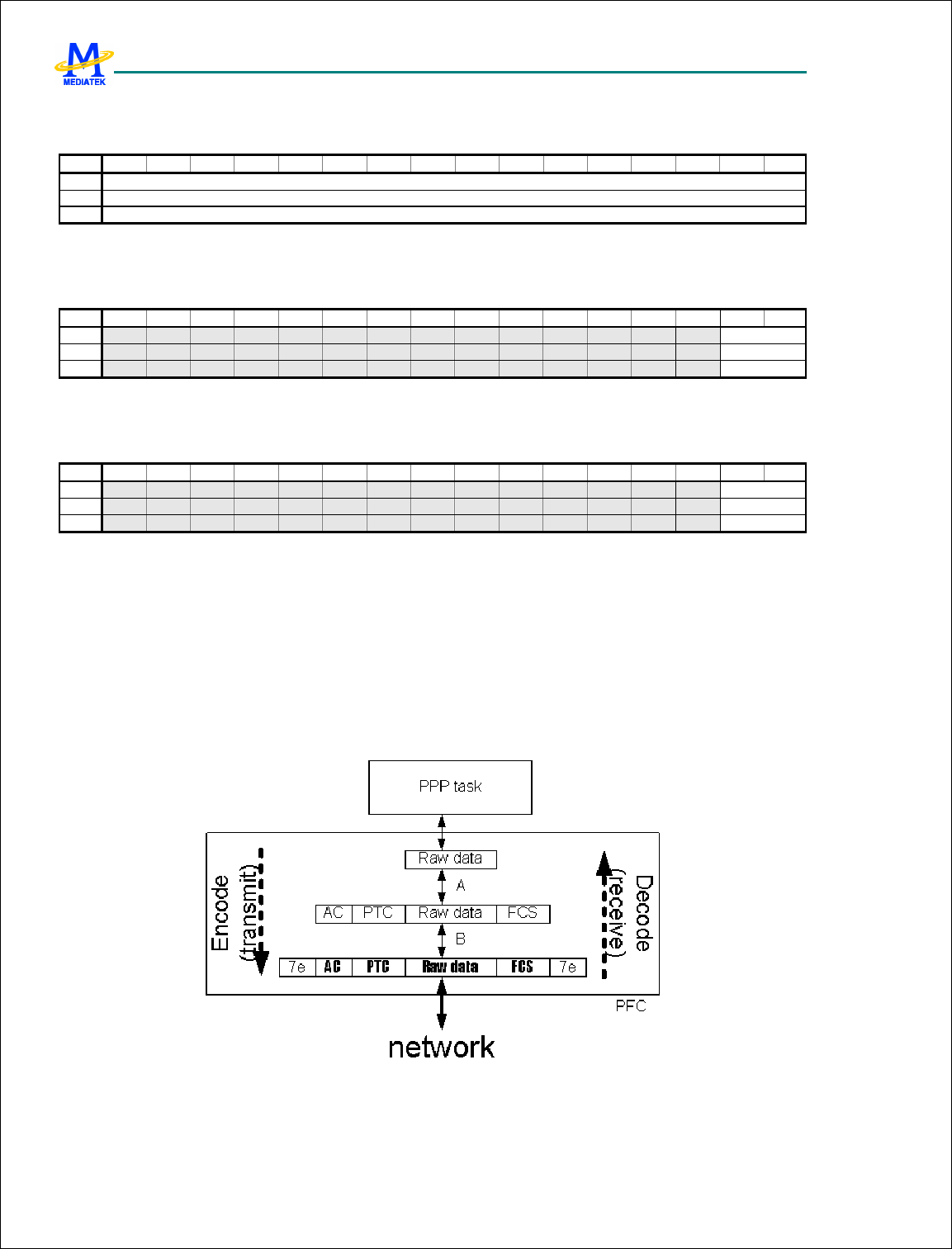
MTK Confidential Release for Konka
MTK Confidential Release for Konka
MT6228 GSM/GPRS Baseband Processor Data Sheet Revision 1.0
204/616 MediaTek Inc. Confidential
EUDLEN Unused write buffer space length in encoding mode.
PFC+0040h PFC decoding protocol PFC_DPTC
Bit 15 14 13 12 11 10 9 8 7 6 5 4 3 2 1 0
Name
DPTC[15:0]
Type RO
Reset
0
DPTC Decoding protocol. This register contains the protocol field value decoded from a frame. Writing 8 or 16
bits depends on the DPFC bit. An 8-bit protocol uses LSB.
PFC+0044h PFC interrupt status PFC_INTSTA
Bit 15 14 13 12 11 10 9 8 7 6 5 4 3 2 1 0
Name
INTSTA
Type RC
Reset
0
INTSTA Interrupt status. Bit 0 indicates that PFC finished with OK or RESUME state. Bit 1 indicates that PFC
failed. Further error information can be obtained from PFC_STAT.
PFC+0048h PFC interrupt enable PFC_INTEN
Bit 15 14 13 12 11 10 9 8 7 6 5 4 3 2 1 0
Name
INTEN
Type R/W
Reset
0
INTEN Interrupt enable control register. When bit 0 is enabled, an interrupt occurs when PFC finishes in the OK or
RESUME state. If bit 1 is enabled, PFC interrupts if an error occurs.
5.4.3 MRU
When a PPP task wants to transmit a set of raw data through the network, the data must be encoded first (Figure 63).
In process A, the raw data is prefixed with an Address (0xff) and Control (0x03) field* (AC), followed by Protocol
field** (PTC). An FCS is appended***.
In process B, the data stream resulting from process A is byte-stuffed. A 0x7e byte is then added both at the front and
at the end of the byte-stuffed stream.
Figure 63 Basic PFC Flow
* The Control field depends on the DACFC, EACFC, and EACCM bits.

MTK Confidential Release for Konka
MTK Confidential Release for Konka
MT6228 GSM/GPRS Baseband Processor Data Sheet Revision 1.0
205/616 MediaTek Inc. Confidential
** The Protocol field depends on the DPTC and EPTC bits.
*** The FCS field depends on the DF32 and EF32 bits.
Figure 64 shows the resulting PPP frame.
Flag
01111110
Address
11111111
Control
00000011
Protocol
8/16 bits
Information
*
Padding
*
FCS
16/32 bits
Flag
01111110
Figure 64 PPP Frame Structure
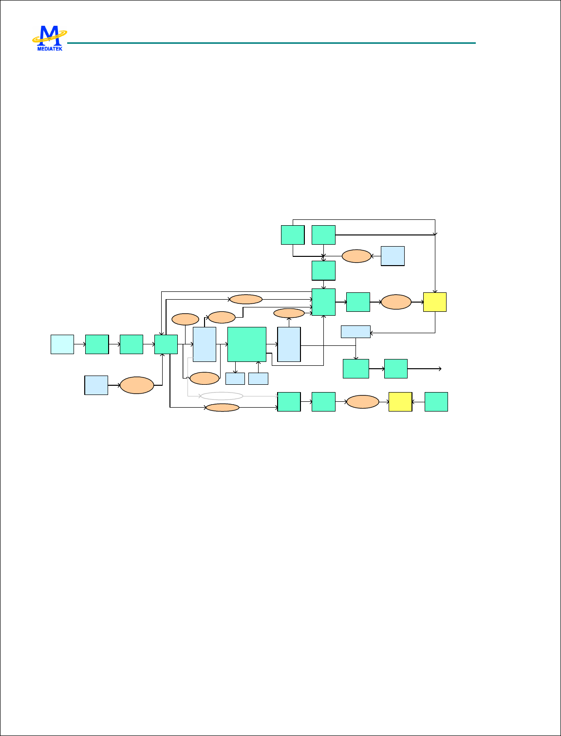
MTK Confidential Release for Konka
MTK Confidential Release for Konka
MT6228 GSM/GPRS Baseband Processor Data Sheet Revision 1.0
206/616 MediaTek Inc. Confidential
6 Multi-Media Subsystem
MT6228 is a highly integrated Baseband/Multimedia single chip. It integrates several hardware-based multimedia
accelerators to enable rich multimedia application. Hardware accelerators include Image signal processor, Image resizer,
JPEG Codec, MPEG-4 Codec, GIF Decoder, PNG Decoder, 2D graphics engine, TV encoder, and advanced hardware
LCD display controller. A lot of attractive multimedia functions can be realized through above hardware accelerators in
MT6228. The functions include camera function, JPEG/GIF/PNG image playback, MPEG-4 video recording, MPEG-4
video playback, TV out, 2D graphics acceleration, and so on. Image data paths of multi-media sub-system are shown in
Figure 1-1. Hardware data paths and Image DMA are designed to make data transfer more efficient. MT6228 also
incorporates NAND Flash, USB 1.1 OTG Controller and SD/SDIO/MMC/MS/MS Pro Controllers for mass data
transfers and storage.
Sensor ISP CRZ OVL Buffer MPEG4/JPEG
Codec Buffer
File
Buffer
File
Buffer
PRZ IPP1
(YUV2RGB)
LCD
(Layer 2)
Image
Buffer
DRZ IPP2
(YUV2RGB)
LCD
(Layer 1)
IPP3
(RGB2YUV)
Photo
Frame
Buffer
TV
Controller
TV
Encoder
Composite Video
TV
Memory
YUV420
YUV422
RGB565
PNGGIF
2D
Figure 6-1 Image Data Path of Multi-media Sub-system
6.1 LCD Interface
6.1.1 General Description
MT6228 contains a versatile LCD controller, which is optimized for multimedia applications. This controller supports
many types of LCD modules and contains a rich feature set to enhance the functionality. These features are:
Up to 320 x 240 resolution
The internal frame buffer supports 8bpp indexed color, RGB 565, RGB 888 and ARGB 8888 format.
Supports 8-bpp (RGB332), 12-bpp (RGB444), 16-bpp (RGB565), 18-bit (RGB666) and 24-bit (RGB888) LCD
modules.
6 Layers Overlay with individual color depth, window size, vertical and horizontal offset, source key, alpha value
and display rotation control(90°,180°, 270°, mirror and mirror then 90°, 180° and 270°)
One color look-up table of 24bpp

MTK Confidential Release for Konka
MTK Confidential Release for Konka
MT6228 GSM/GPRS Baseband Processor Data Sheet Revision 1.0
207/616 MediaTek Inc. Confidential
For parallel LCD modules, the LCD controller can reuse external memory interface or use dedicated 8/9/16/18-bit
parallel interface to access them and 8080 type interface is supported. It can transfer the display data from the internal
SRAM or external SRAM/Flash Memory to the off-chip LCD modules.
For serial LCD modules, this interface performs parallel to serial conversion and both 8- and 9- bit format serial
interface is supported. The 8-bit format serial interface uses four pins – LSCE#, LSDA, LSCK and LSA0 – to enter
commands and data. Meanwhile, the 9-bit format serial interface uses three pins – LSCE#, LSDA and LSCK – for the
same purpose. Data read is not available with the serial interface and data entered must be 8 bits.
Data and command send to LCM are always through the parallel Nandflash/Lcd interface or through serial SPI/LCD
interface. Sending LCM signals through EMI is forbidden, but the pixel data produced by LCD controller can be
dumped to memory through AHB bus.
LPCE0#
LPCE1#
LRST#
LRD#
LPA0
LWR#
NLD[17:0]
LSCE0#
LSCE1#
LSDA
LSA0
LSCK
Figure 2 LCD Interface Block Diagram
Figure 3 shows the timing diagram of this serial interface. When the block is idle, LSCK is forced LOW and LSCE# is
forced HIGH. Once the data register contains data and the interface is enabled, LSCE# is pulled LOW and remain
LOW for the duration of the transmission.
MTK Confidential Release for Konka
MTK Confidential Release for Konka
MT6228 GSM/GPRS Baseband Processor Data Sheet Revision 1.0
208/616 MediaTek Inc. Confidential
8-bit Serial Interface
LSCK(SPH=SPO=0)
LSDA D7
D6 D5 D4 D3 D2 D1 D0
LSCE#
LSA0
9-bit Serial Interface
LSCK(SPH=SPO=0)
LSDA A0
D7 D6 D5 D4 D3 D2 D1 D0
LSCE#
LSA0
Figure 3 Serial LCD Interface Transfer Timing Diagram
LCD = 0x9000_0000
Address Register Function Width Acronym
LCD + 0000h
LCD Interface Status Register 16 LCD_STA
LCD + 0004h LCD Interface Interrupt Enable Register 16 LCD_INTEN
LCD + 0008h LCD Interface Interrupt Status Register 16 LCD_INTSTA
LCD + 000ch LCD Interface Frame Transfer Register 16 LCD_START
LCD + 0010h LCD Parallel/Serial LCM Reset Register 16 LCD_RSTB
LCD + 0014h
LCD Serial Interface Configuration Register 16 LCD_SCNF
LCD + 0018h LCD Parallel Interface 0 Configuration Register 32 LCD_PCNF0
LCD + 001ch LCD Parallel Interface 1 Configuration Register 32 LCD_PCNF1
LCD + 0020h LCD Parallel Interface 2 Configuration Register 32 LCD_PCNF2
LCD + 0040h LCD Main Window Size Register 32 LCD_MWINSIZE
LCD + 0044h LCD ROI Window Write to Memory Offset Register 32 LCD_WROI_W2MOFS
LCD + 0048h LCD ROI Window Write to Memory Control
Register 16 LCD_WROI_W2MCON
LCD + 004ch LCD ROI Window Write to Memory Address
Register 32 LCD_WROI_W2MADD
LCD + 0050h LCD ROI Window Control Register 32 LCD_WROICON
LCD + 0054h
LCD ROI Window Offset Register 32 LCD_WROIOFS
LCD + 0058h LCD ROI Window Command Start Address Register 16 LCD_WROICADD
LCD + 005ch LCD ROI Window Data Start Address Register 16 LCD_WROIDADD
LCD + 0060h LCD ROI Window Size Register 32 LCD_WROISIZE
LCD + 0064h LCD ROI Window Hardware Refresh Register 32 LCD_WROI_HWREF
LCD + 0068h LCD ROI Window Background Color Register 32 LCD_WROI_BGCLR
LCD + 0070h LCD Layer 0 Window Control Register 32 LCD_L0WINCON
LCD + 0074h LCD Layer 0 Source Color Key Register 32 LCD_L0WINSKEY
LCD + 0078h LCD Layer 0 Window Display Offset Register 32 LCD_L0WINOFS
LCD + 007ch LCD Layer 0 Window Display Start Address Register 32 LCD_L0WINADD
LCD + 0080h LCD Layer 0 Window Size 32 LCD_L0WINSIZE

MTK Confidential Release for Konka
MTK Confidential Release for Konka
MT6228 GSM/GPRS Baseband Processor Data Sheet Revision 1.0
209/616 MediaTek Inc. Confidential
LCD + 0090h
LCD Layer 1 Window Control Register 32 LCD_L1WINCON
LCD + 0094h LCD Layer 1 Source Color Key Register 32 LCD_L1WINSKEY
LCD + 0098h LCD Layer 1 Window Display Offset Register 32 LCD_L1WINOFS
LCD + 009ch LCD Layer 1 Window Display Start Address Register 32 LCD_L1WINADD
LCD + 00a0h LCD Layer 1 Window Size 32 LCD_L1WINSIZE
LCD + 00b0h
LCD Layer 2 Window Control Register 32 LCD_L2WINCON
LCD + 00b4h LCD Layer 2 Source Color Key Register 32 LCD_L2WINSKEY
LCD + 00b8h LCD Layer 2 Window Display Offset Register 32 LCD_L2WINOFS
LCD + 00bch LCD Layer 2 Window Display Start Address Register 32 LCD_L2WINADD
LCD + 00c0h LCD Layer 2 Window Size 32 LCD_L2WINSIZE
LCD + 00d0h LCD Layer 3 Window Control Register 32 LCD_L3WINCON
LCD + 00d4h LCD Layer 3 Source Color Key Register 32 LCD_L3WINSKEY
LCD + 00d8h LCD Layer 3 Window Display Offset Register 32 LCD_L3WINOFS
LCD + 00dch LCD Layer 3 Window Display Start Address Register 32 LCD_L3WINADD
LCD + 00e0h LCD Layer 3 Window Size 32 LCD_L3WINSIZE
LCD + 00f0h LCD Layer 4 Window Control Register 32 LCD_L4WINCON
LCD + 00f4h LCD Layer 4 Source Color Key Register 32 LCD_L4WINSKEY
LCD + 00f8h LCD Layer 4 Window Display Offset Register 32 LCD_L4WINOFS
LCD + 00fch LCD Layer 4 Window Display Start Address Register 32 LCD_L4WINADD
LCD + 0100h LCD Layer 4 Window Size 32 LCD_L4WINSIZE
LCD + 0110h LCD Layer 5 Window Control Register 32 LCD_L5WINCON
LCD + 0114h LCD Layer 5 Source Color Key Register 32 LCD_L5WINSKEY
LCD + 0118h LCD Layer 5 Window Display Offset Register 32 LCD_L5WINOFS
LCD + 011ch LCD Layer 5 Window Display Start Address Register 32 LCD_L5WINADD
LCD + 0120h LCD Layer 5 Window Size 32 LCD_L5WINSIZE
LCD + 4000h LCD Parallel Interface 0 Data 32 LCD_PDAT0
LCD + 4100h
LCD Parallel Interface 0 Command 32 LCD_PCMD0
LCD + 5000h LCD Parallel Interface 1 Data 32 LCD_PDAT1
LCD + 5100h LCD Parallel Interface 1 Command 32 LCD_PCMD1
LCD + 6000h LCD Parallel Interface 2 Data 32 LCD_PDAT2
LCD + 6100h LCD Parallel Interface 2 Command 32 LCD_PCMD2
LCD + 8000h
LCD Serial Interface 1 Data 16 LCD_SDAT1
LCD + 8100h LCD Serial Interface 1 Command 16 LCD_SCMD1
LCD + 9000h LCD Serial Interface 0 Data 16 LCD_SDAT0
LCD + 9100h LCD Serial Interface 0 Command 16 LCD_SCMD0
LCD + c800h
~ cbfch LCD Color Palette LUT Register 32 LCD_PAL
LCD + cc00h
~ ccfch LCD Interface Command/Parameter Register 32 LCD_COMD
MTK Confidential Release for Konka
MTK Confidential Release for Konka
MT6228 GSM/GPRS Baseband Processor Data Sheet Revision 1.0
210/616 MediaTek Inc. Confidential
6.1.2 Table 36 Memory map of LCD InterfaceRegister Definitions
LCD +0000h LCD Interface Status Register LCD_STA
Bit 15 14 13 12 11 10 9 8 7 6 5 4 3 2 1 0
Name
CMD_
CPEN
D
DATA
_PEN
D
RUN
Type R R R
Reset
0 0 0
RUN LCD Interface Running Status
DATA_PEND Data Pending Indicator in Hardware Trigger Mode
CMD_PEND Command Pending Indicator in Hardware Triggered Refresh Mode
LCD +0004h LCD Interface Interrupt Enable Register LCD_INTEN
Bit 15 14 13 12 11 10 9 8 7 6 5 4 3 2 1 0
Name
CMD_
CPL
DATA
_CPL CPL
Type R/W R/W R/W
Reset
0 0 0
CPL LCD Frame Transfer Complete Interrupt Control
DATA_CPL Data Transfer Complete in Hardware Triggered Refresh Mode Interrupt Control
CMD_CPL Command Transfer Complete in Hardware Trigger Refresh Mode Interrupt Control
LCD +0008h LCD Interface Interrupt Status Register LCD_INTSTA
Bit 15 14 13 12 11 10 9 8 7 6 5 4 3 2 1 0
Name
CMD_
CPL
DATA
_CPL CPL
Type R R R
Reset
0 0 0
CPL LCD Frame Transfer Complete Interrupt
DATA_CPL Data Transfer Complete in Hardware Triggered Refresh Mode Interrupt
CMD_CPL Command Transfer Complete in Hardware Triggered Refresh Mode Interrupt
LCD +000Ch LCD Interface Frame Transfer Register LCD_START
Bit 15 14 13 12 11 10 9 8 7 6 5 4 3 2 1 0
Name
STAR
T
Type R/W
Reset
0
START Start Control of LCD Frame Transfer
LCD +0010h LCD Parallel/Serial Interface Reset Register LCD_RSTB
Bit 15 14 13 12 11 10 9 8 7 6 5 4 3 2 1 0
Name
RSTB
Type R/W
Reset
1
RSTB Parallel/Serial LCD Module Reset Control
LCD +0014h LCD Serial Interface Configuration Register LCD _SCNF
Bit 15 14 13 12 11 10 9 8 7 6 5 4 3 2 1 0
Name
26M
13M
CSP1
CSP0
8/9
DIV SPH
SPO
MTK Confidential Release for Konka
MTK Confidential Release for Konka
MT6228 GSM/GPRS Baseband Processor Data Sheet Revision 1.0
211/616 MediaTek Inc. Confidential
Type
R/W
R/W
R/W
R/W
R/W
R/W R/W
R/W
Type 0 0 0 0 0 0 0 0
SPO Clock Polarity Control
SPH Clock Phase Control
DIV Serial Clock Divide Select Bits
8/9 8-bit or 9-bit Interface Selection
CSP0 Serial Interface Chip Select 0 Polarity Control
CSP1 Serial Interface Chip Select 1 Polarity Control
LCD +0018h LCD Parallel Interface Configuration Register 0 LCD_PCNF0
Bit 31 30 29 28 27 26 25 24 23 22 21 20 19 18 17 16
Name
C2WS C2WH C2RS DW
Type
R/W R/W R/W R/W
0 0 0 0
Bit 15 14 13 12 11 10 9 8 7 6 5 4 3 2 1 0
Name
26M 13M WST RLT
Type R/W R/W R/W R/W
Reset
0 0 0 0
RLT Read Latency Time
WST Write Wait State Time
13M Enable 13MHz clock gating.
26M Enable 26MHz clock gating.
DW Data width of the parallel interface.
00 8-bit.
01 9-bit
10 16-bit
11 18-bit
C2RS Chip Select (LPCE#) to Read Strobe (LRD#) Setup Time
C2WH Chip Select (LPCE#) to Write Strobe (LWR#) Hold Time
C2WS Chip Select (LPCE#) to Write Strobe (LWR#) Setup Time
LCD +001Ch LCD Parallel Interface Configuration Register 1 LCD_PCNF1
Bit 31 30 29 28 27 26 25 24 23 22 21 20 19 18 17 16
Name
C2WS C2WH C2RS DW
Type R/W R/W R/W R/W
0 0 0 0
Bit 15 14 13 12 11 10 9 8 7 6 5 4 3 2 1 0
Name
26M 13M WST RLT
Type R/W R/W R/W R/W
Reset
0 0 0 0
RLT Read Latency Time
WST Write Wait State Time
13M Enable 13MHz clock gating.
26M Enable 26MHz clock gating.
DW Data width of the parallel interface.
00 8-bit.
01 9-bit
10 16-bit
11 18-bit
C2RS Chip Select (LPCE#) to Read Strobe (LRD#) Setup Time
MTK Confidential Release for Konka
MTK Confidential Release for Konka
MT6228 GSM/GPRS Baseband Processor Data Sheet Revision 1.0
212/616 MediaTek Inc. Confidential
C2WH Chip Select (LPCE#) to Write Strobe (LWR#) Hold Time
C2WS Chip Select (LPCE#) to Write Strobe (LWR#) Setup Time
LCD +0020h LCD Parallel Interface Configuration Register 2 LCD_PCNF2
Bit 31 30 29 28 27 26 25 24 23 22 21 20 19 18 17 16
Name
C2WS C2WH C2RS DW
Type R/W R/W R/W R/W
0 0 0 0
Bit 15 14 13 12 11 10 9 8 7 6 5 4 3 2 1 0
Name
26M 13M WST RLT
Type R/W R/W R/W R/W
Reset
0 0 0 0
RLT Read Latency Time
WST Write Wait State Time
13M Enable 13MHz clock gating.
26M Enable 26MHz clock gating.
DW Data width of the parallel interface.
00 8-bit.
01 9-bit
10 16-bit
11 18-bit
C2RS Chip Select (LPCE#) to Read Strobe (LRD#) Setup Time
C2WH Chip Select (LPCE#) to Write Strobe (LWR#) Hold Time
C2WS Chip Select (LPCE#) to Write Strobe (LWR#) Setup Time
LCD +4000h LCD Parallel 0 Interface Data LCD_PDAT0
Bit 31 30 29 28 27 26 25 24 23 22 21 20 19 18 17 16
Name
DATA[31:16]
Type R/W
Bit 15 14 13 12 11 10 9 8 7 6 5 4 3 2 1 0
Name
DATA[15:0]
Type R/W
DATA Writing to LCD+4000 will drive LPA0 low when sending this data out in parallel BANK0, while writing to
LCD+4100 will drive LPA0 high.
LCD +5000h LCD Parallel 1 Interface Data LCD_PDAT1
Bit 31 30 29 28 27 26 25 24 23 22 21 20 19 18 17 16
Name
DATA[31:16]
Type R/W
Bit 15 14 13 12 11 10 9 8 7 6 5 4 3 2 1 0
Name
DATA[15:0]
Type R/W
DATA Writing to LCD+5000 will drive LPA1 low when sending this data out in parallel BANK1, while writing to
LCD+5100 will drive LPA1 high
LCD +6000h LCD Parallel 2 Interface Data LCD_PDAT2
Bit 31 30 29 28 27 26 25 24 23 22 21 20 19 18 17 16
Name
DATA[31:16]
Type R/W
Bit 15 14 13 12 11 10 9 8 7 6 5 4 3 2 1 0
Name
DATA[15:0]
Type R/W
MTK Confidential Release for Konka
MTK Confidential Release for Konka
MT6228 GSM/GPRS Baseband Processor Data Sheet Revision 1.0
213/616 MediaTek Inc. Confidential
DATA Writing to LCD+6000 will drive LPA2 low when sending this data out in parallel BANK2, while writing to
LCD+6100 will drive LPA2 high
LCD
+8000/8100h LCD Serial Interface 1 Data LCD_SDAT1
Bit 15 14 13 12 11 10 9 8 7 6 5 4 3 2 1 0
Name
DATA
Type W
DATA Writing to LCD+8000 will drive LSA0 low while sending this data out in serial BANK1, while writing to
LCD+8100 will drive LSA0 high
LCD
+9000/9100h LCD Serial Interface 0 Data LCD_SDAT0
Bit 15 14 13 12 11 10 9 8 7 6 5 4 3 2 1 0
Name
DATA
Type W
DATA Writing to LCD+9000 will drive LSA0 low while sending this data out in serial BANK0, while writing to
LCD+9100 will drive LSA0 high
LCD +0040h Main Window Size Register LCD_MWINSIZE
Bit 31 30 29 28 27 26 25 24 23 22 21 20 19 18 17 16
Name
ROW
Type R/W
Bit 15 14 13 12 11 10 9 8 7 6 5 4 3 2 1 0
Name
COLUMN
Type R/W
COLUMN 10-bit Virtual Image Window Column Size
ROW 10-bit Virtual Image Window Row Size
LCD +0044h Region of Interest Window Write to Memory Offset
Register
LCD_WROI_W2
MOFS
Bit 31 30 29 28 27 26 25 24 23 22 21 20 19 18 17 16
Name
Y-OFFSET
Type R/W
Bit 15 14 13 12 11 10 9 8 7 6 5 4 3 2 1 0
Name
X-OFFSET
Type R/W
This control register is used to specify the offset of the ROI window from the LCD_WROI_W2MADDR when writing
the ROI window’s content to memory.
X-OFFSET the x offset of ROI window in the destination memory.
Y-OFFSET the y offset of ROI window in the destination memory.
LCD +0048h Region of Interest Window Write to Memory Control
Register
LCD_WROI_W2
MOON
Bit 15 14 13 12 11 10 9 8 7 6 5 4 3 2 1 0
Name
DISC
ON
W2M_
FORM
AT
W2L
CM
Type R/W R/W R/W
Reset
0 0 0
MTK Confidential Release for Konka
MTK Confidential Release for Konka
MT6228 GSM/GPRS Baseband Processor Data Sheet Revision 1.0
214/616 MediaTek Inc. Confidential
This control register is effective only when the W2M bit is set in LCD_WROICON register.
W2LCM Write to LCM simultaneously.
W2M_FORMAT Write to memory format.
0 RGB565
1 RGB888
DISCON Block Write Enable Control. By setting both DISCON and W2M to 1, the LCD controller will write
out the ROI pixel data as a part of MAIN window, using the width of MAIN window to calculate the write-out address.
If this bit is not set, the ROI window will be written to memory in continuous addresses.
LCD +004Ch Region of Interest Window Write to Memory
Address Register
LCD_WROI_W2
MADD
Bit 31 30 29 28 27 26 25 24 23 22 21 20 19 18 17 16
Name
W2M_ADDR
Type R/W
Bit 15 14 13 12 11 10 9 8 7 6 5 4 3 2 1 0
Name
W2M_ADDR
Type R/W
W2M_ADDR Write to memory address.
LCD +0050h Region of Interest Window Control Register LCD_WROICO
N
Bit
31
30
29
28
27
26
25
24
23
22
21
20
19
18
17
16
Name
EN0
EN1
EN2
EN3
EN4
EN5
PERIOD
Type R/W R/W R/W R/W R/W R/W R/W
Bit
15
14
13
12
11
10
9
8
7
6
5
4
3
2
1
0
Name
ENC W2M COMMAND FORMAT
Type R/W R/W R/W R/W
FORMAT LCD Module Data Format
Bit 0 : in BGR sequence, otherwise in RGB sequence.
Bit 1 : LSB first, otherwise MSB first.
Bit 2 : padding bits on MSBs, otherwise on LSBs.
Bit 5-3 : 000 for RGB332, 001 for RGB444, 010 for RGB565, 011 for RGB666, 100 for RGB888.
Bit 7-6 : 00 for 8-bit interface, 01 for 16-bit interface, 10 for 9-bit interface, 11 for 18-bit interface.
Note: When the interface is configured as 9 bit or 18 bit, the field of bit5-2 is ignored.
00000000 8bit 1cycle/1pixel RGB3.3.2 RRRGGGBB
00000001 1cycle/1pixel RGB3.3.2 BBGGGRRR
00001000 3cycle/2pixel RGB4.4.4 RRRRGGGG
BBBBRRRR
GGGGBBBB
00001011 3cycle/2pixel RGB4.4.4 GGGGRRRR
RRRRBBBB
BBBBGGGG
00010000 2cycle/1pixel RGB5.6.5 RRRRRGGG
GGGBBBBB
00010011 2cycle/1pixel RGB5.6.5 GGGRRRRR
BBBBBGGG
00011000 3cycle/1pixel RGB6.6.6 RRRRRRXX

MTK Confidential Release for Konka
MTK Confidential Release for Konka
MT6228 GSM/GPRS Baseband Processor Data Sheet Revision 1.0
215/616 MediaTek Inc. Confidential
GGGGGGXX
BBBBBBXX
00011100 3cycle/1pixel RGB6.6.6 XXRRRRRR
XXGGGGGG
XXBBBBBB
00100000 3cycle/1pixel RGB8.8.8 RRRRRRRR
GGGGGGGG
BBBBBBBB
10011000 9bit 2cycle/1pixel RGB6.6.6 RRRRRRGGG
GGGBBBBBB
10011011 2cycle/1pixel RGB6.6.6 GGGRRRRRR
BBBBBBGGG
01000000 16bit 1cycle/2pixel RGB3.3.2 RRRGGGBBRRRGGGBB
01000010 1cycle/2pixel RGB3.3.2 RRRGGGBBRRRGGGBB
01000001 1cycle/2pixel RGB3.3.2 BBGGGRRRBBGGGRRR
01000011 1cycle/2pixel RGB3.3.2 BBGGGRRRBBGGGRRR
01001100 1cycle/1pixel RGB4.4.4 XXXXRRRRGGGGBBBB
01001101 1cycle/1pixel RGB4.4.4 XXXXBBBBGGGGRRRR
01001000 1cycle/1pixel RGB4.4.4 RRRRGGGGBBBBXXXX
01001001 1cycle/1pixel RGB4.4.4 BBBBGGGGRRRRXXXX
01010000 1cycle/1pixel RGB5.6.5 RRRRRGGGGGGBBBBB
01010001 1cycle/1pixel RGB5.6.5 BBBBBGGGGGGRRRRR
01011100 3cycle/2pixel RGB6.6.6 XXXXRRRRRRGGGGGG
XXXXBBBBBBRRRRRR
XXXXGGGGGGBBBBBB
01011111 3cycle/2pixel RGB6.6.6 XXXXGGGGGGRRRRRR
XXXXRRRRRRBBBBBB
XXXXBBBBBBGGGGGG
01011000 3cycle/2pixel RGB6.6.6 RRRRRRGGGGGGXXXX
BBBBBBRRRRRRXXXX
GGGGGGBBBBBBXXXX
01011011 3cycle/2pixel RGB6.6.6 GGGGGGRRRRRRXXXX
RRRRRRBBBBBBXXXX
BBBBBBGGGGGGXXXX
01100000 3cycle/2pixel RGB8.8.8 RRRRRRRRGGGGGGGG
BBBBBBBBRRRRRRRR
GGGGGGGGBBBBBBBB
01100011 3cycle/2pixel RGB8.8.8 GGGGGGGGRRRRRRRR
RRRRRRRRBBBBBBBB
BBBBBBBBRRRRRRRR
11011000 18bit 1cycle/1pixel RGB6.6.6 RRRRRRGGGGGGBBBBBB
11011001 1cycle/1pixel RGB6.6.6 BBBBBBGGGGGGRRRRRR
COMMAND Number of Commands to be sent to LCD module. Maximum is 63.
W2M Enable Data Address Increasing After Each Data Transfer
ENC Command Transfer Enable Control
PERIOD Waiting period between two consecutive transfers, effective for both data and command.
ENn Layer Window Enable Control
MTK Confidential Release for Konka
MTK Confidential Release for Konka
MT6228 GSM/GPRS Baseband Processor Data Sheet Revision 1.0
216/616 MediaTek Inc. Confidential
LCD +0054h Region of Interest Window Offset Register LCD_WROIOFS
Bit 31 30 29 28 27 26 25 24 23 22 21 20 19 18 17 16
Name
Y-OFFSET
Type R/W
Bit 15 14 13 12 11 10 9 8 7 6 5 4 3 2 1 0
Name
X-OFFSET
Type R/W
X-OFFSET ROI Window Column Offset
Y-OFFSET ROI Window Row Offset
LCD +0058h Region of Interest Window Command Start Address
Register
LCD_WROICAD
D
Bit 15 14 13 12 11 10 9 8 7 6 5 4 3 2 1 0
Name
ADDR
Type R/W
ADDR ROI Window Command Address. Only writing to LCD modules is allowed.
LCD +005Ch Region of Interest Window Data Start Address
Register
LCD_WROIDAD
D
Bit 15 14 13 12 11 10 9 8 7 6 5 4 3 2 1 0
Name
ADDR
Type R/W
ADDR ROI Window Data Address Only writing to LCD modules is allowed.
LCD +0060h Region of Interest Window Size Register LCD_WROISIZE
Bit 31 30 29 28 27 26 25 24 23 22 21 20 19 18 17 16
Name
ROW
Type R/W
Bit 15 14 13 12 11 10 9 8 7 6 5 4 3 2 1 0
Name
COLUMN
Type R/W
COLUMN ROI Window Column Size (width)
ROW ROI Window Row Size (height)
LCD +0064h Region of Interest Window Hardware Refresh
Register
LCD_WROI_HW
REF
Bit 31 30 29 28 27 26 25 24 23 22 21 20 19 18 17 16
Name
EN0 EN1 EN2 EN3 EN4 EN5 IMGD
MA0
IMGD
MA1
IMGD
MA2
IMGD
MA3
IMGD
MA4
IMGD
MA5
Type R/W R/W R/W R/W R/W R/W R/W R/W R/W R/W R/W R/W
Reset
0 0 0 0 0 0 0 0 0 0 0 0
Bit 15 14 13 12 11 10 9 8 7 6 5 4 3 2 1 0
Name
IMGD
MA_S
EL0
IMGD
MA_S
EL1
IMGD
MA_S
EL2
IMGD
MA_S
EL3
IMGD
MA_S
EL4
IMGD
MA_S
EL5
HWE
N HWR
EF
Type R/W R/W R/W R/W R/W R/W R/W R/W
Reset
0 0 0 0 0 0 0 0
ENn Enable layer n source address from Image_DMA.
IMGDMAn Enable layer n source data from Image_DMA.
IMGDMA_SELnSelect layer n read from Image_DMA0 or Image_DMA1.
MTK Confidential Release for Konka
MTK Confidential Release for Konka
MT6228 GSM/GPRS Baseband Processor Data Sheet Revision 1.0
217/616 MediaTek Inc. Confidential
0 Image_DMA0.
1 Image_DMA1
HWEN Enable hardware triggered LCD fresh.
HWREF Starting the hardware triggered LCD frame transfer.
LCD +0068h Region of Interest Background Color Register LCD_WROI_BG
CLR
Bit 31 30 29 28 27 26 25 24 23 22 21 20 19 18 17 16
Name
RED[7:0]
Type R/W
Reset
1111_1111
Bit 15 14 13 12 11 10 9 8 7 6 5 4 3 2 1 0
Name
GREEN[7:0] BLUE[7:0]
Type
R/W R/W
Reset
1111_1111 1111_1111
RED Red component of ROI window’s background color
GREEN Green component of ROI window’s background color
BLUE Blue component of ROI window’s background color
LCD +0070h Layer 0 Window Control Register LCD_L0WINCO
N
Bit 31 30 29 28 27 26 25 24 23 22 21 20 19 18 17 16
Name
SWP
Type R/W
Bit 15 14 13 12 11 10 9 8 7 6 5 4 3 2 1 0
Name
SRC
KEYE
N ROTATE CLRDPT OPAE
N OPA
Type R/W R/W R/W R/W R/W R/W
OPA Opacity value, used as constant alpha value.
OPAEN Opacity enabled
CLRDPT Color format
00 8bpp indexed color.
01 RGB 565
10 ARGB 8888
11 RGB 888
ROTATE Rotation Configuration
000 0 degree rotation
001 90 degree rotation anti-counterclockwise
010 180 degree rotation anti-counterclockwise
011 270 degree rotation anti-counterclockwise
100 Horizontal flip
101 Horizontal flip then 90 degree rotation anti-counterclockwise
110 Horizontal flip then 180 degree rotation anti-counterclockwise
111 Horizontal flip then 270 degree rotation anti-counterclockwise
KEYEN Source Key Enable Control
SRC Disable auto-increment of the source pixel address
SWP Swap high byte and low byte of pixel data

MTK Confidential Release for Konka
MTK Confidential Release for Konka
MT6228 GSM/GPRS Baseband Processor Data Sheet Revision 1.0
218/616 MediaTek Inc. Confidential
LCD +0074h Layer 0 Source Color Key Register LCD_L0WINSK
EY
Bit 31 30 29 28 27 26 25 24 23 22 21 20 19 18 17 16
Name
SRCKEY[31:16]
Type R/W
Bit 15 14 13 12 11 10 9 8 7 6 5 4 3 2 1 0
Name
SRCKEY[15:0]
Type R/W
SRCKEY Transparent color key of the source image.
LCD +0078h Layer 0 Window Display Offset Register LCD_L0WINOF
S
Bit 31 30 29 28 27 26 25 24 23 22 21 20 19 18 17 16
Name
Y-OFFSET
Type R/W
Bit 15 14 13 12 11 10 9 8 7 6 5 4 3 2 1 0
Name
X-OFFSET
Type R/W
Y-OFFSET Layer 0 Window Row Offset
X-OFFSET Layer 0 Window Column Offset
LCD+007Ch Layer 0 Window Display Start Address Register LCD_L0WINAD
D
Bit 31 30 29 28 27 26 25 24 23 22 21 20 19 18 17 16
Name
ADDR
Type R/W
Bit 15 14 13 12 11 10 9 8 7 6 5 4 3 2 1 0
Name
ADDR
Type R/W
ADDR Layer 0 Window Data Address
LCD +0080h Layer 0 Window Size LCD_L0WINSIZ
E
Bit 31 30 29 28 27 26 25 24 23 22 21 20 19 18 17 16
Name
ROW
Type R/W
Bit 15 14 13 12 11 10 9 8 7 6 5 4 3 2 1 0
Name
COLUMN
Type R/W
ROW Layer 0 Window Row Size
COLUMN Layer 0 Window Column Size
LCD +0090h Layer 1 Window Control Register LCD_L1WINCO
N
Bit 31 30 29 28 27 26 25 24 23 22 21 20 19 18 17 16
Name
SWP
Type R/W
Bit 15 14 13 12 11 10 9 8 7 6 5 4 3 2 1 0
Name
SRC KEYE
N ROTATE CLRDPT OPAE
N OPA
Type R/W R/W R/W R/W R/W R/W
MTK Confidential Release for Konka
MTK Confidential Release for Konka
MT6228 GSM/GPRS Baseband Processor Data Sheet Revision 1.0
219/616 MediaTek Inc. Confidential
OPA Opacity value, used as constant alpha value.
OPAEN Opacity enabled
CLRDPT Color format
00 8bpp indexed color.
01 RGB 565
10 ARGB 8888
11 RGB 888
ROTATE Rotation Configuration
000 0 degree rotation
001 90 degree rotation anti-counterclockwise
010 180 degree rotation anti-counterclockwise
011 270 degree rotation anti-counterclockwise
100 Horizontal flip
101 Horizontal flip then 90 degree rotation anti-counterclockwise
110 Horizontal flip then 180 degree rotation anti-counterclockwise
111 Horizontal flip then 270 degree rotation anti-counterclockwise
KEYEN Source Key Enable Control
SRC Disable auto-increment of the source pixel address
SWP Swap high byte and low byte of pixel data
LCD +0094h Layer 1 Source Color Key Register LCD_L1WINSK
EY
Bit 31 30 29 28 27 26 25 24 23 22 21 20 19 18 17 16
Name
SRCKEY[31:16]
Type R/W
Bit 15 14 13 12 11 10 9 8 7 6 5 4 3 2 1 0
Name
SRCKEY[15:0]
Type R/W
SRCKEY Transparent color key of the source image.
LCD +0098h Layer 1 Window Display Offset Register LCD_L1WINOF
S
Bit 31 30 29 28 27 26 25 24 23 22 21 20 19 18 17 16
Name
Y-OFFSET
Type R/W
Bit 15 14 13 12 11 10 9 8 7 6 5 4 3 2 1 0
Name
X-OFFSET
Type R/W
Y-OFFSET Layer 1 Window Row Offset
X-OFFSET Layer 1 Window Column Offset
LCD+009Ch Layer 1 Window Display Start Address Register LCD_L1WINAD
D
Bit 31 30 29 28 27 26 25 24 23 22 21 20 19 18 17 16
Name
ADDR
Type R/W
Bit 15 14 13 12 11 10 9 8 7 6 5 4 3 2 1 0
Name
ADDR
Type R/W

MTK Confidential Release for Konka
MTK Confidential Release for Konka
MT6228 GSM/GPRS Baseband Processor Data Sheet Revision 1.0
220/616 MediaTek Inc. Confidential
ADDR Layer 1 Window Data Address
LCD +00A0h Layer 1 Window Size LCD_L1WINSIZ
E
Bit 31 30 29 28 27 26 25 24 23 22 21 20 19 18 17 16
Name
ROW
Type R/W
Bit 15 14 13 12 11 10 9 8 7 6 5 4 3 2 1 0
Name
COLUMN
Type R/W
ROW Layer 1 Window Row Size
COLUMN Layer 1 Window Column Size
LCD +00B0h Layer 2 Window Control Register LCD_L2WINCO
N
Bit 31 30 29 28 27 26 25 24 23 22 21 20 19 18 17 16
Name
SWP
Type R/W
Bit 15 14 13 12 11 10 9 8 7 6 5 4 3 2 1 0
Name
SRC
KEYE
N ROTATE CLRDPT OPAE
N OPA
Type R/W R/W R/W R/W R/W R/W
OPA Opacity value, used as constant alpha value.
OPAEN Opacity enabled
CLRDPT Color format
00 8bpp indexed color.
01 RGB 565
10 ARGB 8888
11 RGB 888
ROTATE Rotation Configuration
000 0 degree rotation
001 90 degree rotation anti-counterclockwise
010 180 degree rotation anti-counterclockwise
011 270 degree rotation anti-counterclockwise
100 Horizontal flip
101 Horizontal flip then 90 degree rotation anti-counterclockwise
110 Horizontal flip then 180 degree rotation anti-counterclockwise
111 Horizontal flip then 270 degree rotation anti-counterclockwise
KEYEN Source Key Enable Control
SRC Disable auto-increment of the source pixel address
SWP Swap high byte and low byte of pixel data
LCD +00B4h Layer 2 Source Color Key Register LCD_L2WINSK
EY
Bit 31 30 29 28 27 26 25 24 23 22 21 20 19 18 17 16
Name
SRCKEY[31:16]
Type R/W
Bit 15 14 13 12 11 10 9 8 7 6 5 4 3 2 1 0
Name
SRCKEY[15:0]
Type R/W
MTK Confidential Release for Konka
MTK Confidential Release for Konka
MT6228 GSM/GPRS Baseband Processor Data Sheet Revision 1.0
221/616 MediaTek Inc. Confidential
SRCKEY Transparent color key of the source image.
LCD +00B8h Layer 2 Window Display Offset Register LCD_L2WINOF
S
Bit 31 30 29 28 27 26 25 24 23 22 21 20 19 18 17 16
Name
Y-OFFSET
Type R/W
Bit 15 14 13 12 11 10 9 8 7 6 5 4 3 2 1 0
Name
X-OFFSET
Type R/W
Y-OFFSET Layer 2 Window Row Offset
X-OFFSET Layer 2 Window Column Offset
LCD+00BCh Layer 2 Window Display Start Address Register LCD_L2WINAD
D
Bit 31 30 29 28 27 26 25 24 23 22 21 20 19 18 17 16
Name
ADDR
Type R/W
Bit 15 14 13 12 11 10 9 8 7 6 5 4 3 2 1 0
Name
ADDR
Type R/W
ADDR Layer 1 Window Data Address
LCD +00C0h Layer 2 Window Size LCD_L2WINSIZ
E
Bit 31 30 29 28 27 26 25 24 23 22 21 20 19 18 17 16
Name
ROW
Type R/W
Bit 15 14 13 12 11 10 9 8 7 6 5 4 3 2 1 0
Name
COLUMN
Type R/W
ROW Layer 2 Window Row Size
COLUMN Layer 2 Window Column Size
LCD +00D0h Layer 3 Window Control Register LCD_L3WINCO
N
Bit 31 30 29 28 27 26 25 24 23 22 21 20 19 18 17 16
Name
SWP
Type R/W
Bit 15 14 13 12 11 10 9 8 7 6 5 4 3 2 1 0
Name
SRC KEYE
N ROTATE CLRDPT OPAE
N OPA
Type R/W R/W R/W R/W R/W R/W
OPA Opacity value, used as constant alpha value.
OPAEN Opacity enabled
CLRDPT Color format
00 8bpp indexed color.
01 RGB 565
10 ARGB 8888
11 RGB 888
ROTATE Rotation Configuration
MTK Confidential Release for Konka
MTK Confidential Release for Konka
MT6228 GSM/GPRS Baseband Processor Data Sheet Revision 1.0
222/616 MediaTek Inc. Confidential
000 0 degree rotation
001 90 degree rotation anti-counterclockwise
010 180 degree rotation anti-counterclockwise
011 270 degree rotation anti-counterclockwise
100 Horizontal flip
101 Horizontal flip then 90 degree rotation anti-counterclockwise
110 Horizontal flip then 180 degree rotation anti-counterclockwise
111 Horizontal flip then 270 degree rotation anti-counterclockwise
KEYEN Source Key Enable Control
SRC Disable auto-increment of the source pixel address
SWP Swap high byte and low byte of pixel data
LCD +00D4h Layer 3 Source Color Key Register LCD_L3WINSK
EY
Bit 31 30 29 28 27 26 25 24 23 22 21 20 19 18 17 16
Name
SRCKEY[31:16]
Type R/W
Bit 15 14 13 12 11 10 9 8 7 6 5 4 3 2 1 0
Name
SRCKEY[15:0]
Type R/W
SRCKEY Transparent color key of the source image.
LCD +00D8h Layer 3 Window Display Offset Register LCD_L3WINOF
S
Bit
31 30
29
28
27 26 25
24
23
22 21 20
19
18
17 16
Name
Y-OFFSET
Type R/W
Bit 15 14 13 12 11 10 9 8 7 6 5 4 3 2 1 0
Name
X-OFFSET
Type R/W
Y-OFFSET Layer 3 Window Row Offset
X-OFFSET Layer 3 Window Column Offset
LCD+00DCh Layer 3 Window Display Start Address Register LCD_L3WINAD
D
Bit 31 30 29 28 27 26 25 24 23 22 21 20 19 18 17 16
Name
ADDR
Type R/W
Bit 15 14 13 12 11 10 9 8 7 6 5 4 3 2 1 0
Name
ADDR
Type R/W
ADDR Layer 3 Window Data Address
LCD +00E0h Layer 3 Window Size LCD_L3WINSIZ
E
Bit 31 30 29 28 27 26 25 24 23 22 21 20 19 18 17 16
Name
ROW
Type R/W
Bit 15 14 13 12 11 10 9 8 7 6 5 4 3 2 1 0
Name
COLUMN
Type R/W
MTK Confidential Release for Konka
MTK Confidential Release for Konka
MT6228 GSM/GPRS Baseband Processor Data Sheet Revision 1.0
223/616 MediaTek Inc. Confidential
ROW Layer 3 Window Row Size
COLUMN Layer 3 Window Column Size
LCD +00F0h Layer 4 Window Control Register LCD_L4WINCO
N
Bit 31 30 29 28 27 26 25 24 23 22 21 20 19 18 17 16
Name
SWP
Type R/W
Bit 15 14 13 12 11 10 9 8 7 6 5 4 3 2 1 0
Name
SRC KEYE
N ROTATE CLRDPT OPAE
N OPA
Type R/W R/W R/W R/W R/W R/W
OPA Opacity value, used as constant alpha value.
OPAEN Opacity enabled
CLRDPT Color format
00 8bpp indexed color.
01 RGB 565
10 ARGB 8888
11 RGB 888
ROTATE Rotation Configuration
000 0 degree rotation
001 90 degree rotation anti-counterclockwise
010 180 degree rotation anti-counterclockwise
011 270 degree rotation anti-counterclockwise
100 Horizontal flip
101 Horizontal flip then 90 degree rotation anti-counterclockwise
110 Horizontal flip then 180 degree rotation anti-counterclockwise
111 Horizontal flip then 270 degree rotation anti-counterclockwise
KEYEN Source Key Enable Control
SRC Disable auto-increment of the source pixel address
SWP Swap high byte and low byte of pixel data
LCD +00F4h Layer 4 Source Color Key Register LCD_L4WINSK
EY
Bit 31 30 29 28 27 26 25 24 23 22 21 20 19 18 17 16
Name
SRCKEY[31:16]
Type R/W
Bit 15 14 13 12 11 10 9 8 7 6 5 4 3 2 1 0
Name
SRCKEY[15:0]
Type R/W
SRCKEY Transparent color key of the source image.
LCD +00F8h Layer 4 Window Display Offset Register LCD_L4WINOF
S
Bit 31 30 29 28 27 26 25 24 23 22 21 20 19 18 17 16
Name
Y-OFFSET
Type R/W
Bit 15 14 13 12 11 10 9 8 7 6 5 4 3 2 1 0
Name
X-OFFSET
Type R/W
MTK Confidential Release for Konka
MTK Confidential Release for Konka
MT6228 GSM/GPRS Baseband Processor Data Sheet Revision 1.0
224/616 MediaTek Inc. Confidential
Y-OFFSET Layer 4 Window Row Offset
X-OFFSET Layer 4 Window Column Offset
LCD+00FCh Layer 4 Window Display Start Address Register LCD_L4WINAD
D
Bit 31 30 29 28 27 26 25 24 23 22 21 20 19 18 17 16
Name
ADDR
Type R/W
Bit 15 14 13 12 11 10 9 8 7 6 5 4 3 2 1 0
Name
ADDR
Type R/W
ADDR Layer 4 Window Data Address
LCD +0100h Layer 4 Window Size LCD_L4WINSIZ
E
Bit 31 30 29 28 27 26 25 24 23 22 21 20 19 18 17 16
Name
ROW
Type R/W
Bit 15 14 13 12 11 10 9 8 7 6 5 4 3 2 1 0
Name
COLUMN
Type R/W
ROW Layer 4 Window Row Size
COLUMN Layer 4 Window Column Size
LCD +0110h Layer 5 Window Control Register LCD_L5WINCO
N
Bit 31 30 29 28 27 26 25 24 23 22 21 20 19 18 17 16
Name
SWP
Type R/W
Bit 15 14 13 12 11 10 9 8 7 6 5 4 3 2 1 0
Name
SRC KEYE
N ROTATE CLRDPT OPAE
N OPA
Type R/W R/W R/W R/W R/W R/W
OPA Opacity value, used as constant alpha value.
OPAEN Opacity enabled
CLRDPT Color format
00 8bpp indexed color.
01 RGB 565
10 ARGB 8888
11 RGB 888
ROTATE Rotation Configuration
000 0 degree rotation
001 90 degree rotation anti-counterclockwise
010 180 degree rotation anti-counterclockwise
011 270 degree rotation anti-counterclockwise
100 Horizontal flip
101 Horizontal flip then 90 degree rotation anti-counterclockwise
110 Horizontal flip then 180 degree rotation anti-counterclockwise
111 Horizontal flip then 270 degree rotation anti-counterclockwise
MTK Confidential Release for Konka
MTK Confidential Release for Konka
MT6228 GSM/GPRS Baseband Processor Data Sheet Revision 1.0
225/616 MediaTek Inc. Confidential
KEYEN Source Key Enable Control
SRC Disable auto-increment of the source pixel address
SWP Swap high byte and low byte of pixel data
LCD +0114h Layer 5 Source Color Key Register LCD_L5WINSK
EY
Bit 31 30 29 28 27 26 25 24 23 22 21 20 19 18 17 16
Name
SRCKEY[31:16]
Type R/W
Bit 15 14 13 12 11 10 9 8 7 6 5 4 3 2 1 0
Name
SRCKEY[15:0]
Type R/W
SRCKEY Transparent color key of the source image.
LCD +0118h Layer 5 Window Display Offset Register LCD_L5WINOF
S
Bit 31 30 29 28 27 26 25 24 23 22 21 20 19 18 17 16
Name
Y-OFFSET
Type R/W
Bit 15 14 13 12 11 10 9 8 7 6 5 4 3 2 1 0
Name
X-OFFSET
Type R/W
Y-OFFSET Layer 5 Window Row Offset
X-OFFSET Layer 5 Window Column Offset
LCD+011Ch Layer 5 Window Display Start Address Register LCD_L5WINAD
D
Bit 31 30 29 28 27 26 25 24 23 22 21 20 19 18 17 16
Name
ADDR
Type R/W
Bit 15 14 13 12 11 10 9 8 7 6 5 4 3 2 1 0
Name
ADDR
Type R/W
ADDR Layer 5 Window Data Address
LCD +0120h Layer 5 Window Size LCD_L5WINSIZ
E
Bit
31 30
29
28
27 26 25
24
23
22 21 20
19
18
17 16
Name
ROW
Type R/W
Bit 15 14 13 12 11 10 9 8 7 6 5 4 3 2 1 0
Name
COLUMN
Type R/W
ROW Layer 5 Window Row Size
COLUMNLayer 5 Window Column Size
LCD
+C800h~CBFCh LCD Interface Color Palette LUT Registers LCD_PAL
Bit 31 30 29 28 27 26 25 24 23 22 21 20 19 18 17 16
Name
LUT
Type R/W
MTK Confidential Release for Konka
MTK Confidential Release for Konka
MT6228 GSM/GPRS Baseband Processor Data Sheet Revision 1.0
226/616 MediaTek Inc. Confidential
Bit 15 14 13 12 11 10 9 8 7 6 5 4 3 2 1 0
Name
LUT
Type R/W
LUT These Bits Set LUT Data in RGB565 Format
LCD
+CC00h~CCFC LCD Interface Command/Parameter Registers LCD_COMD
Bit 31 30 29 28 27 26 25 24 23 22 21 20 19 18 17 16
Name
C0 COMM[17:16
]
Type R/W R/W
Bit 15 14 13 12 11 10 9 8 7 6 5 4 3 2 1 0
Name
COMM[15:0]
Type
R/W
COMM Command Data and Parameter Data for LCD Module
C0 Write to ROI Command Address if C0 = 1, otherwise write to ROI Data Address
6.2 NAND FLASH interface
6.2.1 General description
MT6228 provides NAND flash interface.
The NAND FLASH interface support features as follows:
ECC (Hamming code) acceleration capable of one-bit error correction or two bits error detection.
Programmable ECC block size. Support 1, 2 or 4 ECC block within a page.
Word/byte access through APB bus.
Direct Memory Access for massive data transfer.
Latch sensitive interrupt to indicate ready state for read, program, erase operation and error report.
Programmable wait states, command/address setup and hold time, read enable hold time, and write enable
recovery time.
Support page size: 512(528) bytes and 2048(2112) bytes.
Support 2 chip select for NAND flash parts.
Support 8/16 bits I/O interface.
The NFI core can automatically generate ECC parity bits when programming or reading the device. If the user approves
the way it stores the parity bits in the spare area for each page, the AUTOECC mode can be used. Otherwise, the user
can prepare the data (may contains operating system information or ECC parity bits) for the spare area with another
arrangement. In the former case, the core can check the parity bits when reading from the device. The ECC module
features the hamming code, which is capable of correcting one bit error or detecting two bits error within one ECC
block.

MTK Confidential Release for Konka
MTK Confidential Release for Konka
MT6228 GSM/GPRS Baseband Processor Data Sheet Revision 1.0
227/616 MediaTek Inc. Confidential
6.2.2 Register definition
NFI+0000h NAND flash access control register NFI_ACCCON
Bit 15 14 13 12 11 10 9 8 7 6 5 4 3 2 1 0
Name
C2R W2R WH WST RLT
Type R/W R/W R/W R/W R/W
Reset
0 0 0 0 0
This is the timing access control register for the NAND FLASH interface. In order to accommodate operations for
different system clock frequency ranges from 13MHz to 52MHz, wait states and setup/hold time margin can be
configured in this register.
C2R The field represents the minimum required time from NCEB low to NREB low.
W2R The field represents the minimum required time from NWEB high to NREB low. It’s in unit of 2T. So the
actual time ranges from 2T to 8T in step of 2T.
WH Write-enable hold-time.
The field specifies the hold time of NALE, NCLE, NCEB signals relative to the rising edge of NWEB. This
field is associated with WST to expand the write cycle time, and is associated with RLT to expand the read
cycle time.
RLT Read Latency Time
The field specifies how many wait states to be inserted to meet the requirement of the read access time for the
device.
00 No wait state.
01 1T wait state.
10 2T wait state.
11 3T wait state.
WST Write Wait State
The field specifies the wait states to be inserted to meet the requirement of the pulse width of the NWEB
signal.
00 No wait state.
01 1T wait state.
10 2T wait state.
11 3T wait state.
NFI +0004h NFI page format control register NFI_PAGEFMT
Bit 15 14 13 12 11 10 9 8 7 6 5 4 3 2 1 0
Name
B16E
N ECCBLKSIZE ADRM
ODE
PSIZE
Type R/W R/W R/W R/W
Reset
0 0 0 0
This register manages the page format of the device. It includes the bus width selection, the page size, the associated
address format, and the ECC block size.
B16EN 16 bits I/O bus interface enable.
ECCBLKSIZE ECC block size.
This field represents the size of one ECC block. The hardware-fuelled ECC generation provides 2 or 4 blocks
within a single page.
0 ECC block size: 128 bytes. Used for devices with page size equal to 512 bytes.
1 ECC block size: 256 bytes. Used for devices with page size equal to 512 bytes.

MTK Confidential Release for Konka
MTK Confidential Release for Konka
MT6228 GSM/GPRS Baseband Processor Data Sheet Revision 1.0
228/616 MediaTek Inc. Confidential
2 ECC block size: 512 bytes. Used for devices with page size equal to 512 (1 ECC block) or 2048 bytes (4
ECC blocks).
3 ECC block size: 1048 bytes. Used for devices with page size equal to 2048 bytes.
4~ Reserved.
ADRMODE Address mode. This field specifies the input address format.
0 Normal input address mode, in which the half page identifier is not specified in the address assignment
but in the command set. As in Table 37, A7 to A0 identifies the byte address within half a page, A12 to A9
specifies the page address within a block, and other bits specify the block address. The mode is used
mostly for the device with 512 bytes page size.
1 Large size input address mode, in which all address information is specified in the address assignment
rather than in the command set. As in Table 38, A11 to A0 identifies the byte address within a page. The
mode is used for the device with 2048 bytes page size and 8bits I/O interface.
2 Large size input address mode. As in Table 38, A10 to A0 identifies the column address within a page.
The mode is used for the device with 2048 byte page size and 16bits I/O interface.
NLD7 NLD6 NLD5 NLD4 NLD3 NLD2 NLD1 NLD0
First cycle A7 A6 A5 A4 A3 A2 A1 A0
Second cycle
A16 A15 A14 A13 A12 A11 A10 A9
Table 37 Page address assignment of the first type (ADRMODE = 0)
NLD7 NLD6 NLD5 NLD4 NLD3 NLD2 NLD1 NLD0
First cycle A7 A6 A5 A4 A3 A2 A1 A0
Second cycle 0 0 0 0 A11 A10 A9 A8
Table 38 Page address assignment of the second type (ADRMODE = 1 or 2)
PSIZE Page Size.
The field specifies the size of one page for the device. Two most widely used page size are supported.
0 The page size is 512 bytes or 528 bytes (including 512 bytes data area and 16 bytes spare area).
1 The page size is 2048 bytes or 2112 bytes (including 2048 bytes data area and 64 bytes spare area).
2~ Reserved.
NFI +0008h Operation control register NFI_OPCON
Bit 15 14 13 12 11 10 9 8 7 6 5 4 3 2 1 0
Name
NOB SRD EWR ERD BWR BRD
Type W/R WO WO WO R/W R/W
Reset
0 0 0 0 0 0
This register controls the burst mode and the single of the data access. In burst mode, the core supposes there are one or
more than one page of data to be accessed. On the contrary, in single mode, the core supposes there are only less than 4
bytes of data to be accessed.
BRD Burst read mode. Setting this field to be logic-1 enables the data read operation. The NFI core will issue read
cycles to retrieve data from the device when the data FIFO is not full or the device is not in the busy state. The
NFI core supports consecutive page reading. A page address counter is built in. If the reading reaches to the
end of the page, the device will enter the busy state to prepare data of the next page, and the NFI core will
automatically pause reading and remain inactive until the device returns to the ready state. The page address
counter will restart to count from 0 after the device returns to the ready state and start retrieving data again.

MTK Confidential Release for Konka
MTK Confidential Release for Konka
MT6228 GSM/GPRS Baseband Processor Data Sheet Revision 1.0
229/616 MediaTek Inc. Confidential
BWR Burst write mode. Setting to be logic-1 enables the data burst write operation for DMA operation. Actually the
NFI core will issue write cycles once if the data FIFO is not empty even without setting this flag. But if DMA
is to be utilized, the bit should be enabled. If DMA is not to be utilized, the bit didn’t have to be enabled.
ERD ECC read mode. Setting to be logic-1 initializes the ECC checking and correcting for the current page. The
ECC checking is only valid when a full ECC block has been read.
EWR Setting to be logic-1 initializes the ECC parity generation for the current page. The ECC code generation is
only valid when a full ECC block has been programmed.
SRD Setting to be logic-1 initializes the one-shot data read operation. It’s mainly used for read ID and read status
command, which requires no more than 4 read cycles to retrieve data from the device.
NOB The field represents the number of bytes to be retrieved from the device in single mode, and the number of
bytes per AHB transaction in both single and burst mode.
0 Read 4 bytes from the device.
1 Read 1 byte from the device.
2 Read 2 bytes from the device.
3 Read 3 bytes from the device.
NFI +000Ch Command register NFI_CMD
Bit 15 14 13 12 11 10 9 8 7 6 5 4 3 2 1 0
Name
CMD
Type R/W
Reset
45
This is the command input register. The user should write this register to issue a command. Please refer to device
datasheet for the command set. The core can issue some associated commands automatically. Please check out register
NFI_CON for those commands.
CMD Command word.
NFI +0010h Address length register NFI_ADDNOB
Bit 15 14 13 12 11 10 9 8 7 6 5 4 3 2 1 0
Name
ADDR_NOB
Type R/W
Reset
0
This register represents the number of bytes corresponding to current command. The valid number of bytes ranges from
1 to 5. The address format depends on what device to be used and what commands to be applied. The NFI core is made
transparent to those different situations except that the user has to define the number of bytes.
The user should write the target address to the address register NFI_ADDRL before programming this register.
ADDR_NOB Number of bytes for the address
NFI +0014h Least significant address register NFI_ADDRL
Bit 31 30 29 28 27 26 25 24 23 22 21 20 19 18 17 16
Name
ADDR3 ADDR2
Type R/W R/W
Reset
0 0
Bit 15 14 13 12 11 10 9 8 7 6 5 4 3 2 1 0
Name
ADDR1 ADDR0
Type R/W R/W
Reset
0 0
This defines the least significant 4 bytes of the address field to be applied to the device. Since the device bus width is 1
byte, the NFI core arranges the order of address data to be least significant byte first. The user should put the first
address byte in the field ADDR0, the second byte in the field ADDR1, and so on.

MTK Confidential Release for Konka
MTK Confidential Release for Konka
MT6228 GSM/GPRS Baseband Processor Data Sheet Revision 1.0
230/616 MediaTek Inc. Confidential
ADDR3 The fourth address byte.
ADDR2 The third address byte.
ADDR1 The second address byte.
ADDR0 The first address byte.
NFI +0018h Most significant address register NFI_ADDRM
Bit
15
14
13
12 11 10
9 8 7 6 5 4 3 2 1 0
Name
ADDR4
Type R/W
Reset
0
This register defines the most significant byte of the address field to be applied to the device. The NFI core supports
address size up to 5 bytes. Programming this register implicitly indicates that the number of address field is 5. In this
case, the NFI core will automatically set the ADDR_NOB to 5.
ADDR4 The fifth address byte.
NFI +001Ch Write data buffer NFI_DATAW
Bit 31 30 29 28 27 26 25 24 23 22 21 20 19 18 17 16
Name
DW3 DW2
Type
R/W R/W
Reset
0 0
Bit 15 14 13 12 11 10 9 8 7 6 5 4 3 2 1 0
Name
DW1 DW0
Type R/W R/W
Reset
0 0
This is the write port of the data FIFO. It supports word access. The least significant byte DW0 is to be programmed to
the device first, then DW1, and so on.
If the data to be programmed is not word aligned, byte write access will be needed. Instead, the user should use another
register NFI_DATAWB for byte programming. Writing a word to NFI_DATAW is equivalent to writing four bytes
DW0, DW1, DW2, DW3 in order to NFI_DATAWB. Be reminded that the word alignment is from the perspective of
the user. The device bus is byte-wide. According to the flash’s nature, the page address will wrap around once it reaches
the end of the page.
DW3 Write data byte 3.
DW2 Write data byte 2.
DW1 Write data byte 1.
DW0 Write data byte 0.
NFI +0020h Write data buffer for byte access NFI_DATAWB
Bit 15 14 13 12 11 10 9 8 7 6 5 4 3 2 1 0
Name
DW0
Type R/W
Reset
0
This is the write port for the data FIFO for byte access.
DW0 Write data byte.
NFI +0024h Read data buffer NFI_DATAR
Bit 31 30 29 28 27 26 25 24 23 22 21 20 19 18 17 16
Name
DR3 DR2
Type RO RO
Reset
0 0
MTK Confidential Release for Konka
MTK Confidential Release for Konka
MT6228 GSM/GPRS Baseband Processor Data Sheet Revision 1.0
231/616 MediaTek Inc. Confidential
Bit 15 14 13 12 11 10 9 8 7 6 5 4 3 2 1 0
Name
DR1 DR0
Type RO RO
Reset
0 0
This is the read port of the data FIFO. It supports word access. The least significant byte DR0 is the first byte read from
the device, then DR1, and so on.
DR3 Read data byte 3.
DR2 Read data byte 2.
DR1 Read data byte 1.
DR0 Read data byte 0.
NFI +0028h Read data buffer for byte access NFI_DATARB
Bit 15 14 13 12 11 10 9 8 7 6 5 4 3 2 1 0
Name
DR0
Type RO
Reset
0
This is the read port of the data FIFO for byte access.
NFI +002Ch NFI status NFI_PSTA
Bit 15 14 13 12 11 10 9 8 7 6 5 4 3 2 1 0
Name
BUSY
DATA
W
DATA
R ADDR
CMD
Type RO R/W R/W R/W R/W
Reset
0* 0 0 0 0
This register represents the NFI core control status including command mode, address mode, data program and read
mode. The user should poll this register for the end of those operations.
*The value of BUSY bit depends on the GPIO configuration. If GPIO is configured for NAND flash application, the
reset value should be 0, which represents that NAND flash is in idle status. When the NAND flash is busy, the value
will be 1.
BUSY Synchronized busy signal from the NAND flash. It’s read-only.
DATAW The NFI core is in data write mode.
DATAR The NFI core is in data read mode.
ADDR The NFI core is in address mode.
CMD The NFI core is in command mode.
NFI +0030h FIFO control NFI_FIFOCON
Bit 15 14 13 12 11 10 9 8 7 6 5 4 3 2 1 0
Name
RESE
T
FLUS
H
WR_F
ULL
WR_E
MPTY
RD_F
ULL
RD_E
MPTY
Type WO WO RO RO RO RO
Reset
0 0 0 1 0 1
The register represents the status of the data FIFO.
RESET Reset the state machine and data FIFO.
FLUSH Flush the data FIFO.
WR_FULL Data FIFO full in burst write mode.
WR_EMPTY Data FIFO empty in burst write mode.
RD_FULL Data FIFO full in burst read mode.
RD_EMPTY Data FIFO empty in burst read mode.

MTK Confidential Release for Konka
MTK Confidential Release for Konka
MT6228 GSM/GPRS Baseband Processor Data Sheet Revision 1.0
232/616 MediaTek Inc. Confidential
NFI +0034h NFI control NFI_CON
Bit 15 14 13 12 11 10 9 8 7 6 5 4 3 2 1 0
Name
BYTE
_RW
MULT
IPAG
E_CO
N
READ
_CON
PROG
RAM_
CON
ERAS
E_CO
N
SW_P
ROGS
PARE
_EN
MULT
I_PA
GE_R
D_EN
AUTO
ECC_
ENC_
EN
AUTO
ECC_
DEC_
EN
DMA_
WR_E
N
DMA_
RD_E
N
Type R/W R/W R/W R/W R/W R/W R/W R/W R/W R/W R/W
Reset
0 0 0 0 0 0 0 0 0 0 0
The register controls the DMA and ECC functions. For all field, Setting to be logic-1 represents enabled, while 0
represents disabled.
BYTE_RW Enable APB byte access.
MULTIPAGE_CON This bit represents that the first-cycle command for read operation (00h) can be automatically
performed to read the next page automatically. Automatic ECC decoding flag AUTOECC_DEC_EN should
also be enabled for multiple page access.
READ_CON This bit represents that the second-cycle command for read operation (30h) can be automatically
performed.
PROGRAM_CON This bit represents that the second-cycle command for page program operation (10h) can be
automatically performed after the data for the entire page (including the spare area) has been written. It should
be associated with automatic ECC encoding mode enabled.
ERASE_CON The bit represents that the second-cycle command for block erase operation (D0h) can be
automatically performed after the block address is latched.
SW_PROGSPARE_EN If enabled, the NFI core allows the user to program or read the spare area directly.
Otherwise, the spare area can be programmed or read by the core.
MULTI_PAGE_RD_EN Multiple page burst read enable. If enabled, the burst read operation could continue
through multiple pages within a block. It’s also possible and more efficient to associate with DMA scheme to
read a sector of data contained within the same block.
AUTOECC_ENC_EN Automatic ECC encoding enable. If enabled, the ECC parity is written automatically to the
spare area right after the end of the data area. If SW_PROGSPARE_EN is set, however, the mode can’t be
enabled since the core can’t access the spare area.
AUTOECC_DEC_EN Automatic ECC decoding enabled, the error checking and correcting are performed
automatically on the data read from the memory and vice versa. If enabled, when the page address reaches the
end of the data read of one page, additional read cycles will be issued to retrieve the ECC parity-check bits
from the spare area to perform checking and correcting.
DMA_WR_EN This field is used to control the activity of DMA write transfer.
DMA_RD_EN This field is used to control the activity of DMA read transfer.
NFI +0038h Interrupt status register NFI_INTR
Bit 15 14 13 12 11 10 9 8 7 6 5 4 3 2 1 0
Name
BUSY
_RET
URN
ERR_
COR3
ERR_
COR2
ERR_
COR1
ERR_
COR0
ERR_
DET3
ERR_
DET2
ERR_
DET1
ERR_
DET0
ERAS
E_CO
MPLE
TE
RESE
T_CO
MPLE
TE
WR_C
OMPL
ETE
RD
_CO
MPLE
TE
Type
RC
RC
RC
RC
RC
RC
RC
RC
RC
RC
RC
RC
RC
Reset
0 0 0 0 0 0 0 0 0 0 0 0 0
The register indicates the status of all the interrupt sources. Read this register will clear all interrupts.
BUSY_RETURN Indicates that the device state returns from busy by inspecting the R/B# pin.
ERR_COR3 Indicates that the single bit error in ECC block 3 needs to be corrected.
ERR_COR2 Indicates that the single bit error in ECC block 2 needs to be corrected.

MTK Confidential Release for Konka
MTK Confidential Release for Konka
MT6228 GSM/GPRS Baseband Processor Data Sheet Revision 1.0
233/616 MediaTek Inc. Confidential
ERR_COR1 Indicates that the single bit error in ECC block 1 needs to be corrected.
ERR_COR0 Indicates that the single bit error in ECC block 0 needs to be corrected.
ERR_DET3 Indicates an uncorrectable error in ECC block 3.
ERR_DET2 Indicates an uncorrectable error in ECC block 2.
ERR_DET1 Indicates an uncorrectable error in ECC block 1.
ERR_DET0 Indicates an uncorrectable error in ECC block 0.
ERASE_COMPLETE Indicates that the erase operation is completed.
RESET_COMPLETE Indicates that the reset operation is completed.
WR_COMPLETE Indicates that the write operation is completed.
RD_COMPLETE Indicates that the single page read operation is completed.
NFI +003Ch Interrupt enable register NFI_INTR_EN
Bit 15 14 13 12 11 10 9 8 7 6 5 4 3 2 1 0
Name
ERR_
COR3
_EN
ERR_
COR2
_EN
ERR_
COR1
_EN
ERR_
DET3
_EN
ERR_
DET2
_EN
ERR_
DET1
_EN
BUSY
_RET
URN_
EN
ERR_
COR_
EN
ERR_
DET_
EN
ERAS
E_CO
MPLE
TE_E
N
RESE
T_CO
MPLE
TE_E
N
WR_C
OMPL
ETE_
EN
RD_
COM
PLET
E_EN
Type R/W R/W R/W R/W R/W R/W R/W R/W R/W R/W R/W R/W R/W
Reset
0 0 0 0 0 0 0 0 0 0 0 0 0
This register controls the activity for the interrupt sources.
ERR_COR1_EN The error correction interrupt enable for the 2
nd
ECC block.
ERR_COR2_EN The error correction interrupt enable for the 3
rd
ECC block.
ERR_COR3_EN The error correction interrupt enable for the 4
th
ECC block.
ERR_DET1_EN The error detection interrupt enable for the 2
nd
ECC block.
ERR_DET2_EN The error detection interrupt enable for the 3
rd
ECC block.
ERR_DET3_EN The error detection interrupt enable for the 4
th
ECC block.
BUSY_RETURN_EN The busy return interrupt enable.
ERR_COR_EN The error correction interrupt enable for the 1
st
ECC block.
ERR_DET_EN The error detection interrupt enable for the 1
st
ECC block.
ERASE_COMPLETE_EN The erase completion interrupt enable.
RESET_COMPLETE_EN The reset completion interrupt enable.
WR_COMPLETE_EN The single page write completion interrupt enable.
RD_COMPLETE_EN The single page read completion interrupt enable.
NFI+0040h NAND flash page counter NFI_PAGECNT
R
Bit 15 14 13 12 11 10 9 8 7 6 5 4 3 2 1 0
Name
CNTR
Type R/W
Reset
0
The register represents the number of pages that the NFI has read since the issuing of the read command. For some
devices, the data can be read consecutively through different pages without the need to issue another read command.
The user can monitor this register to know current page count, particularly when read DMA is enabled.
CNTR The page counter.
MTK Confidential Release for Konka
MTK Confidential Release for Konka
MT6228 GSM/GPRS Baseband Processor Data Sheet Revision 1.0
234/616 MediaTek Inc. Confidential
NFI+0044h NAND flash page address counter NFI_ADDRCNT
R
Bit 15 14 13 12 11 10 9 8 7 6 5 4 3 2 1 0
Name
CNTR
Type R/W
Reset
0
The register represents the current read/write address with respect to initial address input. It counts in unit of byte. In
page read and page program operation, the address should be the same as that in the state machine in the target device.
NFI supports the address counter up to 4096 bytes.
CNTR The address count.
NFI +0050h ECC block 0 parity error detect syndrome address
NFI_
SYM0_ADDR
Bit 15 14 13 12 11 10 9 8 7 6 5 4 3 2 1 0
Name
SYM
Type RO
Reset
0
This register identifies the address within ECC block 0 that a single bit error has been detected.
SYM The byte address of the error-correctable bit.
NFI +0054h ECC block 1 parity error detect syndrome address NFI_SYM1_ADD
R
Bit 15 14 13 12 11 10 9 8 7 6 5 4 3 2 1 0
Name
SYM
Type RO
Reset
0
This register identifies the address within ECC block 1 that a single bit error has been detected.
SYM The byte address of the error-correctable bit.
NFI +0058h ECC block 2 parity error detect syndrome address NFI_SYM2_ADD
R
Bit 15 14 13 12 11 10 9 8 7 6 5 4 3 2 1 0
Name
SYM
Type RO
Reset
0
This register identifies the address within ECC block 2 that a single bit error has been detected.
SYM The byte address of the error-correctable bit.
NFI +005Ch ECC block 3 parity error detect syndrome address NFI_SYM3_ADD
R
Bit 15 14 13 12 11 10 9 8 7 6 5 4 3 2 1 0
Name
SYM
Type RO
Reset
0
This register identifies the address within ECC block 3 that a single bit error has been detected.

MTK Confidential Release for Konka
MTK Confidential Release for Konka
MT6228 GSM/GPRS Baseband Processor Data Sheet Revision 1.0
235/616 MediaTek Inc. Confidential
SYM The byte address of the error-correctable bit.
NFI +0060h ECC block 0 parity error detect syndrome word NFI_SYM0_DAT
Bit 31 30 29 28 27 26 25 24 23 22 21 20 19 18 17 16
Name
ED3 ED2
Type RO RO
Reset
0 0
Bit 15 14 13 12 11 10 9 8 7 6 5 4 3 2 1 0
Name
ED1 ED0
Type RO RO
Reset
0 0
This register represents the syndrome word for the corrected ECC block 0. To correct the error, the user should first
read NFI_ SYM0_ADDR for the address of the correctable word, and then read NFI_SYM0_DAT, directly XOR the
syndrome word with the data word to obtain the correct word.
NFI +0064h ECC block 1 parity error detect syndrome word NFI_SYM1_DAT
Bit 31 30 29 28 27 26 25 24 23 22 21 20 19 18 17 16
Name
ED3 ED2
Type RO RO
Reset
0 0
Bit 15 14 13 12 11 10 9 8 7 6 5 4 3 2 1 0
Name
ED1 ED0
Type RO RO
Reset
0 0
This register represents the syndrome word for the corrected ECC block 0. To correct the error, the user should first
read NFI_ SYM1_ADDR for the address of the correctable word, and then read NFI_SYM1_DAT, directly XOR the
syndrome word with the data word to obtain the correct word.
NFI +0068h ECC block 2 parity error detect syndrome word NFI_SYM2_DAT
Bit 31 30 29 28 27 26 25 24 23 22 21 20 19 18 17 16
Name
ED3 ED2
Type RO RO
Reset
0 0
Bit 15 14 13 12 11 10 9 8 7 6 5 4 3 2 1 0
Name
ED1 ED0
Type RO RO
Reset
0 0
This register represents the syndrome word for the corrected ECC block 0. To correct the error, the user should first
read NFI_ SYM2_ADDR for the address of the correctable word, and then read NFI_SYM2_DAT, directly XOR the
syndrome word with the data word to obtain the correct word.
NFI +006Ch ECC block 3 parity error detect syndrome word NFI_SYM3_DAT
Bit 31 30 29 28 27 26 25 24 23 22 21 20 19 18 17 16
Name
ED3 ED2
Type
RO RO
Reset
0 0
Bit 15 14 13 12 11 10 9 8 7 6 5 4 3 2 1 0
Name
ED1 ED0
Type RO RO
Reset
0 0
MTK Confidential Release for Konka
MTK Confidential Release for Konka
MT6228 GSM/GPRS Baseband Processor Data Sheet Revision 1.0
236/616 MediaTek Inc. Confidential
This register represents the syndrome word for the corrected ECC block 0. To correct the error, the user should first
read NFI_ SYM3_ADDR for the address of the correctable word, and then read NFI_SYM3_DAT, directly XOR the
syndrome word with the data word to obtain the correct word.\
NFI +0070h NFI ECC error detect indication register NFI_ERRDET
Bit 15 14 13 12 11 10 9 8 7 6 5 4 3 2 1 0
Name
EBLK
3
EBLK
2
EBLK
1
EBLK
0
Type RO RO RO RO
Reset
0 0 0 0
This register identifies the block in which an uncorrectable error has been detected.
NFI +0080h NFI ECC parity word 0 NFI_PAR0
Bit 15 14 13 12 11 10 9 8 7 6 5 4 3 2 1 0
Name
PAR
Type RO
Reset
0
This register represents the ECC parity for the ECC block 0. It’s calculated by the NFI core and can be read by the user.
It’s generated when writing or reading a page.
Register Address Register Function Acronym
NFI +0080h NFI ECC parity word 0 NFI_PAR0
NFI +0084h NFI ECC parity word 1 NFI_PAR1
NFI +0088h NFI ECC parity word 2 NFI_PAR2
NFI +008Ch NFI ECC parity word 3 NFI_PAR3
NFI +0090h NFI ECC parity word 4 NFI_PAR4
NFI +0094h NFI ECC parity word 5 NFI_PAR5
NFI +0098h NFI ECC parity word 6 NFI_PAR6
NFI +009Ch NFI ECC parity word 7 NFI_PAR7
Table 39 NFI parity bits register table
NFI+0100h NFI device select register NFI_CSEL
Bit 15 14 13 12 11 10 9 8 7 6 5 4 3 2 1 0
Name
CSEL
Type R/W
Reset
0
The register is used to select the target device. It decides which CEB pin to be functional. This is useful while using the
high-density device.
CSEL Chip select. The value defaults to 0.
0 Device 1 is selected.
1 Device 2 is selected.
6.2.3 Device programming sequence
This section lists the program sequences to successfully use any compliant devices.
For block erase

MTK Confidential Release for Konka
MTK Confidential Release for Konka
MT6228 GSM/GPRS Baseband Processor Data Sheet Revision 1.0
237/616 MediaTek Inc. Confidential
1. Enable erase complete interrupt (NFI_INTR_EN = 8h).
2. Write command (NFI_CMD = 60h).
3. Write block address (NFI_ADDR).
4. Set the number of address bytes (NFI_ADDRNOB).
5. Check program status (NFI_PSTA) to see whether the operation has been completed. Omitted if ERASE_CON has
been set.
6. Write command (NFI_CMD = D0h). Omitted if ERASE_CON has been set.
7. Check the erase complete interrupt.
For status read
1. Write command (NFI_CMD = 70h).
2. Set single word read for 1 byte (NFI_OPCON = 1100h).
3. Check program status (NFI_PSTA) to see whether the operation has been completed.
4. Read single byte (NFI_DATAR).
For page program
1. Enable write complete interrupt (NFI_INTR_EN = 2h).
2. Set DMA mode, and hardware ECC mode (NFI_CON = Ah).
3. Write command (NFI_CMD = 80h).
4. Write page address (NFI_ADDR).
5. Set the number of address bytes (NFI_ADDRNOB).
6. Set burst write (NFI_OPCON = 2h).
7. In DMA mode, the signal DMA_REQ controls the access. The user can also check the status of the FIFO
(NFI_FIFOCON) and write a pre-specified number of data whenever the FIFO is not full and until the end of page
is reached.
8. Check program status (NFI_PSTA) to see whether all operation has been completed.
9. Set ECC parities write. Omitted if hardware ECC mode has been set.
10. Check program status (NFI_PSTA) to see whether the above operation has been completed.
11. Write command (NFI_CMD = 10h). Omitted if PROGRAM_CON has been set.
12. Check the program complete interrupt.
For page read
1. Enable busy ready, read complete, ECC correct indicator, and ECC error indicator interrupt. (NFI_INTR_EN =
41h).
2. Set DMA mode, and hardware ECC mode. (NFI_CON = 5h).
3. Write command (NFI_CMD = 00h).
4. Write page address (NFI_ADDR).
5. Set the number of address bytes (NFI_ADDRNOB).
MTK Confidential Release for Konka
MTK Confidential Release for Konka
MT6228 GSM/GPRS Baseband Processor Data Sheet Revision 1.0
238/616 MediaTek Inc. Confidential
6. Check busy ready interrupt.
7. Set burst read (NFI_OPCON = 1h).
8. In DMA mode, the signal DMA_REQ controls the access. The user can also check the status of the FIFO
(NFI_FIFOCON) and read a pre-specified number of data whenever the FIFO is not empty and until the end of
page is reached.
9. Set ECC parities check. Omitted if hardware ECC mode has been set.
10. Check program status (NFI_PSTA) or check ECC correct and error interrupt.
11. Read the ECC correction or error information.
6.2.4 Device timing control
This section illustrates the timing diagram.
The ideal timing for write access is listed as listed in Table 40.
Parame
ter
Description Timing specification Timing at 13MHz
(WST, WH) = (0,0)
Timing at 26MHz
(WST, WH) = (0,0)
Timing at 52MHz
(WST, WH) = (1,0)
T
WC1
Write cycle time 3T + WST + WH 230.8ns 105.4ns 76.9ns
T
WC2
Write cycle time 2T + WST + WH 153.9ns 76.9ns 57.7ns
T
DS
Write data setup time 1T + WST 76.9ns 38.5ns 38.5ns
T
DH
Write data hold time 1T + WH 76.9ns 38.5ns 19.2ns
T
WP
Write enable time 1T + WST 76.9ns 38.5ns 38.5ns
T
WH
Write high time 1T + WH 76.9ns 38.5ns 19.2ns
T
CLS
Command latch enable
setup time
1T 76.9ns 38.5ns 19.2ns
T
CLH
Command latch enable
hold time
1T + WH 76.9ns 38.5ns 19.2ns
T
ALS
Address latch enable
setup time
1T 76.9ns 38.5ns 19.2ns
T
ALH
Address latch enable
hold time
1T + WH 76.9ns 38.5ns 19.23ns
F
WC
Write data rate 1 / T
WC2
6.5Mbytes/s 13Mbytes/s 17.3Mbytes/s
Table 40 Write access timing

MTK Confidential Release for Konka
MTK Confidential Release for Konka
MT6228 GSM/GPRS Baseband Processor Data Sheet Revision 1.0
239/616 MediaTek Inc. Confidential
WST
t
CLS,
t
ALS
t
CLH,
t
ALH
t
WP
t
DH
HCLK
NCLE
NWEB
NLD
NCEB
t
CES
t
CEH
t
DS
NALE
command
t
WC1
Figure 4 Command input cycle (1 wait state).
WST
t
ALS
t
ALH
t
WP
t
DH
HCLK
NALE
NWEB
NLD
t
WH
OE
(internal)
NCEB
t
CES
t
CEH
NCLE
t
CLS
t
CLH
t
DH
t
WH
t
DH
t
WP
t
WP
WST WST
A0 A1 A2
t
WC2
t
WC1
Figure 5 Address input cycle (1 wait state)
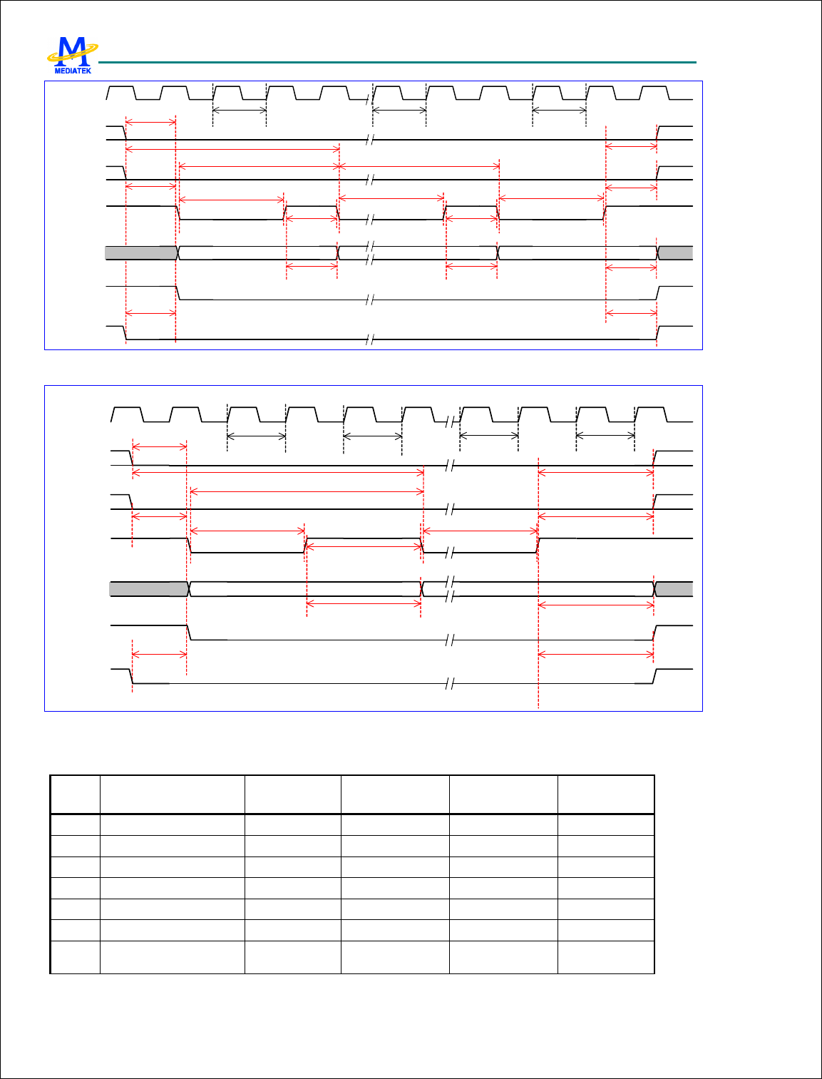
MTK Confidential Release for Konka
MTK Confidential Release for Konka
MT6228 GSM/GPRS Baseband Processor Data Sheet Revision 1.0
240/616 MediaTek Inc. Confidential
WST
t
ALS
t
ALH
t
WP
t
DH
HCLK
NALE
NWEB
NLD
t
WH
OE
(internal)
NCEB
t
CES
t
CEH
NCLE
t
CLS
t
CLH
t
DH
t
WH
t
DH
t
WP
t
WP
WST WST
D0 D526 D527
t
WC2
t
WC1
t
WC2
Figure 6 Consecutive data write cycles (1 wait state, 0 hold time extension)
WST
tALS tALH
tWP
HCLK
NALE
NWEB
NLD
tWH
WHWH
OE
(internal)
NCEB
tCES tCEH
tDH
tDH
NCLE
tCLS
D0 D527
WST
tWP
tCLH
tWC2
tWC1
Figure 7 Consecutive data write cycles (1 wait state, 1 hold time extension)
The ideal timing for read access is as listed in Table 6.
Parame
ter
Description Timing
specification
Timing at 13MHz
(RLT, WH) = (0,0)
Timing at 26MHz
(RLT, WH) = (1,0)
Timing at 52MHz
(RLT, WH) = (2,0)
T
RC1
Read cycle time 3T + RLT + WH 230.8ns 153.8ns 96.2ns
T
RC2
Read cycle time 2T + RLT + WH 153.9ns 115.4ns 76.9ns
T
DS
Read data setup time 1T + RLT 76.9ns 76.9ns 57.7ns
T
DH
Read data hold time 1T + WH 76.9ns 38.5ns 19.2ns
T
RP
Read enable time 1T + RLT 76.9ns 76.9ns 57.7ns
T
RH
Read high time 1T + WH 76.9ns 38.5ns 19.2ns
T
CLS
Command latch enable
setup time
1T 76.9ns 38.5ns 19.2ns
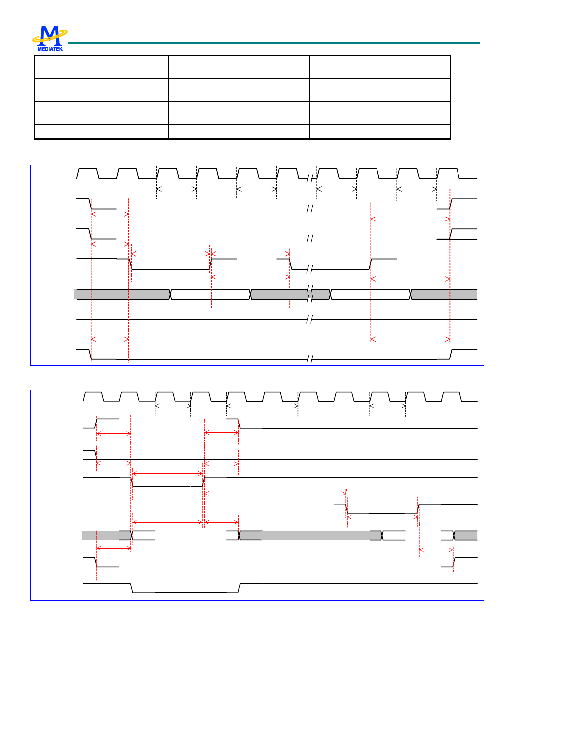
MTK Confidential Release for Konka
MTK Confidential Release for Konka
MT6228 GSM/GPRS Baseband Processor Data Sheet Revision 1.0
241/616 MediaTek Inc. Confidential
T
CLH
Command latch enable
hold time
1T + WH 76.9ns 38.5ns 19.2ns
T
ALS
Address latch enable
setup time
1T 76.9ns 38.5ns 19.2ns
T
ALH
Address latch enable hold
time
1T + WH 76.9ns 38.5ns 19.2ns
F
RC
Write data rate 1 / T
RC2
6.5Mbytes/s 8.7Mbytes/s 13Mbytes/s
Table 41 Read access timing
RLT
tALS
tCLH, tALH
tWP
HCLK
NALE
NREB
NLD
tWH
WHWH
OE
(internal)
NCEB
tCES tCEH
tDH
tDH
NCLE
tCLS
D0 D527
RLT
Figure 8 Serial read cycle (1 wait state, 1 hold time extension)
RLT
tCLS tCLH
tWP
tDH
HCLK
NCLE
NWEB
NLD
NCEB
tCES tCEH
tDS
NALE
70h
tALS tALH
NREB
Status
tWHR
tRP
RLT
OE
(internal)
W2R
Figure 9 Status read cycle (1 wait state)
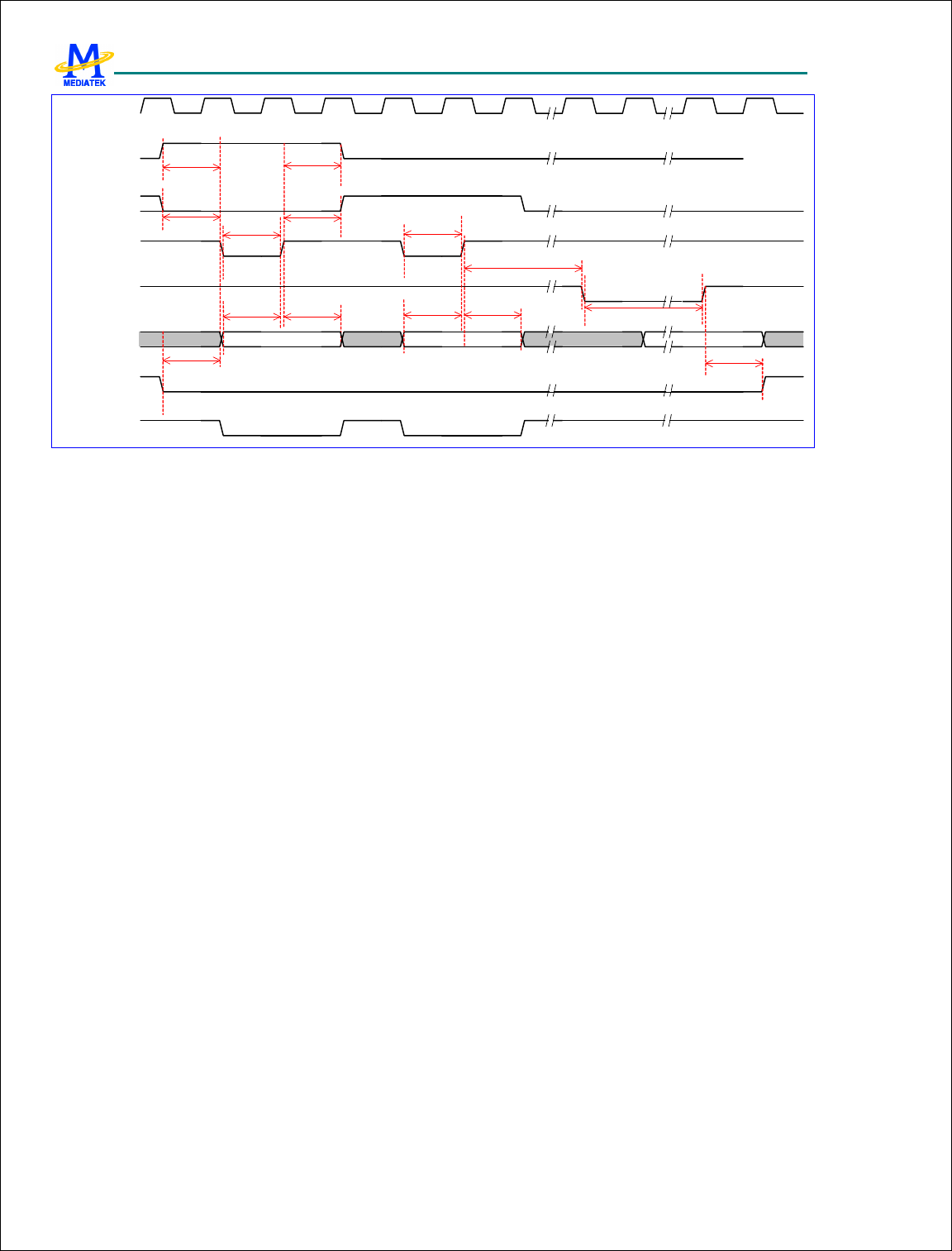
MTK Confidential Release for Konka
MTK Confidential Release for Konka
MT6228 GSM/GPRS Baseband Processor Data Sheet Revision 1.0
242/616 MediaTek Inc. Confidential
tCLS tCLH
tWP
tDH
HCLK
NCLE
NWEB
NLD
NCEB
tCES tCEH
tDS
NALE
90h
tALS tALH
NREB
01h, 06h
tWHR
tRP
OE
(internal)
tWP
00h
tDH
tDS
Figure 10 ID and manufacturer read (0 wait state)
6.3 USB OTG Controller
6.3.1 General Description
The USB OTG controller complies with Universal Serial Bus (USB) Specification Rev 1.1 and USB On-The-Go (OTG)
Supplement Rev. 1.0a. The USB OTG controller supports USB device mode, USB simple host mode, as well as OTG
handshaking capabilities, at full-speed (12 Mbps) operation. The cellular phone uses this widely available USB
interface to exchange data with USB hosts such as a PC or laptop; or to function as a host, allowing it to connect to
other devices. When operating in host mode, only a single peer-to-peer (no intermediate hub) connection is
supported.
The USB device controller provides 5 endpoints in addition to the mandatory control endpoint, three of which are for
TX transactions and two for RX transactions. Word, half-word, and byte access methods are allowed for loading and
unloading the FIFO buffer. Four independent DMA channels are equipped with the separate controllers to accelerate
data transfer. The features of each endpoint are as follows:
1. Endpoint 0 RX: A double buffer is implemented; each buffer is an 8-byte FIFO. DMA transfer is not supported.
2. Endpoint 0 TX: A double buffer is implemented; each buffer is an 8-byte FIFO. DMA transfer is not supported.
3. Endpoint 1 RX: A 64-byte FIFO that accommodates maximum packet size of 64 bytes. DMA transfer is
supported.
4. Endpoint 1 TX: A 64-byte FIFO that accommodates maximum packet size of 64 bytes. DMA transfer is
supported.
5. Endpoint 2 RX: A 64-byte FIFO that accommodates maximum packet size of 64 bytes. DMA transfer is
supported.
6. Endpoint 2 TX: A 64-byte FIFO that accommodates maximum packet size of 64 bytes. DMA transfer is
supported.
7. Endpoint 3 TX: An 8-byte FIFO that accommodates maximum packet size of 8 bytes. DMA transfer is not
supported.
MTK Confidential Release for Konka
MTK Confidential Release for Konka
MT6228 GSM/GPRS Baseband Processor Data Sheet Revision 1.0
243/616 MediaTek Inc. Confidential
This controller is highly software configurable. All endpoints except the control endpoint can be configured to be a
bulk, interrupt or isochronous endpoints.
Note: The Internal Bus clock must be running at 26Mhz or higher for the USB OTG controller to operate correctly.
6.3.2 USB MEMBUF Mapping and BDT Format
The controller uses a buffer descriptor table (BDT) mechanism for control information as well as address pointer into
the data buffer that contains the data for each endpoint. A single dedicated software-addressable local memory
(USB_MEMBUF) is allocated inside the USB controller to contain both the BDT and the data. Detailed descriptions
of the BDT and the USB_MEMBUF mapping follow.
6.3.2.1 USB MEMBUF Memory Map
Figure 11 USB Memory Buffer (96x32)

MTK Confidential Release for Konka
MTK Confidential Release for Konka
MT6228 GSM/GPRS Baseband Processor Data Sheet Revision 1.0
244/616 MediaTek Inc. Confidential
6.3.2.2 Buffer Descriptor Byte Format
Each Buffer Descriptor contains 8 bytes of data. The first word contains control information, and the second word
contains the address of the associated data buffer.
Bit 31:26 25:16 15:8 7 6 5 4 3 2 1
0
Name
RSVD
BC RSVD
OWN
DATA0
/1
KEEP/TOK_PI
D[3]
NINC/TOK_PID
[2]
DTS/TOK_PID[
1]
BDT_STALL/TOK_P
ID[0] 0
0
Name
Buffer Address (32 bits)
(Note: VUSB refers to the USB controller hardware)
BUFFER ADDRESS The Address bits represent the 32 -bit buffer address in USB MEMBUF. These bits are
unchanged by the VUSB hardware.
BC[9:0] The Byte Count bits represent a 10-bit Byte Count. The VUSB Serial Interface Engine (SIE) changes this
field upon completion of a RX transfer with the byte count of the data received.
OWN The OWN bit determines who currently owns the buffer. If OWN=1, VUSB has exclusive access to the
BD. If OWN=0 the microprocessor has exclusive access to the BD. The SIE generally writes a 0 to this
bit when it has completed a token, except when KEEP=1. When OWN=0, the VUSB ignores all other
fields in the BD, and the microprocessor has access to the entire BD. This byte of the BD must be the last
byte updated by the microprocessor when initializing a BD. Once the BD has been assigned to the VUSB,
the microprocessor must not change it in any way.
DATA0/1 The DATA0/1 bit indicates if a DATA0 field (DATA0/1=0) or a DATA1 (DATA0/1=1) field was transmitted
or received. This bit is unchanged by the VUSB.
KEEP/TOK_PID[3] If KEEP=1, once the OWN bit is set, the BD is owned by the VUSB. Typically this bit is set
to 1 for ISO endpoints that are feeding a FIFO. The microprocessor is not informed that a token has
been processed, the data is simply transferred to or from the FIFO. The NINC bit is normally also set
when KEEP=1 to prevent address increment. KEEP must equal 0 to allow the VUSB to release the
BD when a token has been processed.
If KEEP=1, this bit is unchanged by the VUSB; otherwise bit 3 of the current token PID is written
back into the BD by the VUSB.
NINC/TOK_PID[2] The No INCrement bit disables the DMA engine address increment, forcing the DMA engine to
read from or to write to the same address. This feature is useful when data needs to be read from or
written to a single location such as a FIFO. Typically this bit is set with the KEEP bit for ISO
endpoints that interface with a FIFO.
If KEEP=1, this bit is unchanged by the VUSB; otherwise bit 2 of the current token PID is written
back into the BD by the VUSB.
DTS/TOK_PID[1] Setting this bit enables Data Toggle Synchronization by the VUSB. When this bit is 0, no
Data Toggle Synchronization is performed.
If KEEP=1, this bit is unchanged by the VUSB; otherwise bit 1 of the current token PID is written
back into the BD by the VUSB.
BDT_STALL/TOK_PID[0] Setting this bit causes the VUSB to issue a STALL handshake if a token is received by
the SIE that would use the BDT in this location. The BDT is not changed by the SIE (the own
bit and the rest of the BDT remain unchanged) when the BDT-STALL bit is set.
If KEEP=1, this bit is unchanged by the VUSB; otherwise bit 0 of the current token PID is
written back into the BD by the VUSB.
TOK_PID The current token PID is written back into the BD by the VUSB when a transfer is complete. The token
PID takes on values from the USB specification: 0x1 for an OUT token, 0x9 for an IN token or 0xd for a
SETUP token. In host mode, this field is used to report the last returned PID or to indicate the transfer

MTK Confidential Release for Konka
MTK Confidential Release for Konka
MT6228 GSM/GPRS Baseband Processor Data Sheet Revision 1.0
245/616 MediaTek Inc. Confidential
status. The possible values returned are: 0x3 DATA0, 0xb DATA1, 0x2 ACK, 0xe STALL, 0xa NAK, 0x0
Bus Timeout, 0xf Data Error.
6.3.3 Operating Modes
The USB_OTG controller supports 3 modes of operation.
6.3.3.1 Standard Mode
In this mode, MEMBUF data is accessed via a single software read/write operation. Both 8-bit and 32-bit access
methods are supported. Standard mode is the most flexible operating mode with the maximum software control
flexibility. All BDT values are required to be managed by software. However, the throughput for standard mode is
slowest of the three modes due to heavy software intervention.
6.3.3.2 Direct Memory Access (DMA) Mode
In DMA mode, MEMBUF data for endpoints 1 and 2 (TX and RX) is accessed via DMA. This access method allows
for faster data movement. To issue a DMA transfer, software must enable and disable the individual USB DMA
control via its corresponding register set. Aside from the faster data movement, everything is the same as in standard
mode.
6.3.3.3 Fast Mode
To increase the operating throughput, the USB OTG controller provides a “fast mode” operation. This mode is most
suitable for transmission of large, regular chunks of data. While operating in this mode, DMA is enabled
automatically for endpoints 1 and 2 (TX and RX), and each packet transfer is 64 bytes. In order to minimize software
involvement and latency, all interrupts to the MCU (except for fast mode error status) are masked during the
transmission until the last packet is transferred. Fast mode supports only one endpoint and one direction.
Note: When using fast mode, the own bit of the BDT must be 0 to avoid a software
configuration race problem. Hardware manages the own bit value and also BDT values
automatically.
6.3.4 Special Conditions
Due to the complex nature of the USB OTG controller design and software operation, some special cases must be
noted:
1. When using DMA mode, if B2W of the generic DMA is enabled with 4-beat burst and byte access, then the
transfer count of the generic DMA controller must be set to a 4-byte multiple. Otherwise, once the controller
arranges the data into words, the few remaining bytes are incorrectly read or written one byte at a time, and each
byte is padded to a 4-byte word. The internal USB DMA controller treats each read/write as one word and
increments the address after each read/write, thereby incrementing the access pointer incorrectly.
From a software perspective, all transfer byte counts that are not 4-byte aligned must be padded to a 4-byte
multiple; That amount of space must be allocated for receiving: the extra bytes of memory need to be reserved so
the received data does not overwrite any useful data.
For example: If generic DMA is to move 13 bytes of data from USB MEM to SRAM, software must allocate 16
bytes in SRAM for such an operation. The last 3 bytes are unknown data and are to be discarded by software.
2. During a host mode operation, the CRC16 bit of the USB_ERR_STAT register cannot be checked. Instead, use
the TOK_PID bits of the BDT to check for a data CRC error.
MTK Confidential Release for Konka
MTK Confidential Release for Konka
MT6228 GSM/GPRS Baseband Processor Data Sheet Revision 1.0
246/616 MediaTek Inc. Confidential
3. When operating in fast mode, software must ignore the token_dne status bit of the USB_INT_STAT register.
4. Interrupts can come from the following sources:
a. sources listed in the USB_INT_STAT register,
b. sources listed in the USB_OTG_INT_STAT register,
c. sources listed in the USB_FM_ERR_STAT register, or,
d. PHY resume interrupt.
6.3.5 Register Definitions
(Note: VUSB and SIE refer to the USB controller hardware internal modules)
70000000h USB Peripheral ID register USB_PER_ID
Bit 7 6 5 4 3 2 1 0
Name
ID [5:0]
Type RO
Reset
0 0 0x04
DEBUG PURPOSES ONLY
ID Configuration number. This number is set to 0x04 for hardware core version control.
70000004h USB Peripheral ID complement register USB_ID_COMP
Bit 7 6 5 4 3 2 1 0
Name
NID [5:0]
Type RO
Reset
1 1
DEBUG PURPOSES ONLY
NID One’s complement of ID. This register reads back 0xFB.
70000008h USB revision register USB_REV
Bit 7 6 5 4 3 2 1 0
Name
REV [7:0]
Type RO
Reset
DEBUG PURPOSES ONLY
REV Revision ID of the hardware controller core. This register reads back 0x32.
7000000Ch USB Peripheral additional info register USB_ADD_INF
O
Bit 7 6 5 4 3 2 1 0
Name
Type
Reset
DEBUG PURPOSES ONLY
This register is used for debug purposes only. The register reads back 0x01.
70000010h USB OTG Interrupt status register USB_ISTAT
Bit 7 6 5 4 3 2 1 0
Name
ID_CHG 1_MSEC LINE_STATE_C
HG SESS_VLD_
CHG
B_SESS_CH
G A_VBUS_CH
G
Type R/W R/W R/W R/W R/W
MTK Confidential Release for Konka
MTK Confidential Release for Konka
MT6228 GSM/GPRS Baseband Processor Data Sheet Revision 1.0
247/616 MediaTek Inc. Confidential
Reset
0 0 0 0 0
The OTG Interrupt Status Register records changes of the ID and VBUS signals. Software reads this register to
determine which event is causing an interrupt. Only bits that have changed since the last software read are set.
Writing a one to a bit clears the respective interrupt. The change conditions are de-bounced in hardware.
ID_CHG This bit is set when a change in the ID Signal from the USB connector is sensed.
1_MSEC This bit is set when the 1 millisecond timer expires. This bit stays asserted until cleared by software.
The interrupt must be serviced every millisecond to avoid losing 1 ms counts.
LINE_STATE_CHG This interrupt is set when the USB line state (CTL_RG SE0 and JSTATE bits) has been stable
(unchanged) for 1 millisecond, and if the line state value is different from the last time that the line
state was stable. The interrupt is set on transitions between SE0 and J, SE0 and K, and J and K.
Changes in JSTATE while SE0 is true do not cause an interrupt. This interrupt can be used in
detecting Reset, Resume, Connect and Data Line Pulse signaling.
SESS_VLD_CHG This bit is set when a change in VBUS is detected, indicating a session has become valid or a
session is no longer valid.
B_SESS_END_CHG This bit is set when a change in VBUS is detected on a “B” device.
A_VBUS_CHG This bit is set when a change in VBUS is detected on an “A” device.
70000014h USB OTG Interrupt Control register USB_OTG_ICT
RL
Bit 7 6 5 4 3 2 1 0
Name
ID_EN 1_MSEC_EN
LINE
STATE_EN SESS_VLD_
EN B_SESS_EN
A_VBUS_EN
Type R/W R/W R/W R/W R/W
Reset
0 0 0 0 0
ID_EN Enables the ID interrupt.
1_MSEC_EN Enables the 1 millisecond timer interrupt.
LINESTATE_EN Enables the interrupt on a line state change.
SESS_VLD_EN Enables the session valid interrupt.
B_SESS_EN Enables the “B” Session End Interrupt.
A_VBUS_EN Enables the “A” VBUS Valid Interrupt.
70000018h USB OTG status register
USB_
OTG_STAT
Bit 7 6 5 4 3 2 1 0
Name
ID 1_MSEC LINE_STATE_STA
BLE SESS_VLD B_SESS_EN
D A_VBUS_VL
D
Type R/W R/W R/W R/W R/W
Reset
0 0 0 0 0
ID Indicates the current state of the ID pin on the USB connector:
0: A Type A cable has been plugged into the USB connector;
1: no cable is attached or a Type B cable has been plugged into the USB connector.
1_MSEC DEBUG only. This bit is reserved for the 1Msec count. The bit is not useful to software.
LINE_STATE_STABLE This bit is set when the line state (JSTATE and SE0 in the CTL_RG) has been stable for
the previous 1 millisecond. This bit is used to provide a hardware debounce of the line state for
detection of connect, disconnect and resume signaling. First read the state of JSTATE and SE0 in
the CTL_RG, then read this bit. If this bit is 1, then the value of the JSTATE and SE0 bits of the
CTL_RG have been static for the previous 1ms and can be considered debounced.
SESS_VLD This bit is set when the VBUS voltage is above the “B” session Valid threshold.
B_SESS_END This bit is set when the VBUS voltage is below the “B” session End threshold.

MTK Confidential Release for Konka
MTK Confidential Release for Konka
MT6228 GSM/GPRS Baseband Processor Data Sheet Revision 1.0
248/616 MediaTek Inc. Confidential
A_VBUS_VLD This bit is set when the VBUS voltage is above the “A” VBUS Valid threshold.
7000001Ch USB OTG Control register
USB_
OTG_CTRL
Bit 7 6 5 4 3 2 1 0
Name
DP_HIGH DM_HIGH DP_LOW DM_LOW VBUS_ON OTG_EN VBUS_CHG VBUS_DSC
HG
Type R/W R/W R/W R/W R/W R/W R/W R/W
Reset
0 0 0 0 0 0 0 0
The OTG Control Register controls the operation of VBUS and data line termination resistors.
DP_HIGH When set, a pull-up resistor on the D+ Data line is enabled.
DM_HIGH When set, a pull-up resistor on the D- Data line is enabled.
DP_LOW When set, a pull-down resistor on the D+ Data line is enabled.
DM_LOW When set, a pull-down resistor on the D- Data line is enabled.
VBUS_ON When set, the VBUS power signal is turned on.
OTG_EN When set, the pull-up and pull-down controls in this register are used. When OTG_EN is cleared:
• If the CTL register HOST_MODE bit is set, the D+ and D- pull-down resistors are engaged; or,
• If the CTL register HOST_MODE bit is clear and the USB_EN bit is set, the D+ pull-up is engaged.
VBUS_CHG When set, the VBUS signal is charged through a resistor.
VBUS_DSCHG When set, the VBUS signal is discharged through a resistor.
70000020h USB FM packet count number (low byte) USB_FM_PKT_NU
M_L
Bit 7 6 5 4 3 2 1 0
Name
PKT_NUM[7:0]
Type R/W
Reset
0
70000024h USB FM packet count number (low byte) USB_FM_PKT_NU
M_H
Bit 7 6 5 4 3 2 1 0
Name
PKT_NUM[15:8]
Type R/W
Reset
0
FAST MODE ONLY
PKT_NUM These 2 registers combined specify the number of 64-byte packets to be transferred.
70000028h USB FM error status register USB_FM_ERR_
STAT
Bit 7 6 5 4 3 2 1 0
Name
STA_OVR_F
LW
FM_TOK_D
ONE DMA TX DMA RX SUC_ERR NAK_ERR SHRT_ERR
Type R/W R/W R/W R/W R/W R/W R/W
Reset
0 0 0 0 0 0 0
FAST MODE ONLY All status bits that are set are cleared by rewriting a 1.
STA_OVR_FLW Indicates that during fast mode, the non-fast mode status FIFO (+0x50) has overflowed.
FM_TOK_DONE This is the non-fast mode endpoint token done interrupt. During fast mode operation, any
non-fast mode endpoint token done signal is moved to this register bit for indication.
MTK Confidential Release for Konka
MTK Confidential Release for Konka
MT6228 GSM/GPRS Baseband Processor Data Sheet Revision 1.0
249/616 MediaTek Inc. Confidential
DMA_TX_EN DEBUG only. Asserted if fm dma_rx_en is asserted and USB_FM_INT_MASK (+0x6C) mask is
enabled.
DMA_RX_EN DEBUG only. Asserted if fm dma_rx_en is asserted and USB_FM_INT_MASK (+0x6C) mask is
enabled.
SUC_ERR HOST mode only. 3 successive errors. This bit is set when the error count is 3 and
USB_FM_CTRL (+0x2C) is 1, or when the error count is 1 and USB_FM_CTRL (+0x2C) is 0.
NAK_ERR HOST mode only. This bit is set when the NAK count exceeds the IN-NAK Timeout Setting
register.
SHRT_ERR HOST mode only. Short packet error. This bit is set when the data transferred in a single
transaction is less than 64 bytes.
70000028h USB FM control register USB_FM_CTRL
Bit 7 6 5 4 3 2 1 0
Name
TOG_BIT SUC_ERR_E
N
EPT0_TX_O
DD
EPT0_RX_O
DD
FASTMODE
_EN
Type R/W R/W R R R/w
Reset
0 1 0 0 0
FAST MODE ONLY
TOG_BIT Data toggle bit. This bit indicates whether the type of data transmitted or received by hardware was
DATA0 or DATA1.
0: DATA0
1: DATA1
EP0_TX_ODD Endpoint 0 TX ODD. This bit is set when using the TX ODD BDT.
EP0_RX_ODD Endpoint 0 RX ODD. This bit is set when using the RX ODD BDT.
FASTMODE_EN Enable Fast Mode operation. This bit is reset by hardware after the transfer is complete.
70000030h USB FM transfer counter register (low byte) USB_FM_PKT_CN
T_L
Bit 7 6 5 4 3 2 1 0
Name
PKT_CNT[7:0]
Type RO
Reset
0
70000034h USB FM transfer counter register (high byte) USB_FM_PKT_CN
T_H
Bit 7 6 5 4 3 2 1 0
Name
PKT_CNT[15:8]
Type
RO
Reset
0
FAST MODE ONLY
PKT_CNT These 2 registers combined specify the number of 64-byte packets transferred.
70000038h USB FM timeout setting register (high byte) USB_FM_TIMEOU
T
Bit 7 6 5 4 3 2 1 0
Name
NAK_TIMEOUT[7:0]
Type R/W
Reset
1
FAST MODE ONLY
NAK_TIMEOUT HOST mode only. Transfer timeout setting = 64ms * NAK_TIMEOUT
MTK Confidential Release for Konka
MTK Confidential Release for Konka
MT6228 GSM/GPRS Baseband Processor Data Sheet Revision 1.0
250/616 MediaTek Inc. Confidential
7000003Ch USB FM status register USB_FM_STAT
US
Bit 7 6 5 4 3 2 1 0
Name
EPT2_TX_O
DD
EPT2_RX_O
DD
EPT1_TX_O
DD
EPT1_RX_O
DD
Type R R R R
Reset
0 0 0 0
FAST MODE ONLY
EP2_TX_ODD Endpoint 2 TX ODD.
EP2_RX_ODD Endpoint 2 RX ODD.
EP1_TX_ODD Endpoint 1 TX ODD.
EP1_RX_ODD Endpoint 1 RX ODD.
70000050h USB FM additional status register USB_
FM_ADD_STAT
Bit 7 6 5 4 3 2 1 0
Name
ENDPT[3:0] TX ODD
Type RO RO RO
Reset
0 0 0
FAST MODE ONLY
The additional status register stores the status of non-fast mode packet during fast mode operation, to allow the
intermixing of fast mode and non-fast mode packets.
When entering fast mode, any existing status in USB_STAT register that has not yet been cleared is automatically
transferred to this register. The format of this status register is the same as the USB_STAT register, and a 4-byte
FIFO is also used in this case. When the FM_TOK_DONE bit in USB_FM_ERR_STAT is cleared, the
FM_ADD_STAT register is updated with the contents of the next value in the FIFO. FM_TOK_DONE is asserted
until the FIFO is empty.
ENDPT[3:0] These four bits represents the endpoint address that received or transmitted the previous token, so that
the microprocessor can determine which BDT entry was updated by the last USB transaction.
TX This bit indicates whether the last BDT updated was for a transmit data transfer (TX=1) or for a receive data
transfer (TX=0).
ODD This bit indicates that the last buffer descriptor updated was in the odd bank of the BDT. See the earlier
section for more information on BDT address generation.
70000068h USB FM endpoint register USB_FM_ENDP
T
Bit 7 6 5 4 3 2 1 0
Name
TX_RES DMA_DONE OWN TX ENDPT[3:0]
Type R/W R/W R/W R/W R/W
Reset
0 1 0 0 0
FAST MODE ONLY
TX_RES DEVICE mode only. Tx residue. This setting is used when the transmit byte count is not a multiple of
64 bytes. By default, fast mode operates on 64B packet boundaries, and the fast mode-done indication is
asserted once the last 64-byte packet is sent: no further USB DMA sequence takes place. If this bit is set,
the fast mode controller issues an additional dma_tx_en request to the USB DMA controller after the last
64B-aligned packet is sent, even with fast mode-done indication still asserted, allowing the USB DMA
engine to fetch the next non-64B-aligned data. Software needs to take this situation into consideration.
MTK Confidential Release for Konka
MTK Confidential Release for Konka
MT6228 GSM/GPRS Baseband Processor Data Sheet Revision 1.0
251/616 MediaTek Inc. Confidential
DMA_DONE DEBUG only. Test only.
OWN DEBUG only. Own bit of fast mode. This bit is used when a token is received during fast mode but the
BDT is not yet valid, or the BDT is valid but fast mode has not yet been enabled. The bit clears itself once
fast mode completes.
TX DEVICE mode only. The endpoint direction of fast mode. TX=1 indicates a transmit (IN) direction; TX=0
indicates a receive (OUT) direction.
7000006Ch USB FM interrupt mask register USB_FM_INT_MAS
K
Bit 7 6 5 4 3 2 1 0
Name
DMA_TX_EN_M
ASK
DMA_RX_EN_M
ASK
Type R/W R/W
Reset
0 0
FAST MODE ONLY
DMA_TX_MASK DEBUG only. When set, the dma_tx_en interrupt is enabled.
DMA_RX_MASK DEBUG only. When set, the dma_rx_en interrupt is enabled.
70000070h USB extra register USB_EXTRA
Bit 7 6 5 4 3 2 1 0
Name
PHY_RESUME_
INT PHY_RESU
ME_INT_EN
PHY_SUSPN
D
TOGGLE_TE
ST
Type RO R/W R/W R/W
Reset
0 0 0 0
PHY_RESUME_INT Interrupt indicating PHY Resume. This bit can only be asserted when PHY_SUSPND =1.
This bit clears itself when PHY_SUSPND=0.
PHY_RESUME_INT_EN When set, the PHY Resume interrupt is enabled.
PHY_SUSPND When set, the PHY is suspended.
TOGGLE_TEST DEBUG only. Toggles USB DP/DM output automatically.
70000080h USB Interrupt status register USB_INT_STAT
Bit 7 6 5 4 3 2 1 0
Name
STALL ATTACH RESUME SLEEP TOK_DNE SOF_TOK ERROR USB_RST
Type R/W R/W R/W R/W R/W R/W R/W R/W
Reset
0 0 0 0 0 0 0 0
All status bits that are set are cleared by rewriting a 1.
STALL The stall interrupt is used in target and host modes. In target mode the stall bit is asserted when a
STALL handshake is sent by the SIE.
In host mode this bit is set if the VUSB has detected a STALL acknowledgement during the handshake
phase of a USB transaction. This interrupt is useful for determining if the last USB transaction was
completed successfully or stalled.
ATTACH This bit is set if the VUSB has detected the attachment of a USB peripheral. This signal is only valid if
HOST_MODE_EN is true. This interrupt signifies that a peripheral is now present and must be
configured. The ATTACH interrupt is asserted if there have been no transitions on the USB for 2.5us
and the current bus state is not SE0.
RESUME This bit is set when a K-state is observed on the DP/DM signals for 2.5usec. The bit can indicate a
remote wake up signal on the USB bus. When not in suspend mode, disable this interrupt.
(Note: this bit is only useful if the PHY has not been powered down into suspend mode. Otherwise, use
USB_EXTRA register status bits to resume monitoring.)
MTK Confidential Release for Konka
MTK Confidential Release for Konka
MT6228 GSM/GPRS Baseband Processor Data Sheet Revision 1.0
252/616 MediaTek Inc. Confidential
SLEEP This bit is set if the VUSB has detected a constant idle on the USB bus signals for 3 ms. The sleep timer
is reset by activity on the USB bus.
TOK_DNE This bit is set when the current token being processing is complete. The microprocessor must
immediately read the STAT register to determine the End Point and BD used for this token. Clearing this
bit (by writing a one) causes the STAT register to be cleared or the STAT holding register to be loaded into
the STAT register. (Note: When Fast Mode is enabled, DO NOT look at this bit.)
SOF_TOK This bit is set if the VUSB has received a Start Of Frame (SOF) token. In host mode, this bit is set when
the SOF threshold is reached, so that software can prepare for the next SOF.
ERROR This bit is set when any of the error conditions in the ERR_STAT register has occurred. The
microprocessor must then read the ERR_STAT register to determine the source of the error.
USB_RST This bit is set when the VUSB has decoded a valid USB reset. An asserted USB_RST bit informs the
microprocessor to write 0x00 into the address register and enable endpoint 0. USB_RST is set once a
USB reset has been detected for 2.5 microseconds, and is not asserted again until the USB reset condition
has been removed, and then reasserted.
70000084h USB Interrupt Enable register USB_INT_ENB
Bit 7 6 5 4 3 2 1 0
Name
STALL ATTACH RESUME SLEEP TOK_DNE SOF_TOK ERROR USB_RST
Type
R/W R/W R/W R/W R/W R/W R/W R/W
Reset
0 0 0 0 0 0 0 0
STALL Setting this bit enables the STALL interrupt.
ATTACH Setting this bit enables the ATTACH interrupt.
RESUME Setting this bit enables the RESUME interrupt.
SLEEP Setting this bit enables the SLEEP interrupt.
TOK_DNE Setting this bit enables the TOK_DNE interrupt.
SOF_TOK Setting this bit enables the SOF_TOK interrupt.
ERROR Setting this bit enables the ERROR interrupt.
USB_RST Setting this bit enables the USB_RST interrupt.
70000088h USB Error Interrupt Status register USB_ERR_STAT
Bit 7 6 5 4 3 2 1 0
Name
BTS_ERR DMA_ERR BTO_ERR DFN8 CRC16 CRC5/EOF PID_ERR
Type R/W R/W R/W R/W R/W R/W R/W
Reset
0 0 0 0 0 0 0
The Error Interrupt Status Register contains bits for each of the error sources within the VUSB. Each of these bits are
qualified with their respective error enable bits (See Error Enable Register page ). The error bits are OR'ed together
and the result is sent to the ERROR bit of the INT_STAT register. Once an interrupt bit has been set, it can only be
cleared by writing a one to the respective interrupt bit. Each bit is set as soon as the error condition is detected.
Thus, the interrupt does not typically correspond with the end of a token being processed.
(Note: All status bits that are set are cleared by writing a 1.)
BTS_ERR A bit stuff error has been detected. If set, the corresponding packet is rejected due to a bit stuff error.
DMA_ERR This bit is set if the VUSB has requested a DMA access to read a new BDT but the bus is not available
before VUSB needs to receive or transmit data. If processing a TX transfer, a transmit data underflow
condition occurs. If processing an RX transfer, a receive data overflow condition occurs. This
interrupt is useful when developing device arbitration hardware for the microprocessor and VUSB to
minimize bus request and bus grant latency. This bit is also set if a data packet to or from the host is
MTK Confidential Release for Konka
MTK Confidential Release for Konka
MT6228 GSM/GPRS Baseband Processor Data Sheet Revision 1.0
253/616 MediaTek Inc. Confidential
larger than the allocated buffer size in the BDT. In this case the data packet is truncated as it is placed
into the buffer memory.
BTO_ERR This bit is set if a bus turnaround timeout error has occurred. This VUSB uses a bus turnaround timer to
keep track of the amount of time elapsed between the token and data phases of a SETUP or OUT TOKEN,
or between the data and handshake phases of a IN TOKEN. If more than 16 bit times are counted from
the previous EOP before a transition from IDLE, a bus turnaround timeout error occurs.
DFN8 The data field received is not a multiple of 8 bits. The USB Specification 1.0 specifies that the data field
must be an integral number of bytes. If the data field is not an integral number of bytes, this bit is set.
CRC16 The CRC16 failed. If set, the data packet was rejected due to a CRC16 error.
(Note: When in HOST MODE, ignore this bit. Look at the BDT TOK_PID entries instead to
determine error conditions.)
CRC5/EOF This error interrupt has two functions. When the VUSB is operating in peripheral mode
(HOST_MODE_EN=0) this interrupt detects a CRC5 error in token packets generated by the host. If set,
the token packet was rejected due to a CRC5 error. When the VUSB is operating in host mode
(HOST_MODE_EN=1), this interrupt detects End of Frame (EOF) error conditions. This condition
occurs when the VUSB is transmitting or receiving data and the SOF counter has reached zero. This
interrupt is useful when developing USB packet scheduling software to ensure that no USB transactions
cross into the start of the next frame.
PID_ERR The PID check field failed.
7000008Ch USB Error Interrupt Enable register USB_ERR_ENB
Bit 7 6 5 4 3 2 1 0
Name
BTS_ERR DMA_ERR BTO_ERR DFN8 CRC16 CRC5/EOF PID_ERR
Type R/W R/W R/W R/W R/W R/W R/W
Reset
0 0 0 0 0 0 0
BTS_ERR Setting this bit enables the BTS_ERR interrupt.
DMA_ERR Setting this bit enables the DMA_ERR interrupt.
BTO_ERR Setting this bit enables the BTO_ERR interrupt.
DFN8 Setting this bit enables the DFN8_ERR interrupt.
CRC16 Setting this bit enables the CRC16 interrupt.
CRC5/EOF Setting this bit enables the CRC5/EOF_ERR interrupt.
PID_ERR Setting this bit enables the PID_ERR interrupt.
70000090h USB Status register USB_ STAT
Bit 7 6 5 4 3 2 1 0
Name
ENDPT[3:0] TX ODD
Type RO RO RO
Reset
0 0 0
The Status Register reports the transaction status within the VUSB. When the microprocessor has received a
TOK_DNE interrupt, the Status Register should be read to determine the status of the previous endpoint
communication. The data in the status register is valid when the TOK_DNE interrupt bit is asserted. The STAT
register acts as a read window into a status FIFO maintained by the VUSB. When the VUSB uses a BD, the status
register is updated. If another USB transaction is performed before the TOK_DNE interrupt is serviced the VUSB
stores the status of the next transaction in the STAT FIFO. Thus, the STAT register is actually a 4-byte FIFO that
allows the microprocessor to process one transaction while the SIE is processing the next. Clearing the TOK_DNE bit
in the INT_STAT register causes the SIE to update the STAT register with the contents of the next STAT value. If
the data in the STAT holding register is valid, the SIE immediately reasserts the TOK_DNE interrupt.
MTK Confidential Release for Konka
MTK Confidential Release for Konka
MT6228 GSM/GPRS Baseband Processor Data Sheet Revision 1.0
254/616 MediaTek Inc. Confidential
ENDPT[3:0] These four bits encode the endpoint address that received or transmitted the previous token, allowing
the microprocessor to determine which BDT entry was updated by the last USB transaction.
TX This bit indicates whether the last BDT updated was a transmit transfer (TX=1), or a receive data transfer
(TX=0).
ODD This bit indicates that the last buffer descriptor updated was in the odd bank of the BDT. See earlier section
for more information on BDT address generation.
70000094h USB Control register USB_CTL
Bit 7 6 5 4 3 2 1 0
Name
JSTATE SE0
TXDSUSPEN
D /
TOKENBUSY
RESET HOST_MOD
E EN RESUME ODD_RST USB_EN /
SOF_EN
Type R/W R/W R/W R/W R/W R/W R/W R/W
Reset
0 0 0 0 0 0 0 0
JSTATE Live USB differential receiver JSTATE signal. The polarity of this signal is affected by the current state of
LS_EN (See the Address Register description below).
SE0 Live USB Single Ended Zero signal.
TXDSUSPEND / TOKENBUSY
This dual use control signal is used to access TXD_SUSPEND when the VUSB is a target, and Token Busy
when the VUSB is in host mode.
The TXD Suspend bit informs the processor that the SIE has disabled packet transmission and reception.
Clearing this bit allows the SIE to continue token processing. This bit is set by the SIE when a Setup Token
is received allowing software to dequeue any pending packet transactions in the BDT before resuming token
processing.
The Token Busy bit informs the host processor that the VUSB is busy executing a USB token and that no
more token commands should be written to the Token Register. Software must check this bit before writing
any tokens to the Token Register to ensure that token command are not lost.
RESET Setting this bit enables the VUSB to generate USB reset signaling, allowing the VUSB to reset USB
peripherals. This control signal is only valid in host mode, (i.e. HOST_MDOE_EN=1). Software must set
RESET=1 for the required amount of time and then clear it to 0 to end reset signaling. For more
information on RESET signaling see Section 7.1.4.3 of the USB specification version 1.0.
HOST_MODE_EN Setting this bit enables the VUSB to operate in host mode. In host mode the VUSB performs
USB transactions under the programmed control of the host processor.
RESUME Setting this bit allows the VUSB to execute resume signaling, allowing the VUSB to perform remote
wake-up. Software must set RESUME=1 for the required amount of time and then clear it to 0. If the
HOST_MODE_EN bit is set, the VUSB appends a Low Speed End of Packet to the Resume signal when the
RESUME bit is cleared. For more information on RESUME signaling see Section 7.1.4.5 of the USB
specification version 1.0.
ODD_RST Setting this bit resets all the BDT ODD ping/pong bits to 0 which then specify the EVEN BDT bank.
USB_EN / SOF_EN Setting this bit enables the VUSB; clearing the bit disables the VUSB. Setting this bit causes
the SIE to reset all of its ODD bits to the BDTs. Thus, setting this bit resets much of the logic in the SIE.
When host mode is enabled clearing this bit causes the SIE to stop sending SOF tokens.
70000098h USB Address register USB_ADDR
Bit 7 6 5 4 3 2 1 0
Name
LS_EN ADDR[6:0]
Type R/W R/W
Reset
0 0
MTK Confidential Release for Konka
MTK Confidential Release for Konka
MT6228 GSM/GPRS Baseband Processor Data Sheet Revision 1.0
255/616 MediaTek Inc. Confidential
LS_EN The Low Speed enable bit informs the VUSB that the next token command written to the token register
must be performed at low speed. This indication enables the VUSB to perform necessary preparations
for low speed data transmissions.
ADDR[6:0] This 7-bit value defines the USB address that the VUSB decodes in peripheral mode, or transmits when in
host mode.
7000009Ch USB BDT page 1 register USB_BDT_PAG
E_01
Bit 7 6 5 4 3 2 1 0
Name
BDT_BA [15:8]
Type R/W
Reset
0
700000B0h USB BDT page 2 register USB_BDT_PAG
E_02
Bit 7 6 5 4 3 2 1 0
Name
BDT_BA [23:16]
Type R/W
Reset
0
700000B4h USB BDT page 3 register USB_BDT_PAG
E_03
Bit 7 6 5 4 3 2 1 0
Name
BDT_BA [31:24]
Type R/W
Reset
0
BDT_BA[31:8] These 3 registers combined forms the BDT_PAGE pointer. Set these bytes as follows:
USB_BDT_PAGE_01 = 0x0
USB_BDT_PAGE_02 = 0x0
USB_BDT_PAGE_03 = 0xBD
700000A0h USB Frame number low byte register USB_FRM_NU
ML
Bit 7 6 5 4 3 2 1 0
Name
FRM[7:0]
Type RO
Reset
0
700000A4h USB Frame number high byte register USB_FRM_NU
MH
Bit 7 6 5 4 3 2 1 0
Name
FRM[10:8]
Type RO
Reset
0
FRM[10:0] These 2 registers combined represent the 11-bit frame number. The registers are updated with the
current frame number whenever a SOF TOKEN is received.
700000A8h USB Token register USB_TOKEN
Bit 7 6 5 4 3 2 1 0
MTK Confidential Release for Konka
MTK Confidential Release for Konka
MT6228 GSM/GPRS Baseband Processor Data Sheet Revision 1.0
256/616 MediaTek Inc. Confidential
Name TOKEN_PID TOKEN_ENDPT
Type R/W R/W
Reset 0 0
The Token Register is used when performing USB transactions when in host mode (HOST_MODE_EN=1). When
the host processor wishes to execute a USB transaction to a peripheral, it writes the TOKEN type and endpoint to this
register. Once this register has been updated the VUSB begins the specified USB transaction to the address contained
in the Address Register. The host processor must check that the TOKEN_BUSY bit in the control register is not set
before performing a write to the Token Register: checking ensures that token commands are not overwritten before they
can be executed. The address register and endpoint control register 0 are also used when performing a token
command and therefore must also be updated before the Token Register. The address register is used to select the
correct USB peripheral address to transmit by the token command. The endpoint control register determines the
handshake and retry policies used during the transfer.
TOKEN_PID This 4-bit value is the token type that is executed by the VUSB. Valid tokens are:
TOKEN_PID TOKEN type Description
0001 OUT VUSB performs an OUT (TX) Transaction
1001 IN VUSB performs an IN (RX) Transaction
1101 SETUP VUSB performs a SETUP (TX) Transaction
TOKEN_ENDPT This 4-bit value determines the Endpoint address for the token command. The 4-bit value that
is written must be a valid endpoint.
700000ACh USB SOF threshold register USB_SOF_THL
D
Bit 7 6 5 4 3 2 1 0
Name
CNT[7:0]
Type R/W
Reset
0
The Start Of Frame (SOF) Threshold Registers are used only in HOST_MODE. When HOST_MODE is enabled, the
14-bit SOF counter counts the interval between SOF frames. The SOF must be transmitted every millisecond so the
SOF counter is loaded with a value of 12000 since it is based on a 12MHz internal counter. When the SOF counter
reaches zero, a SOF token is transmitted. The SOF threshold register is used to program the number of USB byte
times before the SOF to stop initiating token packet transactions. This register must be set to a value that ensures that
other packets are not actively being transmitted when the SOF timer count reaches zero. When the SOF counter
reaches the threshold value, no more tokens are transmitted until after the SOF has been transmitted. The value
programmed into the threshold register must reserve enough time to ensure that the worst case transaction completes.
In general the worst case transaction is an IN token followed by a data packet from the target, followed by the response
from the host. The actual time required is a function of the maximum packet size on the bus. Typical values for the
SOF threshold are:
Package size (bytes) Time (byte times)
64 74
32 42
16 26
8 18
CNT[7:0] These bits represents the SOF count threshold in BYTE times.
MTK Confidential Release for Konka
MTK Confidential Release for Konka
MT6228 GSM/GPRS Baseband Processor Data Sheet Revision 1.0
257/616 MediaTek Inc. Confidential
700000C0h~
700000FFh USB Endpoint Control register USB_EP_CTL
N
Bit 7 6 5 4 3 2 1 0
Name
HOST_WO_
HUB RETRY_DIS EP_CTL_DIS
EP_RX_EN EP_TX_EN EP_STALL EP_HSHK
Type R/W R/W R/W R/W R/W R/W R/W
Reset
0 0 0 0 0 0 0
The Endpoint Control Registers contains the endpoint control bits for each of the 16 endpoints available on USB for a
decoded address. These four bits define all of the control necessary for any one endpoint. The formats for these
registers are shown in the table on the following page. Endpoint 0 (ENDP0) is associated with control pipe 0 which is
required by USB for all functions. Therefore, after a USB_RST interrupt has been received the microprocessor must
set ENDPT0 to contain 0x0D. In host mode ENDPT0 is used to determine the handshake, retry and low-speed
characteristics of the host transfer. For host mode control, bulk and interrupt transfers, the EP_HSHK bit must be set
to 1; for Isochronous transfers the EP_HSHK must be set to 0. Common values for ENDPT0 in host mode are 0x4D
for Control, Bulk and Interrupt transfers, and 0x4C for Isochronous transfers.
HOST_WO_HUB HOST mode only. This bit is only present in the control register for endpoint 0 (endpt0_rg).
When this bit is set, the host can communicate with a directly connected low-speed device. When
cleared, the host produces a PRE_PID then switches to low-speed signaling when sending a token to
a low-speed device, as required for communication with a low-speed device via a hub.
RETRY_DIS HOST mode only. This bit is only present in the control register for endpoint 0 (endpt0_rg).
When this bit is set, the host does not reattempt NAK’ed transactions. When a transaction is
NAK’ed, the BDT PID field is updated with the NAK pid, and the token done interrupt is set. When
this bit is cleared, NAK’ed transactions are retried in hardware. This bit must be set when the host
is attempting to poll an interrupt endpoint.
EP_CTL_DIS, EP_RX_EN, EP_TX_EN
These 3 bits define if an endpoint is enabled and the direction of the endpoint. The endpoint enable/direction
control is defined as follows:
ep_ctl_dis ep_rx_en ep_tx_en endpoint en / direction control
X 0 0 Disable Endpoint
X 0 1 Enable Endpoint for TX transfers only
X 1 0 Enable Endpoint for RX transfers only
1 1 1 Enable Endpoint for both RX and TX transfers
0 1 1 Enable Endpoint for RX and TX and control transfers
EP_STALL When set to 1, this bit indicates that the endpoint is stalled. This bit has priority over all other
control bits in the End Point Enable register, but is only valid if EP_TX_EN=1 or EP_RX_EN=1.
Any access to this endpoint causes the VUSB to return a STALL handshake. Once an endpoint is
stalled, intervention from the Host Controller is required.
EP_HSHK Setting this bit determines if an endpoint performs handshaking during a transaction to this endpoint.
This bit is generally set to 1 unless the endpoint is an Isochronous endpoint.
700000410h USB DMA enable USB_DMA_EN
Bit 7 6 5 4 3 2 1 0
Name
TX2_DMA_EN RX2_DMA_EN TX1_DMA_EN RX1_DMA_EN
Type W W W W
Reset
0 0 0 0
These are 1 shot signal.
TX2_DMA_EN Setting this bit enablesTX2 DMA.
MTK Confidential Release for Konka
MTK Confidential Release for Konka
MT6228 GSM/GPRS Baseband Processor Data Sheet Revision 1.0
258/616 MediaTek Inc. Confidential
RX2_DMA_EN Setting this bit enables RX2 DMA.
TX1_DMA_EN Setting this bit enables TX1 DMA.
RX1_DMA_EN Setting this bit enables RX1 DMA.
700000414h USB DMA disable USB_DMA_DIS
Bit 7 6 5 4 3 2 1 0
Name
TX2_DMA_DIS RX2_DMA_DIS TX1_DMA_DIS RX1_DMA_DIS
Type W W W W
Reset
0 0 0 0
These are 1 shot signal.
TX2_DMA_DIS Setting this bit disables TX2 DMA.
RX2_DMA_DIS Setting this bit disables RX2 DMA.
TX1_DMA_DIS Setting this bit disables TX1 DMA.
RX1_DMA_DIS Setting this bit disables RX1 DMA.
700000414h USB DMA address counter clear USB_DMA_ADDR_CNTE
R_CLR
Bit 7 6 5 4 3 2 1 0
Name
TX2_DMA_CLR
RX2_DMA_CLR
TX1_DMA_CLR
RX1_DMA_CLR
Type
W W W W
Reset
0 0 0 0
These are 1 shot signals.
TX2_DMA_CLR Setting this bit clears the TX2 DMA address pointer.
RX2_DMA_CLR Setting this bit clears the RX2 DMA address pointer.
TX1_DMA_CLR Setting this bit clears the TX1 DMA address pointer.
RX1_DMA_CLR Setting this bit clears the RX1 DMA address pointer.
7000041Ch USB DMA FM select register USB_DMA_FM_SELEC
T
Bit 7 6 5 4 3 2 1 0
Name
DMA_FM_SEL
Type R/W
Reset
0
FAST MODE ONLY
DMA_FM_SEL Selects which USB DMA controller the FM controller should use.
00: Use RX1 DMA
01: Use TX1 DMA
10: Use RX2 DMA
11: Use TX1 DMA
70000420h USB Soft Reset USB_SOFT_RE
SET
Bit 7 6 5 4 3 2 1 0
Name
SOFT_RESE
T
Type W
Reset
0
SOFT_RESET Setting this bit to 1 invokes a synchronous soft reset. The asserted bit holds high for 4 clock counts,
therefore, software must not issue any read/write within 4T of this reset.

MTK Confidential Release for Konka
MTK Confidential Release for Konka
MT6228 GSM/GPRS Baseband Processor Data Sheet Revision 1.0
259/616 MediaTek Inc. Confidential
70000450h USB PHY Control USB_PHY_CTR
L
Bit 7 6 5 4 3 2 1 0
Name
PUSW2EB_
REG MANUAL
Type R R
Reset
0 0
DEBUG ONLY
The 2 register bits are used to manually control IPUSW2EB signal to PHY. When Manual =1, IPUSW2EB contains
the value of IPUSW2EB_REG.
6.4 Memory Stick and SD Memory Card Controller
6.4.1 Introduction
The controller fully supports the Memory Stick bus protocol as defined in Format Specification version 2.0 of Memory
Stick Standard (Memory Stick PRO) and the SD Memory Card bus protocol as defined in SD Memory Card
Specification Part 1 Physical Layer Specification version 1.0 as well as the MultiMediaCard (MMC) bus protocol as
defined in MMC system specification version 2.2. Since SD Memory Card bus protocol is backward compatible to
MMC bus protocol, the controller is capable of working well as the host on MMC bus under control of proper firmware.
Furthermore, the controller also support SDIO card specification version 1.0 partially. However, the controller can only
be configured as either the host of Memory Stick or the host of SD/MMC Memory Card at one time. Hereafter, the
controller is also abbreviated as MS/SD controller. The following are the main features of the controller.
Interface with MCU by APB bus
16/32-bit access on APB bus
16/32-bit access for control registers
32-bit access for FIFO
Shared pins for Memory Stick and SD/MMC Memory Card
Built-in 32 bytes FIFO buffers for transmit and receive, FIFO is shared for transmit and receive
Built-in CRC circuit
CRC generation can be disabled
DMA supported
Interrupt capabilities
Automatic command execution capability when an interrupt from Memory Stick
Data rate up to 26 Mbps in serial mode, 26x4 Mbps in parallel model, the module is targeted at 26 MHz
operating clock
Serial clock rate on MS/SD/MMC bus is programmable
Card detection capabilities
Controllability of power for memory card
Not support SPI mode for MS/SD/MMC Memory Card
MTK Confidential Release for Konka
MTK Confidential Release for Konka
MT6228 GSM/GPRS Baseband Processor Data Sheet Revision 1.0
260/616 MediaTek Inc. Confidential
Not support multiple SD Memory Cards
6.4.2 Overview
6.4.2.1 Pin Assignment
Since the controller can only be configured as either the host of Memory Stick or the host of SD/MMC Memory Card at
one time, pins for Memory Stick and SD/MMC Memory Card are shared in order to save pin counts. The following
lists pins required for Memory Stick and SD/MMC Memory Card. Table 42 shows how they are shared. In Table 42,
all I/O pads have embedded both pull up and pull down resistor because they are shared by both the Memory Stick and
SD/MMC Memory Card. Pins 2,4,5,8 are only useful for SD/MMC Memory Card. Pull down resistor for these pins can
be used for power saving. All embedded pull-up and pull-down resistors can be disabled by programming the
corresponding control registers if optimal pull-up or pull-down resistors are required on the system board. The pin
VDDPD is used for power saving. Power for Memory Stick or SD/MMC Memory Card can be shut down by
programming the corresponding control register. The pin WP (Write Protection) is only valid when the controller is
configured for SD/MMC Memory Card. It is used to detect the status of Write Protection Switch on SD/MMC Memory
Card.
No. Name Type MMC SD MS MSPRO Description
SD_CLK O CLK CLK SCLK SCLK Clock
SD_DAT3 I/O/PP CD/DAT3 DAT3 Data Line [Bit 3]
SD_DAT0 I/O/PP DAT0 DAT0 SDIO DAT0 Data Line [Bit 0]
SD_DAT1 I/O/PP DAT1 DAT1 Data Line [Bit 1]
SD_DAT2 I/O/PP DAT2 Data Line [Bit 2]
SD_CMD I/O/PP CMD CMD BS BS Command Or Bus State
SD_PWRON O VDD ON/OFF
SD_WP
I
SD_INS
I INS INS
Table 42 Sharing of pins for Memory Stick and SD/MMC Memory Card Controller
6.4.2.2 Card Detection
For Memory Stick, the host or connector should provide a pull up resistor on the signal INS. Therefore, the signal INS
will be logic high if no Memory Stick is on line. The scenario of card detection for Memory Stick is shown in Figure
12. Before Memory Stick is inserted or powered on, on host side SW1 shall be closed and SW2 shall be opened for
card detection. It is the default setting when the controller is powered on. Upon insertion of Memory Stick, the signal
INS will have a transition from high to low. Hereafter, if Memory Stick is removed then the signal INS will return to
logic high. If card insertion is intended to not be supported, SW1 shall be opened and SW2 closed always.
For SD/MMC Memory Card, detection of card insertion/removal by hardware is also supported. Because a pull down
resistor with about 470 KΩ resistance which is impractical to embed in an I/O pad is needed on the signal CD/DAT3,
and it has to be capable of being connected or disconnected dynamically onto the signal CD during initialization period,
an additional I/O pad is needed to switch on/off the pull down resistor on the system board. The scenario of card
detection for SD/MMC Memory Card is shown in Figure 13. Before SD/MMC Memory Card is inserted or powered
on, SW1 and SW2 shall be opened for card detection on the host side. Meanwhile, pull down resistor R
CD
on system
board shall attach onto the signal CD/DAT3 by the output signal RCDEN. In addition, SW3 on the card is default to be
closed. Upon insertion of SD/MMC Memory Card, the signal CD/DAT3 will have a transition from low to high. If
SD/MMC Memory Card is removed then the signal CD/DAT3 will return to logic low. After the card identification
process, pull down resistor R
CD
on system board shall disconnect with the signal CD/DAT3 and SW3 on the card shall
be opened for normal operation.
Since the scheme above needs a mechanical switch such as a relay on system board, it is not ideal enough. Thus, a
dedicated pin “INS” is used to perform card insertion and removal for SD/MMC. The pin “INS” will connect to the pin
MTK Confidential Release for Konka
MTK Confidential Release for Konka
MT6228 GSM/GPRS Baseband Processor Data Sheet Revision 1.0
261/616 MediaTek Inc. Confidential
“VSS2” of a SD/MMC connector. Then the scheme of card detection is the same as that for MS. It is shown in Figure
12.
Figure 12 Card detection for Memory Stick
Figure 13 Card detection for SD/MMC Memory Card
MTK Confidential Release for Konka
MTK Confidential Release for Konka
MT6228 GSM/GPRS Baseband Processor Data Sheet Revision 1.0
262/616 MediaTek Inc. Confidential
6.4.3 Register Definitions
REGISTER ADDRESS REGISTER NAME SYNONYM
MSDC + 0000h MS/SD Memory Card Controller Configuration Register MSDC_CFG
MSDC + 0004h MS/SD Memory Card Controller Status Register MSDC_STA
MSDC + 0008h MS/SD Memory Card Controller Interrupt Register MSDC_INT
MSDC + 000Ch MS/SD Memory Card Controller Data Register MSDC_DAT
MSDC + 00010h MS/SD Memory Card Pin Status Register MSDC_PS
MSDC + 00014h MS/SD Memory Card Controller IO Control Register MSDC_IOCON
MSDC + 0020h SD Memory Card Controller Configuration Register SDC_CFG
MSDC + 0024h SD Memory Card Controller Command Register SDC_CMD
MSDC + 0028h SD Memory Card Controller Argument Register SDC_ARG
MSDC + 002Ch SD Memory Card Controller Status Register SDC_STA
MSDC + 0030h SD Memory Card Controller Response Register 0 SDC_RESP0
MSDC + 0034h SD Memory Card Controller Response Register 1 SDC_RESP1
MSDC + 0038h SD Memory Card Controller Response Register 2 SDC_RESP2
MSDC + 003Ch SD Memory Card Controller Response Register 3 SDC_RESP3
MSDC + 0040h SD Memory Card Controller Command Status Register SDC_CMDSTA
MSDC + 0044h SD Memory Card Controller Data Status Register SDC_DATSTA
MSDC + 0048h SD Memory Card Status Register SDC_CSTA
MSDC + 004Ch SD Memory Card IRQ Mask Register 0 SDC_IRQMASK0
MSDC + 0050h SD Memory Card IRQ Mask Register 1 SDC_IRQMASK1
MSDC + 0054h SDIO Configuration Register SDIO_CFG
MSDC + 0058h SDIO Status Register SDIO_STA
MSDC + 0060h Memory Stick Controller Configuration Register MSC_CFG
MSDC + 0064h Memory Stick Controller Command Register MSC_CMD
MSDC + 0068h Memory Stick Controller Auto Command Register MSC_ACMD
MSDC + 006Ch Memory Stick Controller Status Register MSC_STA
Table 43 MS/SD Controller Register Map
6.4.3.1 Global Register Definitions
MSDC+0000h MS/SD Memory Card Controller Configuration
Register MSDC_CFG
Bit 31 30 29 28 27 26 25 24 23 22 21 20 19 18 17 16
Name
FIFOTHD PRCFG2 PRCFG1 PRCFG0 VDDP
D
RCDE
N
DIRQ
EN
PINE
N
DMAE
N
INTE
N
Type R/W R/W R/W R/W R/W R/W R/W R/W R/W R/W
Reset
0001 01 01 10 0 0 0 0 0 0
Bit 15 14 13 12 11 10 9 8 7 6 5 4 3 2 1 0
Name
SCLKF SCLK
ON CRED
STDB
Y
CLKS
RC RST NOCR
C RED MSD
C
Type R/W R/W R/W R/W R/W W R/W R/W R/W
Reset
00000000 0 0 1 0 0 0 0 0

MTK Confidential Release for Konka
MTK Confidential Release for Konka
MT6228 GSM/GPRS Baseband Processor Data Sheet Revision 1.0
263/616 MediaTek Inc. Confidential
The register is for general configuration of the MS/SD controller. Note that MSDC_CFG[31:16] can be accessed by
16-bit APB bus access.
MSDC The register bit is used to configure the controller as the host of Memory Stick or as the host of SD/MMC
Memory card. The default value is to configure the controller as the host of Memory Stick.
0 Configure the controller as the host of Memory Stick
1 Configure the controller as the host of SD/MMC Memory card
RED Rise Edge Data. The register bit is used to determine that serial data input is latched at the falling edge or the
rising edge of serial clock. The default setting is at the rising edge. If serial data has worse timing, set the
register bit to ‘1’. When memory card has worse timing on return read data, set the register bit to ‘1’.
0 Serial data input is latched at the rising edge of serial clock.
1 Serial data input is latched at the falling edge of serial clock.
NOCRC CRC Disable. A ‘1’ indicates that data transfer without CRC is desired. For write data block, data will be
transmitted without CRC. For read data block, CRC will not be checked. It is for testing purpose.
0 Data transfer with CRC is desired.
1 Data transfer without CRC is desired.
RST Software Reset. Writing a ‘1’ to the register bit will cause internal synchronous reset of MS/SD controller, but
does not reset register settings.
0 Otherwise
1 Reset MS/SD controller
CLKSRC The register bit specifies which clock is used as source clock of memory card. If MUC clock is used, the
fastest clock rate for memory card is 52/2=26MHz. If USB clock is used, the fastest clock rate for memory
card is 48/2=24MHz.
0 Use MCU clock as source clock of memory card.
1 Use USB clock as source clock of memory card.
STDBY Standby Mode. If the module is powered down, operating clock to the module will be stopped. At the same
time, clock to card detection circuitry will also be stopped. If detection of memory card insertion and removal
is desired, write ‘1’ to the register bit. If interrupt for detection of memory card insertion and removal is
enabled, interrupt will take place whenever memory is inserted or removed.
0 Standby mode is disabled.
1 Standby mode is enabled.
CRED Card Rise Edge Data. The register bit is used to determine that serial data from memory card is output at the
falling edge or the rising edge of serial clock. The default setting is at the falling edge.
0 Serial data is output at the falling edge of serial clock.
1 Serial data is output at the rising edge of serial clock.
SCLKON Serial Clock Always On. It is for debugging purpose.
0 Not to have serial clock always on.
1 To have serial clock always on.
SCLKF The register field controls clock frequency of serial clock on MS/SD bus. Denote clock frequency of MS/SD
bus serial clock as f
slave
and clock frequency of the MS/SD controller as f
host
which is 104 or 52 MHz. Then the
value of the register field is as follows. Note that the allowable maximum frequency of f
slave
is 26MHz.
00000000b f
slave
=(1/2) * f
host
00000001b f
slave
= (1/(4*1)) * f
host
00000010b f
slave
= (1/(4*2)) * f
host
00000011b f
slave
= (1/(4*3))* f
host
…
00010000b f
slave
= (1/(4*16))* f
host
…

MTK Confidential Release for Konka
MTK Confidential Release for Konka
MT6228 GSM/GPRS Baseband Processor Data Sheet Revision 1.0
264/616 MediaTek Inc. Confidential
11111111b f
slave
= (1/(4*255)) * f
host
INTEN Interrupt Enable. Note that if interrupt capability is disabled then application software must poll the status of
the register MSDC_STA to check for any interrupt request.
0 Interrupt induced by various conditions is disabled, no matter the controller is configured as the host of
either SD/MMC Memory Card or Memory Stick.
1 Interrupt induced by various conditions is enabled, no matter the controller is configured as the host of
either SD/MMC Memory Card or Memory Stick.
DMAEN DMA Enable. Note that if DMA capability is disabled then application software must poll the status of the
register MSDC_STA for checking any data transfer request. If DMA is desired, the register bit must be set
before command register is written.
0 DMA request induced by various conditions is disabled, no matter the controller is configured as the host
of either SD/MMC Memory Card or Memory Stick.
1 DMA request induced by various conditions is enabled, no matter the controller is configured as the host
of either SD/MMC Memory Card or Memory Stick.
PINEN Pin Interrupt Enable. The register bit is used to control if the pin for card detection is used as an interrupt
source.
0 The pin for card detection is not used as an interrupt source.
1 The pin for card detection is used as an interrupt source.
DIRQEN Data Request Interrupt Enable. The register bit is used to control if data request is used as an interrupt
source.
0 Data request is not used as an interrupt source.
1 Data request is used as an interrupt source.
RCDEN The register bit controls the output pin RCDEN that is used for card identification process when the controller
is for SD/MMC Memory Card. Its output will control the pull down resistor on the system board to connect or
disconnect with the signal CD/DAT3.
0 The output pin RCDEN will output logic low.
1 The output pin RCDEN will output logic high.
VDDPD The register bit controls the output pin VDDPD that is used for power saving. The output pin VDDPD will
control power for memory card.
0 The output pin VDDPD will output logic low. The power for memory card will be turned off.
1 The output pin VDDPD will output logic high. The power for memory card will be turned on.
PRCFG0 Pull Up/Down Register Configuration for the pin WP. The default value is 10.
00 Pull up resistor and pull down resistor in the I/O pad of the pin WP are all disabled.
01 Pull down resistor in the I/O pad of the pin WP is enabled.
10 Pull up resistor in the I/O pad of the pin WP is enabled.
11 Use keeper of IO pad.
PRCFG1 Pull Up/Down Register Configuration for the pin CMD/BS. The default value is 0b01.
00 Pull up resistor and pull down resistor in the I/O pad of the pin CMD/BS are all disabled.
01 Pull down resistor in the I/O pad of the pin CMD/BS is enabled.
10 Pull up resistor in the I/O pad of the pin CMD/BS is enabled.
11 Use keeper of IO pad.
PRCFG2 Pull Up/Down Register Configuration for the pins DAT0, DAT1, DAT2, DAT3. The default value is 0b01.

MTK Confidential Release for Konka
MTK Confidential Release for Konka
MT6228 GSM/GPRS Baseband Processor Data Sheet Revision 1.0
265/616 MediaTek Inc. Confidential
00 Pull up resistor and pull down resistor in the I/O pads o the pins DAT0, DAT1, DAT2, DAT3. are all
disabled.
01 Pull down resistor in the I/O pads of the pins DAT0, DAT1, DAT2, DAT3 and WP. is enabled.
10 Pull up resistor in the I/O pads of the pins DAT0, DAT1, DAT2, DAT3. is enabled.
11 Use keeper of IO pad.
FIFOTHD FIFO Threshold. The register field determines when to issue a DMA request. For write transactions, DMA
requests will be asserted if the number of free entries in FIFO are larger than or equal to the value in the
register field. For read transactions, DMA requests will be asserted if the number of valid entries in FIFO are
larger than or equal to the value in the register field. The register field must be set according to the setting of
data transfer count in DMA burst mode. If single mode for DMA transfer is used, the register field shall be set
to 0b0001.
0000 Invalid.
0001 Threshold value is 1.
0010 Threshold value is 2.
…
1000 Threshold value is 8.
others Invalid
MSDC+0004h
MS/SD Memory Card Controller Status Register MSDC_STA
Bit 15 14 13 12 11 10 9 8 7 6 5 4 3 2 1 0
Name
BUSY
FIFOC
LR FIFOCNT INT DRQ BE BF
Type R W RO RO RO RO RO
Reset
0 - 0000 0 0 0 0
The register contains the status of FIFO, interrupts and data requests.
BF The register bit indicates if FIFO in MS/SD controller is full.
0 FIFO in MS/SD controller is not full.
1 FIFO in MS/SD controller is full.
BE The register bit indicates if FIFO in MS/SD controller is empty.
0 FIFO in MS/SD controller is not empty.
1 FIFO in MS/SD controller is empty.
DRQ The register bit indicates if any data transfer is required. While any data transfer is required, the register bit
still will be active even if the register bit DIRQEN in the register MSDC_CFG is disabled. Data transfer can
be achieved by DMA channel alleviating MCU loading, or by polling the register bit to check if any data
transfer is requested. While the register bit DIRQEN in the register MSDC_CFG is disabled, the second
method is used.
0 No DMA request exists.
1 DMA request exists.
INT The register bit indicates if any interrupt exists. While any interrupt exists, the register bit still will be active
even if the register bit INTEN in the register MSDC_CFG is disabled. MS/SD controller can interrupt MCU
by issuing interrupt request to Interrupt Controller, or software/application polls the register endlessly to check
if any interrupt request exists in MS/SD controller. While the register bit INTEN in the register MSDC_CFG is
disabled, the second method is used. For read commands, it is possible that timeout error takes place. Software
can read the status register to check if timeout error takes place without OS time tick support or data request is
asserted. Note that the register bit will be cleared when reading the register MSDC_INT.
0 No interrupt request exists.
1 Interrupt request exists.
FIFOCNT FIFO Count. The register field shows how many valid entries are in FIFO.

MTK Confidential Release for Konka
MTK Confidential Release for Konka
MT6228 GSM/GPRS Baseband Processor Data Sheet Revision 1.0
266/616 MediaTek Inc. Confidential
0000 There is 0 valid entry in FIFO.
0001 There is 1 valid entry in FIFO.
0010 There are 2 valid entries in FIFO.
…
1000 There are 8 valid entries in FIFO.
others Invalid
FIFOCLR Clear FIFO. Writing ‘1’ to the register bit will cause the content of FIFO clear and reset the status of FIFO
controller.
0 No effect on FIFO.
1 Clear the content of FIFO clear and reset the status of FIFO controller.
BUSY Status of the controller. If the controller is in busy state, the register bit will be ‘1’. Otherwise ‘0’.
0 The controller is in busy state.
1 The controller is in idle state.
MSDC+0008h MS/SD Memory Card Controller Interrupt Register MSDC_INT
Bit 15 14 13 12 11 10 9 8 7 6 5 4 3 2 1 0
Name
SDIOI
RQ
SDR1
BIRQ
MSIFI
RQ
SDMC
IRQ
SDDA
TIRQ
SDCM
DIRQ
PINIR
Q DIRQ
Type RC RC RC RC RC RC RC RC
Reset
0 0 0 0 0 0 0 0
The register contains the status of interrupts. Note that the register still show status of interrupt even though interrupt is
disabled, that is, the register bit INTEN of the register MSDC_CFG is set to ‘0. It implies that software interrupt can be
implemented by polling the register bit INT of the register MSDC_STA and this register. However, if hardware
interrupt is desired, remember to clear the register before setting the register bit INTEN of the register
MSDC_CFG to ‘1’. Or undesired hardware interrupt arisen from previous interrupt status may take place.
DIRQ Data Request Interrupt. The register bit indicates if any interrupt for data request exists. Whenever data request
exists and data request as an interrupt source is enabled, i.e., the register bit DIRQEN in the register
MSDC_CFG is set to ‘1’, the register bit will be active. It will be reset when reading it. For software, data
requests can be recognized by polling the register bit DRQ or by data request interrupt. Data request interrupts
will be generated every FIFOTHD data transfers.
0 No Data Request Interrupt.
1 Data Request Interrupt occurs.
PINIRQ Pin Change Interrupt. The register bit indicates if any interrupt for memory card insertion/removal exists.
Whenever memory card is inserted or removed and card detection interrupt is enabled, i.e., the register bit
PINEN in the register MSDC_CFG is set to ‘1’, the register bit will be set to ‘1’. It will be reset when the
register is read.
0 Otherwise.
1 Card is inserted or removed.
SDCMDIRQ SD Bus CMD Interrupt. The register bit indicates if any interrupt for SD CMD line exists. Whenever
interrupt for SD CMD line exists, i.e., any bit in the register SDC_CMDSTA is active, the register bit will be
set to ‘1’ if interrupt is enabled. It will be reset when the register is read.
0 No SD CMD line interrupt.
1 SD CMD line interrupt exists.
SDDATIRQ SD Bus DAT Interrupt. The register bit indicates if any interrupt for SD DAT line exists. Whenever
interrupt for SD DAT line exists, i.e., any bit in the register SDC_ DATSTA is active, the register bit will be set
to ‘1’ if interrupt is enabled. It will be reset when the register is read.
0 No SD DAT line interrupt.
1 SD DAT line interrupt exists.
MTK Confidential Release for Konka
MTK Confidential Release for Konka
MT6228 GSM/GPRS Baseband Processor Data Sheet Revision 1.0
267/616 MediaTek Inc. Confidential
SDMCIRQ SD Memory Card Interrupt. The register bit indicates if any interrupt for SD Memory Card exists.
Whenever interrupt for SD Memory Card exists, i.e., any bit in the register SDC_CSTA is active, the register
bit will be set to ‘1’ if interrupt is enabled. It will be reset when the register is read.
0 No SD Memory Card interrupt.
1 SD Memory Card interrupt exists.
MSIFIRQ MS Bus Interface Interrupt. The register bit indicates if any interrupt for MS Bus Interface exists.
Whenever interrupt for MS Bus Interface exists, i.e., any bit in the register MSC_STA is active, the register bit
will be set to ‘1’ if interrupt is enabled. It will be reset when the register MSDC_STA or MSC_STA is read.
0 No MS Bus Interface interrupt.
1 MS Bus Interface interrupt exists.
SDR1BIRQ SD/MMC R1b Response Interrupt. The register bit will be active when a SD/MMC command with R1b
response finishes and the DAT0 line has transition from busy to idle state. Single block write commands
with R1b response will cause the interrupt when the command completes no matter successfully or
with CRC error. However, multi-block write commands with R1b response do not cause the interrupt
because multi-block write commands are always stopped by STOP_TRANS commands.
STOP_TRANS commands (with R1b response) behind multi-block write commands will cause the
interrupt. Single block read command with R1b response will cause the interrupt when the command
completes but multi-block read commands do not. Note that STOP_TRANS commands (with R1b
response) behind multi-block read commands will cause the interrupt.
0 No interrupt for SD/MMC R1b response.
1 Interrupt for SD/MMC R1b response exists.
MSDC+000Ch MS/SD Memory Card Controller Data Register MSDC_DAT
Bit 31 30 29 28 27 26 25 24 23 22 21 20 19 18 17 16
Name
DATA[31:16]
Type R/W
Bit 15 14 13 12 11 10 9 8 7 6 5 4 3 2 1 0
Name
DATA[15:0]
Type R/W
The register is used to read/write data from/to FIFO inside MS/SD controller. Data access is in unit of 32 bits.
MSDC+0010h MS/SD Memory Card Pin Status Register MSDC_PS
Bit 31 30 29 28 27 26 25 24 23 22 21 20 19 18 17 16
Name
CMD DAT
Type RO RO
Reset
- -
Bit 15 14 13 12 11 10 9 8 7 6 5 4 3 2 1 0
Name
CDDEBOUNCE PINC
HG PIN0 POEN
0 PIEN0
CDEN
Type RW RC RO R/W R/W R/W
Reset
0000 0 1 0 0 0
The register is used for card detection. When the memory card controller is powered on, and the system is powered on,
the power for the memory card is still off unless power has been supplied by the PMIC. Meanwhile, pad for card
detection defaults to pull down when the system is powered on. The scheme of card detection for MS is the same as
that for SD/MMC.
For detecting card insertion, first pull up INS pin, and then enable card detection and input pin at the same time. After
32 cycles of controller clock, status of pin changes will emerge. For detecting card removal, just keep enabling card
detection and input pin.
CDEN Card Detection Enable. The register bit is used to enable or disable card detection.
MTK Confidential Release for Konka
MTK Confidential Release for Konka
MT6228 GSM/GPRS Baseband Processor Data Sheet Revision 1.0
268/616 MediaTek Inc. Confidential
0 Card detection is disabled.
1 Card detection is enabled.
PIEN0 The register bit is used to control input pin for card detection.
0 Input pin for card detection is disabled.
1 Input pin for card detection is enabled.
POEN0 The register bit is used to control output of input pin for card detection.
0 Output of input pin for card detection is disabled.
1 Output of input pin for card detection is enabled.
PIN0 The register shows the value of input pin for card detection.
0 The value of input pin for card detection is logic low.
1 The value of input pin for card detection is logic high.
PINCHG Pin Change. The register bit indicates the status of card insertion/removal. If memory card is inserted or
removed, the register bit will be set to ‘1’ no matter pin change interrupt is enabled or not. It will be cleared
when the register is read.
0 Otherwise.
1 Card is inserted or removed.
CDDEBOUNCE The register field specifies the time interval for card detection de-bounce. Its default
value is 0. It means that de-bounce interval is 32 cycle time of 32KHz. The interval will extend one cycle
time of 32KHz by increasing the counter by 1.
DAT Memory Card Data Lines.
CMD Memory Card Command Lines.
MSDC+0014h MS/SD Memory Card Controller IO Control Register MSDC_IOCON
Bit 15 14 13 12 11 10 9 8 7 6 5 4 3 2 1 0
Name
PRCFG3 SRCF
G1
SRCF
G0 ODCCFG1 ODCCFG0
Type R/W R/W R/W R/W R/W
Reset
10 1 1 000 011
The register specifies Output Driving Capability and Slew Rate of IO pads for MSDC. The reset value is suggestion
setting. If output driving capability of the pins DAT0, DAT1, DAT2 and DAT3 is too large, it’s possible to arise ground
bounce and thus result in glitch on SCLK.
ODCCFG0 Output driving capability the pins CMD/BS and SCLK
000 2mA
001 4mA
010 6mA
011 8mA
ODCCFG1 Output driving capability the pins DAT0, DAT1, DAT2 and DAT3
000 2mA
001 4mA
010 6mA
011 8mA
SRCFG0 Output driving capability the pins CMD/BS and SCLK
0 Fast Slew Rate
1 Slow Slew Rate
SRCFG1 Output driving capability the pins DAT0, DAT1, DAT2 and DAT3
0 Fast Slew Rate
1 Slow Slew Rate
PRCFG3 Pull Up/Down Register Configuration for the pin INS. The default value is 10.
MTK Confidential Release for Konka
MTK Confidential Release for Konka
MT6228 GSM/GPRS Baseband Processor Data Sheet Revision 1.0
269/616 MediaTek Inc. Confidential
00 Pull up resistor and pull down resistor in the I/O pad of the pin INS are all disabled.
01 Pull down resistor in the I/O pad of the pin INS is enabled.
10 Pull up resistor in the I/O pad of the pin INS is enabled.
11 Use keeper of IO pad.
6.4.3.2 SD Memory Card Controller Register Definitions
MSDC+0020h SD Memory Card Controller Configuration Register SDC_CFG
Bit 31 30 29 28 27 26 25 24 23 22 21 20 19 18 17 16
Name
DTOC WDOD SDIO MDL
W8
MDLE
N SIEN
Type R/W R/W R/W R/W R/W R/W
Reset
00000000 0000 0 0 0 0
Bit 15 14 13 12 11 10 9 8 7 6 5 4 3 2 1 0
Name
BSYDLY BLKLEN
Type R/W R/W
Reset
1000 00000000000
The register is used for configuring the MS/SD Memory Card Controller when it is configured as the host of SD
Memory Card. If the controller is configured as the host of Memory Stick, the contents of the register have no impact
on the operation of the controller. Note that SDC_CFG[31:16] can be accessed by 16-bit APB bus access.
BLKLEN It refers to Block Length. The register field is used to define the length of one block in unit of byte in a data
transaction. The maximal value of block length is 2048 bytes.
000000000000 Reserved.
000000000001 Block length is 1 byte.
000000000010 Block length is 2 bytes.
…
011111111111 Block length is 2047 bytes.
100000000000 Block length is 2048 bytes.
BSYDLY The register field is only valid for the commands with R1b response. If the command has a response of
R1b type, MS/SD controller must monitor the data line 0 for card busy status from the bit time that is two
serial clock cycles after the command end bit to check if operations in SD/MMC Memory Card have finished.
The register field is used to expand the time between the command end bit and end of detection period to
detect card busy status. If time is up and there is no card busy status on data line 0, then the controller will
abandon the detection.
0000 No extend.
0001 Extend one more serial clock cycle.
0010 Extend two more serial clock cycles.
…
1111 Extend fifteen more serial clock cycle.
SIEN Serial Interface Enable. It should be enabled as soon as possible before any command.
0 Serial interface for SD/MMC is disabled.
1 Serial interface for SD/MMC is enabled.
MDLW8 Eight Data Line Enable. The register works when MDLEN is enabled. The register can be enabled only
when MultiMediaCard 4.0 is applied and detected by software application.
0 4-bit Data line is enabled.
1 8-bit Data line is enabled.
SDIO SDIO Enable.
0 SDIO mode is disabled

MTK Confidential Release for Konka
MTK Confidential Release for Konka
MT6228 GSM/GPRS Baseband Processor Data Sheet Revision 1.0
270/616 MediaTek Inc. Confidential
1 SDIO mode is enabled
MDLEN Multiple Data Line Enable. The register can be enabled only when SD Memory Card is applied and detected
by software application. It is the responsibility of the application to program the bit correctly when an
MultiMediaCard is applied. If an MultiMediaCard is applied and 4-bit data line is enabled, then 4 bits will be
output every serial clock. Therefore, data integrity will fail.
0 4-bit Data line is disabled.
1 4-bit Data line is enabled.
WDOD Write Data Output Delay. The period from finish of the response for the initial host write command or the last
write data block in a multiple block write operation to the start bit of the next write data block requires at least
two serial clock cycles. The register field is used to extend the period (Write Data Output Delay) in unit of one
serial clock.
0000 No extend.
0001 Extend one more serial clock cycle.
0010 Extend two more serial clock cycles.
…
1111 Extend fifteen more serial clock cycle.
DTOC Data Timeout Counter. The period from finish of the initial host read command or the last read data block in a
multiple block read operation to the start bit of the next read data block requires at least two serial clock cycles.
The counter is used to extend the period (Read Data Access Time) in unit of 65,536 serial clock. See the
register field description of the register bit RDINT for reference.
00000000 Extend 65,536 more serial clock cycle.
00000001 Extend 65,536x2 more serial clock cycle.
00000010 Extend 65,536x3 more serial clock cycle.
…
11111111 Extend 65,536x 256 more serial clock cycle.
MSDC+0024h SD Memory Card Controller Command Register SDC_CMD
Bit 31 30 29 28 27 26 25 24 23 22 21 20 19 18 17 16
Name
CMDF
AIL
Type R/W
Reset
0
Bit 15 14 13 12 11 10 9 8 7 6 5 4 3 2 1 0
Name
INTC STOP
RW DTYPE IDRT RSPTYP BREA
K CMD
Type R/W R/W R/W R/W R/W R/W R/W R/W
Reset
0 0 0 00 0 000 0 000000
The register defines a SD Memory Card command and its attribute. Before MS/SD controller issues a transaction onto
SD bus, application shall specify other relative setting such as argument for command. After application writes the
register, MS/SD controller will issue the corresponding transaction onto SD serial bus. If the command is
GO_IDLE_STATE, the controller will have serial clock on SD/MMC bus run 128 cycles before issuing the command.
CMD SD Memory Card command. It is totally 6 bits.
BREAK Abort a pending MMC GO_IRQ_MODE command. It is only valid for a pending GO_IRQ_MODE command
waiting for MMC interrupt response.
0 Other fields are valid.
1 Break a pending MMC GO_IRQ_MODE command in the controller. Other fields are invalid.
RSPTYP The register field defines response type for the command. For commands with R1 and R1b response, the
register SDC_CSTA (not SDC_STA) will update after response token is received. This register SDC_CSTA
contains the status of the SD/MMC and it will be used as response interrupt sources. Note that if CMD7 is

MTK Confidential Release for Konka
MTK Confidential Release for Konka
MT6228 GSM/GPRS Baseband Processor Data Sheet Revision 1.0
271/616 MediaTek Inc. Confidential
used with all 0’s RCA then RSPTYP must be “000”. And the command “GO_TO_IDLE” also have
RSPTYP=’000’.
000 There is no response for the command. For instance, broadcast command without response and
GO_INACTIVE_STATE command.
001 The command has R1 response. R1 response token is 48-bit.
010 The command has R2 response. R2 response token is 136-bit.
011 The command has R3 response. Even though R3 is 48-bit response, but it does not contain CRC
checksum.
100 The command has R4 response. R4 response token is 48-bit. (Only for MMC)
101 The command has R5 response. R5 response token is 48-bit. (Only for MMC)
110 The command has R6 response. R6 response token is 48-bit.
111 The command has R1b response. If the command has a response of R1b type, MS/SD controller must
monitor the data line 0 for card busy status from the bit time that is two or four serial clock cycles after
the command end bit to check if operations in SD/MMC Memory Card have finished. There are two
cases for detection of card busy status. The first case is that the host stops the data transmission during
an active write data transfer. The card will assert busy signal after the stop transmission command end
bit followed by four serial clock cycles. The second case is that the card is in idle state or under a
scenario of receiving a stop transmission command between data blocks when multiple block write
command is in progress. The register bit is valid only when the command has a response token.
Note that the response type R4 and R5 mentioned above is for MMC only.
For SDIO, RSPTYP definition is different and shall be set to :
001 (i) CMD5 of SDIO is to be issued. (Where the response is defined as R4 in SDIO spec)
(ii) CMD52 or CMD53 for READ is to be issued. (Where the response is defined as R5 in SDIO
spec)
111 CMD52 for I/O abort or CMD53 for WRITE is to be issued (Where the response is defined as R5
in SDIO spec)
IDRT Identification Response Time. The register bit indicates if the command has a response with N
ID
(that is, 5
serial clock cycles as defined in SD Memory Card Specification Part 1 Physical Layer Specification version
1.0) response time. The register bit is valid only when the command has a response token. Thus the register bit
must be set to ‘1’ for CMD2 (ALL_SEND_CID) and ACMD41 (SD_APP_OP_CMD).
0 Otherwise.
1 The command has a response with N
ID
response time.
DTYPE The register field defines data token type for the command.
00 No data token for the command
01 Single block transaction
10 Multiple block transaction. That is, the command is a multiple block read or write command.
11 Stream operation. It only shall be used when an MultiMediaCard is applied.
RW The register bit defines the command is a read command or write command. The register bit is valid only
when the command will cause a transaction with data token.
0 The command is a read command.
1 The command is a write command.
STOP The register bit indicates if the command is a stop transmission command. It should be set to 1 when
CMD12 (SD/MMC) or CMD52 with I/O abort (SDIO) is to be issued.
0 The command is not a stop transmission command.
1 The command is a stop transmission command.
INTC The register bit indicates if the command is GO_IRQ_STATE. If the command is GO_IRQ_STATE, the period
between command token and response token will not be limited.
MTK Confidential Release for Konka
MTK Confidential Release for Konka
MT6228 GSM/GPRS Baseband Processor Data Sheet Revision 1.0
272/616 MediaTek Inc. Confidential
0 The command is not GO_IRQ_STATE.
1 The command is GO_IRQ_STATE.
CMDFAIL The register bit is used for controlling SDIO interrupt period when CRC error or Command/Data timeout
condition occurs. It is useful only when SDIO 4-bit mode is activated.
0 SDIO Interrupt period will re-start after a stop command (CMD12) or I/O abort command (CMD52) is
issued.
1 SDIO Interrupt period will re-start whenever DAT line is not busy.
MSDC+0028h SD Memory Card Controller Argument Register SDC_ARG
Bit 31 30 29 28 27 26 25 24 23 22 21 20 19 18 17 16
Name
ARG [31:16]
Type R/W
Bit 15 14 13 12 11 10 9 8 7 6 5 4 3 2 1 0
Name
ARG [15:0]
Type R/W
The register contains the argument of the SD/MMC Memory Card command.
MSDC+002Ch SD Memory Card Controller Status Register SDC_STA
Bit
15 14
13
12
11 10 9 8 7 6 5 4 3 2 1 0
Name
WP R1BS
Y RSV DATB
USY
CMDB
USY
SDCB
USY
Type R RO RO RO RO RO
Reset
- 0 0 0 0 0
The register contains various status of MS/SD controller as the controller is configured as the host of SD Memory Card.
SDCBUSY The register field indicates if MS/SD controller is busy, that is, any transmission is going on CMD or DAT
line on SD bus.
0 MS/SD controller is idle.
1 MS/SD controller is busy.
CMDBUSY The register field indicates if any transmission is going on CMD line on SD bus.
0 No transmission is going on CMD line on SD bus.
1 There exists transmission going on CMD line on SD bus.
DATBUSY The register field indicates if any transmission is going on DAT line on SD bus. For those commands
without data but still involving DAT line, the register bit is useless. For example, if an Erase command is
issued, then checking if the register bit is ‘0’ before issuing next command with data would not
guarantee that the controller is idle. In this situation, use the register bit SDCBUSY.
0 No transmission is going on DAT line on SD bus.
1 There exists transmission going on DAT line on SD bus.
R1BSY The register field shows the status of DAT line 0 for commands with R1b response.
0 SD/MMC Memory card is not busy.
1 SD/MMC Memory card is busy.
WP It is used to detect the status of Write Protection Switch on SD Memory Card. The register bit shows the status
of Write Protection Switch on SD Memory Card. There is no default reset value. The pin WP (Write Protection)
is also only useful while the controller is configured for SD Memory Card.
1 Write Protection Switch ON. It means that memory card is desired to be write-protected.
0 Write Protection Switch OFF. It means that memory card is writable.
MSDC+0030h SD Memory Card Controller Response Register 0 SDC_RESP0
Bit 31 30 29 28 27 26 25 24 23 22 21 20 19 18 17 16
Name
RESP [31:16]

MTK Confidential Release for Konka
MTK Confidential Release for Konka
MT6228 GSM/GPRS Baseband Processor Data Sheet Revision 1.0
273/616 MediaTek Inc. Confidential
Type
RO
Bit 15 14 13 12 11 10 9 8 7 6 5 4 3 2 1 0
Name
RESP [15:0]
Type RO
The register contains parts of the last SD/MMC Memory Card bus response. See description for the register field
SDC_RESP3.
MSDC+0034h SD Memory Card Controller Response Register 1 SDC_RESP1
Bit 31 30 29 28 27 26 25 24 23 22 21 20 19 18 17 16
Name
RESP [63:48]
Type RO
Bit 15 14 13 12 11 10 9 8 7 6 5 4 3 2 1 0
Name
RESP [47:32]
Type RO
The register contains parts of the last SD/MMC Memory Card bus response. See description for the register field
SDC_RESP3.
MSDC+0038h SD Memory Card Controller Response Register 2 SDC_RESP2
Bit 31 30 29 28 27 26 25 24 23 22 21 20 19 18 17 16
Name
RESP [95:80]
Type RO
Bit 15 14 13 12 11 10 9 8 7 6 5 4 3 2 1 0
Name
RESP [79:64]
Type RO
The register contains parts of the last SD/MMC Memory Card bus response. See description for the register field
SDC_RESP3.
MSDC+003Ch SD Memory Card Controller Response Register 3 SDC_RESP3
Bit 31 30 29 28 27 26 25 24 23 22 21 20 19 18 17 16
Name
RESP [127:112]
Type RO
Bit 15 14 13 12 11 10 9 8 7 6 5 4 3 2 1 0
Name
RESP [111:96]
Type RO
The register contains parts of the last SD/MMC Memory Card bus response. The register fields SDC_RESP0,
SDC_RESP1, SDC_RESP2 and SDC_RESP3 compose the last SD/MMC Memory card bus response. For response of
type R2, that is, response of the command ALL_SEND_CID, SEND_CSD and SEND_CID, only bit 127 to 0 of
response token is stored in the register field SDC_RESP0, SDC_RESP1, SDC_RESP2 and SDC_RESP3. For response
of other types, only bit 39 to 8 of response token is stored in the register field SDC_RESP0.
MSDC+0040h SD Memory Card Controller Command Status
Register SDC_CMDSTA
Bit 15 14 13 12 11 10 9 8 7 6 5 4 3 2 1 0
Name
MMCI
RQ
RSPC
RCER
R
CMDT
O
CMD
RDY
Type RC RC RC RC
Reset
0 0 0 0

MTK Confidential Release for Konka
MTK Confidential Release for Konka
MT6228 GSM/GPRS Baseband Processor Data Sheet Revision 1.0
274/616 MediaTek Inc. Confidential
The register contains the status of MS/SD controller during command execution and that of MS/SD bus protocol after
command execution when MS/SD controller is configured as the host of SD/MMC Memory Card. The register will
also be used as interrupt sources. The register will be cleared when reading the register. Meanwhile, if interrupt is
enabled and thus interrupt caused by the register is generated, reading the register will deassert the interrupt.
CMDRDY For command without response, the register bit will be ‘1’ once the command completes on SD/MMC bus.
For command with response, the register bit will be ‘1’ whenever the command is issued onto SD/MMC bus
and its corresponding response is received without CRC error.
0 Otherwise.
1 Command with/without response finish successfully without CRC error.
CMDTO Timeout on CMD detected. A ‘1’ indicates that MS/SD controller detected a timeout condition while
waiting for a response on the CMD line.
0 Otherwise.
1 MS/SD controller detected a timeout condition while waiting for a response on the CMD line.
RSPCRCERR CRC error on CMD detected. A ‘1’ indicates that MS/SD controller detected a CRC error after
reading a response from the CMD line.
0 Otherwise.
1 MS/SD controller detected a CRC error after reading a response from the CMD line.
MMCIRQ MMC requests an interrupt. A ‘1’ indicates that a MMC supporting command class 9 issued an interrupt
request.
0 Otherwise.
1 A ‘1’ indicates that a MMC supporting command class 9 issued an interrupt request.
MSDC+0044h SD Memory Card Controller Data Status Register SDC_DATSTA
Bit 15 14 13 12 11 10 9 8 7 6 5 4 3 2 1 0
Name
DATC
RCER
R
DATT
O
BLKD
ONE
Type RC RC RC
Reset
0 0 0
The register contains the status of MS/SD controller during data transfer on DAT line(s) when MS/SD controller is
configured as the host of SD/MMC Memory Card. The register also will be used as interrupt sources. The register will
be cleared when reading the register. Meanwhile, if interrupt is enabled and thus interrupt caused by the register is
generated, reading the register will deassert the interrupt.
BLKDONE The register bit indicates the status of data block transfer.
0 Otherwise.
1 A data block was successfully transferred.
DATTO Timeout on DAT detected. A ‘1’ indicates that MS/SD controller detected a timeout condition while waiting
for data token on the DAT line.
0 Otherwise.
1 MS/SD controller detected a timeout condition while waiting for data token on the DAT line.
DATCRCERR CRC error on DAT detected. A ‘1’ indicates that MS/SD controller detected a CRC error after reading
a block of data from the DAT line or SD/MMC signaled a CRC error after writing a block of data to the DAT
line.
0 Otherwise.
1 MS/SD controller detected a CRC error after reading a block of data from the DAT line or SD/MMC
signaled a CRC error after writing a block of data to the DAT line.
MTK Confidential Release for Konka
MTK Confidential Release for Konka
MT6228 GSM/GPRS Baseband Processor Data Sheet Revision 1.0
275/616 MediaTek Inc. Confidential
MSDC+0048h
SD Memory Card Status Register SDC_CSTA
Bit 31 30 29 28 27 26 25 24 23 22 21 20 19 18 17 16
Name
CSTA [31:16]
Type RC
Reset
0000000000000000
Bit 15 14 13 12 11 10 9 8 7 6 5 4 3 2 1 0
Name
CSTA [15:0]
Type RC
Reset
0000000000000000
After commands with R1 and R1b response this register contains the status of the SD/MMC card and it will be used as
response interrupt sources. In all register fields, logic high indicates error and logic low indicates no error. The register
will be cleared when reading the register. Meanwhile, if interrupt is enabled and thus interrupt caused by the register is
generated, reading the register will deassert the interrupt.
CSTA31 OUT_OF_RANGE. The command’s argument was out of the allowed range for this card.
CSTA30 ADDRESS_ERROR. A misaligned address that did not match the block length was used in the
command.
CSTA29 BLOCK_LEN_ERROR. The transferred block length is not allowed for this card, or the number of
transferred bytes does not match the block length.
CSTA28 ERASE_SEQ_ERROR. An error in the sequence of erase commands occurred.
CSTA27 ERASE_PARAM. An invalid selection of write-blocks for erase occurred.
CSTA26 WP_VIOLATION. Attempt to program a write-protected block.
CSTA25 Reserved. Return zero.
CSTA24 LOCK_UNLOCK_FAILED. Set when a sequence or password error has been detected in lock/unlock
card command or if there was an attempt to access a locked card.
CSTA23 COM_CRC_ERROR. The CRC check of the previous command failed.
CSTA22 ILLEGAL_COMMAND. Command not legal for the card state.
CSTA21 CARD_ECC_FAILED. Card internal ECC was applied but failed to correct the data.
CSTA20 CC_ERROR. Internal card controller error.
CSTA19 ERROR. A general or an unknown error occurred during the operation.
CSTA18 UNDERRUN. The card could not sustain data transfer in stream read mode.
CSTA17 OVERRUN. The card could not sustain data programming in stream write mode.
CSTA16 CID/CSD_OVERWRITE. It can be either one of the following errors: 1. The CID register has been
already written and cannot be overwritten 2. The read only section of the CSD does not match the card. 3. An
attempt to reverse the copy (set as original) or permanent WP (unprotected) bits was made.
CSTA[15:4] Reserved. Return zero.
CSTA3 AKE_SEQ_ERROR. Error in the sequence of authentication process
CSTA[2:0] Reserved. Return zero.
MSDC+004Ch SD Memory Card IRQ Mask Register 0 SDC_IRQMASK
0
Bit 31 30 29 28 27 26 25 24 23 22 21 20 19 18 17 16
Name
IRQMASK [31:16]
Type R/W
Reset
0000000000000000
Bit 15 14 13 12 11 10 9 8 7 6 5 4 3 2 1 0
Name
IRQMASK [15:0]
Type R/W
Reset
0000000000000000
MTK Confidential Release for Konka
MTK Confidential Release for Konka
MT6228 GSM/GPRS Baseband Processor Data Sheet Revision 1.0
276/616 MediaTek Inc. Confidential
The register contains parts of SD Memory Card Interrupt Mask Register. See the register description of the register
SDC_IRQMASK1 for reference. The register will mask interrupt sources from the register SDC_CMDSTA and
SDC_DATSTA. IRQMASK[15:0] is for SDC_CMDSTA and IRQMASK[31:16] for SDC_DATSTA. A ‘1’ in some bit
of the register will mask the corresponding interrupt source with the same bit position. For example, if IRQMASK[0] is
‘1’ then interrupt source from the register field CMDRDY of the register SDC_ CMDSTA will be masked. A ‘0’ in
some bit will not cause interrupt mask on the corresponding interrupt source from the register SDC_CMDSTA and
SDC_DATSTA.
MSDC+0050h SD Memory Card IRQ Mask Register 1 SDC_IRQMASK
1
Bit 31 30 29 28 27 26 25 24 23 22 21 20 19 18 17 16
Name
IRQMASK [63:48]
Type R/W
Reset
0000000000000000
Bit 15 14 13 12 11 10 9 8 7 6 5 4 3 2 1 0
Name
IRQMASK [47:32]
Type R/W
Reset
0000000000000000
The register contains parts of SD Memory Card Interrupt Mask Register. The registers SDC_IRQMASK1 and
SDC_IRQMASK0 compose the SD Memory Card Interrupt Mask Register. The register will mask interrupt sources
from the register SDC_CSTA. A ‘1’ in some bit of the register will mask the corresponding interrupt source with the
same bit position. For example, if IRQMASK[63] is ‘1’ then interrupt source from the register field OUT_OF_RANGE
of the register SDC_ CSTA will be masked. A ‘0’ in some bit will not cause interrupt mask on the corresponding
interrupt source from the register SDC_ CSTA.
MSDC+0054h SDIO Configuration Register SDIO_CFG
Bit 31 30 29 28 27 26 25 24 23 22 21 20 19 18 17 16
Name
Type
Reset
Bit 15 14 13 12 11 10 9 8 7 6 5 4 3 2 1 0
Name
DSBS
EL
INTSE
L
INTE
N
Type R/W R/W R/W
Reset
0 0 0
The register is used to configure functionality for SDIO.
INTEN Interrupt enable for SDIO.
0 Disable
1 Enable
INTSEL Interrupt Signal Selection
0 Use data line 1 as interrupt signal
1 Use data line 5 as interrupt signal
DSBSEL Data Block Start Bit Selection.
0 Use data line 0 as start bit of data block and other data lines are ignored.
1 Start bit of a data block is received only when data line 0-3 all become low.
MSDC+0058h SDIO Status Register SDIO_STA
Bit 31 30 29 28 27 26 25 24 23 22 21 20 19 18 17 16
Name
Type
MTK Confidential Release for Konka
MTK Confidential Release for Konka
MT6228 GSM/GPRS Baseband Processor Data Sheet Revision 1.0
277/616 MediaTek Inc. Confidential
Reset
Bit 15 14 13 12 11 10 9 8 7 6 5 4 3 2 1 0
Name
IRQ
Type RO
Reset
0
6.4.3.3 Memory Stick Controller Register Definitions
MSDC+0060h Memory Stick Controller Configuration Register MSC_CFG
Bit 15 14 13 12 11 10 9 8 7 6 5 4 3 2 1 0
Name
PMOD
E PRED
BUSYCNT SIEN
Type R/W R/W R/W R/W
Reset
0 0 101 0
The register is used for Memory Stick Controller Configuration when MS/SD controller is configured as the host of
Memory Stick.
SIEN Serial Interface Enable. It should be enabled as soon as possible before any command.
0 Serial interface for Memory Stick is disabled.
1 Serial interface for Memory Stick is enabled.
BUSYCNT RDY timeout setting in unit of serial clock cycle. The register field is set to the maximum BUSY timeout
time (set value x 4 +2) to wait until the RDY signal is output from the card. RDY timeout error detection is not
performed when BUSYCNT is set to 0. The initial value is 0x5. That is, BUSY signal exceeding 5x4+2=22
serial clock cycles causes a RDY timeout error.
000 Not detect RDY timeout
001 BUSY signal exceeding 1x4+2=6 serial clock cycles causes a RDY timeout error.
010 BUSY signal exceeding 2x4+2=10 serial clock cycles causes a RDY timeout error.
…
111 BUSY signal exceeding 7x4+2=30 serial clock cycles causes a RDY timeout error.
PRED Parallel Mode Rising Edge Data. The register field is only valid in parallel mode, that is, MSPRO mode. In
parallel mode, data must be driven and latched at the falling edge of serial clock on MS bus. In order to
mitigate hold time issue, the register can be set to ‘1’ such that write data is driven by MSDC at the rising edge
of serial clock on MS bus.
0 Write data is driven by MSDC at the falling edge of serial clock on MS bus.
1 Write data is driven by MSDC at the rising edge of serial clock on MS bus.
PMODE Memory Stick PRO Mode.
0 Use Memory Stick serial mode.
1 Use Memory Stick parallel mode.
MSDC+0064h Memory Stick Controller Command Register MSC_CMD
Bit 15 14 13 12 11 10 9 8 7 6 5 4 3 2 1 0
Name
PID DATASIZE
Type R/W R/W
Reset
0000 0000000000
The register is used for issuing a transaction onto MS bus. Transaction on MS bus is started by writing to the register
MSC_CMD. The direction of data transfer, that is, read or write transaction, is extracted from the register field PID.
16-bit CRC will be transferred for a write transaction even if the register field DATASIZE is programmed as zero under
the condition where the register field NOCRC in the register MSDC_CFG is ‘0’. If the register field NOCRC in the
register MSDC_CFG is ‘1’ and the register field DATASIZE is programmed as zero, then writing to the register
MTK Confidential Release for Konka
MTK Confidential Release for Konka
MT6228 GSM/GPRS Baseband Processor Data Sheet Revision 1.0
278/616 MediaTek Inc. Confidential
MSC_CMD will not induce transaction on MS bus. The same applies for when the register field RDY in the register
MSC_STA is ‘0’.
DATASIZE Data size in unit of byte for the current transaction.
0000000000 Data size is 0 byte.
0000000001 Data size is one byte.
0000000010 Data size is two bytes.
…
0111111111 Data size is 511 bytes.
1000000000 Data size is 512 bytes.
PID Protocol ID. It is used to derive Transfer Protocol Code (TPC). The TPC can be derived by cascading PID and
its reverse version. For example, if PID is 0x1, then TPC is 0x1e, that is, 0b0001 cascades 0b1110. In addition,
the direction of the bus transaction can be determined from the register bit 15, that is, PID[3].
MSDC+0068h Memory Stick Controller Auto Command Register MSC_ACMD
Bit 15 14 13 12 11 10 9 8 7 6 5 4 3 2 1 0
Name
APID ADATASIZE ACEN
Type R/W R/W R/W
Reset
0111 0000000001 0
The register is used for issuing a transaction onto MS bus automatically after the MS command defined in MSC_CMD
completed on MS bus. Auto Command is a function used to automatically execute a command like GET_INT or
READ_REG for checking status after SET_CMD ends. If auto command is enabled, the command set in the register
will be executed once the INT signal on MS bus is detected. After auto command is issued onto MS bus, the register bit
ACEN will become disabled automatically. Note that if auto command is enabled then the register bit RDY in the
register MSC_STA caused by the command defined in MSC_CMD will be suppressed until auto command completes.
Note that the register field ADATASIZE cannot be set to zero, or the result will be unpredictable.
ACEN Auto Command Enable.
0 Auto Command is disabled.
1 Auto Command is enabled.
ADATASIZE Data size in unit of byte for Auto Command. Initial value is 0x01.
0000000000 Data size is 0 byte.
0000000001 Data size is one byte.
0000000010 Data size is two bytes.
…
0111111111 Data size is 511 bytes.
1000000000 Data size is 512 bytes.
APID Auto Command Protocol ID. It is used to derive Transfer Protocol Code (TPC). Initial value is
GSET_INT(0x7).
MSDC+006Ch Memory Stick Controller Status Register MSC_STA
Bit 15 14 13 12 11 10 9 8 7 6 5 4 3 2 1 0
Name
CMDN
K BREQ
ERR CED HSRD
Y
CRCE
R TOER
SIF RDY
Type R R R R RO RO RO RO RO
Reset
0 0 0 0 0 0 0 0 1
The register contains various status of Memory Stick Controller, that is, MS/SD controller is configured as Memory
Stick Controller. These statuses can be used as interrupt sources. Reading the register will NOT clear it. The register
will be cleared whenever a new command is written to the register MSC_CMD.
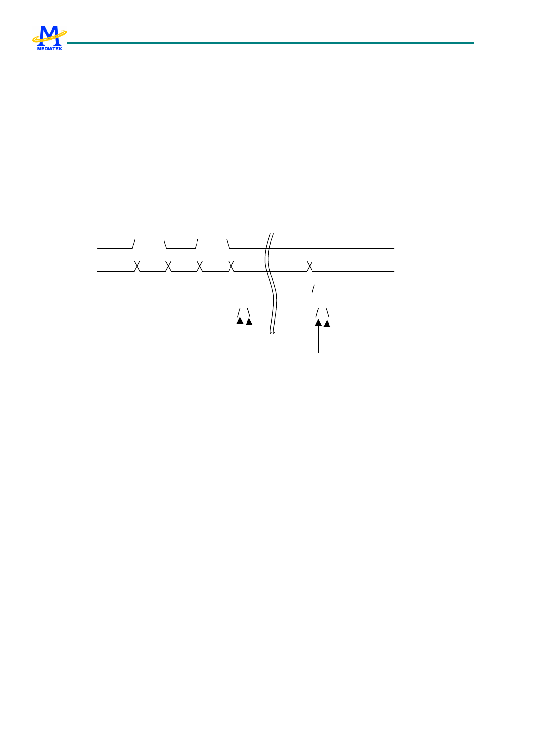
MTK Confidential Release for Konka
MTK Confidential Release for Konka
MT6228 GSM/GPRS Baseband Processor Data Sheet Revision 1.0
279/616 MediaTek Inc. Confidential
RDY The register bit indicates the status of transaction on MS bus. The register bit will be cleared when writing to
the command register MSC_CMD.
0 Otherwise.
1 A transaction on MS bus is ended.
SIF The register bit indicates the status of serial interface. If an interrupt is active on MS bus, the register bit will
be active. Note the difference between the signal RDY and SIF. When parallel mode is enabled, the signal SIF
will be active whenever any of the signal CED, ERR, BREQ and CMDNK is active. In order to separate
interrupts caused by the signals RDY and SIF, the register bit SIF will not become active until the
register MSDC_INT is read once. That is, the sequence for detecting the register bit SIF by polling is as
follows:
1. Detect the register bit RDY of the register MSC_STA
2. Read the register MSDC_INT
3. Detect the register bit SIF of the register MSC_STA
BS0 BS1 BS2 BS3 BS0
command execution command finished
!
"#
"$"#% &"#%
0 Otherwise.
1 An interrupt is active on MS bus
TOER The register bit indicates if a BUSY signal timeout error takes place. When timeout error occurs, the signal BS
will become logic low ‘0’. The register bit will be cleared when writing to the command register MSC_CMD.
0 No timeout error.
1 A BUSY signal timeout error takes place. The register bit RDY will also be active.
CRCER The register bit indicates if a CRC error occurs while receiving read data. The register bit will be cleared when
writing to the command register MSC_CMD.
0 Otherwise.
1 A CRC error occurs while receiving read data. The register bit RDY will also be active.
HSRDY The register bit indicates the status of handshaking on MS bus. The register bit will be cleared when writing to
the command register MSC_CMD.
0 Otherwise.
1 A Memory Stick card responds to a TPC by RDY.
CED The register bit is only valid when parallel mode is enabled. In fact, it’s value is from DAT[0] when serial
interface interrupt takes place. See Format Specification version 2.0 of Memory Stick Standard (Memory Stick
PRO) for more details.
0 Command does not terminate.
1 Command terminates normally or abnormally.
ERR The register bit is only valid when parallel mode is enabled. In fact, it’s value is from DAT[1] when serial
interface interrupt takes place. See Format Specification version 2.0 of Memory Stick Standard (Memory Stick
PRO) for more details.
0 Otherwise.
1 Indicate memory access error during memory access command.

MTK Confidential Release for Konka
MTK Confidential Release for Konka
MT6228 GSM/GPRS Baseband Processor Data Sheet Revision 1.0
280/616 MediaTek Inc. Confidential
BREQ The register bit is only valid when parallel mode is enabled. In fact, it’s value is from DAT[2] when serial
interface interrupt takes place. See Format Specification version 2.0 of Memory Stick Standard (Memory Stick
PRO) for more details.
0 Otherwise.
1 Indicate request for data.
CMDNK The register bit is only valid when parallel mode is enabled. In fact, it’s value is from DAT[3] when serial
interface interrupt takes place. See Format Specification version 2.0 of Memory Stick Standard (Memory Stick
PRO) for more details.
0 Otherwise
1 Indicate non-recognized command.
6.4.4 Application Notes
6.4.4.1 Initialization Procedures After Power On
Disable power down control for MSDC module
Remember to power on MSDC module before starting any operation to it.
6.4.4.2 Card Detection Procedures
The pseudo code is as follows:
MSDC_CFG.PRCFG0 = 2’b10
MSDC_PS = 2’b11
MSDC_CFG.VDDPD = 1
if(MSDC_PS.PINCHG) { // card is inserted
. . .
}
The pseudo code segment perform the following tasks:
1. First pull up CD/DAT3 (INS) pin.
2. Enable card detection and input pin at the same time.
3. Turn on power for memory card.
4. Detect insertion of memory card.
6.4.4.3 Notes on Commands
For MS, check if MSC_STA.RDY is ‘1’ before issuing any command.
For SD/MMC, if the command desired to be issued involves data line, for example, commands with data transfer or
R1b response, check if SDC_STA.SDCBUSY is ‘0’ before issuing. If the command desired to be issued does not
involve data line, only check if SDC_STA.CMDBUSY is ‘0’ before issuing.
6.4.4.4 Notes on Data Transfer
For SD/MMC, if multiple-block-write command is issued then only issue STOP_TRANS command
inter-blocks instead of intra-blocks.
Once SW decides to issue STOP_TRANS commands, no more data transfer from or to the controller.

MTK Confidential Release for Konka
MTK Confidential Release for Konka
MT6228 GSM/GPRS Baseband Processor Data Sheet Revision 1.0
281/616 MediaTek Inc. Confidential
6.4.4.5 Notes on Frequency Change
Before changing the frequency of serial clock on MS/SD/MMC bus, it is necessary to disable serial interface of the
controller. That is, set the register bit SIEN of the register SDC_CFG to ‘0’ for SD/MMC controller, and set the register
bit SIEN of the register MSC_CFG to ‘0’ for Memory Stick controller. Serial interface of the controller needs to be
enabled again before starting any operation to the memory card.
6.4.4.6 Notes on Response Timeout
If a read command doest not receive response, that is, it terminates with a timeout, then register SDC_DATSTA needs
to be cleared by reading it. The register bit “DATTO” should be active. However, it may take a while before the register
bit becomes active. The alternative is to send the STOP_TRANS command. However, this method will receive
response with illegal-command information. Also, remember to check if the register bit SDC_STA.CMDBUSY is
active before issuing the STOP_TRANS command. The procedure is as follows:
1. Read command => response time out
2. Issue STOP_TRANS command => Get Response
3. Read register SDC_DATSTA to clear it
6.4.4.7 Source or Destination Address is not word-aligned
It is possible that the source address is not word-aligned when data move from memory to MSDC. Similarly,
destination address may be not word-aligned when data move from MSDC to memory. This can be solved by setting
DMA byte-to-word functionality.
1. DMAn_CON.SIZE=0
2. DMAn_CON.BTW=1
3. DMAn_CON.BURST=2 (or 4)
4. DMAn_COUNT=byte number instead of word number
5. fifo threshold setting must be 1 (or 2), depending on DMAn_CON.BURST
Note n=4 ~ 11
6.4.4.8 Miscellaneous notes
Siemens MMC card: When a write command is issued and followed by a STOP_TRANS command, Siemens
MMC card will de-assert busy status even though flash programming has not yet finished. Software must use
“Get Status” command to make sure that flash programming finishes.
6.5 Graphic Memory Controller
6.5.1 General Description
Graphic memory controller provides channels to allow graphic engines to access SYSRAM and External Memory.
Simple Request-Acknowledgement handshaking scheme is employed here to ease the complexity of memory access
control circuitry in each graphic engine.

MTK Confidential Release for Konka
MTK Confidential Release for Konka
MT6228 GSM/GPRS Baseband Processor Data Sheet Revision 1.0
282/616 MediaTek Inc. Confidential
To maximize data bandwidth, five individual access ports are implemented, which can access different memory banks
simultaneously. Figure 14 shows the connection between GMC, AHB, and memories. One access port is connected
to the SYSRAM, and the other access port for external memory access is connected to data cache directly.
Figure 14 Graphic memory controller
6.5.2 Register Definitions
Register Address Register Function Acronym
GMC + 0000h GMC Control Register GMC_CON
GMC + 0004h GMC Match Address Register GMC_MATCHADDR
GMC + 0008h GMC Mask Address Register GMC_MASKADDR
GMC + 000Ch GMC INRANGE Master Register GMC_INRANGE_MAST
GMC + 0010h GMC Bandwidth Limiter Register GMC_LIMITER
Table 44 GMC Registers
GMC+0000h GMC Control Register GMC_CON
Bit 31 30 29 28 27 26 25 24 23 22 21 20 19 18 17 16
Name
Type
Reset
Bit 15 14 13 12 11 10 9 8 7 6 5 4 3 2 1 0
Name
TRAP
CLR
BURS
T
TRAP
INV
TRAP
EN
Type W R/W R/W R/W
Reset
0 1 0 0
This register is used to control the functionality for GMC.
TRAP EN To enable address-trapping function. When this function is turned on, GMC compares the address
between the address configured in GMC Match Address Register and the address issued to memory.
MTK Confidential Release for Konka
MTK Confidential Release for Konka
MT6228 GSM/GPRS Baseband Processor Data Sheet Revision 1.0
283/616 MediaTek Inc. Confidential
When the address is matched, the engine number that issued the request is recorded. The record can be
read from GMC INRANGE Master Register
Table 6 shows the engine number of each engine.
Engine
Number Engine Name Engine
Number Engine Name
0 MP4/JPEG 10 CAM (high priority)
1 MP4/JPEG 11 TVE (high priority)
2 MP4/JPEG 12 MP4_MV (high priority)
3 MP4/JPEG 13 2D WRITE
4 MP4/JPEG 14 2D COMMAND QUEUE
5 RESIZER 15 2D READ
6 RESIZER 16 GIF
7 RESIZER 17 PNG
8 IMAGE DMA 18 IPP
9 IMAGE DMA
Table 45 Engine number
TRAP INV Enable trapping range inversion. If this register bit is set, the engine, which issues the address out of the
address range specified with GMC_MATCHADDR, and GMC_MASKADDR, is trapped. The register
bit in GMC_INRANGE_MAST is set accordingly.
BURST Enable burst mode. If burst mode is enabled, arbiter does not change the grant until finishing the burst.
On the other hand, GMC treats every request as a SINGLE transfer.
TRAP CLR This register field is used to clear the record in GMC INRANGE Master Register. This register field is a
write only register field.
GMC+0004h GMC Match Address Register GMC_MATCHA
DDR
Bit 31 30 29 28 27 26 25 24 23 22 21 20 19 18 17 16
Name
ADDR
Type R/W
Bit 15 14 13 12 11 10 9 8 7 6 5 4 3 2 1 0
Name
ADDR
Type R/W
This register is used to specify the trapping address for the address-trapping function.
ADDR The trapping address.
GMC+0008h GMC Mask Address Register GMC_MASKAD
DR
Bit 31 30 29 28 27 26 25 24 23 22 21 20 19 18 17 16
Name
MASK
Type R/W
Bit 15 14 13 12 11 10 9 8 7 6 5 4 3 2 1 0
Name
MASK
Type R/W
This register is used to specify the address mask the address-trapping function. The address comparator ignores the
address bits that is set as “1” in the GMC Mask Address Register.
MASK address mask.
MTK Confidential Release for Konka
MTK Confidential Release for Konka
MT6228 GSM/GPRS Baseband Processor Data Sheet Revision 1.0
284/616 MediaTek Inc. Confidential
GMC+000Ch GMC INRANGE Master Register GMC_INRANGE
_MAST
Bit 31 30 29 28 27 26 25 24 23 22 21 20 19 18 17 16
Name
ENG
18
ENG
17
ENG
16
Type RO RO RO
Bit 15 14 13 12 11 10 9 8 7 6 5 4 3 2 1 0
Name
ENG
15
ENG
14
ENG
13
ENG
12
ENG
11
ENG
10
ENG
9
ENG
8
ENG
7
ENG
6
ENG
5
ENG
4
ENG
3
ENG
2
ENG
1
ENG
0
Type RO RO RO RO RO RO RO RO RO RO RO RO RO RO RO RO
This register is used to show the trapped engine..
ENGn The trapped address is issued by corresponding engine.
GMC+0010h GMC Bandwidth Limiter Register GMC_LIMITER
Bit 31 30 29 28 27 26 25 24 23 22 21 20 19 18 17 16
Name
Type
Reset
Bit 15 14 13 12 11 10 9 8 7 6 5 4 3 2 1 0
Name
LIMITER
Type R/W
Reset
0
This register is used for slow-down function of GMC EMI interface.
LIMITER This register field is used to specify the period that GMC EMI interface can issue a bus request to AHB.
LIMITER represents an AHB request can only be issued in LIMITER X 4 clock cycles. The value of
LIMITER is from 0 to 1023.
6.6 2D acceleration
6.6.1 2D Engine
6.6.1.1 General Description
To enhance MMI display and gaming experiences, a 2D acceleration engine is implemented. It supports ARGB8888,
RGB888, ARGB4444, RGB565 and 8-bpp color modes. Main features are listed as follows:
Rectangle fill with color gradient.
Bitblt: multi-Bitblt without transform, 7 rotate, mirror (transparent) Bitblt
Alpha blending
Binary ROP
Line drawing: normal line, dotted line, anti-alias line
Font caching: normal font, italic font
Circle drawing
Quadratic Bezier curve drawing
Triangle drawing
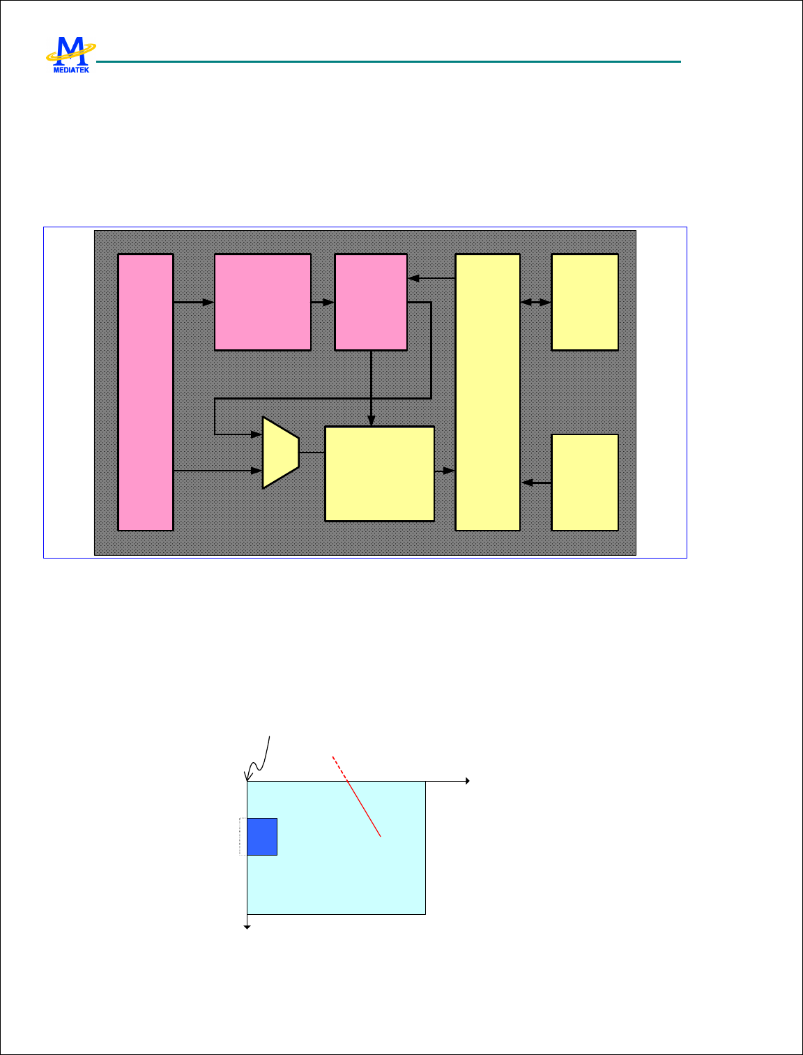
MTK Confidential Release for Konka
MTK Confidential Release for Konka
MT6228 GSM/GPRS Baseband Processor Data Sheet Revision 1.0
285/616 MediaTek Inc. Confidential
MCU can program 2D engine registers via APB. However, MCU has to make sure that the 2D engine is not BUSY
before any write to 2D engine registers occurs. An interrupt scheme is also provided for more flexibility.
A command parser is implemented for further offloading of MCU. The command queue can be randomly assigned in
the system memory, with a maximum depth of 2047 commands. If the command queue is enabled, MCU has to check
if the command queue has free space before writing to the command queue. Command queue parser will consume
command queue entries upon 2D engine requests. Figure 15 shows the command queue and 2D engine block diagram.
Please refer to the graphic command queue functional specification for more details.
2D
engine
Command
queue
APB
slave
Command
parser
DST
memory
read/write
control
SRC
memory
read
control
Graphic
Memory
Interface
Figure 15 The command queue and 2D engine block diagram.
6.6.1.2 Features Introduction
6.6.1.2.1 2D Coordinate
The coordinates in the 2D engine are represented as 12-bit signed integers. The negative part is clipped during
rendering. The maximum resolution can achieve 2047x2047 pixels. The programmed base address is mapped to the
origin of the picture, which is illustrated in Figure 16.
(0,0)
dst_base_addr
x
y
Figure 16 The coordinate of the 2D engine.

MTK Confidential Release for Konka
MTK Confidential Release for Konka
MT6228 GSM/GPRS Baseband Processor Data Sheet Revision 1.0
286/616 MediaTek Inc. Confidential
6.6.1.2.2 Color format
The 2D engine support the color format of 8bpp, RGB565, RGB888, ARGB4444, and ARGB 8888. The color
formats of source and destination can be specified separately. Note that when using the 8bpp format, the source and
destination color formats have to be the same, since table-lookup of color palette is not provided in 2D engine.
Graphic modes of Bitblt, Bitblt with alpha blending, and Bitblt with binary ROP require color format setting for both
source and destination. For other graphic modes, only destination color format needs to be specified. The possible
settings are listed as Table 46Table 47.
Bitblt (Copy, ROP)
Source color format Destination color format
8bpp 8bpp
RGB565
RGB565 RGB888
RGB565
RGB888 RGB888
ARGB4444
ARGB4444 ARGB8888
ARGB4444
ARGB8888 ARGB8888
Table 46 source and destination color format setting for Bitblt.
Bitblt with Alpha Blending
Source color format Destination color format
8bpp 8bpp
RGB565
RGB565 RGB888
RGB565
RGB888 RGB888
RGB565
ARGB4444 RGB888
RGB565
ARGB8888 RGB888
Table 47 source and destination color format setting for alpha blending.
When source image is used, the source key function could be enabled or disabled. When enabled, the source color
key is in the same format of source color. Be aware that the source key is still effective for alpha blending mode.
6.6.1.2.3 Clipping Window
The setting for clipping window is effective for all the 2D graphics. A pair of minimum and maximum boundary is
applied on destination side. The portion outside the clipping window will not be drawn to the destination, but the
pixels on the boundary will be kept. The clipping operation is illustrated in Figure 17.

MTK Confidential Release for Konka
MTK Confidential Release for Konka
MT6228 GSM/GPRS Baseband Processor Data Sheet Revision 1.0
287/616 MediaTek Inc. Confidential
(0,0)
dst_base_addr
g2d_clp_min
g2d_clp_max
Figure 17 The clipping operation of the 2D engine.
6.6.1.2.4 Bitblt operation
The Bitblt function copies the pixels from source picture to destination. To be more flexible, 4 copy directions and 7
kinds of rotations are provided when doing Bitblt operation. Figure 18 illustrates the Bitblt operation and required
settings.
S
src_base_addr
(src_x,src_y)
D
dst_base_addr (dst_x,dst_y)
src_w
src_h
src_x_pitch dst_x_pitch
Figure 18 The clipping operation of the 2D engine.
Note that the size of source and destination blocks can be different. If the source block is larger than destination block,
the size of destination block is used instead of the source size. When source block size is smaller than destination
block size, the pattern of source block is repeated horizontally and vertically in the destination block, which is
illustrated as Figure 19 below.

MTK Confidential Release for Konka
MTK Confidential Release for Konka
MT6228 GSM/GPRS Baseband Processor Data Sheet Revision 1.0
288/616 MediaTek Inc. Confidential
Source Destination
Figure 19 The Bitblt operation when destination size > source size.
6.6.1.2.4.1 Copy direction
When the source block and destination blocks are on the same picture, they may be overlapped by each other. To
prevent error from occurring, 4 directions for Bitblt can be programmed. However, the copy direction shall not be
enabled when doing rotation, or it will produce unwanted results. The 4 kinds of copy direction are shown in Figure
20.
D
D S
S
D
S D
S
Figure 20 The 4 directions of Bitblt operation.
6.6.1.2.4.2 Rotation
To facilitate Bitblt operation, 7 kinds of rotation can be set at the same time. The rotation operation is illustrated as
Figure 21. Here the rotation is done on the destination side, while the read sequence of pixels in source block is
fixed.

MTK Confidential Release for Konka
MTK Confidential Release for Konka
MT6228 GSM/GPRS Baseband Processor Data Sheet Revision 1.0
289/616 MediaTek Inc. Confidential
8).270 degree rotation
+ vertical flip
D
S
D
(src_x,src_y) (dst_x,dst_y)
1).No rotation
D
2).180 degree rotation
D
3).horizontal flip
D
4).vertical flip
5).90 degree rotation 6).270 degree rotation
D
7).90 degree rotation
+ vertical flip
D D
Figure 21 The rotations of Bitblt operation.
6.6.1.2.5 Bitblt with Alpha Blending
Similar to simple Bitblt operation, alpha blending function is provided as well. The pixels in source block are blended
onto destination block. Blending is performed according the formula listed below:
Cd)/255*alpha)-(255 Cs*(alpha C
+
=
,
where Cs is the source color, Cd is the destination color, and alpha is an unsigned integer range from 0 to 255.
The alpha value programmed into the 2D control registers is called constant alpha. When no alpha channel exists, the
constant alpha is used to calculate blended color. If the alpha channel exists ( in ARGB color mode), the per-pixel
alpha is used for blending operation instead of constant alpha.
In addition, the setting of copy directions and rotations are also effective for alpha blending mode. Also, the size and
color format of source block can be different from destination.
6.6.1.2.6 Bitblt with Binary ROP
The ROP (Raster Operation) is another block-wise functional mode. Here the 2D engine provides a set of binary
ROPs. The ROP code has 16 different combinations, which is listed in the definition of 2D control registers ---
G2D_SMODE_CON. Please see sec.1.1.1.3 for detail descriptions.
Similar with other block-wise functions, the copy directions and rotations are also applicable in ROP mode. The size
and color format of source and destination do not need to be the same.
6.6.1.2.7 Rectangle Fill with Color Gradient
Rectangle fill mode provides the configurations for color gradient for both x-direction and y-direction. Each of the
color gradient of component A, R, G, B is represented by 9.16 signed fixed point number. In order to prevent color
crossing the boundary of 0 and 255, it is clipped to 0 and 255 when performing gradient fill. When the color gradient
is disabled, the rectangle is filled by one color. An example of gradient fill is shown in Figure 22.
MTK Confidential Release for Konka
MTK Confidential Release for Konka
MT6228 GSM/GPRS Baseband Processor Data Sheet Revision 1.0
290/616 MediaTek Inc. Confidential
start_clr
x_gradient
y_gradient
Figure 22 Rectangle gradient fill.
6.6.1.2.8 Line Draw
The line drawing function is implemented with the mid-point algorithm. Given the two endpoints of a line, the points
on the line are calculated recursively. The line anti-aliasing is also supported but it requires extra register
configurations. In addition, dotted line is also provided for use. Simultaneously turning on anti-aliasing and
dotted-line is not recommended since the line may result in a strange look.
6.6.1.2.9 Circle Draw
The circle drawing is quite similar with line drawing, using the mid-point algorithm as well. A center point and a
radius have to be programmed into 2D control registers. There are 4 enable bits for each quadrant of a circle, each
determines whether the arcs shall be rendered or not. The setting of circle drawing is illustrated in Figure 23.
0
12
3
(dst_x,dst_y)
radius
Figure 23 Circle drawing.
6.6.1.2.10 Bezier curve
The quadratic Bezier curve is implemented, too. The quadratic Bezier curve is defined by three control points, as
illustrated in Figure 24. The Bezier curve drawing is implemented with subdivision method. The amount of
subdivisions is programmed by software. The curve gets more detailed with the increase of subdivision factor, but it
requires more memory and computing time. To be more precise, doing n times of subdivision needs a buffer of
4
*
2
)1( +n
bytes.
MTK Confidential Release for Konka
MTK Confidential Release for Konka
MT6228 GSM/GPRS Baseband Processor Data Sheet Revision 1.0
291/616 MediaTek Inc. Confidential
p0
p2
p1
Figure 24 Bezier curve.
6.6.1.2.11 Triangle Flat Fill
The 2D engine supports the function of triangle flat fill with the help of software. First, the software divides the triangle
into upper plane and lower plane and passes them to hardware individually. Given the starting vertex’s coordinate and
the slopes of left and right edges, the 2D hardware fills the horizontal segments between the two edges until the
horizontal end is reached. The slope of each edge is in 12.16 bit signed fix-point representation. The programming
of triangle drawing is illustrated in Figure 25.
Horizontal end
start point
start point
Horizontal end
left slope
left slope
right slope
right slope
Figure 25 Triangle drawing.
6.6.1.2.12 Font Drawing
The 2D engine helps to render fonts stored in one-bit-per-pixel format. It expends the zero bits to background color
and expands one bits to foreground color. The background color can be set as transparent. The font drawing can be
programmed as tilt, when given each line’s tilt value.

MTK Confidential Release for Konka
MTK Confidential Release for Konka
MT6228 GSM/GPRS Baseband Processor Data Sheet Revision 1.0
292/616 MediaTek Inc. Confidential
The start bit of font drawing can be non-byte aligned to save memory usage for font caching. In addition, the rotations
can be performed at the same time when drawing fonts.
6.6.1.3 Register Definitions
Table 48 The 2D engine register mapping. summarizes the 2D engine register mapping on APB and through command
queue. The base address of 2D engine is 80670000h.
APB Address
CMQ
mapped
Address
Register Function Acronym
G2D+0100h 100h 2D engine fire mode control register FMODE_CON
102h Reserved
G2D+0104h 104h 2D Engine sub-mode control lower register SMODE_CON_L
106h 2D Engine sub-mode control higher register SMODE_CON_H
G2D+0108h 108h 2D engine common control register COM_CON
10Ah Reserved
G2D+0110h 110h 2D engine status register STA
112h Reserved
G2D+0200h 200h Source base address lower hword register SRC_BASE_L
202h Source base address higher hword register SRC_BASE_H
G2D+0204h 204h Source pitch register SRC_PITCH
206h Reserved
G2D+0208h 208h Source y coordinate register SRC_Y
20Ah Source x coordinate register SRC_X
G2D+020Ch 20Ch Source height register SRC_H
20Eh Source width register SRC_W
G2D+0210h 210h Source color key lower hword register SRC_KEY_L
212h Source color key lower hword register SRC_KEY_H
G2D+0300h 300h Destination base address lower hword register DST_BASE_L
302h Destination base address higher hword register DST_BASE_H
G2D+0304h 304h Destination Pitch Register DST_PITCH
306h Reserved
G2D+0308h 308h Destination y coordinate register 0 DST_Y0
30Ah Destination x coordinate register 0 DST_X0
G2D+030Ch 30Ch Destination y coordinate register 1 DST_Y1
30Eh Destination x coordinate register 1 DST_X1
G2D+0310h 310h Destination y coordinate register 2 DST_Y2
312h Destination x coordinate register 2 DST_X2
G2D+0318h 318h Destination height register DST_H
31Ah Destination width register DST_W
G2D+400h 400h Foreground color lower hword register FGCLR_L
402h Foreground color lower hword register FGCLR_H
G2D+404h 404h Background color lower hword register BGCLR_L
406h Background color lower hword register BGCLR_H

MTK Confidential Release for Konka
MTK Confidential Release for Konka
MT6228 GSM/GPRS Baseband Processor Data Sheet Revision 1.0
293/616 MediaTek Inc. Confidential
G2D+408h 408h Clipping minimum y coordinate register CLP_MIN_Y
40Ah Clipping minimum x coordinate register CLP_MIN_X
G2D+40Ch 40Ch Clipping maximum y coordinate register CLP_MAX_Y
40Eh Clipping maximum x coordinate register CLP_MAX_X
G2D+410h 410h Rectangle color gradient x lower hword register REC_CLRGD_X_L
412h Rectangle color gradient x higher hword register REC_CLRGD_X_H
G2D+414h 414h Rectangle color gradient y lower hword register REC_CLRGD_Y_L
416h Rectangle color gradient y higher hword register REC_CLRGD_Y_H
G2D+0700h ~
G2D+071Fh 700h ~ 71Fh TILT_0300 ~
TILT_1F1C
Table 48 The 2D engine register mapping.
There are several function modes in 2D graphics engine. Some registers are shared between different them. Table 49
summarizes the settings under different function modes.
APB
Address
CMQ
Addres
s
Rectangle fill Bitblt
Operations
Line/Circle
drawing
Bezier curve
drawing Triangle drawing Font caching
G2D+0200h
200h SRC_BASE
SLOPE_L SRC_BASE
G2D+0204h 204h SRC_PITCH
G2D+0208h 208h SRC_XY
G2D+020Ch 20Ch SRC_SIZE
G2D+0210h 210h SRC_KEY SRC_KEY
G2D+0300h
300h DST_BASE DST_BASE
DST_BASE
DST_BASE DST_BASE DST_BASE
G2D+0304h 304h DST_PITCH DST_PITCH DST_PITCH DST_PITCH DST_PITCH DST_PITCH
G2D+0308h 308h DST_XY DST_XY DST_XY0 DST_XY0 DST_XY_START DST_XY
G2D+030Ch 30Ch DST_XY1/
RADIUS DST_XY1 DST_Y_END
G2D+0310h
310h DST_XY2
G2D+0318h 318h DST_SIZE DST_SIZE DST_SIZE
G2D+0400h 400h START_CLR FGCLR FGCLR FGCLR FGCLR
G2D+0404h 404h DST_KEY XY_SQRT BGCLR
G2D+0408h 408h CLP_MIN CLP_MIN CLP_MIN CLP_MIN CLP_MIN CLP_MIN
G2D+040Ch 40Ch CLP_MAX CLP_MAX CLP_MAX CLP_MAX CLP_MAX CLP_MAX
G2D+0410h 410h ALPGD_X BUF_STA_ADD SLOPE_R
G2D+0414h 414h RED_GD_X SUBDIV_TIME
G2D+0418h 418h GREEN_GD_X
G2D+041Ch 41Ch BLUE_GD_X
G2D+0420h 420h ALPGD_Y
G2D+0424h
424h RED_GD_Y
G2D+0428h 428h GREEN_GD_Y
G2D+042Ch 42Ch BLUE_GD_Y
G2D+0700h
~
G2D+071Fh
700h ~
71Fh
TILT_0300 ~
TILT_1F1C
TILT_0300 ~
TILT_1F1C TILT_0300 ~
TILT_1F1C
MTK Confidential Release for Konka
MTK Confidential Release for Konka
MT6228 GSM/GPRS Baseband Processor Data Sheet Revision 1.0
294/616 MediaTek Inc. Confidential
APB
Address
CMQ
Addres
s
Horizontal Line
Gradient
Horizontal
Line Copy
with Mask
G2D+0200h 200h SRC_BASE
G2D+0204h 204h
G2D+0208h 208h
G2D+020Ch 20Ch SRC_SIZE
G2D+0210h 210h
G2D+0300h 300h DST_BASE DST_BASE
G2D+0304h 304h
G2D+0308h 308h
G2D+030Ch 30Ch
G2D+0310h 310h
G2D+0318h 318h DST_SIZE DST_SIZE
G2D+0400h 400h START_CLR
G2D+0404h
404h
G2D+0408h 408h
G2D+040Ch 40Ch
G2D+0410h 410h ALPGD_X MASK_BASE
G2D+0414h 414h RED_GD_X
G2D+0418h
418h GREEN_GD_X
G2D+041Ch 41Ch BLUE_GD_X
G2D+0420h 420h
G2D+0424h 424h
G2D+0428h 428h
G2D+042Ch
42Ch
G2D+0700h
~
G2D+071Fh
700h ~
71Fh
Table 49 2D engine common registers
Below shows common control registers.
G2D+0100h Graphic 2D Engine Fire Mode Control Register G2D_FMODE_C
ON
Bit 15 14 13 12 11 10 9 8 7 6 5 4 3 2 1 0
Name
SRC_CLR_MODE DST_CLR_MODE G2D_ENG_MODE
Type R/W R/W R/W
Reset
000 000 0000
Write this register will fire the 2D engine according to the CLR_MODE and ENG_MODE field.
SRC_CLR_MODE source color mode
000 8-bpp, LUT disabled
001 16-bpp, RGB 565 format
010 32-bpp, ARGB 8888 format
MTK Confidential Release for Konka
MTK Confidential Release for Konka
MT6228 GSM/GPRS Baseband Processor Data Sheet Revision 1.0
295/616 MediaTek Inc. Confidential
011 24-bpp, RGB 888 format
101 16-bpp, ARGB 4444 format
others reserved
DST_CLR_MODE destination color mode
000 8-bpp, LUT disabled
001 16-bpp, RGB 565 format
010 32-bpp, ARGB 8888 format
011 24-bpp, RGB 888 format
101 16-bpp, ARGB 4444 format
others reserved
G2D_ENG_MODE 2D engine function mode
0000 Line draw.
0001 Circle draw.
0010 Bezier curve draw.
0011 Triangle fill.
1000 Rectangle fill.
1001 Bitblt.
1010 Bitblt with alpha blending.
1011 Bitblt with ROP.
1100 Font drawing.
1101 Horizontal line fill with color gradient. In this mode, the source key and the clipping functions are
disabled automatically.
1110 Horizontal line copy with mask. In this mode, the source key and the clipping functions are disabled
automatically.
others not allowed
G2D+0104h Graphic 2D Engine Sub-mode Control Register G2D_SMODE_C
ON
Bit 31 30 29 28 27 26 25 24 23 22 21 20 19 18 17 16
Name
FITA
FNBG
FMSB
_FIRS
T
ALPHA ROP_CODE
Type R/W R/W R/W R/W R/W
Reset
0 0 0 0000 0000
Bit 15 14 13 12 11 10 9 8 7 6 5 4 3 2 1 0
Name
LDOT
LAA_
EN
DST_
KEY_
EN
CLRG
D_EN
BDIR BITA BROT
Type R/W R/W R/W R/W R/W R/W R/W
Reset
0 0 0 0 11 0 111
Write this register to set the 2D engine configuration.
FITA font italic enabled.
FNBG font drawing with no background color
FMSB_FIRST font drawing from most significant bit
ALPHA Bit 7-4 of constant alpha value. ROP_CODE is Bit3-0 of constant alpha value.
ROP_CODE Binary ROP code. Bits 2-0 are also used to specify the start bit position for Font drawing and enabled
arcs for circle drawing.
Bitblt ROP Code Boolean Function Start Bit Position for Font
Drawing Enabled Arcs
MTK Confidential Release for Konka
MTK Confidential Release for Konka
MT6228 GSM/GPRS Baseband Processor Data Sheet Revision 1.0
296/616 MediaTek Inc. Confidential
0000 0 (Black) Bit 0 None
0001 ~(S + D) Bit 1 I
0010 ~S . D Bit 2
0011 ~S Bit 3 ,
0100 S . ~D Bit 4
0101 ~D Bit 5 ,
0110 S ^ D Bit 6 ,
0111 ~(S . D) Bit 7 ,,
1000 S . D Bit 0
1001 ~(S ^ D) Bit 1 ,
1010 D Bit 2 ,
1011 ~S + D Bit 3 , ,
1100 S Bit 4 ,
1101 S + ~D Bit 5 , ,
1110 S + D Bit 6 , ,
1111 1 (White) Bit 7 , , ,
S = Source, D = Destination.
= first quadrant, II = second quadrant, III = third quadrant, IV = fourth quadrant.
LDOT line dotted
LAA_EN line anti-aliasing enabled
DST_KEY_EN Destination key enabled for Bitblt functions
CLRGR_EN Color gradient enabled for rectangle fill
BDIR Bitblt direction:
00 from lower right corner
01 from lower left corner
10 from upper right corner
11 from upper left corner
This field only takes effect when the Bitblt rotation is set as none (111). When doing rotation the Bitblt
direction of source image is always from upper left corner.
BITA Bitblt italic enabled, using the tilt value defined in G2D_TILT_00 ~ G2D_TILT_1F registers. The tilt
function should not be enabled in Alpha Blending and ROP mode.
BROT Bitblt rotation:
000 mirror then rotate 90
001 rotate 90
010 rotate 270
011 mirror then rotate 270
100 rotate 180
101 mirror
110 mirror then rotate 180
111 none
G2D+0108h Graphic 2D Engine Common Control Register G2D_COM_CO
N
Bit 31 30 29 28 27 26 25 24 23 22 21 20 19 18 17 16
MTK Confidential Release for Konka
MTK Confidential Release for Konka
MT6228 GSM/GPRS Baseband Processor Data Sheet Revision 1.0
297/616 MediaTek Inc. Confidential
Name
Type
Reset
Bit 15 14 13 12 11 10 9 8 7 6 5 4 3 2 1 0
Name
CLP_
EN
SRCK
EY_E
N
RST
Type R/W R/W R/W
Reset
0 0 0
Write this register to set the 2D engine configuration.
RST 2D engine reset, only the state machine is reset, the content of control registers will not be reset.
SRCKEY_EN Source key enabled.
CLP_EN Clipping enabled.
G2D+010Ch Graphic 2D Engine Interrupt Control Register G2D_IRQ_CON
Bit 31 30 29 28 27 26 25 24 23 22 21 20 19 18 17 16
Name
Type
Reset
Bit 15 14 13 12 11 10 9 8 7 6 5 4 3 2 1 0
Name
EN
Type R/W
Reset
0
Write this register to set the 2D engine IRQ configuration.
EN interrupt enable. The interrupt is negative edge sensitive.
G2D+0110h Graphic 2D Engine Common Status Register G2D_COM_STA
Bit 31 30 29 28 27 26 25 24 23 22 21 20 19 18 17 16
Name
Type
Reset
Bit 15 14 13 12 11 10 9 8 7 6 5 4 3 2 1 0
Name
BUSY
Type RO
Reset
0
Read this register to get the 2D engine status. 2D engine may function abnormally if any 2D engine register is modified
when BUSY.
BUSY 2D engine is busy
G2D+0200h Graphic 2D Source Base Address Register G2D_SRC_BAS
E
Bit 31 30 29 28 27 26 25 24 23 22 21 20 19 18 17 16
Name
SRC_BASE[31:16]
Type R/W
Reset
0
Bit 15 14 13 12 11 10 9 8 7 6 5 4 3 2 1 0
Name
SRC_BASE[15:0]
Type R/W
Reset
0
SRC_BASE The base address of source image. Also, this field is used for the slope of the left triangle edges
represented in 12.16 format.
MTK Confidential Release for Konka
MTK Confidential Release for Konka
MT6228 GSM/GPRS Baseband Processor Data Sheet Revision 1.0
298/616 MediaTek Inc. Confidential
G2D+0204h Graphic 2D Engine Source Pitch Register G2D_SRC_PITC
H
Bit 15 14 13 12 11 10 9 8 7 6 5 4 3 2 1 0
Name
SRC_PITCH
Type R/W
Reset
0
SRC_PITCH The width of source image in the unit of pixels.
G2D+0208h Graphic 2D Engine Source X and Y Register G2D_SRC_XY
Bit 31 30 29 28 27 26 25 24 23 22 21 20 19 18 17 16
Name
SRC_X
Type R/W
Reset
0
Bit 15 14 13 12 11 10 9 8 7 6 5 4 3 2 1 0
Name
SRC_Y
Type R/W
Reset
0
SRC_Y The starting y co-ordinate of source image. It must be positive although represented as 12-bit signed integer.
SRC_X The starting x co-ordinate of source image. It must be positive although represented as 12-bit signed integer.
G2D+020Ch Graphic 2D Engine Source Size Register G2D_SRC_SIZE
Bit 31 30 29 28 27 26 25 24 23 22 21 20 19 18 17 16
Name
SRC_W
Type R/W
Reset
0
Bit
15 14
13
12
11 10 9 8 7 6 5 4 3 2 1 0
Name
SRC_H
Type R/W
Reset
0
SRC_H The source height for Bitblt, alpha blending and ROP. It must be positive although represented as 12-bit signed
integer.
SRC_W The source width for Bitblt, alpha blending and ROP. It must be positive although represented as 12-bit
signed integer.
G2D+0210h Graphic 2D Engine Source Color Key Register G2D_SRC_KEY
Bit 31 30 29 28 27 26 25 24 23 22 21 20 19 18 17 16
Name
SRC_KEY[31:16]
Type R/W
Reset
0
Bit 15 14 13 12 11 10 9 8 7 6 5 4 3 2 1 0
Name
SRC_KEY[15:0]
Type R/W
Reset
0
SRC_KEY The source color key. The color will be transparent if color keying is enabled.
G2D+0300h Graphic 2D Destination Base Address Register G2D_DST_BAS
E
Bit 31 30 29 28 27 26 25 24 23 22 21 20 19 18 17 16
Name
DST_BASE[31:16]
Type R/W
Reset
0

MTK Confidential Release for Konka
MTK Confidential Release for Konka
MT6228 GSM/GPRS Baseband Processor Data Sheet Revision 1.0
299/616 MediaTek Inc. Confidential
Bit 15 14 13 12 11 10 9 8 7 6 5 4 3 2 1 0
Name
DST_BASE[15:0]
Type R/W
Reset
0
DST_BASE The base address of destination image.
G2D+0304h Graphic 2D Engine Destination Pitch Register G2D_DST_PITC
H
Bit 15 14 13 12 11 10 9 8 7 6 5 4 3 2 1 0
Name
SRC_PITCH
Type R/W
Reset
0
DST_PITCH The width of destination image in the unit of pixels.
G2D+0308h Graphic 2D Engine Destination X and Y Register 0 G2D_DST_XY0
Bit 31 30 29 28 27 26 25 24 23 22 21 20 19 18 17 16
Name
DST_X0
Type R/W
Reset
0
Bit 15 14 13 12 11 10 9 8 7 6 5 4 3 2 1 0
Name
DST_Y0
Type R/W
Reset
0
(DST_X0 , DST_Y0) is used as the starting co-ordinate in Bitblt, alpha blending, ROP, and font drawing mode. In line
mode or triangle fill mode, it is used as one end point. For Bezier curve drawing, it is one of the control points. While
in circle drawing mode, it is the center of the circle. Also this filed is used as the starting point of triangle draw.
DST_X0 Represented by 12-bit signed integer. Negative co-ordinate is allowed.
DST_Y0 Represented by 12-bit signed integer. Negative co-ordinate is allowed.
G2D+030Ch Graphic 2D Engine Destination X and Y Register 1 G2D_DST_XY1
Bit 31 30 29 28 27 26 25 24 23 22 21 20 19 18 17 16
Name
DST_X1
Type R/W
Reset
0
Bit 15 14 13 12 11 10 9 8 7 6 5 4 3 2 1 0
Name
DST_Y1
Type R/W
Reset
0
(DST_X1 , DST_Y1) is used as one end point in Line drawing and triangle fill mode. For Bezier curve drawing, it is
one of the control points. While in circle drawing mode, DST_X1 must be positive since it is the radius of the circle.
Also, Bit 15-0 is used as the vertical end of triangle draw.
DST_X1 Represented by 12-bit signed integer. Negative co-ordinate is allowed.
DST_Y1 Represented by 12-bit signed integer. Negative co-ordinate is allowed.
G2D+0310h Graphic 2D Engine Destination X and Y Register 2 G2D_DST_XY2
Bit 31 30 29 28 27 26 25 24 23 22 21 20 19 18 17 16
Name
DST_X2
Type R/W
Reset
0
Bit 15 14 13 12 11 10 9 8 7 6 5 4 3 2 1 0
Name
DST_Y2
MTK Confidential Release for Konka
MTK Confidential Release for Konka
MT6228 GSM/GPRS Baseband Processor Data Sheet Revision 1.0
300/616 MediaTek Inc. Confidential
Type
R/W
Reset
0
(DST_X2 , DST_Y2) is used as one end point in triangle fill mode. For Bezier curve drawing, it is one of the control
points.
DST_X2 Represented by 12-bit signed integer. Negative co-ordinate is allowed.
DST_Y2 Represented by 12-bit signed integer. Negative co-ordinate is allowed.
G2D+0318h Graphic 2D Engine Destination Size Register G2D_DST_SIZE
Bit 31 30 29 28 27 26 25 24 23 22 21 20 19 18 17 16
Name
DST_W
Type R/W
Reset
0
Bit
15 14
13
12
11 10 9 8 7 6 5 4 3 2 1 0
Name
DST_H
Type R/W
Reset
0
SRC_H The source height for Bitblt, alpha blending and ROP. It must be positive although represented as 12-bit signed
integer.
SRC_W The source width for Bitblt, alpha blending and ROP. It must be positive although represented as 12-bit
signed integer.
G2D+0400h Graphic 2D Engine Foreground Color Register G2D_ FGCLR
Bit 31 30 29 28 27 26 25 24 23 22 21 20 19 18 17 16
Name
FGCLR[31:16]
Type R/W
Reset
0
Bit 15 14 13 12 11 10 9 8 7 6 5 4 3 2 1 0
Name
FGCLR[15:0]
Type R/W
Reset
0
FGCLR The foreground color used for line/circle drawing and font drawing. It is also the start color of rectangle fill.
The format of foreground color depends on the source color mode set in G2D_FMODE_CON register.
G2D+0404h Graphic 2D Engine Background Color Register G2D_BGCLR
Bit 31 30 29 28 27 26 25 24 23 22 21 20 19 18 17 16
Name
BGCLR[31:16]
Type R/W
Reset
0
Bit
15 14
13
12
11 10 9 8 7 6 5 4 3 2 1 0
Name
BGCLR[15:0]
Type R/W
Reset
0
BGCLR The background color of the source. The format of background color depends on the source color mode set in
G2D_FMODE_CON register. Bit 15-0 also used as the XY_SQRT for anti-aliased line drawing. The
XY_SQRT calculation is listed as bellow.
22
)0_1_()0_1_(*2_ YDSTYDSTXDSTXDSTSQRTXY −+−=
G2D+0408h Graphic 2D Engine Clipping Minimum Register G2D_CLIP_MIN
Bit 31 30 29 28 27 26 25 24 23 22 21 20 19 18 17 16
Name
CLIP_MIN_X
Type R/W
MTK Confidential Release for Konka
MTK Confidential Release for Konka
MT6228 GSM/GPRS Baseband Processor Data Sheet Revision 1.0
301/616 MediaTek Inc. Confidential
Reset
0
Bit 15 14 13 12 11 10 9 8 7 6 5 4 3 2 1 0
Name
CLIP_MIN_Y
Type R/W
Reset
0
CLIP_MIN_X The minimum value of x co-ordinate in clipping window, signed 12-bit integer.
CLIP_MIN_Y The minimum value of y co-ordinate in clipping window, signed 12-bit integer..
G2D+040ch Graphic 2D Engine Clipping Maximum Register G2D_CLIP_MAX
Bit 31 30 29 28 27 26 25 24 23 22 21 20 19 18 17 16
Name
CLIP_MAX_X
Type R/W
Reset
11111111111
Bit 15 14 13 12 11 10 9 8 7 6 5 4 3 2 1 0
Name
CLIP_MAX_Y
Type R/W
Reset
11111111111
CLIP_MAX_X The maximum value of x co-ordinate in clipping window, signed 12-bit integer...
CLIP_MAX_Y The maximum value of y co-ordinate in clipping window, signed 12-bit integer..
G2D+0410h Graphic 2D X Alpha Gradient Register G2D_ALPGR_X
Bit 31 30 29 28 27 26 25 24 23 22 21 20 19 18 17 16
Name
ALPHA_GR_X[24:16]
Type R/W
Reset
0
Bit 15 14 13 12 11 10 9 8 7 6 5 4 3 2 1 0
Name
ALPHA_GR_X[15:0]
Type R/W
Reset
0
The color gradient of alpha in x direction for rectangle gradient fill. Bit 31-0 is also used as the start address of the
buffer used for Bezier curve draw. Also, this field is used for the slope of the right triangle edges represented in signed
12.16 format.
ALPHA_GR_X The color gradient of alpha channel, represented in signed 9.16 format.
G2D+0414h Graphic 2D X Red Gradient Register G2D_REDGR_X
Bit 31 30 29 28 27 26 25 24 23 22 21 20 19 18 17 16
Name
RED_GR_X[24:16]
Type R/W
Reset
0
Bit 15 14 13 12 11 10 9 8 7 6 5 4 3 2 1 0
Name
RED_GR_X[15:0]
Type R/W
Reset
0
The color gradient of red in x direction for rectangle gradient fill. Bit 3-0 also used as the times of subdivision for
Bezier curve drawing.
RED_GR_X The color gradient of red component, represented in signed 9.16 format.
G2D+0418h Graphic 2D X Green Gradient Register G2D_
GREENGR_X
Bit 31 30 29 28 27 26 25 24 23 22 21 20 19 18 17 16
Name
GREEN_GR_X[24:16]
MTK Confidential Release for Konka
MTK Confidential Release for Konka
MT6228 GSM/GPRS Baseband Processor Data Sheet Revision 1.0
302/616 MediaTek Inc. Confidential
Type
R/W
Reset
0
Bit 15 14 13 12 11 10 9 8 7 6 5 4 3 2 1 0
Name
GREEN_GR_X[15:0]
Type R/W
Reset
0
GREEN_GR_X The color gradient of blue component, represented in signed 9.16 format.
G2D+041Ch Graphic 2D X Blue Gradient Register G2D_BLUEGR_X
Bit 31 30 29 28 27 26 25 24 23 22 21 20 19 18 17 16
Name
BLUE_GR_X[24:16]
Type R/W
Reset
0
Bit
15 14
13
12
11 10 9 8 7 6 5 4 3 2 1 0
Name
BLUE_GR_X[15:0]
Type R/W
Reset
0
BLUE_GR_X The color gradient of blue component, represented in signed 9.16 format.
G2D+0420h Graphic 2D Y Alpha Gradient Register G2D_ALPGR_Y
Bit 31 30 29 28 27 26 25 24 23 22 21 20 19 18 17 16
Name
ALPHA_GR_Y[24:16]
Type R/W
Reset
0
Bit 15 14 13 12 11 10 9 8 7 6 5 4 3 2 1 0
Name
ALPHA_GR_Y[15:0]
Type R/W
Reset
0
The color gradient of alpha in x direction for rectangle gradient fill.
ALPHA_GR_Y The color gradient of alpha channel, represented in signed 9.16 format.
G2D+0424h Graphic 2D Y Red Gradient Register G2D_REDGR_Y
Bit 31 30 29 28 27 26 25 24 23 22 21 20 19 18 17 16
Name
RED_GR_Y[24:16]
Type R/W
Reset
0
Bit 15 14 13 12 11 10 9 8 7 6 5 4 3 2 1 0
Name
RED_GR_Y[15:0]
Type R/W
Reset
0
The color gradient of red in x direction for rectangle gradient fill.
RED_GR_Y The color gradient of red component, represented in signed 9.16 format.
G2D+0428h Graphic 2D Y Green Gradient Register G2D_
GREENGR_Y
Bit 31 30 29 28 27 26 25 24 23 22 21 20 19 18 17 16
Name
GREEN_GR_Y24:16]
Type R/W
Reset
0
Bit 15 14 13 12 11 10 9 8 7 6 5 4 3 2 1 0
Name
GREEN_GR_Y15:0]
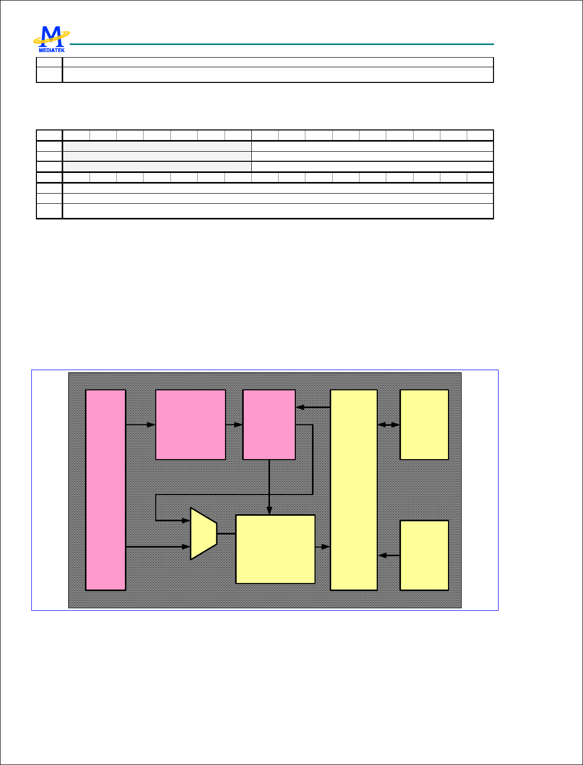
MTK Confidential Release for Konka
MTK Confidential Release for Konka
MT6228 GSM/GPRS Baseband Processor Data Sheet Revision 1.0
303/616 MediaTek Inc. Confidential
Type
R/W
Reset
0
GREEN_GR_Y The color gradient of blue component, represented in signed 9.16 format.
G2D+042Ch Graphic 2D Y Blue Gradient Register G2D_BLUEGR_Y
Bit 31 30 29 28 27 26 25 24 23 22 21 20 19 18 17 16
Name
BLUE_GR_Y[24:16]
Type R/W
Reset
0
Bit 15 14 13 12 11 10 9 8 7 6 5 4 3 2 1 0
Name
BLUE_GR_Y[15:0]
Type R/W
Reset
0
BLUE_GR_Y The color gradient of blue component, represented in signed 9.16 format.
6.6.2 Command Queue
6.6.2.1 General Description
To enhance MMI display and gaming experiences, a command queue parser is implemented for further offloading of
MCU. The command queue with a flexible depth setting is allocated in system memory. If the command queue is
enabled, software program has to check if the command queue has free space before writing to the command queue
data register. Command queue parser consumes the command queue entries upon 2D engine requests. Figure 15
shows the command queue and 2D engine block diagram.
2D
engine
Command
queue
APB
slave
Command
parser
DST
memory
read/write
control
SRC
memory
read
control
Graphic
Memory
Interface
Figure 26 The command queue and 2D engine block diagram.
6.6.2.2 Register Definitions
MCU APB bus registers are listed as follows. The base address of the command queue controller is 80660000h.

MTK Confidential Release for Konka
MTK Confidential Release for Konka
MT6228 GSM/GPRS Baseband Processor Data Sheet Revision 1.0
304/616 MediaTek Inc. Confidential
GCMQ+0000h
Graphic Command Queue Control Register GCMQ_CON
Bit 31 30 29 28 27 26 25 24 23 22 21 20 19 18 17 16
Name
Type
Reset
Bit 15 14 13 12 11 10 9 8 7 6 5 4 3 2 1 0
Name
WEN EN
Type R/W R/W
Reset
0 0
EN Command queue enable. When EN is LOW, the command queue controller is reset.
WEN Command queue in write mode. When WEN is LOW, the command queue consumes the commands in the
queue if command queue is not empty.
GCMQ+0004h
Graphic Command Queue Status Register GCMQ_STA
Bit 31 30 29 28 27 26 25 24 23 22 21 20 19 18 17 16
Name
Type
Reset
Bit 15 14 13 12 11 10 9 8 7 6 5 4 3 2 1 0
Name
WR_R
DY FREE
Type RO RO
Reset
0 100000000
FREE Number of free command queue entries.
WR_RDY Ready to receive command, command-write is not allowed when this status bit is 0. Software has to
check this bit before writing command to gcmq.
GCMQ+0008h Graphic Command Queue Data Register GCMQ_DAT
Bit 31 30 29 28 27 26 25 24 23 22 21 20 19 18 17 16
Name
ADDR
Type WO
Bit 15 14 13 12 11 10 9 8 7 6 5 4 3 2 1 0
Name
DATA
Type WO
ADDR [11:0] Write address for mapped 2D engine registers.
DATA [15:0] Write data for mapped 2D engine registers.
GCMQ+000Ch Graphic Command Queue Base Address Register GCMQ_BASE_
ADD
Bit 31 30 29 28 27 26 25 24 23 22 21 20 19 18 17 16
Name
BASE_ADD[31:16]
Type R/W
Bit 15 14 13 12 11 10 9 8 7 6 5 4 3 2 1 0
Name
BASE_ADD[15:0]
Type R/W
BASE_ADD Starting address of the command queue in memory.
Note : This field can only be modified while the command queue is not enabled; otherwise the behavior of
the command queue is unpredictable.

MTK Confidential Release for Konka
MTK Confidential Release for Konka
MT6228 GSM/GPRS Baseband Processor Data Sheet Revision 1.0
305/616 MediaTek Inc. Confidential
GCMQ+0010h Graphic Command Queue Buffer Length Register GCMQ_LENGT
H
Bit 31 30 29 28 27 26 25 24 23 22 21 20 19 18 17 16
Name
Type
Bit 15 14 13 12 11 10 9 8 7 6 5 4 3 2 1 0
Name
LENGTH
Type R/W
LENGTH[9:0] Length of the command queue. Occupied space of the command queue in the memory is LENGTH
*4Bytes.
Note : This field can only be modified while the command queue is not enabled; otherwise the behavior of
the command queue is unpredictable.
GCMQ+0014h Graphic Command Queue Current Register GCMQ_DMA_A
DDR
Bit 31 30 29 28 27 26 25 24 23 22 21 20 19 18 17 16
Name
GCMQ_DMA_ADDR
Type RO
Bit 15 14 13 12 11 10 9 8 7 6 5 4 3 2 1 0
Name
GCMQ_DMA_ADDR
Type RO
GCMQ_DMA_ADDR Current read or write DMA address of GCMQ.
6.6.2.3
6.7 Capture Resize
6.7.1 General Description
This block provides the image resizing function for image and video capturing scenarios. It receives image data from
the ISP module, performs the image resizing function and outputs to the IMG_DMA module. Figure 27 shows the
block diagram. The capture resize is composed of horizontal and vertical resizing blocks. It can scale up or down
the input image by any ratio. However, the maximum sizes of input and output images are limited to 2048x2048.
Figure 27 Block diagram of the capture resize
The horizontal resizing function is a combination of 2’s power average and bi-linear interpolation. The vertical
resizing function is a bi-linear interpolation. The input and output format are both YUV444. But the internal
MTK Confidential Release for Konka
MTK Confidential Release for Konka
MT6228 GSM/GPRS Baseband Processor Data Sheet Revision 1.0
306/616 MediaTek Inc. Confidential
working memory format is YUV422 to mitigate memory and bandwidth requirements. There is one GMC port
employed in the capture resize for the vertical buffer read/write.
6.7.2 Register Definitions
REGISTER ADDRESS REGISTER NAME SYNONYM
CRZ+ 0000h Capture Resize Configuration Register CRZ_CFG
CRZ + 0004h Capture Resize Control Register CRZ_CON
CRZ + 0008h Capture Resize Status Register CRZ_STA
CRZ + 000Ch Capture Resize Interrupt Register CRZ_INT
CRZ + 0010h Capture Resize Source Image Size Register 1 CRZ_SRCSZ1
CRZ + 0014h Capture Resize Target Image Size Register 1 CRZ_TARSZ1
CRZ + 0018h Capture Resize Horizontal Ratio Register 1 CRZ_HRATIO1
CRZ + 001Ch Capture Resize Vertical Ratio Register 1 CRZ_VRATIO1
CRZ + 0020h Capture Resize Horizontal Residual Register 1 CRZ_HRES1
CRZ + 0024h Capture Resize Vertical Residual Register 1 CRZ_VRES1
CRZ + 0040h Capture Resize Fine Resizing Configuration Register CRZ_FRCFG
CRZ + 005Ch Capture Resize Pixel-Based Resizing Working Memory Base
Address CRZ_PRWMBASE
CRZ + 00B0h Capture Resize Information Register 0 CRZ_INFO0
CRZ + 00B4h Capture Resize Information Register 1 CRZ_INFO1
CRZ + 00B8h Capture Resize Information Register 2 CRZ_INFO2
CRZ + 00BCh Capture Resize Information Register 3 CRZ_INFO3
CRZ + 00C0h Capture Resize Information Register 4 CRZ_INFO4
CRZ + 00C4h Capture Resize Information Register 5 CRZ_INFO5
6.7.2.1 Capture Resize Configuration Register
CRZ+0000h Capture Resize Configuration Register CRZ_CFG
Bit 31 30 29 28 27 26 25 24 23 22 21 20 19 18 17 16
Name
Type
Reset
Bit 15 14 13 12 11 10 9 8 7 6 5 4 3 2 1 0
Name
LBSE
L PSEL
PCON
PELSRC1
Type R/W R/W R/W R/W
Reset
0 0 0 0000
The register is for global configuration of Capture Resize.
PELSRC1 The register field specifies which pixel-based image source is serviced.
0 Camera Interface
1 MPEG4 Encoder DMA
2 MPEG4 Decoder DMA
3 IBW4 DMA
4 IPP
Others Reserved
MTK Confidential Release for Konka
MTK Confidential Release for Konka
MT6228 GSM/GPRS Baseband Processor Data Sheet Revision 1.0
307/616 MediaTek Inc. Confidential
PCON The register bit specifies if pixel-based resizing continues whenever an image finishes processing. Once
continuous run for pixel-based resizing is enabled and pixel-based resizing is running, the only way to stop is
to reset Capture Resize. If to stop immediately is desired, reset Capture Resize directly. If the last image is
desired, set the register bit to ‘0’ first. Then wait until image resizer is not busy again. Finally reset image
resizer.
0 Single run
1 Continuous run
PSEL The register field determines if block-based image sources is serviced.
0 Block-based image source is serviced.
1 Block-based image source is NOT serviced completely. Clock for block-based processes is stopped and
block-based image input is blocked completely.
LBSEL Line buffer selection.
0 Shared memory.
1 Dedicated memory.
6.7.2.2 Capture Resize Control Register
CRZ+0004h Capture Resize Control Register CRZ_CON
Bit 31 30 29 28 27 26 25 24 23 22 21 20 19 18 17 16
Name
PELV
RRST
PELH
RRST
Type R/W R/W
Reset
0 0
Bit 15 14 13 12 11 10 9 8 7 6 5 4 3 2 1
Name
PELV
RENA
PELH
RENA
Type R/W R/W
Reset
0 0
The register is for global control of Capture Resize. Note that software reset does NOT reset all register settings.
Remember to trigger Capture Resize first before triggering image sources to Capture Resize.
PELHRENA Writing ‘1’ to the register bit causes pixel-based fine horizontal resizing proceed to work. However,
if horizontal resizing is not necessary, do not write ‘1’ to the register bit.
PELVRENA Writing ‘1’ to the register bit causes pixel-based fine vertical resizing proceed to work. However, if
vertical resizing is not necessary, do not write ‘1’ to the register bit.
PELHRRST Writing ‘1’ to the register causes pixel-based fine horizontal resizing to stop immediately and have
pixel-based fine horizontal resizing keep in reset state. In order to have pixel-based fine horizontal
resizing go to normal state, write ‘0’ to the register bit.
PELVRRST Writing ‘1’ to the register causes pixel-based fine vertical resizing to stop immediately and have
pixel-based fine vertical resizing keep in reset state. In order to have pixel-based fine vertical
resizing go to normal state, write ‘0’ to the register bit.
6.7.2.3 Capture Resize Status Register
CRZ+0008h Capture Resize Status Register CRZ_STA
Bit 31 30 29 28 27 26 25 24 23 22 21 20 19 18 17 16
Name
Type
Reset
Bit 15 14 13 12 11 10 9 8 7 6 5 4 3 2 1 0
MTK Confidential Release for Konka
MTK Confidential Release for Konka
MT6228 GSM/GPRS Baseband Processor Data Sheet Revision 1.0
308/616 MediaTek Inc. Confidential
Name
PELV
RBUS
Y
PELH
RBUS
Y
Type RO RO
Reset
0 0
The register indicates global status of Capture Resize.
PELHRBUSY Pixel-based HR (Horizontal Resizing) Busy Status
PELVRBUSY Pixel-based VR (Vertical Resizing) Busy Status
6.7.2.4 Capture Resize Interrupt Register
CRZ+000Ch Capture Resize Interrupt Register CRZ_INT
Bit 31 30 29 28 27 26 25 24 23 22 21 20 19 18 17 16
Name
Type
Reset
Bit 15 14 13 12 11 10 9 8 7 6 5 4 3 2 1 0
Name
PELV
RINT
PELH
RINT
Type RC RC
Reset
0 0
The register shows up the interrupt status of resizer.
PELHRINT Interrupt for PELHR (Pixel-based Horizontal Resizing). No matter the register bit
CRZ_FRCFG.HRINTEN is enabled or not, the register bit is active whenever PELHR completes. It
could be as software interrupt by polling the register bit. Clear it by reading the register.
PELVRINT Interrupt for PELVR (Pixel -based Vertical Resizing). No matter the register bit
CRZ_FRCFG.VRINTEN is enabled or not, the register bit is active whenever PELVR completes. It
could be as software interrupt by polling the register bit. Clear it by reading the register.
6.7.2.5 Capture Resize Source Image Size Register 1
CRZ+0010h Capture Resize Source Image Size Register 1 CRZ_SRCSZ1
Bit 31 30 29 28 27 26 25 24 23 22 21 20 19 18 17 16
Name
HS
Type R/W
Bit 15 14 13 12 11 10 9 8 7 6 5 4 3 2 1 0
Name
WS
Type
R/W
The register specifies the size of source image after coarse shrink process. The allowable maximum size is
2048x2048. Note that the width of source image must be a multiple of 8xH
max
and the height of source image must be a
multiple of 8xV
max
when Block Coarse Shrinking is involved.
WS The register field specifies the width of source image after coarse shrink process.
1 The width of source image after coarse shrink process is 1.
2 The width of source image is 2.
…
HS The register field specifies the height of source image after coarse shrink process.
1 The height of source image after coarse shrink process is 1.
2 The height of source image after coarse shrink process is 2.
…
MTK Confidential Release for Konka
MTK Confidential Release for Konka
MT6228 GSM/GPRS Baseband Processor Data Sheet Revision 1.0
309/616 MediaTek Inc. Confidential
6.7.2.6 Capture Resize Target Image Size Register 1
CRZ+0014h Capture Resize Target Image Size Register 1 CRZ_TARSZ1
Bit 31 30 29 28 27 26 25 24 23 22 21 20 19 18 17 16
Name
HT
Type R/W
Bit
15 14
13
12
11 10 9 8 7 6 5 4 3 2 1 0
Name
WT
Type R/W
The register specifies the size of target image. The allowable maximum size is 2048x2048.
WT The register field specifies the width of target image.
1 The width of target image is 1.
2 The width of target image is 2.
…
HT The register field specifies the height of target image.
1 The height of target image is 1.
2 The height of target image is 2.
…
6.7.2.7 Capture Resize Horizontal Ratio Register 1
CRZ+0018h Capture Resize Horizontal Ratio Register CRZ_HRATIO1
Bit 31 30 29 28 27 26 25 24 23 22 21 20 19 18 17 16
Name
RATIO [31:16]
Type R/W
Bit 15 14 13 12 11 10 9 8 7 6 5 4 3 2 1 0
Name
RATIO [15:0]
Type R/W
The register specifies horizontal resizing ratio. It is obtained by CRZ_SRCSZ.WS * 2
20
/ CRZ_TARSZ.WT.
6.7.2.8 Capture Resize Vertical Ratio Register 1
CRZ+001Ch Capture Resize Vertical Ratio Register 1 CRZ_VRATIO1
Bit 31 30 29 28 27 26 25 24 23 22 21 20 19 18 17 16
Name
RATIO [31:16]
Type R/W
Bit 15 14 13 12 11 10 9 8 7 6 5 4 3 2 1 0
Name
RATIO [15:0]
Type R/W
The register specifies vertical resizing ratio. It is obtained by CRZ_SRCSZ.HS * 2
20
/ CRZ_TARSZ.HT.
6.7.2.9 Capture Resize Horizontal Residual Register 1
CRZ+0020h Capture Resize Horizontal Residual Register 1 CRZ_HRES1
Bit 31 30 29 28 27 26 25 24 23 22 21 20 19 18 17 16
Name
Type
Bit 15 14 13 12 11 10 9 8 7 6 5 4 3 2 1 0
Name
RESIDUAL
Type R/W
MTK Confidential Release for Konka
MTK Confidential Release for Konka
MT6228 GSM/GPRS Baseband Processor Data Sheet Revision 1.0
310/616 MediaTek Inc. Confidential
The register specifies horizontal residual. It is obtained by CRZ_SRCSZ.WS % CRZ_TARSZ.WT. The allowable
maximum value is 2046.
6.7.2.10 Capture Resize Vertical Residual Register 1
CRZ+0024h Capture Resize Vertical Residual Register 1 CRZ_VRES1
Bit 31 30 29 28 27 26 25 24 23 22 21 20 19 18 17 16
Name
Type
Bit 15 14 13 12 11 10 9 8 7 6 5 4 3 2 1 0
Name
RESIDUAL
Type R/W
The register specifies vertical residual. It is obtained by CRZ_SRCSZ.HS % CRZ_TARSZ.HT. The allowable
maximum value is 2046.
6.7.2.11 Capture Resize Fine Resizing Configuration Register
CRZ+0040h Capture Resize Fine Resizing Configuration
Register CRZ_FRCFG
Bit 31 30 29 28 27 26 25 24 23 22 21 20 19 18 17 16
Name
WMSZ
Type R/W
Bit 15 14 13 12 11 10 9 8 7 6 5 4 3 2 1 0
Name
PCSF1 VRINT
EN
HRIN
TEN
VRSS
Type R/W R/W R/W R/W
Reset
00 0 0 0
The register specifies various setting of control for fine resizing, including of horizontal and vertical resizing. Note
that all parameters must be set before horizontal and vertical resizing proceeds.
VRSS The register bit specifies whether subsampling for vertical resizing is enabled. For throughput issue, vertical
resizing may be simplified by subsampling lines vertically. The register bit is only valid in pixel-based
mode.
0 Subsampling for vertical resizing is disabled.
1 Subsampling for vertical resizing is enabled.
HRINTEN HR (Horizontal Resizing) Interrupt Enable. When interrupt for HR is enabled, an interrupt is generated
whenever HR finishes.
0 Interrupt for HR is disabled.
1 Interrupt for HR is enabled.
VRINTEN VR (Vertical Resizing) Interrupt Enable. When interrupt for VR is enabled, an interrupt is generated
whenever VR finishes.
0 Interrupt for VR is disabled.
1 Interrupt for VR is enabled.
PCSF1 Coarse Shrinking Factor 1 for pixel-based resizing. Only horizontal coarse shrinking is supported for
pixel-based resizing.
00 No coarse shrinking.
01 Image width becomes 1/2 of original size after coarse shrink pass.
10 Image width becomes 1/4 of original size after coarse shrink pass.
11 Image width becomes 1/8 of original size after coarse shrink pass.
MTK Confidential Release for Konka
MTK Confidential Release for Konka
MT6228 GSM/GPRS Baseband Processor Data Sheet Revision 1.0
311/616 MediaTek Inc. Confidential
WMSZ It stands for Working Memory SiZe. The register specifies how many lines after horizontal resizing can be
filled into working memory. Its minimum value is 4.
6.7.2.12 Capture Resize Pixel-Based Resizing Working Memory Base Address
Register
CRZ+005Ch Capture Resize Pixel-Based Resizing
Working Memory Base Address Register CRZ_PRWMBASE
Bit 31 30 29 28 27 26 25 24 23 22 21 20 19 18 17 16
Name
PRWMBASE [31:16]
Type R/W
Bit 15 14 13 12 11 10 9 8 7 6 5 4 3 2 1 0
Name
PRWMBASE [15:0]
Type R/W
The register specifies the base address of working memory in pixel-based resizing mode. It must be byte-aligned.
When CRZ_CFG.LB_SEL is set, this address should be set as 0x40020000.
6.7.2.13 Capture Resize Information Register 0
CRZ+00B0h Capture Resize Information Register 0 CRZ_INFO0
Bit 31 30 29 28 27 26 25 24 23 22 21 20 19 18 17 16
Name
INFO[31:16]
Type RO
Bit 15 14 13 12 11 10 9 8 7 6 5 4 3 2 1 0
Name
INFO[15:0]
Type RO
The register shows progress of BLKCS. But they are not real processed width/height. Sampling factors must be
taken into consideration. For example, if (V
Y
, V
U
, V
V
)=(2,4,4) then real processed width/height are two times of the
register.
INFO[31:16] BLKCS y
INFO[15:00] BLKCS x
6.7.2.14 Capture Resize Information Register 1
CRZ+00B4 Capture Resize Information Register 1 CRZ_INFO1
Bit 31 30 29 28 27 26 25 24 23 22 21 20 19 18 17 16
Name
INFO[31:16]
Type RO
Bit 15 14 13 12 11 10 9 8 7 6 5 4 3 2 1 0
Name
INFO[15:0]
Type RO
The register shows progress of BLK2PEL.
INFO[31:16] BLK2PEL y
INFO[15:00] BLK2PEL x
MTK Confidential Release for Konka
MTK Confidential Release for Konka
MT6228 GSM/GPRS Baseband Processor Data Sheet Revision 1.0
312/616 MediaTek Inc. Confidential
6.7.2.15 Capture Resize Information Register 2
CRZ+00B8 Capture Resize Information Register 2 CRZ_INFO2
Bit 31 30 29 28 27 26 25 24 23 22 21 20 19 18 17 16
Name
INFO[31:16]
Type RO
Bit
15 14
13
12
11 10 9 8 7 6 5 4 3 2 1 0
Name
INFO[15:0]
Type RO
The register shows progress of pixels received from BLKCS in fine resizing stage.
INFO[31:16] Indicates the account of vertical lines received from BLKCS in fine resizing stage.
INFO[15:00] Indicates the account of horizontal pixels received from BLKCS in fine resizing stage. Note that it
becomes zero when resizing completes.
6.7.2.16 Capture Resize Information Register 3
CRZ+00BC Capture Resize Information Register 3 CRZ_INFO3
Bit 31 30 29 28 27 26 25 24 23 22 21 20 19 18 17 16
Name
INFO[31:16]
Type RO
Bit 15 14 13 12 11 10 9 8 7 6 5 4 3 2 1 0
Name
INFO[15:0]
Type RO
The register shows progress of horizontal resizing in fine resizing stage.
INFO[31:16] Indicates the account of horizontal resizing in fine resizing stage in horizontal direction.
INFO[15:00] Indicates the account of horizontal resizing in fine resizing stage in vertical direction.
6.7.2.17 Capture Resize Information Register 4
CRZ+00C0 Capture Resize Information Register 4 CRZ_INFO4
Bit 31 30 29 28 27 26 25 24 23 22 21 20 19 18 17 16
Name
INFO[31:16]
Type RO
Bit 15 14 13 12 11 10 9 8 7 6 5 4 3 2 1 0
Name
INFO[15:0]
Type RO
The register shows progress of vertical resizing in fine resizing stage.
INFO[31:16] Indicates the account of vertical resizing in fine resizing stage in horizontal direction.
INFO[15:00] Indicates the account of vertical resizing in fine resizing stage in vertical direction.
6.7.2.18 Capture Resize Information Register 5
CRZ+00C5 Capture Resize Information Register 5 CRZ_INFO5
Bit 31 30 29 28 27 26 25 24 23 22 21 20 19 18 17 16
Name
INFO[31:16]
Type RO
Bit 15 14 13 12 11 10 9 8 7 6 5 4 3 2 1 0
Name
INFO[15:0]
Type RO

MTK Confidential Release for Konka
MTK Confidential Release for Konka
MT6228 GSM/GPRS Baseband Processor Data Sheet Revision 1.0
313/616 MediaTek Inc. Confidential
The register shows progress of YUV-to-RGB
INFO[31:16] Indicates YUV-to-RGB in horizontal direction.
INFO[15:00] Indicates YUV-to-RGB in vertical direction.
6.7.3 Application Notes
Working memory. Maximum value is 16 and minimum 4. Remember that each pixel occupies 2 bytes.
Thus minimum requirement for working memory in pixel-based resizing is (pixel number in a line) x2x4
bytes.
Configuration procedure for pixel-based image sources
CRZ_CFG.PSEL=1;
CRZ_CFG.PELSRC = 0;
CRZ_SRCSZ = source image size;
CRZ_TARSZ = target image size;
CRZ_HRATIO = horizontal ratio;
CRZ_VRATIO = vertical ratio;
CRZ_HRES = horizontal residual;
CRZ_VRES = vertical residual;
CRZ_FRCFG = working memory size, interrupt enable;
CRZ_PRWMBASE = working memory base;
CRZ_CON = 0x6;
// Then wait interrupt or polling CRZ_INT.PELHRINT or CRZ_INT.PELVRINT
6.8 Drop Resize
6.8.1 General Description
This block provides a simple resizing function by performing pixel and line dropping. It receives image data from the
Video Encode DMA for videophone local display or the IBW3 DMA for thumbnail image dump, performs the image
resizing function and outputs to the image process engine module. It can scale down the input image by any ratio.
However, the maximum sizes of input and output images are limited to 2048x2048.
6.8.2 Register Definitions
6.8.2.1 Register Map
Table 50 shows the register map.
REGISTER ADDRESS REGISTER NAME SYNONYM
DRZ+ 0000h Drop Resize Start Register DRZ_STR
DRZ+ 0004h Drop Resize Control Register DRZ_CON
DRZ + 0008h Drop Resize Status Register DRZ_STA
DRZ + 000Ch Drop Resize Interrupt Acknowledge Register DRZ_ACKINT
DRZ + 0010h Drop Resize Source Image Size Register DRZ_SRC_SIZE
DRZ + 0014h Drop Resize Target Image Size Register DRZ_TAR_SIZE
DRZ + 0020h Drop Resize Horizontal Ratio Register DRZ_RAT_H
DRZ + 0024h Drop Resize Vertical Ratio Register DRZ_RAT_V
MTK Confidential Release for Konka
MTK Confidential Release for Konka
MT6228 GSM/GPRS Baseband Processor Data Sheet Revision 1.0
314/616 MediaTek Inc. Confidential
Table 50 Register map.
6.8.2.2 Register Description
Followings are detail descriptions of each register.
DRZ+0000h Drop Resize Start Register DRZ_STR
Bit 31 30 29 28 27 26 25 24 23 22 21 20 19 18 17 16
Name
Type R/W R/W R/W R/W R/W R/W R/W R/W R/W R/W R/W R/W R/W R/W R/W R/W
Reset
0 0 0 0 0 0 0 0 0 0 0 0 0 0 0 0
Bit 15 14 13 12 11 10 9 8 7 6 5 4 3 2 1 0
Name
STR
Type R/W R/W R/W R/W R/W R/W R/W R/W R/W R/W R/W R/W R/W R/W R/W R/W
Reset
0 0 0 0 0 0 0 0 0 0 0 0 0 0 0 0
This register controls the activity of Drop Resize. Note that before setting STR to “1”, all the configurations shall be
done by giving proper values.
STR Start the Drop resize engine. Write 1 to this bit will start the FSM of Drop resize. Write 0 to this bit will reset
the FSM of Drop resize.
DRZ+0004h Drop Resize Configuration Register DRZ_CON
Bit 31 30 29 28 27 26 25 24 23 22 21 20 19 18 17 16
Name
Type
Reset
Bit 15 14 13 12 11 10 9 8 7 6 5 4 3 2 1 0
Name
PSEL
AUTO
RSTR
IT
Type R/W R/W R/W

MTK Confidential Release for Konka
MTK Confidential Release for Konka
MT6228 GSM/GPRS Baseband Processor Data Sheet Revision 1.0
315/616 MediaTek Inc. Confidential
Reset
0 0 0
The register specifies the configuration of Drop resize.
IT Interrupt Enabling
0 Disable
1 Enable
AUTO RSTR Automatic restart. Drop Resize automatically restarts itself while current frame is finished.
0 Disable
1 Enable
PSEL Pixel engine selection
0 Video encode DMA
1 IBW3 DMA.
DRZ+0008h Drop Resize Status Register DRZ_STA
Bit 31 30 29 28 27 26 25 24 23 22 21 20 19 18 17 16
Name
RUN
Type RO
Reset
0
Bit 15 14 13 12 11 10 9 8 7 6 5 4 3 2 1 0
Name
IT
Type RO
Reset
0
This register helps software program being well aware of the global status of Drop Resize.
IT Interrupt status for Drop Resize
0 No interrupt is generated.
1 An interrupt is pending and waiting for service.
RUN Drop Resize status
0 Drop Resize is stopped or has completed the transfer already.
1 Drop Resize is currently running.
DRZ+000Ch Drop Resize Interrupt Acknowledge Register DRZ_ACKINT
Bit 31 30 29 28 27 26 25 24 23 22 21 20 19 18 17 16
Name
Type
Bit 15 14 13 12 11 10 9 8 7 6 5 4 3 2 1 0
Name
ACK
Type WO
This register is used to acknowledge the current interrupt request associated with the completion event of Drop Resize
by software program. Note that this is a write-only register, and any read to it will return a value of “0”.
ACK Interrupt acknowledge for the Drop Resize
0 No effect
1 Interrupt request is acknowledged and should be relinquished.
DRZ+0010h Drop Resize Source Image Size Register DRZ_SRC_SIZE
Bit 31 30 29 28 27 26 25 24 23 22 21 20 19 18 17 16
Name
V
Type R/W
Reset
0
Bit 15 14 13 12 11 10 9 8 7 6 5 4 3 2 1 0
Name
H

MTK Confidential Release for Konka
MTK Confidential Release for Konka
MT6228 GSM/GPRS Baseband Processor Data Sheet Revision 1.0
316/616 MediaTek Inc. Confidential
Type
R/W
Reset
0
The register specifies the size of source image. The maximum allowable size is 2048x2048.
V the height of source image-1
H the width of source image-1
DRZ+0014h Drop Resize Target Image Size Register DRZ_TAR_SIZE
Bit 31 30 29 28 27 26 25 24 23 22 21 20 19 18 17 16
Name
V
Type R/W
Reset
0
Bit 15 14 13 12 11 10 9 8 7 6 5 4 3 2 1 0
Name
H
Type R/W
Reset
0
The register specifies the size of target image. The maximum allowable size is 2048x2048.
V the height of target image-1
H the width of target image-1
DRZ+0020h Drop Resize Horizontal Ratio Register DRZ_RAT_H
Bit 31 30 29 28 27 26 25 24 23 22 21 20 19 18 17 16
Name
I [31:16]
Type R/W
Reset
0
Bit 15 14 13 12 11 10 9 8 7 6 5 4 3 2 1 0
Name
Q [15:0]
Type R/W
Reset
0
The register specifies horizontal resizing ratio. It is obtained by (the width of source image/the width of target image) =
I + Q/P = I + Q/the width of target image.
I [31:0] the integer part
Q [31:0] the denominator
DRZ+0024h Drop Resize Vertical Ratio Register DRZ_RAT_V
Bit 31 30 29 28 27 26 25 24 23 22 21 20 19 18 17 16
Name
I [31:16]
Type R/W
Reset
0
Bit 15 14 13 12 11 10 9 8 7 6 5 4 3 2 1 0
Name
Q [15:0]
Type R/W
Reset
0
The register specifies horizontal resizing ratio. It is obtained by (the height of source image/the height of target image)
= I + Q/P = I + Q/the height of target image.
I [31:0] the integer part
Q [31:0] the denominator
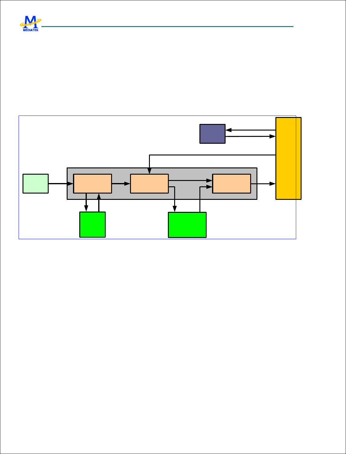
MTK Confidential Release for Konka
MTK Confidential Release for Konka
MT6228 GSM/GPRS Baseband Processor Data Sheet Revision 1.0
317/616 MediaTek Inc. Confidential
6.9 Post Resize
6.9.1 General Description
Figure 27 shows the block diagram of post resize. It receives image data from a block-based source such as JPEG
decoder or from a scan line based source, and then performs image resizing. The capability of resizing in the block is
divided into two portions, coarse pass and fine pass. The first pass is coarse resizing pass and it is able to shrink image
by a factor of 1, 1/4, 1/16, or 1/64. The second pass is the fine resizing pass, which is composed of horizontal and
vertical resizing, and it is able to shrink or enlarge image in fractional ratio. The maximum allowable image size for the
fine resizing pass is 2048x2048. Thus the maximum allowable image size for coarse resizing pass is 16384x16384.
!
"#"
$
% & " ""
% &"""
Figure 28 Block diagram of the post resize
The strip buffer of coarse resizing pass accumulates de-compressed 8x8 YUV blocks separately. These YUV data are
packed into pixels and sent to the fine resizing pass. There is one GMC port employed in the coarse resize for the strip
buffer read/write.
The fine resizing pass is composed of horizontal and vertical resizing blocks. It can scale up or down the input image
by any ratio. However, the maximum sizes of input and output images are limited to 2048x2048. The horizontal
resizing function is a combination of 2’s power average and bi-linear interpolation. The vertical resizing function is a
bi-linear interpolation. The input and output format are both YUV444. But the internal working memory format is
YUV422 to mitigate memory and bandwidth requirements. There is one GMC port employed in the fine resize for the
vertical buffer read/write.
6.9.2 Working Memories
There are two working memories in post resize. One is the strip buffer, and the other is the vertical buffer.
6.9.2.1 Strip Buffer
Let’s denote sampling factor for Y-component as (H
Y
, V
Y
), U-component as (H
U
, V
U
) and V-component as (H
V
, V
V
) in
a JPEG file. The minimum requirement of memory size for the strip buffer is (the image width of after the coarse
resizing pass) * (V
Y
* 8 + V
U
* 8 + V
V
* 8) bytes. It is (2048) * (4 * 8 + 4 * 8 + 2 * 8) = 160K bytes for extreme cases.
To enhance the throughput of JPEG decode process, software may use double buffer scheme. Then it becomes 320K

MTK Confidential Release for Konka
MTK Confidential Release for Konka
MT6228 GSM/GPRS Baseband Processor Data Sheet Revision 1.0
318/616 MediaTek Inc. Confidential
bytes. Please note that the strip buffer is composed of the Y buffer, U buffer, and V buffer. Software can allocate
separate memory for them.
6.9.2.2 Vertical Buffer
The minimum requirement of memory for the vertical buffer is (the target image width) * (the line number of
vertical buffer) * 2 bytes. It is (2048) * (2) * 2 = 4K bytes for extreme cases. To enhance throughputs of overall data
paths, software may use double buffer scheme. Then it becomes 8K bytes.
6.9.3 Source Image
For the coarse resizing pass, the width of the source image must be multiples of 8 * (maximum horizontal sampling
factor). Similarly, the height of the source image must be multiples of 8 * (maximum vertical sampling factor). The
maximum size of target image is 2048x2048.
For the fine resizing pass, the maximum size of source image and target image are both 2048x2048.
6.9.4 Flow Control
For the coarse resizing pass, the coarse resizing will send pixel data to the fine resizing when they are ready with hand
shake signal. If strip buffer is full, the coarse resizing will halt image data input until the strip buffer is available.
For the fine resizing pass, the fine resizing will send pixel data to the image post processing when they are ready with
hand shake signal. If vertical buffer is full, the fine resizing will halt image data input until the vertical is available.
6.9.5 Throughput
For block-based image sources, the process time for one pixel is about 3 cycles. Therefore if 15 frames per second are
desired and Post Resize is running at 52 MHz then the maximum pixel number per frame is about 1.15M. That is about
1075x1075.
For pixel-based image sources, the process time for one pixel is about 2.25 cycles. Therefore if 15 frames per second
are desired and Post Resize is running at 52 MHz then the maximum pixel number per frame is about 1.5M. That is
about 1241x1241.
Since memory bandwidth requirements are different for scale up and down, it may be able to enhance throughput by
adjusting the register setting of PRZ_CFG.BWA0/BWB0. When scaling up, memory bandwidth requirement for read is
higher than memory bandwidth requirements for write. However, when scaling down, memory bandwidth requirement
for write is higher than memory bandwidth requirements for read. Therefore when horizontally scaling up, throughput
can be enhance by setting PRZ_CFG.B0 with higher value than PRZ_CFG.A0. Similarly when horizontally scaling
down, throughput can be enhance by setting PRZ_CFG.A0 with higher value than PRZ_CFG.B0. Therefore when
vertically scale up throughput can be enhance by setting PRZ_CFG.B1 with higher value than PRZ_CFG.A1. Similarly
when vertically scale down throughput can be enhance by setting PRZ_CFG.A1 with higher value than PRZ_CFG.B1.
6.9.6 Register Definitions
REGISTER ADDRESS
REGISTER NAME SYNONYM
PRZ+ 0000h Post Resize Configuration Register PRZ_CFG
PRZ + 0004h Post Resize Control Register PRZ_CON
PRZ + 0008h Post Resize Status Register PRZ_STA
PRZ + 000Ch Post Resize Interrupt Register PRZ_INT
PRZ + 0010h Post Resize Source Image Size Register 1 PRZ_SRCSZ1

MTK Confidential Release for Konka
MTK Confidential Release for Konka
MT6228 GSM/GPRS Baseband Processor Data Sheet Revision 1.0
319/616 MediaTek Inc. Confidential
PRZ + 0014h Post Resize Target Image Size Register 1 PRZ_TARSZ1
PRZ + 0018h Post Resize Horizontal Ratio Register 1 PRZ_HRATIO1
PRZ + 001Ch Post Resize Vertical Ratio Register 1 PRZ_VRATIO1
PRZ + 0020h Post Resize Horizontal Residual Register 1 PRZ_HRES1
PRZ + 0024h Post Resize Vertical Residual Register 1 PRZ_VRES1
PRZ + 0030h Post Resize Block Coarse Shrinking Configuration Register PRZ_BLKCSCFG
PRZ + 0034h Post Resize Y-Component Line Buffer Memory Base Address PRZ_YLMBASE
PRZ + 0038h Post Resize U-Component Line Buffer Memory Base Address PRZ_ULMBASE
PRZ + 003Ch Post Resize V-Component Line Buffer Memory Base Address PRZ_VLMBASE
PRZ + 0040h Post Resize Fine Resizing Configuration Register PRZ_FRCFG
PRZ + 0050h Post Resize Y Line Buffer Size Register PRZ_YLBSIZE
PRZ + 005Ch Post Resize Pixel-Based Resizing Working Memory Base Address PRZ_PRWMBASE
PRZ + 00B0h Post Resize Information Register 0 PRZ_INFO0
PRZ + 00B4h Post Resize Information Register 1 PRZ_INFO1
PRZ + 00B8h Post Resize Information Register 2 PRZ_INFO2
PRZ + 00BCh Post Resize Information Register 3 PRZ_INFO3
PRZ + 00C0h Post Resize Information Register 4 PRZ_INFO4
PRZ + 00C4h Post Resize Information Register 5 PRZ_INFO5
6.9.6.1 Post Resize Configuration Register
PRZ+0000h Post Resize Configuration Register PRZ_CFG
Bit 31 30 29 28 27 26 25 24 23 22 21 20 19 18 17 16
Name
BWB0 BWA0
Type R/W R/W
Reset
0000 0000
Bit 15 14 13 12 11 10 9 8 7 6 5 4 3 2 1 0
Name
LBSE
L PSEL
PCON
PELSRC1
Type R/W R/W R/W R/W
Reset
0 0 0 0000
The register is for global configuration of Post Resize.
PELSRC1 The register field specifies which pixel-based image source is serviced.
1 MPEG4 Encoder DMA
2 MPEG4 Decoder DMA
3 IBW4 DMA
5 IPP
6 JPEG Decoder
Others Reserved
PCON The register bit specifies if pixel-based resizing continues whenever an image finishes processing. Once
continuous run for pixel-based resizing is enabled and pixel-based resizing is running, the only way to stop is
to reset Post Resize. If immediate stop is desired, reset Post Resize directly. If the last image is desired, set the
register bit to ‘0’ first. Then wait till Post Resize is not busy again. Finally reset Post Resize.
0 Single run
1 Continuous run
PSEL The register field determines if block-based image sources is serviced.

MTK Confidential Release for Konka
MTK Confidential Release for Konka
MT6228 GSM/GPRS Baseband Processor Data Sheet Revision 1.0
320/616 MediaTek Inc. Confidential
0 Block-based image source will be serviced.
1 Block-based image source will NOT be serviced completely. Clock for block-based processes will be
stopped and block-based image input will be blocked completely.
LBSEL line buffer selection. When CRZ_CFG.LB_SEL is set, this bit should not be set.
0 Shared memory.
1 Dedicated memory.
BWA0 Bandwidth selection for port A of memory interface 0. In block-based mode, this is the memory interface
between BLKCS and BLKHR. In pixel-based mode, that’s is memory interface between PELHR and PELVR.
Each memory interface has one write port (port A) and one read port (port B). The arbitration between port A
and port B of memory interface 0 is based on the setting of the register fields BWA0 and BWB0. The
arbitration scheme is fair between port A and port B. However, if the register field BWA0 is set larger value
than the register field BWB0 then port A can get more bandwidth than port B.
0 If memory access of port A and port B take place simultaneously, then grant will be given to port B
whenever port A gets grant once.
1 If memory access of port A and port B take place simultaneously, then grant will be given to port B
whenever port A gets grant twice.
2 If memory access of port A and port B take place simultaneously, then grant will be given to port B
whenever port A gets grant three times.
…
BWB0 Bandwidth selection for port b of memory interface 0. In block-based mode, this is the memory interface
between BLKCS and BLKHR. In pixel-based mode, that’s is memory interface between PELHR and PELVR.
Each memory interface has one write port (port A) and one read port (port B). The arbitration between port A
and port B of memory interface 0 is based on the setting of the register fields BWA0 and BWB0. The
arbitration scheme is fair between port A and port B. However, if the register field BWB0 is set larger value
than the register field BWA0 then port B can get more bandwidth than port A.
0 If memory access of port A and port B take place simultaneously, then grant will be given to port A
whenever port B gets grant once.
1 If memory access of port A and port B take place simultaneously, then grant will be given to port A
whenever port B gets grant twice.
2 If memory access of port A and port B take place simultaneously, then grant will be given to port A
whenever port B gets grant three times.
…
6.9.6.2 Post Resize Control Register
PRZ+0004h Post Resize Control Register PRZ_CON
Bit 31 30 29 28 27 26 25 24 23 22 21 20 19 18 17 16
Name
PELV
RRST
PELH
RRST
BLKC
SRST
Type R/W R/W R/W
Reset
0 0 0
Bit 15 14 13 12 11 10 9 8 7 6 5 4 3 2 1 0
Name
PELV
RENA
PELH
RENA
BLKC
SENA
Type R/W R/W R/W
Reset
0 0 0
The register is for global control of Post Resize. Note that block-based and pixel-based resizing cannot execute
parallel. Furthermore, software reset will NOT reset all register setting. Remember trigger Post Resize first
before trigger image sources to Post Resize.
MTK Confidential Release for Konka
MTK Confidential Release for Konka
MT6228 GSM/GPRS Baseband Processor Data Sheet Revision 1.0
321/616 MediaTek Inc. Confidential
BLKCSENA Writing ‘1’ to the register bit will cause Block Coarse Shrinking proceed to work. Block Coarse
Shrinking is designed to cooperate width JPEG decoder. It works on the fly. Bu it needs to be
restarted every time before working.
PELHRENA Writing ‘1’ to the register bit will cause pixel-based fine horizontal resizing proceed to work.
However, if horizontal resizing is not necessary, do not write ‘1’ to the register bit.
PELVRENA Writing ‘1’ to the register bit will cause pixel-based fine vertical resizing proceed to work. However,
if vertical resizing is not necessary, do not write ‘1’ to the register bit.
BLKCSRST Writing ‘1’ to the register bit will force Block Coarse Shrinking to stop immediately and have Block
Coarse Shrinking keep in reset state. In order to have Block Coarse Shrinking go to normal state,
writing ‘0’ to the register bit.
PELHRRST Writing ‘1’ to the register will cause pixel-based fine horizontal resizing to stop immediately and have
pixel-based fine horizontal resizing keep in reset state. In order to have pixel-based fine horizontal
resizing go to normal state, writing ‘0’ to the register bit.
PELVRRST Writing ‘1’ to the register will pixel-based fine vertical resizing to stop immediately and have
pixel-based fine vertical resizing keep in reset state. In order to have pixel-based fine vertical resizing
go to normal state, writing ‘0’ to the register bit.
6.9.6.3 Post Resize Status Register
PRZ+0008h Post Resize Status Register PRZ_STA
Bit 31 30 29 28 27 26 25 24 23 22 21 20 19 18 17 16
Name
Type
Reset
Bit
15 14
13
12
11 10 9 8 7 6 5 4 3 2 1 0
Name
BLKI
NTRA
BSY
PELV
RBUS
Y
PELH
RBUS
Y
BLKC
SBUS
Y
Type RO RO RO RO
Reset
0 0 0 0
The register indicates global status of Post Resize.
BLKCSBUSY Block-based CS (Coarse Shrinking) Busy Status
PELHRBUSY Pixel-based HR (Horizontal Resizing) Busy Status
PELVRBUSY Pixel-based VR (Vertical Resizing) Busy Status
BLKINTRABSY Block-based CS (Coarse Shrinking) Intra-Block Busy Status
6.9.6.4 Post Resize Interrupt Register
PRZ+000Ch Post Resize Interrupt Register PRZ_INT
Bit 31 30 29 28 27 26 25 24 23 22 21 20 19 18 17 16
Name
Type
Reset
Bit 15 14 13 12 11 10 9 8 7 6 5 4 3 2 1 0
Name
PELV
RINT
PELH
RINT
BLKC
SINT
Type RC RC RC
Reset
0 0 0
The register shows up the interrupt status of resizer.

MTK Confidential Release for Konka
MTK Confidential Release for Konka
MT6228 GSM/GPRS Baseband Processor Data Sheet Revision 1.0
322/616 MediaTek Inc. Confidential
BLKCSINT Interrupt for BLKCS (Block-based Coarse Shrink). No matter if the register bit PRZ_BLKCSCFG.INTEN
is enabled or not, the register bit will be active whenever BLKCS completes. It could be used as software
interrupt by polling the register bit. Clear it by reading the register.
PELHRINT Interrupt for PELHR (Pixel-based Horizontal Resizing). No matter if the register bit
PRZ_FRCFG.HRINTEN is enabled or not, the register bit will be active whenever PELHR completes. It
could be used as software interrupt by polling the register bit. Clear it by reading the register.
PELVRINT Interrupt for PELVR (Pixel -based Vertical Resizing). No matter if the register bit
PRZ_FRCFG.VRINTEN is enabled or not, the register bit will be active whenever PELVR completes. It
could be used as software interrupt by polling the register bit. Clear it by reading the register.
6.9.6.5 Post Resize Source Image Size Register 1
PRZ+0010h Post Resize Source Image Size Register 1 PRZ_SRCSZ1
Bit 31 30 29 28 27 26 25 24 23 22 21 20 19 18 17 16
Name
HS
Type R/W
Bit 15 14 13 12 11 10 9 8 7 6 5 4 3 2 1 0
Name
WS
Type R/W
The register specifies the size of source image after coarse shrink process. The maximum allowable size is 2048x2048.
Note that for the width of source image must be multiples of 8xH
max
and the height of source image must be multiples
of 8xV
max
when Block Coarse Shrinking is involved.
WS The register field specifies the width of source image after coarse shrink process.
1 The width of source image after coarse shrink process is 1.
2 The width of source image is 2.
…
HS The register field specifies the height of source image after coarse shrink process.
1 The height of source image after coarse shrink process is 1.
2 The height of source image after coarse shrink process is 2.
…
6.9.6.6 Post Resize Target Image Size Register 1
PRZ+0014h Post Resize Target Image Size Register 1 PRZ_TARSZ1
Bit 31 30 29 28 27 26 25 24 23 22 21 20 19 18 17 16
Name
HT
Type R/W
Bit 15 14 13 12 11 10 9 8 7 6 5 4 3 2 1 0
Name
WT
Type R/W
The register specifies the size of target image. The maximum allowable size is 2048x2048.
WT The register field specifies the width of target image.
1 The width of target image is 1.
2 The width of target image is 2.
…
HT The register field specifies the height of target image.
1 The height of target image is 1.
2 The height of target image is 2.
MTK Confidential Release for Konka
MTK Confidential Release for Konka
MT6228 GSM/GPRS Baseband Processor Data Sheet Revision 1.0
323/616 MediaTek Inc. Confidential
…
6.9.6.7 Post Resize Horizontal Ratio Register 1
PRZ+0018h Post Resize Horizontal Ratio Register PRZ_HRATIO1
Bit 31 30 29 28 27 26 25 24 23 22 21 20 19 18 17 16
Name
RATIO [31:16]
Type R/W
Bit 15 14 13 12 11 10 9 8 7 6 5 4 3 2 1 0
Name
RATIO [15:0]
Type R/W
The register specifies horizontal resizing ratio. It is obtained by PRZ_SRCSZ.WS * 2
20
/ PRZ_TARSZ.WT.
6.9.6.8 Post Resize Vertical Ratio Register 1
PRZ+001Ch Post Resize Vertical Ratio Register 1 PRZ_VRATIO1
Bit 31 30 29 28 27 26 25 24 23 22 21 20 19 18 17 16
Name
RATIO [31:16]
Type R/W
Bit 15 14 13 12 11 10 9 8 7 6 5 4 3 2 1 0
Name
RATIO [15:0]
Type R/W
The register specifies vertical resizing ratio. It is obtained by PRZ_SRCSZ.HS * 2
20
/ PRZ_TARSZ.HT.
6.9.6.9 Post Resize Horizontal Residual Register 1
PRZ+0020h Post Resize Horizontal Residual Register 1 PRZ_HRES1
Bit 31 30 29 28 27 26 25 24 23 22 21 20 19 18 17 16
Name
Type
Bit 15 14 13 12 11 10 9 8 7 6 5 4 3 2 1 0
Name
RESIDUAL
Type R/W
The register specifies horizontal residual. It is obtained by PRZ_SRCSZ.WS % PRZ_TARSZ.WT. The maximum
allowable value is 2046.
6.9.6.10 Post Resize Vertical Residual Register 1
PRZ+0024h Post Resize Vertical Residual Register 1 PRZ_VRES1
Bit 31 30 29 28 27 26 25 24 23 22 21 20 19 18 17 16
Name
Type
Bit 15 14 13 12 11 10 9 8 7 6 5 4 3 2 1 0
Name
RESIDUAL
Type R/W
The register specifies vertical residual. It is obtained by PRZ_SRCSZ.HS % PRZ_TARSZ.HT. The allowable
maximum value is 2046.
MTK Confidential Release for Konka
MTK Confidential Release for Konka
MT6228 GSM/GPRS Baseband Processor Data Sheet Revision 1.0
324/616 MediaTek Inc. Confidential
6.9.6.11 Post Resize Block Coarse Shrinking Configuration Register
PRZ+0030h Post Resize Block Coarse Shrinking
Configuration Register PRZ_BLKCSCFG
Bit 31 30 29 28 27 26 25 24 23 22 21 20 19 18 17 16
Name
INTE
N
Type R/W
Reset
0
Bit 15 14 13 12 11 10 9 8 7 6 5 4 3 2 1 0
Name
VV HV VU HU VY HY CSF
Type R/W R/W R/W R/W R/W R/W R/W
Reset
00 00 00 00 00 00 00
The register is for various configuration of Block Coarse Shrinking in Post Resize. Block Coarse Shrinking is dedicated
for JPEG decoder. Therefore all processes are based on blocks composed of 8x8 pixels. Note that all parameters must
be set before writing ‘1’ to the register bit PRZ_CON.BLKCSENA.
CSF It stands for Coarse Shrink Factor. The value specifies the scale factor in coarse shrink pass.
00 Image size does not change after coarse shrink pass.
01 Image size becomes 1/4 of original size after coarse shrink pass.
10 Image size becomes 1/16 of original size after coarse shrink pass.
11 Image size becomes 1/64 of original size after coarse shrink pass.
HY Horizontal sampling factor for Y-component
00 Horizontal sampling factor for Y-component is 1.
01 Horizontal sampling factor for Y-component is 2.
10 Horizontal sampling factor for Y-component is 4.
11 No Y-component.
VY Vertical sampling factor for Y-component
00 Vertical sampling factor for Y-component is 1.
01 Vertical sampling factor for Y-component is 2.
10 Vertical sampling factor for Y-component is 4.
11 No Y-component.
HU Horizontal sampling factor for U-component
00 Horizontal sampling factor for U-component is 1.
01 Horizontal sampling factor for U-component is 2.
10 Horizontal sampling factor for U-component is 4.
11 No U-component.
VU Vertical sampling factor for U-component
00 Vertical sampling factor for U-component is 1.
01 Vertical sampling factor for U-component is 2.
10 Vertical sampling factor for U-component is 4.
11 No U-component.
HV Horizontal sampling factor for V-component
00 Horizontal sampling factor for V-component is 1.
01 Horizontal sampling factor for V-component is 2.
10 Horizontal sampling factor for V-component is 4.
11 No V-component.
VV Vertical sampling factor for V-component
00 Vertical sampling factor for V-component is 1.
MTK Confidential Release for Konka
MTK Confidential Release for Konka
MT6228 GSM/GPRS Baseband Processor Data Sheet Revision 1.0
325/616 MediaTek Inc. Confidential
01 Vertical sampling factor for V-component is 2.
10 Vertical sampling factor for V-component is 4.
11 No V-component.
INTEN Interrupt Enable. When interrupt for BLKCS is enabled, interrupt will arise whenever BLKCS finishes.
0 Interrupt for BLKCS is disabled.
1 Interrupt for BLKCS is enabled.
6.9.6.12 Post Resize Y-Component Line Buffer Memory Base Address Register
PRZ+0034h Post Resize Y-Component Line Buffer Memory
Base Address Register PRZ_YLMBASE
Bit 31 30 29 28 27 26 25 24 23 22 21 20 19 18 17 16
Name
YLMBASE [31:16]
Type R/W
Bit 15 14 13 12 11 10 9 8 7 6 5 4 3 2 1 0
Name
YLMBASE [15:0]
Type R/W
The register specifies the base address of line buffer for Y-component. It could be byte-aligned. It is only useful in
block-based mode.
6.9.6.13 Post Resize U-Component Line Buffer Memory Base Address Register
PRZ+0038h Post Resize U-Component Line Buffer Memory
Base Address Register PRZ_ULMBASE
Bit 31 30 29 28 27 26 25 24 23 22 21 20 19 18 17 16
Name
ULMBASE [31:16]
Type R/W
Bit 15 14 13 12 11 10 9 8 7 6 5 4 3 2 1 0
Name
ULMBASE [15:0]
Type R/W
The register specifies the base address of line buffer for U-component. It could be byte -aligned. It is only useful in
block-based mode.
6.9.6.14 Post Resize V-Component Line Buffer Memory Base Address Register
PRZ+003Ch Post Resize V-Component Line Buffer Memory
Base Address Register PRZ_VLMBASE
Bit 31 30 29 28 27 26 25 24 23 22 21 20 19 18 17 16
Name
VLMBASE [31:16]
Type R/W
Bit 15 14 13 12 11 10 9 8 7 6 5 4 3 2 1 0
Name
VLMBASE [15:0]
Type R/W
The register specifies the base address of line buffer for V-component. It could be byte -aligned. It is only useful in
block-based mode.
MTK Confidential Release for Konka
MTK Confidential Release for Konka
MT6228 GSM/GPRS Baseband Processor Data Sheet Revision 1.0
326/616 MediaTek Inc. Confidential
6.9.6.15 Post Resize Fine Resizing Configuration Register
PRZ+0040h Post Resize Fine Resizing Configuration Register PRZ_FRCFG
Bit 31 30 29 28 27 26 25 24 23 22 21 20 19 18 17 16
Name
WMSZ
Type R/W
Bit
15 14
13
12
11 10
9 8 7 6 5 4 3 2 1 0
Name
OSEL
PCSF2 PCSF1 VRINT
EN
HRIN
TEN VRSS
Type R/W R/W R/W R/W R/W R/W
Reset
0 00 00 0 0 0
The register specifies various setting of control for fine resizing, including of horizontal and vertical resizing. Note that
all parameters must be set before horizontal and vertical resizing proceeds.
VRSS The register bit specifies whether subsampling for vertical resizing is enabled. For throughput issue, vertical
resizing may be simplified by subsampling lines vertically. The register bit is only valid in pixel-based mode.
0 Subsampling for vertical resizing is disabled.
1 Subsampling for vertical resizing is enabled.
HRINTEN HR (Horizontal Resizing) Interrupt Enable. When interrupt for HR is enabled, interrupt will be issued
whenever HR finishes.
0 Interrupt for HR is disabled.
1 Interrupt for HR is enabled.
VRINTEN VR (Vertical Resizing) Interrupt Enable. When interrupt for VR is enabled, interrupt will be issued
whenever VR finishes.
0 Interrupt for VR is disabled.
1 Interrupt for VR is enabled.
PCSF1 Coarse Shrinking Factor 1 for pixel-based resizing. Only horizontal coarse shrinking is supported for
pixel-based resizing.
00 No coarse shrinking.
01 Image width becomes 1/2 of original size after coarse shrink pass.
10 Image width becomes 1/4 of original size after coarse shrink pass.
11 Image width becomes 1/8 of original size after coarse shrink pass.
OSEL The register bit is used to select output modules.
0 Image DMA.
1 IPP.
WMSZ It stands for Working Memory Size. The register specifies how many lines after horizontal resizing can be
filled into working memory. Its minimum value is 4.
6.9.6.16 Post Resize Y Line Buffer Size Register
PRZ+0050h Post Resize Y Line Buffer Size Register PRZ_YLBSIZE
Bit 31 30 29 28 27 26 25 24 23 22 21 20 19 18 17 16
Name
Type
Bit 15 14 13 12 11 10 9 8 7 6 5 4 3 2 1 0
Name
YLBZE
Type R/W
The register specifies line buffer size for image data after coarse shrinking. It is only useful in block-based mode.
MTK Confidential Release for Konka
MTK Confidential Release for Konka
MT6228 GSM/GPRS Baseband Processor Data Sheet Revision 1.0
327/616 MediaTek Inc. Confidential
YLBSZ It stands for Y-component Line Buffer Size. The register field specifies how many lines of Y-component can
be filled into line buffer. Line buffer size for U- and V-component can be determined according to the
sampling factor. For example, if (V
Y
, V
U
, V
V
)=(4,4,2) and line buffer size for Y-component is 32, lines then
the line buffer size for U-component is also 32 lines and V-component 16 lines. If line buffer has capacity for
whole image after block coarse shrinking, then block coarse shrinking can be used for the application of
scaling down by a factor of 2, or 4, or 8. If dual line buffer is used, block coarse shrinking and horizontal
resizing can execute parallel. The maximum allowable value is 2048.
1 Line buffer size for Y-component is 1 lines.
2 Line buffer size for Y-component is 2 lines.
3 Line buffer size for Y-component is 3 lines.
…
6.9.6.17 Post Resize Pixel-Baed Resizing Working Memory Base Address Register
PRZ+005Ch Post Resize Pixel-Based Resizing Working
Memory Base Address Register PRZ_PRWMBASE
Bit 31 30 29 28 27 26 25 24 23 22 21 20 19 18 17 16
Name
PRWMBASE [31:16]
Type R/W
Bit 15 14 13 12 11 10 9 8 7 6 5 4 3 2 1 0
Name
PRWMBASE [15:0]
Type R/W
The register specifies the base address of working memory in pixel-based resizing mode. It must be byte-aligned.
When PRZ_CFG.LB_SEL is set, this address should be set as 0x40020000.
6.9.6.18 Post Resize Information Register 0
PRZ+00B0h Post Resize Information Register 0 PRZ_INFO0
Bit 31 30 29 28 27 26 25 24 23 22 21 20 19 18 17 16
Name
INFO[31:16]
Type RO
Bit 15 14 13 12 11 10 9 8 7 6 5 4 3 2 1 0
Name
INFO[15:0]
Type RO
The register shows progress of BLKCS. But they are not real processed width/height. Sampling factors must be taken
into consideration. For example, if (V
Y
, V
U
, V
V
)=(2,4,4) then real processed width/height are two times that of the
register value.
INFO[31:16] BLKCS y
INFO[15:00] BLKCS x
6.9.6.19 Post Resize Information Register 1
PRZ+00B4 Post Resize Information Register 1 PRZ_INFO1
Bit 31 30 29 28 27 26 25 24 23 22 21 20 19 18 17 16
Name
INFO[31:16]
Type RO
Bit 15 14 13 12 11 10 9 8 7 6 5 4 3 2 1 0
Name
INFO[15:0]
Type RO
MTK Confidential Release for Konka
MTK Confidential Release for Konka
MT6228 GSM/GPRS Baseband Processor Data Sheet Revision 1.0
328/616 MediaTek Inc. Confidential
The register shows progress of BLK2PEL.
INFO[31:16] BLK2PEL y
INFO[15:00] BLK2PEL x
6.9.6.20 Post Resize Information Register 2
PRZ+00B8 Post Resize Information Register 2 PRZ_INFO2
Bit 31 30 29 28 27 26 25 24 23 22 21 20 19 18 17 16
Name
INFO[31:16]
Type RO
Bit 15 14 13 12 11 10 9 8 7 6 5 4 3 2 1 0
Name
INFO[15:0]
Type RO
The register shows progress of pixels received from BLKCS in fine resizing stage.
INFO[31:16] Indicate the account of vertical lines received from BLKCS in fine resizing stage.
INFO[15:00] Indicate the account of horizontal pixels received from BLKCS in fine resizing stage. Note that it will
become zero when resizing completes.
6.9.6.21 Post Resize Information Register 3
PRZ+00BC Post Resize Information Register 3 PRZ_INFO3
Bit 31 30 29 28 27 26 25 24 23 22 21 20 19 18 17 16
Name
INFO[31:16]
Type RO
Bit 15 14 13 12 11 10 9 8 7 6 5 4 3 2 1 0
Name
INFO[15:0]
Type RO
The register shows progress of horizontal resizing in fine resizing stage.
INFO[31:16] Indicate the account of horizontal resizing in fine resizing stage in horizontal direction.
INFO[15:00] Indicate the account of horizontal resizing in fine resizing stage in vertical direction.
6.9.6.22 Post Resize Information Register 4
PRZ+00C0 Post Resize Information Register 4 PRZ_INFO4
Bit
31 30
29
28
27 26 25
24
23
22 21 20
19
18
17 16
Name
INFO[31:16]
Type RO
Bit 15 14 13 12 11 10 9 8 7 6 5 4 3 2 1 0
Name
INFO[15:0]
Type RO
The register shows progress of vertical resizing in fine resizing stage.
INFO[31:16] Indicate the account of vertical resizing in fine resizing stage in horizontal direction.
INFO[15:00] Indicate the account of vertical resizing in fine resizing stage in vertical direction.

MTK Confidential Release for Konka
MTK Confidential Release for Konka
MT6228 GSM/GPRS Baseband Processor Data Sheet Revision 1.0
329/616 MediaTek Inc. Confidential
6.9.6.23 Post Resize Information Register 5
PRZ+00C5 Post Resize Information Register 5 PRZ_INFO5
Bit 31 30 29 28 27 26 25 24 23 22 21 20 19 18 17 16
Name
INFO[31:16]
Type RO
Bit
15 14
13
12
11 10 9 8 7 6 5 4 3 2 1 0
Name
INFO[15:0]
Type RO
The register shows progress of YUV-to-RGB
INFO[31:16] Indicate YUV-to-RGB in horizontal direction.
INFO[15:00] Indicate YUV-to-RGB in vertical direction.
6.9.7 Application Notes
Determine line buffer size by taking into consideration of CSF and sampling factor. For example, if CSF=3
and (Vy, Vu, Vv)=(4,x,x) then minimum of line buffer could be 4 instead of 32.
Working memory. Maximum value is 16 and minimum 4. Remember that each pixel occupies 2 bytes. Thus
minimum requirement for working memory in pixel-based resizing is (pixel number in a line) x2x4 bytes.
Configuration procedure for block-based image sources
PRZ_CFG.PSEL=0;
PRZ_CFG.PELSRC = 5;
PRZ_BLKCSCFG = select CSF, sampling factor, interrupt enable;
PRZ_YLBBASE = memory base for Y-component;
PRZ_ULBBASE = memory base for U-component;
PRZ_VLBBASE = memory base for V-component;
PRZ_YLBSIZE = line buffer size for Y-component;
Other same as that for pixel-based image sources
PRZ_CON = 0x7;
// Then wait interrupt or polling PRZ_INT.BLKCSINT or PRZ_INT.BLKHRINT or
// PRZ_INT.BLKVRINT
Configuration procedure for pixel-based image sources
PRZ_CFG.PSEL=1;
PRZ_CFG.PELSRC = 1~4;
PRZ_SRCSZ = source image size;
PRZ_TARSZ = target image size;
PRZ_HRATIO = horizontal ratio;
PRZ_VRATIO = vertical ratio;
PRZ_HRES = horizontal residual;
PRZ_VRES = vertical residual;
PRZ_FRCFG = working memory size, interrupt enable;
PRZ_PRWMBASE = working memory base;
PRZ_CON = 0x6;
// Then wait interrupt or polling PRZ_INT.PELHRINT or PRZ_INT.PELVRINT
MTK Confidential Release for Konka
MTK Confidential Release for Konka
MT6228 GSM/GPRS Baseband Processor Data Sheet Revision 1.0
330/616 MediaTek Inc. Confidential
6.10 JPEG Decoder
6.10.1 Overview
To boost JPEG image processing performance, a hardware block is preferred to aid software and deal with JPEG file as
much as possible. As a result, JPEG Decoder is designed to decode all baseline and progressive JPEG images with all
YUV sampling frequencies combinations. To gain the best speed performance, JPEG decoder handles all portions of
JPEG files except the 17-byte SOF marker. The software program only needs to program related control registers
based on the SOF marker and waits for an interrupt coming from hardware. Taking into consideration the limited size
of memories, hardware also supports multiple runs of JPEG progressive images and breakpoints insertion in huge JPEG
files. Multiple runs can greatly reduce memory usage by 1/N where N is the number of runs. Breakpoints insertion
allows software to load partial JPEG file from external flash to internal memory if the JPEG file is too large to sit
internally at one time.
6.10.2 Register Definitions
JPEG+0000h JPEG Decoder Control Register JPEG_FILE_ADDR
Bit 31 30 29 28 27 26 25 24 23 22 21 20 19 18 17 16
Name
FILE_ADDR[31:16]
Type R/W R/W R/W R/W R/W R/W R/W R/W R/W R/W R/W R/W R/W R/W R/W R/W
Bit 15 14 13 12 11 10 9 8 7 6 5 4 3 2 1 0
Name
FILE_ADDR[15:0]
Type R/W R/W R/W R/W R/W R/W R/W R/W R/W R/W R/W R/W R/W R/W R/W R/W
The JPEG file starting address must be a multiple of 4. Not affected by global reset and JPEG decoder abort.
FILE_ADDR Starting physical address of input JPEG file in SRAM
JPEG+0004h JPEG Decoder Control Register TBLS_START_ADD
R
Bit 31 30 29 28 27 26 25 24 23 22 21 20 19 18 17 16
Name
START_ADDR[31:16]
Type
R/W
R/W
R/W
R/W
R/W
R/W
R/W
R/W
R/W
R/W
R/W
R/W
R/W
R/W
R/W
R/W
Bit 15 14 13 12 11 10 9 8 7 6 5 4 3 2 1 0
Name
START_ADDR[15:11]
Type R/W R/W R/W R/W R/W
The table starting address must be a multiple of 2K. Not affected by global reset and JPEG decoder abort. Need
reprogramming for multiple runs of progressive images.
START_ADDR The starting address of the memory space for 4 quantization tables and 8 Huffman tables. The
memory space must be 2K Bytes at least.
JPEG+0008h JPEG Decoder Control Register SAMP_FACTOR
Bit 31 30 29 28 27 26 25 24 23 22 21 20 19 18 17 16
Name
Type
Bit 15 14 13 12 11 10 9 8 7 6 5 4 3 2 1 0
Name
H_SAMP_0[
1:0]
V_SAMP_0[1
:0]
H_SAMP_1[
1:0]
V_SAMP_1[1
:0]
H_SAMP_2[
1:0]
V_SAMP_2[
1:0]
Type R/W R/W R/W R/W R/W R/W
This register contains the sampling factor of YUV components. Not affected by global reset and JPEG decoder abort.
H_SAMP_0 Horizontal sampling factor of the 1
st
component, Y.
MTK Confidential Release for Konka
MTK Confidential Release for Konka
MT6228 GSM/GPRS Baseband Processor Data Sheet Revision 1.0
331/616 MediaTek Inc. Confidential
00 SF is 1
01 SF is 2
10 Invalid
11 SF is 4
V_SAMP_0 Vertical sampling factor of the 1
st
component, Y.
00 SF is 1
01 SF is 2
10 Invalid
11 SF is 4
H_SAMP_1 Horizontal sampling factor of the 2
nd
component, U.
00 SF is 1
01 SF is 2
10 Invalid
12 SF is 4
V_SAMP_1 Vertical sampling factor of the 2
nd
component, U.
00 SF is 1
01 SF is 2
10 Invalid
11 SF is 4
H_SAMP_2 Horizontal sampling factor of the 3
rd
component, V.
00 SF is 1
01 SF is 2
10 Invalid
13 SF is 4
V_SAMP_2 Vertical sampling factor of the 3
rd
component, V.
00 SF is 1
01 SF is 2
10 Invalid
11 SF is 4
JPEG+000Ch
JPEG Decoder Control Register COMP_ID
Bit 31 30 29 28 27 26 25 24 23 22 21 20 19 18 17 16
Name
COMP0_ID[7:0] COMP1_ID[7:0]
Type R/W R/W
Bit 15 14 13 12 11 10 9 8 7 6 5 4 3 2 1 0
Name
COMP2_ID[7:0]
Type
R/W
This register contains the IDs of YUV components. Not affected by global reset and JPEG decoder abort.
COMP0_ID The 1
st
component (Y) ID is extracted from SOF marker.
COMP1_ID The 2
nd
component (U) ID is extracted from SOF marker.
COMP2_ID The 3
rd
component (V) ID is extracted from SOF marker.
JPEG+0010h JPEG Decoder Control Register TOTAL_MCU_NUM
Bit 31 30 29 28 27 26 25 24 23 22 21 20 19 18 17 16
Name
TOTAL_MCU_NUM[31:16]
Type R/W
Bit 15 14 13 12 11 10 9 8 7 6 5 4 3 2 1 0
Name
TOTAL_MCU_NUM[15:0]
Type
R/W
MTK Confidential Release for Konka
MTK Confidential Release for Konka
MT6228 GSM/GPRS Baseband Processor Data Sheet Revision 1.0
332/616 MediaTek Inc. Confidential
This register contains the total MCU number in interleaved scan. Note that if the MCU number is N, program (N-1)
into this register. Not affected by global reset and JPEG decoder abort.
JPEG+0014h JPEG Decoder Control Register INTLV_MCU_NUM_
PER_MCU_ROW
Bit 31 30 29 28 27 26 25 24 23 22 21 20 19 18 17 16
Name
Type
Bit 15 14 13 12 11 10 9 8 7 6 5 4 3 2 1 0
Name
INTLV_MCU_NUM_PER_MCU_ROW[9:0]
Type R/W
This register contains the MCU number per row in interleaved scan. Not affected by global reset and JPEG decoder
abort.
JPEG+0018h JPEG Decoder Control Register
COMP0_NONINTLV
_DU_NUM_PER_M
CU_ROW
Bit 31 30 29 28 27 26 25 24 23 22 21 20 19 18 17 16
Name
Type
Bit 15 14 13 12 11 10 9 8 7 6 5 4 3 2 1 0
Name
DUMMY_DU
COMP0_NONINTLV_MCU_NUM_PER_MCU_ROW[9:0]
Type R/W R/W
This register contains the MCU number per row in non-interleaved scan of the 1
st
component (Y). Not affected by
global reset and JPEG decoder abort. Note that COMP0_NONINTLV_MCU_NUM_PER_MCU_ROW includes the
number of DUMMY_DU if any.
DUMMY_DU Dummy data unit number in non-interleaved scan of the 1
st
component
00 no dummy data unit
01 one dummy data unit
10 two dummy data units
11 three dummy data units
COMP0_NONINTLV_MCU_NUM_PER_MCU_ROW The MCU number per row in non-interleaved scan of the
1
st
component (Y).
In progressive image, dummy data unit columns are inevitable if more than 8 redundant pixel columns are transmitted
to fill up the last MCU in a MCU row. For example, in 422 format, a MCU is composed of 16 x 16 pixels. If a
given image size is 355 x 400, for JPEG encoder to compress, the image grows to 368 x 400 first such that both width
and height are multiples of 16. It can be seen that to be divisible by 16, there are 13 redundant Y-component pixels in
the horizontal (width) direction. These 13 Y-component pixels are compressed by encoders in interleaved scans
because a complete MCU needs 16x16 pixels. It is different from non-interleaved scans, because in non-interleaved
scans a complete MCU only needs 8x8 Y-component pixels. Therefore, among the 13 redundant pixels the first 5 are
still compressed as interleaved scans while the last 8 are dropped. In this case, software must program the
DUMMY_DU field to 1 so the hardware knows one 8x8 data unit should be skipped at the last of a MCU row in
non-interleaved scan.

MTK Confidential Release for Konka
MTK Confidential Release for Konka
MT6228 GSM/GPRS Baseband Processor Data Sheet Revision 1.0
333/616 MediaTek Inc. Confidential
JPEG+001Ch JPEG Decoder Control Register
COMP1_NONINTLV
_DU_NUM_PER_M
CU_ROW
Bit 31 30 29 28 27 26 25 24 23 22 21 20 19 18 17 16
Name
Type
Bit 15 14 13 12 11 10 9 8 7 6 5 4 3 2 1 0
Name
DUMMY_DU
COMP1_NONINTLV_MCU_NUM_PER_MCU_ROW[9:0]
Type R/W R/W
This register contains the MCU number per row in non-interleaved scan of the 2
nd
component (Y). Not affected by
global reset and JPEG decoder abort. Note that COMP1_NONINTLV_MCU_NUM_PER_MCU_ROW includes the
number of DUMMY_DU if any.
DUMMY_DU Dummy data unit number in non-interleaved scan of the 2
nd
component
00 no dummy data unit
01 one dummy data unit
10 two dummy data units
11 three dummy data units
COMP1_NONINTLV_MCU_NUM_PER_MCU_ROW The MCU number per row in non-interleaved scan of the
2
nd
component (U).
JPEG+0020h JPEG Decoder Control Register
COMP2_NONINTLV
_DU_NUM_PER_M
CU_ROW
Bit 31 30 29 28 27 26 25 24 23 22 21 20 19 18 17 16
Name
Type
Bit 15 14 13 12 11 10 9 8 7 6 5 4 3 2 1 0
Name
DUMMY_DU
COMP2_NONINTLV_MCU_NUM_PER_MCU_ROW[9:0]
Type R/W R/W
This register contains the MCU number per row in non-interleaved scan of the 3
rd
component (V). Not affected by
global reset and JPEG decoder abort. Note that COMP2_NONINTLV_MCU_NUM_PER_MCU_ROW includes the
number of DUMMY_DU if any.
DUMMY_DU Dummy data unit number in non-interleaved scan of the 3
rd
component
00 no dummy data unit
01 one dummy data unit
10 two dummy data units
11 three dummy data units
COMP2_NONINTLV_MCU_NUM_PER_MCU_ROW The MCU number per row in non-interleaved scan of the
3
rd
component (V).
JPEG+0024h JPEG Decoder Control Register COMP0_DATA_UNI
T_NUM
Bit 31 30 29 28 27 26 25 24 23 22 21 20 19 18 17 16
Name
COMP0_DATA_UNIT_NUM[31:16]
Type R/W
Bit 15 14 13 12 11 10 9 8 7 6 5 4 3 2 1 0
Name
COMP0_DATA_UNIT_NUM[15:0]
Type
R/W
MTK Confidential Release for Konka
MTK Confidential Release for Konka
MT6228 GSM/GPRS Baseband Processor Data Sheet Revision 1.0
334/616 MediaTek Inc. Confidential
This register contains the 8x8 data unit number of the 1
st
component in non-interleaved scans. Note that if the data
unit number is N, program (N-1) into this register. Not affected by global reset and JPEG decoder abort.
JPEG+0028h JPEG Decoder Control Register COMP1_DATA_UNI
T_NUM
Bit 31 30 29 28 27 26 25 24 23 22 21 20 19 18 17 16
Name
COMP1_DATA_UNIT_NUM[31:16]
Type R/W
Bit 15 14 13 12 11 10 9 8 7 6 5 4 3 2 1 0
Name
COMP1_DATA_UNIT_NUM[15:0]
Type R/W
This register contains the 8x8 data unit number of the 2
nd
component in non-interleaved frame. Note that if the data
unit number is N, program (N-1) into this register. Not affected by global reset and JPEG decoder abort.
JPEG+002Ch JPEG Decoder Control Register COMP2_DATA_UNI
T_NUM
Bit 31 30 29 28 27 26 25 24 23 22 21 20 19 18 17 16
Name
COMP2_DATA_UNIT_NUM[31:16]
Type R/W
Bit 15 14 13 12 11 10 9 8 7 6 5 4 3 2 1 0
Name
COMP2_DATA_UNIT_NUM[15:0]
Type R/W
This register contains the 8x8 data unit number of the 3
rd
component in non-interleaved frame. Note that if the data unit
number is N, program (N-1) into this register. Not affected by global reset and JPEG decoder abort.
JPEG+0030h JPEG Decoder Control Register
COMP0_PROGR_C
OEFF_START_ADD
R
Bit 31 30 29 28 27 26 25 24 23 22 21 20 19 18 17 16
Name
COMP0_PROGR_COEFF_START_ADDR[31:16]
Type R/W
Bit 15 14 13 12 11 10 9 8 7 6 5 4 3 2 1 0
Name
COMP0_PROGR_COEFF_START_ADDR[15:0]
Type R/W
This register contains the starting address of the memory space storing the intermediate progressive coefficients of the
1
st
component. This value must be a multiple of 4. Not affected by global reset and JPEG decoder abort.
JPEG+0034h JPEG Decoder Control Register
COMP1_PROGR_C
OEFF_START_ADD
R
Bit 31 30 29 28 27 26 25 24 23 22 21 20 19 18 17 16
Name
COMP1_PROGR_COEFF_START_ADDR[31:16]
Type R/W
Bit 15 14 13 12 11 10 9 8 7 6 5 4 3 2 1 0
Name
COMP1_PROGR_COEFF_START_ADDR[15:0]
Type R/W
This register contains the starting address of the memory space storing the intermediate progressive coefficients of the
2
nd
component. This value must be a multiple of 4. Not affected by global reset and JPEG decoder abort.
MTK Confidential Release for Konka
MTK Confidential Release for Konka
MT6228 GSM/GPRS Baseband Processor Data Sheet Revision 1.0
335/616 MediaTek Inc. Confidential
JPEG+0038h JPEG Decoder Control Register
COMP2_PROGR_C
OEFF_START_ADD
R
Bit 31 30 29 28 27 26 25 24 23 22 21 20 19 18 17 16
Name
COMP2_PROGR_COEFF_START_ADDR[31:16]
Type R/W
Bit 15 14 13 12 11 10 9 8 7 6 5 4 3 2 1 0
Name
COMP2_PROGR_COEFF_START_ADDR[15:0]
Type R/W
This register contains the starting address of the memory space storing the intermediate progressive coefficients of the
3
rd
component. This value must be a multiple of 4. Not affected by global reset and JPEG decoder abort.
JPEG+003Ch JPEG Decoder Control Register JPEG_CTRL
Bit 31 30 29 28 27 26 25 24 23 22 21 20 19 18 17 16
Name
JPEG
_MOD
E
DU9[2:0] DU8[2:0] DU7[2:0] DU6[2:0] DU5[2:0]
Type R/W R/W R/W R/W R/W R/W
Bit
15 14
13
12
11 10 9 8 7 6 5 4 3 2 1 0
Name
DU4[2:0] DU3[2:0] DU2[2:0] DU1[2:0] DU0[2:0]
Type R/W R/W R/W R/W R/W
This register contains 2 information: the operating mode of JPEG decoder and the order of 3 components in a MCU.
Affected by global reset and JPEG decoder abort. Need reprogramming for multiple runs of progressive images.
JPEG_MODE The operating mode of JPEG decoder.
0 Baseline mode
1 Progressive mode
DU9 The 10
th
data unit component category in a MCU
100 The 10
th
data unit is the 1
st
component (Y)
101 The 10
th
data unit is the 2
nd
component (U)
110 The 10
th
data unit is the 3
rd
component (V)
111 Not used in current frame
000-011 Invalid
DU8 The 9
th
data unit component category in a MCU
100 The 9
th
data unit is the 1
st
component (Y)
101 The 9
th
data unit is the 2
nd
component (U)
110 The 9
th
data unit is the 3
rd
component (V)
111 Not used in current frame
000-011 Invalid
DU7 The 8
th
data unit component category in a MCU
100 The 8
th
data unit is the 1
st
component (Y)
101 The 8
th
data unit is the 2
nd
component (U)
110 The 8
th
data unit is the 3
rd
component (V)
111 Not used in current frame
000-011 Invalid
DU6 The 7
th
data unit component category in a MCU
100 The 7
th
data unit is the 1
st
component (Y)
101 The 7
th
data unit is the 2
nd
component (U)
110 The 7
th
data unit is the 3
rd
component (V)

MTK Confidential Release for Konka
MTK Confidential Release for Konka
MT6228 GSM/GPRS Baseband Processor Data Sheet Revision 1.0
336/616 MediaTek Inc. Confidential
111 Not used in current frame
000-011 Invalid
DU5 The 6
th
data unit component category in a MCU
100 The 6
th
data unit is the 1
st
component (Y)
101 The 6
th
data unit is the 2
nd
component (U)
110 The 6
th
data unit is the 3
rd
component (V)
111 Not used in current frame
000-011 Invalid
DU4 The 5
th
data unit component category in a MCU
100 The 5
th
data unit is the 1
st
component (Y)
101 The 5
th
data unit is the 2
nd
component (U)
110 The 5
th
data unit is the 3
rd
component (V)
111 Not used in current frame
000-011 Invalid
DU3 The 4
th
data unit component category in a MCU
100 The 4
th
data unit is the 1
st
component (Y)
101 The 4
th
data unit is the 2
nd
component (U)
110 The 4
th
data unit is the 3
rd
component (V)
111 Not used in current frame
000-011 Invalid
DU2 The 3
rd
data unit component category in a MCU
100 The 3
rd
data unit is the 1
st
component (Y)
101 The 3
rd
data unit is the 2
nd
component (U)
110 The 3
rd
data unit is the 3
rd
component (V)
111 Not used in current frame
000-011 Invalid
DU1 The 2
nd
data unit component category in a MCU
100 The 2
nd
data unit is the 1
st
component (Y)
101 The 2
nd
data unit is the 2
nd
component (U)
110 The 2
nd
data unit is the 3
rd
component (V)
111 Not used in current frame
000-011 Invalid
DU0 The 1
st
data unit component category in a MCU
100 The 1
st
data unit is the 1
st
component (Y)
101 The 1
st
data unit is the 2
nd
component (U)
110 The 1
st
data unit is the 3
rd
component (V)
111 Not used in current frame
000-011 Invalid
JPEG+0040h JPEG Decoder Control Register JPEG_DEC_TRIG
Bit 31 30 29 28 27 26 25 24 23 22 21 20 19 18 17 16
Name
Type WO
Bit 15 14 13 12 11 10 9 8 7 6 5 4 3 2 1 0
Name
Type WO
JPEG_DEC_TRIG triggers JPEG decoding operation no matter what value is programmed.
MTK Confidential Release for Konka
MTK Confidential Release for Konka
MT6228 GSM/GPRS Baseband Processor Data Sheet Revision 1.0
337/616 MediaTek Inc. Confidential
JPEG+0044h JPEG Decoder Control Register JPEG_DEC_ABOR
T
Bit 31 30 29 28 27 26 25 24 23 22 21 20 19 18 17 16
Name
Type WO
Bit 15 14 13 12 11 10 9 8 7 6 5 4 3 2 1 0
Name
Type WO
JPEG_DEC_ABORT aborts JPEG decoding operation and reset JPEG decoder hardware no matter what value is
programmed.
JPEG+0048h JPEG Decoder Control Register JPEG_FILE_BRP
Bit 31 30 29 28 27 26 25 24 23 22 21 20 19 18 17 16
Name
JPEG_FILE_BRP[31:16]
Type R/W
Bit 15 14 13 12 11 10 9 8 7 6 5 4 3 2 1 0
Name
JPEG_FILE_BRP[15:0]
Type R/W
JPEG_DEC_BRP stands for a 32-bit byte breakpoint address that hardware stalls once the breakpoint address is
encountered. This control register provides a solution for software to swap internal memory content with external
memory in case the JPEG source file is too big for internal memory to store at one time. A breakpoint interrupt fires
when hardware DMA address hits the breakpoint address. Note that the breakpoint address must be a multiple of 4.
Not affected by global reset and JPEG decoder abort.
JPEG+004Ch JPEG Decoder Control Register JPEG_FILE_TOTA
L_SIZE
Bit 31 30 29 28 27 26 25 24 23 22 21 20 19 18 17 16
Name
JPEG_FILE_TOTAL_SIZE[31:16]
Type R/W
Bit 15 14 13 12 11 10 9 8 7 6 5 4 3 2 1 0
Name
JPEG_FILE_TOTAL_SIZE[15:0]
Type R/W
JPEG_FILE_TOTAL_SIZE represents the JPEG source file size in bytes. Hardware fires a file overflow interrupt and
stall if the DMA address equals to this address.
Note that the breakpoint address must be a multiple of 4. If the file size is not divisible by 4, increment the size value
until it is. Not affected by global reset and JPEG decoder abort.
JPEG+0050h JPEG Decoder Control Register INTLV_FIRST_MC
U_INDEX
Bit 31 30 29 28 27 26 25 24 23 22 21 20 19 18 17 16
Name
INTLV_FIRST_MCU_IND
EX[19:16]
Type R/W
Bit 15 14 13 12 11 10 9 8 7 6 5 4 3 2 1 0
Name
INTLV_FIRST_MCU_INDEX[15:0]
Type R/W
MTK Confidential Release for Konka
MTK Confidential Release for Konka
MT6228 GSM/GPRS Baseband Processor Data Sheet Revision 1.0
338/616 MediaTek Inc. Confidential
This control register specifies the first MCU index that hardware processes in the interleaved scans of the current image.
The JPEG decoder is able to skip certain MCUs by defining the first and last MCU index. Not affected by global reset
and JPEG decoder abort.
JPEG+0054h JPEG Decoder Control Register INTLV_LAST_MC
U_INDEX
Bit 31 30 29 28 27 26 25 24 23 22 21 20 19 18 17 16
Name
INTLV_LAST_MCU_IND
EX[19:16]
Type R/W
Bit 15 14 13 12 11 10 9 8 7 6 5 4 3 2 1 0
Name
INTLV_LAST_MCU_INDEX[15:0]
Type R/W
This control register specifies the last MCU index that hardware processes in the interleaved scans of the current image.
The JPEG decoder is able to skip certain MCUs by defining the first and last MCU index. Not affected by global reset
and JPEG decoder abort.
JPEG+0058h JPEG Decoder Control Register COMP0_FIRST_M
CU_INDEX
Bit 31 30 29 28 27 26 25 24 23 22 21 20 19 18 17 16
Name
COMP0_FIRST_MCU_IN
DEX[19:16]
Type R/W
Bit 15 14 13 12 11 10 9 8 7 6 5 4 3 2 1 0
Name
COMP0_FIRST_MCU_INDEX[15:0]
Type R/W
Only effective in progressive images. This control register specifies the first MCU index that hardware processes in
the non-interleaved scans containing Y component of the current image. The JPEG decoder is able to skip certain
MCUs by defining the first and last MCU index. Not affected by global reset and JPEG decoder abort.
JPEG+005Ch
JPEG Decoder Control Register COMP0_LAST_M
CU_INDEX
Bit 31 30 29 28 27 26 25 24 23 22 21 20 19 18 17 16
Name
COMP0_LAST_MCU_IN
DEX[19:16]
Type R/W
Bit 15 14 13 12 11 10 9 8 7 6 5 4 3 2 1 0
Name
COMP0_LAST_MCU_INDEX[15:0]
Type R/W
Only effective in progressive images. This control register specifies the last MCU index that hardware processes in
the non-interleaved scans containing Y component of the current image. The JPEG decoder is able to skip certain
MCUs by defining the first and last MCU index. Not affected by global reset and JPEG decoder abort.
JPEG+0060h JPEG Decoder Control Register COMP1_FIRST_M
CU_INDEX
Bit 31 30 29 28 27 26 25 24 23 22 21 20 19 18 17 16
Name
COMP1_FIRST_MCU_IN
DEX[19:16]
Type R/W
Bit 15 14 13 12 11 10 9 8 7 6 5 4 3 2 1 0

MTK Confidential Release for Konka
MTK Confidential Release for Konka
MT6228 GSM/GPRS Baseband Processor Data Sheet Revision 1.0
339/616 MediaTek Inc. Confidential
Name
COMP1_FIRST_MCU_INDEX[15:0]
Type R/W
Only effective in progressive images. This control register specifies the first MCU index that hardware processes in
the non-interleaved scans containing U component of the current image. The JPEG decoder is able to skip certain
MCUs by defining the first and last MCU index. Not affected by global reset and JPEG decoder abort.
JPEG+0064h JPEG Decoder Control Register COMP1_LAST_M
CU_INDEX
Bit 31 30 29 28 27 26 25 24 23 22 21 20 19 18 17 16
Name
COMP1_LAST_MCU_IN
DEX[19:16]
Type R/W
Bit 15 14 13 12 11 10 9 8 7 6 5 4 3 2 1 0
Name
COMP1_LAST_MCU_INDEX[15:0]
Type R/W
Only effective in progressive images. This control register specifies the last MCU index that hardware processes in
the non-interleaved scans containing U component of the current image. The JPEG decoder is able to skip certain
MCUs by defining the first and last MCU index. Not affected by global reset and JPEG decoder abort.
JPEG+0068h JPEG Decoder Control Register COMP2_FIRST_M
CU_INDEX
Bit 31 30 29 28 27 26 25 24 23 22 21 20 19 18 17 16
Name
COMP2_FIRST_MCU_IN
DEX[19:16]
Type R/W
Bit 15 14 13 12 11 10 9 8 7 6 5 4 3 2 1 0
Name
COMP2_FIRST_MCU_INDEX[15:0]
Type R/W
Only effective in progressive images. This control register specifies the first MCU index that hardware processes in
the non-interleaved scans containing V component of the current image. The JPEG decoder is able to skip certain
MCUs by defining the first and last MCU index. Not affected by global reset and JPEG decoder abort.
JPEG+006Ch JPEG Decoder Control Register COMP2_LAST_M
CU_INDEX
Bit 31 30 29 28 27 26 25 24 23 22 21 20 19 18 17 16
Name
COMP2_LAST_MCU_IN
DEX[19:16]
Type R/W
Bit 15 14 13 12 11 10 9 8 7 6 5 4 3 2 1 0
Name
COMP2_LAST_MCU_INDEX[15:0]
Type R/W
Only effective in progressive images. This control register specifies the last MCU index that hardware processes in the
non-interleaved scans containing V component of the current image. The JPEG decoder is able to skip certain
MCUs by defining the first and last MCU index. Not affected by global reset and JPEG decoder abort.
JPEG+0070h JPEG Decoder Control Register QT_ID
Bit 31 30 29 28 27 26 25 24 23 22 21 20 19 18 17 16
Name
Type
MTK Confidential Release for Konka
MTK Confidential Release for Konka
MT6228 GSM/GPRS Baseband Processor Data Sheet Revision 1.0
340/616 MediaTek Inc. Confidential
Bit 15 14 13 12 11 10 9 8 7 6 5 4 3 2 1 0
Name
COMP0_QT_ID[3:0] COMP1_QT_ID[3:0] COMP2_QT_ID[3:0]
Type R/W R/W R/W
This register contains the quantization table IDs for YUV components. Not affected by global reset and JPEG decoder
abort.
COMP0_QT_ID Quantization table ID of Y component directly extracted from SOF marker
COMP1_QT_ID Quantization table ID of U component directly extracted from SOF marker
COMP2_QT_ID Quantization table ID of V component directly extracted from SOF marker
JPEG+0074h JPEG Decoder Control Register JPEG_DEC_INTE
RRUPT_STATUS
Bit 31 30 29 28 27 26 25 24 23 22 21 20 19 18 17 16
Name
Type
Bit 15 14 13 12 11 10 9 8 7 6 5 4 3 2 1 0
Name
INT2 INT1 INT0
Type RO RO RO
The register reflects the interrupt status.
INT2 Set to 1 by file overflow interrupt
INT1 Set to 1 by breakpoint interrupt
INT0 Set to 1 by end of file interrupt
JPEG+0078h JPEG Decoder Control Register JPEG_DEC_STAT
US
Bit 31 30 29 28 27 26 25 24 23 22 21 20 19 18 17 16
Name
FOS BRPS
EOFS
JPEG_DEC_STATE HUFF_DEC_STATE MARKER_PARSER_STAT
E
Type RO RO RO RO RO RO
Bit 15 14 13 12 11 10 9 8 7 6 5 4 3 2 1 0
Name
SOS_PARSER_STATE DHT_PARSER_STAT
E DQT_PARSER_STA
TE DATA_UNIT_STATE
Type RO RO RO RO
6.11 JPEG Encoder
6.11.1 General Descriptions
The hardware JPEG encoder implements the baseline mode of Standard ISO/IEC 10918-1. It supports YUV 422 and
420 formats for color pictures and grayscale format. With the software assist and suitable destination memory address
setting, JFIF/EXIF JPEG format can also be supported. For hardware reduction, it uses standard DC and AC Huffman
tables for both the luminance and chrominance components. To adjust the picture compression ratio and picture
quality, there are 4 levels of quantization that can be programmed. After initialization by software, the hardware
JPEG encoder can generate the entire compressed file.
Figure 1 shows the procedure of the JPEG encoder. The YUV pixel data that came from image DMA are grouped
into 8x8 blocks and then down-sampled to YUV 422 and YUV420 format. For grayscale encoding, only Y
component is present. When encoding, the first thing to do is to turn the pixel data into the frequency domain using
FDCT. After the quantizer is done, the quantized DCT coefficients are encoded by RLE and VLC.

MTK Confidential Release for Konka
MTK Confidential Release for Konka
MT6228 GSM/GPRS Baseband Processor Data Sheet Revision 1.0
341/616 MediaTek Inc. Confidential
YUV image data
8 x 8 blocks
FDCT Quantizer RLE/VLC
Compressed image data
Table specifications Table specifications
Figure 1 The procedure of JPEG encoder
6.11.2 Register Definitions
JPEG = 0x8060_0000
Register Address Register Function Acronym
JPEG + 008Ch JPEG encoder reset register JPG_ENC_RST
JPEG + 0090h JPEG encoder control register JPG_ENC_CTL
JPEG + 0094h JPEG encoder interrupt status register JPG_ENC_INTSTS
JPEG + 0098h JPEG encoder block count register JPG_ENC_BLK_CNT
JPEG + 009Ch JPEG encoder quality register JPG_ENC_QUALITY
JPEG + 00a0h JPEG encoder base address register JPG_ENC_DEST_ADDR
JPEG + 00a4h JPEG encoder DMA address register JPG_ENC_DMA_ADDR
JPEG + 00a8h JPEG encoder STALL address register JPG_ENC_STALL_ADDR
JPEG + 00ach JPEG encoder frame number register JPG_ENC_FRAME_NUM
JPEG + 00b0h JPEG encoder frame count register JPG_ENC_FRAME_CNT
JPEG + 00b4h JPEG encoder base address2 register JPG_ENC_DEST_ADDR2
JPEG + 00b8h JPEG encoder DMA address2 register JPG_ENC_DMA_ADDR2
JPEG + 00bch JPEG encoder STALL address2 register JPG_ENC_STALL_ADDR2
Table 51 JPEG encoder Registers
JPEG+008ch JPEG encoder reset register JPG_ENC_RST
Bit 31 30 29 28 27 26 25 24 23 22 21 20 19 18 17 16
Name
Type
Reset
Bit 15 14 13 12 11 10 9 8 7 6 5 4 3 2 1 0
Name
ADDR
_RL RST
Type WC R/W
Reset
0 0
RST Reset the JPEG encoder.
ADDR_RL
DMA address reload only for the stall condition. In other condition, this bit cannot be set. This is a
Write-Clear register. This register must be set once after the stall destination address is reconfigured in
the stall condition.
MTK Confidential Release for Konka
MTK Confidential Release for Konka
MT6228 GSM/GPRS Baseband Processor Data Sheet Revision 1.0
342/616 MediaTek Inc. Confidential
JPEG+0090h JPEG encoder control register JPG_ENC_CTL
Bit 31 30 29 28 27 26 25 24 23 22 21 20 19 18 17 16
Name
Type
Reset
Bit 15 14 13 12 11 10 9 8 7 6 5 4 3 2 1 0
Name
ADDR
_SW
CONT
JPG
YUV
IT GRAY
EN
Type R/W R/W R/W R/W R/W R/W R/W
Reset
0 0 0 0 1 0 0
EN Enable the JPEG encoder. This bit is cleared by hardware after encoding is done.
GRAY Do grayscale encode. Remember that the image DMA should be programmed as grayscale too.
0 color
1 grayscale
IT Interrupt enabling
0 Disable
1 Enable
YUV YUV format
0 YUV 422
1 YUV 420
JPG JPEG or other application format support
0 JPEG
1 JFIF/EXIF
CONT JPEG continuous shooting
0 OFF
1 ON
ADDR_SW JPEG destination address switch in continuous shooting mode
0 OFF, destination address accumulates
1 ON, destination address switches between JPG_ENC_DEST_ADDR and JPG_ENC_DEST_ADDR2.
JPEG+0094h JPEG encoder interrupt status register JPG_ENC_INTS
TS
Bit 31 30 29 28 27 26 25 24 23 22 21 20 19 18 17 16
Name
Type
Reset
Bit 15 14 13 12 11 10 9 8 7 6 5 4 3 2 1 0
Name
STAL
L2
STAL
L1 STAL
L DONE
Type RO RO RO RC
Reset
0 0 0 0
DONE Indicates that encoding operation is done. This is a Read-Clear bits.
STALL Indicates that encoding operation is in the stall condition. This bit is not cleared until the stall condition
is cleared and reload bit is set.
STALL1 Indicates that the current stall condition is caused by DMA_ADDR and STALL_ADDR.
STALL2 Indicates that the current stall condition is caused by DMA_ADDR2 and STALL_ADDR2.
JPEG+0098h JPEG block count register JPG_ENC_BLK
_CNT
Bit 31 30 29 28 27 26 25 24 23 22 21 20 19 18 17 16
MTK Confidential Release for Konka
MTK Confidential Release for Konka
MT6228 GSM/GPRS Baseband Processor Data Sheet Revision 1.0
343/616 MediaTek Inc. Confidential
Name
Type
Reset
Bit 15 14 13 12 11 10 9 8 7 6 5 4 3 2 1 0
Name
BLK_CNT
Type RO
Reset
0
BLK_CNT Block count has been encoded.
JPEG+009ch JPEG encoder quality register JPG_ENC_QUALIT
Y
Bit 31 30 29 28 27 26 25 24 23 22 21 20 19 18 17 16
Name
Type
Reset
Bit 15 14 13 12 11 10 9 8 7 6 5 4 3 2 1 0
Name
QUALITY
Type R/W
Reset
00
QUALITY Encode quality.
00 Low quality (quality factor =50), 15~20 times compression ratio.
01 Fair quality (quality factor =75) , 10~15 times compression ratio
10 Good quality (quality factor =90), 6~10 times compression ratio
11 High quality (quality factor =95), 4~6 times compression ratio
JPEG+00a0h JPEG encoder base address register JPG_ENC_DEST_
ADDR
Bit 31 30 29 28 27 26 25 24 23 22 21 20 19 18 17 16
Name
BS_ADDR[31:16]
Type R/W
Reset
0
Bit 15 14 13 12 11 10 9 8 7 6 5 4 3 2 1 0
Name
BS_ADDR[15:0]
Type R/W
Reset
0
BS_ADDR Base address of encoded data.
JPEG+00a4h JPEG encoder current address register JPG_ENC_CURR_
ADDR
Bit 31 30 29 28 27 26 25 24 23 22 21 20 19 18 17 16
Name
DMA_ADDR[31:16]
Type RO
Reset
0
Bit 15 14 13 12 11 10 9 8 7 6 5 4 3 2 1 0
Name
DMA_ADDR[15:0]
Type RO
Reset
0
CURR_ADDR The current DMA address during encoding.
JPEG+00a8h JPEG encoder STALL address register JPG_ENC_STALL_
ADDR
Bit
31
30 29
28
27
26
25
24
23
22
21
20
19
18
17
16
MTK Confidential Release for Konka
MTK Confidential Release for Konka
MT6228 GSM/GPRS Baseband Processor Data Sheet Revision 1.0
344/616 MediaTek Inc. Confidential
Name
STALL_ADDR[31:16]
Type R/W
Reset
0
Bit 15 14 13 12 11 10 9 8 7 6 5 4 3 2 1 0
Name
STALL_ADDR[15:0]
Type R/W
Reset
0
STALL_ADDR This field is the upper bound of JPEG encoder’s write-address. Note that the stall address must be
word-aligned. Whenever the stall address is reached, the JPEG encoder stalls and issues an interrupt to software.
After, if the software programs the JPG_ENC_STALL_ADDR to another value, the JPEG encoder resumes the
encoding procedure and automatically use the JPG_ENC_DEST_ADDR as the new starting address. It means that
before we change the value of JPG_ENC_STALL_ADDR, the JPG_ENC_DEST_ADDR has to be programmed to a
corresponding starting address. However, if the software wants to discard the uncompleted file, it can simply reset the
JPEG encoder to cancel the encode operation. Also, it is important that the value of JPG_ENC_STALL_ADDR
should be larger than JPG_ENC_DEST_ADDR by at least 604 bytes to guarantee that the header of the JPEG file can
be completely written into memory.
JPEG+00ach JPEG encoder continuous shooting frame number JPG_ENC_FRA
ME_NUM
Bit 31 30 29 28 27 26 25 24 23 22 21 20 19 18 17 16
Name
Type
Reset
Bit 15 14 13 12 11 10 9 8 7 6 5 4 3 2 1 0
Name
FRAME_NUM
Type R/W
Reset
0
FRAME_NUM Frame number in continuous shooting is encoded
JPEG+00b0h JPEG encoder continuous shooting current frame
count
JPG_ENC_CUR
R_FRAME_CNT
Bit 31 30 29 28 27 26 25 24 23 22 21 20 19 18 17 16
Name
Type
Reset
Bit 15 14 13 12 11 10 9 8 7 6 5 4 3 2 1 0
Name
FRAME_CNT
Type R/O
Reset
0
FRAME_CNT Frame count has been encoded.
JPEG+00b4h JPEG encoder 2
nd
base address register JPG_ENC_DEST_
ADDR2
Bit 31 30 29 28 27 26 25 24 23 22 21 20 19 18 17 16
Name
BS_ADDR[31:16]
Type R/W
Reset
0
Bit 15 14 13 12 11 10 9 8 7 6 5 4 3 2 1 0
Name
BS_ADDR[15:0]
Type R/W
Reset
0
BS_ADDR Base address of 2
nd
encoded data.
MTK Confidential Release for Konka
MTK Confidential Release for Konka
MT6228 GSM/GPRS Baseband Processor Data Sheet Revision 1.0
345/616 MediaTek Inc. Confidential
JPEG+00b8h JPEG encoder 2
nd
current address register JPG_ENC_CURR_
ADDR2
Bit 31 30 29 28 27 26 25 24 23 22 21 20 19 18 17 16
Name
DMA_ADDR[31:16]
Type RO
Reset
0
Bit 15 14 13 12 11 10 9 8 7 6 5 4 3 2 1 0
Name
DMA_ADDR[15:0]
Type RO
Reset
0
CURR_ADDR The current DMA address during 2
nd
encoding.
JPEG+00bch JPEG encoder STALL address2 register JPG_ENC_STALL_
ADDR2
Bit 31 30 29 28 27 26 25 24 23 22 21 20 19 18 17 16
Name
STALL_ADDR2[31:16]
Type R/W
Reset
0
Bit 15 14 13 12 11 10 9 8 7 6 5 4 3 2 1 0
Name
STALL_ADDR2[15:0]
Type R/W
Reset
0
STALL_ADDR2 This field is the upper bound of JPEG encoder’s write-address2. Note that the stall address2 only
works in continuous shooting and memory auto-switch mode.
6.11.2.1 JFIF/EXIF support
In JFIF/EXIF mode, the JPEG encoder does not generate SOI marker and related thumbnail header and small image
data. The JPEG encoder just outputs the bitstreams from DQT marker. The software needs to provide the suitable
destination address after estimating the size of SOI marker, related thumbnail header and small image data. The SOI
marker and related thumbnail header need to be handled by MCU and the small image data can be output by IMGDMA.
With the suitable destination address configuration, the JFIF/EXIF JPEG format can be generated. Figure 2 illustrates
the data partition for JFIF/EXIF support. Before JPEG encoding, three suitable address configurations provides.
The ADDR1 is provided to SOI maker and the thumbnail header. This part is handled by software. The ADDR2 is
provided to IMGDMA to write RGB small image data. The last address, ADDR3, provides to the JPEG encoder to
write out remaining bitstreams.

MTK Confidential Release for Konka
MTK Confidential Release for Konka
MT6228 GSM/GPRS Baseband Processor Data Sheet Revision 1.0
346/616 MediaTek Inc. Confidential
SOI marker
Thumbnail header
Thumbnail (RGB)
Table misc
Frame header
Scan
EOI marker
Figure 2. The JFIF/EXIF data structure.
6.12 GIF Decoder
6.12.1 General Description
GIF Decoder is aimed to decode GIF images. This hardware-assisted gif decoding alleviates the software from
computation-intensive jobs, and frees the MCU for other jobs. For a handheld device with multimedia functionality,
this kind of hardware acceleration is very beneficial for MCU off loading and achieving high performance. Figure 29
shows the GIF file structure. The GIF decoder is aimed to do LZW decompression, on-the-fly resizing down, clipping
and pitching; header parsing is performed by software.

MTK Confidential Release for Konka
MTK Confidential Release for Konka
MT6228 GSM/GPRS Baseband Processor Data Sheet Revision 1.0
347/616 MediaTek Inc. Confidential
Header
Global
Screen
Descriptior
Signature GIF
Version 87a 89a
Logical Screen
Width, Height
Global color table, ...
Global
Color
Table
R0, 1 byte
G0, 1 byte
B0, 1 byte
R1, 1 byte
G1, 1 byte
B1, 1 byte
...
Extension
Block Image Block
Plain text extension : h01
Graphic control extension : hF9
Comment extension : hFE
Application extension : hFF
ImageHeader
Local color
Table
Minimum
code size
Data block 1
Data block 2
Data block n
Terminator
Figure 29 GIF file structure
6.12.2 Register Definitions
GIFDEC+0000
h Input File Start Address
INFILE_START_AD
DR
Bit 31 30 29 28 27 26 25 24 23 22 21 20 19 18 17 16
Name
INFILE_START_ADDR[31:16]
Type R/W
Reset
0
Bit 15 14 13 12 11 10 9 8 7 6 5 4 3 2 1 0
Name
INFILE_START_ADDR[15:0]
Type R/W
Reset
0
INFILE_START_ADDR The input file starting address. GIF decoder gets decompression data from this address.
The address does not need to be word aligned.
GIFDEC+0004
h Input File count
INFILE_COUNT
Bit 31 30 29 28 27 26 25 24 23 22 21 20 19 18 17 16
Name
INFILE_COUNT31:16]
Type R/W
Reset
0
MTK Confidential Release for Konka
MTK Confidential Release for Konka
MT6228 GSM/GPRS Baseband Processor Data Sheet Revision 1.0
348/616 MediaTek Inc. Confidential
Bit 15 14 13 12 11 10 9 8 7 6 5 4 3 2 1 0
Name
INFILE_COUNT15:0]
Type R/W
Reset
0
INFILE_COUNT GIF decoder supports pause-resume mechanism, i.e., gif decoder would stop decompressing
when input file is empty, and wait for notice from software. Input file count is assigned for this
issue. When gif decoder encounters infile count, it will stop and indicate by interrupt.
GIFDEC+0008
h Color Table Start Address CT_START_AD
DR
Bit 31 30 29 28 27 26 25 24 23 22 21 20 19 18 17 16
Name
CT_START_ADDR[31:16]
Type R/W
Reset
0
Bit 15 14 13 12 11 10 9 8 7 6 5 4 3 2 1 0
Name
CT_START_ADDR [15:0]
Type R/W
Reset
0
CT_START_ADDR The color table starting address. It needs to be word aligned, and each palette entry is one word.
GIFDEC+000C
h Color Table End Address CT_END_ADDR
Bit 31 30 29 28 27 26 25 24 23 22 21 20 19 18 17 16
Name
CT_END_ADDR[31:16]
Type R/W
Reset
0
Bit 15 14 13 12 11 10 9 8 7 6 5 4 3 2 1 0
Name
CT_END_ADDR[15:0]
Type R/W
Reset
0
CT_END_ADDR The color table end address. It needs to be word aligned.
GIFDEC+0010
h LZW Decompression Tree Start Address TREE_START_
ADDR
Bit 31 30 29 28 27 26 25 24 23 22 21 20 19 18 17 16
Name
TREE_START_ADDR[31:16]
Type R/W
Reset
0
Bit 15 14 13 12 11 10 9 8 7 6 5 4 3 2 1 0
Name
TREE_START_ADDR[15:0]
Type R/W
Reset
0
TREE_START_ADDR The LZW decompressing tree starting address. This tree, or called ‘dictionary’, is
essential for LZW decompression. It needs to be word aligned.
GIFDEC+0014
h LZW Decompression Tree END Address TREE_END_AD
DR
Bit 31 30 29 28 27 26 25 24 23 22 21 20 19 18 17 16
Name
TREE_END_ADDR[31:16]
Type R/W
Reset
0
Bit 15 14 13 12 11 10 9 8 7 6 5 4 3 2 1 0
Name
TREE_END_ADDR[15:0]
MTK Confidential Release for Konka
MTK Confidential Release for Konka
MT6228 GSM/GPRS Baseband Processor Data Sheet Revision 1.0
349/616 MediaTek Inc. Confidential
Type
R/W
Reset
0
TREE_END_ADDR The LZW decompressing tree end address. The end address is set to prevent gif decoder from
writing the wrong memory sections. When this happens, gif decoder would stop and generates an interrupt to inform
software. It needs to be word aligned.
GIFDEC+0018
h LZW Decode Stack Start Address STK_START_A
DDR
Bit 31 30 29 28 27 26 25 24 23 22 21 20 19 18 17 16
Name
STK_START_ADDR[31:16]
Type R/W
Reset
0
Bit 15 14 13 12 11 10 9 8 7 6 5 4 3 2 1 0
Name
STK_START_ADDR[15:0]
Type R/W
Reset
0
STK_START_ADDR The stack starting address. The stack is for LZW decompression usage. It needs word aligned.
GIFDEC+001C
h LZW Decode Stack End Address STK_END_ADD
R
Bit 31 30 29 28 27 26 25 24 23 22 21 20 19 18 17 16
Name
STK_END_ADDR[31:16]
Type R/W
Reset
0
Bit 15 14 13 12 11 10 9 8 7 6 5 4 3 2 1 0
Name
STK_END_ADDR[15:0]
Type R/W
Reset
0
STK_END_ADDR The stack end address. The end address is set to prevent gif decoder from writing the wrong
memory sections. When this happens, gif decoder would stop and generates an interrupt to inform software. It needs to
be word aligned.
GIFDEC+0020
h Output File Start Address
OUTFILE_START_
ADDR
Bit 31 30 29 28 27 26 25 24 23 22 21 20 19 18 17 16
Name
OUTFILE_START_ADDR[31:16]
Type R/W
Reset
0
Bit
15 14
13
12
11 10
9 8 7 6 5 4 3 2 1 0
Name
OUTFILE_START_ADDR[15:0]
Type R/W
Reset
0
OUTFILE_START_ADDR Output file start address. It needs word aligned.
GIFDEC+0024
h Output File End Address
OUTFILE_END_AD
DR
Bit 31 30 29 28 27 26 25 24 23 22 21 20 19 18 17 16
Name
OUTFILE_END_ADDR[31:16]
Type R/W
Reset
0
Bit 15 14 13 12 11 10 9 8 7 6 5 4 3 2 1 0
Name
OUTFILE_END_ADDR[15:0]
MTK Confidential Release for Konka
MTK Confidential Release for Konka
MT6228 GSM/GPRS Baseband Processor Data Sheet Revision 1.0
350/616 MediaTek Inc. Confidential
Type
R/W
Reset
0
OUTFILE_END_ADDR Output file end address. The end address is set to prevent gif decoder from writing the
wrong memory sections. When this happens, gif decoder would stop and generates an interrupt to inform software. It
needs to be word aligned.
GIFDEC+0028
h GIF Decompression Enable DEC_EN
Bit 31 30 29 28 27 26 25 24 23 22 21 20 19 18 17 16
Name
Type
Reset
Bit 15 14 13 12 11 10 9 8 7 6 5 4 3 2 1 0
Name
DEC_
EN
Type R/W
Reset
0
DEC_EN GIF decoder enable signal. And it will de-asserted when decompression finishes.
GIFDEC+002C
h GIF File Boundary BOUNDARY
Bit 31 30 29 28 27 26 25 24 23 22 21 20 19 18 17 16
Name
FILE_BOUNDAARY[31:16]
Type R
Reset
0
Bit 15 14 13 12 11 10 9 8 7 6 5 4 3 2 1 0
Name
FILE_BOUNDAARY[15:0]
Type R
Reset
0
BOUNDARY Report the file boundary that gif decoder just fetched.
GIFDEC+0030
h LZW Min Code Size MIN_CODE_SIZ
E
Bit 31 30 29 28 27 26 25 24 23 22 21 20 19 18 17 16
Name
Type
Reset
Bit 15 14 13 12 11 10 9 8 7 6 5 4 3 2 1 0
Name
MIN_CODE_SIZE
Type R/W
Reset
0
MIN_CODE_SIZE GIF min code size for LZW decompression. Reasonable value is 2-11.
GIFDEC+0034
h Interlace Control Register INTERLACE_CT
RL
Bit 31 30 29 28 27 26 25 24 23 22 21 20 19 18 17 16
Name
Type
Reset
Bit 15 14 13 12 11 10 9 8 7 6 5 4 3 2 1 0
Name
INTER
LACE
MTK Confidential Release for Konka
MTK Confidential Release for Konka
MT6228 GSM/GPRS Baseband Processor Data Sheet Revision 1.0
351/616 MediaTek Inc. Confidential
Type
R/W
Reset
0
INTERLACE Interlace enable for GIF decoder.
0 Non-interlaced
1 Interlaced
GIFDEC+0038
h Image width and height register
IMG_WIDTH_HEIG
HT
Bit 31 30 29 28 27 26 25 24 23 22 21 20 19 18 17 16
Name
IMG_WIDTH[15:0]
Type R/W
Reset
0
Bit 15 14 13 12 11 10 9 8 7 6 5 4 3 2 1 0
Name
IMG_HEIGHT[15:0]
Type R/W
Reset
0
IMG_WIDTH Image width.
IMG_HEIGHT Image height.
GIFDEC+003C
h Resize control register RESIZE_CTRL
Bit 31 30 29 28 27 26 25 24 23 22 21 20 19 18 17 16
Name
Type
Reset
Bit 15 14 13 12 11 10 9 8 7 6 5 4 3 2 1 0
Name
RESIZE_H_RATIO RESIZE_W_RATIO
RESIZ
E_EN
Type R/W R/W R/W
Reset
0 0 0
Since input file for gif decoder might be an interlaced file, the gif decoder cannot perform decompress and resize by
resizer at the same time. Hence, there needs a built-in resizer in gif decoder. There is a drop line and drop pixel sizing
down resizer in gif decoder.
RESIZE_EN Enable resize on the fly
0: disable
1: enable
RESIZE_W_RATIO Resize ratio in width
0: no resize
1: ½
2: ¼
3: 1/8
4: 1/16
5: 1/32
6: 1/64
7: 1/128
8: 1/256
9: 1/512
10: 1/1024
11: 1/2048
MTK Confidential Release for Konka
MTK Confidential Release for Konka
MT6228 GSM/GPRS Baseband Processor Data Sheet Revision 1.0
352/616 MediaTek Inc. Confidential
12: 1/4096
13: 1/8192
14: 1/16384
15: 1/32768
RESIZE_H_RATIO Resize ratio in height
0: no resize
1: ½
2: ¼
3: 1/8
4: 1/16
5: 1/32
6: 1/64
7: 1/128
8: 1/256
9: 1/512
10: 1/1024
11: 1/2048
12: 1/4096
13: 1/8192
14: 1/16384
15: 1/32768
GIFDEC+0040
h Transparent Control Register TRANS_CTRL
Bit 31 30 29 28 27 26 25 24 23 22 21 20 19 18 17 16
Name
Type
Reset
Bit 15 14 13 12 11 10 9 8 7 6 5 4 3 2 1 0
Name
TRANS_CL_KEY
TRAN
S_TP
YE
TRAN
S_EN
Type R/W R/W R/W
Reset
0 0 0
Since input file for gif decoder might include transparent color key, gif decoder would handle transparent files
according to setting as following.
TRANS_EN Transparent enable.
0: disable transparent
1: enable transparent
TRANS_TYPE Transparent handling method.
0: replace transparent color as background color.
1: no output when encounter transparent color.
TRANS_CL_KEY Transparent color key.
GIFDEC+0044
h Background Color BG_COLOR
Bit 31 30 29 28 27 26 25 24 23 22 21 20 19 18 17 16
Name
BG_COLOR_B
Type R/W
Reset
0

MTK Confidential Release for Konka
MTK Confidential Release for Konka
MT6228 GSM/GPRS Baseband Processor Data Sheet Revision 1.0
353/616 MediaTek Inc. Confidential
Bit 15 14 13 12 11 10 9 8 7 6 5 4 3 2 1 0
Name
BG_COLOR_G BG_COLOR_R
Type R/W R/W
Reset
0 0
BG_COLOR_R Background R for transparent output.
BG_COLOR_G Background G for transparent output.
BG_COLOR_B Background B for transparent output.
GIFDEC+004C
h LCD width and height register LCD_WH
Bit 31 30 29 28 27 26 25 24 23 22 21 20 19 18 17 16
Name
LCD_W
Type R/W
Reset
0
Bit 15 14 13 12 11 10 9 8 7 6 5 4 3 2 1 0
Name
LCD_H
Type R/W
Reset
0
To speed up gif display and reduce memory usage, gif decoder supports clipping and pitching function. To support
clipping and pitching, LCD width and height are essential for gif decoder.
LCD_W LCD width
LCD_H LCD height
GIFDEC+0050
h Clipping window XY register CLIP_XY
Bit 31 30 29 28 27 26 25 24 23 22 21 20 19 18 17 16
Name
CLIP_X
Type R/W
Reset
0
Bit 15 14 13 12 11 10 9 8 7 6 5 4 3 2 1 0
Name
CLIP_Y
Type R/W
Reset
0
To speed up gif display and reduce memory usage, gif decoder supports clipping and clipping function. To support
clipping and pitching, clipping window-starting point is necessary for gif decoder.
CLIP_X CLIP_X[15] sign bit: 0: positive 1: negative
CLIP_X[14:0] coordinate X for clipping window
CLIP_Y CLIP_Y[15] sign bit: 0: positive 1: negative
CLIP_Y[14:0] coordinate Y for clipping window
GIFDEC+0054
h Clipping window width and height register CLIP_WH
Bit 31 30 29 28 27 26 25 24 23 22 21 20 19 18 17 16
Name
CLIP_W
Type R/W
Reset
0
Bit 15 14 13 12 11 10 9 8 7 6 5 4 3 2 1 0
Name
CLIP_H
Type R/W
Reset
0
MTK Confidential Release for Konka
MTK Confidential Release for Konka
MT6228 GSM/GPRS Baseband Processor Data Sheet Revision 1.0
354/616 MediaTek Inc. Confidential
To speed up gif display and reduce memory usage, gif decoder supports clipping and clipping function. To support
clipping and pitching, clipping window dimension is necessary for gif decoder.
CLIP_W Clipping window width
CLIP_H Clipping window height
GIFDEC+0058
h Image XY IMG_XY
Bit 31 30 29 28 27 26 25 24 23 22 21 20 19 18 17 16
Name
IMG_X
Type R/W
Reset
0
Bit 15 14 13 12 11 10 9 8 7 6 5 4 3 2 1 0
Name
IMG_Y
Type
R/W
Reset
0
To speed up gif display and reduce memory usage, gif decoder supports clipping and clipping function. To support
clipping and pitching, image-starting point is necessary for gif decoder.
IMG_X IMG_X[15] sign bit: 0: positive 1: negative
IMG_X[14:0] X for image logic window
IMG_Y IMG_Y[15] sign bit: 0: positive 1: negative
IMG_Y[14:0] Y for image logic window
GIFDEC+005C
h Image offset XY IMG_OFFSET_X
Y
Bit 31 30 29 28 27 26 25 24 23 22 21 20 19 18 17 16
Name
IMG_OFFSET_X
Type R/W
Reset
0
Bit 15 14 13 12 11 10 9 8 7 6 5 4 3 2 1 0
Name
IMG_OFFSET_Y
Type R/W
Reset
0
To speed up gif display and reduce memory usage, gif decoder supports clipping and clipping function. To support
clipping and pitching, image starting offset is necessary for gif decoder.
IMG_OFFSET_X IMG_OFFSET_X[15:0] offset X for image logic window
IMG_OFFSET_Y IMG_OFFSET_Y[15:0] offset Y for image logic window
GIFDEC+0060
h Interrupt Enable Register IRQ_EN
Bit 31 30 29 28 27 26 25 24 23 22 21 20 19 18 17 16
Name
Type
Reset
Bit
15 14
13
12
11 10
9 8 7 6 5 4 3 2 1 0
Name
TREE
ERRO
R
TREE
FULL
STAC
KFUL
L
PIXEL
OUTF
ULL
INEM
PTY
IMG_C
MP
Type R/W R/W R/W R/W R/W R/W R/W
Reset
0 0 0 0 0 0 0
IMG_CMP Image decompressed complete interrupt enable.
INEMPTY Input file empty interrupt enable.
MTK Confidential Release for Konka
MTK Confidential Release for Konka
MT6228 GSM/GPRS Baseband Processor Data Sheet Revision 1.0
355/616 MediaTek Inc. Confidential
OUTFULL Output file full interrupt enable.
PIXEL Pixel output num error interrupt enable.
STACKFULL Stack output full interrupt enable.
TREEFULL Tree full interrupt enable.
TREEERROR Decompression error interrupt enable.
GIFDEC+0064
h Interrupt Status IRQ_STATUS
Bit 31 30 29 28 27 26 25 24 23 22 21 20 19 18 17 16
Name
Type
Reset
Bit 15 14 13 12 11 10 9 8 7 6 5 4 3 2 1 0
Name
TREE
ERRO
R
TREE
FULL
STAC
KFUL
L
PIXEL
OUTF
ULL
INRM
PTY
IMG_C
MP
Type R R R R R R R
Reset
0 0 0 0 0 0 0
IMG_CMP Image decompressed complete interrupt.
INEMPTY Input file empty interrupt.
OUTFULL Output file full interrupt.
PIXEL Pixel output num errors interrupt.
STACKFULL Stack output full interrupt.
TREEFULL Tree full interrupt.
TREEERROR Decompression error interrupt.
GIFDEC+0068
h GIF Reset RST
Bit 31 30 29 28 27 26 25 24 23 22 21 20 19 18 17 16
Name
Type
Reset
Bit 15 14 13 12 11 10 9 8 7 6 5 4 3 2 1 0
Name
RST
Type R/W
Reset
0
RST Reset for GIF decoder. Write 0x1201, then hardware will reset itself.
GIFDEC+006C
h Color Output Format OUT_FORMAT
Bit 31 30 29 28 27 26 25 24 23 22 21 20 19 18 17 16
Name
Type
Reset
Bit 15 14 13 12 11 10 9 8 7 6 5 4 3 2 1 0
Name
PACK_INDEX_DEPTH
PACK
_INDE
X
PARTI
AL
OUT_FORMA
T
Type R/W R/W R/W
Reset
‘b1000 0 0
OUT_FORMAT To support different applications, gif decoder output data as rgb565, rgb888 and color index mode.
2’b00: RGB565
MTK Confidential Release for Konka
MTK Confidential Release for Konka
MT6228 GSM/GPRS Baseband Processor Data Sheet Revision 1.0
356/616 MediaTek Inc. Confidential
2’b01: RGB888
2’b10: Index
PARTIAL To reduce memory usage, gif decoder support pause-resume mechanism when input file is empty
according setting as blow.
1: enable partial input, i.e. pause-resume mechanism.
0: disable partial input, i.e. pause-resume mechanism.
PACK_INDEX To reduce memory usage, gif decoder support pack index when output format is Index mode.
1: enable pack index
0: disable pack index
PACK_INDEX_DEPTH pack index depth, 1, 2, 4, 8
GIFDEC+0074
h Pack width resize PACK_RESIZE_
W
Bit 31 30 29 28 27 26 25 24 23 22 21 20 19 18 17 16
Name
PACK_RESIZE_W_D PACK_RESIZE_W_N [9:6]
Type R/W R/W
Reset
0 0
Bit 15 14 13 12 11 10 9 8 7 6 5 4 3 2 1 0
Name
PACK_RESIZE_W_N [5:0] PACK_RESIZE_W_Q
Type R/W R/W
Reset
0 0
When in packing index mode, the resizer is different. The resize width ratio doesn’t need to be an integer. Resize ratio =
PACK_RESIZE_W_Q + (PACK_RESIZE_W_N / PACK_RESIZE_W_D)
GIFDEC+0078
h Pack height resize PACK_RESIZE_
H
Bit 31 30 29 28 27 26 25 24 23 22 21 20 19 18 17 16
Name
PACK_RESIZE_H_D PACK_RESIZE_H_N [9:6]
Type R/W R/W
Reset
0 0
Bit 15 14 13 12 11 10 9 8 7 6 5 4 3 2 1 0
Name
PACK_RESIZE_H_N [5:0] PACK_RESIZE_H_Q
Type R/W R/W
Reset
0 0
When in packing index mode, the resizer is different. The resize height ratio doesn’t need to be an integer. Resize ratio
= PACK_RESIZE_H_Q + (PACK_RESIZE_H_N / PACK_RESIZE_H_D)
6.13 PNG Decoder
6.13.1 General Description
PNG Decoder is aimed to decode PNG pictures. This hardware-assisted png decoding alleviates the software from
computation-intensive jobs, and frees the MCU for other jobs. For a handheld device with multimedia functionality,
this kind of hardware acceleration is very beneficial for MCU off loading and achieving high performance. The PNG
decoder is aimed to do ZLIB decompression, on-the-fly resizing down, clipping and pitching; header parsing is
performed by software.
MTK Confidential Release for Konka
MTK Confidential Release for Konka
MT6228 GSM/GPRS Baseband Processor Data Sheet Revision 1.0
357/616 MediaTek Inc. Confidential
6.13.2 Register Definitions
PNGDEC+000
0h Input File Start Address INFILE_START_ADDR
Bit 31 30 29 28 27 26 25 24 23 22 21 20 19 18 17 16
Name
INFILE_START_ADDR[31:16]
Type R/W
Reset
0
Bit 15 14 13 12 11 10 9 8 7 6 5 4 3 2 1 0
Name
INFILE_START_ADDR[15:0]
Type R/W
Reset
0
INFILE_START_ADDR The input file starting address; PNG decoder would get decompression data from this
address. The address hasn’t to be word aligned.
PNGDEC+000
4h Input File count INFILE_COUNT
Bit 31 30 29 28 27 26 25 24 23 22 21 20 19 18 17 16
Name
INFILE_COUNT31:16]
Type R/W
Reset
0
Bit 15 14 13 12 11 10 9 8 7 6 5 4 3 2 1 0
Name
INFILE_COUNT15:0]
Type R/W
Reset
0
INFILE_COUNT PNG decoder supports pause-resume mechanism, i.e., png decoder would stop decompressing
when input file is empty, and wait for notice from software. Input file count is assigned for this issue. When png
decoder encounters infile count, it will stop and indicate by interrupt.
PNGDEC+000
8h Color Table Start Address CT_START_ADDR
Bit 31 30 29 28 27 26 25 24 23 22 21 20 19 18 17 16
Name
CT_START_ADDR[31:16]
Type R/W
Reset
0
Bit 15 14 13 12 11 10 9 8 7 6 5 4 3 2 1 0
Name
CT_START_ADDR [15:0]
Type R/W
Reset
0
CT_START_ADDR The color table starting address. It needs to be word aligned. And each palette entry is one
word.
PNGDEC+001
0h Output File Start Address OUT_START_ADDR
Bit 31 30 29 28 27 26 25 24 23 22 21 20 19 18 17 16
Name
OUT_START_ADDR[31:16]
Type R/W
Reset
0
Bit 15 14 13 12 11 10 9 8 7 6 5 4 3 2 1 0
Name
OUT_START_ADDR[15:0]
Type R/W
Reset
0
MTK Confidential Release for Konka
MTK Confidential Release for Konka
MT6228 GSM/GPRS Baseband Processor Data Sheet Revision 1.0
358/616 MediaTek Inc. Confidential
OUT_START_ADDR Output file start address. It needs to be word aligned.
PNGDEC+001
4h Output file End Address OUT_END_ADDR
Bit 31 30 29 28 27 26 25 24 23 22 21 20 19 18 17 16
Name
OUT_END_ADDR[31:16]
Type R/W
Reset
0
Bit 15 14 13 12 11 10 9 8 7 6 5 4 3 2 1 0
Name
OUT_END_ADDR[15:0]
Type R/W
Reset
0
OUT_END_ADDR Output file end address. It needs to be word aligned.
PNGDEC+001
8h Huffman HCLEN Table Start Address HCELN_START_ADDR
Bit 31 30 29 28 27 26 25 24 23 22 21 20 19 18 17 16
Name
HCLEN_START_ADDR[31:16]
Type R/W
Reset
0
Bit 15 14 13 12 11 10 9 8 7 6 5 4 3 2 1 0
Name
HCLEN_START_ADDR[15:0]
Type R/W
Reset
0
HCLEN_START_ADDR Huffman code length code table starting address. It needs to be word aligned.
PNGDEC+002
0h Huffman code length Start Address LEN_START_ADDR
Bit 31 30 29 28 27 26 25 24 23 22 21 20 19 18 17 16
Name
LEN_START_ADDR[31:16]
Type R/W
Reset
0
Bit 15 14 13 12 11 10 9 8 7 6 5 4 3 2 1 0
Name
LEN_START_ADDR[15:0]
Type R/W
Reset
0
LEN_START_ADDR Huffman code length starting address. It needs to be word aligned.
PNGDEC+002
8h Huffman HLIT Table Start Address HLIT_START_ADD
R
Bit 31 30 29 28 27 26 25 24 23 22 21 20 19 18 17 16
Name
HLIT_START_ADDR[31:16]
Type R/W
Reset
0
Bit 15 14 13 12 11 10 9 8 7 6 5 4 3 2 1 0
Name
HLIT_START_ADDR[15:0]
Type R/W
Reset
0
HLIT_START_ADDE Huffman literal code table starting address. It needs to be word aligned.

MTK Confidential Release for Konka
MTK Confidential Release for Konka
MT6228 GSM/GPRS Baseband Processor Data Sheet Revision 1.0
359/616 MediaTek Inc. Confidential
PNGDEC+003
0h Huffman HDIST Table Start Address HDIST_START_ADD
R
Bit 31 30 29 28 27 26 25 24 23 22 21 20 19 18 17 16
Name
HDIST_START_ADDR[31:16]
Type R/W
Reset
0
Bit 15 14 13 12 11 10 9 8 7 6 5 4 3 2 1 0
Name
HDIST_START_ADDR[15:0]
Type R/W
Reset
0
HDIST_START_ADDR Huffman distance code table starting address. It needs to be word aligned.
PNGDEC+003
8h Line Buffer0 Start Address BUFF0_START_ADD
R
Bit 31 30 29 28 27 26 25 24 23 22 21 20 19 18 17 16
Name
BUFF0_START_ADDR[31:16]
Type R/W
Reset
0
Bit 15 14 13 12 11 10 9 8 7 6 5 4 3 2 1 0
Name
BUFF0_START_ADDR[15:0]
Type R/W
Reset
0
BUFF0_START_ADDR Line buffer0 starting address (for de-filtering). It needs to be word aligned.
PNGDEC+004
0h Line Buffer1 Start Address BUFF1_START_ADD
R
Bit 31 30 29 28 27 26 25 24 23 22 21 20 19 18 17 16
Name
BUFF1_START_ADDR[31:16]
Type R/W
Reset
0
Bit 15 14 13 12 11 10 9 8 7 6 5 4 3 2 1 0
Name
BUFF1_START_ADDR[15:0]
Type R/W
Reset
0
BUFF1_START_ADDR Line buffer1 starting address (for de-filtering). It needs to be word aligned.
PNGDEC+004
8h LZ77 Buffer Start Address LZ77_START_ADDR
Bit 31 30 29 28 27 26 25 24 23 22 21 20 19 18 17 16
Name
LZ77_START_ADDR[31:16]
Type R/W
Reset
0
Bit 15 14 13 12 11 10 9 8 7 6 5 4 3 2 1 0
Name
LZ77_START_ADDR[15:0]
Type R/W
Reset
0
LZ77_START_ADDRLZ77 buffer starting address. It needs to be word aligned.
PNGDEC+005
0h Color_Type COLOR_TYPE
Bit 31 30 29 28 27 26 25 24 23 22 21 20 19 18 17 16
Name
MTK Confidential Release for Konka
MTK Confidential Release for Konka
MT6228 GSM/GPRS Baseband Processor Data Sheet Revision 1.0
360/616 MediaTek Inc. Confidential
Type
Reset
Bit 15 14 13 12 11 10 9 8 7 6 5 4 3 2 1 0
Name
COLOR_DEPTH[4:0]
COLOR_TYPE[2:0]
Type R/W R/W
Reset
0 0
COLOR_TYPE Indicate color type of PNG image.
0: greyscale
2: true color
3: palette
4: greyscale with alpha
6: true color with alpha
COLOR_DEPTH Indicate color bit depth of PNG image.
PNGDEC+005
4h IMG_WIDTH_HEIGHT IMG_WIDTH_HEIGHT
Bit 31 30 29 28 27 26 25 24 23 22 21 20 19 18 17 16
Name
IMG_WIDTH[15:0]
Type R/W
Reset
0
Bit 15 14 13 12 11 10 9 8 7 6 5 4 3 2 1 0
Name
IMG_HEIGHT[15:0]
Type R/W
Reset
0
IMG_WIDTH Image width.
IMG_HEIGHT Image height.
PNGDEC+005
8h Decode Control Register DECODE_CTRL
Bit 31 30 29 28 27 26 25 24 23 22 21 20 19 18 17 16
Name
Type
Reset
Bit 15 14 13 12 11 10 9 8 7 6 5 4 3 2 1 0
Name
DECO
DE_E
N
Type R/W
Reset
0
DECODE_EN Decode enable signal.
PNGDEC+005
Ch Interlace Enable Register INTERLACE_EN
Bit 31 30 29 28 27 26 25 24 23 22 21 20 19 18 17 16
Name
Type
Reset
Bit 15 14 13 12 11 10 9 8 7 6 5 4 3 2 1 0
Name
INTER
LACE_
EN
Type R/W
Reset
0
MTK Confidential Release for Konka
MTK Confidential Release for Konka
MT6228 GSM/GPRS Baseband Processor Data Sheet Revision 1.0
361/616 MediaTek Inc. Confidential
INTERLACE_EN Interlace enable signal.
PNGDEC+006
0h ADLER_ADDR ALER_ADDR
Bit 31 30 29 28 27 26 25 24 23 22 21 20 19 18 17 16
Name
ADLER[31:16]
Type R/W
Reset
0
Bit 15 14 13 12 11 10 9 8 7 6 5 4 3 2 1 0
Name
ADLER[15:0]
Type R/W
Reset
0
ADLER Adler checksum data report.
PNGDEC+006
8h LCD Width Height Register LCD_WH
Bit 31 30 29 28 27 26 25 24 23 22 21 20 19 18 17 16
Name
LCD_W[15:0]
Type R/W
Reset
0
Bit 15 14 13 12 11 10 9 8 7 6 5 4 3 2 1 0
Name
LCD_H[15:0]
Type R/W
Reset
0
LCD_W LCD width.
LCD_H LCD height.
PNGDEC+006
Ch Clipping XY CLIP_XY
Bit 31 30 29 28 27 26 25 24 23 22 21 20 19 18 17 16
Name
CLIP_X
Type R/W
Reset
0
Bit 15 14 13 12 11 10 9 8 7 6 5 4 3 2 1 0
Name
CLIP_Y
Type R/W
Reset
0
CLIP_X CLIP_X[15] sign bit: 0: positive 1: negative
CLIP_X[14:0] X for clipping window
CLIP_Y CLIP_Y[15] sign bit: 0: positive 1: negative
CLIP_Y[14:0] Y for clipping window
PNGDEC+007
0h Clipping window width and height register CLIP_WH
Bit 31 30 29 28 27 26 25 24 23 22 21 20 19 18 17 16
Name
CLIP_W
Type R/W
Reset
0
Bit 15 14 13 12 11 10 9 8 7 6 5 4 3 2 1 0
Name
CLIP_H
Type R/W
Reset
0

MTK Confidential Release for Konka
MTK Confidential Release for Konka
MT6228 GSM/GPRS Baseband Processor Data Sheet Revision 1.0
362/616 MediaTek Inc. Confidential
CLIP_W Clipping window width
CLIP_H Clipping window height
PNGDEC+007
4h Image XY IMG_XY
Bit 31 30 29 28 27 26 25 24 23 22 21 20 19 18 17 16
Name
IMG_X
Type R/W
Reset
0
Bit 15 14 13 12 11 10 9 8 7 6 5 4 3 2 1 0
Name
IMG_Y
Type R/W
Reset
0
IMG_X IMG_X[15] sign bit: 0: positive 1: negative
IMG_X[14:0] X for image logic window
IMG_Y IMG_Y[15] sign bit: 0: positive 1: negative
IMG_Y[14:0] Y for image logic window
PNGDEC+007
8h PNG Reset RST
Bit 31 30 29 28 27 26 25 24 23 22 21 20 19 18 17 16
Name
Type
Reset
Bit 15 14 13 12 11 10 9 8 7 6 5 4 3 2 1 0
Name
RST
Type R/W
Reset
0
RST Reset for PNG decoder. Write 0x1201, then hardware will reset itself.
PNGDEC+007
Ch Color Output Format OUT_FORMAT
Bit 31 30 29 28 27 26 25 24 23 22 21 20 19 18 17 16
Name
Type
Reset
Bit 15 14 13 12 11 10 9 8 7 6 5 4 3 2 1 0
Name
IPP_E
N
CLIP_
PITCH
_EN
PARTIA
L_IRQ_
CTRL
PARTI
AL
OUT_FORMA
T
Type R/W R/W R/W R/W R/W
Reset
0 0 0 0 0
OUT_FORMAT Output color format
2’b00: RGB565
2’b01: RGB888
2’b10: ARGB4444
2’b11: ARGB8888
PARTIAL 1: enable partial input
0: disable partial input
PARTIAL_IRQ_CTRL 1: The input file empty irq and block count end irq will be sent out according to which case
is encountered first. If the two cases are encountered at the same time, both irqs will be
sent out.

MTK Confidential Release for Konka
MTK Confidential Release for Konka
MT6228 GSM/GPRS Baseband Processor Data Sheet Revision 1.0
363/616 MediaTek Inc. Confidential
0: Both input file empty irq and block count end irq will be sent out if the left byte number of
the input file and block are smaller than 4 bytes.
CLIP_PITCH_EN Clip end pitch enable
IPP_EN Enable ipp and png interface
PNGDEC+008
0h Resize Register RESIZE
Bit 31 30 29 28 27 26 25 24 23 22 21 20 19 18 17 16
Name
Type
Reset
Bit 15 14 13 12 11 10 9 8 7 6 5 4 3 2 1 0
Name
RESIZE_W_RATIO RESIZE_H_RATIO
RESIZ
E_EN
Type R/W R/W R/W
Reset
0 0 0
RESIZE_EN Resize on the fly enable
0: disable
1: enable
RESIZE_W_RATIO Resize ratio in width
0: no resize
1: ½
2: ¼
3: 1/8
4: 1/16
5: 1/32
6: 1/64
7: 1/128
8: 1/256
9: 1/512
10: 1/1024
11: 1/2048
12: 1/4096
13: 1/8192
14: 1/16384
15: 1/32768
RESIZE_H_RATIO Resize ratio in height
0: no resize
1: ½
2: ¼
3: 1/8
4: 1/16
5: 1/32
6: 1/64
7: 1/128
8: 1/256
9: 1/512
10: 1/1024
11: 1/2048

MTK Confidential Release for Konka
MTK Confidential Release for Konka
MT6228 GSM/GPRS Baseband Processor Data Sheet Revision 1.0
364/616 MediaTek Inc. Confidential
12: 1/4096
13: 1/8192
14: 1/16384
15: 1/32768
PNGDEC+008
4h Resume Register RESUME
Bit 31 30 29 28 27 26 25 24 23 22 21 20 19 18 17 16
Name
Type
Reset
Bit 15 14 13 12 11 10 9 8 7 6 5 4 3 2 1 0
Name
RESU
ME
Type R/W
Reset
0
RESUME Resume when infile empty or block count end
PNGDEC+008
8h Interrupt Enable Register IRQ_EN
Bit 31 30 29 28 27 26 25 24 23 22 21 20 19 18 17 16
Name
Type
Reset
Bit 15 14 13 12 11 10 9 8 7 6 5 4 3 2 1 0
Name
OVER
_OUT
PUT_
ERRO
R
FILTE
R_BY
TE_E
RROR
COLO
R_IN
DEX_
ERRO
R
BLOC
K_CN
T
INEM
PTY
IMG_C
MP
Type R/W R/W R/W R/W R/W R/W
Reset
0 0 0 0 0 0
IMG_CMP Image decompressed complete irq enable
INEMPTY Input file empty
BLOCK_CNT Block count end
COLOR_INDEX_ERROR output index error
FILTER_BYTE_ERROR decoder decode an error filter type
OVER_OUTPUT_ERROR output over out_end_addr
PNGDEC+008
Ch Interrupt Status IRQ_STATUS
Bit 31 30 29 28 27 26 25 24 23 22 21 20 19 18 17 16
Name
Type
Reset
Bit
15 14
13
12
11 10
9 8 7 6 5 4 3 2 1 0
Name
OVER
_OUT
PUT_
ERRO
R
FILTE
R_BY
TE_E
RROR
COLO
R_IN
DEX_
ERRO
R
BLOC
K_CN
T
INRM
PTY
IMG_C
MP
Type R R R R R R
Reset
0 0 0 0 0 0
MTK Confidential Release for Konka
MTK Confidential Release for Konka
MT6228 GSM/GPRS Baseband Processor Data Sheet Revision 1.0
365/616 MediaTek Inc. Confidential
IMG_CMP Image decompressed complete irq.
INEMPTY Input file empty irq
BLOCK_CNT Block count end irq
COLOR_INDEX_ERROR output index error
FILTER_BYTE_ERROR decoder decode an error filter type
OVER_OUTPUT_ERROR output over out_end_addr
PNGDEC+009
0h IDAT COUNT Register IDAT_COUNT
Bit 31 30 29 28 27 26 25 24 23 22 21 20 19 18 17 16
Name
IDAT_COUNT[31:16]
Type R/W
Reset
0
Bit 15 14 13 12 11 10 9 8 7 6 5 4 3 2 1 0
Name
IDAT_COUNT[15:0]
Type R/W
Reset
0
IDAT_COUNT The length (byte number) of the IDAT.
PNGDEC+009
4h Chunk type CHUNK TYPE
Bit 31 30 29 28 27 26 25 24 23 22 21 20 19 18 17 16
Name
CHUNK_TYPE
Type R/W
Reset
0
Bit 15 14 13 12 11 10 9 8 7 6 5 4 3 2 1 0
Name
CHUNK_TYPE
Type R/W
Reset
0
CHUNK_TYPE chunk type
PNGDEC+009
8h CRC CRC
Bit 31 30 29 28 27 26 25 24 23 22 21 20 19 18 17 16
Name
CRC
Type R
Reset
0
Bit 15 14 13 12 11 10 9 8 7 6 5 4 3 2 1 0
Name
CRC
Type R
Reset
0
CRC read out the crc result
PNGDEC+00A
0h Transparency table start address TRNS_ADDR
Bit 31 30 29 28 27 26 25 24 23 22 21 20 19 18 17 16
Name
TRNS_ADDR
Type R/W
Reset
0
Bit 15 14 13 12 11 10 9 8 7 6 5 4 3 2 1 0
Name
TRNS_ADDR
Type R/W
MTK Confidential Release for Konka
MTK Confidential Release for Konka
MT6228 GSM/GPRS Baseband Processor Data Sheet Revision 1.0
366/616 MediaTek Inc. Confidential
Reset
0
TRAN_ADDR transparency table staring address.
PNGDEC+00A
4h TRNS CTRL TRNS CTRL
Bit 31 30 29 28 27 26 25 24 23 22 21 20 19 18 17 16
Name
Type
Reset
Bit 15 14 13 12 11 10 9 8 7 6 5 4 3 2 1 0
Name
TRAN
S_OU
T_SP
EC
TRAN
S_TA
BLE
TRAN
S_OU
T
TRAN
S_EN
Type R/W R/W R/W R/W
Reset
0 0 0 0
TRANS_EN Transparent enable
TRANS_OUT 0: output transparent color as background color
1: no output when transparent
TRANS_TABLE Transparent table exist
TRANS_OUT_SPEC Transparent color key enable
PNGDEC+00A
8h Transparency key1 TRNS_KEY1
Bit 31 30 29 28 27 26 25 24 23 22 21 20 19 18 17 16
Name
GREY_KEY
Type R/W
Reset
0
Bit 15 14 13 12 11 10 9 8 7 6 5 4 3 2 1 0
Name
R_KEY
Type R/W
Reset
0
GREY_KEY Transparent color key of grayscale image
R_KEY Transparent color key of red component
PNGDEC+00A
Ch Transparency key2 TRNS_KEY2
Bit 31 30 29 28 27 26 25 24 23 22 21 20 19 18 17 16
Name
G_KEY
Type R/W
Reset
0
Bit 15 14 13 12 11 10 9 8 7 6 5 4 3 2 1 0
Name
B_KEY
Type R/W
Reset
0
G_KEY Transparent color key of green component
B_KEY Transparent color key of blue component
PNGDEC+00B
0h Background Color BG_COLOR
Bit 31 30 29 28 27 26 25 24 23 22 21 20 19 18 17 16
MTK Confidential Release for Konka
MTK Confidential Release for Konka
MT6228 GSM/GPRS Baseband Processor Data Sheet Revision 1.0
367/616 MediaTek Inc. Confidential
Name
BG_GREY BG_R
Type R/W R/W
Reset
0 0
Bit 15 14 13 12 11 10 9 8 7 6 5 4 3 2 1 0
Name
BG_G BG_B
Type R/W R
Reset
0 0
BG_GREY background color of grayscale image
BG_R background color of red component
BG_G background color of green component
BG_B background color of blue component
PNGDEC+00B
4h SPECIAL BLOCK SPEC_BLOCK
Bit 31 30 29 28 27 26 25 24 23 22 21 20 19 18 17 16
Name
SPEC_BLOCK_BYTE3 SPEC_BLOCK_BYTE2
Type R/W R/W
Reset
0 0
Bit 15 14 13 12 11 10 9 8 7 6 5 4 3 2 1 0
Name
SPEC_BLOCK_BYTE1 SPEC_BLOCK_BYTE0
Type R/W R/W
Reset
0 0
This register is used for the special case when the length of one IDAT is smaller than or equal to 4 bytes.
SPEC_BLOCK_BYTEx contains the value of byte x of the IDAT.
SPEC_BLOCK_BYTE0 The byte 0 of the IDATSPEC_BLOCK_BYTE1 The byte 1 of the
IDATSPEC_BLOCK_BYTE2 The byte 2 of the IDAT
SPEC_BLOCK_BYTE3 The byte 3 of the IDAT
+00B8h INDEX NUMBER INDEX_NUM
Bit 31 30 29 28 27 26 25 24 23 22 21 20 19 18 17 16
Name
COLOR_NUM
Type R/W R/W R/W R/W R/W R/W R/W R/W
Reset
0 0 0 0 0 0 0 0
Bit 15 14 13 12 11 10 9 8 7 6 5 4 3 2 1 0
Name
TRANS_NUM
Type R/W R/W R/W R/W R/W R/W R/W R/W
Reset
0 0 0 0 0 0 0 0
COLOR_NUM color entry number
TRANS_NUM transparency entry number
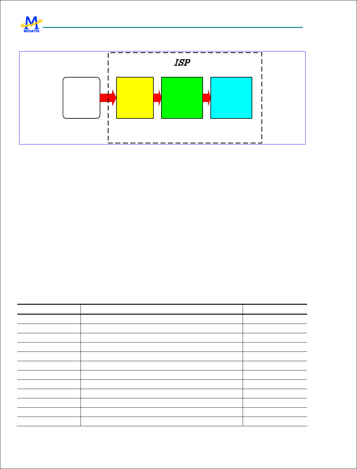
MTK Confidential Release for Konka
MTK Confidential Release for Konka
MT6228 GSM/GPRS Baseband Processor Data Sheet Revision 1.0
368/616 MediaTek Inc. Confidential
6.14 Camera Interface
MT6228 incorporates a feature rich image signal processor to connect with a variety of image sensor components. This
processor consists of timing generated unit (TG) and lens/sensor compensation unit and image process unit.
Timing generated unit (TG) cooperates with master type image sensor only. That means sensor should send vertical and
horizontal signals to TG. TG offers sensor required data clock and receive sensor Bayer pattern raw data by internal
auto synchronization or external pixel clock synchronization. The main purpose of TG is to create data clock for master
type image sensor and accept vertical/horizontal synchronization signal and sensor data, and then generate grabbed area
of raw data or YUV422/RGB565 data to the lens/sensor compensation unit.
Lens/sensor compensation unit generates compensated raw data to the color process unit in Bayer raw data input mode.
In YUV422/RGB565 input mode, this stage is bypassed.
Image process unit accepts Bayer pattern raw data or YUV422/RGB565 data that is generated by lens/sensor
compensation unit. The output of ISP is YCbCr 888 data format which can be easily encoded by the compress engine
(JPEG encoder and MPEG4 encoder). It can be the basic data domain of other data format translation such as R/G/B
domain. The ISP is pipelined, and during processing stages ISP hardware can auto extract meaningful information for
further AE/AF/AWB calculation. These information are temporary stored on ISP registers or memory and can be read
back by MCU.
6.14.1 Register Table
REGISTER ADDRESS REGISTER NAME SYNONYM
CAM + 0000h TG Phase Counter Register CAM_PHSCNT
CAM + 0004h Image Sensor Size Configuration Register CAM_CAMWIN
CAM + 0008h TG Grab Range Start/End Pixel Configuration Register CAM_GRABCOL
CAM + 000Ch TG Grab Range Start/End Line Configuration Register CAM_GRABROW
CAM + 0010h CMOS Sensor Mode Configuration Register CAM_CSMODE
CAM + 0014h Component Offset Adjustment Register CAM_RGBOFF
CAM + 0018h View Finder Mode Control Register CAM_VFCON
CAM + 001Ch Camera Module Interrupt Enable Register CAM_INTEN
CAM + 0020h Camera Module Interrupt Status Register CAM_INTSTA
CAM + 0024h Camera Module Path Config Register CAM_PATH
CAM + 0028h Camera Module Input Address Register CAM_INADDR
CAM + 002Ch Camera Module Output Address Register CAM_OUTADDR

MTK Confidential Release for Konka
MTK Confidential Release for Konka
MT6228 GSM/GPRS Baseband Processor Data Sheet Revision 1.0
369/616 MediaTek Inc. Confidential
CAM + 0030h Preprocessing Control Register 1 CAM_CTRL1
CAM + 0034h Component R,G, B Gain Control Register 1 CAM_RGBGAIN1
CAM + 0038h Component R,G, B Gain Control Register 2 CAM_RGBGAIN2
CAM + 003Ch Histogram Boundary Control Register 1 CAM_HIS0
CAM + 0040h Histogram Boundary Control Register 2 CAM_HIS1
CAM + 0044h Preprocessing Control Register 2 CAM_CTRL2
CAM + 0048h Reserved Reserved
CAM + 004Ch Reserved Reserved
CAM + 0050h Reserved Reserved
CAM + 0054h Reserved Reserved
CAM + 0058h ATF Window 1 Register CAM_AEWIN1
CAM + 005Ch ATF Window 2 Register CAM_ AEWIN2
CAM + 0060h ATF Window 3 Register CAM_ AEWIN3
CAM + 0064h ATF Window 4 Register CAM_ AEWIN4
CAM + 0068h ATF Window 5 Register CAM_ AEWIN5
CAM + 006Ch AWB Window Register CAM_AWBWIN
CAM + 0070h Color Processing Stage Control Register CAM_CPSCON1
CAM + 0074h Interpolation Register 1 CAM_INTER1
CAM + 0078h Interpolation Register 2 CAM_INTER2
CAM + 007Ch Edge Core Register CAM_EDGCORE
CAM + 0080h Edge Gain Register 1 CAM_EDGGAIN1
CAM + 0084h Edge Gain Register 2 CAM_EDGGAIN2
CAM + 0088h Edge Threshold Register CAM_EDGTHRE
CAM + 008Ch Edge Vertical Control Register CAM_EDGVCON
CAM + 0090h Axis RGB Gain Register CAM_AXGAIN
CAM + 0094h OPD Configuration Register CAM_OPDCFG
CAM + 0098h OPD Component Parameter Register CAM_OPDPAR
CAM + 009Ch Color Matrix 1 Register CAM_MATRIX1
CAM + 00A0h Color Matrix 2 Register CAM_MATRIX2
CAM + 00A4h Color Matrix 3 Register CAM_MATRIX3
CAM + 00A8h Color Matrix RGB Gain Register CAM_MTXGAIN
CAM + 00ACh Color Process Stage Control Register 2 CAM_CPSCON2
CAM + 00B0h AWB RGB Gain Register CAM_AWBGAIN
CAM + 00B4h Gamma RGB Flare Register CAM_GAMFLRE
CAM + 00B8h Y Channel Configuration Register CAM_YCHAN
CAM + 00BCh UV Channel Configuration Register CAM_UVCHAN
CAM + 00C0h Space Convert YUV Register 1 CAM_SCONV1
CAM + 00C4h Space Convert YUV Register 2 CAM_SCONV2
CAM + 00C8h Gamma Operation Register 1 CAM_GAMMA1
CAM + 00CCh Gamma Operation Register 2 CAM_GAMMA2
CAM + 00D0h Gamma Operation Register 3 CAM_GAMMA3
CAM + 00D4h OPD Y Result Register CAM_OPDY

MTK Confidential Release for Konka
MTK Confidential Release for Konka
MT6228 GSM/GPRS Baseband Processor Data Sheet Revision 1.0
370/616 MediaTek Inc. Confidential
CAM + 00D8h OPD MG Result Register CAM_OPDMG
CAM + 00DCh OPD RB Result Register CAM_OPDRB
CAM + 00E0h OPD Pixel Counter Register CAM_OPDCNT
CAM + 00E4h Reserved Reserved
CAM + 00E8h Reserved Reserved
CAM + 00ECh Reserved Reserved
CAM + 00F0h Reserved Reserved
CAM + 00F4h ATF Result 1 Register CAM_AE5RLT
CAM + 00F8h ATF Result 2 Register CAM_AE6RLT
CAM + 00FCh ATF Result 3 Register CAM_AE7RLT
CAM + 0100h ATF Result 4 Register CAM_AE8RLT
CAM + 0104h ATF Result 5 Register CAM_AE9RLT
CAM + 0108h Cam Histogram Result 1 CAM_HISRLT0
CAM + 010Ch Cam Histogram Result 2 CAM_HISRLT1
CAM + 0110h Cam Histogram Result 3 CAM_HISRLT2
CAM + 0114h Cam Histogram Result 4 CAM_HISRLT3
CAM + 0118h Cam Histogram Result 5 CAM_HISRLT4
CAM + 011Ch Low Pass Filter Control Register CAM_LPFCON
CAM + 0120h Y Low Pass Filter Control Register CAM_YLPF
CAM + 0124h CbCr Low Pass Filter Control Register CAM_CLPF
CAM + 0128h Vertical Subsample Control Register CAM_VSUB
CAM + 012Ch Horizontal Subsample Control Register CAM_HSUB
CAM + 0130h Sensor Gamma R0 Register CAM_SGAMMAR0
CAM + 0134h Sensor Gamma R1 Register CAM_SGAMMAR1
CAM + 0138h Sensor Gamma R2 Register CAM_SGAMMAR2
CAM + 013Ch Sensor Gamma G0 Register CAM_SGAMMAG0
CAM + 0140h Sensor Gamma G1 Register CAM_SGAMMAG1
CAM + 0144h Sensor Gamma G2 Register CAM_SGAMMAG2
CAM + 0148h Sensor Gamma B0 Register CAM_SGAMMAB0
CAM + 014Ch Sensor Gamma B1 Register CAM_SGAMMAB1
CAM + 0150h Sensor Gamma B2 Register CAM_SGAMMAB2
CAM + 0154h Defect Pixel Configuration Register CAM_DEFECT0
CAM + 0158h Defect Pixel Table Address Register CAM_DEFECT1
CAM + 015Ch Defect Pixel Table Debug Register CAM_DEFECT2
CAM + 0160h Reserved Reserved
CAM + 0164h Reserved Reserved
CAM + 0168h Reserved Reserved
CAM + 016Ch Reserved Reserved
CAM + 0170h Reserved Reserved
CAM + 0174h Reserved Reserved
CAM + 0178h Reserved Reserved
CAM + 017Ch Reserved Reserved

MTK Confidential Release for Konka
MTK Confidential Release for Konka
MT6228 GSM/GPRS Baseband Processor Data Sheet Revision 1.0
371/616 MediaTek Inc. Confidential
CAM + 0180h Camera Interface Debug Mode Control Register CAM_DEBUG
CAM + 0184h Camera Module Debug Information Write Out Destination Address CAM_DSTADDR
CAM + 0188h Camera Module Debug Information Last Transfer Destination Address CAM_LSTADDR
CAM + 018Ch Camera Module Frame Buffer Transfer Out Count Register CAM_XFERCNT
CAM + 0190h CMOS Sensor Test Module Configuration Register 1 CAM_MDLCFG1
CAM + 0194h CMOS Sensor Test Module Configuration Register 2 CAM_MDLCFG2
CAM + 0198h Reserved Reserved
CAM + 019Ch Reserved Reserved
CAM + 01A0h AE Address Register CAM_AEADDR
CAM + 01A4h AE Window Size Register CAM_AESIZE
CAM + 01A8h AE Weight 1 Register CAM_AEWEIGHT0
CAM + 01ACh AE Weight 2 Register CAM_AEWEIGHT1
CAM + 01B0h AE Weight 3 Register CAM_AEWEIGHT2
CAM + 01B4h AE Weight 4 Register CAM_AEWEIGHT3
CAM + 01B8h AE Weight 5 Register CAM_AEWEIGHT4
CAM + 01BCh AE Weight 6 Register CAM_AEWEIGHT5
CAM + 01C0h AE Weight 7 Register CAM_AEWEIGHT6
CAM + 01C4h AE Weight 8 Register CAM_AEWEIGHT7
CAM + 01C8h AE Area Register CAM_AEAREA
CAM + 01CCh AutoDefect Control 1 Register CAM_AEDEFECT0
CAM + 01D0h AutoDefect Control 2 Register CAM_AEDEFECT1
CAM + 01D4h Flash Control Register FLASH_CTRL
CAM + 01D8h Cam Reset Register CAM_RESET
CAM + 01DCh TG Status Register TG_STATUS
CAM + 01E0h Histogram Boundary Control Register 3 CAM_HIS2
CAM + 01E4h Histogram Boundary Control Register 4 CAM_HIS3
CAM + 01E8h Histogram Boundary Control Register 5 CAM_HIS4
CAM + 01ECh Cam Histogram Result 6 CAM_HISRLT5
CAM + 01F0h Cam Histogram Result 7 CAM_HISRLT6
CAM + 01F4h Cam Histogram Result 8 CAM_HISRLT7
CAM + 01F8h Cam Histogram Result 9 CAM_HISRLT8
CAM + 01FCh Cam Histogram Result 10 CAM_HISRLT9
CAM + 0200h Cam Histogram Result 11 CAM_HISRLTA
CAM + 0204h Cam Histogram Result 12 CAM_HISRLTB
CAM + 0208h Cam Histogram Result 13 CAM_HISRLTC
CAM + 020Ch Cam Histogram Result 14 CAM_HISRLTD
CAM + 0210h Cam Histogram Result 15 CAM_HISRLTE
CAM + 0214h Shading Control 1 Register CAM_SHADING1
CAM + 0218h Shading Control 2 Register CAM_SHADING2
CAM + 021Ch Shading R Curve Register 1 CAM_SRCURVE0
CAM + 0220h Shading R Curve Register 2 CAM_SRCURVE1
CAM + 0224h Shading R Curve Register 3 CAM_SRCURVE2
MTK Confidential Release for Konka
MTK Confidential Release for Konka
MT6228 GSM/GPRS Baseband Processor Data Sheet Revision 1.0
372/616 MediaTek Inc. Confidential
CAM + 0228h Shading G Curve Register 1 CAM_SGCURVE0
CAM + 022Ch Shading G Curve Register 2 CAM_SGCURVE1
CAM + 0230h Shading G Curve Register 3 CAM_SGCURVE2
CAM + 0234h Shading B Curve Register 1 CAM_SBCURVE0
CAM + 0238h Shading B Curve Register 2 CAM_SBCURVE1
CAM + 023Ch Shading B Curve Register 3 CAM_SBCURVE2
CAM + 0240h Cam Image-Processor Hue Register 1 CAM_HUE0
CAM + 0244h Cam Image-Processor Hue Register 2 CAM_HUE1
CAM + 0248h GMC Debug Register CAM_GMCDEBUG
CAM + 024Ch Cam Version Register CAM_VERSION
Table 52 Camera Interface Register Map
6.14.1.1 TG Register Definitions
CAM+0000h TG Phase Counter Register CAM_PHSCNT
Bit 31 30 29 28 27 26 25 24 23 22 21 20 19 18 17 16
Name
PCEN
CLKE
N
CLKP
OL CLKCNT CLKRS CLKFL
Type R/W R/W R/W R/W R/W R/W
Reset
0 0 0 1 0 1
Bit 15 14 13 12 11 10 9 8 7 6 5 4 3 2 1 0
Name
HVALI
D_EN
PXCL
K_EN
PXCL
K_INV
PXCL
K_IN
TGCL
K_SE
L
PIXCNT DLATCH
Type R/W R/W R/W R/W R/W R/W R/W
Reset
0 0 0 0 0 1 1
PCEN TG phase counter enable control
CLKEN Enable sensor master clock (mclk) output to sensor
CLKPOL Sensor master clock polarity control
CLKCNT Sensor master clock frequency divider control.
Sensor master clock will be 52Mhz/CLKCNT, where CLKCNT >=1
CLKRS Sensor master clock rising edge control
CLKFL Sensor master clock falling edge control
HVALID_EN HVALID input enable
PXCLK_EN Pixel clock input monitor, used in internal clock synchronization mode
PXCLK_INV Pixel clock inverse
PXCLK_IN 0 Internal clock synchronization
1 External pixel clock synchronization
Internal clock synchronization example waveform
(CLKCNT=1,CLKRS=0,CLKFL=1,PIXCNT=3,DLATCH=2)
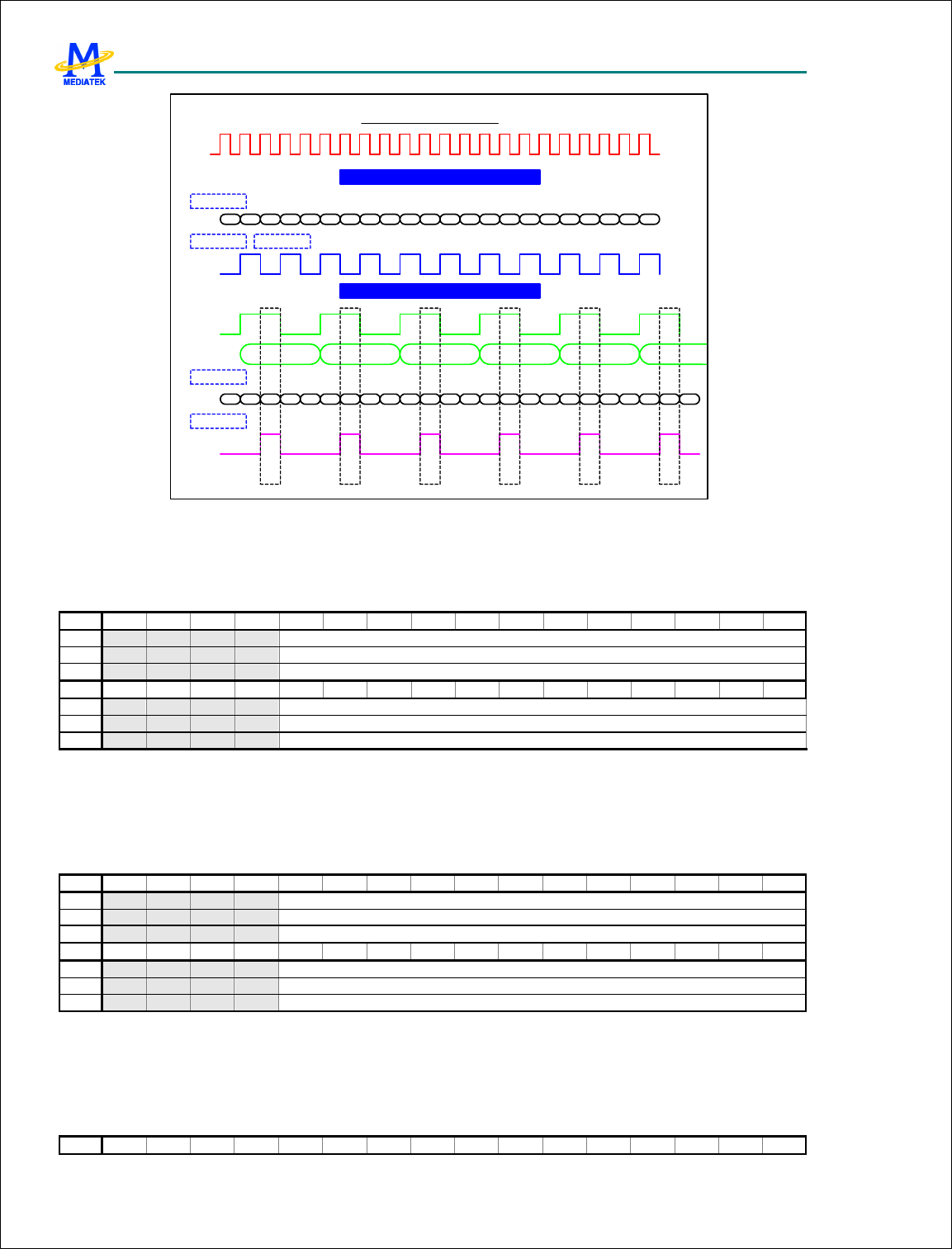
MTK Confidential Release for Konka
MTK Confidential Release for Konka
MT6228 GSM/GPRS Baseband Processor Data Sheet Revision 1.0
373/616 MediaTek Inc. Confidential
0101010101010101010101
0123012301230123012301
52Mhz
mclk
pclk
Bclk
Sensor output signals
ISP output signals
2 3
TGCLK_SEL Sensor master based clock selection (0: 52 Mhz, 1: 48 Mhz)
PIXCNT Sensor data latch frequency control, used in internal clock synchronization mode
DLATCH Sensor data latch position control, used in internal clock synchronization mode
CAM+0004h CMOS Sensor Size Configuration Register CAM_CAMWIN
Bit 31 30 29 28 27 26 25 24 23 22 21 20 19 18 17 16
Name
PIXELS
Type R/W
Reset
Fffh
Bit 15 14 13 12 11 10 9 8 7 6 5 4 3 2 1 0
Name
LINES
Type R/W
Reset
Fffh
PIXEL Total input pixel number
LINE Total input line number
CAM+0008h TG Grab Range Start/End Pixel Configuration
Register
CAM_GRABCO
L
Bit 31 30 29 28 27 26 25 24 23 22 21 20 19 18 17 16
Name
START
Type R/W
Reset
0
Bit 15 14 13 12 11 10 9 8 7 6 5 4 3 2 1 0
Name
END
Type R/W
Reset
0
START Grab start pixel number
END Grab end pixel number
CAM+000Ch TG Grab Range Start/End Line Configuration
Register
CAM_GRABRO
W
Bit 31 30 29 28 27 26 25 24 23 22 21 20 19 18 17 16
MTK Confidential Release for Konka
MTK Confidential Release for Konka
MT6228 GSM/GPRS Baseband Processor Data Sheet Revision 1.0
374/616 MediaTek Inc. Confidential
Name
START
Type R/W
Reset
0
Bit 15 14 13 12 11 10 9 8 7 6 5 4 3 2 1 0
Name
END
Type R/W
Reset
0
START Grab start line number
END Grab end line number
CAM+0010h CMOS Sensor Mode Configuration Register CAM_CSMODE
Bit 31 30 29 28 27 26 25 24 23 22 21 20 19 18 17 16
Name
Type
Reset
Bit 15 14 13 12 11 10 9 8 7 6 5 4 3 2 1 0
Name
VSPO
L
HSPO
L
PWR
ON RST AUTO
EN
Type R/W R/W R/W R/W R/W R/W
Reset
0 0 0 0 0 0
VSPOL Image sensor VSYNC polarity
HSPOL Image sensor HSYNC polarity
AUTO Auto lock sensor input horizontal pixel numbers enable
EN Image sensor process counter enable
CAM+0014h Component R,Gr,B,Gb Offset Adjustment Register CAM_RGBOFF
Bit 31 30 29 28 27 26 25 24 23 22 21 20 19 18 17 16
Name
S00 OFFSET00 S01 OFFSET01
Type R/W R/W R/W R/W
Reset
0 0 0 0
Bit 15 14 13 12 11 10 9 8 7 6 5 4 3 2 1 0
Name
S10 OFFSET10 S11 OFFSET11
Type R/W R/W R/W R/W
Reset
0 0 0 0
S00 Sign of raw data (0,0) offset adjustment control, 0 : positive 1: negative
OFFSET00 Raw data (0,0) offset adjustment
S01 Sign of raw data (0,1) offset adjustment control, 0 : positive 1: negative
OFFSET01 Raw data (0,1) offset adjustment
S10 Sign of raw data (1,0) offset adjustment control, 0 : positive 1: negative
OFFSET10 Raw data (1,0) offset adjustment
S11 Sign of raw data (1,1) offset adjustment control, 0 : positive 1: negative
OFFSET11 Raw data (1,1) offset adjustment
CAM+0018h View Finder Mode Control Register CAM_VFCON
Bit 31 30 29 28 27 26 25 24 23 22 21 20 19 18 17 16
Name
Type
Reset
Bit 15 14 13 12 11 10 9 8 7 6 5 4 3 2 1 0
Name
SP_DELAY SP_M
ODE
TAKE
_PIC FR_CON
Type R/W R/W R/W R/W
Reset
0 0 0 0
MTK Confidential Release for Konka
MTK Confidential Release for Konka
MT6228 GSM/GPRS Baseband Processor Data Sheet Revision 1.0
375/616 MediaTek Inc. Confidential
SP_DELAY Still Picture Mode delay
SP_MODE Still Picture Mode
TAKE_PIC Take Picture Request
FR_CON Frame Sampling Rate Control
000 Every frame is sampled
001 One frame is sampled every 2 frames
010 One frame is sampled every 3 frames
011 One frame is sampled every 4 frames
100 One frame is sampled every 5 frames
101 One frame is sampled every 6 frames
110 One frame is sampled every 7 frames
111 One frame is sampled every 8 frames
CAM+001Ch Camera Module Interrupt Enable Register CAM_INTEN
Bit 31 30 29 28 27 26 25 24 23 22 21 20 19 18 17 16
Name
VSYN
C_INT
_EN
TG_INT_LINENO
Type R/W R/W
Reset
0 ff
Bit 15 14 13 12 11 10 9 8 7 6 5 4 3 2 1 0
Name
TG_IN
T
ATF_I
NT
AEDO
NE
ISPD
ONE IDLE
GMC
OVRU
N
REZO
VRUN
EXPD
O
Type R/W R/W R/W R/W R/W R/W R/W R/W
Reset
0 0 0 0 0 0 0 0
VSYNC_INT_EN Vsync interrupt enable, tg_int will become vsync interrupt when it is enable
TG_INT_LINENO TG interrupt line number
TG_INT TG interrupt
AEDONE AE done interrupt enable control
ISPDONE ISP done interrupt enable control
LDLE Returning idle state interrupt enable control
GMCOVRUN GMC port over run interrupt enable control
REZOVRUN Resizer over run interrupt enable control
EXPDO Exposure done interrupt enable control
CAM+0020h Camera Module Interrupt Status Register CAM_INTSTA
Bit 31 30 29 28 27 26 25 24 23 22 21 20 19 18 17 16
Name
Type
Reset
Bit 15 14 13 12 11 10 9 8 7 6 5 4 3 2 1 0
Name
TG_IN
T
ATF_I
NT
AEDO
NE
ISPD
ONE IDLE
GMC
OVRU
N
REZO
VRUN
EXPD
O
Type R R R R R R R R
Reset
0 0 0 0 0 0 0 0
Interrupt Status corresponding with 0x1c CAM_INTEN
CAM+0024h Camera Module Path Config Register CAM_PATH
Bit 31 30 29 28 27 26 25 24 23 22 21 20 19 18 17 16
MTK Confidential Release for Konka
MTK Confidential Release for Konka
MT6228 GSM/GPRS Baseband Processor Data Sheet Revision 1.0
376/616 MediaTek Inc. Confidential
Name
CNTO
N CNTMODE WRITE_LEVEL
REZ_
DISC
ONN
REZ_
LPF_
OFF
OUTPATH_T
YPE
BURSTW_TYPE[2:
0]
OUTP
ATH_
EN
Type R/W R/W R/W RW RW R/W R/W R/W
Reset
0 0 7 0 0 0 0 0
Bit 15 14 13 12 11 10 9 8 7 6 5 4 3 2 1 0
Name
SWAP
_Y
SWAP
_CBC
R
INDA
TA_F
ORM
AT
INTYPE_SEL INPATH_RATE
INPAT
H_TH
ROTE
N
INPA
TH_S
EL
Type R/W R/W R/W R/W R/W R/W R/W R/W
Reset
0 0 0 0 0 0 0 0
CNTON Enable Debug Mode Data Transfer Counter
CNTMODE Data Transfer Count Selection
00 sRGB count
01 YCbCr count
REZ_DISCONN Resizer disconnect enable
REZ_LPF_OFF Resizer low-Pass disable
WRITE_LEVEL Write FIFO threshold level
OUTPATH_TYPE Outpath Type Select
00 Bayer Format
01 ISP output
02 RGB888 Format
03 RGB565 Format
BURSTW_TYPE Burst write type selecttion
000 Single
001 2 Beat
011 4 Beat
101 8 Beat
111 16 Beat
OUTPATH_EN Enable Output to Memory
SWAP_Y YCbCr in Swap Y
SWAP_CBCR YCbCr in Swap Cb Cr
INDATA_FORMAT Sensor Input Data connection
INTYPE_SEL Input type selection
000 Bayer Format
001 YUV422 Format
101 YCbCr422 Format
010 RGB Format
INPATH_RATE Input type rate control
INPATH_THROTEN Input path throttle enable
INPATH_SEL Input path selection
0 Sensor input
1 From memory
CAM+0028h Camera Module Input Address Register CAM_INADDR
Bit 31 30 29 28 27 26 25 24 23 22 21 20 19 18 17 16
Name
CAM_INADDR[31:16]
Type R/W
Reset
0
Bit 15 14 13 12 11 10 9 8 7 6 5 4 3 2 1 0
MTK Confidential Release for Konka
MTK Confidential Release for Konka
MT6228 GSM/GPRS Baseband Processor Data Sheet Revision 1.0
377/616 MediaTek Inc. Confidential
Name
CAM_INADDR[15:0]
Type R/W
Reset
0
CAM_INADDR Input memory address
CAM+002Ch Camera Module Output Address Register CAM_OUTADD
R
Bit 31 30 29 28 27 26 25 24 23 22 21 20 19 18 17 16
Name
CAM_OUTADDR[31:16]
Type R/W
Reset
0
Bit 15 14 13 12 11 10 9 8 7 6 5 4 3 2 1 0
Name
CAM_OUTADDR[15:0]
Type
R/W
Reset
0
CAM_OUTADDR Output memory address
6.14.1.2 Color Process Register Definition
CAM+0030h Preprocessing Control Register 1 CAM_CTRL1
Bit 31 30 29 28 27 26 25 24 23 22 21 20 19 18 17 16
Name
GAIN_COMP P_LIMIT
Type R/W R/W
Reset
0 0
Bit 15 14 13 12 11 10 9 8 7 6 5 4 3 2 1 0
Name
BYPP
G
PGAI
N_SC
OUNT
_EN
PIXELID PGAIN_INT
PGAIN_FRAC
Type R/W R/W R/W R/W R/W
Reset
0 0 0 1 0
GAIN_COMP Gain Compensation Control
P_LIMIT Interpolation Limitation Control
BYPPG Bypass pre-gain operating enable
PGAIN_SCOUNT_EN Pre-gain saturation count
PIXELID Bayer pixel type of the first pixel
00 R pixel
01 Gr pixel
10 Gb pixel
11 B pixel
PGAIN_INT Pre-gain multiplier integer part
PGAIN_FRAC Pre-gain multiplier fraction part
CAM+0034h Component R,G,B Gain Control Register 1 CAM_RGBGAIN
1
Bit 31 30 29 28 27 26 25 24 23 22 21 20 19 18 17 16
Name
B_GAIN
Type R/W
Reset
80h
Bit 15 14 13 12 11 10 9 8 7 6 5 4 3 2 1 0
Name
GB_GAIN
Type R/W
MTK Confidential Release for Konka
MTK Confidential Release for Konka
MT6228 GSM/GPRS Baseband Processor Data Sheet Revision 1.0
378/616 MediaTek Inc. Confidential
Reset
80h
B_GAIN B Gain
GB_GAIN GB Gain
CAM+0038h Component R,G,B Gain Control Register 2 CAM_RGBGAIN
2
Bit 31 30 29 28 27 26 25 24 23 22 21 20 19 18 17 16
Name
R_GAIN
Type R/W
Reset
80h
Bit 15 14 13 12 11 10 9 8 7 6 5 4 3 2 1 0
Name
GR_GAIN
Type R/W
Reset
80h
R_GAIN R Gain
GR_GAIN GR Gain
CAM+003Ch Histogram Boundary Control Register1 CAM_HIS0
Bit 31 30 29 28 27 26 25 24 23 22 21 20 19 18 17 16
Name
H1_BND H2_BND
Type R/W R/W
Reset
10h 20h
Bit 15 14 13 12 11 10 9 8 7 6 5 4 3 2 1 0
Name
H3_BND H4_BND
Type R/W R/W
Reset
30h 40H
H1_BND Histogram level 0 up boundary value
H2_BND Histogram level 1 up boundary value
H3_BND Histogram level 2 up boundary value
H4_BND Histogram level 3 up boundary value
CAM+0040h Histogram Boundary Control Register2 CAM_HIS1
Bit 31 30 29 28 27 26 25 24 23 22 21 20 19 18 17 16
Name
H5_BND
Type R/W
Reset
80h
Bit 15 14 13 12 11 10 9 8 7 6 5 4 3 2 1 0
Name
Type
Reset
H5_BND Histogram level 4 up boundary value
CAM+0044h Preprocessing Control Register 2 CAM_CTRL2
Bit 31 30 29 28 27 26 25 24 23 22 21 20 19 18 17 16
Name
AEAL
L
CNTE
N
AEPI
D_PO
L
AEGI
D_PO
L
CNTC
LR AEGMSEL AESE
L
Type R/W R/W R/W R/W R/W R/W R/W
Reset
0 1 0 0 0 0 0 1
Bit 15 14 13 12 11 10 9 8 7 6 5 4 3 2 1 0
Name
ATFE
DGEN
ATFA
LL AWB
ALL GONL
Y RLEN
INTEN
Type R/W R/W R/W R/W R/W R/W
MTK Confidential Release for Konka
MTK Confidential Release for Konka
MT6228 GSM/GPRS Baseband Processor Data Sheet Revision 1.0
379/616 MediaTek Inc. Confidential
Reset
1 0 1 0 0 0
AEALL AE full frame single window enable
CNTEN AE counter enable
CNTCLR AE count clear enable
AEPID_POL Polarity of the pixel identifier swapped for AE operating
AEGID_POL Polarity of the line identifier swapped for AE operating
AEGMSEL AE gamma curve selection
00 use gamma curve 0
01 use gamma curve 1
10 use gamma curve 2
11 use gamma curve 3
AESEL AE path select
ATFEDGEN ATG Edge Enable Control
ATFALL ATF area all control
AWBALL AWB full frame single window enable
GONLY Use G component only for AE
RLEN Histogram polarity select enable. AELID_POL,AEPID_POL decide the pixel type
INTEN Interpolation FIFO enable
CAM+0058h ATF Window 1 Register CAM_ATFWIN0
Bit 31 30 29 28 27 26 25 24 23 22 21 20 19 18 17 16
Name
LEFT RIGHT
Type R/W R/W
Reset
0 0
Bit 15 14 13 12 11 10 9 8 7 6 5 4 3 2 1 0
Name
TOP BOTTOM
Type R/W R/W
Reset
0 0
LEFT ATF 1
th
window left side
RIGHT ATF 1
th
window right side
TOP ATF 1
th
window top side
BOTTOM ATF 1
th
window bottom side
CAM+005Ch ATF Window 2 Register CAM_ATFWIN1
Bit 31 30 29 28 27 26 25 24 23 22 21 20 19 18 17 16
Name
LEFT RIGHT
Type R/W R/W
Reset
0 0
Bit 15 14 13 12 11 10 9 8 7 6 5 4 3 2 1 0
Name
TOP BOTTOM
Type R/W R/W
Reset
0 0
LEFT ATF 2
th
window left side
RIGHT ATF 2
th
window right side
TOP ATF 2
th
window top side
BOTTOM ATF 2
th
window bottom side
CAM+0060h ATF Window 3 Register CAM_ATFWIN2
Bit 31 30 29 28 27 26 25 24 23 22 21 20 19 18 17 16
MTK Confidential Release for Konka
MTK Confidential Release for Konka
MT6228 GSM/GPRS Baseband Processor Data Sheet Revision 1.0
380/616 MediaTek Inc. Confidential
Name
LEFT RIGHT
Type R/W R/W
Reset
0 0
Bit 15 14 13 12 11 10 9 8 7 6 5 4 3 2 1 0
Name
TOP BOTTOM
Type R/W R/W
Reset
0 0
LEFT ATF 3
th
window left side
RIGHT ATF 3
th
window right side
TOP ATF 3
th
window top side
BOTTOM ATF 3
th
window bottom side
CAM+0064h ATF Window 4 Register CAM_ATFWIN3
Bit 31 30 29 28 27 26 25 24 23 22 21 20 19 18 17 16
Name
LEFT RIGHT
Type R/W R/W
Reset
0 0
Bit 15 14 13 12 11 10 9 8 7 6 5 4 3 2 1 0
Name
TOP BOTTOM
Type R/W R/W
Reset
0 0
LEFT ATF 4
th
window left side
RIGHT ATF 4
th
window right side
TOP ATF 4
th
window top side
BOTTOM ATF 4
th
window bottom side
CAM+0068h ATF Window 5 Register CAM_ATFWIN4
Bit 31 30 29 28 27 26 25 24 23 22 21 20 19 18 17 16
Name
LEFT RIGHT
Type R/W R/W
Reset
0 0
Bit 15 14 13 12 11 10 9 8 7 6 5 4 3 2 1 0
Name
TOP BOTTOM
Type R/W R/W
Reset
0 0
LEFT ATF 5
th
window left side
RIGHT ATF 5
th
window right side
TOP ATF 5
th
window top side
BOTTOM ATF 5
th
window bottom side
CAM+006Ch AWB Window Register CAM_AWBWIN
Bit 31 30 29 28 27 26 25 24 23 22 21 20 19 18 17 16
Name
LEFT RIGHT
Type R/W R/W
Reset
0 0
Bit 15 14 13 12 11 10 9 8 7 6 5 4 3 2 1 0
Name
TOP BOTTOM
Type R/W R/W
Reset
0 0
LEFT AWB window left side
RIGHT AWB window right side
TOP AWB window top side
MTK Confidential Release for Konka
MTK Confidential Release for Konka
MT6228 GSM/GPRS Baseband Processor Data Sheet Revision 1.0
381/616 MediaTek Inc. Confidential
BOTTOM AWB window bottom side
CAM+0070h Color Processing Stage Control Register CAM_CPSCON1
Bit 31 30 29 28 27 26 25 24 23 22 21 20 19 18 17 16
Name
Type
Reset
Bit 15 14 13 12 11 10 9 8 7 6 5 4 3 2 1 0
Name
BYPI
NT NONL
IN GAVG
LEDG
EN DISLJ
Type R/W R/W R/W R/W R/W
Reset
0 0 0 1 0
BYPINT Interpolation first 4 invalid output pixel used enable
NONLIN Nonlinear mode enable in color correction operation
GAVG G channel average mode
LEDGEN Line edge enable
DISLJ Disable line judge enable
CAM+0074h Interpolation Register1 CAM_INTER1
Bit 31 30 29 28 27 26 25 24 23 22 21 20 19 18 17 16
Name
THRE_V THRE_SM
Type R/W R/W
Reset
0Ah 05h
Bit 15 14 13 12 11 10 9 8 7 6 5 4 3 2 1 0
Name
THRE_DHV THRE_RT
Type R/W R/W
Reset
19h 10h
THRE_V Interpolation parameter
THRE_SM Interpolation parameter
THRE_DHV Interpolation parameter
THRE_RT Interpolation parameter
CAM+0078h Interpolation Register 2 CAM_INTER2
Bit 31 30 29 28 27 26 25 24 23 22 21 20 19 18 17 16
Name
Type
Reset
Bit 15 14 13 12 11 10 9 8 7 6 5 4 3 2 1 0
Name
THRE_LEDGE
Type R/W
Reset
14h
THRE_LEDGE Interpolation parameter
CAM+007Ch Edge Core Register CAM_EDGCOR
E
Bit
31 30
29
28
27 26 25
24
23
22 21 20
19
18
17 16
Name
COREH EMBO
SS1
EMBO
SS2 COREH2
Type R/W R/W R/W R/W
Reset
08h 0 0 1Fh
Bit 15 14 13 12 11 10 9 8 7 6 5 4 3 2 1 0
Name
COREV
TOP_
SLOP
E
CORE_CON

MTK Confidential Release for Konka
MTK Confidential Release for Konka
MT6228 GSM/GPRS Baseband Processor Data Sheet Revision 1.0
382/616 MediaTek Inc. Confidential
Type
R/W R/W
R/W
Reset
8h 0 14h
COREH Edge parameter
EMBOSS1 Emboss effect mode 1 enable
EMBOSS2 Emboss effect mode 2 enable
COREH2 Edge parameter
COREV [3:2] Negative Slope [1:0] Positive Slope
TOP_SLOPE Edge parameter
CORE_CON Edge parameter
CAM+0080h Edge Gain Register 1 CAM_EDGGAIN
1
Bit 31 30 29 28 27 26 25 24 23 22 21 20 19 18 17 16
Name
SPECIGAIN SPECIPONL
Y EGAIN_H EGAIN_H2
Type R/W R/W R/W R/W
Reset
0 0 1 3
Bit 15 14 13 12 11 10 9 8 7 6 5 4 3 2 1 0
Name
EGAIN_VB OILE
N KNEESEL EGAINLILNE
Type R/W R/W R/W R/W
Reset
3 0 3 2
SPECIGAIN Edge special gain value
SPECIPONLY Edge special p only value
EGAIN_H Edge gain H value
EGAIN_H2 Edge gain H2 value
EGAIN_VB Edge gain Vb value
OILEN Oil effect enable
KNEESEL Knee select
EGAINLINE Edge gain line value
CAM+0084h Edge Gain Register 2 CAM_EDGGAIN
2
Bit 31 30 29 28 27 26 25 24 23 22 21 20 19 18 17 16
Name
Type
Reset
Bit 15 14 13 12 11 10 9 8 7 6 5 4 3 2 1 0
Name
SPEC
IABS
SPEC
IINV EGAIN_HC
Type R/W R/W R/W
Reset
0 0 Fh
SPECIABS Edge special absolute enable
SPECIINV Edge special invert enable
EGAIN_HC Edge gain Hc
CAM+0088h Edge Threshold Register CAM_EDGTHR
E
Bit 31 30 29 28 27 26 25 24 23 22 21 20 19 18 17 16
Name
ETH3 ETH_CON
Type
R/W R/W

MTK Confidential Release for Konka
MTK Confidential Release for Konka
MT6228 GSM/GPRS Baseband Processor Data Sheet Revision 1.0
383/616 MediaTek Inc. Confidential
Reset
32h 80h
Bit 15 14 13 12 11 10 9 8 7 6 5 4 3 2 1 0
Name
ONLY
C THRE_EDGE_SUP THRL_EDGE_SUP
Type R/W R/W R/W
Reset
0 07h 07h
ETH3 Edge threshold value
ETH_CON Edge parameter
ONLYC Edge enhanced C component only enable
THRE_EDGE_SUP Edge parameter
THRL_EDGE_SUP Edge parameter
CAM+008Ch Edge Vertical Control Register CAM_EDGVCO
N
Bit 31 30 29 28 27 26 25 24 23 22 21 20 19 18 17 16
Name
HPEN
E_TH1_V HALF_V
Type R/W R/W R/W
Reset
0 18h 1Fh
Bit 15 14 13 12 11 10 9 8 7 6 5 4 3 2 1 0
Name
SUP_V SDN_V E_TH3_V
Type R/W R/W R/W
Reset
0 2 32h
HPEN Edge high pass enable
E_TH1_V Edge parameter
HALF_V Edge parameter
SUP_V Edge parameter
SDN_V Edge parameter
E_TH3_V Edge parameter
CAM+0090h Axis RGB Gain Register CAM_AXGAIN
Bit 31 30 29 28 27 26 25 24 23 22 21 20 19 18 17 16
Name
R_GAIN
Type R/W
Reset
3Fh
Bit 15 14 13 12 11 10 9 8 7 6 5 4 3 2 1 0
Name
G_GAIN B_GAIN
Type R/W R/W
Reset
3Fh 3Fh
R_GAIN Axis R component gain
G_GAIN Axis G component gain
B_GAIN Axis B component gain
CAM+0094h AWB Configuration Register CAM_OPDCFG
Bit 31 30 29 28 27 26 25 24 23 22 21 20 19 18 17 16
Name
OPDE
N
OPDC
LR
SUPSEL U_GAIN
Type R/W R/W R/W R/W
Reset
1 0 3 1Fh
Bit 15 14 13 12 11 10 9 8 7 6 5 4 3 2 1 0
Name
V_GAIN Y_LIMIT
Type R/W R/W
Reset
1Fh 3
MTK Confidential Release for Konka
MTK Confidential Release for Konka
MT6228 GSM/GPRS Baseband Processor Data Sheet Revision 1.0
384/616 MediaTek Inc. Confidential
OPDEN AWB counter enable
OPDCLR AWB counter clear enable
SUPSEL AWB accumulated maximum value setting. Equation is (192 + 8 * SUPSEL).
U_GAIN AWB U gain value
V_GAIN AWB V gain value
Y_LIMIT AWB white point minimum value,
CAM+0098h OPD Component Parameter Register CAM_OPDPAR
Bit 31 30 29 28 27 26 25 24 23 22 21 20 19 18 17 16
Name
S_RB_P S_RB_N
Type R/W R/W
Reset
7Fh 7Fh
Bit 15 14 13 12 11 10 9 8 7 6 5 4 3 2 1 0
Name
S_MG_P S_MG_N
Type R/W R/W
Reset
7Fh 7Fh
S_RB_P AWB SR Bp value
S_RB_N AWB SR Bn value
S_MG_P AWB SM Gp value
S_MG_N AWB SN Gn value
CAM+009Ch Color Matrix 1 Register CAM_MATRIX1
Bit 31 30 29 28 27 26 25 24 23 22 21 20 19 18 17 16
Name
M11
Type R/W
Reset
20h
Bit 15 14 13 12 11 10 9 8 7 6 5 4 3 2 1 0
Name
M12 M13
Type R/W R/W
Reset
80h 80h
M11 Color matrix 11 value
M12 Color matrix 12 value
M13 Color matrix 13 value
CAM+00A0h Color Matrix 2 Register CAM_MATRIX2
Bit 31 30 29 28 27 26 25 24 23 22 21 20 19 18 17 16
Name
M21
Type R/W
Reset
80h
Bit 15 14 13 12 11 10 9 8 7 6 5 4 3 2 1 0
Name
M22 M23
Type R/W R/W
Reset
20h 80h
M21 Color matrix 21 value
M22 Color matrix 22 value
M23 Color matrix 23 value
CAM+00A4h Color Matrix 3 Register CAM_MATRIX3
Bit 31 30 29 28 27 26 25 24 23 22 21 20 19 18 17 16
Name
M31
Type R/W
Reset
80h
Bit 15 14 13 12 11 10 9 8 7 6 5 4 3 2 1 0
MTK Confidential Release for Konka
MTK Confidential Release for Konka
MT6228 GSM/GPRS Baseband Processor Data Sheet Revision 1.0
385/616 MediaTek Inc. Confidential
Name
M32 M33
Type R/W R/W
Reset
80h 20h
M31 Color matrix 31 value
M32 Color matrix 32 value
M33 Color matrix 33 value
CAM+00A8h Color Matrix RGB Gain Register CAM_MTXGAIN
Bit 31 30 29 28 27 26 25 24 23 22 21 20 19 18 17 16
Name
R_GAIN
Type R/W
Reset
20h
Bit 15 14 13 12 11 10 9 8 7 6 5 4 3 2 1 0
Name
G_GAIN B_GAIN
Type R/W R/W
Reset
20h 20h
R_GAIN Color matrix R component gain value
G_GAIN Color matrix G component gain value
B_GAIN Color matrix B component gain value
CAM+00ACh Color Process Stage Control Register 2 CAM_CPSCON2
Bit 31 30 29 28 27 26 25 24 23 22 21 20 19 18 17 16
Name
Type
Reset
Bit 15 14 13 12 11 10 9 8 7 6 5 4 3 2 1 0
Name
BYPG
M
RGBE
DGEN
YEDG
EN
OPRG
M_IVT
Y_EGAIN
Type R/W R/W R/W R/W R/W
Reset
1 0 0 0 2
BYPGM Bypass gamma enable
RGBEDGAINEN Edge enhance before gamma
YEDGEN Edge enhance after gamma
OPDGM_IVT Gamma output inverse mode enable
Y_EGAIN Y channel edge gain value
CAM+00B0h AWB RGB Gain Register CAM_AWBGAI
N
Bit 31 30 29 28 27 26 25 24 23 22 21 20 19 18 17 16
Name
AWB_RGAIN
Type R/W
Reset
80h
Bit 15 14 13 12 11 10 9 8 7 6 5 4 3 2 1 0
Name
AWB_GGAIN AWB_BGAIN
Type R/W R/W
Reset
80h 80h
AWB_RGAIN AWB R component gain value
AWB_GGAIN AWB G component gain value
AWB_BGAIN AWB B component gain value

MTK Confidential Release for Konka
MTK Confidential Release for Konka
MT6228 GSM/GPRS Baseband Processor Data Sheet Revision 1.0
386/616 MediaTek Inc. Confidential
CAM+00B4h Gamma RGB Flare Register CAM_GAMFLR
E
Bit 31 30 29 28 27 26 25 24 23 22 21 20 19 18 17 16
Name
SIGN
_R FLARE_R
Type R/W R/W
Reset
0 0
Bit 15 14 13 12 11 10 9 8 7 6 5 4 3 2 1 0
Name
SIGN_
G FLAIRE_G SIGN
_B FLARE_B
Type R/W R/W R/W R/W
Reset
0 0 0 0
SIGN_R R flare sign
FLARE_R R flare
SIGN_G G flare sign
FLARE_G G flare
SIGN_B R flare sign
FLARE_B G flare
CAM+00B8h Y Channel Configuration Register CAM_YCHAN
Bit 31 30 29 28 27 26 25 24 23 22 21 20 19 18 17 16
Name
CONTRAST_GAIN
Type R/W
Reset
40h
Bit 15 14 13 12 11 10 9 8 7 6 5 4 3 2 1 0
Name
SIGN_
BRIG
HT_O
FFSE
T
BRIGHT_OFFSET UV_L
P_EN
CSUP_EDGE_GAIN
Type R/W R/W R/W R/W
Reset
1 0 0 10h
CONTRAST_GAIN Y channel contrast gain value
SIGN_BRIGHT_OFFSET Sign bit of Y channel brightness offset value
BRIGHT_OFFSET Y channel brightness offset value
UV_LP_EN UV channel low pass enable
CSUP_EDGE_GAIN Chroma suppression edge gain value
CAM+00BCh UV Channel Configuration Register CAM_UVCHAN
Bit 31 30 29 28 27 26 25 24 23 22 21 20 19 18 17 16
Name
U11 V22
Type R/W R/W
Reset
20h 20h
Bit 15 14 13 12 11 10 9 8 7 6 5 4 3 2 1 0
Name
SIGN_
U_OF
FSET
U_OFFSET
SIGN_
V_OF
FSET
V_OFFSET
Type R/W R/W R/W R/W
Reset
0 0 0 0
U11 Hue U channel operating value
V11 Hue V channel operating value
SIGN_U_OFFSET Sign bit of Hue U channel offset value
U_OFFSET Hue U channel offset value

MTK Confidential Release for Konka
MTK Confidential Release for Konka
MT6228 GSM/GPRS Baseband Processor Data Sheet Revision 1.0
387/616 MediaTek Inc. Confidential
SIGN_V_OFFSET Sign bit of Hue V channel offset value
V_OFFSET Hue V channel offset value
CAM+00C0h Space Convert YUV Register 1 CAM_SCONV1
Bit 31 30 29 28 27 26 25 24 23 22 21 20 19 18 17 16
Name
Y_GAIN
Type R/W
Reset
FFh
Bit 15 14 13 12 11 10 9 8 7 6 5 4 3 2 1 0
Name
U_GAIN V_GAIN
Type R/W R/W
Reset
91h B8h
Y_GAIN Space Convert Y channel gain value
U_GAIN Space Convert U channel gain value
V_GAIN Space Convert V channel gain value
CAM+00C4h Space Convert YUV Register 2 CAM_SCONV2
Bit 31 30 29 28 27 26 25 24 23 22 21 20 19 18 17 16
Name
Y_OFFSET
Type R/W
Reset
01h
Bit 15 14 13 12 11 10 9 8 7 6 5 4 3 2 1 0
Name
U_OFFSET V_OFFSET
Type R/W R/W
Reset
80h 80h
Y_OFFSET Space Convert Y channel offset value
U_OFFSET Space Convert U channel offset value
V_OFFSET Space Convert V channel offset value
CAM+00C8h Gamma Operation Register 1 CAM_GAMMA1
Bit 31 30 29 28 27 26 25 24 23 22 21 20 19 18 17 16
Name
GAMMA_B1 GAMMA_B2
Type R/W R/W
Reset
32h 50h
Bit 15 14 13 12 11 10 9 8 7 6 5 4 3 2 1 0
Name
GAMMA_B3 GAMMA_B4
Type R/W R/W
Reset
65h 76h
GAMMA_B1 Gamma operating B1 value
GAMMA_B2 Gamma operating B2 value
GAMMA_B3 Gamma operating B3 value
GAMMA_B4 Gamma operating B4 value
CAM+00CCh Gamma Operation Register 2 CAM_GAMMA2
Bit 31 30 29 28 27 26 25 24 23 22 21 20 19 18 17 16
Name
GAMMA_B5 GAMMA_B6
Type R/W R/W
Reset
94h Aeh
Bit 15 14 13 12 11 10 9 8 7 6 5 4 3 2 1 0
Name
GAMMA_B7 GAMMA_B8
Type R/W R/W
Reset
C5h Dah
GAMMA_B5 Gamma operating B5 value
MTK Confidential Release for Konka
MTK Confidential Release for Konka
MT6228 GSM/GPRS Baseband Processor Data Sheet Revision 1.0
388/616 MediaTek Inc. Confidential
GAMMA_B6 Gamma operating B6 value
GAMMA_B7 Gamma operating B7 value
GAMMA_B8 Gamma operating B8 value
CAM+00D0h Gamma Operation Register 3 CAM_GAMMA3
Bit 31 30 29 28 27 26 25 24 23 22 21 20 19 18 17 16
Name
GAMMA_B9 GAMMA_B10
Type R/W R/W
Reset
E4h EDh
Bit 15 14 13 12 11 10 9 8 7 6 5 4 3 2 1 0
Name
GAMMA_B11
Type R/W
Reset
F7h
GAMMA_B9 Gamma operating B9 value
GAMMA_B10 Gamma operating B10 value
GAMMA_B11 Gamma operating B11 value
CAM+00D4h OPD Y Result Register CAM_OPDY
Bit 31 30 29 28 27 26 25 24 23 22 21 20 19 18 17 16
Name
OPD_Y[31:16]
Type RO
Reset
0
Bit 15 14 13 12 11 10 9 8 7 6 5 4 3 2 1 0
Name
OPD_Y[15:0]
Type RO
Reset
0
OPD_Y OPD Y component accumulation result
CAM+00D8h OPD MG Result Register CAM_OPDMG
Bit 31 30 29 28 27 26 25 24 23 22 21 20 19 18 17 16
Name
OPD_MG[31:16]
Type RO
Reset
0
Bit 15 14 13 12 11 10 9 8 7 6 5 4 3 2 1 0
Name
OPD_MG[15:0]
Type RO
Reset
0
OPD_MG OPD MG component accumulation result
CAM+00DCh OPD RB Result Register CAM_OPDRB
Bit 31 30 29 28 27 26 25 24 23 22 21 20 19 18 17 16
Name
OPD_RB[31:16]
Type RO
Reset
0
Bit 15 14 13 12 11 10 9 8 7 6 5 4 3 2 1 0
Name
OPD_RB[15:0]
Type RO
Reset
0
OPD_RB OPD RB component accumulation result
CAM+00E0h OPD Pixel Count Register CAM_OPDCNT
Bit 31 30 29 28 27 26 25 24 23 22 21 20 19 18 17 16
Name
PXLCNT

MTK Confidential Release for Konka
MTK Confidential Release for Konka
MT6228 GSM/GPRS Baseband Processor Data Sheet Revision 1.0
389/616 MediaTek Inc. Confidential
Type
R
Reset
0
Bit 15 14 13 12 11 10 9 8 7 6 5 4 3 2 1 0
Name
PXLCNT
Type RO
Reset
0
PXLCNT OPD pixel counter accumulation result
CAM+00F4h ATF Result 1 Register CAM_AE5RLT
Bit 31 30 29 28 27 26 25 24 23 22 21 20 19 18 17 16
Name
SUM_ATF1[28:16]
Type RO
Reset
0
Bit 15 14 13 12 11 10 9 8 7 6 5 4 3 2 1 0
Name
SUM_ATF1[15:0]
Type RO
Reset
0
SUM_ATF1 ATF window 1 accumulation result
CAM+00F8h ATF Result 2 Register CAM_ AE6RLT
Bit 31 30 29 28 27 26 25 24 23 22 21 20 19 18 17 16
Name
SUM_ATF2[28:16]
Type RO
Reset
0
Bit 15 14 13 12 11 10 9 8 7 6 5 4 3 2 1 0
Name
SUM_ATF2[15:0]
Type RO
Reset
0
SUM_ATF2 ATF window 2 accumulation result
CAM+00FCh ATF Result 3 Register CAM_ AE7RLT
Bit 31 30 29 28 27 26 25 24 23 22 21 20 19 18 17 16
Name
SUM_ATF3[28:16]
Type RO
Reset
0
Bit 15 14 13 12 11 10 9 8 7 6 5 4 3 2 1 0
Name
SUM_ATF3[15:0]
Type RO
Reset
0
SUM_ATF3 ATF window 3 accumulation result
CAM+0100h ATF Result 4 Register CAM_ AE8RLT
Bit 31 30 29 28 27 26 25 24 23 22 21 20 19 18 17 16
Name
SUM_ATF4[28:16]
Type RO
Reset
0
Bit 15 14 13 12 11 10 9 8 7 6 5 4 3 2 1 0
Name
SUM_ATF4[15:0]
Type RO
Reset
0
MTK Confidential Release for Konka
MTK Confidential Release for Konka
MT6228 GSM/GPRS Baseband Processor Data Sheet Revision 1.0
390/616 MediaTek Inc. Confidential
SUM_ATF4 ATF window 4 accumulation result
CAM+0104h ATF Result 5 Register CAM_ AE9RLT
Bit 31 30 29 28 27 26 25 24 23 22 21 20 19 18 17 16
Name
SUM_ATF5[28:16]
Type RO
Reset
0
Bit 15 14 13 12 11 10 9 8 7 6 5 4 3 2 1 0
Name
SUM_ATF5[15:0]
Type RO
Reset
0
SUM_ATF5 ATF window 5 accumulation result
CAM+0108h CAM Histogram Result 1 CAM_HISRLT0
Bit 31 30 29 28 27 26 25 24 23 22 21 20 19 18 17 16
Name
CAM_HISRLT1[21:16]
Type RO
Reset
0
Bit 15 14 13 12 11 10 9 8 7 6 5 4 3 2 1 0
Name
CAM_HISRLT1[15:0]
Type RO
Reset
0
CAM_HISRLT1 Histogram level 1 count result
CAM+010Ch CAM Histogram Result 2 CAM_HISRLT1
Bit 31 30 29 28 27 26 25 24 23 22 21 20 19 18 17 16
Name
CAM_HISRLT2[21:16]
Type RO
Reset
0
Bit 15 14 13 12 11 10 9 8 7 6 5 4 3 2 1 0
Name
CAM_HISRLT2[15:0]
Type RO
Reset
0
CAM_HISRLT2 Histogram level 2 count result
CAM+0110h CAM Histogram Result 3 CAM_HISRLT2
Bit 31 30 29 28 27 26 25 24 23 22 21 20 19 18 17 16
Name
CAM_HISRLT3[21:16]
Type RO
Reset
0
Bit 15 14 13 12 11 10 9 8 7 6 5 4 3 2 1 0
Name
CAM_HISRLT3[15:0]
Type RO
Reset
0
CAM_HISRLT3 Histogram level 3 count result
CAM+0114h CAM Histogram Result 4 CAM_HISRLT3
Bit 31 30 29 28 27 26 25 24 23 22 21 20 19 18 17 16
Name
CAM_HISRLT4[21:16]
Type RO
Reset
0
Bit 15 14 13 12 11 10 9 8 7 6 5 4 3 2 1 0

MTK Confidential Release for Konka
MTK Confidential Release for Konka
MT6228 GSM/GPRS Baseband Processor Data Sheet Revision 1.0
391/616 MediaTek Inc. Confidential
Name
CAM_HISRLT4[15:0]
Type RO
Reset
0
CAM_HISRLT4 Histogram level 4 count result
CAM+0118h CAM Histogram Result 5 CAM_HISRLT4
Bit
31 30 29
28 27 26
25
24 23
22 21 20
19
18 17 16
Name
CAM_HISRLT5[21:16]
Type RO
Reset
0
Bit 15 14 13 12 11 10 9 8 7 6 5 4 3 2 1 0
Name
CAM_HISRLT5[15:0]
Type RO
Reset
0
CAM_HISRLT5 Histogram level 5 count result
CAM+011Ch Low Pass Filter Control Register CAM_LPFCON
Bit 31 30 29 28 27 26 25 24 23 22 21 20 19 18 17 16
Name
V_LP
F_EN
Type R/W
Reset
0
Bit 15 14 13 12 11 10 9 8 7 6 5 4 3 2 1 0
Name
Y_LP
FEN C_LP
FEN
Type R/W R/W
Reset
0 1
V_LPF_EN Enable vertical low pass filter. Vertical low pass filter will only be available in following two cases:
1. Output image size smaller than 640 pixels.
2. Y_LPFEN or C_LPFEN is turned on
Y_LPFEN Enable Luminance channel low pass filter, if V_LPF_EN is off, only do horizontal low pass
C_LPFEN Enable Chrominance channel low pass filter, if V_LPF_EN is off, only do horizontal low pass
CAM+0120h Y Low Pass Filter Control Register CAM_LPFY
Bit 31 30 29 28 27 26 25 24 23 22 21 20 19 18 17 16
Name
LPFY_WEIGHT0[7:0] LPFY_WEIGHT1[7:0]
Type R/W R/W
Reset
0 0
Bit 15 14 13 12 11 10 9 8 7 6 5 4 3 2 1 0
Name
LPFY_WEIGHT2[7:0] LPFY_WEIGHT3[7:0]
Type R/W R/W
Reset
0 0
LPFY_WEIGHT0 Y low pass filter weighting 0
LPFY_WEIGHT1 Y low pass filter weighting 1
LPFY_WEIGHT2 Y low pass filter weighting 2
LPFY_WEIGHT3 Y low pass filter weighting 3
CAM+0124h CbCr Low Pass Filter Control Register CAM_LPFC
Bit 31 30 29 28 27 26 25 24 23 22 21 20 19 18 17 16
Name
LPFC_WEIGHT0[7:0] LPFC_WEIGHT1[7:0]
Type R/W R/W
Reset
0 0
MTK Confidential Release for Konka
MTK Confidential Release for Konka
MT6228 GSM/GPRS Baseband Processor Data Sheet Revision 1.0
392/616 MediaTek Inc. Confidential
Bit 15 14 13 12 11 10 9 8 7 6 5 4 3 2 1 0
Name
LPFC_WEIGHT2[7:0] LPFC_WEIGHT[7:0]
Type R/W R/W
Reset
0 0
LPFC_WEIGHT0 CbCr low pass filter weighting 0
LPFC _WEIGHT1 CbCr low pass filter weighting 1
LPFC _WEIGHT2 CbCr low pass filter weighting 2
LPFC _WEIGHT3 CbCr low pass filter weighting 3
CAM+0128h Vertical Subsample Control Register CAM_VSUB
Bit 31 30 29 28 27 26 25 24 23 22 21 20 19 18 17 16
Name
V_SU
B_EN
V_SUB_IN
Type R/W R/W
Reset
0 0
Bit 15 14 13 12 11 10 9 8 7 6 5 4 3 2 1 0
Name
V_SUB_OUT
Type R/W
Reset
0
V_SUB_EN Vertical sub-sample enable
V_SUB_IN Source vertical size
V_SUB_OUT Sub-sample vertical size
CAM+012ch Horizontal Subsample Control Register CAM_HSUB
Bit 31 30 29 28 27 26 25 24 23 22 21 20 19 18 17 16
Name
H_SU
B_EN
H_SUB_IN
Type R/W R/W
Reset
0 0
Bit 15 14 13 12 11 10 9 8 7 6 5 4 3 2 1 0
Name
H_SUB_OUT
Type R/W
Reset
0
H_SUB_EN Horizontal sub-sample enable
H_SUB_IN Source horizontal size
H_SUB_OUT Sub-sample horizontal size
CAM+0130h Sensor Gamma R0 Register CAM_SGAMMA
R0
Bit 31 30 29 28 27 26 25 24 23 22 21 20 19 18 17 16
Name
SGAM
MA_E
N
SGAM
MA_I
VT
R_B1
Type R/W R/W R/W
Reset
0 0 32h
Bit 15 14 13 12 11 10 9 8 7 6 5 4 3 2 1 0
Name
R_B2 R_B3
Type R/W R/W
Reset
50h 65h
SGAMMA_EN Sensor Gamma enable
SGAMMA_IVT Sensor Gamma output invert
R_B1 Gamma operating B1 value
R_B2 Gamma operating B2 value
MTK Confidential Release for Konka
MTK Confidential Release for Konka
MT6228 GSM/GPRS Baseband Processor Data Sheet Revision 1.0
393/616 MediaTek Inc. Confidential
R_B3 Gamma operating B3 value
CAM+0134h Sensor Gamma R1 Register CAM_SGAMMA
R1
Bit 31 30 29 28 27 26 25 24 23 22 21 20 19 18 17 16
Name
R_B4 R_B5
Type R/W R/W
Reset
76h 94h
Bit 15 14 13 12 11 10 9 8 7 6 5 4 3 2 1 0
Name
R_B6 R_B7
Type R/W R/W
Reset
AEh C5h
R_B4 Gamma operating B4 value
R_B5 Gamma operating B5 value
R_B6 Gamma operating B6 value
R_B7 Gamma operating B7 value
CAM+0138h Sensor Gamma R2 Register CAM_SGAMMA
R2
Bit 31 30 29 28 27 26 25 24 23 22 21 20 19 18 17 16
Name
R_B8 R_B9
Type R/W R/W
Reset
DAh D4h
Bit 15 14 13 12 11 10 9 8 7 6 5 4 3 2 1 0
Name
R_B10 R_B11
Type R/W R/W
Reset
EDh F7h
R_B8 Gamma operating B8 value
R_B9 Gamma operating B9 value
R_B10 Gamma operating B10 value
R_B11 Gamma operating B11 value
CAM+013ch Sensor Gamma G0 Register CAM_SGAMMA
G0
Bit 31 30 29 28 27 26 25 24 23 22 21 20 19 18 17 16
Name
G_B1 G_B2
Type R/W R/W
Reset
32h 50h
Bit 15 14 13 12 11 10 9 8 7 6 5 4 3 2 1 0
Name
G_B3 G_B4
Type R/W R/W
Reset
65h 76h
G_B1 Gamma operating B1 value
G_B2 Gamma operating B2 value
G_B3 Gamma operating B3 value
G_B4 Gamma operating B4 value
CAM+0140h Sensor Gamma G1 Register CAM_SGAMMA
G1
Bit 31 30 29 28 27 26 25 24 23 22 21 20 19 18 17 16
Name
G_B5 G_B6
Type R/W R/W

MTK Confidential Release for Konka
MTK Confidential Release for Konka
MT6228 GSM/GPRS Baseband Processor Data Sheet Revision 1.0
394/616 MediaTek Inc. Confidential
Reset
94h AEh
Bit 15 14 13 12 11 10 9 8 7 6 5 4 3 2 1 0
Name
G_B7 G_B8
Type R/W R/W
Reset
C5h DAh
G_B5 Gamma operating B5 value
G_B6 Gamma operating B6 value
G_B7 Gamma operating B7 value
G_B8 Gamma operating B8 value
CAM+0144h Sensor Gamma G2 Register CAM_SGAMMA
G2
Bit 31 30 29 28 27 26 25 24 23 22 21 20 19 18 17 16
Name
G_B9 G_B10
Type R/W R/W
Reset
E4h EDh
Bit 15 14 13 12 11 10 9 8 7 6 5 4 3 2 1 0
Name
G_B11
Type R/W
Reset
F7h
G_B9 Gamma operating B9 value
G_B10 Gamma operating B10 value
G_B11 Gamma operating B11 value
CAM+0148h Sensor Gamma B0 Register CAM_SGAMMA
B0
Bit 31 30 29 28 27 26 25 24 23 22 21 20 19 18 17 16
Name
B_B1 B_B2
Type R/W R/W
Reset
32h 50h
Bit 15 14 13 12 11 10 9 8 7 6 5 4 3 2 1 0
Name
B_B3 B_B4
Type R/W R/W
Reset
65h 76h
B_B1 Gamma operating B1 value
B_B2 Gamma operating B2 value
B_B3 Gamma operating B3 value
B_B4 Gamma operating B4 value
CAM+014ch Sensor Gamma B1 Register CAM_SGAMMA
B1
Bit 31 30 29 28 27 26 25 24 23 22 21 20 19 18 17 16
Name
B_B5 B_B6
Type R/W R/W
Reset
94h AEh
Bit 15 14 13 12 11 10 9 8 7 6 5 4 3 2 1 0
Name
B_B7 B_B8
Type R/W R/W
Reset
C5h DAh
B_B5 Gamma operating B5 value
B_B6 Gamma operating B6 value
B_B7 Gamma operating B7 value
MTK Confidential Release for Konka
MTK Confidential Release for Konka
MT6228 GSM/GPRS Baseband Processor Data Sheet Revision 1.0
395/616 MediaTek Inc. Confidential
B_B8 Gamma operating B8 value
CAM+0150h Sensor Gamma B2 Register CAM_SGAMMA
B2
Bit 31 30 29 28 27 26 25 24 23 22 21 20 19 18 17 16
Name
B_B9 B_B10
Type R/W R/W
Reset
E4h EDh
Bit 15 14 13 12 11 10 9 8 7 6 5 4 3 2 1 0
Name
B_B11
Type R/W
Reset
F7h
B_B9 Gamma operating B9 value
B_B10 Gamma operating B10 value
B_B11 Gamma operating B11 value
CAM+00154h Defect Pixel Configuration Register CAM_DEFECT0
Bit 31 30 29 28 27 26 25 24 23 22 21 20 19 18 17 16
Name
DEFE
CT_E
N
Type R/W
Reset
0
Bit 15 14 13 12 11 10 9 8 7 6 5 4 3 2 1 0
Name
Type
Reset
DEFECT_EN Defect table correct enable
CAM+0158h Defect Pixel Table Address Register CAM_DEFECT1
Bit 31 30 29 28 27 26 25 24 23 22 21 20 19 18 17 16
Name
DEFFECT_ADDR[31:16]
Type RW
Reset
2000h
Bit 15 14 13 12 11 10 9 8 7 6 5 4 3 2 1 0
Name
DEFECT_ADDR[15:0]
Type RW
Reset
0
DEFECT_ADDR Defect table location address
CAM+0180h Camera Interface Debug Mode Control Register CAM_DEBUG
Bit 31 30 29 28 27 26 25 24 23 22 21 20 19 18 17 16
Name
Type
Reset
Bit 15 14 13 12 11 10 9 8 7 6 5 4 3 2 1 0
Name
Type
Reset
CAM+0184h Camera Module Debug Information Write Out
Destination Address
CAM_DSTADD
R
Bit 31 30 29 28 27 26 25 24 23 22 21 20 19 18 17 16
MTK Confidential Release for Konka
MTK Confidential Release for Konka
MT6228 GSM/GPRS Baseband Processor Data Sheet Revision 1.0
396/616 MediaTek Inc. Confidential
Name
DST_ADD[31:16]
Type R/W
Reset
4000h
Bit 15 14 13 12 11 10 9 8 7 6 5 4 3 2 1 0
Name
DST_ADD[15:0]
Type R/W
Reset
0000h
DST_ADD Debug Information Write Output Destination Address
CAM+0188h Camera Module Debug Information Last Transfer
Destination Address
CAM_LASTADD
R
Bit 31 30 29 28 27 26 25 24 23 22 21 20 19 18 17 16
Name
LAST_ADD[31:16]
Type
R/W
Reset
0
Bit 15 14 13 12 11 10 9 8 7 6 5 4 3 2 1 0
Name
LAST_ADD[15:0]
Type R/W
Reset
0
LAST_ADD Debug Information Last Transfer Destination Address
CAM+018Ch Camera Module Frame Buffer Transfer Out Count
Register CAM_XFERCNT
Bit 31 30 29 28 27 26 25 24 23 22 21 20 19 18 17 16
Name
XFER_COUNT [31:16]
Type RO
Reset
0
Bit 15 14 13 12 11 10 9 8 7 6 5 4 3 2 1 0
Name
XFER_COUNT[15:0]
Type RO
Reset
0
XFER_COUNT Pixel Transfer Count per Frame
CAM+0190h CMOS Sensor Test Model Configuration Register 1 CAM_MDLCFG
1
Bit 31 30 29 28 27 26 25 24 23 22 21 20 19 18 17 16
Name
VSYNC IDLE_PIXEL_PER_LINE
Type R/W R/W
Reset
0 0
Bit 15 14 13 12 11 10 9 8 7 6 5 4 3 2 1 0
Name
ON RST STILL
PATTERN CLK_DIV
Type R/W R/W R/W R/W R/W
Reset
0 0 0 0 0
VSYNC VSYNC high duration in line unit(IDLE_PIXEL_PER_LINE + PIXEL)
IDLE_PIXEL_PER_LINE HSYNC low duration in pixel unit
ON Enable CMOS Sensor Model
RST Reset CMOS Sensor Model
STILL Still picture Mode
PATTERN CMOS Sensor Model Test Pattern Selection
CLK_DIV Pixel_Clock/System_Clock Ratio
MTK Confidential Release for Konka
MTK Confidential Release for Konka
MT6228 GSM/GPRS Baseband Processor Data Sheet Revision 1.0
397/616 MediaTek Inc. Confidential
CAM +0194h CMOS Sensor Test Model Configuration Register 2 CAM_MDLCFG
2
Bit 31 30 29 28 27 26 25 24 23 22 21 20 19 18 17 16
Name
LINE
Type R/W
Reset
0
Bit 15 14 13 12 11 10 9 8 7 6 5 4 3 2 1 0
Name
PIXEL
Type R/W
Reset
0
LINE CMOS Sensor Model Line Number
PIXEL CMOS Sensor Model Pixel Number (HSYNC high duration in pixel unit)
CAM+0198h Reserved RESERVED
Bit 31 30 29 28 27 26 25 24 23 22 21 20 19 18 17 16
Name
Type
Reset
Bit 15 14 13 12 11 10 9 8 7 6 5 4 3 2 1 0
Name
Type
Reset
CAM+019Ch Reserved RESERVED
Bit 31 30 29 28 27 26 25 24 23 22 21 20 19 18 17 16
Name
Type
Reset
Bit 15 14 13 12 11 10 9 8 7 6 5 4 3 2 1 0
Name
Type
Reset
CAM+01A0h AE Address Register CAM_AEADDR
Bit 31 30 29 28 27 26 25 24 23 22 21 20 19 18 17 16
Name
AE_ADDR[31:16]
Type R/W
Reset
0
Bit 15 14 13 12 11 10 9 8 7 6 5 4 3 2 1 0
Name
AE_ADDR[15:0]
Type R/W
Reset
0
AE_ADDR AE Statistic writed out address.
High bandwidth is required, recommend to set in sram
CAM+01A4h AE Window Size Register CAM_AESIZE
Bit 31 30 29 28 27 26 25 24 23 22 21 20 19 18 17 16
Name
AE_VSIZE[15:0]
Type R/W
Reset
0
Bit 15 14 13 12 11 10 9 8 7 6 5 4 3 2 1 0
Name
AE_HSIZE[15:0]
Type R/W
Reset
0
MTK Confidential Release for Konka
MTK Confidential Release for Konka
MT6228 GSM/GPRS Baseband Processor Data Sheet Revision 1.0
398/616 MediaTek Inc. Confidential
AE_VSIZE AE window vertical size
AE_HSIZE AE window horizontal size
Notes: Total number of AE statistic window is 63 limited. When AE is on, vertical size and
horizontal size must be set to avoid ae window exceed 63
CAM+01A8h AE Weight 1 Register CAM_AEWEIG
HT0
Bit 31 30 29 28 27 26 25 24 23 22 21 20 19 18 17 16
Name
AE_WEIGHT00 AE_WEIGHT01 AE_WEIGHT02 AE_WEIGHT03
Type R/W R/W R/W R/W
Reset
1 1 1 1
Bit 15 14 13 12 11 10 9 8 7 6 5 4 3 2 1 0
Name
AE_WEIGHT04 AE_WEIGHT05 AE_WEIGHT06 AE_WEIGHT07
Type R/W R/W R/W R/W
Reset
1 1 1 1
AE_WEIGHT00~07 AE window 00~07 weight
CAM+01ACh AE Weight 2 Register CAM_AEWEIG
HT1
Bit 31 30 29 28 27 26 25 24 23 22 21 20 19 18 17 16
Name
AE_WEIGHT08 AE_WEIGHT09 AE_WEIGHT10 AE_WEIGHT11
Type R/W R/W R/W R/W
Reset
1 1 1 1
Bit 15 14 13 12 11 10 9 8 7 6 5 4 3 2 1 0
Name
AE_WEIGHT12 AE_WEIGHT13 AE_WEIGHT14 AE_WEIGHT15
Type R/W R/W R/W R/W
Reset
1 1 1 1
AE_WEIGHT08~15 AE window 08~15 weight
CAM+01B0h AE Weight 3 Register CAM_AEWEIG
HT2
Bit 31 30 29 28 27 26 25 24 23 22 21 20 19 18 17 16
Name
AE_WEIGHT16 AE_WEIGHT17 AE_WEIGHT18 AE_WEIGHT19
Type R/W R/W R/W R/W
Reset
1 1 1 1
Bit 15 14 13 12 11 10 9 8 7 6 5 4 3 2 1 0
Name
AE_WEIGHT20 AE_WEIGHT21 AE_WEIGHT22 AE_WEIGHT23
Type R/W R/W R/W R/W
Reset
1 1 1 1
AE_WEIGHT16~23 AE window 16~23 weight
CAM+01B4h AE Weight 4 Register CAM_AEWEIG
HT3
Bit 31 30 29 28 27 26 25 24 23 22 21 20 19 18 17 16
Name
AE_WEIGHT24 AE_WEIGHT25 AE_WEIGHT26 AE_WEIGHT27
Type R/W R/W R/W R/W
Reset
1 1 1 1
Bit 15 14 13 12 11 10 9 8 7 6 5 4 3 2 1 0
Name
AE_WEIGHT28 AE_WEIGHT29 AE_WEIGHT30 AE_WEIGHT31
Type R/W R/W R/W R/W
Reset
1 1 1 1
MTK Confidential Release for Konka
MTK Confidential Release for Konka
MT6228 GSM/GPRS Baseband Processor Data Sheet Revision 1.0
399/616 MediaTek Inc. Confidential
AE_WEIGHT24~31 AE window 24~31 weight
CAM+01B8h AE Weight 5 Register CAM_AEWEIG
HT4
Bit 31 30 29 28 27 26 25 24 23 22 21 20 19 18 17 16
Name
AE_WEIGHT32 AE_WEIGHT33 AE_WEIGHT34 AE_WEIGHT35
Type R/W R/W R/W R/W
Reset
1 1 1 1
Bit 15 14 13 12 11 10 9 8 7 6 5 4 3 2 1 0
Name
AE_WEIGHT36 AE_WEIGHT37 AE_WEIGHT38 AE_WEIGHT39
Type R/W R/W R/W R/W
Reset
1 1 1 1
AE_WEIGHT 32~39 AE window 32~39 weight
CAM+01BCh AE Weight 6 Register CAM_AEWEIG
HT5
Bit 31 30 29 28 27 26 25 24 23 22 21 20 19 18 17 16
Name
AE_WEIGHT40 AE_WEIGHT41 AE_WEIGHT42 AE_WEIGHT43
Type R/W R/W R/W R/W
Reset
1 1 1 1
Bit 15 14 13 12 11 10 9 8 7 6 5 4 3 2 1 0
Name
AE_WEIGHT44 AE_WEIGHT45 AE_WEIGHT46 AE_WEIGHT47
Type R/W R/W R/W R/W
Reset
1 1 1 1
AE_WEIGHT 40~47 AE window 40~47 weight
CAM+01C0h AE Weight 7 Register CAM_AEWEIG
HT6
Bit 31 30 29 28 27 26 25 24 23 22 21 20 19 18 17 16
Name
AE_WEIGHT48 AE_WEIGHT49 AE_WEIGHT50 AE_WEIGHT51
Type R/W R/W R/W R/W
Reset
1 1 1 1
Bit 15 14 13 12 11 10 9 8 7 6 5 4 3 2 1 0
Name
AE_WEIGHT52 AE_WEIGHT53 AE_WEIGHT54 AE_WEIGHT55
Type R/W R/W R/W R/W
Reset
1 1 1 1
AE_WEIGHT 48~55 AE window 48~55 weight
CAM+01C4h AE Weight 8 Register CAM_AEWEIG
HT7
Bit 31 30 29 28 27 26 25 24 23 22 21 20 19 18 17 16
Name
AE_WEIGHT56 AE_WEIGHT57 AE_WEIGHT58 AE_WEIGHT59
Type R/W R/W R/W R/W
Reset
1 1 1 1
Bit 15 14 13 12 11 10 9 8 7 6 5 4 3 2 1 0
Name
AE_WEIGHT60 AE_WEIGHT61 AE_WEIGHT62
Type R/W R/W R/W
Reset
1 1 1
AE_WEIGHT 56~62 AE window 56~62 weight
CAM+01C8h AE Area Register CAM_AEAREA
Bit 31 30 29 28 27 26 25 24 23 22 21 20 19 18 17 16
Name
AE_VOFFSET[7:0] AE_HOFFSET[7:0]
MTK Confidential Release for Konka
MTK Confidential Release for Konka
MT6228 GSM/GPRS Baseband Processor Data Sheet Revision 1.0
400/616 MediaTek Inc. Confidential
Type
R/W R/W
Reset
0 0
Bit 15 14 13 12 11 10 9 8 7 6 5 4 3 2 1 0
Name
AE_FRAMECNT[7:0] AE_AREACNT[5:0]
Type R R
Reset
0 0
AE_VOFFSET AE window vertical offset
AE_HOFFSET AE window horizontal offset
AE_FRAMECNT AE Frame interval counter
AE_AREACNT AE Window Area counter
CAM+01CCh AutoDefect Control 1 Register CAM_ADEFEC
T0
Bit 31 30 29 28 27 26 25 24 23 22 21 20 19 18 17 16
Name
ADC_
EN
ADL_
EN
ADR_
EN
ADU_
EN
ADD_
EN
DEAD
CHEC
K
GCHECKSEL
RBCHECKS
EL BRIGHTTHD BLACKTHD
Type R/W R/W R/W R/W R/W R/W R/W R/W R/W R/W
Reset
0 0 0 0 0 0 0 0 0 0
Bit 15 14 13 12 11 10 9 8 7 6 5 4 3 2 1 0
Name
AE_INTERVAL
Type R/W
Reset
0
ADC_En Center Autodefect cell enable
ADL_En Left Autodefect cell enable
ADR_En Right Autodefect cell enable
ADU_En Up Autodefect cell enable
ADD_En Down Autodefect cell enable
DEADCHECK Dead pixel check enable
GCHECKSEl G pixel check method selection
00 near group check only
01 near and far groups check
10 far group check only
11 reserved
RBCHECKSEl RB pixel check method selection
00 near group check only
01 near and far groups check
10 far group check only
11 reserved
BRIGHTTHD Black pixel threshold = BRIGHTTHD *4
BLACKTHD Black pixel threshold = BLACKTHD *4
AE_INTERVAL AE frame interval
CAM+01D0h AutoDefect Control 2 Register CAM_ADEFECT
1
Bit 31 30 29 28 27 26 25 24 23 22 21 20 19 18 17 16
Name
GCHECKTHD RBCHECKTHD
Type R/W R/W
Reset
0 0
MTK Confidential Release for Konka
MTK Confidential Release for Konka
MT6228 GSM/GPRS Baseband Processor Data Sheet Revision 1.0
401/616 MediaTek Inc. Confidential
Bit 15 14 13 12 11 10 9 8 7 6 5 4 3 2 1 0
Name
GCORRECTTHD RBCORRECTTHD
Type R/W R/W
Reset
0 0
GCHECKTHD G pixel check threshold
RBCHECKTHD RB pixel check threshold
GCORRECTTHD G pixel correct threshold
RBCORRECTTHD RB pixel correct threshold
CAM+01D4h Flash Control Register CAM_FLASH
Bit 31 30 29 28 27 26 25 24 23 22 21 20 19 18 17 16
Name
FLAS
H_OU
T
FLAS
H_EN
FLAS
H_ST
ARTP
NT
FLAS
H_PO
L
FLASH_LNUNIT[3:0]
Type R RW RW RW RW
Reset
0 0 0 0
Bit 15 14 13 12 11 10 9 8 7 6 5 4 3 2 1 0
Name
FLASH_LNUNIT_NO[7:0]
FLASH_FR
AME_DELA
Y[1:0]
Type RW RW
Reset
0 0
FLASH_OUT Flash out status
FLASH_EN Flash enable
FLASH_STARTPNT Flash start point
0 Start from vsync start
1 Start from expdone
FLASH_POL Flash line polarity
FLASH_LNUNIT Flash line unit, 0~15 lines
FLASH_LNUNIT_NO Flash line unit count
FLASH_FRAME_DELAY Flash frame delay
CAM +01D8h CAM RESET Register CAM_RESET
Bit 31 30 29 28 27 26 25 24 23 22 21 20 19 18 17 16
Name
TG_STATUS
Type R
Reset
Bit 15 14 13 12 11 10 9 8 7 6 5 4 3 2 1 0
Name
ISP_FRAME_COUNT[7:0]
ISP_
RES
ET
Type RW RW
Reset
0 0
ISP_FRAME_COUNT ISP frame counter
ISP_RESET ISP reset
MTK Confidential Release for Konka
MTK Confidential Release for Konka
MT6228 GSM/GPRS Baseband Processor Data Sheet Revision 1.0
402/616 MediaTek Inc. Confidential
CAM +01DCh
TG STATUS Register TG_STATUS
Bit 31 30 29 28 27 26 25 24 23 22 21 20 19 18 17 16
Name
SYN_
VFON
LINE_COUNT[11:0]
Type R R
Reset
Bit 15 14 13 12 11 10 9 8 7 6 5 4 3 2 1 0
Name
PIXEL_COUNT[11:0]
Type R
Reset
SYN_VFON TG view finder status
LINE_COUNT TG line counter
PIXEL_COUNT TG pixel counter
CAM+01E0h Histogram Boundary Control Register3 CAM_HIS2
Bit 31 30 29 28 27 26 25 24 23 22 21 20 19 18 17 16
Name
H6_BND H7_BND
Type R/W R/W
Reset
60h 70h
Bit 15 14 13 12 11 10 9 8 7 6 5 4 3 2 1 0
Name
H8_BND H9_BND
Type R/W R/W
Reset
80h 90H
H6_BND Histogram level 6 up boundary value
H7_BND Histogram level 7 up boundary value
H8_BND Histogram level 8 up boundary value
H9_BND Histogram level 9 up boundary value
CAM+01E4h Histogram Boundary Control Register4 CAM_HIS3
Bit 31 30 29 28 27 26 25 24 23 22 21 20 19 18 17 16
Name
HA_BND HB_BND
Type R/W R/W
Reset
a0h b0h
Bit 15 14 13 12 11 10 9 8 7 6 5 4 3 2 1 0
Name
HC_BND HD_BND
Type R/W R/W
Reset
c0h d0H
HA_BND Histogram level A up boundary value
HB_BND Histogram level B up boundary value
HC_BND Histogram level C up boundary value
HD_BND Histogram level D up boundary value
CAM+01E8h Histogram Boundary Control Register5 CAM_HIS4
Bit 31 30 29 28 27 26 25 24 23 22 21 20 19 18 17 16
Name
HE_BND HF_BND
Type R/W R/W
Reset
e0h f0h
Bit 15 14 13 12 11 10 9 8 7 6 5 4 3 2 1 0
Name
Type
Reset
HDE_ND Histogram level E up boundary value
MTK Confidential Release for Konka
MTK Confidential Release for Konka
MT6228 GSM/GPRS Baseband Processor Data Sheet Revision 1.0
403/616 MediaTek Inc. Confidential
HEF_ND Histogram level F up boundary value
CAM+01ECh CAM Histogram Result 6 CAM_HISRLT5
Bit 31 30 29 28 27 26 25 24 23 22 21 20 19 18 17 16
Name
CAM_HISRLT6[21:16]
Type RO
Reset
0
Bit 15 14 13 12 11 10 9 8 7 6 5 4 3 2 1 0
Name
CAM_HISRLT6[15:0]
Type RO
Reset
0
CAM_HISRLT6 Histogram level 6 count result
CAM+01F0h CAM Histogram Result 7 CAM_HISRLT6
Bit 31 30 29 28 27 26 25 24 23 22 21 20 19 18 17 16
Name
CAM_HISRLT7[21:16]
Type RO
Reset
0
Bit 15 14 13 12 11 10 9 8 7 6 5 4 3 2 1 0
Name
CAM_HISRLT7[15:0]
Type RO
Reset
0
CAM_HISRLT7 Histogram level 7 count result
CAM+01F4h CAM Histogram Result 8 CAM_HISRLT7
Bit 31 30 29 28 27 26 25 24 23 22 21 20 19 18 17 16
Name
CAM_HISRLT8[21:16]
Type RO
Reset
0
Bit 15 14 13 12 11 10 9 8 7 6 5 4 3 2 1 0
Name
CAM_HISRLT8[15:0]
Type RO
Reset
0
CAM_HISRLT8 Histogram level 8 count result
CAM+01F8h CAM Histogram Result 9 CAM_HISRLT8
Bit 31 30 29 28 27 26 25 24 23 22 21 20 19 18 17 16
Name
CAM_HISRLT9[21:16]
Type RO
Reset
0
Bit
15 14 13
12 11 10
9 8 7 6 5 4 3 2 1 0
Name
CAM_HISRLT9[15:0]
Type RO
Reset
0
CAM_HISRLT9 Histogram level 9 count result
CAM+01FCh CAM Histogram Result 10 CAM_HISRLT9
Bit 31 30 29 28 27 26 25 24 23 22 21 20 19 18 17 16
Name
CAM_HISRLTA[21:16]
Type RO
Reset
0
Bit 15 14 13 12 11 10 9 8 7 6 5 4 3 2 1 0
Name
CAM_HISRLTA[15:0]
Type RO
Reset
0

MTK Confidential Release for Konka
MTK Confidential Release for Konka
MT6228 GSM/GPRS Baseband Processor Data Sheet Revision 1.0
404/616 MediaTek Inc. Confidential
CAM_HISRLTA Histogram level 10 count result
CAM+0200h CAM Histogram Result 11 CAM_HISRLTA
Bit 31 30 29 28 27 26 25 24 23 22 21 20 19 18 17 16
Name
CAM_HISRLTB[21:16]
Type RO
Reset
0
Bit 15 14 13 12 11 10 9 8 7 6 5 4 3 2 1 0
Name
CAM_HISRLTB[15:0]
Type RO
Reset
0
CAM_HISRLTB Histogram level 11 count result
CAM+0204h CAM Histogram Result 12 CAM_HISRLTB
Bit 31 30 29 28 27 26 25 24 23 22 21 20 19 18 17 16
Name
CAM_HISRLTC[21:16]
Type RO
Reset
0
Bit 15 14 13 12 11 10 9 8 7 6 5 4 3 2 1 0
Name
CAM_HISRLTC[15:0]
Type RO
Reset
0
CAM_HISRLTC Histogram level 12 count result
CAM+0208h CAM Histogram Result 13 CAM_HISRLTC
Bit 31 30 29 28 27 26 25 24 23 22 21 20 19 18 17 16
Name
CAM_HISRLTD[21:16]
Type RO
Reset
0
Bit 15 14 13 12 11 10 9 8 7 6 5 4 3 2 1 0
Name
CAM_HISRLTD[15:0]
Type RO
Reset
0
CAM_HISRLTD Histogram level 13 count result
CAM+020Ch CAM Histogram Result 14 CAM_HISRLTD
Bit 31 30 29 28 27 26 25 24 23 22 21 20 19 18 17 16
Name
CAM_HISRLTE[21:16]
Type RO
Reset
0
Bit 15 14 13 12 11 10 9 8 7 6 5 4 3 2 1 0
Name
CAM_HISRLTE[15:0]
Type RO
Reset
0
CAM_HISRLTE Histogram level 14 count result
CAM+0210h CAM Histogram Result 15 CAM_HISRLTE
Bit 31 30 29 28 27 26 25 24 23 22 21 20 19 18 17 16
Name
CAM_HISRLTF[21:16]
Type RO
Reset
0
Bit 15 14 13 12 11 10 9 8 7 6 5 4 3 2 1 0
Name
CAM_HISRLTF[15:0]
Type RO
MTK Confidential Release for Konka
MTK Confidential Release for Konka
MT6228 GSM/GPRS Baseband Processor Data Sheet Revision 1.0
405/616 MediaTek Inc. Confidential
Reset
0
CAM_HISRLTF Histogram level 15 count result
CAM+00214h Shading Cotrol 1 Register CAM_SHADING
1
Bit 31 30 29 28 27 26 25 24 23 22 21 20 19 18 17 16
Name
SHAD
ING_
RANG
E[8]
SHAD
ING_
RANG
E_EN
SHAD
ING_E
N
SHADING_CENTERY[11:0]
Type RW RW RW RW
Reset
0 0 0 0
Bit 15 14 13 12 11 10 9 8 7 6 5 4 3 2 1 0
Name
K_FACTOR
RADIUS_FA
CTOR SHADING_CENTERX[11:0]
Type R/W R/W RW
Reset
0 0 0
SHADING_RANGE[8] Shading range bit 8
SHADING_RANGE_EN Shading range enable
SHADING_EN Shading enable
Shading_out = Shading_in*(1+Compensation_Ratio)
Where Compensation_Ratio = Effective_Range*(K>>(26-K_FACTOR))
K = KR when R pixel, KG when G pixel, KB when B pixel
K_FACTOR Shading parameter factor, used to scale up parameter.
RADIUS_FACTOR Radius factor, select effective radius range.
Effective_Range = ((effective_diffx)^2) + ((effective_diffy)^2)
Where effective_diffx = (x-centerx)>>(3-RADIUS_FACTOR)
effective_diffy = (y-centery)>>(3-RADIUS_FACTOR)
Because of hardware limitation,
effective maximum radius(range between center) is
00 Effective maximum radius : 4095
01 Effective maximum radius : 2047
02 Effective maximum radius : 1023
03 Effective maximum radius : 511
SHADING_CENTERY Shading center y coordinate x 2
SHADING_CENTERX Shading center x coordinate x 2
CAM+0218h Shading Control 2 Register CAM_SHADING
2
Bit 31 30 29 28 27 26 25 24 23 22 21 20 19 18 17 16
Name
SHADING_KR[7:0] SHADING_KG[7:0]
Type
RW RW
MTK Confidential Release for Konka
MTK Confidential Release for Konka
MT6228 GSM/GPRS Baseband Processor Data Sheet Revision 1.0
406/616 MediaTek Inc. Confidential
Reset
0 0
Bit 15 14 13 12 11 10 9 8 7 6 5 4 3 2 1 0
Name
SHADING_KB[7:0] SHADING_RANGE[7:0]
Type RW R/W
Reset
0 Ff
SHADING_KR Shading R pixel parameter
SHADING_KG Shading G pixel parameter
SHADING_KB Shading B pixel parameter
SHADING_RANGE Shading range, bit8 refer to 0x214 bit 30
CAM+021Ch Shading R Curve Register 1 CAM_SRCURV
E0
Bit 31 30 29 28 27 26 25 24 23 22 21 20 19 18 17 16
Name
SHAD
ING_
CURV
E_EN
SHAD
ING_I
VT
SHADING_C
URVE_SEL SHADING_R_B1
Type R/W R/W R/W R/W
Reset
0 0 0 20h
Bit 15 14 13 12 11 10 9 8 7 6 5 4 3 2 1 0
Name
SHADING_R_B2 SHADING_R_B3
Type R/W R/W
Reset
40h 60h
SHADING_CURVE_EN Shading curve enable
SHADING_IVT Shading curve output invert
SHADING_CURVE_SEL Shading curve input selection
00 1/8 Effective_Range input
01 1/4 Effective_Range input
02 1/2 Effecitve_Range input
03 Effective Range input
SHADING_R_B1 R shading curve operating B1 value
SHADING_R_B2 R shading curve operating B2 value
SHADING_R_B3 R shading curve operating B3 value
CAM+0220h Shading R Curve Register 2 CAM_SRCURV
E1
Bit 31 30 29 28 27 26 25 24 23 22 21 20 19 18 17 16
Name
SHADING_R_B4 SHADING_R_B5
Type R/W R/W
Reset
80h 90h
Bit 15 14 13 12 11 10 9 8 7 6 5 4 3 2 1 0
Name
SHADING_R_B6 SHADING_R_B7
Type R/W R/W
Reset
A0h B0h
SHADING_R_B4 R shading curve operating B4 value
SHADING_R_B5 R shading curve operating B5 value
SHADING_R_B6 R shading curve operating B6 value
SHADING_R_B7 R shading curve operating B7 value

MTK Confidential Release for Konka
MTK Confidential Release for Konka
MT6228 GSM/GPRS Baseband Processor Data Sheet Revision 1.0
407/616 MediaTek Inc. Confidential
CAM+0224h Shading R Curve Register 3 CAM_SRCURV
E2
Bit 31 30 29 28 27 26 25 24 23 22 21 20 19 18 17 16
Name
SHADING_R_B8 SHADING_R_B9
Type R/W R/W
Reset
C0h D0h
Bit 15 14 13 12 11 10 9 8 7 6 5 4 3 2 1 0
Name
SHADING_R_B10 SHADING_R_B11
Type R/W R/W
Reset
E0h F0h
SHADING_R_B8 R shading curve operating B8 value
SHADING_R_B9 R shading curve operating B9 value
SHADING_R_B10 R shading curve operating B10 value
SHADING_R_B11 R shading curve operating B11 value
CAM+0228h Shading G Curve Register 1 CAM_SGCURV
E0
Bit 31 30 29 28 27 26 25 24 23 22 21 20 19 18 17 16
Name
SHADING_G_B1 SHADING_G_B2
Type R/W R/W
Reset
20h 40h
Bit 15 14 13 12 11 10 9 8 7 6 5 4 3 2 1 0
Name
SHADING_G_B3 SHADING_G_B4
Type R/W R/W
Reset
60h 80h
SHADING_G_B1 G shading curve operating B1 value
SHADING_G_B2 G shading curve operating B2 value
SHADING_G_B3 G shading curve operating B3 value
SHADING_G_B4 G shading curve operating B4 value
CAM+022Ch Shading G Curve Register 2 CAM_SGCURV
E1
Bit 31 30 29 28 27 26 25 24 23 22 21 20 19 18 17 16
Name
SHADING_G_B5 SHADING_G_B6
Type R/W R/W
Reset
90h A0h
Bit 15 14 13 12 11 10 9 8 7 6 5 4 3 2 1 0
Name
SHADING_G_B7 SHADING_G_B8
Type R/W R/W
Reset
B0h C0h
SHADING_G_B5 G shading curve operating B5 value
SHADING_G_B6 G shading curve operating B6 value
SHADING_G_B7 G shading curve operating B7 value
SHADING_G_B8 G shading curve operating B8 value
CAM+0230h Shading G Curve Register 3 CAM_SGCURV
E2
Bit 31 30 29 28 27 26 25 24 23 22 21 20 19 18 17 16
Name
SHADING_G_B9 SHADING_G_B10
Type R/W R/W
Reset
D0h E0h

MTK Confidential Release for Konka
MTK Confidential Release for Konka
MT6228 GSM/GPRS Baseband Processor Data Sheet Revision 1.0
408/616 MediaTek Inc. Confidential
Bit 15 14 13 12 11 10 9 8 7 6 5 4 3 2 1 0
Name
SHADING_G_B11
Type R/W
Reset
F0h
SHADING_G_B9 G shading curve operating B9 value
SHADING_G_B10 G shading curve operating B10 value
SHADING_G_B11 G shading curve operating B11 value
CAM+0234h Shading B Curve Register 1 CAM_SBCURV
E0
Bit 31 30 29 28 27 26 25 24 23 22 21 20 19 18 17 16
Name
SHADING_B_B1 SHADING_B_B2
Type R/W R/W
Reset
20h 40h
Bit 15 14 13 12 11 10 9 8 7 6 5 4 3 2 1 0
Name
SHADING_B_B3 SHADING_B_B4
Type R/W R/W
Reset
60h 80h
SHADING_B_B1 B shading curve operating B1 value
SHADING_B_B2 B shading curve operating B2 value
SHADING_B_B3 B shading curve operating B3 value
SHADING_B_B4 B shading curve operating B4 value
CAM+0238h Shading B Curve Register 2 CAM_SGCURV
E1
Bit 31 30 29 28 27 26 25 24 23 22 21 20 19 18 17 16
Name
SHADING_B_B5 SHADING_B_B6
Type R/W R/W
Reset
90h A0h
Bit 15 14 13 12 11 10 9 8 7 6 5 4 3 2 1 0
Name
SHADING_B_B7 SHADING_B_B8
Type R/W R/W
Reset
B0h C0h
SHADING_B_B5 G shading curve operating B5 value
SHADING_B_B6 G shading curve operating B6 value
SHADING_B_B7 G shading curve operating B7 value
SHADING_B_B8 G shading curve operating B8 value
CAM+023Ch Shading B Curve Register 3 CAM_SBCURV
E2
Bit 31 30 29 28 27 26 25 24 23 22 21 20 19 18 17 16
Name
SHADING_B_B9 SHADING_B_B10
Type R/W R/W
Reset
D0h E0h
Bit 15 14 13 12 11 10 9 8 7 6 5 4 3 2 1 0
Name
SHADING_B_B11
Type R/W
Reset
F0h
SHADING_B_B9 B shading curve operating B9 value
SHADING_B_B10 B shading curve operating B10 value
SHADING_B_B11 B shading curve operating B11 value
MTK Confidential Release for Konka
MTK Confidential Release for Konka
MT6228 GSM/GPRS Baseband Processor Data Sheet Revision 1.0
409/616 MediaTek Inc. Confidential
CAM+0240h CAM IMAGE-PROCOR HUE Register 1 CAM_HUE0
Bit 31 30 29 28 27 26 25 24 23 22 21 20 19 18 17 16
Name
HUE
_EN
Type RW
Reset
0
Bit 15 14 13 12 11 10 9 8 7 6 5 4 3 2 1 0
Name
HUE11 HUE12
Type RW RW
Reset
40h 0
CAM+0244h CAM IMAGE-PROCOR HUE Register 2 CAM_HUE1
Bit 31 30 29 28 27 26 25 24 23 22 21 20 19 18 17 16
Name
HUE21 HUE22
Type RW RW
Reset
0 40
Bit 15 14 13 12 11 10 9 8 7 6 5 4 3 2 1 0
Name
Type
Reset
HUE_EN Hue enable
This register controls the parameter of hue adjustment for the image. The effect is performed on the U and V
component of YUV color space. The user should specify the coefficients that form the transformation matrix. The
formula is listed as follows:
θθθθ
cos6422,sin6421,sin6412,cos6411
2221
1211
0
=−===
⋅
=
CCCCwhere
v
u
CC
CC
v
u
i
i
o
The coefficients are in 2’s complement format and range from C0h to 40h (from –64 to 64 in decimal, while 64 is
normalized to 1 corresponding to cosine values). Any value beyond this range is invalid.
For example, to rotate the color space counterclockwise by 30 degree, the coefficients should be 37h, 20h, e0h, and
37h.
HUE11 The coefficient C11 of the transformation matrix in 2’s complement format.
HUE12 The coefficient C12 of the transformation matrix in 2’s complement format.
HUE21 The coefficient C21 of the transformation matrix in 2’s complement format.
HUE22 The coefficient C22 of the transformation matrix in 2’s complement format.
CAM +0248h CAM GMC DEBUG Register CAM_DEBUG
Bit 31 30 29 28 27 26 25 24 23 22 21 20 19 18 17 16
Name
Type
Reset
Bit 15 14 13 12 11 10 9 8 7 6 5 4 3 2 1 0
Name
Type
Reset
CAM +024Ch CAM VERSION Register CAM_VERSION
Bit 31 30 29 28 27 26 25 24 23 22 21 20 19 18 17 16

MTK Confidential Release for Konka
MTK Confidential Release for Konka
MT6228 GSM/GPRS Baseband Processor Data Sheet Revision 1.0
410/616 MediaTek Inc. Confidential
Name
YEAR[16:0]
Type R
Reset
Bit 15 14 13 12 11 10 9 8 7 6 5 4 3 2 1 0
Name
MONTH[15:0] DATE[15:0]
Type R R
Reset
YEAR Year ASCII
MONTH Month ASCII
DATE Date ASCII
6.15 Image DMA
6.15.1 General Description
Image DMA plays the role of moving image data between different image modules and memory. illustrates the
interconnections around Image DMA. The major functions of Image DMA are list below.
Data movement
Color format conversion (RGB565 RGB888, YUV444 YUV420, YUV444 YUV422)
Data stream flow control on JPEG Encoder DMA
Auto double buffer switching for video capture/playback
Hardware handshaking with LCD DMA, and direct couple interface to LCD DMA
Image panning
Supporting BMP image file formats.
Image DMA consists of nine DMA engines. They are JPEG Encode DMA, Video Encode DMA, Video Decode DMA,
Image Buffer Write 1 DMA (IBW1 DMA), Image Buffer Write 2 DMA (IBW2 DMA), Image Buffer Write 3 DMA
(IBW3 DMA), Image Buffer Write 4 DMA (IBW4 DMA), Image Buffer Read 1 DMA (IBR1 DMA), and Image Buffer
Read 2 DMA (IBR2 DMA). Each DMA engine has specific purposes. The details of each DMA engine are described in
following sections.
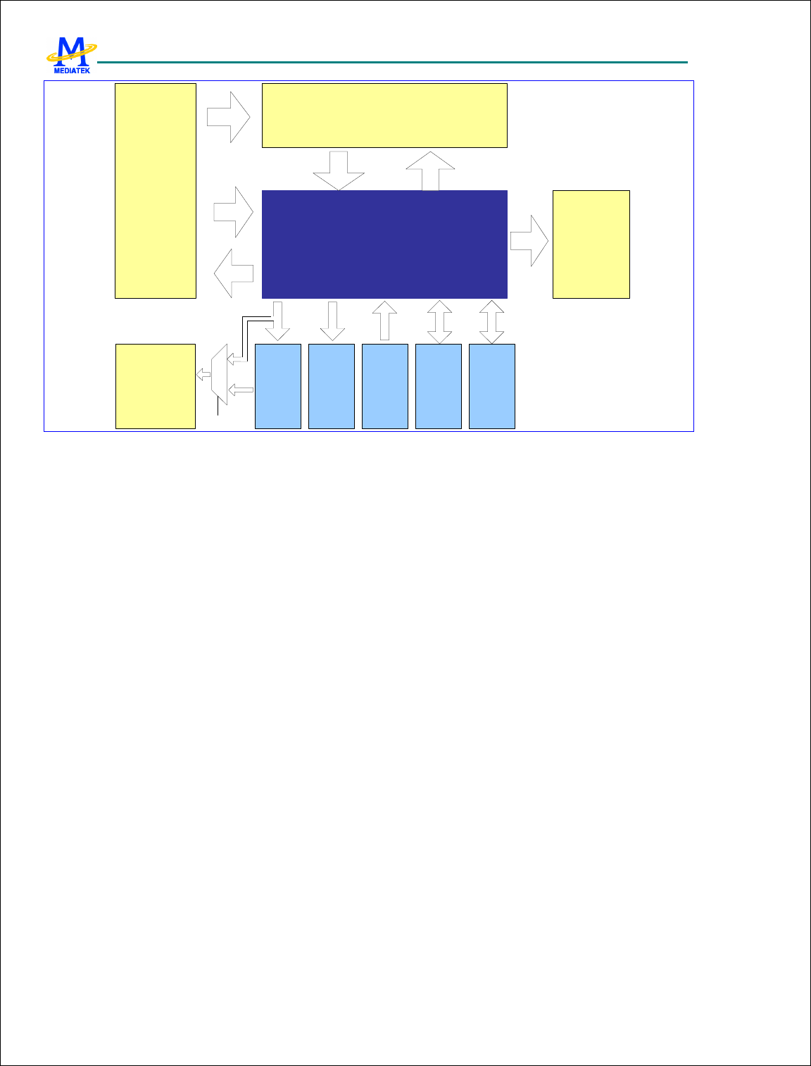
MTK Confidential Release for Konka
MTK Confidential Release for Konka
MT6228 GSM/GPRS Baseband Processor Data Sheet Revision 1.0
411/616 MediaTek Inc. Confidential
Image DMA
Image Process Engine
Resizer
JPEG
Encode
Line
Buffer
(YUV422/
YUV420)
Video
Buffer
(YUV420)
Image
Buffer
(RGB 565/
RGB 888/
BGR 888)
Image
Buffer
(RGB 565/
RGB888)
LCD
Frame
Buffer
(RGB 565/
RGB888)
LCD IF
JPEG
Encoder
DC Mode
By Pixel
By PixelBy Pixel By Pixel By Pixel
By Block
By Pixel
YUV444
1
0
By Pixel
RGB888
By Pixel
YUV444
Figure 30 inter-connection around Image DMA
6.15.1.1 JPEG Encoder DMA
The main function of JPEG Encoder DMA is to receive YUV 444 data from Image Engine by pixels and transmit
YUV422/ YUV420 data to JPEG Encoder by 8 X 8 blocks.
6.15.1.1.1 Flow Control
To achieve pixel to block conversion, line buffer must be given, and its line count must be multiple of 8. For better
performance, it’s recommended to have a minimum of 16 lines of buffer. For applications where images capturing from
the camera, because the data stream from camera can not be stopped, the number of lines must not be less than 16, (24
lines or more is recommended). Otherwise, data may be lost in the interface between the Image Signal Process and
Capture Resize modules.
6.15.1.1.2 Data format conversion
Since the JPEG encoder needs data of signed 2’s complement format. The JPEG Encoder DMA takes the responsibility
to handle the data format conversion. Each of Y, U, or V component values of input data is of 8-bit unsigned format,
which represents a value ranging from 0 to 255. The component value of the data is converted into 8-bit 2’s
complement format, which represents a value ranging from –128 to 127.
6.15.1.1.3 Padding
For pictures whose frame size are not multiples of 16 X 8 blocks for YUV422 mode or 16 X 16 blocks for YUV420
mode, JPEG Encoder DMA takes the responsibility to handle the image boundary. In horizontal direction, JPEG
Encoder DMA automatically pads the last pixel of every line to the tail of the corresponding line until the number of
pixels in the line is multiple of 16. Similarly, JPEG Encoder pads the last line to the tail of the image frame until the
line count is multiples of 8 for YUV422 mode or 16 for YUV420 mode in vertical direction. An example of YUV422
mode is illustrated in . In this case, the original frame size is (16n + 13) X (8n + 6), which is not multiple of 16 X 8.
Therefore, three additional pixels are padded to the end of each line to make the pixel count multiple of 16. In the
vertical direction, two more lines are padded with last line to make line count to multiple of 8.
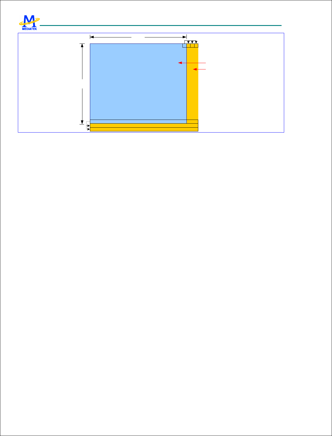
MTK Confidential Release for Konka
MTK Confidential Release for Konka
MT6228 GSM/GPRS Baseband Processor Data Sheet Revision 1.0
412/616 MediaTek Inc. Confidential
16n+13
8n+6
Original Frame
Padded Frame
Figure 31 Frame Padding for YUV422 mode
6.15.1.1.4 Gray Mode
JPEG Encoder DMA also supports Gray Image JPEG Encoding. That is, only Y components are transmitted to JPEG
Encoder for Encoding. For memory and bus bandwidth saving, U and V components are truncated before writing into
buffer memory. As a result, the memory size in gray mode will be half of what it is in YUV422 mode.
Furthermore, the frame padding is a little different from that in normal mode. JPEG Encode DMA will construct the
frame to the multiple of an 8 X 8 block instead of a 16 X 8 or 16 X 16 block in normal mode.
6.15.1.1.5 Auto-Restart
To overlap the Codec processing time with that of file system manipulations, an Auto-Restart mode is designed. JPEG
Encoder DMA automatically restarts itself to receive next frame without being re-configured and re-enabled by MCU.
This can enhance the Shot-to-Shot Delay performance a lot since the file system manipulations would take a long time.
JPEG Encoder DMA will not stop transfer until it is disabled by MCU. Note that associated settings must be
programmed in the Capture/Post Resize and other Image Engines as well.
6.15.1.2 Video Encode DMA
The main function of the Video Encode DMA is to move data from Capture Resize to Video Buffer. Video Buffer is
used to contain YUV420 image data for MPEG4/H.263 codec. It consists of three continuous memory buffers for Y, U,
and V component data.
For MPEG4/H.263 encoding, Video Encode DMA receives data from Capture Resize, and converts it into YUV420
format, and then writes into Y, U, V buffer separately. Software starts MPEG4/H.263 encoder after all of the frame data
are ready.
6.15.1.2.1 Auto-Restart
To reduce MCU interrupt frequency, an Auto-Restart mode is designed. Video DMA automatically restarts itself to
receive next frame without being re-configured and re-enabled by MCU. This can save a lot of MCU time since the
MCU no longer needs to handle Image DMA at each frame boundary, which also makes the data stream smoother.
Usually, double buffer scheme are employed to smooth video encoding. Therefore, the second base address register is
provided in Video DMA to contain the second address. Video DMA automatically switches the base address between
the two addresses at every restart. For the case of single buffer scheme, the two base address registers have to be
programmed with the same address. Video DMA will not stop transfer until it is disabled by MCU. Note that associated
settings must be programmed in Capture Resize and Image Engine as well.

MTK Confidential Release for Konka
MTK Confidential Release for Konka
MT6228 GSM/GPRS Baseband Processor Data Sheet Revision 1.0
413/616 MediaTek Inc. Confidential
6.15.1.3 Video Decode DMA
The main function of the Video Decode DMA is to move data from Video Buffer to Post Resize. Video Buffer is used
to contain YUV420 image data after MPEG4/H.263 codec. It consists of three continuous memory buffers for Y, U, and
V component data. Data format for the Post Resize is YUV444, and therefore color format conversion is needed during
data movement.
For MPEG4/H.263 decoding, MPEG4/H.263 decoder writes out decoded data to video buffer, and Video Decode DMA
is then triggered by software to move data to the Post Resize.
6.15.1.4 Image Buffer Write 1, 2 DMA
The main function of IBW1, IBW2 DMA is to move RGB data from Image Engine to memory or LCD, and the format
of the written data is RGB565 or RGB888. IBW1 plays the role of saving the backup image. Whenever JPEG DMA,
Video DMA, or IBW2 DMA is dumping images, IBW1 can be enabled to dump a backup image simultaneously.
Besides, IBW1 also plays the role of writing local display under videophone scenario.
6.15.1.4.1 Auto-Restart
IBW1, IBW2 DMA can restart itself to receive next frame, and switch base address at every restart.
6.15.1.4.2 Hardware Handshake with LCD DMA
IBW1, IBW2 DMA issues interrupt along with the base address of the LCD buffer to LCD DMA at the end of frame
transfer. LCD DMA could start moving data into LCD based on the signals.
The advantage of hardware handshaking is to reduce interrupts to MCU. This could make system more efficient.
6.15.1.4.3 Direct Couple to LCD DMA
A more efficient and memory saving way to move frame data to LCD is through Direct Couple Interface. The interface
is between IBW1, IBW2 DMA and LCD, as depicted in , and consists of request, acknowledge, and 24-bit data bus. In
this mode, frame data skips the frame buffer and are written to LCD directly. LCD updates the data on the fly.
However this mode cannot work in camera preview. This is because LCD update could halt for a long time, and
therefore the next pixel data from the camera may not be captured in time. Thus, resulting in lost data.
6.15.1.4.4 Image Panning
IBW1, IBW2 DMA can grab a part of the image frame as a new image, as illustrated in . The advantage is that the
system does not need to prepare a large piece of memory to store the entire image frame just to show a small portion of
it. This can save memory usage, especially for large images. The detailed usage is shown in the register definition of
IMGDMA_IBW2_CON, IMGDMA_IBW2_CON.
6.15.1.4.5 Destination Pitch
To write the memory, a pitch register is defined to indicate the memory address jump per line for each base address.
This can save memory usage when writing a rectangular area of a LCD layer.
6.15.1.5 Image Buffer Write 3,4 DMA
The main function of IBW3 DMA is to move data from a Pixel Image Engine to the DRZ, and the format is YUV444 or
RGB888. IBW3 provides the route for thumbnail image dumping. The main function of IBW4 DMA is to move data
from a Pixel Image Engine to the PRZ, and the format is YUV444 or RGB888. IBW4 provides the route for preview
scenario.
MTK Confidential Release for Konka
MTK Confidential Release for Konka
MT6228 GSM/GPRS Baseband Processor Data Sheet Revision 1.0
414/616 MediaTek Inc. Confidential
6.15.1.5.1 Auto-Restart
IBW3 DMA can restart itself to receive next frame.
6.15.1.6 Image Buffer Read 1 DMA
The main function of IBR1 DMA is to move RGB data from memory to Image Post Processor. The data format to
Image Post Processor is RGB888 and the data formats from memory can be RGB565, RGB888 and BGR888 (which
support BMP data format). The data placement in memory is illustrated in .
With IBR1 DMA, RGB image data in memory can be directly used for video encoding, JPEG encoding, and image
panning.
89101112131415 01234567
Byte
R G B
RGB 565
89101112131415 01234567
Byte
RGB 888
89101112131415 01234567
Byte
BGR 888
R
G
B
Figure 32 RGB data in memory
6.15.1.7 Image Buffer Read 2 DMA
The main function of IBR2 DMA is to read photo frame from memory, resize it to the capturing image size, look-up
palette table and overlay it onto the capturing image. The photo frame mask data format can be 1, 2, 4, 8-bpp color
index modes. A 256-entries in 24-bit YUV format palette provides a color index to color value lookup table.
6.15.1.7.1 Auto-Restart
IBR2 DMA can restart itself to read the same photo frame again and again while video capture scenario.
6.15.2 DMA Enabling Sequence
In general, the DMAs at the downstream of the data path must be enabled first. For instance, for Video capturing, the
data path is Camera module Capture Resize Image Engine Video DMA Video Buffer. Video DMA has
to be enabled before Image Processor, Capture Resize and Camera module.
The second example is video playback. The data path is Video Buffer Video DMA Post Resize IPP Engine
IBW2 DMA LCD frame buffer. IBW2 DMA has to be enabled before Post Resize and Image Engine and then
Video DMA.
6.15.3 Register Definitions
Register Address Register Function Acronym
IMGDMA + 0000h
Image DMA Status Register IMGDMA_STA

MTK Confidential Release for Konka
MTK Confidential Release for Konka
MT6228 GSM/GPRS Baseband Processor Data Sheet Revision 1.0
415/616 MediaTek Inc. Confidential
IMGDMA + 0004h
Image DMA Interrupt Acknowledge Register IMGDMA_ACKINT
IMGDMA + 0100h JPEG DMA Start Register IMGDMA_JPEG_STR
IMGDMA + 0104h JPEG DMA Control Register IMGDMA_JPEG_CON
IMGDMA + 0108h JPEG DMA Base Address Register IMGDMA_JPEG_BSADDR
IMGDMA + 010Ch JPEG DMA Horizontal Size Register IMGDMA_JPEG_HSIZE
IMGDMA + 0110h
JPEG DMA Vertical Size Register IMGDMA_JPEG_VSIZE
IMGDMA + 0114h JPEG DMA FIFO Length Register IMGDMA_JPEG_FIFOLEN
IMGDMA + 0118h JPEG Write Pointer Register IMGDMA_JPEG_WRPTR
IMGDMA + 011Ch JPEG Write Horizontal Count Register IMGDMA_JPEG_WRHCNT
IMGDMA + 0120h JPEG Write Vertical Count Register IMGDMA_JPEG_WRVCNT
IMGDMA + 0124h JPEG Read Pointer Register IMGDMA_JPEG_RDPTR
IMGDMA + 0128h JPEG Read Horizontal Count Register IMGDMA_JPEG_RDHCNT
IMGDMA + 012Ch JPEG Read Vertical Count Register IMGDMA_JPEG_RDVCNT
IMGDMA + 0130h JPEG FIFO Line Count Register IMGDMA_JPEG_FFCNT
IMGDMA + 0134h JPEG FIFO Write Line Index Register IMGDMA_JPEG_FFWRLIDX
IMGDMA + 0138h JPEG FIFO Read Line Index Register IMGDMA_JPEG_FFRDLIDX
IMGDMA + 0200h
Video Encode DMA Start Register IMGDMA_VDOENC_STR
IMGDMA + 0204h Video Encode DMA Control Register IMGDMA_VDOENC_CON
IMGDMA + 0210h Video Encode DMA Y Base Address 1 Register IMGDMA_VDOENC_Y_BASE1
IMGDMA + 0214h Video Encode DMA U Base Address 1 Register IMGDMA_VDOENC_U_BASE1
IMGDMA + 0218h Video Encode DMA V Base Address 1 Register IMGDMA_VDOENC_V_BASE1
IMGDMA + 0220h
Video Encode DMA Y Base Address 2 Register IMGDMA_VDOENC_Y_BASE2
IMGDMA + 0224h Video Encode DMA U Base Address 2 Register IMGDMA_VDOENC_U_BASE2
IMGDMA + 0228h Video Encode DMA V Base Address 2 Register IMGDMA_VDOENC_V_BASE2
IMGDMA + 0230h Video Encode DMA Horizontal Size Register IMGDMA_VDOENC_HSIZE
IMGDMA + 0234h Video Encode DMA Vertical Size Register IMGDMA_VDOENC_VSIZE
IMGDMA + 0238h
Video Encode DMA Horizontal Count Register IMGDMA_VDOENC_HCNT
IMGDMA + 023Ch Video Encode DMA Vertical Count Register IMGDMA_VDOENC_VCNT
IMGDMA + 0280h Video Decode DMA Start Register IMGDMA_VDODEC_STR
IMGDMA + 0284h Video Decode DMA Control Register IMGDMA_VDODEC_CON
IMGDMA + 0290h Video Decode DMA Y Base Address 1 Register IMGDMA_VDODEC_Y_BASE1
IMGDMA + 0294h
Video Decode DMA U Base Address 1 Register IMGDMA_VDODEC_U_BASE1
IMGDMA + 0298h Video Decode DMA V Base Address 1 Register IMGDMA_VDODEC_V_BASE1
IMGDMA + 02A0h Video Decode DMA Y Base Address 2 Register IMGDMA_VDODEC_Y_BASE2
IMGDMA + 02A4h Video Decode DMA U Base Address 2 Register IMGDMA_VDODEC_U_BASE2
IMGDMA + 02A8h Video Decode DMA V Base Address 2 Register IMGDMA_VDODEC_V_BASE2
IMGDMA + 02B0h Video Decode DMA Horizontal Size Register IMGDMA_VDODEC_HSIZE
IMGDMA + 02B4h Video Decode DMA Vertical Size Register IMGDMA_VDODEC_VSIZE
IMGDMA + 02B8h Video Decode DMA Horizontal Count Register IMGDMA_VDODEC_HCNT
IMGDMA + 02BCh Video Decode DMA Vertical Count Register IMGDMA_VDODEC_VCNT
IMGDMA + 0300h Image Buffer Write DMA1 Start Register IMGDMA_IBW1_STR
IMGDMA + 0304h Image Buffer Write DMA1 Control Register IMGDMA_IBW1_CON

MTK Confidential Release for Konka
MTK Confidential Release for Konka
MT6228 GSM/GPRS Baseband Processor Data Sheet Revision 1.0
416/616 MediaTek Inc. Confidential
IMGDMA + 0308h
Image Buffer Write DMA1 Base Address 1 Register IMGDMA_IBW1_BSADDR1
IMGDMA + 030Ch Image Buffer Write DMA1 Base Address 2 Register IMGDMA_IBW1_BSADDR2
IMGDMA + 0310h Image Buffer Write DMA1 Horizontal Size IMGDMA_IBW1_HSIZE
IMGDMA + 0314h Image Buffer Write DMA1 Vertical Size IMGDMA_IBW1_VSIZE
IMGDMA + 0318h Image Buffer Write DMA1 CLIP LR IMGDMA_IBW1_CLIPLR
IMGDMA + 031Ch
Image Buffer Write DMA1 CLIP TB IMGDMA_IBW1_CLIPTB
IMGDMA + 0320h Image Buffer Write DMA1 Destination Pitch 1 IMGDMA_IBW1_DPITCH1
IMGDMA + 0324h Image Buffer Write DMA1 Destination Pitch2 IMGDMA_IBW1_DPITCH2
IMGDMA + 0328h Image Buffer Write DMA1 Horizontal Count IMGDMA_IBW1_HCNT
IMGDMA + 032Ch Image Buffer Write DMA1 Vertical Count IMGDMA_IBW1_VCNT
IMGDMA + 0400h Image Buffer Write DMA2 Start Register IMGDMA_IBW2_STR
IMGDMA + 0404h Image Buffer Write DMA2 Control Register IMGDMA_IBW2_CON
IMGDMA + 0408h Image Buffer Write DMA2 Base Address 1 Register IMGDMA_IBW2_BSADDR1
IMGDMA + 040Ch Image Buffer Write DMA2 Base Address 2 Register IMGDMA_IBW2_BSADDR2
IMGDMA + 0410h Image Buffer Write DMA2 Horizontal Size IMGDMA_IBW2_HSIZE
IMGDMA + 0414h Image Buffer Write DMA2 Vertical Size IMGDMA_IBW2_VSIZE
IMGDMA + 0418h
Image Buffer Write DMA2 CLIP LR IMGDMA_IBW2_CLIPLR
IMGDMA + 041Ch Image Buffer Write DMA2 CLIP TB IMGDMA_IBW2_CLIPTB
IMGDMA + 0420h Image Buffer Write DMA2 Destination Pitch 1 IMGDMA_IBW2_DPITCH1
IMGDMA + 0424h Image Buffer Write DMA2 Destination Pitch2 IMGDMA_IBW2_DPITCH2
IMGDMA + 0428h Image Buffer Write DMA2 Horizontal Count IMGDMA_IBW2_HCNT
IMGDMA + 042Ch
Image Buffer Write DMA2 Vertical Count IMGDMA_IBW2_VCNT
IMGDMA + 0500h Image Buffer Write DMA3 Start Register IMGDMA_IBW3_STR
IMGDMA + 0504h Image Buffer Write DMA3 Control Register IMGDMA_IBW3_CON
IMGDMA + 0510h Image Buffer Write DMA3 Horizontal Size IMGDMA_IBW3_HSIZE
IMGDMA + 0514h Image Buffer Write DMA3 Vertical Size IMGDMA_IBW3_VSIZE
IMGDMA + 0528h
Image Buffer Write DMA3 Horizontal Count IMGDMA_IBW3_HCNT
IMGDMA + 052Ch Image Buffer Write DMA3 Vertical Count IMGDMA_IBW3_VCNT
IMGDMA + 0580h Image Buffer Write DMA4 Start Register IMGDMA_IBW4_STR
IMGDMA + 0584h Image Buffer Write DMA4 Control Register IMGDMA_IBW4_CON
IMGDMA + 0590h Image Buffer Write DMA4 Horizontal Size IMGDMA_IBW4_HSIZE
IMGDMA + 0594h
Image Buffer Write DMA4 Vertical Size IMGDMA_IBW4_VSIZE
IMGDMA + 05A8h Image Buffer Write DMA4 Horizontal Count IMGDMA_IBW4_HCNT
IMGDMA + 05ACh Image Buffer Write DMA4 Vertical Count IMGDMA_IBW4_VCNT
IMGDMA + 0600h Image Buffer Read DMA1 Start Register IMGDMA_IBR1_STR
IMGDMA + 0604h Image Buffer Read DMA1 Control Register IMGDMA_IBR1_CON
IMGDMA + 0608h Image Buffer Read DMA1 Base Address Register IMGDMA_IBR1_BSADDR
IMGDMA + 060Ch Image Buffer Read DMA1 Number of Pixels IMGDMA_IBR1_PXLNUM
IMGDMA + 0610h Image Buffer Read DMA1 Remaining Pixels IMGDMA_IBR1_PXLCNT
IMGDMA + 0700h Image Buffer Read DMA2 Start Register IMGDMA_IBR2_STR
IMGDMA + 0704h Image Buffer Read DMA2 Control Register IMGDMA_IBR2_CON
IMGDMA + 0708h Image Buffer Read DMA2 Base Address Register IMGDMA_IBR2_BSADDR
MTK Confidential Release for Konka
MTK Confidential Release for Konka
MT6228 GSM/GPRS Baseband Processor Data Sheet Revision 1.0
417/616 MediaTek Inc. Confidential
IMGDMA + 070Ch
Image Buffer Read DMA2 Configuration Register IMGDMA_IBR2_CFG
IMGDMA + 0710h Image Buffer Read DMA2 Horizontal Size IMGDMA_IBR2_HSIZE
IMGDMA + 0714h Image Buffer Read DMA2 Vertical Size IMGDMA_IBR2_VSIZE
IMGDMA + 0718h Image Buffer Read DMA2 Horizontal Count IMGDMA_IBR2_HCNT
IMGDMA + 071Ch Image Buffer Read DMA2 Vertical Count IMGDMA_IBR2_VCNT
IMGDMA + 0800h
IMGDMA + 0bfch Image Buffer Read DMA2 Palette memory IMGDMA_PAL00~FF
Table 53 Tracer Registers
IMGDMA+000
0h Image DMA Status Register IMGDMA_STA
Bit 31 30 29 28 27 26 25 24 23 22 21 20 19 18 17 16
Name
IBW4
RUN
IBW3
RUN
IBR2
RUN
IBR1
RUN
IBW2
RUN
IBW1
RUN
VDOD
EC
RUN
VDOE
NCR
RUN
VDOE
NCW
RUN
JPEG
RUN
Type RO RO RO RO RO RO RO RO RO RO
Reset
0 0 0 0 0 0 0 0 0 0
Bit 15 14 13 12 11 10 9 8 7 6 5 4 3 2 1 0
Name
IBW4
IT
IBW3
IT
IBR
2IT
IBR1
IT
IBW2
IT
IBW1
IT
VDOD
EC IT
VDOE
NCR
IT
VDOE
NCW
IT
JPEG
IT
Type RO RO RO RO RO RO RO RO RO RO
Reset
0 0 0 0 0 0 0 0 0 0
This register helps software program being well aware of the global status of Image DMA channels.
IT Interrupt status for DMA
2 No interrupt is generated.
3 An interrupt is pending and waiting for service.
RUN DMA status
0 DMA is stopped or has completed the transfer already.
1 DMA is currently running.
IMGDMA+000
4h Image DMA Interrupt Acknowledge Register IMGDMA_ACKI
NT
Bit 31 30 29 28 27 26 25 24 23 22 21 20 19 18 17 16
Name
Type
Bit 15 14 13 12 11 10 9 8 7 6 5 4 3 2 1 0
Name
IBW4
ACK
IBW3
ACK
IBR2
ACK
IBR1
ACK
IBW2
ACK
IBW1
ACK
VDOD
EC
ACK
VDOE
NCR
ACK
VDOE
NCW
ACK
JPEG
ACK
Type WO WO WO WO WO WO WO WO WO WO
This register is used to acknowledge the current interrupt request associated with the completion event of a DMA
channel by software program. Note that this is a write-only register, and any read to it will return a value of “0”.
ACK Interrupt acknowledge for the DMA channel
0 No effect
1 Interrupt request is acknowledged and should be relinquished.
MTK Confidential Release for Konka
MTK Confidential Release for Konka
MT6228 GSM/GPRS Baseband Processor Data Sheet Revision 1.0
418/616 MediaTek Inc. Confidential
IMGDMA+010
0h JPEG DMA Start Register JPEG_STR
Bit 31 30 29 28 27 26 25 24 23 22 21 20 19 18 17 16
Name
Type
Reset
Bit 15 14 13 12 11 10 9 8 7 6 5 4 3 2 1 0
Name
STR
Type R/W
Reset
0
This register controls the activity of a DMA channel. Note that before setting STR to “1”, all the configurations shall be
done by giving proper values.
STR Start control for a DMA channel
0 stop DMA
1 activate DMA
IMGDMA+010
4h JPEG DMA Control Register JPEG_CON
Bit 31 30 29 28 27 26 25 24 23 22 21 20 19 18 17 16
Name
Type
Reset
Bit 15 14 13 12 11 10 9 8 7 6 5 4 3 2 1 0
Name
PSEL
AUTO
RSTR
MODE
1
MODE
0 IT
Type R/W R/W R/W R/W R/W
Reset
0 0 0 0 0
AUTO RSTR Automatic restart. JPEG Encoder DMA automatically restarts while current frame is finished.
0 Disable
1 Enable
MODE Interrupt Enabling
00 YUV422
01 Gray
10 YUV420
11 reserved
IT Interrupt Enabling
0 Disable
1 Enable
PSEL Pixel engine selection
0 Capture resize
1 Post resize
IMGDMA+010
8h JPEG DMA Base Address Register JPEG_BSADDR
Bit 31 30 29 28 27 26 25 24 23 22 21 20 19 18 17 16
Name
ADDR[31:16]
Type R/W
Bit 15 14 13 12 11 10 9 8 7 6 5 4 3 2 1 0
Name
ADR[15:0]
Type R/W
MTK Confidential Release for Konka
MTK Confidential Release for Konka
MT6228 GSM/GPRS Baseband Processor Data Sheet Revision 1.0
419/616 MediaTek Inc. Confidential
ADDR Base address of the JPEG DMA FIFO.
IMGDMA+010
Ch JPEG DMA Horizontal Size Register JPEG_HSIZE
Bit 31 30 29 28 27 26 25 24 23 22 21 20 19 18 17 16
Name
Type
Bit 15 14 13 12 11 10 9 8 7 6 5 4 3 2 1 0
Name
HSIZE
Type R/W
HSIZE Horizontal dimension of image. 0 stands for 1 pixels, and n-1 stands for n pixels.
IMGDMA+011
0h JPEG DMA Vertical Size Register JPEG_VSIZE
Bit 31 30 29 28 27 26 25 24 23 22 21 20 19 18 17 16
Name
Type
Bit 15 14 13 12 11 10 9 8 7 6 5 4 3 2 1 0
Name
VSIZE
Type R/W
VSIZE Vertical dimension of image. 0 stands for 1 pixels, and n-1 stands for n pixels.
IMGDMA+011
4h JPEG DMA FIFO Length Register JPEG_FIFOLEN
Bit
31 30
29
28
27 26 25
24
23
22 21 20
19
18
17 16
Name
Type
Bit 15 14 13 12 11 10 9 8 7 6 5 4 3 2 1 0
Name
FIFOLEN
Type R/W
JPEG DMA FIFO Length must be the multiple of 8. The memory needed for a certain FIFO length is
216
16 ×××
FIFOLEN
HSIZE
bytes for YUV422 mode,
316
16 ×××
FIFOLEN
HSIZE
bytes for YUV420
mode, and
FIFOLEN
HSIZE ××
8
8
bytes for gray mode.
FIFOLEN JPEG DMA FIFO Length. FIFOLEN must be the multiple of 8. recommended values are 24 for
YUV422 mode, 16 for YUV420 mode, and 16 for gray mode.
IMGDMA+011
8h JPEG Write Pointer Register JPEG_WRPTR
Bit 31 30 29 28 27 26 25 24 23 22 21 20 19 18 17 16
Name
WRPTR[31:16]
Type RO
Bit 15 14 13 12 11 10 9 8 7 6 5 4 3 2 1 0
Name
WRPTR[15:0]
Type RO
WRPTR Write pointer to display current writing address.

MTK Confidential Release for Konka
MTK Confidential Release for Konka
MT6228 GSM/GPRS Baseband Processor Data Sheet Revision 1.0
420/616 MediaTek Inc. Confidential
IMGDMA+011
Ch JPEG Write Horizontal Count Register JPEG_WRHCNT
Bit 31 30 29 28 27 26 25 24 23 22 21 20 19 18 17 16
Name
Type
Bit 15 14 13 12 11 10 9 8 7 6 5 4 3 2 1 0
Name
WRHCNT
Type RO
WRHCNT Displays the horizontal pixel count. This is a down-count counter. Hence this register reflects the
remaining pixels of a line.
IMGDMA+012
0h JPEG Write Vertical Count Register JPEG_WRVCNT
Bit 31 30 29 28 27 26 25 24 23 22 21 20 19 18 17 16
Name
Type
Bit 15 14 13 12 11 10 9 8 7 6 5 4 3 2 1 0
Name
WRVCNT
Type RO
WRVCNT Displays the vertical pixel count. This is a down-count counter. Hence this register reflects the remaining
lines.
IMGDMA+012
4h JPEG Read Pointer Register JPEG_RDPTR
Bit 31 30 29 28 27 26 25 24 23 22 21 20 19 18 17 16
Name
RDPTR[31:16]
Type RO
Bit 15 14 13 12 11 10 9 8 7 6 5 4 3 2 1 0
Name
RDPTR[15:0]
Type RO
RDPTR Read pointer to display current reading address.
IMGDMA+012
8h JPEG Read Horizontal Count Register JPEG_RDHCNT
Bit 31 30 29 28 27 26 25 24 23 22 21 20 19 18 17 16
Name
Type
Bit 15 14 13 12 11 10 9 8 7 6 5 4 3 2 1 0
Name
RDHCNT
Type RO
RDHCNT Displays the horizontal pixel count. This is a down-count counter. Hence this register reflects the
remaining pixels of a line.
IMGDMA+012
Ch JPEG Read Vertical Count Register JPEG_RDVCNT
Bit 31 30 29 28 27 26 25 24 23 22 21 20 19 18 17 16
Name
Type
Bit 15 14 13 12 11 10 9 8 7 6 5 4 3 2 1 0
Name
RDVCNT
Type RO
MTK Confidential Release for Konka
MTK Confidential Release for Konka
MT6228 GSM/GPRS Baseband Processor Data Sheet Revision 1.0
421/616 MediaTek Inc. Confidential
RDVCNT Displays the vertical pixel count. This is a down-count counter. Hence this register reflects the remaining
lines.
IMGDMA+013
0h JPEG FIFO Line Count Register JPEG_FFCNT
Bit 31 30 29 28 27 26 25 24 23 22 21 20 19 18 17 16
Name
Type
Bit 15 14 13 12 11 10 9 8 7 6 5 4 3 2 1 0
Name
FFCNT
Type RO
FFCNT Displays the FIFO Line Count of JPEG FIFO.
IMGDMA+013
4h JPEG Write Line Index Register JPEG_FFWRLI
DX
Bit 31 30 29 28 27 26 25 24 23 22 21 20 19 18 17 16
Name
Type
Bit 15 14 13 12 11 10 9 8 7 6 5 4 3 2 1 0
Name
YIDX
Type RO
YIDX Displays which FIFO line JPEG DMA is writing. YIDX = 1 ~ FIFOLEN.
IMGDMA+013
8h JPEG Read Line Index Register JPEG_FFRDLID
X
Bit 31 30 29 28 27 26 25 24 23 22 21 20 19 18 17 16
Name
Type
Bit 15 14 13 12 11 10 9 8 7 6 5 4 3 2 1 0
Name
YIDX
Type RO
YIDX Displays which FIFO line JPEG DMA is reading, YIDX = 1 ~ FIFOLEN.
IMGDMA+020
0h Video Encode DMA Start Register VDOENC_STR
Bit 31 30 29 28 27 26 25 24 23 22 21 20 19 18 17 16
Name
Type
Reset
Bit 15 14 13 12 11 10 9 8 7 6 5 4 3 2 1 0
Name
STR
Type R/W
Reset
0
This register controls the activity of a DMA channel. Note that before setting STR to “1”, all the configurations should
be done by giving proper values.
STR Start control for a DMA channel
0 stop DMA
1 activate DMA

MTK Confidential Release for Konka
MTK Confidential Release for Konka
MT6228 GSM/GPRS Baseband Processor Data Sheet Revision 1.0
422/616 MediaTek Inc. Confidential
IMGDMA+020
4h Video Encode DMA Control Register VDOENC_CON
Bit 31 30 29 28 27 26 25 24 23 22 21 20 19 18 17 16
Name
Type
Reset
Bit 15 14 13 12 11 10 9 8 7 6 5 4 3 2 1 0
Name
PSEL
RSEL
AUTO
RSTR
RD IT
W2R WR IT
Type R/W R/W R/W R/W R/W R/W
Reset
0 0 0 0 0 0
WR IT WDMA Done Interrupt Enable. Interrupt issues when all of the transfers are done. For auto-restart mode,
interrupt issues at every restart.
0 Disable
1 Enable
W2R WDMA hardware trigger to RDMA. While this function is enabled, Video Encode WDMA will write data to
video buffer first, and then a start pulse will issue to Video Encode RDMA to read back from the same buffer.
These data will pass through Resize to convert to LCD frame size.
0 Disable
1 Enable
RD IT RDMA Done Interrupt Enable.
0 Disable
1 Enable
AUTO RSTR Automatic restart. Video DMA automatically restarts while current frame is finished. Base address
will be automatically switched between VDO_BSADD1 and VDO_BSADDR2. For single buffer application,
please set VDO_BSADD1 and VDO_BSADDR2 with the same value.
0 Disable
1 Enable
RSEL RDMA output destination selection.
0 Post resize
1 Drop resize
PSEL WDMA input pixel engine selection
0 Capture resize
1 Post resize
IMGDMA+021
0h Video Encode Y Base Address 1 Register VDOENC_Y_BA
SE1
Bit 31 30 29 28 27 26 25 24 23 22 21 20 19 18 17 16
Name
ADDR
Type R/W
Bit 15 14 13 12 11 10 9 8 7 6 5 4 3 2 1 0
Name
ADDR
Type R/W
ADDR First base address of video frame buffer.
IMGDMA+021
4h Video Encode U Base Address 1 Register VDOENC_U_BA
SE1
Bit 31 30 29 28 27 26 25 24 23 22 21 20 19 18 17 16
Name
ADDR
MTK Confidential Release for Konka
MTK Confidential Release for Konka
MT6228 GSM/GPRS Baseband Processor Data Sheet Revision 1.0
423/616 MediaTek Inc. Confidential
Type
R/W
Bit 15 14 13 12 11 10 9 8 7 6 5 4 3 2 1 0
Name
ADDR
Type R/W
ADDR First base address of video frame buffer.
IMGDMA+021
8h Video Encode VBase Address 1 Register VDOENC_V_BA
SE1
Bit 31 30 29 28 27 26 25 24 23 22 21 20 19 18 17 16
Name
ADDR
Type R/W
Bit 15 14 13 12 11 10 9 8 7 6 5 4 3 2 1 0
Name
ADDR
Type
R/W
ADDR First base address of video frame buffer.
IMGDMA+022
0h Video Encode Y Base Address 2 Register VDOENC_Y_BA
SE2
Bit 31 30 29 28 27 26 25 24 23 22 21 20 19 18 17 16
Name
ADDR
Type R/W
Bit 15 14 13 12 11 10 9 8 7 6 5 4 3 2 1 0
Name
ADDR
Type R/W
ADDR Second base address of video frame buffer.
IMGDMA+022
4h Video Encode U Base Address 2 Register VDOENC_U_BA
SE2
Bit 31 30 29 28 27 26 25 24 23 22 21 20 19 18 17 16
Name
ADDR
Type R/W
Bit 15 14 13 12 11 10 9 8 7 6 5 4 3 2 1 0
Name
ADDR
Type R/W
ADDR Second base address of video frame buffer.
IMGDMA+022
8h Video Encode V Base Address 2 Register VDOENC_V_BA
SE2
Bit 31 30 29 28 27 26 25 24 23 22 21 20 19 18 17 16
Name
ADDR
Type R/W
Bit 15 14 13 12 11 10 9 8 7 6 5 4 3 2 1 0
Name
ADDR
Type R/W
ADDR Second base address of video frame buffer.
IMGDMA+023
0h Video Encode Horizontal Size Register VDOENC_HSIZ
E
Bit 31 30 29 28 27 26 25 24 23 22 21 20 19 18 17 16
Name
Type
MTK Confidential Release for Konka
MTK Confidential Release for Konka
MT6228 GSM/GPRS Baseband Processor Data Sheet Revision 1.0
424/616 MediaTek Inc. Confidential
Bit 15 14 13 12 11 10 9 8 7 6 5 4 3 2 1 0
Name
SIZE
Type R/W
SIZE Horizontal dimension of a video frame. 1 stands for 1 pixel, and n stands for n pixels. Note that the
horizontal size must be multiple of 16.
IMGDMA+023
4h Video Encode Vertical Size Register VDOENC_VSIZ
E
Bit 31 30 29 28 27 26 25 24 23 22 21 20 19 18 17 16
Name
Type
Bit 15 14 13 12 11 10 9 8 7 6 5 4 3 2 1 0
Name
SIZE
Type R/W
SIZE Vertical dimension of a video frame. 1 stands for 1 pixel, and n stands for n pixels. Note that the vertical
size must be multiple of 16.
IMGDMA+023
8h Video Encode Horizontal Count Register VDOENC_HCNT
Bit 31 30 29 28 27 26 25 24 23 22 21 20 19 18 17 16
Name
Type
Bit 15 14 13 12 11 10 9 8 7 6 5 4 3 2 1 0
Name
COUNT
Type RO
COUNT Horizontal pixel count. 1 stands for 1 pixel, and n stands for n pixels.
IMGDMA+023
Ch Video Encode Vertical Count Register VDOENC_VCNT
Bit 31 30 29 28 27 26 25 24 23 22 21 20 19 18 17 16
Name
Type
Bit 15 14 13 12 11 10 9 8 7 6 5 4 3 2 1 0
Name
COUNT
Type RO
COUNT Vertical pixel count. 1 stands for 1 pixel, and n stands for n pixels.
IMGDMA+028
0h Video Decode DMA Start Register VDODEC_STR
Bit 31 30 29 28 27 26 25 24 23 22 21 20 19 18 17 16
Name
Type
Reset
Bit 15 14 13 12 11 10 9 8 7 6 5 4 3 2 1 0
Name
STR
Type R/W
Reset
0
This register controls the activity of a DMA channel. Note that before setting STR to “1”, all the configurations should
be done by giving proper values.
STR Start control for a DMA channel
MTK Confidential Release for Konka
MTK Confidential Release for Konka
MT6228 GSM/GPRS Baseband Processor Data Sheet Revision 1.0
425/616 MediaTek Inc. Confidential
0 stop DMA
1 activate DMA
IMGDMA+028
4h Video Decode DMA Control Register VDODEC_CON
Bit 31 30 29 28 27 26 25 24 23 22 21 20 19 18 17 16
Name
Type
Reset
Bit 15 14 13 12 11 10 9 8 7 6 5 4 3 2 1 0
Name
DONE
IT
Type R/W
Reset
0
DONE IT DMA Done Interrupt Enabling. Interrupt issues when all of the transfers are done. For auto-restart mode,
interrupt issues at every restart.
0 Disable
1 Enable
IMGDMA+029
0h Video Decode Y Base Address 1 Register VDODEC_Y_BA
SE1
Bit 31 30 29 28 27 26 25 24 23 22 21 20 19 18 17 16
Name
ADDR
Type R/W
Bit 15 14 13 12 11 10 9 8 7 6 5 4 3 2 1 0
Name
ADDR
Type R/W
ADDR First base address of video frame buffer.
IMGDMA+029
4h Video Decode U Base Address 1 Register VDODEC_U_BA
SE1
Bit 31 30 29 28 27 26 25 24 23 22 21 20 19 18 17 16
Name
ADDR
Type R/W
Bit 15 14 13 12 11 10 9 8 7 6 5 4 3 2 1 0
Name
ADDR
Type R/W
ADDR First base address of video frame buffer.
IMGDMA+029
8h Video Decode V Base Address 1 Register VDODEC_V_BA
SE1
Bit 31 30 29 28 27 26 25 24 23 22 21 20 19 18 17 16
Name
ADDR
Type R/W
Bit 15 14 13 12 11 10 9 8 7 6 5 4 3 2 1 0
Name
ADDR
Type R/W
ADDR First base address of video frame buffer.

MTK Confidential Release for Konka
MTK Confidential Release for Konka
MT6228 GSM/GPRS Baseband Processor Data Sheet Revision 1.0
426/616 MediaTek Inc. Confidential
IMGDMA+02A
0h Video Decode Y Base Address 2 Register VDODEC_Y_BA
SE2
Bit 31 30 29 28 27 26 25 24 23 22 21 20 19 18 17 16
Name
ADDR
Type R/W
Bit 15 14 13 12 11 10 9 8 7 6 5 4 3 2 1 0
Name
ADDR
Type R/W
ADDR Second base address of video frame buffer.
IMGDMA+02A
4h Video Decode U Base Address 2 Register VDODEC_U_BA
SE2
Bit 31 30 29 28 27 26 25 24 23 22 21 20 19 18 17 16
Name
ADDR
Type R/W
Bit 15 14 13 12 11 10 9 8 7 6 5 4 3 2 1 0
Name
ADDR
Type R/W
ADDR Second base address of video frame buffer.
IMGDMA+02A
8h Video Decode V Base Address 2 Register VDODEC_V_BA
SE2
Bit 31 30 29 28 27 26 25 24 23 22 21 20 19 18 17 16
Name
ADDR
Type R/W
Bit 15 14 13 12 11 10 9 8 7 6 5 4 3 2 1 0
Name
ADDR
Type R/W
ADDR Second base address of video frame buffer.
IMGDMA+02B
0h Video Decode Horizontal Size Register VDODEC_HSIZ
E
Bit 31 30 29 28 27 26 25 24 23 22 21 20 19 18 17 16
Name
Type
Bit 15 14 13 12 11 10 9 8 7 6 5 4 3 2 1 0
Name
SIZE
Type R/W
SIZE Horizontal dimension of a video frame. 1 stands for 1 pixel, and n stands for n pixels. Note that the
horizontal size must be multiple of 16.
IMGDMA+02B
4h Video Decode Vertical Size Register VDODEC_VSIZ
E
Bit 31 30 29 28 27 26 25 24 23 22 21 20 19 18 17 16
Name
Type
Bit 15 14 13 12 11 10 9 8 7 6 5 4 3 2 1 0
Name
SIZE
Type R/W

MTK Confidential Release for Konka
MTK Confidential Release for Konka
MT6228 GSM/GPRS Baseband Processor Data Sheet Revision 1.0
427/616 MediaTek Inc. Confidential
SIZE Vertical dimension of a video frame. 1 stands for 1 pixel, and n stands for n pixels. Note that the vertical
size must be multiple of 16.
IMGDMA+02B
8h Video Decode Horizontal Count Register VDODEC_HCNT
Bit 31 30 29 28 27 26 25 24 23 22 21 20 19 18 17 16
Name
Type
Bit 15 14 13 12 11 10 9 8 7 6 5 4 3 2 1 0
Name
COUNT
Type RO
COUNT Horizontal pixel count. 1 stands for 1 pixel, and n stands for n pixels.
IMGDMA+02B
Ch Video Decode Vertical Count Register VDODEC_VCNT
Bit 31 30 29 28 27 26 25 24 23 22 21 20 19 18 17 16
Name
Type
Bit 15 14 13 12 11 10 9 8 7 6 5 4 3 2 1 0
Name
COUNT
Type RO
COUNT Vertical pixel count. 1 stands for 1 pixel, and n stands for n pixels.
IMGDMA+030
0h Image Buffer Write DMA1 Start Register IBW1_STR
Bit 31 30 29 28 27 26 25 24 23 22 21 20 19 18 17 16
Name
Type
Reset
Bit 15 14 13 12 11 10 9 8 7 6 5 4 3 2 1 0
Name
STR
Type R/W
Reset
0
This register controls the activity of a DMA channel. Note that before setting STR to “1”, all the configurations should
be done by giving proper value
STR Start control for a DMA channel
0 stop DMA
1 activate DMA
IMGDMA+030
4h Image Buffer Write DMA1 Control Register IBW1_CON
Bit 31 30 29 28 27 26 25 24 23 22 21 20 19 18 17 16
Name
Type
Reset
Bit 15 14 13 12 11 10 9 8 7 6 5 4 3 2 1 0
Name
PSEL
1
PSEL
0 888M PAN DC AUTO
RSTR
LCD PITCH
IT
Type R/W R/W R/W R/W R/W R/W R/W R/W R/W
Reset
0 0 0 0 0 0 0 0 0
IT Interrupt Enabling
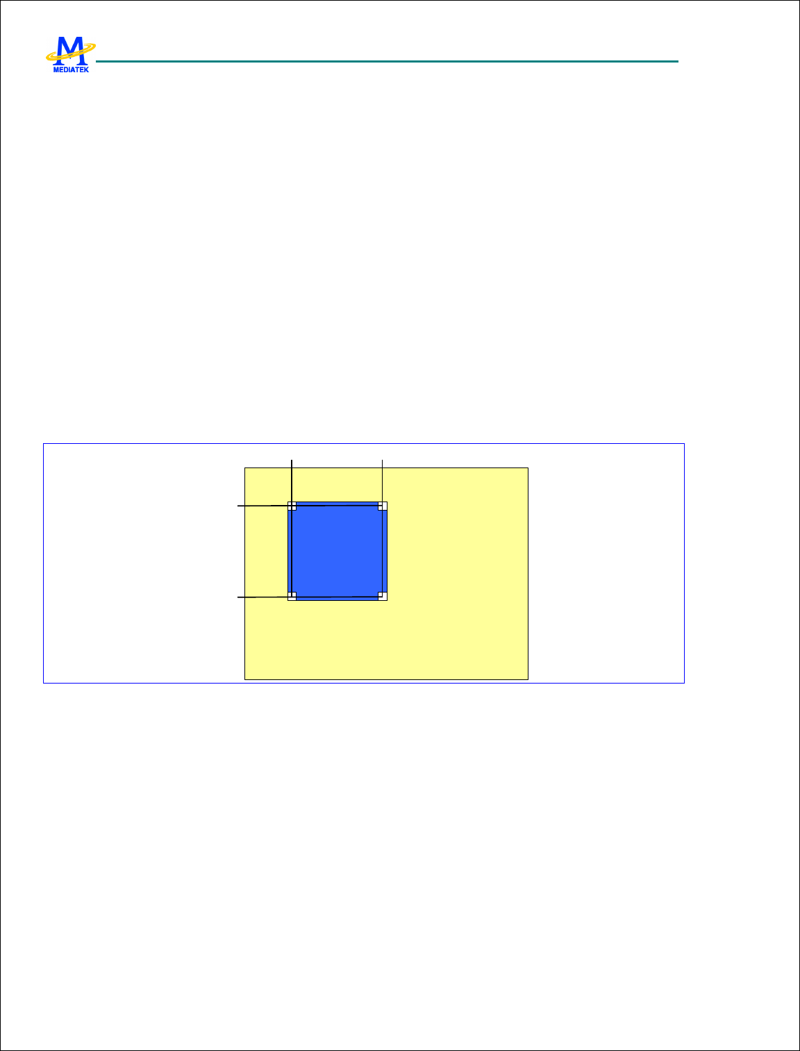
MTK Confidential Release for Konka
MTK Confidential Release for Konka
MT6228 GSM/GPRS Baseband Processor Data Sheet Revision 1.0
428/616 MediaTek Inc. Confidential
0 Disable
1 Enable
PITCH Destination pitch jump.
0 Disable
1 Enable
LCD Signaling LCD DMA. Frame ready signal is issued at the beginning of frames in Direct Couple mode, and is
issued at the end of frames in Dual Buffer mode. Note that in the case of automatic restart plus direct couple
mode, this function must be enabled to trigger LCD DMA.
0 Disable
1 Enable
AUTO RSTR Automatic restart. IBW2 DMA automatically restarts itself while current frame is finished.
0 Disable
1 Enable
DC Directly coupling to LCD DMA. Once this function is enabled, image data will dump to LCD DMA directly
instead of dumping to LCD frame buffer.
0 Disable
1 Enable
PAN Picture panning. Once this function is enabled, only the pixels in the region specified by CLIP_L, CLIP_R,
CLIP_T, and CLIP_B are dumped. The pan window is defined as Figure 33.
CLIP_L CLIP_R
CLIP_T
CLIP_B
Figure 33 Picture Panning
0 Disable
1 Enable
888M Output format control
0 RGB565
1 RGB888
PSEL Pixel engine selection
00 IPP 1
01 IPP 2
10 Capture resize
11 Post resize
MTK Confidential Release for Konka
MTK Confidential Release for Konka
MT6228 GSM/GPRS Baseband Processor Data Sheet Revision 1.0
429/616 MediaTek Inc. Confidential
IMGDMA+030
8h Image Buffer Write DMA1 Base Address 1 Register IBW1_BSADDR
1
Bit 31 30 29 28 27 26 25 24 23 22 21 20 19 18 17 16
Name
ADDR
Type R/W
Bit 15 14 13 12 11 10 9 8 7 6 5 4 3 2 1 0
Name
ADDR
Type R/W
ADDR First base address of the LCD frame buffer.
IMGDMA+030
Ch Image Buffer Write DMA1 Base Address 2 Register IBW1_BSADDR
2
Bit 31 30 29 28 27 26 25 24 23 22 21 20 19 18 17 16
Name
ADDR
Type R/W
Bit 15 14 13 12 11 10 9 8 7 6 5 4 3 2 1 0
Name
ADDR
Type R/W
ADDR Second base address of the LCD frame buffer.
IMGDMA+031
0h Image Buffer Write DMA1 Horizontal Size Register IBW1_HSIZE
Bit 31 30 29 28 27 26 25 24 23 22 21 20 19 18 17 16
Name
Type
Bit 15 14 13 12 11 10 9 8 7 6 5 4 3 2 1 0
Name
SIZE
Type R/W
SIZE Horizontal size of a frame. 0 stands for 1 pixel, and n-1 stands for n pixels.
IMGDMA+031
4h Image Buffer Write DMA1 Vertical Size Register IBW1_VSIZE
Bit 31 30 29 28 27 26 25 24 23 22 21 20 19 18 17 16
Name
Type
Bit 15 14 13 12 11 10 9 8 7 6 5 4 3 2 1 0
Name
SIZE
Type R/W
SIZE Vertical size of a frame. 0 stands for 1 pixel, and n-1 stands for n pixels.
IMGDMA+031
8h Image Buffer Write DMA1 Clip LR Register IBW1_CLIP_LR
Bit 31 30 29 28 27 26 25 24 23 22 21 20 19 18 17 16
Name
Type
Bit 15 14 13 12 11 10 9 8 7 6 5 4 3 2 1 0
Name
RIGHT
Type R/W
LEFT Left boundary of a frame. 0 stands for the first pixel, and n-1 stands for the n
th
pixel.
RIGHT Right boundary of a frame. 0 stands for the first pixel, and n-1 stands for the n
th
pixel.
MTK Confidential Release for Konka
MTK Confidential Release for Konka
MT6228 GSM/GPRS Baseband Processor Data Sheet Revision 1.0
430/616 MediaTek Inc. Confidential
IMGDMA+031
Ch Image Buffer Write DMA1 Clip TB Register IBW1_CLIP_TB
Bit 31 30 29 28 27 26 25 24 23 22 21 20 19 18 17 16
Name
Type
Bit 15 14 13 12 11 10 9 8 7 6 5 4 3 2 1 0
Name
BOTTOM
Type R/W
TOP Top boundary of a frame. 0 stands for the first pixel, and n-1 stands for the n
th
pixel.
BOTTOM Bottom boundary of a frame. 0 stands for the first pixel, and n-1 stands for the n
th
pixel.
IMGDMA+032
0h Image Buffer Write DMA1 Destination Pitch1 Register
IBW1_DPITCH1
Bit 31 30 29 28 27 26 25 24 23 22 21 20 19 18 17 16
Name
Type
Bit 15 14 13 12 11 10 9 8 7 6 5 4 3 2 1 0
Name
PITCH
Type R/W
PITCH Line pitch in bytes corresponds to IBW2_BSADDR1.
IMGDMA+032
4h Image Buffer Write DMA1 Destination Pitch2 Register
IBW1_DPITCH2
Bit 31 30 29 28 27 26 25 24 23 22 21 20 19 18 17 16
Name
Type
Bit 15 14 13 12 11 10 9 8 7 6 5 4 3 2 1 0
Name
PITCH
Type R/W
PITCH Line pitch in bytes corresponds to IBW2_BSADDR1.
IMGDMA+032
8h Image Buffer Write DMA1 Horizontal Count Register IBW1_HCNT
Bit 31 30 29 28 27 26 25 24 23 22 21 20 19 18 17 16
Name
Type
Bit 15 14 13 12 11 10 9 8 7 6 5 4 3 2 1 0
Name
CNT
Type RO
CNT Horizontal pixel count. 0 stands for 1 pixel, and n-1 stands for n pixels.
IMGDMA+032
Ch Image Buffer Write DMA1 Vertical Count Register IBW1_VCNT
Bit 31 30 29 28 27 26 25 24 23 22 21 20 19 18 17 16
Name
Type
Bit 15 14 13 12 11 10 9 8 7 6 5 4 3 2 1 0
Name
CNT
Type RO
CNT Vertical line count. 0 stands for 1 line, and n-1 stands for n lines.
MTK Confidential Release for Konka
MTK Confidential Release for Konka
MT6228 GSM/GPRS Baseband Processor Data Sheet Revision 1.0
431/616 MediaTek Inc. Confidential
IMGDMA+040
0h Image Buffer Write DMA2 Start Register IBW2_STR
Bit 31 30 29 28 27 26 25 24 23 22 21 20 19 18 17 16
Name
Type
Reset
Bit 15 14 13 12 11 10 9 8 7 6 5 4 3 2 1 0
Name
STR
Type R/W
Reset
0
This register controls the activity of a DMA channel. Note that before setting STR to “1”, all the configurations should
be done by giving proper value
STR Start control for a DMA channel
0 stop DMA
1 activate DMA
IMGDMA+040
4h Image Buffer Write DMA2 Control Register IBW2_CON
Bit 31 30 29 28 27 26 25 24 23 22 21 20 19 18 17 16
Name
Type
Reset
Bit 15 14 13 12 11 10 9 8 7 6 5 4 3 2 1 0
Name
PSEL
1
PSEL
0 888M PAN DC AUTO
RSTR
LCD PITCH
IT
Type R/W R/W R/W R/W R/W R/W R/W R/W R/W
Reset
0 0 0 0 0 0 0 0 0
IT Interrupt Enabling
0 Disable
1 Enable
PITCH Destination pitch jump.
0 Disable
1 Enable
LCD Signaling LCD DMA. Frame ready signal is issued at the beginning of frames in Direct Couple mode, and is
issued at the end of frames in Dual Buffer mode. Note that in the case of automatic restart plus direct couple
mode, this function must be enabled to trigger LCD DMA.
0 Disable
1 Enable
AUTO RSTR Automatic restart. IBW2 DMA automatically restarts itself while current frame is finished.
0 Disable
1 Enable
DC Directly coupling to LCD DMA. Once this function is enabled, image data will dump to LCD DMA directly
instead of dumping to LCD frame buffer.
0 Disable
1 Enable
MTK Confidential Release for Konka
MTK Confidential Release for Konka
MT6228 GSM/GPRS Baseband Processor Data Sheet Revision 1.0
432/616 MediaTek Inc. Confidential
PAN Picture panning. Once this function is enabled, only the pixels in the region specified by HPITCH1, HPITCH2,
VPITCH1, and VPITCH2 are dumped. The PITCHs are defined as Figure 33.
0 Disable
1 Enable
888M Output format control
0 RGB565
1 RGB888
PSEL Pixel engine selection
00 IPP 1
01 IPP 2
10 Capture resize
11 Post resize
IMGDMA+040
8h Image Buffer Write DMA2 Base Address 1 Register IBW2_BSADDR
1
Bit 31 30 29 28 27 26 25 24 23 22 21 20 19 18 17 16
Name
ADDR
Type R/W
Bit 15 14 13 12 11 10 9 8 7 6 5 4 3 2 1 0
Name
ADDR
Type R/W
ADDR First base address of the LCD frame buffer.
IMGDMA+040
Ch Image Buffer Write DMA2 Base Address 2 Register IBW2_BSADDR
2
Bit 31 30 29 28 27 26 25 24 23 22 21 20 19 18 17 16
Name
ADDR
Type R/W
Bit 15 14 13 12 11 10 9 8 7 6 5 4 3 2 1 0
Name
ADDR
Type R/W
ADDR Second base address of the LCD frame buffer.
IMGDMA+041
0h Image Buffer Write DMA2 Horizontal Size Register IBW2_HSIZE
Bit 31 30 29 28 27 26 25 24 23 22 21 20 19 18 17 16
Name
Type
Bit 15 14 13 12 11 10 9 8 7 6 5 4 3 2 1 0
Name
SIZE
Type R/W
SIZE Horizontal size of a frame. 0 stands for 1 pixel, and n-1 stands for n pixels.
IMGDMA+041
4h Image Buffer Write DMA2 Vertical Size Register IBW2_VSIZE
Bit 31 30 29 28 27 26 25 24 23 22 21 20 19 18 17 16
Name
Type
Bit 15 14 13 12 11 10 9 8 7 6 5 4 3 2 1 0
Name
SIZE
MTK Confidential Release for Konka
MTK Confidential Release for Konka
MT6228 GSM/GPRS Baseband Processor Data Sheet Revision 1.0
433/616 MediaTek Inc. Confidential
Type
R/W
SIZE Vertical size of a frame. 0 stands for 1 pixel, and n-1 stands for n pixels.
IMGDMA+041
8h Image Buffer Write DMA2 Clip LR Register IBW2_CLIP_LR
Bit 31 30 29 28 27 26 25 24 23 22 21 20 19 18 17 16
Name
Type
Bit 15 14 13 12 11 10 9 8 7 6 5 4 3 2 1 0
Name
RIGHT
Type R/W
LEFT Left boundary of a frame. 0 stands for the first pixel, and n-1 stands for the n
th
pixel.
RIGHT Right boundary of a frame. 0 stands for the first pixel, and n-1 stands for the n
th
pixel.
IMGDMA+041
Ch Image Buffer Write DMA2 Clip TB Register IBW2_CLIP_TB
Bit 31 30 29 28 27 26 25 24 23 22 21 20 19 18 17 16
Name
Type
Bit 15 14 13 12 11 10 9 8 7 6 5 4 3 2 1 0
Name
BOTTOM
Type R/W
TOP Top boundary of a frame. 0 stands for the first pixel, and n-1 stands for the n
th
pixel.
BOTTOM Bottom boundary of a frame. 0 stands for the first pixel, and n-1 stands for the n
th
pixel.
IMGDMA+042
0h Image Buffer Write DMA2 Destination Pitch1 Register
IBW2_DPITCH1
Bit 31 30 29 28 27 26 25 24 23 22 21 20 19 18 17 16
Name
Type
Bit 15 14 13 12 11 10 9 8 7 6 5 4 3 2 1 0
Name
PITCH
Type R/W
PITCH Line pitch in bytes corresponds to IBW2_BSADDR1.
IMGDMA+042
4h Image Buffer Write DMA2 Destination Pitch2 Register
IBW2_DPITCH2
Bit 31 30 29 28 27 26 25 24 23 22 21 20 19 18 17 16
Name
Type
Bit 15 14 13 12 11 10 9 8 7 6 5 4 3 2 1 0
Name
PITCH
Type R/W
PITCH Line pitch in bytes corresponds to IBW2_BSADDR1.
IMGDMA+042
8h Image Buffer Write DMA2 Horizontal Count Register IBW2_HCNT
Bit 31 30 29 28 27 26 25 24 23 22 21 20 19 18 17 16
Name
Type
Bit 15 14 13 12 11 10 9 8 7 6 5 4 3 2 1 0

MTK Confidential Release for Konka
MTK Confidential Release for Konka
MT6228 GSM/GPRS Baseband Processor Data Sheet Revision 1.0
434/616 MediaTek Inc. Confidential
Name
CNT
Type RO
CNT Horizontal pixel count. 0 stands for 1 pixel, and n-1 stands for n pixels.
IMGDMA+042
Ch Image Buffer Write DMA2 Vertical Count Register IBW2_VCNT
Bit 31 30 29 28 27 26 25 24 23 22 21 20 19 18 17 16
Name
Type
Bit 15 14 13 12 11 10 9 8 7 6 5 4 3 2 1 0
Name
CNT
Type RO
CNT Vertical line count. 0 stands for 1 line, and n-1 stands for n lines.
IMGDMA+050
0h Image Buffer Write DMA3 Start Register IBW3_STR
Bit 31 30 29 28 27 26 25 24 23 22 21 20 19 18 17 16
Name
Type
Reset
Bit 15 14 13 12 11 10 9 8 7 6 5 4 3 2 1 0
Name
STR
Type R/W
Reset
0
This register controls the activity of a DMA channel. Note that before setting STR to “1”, all the configurations should
be done by giving proper value
STR Start control for a DMA channel
0 stop DMA
1 activate DMA
IMGDMA+050
4h Image Buffer Write DMA3 Control Register IBW3_CON
Bit 31 30 29 28 27 26 25 24 23 22 21 20 19 18 17 16
Name
Type
Reset
Bit 15 14 13 12 11 10 9 8 7 6 5 4 3 2 1 0
Name
PSEL
1
PSEL
0 AUTO
RSTR
IT
Type R/W R/W R/W R/W
Reset
0 0 0 0
IT Interrupt Enabling
0 Disable
1 Enable
AUTO RSTR Automatic restart. IBW2 DMA automatically restarts itself while current frame is finished.
0 Disable
1 Enable
PSEL Pixel engine selection
00 IPP 1
01 IPP 2

MTK Confidential Release for Konka
MTK Confidential Release for Konka
MT6228 GSM/GPRS Baseband Processor Data Sheet Revision 1.0
435/616 MediaTek Inc. Confidential
10 Capture resize
11 Post resize
IMGDMA+051
0h Image Buffer Write DMA3 Horizontal Size Register IBW3_HSIZE
Bit 31 30 29 28 27 26 25 24 23 22 21 20 19 18 17 16
Name
Type
Bit 15 14 13 12 11 10 9 8 7 6 5 4 3 2 1 0
Name
SIZE
Type R/W
SIZE Horizontal size of a frame. 0 stands for 1 pixel, and n-1 stands for n pixels.
IMGDMA+051
4h Image Buffer Write DMA3 Vertical Size Register IBW3_VSIZE
Bit 31 30 29 28 27 26 25 24 23 22 21 20 19 18 17 16
Name
Type
Bit 15 14 13 12 11 10 9 8 7 6 5 4 3 2 1 0
Name
SIZE
Type R/W
SIZE Vertical size of a frame. 0 stands for 1 pixel, and n-1 stands for n pixels.
IMGDMA+052
8h Image Buffer Write DMA3 Horizontal Count Register IBW3_HCNT
Bit 31 30 29 28 27 26 25 24 23 22 21 20 19 18 17 16
Name
Type
Bit 15 14 13 12 11 10 9 8 7 6 5 4 3 2 1 0
Name
CNT
Type RO
CNT Horizontal pixel count. 0 stands for 1 pixel, and n-1 stands for n pixels.
IMGDMA+052
Ch Image Buffer Write DMA3 Vertical Count Register IBW3_VCNT
Bit 31 30 29 28 27 26 25 24 23 22 21 20 19 18 17 16
Name
Type
Bit 15 14 13 12 11 10 9 8 7 6 5 4 3 2 1 0
Name
CNT
Type RO
CNT Vertical line count. 0 stands for 1 line, and n-1 stands for n lines.
IMGDMA+058
0h Image Buffer Write DMA4 Start Register IBW4_STR
Bit 31 30 29 28 27 26 25 24 23 22 21 20 19 18 17 16
Name
Type
Reset
Bit 15 14 13 12 11 10 9 8 7 6 5 4 3 2 1 0
Name
STR
Type R/W
MTK Confidential Release for Konka
MTK Confidential Release for Konka
MT6228 GSM/GPRS Baseband Processor Data Sheet Revision 1.0
436/616 MediaTek Inc. Confidential
Reset
0
This register controls the activity of a DMA channel. Note that before setting STR to “1”, all the configurations should
be done by giving proper value
STR Start control for a DMA channel
0 stop DMA
1 activate DMA
IMGDMA+058
4h Image Buffer Write DMA4 Control Register IBW4_CON
Bit 31 30 29 28 27 26 25 24 23 22 21 20 19 18 17 16
Name
Type
Reset
Bit 15 14 13 12 11 10 9 8 7 6 5 4 3 2 1 0
Name
PSEL
1
PSEL
0 AUTO
RSTR
IT
Type R/W R/W R/W R/W
Reset
0 0 0 0
IT Interrupt Enabling
0 Disable
1 Enable
AUTO RSTR Automatic restart. IBW2 DMA automatically restarts itself while current frame is finished.
0 Disable
1 Enable
PSEL Pixel engine selection
00 IPP 1
01 IPP 2
10 Capture resize
11 Post resize
IMGDMA+059
0h Image Buffer Write DMA4 Horizontal Size Register IBW4_HSIZE
Bit 31 30 29 28 27 26 25 24 23 22 21 20 19 18 17 16
Name
Type
Bit 15 14 13 12 11 10 9 8 7 6 5 4 3 2 1 0
Name
SIZE
Type R/W
SIZE Horizontal size of a frame. 0 stands for 1 pixel, and n-1 stands for n pixels.
IMGDMA+059
4h Image Buffer Write DMA4 Vertical Size Register IBW4_VSIZE
Bit
31 30
29
28
27 26
25
24
23
22 21 20
19
18
17
16
Name
Type
Bit 15 14 13 12 11 10 9 8 7 6 5 4 3 2 1 0
Name
SIZE
Type R/W
SIZE Vertical size of a frame. 0 stands for 1 pixel, and n-1 stands for n pixels.
MTK Confidential Release for Konka
MTK Confidential Release for Konka
MT6228 GSM/GPRS Baseband Processor Data Sheet Revision 1.0
437/616 MediaTek Inc. Confidential
IMGDMA+05A
8h Image Buffer Write DMA4 Horizontal Count Register IBW4_HCNT
Bit 31 30 29 28 27 26 25 24 23 22 21 20 19 18 17 16
Name
Type
Bit 15 14 13 12 11 10 9 8 7 6 5 4 3 2 1 0
Name
CNT
Type RO
CNT Horizontal pixel count. 0 stands for 1 pixel, and n-1 stands for n pixels.
IMGDMA+05A
Ch Image Buffer Write DMA4 Vertical Count Register IBW4_VCNT
Bit 31 30 29 28 27 26 25 24 23 22 21 20 19 18 17 16
Name
Type
Bit 15 14 13 12 11 10 9 8 7 6 5 4 3 2 1 0
Name
CNT
Type RO
CNT Vertical line count. 0 stands for 1 line, and n-1 stands for n lines.
IMGDMA+060
0h Image Buffer Read DMA1 Start Register IBR1_STR
Bit 31 30 29 28 27 26 25 24 23 22 21 20 19 18 17 16
Name
Type
Reset
Bit 15 14 13 12 11 10 9 8 7 6 5 4 3 2 1 0
Name
STR
Type R/W
Reset
0
This register controls the activity of a DMA channel. Note that before setting STR to “1”, all the configurations should
be done by giving proper values.
STR Start control for a DMA channel
0 stop DMA
1 activate DMA
IMGDMA+060
4h Image Buffer Read DMA1 Control Register IBR1_CON
Bit 31 30 29 28 27 26 25 24 23 22 21 20 19 18 17 16
Name
Type
Reset
Bit 15 14 13 12 11 10 9 8 7 6 5 4 3 2 1 0
Name
ORDE
R FMT
IT
Type R/W R/W R/W
Reset
0 0 0
IT Interrupt Enabling
0 Disable
1 Enable
MTK Confidential Release for Konka
MTK Confidential Release for Konka
MT6228 GSM/GPRS Baseband Processor Data Sheet Revision 1.0
438/616 MediaTek Inc. Confidential
FMT Data format
0 RGB565
1 RGB888
ORDER Data order
0 BGR888, from MSB to LSB.
1 RGB888, from MSB to LSB.
IMGDMA+060
8h Image Buffer Read DMA1 Base Address Register IBR1_BSADDR
Bit 31 30 29 28 27 26 25 24 23 22 21 20 19 18 17 16
Name
ADDR
Type R/W
Bit 15 14 13 12 11 10 9 8 7 6 5 4 3 2 1 0
Name
ADDR
Type R/W
ADDR Base address of the image buffer.
IMGDMA+060
Ch Image Buffer Read DMA1 Number of Pixels Register IBR1_PXLNUM
Bit 31 30 29 28 27 26 25 24 23 22 21 20 19 18 17 16
Name
NUM
Type R/W
Bit 15 14 13 12 11 10 9 8 7 6 5 4 3 2 1 0
Name
NUM
Type R/W
NUM Number of pixels of the transferred image. 0 represents 1 pixel, and n-1 represents n pixels.
IMGDMA+061
0h Image Buffer Read DMA1 Remaining Pixels Register IBR1_PXLCNT
Bit 31 30 29 28 27 26 25 24 23 22 21 20 19 18 17 16
Name
COUNT
Type
RO
Bit 15 14 13 12 11 10 9 8 7 6 5 4 3 2 1 0
Name
COUNT
Type RO
COUNT Pixel count. 0 represents 1 pixel, and n-1 represents n pixels.
IMGDMA+070
0h Image Buffer Read DMA2 Start Register IBR2_STR
Bit 31 30 29 28 27 26 25 24 23 22 21 20 19 18 17 16
Name
Type
Reset
Bit 15 14 13 12 11 10 9 8 7 6 5 4 3 2 1 0
Name
STR
Type R/W
Reset
0
This register controls the activity of a DMA channel. Note that before setting STR to “1”, all the configurations should
be done by giving proper values.
STR Start control for a DMA channel

MTK Confidential Release for Konka
MTK Confidential Release for Konka
MT6228 GSM/GPRS Baseband Processor Data Sheet Revision 1.0
439/616 MediaTek Inc. Confidential
0 stop DMA
1 activate DMA
IMGDMA+070
4h Image Buffer Read DMA2 Control Register IBR2_CON
Bit 31 30 29 28 27 26 25 24 23 22 21 20 19 18 17 16
Name
Type
Reset
Bit 15 14 13 12 11 10 9 8 7 6 5 4 3 2 1 0
Name
PSEL
PALE
N
AUTO
RSTR
MODE
1
MODE
0 IT
Type R/W R/W R/W R/W R/W R/W
Reset
0 0 0 0 0 0
IT Interrupt Enabling
0 Disable
1 Enable
MODE Interrupt Enabling
00 1-bpp mode
01 2-bpp mode
10 4-bpp mode
11 8-bpp mode
AUTO RSTR Automatic restart. IBR2 DMA automatically restarts itself while current frame is finished.
0 Disable
1 Enable
PALEN Photo frame palette Enabling. Please set this bit before any operation with the palette memory.
0 Disable.
1 Enable.
PSEL Pixel engine selection
0 Capture Resize.
1 Post Resize.
IMGDMA+070
8h Image Buffer Read DMA2 Base Address Register IBR2_BSADDR
Bit 31 30 29 28 27 26 25 24 23 22 21 20 19 18 17 16
Name
ADDR
Type R/W
Bit
15 14
13
12
11 10
9 8 7 6 5 4 3 2 1 0
Name
ADDR
Type R/W
ADDR Base address of the photo frame.
IMGDMA+070
Ch Image Buffer Read DMA2 Configuration Register IBR2_CFG
Bit 31 30 29 28 27 26 25 24 23 22 21 20 19 18 17 16
Name
Type
Bit 15 14 13 12 11 10 9 8 7 6 5 4 3 2 1 0
Name
KEY VRATIO HRATIO
Type R/W R/W R/W
MTK Confidential Release for Konka
MTK Confidential Release for Konka
MT6228 GSM/GPRS Baseband Processor Data Sheet Revision 1.0
440/616 MediaTek Inc. Confidential
KEY Transparent color key for overlay function.
VRATIO Horizontal scaling ratio.
HRATIO Vertical scaling ratio.
IMGDMA+071
0h Image Buffer Read DMA2 Horizontal Size Register IBR2_HSIZE
Bit 31 30 29 28 27 26 25 24 23 22 21 20 19 18 17 16
Name
Type
Bit 15 14 13 12 11 10 9 8 7 6 5 4 3 2 1 0
Name
SIZE
Type R/W
SIZE Horizontal size of the photo frame.
IMGDMA+071
4h Image Buffer Read DMA2 Vertical Size Register IBR2_VSIZE
Bit 31 30 29 28 27 26 25 24 23 22 21 20 19 18 17 16
Name
Type
Bit 15 14 13 12 11 10 9 8 7 6 5 4 3 2 1 0
Name
SIZE
Type R/W
SIZE Vertical size of the photo frame.
IMGDMA+071
8h Image Buffer Read DMA2 Horizontal Count Register IBR2_HCNT
Bit 31 30 29 28 27 26 25 24 23 22 21 20 19 18 17 16
Name
Type
Bit 15 14 13 12 11 10 9 8 7 6 5 4 3 2 1 0
Name
CNT
Type RO
CNT Horizontal pixel count. 0 stands for 1 pixel, and n-1 stands for n pixels.
IMGDMA+071
Ch Image Buffer Read DMA2 Vertical Count Register IBR2_VCNT
Bit 31 30 29 28 27 26 25 24 23 22 21 20 19 18 17 16
Name
Type
Bit 15 14 13 12 11 10 9 8 7 6 5 4 3 2 1 0
Name
CNT
Type RO
CNT Vertical line count. 0 stands for 1 line, and n-1 stands for n lines.
IMGDMA+080
0h
IMGDMA+0BF
Ch
Image Buffer Read DMA2 Palette Register 00~FF
IMGDMA_PAL0
0
~FF
Bit 31 30 29 28 27 26 25 24 23 22 21 20 19 18 17 16
Name
COLOR

MTK Confidential Release for Konka
MTK Confidential Release for Konka
MT6228 GSM/GPRS Baseband Processor Data Sheet Revision 1.0
441/616 MediaTek Inc. Confidential
Type
R/W
Bit 15 14 13 12 11 10 9 8 7 6 5 4 3 2 1 0
Name
COLOR
Type R/W
COLOR [23:0] Palette entry color value in YUV format.
6.16 Image Engine
The Image Engine is used to manipulate image adjustments and a variety of filtering effects. It works inside the DMA
architecture, which minimizes the intervention of the CPU. The engine can directly access the external and internal
memories and provide a large extent of flexibility for system performance consideration.
The function of the engine basically contains two categories: pixel adjustment and filtering effect.
Pixel adjustment includes brightness, contrast, and hue adjustment, color adjustment, and gamma correction. These
effects are integrated on both the encoding and decoding path of image and video material. It can provide on-the-fly
manipulation on these raw materials. For camera preview and capture, it can perform the effects on the incoming image
frame immediately, and output to both frame buffer for display and image buffer for image compression. For video
playback, it can perform the effects on the decoded frame immediately and output to the frame buffer for display.
The filtering effect includes linear and non-linear (ranking) effects. The linear filtering provides blur and sharpening
effects with programmable mask design. The non-linear filtering provides ranking filter to emulate noise reduction,
dilation and erosion effects. We can also implement other artistic effects by performing multi-pass filtering with
combination of a variety of effects.
The image Engine includes three independent sub image engines. The first sub image engine, IPP1, is in charge of the
main functions of the engine (pixel adjustment and filtering effect). The second sub image engine, IPP2, only performs
YUV to RGB color conversion. This sub engine can be used to output the RGB data in the image compression or
videophone. The third sub image engine, IPP3, mainly performs RGB to YUV color space conversion and then output
to Post Resizer.
6.16.1 Register Definitions
Register Address Register Function Acronym
IMG+0000h Image flow control register IMGPROC_IMAGE_CON
IMG+0004h Control register IMGPROC_CON
IMG+0008h Interrupt enable register IMGPROC_INTREN
IMG+000Ch Interrupt status register IMGPROC_INTR
IMG+0010h Status register IMGPROC_STATUS
IMG+0100h Hue adjustment coefficient C11 IMGPROC_HUE11
IMG+0104h Hue adjustment coefficient C12 IMGPROC_HUE12
IMG+0108h Hue adjustment coefficient C21 IMGPROC_HUE21
IMG+010Ch Hue adjustment coefficient C22 IMGPROC_HUE22
IMG+0110h Saturation adjustment coefficient IMGPROC_SAT
IMG+0120h Brightness adjustment coefficient B1 IMGPROC_BRIADJ1
IMG+0124h Brightness adjustment coefficient B2 IMGPROC_BRIADJ2
IMG+0128h Contrast adjustment coefficient IMGPROC_CONADJ

MTK Confidential Release for Konka
MTK Confidential Release for Konka
MT6228 GSM/GPRS Baseband Processor Data Sheet Revision 1.0
442/616 MediaTek Inc. Confidential
IMG+0130h Colorize effect coefficient IMGPROC_COLORIZEU
IMG+0134h Colorize effect coefficient IMGPROC_COLORIZEV
IMG+0140h Mask coefficient C11 IMGPROC_MASK11
IMG+0144h Mask coefficient C12 IMGPROC_MASK12
IMG+0148h Mask coefficient C13 IMGPROC_MASK13
IMG+014Ch Mask coefficient C21 IMGPROC_MASK21
IMG+0150h Mask coefficient C22 IMGPROC_MASK22
IMG+0154h Mask coefficient C23 IMGPROC_MASK23
IMG+0158h Mask coefficient C31 IMGPROC_MASK31
IMG+015Ch Mask coefficient C32 IMGPROC_MASK32
IMG+0160h Mask coefficient C33 IMGPROC_MASK33
IMG+0164h Mask down-scaling coefficient IMGPROC_SCALE
IMG+0170h Gamma correction offset for segment 0 IMGPROC_GAMMA_OFF0
IMG+0174h Gamma correction offset for segment 1 IMGPROC_GAMMA_OFF1
IMG+0178h Gamma correction offset for segment 2 IMGPROC_GAMMA_OFF2
IMG+017Ch Gamma correction offset for segment 3 IMGPROC_GAMMA_OFF3
IMG+0180h Gamma correction offset for segment 4 IMGPROC_GAMMA_OFF4
IMG+0184h Gamma correction offset for segment 5 IMGPROC_GAMMA_OFF5
IMG+0188h Gamma correction offset for segment 6 IMGPROC_GAMMA_OFF6
IMG+018Ch Gamma correction offset for segment 7 IMGPROC_GAMMA_OFF7
IMG+0190h Gamma correction slope for segment 0 IMGPROC_GAMMA_SLP0
IMG+0194h Gamma correction slope for segment 1 IMGPROC_GAMMA_SLP1
IMG+0198h Gamma correction slope for segment 2 IMGPROC_GAMMA_SLP2
IMG+019Ch Gamma correction slope for segment 3 IMGPROC_GAMMA_SLP3
IMG+01A0h Gamma correction slope for segment 4 IMGPROC_GAMMA_SLP4
IMG+01A4h Gamma correction slope for segment 5 IMGPROC_GAMMA_SLP5
IMG+01A8h Gamma correction slope for segment 6 IMGPROC_GAMMA_SLP6
IMG+01ACh Gamma correction slope for segment 7 IMGPROC_GAMMA_SLP7
IMG+01B0h Gamma correction control register IMGPROC_GAMMA_CON
IMG+0200h Color adjustment offset x for red segment 1 IMGPROC_COLOR1R_OFFX
IMG+0204h Color adjustment offset x for red segment 2 IMGPROC_COLOR2R_OFFX
IMG+0208h Color adjustment offset x for green segment 1 IMGPROC_COLOR1G_OFFX
IMG+020Ch Color adjustment offset x for green segment 2 IMGPROC_COLOR2G_OFFX
IMG+0210h Color adjustment offset x for blue segment 1 IMGPROC_COLOR1B_OFFX
IMG+0214h Color adjustment offset x for blue segment 2 IMGPROC_COLOR2B_OFFX
IMG+0220h Color adjustment offset y for red segment 1 IMGPROC_COLOR1R_OFFY
IMG+0224h Color adjustment offset y for red segment 2 IMGPROC_COLOR2R_OFFY
IMG+0228h Color adjustment offset y for green segment 1 IMGPROC_COLOR1G_OFFY
IMG+022Ch Color adjustment offset y for green segment 2 IMGPROC_COLOR2G_OFFY
IMG+0230h Color adjustment offset y for blue segment 1 IMGPROC_COLOR1B_OFFY
IMG+0234h Color adjustment offset y for blue segment 2 IMGPROC_COLOR2B_OFFY
IMG+0240h Color adjustment slope for red segment 0 IMGPROC_COLOR1G_SLP
MTK Confidential Release for Konka
MTK Confidential Release for Konka
MT6228 GSM/GPRS Baseband Processor Data Sheet Revision 1.0
443/616 MediaTek Inc. Confidential
IMG+0244h Color adjustment slope for red segment 1 IMGPROC_COLOR1G_SLP
IMG+0248h Color adjustment slope for red segment 2 IMGPROC_COLOR2G_SLP
IMG+0250h Color adjustment slope for red segment 0 IMGPROC_COLOR1G_SLP
IMG+0254h Color adjustment slope for red segment 1 IMGPROC_COLOR1G_SLP
IMG+0258h Color adjustment slope for red segment 2 IMGPROC_COLOR2G_SLP
IMG+0260h Color adjustment slope for red segment 0 IMGPROC_COLOR1G_SLP
IMG+0264h Color adjustment slope for red segment 1 IMGPROC_COLOR1G_SLP
IMG+0268h Color adjustment slope for red segment 2 IMGPROC_COLOR2G_SLP
IMG+0304h Image frame width register IMGPROC_IMGWIDTH
IMG+0308h Image frame height register IMGPROC_IMGHEIGHT
IMG+030Ch Image frame source start address IMGPROC_ADDR_SRC
IMG+0310h Image frame destination start address IMGPROC_ADDR_DST
IMG+0314h Image frame filtering dummy pixel IMGPROC_DUMMYPXL
IMG+0318h RGB to YUV source select IMGPROC_R2Y_SRC
IMG+031Ch Thumbnail output enable IMGPROC_TNL_EN
IMG+0320h Image engine process enable IMGPROC_EN
Table 54 Image Engine Registers
IMG+0000h Image Engine image flow control register IMGPROC_IMA
GE_CON
Bit 15 14 13 12 11 10 9 8 7 6 5 4 3 2 1 0
Name
GMODE MASK RGB GMA CLR INV CBA HSA
Type R/W R/W R/W R/W R/W R/W R/W R/W
Reset
0 0 0 0 0 0 0 0
This register is used to define which effects are to be applied on the video stream or on the stand-alone image. The user
can simply set this register to 0 if intended to bypass Image Engine.
The MSB 4 bits controls the operating mode and image flow of the engine. They should be set prior to enabling the
respective functions; and when all are equal to 0, no operation will take effect.
The MASK field defines which mask filtering effect is to be applied. The RGB format (565/888) of image data can be
both supported by the RGB control bit. The effects comprise of linear and non-linear effects. Some linear effects, such
as Low-pass, High-pass, un-sharpening effects, should be associated with the mask table; therefore the user should
program the mask coefficients. The LP (low-pass) filter provides smoothing effects. Since it is supposed to get
un-biased data, the convolution will be normalized to its original intensity. The HP (high-pass) filter, which provides
sharpening effects, does not necessarily produce un-biased data. We provide two HP filters, one with scaling factor and
the other without. Depending on what mask type is defined, the result may reveal only edge information or may keep
the average intensity to achieve the sharpening effects. We recommend using symmetrical form of mask.
In addition to 3x3 masks, 5x5 and 7x7 masks are also provided. But only the blur effects are provided for the later two
effects. The user does not have to program the mask coefficients.
The LSB 7 bits controls all the pixel adjustment effect.
For gamma correction and color adjustment, which are to be performed on RGB color space, the Image Engine
provides piece-wise linear programming mechanism. The user should know the slope and offset of respective segments.

MTK Confidential Release for Konka
MTK Confidential Release for Konka
MT6228 GSM/GPRS Baseband Processor Data Sheet Revision 1.0
444/616 MediaTek Inc. Confidential
Color invert effect, performed on YUV or RGB color spaces, provides negative film effects.
Contrast and brightness, hue and saturation effects are to be performed on YUV color space. Although, the user can
also do post-processing on the image prepared in RGB form. The Image Engine can convert it into YUV space for
those operations.
GMODE Graph mode. The field defines the image flow in each case.
1000 Image Encode mode. (RGB to YUV) In this mode, the Image Engine performs the color space
conversion from RGB color space to YUV color space. This mode is mainly used in image encoding,
such as JPEG encoding. IPP2 path can be enabled to support the thumbnail RGB data format. In this
mode, we assume no image effects are to be applied.
0101 IMGPROC mode. (RGB to YUV and YUV to RGB) In this mode, the Image Engine applies image
effects on the stand-alone image. The data source and destination is supposed to be in RGB color
space. In this mode, the user should program image size and related information on image DMA. The
image DMA retrieves image, performs image effects on Image Engine, and then writes to the memory.
This mode can also apply on GIF/PNG decoding.
0011 MPEG mode. (YUV to RGB) In this mode, the image is converted from YUV color space to RGB
color space in video showing. This mode is mainly used for video mode.
0010 Capture mode. (YUV to RGB and YUV to RGB) In this mode, the captured image in YUV color
space and performed color space conversion for thumbnail output. This mode is mainly used for
image capture. This mode can be applied on videophone mode. Thumbnail path can be enabled.
0001 Preview mode. (YUV to RGB) In this mode, the Image Engine performs the color space conversion
from YUV color space to RGB color space. This mode is mainly used for preview, image playback.
MASK Mask filtering effect enabling control. (Source and destination image are both in memory)
0101 Linear LP (low-pass) filtering effect enable. Mask coefficients required.
0110 Linear HP (high-pass) filtering effect enable. Mask coefficients required.
0111 Linear HP filtering (with scale down) effect enable. Mask coefficients required.
1001 Blur effect enable. (5x5 mask)
1010 More blur effect enable. (7x7 mask)
1011 Un-sharp mask effect enable. Mask coefficients required.
1100 Maximum ranking (dilation) filter effect enable
1101 Median ranking filter effect enable
1110 Minimum ranking (erosion) filter effect enable
RGB RGB565/888 selection for filter path (only for filtering effect)
0 RGB565
1 RGB888
GMA Gamma correction enable bit
CLR Color adjustment enable bit
INV Color invert enable bit
CBA Contrast and brightness adjustment enable bit
HSA Hue and saturation adjustment enable
001 Gray-scale effect enable
010 Colorize effect enable
101 Hue adjustment enable
110 Saturation adjustment enable
111 Hue and saturation adjustment enable
IMG+0004h Mask filtering Control register IMGPROC_CON
Bit 15 14 13 12 11 10 9 8 7 6 5 4 3 2 1 0
MTK Confidential Release for Konka
MTK Confidential Release for Konka
MT6228 GSM/GPRS Baseband Processor Data Sheet Revision 1.0
445/616 MediaTek Inc. Confidential
Name
INIT
STOP
STAR
T
Type WO WO WO
Reset
0 0 0
This register is used to control the filtering process and coefficients setting.
INIT Writing logic-1 resets hue, saturation, brightness, and contrast adjusting coefficients. The flag is write-only.
STOP Writing logic-1 stops the image filter processing. The flag is write-only.
START Writing logic-1 starts the image filter processing. The flag is write-only.
IMG+0008h Interrupt enable register IMGPROC_INTR
EN
Bit 15 14 13 12 11 10 9 8 7 6 5 4 3 2 1 0
Name
EN
Type R/W
Reset
0
This register is the interrupt enable control register. To enable the interrupt, the flag should be set to be 1.
EN Interrupt enable flag.
IMG +000Ch Interrupt status register IMGPROC_INTR
Bit 15 14 13 12 11 10 9 8 7 6 5 4 3 2 1 0
Name
INTR
Type RC
Reset
0
This register is the interrupt status register. The core set the flag to be 1 to represent the interrupt is asserted. Reading
this register will clear the interrupt.
INTR Interrupt status flag. The flag is read-clear.
IMG +0010h Status register IMGPROC_STS
Bit 15 14 13 12 11 10 9 8 7 6 5 4 3 2 1 0
Name
BUSY
Type RO
Reset
0
This register is the status register. The user could poll this register to see if the filtering process is ready or not. The flag
is read-only.
BUSY Filtering is in process.
IMG+0100h Hue adjustment coefficient C11 IMGPROC_HUE
11
Bit 15 14 13 12 11 10 9 8 7 6 5 4 3 2 1 0
Name
C11
Type R/W
Reset
40h
IMG+0104h Hue adjustment coefficient C12 IMGPROC_HUE
12
Bit 15 14 13 12 11 10 9 8 7 6 5 4 3 2 1 0
Name
C12
Type R/W
Reset
0
MTK Confidential Release for Konka
MTK Confidential Release for Konka
MT6228 GSM/GPRS Baseband Processor Data Sheet Revision 1.0
446/616 MediaTek Inc. Confidential
IMG+0108h Hue adjustment coefficient C21 IMGPROC_HUE
21
Bit 15 14 13 12 11 10 9 8 7 6 5 4 3 2 1 0
Name
C21
Type R/W
Reset
0
IMG+010Ch Hue adjustment coefficient C22 IMGPROC_HUE
22
Bit 15 14 13 12 11 10 9 8 7 6 5 4 3 2 1 0
Name
C22
Type R/W
Reset
40h
This register controls the parameter of hue adjustment for the image. The effect is performed on the U and V
component of YUV color space. The user should specify the coefficients that form the transformation matrix. The
formula is listed as follows:
θθθθ
cos6422,sin6421,sin6412,cos6411
2221
1211
0
=−===
⋅
=
CCCCwhere
v
u
CC
CC
v
u
i
i
o
The coefficients are in 2’s complement format and range from C0h to 40h (from –64 to 64 in decimal, while 64 is
normalized to 1 corresponding to cosine values). Any value beyond this range is invalid.
For example, to rotate the color space counterclockwise by 30 degree, the coefficients should be 37h, 20h, e0h, and
37h.
C11 The coefficient C11 of the transformation matrix in 2’s complement format.
C12 The coefficient C12 of the transformation matrix in 2’s complement format.
C21 The coefficient C21 of the transformation matrix in 2’s complement format.
C22 The coefficient C22 of the transformation matrix in 2’s complement format.
IMG+0110h Saturation adjustment coefficient IMGPROC_SAT
ADJ
Bit 15 14 13 12 11 10 9 8 7 6 5 4 3 2 1 0
Name
SAT
Type R/W
Reset
20h
This register defines the parameter of saturation adjustment for the image. The basics of saturation tuning is to multiply
the U and V component by a scaling factor, which could range from 0 to 127, to degrade or enhance the strength on
color components. Setting to 20h represents no scaling.
SAT Saturation coefficient.
IMG+0120h Brightness adjustment coefficient B1 IMGPROC_BRI
ADJ1
Bit 15 14 13 12 11 10 9 8 7 6 5 4 3 2 1 0
Name
BRI
Type R/W
Reset
0

MTK Confidential Release for Konka
MTK Confidential Release for Konka
MT6228 GSM/GPRS Baseband Processor Data Sheet Revision 1.0
447/616 MediaTek Inc. Confidential
This register defines the parameter of brightness adjustment for the image. The parameter is in unsigned format. Setting
the value to be greater than 0 adds to the intensity of the image pixel. In terms of transfer curve, it represents the offset
in the y-axis. The valid value ranges from 0 to 255.
BRI Brightness adjustment coefficient.
IMG+0124h Brightness adjustment coefficient B2 IMGPROC_BRI
ADJ2
Bit 15 14 13 12 11 10 9 8 7 6 5 4 3 2 1 0
Name
DRK
Type R/W
Reset
0
This register controls the parameter of brightness adjustment for the image. The parameter is in unsigned format.
Setting the value to be greater than 0 degrades the intensity of the image pixel. In terms of transfer curve, it represents
the offset in the x-axis. The valid value ranges from 0 to 255.
DRK Brightness adjustment coefficient
IMG+0128h Contrast adjustment coefficient IMGPROC_CON
ADJ
Bit 15 14 13 12 11 10 9 8 7 6 5 4 3 2 1 0
Name
CON
Type R/W
Reset
20h
This register defines the parameter of contrast adjustment for the image pixel. The parameter is in unsigned format with
normalization factor 20h. Setting the value to be greater than 20h enhances the contrast for the image; and setting the
value to be less than 20h lowers the contrast for the image. The valid value ranges from 0 to 255.
CON Contrast adjustment coefficient
IMG+0130h Colorize u component coefficient IMGPROC_COL
ORIZEU
Bit 15 14 13 12 11 10 9 8 7 6 5 4 3 2 1 0
Name
UCOM
Type R/W
Reset
0
IMG+0134h Colorize v component coefficient IMGPROC_COL
ORIZEV
Bit 15 14 13 12 11 10 9 8 7 6 5 4 3 2 1 0
Name
VCOM
Type R/W
Reset
0
These registers controls the parameters of colorize effect for the image. The valid value ranges from –128 to 127 in 2’s
complement format. If the values of both coefficients are zero, it implies the gray-scale effect.
UCOM Colorize effect u component coefficient.
VCOM Colorize effect v component coefficient.
IMG+0140h Mask coefficient C11 IMGPROC_MAS
K11
Bit 15 14 13 12 11 10 9 8 7 6 5 4 3 2 1 0

MTK Confidential Release for Konka
MTK Confidential Release for Konka
MT6228 GSM/GPRS Baseband Processor Data Sheet Revision 1.0
448/616 MediaTek Inc. Confidential
Name
C11
Type R/W
Reset
0
IMG+0144h Mask coefficient C12 IMGPROC_MAS
K12
Bit 15 14 13 12 11 10 9 8 7 6 5 4 3 2 1 0
Name
C12
Type R/W
Reset
0
IMG+0148h Mask coefficient C13 IMGPROC_MAS
K13
Bit 15 14 13 12 11 10 9 8 7 6 5 4 3 2 1 0
Name
C13
Type R/W
Reset
0
IMG+014Ch Mask coefficient C21 IMGPROC_MAS
K21
Bit 15 14 13 12 11 10 9 8 7 6 5 4 3 2 1 0
Name
C21
Type R/W
Reset
0
IMG+0150h Mask coefficient C22 IMGPROC_MAS
K22
Bit 15 14 13 12 11 10 9 8 7 6 5 4 3 2 1 0
Name
C22
Type R/W
Reset
0
IMG+0154h Mask coefficient C23 IMGPROC_MAS
K23
Bit 15 14 13 12 11 10 9 8 7 6 5 4 3 2 1 0
Name
C23
Type R/W
Reset
0
IMG+0158h Mask coefficient C31 IMGPROC_MAS
K31
Bit 15 14 13 12 11 10 9 8 7 6 5 4 3 2 1 0
Name
C31
Type R/W
Reset
0
IMG+015Ch Mask coefficient C32 IMGPROC_MAS
K32
Bit 15 14 13 12 11 10 9 8 7 6 5 4 3 2 1 0
Name
C32
MTK Confidential Release for Konka
MTK Confidential Release for Konka
MT6228 GSM/GPRS Baseband Processor Data Sheet Revision 1.0
449/616 MediaTek Inc. Confidential
Type
R/W
Reset
0
IMG+0160h Mask coefficient C33 IMGPROC_MAS
K33
Bit 15 14 13 12 11 10 9 8 7 6 5 4 3 2 1 0
Name
C33
Type R/W
Reset
0
These registers define the 9 mask coefficients for linear filtering. The coefficients are in 2’s complement format with
range from –16 to 15. The index associated with these coefficients represents the row index followed by the column
index. The Image Engine performs the same arithmetic convolution on 3 components of the target image.
333231
232221
131211
CCC
CCC
CCC
C11 Mask coefficient C11.
C12 Mask coefficient C12.
C13 Mask coefficient C13.
C21 Mask coefficient C21.
C22 Mask coefficient C22.
C23 Mask coefficient C23.
C31 Mask coefficient C31.
C32 Mask coefficient C32.
C33 Mask coefficient C33
IMG+0164h Mask data down-scaling coefficient IMGPROC_SCA
LE
Bit 15 14 13 12 11 10 9 8 7 6 5 4 3 2 1 0
Name
SCA
Type R/W
Reset
0
This register stores the value that could divide the mask data after convolution. It’s used for normalization, and only for
linear HP mode.
SCA The value used to scale down the mask data.
IMG+0170h Gamma correction offset value for segment 0 IMGPROC_GA
MMA_OFF0
Bit 15 14 13 12 11 10 9 8 7 6 5 4 3 2 1 0
Name
OFF0
Type R/W
Reset
0
This register stores the y-offset value of the segment 0 for gamma correction.
OFF0 Offset value.
For offset values of other segments, please refer to Table 55.
MTK Confidential Release for Konka
MTK Confidential Release for Konka
MT6228 GSM/GPRS Baseband Processor Data Sheet Revision 1.0
450/616 MediaTek Inc. Confidential
IMG+0190h Gamma correction slope value for segment 0 IMGPROC_GA
MMA_SLP0
Bit 15 14 13 12 11 10 9 8 7 6 5 4 3 2 1 0
Name
SLP0
Type R/W
Reset
0
This register stores the slope value of the segment 0 for gamma correction.
SLP0 Slope value.
For slope values of other segments, please refer to Table 55.
IMG+01B0h Gamma correction control register IMGPROC_GAM
MA_CON
Bit 15 14 13 12 11 10 9 8 7 6 5 4 3 2 1 0
Name
GTO
Type R/W
Reset
0
This register is used to control the gamma correction mode.
GTO gamma value greater than one indicator
0 Gamma value is not greater than one.
1 Gamma value is greater than one.
Register Address Register Function Acronym
IMG+0170h Offset value for the 1
st
segment IMGPROC_GAMMA_OFF0
IMG+0174h Offset value for the 2
nd
segment IMGPROC_GAMMA_OFF1
IMG+0178h Offset value for the 3
rd
segment IMGPROC_GAMMA_OFF2
IMG+017Ch Offset value for the 4
th
segment IMGPROC_GAMMA_OFF3
IMG+0180h Offset value for the 5
th
segment IMGPROC_GAMMA_OFF4
IMG+0184h Offset value for the 6
th
segment IMGPROC_GAMMA_OFF5
IMG+0188h Offset value for the 7
th
segment IMGPROC_GAMMA_OFF6
IMG+018Ch Offset value for the 8
th
segment IMGPROC_GAMMA_OFF7
IMG+0190h Slope value for the 1
st
segment IMGPROC_GAMMA_SLP0
IMG+0194h Slope value for the 2
nd
segment IMGPROC_GAMMA_SLP1
IMG+0198h Slope value for the 3
rd
segment IMGPROC_GAMMA_SLP2
IMG+019Ch Slope value for the 4
th
segment IMGPROC_GAMMA_SLP3
IMG+01A0h Slope value for the 5
th
segment IMGPROC_GAMMA_SLP4
IMG+01A4h Slope value for the 6
th
segment IMGPROC_GAMMA_SLP5
IMG+01A8h Slope value for the 7
th
segment IMGPROC_GAMMA_SLP6
IMG+01ACh Slope value for the 8
th
segment IMGPROC_GAMMA_SLP7
Table 55 Gamma correction offset and slope register list
MTK Confidential Release for Konka
MTK Confidential Release for Konka
MT6228 GSM/GPRS Baseband Processor Data Sheet Revision 1.0
451/616 MediaTek Inc. Confidential
IMG+0200h Color adjustment offset x for 2
nd
segment, red IMGPROC_COL
OR1R_OFFX
Bit 15 14 13 12 11 10 9 8 7 6 5 4 3 2 1 0
Name
Type
Reset
IMG+0220h Color adjustment offset y for 2
nd
segment, red IMGPROC_COL
OR1R_OFFY
Bit 15 14 13 12 11 10 9 8 7 6 5 4 3 2 1 0
Name
Type
Reset
IMG+0240h Color adjustment slope for 2
nd
segment, red IMGPROC_COL
OR1R_SLP
Bit 15 14 13 12 11 10 9 8 7 6 5 4 3 2 1 0
Name
SLP
Type R/W
Reset
0
The above lists part of the registers that define the color adjustment parameters.
Color adjustment in Image Engine is used to tune the red, green, and blue color dimension individually to exhibit
required color tone as a whole. We provide 3-segment piecewise linear transfer curve for the user to be configured.
The x offset defines the separation point for input color value. The y offset defines the offset for each segment. The
slope defines the contrast enhancement ratio for each segment.
For the red, green and blue components, the bit-width of the offset value is 8.
OFFX input value separation point.
OFFY output value offset.
SLP Slope. Contrast tuning ratio within the segment.
For all the registers of color adjustment, please refer to Table 6 for detail information.
Register
Address Register Function Bit-width Acronym
IMG+0200h Color adjustment offset x for 2
nd
segment, red 8 IMGPROC_COLOR1R_OFFX
IMG+0204h Color adjustment offset x for 3
rd
segment, red 8 IMGPROC_COLOR2R_OFFX
IMG+0208h Color adjustment offset x for 2
nd
segment, green 8 IMGPROC_COLOR1G_OFFX
IMG+020Ch Color adjustment offset x for 3
rd
segment, green 8 IMGPROC_COLOR2G_OFFX
IMG+0210h Color adjustment offset x for 2
nd
segment, blue 8 IMGPROC_COLOR1R_OFFX
IMG+0214h Color adjustment offset x for 3
rd
segment, blue 8 IMGPROC_COLOR2R_OFFX
IMG+0220h Color adjustment offset y for 2
nd
segment, red 8 IMGPROC_COLOR1R_OFFY
IMG+0224h Color adjustment offset y for 3
rd
segment, red 8 IMGPROC_COLOR2R_OFFY
IMG+0228h Color adjustment offset y for 2
nd
segment, green 8 IMGPROC_COLOR1G_OFFY
IMG+022Ch Color adjustment offset y for 3
rd
segment, green 8 IMGPROC_COLOR2G_OFFY
IMG+0230h Color adjustment offset y for 2
nd
segment, blue 8 IMGPROC_COLOR1R_OFFY
IMG+0234h Color adjustment offset y for 3
rd
segment, blue 8 IMGPROC_COLOR2R_OFFY

MTK Confidential Release for Konka
MTK Confidential Release for Konka
MT6228 GSM/GPRS Baseband Processor Data Sheet Revision 1.0
452/616 MediaTek Inc. Confidential
IMG+0240h Color adjustment slope for 1
st
segment, red 6 IMGPROC_COLOR0R_SLOPE
IMG+0244h Color adjustment slope for 2
nd
segment, red 6 IMGPROC_COLOR1R_SLOPE
IMG+0248h Color adjustment slope for 3
rd
segment, red 6 IMGPROC_COLOR1R_SLOPE
IMG+0250h Color adjustment slope for 1
st
segment, green 6 IMGPROC_COLOR0G_SLOPE
IMG+0254h Color adjustment slope for 2
nd
segment, green 6 IMGPROC_COLOR1G_SLOPE
IMG+0258h Color adjustment slope for 3
rd
segment, green 6 IMGPROC_COLOR1G_SLOPE
IMG+0260h Color adjustment slope for 1
st
segment, blue 6 IMGPROC_COLOR0B_SLOPE
IMG+0264h Color adjustment slope for 2
nd
segment, blue 6 IMGPROC_COLOR1B_SLOPE
IMG+0268h Color adjustment slope for 3
rd
segment, blue 6 IMGPROC_COLOR1B_SLOPE
Table 56 Color adjustment offset and slope register list
MTK Confidential Release for Konka
MTK Confidential Release for Konka
MT6228 GSM/GPRS Baseband Processor Data Sheet Revision 1.0
453/616
MediaTek Inc. Confidential
IMG+0304h Image frame width IMGPROC_IMG
WIDTH
Bit 15 14 13 12 11 10 9 8 7 6 5 4 3 2 1 0
Name
IM
Type R/W
Reset
0
This register is the image frame width register. The maximum allowable frame width is 4095. The Image Engine uses it to
locate the address for every pixel in the image frame.
IM Image frame width
IMG+0308h Image frame height IMGPROC_IMG
HEIGHT
Bit 15 14 13 12 11 10 9 8 7 6 5 4 3 2 1 0
Name
IH
Type R/W
Reset
0
This register is the image frame height register. The maximum allowable frame height is 4095. The Image Engine uses it to
locate the address for every pixel in the image frame.
IH Image frame width
IMG+030Ch Image frame source register IMGPROC_ADD
R_SRC
Bit 31 30 29 28 27 26 25 24 23 22 21 20 19 18 17 16
Name
SRC[31:16]
Type R/W
Reset
0
Bit 15 14 13 12 11 10 9 8 7 6 5 4 3 2 1 0
Name
SRC[15:0]
Type
R/W
Reset
0
This register defines the starting address of the source image frame. The Image Engine takes this address as that of the
top-left pixel in the source image frame, and assumes the image frame is stored continuously, such that, all other pixels in
that image frame can be addressed by an offset, which is calculated by the engine.
SRC The source address
IMG+0310h Image frame destination register IMGPROC_ADD
R_DST
Bit 31 30 29 28 27 26 25 24 23 22 21 20 19 18 17 16
Name
DST[31:16]
Type R/W
Reset
0
Bit 15 14 13 12 11 10 9 8 7 6 5 4 3 2 1 0
Name
DST[15:0]
Type R/W
Reset
0
MTK Confidential Release for Konka
MTK Confidential Release for Konka
MT6228 GSM/GPRS Baseband Processor Data Sheet Revision 1.0
454/616
MediaTek Inc. Confidential
This register defines the starting address of the destination image frame. The Image Engine writes the processed image
pixel by pixel from the top-left corner into the memory. The target image will be stored in the continuous address in the
memory.
DST The destination address
IMG+0314h Dummy pixel IMGPROC_DUM
MYPXL
Bit 15 14 13 12 11 10 9 8 7 6 5 4 3 2 1 0
Name
DUMMY
Type R/W
Reset
0
This register defines the dummy pixel value, which is taken to pad beyond the image frame boundary when performing the
ranking (maximum, median, and minimum) filter. The value is unsigned and is applied on all R/G/B color components
simultaneously.
For linear filtering, the Image Engine only considers the pixels within the image boundary.
DUMMY The dummy pixel.
IMG+0318h R2Y source select IMGPROC_R2Y_
SRC
Bit 15 14 13 12 11 10 9 8 7 6 5 4 3 2 1 0
Name
PNG GIF IMGD
MA
Type R/W R/W R/W
Reset
0 0 0
This register defines the RGB source of IPP3 in IMGPROC mode. (Only one source can be enabled)
ON 1
OFF 0
IMG+031Ch Thumbnail output enable IMGPROC_TNL_
EN
Bit 15 14 13 12 11 10 9 8 7 6 5 4 3 2 1 0
Name
TNL
Type R/W
Reset
0
This register defines if enable the thumbnail data path
ON 1
OFF 0
IMG+0320h Image machine enable IMGPROC_EN
Bit 15 14 13 12 11 10 9 8 7 6 5 4 3 2 1 0
Name
RSTB
EN
Type R/W R/W
Reset
1 0
This register defines the enable and software reset signal of the image processor. Before performing image effect
adjustment, the reset is necessary.
EN 0: Machine disable, pixel-base and filtering path are both disable.
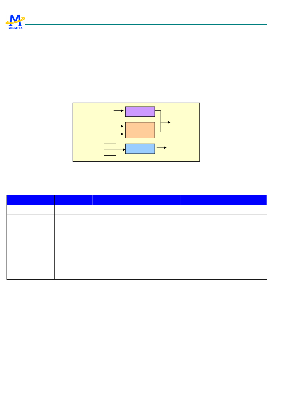
MTK Confidential Release for Konka
MTK Confidential Release for Konka
MT6228 GSM/GPRS Baseband Processor Data Sheet Revision 1.0
455/616
MediaTek Inc. Confidential
1: Machine enable
RSTB 0: low-level Reset, all configurations will be initialized.
1 : Not Reset.
6.16.2 Image Engine in MT6228
The Image Engine (IPP) plays the important role in MT6228 multimedia data path. It performs the necessary color space
conversion for next-stage needs. The path from Post-RESZ to IPP1 can also been applied the image effect. Fig.1 shows its
input/output data format and the relation with other multimedia module.
IPP1
IPP2
IPP3
IMGDMA
GIF_Dec
PNG_Dec
Drop RESZ
Memory
Post RESZ IMGDMA
Post RESZ
IPP1
IPP2
IPP3
IMGDMA
GIF_Dec
PNG_Dec
Drop RESZ
Memory
Post RESZ IMGDMA
Post RESZ
IPP1
IPP2
IPP3
IMGDMA
GIF_Dec
PNG_Dec
Drop RESZ
Memory
Post RESZ IMGDMA
Post RESZ
YUV
YUV
RGB
RGB
RGB
YUV
Fig. 1. Image Engine in MT6228.
The Graph mode setting depends on what kinds of data paths and image engines that we used. The Details are all listed in
Table 4.
Graph mode Used Engine Function Note
Preview IPP1 IPP1: Y2R, YUV/RGB image effect
Capture IPP1, IPP2 IPP1 : Y2R, YUV/RGB image effect
IPP2: Y2R
Thumbnail enable must be set if
using IPP2
MPEG IPP1 IPP1: Y2R, YUV/RGB image effect
IMGPROC IPP1, IPP3 IPP1: Y2R, YUV/RGB image effect
IPP3: R2Y
R2Y source (image_dma, gif, png
decorder) must be selected for IPP3
IMAGE Encode IPP2, IPP3 IPP2: Y2R
IPP3: R2Y
Thumbnail enable must be set if
using IPP2
Table 57. Graph mode of Image Engine.
6.16.3 Image effect application
The Image Engine is the hardware coprocessor that performs image effects on video stream or stand-alone image. It
provides the following effects:
1. Hue adjustment.
2. Saturation adjustment.
3. Contrast and intensity adjustment.
4. Grayscale and colorization.

MTK Confidential Release for Konka
MTK Confidential Release for Konka
MT6228 GSM/GPRS Baseband Processor Data Sheet Revision 1.0
456/616
MediaTek Inc. Confidential
5. Gamma correction.
6. Color adjustment.
7. Linear filtering.
8. Nonlinear filtering.
The format of the coefficients is listed in Table 58.
Function Parameter group Range (normalized factor) Format
Hue C11, C12, C21, C22 -64 ~ 64 (64) 2’s complement
Saturation SAT 0~127 (32) Unsigned
Contrast and brightness BRI1 0~255 Unsigned
BRI2 0~255 Unsigned
Contrast 0~255 (32) Unsigned
Colorize U, V -128~127 2’s complement
Gamma correction Offset 0~63 Unsigned
Slope 0~255 (16) Unsigned
Color adjustment Offset for red 0~31 Unsigned
Slope for red 0~63 (16) Unsigned
Offset for green 0~63 Unsigned
Slope for green 0~63 (16) Unsigned
Offset for blue 0~31 Unsigned
Slope for blue 0~63 (16) Unsigned
Mask C11, C12, C13, C21, C22,
C23, C31, C32, C33
-16~15 2’s complement
Dummy pixel 0~63 Unsigned
Table 58 Coefficients format table
6.16.3.1 Gamma correction and color adjustment
Gamma correction is a nonlinear technique. We use linear-approximation scheme for it and the same curve is applied
equally on red, green, and blue components.
Two approaches are provided. For the first one, the overall input value is equally divided into 8 segments. It’s suitable for
the case when gamma is greater than 1. For the second one, the value is divided into 6 unsymmetrical segments. It’s
suitable for the case when gamma is smaller then 1.
Color adjustment is used to adjust different colors with different curves. For each color, a 3 segment piece-wise linear curve
is applied. The user has to decide the offsets and the slopes of these 3 segments. The coefficients should be positive.
Cool tone and warm tone filters are both popular applications for color adjustment.

MTK Confidential Release for Konka
MTK Confidential Release for Konka
MT6228 GSM/GPRS Baseband Processor Data Sheet Revision 1.0
457/616
MediaTek Inc. Confidential
6.16.3.2 Filtering coefficients for linear filter
The filtering operation in Image Engine basically imposes artifacts on the original image and aims to produce a variety of
effects.
For low pass filter, the matrix can be defined as
numberpositveaisbwhere
b
bbb
b
b
H ,
11
11
2
1
2
2
⋅
+
=
⋅
=
111
111
111
9
1
1
H
,
⋅
=
111
121
111
10
1
2
H
, and
⋅
=
121
242
121
16
1
3
H
are all popular examples that could
present blur or softening effects. The concept can be extended to larger size matrix. For H
1
-like matrix, we provided 5x5
and 7x7 option, which we named blur and more blur effects. The matrices are as follows:
⋅
=
11111
11111
11111
11111
11111
25
1
55x
H
⋅
=
1111111
1111111
1111111
1111111
1111111
1111111
1111111
49
1
77 x
H
For high-pass filter, we illustrate some commonly used matrices.
−
−−
−
=
0 10
15 1
0 10
1
H
,
−−−
−−
−−−
=
111
19 1
111
2
H
,
−
−−
−
=
1 21
25 2
1 21
3
H
These filters present edge enhancement effects. They all have the property that the sum of their elements is unity in order to
avoid amplitude bias in the processed image. In Image Engine, the user can choose HP filtering option for them.

MTK Confidential Release for Konka
MTK Confidential Release for Konka
MT6228 GSM/GPRS Baseband Processor Data Sheet Revision 1.0
458/616
MediaTek Inc. Confidential
For matrix like
−
−−
−
⋅=
0 10
17 1
0 10
3
1
H
, a division-by-3 is required since the sum of its elements is not unity. For this
case, the user should program the register IMGPROC_SCALE and choose HP filtering with scale down option.
For matrix like
−−−
−−
−−−
=
111
18 1
111
H
, the sum of its elements is 0 and no division is required. The user can choose HP
filtering option for it.
6.16.3.3 Nonlinear filter
Median filter is a nonlinear technique that is useful for noise suppression in images. It consists of a 3-by-3 sliding window.
The center pixel in the window is replaced by the median of the pixels in the window.
The idea is further extended to maximum filter and minimum filter. The maximum filter presents dilation effects. It puts
more emphasis on the brighter point in the image. On the contrary, the minimum filter presents erosion effects.
6.16.4 Image process control
For filtering application, the software can initialize, start, and stop the operation of the Image Engine. Setting START bit in
the register IMGPROC_CON starts the operation, and setting STOP bit stops the operation. Notice that the user should not
restart the next process before the Image Engine returns from BUSY state. The user can check the status by monitoring
BUSY bit in the register IMGPROC_STS.
6.17 MPEG-4/H.263 Video CODEC
6.17.1 General Description
MPEG-4 is an emerging video coding standard defined in ISO/IEC 14496-2. It is designed to cover a wide range of
bit-rates (typically, 5 kbps to 10Mbps). MPEG-4 standard has become one of the enabling factors for mobile multimedia
communications. H.263 is another video coding standard that is developed by ITU-T/SG 15 for low-bit-rate applications
below 64kbps. H.263 profile 0 level 10 is the mandatory video decoder in 3GPP specification. Therefore, our goal is to
design a video codec suited to both MPEG-4 and H.263 standard.
There are two coding modes in MPEG-4 video compression: Intra-frame coding and Inter-frame coding. Intra-frame
coding refers to video coding techniques that achieve compression by exploiting the high spatial correlation between
neighboring pels within a video frame. Such techniques are also known as spatial redundancy reduction techniques or
still-image coding techniques. Inter-frame coding refers to video coding techniques that achieve compression by exploiting
the high temporal correlation between the frames of a video sequence. Such methods are also known as temporal
redundancy reduction techniques. Note that inter-frame coding may not be appropriate for some applications. For example,
it would be necessary to decode the complete inter-frame coded sequence before being able to randomly access individual
frames. Thus, a combined approach is normally used in which a number of frames are intra-frame coded (I-frames) at
specific intervals within the sequence and the other frames are inter-frame coded (Predicted or P-frames) with reference to
those key frames. Moreover, intra-frame coding is allowed in P-frames.

MTK Confidential Release for Konka
MTK Confidential Release for Konka
MT6228 GSM/GPRS Baseband Processor Data Sheet Revision 1.0
459/616
MediaTek Inc. Confidential
The ISO/IEC 14496 specification is intended to be generic in the sense that it serves a wide range of applications,
bit-rates, resolutions, qualities and services. A number of coding tools are defined in the specification. Considering the
practicality of implementing the full syntax of this specification, a limited number of subsets of the syntax are also
stipulated by means of “profile” and “level”. A “profile” is a defined subset of the entire bitstream syntax that is defined by
this specification. A “level” is a defined set of constraints imposed on parameters in the bitstream. Our application is
focused on handset devices. Due to restriction of limited resource, only simple profile is supported for most of handset
devices. According to 3GPP TS 26.234 specification, H.263 profile 0 level 10 is the mandatory video decoder. MPEG-4
visual simple profile level 0 is an optional video decoder. The MPEG-4/H.263 codec supports both MPEG-4 simple profile
and H.263 baseline profile. Generally, the file extension of MPEG-4 video file is .mp4. The file extension of 3GPP video
file is .3gp.
The design implements both decoder and encoder. The decoder block diagram is shown in Figure 34. The encoder
block diagram is shown in Figure 35
The decode specification is as follows:
1. Support ISO/IEC 14496-2 MPEG-4 simple profile @ level 0~3
2. Support H.263 profile 0 level 10 (baseline profile)
3. The following visual tools are supported
I-VOP
P-VOP
AC/DC Prediction
4-MV
Unrestricted MV
Error Resilience
Slice Resynchronization
Data Partitioning
Reversible VLC
Short Header Mode
Full and Half Pel accuracy
fcode can be 1~7
Maximum horizontal luminance pixel resolution can be up to 352
Maximum vertical luminance pixel resolution can be up to 288
Error Concealment
Single object
4. Deblocking filter

MTK Confidential Release for Konka
MTK Confidential Release for Konka
MT6228 GSM/GPRS Baseband Processor Data Sheet Revision 1.0
460/616
MediaTek Inc. Confidential
Source images are coded in blocks of pixels. Since correlation among spatially adjacent blocks is not taken into
account during coding, this results in block boundaries being visible when the decoded image is reconstructed.
The purpose of deblocking filter is to reduce blocking artifacts while keeping image edge intact. Blocking effect
can be reduced efficiently and image will be smooth after applying deblocking filter. A high quality deblocking
filter is embedded in the MPEG-4 Decoder. It performs both horizontal and vertical deblocking filtering
simultaneously while decoding. Memory access bandwidth is minimized in the design. Luminance as well as
chrominance data is filtered.
The encoder specification is as follows:
5. Support ISO/IEC 14496-2 MPEG-4 simple profile @ level 0, partially support MPEG-4 simple profile @ level 1
6. Support H.263 profile 0 level 10
7. The following visual tools are supported
I-VOP
P-VOP
DC Prediction
Unrestricted MV
Short Header Mode
Full and Half Pel motion estimation
Decision making logic
fcode can be 1~3
intra_dc_vlc_threshold shall be 0
Maximum horizontal luminance pixel resolution can be up to 352
Maximum vertical luminance pixel resolution can be up to 288
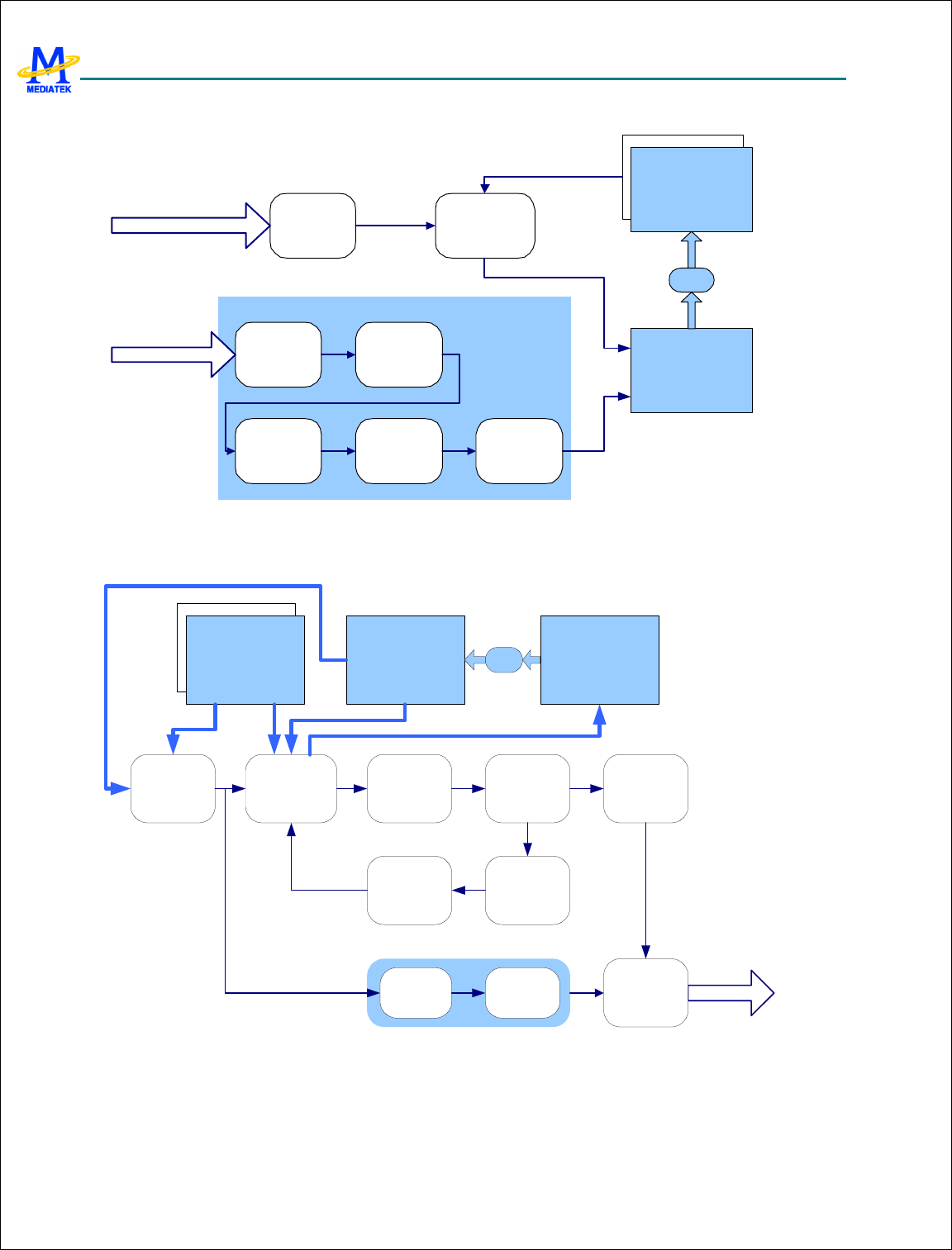
MTK Confidential Release for Konka
MTK Confidential Release for Konka
MT6228 GSM/GPRS Baseband Processor Data Sheet Revision 1.0
461/616
MediaTek Inc. Confidential
Motion
Coding
Motion
Compensation
Variable
Length
Decoding
Inverse
Quantization
Inverse DC &
AC Prediction
Inverse Scan
IDCT
Reference VOP
Reconstructed VOP
Delay
Coded bitstream (Motion)
Coded bitstream (Texture)
Texture Decoding
Figure 34 Block Diagram of Decoder
Delay
Coded bitstream
Reference VOP Reconstructed VOPCurrent VOP
Motion
Estimation Q
Variable
Length
Encoding
Bitstream
Packing
Motion
Compensation FDCT
IDCT IQ
Motion
Vector
Prediction
Variable
Length
Encoding
Figure 35 Block Diagram of Encoder

MTK Confidential Release for Konka
MTK Confidential Release for Konka
MT6228 GSM/GPRS Baseband Processor Data Sheet Revision 1.0
462/616
MediaTek Inc. Confidential
6.17.2 Register Definitions
6.17.2.1 Main Control
MP4+0000h Video CODEC Command Register MP4_CODEC_C
OMD
Bit 31 30 29 28 27 26 25 24 23 22 21 20 19 18 17 16
Name
- - - - - - - - - - - - - - - -
Type
Bit 15 14 13 12 11 10 9 8 7 6 5 4 3 2 1 0
Name
- - - - - - - - - - -
DEC_
STAR
T
ENC_
STAR
T
DEC_
RST
ENC_
RST
CORE
_RST
Type WO WO WO WO WO
This register is the main command register for video CODEC.
CORE_RST Software reset control. Writing 1 to this bit will reset the hardware core excluding APB control register
set of decoder and encoder.
ENC_RST Software reset control. Writing 1 to this bit will reset the APB control register set of encoder. Note that this bit
won’t reset the hardware core.
DEC_RST Software reset control. Writing 1 to this bit will reset the APB control register set of decoder. Note that this bit
won’t reset the hardware core.
ENC_START Start the encode operation if writing 1 to this bit. The encode operation will start only when no decode
operation is running; otherwise the encode operation will queue until decode operation is done.
DEC_START Start the decode operation if writing 1 to this bit. The decode operation will start only when no encode
operation is running; otherwise the decode operation will queue until encode operation is done.
MP4+0004h VLC DMA Command Register MP4_VLC_DMA
_COMD
Bit
31 30 29 28 27 26 25 24 23 22 21 20 19 18 17 16
Name
- - - - - - - - - - - - - - - -
Type
Bit 15 14 13 12 11 10 9 8 7 6 5 4 3 2 1 0
Name
- - - - - - - - - - - - - - RESU
ME STOP
Type WO WO
This register is the main control of VLC DMA.
STOP Stop the VLC DMA. Stop VLC DMA activities through SW rather than HW state machine.
RESUME Resume the VLC DMA access. VLC DMA state machine will go to a pending state if the maximum allowed
write count to target memory is reached and then an interrupt has occured. After re-allocating the target address,
SW writes RESUME to unfreeze the encoding process.

MTK Confidential Release for Konka
MTK Confidential Release for Konka
MT6228 GSM/GPRS Baseband Processor Data Sheet Revision 1.0
463/616
MediaTek Inc. Confidential
6.17.2.2 Encoder
6.17.2.2.1 Control
MP4+0100h Encoder Configuration Register MP4_ENC_COD
EC_CONF
Bit 31 30 29 28 27 26 25 24 23 22 21 20 19 18 17 16
Name
- - - - - - - - - - - - - - - CHEC
K_TV
Type
Reset
0 0 0 0 0 0 0 0 0 0 0 0 0 0 0 0
Bit 15 14 13 12 11 10 9 8 7 6 5 4 3 2 1 0
Name
- - -
MC_B
URST
_EN
PMV
DQUA
N FME
HALF
STEP_LIMIT VPGO
B DCT
IRQ
ENC
Type R/W R/W R/W R/W R/W R/W R/W R/W R/W R/W R/W R/W R/W R/W
Reset
0 0 0 0 0 0 0 0 0 0 0 0 0 0 0 0
This register is used to configure the operating conditions and modes of video CODEC.
ENC Video CODEC Operation Mode
0 Decode Mode
1 Encode Mode
IRQ Control for interrupt request
0 Disable the interrupt reporting mechanism
1 Enable the interrupt reporting mechanism
DCT DCT Control
0 Enable JPEG CODEC Operation
1 Enable MPEG-4 Video CODEC Operation
VPGOB Control for decoding Video Packet Header; keep this for legacy reason.
0 Disable: decoding in Video Packet Level. It means the software will take the responsibility for decoding
packet header of each video packet.
1 Enable: decoding in Video Object Plane Level
STEP_LIMIT Step limit for Motion Estimation. The total number of steps in a n-step search is STEP_LIMIT+2.
Increasing STEP_LIMIT can increase search range of motion vectors.
HALF Motion Estimation uses half-pel resolution
0 Disable. Perform full pel motion estimation only
1 Enable. Perform full pel motion estimation first, then half pel motion estimation
FME Fast Motion Enhancement
0 Enable Four Step Search motion estimation algorithm
1 Enable Mediatek proprietary motion estimation algorithm. This algorithm can improve visual quality in fast
motion pictures while maintaining the same quality as Four Step Search in slow motion pictures. Enabling this
algorithm does not increase search time. Thus, set FME to 1 is recommended.
DQUAN Control for automatic update quantizer_scale process; keep this for legacy reason.
0 Disable
1 Enable
PMV Predictive Motion Vector Search. This is a two pass search algorithm. This algorithm can co-operate with both four
step search (FME=0) and Mediatek proprietary search (FME=1). The idea is to initially consider several highly

MTK Confidential Release for Konka
MTK Confidential Release for Konka
MT6228 GSM/GPRS Baseband Processor Data Sheet Revision 1.0
464/616
MediaTek Inc. Confidential
likely predictors (starting points), perform motion estimation from these predictors, and choose the best result
among these predictors. In our approach, the two predictors approach is adopted. The origin (0,0) is considered as
the predictor of first pass. The minimum BDM point found in first pass will be the predictor of the second pass.
After finishing two-pass motion estimation, choose the best result between the two minimum BDM points. This
algorithm can significantly improve PSNR by about 0.8dB. However, the search time will increase by about 60%.
Setting PMV to 1 or 0 is the trade-off between visual quality and search time.
0 Disable
1 EnableMC_BURST_EN 2-beat Burst mode enable signal in MC.
0 Diable
1 Enable
CHECK_TV Enable signal to check if TV codec is busy before starting encoding operation.
0 Do not check TV codec
1 Check TV codec
MP4+0104h Encoder Status Register MP4_ENC_STS
Bit
31 30 29 28 27 26 25 24 23 22 21 20 19 18 17 16
Name
STATE
Type RO RO RO RO RO RO RO RO RO RO RO RO RO RO RO RO
Bit 15 14 13 12 11 10 9 8 7 6 5 4 3 2 1 0
Name
STATE
Type RO RO RO RO RO RO RO RO RO RO RO RO RO RO RO RO
This register provides the state information of encoding sequencer for software program. It is a mirror of the HW one-hot
sequencer state machine and can be used for debugging or IRQ status judging.
MP4+0108h Encoder Interrupt Mask Register MP4_ENC_IRQ_
MASK
Bit
31 30 29 28 27 26 25 24 23 22 21 20 19 18 17 16
Name
- - - - - - - - - - - - - - - -
Type
Reset
Bit 15 14 13 12 11 10 9 8 7 6 5 4 3 2 1 0
Name
- - - - - - - - - - - - DMA PACK
BLOC
K_DO
NE
ENC_
DONE
Type
R/W
R/W
R/W
R/W
Reset
1 1 1 1
This register contains mask bit for each interrupt source in MPEG-4 Video encoder. It allows each interrupt source to be
disabled or masked out separately under software control. After System Reset or software reset, all bit values will be set to
‘0’ to indicate that interrupt requests are enabled.
DMA Mask of VLE DMA Limit interrupt.
PACK Mask of video packet bit count expire interrupt.
BLOCK_DONE Mask of block procedure complete interrupt.
ENC_DONE Mask of encode complete interrupt.

MTK Confidential Release for Konka
MTK Confidential Release for Konka
MT6228 GSM/GPRS Baseband Processor Data Sheet Revision 1.0
465/616
MediaTek Inc. Confidential
MP4+010Ch Encoder Interrupt Status Register MP4_ENC_IRQ_
STS
Bit 31 30 29 28 27 26 25 24 23 22 21 20 19 18 17 16
Name
- - - - - - - - - - - - - - - -
Type
Bit
15 14 13 12 11 10 9 8 7 6 5 4 3 2 1 0
Name
- - - - - - - - - - - - DMA PACK
BLOC
K_DO
NE
ENC_
DONE
Type RO RO RO RO
This register allows software program to poll which interrupt source generates the interrupt request. A bit set to ‘1’ indicates
a corresponding active interrupt source. Note that IRQ control bit in MP4_ENC_CODEC_CONF should be enabled first
in order to activate the interrupt reporting mechanism.
DMA Mask of VLC DMA interrupt. When decoder detects empty VLD stream buffer, an interrupt will inform the
driver SW to refill the VLD stream buffer.
PACK Video Packet Bit Count Exceed interrupt. If a video packet size is larger than defined the interrupt will happen.
BLOCK_DONE Block decode or encode complete. A normal complete flag if the SW needs a block-based HW decoding
or encoding.
ENC_DONE Encode complete. A normal condition when encoding procedure is done.
MP4+0110h Encoder Interrupt Acknowledge Register MP4_ENC_IRQ_
ACK
Bit 31 30 29 28 27 26 25 24 23 22 21 20 19 18 17 16
Name
- - - - - - - - - - - - - - - -
Type
Bit 15 14 13 12 11 10 9 8 7 6 5 4 3 2 1 0
Name
- - - - - - - - - - - - DMA
PACK
BLOC
K_DO
NE
ENC_
DONE
Type WC WC WC WC
This register provides a mean for software program to acknowledge the interrupt source. Writing a ‘1’ to the specific bit
position will result in an acknowledgement to the corresponding interrupt source and clear the corresponding bit in
MP4_ENC_IRQ_STS.
ENC_DONE Encode Task Complete
BLOCK_DONE Block Task Complete
PACK Video Packet Bit Count Expired
DMA VLC DMA Buffer Limit Reached
MP4+0114h Encoder Configuration Register MP4_ENC_CON
F
Bit 31 30 29 28 27 26 25 24 23 22 21 20 19 18 17 16
Name
- - - - - PACKCNT PACK
Type R/W R/W R/W R/W R/W R/W R/W R/W R/W R/W R/W
Reset
0 0 0 0 0 0 0 0 0 0 0

MTK Confidential Release for Konka
MTK Confidential Release for Konka
MT6228 GSM/GPRS Baseband Processor Data Sheet Revision 1.0
466/616
MediaTek Inc. Confidential
Bit
15 14 13 12 11 10 9 8 7 6 5 4 3 2 1 0
Name
- - INTRA - - SKIP
Type R/W R/W R/W R/W R/W R/W R/W R/W R/W R/W R/W R/W R/W R/W
Reset
0 0 0 0 0 0 0 0 0 0 0 0 0 0
This register is used specially to configure the desired encode conditions and modes for video CODEC.
SKIP Threshold for deciding not_coded bit. The value of SKIP is programmed by software first. The first round of
pattern code (me_pattern_code is set to 6’h0 whenever (SAD
y
+ SDA
u
+ SAD
v
) <= skip_threshold*16
not_coded bit will be set if pattern_code = 6’h0 and motion vector = (0,0)
INTRA Threshold for deciding INTRA Coding in P frame. The value of INTRA is programmed by software first. The
3-bits macro-block type (mb_type) is set to 3’h0 (Inter MB) if SADy < intra_threshold*1024. Otherwise, mb_type
is set to 3’h3 (Intra_MB)
PACK Use Video Packet Mode
0 Disable
1 Enable
PACKCNT Desired Bit Counts for a Video Packet. Used in encode mode to define the largest VLE buffer size of a video
packet
6.17.2.2.2 Base Addresses
MP4+0124h Encoder Current VOP Base Address Register MP4_ENC_VOP
_ADDR
Bit 31 30 29 28 27 26 25 24 23 22 21 20 19 18 17 16
Name
VOP
Type RO RO RO RO RO RO RO RO RO RO RO RO RO RO R/W R/W
Bit 15 14 13 12 11 10 9 8 7 6 5 4 3 2 1 0
Name
VOP - -
Type R/W R/W R/W R/W R/W R/W R/W R/W R/W R/W R/W R/W R/W R/W
This register describes the starting address of Current VOP Frame that is going to be encoded. Note that this base address
should be 4-byte aligned. And the required frame buffer size should be: numbers of pixel per frame * 1.5 bytes (YUV420
format).
VOP Current VOP Base Address.
MP4+0128h Encoder Reference VOP Base Address Register MP4_ENC_REF_
ADDR
Bit 31 30 29 28 27 26 25 24 23 22 21 20 19 18 17 16
Name
REF
Type RO RO RO RO RO RO RO RO RO RO RO RO RO RO R/W R/W
Bit 15 14 13 12 11 10 9 8 7 6 5 4 3 2 1 0
Name
REF - -
Type R/W R/W R/W R/W R/W R/W R/W R/W R/W R/W R/W R/W R/W R/W
This register describes the starting address of Reference VOP Frame. Note that this base address should be 4-byte aligned.
And the required frame buffer size should be: numbers of pixel per frame * 1.5 bytes (YUV420 format).
REF Reference VOP Base Address.

MTK Confidential Release for Konka
MTK Confidential Release for Konka
MT6228 GSM/GPRS Baseband Processor Data Sheet Revision 1.0
467/616
MediaTek Inc. Confidential
MP4+012Ch Encoder Reconstructed VOP Base Address Register MP4_ENC_REC
_ADDR
Bit 31 30 29 28 27 26 25 24 23 22 21 20 19 18 17 16
Name
REC
Type RO RO RO RO RO RO RO RO RO RO RO RO RO RO R/W R/W
Bit
15 14 13 12 11 10 9 8 7 6 5 4 3 2 1 0
Name
REC - -
Type R/W R/W R/W R/W R/W R/W R/W R/W R/W R/W R/W R/W R/W R/W
This register describes the starting address of Reconstructed VOP Frame. Note that this base address should be 4-byte
aligned. And the required frame buffer size should be: numbers of pixel per frame * 1.5 bytes (YUV420 format).
REC Reconstructed VOP Base Address. The high boundary address of Reconstructed VOP should not cross 1M address
boundary because the implementation of address offset counter is 20 bits. i.e. please make sure (the lower 20bits
Reconstructed base address + size of Reconstructed frame) < 2
20
MP4+0130h VLE Data Load-Store LSB Base Address Register
MP4_ENC_DAT
A_STORE_ADD
R
Bit 31 30 29 28 27 26 25 24 23 22 21 20 19 18 17 16
Name
STORE
Type R/W R/W
Bit 15 14 13 12 11 10 9 8 7 6 5 4 3 2 1 0
Name
STORE - -
Type
R/W
R/W
R/W
R/W
R/W
R/W
R/W
R/W
R/W
R/W
R/W
R/W
R/W
R/W
This register describes the LSB address of VLE Data Load-Store buffer in data-partitioned mode. Note that this base
address should be 4-byte aligned. And the required buffer size for encoder and decoder should be: 3K bytes and number of
macroblock per frame * 32 bytes, respectively.
STORE LSB address of VLE Data Load-Store buffer
MP4+0134h DC/AC Prediction Storage LSB Base Address Register MP4_ENC_DAC
P_ADDR
Bit 31 30 29 28 27 26 25 24 23 22 21 20 19 18 17 16
Name
DACP
Type R/W R/W
Bit
15 14 13 12 11 10 9 8 7 6 5 4 3 2 1 0
Name
DACP - -
Type R/W R/W R/W R/W R/W R/W R/W R/W R/W R/W R/W R/W R/W R/W
This register describes the LSB address of DC/AC Prediction Storage buffer. Note that this base address should be 4-byte
aligned. And the required buffer size for encoder and decoder should be: 1K bytes and 4K bytes, respectively.
DACP LSB address of DC/AC Prediction Storage buffer
MP4+0138h Motion Vector Storage LSB Base Address Register MP4_ENC_MVP
_ADDR
Bit 31 30 29 28 27 26 25 24 23 22 21 20 19 18 17 16
Name
MVP_ADDR

MTK Confidential Release for Konka
MTK Confidential Release for Konka
MT6228 GSM/GPRS Baseband Processor Data Sheet Revision 1.0
468/616
MediaTek Inc. Confidential
Type
R/W
R/W
Bit 15 14 13 12 11 10 9 8 7 6 5 4 3 2 1 0
Name
MVP_ADDR - -
Type R/W R/W R/W R/W R/W R/W R/W R/W R/W R/W R/W R/W R/W R/W
This register describes the LSB address of Motion Vector Storage buffer. Note that this base address should be 4-byte
aligned. And the required buffer size for encoder should be mb_x_limit * 2 * 4 bytes, which equals to 320 Bytes for VGA
size.
MVP_ADDR LSB address of Motion Vector Storage buffer
6.17.2.2.3 Data Structure
MP4+0140h Encoder VOP Structure 0 Register MP4_ENC_VOP
_STRUCT0
Bit 31 30 29 28 27 26 25 24 23 22 21 20 19 18 17 16
Name
- - - - - - - - - - - - - - ROUN
D
Type R/W
Bit
15 14 13 12 11 10 9 8 7 6 5 4 3 2 1 0
Name
VLCTHR QUANT FCODE SHOR
T - RVLC
DATA
TYPE
Type R/W R/W R/W R/W R/W R/W R/W R/W R/W R/W R/W R/W R/W R/W R/W R/W
This register is used to describe the header information of a certain Video Object Plane that is going to be processed by
video CODEC.
TYPE vop_coding_type definition, for both decode and encode.
0 This is a P-VOP frame (inter frame)
1 This is an I-VOP frame (intra frame)
DATA data_partitioned, for decode only; keep this for legacy reason.
0 Data stream is in non-data-partitioned mode
1 Data stream is in data-partitioned mode
RVLC resversible_vlc, for decode only; keep this for legacy reason.
0 Data stream contains no reversible VLC information
1 Data stream uses reversible VLC tables.
SHORT short_video_header; for both decode and encode
0 Normal MPEG-4 format
1 H.263 Compatible format
FCODE fcode size setting for both decode and encode, ranges from 0 to 7.
QUANT vop_quant. For both decode and encode. Quantizer scale of the current frame. For variable Q in decode mode,
QUANT is an initial setting of the current frame.
VLCTHR intra_dc_vlc_thr. For decode only. According to VLCTHR, the decoder has to switch from intra DC mode to
inter DC mode when the quantizer_scale is larger than a pre-defined value. VLCTHR ranges from 0 to 7.
ROUND Rounding type of half-pel motion compensation. ROUND==1 means truncation toward zero (the pixel value
is always larger than 0); ROUND==0 means rounding-off addition.
MTK Confidential Release for Konka
MTK Confidential Release for Konka
MT6228 GSM/GPRS Baseband Processor Data Sheet Revision 1.0
469/616
MediaTek Inc. Confidential
MP4+0144h Encoder VOP Structure 1 Register MP4_ENC_VOP
_STRUCT1
Bit 31 30 29 28 27 26 25 24 23 22 21 20 19 18 17 16
Name
- - - HECBIT - - - - MBLENGTH
Type R/W R/W R/W R/W R/W R/W R/W R/W R/W
Bit
15 14 13 12 11 10 9 8 7 6 5 4 3 2 1 0
Name
- - - YLIMIT - - - XLIMIT
Type R/W R/W R/W R/W R/W R/W R/W R/W R/W R/W R/W R/W R/W R/W R/W R/W
This register is used by software program to control the start position and count limit of macroblock for a certain Video
Packet or Video Object Plane that is going to be processed by video CODEC.
XLIMIT Macroblock count in X direction of a frame.
YLIMIT Macroblock count in Y direction of a frame.
MBLENGTH Bit count of Macroblock Number in Video Packet Header. It is a value defined by the following formula:
MBCNT = (XLIMIT+15)/16 * (YLIMIT+15)/16. For larger MBCNT, we have larger MBLENGTH.
MBLENGTH is ranged from 1 to 14.
HECBIT Bit count of extension header code in Video Packet Header
MP4+0148h Encoder VOP Structure 2 Register MP4_ENC_VOP
_STRUCT2
Bit 31 30 29 28 27 26 25 24 23 22 21 20 19 18 17 16
Name
- - - - - - - MBNO
Type R/W R/W R/W R/W R/W R/W R/W R/W R/W
Bit
15 14 13 12 11 10 9 8 7 6 5 4 3 2 1 0
Name
- - - VP_YPOS - - - VP_XPOS
Type R/W R/W R/W R/W R/W R/W R/W R/W R/W R/W
This register is used by software program to control the start position and count limit of macroblock for a certain Video
Packet or Video Object Plane that is going to be processed by video CODEC.
VP_XPOS Starting position of the current Video Packet in X coordinate.
VP_YPOS Starting position of the current Video Packet in Y coordinate.
MBNO Macroblock count limit for a video packet or frame. For a CIF frame the value will be 396.
MP4+014Ch VOP Structure 3 Register MP4_VOP_STR
UCT3
Bit 31 30 29 28 27 26 25 24 23 22 21 20 19 18 17 16
Name
- - - - - - - MBNO
Type RO RO RO RO RO RO RO RO RO
Bit 15 14 13 12 11 10 9 8 7 6 5 4 3 2 1 0
Name
- - - YPOS - - - XPOS
Type RO RO RO RO RO RO RO RO RO RO
This register provides the position and count information of a certain macroblock that is currently under process of video
CODEC.
XPOS Current Macroblock Position in X coordinate
YPOS Current Macroblock Position in Y coordinate
MBNO Current Macroblock Count
MTK Confidential Release for Konka
MTK Confidential Release for Konka
MT6228 GSM/GPRS Baseband Processor Data Sheet Revision 1.0
470/616
MediaTek Inc. Confidential
MP4+0150h MB Structure 0 Register MP4_ENC_MB_
STRUCT0
Bit 31 30 29 28 27 26 25 24 23 22 21 20 19 18 17 16
Name
- - - - - - - - - - - - - QUANTIZER
Type R/W R/W R/W
Bit
15 14 13 12 11 10 9 8 7 6 5 4 3 2 1 0
Name
QUANTIZER DCVL
C AC DQUANT PATTERN TYPE CODE
D
Type R/W R/W R/W R/W R/W R/W R/W R/W R/W R/W R/W R/W R/W R/W R/W R/W
This register is used to store the header information of current macroblock. This register is mostly used for debugging. Also
used to provide hardware certain header information if all header parsing is done by software instead of hardware.
CODED not_coded flag of current macroblock; not_coded can be decoded by hardware from macroblock header.
TYPE mb_coding_type of current macroblock; mb_coding_type can be decoded by hardware from mcbpc in
macroblck header.
PATTERN pattern_code of current macroblock; pattern_code can be decoded by hardware from cbpc and cbpy in
macroblock header.
DQUANT dquant. It can be –2, -1, +1 or +2; total 4 possible choices using 2 bits to represent; dquant can be decoded by
hardware from macroblock header.
AC ac_pred_flag. It decides whether AC prediction is needed; always 0 in encoder; ac_pred_flag can be decoded
by hardware from macroblock header.
DCVLC use_intra_dc_vlc. If this bit is 0, intra AC VLC decode is used (no intra DC exists in current macroblock).
QUANTIZER quantizer_scale, ranged from 1 to 31. It can be variable if we have dquant values.
6.17.2.2.4 VLC DMA
MP4+0160h Encoder VLC DMA Base Address Register MP4_ENC_VLC_
BASE_ADDR
Bit 31 30 29 28 27 26 25 24 23 22 21 20 19 18 17 16
Name
BASE
Type R/W R/W R/W R/W R/W R/W R/W R/W R/W R/W R/W R/W R/W R/W R/W R/W
Bit 15 14 13 12 11 10 9 8 7 6 5 4 3 2 1 0
Name
BASE - -
Type
R/W
R/W
R/W
R/W
R/W
R/W
R/W
R/W
R/W
R/W
R/W
R/W
R/W
R/W
This register is used to describe the address of started Code Word for each VLC DMA buffer. Note that this base address
should be 4-byte aligned.
BASE VLC DMA Base Address
MP4+0164h Encoder VLC DMA Base Bit Count Register MP4_ENC_VLC_
BASE_BITCNT
Bit 31 30 29 28 27 26 25 24 23 22 21 20 19 18 17 16
Name
- - - - - - - - - - - - - - - -
Type
Bit 15 14 13 12 11 10 9 8 7 6 5 4 3 2 1 0
MTK Confidential Release for Konka
MTK Confidential Release for Konka
MT6228 GSM/GPRS Baseband Processor Data Sheet Revision 1.0
471/616
MediaTek Inc. Confidential
Name
- - - - - - - - - - - BIT
Type R/W R/W R/W R/W R/W
This register is used to describe the starting bit position of the 1
st
Code Word in the 1
st
VLC DMA buffer. For the following
VLC DMA buffers, it is assumed that they are all 4-byte aligned and always start from bit position “0”.
BIT Start of Bit at the 1
st
Code Word of 1
st
DMA Buffer
MP4+0168h Encoder VLC DMA Buffer Limit Register MP4_ENC_VLC_
LIMIT
Bit 31 30 29 28 27 26 25 24 23 22 21 20 19 18 17 16
Name
- - - - - - - - - - - - - - - -
Type
Reset
0 0 0 0 0 0 0 0 0 0 0 0 0 0 0 0
Bit 15 14 13 12 11 10 9 8 7 6 5 4 3 2 1 0
Name
LIMIT
Type R/W R/W R/W R/W R/W R/W R/W R/W R/W R/W R/W R/W R/W R/W R/W R/W
Reset
1 1 1 1 1 1 1 1 1 1 1 1 1 1 1 1
This register is used to describe the buffer size of each VLC DMA buffer. Note that the value is counted in word (32-bit).
Whenever the limit is reached and the corresponding interrupt control is enabled, an interrupt request will be generated.
LIMIT DMA Buffer Size, Count in Word (32-bit)
MP4+016Ch Encoder VLC DMA Current Word Register MP4_ENC_VLC_
WORD
Bit
31 30 29 28 27 26 25 24 23 22 21 20 19 18 17 16
Name
ADDR
Type RO RO RO RO RO RO RO RO RO RO RO RO RO RO RO RO
Bit 15 14 13 12 11 10 9 8 7 6 5 4 3 2 1 0
Name
ADDR
Type RO RO RO RO RO RO RO RO RO RO RO RO RO RO RO RO
This register provides the address information of a certain code word that is under process of video CODEC. SW reads it
back after encode of a frame is done.
ADDR VLC DMA current Address
MP4+0170h Encoder VLC DMA Current Bit Count Register MP4_ENC_VLC_
BITCNT
Bit 31 30 29 28 27 26 25 24 23 22 21 20 19 18 17 16
Name
- - - - - - - - - - - - - - - -
Type
Bit 15 14 13 12 11 10 9 8 7 6 5 4 3 2 1 0
Name
- - - - - - - - - - - BITCNT
Type RO RO RO RO RO
This register provides the bit position information of a certain Code Word that is under process of video CODEC.
BITCNT Current Bit Count
MTK Confidential Release for Konka
MTK Confidential Release for Konka
MT6228 GSM/GPRS Baseband Processor Data Sheet Revision 1.0
472/616
MediaTek Inc. Confidential
MP4+0174h Encoder VLC DMA Ring Buffer Ending Address
Register
MP4_ENC_VLC_
JUMP_FROM_A
DDR
Bit 31 30 29 28 27 26 25 24 23 22 21 20 19 18 17 16
Name
JUMP_FROM_ADDR
Type
R/W
R/W
R/W
R/W
R/W
R/W
R/W
R/W
R/W
R/W
R/W
R/W
R/W
R/W
R/W
R/W
Reset
1 1 1 1 1 1 1 1 1 1 1 1 1 1 1 1
Bit 15 14 13 12 11 10 9 8 7 6 5 4 3 2 1 0
Name
JUMP_FROM_ADDR
Type R/W R/W R/W R/W R/W R/W R/W R/W R/W R/W R/W R/W R/W R/W R/W R/W
Reset
1 1 1 1 1 1 1 1 1 1 1 1 1 1 1 1
JUMP_FROM_ADDR The ending address of the current DMA buffer; when a jump takes place in VLC DMA
address counter, the address will jump from the ending address of the current DMA buffer, which is
JUMP_FROM_ADDR, to the starting address of the next DMA buffer, which is JUMP_TO_ADDR.
To disable the ring buffer feature, set this register to all ones; note that the address counter will not
jump until done with the content in memory with address as JUMP_FROM_ADDR. So the memory
content with address JUMP_FROM_ADDR will be executed by hardware.
MP4+0178h Encoder VLC DMA Ring Buffer Starting Address
Register
MP4_ENC_VLC_
JUMP_TO_ADD
R
Bit 31 30 29 28 27 26 25 24 23 22 21 20 19 18 17 16
Name
JUMP_TO_ADDR
Type R/W R/W R/W R/W R/W R/W R/W R/W R/W R/W R/W R/W R/W R/W R/W R/W
Reset
1 1 1 1 1 1 1 1 1 1 1 1 1 1 1 1
Bit 15 14 13 12 11 10 9 8 7 6 5 4 3 2 1 0
Name
JUMP_TO_ADDR
Type R/W R/W R/W R/W R/W R/W R/W R/W R/W R/W R/W R/W R/W R/W R/W R/W
Reset
1 1 1 1 1 1 1 1 1 1 1 1 1 1 1 1
JUMP_TO_ADDR The starting address of the next DMA buffer; when a jump takes place in VLC DMA address
counter, the address will jump from the ending address of the current DMA buffer, which is JUMP_FROM_ADDR, to the
starting address of the next DMA buffer, which is JUMP_TO_ADDR; note that the address counter will not jump until done
with the content in memory with address as JUMP_FROM_ADDR. So the memory content with address
JUMP_FROM_ADDR will be executed by hardware.
6.17.2.2.5 Resync Marker
MP4+0180h MPEG4 Encoder Resync Marker Configuration 0
Register
MP4_ENC_RES
YNC_CONF0
Bit 31 30 29 28 27 26 25 24 23 22 21 20 19 18 17 16
Name
EN MODE
PERIOD_BITS
Type R/W R/W R/W R/W R/W R/W R/W R/W R/W R/W R/W R/W R/W R/W R/W R/W
Reset
0 0 1 1 1 1 1 1 1 1 1 1 1 1 1 1
Bit
15 14 13 12 11 10 9 8 7 6 5 4 3 2 1 0
MTK Confidential Release for Konka
MTK Confidential Release for Konka
MT6228 GSM/GPRS Baseband Processor Data Sheet Revision 1.0
473/616
MediaTek Inc. Confidential
Name
PERIOD_BITS
Type R/W R/W R/W R/W R/W R/W R/W R/W R/W R/W R/W R/W R/W R/W R/W R/W
Reset
1 1 1 1 1 1 1 1 1 1 1 1 1 1 1 1
EN Resync marker insertion enable
0 Disable resync marker insertion
1 Enable resync marker insertion
MODE Resync Marker insertion mode selection
0 resync marker is inserted based on number of bits
1 resync marker is inserted based on number of macroblocks
PERIOD_BITS Period in number of bits to insert resync marker; only effective when MODE is set to 0; hardware will
insert resync marker at the next macroblock boundary once the bit length of a video packet exceeds this value.
MP4+0184h MPEG4 Encoder Resync Marker Configuration 1
Register
MP4_ENC_RES
YNC_CONF1
Bit 31 30 29 28 27 26 25 24 23 22 21 20 19 18 17 16
Name
- - - - - - - - - - - - - - - HEC
Type R/W R/W R/W R/W R/W R/W R/W R/W R/W R/W R/W R/W R/W R/W R/W R/W
Reset
0 0 0 0 0 0 0 0 0 0 0 0 0 0 0 0
Bit 15 14 13 12 11 10 9 8 7 6 5 4 3 2 1 0
Name
PERIOD_MB
Type R/W R/W R/W R/W R/W R/W R/W R/W R/W R/W R/W R/W R/W R/W R/W R/W
Reset
1 1 1 1 1 1 1 1 1 1 1 1 1 1 1 1
HEC Header Extension Code; indicates the value of header_extension_code in MPEG4 standard (ISO/IEC 14496-2)
0 header_extension_code is 0.
1 header_extension_code is 1.
PERIOD_MB Period in number of macroblocks (MB) to insert resync marker; only effective when MODE is set to 1;
hardware will insert resync marker at the next macroblock boundary once the number of macroblock in current
video packet exceeds this value.
MP4+0188h MPEG4 Encoder Local Time Base Register MP4_ENC_TIME
_BASE
Bit 31 30 29 28 27 26 25 24 23 22 21 20 19 18 17 16
Name
- - - - - - - MODULO_TIME_BASE BW
Type R/W R/W R/W R/W R/W R/W R/W R/W R/W R/W R/W R/W R/W R/W R/W R/W
Reset
0 0 0 0 0 0 0 0 0 0 0 0 0 0 0 0
Bit
15 14 13 12 11 10 9 8 7 6 5 4 3 2 1 0
Name
VOP_TIME_INCREMENT
Type R/W R/W R/W R/W R/W R/W R/W R/W R/W R/W R/W R/W R/W R/W R/W R/W
Reset
0 0 0 0 0 0 0 0 0 0 0 0 0 0 0 0
MODULO_TIME_BASE Represent the value of modulo_time_base; value ranges from 0 to 31.
BW Bit width of vop_time_increment. The real bit-width of vop_time_increment is (BW + 1), ranging from 1 to 16.
VOP_TIME_INCREMENT Carries the value of vop_time_increment defined in MPEG4 standard (ISO/IEC 14496-2); the
meaningful bit width of vop_time_increment is signaled by BW field.

MTK Confidential Release for Konka
MTK Confidential Release for Konka
MT6228 GSM/GPRS Baseband Processor Data Sheet Revision 1.0
474/616
MediaTek Inc. Confidential
6.17.2.3 Decoder
MP4+0200h Decoder Configuration Register MP4_DEC_COD
EC_CONF
Bit 31 30 29 28 27 26 25 24 23 22 21 20 19 18 17 16
Name
- - - - - - - - - - - - - - - CHEC
K_TV
Type R/W
Reset
0 0 0 0 0 0 0 0 0 0 0 0 0 0 0 0
Bit 15 14 13 12 11 10 9 8 7 6 5 4 3 2 1 0
Name
DEBL
OCK
COPY
_REC -
MC_B
URST
_EN
PMV DQUA
N FME HALF STEP_LIMIT VPGO
B DCT IRQ ENC
Type R/W R/W R/W R/W R/W R/W R/W R/W R/W R/W R/W R/W R/W R/W R/W R/W
Reset
0 0 0 0 0 0 0 0 0 0 0 0 0 0 0 0
This register is used to configure the operating conditions and modes of video CODEC.
ENC Video CODEC Operation Mode
0 Decode Mode
1 Encode Mode
IRQ Control for interrupt request
0 Disable the interrupt reporting mechanism
1 Enable the interrupt reporting mechanism
DCT DCT Control
0 Enable JPEG CODEC Operation
1 Enable MPEG-4 Video CODEC Operation
VPGOB Control for decoding Video Packet Header; keep this for legacy reason.
0 Disable: decoding in Video Packet Level. It means the software will take the responsibility for decoding
packet header of each video packet.
1 Enable: decoding in Video Object Plane Level
STEP_LIMIT Step limit for Motion Estimation, for encode only; keep this for legacy reason. The total number of steps
in a n-step search is STEP_LIMIT+2. Increasing STEP_LIMIT can increase search range of motion vectors.
HALF Motion Estimation uses half-pel resolution, for encode only; keep this for legacy reason.
0 Disable. Perform full pel motion estimation only
1 Enable. Perform full pel motion estimation first, then half pel motion estimation
FME Fast Motion Enhancement, for encode only; keep this for legacy reason.
0 Enable Four Step Search motion estimation algorithm
1 Enable Mediatek proprietary motion estimation algorithm. This algorithm can improve visual quality in fast
motion pictures while maintaining the same quality as Four Step Search in slow motion pictures. Enabling this
algorithm does not increase search time. Thus, set FME to 1 is recommended.
DQUAN Control for automatic update quantizer_scale process.
0 Disable
1 Enable
PMV Predictive Motion Vector Search, for encode only; keep this for legacy reason. This is a two pass search algorithm.
This algorithm can co-operate with both four step search (FME=0) and Mediatek proprietary search (FME=1). The
idea is to initially consider several highly likely predictors (starting points), perform motion estimation from these
MTK Confidential Release for Konka
MTK Confidential Release for Konka
MT6228 GSM/GPRS Baseband Processor Data Sheet Revision 1.0
475/616
MediaTek Inc. Confidential
predictors, and choose the best result among these predictors. In our approach, the two predictors approach is
adopted. The origin (0,0) is considered as the predictor of first pass. The minimum BDM point found in first pass
will be the predictor of the second pass. After finishing two-pass motion estimation, choose the best result between
the two minimum BDM points. This algorithm can significantly improve PSNR by about 0.8dB. However, the
search time will increase by about 60%. Setting PMV to 1 or 0 is the trade-off between visual quality and search
time.
0 Disable
1 Enable
COPY_REC Enable signal to copy reconstructed memory to deblocking memory.
0 Disable
1 Enable
DEBLOCK Enable signal for deblocking mode. 3 different combination of DEBLOCK and COPY_REC are shown below
00 (DECLOCK = 0 & COPY_REC = 0) : disable both deblocking filter and memory copy from reconstructed
memory to deblocking memory.
01 (DECLOCK = 0 & COPY_REC = 1) : disable both deblocking filter and memory copy from reconstructed
memory to deblocking memory.
10 (DECLOCK = 1 & COPY_REC = 0) : Enable deblocking filter and save deblocked frame to deblocking
memory.
11 (DECLOCK = 1 & COPY_REC = 1) : Disable deblocking filter and save non-deblocked frame to deblocking
memory.
CHECK_TV Enable signal to check if TV codec is busy before starting decoding operation.
0 Do not check TV codec
1 Check TV codec
MP4+0204h Decoder Status Register MP4_DEC_STS
Bit 31 30 29 28 27 26 25 24 23 22 21 20 19 18 17 16
Name
STATE
Type RO RO RO RO RO RO RO RO RO RO RO RO RO RO RO RO
Bit
15 14 13 12 11 10 9 8 7 6 5 4 3 2 1 0
Name
STATE
Type RO RO RO RO RO RO RO RO RO RO RO RO RO RO RO RO
This register provides the state information of decoding sequencer for software program. It is a mirror of the HW one-hot
sequencer state machine and can be used for debugging or IRQ status judging.
MP4+0208h Decoder Interrupt Mask Register MP4_DEC_IRQ_
MASK
Bit 31 30 29 28 27 26 25 24 23 22 21 20 19 18 17 16
Name
- - - - - - - - - - - - - - - -
Type
Reset
Bit 15 14 13 12 11 10 9 8 7 6 5 4 3 2 1 0
Name
- - - - - - - - - - DMA
BLOC
K_DO
NE
DEC_
DONE
MARK
ER RLD VLD
Type R/W R/W R/W R/W R/W R/W
Reset
1 1 1 1 1 1

MTK Confidential Release for Konka
MTK Confidential Release for Konka
MT6228 GSM/GPRS Baseband Processor Data Sheet Revision 1.0
476/616
MediaTek Inc. Confidential
This register contains mask bit for each interrupt sources in MPEG-4 Video Decoder. It allows each interrupt source to be
disabled or masked out separately under software control. After System Reset or software reset, all bit values will be set to
‘0’ to indicate that interrupt requests are enabled.
DMA Mask of VLC DMA interrupt.
BLOCK_DONE Mask of block procedure complete interrupt.
DEC_DONE Mask of decode complete interrupt.
MARK Mask of marker error interrupt in decode.
RLD Mask of run length coding error interrupt
VLD Mask of VLD error interrupt generated in decoding process.
MP4+020Ch Decoder Interrupt Status Register MP4_DEC_IRQ_
STS
Bit 31 30 29 28 27 26 25 24 23 22 21 20 19 18 17 16
Name
- - - - - - - - - - - - - - - -
Type
Bit 15 14 13 12 11 10 9 8 7 6 5 4 3 2 1 0
Name
- - - - - - - - - - DMA
BLOC
K_DO
NE
DEC_
DONE
MARK
RLD VLD
Type RO RO RO RO RO RO
This register allows software program to poll which interrupt source generates the interrupt request. A bit set to ‘1’ indicates
a corresponding active interrupt source. Note that IRQ control bit in MP4_DEC_CODEC_CONF should be enabled first
in order to activate the interrupt reporting mechanism.
DMA Mask of VLC DMA interrupt. When decoder detects empty VLD stream buffer, an interrupt will inform the
driver SW to refill the VLD stream buffer.
BLOCK_DONE Block decode or encode complete. A normal complete flag if the SW needs a block-based HW decoding
or encoding..
DEC_DONE Decode complete. A normal condition when decoding procedure is done.
MARK Marker decode error occurred.
RLD Run length coding error. Generated when the accumulated run value is larger than 64 (the 8x8 block memory
size).
VLD VLD error of decoding process. Generated when a code can not be correctly referenced in VLD table
MP4+0210h Decoder Interrupt Acknowledge Register MP4_DEC_IRQ_
ACK
Bit 31 30 29 28 27 26 25 24 23 22 21 20 19 18 17 16
Name
- - - - - - - - - - - - - - - -
Type
Bit 15 14 13 12 11 10 9 8 7 6 5 4 3 2 1 0
MTK Confidential Release for Konka
MTK Confidential Release for Konka
MT6228 GSM/GPRS Baseband Processor Data Sheet Revision 1.0
477/616
MediaTek Inc. Confidential
Name
- - - - - - - - - - DMA
BLOC
K_DO
NE
DEC_
DONE
MARK
RLD VLD
Type WC WC WC WC WC WC
This register provides a mean for software program to acknowledge the interrupt source. Writing a ‘1’ to the specific bit
position will result in an acknowledgement to the corresponding interrupt source.
VLD Variable Length Decoding Error
RLD Run Length Decoding Error
MARK Marker Decoding Error
DEC_DONE Decode Task Complete
BLOCK_DONE Block Task Complete
DMA VLC DMA Buffer Limit Reached
6.17.2.3.1 Base Address
MP4+0224h Decoder Reference VOP Base Address Register MP4_DEC_REF_
ADDR
Bit 31 30 29 28 27 26 25 24 23 22 21 20 19 18 17 16
Name
REF_ADDR
Type R/W R/W R/W R/W R/W R/W R/W R/W R/W R/W R/W R/W R/W R/W R/W R/W
Bit 15 14 13 12 11 10 9 8 7 6 5 4 3 2 1 0
Name
REF_ADDR - -
Type R/W R/W R/W R/W R/W R/W R/W R/W R/W R/W R/W R/W R/W R/W
This register describes the starting address of Reference VOP Frame. Note that this base address should be 4-byte aligned.
And the required frame buffer size should be: numbers of pixel per frame * 1.5 bytes (YUV420 format).
REF Reference VOP Base Address.
MP4+0228h Decoder Reconstructed VOP Base Address Register MP4_DEC_REC
_ADDR
Bit 31 30 29 28 27 26 25 24 23 22 21 20 19 18 17 16
Name
REC_ADDR
Type R/W R/W R/W R/W R/W R/W R/W R/W R/W R/W R/W R/W R/W R/W R/W R/W
Bit 15 14 13 12 11 10 9 8 7 6 5 4 3 2 1 0
Name
REC_ADDR - -
Type
R/W
R/W
R/W
R/W
R/W
R/W
R/W
R/W
R/W
R/W
R/W
R/W
R/W
R/W
This register describes the starting address of Reconstructed VOP Frame. Note that this base address should be 4-byte
aligned. And the required frame buffer size should be: numbers of pixel per frame * 1.5 bytes (YUV420 format).
REC Reconstructed VOP Base Address.
MP4+022Ch Decoder Deblocking Base Address Register MP4_DEC_DEB
LOCK_ADDR
Bit 31 30 29 28 27 26 25 24 23 22 21 20 19 18 17 16
Name
DEBLOCK_ADDR
Type R/W R/W R/W R/W R/W R/W R/W R/W R/W R/W R/W R/W R/W R/W R/W R/W
Bit 15 14 13 12 11 10 9 8 7 6 5 4 3 2 1 0
MTK Confidential Release for Konka
MTK Confidential Release for Konka
MT6228 GSM/GPRS Baseband Processor Data Sheet Revision 1.0
478/616
MediaTek Inc. Confidential
Name
DEBLOCK_ADDR - -
Type R/W R/W R/W R/W R/W R/W R/W R/W R/W R/W R/W R/W R/W R/W
This register describes the starting address of deblocking frame. Note that this base address should be 4-byte aligned. And
the required frame buffer size should be: numbers of pixel per frame * 1.5 bytes (YUV420 format).
DEBLOCK_ADDR Deblocking Base Address.
MP4+0230h Decoder Data Load-Store LSB Base Address Register
MP4_DEC_DAT
A_STORE_ADD
R
Bit 31 30 29 28 27 26 25 24 23 22 21 20 19 18 17 16
Name
STORE
Type R/W R/W
Bit 15 14 13 12 11 10 9 8 7 6 5 4 3 2 1 0
Name
STORE - -
Type R/W R/W R/W R/W R/W R/W R/W R/W R/W R/W R/W R/W R/W R/W
This register describes the LSB address of memory buffer used to store the macroblock header, Intra DC values and motion
vectors as decoding data-partitioned MPEG4 files. Note that this base address should be 4-byte aligned. And the required
buffer size for encoder and decoder should be: 3K bytes and number of macroblock per frame * 32 bytes, respectively.
STORE LSB address of VLE Data Load-Store buffer
MP4+0234h DC/AC Prediction Storage LSB Base Address Register MP4_DEC_DAC
P_ADDR
Bit 31 30 29 28 27 26 25 24 23 22 21 20 19 18 17 16
Name
DACP
Type R/W R/W
Bit 15 14 13 12 11 10 9 8 7 6 5 4 3 2 1 0
Name
DACP - -
Type R/W R/W R/W R/W R/W R/W R/W R/W R/W R/W R/W R/W R/W R/W
This register describes the LSB address of DC/AC Prediction Storage buffer. Note that this base address should be 4-byte
aligned. And the required buffer size for encoder and decoder should be: 1K bytes and 4K bytes, respectively.
DACP LSB address of DC/AC Prediction Storage buffer
MP4+0238h Motion Vector Storage LSB Base Address Register MP4_DEC_MVP
_ADDR
Bit 31 30 29 28 27 26 25 24 23 22 21 20 19 18 17 16
Name
MVP_ADDR
Type R/W R/W
Bit 15 14 13 12 11 10 9 8 7 6 5 4 3 2 1 0
Name
MVP_ADDR - -
Type
R/W
R/W
R/W
R/W
R/W
R/W
R/W
R/W
R/W
R/W
R/W
R/W
R/W
R/W
This register describes the LSB address of Motion Vector Storage buffer. Note that this base address should be 4-byte
aligned. And the required buffer size for encoder should be mb_x_limit * 2 * 4 bytes, which equals to 320 Bytes for VGA
size.
MVP_ADDR LSB address of Motion Vector Storage buffer
MTK Confidential Release for Konka
MTK Confidential Release for Konka
MT6228 GSM/GPRS Baseband Processor Data Sheet Revision 1.0
479/616
MediaTek Inc. Confidential
6.17.2.3.2 Data Structure
MP4+0240h Decoder VOP Structure 0 Register MP4_DEC_VOP
_STRUCT0
Bit 31 30 29 28 27 26 25 24 23 22 21 20 19 18 17 16
Name
- - - - - - - - - - - - - - ROUN
D
Type R/W
Bit 15 14 13 12 11 10 9 8 7 6 5 4 3 2 1 0
Name
VLCTHR QUANT FCODE SHOR
T - RVLC
DATA
TYPE
Type R/W R/W R/W R/W R/W R/W R/W R/W R/W R/W R/W R/W R/W R/W R/W R/W
This register is used to describe the header information of a certain Video Object Plane that is going to be processed by
video CODEC.
TYPE vop_coding_type definition, for both decode and encode.
0 This is a P-VOP frame (inter frame)
1 This is an I-VOP frame (intra frame)
DATA data_partitioned, for decode only.
0 Data stream is in non-data-partitioned mode
1 Data stream is in data-partitioned mode
RVLC resversible_vlc, for decode only.
0 Data stream contains no reversible VLC information
1 Data stream uses reversible VLC tables.
SHORT short_video_header; for both decode and encode
0 Normal MPEG-4 format
1 H.263 Compatible format
FCODE fcode size setting for both decode and encode, ranges from 0 to 7.
QUANT vop_quant. For both decode and encode. Quantizer scale of the current frame. For variable Q in decode mode,
QUANT is an initial setting of the current frame.
VLCTHR intra_dc_vlc_thr. For decode only. According to VLCTHR, the decoder has to switch from intra DC mode to
inter DC mode when the quantizer_scale is larger than a pre-defined value. VLCTHR ranges from 0 to 7.
ROUND Rounding type of half-pel motion compensation. ROUND==1 means truncation toward zero (the pixel value
is always larger than 0); ROUND==0 means rounding-off addition.
MP4+0244h Decoder VOP Structure 1 Register MP4_DEC_VOP
_STRUCT1
Bit 31 30 29 28 27 26 25 24 23 22 21 20 19 18 17 16
Name
- - - HECBIT - - - - MBLENGTH
Type R/W R/W R/W R/W R/W R/W R/W R/W R/W
Bit
15 14 13 12 11 10 9 8 7 6 5 4 3 2 1 0
Name
- - - YLIMIT - - - XLIMIT
Type R/W R/W R/W R/W R/W R/W R/W R/W R/W R/W R/W R/W R/W R/W R/W R/W
This register is used by software program to control the start position and count limit of macroblock for a certain Video
Packet or Video Object Plane that is going to be processed by video CODEC.
XLIMIT Macroblock count in X direction of a frame.

MTK Confidential Release for Konka
MTK Confidential Release for Konka
MT6228 GSM/GPRS Baseband Processor Data Sheet Revision 1.0
480/616
MediaTek Inc. Confidential
YLIMIT Macroblock count in Y direction of a frame.
MBLENGTH Bit count of Macroblock Number in Video Packet Header. It is a value defined by the following formula:
MBCNT = (XLIMIT+15)/16 * (YLIMIT+15)/16. For larger MBCNT, we have larger MBLENGTH.
MBLENGTH is ranged from 1 to 14.
HECBIT Bit count of header extension code in Video Packet Header; this section includes modulo_time_base,
vop_time_increment, vop_coding_type, intra_dc_vlc_thr and vop_fcode_forward(only in P-VOP).
MP4+0248h Decoder VOP Structure 2 Register MP4_DEC_VOP
_STRUCT2
Bit 31 30 29 28 27 26 25 24 23 22 21 20 19 18 17 16
Name
- - - - - - - MBNO
Type R/W R/W R/W R/W R/W R/W R/W R/W R/W
Bit 15 14 13 12 11 10 9 8 7 6 5 4 3 2 1 0
Name
- - - VP_YPOS - - - VP_XPOS
Type R/W R/W R/W R/W R/W R/W R/W R/W R/W R/W
This register is used by software program to control the start position and count limit of macroblock for a certain Video
Packet or Video Object Plane that is going to be processed by video CODEC.
VP_XPOS Starting position of the current Video Packet in X coordinate.
VP_YPOS Starting position of the current Video Packet in Y coordinate.
MBNO Macroblock count limit for a video packet or frame. For a CIF frame the value will be 396.
MP4+024Ch Decoder MB Structure 0 Register MP4_DEC_MB_
STRUCT0
Bit 31 30 29 28 27 26 25 24 23 22 21 20 19 18 17 16
Name
- - - - - - - - - - - - - QUANTIZER
Type R/W R/W R/W
Bit 15 14 13 12 11 10 9 8 7 6 5 4 3 2 1 0
Name
QUANTIZER DCVL
C AC DQUANT PATTERN TYPE CODE
D
Type
R/W
R/W
R/W
R/W
R/W
R/W
R/W
R/W
R/W
R/W
R/W
R/W
R/W
R/W
R/W
R/W
This register is used to store the header information of the current macroblock. This register is mostly used for debugging.
Also used to provide hardware certain header information if all header parsing is done by software instead of hardware.
CODED not_coded flag of current macroblock; not_coded can be decoded by hardware from macroblock header.
TYPE mb_coding_type of current macroblock; mb_coding_type can be decoded by hardware from mcbpc in
macroblck header.
PATTERN pattern_code of current macroblock; pattern_code can be decoded by hardware from cbpc and cbpy in
macroblock header.
DQUANT dquant. It can be –2, -1, +1 or +2; total 4 possible choices using 2 bits to represent; dquant can be decoded by
hardware from macroblock header.
AC ac_pred_flag. It decides whether AC prediction is needed; always 0 in encoder; ac_pred_flag can be decoded
by hardware from macroblock header.
DCVLC use_intra_dc_vlc. If this bit is 0, intra AC VLC decode is used (no intra DC exists in current macroblock).
QUANTIZER quantizer_scale, ranged from 1 to 31. It can be variable if we have dquant values.
MTK Confidential Release for Konka
MTK Confidential Release for Konka
MT6228 GSM/GPRS Baseband Processor Data Sheet Revision 1.0
481/616
MediaTek Inc. Confidential
6.17.2.3.3 VLC DMA
.
MP4+0260h Decoder VLC DMA Base Address Register MP4_DEC_VLC_
BASE_ADDR
Bit
31 30 29 28 27 26 25 24 23 22 21 20 19 18 17 16
Name
BASE
Type R/W R/W R/W R/W R/W R/W R/W R/W R/W R/W R/W R/W R/W R/W R/W R/W
Bit 15 14 13 12 11 10 9 8 7 6 5 4 3 2 1 0
Name
BASE - -
Type R/W R/W R/W R/W R/W R/W R/W R/W R/W R/W R/W R/W R/W R/W
This register is used to describe the address of started Code Word for each VLC DMA buffer. Note that this base address
should be 4-byte aligned.
BASE VLC DMA Base Address
MP4+0264h Decoder VLC DMA Base Bit Count Register MP4_DEC_VLC_
BASE_BITCNT
Bit 31 30 29 28 27 26 25 24 23 22 21 20 19 18 17 16
Name
- - - - - - - - - - - - - - - -
Type
Bit 15 14 13 12 11 10 9 8 7 6 5 4 3 2 1 0
Name
- - - - - - - - - - - BIT
Type R/W R/W R/W R/W R/W
This register is used to describe the starting bit position of the 1
st
Code Word in the 1
st
VLC DMA buffer. For the following
VLC DMA buffers, it is assumed that they are all 4-byte aligned and always start from bit position “0”.
BIT Start of Bit at the 1
st
Code Word of 1
st
DMA Buffer
MP4+0268h Decoder VLC DMA Buffer Limit Register MP4_DEC_VLC_
LIMIT
Bit 31 30 29 28 27 26 25 24 23 22 21 20 19 18 17 16
Name
- - - - - - - - - - - - - - - -
Type
Reset
0 0 0 0 0 0 0 0 0 0 0 0 0 0 0 0
Bit 15 14 13 12 11 10 9 8 7 6 5 4 3 2 1 0
Name
LIMIT
Type R/W R/W R/W R/W R/W R/W R/W R/W R/W R/W R/W R/W R/W R/W R/W R/W
Reset
1 1 1 1 1 1 1 1 1 1 1 1 1 1 1 1
This register is used to describe the buffer size of each VLC DMA buffer. Note that the value is counted in word (32-bit).
Whenever the limit is reached and the corresponding interrupt control is enabled, an interrupt request will be generated.
LIMIT DMA Buffer Size, Count in Word (32-bit)
MP4+026Ch Decoder VLC DMA Current Word Register MP4_DEC_VLC_
WORD
Bit 31 30 29 28 27 26 25 24 23 22 21 20 19 18 17 16
Name
ADDR
MTK Confidential Release for Konka
MTK Confidential Release for Konka
MT6228 GSM/GPRS Baseband Processor Data Sheet Revision 1.0
482/616
MediaTek Inc. Confidential
Type
RO
RO
RO
RO
RO
RO
RO
RO
RO
RO
RO
RO
RO
RO
RO
RO
Bit 15 14 13 12 11 10 9 8 7 6 5 4 3 2 1 0
Name
ADDR
Type RO RO RO RO RO RO RO RO RO RO RO RO RO RO RO RO
This register provides the address information of a certain code word that is under process of video CODEC. SW reads it
back after decode of a frame is done.
ADDR VLC DMA current Address
MP4+0270h Decoder VLC DMA Current Bit Count Register MP4_DEC_VLC_
BITCNT
Bit 31 30 29 28 27 26 25 24 23 22 21 20 19 18 17 16
Name
- - - - - - - - - - - - - - - -
Type
Bit 15 14 13 12 11 10 9 8 7 6 5 4 3 2 1 0
Name
- - - - - - - - - - - BITCNT
Type RO RO RO RO RO
This register provides the bit position information of a certain Code Word that is under process of video CODEC.
BITCNT Current Bit Count
MP4+0274h Decoder VLC DMA Ring Buffer Ending Address
Register
MP4_DEC_VLC_
JUMP_FROM_A
DDR
Bit
31 30 29 28 27 26 25 24 23 22 21 20 19 18 17 16
Name
JUMP_FROM_ADDR
Type R/W R/W R/W R/W R/W R/W R/W R/W R/W R/W R/W R/W R/W R/W R/W R/W
Reset
1 1 1 1 1 1 1 1 1 1 1 1 1 1 1 1
Bit 15 14 13 12 11 10 9 8 7 6 5 4 3 2 1 0
Name
JUMP_FROM_ADDR
Type R/W R/W R/W R/W R/W R/W R/W R/W R/W R/W R/W R/W R/W R/W R/W R/W
Reset
1 1 1 1 1 1 1 1 1 1 1 1 1 1 1 1
JUMP_FROM_ADDR The ending address of the current DMA buffer; when a jump takes place in VLC DMA
address counter, the address will jump from the ending address of the current DMA buffer, which is
JUMP_FROM_ADDR, to the starting address of the next DMA buffer, which is JUMP_TO_ADDR.
To disable the ring buffer feature, set this register to all ones; note that the address counter will not
jump until done with the content in memory with address as JUMP_FROM_ADDR. So the memory
content with address JUMP_FROM_ADDR will be executed by hardware.
MP4+0278h Decoder VLC DMA Ring Buffer Starting Address
Register
MP4_DEC_VLC_
JUMP_TO_ADD
R
Bit 31 30 29 28 27 26 25 24 23 22 21 20 19 18 17 16
Name
JUMP_TO_ADDR
Type R/W R/W R/W R/W R/W R/W R/W R/W R/W R/W R/W R/W R/W R/W R/W R/W
Reset
1 1 1 1 1 1 1 1 1 1 1 1 1 1 1 1
Bit 15 14 13 12 11 10 9 8 7 6 5 4 3 2 1 0
Name
JUMP_TO_ADDR
Type
R/W
R/W
R/W
R/W
R/W
R/W
R/W
R/W
R/W
R/W
R/W
R/W
R/W
R/W
R/W
R/W

MTK Confidential Release for Konka
MTK Confidential Release for Konka
MT6228 GSM/GPRS Baseband Processor Data Sheet Revision 1.0
483/616
MediaTek Inc. Confidential
Reset
1 1 1 1 1 1 1 1 1 1 1 1 1 1 1 1
JUMP_TO_ADDR The starting address of the next DMA buffer; when a jump takes place in VLC DMA address
counter, the address will jump from the ending address of the current DMA buffer, which is JUMP_FROM_ADDR, to the
starting address of the next DMA buffer, which is JUMP_TO_ADDR; note that the address counter will not jump until done
with the content in memory with address as JUMP_FROM_ADDR. So the memory content with address
JUMP_FROM_ADDR will be executed by hardware.
6.17.2.4 Core
MP4+0300h Core Configuration Register MP4_CORE_CO
NF
Bit 31 30 29 28 27 26 25 24 23 22 21 20 19 18 17 16
Name
- - - - - - - - - - - - - - - -
Type R/W R/W R/W R/W R/W R/W R/W R/W
Reset
0 0 0 0 0 0 0 0 0 0 0 0 0 0 0 0
Bit 15 14 13 12 11 10 9 8 7 6 5 4 3 2 1 0
Name
DEBL
OCKI
NG
COPY
_REC
-
MC_B
URST
_EN
PMV
DQUA
N FME
HALF
STEP_LIMIT VPGO
B DCT
IRQ
ENC
Type R/W R/W R/W R/W R/W R/W R/W R/W R/W R/W R/W R/W R/W R/W R/W R/W
Reset
0 0 0 0 0 0 0 0 0 0 0 0 0 0 0 0
This register is used to configure the operating conditions and modes of video CODEC.
ENC Video CODEC Operation Mode
0 Decode Mode
1 Encode Mode
IRQ Control for interrupt request
0 Disable the interrupt reporting mechanism
1 Enable the interrupt reporting mechanism
DCT DCT Control
0 Enable JPEG CODEC Operation
1 Enable MPEG-4 CODEC Operation
VPGOB Control for decoding Video Packet Header.
0 Disable: decoding in Video Packet Level. It means the software will take the responsibility for decoding
packet header of each video packet.
1 Enable: decoding in Video Object Plane Level
STEP_LIMIT Step limit for Motion Estimation. The total number of steps in a n-step search is STEP_LIMIT+2.
Increasing STEP_LIMIT can increase search range of motion vectors.
HALF Motion Estimation uses half-pel resolution
0 Disable. Perform full pel motion estimation only
1 Enable. Perform full pel motion estimation first, then half pel motion estimation
FME Fast Motion Enhancement
0 Enable Four Step Search motion estimation algorithm
1 Enable Mediatek proprietary motion estimation algorithm. This algorithm can improve visual quality in fast
motion pictures while maintaining the same quality as Four Step Search in slow motion pictures. Enabling this
algorithm does not increase search time. Thus, set FME to 1 is recommended.

MTK Confidential Release for Konka
MTK Confidential Release for Konka
MT6228 GSM/GPRS Baseband Processor Data Sheet Revision 1.0
484/616
MediaTek Inc. Confidential
DQUAN Control for automatic update quantizer_scale process.
0 Disable
1 Enable
PMV Predictive Motion Vector Search. This is a two pass search algorithm. This algorithm can co-operate with both four
step search (FME=0) and Mediatek proprietary search (FME=1). The idea is to initially consider several highly
likely predictors (starting points), perform motion estimation from these predictors, and choose the best result
among these predictors. In our approach, the two predictors approach is adopted. The origin (0,0) is considered as
the predictor of first pass. The minimum BDM point found in first pass will be the predictor of the second pass.
After finishing two-pass motion estimation, choose the best result between the two minimum BDM points. This
algorithm can significantly improve PSNR by about 0.8dB. However, the search time will increase by about 60%.
Setting PMV to 1 or 0 is the trade-off between visual quality and search time.
0 Disable
1 Enable
MC_BURST_EN 2-beat Burst mode enable signal in MC.
0 Diable
1 Enable
COPY_REC Enable signal to copy reconstructed memory to deblocking memory.
0 Disable
1 Enable
DEBLOCK Enable signal for deblocking mode. Please remember to configure Deblocking Base Address Register when
DEBLOCK mode is enable.
3 different combination of DEBLOCK and COPY_REC are shown below
00 (DECLOCK = 0 & COPY_REC = 0) : disable both deblocking filter and memory copy from reconstructed
memory to deblocking memory.
01 (DECLOCK = 0 & COPY_REC = 1) : disable both deblocking filter and memory copy from reconstructed
memory to deblocking memory.
10 (DECLOCK = 1 & COPY_REC = 0) : Enable deblocking filter and save deblocked frame to deblocking
memory.
11 (DECLOCK = 1 & COPY_REC = 1) : Disable deblocking filter and save non-deblocked frame to deblocking
memory.
MP4+0304h Core Encoder Configuration Register MP4_CORE_EN
C_CONF
Bit
31 30 29 28 27 26 25 24 23 22 21 20 19 18 17 16
Name
- - - - - PACKCNT PACK
Type R/W R/W R/W R/W R/W R/W R/W R/W R/W R/W R/W
Reset
0 0 0 0 0 0 0 0 0 0 0
Bit 15 14 13 12 11 10 9 8 7 6 5 4 3 2 1 0
Name
- - INTRA - - SKIP
Type R/W R/W R/W R/W R/W R/W R/W R/W R/W R/W R/W R/W R/W R/W
Reset
0 0 0 0 0 0 0 0 0 0 0 0 0 0
This register is used specially to configure the desired encode conditions and modes for video CODEC.
SKIP Threshold for deciding not_coded bit. The value of SKIP is programmed by software first. The first round of
pattern code (me_pattern_code is set to 6’h0 whenever (SAD
y
+ SDA
u
+ SAD
v
) <= skip_threshold*16
not_coded bit will be set if pattern_code = 6’h0 and motion vector = (0,0)
MTK Confidential Release for Konka
MTK Confidential Release for Konka
MT6228 GSM/GPRS Baseband Processor Data Sheet Revision 1.0
485/616
MediaTek Inc. Confidential
INTRA Threshold for deciding INTRA Coding in P frame. The value of INTRA is programmed by software first. The
3-bits macro-block type (mb_type) is set to 3’h0 (Inter MB) if SADy < intra_threshold*1024. Otherwise, mb_type
is set to 3’h3 (Intra_MB)
PACK Use Video Packet Mode
0 Disable
1 Enable
PACKCNT Desired Bit Counts for a Video Packet. Used in encode mode to define the largest VLE buffer size of a video
packet
MP4+0308h Half Duplex Controller Status Register MP4_DUPLEX_S
TS
Bit
31 30 29 28 27 26 25 24 23 22 21 20 19 18 17 16
Name
DUPLEX_STATE
Type RO RO RO RO RO RO RO RO
Bit 15 14 13 12 11 10 9 8 7 6 5 4 3 2 1 0
Name
DUPLEX_STATE
Type RO RO RO RO RO RO RO RO RO RO RO RO RO RO RO RO
This register is used to read back the current state of duplex controller in MPEG4 Codec.
DUPLEX_STATE Current state of duplex controller.
6.17.2.4.1 Base Addresses
MP4+0310h Core MSB Base Address Register MP4_CORE_BA
SE
Bit 31 30 29 28 27 26 25 24 23 22 21 20 19 18 17 16
Name
CODEC - - - -
Type R/W R/W R/W R/W R/W R/W R/W R/W R/W R/W R/W R/W R/W R/W
Bit 15 14 13 12 11 10 9 8 7 6 5 4 3 2 1 0
Name
- - - - - - - - - - - - - - - -
Type
This register describes the MSB address that is used for VLE Data Load-Store and DC/AC Prediction Storage buffers. FOR
THE FOLLOWING HW-USED OFFSET ADDRESSES, their MSB’s must be confined within 1Mega. In other words,
results of (base address + offset addresses) should have the same value in bit range [31, 20].
CODEC MPEG-4/H.263 CODEC MSB Base Address
MP4+0314h Current VOP Base Address Register MP4_CORE_VO
P_ADDR
Bit 31 30 29 28 27 26 25 24 23 22 21 20 19 18 17 16
Name
VOP
Type
RO
RO
RO
RO
RO
RO
RO
RO
RO
RO
RO
RO
RO
RO
R/W
R/W
Bit 15 14 13 12 11 10 9 8 7 6 5 4 3 2 1 0
Name
VOP - -
Type R/W R/W R/W R/W R/W R/W R/W R/W R/W R/W R/W R/W R/W R/W

MTK Confidential Release for Konka
MTK Confidential Release for Konka
MT6228 GSM/GPRS Baseband Processor Data Sheet Revision 1.0
486/616
MediaTek Inc. Confidential
This register describes the starting address of Current VOP Frame that is going to be encoded. Note that this base address
should be 4-byte aligned. And the required frame buffer size should be: numbers of pixel per frame * 1.5 bytes (YUV420
format).
VOP Current VOP Base Address.
MP4+0318h Core Reference VOP Base Address Register MP4_CORE_RE
F_ADDR
Bit 31 30 29 28 27 26 25 24 23 22 21 20 19 18 17 16
Name
REF
Type RO RO RO RO RO RO RO RO RO RO RO RO RO RO R/W R/W
Bit 15 14 13 12 11 10 9 8 7 6 5 4 3 2 1 0
Name
REF - -
Type R/W R/W R/W R/W R/W R/W R/W R/W R/W R/W R/W R/W R/W R/W
This register describes the starting address of Reference VOP Frame. Note that this base address should be 4-byte aligned.
And the required frame buffer size should be: numbers of pixel per frame * 1.5 bytes (YUV420 format).
REF Reference VOP Base Address.
MP4+031Ch Core Reconstructed VOP Base Address Register MP4_CORE_RE
C_ADDR
Bit 31 30 29 28 27 26 25 24 23 22 21 20 19 18 17 16
Name
REC
Type RO RO RO RO RO RO RO RO RO RO RO RO RO RO R/W R/W
Bit 15 14 13 12 11 10 9 8 7 6 5 4 3 2 1 0
Name
REC - -
Type R/W R/W R/W R/W R/W R/W R/W R/W R/W R/W R/W R/W R/W R/W
This register describes the starting address of Reconstructed VOP Frame. Note that this base address should be 4-byte
aligned. And the required frame buffer size should be: numbers of pixel per frame * 1.5 bytes (YUV420 format).
REC Reconstructed VOP Base Address.
MP4+0320h Core Deblocking Base Address Register MP4_CORE_DE
BLOCK_ADDR
Bit 31 30 29 28 27 26 25 24 23 22 21 20 19 18 17 16
Name
DEBLOCK_ADDR
Type RO RO RO RO RO RO RO RO RO RO RO RO RO RO R/W R/W
Bit 15 14 13 12 11 10 9 8 7 6 5 4 3 2 1 0
Name
DEBLOCK_ADDR - -
Type R/W R/W R/W R/W R/W R/W R/W R/W R/W R/W R/W R/W R/W R/W
This register describes the starting address of deblocking frame. Note that this base address should be 4-byte aligned. And
the required frame buffer size should be: numbers of pixel per frame * 1.5 bytes (YUV420 format).
DEBLOCK_ADDR Deblocking Base Address.
MTK Confidential Release for Konka
MTK Confidential Release for Konka
MT6228 GSM/GPRS Baseband Processor Data Sheet Revision 1.0
487/616
MediaTek Inc. Confidential
MP4+0324h Core VLE Data Load-Store LSB Base Address Register
MP4_CORE_DA
TA_STORE_AD
DR
Bit 31 30 29 28 27 26 25 24 23 22 21 20 19 18 17 16
Name
STORE
Type
R/W
R/W
Bit 15 14 13 12 11 10 9 8 7 6 5 4 3 2 1 0
Name
STORE - -
Type R/W R/W R/W R/W R/W R/W R/W R/W R/W R/W R/W R/W R/W R/W
This register describes the LSB address of VLE Data Load-Store buffer in data-partitioned mode. Note that this base
address should be 4-byte aligned. And the required buffer size for encoder and decoder should be: 3K bytes and number of
macroblock per frame * 32 bytes, respectively.
STORE LSB address of VLE Data Load-Store buffer
MP4+0328h Core DC/AC Prediction Storage LSB Base Address
Register
MP4_CORE_DA
CP_ADDR
Bit 31 30 29 28 27 26 25 24 23 22 21 20 19 18 17 16
Name
DACP
Type R/W R/W
Bit 15 14 13 12 11 10 9 8 7 6 5 4 3 2 1 0
Name
DACP - -
Type R/W R/W R/W R/W R/W R/W R/W R/W R/W R/W R/W R/W R/W R/W
This register describes the LSB address of DC/AC Prediction Storage buffer. Note that this base address should be 4-byte
aligned. And the required buffer size for encoder and decoder should be: 512 bytes and 2K bytes, respectively.
DACP LSB address of DC/AC Prediction Storage buffer
MP4+032Ch Core Motion Vector Storage LSB Base Address
Register
MP4_CORE_MV
P_ADDR
Bit 31 30 29 28 27 26 25 24 23 22 21 20 19 18 17 16
Name
MVD_ADDR
Type R/W R/W
Bit 15 14 13 12 11 10 9 8 7 6 5 4 3 2 1 0
Name
MVD_ADDR - -
Type R/W R/W R/W R/W R/W R/W R/W R/W R/W R/W R/W R/W R/W R/W
This register describes the LSB address of Motion Vector Storage buffer. Note that this base address should be 4-byte
aligned. And the required buffer size for encoder should be mb_x_limit * 2 * 4 bytes, which equals to 320 Bytes for VGA
size.
MVD_ADDR LSB address of Motion Vector Storage buffer
6.17.2.4.2 Data Structure
MP4+0330h Core VOP Structure 0 Register MP4_CORE_VO
P_STRUCT0
Bit 31 30 29 28 27 26 25 24 23 22 21 20 19 18 17 16

MTK Confidential Release for Konka
MTK Confidential Release for Konka
MT6228 GSM/GPRS Baseband Processor Data Sheet Revision 1.0
488/616
MediaTek Inc. Confidential
Name
- - - - - - - - - - - - - - ROUN
D
Type R/W
Bit 15 14 13 12 11 10 9 8 7 6 5 4 3 2 1 0
Name
VLCTHR QUANT FCODE SHOR
T - RVLC
DATA
TYPE
Type R/W R/W R/W R/W R/W R/W R/W R/W R/W R/W R/W R/W R/W R/W R/W R/W
This register is used to describe the header information of a certain Video Object Plane that is going to be processed by
video CODEC.
TYPE vop_coding_type definition, for both decode and encode.
0 This is a P-VOP frame (inter frame)
1 This is an I-VOP frame (intra frame)
DATA data_partitioned, for decode only.
0 Data stream is in non-data-partitioned mode
1 Data stream is in data-partitioned mode
RVLC resversible_vlc, for decode only.
0 Data stream contains no reversible VLC information
1 Data stream uses reversible VLC tables.
SHORT short_video_header; for both decode and encode
0 Normal MPEG-4 format
1 H.263 Compatible format
FCODE fcode size setting for both decode and encode, ranges from 0 to 7.
QUANT vop_quant. For both decode and encode. Quantizer scale of the current frame. For variable Q in decode mode,
QUANT is an initial setting of the current frame.
VLCTHR intra_dc_vlc_thr. For decode only. According to VLCTHR, the decoder has to switch from intra DC mode to
inter DC mode when the quantizer_scale is larger than a pre-defined value. VLCTHR ranges from 0 to 7.
ROUND Rounding type of half-pel motion compensation. ROUND==1 means truncation toward zero (the pixel value
is always larger than 0); ROUND==0 means rounding-off addition.
MP4+0334h Core VOP Structure 1 Register MP4_CORE_VO
P_STRUCT1
Bit 31 30 29 28 27 26 25 24 23 22 21 20 19 18 17 16
Name
- - - HECBIT - - - - MBLENGTH
Type R/W R/W R/W R/W R/W R/W R/W R/W R/W
Bit
15 14 13 12 11 10 9 8 7 6 5 4 3 2 1 0
Name
- - - YLIMIT - - - XLIMIT
Type R/W R/W R/W R/W R/W R/W R/W R/W R/W R/W R/W R/W R/W R/W R/W R/W
This register is used by software program to control the start position and count limit of macroblock for a certain Video
Packet or Video Object Plane that is going to be processed by video CODEC.
XLIMIT Macroblock count in X direction of a frame.
YLIMIT Macroblock count in Y direction of a frame.
MBLENGTH Bit count of Macroblock Number in Video Packet Header. It is a value defined by the following formula:
MBCNT = (XLIMIT+15)/16 * (YLIMIT+15)/16. For larger MBCNT, we have larger MBLENGTH.
MBLENGTH is ranged from 1 to 14.
HECBIT Bit count of extension header code in Video Packet Header

MTK Confidential Release for Konka
MTK Confidential Release for Konka
MT6228 GSM/GPRS Baseband Processor Data Sheet Revision 1.0
489/616
MediaTek Inc. Confidential
MP4+0338h Core VOP Structure 2 Register MP4_CORE_VO
P_STRUCT2
Bit 31 30 29 28 27 26 25 24 23 22 21 20 19 18 17 16
Name
- - - - - - - MBNO
Type R/W R/W R/W R/W R/W R/W R/W R/W R/W
Bit
15 14 13 12 11 10 9 8 7 6 5 4 3 2 1 0
Name
- - - VP_YPOS - - - VP_XPOS
Type R/W R/W R/W R/W R/W R/W R/W R/W R/W R/W
This register is used by software program to control the start position and count limit of macroblock for a certain Video
Packet or Video Object Plane that is going to be processed by video CODEC.
VP_XPOS Starting position of current Video Packet in X coordinate that the SW wants to update.
VP_YPOS Starting position of current Video Packet in Y coordinate that the SW wants to update.
MBNO Macroblock count limit for a video packet or frame. For a CIF frame the value will be 396.
MP4+033Ch Core VOP Structure 3 Register MP4_CORE_VO
P_STRUCT3
Bit
31 30 29 28 27 26 25 24 23 22 21 20 19 18 17 16
Name
- - - - - - - MBNO
Type RO RO RO RO RO RO RO RO RO
Bit 15 14 13 12 11 10 9 8 7 6 5 4 3 2 1 0
Name
- - - YPOS - - - XPOS
Type RO RO RO RO RO RO RO RO RO RO
This register provides the position and count information of a certain macroblock that is currently under process of video
CODEC.
XPOS Current Macroblock Position in X coordinate
YPOS Current Macroblock Position in Y coordinate
MBNO Current Macroblock Count
MP4+0340h Core MB Structure 0 Register MP4_CORE_MB
_STRUCT0
Bit 31 30 29 28 27 26 25 24 23 22 21 20 19 18 17 16
Name
- - - - - - - - - - - - - QUANTIZER
Type R/W R/W R/W
Bit
15 14 13 12 11 10 9 8 7 6 5 4 3 2 1 0
Name
QUANTIZER DCVL
C AC DQUANT PATTERN TYPE CODE
D
Type R/W R/W R/W R/W R/W R/W R/W R/W R/W R/W R/W R/W R/W R/W R/W R/W
This register is used to store the header information of current macroblock. This register is mostly used for debugging. Also
used to provide hardware certain header information if all header parsing is done by software instead of hardware.
CODED not_coded flag of current macroblock; not_coded can be decoded by hardware from macroblock header.
TYPE mb_coding_type of current macroblock; mb_coding_type can be decoded by hardware from mcbpc in
macroblck header.
PATTERN pattern_code of current macroblock; pattern_code can be decoded by hardware from cbpc and cbpy in
macroblock header.
MTK Confidential Release for Konka
MTK Confidential Release for Konka
MT6228 GSM/GPRS Baseband Processor Data Sheet Revision 1.0
490/616
MediaTek Inc. Confidential
DQUANT dquant. It can be –2, -1, +1 or +2; total 4 possible choices using 2 bits to represent; dquant can be decoded by
hardware from macroblock header.
AC ac_pred_flag. It decides whether AC prediction is needed; always 0 in encoder; ac_pred_flag can be decoded
by hardware from macroblock header.
DCVLC use_intra_dc_vlc. If this bit is 0, intra AC VLC decode is used (no intra DC exists in current macroblock).
QUANTIZER quantizer_scale, ranged from 1 to 31. It can be variable if we have dquant values.
MP4+0344h Core MB Structure 1 Register MP4_CORE_MB
_STRUCT1
Bit 31 30 29 28 27 26 25 24 23 22 21 20 19 18 17 16
Name
- - - - DC[1]
Type R/W R/W R/W R/W R/W R/W R/W R/W R/W R/W R/W R/W
Bit 15 14 13 12 11 10 9 8 7 6 5 4 3 2 1 0
Name
- - - - DC[0]
Type R/W R/W R/W R/W R/W R/W R/W R/W R/W R/W R/W R/W
This register is used to store the DC value set 0 and 1 of current macroblock.
DC[0] DC Value for Luminance Block 0
DC[1] DC Value for Luminance Block 1
MP4+0348h Core MB Structure 2 Register MP4_CORE_MB
_STRUCT2
Bit 31 30 29 28 27 26 25 24 23 22 21 20 19 18 17 16
Name
- - - - DC[3]
Type R/W R/W R/W R/W R/W R/W R/W R/W R/W R/W R/W R/W
Bit 15 14 13 12 11 10 9 8 7 6 5 4 3 2 1 0
Name
- - - - DC[2]
Type R/W R/W R/W R/W R/W R/W R/W R/W R/W R/W R/W R/W
This register is used to store the DC value set 2 and 3 of current macroblock. For debug purpose or SW encode/decode
procedure.
DC[2] DC Value for Luminance Block 2
DC[3] DC Value for Luminance Block 3
MP4+034Ch Core MB Structure 3 Register MP4_CORE_MB
_STRUCT3
Bit 31 30 29 28 27 26 25 24 23 22 21 20 19 18 17 16
Name
- - - - DC[5]
Type R/W R/W R/W R/W R/W R/W R/W R/W R/W R/W R/W R/W
Bit 15 14 13 12 11 10 9 8 7 6 5 4 3 2 1 0
Name
- - - - DC[4]
Type R/W R/W R/W R/W R/W R/W R/W R/W R/W R/W R/W R/W
This register is used to store the DC value set 4 and 5 of current macroblock. For debug purpose or SW encode/decode
procedure.
DC[4] DC Value for Chrominance Block 4
DC[5] DC Value for Chrominance Block 5

MTK Confidential Release for Konka
MTK Confidential Release for Konka
MT6228 GSM/GPRS Baseband Processor Data Sheet Revision 1.0
491/616
MediaTek Inc. Confidential
MP4+0350h Core MB Structure 4 Register MP4_CORE_MB
_STRUCT4
Bit 31 30 29 28 27 26 25 24 23 22 21 20 19 18 17 16
Name
- - - - - - - - MVY[0]
Type R/W R/W R/W R/W R/W R/W R/W R/W
Bit
15 14 13 12 11 10 9 8 7 6 5 4 3 2 1 0
Name
- - - - - - - - MVX[0]
Type R/W R/W R/W R/W R/W R/W R/W R/W
This register is used to store the motion vector set 0 of current macroblock. For debug purpose or SW encode/decode
procedure.
MVX[0] X Component of Motion Vector Set 0
MVY[0] Y Component of Motion Vector Set 0
MP4+0354h Core MB Structure 5 Register MP4_CORE_MB
_STRUCT5
Bit 31 30 29 28 27 26 25 24 23 22 21 20 19 18 17 16
Name
- - - - - - - - MVY[1]
Type R/W R/W R/W R/W R/W R/W R/W R/W
Bit 15 14 13 12 11 10 9 8 7 6 5 4 3 2 1 0
Name
- - - - - - - - MVX[1]
Type R/W R/W R/W R/W R/W R/W R/W R/W
This register is used to store the motion vector set 1 of current macroblock. For debug purpose or SW encode/decode
procedure.
MVX[1] X Component of Motion Vector Set 1
MVY[1] Y Component of Motion Vector Set 1
MP4+0358h Core MB Structure 6 Register MP4_CORE_MB
_STRUCT6
Bit 31 30 29 28 27 26 25 24 23 22 21 20 19 18 17 16
Name
- - - - - - - - MVY[2]
Type R/W R/W R/W R/W R/W R/W R/W R/W
Bit 15 14 13 12 11 10 9 8 7 6 5 4 3 2 1 0
Name
- - - - - - - - MVX[2]
Type R/W R/W R/W R/W R/W R/W R/W R/W
This register is used to store the motion vector set 2 of current macroblock. For debug purpose or SW encode/decode
procedure.
MVX[2] X Component of Motion Vector Set 2
MVY[2] Y Component of Motion Vector Set 2
MP4+035Ch Core MB Structure 7 Register MP4_CORE_MB
_STRUCT7
Bit 31 30 29 28 27 26 25 24 23 22 21 20 19 18 17 16
Name
- - - - - - - - MVY[3]
Type R/W R/W R/W R/W R/W R/W R/W R/W
Bit
15 14 13 12 11 10 9 8 7 6 5 4 3 2 1 0

MTK Confidential Release for Konka
MTK Confidential Release for Konka
MT6228 GSM/GPRS Baseband Processor Data Sheet Revision 1.0
492/616
MediaTek Inc. Confidential
Name
- - - - - - - - MVX[3]
Type R/W R/W R/W R/W R/W R/W R/W R/W
This register is used to store the motion vector set 3 of current macroblock. For debug purpose or SW encode/decode
procedure.
MVX[3] X Component of Motion Vector Set 3
MVY[3] Y Component of Motion Vector Set 3
6.17.2.5 VLC DMA
MP4+0370h Core VLC DMA Status Register MP4_CORE_VL
C_DMA_STS
Bit 31 30 29 28 27 26 25 24 23 22 21 20 19 18 17 16
Name
GADDR_LSB
Type RO RO RO RO RO RO RO RO RO RO RO RO RO RO RO RO
Bit 15 14 13 12 11 10 9 8 7 6 5 4 3 2 1 0
Name
- - GLCO
MD
GDRD
Y FULL EMPT
Y VLD VLE PACK
GREQ
STATE
Type
RO
RO
RO
RO
RO
RO
RO
RO
RO
RO
RO
RO
RO
RO
This register provides software program the information of current status of VLD DMA.
STATE State of VLC DMA Engine.
GREQ request for data read/write.
0 No request.
1 Request for data read/write.
PACK VLE Buffer Maximum Size Meet.
VLE VLE Stream Ready
0 VLE is not ready
1 VLE is ready
VLD VLD Stream Ready
0 VLD is not ready
1 VLD is ready
EMPTY FIFO Empty
0 VLC DMA FIFO is not empty
1 VLC DMA FIFO is empty
FULL FIFO Full
0 VLC DMA FIFO is not full
1 VLC DMA FIFO is full
GDRDY Waiting for gdrdy, a signal from GMC, to return.
0 gdrdy has been received.
1 Waiting for gdrdy to return.
GLCOMD Waitinf for glcomd, a signal from GMC, to return.
0 glcomd has been received.
1 Waiting for glcomd to return.
GADDR_LSB Lower 16 bit value of gaddr, a signal to GMC.
MTK Confidential Release for Konka
MTK Confidential Release for Konka
MT6228 GSM/GPRS Baseband Processor Data Sheet Revision 1.0
493/616
MediaTek Inc. Confidential
MP4+0374h Core VLE Status Register MP4_CORE_VL
E_STS
Bit 31 30 29 28 27 26 25 24 23 22 21 20 19 18 17 16
Name
Type RO RO RO RO RO RO RO RO RO RO RO RO RO RO RO RO
Bit
15 14 13 12 11 10 9 8 7 6 5 4 3 2 1 0
Name
GREQ
RELOAD_CNT DONE
STATE
Type RO RO RO RO RO RO RO RO RO RO RO RO RO RO RO RO
This register shows the status of MPEG4 VLE block and is used for hardware debugging.
STATE VLE State
DONE DC/AC coefficient reload done.
RELOAD_CNT DC/AC coefficient reload count.
GREQ VLE request to GMC.
MP4+0378h Core VLC DMA Base Address Register MP4_CORE_VL
C_BASE_ADDR
Bit
31 30 29 28 27 26 25 24 23 22 21 20 19 18 17 16
Name
BASE
Type WO WO WO WO WO WO WO WO WO WO WO WO WO WO WO WO
Bit 15 14 13 12 11 10 9 8 7 6 5 4 3 2 1 0
Name
BASE - -
Type WO WO WO WO WO WO WO WO WO WO WO WO WO WO
This register is used to describe the address of started Code Word for each VLC DMA buffer. Note that this base address
should be 4-byte aligned.
BASE VLC DMA Base Address
MP4+037Ch Core VLC DMA Base Bit Count Register
MP4_CORE_VL
C_BASE_BITCN
T
Bit 31 30 29 28 27 26 25 24 23 22 21 20 19 18 17 16
Name
- - - - - - - - - - - - - - - -
Type
Bit 15 14 13 12 11 10 9 8 7 6 5 4 3 2 1 0
Name
- - - - - - - - - - - BIT
Type WO WO WO WO WO
This register is used to describe the starting bit position of the 1
st
Code Word in the 1
st
VLC DMA buffer. For the following
VLC DMA buffers, it is assumed that they are all 4-byte aligned and always start from bit position “0”.
BIT Start of Bit at the 1
st
Code Word of 1
st
DMA Buffer
MP4+0380h Core VLC DMA Buffer Limit Register MP4_CORE_VL
C_LIMIT
Bit 31 30 29 28 27 26 25 24 23 22 21 20 19 18 17 16
Name
- - - - - - - - - - - - - - - -
Type
Reset
0 0 0 0 0 0 0 0 0 0 0 0 0 0 0 0
MTK Confidential Release for Konka
MTK Confidential Release for Konka
MT6228 GSM/GPRS Baseband Processor Data Sheet Revision 1.0
494/616
MediaTek Inc. Confidential
Bit
15 14 13 12 11 10 9 8 7 6 5 4 3 2 1 0
Name
LIMIT
Type R/W R/W R/W R/W R/W R/W R/W R/W R/W R/W R/W R/W R/W R/W R/W R/W
Reset
1 1 1 1 1 1 1 1 1 1 1 1 1 1 1 1
This register is used to describe the buffer size of each VLC DMA buffer. Note that the value is counted in word (32-bit).
Whenever the limit is reached and the corresponding interrupt control is enabled, an interrupt request will be generated.
LIMIT DMA Buffer Size, Count in Word (32-bit)
MP4+0384h Core VLC DMA Current Word Register MP4_CORE_VL
C_WORD
Bit 31 30 29 28 27 26 25 24 23 22 21 20 19 18 17 16
Name
ADDR
Type RO RO RO RO RO RO RO RO RO RO RO RO RO RO RO RO
Bit 15 14 13 12 11 10 9 8 7 6 5 4 3 2 1 0
Name
ADDR - -
Type RO RO RO RO RO RO RO RO RO RO RO RO RO RO
This register provides the address information of a certain code word that is under process of video CODEC. SW reads it
back after encode of a frame is done.
ADDR VLC DMA current Address
MP4+0388h Core VLC DMA Current Bit Count Register MP4_CORE_VL
C_BITCNT
Bit
31 30 29 28 27 26 25 24 23 22 21 20 19 18 17 16
Name
- - - - - - - - - - - - - - - -
Type
Bit 15 14 13 12 11 10 9 8 7 6 5 4 3 2 1 0
Name
- - - - - - - - - - - BITCNT
Type RO RO RO RO RO
This register provides the bit position information of a certain Code Word that is under process of video CODEC.
BITCNT Current Bit Count
MP4+038Ch Core VLC DMA Ring Buffer Ending Address Register
MP4_CORE_VL
C_JUMP_FROM
_ADDR
Bit 31 30 29 28 27 26 25 24 23 22 21 20 19 18 17 16
Name
JUMP_FROM_ADDR
Type R/W R/W R/W R/W R/W R/W R/W R/W R/W R/W R/W R/W R/W R/W R/W R/W
Reset
1 1 1 1 1 1 1 1 1 1 1 1 1 1 1 1
Bit 15 14 13 12 11 10 9 8 7 6 5 4 3 2 1 0
Name
JUMP_FROM_ADDR
Type
R/W
R/W
R/W
R/W
R/W
R/W
R/W
R/W
R/W
R/W
R/W
R/W
R/W
R/W
R/W
R/W
Reset
1 1 1 1 1 1 1 1 1 1 1 1 1 1 1 1
JUMP_FROM_ADDR The ending address of the current DMA buffer; when a jump takes place in VLC DMA
address counter, the address will jump from the ending address of the current DMA buffer, which is
JUMP_FROM_ADDR, to the starting address of the next DMA buffer, which is JUMP_TO_ADDR. To disable the

MTK Confidential Release for Konka
MTK Confidential Release for Konka
MT6228 GSM/GPRS Baseband Processor Data Sheet Revision 1.0
495/616
MediaTek Inc. Confidential
ring buffer feature, set this register to all ones; note that the address counter will not jump until done with the
content in memory with address as JUMP_FROM_ADDR. So the memory content with address
JUMP_FROM_ADDR will be executed by hardware.
MP4+0390h Core VLC DMA Ring Buffer Starting Address Register
MP4_CORE_VL
C_JUMP_TO_A
DDR
Bit 31 30 29 28 27 26 25 24 23 22 21 20 19 18 17 16
Name
JUMP_TO_ADDR
Type R/W R/W R/W R/W R/W R/W R/W R/W R/W R/W R/W R/W R/W R/W R/W R/W
Reset
1 1 1 1 1 1 1 1 1 1 1 1 1 1 1 1
Bit 15 14 13 12 11 10 9 8 7 6 5 4 3 2 1 0
Name
JUMP_TO_ADDR
Type R/W R/W R/W R/W R/W R/W R/W R/W R/W R/W R/W R/W R/W R/W R/W R/W
Reset
1 1 1 1 1 1 1 1 1 1 1 1 1 1 1 1
JUMP_TO_ADDR The starting address of the next DMA buffer; when a jump takes place in VLC DMA address
counter, the address will jump from the ending address of the current DMA buffer, which is JUMP_FROM_ADDR,
to the starting address of the next DMA buffer, which is JUMP_TO_ADDR; note that the address counter will not
jump until done with the content in memory with address as JUMP_FROM_ADDR. So the memory content with
address JUMP_FROM_ADDR will be executed by hardware.
6.17.2.6 Software Decode Mode
MP4+0400h Software Decode Mode Command Register MP4_SVLD_CO
MD
Bit 31 30 29 28 27 26 25 24 23 22 21 20 19 18 17 16
Name
- - - - - - - - - - - - - - STOP
STAR
T
Type WO WO
Bit
15 14 13 12 11 10 9 8 7 6 5 4 3 2 1 0
Name
- - - - - - CODE
D
MCBP
C
QUAN
T DCT AC CBPY
MV DMAR
K
MMAR
K
FLUS
H
Type WO WO WO WO WO WO WO WO WO WO
For SW decode mode, the following control bits must be sent to HW for block-based decoding. The sequencer (or header
parser) of HW does not decode the following information by itself.
FLUSH flush bits
MMARK Motion Marker
DMARK DC Marker
MV Motion Vector
CBPY cbpy
AC ac_pred_flag
DCT dct_coefficient
QUANT dquant
MCBPC mcbpc
CODED not_coded
START Block Decode Start
MTK Confidential Release for Konka
MTK Confidential Release for Konka
MT6228 GSM/GPRS Baseband Processor Data Sheet Revision 1.0
496/616
MediaTek Inc. Confidential
STOP Block Decode Stop
MP4+0404h Software Decode Mode Bit Count Register MP4_SVLD_BIT
CNT
Bit 31 30 29 28 27 26 25 24 23 22 21 20 19 18 17 16
Name
- - - - - - - - - - - - - - - -
Type
Bit 15 14 13 12 11 10 9 8 7 6 5 4 3 2 1 0
Name
- - - - - - - - - - - BITCNT
Type R/W R/W R/W R/W R/W
BITCNT Number of Bits should be flushed
MP4+0408h Software Decode Mode Marker Indication Register MP4_SVLD_MA
RK
Bit 31 30 29 28 27 26 25 24 23 22 21 20 19 18 17 16
Name
- - - - - - - - - - - - - - - -
Type
Bit 15 14 13 12 11 10 9 8 7 6 5 4 3 2 1 0
Name
- - - - - - - - - - - - - DC MV RESY
N
Type RO RO RO
RESYN Resync Marker
MV Motion Marker
DC DC Marker
MP4+040Ch Software Decode Mode VLD Code Word Register MP4_SVLD_CO
DE
Bit 31 30 29 28 27 26 25 24 23 22 21 20 19 18 17 16
Name
CODE
Type RO RO RO RO RO RO RO RO RO RO RO RO RO RO RO RO
Bit
15 14 13 12 11 10 9 8 7 6 5 4 3 2 1 0
Name
CODE
Type RO RO RO RO RO RO RO RO RO RO RO RO RO RO RO RO
CODE Current Code Word in VLD Stream, MSB Aligned
6.17.2.6.1 Debug
MP4+0500h Motion Estimation SAD for Y Component Register MP4_SAD_Y
Bit 31 30 29 28 27 26 25 24 23 22 21 20 19 18 17 16
Name
- - - - - - INTRA_MB_NUM
Type RO RO RO RO RO RO RO RO RO RO
Bit 15 14 13 12 11 10 9 8 7 6 5 4 3 2 1 0
Name
SADY
Type RO RO RO RO RO RO RO RO RO RO RO RO RO RO RO RO
MP4+0504h Motion Estimation SAD for U Component Register MP4_SAD_U
Bit 31 30 29 28 27 26 25 24 23 22 21 20 19 18 17 16
Name
- - - - - - - - - - - - - - - -

MTK Confidential Release for Konka
MTK Confidential Release for Konka
MT6228 GSM/GPRS Baseband Processor Data Sheet Revision 1.0
497/616
MediaTek Inc. Confidential
Type
Bit 15 14 13 12 11 10 9 8 7 6 5 4 3 2 1 0
Name
SADU
Type RO RO RO RO RO RO RO RO RO RO RO RO RO RO RO RO
MP4+0508h Motion Estimation SAD for V Component Register MP4_SAD_V
Bit
31 30 29 28 27 26 25 24 23 22 21 20 19 18 17 16
Name
- - - - - - - - - - - - - - - -
Type
Bit 15 14 13 12 11 10 9 8 7 6 5 4 3 2 1 0
Name
SADV
Type RO RO RO RO RO RO RO RO RO RO RO RO RO RO RO RO
INTRA_MB_NUM Total number of intra macro-block in a P frame. This register is valid after a P frame finishes
encoding. Software can decide whether to re-encode current P frame as I frame by examining this register.
SADY SAD of luminance (Y) macroblock, for the purpose of debugging
SADU SAD of chrominance (U) macroblock, for the purpose of debugging
SADV SAD of chrominance (V) macroblock, for the purpose of debugging
6.17.2.6.2 Resync Marker
MP4+0600h MPEG4 Core Resync Marker Configuration 0 Register MP4_CORE_RE
SYNC_CONF0
Bit 31 30 29 28 27 26 25 24 23 22 21 20 19 18 17 16
Name
EN
MODE
PERIOD_BITS
Type R/W R/W R/W R/W R/W R/W R/W R/W R/W R/W R/W R/W R/W R/W R/W R/W
Reset
0 0 1 1 1 1 1 1 1 1 1 1 1 1 1 1
Bit 15 14 13 12 11 10 9 8 7 6 5 4 3 2 1 0
Name
PERIOD_BITS
Type R/W R/W R/W R/W R/W R/W R/W R/W R/W R/W R/W R/W R/W R/W R/W R/W
Reset
1 1 1 1 1 1 1 1 1 1 1 1 1 1 1 1
EN Resync marker insertion enable
0 Disable resync marker insertion
1 Enable resync marker insertion
MODE Resync Marker insertion mode selection
0 resync marker is inserted based on number of bits
1 resync marker is inserted based on number of macroblocks
PERIOD_BITS Period in number of bits to insert resync marker; only effective when MODE is set to 0; hardware will
insert resync marker at the next macroblock boundary once the bit length of a video packet exceeds this value.
MP4+0604h MPEG4 Core Resync Marker Configuration 1 Register MP4_CORE_RE
SYNC_CONF1
Bit 31 30 29 28 27 26 25 24 23 22 21 20 19 18 17 16
Name
- - - - - - - - - - - - - - - HEC
Type R/W R/W R/W R/W R/W R/W R/W R/W R/W R/W R/W R/W R/W R/W R/W R/W
Reset
0 0 0 0 0 0 0 0 0 0 0 0 0 0 0 0
Bit 15 14 13 12 11 10 9 8 7 6 5 4 3 2 1 0
Name
PERIOD_MB

MTK Confidential Release for Konka
MTK Confidential Release for Konka
MT6228 GSM/GPRS Baseband Processor Data Sheet Revision 1.0
498/616
MediaTek Inc. Confidential
Type
R/W
R/W
R/W
R/W
R/W
R/W
R/W
R/W
R/W
R/W
R/W
R/W
R/W
R/W
R/W
R/W
Reset
1 1 1 1 1 1 1 1 1 1 1 1 1 1 1 1
HEC Header Extension Code; indicates the value of header_extension_code in MPEG4 standard (ISO/IEC 14496-2)
0 header_extension_code is 0.
1 header_extension_code is 1.
PERIOD_MB Period in number of macroblocks (MB) to insert resync marker; only effective when MODE is set to 1;
hardware will insert resync marker at the next macroblock boundary once the number of macroblock in current
video packet exceeds this value.
MP4+060Ch MPEG4 Core Local Time Base Register MP4_CORE_TIM
E_BASE
Bit
31 30 29 28 27 26 25 24 23 22 21 20 19 18 17 16
Name
- - - - - - - MODULO_TIME_BASE BW
Type R/W R/W R/W R/W R/W R/W R/W R/W R/W R/W R/W R/W R/W R/W R/W R/W
Reset
0 0 0 0 0 0 0 0 0 0 0 0 0 0 0 0
Bit 15 14 13 12 11 10 9 8 7 6 5 4 3 2 1 0
Name
VOP_TIME_INCREMENT
Type R/W R/W R/W R/W R/W R/W R/W R/W R/W R/W R/W R/W R/W R/W R/W R/W
Reset
0 0 0 0 0 0 0 0 0 0 0 0 0 0 0 0
MODULO_TIME_BASE Represent the value of modulo_time_base; value ranges from 0 to 31.
BW Bit width of vop_time_increment. The real bit-width of vop_time_increment is (BW + 1), ranging from 1 to 16.
VOP_TIME_INCREMENT Carries the value of vop_time_increment defined in MPEG4 standard (ISO/IEC 14496-2); the
meaningful bit width of vop_time_increment is signaled by BW field.
6.18 TV Controller
6.18.1 General Description
MT6228 supports NTSC/PAL interlaced TV format. The display function includes two components: a TV controller and a
TV encoder. The main functions of the TV controller are as follows:
1.
Fetch the TV frame buffer.
• In video playback mode, the source is from the video codec buffer in YUV420 format. In this mode, the TV
controller and MPEG4 decoder can also communicate to achieve the best performance.
• In image playback mode, the source is in RGB565 format. In this mode, still images can be displayed. The
LCM controller can direct the image path to the TV controller. When the LCM controller sends frames to the
frame buffer as it does for the LCD display, the TV controller retrieves the frames for display.
2.
Scale the frame size to fit the TV size. MT6228 adopts bilinear interpolation in both horizontal and vertical
dimension to scale up the frame. The user can adjust both the location and the size to achieve a suitable appearance.
In NTSC mode, the ideal display area is 720(W) x 480(H), but the actual display area depends on the TV set. Some
boundary area may be invisible.In PAL mode, the ideal display area is 720(W) x 576(H); the actual display area also
depends on the TV set.
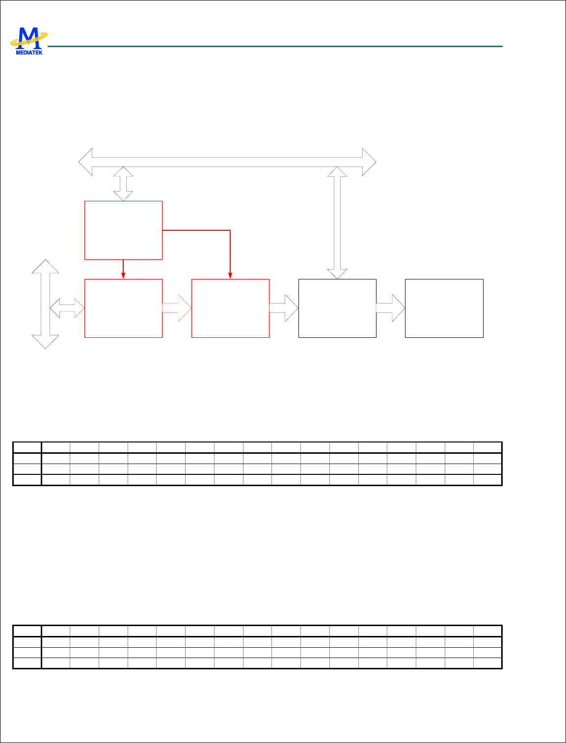
MTK Confidential Release for Konka
MTK Confidential Release for Konka
MT6228 GSM/GPRS Baseband Processor Data Sheet Revision 1.0
499/616
MediaTek Inc. Confidential
TV frame updates consume a lot of bandwidth. For interlaced system, one frame contains 2 fields. In NTSC mode, the
field update rate is 59.94 frames per second (fps); the field update rate in PAL mode is 50 fps. Performance is bound by
the size of the source image. The larger the image size, the higher the bandwidth required to support the TV display.
The controller supports an arbitrary image size up to 640 pixels in height and 480 pixels in width.
Figure 36 depicts the block diagram of the TV controller.
Video DMA
GMC bus
Video scaler TV encoder
TV controller
APB bus
10 bit
Video DAC
YCbCr422
YCbCr420 or
RGB565
Figure 36 Block Diagram of the TV Encoder
6.18.2 Register Definitions
TVC+0000h TVC enable register TVC_ENA
Bit
15 14 13 12 11 10 9 8 7 6 5 4 3 2 1 0
Name
TSEN TVEN
Type R/W R/W
Reset
0 0
The register is double buffer. At the start of each frame, the enable bit is latched into the active buffer and takes effect.
TSEN TV control test signal enable.
0 Disable the test signal display.
1 Enable the test signal display.
TVEN TV controller enable.
0 Disable the TV frame update and display.
1 Enable the TV frame update and display.
TVC+0004h TVC reset control register TVC_RST
Bit 15 14 13 12 11 10 9 8 7 6 5 4 3 2 1 0
Name
RST
Type WO
Reset
0
MTK Confidential Release for Konka
MTK Confidential Release for Konka
MT6228 GSM/GPRS Baseband Processor Data Sheet Revision 1.0
500/616
MediaTek Inc. Confidential
The register is used to reset both the TV controller and the TV encoder. This control bit is write-only.
RST Reset control bit.
TVC+0008h TVC control register TVC_CON
Bit 31 30 29 28 27 26 25 24 23 22 21 20 19 18 17 16
Name
Type
Reset
Bit 15 14 13 12 11 10 9 8 7 6 5 4 3 2 1 0
Name
AB_W
R
AB_R
D BURS
T
DPBU
F
BLKO
UT NOIP YUV_
M
Type R/W R/W R/W R/W R/W R/W R/W
Reset
0 0 0 0 0 0 0
This register contains double buffer control, burst-mode control, buffer configuration, vertical interpolation control, and
color-space control.
AB_WR Double buffer access control. Only five active buffers can be directly programmed through setting AB_WR:
TVC_YADR_SRC, TVC_SRCWIDTH, TVC_TARWIDTH, TVC_HCOEFX, TVC_HCOEFY.
0 Write write-buffer.
1 Write both write-buffer and active-buffer.
AB_RD Double buffer access control.
0 Read write-buffer.
1 Read active-buffer.
BURST Enable memory burst mode access. TVC supports 4-beat burst mode access to memory. Double buffer.
0 Disable burst mode access.
1 Enable burst mode access.
DPBUF Enable deeper buffer for better performance. Double buffer.
0 Disable deeper buffer.
1 Enable deeper buffer.
BLACKOUT Fill the unfilled line buffer area with black pixels. Double buffer.
0 Do not fill with black pixels.
1 Fill with black pixels.
NOIP Bypass vertical interpolation. Enabling this bit reduces the average data access bandwidth by 2. Double buffer.
0 Enable vertical interpolation.
1 Bypass vertical interpolation.
YUV_M Enable YUV mode. Double buffer.
0 RGB565 mode. For LCD dump buffer.
1 YUV420 mode. For MPEG buffer.
TVC+000Ch TVC Y data source address TVC_YADR_SR
C
Bit
31 30 29 28 27 26 25 24 23 22 21 20 19 18 17 16
Name
SRC_Y [31:16]
Type R/W
Reset
0
Bit 15 14 13 12 11 10 9 8 7 6 5 4 3 2 1 0
Name
SRC_Y [15:0]
Type R/W
MTK Confidential Release for Konka
MTK Confidential Release for Konka
MT6228 GSM/GPRS Baseband Processor Data Sheet Revision 1.0
501/616
MediaTek Inc. Confidential
Reset
0
This register is a double buffer. At the start of each frame, the enable bit is latched into the active buffer and takes effect.
In YUV mode, the register represents the Y source address. In RGB mode, the register represents the RGB source address.
TVC+0010h TVC U data source address TVC_UADR_SR
C
Bit 31 30 29 28 27 26 25 24 23 22 21 20 19 18 17 16
Name
SRC_U [31:16]
Type R/W
Reset
0
Bit 15 14 13 12 11 10 9 8 7 6 5 4 3 2 1 0
Name
SRC_U [15:0]
Type
R/W
Reset
0
This register is double buffer. At the start of each frame, the enable bit is latched into the active buffer and takes effect.
In YUV mode, the register represents the U source address. In RGB mode, this register has no function.
TVC+0014h TVC V data source address TVC_VADR_SR
C
Bit 31 30 29 28 27 26 25 24 23 22 21 20 19 18 17 16
Name
SRC_V [31:16]
Type R/W
Reset
0
Bit 15 14 13 12 11 10 9 8 7 6 5 4 3 2 1 0
Name
SRC_V [15:0]
Type R/W
Reset
0
This register is double buffer. At the start of each frame, the enable bit is latched into the active buffer and takes effect.
In YUV mode, the register represents the V source address. In RGB mode, this register has no function.
TVC+0018h TVC horizontal scaling coefficient X TVC_HCOEFX
Bit 15 14 13 12 11 10 9 8 7 6 5 4 3 2 1 0
Name
COEFX
Type R/W
Reset
0
This register is double buffer. At the start of each frame, the enable bit is latched into the active buffer and takes effect.
The scaling coefficients should follow the formula:
,
256
1
1 ) arg(
1 ) ( −
+
=
−
−Wt
Y
X
widthettWt
widthsourceWs
where X, Y are positive integers, and 0 < Y < W
t
– 1.
For example, if the user needs to scale the image width from 640 pixels to 720 pixels, the formula is:
256
719
371
227
719
639 +
=,
giving values X=227 and Y=371.
MTK Confidential Release for Konka
MTK Confidential Release for Konka
MT6228 GSM/GPRS Baseband Processor Data Sheet Revision 1.0
502/616
MediaTek Inc. Confidential
TVC+001Ch TVC horizontal scaling coefficient Y TVC_HCOEFY
Bit 15 14 13 12 11 10 9 8 7 6 5 4 3 2 1 0
Name
COEFY
Type R/W
Reset
0
This register is double buffer. At the start of each frame, the enable bit is latched into the active buffer and takes effect.
TVC+0020h TVC vertical scaling coefficient X TVC_VCOEFX
Bit 15 14 13 12 11 10 9 8 7 6 5 4 3 2 1 0
Name
COEFX
Type R/W
Reset
0
This register is double buffer. At the start of each frame, the enable bit is latched into the active buffer and takes effect.
The scaling coefficients should follow the formula:
tegerinpositiveYX
Ht
Y
X
heightetntHt
heightsourceHs , ,
256 1
1 ) arg(
1 ) ( ∈
−
+
=
−
−
TVC+0024h TVC vertical scaling coefficient Y TVC_VCOEFY
Bit 15 14 13 12 11 10 9 8 7 6 5 4 3 2 1 0
Name
COEFY
Type R/W
Reset
0
This register is double buffer. At the start of each frame, the enable bit is latched into the active buffer and takes effect.
TVC+0028h TVC frame source width control register TVC_SRCWIDTH
Bit 15 14 13 12 11 10 9 8 7 6 5 4 3 2 1 0
Name
SRCWIDTH
Type
R/W
Reset
0
This register is double buffer. At the start of each frame, the enable bit is latched into the active buffer and takes effect.
In YUV mode, the source width is a multiple of 16; in RGB mode, the source width is a multiple of 2.
TVC+002C TVC frame source height control register TVC_SRCHEIGH
T
Bit 15 14 13 12 11 10 9 8 7 6 5 4 3 2 1 0
Name
SRCHEIGHT
Type R/W
Reset
0
This register is double buffer. At the start of each frame, the enable bit is latched into the active buffer and takes effect.
TVC+0030 TVC frame target width control register TVC_TARWIDTH
Bit 15 14 13 12 11 10 9 8 7 6 5 4 3 2 1 0
Name
TARWIDTH
Type R/W
Reset
0
MTK Confidential Release for Konka
MTK Confidential Release for Konka
MT6228 GSM/GPRS Baseband Processor Data Sheet Revision 1.0
503/616
MediaTek Inc. Confidential
This register is double buffer. At the start of each frame, the enable bit is latched into
the active buffer and takes effect.
TVC+0034 TVC frame target height control register TVC_TARHEIGH
T
Bit 15 14 13 12 11 10 9 8 7 6 5 4 3 2 1 0
Name
TARHEIGHT
Type R/W
Reset
0
This register is double buffer. At the start of each frame, the enable bit is latched into the active buffer and takes effect.
TVC+0038h TVC start point control register TVC_START_PO
INT
Bit 31 30 29 28 27 26 25 24 23 22 21 20 19 18 17 16
Name
START_PXL
Type R/W
Reset
0
Bit 15 14 13 12 11 10 9 8 7 6 5 4 3 2 1 0
Name
START_LINE
Type R/W
Reset
0
This register is double buffer. At the start of each frame, the enable bit is latched into the active buffer and takes effect.
This register is used to control the position of frame displayed on TV. Setting START_PXL to 0 and START_LINE to
21(NTSC) or 22(PAL) aligns the frame to the top-left corner of display.
START_PXL Starting pixel position in a line.
START_LINE Starting line of display.
TVC+003Ch TVC register update control register TVC_REG_RDY
Bit 15 14 13 12 11 10 9 8 7 6 5 4 3 2 1 0
Name
REG_
RDY
Type R/W
Reset
0
This register indicates that the double buffer register data is ready to be latched into active buffer.
At the start of each frame, the hardware monitors the bit. If the bit is set to 1 by the software, the double buffer register is
latched into active buffer synchronously, and the REG_RDY bit is automatically cleared.
REG_RDY Double buffer control bit.
TVC+0040h Test signal region start line number control register 1 TVC_PTRN1
Bit
31 30 29 28 27 26 25 24 23 22 21 20 19 18 17 16
Name
SLINE1
Type R/W
Reset
0
Bit 15 14 13 12 11 10 9 8 7 6 5 4 3 2 1 0
Name
SLINE0
Type RO
Reset
0
MTK Confidential Release for Konka
MTK Confidential Release for Konka
MT6228 GSM/GPRS Baseband Processor Data Sheet Revision 1.0
504/616
MediaTek Inc. Confidential
The register specifies the starting line of the 1
st
and 2
nd
regions of the test signal to display. While the running line number
falls in the 1
st
region, the TV iteratively displays the 1
st
line buffer. While it falls in the 2
nd
region, the TV iteratively
displays the 2
nd
line buffer. The data in the line buffers is pre-filled by the user. The line length is 720 pixels.
SLINE1 The starting line of the 2
nd
region.
SLINE0 The starting line of the 1
st
region.
TVC+0044h Test signal region start line number control register 2 TVC_PTRN2
Bit 31 30 29 28 27 26 25 24 23 22 21 20 19 18 17 16
Name
SLINE3
Type R/W
Reset
0
Bit
15 14 13 12 11 10 9 8 7 6 5 4 3 2 1 0
Name
SLINE2
Type R/W
Reset
0
The register specifies the starting line of the 3
rd
and 4
th
regions of the test signal to display. While the running line number
falls in the 3
rd
region, the TV iteratively displays the 3
rd
line buffer. While it falls in the 4
th
region, the TV iteratively
displays the 4
th
line buffer. The data in the line buffers is pre-filled by the user. The line length is 720 pixels.
SLINE3 The starting line of the 4
th
region.
SLINE2 The starting line of the 3
rd
region.
TVC+0048h Line buffer load control register TVC_LINELOAD
Bit
15 14 13 12 11 10 9 8 7 6 5 4 3 2 1 0
Name
BUSY
LL3 LL2 LL1 LL0
Type RO WO WO WO WO
Reset
0 0 0 0 0
The register controls the data loading of the line buffer. Turn off TVEN and TSEN when performing the line loading
operation. The BUSY flag is asserted until the line loading operation is completed.
BUSY Line loading busy.
LL3 Writing one starts loading line buffer 3.
LL2 Writing one starts loading line buffer 2.
LL1 Writing one starts loading line buffer 1.
6.18.2.1 LL0 Writing one starts loading line buffer 0.
6.19 TV encoder
6.19.1 General Description
TV encoder receives a YCbCr stream from the video scaler and encodes the stream into NTSC/PAL signal.
shows the block diagram of the TV encoder.
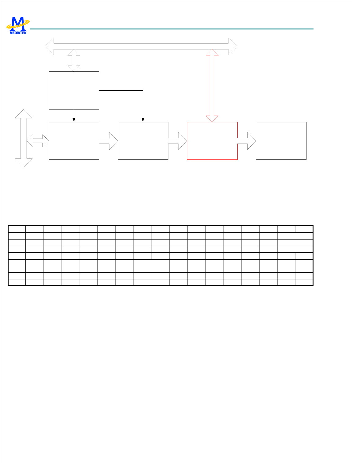
MTK Confidential Release for Konka
MTK Confidential Release for Konka
MT6228 GSM/GPRS Baseband Processor Data Sheet Revision 1.0
505/616
MediaTek Inc. Confidential
Video DMA
GMC bus
Video scaler TV encoder
TV controller
APB bus
10 bit
Video DAC
YCbCr422
YCbCr420 or
RGB565
Figure 37 Block Diagram of TV Encoder
6.19.2 Register Definitions
TVE+0000h Encoder mode control TVE_MODE
Bit
31 30 29 28 27 26 25 24 23 22 21 20 19 18 17 16
Name
TVTYPE
Type R/W R/W R/W R/W R/W R/W R/W R/W R/W R/W R/W R/W R/W R/W R/W
Reset
0 0 0 0 0 0 0 0 0 0 0 0 0 0 0
Bit 15 14 13 12 11 10 9 8 7 6 5 4 3 2 1 0
Name
UVSW
P
BLKE
R
SLOF
F SYDE
L YDEL CUPO
F
YLPO
N
CLPO
N
CLPS
EL SETU
P CBON
ENCO
N
Type R/W R/W R/W R/W R/W R/W R/W R/W R/W R/W R/W R/W
Reset
0 0 0 0 0 0 0 0 0 0 0 0
TVTYPE TV type.
00 NTSC (525 lines, no phase alternation line)
01 PAL-M (525 lines, with phase alternation line)
10 PAL-C (625 lines, with phase alternation line)
11 PAL (625 lines, with phase alternation line)
UVSWP U/V swap.
BLKER Blacker than black mode on.
SLOFF Slew at the beginning and at the end of the horizontal active area off.
SYDEL Delay of Y (half sample resolution).
YDEL Delay of Y (one sample resolution). (Recommended setting is 2.)
CUPOF Chrominance (chroma) of component up-sample off.
YLPON Luminance (luma) low-pass filter on. (Recommended setting is 1.)
CLPON Chroma low-pass filter on. (Recommended setting is 1.)
CLPSEL Chroma low-pass filter coefficient selection.
SETUP 7.5IRE setup enable. (M) NTSC and (M, N) PAL have a blanking pedestal.

MTK Confidential Release for Konka
MTK Confidential Release for Konka
MT6228 GSM/GPRS Baseband Processor Data Sheet Revision 1.0
506/616
MediaTek Inc. Confidential
CBON Enable the color bar.
ENCON Enable the TV encoder.
TVE+0004h Scale control TVE_CSCALE
Bit 31 30 29 28 27 26 25 24 23 22 21 20 19 18 17 16
Name
BLANK
Type
R/W
Reset
0x4
Bit 15 14 13 12 11 10 9 8 7 6 5 4 3 2 1 0
Name
VSCALE USCALE
Type R/W R/W
Reset
0x5A (90) 0x5A (90)
USCALE Scale of U (USCALE/128).
VSCALE Scale of V (VSCALE/128).
BLANK Luma data at this level (BLANKx4) is presented as blank.
TVE+0008h DAC control TVE_DACTRL
Bit 31 30 29 28 27 26 25 24 23 22 21 20 19 18 17 16
Name
TRIMS
ET TRIM
Type R/W R/W R/W R/W R/W R/W R/W R/W R/W R/W R/W R/W R/W
Reset
0 0 0 0 0 0 0 0 0 0 0 0 0
Bit 15 14 13 12 11 10 9 8 7 6 5 4 3 2 1 0
Name
TEST
_COM
P_EN
VPLUGREF
PLUG
_DET
_EN
PDN_
HAIBI
AS
PDN_
DAC2
PDN_
DAC1
PDN_
DAC0
PDN_
BGRE
F
DAC_
EN
Type R/W R/W R/W R/W R/W R/W R/W R/W R/W R/W R/W R/W R/W R/W R/W
Reset
0 0 0 0 0 0 0 0 0 0 0 0 0 0 1
TRIMSET Enable software trimming code setting.
0 Disable.
1 Enable.
TRIM Trimming code for BGVref.
TEST_COMP_EN Comparator test enable.
0 Disable.
1 Enable.
VPLUGREF Plug-in detect threshold selection.
PLUG_DET_EN Plug-in detect enable.
0 Disable.
1 Enable.
PDN_HAIBIAS Half bias current power down mode.
0 Power up.
1 Power down.
PDN_DAC2 DAC power down control.
0 Power up.
1 Power down.
PDN_DAC1 3/4 DAC power down control.
0 Power up.
MTK Confidential Release for Konka
MTK Confidential Release for Konka
MT6228 GSM/GPRS Baseband Processor Data Sheet Revision 1.0
507/616
MediaTek Inc. Confidential
1 Power down.
PDN_DAC0 1/2 DAC power down control.
0 Power up.
1 Power down.
PDN_BGREF BGVref power down control.
0 Power up.
1 Power down.
DAC_EN DAC enable.
TVE+000Ch Burst level control TVE_BURST
Bit 31 30 29 28 27 26 25 24 23 22 21 20 19 18 17 16
Name
UPQINI
Type R/W
Reset
0
Bit 15 14 13 12 11 10 9 8 7 6 5 4 3 2 1 0
Name
BRSTLVL
Type R/W
Reset
0x3A (58)
UPQINI Phase offset of the color burst.
BRSTLVL Color burst level.
TVE+0010h Color frequency control TVE_FREQ
Bit 31 30 29 28 27 26 25 24 23 22 21 20 19 18 17 16
Name
BFP2
Type
R/W
Reset
0xdd0 (3536)
Bit 15 14 13 12 11 10 9 8 7 6 5 4 3 2 1 0
Name
BFP1
Type R/W
Reset
0x10f (271)
Burst frequency control.
2048
4625
2
1
7MHz2 H
X
BFP
BFP
frequencyBurst
+
+
×=
,
where H is the pixel clock cycle number per line.
Use the following table to get BFP1 and BFP2 (in decimal).
TV type H X BFP1 BFP2
NTSC 1716 0 271 3536
PAL 1728 67 336 2061
BFP2 Color burst frequency synthesis value 2.
BFP1 Color burst frequency synthesis value 1.
TVE+0014h Slew control TVE_SLEW
Bit
31 30 29 28 27 26 25 24 23 22 21 20 19 18 17 16
MTK Confidential Release for Konka
MTK Confidential Release for Konka
MT6228 GSM/GPRS Baseband Processor Data Sheet Revision 1.0
508/616
MediaTek Inc. Confidential
Name
SLEWUP
Type R/W
Reset
0xc8 (200)
Bit 15 14 13 12 11 10 9 8 7 6 5 4 3 2 1 0
Name
SLEWDN
Type R/W
Reset
0x6A4 (1700)
SLEWUP Begin cycle of valid pixel with slew rate control.
SLEWDN End cycle of valid pixel with slew rate control.
TVE+0028h Luma low-pass filter coefficients 10-11 TVE_YLPFC
Bit 31 30 29 28 27 26 25 24 23 22 21 20 19 18 17 16
Name
YLPF11 YLPF10
Type R/W R/W
Reset
0x32 (-14) 0x2 (2)
Bit 15 14 13 12 11 10 9 8 7 6 5 4 3 2 1 0
Name
Type
Reset
YLPF11 Luma low-pass filter coefficient 11. Signed integer.
YLPF10 Luma low-pass filter coefficient 10. Signed integer.
TVE+002Ch Luma low-pass filter coefficients 12-15 TVE_YLPFD
Bit 31 30 29 28 27 26 25 24 23 22 21 20 19 18 17 16
Name
YLPF15 YLPF14
Type R/W R/W
Reset
0x2 (2) 0x1e (30)
Bit 15 14 13 12 11 10 9 8 7 6 5 4 3 2 1 0
Name
YLPF13 YLPF12
Type R/W R/W
Reset
0X3d (-3) 0X25 (-27)
YLPF15 Luma low-pass filter coefficient 15. Signed integer.
YLPF14 Luma low-pass filter coefficient 14. Signed integer.
YLPF13 Luma low-pass filter coefficient 13. Signed integer.
YLPF12 Luma low-pass filter coefficient 12. Signed integer.
TVE+0030h Luma low-pass filter coefficients 16-19 TVE_YLPFE
Bit 31 30 29 28 27 26 25 24 23 22 21 20 19 18 17 16
Name
YLPF19 YLPF18
Type R/W R/W
Reset
0x90 (144) 0xb4 (180)
Bit 15 14 13 12 11 10 9 8 7 6 5 4 3 2 1 0
Name
YLPF17 YLPF16
Type
R/W R/W
Reset
0Xff (-1) 0Xc7 (-57)
YLPF19 Luma low-pass filter coefficient 19. Must be unsigned. Hardware extends to 9 bits.
YLPF18 Luma low-pass filter coefficient 18. Must be unsigned. Hardware extends to 9 bits.
YLPF17 Luma low-pass filter coefficient 17. Signed integer.
YLPF16 Luma low-pass filter coefficient 16. Signed integer.
MTK Confidential Release for Konka
MTK Confidential Release for Konka
MT6228 GSM/GPRS Baseband Processor Data Sheet Revision 1.0
509/616
MediaTek Inc. Confidential
TVE+0034h Chrominance low-pass filter coefficients 0-3 TVE_CLPFA
Bit 31 30 29 28 27 26 25 24 23 22 21 20 19 18 17 16
Name
CLPF3 CLPF2
Type R/W R/W
Reset
0x18 0xd
Bit 15 14 13 12 11 10 9 8 7 6 5 4 3 2 1 0
Name
CLPF1 CLPF0
Type R/W R/W
Reset
0x10 0x1
CLPF3 Chrominance low-pass filter coefficient 3.
CLPF2 Chrominance low-pass filter coefficient 2.
CLPF1 Chrominance low-pass filter coefficient 1.
CLPF0 Chrominance low-pass filter coefficient 0.
TVE+0038h Chrominance low-pass filter coefficients 4-7 TVE_CLPFB
Bit 31 30 29 28 27 26 25 24 23 22 21 20 19 18 17 16
Name
CLPF7 CLPF6
Type
R/W R/W
Reset
0x25 0x34
Bit 15 14 13 12 11 10 9 8 7 6 5 4 3 2 1 0
Name
CLPF5 CLPF4
Type R/W R/W
Reset
0x20 0x21
CLPF7 Chrominance low-pass filter coefficient 7.
CLPF6 Chrominance low-pass filter coefficient 6.
CLPF5 Chrominance low-pass filter coefficient 5.
CLPF4 Chrominance low-pass filter coefficient 4.
TVE+003Ch Chrominance low-pass filter coefficients 8-9 TVE_CLPFC
Bit
31 30 29 28 27 26 25 24 23 22 21 20 19 18 17 16
Name
Type
Reset
Bit 15 14 13 12 11 10 9 8 7 6 5 4 3 2 1 0
Name
CLPF9 CLPF8
Type R/W R/W
Reset
0x27 0x3c
CLPF9 Chrominance low-pass filter coefficient 9.
CLPF8 Chrominance low-pass filter coefficient 8.
TVE+0040h Gamma correction coefficient 0 TVE_GAMMAA
Bit
31 30 29 28 27 26 25 24 23 22 21 20 19 18 17 16
Name
GAMMA0
Type R/W
Reset
0
Bit 15 14 13 12 11 10 9 8 7 6 5 4 3 2 1 0
Name
Type
Reset
MTK Confidential Release for Konka
MTK Confidential Release for Konka
MT6228 GSM/GPRS Baseband Processor Data Sheet Revision 1.0
510/616
MediaTek Inc. Confidential
GAMMA0~GAMMA8 indicate the turning points of a piecewise linear approximation for a gamma curve. By default, the
values form a perfect linear equation with no gamma correction.
Gamma correction is performed on Luma only.
GAMMA0
GAMMA1
GAMMA2
GAMMA3
GAMMA8
GAMMA4
GAMMA5
GAMMA6
GAMMA7
GAMMA0 Gamma correction coefficient 0.
TVE+0044h Gamma correction coefficients 1-2 TVE_GAMMAB
Bit
31 30 29 28 27 26 25 24 23 22 21 20 19 18 17 16
Name
GAMMA2
Type R/W
Reset
0x314
Bit 15 14 13 12 11 10 9 8 7 6 5 4 3 2 1 0
Name
GAMMA1
Type R/W
Reset
0x18a
GAMMA2 Gamma correction coefficient 2.
GAMMA1 Gamma correction coefficient 1.
TVE+0048h Gamma correction coefficients 3-4 TVE_GAMMAC
Bit
31 30 29 28 27 26 25 24 23 22 21 20 19 18 17 16
Name
GAMMA4
Type R/W
Reset
0x629
Bit 15 14 13 12 11 10 9 8 7 6 5 4 3 2 1 0
Name
GAMMA3
Type R/W
Reset
0x49e
GAMMA4 Gamma correction coefficient 4.
GAMMA3 Gamma correction coefficient 3.
TVE+004Ch Gamma correction coefficients 5-6 TVE_GAMMAD
Bit 31 30 29 28 27 26 25 24 23 22 21 20 19 18 17 16
MTK Confidential Release for Konka
MTK Confidential Release for Konka
MT6228 GSM/GPRS Baseband Processor Data Sheet Revision 1.0
511/616
MediaTek Inc. Confidential
Name
GAMMA6
Type R/W
Reset
0x93d
Bit 15 14 13 12 11 10 9 8 7 6 5 4 3 2 1 0
Name
GAMMA5
Type R/W
Reset
0x7b3
GAMMA6 Gamma correction coefficient 6.
GAMMA5 Gamma correction coefficient 5.
TVE+0050h Gamma correction coefficients 7-8 TVE_GAMMAE
Bit 31 30 29 28 27 26 25 24 23 22 21 20 19 18 17 16
Name
GAMMA8
Type R/W
Reset
0xc52
Bit 15 14 13 12 11 10 9 8 7 6 5 4 3 2 1 0
Name
GAMMA7
Type R/W
Reset
0xac8
GAMMA8 Gamma correction coefficient 8.
GAMMA7 Gamma correction coefficient 7.
TVE+0060h Software reset control TVE_SWRST
Bit 31 30 29 28 27 26 25 24 23 22 21 20 19 18 17 16
Name
Type
Reset
Bit 15 14 13 12 11 10 9 8 7 6 5 4 3 2 1 0
Name
SWRS
T
Type WO
Reset
0
Writing a 1 invokes a software reset.
TVE+0070h Plug-in detection TVE_PLUG
Bit 15 14 13 12 11 10 9 8 7 6 5 4 3 2 1 0
Name
PLUG
Type
RO
The TV encoder can detect cable plug-in by sensing the output impedance. To enable plug-in detection, set the
TVE_DACTRL register PLUG_DETECT_EN bit. If PLUG_DETECT_EN is enabled, when the cable is plugged in, the
PLUG bit is set to 1. The user can use polling or interrupt schemes (refer to TVE_INTREN and TVE_INTR) for plug-in
detection.
PLUG Plug-in detection.
0 Cable not plugged in.
1 Cable plugged in.

MTK Confidential Release for Konka
MTK Confidential Release for Konka
MT6228 GSM/GPRS Baseband Processor Data Sheet Revision 1.0
512/616
MediaTek Inc. Confidential
7 Audio Front-End
7.1 General Description
The audio front-end essentially consists of voice and audio data paths. Figure 38 shows the block diagram of the audio
front-end. All voice band data paths comply with the GSM 03.50 specification. Mono hands-free audio or external FM
radio playback paths are also provided. The audio stereo path facilitates CD-quality playback, external FM radio, and
voice playback through a headset.
,!- .!(#
,!- . !(
,!-.!(-'
,!-.!(-/
,!-.!(-/
,!-.!(-'
,!-* %'#
,!-* %'
MUXMUX
Stereo-
to-Mono
Stereo-
to-Mono
* 0, +
1
Voice
Signal
Audio
Signal
Voice Amp-0
Voice Amp-1
Audio Amp-R
Audio Amp-L
,!-2%'-/
,!-2%'-'
,!-2%'-'
,!-2%'-/
MUX
MUX
Voice
Signal
Audio
LCH-DAC
Audio
RCH-DAC
Voice DAC
Voice ADC
PGA
Figure 38 Block diagram of audio front-end
Figure 39 shows the digital circuits block diagram of the audio front-end. The APB register block is an APB peripheral
that stores settings from the MCU. The DSP audio port block interfaces with the DSP for control and data
communications. The digital filter block performs filter operations for voice band and audio band signal processing.
The Digital Audio Interface (DAI) block communicates with the System Simulator for FTA or external Bluetooth modules.

MTK Confidential Release for Konka
MTK Confidential Release for Konka
MT6228 GSM/GPRS Baseband Processor Data Sheet Revision 1.0
513/616
MediaTek Inc. Confidential
3
33
3
*
**
*
,
, ,
,
,
, ,
,
4/
4/4/
4/
45
4545
45
45 +
45 +45 +
45 +
,%
,%,%
,%
,/
,/,/
,/
3
33
3
4/
4/4/
4/
,+
,+,+
,+
/+
/+/+
/+
,
, ,
,
,
, ,
,
Figure 39 Block diagram of digital circuits of the audio front-end
To communicate with the external Bluetooth module, the master-mode PCM interface and master-mode I2S/EIAJ interface
are supported. The clock of PCM interface is 256 KHz, and the frame sync is 8 KHz. Both long sync and short sync
interfaces are supported. The PCM interface can transmit 16-bit stereo or 32-bit mono 8KHz sampling rate voice signal.
Figure 40 shows the timing diagram of the PCM interface. Note that the serial data changes when the clock is rising and
is latched when the clock is falling.
-6
-6-6
-6
-7
-7-7
-7
-7
-7-7
-7
-"
-"-"
-"
-"
-"-"
-"
)
))
)
)
))
)
8
88
8 9
99
9
)
))
):
::
:
)
))
)
)
))
)
8
88
8 9
99
9
)
))
):
::
:
)
))
)
)
))
)
Figure 40 Timing diagram of Bluetooth application
I2S/EIAJ interface is designed to transmit high quality audio data. Figure 40 and Figure 41 illustrate the timing diagram
of the two types of interfaces. I2S/EIAJ can support 32KHz, 44.1KHz, and 48KHz sampling rate audio signals. The
MTK Confidential Release for Konka
MTK Confidential Release for Konka
MT6228 GSM/GPRS Baseband Processor Data Sheet Revision 1.0
514/616
MediaTek Inc. Confidential
clock frequency of I2S/EIAJ can be 32×(sampling frequency), or 64×(sampling frequency). For example, to transmit a
44.1KHz CD-quality music, the clock frequency should be 32×44.1KHz = 1.4112MHz or 64×44.1KHz = 2.8224MHz.
I2S/EIAJ interface is not only used for Bluetooth module, but also for external DAC components. Audio data can easily
be sent to the external DAC through the I2S/EIAJ interface.
In this document, the I2S/EIAJ interface is referred to as EDI (External DAC Interface).
EDI_CLK
EDI_WS Left Channel Right Channel
EDI_DAT
6 5 4 3 2 1 0 15 14 13 12 11 10 9 8 7 6 5 4 3 2 1 0 15 14 13 12 11 10 9 8 7 6 5 4 3 2 1 0 15 14 13
Figure 41 EDI Format 1: EIAJ (FMT = 0).
EDI_CLK
EDI_WS Left Channel Right Channel
EDI_DAT
6 5 4 3 2 1 0 15 14 13 12 11 10 9 8 7 6 5 4 3 2 1 0 15 14 13 12 11 10 9 8 7 6 5 4 3 2 1 0 15 14 13
Figure 42 EDI Format 2: I
2
S (FMT = 1).
7.1.1 DAI, PCM and EDI Pin Sharing
DAI, PCM, and EDI interfaces share the same pins. The pin mapping is listed in Table 59.
PIN NAME DAI PCM EDI
DAI_CLK (OUTPUT) DAI_CLK PCM_CLK EDI_CLK
DAI_TX (OUTPUT) DAI_TX PCM_OUT EDI_DAT
DAI_RX (INPUT) DAI_RX PCM_IN
BT_SYNC (OUTPUT) - PCM_SYNC EDI_WS
Table 59 Pin mapping of DAI, PCM, and EDI interfaces.
Beside the shared pins, the EDI interface can also use other dedicated pins. With the dedicated pins, PCM and EDI
interfaces can operate at the same time.

MTK Confidential Release for Konka
MTK Confidential Release for Konka
MT6228 GSM/GPRS Baseband Processor Data Sheet Revision 1.0
515/616
MediaTek Inc. Confidential
int
2
int
1
FIR
SD-DAC
upsampling
DSP
IO BUS
SDM
BYPASS
=00
BYPASS
=01
BYPASS
=10
BYPASS
=11
EDI
PCM DAI
Shared
Pins
Dedicated
Pins
Figure 43 DAI, PCM, EDI interfaces
7.2 Register Definitions
MCU APB bus registers in audio front-end are listed as follows.
AFE+0000h AFE Voice MCU Control Register AFE_VMCU_CO
N0
Bit 15 14 13 12 11 10 9 8 7 6 5 4 3 2 1 0
Name
VAFE
ON
Type R/W
Reset
0
MCU sets this register to start AFE voice operation. A synchronous reset signal is issued, then periodical interrupts of
8-KHz frequency are issued. Clearing this register stops the interrupt generation.
VAFEON Turn on audio front-end operations.
AFE+000Ch AFE Voice Analog-Circuit Control Register 1 AFE_VMCU_CO
N1
Bit 15 14 13 12 11 10 9 8 7 6 5 4 3 2 1 0
Name
VRSD
ON
Type R/W
Reset
0
Set this register for consistency of analog circuit setting. Suggested value is 80h.
VRSDON Turn on the voice-band redundant signed digit function.
0: 1-bit 2-level mode
1: 2-bit 3-level mode

MTK Confidential Release for Konka
MTK Confidential Release for Konka
MT6228 GSM/GPRS Baseband Processor Data Sheet Revision 1.0
516/616
MediaTek Inc. Confidential
AFE+0014h AFE Voice DAI Bluetooth Control Register AFE_VDB_CON
Bit 15 14 13 12 11 10 9 8 7 6 5 4 3 2 1 0
Name
EDIO
N
VDAI
ON
PCMO
N
VBTS
YNC VBTSLEN
Type RW R/W R/W R/W R/W
Reset
0 0 0 0 000
Set this register for DAI test mode and Bluetooth application.
EDION EDI signals are selected as the output of DAI, PCM, EDI shared interface.
0 EDI is not selected. A dedicated EDI interface can be enabled by programming the GPIO selection. Please
refer to GPIO section for details.
1 EDI is selected. VDAION and VBTON are not set.
VDAION Turn on the DAI function.
VBTON Turn on the Bluetooth PCM function.
VBTSYNC Bluetooth PCM frame sync type
0: short
1: long
VBTSLEN Bluetooth PCM long frame sync length = VBTSLEN+1
AFE+0018h AFE Voice Look-Back mode Control Register AFE_VLB_CON
Bit 15 14 13 12 11 10 9 8 7 6 5 4 3 2 1 0
Name
VBYP
ASSII
R
VDAPI
NMOD
E
VINTI
NMOD
E
VDEC
INMO
DE
Type R/W R/W R/W R/W
Reset
0 0 0 0
Set this register for AFE voice digital circuit configuration control. Several loop back modes are implemented for test
purposes. Default values correspond to the normal function mode.
VBYPASSIIR Bypass hardware IIR filters.
VDAPINMODE DSP audio port input mode control
0 Normal mode
1 Loop back mode
VINTINMODE interpolator input mode control
0 Normal mode
1 Loop back mode
VDECINMODE decimator input mode control
0 Normal mode
1 Loop back mode
AFE+0020h AFE Audio MCU Control Register 0 AFE_AMCU_CO
N0
Bit 15 14 13 12 11 10 9 8 7 6 5 4 3 2 1 0
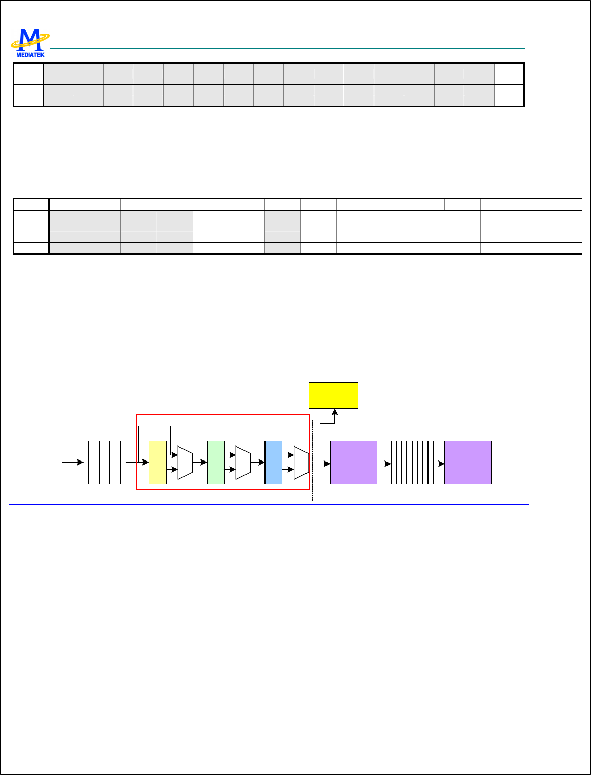
MTK Confidential Release for Konka
MTK Confidential Release for Konka
MT6228 GSM/GPRS Baseband Processor Data Sheet Revision 1.0
517/616
MediaTek Inc. Confidential
Name
AAFE
ON
Type R/W
Reset
0
MCU sets this register to start AFE audio operation. A synchronous reset signal is
issued, then periodical interrupts of 1/6 sampling frequency are issued. Clearing this
register stops the interrupt generation.
AFE+0024h AFE Audio Control Register 1
AFE_AMCU_CON1
Bit 15 14 13 12 11 10 9 8 7 6 5 4 3 2 1
Name BYPASS ADITH
ON ADITHVAL ARAMPSP AMUTE
R
AMUTE
L
AFS
Type RW R/W R/W R/W R/W R/W
R/W
Reset 00 0 00 00 0 0
MCU sets this register to inform hardware of the sampling frequency of audio being played back.
BYPASS To bypass part of the audio hardware path.
00 No bypass. The input data rate is 1/4 sampling frequency. For example, if the sampling frequency is
32KHz, then the input data rate is 8KHz.
01 Bypass the first stage of interpolation. The input data rate is 1/2 the sampling frequency.
10 Bypass two stages of interpolation. The input data rate is the same as the sampling frequency.
11 Bypass two stages of interpolation and EQ filter. The input data rate is the same as the sampling frequency.
int
2
int
1
FIR
SD-DAC
upsampling
DSP
IO BUS
SDM
BYPASS
=00
BYPASS
=01
BYPASS
=10
BYPASS
=11
EDI
Figure 44 Block diagram of the audio path.
ADITHON Turn on the audio dither function.
ADITHVAL Dither scaling setting.
00 1/4
01 1/2
10 1
11 2
ARAMPSP ramp up/down speed selection
00 8, 4096/AFS
01 16, 2048/AFS
10 24, 1024/AFS
11 32, 512/AFS
MTK Confidential Release for Konka
MTK Confidential Release for Konka
MT6228 GSM/GPRS Baseband Processor Data Sheet Revision 1.0
518/616
MediaTek Inc. Confidential
AMUTER Mute the audio R-channel, with a soft ramp up/down.
AMUTEL Mute the audio L-channel, with a soft ramp up/down.
AFS Sampling frequency setting.
00 32-KHz
01 44.1-KHz
10 48-KHz
11 reserved
AFE+0028h AFE EDI Control Register AFE_EDI_CON
Bit 15 14 13 12 11 10 9 8 7 6 5 4 3 2 1 0
Name
WCYCLE FMT
EN
Type R/W R/W R/W
Reset
01111 0 0
This register is used to control the EDI
EN Enable EDI. When EDI is disabled, EDI_DAT and EDI_WS hold low.
0 disable EDI
1 enable EDI
FMT EDI format
0 EIAJ
1 I2S
WCYCLE Clock cycle count in a word. Cycle count = WCYCLE + 1, and WCYCLE can be 15 or 31 only. Any other
values result in an unpredictable error.
15 Cycle count is 16.
31 Cycle count is 32.
EDI_CLK
EDI_WS Left Channel Right Channel
EDI_DAT
6 5 4 3 2 1 0 15 14 13 12 11 10 9 8 7 6 5 4 3 2 1 0 15 14 13 12 11 10 9 8 7 6 5 4 3 2 1 0 15 14 13
16 cycles 16 cycles
Figure 45 Cycle count is 16 for I2S format.
EDI_CLK
EDI_WS Left Channel Right Channel
EDI_DAT
6 5 4 3 2 1 0 15 14 13 12 2 1 0 15 14 13 12 2 1 0 15 14 13
32 cycles 32 cycles
Figure 46 Cycle count is 32 for I2S format.

MTK Confidential Release for Konka
MTK Confidential Release for Konka
MT6228 GSM/GPRS Baseband Processor Data Sheet Revision 1.0
519/616
MediaTek Inc. Confidential
AFE+0040h~00
F0h AFE Audio Equalizer Filter Coefficient Register AFE_EQCOEF
Bit 15 14 13 12 11 10 9 8 7 6 5 4 3 2 1 0
Name
A
Type WO
Audio front-end provides a 45-tap equalizer filter. The filter is shown below.
DO = (A44 X DI44 + A43 X DI43 … + A1 X DI1 + A0 X DI0)/32768.
DIn is the input data, and An is the coefficient of the filter, which is a 16-bit 2’s complement signed integer. DI0 is the last
input data.
The coefficient cannot be programmed when the audio path is enabled, or unpredictable noise may be generated. If
coefficient programming is necessary while the audio path is enabled, the audio path must be muted during programming.
After programming is complete, the audio path is not to be resumed (unmated) for 100 sampling periods.
A Coefficient of the filter.
7.3 Programming Guide
Several cases – including speech call, voice memo record, voice memo playback, melody playback and DAI tests – requires
that partial or the whole audio front-end be turned on.
The following are the recommended voice band path programming procedures to turn on audio front-end:
1. MCU programs the AFE_DAI_CON, AFE_LB_CON, AFE_VAG_CON, AFE_VAC_CON0, AFE_VAC_CON1
and AFE_VAPDN_CON registers for specific operation modes. Refer also to the analog chip interface
specification.
2. MCU clears the VAFE bit of the PDN_CON2 register to ungate the clock for the voice band path. Refer to the
software power down control specification.
3. MCU sets AFE_VMCU_CON to start operation of the voice band path.
The following are the recommended voice band path programming procedures to turn off audio front-end:
1. MCU programs AFE_VAPDN_CON to power down the voice band path analog blocks.
2. MCU clears AFE_VMCU_CON to stop operation of the voice band path.
3. MCU sets VAFE bit of PDN_CON2 register to gate the clock for the voice band path.
To start the DAI test, the MS first receives a GSM Layer 3 TEST_INTERFACE message from the SS and puts the speech
transcoder into one of the following modes:
Normal mode (VDAIMODE[1:0]: 00)
Test of speech encoder/DTX functions (VDAIMODE[1:0]: 10)
Test of speech decoder/DTX functions (VDAIMODE[1:0]: 01)
Test of acoustic devices and A/D & D/A (VDAIMODE[1:0]: 11)
The MS then waits for DAIRST# signaling from the SS. Recognizing this, DSP starts to transmit to and/or receive from
the DSP. For further details, refer to the GSM 11.10 specification.

MTK Confidential Release for Konka
MTK Confidential Release for Konka
MT6228 GSM/GPRS Baseband Processor Data Sheet Revision 1.0
520/616
MediaTek Inc. Confidential
The following are the recommended audio band path programming procedures to turn on audio front-end:
1. MCU programs the AFE_MCU_CON1, AFE_AAG_CON, AFE_AAC_CON, and AFE_AAPDN_CON registers
for specific configurations. Refer also to the analog chip interface specification.
2. MCU clears the AAFE bit of the PDN_CON2 register to ungate the clock for the audio band path. Refer to the
software power down control specification.
3. MCU sets AFE_AMCU_CON0 to start operation of the audio band path.
The following are the recommended audio band path programming procedures to turn off audio front-end:
1. MCU programs the AFE_AAPDN_CON to power down the audio band path analog blocks. Refer also to the
analog block specification for further details.
2. MCU clears AFE_AMCU_CON0 to stop operation of the audio band path.
3. MCU sets the AAFE bit of the PDN_CON2 register to gate the clock for the audio band path.

MTK Confidential Release for Konka
MTK Confidential Release for Konka
MT6228 GSM/GPRS Baseband Processor Data Sheet Revision 1.0
521/616
MediaTek Inc. Confidential
8 Radio Interface Control
This chapter details the MT6228 interface control with the radio part of a GSM terminal. Providing a comprehensive
control scheme, the MT6228 radio interface consists of Baseband Serial Interface (BSI), Baseband Parallel Interface (BPI),
Automatic Power Control (APC) and Automatic Frequency Control (AFC), together with APC-DAC and AFC-DAC.
8.1 Baseband Serial Interface
The Baseband Serial Interface controls external radio components. A 3-wire serial bus transfers data to RF circuitry for
PLL frequency change, reception gain setting, and other radio control purposes. In this unit, BSI data registers are
double-buffered in the same way as the TDMA event registers. The user writes data into the write buffer and the data is
transferred from the write buffer to the active buffer when a TDMA_EVTVAL signal (from the TDMA timer) is pulsed.
Each data register BSI_Dn_DAT is associated with one data control register BSI_Dn_CON, where n denotes the index.
Each data control register identifies which events (signaled by TDMA_BSISTRn, generated by the TDMA timer) trigger
the download process of the word in register BSI_Dn_DAT. The word and its length (in bits) is downloaded via the serial
bus. A special event is triggered when the IMOD flag is set to 1: it provides immediate download process without
software programming the TDMA timer.
If more than one data word is to be downloaded on the same BSI event, the word with the lowest address among them is
downloaded first, followed by the next lowest and so on.
The total download time depends on the word length, the number of words to download, and the clock rates. The
programmer must space the successive event to provide enough time. If the download process of the previous event is not
complete before a new event arrives, the latter is suppressed.
The unit has four output pins: BSI_CLK is the output clock, BSI_DATA is the serial data port, and BSI_CS0 and BSI_CS1
are the select pins for 2 external components. BSI_CS1 is multiplexed with another function. Please refer to GPIO table
for more detail.
In order to support bi-directional read and write operations of the RF chip, software can directly write values to BSI_CLK,
BSI_DATA and BSI_CS by programming the BSI_DOUT register. Data from the RF chip can be read by software via the
register BSI_DIN. If the RF chip interface is a 3-wire interface, then BSI_DATA is bi-directional. Before software can
program the 3-wire behavior, the BSI_IO_CON register must be set. An additional signal path from GPIO accommodates
RF chips with a 4-wire interface.
The block diagram of the BSI unit is as depicted in Figure 47.
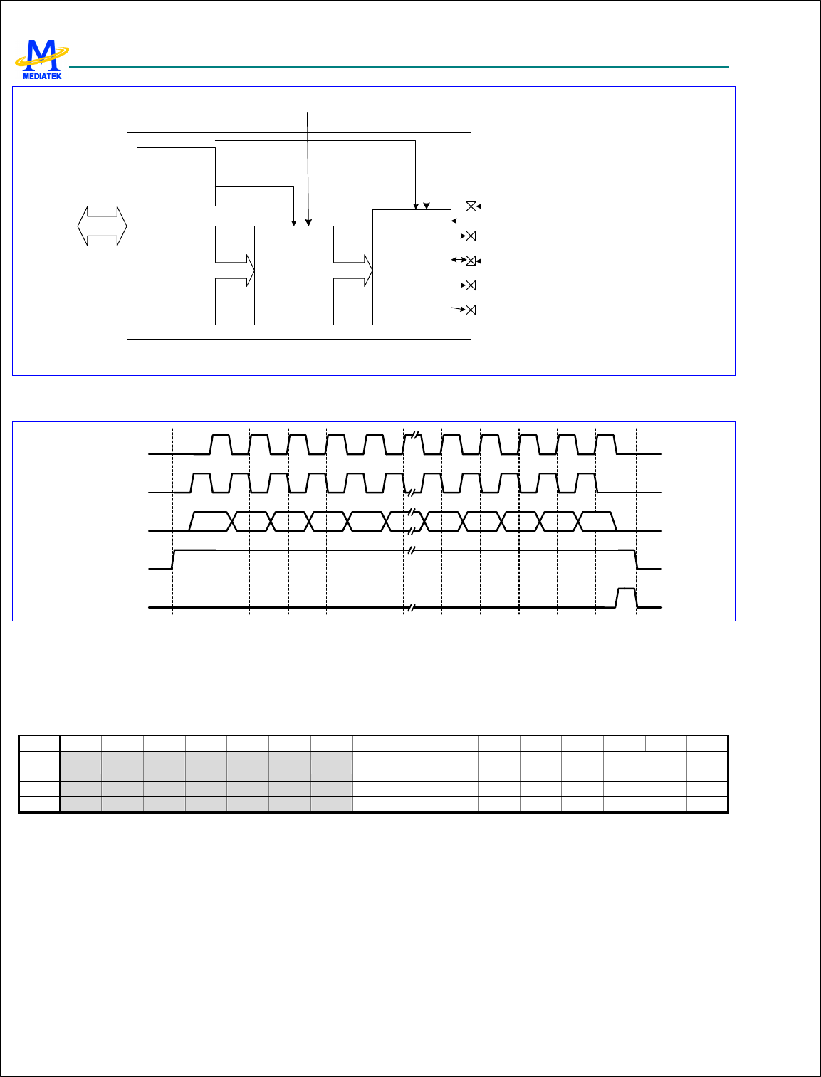
MTK Confidential Release for Konka
MTK Confidential Release for Konka
MT6228 GSM/GPRS Baseband Processor Data Sheet Revision 1.0
522/616
MediaTek Inc. Confidential
Control
Write
buffer
Active
buffer
Serial port
control
SETENV
IMOD
BSI_CS0
BSI_DATA
BSI_CLK
BSI_CS1 (GPIO)
BSI Unit
TDMA_BSISTR (0~15)
(from TDMA timer)
TDMA_EVTVAL
(from TDMA timer)
APB
BUS BSI_DIN_GPIO (read from RFIC)
(GPIO)
Figure 47 Block diagram of BSI unit.
BSI_CSx
(long)
BSI_CLK
(true)
BSI_CSx
(short)
BSI_DATA
BSI_CLK
(invert)
Figure 48 Timing characteristic of BSI interface.
8.1.1 Register Definitions
BSI+0000h BSI control register BSI_CON
Bit 15 14 13 12 11 10 9 8 7 6 5 4 3 2 1 0
Name
SETE
NV
EN1_
POL
EN1_
LEN
EN0_
POL
EN0_
LEN IMOD
CLK_SPD
CLK_
POL
Type R/W R/W R/W R/W R/W WO R/W R/W
Reset
0 0 0 0 0 N/A 0 0
This register is the control register for the BSI unit. The register controls the signal type of the 3-wire interface.
CLK_POL Controls the polarity of BSI_CLK. Refer to Figure 48.
0 True clock polarity
1 Inverted clock polarity
CLK_SPD Defines the clock rate of BSI_CLK. The 3-wire interface provides 4 choices of data bit rate. The default is
13/2 MHz.
00 13/2 MHz
MTK Confidential Release for Konka
MTK Confidential Release for Konka
MT6228 GSM/GPRS Baseband Processor Data Sheet Revision 1.0
523/616
MediaTek Inc. Confidential
01 13/4 MHz
10 13/6 MHz
11 13/8 MHz
IMOD Enables immediate mode. If the user writes 1 to the flag, the download is triggered immediately without waiting
for the timer events. The words for which the register event ID equals 1Fh are downloaded following this signal.
This flag is write-only. The immediate write is exercised only once: the programmer must write the flag again to
invoke another immediate download. Setting the flag does not disable the other events from the timer; the
programmer can disable all events by setting BSI_ENA to all zeros.
ENX_LEN Controls the type of signals BSI_CS0 and BSI_CS1. Refer to Figure 47.
0 Long enable pulse
1 Short enable pulse
ENX_POL Controls the polarity of signals BSI_CS0 and BSI_CS1.
0 True enable pulse polarity
1 Inverted enable pulse polarity
SETENV Enables the write operation of the active buffer.
0 The user writes to the write buffer. The data is then latched in the active buffer after TDMA_EVTVAL is
pulsed.
1 The user writes data directly to the active buffer.
BSI+0004h Control part of data register 0 BSI_D0_CON
Bit 15 14 13 12 11 10 9 8 7 6 5 4 3 2 1 0
Name
ISB LEN EVT_ID
Type R/W R/W R/W
This register is the control part of the data register 0. The register determines the required length of the download data
word, the event to trigger the download process of the word, and the targeted device.
Table 61 lists the 27 data registers of this type. Multiple data control registers may contain the same event ID: the data
words of all registers with the same event ID are downloaded when the event occurs.
EVT_ID Stores the event ID for which the data word awaits to be downloaded.
00000~01111 Synchronous download of the word with the selected EVT_ID event. The relationship between
this field and the event is listed as Table 60.
Event ID (in binary) – EVT_ID Event name
00000
TDMA_BSISTR0
00001
TDMA_BSISTR1
00010
TDMA_BSISTR2
00011
TDMA_BSISTR3
00100
TDMA_BSISTR4
00101
TDMA_BSISTR5
00110
TDMA_BSISTR6
00111
TDMA_BSISTR7
01000
TDMA_BSISTR8
01001
TDMA_BSISTR9
01010
TDMA_BSISTR10

MTK Confidential Release for Konka
MTK Confidential Release for Konka
MT6228 GSM/GPRS Baseband Processor Data Sheet Revision 1.0
524/616
MediaTek Inc. Confidential
01011
TDMA_BSISTR11
01100
TDMA_BSISTR12
01101
TDMA_BSISTR13
01110
TDMA_BSISTR14
01111
TDMA_BSISTR15
Table 60 The relationship between the value of EVT_ID field in the BSI control registers and the TDMA_BSISTR
events.
10000~11110 Reserved
11111 Immediate download
LEN Stores the length of the data word. The actual length is defined as LEN + 1 (in bits). The value ranges from 0
to 31, corresponding to 1 to 32 bits in length.
ISB The flag selects the target device.
0 Device 0 is selected.
1 Device 1 is selected.
BSI +0008h Data part of data register 0 BSI_D0_DAT
Bit 31 30 29 28 27 26 25 24 23 22 21 20 19 18 17 16
Name
DAT [31:16]
Type R/W
Bit 15 14 13 12 11 10 9 8 7 6 5 4 3 2 1 0
Name
DAT [15:0]
Type R/W
This register is the data part of the data register 0. The legal length of the data is up to 32 bits. The actual number of bits
to be transmitted is specified in LEN field in the BSI_D0_CON register.
DAT The field signifies the data part of the data register.
Table 61 lists the address mapping and function of the 27 pairs of data registers.
Register Address Register Function Acronym
BSI +0004h Control part of data register 0 BSI_D0_CON
BSI +0008h Data part of data register 0 BSI_D0_DAT
BSI +000Ch Control part of data register 1 BSI_D1_CON
BSI +0010h Data part of data register 1 BSI_D1_ DAT
BSI +0014h Control part of data register 2 BSI_D2_CON
BSI +0018h Data part of data register 2 BSI_D2_ DAT
BSI +001Ch Control part of data register 3 BSI_D3_CON
BSI +0020h Data part of data register 3 BSI_D3_ DAT
BSI +0024h Control part of data register 4 BSI_D4_CON
BSI +0028h Data part of data register 4 BSI_D4_ DAT
BSI +002Ch Control part of data register 5 BSI_D5_CON
BSI +0030h Data part of data register 5 BSI_D5_ DAT
BSI +0034h Control part of data register 6 BSI_D6_CON
BSI +0038h Data part of data register 6 BSI_D6_ DAT

MTK Confidential Release for Konka
MTK Confidential Release for Konka
MT6228 GSM/GPRS Baseband Processor Data Sheet Revision 1.0
525/616
MediaTek Inc. Confidential
BSI +003Ch Control part of data register 7 BSI_D7_CON
BSI +0040h Data part of data register 7 BSI_D7_ DAT
BSI +0044h Control part of data register 8 BSI_D8_CON
BSI +0048h Data part of data register 8 BSI_D8_ DAT
BSI +004Ch Control part of data register 9 BSI_D9_CON
BSI +0050h Data part of data register 9 BSI_D9_ DAT
BSI +0054h Control part of data register 10 BSI_D10_CON
BSI +0058h Data part of data register 10 BSI_D10_ DATA
BSI +005Ch Control part of data register 11 BSI_D11_CON
BSI +0060h Data part of data register 11 BSI_D11_ DAT
BSI +0064h Control part of data register 12 BSI_D12_CON
BSI +0068h Data part of data register 12 BSI_D12_ DAT
BSI +006Ch Control part of data register 13 BSI_D13_CON
BSI +0070h Data part of data register 13 BSI_D13_ DAT
BSI +0074h Control part of data register 14 BSI_D14_CON
BSI +0078h Data part of data register 14 BSI_D14_ DAT
BSI +007Ch Control part of data register 15 BSI_D15_CON
BSI +0080h Data part of data register 15 BSI_D15_ DAT
BSI +0084h Control part of data register 16 BSI_D16_CON
BSI +0088h Data part of data register 16 BSI_D16_ DAT
BSI +008Ch Control part of data register 17 BSI_D17_CON
BSI +0090h Data part of data register 17 BSI_D17_ DAT
BSI +0094h Control part of data register 18 BSI_D18_CON
BSI +0098h Data part of data register 18 BSI_D18_ DAT
BSI +009Ch Control part of data register 19 BSI_D19_CON
BSI +00A0h Data part of data register 19 BSI_D19_ DAT
BSI +00A4h Control part of data register 20 BSI_D20_CON
BSI +00A8h Data part of data register 20 BSI_D20_ DAT
BSI +00ACh Control part of data register 21 BSI_D21_CON
BSI +00B0h Data part of data register 21 BSI_D21_ DAT
BSI +00B4h Control part of data register 22 BSI_D22_CON
BSI +00B8h Data part of data register 22 BSI_D22_ DAT
BSI +00BCh Control part of data register 23 BSI_D23_CON
BSI +00C0h Data part of data register 23 BSI_D23_ DAT
BSI +00C4h Control part of data register 24 BSI_D24_CON
BSI +00C8h Data part of data register 24 BSI_D24_ DAT
BSI +00CCh Control part of data register 25 BSI_D25_CON
BSI +00D0h Data part of data register 25 BSI_D25_ DAT
BSI +00D4h Control part of data register 26 BSI_D26_CON

MTK Confidential Release for Konka
MTK Confidential Release for Konka
MT6228 GSM/GPRS Baseband Processor Data Sheet Revision 1.0
526/616
MediaTek Inc. Confidential
BSI +00D8h Data part of data register 26 BSI_D26_ DAT
Table 61 BSI data registers
BSI +0190h BSI event enable register BSI_ENA
Bit 15 14 13 12 11 10 9 8 7 6 5 4 3 2 1 0
Name
BSI15
BSI14
BSI13
BSI12
BSI11
BSI10
BSI9
BSI8
BSI7
BSI6
BSI5
BSI4
BSI3
BSI2
BSI1
BSI0
Type R/W R/W R/W R/W R/W R/W R/W R/W R/W R/W R/W R/W R/W R/W R/W R/W
Reset
1 1 1 1 1 1 1 1 1 1 1 1 1 1 1 1
This register enables an event by setting the corresponding bit. After a hardware reset, all bits are initialized to 1. These
bits are also set to 1 after TDMA_EVTVAL pulse.
BSIx Enables downloading of the words corresponding to the events signaled by TMDA_BSI.
0 The event is not enabled.
1 The event is enabled.
BSI +0194h BSI IO mode control register BSI_IO_CON
Bit 15 14 13 12 11 10 9 8 7 6 5 4 3 2 1 0
Name
SEL_
CS1
4_WIR
E
DAT_
DIR MODE
Type R/W R/W R/W R/W R/W R/W R/W R/W R/W R/W R/W R/W R/W R/W R/W R/W
Reset
0 0 0 0 0 0 0 0 0 0 0 0 0 0 1 0
MODE Defines the source of BSI signal.
0 BSI signal is generated by the hardware.
1 BSI signal is generated by the software. In this mode, the BSI clock depends on the value of the field
DOUT.CLK. BSI_CS depends on the value of the field DOUT.CS and BSI_DATA depends on the value of
the field DOUT.DATA.
DAT_DIR Defines the direction of BSI_DATA.
0 BSI _DATA is configured as input. The 3-wire interface is used and BSI_DATA is bi-directional.
1 BSI_DATA is configured as output.
4_WIRE Defines the BSI_DIN source.
0 The 3-wire interface is used and BSI_DATA is bi-directional. BSI_DIN comes from the same pin as
BSI_DATA.
1 The 4-wire interface is used. Another pin (GPIO) is used as BSI_DIN.
SEL_CS1 Defines which of the BSI_CSx (BSI_CS0 or BSI_CS1) is written by the software.
0 BSI_CS0 is selected.
1 BSI_CS1 is selected.
BSI +0198h Software-programmed data out BSI_DOUT
Bit 15 14 13 12 11 10 9 8 7 6 5 4 3 2 1 0
Name
DATA
CS
CLK
Type R/W R/W R/W R/W R/W R/W R/W R/W R/W R/W R/W R/W R/W W W W
Reset
0 0 0 0 0 0 0 0 0 0 0 0 0 0 0 0
CLK Signifies the BSI_CLK signal.
CS Signifies the BSI_CS signal.
DATA Signifies the BSI_DATA signal.
MTK Confidential Release for Konka
MTK Confidential Release for Konka
MT6228 GSM/GPRS Baseband Processor Data Sheet Revision 1.0
527/616
MediaTek Inc. Confidential
BSI +019ch Input data from RF chip BSI_DIN
Bit 15 14 13 12 11 10 9 8 7 6 5 4 3 2 1 0
Name
DIN
Type R/W R/W R/W R/W R/W R/W R/W R/W R/W R/W R/W R/W R/W R/W R/W R
Reset
0 0 0 0 0 0 0 0 0 0 0 0 0 0 0 0
DIN Registers the input value of BSI_DATA from the RF chip.
8.2 Baseband Parallel Interface
8.2.1 General Description
The Baseband Parallel Interface features 10 control pins, which are used for timing-critical external circuits. These pins
typically control front-end components which must be turned on or off at specific times during GSM operation, such as
transmit-enable, band switching, TR-switch, etc.
Event Register
APB I/F
Active
buffer
Write
buffer
Output
buffer
TDMA_EVTVAL
(from TDMA timer)
TDMA_BPISTR (0~21)
(from TDMA timer)
MUX
MUX
Immediate mode
petev
!
"
# $ % &'( ') * + , - , . '/'01 '2 + 3 ) 4'* 5 &, . /$ 6
# $ % &'( ') * + , - , . '/'01 '2 4'7 $ % 6
Figure 49 Block
diagram of BPI interface
The user can program 22 sets of 10-bit registers to set the output value of BPI_BUS0~BPI_BUS9. The data is stored in
the write buffers. The write buffers are then forwarded to the active buffers when the TDMA_EVTVAL signal is pulsed,
usually once per frame. Each of the 22 write buffers corresponds to an active buffer, as well as to a TDMA event.
Each TDMA_BPISTR event triggers the transfer of data in the corresponding active buffer to the output buffer, thus
changing the value of the BPI bus. The user can disable the events by programming the enable registers in the TDMA
timer. If the TDMA_BPISTR event is disabled, the corresponding signal TDMA_BPISTR is not pulsed, and the value on
the BPI bus remains unchanged.
For applications in which BPI signals serve as the switch, current-driving components are typically added to enhance
driving capability. Four configurable output pins provide current up to 8 mA, and help reduce the number of external

MTK Confidential Release for Konka
MTK Confidential Release for Konka
MT6228 GSM/GPRS Baseband Processor Data Sheet Revision 1.0
528/616
MediaTek Inc. Confidential
components. The output pins BPI_BUS6, BPI_BUS7, BPI_BUS8, and BPI_BUS9 are multiplexed with GPIO. Please
refer to the GPIO table for more detailed information.
8.2.2 Register Definitions
BPI+0000h BPI control register BPI_CON
Bit 15 14 13 12 11 10 9 8 7 6 5 4 3 2 1 0
Name
PINM3
PINM2
PINM1
PINM0
PETE
V
Type WO WO WO WO R/W
Reset
0 0 0 0 0
This register is the control register of the BPI unit. The register controls the direct access mode of the active buffer and
the current driving capability for the output pins.
The driving capabilities of BPI_BUS0, BPI_BUS1, BPI_BUS2, and BPI_BUS3 can be 2 mA or 8 mA, determined by the
value of PINM0, PINM1, PINM2, and PINM3, respectively. These output pins provide a higher driving capability and
save on external current-driving components. In addition to the configurable pins, pins BPI_BUS4 to BPI_BUS9 provide
a driving capability of 2 mA (fixed).
PETEV Enables direct access to the active buffer.
0 The user writes data to the write buffer. The data is latched in the active buffer after the TDMA_EVTVAL
signal is pulsed.
1 The user directly writes data to the active buffer without waiting for the TDMA_EVTVAL signal.
PINM0 Controls the driving capability of BPI_BUS0.
0 The output driving capability is 2mA.
1 The output driving capability is 8mA.
PINM1 Controls the driving capability of BPI_BUS1.
0 The output driving capability is 2mA.
1 The output driving capability is 8mA.
PINM2 Controls the driving capability of BPI_BUS2.
0 The output driving capability is 2mA.
1 The output driving capability is 8mA.
PINM3 Controls the driving capability of BPI_BUS3.
0 The output driving capability is 2mA.
1 The output driving capability is 8mA.
BPI +0004h BPI data register 0 BPI_BUF0
Bit 15 14 13 12 11 10 9 8 7 6 5 4 3 2 1 0
Name
PO9 PO8 PO7 PO6 PO5 PO4 PO3 PO2 PO1 PO0
Type R/W R/W R/W R/W R/W R/W R/W R/W R/W R/W
This register defines the BPI signals that are associated with the event TDMA_BPI0.
Table 62 lists 22 registers of the same structure, each of which is associated with one specific event signal from the TDMA
timer. The data registers are all double-buffered. When PETEV is set to 0, the data register links to the write buffer.
When PETEV is set to 1, the data register links to the active buffer.
MTK Confidential Release for Konka
MTK Confidential Release for Konka
MT6228 GSM/GPRS Baseband Processor Data Sheet Revision 1.0
529/616
MediaTek Inc. Confidential
One register, BPI_BUFI, is dedicated for use in immediate mode. Writing a value to that register effects an immediate
change in the corresponding BPI signal and bus.
POx This flag defines the corresponding signals for BPIx after the TDMA event 0 takes place.
The overall data register definition is listed in Table 62.
Register Address Register Function Acronym
BPI +0004h BPI pin data for event TDMA_BPI 0 BPI_BUF0
BPI +0008h BPI pin data for event TDMA_BPI 1 BPI_BUF1
BPI +000Ch BPI pin data for event TDMA_BPI 2 BPI_BUF2
BPI +0010h BPI pin data for event TDMA_BPI 3 BPI_BUF3
BPI +0014h BPI pin data for event TDMA_BPI 4 BPI_BUF4
BPI +0018h BPI pin data for event TDMA_BPI 5 BPI_BUF5
BPI +001Ch BPI pin data for event TDMA_BPI 6 BPI_BUF6
BPI +0020h BPI pin data for event TDMA_BPI 7 BPI_BUF7
BPI +0024h BPI pin data for event TDMA_BPI 8 BPI_BUF8
BPI +0028h BPI pin data for event TDMA_BPI 9 BPI_BUF9
BPI +002Ch BPI pin data for event TDMA_BPI 10 BPI_BUF10
BPI +0030h BPI pin data for event TDMA_BPI 11 BPI_BUF11
BPI +0034h BPI pin data for event TDMA_BPI 12 BPI_BUF12
BPI +0038h BPI pin data for event TDMA_BPI 13 BPI_BUF13
BPI +003Ch BPI pin data for event TDMA_BPI 14 BPI_BUF14
BPI +0040h BPI pin data for event TDMA_BPI 15 BPI_BUF15
BPI +0044h BPI pin data for event TDMA_BPI 16 BPI_BUF16
BPI +0048h BPI pin data for event TDMA_BPI 17 BPI_BUF17
BPI +004Ch BPI pin data for event TDMA_BPI 18 BPI_BUF18
BPI +0050h BPI pin data for event TDMA_BPI 19 BPI_BUF19
BPI +0054h BPI pin data for event TDMA_BPI 20 BPI_BUF20
BPI +0058h BPI pin data for event TDMA_BPI 21 BPI_BUF21
BPI +005Ch BPI pin data for immediate mode BPI_BUFI
Table 62 BPI Data Registers.
BPI +0060h BPI event enable register 0 BPI_ENA0
Bit 15 14 13 12 11 10 9 8 7 6 5 4 3 2 1 0
Name
BEN1
5
BEN1
4
BEN1
3
BEN1
2
BEN1
1
BEN1
0 BEN9 BEN8 BEN7 BEN6 BEN5 BEN4 BEN3 BEN2 BEN1 BEN0
Type R/W R/W R/W R/W R/W R/W R/W R/W R/W R/W R/W R/W R/W R/W R/W R/W
Reset
1 1 1 1 1 1 1 1 1 1 1 1 1 1 1 1
This register enables the events that are signaled by the TDMA timer: by clearing a register bit, the corresponding event
signal is ignored. After a hardware reset, all the enable bits default to 1 (enabled). Upon receiving a TDMA_EVTVAL
pulse, all register bits are also set to 1 (enabled).
BENn This flag indicates whether event n signals are heeded or ignored.

MTK Confidential Release for Konka
MTK Confidential Release for Konka
MT6228 GSM/GPRS Baseband Processor Data Sheet Revision 1.0
530/616
MediaTek Inc. Confidential
0 Event n is disabled (ignored).
1 Event n is enabled.
BPI+0064h BPI event enable register 1 BPI_ENA1
Bit 15 14 13 12 11 10 9 8 7 6 5 4 3 2 1 0
Name
BEN2
1
BEN2
0
BEN1
9
BEN1
8
BEN1
7
BEN1
6
Type R/W R/W R/W R/W R/W R/W
Reset
0 0 0 0 0 0
This register enables the events that are signaled by the TDMA timing generator: by clearing a register bit, the
corresponding event signal is ignored. After a hardware reset, all the enable bits default to 1 (enabled). Upon receiving
the TDMA_EVTVAL pulse, all register bits are also set to 1 (enabled).
BENn This flag indicates whether event n signals are heeded or ignored.
0 Event n is disabled (ignored).
1 Event n is enabled.
8.3 Automatic Power Control (APC) Unit
8.3.1 General Description
The Automatic Power Control (APC) unit controls the Power Amplifier (PA) module. Through APC unit, the proper
transmit power level of the handset can be set to ensure that burst power ramping requirements are met. In one TDMA
frame, up to 7 TDMA events can be enabled to support multi-slot transmission. In practice, 5 banks of ramp profiles are
used in one frame to make up 4 consecutive transmission slots.
The shape and magnitude of the ramp profiles are configurable to fit ramp-up (ramp up from zero), intermediate ramp
(ramp between transmission windows), and ramp-down (ramp down to zero) profiles. Each bank of the ramp profile
consists of 16 8-bit unsigned values, which are adjustable for different conditions.
The entries from one bank of the ramp profile are partitioned into two parts, with 8 values in each half. In normal
operation, the entries in the left half are multiplied by a 10-bit left scaling factor, and the entries in the right half are
multiplied by a 10-bit right scaling factor. The values are then truncated to form 16 10-bit intermediate values. Finally
the intermediate ramp profile are linearly interpolated into 32 10-bit values and sequentially used to update the D/A
converter. The block diagram of the APC unit is shown in Figure 50 .
The APB bus interface is 32 bits wide. Four write accesses are required to program each bank of ramp profile. The
detailed register allocations are listed in Table 63.

MTK Confidential Release for Konka
MTK Confidential Release for Konka
MT6228 GSM/GPRS Baseband Processor Data Sheet Revision 1.0
531/616
MediaTek Inc. Confidential
Ramp profile,
scaling factor,
& offset
Multiplier &
interpolator
APB
I/F
APB BUS
(32bits
data bus)
APC_BUS
(10 bits)
DAC_PU
Power and
clock
control
Output
buffer
TDMA_APCEN
( from TDMA timer )
TDMA_APCSTR (0~6)
( from TDMA timer)
QBIT_EN
APC unit
PDN_APC
( from global
control)
Figure
50 Block diagram of APC unit.
8.3.2 Register Definitions
APC+0000h APC 1st ramp profile #0 APC_PFA0
Bit 31 30 29 28 27 26 25 24 23 22 21 20 19 18 17 16
Name
ENT3 ENT2
Type R/W R/W
Bit 15 14 13 12 11 10 9 8 7 6 5 4 3 2 1 0
Name
ENT1 ENT0
Type R/W R/W
The register stores the first four entries of the first power ramp profile. The first entry resides in the least significant byte
[7:0], the second entry in the second byte [15:8], the third entry in the third byte [23:16], and the fourth in the most
significant byte [31:24]. Since this register provides no hardware reset, the programmer must configure it before any APC
event takes place.
ENT3 The field signifies the 4
th
entry of the 1
st
ramp profile.
ENT2 The field signifies the 3
rd
entry of the 1
st
ramp profile.
ENT1 The field signifies the 2
nd
entry of the 1
st
ramp profile.
ENT0 The field signifies the 1
st
entry of the 1
st
ramp profile.
The overall ramp profile register definition is listed in Table 63.
Register Address Register Function Acronym
APC +0000h
APC 1
st
ramp profile #0 APC_PFA0
APC +0004h
APC 1
st
ramp profile #1 APC_PFA1
APC +0008h
APC 1
st
ramp profile #2 APC_PFA2
APC +000Ch
APC 1
st
ramp profile #3 APC_PFA3
APC +0020h
APC 2
nd
ramp profile #0 APC_PFB0
APC +0024h
APC 2
nd
ramp profile #1 APC_PFB1
APC +0028h
APC 2
nd
ramp profile #2 APC_PFB2
APC +002Ch
APC 2
nd
ramp profile #3 APC_PFB3
APC +0040h
APC 3
rd
ramp profile #0 APC_PFC0
MTK Confidential Release for Konka
MTK Confidential Release for Konka
MT6228 GSM/GPRS Baseband Processor Data Sheet Revision 1.0
532/616
MediaTek Inc. Confidential
APC +0044h
APC 3
rd
ramp profile #1 APC_PFC1
APC +0048h
APC 3
rd
ramp profile #2 APC_PFC2
APC +004Ch
APC 3
rd
ramp profile #3 APC_PFC3
APC +0060h
APC 4
th
ramp profile #0 APC_PFD0
APC +0064h
APC 4
th
ramp profile #1 APC_PFD1
APC +0068h
APC 4
th
ramp profile #2 APC_PFD2
APC +006Ch
APC 4
th
ramp profile #3 APC_PFD3
APC +0080h
APC 5
th
ramp profile #0 APC_PFE0
APC +0084h
APC 5
th
ramp profile #1 APC_PFE1
APC +0088h
APC 5
th
ramp profile #2 APC_PFE2
APC +008Ch
APC 5
th
ramp profile #3 APC_PFE3
APC +00A0h
APC 6
th
ramp profile #0 APC_PFF0
APC +00A4h
APC 6
th
ramp profile #1 APC_PFF1
APC +00A8h
APC 6
th
ramp profile #2 APC_PFF2
APC +00ACh
APC 6
th
ramp profile #3 APC_PFF3
APC +00C0h
APC 7
th
ramp profile #0 APC_PFG0
APC +00C4h
APC 7
th
ramp profile #1 APC_PFG1
APC +00C8h
APC 7
th
ramp profile #2 APC_PFG2
APC +00CCh
APC 7
th
ramp profile #3 APC_PFG3
Table 63 APC ramp profile registers
APC +0010h APC 1st ramp profile left scaling factor APC_SCAL0L
Bit 15 14 13 12 11 10 9 8 7 6 5 4 3 2 1 0
Name
SF
Type R/W
Reset
1_0000_0000
The register stores the left scaling factor of the 1
st
ramp profile. This factor multiplies the first 8 entries of the 1
st
ramp
profile to provide the scaled profile, which is then interpolated to control the D/A converter.
After a hardware reset, the initial value of the register is 256. In this case, no scaling is done (each entry of the ramp
profile is multiplied by 1), because the 8 least significant bits are truncated after multiplication.
The overall scaling factor register definition is listed in Table 64 .
SF Scaling factor. After a hardware reset, the value is 256.
APC +0014h APC 1st ramp profile right scaling factor APC_SCAL0R
Bit 15 14 13 12 11 10 9 8 7 6 5 4 3 2 1 0
Name
SF
Type
R/W
Reset
1_0000_0000
The register stores the right scaling factor of the 1
st
ramp profile. This factor multiplies the last 8 entries of the 1
st
ramp
profile to provide the scaled profile, which is then interpolated to control the D/A converter.

MTK Confidential Release for Konka
MTK Confidential Release for Konka
MT6228 GSM/GPRS Baseband Processor Data Sheet Revision 1.0
533/616
MediaTek Inc. Confidential
After a hardware reset, the initial value of the register is 256. In this case, no scaling is done (each entry of the ramp
profile is multiplied by 1), because the 8 least significant bits are truncated after multiplication.
The overall scaling factor register definition is listed in Table 64 .
SF Scaling factor. After a hardware reset, the value is 256.
APC+0018h APC 1st ramp profile offset value APC_OFFSET0
Bit 15 14 13 12 11 10 9 8 7 6 5 4 3 2 1 0
Name
OFFSET
Type R/W
Reset
0
There are 7 offset values for the corresponding ramp profile.
The 1
st
offset value also serves as the pedestal value. The value is used to power up the APC D/A converter before the RF
signals start to transmit. The D/A converter is then biased on the value, to provide the initial control voltage for the
external control loop. The exact value depends on the characteristics of the external components. The timing to output
the pedestal value is configurable through the TDMA_BULCON2 register of the timing generator; its valid range is 0~127
quarter-bits of time after the baseband D/A converter is powered up.
OFFSET Offset value for the corresponding ramp profile. After a hardware reset, the default value is 0.
The overall offset register definition is listed in Table 64.
Register Address Register Function Acronym
APC +0010h APC 1
st
ramp profile left scaling factor APC_SCAL0L
APC +0014h
APC 1
st
ramp profile right scaling factor APC_SCAL0R
APC +0018h
APC 1
st
ramp profile offset value APC_OFFSET0
APC +0030h APC 2
nd
ramp profile left scaling factor APC_SCAL1L
APC +0034h
APC 2
nd
ramp profile right scaling factor APC_SCAL1R
APC +0038h
APC 2
nd
ramp profile offset value APC_OFFSET1
APC +0050h APC 3
rd
ramp profile left scaling factor APC_SCAL2L
APC +0054h
APC 3
rd
ramp profile right scaling factor APC_SCAL2R
APC +0058h
APC 3
rd
ramp profile offset value APC_OFFSET2
APC +0070h APC 4
th
ramp profile left scaling factor APC_SCAL3L
APC +0074h
APC 4
th
ramp profile right scaling factor APC_SCAL3R
APC +0078h
APC 4
th
ramp profile offset value APC_OFFSET3
APC +0090h APC 5
th
ramp profile left scaling factor APC_SCAL4L
APC +0094h
APC 5
th
ramp profile right scaling factor APC_SCAL4R
APC +0098h
APC 5
th
ramp profile offset value APC_OFFSET4
APC +00B0h APC 6
th
ramp profile left scaling factor APC_SCAL5L
APC +00B4h
APC 6
th
ramp profile right scaling factor APC_SCAL5R
APC +00B8h
APC 6
th
ramp profile offset value APC_OFFSET5
APC +00D0h APC 7
th
ramp profile left scaling factor APC_SCAL6L
APC +00D4h
APC 7
th
ramp profile right scaling factor APC_SCAL6R
APC +00D8h
APC 7
th
ramp profile offset value
APC_OFFSET6
Table 64 APC scaling factor and offset value registers
MTK Confidential Release for Konka
MTK Confidential Release for Konka
MT6228 GSM/GPRS Baseband Processor Data Sheet Revision 1.0
534/616
MediaTek Inc. Confidential
APC+00E0h APC control register APC_CON
Bit 15 14 13 12 11 10 9 8 7 6 5 4 3 2 1 0
Name
GSM FPU
Type R/W R/W
Reset
1 0
GSM Defines the operation mode of the APC module. In GSM mode, each frame has only one slot, thus only one
scaling factor and one offset value must be configured. If the GSM bit is set, the programmer needs only to
configure APC_SCAL0L and APC_OFFSET0. If the bit is not set, the APC module is operating in GPRS mode.
0 The APC module is operating in GPRS mode.
1 The APC module is operating in GSM mode. Default value.
FPU Forces the APC D/A converter to power up. Test only.
0 The APC D/A converter is not forced to power up. The converter is only powered on when the transmission
window is opened. Default value.
1 The APC D/A converter is forced to power up.
8.3.3 Ramp Profile Programming
The first value of the first normalized ramp profile must be written in the least significant byte of the APC_PFA0 register.
The second value must be written in the second least significant byte of the APC_PFA0, and so on.
Each ramp profile can be programmed to form an arbitrary shape.
The start of ramping is triggered by one of the TDMA_APCSTR signals. The timing relationship between
TDMA_APCSTR and TDMA slots is depicted in Figure 51 for 4 consecutive time slots case. The power ramping profile
must comply with the timing mask defined in GSM SPEC 05.05. The timing offset values for 7 ramp profiles are stored
in the TDMA timer register from TDMA_APC0 to TDMA_APC6.
RX MXTX RX
TXTX TX
Figure 51 Timing diagram of TDMA_APCSTR.
Because the APC unit provides more than 5 ramp profiles, up to 4 consecutive transmission slots can accommodated. The
2 additional ramp profiles are useful particularly when the timing between the last 2 transmission time slots and CTIRQ is
uncertain; software can begin writing the ramp profiles for the succeeding frame during the current frame, alleviating the
risk of not writing the succeeding frame’s profile data in time.
In GPRS mode, to fit the intermediate ramp profile between different power levels, a simple scaling scheme is used to
synthesize the ramp profile. The equation is as follows:

MTK Confidential Release for Konka
MTK Confidential Release for Konka
MT6228 GSM/GPRS Baseband Processor Data Sheet Revision 1.0
535/616
MediaTek Inc. Confidential
8 15 if 1,
0 8 if 0,
0,1,...,15,DNSOFFDA
,...,151 ,
2
DN DN
S OFFDA
2
DN DN
S OFFDA
12
1
2
0,15
00
≥≥
≥>
=
=⋅+=
=
+
⋅+=
+
⋅+=
+
−
k
k
l
k
k
klk
kk
lk
pre
where DA = the data to present to the D/A converter,
DN = the normalized data which is stored in the register APC_PFn,
S
0
= the left scaling factor stored in register APC_SCALnL,
S
1
= the right scaling factor stored in register APC_SCALnR, and
OFF = the offset value stored in the register APC_OFFSETn.
The subscript n denotes the index of the ramp profile.
The ramp calculation before interpolation is as depicted in Figure 52.
During each ramp process, each word of the normalized profile is first multiplied by 10-bit scaling factors and added to an
offset value to form a bank of 18-bit words. The first 8 words (in the left half part as in Figure 52) are multiplied by the
left scaling factor S
0
and the last 8 words (in the right half part as in Figure 52) are multiplied by the right scaling factor S
1
.
The lowest 8 bits of each word are then truncated to get a 10-bit result. The scaling factor is 0x100, which represents no
scaling on reset. A value smaller than 0x100 scales the ramp profile down, and a value larger than 100 scales the ramp
profile up.
DN
0
* S
0
+ OFF
DN
4
* S
0
+ OFF
DN
8
* S
1
+ OFF
DN
12
* S
1
+ OFF
DN
15
* S
1
+ OFF
16 Qb
DN
4
* S
0
DN
8
* S
1
OFF
Figure 52 The timing diagram of the APC ramp.
The 16 10-bit words are linearly interpolated into 32 10-bit words. A 10-bit D/A converter is then used to convert these 32
ramp values at a rate of 1.0833 MHz, that is, at quarter-bit rate. The timing diagram is shown in Figure 53 and the final
value is retained on the output until the next event occurs.
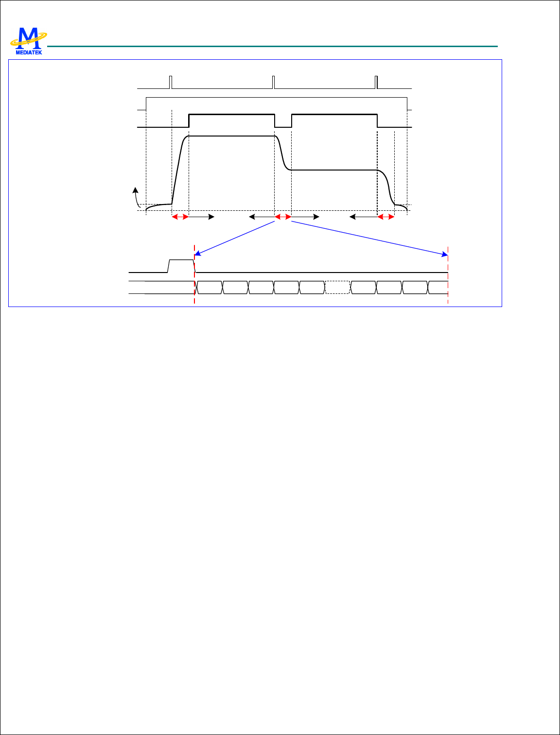
MTK Confidential Release for Konka
MTK Confidential Release for Konka
MT6228 GSM/GPRS Baseband Processor Data Sheet Revision 1.0
536/616
MediaTek Inc. Confidential
TX TX
TX Burst TX Burst
TDMA_APCSTR0
Ramp ProfileRamp Profile Ramp Profile
TDMA_APCSTR2
TDMA_APCSTR1
~29.5us ~29.5us
APC_DATA
TDMA_APCSTR1
TDMA_APCEN
TDMA_APCSTRx
~29.5us
offset
Figure 53 Timing diagram of the APC ramping.
The APC unit is only powered up when the APC window is open. The APC window is controlled by configuring the
TDMA registers TDMA_BULCON1 and TDMA_BULCON2. Please refer to the TDMA timer unit for more detailed
information.
The first offset value stored in the register APC_OFFSET0 also serves as the pedestal value, which is used to provide the
initial power level for the PA.
Since the profile is not double-buffered, the timing to write the ramping profile is critical. The programmer must be
restricted from writing to the data buffer during the ramping process, otherwise the ramp profile may be incorrect and lead
to a malfunction.
8.4 Automatic Frequency Control (AFC) Unit
8.4.1 General Description
The Automatic Frequency Control (AFC) unit provides the direct control of the oscillator for frequency offset and Doppler
shift compensation. The block diagram is of the AFC unit depicted in Figure 54. The module utilizes a 13-bit D/A
converter to achieve high-resolution control. Two modes of operation provide flexibility when controlling the oscillator;
they are described as follows.
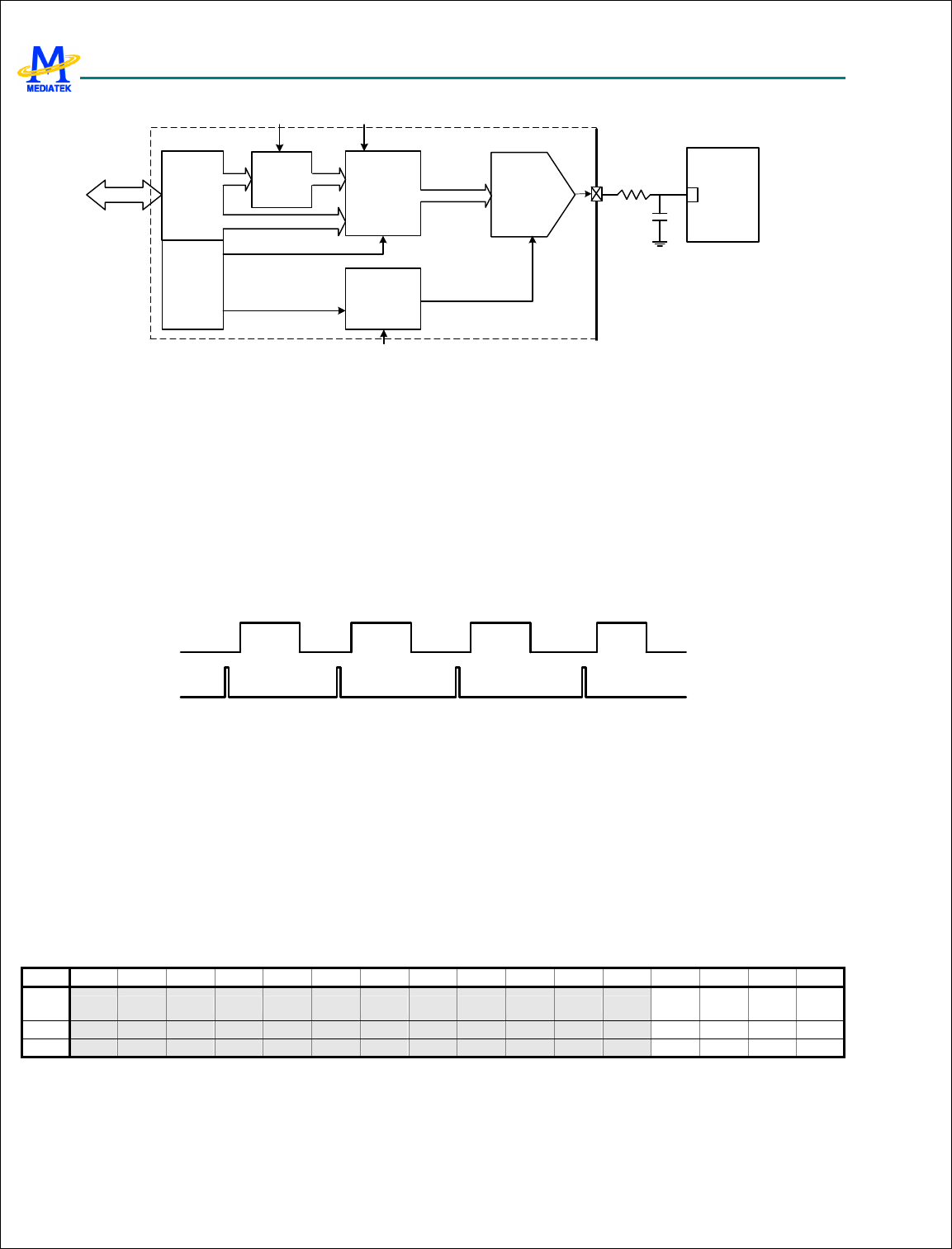
MTK Confidential Release for Konka
MTK Confidential Release for Konka
MT6228 GSM/GPRS Baseband Processor Data Sheet Revision 1.0
537/616
MediaTek Inc. Confidential
+ 0'( $
. 5 44$ &
3 8 $ &
+ 3 ) 0&3 /
APB
BUS
TDMA_AFC
( from TDMA timer )
&'0$
. 5 44$ &
AFC_BUS
3 ) 0&3 /
&$ * '2 0$ &
TDMA_EVTVAL
( from TDMA timer )
3 2 + '//, 03 &
PDN_AFC
( from global control )
VC
AFC unit
9 9 $ % ', 0$ 8 & '0$
: 5 0- 5 0
. 5 44$ &
nPDN_DAC
F_MODE
I_MODE
AFC
Figure 54 Block Diagram of the AFC Controller
In timer-triggered mode, the TDMA timer controls the AFC enabling events. Each TDMA frame can pulse at most four
events. Double buffer architecture is supported. AFC values can be written to the write buffers. When the signal
TDMA_EVTVAL is received, the values in the write buffers are latched into the active buffers. However, AFC values can
also be written to the active buffers directly. Each event is associated with an active buffer sharing the same index.
When a TDMA event is triggered by TDMA_AFC, the value in the corresponding active buffer takes effect. Figure 55
shows a timing diagram of AFC events with respect to TX/RX/MX windows. In this mode, the D/A converter can stay
powered on or be powered on for a programmable duration (256 quarter-bits, by default). The latter option is for power
saving.
RX MX MXTX
AFC_STR0 AFC_STR3AFC_STR2AFC_STR1
Figure 55 Timing Diagram for the AFC Controller
In immediate mode, the MCU can directly control the AFC value without event-triggering. The value written by the MCU
takes effect immediately. In this mode, the D/A converter must be powered on continuously. When transitioning from
immediate mode into timer-triggered mode (by setting flag I_MODE in the register AFC_CON to be 0), the D/A converter
is kept powered on for a programmable duration (256 quarter-bits by default) if a TDMA_AFC is not been pulsed. The
duration is prolonged upon receiving events.
8.4.2 Register Definitions
AFC+0000h AFC control register AFC_CON
Bit 15 14 13 12 11 10 9 8 7 6 5 4 3 2 1 0
Name
RDAC
T
F_MO
DE
FETE
NV
I_MO
DE
Type R/W R/W R/W R/W
Reset
0 0 0 0
Four control modes are defined and can be controlled through the AFC control register.
MTK Confidential Release for Konka
MTK Confidential Release for Konka
MT6228 GSM/GPRS Baseband Processor Data Sheet Revision 1.0
538/616
MediaTek Inc. Confidential
RDACT The flag enables the direct read operation from the active buffer. Note that the control flag is only applicable to
the four data buffers AFC_DAT0, AFC_DAT1, AFC_DAT2, and AFC_DAT3.
0 APB read from the write buffer.
1 APB read from the active buffer.
FETENV The flag enables the direct write operation to the active buffer. Note that the control flag is only applicable
to the four data buffers AFC_DAT0, AFC_DAT1, AFC_DAT2, and AFC_DAT3.
0 APB write to the write buffer.
1 APB write to the active buffer.
F_MODE The flag enables the force power up mode.
0 The force power up mode is not enabled.
1 The force power up mode is enabled.
I_MODE The flag enables immediate mode. To enable immediate mode, force power up mode must also be enabled.
0 Immediate mode is not enabled.
1 Immediate mode is enabled.
AFC +0004h AFC data register 0 AFC_DAT0
Bit 15 14 13 12 11 10 9 8 7 6 5 4 3 2 1 0
Name
AFCD
Type R/W
The register stores the AFC value for the event 0 triggered by the TDMA timer in timer-triggered mode. When the
RDACT or FETENV bit (of the AFC_CON register) is set, the data transfer operates on the active buffer. When neither
flag is set, the data transfer operates on the write buffer.
AFCD The AFC sample for the D/A converter.
Four registers (AFC_DAT0, AFC_DAT1, AFC_DAT2, AFC_DAT3) of the same type correspond to the event triggered by
the TDMA timer. The four registers are summarized in Table 65.
Register Address Register Function Acronym
AFC +0004h AFC control value 0 AFC_DAT0
AFC +0008h AFC control value 1 AFC_DAT1
AFC +000Ch AFC control value 2 AFC_DAT2
AFC +0010h AFC control value 3 AFC_DAT3
Table 65 AFC Data Registers
Immediate mode can only use AFC_DAT0. In this mode, only the control value in the AFC_DAT0 write buffer is used to
control the D/A converter. Unlike timer-triggered mode, the control value in AFC_DAT0 write buffer can bypass the
active buffer stage and be directly coupled to the output buffer in immediate mode. To use immediate mode, program the
AFC_DAT0 in advance and then enable immediate mode by setting the I_MODE flag in the AFC_CON register.
The registers AFC_DATA0, AFC_DAT1, AFC_DAT2, and AFC_DAT3 have no initial values, thus the register must be
programmed before any AFC event takes place. The AFC value for the D/A converter, i.e., the output buffer value, is
initially 0 after power up before any event occurs.

MTK Confidential Release for Konka
MTK Confidential Release for Konka
MT6228 GSM/GPRS Baseband Processor Data Sheet Revision 1.0
539/616
MediaTek Inc. Confidential
AFC +0014h AFC power up period AFC_PUPER
Bit 15 14 13 12 11 10 9 8 7 6 5 4 3 2 1 0
Name
PU_PER
Type R/W
Reset
ff
This register stores the AFC power up period, which is 13 bits wide. The value ranges from 0 to 8191. If the I_MODE
or F_MODE flag is set, this register has no effect since the D/A converter is powered up continuously. If neither flag is set,
the register controls the power up duration of the D/A converter. During that period, the signal nPDN_DAC in Figure 54
is set to 1(power up).
PU_PER Stores the AFC power up period. After hardware power up, the field is initialized to 255.

MTK Confidential Release for Konka
MTK Confidential Release for Konka
MT6228 GSM/GPRS Baseband Processor Data Sheet Revision 1.0
540/616
MediaTek Inc. Confidential
9 Baseband Front End
Baseband Front End is a modem interface between TX/RX mixed-signal modules and digital signal processor (DSP). We
can divide this block into two parts (see Figure 56). The first is the uplink (transmitting) path, which converts bit-stream
from DSP into digital in-phase (I) and quadrature (Q) signals for TX mixed-signal module. The second part is the downlink
(receiving) path, which receives digital in-phase (I) and quadrature (Q) signals from RX mixed-signal module, performs
FIR filtering and then sends results to DSP. Figure 56 illustrates interconnection around Baseband Front End. In the figure
the shadowed blocks compose Baseband Front End. The uplink path is mainly composed of GMSK Modulator and uplink
parts of Baseband Serial Ports, and the downlink path is mainly composed of RX digital FIR filter and downlink parts of
Baseband Serial Ports. Baseband Serial Ports is a serial interface used to communicate with DSP. In addition, there is a set
of control registers in Baseband Front End that is intended for control of TX/RX mixed-signal modules, inclusive of
calibration of DC offset and gain mismatch of downlink analog-to-digital (A/D) converters as well as uplink
digital-to-analog (D/A) converters in TX/RX mixed-signal modules. The timing of bit streaming through Baseband Front
End is completely under control of TDMA timer. Usually only either of uplink and downlink paths is active at one moment.
However, both of the uplink and downlink paths will be active simultaneously when Baseband Front End is in loopback
mode.
When either of TX windows in TDMA timer is opened, the uplink path in Baseband Front End will be activated.
Accordingly components on the uplink path such as GMSK Modulator will be powered on, and then TX mixed-signal
module is also powered on. The subblock Baseband Serial Ports will sink TX data bits from DSP and then forward them to
GMSK Modulator. The outputs from GMSK Modulator are sent to TX mixed-signal module in format of I/Q signals.
Finally D/A conversions are performed in TX mixed-signal module and the output analog signal is output to RF module.
Similarly, while either of RX windows in TDMA timer is opened, the downlink path in Baseband Front End will be
activated. Accordingly components on the downlink path such as RX mixed-signal module and RX digital FIR filter are
then powered on. First A/D conversions are performed in RX mixed-signal module, and then the results in format of I/Q
signals are sourced to RX digital FIR filter. Low-Pass filtering is performed in RX digital FIR filter. Finally the results will
be sourced to DSP through Baseband Serial Ports.
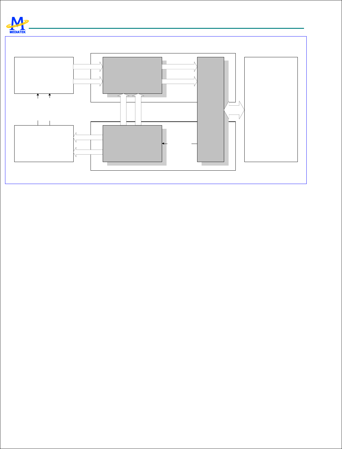
MTK Confidential Release for Konka
MTK Confidential Release for Konka
MT6228 GSM/GPRS Baseband Processor Data Sheet Revision 1.0
541/616
MediaTek Inc. Confidential
! " #
$% " #
Figure 56 Block Diagram Of Baseband Front End
9.1 Baseband Serial Ports
9.1.1 General Description
Baseband Front End communicates with DSP through the sub block of Baseband Serial Ports. Baseband Serial Ports
interfaces with DSP in serial manner. It implies that DSP must be configured carefully in order to have Baseband Serial
Ports cooperate with DSP core correctly.
If downlink path is programmed in bypass-filter mode (NOT bypass-filter loopback mode), behavior of Baseband Serial
Ports will completely be different from that in normal function mode. The special mode is for testing purpose. Please see
the subsequent section of Downlink Path for details.
TX and RX windows are under control of TDMA timer. Please refer to functional specification of TDMA timer for the
details how to open/close a TX/RX window. Opening/Closing of TX/RX windows has two major effects on Baseband Front
End. They are power on/off of corresponding components and data souring/sinking. It is worth noticing that Baseband
Serial Ports is only intended for sinking TX data from DSP or sourcing data to DSP. It does not involve power on/off of
TX/RX mixed-signal modules.
As far as downlink path is concerned, if a RX window is opened by TDMA timer Baseband Front End will have RX
mixed-signal module proceed to make A/D conversion, RX digital filter proceed to perform filtering and Baseband Serial
Ports be activated to source data from RX digital filter to DSP no matter the data is meaningful or not. However, the
interval between the moment that RX mixed-signal module is powered on and the moment that data proceed to be dumped
by Baseband Serial Ports can be well controlled in TDMA timer. Lets denote as RX enable window the interval that RX
mixed-signal module is powered on and denote as RX dump window the interval that data is dumped by Baseband Serial
Ports. If the first samples from RX digital filter desire to be discarded, the corresponding RX enable window must cover the
corresponding RX dump window. Notes that RX dump windows always win over RX enable windows. It means that a RX

MTK Confidential Release for Konka
MTK Confidential Release for Konka
MT6228 GSM/GPRS Baseband Processor Data Sheet Revision 1.0
542/616
MediaTek Inc. Confidential
dump window will always raise a RX enable window. RX enable windows can be raised by TDMA timer or by
programming RX power-down bit in global control registers to be ‘0’. It is useful in debugging environment.
Similarly, a TX dump window refers to the interval that Baseband Serial Ports sinks data from DSP on uplink path and a
TX enable window refers to the interval that TX mixed-signal module is powered on. A TX window controlled by TDMA
timer involves a TX dump window and a TX enable window simultaneously. The interval between the moment that TX
mixed-signal module is powered on and the moment that data proceed to be forwarded from DSP to GMSK modulator by
Baseband Serial Ports can be well controlled in TDMA timer. TX dump windows always win over TX enable windows. It
means that a TX dump window will always raise a TX enable window. TX enable windows can be raised by TDMA timer
or by programming TX power-down bit in global control registers to be ‘0’. It is useful in debugging environment.
Accordingly, Baseband Serial Ports are only under control of TX/RX dump window. Note that if TX/RX dump window is
not integer multiplies of bit-time it will be extended to be integer multiplies of bit-time. For example, if TX/RX dump
window has interval of 156.25 bit-times then it will be extended as 157 bit-times in Baseband Serial Ports.
9.1.2 Register Definitions
BFE+0000h Base-band Common Control Register BFE_CON
Bit 15 14 13 12 11 10 9 8 7 6 5 4 3 2 1 0
Name
BCIE
N
Type R/W
Reset
0
This register is for common control of Baseband Front End. It consists of ciphering encryption control.
BCIEN The bit is for ciphering encryption control. If the bit is set to ‘1’, XOR will performed on some TX bits (payload of
Normal Burst) and ciphering pattern bit from DSP, and then the result is forwarded to GMSK Modulator.
Meanwhile, Baseband Front End will generate signals to drive DSP ciphering process produce corresponding
ciphering pattern bits if the bit is set to ‘1’. If the bit is set to ‘0’, the TX bit from DSP will be forwarded to GMSK
modulator directly. Baseband Front End will not activate DSP ciphering process.
0 Disable ciphering encryption.
1 Enable ciphering encryption.
BFE +0004h Base-band Common Status Register BFE_STA
Bit 15 14 13 12 11 10 9 8 7 6 5 4 3 2 1 0
Name
BULF
S
BULE
N
BDLF
S
BDLE
N
Type RO RO RO RO
Reset
0 0 0 0
This register indicates status of Baseband Front End. Under control of TDMA timer, Baseband Front End can be driven in
several statuses. If downlink path is enabled, then the bit BDLEN will be ‘1’. Otherwise the bit BDLEN will be ‘0’. If
downlink parts of Baseband Serial Ports is enabled, the bit BDLFS will be ‘1’. Otherwise the bit BDLFS will be ‘0’. If
uplink path is enabled, then the bit BULEN will be ‘1’. Otherwise the bit BULEN will be 0. If uplink parts of Baseband
Serial Ports is enabled, the bit BULFS will be ‘1’. Otherwise the bit BULFS will be ‘0’. Once downlink path is enabled, RX
mixed-signal module will also be powered on. Similarly, once uplink path is enabled, TX mixed-signal module will also be
powered on. Furthermore, enabling Baseband Serial Ports for downlink path refers to dumping results from RX digital FIR
filter to DSP. Similarly, enabling Baseband Serial Ports for uplink path refers to forwarding TX bit from DSP to GMSK

MTK Confidential Release for Konka
MTK Confidential Release for Konka
MT6228 GSM/GPRS Baseband Processor Data Sheet Revision 1.0
543/616
MediaTek Inc. Confidential
modulator. BDLEN stands for “Baseband DownLink ENable”. BULEN stands for “Baseband UpLink ENable”. BDLFS
stands for “Baseband DownLink FrameSync”. BULFS stands for “Baseband UpLink FrameSync”.
BDLEN Indicate if downlink path is enabled.
0 Disabled
1 Enabled
BDLFS Indicate if Baseband Serial Ports for downlink path is enabled.
0 Disabled
1 Enabled
BULEN Indicate if uplink path is enabled.
0 Disabled
1 Enabled
BULFS Indicate if Baseband Serial Ports for uplink path is enabled.
0 Disabled
1 Enabled
9.2 Downlink Path (RX Path)
9.2.1 General Description
On downlink path, the subblock between RX mixed-signal module and Baseband Serial Ports is RX Path. It mainly consists
of a digital FIR filter, two sets of multiplexing paths for loopback modes, interface for RX mixed-signal module and
interface for Baseband Serial Ports. The block diagram is shown in Figure 57.
While RX enable windows are opened, RX Path will issue control signals to have RX mixed-signal module proceed to
make A/D conversion. As each conversion is finished, one set of I/Q signals will be latched. There exists a digital FIR filter
for these I/Q signals. The result of filtering will be dumped to Baseband Serial Ports whenever RX dump windows are
opened.
In addition to normal function, there are two loopback modes in RX Path. One is bypass-filter loopback mode, and the other
is through-filter loopback mode. They are intended for verification of DSP firmware and hardware. The bypass-filter
loopback mode refers to that RX digital FIR filter is not on the loopback path. However, the through-filter loopback mode
refers to that RX digital FIR filter is on the loopback path.
The I/Q swap functionality is used to swap I/Q channel signals from RX mixed-signal module before they are latched into
RX digital FIR filter. It is intended to provide flexibility for I/Q connection with RF modules.
There is a special data path not shown in Figure 57. It is a data path from RX mixed-signal module to Baseband Serial
Ports. If downlink path is programmed in “Bypass RX digital FIR filter” mode, ADC outputs out of RX mixed-signal
module will be directed into Baseband Serial Ports directly. Therefore these data can be dumped into DSP and RX FIR
filtering will not be performed on them. Limited by bandwidth of the serial interface between Baseband Serial Ports and
DSP, only ADC outputs which are from either I-channel or Q-channel ADC can be dumped into DSP. Both of I- and
Q-channel ADC outputs cannot be dumped simultaneously. Which channel will be dumped is controlled by the register bit
SWAP of the register RX_CFG when downlink path is programmed in “Bypass RX digital FIR filter” mode. See register
definition below for details. The mode is for measurement of performance of A/D converters in RX mixed-signal module.
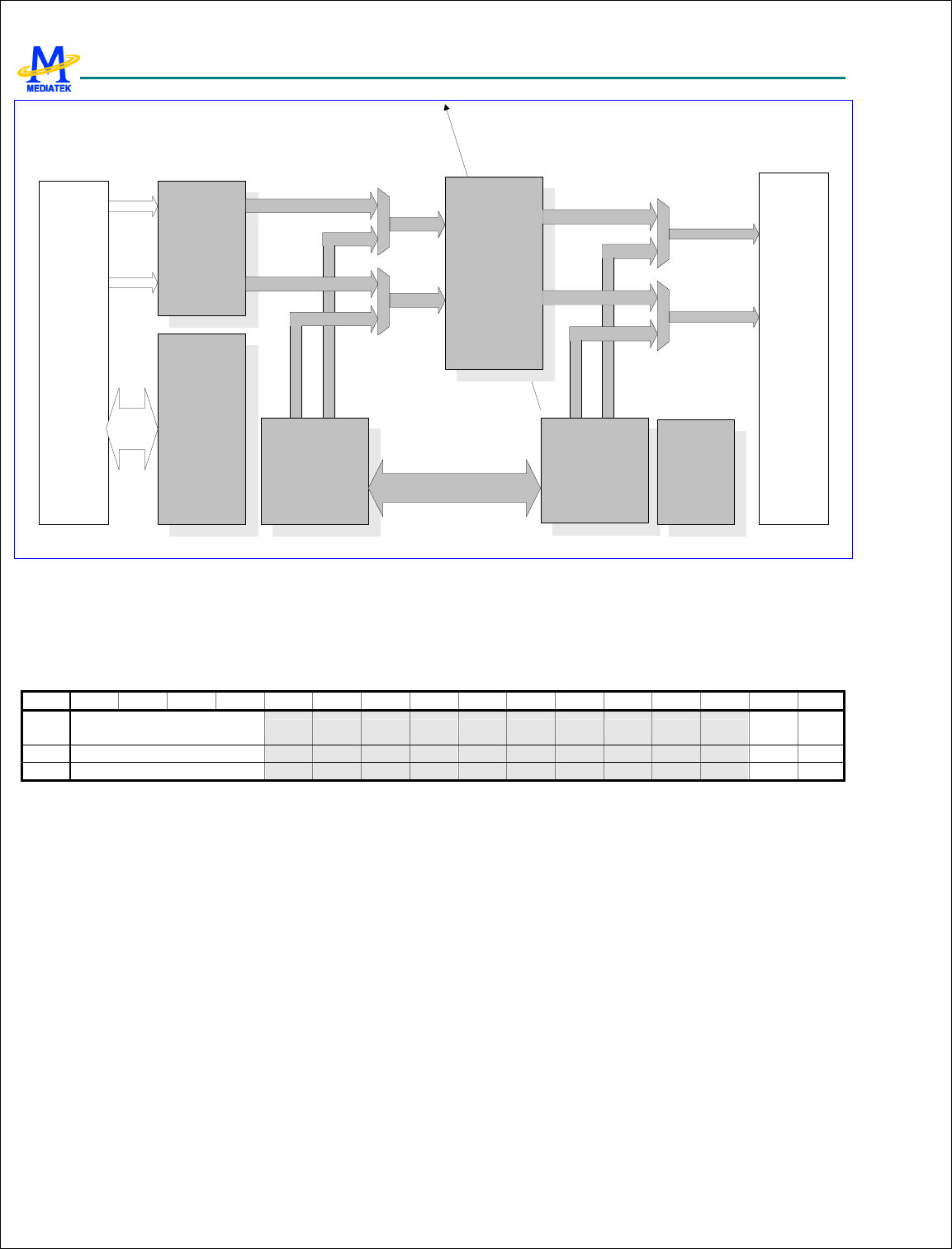
MTK Confidential Release for Konka
MTK Confidential Release for Konka
MT6228 GSM/GPRS Baseband Processor Data Sheet Revision 1.0
544/616
MediaTek Inc. Confidential
&%'"(
' (
)
&%'"(
' (
)
*'#
!#
+ '',,'
*!%
-
$
,'!#
.#
.#
.(
,'
!#
.#
.#
.#
.#
.#
.#
.#
.#
.#
.#
.#
.#
Figure 57 Block Diagram Of RX Path
9.2.2 Register Definitions
BFE +0010h RX Configuration Register RX_CFG
Bit 15 14 13 12 11 10 9 8 7 6 5 4 3 2 1 0
Name
LPDN BYPF
LTR
SWA
P
Type
R/W R/W
R/W
Reset
0000 0 0
This register is for configuration of downlink path, inclusive of configuration of RX mixed-signal module and RX path in
Baseband Front End.
SWAP The register bit is for control of whether I/Q channel signals need swap before they are input to Baseband Front
End. It provides flexibility of connection of I/Q channel signals between RF module and baseband module. The
register bit has another purpose when the register bit “BYPFLTR” is set to 1. Please see description for the register
bit “BYPFLTR”.
0 I- and Q-channel signals are not swapped
1 I- and Q-channel signals are swapped
BYPFLTR Bypass RX FIR filter control. The register bit is used to configure Baseband Front End in the state called
“Bypass RX FIR filter state” or not. Once the bit is set to ‘1’, RX FIR filter will be bypassed. That is, ADC outputs
of RX mixed-signal module that are 11-bit resolution and at sampling rate of 1.083MHz can be dumped into DSP
by Baseband Serial Ports and RX FIR filtering will not be performed on them. Limited by bandwidth of the serial
interface between Baseband Serial Ports and DSP, these ADC outputs are all from either I-channel or Q-channel
ADC. Both of I- and Q-channel ADC outputs cannot be dumped simultaneously. When the bit is set to ‘1’ and the

MTK Confidential Release for Konka
MTK Confidential Release for Konka
MT6228 GSM/GPRS Baseband Processor Data Sheet Revision 1.0
545/616
MediaTek Inc. Confidential
register bit “SWAP” is set to ‘0’, ADC outputs of I-channel will be dumped. When the bit is set to ‘1’ and the
register bit “SWAP” is set to ‘1’, ADC outputs of Q-channel will be dumped.
0 Not bypass RX FIR filter
1 Bypass RX FIR filter
LPDN Late power down control. RX mixed-signal module needs two power down signals. There must exist some delay
between them. The register field is used to control the late-arriving power-down signal.
0000 The delay between two power-down signals is one 13 MHz period.
0001 The delay between two power-down signals is two 13 MHz period.
0010 The delay between two power-down signals is three 13 MHz period.
…
0001 The delay between two power-down signals is 256 13 MHz period.
BFE +0014h RX Control Register RX_CON
Bit 15 14 13 12 11 10 9 8 7 6 5 4 3 2 1 0
Name
BLPEN[1:0]
Type R/W
Reset
0
This register is for control of downlink path, inclusive of control of RX mixed-signal module and RX path in Baseband
Front End module.
BLPEN The register field is for loopback configuration selection in Baseband Front End.
00 Configure Baseband Front End in normal function mode
01 Configure Baseband Front End in bypass-filter loopback mode
10 Configure Baseband Front End in through-filter loopback mode
11 Reserved
BFE +0020h RX Digital FIR Filter Coefficient Register 0 RX_FIR_COEF0
Bit 15 14 13 12 11 10 9 8 7 6 5 4 3 2 1 0
Name
D9 D8 D7 D6 D5 D4 D3 D2 D1 D0
Type
R/W
R/W
R/W
R/W
R/W
R/W
R/W
R/W
R/W
R/W
Reset
0 0 0 0 0 0 0 0 0 0
The register is for RX digital FIR filter coefficient 0. It is coded in 2’s complement. That is, its maximum is 255 and its
minimum is –256. It will be applied on the latest and the oldest taps of 31 taps. The equivalent process flow of RX digital
FIR filtering is shown in Figure 58.
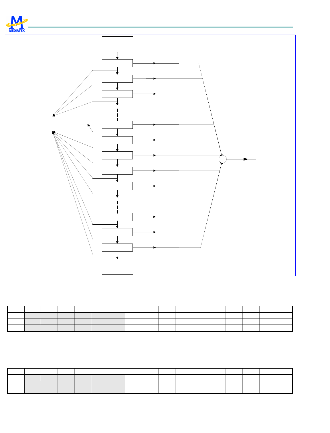
MTK Confidential Release for Konka
MTK Confidential Release for Konka
MT6228 GSM/GPRS Baseband Processor Data Sheet Revision 1.0
546/616
MediaTek Inc. Confidential
/
0
',/
',
',0
1
2
3
',1
4
5
06
07
1/
',2
',3
',2
',1
',/
',
',0
,
#,!#!
'889
-!.
'
Figure 58 Equivalent Process Flow Of RX Digital FIR Filtering
BFE +0024h RX Digital FIR Filter Coefficient Register 1 RX_FIR_COEF1
Bit 15 14 13 12 11 10 9 8 7 6 5 4 3 2 1 0
Name
D9 D8 D7 D6 D5 D4 D3 D2 D1 D0
Type R/W R/W R/W R/W R/W R/W R/W R/W R/W R/W
Reset
0 0 0 0 0 0 0 0 0 0
The register is for RX digital FIR filter coefficient 1. It is coded in 2’s complement. That is, its maximum is 255 and its
minimum is –256.
BFE +0028h RX Digital FIR Filter Coefficient Register 2 RX_FIR_COEF2
Bit 15 14 13 12 11 10 9 8 7 6 5 4 3 2 1 0
Name
D9 D8 D7 D6 D5 D4 D3 D2 D1 D0
Type R/W R/W R/W R/W R/W R/W R/W R/W R/W R/W
Reset
0 0 0 0 0 0 0 0 0 0
MTK Confidential Release for Konka
MTK Confidential Release for Konka
MT6228 GSM/GPRS Baseband Processor Data Sheet Revision 1.0
547/616
MediaTek Inc. Confidential
The register is for RX digital FIR filter coefficient 2. It is coded in 2’s complement. That is, its maximum is 255 and its
minimum is –256.
BFE +002Ch RX Digital FIR Filter Coefficient Register 3 RX_FIR_COEF3
Bit 15 14 13 12 11 10 9 8 7 6 5 4 3 2 1 0
Name
D9
D8
D7
D6
D5
D4
D3
D2
D1
D0
Type R/W R/W R/W R/W R/W R/W R/W R/W R/W R/W
Reset
0 0 0 0 0 0 0 0 0 0
The register is for RX digital FIR filter coefficient 3. It is coded in 2’s complement. That is, its maximum is 255 and its
minimum is –256.
BFE +0030h RX Digital FIR Filter Coefficient Register 4 RX_FIR_COEF4
Bit 15 14 13 12 11 10 9 8 7 6 5 4 3 2 1 0
Name
D9 D8 D7 D6 D5 D4 D3 D2 D1 D0
Type R/W R/W R/W R/W R/W R/W R/W R/W R/W R/W
Reset
0 0 0 0 0 0 0 0 0 0
The register is for RX FIR filter coefficient 4. It is coded in 2’s complement. That is, its maximum is 255 and its minimum
is –256.
BFE +0034h RX Digital FIR Filter Coefficient Register 5 RX_FIR_COEF5
Bit 15 14 13 12 11 10 9 8 7 6 5 4 3 2 1 0
Name
D9 D8 D7 D6 D5 D4 D3 D2 D1 D0
Type R/W R/W R/W R/W R/W R/W R/W R/W R/W R/W
Reset
0 0 0 0 0 0 0 0 0 0
The register is for RX digital FIR filter coefficient 5. It is coded in 2’s complement. That is, its maximum is 255 and its
minimum is –256.
BFE +0038h RX Digital FIR Filter Coefficient Register 6 RX_FIR_COEF6
Bit
15 14 13 12 11 10 9 8 7 6 5 4 3 2 1 0
Name
D9 D8 D7 D6 D5 D4 D3 D2 D1 D0
Type R/W R/W R/W R/W R/W R/W R/W R/W R/W R/W
Reset
0 0 0 0 0 0 0 0 0 0
The register is for RX digital FIR filter coefficient 6. It is coded in 2’s complement. That is, its maximum is 255 and its
minimum is –256.
BFE +003Ch RX Digital FIR Filter Coefficient Register 7 RX_FIR_COEF7
Bit 15 14 13 12 11 10 9 8 7 6 5 4 3 2 1 0
Name
D9 D8 D7 D6 D5 D4 D3 D2 D1 D0
Type R/W R/W R/W R/W R/W R/W R/W R/W R/W R/W
Reset
0 0 0 0 0 0 0 0 0 0
The register is for RX digital FIR filter coefficient 7. It is coded in 2’s complement. That is, its maximum is 255 and its
minimum is –256.
BFE +0040h RX Digital FIR Filter Coefficient Register 8 RX_FIR_COEF8
Bit 15 14 13 12 11 10 9 8 7 6 5 4 3 2 1 0
Name
D9
D8
D7
D6
D5
D4
D3
D2
D1
D0
MTK Confidential Release for Konka
MTK Confidential Release for Konka
MT6228 GSM/GPRS Baseband Processor Data Sheet Revision 1.0
548/616
MediaTek Inc. Confidential
Type
R/W
R/W
R/W
R/W
R/W
R/W
R/W
R/W
R/W
R/W
Reset
0 0 0 0 0 0 0 0 0 0
The register is for RX digital FIR filter coefficient 8. It is coded in 2’s complement. That is, its maximum is 255 and its
minimum is –256.
BFE +0044h RX Digital FIR Filter Coefficient Register 9 RX_FIR_COEF9
Bit 15 14 13 12 11 10 9 8 7 6 5 4 3 2 1 0
Name
D9 D8 D7 D6 D5 D4 D3 D2 D1 D0
Type R/W R/W R/W R/W R/W R/W R/W R/W R/W R/W
Reset
0 0 0 0 0 0 0 0 0 0
The register is for RX digital FIR filter coefficient 9. It is coded in 2’s complement. That is, its maximum is 255 and its
minimum is –256.
BFE +0048h RX Digital FIR Filter Coefficient Register 10 RX_FIR_COEF1
0
Bit 15 14 13 12 11 10 9 8 7 6 5 4 3 2 1 0
Name
D9 D8 D7 D6 D5 D4 D3 D2 D1 D0
Type
R/W
R/W
R/W
R/W
R/W
R/W
R/W
R/W
R/W
R/W
Reset
0 0 0 0 0 0 0 0 0 0
The register is for RX digital FIR filter coefficient 10. It is coded in 2’s complement. That is, its maximum is 255 and its
minimum is –256.
BFE +004Ch RX Digital FIR Filter Coefficient Register 11 RX_FIR_COEF1
1
Bit 15 14 13 12 11 10 9 8 7 6 5 4 3 2 1 0
Name
D9 D8 D7 D6 D5 D4 D3 D2 D1 D0
Type R/W R/W R/W R/W R/W R/W R/W R/W R/W R/W
Reset
0 0 0 0 0 0 0 0 0 0
The register is for RX digital FIR filter coefficient 11. It is coded in 2’s complement. That is, its maximum is 255 and its
minimum is –256.
BFE +0050h RX Digital FIR Filter Coefficient Register 12 RX_FIR_COEF1
2
Bit 15 14 13 12 11 10 9 8 7 6 5 4 3 2 1 0
Name
D9
D8
D7
D6
D5
D4
D3
D2
D1
D0
Type R/W R/W R/W R/W R/W R/W R/W R/W R/W R/W
Reset
0 0 0 0 0 0 0 0 0 0
The register is for RX digital FIR filter coefficient 12. It is coded in 2’s complement. That is, its maximum is 255 and its
minimum is –256.
BFE +0054h RX Digital FIR Filter Coefficient Register 13 RX_FIR_COEF1
3
Bit 15 14 13 12 11 10 9 8 7 6 5 4 3 2 1 0
Name
D9 D8 D7 D6 D5 D4 D3 D2 D1 D0
Type R/W R/W R/W R/W R/W R/W R/W R/W R/W R/W
Reset
0 0 0 0 0 0 0 0 0 0

MTK Confidential Release for Konka
MTK Confidential Release for Konka
MT6228 GSM/GPRS Baseband Processor Data Sheet Revision 1.0
549/616
MediaTek Inc. Confidential
The register is for RX digital FIR filter coefficient 13. It is coded in 2’s complement. That is, its maximum is 255 and its
minimum is –256.
BFE +0058h RX Digital FIR Filter Coefficient Register 14 RX_FIR_COEF1
4
Bit
15 14 13 12 11 10 9 8 7 6 5 4 3 2 1 0
Name
D9 D8 D7 D6 D5 D4 D3 D2 D1 D0
Type R/W R/W R/W R/W R/W R/W R/W R/W R/W R/W
Reset
0 0 0 0 0 0 0 0 0 0
The register is for RX digital FIR filter coefficient 14. It is coded in 2’s complement. That is, its maximum is 255 and its
minimum is –256.
BFE +005Ch RX Digital FIR Filter Coefficient Register 15 RX_FIR_COEF1
5
Bit 15 14 13 12 11 10 9 8 7 6 5 4 3 2 1 0
Name
D9 D8 D7 D6 D5 D4 D3 D2 D1 D0
Type R/W R/W R/W R/W R/W R/W R/W R/W R/W R/W
Reset
0 0 0 0 0 0 0 0 0 0
The register is for RX digital FIR filter coefficient 15. It is coded in 2’s complement. That is, its maximum is 255 and its
minimum is –256.
9.3 Uplink Path (TX Path)
9.3.1 General Description
The purpose of the uplink path inside Baseband Front End is to sink TX symbols, one bit for each symbol, from DSP, then
perform GMSK modulation on them, then perform offset cancellation on I/Q digital signals out of GMSK modulator, and
finally control TX mixed-signal module to make D/A conversion on I/Q signals out of GMSK Modulator with offset
cancellation. Accordingly, the uplink path is composed of uplink parts of Baseband Serial Ports, GSM Encryptor, GMSK
Modulator and Offset Cancellation. The block diagram of uplink path is shown in Figure 59. On uplink path, the content of
a burst, including tail bits, data bits, and training sequence bits is sent from DSP. Translated by GMSK Modulator, these bits
will become I/Q digital signals. Offset cancellation will be performed on these I/Q digital signals to compensate offset error
of D/A converters (DAC) in TX mixed-signal module. Finally the generated I/Q digital signals will be input to TX
mixed-signal module that contains two DAC for I/Q signal respectively. The details of each subblock will be described in
subsequent sections.
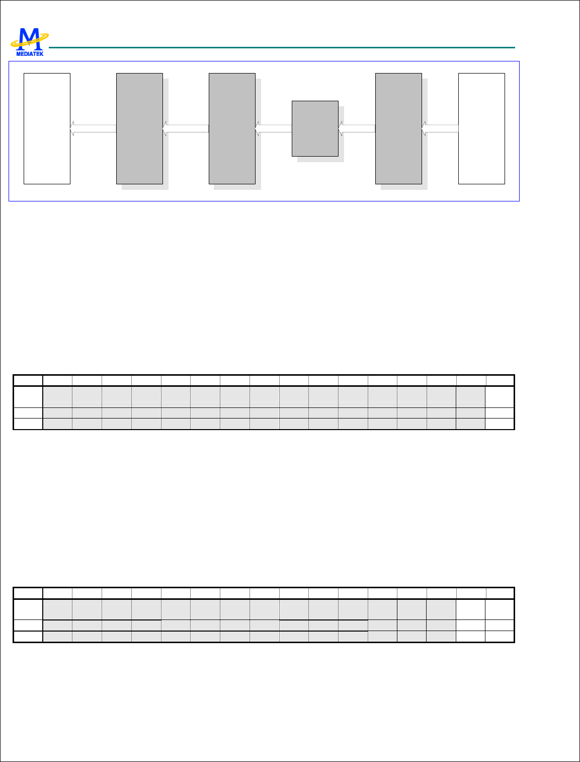
MTK Confidential Release for Konka
MTK Confidential Release for Konka
MT6228 GSM/GPRS Baseband Processor Data Sheet Revision 1.0
550/616
MediaTek Inc. Confidential
)'+%
$%"
:,
:,,
.'
+
+
**
Figure 59 Block Diagram Of Uplink Path
TDMA timer having a quarter-bit timing accuracy gives the timing windows for uplink operation. Uplink operation is
controlled by TX enable window and TX dump window of TDMA timer. Usually TX enable window is opened earlier than
TX dump window. When TX enable window of TDMA timer is opened, uplink path in Baseband Front End will power on
GSK TX mixed-signal module and thus has it drive valid outputs to RF module. However, uplink parts of Baseband Serial
Ports still don’t sink data from DSP through the serial interface between Baseband Serial Ports and DSP until now. Uplink
parts of Baseband Serial Ports will not sink data from DSP until TX dump window of TDMA timer is opened.
9.3.2 Register Definitions
BFE +0060h TX Configuration Register TX_CFG
Bit
15 14 13 12 11 10 9 8 7 6 5 4 3 2 1 0
Name
APND
EN
Type R/W
Reset
0
This register is for configuration of uplink path, inclusive of configuration of TX mixed-signal module and TX path in
Baseband Front End.
APNDEN Appending Bits Enable. The register bit is used to control the ending scheme of GMSK modulation.
0 Suitable for GPRS. If a TX enable window contains several TX dump window, then GMSK modulator will
still output in the intervals between two TX dump window and all 1’s will be fed into GMSK modulator. Note
that when the bit is set to ‘0’, the interval between the moment at which TX enable window is activated
and the moment at which TX dump window is activated must be multiples of one bit time.
1 Suitable for GSM only. After a TX dump window, GMSK modulator will only output for some bit time.
BFE +0064h TX Control Register TX_CON
Bit 15 14 13 12 11 10 9 8 7 6 5 4 3 2 1 0
Name
CALR
CEN
IQSW
P
Type R/W R/W
Reset
0 0
This register is for control of uplink path, inclusive of control of TX mixed-signal module and TX path in Baseband Front
End.

MTK Confidential Release for Konka
MTK Confidential Release for Konka
MT6228 GSM/GPRS Baseband Processor Data Sheet Revision 1.0
551/616
MediaTek Inc. Confidential
CALRCEN Calibration for TX low-pass-filter Enable. The procedure to make calibration processing for smoothing filter
in BBTX mixed-signal module is as follows:
1. Write ‘1’ to the register bit CARLC in the register TX_CON of Baseband Front End in order to activate clock
required for calibration process. Initiate calibration process.
2. Write ‘1’ to the register bit STARTCALRC of Analog Chip Interface. Start calibration process.
3. Read the register bit CALRCDONE of Analog Chip Interface. If read as ‘1’, then calibration process finished.
Otherwise repeat the step.
4. Write ‘0’ to the register bit STARTCALRC of Analog Chip Interface. Stop calibration process.
5. Write ‘0’ to the register bit CARLC in the register TX_CON of Baseband Front End in order to deactivate
clock required for calibration process. Terminate calibration process.
6. The result of calibration process can be read from the register field CALRCOUT of the register
BBTX_AC_CON1 of Analog Chip Interface. Software can set the value to the register field CALRCSEL for
3-dB cutoff frequency selection of smoothing filter in DAC of BBTX of Analog Chip Interface.
0 Dectivate clock required for calibration process.
1 Activate clock required for calibration process.
IQSWP The register bit is for control of I/Q swapping. When the bit is set to ‘1’, phase on I/Q plane will rotate in inverse
direction.
0: I and Q are not swapped.
1: I and Q are swapped.
BFE +0068h TX I/Q Channel Offset Compensation Register TX_OFF
Bit 15 14 13 12 11 10 9 8 7 6 5 4 3 2 1 0
Name
OFFQ[5:0] OFFI[5:0]
Type R/W R/W
Reset
000000 000000
The register is for offset cancellation of I-channel DAC in TX mixed-signal module. It is for compensation of offset error
caused by I/Q-channel DAC in TX mixed-signal module. It is coded in 2’s complement, that is, with maximum 31 and
minimum –32.
OFFI Value of offset cancellation for I-channel DAC in TX mixed-signal module
OFFQ Value of offset cancellation for Q-channel DAC in TX mixed-signal module
MTK Confidential Release for Konka
MTK Confidential Release for Konka
MT6228 GSM/GPRS Baseband Processor Data Sheet Revision 1.0
552/616
MediaTek Inc. Confidential
10 Timing Generator
Timing is the most critical issue in GSM/GPRS applications. The TDMA timer provides a simple interface for the MCU to
program all the timing-related events for receive event control, transmit event control, and timing adjustment. Detailed
descriptions are mentioned in Section 10.1.
In pause mode, the 13MHz reference clock may be switched off temporarily for the purpose of power saving and the
synchronization to the base-station is maintained by using a low power 32KHz crystal oscillator. The 32KHz oscillator is
not accurate and therefore it should be calibrated prior to entering pause mode. The calibration sequence, pause begin
sequence and the wake up sequence are described in Section 10.2.
10.1 TDMA timer
The TDMA timer unit is composed of three major blocks: Quarter bit counter, Signal generator and Event registers.
Figure 60 The block diagram of TDMA timer
By default, the quarter-bit counter continuously counts from 0 to the wrap position. In order to apply to cell synchronization
and neighboring cell monitoring, the wrap position can be changed by the MCU to shorten or lengthen a TDMA frame. The
wrap position is held in the TDMA_WRAP register and the current value of the TDMA quarter bit counter may be read by
the MCU via the TDMA_TQCNT register.
The signal generator handles the overall comparing and event-generating processes. When a match has occurred between
the quarter bit counter and the event register, a predefined control signal is generated. These control signals may be used for
on-chip and off-chip purposes. Signals that change state more than once per frame make use of more than one event
register.
The event registers are programmed to contain the quarter bit position of the event that is to occur. The event registers are
double buffered. The MCU writes into the first register, and the event TDMA_EVTVAL transfers the data from the write
buffer to the active buffer, which is used by the signal generator for comparison with the quarter bit count. The
TDMA_EVTVAL signal itself may be programmed at any quarter bit position. These event registers could be classified into
four groups:
On-chip Control Events
TDMA_EVTVAL

MTK Confidential Release for Konka
MTK Confidential Release for Konka
MT6228 GSM/GPRS Baseband Processor Data Sheet Revision 1.0
553/616
MediaTek Inc. Confidential
This event allows the data values written by the MCU to pass through to the active buffers.
TDMA_WRAP
TDMA quarter bit counter wrap position. This sets the position at which the TDMA quarter bit counter resets back to zero.
The default value is 4999, changing this value will advance or retard the timing events in the frame following the next
TDMA_EVTVAL signal.
TDMA_DTIRQ
DSP TDMA interrupt requests. DTIRQ triggers the DSP to read the command from the MCU/DSP Shard RAM to schedule
the activities that will be executed in the current frame.
TDMA_CTIRQ1/CTIRQ2
MCU TDMA interrupt requests.
TDMA_AUXADC [1:0]
This signal triggers the monitoring ADC to measure the voltage, current, temperature, device id etc..
TDMA_AFC [3:0]
This signal powers up the automatic frequency control DAC for a programmed duration after this event.
Note: For both MCU and DSP TDMA interrupt requests, these signals are all active Low during one quarter bit duration
and they should be used as edge sensitive events by the respective interrupt controllers.
On-chip Receive Events
TDMA_BDLON [5:0]
These registers are a set of six which contain the quarter bit event that initiates the receive window assertion sequence
which powers up and enables the receive ADC, and then enables loading of the receive data into the receive buffer.
TDMA_BDLOFF [5:0]
These registers are a set of six which contain the quarter bit event that initiates the receive window de-assertion sequence
which disables loading of the receive data into the receive buffer, and then powers down the receive ADC.
TDMA_RXWIN[5:0]
DSP TDMA interrupt requests. TDMA_RXWIN is usually used to initiate the related RX processing including two modes.
In single-shot mode, TDMA_RXWIN is generated when the BRXFS signal is de-asserted. In repetitive mode,
TDMA_RXWIN will be generated both regularly with a specific interval after BRXFS signal is asserted and when the
BRXFS signal is de-asserted.
Figure 61 The timing diagram of BRXEN and BRXFS
Note: TDMA_BDLON/OFF event registers, together with TDMA_BDLCON register, generate the corresponding BRXEN
and BRXFS window used to power up/down baseband downlink path and control the duration of data transmission to the
DSP, respectively.
On-chip Transmit Events
TDMA_APC [6:0]
These registers initiate the loading of the transmit burst shaping values from the transmit burst shaping RAM into the
transmit power control DAC.
TDMA_BULON [3:0]

MTK Confidential Release for Konka
MTK Confidential Release for Konka
MT6228 GSM/GPRS Baseband Processor Data Sheet Revision 1.0
554/616
MediaTek Inc. Confidential
This register contains the quarter bit event that initiates the transmit window assertion sequence which powers up the
modulator DAC and then enables reading of bits from the transmit buffer into the GMSK modulator.
TDMA_BULOFF [3:0]
This register contains the quarter bit event that initiates the transmit window de-assertion sequence which disables the
reading of bits from the transmit buffer into the GMSK modulator, and then power down the modulator DAC.
Figure 62 The timing diagram of BTXEN and BTXFS
Note: TDMA_BULON/OFF event registers, together with TDMA_BULCON1, TDMA_BULCON2 register, generate the
corresponding BTXEN, BTXFS and APCEN window used to power up/down the baseband uplink path, control the duration
of data transmission from the DSP and power up/down the APC DAC, respectively.
Off-chip Control Events
TDMA_BSI [15:0]
The quarter bit positions of these 16 BSI events are used to initiate the transfer of serial words to the transceiver and
synthesizer for gain control and frequency adjustment.
TDMA_BPI [21:0]
The quarter bit positions of these 22 BPI events are used to generate changes of state on the output pins to control the
external radio components.
10.1.1 Register Definitions
TDMA+0150h Event Enable Register 0 TDMA_EVTENA
0
Bit 15 14 13 12 11 10 9 8 7 6 5 4 3 2 1 0
Name
AFC3 AFC2 AFC1 AFC0 BDL5 BDL4 BDL3 BDL2 BDL1 BDL0 CTIRQ
2
CTIRQ
1
DTIR
Q
Type R/W R/W R/W R/W R/W R/W R/W R/W R/W R/W R/W R/W R/W
Reset
0 0 0 0 0 0 0 0 0 0 0 0 0
DTIRQ Enable TDMA_DTIRQ
CTIRQn Enable TDMA_CTIRQn
AFCn Enable TDMA_AFCn
BDLn Enable TDMA_BDLONn and TDMA_BDLOFFn
For all these bits,
0 function is disabled
1 function is enabled
TDMA+0154h Event Enable Register 1 TDMA_EVTENA
1
Bit
15 14 13 12 11 10 9 8 7 6 5 4 3 2 1 0
MTK Confidential Release for Konka
MTK Confidential Release for Konka
MT6228 GSM/GPRS Baseband Processor Data Sheet Revision 1.0
555/616
MediaTek Inc. Confidential
Name
GPRS
BUL3
BUL2
BUL1
BUL0
APC6
APC5
APC4
APC3
APC2
APC1
APC0
Type R/W R/W R/W R/W R/W R/W R/W R/W R/W R/W R/W R/W
Reset
0 0 0 0 0 0 0 0 0 0 0 0
APCn Enable TDMA_APCn
BULn Enable TDMA_BULONn and TDMA_BULOFFn
For all these bits,
0 function is disabled
1 function is enabled
TDMA +0158h Event Enable Register 2 TDMA_EVTENA
2
Bit
15 14 13 12 11 10 9 8 7 6 5 4 3 2 1 0
Name
BSI15
BSI14
BSI13
BSI12
BSI11
BSI10
BSI9 BSI8 BSI7 BSI6 BSI5 BSI4 BSI3 BSI2 BSI1 BSI0
Type R/W R/W R/W R/W R/W R/W R/W R/W R/W R/W R/W R/W R/W R/W R/W R/W
Reset
0 0 0 0 0 0 0 0 0 0 0 0 0 0 0 0
BSIn BSI event enable control
0 Disable TDMA_BSIn
1 Enable TDMA_BSIn
TDMA +015Ch Event Enable Register 3 TDMA_EVTENA
3
Bit 15 14 13 12 11 10 9 8 7 6 5 4 3 2 1 0
Name
BPI15
BPI14
BPI13
BPI12
BPI11
BPI10
BPI9
BPI8
BPI7
BPI6
BPI5
BPI4
BPI3
BPI2
BPI1
BPI0
Type R/W R/W R/W R/W R/W R/W R/W R/W R/W R/W R/W R/W R/W R/W R/W R/W
Reset
0 0 0 0 0 0 0 0 0 0 0 0 0 0 0 0
TDMA+0160h Event Enable Register 4 TDMA_EVTENA
4
Bit
15 14 13 12 11 10 9 8 7 6 5 4 3 2 1 0
Name
BPI21
BPI20
BPI19
BPI18
BPI17
BPI16
Type R/W R/W R/W R/W R/W R/W
Reset
0 0 0 0 0 0
BPIn BPI event enable control
0 Disable TDMA_BPIn
1 Enable TDMA_BPIn
TDMA+0164h Event Enable Register 5 TDMA_EVTENA
5
Bit 15 14 13 12 11 10 9 8 7 6 5 4 3 2 1 0
Name
AUX1
AUX0
Type R/W R/W
Reset
0 0
AUX Auxiliary ADC event enable control
0 Disable Auxiliary ADC event
1 Enable Auxiliary ADC event
MTK Confidential Release for Konka
MTK Confidential Release for Konka
MT6228 GSM/GPRS Baseband Processor Data Sheet Revision 1.0
556/616
MediaTek Inc. Confidential
TDMA +0170h Qbit Timer Offset Control Register TDMA_WRAPOF
S
Bit 15 14 13 12 11 10 9 8 7 6 5 4 3 2 1 0
Name
TOI[1:0]
Type R/W
Reset
0
TOI This register defines the value used to advance the Qbit timer in unit of 1/4 quarter bit; the timing advance will be
take place as soon as the TDMA_EVTVAL is occurred, and it will be cleared automatically.
TDMA +0174h Qbit Timer Biasing Control Register TDMA_REGBIA
S
Bit 15 14 13 12 11 10 9 8 7 6 5 4 3 2 1 0
Name
TQ_BIAS[13:0]
Type R/W
Reset
0
TQ_BIAS This register defines the Qbit offset value which will be added to the registers being programmed. It only
takes effects on AFC, BDLON/OFF, BULON/OFF, APC, AUXADC, BSI and BPI event registers.
TDMA +0180h DTX Control Register TDMA_DTXCON
Bit 15 14 13 12 11 10 9 8 7 6 5 4 3 2 1 0
Name
DTX3 DTX2 DTX1 DTX0
Type R/W R/W R/W R/W
DTX DTX flag is used to disable the associated transmit signals
0 BULON0, BULOFF0, APC_EV0 & APC_EV1 are controlled by TDMA_EVTENA1 register
1 BULON0, BULOFF0, APC_EV0 & APC_EV1 are disabled
TDMA +0184h Receive Interrupt Control Register TDMA_RXCON
Bit
15 14 13 12 11 10 9 8 7 6 5 4 3 2 1 0
Name
MOD5
MOD4
MOD3
MOD2
MOD1
MOD0
RXINTCNT[9:0]
Type R/W R/W R/W R/W R/W R/W R/W
RXINTCNT TDMA_RXWIN interrupt generation interval in quarter bit unit
MODn Mode of Receive Interrupts
0 Single shot mode for the corresponding receive window
1 Repetitive mode for the corresponding receive window
TDMA +0188h Baseband Downlink Control Register TDMA_BDLCON
Bit 15 14 13 12 11 10 9 8 7 6 5 4 3 2 1 0
Name
ADC_ON ADC_OFF
Type R/W R/W
ADC_ON BRXEN to BRXFS setup up time in quarter bit unit.
ADC_OFF BRXEN to BRXFS hold up time in quarter bit unit.

MTK Confidential Release for Konka
MTK Confidential Release for Konka
MT6228 GSM/GPRS Baseband Processor Data Sheet Revision 1.0
557/616
MediaTek Inc. Confidential
TDMA +018Ch Baseband Uplink Control Register 1 TDMA_BULCON
1
Bit 15 14 13 12 11 10 9 8 7 6 5 4 3 2 1 0
Name
DAC_ON DAC_OFF
Type R/W R/W
DAC_ON BTXEN to BTXFS setup up time in quarter bit unit.
DAC_OFF BTXEN to BTXFS hold up time in quarter bit unit.
TDMA +0190h Baseband Uplink Control Register 2 TDMA_BULCON
2
Bit
15 14 13 12 11 10 9 8 7 6 5 4 3 2 1 0
Name
APC_HYS
Type R/W
APC_HYS APCEN to BTXEN hysteresis time in quarter bit unit.
Address Type Width Reset Value Name Description
+0000h R [13:0] — TDMA_TQCNT Read quarter bit counter
+0004h R/W [13:0] 0x1387 TDMA_WRAP Latched Qbit counter reset position
+0008h R/W [13:0] 0x1387 TDMA_WRAPIMD Direct Qbit counter reset position
+000Ch R/W [13:0] 0x0000 TDMA_EVTVAL Event latch position
+0010h R/W [13:0] — TDMA_DTIRQ DSP software control
+0014h R/W [13:0] — TDMA_CTIRQ1 MCU software control 1
+0018h R/W [13:0] — TDMA_CTIRQ2 MCU software control 2
+0020h R/W [13:0] — TDMA_AFC0 The 1
st
AFC control
+0024h R/W [13:0] — TDMA_AFC1 The 2
nd
AFC control
+0028h R/W [13:0] — TDMA_AFC2 The 3
rd
AFC control
+002Ch R/W [13:0] — TDMA_AFC3 The 4
th
AFC control
+0030h R/W [13:0] — TDMA_BDLON0
+0034h R/W [13:0] — TDMA_BDLOFF0 Data serialization of the 1
st
RX block
+0038h R/W [13:0] — TDMA_BDLON1
+003Ch R/W [13:0] — TDMA_BDLOFF1 Data serialization of the 2
nd
RX block
+0040h R/W [13:0] — TDMA_BDLON2
+0044h R/W [13:0] — TDMA_BDLOFF2 Data serialization of the 3
rd
RX block
+0048h R/W [13:0] — TDMA_BDLON3
+004Ch R/W [13:0] — TDMA_BDLOFF3 Data serialization of the 4
th
RX block
+0050h R/W [13:0] — TDMA_BDLON4
+0054h R/W [13:0] — TDMA_BDLOFF4 Data serialization of the 5
th
RX block
+0058h R/W [13:0] — TDMA_BDLON5
+005Ch R/W [13:0] — TDMA_BDLOFF5 Data serialization of the 6
th
RX block
+0060h R/W [13:0] — TDMA_BULON0
+0064h R/W [13:0] — TDMA_BULOFF0 Data serialization of the 1
st
TX slot
+0068h R/W [13:0] — TDMA_BULON1
+006Ch R/W [13:0] — TDMA_BULOFF1 Data serialization of the 2
nd
TX slot
+0070h R/W [13:0] — TDMA_BULON2
+0074h R/W [13:0] — TDMA_BULOFF2 Data serialization of the 3
rd
TX slot
+0078h R/W [13:0] — TDMA_BULON3
+007Ch R/W [13:0] — TDMA_BULOFF3 Data serialization of the 4
th
TX slot
+0090h R/W [13:0] — TDMA_APC0 The 1
st
APC control

MTK Confidential Release for Konka
MTK Confidential Release for Konka
MT6228 GSM/GPRS Baseband Processor Data Sheet Revision 1.0
558/616
MediaTek Inc. Confidential
+0094h R/W [13:0] — TDMA_APC1 The 2
nd
APC control
+0098h R/W [13:0] — TDMA_APC2 The 3
rd
APC control
+009Ch R/W [13:0] — TDMA_APC3 The 4
th
APC control
+00A0h R/W [13:0] — TDMA_APC4 The 5
th
APC control
+00A4h R/W [13:0] — TDMA_APC5 The 6
th
APC control
+00A8h R/W [13:0] — TDMA_APC6 The 7
th
APC control
+00B0h R/W [13:0] — TDMA_BSI0 BSI event 0
+00B4h R/W [13:0] — TDMA_BSI1 BSI event 1
+00B8h R/W [13:0] — TDMA_BSI2 BSI event 2
+00BCh R/W [13:0] — TDMA_BSI3 BSI event 3
+00C0h R/W [13:0] — TDMA_BSI4 BSI event 4
+00C4h R/W [13:0] — TDMA_BSI5 BSI event 5
+00C8h R/W [13:0] — TDMA_BSI6 BSI event 6
+00CCh R/W [13:0] — TDMA_BSI7 BSI event 7
+00D0h R/W [13:0] — TDMA_BSI8 BSI event 8
+00D4h R/W [13:0] — TDMA_BSI9 BSI event 9
+00D8h R/W [13:0] — TDMA_BSI10 BSI event 10
+00DCh R/W [13:0] — TDMA_BSI11 BSI event 11
+00E0h R/W [13:0] — TDMA_BSI12 BSI event 12
+00E4h R/W [13:0] — TDMA_BSI13 BSI event 13
+00E8h R/W [13:0] — TDMA_BSI14 BSI event 14
+00ECh R/W [13:0] — TDMA_BSI15 BSI event 15
+0100h R/W [13:0] — TDMA_BPI0 BPI event 0
+0104h R/W [13:0] — TDMA_BPI1 BPI event 1
+0108h R/W [13:0] — TDMA_BPI2 BPI event 2
+010Ch R/W [13:0] — TDMA_BPI3 BPI event 3
+0110h R/W [13:0] — TDMA_BPI4 BPI event 4
+0114h R/W [13:0] — TDMA_BPI5 BPI event 5
+0118h R/W [13:0] — TDMA_BPI6 BPI event 6
+011Ch R/W [13:0] — TDMA_BPI7 BPI event 7
+0120h R/W [13:0] — TDMA_BPI8 BPI event 8
+0124h R/W [13:0] — TDMA_BPI9 BPI event 9
+0128h R/W [13:0] — TDMA_BPI10 BPI event 10
+012Ch R/W [13:0] — TDMA_BPI11 BPI event 11
+0130h R/W [13:0] — TDMA_BPI12 BPI event 12
+0134h R/W [13:0] — TDMA_BPI13 BPI event 13
+0138h R/W [13:0] — TDMA_BPI14 BPI event 14
+013Ch R/W [13:0] — TDMA_BPI15 BPI event 15
+0140h R/W [13:0] — TDMA_BPI16 BPI event 16
+0144h R/W [13:0] — TDMA_BPI17 BPI event 17
+0148h R/W [13:0] — TDMA_BPI18 BPI event 18
+014Ch R/W [13:0] — TDMA_BPI19 BPI event 19
+01A0h R/W [13:0] — TDMA_BPI20 BPI event 20
+01A4h R/W [13:0] — TDMA_BPI21 BPI event 21
+01B0h R/W [13:0] — TDMA_AUXEV0 Auxiliary ADC event 0
+01B4h R/W [13:0] — TDMA_AUXEV1 Auxiliary ADC event 1
+0150h R/W [15:0] 0x0000 TDMA_EVTENA0 Event Enable Control 0
+0154h R/W [15:0] 0x0000 TDMA_EVTENA1 Event Enable Control 1
+0158h R/W [15:0] 0x0000 TDMA_EVTENA2 Event Enable Control 2
+015Ch R/W [15:0] 0x0000 TDMA_EVTENA3 Event Enable Control 3

MTK Confidential Release for Konka
MTK Confidential Release for Konka
MT6228 GSM/GPRS Baseband Processor Data Sheet Revision 1.0
559/616
MediaTek Inc. Confidential
+0160h R/W [5:0] 0x0000 TDMA_EVTENA4 Event Enable Control 4
+0164h R/W [0] 0x0000 TDMA_EVTENA5 Event Enable Control 5
+0170h R/W [1:0] 0x0000 TDMA_WRAPOFS TQ Counter Offset Control Register
+0174h R/W [13:0] 0x0000 TDMA_REGBIAS Biasing Control Register
+0180h R/W [3:0] — TDMA_DTXCON DTX Control Register
+0184h R/W [15:0] — TDMA_RXCON Receive Interrupt Control Register
+0188h R/W [15:0] — TDMA_BDLCON Downlink Control Register
+018Ch R/W [15:0] — TDMA_BULCON1 Uplink Control Register 1
+0190h R/W [7:0] — TDMA_BULCON2 Uplink Control Register 2
Table 66 TDMA Timer Register Map
10.2 Slow Clocking Unit
Figure 63 The block diagram of the slow clocking unit
The slow clocking unit is provided to maintain the synchronization to the base-station timing using a 32KHz crystal
oscillator while the 13MHz reference clock is switched off. As shown in Figure 63, this unit is composed of frequency
measurement unit, pause unit, and clock management unit.
Because of the inaccuracy of the 32KHz oscillator, a frequency measurement unit is provided to calibrate the 32KHz crystal
taking the accurate 13MHz source as the reference. The calibration procedure always takes place prior to the pause period.
The pause unit is used to initiate and terminate the pause mode procedure and it also works as a coarse time-base during the
pause period.
The clock management unit is used to control the system clock while switching between the normal mode and the pause
mode. SRCLKENA is used to turn on/off the clock squarer, DSP PLL and off-chip TCVCXO. CLOCK_OFF signal is used

MTK Confidential Release for Konka
MTK Confidential Release for Konka
MT6228 GSM/GPRS Baseband Processor Data Sheet Revision 1.0
560/616
MediaTek Inc. Confidential
for gating the main MCU and DSP clock, and VCXO_OFF is used as the acknowledgement signal of the CLOCK_OFF
request.
10.2.1 Register Definitions
TDMA +0218h
Slow clocking unit control register SM_CON
Bit 15 14 13 12 11 10 9 8 7 6 5 4 3 2 1 0
Name
PAUSE_STA
RT
FM_STAR
T
Type W W
Reset
0 0
FM_START Initiate the frequency measurement procedure
PAUSE_START Initiate the pause mode procedure at the next timer wrap position
TDMA +0220h Slow clocking unit status register SM_STA
Bit 15 14 13 12 11 10 9 8
Name
PAUSE_ABO
RT
Type R
Bit 7 6 5 4 3 2 1 0
Name
SETTLE_CP
L PAUSE_CPL
PAUSE_INT PAUSE_RQS
T FM_CPL FM_RQST
Type R R R R R R
FM_RQST Frequency measurement procedure is requested
FM_CPL Frequency measurement procedure is completed
PAUSE_RQST Pause mode procedure is requested
PAUSE_INT Asynchronous wake up from pause mode
PAUSE_CPL Pause period is completed
SETTLE_CPL Settling period is completed
PAUSE_ABORT Pause mode is aborted because of the reception of interrupt prior to entering pause mode
TDMA +022Ch Slow clocking unit configuration register SM_CNF
Bit 15 14 13 12 11 10 9 8 7 6 5 4 3 2 1 0
Name
MSDC
RTC EINT KP SM FM
Type R/W R/W R/W R/W R/W R/W
Reset
0 0 0 0 1 1
FM Enable interrupt generation upon completion of frequency measurement procedure
SM Enable interrupt generation upon completion of pause mode procedure
KP Enable asynchronous wake-up from pause mode by key press
EINT Enable asynchronous wake-up from pause mode by external interrupt
RTC Enable asynchronous wake-up from pause mode by real time clock interrupt
MSDC Enable asynchronous wake-up from pause mode by memory card insertion interrupt
TDMA +0300h Power-down indication of DSP ROM DSPROMPD
Bit 15 14 13 12 11 10 9 8 7 6 5 4 3 2 1 0
Name
PD_11
PD_10
PD_9 PD_8 PD_7 PD_6 PD_5 PD_4 PD_3 PD_2 PD_1 PD_0
Type R/W R/W R/W R/W R/W R/W R/W R/W R/W R/W R/W R/W

MTK Confidential Release for Konka
MTK Confidential Release for Konka
MT6228 GSM/GPRS Baseband Processor Data Sheet Revision 1.0
561/616
MediaTek Inc. Confidential
Reset
0 0 0 0 0 0 0 0 0 0 0 0
PD_X Power-down indication of page X of DSP CM ROM, X = 5:0
0 power down disabled
1 power down enabled
PD_X Power-down indication of page X of DSP PM ROM, X = 11:6
0 power down disabled
1 power down enabled
This register is for controlling the VIA-ROM, which requires a reset signal whenever the ROM is wakened up from
power-down mode. It means that as long as MCU plans to interrupt DSP from slow idle, the register should be programmed
in advance by 15us, otherwise the read data would be unknown. Total of 12 pages are programmable and is to be reserveed
for future usage, by which the MCU can dynamically wake-up only the pages that needs to be accessed. However, for now,
MCU can just simply program the register to all one’s or all zero’s. In view of the hardware, the 12 bits are ANDED as a
power-down indication. As the indication turns from high to low, a counter will be triggered to count the 15-us interval
according to the MCU clock, then a negative pulse will be generated as the ROM reset.
Address Type Width Reset Value Name Description
+0200h R/W [2:0]
—
SM_PAUSE_M MSB of pause duration
+0204h R/W [15:0]
—
SM_PAUSE_L 16 LSB of pause duration
+0208h R/W [13:0]
—
SM_CLK_SETTLE Off-chip VCXO settling duration
+020Ch R [2:0]
—
SM_FINAL_PAUSE_M MSB of final pause count
+0210h R [15:0]
—
SM_FINAL_PAUSE_L 16 LSB of final pause count
+0214h R [13:0]
—
SM_QBIT_START TQ_ COUNT value at the start of the pause
+0218h W [1:0] 0x0000 SM_CON SM control register
+021Ch R [7:3,1:0]
0x0000 SM_STA SM status register
+0220h R/W [15:0]
—
SM_FM_DURATION 32KHz measurement duration
+0224h R [9:0]
—
SM_FM_RESULT_M 10 MSB of frequency measurement result
+0228h R [15:0]
—
SM_FM_RESULT_L 16 LSB of frequency measurement result
+022Ch R/W [4:0] 0x0000
SM_CNF SM configuration register
10.2.2 Frequency Measurement
Figure 64 Block Diagram of Frequency Measurement Unit
The MCU writes into the SM_FM_DURATION register the number of clock cycles during which the 32768 Hz clock will
be measured. Then, the MCU sets the FM_START bit in the SM_CON register, the hardware sets the FM_RQST flag and
resets the FM_CPL flag automatically, and the 32kHz and 13MHz counters are simultaneously started from zero.
When the 32kHz counter reaches the terminal value determined by the SM_FM_DURATION register, the current value of
the 13MHz counter is stored in the SM_FM_RESULT register, the counters are stopped, the FM_RQST is reset, and the
FM_CPL flag is set.

MTK Confidential Release for Konka
MTK Confidential Release for Konka
MT6228 GSM/GPRS Baseband Processor Data Sheet Revision 1.0
562/616
MediaTek Inc. Confidential
The SM_FM_DURATION is 16 bits wide, and the 32K counter counts
)1(2
+
×
N
cycles of 32768Hz. This gives a
maximum of almost 4.00s measurement duration.
RESULTFMSM
DURATIONFMSM
frequencyMeasured __
1013)1__(2
_
6
××+×
=
10.2.3 Pause Mode Operation
The MCU writes the pause and settling time into the SM_PAUSE_M, SM_PAUSE_L and SM_CLK_SETTLE registers and
the sum of the pause time and settling time must be as close as possible to the TDMA frame boundary, taking into account
of the frequency measurement result.
The MCU should set the PAUSE_START bit ahead of the TDMA_EVTVAL event. The hardware sets the PAUSE_RQST
flag and resets the PAUSE_INT, PAUSE_CPL, SETTLE_CPL, PAUSE_ABORT flags automatically, and the pause mode
operation will be initiated at the next timer wrap position.
When the pause duration reaches the programmed terminal value or the asynchronous wake up event is received, the pause
mode operation is ended/stopped/aborted and the corresponding flag is set (PAUSE_CPL, PAUSE_INT and
PAUSE_ABORT). Then, the MCU calculates the timing offset and adjusts the TDMA_WRAPIMD position accordingly.
The number of quarter bit time elapsed during the pause operation is:
)__(
__
__
__
___
)____(__
1DURATIONFMSM24
RESULTFMSM
durationbitquarter
durationperiodk32
Kqbit
STARTQBITSMWRAPTQqbit
qbitSETTLECLKSMPAUSEFINALSMKqbitbitquarterNb
+×
==
−=∆
∆
−
+
×
=
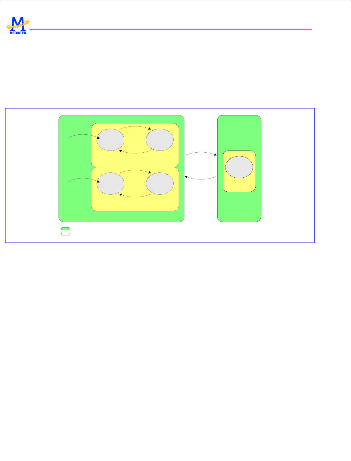
MTK Confidential Release for Konka
MTK Confidential Release for Konka
MT6228 GSM/GPRS Baseband Processor Data Sheet Revision 1.0
563/616
MediaTek Inc. Confidential
11 Power, Clocks and Reset
This chapter describes the power, clock and reset management functions provided by MT6228. Together with Power
Management IC (PMIC), MT6228 offers both fine and coarse resolutions of power control through software programming.
With this efficient method, the developer can turn on selective resources accordingly in order to achieve optimized power
consumption. The operating modes of MT6228 as well as main power states provided by the PMIC are shown in Figure
65.
Active Mode Sleep Mode
Active Mode
Power Down
Mode
Power On Software
Program
Software
Program
Power On
Software
Program
Active State Standby State
Pause Mode
MT6228
Processors
MT6228
Peripherals
Phone Power State
MT6228 Operating Mode
MT6228
Figure 65 Major Phone Power States and Operating Modes for MT6228 based terminal
11.1 B2PSI
11.1.1 General Description
MT6228 uses a 3-wire B2PSI interface to connect to PMIC. This bi-directional serial bus interface allows baseband to
write to or read from PMIC. The bus protocol utilizes a 16-bit format. B2PSICK is the serial bus clock and is driven by
the master. B2PSIDAT is the serial data; master or slave can drive it. B2PSICS is the bus selection signal. Once the
B2PSICS goes LOW, baseband starts to transfer the 4 register bits followed by a read/write bit, then waits 3 clock cycles
for the PMIC B2PSI state machine to decode the operation for the next 8 data bits. The state machine should count 16
clocks to complete the data transfer.
MTK Confidential Release for Konka
MTK Confidential Release for Konka
MT6228 GSM/GPRS Baseband Processor Data Sheet Revision 1.0
564/616
MediaTek Inc. Confidential
B 2 P S I C K
B 2 P S I C K
R 3 R 2 R 1 R 0 W X X X D 7 D 6 D 5 D 4 D 3 D 2 D 1 D 0
R 3 R 2 R 1 R 0 R X X X D 7 D 6 D 5 D 4 D 3 D 2 D 1 D 0
T > 1 0 0 n se c
R e ce iv e
I n d e x
R eg is t er
D e c o d e
W rite R e gis te r C on te n t
R e ce iv e
I n d e x
R eg is t er
D e c o d e
R e ad R e gis te r C on te n t
B 2 P S I D A T
B 2 P S I D A T
B 2 P S I C S
B 2 P S I C S
Figure 66 B2PSI bus timing
11.1.2 Register Definitions
B2PSI+0000h B2PSI data register B2PSI_DATA
Bit 15 14 13 12 11 10 9 8 7 6 5 4 3 2 1 0
Name
B2PSI_DATA [15:0]
Type R/W
Reset
0
B2PSI_DATA The B2PSI DATA format contains 4 bit register + 3 bit do not care + write / read bit + 8 bit data.
0 Read operation
1 Write operation
To prevent a writing error, B2PSI_DATA must be set to 8216h before the actual data write.
B2PSI +0008h B2PSI baud rate divider register B2PSI _DIV
Bit 15 14 13 12 11 10 9 8 7 6 5 4 3 2 1 0
Name
B2PSI _DIV [15:0]
Type R/W
Reset
0
B2PSI_DIV B2PSI clock rate divisor. B2PSICK = system clock rate / div.
B2PSI+0010h B2PSI status register B2PSI_STAT
Bit 15 14 13 12 11 10 9 8 7 6 5 4 3 2 1 0
Name
WRIT
E_SU
CCES
S
READ
_REA
DT
Type RC RC
Reset
0 0
READ_READY Read data ready.
0 Read data is not ready yet.
1 Read data is ready. The bit is cleared by reading B2PSI_STAT register or if B2PSI initializes a new transmit.

MTK Confidential Release for Konka
MTK Confidential Release for Konka
MT6228 GSM/GPRS Baseband Processor Data Sheet Revision 1.0
565/616
MediaTek Inc. Confidential
WRITE_SUCCESS B2PSI write successfully.
0 B2PSI write is not finished yet.
1 B2PSI write has finished. The bit is cleared by reading B2PSI_STAT register or if B2PSI initializes a new
transmit.
B2PSI+0014h B2PSI CS to CK time register B2PSI_TIME
Bit 15 14 13 12 11 10 9 8 7 6 5 4 3 2 1 0
Name
B2PSI_TIME
Type R/W
Reset
0
B2PSI_TIME The time interval that first B2PSICK is started after the B2PSICS is active low.
Time interval = 1/system clock * B2PSI_time.
11.2 Clocks
There are two major time bases in MT6228. The faster one is the 13 MHz clock originating from an off-chip
temperature-compensated voltage controlled oscillator (TCVCXO) that can be either 13 MHz or 26 MHz. This signal is
the input from the SYSCLK pad that is then converted to the square-wave signal by the clock squarer. The other time base
is the 32768 Hz clock generated by an on-chip oscillator connected to an external crystal. Figure 67 shows the clock
sources as well as their utilizations inside the chip.
32KHz
OSC
/2
Clock
Squarer
AHB Bus Clock
APB Bus Clock
MCU Clock
32KHz Clock
AHB
MCU
MCU_DIV2
MT6228 CoreMT6228 I/O
SYSCLK
XIN
XOUT
CLKSQ_PLD
MD PLL
MPLL USB PLL USB Clock
CLKSEL
TV PLL
CLKSEL
MCU
DCM
MCUCLK
ARM
DCM
ARMCLK
TV Clock
104MHz
DSP
DCM
DSPCLK
104MHz ~
13MHz
104MHz ~
13MHz
52MHz ~
13MHz
Figure 67 Clock distributions inside the MT6228.

MTK Confidential Release for Konka
MTK Confidential Release for Konka
MT6228 GSM/GPRS Baseband Processor Data Sheet Revision 1.0
566/616
MediaTek Inc. Confidential
11.2.1 32.768 KHz Time Base
The 32768 Hz clock is always running. It is mainly used as the time base of the Real Time Clock (RTC) module, which
maintains time and date with counters. Therefore, the 32768 Hz oscillator and the RTC module are powered by separate
voltage supplies that are not be powered down when the other power supplies are.
In low power mode, the 13 MHz time base is turned off, so the 32768 Hz clock is employed to update critical TDMA timer
and Watchdog Timer. This time base is also used to clock the keypad scanner logic.
11.2.2 13 MHz Time Base
A 1/2-divider, for MCU Clock, exists to allow usage of either 26 or 13 MHz TCVCXO as clock input.
Three phase-locked loops (MDPLL, TPLL and UPLL) are used to generate four primary clocks, MCU_CLOCK,
DSP_CLOCK, USB_CLOCK and TV_CLOCK, and to clock modules in the MCU Clock Domain and DSP Clock Domain,
USB and TV Encoder, respectively. These PLLs require no off-chip components for operations and can be turned off
independently in order to save power. After power-on, all the PLLs are off by default and the source clock signal is
selected through multiplexers. The software takes care of the PLL lock time while changing the clock selections. The
PLLs and their usages are listed below.
MDPLL provides the MCU system clock (MCU_CLOCK) and DSP system clock (DSP_CLOCK. DPLL).
MCU_CLOCK clocks the MCU core, MCU memory system and MCU peripherals as well.
DSP_CLOCK clocks DSP core and DSP-related modules. MDPLL can be programmed to provide
1X to 8X output of 13 MHz reference. However, because of the employment of DCM (dynamic
clock manager), the output of MDPLL are set as 104 MHz. The clock rates of MCU system and
DSP system can only be changed by programming the clock rate setting of MCU DCM and DSP
DCM.
UPLL provides the USB clock, USB_CLOCK. The UPLL input is a 4 MHz clock, which comes from 104 MHz
clock generated by MDPLL and then divided by 26. UPLL pumps the input clock source 12 times to generate 48
MHz for USB module.
TPLL provides the TV encoder clock, TV_CLOCK. The TPLL input is a 3 MHz clock, which comes from the
48 MHz clock generated by UPLL and then divided by 16. TPLL pumps the input clock source 9 times to
generate 27 MHz for TV encoder.
Note that PLLs need some time to become stable after being powered up. The software takes care of the PLL lock time
before switching them to the proper frequency. Usually, a software loop longer than the PLL lock time is employed to
deal with the problem.
For power management, the MCU software program may stop MCU Clock by setting the Sleep Control Register. Any
interrupt requests to MCU can terminate the sleep mode, and thus returning MCU to the running mode.
AHB can also be stopped by setting the Sleep Control Register. However, the behavior of AHB in sleep mode is a little
different from that of MCU. After entering Sleep Mode, it can be temporarily waken up by any “hreq” (bus request), and
then go back to sleep automatically after all “hreqs” de-assert. Therefore, any transactions can still take place as usual
during AHB sleep mode, and power is saved when there are no transactions. The penalty associated with this is that the
system loses some efficiency due to the switching on and off of the bus clock, but this impact is small.
MTK Confidential Release for Konka
MTK Confidential Release for Konka
MT6228 GSM/GPRS Baseband Processor Data Sheet Revision 1.0
567/616
MediaTek Inc. Confidential
11.2.3 Dynamic Clock Switch of MCU Clock
Dynamic Clock Manager is implemented to allow MCU and DSP switching clock dynamically without any jitter, and
enabling signal drift, and system can operate stably during any clock rate switch.
Please note that MDPLL must be enabled and the frequency is set as 104 MHz. Before switching to the 104 MHz clock
rate, the clock from MD DIV2 feeds through dynamic clock manager (DCM) directly. That means if MD DIV2 is enabled,
the internal clock rate is the half of SYSCLK. Contrarily, the internal clock rate is identical to SYSCLK.
However, the settings of some hardware modules are required to change before or after clock rate change. Software has
the responsibility of changing them at the proper timing. The following table is a list of hardware modules that need to
change their settings during a clock rate change.
Module Name Programming Sequence
EMI
Wait state is changed before clock rate change if the clock rate changes from low
to high, and after the clock rate change if the clock rate changes from high to low.
The new wait state does not take effect until the current EMI access is complete.
Software should insert a period of time before switching clock.
NAND
Wait state is changed before clock rate change if the clock rate changes from low
to high, and after clock rate change if the clock rate changes from high to low.
New wait state will not take effect until current EMI access is complete. Software
should insert a period of time before switching clock.
LCD Change wait state while LCD in IDLE state.
Table 67 Programming sequence during clock switch
11.2.4 Register Definitions
CONFG+0100h
MDPLL Frequency Register MDPLL
Bit
15 14 13 12 11 10 9 8 7 6 5 4 3 2 1 0
Name
CALI RST SPD
Type R/W R/W R/W
Reset
0 0 0
SPD Selects the Output Clock Rate for MDPLL.
Note: The output of MDPLL is a 104 MHz clock for normal function. The clock rate of MCU system and DSP
system is adjusted by programming MCU DCM and DSP DCM.
000 power down
001 13MHz x 2
010 13MHz x 3
011 13MHz x 4
000 13MHz x 5
101 13MHz x 6
110 13MHz x 7
111 13MHz x 8
RST Resets Control of MDPLL
0 Normal Operation
MTK Confidential Release for Konka
MTK Confidential Release for Konka
MT6228 GSM/GPRS Baseband Processor Data Sheet Revision 1.0
568/616
MediaTek Inc. Confidential
1 Reset the MDPLL
CALI Calibration Control for MDPLL
CONFG+108h UPLL Frequency register UPLL
Bit 15 14 13 12 11 10 9 8 7 6 5 4 3 2 1 0
Name
CALI RST
Type
R/W R/W
Reset
0 0
RST Resets Control of UPLL
0 Normal Operation
1 Reset the UPLL
CALI Calibration Control for UPLL
CONFG+10Ch TPLL Frequency register TPLL
Bit 15 14 13 12 11 10 9 8 7 6 5 4 3 2 1 0
Name
CALI RST
Type R/W R/W
Reset
0 0
RST Reset Control of TPLL
0 Normal Operation
1 Reset the TPLL
CALI Calibration Control for TPLL
CONFG+110h Clock Control Register CLK_CON
Bit 15 14 13 12 11 10 9 8 7 6 5 4 3 2 1 0
Name
TV_E
XTCK
USB_
EXTC
K
DSP_
EXTC
K
TPLL_
TMA
UPLL
_TMA
MDPL
L_TM
A
CLKS
Q_PL
D
MD_D
IV2 MDPL
L
Type R/W R/W R/W R/W R/W R/W R/W R/W R/W
Reset
0 0 0 0 0 0 0 0 0
MDPLL Selects MCU and DSP clock source
0 MDPLL bypassed
1 Using MDPLL Clock
MD_DIV2 Control the x2 clock divider for MDPLL reference clock input.
0 Divider bypassed
1 Divider not bypassed
CLKSQ_PLD Pull Down Control
0 Disable
1 Enables
MDPLL_TMA MDPLL test mode
0 Disable
1 Enable
UPLL_TMA UPLL test mode
0 Disable
1 Enable
TPLL_TMA TPLL test mode
MTK Confidential Release for Konka
MTK Confidential Release for Konka
MT6228 GSM/GPRS Baseband Processor Data Sheet Revision 1.0
569/616
MediaTek Inc. Confidential
0 Disable
1 Enable
DSP_EXTCK DSP external clock. When enabled, an external clock source from PIN EINT0 is used instead of DSP
clock from MDPLL output.
0 Disable
1 Enable
USB_EXTCK USB external clock. When enabled, an external clock source from EINT1 is used instead of UPLL
output.
0 Disable
1 Enable
TV_EXTCK TV external clock. When enabled, an external clock source from EINT3 is used instead of TPLL output.
0 Disable
1 Enable
CONFG+114h Sleep Control Register SLEEP_CON
Bit 15 14 13 12 11 10 9 8 7 6 5 4 3 2 1 0
Name
DSP AHB MCU
Type
WO
WO
WO
Reset
0 0 0
MCU Stops the MCU Clock to force MCU Processor to enter sleep mode. MCU clock resumes as long as there is an
interrupt request or system is reset.
0 MCU Clock is running
1 MCU Clock is stopped
AHB Stops the AHB Bus Clock to force the entire bus to enter sleep mode. AHB clock resumes as long as there is an
interrupt request or system is reset.
0 AHB Bus Clock is running
1 AHB Bus Clock is stopped
DSP Stops the DSP Clock.
0 DSP Bus Clock is running
1 DSP Bus Clock is stopped
CONFG+0118h
MCU Clock Control Register MCUCLK_CON
Bit 15 14 13 12 11 10 9 8 7 6 5 4 3 2 1 0
Name
ARM_FSEL MCU_FSEL
Type
R/W R/W
Reset
3 3
MCU_FSEL MCU clock frequency selection. This control register is used to control the output clock frequency of MCU
Dynamic Clock Manager. The clock frequency is from 13MHz to 52MHz. The waveforms of the output clock
are shown below.
Note that the clock period of 39MHz is not uniform. The shortest period of 39MHz clock is the same as the
period of 52MHz. As a result, the wait states of external interfaces, such as EMI, NAND, and so on, have
to be configured based on 52MHz timing. Therefore, the MCU performance executing in external memory
at 39MHz may be worse than at 26MHz.
Also note that the maximum latency of clock switch is 8 104MHz-clock periods. Software provides at least
8T locking time after clock switch command.
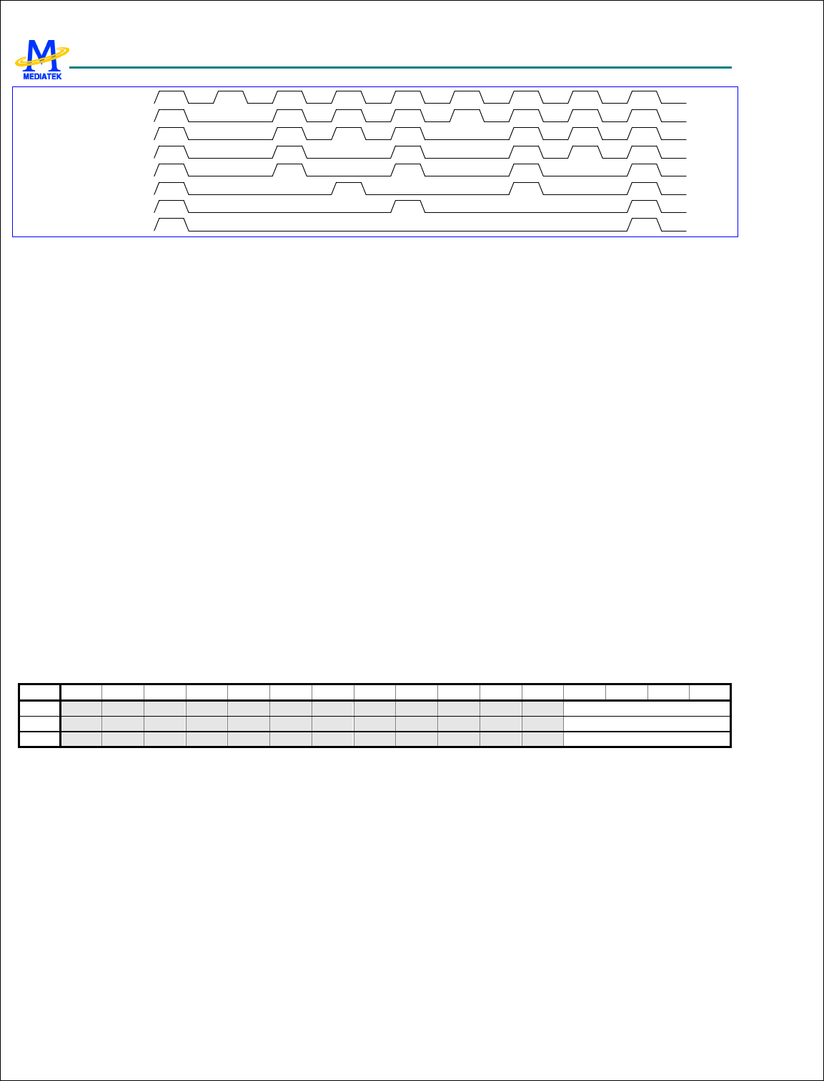
MTK Confidential Release for Konka
MTK Confidential Release for Konka
MT6228 GSM/GPRS Baseband Processor Data Sheet Revision 1.0
570/616
MediaTek Inc. Confidential
104MHz
91MHz
78MHz
65MHz
52MHz
39MHz
26MHz
13MHz
Figure 68 Output of Dynamic Clock Manager
0 13MHz
1 26MHz
2 39MHz
3 52MHz
Others reserved
ARM_FSEL ARM clock frequency selection. This control register is used to control the output clock frequency of ARM
Dynamic Clock Manager. The clock frequency is from 13MHz to 104MHz. 39MHz is not a uniform period
clock.
0 13MHz
1 26MHz
2 39MHz
3 52MHz
4 reserved
5 reserved
6 reserved
7 104MHz
Others reserved
CONFG+011C
h DSP Clock Control Register DSPCLK_CON
Bit 15 14 13 12 11 10 9 8 7 6 5 4 3 2 1 0
Name
DSP_FSEL
Type R/W
Reset
3
DSP_FSEL DSP clock frequency selection. This control register is used to control the output clock frequency of DSP
Dynamic Clock Manager. The clock frequency is from 13MHz to 104MHz. 39MHz, 65MHz, 78MHz, and
91MHz are not a uniform period clock rate.
0 13MHz
1 26MHz
2 39MHz
3 52MHz
4 65MHz
5 78MHz
6 91MHz
7 104MHz
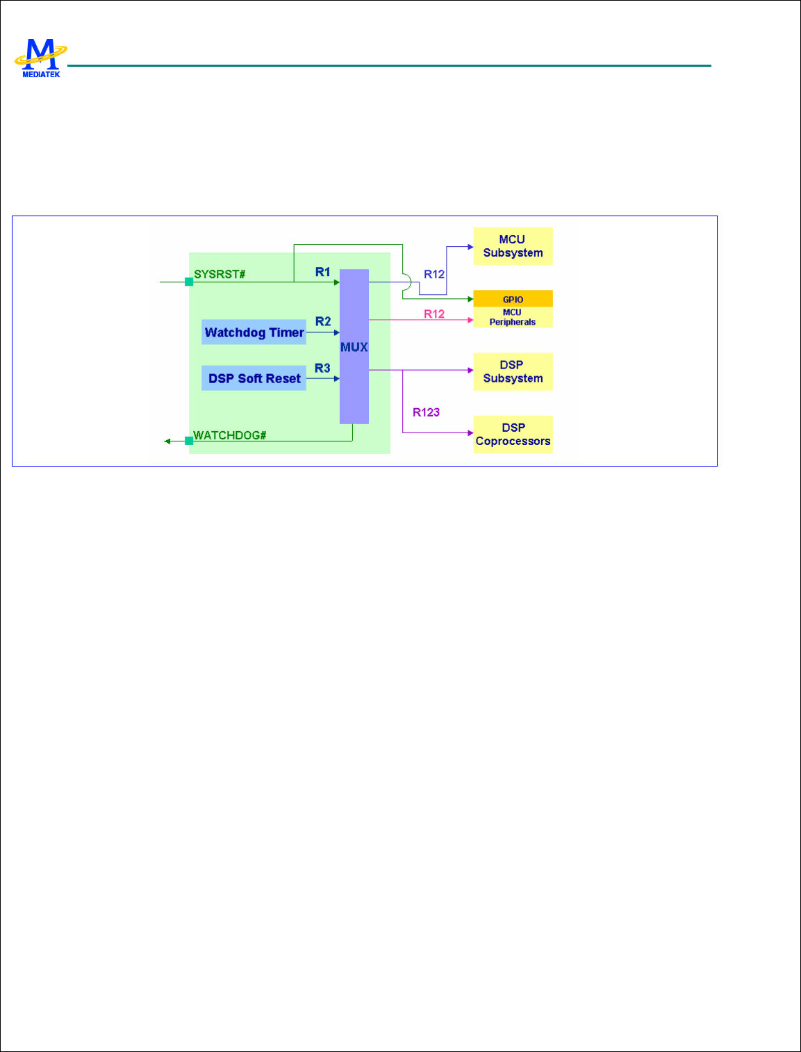
MTK Confidential Release for Konka
MTK Confidential Release for Konka
MT6228 GSM/GPRS Baseband Processor Data Sheet Revision 1.0
571/616
MediaTek Inc. Confidential
Others reserved
11.3 Reset Generation Unit (RGU)
Figure 69 shows the reset scheme used in MT6228. MT6228 provides three kinds of resets: hardware reset, watchdog
reset, and software reset.
Figure 69 Reset Scheme Used in MT6228
11.3.1 General Description
11.3.1.1 Hardware Reset
This reset is input through the SYSRST# pin, which is driven low during power-on. The hardware reset has a global
effect on the chip: all digital and analog circuits are initialized, except the Real Time Clock module. The initial states of
the MT6228 sub-blocks are as follows:.
All analog circuits are turned off.
All PLLs are turned off and bypassed. The 13 MHz system clock is the default time
base.
Special trap states in GPIO.
11.3.1.2 Watchdog Reset
A watchdog reset is generated when the Watchdog Timer expires: the MCU software failed to re-program the timer counter
in time. This situation is typically induced by abnormal software execution, which can be aborted by a hardwired
watchdog reset. Hardware blocks that are affected by the watchdog reset are:
MCU subsystem,
DSP subsystem, and
External components (trigged by software).

MTK Confidential Release for Konka
MTK Confidential Release for Konka
MT6228 GSM/GPRS Baseband Processor Data Sheet Revision 1.0
572/616
MediaTek Inc. Confidential
11.3.1.3 Software Resets
Software resets are local reset signals that initialize specific hardware components. For example, if hardware failures are
detected, the MCU or DSP software may write to software reset trigger registers to reset those specific hardware modules to
their initial states.
The following modules have software resets.
DSP Core
DSP Coprocessors
11.3.2 Register Definitions
RGU +0000h Watchdog Timer Control Register WDT_MODE
Bit 15 14 13 12 11 10 9 8 7 6 5 4 3 2 1 0
Name
KEY[7:0]
AUTO
-REST
ART
IRQ EXTE
N
EXTP
OL
ENAB
LE
Type
R/W
R/W
R/W
R/W
R/W
Reset
0 0 0 0 1
ENABLE Enables the Watchdog Timer.
0 Disables the Watchdog Timer.
1 Enables the Watchdog Timer.
EXTPOL Defines the polarity of the external watchdog pin.
0 Active low.
1 Active high.
EXTEN Specifies whether or not to generate an external watchdog reset signal.
0 The watchdog does not generate an external watchdog reset signal.
1 If the watchdog counter reaches zero, an external watchdog signal is generated.
IRQ Issues an interrupt instead of a Watchdog Timer reset. For debug purposes, RGU issues an interrupt to the MCU
instead of resetting the system.
0 Disable.
1 Enable.
AUTO-RESTART Restarts the Watchdog Timer counter with the value of WDT_LENGTH while task ID is written
into Software Debug Unit.
0 Disable. The counter restarts by writing KEY into the WDT_RESTART register.
1 Enable. The counter restarts by writing KEY into the WDT_RESTART register or by writing
task ID into the software debug unit.
KEY Write access is allowed if KEY=0x22.
RGU +0004h Watchdog Time-Out Interval Register WDT_LENGTH
Bit 15 14 13 12 11 10 9 8 7 6 5 4 3 2 1 0
Name
TIMEOUT[10:0] KEY[4:0]
Type WO
Reset
111_1111_1111b
KEY Write access is allowed if KEY=08h.
MTK Confidential Release for Konka
MTK Confidential Release for Konka
MT6228 GSM/GPRS Baseband Processor Data Sheet Revision 1.0
573/616
MediaTek Inc. Confidential
TIMEOUT The counter is restarted with {TIMEOUT [10:0], 1_1111_1111b}. Thus the Watchdog Timer time-out
period is a multiple of 512*T
32k
=15.6ms.
RGU +0008h Watchdog Timer Restart Register WDT_RESTART
Bit 15 14 13 12 11 10 9 8 7 6 5 4 3 2 1 0
Name
KEY[15:0]
Type
Reset
KEY Restart the counter if KEY=1971h.
RGU +000Ch Watchdog Timer Status Register WDT_STA
Bit
15 14 13 12 11 10 9 8 7 6 5 4 3 2 1 0
Name
WDT SW_W
DT
Type RO RO
Reset
0 0
WDT Indicates the cause of the watchdog reset.
0 Reset not due to Watchdog Timer.
1 Reset because the Watchdog Timer time-out period expired.
SW_WDT Indicates if the watchdog was triggered by software.
0 Reset not due to software-triggered Watchdog Timer.
1 Reset due to software-triggered Watchdog Timer.
NOTE: A system reset does not affect this register. This bit is cleared when the WTU_MODE register ENABLE bit is
written.
RGU +0010h CPU Peripheral Software Reset Register SW_PERIPH_RS
TN
Bit 15 14 13 12 11 10 9 8 7 6 5 4 3 2 1 0
Name
DAMR
ST
USBR
ST
KEY
Type R/W R/W
Reset
0 0
KEY Write access is allowed if KEY=37h.
DMARST Reset the DMA peripheral.
0 No reset.
1 Invoke a reset.
USBRST Reset the USB.
0 No reset.
1 Invoke a reset.
RGU +0014h DSP Software Reset Register SW_DSP_RSTN
Bit 15 14 13 12 11 10 9 8 7 6 5 4 3 2 1 0
Name
RST
Type R/W
Reset
0
RST Controls the DSP System Reset Control.
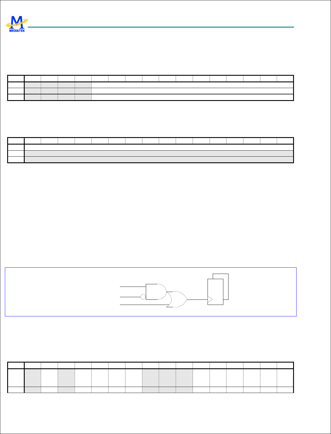
MTK Confidential Release for Konka
MTK Confidential Release for Konka
MT6228 GSM/GPRS Baseband Processor Data Sheet Revision 1.0
574/616
MediaTek Inc. Confidential
0 No reset.
1 Invoke a reset.
RGU +0018h Watchdog Timer Reset Signal Duration Register WDT_RSTINTRE
VAL
Bit 15 14 13 12 11 10 9 8 7 6 5 4 3 2 1 0
Name
LENGTH[ 11:0]
Type R/W
Reset
FFFh
LENGTH This register indicates the reset duration when Watchdog Timer times out. However, if the WDT_MODE
register IRQ bit is set to 1, an interrupt is issued instead of a reset.
RGU+001Ch Watchdog Timer Software Reset Register WDT_SWRST
Bit 15 14 13 12 11 10 9 8 7 6 5 4 3 2 1 0
Name
KEY[15:0]
Type
Reset
Software-triggered Watchdog Timer reset. If the register content matches the KEY, a watchdog reset is issued. However,
if the WDT_MODE register IRQ bit is set to 1, an interrupt is issued instead of a reset.
KEY 1209h
11.4 Software Power Down Control
In addition to the Pause Mode capability while in the Standby State, the software program can also put each peripheral
independently into Power Down Mode while in the Active State by gating off their clock. The typical logic
implementation is depicted in Figure 70. For all configuration bits, 1 signifies that the function is in Power Down Mode,
and 0 means the function is in the Active Mode.
CLOCK
POWER DOWN
TESTMODE
Figure 70 Power Down Control at Block Level
11.4.1 Register Definitions
CONFG+300h Power Down Control 0 Register PDN_CON0
Bit 15 14 13 12 11 10 9 8 7 6 5 4 3 2 1 0
Name
MDPL
L CLK_
DIV2
CLKS
Q UPLL TPLL PPP CHE
WAVE
TABL
E
GCU USB DMA
Type R/W R/W R/W R/W R/W R/W R/W R/W R/W R/W R/W

MTK Confidential Release for Konka
MTK Confidential Release for Konka
MT6228 GSM/GPRS Baseband Processor Data Sheet Revision 1.0
575/616
MediaTek Inc. Confidential
Reset
1 1 0 1 1 1 1 1 1 1 1
DMA Controls the DMA Controller Power Down.
USB Controls the USB Controller Power Down.
GCU Controls the GCU Controller Power Down.
WAVETALBE Controls the DSP WaveTable DMA Power Down.
CHE Controls the CHE Power Down.
PPP Controls the PPP Framer Power Down.
TPLL Controls the TPLL Power Down.
UPLL Controls the UPLL Power Down.
CLKSQ Controls the Clock squarer Power Down.
CLK_DIV2 Controls the Input Clock DIV2 Power Down.
MDPLL Controls the MCU and DSP PLL Power Down.
CONFG +304h Power Down Control 1 Register PDN_CON1
Bit 15 14 13 12 11 10 9 8 7 6 5 4 3 2 1 0
Name
IRDA
UART
3 B2PSI
NFI
PWM2
SWDB
G MSDC
UART
2 LCD
ALTE
R PWM1
SIM
UART
1 GPIO
KP
GPT
Type R/W R/W R/W R/W R/W R/W R/W R/W R/W R/W R/W R/W R/W R/W R/W R/W
Reset
1 1 1 1 1 1 1 1 1 1 1 1 0 1 1 1
GPT Controls the General Purpose Timer Power Down.
KP Controls the Keypad Scanner Power Down.
GPIO Controls the GPIO Power Down.
UART1 Controls the UART1 Controller Power Down.
SIM Controls the SIM Controller Power Down.
PWM1 Controls the PWM1 Generator Power Down.
ALTER Controls the Alerter Generator Power Down.
LCD Controls the Serial LCD Controller Power Down.
UART2 Controls the UART2 Controller Power Down.
MSDC Controls the MS/SD Controller Power Down.
PWM2 Controls the PWM2 Generator Power Down.
SWDBG Controls the MCU/DSP Software Debug Power Down.
NFI Controls the NAND FLASH Interface Power Down.
B2PSI Controls the Serial Port Interface Power Down.
UART3 Controls the UART3 Controller Power Down.
IRDA Controls the IrDA Framer Power Down.
CONFG +308h Power Down Control 2 Register PDN_CON2
Bit 15 14 13 12 11 10 9 8 7 6 5 4 3 2 1 0
Name
GMSK
BBRX
SCCB
AAFE
DIV GCC BFE VAFE AUXA
D FCS APC AFC BPI BSI RTC TDMA
Type R/W R/W R/W R/W R/W R/W R/W R/W R/W R/W R/W R/W R/W R/W R/W R/W
Reset
1 1 1 1 1 1 1 1 1 1 1 1 1 1 1 1
TDMA Controls the TDMA Power Down.
RTC Controls the RTC Power Down.

MTK Confidential Release for Konka
MTK Confidential Release for Konka
MT6228 GSM/GPRS Baseband Processor Data Sheet Revision 1.0
576/616
MediaTek Inc. Confidential
BSI Controls the BSI Power Down. This control is not be updated until both tdma_evtval and qbit_en are asserted.
BPI Controls the BPI Power Down. This control is not be updated until both tdma_evtval and qbit_en are asserted.
AFC Controls the AFC Power Down. This control is not be updated until both tdma_evtval and qbit_en are asserted.
APC Controls the APC Power Down. This control is not be updated until both tdma_evtval and qbit_en are asserted.
FCS Controls the FCS Power Down.
AUXAD Controls the AUX ADC Power Down.
VAFE Controls the Audio Front End of VBI Power Down.
BFE Controls the Base-Band Front End Power Down.
GCU Controls the GCU Power Down.
DIV Controls the Divider Power Down.
AAFE Controls the Audio Front End of MP3 Power Down.
SCCB Controls the SCCB Power Down.
BBRX Controls the BB RX Power Down.
GMSK Controls the GMSK Power Down.
CONFG +30Ch Power Down Control 3 Register PDN_CON3
Bit 15 14 13 12 11 10 9 8 7 6 5 4 3 2 1 0
Name
DRZ IMGD
MA DCT ISP PRZ JPEG MP4 G2D GCMQ
GIF PNG IPP TV CRZ RESZ
LB ICE
Type R/W R/W R/W R/W R/W R/W R/W R/W R/W R/W R/W R/W R/W R/W R/W R/W
Reset
1 1 1 1 1 1 1 1 1 1 1 1 1 1 1 1
ICE Enables the debug feature of the ARM7EJS core. Controls the DBGEN pin of the ICEBreaker.
RESZ LB Controls the Post Resizer Power Down.
TV Controls the TV Encoder Power Down.
CRZ Controls the Capture Resizer Power Down.
IPP Controls the Image Processor Power Down.
PNG Controls the PNG Decoder Power Down.
GIF Controls the GIF Decoder Power Down.
GCMQ Controls the Graphic Command Queue Power Down.
G2D Controls the 2D Accelerator Power Down.
MP4 Controls the MPEG-4 Power Down.
JPEG Controls the JPEG Power Down.
REZ Controls the Resizer Power Down.
ISP Controls the Image Signal Processor Power Down.
DCT Controls the DCT Power Down.
IMGDMA Controls the Image DMA Power Down.
DRZ Controls the Drop Resizer Power Down.
CONFG +330h Power Down Control 4 Register PDN_CON4
Bit
15 14 13 12 11 10 9 8 7 6 5 4 3 2 1 0
Name
APC AFC BPI BSI
Type WO WO WO WO
Reset
1 1 1 1
BSI Controls the BSI Power Down. This control is updated immediately.
BPI Controls the BPI Power Down. This control is updated immediately.
MTK Confidential Release for Konka
MTK Confidential Release for Konka
MT6228 GSM/GPRS Baseband Processor Data Sheet Revision 1.0
577/616
MediaTek Inc. Confidential
AFC Controls the AFC Power Down. This control is updated immediately.
APC Controls the APC Power Down. This control is updated immediately.
CONFG+0310h
Power Down Set 0 Register PDN_SET0
Bit 15 14 13 12 11 10 9 8 7 6 5 4 3 2 1 0
Name
MDPL
L CLK_
DIV2
CLKS
Q UPLL
TPLL
PPP
CHE
WAVE
TABL
E
GCU
USB
DMA
Type W1S W1S W1S W1S W1S W1S W1S W1S W1S W1S W1S
CONFG+0314h
Power Down Set 1 Register PDN_SET1
Bit 15 14 13 12 11 10 9 8 7 6 5 4 3 2 1 0
Name
IRDA
UART
3 B2PSI
NFI
TRC
PWM2
MSDC
UART
2 LCD
ALTE
R PWM1
SIM
UART
1 GPIO
KP
GPT
Type W1S W1S W1S W1S W1S W1S W1S W1S W1S W1S W1S W1S W1S W1S W1S W1S
CONFG+0318h
Power Down Set 2 Register PDN_SET2
Bit 15 14 13 12 11 10 9 8 7 6 5 4 3 2 1 0
Name
GMSK
BBRX
SCCB
AAFE
DIV GCC BFE VAFE AUXA
D FCS APC AFC BPI BSI RTC TDMA
Type W1S W1S W1S W1S W1S W1S W1S W1S W1S W1S W1S W1S W1S W1S W1S W1S
CONFG+031C
h Power Down Set 3 Register PDN_SET3
Bit 15 14 13 12 11 10 9 8 7 6 5 4 3 2 1 0
Name
DRZ IMGD
MA DCT ISP REZ JPEG MP4 G2D GCMQ
GIF PNG IPP TV CRZ RESZ
LB ICE
Type W1S W1S W1S W1S W1S W1S W1S W1S W1S W1S W1S W1S W1S W1S W1S W1S
CONFG+0334h
Power Down Set 4 Register PDN_SET4
Bit 15 14 13 12 11 10 9 8 7 6 5 4 3 2 1 0
Name
APC AFC BPI BSI
Type W1S W1S W1S W1S
These registers are used to set power down control bit individually. Only bits set to 1 are in effect. Setting the bits to 1
sets the corresponding power down control bits to 1. Otherwise, the bits retain their original value.
EACH BIT Set the Associated Power Down Control Bit to 1.
0 No effect.
1 Set corresponding bit to 1.
CONFG+0320h
Power Down Clear 0 Register PDN_CLR0
Bit
15 14 13 12 11 10 9 8 7 6 5 4 3 2 1 0
Name
MDPL
L CLK_
DIV2
CLKS
Q UPLL TPLL PPP CHE
WAVE
TABL
E
GCU USB DMA
Type W1C W1C W1C W1C W1C W1C W1C W1C W1C W1C W1C

MTK Confidential Release for Konka
MTK Confidential Release for Konka
MT6228 GSM/GPRS Baseband Processor Data Sheet Revision 1.0
578/616
MediaTek Inc. Confidential
CONFG+0324h
Power Down Clear 1 Register PDN_CLR1
Bit 15 14 13 12 11 10 9 8 7 6 5 4 3 2 1 0
Name
IRDA UART
3 B2PSI
NFI TRC PWM2
MSDC
UART
2 LCD ALTE
R PWM1
SIM UART
1 GPIO KP GPT
Type W1C W1C W1C W1C W1C W1C W1C W1C W1C W1C W1C W1C W1C W1C W1C W1C
CONFG+0328h
Power Down Clear 2 Register PDN_CLR2
Bit 15 14 13 12 11 10 9 8 7 6 5 4 3 2 1 0
Name
GMSK
BBRX
SCCB
AAFE
DIV GCC BFE VAFE AUXA
D FCS APC AFC BPI BSI RTC TDMA
Type W1C W1C W1C W1C W1C W1C W1C W1C W1C W1C W1C W1C W1C W1C W1C W1C
CONFG+032C
h Power Down Clear 3 Register PDN_CLR3
Bit 15 14 13 12 11 10 9 8 7 6 5 4 3 2 1 0
Name
DRZ IMGD
MA DCT ISP REZ JPEG MP4 G2D GCMQ
GIF PNG IPP TV CRZ RESZ
LB ICE
Type
W1C
W1C
W1C
W1C
W1C
W1C
W1C
W1C
W1C
W1C
W1C
W1C
W1C
W1C
W1C
W1C
CONFG+0338h
Power Down Clear 4 Register PDN_CLR4
Bit 15 14 13 12 11 10 9 8 7 6 5 4 3 2 1 0
Name
APC AFC BPI BSI
Type W1C W1C W1C W1C
These registers are used to clear power down control bits individually. Only the bits set to 1 are in effect. Setting the
bits to 1 sets the corresponding power down control bits to 0. Otherwise, the bits retain their original value.
EACH BIT Clear the Associated Power Down Control Bit.
0 no effect
1 Set corresponding bit to 0

MTK Confidential Release for Konka
MTK Confidential Release for Konka
MT6228 GSM/GPRS Baseband Processor Data Sheet Revision 1.0
579/616
MediaTek Inc. Confidential
12 Analog Front-end & Analog Blocks
12.1 General Description
To communicate with analog blocks, a common control interface for all analog blocks is implemented. In addition, there are
some dedicated interfaces for data transfer. The common control interface translates APB bus write and read cycle for
specific addresses related to analog front-end control. During writing or reading of any of these control registers, there is a
latency associated with transferring of data to or from the analog front-end. Dedicated data interface of each analog block is
implemented in the corresponding digital block. The Analog Blocks includes the following analog function for complete
GSM/GPRS base-band signal processing:
1. Base-band RX: For I/Q channels base-band A/D conversion
2. Base-band TX: For I/Q channels base-band D/A conversion and smoothing filtering, DC level shifting
3. RF Control: Two DACs for automatic power control (APC) and automatic frequency control (AFC) are included.
Their outputs are provided to external RF power amplifier and VCXO), respectively.
4. Auxiliary ADC: Providing an ADC for battery and other auxiliary analog function monitoring
5. Audio mixed-signal blocks: It provides complete analog voice signal processing including microphone amplification,
A/D conversion, D/A conversion, earphone driver, and etc. Besides, dedicated stereo D/A conversion and
amplification for audio signals are included).
6. Clock Generation: A clock squarer for shaping system clock, and three PLLs that provide clock signals to DSP, MCU,
and USB units are included
7. XOSC32: It is a 32-KHz crystal oscillator circuit for RTC application Analog Block Descriptions
12.1.1 BBRX
12.1.1.1 Block Descriptions
The receiver (RX) performs base-band I/Q channels downlink analog-to-digital conversion:
1. Analog input multiplexer: For each channel, a 4-input multiplexer that supports offset and gain calibration is included.
2. A/D converter: Two 14-bit sigma-delta ADCs perform I/Q digitization for further digital signal processing.
12.1.1.2 Functional Specifications
The functional specifications of the base-band downlink receiver are listed in the following table.
Symbol Parameter Min Typical Max Unit
N Resolution 14 Bit
FC Clock Rate 26 MHz
FS Output Sampling Rate 13/12 MSPS
Input Swing
When GAIN=’0’
0.8*AVDD
0.4*AVDD
Vpk
Vpk
MTK Confidential Release for Konka
MTK Confidential Release for Konka
MT6228 GSM/GPRS Baseband Processor Data Sheet Revision 1.0
580/616
MediaTek Inc. Confidential
When GAIN=’1’
OE Offset Error +/- 10 mV
FSE Full Swing Error +/- 30 mV
I/Q Gain Mismatch 0.5 dB
SINAD Signal to Noise and Distortion Ratio
- 45kHz sine wave in [0:90] kHz bandwidth
- 145kHz sine wave in [10:190] kHz
bandwidth
65
65
dB
dB
ICN Idle channel noise
- [0:90] kHz bandwidth
- [10:190] kHz bandwidth
-74
-70
dB
dB
DR Dynamic Range
- [0:90] kHz bandwidth
- [10:190] kHz bandwidth
74
70
dB
dB
RIN Input Resistance 75 k
DVDD Digital Power Supply 1.6 1.8 2.0 V
AVDD Analog Power Supply 2.5 2.8 3.1 V
T Operating Temperature -20 80
Current Consumption
Power-up
Power-Down
5
5
mA
A
Table 68 Base-band Downlink Specifications
12.1.2 BBTX
12.1.2.1 Block Descriptions
The transmitter (TX) performs base-band I/Q channels up-link digital-to-analog conversion. Each channel includes:
1. 10-Bits D/A Converter: It converts digital GMSK modulated signals to analog domain. The input to the DAC is sampled
at 4.33-MHz rate with 10-bits resolution.
2. Smoothing Filter: The low-pass filter performs smoothing function for DAC output signals with a 350-kHz 2nd-order
Butterworth frequency response.
12.1.2.2 Function Specifications
The functional specifications of the base-band uplink transmitter are listed in the following table.
Symbol Parameter Min Typical Max Unit
N Resolution 10 Bit
FS Sampling Rate 4.33 MSPS
SINAD Signal to Noise and Distortion Ratio 57 60 dB
Output Swing 0.18*AVDD 0.89*AVDD V
VOCM Output CM Voltage 0.34*AVDD 0.5*AVDD 0.62*AVDD V

MTK Confidential Release for Konka
MTK Confidential Release for Konka
MT6228 GSM/GPRS Baseband Processor Data Sheet Revision 1.0
581/616
MediaTek Inc. Confidential
Output Capacitance 20 PF
Output Resistance 10 K
DNL Differential Nonlinearity +/- 0.5 LSB
INL Integral Nonlinearity +/- 1.0 LSB
OE Offset Error +/- 15 mV
FSE Full Swing Error +/- 30 mV
FCUT Filter –3dB Cutoff Frequency 300 350 400 KHz
ATT Filter Attenuation at
100-KHz
270-KHz
4.33-MHz
0.1
2.2
46.4
0.0
1.3
43.7
0.0
0.8
41.4
dB
dB
dB
I/Q Gain Mismatch +/- 0.5 dB
I/Q Gain Mismatch Correction Range -1.18 +1.18 dB
DVDD Digital Power Supply 1.6 1.8 2.0 V
AVDD Analog Power Supply 2.5 2.8 3.1 V
T Operating Temperature -20 80
Current Consumption
Power-up
Power-Down
5
5
mA
A
Table 69 Base-band Uplink Transmitter Specifications
12.1.3 AFC-DAC
12.1.3.1 Block Descriptions
As shown in the following figure, together with a 2
nd
-oder digital sigma-delta modulator, AFC-DAC is designed to produce
a single-ended output signal at AFC pin. AFC pin should be connected to an external 1
st
-order R-C low pass filter to meet
the 13-bits resolution (DNL) requirement
2
.
The AFC_BYP pin is the mid-tap of a resistor divider inside the chip to offer the AFC output common-mode level. Nominal
value of this common-mode voltage is half the analog power supply, and typical value of output impedance of AFC_BYP
pin is about 21k. To suppress the noise on common mode level, it is suggested to add an external capacitance between
AFC_BYP pin and ground. The value of the bypass capacitor should be chosen as large as possible but still meet the
settling time requirement set by overall AFC algorithm
3
.
2
DNL performance depends on external output RC filter bandwidth: the narrower the bandwidth, the better the DNL. Thus,
there exists a tradeoff between output setting speed and DNL performance
3
AFC_BYP output impedance and bypass capacitance determine the common-mode settling RC time constant. Insufficient
common-mode settling will affect the INL performance. A typical value of 1nF is suggested.
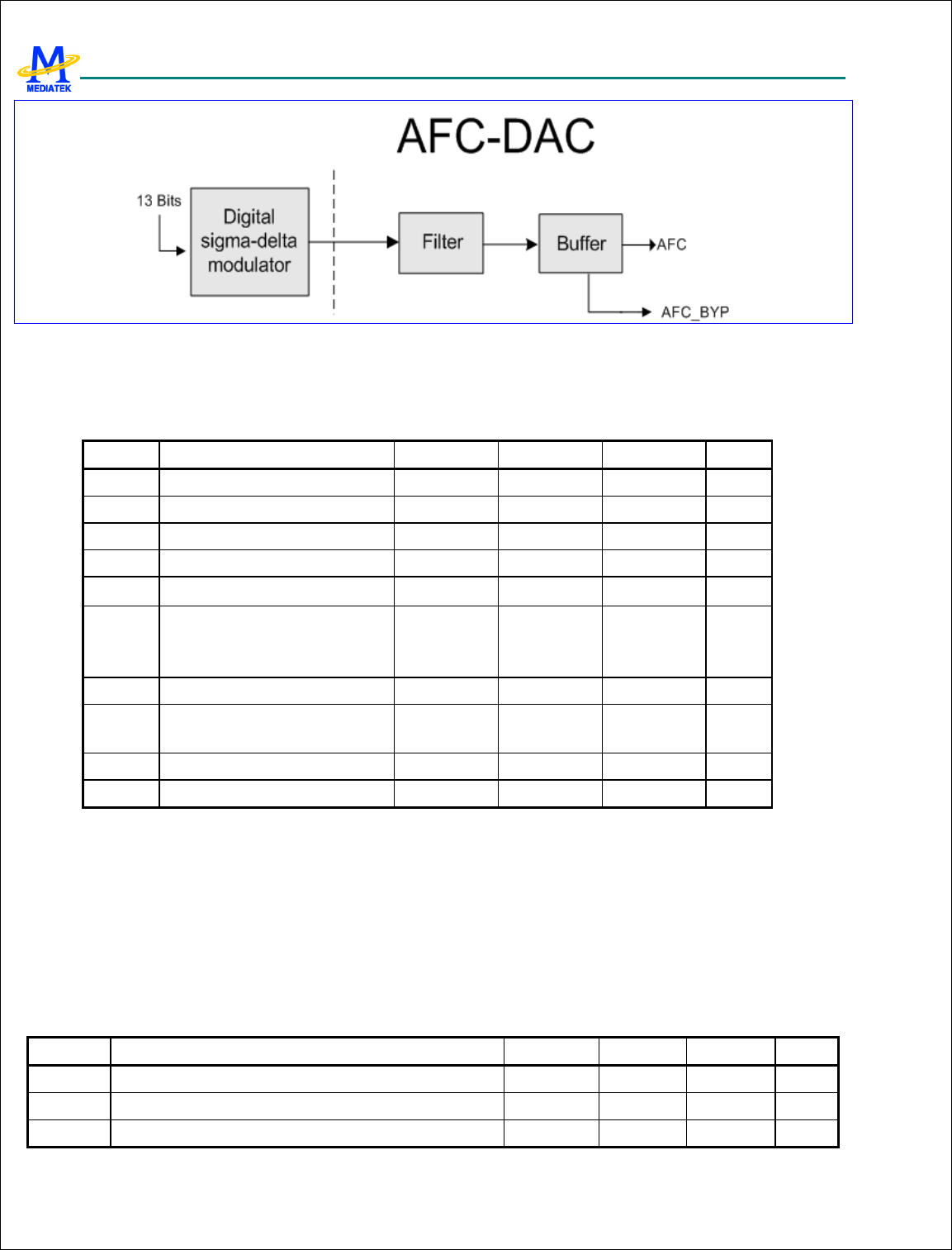
MTK Confidential Release for Konka
MTK Confidential Release for Konka
MT6228 GSM/GPRS Baseband Processor Data Sheet Revision 1.0
582/616
MediaTek Inc. Confidential
Figure 71 Block diagram of AFC-DAC
12.1.3.2 Functional Specifications
The following table gives the electrical specification of AFC-DAC.
Symbol Parameter Min Typical Max Unit
N Resolution 13 Bit
FS Sampling Rate 6500 KHz
DVDD Digital Power Supply 1.6 1.8 2.0 V
AVDD Analog Power Supply 2.6 2.8 3.1 V
T Operating Temperature -20 80
Current Consumption
Power-up
Power-Down
1.2
1 mA
A
Output Swing 0.75*AVDD V
Output Resistor
(in AFC output RC network)
1 K
DNL Differential Nonlinearity +1/-1 LSB
INL Integral Nonlinearity +4.0/-4.0 LSB
Table 70 Functional specification of AFC-DAC
12.1.4 APC-DAC
12.1.4.1 Block Descriptions
The APC-DAC is a 10-bits DAC with output buffer aimed for automatic power control. Here blow are its analog pin
assignment and functional specification tables.
12.1.4.2 Function Specifications
Symbol Parameter Min Typical Max Unit
N Resolution 10 Bit
FS Sampling Rate 1.0833 MSPS
SINAD Signal to Noise and Distortion Ratio 50 dB
MTK Confidential Release for Konka
MTK Confidential Release for Konka
MT6228 GSM/GPRS Baseband Processor Data Sheet Revision 1.0
583/616
MediaTek Inc. Confidential
(10-KHz Sine with 1.0V Swing & 100-KHz BW)
99% Settling Time (Full Swing on Maximal Capacitance) 5 S
Output Swing AVDD-0.2 V
Output Capacitance 200 pF
Output Resistance 10 K
DNL Differential Nonlinearity +/- 0.5 LSB
INL Integral Nonlinearity +/- 1.0 LSB
OE Offset Error +/- 10 mV
FSE Full Swing Error +/- 10 mV
DVDD Digital Power Supply 1.6 1.8 2.0 V
AVDD Analog Power Supply 2.5 2.8 3.1 V
T Operating Temperature -20 80
Current Consumption
Power-up
Power-Down
600
1
A
A
Table 71 APC-DAC Specifications
12.1.5 Auxiliary ADC
12.1.5.1 Block Descriptions
The auxiliary ADC includes the following functional blocks:
1. Analog Multiplexer: The analog multiplexer selects signal from one of the seven auxiliary input pins. Real word
message to be monitored, like temperature, should be transferred to the voltage domain.
2. 10 bits A/D Converter: The ADC converts the multiplexed input signal to 10-bit digital data.
12.1.5.2 Function Specifications
The functional specifications of the auxiliary ADC are listed in the following table.
Symbol Parameter Min Typical Max Unit
N Resolution 10 Bit
FC Clock Rate 0.1 1.0833 5 MHz
FS Sampling Rate @ N-Bit 5/(N+1) MSPS
Input Swing 1.0 AVDD V
VREFP Positive Reference Voltage
(Defined by AUX_REF pin)
1.0 AVDD V
CIN Input Capacitance
Unselected Channel
Selected Channel
50
1.2
fF
pF
RIN Input Resistance
Unselected Channel
Selected Channel
10
1.8
M
M

MTK Confidential Release for Konka
MTK Confidential Release for Konka
MT6228 GSM/GPRS Baseband Processor Data Sheet Revision 1.0
584/616
MediaTek Inc. Confidential
RS Resistor String Between AUX_REF pin & ground
Power Up
Power Down
35
10
50 65 K
M
Clock Latency 11 1/FC
DNL Differential Nonlinearity +0.5/-0.5 LSB
INL Integral Nonlinearity +1.0/-1.0 LSB
OE Offset Error +/- 10 mV
FSE Full Swing Error +/- 10 mV
SINAD Signal to Noise and Distortion Ratio (10-KHz Full
Swing Input & 13-MHz Clock Rate) 50 dB
DVDD Digital Power Supply 1.6 1.8 2.0 V
AVDD Analog Power Supply 2.5 2.8 3.1 V
T Operating Temperature -20 80
Current Consumption
Power-up
Power-Down
300
1
A
A
Table 72 The Functional specification of Auxiliary ADC
12.1.6 Audio mixed-signal blocks
12.1.6.1 Block Descriptions
Audio mixed-signal blocks (AMB) integrate complete voice uplink/downlink and audio playback functions. As shown in
the following figure, it includes mainly three parts. The first consists of stereo audio DACs and speaker amplifiers for audio
playback. The second is the voice downlink path, including voice-band DACs and amplifiers, which produces voice signal
to earphone or other auxiliary output device. Amplifiers in these two blocks are equipped with multiplexers to accept
signals from internal audio/voice or external radio sources. The last is the voice uplink path, which is the interface between
microphone (or other auxiliary input device) input and MT6228 DSP. A set of bias voltage is provided for external electret
microphone..

MTK Confidential Release for Konka
MTK Confidential Release for Konka
MT6228 GSM/GPRS Baseband Processor Data Sheet Revision 1.0
585/616
MediaTek Inc. Confidential
Figure 72 Block diagram of audio mixed-signal blocks.
12.1.6.2 Functional Specifications
The following table gives functional specifications of voice-band uplink/downlink blocks.
Symbol Parameter Min Typical Max Unit
FS Sampling Rate 4096 KHz
CREF Decoupling Cap Between AU_VREF_P
And AU_VREF_N
47 NF
DVDD Digital Power Supply 1.6 1.8 2.0 V
AVDD Analog Power Supply 2.5 2.8 3.1 V
T Operating Temperature -20 80
IDC Current Consumption 5 mA
VMIC Microphone Biasing Voltage 1.9 V
MTK Confidential Release for Konka
MTK Confidential Release for Konka
MT6228 GSM/GPRS Baseband Processor Data Sheet Revision 1.0
586/616
MediaTek Inc. Confidential
IMIC
Current Draw From Microphone Bias
Pins
2 mA
Uplink Path
4
SINAD
Signal to Noise and Distortion Ratio
Input Level: -40 dbm0
Input Level: 0 dbm0
29
69
dB
dB
RIN Input Impedance (Differential) 13 20 27 K
ICN Idle Channel Noise -67 dBm0
XT Crosstalk Level -66 dBm0
Downlink Path
5
SINAD
Signal to Noise and Distortion Ratio
Input Level: -40 dBm0
Input Level: 0 dBm0
29
69
dB
dB
RLOAD Output Resistor Load (Differential) 28
CLOAD Output Capacitor Load 200 pF
ICN Idle Channel Noise of Transmit Path -67 dBm0
XT Crosstalk Level on Transmit Path -66 dBm0
Table 73 Functional specifications of analog voice blocks
Functional specifications of the audio blocks are described in the following.
Symbol Parameter Min Typical Max Unit
FCK Clock Frequency Fs*128 KHz
Fs Sampling Rate 32 44.1 48 KHz
AVDD Power Supply 2.6 2.8 3.1 V
T Operating Temperature -20 80
IDC Current Consumption 5 mA
PSNR
Peak Signal to Noise Ratio
80 dB
DR Dynamic Range 80 dB
VOUT Output Swing for 0dBFS Input Level 0.85 Vrms
THD
Total Harmonic Distortion
-40
-60
dB
4
For uplink-path, not all gain setting of VUPG meets the specification listed on table, especially for the several highest
gains. The maximum gain that meets the specification is to be determined.
5
For downlink-path, not all gain setting of VDPG meets the specification listed on table, especially for the several lowest
gains. The minimum gain that meets the specification is to be determined.
MTK Confidential Release for Konka
MTK Confidential Release for Konka
MT6228 GSM/GPRS Baseband Processor Data Sheet Revision 1.0
587/616
MediaTek Inc. Confidential
45mW at 16 Load
22mW at 32 Load
dB
RLOAD Output Resistor Load (Single-Ended) 16
CLOAD Output Capacitor Load 200 pF
XT L-R Channel Cross Talk TBD dB
Table 74 Functional specifications of the analog audio blocks
12.1.7 Clock Squarer
12.1.7.1 Block Descriptions
For most VCXO, the output clock waveform is sinusoidal with too small amplitude (about several hundred mV) to make
MT6228 digital circuits function well. Clock squarer is designed to convert such a small signal to a rail-to-rail clock signal
with excellent duty-cycle. It provides also a pull-down function when the circuit is powered-down.
12.1.7.2 Function Specifications
The functional specification of clock squarer is shown in Table 75.
Symbol Parameter Min Typical Max Unit
Fin Input Clock Frequency 13 MHz
Fout Output Clock Frequency 13 MHz
Vin Input Signal Amplitude 500 AVDD mVpp
DcycIN Input Signal Duty Cycle 50 %
DcycOUT Output Signal Duty Cycle DcycIN-5 DcycIN+5 %
TR Rise Time on Pin CLKSQOUT 5 ns/pF
TF Fall Time on Pin CLKSQOUT 5 ns/pF
DVDD Digital Power Supply 1.3 1.5 1.7 V
AVDD Analog Power Supply 2.5 2.8 3.1 V
T Operating Temperature -20 80
Current Consumption TBD A
Table 75 The Functional Specification of Clock Squarer
12.1.7.3 Application Notes
Here below in the figure is an equivalent circuit of the clock squarer. Please be noted that the clock squarer is designed to
accept a sinusoidal input signal. If the input signal is not sinusoidal, its harmonic distortion should be low enough to not
produce a wrong clock output. As an reference, for a 13MHz sinusoidal signal input with amplitude of 0.2V the harmonic
distortion should be smaller than 0.02V.
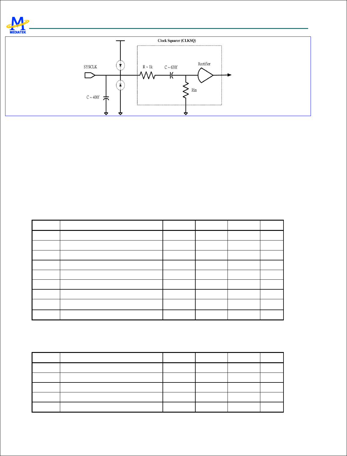
MTK Confidential Release for Konka
MTK Confidential Release for Konka
MT6228 GSM/GPRS Baseband Processor Data Sheet Revision 1.0
588/616
MediaTek Inc. Confidential
Figure 73 Equivalent circuit of Clock Squarer.
12.1.8 Phase Locked Loop
12.1.8.1 Block Descriptions
MT6228 includes three PLLs: DSP PLL, MCU PLL, and USB PLL. DSP PLL and MCU PLL are identical and
programmable to provide either 52MHz or 78 MHz output clock while accepts 13MHz signal. USB PLL is designed to
accept 4MHz input clock signal and provides 48MHz output clock.
12.1.8.2 Function Specifications
The functional specification of DSP/MCU PLL is shown in the following table.
Symbol Parameter Min Typical Max Unit
Fin Input Clock Frequency 13 MHz
Fout Output Clock Frequency 52 78 MHz
Lock-in Time TBD s
Output Clock Duty Cycle 40 50 60 %
Output Clock Jitter 650 ps
DVDD Digital Power Supply 1.6 1.8 2.0 V
AVDD Analog Power Supply 2.5 2.8 3.1 V
T Operating Temperature -20 80
Current Consumption TBD A
Table 76 The Functional Specification of DSP/MCU PLL
The functional specification of USB PLL is shown below.
Symbol Parameter Min Typical Max Unit
Fin Input Clock Frequency 4 MHz
Fout Output Clock Frequency 48 MHz
Lock-in Time TBD s
Output Clock Duty Cycle 40 50 60 %
Output Clock Jitter 650 ps
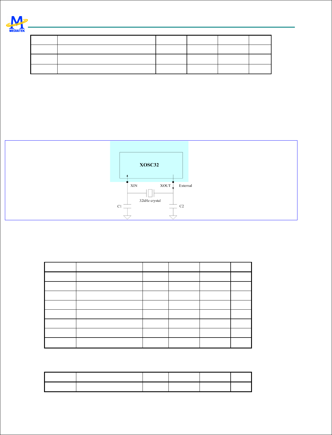
MTK Confidential Release for Konka
MTK Confidential Release for Konka
MT6228 GSM/GPRS Baseband Processor Data Sheet Revision 1.0
589/616
MediaTek Inc. Confidential
DVDD Digital Power Supply 1.3 1.5 1.7 V
AVDD Analog Power Supply 2.5 2.8 3.1 V
T Operating Temperature -20 80
Current Consumption TBD A
Table 77 The Functional Specification of USB PLL
12.1.9 32-KHz Crystal Oscillator
12.1.9.1 Block Descriptions
The low-power 32-KHz crystal oscillator XOSC32 is designed to work with an external piezoelectric 32.768kHz crystal
and a load composed of two functional capacitors, as shown in the following figure.
Figure 74 Block diagram of XOSC32
12.1.9.2 Functional specifications
The functional specification of XOSC32 is shown in the following table.
Symbol Parameter Min Typical Max Unit
AVDDRTC Analog power supply 1.08 1.2 1.65 V
Tosc Start-up time 5 sec
Dcyc Duty cycle 50 %
TR Rise time on XOSCOUT TBD ns/pF
TF Fall time on XOSCOUT TBD ns/pF
Current consumption 5 A
Leakage current 1 A
T Operating temperature -20 80
Table 78 Functional Specification of XOSC32
Here below are a few recommendations for the crystal parameters for use with XOSC32.
Symbol Parameter Min Typical Max Unit
F Frequency range 32768 Hz

MTK Confidential Release for Konka
MTK Confidential Release for Konka
MT6228 GSM/GPRS Baseband Processor Data Sheet Revision 1.0
590/616
MediaTek Inc. Confidential
GL Drive level 5 uW
f/f Frequency tolerance +/- 20 Ppm
ESR Series resistance 50 K
C0 Static capacitance 1.6 pF
CL
6
Load capacitance 6 12.5 pF
Table 79 Recommended Parameters of the 32kHz crystal
12.2 MCU Register Definitions
12.2.1 BBRX
MCU APB bus registers for BBRX ADC are listed as followings.
MIXED+0300h BBRX ADC Analog-Circuit Control Register BBRX_AC_CON
Bit 15 14 13 12 11 10 9 8 7 6 5 4 3 2 1 0
Name
QSEL ISEL RSV
PDNC
HP
GAIN
CALBIAS
Type R/W R/W R/W R/W R/W R/W
Reset
00 00 0 0 0 00000
Set this register for analog circuit configuration controls.
CALBIAS The register field is for control of biasing current in BBRX mixed-signal module. It is coded in 2’s complement.
That is, its maximum is 15 and minimum is –16. Biasing current in BBRX mixed-signal module has impact on
the performance of A/D conversion. The larger the value of the register field, the larger the biasing current in
BBRX mixed-signal module, and the larger the SNR.
GAIN The register bit is for configuration of gain control of analog inputs in GSM RX mixed-signal module. When the
bit is set to 1, gain control for analog inputs will be turned on and thus GSM RX mixed-signal module can provide
higher resolutions. When the bit is set to 0, gain control for analog inputs will be turned off and thus GSM RX
mixed-signal module can only provide lower resolutions.
0 Gain control for analog inputs in GSM RX mixed-signal module will be turned off.
1 Gain control for analog inputs in GSM RX mixed-signal module will be turned on.
PDNCHP Power down control for charge pumping of GSM RX ADC.
0 Power down charge pumping of GSM RX ADC.
1 Power up charge pumping of GSM RX ADC.
ISEL Loopback configuration selection for I-channel in BBRX mixed-signal module
00 Normal mode
01 Loopback TX analog I
10 Loopback TX analog Q
11 Select the grounded input
QSEL Loopback configuration selection for Q-channel in BBRX mixed-signal module
00 Normal mode
6
CL is the parallel combination of C1 and C2 in the block diagram.

MTK Confidential Release for Konka
MTK Confidential Release for Konka
MT6228 GSM/GPRS Baseband Processor Data Sheet Revision 1.0
591/616
MediaTek Inc. Confidential
01 Loopback TX analog Q
10 Loopback TX analog I
11 Select the grounded input
12.2.2 BBTX
MCU APB bus registers for BBTX DAC are listed as followings.
MIXED+0400h BBTX DAC Analog-Circuit Control Register 0 BBTX_AC_CON
0
Bit 15 14 13 12 11 10 9 8 7 6 5 4 3 2 1 0
Name
CALR
CDON
E
STAR
TCAL
RC
GAIN CALRCSEL TRIMI TRIMQ
Type R R/W R/W R/W R/W R/W
Reset
0 0 000 000 0000 0000
Set this register for analog circuit configuration controls. The procedure to perform calibration processing for smoothing
filter in BBTX mixed-signal module is as follows:
7. Write 1 to the register bit CARLC in the register TX_CON of Baseband Front End in order to activate clock
required for calibration process. Initiate calibration process.
8. Write 1 to the register bit STARTCALRC. Start calibration process.
9. Read the register bit CALRCDONE. If read as 1, then calibration process finished. Otherwise repeat the step.
10. Write 0 to the register bit STARTCALRC. Stop calibration process.
11. Write 0 to the register bit CARLC in the register TX_CON of Baseband Front End in order to deactivate clock
required for calibration process. Terminate calibration process.
12. The result of calibration process can be read from the register field CALRCOUT of the register
BBTX_AC_CON1. Software can set the value to the register field CALRCSEL for 3-dB cutoff frequency
selection of smoothing filter in DAC of BBTX.
Remember to set the register field CALRCCONT of the register BBTX_AC_CON1 to 0xb before the calibration process. It
only needs to be set once.
TRIMQ The register field is used to control gain trimming of Q-channel DAC in BBTX mixed-signal module. It is coded
in 2’s complement, that is, with maximum 15 and minimum –16.
TRIMI The register field is used to control gain trimming of I-channel DAC in BBTX mixed-signal module. It is coded in
2’s complement, that is, with maximum 15 and minimum –16.
CALRCSEL The register field is for selection of cutoff frequency of smoothing filter in BBTX mixed-signal module.
It is coded in 2’s complement. That is, its maximum is 3 and minimum is –4.
GAIN The register field is used to control gain of DAC in BBTX mixed-signal module. It has impact on both of I- and
Q-channel DAC in BBTX mixed-signal module. It is coded in 2’s complement, that is, with maximum 3 and
minimum –4.
STARTCALRC Whenever 1 is writing to the bit, calibration process for smoothing filter in BBTX mixed-signal module
will be triggered. Once the calibration process is completed, the register bit CARLDONE will be read as 1.

MTK Confidential Release for Konka
MTK Confidential Release for Konka
MT6228 GSM/GPRS Baseband Processor Data Sheet Revision 1.0
592/616
MediaTek Inc. Confidential
CALRCDONE The register bit indicates if calibration process for smoothing filter in BBTX mixed-signal module has
finished. When calibration processing finishes, the register bit will be 1. When the register bit STARTCALRC is
set to 0, the register bit becomes 0 again.
MIXED+0404h BBTX DAC Analog-Circuit Control Register 1 BBTX_AC_CON
1
Bit 15 14 13 12 11 10 9 8 7 6 5 4 3 2 1 0
Name
CALRCOUT FLOA
T CALRCCNT CALBIAS CMV
Type R R/W R/W R/W R/W
Reset
- 0 0000 00000 000
Set this register for analog circuit configuration controls.
CMV The register field is used to control common voltage in BBTX mixed-signal module. It is coded in 2’s complement,
that is, with maximum 3 and minimum –4.
CALBIAS The register field is for control of biasing current in BBTX mixed-signal module. It is coded in 2’s
complement. That is, its maximum is 15 and minimum is –16. Biasing current in BBTX mixed-signal module has
impact on performance of D/A conversion. Larger the value of the register field, the larger the biasing current in
BBTX mixed-signal module.
CALRCCNT Parameter for calibration process of smoothing filter in BBTX mixed-signal module. Default value is
eleven. Note that it is NOT coded in 2’s complement. Therefore the range of its value is from 0 to 15. Remember
to set it to 0xb before BBTX calibration process. It only needs to be set once.
FLOAT The register field is used to have the outputs of DAC in BBTX mixed-signal module float or not.
CALRCOUT After calibration processing for smoothing filter in BBTX mixed-signal module, a set of 3-bit value is
obtained. It is coded in 2’s complement.
12.2.3 AFC DAC
MCU APB bus registers for AFC DAC are listed as follows.
MIXED+0500h AFC DAC Analog-Circuit Control Register AFC_AC_CON
Bit 15 14 13 12 11 10 9 8 7 6 5 4 3 2 1 0
Name
TEST
PDN_
CHPU
MP
CALI
Type
R/W R/W
R/W
Reset
0 0 0
Set this register for analog circuit configuration controls. Please refer to analog functional specification for more details.
TEST test control
PDN_CHPUMP charge pump power down
CALI biasing current control
12.2.4 APC DAC
MCU APB bus registers for APC DAC are listed as followings.
MTK Confidential Release for Konka
MTK Confidential Release for Konka
MT6228 GSM/GPRS Baseband Processor Data Sheet Revision 1.0
593/616
MediaTek Inc. Confidential
MIXED+0600h APC DAC Analog-Circuit Control Register APC_AC_CON
Bit 15 14 13 12 11 10 9 8 7 6 5 4 3 2 1 0
Name
BYP CALI
Type R/W R/W
Reset
0 0
Set this register for analog circuit configuration controls. Please refer to analog functional specification for more details.
BYP bypass output buffer
CALI biasing current control
12.2.5 Auxiliary ADC
MCU APB bus registers for AUX ADC are listed as followings.
MIXED+0700h Auxiliary ADC Analog-Circuit Control Register AUX_AC_CON
Bit 15 14 13 12 11 10 9 8 7 6 5 4 3 2 1 0
Name
CALI
Type
R/W
Reset
0
Set this register for analog circuit configuration controls. Please refer to analog functional specification for more details.
CALI biasing current control
12.2.6 Voice Front-end
MCU APB bus registers for speech are listed as followings.
MIXED+0100h AFE Voice Analog Gain Control Register AFE_VAG_CON
Bit 15 14 13 12 11 10 9 8 7 6 5 4 3 2 1 0
Name
VUPG VDPG0 VDPG1
Type R/W R/W R/W
Reset
0000 0000 0000
Set this register for analog PGA gains. VUPG is set for microphone input volume control. And VDPG0 and VDPG1 are set
for two output volume controls
VUPG voice-band up-link PGA gain control bits
VCFG [2] =’0’ VCFG [2] =’1’
VUPG [4:0] Gain VUPG [4:0] Gain
11111 42 dB XX111 -21dB
11110 40 dB XX110 -18dB
11101 38 dB XX101 -15dB
11100 36 dB XX100 -12dB
11011 34 dB XX011 -9dB
11010 32 dB XX010 -6dB
11001 30 dB XX001 -3dB
MTK Confidential Release for Konka
MTK Confidential Release for Konka
MT6228 GSM/GPRS Baseband Processor Data Sheet Revision 1.0
594/616
MediaTek Inc. Confidential
11000 28 dB XX000 0dB
10111 26 dB
10110 24 dB
10101 22 dB
10100 20 dB
10011 18 dB
10010 16 dB
10001 14 dB
10000 12 dB
01111 10 dB
01110 8 dB
01101 6 dB
01100 4 dB
01011 2 dB
01010 0 dB
01001 -2 dB
01000 -4 dB
00111 -6 dB
00110 -8 dB
00101 -10 dB
00100 -12 dB
00011 -14 dB
00010 -16 dB
00001 -18 dB
00000 -20 dB
Table 80 Uplink PGA gain setting (VUPG [4:0])
VDPG0 voice-band down-link PGA0 gain control bits
VDPG1 voice-band down-link PGA1 gain control bits
VDPG0 [3:0] / VDPG1 [3:0] Gain
1111 8dB
1110 6dB
1101 4dB
1100 2dB
1011 0dB
1010 -2dB
1001 -4dB
1000 -6dB
0111 -8dB

MTK Confidential Release for Konka
MTK Confidential Release for Konka
MT6228 GSM/GPRS Baseband Processor Data Sheet Revision 1.0
595/616
MediaTek Inc. Confidential
0110 -10dB
0101 -12dB
0100 -14dB
0011 -16dB
0010 -18dB
0001 -20dB
0000 -22dB
Table 81 Downlink power amplifier gain setting
MIXED+0104h
AFE Voice Analog-Circuit Control Register 0 AFE_VAC_CON0
Bit 15 14 13 12 11 10 9 8 7 6 5 4 3 2 1 0
Name
VCFG VDSEND VCALI
Type R/W R/W R/W
Reset
0000 00 00000
Set this register for analog circuit configuration controls.
VCFG[3] microphone biasing control
0 differential biasing
1 single-ended biasing
VCFG[2] gain mode control
0 amplification
1 attenuation
VCFG[1] coupling control
0 AC
1 DC
VCFG[0] input select control
0 input 0
1 input 1
VDSEND[1] single-ended configuration control for out1
VDSEND[0] single-ended configuration control for out0
VCALI biasing current control, in 2’s complement format
MIXED+0108h
AFE Voice Analog-Circuit Control Register 1 AFE_VAC_CON1
Bit 15 14 13 12 11 10 9 8 7 6 5 4 3 2 1 0
Name
VBG_CTRL
VPDN
_CHP
UMP
VFLO
AT
VRSD
ON
VRES
SW
VBUF
0SEL VBUF1SEL
VADC
INMO
DE
VDAC
INMO
DE
Type R/W R/W R/W R/W R/W R/W R/W R/W R/W
Reset
000 0 0 0 0 0 000 0 0
Set this register for analog circuit configuration controls. There are several loop back modes and test modes implemented
for test purposes. Suggested value is 0084h.
VBG_CTRL voice-band band-gap control
VPDN_CHPUMP voice-band charge pump power down

MTK Confidential Release for Konka
MTK Confidential Release for Konka
MT6228 GSM/GPRS Baseband Processor Data Sheet Revision 1.0
596/616
MediaTek Inc. Confidential
0: power down (normal operating mode)
1: charge pump on (for fab. process)
VFLOAT voice-band output driver float
0: normal operating mode
1: float mode
VRSDON voice-band redundant signed digit function on
0: 1-bit 2-level mode
1: 2-bit 3-level mode
VRESSW voice-band output buffer 1 output DC voltage control.
VBUF0SEL voice buffer 0 input selection (reserved.)
VBUF1SEL voice buffer 1 input selection
001: voice DAC output
010: external FM radio input
100: audio DAC output
OTHERS: reserved.
VADCINMODE Voice-band ADC output mode.
0: normal operating mode
1: the ADC input from the DAC output
VDACINMODE Voice-band DAC input mode.
0: normal operating mode
1: the DAC input from the ADC output
MIXED+010Ch AFE Voice Analog Power Down Control Register AFE_VAPDN_C
ON
Bit 15 14 13 12 11 10 9 8 7 6 5 4 3 2 1 0
Name
VPDN
_BIAS
VPDN
_LNA
VPDN
_ADC
VPDN
_DAC
VPDN
_OUT
1
VPDN
_OUT
0
Type R/W R/W R/W R/W R/W R/W
Reset
0 0 0 0 0 0
Set this register to power up analog blocks. 0: power down, 1: power up.
VPDN_BIAS bias block
VPDN_LNA low noise amplifier block
VPDN_ADC ADC block
VPDN_DAC DAC block
VPDN_OUT1 OUT1 buffer block
VPDN_OUT0 OUT0 buffer block
MIXED+0110h AFE Voice AGC Control Register AFE_VAGC_CO
N
Bit 15 14 13 12 11 10 9 8 7 6 5 4 3 2 1 0
Name
AGCT
EST
RELNOIDUR
SEL
RELNOILEV
SEL FRELCKSEL
SRELCKSEL
ATTTHDCAL
ATTC
KSEL
HYST
EREN
AGCE
N
Type R/W R/W R/W R/W R/W R/W R/W R/W R/W
Reset
0 00 00 00 00 00 0 0 0

MTK Confidential Release for Konka
MTK Confidential Release for Konka
MT6228 GSM/GPRS Baseband Processor Data Sheet Revision 1.0
597/616
MediaTek Inc. Confidential
Set this register for analog circuit configuration controls. There are several loop back modes and test modes implemented
for test purposes. Suggested value is 0dcfh.
AGCEN AGC function enable
HYSTEREN AGC hysteresis function enable
ATTCKSEL attack clock selection
0: 16 KHz
1: 32 KHz
ATTTHDCAL attack threshold calibration
SRELCKSEL release slow clock selection
00: 1000/512 Hz
01: 1000/256 Hz
10: 1000/128 Hz
11: 1000/64 Hz
FRELCKSEL release fast clock selection
00: 1000/64 Hz
01: 1000/32 Hz
10: 1000/16 Hz
11: 1000/8 Hz
RELNOILEVSEL release noise level selection
00: -8 dB
01: -14 dB
10: -20 dB
11: -26 dB
RELNOIDURSEL release noise duration selection
00: 64 ms
01: 32 ms
10: 16 ms
11: 8 ms, 32768/4096
12.2.7 Audio Front-end
MCU APB bus registers for audio are listed as followings.
MIXED+0200h AFE Audio Analog Gain Control Register AFE_AAG_CON
Bit 15 14 13 12 11 10 9 8 7 6 5 4 3 2 1 0
Name
AMUT
ER
AMUT
EL APGR APGL
Type
R/W
R/W
R/W R/W
Reset
0 0 0000 0000
Set this register for analog PGA gains.
AMUTER audio PGA L-channel mute control
AMUTEL audio PGA R-channel mute control

MTK Confidential Release for Konka
MTK Confidential Release for Konka
MT6228 GSM/GPRS Baseband Processor Data Sheet Revision 1.0
598/616
MediaTek Inc. Confidential
APGR audio PGA R-channel gain control
APGL audio PGA L-channel gain control
MIXED+0204h AFE Audio Analog-Circuit Control Register AFE_AAC_CON
Bit 15 14 13 12 11 10 9 8 7 6 5 4 3 2 1 0
Name
ARCO
N ABUFSELR ABUFSELL ACALI
Type R/W R/W R/W R/W
Reset
0 000 000 00000
Set this register for analog circuit configuration controls.
ARCON audio external RC control
ABUFSELR audio buffer R-channel input selection
000: audio DAC R/L-channel output; stereo to mono
001: audio DAC R-channel output
010: voice DAC output
100: external FM R/L-channel radio output, stereo to mono
101: external FM R-channel radio output
OTHERS: reserved.
ABUFSELL audio buffer L-channel input selection
000: audio DAC R/L-channel output; stereo to mono
001: audio DAC L-channel output
010: voice DAC output
100: external FM R/L-channel radio output, stereo to mono
101: external FM L-channel radio output
OTHERS: reserved.
ACALI audio bias current control, in 2’s complement format
MIXED+0208h
AFE Audio Analog Power Down Control Register AFE_AAPDN_C
ON
Bit 15 14 13 12 11 10 9 8 7 6 5 4 3 2 1 0
Name
ACNR APDN
_BIAS
APDN
_DAC
R
APDN
_DAC
L
APDN
_OUT
R
APDN
_OUT
L
Type R/W R/W R/W R/W R/W R/W
Reset
000000 0 0 0 0 0
Set this register to power up analog blocks. 0: power down, 1: power up. Suggested value is 00ffh.
ACNR audio click noise reduction
APDN_BIAS BIAS block
APDN_DACR R-channel DAC block
APDN_DACL L-channel DAC block
APDN_OUTR R-channel OUT buffer block
APDN_OUTL L-channel OUT buffer block
MTK Confidential Release for Konka
MTK Confidential Release for Konka
MT6228 GSM/GPRS Baseband Processor Data Sheet Revision 1.0
599/616
MediaTek Inc. Confidential
12.2.8 Reserved
Some registers are reserved for further extensions.
MIXED+0800h Reserved 0 Analog Circuit Control Register 0 RES0_AC_CON
0
Bit
15 14 13 12 11 10 9 8 7 6 5 4 3 2 1 0
Name
Type R/W R/W R/W R/W R/W R/W R/W R/W R/W R/W R/W R/W R/W R/W R/W R/W
Reset
0 0 0 0 0 0 0 0 0 0 0 0 0 0 0 0
MIXED+0804h
Reserved 0 Analog Circuit Control Register 1 RES0_AC_CON
1
Bit 15 14 13 12 11 10 9 8 7 6 5 4 3 2 1 0
Name
Type R/W R/W R/W R/W R/W R/W R/W R/W R/W R/W R/W R/W R/W R/W R/W R/W
Reset
0 0 0 0 0 0 0 0 0 0 0 0 0 0 0 0
MIXED+0900h Reserved 1 Analog Circuit Control Register 0 RES1_AC_CON
0
Bit 15 14 13 12 11 10 9 8 7 6 5 4 3 2 1 0
Name
Type R/W R/W R/W R/W R/W R/W R/W R/W R/W R/W R/W R/W R/W R/W R/W R/W
Reset
0 0 0 0 0 0 0 0 0 0 0 0 0 0 0 0
MIXED+0904h Reserved 1 Analog Circuit Control Register 1 RES1_AC_CON
1
Bit 15 14 13 12 11 10 9 8 7 6 5 4 3 2 1 0
Name
Type
R/W
R/W
R/W
R/W
R/W
R/W
R/W
R/W
R/W
R/W
R/W
R/W
R/W
R/W
R/W
R/W
Reset
0 0 0 0 0 0 0 0 0 0 0 0 0 0 0 0
MIXED+0A00h Reserved 2 Analog Circuit Control Register 0 RES2_AC_CON
0
Bit
15 14 13 12 11 10 9 8 7 6 5 4 3 2 1 0
Name
Type R/W R/W R/W R/W R/W R/W R/W R/W R/W R/W R/W R/W R/W R/W R/W R/W
Reset
0 0 0 0 0 0 0 0 0 0 0 0 0 0 0 0
MIXED+0A04h Reserved 2 Analog Circuit Control Register 1 RES2_AC_CON
1
Bit 15 14 13 12 11 10 9 8 7 6 5 4 3 2 1 0
Name
Type R/W R/W R/W R/W R/W R/W R/W R/W R/W R/W R/W R/W R/W R/W R/W R/W
Reset
0 0 0 0 0 0 0 0 0 0 0 0 0 0 0 0
MTK Confidential Release for Konka
MTK Confidential Release for Konka
MT6228 GSM/GPRS Baseband Processor Data Sheet Revision 1.0
600/616
MediaTek Inc. Confidential
MIXED+0B00h Reserved 3 Analog Circuit Control Register 0 RES3_AC_CON
0
Bit 15 14 13 12 11 10 9 8 7 6 5 4 3 2 1 0
Name
Type R/W R/W R/W R/W R/W R/W R/W R/W R/W R/W R/W R/W R/W R/W R/W R/W
Reset
0 0 0 0 0 0 0 0 0 0 0 0 0 0 0 0
MIXED+0B04h Reserved 3 Analog Circuit Control Register 1 RES3_AC_CON
1
Bit 15 14 13 12 11 10 9 8 7 6 5 4 3 2 1 0
Name
Type
R/W
R/W
R/W
R/W
R/W
R/W
R/W
R/W
R/W
R/W
R/W
R/W
R/W
R/W
R/W
R/W
Reset
0 0 0 0 0 0 0 0 0 0 0 0 0 0 0 0
MIXED+0C00h Reserved 4 Analog Circuit Control Register 0 RES4_AC_CON
0
Bit
15 14 13 12 11 10 9 8 7 6 5 4 3 2 1 0
Name
Type R/W R/W R/W R/W R/W R/W R/W R/W R/W R/W R/W R/W R/W R/W R/W R/W
Reset
0 0 0 0 0 0 0 0 0 0 0 0 0 0 0 0
MIXED+0C04h Reserved 4 Analog Circuit Control Register 1 RES4_AC_CON1
Bit
15 14 13 12 11 10 9 8 7 6 5 4 3 2 1 0
Name
Type R/W R/W R/W R/W R/W R/W R/W R/W R/W R/W R/W R/W R/W R/W R/W R/W
Reset
0 0 0 0 0 0 0 0 0 0 0 0 0 0 0 0
MIXED+0D00h Reserved 5 Analog Circuit Control Register 0 RES5_AC_CON0
Bit
15 14 13 12 11 10 9 8 7 6 5 4 3 2 1 0
Name
Type R/W R/W R/W R/W R/W R/W R/W R/W R/W R/W R/W R/W R/W R/W R/W R/W
Reset
0 0 0 0 0 0 0 0 0 0 0 0 0 0 0 0
MIXED+0D04h Reserved 5 Analog Circuit Control Register 1 RES5_AC_CON1
Bit 15 14 13 12 11 10 9 8 7 6 5 4 3 2 1 0
Name
Type R/W R/W R/W R/W R/W R/W R/W R/W R/W R/W R/W R/W R/W R/W R/W R/W
Reset
0 0 0 0 0 0 0 0 0 0 0 0 0 0 0 0
MIXED+0E00h Reserved 6 Analog Circuit Control Register 0 RES6_AC_CON0
Bit 15 14 13 12 11 10 9 8 7 6 5 4 3 2 1 0
Name
Type R/W R/W R/W R/W R/W R/W R/W R/W R/W R/W R/W R/W R/W R/W R/W R/W
Reset
0 0 0 0 0 0 0 0 0 0 0 0 0 0 0 0

MTK Confidential Release for Konka
MTK Confidential Release for Konka
MT6228 GSM/GPRS Baseband Processor Data Sheet Revision 1.0
601/616
MediaTek Inc. Confidential
MIXED+0E04h Reserved 6 Analog Circuit Control Register 1 RES6_AC_CON1
Bit 15 14 13 12 11 10 9 8 7 6 5 4 3 2 1 0
Name
Type R/W R/W R/W R/W R/W R/W R/W R/W R/W R/W R/W R/W R/W R/W R/W R/W
Reset
0 0 0 0 0 0 0 0 0 0 0 0 0 0 0 0
MIXED+0F00h Reserved 7 Analog Circuit Control Register 0 RES7_AC_CON0
Bit 15 14 13 12 11 10 9 8 7 6 5 4 3 2 1 0
Name
Type R/W R/W R/W R/W R/W R/W R/W R/W R/W R/W R/W R/W R/W R/W R/W R/W
Reset
0 0 0 0 0 0 0 0 0 0 0 0 0 0 0 0
MIXED+0F04h Reserved 7 Analog Circuit Control Register 1 RES7_AC_CON1
Bit 15 14 13 12 11 10 9 8 7 6 5 4 3 2 1 0
Name
Type R/W R/W R/W R/W R/W R/W R/W R/W R/W R/W R/W R/W R/W R/W R/W R/W
Reset
0 0 0 0 0 0 0 0 0 0 0 0 0 0 0 0
12.3 Programming Guide
12.3.1 BBRX Register Setup
The register used to control analog base-band receiver is BBRX_AC_CON.
12.3.1.1 Programmable Biasing Current
To maximize the yield in modern digital process, the receiver features providing 5-bit 32-level programmable current to
bias internal analog blocks. The 5-bits registers CALBIAS [4:0] is coded with 2’s complement format.
12.3.1.2 Offset / Gain Calibration
The base-band downlink receiver (RX), together with the base-band uplink transmitter (TX) introduced in the next section,
provides necessary analog hardware for DSP algorithm to correct the mismatch and offset error. The connection for
measurement of both RX/TX mismatch and gain error is shown in Figure 75, and the corresponding calibration procedure
is described below.

MTK Confidential Release for Konka
MTK Confidential Release for Konka
MT6228 GSM/GPRS Baseband Processor Data Sheet Revision 1.0
602/616
MediaTek Inc. Confidential
Figure 75 Base-band A/D and D/A Offset and Gain Calibration
12.3.1.3 Downlink RX Offset Error Calibration
The RX offset measurement is achieved by selecting grounded input to A/D converter (set ISEL [1:0] =’11’ and QSEL [1:0]
=’11’ to select channel 3 of the analog input multiplexer, as shown in Figure 76. The output of the ADC is sent to DSP for
further offset cancellation. The offset cancellation accuracy depends on the number of samples being converted. That is,
more accurate measurement can be obtained by collecting more samples followed by averaging algorithm.
Figure 76 Downlink ADC Offset Error Measurement
12.3.1.4 Downlink RX and Uplink TX Gain Error Calibration
To measure the gain mismatch error, both I/Q uplink TXs should be programmed to produce full-scale pure sinusoidal
waves output. Such signals are then fed to downlink RX for A/D conversion, in the following two steps.

MTK Confidential Release for Konka
MTK Confidential Release for Konka
MT6228 GSM/GPRS Baseband Processor Data Sheet Revision 1.0
603/616
MediaTek Inc. Confidential
A. The uplink I-channel output are connected to the downlink I-channel input, and the uplink Q-channel output are
connected to the downlink Q-channel input. This can be achieved by setting ISEL [1:0] =’01’ and QSEL [1:0] =’01’
(shown in Figure 77 (A))..
B. The uplink I-channel output are then connected to the downlink Q-channel input, and the uplink Q-channel output are
connected to the downlink I-channel input. This can be achieved by setting ISEL [1:0] =’10’ and QSEL [1:0] =’10’
(shown in Figure 77 (B)).
Figure 77 Downlink RX and Up-link TX Gain Mismatch Measurement (A) I/Q TX connect to I/Q RX (B) I/Q TX connect
to Q/I RX
Once above successive procedures are completed, RX/TX gain mismatch could be easily obtained because the amplitude
mismatch on RX digitized result in step A and B is the sum and difference of RX and TX gain mismatch, respectively.
The gain error of the downlink RX can be corrected in the DSP section and the uplink TX gain error can be corrected by the
gain trimming facility that TX block provide.
12.3.1.5 Uplink TX Offset Error Calibration
Once the offset of the downlink RX is known and corrected, the offset of the uplink TX alone could be easily estimated.
The offset error of TX should be corrected in the digital domain by means of the programmable feature of the digital
GMSK modulator.
Finally, it is important that above three calibration procedures should be exercised in order, that is, correct the RX offset
first, then RX/TX gain mismatch, and finally TX offset. This is owing to that analog gain calibration in TX will affect its
offset, while the digital offset correction has no effect on gain.
12.3.2 BBTX Register Setup
The register used to control analog base-band transmitter is BBTX_AC_CON0 and BBTX_AC_CON1.

MTK Confidential Release for Konka
MTK Confidential Release for Konka
MT6228 GSM/GPRS Baseband Processor Data Sheet Revision 1.0
604/616
MediaTek Inc. Confidential
12.3.2.1 Output Gain Control
The output swing of the uplink transmitter is controlled by register GAIN [2:0] coded in 2’s complement with about 2dB
step. When TRIMI [3:0] / TRIMQ [3:0] = 0 the swing is listed in Table 82, defined to be the difference between positive
and negative output signal.
GAIN [2:0] Output Swing For AVDD=2.8 (V)
+3 (011) AVDD*0.900 (+6.02 dB) 2.52
+2 (010) AVDD*0.720 (+4.08 dB) 2.02
+1 (001) AVDD*0.576 (+2.14 dB) 1.61
+0 (000) AVDD*0.450 (+0.00 dB) 1.26
-1 (111) AVDD*0.360 (-1.94 dB) 1
-2 (110) AVDD*0.288 (-3.88 dB) 0.81
-3 (101) AVDD*0.225 (-6.02 dB) 0.63
-4 (100) AVDD*0.180 (-7.95 dB) 0.5
Table 82 Output Swing Control Table
12.3.2.2 Output Gain Trimming
I/Q channels can also be trimmed separately to compensate gain mismatch in the base-band transmitter or the whole
transmission path including RF module. The gain trimming is adjusted in 16 steps spread from –1.18dB to +1.18dB (Table
83), compared to the full-scale range set by GAIN [2:0].
TRIMI [3:0] / TRIMQ [3:0] Gain Step (dB)
+7 (0111) 1.18
+6 (0110) 1.00
+5 (0101) 0.83
+4 (0100) 0.66
+3 (0011) 0.49
+2 (0010) 0.32
+1 (0001) 0.16
+0 (0000) 0.00
-1 (1111) -0.16
-2 (1110) -0.31
-3 (1101) -0.46
-4 (1100) -0.61
-5 (1011) -0.75
-6 (1010) -0.90
-7 (1001) -1.04
MTK Confidential Release for Konka
MTK Confidential Release for Konka
MT6228 GSM/GPRS Baseband Processor Data Sheet Revision 1.0
605/616
MediaTek Inc. Confidential
-8 (1000) -1.18
Table 83 Gain Trimming Control Table
12.3.2.3 Output Common-Mode Voltage
The output common-mode voltage is controlled by CMV [2:0] with about 0.08*AVDD step, as listed in the following table.
CMV [2:0] Common-Mode Voltage
+3 (011) AVDD*0.62
+2 (010) AVDD*0.58
+1 (001) AVDD*0.54
+0 (000) AVDD*0.50
-1 (111) AVDD*0.46
-2 (110) AVDD*0.42
-3 (101) AVDD*0.38
-4 (100) AVDD*0.34
Table 84 Output Common-Mode Voltage Control Table
12.3.2.4 Programmable Biasing Current
The transmitter features providing 5-bit 32-level programmable current to bias internal analog blocks. The 5-bits registers
CALBIAS [4:0] is coded with 2’s complement format.
12.3.2.5 Smoothing Filter Characteristic
The 2
nd
–order Butterworth smoothing filter is used to suppress the image at DAC output: it provides more than 40dB
attenuation at the 4.44MHz sampling frequency. To tackle with the digital process component variation, programmable
cutoff frequency control bits CALRCSEL [2:0] are included. User can directly change the filter cut-off frequency by
different CALRCSEL value (coded with 2’s complement format and with a default value 0). In addition, an internal
calibration process is provided, by setting START CALRC to high and CALRCCNT to an appropriate value (default is 11).
After the calibration process, the filter cut-off frequency is calibrated to 350kHz +/- 50 kHz and a new CALRCOUT value
is stored in the register. During the calibration process, the output of the cell is high-impedance.
12.3.3 AFC-DAC Register Setup
The register used to control the APC DAC is AFC_AC_CON, which providing 5-bit 32-level programmable current to bias
internal analog blocks. The 5-bits registers CALI [4:0] is coded with 2’s complement format.
12.3.4 APC-DAC Register Setup
The register used to control the APC DAC is AFC_AC_CON, which providing 5-bit 32-level programmable current to bias
internal analog blocks. The 5-bits registers CALI [4:0] is coded with 2’s complement format.
12.3.5 Auxiliary A/D Conversion Register Setup
The register used to control the Aux-ADC is AUX_AC_CON. For this register, which providing 5-bit 32-level

MTK Confidential Release for Konka
MTK Confidential Release for Konka
MT6228 GSM/GPRS Baseband Processor Data Sheet Revision 1.0
606/616
MediaTek Inc. Confidential
programmable current to bias internal analog blocks. The 5-bits registers CALI [4:0] is coded with 2’s complement format.
12.3.6 Voice-band Blocks Register Setup
The registers used to control AMB are AFE_VAG_CON, AFE_VAC_CON0, AFE_VAC_CON1, and AFE_VAPDN_CON.
For these registers, please refer to chapter “Analog Chip Interface”
12.3.6.1 Reference Circuit
The voice-band blocks include internal bias circuits, a differential bandgap voltage reference circuit and a differential
microphone bias circuit. Internal bias current could be calibrated by varying VCALI[4:0] (coded with 2’s complement
format).
The differential bandgap circuit generates a low temperature dependent voltage for internal use. For proper operation, there
should be an external 47nF capacitor connected between differential output pins AU_VREFP and AU_VREFN. The
bandgap voltage (~1.24V
7
, typical) also defines the dBm0 reference level through out the audio mixed-signal blocks. The
following table illustrates typical 0dBm0 voltage when uplink/downlink programmable gains are unity. For other gain
setting, 0dBm0 reference level should be scaled accordingly.
Symbol Parameter Min Typical Max Unit
V
0dBm0
,
UP
0dBm0 Voltage for Uplink Path, Applied
Differentially Between Positive and
Negative Microphone Input Pins
0.2V V-rms
V
0dBm0,Dn
0dBm0 voltage for Downlink Path,
Appeared Differentially Between Positive
and Negative Power Amplifier Output Pins
0.6V V-rms
Table 85 0dBm0 reference level for unity uplink/downlink gain
The microphone bias circuit generates a differential output voltage between AU_MICBIAS_P and AU_MICBIAS_N for
external electret type microphone. Typical output voltage is 1.9 V. In singled-ended mode, by set VCFG[3] =1,
AU_MICBIAS_N is pull down while output voltage is present on AU_MICBIAS_P, respect to ground. The max current
supplied by microphone bias circuit is 2mA.
12.3.6.2 Uplink Path
Uplink path of voice-band blocks includes an uplink programmable gain amplifier and a sigma-delta modulator.
12.3.6.2.1 Uplink Programmable Gain Amplifier
Input to the PGA is a multiplexer controlled by VCFG [3:0], as described in the following table. In normal operation, both
input AC and DC coupling are feasible for attenuation the input signal (gain <= 0dB). However, only AC coupling is
suggested if amplification of input signal is desired (gain>=0dB).
Control Function Descriptions
7
The bandgap voltage could be calibrated by adjusting control signal VBG_CTRL[1:0]. Its default value is [00].
VBG_CTRL not only adjust the bandgap voltage but also vary its temperature dependence. Optimal value of VBG_CTRL
is to be determined.
MTK Confidential Release for Konka
MTK Confidential Release for Konka
MT6228 GSM/GPRS Baseband Processor Data Sheet Revision 1.0
607/616
MediaTek Inc. Confidential
Signal
VCFG [0] Input Selector 0: Input 0 (From AU_VIN0_P / AU_VIN0_N) Is Selected
1: Input 1 (From AU_VIN1_P / AU_VIN1_N) Is Selected
VCFG [1] Coupling Mode 0: AC Coupling
1: DC Coupling
VCFG [2] Gain Mode 0: Amplification Mode (gain >= 0 dB)
1: Attenuation Mode (gain <= 0dB)
VCFG [3] Microphone
Biasing 0: Differential Biasing (Take Bias Voltage Between AU_MICBIAS_P
and AU_MICBIAS_N)
1: Signal-Ended Biasing (Take Bias Voltage From AU_MICBIAS_P
Respected to Ground. AU_MICBIAS_N Is Connected to Ground)
Table 86 Uplink PGA input configuration setting
The PGA itself provides programmable gain (through VUPG [3:0]) with step of 3dB, as listed in the following table.
VCFG [2] =’0’ VCFG [2] =’1’
VUPG [3:0] Gain VUPG [3:0] Gain
1111 NA X111 -21dB
1110 42dB X110 -18dB
1101 39dB X101 -15dB
1100 36dB X100 -12dB
1011 33dB X011 -9dB
1010 30dB X010 -6dB
1001 27dB X001 -3dB
1000 24dB X000 0dB
0111 21dB
0110 18dB
0101 15dB
0100 12dB
0011 9dB
0010 6dB
0001 3dB
0000 0dB
Table 87 Uplink PGA gain setting (VUPG [3:0])
The following table illustrates typically the 0dBm0 voltage applied at the microphone inputs, differentially, for several gain
settings.
VCFG [2] =’0’ VCFG [2] =’1’
VUPG [3:0] 0dBm0 (V-rms) VUPG [3:0] 0dBm0 (V-rms)
1100 3.17mV X110 1.59V
1000 12.6mV X100 0.8V
MTK Confidential Release for Konka
MTK Confidential Release for Konka
MT6228 GSM/GPRS Baseband Processor Data Sheet Revision 1.0
608/616
MediaTek Inc. Confidential
0100 50.2mV X010 0.4V
0000 0.2V X000 0.2V
Table 88 0dBm0 voltage at microphone input pins
12.3.6.2.2 Sigma-Delta Modulator
Analog-to-digital conversion in uplink path is made with a second-order sigma-delta modulator (SDM) whose sampling
rate is 4096kHz. Output signals are coded in either one-bit or RSD format, optionally controlled by VRSDON register.
For test purpose, one can set VADCINMODE to HI to form a look-back path from downlink DAC output to SDM input.
The default value of VADCINMODE is zero.
12.3.6.3 Downlink Path
Downlink path of voice-band blocks includes a digital to analog converter (DAC) and two programmable output power
amplifiers.
12.3.6.3.1 Digital to Analog Converter
The DAC converts input bit-stream to analog signal by sampling rate of 4096kHz. . Besides, it performs a 2
nd
-order 40kHz
butterworth filtering. The DAC receives input signals from MT6228 DSP by set VDACINMODE = 0. It can also take
inputs from SDM output by setting VDACINMODE = 1.
12.3.6.3.2 Downlink Programmable Power Amplifier
Voice-band analog blocks include two identical output power amplifiers with programmable gain. Amplifier 0 and amplifier
1 can be configured to either differential or single-ended mode by adjusting VDSEND [0] and VDSEND [1], respectively.
In single-ended mode, when VDSEND[0] =1, output signal is present at AU_VOUT0_P pin respect to ground. Same as
VDSEND[1] for AU_VOUT1_P pin.
For the amplifier itself, programmable gain setting is described in the following table.
VDPG0 [3:0] / VDPG1 [3:0] Gain
1111 8dB
1110 6dB
1101 4dB
1100 2dB
1011 0dB
1010 -2dB
1001 -4dB
1000 -6dB
0111 -8dB
0110 -10dB
0101 -12dB
0100 -14dB
0011 -16dB
MTK Confidential Release for Konka
MTK Confidential Release for Konka
MT6228 GSM/GPRS Baseband Processor Data Sheet Revision 1.0
609/616
MediaTek Inc. Confidential
0010 -18dB
0001 -20dB
0000 -22dB
Table 89 Downlink power amplifier gain setting
Control signal VFLOAT, when set to ‘HI’, is used to make output nodes totally floating in power down mode. If VFLOAT
is set to ‘LOW” in power down mode, there will be a resistor of 50k ohm (typical) between AU_VOUT0_P and
AU_VOUT0_N, as well as between AU_VOUT0_P and AU_VOUT0_N.
The amplifiers deliver signal power to drive external earphone. The minimum resistive load is 28 ohm and the upper limit
of the output current is 50mA. On the basis that 3.14dBm0 digital input signal into downlink path produces DAC output
differential voltage of 0.87V-rms (typical), the following table illustrates the power amplifier output signal level (in V-rms)
and signal power for an external 32 ohm resistive load.
VDPG Output Signal
Level (V-rms) Output Signal Power
(mW / dBm)
0010 0.11 0.37/-4.3
0110 0.27 2.28/3.6
1010 0.69 14.8/11.7
1110 1.74 94.6/19.8
Table 90 Output signal level/power for 3.14dBm0 input. External resistive load = 32 ohm
The following table illustrates the output signal level and power for different resistive load when VDPG =1110.
RLOAD Output Signal
Level (V-rms) Output Signal Power
(mW / dBm)
30 1.74 101/20
100 1.74 30.3/14.8
600 1.74 5/7
Table 91 Output signal level/power for 3.14dBm0 input, VDPG =1110
12.3.6.4 Power Down Control
Each block inside audio mixed-signal blocks features dedicated power-down control, as illustrated in the following table.
Control
Signal Descriptions
VPDN_BIAS Power Down Reference Circuits (Active Low)
VPDN_LNA Power Down Uplink PGA (Active Low)
VPDN_ADC Power Down Uplink SDM (Active Low)
VPDN_DAC Power Down DAC (Active Low)
VPDN_OUT0
Power Down Downlink Power Amp 0 (Active Low)
VPDN_OUT1
Power Down Downlink Power Amp 1 (Active Low)

MTK Confidential Release for Konka
MTK Confidential Release for Konka
MT6228 GSM/GPRS Baseband Processor Data Sheet Revision 1.0
610/616
MediaTek Inc. Confidential
Table 92 Voice-band blocks power down control
12.3.7 Audio-band Blocks Register Setup
The registers used to control audio blocks are AFE_AAG_CON, AFE_AAC_CON, and AFE_AAPDN_CON. For these
registers, please refer to chapter “Analog Chip Interface”
12.3.7.1 Output Gain Control
Audio blocks include stereo audio DACs and programmable output power amplifiers. The DACs convert input bit-stream
to analog signal by sampling rate of Fs*128 where Fs could be 32kHz, 44.1kHz, or 48kHz. Besides, it performs a 2
nd
-order
butterworth filtering. The two identical output power amplifiers with programmable gain are designed to driving external
AC-coupled single-end speaker. The minimum resistor load is 16 ohm and the maximum driving current is 50mA. The
programmable gain setting, controlled by APGR[] and APGL[], is the same as that of the voice-band amplifiers.
Unlike voice signals, 0dBFS defines the full-scale audio signals amplitude. Based on bandgap reference voltage again, the
following table illustrates the power amplifier output signal level (in V-rms) and signal power for an external 16 ohm
resistive load.
APGR[]/
APGL[] Output Signal
Level (V-rms) Output Signal Power
(mW / dBm)
0010 0.055 0.19/-7.2
0110 0.135 1.14/0.6
1010 0.345 7.44/8.7
1110 0.87 47.3/16.7
Table 93 Output signal level/power for 0dBFS input. External resistive load = 16 ohm
12.3.7.2 Mute Function and Power Down Control
By setting AMUTER (AMUTEL) to high, right (Left) channel output will be muted.
Each block inside audio mixed-signal blocks features dedicated power-down control, as illustrated in the following table.
Control Signal Descriptions
APDN_BIAS Power Down Reference Circuits (Active Low)
APDN_DACL
Power Down L-Channel DAC (Active Low)
APDN_DACR Power Down R-Channel DAC (Active Low)
APDN_OUTL Power Down L-Channel Audio Amplifier (Active Low)
APDN_OUTR Power Down R-Channel Audio Amplifier (Active Low)
Table 94 Audio-band blocks power down control
12.3.8 Multiplexers for Audio and Voice Amplifiers
The audio/voice amplifiers feature accepting signals from various signal sources including AU_FMINR/AU_FMINL pins,
that aimed to receive stereo AM/FM signal from external radio chip:
1) Voice-band amplifier 0 accepts signals from voice DAC output only.

MTK Confidential Release for Konka
MTK Confidential Release for Konka
MT6228 GSM/GPRS Baseband Processor Data Sheet Revision 1.0
611/616
MediaTek Inc. Confidential
2) Voice-band amplifier 1 accepts signal from either voice DAC, audio DAC, or AM/FM radio input pins (controlled
by register VBUF1SEL[] ). For the last two cases, left and right channel signals will be summed together to form a
mono signal first.
3) Audio left/right channel amplifiers receive signals from either voice DAC, audio DAC, or AM/FM radio input pins
(controlled by registers ABUFSELL[] and ABUFSELR[] ), too. Left and right channel amplifiers will produce
identical output waveforms when receiving mono signals from voice DAC.
12.3.9 Clock Squarer Register Setup
The register used to control clock squarer is CLK_CON. For this register, please refer to chapter “Clocks”
CLKSQ_PLD is used to bypass the clock squarer.
12.3.10 Phase-Locked Loop Register Setup
For registers control the PLL, please refer to chapter “Clocks” and “Software Power Down Control”
12.3.10.1 Frequency Setup
The DSP/MCU PLL itself could be programmable to output either 52MHz or 78MHz clocks. Accompanied with additional
digital dividers, 13/26/39/52/65/78 MHz clock outputs are supported.
12.3.10.2 Programmable Biasing Current
The PLLs feature providing 5-bit 32-level programmable current to bias internal analog blocks. The 5-bits registers CALI
[4:0] is coded with 2’s complement format.
12.3.11 32-khz Crystal Oscillator Register Setup
For registers that control the oscillator, please refer to chapter “Real Time Clock” and “Software Power Down Control”.
XOSCCALI[4:0] is the calibration control registers of the bias current, and is coded with 2’s complement format.
1
CL is the parallel combination of C1 and C2 in the block diagram.
MTK Confidential Release for Konka
MTK Confidential Release for Konka
MT6228 GSM/GPRS Baseband Processor Data Sheet Revision 1.0
612/616
MediaTek Inc. Confidential
13 Digital Pin Electrical Characteristics
Based on I/O power supply (VDD33) = 3.3 V
Vil (max) = 0.8 V
Vih (min) = 2.0 V
PU/PD Resistor Ball
13x13
Name Dir Driving Iol &
Ioh Typ (mA)
Vol at Iol Max
(V)
Voh at Ioh Min
(V) Min Typ Max
Pull Cin
(pF)
JTAG Port
E4 JTRST# I 40K 75K 190K PD 2
F5 JTCK I 40K 75K 190K PU 2
F4 JTDI I 40K 75K 190K PU 2
F3 JTMS I 40K 75K 190K PU 2
F2 JTDO O 4 0.4 2.4
F1 JRTCK O 4 0.4 2.4
RF Parallel Control Unit
G5 BPI_BUS0 O 2/8 0.4 2.4
G4 BPI_BUS1 O 2/8 0.4 2.4
G3 BPI_BUS2 O 2/8 0.4 2.4
G1 BPI_BUS3 O 2/8 0.4 2.4
J6 BPI_BUS4 O 2 0.4 2.4
H5 BPI_BUS5 O 2 0.4 2.4
H4 BPI_BUS6 IO 2 0.4 2.4 40K 75K 190K PD 2
H3 BPI_BUS7 IO 2 0.4 2.4 40K 75K 190K PD 2
H2 BPI_BUS8 IO 2 0.4 2.4 40K 75K 190K PD 2
J5 BPI_BUS9 IO 2 0.4 2.4 40K 75K 190K PD 2
RF Serial Control Unit
J4 BSI_CS0 O 2 0.4 2.4
J3 BSI_DATA O 2 0.4 2.4
J2 BSI_CLK O 2 0.4 2.4
PWM Interface
R4 PWM1 IO 2 0.4 2.4 40K 75K 190K PD 2
R3 PWM2 IO 2 0.4 2.4 40K 75K 190K PD 2
R2 ALERTER IO 2 0.4 2.4 40K 75K 190K PD 2
Serial LCD/PM IC Interface
J1 LSCK IO 2/4/6/8 0.4 2.4 40K 75K 190K PU 2
K5 LSA0 IO 2/4/6/8 0.4 2.4 40K 75K 190K PU 2
K4 LSDA IO 2/4/6/8 0.4 2.4 40K 75K 190K PU 2
K3 LSCE0# IO 2/4/6/8 0.4 2.4 40K 75K 190K PU 2
K2 LSCE1# IO 2/4/6/8 0.4 2.4 40K 75K 190K PU 2
Parallel LCD/NAND-Flash
Interface
K6 LPCE1# IO 2/4/6/8 0.4 2.4 40K 75K 190K PU 2
L5 LPCE0# O 2/4/6/8
L4 LRST# O 2/4/6/8
L3 LRD# O 2/4/6/8

MTK Confidential Release for Konka
MTK Confidential Release for Konka
MT6228 GSM/GPRS Baseband Processor Data Sheet Revision 1.0
613/616
MediaTek Inc. Confidential
L2 LPA0 O 2/4/6/8
L1 LWR# O 2/4/6/8
G7 NLD17 IO 2/4/6/8 0.4 2.4 40K 75K 190K PD 2
J9 NLD16 IO 2/4/6/8 0.4 2.4 40K 75K 190K PD 2
K9 NLD15 IO 2/4/6/8 0.4 2.4 40K 75K 190K PD 2
J10 NLD14 IO 2/4/6/8 0.4 2.4 40K 75K 190K PD 2
L9 NDL13 IO 2/4/6/8 0.4 2.4 40K 75K 190K PD 2
K10 NLD12 IO 2/4/6/8 0.4 2.4 40K 75K 190K PD 2
J11 NLD11 IO 2/4/6/8 0.4 2.4 40K 75K 190K PD 2
L10 NLD10 IO 2/4/6/8 0.4 2.4 40K 75K 190K PD 2
K11 NLD9 IO 2/4/6/8 0.4 2.4 40K 75K 190K PD 2
L11 NLD8 IO 2/4/6/8 0.4 2.4 40K 75K 190K PD 2
L6 NLD7 IO 2/4/6/8 0.4 2.4 40K 75K 190K PD 2
M5 NLD6 IO 2/4/6/8 0.4 2.4 40K 75K 190K PD 2
M4 NLD5 IO 2/4/6/8 0.4 2.4 40K 75K 190K PD 2
M3 NLD4 IO 2/4/6/8 0.4 2.4 40K 75K 190K PD 2
N5 NLD3 IO 2/4/6/8 0.4 2.4 40K 75K 190K PD 2
N4 NLD2 IO 2/4/6/8 0.4 2.4 40K 75K 190K PD 2
N3 NLD1 IO 2/4/6/8 0.4 2.4 40K 75K 190K PD 2
N2 NLD0 IO 2/4/6/8 0.4 2.4 40K 75K 190K PD 2
N1 NRNB IO 2/4/6/8 0.4 2.4 40K 75K 190K PU 2
P5 NCLE IO 2/4/6/8 0.4 2.4 40K 75K 190K PD 2
P4 NALE IO 2/4/6/8 0.4 2.4 40K 75K 190K PD 2
P3 NWE# IO 2/4/6/8 0.4 2.4 40K 75K 190K PU 2
P2 NRE# IO 2/4/6/8 0.4 2.4 40K 75K 190K PU 2
P1 NCE# IO 2/4/6/8 0.4 2.4 40K 75K 190K PU 2
SIM Card Interface
M19 SIMRST O 2 0.4 2.4
L16 SIMCLK O 2 0.4 2.4
L17 SIMVCC O 2 0.4 2.4
L18 SIMSEL IO 2/4/6/8 0.4 2.4 40K 75K 190K PD 2
L19 SIMDATA IO 2 0.4 2.4 2
Dedicated GPIO Interface
U3 GPIO0 IO 2 0.4 2.4 40K 75K 190K PD 2
U1 GPIO1 IO 2 0.4 2.4 40K 75K 190K PD 2
D17 GPIO2 IO 2 0.4 2.4 40K 75K 190K PU 2
C19 GPIO3 IO 2 0.4 2.4 40K 75K 190K PU 2
C18 GPIO4 IO 2/4/6/8 0.4 2.4 2
C17 GPIO5 IO 2/4/6/8 0.4 2.4 2
A19 GPIO6 IO 2/4/6/8 0.4 2.4 2
B18 GPIO7 IO 2/4/6/8 0.4 2.4 2
A18 GPIO8 IO 4 0.4 2.4 2
A17 GPIO9 IO 4 0.4 2.4 2
Miscellaneous
T2 SYSRST# I 2
R16 WATCHDOG# O 4 0.4 2.4
T1 SRCLKENAN O 2 0.4 2.4
T4 SRCLKENA O 2 0.4 2.4
T3 SRCLKENAI IO 2 0.4 2.4 40K 75K 190K PD 2

MTK Confidential Release for Konka
MTK Confidential Release for Konka
MT6228 GSM/GPRS Baseband Processor Data Sheet Revision 1.0
614/616
MediaTek Inc. Confidential
E5 TESTMODE I 40K 75K 190K PD 2
D15 ESDM_CK O
Keypad Interface
H17 KCOL6 I 2 40K 75K 190K PU 2
H18 KCOL5 I 2 40K 75K 190K PU 2
H19 KCOL4 I 2 40K 75K 190K PU 2
G15 KCOL3 I 2 40K 75K 190K PU 2
G16 KCOL2 I 2 40K 75K 190K PU 2
G17 KCOL1 I 2 40K 75K 190K PU 2
G18 KCOL0 I 2 40K 75K 190K PU 2
G19 KROW5 O 2/8 0.4 2.4
F15 KROW4 O 2/8 0.4 2.4
F16 KROW3 O 2/8 0.4 2.4
F17 KROW2 O 2/8 0.4 2.4
E16 KROW1 O 2 0.4 2.4
E17 KROW0 O 2 0.4 2.4
External Interrupt Interface
U2 EINT0 I 40K 75K 190K PU 2
V1 EINT1 I 40K 75K 190K PU 2
W1 EINT2 I 40K 75K 190K PU 2
V2 EINT3 I 40K 75K 190K PU 2
U4 MIRQ I 4 0.4 2.4 40K 75K 190K PU 2
B17 MFIQ I 2/4/6/8 0.4 2.4 40K 75K 190K PU 2
External Memory Interface
R15 ED0 IO 2~32 0.4 2.4 2
T19 ED1 IO 2~32 0.4 2.4 2
T18 ED2 IO 2~32 0.4 2.4 2
U19 ED3 IO 2~32 0.4 2.4 2
U18 ED4 IO 2~32 0.4 2.4 2
V19 ED5 IO 2~32 0.4 2.4 2
W19
ED6 IO 2~32 0.4 2.4 2
W18 ED7 IO 2~32 0.4 2.4 2
U17 ED8 IO 2~32 0.4 2.4 2
W17 ED9 IO 2~32 0.4 2.4 2
T16 ED10 IO 2~32 0.4 2.4 2
U16 ED11 IO 2~32 0.4 2.4 2
V16 ED12 IO 2~32 0.4 2.4 2
T15 ED13 IO 2~32 0.4 2.4 2
U15 ED14 IO 2~32 0.4 2.4 2
W15 ED15 IO 2~32 0.4 2.4 2
P12 ERD# O 2~32 0.4 2.4
T12 EWR# O 2~32 0.4 2.4
U12 ECS0# O 2~32 0.4 2.4
V12 ECS1# O 2~32 0.4 2.4
P11 ECS2# O 2~32 0.4 2.4
R11 ECS3# O 2~32 0.4 2.4
R14 EWAIT O 2~32 40K 75K 190K PU
T14 ECAS# O 2~32 0.4 2.4
W14
ERAS# O 2~32 0.4 2.4

MTK Confidential Release for Konka
MTK Confidential Release for Konka
MT6228 GSM/GPRS Baseband Processor Data Sheet Revision 1.0
615/616
MediaTek Inc. Confidential
R13 ECKE O 2~32 0.4 2.4
T13 EDCLK O 2~32 0.4 2.4
V13 ELB# O 2~32 0.4 2.4
W13 EUB# O 2~32 0.4 2.4
T11 EPDN# O 10 0.4 2.4
W11 EADV# O 2~32 0.4 2.4
V11 ECLK O 2~32 0.4 2.4
P10 EA0 O 2~32 0.4 2.4
T10 EA1 O 2~32 0.4 2.4
U10 EA2 O 2~32 0.4 2.4
W10 EA3 O 2~32 0.4 2.4
R9 EA4 O 2~32 0.4 2.4
T9 EA5 O 2~32 0.4 2.4
U9 EA6 O 2~32 0.4 2.4
V9 EA7 O 2~32 0.4 2.4
R8 EA8 O 2~32 0.4 2.4
T8 EA9 O 2~32 0.4 2.4
W8 EA10 O 2~32 0.4 2.4
P8 EA11 O 2~32 0.4 2.4
R7 EA12 O 2~32 0.4 2.4
U7 EA13 O 2~32 0.4 2.4
V7 EA14 O 2~32 0.4 2.4
W7 EA15 O 2~32 0.4 2.4
T6 EA16 O 2~32 0.4 2.4
U6 EA17 O 2~32 0.4 2.4
W6 EA18 O 2~32 0.4 2.4
R5 EA19 O 2~32 0.4 2.4
T5 EA20 O 2~32 0.4 2.4
U5 EA21 O 2~32 0.4 2.4
V5 EA22 O 2~32 0.4 2.4
W4 EA23 O 2~32 0.4 2.4
V4 EA24 O 2~32 0.4 2.4
W3 EA25 O 2~32 0.4 2.4
P17 MCCM0 IO 2/4/6/8 0.4 2.4 40K 75K 190K PU/PD 2
P18 MCDA0 IO 2/4/6/8 0.4 2.4 40K 75K 190K PU/PD 2
P19 MCDA1 IO 2/4/6/8 0.4 2.4 40K 75K 190K PU/PD
2
N17 MCDA2 IO 2/4/6/8 0.4 2.4 40K 75K 190K PU/PD 2
N18 MCDA3 IO 2/4/6/8 0.4 2.4 40K 75K 190K PU/PD 2
M18 MCCK O 2/4/6/8 0.4 2.4
N19 MCPWRON O 2 0.4 2.4
M16 MCWP I 2 40K 75K 190K PU/PD 2
M17 MCINS I 2 40K 75K 190K PU/PD
2
UART/IrDA Interface
K15 URXD1 I 2/4/6/8 40K 75K 190K PU 2
K16 UTXD1 O 2/4/6/8 0.4 2.4
K17 UCTS1 I 2/4/6/8 40K 75K 190K PU 2
K18 URTS1 O 2/4/6/8 0.4 2.4
K19 URXD2 IO 2/4/6/8 0.4 2.4 40K 75K 190K PU 2

MTK Confidential Release for Konka
MTK Confidential Release for Konka
MT6228 GSM/GPRS Baseband Processor Data Sheet Revision 1.0
616/616
MediaTek Inc. Confidential
J15 UTXD2 IO 2/4/6/8 0.4 2.4 40K 75K 190K PU 2
J16 URXD3 IO 2/4/6/8 0.4 2.4 40K 75K 190K PU 2
J17 UTXD3 IO 2/4/6/8 0.4 2.4 40K 75K 190K PU 2
J19 IRDA_RXD IO 2/4/6/8 0.4 2.4 40K 75K 190K PU 2
H15 IRDA_TXD IO 2/4/6/8 0.4 2.4 40K 75K 190K PU 2
H16 IRDA_PDN IO 2/4/6/8 0.4 2.4 40K 75K 190K PU 2
Digital Audio Interface
E18 DAICLK IO 2/4/6/8 0.4 2.4 40K 75K 190K PU 2
E19 DAIPCMOUT IO 2/4/6/8 0.4 2.4 40K 75K 190K PD 2
D16 DAIPCMIN IO 2/4/6/8 0.4 2.4 40K 75K 190K PU 2
D19 DAIRST IO 2/4/6/8 0.4 2.4 40K 75K 190K PU 2
D18 DAISYNC IO 2/4/6/8 0.4 2.4 40K 75K 190K PU 2
CMOS Sensor Interface
J12 CMRST IO 2 0.4 2.4 40K 75K 190K PD 2
K12 CMPDN IO 2 0.4 2.4 40K 75K 190K PD 2
H12 CMVREF I 2 40K 75K 190K PD 2
H11 CMHREF I 2 40K 75K 190K PD 2
H9 CMPCLK I 2 40K 75K 190K PD 2
H10 CMMCLK O 2/4/6/8 0.4 2.4
H8 CMDAT9 I 2/4/6/8 0.4 2.4 40K 75K 190K PD 2
J8 CMDAT8 I 2/4/6/8 0.4 2.4 40K 75K 190K PD 2
K8 CMDAT7 I 2/4/6/8 0.4 2.4 40K 75K 190K PD 2
L8 CMDAT6 I 2/4/6/8 0.4 2.4 40K 75K 190K PD 2
M8 CMDAT5 I 2/4/6/8 0.4 2.4 40K 75K 190K PD 2
M9 CMDAT4 I 2/4/6/8 0.4 2.4 40K 75K 190K PD 2
M10 CMDAT3 I 2/4/6/8 0.4 2.4 40K 75K 190K PD 2
M11 CMDAT2 I 2/4/6/8 0.4 2.4 40K 75K 190K PD 2
M12 CMDAT1 IO 2/4/6/8 0.4 2.4 40K 75K 190K PD 2
L12 CMDAT0 IO 2/4/6/8 0.4 2.4 40K 75K 190K PD 2