MT6235 Datasheet. Www.s Manuals.com. R1.02 Mediatek
User Manual: Datasheets MT6235.
Open the PDF directly: View PDF ![]() .
.
Page Count: 600 [warning: Documents this large are best viewed by clicking the View PDF Link!]
MT6235 GSM/GPRS Baseband
Processor Data Sheet
Revision 1.02
Apr 07, 2008

MT6235 GSM/GPRS Baseband Processor Data Sheet Revision 1.02
2/599 MediaTek Inc. Confidential
Revision History
Revision Date Comments
1.00 Sept 18, 2007 First Release
1.01
Dec 13, 2007 1. Update GPIO10 GPIO11 mode definition
2. Update ch8 audio front end and ch13 analog front end & analog blocks for PMU ball name
change (VMC,VSW_A, VCAMERA) > (VBT, VCAM_A, VCAM_D)
1.02 Apr 07, 2008
1. Update RGU, MCU, RTC, SIM, EMI, GLCON, TG, System Overview, and Product
Description

MT6235 GSM/GPRS Baseband Processor Data Sheet Revision 1.02
3/599 MediaTek Inc. Confidential
TABLE OF CONTENTS
Revision History......................................................................................................................................2
Preface......................................................................................................................................................5
1. System Overview...............................................................................................................................6
Platform Features................................................................................................................................................................. 9
1.1 MODEM Features.....................................................................................................................................................11
1.2 Multi-Media Features............................................................................................................................................... 12
1.3 General Description ................................................................................................................................................. 13
2 Product Description........................................................................................................................15
2.1 Pin Outs.................................................................................................................................................................... 15
2.2 Top Marking Definition ........................................................................................................................................... 18
2.3 DC Characteristics ................................................................................................................................................... 19
2.4 Pin Description......................................................................................................................................................... 20
2.5 Power Description.................................................................................................................................................... 32
3 Micro-Controller Unit Subsystem.................................................................................................40
3.1 Processor Core ......................................................................................................................................................... 41
3.2 Memory Management.............................................................................................................................................. 41
3.3 Bus System............................................................................................................................................................... 44
3.4 Direct Memory Access............................................................................................................................................. 48
3.5 Interrupt Controller .................................................................................................................................................. 66
3.6 BUS Monitor (BM).................................................................................................................................................. 82
3.7 External Memory Interface (6235)........................................................................................................................... 93
4 Microcontroller Peripherals ........................................................................................................104
4.1 Security Engine with JTAG control ....................................................................................................................... 104
4.2 EFUSE Controller (efusec) .................................................................................................................................... 107
4.3 Pulse-Width Modulation Outputs............................................................................................................................111
4.4 SIM Interface ......................................................................................................................................................... 150
4.5 Keypad Scanner ..................................................................................................................................................... 159
4.6 General Purpose Inputs/Outputs ............................................................................................................................ 162
4.7 General Purpose Timer........................................................................................................................................... 181
4.8 UART..................................................................................................................................................................... 184
4.9 IrDA Framer........................................................................................................................................................... 199
4.10 Real Time Clock..................................................................................................................................................... 208
4.11 Auxiliary ADC Unit ............................................................................................................................................... 216
4.12 I2C / SCCB Controller........................................................................................................................................... 220
5 Microcontroller Coprocessors .....................................................................................................232
5.1 Divider ................................................................................................................................................................... 232
5.2 CSD Accelerator .................................................................................................................................................... 234
5.3 FCS Codec ............................................................................................................................................................. 246
5.4 GPRS Cipher Unit.................................................................................................................................................. 248
6 MCU/DSP Interface......................................................................................................................252
6.1 MCU/DSP Shared Registers .................................................................................................................................. 254
6.2 MCU/DSP Shared RAM ........................................................................................................................................ 261
6.3 AHB-to-DDMA Bridge.......................................................................................................................................... 263
7 Multi-Media Subsystem ...............................................................................................................268
7.1 LCD Interface ........................................................................................................................................................ 268
7.2 Capture Resize ....................................................................................................................................................... 292

MT6235 GSM/GPRS Baseband Processor Data Sheet Revision 1.02
4/599 MediaTek Inc. Confidential
7.3 NAND FLASH interface ....................................................................................................................................... 300
7.4 USB 2.0 High-Speed Dual-Role Controller........................................................................................................... 320
7.5 Memory Stick and SD Memory Card Controller ................................................................................................... 358
7.6 2D acceleration ...................................................................................................................................................... 383
7.7 Camera Interface.................................................................................................................................................... 410
8 Audio Front-End...........................................................................................................................422
8.1 General Description ............................................................................................................................................... 422
8.2 Register Definitions ............................................................................................................................................... 425
8.3 DSP Register Definitions ....................................................................................................................................... 439
8.4 Programming Guide............................................................................................................................................... 444
9 Radio Interface Control ...............................................................................................................446
9.1 Baseband Serial Interface....................................................................................................................................... 446
9.2 Baseband Parallel Interface.................................................................................................................................... 454
9.3 Automatic Power Control (APC) Unit ................................................................................................................... 457
9.4 Automatic Frequency Control (AFC) Unit ............................................................................................................ 464
10 Baseband Front End.....................................................................................................................467
10.1 Baseband Serial Ports............................................................................................................................................. 468
10.2 Downlink Path (RX Path) ...................................................................................................................................... 472
10.3 Uplink Path (TX Path) ........................................................................................................................................... 480
11 Timing Generator.........................................................................................................................487
11.1 TDMA timer........................................................................................................................................................... 487
11.2 Slow Clocking Unit................................................................................................................................................ 499
12 Power, Clocks and Reset ..............................................................................................................503
12.1 Clocks .................................................................................................................................................................... 503
12.2 Reset Generation Unit (RGU)................................................................................................................................ 507
12.3 Global Configuration Registers...............................................................................................................................511
13 Analog Front-end & Analog Blocks............................................................................................526
13.1 General Description ............................................................................................................................................... 526
13.2 MCU Register Definitions ..................................................................................................................................... 537
13.3 Programming Guide............................................................................................................................................... 579
14 Digital Pin Electrical Characteristics..........................................................................................593

MT6235 GSM/GPRS Baseband Processor Data Sheet Revision 1.02
5/599 MediaTek Inc. Confidential
Preface
Acronym for Register Type
R/W Capable of both read and write access
RO Read only
RC Read only. After reading the register bank, each bit which is HIGH(1) will be cleared to LOW(0 )
automatically.
WO Write only
W1S Write only. When writing data bits to register bank, each bit which is HIGH(1) will cause the
corresponding bit to be set to 1. Data bits which are LOW(0) has no effect on the corresponding bit.
W1C Write only. When writing data bits to register bank, each bit which is HIGH(1) will cause the
corresponding bit to be cleared to 0. Data bits which are LOW(0) has no effect on the corresponding bit.

MT6235 GSM/GPRS Baseband Processor Data Sheet Revision 1.02
6/599 MediaTek Inc. Confidential
1. System Overview
MT6235 is a highly-integrated and extremely powerful
single-chip solution for GSM/GPRS/EDGE mobile phones.
Based on the 32-bit ARM926EJ-STM RISC processor,
MT6235’s superb processing power, along with high
bandwidth architecture and dedicated hardware support,
provides an unprecedented platform for high performance
GPRS/EDGE Class 12 MODEM application. Overall,
MT6235 presents a revolutionary platform for mobile
devices.
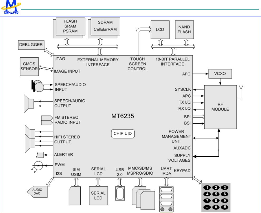
Typical application diagram is shown in Figure 1.
Platform
MT6235 is capable of running the ARM926EJ-STM RISC
processor at up to 208 MHz, thus providing fast data
processing capabilities. In addition to the high clock
frequency, separate CODE and DATA caches are also
included to further improve the overall system efficiency.
For large amounts of data transfer, high performance DMA
(Direct Memory Access) with hardware flow control is
implemented, which greatly enhances the data movement
speed while reducing MCU processing load.
Targeted as a high performance platform for mobile
applications, hardware flash content protection is also
provided to prevent unauthorized porting of the software
load to protect the manufacturer’s development
investment.
Memory
To provide the greatest capacity for expansion and
maximum bandwidth for data intensive applications such
as multimedia features, MT6235 supports up to 4 external
state-of-the-art devices through its 8/16-bit host interface.
High performance devices such as Mobile SDRAM and
Cellular RAM are supported for maximum bandwidth.
Traditional devices such as burst/page mode flash, page
mode SRAM, and Pseudo SRAM are also supported. For
greatest compatibility, the memory interface can also be
used to connect to legacy devices such as Color/Parallel
LCD, and multi-media companion chips are all supported
through this interface. To minimize power consumption
and ensure low noise, this interface is designed for flexible
I/O voltage and allows lowering of the supply voltage
down to 1.8V. The driving strength is configurable for
signal integrity adjustment.
Multi-media
The MT6235 multi-media subsystem provides a
connection to a CMOS image sensor and supports a
resolution up to 2.0 Mpixels. With its high performance
application platform, MT6235 allows efficient processing
of image and video data.
In addition to image and video features, MT6235 utilizes
high resolution DAC, digital audio, and audio synthesis
technology to provide superior audio features for all future
multi-media needs.
Connectivity and Storage
To take advantage of its incredible multimedia strengths,
MT6235 incorporates myriads of advanced connectivity
and storage options for data storage and communication.
MT6235 supports UART, Fast IrDA, USB 2.0, SDIO,
Bluetooth, Touch Screen Controller, WIFI Interface, and
MMC/SD/MS/MS Pro storage systems. These interfaces
provide MT6235 users with the highest degree of
flexibility in implementing solutions suitable for the
targeted application.
To achieve a complete user interface, MT6235 also brings
together all the necessary peripheral blocks for a
multi-media GSM/GPRS/EDGE phone. The peripheral
blocks include the Keypad Scanner with the capability to
detect multiple key presses, SIM Controller, Alerter, Real
Time Clock, PWM, Serial LCD Controller, and General
Purpose Programmable I/Os.
Furthermore, to provide much better configurability and
bandwidth for multi-media products, an additional 18-bit
parallel interface is incorporated. This interface enables
connection to LCD panels as well as NAND flash devices
for additional multi-media data storage.
Audio

MT6235 GSM/GPRS Baseband Processor Data Sheet Revision 1.02
7/599 MediaTek Inc. Confidential
Using a highly integrated mixed-signal Audio Front-End,
the MT6235 architecture allows for easy audio interfacing
with direct connection to the audio transducers. The
audio interface integrates D/A and A/D Converters for
Voice band, as well as high resolution Stereo D/A
Converters for Audio band. In addition, MT6235 also
provides Stereo Input and Analog MUX.
MT6235 supports AMR codec to adaptively optimize
speech and audio quality. Moreover, HE-AAC codec is
implemented to deliver CD-quality audio at low bit rates.
On the whole, MT6235’s audio features provide a rich
solution for multi-media applications.
Radio
MT6235 integrates a mixed-signal baseband front-end in
order to provide a well-organized radio interface with
flexibility for efficient customization. The front-end
contains gain and offset calibration mechanisms, and filters
with programmable coefficients for comprehensive
compatibility control on RF modules. This approach
allows the usage of a high resolution D/A Converter for
controlling VCXO or crystal, reducing the need for an
expensive TCVCXO. MT6235 achieves great MODEM
performance by utilizing a 14-bit high resolution A/D
Converter in the RF downlink path. Furthermore, to
reduce the need for extra external current-driving
component, the driving strength of some BPI outputs is
designed to be configurable.
Debug Function
The JTAG interface enables in-circuit debugging of the
software program with the ARM926EJ-S core. With this
standardized debugging interface, MT6235 provides
developers with a wide set of options in choosing ARM
development kits from different third party vendors.
Power Management
The MT6235 offers various low-power features to help
reduce system power consumption. These features
include a Pause Mode of 32 KHz clocking in Standby State,
Power Down Mode for individual peripherals, and
Processor Sleep Mode. MT6235 is also fabricated in an
advanced low leakage CMOS process, hence providing an
overall ultra low leakage solution.
Package
The MT6235 device is offered in a 13mm×13mm, 362-ball,
0.5 mm pitch, TFBGA package.
MT6235 GSM/GPRS Baseband Processor Data Sheet Revision 1.02
8/599 MediaTek Inc. Confidential
Figure 1 Typical application of MT6235

MT6235 GSM/GPRS Baseband Processor Data Sheet Revision 1.02
9/599 MediaTek Inc. Confidential
Platform Features
General
z Integrated voice-band, audio-band and base-band
analog front ends
z TFBGA 13mm×13mm, 362-ball, 0.5 mm pitch
package
MCU Subsystem
z ARM926EJ-S 32-bit RISC processor
z High performance multi-layer AMBA bus
z Java hardware acceleration for fast Java-based
games and applets
z Operating frequency: 26/52/104/208 MHz
z Dedicated DMA bus
z 14 DMA channels
z 512K bits on-chip SRAM
z 384K bits Instruction-TCM
z 640K bits Data-TCM
z 128K bits Instruction-Cache
z 128K bits Data-Cache
z On-chip boot ROM for Factory Flash
Programming
z Watchdog timer for system crash recovery
z 3 sets of General Purpose Timer
z Circuit Switch Data coprocessor
z Division coprocessor
z PPP Framer coprocessor
External Memory Interface
z Supports up to 4 external memory devices
z Supports 8-bit or 16-bit memory components with
maximum size of up to 128M Bytes each
z Supports Mobile SDRAM and Cellular RAM
z Supports Flash and SRAM/PSRAM with page
mode or burst mode
z Industry standard Parallel LCD interface
z Supports multi-media companion chips with 8/16
bits data width
z Flexible I/O voltage of 1.8V ~ 2.8V for memory
interface
z Configurable driving strength for memory
interface
User Interfaces
z 8-row × 8-column keypad controller with
hardware scanner
z Supports multiple key presses for gaming
z SIM/USIM controller with hardware T=0/T=1
protocol control
z Real Time Clock (RTC) operating with a separate
power supply
z General Purpose I/Os (GPIOs)
z 4 sets of Pulse Width Modulation (PWM) output
z Alerter output with Enhanced PWM or PDM
z 8 external interrupt lines
Security
z Supports security key and 126 bit chip unique ID
Connectivity
z 3 UARTs with hardware flow control and speeds
up to 921600 bps
z IrDA modulator/demodulator with hardware
framer. Supports SIR/MIR/FIR operating speeds.
z USB 2.0 capability
z Multi Media Card, Secure Digital Memory Card,
Memory Stick, Memory Stick Pro host controller
with flexible I/O voltage power

MT6235 GSM/GPRS Baseband Processor Data Sheet Revision 1.02
10/599 MediaTek Inc. Confidential
z Supports SDIO interface for SDIO peripherals as
well as WIFI connectivity
z DAI/PCM and I2S interface for Audio application
Power Management
z Power Down Mode for analog and digital circuits
z Processor Sleep Mode
z Pause Mode of 32 KHz clocking in Standby State
z 4-channel Auxiliary 10-bit A/D Converter for
charger and battery monitoring and photo sensing
Test and Debug
z Built-in digital and analog loop back modes for
both Audio and Baseband Front-End
z DAI port complying with GSM Rec.11.10
z JTAG port for debugging embedded MCU

MT6235 GSM/GPRS Baseband Processor Data Sheet Revision 1.02
11/599 MediaTek Inc. Confidential
1.1 MODEM Features
Radio Interface and Baseband Front End
z GMSK modulator with analog I and Q channel
outputs
z 10-bit D/A Converter for uplink baseband I and Q
signals
z 14-bit high resolution A/D Converter for downlink
baseband I and Q signals
z Calibration mechanism of offset and gain
mismatch for baseband A/D Converter and D/A
Converter
z 10-bit D/A Converter for Automatic Power
Control
z 13-bit high resolution D/A Converter for
Automatic Frequency Control
z Programmable Radio RX filter
z 2 channels Baseband Serial Interface (BSI) with
3-wire control
z Bi-directional BSI interface. RF chip register
read access with 3-wire or 4-wire interface.
z 10-Pin Baseband Parallel Interface (BPI) with
programmable driving strength
z Multi-band support
Voice and Modem CODEC
z Dial tone generation
z Voice memo
z Noise reduction
z Echo suppression
z Advanced sidetone Oscillation Reduction
z Digital sidetone generator with programmable
gain
z Two programmable acoustic compensation filters
z GSM/GPRS quad vocoders for adaptive multirate
(AMR), enhanced full rate (EFR), full rate (FR)
and half rate (HR)
z GSM channel coding, equalization and A5/1, A5/2
and A5/3 ciphering
z GPRS GEA1, GEA2 and GEA3 ciphering
z Programmable GSM/GPRS/EDGE modem
z Packet Switched Data with CS1/CS2/CS3/CS4
coding schemes
z GSM Circuit Switch Data
z GPRS/EDGE Class 12
Voice Interface and Voice Front End
z Two microphone inputs sharing one low noise
amplifier with programmable gain and automatic
gain control (AGC) mechanisms
z Voice power amplifier with programmable gain
z 2nd order Sigma-Delta A/D Converter for voice
uplink path
z D/A Converter for voice downlink path
z Supports half-duplex hands-free operation
z Compliant with GSM 03.50

MT6235 GSM/GPRS Baseband Processor Data Sheet Revision 1.02
12/599 MediaTek Inc. Confidential
1.2 Multi-Media Features
LCD/NAND Flash Interface
z Dedicated Parallel Interface supports 3 external
devices with 8-/16-bit NAND flash interface,
8-/9-/16-/18-bit Parallel interface, and Serial
interface for LCM
z Built-in NAND Flash Controller with 1-bit ECC
for mass storage
LCD Controller
z Supports simultaneous connection to up to 3
parallel LCD and 2 serial LCD modules
z Supports LCM format: RGB332, RGB444,
RGB565, RGB666, RGB888
z Supports LCD module with maximum resolution
up to 800x600 at 24bpp
z Per pixel alpha channel
z True color engine
z Supports hardware display rotation
z Capable of combining display memories with up to
6 blending layers
Image Signal Processor
z 8 bit YUV format image input
z Capable of processing image of size up to 2.0 M
pixels
z IEEE Std 1180-1990 IDCT standards compliance
z Supports progressive image processing to
minimize storage space requirement
z Supports reload-able DMA for VLD stream
Image Data Processing
z Supports Digital Zoom
z Supports RGB888/565, YUV444 image
processing
z High throughput hardware scaler. Capable of
tailoring an image to an arbitrary size.
z Horizontal scaling in averaging method
z Vertical scaling in bilinear method
z YUV and RGB color space conversion
z Boundary padding
2D Accelerator
z Supports 32-bpp ARGB8888, 24-bpp RGB888,
16-bpp RGB565, and 8-bpp index color modes
z Supports SVG Tiny
z Rectangle gradient fill
z BitBlt: multi-BitBlt with 7 rotation, 16 binary ROP
z Alpha blending with 7 rotation
z Line drawing: normal line, dotted line,
anti-aliasing
z Circle drawing
z Bezier curve drawing
z Triangle flat fill
z Font caching: normal font, italic font
z Command queue with max depth of 2047
Audio CODEC
z Supports HE-AAC codec decode
z Supports AAC codec decode
z Wavetable synthesis with up to 64 tones
z Advanced wavetable synthesizer capable of
generating simulated stereo
z Wavetable including GM full set of 128
instruments and 47 sets of percussions
z PCM Playback and Record
z Digital Audio Playback
Audio Interface and Audio Front End
z Supports I2S interface

MT6235 GSM/GPRS Baseband Processor Data Sheet Revision 1.02
13/599 MediaTek Inc. Confidential
z High resolution D/A Converters for Stereo Audio
playback
z Stereo analog input for stereo audio source
z Analog multiplexer for stereo audio
z Stereo to mono conversion
1.3 General Description
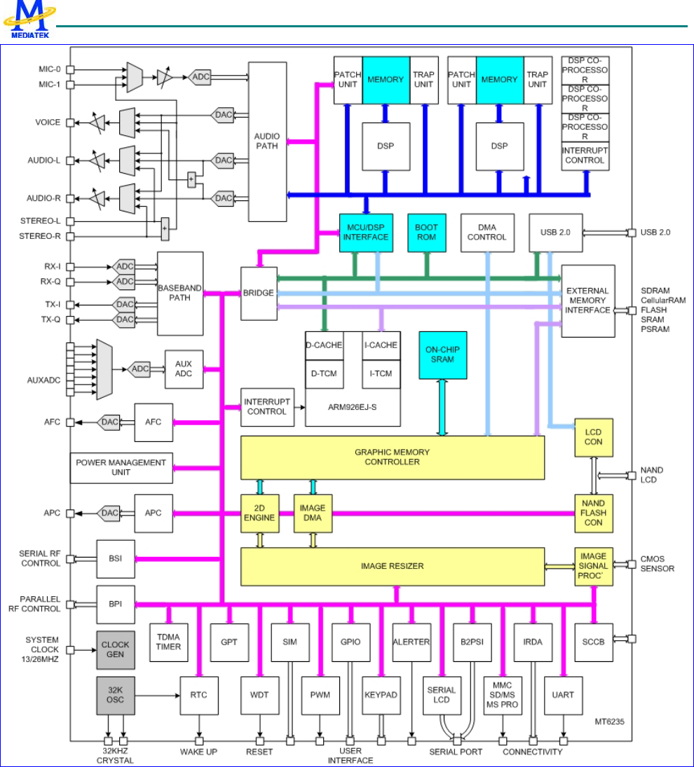
Figure 2 depicts the block diagram of MT6235. Based on a dual-processor architecture, MT6235 integrates both an
ARM926EJ-S core and a digital signal processor core. ARM926EJ-S is the main processor responsible for running
high-level GSM/GPRS protocol software as well as multi-media applications. The digital signal processor manages the
low-level MODEM as well as advanced audio functions. Except for a few mixed-signal circuitries, the other building
blocks in MT6235 are connected to either the microcontroller or the digital signal processor.
MT6235consists of the following subsystems:
z Microcontroller Unit (MCU) Subsystem: includes an ARM926EJ-S RISC processor and its accompanying
memory management and interrupt handling logics;
z Digital Signal Processor (DSP) Subsystem: includes a DSP and its accompanying memory, memory controller, and
interrupt controller;
z MCU/DSP Interface: the junction at which the MCU and the DSP exchange hardware and software information;
z Microcontroller Peripherals: includes all user interface modules and RF control interface modules;
z Microcontroller Coprocessors: runs computing-intensive processes in place of the Microcontroller;
z DSP Peripherals: hardware accelerators for GSM/GPRS/EDGE channel codec;
z Multi-media Subsystem: integrates several advanced accelerators to support multi-media applications;
z Voice Front End: the data path for converting analog speech to and from digital speech;
z Audio Front End: the data path for converting stereo audio from an audio source;
z Baseband Front End: the data path for converting a digital signal to and from an analog signal from the RF
modules;
z Timing Generator: generates the control signals related to the TDMA frame timing; and,
z Power, Reset and Clock Subsystem: manages the power, reset, and clock distribution inside MT6235.
Details of the individual subsystems and blocks are described in the following chapters.
MT6235 GSM/GPRS Baseband Processor Data Sheet Revision 1.02
14/599 MediaTek Inc. Confidential
Figure 2 MT6235 block diagram.

MT6235 GSM/GPRS Baseband Processor Data Sheet Revision 1.02
15/599 MediaTek Inc. Confidential
2 Product Description
2.1 Pin Outs
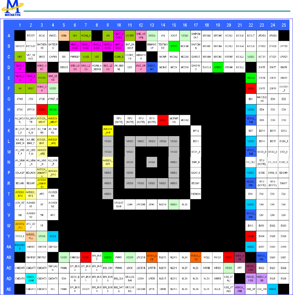
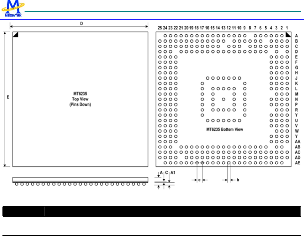
One type of package for this product, TFBGA 13mm*13mm, 362-ball, 0.5 mm pitch package, is offered.
Pin-outs and the top view are illustrated in Figure 3 for this package. Outline and dimension of package is illustrated in
Figure 4, while the definition of package is shown in Table 1.
MT6235 GSM/GPRS Baseband Processor Data Sheet Revision 1.02
16/599 MediaTek Inc. Confidential
Figure 3 Top view of MT6235 TFBGA 13mm*13mm, 362-ball, 0.5 mm pitch package
Notes: RFU is reserved for future use and leave as NC in normal operation.
MT6235 GSM/GPRS Baseband Processor Data Sheet Revision 1.02
17/599 MediaTek Inc. Confidential
Figure 4 Outlines and dimension of TFBGA 13mm*13mm, 362-ball, 0.5 mm pitch package
Body Size Ball Count Ball Pitch Ball Dia. Package Thk. Stand Off Substrate Thk.
D E N e b A (MAX) A1(NOM) C
13 13 362 0.5 0.3 1.2 0.21 0.36
Table 1 Definition of TFBGA 13mm*13mm, 362-ball, 0.5 mm pitch package (Unit: mm)

MT6235 GSM/GPRS Baseband Processor Data Sheet Revision 1.02
18/599 MediaTek Inc. Confidential
2.2 Top Marking Definition
S
MT6235A: Part No.
DDDD: Date Code
###: Subcontractor Code
LLLLL: U1 Die Lot No.
S: Special Code
MT6235A
DDDD-###
LLLLL

MT6235 GSM/GPRS Baseband Processor Data Sheet Revision 1.02
19/599 MediaTek Inc. Confidential
2.3 DC Characteristics
2.3.1 Absolute Maximum Ratings
Prolonged exposure to absolute maximum ratings may reduce device reliability. Functional operation at these maximum
ratings is not implied.
Item Symbol Min Max Unit
IO power supply VDD33 -0.3 VDD33+0.3 V
I/O input voltage VDD33 -0.3 VDD33+0.3 V
Operating temperature Topr -20 80 Celsius
Storage temperature Tstg -55 125 Celsius

MT6235 GSM/GPRS Baseband Processor Data Sheet Revision 1.02
20/599 MediaTek Inc. Confidential
2.4 Pin Description
Ball
13X13 Name Dir
Description
Mode0 Mode1 Mode2 Mode3
PU/
PD Rese
t
JTAG Port
G4 JTRST_B I JTAG test port reset input PD PD
G3 JTCK I JTAG test port clock input PU PU
G2 JTDI I JTAG test port data input PU PU
G1 JTMS I JTAG test port mode switch PU PU
H1 JTDO IO JTAG test port data output
H2 JRTCK IO JTAG test port returned clock output
RF Parallel Control Unit
AE6 BPI_BUS0 IO RF hard-wire control bus 0
AD7 BPI_BUS1 IO RF hard-wire control bus 1
AC7 BPI_BUS2 IO RF hard-wire control bus 2
AC6 BPI_BUS3 IO RF hard-wire control bus 3 GPIO19 BPI_BUS3 PU/
PD
PD
AE8 BPI_BUS4 IO RF hard-wire control bus 4
AD8 BPI_BUS5 IO RF hard-wire control bus 5
AC8 BPI_BUS6 IO RF hard-wire control bus 6 GPIO20 BPI_BUS6 PU/
PD
PD
AB8 BPI_BUS7 IO RF hard-wire control bus 7 GPIO21 BPI_BUS7 PU/
PD
PD

MT6235 GSM/GPRS Baseband Processor Data Sheet Revision 1.02
21/599 MediaTek Inc. Confidential
AE9 BPI_BUS8 IO RF hard-wire control bus 8 GPIO22 BPI_BUS8 PU/
PD
PD
AD9 BPI_BUS9 IO RF hard-wire control bus 9 GPIO23 BPI_BUS9 BSI_CS1 PU/
PD
PD
RF Serial Control Unit
AC9 BSI_CS0 IO RF 3-wire interface chip select 0
AE10 BSI_DATA IO RF 3-wire interface data output
AD10 BSI_CLK IO RF 3-wire interface clock output
PWM Interface
AC10 PWM0 IO Pulse width modulated signal 0 GPIO39 PWM0 PU/
PD
PD
AB10 PWM1 IO Pulse width modulated signal 1 GPIO40 PWM1 BSI_RFIN PU/
PD
PD
AC5 PWM2 IO Pulse width modulated signal 2 GPIO17 PWM2 D2_TID5 PU/
PD
PD
AE5 PWM3 IO Pulse width modulated signal 3 GPIO18 PWM3 D2_TID6 PU/
PD
PD
Camera Control Interface
AE4 SCL IO GPIO15 SCL D2_TID3 PU/
PD
PU
AD5 SDA IO GPIO16 SDA D2_TID4 PU/
PD
PU
Serial LCD/PM IC Interface
AC11 LSCK IO Serial display interface data output GPIO24 LSCK DSP_GPO2 IRQ0 PU/
PD
PD
U11 LSA0 IO Serial display interface address output GPIO25 LSA0 DSP_GPO3 IRQ1 PU/
PD
PD

MT6235 GSM/GPRS Baseband Processor Data Sheet Revision 1.02
22/599 MediaTek Inc. Confidential
AD12 LSDA IO Serial display interface clock output GPIO26 LSDA CLKM1 TDTIRQ PU/
PD
PD
AE12 LSCE0B IO Serial display interface chip select 0
output
GPIO27 LSCE0B CLKM2 TCTIRQ2 PU/
PD
PU
AC12 LSCE1B IO
Serial display interface chip select 1
output
GPIO28 LSCE1B LPCE2B TCTIRQ1
PU/
PD
PU
Parallel LCD/NAND-Flash Interface
AB12 LPCE1B IO Parallel display interface chip select 1
output
GPIO29 LPCE1B NCE1B TEVTVAL
PU/
PD
PU
U12 LPCE0B IO
Parallel display interface chip select 0
output
AE13 LPTE IO GPIO30 LPTE PU/
PD
PD
AC13 LRSTB IO Parallel display interface Reset Signal
AD13 LRDB IO Parallel display interface Read Strobe
U13 LPA0 IO
Parallel display interface address
output
AE14 LWRB IO Parallel display interface Write Strobe
AD14 NLD17 IO Parallel LCD/NAND-Flash Data 17 GPIO31 NLD17 PU/
PD
PD
AC14 NLD16 IO Parallel LCD/NAND-Flash Data 16 GPIO32 NLD16 PU/
PD
PD
AB14 NLD15 IO Parallel LCD/NAND-Flash Data 15 PD
U14 NLD14 IO Parallel LCD/NAND-Flash Data 14 PD
AE15 NDL13 IO Parallel LCD/NAND-Flash Data 13 PD
AD15 NLD12 IO Parallel LCD/NAND-Flash Data 12 PD
AC15 NLD11 IO Parallel LCD/NAND-Flash Data 11 PD
AB15 NLD10 IO Parallel LCD/NAND-Flash Data 10 PD
AE16 NLD9 IO Parallel LCD/NAND-Flash Data 9 PD
AD16 NLD8 IO Parallel LCD/NAND-Flash Data 8 PD
AC16 NLD7 IO Parallel LCD/NAND-Flash Data 7 PD
AB16 NLD6 IO Parallel LCD/NAND-Flash Data 6 PD
U16 NLD5 IO Parallel LCD/NAND-Flash Data 5 PD
AE17 NLD4 IO Parallel LCD/NAND-Flash Data 4 PD
AD17 NLD3 IO Parallel LCD/NAND-Flash Data 3 PD
AC17 NLD2 IO Parallel LCD/NAND-Flash Data 2 PD
AE18 NLD1 IO Parallel LCD/NAND-Flash Data 1 PD
AD18 NLD0 IO Parallel LCD/NAND-Flash Data 0 PD
AC18 NRNB IO NAND-Flash Read/Busy Flag GPIO33 NRNB PU/
PD
PU
AB18 NCLE IO NAND-Flash Command Latch Signal GPIO34 NCLE
PU/
PD
AE19 NALE IO NAND-Flash Address Latch Signal GPIO35 NALE
PU/
PD
AD19 NWEB IO NAND-Flash Write Strobe GPIO36 NWEB
PU/
PD
AC19 NREB IO NAND-Flash Read Strobe GPIO37 NREB
PU/
PD

MT6235 GSM/GPRS Baseband Processor Data Sheet Revision 1.02
23/599 MediaTek Inc. Confidential
AB19 NCEB IO NAND-Flash Chip select output GPIO38 NCE0B
PU/
PD
Miscellaneous
F25 SYSRST_B I System reset input active low PU PU
G23 WATCHDOG IO Watchdog reset output
U10 SRCLKENAN IO
External TCXO enable output active
low
GPIO42 SRCLKEN
AN
PU/
PD
AE11 SRCLKENA IO External TCXO enable output active
high
GPIO41 SRCLKEN
A
PU/
PD
AD11 SRCLKENAI IO External TCXO enable input GPIO43 SRCLKEN
AI
PU/
PD
PD
B14 TESTMODE I TESTMODE enable input PD PD
Y4 VCCQ I
AA1 FSOURCE I
AD6 SECU_EN I
AE7 XBOOT I PD PD
Keypad Interface
A22 KCOL7 IO Keypad column 7 GPIO55 KCOL7 IRDA_PDN PU/
PD
PU
B22 KCOL6 IO Keypad column 6 GPIO56 KCOL6 PU/
PD
PU
A21 KCOL5 IO Keypad column 5 PU PU
B21 KCOL4 IO Keypad column 4 PU PU
C21 KCOL3 IO Keypad column 3 PU PU
D21 KCOL2 IO Keypad column 2 PU PU
A20 KCOL1 IO Keypad column 1 PU PU
B20 KCOL0 IO Keypad column 0 PU PU
C20 KROW7 IO Keypad row 7 GPIO57 KROW7 CLKM4 PU/
PD
PD
D20 KROW6 IO Keypad row 6 GPIO58 KROW6 PU/
PD
PD
A19 KROW5 IO Keypad row 5
B19 KROW4 IO Keypad row 4
C19 KROW3 IO Keypad row 3
A18 KROW2 IO Keypad row 2
B18 KROW1 IO Keypad row 1
C18 KROW0 IO Keypad row 0
External Interrupt Interface
F24 EINT0 IO External interrupt 0 PU PU
F23 EINT1 IO External interrupt 1 PU PU
E25 EINT2 IO External interrupt 2 PU PU
E24 EINT3 IO External interrupt 3 GPIO44 EINT3 DRF_DAT
A
IRQ2 PU/
PD
PU
E23 EINT4 IO External interrupt 4 GPIO45 EINT4 DRF_EN CLKM3
PU/
PD
PU
D23 EINT5 IO External interrupt 5 GPIO46 EINT5 EDICK PU/
PD
PU
D25 EINT6 IO External interrupt 6 GPIO47 EINT6 EDIWS PU/
PD
PU
D24 EINT7 IO External interrupt 7 GPIO48 EINT7 EDIDAT PU/
PD
PU

MT6235 GSM/GPRS Baseband Processor Data Sheet Revision 1.02
24/599 MediaTek Inc. Confidential
K17 MFIQ IO Interrupt to MCU GPIO66 :nFIQ CLKM7 PU/
PD
PU
External Memory Interface
G24 ED0 IO External memory data bus 0
G22 ED1 IO External memory data bus 1
G25 ED2 IO External memory data bus 2
H24 ED3 IO External memory data bus 3
H23 ED4 IO External memory data bus 4
J23 ED5 IO External memory data bus 5
J24 ED6 IO External memory data bus 6
K22 ED7 IO External memory data bus 7
H25 ED8 IO External memory data bus 8
J25 ED9 IO External memory data bus 9
K23 ED10 IO External memory data bus 10
K24 ED11 IO External memory data bus 11
K25 ED12 IO External memory data bus 12
L17 ED13 IO External memory data bus 13
L23 ED14 IO External memory data bus 14
L24 ED15 IO External memory data bus 15
M25 ERD_B IO External memory read strobe
N17 EWR_B IO External memory write strobe
L25 ECS0_B IO External memory chip select 0
M17 ECS1_B IO External memory chip select 1
M23 ECS2_B IO External memory chip select 2
M24 ECS3_B IO External memory chip select 3
R25 EWAIT IO
Flash, PSRAM and CellularRAM data
ready
PD
N25 ECAS_B IO MobileRAM column address
P24 ERAS_B IO MobileRAM row address
P23 ECKE IO MobileRAM clock enable
N22 ED_CLK O MobileRAM clock
T17 EADMUX IO GPIO65
EADMUX CLKM6 PU/
PD
R17 EDQM1 IO
P25 EDQM0 IO
P17 EADV_B O
Flash, PSRAM and CellularRAM
address valid
N24 EC_CLK O Flash, PSRAM and CellularRAM
clock
T23 EA0 IO External memory address bus 0
T22 EA1 IO External memory address bus 1
T24 EA2 IO External memory address bus 2
T25 EA3 IO External memory address bus 3
U23 EA4 IO External memory address bus 4
U24 EA5 IO External memory address bus 5
U25 EA6 IO External memory address bus 6
V23 EA7 IO External memory address bus 7
V24 EA8 IO External memory address bus 8
V25 EA9 IO External memory address bus 9
W22 EA10 IO External memory address bus 10

MT6235 GSM/GPRS Baseband Processor Data Sheet Revision 1.02
25/599 MediaTek Inc. Confidential
W23 EA11 IO External memory address bus 11
W24 EA12 IO External memory address bus 12
W25 EA13 IO External memory address bus 13
Y23 EA14 IO External memory address bus 14
Y24 EA15 IO External memory address bus 15
Y25 EA16 IO External memory address bus 16
AA23 EA17 IO External memory address bus 17
AA24 EA18 IO External memory address bus 18
AA25 EA19 IO External memory address bus 19
AB24 EA20 IO External memory address bus 20
AB25 EA21 IO External memory address bus 21
AC23 EA22 IO External memory address bus 22
AC24 EA23 IO External memory address bus 23
AC25 EA24 IO External memory address bus 24
AD24 EA25 IO External memory address bus 25
AD25 EA26 IO External memory address bus 26 GPIO64 EA26 CLKM5 PU/
PD
USB Interface
AD20 USB_XTALI IO
AE20 USB_XTALO IO
AE21 VSSCA_USB IO
AD22 VSSCD_USB IO
AC21 VRT IO
AD23 VSS33_USB IO
AE22 USB_DP IO USB D+ Input/Output
AE23 USB_DM IO USB D- Input/Output
Memory Card Interface
B16 MCCM0 IO SD Command/MS Bus State Output GPIO67 MC0CM0 TDMA_C
K
PU/
PD
PU
C16 MCDA0 IO
SD Serial Data IO 0/MS Serial Data
IO
GPIO68 MC0DA0 TDMA_D
1
PU/
PD
PU
D16 MCDA1 IO SD Serial Data IO 1 GPIO69 MC0DA1 TDMA_D
0
PU/
PD
PU
J16 MCDA2 IO SD Serial Data IO 2 GPIO70 MC0DA2 TDMA_FS
PU/
PD
PU
C15 MCDA3 IO SD Serial Data IO 3 GPIO71 MC0DA3 PU/
PD
PU
D15 MCCK IO
SD Serial Clock/MS Serial Clock
Output
GPIO72 MC0CK PU/
PD
PU
J15 MCPWRON IO SD Power On Control Output GPIO73 MC0PWR
ON
CLKM8 PU/
PD
PU
C14 MCWP IO SD Write Protect Input GPIO74 MC0WP CLKM9 PU/
PD
PU
D14 MCINS IO SD Card Detect Input GPIO75 MC0INS PU/
PD
PU
UART/IrDA Interface
C25 URXD1 IO UART 1 receive data PU
C24 UTXD1 IO UART 1 transmit data
C23 UCTS1 IO UART 1 clear to send GPIO49 UCTS1 UCTS2 PU/
PD
PU
B25 URTS1 IO UART 1 request to send GPIO50 URTS1 URTS2 PU/

MT6235 GSM/GPRS Baseband Processor Data Sheet Revision 1.02
26/599 MediaTek Inc. Confidential
PD
A24 URXD2 IO UART 2 receive data GPIO51 URXD2 UCTS3 PU/
PD
PU
B24 UTXD2 IO UART 2 transmit data GPIO52 UTXD2 URTS3 PU/
PD
PU
A23 URXD3 IO UART 3 receive data GPIO53 URXD3 IRDA_RX
D
PU/
PD
PU
B23 UTXD3 IO UART 3 transmit data GPIO54 UTXD3 IRDA_TX
D
PU/
PD
PU
Digital Audio Interface
D18 DAICLK IO DAI clock output GPIO59 DAICLK PU/
PD
PD
A17 DAIPCMOUT IO DAI pcm data out GPIO60 DAIPCMO
UT
PU/
PD
PD
B17 DAIPCMIN IO DAI pcm data input GPIO61 DAIPCMI
N
PU/
PD
PD
C17 DAIRST IO DAI reset signal input GPIO62 DAIRST PU/
PD
PD
D17 DAISYNC IO
DAI frame synchronization signal
output
GPIO63 DAISYNC
PU/
PD
PD
CMOS Sensor Interface
AA2 CMRST IO CMOS sensor reset signal output GPIO0 CMRST CLKM0 DSP_GPO
0
PU/
PD
PD
AA3 CMPDN IO CMOS sensor power down control GPIO1 CMPDN DSP_GPO
1
PU/
PD
PD
AB3 CMVREF IO Sensor vertical reference signal input GPIO2 CMVREF TBTXEN D1_TID0 PU/
PD
PD
AB2 CMHREF IO
Sensor horizontal reference signal
input
GPIO3 CMHREF TBTXFS PU/
PD
PD
AA4 CMPCLK IO CMOS sensor pixel clock input GPIO4 CMPCLK TBRXEN D1_TID1 PU/
PD
PD
AB6 CMMCLK IO CMOS sensor master clock output GPIO5 CMMCLK TBRXFS PU/
PD
PD
AC2 CMDAT7 IO CMOS sensor data input 7 GPIO6 CMDAT7 D1ICK PU/
PD
PD
AC3 CMDAT6 IO CMOS sensor data input 6 GPIO7 CMDAT6 D1ID
PU/
PD
PD
AC1 CMDAT5 IO CMOS sensor data input 5 GPIO8 CMDAT5 D1IMS PU/
PD
PD
AD1 CMDAT4 IO CMOS sensor data input 4 GPIO9 CMDAT4 D2ICK PU/
PD
PD
AE2 CMDAT3 IO CMOS sensor data input 3 GPIO10 CMDAT3 D2ID PU/
PD
PD
AD3 CMDAT2 IO CMOS sensor data input 2 GPIO11 CMDAT2 D2IMS PU/
PD
PD
AD4 CMDAT1 IO CMOS sensor data input 1 GPIO12 CMDAT1 D2_TID0
PU/
PD
PD
AE3 CMDAT0 IO CMOS sensor data input 0 GPIO13 CMDAT0 D2_TID1
PU/
PD
PD
AC4 CMFLASH IO GPIO14 CMFLASH D2_TID2
PU/
PD
PD
Analog Interface
J1 AU_MOUTL O Audio analog output left channel

MT6235 GSM/GPRS Baseband Processor Data Sheet Revision 1.02
27/599 MediaTek Inc. Confidential
J2 AU_MOUTR O Audio analog output right channel
K4 AU_FMINL I FM radio analog input left channel
K3 AU_FMINR I FM radio analog input right channel
K2 AU_OUT0_N O Earphone 0 amplifier output (-)
K1 AU_OUT0_P O Earphone 0 amplifier output (+)
L2 AU_MICBIAS
_P
O Microphone bias supply (+)
L1 AU_MICBIAS
_N
O Microphone bias supply (-)
M2 AU_VREF_N O Audio reference voltage (-)
M1 AU_VREF_P O Audio reference voltage (+)
N1 AU_VIN0_P I Microphone 0 amplifier input (+)
N2 AU_VIN0_N I Microphone 0 amplifier input (-)
N3 AU_VIN1_N I Microphone 1 amplifier input (-)
N4 AU_VIN1_P I Microphone 1 amplifier input (+)
P1 BDLAQP I
Quadrature input (Q+) baseband codec
downlink
P2 BDLAQN I
Quadrature input (Q-) baseband codec
downlink
R1 BDLAIN I
In-phase input (I+) baseband codec
downlink
R2 BDLAIP I
In-phase input (I-) baseband codec
downlink
T3 APC I Automatic power control DAC output
T4 AUXADIN0 I Auxiliary ADC input 0
U2 AUXADIN1 I Auxiliary ADC input 1
U4 AUXADIN2 I Auxiliary ADC input 2
V2 AUXADIN3 I Auxiliary ADC input 3
U1 AUX_REF I Auxiliary ADC reference voltage input
U3 XP I
V1 XM I
W3 YP I
V3 YM I
V4 AFC O
Automatic frequency control DAC
output
W2 AFC_BYP O Automatic frequency control DAC
bypass capacitance
B1 BATDET I
C2 VRF_SENSE I
C1 VRF I
E3 VTCXO I
F2 VREF I
C12 VIBRATOR O
D11 LED O
A11 VCORE I
C11 VCORE_FB I
B11 BAT_BACKU
P
I
F1 VA
A9 VM I
D10 VM_SENSE I

MT6235 GSM/GPRS Baseband Processor Data Sheet Revision 1.02
28/599 MediaTek Inc. Confidential
C10 VCAM_D II
D8 VCAM_A_SE
NSE
I
A7 VCAM_A
I
C8 VBT I
A6 VIO I
C7 VUSB I
A5 VSIM I
C5 SIO IO
C6 PWRKEY I
D5 ISENSE I
A4 VMSEL I
B4 GATEDRV I
C4 CHRIN I
A3 SCLK I
B3 BATSENSE I
C3 SRST O
A2 RESET I
B2 RSTCAP IO
VCXO Interface
Y1 SYSCLK I 13MHz or 26MHz system clock input
RTC Interface
A14 XIN I 32.768 KHz crystal input
A15 XOUT O 32.768 KHz crystal output
B13 BBWAKEUP IO Baseband power on/off control
Supply Voltages
H3 VDDK Supply voltage of internal logic
AB7 VDDK Supply voltage of internal logic
AB20 VDDK Supply voltage of internal logic
Y22 VDDK Supply voltage of internal logic
F22 VDDK Supply voltage of internal logic
J14 VDDK Supply voltage of internal logic
AB23 VDD33_EMI Supply voltage of memory interface
driver
V22 VDD33_EMI Supply voltage of memory interface
driver
R22 VDD33_EMI Supply voltage of memory interface
driver
M22 VDD33_EMI Supply voltage of memory interface
driver
J22 VDD33_EMI Supply voltage of memory interface
driver
AD2 VDD33_CAM
AB13 VDD33_LCD
AB17 VDD33_LCD
AC22 VDD33_USB
AB21 VDDC_USB
D13 VDD33_MC

MT6235 GSM/GPRS Baseband Processor Data Sheet Revision 1.02
29/599 MediaTek Inc. Confidential
H4 VDD33 Supply voltage of drivers except
memory interface, USB and
MS/MMC/SD
AB9 VDD33 Supply voltage of drivers except
memory interface, USB and
MS/MMC/SD
E22 VDD33 Supply voltage of drivers except
memory interface, USB and
MS/MMC/SD
D19 VDD33 Supply voltage of drivers except
memory interface, USB and
MS/MMC/SD
F4 VSS33 Ground of drivers except memory
interface, USB and MS/MMC/SD
Y3 VSS33 Ground of drivers except memory
interface, USB and MS/MMC/SD
AB5 VSS33 Ground of drivers except memory
interface, USB and MS/MMC/SD
AB11 VSS33 Ground of drivers except memory
interface, USB and MS/MMC/SD
U15 VSS33 Ground of drivers except memory
interface, USB and MS/MMC/SD
AC20 VSS33 Ground of drivers except memory
interface, USB and MS/MMC/SD
AE24 VSS33 Ground of drivers except memory
interface, USB and MS/MMC/SD
AA22 VSS33 Ground of drivers except memory
interface, USB and MS/MMC/SD
U22 VSS33 Ground of drivers except memory
interface, USB and MS/MMC/SD
P22 VSS33 Ground of drivers except memory
interface, USB and MS/MMC/SD
L22 VSS33 Ground of drivers except memory
interface, USB and MS/MMC/SD
H22 VSS33 Ground of drivers except memory
interface, USB and MS/MMC/SD
C22 VSS33 Ground of drivers except memory
interface, USB and MS/MMC/SD
A16 VSS33 Ground of drivers except memory
interface, USB and MS/MMC/SD
A13 VSS33 Ground of drivers except memory
interface, USB and MS/MMC/SD
L9 VSS33 Ground of drivers except memory
interface, USB and MS/MMC/SD
L11 VSS33 Ground of drivers except memory
interface, USB and MS/MMC/SD
L12 VSS33 Ground of drivers except memory
interface, USB and MS/MMC/SD
L13 VSS33 Ground of drivers except memory
interface, USB and MS/MMC/SD
L14 VSS33 Ground of drivers except memory
interface, USB and MS/MMC/SD
L15 VSS33 Ground of drivers except memory
interface, USB and MS/MMC/SD

MT6235 GSM/GPRS Baseband Processor Data Sheet Revision 1.02
30/599 MediaTek Inc. Confidential
M9 VSS33 Ground of drivers except memory
interface, USB and MS/MMC/SD
M11 VSS33 Ground of drivers except memory
interface, USB and MS/MMC/SD
M15 VSS33 Ground of drivers except memory
interface, USB and MS/MMC/SD
N11 VSS33 Ground of drivers except memory
interface, USB and MS/MMC/SD
N13 VSS33 Ground of drivers except memory
interface, USB and MS/MMC/SD
N15 VSS33 Ground of drivers except memory
interface, USB and MS/MMC/SD
P9 VSS33 Ground of drivers except memory
interface, USB and MS/MMC/SD
P11 VSS33 Ground of drivers except memory
interface, USB and MS/MMC/SD
P15 VSS33 Ground of drivers except memory
interface, USB and MS/MMC/SD
R9 VSS33 Ground of drivers except memory
interface, USB and MS/MMC/SD
R11 VSS33 Ground of drivers except memory
interface, USB and MS/MMC/SD
R12 VSS33 Ground of drivers except memory
interface, USB and MS/MMC/SD
R13 VSS33 Ground of drivers except memory
interface, USB and MS/MMC/SD
R14 VSS33 Ground of drivers except memory
interface, USB and MS/MMC/SD
R15 VSS33 Ground of drivers except memory
interface, USB and MS/MMC/SD
T9 VSS33 Ground of drivers except memory
interface, USB and MS/MMC/SD
W1 AVCC12_PLL
Y2 AVSS12_PLL
B15 VRTC Supply voltage for Real Time Clock
Analog Supplies
J4 AVDD28_MB
UF
Supply Voltage for Audio band section
J3 AVSS28_MBU
F
GND for Audio band section
K9 AVDD28_BUF Supply voltage for voice band transmit
section
L3 AVSS28_BUF GND for voice band transmit section
L4 AVDD28_AFE Supply voltage for voice band receive
section
M3 AGND28_AFE GND reference voltage for voice band
section
N9 AVSS28_AFE GND for voice band receive section
P4 AGND28_RFE GND reference voltage for baseband
section, APC, AFC and AUXADC
P3 AVSS28_GSM
RFTX
GND for baseband transmit section

MT6235 GSM/GPRS Baseband Processor Data Sheet Revision 1.02
31/599 MediaTek Inc. Confidential
R3 AVDD28_GS
MRFTX
Supply voltage for baseband transmit
section
T2 AVSS28_RFE GND for baseband receive section,
APC, AFC and AUXADC
T1 AVDD28_RFE Supply voltage for baseband receive
section, APC, AFC and AUXADC
D1 VBAT_VRF
D3 AGND_VRF
E4 GND_LDOS
E2 VBAT_VA
E1 VBAT_VA
F3 AGND_VA
D12 GND_DRV
A12 GND_VCORE
A10 VBAT_VCOR
E
B10 VBAT_LDOS1
B9 VBAT_LDOS1
B8 VBAT_LDOS2
D7 GND_LDOS
B7 VBAT_LDOS2
B6 VBAT_LDOS3
D6 GND_LDOS
D9 GND_LDOS
Table 2 Pin Descriptions (Bolded types are functions at reset)

MT6235 GSM/GPRS Baseband Processor Data Sheet Revision 1.02
32/599 MediaTek Inc. Confidential
2.5 Power Description
BALL NAME IO SUPPLY IO GND CORE SUPPLY CORE GND REMARK
B1 BATDET
C2 VRF_SENSE
C1 VRF
D1 VBAT_VRF
D3 AGND_VRF
E4 GND_LDOS
E3 VTCXO
E2 VBAT_VA
F1 VA
E1 VBAT_VA
F2 VREF
F3 AGND_VA
G4 JTRST_B VDD33 VSS33 VDDK VSS33
F4 VSS33
G3 JTCK VDD33 VSS33 VDDK VSS33
G2 JTDI VDD33 VSS33 VDDK VSS33
G1 JTMS VDD33 VSS33 VDDK VSS33
H1 JTDO VDD33 VSS33 VDDK VSS33
H3 VDDK
H2 JRTCK VDD33 VSS33 VDDK VSS33
H4 VDD33
J4 AVDD28_MBUF
J2 AU_MOUTR
J3 AVSS28_MBUF
J1 AU_MOUTL
K3 AU_FMINR
K4 AU_FMINL
K9 AVDD28_BUF
K2 AU_OUT0_N
K1 AU_OUT0_P
L3 AVSS28_BUF
L2 AU_MICBIAS_P
L1 AU_MICBIAS_N
L4 AVDD28_AFE
M2 AU_VREF_N
M1 AU_VREF_P
M3 AGND28_AFE
N1 AU_VIN0_P
N2 AU_VIN0_N
N3 AU_VIN1_N
N4 AU_VIN1_P
N9 AVSS28_AFE
P3 AVSS28_GSMRFTX
P4 AGND28_RFE
R3 AVDD28_GSMRFTX

MT6235 GSM/GPRS Baseband Processor Data Sheet Revision 1.02
33/599 MediaTek Inc. Confidential
P1 BDLAQP
P2 BDLAQN
R1 BDLAIN
R2 BDLAIP
T3 APC
T1 AVDD28_RFE
U1 AUX_REF
T4 AUXADIN0
U2 AUXADIN1
T2 AVSS28_RFE
U3 XP
U4 AUXADIN2
V1 XM
V2 AUXADIN3
V3 YM
V4 AFC
W3 YP
W2 AFC_BYP
W1 AVCC12_PLL
Y1 SYSCLK AVCC12_PLL AVSS12_PLL AVCC12_PLL AVSS12_PLL
Y2 AVSS12_PLL
Y3 VSS33
Y4 VCCQ
AA1 FSOURCE
AA2 CMRST VDD33_CAM VSS33 VDDK VSS33
AA3 CMPDN VDD33_CAM VSS33 VDDK VSS33
AB3 CMVREF VDD33_CAM VSS33 VDDK VSS33
AB2 CMHREF VDD33_CAM VSS33 VDDK VSS33
AA4 CMPCLK VDD33_CAM VSS33 VDDK VSS33
AB6 CMMCLK VDD33_CAM VSS33 VDDK VSS33
AC2 CMDAT7 VDD33_CAM VSS33 VDDK VSS33
AC3 CMDAT6 VDD33_CAM VSS33 VDDK VSS33
AC1 CMDAT5 VDD33_CAM VSS33 VDDK VSS33
AD2 VDD33_CAM
AD1 CMDAT4 VDD33_CAM VSS33 VDDK VSS33
AE2 CMDAT3 VDD33_CAM VSS33 VDDK VSS33
AD3 CMDAT2 VDD33_CAM VSS33 VDDK VSS33
AD4 CMDAT1 VDD33_CAM VSS33 VDDK VSS33
AE3 CMDAT0 VDD33_CAM VSS33 VDDK VSS33
AC4 CMFLASH VDD33_CAM VSS33 VDDK VSS33
AB7 VDDK
AE4 SCL VDD33_CAM VSS33 VDDK VSS33
AD5 SDA VDD33_CAM VSS33 VDDK VSS33
AC5 PWM2 VDD33_CAM VSS33 VDDK VSS33
AE5 PWM3 VDD33_CAM VSS33 VDDK VSS33
AB5 VSS33
AD6 SECU_EN VDD33 VSS33 VDDK VSS33
AE7 XBOOT VDD33 VSS33 VDDK VSS33
AE6 BPI_BUS0 VDD33 VSS33 VDDK VSS33

MT6235 GSM/GPRS Baseband Processor Data Sheet Revision 1.02
34/599 MediaTek Inc. Confidential
AD7 BPI_BUS1 VDD33 VSS33 VDDK VSS33
AC7 BPI_BUS2 VDD33 VSS33 VDDK VSS33
AC6 BPI_BUS3 VDD33 VSS33 VDDK VSS33
AE8 BPI_BUS4 VDD33 VSS33 VDDK VSS33
AD8 BPI_BUS5 VDD33 VSS33 VDDK VSS33
AC8 BPI_BUS6 VDD33 VSS33 VDDK VSS33
AB8 BPI_BUS7 VDD33 VSS33 VDDK VSS33
AE9 BPI_BUS8 VDD33 VSS33 VDDK VSS33
AB9 VDD33
AD9 BPI_BUS9 VDD33 VSS33 VDDK VSS33
AC9 BSI_CS0 VDD33 VSS33 VDDK VSS33
AE10 BSI_DATA VDD33 VSS33 VDDK VSS33
AD10 BSI_CLK VDD33 VSS33 VDDK VSS33
AC10 PWM0 VDD33 VSS33 VDDK VSS33
AB10 PWM1 VDD33 VSS33 VDDK VSS33
U10 SRCLKENAN VDD33 VSS33 VDDK VSS33
AE11 SRCLKENA VDD33 VSS33 VDDK VSS33
AD11 SRCLKENAI VDD33 VSS33 VDDK VSS33
AB11 VSS33
AC11 LSCK VDD33_LCD VSS33 VDDK VSS33
U11 LSA0 VDD33_LCD VSS33 VDDK VSS33
AD12 LSDA VDD33_LCD VSS33 VDDK VSS33
AE12 LSCE0B VDD33_LCD VSS33 VDDK VSS33
AC12 LSCE1B VDD33_LCD VSS33 VDDK VSS33
AB12 LPCE1B VDD33_LCD VSS33 VDDK VSS33
U12 LPCE0B VDD33_LCD VSS33 VDDK VSS33
AE13 LPTE VDD33_LCD VSS33 VDDK VSS33
AC13 LRSTB VDD33_LCD VSS33 VDDK VSS33
AD13 LRDB VDD33_LCD VSS33 VDDK VSS33
AB13 VDD33_LCD
U13 LPA0 VDD33_LCD VSS33 VDDK VSS33
AE14 LWRB VDD33_LCD VSS33 VDDK VSS33
AD14 NLD17 VDD33_LCD VSS33 VDDK VSS33
AC14 NLD16 VDD33_LCD VSS33 VDDK VSS33
AB14 NLD15 VDD33_LCD VSS33 VDDK VSS33
U14 NLD14 VDD33_LCD VSS33 VDDK VSS33
AE15 NLD13 VDD33_LCD VSS33 VDDK VSS33
AD15 NLD12 VDD33_LCD VSS33 VDDK VSS33
AC15 NLD11 VDD33_LCD VSS33 VDDK VSS33
U15 VSS33
AB15 NLD10 VDD33_LCD VSS33 VDDK VSS33
AE16 NLD9 VDD33_LCD VSS33 VDDK VSS33
AD16 NLD8 VDD33_LCD VSS33 VDDK VSS33
AC16 NLD7 VDD33_LCD VSS33 VDDK VSS33
AB16 NLD6 VDD33_LCD VSS33 VDDK VSS33
U16 NLD5 VDD33_LCD VSS33 VDDK VSS33
AE17 NLD4 VDD33_LCD VSS33 VDDK VSS33
AD17 NLD3 VDD33_LCD VSS33 VDDK VSS33
AC17 NLD2 VDD33_LCD VSS33 VDDK VSS33

MT6235 GSM/GPRS Baseband Processor Data Sheet Revision 1.02
35/599 MediaTek Inc. Confidential
AB17 VDD33_LCD
AE18 NLD1 VDD33_LCD VSS33 VDDK VSS33
AD18 NLD0 VDD33_LCD VSS33 VDDK VSS33
AC18 NRNB VDD33_LCD VSS33 VDDK VSS33
AB18 NCLE VDD33_LCD VSS33 VDDK VSS33
AE19 NALE VDD33_LCD VSS33 VDDK VSS33
AD19 NWEB VDD33_LCD VSS33 VDDK VSS33
AC19 NREB VDD33_LCD VSS33 VDDK VSS33
AB19 NCEB VDD33_LCD VSS33 VDDK VSS33
AB20 VDDK
AC20 VSS33
AD20 USB_XTALI
AE20 USB_XTALO
AE21 VSSCA_USB
AD22 VSSCD_USB
AB21 VDDC_USB
AC21 VRT
AD23 VSS33_USB
AC22 VDD33_USB
AE22 USB_DP
AE23 USB_DM
AE24 VSS33
AD25 EA26 VDD33_EMI VSS33 VDDK VSS33
AD24 EA25 VDD33_EMI VSS33 VDDK VSS33
AC25 EA24 VDD33_EMI VSS33 VDDK VSS33
AC24 EA23 VDD33_EMI VSS33 VDDK VSS33
AC23 EA22 VDD33_EMI VSS33 VDDK VSS33
AB25 EA21 VDD33_EMI VSS33 VDDK VSS33
AA22 VSS33
AB24 EA20 VDD33_EMI VSS33 VDDK VSS33
AA25 EA19 VDD33_EMI VSS33 VDDK VSS33
AA24 EA18 VDD33_EMI VSS33 VDDK VSS33
AB23 VDD33_EMI
AA23 EA17 VDD33_EMI VSS33 VDDK VSS33
Y25 EA16 VDD33_EMI VSS33 VDDK VSS33
Y22 VDDK
Y24 EA15 VDD33_EMI VSS33 VDDK VSS33
Y23 EA14 VDD33_EMI VSS33 VDDK VSS33
W25 EA13 VDD33_EMI VSS33 VDDK VSS33
W24 EA12 VDD33_EMI VSS33 VDDK VSS33
V22 VDD33_EMI
W23 EA11 VDD33_EMI VSS33 VDDK VSS33
W22 EA10 VDD33_EMI VSS33 VDDK VSS33
V25 EA9 VDD33_EMI VSS33 VDDK VSS33
V24 EA8 VDD33_EMI VSS33 VDDK VSS33
V23 EA7 VDD33_EMI VSS33 VDDK VSS33
U25 EA6 VDD33_EMI VSS33 VDDK VSS33
U24 EA5 VDD33_EMI VSS33 VDDK VSS33
U23 EA4 VDD33_EMI VSS33 VDDK VSS33

MT6235 GSM/GPRS Baseband Processor Data Sheet Revision 1.02
36/599 MediaTek Inc. Confidential
T25 EA3 VDD33_EMI VSS33 VDDK VSS33
U22 VSS33
T24 EA2 VDD33_EMI VSS33 VDDK VSS33
T22 EA1 VDD33_EMI VSS33 VDDK VSS33
T23 EA0 VDD33_EMI VSS33 VDDK VSS33
T17 EADMUX VDD33_EMI VSS33 VDDK VSS33
R25 EWAIT VDD33_EMI VSS33 VDDK VSS33
R17 EDQM1 VDD33_EMI VSS33 VDDK VSS33
P25 EDQM0 VDD33_EMI VSS33 VDDK VSS33
P24 ERAS_B VDD33_EMI VSS33 VDDK VSS33
N25 ECAS_B VDD33_EMI VSS33 VDDK VSS33
R22 VDD33_EMI
P17 EADV_B VDD33_EMI VSS33 VDDK VSS33
N22 ED_CLK VDD33_EMI VSS33 VDDK VSS33
P22 VSS33
N24 EC_CLK VDD33_EMI VSS33 VDDK VSS33
P23 ECKE VDD33_EMI VSS33 VDDK VSS33
N17 EWR_B VDD33_EMI VSS33 VDDK VSS33
M25 ERD_B VDD33_EMI VSS33 VDDK VSS33
M24 ECS3_B VDD33_EMI VSS33 VDDK VSS33
M23 ECS2_B VDD33_EMI VSS33 VDDK VSS33
M17 ECS1_B VDD33_EMI VSS33 VDDK VSS33
L25 ECS0_B VDD33_EMI VSS33 VDDK VSS33
L24 ED15 VDD33_EMI VSS33 VDDK VSS33
M22 VDD33_EMI
L23 ED14 VDD33_EMI VSS33 VDDK VSS33
L17 ED13 VDD33_EMI VSS33 VDDK VSS33
K25 ED12 VDD33_EMI VSS33 VDDK VSS33
L22 VSS33
K24 ED11 VDD33_EMI VSS33 VDDK VSS33
K23 ED10 VDD33_EMI VSS33 VDDK VSS33
J25 ED9 VDD33_EMI VSS33 VDDK VSS33
H25 ED8 VDD33_EMI VSS33 VDDK VSS33
K22 ED7 VDD33_EMI VSS33 VDDK VSS33
J24 ED6 VDD33_EMI VSS33 VDDK VSS33
J23 ED5 VDD33_EMI VSS33 VDDK VSS33
H23 ED4 VDD33_EMI VSS33 VDDK VSS33
H24 ED3 VDD33_EMI VSS33 VDDK VSS33
J22 VDD33_EMI
G25 ED2 VDD33_EMI VSS33 VDDK VSS33
G22 ED1 VDD33_EMI VSS33 VDDK VSS33
G24 ED0 VDD33_EMI VSS33 VDDK VSS33
K17 MFIQ VDD33_EMI VSS33 VDDK VSS33
G23 WATCHDOG VDD33_EMI VSS33 VDDK VSS33
H22 VSS33
F22 VDDK
F25 SYSRST_B VDD33 VSS33 VDDK VSS33
F24 EINT0 VDD33 VSS33 VDDK VSS33
F23 EINT1 VDD33 VSS33 VDDK VSS33

MT6235 GSM/GPRS Baseband Processor Data Sheet Revision 1.02
37/599 MediaTek Inc. Confidential
E25 EINT2 VDD33 VSS33 VDDK VSS33
E24 EINT3 VDD33 VSS33 VDDK VSS33
E23 EINT4 VDD33 VSS33 VDDK VSS33
D23 EINT5 VDD33 VSS33 VDDK VSS33
D25 EINT6 VDD33 VSS33 VDDK VSS33
D24 EINT7 VDD33 VSS33 VDDK VSS33
E22 VDD33
C25 URXD1 VDD33 VSS33 VDDK VSS33
C24 UTXD1 VDD33 VSS33 VDDK VSS33
C23 UCTS1 VDD33 VSS33 VDDK VSS33
B25 URTS1 VDD33 VSS33 VDDK VSS33
A24 URXD2 VDD33 VSS33 VDDK VSS33
B24 UTXD2 VDD33 VSS33 VDDK VSS33
A23 URXD3 VDD33 VSS33 VDDK VSS33
B23 UTXD3 VDD33 VSS33 VDDK VSS33
C22 VSS33
A22 KCOL7 VDD33 VSS33 VDDK VSS33
B22 KCOL6 VDD33 VSS33 VDDK VSS33
A21 KCOL5 VDD33 VSS33 VDDK VSS33
B21 KCOL4 VDD33 VSS33 VDDK VSS33
C21 KCOL3 VDD33 VSS33 VDDK VSS33
D21 KCOL2 VDD33 VSS33 VDDK VSS33
A20 KCOL1 VDD33 VSS33 VDDK VSS33
B20 KCOL0 VDD33 VSS33 VDDK VSS33
C20 KROW7 VDD33 VSS33 VDDK VSS33
D20 KROW6 VDD33 VSS33 VDDK VSS33
A19 KROW5 VDD33 VSS33 VDDK VSS33
D19 VDD33
B19 KROW4 VDD33 VSS33 VDDK VSS33
C19 KROW3 VDD33 VSS33 VDDK VSS33
A18 KROW2 VDD33 VSS33 VDDK VSS33
B18 KROW1 VDD33 VSS33 VDDK VSS33
C18 KROW0 VDD33 VSS33 VDDK VSS33
D18 DAICLK VDD33 VSS33 VDDK VSS33
A17 DAIPCMOUT VDD33 VSS33 VDDK VSS33
B17 DAIPCMIN VDD33 VSS33 VDDK VSS33
C17 DAIRST VDD33 VSS33 VDDK VSS33
A16 VSS33
D17 DAISYNC VDD33 VSS33 VDDK VSS33
B16 MCCM0 VDD33_MC VSS33 VDDK VSS33
C16 MCDA0 VDD33_MC VSS33 VDDK VSS33
D16 MCDA1 VDD33_MC VSS33 VDDK VSS33
J16 MCDA2 VDD33_MC VSS33 VDDK VSS33
C15 MCDA3 VDD33_MC VSS33 VDDK VSS33
D15 MCCK VDD33_MC VSS33 VDDK VSS33
J15 MCPWRON VDD33_MC VSS33 VDDK VSS33
C14 MCWP VDD33_MC VSS33 VDDK VSS33
J14 VDDK
D14 MCINS VDD33_MC VSS33 VDDK VSS33

MT6235 GSM/GPRS Baseband Processor Data Sheet Revision 1.02
38/599 MediaTek Inc. Confidential
D13 VDD33_MC
B15 VRTC
A15 XOUT VRTC VSS33 VDDK VSS33
A14 XIN VRTC VSS33 VDDK VSS33
B13 BBWAKEUP VRTC VSS33 VDDK VSS33
B14 TESTMODE VRTC VSS33 VDDK VSS33
A13 VSS33
C12 VIBRATOR
D12 GND_DRV
D11 LED
A12 GND_VCORE
A11 VCORE
C11 VCORE_FB
A10 VBAT_VCORE
B11 BAT_BACKUP
A9 VM
D10 VM_SENSE
B10 VBAT_LDOS1
C10 VCAM_D
B9 VBAT_LDOS1
D9 GND_LDOS
D8 VCAM_A_SENSE
A7 VCAM_A
C8 VBT
B8 VBAT_LDOS2
A6 VIO
D7 GND_LDOS
C7 VUSB
B7 VBAT_LDOS2
A5 VSIM
C5 SIO
C6 PWRKEY
B6 VBAT_LDOS3
D6 GND_LDOS
D5 ISENSE
A4 VMSEL
B4 GATEDRV
C4 CHRIN
A3 SCLK
B3 \BATSENSE
C3 SRST
A2 RESET
B2 RSTCAP
L9 VSS33
L11 VSS33
L12 VSS33
L13 VSS33
L14 VSS33
L15 VSS33

MT6235 GSM/GPRS Baseband Processor Data Sheet Revision 1.02
39/599 MediaTek Inc. Confidential
M9 VSS33
M11 VSS33
M15 VSS33
N11 VSS33
N13 VSS33
N15 VSS33
P9 VSS33
P11 VSS33
P15 VSS33
R9 VSS33
R11 VSS33
R12 VSS33
R13 VSS33
R14 VSS33
R15 VSS33
T9 VSS33
Table 3 Power Descriptions

MT6235 GSM/GPRS Baseband Processor Data Sheet Revision 1.02
40/599 MediaTek Inc. Confidential
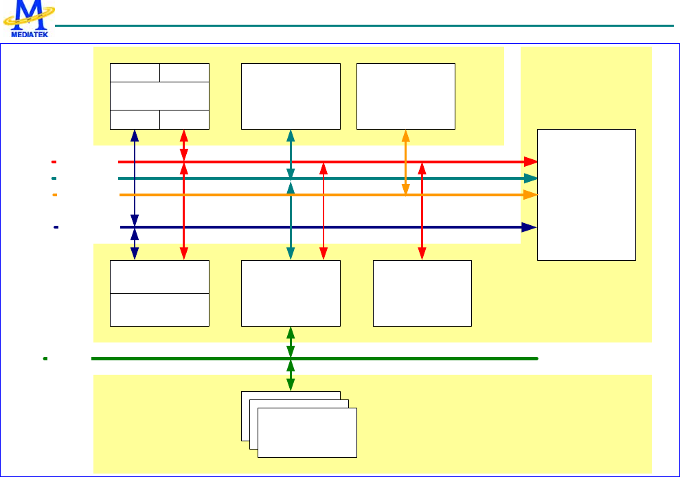
3 Micro-Controller Unit Subsystem
Figure 5 illustrates the block diagram of the Micro-Controller Unit Subsystem in MT6235.The subsystem utilizes a main
32-bit ARM926EJ-S RISC processor, which plays the role of the main bus master controlling the whole subsystem. The
ARM926EJ-S RISC is equipped with instruction cache, instruction TCM, data cache, and data TCM. The size of instruction
cache and data cache are both 16KB. The size of instruction TCM is 48KB. The size of data TCM is 80KB. If the requested
content is found in TCM or in cache, no bus transaction is required. If the code cache hit rate is high enough, bus traffic can
be effectively reduced and processor core performance maximized.
The bus comprises of two-level system buses: Advanced High-Performance Bus (AHB) and Advanced Peripheral Bus
(APB). All bus transactions originate from bus masters, while slaves can only respond to requests from bus masters.
Before data transfer can be established, the bus master must ask for bus ownership, accomplished by request-grant
handshaking protocol between masters and arbiters.
Two levels of bus hierarchy are designed to provide optimum usage for different performance requirements. Specifically,
AHB Bus, the main system bus, is tailored toward high-speed requirements and provides 32-bit data path with multiplex
scheme for bus interconnections. The APB Bus, on the other hand, is designed to reduce interface complexity for lower
data transfer rate, and so it is isolated from high bandwidth AHB Bus by APB Bridge. APB Bus supports 16-bit
addressing and both 16-bit and 32-bit data paths. APB Bus is also optimized for minimal power consumption by turning
off the clock when there is no APB bus activity.
During operation, if the target slave is located on AHB Bus, the transaction is conducted directly on AHB Bus. However,
if the target slave is a peripheral and is attached to the APB bus, then the transaction is conducted between AHB and APB
bus through the use of APB Bridge.
The MT6235 MCU subsystem supports only memory addressing method. Therefore all components are mapped onto the
MCU 32-bit address space. A Memory Management Unit is employed to allow for a central decode scheme. The MMU
generates appropriate selection signals for each memory-addressed module on the AHB Bus.
In order to off-load the processor core, a DMA Controller is designated to act as a master and share the bus resources on
AHB Bus to perform fast data movement between modules. This controller provides fourteen DMA channels.
The Interrupt Controller provides a software interface to manipulate interrupt events; it can handle up to 50 interrupt
sources asserted at the same time. In general, the controller generates 2 levels of interrupt requests, FIQ and IRQ, to the
processor.
A 64K Byte SRAM is provided as system memory for high-speed data access. For factory programming purposes, a Boot
ROM module is also integrated. These two modules use the same Internal Memory Controller to connect to AHB Bus.
External Memory Interface supports both 8-bit and 16-bit devices. This interface supports both synchronous and
asynchronous components, such as Flash, SRAM, SDRAM and parallel LCD. This interface supports page and burst
mode type of Flash, Cellular RAM, as well as high performance MobileRAM. Since AHB Bus is 32-bit wide, all data
transfers are converted into several 8-bit or 16-bit cycles depending on the data width of the target device.
MT6235 GSM/GPRS Baseband Processor Data Sheet Revision 1.02
41/599 MediaTek Inc. Confidential
APB Slaves
AHB Slaves
AHB Masters
ARM926EJ-S
16KB
ICACHE 16KB
DCACHE
48KB ITCM 80KB DTCM
AHB Layer 1
AHB Layer 2
AHB Layer 4
Other AHB
Masters (DMA ,
USB, ...)
EMI Controller
System RAM
(64KB)
System ROM
AHB/APB
Bridge
APB Bus
APB
Peripherals
APB
Peripherals
APB
Peripherals
LCD Controller
Graphic
AHB Layer 3
Figure 5 Block Diagram of the Micro-Controller Unit Subsystem in MT6235
3.1 Processor Core
3.1.1 General Description
The Micro-Controller Unit Subsystem in MT6235 uses the 32-bit ARM926EJ-S RISC processor that is based on the Von
Neumann architecture with a single 32-bit data bus carrying both instructions and data. The memory interface of
ARM926EJ-S is totally compliant with the AMBA based bus system, which allows direct connection to the AHB Bus.
3.2 Memory Management
3.2.1 General Description
The processor core of MT6235 supports only a memory addressing method for instruction fetch and data access. The core
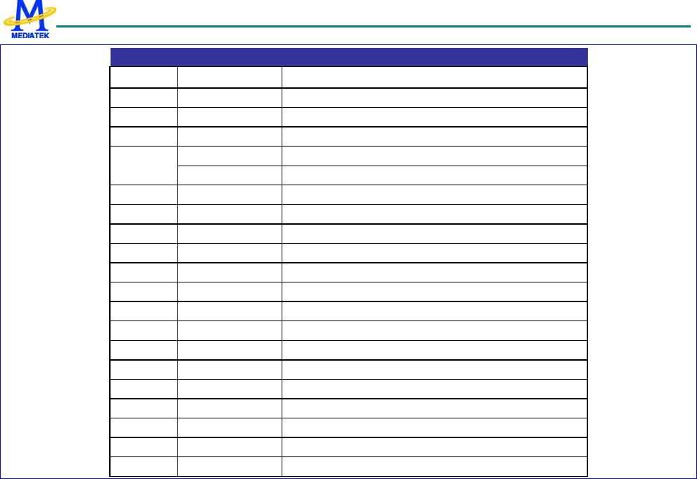
manages a 32-bit address space that has addressing capability of up to 4 GB. System RAM, System ROM, Registers,
MCU Peripherals and external components are all mapped onto such 32-bit address space, as depicted in Figure 6.
MT6235 GSM/GPRS Baseband Processor Data Sheet Revision 1.02
42/599 MediaTek Inc. Confidential
BANK Base Address Description
BANK0 0000_0000h EMI Band 0 / Boot Code
BANK1 1000_0000h EMI Bank 1
BANK2 2000_0000h EMI Bank 2
BANK3 3000_0000h EMI Bank 3
4000_0000h System RAM
4800_0000h System ROM
BANK5 5000_0000h TCM
BANK6 6000_0000h USB
6100_0000h Virtual FIFO Slave
BANK7 7000_0000h Reserved
BANK8 8000_0000h APB Peripheral
BANK9 9000_0000h LCD
BANK10 A000_0000h CPU-DSP Share RAM1
A100_0000h CPU-DSP Share RAM2
A200_0000h DSP IDMA Port 1
A300_0000h DSP IDMA Port 2
BANK11 B000_0000h Reserved
BANK12 C000_0000h Reserved
BANK13 D000_0000h Reserved
BANK14 E000_0000h Reserved
BANK15 F000_0000h Reserved
BANK4
Figure 6 The Memory Layout of MT6235
The address space is organized into blocks of 256 MB each. The block number is uniquely selected by address line
A31-A28 of the internal system bus.
3.2.1.1 External Access
To allow external access, the MT6235 can output 27bits (A26-A0) of address lines along with 4 selection signals that
correspond to the associated memory blocks. That is, MT6235 can support up to 4 MCU addressable external components.
The data width of internal system bus is fixed at 32-bit wide, while the data width of the external components is either 16–
bit or 8-bit.
Since devices are usually available with varied operating grades, adaptive configurations for different applications are
needed. MT6235 provides software programmable registers to configure their wait-states to adapt to different operating
conditions.
3.2.1.2 Memory Re-mapping Mechanism
To permit more flexible system configuration, a memory re-mapping mechanism is provided. The mechanism allows
software program to swap BANK0 (ECS0#) and BANK1 (ECS1#) dynamically. Whenever the bit value of RM0 in
register EMI_REMAP is changed, these two banks are swapped accordingly. Furthermore, it allows system to boot from
System ROM as detailed in 3.2.1.3 Boot Sequence.

MT6235 GSM/GPRS Baseband Processor Data Sheet Revision 1.02
43/599 MediaTek Inc. Confidential
3.2.1.3 Boot Sequence
Since the ARM926EJ-S core always starts to fetch instructions from the lowest memory address at 00000000h after system
has been reset, the system is designed to have a dynamic mapping architecture capable of associating Boot Code, external
Flash or external SRAM with the memory block 0000_0000h – 0fff_ffffh.
By default, the Boot Code is mapped onto 0000_0000h – 0fff_ffffh after a system reset. In this special boot mode,
External Memory Controller does not access external memory; instead, the EMI Controller send predefined Boot Code
back to the ARM926EJ-S core, which instructs the processor to execute the program in System ROM. This configuration
can be changed by programming bit value of RM1 in register EMI_REMAP directly.
MT6235 system provides one boot up scheme:
z Start up system of running codes from Boot Code for factory programming or NAND flash boot.
3.2.1.3.1 Boot Code
The Boot Code is placed together with Memory Re-Mapping Mechanism in External Memory Controller, and comprises of
just two words of instructions as shown below. A jump instruction leads the processor to run the code starting at address
48000000h where the System ROM is placed.
ADDRESS BINARY CODE ASSEMBLY
00000000h E51FF004h LDR PC, 0x4
00000004h 48000000h (DATA)
3.2.1.3.2 Factory Programming
The configuration for factory programming is shown in Figure 7. Usually the Factory Programming Host connects with
MT6235 via the UART interface. The download speed can be up to 921K bps while MCU is running at 26MHz.
After the system has reset, the Boot Code guides the processor to run the Factory Programming software placed in System
ROM. Then, MT6235 starts and polls the UART1 port until valid information is detected. The first information received
on the UART1 is used to configure the chip for factory programming. The Flash downloader program is then transferred
into System RAM or external SRAM.
Further information is detailed in the MT6235 Software Programming Specification.
MT6235 Factory
Programming
Host
FLASH
UART
External
Memory
Interface
Figure 7 System configuration required for factory programming
MT6235 GSM/GPRS Baseband Processor Data Sheet Revision 1.02
44/599 MediaTek Inc. Confidential
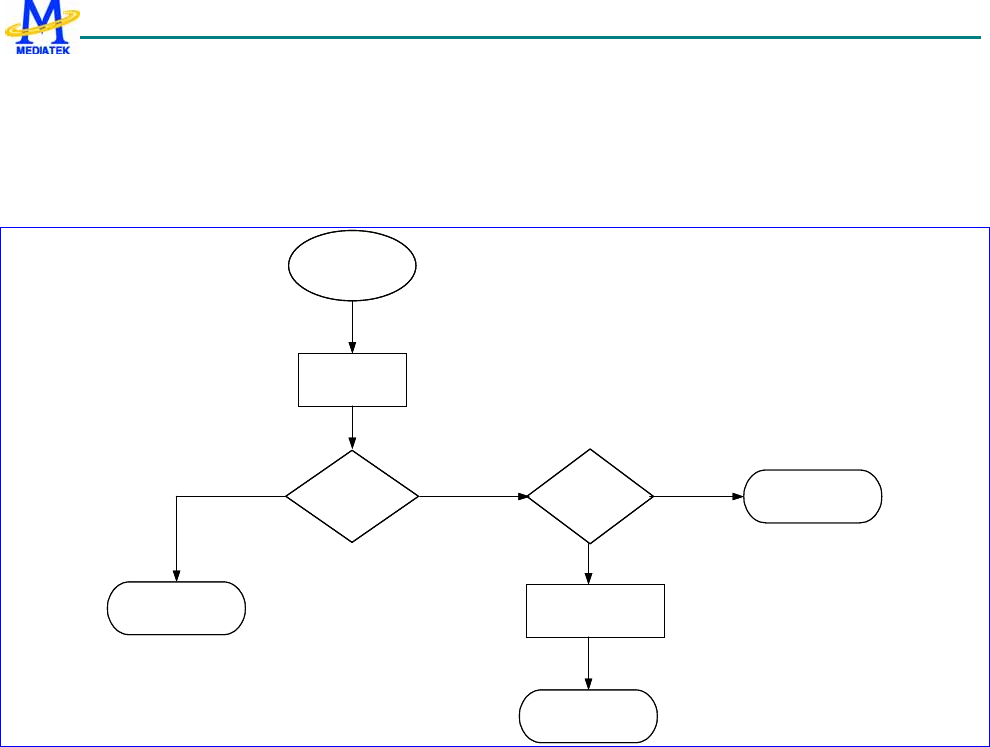
3.2.1.3.3 NAND Flash Booting
If MT6235 cannot receive data from UART1 for a certain amount of time, the program in System ROM checks if any valid
boot loader exists in NAND flash. If found, the boot loader code is copied from NAND flash to RAM (internal or external)
and executed to start the real application software. If no valid boot loader can be found in NAND flash, MT6235 starts
executing code in EMI bank0 memory. The whole boot sequence is shown in the following figure.
Boot from
System ROM
Check UART
input
Receive
from UART
Copy loader from
NAND to RAM
Valid loader
on NAND
YN
Y
N
Factory
programming
Boot from
loader in RAM
Boot from
EMI bank 0
Boot from
System ROM
Check UART
input
Receive
from UART
Copy loader from
NAND to RAM
Valid loader
on NAND
YN
Y
N
Factory
programming
Boot from
loader in RAM
Boot from
EMI bank 0
Figure 8 Boot sequence
3.2.1.4 Little Endian Mode
The MT6235 system always treats 32-bit words of memory in Little Endian format. In Little Endian mode, the lowest
numbered byte in a word is stored in the least significant position, and the highest numbered byte in the most significant
position. Byte 0 of the memory system is therefore connected to data lines 7 through 0.
3.3 Bus System
3.3.1 General Description
Two levels of bus hierarchy are employed in the Micro-Controller Unit Subsystem of MT6235. As depicted in Figure 5,
AHB Bus and APB Bus serve as system backbone and peripheral buses, while an APB bridge connects these two buses.
Both AHB and APB Buses operate at the same or half the clock rate of processor core.
The APB Bridge is the only bus master residing on the APB bus. All APB slaves are mapped onto memory block MB8 in
the MCU 32-bit addressing space. A central address decoder is implemented inside the bridge to generate select signals
for individual peripherals. In addition, since the base address of each APB slave is associated with select signals, the
address bus on APB contains only the value of offset address.

MT6235 GSM/GPRS Baseband Processor Data Sheet Revision 1.02
45/599 MediaTek Inc. Confidential
The maximum address space that can be allocated to a single APB slave is 64 KB, i.e. 16-bit address lines. The width of
the data bus is mainly constrained to 16 bits to minimize the design complexity and power consumption while some use
32-bit data buses to accommodate more bandwidth. In the case where an APB slave needs large amount of transfers, the
device driver can also request DMA channels to conduct a burst of data transfer. The base address and data width of each
peripheral are listed in Table 4.
Base Address Description Data
Width Software Base ID
8001_0000h EFUSE Control 32 EFUSEC Base
8001_0000h Configuration Registers
(Clock, Power Down, Version and Reset) 16 CONFG Base
8002_0000h General Purpose Inputs/Outputs 16 GPIO Base
8003_0000h Reset Generation Unit 16 RGU Base
8100_0000h External Memory Interface 32 EMI Base
8101_0000h Interrupt Controller 32 CIRQ Base
8102_0000h DMA Controller 32 DMA Base
8103_0000h UART 1 16 UART1 Base
8104_0000h UART 2 16 UART2 Base
8105_0000h UART 3 16 UART3 Base
8106_0000h General Purpose Timer 16 GPT Base
8107_0000h Reserved 16 Reserved
8108_0000h Keypad Scanner 16 KP Base
8109_0000h Pulse-Width Modulation Outputs 32 PWM Base
810a_0000h SIM Interface 16 SIM Base
810b_0000h Reserved
810c_0000h Real Time Clock 16 RTC Base
810d_0000h Secure Engine 32 SEJ Base
810e_0000h Bus Monitor 32 BM Base
810f_0000h IrDA 16 IRDA Base
8110_0000h I2C 16 I2C Base
8111_0000h MS/SD Controller 32 MSDC Base
8112_0000h NAND Flash Interface 32 NFI Base
8113_0000h Reserved
8114_0000h Second MS/SD Interface 16 MSDC2 Base
8200_0000h TDMA Timer 32 TDMA Base
8201_0000h Base-Band Serial Interface 32 BSI Base
8202_0000h Base-Band Parallel Interface 16 BPI Base
8203_0000h Automatic Frequency Control Unit 16 AFC Base
8204_0000h Automatic Power Control Unit 32 APC Base
8205_0000h Auxiliary ADC Unit 16 AUXADC Base
8206_0000h Divider/Modulus Coprocessor 32 DIVIDER Base

MT6235 GSM/GPRS Baseband Processor Data Sheet Revision 1.02
46/599 MediaTek Inc. Confidential
8207_0000h Frame Check Sequence 16 FCS Base
8208_0000h GPRS Cipher Unit 32 GCU Base
8209_0000h CSD Format Conversion Coprocessor 32 CSD_ACC Base
820a_0000h MCU-DSP Shared Register 1 16 SHARE1 Base
820b_0000h IRDBG1 16 IRDBG Base
820c_0000h MCU-DSP Shared Register 2 16 SHARE2 Base
820d_0000h IRDBG2 16 IRDBG2 Bas3
820e_0000h DSP Patch Unit 16 PATCH Base
820f_0000h Audio Front End 16 AFE Base
8210_0000h Base-Band Front End 16 BFE Base
8211_0000h Reserved
8212_0000h Reserved
8300_0000h PLL / Clock square configuration 16 PLL_CLKSQ Base
8301_0000h Analog Chip Interface Controller 16 ACIF Base
8302_0000h Reserved
8400_0000h Graphics Memory Controller 32 GMC Base
8401_0000h 2D Accelerator 32 G2D Base
8402_0000h 2D Command Queue 32 GCMQ Base
8403_0000h Reserved
8404_0000h Reserved
8405_0000h Reserved
8406_0000h Reserved
8407_0000h Reserved
8408_0000h Reserved
8409_0000h Reserved
840a_0000h Reserved
840b_0000h Camera Interface 32 CAM Base
840c_0000h Reserved
840d_0000h Reserved
840e_0000h Capture Resizer 32 CRZ Base
840f_0000h Reserved
8410_0000h Reserved
8411_0000h Reserved
Table 4 Register Base Addresses for MCU Peripherals
REGISTER ADDRESS REGISTER NAME SYNONYM
CONFG + 0000h Hardware Version Register HW_VER
CONFG + 0004h Software Version Register SW_VER
CONFG + 0008h Hardware Code Register HW_CODE

MT6235 GSM/GPRS Baseband Processor Data Sheet Revision 1.02
47/599 MediaTek Inc. Confidential
CONFG + 0404h APB Bus Control Register APB_CON
CONFG + 0500h IRWIN Control Register IRWIN_CON
Table 5 APB Bridge Register Map
3.3.2 Register Definitions
CONFG+0000h Hardware Version Register HW_VERSION
Bit 15 14 13 12 11 10 9 8 7 6 5 4 3 2 1 0
Name EXTP MAJREV MINREV
Type RO RO RO RO
Reset 8 A 0 0
This register is used by software to determine the hardware version of the chip. The register contains a new value
whenever each metal fix or major step is performed. All values are incremented by a step of 1.
MINREV Minor Revision of the chip
MAJREV Major Revision of the chip
EXTP This field shows the existence of Hardware Code Register that presents the Hardware ID while the value is other
than zero.
CONFG+0004h Software Version Register SW_VERSION
Bit 15 14 13 12 11 10 9 8 7 6 5 4 3 2 1 0
Name EXTP MAJREV MINREV
Type RO RO RO RO
Reset 8 A 0 0
This register is used by software to determine the software version used with this chip. All values are incremented by a
step of 1.
MINREV Minor Revision of the Software
MAJREV Major Revision of the Software
EXTP This field shows the existence of Software Code Register that presents the Software ID when the value is other
than zero.
CONFG+0008h Hardware Code Register HW_CODE
Bit 15 14 13 12 11 10 9 8 7 6 5 4 3 2 1 0
Name CODE3 CODE2 CODE1 CODE0
Type RO RO RO RO
Reset 6 2 3 5
This register presents the Hardware ID.
CODE This version of chip is coded as 6235h.
CONFG+0404h APB Bus Control Register APB_CON
Bit 15 14 13 12 11 10 9 8 7 6 5 4 3 2 1 0
Name APBW
4 APBW
3 APBW
2 APBW
1 APBW
0 APBR
4 APBR
3 APBR
2 APBR
1 APBR
0
Type R/W R/W R/W R/W R/W R/W R/W R/W R/W R/W
Reset 0 0 0 0 0 1 1 1 1 1
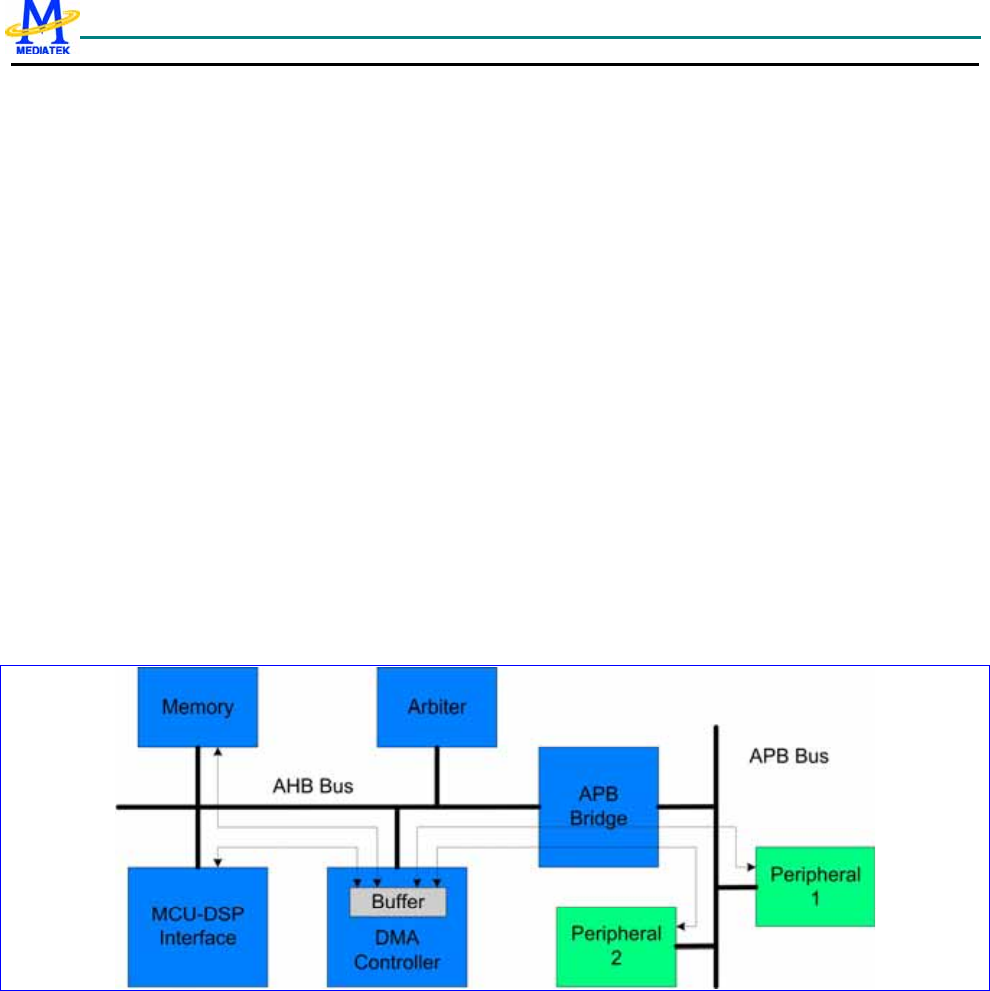
MT6235 GSM/GPRS Baseband Processor Data Sheet Revision 1.02
48/599 MediaTek Inc. Confidential
This register is used to control the timing of Read Cycle and Write Cycle on APB Bus. Note that APB Bridge 2 is
different from other bridges: the access time is varied, and access is not complete until an acknowledge signal from APB
slave is asserted.
APBR0-APBR6 Read Access Time on APB Bus
0 1-Cycle Access
1 2-Cycle Access
APBW0-APBW6 Write Access Time on APB Bus
0 1-Cycle Access
1 2-Cycle Access
3.4 Direct Memory Access
3.4.1 General Description
A generic DMA Controller is placed on Layer 2 AHB Bus to support fast data transfers and to off-load the processor. With
this controller, specific devices on AHB or APB buses can benefit greatly from quick completion of data movement from or
to memory modules such as Internal System RAM or External SRAM, excluding TCM. TCM is invisible for DMA
engine.. Such Generic DMA Controller can also be used to connect any two devices other than memory module as long as
they can be addressed in memory space.
Figure 9 Variety Data Paths of DMA Transfers
Up to fourteen channels of simultaneous data transfers are supported. Each channel has a similar set of registers to be
configured to different scheme as desired. If more than fourteen devices are requesting the DMA resources at the same
time, software based arbitration should be employed. Once the service candidate is decided, the responsible device driver
should configure the Generic DMA Controller properly in order to conduct DMA transfers. Both Interrupt and Polling
based schemes in handling the completion event are supported. The block diagram of such generic DMA Controller is
illustrated in Figure 10.
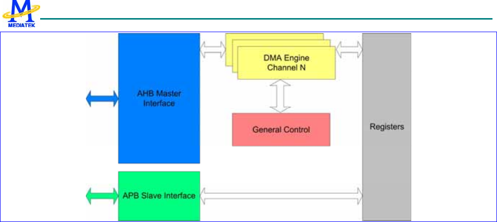
MT6235 GSM/GPRS Baseband Processor Data Sheet Revision 1.02
49/599 MediaTek Inc. Confidential
Figure 10 Block Diagram of Direct memory Access Module
3.4.1.1 Full-Size & Half-Size DMA Channels
There are three types of DMA channels in the DMA controller. The first one is called a full-size DMA channel, the second
one is called a half-size DMA channel, and the last is Virtual FIFO DMA. Channels 1 through 3 are full-size DMA
channels; channels 4 through 10 are half-size ones; and channels 11 through 14 are Virtual FIFO DMAs. The difference
between the first two types of DMA channels is that both source and destination address are programmable in full-size
DMA channels, but only the address of one side can be programmed in half-size DMA channel. In half-size channels,
only either the source or destination address can be programmed, while the addresses of the other side is preset. Which
preset address is used depends on the setting of MAS in DMA Channel Control Register. Refer to the Register Definition
section for more detail.
3.4.1.2 Ring Buffer & Double Buffer Memory Data Movement
DMA channels 1 through 10 support ring-buffer and double-buffer memory data movement. This can be achieved by
programming DMA_WPPT and DMA_WPTO, as well as setting WPEN in DMA_CON register to enable. Figure 11
illustrates how this function works. Once the transfer counter reaches the value of WPPT, the next address jumps to the
WPTO address after completing the WPPT data transfer. Note that only one side can be configured as ring-buffer or
double-buffer memory, and this is controlled by WPSD in DMA_CON register.
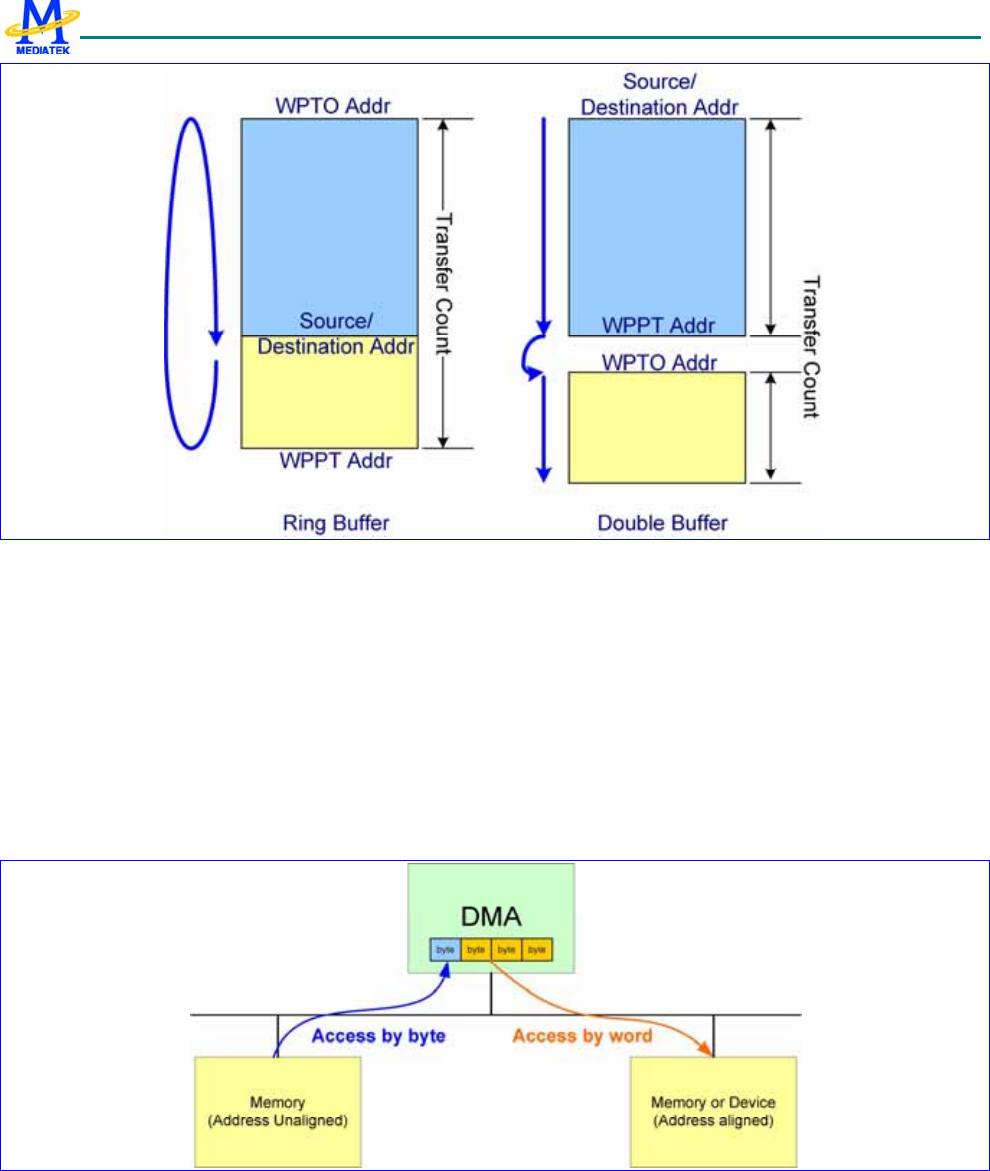
MT6235 GSM/GPRS Baseband Processor Data Sheet Revision 1.02
50/599 MediaTek Inc. Confidential
Figure 11 Ring Buffer and Double Buffer Memory Data Movement
3.4.1.3 Unaligned Word Access
The address of word access on AHB bus must be aligned to word boundary, or the 2 LSB is truncated to 00b. If
programmers do not notice this, it may cause an incorrect data fetch. In the case where data is to be moved from
unaligned addresses to aligned addresses, the word is usually first split into four bytes and then moved byte by byte. This
results in four read and four write transfers on the bus.
To improve bus efficiency, unaligned-word access is provided in DMA4~10. While this function is enabled, DMAs move
data from unaligned address to aligned address by executing four continuous byte-read access and one word-write access,
reducing the number of transfers on the bus by three.
Figure 12 Unaligned Word Accesses
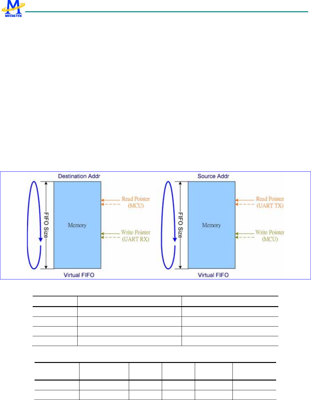
MT6235 GSM/GPRS Baseband Processor Data Sheet Revision 1.02
51/599 MediaTek Inc. Confidential
3.4.1.4 Virtual FIFO DMA
Virtual FIFO DMA is used to ease UART control. The difference between the Virtual FIFO DMAs and the ordinary
DMAs is that Virtual FIFO DMA contains additional FIFO controller. The read and write pointers are kept in the Virtual
FIFO DMA. During a read from the FIFO, the read pointer points to the address of the next data. During a write to the
FIFO, the write pointer moves to the next address. If the FIFO is empty, a FIFO read is not allowed. Similarly, data is
not written into the FIFO if the FIFO is full. Due to UART flow control requirements, an alert length is programmed.
Once the FIFO Space is less than this value, an alert signal is issued to enable UART flow control. The type of flow
control performed depends on the setting in UART.
Each Virtual FIFO DMA can be programmed as RX or TX FIFO. This depends on the setting of DIR in DMA_CON
register. If DIR is “0”(READ), it means TX FIFO. On the other hand, if DIR is “1”(WRITE), the Virtual FIFO DMA is
specified as a RX FIFO.
Virtual FIFO DMA provides an interrupt to MCU. This interrupt informs MCU that there is data in the FIFO, and the
amount of data is over or under the value defined in DMA_COUNT register. With this, MCU does not need to poll DMA
to know when data must be removed from or put into the FIFO.
Note that Virtual FIFO DMAs cannot be used as generic DMAs, i.e. DMA1~10.
Figure 13 Virtual FIFO DMA
DMA number Address of Virtual FIFO Access Port Associated UART
DMA11 6100_0000h UART1 RX / ALL UART TX
DMA12 6100_0100h UART2 RX / ALL UART TX
DMA13 6100_0200h UART3 RX / ALL UART TX
DMA14 6100_0300h ALL UART TX
Table 6 Virtual FIFO Access Port
DMA number Type Ring Buffer Double
Buffer Burst Mode Unaligned Word
Access
DMA1 Full Size
DMA2 Full Size

MT6235 GSM/GPRS Baseband Processor Data Sheet Revision 1.02
52/599 MediaTek Inc. Confidential
DMA3 Full Size
DMA4 Half Size
DMA5 Half Size
DMA6 Half Size
DMA7 Half Size
DMA8 Half Size
DMA9 Half Size
DMA10 Half Size
DMA11 Virtual FIFO
DMA12 Virtual FIFO
DMA13 Virtual FIFO
DMA14 Virtual FIFO
Table 7 Function List of DMA channels
REGISTER ADDRESS REGISTER NAME SYNONYM
DMA + 0000h DMA Global Status Register DMA_GLBSTA
DMA + 0028h DMA Global Bandwidth Limiter Register DMA_GLBLIMITER
DMA + 0100h DMA Channel 1 Source Address Register DMA1_SRC
DMA + 0104h DMA Channel 1 Destination Address Register DMA1_DST
DMA + 0108h DMA Channel 1 Wrap Point Address Register DMA1_WPPT
DMA + 010Ch DMA Channel 1 Wrap To Address Register DMA1_WPTO
DMA + 0110h DMA Channel 1 Transfer Count Register DMA1_COUNT
DMA + 0114h DMA Channel 1 Control Register DMA1_CON
DMA + 0118h DMA Channel 1 Start Register DMA1_START
DMA + 011Ch DMA Channel 1 Interrupt Status Register DMA1_INTSTA
DMA + 0120h DMA Channel 1 Interrupt Acknowledge Register DMA1_ACKINT
DMA + 0124h DMA Channel 1 Remaining Length of Current Transfer DMA1_RLCT
DMA + 0128h DMA Channel 1 Bandwidth Limiter Register DMA1_LIMITER
DMA + 0200h DMA Channel 2 Source Address Register DMA2_SRC
DMA + 0204h DMA Channel 2 Destination Address Register DMA2_DST
DMA + 0208h DMA Channel 2 Wrap Point Address Register DMA2_WPPT
DMA + 020Ch DMA Channel 2 Wrap To Address Register DMA2_WPTO
DMA + 0210h DMA Channel 2 Transfer Count Register DMA2_COUNT
DMA + 0214h DMA Channel 2 Control Register DMA2_CON
DMA + 0218h DMA Channel 2 Start Register DMA2_START
DMA + 021Ch DMA Channel 2 Interrupt Status Register DMA2_INTSTA
DMA + 0220h DMA Channel 2 Interrupt Acknowledge Register DMA2_ACKINT
DMA + 0224h DMA Channel 2 Remaining Length of Current Transfer DMA2_RLCT
DMA + 0228h DMA Channel 2 Bandwidth Limiter Register DMA2_LIMITER

MT6235 GSM/GPRS Baseband Processor Data Sheet Revision 1.02
53/599 MediaTek Inc. Confidential
DMA + 0300h DMA Channel 3 Source Address Register DMA3_SRC
DMA + 0304h DMA Channel 3 Destination Address Register DMA3_DST
DMA + 0308h DMA Channel 3 Wrap Point Address Register DMA3_WPPT
DMA + 030Ch DMA Channel 3 Wrap To Address Register DMA3_WPTO
DMA + 0310h DMA Channel 3 Transfer Count Register DMA3_COUNT
DMA + 0314h DMA Channel 3 Control Register DMA3_CON
DMA + 0318h DMA Channel 3 Start Register DMA3_START
DMA + 031Ch DMA Channel 3 Interrupt Status Register DMA3_INTSTA
DMA + 0320h DMA Channel 3 Interrupt Acknowledge Register DMA3_ACKINT
DMA + 0324h DMA Channel 3 Remaining Length of Current Transfer DMA3_RLCT
DMA + 0328h DMA Channel 3 Bandwidth Limiter Register DMA3_LIMITER
DMA + 0408h DMA Channel 4 Wrap Point Address Register DMA4_WPPT
DMA + 040Ch DMA Channel 4 Wrap To Address Register DMA4_WPTO
DMA + 0410h DMA Channel 4 Transfer Count Register DMA4_COUNT
DMA + 0414h DMA Channel 4 Control Register DMA4_CON
DMA + 0418h DMA Channel 4 Start Register DMA4_START
DMA + 041Ch DMA Channel 4 Interrupt Status Register DMA4_INTSTA
DMA + 0420h DMA Channel 4 Interrupt Acknowledge Register DMA4_ACKINT
DMA + 0424h DMA Channel 4 Remaining Length of Current Transfer DMA4_RLCT
DMA + 0428h DMA Channel 4 Bandwidth Limiter Register DMA4_LIMITER
DMA + 042Ch DMA Channel 4 Programmable Address Register DMA4_PGMADDR
DMA + 0508h DMA Channel 5 Wrap Point Address Register DMA5_WPPT
DMA + 050Ch DMA Channel 5 Wrap To Address Register DMA5_WPTO
DMA + 0510h DMA Channel 5 Transfer Count Register DMA5_COUNT
DMA + 0514h DMA Channel 5 Control Register DMA5_CON
DMA + 0518h DMA Channel 5 Start Register DMA5_START
DMA + 051Ch DMA Channel 5 Interrupt Status Register DMA5_INTSTA
DMA + 0520h DMA Channel 5 Interrupt Acknowledge Register DMA5_ACKINT
DMA + 0524h DMA Channel 5 Remaining Length of Current Transfer DMA5_RLCT
DMA + 0528h DMA Channel 5 Bandwidth Limiter Register DMA5_LIMITER
DMA + 052Ch DMA Channel 5 Programmable Address Register DMA5_PGMADDR
DMA + 0608h DMA Channel 6 Wrap Point Address Register DMA6_WPPT
DMA + 060Ch DMA Channel 6 Wrap To Address Register DMA6_WPTO
DMA + 0610h DMA Channel 6 Transfer Count Register DMA6_COUNT
DMA + 0614h DMA Channel 6 Control Register DMA6_CON
DMA + 0618h DMA Channel 6 Start Register DMA6_START
DMA + 061Ch DMA Channel 6 Interrupt Status Register DMA6_INTSTA
DMA + 0620h DMA Channel 6 Interrupt Acknowledge Register DMA6_ACKINT
DMA + 0624h DMA Channel 6 Remaining Length of Current Transfer DMA6_RLCT

MT6235 GSM/GPRS Baseband Processor Data Sheet Revision 1.02
54/599 MediaTek Inc. Confidential
DMA + 0628h DMA Channel 6 Bandwidth Limiter Register DMA6_LIMITER
DMA + 062Ch DMA Channel 6 Programmable Address Register DMA6_PGMADDR
DMA + 0708h DMA Channel 7 Wrap Point Address Register DMA7_WPPT
DMA + 070Ch DMA Channel 7 Wrap To Address Register DMA7_WPTO
DMA + 0710h DMA Channel 7 Transfer Count Register DMA7_COUNT
DMA + 0714h DMA Channel 7 Control Register DMA7_CON
DMA + 0718h DMA Channel 7 Start Register DMA7_START
DMA + 071Ch DMA Channel 7 Interrupt Status Register DMA7_INTSTA
DMA + 0720h DMA Channel 7 Interrupt Acknowledge Register DMA7_ACKINT
DMA + 0724h DMA Channel 7 Remaining Length of Current Transfer DMA7_RLCT
DMA + 0728h DMA Channel 7 Bandwidth Limiter Register DMA7_LIMITER
DMA + 072Ch DMA Channel 7 Programmable Address Register DMA7_PGMADDR
DMA + 0808h DMA Channel 8 Wrap Point Address Register DMA8_WPPT
DMA + 080Ch DMA Channel 8 Wrap To Address Register DMA8_WPTO
DMA + 0810h DMA Channel 8 Transfer Count Register DMA8_COUNT
DMA + 0814h DMA Channel 8 Control Register DMA8_CON
DMA + 0818h DMA Channel 8 Start Register DMA8_START
DMA + 081Ch DMA Channel 8 Interrupt Status Register DMA8_INTSTA
DMA + 0820h DMA Channel 8 Interrupt Acknowledge Register DMA8_ACKINT
DMA + 0824h DMA Channel 8 Remaining Length of Current Transfer DMA8_RLCT
DMA + 0828h DMA Channel 8 Bandwidth Limiter Register DMA8_LIMITER
DMA + 082Ch DMA Channel 8 Programmable Address Register DMA8_PGMADDR
DMA + 0908h DMA Channel 9 Wrap Point Address Register DMA9_WPPT
DMA + 090Ch DMA Channel 9 Wrap To Address Register DMA9_WPTO
DMA + 0910h DMA Channel 9 Transfer Count Register DMA9_COUNT
DMA + 0914h DMA Channel 9 Control Register DMA9_CON
DMA + 0918h DMA Channel 9 Start Register DMA9_START
DMA + 091Ch DMA Channel 9 Interrupt Status Register DMA9_INTSTA
DMA + 0920h DMA Channel 9 Interrupt Acknowledge Register DMA9_ACKINT
DMA + 0924h DMA Channel 9 Remaining Length of Current Transfer DMA9_RLCT
DMA + 0928h DMA Channel 9 Bandwidth Limiter Register DMA9_LIMITER
DMA + 092Ch DMA Channel 9 Programmable Address Register DMA9_PGMADDR
DMA + 0A08h DMA Channel 10 Wrap Point Address Register DMA10_WPPT
DMA + 0A0Ch DMA Channel 10 Wrap To Address Register DMA10_WPTO
DMA + 0A10h DMA Channel 10 Transfer Count Register DMA10_COUNT
DMA + 0A14h DMA Channel 10 Control Register DMA10_CON
DMA + 0A18h DMA Channel 10 Start Register DMA10_START
DMA + 0A1Ch DMA Channel 10 Interrupt Status Register DMA10_INTSTA
DMA + 0A20h DMA Channel 10 Interrupt Acknowledge Register DMA10_ACKINT

MT6235 GSM/GPRS Baseband Processor Data Sheet Revision 1.02
55/599 MediaTek Inc. Confidential
DMA + 0A24h DMA Channel 10 Remaining Length of Current
Transfer DMA10_RLCT
DMA + 0A28h DMA Channel 10 Bandwidth Limiter Register DMA10_LIMITER
DMA + 0A2Ch DMA Channel 10 Programmable Address Register DMA10_PGMADDR
DMA + 0B10h DMA Channel 11 Transfer Count Register DMA11_COUNT
DMA + 0B14h DMA Channel 11 Control Register DMA11_CON
DMA + 0B18h DMA Channel 11 Start Register DMA11_START
DMA + 0B1Ch DMA Channel 11 Interrupt Status Register DMA11_INTSTA
DMA + 0B20h DMA Channel 11 Interrupt Acknowledge Register DMA11_ACKINT
DMA + 0B28h DMA Channel 11 Bandwidth Limiter Register DMA11_LIMITER
DMA + 0B2Ch DMA Channel 11 Programmable Address Register DMA11_PGMADDR
DMA + 0B30h DMA Channel 11 Write Pointer DMA11_WRPTR
DMA + 0B34h DMA Channel 11 Read Pointer DMA11_RDPTR
DMA + 0B38h DMA Channel 11 FIFO Count DMA11_FFCNT
DMA + 0B3Ch DMA Channel 11 FIFO Status DMA11_FFSTA
DMA + 0B40h DMA Channel 11 Alert Length DMA11_ALTLEN
DMA + 0B44h DMA Channel 11 FIFO Size DMA11_FFSIZE
DMA + 0C10h DMA Channel 12 Transfer Count Register DMA12_COUNT
DMA + 0C14h DMA Channel 12 Control Register DMA12_CON
DMA + 0C18h DMA Channel 12 Start Register DMA12_START
DMA + 0C1Ch DMA Channel 12 Interrupt Status Register DMA12_INTSTA
DMA + 0C20h DMA Channel 12 Interrupt Acknowledge Register DMA12_ACKINT
DMA + 0C28h DMA Channel 12 Bandwidth Limiter Register DMA12_LIMITER
DMA + 0C2Ch DMA Channel 12 Programmable Address Register DMA12_PGMADDR
DMA + 0C30h DMA Channel 12 Write Pointer DMA12_WRPTR
DMA + 0C34h DMA Channel 12 Read Pointer DMA12_RDPTR
DMA + 0C38h DMA Channel 12 FIFO Count DMA12_FFCNT
DMA + 0C3Ch DMA Channel 12 FIFO Status DMA12_FFSTA
DMA + 0C40h DMA Channel 12 Alert Length DMA12_ALTLEN
DMA + 0C44h DMA Channel 12 FIFO Size DMA12_FFSIZE
DMA + 0D10h DMA Channel 13 Transfer Count Register DMA13_COUNT
DMA + 0D14h DMA Channel 13 Control Register DMA13_CON
DMA + 0D18h DMA Channel 13 Start Register DMA13_START
DMA + 0D1Ch DMA Channel 13 Interrupt Status Register DMA13_INTSTA
DMA + 0D20h DMA Channel 13 Interrupt Acknowledge Register DMA13_ACKINT
DMA + 0D28h DMA Channel 13 Bandwidth Limiter Register DMA13_LIMITER
DMA + 0D2Ch DMA Channel 13 Programmable Address Register DMA13_PGMADDR
DMA + 0D30h DMA Channel 13 Write Pointer DMA13_WRPTR
DMA + 0D34h DMA Channel 13 Read Pointer DMA13_RDPTR
DMA + 0D38h DMA Channel 13 FIFO Count DMA13_FFCNT

MT6235 GSM/GPRS Baseband Processor Data Sheet Revision 1.02
56/599 MediaTek Inc. Confidential
DMA + 0D3Ch DMA Channel 13 FIFO Status DMA13_FFSTA
DMA + 0D40h DMA Channel 13 Alert Length DMA13_ALTLEN
DMA + 0D44h DMA Channel 13 FIFO Size DMA13_FFSIZE
DMA + 0E10h DMA Channel 14 Transfer Count Register DMA14_COUNT
DMA + 0E14h DMA Channel 14 Control Register DMA14_CON
DMA + 0E18h DMA Channel 14 Start Register DMA14_START
DMA + 0E1Ch DMA Channel 14 Interrupt Status Register DMA14_INTSTA
DMA + 0E20h DMA Channel 14 Interrupt Acknowledge Register DMA14_ACKINT
DMA + 0E28h DMA Channel 14 Bandwidth Limiter Register DMA14_LIMITER
DMA + 0E2Ch DMA Channel 14 Programmable Address Register DMA14_PGMADDR
DMA + 0E30h DMA Channel 14 Write Pointer DMA14_WRPTR
DMA + 0E34h DMA Channel 14 Read Pointer DMA14_RDPTR
DMA + 0E38h DMA Channel 14 FIFO Count DMA14_FFCNT
DMA + 0E3Ch DMA Channel 14 FIFO Status DMA14_FFSTA
DMA + 0E40h DMA Channel 14 Alert Length DMA14_ALTLEN
DMA + 0E44h DMA Channel 14 FIFO Size DMA14_FFSIZE
Table 8 DMA Controller Register Map
3.4.2 Register Definitions
Register programming tips:
z Start registers shall be cleared, when associated channels are being programmed.
z PGMADDR, i.e. programmable address, only exists in half-size DMA channels. If DIR in Control Register is
high, PGMADDR represents Destination Address. Conversely, If DIR in Control Register is low, PGMADDR
represents Source Address.
z Functions of ring-buffer and double-buffer memory data movement can be activated on either source side or
destination side by programming DMA_WPPT & and DMA_WPTO, as well as setting WPEN in DMA_CON
register high. WPSD in DMA_CON register determines the activated side.
DMA+0000h DMA Global Status Register DMA_GLBSTA
Bit 31 30 29 28 27 26 25 24 23 22 21 20 19 18 17 16
Name IT14
RUN1
4 IT13 RUN1
3 IT12 RUN1
2 IT11 RUN1
1 IT10 RUN1
0 IT9 RUN9
Type RO RO RO RO RO RO RO RO RO RO RO RO
Reset 0 0 0 0 0 0 0 0 0 0 0 0
Bit 15 14 13 12 11 10 9 8 7 6 5 4 3 2 1 0
Name IT8 RUN8 IT7 RUN7 IT6 RUN6 IT5 RUN5 IT4 RUN4 IT3 RUN3 IT2 RUN2 IT1 RUN1
Type RO RO RO RO RO RO RO RO RO RO RO RO RO RO RO RO
Reset 0 0 0 0 0 0 0 0 0 0 0 0 0 0 0 0
This register helps software program keep track of the global status of DMA channels.
RUNN DMA channel n status
MT6235 GSM/GPRS Baseband Processor Data Sheet Revision 1.02
57/599 MediaTek Inc. Confidential
0 Channel n is stopped or has completed the transfer already.
1 Channel n is currently running.
ITN Interrupt status for channel n
0 No interrupt is generated.
1 An interrupt is pending and waiting for service.
DMA+0028h DMA Global Bandwidth limiter Register DMA_GLBLIMIT
ER
Bit 31 30 29 28 27 26 25 24 23 22 21 20 19 18 17 16
Name
Type
Reset
Bit 15 14 13 12 11 10 9 8 7 6 5 4 3 2 1 0
Name GLBLIMITER
Type WO
Reset 0
Please refer to the expression in DMAn_LIMITER for detailed note. The value of DMA_GLBLIMITER is set to all
DMA channels, from 1 to 14.
DMA+0n00h DMA Channel n Source Address Register DMAn_SRC
Bit 31 30 29 28 27 26 25 24 23 22 21 20 19 18 17 16
Name SRC[31:16]
Type R/W
Reset 0
Bit 15 14 13 12 11 10 9 8 7 6 5 4 3 2 1 0
Name SRC[15:0]
Type R/W
Reset 0
The above registers contain the base or current source address that the DMA channel is currently operating on. Writing to
this register specifies the base address of transfer source for a DMA channel. Before programming these registers, the
software program should make sure that STR in DMAn_START is set to 0; that is, the DMA channel is stopped and
disabled completely. Otherwise, the DMA channel may run out of order. Reading this register returns the address value
from which the DMA is reading.
Note that n is from 1 to 3 and SRC can’t be TCM address. TCM is not accessible by DMA..
SRC SRC[31:0] specifies the base or current address of transfer source for a DMA channel, i.e. channel 1, 2 or 3.
WRITE Base address of transfer source
READ Address from which DMA is reading
DMA+0n04h DMA Channel n Destination Address Register DMAn_DST
Bit 31 30 29 28 27 26 25 24 23 22 21 20 19 18 17 16
Name DST[31:16]
Type R/W
Reset 0
Bit 15 14 13 12 11 10 9 8 7 6 5 4 3 2 1 0
Name DST[15:0]
Type R/W
Reset 0
MT6235 GSM/GPRS Baseband Processor Data Sheet Revision 1.02
58/599 MediaTek Inc. Confidential
The above registers contain the base or current destination address that the DMA channel is currently operating on..
Writing to this register specifies the base address of the transfer destination for a DMA channel. Before programming
these registers, the software should make sure that STR in DMAn_START is set to ‘0’; that is, the DMA channel is stopped
and disabled completely. Otherwise, the DMA channel may run out of order. Reading this register returns the address
value to which the DMA is writing.
Note that n is from 1 to 3 and DST can’t be TCM address. TCM is not accessible by DMA.
DST DST[31:0] specifies the base or current address of transfer destination for a DMA channel, i.e. channel 1, 2 or 3.
WRITE Base address of transfer destination.
READ Address to which DMA is writing.
DMA+0n08h DMA Channel n Wrap Point Count Register DMAn_WPPT
Bit 31 30 29 28 27 26 25 24 23 22 21 20 19 18 17 16
Name
Type
Reset
Bit 15 14 13 12 11 10 9 8 7 6 5 4 3 2 1 0
Name WPPT[15:0]
Type R/W
Reset 0
The above registers are to specify the transfer count required to perform before the jump point. This can be used to
support ring buffer or double buffer style memory accesses. To enable this function, two control bits, WPEN and WPSD,
in DMA control register must be programmed. See the following register description for more details. If the
transfercounter in the DMA engine matches this value, an address jump occurs, and the next address is the address specified
in DMAn_WPTO. Before programming these registers, the software should make sure that STR in DMAn_START is set
to ‘0’, that is the DMA channel is stopped and disabled completely. Otherwise, the DMA channel may run out of order.
To enable this function, WPEN in DMA_CON is set. Note that the total size of data specify in the wrap point count in a
DMA channel is determined by LEN together with the SIZE in DMAn_CON, i.e. WPPT x SIZE.
Note that n is from 1 to 10.
WPPT WPPT[15:0] specifies the amount of the transfer count from start to jumping point for a DMA channel, i.e.
channel 1 – 10.
WRITE Wrap point transfer count.
READ Value set by the programmer.
DMA+0n0Ch DMA Channel n Wrap To Address Register DMAn_WPTO
Bit 31 30 29 28 27 26 25 24 23 22 21 20 19 18 17 16
Name WPTO[31:16]
Type R/W
Reset 0
Bit 15 14 13 12 11 10 9 8 7 6 5 4 3 2 1 0
Name WPTO[15:0]
Type R/W
Reset 0
The above registers specify the address of the jump destination of a given DMA transfer to support ring buffer or double
buffer style memory accesses. To enable this function, set the two control bits, WPEN and WPSD, in the DMA control
register . See the following register description for more details. Before programming these registers, the software
MT6235 GSM/GPRS Baseband Processor Data Sheet Revision 1.02
59/599 MediaTek Inc. Confidential
should make sure that STR in DMAn_START is set to ‘0’, that is the DMA channel is stopped and disabled completely.
Otherwise, the DMA channel may run out of order. To enable this function, WPEN in DMA_CON should be set.
Note that n is from 1 to 10.
WPTO WPTO[31:0] specifies the address of the jump point for a DMA channel, i.e. channel 1 – 10.
WRITE Address of the jump destination.
READ Value set by the programmer.
DMA+0n10h DMA Channel n Transfer Count Register DMAn_COUNT
Bit 31 30 29 28 27 26 25 24 23 22 21 20 19 18 17 16
Name
Type
Reset
Bit 15 14 13 12 11 10 9 8 7 6 5 4 3 2 1 0
Name LEN
Type R/W
Reset 0
This register specifies the amount of total transfer count that the DMA channel is required to perform. Upon completion,
the DMA channel generates an interrupt request to the processor while ITEN in DMAn_CON is set as ‘1’. Note that the
total size of data being transferred by a DMA channel is determined by LEN together with the SIZE in DMAn_CON, i.e.
LEN x SIZE.
For virtual FIFO DMA, this register is used to configure the RX threshold and TX threshold. Interrupt is triggered while
FIFO count >= RX threshold in RX path or FIFO count =< TX threshold in TX path. Note that ITEN bit in DMA_CON
register shall be set, or no interrupt is issued.
Note that n is from 1 to 14.
LEN The amount of total transfer count
DMA+0n14h DMA Channel n Control Register DMAn_CON
Bit 31 30 29 28 27 26 25 24 23 22 21 20 19 18 17 16
Name MAS DIR WPEN WPSD
Type R/W R/W R/W R/W
Reset 0 0 0 0
Bit 15 14 13 12 11 10 9 8 7 6 5 4 3 2 1 0
Name ITEN BURST B2W DRQ DINC SINC SIZE
Type R/W R/W R/W R/W R/W R/W R/W
Reset 0 0 0 0 0 0 0
This register contains all the available control schemes for a DMA channel that is ready for software programmer to
configure. Note that all these fields cannot be changed while DMA transfer is in progress or an unexpected situation may
occur.
Note that n is from 1 to 14.
SIZE Data size within the confine of a bus cycle per transfer.
These bits confines the data transfer size between source and destination to the specified value for individual bus
cycle. The size is in terms of byte and has maximum value of 4 bytes. It is mainly decided by the data width of
a DMA master.
00 Byte transfer/1 byte

MT6235 GSM/GPRS Baseband Processor Data Sheet Revision 1.02
60/599 MediaTek Inc. Confidential
01 Half-word transfer/2 bytes
10 Word transfer/4 bytes
11 Reserved
SINC Incremental source address. Source addresses increase every transfer. If the setting of SIZE is Byte, Source
addresses increase by 1 every single transfer. If Half-Word, increase by 2; and if Word, increase by 4.
0 Disable
1 Enable
DINC Incremental destination address. Destination addresses increase every transfer. If the setting of SIZE is Byte,
Destination addresses increase by 1 every single transfer. If Half-Word, increase by 2; and Iif Word, increase by
4.
0 Disable
1 Enable
DREQ Throttle and handshake control for DMA transfer
0 No throttle control during DMA transfer or transfers occurred only between memories
1 Hardware handshake management
The DMA master is able to throttle down the transfer rate by way of request-grant handshake.
B2W Word to Byte or Byte to Word transfer for the applications of transferring non-word-aligned-address data to
word-aligned-address data. Note that BURST is set to 4-beat burst while enabling this function, and the SIZE is
set to Byte.
NO effect on channel 1 – 3 & 11 - 14.
0 Disable
1 Enable
BURST Transfer Type. Burst-type transfers have better bus efficiency. Mass data movement is recommended to use this
kind of transfer. However, note that burst-type transfer does not stop until all of the beats in a burst are
completed or transfer length is reached. FIFO threshold of peripherals must be configured carefully while being
used to move data from/to the peripherals.
What transfer type can be used is restricted by the SIZE. If SIZE is 00b, i.e. byte transfer, all of the four transfer
types can be used. If SIZE is 01b, i.e. half-word transfer, 16-beat incrementing burst cannot be used. If SIZE is
10b, i.e. word transfer, only single and 4-beat incrementing burst can be used.
NO effect on channel 11 - 14.
000 Single
001 Reserved
010 4-beat incrementing burst
011 Reserved
100 8-beat incrementing burst
101 Reserved
110 16-beat incrementing burst
111 Reserved
ITEN DMA transfer completion interrupt enable.
0 Disable
1 Enable
WPSD The side using address-wrapping function. Only one side of a DMA channel can activate address-wrapping
function at a time.
NO effect on channel 11 - 14.

MT6235 GSM/GPRS Baseband Processor Data Sheet Revision 1.02
61/599 MediaTek Inc. Confidential
0 Address-wrapping on source .
1 Address-wrapping on destination.
WPEN Address-wrapping for ring buffer and double buffer. The next address of DMA jumps to WRAP TO address
when the current address matches WRAP POINT count.
NO effect on channel 11 - 14.
0 Disable
1 Enable
DIR Directions of DMA transfer for half-size and Virtual FIFO DMA channels, i.e. channels 4~14. The direction is
from the perspective of the DMA masters. WRITE means read from master and then write to the address
specified in DMA_PGMADDR, and vice versa.
NO effect on channel 1 - 3.
0 Read
1 Write
MAS Master selection. Specifies which master occupies this DMA channel. Once assigned to certain master, the
corresponding DREQ and DACK are connected. For half-size and Virtual FIFO DMA channels, i.e. channels 4 ~
14, a predefined address is assigned as well.
00000 SIM
00001 MSDC
00010 IrDA TX
00011 IrDA RX
00100 Reserved
00101 Reserved
00110 Reserved
00111 Reserved
01000 UART1 TX
01001 UART1 RX
01010 UART2 TX
01011 UART2 RX
01100 UART3 TX
01101 UART3 RX
01110 DSP-DMA1
01111 NFI TX
10000 NFI RX
10001 DSP-DMA2
10010 I2C TX
10011 I2C RX
10100 Reserved
10101 Reserved
OTHERS Reserved
DMA+0n18h DMA Channel n Start Register DMAn_START
Bit 31 30 29 28 27 26 25 24 23 22 21 20 19 18 17 16
Name
Type
Reset

MT6235 GSM/GPRS Baseband Processor Data Sheet Revision 1.02
62/599 MediaTek Inc. Confidential
Bit 15 14 13 12 11 10 9 8 7 6 5 4 3 2 1 0
Name STR
Type R/W
Reset 0
This register controls the activity of a DMA channel. Note that prior to setting STR to “1”, all the configurations should
be done by giving proper value to the registers. Note also that once the STR is set to “1”, the hardware does not clear it
automatically no matter if the DMA channel accomplishes the DMA transfer or not. In other works, the value of STR
stays “1” regardless of the completion of DMA transfer. Therefore, the software program should be sure to clear STR to
“0” before restarting another DMA transfer. If this bit is cleared to “0” during DMA transfer is active, software should
polling MDDMA_GLBSTA RUNN after this bit is cleared to ensure current DMA transfer is terminated by DMA engine.
Note that n is from 1 to 14.
STR Start control for a DMA channel.
0 The DMA channel is stopped.
1 The DMA channel is started and running.
DMA+0n1Ch DMA Channel n Interrupt Status Register DMAn_INTSTA
Bit 31 30 29 28 27 26 25 24 23 22 21 20 19 18 17 16
Name
Type
Reset
Bit 15 14 13 12 11 10 9 8 7 6 5 4 3 2 1 0
Name INT
Type RO
Reset 0
This register shows the interrupt status of a DMA channel. It has the same value as DMA_GLBSTA.
Note that n is from 1 to 14.
INT Interrupt Status for DMA Channel
0 No interrupt request is generated.
1 One interrupt request is pending and waiting for service.
DMA+0n20h DMA Channel n Interrupt Acknowledge Register DMAn_ACKINT
Bit 31 30 29 28 27 26 25 24 23 22 21 20 19 18 17 16
Name
Type
Reset
Bit 15 14 13 12 11 10 9 8 7 6 5 4 3 2 1 0
Name ACK
Type WO
Reset 0
This register is used to acknowledge the current interrupt request associated with the completion event of a DMA channel
by software program. Note that this is a write-only register, and any read to it returns a value of “0”.
Note that n is from 1 to 14.
ACK Interrupt acknowledge for the DMA channel
0 No effect
MT6235 GSM/GPRS Baseband Processor Data Sheet Revision 1.02
63/599 MediaTek Inc. Confidential
1 Interrupt request is acknowledged and should be relinquished.
DMA+0n24h DMA Channel n Remaining Length of Current Transfer DMAn_RLCT
Bit 31 30 29 28 27 26 25 24 23 22 21 20 19 18 17 16
Name
Type
Reset
Bit 15 14 13 12 11 10 9 8 7 6 5 4 3 2 1 0
Name RLCT
Type RO
Reset 0
This register is to reflect the left count of the transfer. Note that this value is transfer count not the transfer data size.
Note that n is from 1 to 10.
DMA+0n28h DMA Bandwidth limiter Register DMAn_LIMITER
Bit 31 30 29 28 27 26 25 24 23 22 21 20 19 18 17 16
Name
Type
Reset
Bit 15 14 13 12 11 10 9 8 7 6 5 4 3 2 1 0
Name LIMITER
Type R/W
Reset 0
This register is to suppress the Bus utilization of the DMA channel. The value is from 0 to 255. 0 means no limitation,
and 255 means totally banned. The value between 0 and 255 means certain DMA can have permission to use AHB every
(4 X n) AHB clock cycles.
Note that it is not recommended to limit the Bus utilization of the DMA channels because this increases the latency of
response to the masters, and the transfer rate decreases as well. Before using it, programmer must make sure that the bus
masters have some protective mechanism to avoid entering the wrong states.
Note that n is from 1 to 14.
LIMITER from 0 to 255. 0 means no limitation, 255 means totally banned, and others mean Bus access permission
every (4 X n) AHB clock.
DMA+0n2Ch DMA Channel n Programmable Address Register DMAn_PGMADD
R
Bit 31 30 29 28 27 26 25 24 23 22 21 20 19 18 17 16
Name PGMADDR[31:16]
Type R/W
Reset 0
Bit 15 14 13 12 11 10 9 8 7 6 5 4 3 2 1 0
Name PGMADDR[15:0]
Type R/W
Reset 0
The above registers specify the address for a half-size DMA channel. This address represents a source address if DIR in
DMA_CON is set to 0, and represents a destination address if DIR in DMA_CON is set to 1. Before being able to

MT6235 GSM/GPRS Baseband Processor Data Sheet Revision 1.02
64/599 MediaTek Inc. Confidential
program these register, the software should make sure that STR in DMAn_START is set to ‘0’, that is the DMA channel is
stopped and disabled completely. Otherwise, the DMA channel may run out of order.
Note that n is from 4 to 14 and PGMADDR can’t be TCM address. TCM is not accessible by DMA.
PGMADDR PGMADDR[31:0] specifies the addresses for a half-size or a Virtual FIFO DMA channel, i.e. channel 4 – 14.
WRITE Base address of transfer source or destination according to DIR bit
READ Current address of the transfer.
DMA+0n30h DMA Channel n Virtual FIFO Write Pointer Register DMAn_WRPTR
Bit 31 30 29 28 27 26 25 24 23 22 21 20 19 18 17 16
Name WRPTR[31:16]
Type RO
Bit 15 14 13 12 11 10 9 8 7 6 5 4 3 2 1 0
Name WRPTR[15:0]
Type RO
Note that n is from 11 to 14.
WRPTR Virtual FIFO Write Pointer.
DMA+0n34h DMA Channel n Virtual FIFO Read Pointer Register DMAn_RDPTR
Bit 31 30 29 28 27 26 25 24 23 22 21 20 19 18 17 16
Name RDPTR[31:16]
Type RO
Bit 15 14 13 12 11 10 9 8 7 6 5 4 3 2 1 0
Name RDPTR[15:0]
Type RO
Note that n is from 11 to 14.
RDPTR Virtual FIFO Read Pointer.
DMA+0n38h DMA Channel n Virtual FIFO Data Count Register DMAn_FFCNT
Bit 31 30 29 28 27 26 25 24 23 22 21 20 19 18 17 16
Name
Type
Bit 15 14 13 12 11 10 9 8 7 6 5 4 3 2 1 0
Name FFCNT
Type RO
Note that n is from 11 to 14.
FFCNT To display the number of data stored in FIFO. 0 means FIFO empty, and FIFO is full if FFCNT is equal to
FFSIZE.
DMA+0n3Ch DMA Channel n Virtual FIFO Status Register DMAn_FFSTA
Bit 31 30 29 28 27 26 25 24 23 22 21 20 19 18 17 16
Name
Type
Reset
Bit 15 14 13 12 11 10 9 8 7 6 5 4 3 2 1 0
Name ALT
EMPT
Y FULL
MT6235 GSM/GPRS Baseband Processor Data Sheet Revision 1.02
65/599 MediaTek Inc. Confidential
Type RO RO RO
Reset 0 1 0
Note that n is from 11 to 14.
FULL To indicate FIFO is full.
0 Not Full
1 Full
EMPTY To indicate FIFO is empty.
0 Not Empty
1 Empty
ALT To indicate FIFO Count is larger than ALTLEN. DMA issues an alert signal to UART to enable UART flow
control.
0 Not reach alert region.
1 Reach alert region.
DMA+0n40h DMA Channel n Virtual FIFO Alert Length Register DMAn_ALTLEN
Bit 31 30 29 28 27 26 25 24 23 22 21 20 19 18 17 16
Name
Type
Reset
Bit 15 14 13 12 11 10 9 8 7 6 5 4 3 2 1 0
Name ALTLEN
Type R/W
Reset 0
Note that n is from 11 to 14.
ALTLEN Specifies the Alert Length of Virtual FIFO DMA. Once the remaining FIFO space is less than ALTLEN, an
alert signal is issued to UART to enable flow control. Normally, ALTLEN shall be larger than 16 for UART
application.
DMA+0n44h DMA Channel n Virtual FIFO Size Register DMAn_FFSIZE
Bit 31 30 29 28 27 26 25 24 23 22 21 20 19 18 17 16
Name
Type
Reset
Bit 15 14 13 12 11 10 9 8 7 6 5 4 3 2 1 0
Name FFSIZE
Type R/W
Reset 0
Note that n is from 11 to 14.
FFSIZE Specifies the FIFO Size of Virtual FIFO DMA.
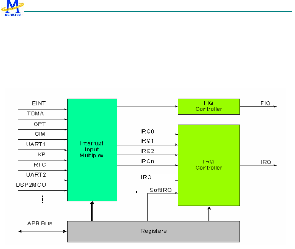
MT6235 GSM/GPRS Baseband Processor Data Sheet Revision 1.02
66/599 MediaTek Inc. Confidential
3.5 Interrupt Controller
3.5.1 General Description
Figure 14 outlines the major functionality of the MCU Interrupt Controller. The interrupt controller processes all
interrupt sources coming from external lines and internal MCU peripherals. Since ARM9EJ-S core supports two levels of
interrupt latency, this controller generates two request signals: FIQ for fast, low latency interrupt request and IRQ for more
general interrupts with lower priority.
31 (hex)
Figure 15 Block Diagram of the Interrupt Controller
One and only one of the interrupt sources can be assigned to FIQ Controller and have the highest priority in requesting
timing critical service. All the others share the same IRQ signal by connecting them to IRQ Controller. The IRQ
Controller manages up 50 interrupt lines of IRQ0 to IRQ31 with fixed priority in descending order.
The Interrupt Controller provides a simple software interface by mean of registers to manipulate the interrupt request shared
system. IRQ Selection Registers and FIQ Selection Register determine the source priority and connecting relation among
sources and interrupt lines. IRQ Source Status Register allows software program to identify the source of interrupt that
generates the interrupt request. IRQ Mask Register provides software to mask out undesired sources some time. End of
Interrupt Register permits software program to indicate to the controller that a certain interrupt service routine has been
finished.
Binary coded version of IRQ Source Status Register is also made available for software program to helpfully identify the
interrupt source. Note that while taking advantage of this, it should also take the binary coded version of End of Interrupt
Register coincidently.
The essential Interrupt Table of ARM926EJ-S core is shown as Table 9.

MT6235 GSM/GPRS Baseband Processor Data Sheet Revision 1.02
67/599 MediaTek Inc. Confidential
Address Description
00000000h System Reset
00000018h IRQ
0000001Ch FIQ
Table 10 Interrupt Table of ARM926EJ-S
3.5.1.1 Interrupt Source Masking
Interrupt controller provides the function of Interrupt Source Masking by the way of programming MASK register. Any
of them can be masked individually.
However, because of the bus latency, the masking takes effect no earlier than 3 clock cycles later. In this time, the
to-be-masked interrupts could come in and generate an IRQ pulse to MCU, and then disappear immediately. This IRQ
forces MCU going to Interrupt Service Routine and polling Status Register (IRQ_STA(IRQ_STAH+IRQ_STAL) or
IRQ_STA2), but the register shows there is no interrupt. This might cause MCU malfunction.
There are two ways for programmer to protect their software.
1. Return from ISR (Interrupt Service Routine) immediately while the Status register shows no interrupt.
2. Set I bit of MCU before doing Interrupt Masking, and then clear it after Interrupt Masking done.
Both avoid the problem, but the first item recommended to have in the ISR.
3.5.1.2 External Interrupt
This interrupt controller also integrates an External Interrupt Controller that can support up to 8 interrupt requests coming
from external sources, the EINT0~7, and 4 WakeUp interrupt requests, i.e. EINT8-B, coming from peripherals. All external
interrupts can inform system to resume the system clock.
The eight external interrupts can be used for different kind of applications, mainly for event detections: detection of hand
free connection, detection of hood opening, detection of battery charger connection.
Since the external event may be unstable in a certain period, a de-bounce mechanism is introduced to ensure the
functionality. The circuitry is mainly used to verify that the input signal remains stable for a programmable number of
periods of the clock. When this condition is satisfied, for the appearance or the disappearance of the input, the output of
the de-bounce logic changes to the desired state. Note that, because it uses the 32 KHz slow clock for performing the
de-bounce process, the parameter of de-bounce period and de-bounce enable takes effect no sooner than one 32 KHz clock
cycle (~31.25us) after the software program sets them. When the sources of External Interrupt Controller are used to
resume the system clock in sleep mode, the de-bounce mechanism must be enabled. However, the polarities of EINTs are
clocked with the system clock. Any changes to them take effect immediately.
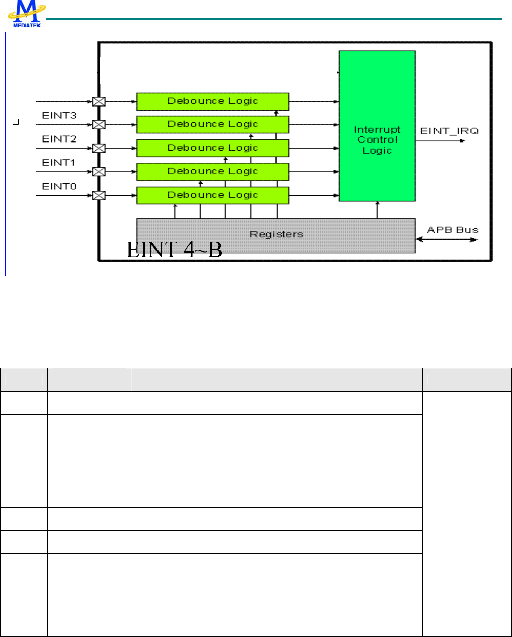
MT6235 GSM/GPRS Baseband Processor Data Sheet Revision 1.02
68/599 MediaTek Inc. Confidential
Figure 16 Block Diagram of External Interrupt Controller
3.5.1.3 External Interrupt Input Pins
EINT Edge / Level
HW Debounce SOURCE PIN SUPPLEMENT
EINT0 Edge / Level
Yes EINT0
EINT1 Edge / Level
Yes EINT1
EINT2 Edge / Level
Yes EINT2
EINT3 Edge / Level
Yes if(GPIO44_M==1) then EINT3=EINT3
else EINT3=1
EINT4 Edge / Level
Yes if(GPIO45_M==1) then EINT4=EINT4
else EINT4=1
EINT5 Edge / Level
Yes if(GPIO46_M==1) then EINT5=EINT5
else EINT5=1
EINT6 Edge / Level
Yes if(GPIO47_M==1) then EINT6=EINT6
else EINT6=1
EINT7 Edge / Level
Yes if(GPIO48_M==1) then EINT7=EINT7
else EINT7=1
EINT8 Edge / Level
Yes PMIC Charge Detection (Low Active)
EINT9 Edge / Level
Yes URXD1
1. GPIOs should
be in the input
mode and are
effected by GPIO
data input
inversion
registers.
2. GPIOxx_M is
the GPIO mode
control registers,
please refer to
GPIO segment.

MT6235 GSM/GPRS Baseband Processor Data Sheet Revision 1.02
69/599 MediaTek Inc. Confidential
EINTA Edge / Level
Yes URXD2
EINTB Edge / Level
Yes URXD3
REGISTER ADDRESS REGISTER NAME SYNONYM
CIRQ + 0000h IRQ Selection 0 Register IRQ_SEL0
CIRQ + 0004h IRQ Selection 1 Register IRQ_SEL1
CIRQ + 0008h IRQ Selection 2 Register IRQ_SEL2
CIRQ + 000Ch IRQ Selection 3 Register IRQ_SEL3
CIRQ + 0010h IRQ Selection 4 Register IRQ_SEL4
CIRQ + 0014h IRQ Selection 5 Register IRQ_SEL5
CIRQ + 0018h IRQ Selection 6 Register IRQ_SEL6
CIRQ + 001ch IRQ Selection 7 Register IRQ_SEL7
CIRQ + 0020h IRQ Selection 8 Register IRQ_SEL8
CIRQ + 0034h FIQ Selection Register FIQ_SEL
CIRQ + 0038h IRQ Mask Register (LSB) IRQ_MASKL
CIRQ + 003ch IRQ Mask Register (MSB) IRQ_MASKH
CIRQ + 0040h IRQ Mask Clear Register (LSB) IRQ_MASK_CLRL
CIRQ + 0044h IRQ Mask Clear Register (MSB) IRQ_MASK_CLRH
CIRQ + 0048h IRQ Mask Set Register (LSB) IRQ_MASK_SETL
CIRQ + 004ch IRQ Mask Set Register (MSB) IRQ_MASK_SETH
CIRQ + 0050h IRQ Status Register (LSB) IRQ_STAL
CIRQ + 0054h IRQ Status Register (MSB) IRQ_STAH
CIRQ + 0058h IRQ End of Interrupt Register (LSB) IRQ_EOIL
CIRQ + 005ch IRQ End of Interrupt Register (MSB) IRQ_EOIH
CIRQ + 0060h IRQ Sensitive Register (LSB) IRQ_SENSL
CIRQ + 0064h IRQ Sensitive Register (MSB) IRQ_SENSH
CIRQ + 0068h IRQ Software Interrupt Register (LSB) IRQ_SOFTL
CIRQ + 006ch IRQ Software Interrupt Register (MSB) IRQ_SOFTH
CIRQ + 0070h FIQ Control Register FIQ_CON
CIRQ + 0074h FIQ End of Interrupt Register FIQ_EOI
CIRQ + 0078h Binary Coded Value of IRQ_STATUS IRQ_STA2
CIRQ + 007ch Binary Coded Value of IRQ_EOI IRQ_EOI2
CIRQ + 0080h Binary Coded Value of IRQ_SOFT IRQ_SOFT2
CIRQ + 0100h EINT Status Register EINT_STA
CIRQ + 0104h EINT Mask Register EINT_MASK
CIRQ + 0108h EINT Mask Disable Register EINT_MASK_DIS
CIRQ + 010Ch EINT Mask Enable Register EINT_MASK_EN
MT6235 GSM/GPRS Baseband Processor Data Sheet Revision 1.02
70/599 MediaTek Inc. Confidential
CIRQ + 0110h EINT Interrupt Acknowledge Register EINT_INTACK
CIRQ + 0114h EINT Sensitive Register EINT_SENS
CIRQ + 0120h EINT0 De-bounce Control Register EINT0_CON
CIRQ + 0130h EINT1 De-bounce Control Register EINT1_CON
CIRQ + 0140h EINT2 De-bounce Control Register EINT2_CON
CIRQ + 0150h EINT3 De-bounce Control Register EINT3_CON
CIRQ + 0160h EINT4 De-bounce Control Register EINT4_CON
CIRQ + 0170h EINT5 De-bounce Control Register EINT5_CON
CIRQ + 0180h EINT6 De-bounce Control Register EINT6_CON
CIRQ + 0190h EINT7 De-bounce Control Register EINT7_CON
CIRQ + 01a0h EINT8 De-bounce Control Register EINT8_CON
CIRQ + 01b0h EINT9 De-bounce Control Register EINT9_CON
CIRQ + 01c0h EINTA De-bounce Control Register EINT10_CON
CIRQ + 01d0h EINTB De-bounce Control Register EINT11_CON
Table 11 Interrupt Controller Register Map
3.5.2 Register Definitions
CIRQ+0000h IRQ Selection 0 Register IRQ_SEL0
Bit 31 30 29 28 27 26 25 24 23 22 21 20 19 18 17 16
Name IRQ4 IRQ3 IRQ2
Type R/W R/W R/W
Reset 0x4 0x3
Bit 15 14 13 12 11 10 9 8 7 6 5 4 3 2 1 0
Name IRQ2 IRQ1 IRQ0
Type R/W R/W R/W
Reset 0x2 0x1 0x0
CIRQ+0004h IRQ Selection 1 Register IRQ_SEL1
Bit 31 30 29 28 27 26 25 24 23 22 21 20 19 18 17 16
Name IRQ9 IRQ8 IRQ7
Type R/W R/W R/W
Reset 0x9 0x8
Bit 15 14 13 12 11 10 9 8 7 6 5 4 3 2 1 0
Name IRQ7 IRQ6 IRQ5
Type R/W R/W R/W
Reset 0x7 0x6 0x5
CIRQ+0008h IRQ Selection 2 Register IRQ_SEL2
Bit 31 30 29 28 27 26 25 24 23 22 21 20 19 18 17 16
Name IRQE IRQD IRQC
Type R/W R/W R/W
Reset 0xe 0xD
Bit 15 14 13 12 11 10 9 8 7 6 5 4 3 2 1 0
Name IRQC IRQB IRQA
Type R/W R/W R/W
MT6235 GSM/GPRS Baseband Processor Data Sheet Revision 1.02
71/599 MediaTek Inc. Confidential
Reset 0xc 0xb 0xa
CIRQ+000ch IRQ Selection 3 Register IRQ_SEL3
Bit 31 30 29 28 27 26 25 24 23 22 21 20 19 18 17 16
Name IRQ13 IRQ12 IRQ11
Type R/W R/W R/W
Reset 0x13 0x12
Bit 15 14 13 12 11 10 9 8 7 6 5 4 3 2 1 0
Name IRQ11 IRQ10 IRQF
Type R/W R/W R/W
Reset 0x11 0x10 0xf
CIRQ+0010h IRQ Selection 4 Register IRQ_SEL4
Bit 31 30 29 28 27 26 25 24 23 22 21 20 19 18 17 16
Name IRQ18 IRQ17 IRQ16
Type R/W R/W R/W
Reset 0x18 0x17
Bit 15 14 13 12 11 10 9 8 7 6 5 4 3 2 1 0
Name IRQ16 IRQ15 IRQ14
Type R/W R/W R/W
Reset 0x16 0x15 0x14
CIRQ+0014h IRQ Selection 5 Register IRQ_SEL5
Bit 31 30 29 28 27 26 25 24 23 22 21 20 19 18 17 16
Name IRQ1D IRQ1C IRQ1B
Type R/W R/W R/W
Reset 0x1d 0x1c
Bit 15 14 13 12 11 10 9 8 7 6 5 4 3 2 1 0
Name IRQ1B IRQ1A IRQ19
Type R/W R/W R/W
Reset 0x1b 0x1a 0x19
CIRQ+0018h IRQ Selection 6 Register IRQ_SEL6
Bit 31 30 29 28 27 26 25 24 23 22 21 20 19 18 17 16
Name IRQ22 IRQ21 IRQ20
Type R/W R/W R/W
Reset 0x22 0x21
Bit 15 14 13 12 11 10 9 8 7 6 5 4 3 2 1 0
Name IRQ20 IRQ1F IRQ1E
Type R/W R/W R/W
Reset 0x20 0x1f 0x1e
CIRQ+001ch IRQ Selection 7 Register IRQ_SEL7
Bit 31 30 29 28 27 26 25 24 23 22 21 20 19 18 17 16
Name IRQ27 IRQ26 IRQ25
Type R/W R/W R/W
Reset 0x27 0x26
Bit 15 14 13 12 11 10 9 8 7 6 5 4 3 2 1 0
Name IRQ25 IRQ24 IRQ23
Type R/W R/W R/W
Reset 0x25 0x24 0x23
MT6235 GSM/GPRS Baseband Processor Data Sheet Revision 1.02
72/599 MediaTek Inc. Confidential
CIRQ+0020h IRQ Selection 8 Register IRQ_SEL8
Bit 31 30 29 28 27 26 25 24 23 22 21 20 19 18 17 16
Name IRQ2C IRQ2B IRQ2A
Type R/W R/W R/W
Reset 0x2c 0x2b
Bit 15 14 13 12 11 10 9 8 7 6 5 4 3 2 1 0
Name IRQ2A IRQ29 IRQ28
Type R/W R/W R/W
Reset 0x2a 0x29 0x28
CIRQ+0024h IRQ Selection 9 Register IRQ_SEL9
Bit 31 30 29 28 27 26 25 24 23 22 21 20 19 18 17 16
Name IRQ31 IRQ30 IRQ2F
Type R/W R/W R/W
Reset 0x31 0x30
Bit 15 14 13 12 11 10 9 8 7 6 5 4 3 2 1 0
Name IRQ2F IRQ2E IRQ2D
Type R/W R/W R/W
Reset 0x2f 0x2e 0x2d
CIRQ+0034h FIQ Selection Register FIQ_SEL
Bit 31 30 29 28 27 26 25 24 23 22 21 20 19 18 17 16
Name
Type
Reset
Bit 15 14 13 12 11 10 9 8 7 6 5 4 3 2 1 0
Name FIQ
Type R/W
Reset 0
The IRQ/FIQ Selection Registers provide system designers with a flexible routing scheme to make various mappings of
priority among interrupt sources possible. The registers allow the interrupt sources to be mapped onto interrupt requests
of either FIQ or IRQ. While only one interrupt source can be assigned to FIQ, the other ones share IRQs by mapping
them onto IRQ0 to IRQ1F connected to IRQ controller. The priority sequence of IRQ0~IRQ31 is fixed, i.e. IRQ0 > IRQ1 >
IRQ2 > … > IRQ30 > IRQ31. During the software configuration process, the Interrupt Source Code of desired interrupt
source should be written into source field of the corresponding IRQ_SEL0-IRQ_SEL9/FIQ_SEL. Six-bit Interrupt Source
Codes for all interrupt sources are fixed and defined.
Interrupt Source STA2 (Hex) STAH_STAL
GPI_FIQ 0 000_00000001
TDMA_CTIRQ1 1 000_00000002
TDMA_CTIRQ2 2 000_00000004
DSP2CPU 3 000_00000008
SIM 4 000_00000010
DMA 5 000_00000020

MT6235 GSM/GPRS Baseband Processor Data Sheet Revision 1.02
73/599 MediaTek Inc. Confidential
TDMA 6 000_00000040
UART1 7 000_00000080
KeyPad 8 000_00000100
UART2 9 000_00000200
GPTimer a 000_00000400
EINT b 000_00000800
USB MC c 000_00001000
MSDC d 000_00002000
RTC e 000_00004000
IrDA f 000_00008000
LCD 10 000_00010000
UART3 11 000_00020000
GPI0 12 000_00040000
WDT 13 000_00080000
Reserved 14 000_00100000
Reserved 15 000_00200000
NFI 16 000_00400000
Reserved 17 000_00800000
Reserved 18 000_01000000
Reserved 19 000_02000000
Reserved 1a 000_04000000
I2C 1b 000_08000000
G2D 1c 000_10000000
Reserved 1d 000_20000000
CAM 1e 000_40000000
Reserved 1f 000_80000000
Reserved 20 001_00000000
Reserved 21 002_00000000
Reserved 22 004_00000000
Reserved 23 008_00000000
Resizer_crz 24 010_00000000
Reserved 25 020_00000000
Reserved 26 040_00000000
Reserved 27 080_00000000
DSPINT 28 100_00000000
USB DMA 29 200_00000000
PWM 2A 400_00000000
GPI1 2B 800_00000000
GPI2 2C 1000_00000000
IRDebug1 2D 2000_00000000
MT6235 GSM/GPRS Baseband Processor Data Sheet Revision 1.02
74/599 MediaTek Inc. Confidential
IRDebug2 2E 4000_00000000
Reserved 2F 8000_00000000
Reserved 30 10000_00000000
AUXADC 31 20000_00000000
Table 12 Interrupt Source Code for Interrupt Sources
FIQ, IRQ0-31 The 5-bit content of this field corresponds to an Interrupt Source Code shown above.
CIRQ+0038h IRQ Mask Register (LSB) IRQ_MASKL
Bit 31 30 29 28 27 26 25 24 23 22 21 20 19 18 17 16
Name IRQ1F IRQ1E IRQ1D IRQ1C IRQ1B IRQ1A IRQ19 IRQ18 IRQ17 IRQ16 IRQ15 IRQ14 IRQ13 IRQ12 IRQ11 IRQ10
Type R/W R/W R/W R/W R/W R/W R/W R/W R/W R/W R/W R/W R/W R/W R/W R/W
Reset 1 1 1 1 1 1 1 1 1 1 1 1 1 1 1 1
Bit 15 14 13 12 11 10 9 8 7 6 5 4 3 2 1 0
Name IRQF IRQE IRQD IRQC IRQB IRQA IRQ9 IRQ8 IRQ7 IRQ6 IRQ5 IRQ4 IRQ3 IRQ2 IRQ1 IRQ0
Type R/W R/W R/W R/W R/W R/W R/W R/W R/W R/W R/W R/W R/W R/W R/W R/W
Reset 1 1 1 1 1 1 1 1 1 1 1 1 1 1 1 1
CIRQ+003ch IRQ Mask Register (MSB) IRQ_MASKH
Bit 31 30 29 28 27 26 25 24 23 22 21 20 19 18 17 16
Name IRQ31 IRQ30
Type R/W R/W
Reset 1 1
Bit 15 14 13 12 11 10 9 8 7 6 5 4 3 2 1 0
Name IRQ2F IRQ2E IRQ2D IRQ2C IRQ2B IRQ2A IRQ29 IRQ28 IRQ27 IRQ26 IRQ25 IRQ24 IRQ23 IRQ22 IRQ21 IRQ20
Type R/W R/W R/W R/W R/W R/W R/W R/W R/W R/W R/W R/W R/W R/W R/W R/W
Reset 1 1 1 1 1 1 1 1 1 1 1 1 1 1 1 1
This register contains a mask bit for each interrupt line in IRQ Controller. The register allows each interrupt source IRQ0
to IRQ1F to be disabled or masked separately under software control. After a system reset, all bit values are set to 1 to
indicate that interrupt requests are prohibited.
IRQ0-31 Mask control for the associated interrupt source in the IRQ controller
0 Interrupt is enabled.
1 Interrupt is disabled.
CIRQ+0040h IRQ Mask Clear Register (LSB) IRQ_MASK_CL
RL
Bit 31 30 29 28 27 26 25 24 23 22 21 20 19 18 17 16
Name IRQ1F IRQ1E IRQ1D IRQ1C IRQ1B IRQ1A IRQ19 IRQ18 IRQ17 IRQ16 IRQ15 IRQ14 IRQ13 IRQ12 IRQ11 IRQ10
Type W1C W1C W1C W1C W1C W1C W1C W1C W1C W1C W1C W1C W1C W1C W1C W1C
Bit 15 14 13 12 11 10 9 8 7 6 5 4 3 2 1 0
Name IRQF IRQE IRQD IRQC IRQB IRQA IRQ9 IRQ8 IRQ7 IRQ6 IRQ5 IRQ4 IRQ3 IRQ2 IRQ1 IRQ0
Type W1C W1C W1C W1C W1C W1C W1C W1C W1C W1C W1C W1C W1C W1C W1C W1C

MT6235 GSM/GPRS Baseband Processor Data Sheet Revision 1.02
75/599 MediaTek Inc. Confidential
CIRQ+0044h IRQ Mask Clear Register (MSB) IRQ_MASK_CL
RH
Bit 31 30 29 28 27 26 25 24 23 22 21 20 19 18 17 16
Name IRQ31 IRQ30
Type W1C W1C
Bit 15 14 13 12 11 10 9 8 7 6 5 4 3 2 1 0
Name IRQ2F IRQ2E IRQ2D IRQ2C IRQ2B IRQ2A IRQ29 IRQ28 IRQ27 IRQ26 IRQ25 IRQ24 IRQ23 IRQ22 IRQ21 IRQ20
Type W1C W1C W1C W1C W1C W1C W1C W1C W1C W1C W1C W1C W1C W1C W1C W1C
This register is used to clear bits in IRQ Mask Register. When writing to this register, the data bits that are HIGH cause
the corresponding bits in IRQ Mask Register to be cleared. Data bits that are LOW have no effect on the corresponding
bits in IRQ Mask Register.
IRQ0-31 Clear corresponding bits in IRQ Mask Register.
0 No effect.
1 Disable the corresponding MASK bit.
CIRQ+0048h IRQ Mask SET Register (LSB) IRQ_MASK_SET
L
Bit 31 30 29 28 27 26 25 24 23 22 21 20 19 18 17 16
Name IRQ1F IRQ1E IRQ1D IRQ1C IRQ1B IRQ1A IRQ19 IRQ18 IRQ17 IRQ16 IRQ15 IRQ14 IRQ13 IRQ12 IRQ11 IRQ10
Type W1S W1S W1S W1S W1S W1S W1S W1S W1S W1S W1S W1S W1S W1S W1S W1S
Bit 15 14 13 12 11 10 9 8 7 6 5 4 3 2 1 0
Name IRQF IRQE IRQD IRQC IRQB IRQA IRQ9 IRQ8 IRQ7 IRQ6 IRQ5 IRQ4 IRQ3 IRQ2 IRQ1 IRQ0
Type W1S W1S W1S W1S W1S W1S W1S W1S W1S W1S W1S W1S W1S W1S W1S W1S
CIRQ+004ch IRQ Mask SET Register (MSB) IRQ_MASK_SET
H
Bit 31 30 29 28 27 26 25 24 23 22 21 20 19 18 17 16
Name IRQ31 IRQ30
Type W1S W1S
Bit 15 14 13 12 11 10 9 8 7 6 5 4 3 2 1 0
Name IRQ2F IRQ2E IRQ2D IRQ2C IRQ2B IRQ2A IRQ29 IRQ28 IRQ27 IRQ26 IRQ25 IRQ24 IRQ23 IRQ22 IRQ21 IRQ20
Type W1S W1S W1S W1S W1S W1S W1S W1S W1S W1S W1S W1S W1S W1S W1S W1S
This register is used to set bits in the IRQ Mask Register. When writing to this register, the data bits that are HIGH cause
the corresponding bits in IRQ Mask Register to be set. Data bits that are LOW have no effect on the corresponding bits in
IRQ Mask Register.
IRQ0-31 Set corresponding bits in IRQ Mask Register.
0 No effect.
1 Enable corresponding MASK bit.
CIRQ+0050h IRQ Source Status Register (LSB) IRQ_STAL
Bit 31 30 29 28 27 26 25 24 23 22 21 20 19 18 17 16
Name IRQ1F IRQ1E IRQ1D IRQ1C IRQ1B IRQ1A IRQ19 IRQ18 IRQ17 IRQ16 IRQ15 IRQ14 IRQ13 IRQ12 IRQ11 IRQ10
Type RO RO RO RO RO RO RO RO RO RO RO RO RO RO RO RO
Reset 0 0 0 0 0 0 0 0 0 0 0 0 0 0 0 0
Bit 15 14 13 12 11 10 9 8 7 6 5 4 3 2 1 0
Name IRQF IRQE IRQD IRQC IRQB IRQA IRQ9 IRQ8 IRQ7 IRQ6 IRQ5 IRQ4 IRQ3 IRQ2 IRQ1 IRQ0

MT6235 GSM/GPRS Baseband Processor Data Sheet Revision 1.02
76/599 MediaTek Inc. Confidential
Type RO RO RO RO RO RO RO RO RO RO RO RO RO RO RO RO
Reset 0 0 0 0 0 0 0 0 0 0 0 0 0 0 0 0
CIRQ+0054h IRQ Source Status Register (MSB) IRQ_STAH
Bit 31 30 29 28 27 26 25 24 23 22 21 20 19 18 17 16
Name IRQ31 IRQ30
Type RO RO
Reset 0 0
Bit 15 14 13 12 11 10 9 8 7 6 5 4 3 2 1 0
Name IRQ2F IRQ2E IRQ2D IRQ2C IRQ2B IRQ2A IRQ29 IRQ28 IRQ27 IRQ26 IRQ25 IRQ24 IRQ23 IRQ22 IRQ21 IRQ20
Type RO RO RO RO RO RO RO RO RO RO RO RO RO RO RO RO
Reset 0 0 0 0 0 0 0 0 0 0 0 0 0 0 0 0
This Register allows software to poll which interrupt line has generated an IRQ interrupt request. A bit set to 1 indicates a
corresponding active interrupt line. Only one flag is active at a time. The IRQ_STA is type of read-clear; write access
has no effect on the content.
IRQ0-31 Interrupt indicator for the associated interrupt source.
0 The associated interrupt source is non-active.
1 The associated interrupt source is asserted.
CIRQ+0058h IRQ End of Interrupt Register (LSB) IRQ_EOIL
Bit 31 30 29 28 27 26 25 24 23 22 21 20 19 18 17 16
Name IRQ1F IRQ1E IRQ1D IRQ1C IRQ1B IRQ1A IRQ19 IRQ18 IRQ17 IRQ16 IRQ15 IRQ14 IRQ13 IRQ12 IRQ11 IRQ10
Type WO WO WO WO WO WO WO WO WO WO WO WO WO WO WO WO
Reset 0 0 0 0 0 0 0 0 0 0 0 0 0 0 0 0
Bit 15 14 13 12 11 10 9 8 7 6 5 4 3 2 1 0
Name IRQF IRQE IRQD IRQC IRQB IRQA IRQ9 IRQ8 IRQ7 IRQ6 IRQ5 IRQ4 IRQ3 IRQ2 IRQ1 IRQ0
Type WO WO WO WO WO WO WO WO WO WO WO WO WO WO WO WO
Reset 0 0 0 0 0 0 0 0 0 0 0 0 0 0 0 0
CIRQ+005ch IRQ End of Interrupt Register (MSB) IRQ_EOIH
Bit 31 30 29 28 27 26 25 24 23 22 21 20 19 18 17 16
Name IRQ31 IRQ30
Type WO WO
Reset 0 0
Bit 15 14 13 12 11 10 9 8 7 6 5 4 3 2 1 0
Name IRQ2F IRQ2E IRQ2D IRQ2C IRQ2B IRQ2A IRQ29 IRQ28 IRQ27 IRQ26 IRQ25 IRQ24 IRQ23 IRQ22 IRQ21 IRQ20
Type WO WO WO WO WO WO WO WO WO WO WO WO WO WO WO WO
Reset 0 0 0 0 0 0 0 0 0 0 0 0 0 0 0 0
This register provides a mean for software to relinquish and to refresh the interrupt controller. Writing a 1 to a specific bit
position results in an End of Interrupt command issued internally to the corresponding interrupt line.
IRQ0-31 End of Interrupt command for the associated interrupt line.
0 No service is currently in progress or pending.
1 Interrupt request is in-service.
CIRQ+0060h IRQ Sensitive Register (LSB) IRQ_SENSL
Bit 31 30 29 28 27 26 25 24 23 22 21 20 19 18 17 16
Name IRQ1F IRQ1E IRQ1D IRQ1C IRQ1B IRQ1A IRQ19 IRQ18 IRQ17 IRQ16 IRQ15 IRQ14 IRQ13 IRQ12 IRQ11 IRQ10
Type R/W R/W R/W R/W R/W R/W R/W R/W R/W R/W R/W R/W R/W R/W R/W R/W

MT6235 GSM/GPRS Baseband Processor Data Sheet Revision 1.02
77/599 MediaTek Inc. Confidential
Reset 0 0 0 0 0 0 0 0 0 0 0 0 0 0 0 0
Bit 15 14 13 12 11 10 9 8 7 6 5 4 3 2 1 0
Name IRQF IRQE IRQD IRQC IRQB IRQA IRQ9 IRQ8 IRQ7 IRQ6 IRQ5 IRQ4 IRQ3 IRQ2 IRQ1 IRQ0
Type R/W R/W R/W R/W R/W R/W R/W R/W R/W R/W R/W R/W R/W R/W R/W R/W
Reset 0 0 0 0 0 0 0 0 0 0 0 0 0 0 0 0
CIRQ+0064h IRQ Sensitive Register (MSB) IRQ_SENSH
Bit 31 30 29 28 27 26 25 24 23 22 21 20 19 18 17 16
Name IRQ31 IRQ30
Type R/W R/W
Reset 0 0
Bit 15 14 13 12 11 10 9 8 7 6 5 4 3 2 1 0
Name IRQ2F IRQ2E IRQ2D IRQ2C IRQ2B IRQ2A IRQ29 IRQ28 IRQ27 IRQ26 IRQ25 IRQ24 IRQ23 IRQ22 IRQ21 IRQ20
Type R/W R/W R/W R/W R/W R/W R/W R/W R/W R/W R/W R/W R/W R/W R/W R/W
Reset 0 0 0 0 0 0 0 0 0 0 0 0 0 0 0 0
All interrupt lines of IRQ Controller, IRQ0~IRQ31 can be programmed as either edge or level sensitive. By default, all
the interrupt lines are edge sensitive and should be active LOW. Once a interrupt line is programmed as edge sensitive, an
interrupt request is triggered only at the falling edge of interrupt line, and the next interrupt is not accepted until the EOI
command is given. However, level sensitive interrupts trigger is according to the signal level of the interrupt line. Once
the interrupt line become from HIGH to LOW, an interrupt request is triggered, and another interrupt request is triggered if
the signal level remain LOW after an EOI command. Note that in edge sensitive mode, even if the signal level remains
LOW after EOI command, another interrupt request is not triggered. That is because edge sensitive interrupt is only
triggered at the falling edge.
IRQ0-31 Sensitivity type of the associated Interrupt Source
0 Edge sensitivity with active LOW
1 Level sensitivity with active LOW
CIRQ+0068h IRQ Software Interrupt Register (LSB) IRQ_SOFTL
Bit 31 30 29 28 27 26 25 24 23 22 21 20 19 18 17 16
Name IRQ1F IRQ1E IRQ1D IRQ1C IRQ1B IRQ1A IRQ19 IRQ18 IRQ17 IRQ16 IRQ15 IRQ14 IRQ13 IRQ12 IRQ11 IRQ10
Type R/W R/W R/W R/W R/W R/W R/W R/W R/W R/W R/W R/W R/W R/W R/W R/W
Reset 0 0 0 0 0 0 0 0 0 0 0 0 0 0 0 0
Bit 15 14 13 12 11 10 9 8 7 6 5 4 3 2 1 0
Name IRQF IRQE IRQD IRQC IRQB IRQA IRQ9 IRQ8 IRQ7 IRQ6 IRQ5 IRQ4 IRQ3 IRQ2 IRQ1 IRQ0
Type R/W R/W R/W R/W R/W R/W R/W R/W R/W R/W R/W R/W R/W R/W R/W R/W
Reset 0 0 0 0 0 0 0 0 0 0 0 0 0 0 0 0
CIRQ+006ch IRQ Software Interrupt Register (MSB) IRQ_SOFTH
Bit 31 30 29 28 27 26 25 24 23 22 21 20 19 18 17 16
Name IRQ31 IRQ30
Type R/W R/W
Reset 0 0
Bit 15 14 13 12 11 10 9 8 7 6 5 4 3 2 1 0
Name IRQ2F IRQ2E IRQ2D IRQ2C IRQ2B IRQ2A IRQ29 IRQ28 IRQ27 IRQ26 IRQ25 IRQ24 IRQ23 IRQ22 IRQ21 IRQ20
Type R/W R/W R/W R/W R/W R/W R/W R/W R/W R/W R/W R/W R/W R/W R/W R/W
Reset 0 0 0 0 0 0 0 0 0 0 0 0 0 0 0 0
Setting “1” to the specific bit position generates a software interrupt for corresponding interrupt line before mask. This
register is used for debug purpose.
MT6235 GSM/GPRS Baseband Processor Data Sheet Revision 1.02
78/599 MediaTek Inc. Confidential
IRQ0-IRQ31 Software Interrupt
CIRQ+0070h FIQ Control Register FIQ_CON
Bit 31 30 29 28 27 26 25 24 23 22 21 20 19 18 17 16
Name
Type
Reset
Bit 15 14 13 12 11 10 9 8 7 6 5 4 3 2 1 0
Name SENS MASK
Type R/W R/W
Reset 0 1
This register provides a means for software program to control the FIQ controller.
MASK Mask control for the FIQ Interrupt Source
0 Interrupt is enabled.
1 Interrupt is disabled.
SENS Sensitivity type of the FIQ Interrupt Source
0 Edge sensitivity with active LOW
1 Level sensitivity with active LOW
CIRQ+0074h FIQ End of Interrupt Register FIQ_EOI
Bit 31 30 29 28 27 26 25 24 23 22 21 20 19 18 17 16
Name
Type
Reset
Bit 15 14 13 12 11 10 9 8 7 6 5 4 3 2 1 0
Name EOI
Type WO
Reset 0
This register provides a means for software to relinquish and to refresh the FIQ controller. Writing a ‘1’ to the specific bit
position results in an End of Interrupt command issued internally to the corresponding interrupt line.
EOI End of Interrupt command
CIRQ+0078h Binary Coded Value of IRQ_STATUS IRQ_STA2
Bit 31 30 29 28 27 26 25 24 23 22 21 20 19 18 17 16
Name
Type
Reset
Bit 15 14 13 12 11 10 9 8 7 6 5 4 3 2 1 0
Name NOIR
Q STS
Type RC RC
Reset 0 0
This Register is a binary coded version of IRQ_STA. It is used by the software program to poll which interrupt line has
generated the IRQ interrupt request in a much easier way. Any read to it has the same result as reading IRQ_STA. The
IRQ_STA2 is also read-only and read-clear; write access has no effect on the content. Note that IRQ_STA2 should be
coupled with IRQ_EOI2 while using it.
STS Binary coded value of IRQ_STA
MT6235 GSM/GPRS Baseband Processor Data Sheet Revision 1.02
79/599 MediaTek Inc. Confidential
NOIRQ Indicating if there is an IRQ or not. If there is no IRQ, this bit is HIGH, and the value of STS is 00_0000b.
CIRQ+007ch Binary Coded Value of IRQ_EOI IRQ_EOI2
Bit 31 30 29 28 27 26 25 24 23 22 21 20 19 18 17 16
Name
Type
Reset
Bit 15 14 13 12 11 10 9 8 7 6 5 4 3 2 1 0
Name EOI
Type WO
Reset 0
This register is a binary coded version of IRQ_EOI. It provides an easier way for software program to relinquish and to
refresh the interrupt controller. Writing a specific code results in an End of Interrupt command issued internally to the
corresponding interrupt line. Note that IRQ_EOI2 should be coupled with IRQ_STA2 while using it.
EOI Binary coded value of IRQ_EOI
CIRQ+0080h Binary Coded Value of IRQ_SOFT IRQ_SOFT2
Bit 31 30 29 28 27 26 25 24 23 22 21 20 19 18 17 16
Name
Type
Reset
Bit 15 14 13 12 11 10 9 8 7 6 5 4 3 2 1 0
Name SOFT
Type WO
Reset 0
This register is a binary coded version of IRQ_SOFT.
SOFT Binary Coded Value of IRQ_SOFT
CIRQ+0100h EINT Interrupt Status Register EINT_STA
Bit 31 30 29 28 27 26 25 24 23 22 21 20 19 18 17 16
Name
Type
Reset
Bit 15 14 13 12 11 10 9 8 7 6 5 4 3 2 1 0
Name EINTB EINTA EINT9 EINT8 EINT7 EINT6 EINT5 EINT4 EINT3 EINT2 EINT1 EINT0
Type RO RO RO RO RO RO RO RO RO RO RO RO
Reset 0 0 0 0 0 0 0 0 0 0 0 0
This register keeps up with current status that which EINT Source generates the interrupt request. If EINT sources are set
to edge sensitivity, EINT_IRQ is de-asserted while this register is read.
EINT0-EINTB Interrupt status
0 No interrupt request is generated.
1 Interrupt request is pending.
CIRQ+0104h EINT Interrupt Mask Register EINT_MASK
Bit 31 30 29 28 27 26 25 24 23 22 21 20 19 18 17 16
Name
Type
Reset

MT6235 GSM/GPRS Baseband Processor Data Sheet Revision 1.02
80/599 MediaTek Inc. Confidential
Bit 15 14 13 12 11 10 9 8 7 6 5 4 3 2 1 0
Name EINTB EINTA EINT9 EINT8 EINT7 EINT6 EINT5 EINT4 EINT3 EINT2 EINT1 EINT0
Type R/W R/W R/W R/W R/W R/W R/W R/W R/W R/W R/W R/W
Reset 1 1 1 1 1 1 1 1 1 1 1 1
This register controls whether or not EINT Source is allowed to generate an interrupt request. Setting a “1” to
the specific bit position prohibits the external interrupt line from becoming active.
EINT0-EINTB Interrupt Mask
0 Interrupt request is enabled.
1 Interrupt request is disabled.
CIRQ+0108h EINT Interrupt Mask Clear Register EINT_MASK_CL
R
Bit 31 30 29 28 27 26 25 24 23 22 21 20 19 18 17 16
Name
Type
Bit 15 14 13 12 11 10 9 8 7 6 5 4 3 2 1 0
Name EINTB EINTA EINT9 EINT8 EINT7 EINT6 EINT5 EINT4 EINT3 EINT2 EINT1 EINT0
Type W1C W1C W1C W1C W1C W1C W1C W1C W1C W1C W1C W1C
This register is used to clear individual mask bits. Only the bits set to 1 are in effect, and interrupt masks for which the
mask bit is set are cleared (set to 0). Otherwise the interrupt mask bit retains its original value.
EINT0-EINTB Disable mask for the associated external interrupt source.
0 No effect.
1 Disable the corresponding MASK bit.
CIRQ+010Ch EINT Interrupt Mask Set Register EINT_MASK_SE
T
Bit 31 30 29 28 27 26 25 24 23 22 21 20 19 18 17 16
Name
Type
Bit 15 14 13 12 11 10 9 8 7 6 5 4 3 2 1 0
Name EINTB EINTA EINT9 EINT8 EINT7 EINT6 EINT5 EINT4 EINT3 EINT2 EINT1 EINT0
Type W1S W1S W1S W1S W1S W1S W1S W1S W1S W1S W1S W1S
This register is used to set individual mask bits. Only the bits set to 1 are in effect, and interrupt masks for which the mask
bit is set are set to 1. Otherwise the interrupt mask bit retains its original value.
EINT0-EINTB Disable mask for the associated external interrupt source.
0 No effect.
1 Enable corresponding MASK bit.
CIRQ+0110h EINT Interrupt Acknowledge Register EINT_INTACK
Bit 31 30 29 28 27 26 25 24 23 22 21 20 19 18 17 16
Name
Type
Reset
Bit 15 14 13 12 11 10 9 8 7 6 5 4 3 2 1 0
Name EINTB EINTA EINT9 EINT8 EINT7 EINT6 EINT5 EINT4 EINT3 EINT2 EINT1 EINT0
Type WO WO WO WO WO WO WO WO WO WO WO WO
MT6235 GSM/GPRS Baseband Processor Data Sheet Revision 1.02
81/599 MediaTek Inc. Confidential
Reset 0 0 0 0 0 0 0 0 0 0 0 0
Writing “1” to the specific bit position acknowledge the interrupt request correspondingly to the external interrupt line
source.
EINT0-EINTB Interrupt acknowledgement
0 No effect
1 Interrupt request is acknowledged.
CIRQ+0114h EINT Sensitive Register EINT_SENS
Bit 31 30 29 28 27 26 25 24 23 22 21 20 19 18 17 16
Name
Type
Reset
Bit 15 14 13 12 11 10 9 8 7 6 5 4 3 2 1 0
Name EINTB EINTA EINT9 EINT8 EINT7 EINT6 EINT5 EINT4 EINT3 EINT2 EINT1 EINT0
Type R/W R/W R/W R/W R/W R/W R/W R/W R/W R/W R/W R/W
Reset 1 1 1 1 1 1 1 1 1 1 1 1
Sensitivity type of external interrupt source.
EINT0-B Sensitivity type of the associated external interrupt source.
0 Edge sensitivity with active LOW.
1 Level sensitivity with active LOW.
CIRQ+01m0h EINTn De-bounce Control Register EINTn_CON
Bit 31 30 29 28 27 26 25 24 23 22 21 20 19 18 17 16
Name
Type
Reset
Bit 15 14 13 12 11 10 9 8 7 6 5 4 3 2 1 0
Name EN POL CNT
Type R/W R/W R/W
Reset 0 0 0
These registers control the de-bounce logic for external interrupt sources in order to minimize the possibility of false
activations. Note that n is from 0 to 11, and m is n + 2. When the external interrupt sources is used to resume the system
clock from the sleep mode, the De-bounce control circuit must be enabled.
CNT De-bounce duration in terms of number of 32 KHz clock cycles.
POL Activation type of the EINT source
0 Negative polarity
1 Positive polarity
EN De-bounce control circuit
0 Disable
1 Enable

MT6235 GSM/GPRS Baseband Processor Data Sheet Revision 1.02
82/599 MediaTek Inc. Confidential
3.6 BUS Monitor (BM)
3.6.1 General Description
MT6235 contains 4-layer AHB BUS. Most of them contain AHB master and slave modules. BUS Monitor (BM) provides
an interface to provide the BUS access usage to help analyze system performance. In BM, only EN is cleared to 0 after
reset. Other registers do not effect by reset.
3.6.2 Register Definitions
BM+0000h BM control BM_CON
Bit 31 30 29 28 27 26 25 24 23 22 21 20 19 18 17 16
Name
Type
Reset
Bit 15 14 13 12 11 10 9 8 7 6 5 4 3 2 1 0
Name CLR EN
Type WO R/W
Reset 0
EN Enable the BM. BM is off after reset. You have to turn on it by write EN =1.
0 BM is disabled.
1 BM is enabled.
CLR All statistics recorded in BM is going to clear if you write CLR=1. CLR is a one-shot control bit.
BM+0004h Layer-2 AHB master filter BM_LYR2_HMA
STER
Bit 31 30 29 28 27 26 25 24 23 22 21 20 19 18 17 16
Name
Type
Bit 15 14 13 12 11 10 9 8 7 6 5 4 3 2 1 0
Name MASEN
Type R/W
MASEN Master enable filter.
0 Disable the logging when the transaction is caused by the corresponding master.
1 Enable the logging when the transaction is caused by the corresponding master.
bit0 VFF Por t
bit1 DMA
bit2 Wavetable
bit3 USB
bit4 IRDBG1
bit5 IRDBG2

MT6235 GSM/GPRS Baseband Processor Data Sheet Revision 1.02
83/599 MediaTek Inc. Confidential
bit6 IRDA
bit7 PWM
BM+0008h BM cycle count BM_CYCLE_CN
T
Bit 31 30 29 28 27 26 25 24 23 22 21 20 19 18 17 16
Name CYCLE_CNT[31:16]
Type RO
Bit 15 14 13 12 11 10 9 8 7 6 5 4 3 2 1 0
Name CYCLE_CNT[15:0]
Type RO
CYCLE_CNT CYCLE_CNT indicates how many cycles passed when EN=1.
CYCLE_CNT is only cleared by CLR and is not affected by RESET.
BM+0010h Layer-1 AHB active cycle count BM_LYR1_ACC
NT
Bit 31 30 29 28 27 26 25 24 23 22 21 20 19 18 17 16
Name LYR1_ACCNT[31:16]
Type RO
Bit 15 14 13 12 11 10 9 8 7 6 5 4 3 2 1 0
Name LYR1_ACCNT[15:0]
Type RO
LYR1_ACCNT LYR1_ACCNT indicates how many cycles HTRANS is (non-IDLE and non-BUSY) and increments in
every cycle when (EN=1) and (HTRANS=NON-SEQ or SEQ).
LYR1_ACCNT is only cleared by CLR and is not affected by RESET.
BM+0014h Layer-1 AHB transaction count BM_LYR1_TCN
T
Bit 31 30 29 28 27 26 25 24 23 22 21 20 19 18 17 16
Name LYR1_TCNT[31:16]
Type RO
Bit 15 14 13 12 11 10 9 8 7 6 5 4 3 2 1 0
Name LYR1_TCNT[15:0]
Type RO
LYR1_TCNT LYR1_TCNT indicates transaction accumulation and increments in every cycle when (EN=1) and
(HTRANS=NON-SEQ or SEQ) and (HREADY=1).
LYR1_ACNT is only cleared by CLR and is not affected by RESET.
BM+0018h Layer-1 AHB word count BM_LYR1_WCN
T
Bit 31 30 29 28 27 26 25 24 23 22 21 20 19 18 17 16
Name LYR1_WCNT[31:16]
MT6235 GSM/GPRS Baseband Processor Data Sheet Revision 1.02
84/599 MediaTek Inc. Confidential
Type RO
Bit 15 14 13 12 11 10 9 8 7 6 5 4 3 2 1 0
Name LYR1_WCNT[15:0]
Type RO
LYR1_WCNT LYR1_WCNT indicates transaction of word counts been transferred and increases depends HSIZE in
every cycle when (EN=1) and (HTRANS=NON-SEQ or SEQ) and (HREADY=1). A word means 4 bytes (32-bit)
in this document. The total data counts transferred less then 1 word is truncated. (For example, the BUS transfers
33 bytes after EN=1. you will get 8 in WCNT. The last byte count is ignored.)
LYR1_WCNT is only cleared by CLR and is not affected by RESET.
HSIZE=00 8-bit data. WCNT increases 1.
HSIZE=01 16-bit data. WCNT increases 2.
HSIZE=10 32-bit data. WCNT increases 4.
OTHER Not supported.
BM+0020h Layer-1 AHB status FIFO 0~3 BM_LYR1_FIFO
0
Bit 31 30 29 28 27 26 25 24 23 22 21 20 19 18 17 16
Name LYR1_HDY3 LYR1_HSEL3 LYR1_HDY2 LYR1_HSEL2
Type RO RO RO RO
Bit 15 14 13 12 11 10 9 8 7 6 5 4 3 2 1 0
Name LYR1_HDY1 LYR1_HSEL1 LYR1_HDY0 LYR1_HSEL0
Type RO RO RO RO
BM+0024h Layer-1 AHB status FIFO 4~7 BM_LYR1_FIFO
4
Bit 31 30 29 28 27 26 25 24 23 22 21 20 19 18 17 16
Name LYR1_HDY7 LYR1_HSEL7 LYR1_HDY6 LYR1_HSEL6
Type RO RO RO RO
Bit 15 14 13 12 11 10 9 8 7 6 5 4 3 2 1 0
Name LYR1_HDY5 LYR1_HSEL5 LYR1_HDY4 LYR1_HSEL4
Type RO RO RO RO
BM+0028h Layer-1 AHB status FIFO 8~11 BM_LYR1_FIFO
8
Bit 31 30 29 28 27 26 25 24 23 22 21 20 19 18 17 16
Name LYR1_HDY11 LYR1_HSEL11 LYR1_HDY10 LYR1_HSEL10
Type RO RO RO RO
Bit 15 14 13 12 11 10 9 8 7 6 5 4 3 2 1 0
Name LYR1_HDY9 LYR1_HSEL9 LYR1_HDY8 LYR1_HSEL8
Type RO RO RO RO
BM+002ch Layer-1 AHB status FIFO 12~15 BM_LYR1_FIFO
C
Bit 31 30 29 28 27 26 25 24 23 22 21 20 19 18 17 16
Name LYR1_HDY15 LYR1_HSEL15 LYR1_HDY14 LYR1_HSEL14
MT6235 GSM/GPRS Baseband Processor Data Sheet Revision 1.02
85/599 MediaTek Inc. Confidential
Type RO RO RO RO
Bit 15 14 13 12 11 10 9 8 7 6 5 4 3 2 1 0
Name LYR1_HDY13 LYR1_HSEL13 LYR1_HDY12 LYR1_HSEL12
Type RO RO RO RO
BM keeps FIFOs internal recording HSEL and HREADY status on BUS for each layer. 0th is the latest one and 15th is the
oldest. The FIFO only shifts when (EN=1) and (HTRANS=SEQ or NON-SEQ) and (HREADY=0) and (slaves’ HREADYs
differ from HDY0). If all above conditions meet, then (HRDY0=current HREADY on BUS) and (HRDY1=HRDY0) and
(HRDY2=HRDY1) and … and (HRDY15=HRDY14). HSEL follows the same rules.
HSELx The xth HSEL status on BUS
bit0 EMI
bit1 System memory
bit2 LCD
HRDYx The xth HREADY status on BUS
bit0 EMI
bit1 System memory
bit2 LCD
BM+0030h Layer-2 AHB active cycle count BM_LYR2_ACC
NT
Bit 31 30 29 28 27 26 25 24 23 22 21 20 19 18 17 16
Name LYR2_ACCNT[31:16]
Type RO
Bit 15 14 13 12 11 10 9 8 7 6 5 4 3 2 1 0
Name LYR2_ACCNT[15:0]
Type RO
LYR2_ACCNT LYR2_ACCNT indicates how many cycles HTRANS is (non-IDLE and non-BUSY) and increments in
every cycle when (EN=1) and (HTRANS=NON-SEQ or SEQ).
LYR2_ACCNT is only cleared by CLR and is not affected by RESET.
BM+0034h Layer-2 AHB transaction count BM_LYR2_TCN
T
Bit 31 30 29 28 27 26 25 24 23 22 21 20 19 18 17 16
Name LYR2_TCNT[31:16]
Type RO
Bit 15 14 13 12 11 10 9 8 7 6 5 4 3 2 1 0
Name LYR2_TCNT[15:0]
Type RO
LYR2_TCNT LYR2_TCNT indicates transaction accumulation and increments in every cycle when (EN=1) and
(HTRANS=NON-SEQ or SEQ) and (HREADY=1).
LYR2_ACNT is only cleared by CLR and is not affected by RESET.

MT6235 GSM/GPRS Baseband Processor Data Sheet Revision 1.02
86/599 MediaTek Inc. Confidential
BM+0038h Layer-2 AHB word count BM_LYR2_WCN
T
Bit 31 30 29 28 27 26 25 24 23 22 21 20 19 18 17 16
Name LYR2_WCNT[31:16]
Type RO
Bit 15 14 13 12 11 10 9 8 7 6 5 4 3 2 1 0
Name LYR2_WCNT[15:0]
Type RO
LYR2_WCNT LYR2_WCNT indicates transaction of word counts been transferred and increases depends HSIZE in
every cycle when (EN=1) and (HTRANS=NON-SEQ or SEQ) and (HREADY=1). A word means 4 bytes (32-bit)
in this document. The total data counts transferred less then 1 word is truncated. (For example, the BUS transfers
33 bytes after EN=1. you will get 8 in WCNT. The last byte count is ignored.)
LYR2_WCNT is only cleared by CLR and is not affected by RESET.
HSIZE=00 8-bit data. WCNT increases 1.
HSIZE=01 16-bit data. WCNT increases 2.
HSIZE=10 32-bit data. WCNT increases 4.
OTHER Not supported.
BM+0040h Layer-2 AHB status FIFO 0~1 BM_LYR2_FIFO
0
Bit 31 30 29 28 27 26 25 24 23 22 21 20 19 18 17 16
Name LYR2_HDY1 LYR2_HSEL1
Type RO RO
Bit 15 14 13 12 11 10 9 8 7 6 5 4 3 2 1 0
Name LYR2_HDY0 LYR2_HSEL0
Type RO RO
BM+0044h Layer-2 AHB status FIFO 2~3 BM_LYR2_FIFO
2
Bit 31 30 29 28 27 26 25 24 23 22 21 20 19 18 17 16
Name LYR2_HDY3 LYR2_HSEL3
Type RO RO
Bit 15 14 13 12 11 10 9 8 7 6 5 4 3 2 1 0
Name LYR2_HDY2 LYR2_HSEL2
Type RO RO
BM+0048h Layer-2 AHB status FIFO 4~5 BM_LYR2_FIFO
4
Bit 31 30 29 28 27 26 25 24 23 22 21 20 19 18 17 16
Name LYR2_HDY5 LYR2_HSEL5
Type RO RO
Bit 15 14 13 12 11 10 9 8 7 6 5 4 3 2 1 0
Name LYR2_HDY4 LYR2_HSEL4
Type RO RO
MT6235 GSM/GPRS Baseband Processor Data Sheet Revision 1.02
87/599 MediaTek Inc. Confidential
BM+004ch Layer-2 AHB status FIFO 6~7 BM_LYR2_FIFO
6
Bit 31 30 29 28 27 26 25 24 23 22 21 20 19 18 17 16
Name LYR2_HDY7 LYR2_HSEL7
Type RO RO
Bit 15 14 13 12 11 10 9 8 7 6 5 4 3 2 1 0
Name LYR2_HDY6 LYR2_HSEL6
Type RO RO
BM+0050h Layer-2 AHB status FIFO 8~9 BM_LYR2_FIFO
8
Bit 31 30 29 28 27 26 25 24 23 22 21 20 19 18 17 16
Name LYR2_HDY9 LYR2_HSEL9
Type RO RO
Bit 15 14 13 12 11 10 9 8 7 6 5 4 3 2 1 0
Name LYR2_HDY8 LYR2_HSEL8
Type RO RO
BM+0054h Layer-2 AHB status FIFO 10~11 BM_LYR2_FIFO
A
Bit 31 30 29 28 27 26 25 24 23 22 21 20 19 18 17 16
Name LYR2_HDY11 LYR2_HSEL11
Type RO RO
Bit 15 14 13 12 11 10 9 8 7 6 5 4 3 2 1 0
Name LYR2_HDY10 LYR2_HSEL10
Type RO RO
BM+0058h Layer-2 AHB status FIFO 12~13 BM_LYR2_FIFO
C
Bit 31 30 29 28 27 26 25 24 23 22 21 20 19 18 17 16
Name LYR2_HDY13 LYR2_HSEL13
Type RO RO
Bit 15 14 13 12 11 10 9 8 7 6 5 4 3 2 1 0
Name LYR2_HDY12 LYR2_HSEL12
Type RO RO
BM+005ch Layer-2 AHB status FIFO 14~15 BM_LYR2_FIFO
E
Bit 31 30 29 28 27 26 25 24 23 22 21 20 19 18 17 16
Name LYR2_HDY15 LYR2_HSEL15
Type RO RO
Bit 15 14 13 12 11 10 9 8 7 6 5 4 3 2 1 0
Name LYR2_HDY14 LYR2_HSEL14
Type RO RO
BM keeps FIFOs internal recording HSEL and HREADY status on BUS for each layer. 0th is the latest one and 15th is the
oldest. The FIFO only shifts when (EN=1) and (HTRANS=SEQ or NON-SEQ) and (HREADY=0) and (slaves’ HREADYs
MT6235 GSM/GPRS Baseband Processor Data Sheet Revision 1.02
88/599 MediaTek Inc. Confidential
differ from HDY0). If all above conditions meet, then (HRDY0=current HREADY on BUS) and (HRDY1=HRDY0) and
(HRDY2=HRDY1) and … and (HRDY15=HRDY14). HSEL follows the same rules.
HSELx The xth HSEL status on BUS
bit0 APB
bit1 SHARE1
bit2 SHARE2
bit3 IDMA1
bit4 IDMA2
HRDYx The xth HREADY status on BUS
bit0 APB
bit1 SHARE1
bit2 SHARE2
bit3 IDMA1
bit4 IDMA2
BM+0060h Layer-2 AHB master FIFO 0~7 BM_LYR2_MFIF
O0
Bit 31 30 29 28 27 26 25 24 23 22 21 20 19 18 17 16
Name LYR2_MSEL7 LYR2_MSEL6 LYR2_MSEL5 LYR2_MSEL4
Type RO RO RO RO
Bit 15 14 13 12 11 10 9 8 7 6 5 4 3 2 1 0
Name LYR2_MSEL3 LYR2_MSEL2 LYR2_MSEL1 LYR2_MSEL0
Type RO RO RO RO
BM+0064h Layer-2 AHB master FIFO 8~15 BM_LYR2_MFIF
O8
Bit 31 30 29 28 27 26 25 24 23 22 21 20 19 18 17 16
Name LYR2_MSEL15 LYR2_MSEL14 LYR2_MSEL13 LYR2_MSEL12
Type RO RO RO RO
Bit 15 14 13 12 11 10 9 8 7 6 5 4 3 2 1 0
Name LYR2_MSEL11 LYR2_MSEL10 LYR2_MSEL9 LYR2_MSEL8
Type RO RO RO RO
BM keeps a specific FIFO for layer-2 AHB to record HMASTER. 0th is the latest one and 15th is the oldest. The FIFO only
shifts when (EN=1) and (HTRANS=SEQ or NON-SEQ) and (HREADY=1) and (the bus transaction is caused by master
which is enabled in LYR2_HMASTER).
If all above conditions meet, then (MSEL0=current HMASTER_ENC) and (MSEL1=MSEL0) and (MSEL2=MSEL1)
and … and (MSEL15=MSEL14).
MSELx The xth MSEL status on BUS.
000 Vitual FIFO
001 DMA
010 Wavetable
011 USB
MT6235 GSM/GPRS Baseband Processor Data Sheet Revision 1.02
89/599 MediaTek Inc. Confidential
100 IRDGB1
101 IRDBG2
110 IRDA
111 PWM
BM+0070h Layer-3 AHB active cycle count BM_LYR3_ACC
NT
Bit 31 30 29 28 27 26 25 24 23 22 21 20 19 18 17 16
Name LYR3_ACCNT[31:16]
Type RO
Bit 15 14 13 12 11 10 9 8 7 6 5 4 3 2 1 0
Name LYR3_ACCNT[15:0]
Type RO
LYR3_ACCNT LYR3_ACCNT indicates how many cycles HTRANS is (non-IDLE and non-BUSY) and increments in
every cycle when (EN=1) and (HTRANS=NON-SEQ or SEQ).
LYR3_ACCNT is only cleared by CLR and is not affected by RESET.
BM+0074h Layer-3 AHB transaction count BM_LYR3_TCN
T
Bit 31 30 29 28 27 26 25 24 23 22 21 20 19 18 17 16
Name LYR3_TCNT[31:16]
Type RO
Bit 15 14 13 12 11 10 9 8 7 6 5 4 3 2 1 0
Name LYR3_TCNT[15:0]
Type RO
LYR3_TCNT LYR3_TCNT indicates transaction accumulation and increments in every cycle when (EN=1) and
(HTRANS=NON-SEQ or SEQ) and (HREADY=1).
LYR3_ACNT is only cleared by CLR and is not affected by RESET.
BM+0078h Layer-3 AHB word count BM_LYR3_WCN
T
Bit 31 30 29 28 27 26 25 24 23 22 21 20 19 18 17 16
Name LYR3_WCNT[31:16]
Type RO
Bit 15 14 13 12 11 10 9 8 7 6 5 4 3 2 1 0
Name LYR3_WCNT[15:0]
Type RO
LYR3_WCNT LYR3_WCNT indicates transaction of word counts been transferred and increases depends HSIZE in
every cycle when (EN=1) and (HTRANS=NON-SEQ or SEQ) and (HREADY=1). A word means 4 bytes (32-bit)
in this document. The total data counts transferred less then 1 word is truncated. (For example, the BUS transfers
33 bytes after EN=1. you will get 8 in WCNT. The last byte count is ignored.)
LYR3_WCNT is only cleared by CLR and is not affected by RESET.
HSIZE=00 8-bit data. WCNT increases 1.
MT6235 GSM/GPRS Baseband Processor Data Sheet Revision 1.02
90/599 MediaTek Inc. Confidential
HSIZE=01 16-bit data. WCNT increases 2.
HSIZE=10 32-bit data. WCNT increases 4.
OTHER Not supported.
BM+0090h Layer-4 AHB active cycle count BM_LYR4_ACC
NT
Bit 31 30 29 28 27 26 25 24 23 22 21 20 19 18 17 16
Name LYR4_ACCNT[31:16]
Type RO
Bit 15 14 13 12 11 10 9 8 7 6 5 4 3 2 1 0
Name LYR4_ACCNT[15:0]
Type RO
LYR4_ACCNT LYR4_ACCNT indicates how many cycles HTRANS is (non-IDLE and non-BUSY) and increments in
every cycle when (EN=1) and (HTRANS=NON-SEQ or SEQ).
LYR4_ACCNT is only cleared by CLR and is not affected by RESET.
BM+0094h Layer-4 AHB transaction count BM_LYR4_TCN
T
Bit 31 30 29 28 27 26 25 24 23 22 21 20 19 18 17 16
Name LYR4_TCNT[31:16]
Type RO
Bit 15 14 13 12 11 10 9 8 7 6 5 4 3 2 1 0
Name LYR4_TCNT[15:0]
Type RO
LYR4_TCNT LYR4_TCNT indicates transaction accumulation and increments in every cycle when (EN=1) and
(HTRANS=NON-SEQ or SEQ) and (HREADY=1).
LYR4_ACNT is only cleared by CLR and is not affected by RESET.
BM+0098h Layer-4 AHB word count BM_LYR4_WCN
T
Bit 31 30 29 28 27 26 25 24 23 22 21 20 19 18 17 16
Name LYR4_WCNT[31:16]
Type RO
Bit 15 14 13 12 11 10 9 8 7 6 5 4 3 2 1 0
Name LYR4_WCNT[15:0]
Type RO
LYR4_WCNT LYR4_WCNT indicates transaction of word counts been transferred and increases depends HSIZE in
every cycle when (EN=1) and (HTRANS=NON-SEQ or SEQ) and (HREADY=1). A word means 4 bytes (32-bit)
in this document. The total data counts transferred less then 1 word is truncated. (For example, the BUS transfers
33 bytes after EN=1. you will get 8 in WCNT. The last byte count is ignored.)
LYR4_WCNT is only cleared by CLR and is not affected by RESET.
HSIZE=00 8-bit data. WCNT increases 1.
HSIZE=01 16-bit data. WCNT increases 2.
MT6235 GSM/GPRS Baseband Processor Data Sheet Revision 1.02
91/599 MediaTek Inc. Confidential
HSIZE=10 32-bit data. WCNT increases 4.
OTHER Not supported.
BM+00a0h Layer-4 AHB FIFO 0~3 BM_LYR4_FIFO
0
Bit 31 30 29 28 27 26 25 24 23 22 21 20 19 18 17 16
Name LYR4_HDY3 LYR4_HSEL3 LYR4_HDY2 LYR4_HSEL
2
Type RO RO RO RO
Bit 15 14 13 12 11 10 9 8 7 6 5 4 3 2 1 0
Name LYR4_HDY1 LYR4_HSEL1 LYR4_HDY0 LYR4_HSEL
0
Type RO RO RO RO
BM+00a4h Layer-4 AHB FIFO 4~7 BM_LYR4_FIFO
4
Bit 31 30 29 28 27 26 25 24 23 22 21 20 19 18 17 16
Name LYR4_HDY7 LYR4_HSEL7 LYR4_HDY6 LYR4_HSEL
6
Type RO RO RO RO
Bit 15 14 13 12 11 10 9 8 7 6 5 4 3 2 1 0
Name LYR4_HDY5 LYR4_HSEL5 LYR4_HDY4 LYR4_HSEL
4
Type RO RO RO RO
BM+00a8h Layer-4 AHB FIFO 8~11 BM_LYR4_FIFO
8
Bit 31 30 29 28 27 26 25 24 23 22 21 20 19 18 17 16
Name LYR4_HDY11 LYR4_HSEL1
1 LYR4_HDY10 LYR4_HSEL
10
Type RO RO RO RO
Bit 15 14 13 12 11 10 9 8 7 6 5 4 3 2 1 0
Name LYR4_HDY9 LYR4_HSEL9 LYR4_HDY8 LYR4_HSEL
8
Type RO RO RO RO
BM+00ach Layer-4 AHB FIFO 12~15 BM_LYR4_FIFO
C
Bit 31 30 29 28 27 26 25 24 23 22 21 20 19 18 17 16
Name LYR4_HDY15 LYR4_HSEL1
5 LYR4_HDY14 LYR4_HSEL
14
Type RO RO RO RO
Bit 15 14 13 12 11 10 9 8 7 6 5 4 3 2 1 0
Name LYR4_HDY13 LYR4_HSEL1
3 LYR4_HDY12 LYR4_HSEL
12
Type RO RO RO RO
BM keeps FIFOs internal recording HSEL and HREADY status on BUS for each layer. 0th is the latest one and 15th is the
oldest. The FIFO only shifts when (EN=1) and (HTRANS=SEQ or NON-SEQ) and (HREADY=0) and (slaves’ HREADYs

MT6235 GSM/GPRS Baseband Processor Data Sheet Revision 1.02
92/599 MediaTek Inc. Confidential
differ from HDY0). If all above conditions meet, then (HRDY0=current HREADY on BUS) and (HRDY1=HRDY0) and
(HRDY2=HRDY1) and … and (HRDY15=HRDY14). HSEL follows the same rules.
HSELx The xth HSEL status on BUS
bit0 EMI
bit1 System memory
HRDYx The xth HREADY status on BUS
bit0 EMI
bit1 System memory

MT6235 GSM/GPRS Baseband Processor Data Sheet Revision 1.02
93/599 MediaTek Inc. Confidential
3.7 External Memory Interface (6235)
3.7.1 General Description
MT6235 incorporates a powerful and flexible memory controller, External Memory Interface, to connect with a variety of
memory components. This controller provides one generic access scheme for FLASH Memory, SRAM, PSRAM and. Up to
4 memory banks can be supported simultaneously, BANK0-BANK3, with a maximum size of 128MB each. This controller
also provides another access scheme for DRAM (SDR), and only one bank can be supported, with a maximum size of
128MB.
The software program can treat different components by simply specifying certain predefined parameters. All these
parameters are based on cycle time of system clock.
The interface definition based on such scheme is listed in Table 13. Note that, this interface always operates data in Little
Endian format for all types of accesses.
Signal Name Type Description
XADMUX I Define ADMUX or not in NOR flash / PSRAM
EWAIT I Wait Signal Input
ED[15:0] I/O Data Bus
EA[26:0] I/O Address Bus
ECS# [3:0] O BANK3~BANK0 Selection Signal
EWR# O Write Enable Strobe
ERD# O Read Enable Strobe
EDQM[1:0]# O Data mask
EADV# O Burst Mode FLASH Memory Address Latch Signal
ERAS# O Row address latch signal (SDR DRAM)
ECAS# O Column address latch signal (SDR DRAM)
ECKE# O CLOK enable signal (SDR DRAM)
EC_CLK O Burst Mode FLASH/PSRAM Memory Clock Signal
ED_CLK O DRAM clock signal
Table 13 External Memory Interface of MT6235
REGISTER ADDRESS REGISTER NAME SYNONYM
EMI + 0000h PSRAM controller register for BANK0 EMI_CONA
EMI + 0008h PSRAM controller register for BANK1 EMI_CONB
EMI + 0010h PSRAM controller register for BANK2 EMI_CONC
EMI + 0018h PSRAM controller register for BANK3 EMI_COND
EMI + 0040h DRAM MR/EMR EMI_CONI
EMI + 0048h DRAM controller timing configuration I EMI_CONJ

MT6235 GSM/GPRS Baseband Processor Data Sheet Revision 1.02
94/599 MediaTek Inc. Confidential
EMI + 0050h DRAM controller timing configuration II EMI_CONK
EMI + 0058h DRAM controller read data path configuration EMI_CONL
EMI + 0060h DRAM controller read delay timing configuration EMI_CONM
EMI + 0068h DRAM controller function configuration EMI_CONN
EMI + 0070h EMI General Control Register A EMI_GENA
EMI + 0078h EMI General Control Register B EMI_GENB
EMI + 0080h EMI General Control Register C EMI_GENC
EMI + 0088h EMI General Control Register D EMI_GEND
Table 14 External Memory Interface Register Map
3.7.2 Registers
+0000h ~ 0018h Register EMI_CONA~D
Bit 31 30 29 28 27 26 25 24 23 22 21 20 19 18 17 16
Name PSIZE WPLO
SRAM
_16 AD_M
UX ADV_
EN AS_R
D AS_W
R AP_R
D AS_WAIT CS_END SY_SET
Type R/W R/W R/W R/W R/W R/W R/W R/W R/W R/W R/W
Reset 0 0 1 0 0 1 1 0 7 1 0
Bit 15 14 13 12 11 10 9 8 7 6 5 4 3 2 1 0
Name WR_WAIT_1ST RD_WAIT_1ST AS_ADV AS_SET
WAIT_
EN RESE
RVED AS_HOLD
Type R/W R/W R/W R/W R/W R/W
Reset F F 3 3 0 3
PSIZE : Page size for page read mode
PSIZE 00 01 10
Sram_16 = 1 8 byte 16 byte 32 byte
Sram_16 = 0 4 byte 8 byte 16 byte
WPOL :
1: Wait polarity change
0: Wait polarity not change
SRAM_16 :
1: Data bit [15:0]
0: Data bit [ 7:0]
ADMUX:
1: ADMUX type memory
0: Non ADMUX type memory
ADVEN:
1: ADV enable in asynchronous read / write
0: ADV disable in asynchronous read / write

MT6235 GSM/GPRS Baseband Processor Data Sheet Revision 1.02
95/599 MediaTek Inc. Confidential
AS_RD:
1: Turn on asynchronous read
0: Turn off asynchronous read
AS_WR:
1: Turn on asynchronous write
0: Turn off asynchronous write
AP_RD:
1: Turn on asynchronous page read (burst-page read)
0: Turn off asynchronous page read(burst-page read)
AS_WAIT:
Adjust wait time in every transaction of asynchronous mode ( 0: 1clk , 1: 2clk ……)
CS_END:
Adjust CS disable time in the end of every transaction ( 0: 1clk , 1: 2clk ……)
SY_SET:
Adjust init set up time in every transaction of synchronous mode ( 0: 1clk , 1: 2clk ……)
WR_WAIT_1st:
Adjust first write wait time in every transaction of page read mode ( 0: 1clk , 1: 2clk ……)
RD_WAIT_1st:
Adjust first read wait time in every transaction of page read mode ( 0: 1clk , 1: 2clk ……)
For synchronous mode, RD_WAIT_1st[1:0] is used to adjust read wait time in every transaction
AS_ADV:
Adjust ADV time in every transaction of asynchronous mode ( 0: 1clk , 1: 2clk ……)
AS_SET:
Adjust init set up time in every transaction of asynchronous mode ( 0: 1clk , 1: 2clk ……)
WAIT_EN:
1: Pass XWAIT signal from external memory to controller
0: Skip XWAIT signal and pass 1 to controller
AS_HOLD:
Adjust hold time in every transaction of asynchronous and synchronus mode ( 0: 1clk , 1: 2clk ……)

MT6235 GSM/GPRS Baseband Processor Data Sheet Revision 1.02
96/599 MediaTek Inc. Confidential
+0040h Register EMI_CONI
Bit 31 30 29 28 27 26 25 24 23 22 21 20 19 18 17 16
Name MBA1 MBA0 MA12 MA11 MA10 MA9 MA8 MA7 MA6 MA5 MA4 MA3 MA2 MA1 MA0
Type R/W R/W R/W R/W R/W R/W R/W R/W R/W R/W R/W R/W R/W R/W R/W R/W
Reset 0 0 0 0 0 0 0 0 0 0 0 0 0 0 0 0
Bit 15 14 13 12 11 10 9 8 7 6 5 4 3 2 1 0
Name EBA1 EBA0
EBA1
2 EBA1
1 EBA1
0 EBA9 EBA8 EBA7 EBA6 EBA5 EBA4 EBA3 EBA2 EBA1 EBA0
Type R/W R/W R/W R/W R/W R/W R/W R/W R/W R/W R/W R/W R/W R/W R/W R/W
Reset 0 0 0 0 0 0 0 0 0 0 0 0 0 0 0 0
MBA1~0 : DRAM bank address setting when load mode register to DRAM
MA12~0 : DRAM mode register value
EBA1~0 : DRAM bank address setting when load extended mode register to DRAM
EA12~0 : DRAM extended mode register value
+0048h Register EMI_CONJ
Bit 31 30 29 28 27 26 25 24 23 22 21 20 19 18 17 16
Name E_ES PRAL_CYC REF_CYC EXIT_SREF_CYC LDMR_CYC
Type R/W R/W R/W R/W R/W
Reset 0 0 0 0 0
Bit 15 14 13 12 11 10 9 8 7 6 5 4 3 2 1 0
Name ACT_RC_CYC ACT_RR_CYC WR_WAIT_C
YC RD_WAIT_C
YC
Type R/W R/W R/W R/W
Reset 0 0 0 0
E_ES : Extend EXIT_SREF_CYC
PRAL_CYC : DRAM pre-charge cycle time ( TRP)
REF_CYC : DRAM refresh cycle time (TRFC)
EXIT_SREF_CYC : DRAM exit self refresh to first valid command cycle time (TXSR)
LDMR_CYC : DRAM load mode/e-mode register cycle time (TMRD)
ACT_RC_CYC : DRAM active to read/write command delay cycle time (TRCD)
ACT_RR_CYC : DRAM active bank A to active bank b delay cycle time (TRRD)
WR_WAIT_CYC : DRAM write recovery cycle time (TWR)
RD_WAIT_CYC : DRAM read command to pre-charge delay cycle time ( adjust final read command to
pre-charge command delay cycle time
MT6235 GSM/GPRS Baseband Processor Data Sheet Revision 1.02
97/599 MediaTek Inc. Confidential
+0050h Register EMI_CONK
Bit 31 30 29 28 27 26 25 24 23 22 21 20 19 18 17 16
Name REEP_CYC
Type R/W
Reset 0
Bit 15 14 13 12 11 10 9 8 7 6 5 4 3 2 1 0
Name PW_E
N PW_CYC
Type R/W R/W
Reset 0 0
REFP_CYC : Auto refresh period cycle time ( TREF )
PW_EN : Power on wait-count enable
PW_CYC : Power on wait cycle time
+0058h Register EMI_CONL
Bit 31 30 29 28 27 26 25 24 23 22 21 20 19 18 17 16
Name DW_PSEL DPD_CYC
Type R/W R/W
Reset 0 0
Bit 15 14 13 12 11 10 9 8 7 6 5 4 3 2 1 0
Name RAS_MIN_CYC PATH_SEL RD_DEL_SEL
Type R/W R/W R/W
Reset 0 0 0
DW_PSEL : Define EMI output clock to DRAM phase select
DW_PSEL[5:0] : Adjust phase delay --- > 1 tape (0.3~0.5 ns)
DPD_CYC : Enter and exit DRAM power down state cycle time
RAS_MIN_CYC : Active to pre-charge minimum cycle time
PATH_SEL : Data input path select from external memory
RD_DEL_SEL : Read data delay cycle time to read command (SDR SDRAM), include CAS latency, IO pad delay,
PCB delay
+0060h Register EMI_CONM
Bit 31 30 29 28 27 26 25 24 23 22 21 20 19 18 17 16
Name
MT6235 GSM/GPRS Baseband Processor Data Sheet Revision 1.02
98/599 MediaTek Inc. Confidential
Type
Reset
Bit 15 14 13 12 11 10 9 8 7 6 5 4 3 2 1 0
Name RD_PDEL_SEL_BY1 RD_PDEL_SEL_BY0
Type R/W R/W
Reset 0 0
RD_PDEL_SEL_BY1 : Read phase delay for DRAM input data bit [15:8]
RD_PDEL_SEL_BY0 : Read phase delay for DRAM input data bit [ 7:0]
+0068h Register EMI_CONN
Bit 31 30 29 28 27 26 25 24 23 22 21 20 19 18 17 16
Name PRAL
_EN AREF
1_EN AREF
2_EN LDMR
_EN LDEM
R_EN ADDR_TYPE DGB_EN
Type R/W R/W R/W R/W R/W R/W R/W
Reset 0 0 0 0 0 0 0
Bit 15 14 13 12 11 10 9 8 7 6 5 4 3 2 1 0
Name SREF
_ST PDN_
ST SREF
_EN PDN_
EN REF_
CNT_
EN
DRA
M_EN
Type R/W R/W R/W R/W R/W R/W
Reset 0 0 0 0 0 0
PRAL_EN : Single pre-charge all enable ( for DRAM initialize)
ARF1_EN : Single auto-refresh-1 enable ( for DRAM initialize)
ARF2_EN : Single auto-refresh-2 enable ( for DRAM initialize)
LDMR_EN : Single load mode register enable ( for DRAM initialize)
LDEM_EN : Single load extended mode register enable ( for DRAM initialize)
ADDR_TYPE : DRAM address type
ADDR_TYPE Row address bits Bank address bits Column address bits
000 11 1 8
001 11 2 8
010 12 2 8
011 12 2 9
100 13 2 9
101 13 2 10
110 14 2 10
DBG_EN :
00 : Normal mode
Others : Internal debug mode, and do not set!

MT6235 GSM/GPRS Baseband Processor Data Sheet Revision 1.02
99/599 MediaTek Inc. Confidential
SREF_ST :
1 : DRAM in self refresh status
0 : DRAM exit self refresh status
PDN_ST :
1 : DRAM in power down status
0 : DRAM exit power down status
SREF_EN :
1 : DRAM enter self refresh
0 : DRAM exit self refresh
PDN_EN :
1 : DRAM enter power down, when dram controller is IDLE ( the controller will exit power down status,
and exercise auto refresh step to keep data correctable in DRAM, if the refresh time is end)
0 : DRAM will not enter power down .
REF_CNT_EN :
1 : Enable auto refresh
0 : Disable auto refresh
DRAM_EN :
1 : Enable DRAM controller
0 : Disable DRAM controller
+0070h Register EMI_GENA
Bit 31 30 29 28 27 26 25 24 23 22 21 20 19 18 17 16
Name SW_PSEL
CRE_
EN
CRE_
VALU
E
SYW_
WTD SYR_
WTD WRPS LSS EST L2_E
N
Type R/W R/W R/W R/W R/W R/W R/W R/W R/W
Reset 0 0 0 0 0 0 0 0 1
Bit 15 14 13 12 11 10 9 8 7 6 5 4 3 2 1 0
Name HDD
SWAI
T_NL
AT_E
N
SDAT
A_NL
AT_E
N
CRAT
E SCLK
_EN DCLK
_EN
SDAT
_DLA
T_EN
SDAT
_NDA
T_EN
AS_A
P_RD
_D
ACTIV
E_WR
_DIS
ACTIV
E_RD
_DIS
M1_T
OP M0_T
OP RM1 RM0
Type R/W R/W R/W R/W R/W R/W R/W R/W R/W R/W R/W R/W R/W R/W R/W
Reset 0 0 0 0 0 0 0 0 0 0 0 0 0 0 0
SW_PSEL : Define EMI output clock to PSRAM phase select
SW_PSEL[5:0] : Adjust phase delay --- > 1 tape (0.3~0.5 ns)
CRE_EN
1: Assign EA26 as GPIO function for PSRAM CRE
0: disable
CRE_VALUE
Assign CRE output value

MT6235 GSM/GPRS Baseband Processor Data Sheet Revision 1.02
100/599 MediaTek Inc. Confidential
SYW_WTD :
1: Wait signal delay 1 more cycle at synchronous write mode of PSRAM
0: disable
SYR_WTD :
1: Wait signal delay 1 more cycle at synchronous read mode of PSRAM
0: disable
WRPS :
1: WRAP mode only PSRAM ( The PSRAM cannot support continues access mode)
0: disable
LSS :
1: Low speed PSRAM ( clock rate of EMI to PSRAM is 2:1)
0: disable
EST :
1: Extended PSRAM AS_WAIT timing 1 bit.
0: disable
L2_EN :
1: Resolve data consistence problem from L2.
0: disable
HDD :
1: Enable DRAM access at enough bus data rate without concern FIFO condition.
0: disable
SWAIT_NLAT_EN :
1: Latch XWAIT signal by negative edge of HCLK_CK enable (for low speed operation , especially in FPGA ENV)
0: disable
SDATA_NLAT_EN :
1: Latch XDATA(DEMUX) or XADDR(ADMUX) signal by negative edge of HCLK_CK enable
(for low speed operation , especially in FPGA ENV)
0: disable
CRATE:
1: If HDD is enable
0: disable
SCLKEN : : SRAM controller clock out enable
1: Enable
0: Disable
DCLKEN : DRAM controller clock out enable
1: Enable
0: Disable
SDAT_DLAT_EN: SRAM input data sampled by DLAT_CLK positive edge like DRAM

MT6235 GSM/GPRS Baseband Processor Data Sheet Revision 1.02
101/599 MediaTek Inc. Confidential
1: Enable
0: Disable
SDAT_NDLAT_EN: SRAM input data sampled by DLAT_CLK negative edge like DRAM
1: Enable
0: Disable
AS_AP_RD_D: SRAM input data delay 1T
1: Enable
0: Disable
ACTIVE_WR_DIS: Continuous active next access bank for DRAM write without pre-charge
1: Enable
0: Disable
ACTIVE_RD_DIS: Continuous active next access bank for DRAM read without pre-charge
1: Enable
0: Disable
M1_TOP : 1: Master-1 top priority on
0: Master-1 top priority off
M0_TOP : 1: Master-0 top priority on
0: Master-0 top priority off
RM1 : 1: External boot
0: Internal boot
When internal boot (RM1 = 0) is selected, ARM will fetch 2 fixed instructions from EMI and jump into the boot
ROM area. During the boot ROM execution, RM1 must be set to 1 before burst transactions to EMI!
RM0 : 1: CS[0]/CS[1] change
0: CS[0]/CS[1] not change
+0078h Register EMI_GENB
Bit 31 30 29 28 27 26 25 24 23 22 21 20 19 18 17 16
Name
Type
Reset
Bit 15 14 13 12 11 10 9 8 7 6 5 4 3 2 1 0
Name DCKS
R DCKE
2 DCKE
4 DCKE
8 DCKE
16 SCKS
R SCKE
2 SCKE
4 SCKE
8 SCKE
16
Type R/W R/W R/W R/W R/W R/W R/W R/W R/W R/W
Reset 0 0 0 0 0 0 0 0 0 0
DCKSR : DCK Pad Slew Rate Control
DCKEx : DCK Pad Driving Control
SCKSR : SCK Pad Slew Rate Control
MT6235 GSM/GPRS Baseband Processor Data Sheet Revision 1.02
102/599 MediaTek Inc. Confidential
SCKEx : SCK Pad Driving Control
+0080h Register EMI_GENC
Bit 31 30 29 28 27 26 25 24 23 22 21 20 19 18 17 16
Name EASR EAE2 EAE4 EAE8
EAE1
6 EDSR EDE2 EDE4 EDE8 EDE1
6 ECSS
R ECSE
2 ECSE
4 ECSE
8 ECSE
16
Type R/W R/W R/W R/W R/W R/W R/W R/W R/W R/W R/W R/W R/W R/W R/W
Reset 0 0 0 0 0 0 0 0 0 0 0 0 0 0 0
Bit 15 14 13 12 11 10 9 8 7 6 5 4 3 2 1 0
Name ERWS
R ERWE
2 ERWE
4 ERWE
8 ERWE
16 EADV
SR EADV
E2 EADV
E4 EADV
E8 EADV
E16 ERCS
R ERCE
2 ERCE
4 ERCE
8 ERCE
16
Type R/W R/W R/W R/W R/W R/W R/W R/W R/W R/W R/W R/W R/W R/W R/W
Reset 0 0 0 0 0 0 0 0 0 0 0 0 0 0 0
EASR : Address Pad Slew Rate Control
EAEx : Address Pad Driving Control
EDSR : Data Pad Slew Rate Control
EDEx : Data Pad Driving Control
ECSSR : CS Pad Slew Rate Control
ECSEx : CS Pad Driving Control
ERWSR : RD/WR Pad Slew Rate Control
ERWEx : RD/WR Pad Driving Control
EADVSR : ADV Pad Slew Rate Control
EADVEx : ADV Pad Driving Control
ERCSR : RAS/CAS Pad Slew Rate Control
ERCEx : RAS/CAS Pad Driving Control
+0088h Register EMI_GEND
Bit 31 30 29 28 27 26 25 24 23 22 21 20 19 18 17 16
Name S_PSEL_BY1 DRAM_CS_EN
Type R/W R/W R/W R/W R/W R/W R/W R/W R/W R/W R/W R/W R/W R/W R/W R/W
Reset 0 0 0 0 0 0 0 0 0 0 0 0 0 0 0 0
Bit 15 14 13 12 11 10 9 8 7 6 5 4 3 2 1 0
Name S_PSEL_BY0 SRAM_CS_EN
Type R/W R/W R/W R/W R/W R/W R/W R/W R/W R/W R/W R/W R/W R/W R/W R/W
Reset 0 0 0 0 0 0 0 0 0 0 0 0 1 1 1 1
S_PDEL_SEL_BY1 : Read phase delay for SRAM input data bit [15:8]
S_PDEL_SEL_BY0 : Read phase delay for SRAM input data bit [ 7:0]
DRAM_CS_EN : From bank_3 to bank_0 ( only one bank can be turned on for DRAM controller)

MT6235 GSM/GPRS Baseband Processor Data Sheet Revision 1.02
103/599 MediaTek Inc. Confidential
1: Enable
0: Disable
SRAM_CS_EN : From bank_3 to bank_0 ( all banks can be turned on, except the bank assigned to DRAM)
1: Enable
0: Disable

MT6235 GSM/GPRS Baseband Processor Data Sheet Revision 1.02
104/599 MediaTek Inc. Confidential
4 Microcontroller Peripherals
Microcontroller (MCU) Peripherals are devices that are under direct control of the Microcontroller. Most of the devices
are attached to the Advanced Peripheral Bus (APB) of the MCU subsystem, and serve as APB slaves. Each MCU
peripheral must be accessed as a memory-mapped I/O device; that is, the MCU or the DMA bus master reads from or writes
to the specific peripheral by issuing memory-addressed transactions.
4.1 Security Engine with JTAG control
4.1.1 General Description
The Secure Engine module is responsible for security functions in the MT6235. SEJ realizes an efficient scheme to protect
the program in non-volatile memory. Applying the flows in the IC with Chip-ID can: a) encrypted codes to protect the
codes to be cracked (Confidentiality); b) guarantee the integrity; c) Copyright protection.
To protect the program in the novo memory, SEJ references 1: Chip UID; 2: custom seed; 3: Internal reproducible noise to
enlarge the entropy space of ciphering. After proper configuration in BCON and BSEED, users can encrypt program
plaintext into cipher-texts and store them onto NoVo memory. Due to the program are stored in ciphered mode, it’s not
easy to be disassembled. Further, the encryption process has referred to Chip UID, which may be different between two
different chips, the cipher-text encrypted referred to Chip UIDA is very likely decrypted to wrong one referred to other IDs.
4.1.2 Register Definitions
Figure 17: SEJ Registers
Register Address Register Function Acronym
SEJ + 00c0h SEJ Secure Booting control SEJ_BCON
SEJ + 00c4h SEJ Secure Booting source data SEJ_BSRC
SEJ + 00c8h SEJ Secure Booting seed data SEJ_BSEED
SEJ + 00cch SEJ Secure Booting encrypted data SEJ_BENC
SEJ + 00d0h SEJ Secure Booting decrypted data SEJ_BDEC
SEJ + 00e0h SEJ Soft OTP SEJ_SO0
SEJ + 00e4h SEJ Soft OTP SEJ_SO1
SEJ + 00e8h SEJ Soft OTP SEJ_SO2
SEJ + 00ech SEJ Soft OTP SEJ_SO3
SEJ + 00f0h SEJ Soft OTP SEJ_SO4
SEJ + 00f4h SEJ Soft OTP SEJ_SO5
SEJ + 00f8h SEJ Soft OTP SEJ_SO6
SEJ + 00fch SEJ Soft OTP SEJ_SO7
SEJ+00c0h SEJ Secure Booting control SEJ_BCON
Bit 31 30 29 28 27 26 25 24 23 22 21 20 19 18 17 16
Name
Type
MT6235 GSM/GPRS Baseband Processor Data Sheet Revision 1.02
105/599 MediaTek Inc. Confidential
Reset
Bit 15 14 13 12 11 10 9 8 7 6 5 4 3 2 1 0
Name SOTP_LOCK DIS
Type R/W R/W
Reset 0 0
DIS Disable Secure Booting function. When DIS is asserted, the data read from SEJ_BENC and SEJ_BDEC is the
same as SEJ_BSRC.
SOTP_LOCK SoftOTP lock bit. This bit can be modified from 0 to 1 and never return from 1 to 0. SEJ_SOx can be
modified when OTP_LCOK=0.
SEJ+00c4h SEJ Secure Booting source data SEJ_BSRC
Bit 31 30 29 28 27 26 25 24 23 22 21 20 19 18 17 16
Name BSRC[31:16]
Type WO
Reset 0
Bit 15 14 13 12 11 10 9 8 7 6 5 4 3 2 1 0
Name BSRC[15:0]
Type WO
Reset 0
BSRC Source data for Secure Booting to be encrypted (obtained from SEJ_BENC) or decrypted (obtained from
SEJ_BDEC).
SEJ+00c8h SEJ Secure Booting seed value SEJ_BSEED
Bit 31 30 29 28 27 26 25 24 23 22 21 20 19 18 17 16
Name BSEED[31:16]
Type WO
Reset 0
Bit 15 14 13 12 11 10 9 8 7 6 5 4 3 2 1 0
Name BSEED[15:0]
Type WO
Reset 0
BSEED Seed data needed to increase security of the Boot Secure function. Set the seed value before performing Boot
Secure the first time.
SEJ+00cch SEJ Secure Booting encrypted data SEJ_BENC
Bit 31 30 29 28 27 26 25 24 23 22 21 20 19 18 17 16
Name BENC[31:16]
Type RO
Reset 0
Bit 15 14 13 12 11 10 9 8 7 6 5 4 3 2 1 0
Name BENC[15:0]
Type RO
Reset 0
BENC Encrypted data from SEJ_BSRC.
SEJ+00d0h SEJ Secure Booting decrypted data SEJ_BDEC
Bit 31 30 29 28 27 26 25 24 23 22 21 20 19 18 17 16
Name BDEC[31:16]
Type RO
Reset 0
Bit 15 14 13 12 11 10 9 8 7 6 5 4 3 2 1 0
Name BDEC[15:0]
Type RO

MT6235 GSM/GPRS Baseband Processor Data Sheet Revision 1.02
106/599 MediaTek Inc. Confidential
Reset 0
BDEC Decrypted data from SEJ_BSRC.
SEJ+00e0h SEJ Soft OTP SEJ_SO0
Bit 31 30 29 28 27 26 25 24 23 22 21 20 19 18 17 16
Name SOFT_OTP[31:16]
Type R/W
Reset
Bit 15 14 13 12 11 10 9 8 7 6 5 4 3 2 1 0
Name SOFT_OTP[15:0]
Type R/W
Reset
SEJ+00e4h SEJ Soft OTP SEJ_SO1
Bit 31 30 29 28 27 26 25 24 23 22 21 20 19 18 17 16
Name SOFT_OTP[63:48]
Type R/W
Reset
Bit 15 14 13 12 11 10 9 8 7 6 5 4 3 2 1 0
Name SOFT_OTP[47:32]
Type R/W
Reset
SEJ+00e8h SEJ Soft OTP SEJ_SO2
Bit 31 30 29 28 27 26 25 24 23 22 21 20 19 18 17 16
Name SOFT_OTP[95:80]
Type R/W
Reset
Bit 15 14 13 12 11 10 9 8 7 6 5 4 3 2 1 0
Name SOFT_OTP[79:64]
Type R/W
Reset
SEJ+00ech SEJ Soft OTP SEJ_SO3
Bit 31 30 29 28 27 26 25 24 23 22 21 20 19 18 17 16
Name SOFT_OTP[127:112]
Type R/W
Reset
Bit 15 14 13 12 11 10 9 8 7 6 5 4 3 2 1 0
Name SOFT_OTP[111:96]
Type R/W
Reset
SEJ+00f0h SEJ Soft OTP SEJ_SO4
Bit 31 30 29 28 27 26 25 24 23 22 21 20 19 18 17 16
Name SOFT_OTP[159:144]
Type R/W
Reset
Bit 15 14 13 12 11 10 9 8 7 6 5 4 3 2 1 0
Name SOFT_OTP[143:128]
Type R/W
Reset
MT6235 GSM/GPRS Baseband Processor Data Sheet Revision 1.02
107/599 MediaTek Inc. Confidential
SEJ+00f4h SEJ Soft OTP SEJ_SO5
Bit 31 30 29 28 27 26 25 24 23 22 21 20 19 18 17 16
Name SOFT_OTP[191:176]
Type R/W
Reset
Bit 15 14 13 12 11 10 9 8 7 6 5 4 3 2 1 0
Name SOFT_OTP[175:160]
Type R/W
Reset
SEJ+00f8h SEJ Soft OTP SEJ_SO6
Bit 31 30 29 28 27 26 25 24 23 22 21 20 19 18 17 16
Name SOFT_OTP[223:208]
Type R/W
Reset
Bit 15 14 13 12 11 10 9 8 7 6 5 4 3 2 1 0
Name SOFT_OTP[207:192]
Type R/W
Reset
SEJ+00fch SEJ Soft OTP SEJ_SO7
Bit 31 30 29 28 27 26 25 24 23 22 21 20 19 18 17 16
Name SOFT_OTP[255:240]
Type R/W
Reset
Bit 15 14 13 12 11 10 9 8 7 6 5 4 3 2 1 0
Name SOFT_OTP[239:224]
Type R/W
Reset
SEJ_SO Software control values for Secure Booting usage (SEJ_BENC/SEJ_BDEC). SOFTOTP is one parameter of all
for encryption/decryption function. This register can be modify when OTP_LOCK=0.
4.2 EFUSE Controller (efusec)
4.2.1 General Description
There are six 64-bit EFUSE macros in the chip. EFUSE macro is a one-time-programming non-volatile memory. We
usually use it as storage of sensitive and important data. EFUSE controller delivers EFUSE status and re-initializes EFUSE
macro. You can program the EFUSE via EFUSE controller with proper configuration and sequences.
4.2.2 Register Definitions
EFUSEC+0000
h EFUSE control EFUSEC_CON
Bit 31 30 29 28 27 26 25 24 23 22 21 20 19 18 17 16
Name
Type
Reset
Bit 15 14 13 12 11 10 9 8 7 6 5 4 3 2 1 0
MT6235 GSM/GPRS Baseband Processor Data Sheet Revision 1.02
108/599 MediaTek Inc. Confidential
Name ESEL WSEL F52M RD BUSY
V
LD
Type R/W R/W R/W WO RO RO
Reset 0 0 0 0 0 0
VLD Indicate if EFUSE data are valid or not. EFUSEC will initialize all EFUSE macros automatically. After finishing
the initialization, this bit will change to 1 from 0. In other case, if you initialize EFUSE macros by write RD=1
manually, the VLD will go to low. After RD process done, VLD will go to high again.
BUSY EFUSE controller is busy. You can write EFUSEC control registers only when BUSY is low.
RD Initialize EFUSE macros manually. The BUSY is 1 and VLD is 0 while EFUSEC re-initialize all EFUSE macros.
After finishing the initialization, BUSY changes to 0 and VLD changes to 1.
F52M System bus speed selection. Change this field depends on the reality.
0 System bus frequency is 26MHz
1 System bus frequency is 52MHz
WSEL EFUSE word selection. There are 2 32-bit words in each EFUSE macro. You should decide which word you will
program
ESEL EFUSE macro selection. There are 6 EFUSE macros in the system. You should decide which macro you will
program
ESEL WSEL EFUSE_Dx
001 0 EFUSE_D0
001 1 EFUSE_D1
010 0 EFUSE_D2
010 1 EFUSE_D3
011 0 EFUSE_D4
011 1 EFUSE_D5
100 0 EFUSE_D6
100 1 EFUSE_D7
101 0 EFUSE_D8
101 1 EFUSE_D9
EFUSEC+0004
h EFUSE write data EFUSEC_WDAT
Bit 31 30 29 28 27 26 25 24 23 22 21 20 19 18 17 16
Name WDAT[31:16]
Type R/W
Reset N/A
Bit 15 14 13 12 11 10 9 8 7 6 5 4 3 2 1 0
Name WDAT
[
15:0
]
Type R/W
Reset N/A
WDAT After setting the EFUSE_SEL and WSEL, you can write WDAT with values you want to program. Once you write
EFUSEC_WDAT, EFUSEC starts blowing EFUSE operation. The BUSY flag rises. After the EFUSEC finished
the blowing process, the BUSY flag lowers. You can follow the guidelines below:
1. Wait until BUSY is 0
2. Set VCCQ=3.7V from 2.8V; VFSOURCE=3.7V from Hi-Z or Ground
3. Set ESEL and WSEL.
4. Write EFUSEC_WDAT with your prefer value.
5. Wait until BUSY is 0
MT6235 GSM/GPRS Baseband Processor Data Sheet Revision 1.02
109/599 MediaTek Inc. Confidential
6. If you want to blow other EFUSE macro, jump step 1
7. Set VCCQ=2.8V; VFSOURCE=Hi-Z or Ground
8. Write RD = 1. Wait BUSY=0 and VALID=1. Check the EFUSE contents you blew.
Notice: each bit valued 1 in WDAT means a blowing operation. Blown bits can not be blown again. Such that the
final EFUSE content should be the original EFUSE content OR WDAT.
EFUSEC+0010
h EFUSE data out EFUSE_D0
Bit 31 30 29 28 27 26 25 24 23 22 21 20 19 18 17 16
Name EFUSE_D0
Type R/W
Reset 0
Bit 15 14 13 12 11 10 9 8 7 6 5 4 3 2 1 0
Name EFUSE
_
D0
Type R/W
Reset 0
EFUSEC+0014
h EFUSE data out EFUSE_D1
Bit 31 30 29 28 27 26 25 24 23 22 21 20 19 18 17 16
Name D01W
P EFUSE_D1
Type R/W R/W
Reset 0 0
Bit 15 14 13 12 11 10 9 8 7 6 5 4 3 2 1 0
Name EFUSE
_
D1
Type R/W
Reset 0
EFUSEC+0018
h EFUSE data out EFUSE_D2
Bit 31 30 29 28 27 26 25 24 23 22 21 20 19 18 17 16
Name EFUSE_D2
Type R/W
Reset 0
Bit 15 14 13 12 11 10 9 8 7 6 5 4 3 2 1 0
Name EFUSE
_
D2
Type R/W
Reset 0
EFUSEC+001c
h EFUSE data out EFUSE_D3
Bit 31 30 29 28 27 26 25 24 23 22 21 20 19 18 17 16
Name D23W
P EFUSE_D3
Type R/W R/W
Reset 0 0
Bit 15 14 13 12 11 10 9 8 7 6 5 4 3 2 1 0
Name EFUSE
_
D3
MT6235 GSM/GPRS Baseband Processor Data Sheet Revision 1.02
110/599 MediaTek Inc. Confidential
Type R/W
Reset 0
EFUSEC+0020
h EFUSE data out EFUSE_D4
Bit 31 30 29 28 27 26 25 24 23 22 21 20 19 18 17 16
Name EFUSE_D4
Type R/W
Reset 0
Bit 15 14 13 12 11 10 9 8 7 6 5 4 3 2 1 0
Name EFUSE
_
D4
Type R/W
Reset 0
EFUSEC+0024
h EFUSE data out EFUSE_D5
Bit 31 30 29 28 27 26 25 24 23 22 21 20 19 18 17 16
Name D45W
P EFUSE_D5
Type R/W R/W
Reset 0 0
Bit 15 14 13 12 11 10 9 8 7 6 5 4 3 2 1 0
Name EFUSE
_
D5
Type R/W
Reset 0
EFUSEC+0028
h EFUSE data out EFUSE_D6
Bit 31 30 29 28 27 26 25 24 23 22 21 20 19 18 17 16
Name EFUSE_D6
Type R/W
Reset 0
Bit 15 14 13 12 11 10 9 8 7 6 5 4 3 2 1 0
Name EFUSE
_
D6
Type R/W
Reset 0
EFUSEC+002c
h EFUSE data out EFUSE_D7
Bit 31 30 29 28 27 26 25 24 23 22 21 20 19 18 17 16
Name D67W
P EFUSE_D7
Type R/W R/W
Reset 0 0
Bit 15 14 13 12 11 10 9 8 7 6 5 4 3 2 1 0
Name EFUSE
_
D7
Type R/W
Reset 0

MT6235 GSM/GPRS Baseband Processor Data Sheet Revision 1.02
111/599 MediaTek Inc. Confidential
EFUSEC+0030
h EFUSE data out EFUSE_D8
Bit 31 30 29 28 27 26 25 24 23 22 21 20 19 18 17 16
Name EFUSE_D8
Type R/W
Reset 0
Bit 15 14 13 12 11 10 9 8 7 6 5 4 3 2 1 0
Name EFUSE
_
D8
Type R/W
Reset 0
EFUSEC+0034
h EFUSE data out EFUSE_D9
Bit 31 30 29 28 27 26 25 24 23 22 21 20 19 18 17 16
Name D89W
P EFUSE_D9
Type R/W R/W
Reset 0 0
Bit 15 14 13 12 11 10 9 8 7 6 5 4 3 2 1 0
Name EFUSE
_
D9
Type R/W
Reset 0
EFUSE_Dx EFUSE Dx output data
DxyWP Write protection bit for EFUSE_Dx and EFUSE_Dy
0 EFUSE_Dx and EFUSE_Dy can be blown.
1 EFUSE_Dx and EFUSE_Dy can not be blown.
4.3 Pulse-Width Modulation Outputs
4.3.1 General Description
Six generic pulse-width modulators are implemented to generate pulse sequences with programmable frequency and
duration for LCD backlight, charging or other purpose. Before enabling PWM, the pulse sequences must be prepared either
in the memory or registers. Then PWM, as shown in Fig. 1, will read the pulse sequences to generate random waveform to
meet all kinds of applications.
. . . . . .
PWM
DATA
32-bit
Fig. 1 The generation procedure of PWM.
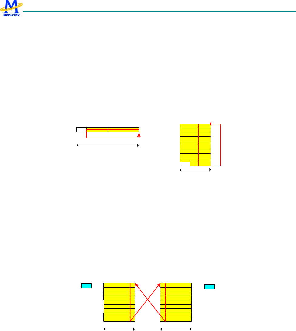
MT6235 GSM/GPRS Baseband Processor Data Sheet Revision 1.02
112/599 MediaTek Inc. Confidential
There are two basic operational modes about PWM, which is set by PWM_MODE. In periodical mode, all pulse
sequence with be repeatedly generated by the number of WAVE_NUM[15:0]. If WAVE_NUM is 0 which means infinite,
the waveform generation could be stopped by PWM_EN. As for the pulse sequence data source in the periodical mode, if
the data are less than or equal to 64 bits, they can be directly set in SEND_DATA0[31:0] and SEND_DATA1[31:0] and
SRCSEL=0 to reduce memory bandwidth. STOP_BITPOS[5:0] is used to indicate the stop bit position in the total 64-bits
data. For example, if STOP_BITPOS is 0, only SEND_DATA0[0] will be generated, and so on until SEND_DATA1[31]. If
SRCSEL=1 which means memory mode, the pulse sequence data are put in memory with address set by
BUF0_BASE_ADDR and the length is BUF0_SIZE. STOP_BITPOS[4:0] is to indicate the stop bit position in the last
32-bits data. The format of pulse sequences that stored in periodical mode is as shown in Fig. 2.
SEND
DATA0
64-bit
or
32-bit
Memory
SEND
DATA1
Fig. 2 The pulse sequence in periodical mode.
On the other hand, the pulse sequence is stored in dual memory buffers in random mode. The format of pulse
sequences that stored in the memory is as shown in Fig. 3. Valid bit is used to indicate data are ready in the respective
memory buffer. The PWM generation will clear this bit after all data in that buffer are fetched. The memory buffers are set
by address BUF0_BASE_ADDR and BUF0_SIZE for memory buffer0 and BUF1_BASE_ADDR and BUF1_SIZE for
memory buffer1. The program should prepare the pulse sequence and set the valid to 1 in time before all data in the other
memory buffer are fetched or the HW will issue UNDERFLOW interrupt to inform pulse generation will be stopped
because of no valid data.
32-bit
Memory 0
32-bit
Memory 1
Valid 0
Valid 1
Fig. 3 The pulse sequence in random mode
PWM always reference bus block clock or 13MHz clock as base, and CLKDIV[2:0] and CLKSEL can decide the
sample rate of each PWM. When system is in the sleep mode, block clock will be disabled and only OLD_PWM_MODE
with CLKSEL=1 (32 KHz) is supported. Only PWM1, PWM2 and PWM3 support OLD_PWM_MODE. For each sample
MT6235 GSM/GPRS Baseband Processor Data Sheet Revision 1.02
113/599 MediaTek Inc. Confidential
output, the duration is decided by HDURATION[15:0] when output is high and LDURATION[15:0] when output is low. If
the pulse sequence is repeated which is specified by WAVE_NUM[15:0], a special output could be set by GUARD_VALUE
and GUARD_DURATION[15:0] between these pulse sequence. The PWM output will be the value specified by
IDLE_VALUE when PWM is not enabled or the pulse sequence is finished.
01
send_data0
…
send_data1
…
guard_duration
guard_value
hdurationlduration
101
~~
01
send_data0
…
send_data1
…
101
~~
idle_value
Fig. 4 The pulse sequence output pattern
In order to provide precise timing relation between different PWM outputs, we provide PWM_SEQ_MODE. In this
mode, the starting position of waveform outputs of PWM3, PWM4, PWM5 and PWM6 will follow the previous one by the
delay values PWM4_DEALY_DURATION[15:0], PWM5_DEALY_DURATION[15:0] and
PWM6_DEALY_DURATION[15:0]. Also the clock scale of each delay can be specified by PWM4_DELAY_CLKSEL,
PWM5_DELAY_CLKSEL and PWM6_DELAY_CLKSEL.
PWM4
PWM3
PWM4_delay_duration
PWM5
PWM5_delay_duration
PWM6
PWM6_delay_duration
Fig. 5 The sequential output mode
Also PWM1, PWM2 and PWM3 support original PWM output mode. The output waveform is specified by
DATA_WIDTH[12:0] and THRESH[12:0]. The output waveform is shown in Fig. 6.
guard_period
guard_value
data_width
pwm_thresh
data_width
pwm_thresh
Fig. 6 The old PWM mode
For hardware and system consideration, CLKSRC might be slightly different in different situations. The following
table is to summary all possible situations.
MT6235 GSM/GPRS Baseband Processor Data Sheet Revision 1.02
114/599 MediaTek Inc. Confidential
PWM_OLD_MODE PWM_CLKSEL PWM_FIX_CLK_MODE CLKSRC
0 block clock
0 1 13 MHz 1
1 NA* 32 KHz
0 block clock
0
1 13 MHz
0 block clock / 1625
0
1
1 13 MHz/1625 = 8
KHz
*: When both PWM_OLD_MODE and PWM_CLKSEL equal to 1, PWM_FIX_CLK_MODE
should be 0 to avoid malfunction.
4.3.2 Register Table
Register Address Register Function Acronym
PWM + 0000h PWM enable register PWM_ENABLE
PWM + 0004h PWM4 delay duration register PWM4_DELAY
PWM + 0008h PWM5 delay duration register PWM5_DELAY
PWM + 000Ch PWM6 delay duration register PWM6_DELAY
PWM + 0010h PWM1 control register PWM1_CON
PWM + 0014h PWM1 high duration register PWM1_HDURATION
PWM + 0018h PWM1 low duration register PWM1_LDURATION
PWM + 001Ch PWM1 guard duration register PWM1_GDURATION
PWM + 0020h PWM1 buffer0 base address register PWM1_BUF0_BASE_ADDR
PWM + 0024h PWM1 buffer0 size register PWM1_BUF0_SIZE
PWM + 0028h PWM1 buffer1 base address register PWM1_BUF1_BASE_ADDR
PWM + 002Ch PWM1 buffer1 size register PWM1_BUF1_SIZE
PWM + 0030h PWM1 send data0 register PWM1_SEND_DATA0
PWM + 0034h PWM1 send data1 register PWM1_SEND_DATA1
PWM + 0038h PWM1 wave number register PWM1_WAVE_NUM
PWM + 003Ch PWM1 data width PWM1_DATA_WIDTH
PWM + 0040h PWM1 threshold register PWM1_THRESH
PWM + 0044h PWM1 send waveform number register PWM1_SEND_WAVENUM
PWM + 0048h PWM1 valid register PWM1_VALID
PWM + 0050h PWM2 control register PWM2_CON
PWM + 0054h PWM2 high duration register PWM2_HDURATION
PWM + 0058h PWM2 low duration register PWM2_LDURATION

MT6235 GSM/GPRS Baseband Processor Data Sheet Revision 1.02
115/599 MediaTek Inc. Confidential
PWM + 005Ch PWM2 guard duration register PWM2_GDURATION
PWM + 0060h PWM2 buffer0 base address register PWM2_BUF0_BASE_ADDR
PWM + 0064h PWM2 buffer0 size register PWM2_BUF0_SIZE
PWM + 0068h PWM2 buffer1 base address register PWM2_BUF1_BASE_ADDR
PWM + 006Ch PWM2 buffer1 size register PWM2_BUF1_SIZE
PWM + 0070h PWM2 send data0 register PWM2_SEND_DATA0
PWM + 0074h PWM2 send data1 register PWM2_SEND_DATA1
PWM + 0078h PWM2 wave number register PWM2_WAVE_NUM
PWM + 007Ch PWM2 data width PWM2_DATA_WIDTH
PWM + 0080h PWM2 threshold register PWM2_THRESH
PWM + 0084h PWM2 send waveform number register PWM2_SEND_WAVENUM
PWM + 0088h PWM2 valid register PWM2_VALID
PWM + 0090h PWM3 control register PWM3_CON
PWM + 0094h PWM3 high duration register PWM3_HDURATION
PWM + 0098h PWM3 low duration register PWM3_LDURATION
PWM + 009Ch PWM3 guard duration register PWM3_GDURATION
PWM + 00A0h PWM3 buffer0 base address register PWM3_BUF0_BASE_ADDR
PWM + 00A4h PWM3 buffer0 size register PWM3_BUF0_SIZE
PWM + 00A8h PWM3 buffer1 base address register PWM3_BUF1_BASE_ADDR
PWM + 00ACh PWM3 buffer1 size register PWM3_BUF1_SIZE
PWM + 00B0h PWM3 send data0 register PWM3_SEND_DATA0
PWM + 00B4h PWM3 send data1 register PWM3_SEND_DATA1
PWM + 00B8h PWM3 wave number register PWM3_WAVE_NUM
PWM + 00BCh PWM3 data width PWM3_DATA_WIDTH
PWM + 00C0h PWM3 threshold register PWM3_THRESH
PWM + 00C4h PWM3 send waveform number register PWM3_SEND_WAVENUM
PWM + 00C8h PWM3 valid register PWM3_VALID
PWM + 00D0h PWM4 control register PWM4_CON
PWM + 00D4h PWM4 high duration register PWM4_HDURATION
PWM + 00D8h PWM4 low duration register PWM4_LDURATION
PWM + 00DCh PWM4 guard duration register PWM4_GDURATION
PWM + 00E0h PWM4 buffer0 base address register PWM4_BUF0_BASE_ADDR
PWM + 00E4h PWM4 buffer0 size register PWM4_BUF0_SIZE
PWM + 00E8h PWM4 buffer1 base address register PWM4_BUF1_BASE_ADDR
PWM + 00ECh PWM4 buffer1 size register PWM4_BUF1_SIZE
PWM + 00F0h PWM4 send data0 register PWM4_SEND_DATA0
PWM + 00F4h PWM4 send data1 register PWM4_SEND_DATA1

MT6235 GSM/GPRS Baseband Processor Data Sheet Revision 1.02
116/599 MediaTek Inc. Confidential
PWM + 00F8h PWM4 wave number register PWM4_WAVE_NUM
PWM + 00FCh PWM4 send waveform number register PWM4_SEND_WAVENUM
PWM + 0100h PWM4 valid register PWM4_VALID
PWM + 0110h PWM5 control register PWM5_CON
PWM + 0114h PWM5 high duration register PWM5_HDURATION
PWM + 0118h PWM5 low duration register PWM5_LDURATION
PWM + 011Ch PWM5 guard duration register PWM5_GDURATION
PWM + 0120h PWM5 buffer0 base address register PWM5_BUF0_BASE_ADDR
PWM + 0124h PWM5 buffer0 size register PWM5_BUF0_SIZE
PWM + 0128h PWM5 buffer1 base address register PWM5_BUF1_BASE_ADDR
PWM + 012Ch PWM5 buffer1 size register PWM5_BUF1_SIZE
PWM + 0130h PWM5 send data0 register PWM5_SEND_DATA0
PWM + 0134h PWM5 send data1 register PWM5_SEND_DATA1
PWM + 0138h PWM5 wave number register PWM5_WAVE_NUM
PWM + 013Ch PWM5 send waveform number register PWM5_SEND_WAVENUM
PWM + 0140h PWM5 valid register PWM5_VALID
PWM + 0150h PWM6 control register PWM6_CON
PWM + 0154h PWM6 high duration register PWM6_HDURATION
PWM + 0158h PWM6 low duration register PWM6_LDURATION
PWM + 015Ch PWM6 guard duration register PWM6_GDURATION
PWM + 0160h PWM6 buffer0 base address register PWM6_BUF0_BASE_ADDR
PWM + 0164h PWM6 buffer0 size register PWM6_BUF0_SIZE
PWM + 0168h PWM6 buffer1 base address register PWM6_BUF1_BASE_ADDR
PWM + 016Ch PWM6 buffer1 size register PWM6_BUF1_SIZE
PWM + 0170h PWM6 send data0 register PWM6_SEND_DATA0
PWM + 0174h PWM6 send data1 register PWM6_SEND_DATA1
PWM + 0178h PWM6 wave number register PWM6_WAVE_NUM
PWM + 017Ch PWM6 send waveform number register PWM6_SEND_WAVENUM
PWM + 0180h PWM6 valid register PWM6_VALID
PWM + 0190h PWM interrupt enable register PWM_INT_ENABLE
PWM + 0194h PWM interrupt status register PWM_INT_STATUS
PWM + 0198h PWM interrupt acknowledge register PWM_INT_ACK
Table 15 PWM Registers

MT6235 GSM/GPRS Baseband Processor Data Sheet Revision 1.02
117/599 MediaTek Inc. Confidential
4.3.3 Register Definitions
PWM+0000h PWM Enable register PWM_ENABLE
Bit 31 30 29 28 27 26 25 24 23 22 21 20 19 18 17 16
Name
Type
Reset
Bit 15 14 13 12 11 10 9 8 7 6 5 4 3 2 1 0
Name
PWM_
DELA
Y_FIX
_CLK
_MOD
E
PWM_
SEQ_
MODE
PWM6
_EN PWM5
_EN PWM4
_EN PWM3
_EN PWM2
_EN PWM1
_EN
Type R/W R/W R/W R/W R/W R/W R/W R/W
Reset 0 0 0 0 0 0 0 0
PWM1_EN Set to 1 to enable PWM1
PWM2_EN Set to 1 to enable PWM2
PWM3_EN Set to 1 to enable PWM3
PWM4_EN Set to 1 to enable PWM4
PWM5_EN Set to 1 to enable PWM5
PWM6_EN Set to 1 to enable PWM6
PWM_SEQ_MODE Set to 1 to enable PWM3, PWM4, PWM5 and PWM6 sequential delay mode. In this mode, PWM3
starts first and then after PWM4_DELAY_TIME, PWM4 will start. After PWM4 starts, PWM5 will start after
PWM5_DELAY_TIME and so on for PWM6.
Note: The output of PWM_SEQ_MODE is started after PWM3 is enabled. And PWM_SEQ_MODE should be set before
PWM4, PWM5 and PWM6 are enabled or at the same time. Also this mode doesn’t work when PWM3 is set at
OLD_PWM_MODE and CLKSEL=1.
PWM_DELAY_FIX_CLK_MODE Set to 1 to force all delay between PWM3, PWM4, PWM5 and PWM6 in unit of
13MHz clock rather than block clock.
PWM+0004h PWM4 Delay Duration register PWM4_DELAY
Bit 31 30 29 28 27 26 25 24 23 22 21 20 19 18 17 16
Name DELA
Y_CL
KSEL
Type R/W
Reset 0
Bit 15 14 13 12 11 10 9 8 7 6 5 4 3 2 1 0
Name PWM4_DELAY_DURATION[15:0]
Type R/W
Reset 0
PWM4_DELAY_DURATION The time difference between PWM3 and PWM4.
DELAY_CLKSEL The clock unit of PWM4_DELAY_DURATION.
0 CLK=CLKSRC
1 CLK=CLKSRC/1625
MT6235 GSM/GPRS Baseband Processor Data Sheet Revision 1.02
118/599 MediaTek Inc. Confidential
PWM+0008h PWM5 Delay Duration register PWM5_DELAY
Bit 31 30 29 28 27 26 25 24 23 22 21 20 19 18 17 16
Name DELA
Y_CL
KSEL
Type R/W
Reset 0
Bit 15 14 13 12 11 10 9 8 7 6 5 4 3 2 1 0
Name PWM5_DELAY_DURATION[15:0]
Type R/W
Reset 0
PWM5_DELAY_DURATION The time difference between PWM4 and PWM5.
DELAY_CLKSEL The clock unit of PWM5_DELAY_DURATION.
0 CLK=CLKSRC
1 CLK=CLKSRC/1625
PWM+000Ch PWM6 Delay Duration register PWM6_DELAY
Bit 31 30 29 28 27 26 25 24 23 22 21 20 19 18 17 16
Name DELA
Y_CL
KSEL
Type R/W
Reset 0
Bit 15 14 13 12 11 10 9 8 7 6 5 4 3 2 1 0
Name PWM6_DELAY_DURATION[15:0]
Type R/W
Reset 0
PWM6_DELAY_DURATION The time difference between PWM5 and PWM6.
DELAY_CLKSEL The clock unit of PWM6_DELAY_DURATION.
0 CLK=CLKSRC
1 CLK=CLKSRC/1625
PWM+0010h PWM1 Control register PWM1_CON
Bit 31 30 29 28 27 26 25 24 23 22 21 20 19 18 17 16
Name
Type
Reset
Bit 15 14 13 12 11 10 9 8 7 6 5 4 3 2 1 0
Name OLD_
PWM_
MODE STOP_BITPOS[5:0] GUAR
D_VA
LUE
IDLE_
VALU
E MODE SRCS
EL
FIX_C
LK_M
ODE
CLKS
EL CLKDIV [2:0]
Type R/W R/W R/W R/W R/W R/W R/W R/W R/W
Reset 0 3Fh 0 0 0 0 0 0 0
CLKDIV Select PWM1 clock scale.
000 CLK Hz
001 CLK/2 Hz
010 CLK/4 Hz

MT6235 GSM/GPRS Baseband Processor Data Sheet Revision 1.02
119/599 MediaTek Inc. Confidential
011 CLK/8 Hz
100 CLK/16 Hz
101 CLK/32 Hz
110 CLK/64 Hz
111 CLK/128 Hz
CLKSEL Select PWM1 clock
0 CLK=CLKSRC
1 CLK=CLKSRC/1625
FIX_CLK_MODE Select PWM1 clock reference
0 CLKSRC= block clock
1 CLKSRC= 13 MHz
SRCSEL Select PWM1 data source
0 FIFO mode
1 Memory mode
MODE Select Random Generator mode
0 Periodical PWM mode.
1 Random PWM mode
Note: When using random generator mode, the data source comes from dual buffers in memory.
IDLE_VALUE PWM1 output value when idle state.
GUARD_VALUE PWM1 output value when guard time.
STOP_BITPOS The stop bit position for source data in periodical mode. In FIFO mode, it’s used to indicate the stop bit
position in total 64 bits. In Memory mode, it’s for the stop bit position in the last 32 bits.
OLD_PWM_MODE Use old PWM mode
0 New PWM mode
1 Old PWM mode
Note: Using old PWM mode also means periodical mode. So SRCSEL and MODE is ignored in this situation. Only old
PWM mode with 32 KHz clock source could work in the system sleep-mode.
PWM+0014h PWM1 High Duration register PWM1_HDURAT
ION
Bit 31 30 29 28 27 26 25 24 23 22 21 20 19 18 17 16
Name
Type
Reset
Bit 15 14 13 12 11 10 9 8 7 6 5 4 3 2 1 0
Name HDURATION[15:0]
Type R/W
Reset 1
HDURATION PWM1 pulse duration based on the current clock when PWM output is high. If duration =N, need to
program N-1 in this register.
Note: The duration of PWM must not be 0.
MT6235 GSM/GPRS Baseband Processor Data Sheet Revision 1.02
120/599 MediaTek Inc. Confidential
PWM+0018h PWM1 Low Duration register PWM1_LDURAT
ION
Bit 31 30 29 28 27 26 25 24 23 22 21 20 19 18 17 16
Name
Type
Reset
Bit 15 14 13 12 11 10 9 8 7 6 5 4 3 2 1 0
Name LDURATION[15:0]
Type R/W
Reset 1
LDURATION PWM1 pulse duration based on the current clock when PWM output is low. If duration =N, need to
program N-1 in this register.
Note: The duration of PWM must not be 0.
PWM+001Ch PWM1 Guard Duration register PWM1_GDRUA
TION
Bit 31 30 29 28 27 26 25 24 23 22 21 20 19 18 17 16
Name
Type
Reset
Bit 15 14 13 12 11 10 9 8 7 6 5 4 3 2 1 0
Name GUARD_DURATION[15:0]
Type R/W
Reset 0
GUDAR_DURATION It’s the guarding interval between individual waveforms and the output is decided by
GUARD_VALUE. Also if it equals to N, it needs to program N-1 in this register.
Note: If this duration is 0, it means no guarding interval.
PWM+0020h PWM1 Buffer0 Base Address register PWM1_BUF0_BAS
E_ ADDR
Bit 31 30 29 28 27 26 25 24 23 22 21 20 19 18 17 16
Name BUF0_BS_ADDR[31:16]
Type R/W
Reset 0
Bit 15 14 13 12 11 10 9 8 7 6 5 4 3 2 1 0
Name BUF0_BS_ADDR[15:0]
Type R/W
Reset 0
BUF0_BS_ADDR The base address of memory buffer0 for PWM1’s waveform data.
PWM+0024h PWM1 Buffer0 Size register PWM1_BUF0_SI
ZE
Bit 31 30 29 28 27 26 25 24 23 22 21 20 19 18 17 16
Name

MT6235 GSM/GPRS Baseband Processor Data Sheet Revision 1.02
121/599 MediaTek Inc. Confidential
Type
Reset
Bit 15 14 13 12 11 10 9 8 7 6 5 4 3 2 1 0
Name BUF0_SIZE[15:0]
Type R/W
Reset 0
BUF0_SIZE The length of the waveform data in memory buffer0 that PWM1 should generate. If it equals to N, need to
program N-1 in this register.
Note: The size is in unit of 32-bit data.
PWM+0028h PWM1 Buffer1 Base Address register PWM1_BUF1_
_BASE_ ADDR
Bit 31 30 29 28 27 26 25 24 23 22 21 20 19 18 17 16
Name BUF1_BS_ADDR[31:16]
Type R/W
Reset 0
Bit 15 14 13 12 11 10 9 8 7 6 5 4 3 2 1 0
Name BUF1_BS_ADDR[15:0]
Type R/W
Reset 0
BUF1_BS_ADDR The base address of memory buffer1 for PWM1’s waveform data.
Note: The memory buffer1 is useless in periodical mode.
PWM+002Ch PWM1 Buffer1 Size register PWM1_BUF1_SI
ZE
Bit 31 30 29 28 27 26 25 24 23 22 21 20 19 18 17 16
Name
Type
Reset
Bit 15 14 13 12 11 10 9 8 7 6 5 4 3 2 1 0
Name BUF1_SIZE[15:0]
Type R/W
Reset 0
BUF1_SIZE The length of the waveform data in memory buffer1 that PWM1 should generate. If it equals to N, need to
program N-1 in this register.
PWM+0030h PWM1 Send Data0 register PWM1_SEND_DAT
A0
Bit 31 30 29 28 27 26 25 24 23 22 21 20 19 18 17 16
Name SEND_DATA0 [31:16]
Type R/W
Reset 0
Bit 15 14 13 12 11 10 9 8 7 6 5 4 3 2 1 0
Name SEND_DATA0[15:0]
Type R/W
Reset 0
MT6235 GSM/GPRS Baseband Processor Data Sheet Revision 1.02
122/599 MediaTek Inc. Confidential
SEND_DATA0 PWM1 local buffer0 of pulse sequence data to be generated.
Note: This value should be written only in periodically FIFO mode. In other mode, this buffer is for internal memory
access.
PWM+0034h PWM1 Send Data1 register PWM1_SEND_DAT
A1
Bit 31 30 29 28 27 26 25 24 23 22 21 20 19 18 17 16
Name SEND_DATA1[31:16]
Type R/W
Reset 0
Bit 15 14 13 12 11 10 9 8 7 6 5 4 3 2 1 0
Name SEND_DATA1[15:0]
Type R/W
Reset 0
SEND_DATA1 PWM1 local buffer0 of pulse sequence data to be generated.
Note: This value should be written only in periodically FIFO mode. In other mode, this buffer is for internal memory
access.
PWM+0038h PWM1 Wave Number register PWM1_WAVE_
NUM
Bit 31 30 29 28 27 26 25 24 23 22 21 20 19 18 17 16
Name
Type
Reset
Bit 15 14 13 12 11 10 9 8 7 6 5 4 3 2 1 0
Name WAVE_NUM[15:0]
Type R/W
Reset 0
WAVE_NUM The number by which PWM1 will generate from the pulse data repeatedly.
Note: If WAVE_NUM=0, the waveform generation will not stop until it is disabled.
PWM+003Ch PWM1 Data Width register PWM1_DATA_
WIDTH
Bit 31 30 29 28 27 26 25 24 23 22 21 20 19 18 17 16
Name
Type
Reset
Bit 15 14 13 12 11 10 9 8 7 6 5 4 3 2 1 0
Name DATA_WIDTH[12:0]
Type R/W
Reset 0
DATA_WIDTH The PWM1 pulse data width in the old PWM mode.

MT6235 GSM/GPRS Baseband Processor Data Sheet Revision 1.02
123/599 MediaTek Inc. Confidential
PWM+0040h PWM1 Thresh register PWM1_THRESH
Bit 31 30 29 28 27 26 25 24 23 22 21 20 19 18 17 16
Name
Type
Reset
Bit 15 14 13 12 11 10 9 8 7 6 5 4 3 2 1 0
Name THRESH[12:0]
Type R/W
Reset 0
THRESH The PWM1 pulse data high/low switching threshold in the old PWM mode.
PWM+0044h PWM1 Send Wave Number register PWM1_SEND_
WAVENUM
Bit 31 30 29 28 27 26 25 24 23 22 21 20 19 18 17 16
Name
Type
Reset
Bit 15 14 13 12 11 10 9 8 7 6 5 4 3 2 1 0
Name SEND_WAVENUM[15:0]
Type RO
Reset 0
SEND_WAVENUM The number by which PWM1 has already generated from the specified data source in the periodical
mode.
PWM+0048h PWM1 Valid register PWM1_VALID
Bit 31 30 29 28 27 26 25 24 23 22 21 20 19 18 17 16
Name
Type
Reset
Bit 15 14 13 12 11 10 9 8 7 6 5 4 3 2 1 0
Name
BUF1
_VALI
D_WE
N
BUF1
_VALI
D
BUF0
_VALI
D_WE
N
BUF0
_VALI
D
Type W R/W W R/W
Reset 0 0 0 0
BUF0_VALID The valid status is used to indicate pulse data in memory buffer0 is ready.
BUF0_VALID_WEN This bit must be set to modify BUF0_VALID.
BUF1_VALID The valid status is used to indicate pulse data in memory buffer1 is ready.
BUF1_VALID_WEN This bit must be set to modify BUF1_VALID.
Note: The program should set these bits after data are prepared in memory. The HW will clear these bits after it has used all
data in the specified memory.
PWM+0050h PWM2 Control register PWM2_CON
Bit 31 30 29 28 27 26 25 24 23 22 21 20 19 18 17 16

MT6235 GSM/GPRS Baseband Processor Data Sheet Revision 1.02
124/599 MediaTek Inc. Confidential
Name
Type
Reset
Bit 15 14 13 12 11 10 9 8 7 6 5 4 3 2 1 0
Name OLD_
PWM_
MODE STOP_BITPOS[5:0] GUAR
D_VA
LUE
IDLE_
VALU
E MODE SRCS
EL
FIX_C
LK_M
ODE
CLKS
EL CLKDIV [2:0]
Type R/W R/W R/W R/W R/W R/W R/W R/W R/W
Reset 0 3Fh 0 0 0 0 0 0 0
CLKDIV Select PWM2 clock scale.
000 CLK Hz
001 CLK/2 Hz
010 CLK/4 Hz
011 CLK/8 Hz
100 CLK/16 Hz
101 CLK/32 Hz
110 CLK/64 Hz
111 CLK/128 Hz
CLKSEL Select PWM1 clock
0 CLK=CLKSRC
1 CLK=CLKSRC/1625
FIX_CLK_MODE Select PWM1 clock reference
0 CLKSRC= block clock
1 CLKSRC= 13 MHz
SRCSEL Select PWM2 data source
0 FIFO mode
1 Memory mode
MODE Select Random Generator mode
0 Periodical PWM mode.
1 Random PWM mode
Note: When using random generator mode, the data source comes from dual buffers in memory.
IDLE_VALUE PWM2 output value when idle state.
GUARD_VALUE PWM2 output value when guard time.
STOP_BITPOS The stop bit position for source data in periodical mode. In FIFO mode, it’s used to indicate the stop bit
position in total 64 bits. In Memory mode, it’s for the stop bit position in the last 32 bits.
OLD_PWM_MODE Use old PWM mode
0 New PWM mode
1 Old PWM mode
Note: Using old PWM mode also means periodical mode. So SRCSEL and MODE is ignored in this situation. Only old
PWM mode with 32 KHz clock source could work in the system sleep-mode.

MT6235 GSM/GPRS Baseband Processor Data Sheet Revision 1.02
125/599 MediaTek Inc. Confidential
PWM+0054h PWM2 High Duration register PWM2_HDURAT
ION
Bit 31 30 29 28 27 26 25 24 23 22 21 20 19 18 17 16
Name
Type
Reset
Bit 15 14 13 12 11 10 9 8 7 6 5 4 3 2 1 0
Name HDURATION[15:0]
Type R/W
Reset 1
HDURATION PWM2 pulse duration based on the current clock when PWM output is high. If duration =N, need to
program N-1 in this register.
Note: The duration of PWM must not be 0.
PWM+0058h PWM2 Low Duration register PWM2_LDURAT
ION
Bit 31 30 29 28 27 26 25 24 23 22 21 20 19 18 17 16
Name
Type
Reset
Bit 15 14 13 12 11 10 9 8 7 6 5 4 3 2 1 0
Name LDURATION[15:0]
Type R/W
Reset 1
LDURATION PWM2 pulse duration based on the current clock when PWM output is low. If duration =N, need to
program N-1 in this register.
Note: The duration of PWM must not be 0.
PWM+005Ch PWM2 Guard Duration register PWM2_GDRUA
TION
Bit 31 30 29 28 27 26 25 24 23 22 21 20 19 18 17 16
Name
Type
Reset
Bit 15 14 13 12 11 10 9 8 7 6 5 4 3 2 1 0
Name GUARD_DURATION[15:0]
Type R/W
Reset 0
GUDAR_DURATION It’s the guarding interval between individual waveforms and the output is decided by
GUARD_VALUE. Also if it equals to N, it needs to program N-1 in this register.
Note: If this duration is 0, it means no guarding interval.

MT6235 GSM/GPRS Baseband Processor Data Sheet Revision 1.02
126/599 MediaTek Inc. Confidential
PWM+0060h PWM2 Buffer0 Base Address register PWM2_BUF0_BAS
E_ ADDR
Bit 31 30 29 28 27 26 25 24 23 22 21 20 19 18 17 16
Name BUF0_BS_ADDR[31:16]
Type R/W
Reset 0
Bit 15 14 13 12 11 10 9 8 7 6 5 4 3 2 1 0
Name BUF0_BS_ADDR[15:0]
Type R/W
Reset 0
BUF0_BS_ADDR The base address of memory buffer0 for PWM2’s waveform data.
PWM+0064h PWM2 Buffer0 Size register PWM2_BUF0_SI
ZE
Bit 31 30 29 28 27 26 25 24 23 22 21 20 19 18 17 16
Name
Type
Reset
Bit 15 14 13 12 11 10 9 8 7 6 5 4 3 2 1 0
Name BUF0_SIZE[15:0]
Type R/W
Reset 0
BUF0_SIZE The length of the waveform data in memory buffer0 that PWM2 should generate. If it equals to N, need to
program N-1 in this register.
PWM+0068h PWM2 Buffer1 Base Address register PWM2_BUF1_
_BASE_ ADDR
Bit 31 30 29 28 27 26 25 24 23 22 21 20 19 18 17 16
Name BUF1_BS_ADDR[31:16]
Type R/W
Reset 0
Bit 15 14 13 12 11 10 9 8 7 6 5 4 3 2 1 0
Name BUF1_BS_ADDR[15:0]
Type R/W
Reset 0
BUF1_BS_ADDR The base address of memory buffer1 for PWM2’s waveform data.
Note: The memory buffer1 is useless in periodical mode.
PWM+006Ch PWM2 Buffer1 Size register PWM2_BUF1_SI
ZE
Bit 31 30 29 28 27 26 25 24 23 22 21 20 19 18 17 16
Name
Type
Reset
Bit 15 14 13 12 11 10 9 8 7 6 5 4 3 2 1 0

MT6235 GSM/GPRS Baseband Processor Data Sheet Revision 1.02
127/599 MediaTek Inc. Confidential
Name BUF1_SIZE[15:0]
Type R/W
Reset 0
BUF1_SIZE The length of the waveform data in memory buffer1 that PWM2 should generate. If it equals to N, need to
program N-1 in this register.
PWM+0070h PWM2 Send Data0 register PWM2_SEND_DAT
A0
Bit 31 30 29 28 27 26 25 24 23 22 21 20 19 18 17 16
Name SEND_DATA0 [31:16]
Type R/W
Reset 0
Bit 15 14 13 12 11 10 9 8 7 6 5 4 3 2 1 0
Name SEND_DATA0[15:0]
Type R/W
Reset 0
SEND_DATA0 PWM2 local buffer0 of pulse sequence data to be generated.
Note: This value should be written only in periodically FIFO mode. In other mode, this buffer is for internal memory
access.
PWM+0074h PWM2 Send Data1 register PWM2_SEND_DAT
A1
Bit 31 30 29 28 27 26 25 24 23 22 21 20 19 18 17 16
Name SEND_DATA1[31:16]
Type R/W
Reset 0
Bit 15 14 13 12 11 10 9 8 7 6 5 4 3 2 1 0
Name SEND_DATA1[15:0]
Type R/W
Reset 0
SEND_DATA1 PWM2 local buffer0 of pulse sequence data to be generated.
Note: This value should be written only in periodically FIFO mode. In other mode, this buffer is for internal memory
access.
PWM+0078h PWM2 Wave Number register PWM2_WAVE_
NUM
Bit 31 30 29 28 27 26 25 24 23 22 21 20 19 18 17 16
Name
Type
Reset
Bit 15 14 13 12 11 10 9 8 7 6 5 4 3 2 1 0
Name WAVE_NUM[15:0]
Type R/W
Reset 0
WAVE_NUM The number by which PWM2 will generate from the pulse data repeatedly.
MT6235 GSM/GPRS Baseband Processor Data Sheet Revision 1.02
128/599 MediaTek Inc. Confidential
Note: If WAVE_NUM=0, the waveform generation will not stop until it is disabled.
PWM+007Ch PWM2 Data Width register PWM2_DATA_
WIDTH
Bit 31 30 29 28 27 26 25 24 23 22 21 20 19 18 17 16
Name
Type
Reset
Bit 15 14 13 12 11 10 9 8 7 6 5 4 3 2 1 0
Name DATA_WIDTH[12:0]
Type R/W
Reset 0
DATA_WIDTH The PWM2 pulse data width in the old PWM mode.
PWM+0080h PWM2 Thresh register PWM2_THRESH
Bit 31 30 29 28 27 26 25 24 23 22 21 20 19 18 17 16
Name
Type
Reset
Bit 15 14 13 12 11 10 9 8 7 6 5 4 3 2 1 0
Name THRESH[12:0]
Type R/W
Reset 0
THRESH The PWM2 pulse data high/low switching threshold in the old PWM mode.
PWM+0084h PWM2 Send Wave Number register PWM2_SEND_
WAVENUM
Bit 31 30 29 28 27 26 25 24 23 22 21 20 19 18 17 16
Name
Type
Reset
Bit 15 14 13 12 11 10 9 8 7 6 5 4 3 2 1 0
Name SEND_WAVENUM[15:0]
Type RO
Reset 0
SEND_WAVENUM The number by which PWM2 has already generated from the specified data source in the periodical
mode.
PWM+0088h PWM2 Valid register PWM2_VALID
Bit 31 30 29 28 27 26 25 24 23 22 21 20 19 18 17 16
Name
Type
Reset
Bit 15 14 13 12 11 10 9 8 7 6 5 4 3 2 1 0

MT6235 GSM/GPRS Baseband Processor Data Sheet Revision 1.02
129/599 MediaTek Inc. Confidential
Name
BUF1
_VALI
D_WE
N
BUF1
_VALI
D
BUF0
_VALI
D_WE
N
BUF0
_VALI
D
Type W R/W W R/W
Reset 0 0 0 0
BUF0_VALID The valid status is used to indicate pulse data in memory buffer0 is ready.
BUF0_VALID_WEN This bit must be set to modify BUF0_VALID.
BUF1_VALID The valid status is used to indicate pulse data in memory buffer1 is ready.
BUF1_VALID_WEN This bit must be set to modify BUF1_VALID.
Note: The program should set these bits after data are prepared in memory. The HW will clear these bits after it has used all
data in the specified memory.
PWM+0090h PWM3 Control register PWM3_CON
Bit 31 30 29 28 27 26 25 24 23 22 21 20 19 18 17 16
Name
Type
Reset
Bit 15 14 13 12 11 10 9 8 7 6 5 4 3 2 1 0
Name OLD_
PWM_
MODE STOP_BITPOS[5:0] GUAR
D_VA
LUE
IDLE_
VALU
E MODE SRCS
EL
FIX_C
LK_M
ODE
CLKS
EL CLKDIV [2:0]
Type R/W R/W R/W R/W R/W R/W R/W R/W R/W
Reset 0 3Fh 0 0 0 0 0 0 0
CLKDIV Select PWM3 clock scale.
000 CLK Hz
001 CLK/2 Hz
010 CLK/4 Hz
011 CLK/8 Hz
100 CLK/16 Hz
101 CLK/32 Hz
110 CLK/64 Hz
111 CLK/128 Hz
CLKSEL Select PWM1 clock
0 CLK=CLKSRC
1 CLK=CLKSRC/1625
FIX_CLK_MODE Select PWM1 clock reference
0 CLKSRC= block clock
1 CLKSRC= 13 MHz
SRCSEL Select PWM3 data source
0 FIFO mode
1 Memory mode
MODE Select Random Generator mode
0 Periodical PWM mode.
1 Random PWM mode

MT6235 GSM/GPRS Baseband Processor Data Sheet Revision 1.02
130/599 MediaTek Inc. Confidential
Note: When using random generator mode, the data source comes from dual buffers in memory.
IDLE_VALUE PWM3 output value when idle state.
GUARD_VALUE PWM3 output value when guard time.
STOP_BITPOS The stop bit position for source data in periodical mode. In FIFO mode, it’s used to indicate the stop bit
position in total 64 bits. In Memory mode, it’s for the stop bit position in the last 32 bits.
OLD_PWM_MODE Use old PWM mode
0 New PWM mode
1 Old PWM mode
Note: Using old PWM mode also means periodical mode. So SRCSEL and MODE is ignored in this situation. Only old
PWM mode with 32 KHz clock source could work in the system sleep-mode.
PWM+0094h PWM3 High Duration register PWM3_HDURAT
ION
Bit 31 30 29 28 27 26 25 24 23 22 21 20 19 18 17 16
Name
Type
Reset
Bit 15 14 13 12 11 10 9 8 7 6 5 4 3 2 1 0
Name HDURATION[15:0]
Type R/W
Reset 1
HDURATION PWM3 pulse duration based on the current clock when PWM output is high. If duration =N, need to
program N-1 in this register.
Note: The duration of PWM must not be 0.
PWM+0098h PWM3 Low Duration register PWM3_LDURAT
ION
Bit 31 30 29 28 27 26 25 24 23 22 21 20 19 18 17 16
Name
Type
Reset
Bit 15 14 13 12 11 10 9 8 7 6 5 4 3 2 1 0
Name LDURATION[15:0]
Type R/W
Reset 1
LDURATION PWM3 pulse duration based on the current clock when PWM output is low. If duration =N, need to
program N-1 in this register.
Note: The duration of PWM must not be 0.
PWM+009Ch PWM3 Guard Duration register PWM3_GDRUA
TION
Bit 31 30 29 28 27 26 25 24 23 22 21 20 19 18 17 16
Name
MT6235 GSM/GPRS Baseband Processor Data Sheet Revision 1.02
131/599 MediaTek Inc. Confidential
Type
Reset
Bit 15 14 13 12 11 10 9 8 7 6 5 4 3 2 1 0
Name GUARD_DURATION[15:0]
Type R/W
Reset 0
GUDAR_DURATION It’s the guarding interval between individual waveforms and the output is decided by
GUARD_VALUE. Also if it equals to N, it needs to program N-1 in this register.
Note: If this duration is 0, it means no guarding interval.
PWM+00A0h PWM3 Buffer0 Base Address register PWM3_BUF0_BAS
E_ ADDR
Bit 31 30 29 28 27 26 25 24 23 22 21 20 19 18 17 16
Name BUF0_BS_ADDR[31:16]
Type R/W
Reset 0
Bit 15 14 13 12 11 10 9 8 7 6 5 4 3 2 1 0
Name BUF0_BS_ADDR[15:0]
Type R/W
Reset 0
BUF0_BS_ADDR The base address of memory buffer0 for PWM3’s waveform data.
PWM+00A4h PWM3 Buffer0 Size register PWM3_BUF0_SI
ZE
Bit 31 30 29 28 27 26 25 24 23 22 21 20 19 18 17 16
Name
Type
Reset
Bit 15 14 13 12 11 10 9 8 7 6 5 4 3 2 1 0
Name BUF0_SIZE[15:0]
Type R/W
Reset 0
BUF0_SIZE The length of the waveform data in memory buffer0 that PWM3 should generate. If it equals to N, need to
program N-1 in this register.
PWM+00A8h PWM3 Buffer1 Base Address register PWM3_BUF1_
_BASE_ ADDR
Bit 31 30 29 28 27 26 25 24 23 22 21 20 19 18 17 16
Name BUF1_BS_ADDR[31:16]
Type R/W
Reset 0
Bit 15 14 13 12 11 10 9 8 7 6 5 4 3 2 1 0
Name BUF1_BS_ADDR[15:0]
Type R/W
Reset 0
MT6235 GSM/GPRS Baseband Processor Data Sheet Revision 1.02
132/599 MediaTek Inc. Confidential
BUF1_BS_ADDR The base address of memory buffer1 for PWM3’s waveform data.
Note: The memory buffer1 is useless in periodical mode.
PWM+00ACh PWM3 Buffer1 Size register PWM3_BUF1_SI
ZE
Bit 31 30 29 28 27 26 25 24 23 22 21 20 19 18 17 16
Name
Type
Reset
Bit 15 14 13 12 11 10 9 8 7 6 5 4 3 2 1 0
Name BUF1_SIZE[15:0]
Type R/W
Reset 0
BUF1_SIZE The length of the waveform data in memory buffer1 that PWM3 should generate. If it equals to N, need to
program N-1 in this register.
PWM+00B0h PWM3 Send Data0 register PWM3_SEND_DAT
A0
Bit 31 30 29 28 27 26 25 24 23 22 21 20 19 18 17 16
Name SEND_DATA0 [31:16]
Type R/W
Reset 0
Bit 15 14 13 12 11 10 9 8 7 6 5 4 3 2 1 0
Name SEND_DATA0[15:0]
Type R/W
Reset 0
SEND_DATA0 PWM3 local buffer0 of pulse sequence data to be generated.
Note: This value should be written only in periodically FIFO mode. In other mode, this buffer is for internal memory
access.
PWM+00B4h PWM3 Send Data1 register PWM3_SEND_DAT
A1
Bit 31 30 29 28 27 26 25 24 23 22 21 20 19 18 17 16
Name SEND_DATA1[31:16]
Type R/W
Reset 0
Bit 15 14 13 12 11 10 9 8 7 6 5 4 3 2 1 0
Name SEND_DATA1[15:0]
Type R/W
Reset 0
SEND_DATA1 PWM3 local buffer0 of pulse sequence data to be generated.
Note: This value should be written only in periodically FIFO mode. In other mode, this buffer is for internal memory
access.

MT6235 GSM/GPRS Baseband Processor Data Sheet Revision 1.02
133/599 MediaTek Inc. Confidential
PWM+00B8h PWM3 Wave Number register PWM3_WAVE_
NUM
Bit 31 30 29 28 27 26 25 24 23 22 21 20 19 18 17 16
Name
Type
Reset
Bit 15 14 13 12 11 10 9 8 7 6 5 4 3 2 1 0
Name WAVE_NUM[15:0]
Type R/W
Reset 0
WAVE_NUM The number by which PWM3 will generate from the pulse data repeatedly.
Note: If WAVE_NUM=0, the waveform generation will not stop until it is disabled.
PWM+00BCh PWM3 Data Width register PWM3_DATA_
WIDTH
Bit 31 30 29 28 27 26 25 24 23 22 21 20 19 18 17 16
Name
Type
Reset
Bit 15 14 13 12 11 10 9 8 7 6 5 4 3 2 1 0
Name DATA_WIDTH[12:0]
Type R/W
Reset 0
DATA_WIDTH The PWM3 pulse data width in the old PWM mode.
PWM+00C0h PWM3 Thresh register PWM3_THRESH
Bit 31 30 29 28 27 26 25 24 23 22 21 20 19 18 17 16
Name
Type
Reset
Bit 15 14 13 12 11 10 9 8 7 6 5 4 3 2 1 0
Name THRESH[12:0]
Type R/W
Reset 0
THRESH The PWM3 pulse data high/low switching threshold in the old PWM mode.
PWM+00C4h PWM3 Send Wave Number register PWM3_SEND_
WAVENUM
Bit 31 30 29 28 27 26 25 24 23 22 21 20 19 18 17 16
Name
Type
Reset
Bit 15 14 13 12 11 10 9 8 7 6 5 4 3 2 1 0
Name SEND_WAVENUM[15:0]
Type RO
MT6235 GSM/GPRS Baseband Processor Data Sheet Revision 1.02
134/599 MediaTek Inc. Confidential
Reset 0
SEND_WAVENUM The number by which PWM3 has already generated from the specified data source in the periodical
mode.
PWM+00C8h PWM3 Valid register PWM3_VALID
Bit 31 30 29 28 27 26 25 24 23 22 21 20 19 18 17 16
Name
Type
Reset
Bit 15 14 13 12 11 10 9 8 7 6 5 4 3 2 1 0
Name
BUF1
_VALI
D_WE
N
BUF1
_VALI
D
BUF0
_VALI
D_WE
N
BUF0
_VALI
D
Type W R/W W R/W
Reset 0 0 0 0
BUF0_VALID The valid status is used to indicate pulse data in memory buffer0 is ready.
BUF0_VALID_WEN This bit must be set to modify BUF0_VALID.
BUF1_VALID The valid status is used to indicate pulse data in memory buffer1 is ready.
BUF1_VALID_WEN This bit must be set to modify BUF1_VALID.
Note: The program should set these bits after data are prepared in memory. The HW will clear these bits after it has used all
data in the specified memory.
PWM+00D0h PWM4 Control register PWM4_CON
Bit 31 30 29 28 27 26 25 24 23 22 21 20 19 18 17 16
Name
Type
Reset
Bit 15 14 13 12 11 10 9 8 7 6 5 4 3 2 1 0
Name OLD_
PWM_
MODE STOP_BITPOS[5:0] GUAR
D_VA
LUE
IDLE_
VALU
E MODE SRCS
EL
FIX_C
LK_M
ODE
CLKS
EL CLKDIV [2:0]
Type R/W R/W R/W R/W R/W R/W R/W R/W R/W
Reset 0 3Fh 0 0 0 0 0 0 0
CLKDIV Select PWM4 clock scale.
000 CLK Hz
001 CLK/2 Hz
010 CLK/4 Hz
011 CLK/8 Hz
100 CLK/16 Hz
101 CLK/32 Hz
110 CLK/64 Hz
111 CLK/128 Hz
CLKSEL Select PWM1 clock
0 CLK=CLKSRC
1 CLK=CLKSRC/1625

MT6235 GSM/GPRS Baseband Processor Data Sheet Revision 1.02
135/599 MediaTek Inc. Confidential
FIX_CLK_MODE Select PWM1 clock reference
0 CLKSRC= block clock
1 CLKSRC= 13 MHz
SRCSEL Select PWM4 data source
0 FIFO mode
1 Memory mode
MODE Select Random Generator mode
0 Periodical PWM mode.
1 Random PWM mode
Note: When using random generator mode, the data source comes from dual buffers in memory.
IDLE_VALUE PWM4 output value when idle state.
GUARD_VALUE PWM4 output value when guard time.
STOP_BITPOS The stop bit position for source data in periodical mode. In FIFO mode, it’s used to indicate the stop bit
position in total 64 bits. In Memory mode, it’s for the stop bit position in the last 32 bits.
PWM+00D4h PWM4 High Duration register PWM4_HDURAT
ION
Bit 31 30 29 28 27 26 25 24 23 22 21 20 19 18 17 16
Name
Type
Reset
Bit 15 14 13 12 11 10 9 8 7 6 5 4 3 2 1 0
Name HDURATION[15:0]
Type R/W
Reset 1
HDURATION PWM4 pulse duration based on the current clock when PWM output is high. If duration =N, need to
program N-1 in this register.
Note: The duration of PWM must not be 0.
PWM+00D8h PWM4 Low Duration register PWM4_LDURAT
ION
Bit 31 30 29 28 27 26 25 24 23 22 21 20 19 18 17 16
Name
Type
Reset
Bit 15 14 13 12 11 10 9 8 7 6 5 4 3 2 1 0
Name LDURATION[15:0]
Type R/W
Reset 1
LDURATION PWM4 pulse duration based on the current clock when PWM output is low. If duration =N, need to
program N-1 in this register.
Note: The duration of PWM must not be 0.
MT6235 GSM/GPRS Baseband Processor Data Sheet Revision 1.02
136/599 MediaTek Inc. Confidential
PWM+00DCh PWM4 Guard Duration register PWM4_GDRUA
TION
Bit 31 30 29 28 27 26 25 24 23 22 21 20 19 18 17 16
Name
Type
Reset
Bit 15 14 13 12 11 10 9 8 7 6 5 4 3 2 1 0
Name GUARD_DURATION[15:0]
Type R/W
Reset 0
GUDAR_DURATION It’s the guarding interval between individual waveforms and the output is decided by
GUARD_VALUE. Also if it equals to N, it needs to program N-1 in this register.
Note: If this duration is 0, it means no guarding interval.
PWM+00E0h PWM4 Buffer0 Base Address register PWM4_BUF0_BAS
E_ ADDR
Bit 31 30 29 28 27 26 25 24 23 22 21 20 19 18 17 16
Name BUF0_BS_ADDR[31:16]
Type R/W
Reset 0
Bit 15 14 13 12 11 10 9 8 7 6 5 4 3 2 1 0
Name BUF0_BS_ADDR[15:0]
Type R/W
Reset 0
BUF0_BS_ADDR The base address of memory buffer0 for PWM4’s waveform data.
PWM+00E4h PWM4 Buffer0 Size register PWM4_BUF0_SI
ZE
Bit 31 30 29 28 27 26 25 24 23 22 21 20 19 18 17 16
Name
Type
Reset
Bit 15 14 13 12 11 10 9 8 7 6 5 4 3 2 1 0
Name BUF0_SIZE[15:0]
Type R/W
Reset 0
BUF0_SIZE The length of the waveform data in memory buffer0 that PWM4 should generate. If it equals to N, need to
program N-1 in this register.
PWM+00E8h PWM4 Buffer1 Base Address register PWM4_BUF1_
_BASE_ ADDR
Bit 31 30 29 28 27 26 25 24 23 22 21 20 19 18 17 16
Name BUF1_BS_ADDR[31:16]
Type R/W
MT6235 GSM/GPRS Baseband Processor Data Sheet Revision 1.02
137/599 MediaTek Inc. Confidential
Reset 0
Bit 15 14 13 12 11 10 9 8 7 6 5 4 3 2 1 0
Name BUF1_BS_ADDR[15:0]
Type R/W
Reset 0
BUF1_BS_ADDR The base address of memory buffer1 for PWM4’s waveform data.
Note: The memory buffer1 is useless in periodical mode.
PWM+00ECh PWM4 Buffer1 Size register PWM4_BUF1_SI
ZE
Bit 31 30 29 28 27 26 25 24 23 22 21 20 19 18 17 16
Name
Type
Reset
Bit 15 14 13 12 11 10 9 8 7 6 5 4 3 2 1 0
Name BUF1_SIZE[15:0]
Type R/W
Reset 0
BUF1_SIZE The length of the waveform data in memory buffer1 that PWM4 should generate. If it equals to N, need to
program N-1 in this register.
PWM+00F0h PWM4 Send Data0 register PWM4_SEND_DAT
A0
Bit 31 30 29 28 27 26 25 24 23 22 21 20 19 18 17 16
Name SEND_DATA0 [31:16]
Type R/W
Reset 0
Bit 15 14 13 12 11 10 9 8 7 6 5 4 3 2 1 0
Name SEND_DATA0[15:0]
Type R/W
Reset 0
SEND_DATA0 PWM4 local buffer0 of pulse sequence data to be generated.
Note: This value should be written only in periodically FIFO mode. In other mode, this buffer is for internal memory
access.
PWM+00F4h PWM4 Send Data1 register PWM4_SEND_DAT
A1
Bit 31 30 29 28 27 26 25 24 23 22 21 20 19 18 17 16
Name SEND_DATA1[31:16]
Type R/W
Reset 0
Bit 15 14 13 12 11 10 9 8 7 6 5 4 3 2 1 0
Name SEND_DATA1[15:0]
Type R/W
Reset 0
MT6235 GSM/GPRS Baseband Processor Data Sheet Revision 1.02
138/599 MediaTek Inc. Confidential
SEND_DATA1 PWM4 local buffer0 of pulse sequence data to be generated.
Note: This value should be written only in periodically FIFO mode. In other mode, this buffer is for internal memory
access.
PWM+00F8h PWM4 Wave Number register PWM4_WAVE_
NUM
Bit 31 30 29 28 27 26 25 24 23 22 21 20 19 18 17 16
Name
Type
Reset
Bit 15 14 13 12 11 10 9 8 7 6 5 4 3 2 1 0
Name WAVE_NUM[15:0]
Type R/W
Reset 0
WAVE_NUM The number by which PWM4 will generate from the pulse data repeatedly.
Note: If WAVE_NUM=0, the waveform generation will not stop until it is disabled.
PWM+00FCh PWM4 Send Wave Number register PWM4_SEND_
WAVENUM
Bit 31 30 29 28 27 26 25 24 23 22 21 20 19 18 17 16
Name
Type
Reset
Bit 15 14 13 12 11 10 9 8 7 6 5 4 3 2 1 0
Name SEND_WAVENUM[15:0]
Type RO
Reset 0
SEND_WAVENUM The number by which PWM4 has already generated from the specified data source in the periodical
mode.
PWM+0100h PWM4 Valid register PWM4_VALID
Bit 31 30 29 28 27 26 25 24 23 22 21 20 19 18 17 16
Name
Type
Reset
Bit 15 14 13 12 11 10 9 8 7 6 5 4 3 2 1 0
Name
BUF1
_VALI
D_WE
N
BUF1
_VALI
D
BUF0
_VALI
D_WE
N
BUF0
_VALI
D
Type W R/W W R/W
Reset 0 0 0 0
BUF0_VALID The valid status is used to indicate pulse data in memory buffer0 is ready.
BUF0_VALID_WEN This bit must be set to modify BUF0_VALID.
BUF1_VALID The valid status is used to indicate pulse data in memory buffer1 is ready.
BUF1_VALID_WEN This bit must be set to modify BUF1_VALID.

MT6235 GSM/GPRS Baseband Processor Data Sheet Revision 1.02
139/599 MediaTek Inc. Confidential
Note: The program should set these bits after data are prepared in memory. The HW will clear these bits after it has used all
data in the specified memory.
PWM+0110h PWM5 Control register PWM5_CON
Bit 31 30 29 28 27 26 25 24 23 22 21 20 19 18 17 16
Name
Type
Reset
Bit 15 14 13 12 11 10 9 8 7 6 5 4 3 2 1 0
Name OLD_
PWM_
MODE STOP_BITPOS[5:0] GUAR
D_VA
LUE
IDLE_
VALU
E MODE SRCS
EL
FIX_C
LK_M
ODE
CLKS
EL CLKDIV [2:0]
Type R/W R/W R/W R/W R/W R/W R/W R/W R/W
Reset 0 3Fh 0 0 0 0 0 0 0
CLKDIV Select PWM5 clock scale.
000 CLK Hz
001 CLK/2 Hz
010 CLK/4 Hz
011 CLK/8 Hz
100 CLK/16 Hz
101 CLK/32 Hz
110 CLK/64 Hz
111 CLK/128 Hz
CLKSEL Select PWM1 clock
0 CLK=CLKSRC
1 CLK=CLKSRC/1625
FIX_CLK_MODE Select PWM1 clock reference
0 CLKSRC= block clock
1 CLKSRC= 13 MHz
SRCSEL Select PWM5 data source
0 FIFO mode
2 Memory mode
MODE Select Random Generator mode
2 Periodical PWM mode.
3 Random PWM mode
Note: When using random generator mode, the data source comes from dual buffers in memory.
IDLE_VALUE PWM5 output value when idle state.
GUARD_VALUE PWM5 output value when guard time.
STOP_BITPOS The stop bit position for source data in periodical mode. In FIFO mode, it’s used to indicate the stop bit
position in total 64 bits. In Memory mode, it’s for the stop bit position in the last 32 bits.
MT6235 GSM/GPRS Baseband Processor Data Sheet Revision 1.02
140/599 MediaTek Inc. Confidential
PWM+0114h PWM5 High Duration register PWM5_HDURAT
ION
Bit 31 30 29 28 27 26 25 24 23 22 21 20 19 18 17 16
Name
Type
Reset
Bit 15 14 13 12 11 10 9 8 7 6 5 4 3 2 1 0
Name HDURATION[15:0]
Type R/W
Reset 1
HDURATION PWM5 pulse duration based on the current clock when PWM output is high. If duration =N, need to
program N-1 in this register.
Note: The duration of PWM must not be 0.
PWM+0118h PWM5 Low Duration register PWM5_LDURAT
ION
Bit 31 30 29 28 27 26 25 24 23 22 21 20 19 18 17 16
Name
Type
Reset
Bit 15 14 13 12 11 10 9 8 7 6 5 4 3 2 1 0
Name LDURATION[15:0]
Type R/W
Reset 1
LDURATION PWM5 pulse duration based on the current clock when PWM output is low. If duration =N, need to
program N-1 in this register.
Note: The duration of PWM must not be 0.
PWM+011Ch PWM5 Guard Duration register PWM5_GDRUA
TION
Bit 31 30 29 28 27 26 25 24 23 22 21 20 19 18 17 16
Name
Type
Reset
Bit 15 14 13 12 11 10 9 8 7 6 5 4 3 2 1 0
Name GUARD_DURATION[15:0]
Type R/W
Reset 0
GUDAR_DURATION It’s the guarding interval between individual waveforms and the output is decided by
GUARD_VALUE. Also if it equals to N, it needs to program N-1 in this register.
Note: If this duration is 0, it means no guarding interval.

MT6235 GSM/GPRS Baseband Processor Data Sheet Revision 1.02
141/599 MediaTek Inc. Confidential
PWM+0120h PWM5 Buffer0 Base Address register PWM5_BUF0_BAS
E_ ADDR
Bit 31 30 29 28 27 26 25 24 23 22 21 20 19 18 17 16
Name BUF0_BS_ADDR[31:16]
Type R/W
Reset 0
Bit 15 14 13 12 11 10 9 8 7 6 5 4 3 2 1 0
Name BUF0_BS_ADDR[15:0]
Type R/W
Reset 0
BUF0_BS_ADDR The base address of memory buffer0 for PWM5’s waveform data.
PWM+0124h PWM5 Buffer0 Size register PWM5_BUF0_SI
ZE
Bit 31 30 29 28 27 26 25 24 23 22 21 20 19 18 17 16
Name
Type
Reset
Bit 15 14 13 12 11 10 9 8 7 6 5 4 3 2 1 0
Name BUF0_SIZE[15:0]
Type R/W
Reset 0
BUF0_SIZE The length of the waveform data in memory buffer0 that PWM5 should generate. If it equals to N, need to
program N-1 in this register.
PWM+0128h PWM5 Buffer1 Base Address register PWM5_BUF1_
_BASE_ ADDR
Bit 31 30 29 28 27 26 25 24 23 22 21 20 19 18 17 16
Name BUF1_BS_ADDR[31:16]
Type R/W
Reset 0
Bit 15 14 13 12 11 10 9 8 7 6 5 4 3 2 1 0
Name BUF1_BS_ADDR[15:0]
Type R/W
Reset 0
BUF1_BS_ADDR The base address of memory buffer1 for PWM5’s waveform data.
Note: The memory buffer1 is useless in periodical mode.
PWM+012Ch PWM5 Buffer1 Size register PWM5_BUF1_SI
ZE
Bit 31 30 29 28 27 26 25 24 23 22 21 20 19 18 17 16
Name
Type
Reset
Bit 15 14 13 12 11 10 9 8 7 6 5 4 3 2 1 0
MT6235 GSM/GPRS Baseband Processor Data Sheet Revision 1.02
142/599 MediaTek Inc. Confidential
Name BUF1_SIZE[15:0]
Type R/W
Reset 0
BUF1_SIZE The length of the waveform data in memory buffer1 that PWM5 should generate. If it equals to N, need to
program N-1 in this register.
PWM+0130h PWM5 Send Data0 register PWM5_SEND_DAT
A0
Bit 31 30 29 28 27 26 25 24 23 22 21 20 19 18 17 16
Name SEND_DATA0 [31:16]
Type R/W
Reset 0
Bit 15 14 13 12 11 10 9 8 7 6 5 4 3 2 1 0
Name SEND_DATA0[15:0]
Type R/W
Reset 0
SEND_DATA0 PWM5 local buffer0 of pulse sequence data to be generated.
Note: This value should be written only in periodically FIFO mode. In other mode, this buffer is for internal memory
access.
PWM+0134h PWM5 Send Data1 register PWM5_SEND_DAT
A1
Bit 31 30 29 28 27 26 25 24 23 22 21 20 19 18 17 16
Name SEND_DATA1[31:16]
Type R/W
Reset 0
Bit 15 14 13 12 11 10 9 8 7 6 5 4 3 2 1 0
Name SEND_DATA1[15:0]
Type R/W
Reset 0
SEND_DATA1 PWM5 local buffer0 of pulse sequence data to be generated.
Note: This value should be written only in periodically FIFO mode. In other mode, this buffer is for internal memory
access.
PWM+0138h PWM5 Wave Number register PWM5_WAVE_
NUM
Bit 31 30 29 28 27 26 25 24 23 22 21 20 19 18 17 16
Name
Type
Reset
Bit 15 14 13 12 11 10 9 8 7 6 5 4 3 2 1 0
Name WAVE_NUM[15:0]
Type R/W
Reset 0
WAVE_NUM The number by which PWM5 will generate from the pulse data repeatedly.
MT6235 GSM/GPRS Baseband Processor Data Sheet Revision 1.02
143/599 MediaTek Inc. Confidential
Note: If WAVE_NUM=0, the waveform generation will not stop until it is disabled.
PWM+013Ch PWM5 Send Wave Number register PWM5_SEND_
WAVENUM
Bit 31 30 29 28 27 26 25 24 23 22 21 20 19 18 17 16
Name
Type
Reset
Bit 15 14 13 12 11 10 9 8 7 6 5 4 3 2 1 0
Name SEND_WAVENUM[15:0]
Type RO
Reset 0
SEND_WAVENUM The number by which PWM5 has already generated from the specified data source in the periodical
mode.
PWM+0140h PWM5 Valid register PWM5_VALID
Bit 31 30 29 28 27 26 25 24 23 22 21 20 19 18 17 16
Name
Type
Reset
Bit 15 14 13 12 11 10 9 8 7 6 5 4 3 2 1 0
Name
BUF1
_VALI
D_WE
N
BUF1
_VALI
D
BUF0
_VALI
D_WE
N
BUF0
_VALI
D
Type W R/W W R/W
Reset 0 0 0 0
BUF0_VALID The valid status is used to indicate pulse data in memory buffer0 is ready.
BUF0_VALID_WEN This bit must be set to modify BUF0_VALID.
BUF1_VALID The valid status is used to indicate pulse data in memory buffer1 is ready.
BUF1_VALID_WEN This bit must be set to modify BUF1_VALID.
Note: The program should set these bits after data are prepared in memory. The HW will clear these bits after it has used all
data in the specified memory.
PWM+0150h PWM6 Control register PWM6_CON
Bit 31 30 29 28 27 26 25 24 23 22 21 20 19 18 17 16
Name
Type
Reset
Bit 15 14 13 12 11 10 9 8 7 6 5 4 3 2 1 0
Name OLD_
PWM_
MODE STOP_BITPOS[5:0] GUAR
D_VA
LUE
IDLE_
VALU
E MODE SRCS
EL
FIX_C
LK_M
ODE
CLKS
EL CLKDIV [2:0]
Type R/W R/W R/W R/W R/W R/W R/W R/W R/W
Reset 0 3Fh 0 0 0 0 0 0 0
CLKDIV Select PWM6 clock scale.

MT6235 GSM/GPRS Baseband Processor Data Sheet Revision 1.02
144/599 MediaTek Inc. Confidential
000 CLK Hz
001 CLK/2 Hz
010 CLK/4 Hz
011 CLK/8 Hz
100 CLK/16 Hz
101 CLK/32 Hz
110 CLK/64 Hz
111 CLK/128 Hz
CLKSEL Select PWM1 clock
0 CLK=CLKSRC
1 CLK=CLKSRC/1625
FIX_CLK_MODE Select PWM1 clock reference
0 CLKSRC= block clock
1 CLKSRC= 13 MHz
SRCSEL Select PWM6 data source
0 FIFO mode
3 Memory mode
MODE Select Random Generator mode
4 Periodical PWM mode.
5 Random PWM mode
Note: When using random generator mode, the data source comes from dual buffers in memory.
IDLE_VALUE PWM6 output value when idle state.
GUARD_VALUE PWM6 output value when guard time.
STOP_BITPOS The stop bit position for source data in periodical mode. In FIFO mode, it’s used to indicate the stop bit
position in total 64 bits. In Memory mode, it’s for the stop bit position in the last 32 bits.
PWM+0154h PWM6 High Duration register PWM6_HDURAT
ION
Bit 31 30 29 28 27 26 25 24 23 22 21 20 19 18 17 16
Name
Type
Reset
Bit 15 14 13 12 11 10 9 8 7 6 5 4 3 2 1 0
Name HDURATION[15:0]
Type R/W
Reset 1
HDURATION PWM6 pulse duration based on the current clock when PWM output is high. If duration =N, need to
program N-1 in this register.
Note: The duration of PWM must not be 0.

MT6235 GSM/GPRS Baseband Processor Data Sheet Revision 1.02
145/599 MediaTek Inc. Confidential
PWM+0158h PWM6 Low Duration register PWM6_LDURAT
ION
Bit 31 30 29 28 27 26 25 24 23 22 21 20 19 18 17 16
Name
Type
Reset
Bit 15 14 13 12 11 10 9 8 7 6 5 4 3 2 1 0
Name LDURATION[15:0]
Type R/W
Reset 1
LDURATION PWM6 pulse duration based on the current clock when PWM output is low. If duration =N, need to
program N-1 in this register.
Note: The duration of PWM must not be 0.
PWM+015Ch PWM6 Guard Duration register PWM6_GDRUA
TION
Bit 31 30 29 28 27 26 25 24 23 22 21 20 19 18 17 16
Name
Type
Reset
Bit 15 14 13 12 11 10 9 8 7 6 5 4 3 2 1 0
Name GUARD_DURATION[15:0]
Type R/W
Reset 0
GUDAR_DURATION It’s the guarding interval between individual waveforms and the output is decided by
GUARD_VALUE. Also if it equals to N, it needs to program N-1 in this register.
Note: If this duration is 0, it means no guarding interval.
PWM+0160h PWM6 Buffer0 Base Address register PWM6_BUF0_BAS
E_ ADDR
Bit 31 30 29 28 27 26 25 24 23 22 21 20 19 18 17 16
Name BUF0_BS_ADDR[31:16]
Type R/W
Reset 0
Bit 15 14 13 12 11 10 9 8 7 6 5 4 3 2 1 0
Name BUF0_BS_ADDR[15:0]
Type R/W
Reset 0
BUF0_BS_ADDR The base address of memory buffer0 for PWM6’s waveform data.
PWM+0164h PWM6 Buffer0 Size register PWM6_BUF0_SI
ZE
Bit 31 30 29 28 27 26 25 24 23 22 21 20 19 18 17 16
Name

MT6235 GSM/GPRS Baseband Processor Data Sheet Revision 1.02
146/599 MediaTek Inc. Confidential
Type
Reset
Bit 15 14 13 12 11 10 9 8 7 6 5 4 3 2 1 0
Name BUF0_SIZE[15:0]
Type R/W
Reset 0
BUF0_SIZE The length of the waveform data in memory buffer0 that PWM6 should generate. If it equals to N, need to
program N-1 in this register.
PWM+0168h PWM6 Buffer1 Base Address register PWM6_BUF1_
_BASE_ ADDR
Bit 31 30 29 28 27 26 25 24 23 22 21 20 19 18 17 16
Name BUF1_BS_ADDR[31:16]
Type R/W
Reset 0
Bit 15 14 13 12 11 10 9 8 7 6 5 4 3 2 1 0
Name BUF1_BS_ADDR[15:0]
Type R/W
Reset 0
BUF1_BS_ADDR The base address of memory buffer1 for PWM6’s waveform data.
Note: The memory buffer1 is useless in periodical mode.
PWM+016Ch PWM6 Buffer1 Size register PWM6_BUF1_SI
ZE
Bit 31 30 29 28 27 26 25 24 23 22 21 20 19 18 17 16
Name
Type
Reset
Bit 15 14 13 12 11 10 9 8 7 6 5 4 3 2 1 0
Name BUF1_SIZE[15:0]
Type R/W
Reset 0
BUF1_SIZE The length of the waveform data in memory buffer1 that PWM6 should generate. If it equals to N, need to
program N-1 in this register.
PWM+0170h PWM6 Send Data0 register PWM6_SEND_DAT
A0
Bit 31 30 29 28 27 26 25 24 23 22 21 20 19 18 17 16
Name SEND_DATA0 [31:16]
Type R/W
Reset 0
Bit 15 14 13 12 11 10 9 8 7 6 5 4 3 2 1 0
Name SEND_DATA0[15:0]
Type R/W
Reset 0
MT6235 GSM/GPRS Baseband Processor Data Sheet Revision 1.02
147/599 MediaTek Inc. Confidential
SEND_DATA0 PWM6 local buffer0 of pulse sequence data to be generated.
Note: This value should be written only in periodically FIFO mode. In other mode, this buffer is for internal memory
access.
PWM+0174h PWM6 Send Data1 register PWM6_SEND_DAT
A1
Bit 31 30 29 28 27 26 25 24 23 22 21 20 19 18 17 16
Name SEND_DATA1[31:16]
Type R/W
Reset 0
Bit 15 14 13 12 11 10 9 8 7 6 5 4 3 2 1 0
Name SEND_DATA1[15:0]
Type R/W
Reset 0
SEND_DATA1 PWM6 local buffer0 of pulse sequence data to be generated.
Note: This value should be written only in periodically FIFO mode. In other mode, this buffer is for internal memory
access.
PWM+0178h PWM6 Wave Number register PWM6_WAVE_
NUM
Bit 31 30 29 28 27 26 25 24 23 22 21 20 19 18 17 16
Name
Type
Reset
Bit 15 14 13 12 11 10 9 8 7 6 5 4 3 2 1 0
Name WAVE_NUM[15:0]
Type R/W
Reset 0
WAVE_NUM The number by which PWM6 will generate from the pulse data repeatedly.
Note: If WAVE_NUM=0, the waveform generation will not stop until it is disabled.
PWM+017Ch PWM6 Send Wave Number register PWM6_SEND_
WAVENUM
Bit 31 30 29 28 27 26 25 24 23 22 21 20 19 18 17 16
Name
Type
Reset
Bit 15 14 13 12 11 10 9 8 7 6 5 4 3 2 1 0
Name SEND_WAVENUM[15:0]
Type RO
Reset 0
SEND_WAVENUM The number by which PWM6 has already generated from the specified data source in the periodical
mode.

MT6235 GSM/GPRS Baseband Processor Data Sheet Revision 1.02
148/599 MediaTek Inc. Confidential
PWM+0180h PWM6 Valid register PWM6_VALID
Bit 31 30 29 28 27 26 25 24 23 22 21 20 19 18 17 16
Name
Type
Reset
Bit 15 14 13 12 11 10 9 8 7 6 5 4 3 2 1 0
Name
BUF1
_VALI
D_WE
N
BUF1
_VALI
D
BUF0
_VALI
D_WE
N
BUF0
_VALI
D
Type W R/W W R/W
Reset 0 0 0 0
BUF0_VALID The valid status is used to indicate pulse data in memory buffer0 is ready.
BUF0_VALID_WEN This bit must be set to modify BUF0_VALID.
BUF1_VALID The valid status is used to indicate pulse data in memory buffer1 is ready.
BUF1_VALID_WEN This bit must be set to modify BUF1_VALID.
Note: The program should set these bits after data are prepared in memory. The HW will clear these bits after it has used all
data in the specified memory.
PWM+0190h PWM Interrupt Enable register PWM_INT_ENA
BLE
Bit 31 30 29 28 27 26 25 24 23 22 21 20 19 18 17 16
Name
Type
Reset
Bit 15 14 13 12 11 10 9 8 7 6 5 4 3 2 1 0
Name
PWM6
_INT_
UNDE
RFLO
W_EN
PWM6
_INT_
FINIS
H_EN
PWM5
_INT_
UNDE
RFLO
W_EN
PWM5
_INT_
FINIS
H_EN
PWM4
_INT_
UNDE
RFLO
W_EN
PWM4
_INT_
FINIS
H_EN
PWM3
_INT_
UNDE
RFLO
W_EN
PWM3
_INT_
FINIS
H_EN
PWM2
_INT_
UNDE
RFLO
W_EN
PWM2
_INT_
FINIS
H_EN
PWM1
_INT_
UNDE
RFLO
W_EN
PWM1
_INT_
FINIS
H_EN
Type R/W R/W R/W R/W R/W R/W R/W R/W R/W R/W R/W R/W
Reset 0 0 0 0 0 0 0 0 0 0 0 0
PWM1_INT_FINISH_EN Set to 1 to enable PWM1 finish interrupt
PWM1_INT_UNDERFLOW_EN Set to 1 to enable PWM1 underflow interrupt
PWM2_INT_FINISH_EN Set to 1 to enable PWM2 finish interrupt
PWM2_INT_UNDERFLOW_EN Set to 1 to enable PWM2 underflow interrupt
PWM3_INT_FINISH_EN Set to 1 to enable PWM3 finish interrupt
PWM3_INT_UNDERFLOW_EN Set to 1 to enable PWM3 underflow interrupt
PWM4_INT_FINISH_EN Set to 1 to enable PWM4 finish interrupt
PWM4_INT_UNDERFLOW_EN Set to 1 to enable PWM4 underflow interrupt
PWM5_INT_FINISH_EN Set to 1 to enable PWM5 finish interrupt
PWM5_INT_UNDERFLOW_EN Set to 1 to enable PWM5 underflow interrupt
PWM6_INT_FINISH_EN Set to 1 to enable PWM6 finish interrupt
PWM6_INT_UNDERFLOW_EN Set to 1 to enable PWM6 underflow interrupt

MT6235 GSM/GPRS Baseband Processor Data Sheet Revision 1.02
149/599 MediaTek Inc. Confidential
PWM+0194h PWM Interrupt Status register PWM_INT_STAT
US
Bit 31 30 29 28 27 26 25 24 23 22 21 20 19 18 17 16
Name
Type
Reset
Bit 15 14 13 12 11 10 9 8 7 6 5 4 3 2 1 0
Name
PWM6
_INT_
UNDE
RFLO
W_ST
PWM6
_INT_
FINIS
H_ST
PWM5
_INT_
UNDE
RFLO
W_ST
PWM5
_INT_
FINIS
H_ST
PWM4
_INT_
UNDE
RFLO
W_ST
PWM4
_INT_
FINIS
H_ST
PWM3
_INT_
UNDE
RFLO
W_ST
PWM3
_INT_
FINIS
H_ST
PWM2
_INT_
UNDE
RFLO
W_ST
PWM2
_INT_
FINIS
H_ST
PWM1
_INT_
UNDE
RFLO
W_ST
PWM1
_INT_
FINIS
H_ST
Type R R R R R R R R R R R R
Reset 0 0 0 0 0 0 0 0 0 0 0 0
PWM1_INT_FINISH_ST PWM1 finish status
PWM1_INT_UNDERFLOW_ST PWM1 underflow status
PWM2_INT_FINISH_ST PWM2 finish status
PWM2_INT_UNDERFLOW_ST PWM2 underflow status
PWM3_INT_FINISH_ST PWM3 finish status
PWM3_INT_UNDERFLOW_ST PWM3 underflow status
PWM4_INT_FINISH_ST PWM4 finish status
PWM4_INT_UNDERFLOW_ST PWM4 underflow status
PWM5_INT_FINISH_ST PWM5 finish status
PWM5_INT_UNDERFLOW_ST PWM5 underflow status
PWM6_INT_FINISH_ST PWM6 finish status
PWM6_INT_UNDERFLOW_ST PWM6 underflow status
Note: The interrupt status will be auto-cleared if interrupt enable or PWM enable is cleared.
PWM+0198h PWM Interrupt Acknowledge register PWM_INT_ACK
Bit 31 30 29 28 27 26 25 24 23 22 21 20 19 18 17 16
Name
Type
Reset
Bit 15 14 13 12 11 10 9 8 7 6 5 4 3 2 1 0
Name
PWM6
_INT_
UNDE
RFLO
W_AC
K
PWM6
_INT_
FINIS
H_AC
K
PWM5
_INT_
UNDE
RFLO
W_AC
K
PWM5
_INT_
FINIS
H_AC
K
PWM4
_INT_
UNDE
RFLO
W_AC
K
PWM4
_INT_
FINIS
H_AC
K
PWM3
_INT_
UNDE
RFLO
W_AC
K
PWM3
_INT_
FINIS
H_AC
K
PWM2
_INT_
UNDE
RFLO
W_AC
K
PWM2
_INT_
FINIS
H_AC
K
PWM1
_INT_
UNDE
RFLO
W_AC
K
PWM1
_INT_
FINIS
H_AC
K
Type W W W W W W W W W W W W
Reset 0 0 0 0 0 0 0 0 0 0 0 0
PWM1_INT_FINISH_ACK Set to 1 to clear PWM1 finish interrupt
PWM1_INT_UNDERFLOW_ACK Set to 1 to clear PWM1 underflow interrupt
PWM2_INT_FINISH_ACK Set to 1 to clear PWM2 finish interrupt
PWM2_INT_UNDERFLOW_ACK Set to 1 to clear PWM2 underflow interrupt
PWM3_INT_FINISH_ACK Set to 1 to clear PWM3 finish interrupt
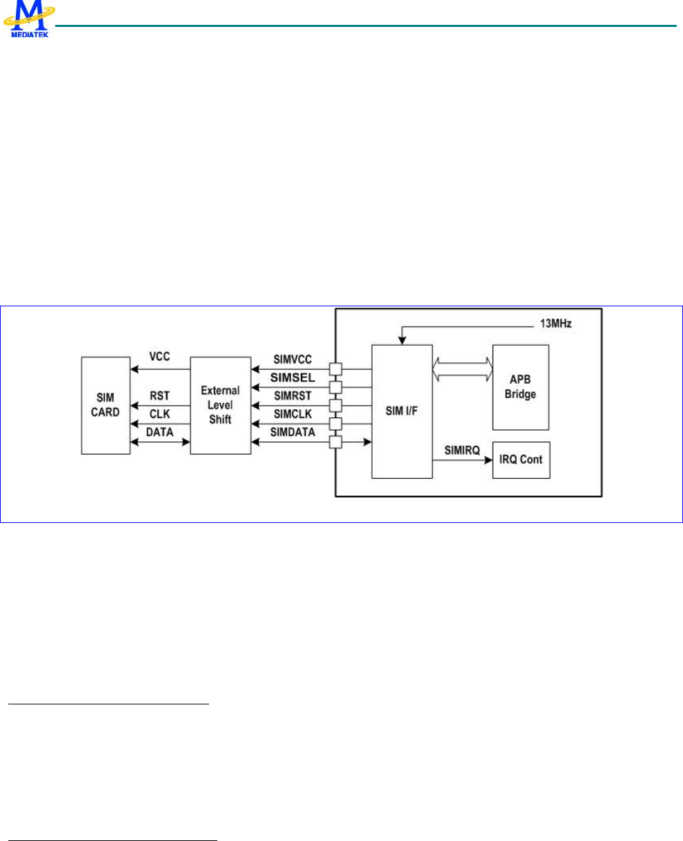
MT6235 GSM/GPRS Baseband Processor Data Sheet Revision 1.02
150/599 MediaTek Inc. Confidential
PWM3_INT_UNDERFLOW_ACK Set to 1 to clear PWM3 underflow interrupt
PWM4_INT_FINISH_ACK Set to 1 to clear PWM4 finish interrupt
PWM4_INT_UNDERFLOW_ACK Set to 1 to clear PWM4 underflow interrupt
PWM5_INT_FINISH_ACK Set to 1 to clear PWM5 finish interrupt
PWM5_INT_UNDERFLOW_ACK Set to 1 to clear PWM5 underflow interrupt
PWM6_INT_FINISH_ACK Set to 1 to clear PWM6 finish interrupt
PWM6_INT_UNDERFLOW_ACK Set to 1 to clear PWM6 underflow interrupt
4.4 SIM Interface
The MT6235 contains a dedicated smart card interface to allow the MCU to access. It can operate via 5 terminals, using
SIMVCC, SIMSEL, SIMRST, SIMCLK and SIMDATA.
Figure 18 SIM Interface Block Diagram
The SIMVCC is used to control the external voltage supply to the SIM card and SIMSEL determines the regulated smart
card supply voltage. SIMRST is used as the SIM card reset signal. Besides, SIMDATA and SIMCLK are used for data
exchange purpose.
Basically, the SIM interface acts as a half duplex asynchronous communication port and its data format is composed of ten
consecutive bits: a start bit in state Low, eight information bits, and a tenth bit used for parity checking. The data format can
be divided into two modes as follows:
Direct Mode (ODD=SDIR=SINV=0)
SB D0 D1 D2 D3 D4 D5 D6 D7 PB
SB: Start Bit (in state Low)
Dx: Data Byte (LSB is first and logic level ONE is High)
PB: Even Parity Check Bit
Indirect Mode (ODD=SDIR=SINV=1)
SB N7 N6 N5 N4 N3 N2 N1 N0 PB
SB: Start Bit (in state Low)
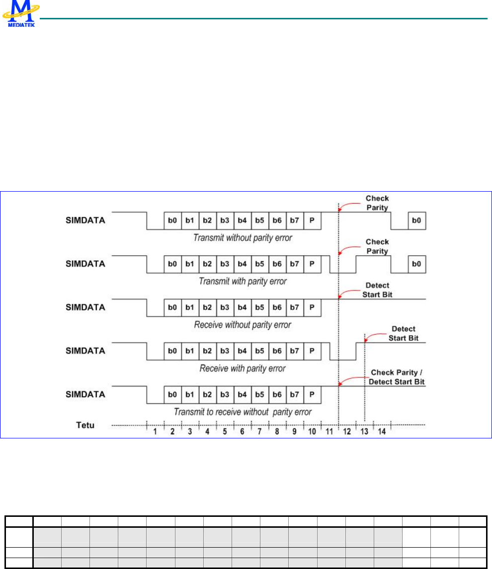
MT6235 GSM/GPRS Baseband Processor Data Sheet Revision 1.02
151/599 MediaTek Inc. Confidential
Nx: Data Byte (MSB is first and logic level ONE is Low)
PB: Odd Parity Check Bit
If the receiver gets a wrong parity bit, it will respond by pulling the SIMDATA Low to inform the transmitter and the
transmitter will retransmit the character.
When the receiver is a SIM Card, the error response starts 0.5 bits after the PB and it may last for 1~2 bit periods.
When the receiver is the SIM interface, the error response starts 0.5 bits after the PB and lasts for 1.5 bit period.
When the SIM interface is the transmitter, it will take totally 14 bits guard period whether the error response appears. If the
receiver shows the error response, the SIM interface will retransmit the previous character again else it will transmit the
next character.
Figure 19 SIM Interface Timing Diagram
4.4.1 Register Definitions
SIM+0000h SIM module control register SIM_CONT
Bit 15 14 13 12 11 10 9 8 7 6 5 4 3 2 1 0
Name WRST
CSTO
P SIMO
N
Type W R/W R/W
Reset 0 0 0
SIMON SIM card power-up/power-down control
0 Initiate the card deactivation sequence
1 Initiate the card activation sequence
CSTOP Enable clock stop mode. Together with CPOL in SIM_CNF register, it determines the polarity of the SIMCLK in
this mode.

MT6235 GSM/GPRS Baseband Processor Data Sheet Revision 1.02
152/599 MediaTek Inc. Confidential
0 Enable the SIMCLK output.
1 Disable the SIMCLK output
WRST SIM card warm reset control
SIM+0004h SIM module configuration register SIM_CONF
Bit 15 14 13 12 11 10 9 8 7 6 5 4 3 2 1 0
Name HFEN T0EN T1EN TOUT SIMS
EL ODD SDIR SINV CPOL
TXAC
K RXAC
K
Type R/W R/W R/W R/W R/W R/W R/W R/W R/W R/W R/W
Reset 0 0 0 0 0 0 0 0 0 0 0
RXACK SIM card reception error handshake control
0 Disable character receipt handshaking
1 Enable character receipt handshaking
TXACK SIM card transmission error handshake control
0 Disable character transmission handshaking
1 Enable character transmission handshaking
CPOL SIMCLK polarity control in clock stop mode
0 Make SIMCLK stop in LOW level
1 Make SIMCLK stop in HIGH level
SINV Data Inverter.
0 Not invert the transmitted and received data
1 Invert the transmitted and received data
SDIR Data Transfer Direction
0 LSB is transmitted and received first
1 MSB is transmitted and received first
ODD Select odd or even parity
0 Even parity
1 Odd parity
SIMSEL SIM card supply voltage select
0 SIMSEL pin is set to LOW level
1 SIMSEL pin is set to HIGH level
TOUT SIM work waiting time counter control
0 Disable Time-Out counter
1 Enable Time-Out counter
T1EN T=1 protocol controller control
0 Disable T=1 protocol controller
1 Enable T=1 protocol controller
T0EN T=0 protocol controller control
0 Disable T=0 protocol controller
1 Enable T=0 protocol controller
HFEN Hardware flow control
0 Disable hardware flow control
1 Enable hardware flow control
MT6235 GSM/GPRS Baseband Processor Data Sheet Revision 1.02
153/599 MediaTek Inc. Confidential
SIM +0008h SIM Baud Rate Register SIM_BRR
Bit 15 14 13 12 11 10 9 8 7 6 5 4 3 2 1 0
Name ETU[8:0] SIMCLK[1:0]
Type R/W R/W
Reset 372d 01
SIMCLK Set SIMCLK frequency
00 13/2 MHz
01 13/4 MHz
10 13/8 MHz
11 13/32 MHz
ETU Determines the duration of elementary time unit in unit of SIMCLK
SIM +0010h SIM interrupt enable register SIM_IRQEN
Bit 15 14 13 12 11 10 9 8 7 6 5 4 3 2 1 0
Name EDCE
RR T1EN
D RXER
R T0EN
D SIMO
FF ATRER
R TXER
R TOU
T OVRU
N RXTID
E TXTID
E
Type R/W R/W R/W R/W R/W R/W R/W R/W R/W R/W R/W
Reset 0 0 0 0 0 0 0 0 0 0 0
For all these bits
0 Interrupt is disabled
1 Interrupt is enabled
SIM +0014h SIM module status register SIM_STS
Bit 15 14 13 12 11 10 9 8 7 6 5 4 3 2 1 0
Name EDCE
RR T1EN
D RXER
R T0EN
D SIMO
FF ATRER
R TXER
R TOU
T OVRU
N RXTID
E TXTID
E
Type R/C R/C R/C R/C R/C R/C R/C R/C R/C R R
Reset — — — — — — — — — — —
TXTIDE Transmit FIFO tide mark reached interrupt occurred
RXTIDE Receive FIFO tide mark reached interrupt occurred
OVRUN Transmit/Receive FIFO overrun interrupt occurred
TOUT Between character timeout interrupt occurred
TXERR Character transmission error interrupt occurred
ATRERR ATR start time-out interrupt occurred
SIMOFF Card deactivation complete interrupt occurred
T0END Data Transfer handled by T=0 Controller completed interrupt occurred
RXERR Character reception error interrupt occurred
T1END Data Transfer handled by T=1 Controller completed interrupt occurred
EDCERR T=1 Controller CRC error occurred
SIM +0020h SIM retry limit register SIM_RETRY
Bit 15 14 13 12 11 10 9 8 7 6 5 4 3 2 1 0
Name TXRETRY RXRETRY
Type R/W R/W
Reset 3h 3h
MT6235 GSM/GPRS Baseband Processor Data Sheet Revision 1.02
154/599 MediaTek Inc. Confidential
RXRETRY Specify the max. numbers of receive retries that are allowed when parity error has occurred.
TXRETRY Specify the max. numbers of transmit retries that are allowed when parity error has occurred.
SIM+0024h SIM FIFO tide mark register SIM_TIDE
Bit 15 14 13 12 11 10 9 8 7 6 5 4 3 2 1 0
Name TXTIDE[3:0] RXTIDE[3:0]
Type R/W R/W
Reset 0h 0h
RXTIDE Trigger point for RXTIDE interrupt
TXTIDE Trigger point for TXTIDE interrupt
SIM +0030h Data register used as Tx/Rx Data Register SIM_DATA
Bit 15 14 13 12 11 10 9 8 7 6 5 4 3 2 1 0
Name DATA[7:0]
Type R/W
Reset —
DATA Eight data digits. These correspond to the character being read or written
SIM +0034h SIM FIFO count register SIM_COUNT
Bit 15 14 13 12 11 10 9 8 7 6 5 4 3 2 1 0
Name COUNT[4:0]
Type R/W
Reset 0h
COUNT The number of characters in the SIM FIFO when read, and flushes when written.
SIM +0040h SIM activation time register SIM_ATIME
Bit 15 14 13 12 11 10 9 8 7 6 5 4 3 2 1 0
Name ATIME[15:0]
Type R/W
Reset AFC7h
ATIME The register defines the duration, in SIM clock cycles, of the time taken for each of the three stages of the card
activation process
SIM +0044h SIM deactivation time register SIM_DTIME
Bit 15 14 13 12 11 10 9 8 7 6 5 4 3 2 1 0
Name DTIME[11:0]
Type R/W
Reset 3E7h
DTIME The register defines the duration, in 13MHz clock cycles, of the time taken for each of the three stages of the
card deactivation sequence
SIM+0048h Character to character waiting time register SIM_WTIME
Bit 15 14 13 12 11 10 9 8 7 6 5 4 3 2 1 0
Name WTIME[15:0]
Type R/W
Reset 983h
WTIME Maximum interval between the leading edge of two consecutive characters in 4 ETU unit
MT6235 GSM/GPRS Baseband Processor Data Sheet Revision 1.02
155/599 MediaTek Inc. Confidential
SIM+004Ch Block to block guard time register SIM_GTIME
Bit 15 14 13 12 11 10 9 8 7 6 5 4 3 2 1 0
Name GTIME
Type R/W
Reset 10d
GTIME Minimum interval between the leading edge of two consecutive characters sent in opposite directions in ETU unit
SIM +0050h Block to error signal time register SIM_ETIME
Bit 15 14 13 12 11 10 9 8 7 6 5 4 3 2 1 0
Name ETIME
Type R/W
Reset 15d
ETIME The register defines the interval, in 1/16 ETU unit, between the end of transmitted parity bit and time to check
parity error signal sent from SIM card.
SIM +0060h SIM command header register: INS SIM_INS
Bit 15 14 13 12 11 10 9 8 7 6 5 4 3 2 1 0
Name INSD SIMINS[7:0]
Type R/W R/W
Reset 0h 0h
SIMINS This field should be identical to the INS instruction code. When writing to this register, the T=0 controller will be
activated and data transfer will be initiated.
INSD [Description for this register field]
0 T=0 controller receives data from the SIM card
1 T=0 controller sends data to the SIM card
SIM +0064h SIM command header register: P3 SIM_P3
(ICC_LEN)
Bit 15 14 13 12 11 10 9 8 7 6 5 4 3 2 1 0
Name SIMP3[8:0]
Type R/W
Reset 0h
SIMP3 This field should be identical to the P3 instruction code. It should be written prior to the SIM_INS register. While
the data transfer is going on, this field shows the no. of the remaining data to be sent or to be received
SIM +0068h SIM procedure byte register: SW1 SIM_SW1
(ICC_LEN)
Bit 15 14 13 12 11 10 9 8 7 6 5 4 3 2 1 0
Name SIMSW1[7:0]
Type R
Reset 0h
SIMSW1 This field holds the last received procedure byte for debug purpose. When the T0END interrupt occurred, it
keeps the SW1 procedure byte.
SIM +006Ch SIM procedure byte register: SW2 SIM_SW2
(ICC_EDC)
Bit 15 14 13 12 11 10 9 8 7 6 5 4 3 2 1 0

MT6235 GSM/GPRS Baseband Processor Data Sheet Revision 1.02
156/599 MediaTek Inc. Confidential
Name SIMSW2[7:0]
Type R
Reset 0h
SIMSW2 This field holds the SW2 procedure byte
4.4.2 SIM Card Insertion and Removal
The detection of physical connection to the SIM card and card removal is done by the external interrupt controller or by
GPIO.
4.4.3 Card Activation and Deactivation
The card activation and deactivation sequence both are controlled by H/W. The MCU initiates the activation sequence by
writing a “1” to bit 0 of the SIM_CON register, and then the interface performs the following activation sequence:
z Assert SIMRST LOW
z Set SIMVCC at HIGH level and SIMDATA in reception mode
z Enable SIMCLK clock
z De-assert SIMRST HIGH (required if it belongs to active low reset SIM card)
The final step in a typical card session is contact deactivation in order that the card is not electrically damaged. The
deactivation sequence is initiated by writing a “0” to bit 0 of the SIM_CONT register, and then the interface performs the
following deactivation sequence:
z Assert SIMRST LOW
z Set SCIMCLK at LOW level
z Set SIMDATA at LOW level
z Set SIMVCC at LOW level
4.4.4 Answer to Reset Sequence
After card activation, a reset operation results in an answer from the card consisting of the initial character TS, followed by
at most 32 characters. The initial character TS provides a bit synchronization sequence and defines the conventions to
interpret data bytes in all subsequent characters.
On reception of the first character, TS, MCU should read this character, establish the respective required convention and
reprogram the related registers. These processes should be completed prior to the completion of reception of the next
character. And then, the remainder of the ATR sequence is received, read via the SIM_DATA in the selected convention and
interpreted by the S/W.
The timing requirement and procedures for ATR sequence are handled by H/W and shall meet the requirement of ISO
7816-3 as shown in Figure 20.
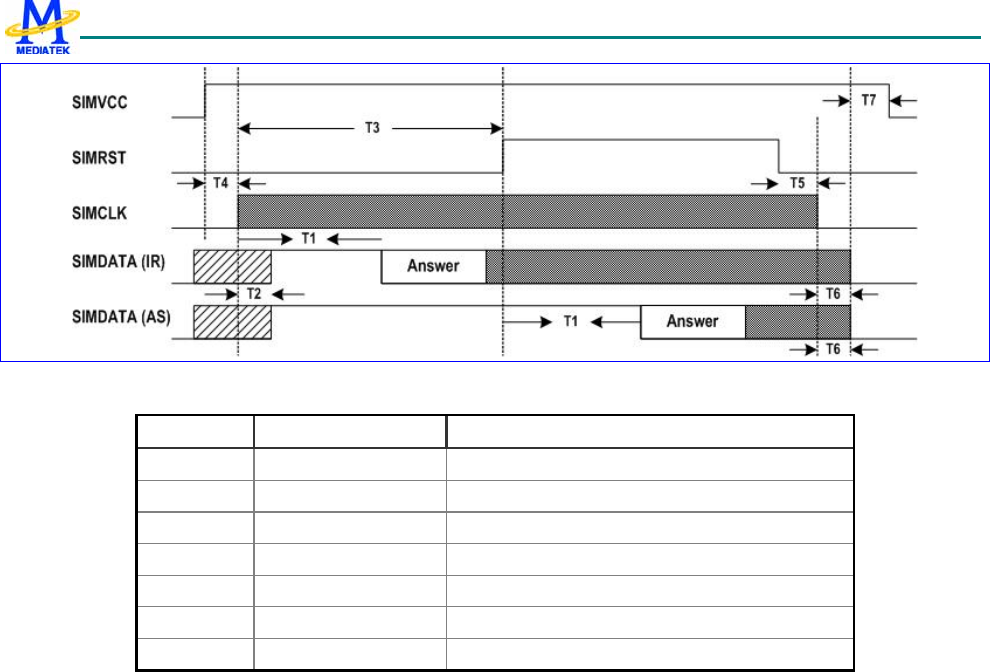
MT6235 GSM/GPRS Baseband Processor Data Sheet Revision 1.02
157/599 MediaTek Inc. Confidential
Figure 20 Answer to Reset Sequence
Time Value Comment
T1 > 400 SIMCLK SIMCLK start to ATR appear
T2 < 200 SIMCLK SIMCLK start to SIMDATA in reception mode
T3 > 40000 SIMCLK SIMCLK start to SIMRST High
T4 — SIMVCC High to SIMCLK start
T5 — SIMRST Low to SIMCLK stop
T6 — SIMCLK stop to SIMDATA Low
T7 — SIMDATA Low to SIMVCC Low
Table 16 Answer to Reset Sequence Time-Out Condition
4.4.5 SIM Data Transfer
Two transfer modes are provided, either in software controlled byte by byte fashion or in a block fashion using T=0
controller and DMA controller. In both modes, the time-out counter could be enabled to monitor the elapsed time between
two consecutive bytes.
1.1.1.1. Byte Transfer Mode
This mode is used during ATR and PPS procedure. In this mode, the SIM interface only ensures error free character
transmission and reception.
Receiving Character
Upon detection of the start-bit sent by SIM card, the interface transforms into reception mode and the following bits are
shifted into an internal register. If no parity error is detected or character-receive handshaking is disabled, the
received-character is written into the SIM FIFO and the SIM_COUNT register is increased by one. Otherwise, the
SIMDATA line is held low at 0.5 etu after detecting the parity error for 1.5 etus, and the character is re-received. If a
character fails to be received correctly for the RXRETRY times, the receive-handshaking is aborted and the last-received
character is written into the SIM FIFO, the SIM_COUNT is increased by one and the RXERR interrupt is generated
When the number of characters held in the receive FIFO exceeds the level defined in the SIM_TIDE
register, a RXTIDE interrupt is generated. The number of characters held in the SIM FIFO can be

MT6235 GSM/GPRS Baseband Processor Data Sheet Revision 1.02
158/599 MediaTek Inc. Confidential
determined by reading the SIM_COUNT register and writing to this register will flush the SIM FIFO.
Sending Character
Characters that are to be sent to the card are first written into the SIM FIFO and then automatically transmitted to the card
at timed intervals. If character-transmit handshaking is enabled, the SIMDATA line is sampled at 1 etu after the parity bit. If
the card indicates that it did not receive the character correctly, the character is retransmitted a maximum of TXRETRY
times before a TXERR interrupt is generated and the transmission is aborted. Otherwise, the succeeding byte in the SIM
FIFO is transmitted.
If a character fails to be transmitted and a TXERR interrupt is generated, the interface needs to be reset by flushing the SIM
FIFO before any subsequent transmit or receive operation.
When the number of characters held in the SIM FIFO falls below the level defined in the SIM_TIDE register, a TXTIDE
interrupt is generated. The number of characters held in the SIM FIFO can be determined by reading the SIM_COUNT
register and writing to this register will flush the SIM FIFO.
1.1.1.2. Block Transfer Mode
Basically, the SIM interface is designed to work in conjunction with the T=0 protocol controller and the DMA controller
during non-ATR and non-PPS phase, though it is still possible for software to service the data transfer manually like in byte
transfer mode if necessary and thus the T=0 protocol should be controlled by software.
The T=0 controller is accessed via four registers representing the instruction header bytes INS and P3, and the procedure
bytes SW1 and SW2. These registers are:
SIM_INS, SIM_P3
SIM_SW1, SIM_SW2
During characters transfer, SIM_P3 holds the number of characters to be sent or to be received and SIM_SW1 holds the last
received procedure byte including NULL, ACK, NACK and SW1 for debug purpose.
Data Receive Instruction
Data Receive Instructions receive data from the SIM card. It is instantiated as the following procedure.
1. Enable the T=0 protocol controller by setting the T0EN bit to 1 in SIM_CONF register
2. Program the SIM_TIDE register to 0x0000 (TXTIDE = 0, RXTIDE = 0)
3. Program the SIM_IRQEN to 0x019C (Enable RXERR, TXERR, T0END, TOUT and OVRUN interrupts)
4. Write CLA, INS, P1, P2 and P3 into SIM FIFO
5. Program the DMA controller :
DMAn_MSBSRC and DMAn_LSBSRC : address of SIM_DATA register
DMAn_MSBDST and DMAn_LSBDST : memory address reserved to store the received characters
DMAn_COUNT : identical to P3 or 256 (if P3 == 0)
DMAn_CON : 0x0078
6. Write P3 into SIM_P3 register and then INS into SIM_INS register (Data Transfer is initiated
now)
7. Enable the Time-out counter by setting the TOUT bit to 1 in SIM_CONF register
8. Start the DMA controller by writing 0x8000 into the DMAn_START register to
Upon completion of the Data Receive Instruction, T0END interrupt will be generated and then the Time-out counter should
be disabled by setting the TOUT bit back to 0 in SIM_CONF register.

MT6235 GSM/GPRS Baseband Processor Data Sheet Revision 1.02
159/599 MediaTek Inc. Confidential
If error occurs during data transfer (RXERR, TXERR, OVRUN or TOUT interrupt is generated), the SIM card should be
deactivated first and then activated prior subsequent operations.
Data Send Instruction
Data Send Instructions send data to the SIM card. It is instantiated as the following procedure.
1. Enable the T=0 protocol controller by setting the T0EN bit to 1 in SIM_CONF register
2. Program the SIM_TIDE register to 0x0100 (TXTIDE = 1, RXTIDE = 0)
3. Program the SIM_IRQEN to 0x019C (Enable RXERR, TXERR, T0END, TOUT and OVRUN interrupts)
4. Write CLA, INS, P1, P2 and P3 into SIM FIFO
5. Program the DMA controller :
DMAn_MSBSRC and DMAn_LSBSRC : memory address reserved to store the transmitted characters
DMAn_MSBDST and DMAn_LSBDST : address of SIM_DATA register
DMAn_COUNT : identical to P3
DMAn_CON : 0x0074
6. Write P3 into SIM_P3 register and then (0x0100 | INS) into SIM_INS register (Data Transfer
is initiated now)
7. Enable the Time-out counter by setting the TOUT bit to 1 in SIM_CONF register
8. Start the DMA controller by writing 0x8000 into the DMAn_START register
Upon completion of the Data Send Instruction, T0END interrupt will be generated and then the Time-out counter should be
disabled by setting the TOUT bit back to 0 in SIM_CONF register.
If error occurs during data transfer (RXERR, TXERR, OVRUN or TOUT interrupt is generated), the SIM card should be
deactivated first and then activated prior subsequent operations.
4.5 Keypad Scanner
4.5.1 General Description
The keypad can be divided into two parts: one is the keypad interface including 8 columns and 8 rows with one dedicated
power-key, as shown in Fig. 7 錯誤! 找不到參照來源。錯誤! 找不到參照來源。; the other is the key detection block
which provides key pressed, key released and de-bounce mechanisms. Each time the key is pressed or released, i.e.
something different in the 8 x 8 matrix or power-key, the key detection block senses the change and recognizes if a key has
been pressed or released. Whenever the key status changes and is stable, a KEYPAD IRQ is issued. The MCU can then
read the key(s) pressed directly in KP_HI_KEY, KP_MID_KEY and KP_LOW_KEY registers. To ensure that the key
pressed information is not missed, the status register in keypad is not read-cleared by APB read command. The status
register can only be changed by the key-pressed detection FSM.
This keypad can detect one or two key-pressed simultaneously with any combination. Fig. 8 shows one key pressed
condition. Fig. 9 (a) and Fig. 9 (b) illustrate two keys pressed cases. Since the key press detection depends on the HIGH
or LOW level of the external keypad interface, if keys are pressed at the same time and there exists a key that is on the same
column and the same row with the other keys, the pressed key cannot be correctly decoded. For example, if there are three
key presses: key1 = (x1, y1), key2 = (x2, y2), and key3 = (x1, y2), then both key3 and key4 = (x2, y1) are detected, and
therefore they cannot be distinguished correctly. Hence, the keypad can detect only one or two keys pressed
simultaneously at any combination. More than two keys pressed simultaneously in a specific pattern retrieve the wrong
information.
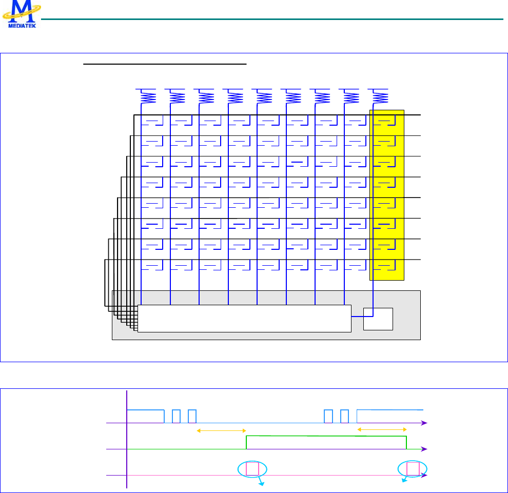
MT6235 GSM/GPRS Baseband Processor Data Sheet Revision 1.02
160/599 MediaTek Inc. Confidential
Dedicated for Power-key
(8x8 + one power-key) key matrix
ROW0
ROW1
ROW2
ROW3
ROW4
Baseband
PM IC integrated BB chip
COL1 COL2 COL3 COL4 COL5 COL6
PMIC
COL0 COL7PW R_KEY
1
111
11111
111111
111
111
11
1111
11111
1
1
1
1
1
1
1
1
1
1
1
1
1
1
11111
111
1
11111
111
1
1
1111
111
ROW5
ROW6
ROW7
Fig. 7 8x8 matrix with one power-key
Key-pressed Status
De-bounce time De-bounce time
Key Pressed
KP_IRQ
KEY_PRESS_IRQ
KEY_RELEASE_IRQ
Fig. 8. One key pressed with de-bounce mechanism denoted

MT6235 GSM/GPRS Baseband Processor Data Sheet Revision 1.02
161/599 MediaTek Inc. Confidential
Key1 pressed
Key2 pressed
Status
IRQ
Key1 pressed Key2 pressed Key1 released Key2 released
Key1 pressed
Key2 pressed
Status
IRQ
Key1 pressed Key2 pressed Key2 released Key1 released
(a)
(b)
Key1 pressed
Key2 pressed
Status
IRQ
Key1 pressed Key2 pressed Key1 released Key2 released
Key1 pressed
Key2 pressed
Status
IRQ
Key1 pressed Key2 pressed Key2 released Key1 released
(a)
(b)
Fig. 9. (a) Two keys pressed, case 1 (b) Two keys pressed, case 2
4.5.2 Register Definitions
KP +0000h Keypad status KP_STA
Bit 15 14 13 12 11 10 9 8 7 6 5 4 3 2 1 0
Name STA
Type RO
Reset 0
STA This register indicates the keypad status. The register is not cleared by the read operation.
0 No key pressed
1 Key pressed
KP +0004h Keypad scanning output Register KP_MEM1
Bit 15 14 13 12 11 10 9 8 7 6 5 4 3 2 1 0
Name KEYS [15:0]
Type RO
Reset 16’hFFFF
The register shows up the key-press status of key0~key15
KP +0008h Keypad scanning output Register KP_MEM2
Bit 15 14 13 12 11 10 9 8 7 6 5 4 3 2 1 0
Name KEYS [15:0]
Type RO
Reset 16’hFFFF
The register shows up the key-press status of key16~key31
KP +000Ch Keypad scanning output Register KP_MEM3
Bit 15 14 13 12 11 10 9 8 7 6 5 4 3 2 1 0

MT6235 GSM/GPRS Baseband Processor Data Sheet Revision 1.02
162/599 MediaTek Inc. Confidential
Name KEYS [15:0]
Type RO
Reset 16’hFFFF
The register shows up the key-press status of key32~key47
KP +0010h Keypad scanning output Register KP_MEM4
Bit 15 14 13 12 11 10 9 8 7 6 5 4 3 2 1 0
Name KEYS [15:0]
Type RO
Reset 16’hFFFF
The register shows up the key-press status of key48~key63
KP +0014h Keypad scanning output Register KP_MEM5
Bit 15 14 13 12 11 10 9 8 7 6 5 4 3 2 1 0
Name KEYS [7:0]
Type RO
Reset 8’hFF
The register shows up the key-press status of key64~key71
These two registers list the status of 35 keys on the keypad but KEY[8], KEY[17], KEY[26], KEY[35], KEY[44] ,
KEY[53] , KEY[62] , KEY[71] is dedicated for power key. When the MCU receives the KEYPAD IRQ, both two
registers must be read. If any key is pressed, the relative bit is set to 0.
KEYS Status list of the 72 keys.
KP +00018h De-bounce period setting KP_DEBOUNCE
Bit 15 14 13 12 11 10 9 8 7 6 5 4 3 2 1 0
Name DEBOUNCE [13:0]
Type R/W
Reset 400h
This register defines the waiting period before key press or release events are considered stale.
DEBOUNCE De-bounce time = KP_DEBOUNCE/32 ms.
4.6 General Purpose Inputs/Outputs
MT6235 offers 76 general-purpose I/O pins. By setting the control registers, MCU software can control the direction, the
output value, and read the input values on these pins. These GPIOs are multiplexed with other functionalities to reduce the
pin count. There are 10 clock-out ports embedded in 76 GPIO pins, and each clock-out can be programmed to output
appropriate clock source.
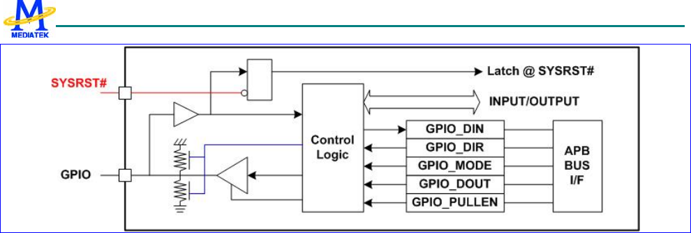
MT6235 GSM/GPRS Baseband Processor Data Sheet Revision 1.02
163/599 MediaTek Inc. Confidential
Figure 21 GPIO Block Diagram
GPIOs at RESET
Upon hardware reset (SYSRST#), GPIOs are all configured as inputs and the following alternative usages of GPIO pins are
enabled:
These GPIOs are used to latch the inputs upon reset to memorize the desired configuration to make sure that the system
restarts or boots in the right mode.
Multiplexing of Signals on GPIO
The GPIO pins can be multiplexed with other signals.
z CMRST, CMPDN, CMVREF, CMHREF, CMPCLK, CMMCLK, CMDAT7~0, CMFLASH: CMOS sensor
interface
z SCL, SDL: I2C interface
z DAICLK, DAIPCMIN, DAIPCMOUT, DAIRST, DAISYNC: digital audio interface for FTA
z BPI_BUS3, BPI_BUS6, BPI_BUS7, BPI_BUS8, BPI_BUS9: radio hard-wire control
z BSI_CS1: additional chip select signal for radio 3-wire interface
z LSCK, LSA0, LSDA, LSCE0#, LSCE1#: serial display interface
z NRNB, NCLE, NALE, NWEB, NCE0# NCE1#: Nandflash interface
z NLD17, NLD16, LPCE1#, LPECE2#, LPTE: parallel display interface data and chip select signal
z PWM0, PWM1, PWM2, PWM3 : pulse width modulation signal
z URTS1, UCTS1: data and flow control signals for UART1
z URXD2, UTXD2, URTS2, UCTS2: data and flow control signals for UART2
z URXD3, UTXD3, URTS3, UCTS3: data signals for UART3
z IDRA_RXD, IRDA_TXD, IRDA_PDN: IrDA interface signals
z SRCLKENAI, SRCLKENA, SRCLKENAN: external power on signal of the external VCXO LDO
z EINT3, EINT4, EINT5, EINT6, EINT7: External interrupt signals
z KCOL7, KCOL6, KROW7, KROW6: Keypad signals

MT6235 GSM/GPRS Baseband Processor Data Sheet Revision 1.02
164/599 MediaTek Inc. Confidential
z EADMUX: External Memory AD-MUX select signal
z EA26: external memory interface address bit 26
z MC0CM0, MC0DA0~3, MC0CK, MC0PWRON, MC0WP, MC0INS : MMC Card 0 interface
z IRQ2, IRQ1, IRQ0 : external interrupt
z 32KHz, 6.5MHz, 13MHz, 26MHz clocks
4.6.1 Register Definitions
GPIO+0000h GPIO direction control register 1 GPIO_DIR1
Bit 15 14 13 12 11 10 9 8 7 6 5 4 3 2 1 0
Name GPIO1
5 GPIO1
4 GPIO1
3 GPIO1
2 GPIO1
1 GPIO1
0 GPIO9 GPIO8 GPIO7 GPIO6 GPIO5 GPIO4 GPIO3 GPIO2 GPIO1 GPIO
0
Type R/W R/W R/W R/W R/W R/W R/W R/W R/W R/W R/W R/W R/W R/W R/W R/W
Reset 0 0 0 0 0 0 0 0 0 0 0 0 0 0 0 0
GPIO +0040h GPIO direction control register 2 GPIO_DIR2
Bit 15 14 13 12 11 10 9 8 7 6 5 4 3 2 1 0
Name GPIO3
1 GPIO3
0 GPIO2
9 GPIO2
8 GPIO2
7 GPIO2
6 GPIO2
5 GPIO2
4 GPIO2
3 GPIO2
2 GPIO2
1 PGIO2
0 GPIO1
9 GPIO1
8 GPIO1
7 GPIO
16
Type R/W R/W R/W R/W R/W R/W R/W R/W R/W R/W R/W R/W R/W R/W R/W R/W
Reset 0 0 0 0 0 0 0 0 0 0 0 0 0 0 0 0
GPIO+0080h GPIO direction control register 3 GPIO_DIR3
Bit 15 14 13 12 11 10 9 8 7 6 5 4 3 2 1 0
Name GPIO4
7 GPIO4
6 GPIO4
5 GPIO4
4 GPIO4
3 GPIO4
2 GPIO4
1 GPIO4
0 GPIO3
9 GPIO3
8 GPIO3
7 GPIO3
6 GPIO3
5 GPIO3
4 GPIO3
3 GPIO
32
Type R/W R/W R/W R/W R/W R/W R/W R/W R/W R/W R/W R/W R/W R/W R/W R/W
Reset 0 0 0 0 0 0 0 0 0 0 0 0 0 0 0 0
GPIO+00C0h GPIO direction control register 4 GPIO_DIR4
Bit 15 14 13 12 11 10 9 8 7 6 5 4 3 2 1 0
Name GPIO6
3 GPIO6
2 GPIO6
1 GPIO6
0 GPIO5
9 GPIO5
8 GPIO5
7 GPIO5
6 GPIO5
5 GPIO5
4 GPIO5
3 GPIO5
2 GPIO5
1 GPIO5
0 GPIO4
9 GPIO
48
Type R/W R/W R/W R/W R/W R/W R/W R/W R/W R/W R/W R/W R/W R/W R/W R/W
Reset 0 0 0 0 0 0 0 0 0 0 0 0 0 0 0 0
GPIO+0100h GPIO direction control register 5 GPIO_DIR5
Bit 15 14 13 12 11 10 9 8 7 6 5 4 3 2 1 0
Name GPIO7
5 GPIO7
4 GPIO7
3 GPIO7
2 GPIO7
1 GPIO7
0 GPIO6
9 GPIO6
8 GPIO6
7 GPIO6
6 GPIO6
5 GPIO
64
Type R/W R/W R/W R/W R/W R/W R/W R/W R/W R/W R/W R/W
Reset 0 0 0 0 0 0 0 0 0 0 0 0
GPIOn GPIO direction control
0 GPIOs are configured as input
1 GPIOs are configured as output
MT6235 GSM/GPRS Baseband Processor Data Sheet Revision 1.02
165/599 MediaTek Inc. Confidential
GPIO +0200h GPIO pull-up/pull-down enable register 1 GPIO_PULLEN1
Bit 15 14 13 12 11 10 9 8 7 6 5 4 3 2 1 0
Name GPIO1
5 GPIO1
4 GPIO1
3 GPIO1
2 GPIO1
1 GPIO1
0 GPIO9 GPIO8 GPIO7 GPIO6 GPIO5 GPIO4 GPIO3 GPIO2 GPIO1 GPIO
0
Type R/W R/W R/W R/W R/W R/W R/W R/W R/W R/W R/W R/W R/W R/W R/W R/W
Reset 1 1 1 1 1 1 1 1 1 1 1 1 1 1 1 1
GPIO +0240h GPIO pull-up/pull-down enable register 2 GPIO_PULLEN2
Bit 15 14 13 12 11 10 9 8 7 6 5 4 3 2 1 0
Name GPIO3
1 GPIO3
0 GPIO2
9 GPIO2
8 GPIO2
7 GPIO2
6 GPIO2
5 GPIO2
4 GPIO2
3 GPIO2
2 GPIO2
1 PGIO2
0 GPIO1
9 GPIO1
8 GPIO1
7 GPIO
16
Type R/W R/W R/W R/W R/W R/W R/W R/W R/W R/W R/W R/W R/W R/W R/W R/W
Reset 1 1 1 1 1 1 1 1 1 1 1 1 1 1 1 1
GPIO+0280h GPIO pull-up/pull-down enable register 3 GPIO_PULLEN3
Bit 15 14 13 12 11 10 9 8 7 6 5 4 3 2 1 0
Name GPIO4
7 GPIO4
6 GPIO4
5 GPIO4
4 GPIO4
3 GPIO4
2 GPIO4
1 GPIO4
0 GPIO3
9 GPIO3
8 GPIO3
7 GPIO3
6 GPIO3
5 GPIO3
4 GPIO3
3 GPIO
32
Type R/W R/W R/W R/W R/W R/W R/W R/W R/W R/W R/W R/W R/W R/W R/W R/W
Reset 1 1 1 1 1 0 0 1 1 0 0 0 0 0 1 1
GPIO+02C0h GPIO pull-up/pull-down enable register 4 GPIO_PULLEN4
Bit 15 14 13 12 11 10 9 8 7 6 5 4 3 2 1 0
Name GPIO6
3 GPIO6
2 GPIO6
1 GPIO6
0 GPIO5
9 GPIO5
8 GPIO5
7 GPIO5
6 GPIO5
5 GPIO5
4 GPIO5
3 GPIO5
2 GPIO5
1 GPIO5
0 GPIO4
9 GPIO
48
Type R/W R/W R/W R/W R/W R/W R/W R/W R/W R/W R/W R/W R/W R/W R/W R/W
Reset 1 1 1 1 1 1 1 1 1 1 1 1 1 0 1 1
GPIO+0300h GPIO pull-up/pull-down enable register 5 GPIO_PULLEN5
Bit 15 14 13 12 11 10 9 8 7 6 5 4 3 2 1 0
Name GPIO7
5 GPIO7
4 GPIO7
3 GPIO7
2 GPIO7
1 GPIO7
0 GPIO6
9 GPIO6
8 GPIO6
7 GPIO6
6 GPIO6
5 GPIO
64
Type R/W R/W R/W R/W R/W R/W R/W R/W R/W R/W R/W R/W
Reset 1 1 1 1 1 1 1 1 1 1 0 0
GPIOn GPIO pull up/down enable
0 GPIOs pull up/down is not enabled
1 GPIOs pull up/down is enabled
GPIO +0400h GPIO pull-up/pull-down select register 1 GPIO_PULLSEL
1
Bit 15 14 13 12 11 10 9 8 7 6 5 4 3 2 1 0
Name GPIO1
5 GPIO1
4 GPIO1
3 GPIO1
2 GPIO1
1 GPIO1
0 GPIO9 GPIO8 GPIO7 GPIO6 GPIO5 GPIO4 GPIO3 GPIO2 GPIO1 GPIO
0
Type R/W R/W R/W R/W R/W R/W R/W R/W R/W R/W R/W R/W R/W R/W R/W R/W
Reset 1 0 0 0 0 0 0 0 0 0 0 0 0 0 0 0
MT6235 GSM/GPRS Baseband Processor Data Sheet Revision 1.02
166/599 MediaTek Inc. Confidential
GPIO +0440h GPIO pull-up/pull-down select register 2 GPIO_PULLSEL
2
Bit 15 14 13 12 11 10 9 8 7 6 5 4 3 2 1 0
Name GPIO3
1 GPIO3
0 GPIO2
9 GPIO2
8 GPIO2
7 GPIO2
6 GPIO2
5 GPIO2
4 GPIO2
3 GPIO2
2 GPIO2
1 PGIO2
0 GPIO1
9 GPIO1
8 GPIO1
7 GPIO
16
Type R/W R/W R/W R/W R/W R/W R/W R/W R/W R/W R/W R/W R/W R/W R/W R/W
Reset 0 0 1 1 1 0 0 0 0 0 0 0 0 0 0 1
GPIO+0480h GPIO pull-up/pull-down select register 3 GPIO_PULLSEL
3
Bit 15 14 13 12 11 10 9 8 7 6 5 4 3 2 1 0
Name GPIO4
7 GPIO4
6 GPIO4
5 GPIO4
4 GPIO4
3 GPIO4
2 GPIO4
1 GPIO4
0 GPIO3
9 GPIO3
8 GPIO3
7 GPIO3
6 GPIO3
5 GPIO3
4 GPIO3
3 GPIO
32
Type R/W R/W R/W R/W R/W R/W R/W R/W R/W R/W R/W R/W R/W R/W R/W R/W
Reset 1 1 1 1 0 0 0 0 0 0 0 0 0 0 1 0
GPIO+04C0h GPIO pull-up/pull-down select register 4 GPIO_PULLSEL
4
Bit 15 14 13 12 11 10 9 8 7 6 5 4 3 2 1 0
Name GPIO6
3 GPIO6
2 GPIO6
1 GPIO6
0 GPIO5
9 GPIO5
8 GPIO5
7 GPIO5
6 GPIO5
5 GPIO5
4 GPIO5
3 GPIO5
2 GPIO5
1 GPIO5
0 GPIO4
9 GPIO
48
Type R/W R/W R/W R/W R/W R/W R/W R/W R/W R/W R/W R/W R/W R/W R/W R/W
Reset 0 1 0 0 0 0 0 1 1 1 1 1 1 0 1 1
GPIO+0500h GPIO pull-up/pull-down select register 5 GPIO_PULLSEL
5
Bit 15 14 13 12 11 10 9 8 7 6 5 4 3 2 1 0
Name GPIO7
5 GPIO7
4 GPIO7
3 GPIO7
2 GPIO7
1 GPIO7
0 GPIO6
9 GPIO6
8 GPIO6
7 GPIO6
6 GPIO6
5 GPIO
64
Type R/W R/W R/W R/W R/W R/W R/W R/W R/W R/W R/W R/W
Reset 1 1 1 1 1 1 1 1 1 1 0 0
GPIOn GPIO pull up/down selection
0 GPIOs pull down is selected
1 GPIOs pull up is selected
GPIO +0600h GPIO data inversion control register 1 GPIO_DINV1
Bit 15 14 13 12 11 10 9 8 7 6 5 4 3 2 1 0
Name INV15 INV14 INV13 INV12 INV11 INV10 INV9 INV8 INV7 INV6 INV5 INV4 INV3 INV2 INV1 INV0
Type R/W R/W R/W R/W R/W R/W R/W R/W R/W R/W R/W R/W R/W R/W R/W R/W
Reset 0 0 0 0 0 0 0 0 0 0 0 0 0 0 0 0
GPIO +0640h GPIO data inversion control register 2 GPIO_DINV2
Bit 15 14 13 12 11 10 9 8 7 6 5 4 3 2 1 0
Name INV31 INV30 INV29 INV28 INV27 INV26 INV25 INV24 INV23 INV22 INV21 INV20 INV19 IVN18 INV17 INV16
Type R/W R/W R/W R/W R/W R/W R/W R/W R/W R/W R/W R/W R/W R/W R/W R/W
Reset 0 0 0 0 0 0 0 0 0 0 0 0 0 0 0 0
MT6235 GSM/GPRS Baseband Processor Data Sheet Revision 1.02
167/599 MediaTek Inc. Confidential
GPIO +0680h GPIO data inversion control register 3 GPIO_DINV3
Bit 15 14 13 12 11 10 9 8 7 6 5 4 3 2 1 0
Name INV47 INV46 INV45 INV44 INV43 INV42 INV41 INV40 INV39 INV38 INV37 INV36 INV35 INV34 INV33 INV32
Type R/W R/W R/W R/W R/W R/W R/W R/W R/W R/W R/W R/W R/W R/W R/W R/W
Reset 0 0 0 0 0 0 0 0 0 0 0 0 0 0 0 0
GPIO+06C0h GPIO data inversion control register 4 GPIO_DINV4
Bit 15 14 13 12 11 10 9 8 7 6 5 4 3 2 1 0
Name NV63 INV62 INV61 INV60 INV59 INV58 INV57 INV56 INV55 INV54 INV53 INV52 INV51 INV50 INV49 INV48
Type R/W R/W R/W R/W R/W R/W R/W R/W R/W R/W R/W R/W R/W R/W R/W R/W
Reset 0 0 0 0 0 0 0 0 0 0 0 0 0 0 0 0
GPIO+0700h GPIO data inversion control register 5 GPIO_DINV5
Bit 15 14 13 12 11 10 9 8 7 6 5 4 3 2 1 0
Name INV75 INV74 INV73 INV72 INV71 INV70 INV69 INV68 INV67 INV66 INV65 INV64
Type R/W R/W R/W R/W R/W R/W R/W R/W R/W R/W R/W R/W
Reset 0 0 0 0 0 0 0 0 0 0 0 0
INVn GPIO inversion control
0 GPIOs data inversion disable
1 GPIOs data inversion enable
GPIO +0800h GPIO data output register 1 GPIO_DOUT1
Bit 15 14 13 12 11 10 9 8 7 6 5 4 3 2 1 0
Name GPIO1
5 GPIO1
4 GPIO1
3 GPIO1
2 GPIO1
1 GPIO1
0 GPIO9 GPIO8 GPIO7 GPIO6 GPIO5 GPIO4 GPIO3 GPIO2 GPIO1 GPIO
0
Type R/W R/W R/W R/W R/W R/W R/W R/W R/W R/W R/W R/W R/W R/W R/W R/W
Reset 0 0 0 0 0 0 0 0 0 0 0 0 0 0 0 0
GPIO +0840h GPIO data output register 2 GPIO_DOUT2
Bit 15 14 13 12 11 10 9 8 7 6 5 4 3 2 1 0
Name GPIO3
1 GPIO3
0 GPIO2
9 GPIO2
8 GPIO2
7 GPIO2
6 GPIO2
5 GPIO2
4 GPIO2
3 GPIO2
2 GPIO2
1 PGIO2
0 GPIO1
9 GPIO1
8 GPIO1
7 GPIO
16
Type R/W R/W R/W R/W R/W R/W R/W R/W R/W R/W R/W R/W R/W R/W R/W R/W
Reset 0 0 0 0 0 0 0 0 0 0 0 0 0 0 0 0
GPIO +0880h GPIO data output register 3 GPIO_DOUT3
Bit 15 14 13 12 11 10 9 8 7 6 5 4 3 2 1 0
Name GPIO4
7 GPIO4
6 GPIO4
5 GPIO4
4 GPIO4
3 GPIO4
2 GPIO4
1 GPIO4
0 GPIO3
9 GPIO3
8 GPIO3
7 GPIO3
6 GPIO3
5 GPIO3
4 GPIO3
3 GPIO
32
Type R/W R/W R/W R/W R/W R/W R/W R/W R/W R/W R/W R/W R/W R/W R/W R/W
Reset 0 0 0 0 0 0 0 0 0 0 0 0 0 0 0 0
GPIO+08C0h GPIO data output register 4 GPIO_DOUT4
Bit 15 14 13 12 11 10 9 8 7 6 5 4 3 2 1 0

MT6235 GSM/GPRS Baseband Processor Data Sheet Revision 1.02
168/599 MediaTek Inc. Confidential
Name GPIO6
3 GPIO6
2 GPIO6
1 GPIO6
0 GPIO5
9 GPIO5
8 GPIO5
7 GPIO5
6 GPIO5
5 GPIO5
4 GPIO5
3 GPIO5
2 GPIO5
1 GPIO5
0 GPIO4
9 GPIO
48
Type R/W R/W R/W R/W R/W R/W R/W R/W R/W R/W R/W R/W R/W R/W R/W R/W
Reset 0 0 0 0 0 0 0 0 0 0 0 0 0 0 0 0
GPIO+0900h GPIO data output register 5 GPIO_DOUT5
Bit 15 14 13 12 11 10 9 8 7 6 5 4 3 2 1 0
Name GPIO7
5 GPIO7
4 GPIO7
3 GPIO7
2 GPIO7
1 GPIO7
0 GPIO6
9 GPIO6
8 GPIO6
7 GPIO6
6 GPIO6
5 GPIO
64
Type R/W R/W R/W R/W R/W R/W R/W R/W R/W R/W R/W R/W
Reset 0 0 0 0 0 0 0 0 0 0 0 0
GPIOn GPIO data output control
0 GPIOs data output 1
1 GPIOs data output 0
GPIO +0A00h GPIO data Input register 1 GPIO_DIN1
Bit 15 14 13 12 11 10 9 8 7 6 5 4 3 2 1 0
Name GPIO1
5 GPIO1
4 GPIO1
3 GPIO1
2 GPIO1
1 GPIO1
0 GPIO9 GPIO8 GPIO7 GPIO6 GPIO5 GPIO4 GPIO3 GPIO2 GPIO1 GPIO
0
Type RO RO RO RO RO RO RO RO RO RO RO RO RO RO RO RO
Reset X X X X X X X X X X X X X X X X
GPIO +0A40h GPIO data Input register 2 GPIO_DIN2
Bit 15 14 13 12 11 10 9 8 7 6 5 4 3 2 1 0
Name GPIO3
1 GPIO3
0 GPIO2
9 GPIO2
8 GPIO2
7 GPIO2
6 GPIO2
5 GPIO2
4 GPIO2
3 GPIO2
2 GPIO2
1 PGIO2
0 GPIO1
9 GPIO1
8 GPIO1
7 GPIO
16
Type RO RO RO RO RO RO RO RO RO RO RO RO RO RO RO RO
Reset X X X X X X X X X X X X X X X X
GPIO +0A80h GPIO data Input register 3 GPIO_DIN3
Bit 15 14 13 12 11 10 9 8 7 6 5 4 3 2 1 0
Name GPIO4
7 GPIO4
6 GPIO4
5 GPIO4
4 GPIO4
3 GPIO4
2 GPIO4
1 GPIO4
0 GPIO3
9 GPIO3
8 GPIO3
7 GPIO3
6 GPIO3
5 GPIO3
4 GPIO3
3 GPIO
32
Type RO RO RO RO RO RO RO RO RO RO RO RO RO RO RO RO
Reset X X X X X X X X X X X X X X X X
GPIO+0AC0h GPIO data input register 4 GPIO_DIN4
Bit 15 14 13 12 11 10 9 8 7 6 5 4 3 2 1 0
Name GPIO6
3 GPIO6
2 GPIO6
1 GPIO6
0 GPIO5
9 GPIO5
8 GPIO5
7 GPIO5
6 GPIO5
5 GPIO5
4 GPIO5
3 GPIO5
2 GPIO5
1 GPIO5
0 GPIO4
9 GPIO
48
Type RO RO RO RO RO RO RO RO RO RO RO RO RO RO RO RO
Reset X X X X X X X X X X X X X X X X
GPIO+0B00h GPIO data input register 5 GPIO_DIN5
Bit 15 14 13 12 11 10 9 8 7 6 5 4 3 2 1 0
Name GPIO7
5 GPIO7
4 GPIO7
3 GPIO7
2 GPIO7
1 GPIO7
0 GPIO6
9 GPIO6
8 GPIO6
7 GPIO6
6 GPIO6
5 GPIO
64
Type RO RO RO RO RO RO RO RO RO RO RO RO
Reset X X X X X X X X X X X X
GPIOn GPIOs data input

MT6235 GSM/GPRS Baseband Processor Data Sheet Revision 1.02
169/599 MediaTek Inc. Confidential
GPIO +1000h GPIO mode control register 1 GPIO_MODE1
Bit 15 14 13 12 11 10 9 8 7 6 5 4 3 2 1 0
Name GPIO7_M GPIO6_M GPIO5_M GPIO4_M GPIO3_M GPIO2_M GPIO1_M GPIO0_M
Type R/W R/W R/W R/W R/W R/W R/W R/W
Reset 00 00 00 00 00 00 00 00
GPIO0_M GPIO mode selection
00 Configured as GPIO function
01 CMOS Sensor Reset control Signal (CMRST)
10 clk_out0
11 DSP_GPO0 (DSP_GPO0)
GPIO1_M GPIO mode selection
00 Configured as GPIO function
01 CMOS Sensor Power Down control Signal (CMPDN)
10 DSP_GPO1 (DSP_GPO1)
11 Reserved
GPIO2_M GPIO mode selection
00 Configured as GPIO function
01 CMOS Sensor Vertical Reference input (CMVREF)
10 TDMA Debug (TBTXEN)
11 Master DSP Task ID bit 0(D1_TID0)
GPIO3_M GPIO mode selection
00 Configured as GPIO function
01 CMOS Sensor Horizontal Reference input (CMHREF)
10 TDMA Debug (TBTXFS)
11 Reserved
GPIO4_M GPIO mode selection
00 Configured as GPIO function
01 CMOS Sensor Clock input signal (CMPCLK)
10 TDMA Debug (TBRXEN)
11 Master DSP Task ID bit 1(D1_TID1)
GPIO5_M GPIO mode selection
00 Configured as GPIO function
01 CMOS Sensor Clock output signal (CMMCLK)
10 TDMA Debug (TBRXFS)
11 Reserved
GPIO6_M GPIO mode selection
00 Configured as GPIO function
01 CMOS Sensor Data input signal bit7 (CMDAT7)
10 Reserved
11 Master DSP ICE Clock (D1ICK))
GPIO7_M GPIO mode selection
00 Configured as GPIO function

MT6235 GSM/GPRS Baseband Processor Data Sheet Revision 1.02
170/599 MediaTek Inc. Confidential
01 CMOS Sensor Data input signal bit6 (CMDAT6)
10 Reserved
11 Master DSP ICE Data (D1ID)
GPIO +1100h GPIO mode control register 2 GPIO_MODE2
Bit 15 14 13 12 11 10 9 8 7 6 5 4 3 2 1 0
Name GPIO15_M GPIO14_M GPIO13_M GPIO12_M GPIO11_M GPIO10_M GPIO9_M GPIO8_M
Type R/W R/W R/W R/W R/W R/W R/W R/W
Reset 00 00 00 00 00 00 00 00
GPIO8_M GPIO mode selection
00 Configured as GPIO function
01 CMOS Sensor Data input signal bit5 (CMDAT5)
10 Reserved
11 Master DSP ICE Model Select (D1IMS)
GPIO9_M GPIO mode selection
00 Configured as GPIO function
01 CMOS Sensor Data input signal bit4 (CMDAT4)
10 Reserved
11 Slave DSP ICE Clock (D2ICK)
GPIO10_M GPIO mode selection
00 Configured as GPIO function
01 CMOS Sensor Data input signal bit3 (CMDAT3)
10 Reserved
11 Slave DSP ICE Data (D2ID)
GPIO11_M GPIO mode selection
00 Configured as GPIO function
01 CMOS Sensor Data input signal bit2 (CMDAT2)
10 Reserved
11 Slave DSP ICE Mode Select (D2IMS)
GPIO12_M GPIO mode selection
00 Configured as GPIO function
01 CMOS Sensor Data input signal bit1 (CMDAT1)
10 Reserved
11 Slave DSP Task ID Bit0 (D2_TID0)
GPIO13_M GPIO mode selection
00 Configured as GPIO function
01 CMOS Sensor Data input signal bit 0 (CMDAT0)
10 Resereved
11 Slave DSP Task ID Bit1 (D2_TID1)
GPIO14_M GPIO mode selection
00 Configured as GPIO function
01 CMOS Sensor Flash Control (CMFLASH)
10 Reserved
11 Slave DSP Task ID Bit2 (D2_TID2)

MT6235 GSM/GPRS Baseband Processor Data Sheet Revision 1.02
171/599 MediaTek Inc. Confidential
GPIO15_M GPIO mode selection
00 Configured as GPIO function
01 I2C Clock (SCL)
10 Reserved
11 Slave DSP Task ID Bit3 (D2_TID3)
GPIO +1200h GPIO mode control register 3 GPIO_MODE3
Bit 15 14 13 12 11 10 9 8 7 6 5 4 3 2 1 0
Name GPIO23_M GPIO22_M GPIO21_M GPIO20_M GPIO19_M GPIO18_M GPIO17_M GPIO16_M
Type R/W R/W R/W R/W R/W R/W R/W R/W
Reset 00 00 00 00 00 00 00 00
GPIO16_M GPIO mode selection
00 Configured as GPIO function
01 I2C Data (SDA)
10 Reserved
11 Slave DSP Task ID Bit4 (D2_TID4)
GPIO17_M GPIO mode selection
00 Configured as GPIO function
01 PWM2 (PWM2)
10 Reserved
11 Slave DSP Task ID Bit5 (D2_TID5)
GPIO18_M GPIO mode selection
00 Configured as GPIO function
01 PWM3 (PWM3)
10 Reserved
11 Slave DSP Task ID Bit6 (D2_TID6)
GPIO19_M GPIO mode selection
00 Configured as GPIO function
01 BPI_BUS3 (BPI_BUS3)
10 Reserved
11 Reserved
GPIO20_M GPIO mode selection
00 Configured as GPIO function
01 BPI_BUS6 (BPI_BUS6)
10 Reserved
11 Reserved
GPIO21_M GPIO mode selection
00 Configured as GPIO function
01 BPI_BUS7 (BPI_BUS7)
10 Reserved
11 Reserved
GPIO22_M GPIO mode selection
00 Configured as GPIO function
01 BPI_BUS8 (BPI_BUS8)

MT6235 GSM/GPRS Baseband Processor Data Sheet Revision 1.02
172/599 MediaTek Inc. Confidential
10 Reserved
11 Reserved
GPIO23_M GPIO mode selection
00 Configured as GPIO function
01 BPI_BUS9 (BPI_BUS9)
10 BSI_CS1 (BS1_CS1)
11 Reserved
GPIO +1300h GPIO mode control register 4 GPIO_MODE4
Bit 15 14 13 12 11 10 9 8 7 6 5 4 3 2 1 0
Name GPIO31_M GPIO30_M GPIO29_M GPIO28_M GPIO27_M GPIO26_M GPIO25_M GPIO24_M
Type R/W R/W R/W R/W R/W R/W R/W R/W
Reset 00 00 00 00 00 00 00 00
GPIO24_M GPIO mode selection
00 Configured as GPIO function
01 Serial LCD Clock Output (LSCK)
10 DSP_GPO2
11 Interrupt Input 0 (IRQ0)
GPIO25_M GPIO mode selection
00 Configured as GPIO function
01 Serial LCD Address (LSA0)
10 DSP_GPO3
11 Interrupt Input 1 (IRQ1)
GPIO26_M GPIO mode selection
00 Configured as GPIO function
01 Serial LCD Data (LSDA)
10 clk_out1
11 TDMA Timer Debug (TDTIRQ)
GPIO27_M GPIO mode selection
00 Configured as GPIO function
01 Serial LCD Chip Select 0 (LSCE0#)
10 clk_out2
11 TDMA Timer Debug (TCTIRQ2)
GPIO28_M GPIO mode selection
00 Configured as GPIO function
01 Serial LCD Chip Select 1 (LSCE1#)
10 Parallel LCD Chip Select 2 (LPCE2#)
11 TDMA Timer Debug (TCTIRQ1)
GPIO29_M GPIO mode selection
00 Configured as GPIO function
01 Parallel LCD Chip Select 1 (LPCE1#)
10 Nandflash Interface Chip Select 1 (NCE1#)
11 TDMA Timer Debug (TEVTVAL)

MT6235 GSM/GPRS Baseband Processor Data Sheet Revision 1.02
173/599 MediaTek Inc. Confidential
GPIO30_M GPIO mode selection
00 Configured as GPIO function
01 LCD LPTE (LPTE)
10 Reserved
11 Reserved
GPIO31_M GPIO mode selection
00 Configured as GPIO function
01 Parallel LCD Data Bit17 (NLD17)
10 Reserved
11 Reserved
GPIO +1400h GPIO mode control register 5 GPIO_MODE5
Bit 15 14 13 12 11 10 9 8 7 6 5 4 3 2 1 0
Name GPIO39_M GPIO38_M GPIO37_M GPIO36_M GPIO35_M GPIO34_M GPIO33_M GPIO32_M
Type R/W R/W R/W R/W R/W R/W R/W R/W
Reset 00 01 01 01 01 01 01 00
GPIO32_M GPIO mode selection
00 Configured as GPIO function
01 Nandflash/Parallel LCD Interface Bit16 (NLD16)
10 Reserved
11 Reserved
GPIO33_M GPIO mode selection
00 Configured as GPIO function
01 Nandflash Interface Ready/Busy Signal (NRNB)
10 Reserved
11 Reserved
GPIO34_M GPIO mode selection
00 Configured as GPIO function
01 Nandflash Interface Command Latch Signal (NCLE)
10 Reserved
11 Reserved
GPIO35_M GPIO mode selection
00 Configured as GPIO function
01 Nandflash Interface Address Latch Signal (NALE)
10 Reserved
11 Reserved
GPIO36_M GPIO mode selection
00 Configured as GPIO function
01 Nandflash Interface Write Enable Signal (NWEB)
10 Reserved
11 Reserved
GPIO37_M GPIO mode selection
00 Configured as GPIO function
01 Nandflash Interface Read Enable Signal (NREB)

MT6235 GSM/GPRS Baseband Processor Data Sheet Revision 1.02
174/599 MediaTek Inc. Confidential
10 Reserved
11 Reserved
GPIO38_M GPIO mode selection
00 Configured as GPIO function
01 Nandflash Interface Chip Select 0 (NCE0#)
10 Reserved
11 Reserved
GPIO39_M GPIO mode selection
00 Configured as GPIO function
01 PWM0 (PWM0)
10 Reserved
11 Reserved
GPIO +1500h GPIO mode control register 6 GPIO_MODE6
Bit 15 14 13 12 11 10 9 8 7 6 5 4 3 2 1 0
Name GPIO47_M GPIO46_M GPIO45_M GPIO44_M GPIO43_M GPIO42_M GPIO41_M GPIO40_M
Type R/W R/W R/W R/W R/W R/W R/W R/W
Reset 00 00 00 00 00 01 01 00
GPIO40_M GPIO mode selection
00 Configured as GPIO function
01 PWM1 (PWM1)
10 BSI_RFIN(BSI_RFIN)
11 Reserved
GPIO41_M GPIO mode selection
00 Configured as GPIO function
01 VCXO enable output signal high active (SRCLKENA)
10 Reserved
11 Reserved
GPIO42_M GPIO mode selection
00 Configured as GPIO function
01 VCXO enable output signal low active (SRCLKENAN)
10 Reserved
11 Reserved
GPIO43_M GPIO mode selection
00 Configured as GPIO function
01 VCXO enable input signal (SRCLKENAI)
10 Reserved
11 Reserved
GPIO44_M GPIO mode selection
00 Configured as GPIO function
01 External Interrupt 3 (EINT3)
10 Reserved
11 Interrupt Input 2 (IRQ2)

MT6235 GSM/GPRS Baseband Processor Data Sheet Revision 1.02
175/599 MediaTek Inc. Confidential
GPIO45_M GPIO mode selection
00 Configured as GPIO function
01 External Interrupt 4 (EINT4)
10 Reserved
11 clock_out3
GPIO46_M GPIO mode selection
00 Configured as GPIO function
01 External Interrupt 5 (EINT5)
10 EDICK (EDICK)
11 Reserved
GPIO47_M GPIO mode selection
00 Configured as GPIO function
01 External Interrupt 6 (EINT6)
10 EDIWS (EDIWS)
11 Reserved
GPIO +1600h GPIO mode control register 7 GPIO_MODE7
Bit 15 14 13 12 11 10 9 8 7 6 5 4 3 2 1 0
Name GPIO55 GPIO54 GPIO53 GPIO52 GPIO51 GPIO50 GPIO49 GPIO48
Type R/W R/W R/W R/W R/W R/W R/W R/W
Reset 00 00 00 00 00 01 01 00
GPIO48_M GPIO mode selection
00 Configured as GPIO function
01 External Interrupt 7 (EINT7)
10 EDIDAT (EDIDAT)
11 Reserved
GPIO49_M GPIO mode selection
00 Configured as GPIO function
01 UART1 CTS Signal (UCTS1)
10 UART2 CTS Signal (UCTS2)
11 Reserved
GPIO50_M GPIO mode selection
00 Configured as GPIO function
01 UART1 RTC Signal (URTS1)
10 UART2 RTC Signal (URTS2)
11 Reserved
GPIO51_M GPIO mode selection
00 Configured as GPIO function
01 UART2 RXD Signal (URXD2)
10 UART3 CTS Signal (UCTS3)
11 Reserved
GPIO52_M GPIO mode selection
00 Configured as GPIO function
01 UART2 TXD Signal (UTXD2)

MT6235 GSM/GPRS Baseband Processor Data Sheet Revision 1.02
176/599 MediaTek Inc. Confidential
10 UART3 RTS Signal (URTS3)
11 Reserved
GPIO53_M GPIO mode selection
00 Configured as GPIO function
01 UART3 RXD Signal (URXD3)
10 IrDA RXD Signal (IRDA_RXD)
11 Reserved
GPIO54_M GPIO mode selection
00 Configured as GPIO function
01 UART3 TXD Signal (UTXD3)
10 IrDA TXD Signal (IRDA_TXD)
11 Reserved
GPIO55_M GPIO mode selection
00 Configured as GPIO function
01 Keyboard Column 7 (KCOL7)
10 IrDA Power Down Signal (IRDA_PDN)
11 Reserved
GPIO +1700h GPIO mode control register 8 GPIO_MODE8
Bit 15 14 13 12 11 10 9 8 7 6 5 4 3 2 1 0
Name GPIO63 GPIO62 GPIO61 GPIO60 GPIO59 GPIO58 GPIO57 GPIO56
Type R/W R/W R/W R/W R/W R/W R/W R/W
Reset 00 00 00 00 00 00 00 00
GPIO56_M GPIO mode selection
00 Configured as GPIO function
01 Keyboard Column 6 (KCOL6)
10 Reserved
11 Reserved
GPIO57_M GPIO mode selection
00 Configured as GPIO function
01 Keyboard Row 7 (KROW7)
10 clock-out4
11 Reserved
GPIO58_M GPIO mode selection
00 Configured as GPIO function
01 Keyboard Row 6 (KROW6)
10 Reserved
11 Reserved
GPIO59_M GPIO mode selection
00 Configured as GPIO function
01 Digital Audio Interface PCM Clock Output (DAICLK)
10 Reserved
11 Reserved

MT6235 GSM/GPRS Baseband Processor Data Sheet Revision 1.02
177/599 MediaTek Inc. Confidential
GPIO60_M GPIO mode selection
00 Configured as GPIO function
01 Digital Audio Interface PCM Data Output (DAIPCMOUT)
10 Reserved
11 Reserved
GPIO61_M GPIO mode selection
00 Configured as GPIO function
01 Digital Audio Interface PCM Data Input (DAIPCMIN)
10 Reserved
11 Reserved
GPIO62_M GPIO mode selection
00 Configured as GPIO function
01 Digital Audio Interface Reset Signal (DAIRST)
10 Reserved
11 Reserved
GPIO63_M GPIO mode selection
00 Configured as GPIO function
01 Digital Audio Interface Sync Signal (DAISYNC)
10 Reserved
11 Reserved
GPIO +1800h GPIO mode control register 9 GPIO_MODE9
Bit 15 14 13 12 11 10 9 8 7 6 5 4 3 2 1 0
Name GPIO71 GPIO70 GPIO69 GPIO68 GPIO67 GPIO66 GPIO65 GPIO64
Type R/W R/W R/W R/W R/W R/W R/W R/W
Reset 00 00 00 00 00 00 01 01
GPIO64_M GPIO mode selection
00 Configured as GPIO function
01 External memory address bit 26 (EA26)
10 clock_out5
11 Reserved
GPIO65_M GPIO mode selection
00 Configured as GPIO function
01 EADMUX Only used when being boot-up. After system reset, EADMUX is of no use.
10 clock_out6
11 Reserved
GPIO66_M GPIO mode selection
00 Configured as GPIO function
01 MFIQ (MFIQ)
10 clock_out7
11 Reserved
GPIO67_M GPIO mode selection
00 Configured as GPIO function

MT6235 GSM/GPRS Baseband Processor Data Sheet Revision 1.02
178/599 MediaTek Inc. Confidential
01 Memory Card 0 Command signal (MC0CM0)
10 Reserved
11 TDMA Timer Debug (TDMA_CK)
GPIO68_M GPIO mode selection
00 Configured as GPIO function
01 Memory Card 0 Data Bit 0 (MC0DA0)
10 Reserved
11 TDMA Timer Debug (TDMA_D1)
GPIO69_M GPIO mode selection
00 Configured as GPIO function
01 Memory Card 0 Data Bit 1 (MC0DA1)
10 Reserved
11 TDMA Timer Debug (TDMA_D0)
GPIO70_M GPIO mode selection
00 Configured as GPIO function
01 Memory Card 0 Data Bit 2 (MC0DA2)
10 Reserved
11 TDMA Timer Debug (TDMA_FS)
GPIO71_M GPIO mode selection
00 Configured as GPIO function
01 Memory Card 0 Data Bit 3 (MC0DA3)
10 Reserved
11 Reserved
GPIO +1900h GPIO mode control register A GPIO_MODEA
Bit 15 14 13 12 11 10 9 8 7 6 5 4 3 2 1 0
Name GPIO75 GPIO74 GPIO73 GPIO72
Type R/W R/W R/W R/W
Reset 00 00 00 00
GPIO72_M GPIO mode selection
00 Configured as GPIO function
01 Memory Card 0 Clock output (MC0CK)
10 Reserved
11 Reserved
GPIO73_M GPIO mode selection
00 Configured as GPIO function
01 Memory Card 0 Power On (MC0PWRON)
10 clock_out8
11 Reserved
GPIO74_M GPIO mode selection
00 Configured as GPIO function
01 Memory Card 0 Write Protection (MC0WP)
10 clock_out9
MT6235 GSM/GPRS Baseband Processor Data Sheet Revision 1.02
179/599 MediaTek Inc. Confidential
11 Reserved
GPIO75_M GPIO mode selection
00 Configured as GPIO function
01 Memory Card 0 Card insertion identification (MC0INS)
10 Reserved
11 Reserved
GPIO+3000h CLK_OUT1 setting CLK_OUT1
Bit 15 14 13 12 11 10 9 8 7 6 5 4 3 2 1 0
Name CLKOUT
Type R/W R/W R/W R/W R/W R/W R/W R/W R/W R/W R/W R/W
Reset 0 0 0 0 0 0 0 0 0 0 0 0
CLKOUT select the clock output source of clk_out0
0 f65m_ck, 6.5MHz
1 f104m_ck
2 f52m_ck
3 f26m_ck
4 f13m_ck
5 fmcu_ck
6 f32k_ck
7 gdsp1_ck
8 gdsp2_ck
9 mcu_hclk_ck,
A 104Mhz AHB clock
B mclk_ck
C slow_ck
D fdsp_ck
E fusb_ck
F f48m_ck
10 f52m_en
Other Reserved
GPIO+3100h CLK_OUT2 setting CLK_OUT2
Bit 15 14 13 12 11 10 9 8 7 6 5 4 3 2 1 0
Name CLKOUT
Type R/W
Reset 0
CLKOUT select the clock output source of clk_out1
GPIO+3200h CLK_OUT3 setting CLK_OUT3
Bit 15 14 13 12 11 10 9 8 7 6 5 4 3 2 1 0
Name CLKOUT
MT6235 GSM/GPRS Baseband Processor Data Sheet Revision 1.02
180/599 MediaTek Inc. Confidential
Type R/W
Reset 0
CLKOUT select the clock output source of clk_out2
GPIO+3300h CLK_OUT4 setting CLK_OUT4
Bit 15 14 13 12 11 10 9 8 7 6 5 4 3 2 1 0
Name CLKOUT
Type R/W
Reset 0
CLKOUT select the clock output source of clk_out3
GPIO+3400h CLK_OUT5 setting CLK_OUT5
Bit 15 14 13 12 11 10 9 8 7 6 5 4 3 2 1 0
Name CLKOUT
Type R/W
Reset 0
CLKOUT select the clock output source of clk_out4
GPIO+3500h CLK_OUT6 setting CLK_OUT6
Bit 15 14 13 12 11 10 9 8 7 6 5 4 3 2 1 0
Name CLKOUT
Type R/W
Reset 0
CLKOUT select the clock output source of clk_out5
GPIO+3600h CLK_OUT7 setting CLK_OUT7
Bit 15 14 13 12 11 10 9 8 7 6 5 4 3 2 1 0
Name CLKOUT
Type R/W
Reset 0
CLKOUT select the clock output source of clk_out6
GPIO+3700h CLK_OUT8 setting CLK_OUT8
Bit 15 14 13 12 11 10 9 8 7 6 5 4 3 2 1 0
Name CLKOUT
Type R/W
Reset 0
CLKOUT select the clock output source of clk_out7
GPIO+3800h CLK_OUT9 setting CLK_OUT9
Bit 15 14 13 12 11 10 9 8 7 6 5 4 3 2 1 0

MT6235 GSM/GPRS Baseband Processor Data Sheet Revision 1.02
181/599 MediaTek Inc. Confidential
Name CLKOUT
Type R/W
Reset 0
CLKOUT select the clock output source of clk_out8
GPIO+3900h CLK_OUT10 setting CLK_OUT10
Bit 15 14 13 12 11 10 9 8 7 6 5 4 3 2 1 0
Name CLKOUT
Type R/W
Reset 0
CLKOUT select the clock output source of clk_out9
GPIO+xxx4h GPIO xxx register SET GPIO_XXX_SET
For all registers addresses listed above, writing to the +4h addresse offset will perform a bit-wise OR function between the
16bit written value and the 16bit register value already existing in the corresponding GPIO_xxx registers.
Eg.
If GPIO_DIR1 (GPIO+0000h) = 16’h0F0F,
writing GPIO_DIR1_SET (GPIO+0004h) = 16’F0F0 will result in GPIO_DIR1 = 16’hFFFF.
GPIO+xxx8h GPIO xxx register CLR GPIO_XXX_CLR
For all registers addresses listed above, writing to the +8h addresse offset will perform a bit-wise AND-NOT function
between the 16bit written value and the 16bit register value already existing in the corresponding GPIO_xxx registers.
Eg.
If GPIO_DIR1 (GPIO+0000h) = 16’h0F0F,
writing GPIO_DIR1_CLR (GPIO+0008h) = 16’0F0F will result in GPIO_DIR1 = 16’h0000.
4.7 General Purpose Timer
4.7.1 General Description
Three general-purpose timers are provided. The timers are 16 bits long and run independently of each other, although they
share the same clock source. Two timers can operate in one of two modes: one-shot mode and auto-repeat mode; the other
is a free running timer. In one-shot mode, when the timer counts down and reaches zero, it is halted. In auto-repeat
mode, when the timer reaches zero, it simply resets to countdown initial value and repeats the countdown to zero; this loop
repeats until the disable signal is set to 1. Regardless of the timer’s mode, if the countdown initial value (i.e.
GPTIMER1_DAT for GPT1 or GPTIMER_DAT2 for GPT2) is written when the timer is running, the new initial value does
not take effect until the next time the timer is restarted. In auto-repeat mode, the new countdown start value is used on the
next countdown iteration. Therefore, before enabling the gptimer, the desired values for GPTIMER_DAT and the
GPTIMER_PRESCALER registers must first be set.
MT6235 GSM/GPRS Baseband Processor Data Sheet Revision 1.02
182/599 MediaTek Inc. Confidential
4.7.2 Register Definitions
GPT +0000h GPT1 Control register GPTIMER1_CON
Bit 15 14 13 12 11 10 9 8 7 6 5 4 3 2 1 0
Name EN MODE
Type R/W R/W
Reset 0 0
MODE This register controls GPT1 to count repeatedly (in a loop) or just one-shot.
0 One-shot mode is selected.
1 Auto-repeat mode is selected.
EN This register controls GPT1 to start counting or to stop.
0 GPT1 is disabled.
1 GPT1 is enabled.
GPT +0004h GPT1 Time-Out Interval register GPTIMER1_DAT
Bit 15 14 13 12 11 10 9 8 7 6 5 4 3 2 1 0
Name CNT [15:0]
Type R/W
Reset FFFFh
CNT [15:0] Initial counting value. GPT1 counts down from GPTIMER1_DAT. When GPT1 counts down to zero, a
GPT1 interrupt is generated.
GPT +0008h GPT2 Control register GPTIMER2_CON
Bit 15 14 13 12 11 10 9 8 7 6 5 4 3 2 1 0
Name EN MODE
Type R/W R/W
Reset 0 0
MODE This register controls GPT2 to count repeatedly (in a loop) or just one-shot.
0 One-shot mode is selected
1 Auto-repeat mode is selected
EN This register controls GPT2 to start counting or to stop.
0 GPT2 is disabled.
1 GPT2 is enabled.
GPT +000Ch GPT2 Time-Out Interval register GPTIMER2_DAT
Bit 15 14 13 12 11 10 9 8 7 6 5 4 3 2 1 0
Name CNT [15:0]
Type R/W
Reset FFFFh
CNT [15:0] Initial counting value. GPT2 counts down from GPTIMER2_DAT. When GPT2 counts down to zero, a
GPT2 interrupt is generated.
GPT +0010h GPT Status register GPTIMER_STA
Bit 15 14 13 12 11 10 9 8 7 6 5 4 3 2 1 0
Name GPT2 GPT1
Type RC RC

MT6235 GSM/GPRS Baseband Processor Data Sheet Revision 1.02
183/599 MediaTek Inc. Confidential
Reset 0 0
This register illustrates the gptimer timeout status. Each flag is set when the corresponding timer countdown completes,
and can be cleared when the CPU reads the status register.
GPT +0014h GPT1 Prescaler register GPTIMER1_PRES
CALER
Bit 15 14 13 12 11 10 9 8 7 6 5 4 3 2 1 0
Name PRESCALER [2:0]
Type R/W
Reset 100b
PRESCALER This register controls the counting clock for gptimer1.
000 16384 Hz
001 8192 Hz
010 4096 Hz
011 2048 Hz
100 1024 Hz
101 512 Hz
110 256 Hz
111 128 Hz
GPT +0018h GPT2 Prescaler register GPTIMER2_PRES
CALER
Bit 15 14 13 12 11 10 9 8 7 6 5 4 3 2 1 0
Name PRESCALER [2:0]
Type R/W
Reset 100b
PRESCALER This register controls the counting clock for gptimer2.
000 16384 Hz
001 8192 Hz
010 4096 Hz
011 2048 Hz
100 1024 Hz
101 512 Hz
110 256 Hz
111 128 Hz
GPT+001Ch GPT3 Control register GPTIMER3_CON
Bit 15 14 13 12 11 10 9 8 7 6 5 4 3 2 1 0
Name EN
Type R/W
Reset 0
EN This register controls GPT3 to start counting or to stop.
0 GPT3 is disabled.
1 GPT3 is enabled.

MT6235 GSM/GPRS Baseband Processor Data Sheet Revision 1.02
184/599 MediaTek Inc. Confidential
GPT+0020h GPT3 Time-Out Interval register GPTIMER3_DAT
Bit 15 14 13 12 11 10 9 8 7 6 5 4 3 2 1 0
Name CNT[15:0]
Type RO
Reset 0
CNT [15:0] If EN=1, GPT3 is a free running timer . Software reads this register for the countdown start value for GPT3.
GPT+0024h GPT3 Prescaler register GPTIMER3_PRES
CALER
Bit 15 14 13 12 11 10 9 8 7 6 5 4 3 2 1 0
Name PRESCALER [2:0]
Type R/W
Reset 100b
PRESCALER This register controls the counting clock for gptimer3.
000 16384 Hz
001 8192 Hz
010 4096 Hz
011 2048 Hz
100 1024 Hz
101 512 Hz
110 256 Hz
111 128 Hz
4.8 UART
4.8.1 General Description
The baseband chipset houses three UARTs. The UARTs provide full duplex serial communication channels between
baseband chipset and external devices.
The UART has M16C450 and M16550A modes of operation, which are compatible with a range of standard software
drivers. The extensions have been designed to be broadly software compatible with 16550A variants, but certain areas
offer no consensus.
In common with the M16550A, the UART supports word lengths from five to eight bits, an optional parity bit and one or
two stop bits, and is fully programmable by an 8-bit CPU interface. A 16-bit programmable baud rate generator and an
8-bit scratch register are included, together with separate transmit and receive FIFOs. Eight modem control lines and a
diagnostic loop-back mode are provided. The UART also includes two DMA handshake lines, used to indicate when the
FIFOs are ready to transfer data to the CPU. Interrupts can be generated from any of the 10 sources.
Note: The UART has been designed so that all internal operations are synchronized by the CLK signal. This
synchronization results in minor timing differences between the UART and the industry standard 16550A device, which
means that the core is not clock for clock identical to the original device.
After a hardware reset, the UART is in M16C450 mode. Its FIFOs can be enabled and the UART can then enter
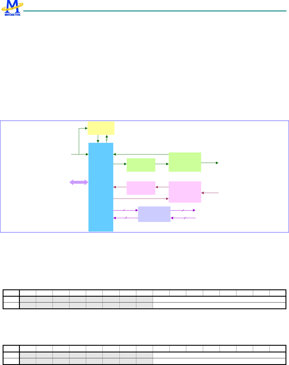
MT6235 GSM/GPRS Baseband Processor Data Sheet Revision 1.02
185/599 MediaTek Inc. Confidential
M16550A mode. The UART adds further functionality beyond M16550A mode. Each of the extended functions can be
selected individually under software control.
The UART provides more powerful enhancements than the industry-standard 16550:
z Hardware flow control. This feature is very useful when the ISR latency is hard to predict and control in the
embedded applications. The MCU is relieved of having to fetch the received data within a fixed amount of time.
z Output of an IR-compatible electrical pulse with a width 3/16 of that of a regular bit period.
Note: In order to enable any of the enhancements, the Enhanced Mode bit, EFR[4], must be set. If EFR[4] is not set,
IER[7:5], FCR[5:4], ISR[5:4] and MCR[7:6] cannot be written. The Enhanced Mode bit ensures that the UART is
backward compatible with software that has been written for 16C450 and 16550A devices.
Figure 22 shows the block diagram of the UART device.
APB
BUS
I/F
Baud Rate
Generator
TX FIFO TX Machine
RX FIFO
Modem
Control
RX Machine
Modem Outputs
Modem Inputs
APB Bus
clock
divisor
uart_tx_data
uart_rx_data
baud
Figure 22 Block Diagram of UART
4.8.2 Register Definitions
n = 1, 2, 3; for uart1, uart2 and uart3 respectively.
UARTn+0000h RX Buffer Register UARTn_RBR
Bit 15 14 13 12 11 10 9 8 7 6 5 4 3 2 1 0
Name RBR[7:0]
Type RO
RBR RX Buffer Register. Read-only register. The received data can be read by accessing this register.
Modified when LCR[7] = 0.
UARTn+0000h TX Holding Register UARTn_THR
Bit 15 14 13 12 11 10 9 8 7 6 5 4 3 2 1 0
Name THR[7:0]
Type WO

MT6235 GSM/GPRS Baseband Processor Data Sheet Revision 1.02
186/599 MediaTek Inc. Confidential
THR TX Holding Register. Write-only register. The data to be transmitted is written to this register, and then sent to
the PC via serial communication.
Modified when LCR[7] = 0.
UARTn+0004h Interrupt Enable Register UARTn_IER
Bit 15 14 13 12 11 10 9 8 7 6 5 4 3 2 1 0
Name CTSI RTSI XOFFI X EDSSI ELSI ETBEI ERBFI
Type R/W
Reset 0
IER By storing a ‘1’ to a specific bit position, the interrupt associated with that bit is enabled. Otherwise, the interrupt
is disabled.
IER[3:0] are modified when LCR[7] = 0.
IER[7:4] are modified when LCR[7] = 0 & EFR[4] = 1.
CTSI Masks an interrupt that is generated when a rising edge is detected on the CTS modem control line.
Note: This interrupt is only enabled when hardware flow control is enabled.
0 Unmask an interrupt that is generated when a rising edge is detected on the CTS modem control line.
1 Mask an interrupt that is generated when a rising edge is detected on the CTS modem control line.
RTSI Masks an interrupt that is generated when a rising edge is detected on the RTS modem control line.
Note: This interrupt is only enabled when hardware flow control is enabled.
0 Unmask an interrupt that is generated when a rising edge is detected on the RTS modem control line.
1 Mask an interrupt that is generated when a rising edge is detected on the RTS modem control line.
XOFFI Masks an interrupt that is generated when an XOFF character is received.
Note: This interrupt is only enabled when software flow control is enabled.
0 Unmask an interrupt that is generated when an XOFF character is received.
1 Mask an interrupt that is generated when an XOFF character is received.
EDSSI When set ("1"), an interrupt is generated if DDCD, TERI, DDSR or DCTS (MSR[4:1]) becomes set.
0 No interrupt is generated if DDCD, TERI, DDSR or DCTS (MSR[4:1]) becomes set.
1 An interrupt is generated if DDCD, TERI, DDSR or DCTS (MSR[4:1]) becomes set.
ELSI When set ("1"), an interrupt is generated if BI, FE, PE or OE (LSR[4:1]) becomes set.
0 No interrupt is generated if BI, FE, PE or OE (LSR[4:1]) becomes set.
1 An interrupt is generated if BI, FE, PE or OE (LSR[4:1]) becomes set.
ETBEI When set ("1"), an interrupt is generated if the TX Holding Register is empty or the contents of the TX FIFO
have been reduced to its Trigger Level.
0 No interrupt is generated if the TX Holding Register is empty or the contents of the TX FIFO have been
reduced to its Trigger Level.
1 An interrupt is generated if the TX Holding Register is empty or the contents of the TX FIFO have been
reduced to its Trigger Level
ERBFI When set ("1"), an interrupt is generated if the RX Buffer contains data.
0 No interrupt is generated if the RX Buffer contains data.
1 An interrupt is generated if the RX Buffer contains data.
UARTn+0008h Interrupt Identification Register UARTn_IIR
Bit 15 14 13 12 11 10 9 8 7 6 5 4 3 2 1 0
Name FIFOE ID4 ID3 ID2 ID1 ID0 NINT
Type RO

MT6235 GSM/GPRS Baseband Processor Data Sheet Revision 1.02
187/599 MediaTek Inc. Confidential
Reset 0 0 0 0 0 0 0 1
IIR Identify if there are pending interrupts; ID4 and ID3 are presented only when EFR[4] = 1.
The following table gives the IIR[5:0] codes associated with the possible interrupts:
IIR[5:0] Priority Level Interrupt Source
000001 - No interrupt pending
000110 1 Line Status Interrupt BI, FE, PE or OE set in LSR
000100 2 RX Data Received RX Data received or RX Trigger Level reached.
001100 2 RX Data Timeout Timeout on character in RX FIFO.
000010 3 TX Holding Register Empty TX Holding Register empty or TX FIFO Trigger Level reached.
000000 4 Modem Status change DDCD, TERI, DDSR or DCTS set in MSR
010000 5 Software Flow Control XOFF Character received
100000 6 Hardware Flow Control CTS or RTS Rising Edge
Table 17 The IIR[5:0] codes associated with the possible interrupts
Line Status Interrupt: A RX Line Status Interrupt (IIR[5:0`] == 000110b) is generated if ELSI (IER[2]) is set and any of BI,
FE, PE or OE (LSR[4:1]) becomes set. The interrupt is cleared by reading the Line Status Register.
RX Data Received Interrupt: A RX Received interrupt (IER[5:0] == 000100b) is generated if EFRBI (IER[0]) is set and
either RX Data is placed in the RX Buffer Register or the RX Trigger Level is reached. The interrupt is cleared by reading
the RX Buffer Register or the RX FIFO (if enabled).
RX Data Timeout Interrupt:
When virtual FIFO mode is disabled, RX Data Timeout Interrupt is generated if all of the following apply:
1. FIFO contains at least one character;
2. The most recent character was received longer than four character periods ago (including all start, parity and stop bits);
3. The most recent CPU read of the FIFO was longer than four character periods ago.
The timeout timer is restarted on receipt of a new byte from the RX Shift Register, or on a CPU read from the RX FIFO.
The RX Data Timeout Interrupt is enabled by setting EFRBI (IER[0]) to 1, and is cleared by reading RX FIFO.
When virtual FIFO mode is enabled, RX Data Timeout Interrupt is generated if all of the following apply:
1. FIFO is empty;
2. The most recent character was received longer than four character periods ago (including all start, parity and stop bits);
3. The most recent CPU read of the FIFO was longer than four character periods ago.
The timeout timer is restarted on receipt of a new byte from the RX Shift Register.
RX Holding Register Empty Interrupt: A TX Holding Register Empty Interrupt (IIR[5:0] = 000010b) is generated if ETRBI
(IER[1]) is set and either the TX Holding Register or, if FIFOs are enabled, the TX FIFO becomes empty. The interrupt is
cleared by writing to the TX Holding Register or TX FIFO if FIFO enabled.

MT6235 GSM/GPRS Baseband Processor Data Sheet Revision 1.02
188/599 MediaTek Inc. Confidential
Modem Status Change Interrupt: A Modem Status Change Interrupt (IIR[5:0] = 000000b) is generated if EDSSI (IER[3]) is
set and either DDCD, TERI, DDSR or DCTS (MSR[3:0]) becomes set. The interrupt is cleared by reading the Modem
Status Register.
Software Flow Control Interrupt: A Software Flow Control Interrupt (IIR[5:0] = 010000b) is generated if Software Flow
Control is enabled and XOFFI (IER[5]) becomes set, indicating that an XOFF character has been received. The interrupt
is cleared by reading the Interrupt Identification Register.
Hardware Flow Control Interrupt: A Hardware Flow Control Interrupt (IER[5:0] = 100000b) is generated if Hardware Flow
Control is enabled and either RTSI (IER[6]) or CTSI (IER[7]) becomes set indicating that a rising edge has been detected
on either the RTS/CTS Modem Control line. The interrupt is cleared by reading the Interrupt Identification Register.
UARTn+0008h FIFO Control Register UARTn_FCR
Bit 15 14 13 12 11 10 9 8 7 6 5 4 3 2 1 0
Name RFTL1RFTL0 TFTL1 TFTL0 DMA1 CLRT CLRR FIFOE
Type WO
FCR FCR is used to control the trigger levels of the FIFOs, or flush the FIFOs.
FCR[7:6] is modified when LCR != BFh
FCR[5:4] is modified when LCR != BFh & EFR[4] = 1
FCR[4:0] is modified when LCR != BFh
FCR[7:6] RX FIFO trigger threshold
0 1
1 6
2 12
3 RXTRIG
FCR[5:4] TX FIFO trigger threshold
0 1
1 4
2 8
3 14 (FIFOSIZE - 2)
DMA1 This bit determines the DMA mode, which the TXRDY and RXRDY pins support. TXRDY and RXRDY act to
support single-byte transfers between the UART and memory (DMA mode 0) or multiple byte transfers (DMA
mode1). Note that this bit has no effect unless the FIFOE bit is set as well
0 The device operates in DMA Mode 0.
1 The device operates in DMA Mode 1.
TXRDY – mode0: Goes active (low) when the TX FIFO or the TX Holding Register is empty. Becomes inactive
when a byte is written to the Transmit channel.
TXRDY – mode1: Goes active (low) when there are no characters in the TX FIFO. Becomes inactive when the
TX FIFO is full.
RXRDY – mode0: Becomes active (low) when at least one character is in the RX FIFO or the RX Buffer Register
is full. Becomes inactive when there are no more characters in the RX FIFO or RX Buffer register.
RXRDY – mode1: Becomes active (low) when the RX FIFO Trigger Level is reached or an RX FIFO Character
Timeout occurs. Goes inactive when the RX FIFO is empty.
CLRT Clear Transmit FIFO. This bit is self-clearing.
0 Leave TX FIFO intact.

MT6235 GSM/GPRS Baseband Processor Data Sheet Revision 1.02
189/599 MediaTek Inc. Confidential
1 Clear all the bytes in the TX FIFO.
CLRR Clear Receive FIFO. This bit is self-clearing.
0 Leave RX FIFO intact.
1 Clear all the bytes in the RX FIFO.
FIFOE FIFO Enabled. This bit must be set to 1 for any of the other bits in the registers to have any effect.
0 Disable both the RX and TX FIFOs.
1 Enable both the RX and TX FIFOs.
UARTn+000Ch Line Control Register UARTn_LCR
Bit 15 14 13 12 11 10 9 8 7 6 5 4 3 2 1 0
Name DLAB SB SP EPS PEN STB WLS1 WLS0
Type R/W
Reset 0 0 0 0 0 0 0 0
LCR Line Control Register. Determines characteristics of serial communication signals.
Modified when LCR[7] = 0.
DLAB Divisor Latch Access Bit.
0 The RX and TX Registers are read/written at Address 0 and the IER register is read/written at Address 4.
1 The Divisor Latch LS is read/written at Address 0 and the Divisor Latch MS is read/written at Address 4.
SB Set Break
0 No effect
1 SOUT signal is forced into the “0” state.
SP Stick Parity
0 No effect.
1 The Parity bit is forced into a defined state, depending on the states of EPS and PEN:
If EPS=1 & PEN=1, the Parity bit is set and checked = 0.
If EPS=0 & PEN=1, the Parity bit is set and checked = 1.
EPS Even Parity Select
0 When EPS=0, an odd number of ones is sent and checked.
1 When EPS=1, an even number of ones is sent and checked.
PEN Parity Enable
0 The Parity is neither transmitted nor checked.
1 The Parity is transmitted and checked.
STB Number of STOP bits
0 One STOP bit is always added.
1 Two STOP bits are added after each character is sent; unless the character length is 5 when 1 STOP bit is
added.
WLS1, 0 Word Length Select.
0 5 bits
1 6 bits
2 7 bits
3 8 bits
UARTn+0010h Modem Control Register UARTn_MCR
Bit 15 14 13 12 11 10 9 8 7 6 5 4 3 2 1 0
MT6235 GSM/GPRS Baseband Processor Data Sheet Revision 1.02
190/599 MediaTek Inc. Confidential
Name
X
OFF
STAT
US
IR
ENAB
LE X LOOP OUT2 OUT1 RTS DTR
Type R/W
Reset 0 0 0 0 0 0 0 0
MCR Modem Control Register. Control interface signals of the UART.
MCR[4:0] are modified when LCR[7] = 0,
MCR[7:6] are modified when LCR[7] = 0 & EFR[4] = 1.
XOFF Status This is a read-only bit.
0 When an XON character is received.
1 When an XOFF character is received.LOOP Loop-back control bit.
0 No loop-back is enabled.
1 Loop-back mode is enabled.
OUT2 Controls the state of the output NOUT2, even in loop mode.
0 NOUT2=1.
1 NOUT2=0.
OUT1 Controls the state of the output NOUT1, even in loop mode.
0 NOUT1=1.
1 NOUT1=0.
RTS Controls the state of the output NRTS, even in loop mode.
0 NRTS=1.
1 NRTS=0.
DTR Control the state of the output NDTR, even in loop mode.
0 NDTR=1.
1 NDTR=0.
UARTn+0014h Line Status Register UARTn_LSR
Bit 15 14 13 12 11 10 9 8 7 6 5 4 3 2 1 0
Name FIFOE
RR TEMT THRE BI FE PE OE DR
Type R/W
Reset 0 1 1 0 0 0 0 0
LSR Line Status Register.
Modified when LCR[7] = 0.
FIFOERR RX FIFO Error Indicator.
0 No PE, FE, BI set in the RX FIFO.
1 Set to 1 when there is at least one PE, FE or BI in the RX FIFO.
TEMT TX Holding Register (or TX FIFO) and the TX Shift Register are empty.
0 Empty conditions below are not met.
1 If FIFOs are enabled, the bit is set whenever the TX FIFO and the TX Shift Register are empty. If FIFOs are
disabled, the bit is set whenever TX Holding Register and TX Shift Register are empty.
THRE Indicates if there is room for TX Holding Register or TX FIFO is reduced to its Trigger Level.
0 Reset whenever the contents of the TX FIFO are more than its Trigger Level (FIFOs are enabled), or
whenever TX Holding Register is not empty(FIFOs are disabled).

MT6235 GSM/GPRS Baseband Processor Data Sheet Revision 1.02
191/599 MediaTek Inc. Confidential
1 Set whenever the contents of the TX FIFO are reduced to its Trigger Level (FIFOs are enabled), or whenever
TX Holding Register is empty and ready to accept new data (FIFOs are disabled).
BI Break Interrupt.
0 Reset by the CPU reading this register
1 If the FIFOs are disabled, this bit is set whenever the SIN is held in the 0 state for more than one transmission
time (START bit + DATA bits + PARITY + STOP bits).
If the FIFOs are enabled, this error is associated with a corresponding character in the FIFO and is flagged
when this byte is at the top of the FIFO. When a break occurs, only one zero character is loaded into the
FIFO: the next character transfer is enabled when SIN goes into the marking state and receives the next valid
start bit.
FE Framing Error.
0 Reset by the CPU reading this register
1 If the FIFOs are disabled, this bit is set if the received data did not have a valid STOP bit. If the FIFOs are
enabled, the state of this bit is revealed when the byte it refers to is the next to be read.
PE Parity Error
0 Reset by the CPU reading this register
1 If the FIFOs are disabled, this bit is set if the received data did not have a valid parity bit. If the FIFOs are
enabled, the state of this bit is revealed when the referred byte is the next to be read.
OE Overrun Error.
0 Reset by the CPU reading this register.
1 If the FIFOs are disabled, this bit is set if the RX Buffer was not read by the CPU before new data from the
RX Shift Register overwrote the previous contents.
If the FIFOs are enabled, an overrun error occurs when the RX FIFO is full and the RX Shift Register
becomes full. OE is set as soon as this happens. The character in the Shift Register is then overwritten, but
not transferred to the FIFO.
DR Data Ready.
0 Cleared by the CPU reading the RX Buffer or by reading all the FIFO bytes.
1 Set by the RX Buffer becoming full or by a byte being transferred into the FIFO.
UARTn+0018h Modem Status Register UARTn_MSR
Bit 15 14 13 12 11 10 9 8 7 6 5 4 3 2 1 0
Name DCD RI DSR CTS DDCD TERI DDSR DCTS
Type R/W R/W R/W R/W R/W R/W R/W R/W
Reset Input Input Input Input 0 0 0 0
Note: After a reset, D4-D7 are inputs. A modem status interrupt can be cleared by writing ‘0’ or set by writing ‘1’ to this
register. D0-D3 can be written to.
Modified when LCR[7] = 0.
MSR Modem Status Register
DCD Data Carry Detect.
When Loop = "0", this value is the complement of the NDCD input signal.
When Loop = "1", this value is equal to the OUT2 bit in the Modem Control Register.
RI Ring Indicator.
When Loop = "0", this value is the complement of the NRI input signal.

MT6235 GSM/GPRS Baseband Processor Data Sheet Revision 1.02
192/599 MediaTek Inc. Confidential
When Loop = "1", this value is equal to the OUT1 bit in the Modem Control Register.
DSR Data Set Ready
When Loop = "0", this value is the complement of the NDSR input signal.
When Loop = "1", this value is equal to the DTR bit in the Modem Control Register.
CTS Clear To Send.
When Loop = "0", this value is the complement of the NCTS input signal.
When Loop = "1", this value is equal to the RTS bit in the Modem Control Register.
DDCD Delta Data Carry Detect.
0 The state of DCD has not changed since the Modem Status Register was last read
1 Set if the state of DCD has changed since the Modem Status Register was last read.
TERI Trailing Edge Ring Indicator
0 The NRI input does not change since this register was last read.
1 Set if the NRI input changes from “0” to “1” since this register was last read.
DDSR Delta Data Set Ready
0 Cleared if the state of DSR has not changed since this register was last read.
1 Set if the state of DSR has changed since this register was last read.
DCTS Delta Clear To Send
0 Cleared if the state of CTS has not changed since this register was last read.
1 Set if the state of CTS has changed since this register was last read.
UARTn+001Ch Scratch Register UARTn_SCR
Bit 15 14 13 12 11 10 9 8 7 6 5 4 3 2 1 0
Name SCR[7:0]
Type R/W
A general purpose read/write register. After reset, its value is un-defined.
Modified when LCR[7] = 0.
UARTn+0000h Divisor Latch (LS) UARTn_DLL
Bit 15 14 13 12 11 10 9 8 7 6 5 4 3 2 1 0
Name DLL[7:0]
Type R/W
Reset 1
UARTn+0004h Divisor Latch (MS) UARTn_DLM
Bit 15 14 13 12 11 10 9 8 7 6 5 4 3 2 1 0
Name DLL[7:0]
Type R/W
Reset 0
Note: DLL & DLM can only be updated if DLAB is set (“1”).. Note too that division by 1 generates a BAUD signal that
is constantly high.
Modified when LCR[7] = 1.
MT6235 GSM/GPRS Baseband Processor Data Sheet Revision 1.02
193/599 MediaTek Inc. Confidential
The table below shows the divisor needed to generate a given baud rate from CLK inputs of 13, 26 MHz and 52 MHz.
The effective clock enable generated is 16 x the required baud rate.
BAUD 13MHz 26MHz 52MHz
110 7386 14773 29545
300 2708 5417 10833
1200 677 1354 2708
2400 338 677 1354
4800 169 339 677
9600 85 169 339
19200 42 85 169
38400 21 42 85
57600 14 28 56
115200 6 14 28
Table 18 Divisor needed to generate a given baud rate
UARTn+0008h Enhanced Feature Register UARTn_EFR
Bit 15 14 13 12 11 10 9 8 7 6 5 4 3 2 1 0
Name
A
UTO
CTS
A
UTO
RTS D5 ENAB
LE -E SW FLOW CONT[3:0]
Type R/W R/W R/W R/W R/W
Reset 0 0 0 0 0
*NOTE: Only when LCR=BF’h
Auto CTS Enables hardware transmission flow control
0 Disabled.
1 Enabled.
Auto RTS Enables hardware reception flow control
0 Disabled.
1 Enabled.
Enable-E Enable enhancement features.
0 Disabled.
1 Enabled.
CONT[3:0] Software flow control bits.
00xx No TX Flow Control
10xx Transmit XON1/XOFF1 as flow control bytes
01xx Transmit XON2/XOFF2 as flow control bytes
11xx Transmit XON1 & XON2 and XOFF1 & XOFF2 as flow control words
xx00 No RX Flow Control
xx10 Receive XON1/XOFF1 as flow control bytes
xx01 Receive XON2/XOFF2 as flow control bytes
xx11 Receive XON1 & XON2 and XOFF1 & XOFF2 as flow control words
UARTn+0010h XON1 UARTn_XON1
Bit 15 14 13 12 11 10 9 8 7 6 5 4 3 2 1 0
MT6235 GSM/GPRS Baseband Processor Data Sheet Revision 1.02
194/599 MediaTek Inc. Confidential
Name XON1[7:0]
Type R/W
Reset 0
UARTn+0014h XON2 UARTn_XON2
Bit 15 14 13 12 11 10 9 8 7 6 5 4 3 2 1 0
Name XON2[7:0]
Type R/W
Reset 0
UARTn+0018h XOFF1 UARTn_XOFF1
Bit 15 14 13 12 11 10 9 8 7 6 5 4 3 2 1 0
Name XOFF1[7:0]
Type R/W
Reset 0
UARTn+001Ch XOFF2 UARTn_XOFF2
Bit 15 14 13 12 11 10 9 8 7 6 5 4 3 2 1 0
Name XOFF2[7:0]
Type R/W
Reset 0
*Note: XON1, XON2, XOFF1, XOFF2 are valid only when LCR=BFh.
UARTn+0020h AUTOBAUD_EN UARTn_AUTOBAUD
_EN
Bit 15 14 13 12 11 10 9 8 7 6 5 4 3 2 1 0
Name AUTO
_EN
Type R/W
Reset 0
AUTOBAUD_EN Auto-baud enable signal
0 Auto-baud function disable
1 Auto-baud function enable
UARTn+0024h HIGH SPEED UART UARTn_HIGHSPEED
Bit 15 14 13 12 11 10 9 8 7 6 5 4 3 2 1 0
Name SPEED [1:0]
Type R/W
Reset 0
SPEED UART sample counter base
0 based on 16*baud_pulse, baud_rate = system clock frequency/16/{DLH, DLL}
1 based on 8*baud_pulse, baud_rate = system clock frequency/8/{DLH, DLL}
2 based on 4*baud_pulse, baud_rate = system clock frequency/4/{DLH, DLL}
3 based on sampe_count * baud_pulse, baud_rate = system clock frequency / sampe_count

MT6235 GSM/GPRS Baseband Processor Data Sheet Revision 1.02
195/599 MediaTek Inc. Confidential
The table below shows the divisor needed to generate a given baud rate from CLK inputs of 13M Hz based on different
HIGHSPEED value.
BAUD HIGHSPEED = 0 HIGHSPEED = 1 HIGHSPEED = 2
110 7386 14773 29545
300 2708 7386 14773
1200 677 2708 7386
2400 338 677 2708
4800 169 338 677
9600 85 169 338
19200 42 85 169
38400 21 42 85
57600 14 21 42
115200 7 14 21
230400 * 7 14
460800 * * 7
921600 * * *
Table 19 Divisor needed to generate a given baud rate from 13MHz based on different HIGHSPEED value
The table below shows the divisor needed to generate a given baud rate from CLK inputs of 26 MHz based on different
HIGHSPEED value.
BAUD HIGHSPEED = 0 HIGHSPEED = 1 HIGHSPEED = 2
110 14773 29545 59091
300 5417 14773 29545
1200 1354 5417 14773
2400 677 1354 5417
4800 339 677 1354
9600 169 339 667
19200 85 169 339
38400 42 85 169
57600 28 42 85
115200 14 28 42
230400 7 14 28
460800 * 7 14
921600 * * 7
Table 20 Divisor needed to generate a given baud rate from 26 MHz based on different HIGHSPEED value
MT6235 GSM/GPRS Baseband Processor Data Sheet Revision 1.02
196/599 MediaTek Inc. Confidential
The table below shows the divisor needed to generate a given baud rate from CLK inputs of 52MHz based on different
HIGHSPEED value.
BAUD HIGHSPEED = 0 HIGHSPEED = 1 HIGHSPEED = 2
110 29545 59091 118182
300 10833 29545 59091
1200 2708 10833 29545
2400 1354 2708 10833
4800 677 1354 2708
9600 339 677 1354
19200 169 339 677
38400 85 169 339
57600 56 85 169
115200 28 56 85
230400 14 28 56
460800 7 14 28
921600 * 7 14
Table 21 Divisor needed to generate a given baud rate from 52 MHz based on different HIGHSPEED value
UARTn+0028h SAMPLE_COUNT UARTn_SAMPLE_COUN
T
Bit 15 14 13 12 11 10 9 8 7 6 5 4 3 2 1 0
Name SAMPLECOUNT [7:0]
Type R/W
Reset 0
When HIGHSPEED=3, the sample_count is the threshold value for UART sample counter (sample_num).
Count from 0 to sample_count.
For example, this register shall be set to 13 when you want to diveded by 14.
UARTn+002Ch SAMPLE_POINT UARTn_SAMPLE_POINT
Bit 15 14 13 12 11 10 9 8 7 6 5 4 3 2 1 0
Name SAMPLEPOINT [7:0]
Type R/W
Reset Ffh
When HIGHSPEED=3, UART gets the input data when sample_count=sample_num.
e.g. system clock = 13MHz, 921600 = 13000000 / 14
sample_count = 14 and sample point = 7 (sample the central point to decrease the inaccuracy)
The SAMPLE_POINT is usually (SAMPLE_COUNT/2).
UARTn+0030h AUTOBAUD_REG UARTn_AUTOBAUD_RE
G
Bit 15 14 13 12 11 10 9 8 7 6 5 4 3 2 1 0

MT6235 GSM/GPRS Baseband Processor Data Sheet Revision 1.02
197/599 MediaTek Inc. Confidential
Name BAUD_STAT[3:0] BAUDRATE[3:0]
Type RO RO
Reset 0 0
BAUD_RATE Autobaud baud rate
0 115200
1 57600
2 38400
3 19200
4 9600
5 4800
6 2400
7 1200
8 300
9 110
BAUDSTAT Autobaud format
0 Autobaud is detecting
1 AT_7N1
2 AT_7O1
3 AT_7E1
4 AT_8N1
5 AT_8O1
6 AT_8E1
7 at_7N1
8 at_7E1
9 at_7O1
10 at_8N1
11 at_8E1
12 at_8O1
13 Autobaud detection fails
UARTn+0034h Rate Fix Address UARTn_RATEFIX_AD
Bit 15 14 13 12 11 10 9 8 7 6 5 4 3 2 1 0
Name REST
RICT FREQ
_SEL
AUTO
BAUD
_RAT
E_FIX
RXTE_
FIX
Type R/W R/W R/W R/W
Reset 0 0 0 0
RATE_FIX When you set "rate_fix"(34H[0]), you can transmit and receive data only if 1) the f13m_en
is enable and the freq_sel (34H[2]) is set to 1, or
2) the f26m_en is enable and the freq_sel (34H[2]) is set to 0.
AUTOBAUD_RATE_FIX When you set "autobaud_rate_fix"(34H[1]), you can tx/rx the autobaud packet only if
1) the f13m_en is enable and the freq_sel (34H[2]) is set to 1, or
2) the f26m_en is enable and the freq_sel (34H[2]) is set to 0.
MT6235 GSM/GPRS Baseband Processor Data Sheet Revision 1.02
198/599 MediaTek Inc. Confidential
FREQ_SEL
0 Select f26m_en for rate_fix and autobaud_rate_fix
1 Select f13m_en for rate_fix and autobaud_rate_fix
RESTRICT The "restrict" (34H[3]) is used to set a more condition for the autobaud fsm starting point
UARTn+0038h AUTOBAUDSAMPLE UARTn_AUTOBAUDSAM
PLE
Bit 15 14 13 12 11 10 9 8 7 6 5 4 3 2 1 0
Name AUTOBAUDSAMPLE
Type R/W R/W R/W R/W R/W R/W R/W
Reset dh
Since the system clock may change, autobaud sample duration should change as system clock changes.
When system clock = 13MHz, autobaudsample = 6; when system clock = 26MHz, autobaudsample = 13.
UARTn+003Ch Guard time added register UARTn_GUARD
Bit 15 14 13 12 11 10 9 8 7 6 5 4 3 2 1 0
Name GUARD_
EN GUARD_CNT[3:0]
Type R/W R/W R/W R/W R/W
Reset 0 0 0 0 0
GUARD_CNT Guard interval count value. Guard interval = (1/(system clock / div_step / div )) * GUARD_CNT.
GUARD_EN Guard interval add enable signal.
0 No guard interval added.
1 Add guard interval after stop bit.
UARTn+0040h Escape character register UARTn_ESCAPE_DAT
Bit 15 14 13 12 11 10 9 8 7 6 5 4 3 2 1 0
Name ESCAPE_DAT[7:0]
Type WO
Reset FFh
ESCAPE_DAT Escape character added before software flow control data and escape character, i.e. if tx data is xon (31h),
with esc_en =1, uart transmits data as esc + CEh (~xon).
UARTn+0044h Escape enable register UARTn_ESCAPE_EN
Bit 15 14 13 12 11 10 9 8 7 6 5 4 3 2 1 0
Name ESC_E
N
Type R/W
Reset 0
ESC_EN Add escape character in transmitter and remove escape character in receiver by UART.
0 Do not deal with the escape character.
1 Add escape character in transmitter and remove escape character in receiver.
UARTn+0048h Sleep enable register UARTn_SLEEP_EN
Bit 15 14 13 12 11 10 9 8 7 6 5 4 3 2 1 0

MT6235 GSM/GPRS Baseband Processor Data Sheet Revision 1.02
199/599 MediaTek Inc. Confidential
Name SELL
P_EN
Type R/W
Reset 0
SLEEP_EN For sleep mode issue
0 Do not deal with sleep mode indicate signal
1 To activate hardware flow control or software control according to software initial setting when chip enters
sleep mode. Releasing hardware flow when chip wakes up; but for software control, uart sends xon when
awaken and when FIFO does not reach threshold level.
UARTn+004Ch Virtual FIFO enable register UARTn_VFIFO_EN
Bit 15 14 13 12 11 10 9 8 7 6 5 4 3 2 1 0
Name VFIFO
_EN
Type R/W
Reset 0
VFIFO_EN Virtual FIFO mechanism enable signal.
0 Disable VFIFO mode.
1 Enable VFIFO mode. When virtual mode is enabled, the flow control is based on the DMA threshold, and
generates a timeout interrupt for DMA.
UARTn+0050h Rx Trigger Address UARTn_RXTRI_
AD
Bit 15 14 13 12 11 10 9 8 7 6 5 4 3 2 1 0
Name RXTRIG[3:0]
Type R/W
Reset 0
RXTRIG When {rtm,rtl}=2’b11, The Rx FIFO threshold will be Rxtrig.
4.9 IrDA Framer
4.9.1 General Description
IrDA framer is implemented to reduce the CPU loading for IrDA transmissions by performing all the physical level
protocol framing in hardware. From a software perspective, the framer need only prepare and process the raw data for
transmission and reception. Generic DMA is required to move the data between IrDA framer’s internal FIFO and
software-designated memory. The IrDA framer supports IrDA SIR, MIR, and FIR modes of operation. SIR mode
includes operation from 9600bps ~ 115200bps, MIR includes operation at 567000bps or 1152000bps, and FIR mode
includes operation at 4Mbps.

MT6235 GSM/GPRS Baseband Processor Data Sheet Revision 1.02
200/599 MediaTek Inc. Confidential
4.9.2 Register Definitions
IRDA+0000h TX BUF and RX BUF BUF
Bit 15 14 13 12 11 10 9 8 7 6 5 4 3 2 1 0
Name BUF[7:0]
Type R/W
Reset 0
BUF IrDA Framer transmit or receive data.
A write to this register writes into the internal TX FIFO.
A read from this register reads from the internal RX FIFO.
IRDA+0004h TX BUF and RX BUF clear signal BUF_CLEAR
Bit 15 14 13 12 11 10 9 8 7 6 5 4 3 2 1 0
Name CLEAR
Type R/W
Reset 0
CLEAR SIR mode only. When CLEAR=1, both the TX and RX FIFO are cleared. This is used primarily for debug
purpose. Normal operation does not require this. This control signaled can only be issued under SIR mode.
IRDA+0008h Maximum Turn Around Time
Bit 15 14 13 12 11 10 9 8 7 6 5 4 3 2 1
Name MAX_T [13:0]
Type R/W
Reset 3E80h
MAX_T The maximum time that a station can hold the P/F bit. This parameter along with the baud rate parameter dictates
the maximum number of bytes that a station can transmit before passing the line to another station by transmitting
a frame with the P/F bit. This parameter is used by one station to indicate the maximum time the other station
can send before it must turn the link around. For baud rates less than 115200 kbps, 500 ms is the only valid value.
The default value is 500 ms.
IRDA+000Ch Minimum Turn Around Time MIN_T
Bit 15 14 13 12 11 10 9 8 7 6 5 4 3 2 1 0
Name MIN_T [15:0]
Type R/W
Reset FDE8h
MIN_T Minimum turn around time, the default value is 10 ms. The minimum turn around time parameter deals with the
time needed for a receiver to recover following saturation by transmission from the same device. This parameter
corresponds to the required time delay between the last byte of the last frame sent by a station and the point at
which it is ready to receive the first byte of a frame from another station, i.e. the latency for a transmit to complete
and be ready to receive.
IRDA+0010h Number of additional BOFs prefixed to the beginning
of a frame BOFS
Bit 15 14 13 12 11 10 9 8 7 6 5 4 3 2 1 0
Name TYPE BOFS [6:0]
MT6235 GSM/GPRS Baseband Processor Data Sheet Revision 1.02
201/599 MediaTek Inc. Confidential
Type R/W R/W
Reset 0 1011b
BOFs For SIR mode: the additional BOFs parameter indicates the number of additional flags needed at the beginning of
every frame. The main purpose for the additional BOFs is to provide a delay at the beginning of each frame for
devices with a long interrupt latency.
For MIR mode: This parameter indicates the number of double STA’s to transmit in the beginning. This value
should be set to 0 (for default 2 STA’s) for MIR mode, unless more are required.
For FIR mode: This parameter has no effect.
TYPE SIR mode only. Additional BOFs type.
1 BOF = C0h
0 BOF = FFh
IRDA+0014h Baud rate divisor DIV
Bit 15 14 13 12 11 10 9 8 7 6 5 4 3 2 1 0
Name DIV[15:0]
Type R/W
Reset 55h
DIV Transmit or receive rate divider. Rate = System clock frequency / DIV/ 16. The default value is 55h when in
contention mode. This divisor is also used to determine the RX FIFO timeout threshold.
IRDA+0018h Transmit frame size TX_FRAME_SIZ
E
Bit 15 14 13 12 11 10 9 8 7 6 5 4 3 2 1 0
Name TX_FRAME_SIZE[11:0]
Type R/W
Reset 40h
TX_FRAME_SIZE Transmit frame size; the default value is 64 when in contention mode.
IRDA+001Ch Receiving frame1 size RX_FRAME1_SI
ZE
Bit 15 14 13 12 11 10 9 8 7 6 5 4 3 2 1 0
Name RX_FRAME1_SIZE[11:0]
Type RO
Reset 0
RX_FRAME1_SIZE Reports the number of byte received. Includes only the A+C+I fields.
IRDA+0020h Transmit abort indication ABORT
Bit 15 14 13 12 11 10 9 8 7 6 5 4 3 2 1 0
Name ABOR
T
Type R/W
Reset 0
ABORT SIR mode only. When set 1, the framer transmits an abort sequence and closes the frame without an FCS field or
an ending flag.
Note: Tx abort can be achieved in MIR and FIR by simply disabling the tx_en signal.
MT6235 GSM/GPRS Baseband Processor Data Sheet Revision 1.02
202/599 MediaTek Inc. Confidential
IRDA+0024h IrDA framer transmit enable signal
Bit 15 14 13 12 11 10 9 8 7 6 5 4 3 2 1
Name TX_ONE TXINVER
T MOD
E
Type R/W R/W R/W
Reset 0 0 0
TX_EN Transmit enable.
MODE SIR mode only. Modulation type selection.
0 3/16 modulation
1 1.61us
TXINVERT Invert the transmit signal.
0 Transmit signal is not inverted.
1 Transmit signal is inverted.
TX_ONE: Controls the transmit enable signal is one or not.
0 tx_en is not de-asserted until software programs a so.
1 tx_en is de-asserted (i.e. transmit disabled) automatically after one frame has been sent.
IRDA+0028h IrDA framer receive enable signal RX_EN
Bit 15 14 13 12 11 10 9 8 7 6 5 4 3 2 1 0
Name RX_ON
E
RXINVE
RT
RX_E
N
Type R/W R/W R/W
Reset 0 0 0
RX_EN Receive enable.
RXINVERT Invert the receive signal.
0 Receive signal is not inverted.
1 Receive signal is inverted.
RX_ONE Disable receive when get one frame.
0 rx_en is not de-asserted until software programs so.
1 rx_en is de-asserted (i.e. transmit disabled) automatically after one frame has been sent.
IRDA+002Ch FIFO trigger level indication TRIGGER
Bit 15 14 13 12 11 10 9 8 7 6 5 4 3 2 1 0
Name RX_TRIG[ TX_TRIG
Type R/W R/W
Reset 0 0
TX_TRIG TX FIFO interrupt trigger threshold. When the amount of data in the TX FIFO is less than the specified
amount, dma req is asserted. (When TX_TRIG = 03, dma req is always asserted as long as FIFO is not full.)
00 0 byte
01 1 byte
02 8 byte
03 16 byte
RX_TRIG RX FIFO interrupt trigger threshold. When the amount of data in RX FIFO is above the specified amount,
dma req is asserted.
00 1 byte

MT6235 GSM/GPRS Baseband Processor Data Sheet Revision 1.02
203/599 MediaTek Inc. Confidential
01 2 byte
02 3 byte
IRDA+0030h IRQ enable signal IRQ_ENABLE
Bit 15 14 13 12 11 10 9 8 7 6 5 4 3 2 1 0
Name 2NDR
X_CO
MP
RXRES
TART
THRES
HTIME
OUT
FIFOTI
MEOU
T
TXABO
RT
RXABO
RT
MAXTI
MEOU
T
MINTI
MEOU
T
RXCO
MPLET
E
TXCO
MPLET
E
ERRO
R
RXTHR
ES
TXTHR
ES
Type R/W R/W R/W R/W R/W R/W R/W R/W R/W R/W R/W R/W
Reset 0 0 0 0 0 0 0 0 0 0 0 0
TXRES Transmit data reaches the threshold level. (For debug only. Should be set to 0.)
0 No interrupt is generated.
1 Interrupt is generated when transmit FIFO size reaches threshold.
RXRES Receive data reaches the threshold level. (For debug only. Should be set to 0.)
0 No interrupt is generated.
1 Interrupt is generated when receive FIFO size reaches threshold.
ERROR Error status interrupt enable.
0 No interrupt is generated.
1 Interrupt is generated when one of the error statuses occurs.
TXCOMPLETE Transmit one frame completely.
0 No interrupt is generated.
1 Interrupt is generated when transmitting one frame completely.
RXCOMPLETE Receive one frame completely.
0 No interrupt is generated.
1 Interrupt is generated when receiving one frame completely.
MINTIMEOUT Minimum time timeout.
0 No interrupt is generated.
1 Interrupt is generated when minimum timer is timed out.
MAXTIMEOUT Maximum time timeout.
0 No interrupt is generated.
1 Interrupt is generated when maximum timer is timed out.
RXABORT Receiving aborting frame.
0 No interrupt is generated.
1 Interrupt is generated when receiving aborting frame.
TXABORT SIR mode only. Transmitting aborting frame.
0 No interrupt is generated.
1 Interrupt is generated when transmitting aborting frame.
FIFOTIMEOUT FIFO timeout.
0 No interrupt is generated.
1 Interrupt is generated when FIFO timeout.
THRESHTIMEOUT Threshold time timeout.
0 No interrupt is generated.
1 Interrupt is generated when threshold timer is timed out.
RXRESTART SIR mode only. Receiving a new frame before one frame is received completely.
0 No interrupt is generated.
MT6235 GSM/GPRS Baseband Processor Data Sheet Revision 1.02
204/599 MediaTek Inc. Confidential
1 Interrupt is generated when receiving a new frame before one frame is received completely.
2NDRX_COMP Receiving second frame and get P/F bit.
0 No interrupt is generated.
1 Interrupt is generated when receiving second frame and get P/F bit completely.
IRDA+0034h Interrupt Status IRQ_STA
Bit 15 14 13 12 11 10 9 8 7 6 5 4 3 2 1 0
Name 2NDR
X_CO
MP
RXRES
TART
THRES
HTIME
OUT
FIFOTI
MEOU
T
TXABO
RT
RXABO
RT
MAXTI
MEOU
T
MINTI
MEOU
T
RXCO
MPLET
E
TXCO
MPLET
E
ERRO
R
RXTRE
S
TXTRE
S
Type RC RC RC RC RC RC RC RC RC RC RC RC RC
Reset 0 0 0 0 0 0 0 0 0 0 0 0 0
TXFIFO Transmit FIFO reaches threshold. (For debug only. Not recommended for normal usage.)
RXFIFO Receive FIFO reaches threshold. (For debug only. Not recommended for normal usage.)
ERROR Generated when any of status in Error Status register occurs.
Once the source of an interrupt is determined to be caused by an error (bit 2), the error status register should be
read. Once read, both the error status register and the interrupt source are read-cleared. If the error status
register indicates either a frame 1 or frame 2 error, the corresponding frame status register should be read.
TXCOMPLETE Transmitting one frame completely.
RXCOMPLETE Receiving one frame completely.
MINTIMEOUT Minimum turn around time timeout.
MAXTIMEOUT Maximum turn around time timeout.
RXABORT Receiving aborting frame.
TXABORT Transmitting aborting frame.
FIFOTIMEOUT FIFO is timeout.
THRESHTIMEOUT Threshold time timeout.
RXRESTART Receiving a new frame before one frame is received completely.
2NDRX_COMP Receiving second frame and get P/F bit completely.
IRDA+0038h ERROR STATUS register ERR_STATUS
Bit 15 14 13 12 11 10 9 8 7 6 5 4 3 2 1 0
Name
TX FIFO
UNDERR
UN
FRAME
2 DATA
ERR
FRAME
1 DATA
ERR
RESER
VED2
RESER
VED
OVER
RUN
RXSIZ
E
Type R/W R/W R/W R/W R/W R/W R/W
Reset 0 0 0 0 0 0 0
RXSIZE Receive frame size error.
OVERRUN Frame overrun.
RESERVED Reserved for future use.
RESERVED2 Reserved for future use.
FRAME1 DATA ERR Indicates that an error condition occurred in RX frame1. Must check the RX frame1 status.
FRAME2 DATA ERR Indicates that an error condition occurred in RX frame2. Must check the RX frame2 status.
TX FIFO UNDERRUN MIR and FIR mode only.
TX FIFO underrun has occurred. Data transmission is aborted. Software must reset the tx_en signal.
MT6235 GSM/GPRS Baseband Processor Data Sheet Revision 1.02
205/599 MediaTek Inc. Confidential
IRDA+003Ch Transceiver power on/off control. Transceiver mode
select.
TRANSCEIVER_
PDN
Bit 15 14 13 12 11 10 9 8 7 6 5 4 3 2 1 0
Name TXCVR
CONFIG
TX
MANUAL
TRANS_
PDN
Type R/W R/W R/W
Reset 0 0 0
TRANSCEIVER_PDN Used for power on/off control for external IrDA transceiver.
TX_MANUAL When txcvr config is set to 1, this bit can be used to select the operation mode of the external IrDA
transceiver (some transceivers require selection between high speed and low speed operating modes), by
software programming the desired sequence to transmit through the irda_txd pin.
TXCVR CONFIG
0 Irda_txd comes from core logic.
1 Irda_txd depends on tx_manual value.
IRDA+0040h Maximum number of receiving frame size RX_FRAME_MA
X
Bit 15 14 13 12 11 10 9 8 7 6 5 4 3 2 1 0
Name MAX_RX_FRAME_SIZE_
Type R/W
Reset 0
RX_FRAME_MAX Receive frame I field max size, when actual receiving frame size is larger than rx_frame_max,
RXSIZE is asserted. The maximum allowed I field size is 2048.
IRDA+0044h Threshold Time THRESH_T
Bit 15 14 13 12 11 10 9 8 7 6 5 4 3 2 1 0
Name DISCONNECT_TIME[15:0]
Type R/W
Reset bb8h
THRESHOLD TIME Threshold time; used to control the time a station waits without receiving a valid frame before
disconnecting the link. Associated with this is the time a station waits without receiving a valid frame
before sending a status indication to the service user layer.
IRDA+0048h Counter enable signal COUNT_ENABL
E
Bit 15 14 13 12 11 10 9 8 7 6 5 4 3 2 1 0
Name THRESH
_EN
MIN_E
N
MAX_E
N
Type R/W R/W R/W
Reset 0 0 0
COUNT_ENABLE Counter enable signals.
IRDA+004Ch Indication of system clock rate CLOCK_RATE
Bit 15 14 13 12 11 10 9 8 7 6 5 4 3 2 1 0
Name CLOCK_RAT
E

MT6235 GSM/GPRS Baseband Processor Data Sheet Revision 1.02
206/599 MediaTek Inc. Confidential
Type R/W
Reset 0
CLOCK_RATE SIR mode only Indication of the system clock rate.
0 26 MHz
1 52 MHz
2 13 MHz
IRDA+0050h System Clock Rate Fix RATE_FIX
Bit 15 14 13 12 11 10 9 8 7 6 5 4 3 2 1 0
Name MIR
TIMING
TUNE
CRC
REPOR
T
SIR
FRAMIN
G SET
RATE_F
IX
Type R/W R/W R/W R/W
Reset 0 0 0 0
RATE_FIX SIR mode only Fix the IrDA framer sample base clock rate as 13 MHz.
0 Clock rate based on clock_rate selection.
1 Clock rate fixed at 13 MHz.
SIR FRAMING SET SIR mode only. Framing error check condition.
0 Ignore the STOP bit of the last byte of a frame.
1 Check the STOP bit of the last byte of a frame.
CRC REPORT When set to 1, CRC error is reported via error status register and error interrupt.
MIR TIMING TUNE MIR mode only. For some transceivers, in MIR 0.576mbps mode, the RX output pulse does not
conform to IRDA specification. Therefore, this option is used to detect the RX output from those transceivers
correctly.
0 For transceivers that conform to spec.
1 For transceivers that do not conform to spec, and the RX output pulse is half of that specified.
IRDA+0054h RX Frame1 Status FRAME1_S
Bit 15 14 13 12 11 10 9 8 7 6 5 4 3 2 1
Name FIR STO
ERR FIR 4PPM
ERR
MIR
HDLC
ERR
UNKNOW_
ERROR
PF_DETEC
T CRC_FAI
Type R/W R/W R/W R/W R/W R/W
Reset 0 0 0 0 0 0
FRAME_ERROR SIR mode only. Framing error, i.e. STOP bit = 0.
0 No framing error
1 Framing error occurred
CRC_FAIL CRC check fail
2 CRC check successfully
3 CRC check fail
PF_DETECT P/F bit detect
0 Not a P/F bit frame
1 Detected P/F bit in this frame
UNKNOWN_ERROR SIR mode only. Receiving error data, i.e. escape character is followed by a character that is not an
ESC, BOF, or EOF character.
0 Data received correctly.

MT6235 GSM/GPRS Baseband Processor Data Sheet Revision 1.02
207/599 MediaTek Inc. Confidential
1 Unknown error occurred.
MIR HDLC ERR MIR mode only. MIR HDLC encoding error
0 No error
1 Error
FIR 4PPM ERR FIR mode only. FIR 4ppm encoding error
0 No error
1 Error
FIR STO ERR FIR mode only. FIR STO sequence error
0 No error
1 Error
IRDA+0058h RX Frame2 Status FRAME2_STAT
US
Bit 15 14 13 12 11 10 9 8 7 6 5 4 3 2 1 0
Name FIR STO
ERR
FIR
4PPM
ERR
MIR
HDLC
ERR
UNKNOW
_ERROR
PF_DETE
CT
CRC_FAI
L
FRAME_
ERROR
Type R/W R/W R/W R/W R/W R/W R/W
Reset 0 0 0 0 0 0 0
FRAME_ERROR SIR mode only. Framing error, i.e. STOP bit = 0
0 No framing error.
1 Framing error occurred.
CRC_FAIL CRC check fail.
0 CRC check successfully.
1 CRC check fail.
PF_DETECT P/F bit detect.
0 Not a P/F bit frame.
1 Detected P/F bit in this frame.
UNKNOWN_ERROR SIR mode only. Receiving error data, i.e. escape character is followed by a character that is not an
ESC, BOF, or EOF character.
0 Data receiving correctly.
1 Unknown error occurred.
MIR HDLC ERR MIR mode only. MIR HDLC encoding error.
0 No error
1 Error
FIR 4PPM ERR FIR mode only.FIR 4ppm encoding error
0 No error
1 Error
FIR STO ERR FIR mode only.FIR STO sequence error
0 No error
1 Error
IRDA+005Ch Receiving frame2 size RX_FRAME2_SI
ZE
Bit 15 14 13 12 11 10 9 8 7 6 5 4 3 2 1 0

MT6235 GSM/GPRS Baseband Processor Data Sheet Revision 1.02
208/599 MediaTek Inc. Confidential
Name RX_FRAME2_SIZE[11:0]
Type RO
Reset 0
RX_FRAME2_SIZE Reports the number of byte received. Includes only the A+C+I fields.
IRDA+0060h Irda Mode Select IRDA
_
Bit 15 14 13 12 11 10 9 8 7 6 5 4 3 2 1
Name MIR SPEED IRD
A
Type R/W
R
Reset 0
IRDA MODE Selects the IrDA operating mode. NOTE: this mode selection cannot be issued while transmitting or
receiving.
00 IR mode
01 MIR mode
10 FIR mode
MIR SPEED Select the MIR speed.
0 0.576 Mbps
1 1.152 Mbps
IRDA+0064h Fifo Status FIFO_STAT
Bit 15 14 13 12 11 10 9 8 7 6 5 4 3 2 1 0
Name RX FIFO
HOLD
TX FIFO
WR FULL
TX FIFO
RD
EMPTY
RX FIFO
WR FULL
RX FIFO
RD
EMPTY
Type RO RO RO RO RO
Reset 0 0 1 0 1
This register indicates the real time FIFO status, for monitoring purposes.
4.10 Real Time Clock
4.10.1 General Description
The Real Time Clock (RTC) module provides time and data information. The clock is based on a 32.768KHz oscillator
with an independent power supply. When the mobile handset is powered off, a dedicated regulator supplies the RTC block.
If the main battery is not present, a backup supply such as a small mercury cell battery or a large capacitor is used. In
addition to providing timing data, an alarm interrupt is generated and can be used to power up the baseband core via the
BBWAKEUP pin. Regulator interrupts corresponding to seconds, minutes, hours and days can be generated whenever the
time counter value reaches a maximum value (e.g., 59 for seconds and minutes, 23 for hours, etc.). The year span is
supported up to 2127. The maximum day-of-month values, which depend on the leap year condition, are stored in the
RTC block.

MT6235 GSM/GPRS Baseband Processor Data Sheet Revision 1.02
209/599 MediaTek Inc. Confidential
4.10.2 Register Definitions
RTC+0000h Baseband power up RTC_BBPU
Bit 15 14 13 12 11 10 9 8 7 6 5 4 3 2 1 0
Name KEY_BBPU DBIN
G CBUS
Y RELOA
D CLRPK
Y AUTO BBPU WRITE_E
N
PWRE
N
Type WO RO RO WO WO R/W R/W R/W R/W
KEY_BBPU A bus write is acceptable only when KEY_BBPU=0x43.
DBING This bit indicates RTC is still de-bouncing.
CBUSY The read/write channels between RTC / Core is busy. This bit indicates high after software program sequence to
anyone of RTC data registers and enable the transfer by RTC_WRTGR=1. By the way, it is high after the reset
from low to high because RTC reload process.
RELOAD Reload the values from RTC domain to Core domain. Generally speaking, RTC will reload synchronize the data
from RTC to core when reset from 0 to 1. This bit can be treated as debug bit.
CLRPKY Clear powerkey1 and powerkey2 at the same time. In some cases, software may clear powerkey1 & powerkey2.
The BBWAKEUP depends on the matching specific patterns of powerkey1 and powerkey2. If any one of
powerkey1 or powerkey2 or BBPU is cleared, BBWAKEUP goes low immediately. Software can’t program the
other control bits without power. By program RTC_BBPU with CLRPKY=1 and BBPU=0 condition, RTC can
clear powerkey1, powerkey2 and BBPU at the same moment.
AUTO Controls if BBWAKEUP is automatically in the low state when SYSRST# transitions from high to low.
0 BBWAKEUP is not automatically in the low state when SYSRST# transitions from high to low.
1 BBWAKEUP is automatically in the low state when SYSRST# transitions from high to low.
BBPU Controls the power of PMIC. If powerkey1=A357h and powerkey2=67D2h, PMIC takes on the value
programmed by software; otherwise PMIC is low.
0 Power down
1 Power on
WRITE_EN When WRITE_EN is write 0 by the MCU, the RTC programing interface is disabled immediately (MCU can't
program RTC). After the debounce counter is time-out, the interface enabled again (MCU can program RTC).
The debounce counter time-out period is decided by RTC_PDN1. Note that the WRITE_EN value read out is
meaningless. The hardware only care about the "write-0 action" to WRITE_EN control bit.
When WRITE_EN==0, avoid to "read out RTC_BBPU, AND/OR something and write back", like this ->
*RTC_BBPU=*RTC_BBPU|RTC_BBPU_KEY|0x1. This would disable RTC write interface for a while and
hard to debug.
PWREN
0 RTC alarm has no action on power switch.
1 When an RTC alarm occurs, BBPU is set to 1 and the system powers on by RTC alarm wakeup.
RTC+0004h RTC IRQ status RTC_IRQ_STA
Bit 15 14 13 12 11 10 9 8 7 6 5 4 3 2 1 0
Name TCST
A ALST
A
Type R/C R/C
ALSTA This register indicates the IRQ status and whether or not the alarm condition has been met.
0 No IRQ occurred; the alarm condition has not been met.

MT6235 GSM/GPRS Baseband Processor Data Sheet Revision 1.02
210/599 MediaTek Inc. Confidential
1 IRQ occurred; the alarm condition has been met.
TCSTA This register indicates the IRQ status and whether or not the tick condition has been met.
0 No IRQ occurred; the tick condition has not been met.
1 IRQ occurred; the tick condition has been met.
RTC+0008h RTC IRQ enable RTC_IRQ_EN
Bit 15 14 13 12 11 10 9 8 7 6 5 4 3 2 1 0
Name ONESHO
T
TC_E
N AL_E
N
Type R/W R/W R/W
The function is only active when RTC_POWERKEY1 & RTC_POWERKEY2 match the correct values.
ONESHOT Controls automatic reset of AL_EN and TC_EN.
AL_EN This register enables the control bit for IRQ generation if the alarm condition has been met.
0 Disable IRQ generations.
1 Enable the alarm time match interrupt. Clear the interrupt when ONESHOT is high upon generation of the
corresponding IRQ.
TC_EN This register enables the control bit for IRQ generation if the tick condition has been met.
0 Disable IRQ generations.
1 Enable the tick time match interrupt. Clear the interrupt when ONESHOT is high upon generation of the
corresponding IRQ.
RTC+000Ch Counter increment IRQ enable RTC_CII_EN
Bit 15 14 13 12 11 10 9 8 7 6 5 4 3 2 1 0
Name 1/8SEC
CII
1/4SEC
CII
1/2SEC
CII YEACI
I MTHC
II DOW
CII DOMC
II HOUC
II MINCII SECC
II
Type R/W R/W R/W R/W R/W R/W R/W R/W R/W R/W
This register activates or de-activates the IRQ generation when the TC counter reaches its maximum value.
SECCII Set this bit to 1 to activate the IRQ at each second update.
MINCII Set the bit to 1 to activate the IRQ at each minute update.
HOUCII Set the bit to 1 to activate the IRQ at each hour update.
DOMCII Set the bit to 1 to activate the IRQ at each day-of-month update.
DOWCII Set the bit to 1 to activate the IRQ at each day-of-week update.
MTHCII Set the bit to 1 to activate the IRQ at each month update.
YEACII Set the bit to 1 to activate the IRQ at each year update.
1/2SECCII Set the bit to 1 to activate the IRQ at each one-half of a second update.
1/4SECCII Set the bit to 1 to activate the IRQ at each one-fourth of a second update.
1/8SECCII Set the bit to 1 to activate the IRQ at each one-eighth of a second update.
RTC+0010h RTC alarm mask RTC_AL_MASK
Bit 15 14 13 12 11 10 9 8 7 6 5 4 3 2 1 0
Name YEA_M
SK
MTH_M
SK
DOW_M
SK
DOM_M
SK
HOU_M
SK
MIN_MS
K
SEC_M
SK
Type R/W R/W R/W R/W R/W R/W R/W

MT6235 GSM/GPRS Baseband Processor Data Sheet Revision 1.02
211/599 MediaTek Inc. Confidential
The alarm condition for alarm IRQ generation depends on whether or not the corresponding bit in this register is masked.
Warning: If you set all bits 1 in RTC_AL_MASK (i.e. RTC_AL_MASK=0x7f) and PWREN=1 in RTC_BBPU, it means
alarm comes EVERY SECOND, not disabled.
SEC_MSK
0 Condition (RTC_TC_SEC = RTC_AL_SEC) is checked to generate the alarm signal.
1 Condition (RTC_TC_SEC = RTC_AL_SEC) is masked, i.e. the value of RTC_TC_SEC does not affect the
alarm IRQ generation.
MIN_MSK
0 Condition (RTC_TC_MIN = RTC_AL_MIN) is checked to generate the alarm signal.
1 Condition (RTC_TC_MIN = RTC_AL_MIN) is masked, i.e. the value of RTC_TC_MIN does not affect the
alarm IRQ generation.
HOU_MSK
0 Condition (RTC_TC_HOU = RTC_AL_HOU) is checked to generate the alarm signal.
1 Condition (RTC_TC_HOU = RTC_AL_HOU) is masked, i.e. the value of RTC_TC_HOU does not affect the
alarm IRQ generation.
DOM_MSK
0 Condition (RTC_TC_DOM = RTC_AL_DOM) is checked to generate the alarm signal.
1 Condition (RTC_TC_DOM = RTC_AL_DOM) is masked, i.e. the value of RTC_TC_DOM does not affect the
alarm IRQ generation.
DOW_MSK
0 Condition (RTC_TC_DOW = RTC_AL_DOW) is checked to generate the alarm signal.
1 Condition (RTC_TC_DOW = RTC_AL_DOW) is masked, i.e. the value of RTC_TC_DOW does not affect
the alarm IRQ generation.
MTH_MSK
0 Condition (RTC_TC_MTH = RTC_AL_MTH) is checked to generate the alarm signal.
1 Condition (RTC_TC_MTH = RTC_AL_MTH) is masked, i.e. the value of RTC_TC_MTH does not affect the
alarm IRQ generation.
YEA_MSK
0 Condition (RTC_TC_YEA = RTC_AL_YEA) is checked to generate the alarm signal.
1 Condition (RTC_TC_YEA = RTC_AL_YEA) is masked, i.e. the value of RTC_TC_YEA does not affect the
alarm IRQ generation.
RTC+0014h RTC seconds time counter register RTC_TC_SEC
Bit 15 14 13 12 11 10 9 8 7 6 5 4 3 2 1 0
Name TC_SECOND
Type R/W
TC_SECOND The second initial value for the time counter. The range of its value is: 0-59.
RTC+0018h RTC minutes time counter register RTC_TC_MIN
Bit 15 14 13 12 11 10 9 8 7 6 5 4 3 2 1 0
Name TC_MINUTE
Type R/W
TC_MINUTE The minute initial value for the time counter. The range of its value is: 0-59.
MT6235 GSM/GPRS Baseband Processor Data Sheet Revision 1.02
212/599 MediaTek Inc. Confidential
RTC+001Ch RTC hours time counter register RTC_TC_HOU
Bit 15 14 13 12 11 10 9 8 7 6 5 4 3 2 1 0
Name TC_HOUR
Type R/W
TC_HOUR The hour initial value for the time counter. The range of its value is: 0-23.
RTC+0x0020 RTC day-of-month time counter register RTC_TC_DOM
Bit 15 14 13 12 11 10 9 8 7 6 5 4 3 2 1 0
Name TC_DOM
Type R/W
TC_DOM The day-of-month initial value for the time counter. The day-of-month maximum value depends on the leap
year condition, i.e. 2 LSB of year time counter are zeros.
RTC+0x0024 RTC day-of-week time counter register RTC_TC_DOW
Bit 15 14 13 12 11 10 9 8 7 6 5 4 3 2 1 0
Name TC_DOW
Type R/W
TC_DOW The day-of-week initial value for the time counter. The range of its value is: 1-7.
RTC+0x0028 RTC month time counter register RTC_TC_MTH
Bit 15 14 13 12 11 10 9 8 7 6 5 4 3 2 1 0
Name TC_MONTH
Type R/W
TC_MONTH The month initial value for the time counter. The range of its value is: 1-12.
RTC+0x002C RTC year time counter register RTC_TC_YEA
Bit 15 14 13 12 11 10 9 8 7 6 5 4 3 2 1 0
Name AL_SECOND
Type R/W
TC_YEAR The year initial value for the time counter. The range of its value is: 0-127. (2000-2127)
RTC+0x0030 RTC second alarm setting register RTC_AL_SEC
Bit 15 14 13 12 11 10 9 8 7 6 5 4 3 2 1 0
Name AL_SECOND
Type R/W
AL_SECOND The second value of the alarm counter setting. The range of its value is: 0-59.
MT6235 GSM/GPRS Baseband Processor Data Sheet Revision 1.02
213/599 MediaTek Inc. Confidential
RTC+0x0034 RTC minute alarm setting register RTC_AL_MIN
Bit 15 14 13 12 11 10 9 8 7 6 5 4 3 2 1 0
Name AL_MINUTE
Type R/W
AL_MINUTE The minute value of the alarm counter setting. The range of its value is: 0-59.
RTC+0x0038 RTC hour alarm setting register RTC_AL_HOU
Bit 15 14 13 12 11 10 9 8 7 6 5 4 3 2 1 0
Name AL_HOUR
Type R/W
AL_HOUR The hour value of the alarm counter setting. The range of its value is: 0-23.
RTC+0x003C RTC day-of-month alarm setting register RTC_AL_DOM
Bit 15 14 13 12 11 10 9 8 7 6 5 4 3 2 1 0
Name AL_DOM
Type R/W
AL_DOM The day-of-month value of the alarm counter setting. The day-of-month maximum value depends on the
leap year condition, i.e. 2 LSB of year time counter are zeros.
RTC+0x0040 RTC day-of-week alarm setting register RTC_AL_DOW
Bit 15 14 13 12 11 10 9 8 7 6 5 4 3 2 1 0
Name AL_DOW
Type R/W
AL_DOW The day-of-week value of the alarm counter setting. The range of its value is: 1-7.
RTC+0x0044 RTC month alarm setting register RTC_AL_MTH
Bit 15 14 13 12 11 10 9 8 7 6 5 4 3 2 1 0
Name AL_MONTH
Type R/W
AL_MONTH The month value of the alarm counter setting. The range of its value is: 1-12.
RTC+0x0048 RTC year alarm setting register RTC_AL_YEA
Bit 15 14 13 12 11 10 9 8 7 6 5 4 3 2 1 0
Name AL_YEAR
Type R/W
AL_YEAR The year value of the alarm counter setting. The range of its value is: 0-127. (2000-2127)
MT6235 GSM/GPRS Baseband Processor Data Sheet Revision 1.02
214/599 MediaTek Inc. Confidential
RTC+0x004C XOSC bias current control register RTC_XOSCCALI
Bit 15 14 13 12 11 10 9 8 7 6 5 4 3 2 1 0
Name XOSCCALI
Type RO
XOSCCALI This register controls the XOSC32 bias current.
RTC+0050h RTC_POWERKEY1 register RTC_POWERKE
Y1
Bit 15 14 13 12 11 10 9 8 7 6 5 4 3 2 1 0
Name RTC_POWERKEY1
Type R/W
RTC+0054h RTC_POWERKEY2 register RTC_POWERKE
Y2
Bit 15 14 13 12 11 10 9 8 7 6 5 4 3 2 1 0
Name RTC_POWERKEY2
Type R/W
These register sets are used to determine if the real time clock has been programmed by software; i.e. the time value in real
time clock is correct. When the real time clock is first powered on, the register contents are all undefined, therefore the
time values shown are incorrect. Software needs to know if the real time clock has been programmed. Hence, these two
registers are defined to solve this power-on issue. After software programs the correct value, these two register sets do not
need to be updated. In addition to programming the correct time value, when the contents of these register sets are wrong,
the interrupt is not generated. Therefore, the real time clock does not generate the interrupts before the software programs
the registers; unwanted interrupt due to wrong time value do not occur. The correct values of these two register sets are:
RTC_POWERKEY1 A357h
RTC_POWERKEY2 67D2h
RTC+0058h PDN1 RTC_PDN1
Bit 15 14 13 12 11 10 9 8 7 6 5 4 3 2 1 0
Name RTC_PDN1[7:0]
Type R/W
RTC_PDN1[3:1] is for reset de-bounce mechanism. When RTC_POWERKEY1 & RTC_POWERKEY2 do not match the
correct values, RTC_PDN1[3:1] is set to 3 (011 in binary).
0 2ms
1 8ms
2 32ms
3 128ms
4 256ms
5 512ms
6 1024ms
7 2048ms
RTC_PDN1[7:4] & RTC_PDN1[0] is the spare register for software to keep power on and power off state information.
MT6235 GSM/GPRS Baseband Processor Data Sheet Revision 1.02
215/599 MediaTek Inc. Confidential
RTC+005Ch PDN2 RTC_PDN2
Bit 15 14 13 12 11 10 9 8 7 6 5 4 3 2 1 0
Name RTC_PDN2[7:0]
Type R/W
RTC_PDN2 The spare register for software to keep power on and power off state information.
RTC+0064h Spare register for specific purpose RTC_SPAR1
Bit 15 14 13 12 11 10 9 8 7 6 5 4 3 2 1 0
Name RTC_SPAR1
Type R/W
RTC_SPARX These registers are reserved for specific purpose.
RTC+006ch One-time calibration offset RTC_DIFF
Bit 15 14 13 12 11 10 9 8 7 6 5 4 3 2 1 0
Name RTC_DIFF
Type R/W
The function is only active when RTC_POWERKEY1 & RTC_POWERKEY2 match the correct values.
RTC_DIFF These registers are used to adjust the internal counter of RTC. It effects once and returns to zero in done.
In some cases, you observe the RTC is faster or slower than the standard. To change RTC_TC_SEC is coarse and
may cause alarm problem. RTC_DIFF provides a finer time unit. An internal 15-bit counter accumulates in each
32768-HZ clock. Entering a non-zero value into the RTC_DIFF causes the internal RTC counter increases or
decreases RTC_DIFF when RTC_DIFF changes to zero again. RTC_DIFF represents as 2’s completement form.
For example, if you fill in 0xfff into RTC_DIFF, the internal counter decreases 1 when RTC_DIFF returns to zero.
In other words, you can only use RTC_DIFF continuously if RTC_DIFF is equal to zero now.
Note: RTC_DIFF ranges from 0x800 (-2048) to 0x7fd (2045). 0x7ff & 0x7fe are forbid to use.
RTC+0070h Repeat calibration offset RTC_CALI
Bit 15 14 13 12 11 10 9 8 7 6 5 4 3 2 1 0
Name RTC_CALI
Type WO
The function is only active when RTC_POWERKEY1 & RTC_POWERKEY2 match the correct values.
RTC_CALI These registers provide a repeat calibration scheme. RTC_CALI provides 7-bit calibration capability in
8-second duration; in other words, 5-bit calibration capability in each second. RTC_CALI represents in 2’s
complement form, such that you can adjust RTC increasing or decreasing.

MT6235 GSM/GPRS Baseband Processor Data Sheet Revision 1.02
216/599 MediaTek Inc. Confidential
Due to RTC_CALI is revealed in 8 seconds, the resolution is less than a 1/32768 clock.
Avg. resolution: 1/32768/8=3.81us
Avg. adjust range: -0.244~0.240ms/sec in 2’s complement: -0x40~0x3f (-64~63)
RTC+0074h Enable the transfers from core to RTC in the queue RTC_WRTGR
Bit 15 14 13 12 11 10 9 8 7 6 5 4 3 2 1 0
Name WRTG
R
Type WO
WRTGR This register enables the transfers from core to RTC. After you modify all the RTC registers you’d like to
change, you must write RTC_WRTGR to 1 to trigger the transfer. The prior writing operations are queued at core
power domain. The pending data will not be transferred to RTC domain until WRTGR=1.
After WRTGR=1, the pending data is transferred to RTC domain sequentially in order of register address, from
low to high. For example: RTC_BBPU -> RTC_IRQ_EN -> RTC_CII_EN -> RTC_AL_MASK -> RTC_TC_SEC
-> etc. The CBUSY in RTC_BBPU is equal to 1 in writing process. You can observe CBUSY to determine when
the transmission completes.
4.11 Auxiliary ADC Unit
The auxiliary ADC unit is used to monitor the status of the battery and charger, to identify the plugged peripheral, and to
perform temperature measurement. Seven input channels allow diverse applications in this unit.
Each channel can operate in one of two modes: immediate mode and timer-triggered mode. The mode of each channel
can be individually selected through register AUXADC_CON0. For example, if the flag SYN0 in the register
AUXADC_CON0 is set, the channel 0 is set in timer-triggered mode. Otherwise, the channel operates in immediate
mode.
In immediate mode, the A/D converter samples the value once only when the flag in the AUXADC_CON1 register has
been set. For example, if the flag IMM0 in AUXADC_CON1 is set, the A/D converter samples the data for channel 0.
The IMM flags must be cleared and set again to initialize another sampling.
The value sampled for channel 0 is stored in register AUXADC_DAT0, the value for channel 1 is stored in register
AUXADC_DAT1, etc.
If the AUTOSET flag in the register AUXADC_CON3 is set, the auto-sample function is enabled. The A/D converter
samples the data for the channel in which the corresponding data register has been read. For example, in the case where
the SYN1 flag is not set, the AUTOSET flag is set, when the data register AUXADC_DAT0 has been read, the A/D
converter samples the next value for channel 1 immediately.
If multiple channels are selected at the same time, the task is performed sequentially on every selected channel. For
example, if AUXADC_CON1 is set to 0x7f, that is, all 7 channels are selected, the state machine in the unit starts sampling
from channel 6 to channel 0, and saves the values of each input channel in the respective registers. The same process also
applies in timer-triggered mode.

MT6235 GSM/GPRS Baseband Processor Data Sheet Revision 1.02
217/599 MediaTek Inc. Confidential
In timer-triggered mode, the A/D converter samples the value for the channels in which the corresponding SYN flags are set
when the TDMA timer counts to the value specified in the register TDMA_AUXEV1, which is placed in the TDMA timer.
For example, if AUXADC_CON0 is set to 0x7f, all 7 channels are selected to be in timer-triggered mode. The state
machine samples all 7 channels sequentially and save the values in registers from AUXADC_DAT0 to AUXADC_DAT6,
as it does in immediate mode.
There is a dedicated timer-triggered scheme for channel 0. This scheme is enabled by setting the SYN7 flag in the register
AUXADC_CON2. The timing offset for this event is stored in the register TDMA_AUXEV0 in the TDMA timer. The
sampled data triggered by this specific event is stored in the register AUXADC_DAT7. It is used to separate the results of
two individual software routines that perform actions on the auxiliary ADC unit.
The AUTOCLRn in the register AUXADC_CON3 is set when it is intended to sample only once after setting
timer-triggered mode. If AUTOCLR1 flag has been set, after the data for the channels in timer-triggered mode has been
stored, the SYNn flags in the register AUXADC_CON0 are cleared. If AUTOCLR0 flag has been set, after the data for
the channel 0 has been stored in the register AUXADC_DAT7, the SYN7 flag in the register AUXADC_CON2 is cleared.
The usage of the immediate mode and timer-triggered mode are mutually exclusive in terms of individual channels.
The PUWAIT_EN bit in the registers AUXADC_CON3 is used to power up the analog port in advance. This ensures that
the power has ramped up to the stable state before A/D converter starts the conversion. The analog part is automatically
powered down after the conversion is completed.
In MT6235, there are only four external pins (channel 0~3) for voltage detection. The other channels (4~6) are for battery
voltage, battery current, and charger, respectively.
4.11.1 Register Definitions
AUXADC+0000
h Auxiliary ADC control register 0 AUXADC_CON0
Bit 15 14 13 12 11 10 9 8 7 6 5 4 3 2 1 0
Name SYN6 SYN5 SYN4 SYN3 SYN2 SYN1 SYN0
Type R/W R/W R/W R/W R/W R/W R/W
Reset 0 0 0 0 0 0 0
SYNn These 7 bits define whether the corresponding channel is sampled or not in timer-triggered mode. It is associated
with timing offset register TDMA_AUXEV1. It supports multiple flags. The flags can be automatically cleared
after those channel have been sampled if AUTOCLR1 in the register AUXADC_CON3 is set. To monitor ISENSE
and BATSNS, the register INT_NODE_MUX[2] must be set to 1 in advanced.
0 The channel is not selected.
1 The channel is selected.
AUXADC+0004
h Auxiliary ADC control register 1 AUXADC_CON1
Bit 15 14 13 12 11 10 9 8 7 6 5 4 3 2 1 0
Name IMM6 IMM5 IMM4 IMM3 IMM2 IMM1 IMM0
Type R/W R/W R/W R/W R/W R/W R/W
Reset 0 0 0 0 0 0 0
IMMn These 7 bits are set individually to sample the data for the corresponding channel. It supports multiple flags.

MT6235 GSM/GPRS Baseband Processor Data Sheet Revision 1.02
218/599 MediaTek Inc. Confidential
0 The channel is not selected.
1 The channel is selected.
AUXADC+0008
h Auxiliary ADC control register 2 AUXADC_CON2
Bit 15 14 13 12 11 10 9 8 7 6 5 4 3 2 1 0
Name SYN7
Type R/W
Reset 0
SYN7 This bit is used only for channel 0 and is to be associated with timing offset register TDMA_AUXEV0 in the
TDMA timer in timer-triggered mode. The flag can be automatically cleared after channel 0 has been sampled if
AUTOCLR0 in the register AUXADC_CON3 is set.
0 The channel is not selected.
1 The channel is selected.
AUXADC+000
Ch Auxiliary ADC control register 3 AUXADC_CON3
Bit 15 14 13 12 11 10 9 8 7 6 5 4 3 2 1 0
Name AUTO
SET
PUWA
IT_EN AUTO
CLR1 AUTO
CLR0 STA
Type R/W R/W R/W R/W RO
Reset 0 0 0 0 0
AUTOSET This field defines the auto-sample mode of the module. In auto-sample mode, each channel with its sample
register being read can start sampling immediately without configuring the control register AUXADC_CON1
again.
PUWAIT_EN Thus field enables the power warm-up period to ensure power stability before the SAR process takes
place. It is recommended to activate this field.
0 The mode is not enabled.
1 The mode is enabled.
AUTOCLR1 The field defines the auto-clear mode of the module for event 1. In auto-clear mode, each
timer-triggered channel gets samples of the specified channels once the SYNn bit in the register AUXADC_CON0
has been set. The SYNn bits are automatically cleared and the channel is not enabled again by the timer event
except when the SYNn flags are set again.
0 The automatic clear mode is not enabled.
1 The automatic clear mode is enabled.
AUTOCLR0 The field defines the auto-clear mode of the module for event 0. In auto-clear mode, the timer-triggered
channel 0 gets the sample once the SYN7 bit in the register AUXADC_CON2 has been set. The SYN7 bit is
automatically cleared and the channel is not enabled again by the timer event 0 except when the SYN7 flag is set
again.
0 The automatic clear mode is not enabled.
1 The automatic clear mode is enabled.
STA The field defines the state of the module.
0 This module is idle.
1 This module is busy.
MT6235 GSM/GPRS Baseband Processor Data Sheet Revision 1.02
219/599 MediaTek Inc. Confidential
AUXADC+0010
h Auxiliary ADC channel 0 register AUXADC_DAT0
Bit 15 14 13 12 11 10 9 8 7 6 5 4 3 2 1 0
Name DAT
Type RO
Reset 0
The register stores the sampled data for the channel 0. There are 8 registers of the same type for the corresponding
channel . The overall register definition is listed in Table 22.
Register Address Register Function Acronym
AUXADC+0010h Auxiliary ADC channel 0 data register AUXADC_DAT0
AUXADC+0014h Auxiliary ADC channel 1 data register AUXADC_DAT1
AUXADC+0018h Auxiliary ADC channel 2 data register AUXADC_DAT2
AUXADC+001Ch Auxiliary ADC channel 3 data register AUXADC_DAT3
AUXADC+0020h Auxiliary ADC channel 4 data register AUXADC_DAT4
AUXADC+0024h Auxiliary ADC channel 5 data register AUXADC_DAT5
AUXADC+0028h Auxiliary ADC channel 6 data register AUXADC_DAT6
AUXADC+002Ch Auxiliary ADC channel 0 data register for TDMA event 0 AUXADC_DAT7
Table 22 Auxiliary ADC data register list
AUXADC
+0030h Touch Screen Debounce Time AUX_TS_DEBT
Bit 15 14 13 12 11 10 9 8 7 6 5 4 3 2 1 0
Name DEBOUNCE TIME
Type R/W
Reset 0
DEBOUNCE TIME While the analog touch screen irq signal is from high to low level, auxadc will issue an interrupt
after the debounce time.
AUXADC
+0034h Touch Screen Sample Command AUX_TS_CMD
Bit 15 14 13 12 11 10 9 8 7 6 5 4 3 2 1 0
Name ADDRESS MODE SE/DF PD
Type R/W R/W R/W R/W R/W R/W R/W
Reset 0 0 0 0 0 0 0
ADDRESS Define which x or y or z data will be sampled.
001 Y Position
011 Z1 Position
100 Z2 Position
101 X Position
MT6235 GSM/GPRS Baseband Processor Data Sheet Revision 1.02
220/599 MediaTek Inc. Confidential
Others Reserved
MODE Select the sample resolution
0 10-bit resolution
1 8-bit resolution
SE/DF Mode selection
0 Differential mode
1 Single-end mode
PD Power down control for analog IRQ signal and touch screen sample control signal
00 Turn on Y-_drive signal and PDN_sh_ref
01 Turn on PDN_IRQ and PDN_sh_ref
10 Reserved
11 Turn on PDN_IRQ
AUXADC
+0038h Touch Screen Control AUX_TS_CON
Bit 15 14 13 12 11 10 9 8 7 6 5 4 3 2 1 0
Name ST SPL
Type R R/W
Reset 0 0
SPL Touch Screen Sample Trigger
0 No Action
1 While SW writes 1’b1, auxadc will trigger the touch screen process. After the sample process of touch screen
finishes, this bit will be disserted.
ST Touch Screen Status
0 Touch Screen is idle.
1 Touch Screen is touched.
AUXADC
+003Ch Touch Screen Sample DATA AUX_TS_DAT0
Bit 15 14 13 12 11 10 9 8 7 6 5 4 3 2 1 0
Name DAT
Type RO
Reset 0
This register stores the touch screen sample data.
4.12 I2C / SCCB Controller
4.12.1 General Description
I2C (Inter-IC) /SCCB (Serial Camera Control Bus) is a two-wire serial interface. The two signals are SCL and SDA.
SCL is a clock signal that is driven by the master. SDA is a bi-directional data signal that can be driven by either the
master or the slave. This generic controller supports the master role and conforms to the I2C specification.

MT6235 GSM/GPRS Baseband Processor Data Sheet Revision 1.02
221/599 MediaTek Inc. Confidential
4.12.1.1 Feature Support
I2C compliant master mode operation
Adjustable clock speed for LS/FS mode operation.
7bit/10 bit addressing support.
High Speed mode support.
Slave Clock Extension support.
START/STOP/REPEATED START condition
Manual/DMA Transfer Mode
Multi write per transfer (up to 8 data bytes for non dma mode and 255 data bytes for dma mode)
Multi read per transfer (up to 8 data bytes for non dma mode and 255 data bytes for dma mode)
Multi transfer per transaction (up to 256 write transfers or 256 read transfers with dma mode)
DMA mode with Fifo Flow Control and bus signal holding
Combined format transfer with length change capability.
Active drive / wired-and I/O configuration
4.12.1.2 Manual/DMA Transfer Mode
The controller offers 2 types of transfer mode, Manual and DMA.
When Manual mode is selected, in addition to the slave address register, the controller has a built-in 8byte deep FIFO which
allows mcu to prepare up to 8 bytes of data for a write transfer, or read up to 8 bytes of data for a read transfer.
When DMA mode is enabled, the data to and from the FIFO is controlled via DMA transfer and can therefore support up to
255 bytes of consecutive read or write, with the data read from or write to another memory space. When DMA mode is
enabled, flow control mechanism is also implemented to hold the bus clk when FIFO underflow or overflow condition is
encountered.
4.12.1.3 Transfer format support
This controller has been designed to be as generic as possible in order to support a wide range of devices that may utilize
different combinations of transfer formats. Here are the transfer format types that can be supported through different
software configuration:
(Wording convention note:
transfer = anything encapsulated within a Start and Stop or Repeated Start.
transfer length = the number of bytes within the transfer.
transaction = this is the top unit. Everything combined equals 1 transaction.
Transaction length = the number of transfers to be conducted.
)
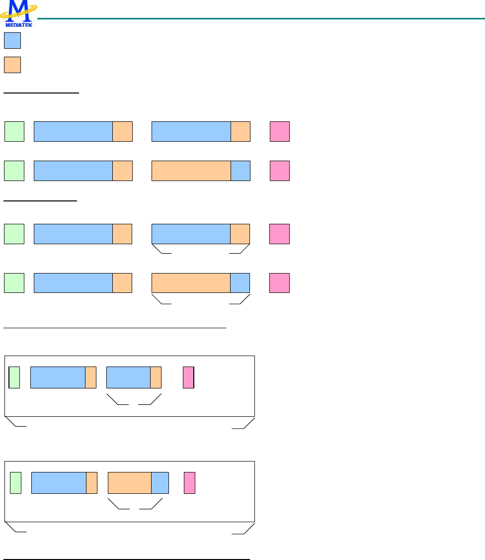
MT6235 GSM/GPRS Baseband Processor Data Sheet Revision 1.02
222/599 MediaTek Inc. Confidential
Master to slave dir
Slave to master dir
Single Byte Access
Slave Address
A
S
DATA A
P
Slave Address
A
S
DATA nA
P
Single Byte Write
Single Byte Read
Multi Byte Access
Slave Address A
S
DATA AP
N bytes + ack
Slave Address A
S
DATA A/
nA P
N bytes + ack/nak
Multi Byte Write
Multi Byte Read
Multi Byte Transfer + Multi Transfer (same direction)
Slave
Address ADATA A
S
P
Slave
Address
A
DATA
A/
nA
S
P
N bytes + ack/nak
N bytes + ack/nak
Multi Byte Write + Multi Transfer
Multi Byte Read + Multi Transfer
X transfers
+ wait time +
X transfers
+ wait time +
Multi Byte Transfer + Multi Transfer w RS (same direction)
MT6235 GSM/GPRS Baseband Processor Data Sheet Revision 1.02
223/599 MediaTek Inc. Confidential
Slave
Address
A
DATA
A
SR
Slave
Address ADATA A/
nA
S
R
N bytes + ack/nak
N bytes + ack/nak
Multi Byte Write + Multi Transfer + Repeated Start
Multi Byte Read + Multi Transfer + Repeated Start
X transfers
X transfers
++
P
P
+
Combined Write/Read with Repeated Start (direction change)
(Note: Only supports Write and then Read sequence. Read and then Write is not supported)
Slave
Address
A
SDATA
A
R
N bytes + ack/nak
Slave
Address
A
DATA
A
P
M bytes + ack/nak
Combined Multi Byte Write + Multi Byte Read
4.12.2 Programming Examples
Common Transfer Programmable Parameters
Slave
Address ADATA
A
SP/
RS
transfer_len
Programmable Parameters
transac_len
DATA
A
rs_stop
slave_addr
Slave
Address ADATA
A
S
P/
RS
DATA A
delay_len
transfer_len / aux transfer_len
slave_addr + dir change
Output Waveform Timing Programmable Parameters
MT6235 GSM/GPRS Baseband Processor Data Sheet Revision 1.02
224/599 MediaTek Inc. Confidential
sample_cnt_div * (1/13Mhz) step_cnt_div = number of samples
half pulse width =
step_cnt_div * sample_cnt_div * (1/13Mhz)
Sample width =
4.12.3 Register Definitions
I2CREG+0000h Data Port Register DATA_PORT
Bit 15 14 13 12 11 10 9 8 7 6 5 4 3 2 1 0
Name FIFO DATA
Type R/W
Reset 0
DATA_PORT[7:0] This is the FIFO access port. During master write sequences (slave_addr[0] = 0), this port
can be written by APB, and during master read sequences (slave_addr[0] = 1), this port can be
read by APB.
(NOTE) Slave_addr must be set correctly before accessing the fifo.
(DEBUG ONLY) If the fifo_apb_debug bit is set, then the FIFO can be read and write by the APB
I2CREG+0004h Slave Address Register SLAVE_ADDR
Bit 15 14 13 12 11 10 9 8 7 6 5 4 3 2 1 0
Name SLAVE_ADDR
Type R/W
Reset 0
SLAVE_ADDR [7:0] This specifies the slave address of the device to be accessed. Bit 0 is defined by the I2C
protocol as a bit that indicates the direction of transfer. 1 = master read, 0 = master write.
I2CREG+0008h Interrupt Mask Register INTR_MASK
Bit 15 14 13 12 11 10 9 8 7 6 5 4 3 2 1 0
Name
DEBU
G
HS_N
ACKE
R
ACKE
RR
TRAN
SAC_
COMP
Type R.W R/W R/WR/W
Reset 1 1 1 1
This register provides masks for the corresponding interrupt sources as indicated in intr_stat register.
1 = allow interrupt
0 = disable interrupt
Note: while disabled, the corresponding interrupt will not be asserted, however the intr_stat will still be updated with the
status. Ie. mask does not affect intr_stat register values.

MT6235 GSM/GPRS Baseband Processor Data Sheet Revision 1.02
225/599 MediaTek Inc. Confidential
I2CREG+000C
h Interrupt Status Register INTR_STAT
Bit 15 14 13 12 11 10 9 8 7 6 5 4 3 2 1 0
Name
HS_N
ACKE
RR
ACKE
RR
TRAN
SAC_
COMP
Type W1C W1CW1C
Reset 0 0 0
When an interrupt is issued by i2c controller, this register will need to be read by mcu to determine the cause for the
interrupt. After this status has been read and appropriate actions are taken, the corresponding interrupt source will need to
be write 1 cleared.
HS_NACKERR This status is asserted if hs master code nack error detection is enabled. If enabled, hs master
code nack err will cause transaction to end and stop will be issued.
ACKERR This status is asserted if ACK error detection is enabled. If enabled, ackerr will cause transaction to
end and stop will be issued.
TRANSAC_COMP This status is asserted when a transaction has completed successfully.
I2CREG+0010h Control Register CONTROL
Bit 15 14 13 12 11 10 9 8 7 6 5 4 3 2 1 0
Name
TRAN
SFER
_LEN
_CHA
NGE
ACKE
RR_D
ET_E
N
DIR_C
HANG
E
CLK_
EXT
EN
DMA_
EN RS_S
TOP
Type R/W R/W RW RW RW RW R/W
Reset 0 0 0 0 0 0 0
TRANSFER_LEN_CHANGEThis options specifies whether or not to change the transfer length after the fist
transfer completes. If enabled, the transfers after the first transfer will use the
transfer_len_aux parameter.
ACKERR_DET_EN This option enables slave ack error detection. When enabled, if slave ack error is detected,
the master shall terminate the transaction by issuing a STOP condition and then asserts
ackerr interrupt. Mcu shall handle this case appropriately and then resets the fifo address
before reissuing transaction again. If this option is disabled, the controller will ignore slave
ack error and keep on scheduled transaction.
0 disable
1 enable
DIR_CHANGE This option is used for combined transfer format, where the direction of transfer is to be
changed from write to read after the FIRST RS condition. Note: when set to 1, the transfers
after the direction change will be based on the transfer_len_aux parameter.
0 disable
1 enable
CLK_EXT_EN I2C spec allows slaves to hold the SCL line low if it is not yet ready for further processing.
Therefore, if this bit is set to 1, master controller will enter a high wait state until the slave
releases the SCL line.

MT6235 GSM/GPRS Baseband Processor Data Sheet Revision 1.02
226/599 MediaTek Inc. Confidential
DMA_EN By default, this is disabled, and fifo data shall be manually prepared by mcu. This default
setting should be used for transfer sizes of less than 8 data bytes and no multiple transfer is
configured. When enabled, dma requests are turned on, and the fifo data should be
prepared in memory.
RS_STOP In LS/FS mode, this bit affects multi-transfer transaction only. It controls whether or not
REPEATED-START condition is used between transfers. The last ending transfer always
ends with a STOP.
In HS mode, this bit must be set to 1.
0 use STOP
1 use REPEATED-START
I2CREG+0014h Transfer Length Register (Number of Bytesper
Transfer) TRANSFER_LEN
Bit 15 14 13 12 11 10 9 8 7 6 5 4 3 2 1 0
Name TRANSFER_LEN_AUX TRANSFER_LEN
Type R/W R/W
Reset ‘h1 ‘h1
TRANSFER_LEN_AUX[4:0]This field is valid only when dir_change is set to 1. This indicates the number of
DATA BYTES to be transferred in 1 transfer unit (excluding slave address byte) for the
transfers following the direction change. I.e., if dir_change =1, then the first write
transfer length depends on transfer_len, while the second read transfer length depend on
transfer_len_aux. Dir change is always after the first transfer.
(NOTE) The value must be set greater than 1, otherwise no transfer will take place.
TRANSFER_LEN[7:0] This indicates the number of DATA BYTES to be transferred in 1 transfer unit
(excluding slave address byte)
(NOTE) The value must be set greater than 1, otherwise no transfer will take place.
I2CREG+0018h Transaction Length Register (Number of Transfers per
Transaction) TRANSAC_LEN
Bit 15 14 13 12 11 10 9 8 7 6 5 4 3 2 1 0
Name TRANSAC_LEN
Type R/W
Reset ‘h1
TRANSAC_LEN[7:0] This indicates the number of TRANSFERS to be transferred in 1 transaction
(NOTE) The value must be set greater than 1, otherwise no transfer will take place.
I2CREG+001C
h Inter Delay Length Register DELAY_LEN
Bit 15 14 13 12 11 10 9 8 7 6 5 4 3 2 1 0
Name DELAY_LEN
Type R/W
Reset ‘h2

MT6235 GSM/GPRS Baseband Processor Data Sheet Revision 1.02
227/599 MediaTek Inc. Confidential
DELAY_LEN[3:0] This sets the wait delay between consecutive transfers when RS_STOP bit is set to 0. (the
unit is same as the half pulse width)
I2CREG+0020h Timing Control Register TIMING
Bit 15 14 13 12 11 10 9 8 7 6 5 4 3 2 1 0
Name DATA
READ
ADJ DATA_READ_TIME SAMPLE_CNT_DIV STEP_CNT_DIV
Type R/W R/W R/W R/W
Reset ‘h0 ‘h1 ‘h3 ‘h3
LS/FS only. This register is used to control the output waveform timing. Each half pulse width (ie. each high or low pulse)
is equal to = step_cnt_div * (sample_cnt_div * 1/13Mhz)
SAMPLE_CNT_DIV[2:0] Used for LS/FS only. This adjusts the width of each sample. (sample width =
sample_cnt_div * 1/13Mhz)
STEP_CNT_DIV[5:0] This specifies the number of samples per half pulse width (ie. each high or low pulse)
DATA_READ_ADJ When set to 1, data latch in sampling time during master reads are adjusted according to
DATA_READ_TIME value. Otherwise, by default, data is latched in at half of the high pulse
width point. This value must be set to less or equal to half the high pulse width.
DATA_READ_TIME[2:0] This value is valid only when DATA_READ_ADJ is set to 1. This can be used to adjust
so that data is latched in at earlier sampling points (assuming data is settled by then)
I2CREG+0024h Start Register START
Bit 15 14 13 12 11 10 9 8 7 6 5 4 3 2 1 0
Name
STAR
T
Type R/W
Reset 0
START This register starts the transaction on the bus. It is auto deasserted at the end of the
transaction.
I2CREG+0030h Fifo Status Register FIFO_STAT
Bit 15 14 13 12 11 10 9 8 7 6 5 4 3 2 1 0
Name RD_ADDR WR_ADDR FIFO_OFFSET
WR_F
ULL RD_E
MPTY
Type RO RO RO RO RO
Reset 0 0 0 0 0 0 0
RD_ADDR[3:0] The current rd address pointer. (only bit [2:0] has physical meaning)
WR_ADDR[3:0] The current wr address pointer. (only bit [2:0] has physical meaning)
FIFO_OFFSET[3:0] wr_addr[3:0] – rd_addr[3:0]
WR_FULL This indicates that the fifo is full.
RD_EMPTY This indicates that the fifo is empty.
I2CREG+0034h Fifo Thresh Register FIFO_THRESH
Bit 15 14 13 12 11 10 9 8 7 6 5 4 3 2 1 0

MT6235 GSM/GPRS Baseband Processor Data Sheet Revision 1.02
228/599 MediaTek Inc. Confidential
Name TX_TRIG_THRESH RX_TRIG_THRESH
Type RW R/W
Reset ‘h7 ‘h0
DEBUG ONLY. By default, these values do not need to be adjusted. Note! for RX, no timeout mechanism is
implemented. Therefore, RX_trig_thresh must be left at 0, or there would be data left in the fifo that
is not fetched by DMA controller.
TX_TRIG_THRESH[2:0] When tx fifo level is below this value, tx dma request is asserted.
RX_TRIG_THRESH[2:0] When rx fifo level is above this value, rx dma request is asserted.
I2CREG+0038h Fifo Address Clear Register FIFO_ADDR_CL
R
Bit 15 14 13 12 11 10 9 8 7 6 5 4 3 2 1 0
Name
FIFO_
ADDR
_CR
Type WO
Reset 0
FIFO_ADDR_CLR When written with a 1’b1, a 1 pulse fifo_addr_clr is generated to clear the fifo address to
back to 0.
I2CREG+0040h IO Config Register IO_CONFIG
Bit 15 14 13 12 11 10 9 8 7 6 5 4 3 2 1 0
Name
IO
SYNC
EN
SDA_I
O_CO
NFIG
SCL_I
O_CO
NFIG
Type R/W R/WR/W
Reset 0 0 0
This register is used to configure the I/O for the sda and scl lines to select between normal i/o mode, or open-drain mode to
support wired-and bus.
IO_SYNC_EN DEBUG ONLY: When set to 1, scl and sda inputs will be first dual synced by bclk_ck. This
should not be needed. Only reserved for debugging.
SDA_IO_CONFIG 0 normal tristate io mode
1 open-drain mode
SCL_IO_CONFIG 0 normal tristate io mode
1 open-drain mode
I2CREG+0044h RESERVED DEBUG Register DEBUG
Bit 15 14 13 12 11 10 9 8 7 6 5 4 3 2 1 0
Name
Type R/W R/WR/W
Reset 0 0 0
NOTE: This register is for DEBUG ONLY. The bits are R/W, do not change the values from the default value.

MT6235 GSM/GPRS Baseband Processor Data Sheet Revision 1.02
229/599 MediaTek Inc. Confidential
I2CREG+0048h High Speed Mode Register HS
Bit 15 14 13 12 11 10 9 8 7 6 5 4 3 2 1 0
Name HS_SAMPLE_CNT
DIV HS_STEP_CNT_DIV MASTER_CODE
HS_N
ACKE
RR_D
ET_E
N
HS_E
N
Type R/W R/W R/W R/W R/W
Reset 0 1 0 1 0
This register contains options for supporting high speed operation features
Each HS half pulse width (ie. each high or low pulse) is equal to = step_cnt_div * (sample_cnt_div * 1/13Mhz)
HS_SAMPLE_CNT_DIV[2:0]When high speed mode is entered after the master code transfer has been
completed, the sample width becomes dependent on this parameter.
HS_STEP_CNT_DIV[2:0] When high speed mode is entered after the master code transfer has been completed,
the number of samples per half pulse width becomes dependent on this value.
MASTER_CODE[2:0] This is the 3 bit programmable value for the master code to be transmitted.
HS_NACKERR_DET_EN This enables NACKERR detection during the master code transmission. When
enabled, if NACK is not received after master code has been transmitted, the transaction
will terminated with a STOP condition.
HS_EN This enables the high speed transaction. (note: rs_stop must be set to 1 as well)
I2CREG+0050h Soft Reset Register SOFTRESET
Bit 15 14 13 12 11 10 9 8 7 6 5 4 3 2 1 0
Name
SOFT
_RES
ET
Type WO
Reset 0
SOFT_RESET When written with a 1’b1, a 1 pulse soft reset is used as synchronous reset to reset the I2C
internal hardware circuits.
I2CREG+0064h Debug Status Register DEBUGSTAT
Bit 15 14 13 12 11 10 9 8 7 6 5 4 3 2 1 0
Name
BUS_
BUSY
MAST
ER_W
RITE
MAST
ER_R
EAD MASTER_STATE
Type RO RO RO RO
Reset 0 1 0 0
BUS_BUSY DEBUG ONLY: valid when bus_detect_en is 1. bus_busy = 1 indicates a start transaction
has been detected and no stop condition has been detected yet.
MASTER_WRITE DEBUG ONLY: 1 = current transfer is in the master write dir
MASTER_READ DEBUG ONLY: 1 = current transfer is in the master read dir
MASTER_STATE[3:0] DEBUG ONLY: reads back the current master_state.

MT6235 GSM/GPRS Baseband Processor Data Sheet Revision 1.02
230/599 MediaTek Inc. Confidential
I2CREG+0068h Debug Control Register DEBUGCTRL
Bit 15 14 13 12 11 10 9 8 7 6 5 4 3 2 1 0
Name
APB_
DEBU
G_RD
FIFO_
APB_
DEBU
G
Type WOR/W
Reset 0 0
APB_DEBUG_RD This bit is only valid when fifo_apb_debug is set to 1. Writing to this register will generate a
1 pulsed fifo apb rd signal for reading the fifo data.
FIFO_APB_DEBUG This is used for trace32 debug purposes. When using trace32, and the memory map is
shown, turning this bit on will block the normal apb read access. Apb read access to the fifo
is then enabled by writing to apb_debug_rd.
0 disable
1 enable

MT6235 GSM/GPRS Baseband Processor Data Sheet Revision 1.02
231/599 MediaTek Inc. Confidential

MT6235 GSM/GPRS Baseband Processor Data Sheet Revision 1.02
232/599 MediaTek Inc. Confidential
5 Microcontroller Coprocessors
Microcontroller Coprocessors are designed to run computing-intensive processes in place of the Microcontroller (MCU).
These coprocessors especially target timing critical GSM/GPRS Modem processes that require fast response and large data
movement. Controls to the coprocessors are all through memory access via the APB.
5.1 Divider
To ease the processing load of MCU, a divider is employed here. The divider can operate signed and unsigned 32bit/32bit
division, as well as modulus. The processing time of the divider is from 1 clock cycle to 33 clock cycles, which depends
upon the magnitude of the value of the dividend. The detailed processing time is listed below in Table 18. From the table
we can see that there are two kind of processing time (except for when the dividend is zero) in an item. Which kind depends
on whether there is the need for restoration at the last step of the division operation.
After the divider is started by setting START to “1” in Divider Control Register, DIV_RDY will go low, and it will be
asserted after the division process is finished. MCU could detect this status bit by polling it to know the correct access
timing. In order to simplify polling, only the value of register DIV_RDY will appear while Divider Control Register is read.
Hence, MCU does not need to mask other bits to extract the value of DIV_RDY.
In GSM/GPRS system, many divisions are executed with some constant divisors. Therefore, some often-used constants are
stored in the divider to speed up the process. By controlling control bits IS_CNST and CNST_IDX in Divider Control
register, one can start a division without giving a divisor. This could save the time for writing divisor in and the instruction
fetch time, and thus make the process more efficient.
Signed Division Unsigned Division
Dividend Clock Cycles Dividend Clock Cycles
0000_0000h 1 0000_0000h 1
0000_00ffh – (-0000
_
0100h),
excluding 0x0000_0000
8 or 9 0000_0001h - 0000_00ffh 8 or 9
0000_ffffh – (-0001_0000h) 16 or 17 0000_0100h - 0000_ffffh 16 or 17
00ff_ffffh – (-0100_0000h) 24 or 25 0001_0000h - 00ff_ffffh 24 or 25
7fff_ffffh – (-8000_0000h) 32 or 33 0100_0000h - ffff_ffffh 32 or 33
Table 23 Processing time in different value of dividend.
5.1.1 Register Definitions
DIVIDER+0000
h Divider Control Register DIV_CON
Bit 31 30 29 28 27 26 25 24 23 22 21 20 19 18 17 16
Name CNST_IDX
Type WO
Reset 0
Bit 15 14 13 12 11 10 9 8 7 6 5 4 3 2 1 0
Name IN_CN
ST SIGN DIV_R
DY STAR
T
MT6235 GSM/GPRS Baseband Processor Data Sheet Revision 1.02
233/599 MediaTek Inc. Confidential
Type WO WO RO WO
Reset 0 1 1 0
START To start division. It will return to 0 after division has started.
DIV_RDY Current status of divider. Note that when DIV_CON register is read, only the value of DIV_RDY will appear.
That means program does not need to mask other part of the register to extract the information of DIV_RDY.
0 division is in progress.
1 division is finished.
SIGN To indicate signed or unsigned division.
0 Unsigned division.
1 Signed division.
IS_CNST To indicate if internal constant value should be used as a divisor. If IS_CNST is enabled, User does not need
to write the value of the divisor, and divider will automatically use the internal constant value instead. What
value divider will use depends on the value of CNST_IDX.
0 Normal division. Divisor is written in via APB
1 Using internal constant divisor instead.
CNST_IDX Index of constant divisor.
0 divisor = 13
1 divisor = 26
2 divisor = 51
3 divisor = 52
4 divisor = 102
5 divisor = 104
DIVIDER
+0004h Divider Dividend register DIV_DIVIDEND
Bit 31 30 29 28 27 26 25 24 23 22 21 20 19 18 17 16
Name DIVIDEND[31:16]
Type WO
Reset 0
Bit 15 14 13 12 11 10 9 8 7 6 5 4 3 2 1 0
Name DIVIDEND[15:0]
Type WO
Reset 0
Dividend.
DIVIDER
+0008h Divider Divisor register DIV_DIVISOR
Bit 31 30 29 28 27 26 25 24 23 22 21 20 19 18 17 16
Name DIVISOR[31:16]
Type R/W
Reset 0
Bit 15 14 13 12 11 10 9 8 7 6 5 4 3 2 1 0
Name DIVISOR[15:0]
Type R/W
Reset 0
Divisor.
MT6235 GSM/GPRS Baseband Processor Data Sheet Revision 1.02
234/599 MediaTek Inc. Confidential
DIVIDER
+000Ch Divider Quotient register DIV_QUOTIENT
Bit 31 30 29 28 27 26 25 24 23 22 21 20 19 18 17 16
Name QUOTIENT[31:16]
Type RO
Reset 0
Bit 15 14 13 12 11 10 9 8 7 6 5 4 3 2 1 0
Name QUOTIENT[15:0]
Type RO
Reset 0
Quotient.
DIVIDER
+0010h Divider Remainder register DIV_REMAINDE
R
Bit 31 30 29 28 27 26 25 24 23 22 21 20 19 18 17 16
Name REMAINDER[31:16]
Type RO
Reset 0
Bit 15 14 13 12 11 10 9 8 7 6 5 4 3 2 1 0
Name REMAINDER[15:0]
Type RO
Reset 0
Remainder.
5.2 CSD Accelerator
5.2.1 General Description
This unit performs the data format conversion of RA0, RA1, and FAX in CSD service. CSD service consists of two major
functions: data flow throttling and data format conversion. The data format conversion is a bit-wise operation and takes a
number of instructions to complete a conversion. Therefore, it is not efficient to do by MCU itself. A coprocessor, CSD
accelerator, is designed here to reduce the computing power needed to perform this function.
CSD accelerator only helps in converting data format; the data flow throttling function is still implemented by the MCU.
CSD accelerator performs three types of data format conversion, RA0, RA1, and FAX.
For RA0 conversion, only uplink RA0 data format conversion is provided here. This is because there are too many
judgments on the downlink path conversion, which will greatly increase area cost. Uplink RA0 conversion is to insert one
start bit and one stop bit before and after a byte, respectively, during 16 bytes. Figure 23 illustrates the detailed conversion
table.
RA0 converter can only process RA0 data state by state. Before filling in new data, software must make sure the converted
data of certain state is withdrawn, or the converted data will be replaced by the new data. For example, if 32-bit data is
written, and the state pointer goes from state 0 to state 1, and word ready of state 0 is asserted; then, before writing the next
32-bit data, the word of state 0 should be withdrawn first, or the data will be lost.
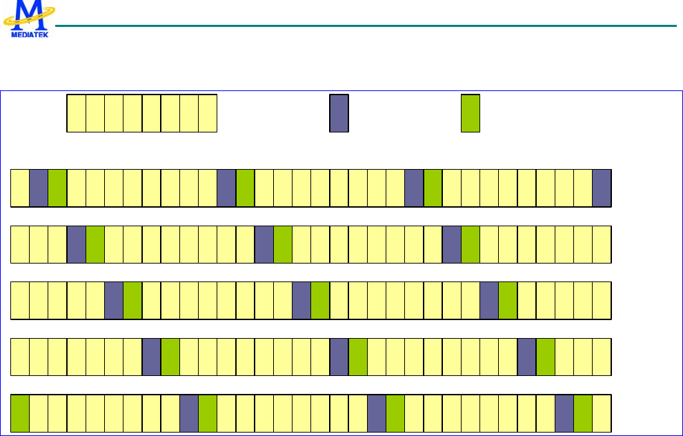
MT6235 GSM/GPRS Baseband Processor Data Sheet Revision 1.02
235/599 MediaTek Inc. Confidential
RA0 records the number of written bytes, state pointer, and ready state word. The information can help software to perform
flow control. See Register Definition for more detail.
Data bits Stop bitStart bit
State 0
State 1
State 2
State 3
State 4
Figure 23 data format conversion of RA0
For RA1 conversion, both directions, downlink and uplink, are supported. The data formats vary in different data rate. The
detailed conversion table is shown in Figure 24 and Figure 25. The yellow part is the payload data, and the blue part is the
status bit.
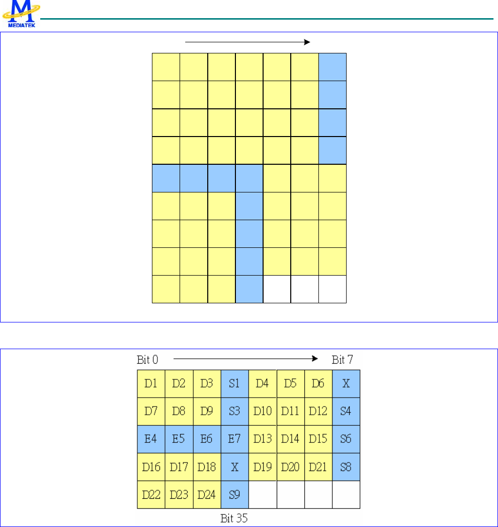
MT6235 GSM/GPRS Baseband Processor Data Sheet Revision 1.02
236/599 MediaTek Inc. Confidential
D1 D2 D3 D4 D5 D6 S1
D7 D8 D9 D10 D11 D12 X
D13 D14 D15 D16 D17 D18 S3
D19 D20 D21 D22 D23 D24 S4
E4 E5 E6 E7 D25 D26 D27
D28 D29 D30 S6 D31 D32 D33
D34 D35 D36 XD37 D38 D39
D40 D41 D42 S8 D43 D44 D45
D46 D47 D48 S9
Bit 0
Bit 59
Bit 6
Figure 24 data format conversion for 6k/12k RA1
Figure 25 data format conversion for 3.6k RA1
For FAX, two types of bit-reversal functions are provided. One is bit-wise reversal, and the other is byte-wise reversal,
which are illustrated in Figure 26 and Figure 27, respectively.
MT6235 GSM/GPRS Baseband Processor Data Sheet Revision 1.02
237/599 MediaTek Inc. Confidential
b31 b30 b29 b0
b0 b1 b2 b31
Figure 26 Type 1 bit reverse
b31 b0b7b15b23
b0b7 b15 b8 b23 b16 b31 b24
Figure 27 Type 2 bit reverse
Register Address Register Function Acronym
CSD + 0000h CSD RA0 Control Register CSD_RA0_CON
CSD + 0004h CSD RA0 Status Register CSD_RA0_STA
CSD + 0008h CSD RA0 Input Data Register CSD_RA0_DI
CSD + 000Ch CSD RA0 Output Data Register CSD_RA0_DO
CSD + 0100h CSD RA1 6K/12K Uplink Input Data Register 0 CSD_RA1_6K_12K_ULDI0
CSD + 0104h CSD RA1 6K/12K Uplink Input Data Register 1 CSD_RA1_6K_12K_ULDI1
CSD + 0108h CSD RA1 6K/12K Uplink Status Data Register CSD_RA1_6K_12K_ULSTUS
CSD + 010Ch CSD RA1 6K/12K Uplink Output Data Register 0 CSD_RA1_6K_12K_ULDO0
CSD + 0110h CSD RA1 6K/12K Uplink Output Data Register 1 CSD_RA1_6K_12K_ULDO1
CSD + 0200h CSD RA1 6K/12K Downlink Input Data Register 0 CSD_RA1_6K_12K_DLDI0
CSD + 0204h CSD RA1 6K/12K Downlink Input Data Register 1 CSD_RA1_6K_12K_DLDI1
CSD + 0208h CSD RA1 6K/12K Downlink Output Data Register 0 CSD_RA1_6K_12K_DLDO0
CSD + 020Ch CSD RA1 6K/12K Downlink Output Data Register 1 CSD_RA1_6K_12K_DLDO1
CSD + 0210h CSD RA1 6K/12K Downlink Status Data Register CSD_RA1_6K_12K_DLSTUS
CSD + 0300h CSD RA13.6K Uplink Input Data Register 0 CSD_RA1_3P6K_ULDI0
CSD + 0304h CSD RA13.6K Uplink Status Data Register CSD_RA1_3P6K_ULSTUS
CSD + 0308h CSD RA13.6K Uplink Output Data Register 0 CSD_RA1_3P6K_ULDO0
CSD + 030Ch CSD RA13.6K Uplink Output Data Register 1 CSD_RA1_3P6K_ULDO1
CSD + 0400h CSD RA1 3.6K Downlink Input Data Register 0 CSD_RA1_3P6K_DLDI0
CSD + 0404h CSD RA1 3.6K Downlink Input Data Register 1 CSD_RA1_3P6K_DLDI1
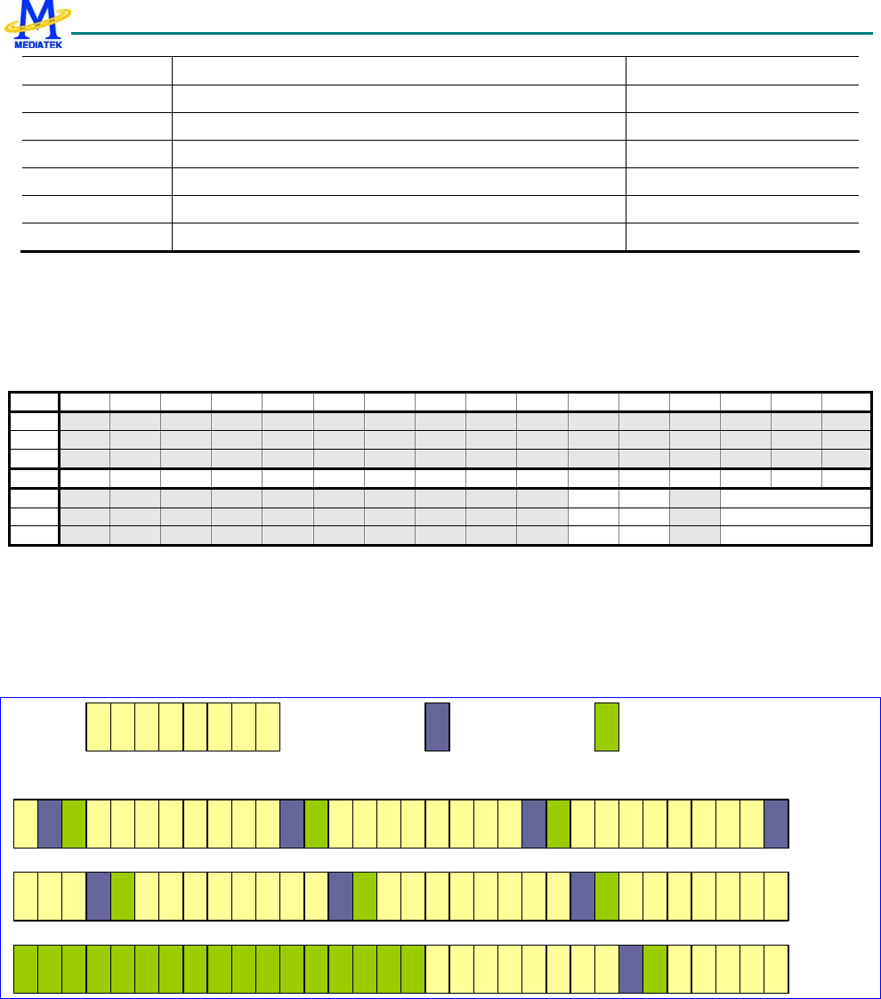
MT6235 GSM/GPRS Baseband Processor Data Sheet Revision 1.02
238/599 MediaTek Inc. Confidential
CSD + 0408h CSD RA1 3.6K Downlink Output Data Register 0 CSD_RA1_3P6K_DLDO0
CSD + 040Ch CSD RA1 3.6K Downlink Status Data Register CSD_RA1_3P6K_DLSTUS
CSD + 0500h CSD FAX Bit Reverse Type 1 Input Data Register CSD_FAX_BR1_DI
CSD + 0504h CSD FAX Bit Reverse Type 1 Output Data Register CSD_FAX_BR1_DO
CSD + 0510h CSD FAX Bit Reverse Type 2 Input Data Register CSD_FAX_BR2_DI
CSD + 0514h CSD FAX Bit Reverse Type 2 Output Data Register CSD_FAX_BR2_DO
Table 24 CSD Accelerater Registers
5.2.2 Register Definitions
CSD+0000h CSD RA0 Control Register CSD_RA0_CON
Bit 31 30 29 28 27 26 25 24 23 22 21 20 19 18 17 16
Name
Type
Reset
Bit 15 14 13 12 11 10 9 8 7 6 5 4 3 2 1 0
Name RST BTS0 VLD_BYTE
Type WO WO WO
Reset 0 0 100
VLD_BYTE Specify how many valid bytes in the current input data. It must be specified before filling data in.
BTS0 Back to state 0. Force RA0 converter go back to state 0. Incomplete word will be padded by STOP bit. For
instance, back-to-state0 command is issued after 8 byte data are filled in. Then these bit after the 8th byte will be
padded with stop bits, and RDYWD2 is asserted. After removing state word 2, the state pointer goes back to state
0. Note that new data filling should take place after removing state word 2, or the state pointer may be out of order.
Data bits Stop bitStart bit
State 0
State 1
State 2
Figure 28 Example of Back to state 0
RST Reset RA0 converter. In case, erroneously operation makes data disordered. This bit can restore all state to original
state.

MT6235 GSM/GPRS Baseband Processor Data Sheet Revision 1.02
239/599 MediaTek Inc. Confidential
CSD+0004h CSD RA0 Status Register CSD_RA0_STA
Bit 31 30 29 28 27 26 25 24 23 22 21 20 19 18 17 16
Name
Type
Reset
Bit 15 14 13 12 11 10 9 8 7 6 5 4 3 2 1 0
Name BYTECNT CRTSTA RDYWD
Type RO RO RC
Reset 0 0 0
RDYWD0~4 Ready word. To indicate which state word is ready for withdrawal. Data should be withdrawn before next
data fills into CSD_RA0_DI, if there are any bits asserted.
0 Not ready
1 Ready
CRTSTA current state. State0 ~ state4. To indicate which state word software is filling in.
BYTECNT The total number of bytes software is filling in.
CSD+0008h CSD RA0 Input Data Register CSD_RA0_DI
Bit 31 30 29 28 27 26 25 24 23 22 21 20 19 18 17 16
Name DIN
Type WO
Reset 0
Bit 15 14 13 12 11 10 9 8 7 6 5 4 3 2 1 0
Name DIN
Type WO
Reset 0
DIN The RA0 convert input data. Ready word indicator shall be check before filling in data. If any words are ready,
withdraw them first; otherwise the ready data in RA0 converter will be replaced.
CSD+000Ch CSD RA0 Output Data Register CSD_RA0_DO
Bit 31 30 29 28 27 26 25 24 23 22 21 20 19 18 17 16
Name DOUT
Type RO
Reset 0
Bit 15 14 13 12 11 10 9 8 7 6 5 4 3 2 1 0
Name DOUT
Type RO
Reset 0
DOUT RA0 converted data. The return data corresponds to the ready word indicator defined in CSD_RA0_STA register.
The five bit of RDYWD map to state0 ~ state 4 accordingly. When CSD_RA0_DO is read, the asserted state word
will be returned. If there are two state words asserted at the same time, the lower one will be returned.
CSD+0100h CSD RA1 6K/12K Uplink Input Data Register 0 CSD_RA1_6K_1
2K_ULDI0
Bit 31 30 29 28 27 26 25 24 23 22 21 20 19 18 17 16
Name DIN
Type WO
Reset 0
Bit 15 14 13 12 11 10 9 8 7 6 5 4 3 2 1 0

MT6235 GSM/GPRS Baseband Processor Data Sheet Revision 1.02
240/599 MediaTek Inc. Confidential
Name DIN
Type WO
Reset 0
DIN The D1 to D32 of RA1 uplink data.
CSD+0104h CSD RA1 6K/12K Uplink Input Data Register 1 CSD_RA1_6K_1
2K_ULDI1
Bit 31 30 29 28 27 26 25 24 23 22 21 20 19 18 17 16
Name
Type
Reset
Bit 15 14 13 12 11 10 9 8 7 6 5 4 3 2 1 0
Name DIN
Type WO
Reset 0
DIN The D33 to D48 of RA1 uplink data.
CSD+0108h CSD RA1 6K/12K Uplink Status Data Register CSD_RA1_6K_1
2K_ULSTUS
Bit 31 30 29 28 27 26 25 24 23 22 21 20 19 18 17 16
Name
Type
Reset
Bit 15 14 13 12 11 10 9 8 7 6 5 4 3 2 1 0
Name E7 E6 E5 E4 X SB SA
Type WO WO WO WO WO WO WO
Reset 0 0 0 0 0 0 0
SA Represents S1, S3, S6, and S8 of status bits.
SB Represents S4 and S9 of status bits.
X Represents X of status bits.
E4 Represents E4 of status bits.
E5 Represents E5 of status bits.
E6 Represents E6 of status bits.
E7 Represents E7 of status bits.
CSD+010Ch CSD RA1 6K/12K Uplink Output Data Register 0 CSD_RA1_6K_1
2K_ULDO0
Bit 31 30 29 28 27 26 25 24 23 22 21 20 19 18 17 16
Name DOUT
Type RO
Reset 0
Bit 15 14 13 12 11 10 9 8 7 6 5 4 3 2 1 0
Name DOU
Type RO
Reset 0
DOUT The bit 0 to bit 31 of RA1 6K/12K uplink frame.
MT6235 GSM/GPRS Baseband Processor Data Sheet Revision 1.02
241/599 MediaTek Inc. Confidential
CSD+0110h CSD RA1 6K/12K Uplink Output Data Register 1 CSD_RA1_6K_1
2K_ULDO1
Bit 31 30 29 28 27 26 25 24 23 22 21 20 19 18 17 16
Name DOUT
Type RO
Reset 0
Bit 15 14 13 12 11 10 9 8 7 6 5 4 3 2 1 0
Name DOUT
Type RO
Reset 0
DOUT The bit32 to bit 59 of RA1 6K/12K uplink frame.
CSD+0200h CSD RA1 6K/12K Downlink Input Data Register 0 CSD_RA1_6K_1
2K_DLDI0
Bit 31 30 29 28 27 26 25 24 23 22 21 20 19 18 17 16
Name DIN
Type WO
Reset 0
Bit 15 14 13 12 11 10 9 8 7 6 5 4 3 2 1 0
Name DIN
Type WO
Reset 0
DIN The bit 0 to bit 31 of RA1 6K/12K downlink frame.
CSD+0204h CSD RA1 6K/12K Downlink Input Data Register 1 CSD_RA1_6K_1
2K_DLDI1
Bit 31 30 29 28 27 26 25 24 23 22 21 20 19 18 17 16
Name DIN
Type WO
Reset 0
Bit 15 14 13 12 11 10 9 8 7 6 5 4 3 2 1 0
Name DIN
Type WO
Reset 0
DIN The bit32 to bit 59 of RA1 6K/12K downlink frame.
CSD+0208h CSD RA1 6K/12K Downlink Output Data Register 0 CSD_RA1_6K_1
2K_DLDO0
Bit 31 30 29 28 27 26 25 24 23 22 21 20 19 18 17 16
Name DOUT
Type RO
Reset 0
Bit 15 14 13 12 11 10 9 8 7 6 5 4 3 2 1 0
Name DOUT
Type RO
Reset 0
DOUT The D1 to D32 of RA1 downlink data.

MT6235 GSM/GPRS Baseband Processor Data Sheet Revision 1.02
242/599 MediaTek Inc. Confidential
CSD+020Ch CSD RA1 6K/12K Downlink Output Data Register 1 CSD_RA1_6K_1
2K_DLDO1
Bit 31 30 29 28 27 26 25 24 23 22 21 20 19 18 17 16
Name
Type
Reset
Bit 15 14 13 12 11 10 9 8 7 6 5 4 3 2 1 0
Name DOUT
Type RO
Reset 0
DOUT The D33 to D48 of RA1 downlink data.
CSD+0210h CSD RA1 6K/12K Downlink Status Data Register CSD_RA1_6K_1
2K_DLSTUS
Bit 31 30 29 28 27 26 25 24 23 22 21 20 19 18 17 16
Name
Type
Reset
Bit 15 14 13 12 11 10 9 8 7 6 5 4 3 2 1 0
Name E7 E6 E5 E4 X SB SA
Type RO RO RO RO RO RO RO
Reset 0 0 0 0 0 0 0
SA The result of majority votes of S1, S3, S6 and S8. SA is “0” if equal vote.
SB The result of majority votes of S4 and S9. SB is “0” if equal vote.
X The result of majority votes of two X bits in downlink frame. X is “0” if equal vote.
E4 Represents E4 of status bits.
E5 Represents E5 of status bits.
E6 Represents E6 of status bits.
E7 Represents E7 of status bits.
CSD+0300h CSD RA1 3.6K Uplink Input Data Register 0 CSD_RA1_3P6K
_ULDI0
Bit 31 30 29 28 27 26 25 24 23 22 21 20 19 18 17 16
Name DIN
Type WO
Reset 0
Bit 15 14 13 12 11 10 9 8 7 6 5 4 3 2 1 0
Name DIN
Type WO
Reset 0
DIN The D1 to D24 of RA1 3.6K uplink data.
CSD+0304h CSD RA1 3.6K Uplink Status Data Register CSD_RA1_3P6K
_ULSTUS
Bit 31 30 29 28 27 26 25 24 23 22 21 20 19 18 17 16
Name
Type
MT6235 GSM/GPRS Baseband Processor Data Sheet Revision 1.02
243/599 MediaTek Inc. Confidential
Reset
Bit 15 14 13 12 11 10 9 8 7 6 5 4 3 2 1 0
Name E7 E6 E5 E4 X SB SA
Type WO WO WO WO WO WO WO
Reset 0 0 0 0 0 0 0
SA Represents S1, S3, S6, and S8 of status bits.
SB Represents S4 and S9 of status bits.
X Represents X of status bits.
E4 Represents E4 of status bits.
E5 Represents E5 of status bits.
E6 Represents E6 of status bits.
E7 Represents E7 of status bits.
CSD+0308h CSD RA1 3.6K Uplink Output Data Register 0 CSD_RA1_3P6K
_ULDO0
Bit 31 30 29 28 27 26 25 24 23 22 21 20 19 18 17 16
Name DOUT
Type RO
Reset 0
Bit 15 14 13 12 11 10 9 8 7 6 5 4 3 2 1 0
Name DOUT
Type RO
Reset 0
DOUT The bit 0 to bit 31 of RA1 3.6K uplink frame
CSD+030Ch CSD RA1 3.6K Uplink Output Data Register 1 CSD_RA1_3P6K
_ULDO1
Bit 31 30 29 28 27 26 25 24 23 22 21 20 19 18 17 16
Name
Type
Reset
Bit 15 14 13 12 11 10 9 8 7 6 5 4 3 2 1 0
Name DOUT
Type RO
Reset 0
DOUT The bit 32 to bit 35 of RA1 3.6K uplink frame
CSD+0400h CSD RA1 3.6K Downlink Input Data Register 0 CSD_RA1_3P6K
_DLDI0
Bit 31 30 29 28 27 26 25 24 23 22 21 20 19 18 17 16
Name DIN
Type WO
Reset 0
Bit 15 14 13 12 11 10 9 8 7 6 5 4 3 2 1 0
Name DIN
Type WO
Reset 0
DIN The bit 0 to bit 31 of RA1 3.6K downlink frame
MT6235 GSM/GPRS Baseband Processor Data Sheet Revision 1.02
244/599 MediaTek Inc. Confidential
CSD+0404h CSD RA1 3.6K Downlink Input Data Register 1 CSD_RA1_3P6K
_DLDI1
Bit 31 30 29 28 27 26 25 24 23 22 21 20 19 18 17 16
Name
Type
Reset
Bit 15 14 13 12 11 10 9 8 7 6 5 4 3 2 1 0
Name DIN
Type WO
Reset 0
DIN The bit 32 to bit 35 of RA1 3.6K downlink frame
CSD+0408h CSD RA1 3.6K Downlink Output Data Register 0 CSD_RA1_3P6K
_DLDO0
Bit 31 30 29 28 27 26 25 24 23 22 21 20 19 18 17 16
Name DOUT
Type RO
Reset 0
Bit 15 14 13 12 11 10 9 8 7 6 5 4 3 2 1 0
Name DOUT
Type RO
Reset 0
DIN The D1 to D24 of RA1 3.6K downlink data.
CSD+040Ch CSD RA1 3.6K Downlink Status Data Register CSD_RA1_3P6K
_DLSTUS
Bit 31 30 29 28 27 26 25 24 23 22 21 20 19 18 17 16
Name
Type
Reset
Bit 15 14 13 12 11 10 9 8 7 6 5 4 3 2 1 0
Name E7 E6 E5 E4 X SB SA
Type RO RO RO RO RO RO RO
Reset 0 0 0 0 0 0 0
SA The result of majority votes of S1, S3, S6 and S8. SA is “0” if equal vote.
SB The result of majority votes of S4 and S9. SB is “0” if equal vote.
X The result of majority votes of two X bits in downlink frame. X is “0” if equal vote.
E4 Represents E4 of status bits.
E5 Represents E5 of status bits.
E6 Represents E6 of status bits.
E7 Represents E7 of status bits.
CSD+0500h CSD FAX Bit Reverse Type 1 Input Data Register CSD_FAX_BR1_
DI
Bit 31 30 29 28 27 26 25 24 23 22 21 20 19 18 17 16
Name DIN
Type WO

MT6235 GSM/GPRS Baseband Processor Data Sheet Revision 1.02
245/599 MediaTek Inc. Confidential
Reset 0
Bit 15 14 13 12 11 10 9 8 7 6 5 4 3 2 1 0
Name DIN
Type WO
Reset 0
DIN 32-bit input data for type 1 bit reverse of FAX data. The action of Type 1 bit reverse is to reverse this word by
word.
CSD+0504h CSD FAX Bit Reverse Type 1 Output Data Register CSD_FAX_BR1_
DO
Bit 31 30 29 28 27 26 25 24 23 22 21 20 19 18 17 16
Name DOUT
Type RO
Reset 0
Bit 15 14 13 12 11 10 9 8 7 6 5 4 3 2 1 0
Name DOUT
Type RO
Reset 0
DOUT 32-bit result data for type 1 bit reverse of FAX data.
CSD+0510h CSD FAX Bit Reverse Type 2 Input Data Register CSD_FAX_BR2_
DI
Bit 31 30 29 28 27 26 25 24 23 22 21 20 19 18 17 16
Name DIN
Type WO
Reset 0
Bit 15 14 13 12 11 10 9 8 7 6 5 4 3 2 1 0
Name DIN
Type WO
Reset 0
DIN 32-bit input data for type 2 bit reverse of FAX data. The action of Type 1 bit reverse is to reverse this word by
byte.
CSD+0514h CSD FAX Bit Reverse Type 2 Output Data Register CSD_FAX_BR2_
DO
Bit 31 30 29 28 27 26 25 24 23 22 21 20 19 18 17 16
Name DOUT
Type RO
Reset 0
Bit 15 14 13 12 11 10 9 8 7 6 5 4 3 2 1 0
Name DOUT
Type RO
Reset 0
DOUT 32-bit result data for type 2 bit reverse of FAX data.

MT6235 GSM/GPRS Baseband Processor Data Sheet Revision 1.02
246/599 MediaTek Inc. Confidential
5.3 FCS Codec
5.3.1 General Description
FCS (Frame Check Sequence) is used to detect errors in the following information bits:
z RLP-frame of CSD services in GSM. The frame length is fixed as 240 or 576 bits including the 24-bit FCS field.
z LLC-frame of GPRS service. The frame length is determined by the information field, and length of the FCS field
is 24-bit.
Generation of the frame check sequence is very similar to the CRC coding in baseband signal processing. ETSI GSM
specifications 04.22 and 04.64 both define the coding rule. The coding rules are:
1. The CRC shall be ones complement of the modulo-2 sum of:
z the remainder of xkx(x23+x22+x21+…+x2+x+1) modulo-2 divided by the generator polynomial, where k is the
number of bits of the dividend. (i.e. fill the shift registers with all ones initially before feeding data)
z the remainder of the modulo-2 division by the generator polynomial of the product of x24 by the dividend, which
are the information bits.
2. The CRC-24 generator polynomial is:
G(x)=x24+x23+x21+x20+x19+x17+x16+x15+x13+x8+x7+x5+x4+x2+1
3. The 24-bit CRC are appended to the data bits in the MSB-first manner.
4. Decoding is identical to encoding except that data fed into the syndrome circuit is 24-bit longer than the
information bits at encoding. The dividend is also multiplied by x24. If no error occurs, the remainder should satisfy
R(x)=x22+x21+x19+x18+x16+x15+x11+x8+x5+x4 (0x6d8930)
And the parity output word will be 0x9276cf.
In contrast to conventional CRC, this special coding scheme makes the encoder fully identical to the decoder and simplifies
the hardware design.
5.3.2 Register Definitions
FCS+0000h FCS input data register FCS_DATA
Bit 15 14 13 12 11 10 9 8 7 6 5 4 3 2 1 0
Name D15 D14 D13 D12 D11 D10 D9 D8 D7 D6 D5 D4 D3 D2 D1 D0
Type R/W R/W R/W R/W R/W R/W R/W R/W R/W R/W R/W R/W R/W R/W R/W R/W
THE data bits input. First write of this register is the starting point of the encode or decode process.
DX X=0…15. The input format is D15·xn+ D14·xn-1+ D13·xn-2+ … + Dk·xk+ …, thus D15 is the first bit being pushed
into the shift register. If the last data word is less than 16 bits, the rest bits are neglected.
FCS+0004h Input data length indication register FCS_DLEN
Bit 15 14 13 12 11 10 9 8 7 6 5 4 3 2 1 0
Name LEN
Type WO
MT6235 GSM/GPRS Baseband Processor Data Sheet Revision 1.02
247/599 MediaTek Inc. Confidential
THE MCU specifies the total data length in bits to be encoded or decoded.
LEN The data length. A number of multiple-of-8 is required (Number_of_Bytes x 8)
FCS+0x0008h FCS parity output register 1, MSB part FCS_PAR1
Bit 15 14 13 12 11 10 9 8 7 6 5 4 3 2 1 0
Name P15 P14 P13 P12 P11 P10 P9 P8 P7 P6 P5 P4 P3 P2 P1 P0
Type RC RC RC RC RC RC RC RC RC RC RC RC RC RC RC RC
Reset 0 0 0 0 0 0 0 0 0 0 0 0 0 0 0 0
FCS+000Ch FCS parity output register 2, LSB part FCS_PAR2
Bit 15 14 13 12 11 10 9 8 7 6 5 4 3 2 1 0
Name P23 P22 P21 P20 P19 P18 P17 P16
Type RC RC RC RC RC RC RC RC
Reset 0 0 0 0 0 0 0 0
PARITY bits output. For FCS_PAR2, bit 8 to bit15 will be filled by zeros when reading.
PX X=0…23. The output format is P23·D23+ P22·D22+ P21·D21+ … + Pk·Dk+ …+P1·D1+P0, thus P23 is the
earliest bit being popped out from the shift register and first appended to the information bits. In other words,
{FCS_PAR2[7:0], FCS_PAR1[15:8], FCS_PAR1[7:0] } is the order of appending parity to data.
FCS+0010h FCS codec status register FCS_STAT
Bit 15 14 13 12 11 10 9 8 7 6 5 4 3 2 1 0
Name BUSY FER RDY
Type RC RC RC
Reset 0 1 0
BUSY Since the codec works in serial manner and the data word is input in parallel manner, BUSY = 1 indicates that
current data word is being processed and write to FCS_DATA is invalid. BUSY = 0 allows write of FCS_DATA
during encode or decode process.
FER Frame error indication, only for decode mode. FER = 0 means no error occurs and FER = 1 means the parity
check has failed. Write of FCS_RST.RST or first write of FCS_DATA will reset this bit to 0.
RDY When RDY = 1, the encode or decode process has been finished. For encode, the parity data in FCS_PAR1 and
FCS_PAR2 are correctly available. For decode, FCS_STAT.FER indication is valid. Write of FCS_RST.RST
or first write of FCS_DATA will reset this bit to 0.
FCS+0014h FCS codec reset register FCS_RST
Bit 15 14 13 12 11 10 9 8 7 6 5 4 3 2 1 0
Name EN_D
E PAR BIT RST
Type WO WO WO WO
RST RST = 0 resets the CRC coprocessor. Before setup of FCS codec, the MCU needs to set RST = 0 to flush the shift
register content before encode or decode.
BIT BIT = 0 means not to invert the bit order in a byte of data words when the codec is running. BIT = 1 means the bit
order in a byte written in FCS_DATA should be reversed.
PAR PAR = 0 means not to invert the bit order in a byte of parity words when the codec is running, include reading of
FCS_PAR1 and FCS_PAR2. PAR = 1 means bit order of parity words should be reversed, in decoding or
encoding.
EN_DE EN_DE = 0 means encode; EN_DE = 1 means decode
MT6235 GSM/GPRS Baseband Processor Data Sheet Revision 1.02
248/599 MediaTek Inc. Confidential
5.4 GPRS Cipher Unit
5.4.1 General Description
The unit implements the GPRS encryption/decryption scheme that accelerates the computation of encryption and
decryption GPRS pattern. The block accelerates the computation of the key stream. However the bit-wise
encryption/decryption of the data is still done by the MCU.
Both GEA and GEA2 are supported.
Register Address Register Function Acronym
GCU+0000h GPRS Encryption Algorithm Control Register GCU_CON
GCU+0004h GPRS Encryption Algorithm Status Register GCU_SAT
GCU+0008h GPRS Secret Key Kc 0 Register GCU_SKEY0
GCU+000Ch GPRS Secret Key Kc 1 Register GCU_SKEY1
GCU+0010h GPRS Message Key Register GCU_MKEY
GCU+0014h GPRS Ciphered Data Register GCU_CDATA
Table 25 GCU Registers
5.4.2 Register Definitions
GCU+0000h GPRS Encryption Algorithm Control Register GCU_CON
Bit 31 30 29 28 27 26 25 24 23 22 21 20 19 18 17 16
Name
Type
Reset
Bit 15 14 13 12 11 10 9 8 7 6 5 4 3 2 1 0
Name RBO KS SINIT DIR GEA2
Type R/W R/W WO R/W R/W
Reset 0 10 0 0 0
This register controls the key generation function of the GPRS Encryption Algorithm.
GEA2 Choose the encryption/decryption scheme. 1 = GEA2, while 0 = GEA.
DIR The DIRECTION input of the GPRS Encryption Algorithm.
SINIT Start initialization. The MCU writes 1 to start initialization. The bit is always read at 0.
KS Control the read access. 00 = byte access, 01 = half word (16 bits) access, 10 = word access, 11 reserved. Default
value is 10.
RBO Reversal Byte Order bit. If the bit was set to 1, the byte order of GCU_SKEY0, GCU_SKEY1, GCU_MKEY in
write operation and GCU_SKEY0, GCU_SKEY1, GCU_MKEY, GCU_CDATA in read operation would be the
reverse of baseband processor, and if the bit was 0, the behavior would be the same as baseband processor.
Byte-order of GCU_CON and GCU_SAT is not affected. The default value is 0 which is different from that in
MT6217.
MT6235 GSM/GPRS Baseband Processor Data Sheet Revision 1.02
249/599 MediaTek Inc. Confidential
GCU+0004h GPRS Encryption Algorithm Status Register GCU_SAT
Bit 31 30 29 28 27 26 25 24 23 22 21 20 19 18 17 16
Name
Type
Reset
Bit 15 14 13 12 11 10 9 8 7 6 5 4 3 2 1 0
Name STAT KEY_
COM INIT
Type RO RO RO
Reset 110 0 0
This register shows the status of the GPRS Encryption unit.
INIT Initialization flag. 1 = the GCU is currently performing the initialization phase.
KEY_COM Key-stream computation. 1 = the GCU is computing new key stream, while 0 = a new key is available or the
GCU is in initialization phase.
STAT The state of GCU core. For debug purpose.
GCU+0008h GPRS Secret Key Kc 0 Register GCU_SKEY0
Bit 31 30 29 28 27 26 25 24 23 22 21 20 19 18 17 16
Name KC[31:16]
Type R/W
Reset 0
Bit 15 14 13 12 11 10 9 8 7 6 5 4 3 2 1 0
Name KC[15:0]
Type R/W
Reset 0
GCU+000Ch GPRS Secret Key Kc 1 Register GCU_SKEY1
Bit 31 30 29 28 27 26 25 24 23 22 21 20 19 18 17 16
Name KC[63:48]
Type R/W
Reset 0
Bit 15 14 13 12 11 10 9 8 7 6 5 4 3 2 1 0
Name KC[47:32]
Type R/W
Reset 0
This set of registers shall be programmed with the GPRS Encryption Algorithm secret key.
GCU+0010h GPRS Message Key Register GCU_MKEY
Bit 31 30 29 28 27 26 25 24 23 22 21 20 19 18 17 16
Name MKEY[31:16]
Type R/W
Reset 0
Bit 15 14 13 12 11 10 9 8 7 6 5 4 3 2 1 0
Name MKEY[15:0]
Type R/W
Reset 0
This register shall be programmed with the “message key” for the GPRS Encryption Algorithm.

MT6235 GSM/GPRS Baseband Processor Data Sheet Revision 1.02
250/599 MediaTek Inc. Confidential
GCU+0014h GPRS Ciphered DATA Register GCU_CDATA
Bit 31 30 29 28 27 26 25 24 23 22 21 20 19 18 17 16
Name CDATA[31:16]
Type RO
Bit 15 14 13 12 11 10 9 8 7 6 5 4 3 2 1 0
Name CDATA[15:0]
Type RO
The register contains the key stream. GCU will continue to generate next word of key while current word of key is
removed.

MT6235 GSM/GPRS Baseband Processor Data Sheet Revision 1.02
251/599 MediaTek Inc. Confidential
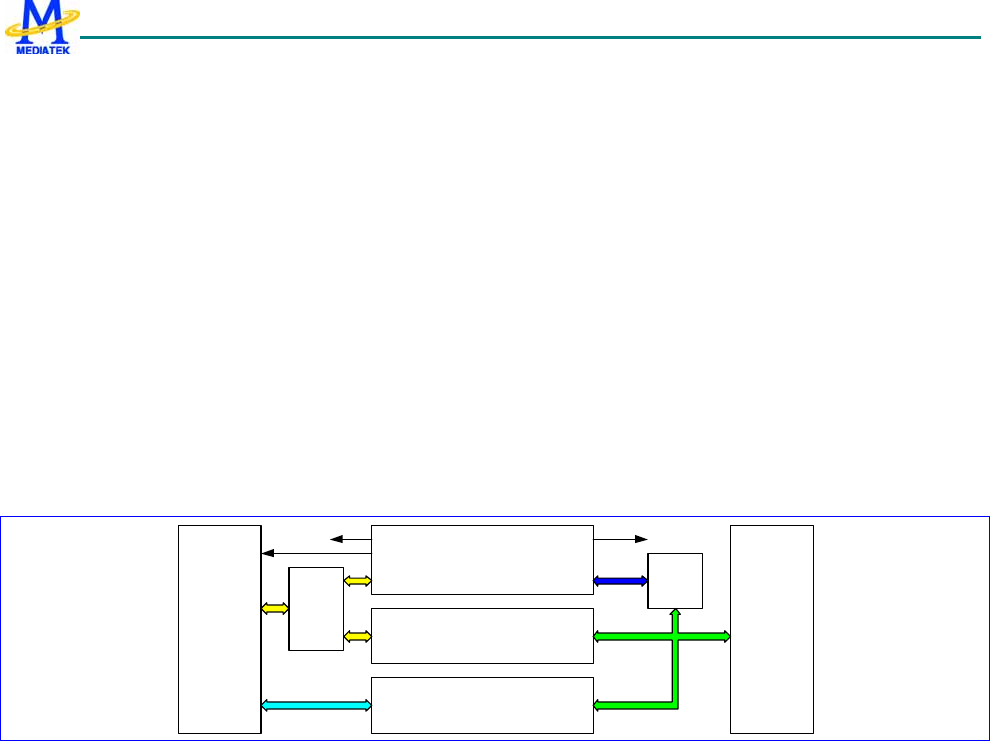
MT6235 GSM/GPRS Baseband Processor Data Sheet Revision 1.02
252/599 MediaTek Inc. Confidential
6 MCU/DSP Interface
MCU/DSP Interface resides between the Microcontroller Unit Subsystem and the Digital Signal Processor Subsystem. It
serves as the command and data exchange medium by which the MCU and the DSP communicate with each other.
As shown in Figure 29, MCU/DSP Interface is composed of three parts, namely:
z MCU/DSP Shared Registers, which are used for hardware controls and status signaling;
z MCU/DSP Shared RAM, where software of both sides exchange commands and data;
z AHB-to-DDMA Bridge, which translates AHB cycles to the DSP’s Internal DMA cycles and allows an AHB
master to access the memory of the DSP.
On the MCU Subsystem side, MCU/DSP Shared Registers are connected to APB, while MCU/DSP Shared RAM and
AHB-to-DDMA Bridge are connected to AHB. Therefore, MCU/DSP Shared Registers are allocated an APB address space,
whereas MCU/DSP Shared RAM and AHB-to-DDMA Bridge are mapped to AHB pages. On the DSP Subsystem side,
MCU/DSP Shared RAM and most MCU/DSP Shared Registers are attached to the DSP I/O bus through DSP I/O Hub.
MCU/DSP
Shared Registers
Shared RAM
AHB-to-DDMA Bridge
DSP MCU
I/O
Hub
APB
Br idg e
Int errupt s
Cont rols
IDMA
APB
AHB
Interrupt
I/O Bus MCU/DSP
Figure 29 MCU/DSP Interface block diagram.
Referring to Figure 1, the 640 16-bit words of MCU/DSP Shared RAM are allocated to the beginning of the AHB page at
50000000h for master DSP and at 58000000h for slave DSP. This memory can be accessed in 16-bit half-words or 8-bit
bytes by an AHB master, but not in 32-bit words.
The AHB pages beginning from 60000000h and from 68000000h are devoted to AHB-to-DDMA Bridges of the master and
slave DSP, which link DSP memories to AHB like AHB slaves. Specifically, the master DSP Code Memory, Program
Memory and Data Memory are mapped to the 1M-byte areas starting at 60000000h, 60100000h and 60200000h,
respectively (or 68000000h, 68100000h, and 68200000h for slave DSP). Each 1M-byte area is evenly partitioned to sixteen
64K-byte blocks corresponding to the 16 pages of one type of DSP memory. Because CM is 24-bit wide, its word is zero
extended to 32 bits over AHB and thus must be accessed in 32-bit words. PM and DM are both 16-bit wide, thus shall be
accessed in half-words (16-bit). Moreover, the PM data are protected when written through IDMA of slave DSP.
Correspondingly, L1 should prepare the PM data by specific encryption method in advance, and the hardware should take
responsibility of decryption before writing them into PM RAM through IDMA. The following block diagram depicts the
relation.

MT6235 GSM/GPRS Baseband Processor Data Sheet Revision 1.02
253/599 MediaTek Inc. Confidential
L1
PM data XOR
PM_XOR_MASK
pm_e_mess
pm_d_messXORPM RAM
AHB-to-IDMA
bridge
ecryption
decryption
Figure 30 PM data encryption/decryption
Reserved
DSP Code Memory Page 0
64 KBytes
DSP Code Memory Page 15
64 KBytes
DSP Program Memory Page 0
64 KBytes
DSP Program Memory Page 15
64 KBytes
DSP Dat a Memory Page 0
64 KBytes
DSPData Memory Page 15
64 KBytes
DSP DDMAS
Lo n g R e a d / Wr it e P a g e
64 KBytes
hort Read/Write Page
64 KBytes
Reserved
MCU/DSP Shared RAM
50000000h
60000000h
600F0000h
60100000h
601F0000h
60200000h
602F0000h
60300000h
60310000h
60320000h
500002BFh
6000FFFFh
600FFFFFh
6010FFFFh
601FFFFFh
6020FFFFh
602FFFFFh
6030FFFFh
6031FFFFh
6FFFFFFFh
DSP Program Memory Page
16384 Words x 16 Bits
0000h
7FFFh
Res e rved
16384 Words x 16 Bits
8000h
FFFFh
DSP Code Memory Page
16384 Words x 32 Bits
MCU Byt es
DSP Code Word
0000h
FFFFh
LSBMSB
DSP Data Memory Page
16384 Words x 16 Bits
7FFFh
0000h
Res e rved
16384 Words x 16 Bits
8000h
FFFFh
0
1
2
3
23:16
15:8
7:0
DSP DDMA
352 x 16-bit
Figure 3 Mapping of MCU/Master DSP Interface on the MCU memory space. For the MCU/Slave DSP Interface, the
difference is 08000000h base address offset at MCU side only.
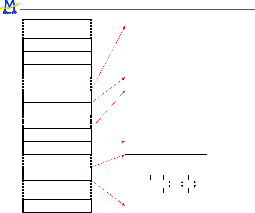
MT6235 GSM/GPRS Baseband Processor Data Sheet Revision 1.02
254/599 MediaTek Inc. Confidential
Reserved
DSP Code Memory Page 0
64 KBytes
DSP Code Memory Page 15
64 KBytes
DSP Program Memory Page 0
64 KBytes
DSP Program Memor y Page 15
64 KBytes
DSP Dat a Memory Page 0
64 KBytes
DSP Data Memory Page 15
64 KBytes
DSP DDMAS
Long Read/Wr it e Page
64 KBytes
hort Read/Wr it e Page
64 KBytes
Reserved
MCU/DSP Shared RAM
58000000h
68000000h
680F0000h
68100000h
681F0000h
68200000h
682F0000h
68300000h
68310000h
68320000h
5800055Fh
6800FFFFh
680FFFFFh
6810FFFFh
681FFFFFh
6820FFFFh
682FFFFFh
6830FFFFh
6831FFFFh
6FFFFFFFh
DSP Program Memory Page
16384 Wor ds x 16 Bit s
0000h
7FFFh
Res e r v ed
16384 Wor ds x 16 Bit s
8000h
FFFFh
DSP Code Memory Page
16384 Wor ds x 32 Bit s
MCU Byt es
DSP Code Word
0000h
FFFFh
LSBMSB
DSP Data Memory Page
16384 Wor ds x 16 Bit s
7FFFh
0000h
Res e r v ed
16384 Wor ds x 16 Bit s
8000h
FFFFh
0
1
2
3
23:16
15:8 7:0
DSP DDMA
688 x 16-bit
Figure 31 Mapping of MCU/Slave DSP Interface on the MCU memory space. For the MCU/Master DSP Interface, the
difference is 08000000h base address offset at MCU side only
6.1 MCU/DSP Shared Registers
6.1.1 General Description
MCU/DSP Shared Registers are a set of registers that are accessible by both the MCU and the DSP for
z the control of the DSP hardware, such as reset and power-down;
z the identification of the ongoing DSP tasks,

MT6235 GSM/GPRS Baseband Processor Data Sheet Revision 1.02
255/599 MediaTek Inc. Confidential
z the recognition of the DSP to MCU Interrupt, which informs the MCU of certain events happening in the DSP
side;
z the generation of the MCU to DSP Interrupt, by which the MCU sends commands and messages to the DSP;
z TDMA frame counts, which are referenced by the software for TDMA timing and are employed by GSM Cipher
Coprocessor in generating ciphering keys.
Functionalities of MCU/DSP Shared Registers are hardwired, which is different from MCU/DSP Shared RAM whose usage
is software-defined.
6.1.2 Register Definitions
Table 26 and Table2 list MCU/DSP Shared Registers and their address mapping to the MCU address space and DSP I/O
space. The MCU register addresses are the offsets from the base address 80300000h for master DSP (DSP1) and
80320000h for slave DSP (DSP2) on APB bus.
MCU Register
Address
DSP Register
Address Register Function Acronym
0000h N/A DSP1 Control Register SHARE_DSP1CTL
0004h 601h MCU-to-DSP1 Interrupt 1 Register SHARE_M2D1I1
0008h 602h MCU-to-DSP1 Interrupt 2 Register SHARE_M2D1I2
000Ch N/A DSP1-to-MCU Interrupt Control Register SHARE_D12MCTL
0010h N/A DSP1-to-MCU Interrupt Status Register SHARE_D12MSTA
0014h 605h DSP1 Task Identification Register SHARE_D12MTID
0018h 606h TDMA Counter Enable Register SHARE_1TDMAEN
001Ch 607h TDMA T1 Counter SHARE_1TDMAT1
0020h 608h TDMA T2 Counter SHARE_1TDMAT2
0024h 608h TDMA T3 Counter SHARE_1TDMAT3
0028h 60Ah DSP1 Debugging Control SHARE_DSP1DBG
0030h N/A DSP1 Task 1 Time Out SHARE_DSP1T1TO
0034h N/A DSP1 Task 2 Time Out SHARE_DSP1T2TO
N/A 60Bh DSP power-down source SHREG_1PWDNSRC
0048h 60Ch DSP self power-down control SHARE_1PWDNCON
N/A 60Dh DSP PC SHREG_D1PC
N/A 60Eh DSP CNTR SHREG_D1CNTR
004Ch N/A DSP slow-idle mode switch SHARE_DSP1CKR
Table 26 MCU/DSP1 Shared Registers
MCU Register
Address
DSP Register
Address Register Function Acronym
0000h N/A DSP2 Control Register SHARE_DSP2CTL

MT6235 GSM/GPRS Baseband Processor Data Sheet Revision 1.02
256/599 MediaTek Inc. Confidential
0004h 601h MCU-to-DSP2 Interrupt 1 Register SHARE_M2D2I1
0008h 602h MCU-to-DSP2 Interrupt 2 Register SHARE_M2D2I2
000Ch N/A DSP2-to-MCU Interrupt Control Register SHARE_D22MCTL
0010h N/A DSP2-to-MCU Interrupt Status Register SHARE_D22MSTA
0014h 605h DSP2 Task Identification Register SHARE_D22MTID
0018h 606h TDMA Counter Enable Register SHARE_2TDMAEN
001Ch 607h TDMA T1 Counter SHARE_2TDMAT1
0020h 608h TDMA T2 Counter SHARE_2TDMAT2
0024h 608h TDMA T3 Counter SHARE_2TDMAT3
0028h 60Ah DSP2 Debugging Control SHARE_DSP2DBG
002Ch N/A DSP2 Task 0 Time Out SHARE_DSP2T0TO
0030h N/A DSP2 Task 1 Time Out SHARE_DSP2T1TO
0034h N/A DSP2 Task 2 Time Out SHARE_DSP2T2TO
0038h N/A DSP2 Task 3 Time Out SHARE_DSP2T3TO
003Ch N/A DSP2 Task 4 Time Out SHARE_DSP2T4TO
N/A 60Bh DSP power-down source SHREG_2PWDNSRC
0048h 60Ch DSP self power-down control SHARE_2PWDNCON
N/A 60Dh DSP PC SHREG_D1PC
N/A 60Eh DSP CNTR SHREG_D1CNTR
004Ch N/A DSP slow-idle mode switch SHARE_DSP2CKR
Table 2 MCU/DSP2 Shared Registers
+0000hMCU N/ADSP DSP1 CONTROL
REGISTER
Bit 15 14 13 12 11 10 9 8 7 6 5 4 3 2 1 0
Name PWDA
CK PWDN BOOT RSTN
Type R R/W R/W R/W
Reset 0 1 1 0
This register directly controls the DSP signals: RSTn, BMODE, and PWDn. After the hardware reset, the RSTN bit and
BOOT bit are reset to 0 and 1, respectively, thus keeping the DSP in reset state with BMODE = 1. The MCU shall then
write 1 to RSTN to end the reset and to start booting of the DSP. Only bit 0 is accessible by DSP, by which DSP can learn
how it is reset, whether by MCU (RSTN = 1) or due to DSP-code crazy execution. Therefore after normal DSP booting
sequence from MCU, DSP code should read back the RSTN bit before entering any task.
PWDACK DSP power-down mode acknowledgement. This bit is read true when the DSP enter the IDLE state.
PWDN DSP power-down control. This bit is connected to the PWDN pin of the DSP. A 1-to-0 transition of this bit causes
the DSP to enter power-down mode, while a 0-to-1 transition of this bit wakes the DSP.
BOOT DSP boot mode. This bit is connected to the BMODE pin of the DSP. If BMODE is 1 when RSTn transit from 0 to
1, the DSP will enter the boot mode waiting for the completion of its program download.

MT6235 GSM/GPRS Baseband Processor Data Sheet Revision 1.02
257/599 MediaTek Inc. Confidential
RSTN DSP reset. This bit controls the RSTn input of the DSP.
0 Reset DSP.
+0000hMCU N/ADSP DSP2 CONTROL
REGISTER
Bit 15 14 13 12 11 10 9 8 7 6 5 4 3 2 1 0
Name PWDA
CK PWDN BOOT RSTN
Type R R/W R/W R/W
Reset 0 1 1 1
This register resides at slave DSP side with the same function with SHARE_DSP1CTL. However, since slave DSP should
be reset from DSP1, therefore RSTN of SHARE_DSP2CTL has to be initialized to be bit 0. Only bit 0 is accessible by DSP,
by which DSP can learn how it is reset, whether by MCU (RSTN = 1) or due to DSP-code crazy execution. Therefore after
normal DSP booting sequence from MCU, DSP code should read back the RSTN bit before entering any task.
+0004hMCU 601hDSP MCU-TO-DSP1
INTERRUPT 1
REGISTER
Bit 15 14 13 12 11 10 9 8 7 6 5 4 3 2 1 0
Name INTERRUPT LABEL
Type R/W
This register is written by the MCU to generate an interrupt request to the DSP. The generated interrupt shall have a higher
priority in the DSP side so that it can be serviced regardless of the status of DSP tasks. Contents of the register have no
hardware significance but shall be referenced by the MCU and DSP as the reason for the interrupt.
+0008hMCU 602hDSP MCU-TO-DSP1
INTERRUPT 2
REGISTER
Bit 15 14 13 12 11 10 9 8 7 6 5 4 3 2 1 0
Name INTERRUPT LABEL
Type R/W
This register is written by the MCU to generate an interrupt request to the DSP. The generated interrupt should have a lower
priority in the DSP side; therefore it may or may not be serviced immediately, depending on the status of DSP tasks.
Contents of the register have no hardware significance but shall be referenced by the MCU and DSP as the reason for the
interrupt.
+000ChMCU N/ADSP
DSP1-TO-MCU
INTERRUPT
CONTROL
REGISTER
Bit 15 14 13 12 11 10 9 8 7 6 5 4 3 2 1 0

MT6235 GSM/GPRS Baseband Processor Data Sheet Revision 1.02
258/599 MediaTek Inc. Confidential
Name TASK
7 TASK
6 TASK
5 TASK
4 TASK
3 TASK
2 TASK
1 TASK
0
Type R/W R/W R/W R/W R/W R/W R/W R/W
Reset 0 0 0 0 0 0 0 0
This register is programmed by the MCU to enable or disable the task interrupts asserted by the DSP. The interrupt for Task
X is asserted when TASKX is set and the MCU/DSP Shared RAM word at address X is written by the DSP.
TASKX Task Interrupt X Enable.
0 Disable the interrupt for Task X.
1 Enable the interrupt for Task X.
+0010hMCU N/ADSP
DSP1-TO-MCU
INTERRUPT
STATUS
REGISTER
Bit 15 14 13 12 11 10 9 8 7 6 5 4 3 2 1 0
Name TASK
7 TASK
6 TASK
5 TASK
4 TASK
3 TASK
2 TASK
1 TASK
0
Type RC RC RC RC RC RC RC RC
Reset 0 0 0 0 0 0 0 0
Bits of this register are set by the DSP to assert an interrupt to the MCU. When the DSP writes to the word address X in
MCU/DSP Shared RAM, the corresponding TASKX bit is set in this register. An MCU interrupt will be generated if
TASKX is not masked in SHARE_D1MCTL. To acknowledge the interrupt, the MCU shall read this register for the
interrupt status. After the read the interrupt flags will be cleared so that new Task Interrupts can be generated.
TASKX Task X Interrupt flag.
0 Task X Interrupt has not been asserted.
1 Task X Interrupt has been asserted.
+0014hMCU 605hDSP DSP1 TASK
IDENTIFICATIO
N REGISTER
Bit 15 14 13 12 11 10 9 8 7 6 5 4 3 2 1 0
Name TASK IDENTIFICATION CODE
Type R
This register is used by the DSP software posting its task status to the MCU. Contents of the register are observable as
debug signals.
+0018hMCU 606hDSP
TDMA
COUNTER
ENABLE
REGISTER
Bit 15 14 13 12 11 10 9 8 7 6 5 4 3 2 1 0
Name T3EN T2EN T1EN
Type R/W R/W R/W

MT6235 GSM/GPRS Baseband Processor Data Sheet Revision 1.02
259/599 MediaTek Inc. Confidential
This register is programmed by the MCU software to enable or disable the TDMA frame counter (T1, T2, T3) Shared
Registers. Contents of T1, T2 and T3 are referenced by the GSM Cipher Coprocessor for key generations.
T3EN T3 counter enable.
0 Disable SHARE_TDMAT3 counting so that it will not be updated by DTIRQ.
1 Enable SHARE_TDMAT3 counting so that it will be updated by DTIRQ.
T2EN T2 counter enable. 0 = disable, 1 = enable.
0 Disable SHARE_TDMAT2 counting so that it will not be updated by DTIRQ.
1 Enable SHARE_TDMAT2 counting so that it will be updated by DTIRQ.
T1EN T1 counter enable. 0 = disable, 1 = enable.
0 Disable SHARE_TDMAT1 counting so that it will not be updated by DTIRQ.
1 Enable SHARE_TDMAT1 counting so that it will be updated by DTIRQ.
+001ChMCU 607hDSP T1 COUNTER
Bit 15 14 13 12 11 10 9 8 7 6 5 4 3 2 1 0
Name T1
Type R/W
This register is the T1 part of the reduced TDMA frame number (RFN), i.e.,
T1 = TDMA frame number div (26 × 51).
At the asserting edge of the TDMA Frame Interrupt for DSP (DTIRQ), if the MCU has written to this register in advance,
T1 will be initialized to the written value. Otherwise T1 will be incremented by 1 if T2 = 25, T3 = 50 and T1EN = T2EN =
T3EN = 1.
+0020hMCU 608hDSP T2 COUNTER
Bit 15 14 13 12 11 10 9 8 7 6 5 4 3 2 1 0
Name T2
Type R/W
This register is the T2 part of the reduced TDMA frame number, i.e., T2 = TDMA frame number modulo 26.
At the asserting edge of DTIRQ, if the MCU has written to this register in advance, T2 will be initialized to the written
value. Otherwise T2 will be incremented by 1 modulo 26 if T2EN = 1.
+0024hMCU 609hDSP T3 COUNTER
Bit 15 14 13 12 11 10 9 8 7 6 5 4 3 2 1 0
Name T3
Type R/W
This register is the T3 count for calculating T3 of the reduced TDMA frame number. Specifically,
T3 = TDMA frame number modulo 51.
At the asserting edge of DTIRQ, if the MCU has written to this register in advance, T3 will be initialized to the written
value. Otherwise T3 will be incremented by 1 modulo 51 if T3EN = 1.
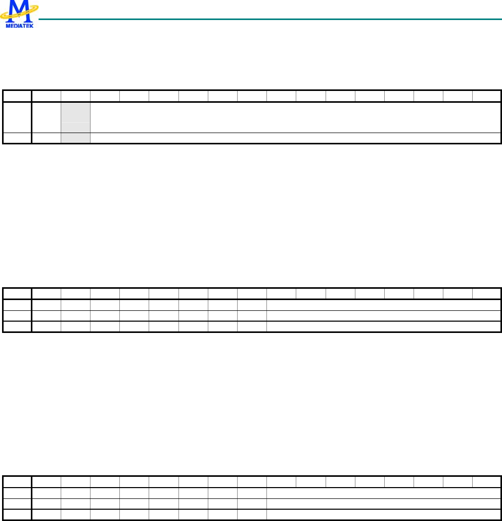
MT6235 GSM/GPRS Baseband Processor Data Sheet Revision 1.02
260/599 MediaTek Inc. Confidential
+0048hMCU 60ChDSP DSP SELF
POWER-DOWN
CONTROL
Bit 15 14 13 12 11 10 9 8 7 6 5 4 3 2 1 0
Name SELF
_PWD
NEN DSP_CNTR_WORD
Type R/W R/W
SEL_PWDNEN self power-down enable, programmed by MCU to enable the DSP self power-down mechanism through
CNTR internal register.
0 disable
1 enable
DSP_CNTR_WORD programmed by MCU to indicate the upper bound of CNTR value
+004ChMCU N/ADSP SHARE_DSP1C
KR
Bit 15 14 13 12 11 10 9 8 7 6 5 4 3 2 1 0
Name HOST_DEEP_CKR
Type R/W
Reset 0
DEEP_CKR To further saving host DSP power dissipation, the traditional CKR (DSP clock divider ratio for slow
IDLE mode) is split to two selections. One is for deep-sleep control, as configured by this register; the other is for
shallow sleep, which is programmed through SHRAM as before. Whenever RX frames assert, the CKR switch
from HOST_DEEP_CKR to another accordingly.
+004ChMCU N/ADSP SHARE_DSP2C
KR
Bit 15 14 13 12 11 10 9 8 7 6 5 4 3 2 1 0
Name SLAVE_DEEP_CKR
Type R/W
Reset 0
DEEP_CKR To further saving slave DSP power dissipation, the traditional CKR (DSP clock divider ratio for slow
IDLE mode) is split to two selections. One is for deep-sleep control, as configured by this register; the other is for
shallow sleep, which is programmed through SHRAM as before. Whenever TX frames assert, the CKR switch
from SLAVE_DEEP_CKR to another accordingly.

MT6235 GSM/GPRS Baseband Processor Data Sheet Revision 1.02
261/599 MediaTek Inc. Confidential
N/AMCU 60BhDSP DSP
POWER-DOWN
SOURCE
Bit 15 14 13 12 11 10 9 8 7 6 5 4 3 2 1 0
Name DSP_
PWDN HW_P
WDN
Type RO RO
Reset 0 0
This register is used to indicate the power-down source comes either from HW or DSP self. The signal is active high. And
the HW_PWDN includes the effect of MCU power-down (write through SHARE_DSPCTL), trap indicator (see the spec. of
patch unit), timeout indication (debug unit in sherif), and stack error.
N/AMCU 60DhDSP SHREG_DXPC
Bit 15 14 13 12 11 10 9 8 7 6 5 4 3 2 1 0
Name DSP_PC
Type R/W
Reset 0
N/AMCU 60EhDSP SHREG_DXCNT
R
Bit 15 14 13 12 11 10 9 8 7 6 5 4 3 2 1 0
Name DSP_CNTR
Type R/W
Reset 0
6.2 MCU/DSP Shared RAM
6.2.1 General Description
This is a 640 words × 16 bits dual-port static RAM that is accessible by both the MCU and the DSP. It serves as the
command and data exchange medium between the two processors. Except for some MCU/DSP Shared RAM words that
trigger interrupts, the software can allocate the memory for whatever purposes, such as
z Speech algorithm control parameters,
z Software task control parameters,
z Downlink channel processing results,
z Downlink channel data buffers, and
z Uplink channel data buffers.

MT6235 GSM/GPRS Baseband Processor Data Sheet Revision 1.02
262/599 MediaTek Inc. Confidential
The first eight MCU/DSP Shared RAM words are used for DSP event reports. When the DSP writes to one of these words,
a respective bit will be set in the SHARE_D2MSTA register and the DSP-to-MCU Interrupt will be asserted. Then the
MCU may read the MCU/DSP Shared RAM word to see the reason for the interrupt.
MCU/DSP Shared RAM can be accessed by the MCU in halfwords (16 bits) or bytes, but not in words (32 bits).
Simultaneous accesses from the MCU and the DSP are allowed, but simultaneous writes from both sides to the same word
should be avoided by the software as the word content would be undefined.
6.2.2 MCU/DSP Shared RAM Utilizations
Table3 and Table4 are the utilization of MCU/DSP Shared RAM, whose base address in the MCU side is 50000000h for
DSP1 and 58000000h for DSP2.
MCU Address DSP I/O Address Acronym Description
0000h 0000h DP_D12M_TASK0 First DSP task interrupt.
0002h 0001h DP_D12M_TASK1 Second DSP task interrupt.
0004h 0002h DP_D12M_TASK2 Third DSP task interrupt.
0006h 0003h DP_D12M_TASK3 Fourth DSP task interrupt.
0008h 0004h DP_D12M_TASK4 Fifth DSP task interrupt.
000Ah 0005h DP_D12M_TASK5 Sixth DSP task interrupt.
000Ch 0006h DP_D12M_TASK6 Seventh DSP task interrupt.
000Eh 0007h DP_D12M_TASK7 Eighth DSP task interrupt.
0010h
|
02BFh
0008h
|
014Fh
N/A Software defined.
Table 3 MCU/DSP1 Shared RAM utilizations.
MCU Address DSP I/O Address Acronym Description
0000h 0000h DP_D22M_TASK0 First DSP task interrupt.
0002h 0001h DP_D22M_TASK1 Second DSP task interrupt.
0004h 0002h DP_D22M_TASK2 Third DSP task interrupt.
0006h 0003h DP_D22M_TASK3 Fourth DSP task interrupt.
0008h 0004h DP_D22M_TASK4 Fifth DSP task interrupt.
000Ah 0005h DP_D22M_TASK5 Sixth DSP task interrupt.
000Ch 0006h DP_D22M_TASK6 Seventh DSP task interrupt.
000Eh 0007h DP_D22M_TASK7 Eighth DSP task interrupt.
0010h
|
055Fh
0008h
|
02B0h
N/A Software defined.
Table 4 MCU/DSP2 Shared RAM utilizations.

MT6235 GSM/GPRS Baseband Processor Data Sheet Revision 1.02
263/599 MediaTek Inc. Confidential
6.3 AHB-to-DDMA Bridge
6.3.1 General Description
AHB-to-DDMA Bridge links the AHB to the DSP DDMA port, which allows an external host to read from or write to the
DSP memory directly, so the AHB masters, i.e., the MCU and the AHB DMA Controller, can access the DSP program and
data memory without interrupting the DSP. This capability is useful in
z DSP Program downloading or uploading,
z DSP Data exchange, and
z DSP booting.
Referring to Figure 3, AHB-to-DDMA Bridge works in the AHB memory space beginning from 60000000h to 67FFFFFFh
for DSP1 and from 68000000h to 6FFFFFFFh for DSP2. As for the memory mapping on AHB bus, MCU/DSP1and
MCU/DSP2 interfaces differ in nothing more than the base address, therefore the following description is illustrated by
DSP1 case only.
The DSP Program Code Memory space comprising of sixteen 16384 × 24-bit pages is mapped to the AHB region from
60000000h to 600FFFFFh. The region further consists of sixteen 65536-byte blocks corresponding to the sixteen DSP
Program Code overlay pages, whose data words are transferred to or from AHB as 32-bit words.
The second 1M-byte AHB region from 60100000h to 601FFFFFh is mapped to the sixteen 16384 × 16-bit DSP Program
Data Memory pages. Again the region is partitioned to sixteen 65536-byte blocks. In each block the lower 32768 bytes are
mapped to one DSP Program Data overlay page and the upper 32768 bytes are reserved. Data in this region shall be
accessed as halfwords over AHB.
The third 1M-byte AHB region from 60200000h to 602FFFFFh is mapped to the sixteen 16384 × 16-bit DSP Data Memory
pages. The region is also partitioned to sixteen 65536-byte blocks, whose lower halves correspond to the sixteen DSP Data
Memory overlay pages. Data in this region shall be accessed as halfwords over AHB.
Access to the above three regions are converted to the DSP DDMA cycles carrying data and address information, thus are
called addressed DDMA cycles. The inclusion of address information enables random access at the expense of lower
transfer rate. For sequential read or write to the DSP memory, a more efficient way would be to provide address information
for the very first data transfer, and then rely on the auto-incrementing DDMA address register in the DSP core to provide
addresses of the rest of the data transfers. This way, the transfer rate can be improved as address information is not
converted every time.
Contrary to the addressed DDMA cycles produced by AHB accessing 6000000h to 602FFFFFh, the DDMA Short
Read/Write port (0x60310000 ~ 0x6031FFFF) may be used. This port relies on the DDMA address maintained within the
DSP core, thus generates no address latching cycles when they are accessed. Whenever a DDMA read/write is completed,
the DSP increments the internal DDMA address by one, so the next word can be accessed readily. Therefore, to access a
DSP memory block, only the first word needs to be accessed with an explicitly addressed DDMA cycle. All the other words
can be read or written through the Long or Short DDMA port.
An AHB-to-DDMA access will sometimes introduce wait states on AHB by toggling idma_hready. For write operations, if
throttle control is carefully executed (i.e., two DDMA transfers are expanded by enough cycles that the first transaction has
enough time to complete), idma_hready will never be toggled. For read operations, things are different in address mode
access and short mode access. For address mode, idma_hready always toggles until the read transaction is completed. In
MT6235 GSM/GPRS Baseband Processor Data Sheet Revision 1.02
264/599 MediaTek Inc. Confidential
short mode, since the actual read data is fetched at the previous transaction, idma_hready will not be toggled unless the
consecutive request comes too soon.
The Short DDMA ports shall be accessed in words if the DSP Program Code memory is targeted; or in half-words if the
DSP Program Data or DSP Data memory is targeted.
During DSP booting, the DSP program execution is held off until the DDMA writes to the Program Code Memory address
zero. Therefore, MCU software should load all necessary DSP memory locations with proper code/data before writing to
the DSP Program Code Memory address 0, which is mapped to MCU address 0x60000000. As for the PM
encryption/decryption, the PM_XOR_MASK is 0xBF96, and the following table can describe the encryption
Before encryption After encryption
pm_data[0] pm_e_data[13]
pm_data[1] pm_e_data[4]
pm_data[2] pm_e_data[15]
pm_data[3] pm_e_data[1]
pm_data[4] pm_e_data[12]
pm_data[5] pm_e_data[3]
pm_data[6] pm_e_data[8]
pm_data[7] pm_e_data[0]
pm_data[8] pm_e_data[9]
pm_data[9] pm_e_data[11]
pm_data[10] pm_e_data[5]
pm_data[11] pm_e_data[10]
pm_data[12] pm_e_data[6]
pm_data[13] pm_e_data[7]
pm_data[14] pm_e_data[2]
pm_data[15] pm_e_data[14]
Table 5 PM encription
6.3.2 Register Definitions
60310000h DDMA Short Read/Write Port DDMA_SHORT
Bit 15 14 13 12 11 10 9 8 7 6 5 4 3 2 1 0
Name DDMA_SHORT
Type R/W
This is the read/write port for AHB-to-DDMA data access using short DDMA cycles. When this port is read, an DDMA
read cycle is sent to the DSP, which returns the content of DDMA data buffer to AHB via AHB-to-DDMA Bridge, then
reads a specific location in its memory and puts the read data into the DDMA data buffer. When this port is written, a
DDMA write cycle is sent to the DSP, which writes the AHB data to a specific location in its memory. Meanwhile, another
AHB transaction can be proceeding.

MT6235 GSM/GPRS Baseband Processor Data Sheet Revision 1.02
265/599 MediaTek Inc. Confidential
For CM transfers, bits 0 to 23 contain the data word. For PM or DM transfers, only bits 0 to 15 are used. The unused bits
have undefined values if read.

MT6235 GSM/GPRS Baseband Processor Data Sheet Revision 1.02
266/599 MediaTek Inc. Confidential

MT6235 GSM/GPRS Baseband Processor Data Sheet Revision 1.02
267/599 MediaTek Inc. Confidential

MT6235 GSM/GPRS Baseband Processor Data Sheet Revision 1.02
268/599 MediaTek Inc. Confidential
7 Multi-Media Subsystem
MT6235 is specially designed to support multi-media terminals. It integrates several hardware based accelerators, like
advanced LCD display controller and hardware Image Resizer. Besides, MT6235 also incorporates NAND Flash, USB 2.0
Device and SD/MMC/MS/MS Pro Controllers for massive data transfers and storages. This chapter describes those
functional blocks in detail.
7.1 LCD Interface
7.1.1 General Description
MT6235 contains a versatile LCD controller which is optimized for multimedia applications. This controller supports many
types of LCD modules and contains a rich feature set to enhance the functionality. These features are:
z Up to 320 x 240 resolution
z The internal frame buffer supports 8bpp indexed color, RGB 565, RGB 888 and ARGB 8888 format.
z Supports 8-bpp (RGB332), 12-bpp (RGB444), 16-bpp (RGB565), 18-bit (RGB666) and 24-bit (RGB888) LCD
modules.
z 6 Layers Overlay with individual color depth, window size, vertical and horizontal offset, source key, alpha value and
display rotation control(90°,180°, 270°, mirror and mirror then 90°, 180° and 270°)
z One Color Look-Up Table
z Three Gamma Correction Tables
For parallel LCD modules, the LCD controller can reuse external memory interface or use dedicated 8/9/16/18-bit parallel
interface to access them and 8080 type interface is supported. It can transfer the display data from the internal SRAM or
external SRAM/Flash Memory to the off-chip LCD modules.
For serial LCD modules, this interface performs parallel to serial conversion and both 8- and 9- bit serial interface is
supported. The 8-bit serial interface uses four pins – LSCE#, LSDA, LSCK and LSA0 – to enter commands and data.
Meanwhile, the 9-bit serial interface uses three pins – LSCE#, LSDA and LSCK – for the same purpose. Data read is not
available with the serial interface and data entered must be 8 bits.
MT6235 GSM/GPRS Baseband Processor Data Sheet Revision 1.02
269/599 MediaTek Inc. Confidential
LPCE0#
LPCE1#
LRST#
LRD#
LPA0
LWR#
NLD[17:0]
LSCE0#
LSCE1#
LSDA
LSA0
LSCK
Layer 3
Controller
Layer 1
Controller
Parallel LCD
Channel
Controller
Serial LCD
Channel
Controller
Overlay
LCD AHB
Master
Layer 0
Controller
Layer 2
Controller
AHB BUS
LUT
Layer 5
Controller
Layer 4
Controller
Figure 32 LCD Interface Block Diagram
Figure 33 shows the timing diagram of this serial interface. When the block is idle, LSCK is forced LOW and LSCE# is
forced HIGH. Once the data register contains data and the interface is enabled, LSCE# is pulled LOW and remain LOW for
the duration of the transmission.
8-bit Serial Interface
LSCK(SPH=SPO=0)
LSDA D7 D6 D5 D4 D3 D2 D1 D0
LSCE#
LSA0
9-bit Serial Interface
LSCK(SPH=SPO=0)
LSDA A0 D7 D6 D5 D4 D3 D2 D1 D0
LSCE#
LSA0
Figure 33 LCD Interface Transfer Timing Diagram
LCD = 0x9000_0000

MT6235 GSM/GPRS Baseband Processor Data Sheet Revision 1.02
270/599 MediaTek Inc. Confidential
Address Register Function Width Acronym
LCD + 0000h LCD Interface Status Register 16 LCD_STA
LCD + 0004h LCD Interface Interrupt Enable Register 16 LCD_INTEN
LCD + 0008h LCD Interface Interrupt Status Register 16 LCD_INTSTA
LCD + 000ch LCD Interface Frame Transfer Register 16 LCD_START
LCD + 0010h LCD Parallel/Serial LCM Reset Register 16 LCD_RSTB
LCD + 0014h LCD Serial Interface Configuration Register 16 LCD_SCNF
LCD + 0018h LCD Parallel Interface 0 Configuration Register 32 LCD_PCNF0
LCD + 001ch LCD Parallel Interface 1 Configuration Register 32 LCD_PCNF1
LCD + 0020h LCD Parallel Interface 2 Configuration Register 32 LCD_PCNF2
LCD + 0024h LCD Tearing Control Register 32 LCD_TECON
LCD + 0040h LCD Main Window Size Register 32 LCD_MWINSIZE
LCD + 0044h LCD ROI Window Write to Memory Offset Register 32 LCD_WROI_W2MOFS
LCD + 0048h LCD ROI Window Write to Memory Control Register 24 LCD_WROI_W2MCON
LCD + 004ch LCD ROI Window Write to Memory Address Register 32 LCD_WROI_W2MADD
LCD + 0050h LCD ROI Window Control Register 32 LCD_WROICON
LCD + 0054h LCD ROI Window Offset Register 32 LCD_WROIOFS
LCD + 0058h LCD ROI Window Command Start Address Register 16 LCD_WROICADD
LCD + 005ch LCD ROI Window Data Start Address Register 16 LCD_WROIDADD
LCD + 0060h LCD ROI Window Size Register 32 LCD_WROISIZE
LCD + 0064h LCD ROI Window Hardware Refresh Register 32 LCD_WROI_HWREF
LCD + 0068h LCD ROI Window Background Color Register 32 LCD_WROI_BGCLR
LCD + 0070h LCD Layer 0 Window Control Register 32 LCD_L0WINCON
LCD + 0074h LCD Layer 0 Source Color Key Register 32 LCD_L0WINSKEY
LCD + 0078h LCD Layer 0 Window Display Offset Register 32 LCD_L0WINOFS
LCD + 007ch LCD Layer 0 Window Display Start Address Register 32 LCD_L0WINADD
LCD + 0080h LCD Layer 0 Window Size 32 LCD_L0WINSIZE
LCD + 0090h LCD Layer 1 Window Control Register 32 LCD_L1WINCON
LCD + 0094h LCD Layer 1 Source Color Key Register 32 LCD_L1WINSKEY
LCD + 0098h LCD Layer 1 Window Display Offset Register 32 LCD_L1WINOFS
LCD + 009ch LCD Layer 1 Window Display Start Address Register 32 LCD_L1WINADD
LCD + 00a0h LCD Layer 1 Window Size 32 LCD_L1WINSIZE
LCD + 00b0h LCD Layer 2 Window Control Register 32 LCD_L2WINCON
LCD + 00b4h LCD Layer 2 Source Color Key Register 32 LCD_L2WINSKEY
LCD + 00b8h LCD Layer 2 Window Display Offset Register 32 LCD_L2WINOFS
LCD + 00bch LCD Layer 2 Window Display Start Address Register 32 LCD_L2WINADD
LCD + 00c0h LCD Layer 2 Window Size 32 LCD_L2WINSIZE
LCD + 00d0h LCD Layer 3 Window Control Register 32 LCD_L3WINCON
LCD + 00d4h LCD Layer 3 Source Color Key Register 32 LCD_L3WINSKEY

MT6235 GSM/GPRS Baseband Processor Data Sheet Revision 1.02
271/599 MediaTek Inc. Confidential
LCD + 00d8h LCD Layer 3 Window Display Offset Register 32 LCD_L3WINOFS
LCD + 00dch LCD Layer 3 Window Display Start Address Register 32 LCD_L3WINADD
LCD + 00e0h LCD Layer 3 Window Size 32 LCD_L3WINSIZE
LCD + 00f0h LCD Layer 4 Window Control Register 32 LCD_L4WINCON
LCD + 00f4h LCD Layer 4 Source Color Key Register 32 LCD_L4WINSKEY
LCD + 00f8h LCD Layer 4 Window Display Offset Register 32 LCD_L4WINOFS
LCD + 00fch LCD Layer 4 Window Display Start Address Register 32 LCD_L4WINADD
LCD + 0100h LCD Layer 4 Window Size 32 LCD_L4WINSIZE
LCD + 0110h LCD Layer 5 Window Control Register 32 LCD_L5WINCON
LCD + 0114h LCD Layer 5 Source Color Key Register 32 LCD_L5WINSKEY
LCD + 0118h LCD Layer 5 Window Display Offset Register 32 LCD_L5WINOFS
LCD + 011ch LCD Layer 5 Window Display Start Address Register 32 LCD_L5WINADD
LCD + 0120h LCD Layer 5 Window Size 32 LCD_L5WINSIZE
LCD + 4000h LCD Parallel Interface 0 Data 32 LCD_PDAT0
LCD + 4100h LCD Parallel Interface 0 Command 32 LCD_PCMD0
LCD + 5000h LCD Parallel Interface 1 Data 32 LCD_PDAT1
LCD + 5100h LCD Parallel Interface 1 Command 32 LCD_PCMD1
LCD + 6000h LCD Parallel Interface 2 Data 32 LCD_PDAT2
LCD + 6100h LCD Parallel Interface 2 Command 32 LCD_PCMD2
LCD + 8000h LCD Serial Interface 1 Data 16 LCD_SDAT1
LCD + 8100h LCD Serial Interface 1 Command 16 LCD_SCMD1
LCD + 9000h LCD Serial Interface 0 Data 16 LCD_SDAT0
LCD + 9100h LCD Serial Interface 0 Command 16 LCD_SCMD0
LCD + c000h
~ c3fch LCD Gamma Correction LUT Register 32 LCD_GAMMA
LCD + c400h
~ c7fch LCD Color Palette LUT Register 32 LCD_PAL
LCD + c800h
~ c87c LCD Interface Command/Parameter0 Register 32 LCD_COMD0
LCD + c880h
~ c8fch LCD Interface Command/Parameter1 Register 32 LCD_COMD1
Table 27 Memory map of LCD Interface
7.1.2 Register Definitions
LCD +0000h LCD Interface Status Register LCD_STA
Bit 15 14 13 12 11 10 9 8 7 6 5 4 3 2 1 0
Name TE_P
END
CMD_
CPEN
D
DATA
_PEN
D RUN
Type R/W R R R
Reset 0 0 0 0
MT6235 GSM/GPRS Baseband Processor Data Sheet Revision 1.02
272/599 MediaTek Inc. Confidential
RUN LCD Interface Running Status
DATA_PEND Data Pending Indicator in Hardware Trigger Mode
CMD_PEND Command Pending Indicator in Hardware Triggered Refresh Mode
TE_PEND Frame update pending for tearing input
LCD +0004h LCD Interface Interrupt Enable Register LCD_INTEN
Bit 15 14 13 12 11 10 9 8 7 6 5 4 3 2 1 0
Name TE_C
PL CMD_
CPL DATA
_CPL CPL
Type R/W R/W R/W R/W
Reset 0 0 0 0
CPL LCD Frame Transfer Complete Interrupt Control
DATA_CPL Data Transfer Complete in Hardware Triggered Refresh Mode Interrupt Control
CMD_CPL Command Transfer Complete in Hardware Trigger Refresh Mode Interrupt Control
TE_CPL Issue an interrupt when TE pending complete
LCD +0008h LCD Interface Interrupt Status Register LCD_INTSTA
Bit 15 14 13 12 11 10 9 8 7 6 5 4 3 2 1 0
Name TE_
CPL CMD_
CPL DATA
_CPL CPL
Type R R R R
Reset 0 0 0 0
CPL LCD Frame Transfer Complete Interrupt
DATA_CPL Data Transfer Complete in Hardware Triggered Refresh Mode Interrupt
CMD_CPL Command Transfer Complete in Hardware Triggered Refresh Mode Interrupt
TE_ CPL Frame update pending for tearing input
LCD +000Ch LCD Interface Frame Transfer Register LCD_START
Bit 15 14 13 12 11 10 9 8 7 6 5 4 3 2 1 0
Name STAR
T
Type R/W
Reset 0
START Start Control of LCD Frame Transfer
LCD +0010h LCD Parallel/Serial Interface Reset Register LCD_RSTB
Bit 15 14 13 12 11 10 9 8 7 6 5 4 3 2 1 0
Name RSTB
Type R/W
Reset 1
RSTB Parallel/Serial LCD Module Reset Control
LCD +0014h LCD Serial Interface Configuration Register LCD _SCNF
Bit 15 14 13 12 11 10 9 8 7 6 5 4 3 2 1 0
Name 26M 13M GAMMA_ID CSP1 CSP0 8/9 DIV SPH SPO
Type R/W R/W R/W R/W R/W R/W R/W R/W R/W
Type 0 0 0 0 0 0 0 0 0

MT6235 GSM/GPRS Baseband Processor Data Sheet Revision 1.02
273/599 MediaTek Inc. Confidential
SPO Clock Polarity Control
SPH Clock Phase Control
DIV Serial Clock Divide Select Bits
8/9 8-bit or 9-bit Interface Selection
CSP0 Serial Interface Chip Select 0 Polarity Control
CSP1 Serial Interface Chip Select 1 Polarity Control
GAMMA_ID Gamma correction LUT ID
00 table 0
01 table 1
10 table 2
11 no table selected
13M Enable 13MHz clock gating.
26M Enable 26MHz clock gating.
LCD +0018h LCD Parallel Interface Configuration Register 0 LCD_PCNF0
Bit 31 30 29 28 27 26 25 24 23 22 21 20 19 18 17 16
Name C2WS C2WH C2RS GAMMA_ID_
R GAMMA_ID_
G GAMMA_ID_
B DW
Type R/W R/W R/W R/W R/W R/W R/W
0 0 0 0 0 0 0
Bit 15 14 13 12 11 10 9 8 7 6 5 4 3 2 1 0
Name 52M 26M WST RLT
Type R/W R/W R/W R/W
Reset 0 0 0 0
RLT Read Latency Time
Actual Read Latency cycles = RLT+2 cycles
WST Write Wait State Time
26M Enable 26MHz clock gating.
52M Enable 52MHz clock gating.
DW Data width of the parallel interface
00 8-bit.
01 9-bit
10 16-bit
11 18-bit
GAMMA_ID_R Gamma Correction LUT ID for Red Component
00 table 0
01 table 1
10 table 2
11 no table selected
GAMMA_ID_G Gamma correction LUT ID for Green Component
00 table 0
01 table 1
10 table 2
11 no table selected
GAMMA_ID_B Gamma correction LUT ID for Blue Component
MT6235 GSM/GPRS Baseband Processor Data Sheet Revision 1.02
274/599 MediaTek Inc. Confidential
00 table 0
01 table 1
10 table 2
11 no table selected
C2RS Chip Select (LPCE#) to Read Strobe (LRD#) Setup Time
C2WH Chip Select (LPCE#) to Write Strobe (LWR#) Hold Time
C2WS Chip Select (LPCE#) to Write Strobe (LWR#) Setup Time
LCD +001Ch LCD Parallel Interface Configuration Register 1 LCD_PCNF1
Bit 31 30 29 28 27 26 25 24 23 22 21 20 19 18 17 16
Name C2WS C2WH C2RS GAMMA_ID DW
Type R/W R/W R/W R/W R/W
0 0 0 11 0
Bit 15 14 13 12 11 10 9 8 7 6 5 4 3 2 1 0
Name 52M 26M WST RLT
Type R/W R/W R/W R/W
Reset 0 0 0 0
RLT Read Latency Time
Actual Read Latency cycles = RLT+2 cycles
WST Write Wait State Time
26M Enable 26MHz clock gating.
52M Enable 52MHz clock gating.
DW Data width of the parallel interface
00 8-bit.
01 9-bit
10 16-bit
11 18-bit
GAMMA_ID Gamma correction LUT ID
00 table 0
01 table 1
10 table 2
11 no table selected
C2RS Chip Select (LPCE#) to Read Strobe (LRD#) Setup Time
C2WH Chip Select (LPCE#) to Write Strobe (LWR#) Hold Time
C2WS Chip Select (LPCE#) to Write Strobe (LWR#) Setup Time
LCD +0020h LCD Parallel Interface Configuration Register 2 LCD_PCNF2
Bit 31 30 29 28 27 26 25 24 23 22 21 20 19 18 17 16
Name C2WS C2WH C2RS GAMMA_ID DW
Type R/W R/W R/W R/W R/W
0 0 0 0 0
Bit 15 14 13 12 11 10 9 8 7 6 5 4 3 2 1 0
Name 52M 26M WST RLT
Type R/W R/W R/W R/W
Reset 0 0 0 0
RLT Read Latency Time
Actual Read Latency cycles = RLT+2 cycles

MT6235 GSM/GPRS Baseband Processor Data Sheet Revision 1.02
275/599 MediaTek Inc. Confidential
WST Write Wait State Time
26M Enable 26MHz clock gating.
52M Enable 52MHz clock gating.
DW Data width of the parallel interface.
00 8-bit.
01 9-bit
10 16-bit
11 18-bit
GAMMA_ID Gamma correction LUT ID
00 table 0
01 table 1
10 table 2
11 no table selected
C2RS Chip Select (LPCE#) to Read Strobe (LRD#) Setup Time
C2WH Chip Select (LPCE#) to Write Strobe (LWR#) Hold Time
C2WS Chip Select (LPCE#) to Write Strobe (LWR#) Setup Time
LCD Controller Synchronization Modes
When TE_EN is enabled, LCD controller will synchronize its updating to LCM refresh timing. And it supports two
synchronizing modes depending on TE_MODE.
TE Signal Polarity
TE_EDGE_SEL can be used to select TE polarity for TE signal detection.
TE_EDGE_SEL value TE signal detection
0 Detect a TE signal at its rising edge. This setting is for active high TE signal.
1 Detect a TE signal at its falling edge. This setting if for active low TE signal.
Table 2 TE Signal Polarity
Vertical Synchronization Mode
MT6235 LCD supports vertical synchronization mode to avoid tearing effect.
In this mode, LCD controller starts to update LCM after each rising edge of the TE input (or falling edge, if
TE_EDGE_SEL is set to 1) (see Figure 3).
Figure 34 Vertical Synchronization Mode
LCD +0024h LCD Tearing Control Register LCD_TECON
Bit 31 30 29 28 27 26 25 24 23 22 21 20 19 18 17 16
TE input
LCD updating
Vertical Synchro

MT6235 GSM/GPRS Baseband Processor Data Sheet Revision 1.02
276/599 MediaTek Inc. Confidential
Name
Type
Reset
Bit 15 14 13 12 11 10 9 8 7 6 5 4 3 2 1 0
Name TE_E
DGE_
SEL
TE_E
N
Type R/W R/W
Reset 0 0
TE_EN Enable tearing control. LCD controller will synchronize to LCM refresh timing.
TE_EDGE_SEL Select sync edge.
0 Rising edge
1 Falling edge
LCD +4000h LCD Parallel 0 Interface Data LCD_PDAT0
Bit 31 30 29 28 27 26 25 24 23 22 21 20 19 18 17 16
Name DATA[31:16]
Type R/W
Bit 15 14 13 12 11 10 9 8 7 6 5 4 3 2 1 0
Name DATA[15:0]
Type R/W
DATA Writing to LCD+4000 will drive LPA0 low when sending this data out in parallel BANK0, while writing to
LCD+4100 will drive LPA0 high.
LCD +5000h LCD Parallel 1 Interface Data LCD_PDAT1
Bit 31 30 29 28 27 26 25 24 23 22 21 20 19 18 17 16
Name DATA[31:16]
Type R/W
Bit 15 14 13 12 11 10 9 8 7 6 5 4 3 2 1 0
Name DATA[15:0]
Type R/W
DATA Writing to LCD+5000 will drive LPA1 low when sending this data out in parallel BANK1, while writing to
LCD+5100 will drive LPA1 high
LCD +6000h LCD Parallel 2 Interface Data LCD_PDAT2
Bit 31 30 29 28 27 26 25 24 23 22 21 20 19 18 17 16
Name DATA[31:16]
Type R/W
Bit 15 14 13 12 11 10 9 8 7 6 5 4 3 2 1 0
Name DATA[15:0]
Type R/W
DATA Writing to LCD+6000 will drive LPA2 low when sending this data out in parallel BANK2, while writing to
LCD+6100 will drive LPA2 high
LCD
+8000/8100h LCD Serial Interface 1 Data LCD_SDAT1
Bit 15 14 13 12 11 10 9 8 7 6 5 4 3 2 1 0
Name DATA
MT6235 GSM/GPRS Baseband Processor Data Sheet Revision 1.02
277/599 MediaTek Inc. Confidential
Type W
DATA Writing to LCD+8000 will drive LSA0 low while sending this data out in serial BANK1, while writing to
LCD+8100 will drive LSA0 high
LCD
+9000/9100h LCD Serial Interface 0 Data LCD_SDAT0
Bit 15 14 13 12 11 10 9 8 7 6 5 4 3 2 1 0
Name DATA
Type W
DATA Writing to LCD+9000 will drive LSA0 low while sending this data out in serial BANK0, while writing to
LCD+9100 will drive LSA0 high
LCD +0040h Main Window Size Register LCD_MWINSIZE
Bit 31 30 29 28 27 26 25 24 23 22 21 20 19 18 17 16
Name ROW
Type R/W
Bit 15 14 13 12 11 10 9 8 7 6 5 4 3 2 1 0
Name COLUMN
Type R/W
COLUMN 10-bit Virtual Image Window Column Size
ROW 10-bit Virtual Image Window Row Size
LCD +0044h Region of Interest Window Write to Memory Offset
Register
LCD_WROI_W2M
OFS
Bit 31 30 29 28 27 26 25 24 23 22 21 20 19 18 17 16
Name Y-OFFSET
Type R/W
Bit 15 14 13 12 11 10 9 8 7 6 5 4 3 2 1 0
Name X-OFFSET
Type R/W
This control register is used to specify the offset of the ROI window from the LCD_WROI_W2MADDR when writing the
ROI window’s content to memory.
X-OFFSET the x offset of ROI window in the destination memory.
Y-OFFSET the y offset of ROI window in the destination memory.
LCD +0048h Region of Interest Window Write to Memory Control
Register
LCD_WROI_W2M
CON
Bit 31 30 29 28 27 26 25 24 23 22 21 20 19 18 17 16
Name
Type
Reset
Bit 15 14 13 12 11 10 9 8 7 6 5 4 3 2 1 0
Name OUTPUT_ALPHA DC_O
UT_E
N
ADDI
NC_DI
SABL
E
DISC
ON W2M_FORM
AT W2LC
M
Type R/W R/W R/W R/W R/W R/W
Reset 0xff 0 0 0 0 0
MT6235 GSM/GPRS Baseband Processor Data Sheet Revision 1.02
278/599 MediaTek Inc. Confidential
This control register is effective only when the W2M bit is set in LCD_WROICON register.
W2LCM Write to LCM simultaneously.
W2M_FORMAT Write to memory format.
00 RGB565
01 RGB888
10 ARGB8888
DISCON Block Write Enable Control. By setting both DISCON and W2M to 1, the LCD controller will write out
the ROI pixel data as a part of MAIN window, using the width of MAIN window to calculate the write-out address. If this
bit is not set, the ROI window will be written to memory in continuous addresses.
ADDINC_DISABLE Disable address increase when writing to memory.
DC_OUT_EN Enable direct couple to rotator 3.
OUTPUT_ALPHA Output Alpha value.
LCD +004Ch Region of Interest Window Write to Memory Address
Register LCD_WROI_W2M
ADD
Bit 31 30 29 28 27 26 25 24 23 22 21 20 19 18 17 16
Name W2M_ADDR
Type R/W
Bit 15 14 13 12 11 10 9 8 7 6 5 4 3 2 1 0
Name W2M_ADDR
Type R/W
W2M_ADDR Write to memory address. For better memory write efficiency, it is recommended to 64 bytes
alignment, but it is not restricted to 64 bytes alignment.
LCD +0050h Region of Interest Window Control Register LCD_WROICON
Bit 31 30 29 28 27 26 25 24 23 22 21 20 19 18 17 16
Name EN0 EN1 EN2 EN3 EN4 EN5 PERIOD
Type R/W R/W R/W R/W R/W R/W R/W
Bit 15 14 13 12 11 10 9876543 2 10
Name ENC W2M
COM_
SEL COMMAND FORMAT
Type R/W R/W R/W R/W R/W
FORMAT LCD Module Data Format
Bit 0 : in BGR sequence, otherwise in RGB sequence.
Bit 1 : LSB first, otherwise MSB first.
Bit 2 : padding bits on MSBs, otherwise on LSBs.
Bit 5-3 : 000 for RGB332, 001 for RGB444, 010 for RGB565, 011 for RGB666, 100 for RGB888.
Bit 7-6 : 00 for 8-bit interface, 01 for 16-bit interface, 10 for 9-bit interface, 11 for 18-bit interface.
Note: When the interface is configured as 9 bit or 18 bit, the field of bit5-2 is ignored.
00000000 8bit 1cycle/1pixel RGB3.3.2 RRRGGGBB
00000001 1cycle/1pixel RGB3.3.2 BBGGGRRR
00001000 3cycle/2pixel RGB4.4.4 RRRRGGGG
BBBBRRRR
GGGGBBBB

MT6235 GSM/GPRS Baseband Processor Data Sheet Revision 1.02
279/599 MediaTek Inc. Confidential
00001011 3cycle/2pixel RGB4.4.4 GGGGRRRR
RRRRBBBB
BBBBGGGG
00010000 2cycle/1pixel RGB5.6.5 RRRRRGGG
GGGBBBBB
00010011 2cycle/1pixel RGB5.6.5 GGGRRRRR
BBBBBGGG
00011000 3cycle/1pixel RGB6.6.6 RRRRRRXX
GGGGGGXX
BBBBBBXX
00011100 3cycle/1pixel RGB6.6.6 XXRRRRRR
XXGGGGGG
XXBBBBBB
00100000 3cycle/1pixel RGB8.8.8 RRRRRRRR
GGGGGGGG
BBBBBBBB
10xxxx00 9bit 2cycle/1pixel RGB6.6.6 RRRRRRGGG
GGGBBBBBB
10xxxx11 2cycle/1pixel RGB6.6.6 GGGRRRRRR
BBBBBBGGG
01000000 16bit 1cycle/2pixel RGB3.3.2 RRRGGGBBRRRGGGBB
01000010 1cycle/2pixel RGB3.3.2 RRRGGGBBRRRGGGBB
01000001 1cycle/2pixel RGB3.3.2 BBGGGRRRBBGGGRRR
01000011 1cycle/2pixel RGB3.3.2 BBGGGRRRBBGGGRRR
01001100 1cycle/1pixel RGB4.4.4 XXXXRRRRGGGGBBBB
01001101 1cycle/1pixel RGB4.4.4 XXXXBBBBGGGGRRRR
01001000 1cycle/1pixel RGB4.4.4 RRRRGGGGBBBBXXXX
01001001 1cycle/1pixel RGB4.4.4 BBBBGGGGRRRRXXXX
01010000 1cycle/1pixel RGB5.6.5 RRRRRGGGGGGBBBBB
01010001 1cycle/1pixel RGB5.6.5 BBBBBGGGGGGRRRRR
01011100 3cycle/2pixel RGB6.6.6 XXXXRRRRRRGGGGGG
XXXXBBBBBBRRRRRR
XXXXGGGGGGBBBBBB
01011111 3cycle/2pixel RGB6.6.6 XXXXGGGGGGRRRRRR
XXXXRRRRRRBBBBBB
XXXXBBBBBBGGGGGG
01011000 3cycle/2pixel RGB6.6.6 RRRRRRGGGGGGXXXX
BBBBBBRRRRRRXXXX
GGGGGGBBBBBBXXXX
01011011 3cycle/2pixel RGB6.6.6 GGGGGGRRRRRRXXXX
RRRRRRBBBBBBXXXX
BBBBBBGGGGGGXXXX
01100000 3cycle/2pixel RGB8.8.8 RRRRRRRRGGGGGGGG

MT6235 GSM/GPRS Baseband Processor Data Sheet Revision 1.02
280/599 MediaTek Inc. Confidential
BBBBBBBBRRRRRRRR
GGGGGGGGBBBBBBBB
01100011 3cycle/2pixel RGB8.8.8 GGGGGGGGRRRRRRRR
RRRRRRRRBBBBBBBB
BBBBBBBBRRRRRRRR
11xxxx00 18bit 1cycle/1pixel RGB6.6.6 RRRRRRGGGGGGBBBBBB
11xxxx01 1cycle/1pixel RGB6.6.6 BBBBBBGGGGGGRRRRRR
11100000 3cycle/2pixel RGB8.8.8 RRRRRRRRGGGGGGGG
BBBBBBBBRRRRRRRR
GGGGGGGGBBBBBBBB
11100011 3cycle/2pixel RGB8.8.8 GGGGGGGGRRRRRRRR
RRRRRRRRBBBBBBBB
BBBBBBBBRRRRRRRR
COM_SEL Command Queue ID Selection
COMMAND Number of Commands to be sent to LCD module. Maximum is 31.
W2M Enable Write to Memory
ENC Command Transfer Enable Control
PERIOD Waiting period between two consecutive transfers, effective for both data and command.
ENn Layer Window Enable Control
LCD +0054h Region of Interest Window Offset Register LCD_WROIOFS
Bit 31 30 29 28 27 26 25 24 23 22 21 20 19 18 17 16
Name Y-OFFSET
Type R/W
Bit 15 14 13 12 11 10 9 8 7 6 5 4 3 2 1 0
Name X-OFFSET
Type R/W
X-OFFSET ROI Window Column Offset
Y-OFFSET ROI Window Row Offset
LCD +0058h Region of Interest Window Command Start Address
Register
LCD_WROICAD
D
Bit 15 14 13 12 11 10 9 8 7 6 5 4 3 2 1 0
Name ADDR
Type R/W
ADDR ROI Window Command Address. Only writing to LCD modules is allowed.
LCD +005Ch Region of Interest Window Data Start Address Register LCD_WROIDAD
D
Bit 15 14 13 12 11 10 9 8 7 6 5 4 3 2 1 0
Name ADDR
Type R/W
ADDR ROI Window Data Address Only writing to LCD modules is allowed.
MT6235 GSM/GPRS Baseband Processor Data Sheet Revision 1.02
281/599 MediaTek Inc. Confidential
LCD +0060h Region of Interest Window Size Register LCD_WROISIZE
Bit 31 30 29 28 27 26 25 24 23 22 21 20 19 18 17 16
Name ROW
Type R/W
Bit 15 14 13 12 11 10 9 8 7 6 5 4 3 2 1 0
Name COLUMN
Type R/W
COLUMN ROI Window Column Size
ROW ROI Window Row Size
LCD +0064h Region of Interest Window Hardware Refresh Register LCD_WROI_HW
REF
Bit 31 30 29 28 27 26 25 24 23 22 21 20 19 18 17 16
Name EN0 EN1 EN2 EN3 EN4 EN5 HWREF_SEL
Type R/W R/W R/W R/W R/W R/W R/W
Reset 0 0 0 0 0 0 0
Bit 15 14 13 12 11 10 9 8 7 6 5 4 3 2 1 0
Name HWEN HWR
EF
Type R/W R/W
Reset 0 0
ENn Enable layer n source address from Image_DMA.
HWEN Enable hardware triggered LCD fresh.
HWREF_SEL Select hardware triggered source.
00 triggered by IRT1.
01 triggered by IBW1.
10 triggered by IRT2 (without base address).
11 triggered by IBW2 (without base address).
HWREF Starting the hardware triggered LCD frame transfer.
LCD +0068h Region of Interest Window Direct Couple Register LCD_WROI_DC
Bit 31 30 29 28 27 26 25 24 23 22 21 20 19 18 17 16
Name EN0 EN1 EN2 EN3 EN4 EN5
Type R/W R/W R/W R/W R/W R/W
Reset 0 0 0 0 0 0
Bit 15 14 13 12 11 10 9 8 7 6 5 4 3 2 1 0
Name DC_SEL0 DC_SEL1 DC_SEL2 DC_SEL3 DC_SEL4 DC_SEL5
Type R/W R/W R/W R/W R/W R/W
Reset 0 0 0 0 0 0
ENn Enable layer n source data from Image_DMA.
DC_SELnSelect source layer n data.
00 Reserved.
01 IBW1
10 IRT2
11 IBW2
Note : When direct couple is enabled on mulitple layers, the source data of each layer should be different.
MT6235 GSM/GPRS Baseband Processor Data Sheet Revision 1.02
282/599 MediaTek Inc. Confidential
LCD +006Ch Region of Interest Background Color Register LCD_WROI_BG
CLR
Bit 31 30 29 28 27 26 25 24 23 22 21 20 19 18 17 16
Name RED[7:0]
Type R/W
Reset 1111_1111
Bit 15 14 13 12 11 10 9 8 7 6 5 4 3 2 1 0
Name GREEN[7:0] BLUE[7:0]
Type R/W R/W
Reset 1111_1111 1111_1111
RED Red component of ROI window’s background color
GREEN Green component of ROI window’s background color
BLUE Blue component of ROI window’s background color
LCD +0070h Layer 0 Window Control Register LCD_L0WINCO
N
Bit 31 30 29 28 27 26 25 24 23 22 21 20 19 18 17 16
Name
READ
_CAC
HE_DI
S
SWP
Type R/W R/W
Bit 15 14 13 12 11 10 9 8 7 6 5 4 3 2 1 0
Name SRC KEYE
N ROTATE CLRDPT
OPAE
N OPA
Type R/W R/W R/W R/W R/W R/W
OPA Opacity value, used as constant alpha value.
OPAEN Opacity enabled
CLRDPT Color format
00 8bpp indexed color.
01 RGB 565
10 ARGB 8888
11 RGB 888
ROTATE Rotation Configuration
000 0 degree rotation
001 90 degree rotation anti-counterclockwise
010 180 degree rotation anti-counterclockwise
011 270 degree rotation anti-counterclockwise
100 Horizontal flip
101 Horizontal flip then 90 degree rotation anti-counterclockwise
110 Horizontal flip then 180 degree rotation anti-counterclockwise
111 Horizontal flip then 270 degree rotation anti-counterclockwise
KEYEN Source Key Enable Control
SRC Disable auto-increment of the source pixel address
SWP Swap high byte and low byte of pixel data
READ_CACHE_DIS Disable read cache, issue single access

MT6235 GSM/GPRS Baseband Processor Data Sheet Revision 1.02
283/599 MediaTek Inc. Confidential
LCD +0074h Layer 0 Source Color Key Register LCD_L0WINSKE
Y
Bit 31 30 29 28 27 26 25 24 23 22 21 20 19 18 17 16
Name SRCKEY[31:16]
Type R/W
Bit 15 14 13 12 11 10 9 8 7 6 5 4 3 2 1 0
Name SRCKEY[15:0]
Type R/W
SRCKEY Transparent color key of the source image.
LCD +0078h Layer 0 Window Display Offset Register LCD_L0WINOFS
Bit 31 30 29 28 27 26 25 24 23 22 21 20 19 18 17 16
Name Y-OFFSET
Type R/W
Bit 15 14 13 12 11 10 9 8 7 6 5 4 3 2 1 0
Name X-OFFSET
Type R/W
Y-OFFSET Layer 0 Window Row Offset
X-OFFSET Layer 0 Window Column Offset
LCD+007Ch Layer 0 Window Display Start Address Register LCD_L0WINADD
Bit 31 30 29 28 27 26 25 24 23 22 21 20 19 18 17 16
Name ADDR
Type R/W
Bit 15 14 13 12 11 10 9 8 7 6 5 4 3 2 1 0
Name ADDR
Type R/W
ADDR Layer 0 Window Data Address. Note that the layer start address must be word-aligned.
LCD +0080h Layer 0 Window Size LCD_L0WINSIZ
E
Bit 31 30 29 28 27 26 25 24 23 22 21 20 19 18 17 16
Name ROW
Type R/W
Bit 15 14 13 12 11 10 9 8 7 6 5 4 3 2 1 0
Name COLUMN
Type R/W
ROW Layer 0 Window Row Size
COLUMN Layer 0 Window Column Size
LCD +0090h Layer 1 Window Control Register LCD_L1WINCO
N
Bit 31 30 29 28 27 26 25 24 23 22 21 20 19 18 17 16
Name SWP
Type R/W
Bit 15 14 13 12 11 10 9 8 7 6 5 4 3 2 1 0

MT6235 GSM/GPRS Baseband Processor Data Sheet Revision 1.02
284/599 MediaTek Inc. Confidential
Name SRC KEYE
N ROTATE CLRDPT
OPAE
N OPA
Type R/W R/W R/W R/W R/W R/W
OPA Opacity value, used as constant alpha value.
OPAEN Opacity enabled
CLRDPT Color format
00 8bpp indexed color.
01 RGB 565
10 ARGB 8888
11 RGB 888
ROTATE Rotation Configuration
000 0 degree rotation
001 90 degree rotation anti-counterclockwise
010 180 degree rotation anti-counterclockwise
011 270 degree rotation anti-counterclockwise
100 Horizontal flip
101 Horizontal flip then 90 degree rotation anti-counterclockwise
110 Horizontal flip then 180 degree rotation anti-counterclockwise
111 Horizontal flip then 270 degree rotation anti-counterclockwise
KEYEN Source Key Enable Control
SRC Disable auto-increment of the source pixel address
SWP Swap high byte and low byte of pixel data
READ_CACHE_DIS Disable read cache, issue single access
LCD +0094h Layer 1 Source Color Key Register LCD_L1WINSKE
Y
Bit 31 30 29 28 27 26 25 24 23 22 21 20 19 18 17 16
Name SRCKEY[31:16]
Type R/W
Bit 15 14 13 12 11 10 9 8 7 6 5 4 3 2 1 0
Name SRCKEY[15:0]
Type R/W
SRCKEY Transparent color key of the source image.
LCD +0098h Layer 1 Window Display Offset Register LCD_L1WINOFS
Bit 31 30 29 28 27 26 25 24 23 22 21 20 19 18 17 16
Name Y-OFFSET
Type R/W
Bit 15 14 13 12 11 10 9 8 7 6 5 4 3 2 1 0
Name X-OFFSET
Type R/W
Y-OFFSET Layer 1 Window Row Offset
X-OFFSET Layer 1 Window Column Offset
LCD+009Ch Layer 1 Window Display Start Address Register LCD_L1WINADD
Bit 31 30 29 28 27 26 25 24 23 22 21 20 19 18 17 16

MT6235 GSM/GPRS Baseband Processor Data Sheet Revision 1.02
285/599 MediaTek Inc. Confidential
Name ADDR
Type R/W
Bit 15 14 13 12 11 10 9 8 7 6 5 4 3 2 1 0
Name ADDR
Type R/W
ADDR Layer 1 Window Data Address. Note that the layer start address must be word-aligned.
LCD +00A0h Layer 1 Window Size LCD_L1WINSIZ
E
Bit 31 30 29 28 27 26 25 24 23 22 21 20 19 18 17 16
Name ROW
Type R/W
Bit 15 14 13 12 11 10 9 8 7 6 5 4 3 2 1 0
Name COLUMN
Type R/W
ROW Layer 1 Window Row Size
COLUMN Layer 1 Window Column Size
LCD +00B0h Layer 2 Window Control Register LCD_L2WINCO
N
Bit 31 30 29 28 27 26 25 24 23 22 21 20 19 18 17 16
Name SWP
Type R/W
Bit 15 14 13 12 11 10 9 8 7 6 5 4 3 2 1 0
Name SRC KEYE
N ROTATE CLRDPT
OPAE
N OPA
Type R/W R/W R/W R/W R/W R/W
OPA Opacity value, used as constant alpha value.
OPAEN Opacity enabled
CLRDPT Color format
00 8bpp indexed color.
01 RGB 565
10 ARGB 8888
11 RGB 888
ROTATE Rotation Configuration
000 0 degree rotation
001 90 degree rotation anti-counterclockwise
010 180 degree rotation anti-counterclockwise
011 270 degree rotation anti-counterclockwise
100 Horizontal flip
101 Horizontal flip then 90 degree rotation anti-counterclockwise
110 Horizontal flip then 180 degree rotation anti-counterclockwise
111 Horizontal flip then 270 degree rotation anti-counterclockwise
KEYEN Source Key Enable Control
SRC Disable auto-increment of the source pixel address
SWP Swap high byte and low byte of pixel data

MT6235 GSM/GPRS Baseband Processor Data Sheet Revision 1.02
286/599 MediaTek Inc. Confidential
READ_CACHE_DIS Disable read cache, issue single access
LCD +00B4h Layer 2 Source Color Key Register LCD_L2WINSKE
Y
Bit 31 30 29 28 27 26 25 24 23 22 21 20 19 18 17 16
Name SRCKEY[31:16]
Type R/W
Bit 15 14 13 12 11 10 9 8 7 6 5 4 3 2 1 0
Name SRCKEY[15:0]
Type R/W
SRCKEY Transparent color key of the source image.
LCD +00B8h Layer 2 Window Display Offset Register LCD_L2WINOFS
Bit 31 30 29 28 27 26 25 24 23 22 21 20 19 18 17 16
Name Y-OFFSET
Type R/W
Bit 15 14 13 12 11 10 9 8 7 6 5 4 3 2 1 0
Name X-OFFSET
Type R/W
Y-OFFSET Layer 2 Window Row Offset
X-OFFSET Layer 2 Window Column Offset
LCD+00BCh Layer 2 Window Display Start Address Register LCD_L2WINADD
Bit 31 30 29 28 27 26 25 24 23 22 21 20 19 18 17 16
Name ADDR
Type R/W
Bit 15 14 13 12 11 10 9 8 7 6 5 4 3 2 1 0
Name ADDR
Type R/W
ADDR Layer 1 Window Data Address Note that the layer start address must be word-aligned.
LCD +00C0h Layer 2 Window Size LCD_L2WINSIZ
E
Bit 31 30 29 28 27 26 25 24 23 22 21 20 19 18 17 16
Name ROW
Type R/W
Bit 15 14 13 12 11 10 9 8 7 6 5 4 3 2 1 0
Name COLUMN
Type R/W
ROW Layer 2 Window Row Size
COLUMN Layer 2 Window Column Size
LCD +00D0h Layer 3 Window Control Register LCD_L3WINCO
N
Bit 31 30 29 28 27 26 25 24 23 22 21 20 19 18 17 16
Name SWP
Type R/W
Bit 15 14 13 12 11 10 9 8 7 6 5 4 3 2 1 0

MT6235 GSM/GPRS Baseband Processor Data Sheet Revision 1.02
287/599 MediaTek Inc. Confidential
Name SRC KEYE
N ROTATE CLRDPT
OPAE
N OPA
Type R/W R/W R/W R/W R/W R/W
OPA Opacity value, used as constant alpha value.
OPAEN Opacity enabled
CLRDPT Color format
00 8bpp indexed color.
01 RGB 565
10 ARGB 8888
11 RGB 888
ROTATE Rotation Configuration
000 0 degree rotation
001 90 degree rotation anti-counterclockwise
010 180 degree rotation anti-counterclockwise
011 270 degree rotation anti-counterclockwise
100 Horizontal flip
101 Horizontal flip then 90 degree rotation anti-counterclockwise
110 Horizontal flip then 180 degree rotation anti-counterclockwise
111 Horizontal flip then 270 degree rotation anti-counterclockwise
KEYEN Source Key Enable Control
SRC Disable auto-increment of the source pixel address
SWP Swap high byte and low byte of pixel data
READ_CACHE_DIS Disable read cache, issue single access
LCD +00D4h Layer 3 Source Color Key Register LCD_L3WINSKE
Y
Bit 31 30 29 28 27 26 25 24 23 22 21 20 19 18 17 16
Name SRCKEY[31:16]
Type R/W
Bit 15 14 13 12 11 10 9 8 7 6 5 4 3 2 1 0
Name SRCKEY[15:0]
Type R/W
SRCKEY Transparent color key of the source image.
LCD +00D8h Layer 3 Window Display Offset Register LCD_L3WINOFS
Bit 31 30 29 28 27 26 25 24 23 22 21 20 19 18 17 16
Name Y-OFFSET
Type R/W
Bit 15 14 13 12 11 10 9 8 7 6 5 4 3 2 1 0
Name X-OFFSET
Type R/W
Y-OFFSET Layer 3 Window Row Offset
X-OFFSET Layer 3 Window Column Offset
LCD+00DCh Layer 3 Window Display Start Address Register LCD_L3WINADD
Bit 31 30 29 28 27 26 25 24 23 22 21 20 19 18 17 16
MT6235 GSM/GPRS Baseband Processor Data Sheet Revision 1.02
288/599 MediaTek Inc. Confidential
Name ADDR
Type R/W
Bit 15 14 13 12 11 10 9 8 7 6 5 4 3 2 1 0
Name ADDR
Type R/W
ADDR Layer 3 Window Data Address Note that the layer start address must be word-aligned.
LCD +00E0h Layer 3 Window Size LCD_L3WINSIZ
E
Bit 31 30 29 28 27 26 25 24 23 22 21 20 19 18 17 16
Name ROW
Type R/W
Bit 15 14 13 12 11 10 9 8 7 6 5 4 3 2 1 0
Name COLUMN
Type R/W
ROW Layer 3 Window Row Size
COLUMN Layer 3 Window Column Size
LCD +00F0h Layer 4 Window Control Register LCD_L4WINCO
N
Bit 31 30 29 28 27 26 25 24 23 22 21 20 19 18 17 16
Name SWP
Type R/W
Bit 15 14 13 12 11 10 9 8 7 6 5 4 3 2 1 0
Name SRC KEYE
N ROTATE CLRDPT
OPAE
N OPA
Type R/W R/W R/W R/W R/W R/W
OPA Opacity value, used as constant alpha value.
OPAEN Opacity enabled
CLRDPT Color format
00 8bpp indexed color.
01 RGB 565
10 ARGB 8888
11 RGB 888
ROTATE Rotation Configuration
000 0 degree rotation
001 90 degree rotation anti-counterclockwise
010 180 degree rotation anti-counterclockwise
011 270 degree rotation anti-counterclockwise
100 Horizontal flip
101 Horizontal flip then 90 degree rotation anti-counterclockwise
110 Horizontal flip then 180 degree rotation anti-counterclockwise
111 Horizontal flip then 270 degree rotation anti-counterclockwise
KEYEN Source Key Enable Control
SRC Disable auto-increment of the source pixel address
SWP Swap high byte and low byte of pixel data

MT6235 GSM/GPRS Baseband Processor Data Sheet Revision 1.02
289/599 MediaTek Inc. Confidential
READ_CACHE_DIS Disable read cache, issue single access
LCD +00F4h Layer 4 Source Color Key Register LCD_L4WINSKE
Y
Bit 31 30 29 28 27 26 25 24 23 22 21 20 19 18 17 16
Name SRCKEY[31:16]
Type R/W
Bit 15 14 13 12 11 10 9 8 7 6 5 4 3 2 1 0
Name SRCKEY[15:0]
Type R/W
SRCKEY Transparent color key of the source image.
LCD +00F8h Layer 4 Window Display Offset Register LCD_L4WINOFS
Bit 31 30 29 28 27 26 25 24 23 22 21 20 19 18 17 16
Name Y-OFFSET
Type R/W
Bit 15 14 13 12 11 10 9 8 7 6 5 4 3 2 1 0
Name X-OFFSET
Type R/W
Y-OFFSET Layer 4 Window Row Offset
X-OFFSET Layer 4 Window Column Offset
LCD+00FCh Layer 4 Window Display Start Address Register LCD_L4WINADD
Bit 31 30 29 28 27 26 25 24 23 22 21 20 19 18 17 16
Name ADDR
Type R/W
Bit 15 14 13 12 11 10 9 8 7 6 5 4 3 2 1 0
Name ADDR
Type R/W
ADDR Layer 4 Window Data Address Note that the layer start address must be word-aligned.
LCD +0100h Layer 4 Window Size LCD_L4WINSIZ
E
Bit 31 30 29 28 27 26 25 24 23 22 21 20 19 18 17 16
Name ROW
Type R/W
Bit 15 14 13 12 11 10 9 8 7 6 5 4 3 2 1 0
Name COLUMN
Type R/W
ROW Layer 4 Window Row Size
COLUMN Layer 4 Window Column Size
LCD +0110h Layer 5 Window Control Register LCD_L5WINCO
N
Bit 31 30 29 28 27 26 25 24 23 22 21 20 19 18 17 16
Name SWP
Type R/W
Bit 15 14 13 12 11 10 9 8 7 6 5 4 3 2 1 0
MT6235 GSM/GPRS Baseband Processor Data Sheet Revision 1.02
290/599 MediaTek Inc. Confidential
Name SRC KEYE
N ROTATE CLRDPT
OPAE
N OPA
Type R/W R/W R/W R/W R/W R/W
OPA Opacity value, used as constant alpha value.
OPAEN Opacity enabled
CLRDPT Color format
00 8bpp indexed color.
01 RGB 565
10 ARGB 8888
11 RGB 888
ROTATE Rotation Configuration
000 0 degree rotation
001 90 degree rotation anti-counterclockwise
010 180 degree rotation anti-counterclockwise
011 270 degree rotation anti-counterclockwise
100 Horizontal flip
101 Horizontal flip then 90 degree rotation anti-counterclockwise
110 Horizontal flip then 180 degree rotation anti-counterclockwise
111 Horizontal flip then 270 degree rotation anti-counterclockwise
KEYEN Source Key Enable Control
SRC Disable auto-increment of the source pixel address
SWP Swap high byte and low byte of pixel data
READ_CACHE_DIS Disable read cache, issue single access
LCD +0114h Layer 5 Source Color Key Register LCD_L5WINSKE
Y
Bit 31 30 29 28 27 26 25 24 23 22 21 20 19 18 17 16
Name SRCKEY[31:16]
Type R/W
Bit 15 14 13 12 11 10 9 8 7 6 5 4 3 2 1 0
Name SRCKEY[15:0]
Type R/W
SRCKEY Transparent color key of the source image.
LCD +0118h Layer 5 Window Display Offset Register LCD_L5WINOFS
Bit 31 30 29 28 27 26 25 24 23 22 21 20 19 18 17 16
Name Y-OFFSET
Type R/W
Bit 15 14 13 12 11 10 9 8 7 6 5 4 3 2 1 0
Name X-OFFSET
Type R/W
Y-OFFSET Layer 5 Window Row Offset
X-OFFSET Layer 5 Window Column Offset
LCD+011Ch Layer 5 Window Display Start Address Register LCD_L5WINADD
Bit 31 30 29 28 27 26 25 24 23 22 21 20 19 18 17 16
MT6235 GSM/GPRS Baseband Processor Data Sheet Revision 1.02
291/599 MediaTek Inc. Confidential
Name ADDR
Type R/W
Bit 15 14 13 12 11 10 9 8 7 6 5 4 3 2 1 0
Name ADDR
Type R/W
ADDR Layer 5 Window Data Address Note that the layer start address must be word-aligned.
LCD +0120h Layer 5 Window Size LCD_L5WINSIZ
E
Bit 31 30 29 28 27 26 25 24 23 22 21 20 19 18 17 16
Name ROW
Type R/W
Bit 15 14 13 12 11 10 9 8 7 6 5 4 3 2 1 0
Name COLUMN
Type R/W
ROW Layer 5 Window Row Size
COLUMNLayer 5 Window Column Size
LCD
+C000h~C3FCh LCD Interface Gamma Correction LUT Registers LCD_GAMMA
Bit 31 30 29 28 27 26 25 24 23 22 21 20 19 18 17 16
Name GAMMA_LUT2
Type R/W
Bit 15 14 13 12 11 10 9 8 7 6 5 4 3 2 1 0
Name GAMM_LUT1 GAMMA_LUT0
Type R/W R/W
GAMMA_LUT0 These Bits Set Gamma LUT 0.
GAMMA_LUT1 These Bits Set Gamma LUT 1.
GAMMA_LUT2 These Bits Set Gamma LUT 2.
LCD
+C400h~C7FCh LCD Interface Color Palette LUT Registers LCD_PAL
Bit 31 30 29 28 27 26 25 24 23 22 21 20 19 18 17 16
Name LUT
Type R/W
Bit 15 14 13 12 11 10 9 8 7 6 5 4 3 2 1 0
Name LUT
Type R/W
LUT These Bits Set Color Palette in RGB888 format.
LCD +C800h~C8FC LCD Interface Command/Parameter Registers LCD_COMD
Bit 31 30 29 28 27 26 25 24 23 22 21 20 19 18 17 16
Name C0 COMM[17:16
]
Type R/W R/W
Bit 15 14 13 12 11 10 9 8 7 6 5 4 3 2 1 0
Name COMM[15:0]
Type R/W
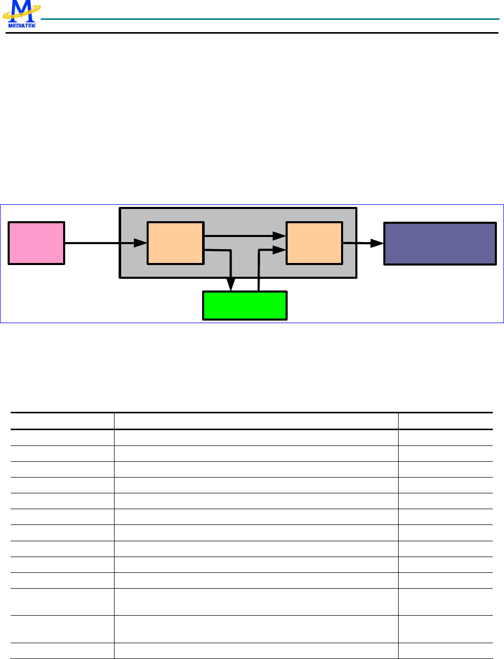
MT6235 GSM/GPRS Baseband Processor Data Sheet Revision 1.02
292/599 MediaTek Inc. Confidential
COMM Command Data and Parameter Data for LCD Module
C0 Write to ROI Command Address if C0 = 1, otherwise write to ROI Data Address
7.2 Capture Resize
7.2.1 General Description
This block provides the image resizing function for image and video capturing scenarios. It receives image data from the
ISP module, performs the image resizing function and outputs to the IMG_DMA module. Figure 35 shows the block
diagram. The capture resize is composed of horizontal and vertical resizing blocks. It can scale up or down the input
image by any ratio. However, the maximum sizes of input and output images are limited to 4095x4095.
Vertical
resize
ISP
YUV444
vert. buffer
YUV444
IMG_DMA
YUV422
Horizontal
resize
Figure 35 Block diagram of the capture resize
The resizing function is cubic interpolation. The input and output format are both YUV444. But the internal working
memory format is YUV422 to mitigate memory and bandwidth requirements.
7.2.2 Register Definitions
REGISTER ADDRESS REGISTER NAME SYNONYM
CRZ+ 0000h Capture Resize Configuration Register CRZ_CFG
CRZ + 0004h Capture Resize Control Register CRZ_CON
CRZ + 0008h Capture Resize Status Register CRZ_STA
CRZ + 000Ch Capture Resize Interrupt Register CRZ_INT
CRZ + 0010h Capture Resize Source Image Size Register 1 CRZ_SRCSZ1
CRZ + 0014h Capture Resize Target Image Size Register 1 CRZ_TARSZ1
CRZ + 0018h Capture Resize Horizontal Ratio Register 1 CRZ_HRATIO1
CRZ + 001Ch Capture Resize Vertical Ratio Register 1 CRZ_VRATIO1
CRZ +003Ch Capture Resize Coefficient Table CRZ_GMCBASE
CRZ + 0040h Capture Resize Coefficient Table CRZ_FRCFG
CRZ+0044h Capture Resize YUV Y-Component Target Memory Base Address
Register CRZ_TMBASE_Y
CRZ+0048h Capture Resize YUV U-Component Target Memory Base Address
Register CRZ_TMBASE_U
CRZ+004Ch Capture Resize YUV V-Component Target Memory Base Address CRZ_TMBASE_V
MT6235 GSM/GPRS Baseband Processor Data Sheet Revision 1.02
293/599 MediaTek Inc. Confidential
Register
CRZ+0084h Capture Resize Target Memory Base Address Register 1 CRZ_TMBASE1
CRZ+0088h Capture Resize Target Memory Base Address Register 2 CRZ_TMBASE1
7.2.2.1 Capture Resize Configuration Register
CRZ+0000h Capture Resize Configuration Register CRZ_CFG
Bit 31 30 29 28 27 26 25 24 23 22 21 20 19 18 17 16
Name LBMAX
Type R/W
Reset 0
Bit 15 14 13 12 11 10 9 8 7 6 5 4 3 2 1 0
Name NORG
BDB NORF
DB VSRS
TEN ECV INTEN
[1] INTEN
[0] LBSE
L PCON OUTFMT
Type R/W R/W R/W R/W R/W R/W R/W R/W R/W
Reset 0 0 0 0 0 0 1 0 0
The register is for global configuration of Capture Resize.
OUTFMT The register field specifies which format reszier outputs
0 RGB565
1 YUV420
3 YUV422
Others Reserved
Note: If YUV420 or YUV422 is selected, output width will be padded to 16’s multiples.
PCON The register bit specifies if pixel-based resizing continues whenever an image finishes processing. Once
continuous run for pixel-based resizing is enabled and pixel-based resizing is running, the only way to stop is to
reset Capture Resize. If to stop immediately is desired, reset Capture Resize directly. If the last image is
desired, set the register bit to ‘0’ first. Then wait until image resizer is not busy again. Finally reset image
resizer.
0 Single run
1 Continuous run
LBSEL Line buffer selection.
0 CRZ cant work!
1 Dedicated memory.
INTEN[0] Frame Done Interrupt Enable. When interrupt is enabled, an interrupt is generated whenever CRZ finishes.
0 Interrupt for is disabled.
1 Interrupt for is enabled.
INTEN[1] Frame Start Interrupt Enable. When interrupt is enabled, an interrupt is generated whenever CRZ begin
working.
0 Interrupt for is disabled.
1 Interrupt for is enabled.
ECV The register field determines whether using ‘ec’ algorithm for vertical downscaling
0 cubic
1 ec. It helps when bandwidth is very critical.
VSRSTEN The register field determines whether force reset when vsync arise but previous frame not done yet.
0 Not force reset

MT6235 GSM/GPRS Baseband Processor Data Sheet Revision 1.02
294/599 MediaTek Inc. Confidential
1 Force reset when vsync
NORFDB The register field determines not double buffer some registers.
0 Double buffering registers
1 No double buffering registers
NORGBDB The register field determines whether base address of RGB565 output switching or not.
0 Auto switching between CRZ_TMBASE1 and CRZ_TMBASE2
1 No auto switching. Always CRZ_TMBASE1.
LBMAX Number of lines used in upsampling scenario :
WMIN = ((WS > WT) ? WT : WS); // use for Width down, and Height up
WMIN_EVEN = WMIN + WMIN%2;
(int)(1600 / WMIN_EVEN) * 6;
7.2.2.2 Capture Resize Control Register
CRZ+0004h Capture Resize Control Register CRZ_CON
Bit 31 30 29 28 27 26 25 24 23 22 21 20 19 18 17 16
Name PELR
ST
Type R/W
Reset 0
Bit 15 14 13 12 11 10 9 8 7 6 5 4 3 2 1
Name PELE
NA
Type R/W
Reset 0
The register is for global control of Capture Resize. Note that software reset does NOT reset all register settings.
Remember to trigger Capture Resize first before triggering image sources to Capture Resize.
PELENA Writing ‘1’ to the register bit causes CRZ proceed to work.
PELRST Writing ‘1’ to the register causes CRZ to stop immediately and keep in reset state. In order to go to normal
state, write ‘0’ to the register bit.
7.2.2.3 Capture Resize Status Register
CRZ+0008h Capture Resize Status Register CRZ_STA
Bit 31 30 29 28 27 26 25 24 23 22 21 20 19 18 17 16
Name
Type
Reset
Bit 15 14 13 12 11 10 9 8 7 6 5 4 3 2 1 0
Name BUSYI BUSY
O
Type RO RO
Reset
The register indicates global status of Capture Resize.
BUSYI Input interface busy.

MT6235 GSM/GPRS Baseband Processor Data Sheet Revision 1.02
295/599 MediaTek Inc. Confidential
BUSYO Output interface busy.
7.2.2.4 Capture Resize Interrupt Register
CRZ+000Ch Capture Resize Interrupt Register CRZ_INT
Bit 31 30 29 28 27 26 25 24 23 22 21 20 19 18 17 16
Name
Type
Reset
Bit 15 14 13 12 11 10 9 8 7 6 5 4 3 2 1 0
Name FSTIN
T PELIN
T
Type RC RC
Reset 0 0
The register shows up the interrupt status of resizer.
PELINT Interrupt for CRZ. No matter the register bit CRZ_CFG.INTEN[0] is enabled or not, the register bit is active
whenever CRZ completes. It could be as software interrupt by polling the register bit. Clear it by reading
the register.
FSTINT Interrupt for CRZ. No matter the register bit CRZ_CFG.INTEN[1] is enabled or not, the register bit is active
whenever CRZ start working. It could be as software interrupt by polling the register bit. Clear it by
reading the register.
7.2.2.5 Capture Resize Source Image Size Register 1
CRZ+0010h Capture Resize Source Image Size Register 1 CRZ_SRCSZ1
Bit 31 30 29 28 27 26 25 24 23 22 21 20 19 18 17 16
Name HS
Type R/W
Bit 15 14 13 12 11 10 9 8 7 6 5 4 3 2 1 0
Name WS
Type R/W
The register specifies the size of source image after coarse shrink process. The allowable maximum size is 4095x4095
with limitation written in application notes.
WS The register field specifies the width of source image after coarse shrink process.
1 The width of source image after coarse shrink process is 1.
2 The width of source image is 2.
…
HS The register field specifies the height of source image after coarse shrink process.
1 The height of source image after coarse shrink process is 1.
2 The height of source image after coarse shrink process is 2.
…
MT6235 GSM/GPRS Baseband Processor Data Sheet Revision 1.02
296/599 MediaTek Inc. Confidential
7.2.2.6 Capture Resize Target Image Size Register 1
CRZ+0014h Capture Resize Target Image Size Register 1 CRZ_TARSZ1
Bit 31 30 29 28 27 26 25 24 23 22 21 20 19 18 17 16
Name HT
Type R/W
Bit 15 14 13 12 11 10 9 8 7 6 5 4 3 2 1 0
Name WT
Type R/W
The register specifies the size of target image. The allowable maximum size is 4095x4095 with limitation written in
application notes.
WT The register field specifies the width of target image.
1 The width of target image is 1.
2 The width of target image is 2.
…
HT The register field specifies the height of target image.
1 The height of target image is 1.
2 The height of target image is 2.
…
7.2.2.7 Capture Resize Horizontal Ratio Register 1
CRZ+0018h Capture Resize Horizontal Ratio Register CRZ_HRATIO1
Bit 31 30 29 28 27 26 25 24 23 22 21 20 19 18 17 16
Name RATIO [31:16]
Type R/W
Bit 15 14 13 12 11 10 9 8 7 6 5 4 3 2 1 0
Name RATIO [15:0]
Type R/W
The register specifies horizontal resizing ratio. It is obtained by
CRZ_SRCSZ.HS > CRZ_TARSZ.HT
? ((CRZ_TARSZ.HT - 1)* 220 + (CRZ_SRCSZ.HS -1)/2) / (CRZ_SRCSZ.HS -1)
: ((CRZ_SRCSZ.HS - 1)* 220 + (CRZ_TARSZ.HT-1)/2) / (CRZ_TARSZ.HT-1).
7.2.2.8 Capture Resize Vertical Ratio Register 1
CRZ+001Ch Capture Resize Vertical Ratio Register 1 CRZ_VRATIO1
Bit 31 30 29 28 27 26 25 24 23 22 21 20 19 18 17 16
Name RATIO [31:16]
Type R/W
Bit 15 14 13 12 11 10 9 8 7 6 5 4 3 2 1 0
Name RATIO [15:0]
Type R/W
The register specifies vertical resizing ratio. It is obtained by
MT6235 GSM/GPRS Baseband Processor Data Sheet Revision 1.02
297/599 MediaTek Inc. Confidential
CRZ_SRCSZ.VS > CRZ_TARSZ.VT
? ((CRZ_TARSZ.VT - 1)* 220 + (CRZ_SRCSZ.VS -1)/2) / (CRZ_SRCSZ.VS -1)
: ((CRZ_SRCSZ.VS - 1)* 220 + (CRZ_TARSZ.VT-1)/2) / (CRZ_TARSZ.VT-1).
7.2.2.9 Capture Resize GMC BASE Register
CRZ+003Ch Capture Resize Coefficient Table CRZ_GMCBASE
Bit 31 30 29 28 27 26 25 24 23 22 21 20 19 18 17 16
Name GMCBASE[31:16]
Type R/W
Reset 0
Bit 15 14 13 12 11 10 9 8 7 6 5 4 3 2 1 0
Name GMCBASE[15:2]
Type R/W
Reset 0
The register specifies the base address of GMC buffer address. It should be word-aligned. And it is meaningful to use
internal ram. When CRZ_FRCFG..GMCPIXLE = 0, this register is meaningless.
7.2.2.10 Capture Resize Coefficient Table Register
CRZ+0040h Capture Resize Coefficient Table CRZ_FRCFG
Bit 31 30 29 28 27 26 25 24 23 22 21 20 19 18 17 16
Name GMCPIXEL
Type R/W
Reset 0
Bit 15 14 13 12 11 10 9 8 7 6 5 4 3 2 1 0
Name USEL DSEL
Type R/W R/W
Reset 0 1 1 0 1 0 1 1 0 1
The register specifies the coefficient table for resizing. Valid number is form 0 to 19. While ‘1’ is the most blur and ‘19’ is
the sharpest. ‘0’ is a special case, may or may not sharp than ‘1’.
USEL choose ‘USEL’ > 12 may get undesirable result, ‘8’ is recommended.
DSEL ‘15’ is recommended.
GMCPIXEL Use how many bytes of internal memory as additional resizer buffer. Only even numbers are allowed.
0 Disable this feature.
2 2 pixels; 4 bytes.
4 4 pixels; 8 bytes.
6 6 pixels; 12 bytes.
MT6235 GSM/GPRS Baseband Processor Data Sheet Revision 1.02
298/599 MediaTek Inc. Confidential
…
CRZ+0044h Capture Resize YUV Y-Component Target
Memory Base Address Register CRZ_TMBASE_Y
Bit 31 30 29 28 27 26 25 24 23 22 21 20 19 18 17 16
Name TMBASE_Y[31:16]
Type R/W
Bit 15 14 13 12 11 10 9 8 7 6 5 4 3 2 1 0
Name TMBASE_Y[15:2]
Type R/W
The register specifies the base address of YUV output for Y-component. It should be word-aligned. It’s only useful in YUV
mode.
CRZ+0048h Capture Resize YUV U-Component Target
Memory Base Address Register CRZ_TMBASE_U
Bit 31 30 29 28 27 26 25 24 23 22 21 20 19 18 17 16
Name TMBASE_U[31:16]
Type R/W
Bit 15 14 13 12 11 10 9 8 7 6 5 4 3 2 1 0
Name TMBASE_U[15:2]
Type R/W
The register specifies the base address of YUV output for U-component. It should be word-aligned. It’s only useful in
mode.
CRZ+004Ch Capture Resize YUV V-Component Target
Memory Base Address Register CRZ_TMBASE_V
Bit 31 30 29 28 27 26 25 24 23 22 21 20 19 18 17 16
Name TMBASE_V[31:16]
Type R/W
Bit 15 14 13 12 11 10 9 8 7 6 5 4 3 2 1 0
Name TMBASE_V[15:2]
Type R/W
The register specifies the base address of YUV output for V-component. It should be word-aligned. It’s only useful in YUV
mode.
CRZ+0084h Capture Resize Target Memory Base Address
Register CRZ_TMBASE1
Bit 31 30 29 28 27 26 25 24 23 22 21 20 19 18 17 16
Name TMBASE1 [31:16]
Type R/W
Bit 15 14 13 12 11 10 9 8 7 6 5 4 3 2 1 0
Name TMBASE1 [15:1]
Type R/W

MT6235 GSM/GPRS Baseband Processor Data Sheet Revision 1.02
299/599 MediaTek Inc. Confidential
The register specifies the base address of target memory for RGB565 mode. Target memory is memory space for
destination of YUV2RGB. It’ must be half-word (2 bytes) aligned. RESZ_TMBASE1 and RESZ_TMBASE2 are
auto-switched by hardware, so both two registers should be filled. If dual buffer is not required, please fill these two
registers with the same value.
CRZ+0088h Capture Resize Target Memory Base Address
Register CRZ_TMBASE2
Bit 31 30 29 28 27 26 25 24 23 22 21 20 19 18 17 16
Name TMBASE2 [31:16]
Type R/W
Bit 15 14 13 12 11 10 9 8 7 6 5 4 3 2 1 0
Name TMBASE2 [15:1]
Type R/W
The register specifies the base address of target memory for RGB565 mode. Target memory is memory space for
destination of YUV2RGB. It’ must be half-word (2 bytes) aligned. RESZ_TMBASE1 and RESZ_TMBASE2 are
auto-switched by hardware, so both two registers should be filled. If dual buffer is not required, please fill these two
registers with the same value.
7.2.3 Application Notes
z SRCSZ and TARSZ limitation for upscaling
CRZ_SRCSZ.WS >= 3;
CRZ_SRCSZ.HS >= 3;
(CRZ_TARSZ.WT-1) / (CRZ_SRCSZ.WS-1) <= 64;
z SRCSZ and TARSZ limitation for downcaling
2 <= CRZ_TARSZ.WT <= 1600;
2 <= CRZ_TARSZ.HT <= 1600;
(CRZ_TARSZ.WT-1) / (CRZ_SRCSZ.WS-1) >= 1/2048;
z Configuration procedure for pixel-based image sources
CRZ_SRCSZ = source image size;
CRZ_TARSZ = target image size;
CRZ_CFG.LBSEL = 1; // must be 1, crz cant work when set to 0
CRZ_CFG.OUTFMT = 3 or 1 or 0;
WMIN = (WS > WT) ? WT : WS; // use for Width down and Height up
WMIN_EVEN = WMIN + WMIN%2;
CRZ_CFG.LBMAX = (int)(1600/ WMIN_EVEN) * 6;
CRZ_HRATIO = horizontal ratio;
CRZ_VRATIO = vertical ratio;
CRZ_TMBASE*
CRZ_CON = 0x1;

MT6235 GSM/GPRS Baseband Processor Data Sheet Revision 1.02
300/599 MediaTek Inc. Confidential
7.3 NAND FLASH interface
7.3.1 General description
MT6235 provides NAND flash interface.
The NAND FLASH interface support features as follows:
z ECC (Hamming code) acceleration capable of one-bit error correction or two bits error detection.
z Programmable ECC block size. Support 1, 2 or 4 ECC block within a page.
z Word/byte access through APB bus.
z Direct Memory Access for massive data transfer.
z Latch sensitive interrupt to indicate ready state for read, program, erase operation and error report.
z Programmable wait states, command/address setup and hold time, read enable hold time, and write enable recovery
time.
z Support page size: 512(528) bytes and 2048(2112) bytes.
z Support 2 chip select for NAND flash parts.
z Support 8/16 bits I/O interface.
The NFI core can automatically generate ECC parity bits when programming or reading the device. If the user approves the
way it stores the parity bits in the spare area for each page, the AUTOECC mode can be used. Otherwise, the user can
prepare the data (may contains operating system information or ECC parity bits) for the spare area with another
arrangement. In the former case, the core can check the parity bits when reading from the device. The ECC module features
the hamming code, which is capable of correcting one bit error or detecting two bits error within one ECC block.
7.3.2 Registers Memory Map
Software responsibility and controllable functions
Register Address Acronym Register Function
NFI +0000h NFI_ACCCON NAND Flash Access Control
NFI +0004h NFI_PAGEFMT NFI Page Format Control
NFI +0008h NFI_OPCON Operation Control
NFI +0010h NFI_CMD Command
NFI +0020h NFI_ADDRNOB Address Length
NFI +0024h NFI_ADDRL Least Significant Address
NFI +0028h NFI_ADDRM Most Significant Address
NFI +0030h NFI_DATAW Write Data Buffer
NFI +0034h NFI_DATAWB Write Data Buffer for Byte Access

MT6235 GSM/GPRS Baseband Processor Data Sheet Revision 1.02
301/599 MediaTek Inc. Confidential
NFI +0038h NFI_DATAR Read Data Buffer
NFI +003Ch NFI_DATARB Read Data Buffer for Byte Access
NFI +0040h NFI_PSTA NFI Status
NFI +0044h NFI_FIFOSTA NFI FIFO Status
NFI +0050h NFI_FIFODATA0 NFI FIFO Data 0
NFI +0054h NFI_FIFODATA1 NFI FIFO Data 1
NFI +0058h NFI_FIFODATA2 NFI FIFO Data 2
NFI +005Ch NFI_FIFODATA3 NFI FIFO Data 3
NFI +0060h NFI_CON NFI Control
NFI +0064h NFI_INTR NFI Interrupt Status
NFI +0068h NFI_INTR_EN NFI Interrupt Enable
NFI +0070h NFI_PAGECNTR NAND Flash Page Counter
NFI +0074h NFI_ADDRCNTR NAND Flash Page Address Counter
Main Area ECC
NFI +0080h NFI_SYM0_ADDR ECC Block 0 Parity Error Detect Syndrome Address
NFI +0084h NFI_SYM1_ADDR ECC Block 1 Parity Error Detect Syndrome Address
NFI +0088h NFI_SYM2_ADDR ECC Block 2 Parity Error Detect Syndrome Address
NFI +008Ch NFI_SYM3_ADDR ECC Block 3 Parity Error Detect Syndrome Address
NFI +0090h NFI_SYM4_ADDR ECC Block 4 Parity Error Detect Syndrome Address
NFI +0094h NFI_SYM5_ADDR ECC Block 5 Parity Error Detect Syndrome Address
NFI +0098h NFI_SYM6_ADDR ECC Block 6 Parity Error Detect Syndrome Address
NFI +009Ch NFI_SYM7_ADDR Spare ECC Block 7 Parity Error Detect Syndrome Address
NFI +00A0h NFI_SYMS0_ADDR Spare ECC Block 0 Parity Error Detect Syndrome Address
NFI +00A4h NFI_SYMS1_ADDR Spare ECC Block 1 Parity Error Detect Syndrome Address
NFI +00A8h NFI_SYMS2_ADDR Spare ECC Block 2 Parity Error Detect Syndrome Address
NFI +00ACh NFI_SYMS3_ADDR Spare ECC Block 3 Parity Error Detect Syndrome Address
NFI +00B0h NFI_SYM0_DATA ECC Block 0 Parity Error Detect Syndrome Word
NFI +00B4h NFI_SYM1_DATA ECC Block 1 Parity Error Detect Syndrome Word
NFI +00B8h NFI_SYM2_DATA ECC Block 2 Parity Error Detect Syndrome Word
NFI +00BCh NFI_SYM3_DATA ECC Block 3 Parity Error Detect Syndrome Word
NFI +00C0h NFI_SYM4_DATA ECC Block 4 Parity Error Detect Syndrome Word
NFI +00C4h NFI_SYM5_DATA ECC Block 5 Parity Error Detect Syndrome Word

MT6235 GSM/GPRS Baseband Processor Data Sheet Revision 1.02
302/599 MediaTek Inc. Confidential
NFI +00C8h NFI_SYM6_DATA ECC Block 6 Parity Error Detect Syndrome Word
NFI +00CCh NFI_SYM7_DATA ECC Block 7 Parity Error Detect Syndrome Word
NFI +00D0h NFI_SYMS0_DATA Spare ECC Block 0 Parity Error Detect Syndrome Word
NFI +00D4h NFI_SYMS1_DATA Spare ECC Block 1 Parity Error Detect Syndrome Word
NFI +00D8h NFI_SYMS2_DATA Spare ECC Block 2 Parity Error Detect Syndrome Word
NFI +00DCh NFI_SYMS3_DATA Spare ECC Block 3 Parity Error Detect Syndrome Word
NFI +00E0h NFI_PAR_0P NFI ECC Parity Word 0
NFI +00E4h NFI_PAR_0C NFI ECC Parity Word 0
NFI +00E8h NFI_PAR_1P NFI ECC Parity Word 1
NFI +00ECh NFI_PAR_1C NFI ECC Parity Word 1
NFI +00F0h NFI_PAR_2P NFI ECC Parity Word 2
NFI +00F4h NFI_PAR_2C NFI ECC Parity Word 2
NFI +00F8h NFI_PAR_3P NFI ECC Parity Word 3
NFI +00FCh NFI_PAR_3C NFI ECC Parity Word 3
NFI +0100h NFI_PAR_4P NFI ECC Parity Word 4
NFI +0104h NFI_PAR_4C NFI ECC Parity Word 4
NFI +0108h NFI_PAR_5P NFI ECC Parity Word 5
NFI +010Ch NFI_PAR_5C NFI ECC Parity Word 5
NFI +0110h NFI_PAR_6P NFI ECC Parity Word 6
NFI +0114h NFI_PAR_6C NFI ECC Parity Word 6
NFI +0118h NFI_PAR_7P NFI ECC Parity Word 7
NFI +011Ch NFI_PAR_7C NFI ECC Parity Word 7
NFI +0120h NFI_PARS_0P NFI Spare ECC Parity Word 0
NFI +0124h NFI_PARS_0C NFI Spare ECC Parity Word 0
NFI +0128h NFI_PARS_1P NFI Spare ECC Parity Word 1
NFI +012Ch NFI_PARS_1C NFI Spare ECC Parity Word 1
NFI +0130h NFI_PARS_2P NFI Spare ECC Parity Word 2
NFI +0134h NFI_PARS_2C NFI Spare ECC Parity Word 2
NFI +0138h NFI_PARS_3P NFI Spare ECC Parity Word 3
NFI +013Ch NFI_PARS_3C NFI Spare ECC Parity Word 3
NFI +0140h NFI_ECCDET NFI ECC Error Detect Indication
NFI +0144h NFI_PARECC NFI ECC Parity Error Indication
NFI +0148h NFI_SCON NFI Spare ECC Control
I/O Pin Control
NFI +0200h NFI_CSEL NAND Flash Device Select

MT6235 GSM/GPRS Baseband Processor Data Sheet Revision 1.02
303/599 MediaTek Inc. Confidential
NFI +0204h NFI_IOCON NFI IO Control
Table 5 Registers Memory Map Table
7.3.3 Register definition
NFI+0000h NAND flash access control register NFI_ACCCON
Bit 31 30 29 28 27 26 25 24 23 22 21 20 19 18 17 16
Name LCD2NAND C2R
Type R/W R/W
Reset 0 0
Bit 15 14 13 12 11 10 9 8 7 6 5 4 3 2 1 0
Name W2R WH WST RLT
Type R/W R/W R/W R/W
Reset 0 0 0 0
This is the timing access control register for the NAND FLASH interface. In order to accommodate operations for different
system clock frequency ranges from 13MHz to 52MHz, wait states and setup/hold time margin can be configured in this
register.
C2R The field represents the minimum required time from NCEB low to NREB low.
W2R The field represents the minimum required time from NWEB high to NREB low. It’s in unit of 2T. So the actual
time ranges from 2T to 8T in step of 2T.
WH Write-enable hold-time.
The field specifies the hold time of NALE, NCLE, NCEB signals relative to the rising edge of NWEB. This field
is associated with WST to expand the write cycle time, and is associated with RLT to expand the read cycle time.
RLT Read Latency Time
The field specifies how many wait states to be inserted to meet the requirement of the read access time for the
device.
00 No wait state.
01 1T wait state.
10 2T wait state.
11 3T wait state.
WST Write Wait State
The field specifies the wait states to be inserted to meet the requirement of the pulse width of the NWEB signal.
00 No wait state.
01 1T wait state.
10 2T wait state.
11 3T wait state.
LCD2NAND Arbitration Wait State
The field specifies the wait states to be inserted for the APB arbitrator when bus user changes.
NFI +0004h NFI page format control register NFI_PAGEFMT
Bit 15 14 13 12 11 10 9 8 7 6 5 4 3 2 1 0

MT6235 GSM/GPRS Baseband Processor Data Sheet Revision 1.02
304/599 MediaTek Inc. Confidential
Name
B16E
N ECCBLKSIZE ADRMODE PSIZE
Type R/W R/W R/W R/W
Reset 0 0 0 0
This register manages the page format of the device. It includes the bus width selection, the page size, the associated
address format, and the ECC block size.
B16EN 16 bits I/O bus interface enable.
ECCBLKSIZE ECC block size.
This field represents the size of one ECC block. The hardware-fuelled ECC generation provides 2 or 4
blocks within a single page.
0 ECC block size: 128 bytes. Used for devices with page size equal to 512 bytes.
1 ECC block size: 256 bytes. Used for devices with page size equal to 512 bytes.
2 ECC block size: 512 bytes. Used for devices with page size equal to 512 (1 ECC block) or 2048 bytes (4 ECC
blocks).
3 ECC block size: 1024 bytes. Used for devices with page size equal to 2048 bytes.
4~ Reserved.
ADRMODE Address mode. This field specifies the input address format.
0 Normal input address mode, in which the half page identifier is not specified in the address assignment but in
the command set. As in Table 28, A7 to A0 identifies the byte address within half a page, A12 to A9 specifies
the page address within a block, and other bits specify the block address. The mode is used mostly for the
device with 512 bytes page size.
1 Large size input address mode, in which all address information is specified in the address assignment rather
than in the command set. As in Table 29, A11 to A0 identifies the byte address within a page. The mode is
used for the device with 2048 bytes page size and 8bits I/O interface.
2 Large size input address mode. As in Table 29, A10 to A0 identifies the column address within a page. The
mode is used for the device with 2048 byte page size and 16bits I/O interface.
NLD7 NLD6 NLD5 NLD4 NLD3 NLD2 NLD1 NLD0
First cycle A7 A6 A5 A4 A3 A2 A1 A0
Second cycle A16 A15 A14 A13 A12 A11 A10 A9
Table 28 Page address assignment of the first type (ADRMODE = 0)
NLD7 NLD6 NLD5 NLD4 NLD3 NLD2 NLD1 NLD0
First cycle A7 A6 A5 A4 A3 A2 A1 A0
Second cycle 0 0 0 0 A11 A10 A9 A8
Table 29 Page address assignment of the second type (ADRMODE = 1 or 2)
PSIZE Page Size.
The field specifies the size of one page for the device. Two most widely used page size are supported.
0 The page size is 512 bytes or 528 bytes (including 512 bytes data area and 16 bytes spare area).
1 The page size is 2048 bytes or 2112 bytes (including 2048 bytes data area and 64 bytes spare area).
2~ Reserved.

MT6235 GSM/GPRS Baseband Processor Data Sheet Revision 1.02
305/599 MediaTek Inc. Confidential
NFI +0008h Operation control register NFI_OPCON
Bit 15 14 13 12 11 10 9 8 7 6 5 4 3 2 1 0
Name NOB
FIFO_
RST
FIFO_
FLUS
H SRD BWR BRD
Type W/R WO WO WO R/W R/W
Reset 0 0 0 0 0 0
This register controls the burst mode and the single of the data access. In burst mode, the core supposes there are one or
more than one page of data to be accessed. On the contrary, in single mode, the core supposes there are only less than 4
bytes of data to be accessed. This is recommended to reset the state machine, data FIFO and flush the data FIFO before
starting a new command sequence.
BRD Burst read mode. Setting this field to be logic-1 enables the data read operation. The NFI core will issue read
cycles to retrieve data from the device when the data FIFO is not full or the device is not in the busy state. The
NFI core supports consecutive page reading. A page address counter is built in. If the reading reaches to the
end of the page, the device will enter the busy state to prepare data of the next page, and the NFI core will
automatically pause reading and remain inactive until the device returns to the ready state. The page address
counter will restart to count from 0 after the device returns to the ready state and start retrieving data again.
BWR Burst write mode. Setting to be logic-1 enables the data burst write operation for DMA operation. Actually the
NFI core will issue write cycles once if the data FIFO is not empty even without setting this flag. But if DMA
is to be utilized, the bit should be enabled. If DMA is not to be utilized, the bit didn’t have to be enabled.
SRD Setting to be logic-1 initializes the one-shot data read operation. It’s mainly used for read ID and read status
command, which requires no more than 4 read cycles to retrieve data from the device.
NOB The field represents the number of bytes to be retrieved from the device in single mode, and the number of
bytes per AHB transaction in both single and burst mode.
0 Read 4 bytes from the device.
1 Read 1 byte from the device.
2 Read 2 bytes from the device.
3 Read 3 bytes from the device.
FIFO_RST Reset the state machine and data FIFO.
FIFO_FLUSH Flush the data FIFO.
NFI +0010h Command register NFI_CMD
Bit 15 14 13 12 11 10 9 8 7 6 5 4 3 2 1 0
Name CMD
Type R/W
Reset 45
This is the command input register. The user should write this register to issue a command. Please refer to device datasheet
for the command set. The core can issue some associated commands automatically. Please check out register NFI_CON for
those commands.
CMD Command word.
NFI +0020h Address length register NFI_ADDRNOB
Bit 15 14 13 12 11 10 9 8 7 6 5 4 3 2 1 0
Name ADDR_NOB
MT6235 GSM/GPRS Baseband Processor Data Sheet Revision 1.02
306/599 MediaTek Inc. Confidential
Type R/W
Reset 0
This register represents the number of bytes corresponding to current command. The valid number of bytes ranges from 1 to
8. The address format depends on what device to be used and what commands to be applied. The NFI core is made
transparent to those different situations except that the user has to define the number of bytes.
The user should write the target address to the address register NFI_ADDRL before programming this register.
ADDR_NOB Number of bytes for the address
NFI +0024h Least significant address register NFI_ADDRL
Bit 31 30 29 28 27 26 25 24 23 22 21 20 19 18 17 16
Name ADDR3 ADDR2
Type R/W R/W
Reset 0 0
Bit 15 14 13 12 11 10 9 8 7 6 5 4 3 2 1 0
Name ADDR1 ADDR0
Type R/W R/W
Reset 0 0
This defines the least significant 4 bytes of the address field to be applied to the device. Since the device bus width is 1 byte,
the NFI core arranges the order of address data to be least significant byte first. The user should put the first address byte in
the field ADDR0, the second byte in the field ADDR1, and so on.
ADDRn The n-th address byte.
NFI +0028h Most significant address register NFI_ADDRM
Bit 31 30 29 28 27 26 25 24 23 22 21 20 19 18 17 16
Name ADDR7 ADDR6
Type R/W R/W
Reset 0 0
Bit 15 14 13 12 11 10 9 8 7 6 5 4 3 2 1 0
Name ADDR5 ADDR4
Type R/W R/W
Reset 0 0
This register defines the most significant byte of the address field to be applied to the device. The NFI core supports
address size up to 8 bytes. Programming this register implicitly indicates that the number of address field is larger than 4.
ADDRn The n-th address byte.
NFI +0030h Write data buffer NFI_DATAW
Bit 31 30 29 28 27 26 25 24 23 22 21 20 19 18 17 16
Name DW3 DW2
Type R/W R/W
Reset 0 0
Bit 15 14 13 12 11 10 9 8 7 6 5 4 3 2 1 0
Name DW1 DW0
Type R/W R/W
Reset 0 0
This is the write port of the data FIFO. It supports word access. The least significant byte DW0 is to be programmed to the
device first, then DW1, and so on.
If the data to be programmed is not word aligned, byte write access will be needed. Instead, the user should use another
MT6235 GSM/GPRS Baseband Processor Data Sheet Revision 1.02
307/599 MediaTek Inc. Confidential
register NFI_DATAWB for byte programming. Writing a word to NFI_DATAW is equivalent to writing four bytes DW0,
DW1, DW2, DW3 in order to NFI_DATAWB. Be reminded that the word alignment is from the perspective of the user.
The device bus is byte-wide. According to the flash’s nature, the page address will wrap around once it reaches the end of
the page.
DW3 Write data byte 3.
DW2 Write data byte 2.
DW1 Write data byte 1.
DW0 Write data byte 0.
NFI +0034h Write data buffer for byte access NFI_DATAWB
Bit 15 14 13 12 11 10 9 8 7 6 5 4 3 2 1 0
Name DW0
Type R/W
Reset 0
This is the write port for the data FIFO for byte access.
DW0 Write data byte.
NFI +0038h Read data buffer NFI_DATAR
Bit 31 30 29 28 27 26 25 24 23 22 21 20 19 18 17 16
Name DR3 DR2
Type RO RO
Reset 0 0
Bit 15 14 13 12 11 10 9 8 7 6 5 4 3 2 1 0
Name DR1 DR0
Type RO RO
Reset 0 0
This is the read port of the data FIFO. It supports word access. The least significant byte DR0 is the first byte read from the
device, then DR1, and so on.
DR3 Read data byte 3.
DR2 Read data byte 2.
DR1 Read data byte 1.
DR0 Read data byte 0.
NFI +003Ch Read data buffer for byte access NFI_DATARB
Bit 15 14 13 12 11 10 9 8 7 6 5 4 3 2 1 0
Name DR0
Type RO
Reset 0
This is the read port of the data FIFO for byte access.
DR0 Read data byte 0.
NFI +0040h NFI status NFI_PSTA
Bit 31 30 29 28 27 26 25 24 23 22 21 20 19 18 17 16
Name NAND_FSM NFI_FSM
Type RO RO
Reset 0 0

MT6235 GSM/GPRS Baseband Processor Data Sheet Revision 1.02
308/599 MediaTek Inc. Confidential
Bit 15 14 13 12 11 10 9 8 7 6 5 4 3 2 1 0
Name
NAND
_BUS
Y BUSY
DATA
W DATA
R ADDR CMD
Type RO RO RO RO RO RO
Reset 0 0* 0 0 0 0
This register represents the NFI core control status including command mode, address mode, data program and read mode.
The user should poll this register for the end of those operations.
*The value of BUSY/NAND_BUSY bit depends on the GPIO configuration. If GPIO is configured for NAND flash
application, the reset value should be 0, which represents that NAND flash is in idle status. When the NAND flash is busy,
the value will be 1.
BUSY Synchronized busy signal from the NAND flash. It’s read-only. This signal is sampled from NFI
NAND_BUSY Asynchronized busy signal from the output pin of the NAND flash. It’s read-only.
DATAW The NFI core is in data write mode.
DATAR The NFI core is in data read mode.
ADDR The NFI core is in address mode.
CMD The NFI core is in command mode.
NFI_FSM The field represents the state of NFI internal FSM.
0000 idle.
0001 reset. Reset command to ready
0010 read busy.
0011 read data.
0100 program busy
0101 program data. Input data command to program command
1000 erase busy. Erase command to ready
1001 erase data. Erase command 1 to erase command 2
NAND_FSM The field represents the state of NAND interface FSM.
00000 IDLE. idle.
00101 CMD_WRST. command write set up
00110 CMD_WR. Command write enable.
00111 CMD_WRHD. Command write hold.
00100 CMD_WRRDY
01001 ADDR_WRST. Address write set up
01010 ADDR_WR. Address write enable
01011 ADDR_WRHD. Address write hold
01000 ADDR_WRRDY.
01100 CA2DEXT. Command address write extension.
10001 DATA_RDST. Data read set up.
10010 DATA_RD. Data read enable.
10011 DATA_RDHD. Data read hold.
11000 DATA_WRRDY.
11001 DATA_WRST. Data write set up.
11010 DATA_WR. Data write enable.
11011 DATA_WRHD. Data write hold.

MT6235 GSM/GPRS Baseband Processor Data Sheet Revision 1.02
309/599 MediaTek Inc. Confidential
NFI +0044h FIFO Status NFI_FIFOSTA
Bit 15 14 13 12 11 10 9 8 7 6 5 4 3 2 1 0
Name WR_F
ULL WR_E
MPTY WR_REMAIN
RD_F
ULL RD_E
MPTY RD_REMAIN
Type RO RO RO RO RO RO
Reset 0 1 0 0 1 0
The register represents the status of the data FIFO.
WR_FULL Data FIFO full in burst write mode.
WR_EMPTY Data FIFO empty in burst write mode.
RD_FULL Data FIFO full in burst read mode.
RD_EMPTY Data FIFO empty in burst read mode.
RD_REMAIN Data FIFO remaining byte number in burst read mode.
WR_REMAIN Data FIFO remaining byte number in burst write mode.
NFI +0050h FIFO Content Data 0 NFI_FIFODATA0
Bit 31 30 29 28 27 26 25 24 23 22 21 20 19 18 17 16
Name FIFO_DATA0
Type RO
Reset 0
Bit 15 14 13 12 11 10 9 8 7 6 5 4 3 2 1 0
Name FIFO_DATA0
Type RO
Reset 0
This register represents the content data 0 of fifo.
NFI +0054h FIFO Content Data 1 NFI_FIFODATA1
Bit 31 30 29 28 27 26 25 24 23 22 21 20 19 18 17 16
Name FIFO_DATA1
Type RO
Reset 0
Bit 15 14 13 12 11 10 9 8 7 6 5 4 3 2 1 0
Name FIFO_DATA1
Type RO
Reset 0
This register represents the content data 1 of fifo.
NFI +0058h FIFO Content Data 2 NFI_FIFODATA2
Bit 31 30 29 28 27 26 25 24 23 22 21 20 19 18 17 16
Name FIFO_DATA2
Type RO
Reset 0
Bit 15 14 13 12 11 10 9 8 7 6 5 4 3 2 1 0
Name FIFO_DATA2
Type RO
Reset 0
This register represents the content data 2 of fifo.

MT6235 GSM/GPRS Baseband Processor Data Sheet Revision 1.02
310/599 MediaTek Inc. Confidential
NFI +005Ch FIFO Content Data 3 NFI_FIFODATA3
Bit 31 30 29 28 27 26 25 24 23 22 21 20 19 18 17 16
Name FIFO_DATA3
Type RO
Reset 0
Bit 15 14 13 12 11 10 9 8 7 6 5 4 3 2 1 0
Name FIFO_DATA3
Type RO
Reset 0
This register represents the content data 3 of fifo.
NFI +0060h NFI control NFI_CON
Bit 15 14 13 12 11 10 9 8 7 6 5 4 3 2 1 0
Name BYTE
_RW
MAIN
_ECC
_EN
SPAR
E_EC
C_EN DMA_
PAUS
E_EN
SPAR
E_EN
MULTI
_PAG
E_RD
_EN
AUTO
ECC_
ENC_
EN
AUTO
ECC_
DEC_
EN
DMA_
WR_E
N
DMA_
RD_E
N
Type R/W R/W R/W R/W R/W R/W R/W R/W R/W R/W
Reset 0 0 0 0 0 0 0 0 0 0
The register controls the DMA and ECC functions. For all field, Setting to be logic-1 represents enabled, while 0 represents
disabled.
BYTE_RW Enable byte access. The valid bytes read from NFI_DATAR and NFI_DATAW is only DR0
and DW0 if BYTE_RW is enabled.
SPARE_EN If enabled, the NFI core allows the user to program or read the spare area directly. Otherwise,
the spare area can be programmed or read by the core.
MULTI_PAGE_RD_EN Multiple page burst read enable. If enabled, the burst read operation could continue through
multiple pages within a block. It’s also possible and more efficient to associate with DMA
scheme to read a sector of data contained within the same block.
AUTOECC_ENC_EN Automatic ECC encoding enable. If enabled, the ECC parity is written automatically to the
spare area. If disable ECC encoding engine, it write the default parity in the spare area.
AUTOECC_DEC_EN Automatic ECC decoding enabled, the error checking and correcting are performed
automatically on the data read from the memory and vice versa. If enabled, when the page
address reaches the end of the data read of one page
DMA_WR_EN This field is used to control the activity of DMA write transfer.
DMA_RD_EN This field is used to control the activity of DMA read transfer.
DMA_PAUSE_EN DMA pause
MAIN_ECC_EN This field is used to enable generation of ECC parities for main area.
SPARE_ECC_EN This field is used to enable generation of ECC parities for spare area. If SPARE_EN is not
set, however, the mode can’t be enabled since the core can’t access the spare area.
NFI +0064h Interrupt status register NFI_INTR
Bit 31 30 29 28 27 26 25 24 23 22 21 20 19 18 17 16
Name
BUSY
_RET
URN
ERRS
_COR
3
ERRS
_COR
2
ERRS
_COR
1
ERRS
_COR
0
ERR_
COR7 ERR_
COR6 ERR_
COR5 ERR_
COR4 ERR_
COR3 ERR_
COR2 ERR_
COR1 ERR_
COR0
Type RC RC RC RC RC RC RC RC RC RC RC RC RC

MT6235 GSM/GPRS Baseband Processor Data Sheet Revision 1.02
311/599 MediaTek Inc. Confidential
Reset 0 0 0 0 0 0 0 0 0 0 0 0 0
Bit 15 14 13 12 11 10 9 8 7 6 5 4 3 2 1 0
Name
ERAS
E_CO
MPLE
TE
RESE
T_CO
MPLE
TE
WR_C
OMPL
ETE
RD
_COM
PLET
E
ERRS
_DET
3
ERRS
_DET
2
ERRS
_DET
1
ERRS
_DET
0
ERR_
DET7 ERR_
DET6 ERR_
DET5 ERR_
DET4 ERR_
DET3 ERR_
DET2 ERR_
DET1 ERR_
DET0
Type RC RC RC RC RC RC RC RC RC RC RC RC RC RC RC RC
Reset 0 0 0 0 0 0 0 0 0 0 0 0 0 0 0 0
The register indicates the status of all the interrupt sources. Read this register will clear all interrupts.
BUSY_RETURN Indicates that the device state returns from busy by inspecting the R/B# pin.
ERR_CORn Indicates that the single bit error in ECC block n needs to be corrected.
ERR_DETn Indicates an uncorrectable error in ECC block n.
ERRS_CORn Indicates that the single bit error in spare ECC block n needs to be corrected.
ERRS_DETn Indicates an uncorrectable error in spare ECC block n.
ERASE_COMPLETE Indicates that the erase operation is completed.
RESET_COMPLETE Indicates that the reset operation is completed.
WR_COMPLETE Indicates that the write operation is completed.
RD_COMPLETE Indicates that the single page read operation is completed.
NFI +0068h Interrupt enable register NFI_INTR_EN
Bit 31 30 29 28 27 26 25 24 23 22 21 20 19 18 17 16
Name
BUSY
_RET
URN_
EN
ERRS
_COR
3_EN
ERRS
_COR
2_EN
ERRS
_COR
1_EN
ERRS
_COR
0_EN
ERR_
COR7
_EN
ERR_
COR6
_EN
ERR_
COR5
_EN
ERR_
COR4
_EN
ERR_
COR3
_EN
ERR_
COR2
_EN
ERR_
COR1
_EN
ERR_
COR0
_EN
Type R/W R/W R/W R/W R/W R/W R/W R/W R/W R/W R/W R/W R/W
Reset 0 0 0 0 0 0 0 0 0 0 0 0 0
Bit 15 14 13 12 11 10 9 8 7 6 5 4 3 2 1 0
Name
ERAS
E_CO
MPLE
TE_E
N
RESE
T_CO
MPLE
TE_E
N
WR_C
OMPL
ETE_
EN
RD_
COMP
LETE
_EN
ERRS
_DET
3_EN
ERRS
_DET
2_EN
ERRS
_DET
1_EN
ERRS
_DET
0_EN
ERR_
DET7
_EN
ERR_
DET6
_EN
ERR_
DET5
_EN
ERR_
DET4
_EN
ERR_
DET3
_EN
ERR_
DET2
_EN
ERR_
DET1
_EN
ERR_
DET0
_EN
Type R/W R/W R/W R/W R/W R/W R/W R/W R/W R/W R/W R/W R/W R/W R/W R/W
Reset 0 0 0 0 0 0 0 0 0 0 0 0 0 0 0 0
This register controls the activity for the interrupt sources.
ERR_CORn_EN The error correction interrupt enable for the n ECC block.
ERR_DETn_EN The error detection interrupt enable for the n ECC block.
ERRS_DETn_EN The error detection interrupt enable for the n spare ECC block.
ERRS_DETn_EN The error detection interrupt enable for the n spare ECC block.
BUSY_RETURN_EN The busy return interrupt enable.
ERASE_COMPLETE_EN The erase completion interrupt enable.
RESET_COMPLETE_EN The reset completion interrupt enable.
WR_COMPLETE_EN The single page write completion interrupt enable.
RD_COMPLETE_EN The single page read completion interrupt enable.
NFI+0070h NAND flash page counter NFI_PAGECNTR
Bit 15 14 13 12 11 10 9 8 7 6 5 4 3 2 1 0

MT6235 GSM/GPRS Baseband Processor Data Sheet Revision 1.02
312/599 MediaTek Inc. Confidential
Name CNTR
Type RO
Reset 0
The register represents the number of pages that the NFI has read since the issuing of the read command. For some devices,
the data can be read consecutively through different pages without the need to issue another read command. The user can
monitor this register to know current page count, particularly when read DMA is enabled.
CNTR The page counter.
NFI+0074h NAND flash page address counter NFI_ADDRCNTR
Bit 15 14 13 12 11 10 9 8 7 6 5 4 3 2 1 0
Name CNTR
Type RO
Reset 0
The register represents the current read/write address with respect to initial address input. It counts in unit of byte. In page
read and page program operation, the address should be the same as that in the state machine in the target device.
NFI supports the address counter up to 4096 bytes.
CNTR The address count.
NFI +0080h ECC block 0 parity error detect syndrome address NFI_ SYM0_ADDR
Bit 15 14 13 12 11 10 9 8 7 6 5 4 3 2 1 0
Name SYM
Type RO
Reset 0
This register identifies the address within ECC block 0 that a single bit error has been detected.
SYM The byte address of the error-correctable bit.
Register Address Register Function Acronym
NFI +0080h NFI ECC Syndrome address 0 NFI_SYM0_ADDR
NFI +0084h NFI ECC Syndrome address 1 NFI_SYM1_ADDR
NFI +0088h NFI ECC Syndrome address 2 NFI_SYM2_ADDR
NFI +008Ch NFI ECC Syndrome address 3 NFI_SYM3_ADDR
NFI +0090h NFI ECC Syndrome address 4 NFI_SYM4_ADDR
NFI +0094h NFI ECC Syndrome address 5 NFI_SYM5_ADDR
NFI +0098h NFI ECC Syndrome address 6 NFI_SYM6_ADDR
NFI +009Ch NFI ECC Syndrome address 7 NFI_SYM7_ADDR
NFI +00A0h NFI Spare ECC Syndrome address 0 NFI_SYMS0_ADDR
NFI +00A4h NFI Spare ECC Syndrome address 1 NFI_SYMS1_ADDR
NFI +00A8h NFI Spare ECC Syndrome address 2 NFI_SYMS2_ADDR
NFI +00ACh NFI Spare ECC Syndrome address 3 NFI_SYMS3_ADDR
Table 30 NFI Syndrome address register table

MT6235 GSM/GPRS Baseband Processor Data Sheet Revision 1.02
313/599 MediaTek Inc. Confidential
NFI +00B0h ECC block 0 parity error detect syndrome word NFI_SYM0_DATA
Bit 31 30 29 28 27 26 25 24 23 22 21 20 19 18 17 16
Name ED3 ED2
Type RO RO
Reset 0 0
Bit 15 14 13 12 11 10 9 8 7 6 5 4 3 2 1 0
Name ED1 ED0
Type RO RO
Reset 0 0
This register represents the syndrome word for the corrected ECC block 0. To correct the error, the user should first read
NFI_ SYM0_ADDR for the address of the correctable word, and then read NFI_SYM0_DAT, directly XOR the syndrome
word with the data word to obtain the correct word.
Register Address Register Function Acronym
NFI +00B0h NFI ECC Syndrome data 0 NFI_SYM0_DATA
NFI +00B4h NFI ECC Syndrome data 1 NFI_SYM1_DATA
NFI +00B8h NFI ECC Syndrome data 2 NFI_SYM2_DATA
NFI +00BCh NFI ECC Syndrome data 3 NFI_SYM3_DATA
NFI +00C0h NFI ECC Syndrome data 4 NFI_SYM4_DATA
NFI +00C4h NFI ECC Syndrome data 5 NFI_SYM5_DATA
NFI +00C8h NFI ECC Syndrome data 6 NFI_SYM6_DATA
NFI +00CCh NFI ECC Syndrome data 7 NFI_SYM7_DATA
NFI +00D0h NFI Spare ECC Syndrome data 0 NFI_SYMS0_DATA
NFI +00D4h NFI Spare ECC Syndrome data 1 NFI_SYMS1_DATA
NFI +00D8h NFI Spare ECC Syndrome data 2 NFI_SYMS2_DATA
NFI +00DCh NFI Spare ECC Syndrome data 3 NFI_SYMS3_DATA
Table 4 NFI Syndrome data register table
NFI +00E0h NFI ECC parity word 0 NFI_PAR_0P
Bit 15 14 13 12 11 10 9 8 7 6 5 4 3 2 1 0
Name PAR
Type RO
Reset 0
This register represents the ECC parity for the ECC block 0. It’s calculated by the NFI core and can be read by the user. It’s
generated when writing or reading a page.
Register Address Register Function Acronym
NFI +00E0h NFI ECC parity word 0 NFI_PAR_0P
NFI +00E4h NFI ECC parity word 0 NFI_PAR_0C
NFI +00E8h NFI ECC parity word 1 NFI_PAR_1P
NFI +00ECh NFI ECC parity word 1 NFI_PAR_1C
NFI +00F0h NFI ECC parity word 2 NFI_PAR_2P

MT6235 GSM/GPRS Baseband Processor Data Sheet Revision 1.02
314/599 MediaTek Inc. Confidential
NFI +00F4h NFI ECC parity word 2 NFI_PAR_2C
NFI +00F8h NFI ECC parity word 3 NFI_PAR_3P
NFI +00FCh NFI ECC parity word 3 NFI_PAR_3C
NFI +0100h NFI ECC parity word 4 NFI_PAR_4P
NFI +0104h NFI ECC parity word 4 NFI_PAR_4C
NFI +0108h NFI ECC parity word 5 NFI_PAR_5P
NFI +010Ch NFI ECC parity word 5 NFI_PAR_5C
NFI +0110h NFI ECC parity word 6 NFI_PAR_6P
NFI +0114h NFI ECC parity word 6 NFI_PAR_6C
NFI +0118h NFI ECC parity word 7 NFI_PAR_7P
NFI +011Ch NFI ECC parity word 7 NFI_PAR_7C
NFI +0120h NFI ECC parity word 0 NFI_PARS_0P
NFI +0124h NFI ECC parity word 0 NFI_PARS_0C
NFI +0128h NFI ECC parity word 1 NFI_PARS_1P
NFI +012Ch NFI ECC parity word 1 NFI_PARS_1C
NFI +0130h NFI ECC parity word 2 NFI_PARS_2P
NFI +0134h NFI ECC parity word 2 NFI_PARS_2C
NFI +0138h NFI ECC parity word 3 NFI_PARS_3P
NFI +013Ch NFI ECC parity word 3 NFI_PARS_3C
Table 5 NFI parity bits register table
NFI +0140h NFI ECC error detect indication register NFI_ERRDET
Bit 31 30 29 28 27 26 25 24 23 22 21 20 19 18 17 16
Name
CES_
BLK3 CES_
BLK2 CES_
BLK1 CES_
BLK0 CE_B
LK7 CE_B
LK6 CE_B
LK5 CE_B
LK4 CE_B
LK3 CE_B
LK2 CE_B
LK1 CE_B
LK0
Type RO RO RO RO RO RO RO RO RO RO RO RO
Reset 0 0 0 0 0 0 0 0 0 0 0 0
Bit 15 14 13 12 11 10 9 8 7 6 5 4 3 2 1 0
Name
ESBL
K3 ESBL
K2 ESBL
K1 ESBL
K0 EBLK
7 EBLK
6 EBLK
5 EBLK
4 EBLK
3 EBLK
2 EBLK
1 EBLK
0
Type RO RO RO RO RO RO RO RO RO RO RO RO
Reset 0 0 0 0 0 0 0 0 0 0 0 0
This register identifies the block in which an uncorrectable error has been detected.
EBLKn The uncorrectable errors in the block n.
CE_BLKn The correctable error of the block n.
ESBLKn The uncorrectable errors in the spare block n.
CES_BLKn The correctable error of the spare block n.
NFI +0144h NFI ECC parity error indication register NFI_PARERR
Bit 31 30 29 28 27 26 25 24 23 22 21 20 19 18 17 16
Name
PES_
BLK3 PES_
BLK2 PES_
BLK1 PES_
BLK0 PE_B
LK7 PE_B
LK6 PE_B
LK5 PE_B
LK4 PE_B
LK3 PE_B
LK2 PE_B
LK1 PE_B
LK0
Type RO RO RO RO RO RO RO RO RO RO RO RO

MT6235 GSM/GPRS Baseband Processor Data Sheet Revision 1.02
315/599 MediaTek Inc. Confidential
Reset 0 0 0 0 0 0 0 0 0 0 0 0
Bit 15 14 13 12 11 10 9 8 7 6 5 4 3 2 1 0
Name
NO_E
SBLK
3
NO_E
SBLK
2
NO_E
SBLK
1
NO_E
SBLK
0
NO_E
BLK7 NO_E
BLK6 NO_E
BLK5 NO_E
BLK4 NO_E
BLK3 NO_E
BLK2 NO_E
BLK1 NO_E
BLK0
Type RO RO RO RO RO RO RO RO RO RO RO RO
Reset 0 0 0 0 0 0 0 0 0 0 0 0
This register identifies the block in which an uncorrectable error has been detected.
NO_EBLKn No errors in the block n.
PE_BLKn The correctable error in parities of the block n.
NO_ESBLKn No errors in the spare block n.
PES_BLKn The correctable error in parities of the spare block n.
NFI+0148h NFI Spare ECC Control register NFI_SCON
Bit 15 14 13 12 11 10 9 8 7 6 5 4 3 2 1 0
Name SPARE_ECC_STR SPARE_ECC_NUM
Type R/W R/W
Reset 0 0
The register is used to control ECC for spare data.
SPARE_ECC_NUM byte number in spare for ECC. (0-8)
SPARE_ECC_STR start byte number in spare for ECC. (0-7)
NFI+0200h NFI device select register NFI_CSEL
Bit 15 14 13 12 11 10 9 8 7 6 5 4 3 2 1 0
Name CSEL
Type R/W
Reset 0
The register is used to select the target device. It decides which CEB pin to be functional. This is useful while using the
high-density device.
CSEL Chip select. The value defaults to 0.
0 Device 1 is selected.
1 Device 2 is selected.
NFI+0204h NFI IO Control register NFI_IOCON
Bit 15 14 13 12 11 10 9 8 7 6 5 4 3 2 1 0
Name
NLD_
PD
Type R/W
Reset 0
Data bus pull down when no use.
NLD_PD data bus pull down when no use.
0 disable.
1 enable.
MT6235 GSM/GPRS Baseband Processor Data Sheet Revision 1.02
316/599 MediaTek Inc. Confidential
7.3.4 Device timing control
This section illustrates the timing diagram.
The ideal timing for write access is listed as listed in Table 31.
Parame
ter Description Timing specification Timing at 13MHz
(WST, WH) = (0,0)
Timing at 26MHz
(WST, WH) = (0,0)
Timing at 52MHz
(WST, WH) = (1,0)
TWC1 Write cycle time 3T + WST + WH 230.8ns 105.4ns 76.9ns
TWC2 Write cycle time 2T + WST + WH 153.9ns 76.9ns 57.7ns
TDS Write data setup time 1T + WST 76.9ns 38.5ns 38.5ns
TDH Write data hold time 1T + WH 76.9ns 38.5ns 19.2ns
TWP Write enable time 1T + WST 76.9ns 38.5ns 38.5ns
TWH Write high time 1T + WH 76.9ns 38.5ns 19.2ns
TCLS Command latch enable
setup time 1T 76.9ns 38.5ns 19.2ns
TCLH Command latch enable
hold time 1T + WH 76.9ns 38.5ns 19.2ns
TALS Address latch enable
setup time 1T 76.9ns 38.5ns 19.2ns
TALH Address latch enable
hold time 1T + WH 76.9ns 38.5ns 19.23ns
FWC Write data rate 1 / TWC2 6.5Mbytes/s 13Mbytes/s 17.3Mbytes/s
Table 31 Write access timing
WST
tCLS, tALS tCLH, tALH
tWP
tDH
HCLK
NCLE
NWEB
NLD
NCEB
tCES tCEH
tDS
NALE
command
tWC1
Figure 36 Command input cycle (1 wait state).
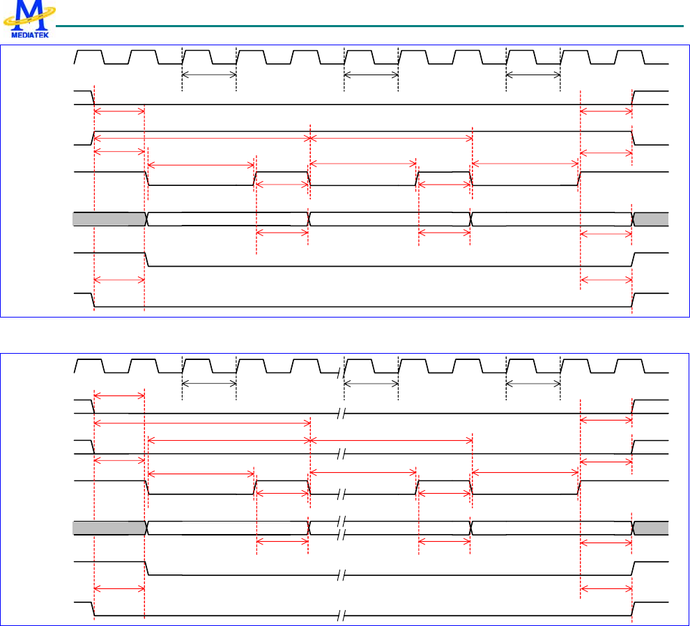
MT6235 GSM/GPRS Baseband Processor Data Sheet Revision 1.02
317/599 MediaTek Inc. Confidential
WST
tALS tALH
tWP
tDH
HCLK
NALE
NWEB
NLD
tWH
OE
(internal)
NCEB tCES tCEH
NCLE
tCLS tCLH
tDH
tWH
tDH
tWP tWP
WST WST
A0 A1 A2
tWC2
tWC1
Figure 37 Address input cycle (1 wait state)
WST
tALS tALH
tWP
tDH
HCLK
NALE
NWEB
NLD
tWH
OE
(internal)
NCEB tCES tCEH
NCLE tCLS
tCLH
tDH
tWH
tDH
tWP tWP
WST WST
D0 D526 D527
tWC2
tWC1
tWC2
Figure 38 Consecutive data write cycles (1 wait state, 0 hold time extension)
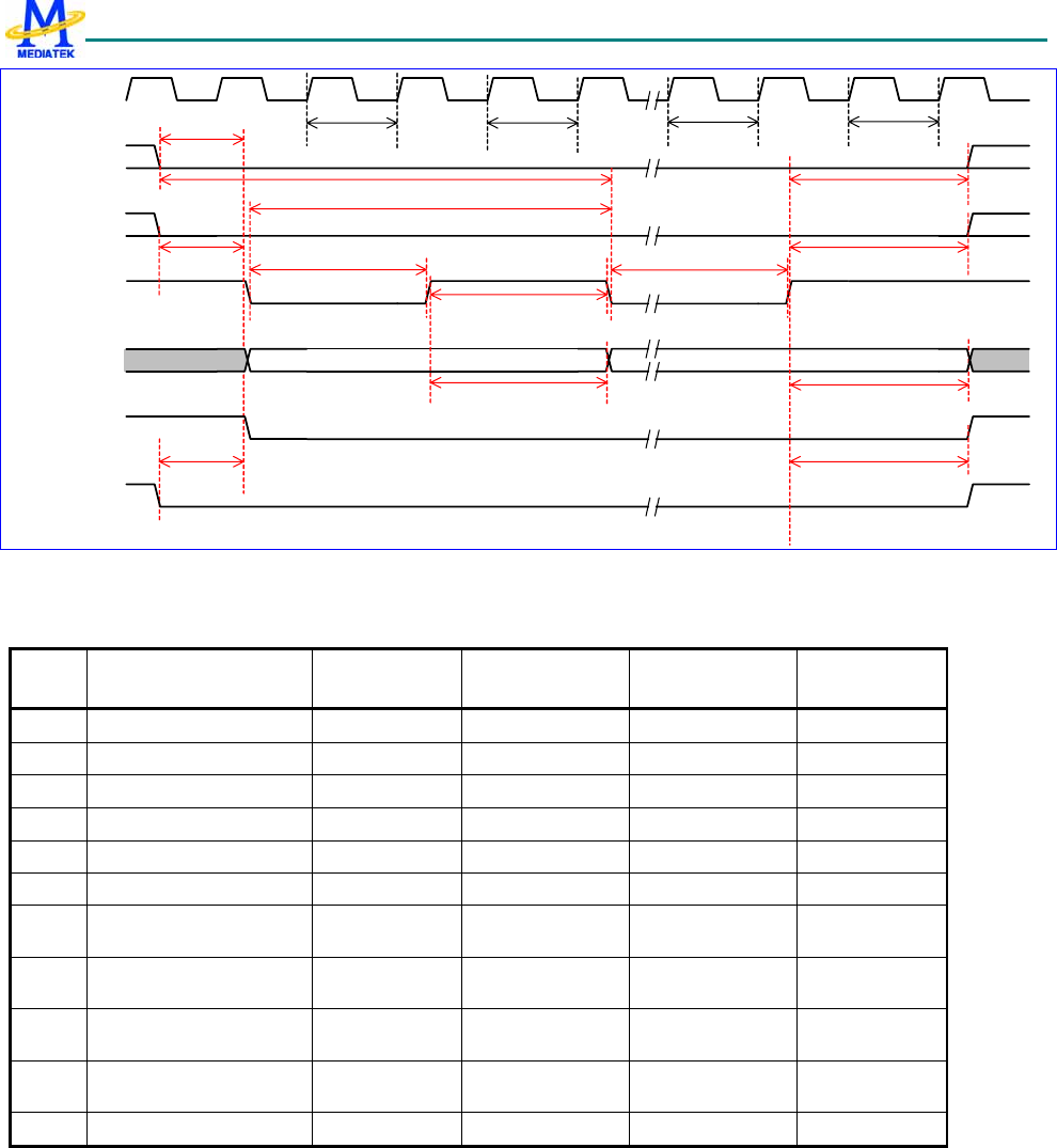
MT6235 GSM/GPRS Baseband Processor Data Sheet Revision 1.02
318/599 MediaTek Inc. Confidential
WST
t
ALS t
ALH
t
WP
HCLK
NALE
NWEB
NLD
t
WH
WH
WH
OE
(internal)
NCEB t
CES
t
CEH
t
DH
t
DH
NCLE
t
CLS
D0 D527
WST
tWP
tCLH
tWC2
tWC1
Figure 39 Consecutive data write cycles (1 wait state, 1 hold time extension)
The ideal timing for read access is as listed in Table 18.
Parame
ter Description Timing
specification Timing at 13MHz
(RLT, WH) = (0,0)
Timing at 26MHz
(RLT, WH) = (1,0)
Timing at 52MHz
(RLT, WH) = (2,0)
T
RC1
Read cycle time 3T + RLT + WH 230.8ns 153.8ns 96.2ns
T
RC2
Read cycle time 2T + RLT + WH 153.9ns 115.4ns 76.9ns
T
DS
Read data setup time 1T + RLT 76.9ns 76.9ns 57.7ns
T
DH
Read data hold time 1T + WH 76.9ns 38.5ns 19.2ns
T
RP
Read enable time 1T + RLT 76.9ns 76.9ns 57.7ns
T
RH
Read high time 1T + WH 76.9ns 38.5ns 19.2ns
T
CLS
Command latch enable
setup time 1T 76.9ns 38.5ns 19.2ns
T
CLH
Command latch enable
hold time 1T + WH 76.9ns 38.5ns 19.2ns
T
ALS
Address latch enable
setup time 1T 76.9ns 38.5ns 19.2ns
T
ALH
Address latch enable hold
time 1T + WH 76.9ns 38.5ns 19.2ns
F
RC
Write data rate 1 / T
RC2
6.5Mbytes/s 8.7Mbytes/s 13Mbytes/s
Table 32 Read access timing
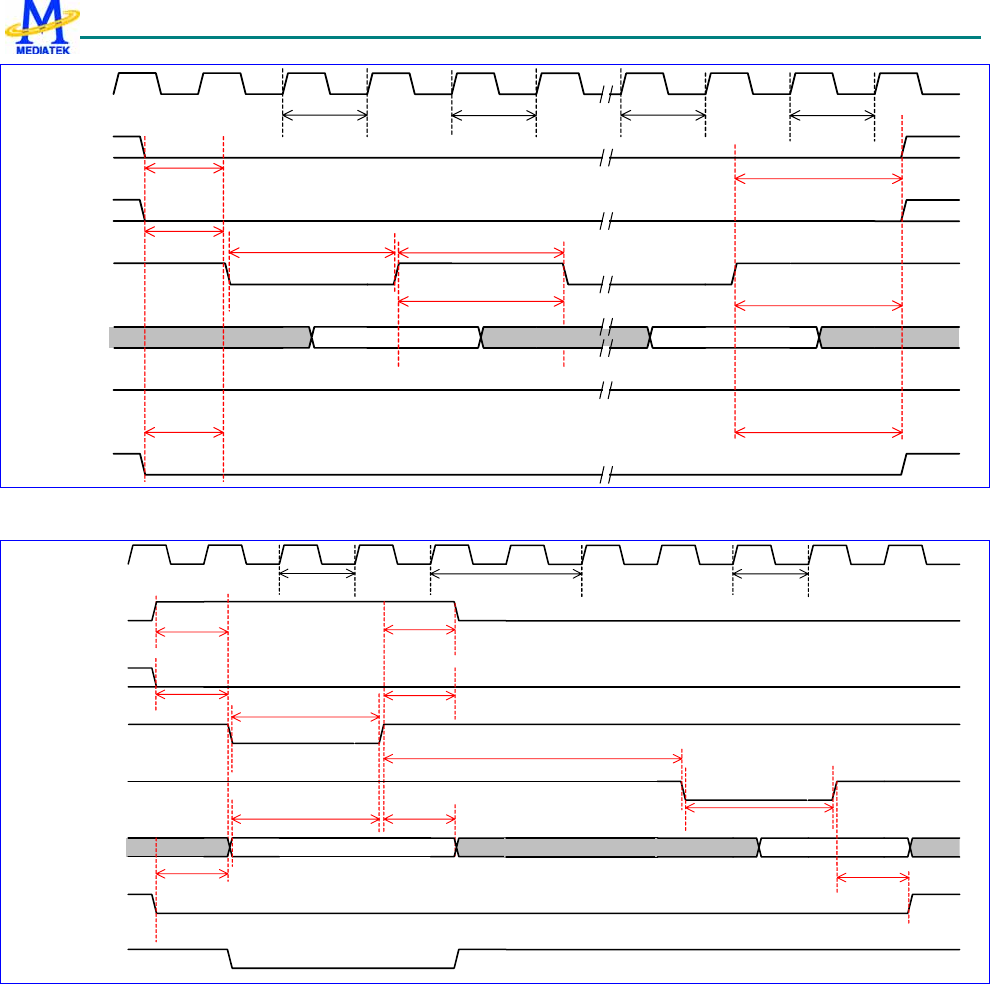
MT6235 GSM/GPRS Baseband Processor Data Sheet Revision 1.02
319/599 MediaTek Inc. Confidential
RLT
t
ALS
t
CLH
, t
ALH
tWP
HCLK
NALE
NREB
NLD
t
WH
WH
WH
OE
(internal)
NCEB
t
CES
t
CEH
t
DH
t
DH
NCLE
t
CLS
D0 D527
RLT
Figure 40 Serial read cycle (1 wait state, 1 hold time extension)
RLT
t
CLS
t
CLH
tWP
tDH
HCLK
NCLE
NWEB
NLD
NCEB
t
CES
t
CEH
tDS
NALE
70h
tALS
t
ALH
NREB
Status
tWHR
t
RP
RLT
OE
(internal)
W2R
Figure 41 Status read cycle (1 wait state)
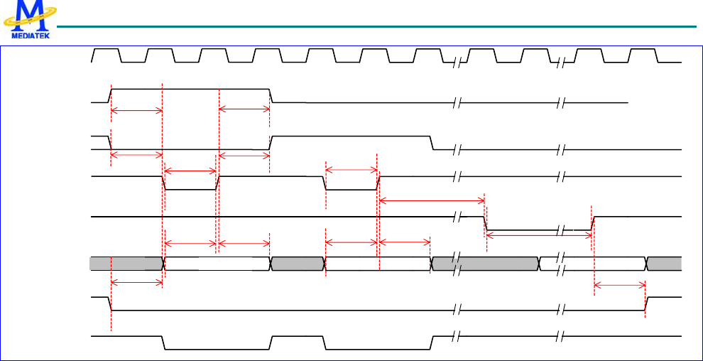
MT6235 GSM/GPRS Baseband Processor Data Sheet Revision 1.02
320/599 MediaTek Inc. Confidential
tCLS tCLH
tWP
tDH
HCLK
NCLE
NWEB
NLD
NCEB
tCES tCEH
tDS
NALE
90h
tALS tALH
NREB
01h, 06h
tWHR
tRP
OE
(internal)
tWP
00h
tDH
tDS
Figure 42 ID and manufacturer read (0 wait state)
7.4 USB 2.0 High-Speed Dual-Role Controller
7.4.1 General Description
The USB2.0 Controller can support 4 Tx and 3 Rx endpoints(excluding Endpoint 0). These endpoints can be
individually configured in software to handle either Bulk transfers, Interrupt transfers or Isochronous transfers.
There are 4 DMA channels and the embedded RAM size is 4Kbytes. The embedded RAM can be dynamically
configured to each endpoint.
Here is provided features.
Operates as the peripheral in point-to-point communications with another USB function
Complies with the USB 2.0 standard for high-speed (480Mbps) functions
Supports point-to-point communications with one high- or full-speed device
Supports Suspend and Resume signaling
Supports High-Bandwidth Isochronous & Interrupt transfers
UTMI+ Level 2 Transceiver Interface
Synchronous RAM interface for FIFOs
Support for DMA access to FIFOs
Software connect/disconnect option
Supports multi-layer operations on the AHB bus
Performs all transaction scheduling in hardware
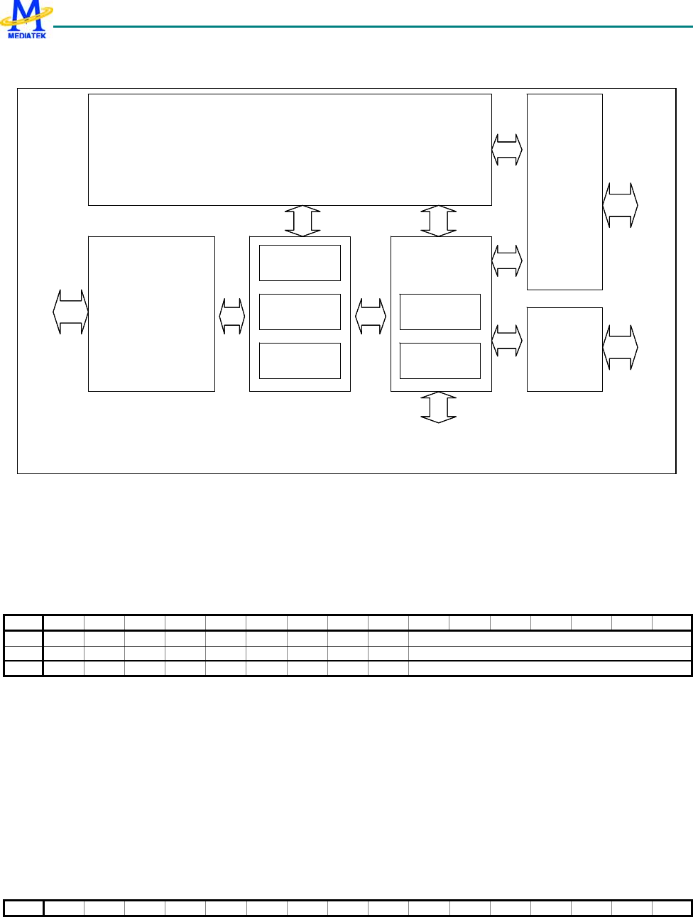
MT6235 GSM/GPRS Baseband Processor Data Sheet Revision 1.02
321/599 MediaTek Inc. Confidential
The USB2.0 Controller Block Diagram is as illustrated.
7.4.2 Register Definitions
USB COMMON REGISTER
USB+0000h Function Address Register FADDR
Bit 7 6 5 4 3 2 1 0
Name FUNCTION ADDRESS
Type R R/W
Reset 0 0
Function Address FAddr is an 8-bit register that should be written with the 7-bit address of the peripheral part
of the transaction. When the USB2.0 controller is being used in Peripheral mode (DevCtl.bit2=0), this register
should be written with the address received through a SET_ADDRESS command, which will then be used for
decoding the function address in subsequent token packets. When the USB2.0 controller is being used in Host
mode (DevCtl.bit2=1), this register should be set to the value sent in a SET_ADDRESS command during device
enumeration as the address for the peripheral device.
Peripheral Mode
USB+0001h Power Management Register POWER
Bit 15 14 13 12 11 10 9 8 7 6 5 4 3 2 1 0
Endpoint Control
UTM
Synchronization
Packet
Encode
Packet
Decode
CRC
Gen/Check
Rx
Buffer
Tx
Buffer
RAM
controller
DMA
controller
CPU
Interface
AHB
slave
AHB
master
UTMI
RAM
Endpoint Control
UTM
Synchronization
Packet
Encode
Packet
Decode
CRC
Gen/Check
Packet
Encode
Packet
Decode
CRC
Gen/Check
Rx
Buffer
Tx
Buffer
RAM
controller
Rx
Buffer
Tx
Buffer
RAM
controller
DMA
controller
CPU
Interface
AHB
slave
AHB
master
UTMI
RAM

MT6235 GSM/GPRS Baseband Processor Data Sheet Revision 1.02
322/599 MediaTek Inc. Confidential
Name
ISO
UPDA
TE
SOFT
CONN HS
ENAB HS
MODE RESE
T RESU
ME
SUSP
END
MODE
ENAB
LE
SUSP
ENDM
Type R/W R/W R/W R R R/W R R/W
Reset 0 0 1 0 0 0 0 0
Host Mode
USB+0001h Power Management Register POWER
Bit 15 14 13 12 11 10 9 8 7 6 5 4 3 2 1 0
Name
HS
ENAB HS
MODE RESE
T RESU
ME
SUSP
END
MODE
ENAB
LE
SUSP
ENDM
Type R/W R R/W R/W set R/W
Reset 1 0 0 0 0 0
EnableSuspendM Set by the CPU to enable the SUSPENDM output
SuspendMode In Host mode, this bit is set by the CPU to enter Suspend mode. In Peripheral mode, this bit is set
on entry into Suspend mode. It is cleared when the CPU reads the interrupt register, or sets the Resume bit
above.
Resume Set by the CPU to generate Resume signaling when the function is in Suspend mode. The CPU should
clear this bit after 10 ms (a maximum of 15 ms) to end Resume signaling. In Host mode, this bit is also
automatically set when Resume signaling from the target is detected while the USB2.0 controller is suspended.
Reset This bit is set when Reset signaling is present on the bus. Note: This bit is Read/Write from the CPU in
Host Mode but Read-Only in Peripheral Mode.
HSMode When set, this read-only bit indicates High-speed mode successfully negotiated during USB reset. In
Peripheral Mode, becomes valid when USB reset completes (as indicated by USB reset interrupt). In Host Mode,
becomes valid when Reset bit is cleared. Remains valid for the duration of the session.
Note: Allowance is made for Tiny-J signaling in determining the transfer speed to select.
HSEnab When set by the CPU, the USB2.0 controller will negotiate for High-speed mode when the device is
reset by the hub. If not set, the device will only operate in Full-speed mode.
SoftConn If Soft Connect/Disconnect feature is enabled, then the USB D+/D- lines is enabled when this bit is set
by the CPU and tri-stated when this bit is cleared by the CPU. Note: Only valid in Peripheral Mode.
ISOupdate When set by the CPU, the USB2.0 controller will wait for an SOF token from the time TxPktRdy is set
before sending the packet. If an IN token is received before an SOF token, then a zero length data packet will be
sent.
Note: Only valid in Peripheral Mode. Also, this bit only affects endpoints performing Isochronous transfers.
USB+0002h Tx Interrupt Status Register INTRTX
Bit 15 14 13 12 11 10 9 8 7 6 5 4 3 2 1 0
Name
EP5
TX EP4
TX EP3
TX EP2
TX EP1
TX EP0
MT6235 GSM/GPRS Baseband Processor Data Sheet Revision 1.02
323/599 MediaTek Inc. Confidential
Type R R R R R R
Reset 0 0 0 0 0 0
EP0 Endpoint0 interrupt event
EP1_TX Tx Endpoint 1 interrupt event
EP2_TX Tx Endpoint 2 interrupt event
EP3_TX Tx Endpoint 3 interrupt event
EP4_TX Tx Endpoint 4 interrupt event
EP5_TX Tx Endpoint 5 interrupt event
USB+0004h Rx Interrupt Status Register INTRRX
Bit 15 14 13 12 11 10 9 8 7 6 5 4 3 2 1 0
Name
EP3
RX EP2
RX EP1
RX
Type R/W R/W R/W
Reset 0 0 0
INTRRX[15:0] Rx Interrupt Status register is “write 0 clear”
EP1_RX Rx Endpoint 1 interrupt event
EP2_RX Rx Endpoint 2 interrupt event
EP3_RX Rx Endpoint 3 interrupt event
USB+0006h Tx Interrupt Enable Register INTRTXE
Bit 15 14 13 12 11 10 9 8 7 6 5 4 3 2 1 0
Name
EP5
TXE EP4
TXE EP3
TXE EP2
TXE EP1
TXE EP0
E
Type R/W R/W R/W R/W R/W R/W
Reset 1 1 1 1 1 1
EP0_E 0: Endpoint0 interrupt event disable 1: Endpoint0 interrupt event enable
EP1_TXE 0:Tx Endpoint 1 interrupt event disable 1:Tx Endpoint 1 interrupt event enable
EP2_TXE 0:Tx Endpoint 2 interrupt event disable 1:Tx Endpoint 2 interrupt event enable
EP3_TXE 0:Tx Endpoint 3 interrupt event disable 1:Tx Endpoint 3 interrupt event enable
EP4_TXE 0:Tx Endpoint 4 interrupt event disable 1:Tx Endpoint 4 interrupt event enable
EP5_TXE 0:Tx Endpoint 5 interrupt event disable 1:Tx Endpoint 5 interrupt event enable
USB+0008h Rx Interrupt Enable Register INTRRXE
Bit 15 14 13 12 11 10 9 8 7 6 5 4 3 2 1 0
Name
EP3
RXE EP2
RXE EP1
RXE
Type R/W R/W R/W
Reset 1 1 1
EP1_RXE 0:Rx Endpoint 1 interrupt event disable 1:Rx Endpoint 1 interrupt event enable
EP2_RXE 0:rx Endpoint 2 interrupt event disable 1:Rx Endpoint 2 interrupt event enable
EP3_RXE 0:Rx Endpoint 3 interrupt event disable 1:Rx Endpoint 3 interrupt event enable
MT6235 GSM/GPRS Baseband Processor Data Sheet Revision 1.02
324/599 MediaTek Inc. Confidential
USB+000Ah Common USB interrupts Register INTRUSB
Bit 15 14 13 12 11 10 9 8 7 6 5 4 3 2 1 0
Name
V
BUS
ERRO
R
SESS
REQ DISC
ON CONN SOF RESE
T/BAB
BLE
RESU
ME SUSP
END
Type R R R R R R R R
Reset 0 0 0 0 0 0 0 0
Suspend Set when Suspend signaling is detected on the bus. Only valid in Peripheral mode.
Resume Set when Resume signaling is detected on the bus while the USB2.0 controller is in Suspend mode.
Reset Set in Peripheral mode when Reset signaling is detected on the bus.
Babble Set in Host mode when babble is detected. Note: Only active after first SOF has been sent.
SOF Set when a new frame starts.
Conn Set when a device connection is detected. Only valid in Host mode. Valid at all transaction speeds.
Discon Set in Host mode when a device disconnect is detected. Set in Peripheral mode when a session ends.
Valid at all transaction speeds.
SessReq Set when Session Request signaling has been detected. Only valid when USB2.0 controller is ‘A’
device.
VBusError Set when VBus drops below the VBus Valid threshold during a session. Only valid when USB2.0
controller is ‘A’ device.
USB+000Bh Common USB interrupts Enable Register INTRUSBE
Bit 15 14 13 12 11 10 9 8 7 6 5 4 3 2 1 0
Name
V
BUS
ERRO
R_E
SESS
REQ_
E
DISC
ON_E CONN
_E SOF_
E
RESE
T/BAB
BLE_
E
RESU
ME_E
SUSP
END_
E
Type R/W R/W R/W R/W R/W R/W R/W R/W
Reset 0 0 0 0 0 1 1 0
SuspendE Suspend interrupt enable.
ResumeE Resume interrupt enable
Reset/BabbleE Reset/Babble interrupt enable
SOFE SOF interrupt enable
ConnE Conn interrupt enable
DisconE Discon interrupt enable
SessReqE SessReq interrupt enable
VBusErrorE VBusError interrupt enable
USB+000Ch Frame Number Register FRAME
Bit 15 14 13 12 11 10 9 8 7 6 5 4 3 2 1 0
Name 0 FRAME NUMBER
Type R R
Reset 0 0
FRAME Frame is a 11-bit read-only register that holds the last received frame number.
MT6235 GSM/GPRS Baseband Processor Data Sheet Revision 1.02
325/599 MediaTek Inc. Confidential
USB+000Eh Endpoint Selecting Index Register INDEX
Bit 15 14 13 12 11 10 9 8 7 6 5 4 3 2 1 0
Name SELECTED ENDPOINT
Type R/W
Reset 0
INDEX Each Tx endpoint and each Rx endpoint have their own set of control/status registers located between
29900h – 299FFh. In addition one set of Tx control/status and one set of Rx control/status registers appear at
29810h – 2981Fh. Index is a 4-bit register that determines which endpoint control/status registers are accessed.
Before accessing an endpoint’s control/status registers at 29810h – 2981Fh, the endpoint number should be
written to the Index register to ensure that the correct control/status registers appear in the memory map.
USB+000Fh Test Mode Enable Register TESTMODE
Bit 15 14 13 12 11 10 9 8 7 6 5 4 3 2 1 0
Name
FORC
E_HO
ST
FIFO_
ACCE
SS
FORC
E_FS FORC
E_HS
TEST
_PAC
KET
TEST
_K TEST
J
TEST
_SE0_
NAK
Type R/W SET R/W R/W R/W R/W R/W R/W
Reset 0 0 0 0 0 0 0 0
Test_SE0_NAK (High-speed mode) The CPU sets this bit to enter the Test_SE0_NAK test mode. In this mode,
the USB2.0 controller remains in High-speed mode but responds to any valid IN token with a NAK.
Test_J (High-speed mode) The CPU sets this bit to enter the Test_J test mode. In this mode, the USB2.0
controller transmits a continuous J on the bus.
Test_K (High-speed mode) The CPU sets this bit to enter the Test_K test mode. In this mode, the USB2.0
controller transmits a continuous K on the bus.
Test_Packet (High-speed mode) The CPU sets this bit to enter the Test_Packet test mode. In this mode, the
USB2.0 controller repetitively transmits on the bus a 53-byte test packet, the form of which is defined in the
Universal Serial Bus Specification Revision 2.0, Section 7.1.20. Note: The test packet has a fixed format and
must be loaded into the Endpoint 0 FIFO before the test mode is entered.
Force_HS The CPU sets this bit either in conjunction with bit 7 above or to force the USB2.0 controller into
High-speed mode when it receives a USB reset.
Force_FS The CPU sets this bit either in conjunction with bit 7 above or to force the USB2.0 controller into
Fullspeed mode when it receives a USB reset.
FIFO_Access The CPU sets this bit to transfer the packet in the Endpoint 0 Tx FIFO to the Endpoint 0 Rx FIFO.
It is cleared automatically.
Force_Host The CPU sets this bit to instruct the core to enter Host mode when the Session bit is set, regardless
of whether it is connected to any peripheral. The state of the CID input, HostDisconnect and LineState signals are
ignored. The core will then remain in Host mode until the Session bit is cleared, even if a device is disconnected,
and if the Force_Host bit remains set, will re-enter Host mode the next time the Session bit is set.While in this

MT6235 GSM/GPRS Baseband Processor Data Sheet Revision 1.02
326/599 MediaTek Inc. Confidential
mode, the status of the HOSTDISCON signal from the PHY may be read from bit 7 of the ACTLR0.DevCtl
register.
The operating speed is determined from the Force_HS and Force_FS bits as follows:
Force_HS Force_FS Operating Speed
0 0 Low Speed
0 1 Full Speed
1 0 High Speed
1 1 Undefined
USB INDEXED REGISTER
EP0 INDEXED REGISTER
Peripheral Mode
USB+0100h EP0 Control Status Register CSR0
Bit 15 14 13 12 11 10 9 8 7 6 5 4 3 2 1 0
Name
FLUS
HFIFO
SERVI
CESE
TUPE
ND
SERVI
CED
RXPK
TRDY
SEND
STAL
L
SETU
PEND DATA
END
SEND
STAL
L
TXPK
TRDY RXPK
TRDY
Type SET SET SET SET R SET
R/CLE
AR R/SET R
Reset 0 0 0 0 0 0 0 0 0
RxPktRdy This bit is set when a data packet has been received. An interrupt is generated when this bit is set.
The CPU clears this bit by setting the ServicedRxPktRdy bit.
TxPktRdy The CPU sets this bit after loading a data packet into the FIFO. It is cleared automatically when a data
packet has been transmitted. An interrupt is also generated at this point (if enabled).
SentStall This bit is set when a STALL handshake is transmitted. The CPU should clear this bit.
DataEnd The CPU sets this bit:
1. When setting TxPktRdy for the last data packet.
2. When clearing RxPktRdy after unloading the last data packet.
3. When setting TxPktRdy for a zero length data packet.
It is cleared automatically.
SetupEnd This bit will be set when a control transaction ends before the DataEnd bit has been set. An interrupt
will be generated and the FIFO flushed at this time. The bit is cleared by the CPU writing a 1 to the
ServicedSetupEnd bit.
SendStall The CPU writes a 1 to this bit to terminate the current transaction. The STALL handshake will be
transmitted and then this bit will be cleared automatically. Note: The FIFO should be flushed before SendStall is
set.
ServiceRxPktRdy The CPU writes a 1 to this bit to clear the RxPktRdy bit. It is cleared automatically.

MT6235 GSM/GPRS Baseband Processor Data Sheet Revision 1.02
327/599 MediaTek Inc. Confidential
ServiceSetupEnd The CPU writes a 1 to this bit to clear the SetupEnd bit. It is cleared automatically.
FlushFIFO The CPU writes a 1 to this bit to flush the next packet to be transmitted/read from the Endpoint 0
FIFO. It is cleared automatically. The FIFO pointer is reset and the TxPktRdy/RxPktRdy bit (below) is cleared.
Note: FlushFIFO should only be used when TxPktRdy/RxPktRdy is set. At other times, it may cause data to be
corrupted.
Host Mode
USB+0100h EP0 Control Status Register CSR0
Bit 15 14 13 12 11 10 9 8 7 6 5 4 3 2 1 0
Name
DIS
PING
FLUS
HFIFO
NAK
TIME
OUT
STAT
USPK
T
REQ
PKT ERRO
R SETU
PPKT RXST
ALL TXPK
TRDY RXPK
TRDY
Type R/W SET R/CLE
AR R/W R/W R/CLE
AR R/CLE
AR R/CLE
AR R/SET R/CLE
AR
Reset 0 0 0 0 0 0 0 0 0 0
RxPktRdy This bit is set when a data packet has been received. An interrupt is generated (if enabled) when this
bit is set. The CPU should clear this bit when the packet has been read from the FIFO.
TxPktRdy The CPU sets this bit after loading a data packet into the FIFO. It is cleared automatically when a data
packet has been transmitted. An interrupt is also generated at this point (if enabled).
RxStall This bit is set when a STALL handshake is received. The CPU should clear this bit.
SetupPkt The CPU sets this bit, at the same time as the TxPktRdy bit is set, to send a SETUP token instead of
an OUT token for the transaction. Note: Setting this bit also clears the DataToggle.
Error This bit will be set when three attempts have been made to perform a transaction with no response from
the peripheral. The CPU should clear this bit. An interrupt is generated when this bit is set.
ReqPkt The CPU sets this bit to request an IN transaction. It is cleared when RxPktRdy is set.
StatusPkt The CPU sets this bit at the same time as the TxPktRdy or ReqPkt bit is set, to perform a status stage
transaction. Setting this bit ensures that the data toggle is set to 1 so that a DATA1 packet is used for the Status
Stage transaction.
NAKTimeout This bit will be set when Endpoint 0 is halted following the receipt of NAK responses for longer than
the time set by the NAKLimit0 register. The CPU should clear this bit to allow the endpoint to continue.
FlushFIFO The CPU writes a 1 to this bit to flush the next packet to be transmitted/read from the Endpoint 0
FIFO. The FIFO pointer is reset and the TxPktRdy/RxPktRdy bit (below) is cleared. Note: FlushFIFO should only
be used when TxPktRdy/RxPktRdy is set. At other times, it may cause data to be corrupted.
DisPing The CPU writes a 1 to this bit to instruct the core not to issue PING tokens in data and status phases of
a high-speed Control transfer (for use with devices that do not respond to PING)
USB+0108h EP0 Received bytes Register COUNT0
Bit 15 14 13 12 11 10 9 8 7 6 5 4 3 2 1 0
Name EP0 RX COUNT
Type R
Reset 0

MT6235 GSM/GPRS Baseband Processor Data Sheet Revision 1.02
328/599 MediaTek Inc. Confidential
EP0 RX Count0 Count0 is a 7-bit read-only register that indicates the number of received data bytes in the
Endpoint 0 FIFO. The value returned changes as the contents of the FIFO change and is only valid while
RxPktRdy (IDXEPR0.CSR0.bit0) is set.
Host Mode
USB+010Bh NAK Limit Register NAKLIMT0
Bit 15 14 13 12 11 10 9 8 7 6 5 4 3 2 1 0
Name NAK
LIMIT0
Type R/W
Reset 0
NAKLimit0 NAKLimit0 is a 5-bit register that sets the number of frames/microframes (High-Speed transfers) after
which Endpoint 0 should timeout on receiving a stream of NAK responses. (Equivalent settings for other
endpoints can be made through their TxInterval and RxInterval registers.). The number of frames/microframes
selected is 2(m-1) (where m is the value set in the register, valid values 2 – 16). If the host receives NAK responses
from the target for more frames than the number represented by the Limit set in this register, the endpoint will be
halted. Note: A value of 0 or 1 disables the NAK timeout function.
USB+010Fh Core Configuration Register CONFIGDATA
Bit 15 14 13 12 11 10 9 8 7 6 5 4 3 2 1 0
Name
MP
RXE MP
TXE
BIGE
NDIA
N
HBRX
E HBTX
E
DYNFI
FOSIZ
ING
SOFT
CONE
UTMI
DATA
WIDT
H
Type R R R R R R R R
Reset
UTMIDataWidth Indicates selected UTMI+ data width. 0 8 bits; 1 16 bits.
SoftConE When set to ‘1’ indicates Soft Connect/Disconnect option selected.
DynFIFOSizeing When set to ‘1’ indicates Dynamic FIFO Sizing option selected.
HBTxE When set to ‘1’ indicates High-bandwidth Tx ISO Endpoint Support selected.
HBRxE When set to ‘1’ indicates High-bandwidth Rx ISO Endpoint Support selected
BigEndian When set to ‘1’ indicates Big Endian ordering is selected.
MPTxE When set to ‘1’, automatic splitting of bulk packets is selected.
MPRxE When set to ‘1’, automatic amalgamation of bulk packets is selected.
EP1 INDEXED REGISTER
USB+0110h TXMAP Register TXMAP
Bit 15 14 13 12 11 10 9 8 7 6 5 4 3 2 1 0
Name M-1 MAXIMUM PAYLOAD TRANSACTION
Type R/W R/W
Reset 0 0
TxMaxP Maxmum payload size for indexed TX endpoint
m-1 Packet multiplier m

MT6235 GSM/GPRS Baseband Processor Data Sheet Revision 1.02
329/599 MediaTek Inc. Confidential
TxMaxP Register
The TxMaxP register defines the maximum amount of data that can be transferred through the selected Tx
endpoint in a single operation. There is a TxMaxP register for each Tx endpoint (except Endpoint 0).
Bits 10:0 define (in bytes) the maximum payload transmitted in a single transaction. The value set can be up to
1024 bytes but is subject to the constraints placed by the USB Specification on packet sizes for Bulk, Interrupt
and Isochronous transfers in Fullspeed and High-speed operations. Where the option of High-bandwidth
Isochronous/Interrupt endpoints or of packet splitting on Bulk endpoints has been taken when the core is
configured, the register includes either 2 or 5 further bits that define a multiplier m which is equal to one more
than the value recorded.
In the case of Bulk endpoints with the packet splitting option enabled, the multiplier m can be up to 32 and defines
the maximum number of ‘USB’ packets (i.e. packets for transmission over the USB) of the specified payload into
which a single data packet placed in the FIFO should be split, prior to transfer. (If the packet splitting option is not
enabled, bit15–13 is not implemented and bit12–11(if included) is ignored.) Note: The data packet is required to
be an exact multiple of the payload specified by bits 10:0, which is itself required to be either 8, 16, 32, 64 or (in
the case of High Speed transfers) 512 bytes.
For Isochronous/Interrupt endpoints operating in High-Speed mode and with the High-bandwidth option enabled,
m may only be either 2 or 3 (corresponding to bit 11 set or bit 12 set, respectively) and it specifies the maximum
number of such transactions that can take place in a single microframe. If either bit 11 or bit 12 is non-zero, the
USB2.0 controller will automatically split any data packet written to the FIFO into up to 2 or 3 ‘USB’ packets, each
containing the specified payload (or less). The maximum payload for each transaction is 1024 bytes, so this
allows up to 3072 bytes to be transmitted in each microframe. (For Isochronous/Interrupt transfers in Full-speed
mod, bits 11 and 12 are ignored.)
The value written to bits 10:0 (multiplied by m in the case of high-bandwidth Isochronous/Interrupt transfers) must
match the value given in the wMaxPacketSize field of the Standard Endpoint Descriptor for the associated
endpoint (see USB Specification Revision 2.0, Chapter 9). A mismatch could cause unexpected results.
The total amount of data represented by the value written to this register (specified payload × m) must not exceed
the FIFO size for the Tx endpoint, and should not exceed half the FIFO size if double-buffering is required.
If this register is changed after packets have been sent from the endpoint, the Tx endpoint FIFO should be
completely flushed (using the FlushFIFO bit in TxCSR) after writing the new value to this register.
Peripheral Mode
USB+0112h Tx CSR Register TXCSR
Bit 15 14 13 12 11 10 9 8 7 6 5 4 3 2 1 0
Name AUTO
SET ISO MODE
DMAR
EQEN
FRCD
ATAT
OG
DMAR
EQMO
DE
AUTO
SETE
N_SP
KT
INCO
MPTX
CLRD
ATAT
OG
SENT
STAL
L
SEND
STAL
L
FLUS
HFIFO UNDE
RRUN
FIFON
OTEM
PTY
TXPK
TRDY
Type R/W R/W R/W R/W R/W R/W R/W R/W R/W R/W R/W R/W R/W R R/W
Reset 0 0 0 0 0 0 0 0 0 0 0 0 0 0 0
TxPktRdy The CPU sets this bit after loading a data packet into the FIFO. It is cleared automatically when a data
packet has been transmitted. An interrupt is also generated at this point (if enabled). TxPktRdy is also

MT6235 GSM/GPRS Baseband Processor Data Sheet Revision 1.02
330/599 MediaTek Inc. Confidential
automatically cleared (but no interrupt is generated) prior to loading a second packet into a double-buffered
FIFO.
FIFONotEmpty The USB sets this bit when there is at least 1 packet in the TxFIFO.
UnderRun The USB sets this bit if an IN token is received when the TxPktRdy bit not set. The CPU should clear
this bit (write 0 clear).
FlushFIFO The CPU writes a 1 to this bit to flush the latest packet from the endpoint TxFIFO. The FIFO pointer is
reset, the TxPktRdy bit is cleared and an interrupt is generated. May be set simultaneously with TxPktRdy to
abort the packet that is currently being loaded into the FIFO. Note: FlushFIFO should only be used when
TxPktRdy is set. At other times, it may cause data to be corrupted. Also note that, if the FIFO is double-buffered,
FlushFIFO may need to be set twice to completely clear the FIFO.
SendStall The CPU writes a 1 to this bit to issue a STALL handshake to an IN token. The CPU clears this bit to
terminate the stall condition. Note: This bit has no effect where the endpoint is being used for Isochronous
transfer.
SentStall This bit is set when a STALL handshake is transmitted. The FIFO is flushed and the TxPktRdy bit is
cleared. The CPU should clear this bit.
ClrDataTog The CPU writes a 1 to this bit to reset the endpoint data toggle to 0.
IncompTx When the endpoint is being used for high-bandwidth Isochronous/Interrupt transfers, this bit is set to
indicate where a large packet has been split into 2 or 3 packets for transmission but insufficient IN tokens have
been received to send all the parts. Note: In anything other than a high-bandwidth transfer, this bit will always
return 0.
AutoSetEn_SPKT If the CPU sets this bit, TxPktRdy will be automatically set when the short packet is loaded
into the TxFIFO completely. But, this function only works in Tx endpoint 1 and 2. Besides, Tx endpoint 1 has to
use DMA channel 1 to move data and Tx endpoint 2 has to use DMA channel 2 to move data.
DMAReqMode The CPU sets this bit to select DMA Request Mode 1 and clears it to select DMA Request Mode
0. Note: This bit must not be cleared either before or in the same cycle as the DMAReqEn bit is cleared.
FrcDataTog The CPU sets this bit to force the endpoint data toggle to switch and the data packet to be cleared
from the FIFO, regardless of whether an ACK was received. This can be used by Interrupt Tx endpoints that are
used to communicate rate feedback for Isochronous endpoints.
DMAReqEn The CPU sets this bit to enable the DMA request for the Tx endpoint.
Mode The CPU sets this bit to enable the endpoint direction as Tx, and clears the bit to enable it as Rx. Note:
This bit only has any effect where the same endpoint FIFO is used for both Tx and Rx transactions.
ISO The CPU sets this bit to enable the Tx endpoint for Isochronous transfers, and clears it to enable the Tx
endpoint for Bulk or Interrupt transfers. Note: This bit only has any effect in Peripheral mode. In Host mode, it
always returns zero.
AutoSet If the CPU sets this bit, TxPktRdy will be automatically set when data of the maximum packet size
(value in TxMaxP) is loaded into the TxFIFO. If a packet of less than the maximum packet size is loaded, then
TxPktRdy will have to be set manually if AutoSetEn_SPKT is not enabled.

MT6235 GSM/GPRS Baseband Processor Data Sheet Revision 1.02
331/599 MediaTek Inc. Confidential
Host Mode
USB+0112h Tx CSR Register TXCSR
Bit 15 14 13 12 11 10 9 8 7 6 5 4 3 2 1 0
Name AUTO
SET MODE
DMAR
EQEN
FRCD
ATAT
OG
DMAR
EQMO
DE
NAK
TIME
OUT/I
NCOM
PTX
CLRD
ATAT
OG
RXST
ALL FLUS
HFIFO ERRO
R
FIFON
OTEM
PTY
TXPK
TRDY
Type R/W R/W R/W R/W R/W R/W R/CLE
AR SET R/CLE
AR SET
R/CLE
AR R/CLE
AR R/SET
Reset 0 0 0 0 0 0 0 0 0 0 0 0 0
TxPktRdy The CPU sets this bit after loading a data packet into the FIFO. It is cleared automatically when a data
packet has been transmitted. An interrupt is also generated at this point (if enabled). TxPktRdy is also
automatically cleared prior to loading a second packet into a double-buffered FIFO.
FIFONotEmpty The USB sets this bit when there is at least 1 packet in the Tx FIFO.
Error The USB sets this bit when 3 attempts have been made to send a packet and no handshake packet has
been received. When the bit is set, an interrupt is generated, TxPktRdy is cleared and the FIFO is completely
flushed. The CPU should clear this bit. Valid only when the endpoint is operating in Bulk or Interrupt mode.
FlushFIFO The CPU writes a 1 to this bit to flush the latest packet from the endpoint Tx FIFO. The FIFO pointer
is reset, the TxPktRdy bit (below) is cleared and an interrupt is generated. May be set simultaneously with
TxPktRdy to abort the packet that is currently being loaded into the FIFO. Note: FlushFIFO should only be used
when TxPktRdy is set. At other times, it may cause data to be corrupted. Also note that, if the FIFO is
double-buffered, FlushFIFO may need to be set twice to completely clear the FIFO.
RxStall This bit is set when a STALL handshake is received. When this bit is set, any DMA request that is in
progress is stopped, the FIFO is completely flushed and the TxPktRdy bit is cleared (see below). The CPU
should clear this bit.
ClrDataTog The CPU writes a 1 to this bit to reset the endpoint data toggle to 0.
NAKTimeout Bulk endpoints only: This bit will be set when the Tx endpoint is halted following the receipt of NAK
responses for longer than the time set as the NAK Limit by the TxInterval register. The CPU should clear this bit
to allow the endpoint to continue.
IncompTx High-bandwidth Interrupt endpoints only: This bit will be set if no response is received from the device
to which the packet is being sent.
DMAReqMode The CPU sets this bit to select DMA Request Mode 1 and clears it to select DMA Request Mode
0. Note: This bit must not be cleared either before or in the same cycle as the above DMAReqEnab bit is cleared.
FrcDataTog The CPU sets this bit to force the endpoint data toggle to switch and the data packet to be cleared
from the FIFO, regardless of whether an ACK was received. This can be used by Interrupt Tx endpoints that are
used to communicate rate feedback for Isochronous endpoints.
DMAReqEnab The CPU sets this bit to enable the DMA request for the Tx endpoint.

MT6235 GSM/GPRS Baseband Processor Data Sheet Revision 1.02
332/599 MediaTek Inc. Confidential
Mode The CPU sets this bit to enable the endpoint direction as Tx, and clears it to enable the endpoint direction
as Rx. Note: This bit only has any effect where the same endpoint FIFO is used for both Tx and Rx transactions.
AutoSet If the CPU sets this bit, TxPktRdy will be automatically set when a packet of the maximum packet size
(TxMaxP) is loaded into the Tx FIFO. If a packet of less than the maximum packet size is loaded, then TxPktRdy
will have to be set manually. Note: Should not be set for either high-bandwidth Isochronous endpoints or
high-bandwidth Interrupt endpoints.
USB+0114h RXMAP Register RXMAP
Bit 15 14 13 12 11 10 9 8 7 6 5 4 3 2 1 0
Name M-1 MAXIMUM PAYLOA TRANSACTION
Type R/W R/W
Reset 0 0
RxMaxP Maxmum payload size for indexed RX endpoint
m-1 Packet multiplier m
RxMaxP Register The RxMaxP register defines the maximum amount of data that can be transferred through
the selected Rx endpoint in a single operation. There is a RxMaxP register for each Rx endpoint (except Endpoint
0).
Bits 10:0 define (in bytes) the maximum payload transmitted in a single transaction. The value set can be up to
1024 bytes but is subject to the constraints placed by the USB Specification on packet sizes for Bulk, Interrupt
and Isochronous transfers in Full-speed and High-speed operations.
Where the option of High-bandwidth Isochronous/Interrupt endpoints or of combining Bulk packets has been
taken when the core is configured, the register includes either 2 or 5 further bits that define a multiplier m which is
equal to one more than the value recorded.
For Bulk endpoints with the packet combining option enabled, the multiplier m can be up to 32 and defines the
number of USB packets of the specified payload which are to be combined into a single data packet within the
FIFO. (If the packet splitting option is not enabled, bit15–bit13 is not implemented and bit12–bit11 (if included) is
ignored.)
For Isochronous/Interrupt endpoints operating in High-Speed mode and with the High-bandwidth option enabled,
m may only be either 2 or 3 (corresponding to bit 11 set or bit 12 set, respectively) and it specifies the maximum
number of such transactions that can take place in a single microframe. If either bit 11 or bit 12 is non-zero, the
USB2.0 controller will automatically combine the separate USB packets received in any microframe into a single
packet within the Rx FIFO. The maximum payload for each transaction is 1024 bytes, so this allows up to 3072
bytes to be received in each microframe. (For Isochronous/Interrupt transfers in Full-speed mode or if
High-bandwidth is not enabled, bits 11 and 12 are ignored.) The value written to bits 10:0 (multiplied by m in the
case of high-bandwidth Isochronous/Interrupt transfers) must match the value given in the wMaxPacketSize field
of the Standard Endpoint Descriptor for the associated endpoint (see USB Specification Revision 2.0, Chapter 9).
A mismatch could cause unexpected results.

MT6235 GSM/GPRS Baseband Processor Data Sheet Revision 1.02
333/599 MediaTek Inc. Confidential
The total amount of data represented by the value written to this register (specified payload × m) must not exceed
the FIFO size for the OUT endpoint, and should not exceed half the FIFO size if double-buffering is required.
Peripheral Mode
USB+0116h Rx CSR Register RXCSR
Bit 15 14 13 12 11 10 9 8 7 6 5 4 3 2 1 0
Name AUTO
CLEA
R ISO DMAR
EQEN
DISNY
ET/PI
DERR
DMAR
EQMO
DE
AUTO
CLRE
N_SP
KT
INCO
MPRX
INTRE
N
INCO
MPRX
CLRD
ATAT
OG
SENT
STAL
L
SEND
STAL
L
FLUS
HFIFO DATA
ERR OVER
RUN FIFOF
ULL RXPK
TRDY
Type R/W R/W R/W R/W R/W R/W R/W R/W R/W R/W R/W R/W R/W R/W R R/W
Reset 0 0 0 0 0 0 0 0 0 0 0 0 0 0 0 0
RxPktRdy This bit is set when a data packet has been received (to RxFIFO). The CPU should clear this bit when
the packet has been unloaded from the RxFIFO. An interrupt is generated when the bit is set.
FIFOFull This bit is set when no more packets can be loaded into the RxFIFO.
OverRun This bit is set if an OUT packet cannot be loaded into the RxFIFO. The CPU should clear this bit (write
0 clear). Note: This bit is only valid when the endpoint is operating in ISO mode. In Bulk Mode, it always returns
zero. The new incoming packet won’t be written to RxFIFO. An interrupt is generated when the bit is set and
OverRunIntrEn is set.
DataError This bit is set when RxPktRdy is set if the data packet has a CRC or bit-stuff error. The CPU should
write 0 to clear this bit. Note: This bit is only valid when the endpoint is operating in ISO mode. In Bulk Mode, it
always returns zero. An interrupt is generated when the bit is set and DataErrIntrEn is set.
FlushFIFO The CPU writes a 1 to this bit to flush the next packet to be read from the endpoint RxFIFO. The
RxFIFO pointer is reset and the RxPktRdy bit is cleared. Note: FlushFIFO should only be used when RxPktRdy is
set. At other times, it may cause data to be corrupted. Also note that, if the RxFIFO is double buffered, FlushFIFO
may need to be set twice to completely clear the RxFIFO.
SendStall The CPU writes a 1 to this bit to issue a STALL handshake. The CPU clears this bit to terminate the
stall condition. Note: This bit has no effect where the endpoint is being used for ISO transfers.
SentStall This bit is set when a STALL handshake is transmitted. The CPU should clear this bit. An interrupt is
generated when the bit is set.
ClrDataTog The CPU writes a 1 to this bit to reset the endpoint data toggle to 0.
IncompRx This bit is set in a high-bandwidth Isochronous/Interrupt transfer if the packet in the RxFIFO is
incomplete because parts of the data were not received. It is cleared when RxPktRdy is cleared or write 0 to clear.
Note: In anything other than a high-bandwidth transfer, this bit will always return 0. An interrupt is generated
when the bit is set and IncompRxIntrEn is set.
IncompRxIntrEn IncompRx and PidErr interrupt enable.
AutoClrEn_SPKT The CPU write a 1 to this bit to enable short packets’ RxPktRdy to be automatically cleared.
Whe this bit is turned on, AutoClear must also be turned on. If ISO and AutoClrEn_SPKT are both set, when

MT6235 GSM/GPRS Baseband Processor Data Sheet Revision 1.02
334/599 MediaTek Inc. Confidential
short packets are unloaded, RxPktRdy will be cleared automatically. But, these short packets must have no
IncompRx, PidErr, DataErr or OverRun status.
DMAReqMode The CPU sets this bit to select DMA Request Mode 1 and clears it to select DMA Request Mode
0.
DMA Request Mode 1: Rx endpoint interrupt is generated only when DMA Request Mode 1 and received a
short packet. RxDMAReq is generated when receiving a Max-Packet-size packet.
DMA Request Mode 0: No Rx endpoint interrupt. RxDMAReq is generated when RxPktRdy is set.
DisNyet(bulk/interrupt transactions) The CPU sets this bit to disable the sending of NYET handshakes. When
set, all successfully received Rx packets are ACK’d including at the point at which the RxFIFO becomes full. Note:
This bit only has any effect in High-speed mode, in which mode it should be set for all interrupt endpoint.
PidErr(ISO transactions) This bit is set when there is a PID error in the received packet. It is cleared when
RxPktRdy is cleared or write 0 to clear. An interrupt is generated when the bit is set and IncompRxIntrEn is set.
DMAReqEn The CPU sets this bit to enable the DMA request for the Rx endpoint.
ISO The CPU sets this bit to enable the Rx endpoint for Isochronous transfers, and clears it to enable the Rx
endpoint for Bulk/Interrupt transfers.
AutoClear If the CPU sets this bit then the RxPktRdy bit will be automatically cleared when a packet of RxMaxP
bytes has been unloaded from the RxFIFO. When packets of less than the maximum packet size are unloaded,
RxPktRdy will have to be cleared manually if AutoClrEn_SPKT is not enabled.
Host Mode
USB+0116h Rx CSR Register RXCSR
Bit 15 14 13 12 11 10 9 8 7 6 5 4 3 2 1 0
Name AUTO
CLEA
R
AUTO
REQ
DMAR
EQEN
AB
PIDER
ROR
DMAR
EQMO
DE
INCO
MPRX
CLRD
ATAT
OG
RXST
ALL REQP
KT FLUS
HFIFO
DATA
ERR/
NAKTI
MREO
UT
ERRO
R FIFOF
ULL RXPK
TRDY
Type R/W R/W R/W R R/W R/CLE
AR R/W R/CLE
AR R/W SET R/CLE
AR R/CLE
AR R R/CLE
AR
Reset 0 0 0 0 0 0 0 0 0 0 0 0 0 0 0 0
RxPktRdy This bit is set when a data packet has been received. The CPU should clear this bit when the packet
has been unloaded from the Rx FIFO. An interrupt is generated when the bit is set.
FIFOFull This bit is set when no more packets can be loaded into the Rx FIFO.
Error The USB sets this bit when 3 attempts have been made to receive a packet and no data packet has been
received. The CPU should clear this bit. An interrupt is generated when the bit is set. Note: This bit is only valid
when the Rx endpoint is operating in Bulk or Interrupt mode. In ISO mode, it always returns zero.
NAKTimeout In Bulk mode, this bit will be set when the Rx endpoint is halted following the receipt of NAK
responses for longer than the time set as the NAK Limit by the RxInterval register.
DataError When operating in ISO mode, this bit is set when RxPktRdy is set if the data packet has a CRC or
bit-stuff error and cleared when RxPktRdy is cleared.

MT6235 GSM/GPRS Baseband Processor Data Sheet Revision 1.02
335/599 MediaTek Inc. Confidential
FlushFIFO The CPU writes a 1 to this bit to flush the next packet to be read from the endpoint Rx FIFO. The
FIFO pointer is reset and the RxPktRdy bit (below) is cleared. Note: FlushFIFO should only be used when
RxPktRdy is set. At other times, it may cause data to be corrupted. Also note that, if the FIFO is double-buffered,
FlushFIFO may need to be set twice to completely clear the FIFO.
ReqPkt The CPU writes a 1 to this bit to request an IN transaction. It is cleared when RxPktRdy is set.
RxStall When a STALL handshake is received, this bit is set and an interrupt is generated. The CPU should clear
this bit.
ClrDataTog The CPU writes a 1 to this bit to reset the endpoint data toggle to 0.
IncompRx This bit will be set in a high-bandwidth Isochronous/Interrupt transfer if the packet received is
incomplete. It will be cleared when RxPktRdy is cleared. Note: If USB protocols are followed correctly, this bit
should never be set. The bit becoming set indicates a failure of the associated Peripheral device to behave
correctly. (In anything other than a high-bandwidth transfer, this bit will always return 0.)
DMAReqMode The CPU sets this bit to select DMA Request Mode 1 and clears it to select DMA Request Mode
0. Note: This bit should not be cleared in the same cycle as RxPktRdy is cleared
PIDError ISO Transactions Only: The core sets this bit to indicate a PID error in the received packet.
Bulk/Interrupt Transactions: The setting of this bit is ignored.
DMAReqEnab The CPU sets this bit to enable the DMA request for the Rx endpoint.
AutoReq If the CPU sets this bit, the ReqPkt bit will be automatically set when the RxPktRdy bit is cleared. Note:
This bit is automatically cleared when a short packet is received.
AutoClr f the CPU sets this bit then the RxPktRdy bit will be automatically cleared when a packet of RxMaxP
bytes has been unloaded from the Rx FIFO. When packets of less than the maximum packet size are unloaded,
RxPktRdy will have to be cleared manually. Note: Should not be set for highbandwidth Isochronous endpoints.
USB+0118h Rx Count Register RXCOUNT
Bit 15 14 13 12 11 10 9 8 7 6 5 4 3 2 1 0
Name RXCOUNT
Type R
Reset 0
RxCount It is a 14-bit read-only register that holds the number of received data bytes in the packet in the RxFIFO.
Note: The value returned changes as the FIFO is unloaded and is only valid while RxPktRdy(RxCSR.D0) is set.
Host Mode
USB+011Ah TxType Register TXTYPE
Bit 15 14 13 12 11 10 9 8 7 6 5 4 3 2 1 0
Name
TX_PROTOC
OL TX_TARGET EP NUMBER
Type R/W R/W
Reset 0 0
Target EndpointNumber (Host Mode Only) The CPU should set this value to the endpoint number contained in
the Tx endpoint descriptor returned to the USB2.0 Controller during device enumeration.

MT6235 GSM/GPRS Baseband Processor Data Sheet Revision 1.02
336/599 MediaTek Inc. Confidential
Protocol (Host Mode Only) The CPU should set this to select the required protocol for the Tx endpoint:
00 : Illegal
01 : Isochronous
10 : Bulk
11 : Interrupt
USB+011Bh TxInterval Register TXINTERVAL
Bit 15 14 13 12 11 10 9 8 7 6 5 4 3 2 1 0
Name TX POLLING INTERVAL/NAK LIMIT M
Type R/W
Reset 0
TxInterval Register TxInterval is an 8-bit register that, for Interrupt and Isochronous transfers, defines the polling
interval for the currently-selected Tx endpoint. For Bulk endpoints, this register sets the number of
frames/microframes after which the endpoint should timeout on receiving a stream of NAK responses. There is a
TxInterval register for each configured Tx endpoint (except Endpoint 0).
Tx Polling Interval / NAK Limit (m), (Host Mode Only)
In each case the value that is set defines a number of frames/microframes (High Speed transfers), as follows:
Transfer Type Speed
Valid
value
s (m)
Interpretation
Low
Speed or
Full
Speed
1 –
255
Polling interval is m
frames.
Interrupt
High
Speed 1 – 16 Polling interval is 2(m-1)
microframes
Isochronous
Full
Speed or
High
Speed
1 – 16 Polling interval is 2(m-1)
frames/microframes
Bulk
Full
Speed or
High
Speed
2 – 16
NAK Limit is 2(m-1)
frames/microframes.
Note: A value of 0 or 1
disables the NAK timeout
function.
USB+011Ch RxType Register RXTYPE
Bit 15 14 13 12 11 10 9 8 7 6 5 4 3 2 1 0
Name
RX_PROTOC
OL RX_TARGET EP NUMBER

MT6235 GSM/GPRS Baseband Processor Data Sheet Revision 1.02
337/599 MediaTek Inc. Confidential
Type R/W R/W
Reset 0 0
Target EndpointNumber (Host Mode Only) The CPU should set this value to the endpoint number contained in
the Tx endpoint descriptor returned to the USB2.0 Controller during device enumeration.
Protocol (Host Mode Only) The CPU should set this to select the required protocol for the Tx endpoint:
00 : Illegal
01 : Isochronous
10 : Bulk
11 : Interrupt
USB+011Dh RxInterval Register RXINTERVAL
Bit 15 14 13 12 11 10 9 8 7 6 5 4 3 2 1 0
Name RX POLLING INTERVAL/NAK LIMIT M
Type R/W
Reset 0
RxInterval Register RxInterval is an 8-bit register that, for Interrupt and Isochronous transfers, defines the
polling interval for the currently-selected Rx endpoint. For Bulk endpoints, this register sets the number of
frames/microframes after which the endpoint should timeout on receiving a stream of NAK responses. There is a
RxInterval register for each configured Rx endpoint (except Endpoint 0).
Rx Polling Interval / NAK Limit (m), (Host Mode Only)
In each case the value that is set defines a number of frames/microframes (High Speed transfers), as follows:
Transfer
Type Speed
Valid
values
(m)
Interpretation
Low
Speed or
Full Speed
1 –
255 Polling interval is m frames.
Interrupt
High
Speed 1 – 16 Polling interval is 2(m-1)
microframes
Isochronous
Full Speed
or High
Speed
1 – 16 Polling interval is 2(m-1)
frames/microframes
Bulk
Full Speed
or High
Speed
2 – 16
NAK Limit is 2(m-1)
frames/microframes. Note: A
value of 0 or 1 disables the
NAK timeout function.
Peripheral Mode
USB+011Fh Configured FIFO Size Register FIFOSIZE
Bit 15 14 13 12 11 10 9 8 7 6 5 4 3 2 1 0

MT6235 GSM/GPRS Baseband Processor Data Sheet Revision 1.02
338/599 MediaTek Inc. Confidential
Name RXFIFOSIZE TXFIFOSIZE
Type R R
Reset
TxFIFOSize Indicate the TxFIFO size of 2n bytes, (ex: value 10 means 210 = 1024 bytes.)
RxFIFOSize Indicate the RxFIFO size of 2n bytes, (ex: value 10 means 210 = 1024 bytes.)
USB+0120h ~ USB+012Fh stands for Endpoint 2 Registers and their behaviors are the same as Endpoint 1.
USB+0130h ~ USB+013Fh stands for Endpoint 3 Registers and their behaviors are the same as Endpoint 1.
USB+0140h ~ USB+014Fh stands for Endpoint 4 Registers and their behaviors are the same as Endpoint 1.
USB+0150h ~ USB+015Fh stands for Endpoint 5 Registers and their behaviors are the same as Endpoint 1.
USB ENDPOINT FIFOS REGISTER
USB+0020h~
USB+005F USB Endpoint FIFO Register FIFOX
Bit 31 30 29 28 27 26 25 24 23 22 21 20 19 18 17 16
Name FIFO_DATA[31:16]
Type R/W
Reset 0
Bit 15 14 13 12 11 10 9 8 7 6 5 4 3 2 1 0
Name FIFODATA[15:0]
Type R/W
Reset 0
FIFOData 32-bits FIFO data access window
The Endpoint FIFO Registers provides 5 addresses for CPU access to the FIFOs for each endpoint. Writing to
these addresses loads data into the TxFIFO for the corresponding endpoint. Reading from these addresses
unloads data from the RxFIFO for the corresponding endpoint.
ote: (i) Transfers to and from FIFOs may be 8-bit, 16-bit or 32-bit as required, and any combination of access is
allowed provided the data accessed is contiguous. However, all the transfers associated with one packet must be
of the same width so that the data is consistently byte-, word- or double-word-aligned. The last transfer may
however contain fewer bytes than the previous transfers in order to complete an odd-byte or odd-word transfer.
(ii) Depending on the size of the FIFO and the expected maximum packet size, the FIFOs support either
single-packet or double-packet buffering. However, burst writing of multiple packets is not supported as flags
need to be set after each packet is written.
(iii) Following a STALL response or a Tx Strike Out error on Endpoint 0 – 4, the associated FIFO is completely
flushed
USB ADDITIONAL CONTROL AND CONFIGURATION REGISTER
USB+0060h OTG device control Register DEVCTL
Bit 15 14 13 12 11 10 9 8 7 6 5 4 3 2 1 0

MT6235 GSM/GPRS Baseband Processor Data Sheet Revision 1.02
339/599 MediaTek Inc. Confidential
Name
B-DE
VICE FS
DEV LS
DEV VBUS HOST
MODE HOST
REQ SESSI
ON
Type R/W R/W R/W R/W R/W R/W R/W
Reset 0 0 0 0 0 0 0
Session When operating as an ‘A’ device, this bit is set or cleared by the CPU to start or end a session. When
operating as a ‘B’ device, this bit is set/cleared by the USB2.0 controller when a session starts/ends. It is also set
by the CPU to initiate the Session Request Protocol. When the USB2.0 controller is in Suspend mode, the bit
may be cleared by the CPU to perform a software disconnect. Note: Clearing this bit when the core is not
suspended will result in undefined behavior.
HostReq When set, the USB2.0 controller will initiate the Host Negotiation when Suspend mode is entered. It is
cleared when Host Negotiation is completed. (‘B’ device only)
HostMode This Read-only bit is set when the USB2.0 controller is acting as a Host.
VBus
These Read-only bits encode the current VBus level as follows:
Bit4 Bit3 Meaning
0 0 Below SessionEnd
0 1 Above SessionEnd, below AValid
1 0 Above AValid, below VBusValid
1 1 Above VBusValid
LSDev This Read-only bit is set when a low-speed device has been detected being connected to the port. Only
valid in Host mode.
FSDev This Read-only bit is set when a full-speed or high-speed device has been detected being connected to
the port. (High-speed devices are distinguished from full-speed by checking for high-speed chirps when the
device is reset.) Only valid in Host mode.
B-Device This Read-only bit indicates whether the USB2.0 controller is operating as the ‘A’ device or the ‘B’
device. 0 ⇒ ‘A’ device; 1 ⇒ ‘B’ device. Only valid while a session is in progress. Note: If the core is in
Force_Host mode (i.e. a session has been started with Testmode Register, 2980Ch.bit24 = 1), this bit will
indicate the state of the HOSTDISCON input signal from the PHY.
USB+0061h Power Up Counter Register PWRUPCNT
Bit 7 6 5 4 3 2 1 0
Name PWRUPCNT
Type R/W
Reset 4’hf
PWRUPCNT[3:0] Power Up Counter Limit. Power Up Counter is used to count the K state duration during
suspend and when it is timeout, the resume interrupt will be issued. The register should be configured according
to AHB clock speed.

MT6235 GSM/GPRS Baseband Processor Data Sheet Revision 1.02
340/599 MediaTek Inc. Confidential
USB+0062h Tx FIFO Size Register TXFIFOSZ
Bit 15 14 13 12 11 10 9 8 7 6 5 4 3 2 1 0
Name
TX
DPB TXSZ
Type R/W R/W
Reset 0 0
TXDPB Defines whether double-packet buffering supported for TxFIFO. When ‘1’, double-packet buffering is
supported. When ‘0’, only single-packet buffering is supported.
TXSZ Maximum packet size to be allowed for (before any splitting within the FIFO of Bulk/High-Bandwidth
packets prior to transmission). If TxDPB = 0, the FIFO will also be this size; if TxDPB = 1, the FIFO will be twice
this size
USB+0063h Rx FIFO Size Register RXFIFOSZ
Bit 15 14 13 12 11 10 9 8 7 6 5 4 3 2 1 0
Name
RX
DPB RXSZ
Type R/W R/W
Reset 0 0
RXDPB Defines whether double-packet buffering supported for TxFIFO. When ‘1’, double-packet buffering is
supported. When ‘0’, only single-packet buffering is supported.
RXSZ Maximum packet size to be allowed for (before any splitting within the FIFO of Bulk/High-Bandwidth
packets prior to transmission). If TxDPB = 0, the FIFO will also be this size; if TxDPB = 1, the FIFO will be twice
this size
TxSZ[3:0] Packet Size (Bytes)
0 0 0 0 8
0 0 0 1 16
0 0 1 0 32
0 0 1 1 64
0 1 0 0 128
0 1 0 1 256
0 1 1 0 512
0 1 1 1 1024
1 0 0 0 2048 (Single-packet buffering
only)
1 0 0 1 4096 (Single-packet buffering
only)
1 1 1 1 3072 (Single-packet buffering
only)

MT6235 GSM/GPRS Baseband Processor Data Sheet Revision 1.02
341/599 MediaTek Inc. Confidential
USB+0064h Tx FIFO Address Register TXFIFOADD
Bit 15 14 13 12 11 10 9 8 7 6 5 4 3 2 1 0
Name TXFIFOADD
Type R/W
Reset 0
TxFIFOadd TxFIFOadd is a 13-bit register which controls the start address of the selected Rx endpoint FIFO.
TxFIFOadd[12:0] Start Address
0 0 0 0 0000
0 0 0 1 0008
0 0 0 2 0010
0 0 0 3 0018
… …
1 F F F FFF8
USB+0066h Rx FIFO Address Register RXFIFOADD
Bit 15 14 13 12 11 10 9 8 7 6 5 4 3 2 1 0
Name
DATA
ERRI
NTRE
N
OVER
RUNI
NTRE
N
RXFIFOADD
Type R/W R/W R/W
Reset 0 0 0
RxFIFOadd RxFIFOadd is a 13-bit register which controls the start address of the selected Rx endpoint FIFO.
TxSZ[3:0] Packet Size (Bytes)
0 0 0 0 8
0 0 0 1 16
0 0 1 0 32
0 0 1 1 64
0 1 0 0 128
0 1 0 1 256
0 1 1 0 512
0 1 1 1 1024
1 0 0 0 2048 (Single-packet buffering
only)
1 0 0 1 4096 (Single-packet buffering
only)
1 1 1 1 3072 (Single-packet buffering
only)

MT6235 GSM/GPRS Baseband Processor Data Sheet Revision 1.02
342/599 MediaTek Inc. Confidential
RxFIFOadd[12:0] Start Address
0 0 0 0 0000
0 0 0 1 0008
0 0 0 2 0010
0 0 0 3 0018
… …
1 F F F FFF8
OVERRUNINTREN OverRun interrupt enable. The OverRun status bit is in RxCSR[2] and it should be write 0 to
clear.
DATAERRINTREN DataErr interrupt enable. The DataErr status bit is in RxCSR[3] and it should be write 0 to
clear.
USB+006Ch Register HWVERS
Bit 15 14 13 12 11 10 9 8 7 6 5 4 3 2 1 0
Name RC XX YY
Type R R R
Reset 0 0 0
RC Set to ‘1’ if RTL used from a Release Candidate rather than from a full release of the core.
XX Major Version Number (Range 0 – 31).
YYY Minor Version Number (Range 0 – 999).
HWVers register is a 16-bit read-only register that returns information about the version of the RTL from which the
core hardware was generated, in particular the RTL version number (vxx.yyy).
USB+0070h Software Reset Register SWRST
Bit 15 14 13 12 11 10 9 8 7 6 5 4 3 2 1 0
Name OPSTATE
REDU
CEDL
Y
UNDO
_SRP
FIX
FRC_
VBUS
VALID
SWRS
T
DISU
SBRE
SET
Type RO R/W R/W R/W R/W R/W
Reset 0 0 0 0 0 0
DisUSBReset The CPU sets this bit to Disable USBReset function. And, then the CPU can reset the hardware
by SwRst. USBReset will be asserted when doing High Speed Detection Handshake. (This bit will only be reset
when hardware reset.)
SWRst The CPU sets this bit to reset the endpoint and RAM interface hardware.
FRC_VbusValid The CPU sets this bit to force VBusVal = 1, VBusSess = 1 and VBusLo = 0.
Undo_SRPFix The CPU sets this bit to recover to the original circuit of USB2.0 IP about SRP.
ReduceDly The CPU can set this bit to reduce inter-pkt delay.
OpState This register indicates the USB controller state information.
MT6235 GSM/GPRS Baseband Processor Data Sheet Revision 1.02
343/599 MediaTek Inc. Confidential
USB+0078h Info. about number of Tx and Rx Register EPINFO
Bit 15 14 13 12 11 10 9 8 7 6 5 4 3 2 1 0
Name RXENDPOINTS TXENDPOINTS
Type R R
Reset 0 0
TxEndPoints The number of Tx endpoints implemented in the design.
RxEndPoints The number of Rx endpoints implemented in the design.
This 8-bit read-only register allows read-back of the number of Tx and Rx endpoints included in the design.
USB+0079h Info. about the width of RAM and the number of DMA
channel Register RAMINFO
Bit 15 14 13 12 11 10 9 8 7 6 5 4 3 2 1 0
Name DMACHANS RAMBITS
Type R R
Reset 0 0
RamBits The width of the RAM address bus – 1.
DMA Channels The number of DMA channels implemented in the design.
This 8-bit read-only register provides information about the width of the RAM and the number of DMA channels.
USB+007Ah Info. about delay to be applied Register LINKINFO
Bit 15 14 13 12 11 10 9 8 7 6 5 4 3 2 1 0
Name WTCON WTID
Type R/W R/W
Reset 8’h5C
Wait ID Filter
Sets the delay to be applied from IDPULLUP being asserted to IDDIG being considered valid in units of 4.369ms.
(The default setting corresponds to 52.43ms.)
Wait Connect Filter
Sets the wait to be applied to allow for the user’s connect/disconnect filter in units of 533.3ns. (The default setting
corresponds to 2.667µs.)
This 8-bit register allows some delays to be specified.
USB+007Bh VBus Pulsing Charge Register VPLEN
Bit 15 14 13 12 11 10 9 8 7 6 5 4 3 2 1 0
Name VPLEN
Type R/W
Reset 8’h3C
VPLen Sets the duration of the VBus pulsing charge in units of 136.5 us. (The default setting corresponds to
8.19ms)
This 8-bit register sets the duration of the VBus pulsing charge.

MT6235 GSM/GPRS Baseband Processor Data Sheet Revision 1.02
344/599 MediaTek Inc. Confidential
USB+007Ch Time buffer available on HS transactions Register HS_EOF1
Bit 15 14 13 12 11 10 9 8 7 6 5 4 3 2 1 0
Name HS_EOF1
Type R/W
Reset 8’h80
High-Speed End-Of-Frame 1 Sets for High-speed transactions the time before EOF to stop beginning new transactions,
in units of 133.3ns. (The default setting corresponds to 17.07µs.)
USB+007Dh Time buffer available on FS transactions Register FS_EOF1
Bit 15 14 13 12 11 10 9 8 7 6 5 4 3 2 1 0
Name FS_EOF1
Type R/W
Reset 8’h77
Full-Speed End-Of-Frame 1 Sets for Full-speed transactions the time before EOF to stop beginning new transactions, in
units of 533.3ns. (The default setting corresponds to 63.46µs.)
USB+007Eh Time buffer available on LS transactions Register LS_EOF1
Bit 15 14 13 12 11 10 9 8 7 6 5 4 3 2 1 0
Name LS_EOF1
Type R/W
Reset 8’h72
Low-Speed End-Of-Frame 1 Sets for Low-speed transactions the time before EOF to stop beginning new transactions, in
units of 1.067µs. (The default setting corresponds to 121.6µs.).
USB+007Fh RESET Information Register RSTINFO
Bit 7 6 5 4 3 2 1 0
Name WTFSSE0 WTCHRP
Type R/W R/W
Reset 0 0
WTChrp Sets the delay to be applied from detecting Reset to sending chirp K (for Device only). The duration =
272.8 x WTChrp + 0.1 usec. (This register will only be reset when hardware reset.)
WTFSSE0 The field signifies the SE0 signal duration before issue the reset signal(for Device only). The duration
= 272.8 x WTFSSE0 + 2.5 usec. (This register will only be reset when hardware reset.)
USB RQPKTCOUNT REGISTER
USB+0300h EP1 RxPktCount Register EP1RXPKTCOUNT
Bit 15 14 13 12 11 10 9 8 7 6 5 4 3 2 1 0
Name EP1RXPKTCOUNT
Type R/W
Reset 0
EP1RqPktCount (Host Mode Only) Sets the number of packets of Rx Endpoint 1 size MaxP that are to be transferred in a
block transfer. Only used in Host mode when AutoReq is set. Has no effect in Peripheral mode or when AutoReq is not set.
MT6235 GSM/GPRS Baseband Processor Data Sheet Revision 1.02
345/599 MediaTek Inc. Confidential
USB+0302h EP2 RxPktCount Register EP2RXPKTCOUNT
Bit 15 14 13 12 11 10 9 8 7 6 5 4 3 2 1 0
Name EP1RXPKTCOUNT
Type R/W
Reset 0
EP2RqPktCount (Host Mode Only) Sets the number of packets of Rx Endpoint 1 size MaxP that are to be transferred in a
block transfer. Only used in Host mode when AutoReq is set. Has no effect in Peripheral mode or when AutoReq is not set.
USB+0304h EP3 RxPktCount Register EP3RXPKTCOUNT
Bit 15 14 13 12 11 10 9 8 7 6 5 4 3 2 1 0
Name EP1RXPKTCOUNT
Type R/W
Reset 0
EP3RqPktCount (Host Mode Only) Sets the number of packets of Rx Endpoint 1 size MaxP that are to be transferred in a
block transfer. Only used in Host mode when AutoReq is set. Has no effect in Peripheral mode or when AutoReq is not set.
RqPktCount (Host Mode Only) For each Rx Endpoint 1 – 3, the USB2.0 controller provides a 16-bit
RqPktCount register. This read/write register is used in Host mode to specify the number of packets that are to
be transferred in a block transfer of one or more Bulk packets of length MaxP to Rx Endpoint n. The core uses
the value recorded in this register to determine the number of requests to issue where the AutoReq option
(included in the RxCSR register) has been set.
Note: Multiple packets combined into a single bulk packet within the FIFO count as one packet.
USB DMA CONTROL REGISTER
USB+0200h DMA Interrupt Status Register DMA_INTR
Bit 31 30 29 28 27 26 25 24 23 22 21 20 19 18 17 16
Name
PPB_
FINIS
H4
PPA_
FINIS
H4
PPB_
FINIS
H3
PPA_
FINIS
H3
PPB_
FINIS
H2
PPA_
FINIS
H2
PPB_
FINIS
H1
PPA_
FINIS
H1
Type R/W R/W R/W R/W R/W R/W R/W R/W
Reset 0 0 0 0 0 0 0 0
Bit 15 14 13 12 11 10 9 8 7 6 5 4 3 2 1 0
Name DMA_INTR
Type R/W
Reset 0
DMA_INTR Indicates pending DMA interrupts, one bit per DMA channel implemented. Bit 0 is used for DMA
channel 1, Bit 1 is used for DMA channel 2 etc. Write 0 clear.
PPA_Finish1 Indicates dma channel 1 PingPongA finish status. Write 0 clear.
PPB_Finish1 Indicates dma channel 1 PingPongB finish status. Write 0 clear.
PPA_Finish2 Indicates dma channel 2 PingPongA finish status. Write 0 clear.
PPB_Finish2 Indicates dma channel 2 PingPongB finish status. Write 0 clear.
PPA_Finish3 Indicates dma channel 3 PingPongA finish status. Write 0 clear.
PPB_Finish3 Indicates dma channel 3 PingPongB finish status. Write 0 clear.

MT6235 GSM/GPRS Baseband Processor Data Sheet Revision 1.02
346/599 MediaTek Inc. Confidential
PPA_Finish4 Indicates dma channel 4 PingPongA finish status. Write 0 clear.
PPB_Finish4 Indicates dma channel 4 PingPongB finish status. Write 0 clear.
USB+0204h DMA Channel 1 Control Register DMA_CNTL1
Bit 15 14 13 12 11 10 9 8 7 6 5 4 3 2 1 0
Name
ENDM
AMOD
E2
PP_R
ST PP_E
N BURST_MOD
E BUS_
ERR ENDPNT INT_E
N DMA_
MODE DMA_
DIR DMA_
EN
Type R/W R/W R/W R/W R/W R/W R/W R/W R/W R/W
Reset 0 0 0 0 0 0 0 0 0 0
DMA_EN Enable DMA. The bit will be cleared when the DMA transfer is completed.
DMA_DIR Direction. 0 : DMA Write(Rx endpoint), 1 : DMA Read(Tx endpoint).
DMA_MODE DMA Mode.
INT_EN Interrupt Enable.
EndPnt[3 :0] Endpoint number.
BUS_ERR Bus Error.
BURST_MODE Burst Mode.
00 : Burst Mode 0 : Bursts of unspecified length.
01: Burst Mode 1 : INCR4 or unspecified length.
10: Burst Mode 2 : INCR8, INCR4 or unspecified length.
11: Burst Mode 3 : INCR16, INCR8, INCR4 or unspecified length.
PP_EN PingPong Buffer Enable.
PP_RST The CPU writes 1 to this bit to reset PingPong Buffer Sequence. The bit stands for current PingPong
Buffer Sequence when read.
EnDMAMode2 Enable DMA mode 2 function. DMA mode 2: The short packets will be moved even the short
packets are not the last transfer of this DMA Count.
DMA_CNTL2, DMA_CNTL3, DMA_CNTL4, DMA_CNTL5 and DMA_CNTL6 have the same modification.
USB+0208h DMA Channel 1 ADDRESS Register DMA_ADDR1
Bit 31 30 29 28 27 26 25 24 23 22 21 20 19 18 17 16
Name DMA_ADDR1[31:16]
Type R/W
Reset 0
Bit 15 14 13 12 11 10 9 8 7 6 5 4 3 2 1 0
Name DMA_ADDR1[15:0]
Type R/W
Reset 0
DMA_ADDR1 32bits DMA start address, updated (increase) by USB2.0 controller automatically while multiple
packet DMA (DMA Mode = 1) is used
DMA_ADDR2, DMA_ADDR3, DMA_ADDR4, DMA_ADDR5 and DMA_ADDR6 have the same modification.

MT6235 GSM/GPRS Baseband Processor Data Sheet Revision 1.02
347/599 MediaTek Inc. Confidential
USB+020Ch DMA Channel 1 BYTE COUNT Register DMA_COUNT1
Bit 31 30 29 28 27 26 25 24 23 22 21 20 19 18 17 16
Name DMA_COUNT1[31:16]
Type R/W
Reset 0
Bit 15 14 13 12 11 10 9 8 7 6 5 4 3 2 1 0
Name DMA_COUNT1[15:0]
Type R/W
Reset 0
DMA_COUNT1 32bits DMA transfer count with byte unit, updated (decrease) by USB2.0 controller automatically
while each packet is transferred.
DMA_ COUNT 2, DMA_ COUNT3, DMA_ COUNT4, DMA_ COUNT5 and DMA_ COUNT6 have the same modification.
USB+0210h DMA Channel 1 Limiter Register DMA_LIMITER1
Bit 31 30 29 28 27 26 25 24 23 22 21 20 19 18 17 16
Name
Type
Reset
Bit 15 14 13 12 11 10 9 8 7 6 5 4 3 2 1 0
Name DMA_LIMITER
Type R/W
Reset 0 0 0 0 0 0 0 0 0
DMA_LIMITER This register is to suppress the Bus utilization of the DMA channel. The value is from 0 to 255.
0 means no limitation, and 255 means totally banned. The value between 0 and 255 means certain DMA can
have permission to use AHB every (4 X n) AHB clock cycles.
Note that it is not recommended to limit the Bus utilization of the DMA channels because this increases the
latency of response to the masters, and the transfer rate decreases as well. Before using it, programmer must
make sure that the bus masters have some protective mechanism to avoid entering the wrong states.
USB+0214h ~ USB+0220h stands for DMA Channel 2 Registers and their behaviors are the same as DMA channel 1.
USB+0224h ~ USB+0230h stands for DMA Channel 3 Registers and their behaviors are the same as DMA channel 1.
USB+0234h ~ USB+0240h stands for DMA Channel 4 Registers and their behaviors are the same as DMA channel 1.
USB+0244h ~ USB+0250h stands for DMA Channel 5 Registers and their behaviors are the same as DMA channel 1.
USB+0254h ~ USB+0260h stands for DMA Channel 6 Registers and their behaviors are the same as DMA channel 1.
USB+0284h DMA Channel 1 PingPong Control Register DMA_PP_CNTL1
Bit 15 14 13 12 11 10 9 8 7 6 5 4 3 2 1 0
Name
DMA_
EN
Type R/W
Reset 0
DMA_EN Enable DMA(PingPong Buffer DMA). The bit will be cleared when the DMA transfer is completed.

MT6235 GSM/GPRS Baseband Processor Data Sheet Revision 1.02
348/599 MediaTek Inc. Confidential
USB+0288h DMA Channel 1 PingPong Address Register DMA_PP_ADDR
1
Bit 31 30 29 28 27 26 25 24 23 22 21 20 19 18 17 16
Name DMA_PP_ADDR1[31:16]
Type R/W
Reset 0
Bit 15 14 13 12 11 10 9 8 7 6 5 4 3 2 1 0
Name DMA_PP_ADDR1[15:0]
Type R/W
Reset 0
DMA_PP_ADDR1[31:0] DMA(PingPong Buffer DMA) Channel 1 AHB Memory Address.
USB+028Ch DMA Channel 1 PingPong Count Register DMA_PP_CNT1
Bit 31 30 29 28 27 26 25 24 23 22 21 20 19 18 17 16
Name DMA_PP_CNT1[31:16]
Type R/W
Reset 0
Bit 15 14 13 12 11 10 9 8 7 6 5 4 3 2 1 0
Name DMA_PP_CNT1[15:0]
Type R/W
Reset 0
DMA_PP_CNT1[31:0] DMA(PingPong Buffer DMA) Channel 1 Byte Count.
USB+0294h ~ USB+029Ch stands for DMA Channel 2 PingPong Registers and their behaviors are the same as DMA channel 1.
USB+02A4h ~ USB+02ACh stands for DMA Channel 3 PingPong Registers and their behaviors are the same as DMA channel 1.
USB+02B4h ~ USB+02BCh stands for DMA Channel 4 PingPong Registers and their behaviors are the same as DMA channel 1.
USB+02C4h ~ USB+02CCh stands for DMA Channel 5 PingPong Registers and their behaviors are the same as DMA channel 1.
USB+02D4h ~ USB+02DCh stands for DMA Channel 6 PingPong Registers and their behaviors are the same as DMA channel 1.
USB+0400h DMA Channel 1 Real Count Register DMA_REALCNT
Bit 31 30 29 28 27 26 25 24 23 22 21 20 19 18 17 16
Name DMA_REALCNT[31:16]
Type R
Reset 0
Bit 15 14 13 12 11 10 9 8 7 6 5 4 3 2 1 0
Name DMA_REACNT[15:0]
Type R
Reset 0
DMA_REALCNT[31:0] Indicate current transferred bytes of DMA channel 1.
USB+0404h DMA Channel 1 PingPong Real Count Register DMA_PP_REAL
CNT
Bit 31 30 29 28 27 26 25 24 23 22 21 20 19 18 17 16
Name DMA_PP_REALCNT[31:16]
Type R
Reset 0
Bit 15 14 13 12 11 10 9 8 7 6 5 4 3 2 1 0
Name DMA_PP_REALCNT[15:0]

MT6235 GSM/GPRS Baseband Processor Data Sheet Revision 1.02
349/599 MediaTek Inc. Confidential
Type R
Reset 0
DMA_PP_REALCNT[31:0] Indicate current transferred bytes of DMA channel 1 PingPong.
USB+0408h DMA Channel 1 Timer Register DMA_TIMER
Bit 15 14 13 12 11 10 9 8 7 6 5 4 3 2 1 0
Name
TIME
OUT_
STAT
US
ENTIM
ER REG_TIMEOUT
Type R/W R/W R/W
Reset 0 0 0
EnTimer Enable timer. When the timer is enabled and there is no this DMA transaction during the reg_timeout
duration, then DMA interrupt will be issued. The timer will be reset whenever EnTimer = 0 or (DMA_EN = 0 and
DAM_EN_PP = 0).
REG_TIMEOUT To config timeout duration. Timeout duration = 1280 * reg_timeout + 2.5 us.
Timeout_Status Indicates the DMA channel has timeout situation. Write 0 clear.
USB+0410h ~ USB+0418h stands for DMA Channel 2 Registers and their behaviors are the same as DMA channel 1.
USB+0420h ~ USB+0428h stands for DMA Channel 3 Registers and their behaviors are the same as DMA channel 1.
USB+0430h ~ USB+0438h stands for DMA Channel 4 Registers and their behaviors are the same as DMA channel 1.
USB+0440h ~ USB+0448h stands for DMA Channel 5 Registers and their behaviors are the same as DMA channel 1.
USB+0450h ~ USB+0458h stands for DMA Channel 6 Registers and their behaviors are the same as DMA channel 1.
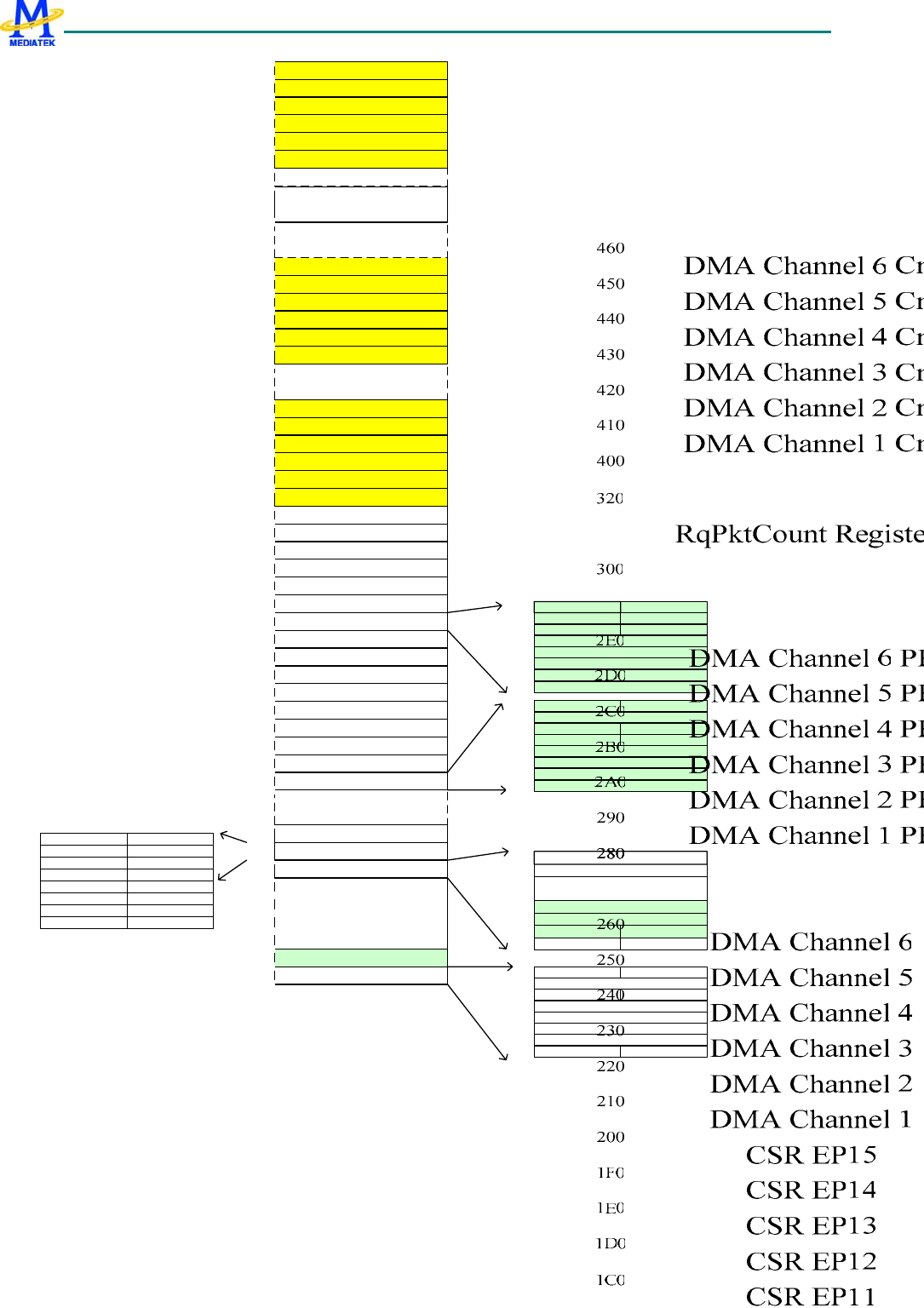
MT6235 GSM/GPRS Baseband Processor Data Sheet Revision 1.02
350/599 MediaTek Inc. Confidential

MT6235 GSM/GPRS Baseband Processor Data Sheet Revision 1.02
351/599 MediaTek Inc. Confidential
USB PHY CONTROL REGISTER
USB+0600h PHY Control Register 1 PHYCR1
Bit 31 30 29 28 27 26 25 24 23 22 21 20 19 18 17 16
Name
HS_T
X_I_E
N_MO
DE
HS_T
X_SP
_SEL
HS_SQ_INIT
_EN_DG[1:0]
HS_S
Q_EN
_DG
HS_S
Q_EN
_MOD
E
HS_S
QS
HS_R
CV_E
N_MO
DE
HS_RCVB[3:0] PLL_VCOG[1
:0] PLL_VCOB[1
:0]
Type R/W R/W R/W R/W R/W R/W R/W R/W R/W R/W R/W R/W R/W R/W R/W R/W
Reset 1 0 0 1 1 1 0 0 0 1 0 0 0 0 0 0
Bit 15 14 13 12 11 10 9 8 7 6 5 4 3 2 1 0
Name PLL_CCP[3:0]
PLL_
CLF
EN_L
S_CM
PSAT
PLL_
EN NEG_
TRI_E
N_B
USB2
0_TX_
TST
BIDI_
MODE CDR_TST
[1:0]
GATE
_
EN_B
Type R/W R/W R/W R/W R/W R/W R/W R/W R/W R/W R/W R/W R/W R/W R/W R/W
Reset 0 1 1 0 0 0 0 0 0 0 0 0 0 0 0 0
GATED_EN_B High level clock gating enable 0: enable 1: disable
CDR_TST CDR function option ,CDR_TST[1]: phase accumulation option,0: accumulation disable,1:
accumulation enable CDR_TST[0]: reference phase number option,0: 4 phases,1: 6 phases
BIDI_MODE UTMI data bus bi-directional mode 0: disable,1: enable
USB20_TX_TST TX macro test option, debug usage,0: disable,1: enable
NEG_TRI_EN_B UTMI output signal aligned to negative edge for hold time issue,0: negative edge triggered
output,1: positive edge triggered output
PLL_EN USB2.0 PHY PLL enable,0: disable,1: enable
EN_LS_CMPSAT LS Tx mode DM RPU compensation enable when in client mode,0: disable,1: enable
PLL_CLF PLL loop filter control,0: disable,1: enable
PLL_CPP PLL CP bias current selection,charge pump current = 3.125uA * n,0001 : 3.125uA * 1,0010 :
3.125uA * 2…1111 : 3.125uA * 15
PLL_VCOB PLL VCO bias current selection,00: 0uA,01: 25uA * 1.5,10: 25uA * 2.5,11: 25uA * 3.5
PLL_VCOG PLL VCO gain selection ,x0 : enhance Kvco gain,x1: normal Kvco gain
HS_RCVB HS RCV bias selection, HS RCV 1st stage bias current,xxx0: 600u,xxx1: 675u
HS_RCV_EN_MODE HS RCV enable mode selection,0: HS RCV enable by HS RCV,1: HS RCV always
enabled while USB operating in HS mode
HS_SQS HS SQ hystress mode Reserved
HS_SQ_EN_MODE HS SQ enable mode selection,0: SQ enable by HS RCV,1: SQ always enabled while
USB operating
HS_SQ_EN_DG HS SQ de-glitch time after HS RCV enabled,0:SQ output de-glitch 4T 480M CLK,1:SQ
output de-glitch 5T 480M CLK
HS_SQ_INIT_EN_DG HS SQ first time initializing de-glitch:gated by

MT6235 GSM/GPRS Baseband Processor Data Sheet Revision 1.02
352/599 MediaTek Inc. Confidential
00: 1T ref CLK
01: 1.5T ref CLK
10: 2T ref CLK
11: 2.5T ref CLK
HS_TX_SP_SEL HS TX LOAD sampling point selection,0: sampling the HS TX data at rising edge,1:
sampling the HS TX data at falling edge
HS_TX_I_EN_MODE HS TX I enable mode selection,0: HS TX current always enabled while HS TERM
enabled,1: HS_TX current enabled when HS TX module enabled
USB+0604h PHY Control Register 2 PHYCR2
Bit 31 30 29 28 27 26 25 24 23 22 21 20 19 18 17 16
Name
FORC
E_DR
V_VB
US
FORC
E_DM
_PUL
LDOW
N
FORC
E_DP
_PUL
LDOW
N
HS_TERMC[4:0]
FORC
E_DA
TA_IN
FORC
E_TX
VALID
HS_T
ERM_
SEL
HS_DISCN[1:
0] HS_DISCP[1:
0]
Type R/W R/W R/W R/W R/W R/W R/W R/W R/W R/W R/W R/W R/W R/W R/W R/W
Reset 0 0 0 0 1 0 0 0 0 0 0 0 0 0 0 1
Bit 15 14 13 12 11 10 9 8 7 6 5 4 3 2 1 0
Name HS_SQTL[2:0] HS_SQTH[2:0] HS_SQD[3:0] HS_SQB[3:0]
Type R/W R/W R/W R/W R/W R/W R/W R/W R/W R/W R/W R/W R/W R/W R/W R/W
Reset 0 0 1 1 0 1 0 0 0 0 1 0 0 1 0 0
HS_SQB HS SQ bias selection,HS_SQB[0]: HS SQ 1st stage bias current,xxx0: 600uA,xxx1: 675uA
HS_SQD HS SQ de-glitch control
xx00: 16u (min current, max de-glitch)
xx01: 32u
xx10: 61u
xx11: 122u (max current, min de-glitch)
HS_SQTH HS SQ threshold high selection
000: 165mV
001: 155mV
010: 145mV
011: 135mV
100: 125mV
101: 115mV
110: 105mV
111: 95mV
HS_SQTL HS SQ threshold low selection,Reserved
HS_DISCP HS_DISCP[0] : see HS_DISCN[1:0] ,HS_DISCP[1]: disconnect 1st stage bias current,
0: 420uA 1: 490uA

MT6235 GSM/GPRS Baseband Processor Data Sheet Revision 1.02
353/599 MediaTek Inc. Confidential
HS_DISCN HS DISC reference level HS_DISCP[0],HS_DISCN[1:0]
000: 615mV
001: 605mV
010: 595mV
011: 585mV
100: 575mV
101: 565mV
110: 555mV
111: 545mV
HS_TERM_SEL HS TERM module selection (see HS_TERMC),0: analog termination,1: digital termination
FORCE_TAVALID FORCE PHY TXVALID SIGNAL ENABLE WHEN PHY_TESTMODE = 1,1: enable 0: disable
FORCE_TAVALIDH FORCE PHY TXVALIDH SIGNAL ENABLE WHEN PHY_TESTMODE = 1,1: enable 0:
disable
HS_TERMC HS TERM impedence control code (see HS_TERM_SEL),In analog termination mode
HS_TERM_SEL: 0
internal reference voltage:
x0000: 480mV
x0001: 470mV
x0010: 460mV
x0011: 450mV
x0100: 440mV
x0101: 430mV
x0110: 420mV
x0111: 410mV
x1000: 400mV
x1001: 390mV
x1010: 380mV
x1011: 370mV
the final output swing is about (the termnation voltage + 400mv)/2.
In digital termination mode HS_TERM_SEL: 1
00000: for max swing
...
11111: for min swing
FORCE_DP_PULLDOWN FORCE PHY DP_PULLDOWN SIGNAL ENABLE WHEN PHY_TESTMODE = 1,1:
enable 0: disable

MT6235 GSM/GPRS Baseband Processor Data Sheet Revision 1.02
354/599 MediaTek Inc. Confidential
FORCE_DM_PULLDOWN FORCE PHY DM_PULLDOWN SIGNAL ENABLE WHEN PHY_TESTMODE = 1,1:
enable 0: disable
FORCE_DRV_VBUS FORCE PHY DRV_VBUS SIGNAL ENABLE WHEN PHY_TESTMODE = 1,1: enable 0:
disable
USB+0608h PHY Control Register 3 PHYCR3
Bit 31 30 29 28 27 26 25 24 23 22 21 20 19 18 17 16
Name AIO1_SEL[2:0] GHX_SEL[3:0] CLKM
ODE XTAL_BIAS[2:0] TEST_CTRL[3:0]
Type R/W R/W R/W R/W R/W R/W R/W R/W R/W R/W R/W R/W R/W R/W R/W R/W
Reset 0 1 1 0 1 1 1 1 1 0 0 0 0 0 0 0
Bit 15 14 13 12 11 10 9 8 7 6 5 4 3 2 1 0
Name PLL_DR[5:0] FEN_
HS_T
X_I
FEN_
FS_L
S_RC
V
FEN_
FS_L
S_TX
IREF_
MODE
_SEL
FEN_
HS_R
CV IADJ[2:0]
Type R/W R/W R/W R/W R/W R/W R/W R/W R/W R/W R/W R/W R/W R/W R/W R/W
Reset 0 0 0 0 1 0 1 0 0 0 0 0 0 1 0 0
IADJ HS TX bias current selection
000: 840mV/( Rext + 300)
001: 830mV/( Rext + 300)
010: 820mV/( Rext + 300)
011: 810mV/( Rext + 300)
100: 800mV/( Rext + 300)
101: 790mV/( Rext + 300)
110: 780mV/( Rext + 300)
111: 770mV/( Rext + 300)
Rext = 5.1k (typ.)
FEN_HS_RCV Forced HS RCV and Squelch enable for test purpose,0: disable,1: enable
IREF_MODE_SEL HS SQ reference current mode selection ,0: HS SQ current always enabled while USB
operating ,1: HS SQ current enabled while HS RX module enabled
FEN_FS_LS_TX Forced FS/LS output enable for test purpose,0: disable,1: enable
FEN_FS_LS_RCV Forced FS/LS RCV enable for test purpose,0: disable,1: enable
FEN_HS_TX_I Forced HS TX current source enable for test purpose,0: disable,1: enable
PLL_DR PLL div ratio 480/reference CLK=PLL_DR ex: 30MHz xtal case, PLL_DR = 480/30 = 16 = 0x10
TEST_CTRL Test mode control TEST_CTRL[3]:0: normal UTMI operation
1: 240MHz clock ouput, with while TEST_CTRL[0]=1 and FEN_HS_TX_I=11
TEST_CTRL[2:1]:
0x: termination resistor connected to PAD_VRT
10: termination resistor connected to PAD_VRT1

MT6235 GSM/GPRS Baseband Processor Data Sheet Revision 1.02
355/599 MediaTek Inc. Confidential
11: termination resistor connected to inaccurate internal 5.1k
TEST_CTRL[0]:
0: normal UTMI operation
1: TX controlled by FEN_HS_TX_I/FEN_FS_LS_TX
XTAL_BIAS XTAL bias selection Reserved
CLKMODE External/Internal input CLK source selection
x00: internal clk source USB_INTA1_CK
x01: internal clk source USB_INTA2_CK
x10: internal clk source USB_INTD_CK
GHX_SEL GHX Digital output selection
xx00: none
xx01: HS DISC output for USB 2.0 RX DC test (see DOUT1_SEL)
xx10: HS SQ output for USB 2.0 RX DC test (see DOUT1_SEL)
xx11: HS RX output for USB 2.0 RX DC test (see DOUT1_SEL)
AIO1_SEL Analog IO1 selection for test (IO via XTALI pin)
0xxx: diable AIO1
100: external bgr input
101: monitor internal bgr voltage
110: monitor internal pll loop filter voltage
111: monitor internal hs termination control voltage
AIO ouput only valid for XTALI_GPIO_EN=1 & XTALI_GPIO_OE=0
USB+060Ch PHY Control Register 4 PHYCR4
Bit 31 30 29 28 27 26 25 24 23 22 21 20 19 18 17 16
Name
XTAL
O_GPI
O_O
XTALI
_GPIO
_I
XTAL
O_GPI
O_OE
XTAL
O_GPI
O_E8
XTAL
O_GPI
O_EN
XTALI
O_GPI
O_I
XTALI
_GPIO
_OE
XTALI
_GPIO
_E8
XTALI
_GPIO
_EN
XTALI
_GPI
O_I
Type R/W R/W R/W R/W R/W R/W R/W R/W R/W R/W R/W R/W R/W R/W R/W R/W
Reset 0 0 0 0 0 0 0 0 0 0 0 0 0 0 0 0
Bit 15 14 13 12 11 10 9 8 7 6 5 4 3 2 1 0
Name BGR_DIV[1:0
] BGR_
SELP
H
BGR_
CHIP_
EN
BGR_I
SRC_
EN
BGR_
CLK_
EN
BGR_
BGR_
EN DOUT2_SEL[2:0] DOUT1_SEL[2:0]
Type R/W R/W R/W R/W R/W R/W R/W R/W R/W R/W R/W R/W R/W R/W R/W R/W
Reset 0 1 0 0 1 0 0 0 0 1 0 0 0 1 0 0
DOUT1_SEL Digital output 1 selection for test (output via VRT pin)
000: normal function
001: bgr ph1
010: bgr ph1s_
011: bgr pheq_
100: USB 2.0 RX DC test (see GHX_SEL)

MT6235 GSM/GPRS Baseband Processor Data Sheet Revision 1.02
356/599 MediaTek Inc. Confidential
101: USB 1.1 RXM
110: USB 1.1 RXP
111: USB 1.1 RXD
DOUT1 ouput only valid for XTALI_GPIO_EN=1 & XTALI_GPIO_OE=1
DOUT2_SEL Digital output 2 selection for test (output via VRT pin)
000: normal function
x01: bgr ph2
x10: bgr ph2s_
x11: bgr pho_
DOUT2 ouput only valid for XTALO_GPIO_EN=1 & XTALO_GPIO_OE=1
BGR_BGR_EN Force BGR enable 0: disable 1: enableBGRCLKEN
BGR_CLK_EN Force BGR chop clock enable 0: disable 1: enable
BGR_ISRC_EN Force BGR current source generator enable 0: disable 1: enable
BGR_CHP_EN BGR chop enable 0: disable 1: enable
BGR_DIV BGR chop clk rate
00: 836k
11: 836k/2
10: 836k/4
11: 836k/8
XTALI_GPIO_I XTALI pin GPIO output data Reserved
XTALI_GPIO_EN XTALI output pin GPIO enable Reserved
XTALI_GPIO_E8 XTALI output pin GPIO output capability control Reserved
XTALI_GPIO_OE XTALI output pin GPIO direction selection Reserved
XTALO_GPIO_I XTALO pin GPIO output data Reserved
XTALO_GPIO_EN XTALO output pin GPIO enable Reserved
XTALO_GPIO_E8 XTALO output pin GPIO output capability control Reserved
XTALO_GPIO_OE XTALO output pin GPIO direction selection reserved
XTALI_GPIO_I XTALI pin GPIO output data Reserved
XTALO_GPIO_I XTALO pin GPIO output data Reserved
USB+0610h PHY Control Register 5 PHYCR5
Bit 31 30 29 28 27 26 25 24 23 22 21 20 19 18 17 16
Name
DM_P
ULL_
DOW
N
DP_P
ULL_
DOW
N
XCVR_SELE
CT[1:0] SUSP
ENDM
TERM
_SEL
ECT
OP_MODEL[
1:0]
FORC
E_IDP
ULLU
P
UTMI_
MUXS
EL
USB_MODE[
1:0]
FORC
E_XC
VR_S
ELEC
T
FORC
E_SU
SPEN
DM
FORC
E_TE
RM_S
ELEC
T
FORC
E_OP
MODE
Type R/W R/W R/W R/W R/W R/W R/W R/W R/W R/W R/W R/W R/W R/W R/W R/W
Reset 0 0 0 0 0 0 0 0 0 0 0 0 0 1 0 0
Bit 15 14 13 12 11 10 9 8 7 6 5 4 3 2 1 0

MT6235 GSM/GPRS Baseband Processor Data Sheet Revision 1.02
357/599 MediaTek Inc. Confidential
Name PROBE_SEL[7:0] VBUS
CMP_
EN CLK_DIV_CNT[2:0] CDR_FILT[3:0]
Type R/W R/W R/W R/W R/W R/W R/W R/W R/W R/W R/W R/W R/W R/W R/W R/W
Reset 0 0 0 0 0 0 0 0 1 0 0 0 0 0 1 0
CDR_FILT CDR low pass filter selection, debug usage
CLK_DIVC_CNT The divide ratio of div_ck
PROBE_SEL Debug signal selection
FORCE_OPMODE FORCE PHY OPMODE SIGNAL ENABLE WHEN PHY_TESTMODE = 1,1: enable 0:
disable
FORCE_TERM_SELECT FORCE PHY TERM_SELECT SIGNAL ENABLE WHEN PHY_TESTMODE = 1,1:
enable 0: disable
FORCE_SUSPENDM FORCE PHY SUSPENDM SIGNAL ENABLE WHEN PHY_TESTMODE = 1,1: enable 0:
disable
FORCE_XCVR_SELECT FORCE PHY XCVR_SELECT SIGNAL ENABLE WHEN PHY_TESTMODE = 1,1:
enable 0: disable
USB_MODE Test mode selection ( for testing)
00: normal operation
01: loop-back mode1 enable, the pseudo random number will be generated inside USB2.0 PHY macro and
transmit onto USB bus. The data will be received by receiver and then be compared. The compared result is
muxed on line_state[1] and should be always be 1.
10: loop-back mode2 enable, the packet is longer.
UTMI_MUXSEL FORCE PHY UTMI SIGNAL ENABLE WHEN PHY_TESTMODE = 1,1: enable 0: disable
FORCE_IDPULLUP FORCE PHY IDPULLUP SIGNAL ENABLE WHEN PHY_TESTMODE = 1,1: enable 0:
disable
OPMODE It controls the USB2.0 controller to PHY output signal: OPMODE[1:0] when PHY_TESTMODE = 1
TERMSEL It controls the USB2.0 controller to PHY output signal: TERMSEL when PHY_TESTMODE = 1
SUSPENDM It controls the USB2.0 controller to PHY output signal: SUSPENDM when PHY_TESTMODE = 1
XCVRSEL It controls the USB2.0 controller to PHY output signal: XCVRSEL[1:0] when PHY_TESTMODE = 1
DPPULLDOWN It controls the USB2.0 controller to PHY output signal: DPPULLDOWN when PHY_TESTMODE
= 1
DMPULLDOWN It controls the USB2.0 controller to PHY output signal: DMPULLDOWN when PHY_TESTMODE
= 1
USB+0614h PHY UTMI Interface Register 1 PHYIR1
Bit 31 30 29 28 27 26 25 24 23 22 21 20 19 18 17 16
Name LINESTATE[
1:0]
HOST
DISC
ON
TXRE
ADY RXER
ROR RXAC
TIVE RXVA
LIDH RXVA
LID XDATA_OUT[15:8]
MT6235 GSM/GPRS Baseband Processor Data Sheet Revision 1.02
358/599 MediaTek Inc. Confidential
Type R R R R R R R R R R R R R R R R
Reset 0 0 0 0 0 0 0 0 0 0 0 0 0 0 0 0
Bit 15 14 13 12 11 10 9 8 7 6 5 4 3 2 1 0
Name XDATA_OUT[7:0] XDATA_IN[7:4]
TX_V
ALIDH TX_V
ALID DRVV
BUS IDPUL
LUP
Type R R R R R R R R R/W R/W R/W R/W R/W R/W R/W R/W
Reset 0 0 0 0 0 0 0 0 0 0 0 0 0 0 0 0
IDPULLUP It controls the USB2.0 controller to PHY output signal: IDPULLUP when PHY_TESTMODE = 1
DRVVBUS It controls the USB2.0 controller to PHY output signal: DRVVBUS when PHY_TESTMODE = 1
TX_VALID It controls the USB2.0 controller to PHY output signal: TX_VALID when PHY_TESTMODE = 1
TX_VALIDH It controls the USB2.0 controller to PHY output signal: TX_VALIDH when PHY_TESTMODE = 1
XDATA_IN It controls the USB2.0 controller to PHY input signal: XDATA_IN[15:0] when PHY_TESTMODE = 1
XDATA_OUT It controls the USB2.0 controller to PHY input signal: XDATA_OUT[15:0] when PHY_TESTMODE
= 1
RXVALID It controls the USB2.0 controller to PHY input signal: RXVALID when PHY_TESTMODE = 1
RXVALIDH It controls the USB2.0 controller to PHY input signal: RXVALIDH when PHY_TESTMODE = 1
RXACTIVE It controls the USB2.0 controller to PHY input signal: RXACTIVE when PHY_TESTMODE = 1
RXERROR It controls the USB2.0 controller to PHY input signal: RXERROR when PHY_TESTMODE = 1
TXREADY It controls the USB2.0 controller to PHY input signal: TXREADY when PHY_TESTMODE = 1
HOSTDISCON It controls the USB2.0 controller to PHY input signal: HOSTDISCON when PHY_TESTMODE = 1
LINE_STATE It controls the USB2.0 controller to PHY input signal: LINE_STATE when PHY_TESTMODE = 1
USB+0618h PHY UTMI Interface Register 2 PHYIR2
Bit 31 30 29 28 27 26 25 24 23 22 21 20 19 18 17 16
Name
Type
Reset
Bit 15 14 13 12 11 10 9 8 7 6 5 4 3 2 1 0
Name IDDIG
VBUS
VALID SESS
END AVALI
D
Type R R R R
Reset 0 0 0 0
AVALID It controls the USB2.0 controller to PHY input signal: AVALID when PHY_TESTMODE = 1
SESSEND It controls the USB2.0 controller to PHY input signal: SESSEND when PHY_TESTMODE = 1
VBUSVALID It controls the USB2.0 controller to PHY input signal: VBUSVALID when PHY_TESTMODE = 1
IDDIG It controls the USB2.0 controller to PHY input signal: IDDIG when PHY_TESTMODE = 1
7.5 Memory Stick and SD Memory Card Controller
7.5.1 Introduction
The controller fully supports the Memory Stick bus protocol as defined in Format Specification version 2.0 of Memory
Stick Standard (Memory Stick PRO) and the SD Memory Card bus protocol as defined in SD Memory Card Specification

MT6235 GSM/GPRS Baseband Processor Data Sheet Revision 1.02
359/599 MediaTek Inc. Confidential
Part 1 Physical Layer Specification version 1.0 as well as the MultiMediaCard (MMC) bus protocol as defined in MMC
system specification version 2.2. Since SD Memory Card bus protocol is backward compatible to MMC bus protocol, the
controller is capable of working well as the host on MMC bus under control of proper firmware. Furthermore, the controller
also support SDIO card specification version 1.0 partially. However, the controller can only be configured as either the host
of Memory Stick or the host of SD/MMC Memory Card at one time. Hereafter, the controller is also abbreviated as MS/SD
controller. The following are the main features of the controller.
z Interface with MCU by APB bus
z 16/32-bit access on APB bus
z 16/32-bit access for control registers
z 32-bit access for FIFO
z Shared pins for Memory Stick and SD/MMC Memory Card
z Built-in 32 bytes FIFO buffers for transmit and receive, FIFO is shared for transmit and receive
z Built-in CRC circuit
z CRC generation can be disabled
z DMA supported
z Interrupt capabilities
z Automatic command execution capability when an interrupt from Memory Stick
z Data rate up to 26 Mbps in serial mode, 26x4 Mbps in parallel model, the module is targeted at 26 MHz operating
clock
z Serial clock rate on MS/SD/MMC bus is programmable
z Card detection capabilities
z Controllability of power for memory card
z Not support SPI mode for MS/SD/MMC Memory Card
z Not support multiple SD Memory Cards
7.5.2 Overview
7.5.2.1 Pin Assignment
Since the controller can only be configured as either the host of Memory Stick or the host of SD/MMC Memory Card at
one time, pins for Memory Stick and SD/MMC Memory Card are shared in order to save pin counts. The following lists
pins required for Memory Stick and SD/MMC Memory Card. Table 33 shows how they are shared. In Table 33, all I/O
pads have embedded both pull up and pull down resistor because they are shared by both the Memory Stick and SD/MMC
Memory Card. Pins 2,4,5,8 are only useful for SD/MMC Memory Card. Pull down resistor for these pins can be used for
power saving. All embedded pull-up and pull-down resistors can be disabled by programming the corresponding control
registers if optimal pull-up or pull-down resistors are required on the system board. The pin VDDPD is used for power
saving. Power for Memory Stick or SD/MMC Memory Card can be shut down by programming the corresponding control
MT6235 GSM/GPRS Baseband Processor Data Sheet Revision 1.02
360/599 MediaTek Inc. Confidential
register. The pin WP (Write Protection) is only valid when the controller is configured for SD/MMC Memory Card. It is
used to detect the status of Write Protection Switch on SD/MMC Memory Card.
No. Name T
y
pe MMC SD MS MSPRO Description
1SD_CLK O CLK CLK SCLK SCLK Clock
2SD_DAT3 I/O/PP CD/DAT3 DAT3 Data Line [Bit 3]
3SD_DAT0 I/O/PP DAT0 DAT0 SDIO DAT0 Data Line [Bit 0]
4SD_DAT1 I/O/PP DAT1 DAT1 Data Line [Bit 1]
5SD_DAT2 I/O/PP DAT2 DAT2 Data Line [Bit 2]
6SD_CMD I/O/PP CMD CMD BS BS Command Or Bus State
7SD_PWRON O VDD ON/OFF
8SD_WP IWrite Protection Switch in SD
9SD_INS IVSS2 VSS2 INS INS Card Detection
Table 33 Sharing of pins for Memory Stick and SD/MMC Memory Card Controller
7.5.2.2 Card Detection
For Memory Stick, the host or connector should provide a pull up resistor on the signal INS. Therefore, the signal INS will
be logic high if no Memory Stick is on line. The scenario of card detection for Memory Stick is shown in Figure 43. Before
Memory Stick is inserted or powered on, on host side SW1 shall be closed and SW2 shall be opened for card detection. It is
the default setting when the controller is powered on. Upon insertion of Memory Stick, the signal INS will have a transition
from high to low. Hereafter, if Memory Stick is removed then the signal INS will return to logic high. If card insertion is
intended to not be supported, SW1 shall be opened and SW2 closed always.
For SD/MMC Memory Card, detection of card insertion/removal by hardware is also supported. Because a pull down
resistor with about 470 KΩ resistance which is impractical to embed in an I/O pad is needed on the signal CD/DAT3, and it
has to be capable of being connected or disconnected dynamically onto the signal CD during initialization period, an
additional I/O pad is needed to switch on/off the pull down resistor on the system board. The scenario of card detection for
SD/MMC Memory Card is shown in Figure 44. Before SD/MMC Memory Card is inserted or powered on, SW1 and SW2
shall be opened for card detection on the host side. Meanwhile, pull down resistor RCD on system board shall attach onto the
signal CD/DAT3 by the output signal RCDEN. In addition, SW3 on the card is default to be closed. Upon insertion of
SD/MMC Memory Card, the signal CD/DAT3 will have a transition from low to high. If SD/MMC Memory Card is
removed then the signal CD/DAT3 will return to logic low. After the card identification process, pull down resistor RCD on
system board shall disconnect with the signal CD/DAT3 and SW3 on the card shall be opened for normal operation.
Since the scheme above needs a mechanical switch such as a relay on system board, it is not ideal enough. Thus, a
dedicated pin “INS” is used to perform card insertion and removal for SD/MMC. The pin “INS” will connect to the pin
“VSS2” of a SD/MMC connector. Then the scheme of card detection is the same as that for MS. It is shown in Figure 43.
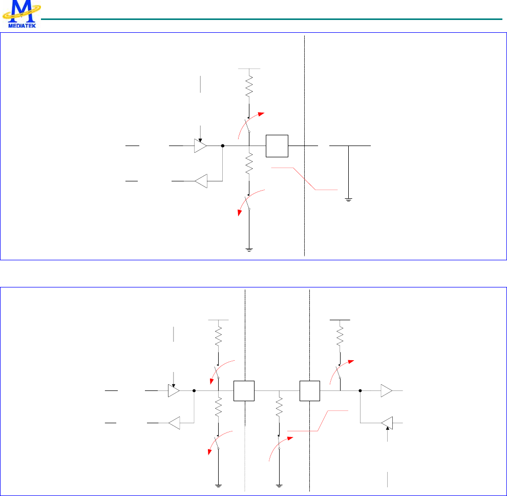
MT6235 GSM/GPRS Baseband Processor Data Sheet Revision 1.02
361/599 MediaTek Inc. Confidential
INS
RPU
PAD
SW1
RPD
SW2
DAT3 OUT
CD/DAT3 IN
HOST CARD
output enable
Figure 43 Card detection for Memory Stick
RPU
PAD
SW1
RPD
SW2
DAT3 OUT
CD/DAT3 IN
HOST CARD
10-90 K
SW3
output enable
output enable
470 Kohm
RCDEN
PAD
Figure 44 Card detection for SD/MMC Memory Card

MT6235 GSM/GPRS Baseband Processor Data Sheet Revision 1.02
362/599 MediaTek Inc. Confidential
7.5.3 Register Definitions
REGISTER ADDRESS REGISTER NAME SYNONYM
MSDC + 0000h MS/SD Memory Card Controller Configuration Register MSDC_CFG
MSDC + 0004h MS/SD Memory Card Controller Status Register MSDC_STA
MSDC + 0008h MS/SD Memory Card Controller Interrupt Register MSDC_INT
MSDC + 000Ch MS/SD Memory Card Controller Data Register MSDC_DAT
MSDC + 00010h MS/SD Memory Card Pin Status Register MSDC_PS
MSDC + 00014h MS/SD Memory Card Controller IO Control Register MSDC_IOCON
MSDC + 0020h SD Memory Card Controller Configuration Register SDC_CFG
MSDC + 0024h SD Memory Card Controller Command Register SDC_CMD
MSDC + 0028h SD Memory Card Controller Argument Register SDC_ARG
MSDC + 002Ch SD Memory Card Controller Status Register SDC_STA
MSDC + 0030h SD Memory Card Controller Response Register 0 SDC_RESP0
MSDC + 0034h SD Memory Card Controller Response Register 1 SDC_RESP1
MSDC + 0038h SD Memory Card Controller Response Register 2 SDC_RESP2
MSDC + 003Ch SD Memory Card Controller Response Register 3 SDC_RESP3
MSDC + 0040h SD Memory Card Controller Command Status Register SDC_CMDSTA
MSDC + 0044h SD Memory Card Controller Data Status Register SDC_DATSTA
MSDC + 0048h SD Memory Card Status Register SDC_CSTA
MSDC + 004Ch SD Memory Card IRQ Mask Register 0 SDC_IRQMASK0
MSDC + 0050h SD Memory Card IRQ Mask Register 1 SDC_IRQMASK1
MSDC + 0054h SDIO Configuration Register SDIO_CFG
MSDC + 0058h SDIO Status Register SDIO_STA
MSDC + 0060h Memory Stick Controller Configuration Register MSC_CFG
MSDC + 0064h Memory Stick Controller Command Register MSC_CMD
MSDC + 0068h Memory Stick Controller Auto Command Register MSC_ACMD
MSDC + 006Ch Memory Stick Controller Status Register MSC_STA
Table 34 MS/SD Controller Register Map
7.5.3.1 Global Register Definitions
MSDC+0000h MS/SD Memory Card Controller Configuration Register MSDC_CFG
Bit 31 30 29 28 27 26 25 24 23 22 21 20 19 18 17 16
Name FIFOTHD PRCFG2 PRCFG1 PRCFG0
VDDP
D RCDE
N DIRQ
EN PINEN DMAE
N INTEN
Type R/W R/W R/W R/W R/W R/W R/W R/W R/W R/W
Reset 0001 01 01 10 0 0 0 0 0 0
Bit 15 14 13 12 11 10 9 8 7 6 5 4 3 2 1 0
Name SCLKF SCLK
ON RED STDB
Y CLKS
RC RST NOCR
C MSDC
Type R/W R/W R/W R/W R/W W R/W R/W

MT6235 GSM/GPRS Baseband Processor Data Sheet Revision 1.02
363/599 MediaTek Inc. Confidential
Reset 00000000 0 0 1 0 0 0 0
The register is for general configuration of the MS/SD controller. Note that MSDC_CFG[31:16] can be accessed by 16-bit
APB bus access.
MSDC The register bit is used to configure the controller as the host of Memory Stick or as the host of SD/MMC Memory
card. The default value is to configure the controller as the host of Memory Stick.
0 Configure the controller as the host of Memory Stick
1 Configure the controller as the host of SD/MMC Memory card
NOCRC CRC Disable. A ‘1’ indicates that data transfer without CRC is desired. For write data block, data will be
transmitted without CRC. For read data block, CRC will not be checked. It is for testing purpose.
0 Data transfer with CRC is desired.
1 Data transfer without CRC is desired.
RST Software Reset. Writing a ‘1’ to the register bit will cause internal synchronous reset of MS/SD controller, but does
not reset register settings.
0 Otherwise
1 Reset MS/SD controller
CLKSRC The register bit specifies which clock is used as source clock of memory card. If MUC clock is used, the
fastest clock rate for memory card is 52/2=26MHz. If USB clock is used, the fastest clock rate for memory card is
48/2=24MHz.
0 Use MCU clock as source clock of memory card.
1 Use USB clock as source clock of memory card.
STDBY Standby Mode. If the module is powered down, operating clock to the module will be stopped. At the same time,
clock to card detection circuitry will also be stopped. If detection of memory card insertion and removal is desired,
write ‘1’ to the register bit. If interrupt for detection of memory card insertion and removal is enabled, interrupt
will take place whenever memory is inserted or removed.
0 Standby mode is disabled.
1 Standby mode is enabled.
RED Rise Edge Data. The register bit is used to determine that serial data input is latched at the falling edge or the rising
edge of serial clock. The default setting is at the rising edge. If serial data has worse timing, set the register bit to
‘1’. When memory card has worse timing on return read data, set the register bit to ‘1’.
0 Serial data input is latched at the rising edge of serial clock.
1 Serial data input is latched at the falling edge of serial clock.
SCLKON Serial Clock Always On. It is for debugging purpose.
0 Not to have serial clock always on.
1 To have serial clock always on.
SCLKF The register field controls clock frequency of serial clock on MS/SD bus. Denote clock frequency of MS/SD bus
serial clock as fslave and clock frequency of the MS/SD controller as fhost which is 104 or 52 MHz. Then the value
of the register field is as follows. Note that the allowable maximum frequency of fslave is 26MHz.
00000000b f
slave =(1/2) * fhost
00000001b f
slave = (1/(4*1)) * fhost
00000010b f
slave = (1/(4*2)) * fhost
00000011b f
slave = (1/(4*3))* fhost
…
00010000b f
slave = (1/(4*16))* fhost

MT6235 GSM/GPRS Baseband Processor Data Sheet Revision 1.02
364/599 MediaTek Inc. Confidential
…
11111111b f
slave = (1/(4*255)) * fhost
INTEN Interrupt Enable. Note that if interrupt capability is disabled then application software must poll the status of the
register MSDC_STA to check for any interrupt request.
0 Interrupt induced by various conditions is disabled, no matter the controller is configured as the host of either
SD/MMC Memory Card or Memory Stick.
1 Interrupt induced by various conditions is enabled, no matter the controller is configured as the host of either
SD/MMC Memory Card or Memory Stick.
DMAEN DMA Enable. Note that if DMA capability is disabled then application software must poll the status of the
register MSDC_STA for checking any data transfer request. If DMA is desired, the register bit must be set before
command register is written.
0 DMA request induced by various conditions is disabled, no matter the controller is configured as the host of
either SD/MMC Memory Card or Memory Stick.
1 DMA request induced by various conditions is enabled, no matter the controller is configured as the host of
either SD/MMC Memory Card or Memory Stick.
PINEN Pin Interrupt Enable. The register bit is used to control if the pin for card detection is used as an interrupt source.
0 The pin for card detection is not used as an interrupt source.
1 The pin for card detection is used as an interrupt source.
DIRQEN Data Request Interrupt Enable. The register bit is used to control if data request is used as an interrupt source.
0 Data request is not used as an interrupt source.
1 Data request is used as an interrupt source.
RCDEN The register bit controls the output pin RCDEN that is used for card identification process when the controller is
for SD/MMC Memory Card. Its output will control the pull down resistor on the system board to connect or
disconnect with the signal CD/DAT3.
0 The output pin RCDEN will output logic low.
1 The output pin RCDEN will output logic high.
VDDPD The register bit controls the output pin VDDPD that is used for power saving. The output pin VDDPD will control
power for memory card.
0 The output pin VDDPD will output logic low. The power for memory card will be turned off.
1 The output pin VDDPD will output logic high. The power for memory card will be turned on.
PRCFG0 Pull Up/Down Register Configuration for the pin WP. The default value is 10.
00 Pull up resistor and pull down resistor in the I/O pad of the pin WP are all disabled.
01 Pull down resistor in the I/O pad of the pin WP is enabled.
10 Pull up resistor in the I/O pad of the pin WP is enabled.
11 Use keeper of IO pad.
PRCFG1 Pull Up/Down Register Configuration for the pin CMD/BS. The default value is 0b01.
00 Pull up resistor and pull down resistor in the I/O pad of the pin CMD/BS are all disabled.
01 Pull down resistor in the I/O pad of the pin CMD/BS is enabled.
10 Pull up resistor in the I/O pad of the pin CMD/BS is enabled.
11 Use keeper of IO pad.
PRCFG2 Pull Up/Down Register Configuration for the pins DAT0, DAT1, DAT2, DAT3. The default value is 0b01.
00 Pull up resistor and pull down resistor in the I/O pads o the pins DAT0, DAT1, DAT2, DAT3. are all disabled.
01 Pull down resistor in the I/O pads of the pins DAT0, DAT1, DAT2, DAT3 and WP. is enabled.
10 Pull up resistor in the I/O pads of the pins DAT0, DAT1, DAT2, DAT3. is enabled.

MT6235 GSM/GPRS Baseband Processor Data Sheet Revision 1.02
365/599 MediaTek Inc. Confidential
11 Use keeper of IO pad.
FIFOTHD FIFO Threshold. The register field determines when to issue a DMA request. For write transactions, DMA
requests will be asserted if the number of free entries in FIFO are larger than or equal to the value in the register
field. For read transactions, DMA requests will be asserted if the number of valid entries in FIFO are larger than or
equal to the value in the register field. The register field must be set according to the setting of data transfer count
in DMA burst mode. If single mode for DMA transfer is used, the register field shall be set to 0b0001.
0000 Invalid.
0001 Threshold value is 1.
0010 Threshold value is 2.
…
1000 Threshold value is 8.
others Invalid
MSDC+0004h MS/SD Memory Card Controller Status Register MSDC_STA
Bit 15 14 13 12 11 10 9 8 7 6 5 4 3 2 1 0
Name BUSY FIFOC
LR FIFOCNT INT DRQ BE BF
Type R W RO RO RO RO RO
Reset 0 - 0000 0 0 0 0
The register contains the status of FIFO, interrupts and data requests.
BF The register bit indicates if FIFO in MS/SD controller is full.
0 FIFO in MS/SD controller is not full.
1 FIFO in MS/SD controller is full.
BE The register bit indicates if FIFO in MS/SD controller is empty.
0 FIFO in MS/SD controller is not empty.
1 FIFO in MS/SD controller is empty.
DRQ The register bit indicates if any data transfer is required. While any data transfer is required, the register bit still
will be active even if the register bit DIRQEN in the register MSDC_CFG is disabled. Data transfer can be
achieved by DMA channel alleviating MCU loading, or by polling the register bit to check if any data transfer is
requested. While the register bit DIRQEN in the register MSDC_CFG is disabled, the second method is used.
0 No DMA request exists.
1 DMA request exists.
INT The register bit indicates if any interrupt exists. While any interrupt exists, the register bit still will be active even
if the register bit INTEN in the register MSDC_CFG is disabled. MS/SD controller can interrupt MCU by issuing
interrupt request to Interrupt Controller, or software/application polls the register endlessly to check if any
interrupt request exists in MS/SD controller. While the register bit INTEN in the register MSDC_CFG is disabled,
the second method is used. For read commands, it is possible that timeout error takes place. Software can read the
status register to check if timeout error takes place without OS time tick support or data request is asserted. Note
that the register bit will be cleared when reading the register MSDC_INT.
0 No interrupt request exists.
1 Interrupt request exists.
FIFOCNT FIFO Count. The register field shows how many valid entries are in FIFO.
0000 There is 0 valid entry in FIFO.
0001 There is 1 valid entry in FIFO.

MT6235 GSM/GPRS Baseband Processor Data Sheet Revision 1.02
366/599 MediaTek Inc. Confidential
0010 There are 2 valid entries in FIFO.
…
1000 There are 8 valid entries in FIFO.
others Invalid
FIFOCLR Clear FIFO. Writing ‘1’ to the register bit will cause the content of FIFO clear and reset the status of FIFO
controller.
0 No effect on FIFO.
1 Clear the content of FIFO clear and reset the status of FIFO controller.
BUSY Status of the controller. If the controller is in busy state, the register bit will be ‘1’. Otherwise ‘0’.
0 The controller is in busy state.
1 The controller is in idle state.
MSDC+0008h MS/SD Memory Card Controller Interrupt Register MSDC_INT
Bit 15 14 13 12 11 10 9 8 7 6 5 4 3 2 1 0
Name SDIOI
RQ SDR1
BIRQ MSIFI
RQ SDMC
IRQ SDDA
TIRQ SDCM
DIRQ PINIR
Q DIRQ
Type RC RC RC RC RC RC RC RC
Reset 0 0 0 0 0 0 0 0
The register contains the status of interrupts. Note that the register still show status of interrupt even though interrupt is
disabled, that is, the register bit INTEN of the register MSDC_CFG is set to ‘0. It implies that software interrupt can be
implemented by polling the register bit INT of the register MSDC_STA and this register. However, if hardware interrupt
is desired, remember to clear the register before setting the register bit INTEN of the register MSDC_CFG to ‘1’. Or
undesired hardware interrupt arisen from previous interrupt status may take place.
DIRQ Data Request Interrupt. The register bit indicates if any interrupt for data request exists. Whenever data request
exists and data request as an interrupt source is enabled, i.e., the register bit DIRQEN in the register MSDC_CFG
is set to ‘1’, the register bit will be active. It will be reset when reading it. For software, data requests can be
recognized by polling the register bit DRQ or by data request interrupt. Data request interrupts will be generated
every FIFOTHD data transfers.
0 No Data Request Interrupt.
1 Data Request Interrupt occurs.
PINIRQ Pin Change Interrupt. The register bit indicates if any interrupt for memory card insertion/removal exists.
Whenever memory card is inserted or removed and card detection interrupt is enabled, i.e., the register bit PINEN
in the register MSDC_CFG is set to ‘1’, the register bit will be set to ‘1’. It will be reset when the register is read.
0 Otherwise.
1 Card is inserted or removed.
SDCMDIRQ SD Bus CMD Interrupt. The register bit indicates if any interrupt for SD CMD line exists. Whenever
interrupt for SD CMD line exists, i.e., any bit in the register SDC_CMDSTA is active, the register bit will be set to
‘1’ if interrupt is enabled. It will be reset when the register is read.
0 No SD CMD line interrupt.
1 SD CMD line interrupt exists.
SDDATIRQ SD Bus DAT Interrupt. The register bit indicates if any interrupt for SD DAT line exists. Whenever interrupt
for SD DAT line exists, i.e., any bit in the register SDC_ DATSTA is active, the register bit will be set to ‘1’ if
interrupt is enabled. It will be reset when the register is read.
0 No SD DAT line interrupt.

MT6235 GSM/GPRS Baseband Processor Data Sheet Revision 1.02
367/599 MediaTek Inc. Confidential
1 SD DAT line interrupt exists.
SDMCIRQ SD Memory Card Interrupt. The register bit indicates if any interrupt for SD Memory Card exists. Whenever
interrupt for SD Memory Card exists, i.e., any bit in the register SDC_CSTA is active, the register bit will be set to
‘1’ if interrupt is enabled. It will be reset when the register is read.
0 No SD Memory Card interrupt.
1 SD Memory Card interrupt exists.
MSIFIRQ MS Bus Interface Interrupt. The register bit indicates if any interrupt for MS Bus Interface exists. Whenever
interrupt for MS Bus Interface exists, i.e., any bit in the register MSC_STA is active, the register bit will be set to
‘1’ if interrupt is enabled. It will be reset when the register MSDC_STA or MSC_STA is read.
0 No MS Bus Interface interrupt.
1 MS Bus Interface interrupt exists.
SDR1BIRQ SD/MMC R1b Response Interrupt. The register bit will be active when a SD/MMC command with R1b
response finishes and the DAT0 line has transition from busy to idle state. Single block write commands with
R1b response will cause the interrupt when the command completes no matter successfully or with CRC
error. However, multi-block write commands with R1b response do not cause the interrupt because
multi-block write commands are always stopped by STOP_TRANS commands. STOP_TRANS
commands (with R1b response) behind multi-block write commands will cause the interrupt. Single
block read command with R1b response will cause the interrupt when the command completes but
multi-block read commands do not. Note that STOP_TRANS commands (with R1b response) behind
multi-block read commands will cause the interrupt.
0 No interrupt for SD/MMC R1b response.
1 Interrupt for SD/MMC R1b response exists.
MSDC+000Ch MS/SD Memory Card Controller Data Register MSDC_DAT
Bit 31 30 29 28 27 26 25 24 23 22 21 20 19 18 17 16
Name DATA[31:16]
Type R/W
Bit 15 14 13 12 11 10 9 8 7 6 5 4 3 2 1 0
Name DATA[15:0]
Type R/W
The register is used to read/write data from/to FIFO inside MS/SD controller. Data access is in unit of 32 bits.
MSDC+0010h MS/SD Memory Card Pin Status Register MSDC_PS
Bit 31 30 29 28 27 26 25 24 23 22 21 20 19 18 17 16
Name CMD DAT
Type RO RO
Reset - -
Bit 15 14 13 12 11 10 9 8 7 6 5 4 3 2 1 0
Name CDDEBOUNCE PINC
HG PIN0 POEN
0 PIEN0 CDEN
Type RW RC RO R/W R/W R/W
Reset 0000 0 1 0 0 0
The register is used for card detection. When the memory card controller is powered on, and the system is powered on, the
power for the memory card is still off unless power has been supplied by the PMIC. Meanwhile, pad for card detection
defaults to pull down when the system is powered on. The scheme of card detection for MS is the same as that for
SD/MMC.

MT6235 GSM/GPRS Baseband Processor Data Sheet Revision 1.02
368/599 MediaTek Inc. Confidential
For detecting card insertion, first pull up INS pin, and then enable card detection and input pin at the same time. After 32
cycles of controller clock, status of pin changes will emerge. For detecting card removal, just keep enabling card detection
and input pin.
CDEN Card Detection Enable. The register bit is used to enable or disable card detection.
0 Card detection is disabled.
1 Card detection is enabled.
PIEN0 The register bit is used to control input pin for card detection.
0 Input pin for card detection is disabled.
1 Input pin for card detection is enabled.
POEN0 The register bit is used to control output of input pin for card detection.
0 Output of input pin for card detection is disabled.
1 Output of input pin for card detection is enabled.
PIN0 The register shows the value of input pin for card detection.
0 The value of input pin for card detection is logic low.
1 The value of input pin for card detection is logic high.
PINCHG Pin Change. The register bit indicates the status of card insertion/removal. If memory card is inserted or
removed, the register bit will be set to ‘1’ no matter pin change interrupt is enabled or not. It will be cleared when
the register is read.
0 Otherwise.
1 Card is inserted or removed.
CDDEBOUNCE The register field specifies the time interval for card detection de-bounce. Its default value is 0. It means
that de-bounce interval is 32 cycle time of 32KHz. The interval will extend one cycle time of 32KHz by increasing
the counter by 1.
DAT Memory Card Data Lines.
CMD Memory Card Command Lines.
MSDC+0014h MS/SD Memory Card Controller IO Control Register MSDC_IOCON
Bit 31 30 29 28 27 26 25 24 23 22 21 20 19 18 17 16
Name DLT
Type R/W
Reset 00000010
Bit 15 14 13 12 11 10 9 8 7 6 5 4 3 2 1 0
Name CMDR
E PRCFG3
SRCF
G1 SRCF
G0 ODCCFG1 ODCCFG0
Type R/W R/W R/W R/W R/W R/W
Reset 0 10 1 1 000 011
The register specifies Output Driving Capability and Slew Rate of IO pads for MSDC. The reset value is suggestion
setting. If output driving capability of the pins DAT0, DAT1, DAT2 and DAT3 is too large, it’s possible to arise ground
bounce and thus result in glitch on SCLK.
ODCCFG0 Output driving capability the pins CMD/BS and SCLK
000 4mA
010 8mA
100 12mA
110 16mA
ODCCFG1 Output driving capability the pins DAT0, DAT1, DAT2 and DAT3
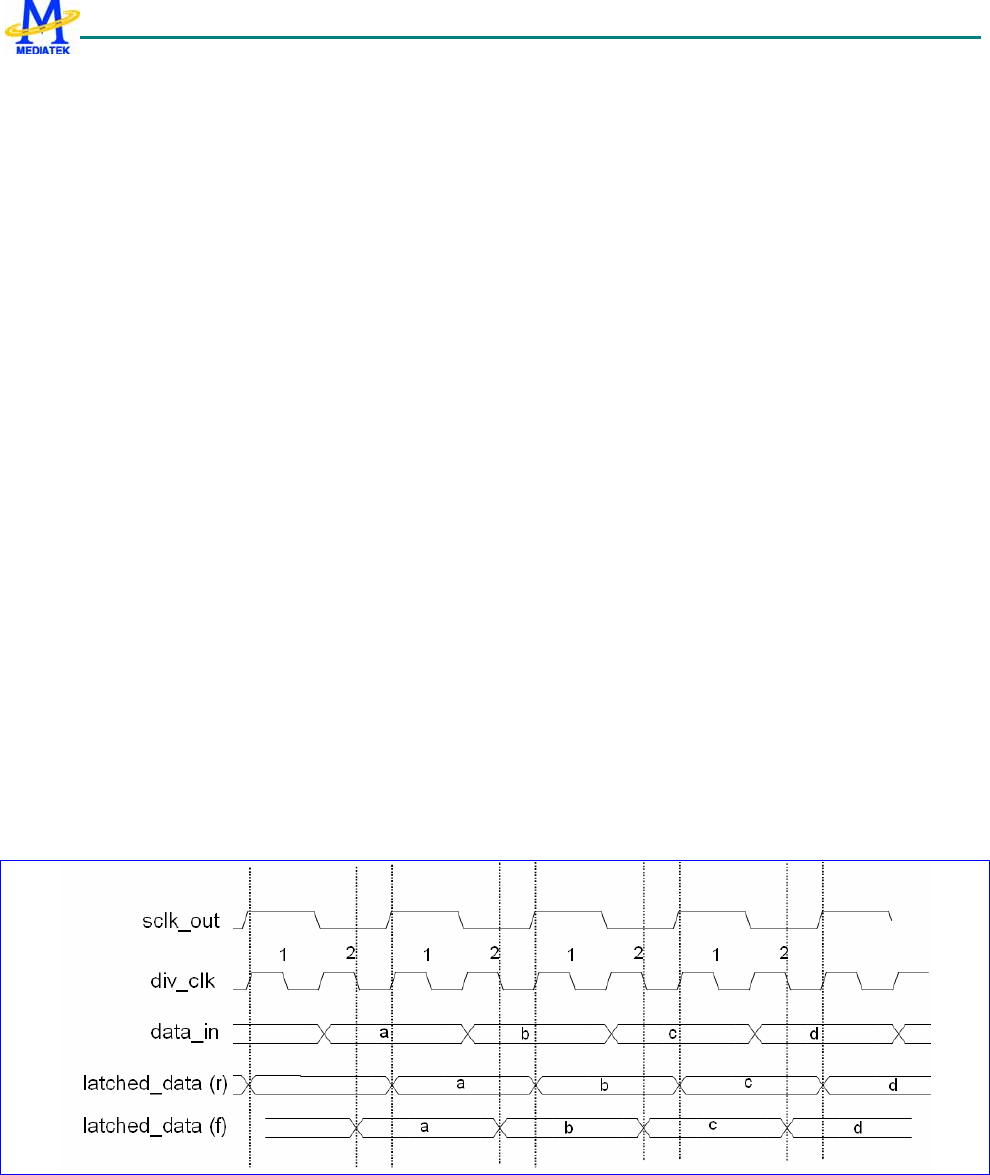
MT6235 GSM/GPRS Baseband Processor Data Sheet Revision 1.02
369/599 MediaTek Inc. Confidential
000 4mA
010 8mA
100 12mA
110 16mA
SRCFG0 Output driving capability the pins CMD/BS and SCLK
0 Fast Slew Rate
1 Slow Slew Rate
SRCFG1 Output driving capability the pins DAT0, DAT1, DAT2 and DAT3
0 Fast Slew Rate
1 Slow Slew Rate
PRCFG3 Pull Up/Down Register Configuration for the pin INS. The default value is 10.
00 Pull up resistor and pull down resistor in the I/O pad of the pin INS are all disabled.
01 Pull down resistor in the I/O pad of the pin INS is enabled.
10 Pull up resistor in the I/O pad of the pin INS is enabled.
11 Use keeper of IO pad.
CMDRE The register bit is used to determine whether the host should latch response token (which is sent from card on
CMD line ) at rising edge or falling edge of serial clock.
0 Host latches response at rising edge of serial clock
1 Host latches response at falling edge of serial clock
DLT Data Latch Timing. The register is used for SW to select the latch timing on data line.
Figure 3 illustrates the data line latch timing. sclk_out is the serial clock output to card. div_clk is the internal
clock used for generating divided clock. The number “1 2 1 2” means the current sclk_out is divided from
div_clk by a ratio of 2. data_in is the output data from card, and latched_data(r)/(f) is the rising/falling edge
latched data inside the host (configured by RED in MSDC_CFG). In this example, SCLKF(in MSDC_CFG)
is set to 8’b0 which means the division ratio is 2, and DLT is set to 1. Note that the value of DLT CANNOT be
set as 0 and its value should not exceed the division ratio ( in the example, the division ratio is 2). Also note
that, the latching time will be one div_clk later than the indicated DLT value and the falling edge is always
half div_clk ahead from rising edge. The default value of DLT is set to 8’b2.
Figure 3 Illustration of data line latch timing

MT6235 GSM/GPRS Baseband Processor Data Sheet Revision 1.02
370/599 MediaTek Inc. Confidential
7.5.3.2 SD Memory Card Controller Register Definitions
MSDC+0020h SD Memory Card Controller Configuration Register SDC_CFG
Bit 31 30 29 28 27 26 25 24 23 22 21 20 19 18 17 16
Name DTOC WDOD SDIO MDLW
8 MDLE
N SIEN
Type R/W R/W R/W R/W R/W R/W
Reset 00000000 0000 0 0 0 0
Bit 15 14 13 12 11 10 9 8 7 6 5 4 3 2 1 0
Name BSYDLY BLKLEN
Type R/W R/W
Reset 1000 00000000000
The register is used for configuring the MS/SD Memory Card Controller when it is configured as the host of SD Memory
Card. If the controller is configured as the host of Memory Stick, the contents of the register have no impact on the
operation of the controller. Note that SDC_CFG[31:16] can be accessed by 16-bit APB bus access.
BLKLEN It refers to Block Length. The register field is used to define the length of one block in unit of byte in a data
transaction. The maximal value of block length is 2048 bytes.
000000000000 Reserved.
000000000001 Block length is 1 byte.
000000000010 Block length is 2 bytes.
…
011111111111 Block length is 2047 bytes.
100000000000 Block length is 2048 bytes.
BSYDLY The register field is only valid for the commands with R1b response. If the command has a response of R1b
type, MS/SD controller must monitor the data line 0 for card busy status from the bit time that is two serial clock
cycles after the command end bit to check if operations in SD/MMC Memory Card have finished. The register
field is used to expand the time between the command end bit and end of detection period to detect card busy
status. If time is up and there is no card busy status on data line 0, then the controller will abandon the detection.
0000 No extend.
0001 Extend one more serial clock cycle.
0010 Extend two more serial clock cycles.
…
1111 Extend fifteen more serial clock cycle.
SIEN Serial Interface Enable. It should be enabled as soon as possible before any command.
0 Serial interface for SD/MMC is disabled.
1 Serial interface for SD/MMC is enabled.
MDLW8 Eight Data Line Enable. The register works when MDLEN is enabled. The register can be enabled only when
MultiMediaCard 4.0 is applied and detected by software application.
0 4-bit Data line is enabled.
1 8-bit Data line is enabled.
SDIO SDIO Enable.
0 SDIO mode is disabled
1 SDIO mode is enabled
MDLEN Multiple Data Line Enable. The register can be enabled only when SD Memory Card is applied and detected by
software application. It is the responsibility of the application to program the bit correctly when an
MT6235 GSM/GPRS Baseband Processor Data Sheet Revision 1.02
371/599 MediaTek Inc. Confidential
MultiMediaCard is applied. If an MultiMediaCard is applied and 4-bit data line is enabled, then 4 bits will be
output every serial clock. Therefore, data integrity will fail.
0 4-bit Data line is disabled.
1 4-bit Data line is enabled.
WDOD Write Data Output Delay. The period from finish of the response for the initial host write command or the last
write data block in a multiple block write operation to the start bit of the next write data block requires at least two
serial clock cycles. The register field is used to extend the period (Write Data Output Delay) in unit of one serial
clock.
0000 No extend.
0001 Extend one more serial clock cycle.
0010 Extend two more serial clock cycles.
…
1111 Extend fifteen more serial clock cycle.
DTOC Data Timeout Counter. The period from finish of the initial host read command or the last read data block in a
multiple block read operation to the start bit of the next read data block requires at least two serial clock cycles.
The counter is used to extend the period (Read Data Access Time) in unit of 65,536 serial clock. See the register
field description of the register bit RDINT for reference.
00000000 Extend 65,536 more serial clock cycle.
00000001 Extend 65,536x2 more serial clock cycle.
00000010 Extend 65,536x3 more serial clock cycle.
…
11111111 Extend 65,536x 256 more serial clock cycle.
MSDC+0024h SD Memory Card Controller Command Register SDC_CMD
Bit 31 30 29 28 27 26 25 24 23 22 21 20 19 18 17 16
Name CMDF
AIL
Type R/W
Reset 0
Bit 15 14 13 12 11 10 9 8 7 6 5 4 3 2 1 0
Name INTC STOP RW DTYPE IDRT RSPTYP BREA
K CMD
Type R/W R/W R/W R/W R/W R/W R/W R/W
Reset 0 0 0 00 0 000 0 000000
The register defines a SD Memory Card command and its attribute. Before MS/SD controller issues a transaction onto SD
bus, application shall specify other relative setting such as argument for command. After application writes the register,
MS/SD controller will issue the corresponding transaction onto SD serial bus. If the command is GO_IDLE_STATE, the
controller will have serial clock on SD/MMC bus run 128 cycles before issuing the command.
CMD SD Memory Card command. It is totally 6 bits.
BREAK Abort a pending MMC GO_IRQ_MODE command. It is only valid for a pending GO_IRQ_MODE command
waiting for MMC interrupt response.
0 Other fields are valid.
1 Break a pending MMC GO_IRQ_MODE command in the controller. Other fields are invalid.
RSPTYP The register field defines response type for the command. For commands with R1 and R1b response, the
register SDC_CSTA (not SDC_STA) will update after response token is received. This register SDC_CSTA

MT6235 GSM/GPRS Baseband Processor Data Sheet Revision 1.02
372/599 MediaTek Inc. Confidential
contains the status of the SD/MMC and it will be used as response interrupt sources. Note that if CMD7 is used
with all 0’s RCA then RSPTYP must be “000”. And the command “GO_TO_IDLE” also have RSPTYP=’000’.
000 There is no response for the command. For instance, broadcast command without response and
GO_INACTIVE_STATE command.
001 The command has R1 response. R1 response token is 48-bit.
010 The command has R2 response. R2 response token is 136-bit.
011 The command has R3 response. Even though R3 is 48-bit response, but it does not contain CRC checksum.
100 The command has R4 response. R4 response token is 48-bit. (Only for MMC)
101 The command has R5 response. R5 response token is 48-bit. (Only for MMC)
110 The command has R6 response. R6 response token is 48-bit.
111 The command has R1b response. If the command has a response of R1b type, MS/SD controller must
monitor the data line 0 for card busy status from the bit time that is two or four serial clock cycles after
the command end bit to check if operations in SD/MMC Memory Card have finished. There are two
cases for detection of card busy status. The first case is that the host stops the data transmission during
an active write data transfer. The card will assert busy signal after the stop transmission command end
bit followed by four serial clock cycles. The second case is that the card is in idle state or under a
scenario of receiving a stop transmission command between data blocks when multiple block write
command is in progress. The register bit is valid only when the command has a response token.
Note that the response type R4 and R5 mentioned above is for MMC only.
For SDIO, RSPTYP definition is different and shall be set to :
001 (i) CMD5 of SDIO is to be issued. (Where the response is defined as R4 in SDIO spec)
(ii) CMD52 or CMD53 for READ is to be issued. (Where the response is defined as R5 in SDIO spec)
111 CMD52 for I/O abort or CMD53 for WRITE is to be issued (Where the response is defined as R5 in
SDIO spec)
IDRT Identification Response Time. The register bit indicates if the command has a response with NID (that is, 5 serial
clock cycles as defined in SD Memory Card Specification Part 1 Physical Layer Specification version 1.0)
response time. The register bit is valid only when the command has a response token. Thus the register bit must be
set to ‘1’ for CMD2 (ALL_SEND_CID) and ACMD41 (SD_APP_OP_CMD).
0 Otherwise.
1 The command has a response with NID response time.
DTYPE The register field defines data token type for the command.
00 No data token for the command
01 Single block transaction
10 Multiple block transaction. That is, the command is a multiple block read or write command.
11 Stream operation. It only shall be used when an MultiMediaCard is applied.
RW The register bit defines the command is a read command or write command. The register bit is valid only when the
command will cause a transaction with data token.
0 The command is a read command.
1 The command is a write command.
STOP The register bit indicates if the command is a stop transmission command. It should be set to 1 when CMD12
(SD/MMC) or CMD52 with I/O abort (SDIO) is to be issued.
0 The command is not a stop transmission command.
1 The command is a stop transmission command.

MT6235 GSM/GPRS Baseband Processor Data Sheet Revision 1.02
373/599 MediaTek Inc. Confidential
INTC The register bit indicates if the command is GO_IRQ_STATE. If the command is GO_IRQ_STATE, the period
between command token and response token will not be limited.
0 The command is not GO_IRQ_STATE.
1 The command is GO_IRQ_STATE.
CMDFAIL The register bit is used for controlling SDIO interrupt period when CRC error or Command/Data timeout
condition occurs. It is useful only when SDIO 4-bit mode is activated.
0 SDIO Interrupt period will re-start after a stop command (CMD12) or I/O abort command
(CMD52) is issued.
1 SDIO Interrupt period will re-start whenever DAT line is not busy.
MSDC+0028h SD Memory Card Controller Argument Register SDC_ARG
Bit 31 30 29 28 27 26 25 24 23 22 21 20 19 18 17 16
Name ARG [31:16]
Type R/W
Bit 15 14 13 12 11 10 9 8 7 6 5 4 3 2 1 0
Name ARG [15:0]
Type R/W
The register contains the argument of the SD/MMC Memory Card command.
MSDC+002Ch SD Memory Card Controller Status Register SDC_STA
Bit 15 14 13 12 11 10 9 8 7 6 5 4 3 2 1 0
Name WP R1BS
Y RSV DATB
USY CMDB
USY SDCB
USY
Type R RO RO RO RO RO
Reset - 0 0 0 0 0
The register contains various status of MS/SD controller as the controller is configured as the host of SD Memory Card.
SDCBUSY The register field indicates if MS/SD controller is busy, that is, any transmission is going on CMD or DAT
line on SD bus.
0 MS/SD controller is idle.
1 MS/SD controller is busy.
CMDBUSY The register field indicates if any transmission is going on CMD line on SD bus.
0 No transmission is going on CMD line on SD bus.
1 There exists transmission going on CMD line on SD bus.
DATBUSY The register field indicates if any transmission is going on DAT line on SD bus. For those commands
without data but still involving DAT line, the register bit is useless. For example, if an Erase command is
issued, then checking if the register bit is ‘0’ before issuing next command with data would not guarantee
that the controller is idle. In this situation, use the register bit SDCBUSY.
0 No transmission is going on DAT line on SD bus.
1 There exists transmission going on DAT line on SD bus.
R1BSY The register field shows the status of DAT line 0 for commands with R1b response.
0 SD/MMC Memory card is not busy.
1 SD/MMC Memory card is busy.

MT6235 GSM/GPRS Baseband Processor Data Sheet Revision 1.02
374/599 MediaTek Inc. Confidential
WP It is used to detect the status of Write Protection Switch on SD Memory Card. The register bit shows the status of
Write Protection Switch on SD Memory Card. There is no default reset value. The pin WP (Write Protection) is
also only useful while the controller is configured for SD Memory Card.
1 Write Protection Switch ON. It means that memory card is desired to be write-protected.
0 Write Protection Switch OFF. It means that memory card is writable.
MSDC+0030h SD Memory Card Controller Response Register 0 SDC_RESP0
Bit 31 30 29 28 27 26 25 24 23 22 21 20 19 18 17 16
Name RESP [31:16]
Type RO
Bit 15 14 13 12 11 10 9 8 7 6 5 4 3 2 1 0
Name RESP [15:0]
Type RO
The register contains parts of the last SD/MMC Memory Card bus response. See description for the register field
SDC_RESP3.
MSDC+0034h SD Memory Card Controller Response Register 1 SDC_RESP1
Bit 31 30 29 28 27 26 25 24 23 22 21 20 19 18 17 16
Name RESP [63:48]
Type RO
Bit 15 14 13 12 11 10 9 8 7 6 5 4 3 2 1 0
Name RESP [47:32]
Type RO
The register contains parts of the last SD/MMC Memory Card bus response. See description for the register field
SDC_RESP3.
MSDC+0038h SD Memory Card Controller Response Register 2 SDC_RESP2
Bit 31 30 29 28 27 26 25 24 23 22 21 20 19 18 17 16
Name RESP [95:80]
Type RO
Bit 15 14 13 12 11 10 9 8 7 6 5 4 3 2 1 0
Name RESP [79:64]
Type RO
The register contains parts of the last SD/MMC Memory Card bus response. See description for the register field
SDC_RESP3.
MSDC+003Ch SD Memory Card Controller Response Register 3 SDC_RESP3
Bit 31 30 29 28 27 26 25 24 23 22 21 20 19 18 17 16
Name RESP [127:112]
Type RO
Bit 15 14 13 12 11 10 9 8 7 6 5 4 3 2 1 0
Name RESP [111:96]
Type RO
The register contains parts of the last SD/MMC Memory Card bus response. The register fields SDC_RESP0, SDC_RESP1,
SDC_RESP2 and SDC_RESP3 compose the last SD/MMC Memory card bus response. For response of type R2, that is,
response of the command ALL_SEND_CID, SEND_CSD and SEND_CID, only bit 127 to 0 of response token is stored in

MT6235 GSM/GPRS Baseband Processor Data Sheet Revision 1.02
375/599 MediaTek Inc. Confidential
the register field SDC_RESP0, SDC_RESP1, SDC_RESP2 and SDC_RESP3. For response of other types, only bit 39 to 8
of response token is stored in the register field SDC_RESP0.
MSDC+0040h SD Memory Card Controller Command Status Register SDC_CMDSTA
Bit 15 14 13 12 11 10 9 8 7 6 5 4 3 2 1 0
Name MMCI
RQ
RSPC
RCER
R
CMDT
O CMDR
DY
Type RC RC RC RC
Reset 0 0 0 0
The register contains the status of MS/SD controller during command execution and that of MS/SD bus protocol after
command execution when MS/SD controller is configured as the host of SD/MMC Memory Card. The register will also be
used as interrupt sources. The register will be cleared when reading the register. Meanwhile, if interrupt is enabled and thus
interrupt caused by the register is generated, reading the register will deassert the interrupt.
CMDRDY For command without response, the register bit will be ‘1’ once the command completes on SD/MMC bus. For
command with response, the register bit will be ‘1’ whenever the command is issued onto SD/MMC bus and its
corresponding response is received without CRC error.
0 Otherwise.
1 Command with/without response finish successfully without CRC error.
CMDTO Timeout on CMD detected. A ‘1’ indicates that MS/SD controller detected a timeout condition while waiting
for a response on the CMD line.
0 Otherwise.
1 MS/SD controller detected a timeout condition while waiting for a response on the CMD line.
RSPCRCERR CRC error on CMD detected. A ‘1’ indicates that MS/SD controller detected a CRC error after reading a
response from the CMD line.
0 Otherwise.
1 MS/SD controller detected a CRC error after reading a response from the CMD line.
MMCIRQ MMC requests an interrupt. A ‘1’ indicates that a MMC supporting command class 9 issued an interrupt
request.
0 Otherwise.
1 A ‘1’ indicates that a MMC supporting command class 9 issued an interrupt request.
MSDC+0044h SD Memory Card Controller Data Status Register SDC_DATSTA
Bit 15 14 13 12 11 10 9 8 7 6 5 4 3 2 1 0
Name DATC
RCER
R
DATT
O BLKD
ONE
Type RC RC RC
Reset 0 0 0
The register contains the status of MS/SD controller during data transfer on DAT line(s) when MS/SD controller is
configured as the host of SD/MMC Memory Card. The register also will be used as interrupt sources. The register will be
cleared when reading the register. Meanwhile, if interrupt is enabled and thus interrupt caused by the register is generated,
reading the register will deassert the interrupt.
BLKDONE The register bit indicates the status of data block transfer.
0 Otherwise.

MT6235 GSM/GPRS Baseband Processor Data Sheet Revision 1.02
376/599 MediaTek Inc. Confidential
1 A data block was successfully transferred.
DATTO Timeout on DAT detected. A ‘1’ indicates that MS/SD controller detected a timeout condition while waiting for
data token on the DAT line.
0 Otherwise.
1 MS/SD controller detected a timeout condition while waiting for data token on the DAT line.
DATCRCERR CRC error on DAT detected. A ‘1’ indicates that MS/SD controller detected a CRC error after reading a
block of data from the DAT line or SD/MMC signaled a CRC error after writing a block of data to the DAT line.
0 Otherwise.
1 MS/SD controller detected a CRC error after reading a block of data from the DAT line or SD/MMC signaled
a CRC error after writing a block of data to the DAT line.
MSDC+0048h SD Memory Card Status Register SDC_CSTA
Bit 31 30 29 28 27 26 25 24 23 22 21 20 19 18 17 16
Name CSTA [31:16]
Type RC
Reset 0000000000000000
Bit 15 14 13 12 11 10 9 8 7 6 5 4 3 2 1 0
Name CSTA [15:0]
Type RC
Reset 0000000000000000
After commands with R1 and R1b response this register contains the status of the SD/MMC card and it will be used as
response interrupt sources. In all register fields, logic high indicates error and logic low indicates no error. The register will
be cleared when reading the register. Meanwhile, if interrupt is enabled and thus interrupt caused by the register is
generated, reading the register will deassert the interrupt.
CSTA31 OUT_OF_RANGE. The command’s argument was out of the allowed range for this card.
CSTA30 ADDRESS_ERROR. A misaligned address that did not match the block length was used in the command.
CSTA29 BLOCK_LEN_ERROR. The transferred block length is not allowed for this card, or the number of
transferred bytes does not match the block length.
CSTA28 ERASE_SEQ_ERROR. An error in the sequence of erase commands occurred.
CSTA27 ERASE_PARAM. An invalid selection of write-blocks for erase occurred.
CSTA26 WP_VIOLATION. Attempt to program a write-protected block.
CSTA25 Reserved. Return zero.
CSTA24 LOCK_UNLOCK_FAILED. Set when a sequence or password error has been detected in lock/unlock card
command or if there was an attempt to access a locked card.
CSTA23 COM_CRC_ERROR. The CRC check of the previous command failed.
CSTA22 ILLEGAL_COMMAND. Command not legal for the card state.
CSTA21 CARD_ECC_FAILED. Card internal ECC was applied but failed to correct the data.
CSTA20 CC_ERROR. Internal card controller error.
CSTA19 ERROR. A general or an unknown error occurred during the operation.
CSTA18 UNDERRUN. The card could not sustain data transfer in stream read mode.
CSTA17 OVERRUN. The card could not sustain data programming in stream write mode.
CSTA16 CID/CSD_OVERWRITE. It can be either one of the following errors: 1. The CID register has been already
written and cannot be overwritten 2. The read only section of the CSD does not match the card. 3. An attempt to
reverse the copy (set as original) or permanent WP (unprotected) bits was made.
CSTA[15:4] Reserved. Return zero.
MT6235 GSM/GPRS Baseband Processor Data Sheet Revision 1.02
377/599 MediaTek Inc. Confidential
CSTA3 AKE_SEQ_ERROR. Error in the sequence of authentication process
CSTA[2:0] Reserved. Return zero.
MSDC+004Ch SD Memory Card IRQ Mask Register 0 SDC_IRQMASK0
Bit 31 30 29 28 27 26 25 24 23 22 21 20 19 18 17 16
Name IRQMASK [31:16]
Type R/W
Reset 0000000000000000
Bit 15 14 13 12 11 10 9 8 7 6 5 4 3 2 1 0
Name IRQMASK [15:0]
Type R/W
Reset 0000000000000000
The register contains parts of SD Memory Card Interrupt Mask Register. See the register description of the register
SDC_IRQMASK1 for reference. The register will mask interrupt sources from the register SDC_CMDSTA and
SDC_DATSTA. IRQMASK[15:0] is for SDC_CMDSTA and IRQMASK[31:16] for SDC_DATSTA. A ‘1’ in some bit of
the register will mask the corresponding interrupt source with the same bit position. For example, if IRQMASK[0] is ‘1’
then interrupt source from the register field CMDRDY of the register SDC_ CMDSTA will be masked. A ‘0’ in some bit
will not cause interrupt mask on the corresponding interrupt source from the register SDC_CMDSTA and SDC_DATSTA.
MSDC+0050h SD Memory Card IRQ Mask Register 1 SDC_IRQMASK1
Bit 31 30 29 28 27 26 25 24 23 22 21 20 19 18 17 16
Name IRQMASK [63:48]
Type R/W
Reset 0000000000000000
Bit 15 14 13 12 11 10 9 8 7 6 5 4 3 2 1 0
Name IRQMASK [47:32]
Type R/W
Reset 0000000000000000
The register contains parts of SD Memory Card Interrupt Mask Register. The registers SDC_IRQMASK1 and
SDC_IRQMASK0 compose the SD Memory Card Interrupt Mask Register. The register will mask interrupt sources from
the register SDC_CSTA. A ‘1’ in some bit of the register will mask the corresponding interrupt source with the same bit
position. For example, if IRQMASK[63] is ‘1’ then interrupt source from the register field OUT_OF_RANGE of the
register SDC_ CSTA will be masked. A ‘0’ in some bit will not cause interrupt mask on the corresponding interrupt source
from the register SDC_ CSTA.
MSDC+0054h SDIO Configuration Register SDIO_CFG
Bit 31 30 29 28 27 26 25 24 23 22 21 20 19 18 17 16
Name
Type
Reset
Bit 15 14 13 12 11 10 9 8 7 6 5 4 3 2 1 0
Name DSBS
EL INTSE
L INTEN
Type R/W R/W R/W
Reset 0 0 0
The register is used to configure functionality for SDIO.
INTEN Interrupt enable for SDIO.

MT6235 GSM/GPRS Baseband Processor Data Sheet Revision 1.02
378/599 MediaTek Inc. Confidential
0 Disable
1 Enable
INTSEL Interrupt Signal Selection
0 Use data line 1 as interrupt signal
1 Use data line 5 as interrupt signal
DSBSEL Data Block Start Bit Selection.
0 Use data line 0 as start bit of data block and other data lines are ignored.
1 Start bit of a data block is received only when data line 0-3 all become low.
MSDC+0058h SDIO Status Register SDIO_STA
Bit 31 30 29 28 27 26 25 24 23 22 21 20 19 18 17 16
Name
Type
Reset
Bit 15 14 13 12 11 10 9 8 7 6 5 4 3 2 1 0
Name IRQ
Type RO
Reset 0
7.5.3.3 Memory Stick Controller Register Definitions
MSDC+0060h Memory Stick Controller Configuration Register MSC_CFG
Bit 15 14 13 12 11 10 9 8 7 6 5 4 3 2 1 0
Name PMOD
E PRED BUSYCNT SIEN
Type R/W R/W R/W R/W
Reset 0 0 101 0
The register is used for Memory Stick Controller Configuration when MS/SD controller is configured as the host of
Memory Stick.
SIEN Serial Interface Enable. It should be enabled as soon as possible before any command.
0 Serial interface for Memory Stick is disabled.
1 Serial interface for Memory Stick is enabled.
BUSYCNT RDY timeout setting in unit of serial clock cycle. The register field is set to the maximum BUSY timeout time
(set value x 4 +2) to wait until the RDY signal is output from the card. RDY timeout error detection is not
performed when BUSYCNT is set to 0. The initial value is 0x5. That is, BUSY signal exceeding 5x4+2=22 serial
clock cycles causes a RDY timeout error.
000 Not detect RDY timeout
001 BUSY signal exceeding 1x4+2=6 serial clock cycles causes a RDY timeout error.
010 BUSY signal exceeding 2x4+2=10 serial clock cycles causes a RDY timeout error.
…
111 BUSY signal exceeding 7x4+2=30 serial clock cycles causes a RDY timeout error.
PRED Parallel Mode Rising Edge Data. The register field is only valid in parallel mode, that is, MSPRO mode. In
parallel mode, data must be driven and latched at the falling edge of serial clock on MS bus. In order to mitigate
MT6235 GSM/GPRS Baseband Processor Data Sheet Revision 1.02
379/599 MediaTek Inc. Confidential
hold time issue, the register can be set to ‘1’ such that write data is driven by MSDC at the rising edge of serial
clock on MS bus.
0 Write data is driven by MSDC at the falling edge of serial clock on MS bus.
1 Write data is driven by MSDC at the rising edge of serial clock on MS bus.
PMODE Memory Stick PRO Mode.
0 Use Memory Stick serial mode.
1 Use Memory Stick parallel mode.
MSDC+0064h Memory Stick Controller Command Register MSC_CMD
Bit 15 14 13 12 11 10 9 8 7 6 5 4 3 2 1 0
Name PID DATASIZE
Type R/W R/W
Reset 0000 0000000000
The register is used for issuing a transaction onto MS bus. Transaction on MS bus is started by writing to the register
MSC_CMD. The direction of data transfer, that is, read or write transaction, is extracted from the register field PID. 16-bit
CRC will be transferred for a write transaction even if the register field DATASIZE is programmed as zero under the
condition where the register field NOCRC in the register MSDC_CFG is ‘0’. If the register field NOCRC in the register
MSDC_CFG is ‘1’ and the register field DATASIZE is programmed as zero, then writing to the register MSC_CMD will
not induce transaction on MS bus. The same applies for when the register field RDY in the register MSC_STA is ‘0’.
DATASIZE Data size in unit of byte for the current transaction.
0000000000 Data size is 0 byte.
0000000001 Data size is one byte.
0000000010 Data size is two bytes.
…
0111111111 Data size is 511 bytes.
1000000000 Data size is 512 bytes.
PID Protocol ID. It is used to derive Transfer Protocol Code (TPC). The TPC can be derived by cascading PID and its
reverse version. For example, if PID is 0x1, then TPC is 0x1e, that is, 0b0001 cascades 0b1110. In addition, the
direction of the bus transaction can be determined from the register bit 15, that is, PID[3].
MSDC+0068h Memory Stick Controller Auto Command Register MSC_ACMD
Bit 15 14 13 12 11 10 9 8 7 6 5 4 3 2 1 0
Name APID ADATASIZE ACEN
Type R/W R/W R/W
Reset 0111 0000000001 0
The register is used for issuing a transaction onto MS bus automatically after the MS command defined in MSC_CMD
completed on MS bus. Auto Command is a function used to automatically execute a command like GET_INT or
READ_REG for checking status after SET_CMD ends. If auto command is enabled, the command set in the register will be
executed once the INT signal on MS bus is detected. After auto command is issued onto MS bus, the register bit ACEN will
become disabled automatically. Note that if auto command is enabled then the register bit RDY in the register MSC_STA
caused by the command defined in MSC_CMD will be suppressed until auto command completes. Note that the register
field ADATASIZE cannot be set to zero, or the result will be unpredictable.
ACEN Auto Command Enable.
0 Auto Command is disabled.
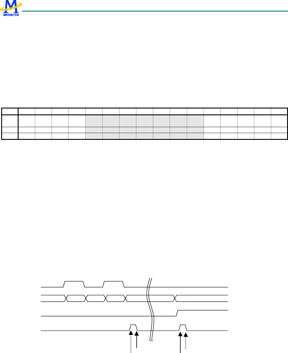
MT6235 GSM/GPRS Baseband Processor Data Sheet Revision 1.02
380/599 MediaTek Inc. Confidential
1 Auto Command is enabled.
ADATASIZE Data size in unit of byte for Auto Command. Initial value is 0x01.
0000000000 Data size is 0 byte.
0000000001 Data size is one byte.
0000000010 Data size is two bytes.
…
0111111111 Data size is 511 bytes.
1000000000 Data size is 512 bytes.
APID Auto Command Protocol ID. It is used to derive Transfer Protocol Code (TPC). Initial value is GSET_INT(0x7).
MSDC+006Ch Memory Stick Controller Status Register MSC_STA
Bit 15 14 13 12 11 10 9 8 7 6 5 4 3 2 1 0
Name CMDN
K BREQ ERR CED HSRD
Y CRCE
R TOER SIF RDY
Type R R R R RO RO RO RO RO
Reset 0 0 0 0 0 0 0 0 1
The register contains various status of Memory Stick Controller, that is, MS/SD controller is configured as Memory Stick
Controller. These statuses can be used as interrupt sources. Reading the register will NOT clear it. The register will be
cleared whenever a new command is written to the register MSC_CMD.
RDY The register bit indicates the status of transaction on MS bus. The register bit will be cleared when writing to the
command register MSC_CMD.
0 Otherwise.
1 A transaction on MS bus is ended.
SIF The register bit indicates the status of serial interface. If an interrupt is active on MS bus, the register bit will be
active. Note the difference between the signal RDY and SIF. When parallel mode is enabled, the signal SIF will be
active whenever any of the signal CED, ERR, BREQ and CMDNK is active. In order to separate interrupts
caused by the signals RDY and SIF, the register bit SIF will not become active until the register MSDC_INT
is read once. That is, the sequence for detecting the register bit SIF by polling is as follows:
1. Detect the register bit RDY of the register MSC_STA
2. Read the register MSDC_INT
3. Detect the register bit SIF of the register MSC_STA
BS BS0 BS1 BS2 BS3 BS0
SDIO command execution command finished
INT
IRQ
RDY IRQ clear SIF IRQ clear
0 Otherwise.
1 An interrupt is active on MS bus

MT6235 GSM/GPRS Baseband Processor Data Sheet Revision 1.02
381/599 MediaTek Inc. Confidential
TOER The register bit indicates if a BUSY signal timeout error takes place. When timeout error occurs, the signal BS will
become logic low ‘0’. The register bit will be cleared when writing to the command register MSC_CMD.
0 No timeout error.
1 A BUSY signal timeout error takes place. The register bit RDY will also be active.
CRCER The register bit indicates if a CRC error occurs while receiving read data. The register bit will be cleared when
writing to the command register MSC_CMD.
0 Otherwise.
1 A CRC error occurs while receiving read data. The register bit RDY will also be active.
HSRDY The register bit indicates the status of handshaking on MS bus. The register bit will be cleared when writing to the
command register MSC_CMD.
0 Otherwise.
1 A Memory Stick card responds to a TPC by RDY.
CED The register bit is only valid when parallel mode is enabled. In fact, it’s value is from DAT[0] when serial interface
interrupt takes place. See Format Specification version 2.0 of Memory Stick Standard (Memory Stick PRO) for
more details.
0 Command does not terminate.
1 Command terminates normally or abnormally.
ERR The register bit is only valid when parallel mode is enabled. In fact, it’s value is from DAT[1] when serial interface
interrupt takes place. See Format Specification version 2.0 of Memory Stick Standard (Memory Stick PRO) for
more details.
0 Otherwise.
1 Indicate memory access error during memory access command.
BREQ The register bit is only valid when parallel mode is enabled. In fact, it’s value is from DAT[2] when serial interface
interrupt takes place. See Format Specification version 2.0 of Memory Stick Standard (Memory Stick PRO) for
more details.
0 Otherwise.
1 Indicate request for data.
CMDNK The register bit is only valid when parallel mode is enabled. In fact, it’s value is from DAT[3] when serial
interface interrupt takes place. See Format Specification version 2.0 of Memory Stick Standard (Memory Stick
PRO) for more details.
0 Otherwise
1 Indicate non-recognized command.
7.5.4 Application Notes
7.5.4.1 Initialization Procedures After Power On
Disable power down control for MSDC module
Remember to power on MSDC module before starting any operation to it.
7.5.4.2 Card Detection Procedures
The pseudo code is as follows:

MT6235 GSM/GPRS Baseband Processor Data Sheet Revision 1.02
382/599 MediaTek Inc. Confidential
MSDC_CFG.PRCFG0 = 2’b10
MSDC_PS = 2’b11
MSDC_CFG.VDDPD = 1
if(MSDC_PS.PINCHG) { // card is inserted
. . .
}
The pseudo code segment perform the following tasks:
1. First pull up CD/DAT3 (INS) pin.
2. Enable card detection and input pin at the same time.
3. Turn on power for memory card.
4. Detect insertion of memory card.
7.5.4.3 Notes on Commands
For MS, check if MSC_STA.RDY is ‘1’ before issuing any command.
For SD/MMC, if the command desired to be issued involves data line, for example, commands with data transfer or R1b
response, check if SDC_STA.SDCBUSY is ‘0’ before issuing. If the command desired to be issued does not involve data
line, only check if SDC_STA.CMDBUSY is ‘0’ before issuing.
7.5.4.4 Notes on Data Transfer
z For SD/MMC, if multiple-block-write command is issued then only issue STOP_TRANS command inter-blocks
instead of intra-blocks.
z Once SW decides to issue STOP_TRANS commands, no more data transfer from or to the controller.
7.5.4.5 Notes on Frequency Change
Before changing the frequency of serial clock on MS/SD/MMC bus, it is necessary to disable serial interface of the
controller. That is, set the register bit SIEN of the register SDC_CFG to ‘0’ for SD/MMC controller, and set the register bit
SIEN of the register MSC_CFG to ‘0’ for Memory Stick controller. Serial interface of the controller needs to be enabled
again before starting any operation to the memory card.
7.5.4.6 Notes on Response Timeout
If a read command doest not receive response, that is, it terminates with a timeout, then register SDC_DATSTA needs to be
cleared by reading it. The register bit “DATTO” should be active. However, it may take a while before the register bit
becomes active. The alternative is to send the STOP_TRANS command. However, this method will receive response with
illegal-command information. Also, remember to check if the register bit SDC_STA.CMDBUSY is active before issuing
the STOP_TRANS command. The procedure is as follows:
1. Read command => response time out
2. Issue STOP_TRANS command => Get Response
3. Read register SDC_DATSTA to clear it

MT6235 GSM/GPRS Baseband Processor Data Sheet Revision 1.02
383/599 MediaTek Inc. Confidential
7.5.4.7 Source or Destination Address is not word-aligned
It is possible that the source address is not word-aligned when data move from memory to MSDC. Similarly, destination
address may be not word-aligned when data move from MSDC to memory. This can be solved by setting DMA
byte-to-word functionality.
1. DMAn_CON.SIZE=0
2. DMAn_CON.BTW=1
3. DMAn_CON.BURST=2 (or 4)
4. DMAn_COUNT=byte number instead of word number
5. fifo threshold setting must be 1 (or 2), depending on DMAn_CON.BURST
Note n=4 ~ 11
7.5.4.8 Miscellaneous notes
z Siemens MMC card: When a write command is issued and followed by a STOP_TRANS command, Siemens
MMC card will de-assert busy status even though flash programming has not yet finished. Software must use “Get
Status” command to make sure that flash programming finishes.
7.6 2D acceleration
7.6.1 2D Engine
7.6.1.1 General Description
To enhance MMI display and gaming experiences, a 2D acceleration engine is implemented. It supports ARGB8888,
RGB888, ARGB4444, RGB565 and 8-bpp color modes. Main features are listed as follows:
z Rectangle fill with color gradient.
z Bitblt: multi-Bitblt without transform, 7 rotate, mirror (transparent) Bitblt
z Alpha blending
z Binary ROP
z Line drawing: normal line, dotted line, anti-alias line
z Font caching: normal font, italic font
z Circle drawing or circle fill
z Quadratic Bezier curve drawing
z Triangle drawing
z Polygon fill with single color or image pattern
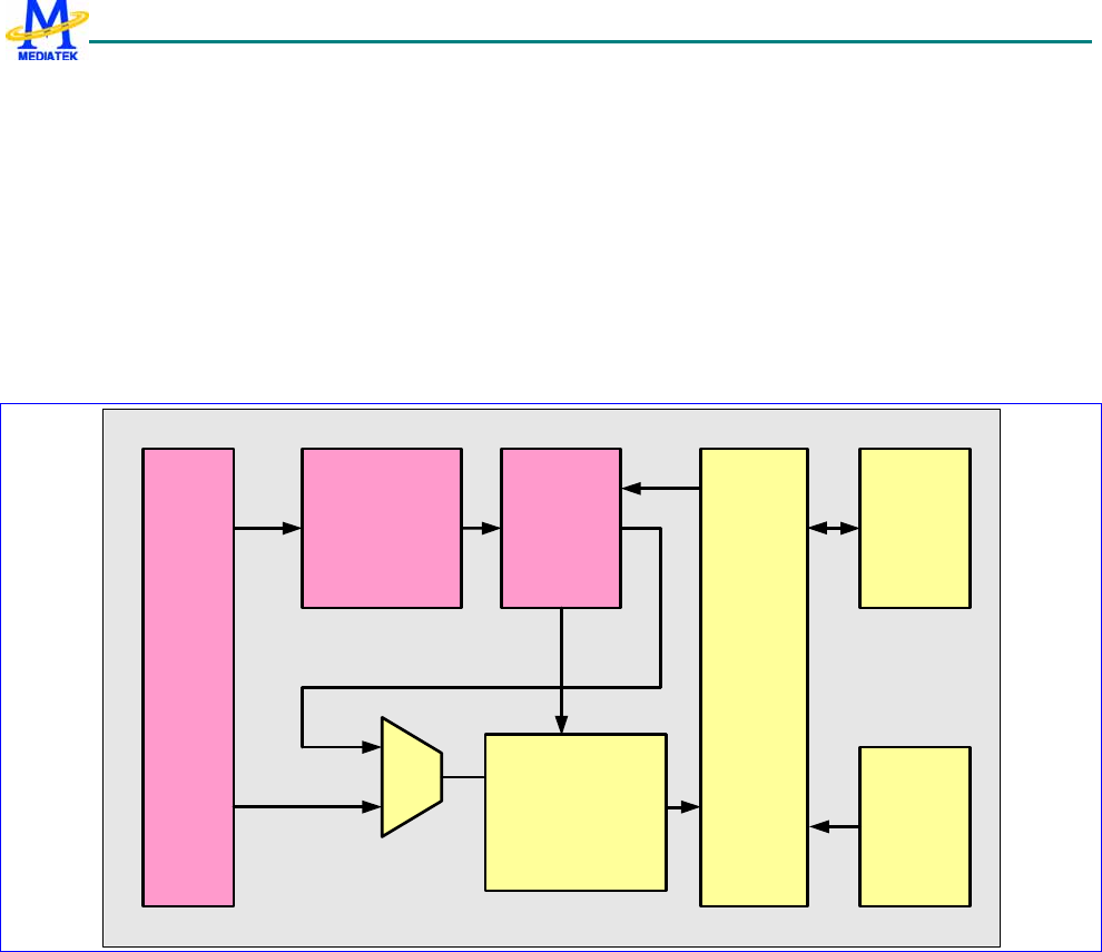
MT6235 GSM/GPRS Baseband Processor Data Sheet Revision 1.02
384/599 MediaTek Inc. Confidential
z Thick line drawing
z Specific output color replacement
MCU can program 2D engine registers via APB. However, MCU has to make sure that the 2D engine is not BUSY before
any write to 2D engine registers occurs. An interrupt scheme is also provided for more flexibility.
A command parser is implemented for further offloading of MCU. The command queue can be randomly assigned in the
system memory, with a maximum depth of 2047 commands. If the command queue is enabled, MCU has to check if the
command queue has free space before writing to the command queue. Command queue parser will consume command
queue entries upon 2D engine requests. Figure 45 shows the command queue and 2D engine block diagram. Please refer to
the graphic command queue functional specification for more details.
2D
engine
Command
queue
APB
slave
Command
parser
DST
memory
read/write
control
SRC
memory
read
control
Graphic
Memory
Interface
Figure 45 The command queue and 2D engine block diagram.
7.6.1.2 Features Introduction
7.6.1.2.1 2D Coordinate
The coordinates in the 2D engine are represented as 12-bit signed integers. The negative part is clipped during rendering.
The maximum resolution can achieve 2047x2047 pixels. The programmed base address is mapped to the origin of the
picture, which is illustrated in Figure 46.

MT6235 GSM/GPRS Baseband Processor Data Sheet Revision 1.02
385/599 MediaTek Inc. Confidential
(0,0)
dst_base_addr
x
y
Figure 46 The coordinate of the 2D engine.
7.6.1.2.2 Color format
The 2D engine support the color format of 8bpp, RGB565, RGB888, ARGB4444, and ARGB 8888. The color formats of
source and destination can be specified separately. Note that when using the 8bpp format, the source and destination color
formats have to be the same, since table-lookup of color palette is not provided in 2D engine. Graphic modes of Bitblt,
Bitblt with alpha blending, and Bitblt with binary ROP require color format setting for both source and destination. For
other graphic modes, only destination color format needs to be specified. The possible settings are listed as Table
35Table 36.
Bitblt (Copy, ROP)
Source color format Destination color format
8bpp 8bpp
RGB565
RGB565 RGB888
RGB565
RGB888 RGB888
ARGB4444
ARGB4444 ARGB8888
ARGB4444
ARGB8888 ARGB8888
Table 35 source and destination color format setting for Bitblt.
Bitblt with Alpha Blending
Source color format Destination color format
8bpp 8bpp
RGB565
RGB565 RGB888
RGB888 RGB565
MT6235 GSM/GPRS Baseband Processor Data Sheet Revision 1.02
386/599 MediaTek Inc. Confidential
RGB888
RGB565
ARGB4444 RGB888
RGB565
ARGB8888 RGB888
Table 36 source and destination color format setting for alpha blending.
When source image is used, the source key function could be enabled or disabled. When enabled, the source color key is
in the same format of source color. Be aware that the source key is still effective for alpha blending mode.
7.6.1.2.3 Clipping Window
The setting for clipping window is effective for all the 2D graphics. A pair of minimum and maximum boundary is
applied on destination side. The portion outside the clipping window will not be drawn to the destination, but the pixels
on the boundary will be kept. The clipping operation is illustrated in Figure 47.
(0,0)
dst_base_addr
g2d_clp_min
g2d_clp_max
Figure 47 The clipping operation of the 2D engine.
7.6.1.2.4 Bitblt operation
The Bitblt function copies the pixels from source picture to destination. To be more flexible, 4 copy directions and 7 kinds
of rotations are provided when doing Bitblt operation. Figure 48 illustrates the Bitblt operation and required settings.
S
src_base_addr
(src_x,src_y)
D
dst_base_addr (dst_x,dst_y)
src_w
src_h
src_x_pitch
dst_x_pitch

MT6235 GSM/GPRS Baseband Processor Data Sheet Revision 1.02
387/599 MediaTek Inc. Confidential
Figure 48 The clipping operation of the 2D engine.
Note that the size of source and destination blocks can be different. If the source block is larger than destination block, the
size of destination block is used instead of the source size. When source block size is smaller than destination block size,
the pattern of source block is repeated horizontally and vertically in the destination block, which is illustrated as Figure 49
below.
Source Destination
Figure 49 The Bitblt operation when destination size > source size.
7.6.1.2.4.1 Copy direction
When the source block and destination blocks are on the same picture, they may be overlapped by each other. To prevent
error from occurring, 4 directions for Bitblt can be programmed. However, the copy direction shall not be enabled when
doing rotation, or it will produce unwanted results. The 4 kinds of copy direction are shown in Figure 50.
D
D S
S
D
S
D
S
Figure 50 The 4 directions of Bitblt operation.
7.6.1.2.4.2 Rotation
To facilitate Bitblt operation, 7 kinds of rotation can be set at the same time. The rotation operation is illustrated as Figure
51. Here the rotation is done on the destination side, while the read sequence of pixels in source block is fixed.

MT6235 GSM/GPRS Baseband Processor Data Sheet Revision 1.02
388/599 MediaTek Inc. Confidential
8).270 degree rotation
+ vertical flip
D
S
D
(src_x,src_y) (dst_x,dst_y)
1).No rotation
D
2).180 degree rotation
D
3).horizontal flip
D
4).vertical flip
5).90 degree rotation 6).270 degree rotation
D
7).90 degree rotation
+ vertical flip
D D
Figure 51 The rotations of Bitblt operation.
7.6.1.2.5 Bitblt with Alpha Blending
Similar to simple Bitblt operation, alpha blending function is provided as well. The pixels in source block are blended
onto destination block. Blending is performed according the formula listed below:
Cd)/255*alpha)-(255 Cs*(alpha C += ,
where Cs is the source color, Cd is the destination color, and alpha is an unsigned integer range from 0 to 255.
The alpha value programmed into the 2D control registers is called constant alpha. When no alpha channel exists, the
constant alpha is used to calculate blended color. If the alpha channel exists ( in ARGB color mode), the per-pixel alpha is
used for blending operation instead of constant alpha.
In addition, the setting of copy directions and rotations are also effective for alpha blending mode. Also, the size and color
format of source block can be different from destination.
7.6.1.2.6 Bitblt with Binary ROP
The ROP (Raster Operation) is another block-wise functional mode. Here the 2D engine provides a set of binary ROPs.
The ROP code has 16 different combinations, which is listed in the definition of 2D control registers ---
G2D_SMODE_CON. Please see sec.7.6.1.3 for detail descriptions.
Similar with other block-wise functions, the copy directions and rotations are also applicable in ROP mode. The size and
color format of source and destination do not need to be the same.
7.6.1.2.7 Rectangle Fill with Color Gradient
Rectangle fill mode provides the configurations for color gradient for both x-direction and y-direction. Each of the color
gradient of component A, R, G, B is represented by 9.16 signed fixed point number. In order to prevent color crossing the
boundary of 0 and 255, it is clipped to 0 and 255 when performing gradient fill. When the color gradient is disabled, the
rectangle is filled by one color. An example of gradient fill is shown in Figure 52.
MT6235 GSM/GPRS Baseband Processor Data Sheet Revision 1.02
389/599 MediaTek Inc. Confidential
start_clr
x_gradient
y_gradient
Figure 52 Rectangle gradient fill.
7.6.1.2.8 Line Draw
The line drawing function is implemented with the mid-point algorithm. Given the two endpoints of a line, the points on
the line are calculated recursively. The line anti-aliasing is also supported but it requires extra register configurations. In
addition, dotted line is also provided for use. Simultaneously turning on anti-aliasing and dotted-line is not recommended
since the line may result in a strange look.
7.6.1.2.9 Circle Draw
The circle drawing is quite similar with line drawing, using the mid-point algorithm as well. A center point and a radius
have to be programmed into 2D control registers. There are 4 enable bits for each quadrant of a circle, each determines
whether the arcs shall be rendered or not. The setting of circle drawing is illustrated in Figure 53.
0
12
3
(dst_x,dst_y)
radius
Figure 53 Circle drawing.
7.6.1.2.10 Bezier curve
The quadratic Bezier curve is implemented, too. The quadratic Bezier curve is defined by three control points, as
illustrated in Figure 54. The Bezier curve drawing is implemented with subdivision method. The amount of
subdivisions is programmed by software. The curve gets more detailed with the increase of subdivision factor, but it
requires more memory and computing time. To be more precise, doing n times of subdivision needs a buffer of 4*2 )1( +n
bytes.

MT6235 GSM/GPRS Baseband Processor Data Sheet Revision 1.02
390/599 MediaTek Inc. Confidential
p0
p2
p1
Figure 54 Bezier curve.
7.6.1.2.11 Triangle Flat Fill
The 2D engine supports the function of triangle flat fill with the help of software. First, the software divides the triangle
into upper plane and lower plane and passes them to hardware individually. Given the starting vertex’s coordinate and the
slopes of left and right edges, the 2D hardware fills the horizontal segments between the two edges until the horizontal end
is reached. The slope of each edge is in 12.16 bit signed fix-point representation. The programming of triangle drawing
is illustrated in Figure 55.
Horizontal end
start point
start point
Horizontal end
left slope
left slope
right slope
right slope
Figure 55 Triangle drawing.

MT6235 GSM/GPRS Baseband Processor Data Sheet Revision 1.02
391/599 MediaTek Inc. Confidential
7.6.1.2.12 Font Drawing
The 2D engine helps to render fonts stored in one-bit-per-pixel format. It expends the zero bits to background color and
expands one bits to foreground color. The background color can be set as transparent. The font drawing can be
programmed as tilt, when given each line’s tilt value.
The start bit of font drawing can be non-byte aligned to save memory usage for font caching. In addition, the rotations can
be performed at the same time when drawing fonts.
7.6.1.2.13 Polygon Fill
In MT6511, 2D engine supports the function of polygon fill with its edges specified in memory. The maximum number of
edge is 2047, which will occupy 32KB memory space (16 bytes per edge) during polygon fill processing. Software need to
indicate the starting address of input edge list by setting G2D_BUF_STA_ADDR_0 and allocate another memory space for
the polygon fill processing by setting G2D_BUF_STA_ADDR_1. It’s noted that filling a polygon with a list of cross edges
will cause an un-expected result. Dividing this kind of polygon into several ones without cross edges is recommended.
Polygon fill with image is also supported. The maximum image pattern size is 64x64 which is needed to be put in
memory starting from BUF_STA_ADDR_2.
Figure 56 Polygon fill.
Figure 57 Cross edges. Divide into 1 - 5 triangles is recommended.
Figure 14 Polygon fill with image pattern.

MT6235 GSM/GPRS Baseband Processor Data Sheet Revision 1.02
392/599 MediaTek Inc. Confidential
7.6.1.2.14 Thick Line Drawing
2D engine line drawing with thickness, i.e. thick line drawing. The two end caps of the thick line could be selected as
round type or flat (no end cap). Line pattern is also supported in thick line drawing mode. No end cap would be added
in patterned thick line.
Figure 16 Thick Line Drawing, odd thickness and even thickness.
7.6.1.3 Register Definitions
Table 37 The 2D engine register mapping. summarizes the 2D engine register mapping on APB and through command
queue. The base address of 2D engine is 80670000h.
APB Address CMQ
mapped
Address Register Function Acronym
G2D+0100h 100h 2D engine fire mode control register FMODE_CON
102h Reserved
G2D+0104h 104h 2D Engine sub-mode control lower register SMODE_CON_L
106h 2D Engine sub-mode control higher register SMODE_CON_H
G2D+0108h 108h 2D engine common control register COM_CON
10Ah Reserved
G2D+0110h 110h 2D engine status register STA
112h Reserved
G2D+0200h 200h Source base address lower hword register SRC_BASE_L
202h Source base address higher hword register SRC_BASE_H
G2D+0204h 204h Source pitch register SRC_PITCH
206h Reserved
G2D+0208h 208h Source y coordinate register SRC_Y
20Ah Source x coordinate register SRC_X
G2D+020Ch 20Ch Source height register SRC_H
20Eh Source width register SRC_W
G2D+0210h 210h Source color key lower hword register SRC_KEY_L
212h Source color key lower hword register SRC_KEY_H

MT6235 GSM/GPRS Baseband Processor Data Sheet Revision 1.02
393/599 MediaTek Inc. Confidential
G2D+0300h 300h Destination base address lower hword register DST_BASE_L
302h Destination base address higher hword register DST_BASE_H
G2D+0304h 304h Destination Pitch Register DST_PITCH
306h Reserved
G2D+0308h 308h Destination y coordinate register 0 DST_Y0
30Ah Destination x coordinate register 0 DST_X0
G2D+030Ch 30Ch Destination y coordinate register 1 DST_Y1
30Eh Destination x coordinate register 1 DST_X1
G2D+0310h 310h Destination y coordinate register 2 DST_Y2
312h Destination x coordinate register 2 DST_X2
G2D+0318h 318h Destination height register DST_H
31Ah Destination width register DST_W
G2D+320 320h Pattern width and height register PAT_WH
322h Pattern x and y offset register PAT_XY
G2D+324 324h Pattern pitch Register PAT_PITCH
G2D+400h 400h Foreground color lower hword register FGCLR_L
402h Foreground color lower hword register FGCLR_H
G2D+404h 404h Background color lower hword register BGCLR_L
406h Background color lower hword register BGCLR_H
G2D+408h 408h Clipping minimum y coordinate register CLP_MIN_Y
40Ah Clipping minimum x coordinate register
CLP_MIN_X
G2D+40Ch 40Ch Clipping maximum y coordinate register CLP_MAX_Y
40Eh Clipping maximum x coordinate register CLP_MAX_X
G2D+410h 410h Rectangle color gradient of alpha componet x
lower hword register ALPGR_X_L
412h
Rectangle color gradient of alpha componet x
higher hword register ALPGR_X_H
G2D+414h 414h Rectangle color gradient of red component y
lower hword register REDGR_X_L
416h
Rectangle color gradient of red component y
higher hword register REDGR_X_H
G2D+418h 418h Rectangle color gradient of green component x
lower hword register GREENGR_X_L
41Ah
Rectangle color gradient of green component x
higher hword register GREENGR_X_H
G2D+41Ch 41Ch Rectangle color gradient of blue component x
lower hword register BLUEGR_X_L
41Eh
Rectangle color gradient of blue component x
higher hword register BLUE_X_H
G2D+420h 420h Rectangle color gradient of alpha component y
lower hword register ALPGR_Y_L
422h
Rectangle color gradient of alpha component y ALPGR_Y_H

MT6235 GSM/GPRS Baseband Processor Data Sheet Revision 1.02
394/599 MediaTek Inc. Confidential
higher hword register
G2D+424h 424h Rectangle color gradient of red component y
lower hword register REDGR_Y_L
426h
Rectangle color gradient of red component y
higher hword register REDGR_Y_H
G2D+428h 428h Rectangle color gradient of green component y
lower hword register GREENGR_Y_L
42Ah
Rectangle color gradient of green component y
higher hword register GREENGR_Y_H
G2D+42Ch 42Ch Rectangle color gradient of blue component y
lower hword register BLUEGR_Y_L
42Eh
Rectangle color gradient of blue component y
higher hword register BLUEGR_Y_H
G2D+430h 430h Buffer 0 start address lower hword register BUF_STA_ADDR_0
_L
432h Buffer 0 start address higher hword register BUF_STA_ADDR_0
_H
G2D+434h 434h Buffer 1 start address lower hword register BUF_STA_ADDR_1
_L
436h Buffer 1 start address higher hword register BUF_STA_ADDR_1
_H
G2D+438h 438h Buffer 2 start address lower hword register BUF_STA_ADDR_2
_L
43Ah Buffer 2 start address higher hword register BUF_STA_ADDR_2
_H
G2D+0700h ~
G2D+071Fh 700h ~ 71Fh TILT_0300 ~
TILT_1F1C
Table 37 The 2D engine register mapping.
There are several function modes in 2D graphics engine. Some registers are shared between different them. Table 38
summarizes the settings under different function modes.
APB
Address
CMQ
Addres
s Rectangle fill Bitblt
Operations Line/Circle
drawing Bezier curve
drawing Triangle drawing Font caching
G2D+0200h 200h SRC_BASE SLOPE_L SRC_BASE
G2D+0204h 204h SRC_PITCH
G2D+0208h 208h SRC_XY
G2D+020Ch 20Ch SRC_SIZE
G2D+0210h 210h SRC_KEY SRC_KEY
G2D+0214h 214h AVO_CLR AVO_ CLR AV O _ C LR AV O _C L R AVO_CLR AV O _C L R
G2D+0218h 218h REP_CLR REP_CLR REP_CLR REP_CLR REP_CLR REP_CLR
G2D+0300h 300h DST_BASE DST_BASE DST_BASE DST_BASE DST_BASE DST_BASE
G2D+0304h 304h DST_PITCH DST_PITCH DST_PITCH DST_PITCH DST_PITCH DST_PITCH
G2D+0308h 308h DST_XY DST_XY DST_XY0 DST_XY0 DST_XY_START DST_XY

MT6235 GSM/GPRS Baseband Processor Data Sheet Revision 1.02
395/599 MediaTek Inc. Confidential
G2D+030Ch 30Ch DST_XY1/
RADIUS DST_XY1 DST_Y_END
G2D+0310h 310h DST_XY2
G2D+0318h 318h DST_SIZE DST_SIZE DST_SIZE
G2D+0320h 320h
G2D+0324h 324h
G2D+0400h 400h START_CLR FGCLR FGCLR FGCLR FGCLR
G2D+0404h 404h DST_KEY XY_SQRT BGCLR
G2D+0408h 408h CLP_MIN CLP_MIN CLP_MIN CLP_MIN CLP_MIN CLP_MIN
G2D+040Ch 40Ch CLP_MAX CLP_MAX CLP_MAX CLP_MAX CLP_MAX CLP_MAX
G2D+0410h 410h ALPGD_X
G2D+0414h 414h RED_GD_X SUBDIV_TIME
G2D+0418h 418h GREEN_GD_X
G2D+041Ch 41Ch BLUE_GD_X
G2D+0420h 420h ALPGD_Y
G2D+0424h 424h RED_GD_Y
G2D+0428h 428h GREEN_GD_Y
G2D+042Ch 42Ch BLUE_GD_Y
G2D+430h 430h BUF_STA_ADD SLOPE_R
G2D+434h 434h
G2D+438h 438h
G2D+0700h
~
G2D+071Fh
700h ~
71Fh
TILT_0300 ~
TILT_1F1C
TILT_0300 ~
TILT_1F1C TILT_0300 ~
TILT_1F1C
APB
Address
CMQ
Addres
s
Horizontal Line
Gradient
Horizontal
Line Copy
with Mask
Polygon Fill
with Image
Pattern
Thick Line
Drawing
G2D+0200h 200h SRC_BASE
G2D+0204h 204h
G2D+0208h 208h
G2D+020Ch 20Ch SRC_SIZE
G2D+0210h 210h
G2D+0214h 214h AVO_CLR AVO_CLR AVO_CLR AVO_CLR
G2D+0218h 218h REP_CLR REP_CLR REP_CLR REP_CLR
G2D+0300h 300h DST_BASE DST_BASE DST_BASE DST_BASE
G2D+0304h 304h DST_PITCH DST_PITCH
G2D+0308h 308h DST_XY0
G2D+030Ch 30Ch DST_XY1
G2D+0310h 310h

MT6235 GSM/GPRS Baseband Processor Data Sheet Revision 1.02
396/599 MediaTek Inc. Confidential
G2D+0318h 318h DST_SIZE DST_SIZE
G2D+320h 320h PAT_XYWH
G2D+324h 324h PAT_PITCH
G2D+0400h 400h START_CLR FG_CLR FG_CLR
G2D+0404h 404h
G2D+0408h 408h CLP_MIN CLP_MIN
G2D+040Ch 40Ch CLP_MAX CLP_MAX
G2D+0410h 410h ALPGD_X
G2D+0414h 414h RED_GD_X
G2D+0418h 418h GREEN_GD_X TLINE_CON
G2D+041Ch 41Ch BLUE_GD_X
G2D+0420h 420h
G2D+0424h 424h
G2D+0428h 428h
G2D+042Ch 42Ch
G2D+430h 430h MASK_BASE EDGE_ADDR EDGE_ADDR
G2D+434h 434h SORT_ADDR SORT_ADDR
G2D+438h 438h PAT_ADDR
G2D+0700h
~
G2D+071Fh
700h ~
71Fh
Table 38 2D engine common registers
Below shows common control registers.
G2D+0100h Graphic 2D Engine Fire Mode Control Register G2D_FMODE_C
ON
Bit 15 14 13 12 11 10 9 8 7 6 5 4 3 2 1 0
Name SRC_CLR_MODE DST_CLR_MODE G2D_ENG_MODE
Type R/W R/W R/W
Reset 000 000 0000
Write this register will fire the 2D engine according to the CLR_MODE and ENG_MODE field.
SRC_CLR_MODE source color mode
000 8-bpp, LUT disabled
001 16-bpp, RGB 565 format
010 32-bpp, ARGB 8888 format
011 24-bpp, RGB 888 format
101 16-bpp, ARGB 4444 format
others reserved
DST_CLR_MODE destination color mode
000 8-bpp, LUT disabled
001 16-bpp, RGB 565 format

MT6235 GSM/GPRS Baseband Processor Data Sheet Revision 1.02
397/599 MediaTek Inc. Confidential
010 32-bpp, ARGB 8888 format
011 24-bpp, RGB 888 format
101 16-bpp, ARGB 4444 format
others reserved
G2D_ENG_MODE 2D engine function mode
0000 Line draw.
0001 Circle draw.
0010 Bezier curve draw.
0011 Triangle fill.
0110 Polygon fill.
0111 Thick line mode.
1000 Rectangle fill.
1001 Bitblt.
1010 Bitblt with alpha blending.
1011 Bitblt with ROP.
1100 Font drawing.
1101 Horizontal line fill with color gradient. In this mode, the source key and the clipping functions are
disabled automatically.
1110 Horizontal line copy with mask. In this mode, the source key and the clipping functions are disabled
automatically.
others not allowed
G2D+0104h Graphic 2D Engine Sub-mode Control Register G2D_SMODE_C
ON
Bit 31 30 29 28 27 26 25 24 23 22 21 20 19 18 17 16
Name FITA FNBG
FMSB
_FIRS
T CLR_
REP_
EN
CF_E
N ALPHA ROP_CODE
Type R/W R/W R/W R/W R/W R/W R/W
Reset 0 0 0 0 0 0000 0000
Bit 15 14 13 12 11 10 9 8 7 6 5 4 3 2 1 0
Name LDOT LIMG
LAA_
EN
DST_
KEY_
EN
CLRG
D_EN BDIR BITA BROT
Type R/W R/W R/W R/W R/W R/W R/W R/W
Reset 0 0 0 0 0 11 0 111
Write this register to set the 2D engine configuration.
FITA font italic enabled.
FNBG font drawing with no background color
FMSB_FIRST font drawing from most significant bit
CLR_REP_EN Output color replacement enable.
CF_EN Circle fill enabled.
ALPHA Bit 7-4 of constant alpha value. ROP_CODE is Bit3-0 of constant alpha value.
ROP_CODE Binary ROP code. Bits 2-0 are also used to specify the start bit position for Font drawing and enabled arcs
for circle drawing.

MT6235 GSM/GPRS Baseband Processor Data Sheet Revision 1.02
398/599 MediaTek Inc. Confidential
Bitblt ROP Code Boolean Function Start Bit Position for Font
Drawing Enabled Arcs
0000 0 (Black) Bit 0 None
0001 ~(S + D) Bit 1 I
0010 ~S . D Bit 2 Ⅱ
0011 ~S Bit 3 Ⅰ, Ⅱ
0100 S . ~D Bit 4 Ⅲ
0101 ~D Bit 5 Ⅰ, Ⅲ
0110 S ^ D Bit 6 Ⅱ, Ⅲ
0111 ~(S . D) Bit 7 Ⅰ,Ⅱ, Ⅲ
1000 S . D Bit 0 Ⅳ
1001 ~(S ^ D) Bit 1 Ⅰ, Ⅳ
1010 D Bit 2 Ⅱ, Ⅲ
1011 ~S + D Bit 3 Ⅰ, Ⅱ, Ⅳ
1100 S Bit 4 Ⅲ, Ⅳ
1101 S + ~D Bit 5 Ⅰ, Ⅲ, Ⅳ
1110 S + D Bit 6 Ⅱ, Ⅲ, Ⅳ
1111 1 (White) Bit 7 Ⅰ, Ⅱ, Ⅲ, Ⅳ
S = Source, D = Destination.
I = first quadrant, II = second quadrant, III = third quadrant, IV = fourth quadrant.
LIMG Polygon fill with image pattern.
LDOT line dotted
LAA_EN line anti-aliasing enabled
DST_KEY_EN Destination key enabled for Bitblt functions
CLRGR_EN Color gradient enabled for rectangle fill
BDIR Bitblt direction:
00 from lower right corner
01 from lower left corner
10 from upper right corner
11 from upper left corner
This field only takes effect when the Bitblt rotation is set as none (111). When doing rotation the Bitblt direction of
source image is always from upper left corner.
BITA Bitblt italic enabled, using the tilt value defined in G2D_TILT_00 ~ G2D_TILT_1F registers. The tilt function
should not be enabled in Alpha Blending and ROP mode.
BROT Bitblt rotation:
000 mirror then rotate 90
001 rotate 90
010 rotate 270
011 mirror then rotate 270
100 rotate 180

MT6235 GSM/GPRS Baseband Processor Data Sheet Revision 1.02
399/599 MediaTek Inc. Confidential
101 mirror
110 mirror then rotate 180
111 none
G2D+0108h Graphic 2D Engine Common Control Register G2D_COM_CON
Bit 31 30 29 28 27 26 25 24 23 22 21 20 19 18 17 16
Name
Type
Reset
Bit 15 14 13 12 11 10 9 8 7 6 5 4 3 2 1 0
Name CLP_
EN
SRCK
EY_E
N RST
Type R/W R/W R/W
Reset 0 0 0
Write this register to set the 2D engine configuration.
RST 2D engine reset, only the state machine is reset, the content of control registers will not be reset.
SRCKEY_EN Source key enabled.
CLP_EN Clipping enabled.
G2D+010Ch Graphic 2D Engine Interrupt Control Register G2D_IRQ_CON
Bit 31 30 29 28 27 26 25 24 23 22 21 20 19 18 17 16
Name
Type
Reset
Bit 15 14 13 12 11 10 9 8 7 6 5 4 3 2 1 0
Name EN
Type R/W
Reset 0
Write this register to set the 2D engine IRQ configuration.
EN interrupt enable. The interrupt is negative edge sensitive.
G2D+0110h Graphic 2D Engine Common Status Register G2D_COM_STA
Bit 31 30 29 28 27 26 25 24 23 22 21 20 19 18 17 16
Name
Type
Reset
Bit 15 14 13 12 11 10 9 8 7 6 5 4 3 2 1 0
Name BUSY
Type RO
Reset 0
Read this register to get the 2D engine status. 2D engine may function abnormally if any 2D engine register is modified
when BUSY.
BUSY 2D engine is busy
MT6235 GSM/GPRS Baseband Processor Data Sheet Revision 1.02
400/599 MediaTek Inc. Confidential
G2D+0200h Graphic 2D Source Base Address Register G2D_SRC_BAS
E
Bit 31 30 29 28 27 26 25 24 23 22 21 20 19 18 17 16
Name SRC_BASE[31:16]
Type R/W
Reset 0
Bit 15 14 13 12 11 10 9 8 7 6 5 4 3 2 1 0
Name SRC_BASE[15:0]
Type R/W
Reset 0
SRC_BASE The base address of source image. Also, this field is used for the slope of the left triangle edges
represented in 12.16 format.
G2D+0204h Graphic 2D Engine Source Pitch Register G2D_SRC_PITC
H
Bit 15 14 13 12 11 10 9 8 7 6 5 4 3 2 1 0
Name SRC_PITCH
Type R/W
Reset 0
SRC_PITCH The width of source image in the unit of pixels.
G2D+0208h Graphic 2D Engine Source X and Y Register G2D_SRC_XY
Bit 31 30 29 28 27 26 25 24 23 22 21 20 19 18 17 16
Name SRC_X
Type R/W
Reset 0
Bit 15 14 13 12 11 10 9 8 7 6 5 4 3 2 1 0
Name SRC_Y
Type R/W
Reset 0
SRC_Y The starting y co-ordinate of source image. It must be positive although represented as 12-bit signed integer.
SRC_X The starting x co-ordinate of source image. It must be positive although represented as 12-bit signed integer.
G2D+020Ch Graphic 2D Engine Source Size Register G2D_SRC_SIZE
Bit 31 30 29 28 27 26 25 24 23 22 21 20 19 18 17 16
Name SRC_W
Type R/W
Reset 0
Bit 15 14 13 12 11 10 9 8 7 6 5 4 3 2 1 0
Name SRC_H
Type R/W
Reset 0
SRC_H The source height for Bitblt, alpha blending and ROP. It must be positive although represented as 12-bit signed
integer.
SRC_W The source width for Bitblt, alpha blending and ROP. It must be positive although represented as 12-bit signed
integer.

MT6235 GSM/GPRS Baseband Processor Data Sheet Revision 1.02
401/599 MediaTek Inc. Confidential
G2D+0210h Graphic 2D Engine Source Color Key Register G2D_SRC_KEY
Bit 31 30 29 28 27 26 25 24 23 22 21 20 19 18 17 16
Name SRC_KEY[31:16]
Type R/W
Reset 0
Bit 15 14 13 12 11 10 9 8 7 6 5 4 3 2 1 0
Name SRC_KEY[15:0]
Type R/W
Reset 0
SRC_KEY The source color key. The color will be transparent if color keying is enabled.
G2D+0214h Graphic 2D Engine Destination Avoidance Color G2D_DST_AVO_
CLR
Bit 31 30 29 28 27 26 25 24 23 22 21 20 19 18 17 16
Name DST_AVO_CLR[31:16]
Type R/W
Reset 0
Bit 15 14 13 12 11 10 9 8 7 6 5 4 3 2 1 0
Name DST_AVO_CLR[15:0]
Type R/W
Reset 0
DST_AVO_CLR The output color with DST_AVO_CLR would be replaced with DST_REP_CLR when
CLR_REP_EN is enabled.
G2D+0218h Graphic 2D Engine Destination Replacement Color G2D_DST_REP_
CLR
Bit 31 30 29 28 27 26 25 24 23 22 21 20 19 18 17 16
Name DST_REP_CLR[31:16]
Type R/W
Reset 0
Bit 15 14 13 12 11 10 9 8 7 6 5 4 3 2 1 0
Name DST_REP_CLR[15:0]
Type R/W
Reset 0
DST_REP_CLR The output color with DST_AVO_CLR would be replaced with DST_REP_CLR when
CLR_REP_EN is enabled.
G2D+0300h Graphic 2D Destination Base Address Register G2D_DST_BASE
Bit 31 30 29 28 27 26 25 24 23 22 21 20 19 18 17 16
Name DST_BASE[31:16]
Type R/W
Reset 0
Bit 15 14 13 12 11 10 9 8 7 6 5 4 3 2 1 0
Name DST_BASE[15:0]
MT6235 GSM/GPRS Baseband Processor Data Sheet Revision 1.02
402/599 MediaTek Inc. Confidential
Type R/W
Reset 0
DST_BASE The base address of destination image.
G2D+0304h Graphic 2D Engine Destination Pitch Register G2D_DST_PITC
H
Bit 15 14 13 12 11 10 9 8 7 6 5 4 3 2 1 0
Name SRC_PITCH
Type R/W
Reset 0
DST_PITCH The width of destination image in the unit of pixels.
G2D+0308h Graphic 2D Engine Destination X and Y Register 0 G2D_DST_XY0
Bit 31 30 29 28 27 26 25 24 23 22 21 20 19 18 17 16
Name DST_X0
Type R/W
Reset 0
Bit 15 14 13 12 11 10 9 8 7 6 5 4 3 2 1 0
Name DST_Y0
Type R/W
Reset 0
(DST_X0 , DST_Y0) is used as the starting co-ordinate in Bitblt, alpha blending, ROP, and font drawing mode. In line
mode or triangle fill mode, it is used as one end point. For Bezier curve drawing, it is one of the control points. While in
circle drawing mode, it is the center of the circle. Also this filed is used as the starting point of triangle draw.
DST_X0 Represented by 12-bit signed integer. Negative co-ordinate is allowed.
DST_Y0 Represented by 12-bit signed integer. Negative co-ordinate is allowed.
G2D+030Ch Graphic 2D Engine Destination X and Y Register 1 G2D_DST_XY1
Bit 31 30 29 28 27 26 25 24 23 22 21 20 19 18 17 16
Name DST_X1
Type R/W
Reset 0
Bit 15 14 13 12 11 10 9 8 7 6 5 4 3 2 1 0
Name DST_Y1
Type R/W
Reset 0
(DST_X1 , DST_Y1) is used as one end point in Line drawing and triangle fill mode. For Bezier curve drawing, it is one of
the control points. While in circle drawing mode, DST_X1 must be positive since it is the radius of the circle. Also, Bit
15-0 is used as the vertical end of triangle draw.
DST_X1 Represented by 12-bit signed integer. Negative co-ordinate is allowed.
DST_Y1 Represented by 12-bit signed integer. Negative co-ordinate is allowed.
G2D+0310h Graphic 2D Engine Destination X and Y Register 2 G2D_DST_XY2
Bit 31 30 29 28 27 26 25 24 23 22 21 20 19 18 17 16
Name DST_X2
Type R/W
MT6235 GSM/GPRS Baseband Processor Data Sheet Revision 1.02
403/599 MediaTek Inc. Confidential
Reset 0
Bit 15 14 13 12 11 10 9 8 7 6 5 4 3 2 1 0
Name DST_Y2
Type R/W
Reset 0
(DST_X2 , DST_Y2) is used as one end point in triangle fill mode. For Bezier curve drawing, it is one of the control points.
DST_X2 Represented by 12-bit signed integer. Negative co-ordinate is allowed.
DST_Y2 Represented by 12-bit signed integer. Negative co-ordinate is allowed.
G2D+0318h Graphic 2D Engine Destination Size Register G2D_DST_SIZE
Bit 31 30 29 28 27 26 25 24 23 22 21 20 19 18 17 16
Name DST_W
Type R/W
Reset 0
Bit 15 14 13 12 11 10 9 8 7 6 5 4 3 2 1 0
Name DST_H
Type R/W
Reset 0
SRC_H The source height for Bitblt, alpha blending and ROP. It must be positive although represented as 12-bit signed
integer.
SRC_W The source width for Bitblt, alpha blending and ROP. It must be positive although represented as 12-bit signed
integer.
G2D+0320h Graphic 2D Engine Pattern X Y W H Register G2D_PAT_XYW
H
Bit 31 30 29 28 27 26 25 24 23 22 21 20 19 18 17 16
Name PAT_X PAT_Y
Type R/W R/W
Reset 0 0
Bit 15 14 13 12 11 10 9 8 7 6 5 4 3 2 1 0
Name PAT_W PAT_H
Type R/W R/W
Reset 0 0
PAT_X The starting x co-ordinate of pattern image for Polygon-Fill.
PAT_Y The starting y co-ordinate of pattern image for Polygon-Fill.
PAT_W The pattern width for Polygon-Fill.
PAT_H The pattern height for Polygon-Fill.
G2D+0324h Graphic 2D EnginePattern Pitch Register G2D_PAT_PITC
H
Bit 31 30 29 28 27 26 25 24 23 22 21 20 19 18 17 16
Name
Type
Reset
Bit 15 14 13 12 11 10 9 8 7 6 5 4 3 2 1 0
Name PAT_PITCH
MT6235 GSM/GPRS Baseband Processor Data Sheet Revision 1.02
404/599 MediaTek Inc. Confidential
Type R/W
Reset 0
PAT_PITCH The width of pattern in the unit of pixels. The maximum width of pattern is 32.
G2D+0400h Graphic 2D Engine Foreground Color Register G2D_ FGCLR
Bit 31 30 29 28 27 26 25 24 23 22 21 20 19 18 17 16
Name FGCLR[31:16]
Type R/W
Reset 0
Bit 15 14 13 12 11 10 9 8 7 6 5 4 3 2 1 0
Name FGCLR[15:0]
Type R/W
Reset 0
FGCLR The foreground color used for line/circle drawing and font drawing. It is also the start color of rectangle fill. The
format of foreground color depends on the source color mode set in G2D_FMODE_CON register.
G2D+0404h Graphic 2D Engine Background Color Register G2D_BGCLR
Bit 31 30 29 28 27 26 25 24 23 22 21 20 19 18 17 16
Name BGCLR[31:16]
Type R/W
Reset 0
Bit 15 14 13 12 11 10 9 8 7 6 5 4 3 2 1 0
Name BGCLR[15:0]
Type R/W
Reset 0
BGCLR The background color of the source. The format of background color depends on the source color mode set in
G2D_FMODE_CON register. Bit 15-0 also used as the XY_SQRT for anti-aliased line drawing. The XY_SQRT
calculation is listed as bellow.
22 )0_1_()0_1_(*2_ YDSTYDSTXDSTXDSTSQRTXY −+−=
G2D+0408h Graphic 2D Engine Clipping Minimum Register G2D_CLIP_MIN
Bit 31 30 29 28 27 26 25 24 23 22 21 20 19 18 17 16
Name CLIP_MIN_X
Type R/W
Reset 0
Bit 15 14 13 12 11 10 9 8 7 6 5 4 3 2 1 0
Name CLIP_MIN_Y
Type R/W
Reset 0
CLIP_MIN_X The minimum value of x co-ordinate in clipping window, signed 12-bit integer.
CLIP_MIN_Y The minimum value of y co-ordinate in clipping window, signed 12-bit integer..
G2D+040ch Graphic 2D Engine Clipping Maximum Register G2D_CLIP_MAX
Bit 31 30 29 28 27 26 25 24 23 22 21 20 19 18 17 16
Name CLIP_MAX_X
Type R/W
MT6235 GSM/GPRS Baseband Processor Data Sheet Revision 1.02
405/599 MediaTek Inc. Confidential
Reset 11111111111
Bit 15 14 13 12 11 10 9 8 7 6 5 4 3 2 1 0
Name CLIP_MAX_Y
Type R/W
Reset 11111111111
CLIP_MAX_X The maximum value of x co-ordinate in clipping window, signed 12-bit integer...
CLIP_MAX_Y The maximum value of y co-ordinate in clipping window, signed 12-bit integer..
G2D+0410h Graphic 2D X Alpha Gradient Register G2D_ALPGR_X
Bit 31 30 29 28 27 26 25 24 23 22 21 20 19 18 17 16
Name ALPHA_GR_X[24:16]
Type R/W
Reset 0
Bit 15 14 13 12 11 10 9 8 7 6 5 4 3 2 1 0
Name ALPHA_GR_X[15:0]
Type R/W
Reset 0
The color gradient of alpha in x direction for rectangle gradient fill.
ALPHA_GR_X The color gradient of alpha channel, represented in signed 9.16 format.
G2D+0414h Graphic 2D X Red Gradient Register G2D_REDGR_X
Bit 31 30 29 28 27 26 25 24 23 22 21 20 19 18 17 16
Name RED_GR_X[24:16]
Type R/W
Reset 0
Bit 15 14 13 12 11 10 9 8 7 6 5 4 3 2 1 0
Name RED_GR_X[15:0]
Type R/W
Reset 0
The color gradient of red in x direction for rectangle gradient fill. Bit 3-0 also used as the times of subdivision for Bezier
curve drawing.
RED_GR_X The color gradient of red component, represented in signed 9.16 format.
G2D+0418h Graphic 2D X Green Gradient Register G2D_
GREENGR_X
Bit 31 30 29 28 27 26 25 24 23 22 21 20 19 18 17 16
Name GREEN_GR_X[24:16]
Type R/W
Reset 0
Bit 15 14 13 12 11 10 9 8 7 6 5 4 3 2 1 0
Name GREEN_GR_X[15:0]
Type R/W
Reset 0
GREEN_GR_X The color gradient of blue component, represented in signed 9.16 format.
GREEN_GR_X[15] Enable thick line pattern.
GREEN_GR_X[14] Thick line starting point cap drawing enable.
MT6235 GSM/GPRS Baseband Processor Data Sheet Revision 1.02
406/599 MediaTek Inc. Confidential
GREEN_GR_X[13] Thick line end point cap drawing enable.
GREEN_GR_X[12] Thickness error auto compensation enable.
GREEN_GR_X[11] Adjusted polygon fill algorithm for thick line drawing.
GREEN_GR_X[10:0]Thickness of the thick line.
G2D+041Ch Graphic 2D X Blue Gradient Register G2D_BLUEGR_X
Bit 31 30 29 28 27 26 25 24 23 22 21 20 19 18 17 16
Name BLUE_GR_X[24:16]
Type R/W
Reset 0
Bit 15 14 13 12 11 10 9 8 7 6 5 4 3 2 1 0
Name BLUE_GR_X[15:0]
Type R/W
Reset 0
BLUE_GR_X The color gradient of blue component, represented in signed 9.16 format.
G2D+0420h Graphic 2D Y Alpha Gradient Register G2D_ALPGR_Y
Bit 31 30 29 28 27 26 25 24 23 22 21 20 19 18 17 16
Name ALPHA_GR_Y[24:16]
Type R/W
Reset 0
Bit 15 14 13 12 11 10 9 8 7 6 5 4 3 2 1 0
Name ALPHA_GR_Y[15:0]
Type R/W
Reset 0
The color gradient of alpha in x direction for rectangle gradient fill.
ALPHA_GR_Y The color gradient of alpha channel, represented in signed 9.16 format.
G2D+0424h Graphic 2D Y Red Gradient Register G2D_REDGR_Y
Bit 31 30 29 28 27 26 25 24 23 22 21 20 19 18 17 16
Name RED_GR_Y[24:16]
Type R/W
Reset 0
Bit 15 14 13 12 11 10 9 8 7 6 5 4 3 2 1 0
Name RED_GR_Y[15:0]
Type R/W
Reset 0
The color gradient of red in x direction for rectangle gradient fill.
RED_GR_Y The color gradient of red component, represented in signed 9.16 format.
G2D+0428h Graphic 2D Y Green Gradient Register G2D_
GREENGR_Y
Bit 31 30 29 28 27 26 25 24 23 22 21 20 19 18 17 16
Name GREEN_GR_Y24:16]
Type R/W
Reset 0
Bit 15 14 13 12 11 10 9 8 7 6 5 4 3 2 1 0

MT6235 GSM/GPRS Baseband Processor Data Sheet Revision 1.02
407/599 MediaTek Inc. Confidential
Name GREEN_GR_Y15:0]
Type R/W
Reset 0
GREEN_GR_Y The color gradient of blue component, represented in signed 9.16 format.
G2D+042Ch Graphic 2D Y Blue Gradient Register G2D_BLUEGR_Y
Bit 31 30 29 28 27 26 25 24 23 22 21 20 19 18 17 16
Name BLUE_GR_Y[24:16]
Type R/W
Reset 0
Bit 15 14 13 12 11 10 9 8 7 6 5 4 3 2 1 0
Name BLUE_GR_Y[15:0]
Type R/W
Reset 0
BLUE_GR_Y The color gradient of blue component, represented in signed 9.16 format.
G2D+0430h Graphic 2D Engine Buffer Start Address 0 G2D_BUF_STA_
ADDR_0
Bit 31 30 29 28 27 26 25 24 23 22 21 20 19 18 17 16
Name BUF_STA_ADDR_0[31:16]
Type R/W
Reset 0
Bit 15 14 13 12 11 10 9 8 7 6 5 4 3 2 1 0
Name BUF_STA_ADDR_0[15:0]
Type R/W
Reset 0
BUF_STA_ADDR_0 The buffer 0 start address. Buffer 0 is used for storing temporal CP data for Bezier Curve function,
raw edge data for Polygon-Fill function, and temporary edge (4 edges) storage for thick line drawing. Also, this
field is used for the slope of the right triangle edges represented in signed 12.16 format and mask address of
horizontal line copy with mask function.
G2D+0434h Graphic 2D Engine Buffer Start Address 1 G2D_BUF_STA_
ADDR_1
Bit 31 30 29 28 27 26 25 24 23 22 21 20 19 18 17 16
Name BUF_STA_ADDR_1[31:16]
Type R/W
Reset 0
Bit 15 14 13 12 11 10 9 8 7 6 5 4 3 2 1 0
Name BUF_STA_ADDR_1[15:0]
Type R/W
Reset 0
BUF_STA_ADDR_1 The buffer 1 start address. Buffer 1 is used for storing edge processing temporal data for
Polygon-Fill function.
G2D+0438h Graphic 2D Engine Buffer Start Address 2 G2D_BUF_STA_
ADDR_2
Bit 31 30 29 28 27 26 25 24 23 22 21 20 19 18 17 16
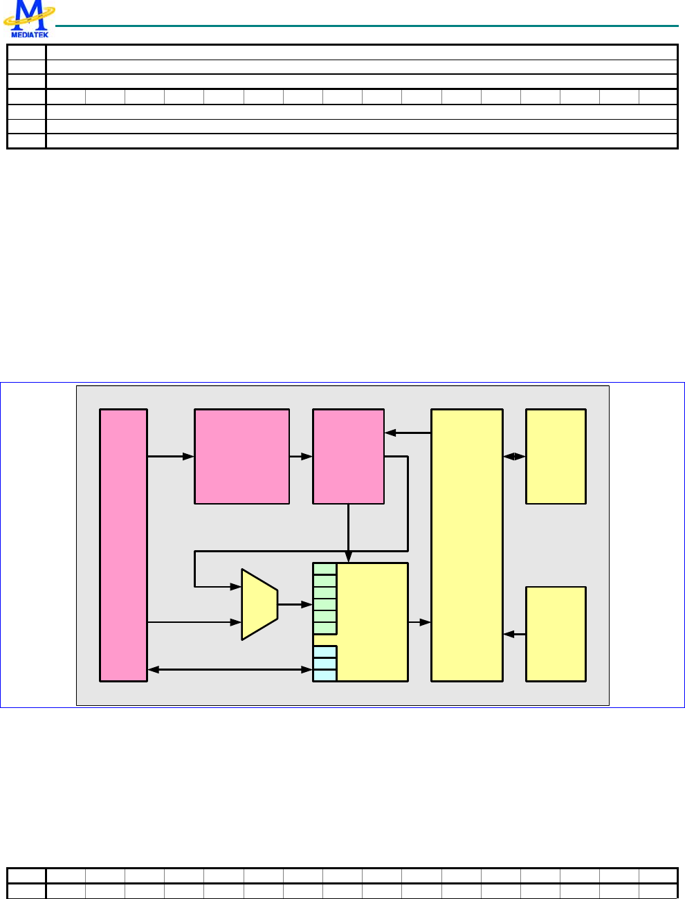
MT6235 GSM/GPRS Baseband Processor Data Sheet Revision 1.02
408/599 MediaTek Inc. Confidential
Name BUF_STA_ADDR_2[31:16]
Type R/W
Reset 0
Bit 15 14 13 12 11 10 9 8 7 6 5 4 3 2 1 0
Name BUF_STA_ADDR_2[15:0]
Type R/W
Reset 0
BUF_STA_ADDR_2 The buffer 2 start address. Buffer 2 is used for storing image data for polygon fill with image
pattern.
7.6.2 Command Queue
7.6.2.1 General Description
To enhance MMI display and gaming experiences, a command queue controllrt is implemented for further offloading of
MCU. If the command queue is enabled, software program has to check the command queue free space before writing to
the command queue data register. Command queue parser will consume command queue entries upon 2D engine requests.
Figure 45 shows the command queue and 2D engine block diagram.
Register
bank
2D
engine
Command queue
APB
slave
Command
parser
DST
memory
read/write
control
SRC
memory
read
control
Figure 58 The command queue and 2D engine block diagram.
7.6.2.2 Register Definitions
MCU APB bus registers are listed as followings. The base address of the command queue controller is 80660000h.
GCMQ+0000h Graphic Command Queue Control Register GCMQ_CON
Bit 31 30 29 28 27 26 25 24 23 22 21 20 19 18 17 16
Name

MT6235 GSM/GPRS Baseband Processor Data Sheet Revision 1.02
409/599 MediaTek Inc. Confidential
Type
Reset
Bit 15 14 13 12 11 10 9 8 7 6 5 4 3 2 1 0
Name WENEN
Type R/WR/W
Reset 0 0
EN command queue enable. When EN is low, the command queue controller will be reset.
WEN command queue in write mode. When WEN is low, the command queue will consume the commands in the queue
if command queue is not empty.
GCMQ+0004h Graphic Command Queue Status Register GCMQ_STA
Bit 31 30 29 28 27 26 25 24 23 22 21 20 19 18 17 16
Name
Type
Reset
Bit 15 14 13 12 11 10 9 8 7 6 5 4 3 2 1 0
Name WR_R
DY FREE
Type RO RO
Reset 0 100000000
FREE number of free command queue entries
WR_RDY ready to receive command, command-write is not allowed when this status bit is 0. Software has to check
this bit before writing command to gcmq.
GCMQ+0008h Graphic Command Queue Data Register GCMQ_DAT
Bit 31 30 29 28 27 26 25 24 23 22 21 20 19 18 17 16
Name ADDR
Type WO
Bit 15 14 13 12 11 10 9 8 7 6 5 4 3 2 1 0
Name DATA
Type WO
ADDR [11:0] write address for mapped 2D engine registers
DATA [15:0] write data for mapped 2D engine registers
GCMQ+000Ch Graphic Command Queue Base Address Register GCMQ_BASE_A
DD
Bit 31 30 29 28 27 26 25 24 23 22 21 20 19 18 17 16
Name BASE_ADD[31:16]
Type R/W
Bit 15 14 13 12 11 10 9 8 7 6 5 4 3 2 1 0
Name BASE_ADD[15:0]
Type R/W
BASE_ADD the starting address of the command queue in the memory.
Note : This field only can be modified while the command queue is not enabled. Otherwise the behavior of the
command queue will be unpredictable.
GCMQ+0010h Graphic Command Queue Buffer Length Register GCMQ_LENGTH
Bit 31 30 29 28 27 26 25 24 23 22 21 20 19 18 17 16

MT6235 GSM/GPRS Baseband Processor Data Sheet Revision 1.02
410/599 MediaTek Inc. Confidential
Name
Type
Bit 15 14 13 12 11 10 9 8 7 6 5 4 3 2 1 0
Name LENGTH
Type R/W
LENGTH[9:0] the occupied space of the command queue in the memory is LENGTH *4Bytes.
Note : This field only can be modified while the command queue is not enabled. Otherwise the behavior of the
command queue will be unpredictable.
GCMQ+0014h Graphic Command Queue Current Register GCMQ_DMA_AD
DR
Bit 31 30 29 28 27 26 25 24 23 22 21 20 19 18 17 16
Name GCMQ_DMA_ADDR
Type RO
Bit 15 14 13 12 11 10 9 8 7 6 5 4 3 2 1 0
Name GCMQ_DMA_ADDR
Type RO
GCMQ_DMA_ADDR the current read or write DMA address of GCMQ.
7.7 Camera Interface
Sensor
(SOC) TG Color Process
ISP
Hue Saturation
Brightness Contrast
Grab
DownSample
MT6235 ISP support VGA/XGA Sensor YUV422/RGB565 interface. Included Functions are Brightness、Contrast、
Saturation、Hue Tuning and Input Image Grab Window. Down Sample Function can be used before image output from ISP.
7.7.1 Register Table
REGISTER ADDRESS REGISTER NAME SYNONYM
CAM + 0000h TG Phase Counter Register CAM_PHSCNT
CAM + 0004h Sensor Size Configuration Register CAM_CAMWIN
CAM + 0008h TG Grab Range Start/End Pixel Configuration Register CAM_GRABCOL
CAM + 000Ch TG Grab Range Start/End Line Configuration Register CAM_GRABROW

MT6235 GSM/GPRS Baseband Processor Data Sheet Revision 1.02
411/599 MediaTek Inc. Confidential
CAM + 0010h Sensor Mode Configuration Register CAM_CSMODE
CAM + 0018h View Finder Mode Control Register CAM_VFCON
CAM + 001Ch Camera Module Interrupt Enable Register CAM_INTEN
CAM + 0020h Camera Module Interrupt Status Register CAM_INTSTA
CAM + 0024h Camera Module Path Config Register CAM_PATH
CAM + 0028h Camera Module Input Address Register CAM_INADDR
CAM + 002Ch Camera Module Output Address Register CAM_OUTADDR
CAM + 0030h Preprocessing Control Register 1 CAM_CTRL1
CAM + 00B8h Y Channel Configuration Register CAM_YCHAN
CAM + 00BCh UV Channel Configuration Register CAM_UVCHAN
CAM + 00C0h Space Convert YUV Register 1 CAM_SCONV1
CAM + 00C4h Space Convert YUV Register 2 CAM_SCONV2
CAM + 0128h Vertical Subsample Control Register CAM_VSUB
CAM + 012Ch Horizontal Subsample Control Register CAM_HSUB
CAM + 0174h Result Window Vertical Size Register RWINV_SEL
CAM + 0178h Result Window Horizontal Size Register RWINH_SEL
CAM + 0180h Camera Interface Debug Mode Control Register CAM_DEBUG
CAM + 0184h Camera Module Debug Information Write Out Destination Address CAM_DSTADDR
CAM + 0188h Camera Module Debug Information Last Transfer Destination Address CAM_LSTADDR
CAM + 018Ch Camera Module Frame Buffer Transfer Out Count Register CAM_XFERCNT
CAM + 0190h Sensor Test Module Configuration Register 1 CAM_MDLCFG1
CAM + 0194h Sensor Test Module Configuration Register 2 CAM_MDLCFG2
CAM + 01D8h Cam Reset Register CAM_RESET
CAM + 01DCh TG Status Register TG_STATUS
CAM + 0248h GMC Debug Register CAM_GMCDEBUG
CAM + 0274h Cam Version Register CAM_VERSION
Table 39 Camera Interface Register Map
7.7.1.1 TG Register Definitions
CAM+0000h TG Phase Counter Register CAM_PHSCNT
Bit 31 30 29 28 27 26 25 24 23 22 21 20 19 18 17 16
Name PCEN CLKE
N CLKP
OL CLKCNT CLKRS CLKFL
Type R/W R/W R/W R/W R/W R/W
Reset 0 0 0 1 0 1
Bit 15 14 13 12 11 10 9 8 7 6 5 4 3 2 1 0
Name HVALI
D_EN PXCL
K_EN PXCL
K_INV PXCL
K_IN
CLKF
L_PO
L TGCL
K_SE
L PIXCNT DLATCH
Type R/W R/W R/W R/W R/W R/W R/W R/W
Reset 0 0 0 0 0 0 1 1
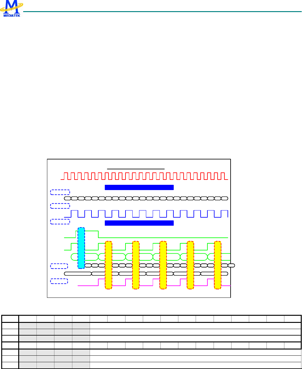
MT6235 GSM/GPRS Baseband Processor Data Sheet Revision 1.02
412/599 MediaTek Inc. Confidential
PCEN TG phase counter enable control
CLKEN Enable sensor master clock (mclk) output to sensor
CLKPOL Sensor master clock polarity control
CLKCNT Sensor master clock frequency divider control.
Sensor master clock will be 52Mhz/CLKCNT, where CLKCNT >=1.
CLKRS Sensor master clock rising edge control
CLKFL Sensor master clock falling edge control
HVALID_EN Sensor hvalid or href enable
PXCLK_EN Sensor clock input monitor.
PXCLK_INV Pixel clock inverse
PXCLK_IN Pixel clock sync enable. If sensor master based clock is 48 Mhz, PXCLK_IN must be enabled.
CLKFL_POL Sensor clock falling edge polarity
TGCLK_SEL Sensor master based clock selection (0: 52 Mhz, 1: 48 Mhz)
PIXCNT Sensor data latch frequency control
DLATCH Sensor data latch position control
Example waveform(CLKCNT=1,CLKRS=0,CLKFL=1,PIXCNT=3,DLATCH=2)
Internal Clock Sync
0101010101010101010101
0123012301230123012301
52Mhz
mclk
pclk
Bclk
CLKCNT=1
CLKRS=0
CLKFL=1 Sensor output signals
ISP output signals
PIXCNT=3
DLATCH=2
hsync
1 2 3
Pixel_ID 4 5
0 1
0
CAM+0004h Sensor Size Configuration Register CAM_CAMWIN
Bit 31 30 29 28 27 26 25 24 23 22 21 20 19 18 17 16
Name PIXELS
Type R/W
Reset fffh
Bit 15 14 13 12 11 10 9 8 7 6 5 4 3 2 1 0
Name LINES
Type R/W
Reset fffh
PIXEL Total input pixel number
LINE Total input line number
MT6235 GSM/GPRS Baseband Processor Data Sheet Revision 1.02
413/599 MediaTek Inc. Confidential
CAM+0008h TG Grab Range Start/End Pixel Configuration Register CAM_GRABCOL
Bit 31 30 29 28 27 26 25 24 23 22 21 20 19 18 17 16
Name START
Type R/W
Reset 0
Bit 15 14 13 12 11 10 9 8 7 6 5 4 3 2 1 0
Name END
Type R/W
Reset 0
START Grab start pixel number
END Grab end pixel number
CAM+000Ch TG Grab Range Start/End Line Configuration Register CAM_GRABRO
W
Bit 31 30 29 28 27 26 25 24 23 22 21 20 19 18 17 16
Name START
Type R/W
Reset 0
Bit 15 14 13 12 11 10 9 8 7 6 5 4 3 2 1 0
Name END
Type R/W
Reset 0
START Grab start line number
END Grab end line number
CAM+0010h Sensor Mode Configuration Register CAM_CSMODE
Bit 31 30 29 28 27 26 25 24 23 22 21 20 19 18 17 16
Name
Type
Reset
Bit 15 14 13 12 11 10 9 8 7 6 5 4 3 2 1 0
Name VSPO
L HSPO
L PWR
ON RST AUTO EN
Type R/W R/W R/W R/W R/W R/W
Reset 0 0 0 0 0 0
VSPOL Sensor Vsync input polarity
HSPOL Sensor Hsync input polarity
AUTO Auto lock sensor input horizontal pixel numbers enable
EN Sensor process counter enable
CAM+0018h View Finder Mode Control Register CAM_VFCON
Bit 31 30 29 28 27 26 25 24 23 22 21 20 19 18 17 16
Name AV_S
YNC_
SEL AV_SYNC_LINENO[11:0]
Type R/W R/W
Reset 0 0
Bit 15 14 13 12 11 10 9 8 7 6 5 4 3 2 1 0
MT6235 GSM/GPRS Baseband Processor Data Sheet Revision 1.02
414/599 MediaTek Inc. Confidential
Name SP_DELAY
SP_M
ODE TAKE
_PIC FR_CON
Type R/W R/W R/W R/W
Reset 0 0 0 0
AV_SYNC_SEL Av_sync start point selection
0 Start from AV_SYNC_LINENO
1 Start from vsync
AV_SYNC_LINENO Av_sync start point line counts
SP_DELAY Still Picture Mode delay
SP_MODE Still Picture Mode
TAKE_PIC Take Picture Request
FR_CON Frame Sampling Rate Control
000 Every frame is sampled
001 One frame is sampled every 2 frames
010 One frame is sampled every 3 frames
011 One frame is sampled every 4 frames
100 One frame is sampled every 5 frames
101 One frame is sampled every 6 frames
110 One frame is sampled every 7 frames
111 One frame is sampled every 8 frames
CAM+001Ch Camera Module Interrupt Enable Register CAM_INTEN
Bit 31 30 29 28 27 26 25 24 23 22 21 20 19 18 17 16
Name VSYN
C_INT
_SEL
Type R/W
Reset 0
Bit 15 14 13 12 11 10 9 8 7 6 5 4 3 2 1 0
Name AV_S
YNC_I
NT
VSYN
C_INT ISPDO
NE IDLE GMCO
VRUN REZO
VRUN EXPD
O
Type R/W R/W R/W R/W R/W R/W R/W
Reset 0 0 0 0 0 0 0
VSYNC_SEL Vsync interrupt selection
0 From Vsync Falling Edge
1 From Vsync Rising Edge
AV_SYNC_INT AV sync interrupt
VSYNC_INT Vsync interrupt
ISPDONE ISP done interrupt enable control
IDLE Returning idle state interrupt enable control
GMCOVRUN GMC port over run interrupt enable control
REZOVRUN Resizer over run interrupt enable control
EXPDO Exposure done interrupt enable control
CAM+0020h Camera Module Interrupt Status Register CAM_INTSTA
Bit 31 30 29 28 27 26 25 24 23 22 21 20 19 18 17 16

MT6235 GSM/GPRS Baseband Processor Data Sheet Revision 1.02
415/599 MediaTek Inc. Confidential
Name
Type
Reset
Bit 15 14 13 12 11 10 9 8 7 6 5 4 3 2 1 0
Name AV_S
YNC_I
NT
VSYN
C_INT ISPD
ONE IDLE GMCO
VRUN REZO
VRUN EXPD
O
Type R/W R R R R R R
Reset 0 0 0 0 0 0 0
CAM+0024h Camera Module Path Config Register CAM_PATH
Bit 31 30 29 28 27 26 25 24 23 22 21 20 19 18 17 16
Name CNTO
N CNTMODE WRITE_LEVEL
BAYE
R10_
OUT
REZ_
DISC
ONN
REZ_
LPF_
OFF
OUTPATH_T
YPE OUTP
ATH_
EN
Type R/W R/W R/W R/W RW RW R/W R/W
Reset 0 0 3 0 0 0 0 0
Bit 15 14 13 12 11 10 9 8 7 6 5 4 3 2 1 0
Name
SWAP
_Y
SWAP
_CBC
R
INDAT
A_FO
RMAT INTYPE_SEL INPATH_RATE
INPAT
H_TH
ROTE
N
INPA
TH_S
EL
Type R/W R/W R/W R/W R/W R/W R/W R/W
Reset 0 0 0 0 1 0 0 0
CNTON Enable Debug Mode Data Transfer Counter
CNTMODE Data Transfer Count Selection
00 sRGB count
01 YCbCr count
REZ_D ISCON N Resizer disconnect enable
REZ_LPF_OFF Resizer low-Pass disable
WRITE_LEVEL Write FIFO threshold level
BAYER10_OUT 10-bit Bayer Format output.
Outpath type should be set to 00.
OUTPATH_TYPE Outpath Type Select
00 Bayer Format
01 ISP output
02 RGB888 Format
03 RGB565 Format
OUTPATH_EN Enable Output to Memory
SWAP_Y YCbCr in Swap Y
SWAP_CBCR YCbCr in Swap Cb Cr
INDATA_FORMAT Sensor Input Data connection
INTYPE_SEL Input type selection
000 Bayer Format
001 YUV422 Format
Default Input Format : UYVY
101 YCbCr422 Format
010 RGB Format
MT6235 GSM/GPRS Baseband Processor Data Sheet Revision 1.02
416/599 MediaTek Inc. Confidential
To enable YUV422/YCbCr422 input fast mode, refer to CAM + 011C bit 20
INPATH_RATE Input type rate control
INPATH_THROTEN Input path throttle enable
INPATH_SEL Input path selection
0 Sensor input
1 From memory
CAM+0028h Camera Module Input Address Register CAM_INADDR
Bit 31 30 29 28 27 26 25 24 23 22 21 20 19 18 17 16
Name CAM_INADDR[31:16]
Type R/W
Reset 0
Bit 15 14 13 12 11 10 9 8 7 6 5 4 3 2 1 0
Name CAM_INADDR[15:0]
Type R/W
Reset 0
CAM_INADDR Input memory address
CAM+002Ch Camera Module Output Address Register CAM_OUTADDR
Bit 31 30 29 28 27 26 25 24 23 22 21 20 19 18 17 16
Name CAM_OUTADDR[31:16]
Type R/W
Reset 0
Bit 15 14 13 12 11 10 9 8 7 6 5 4 3 2 1 0
Name CAM_OUTADDR[15:0]
Type R/W
Reset 0
CAM_OUTADDR Output memory address
7.7.1.2 Color Process Register Definition
CAM+00B8h Y Channel Configuration Register CAM_YCHAN
Bit 31 30 29 28 27 26 25 24 23 22 21 20 19 18 17 16
Name CONTRAST_GAIN
Type R/W
Reset 40h
Bit 15 14 13 12 11 10 9 8 7 6 5 4 3 2 1 0
Name
SIGN_
BRIG
HT_O
FFSE
T
BRIGHT_OFFSET VSUP
_EN UV_L
P_EN CSUP_EDGE_GAIN
Type R/W R/W R/W R/W R/W
Reset 1 0 0 0 10h
CONTRAST_GAIN Y channel contrast gain value
SIGN_BRIGHT_OFFSET Sign bit of Y channel brightness offset value
BRIGHT_OFFSET Y channel brightness offset value
VSUP_EN Vertical Edge color suppression enable
UV_LP_EN UV channel low pass enable
MT6235 GSM/GPRS Baseband Processor Data Sheet Revision 1.02
417/599 MediaTek Inc. Confidential
CSUP_EDGE_GAIN Chroma suppression edge gain value(1.3)
CAM+00BCh UV Channel Configuration Register CAM_UVCHAN
Bit 31 30 29 28 27 26 25 24 23 22 21 20 19 18 17 16
Name U11 V22
Type R/W R/W
Reset 20h 20h
Bit 15 14 13 12 11 10 9 8 7 6 5 4 3 2 1 0
Name SIGN_
U_OF
FSET U_OFFSET SIGN_
V_OF
FSET V_OFFSET
Type R/W R/W R/W R/W
Reset 0 0 0 0
U11 Hue U channel operating value
V11 Hue V channel operating value
SIGN_U_OFFSET Sign bit of Hue U channel offset value
U_OFFSET Hue U channel offset value
SIGN_V_OFFSET Sign bit of Hue V channel offset value
V_OFFSET Hue V channel offset value
CAM+00C0h Space Convert YUV Register 1 CAM_SCONV1
Bit 31 30 29 28 27 26 25 24 23 22 21 20 19 18 17 16
Name Y_GAIN
Type R/W
Reset FFh
Bit 15 14 13 12 11 10 9 8 7 6 5 4 3 2 1 0
Name U_GAIN V_GAIN
Type R/W R/W
Reset 91h B8h
Y_GAIN Space Convert Y channel gain value
U_GAIN Space Convert U channel gain value
V_GAIN Space Convert V channel gain value
CAM+00C4h Space Convert YUV Register 2 CAM_SCONV2
Bit 31 30 29 28 27 26 25 24 23 22 21 20 19 18 17 16
Name Y_OFFSET
Type R/W
Reset 01h
Bit 15 14 13 12 11 10 9 8 7 6 5 4 3 2 1 0
Name U_OFFSET V_OFFSET
Type R/W R/W
Reset 80h 80h
Y_OFFSET Space Convert Y channel offset value
U_OFFSET Space Convert U channel offset value
V_OFFSET Space Convert V channel offset value
CAM+0128h Vertical Subsample Control Register CAM_VSUB
Bit 31 30 29 28 27 26 25 24 23 22 21 20 19 18 17 16
MT6235 GSM/GPRS Baseband Processor Data Sheet Revision 1.02
418/599 MediaTek Inc. Confidential
Name V_SU
B_EN V_SUB_IN
Type R/W R/W
Reset 0 0
Bit 15 14 13 12 11 10 9 8 7 6 5 4 3 2 1 0
Name V_SUB_OUT
Type R/W
Reset 0
V_SUB_EN Vertical sub-sample enable
V_SUB_IN Source vertical size
V_SUB_OUT Sub-sample vertical size
CAM+012ch Horizontal Subsample Control Register CAM_HSUB
Bit 31 30 29 28 27 26 25 24 23 22 21 20 19 18 17 16
Name H_SU
B_EN H_SUB_IN
Type R/W R/W
Reset 0 0
Bit 15 14 13 12 11 10 9 8 7 6 5 4 3 2 1 0
Name H_SUB_OUT
Type R/W
Reset 0
H_SUB_EN Horizontal sub-sample enable
H_SUB_IN Source horizontal size
H_SUB_OUT Sub-sample horizontal size
CAM+0174h Result Window Vertical Size Register RWINV_SEL
Bit 31 30 29 28 27 26 25 24 23 22 21 20 19 18 17 16
Name RWIN
_EN RWINV_START
Type R/W R/W
Reset 0h 0h
Bit 15 14 13 12 11 10 9 8 7 6 5 4 3 2 1 0
Name RWINV_END
Type R/W
Reset 0h
RWIN_EN Result window enable
RWINV_START Result window vertical start line
RWINV_END Result window vertical end line
CAM+0178h Result Window Horizontal Size Register RWINH_SEL
Bit 31 30 29 28 27 26 25 24 23 22 21 20 19 18 17 16
Name RWINH_START
Type R/W
Reset 0h
Bit 15 14 13 12 11 10 9 8 7 6 5 4 3 2 1 0
Name RWINH_END
Type R/W
Reset 0h
RWINH_START Result window horizontal start pixel
MT6235 GSM/GPRS Baseband Processor Data Sheet Revision 1.02
419/599 MediaTek Inc. Confidential
RWINH_END Result window horizontal end pixel
CAM+0180h Camera Interface Debug Mode Control Register CAM_DEBUG
Bit 31 30 29 28 27 26 25 24 23 22 21 20 19 18 17 16
Name
Type
Reset
Bit 15 14 13 12 11 10 9 8 7 6 5 4 3 2 1 0
Name
Type
Reset
CAM+0184h Camera Module Debug Information Write Out
Destination Address CAM_DSTADDR
Bit 31 30 29 28 27 26 25 24 23 22 21 20 19 18 17 16
Name DST_ADD[31:16]
Type R/W
Reset 4000h
Bit 15 14 13 12 11 10 9 8 7 6 5 4 3 2 1 0
Name DST_ADD[15:0]
Type R/W
Reset 0000h
DST_ADD Debug Information Write Output Destination Address
CAM+0188h Camera Module Debug Information Last Transfer
Destination Address CAM_LASTADD
R
Bit 31 30 29 28 27 26 25 24 23 22 21 20 19 18 17 16
Name LAST_ADD[31:16]
Type R/W
Reset 0
Bit 15 14 13 12 11 10 9 8 7 6 5 4 3 2 1 0
Name LAST_ADD[15:0]
Type R/W
Reset 0
LAST_ADD Debug Information Last Transfer Destination Address
CAM+018Ch Camera Module Frame Buffer Transfer Out Count
Register CAM_XFERCNT
Bit 31 30 29 28 27 26 25 24 23 22 21 20 19 18 17 16
Name XFER_COUNT [31:16]
Type RO
Reset 0
Bit 15 14 13 12 11 10 9 8 7 6 5 4 3 2 1 0
Name XFER_COUNT[15:0]
Type RO
Reset 0
XFER_COUNT Pixel Transfer Count per Frame
MT6235 GSM/GPRS Baseband Processor Data Sheet Revision 1.02
420/599 MediaTek Inc. Confidential
CAM+0190h Sensor Test Model Configuration Register 1 CAM_MDLCFG1
Bit 31 30 29 28 27 26 25 24 23 22 21 20 19 18 17 16
Name VSYNC IDLE_PIXEL_PER_LINE
Type R/W R/W
Reset 0 0
Bit 15 14 13 12 11 10 9 8 7 6 5 4 3 2 1 0
Name LINEC
HG_E
N
GRAY
_LEV
EL ON RST STILL PATT
ERN PIXEL_SEL CLK_DIV
Type R/W R/W R/W R/W R/W R/W R/W R/W
Reset 0 0 0 0 0 0 0 0
VSYNC VSYNC high duration in line unit(IDLE_PIXEL_PER_LINE + PIXEL)
IDLE_PIXEL_PER_LINE HSYNC low duration in pixel unit
LINECHG_EN Pattern 0 2 lines change mode enable
GRAY_LEVEL Sensor Model Gray Level Enable. When gray level is enable, increased gray level pattern will
be generated.
ON Enable Sensor Model.
RST Reset Sensor Model
STILL Still picture Mode
PATTERN Sensor Model Test Pattern Selection
PIXEL_SEL Sensor Model output pixel selection.
00 All pixels
01 01 pixel
10 10 pixel
11 00 and 11 pixels
CLK_DIV Pixel_Clock/System_Clock Ratio
CAM +0194h Sensor Test Model Configuration Register 2 CAM_MDLCFG2
Bit 31 30 29 28 27 26 25 24 23 22 21 20 19 18 17 16
Name LINE
Type R/W
Reset 0
Bit 15 14 13 12 11 10 9 8 7 6 5 4 3 2 1 0
Name PIXEL
Type R/W
Reset 0
LINE Sensor Model Line Number
PIXEL Sensor Model Pixel Number (HSYNC high duration in pixel unit)
CAM +01D8h CAM RESET Register CAM_RESET
Bit 31 30 29 28 27 26 25 24 23 22 21 20 19 18 17 16
Name TG_STATUS
Type R
Reset
Bit 15 14 13 12 11 10 9 8 7 6 5 4 3 2 1 0
Name ISP_FRAME_COUNT[7:0] ISP_
RES
ET
MT6235 GSM/GPRS Baseband Processor Data Sheet Revision 1.02
421/599 MediaTek Inc. Confidential
Type RW RW
Reset 0 0
ISP_FRAME_COUNT ISP frame counter
ISP_RESET ISP reset
CAM +01DCh TG STATUS Register TG_STATUS
Bit 31 30 29 28 27 26 25 24 23 22 21 20 19 18 17 16
Name SYN_
VFON LINE_COUNT[11:0]
Type R R
Reset
Bit 15 14 13 12 11 10 9 8 7 6 5 4 3 2 1 0
Name PIXEL_COUNT[11:0]
Type R
Reset
SYN_VFON TG view finder status
LINE_COUNT TG line counter
PIXEL_COUNT TG pixel counter
CAM +0248h CAM GMC DEBUG Register CAM_DEBUG
Bit 31 30 29 28 27 26 25 24 23 22 21 20 19 18 17 16
Name
Type
Reset
Bit 15 14 13 12 11 10 9 8 7 6 5 4 3 2 1 0
Name
Type
Reset
CAM +0274h CAM VERSION Register CAM_VERSION
Bit 31 30 29 28 27 26 25 24 23 22 21 20 19 18 17 16
Name YEAR[16:0]
Type R
Reset
Bit 15 14 13 12 11 10 9 8 7 6 5 4 3 2 1 0
Name MONTH[15:0] DATE[15:0]
Type R R
Reset
YEAR Year ASCII
MONTH Month ASCII
DATE Date ASCII
MT6235 GSM/GPRS Baseband Processor Data Sheet Revision 1.02
422/599 MediaTek Inc. Confidential
8 Audio Front-End
8.1 General Description
The audio front-end essentially consists of voice and audio data paths. Figure 59 shows the block diagram of the audio
front-end. All voice band data paths comply with the GSM 03.50 specification. Mono hands-free audio or external FM
radio playback paths are also provided. The audio stereo path facilitates CD-quality playback, external FM radio, and voice
playback through a headset.
AU_MOUTL
AU_MOUTR
AU_OUT0_P
AU_OUT0_N
AU_FMINL
AU_FMINR
MUXMUX
Stereo-
to-Mono FM/AM radio
chip
Voice
Signal
Audio
Signal
Voice Amp-1
Audio Amp-R
Audio Amp-L
AU_VIN0_P
AU_VIN0_N
AU_VIN1_N
AU_VIN1_P
MUX
Voice
Signal
Audio
LCH-DAC
Audio
RCH-DAC
Voice
DAC
Voice
ADC
PGA
Figure 59 Block diagram of audio front-end
Figure 60 shows the digital circuits block diagram of the audio front-end. The APB register block is an APB peripheral that
stores settings from the MCU. The DSP audio port (DAP) block interfaces with the DSP for control and data
communications. The digital filter block performs filter operations for voice band and audio band signal processing.
The Digital Audio Interface (DAI) block communicates with the System Simulator for FTA or external Bluetooth modules.
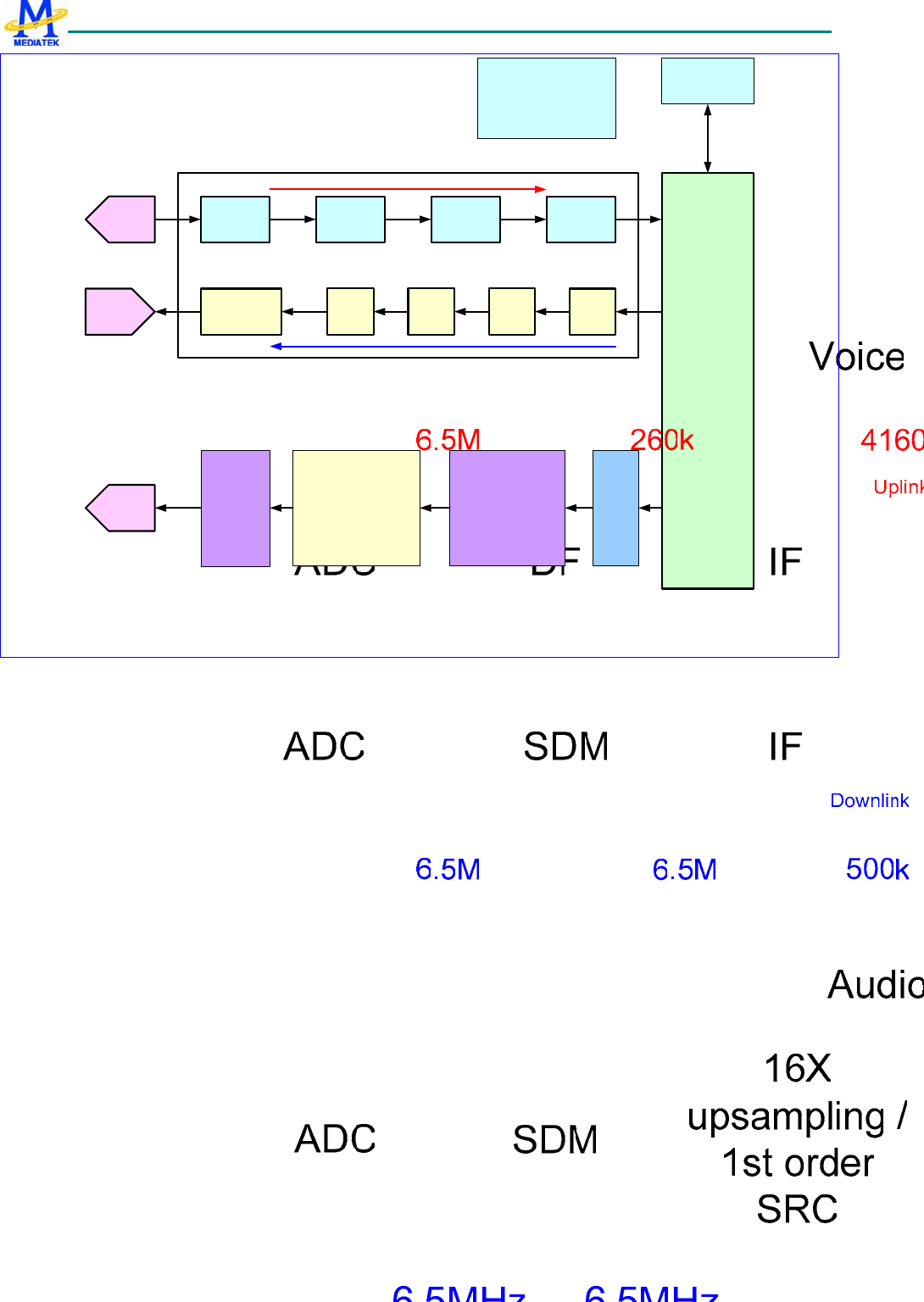
MT6235 GSM/GPRS Baseband Processor Data Sheet Revision 1.02
423/599 MediaTek Inc. Confidential
Figure 60 Block diagram of digital circuits of the audio front-end
To communicate with the external Bluetooth module, the master-mode PCM interface and master-mode I2S/EIAJ interface
are supported. The clock of PCM interface is 256 kHz while the frame sync is 8 kHz. Both long sync and short sync
interfaces are supported. The PCM interface can transmit 16-bit stereo or 32-bit mono 8 kHz sampling rate voice signal.
Figure 61 shows the timing diagram of the PCM interface. Note that the serial data changes when the clock is rising and
is latched when the clock is falling.
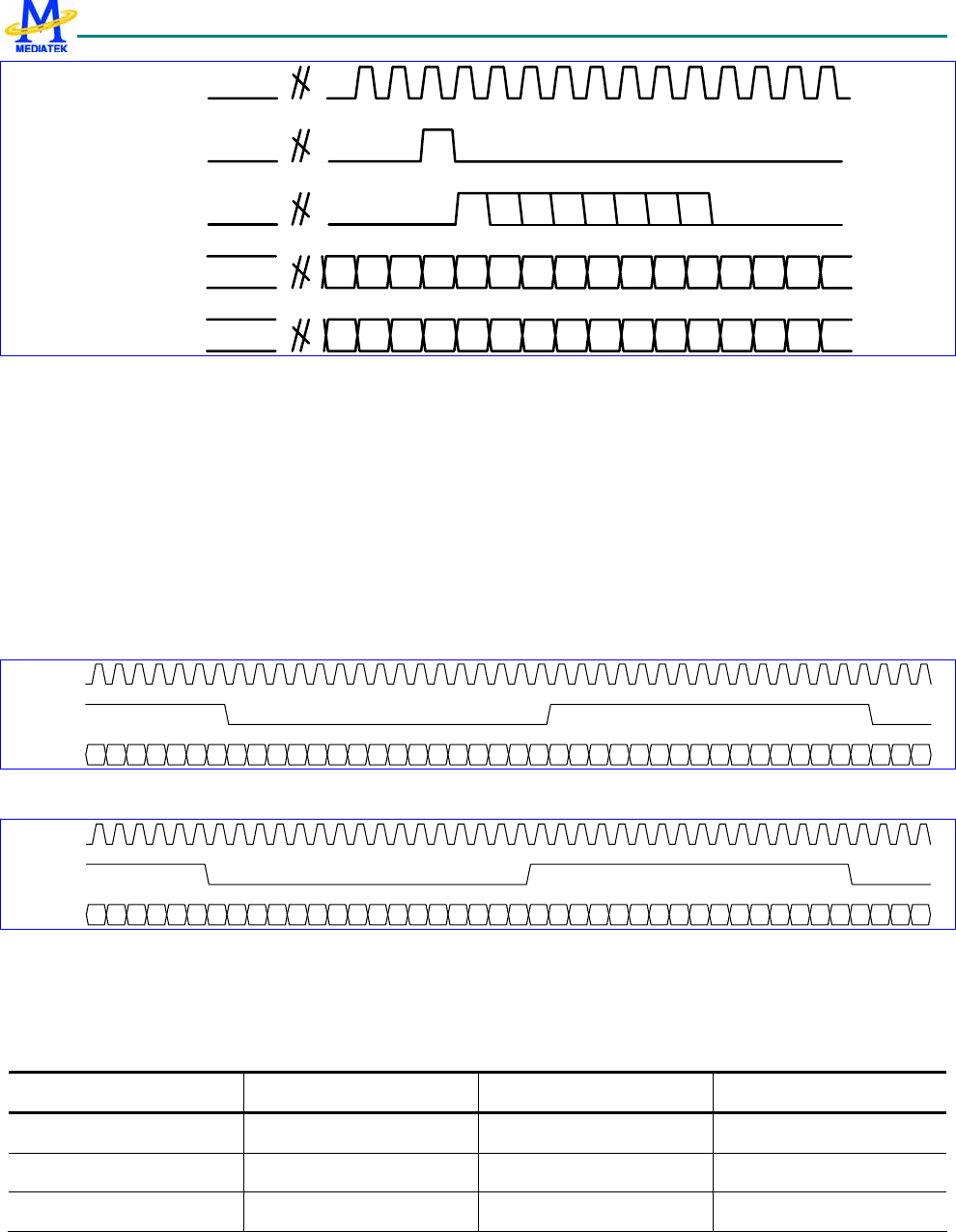
MT6235 GSM/GPRS Baseband Processor Data Sheet Revision 1.02
424/599 MediaTek Inc. Confidential
dai_clk
dai_tx
dai_rx
bt_sync(s)
bt_sync(l)
213103028 2427 2526 222329
213103028 2427 2526 222329
3
3
Figure 61 Timing diagram of Bluetooth application
I2S/EIAJ interface is designed to transmit high quality audio data. Figure 62 and Figure 63 EDI Format 2: I2S (FMT = 1).
illustrate the timing diagram of the two types of interfaces. I2S/EIAJ can support 32 kHz, 44.1 kHz, and 48 kHz sampling
rate audio signals. The clock frequency of I2S/EIAJ can be 32×(sampling frequency), or 64×(sampling frequency). For
example, to transmit a 44.1 kHz CD-quality music, the clock frequency should be 32 × 44.1 kHz = 1.4112 MHz or 64 ×
44.1 kHz = 2.8224 MHz.
I2S/EIAJ interface is not only used for Bluetooth module, but also for external DAC components. Audio data can easily
be sent to the external DAC through the I2S/EIAJ interface.
In this document, the I2S/EIAJ interface is referred to as EDI (External DAC Interface).
EDI_CLK
EDI_WS Left Channel Right Channel
EDI_DAT
6 5 4 3 2 1 0 15 14 13 12 11 10 9 8 7 6 5 4 3 2 1 0 15 14 13 12 11 10 9 8 7 6 5 4 3 2 1 0 15 14 13
Figure 62 EDI Format 1: EIAJ (FMT = 0).
EDI_CLK
EDI_WS Left Channel Right Channel
EDI_DAT
6 5 4 3 2 1 0 15 14 13 12 11 10 9 8 7 6 5 4 3 2 1 0 15 14 13 12 11 10 9 8 7 6 5 4 3 2 1 0 15 14 13
Figure 63 EDI Format 2: I2S (FMT = 1).
8.1.1 DAI, PCM and EDI Pin Sharing
DAI, PCM, and EDI interfaces share the same pins. The pin mapping is listed in Table 40.
PIN NAME DAI PCM EDI
DAI_CLK (OUTPUT) DAI_CLK PCM_CLK EDI_CLK
DAI_TX (OUTPUT) DAI_TX PCM_OUT EDI_DAT
DAI_RX (INPUT) DAI_RX PCM_IN
MT6235 GSM/GPRS Baseband Processor Data Sheet Revision 1.02
425/599 MediaTek Inc. Confidential
BT_SYNC (OUTPUT) - PCM_SYNC EDI_WS
Table 40 Pin mapping of DAI, PCM, and EDI interfaces.
Beside the shared pins, the EDI interface can also use other dedicated pins. With the dedicated pins, PCM and EDI
interfaces can operate at the same time.
EQ 8X up-
sampling
DSP
IO BUS SDM
16X upsampling /
1st Order SRC D/A
32k
44.1k
48k
1X Fs 8X Fs 6.5MHz
EDI
PCM DAI
Shared
Pins
Dedicated
Pins
Figure 64 DAI, PCM, EDI interfaces
8.2 Register Definitions
MCU APB bus registers in audio front-end are listed as follows.
0x820F0000 AFE Voice MCU Control Register AFE_VMCU_CO
N0
Bit 15 14 13 12 11 10 9 8 7 6 5 4 3 2 1 0
Name VAFE
ON
Type R/W
Reset 0
MCU sets this register to start AFE voice operation. A synchronous reset signal is issued, then periodical interrupts of
8-KHz frequency are issued. Clearing this register stops the interrupt generation.
VAFEON Turn on voice front-end operations.
0 off
1 on
0x820F000C AFE Voice Analog-Circuit Control Register 1 AFE_VMCU_CO
N1
Bit 15 14 13 12 11 10 9 8 7 6 5 4 3 2 1 0

MT6235 GSM/GPRS Baseband Processor Data Sheet Revision 1.02
426/599 MediaTek Inc. Confidential
Name VMOD
E4K
VAFE
CLR_
EN
VRSD
ON VDL_IIRMOD
E VUL_IIRMOD
E VDLDITH_VA
L
VDLDI
TH_O
N
Type R/W R/W R/W R/W R/W R/W R/W
Reset 0 0 0 00 00 00 0
Set this register for consistency of analog circuit setting. Suggested value is 80h.
VMODE4K DSP data mode selection
0 8k mode
1 4k mode
VAFECLR_EN Enable signal to reset voice downlink buffer or not while VAFE is powered down.
0 NO reset voice downlink buffer while VAFE is powered down
1 Reset voice downlink buffer while VAFE is powered down
VRSDON Turn on the voice-band redundant signed digit function.
0 1-bit 2-level mode
1 2-bit 3-level mode
VDL_IIRMODE Voice downlink IIR coefficients set selection
00 4k : 90Hz, 8k: 180Hz.
01 4k : 160Hz, 8k: 320Hz.
10 4k : 200Hz, 8k: 400Hz
11 4k : 320Hz, 8k: 640Hz
VUL_IIRMODE Voice uplink IIR coefficients set selection
00 4k : 90Hz, 8k: 180Hz.
01 4k : 160Hz, 8k: 320Hz.
10 4k : 200Hz, 8k: 400Hz
11 4k : 320Hz, 8k: 640Hz
VDITHVAL Voice downlink dither scaling setting
00 1
01 2
10 4
11 8
VDITHON Turn on the voice downlink dither function.
0 Turn off
1 Turn on
0x820F0014 AFE Voice DAI Bluetooth Control Register AFE_VDB_CON
Bit 15 14 13 12 11 10 9 8 7 6 5 4 3 2 1 0
Name
VDAI
BT_C
LR_E
N
EDIO
N VDAI
ON VBTO
N VBTS
YNC VBTSLEN
Type R/W RW R/W R/W R/W R/W
Reset 0 0 0 0 0 000
Set this register for DAI test mode and Bluetooth application.
DAIBT_CLR_EN Enable signal to reset DAIBT buffer or not while VAFE is powered down.

MT6235 GSM/GPRS Baseband Processor Data Sheet Revision 1.02
427/599 MediaTek Inc. Confidential
0 NO reset DAIBT buffer while VAFE is powered down
1 Reset DAIBT buffer while VAFE is powered down
EDION EDI signals are selected as the output of DAI, PCM, EDI shared interface.
0 EDI is not selected. A dedicated EDI interface can be enabled by programming the GPIO selection. Please
refer to GPIO section for details.
1 EDI is selected. VDAION and VBTON are not set.
VDAION Turn on the DAI function.
0 off
1 on
VBTON Turn on the Bluetooth PCM function.
0 off
1 on
VBTSYNC Bluetooth PCM frame sync type
0: short
1: long
VBTSLEN Bluetooth PCM long frame sync length = VBTSLEN+1
0x820F0018 AFE Voice Look-Back mode Control Register AFE_VLB_CON
Bit 15 14 13 12 11 10 9 8 7 6 5 4 3 2 1 0
Name VDSP
BYPA
SS
VDSP
CSMO
DE
VBYP
ASSII
R
VDAPI
NMOD
E
VINTI
NMOD
E
VDEC
INMO
DE
Type R/W R/W R/W R/W R/W R/W
Reset 0 0 0 0 0 0
Set this register for AFE voice digital circuit configuration control. Several loop back modes are implemented for test
purposes. Default values correspond to the normal function mode.
VDSPBYPASS Loopback data won’t be gated by VDSPRDY.
0 Normal Mode
1 Bypass DSP loopback mode
VDSPCSMODE DSP COSIM only, to align DATA.
0 Normal mode
1 DSP COSIM mode
VBYPASSIIR Bypass IIR filter
0 Normal mode
1 Bypass
VDAPINMODE DSP audio port input mode control
0 Normal mode
1 Loop back mode
VINTINMODE interpolator input mode control

MT6235 GSM/GPRS Baseband Processor Data Sheet Revision 1.02
428/599 MediaTek Inc. Confidential
0 Normal mode
1 Loop back mode
VDECINMODE decimator input mode control
0 Normal mode
1 Loop back mode
0x820F0020 AFE Audio MCU Control Register 0 AFE_AMCU_CON0
Bit 15 14 13 12 11 10 9 8 7 6 5 4 3 2 1 0
Name AAFE
ON
Type R/W
Reset 0
MCU sets this register to start AFE audio operation. A synchronous reset signal is issued, and then periodical interrupts of
1/6 sampling frequency are issued. Clearing this register stops the interrupt generation.
AAFEON Turn on audio front-end operations.
0 off
1 on
0x820F0024 AFE Audio Control Register 1 AFE_AMCU_CON1
Bit 15 14 13 12 11 10 9 8 7 6 5 4 3 2 1 0
Name ASDM
CK_P
HASE MONO SEL_I
DWA BYPASS SDM_
MODE GAIN ARAMPSP AMUT
ER AMUT
EL AFS
Type R/W R/W R/W RW R/W R/W R/W R/W R/W R/W
Reset 0 0 1 00 0 0 00 0 0 00
MCU sets this register to inform hardware of the sampling frequency of audio being played back.
ASDMCK_PHASE Phase of Audio SDM Clock. Please set to 0.
SEL_IDWA IDWA function selection.
0 Disable IDWA
1 Enable IDWA
MONO Mono mode select. AFE HW will do (left + right) / 2 operation to the audio sample pair. Thus both right/left
channels DAC will have the same inputs.
0 Disable mono mode.
1 Enable mono mode.
BYPASS To bypass part of the audio hardware path. Bit 1 please always set to 1 to bypass Interpolation.
00 No bypass. The input data rate is 1/4 sampling frequency. For example, if the sampling frequency is 32
KHz, then the input data rate is 8 KHz.
01 Bypass the first stage of interpolation. The input data rate is 1/2 the sampling frequency.
10 Bypass two stages of interpolation. The input data rate is the same as the sampling frequency.
11 Bypass two stages of interpolation and EQ filter. The input data rate is the same as the sampling frequency.
MT6235 GSM/GPRS Baseband Processor Data Sheet Revision 1.02
429/599 MediaTek Inc. Confidential
EQ 8X up-
sampling
DSP
IO BUS SDM
16X upsampling /
1st Order SRC D/A
32k
44.1k
48k
1X Fs 8X Fs 6.5MHz
EDI
Figure 65 Block diagram of the audio path.
SDM_MODE SDM mode control
0 zero extension.
1 sign extension.
GAIN Gain Setting at Audio SDM input, Please set to 1.
0 1X
1 1/2X
ARAMPSP ramp up/down speed selection
00 8, 4096/AFS
01 16, 2048/AFS
10 24, 1024/AFS
11 32, 512/AFS
AMUTER Mute the audio R-channel, with a soft ramp up/down.
0 no mute
1 mute
AMUTEL Mute the audio L-channel, with a soft ramp up/down.
0 no mute
1 mute
AFS Sampling frequency setting.
00 32-KHz
01 44.1-KHz
10 48-KHz
11 reserved
0x820F0028 AFE EDI Control Register AFE_EDI_CON
Bit 15 14 13 12 11 10 9 8 7 6 5 4 3 2 1 0
Name DIR SRC WCYCLE FMT EN
Type R/W R/W R/W R/W R/W
Reset 0 0 01111 0 0
This register is used to control the EDI

MT6235 GSM/GPRS Baseband Processor Data Sheet Revision 1.02
430/599 MediaTek Inc. Confidential
EN Enable EDI. When EDI is disabled, EDI_DAT and EDI_WS hold low.
0 disable EDI
1 enable EDI
FMT EDI format
0 EIAJ
1 I2S
WCYCLE Clock cycle count in a word. Cycle count = WCYCLE + 1, and WCYCLE can be 15 or 31 only. Any other
values result in an unpredictable error.
15 Cycle count is 16.
31 Cycle count is 32.
SRC I2S clock and WS signal source.
0 Internal mode. The clock and word select signals are fed to external device from AFE.
1 External mode. The clock and word select signals are fed externally from the connected device. There is a
buffer control mechanism to deal with the clock mismatch between internal and external clocks.
DIR Serial data bit direction
0 Output mode. Audio data is fed out to the external device.
1 Input mode or recording mode. By this recording mechanism, DSP can do some post processing or voice
memos.
EDI_CLK
EDI_WS Left Channel Right Channel
EDI_DAT 654321015 14 13 12 11 10 987654321015 14 13 12 11 10 9 8 7 6 5 4 3 2 1 0 15 14 13
16 cycles 16 cycles
Figure 66 Cycle count is 16 for I2S format.
EDI_CLK
EDI_WS Left Channel Right Channel
EDI_DAT 654321015 14 13 12 2 1 0 15 14 13 12 2 1 0 15 14 13
32 cycles 32 cycles
Figure 67 Cycle count is 32 for I2S format.
0x820F0030 Audio/Voice DAC SineWave Generator AFE_DAC_TEST
Bit 15 14 13 12 11 10 9 8 7 6 5 4 3 2 1 0
Name VON AON MUTE AMP_DIV FREQ_DIV
Type R/W R/W R/W R/W R/W
Reset 0 0 0 111 0000_0001
This register is only for analog design verification on audio/voice DACs.
VON Makes voice DAC output the test sine wave.
0 Voice DAC inputs are normal voice samples
1 Voice DAC inputs are sine waves

MT6235 GSM/GPRS Baseband Processor Data Sheet Revision 1.02
431/599 MediaTek Inc. Confidential
AON Makes audio DAC output the test sine wave.
0 Audio DAC inputs are normal audio samples
1 Audio DAC inputs are sine waves
MUTE Mute switch.
0 Turn on the sine wave output in this test mode.
1 Mute the sine wave output.
AMP_DIV Amplitude setting.
111 full scale
110 1/2 full scale
101 1/4 full scale
100 1/8 full scale
FREQ_DIV Frequency setting, 1 hot.
0000_0001 1X frequency
0000_0010 2X frequency
0000_0100 3X frequency
0000_1000 4X frequency
0001_0000 8X frequency
0010_0000 16X frequency
0100_0000 32X frequency
1000_0000 64X frequency
0x820F0034 Audio/Voice Interactive Mode Setting AFE_VAM_SET
Bit 15 14 13 12 11 10 9 8 7 6 5 4 3 2 1 0
Name A2V PER_VAL
Type R/W R/W
Reset 0 101
A2V Redirect audio interrupt to voice interrupt. In other words, replace voice interrupt by audio interrupt.
0 [voice interrupt / audio interrupt] Æ [voice / audio]
1 [audio interrupt / no interrupt] Æ [voice / audio]
PER_VAL Counter reset value for audio interrupt generation period setting. For example, by default, the setting = 5
causes interrupt per 6 L/R samples. Changing this value can change the rate of audio interrupt.
0x820F0040~
0x820F00F0 AFE Audio Equalizer Filter Coefficient Register AFE_EQCOEF
Bit 15 14 13 12 11 10 9 8 7 6 5 4 3 2 1 0
Name A
Type WO
Audio front-end provides a 45-tap equalizer filter. The filter is shown below.
DO = (A44 X DI44 + A43 X DI43 … + A1 X DI1 + A0 X DI0)/32768.
DIn is the input data, and An is the coefficient of the filter, which is a 16-bit 2’s complement signed integer. DI0 is the last
input data.

MT6235 GSM/GPRS Baseband Processor Data Sheet Revision 1.02
432/599 MediaTek Inc. Confidential
The coefficient cannot be programmed when the audio path is enabled, or unpredictable noise may be generated. If
coefficient programming is necessary while the audio path is enabled, the audio path must be muted during programming.
After programming is complete, the audio path is not to be resumed (unmated) for 100 sampling periods.
A Coefficient of the filter.
Address Coefficient Address Coefficient Address Coefficient
0x820f0040 A0 0x820f007C A15 0x820f00B8 A30
0x820f0044 A1 0x820f0080 A16 0x820f00BC A31
0x820f0048 A2 0x820f0084 A17 0x820f00C0 A32
0x820f004C A3 0x820f0088 A18 0x820f00C4 A33
0x820f0050 A4 0x820f008C A19 0x820f00C8 A34
0x820f0054 A5 0x820f0090 A20 0x820f00CC A35
0x820f0058 A6 0x820f0094 A21 0x820f00D0 A36
0x820f005C A7 0x820f0098 A22 0x820f00D4 A37
0x820f0060 A8 0x820f009C A23 0x820f00D8 A38
0x820f0064 A9 0x820f00A0 A24 0x820f00DC A39
0x820f0068 A10 0x820f00A4 A25 0x820f00E0 A40
0x820f006C A11 0x820f00A8 A26 0x820f00E4 A41
0x820f0070 A12 0x820f00Ac A27 0x820f00E8 A42
0x820f0074 A13 0x820f00B0 A28 0x820f00EC A43
0x820f0078 A14 0x820f00B4 A29 0x820f00F0 A44
Table 41
0x820F0100 AFE AGC Control Register 0 AFE_VAGC_CON0
Bit 15 14 13 12 11 10 9 8 7 6 5 4 3 2 1 0
Name MINPGAGAIN PGAGAIN
FRFL
G RATK
FLG SATK
FLG AGCO
N
Type R/W R/W R/W R/W R/W R/W
Reset 001010 101000 0 1 1 1
This register sets the control signals for AGC.
AGCON Switch of the AGC
0 Off
1 On
SATKFLG Sample Attack Flag
0 off
1 on
RATKFLG RMS Attack Flag
0 off
1 on
FRFLG Free Release Flag
0 off
1 on
PGAGAIN PGA gain settings (from -43dB to 20 dB), it is also the maximum PGA gain settings while AGC is on.

MT6235 GSM/GPRS Baseband Processor Data Sheet Revision 1.02
433/599 MediaTek Inc. Confidential
000000 -43dB
000001 -42dB
|
111110 19dB
111111 20dB
MINPGAGAIN minima PGA gain settings (from -43 to 20 dB). PGA gain is always larger than MINPGAGAIN.
000000 -43dB
000001 -42dB
|
111110 19dB
111111 20dB
0x820F0104 AFE AGC Control Register 1 AFE_VAGC_CON1
Bit 15 14 13 12 11 10 9 8 7 6 5 4 3 2 1 0
Name VSDM
_GAIN VAGC
_SEL
VAGC
_CTR
L ECNTRRLZS ECNTRRLZF ECNTRATK
Type R/W R/W R/W R/W R/W R/W
Reset 0 1 0 1100 1100 1000
This register sets the control signals for AGC and VSDM.
VSDM_GAIN Input gain before Voice SDM
0 1/2 X
1 1X
VAGC_SEL Selection of AGC output.
0 bypass AGC.
1 AGC compensation on.
VAGC_CTRL Selection the AGC gain control master.
0 Control by AFE.
1 Control by DSP.
ECNTRATK Attack counter, control attack speed.(unit: N samples@52kHz ). Attach will be triggered if N samples
amplitude exceed attack threshold (ENTHDATK)
0 always attack, please don’t set to this values.
1~15 N=1~15
ECNTRRLZF Fast release counter, control fast release speed.(unit: N samples@52kHz ). Release will be triggered if N
samples amplitude lower than slow release threshold (ENTHDRLS)
0 1
1 3
2 7
3 15

MT6235 GSM/GPRS Baseband Processor Data Sheet Revision 1.02
434/599 MediaTek Inc. Confidential
4 31
5 63
6 127
7 255
8 511
9 1023
10 2043
11 4095
12 8191
13 16383
14 32767
15 65535
ECNTRRLZS Slow release counter, control slow release speed.(unit: N samples@52kHz ). Release will be triggered if
N samples amplitude lower than hysteresis threshold (ENTHDHYS)
0 1
1 3
2 7
3 15
4 31
5 63
6 127
7 255
8 511
9 1023
10 2043
11 4095
12 8191
13 16383
14 32767
15 65535
0x820F0108 AFE AGC Control Register 2 AFE_VAGC_CON2
Bit 15 14 13 12 11 10 9 8 7 6 5 4 3 2 1 0
Name ERMSFBATTF ERMSFBATTR ERMSFBF ERMSFBR
Type R/W R/W R/W R/W
Reset 1010 0100 1011 0101
This register sets the control signals for AGC.
ERMSFBR RMS rising factor. The larger the number; the slower the signal energy estimation.
0 1x RMS power estimation.
1 2x RMS power estimation.
2 4x RMS power estimation.

MT6235 GSM/GPRS Baseband Processor Data Sheet Revision 1.02
435/599 MediaTek Inc. Confidential
3 8x RMS power estimation.
|
14 16384x RMS power estimation.
15 32768x RMS power estimation.
ERMSFBF RMS falling factor. The larger the number; the slower the signal energy estimation.
0 1x RMS power estimation.
1 2x RMS power estimation.
2 4x RMS power estimation.
3 8x RMS power estimation.
|
14 16384x RMS power estimation.
15 32768x RMS power estimation.
ERMSFBATTR RMS for Attack rising factor. The larger the number; the slower the signal energy estimation.
0 1x RMS power estimation.
1 2x RMS power estimation.
2 4x RMS power estimation.
3 8x RMS power estimation.
|
14 16384x RMS power estimation.
15 32768x RMS power estimation.
ERMSFBATTF RMS for Attack falling factor. The larger the number; the slower the signal energy estimation.
0 1x RMS power estimation.
1 2x RMS power estimation.
2 4x RMS power estimation.
3 8x RMS power estimation.
|
14 16384x RMS power estimation.
15 32768x RMS power estimation.
0x820F010C AFE AGC Control Register 3 AFE_VAGC_CON3
Bit 15 14 13 12 11 10 9 8 7 6 5 4 3 2 1 0
Name EGAINCOMP_CSS EGAINCOMP_CSM EGAINCOMP_CSF EGAINCOMP_FC_T
HD EGAINCOMP
_LOWER EGAINCOMP
_UPPER
Type R/W R/W R/W R/W R/W R/W
Reset 001 011 011 101 01 01
This register sets the control signals for AGC.

MT6235 GSM/GPRS Baseband Processor Data Sheet Revision 1.02
436/599 MediaTek Inc. Confidential
Figure 68 Gain Compensation procedures.
EGAINCOMP_UPPER Gain compensation upper threshold, 32768 = 0dB (Figure 68 Gain Compensation
procedures.)
00 33095
01 33423
10 33751
11 34078
EGAINCOMP_LOWER Gain compensation lower threshold, 32768 = 0dB (Figure 68 Gain Compensation
procedures.)
00 32440
01 32112
10 31784
11 31457
EGAINCOMP_FC_THD Gain compensation convergence threshold (Figure 68 Gain Compensation procedures.).
000 34406
001 36044
010 37683
011 39321
100 40960
101 42598
110 44236
111 45875
EGAINCOMP_FC_CSF Gain compensation fast converge speed. (While compensation gain is 0.3dB far from 32768,
the convergence speed is fast)
000 31948 (8X)
001 31129 (7X)
010 30310 (6X)
011 29491 (5X)
MT6235 GSM/GPRS Baseband Processor Data Sheet Revision 1.02
437/599 MediaTek Inc. Confidential
100 28672 (4X)
101 27852 (3X)
110 27033 (2X)
111 26214 (1X)
EGAINCOMP_FC_CSM Gain compensation converge speed middle. (While compensation gain is 0.15dB ~ 0.3dB
from 32768, the convergence speed is middle)
000 32686 (8X)
001 32604 (7X)
010 32552 (6X)
011 32440 (5X)
100 32358 (4X)
101 32276 (3X)
110 32194 (2X)
111 32112 (1X)
EGAINCOMP_FC_CSS Gain compensation converge speed slow. (While compensation gain is inside 0.15dB from
32768, the convergence speed is slow)
000 32751 (8X)
001 32735 (7X)
010 32718 (6X)
011 32702 (5X)
100 32686 (4X)
101 32669 (3X)
110 32653 (2X)
111 32636 (1X)
0x820F0110 AFE AGC Control Register 4 AFE_VAGC_CON4
Bit 15 14 13 12 11 10 9 8 7 6 5 4 3 2 1 0
Name ENTHDATKRMS ENTHDATK ESRELWINWIDTH1
Type R/W R/W R/W
Reset 000100 000001 1000
This register sets the control signals for AGC.
ESRELWINWIDTH1 speech release window width for strong VAD
0 10 @ 52kHz samples
1 20 @ 52kHz samples
2 40 @ 52kHz samples
3 80 @ 52kHz samples
4 160 @ 52kHz samples
5 325 @ 52kHz samples
6 650 @ 52kHz samples
7 1300 @ 52kHz samples
MT6235 GSM/GPRS Baseband Processor Data Sheet Revision 1.02
438/599 MediaTek Inc. Confidential
8 2600 @ 52kHz samples
9 5200 @ 52kHz samples
10 10000 @ 52kHz samples
11 15000 @ 52kHz samples
12 20000 @ 52kHz samples
13 25000 @ 52kHz samples
14 30000 @ 52kHz samples
15 32767 @ 52kHz samples
ENTHDATK Attack threshold
[0~63] is map to [-63~0]dB FS
ENTHDATKRMS RMS attack threshold
[0~63] is map to [-63~0]dB FS
0x820F0114 AFE AGC Control Register 5 AFE_VAGC_CON5
Bit 15 14 13 12 11 10 9 8 7 6 5 4 3 2 1 0
Name ENTHDRLS ENTHDHYS ESRELWINWIDTH2
Type R/W R/W R/W
Reset 001101 000111 1000
This register sets the control signals for AGC.
ESRELWINWIDTH2 speech release window width for weak VAD
0 10 @ 52kHz samples
1 20 @ 52kHz samples
2 40 @ 52kHz samples
3 80 @ 52kHz samples
4 160 @ 52kHz samples
5 325 @ 52kHz samples
6 650 @ 52kHz samples
7 1300 @ 52kHz samples
8 2600 @ 52kHz samples
9 5200 @ 52kHz samples
10 10000 @ 52kHz samples
11 15000 @ 52kHz samples
12 20000 @ 52kHz samples
13 25000 @ 52kHz samples
14 30000 @ 52kHz samples
15 32767 @ 52kHz samples
ENTHDHYS Hysteresis threshold
[0~63] is map to [-63~0]dB FS
ENTHDRLS Slow release threshold
MT6235 GSM/GPRS Baseband Processor Data Sheet Revision 1.02
439/599 MediaTek Inc. Confidential
[0~63] is map to [-63~0]dB FS
0x820F0118 AFE AGC Control Register 6 AFE_VAGC_CON6
Bit 15 14 13 12 11 10 9 8 7 6 5 4 3 2 1 0
Name EPATTLIMITER PATTRELD
NATK
FLG
PATT
RELF
LG ENTHDNOZ
Type R/W R/W R/W R/W R/W
Reset 0100 0000 1 1 111101
This register sets the control signals for AGC.
ENTHDNOZ Idle threshold
[0~63] is map to [-63~0]dB FS
PATTRELFLG post attack/release flag
0 off
1 on
NATKFLG noise adaptive attenuation enable attack flag
0 off
1 on
PATTRELD Post attack/release latency
0~15 is map to 0~15 sample @260kHz sampling rate
EPATTLIMITER Post attack limiter
[0,15] is map to [0,-7.5dBFs], the spacing is 0.5dB
8.3 DSP Register Definitions
0x640 AFE Voice Uplink Data Register 0 AFE_VUL_DAT0
Bit 15 14 13 12 11 10 9 8 7 6 5 4 3 2 1 0
Name VUL_DAT0
Type RO
Reset 0
Voice band uplink transmission data register 0. The content of this register is updated by uplink digital filter outputs. This
register is read by DSP in an 8K ISR.
0x641 AFE Voice Uplink Data Register 1 AFE_VUL_DAT1
Bit 15 14 13 12 11 10 9 8 7 6 5 4 3 2 1 0
Name VUL_DAT1
Type RO
Reset 0
MT6235 GSM/GPRS Baseband Processor Data Sheet Revision 1.02
440/599 MediaTek Inc. Confidential
Voice band uplink transmission data register 1. The content of this register is updated by uplink digital filter outputs. This
register is read by DSP in an 8K ISR if VBYPASSIIR of AFE_LB_CON is set.
0x642 AFE Voice Downlink Data Register 0 AFE_VDL_DAT0
Bit 15 14 13 12 11 10 9 8 7 6 5 4 3 2 1 0
Name VDL_DAT0
Type WO
Reset 0
Voice band downlink receiving data register 0. This register is written by DSP in an 8K ISR. The content of this register
is used as downlink digital filter inputs.
0x643 AFE Voice Downlink Data Register 1 AFE_VDL_DAT1
Bit 15 14 13 12 11 10 9 8 7 6 5 4 3 2 1 0
Name VDL_DAT1
Type WO
Reset 0
Voice band downlink receiving data register 1. This register is written by DSP in an 8K ISR if VBYPASSIIR of
AFE_VLB_CON is set. The content of this register is used as downlink digital filter inputs.
0x644 AFE Voice DAI Bluetooth Transmission Data Register
0 AFE_VDBTX_DA
T0
Bit 15 14 13 12 11 10 9 8 7 6 5 4 3 2 1 0
Name VDBTX_DAT0
Type WO
Reset 0
DAI Bluetooth transmission data register 0. This register is written by DSP in an 8K ISR if the Bluetooth function is
turned on. The content of this register is shifted out to the Bluetooth interface.
0x645 AFE Voice DAI Bluetooth Transmission Data Register
1 AFE_VDBTX_DA
T1
Bit 15 14 13 12 11 10 9 8 7 6 5 4 3 2 1 0
Name VDBTX_DAT 1
Type WO
Reset 0
DAI Bluetooth transmission data register 1. This register is written by DSP in an 8K ISR if the corresponding DAI test is
set or the Bluetooth function is turned on. The content of this register is shifted out to the SS or Bluetooth interface.
0x646 AFE Voice DAI Bluetooth Receiving Data Register 0 AFE_VDBRX_D
AT0
Bit 15 14 13 12 11 10 9 8 7 6 5 4 3 2 1 0
Name VDBRX_DAT 0
Type RO
Reset 0
MT6235 GSM/GPRS Baseband Processor Data Sheet Revision 1.02
441/599 MediaTek Inc. Confidential
DAI Bluetooth receiving data register 0. This register is read by DSP in an 8K ISR if the Bluetooth function is turned on.
The content of this register is shifted in from the Bluetooth interface.
0x647 AFE Voice DAI Bluetooth Receiving Data Register 1 AFE_VDBRX_DA
T1
Bit 15 14 13 12 11 10 9 8 7 6 5 4 3 2 1 0
Name VDBRX_DAT 1
Type RO
Reset 0
DAI Bluetooth receiving data register 1. This register is read by DSP in an 8K ISR if the corresponding DAI test is set or
the Bluetooth function is turned on. The content of this register is shifted in from the SS or Bluetooth module.
0x648 AFE Voice DAI Bluetooth Control Register AFE_VDSP_CON
Bit 15 14 13 12 11 10 9 8 7 6 5 4 3 2 1 0
Name VDSP
_RDY
Type R/W
Reset 0
DSP sets this register to inform hardware that it is ready for data transmission. In DAI test modes, DSP starts a test by
setting vdsp_rdy when speech samples are required or are ready. In normal mode, the DSP asserts this bit to ungate the
downlink path data. Otherwise, the downlink data remains zero.
VDSP_RDY Ready indication to start the voice band data path.
0 DSP data is not ready.
1 DSP data is ready.
0x649 AFE I2S Input Mode Buffer AFE_EDI_RDATA
Bit 15 14 13 12 11 10 9 8 7 6 5 4 3 2 1 0
Name RDATA
Type RO
Reset 0
This is the register for reading I2S input data. For each audio interrupt, DSP should read 6 pairs (total 12 reads) of the input
data. If DSP is reading too fast or too slow, there is a 2-word margin for repeating or dropping the samples that DSP read
rate can not match-up with audio front end.
DATA Read data port. Left channel first, and then right channel.
0x64A AFE AGC DSP Control AEF_VAGC_VAD
Bit 15 14 13 12 11 10 9 8 7 6 5 4 3 2 1 0
Name NADPATT_DBGAIN
NGAT
EOPE
N VAD2 VAD
Type R/W R/W R/W R/W
Reset 000000 0 0 0
This register is for DSP to read/write the parameter of AGC.
MT6235 GSM/GPRS Baseband Processor Data Sheet Revision 1.02
442/599 MediaTek Inc. Confidential
VAD Strong VAD flag
0 off
1 on
VAD2 Weak VAD flag
0 off
1 on
NGATEOPEN noise gate flag
0 noise gate close
1 noise gate open
NADPATT_DBGAIN noise adaptive attenuation DB gain
[0,63] 0~63dB
0x64B AFE AGC DSP Control AEF_VAGC_CNTR
Bit 15 14 13 12 11 10 9 8 7 6 5 4 3 2 1 0
Name CNTR_REL_FF TONE
FLG
Type R/W R/W
Reset 000000000000000 0
This register is for DSP to read/write the parameter of AGC.
TONEFLG Tone flag
0 off
1 on
CNTR_REL_FF Proceed very fast release if N samples value smaller than the fast release threshold
0~32767 N=0~32767 @ 52kHz sampling rate.
0x64C AFE AGC DSP Control1 AEF_VAGC_CNTR1
Bit 15 14 13 12 11 10 9 8 7 6 5 4 3 2 1 0
Name NCNTRRLZ NCNTRATK
Type RO RO
Reset 0000_0000 0000_0000
This register is for DSP to read the parameter of AGC.
NCNTRRLZ Release counter (in unit of 52kHz/256 sampling rate).
NCNTRATK Attack counter (in unit of 52kHz/16 sampling rate).
0x64D AFE AGC DSP Control AEF_VAGC_STETE
Bit 15 14 13 12 11 10 9 8 7 6 5 4 3 2 1 0
Name SSTATE FGAINDB
Type RO RO
Reset 00 000000
MT6235 GSM/GPRS Baseband Processor Data Sheet Revision 1.02
443/599 MediaTek Inc. Confidential
This register is for DSP to read the parameter of AGC.
FGAINDB Current PGA gain (from 0 to 63 dB).
SSTATE Current AGC state.
0x64E AFE AGC DSP Control AEF_VAGC_RMS
Bit 15 14 13 12 11 10 9 8 7 6 5 4 3 2 1 0
Name SIGRMSATT SIGRMS
Type RO RO
Reset 00000000 00000000
This register is for DSP to read the parameter of AGC.
SIGRMS RMS of signal
SIGRMSATT RMS of signal for attack usage
0x64F AFE Audio Control Register AFE_ADSP_CON
Bit 15 14 13 12 11 10 9 8 7 6 5 4 3 2 1 0
Name ARST
_FIFO ADSP
_RDY
Type R/W R/W
Reset 0 0
DSP sets this register to inform hardware that it is ready for data transmission. DSP asserts this bit to ungate the audio
path data. Otherwise, the audio path data remains zero.
ADSP_RDY Ready to ungate audio data path.
ARST_FIFO Reset the FIFO read/write pointers and the interrupt counter.
0x650 AFE Audio Right-Channel Data Register 0 AFE_ARCH_DA
T0
Bit 15 14 13 12 11 10 9 8 7 6 5 4 3 2 1 0
Name ARCH_DAT0
Type W
Reset 0
Audio right channel data register 0. The content of this register is used as the right channel digital filter inputs.
The frequency of audio interrupts varies with the audio sampling rate and bypass setting, and can be 1/6 the audio sampling
rate, or 1/12 the sampling rate, or 1/24 the sampling rate. The frequency depends on the setting of BYPASS.
z BYPASS = 00b: 1/24 the sampling rate.
z BYPASS = 01b: 1/12 the sampling rate.
z BYPASS = 10b: 1/6 the sampling rate.
z BYPASS = 11b: 1/6 the sampling rate.
For DSP, 6 audio samples are written when an interrupt is received.
MT6235 GSM/GPRS Baseband Processor Data Sheet Revision 1.02
444/599 MediaTek Inc. Confidential
0x651 AFE AGC DSP GAIN AFE_VAGC_GAIN
Bit 15 14 13 12 11 10 9 8 7 6 5 4 3 2 1 0
Name VAGC_GAIN
Type R/W
Reset 000000
AGC Gain setting by AGC. It is only validate while VAGC_CTRL is set to 1.
0x658 AFE Audio Left-Channel Data Register 0 AFE_ALCH_DAT
0
Bit 15 14 13 12 11 10 9 8 7 6 5 4 3 2 1 0
Name ALCH_DAT0
Type W
Reset 0
Audio left channel data register 0. The content of this register is used as the left channel digital filter inputs.
8.4 Programming Guide
Several cases – including speech call, voice memo record, voice memo playback, melody playback and DAI tests – requires
that partial or the whole audio front-end be turned on.
The following are the recommended voice band path programming procedures to turn on audio front-end:
1. MCU programs the AFE_VMCU_CON1, AFE_DAI_CON, AFE_VAGC_CON1, AFE_VAGC_CON2,
AFE_VAGC_CON3, AFE_VAGC_CON4, AFE_VAGC_CON5, AFE_VAGC_CON6, AFE_VLB_CON,
AFE_VAG_CON, AFE_VAC_CON0, AFE_VAC_CON1 and AFE_VAPDN_CON registers for specific
operation modes. Refer also to the analog chip interface specification.
2. MCU clears the VAFE bit of the PDN_CON2 register to ungate the clock for the voice band path. Refer to the
software power down control specification.
3. MCU sets AFE_VMCU_CON0 to start operation of the voice band path.
The following are the recommended voice band path programming procedures to turn off audio front-end:
1. MCU programs AFE_VAPDN_CON to power down the voice band path analog blocks.
2. MCU clears AFE_VMCU_CON0 to stop operation of the voice band path.
3. MCU sets VAFE bit of PDN_CON2 register to gate the clock for the voice band path.
The following are the recommended audio band path programming procedures to turn on audio front-end:
1. MCU programs the AFE_AMCU_CON1, AFE_AAG_CON, AFE_AAC_CON, and AFE_AAPDN_CON
registers for specific configurations. Refer also to the analog chip interface specification.

MT6235 GSM/GPRS Baseband Processor Data Sheet Revision 1.02
445/599 MediaTek Inc. Confidential
2. MCU clears the AAFE bit of the PDN_CON2 register to ungate the clock for the audio band path. Refer
to the software power down control specification.
3. MCU sets AFE_AMCU_CON0 to start operation of the audio band path.
The following are the recommended audio band path programming procedures to turn off audio front-end:
1. MCU programs the AFE_AAPDN_CON to power down the audio band path analog blocks. Refer
also to the analog block specification for further details.
2. MCU clears AFE_AMCU_CON0 to stop operation of the audio band path.
3. MCU sets the AAFE bit of the PDN_CON2 register to gate the clock for the audio band path.

MT6235 GSM/GPRS Baseband Processor Data Sheet Revision 1.02
446/599 MediaTek Inc. Confidential
9 Radio Interface Control
This chapter details the MT6235 interface control with the radio part of a GSM terminal. Providing a comprehensive
control scheme, the MT6235 radio interface consists of Baseband Serial Interface (BSI), Baseband Parallel Interface (BPI),
Automatic Power Control (APC) and Automatic Frequency Control (AFC), together with APC-DAC and AFC-DAC.
9.1 Baseband Serial Interface
The Baseband Serial Interface controls external radio components. A 3-wire serial bus transfers data to RF circuitry for
PLL frequency change, reception gain setting, and other radio control purposes. In this unit, BSI data registers are
double-buffered in the same way as the TDMA event registers. The user writes data into the write buffer and the data is
transferred from the write buffer to the active buffer when a TDMA_EVTVAL signal (from the TDMA timer) is pulsed.
Each data register BSI_Dn_DAT is associated with one data control register BSI_Dn_CON, where n denotes the index.
Each data control register identifies which events (signaled by TDMA_BSISTRn, generated by the TDMA timer) trigger
the download process of the word in register BSI_Dn_DAT. The word and its length (in bits) is downloaded via the serial
bus. A special event is triggered when the IMOD flag is set to 1: it provides immediate download process without
software programming the TDMA timer.
If more than one data word is to be downloaded on the same BSI event, the word with the lowest address among them is
downloaded first, followed by the next lowest and so on.
The total download time depends on the word length, the number of words to download, and the clock rates. The
programmer must space the successive event to provide enough time. If the download process of the previous event is not
complete before a new event arrives, the latter is suppressed.
The unit has four output pins: BSI_CLK is the output clock, BSI_DATA is the serial data port, and BSI_CS0 and BSI_CS1
are the select pins for 2 external components. BSI_CS1 is multiplexed with another function. Please refer to GPIO table
for more detail.
In order to support bi-directional read and write operations of the RF chip, software can directly write values to BSI_CLK,
BSI_DATA and BSI_CS by programming the BSI_DOUT register. Data from the RF chip can be read by software via the
register BSI_DIN. If the RF chip interface is a 3-wire interface, then BSI_DATA is bi-directional. Before software can
program the 3-wire behavior, the BSI_IO_CON register must be set. An additional signal path from GPIO accommodates
RF chips with a 4-wire interface.
The block diagram of the BSI unit is as depicted in Figure 69.

MT6235 GSM/GPRS Baseband Processor Data Sheet Revision 1.02
447/599 MediaTek Inc. Confidential
z
Control
Write
buffer
Active
buffer
Serial port
control
SETENV
IMOD
BSI_CS0
BSI_DATA
BSI_CLK
BSI_CS1 (GPIO)
BSI Unit
TDMA_BSISTR (0~15)
(from TDMA timer)
TDMA_EVTVAL
(from TDMA timer)
APB
BUS BSI_DIN_GPIO (read from RFIC)
(GPIO)
Figure 69 Block diagram of BSI unit.
z
BSI_CSx
(long)
BSI_CLK
(true)
BSI_CSx
(short)
BSI_DATA
BSI_CLK
(invert)
LSBMSB
Figure 70 Timing characteristic of BSI interface.
9.1.1 Register Definitions
BSI+0000h BSI control register BSI_CON
Bit 15 14 13 12 11 10 9 8 7 6 5 4 3 2 1 0
Name SETE
NV EN1_
POL EN1_
LEN EN0_
POL EN0_
LEN IMOD CLK_SPD CLK_
POL
Type R/W R/W R/W R/W R/W WO R/W R/W
Reset 0 0 0 0 0 N/A 0 0
This register is the control register for the BSI unit. The register controls the signal type of the 3-wire interface.
CLK_POL Controls the polarity of BSI_CLK. Refer to Figure 70.
0 True clock polarity
1 Inverted clock polarity
CLK_SPD Defines the clock rate of BSI_CLK. The 3-wire interface provides 4 choices of data bit rate. The default is
52/2 MHz.
00 52/2 MHz
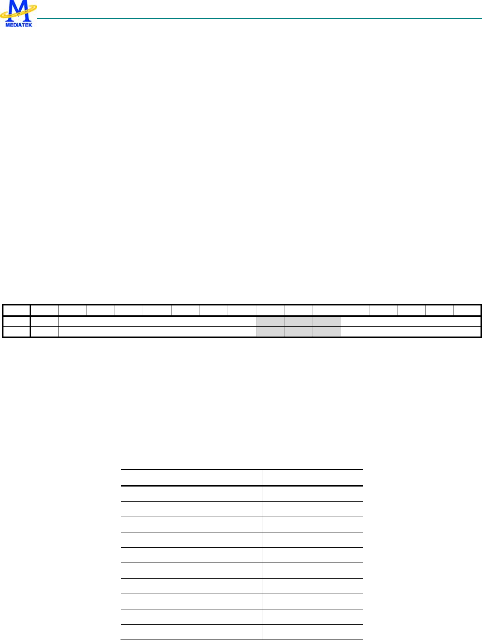
MT6235 GSM/GPRS Baseband Processor Data Sheet Revision 1.02
448/599 MediaTek Inc. Confidential
01 52/4 MHz
10 52/6 MHz
11 52/8 MHz
IMOD Enables immediate mode. If the user writes 1 to the flag, the download is triggered immediately without waiting
for the timer events. The words for which the register event ID equals 1Fh are downloaded following this signal.
This flag is write-only. The immediate write is exercised only once: the programmer must write the flag again to
invoke another immediate download. Setting the flag does not disable the other events from the timer; the
programmer can disable all events by setting BSI_ENA to all zeros.
ENX_LEN Controls the type of signals BSI_CS0 and BSI_CS1. Refer to Figure 69.
0 Long enable pulse
1 Short enable pulse
ENX_POL Controls the polarity of signals BSI_CS0 and BSI_CS1.
0 True enable pulse polarity
1 Inverted enable pulse polarity
SETENV Enables the write operation of the active buffer.
0 The user writes to the write buffer. The data is then latched in the active buffer after TDMA_EVTVAL is
pulsed.
1 The user writes data directly to the active buffer.
BSI+0004h Control part of data register 0 BSI_D0_CON
Bit 15 14 13 12 11 10 9 8 7 6 5 4 3 2 1 0
Name ISB LEN EVT_ID
Type R/W R/W R/W
This register is the control part of the data register 0. The register determines the required length of the download data
word, the event to trigger the download process of the word, and the targeted device.
Table 43 lists the 44 data registers of this type. The max length of the first 40 data registers is 32 bits, and that of the last 4
data registers is 78 bits. Multiple data control registers may contain the same event ID. The data words of all registers with
the same event ID are downloaded when the event occurs.
EVT_ID Stores the event ID for which the data word awaits to be downloaded.
00000~10011 Synchronous download of the word with the selected EVT_ID event. The relationship
between this field and the event is listed as Table 42.
Event ID (in binary) – EVT_ID Event name
00000 TDMA_BSISTR0
00001 TDMA_BSISTR1
00010 TDMA_BSISTR2
00011 TDMA_BSISTR3
00100 TDMA_BSISTR4
00101 TDMA_BSISTR5
00110 TDMA_BSISTR6
00111 TDMA_BSISTR7
01000 TDMA_BSISTR8
01001 TDMA_BSISTR9
MT6235 GSM/GPRS Baseband Processor Data Sheet Revision 1.02
449/599 MediaTek Inc. Confidential
01010 TDMA_BSISTR10
01011 TDMA_BSISTR11
01100 TDMA_BSISTR12
01101 TDMA_BSISTR13
01110 TDMA_BSISTR14
01111 TDMA_BSISTR15
10000 TDMA_BSISTR16
10001 TDMA_BSISTR17
10010 TDMA_BSISTR18
10011 TDMA_BSISTR19
Table 42 The relationship between the value of EVT_ID field in the BSI control registers and the TDMA_BSISTR
events.
10100~11110 Reserved
11111 Immediate download
LEN The field stores the length of the data word. The actual length is defined as LEN + 1 in units of bits. For data
registers 0~39, the value ranges from 0 to 31, corresponding to 1 to 32 bits in length. For data registers 40~43, the
value ranges from 0 to 77, corresponding to 1 to 78 bits in length.
ISB The flag selects the target device.
0 Device 0 is selected.
1 Device 1 is selected.
BSI +0008h Data part of data register 0 BSI_D0_DAT
Bit 31 30 29 28 27 26 25 24 23 22 21 20 19 18 17 16
Name DAT [31:16]
Type R/W
Bit 15 14 13 12 11 10 9 8 7 6 5 4 3 2 1 0
Name DAT [15:0]
Type R/W
This register is the data part of the data register 0. The legal length of the data is up to 32 bits. The actual number of bits
to be transmitted is specified in LEN field in the BSI_D0_CON register.
DAT The field signifies the data part of the data register.
Table 43 lists the address mapping and function of the 44 pairs of data registers.
Register Address Register Function Acronym
BSI +0004h Control part of data register 0 BSI_D0_CON
BSI +0008h Data part of data register 0 BSI_D0_DAT
BSI +000Ch Control part of data register 1 BSI_D1_CON
BSI +0010h Data part of data register 1 BSI_D1_ DAT
BSI +0014h Control part of data register 2 BSI_D2_CON
BSI +0018h Data part of data register 2 BSI_D2_ DAT
BSI +001Ch Control part of data register 3 BSI_D3_CON
BSI +0020h Data part of data register 3 BSI_D3_ DAT

MT6235 GSM/GPRS Baseband Processor Data Sheet Revision 1.02
450/599 MediaTek Inc. Confidential
BSI +0024h Control part of data register 4 BSI_D4_CON
BSI +0028h Data part of data register 4 BSI_D4_ DAT
BSI +002Ch Control part of data register 5 BSI_D5_CON
BSI +0030h Data part of data register 5 BSI_D5_ DAT
BSI +0034h Control part of data register 6 BSI_D6_CON
BSI +0038h Data part of data register 6 BSI_D6_ DAT
BSI +003Ch Control part of data register 7 BSI_D7_CON
BSI +0040h Data part of data register 7 BSI_D7_ DAT
BSI +0044h Control part of data register 8 BSI_D8_CON
BSI +0048h Data part of data register 8 BSI_D8_ DAT
BSI +004Ch Control part of data register 9 BSI_D9_CON
BSI +0050h Data part of data register 9 BSI_D9_ DAT
BSI +0054h Control part of data register 10 BSI_D10_CON
BSI +0058h Data part of data register 10 BSI_D10_ DATA
BSI +005Ch Control part of data register 11 BSI_D11_CON
BSI +0060h Data part of data register 11 BSI_D11_ DAT
BSI +0064h Control part of data register 12 BSI_D12_CON
BSI +0068h Data part of data register 12 BSI_D12_ DAT
BSI +006Ch Control part of data register 13 BSI_D13_CON
BSI +0070h Data part of data register 13 BSI_D13_ DAT
BSI +0074h Control part of data register 14 BSI_D14_CON
BSI +0078h Data part of data register 14 BSI_D14_ DAT
BSI +007Ch Control part of data register 15 BSI_D15_CON
BSI +0080h Data part of data register 15 BSI_D15_ DAT
BSI +0084h Control part of data register 16 BSI_D16_CON
BSI +0088h Data part of data register 16 BSI_D16_ DAT
BSI +008Ch Control part of data register 17 BSI_D17_CON
BSI +0090h Data part of data register 17 BSI_D17_ DAT
BSI +0094h Control part of data register 18 BSI_D18_CON
BSI +0098h Data part of data register 18 BSI_D18_ DAT
BSI +009Ch Control part of data register 19 BSI_D19_CON
BSI +00A0h Data part of data register 19 BSI_D19_ DAT
BSI +00A4h Control part of data register 20 BSI_D20_CON
BSI +00A8h Data part of data register 20 BSI_D20_ DAT
BSI +00ACh Control part of data register 21 BSI_D21_CON
BSI +00B0h Data part of data register 21 BSI_D21_ DAT
BSI +00B4h Control part of data register 22 BSI_D22_CON
BSI +00B8h Data part of data register 22 BSI_D22_ DAT
BSI +00BCh Control part of data register 23 BSI_D23_CON

MT6235 GSM/GPRS Baseband Processor Data Sheet Revision 1.02
451/599 MediaTek Inc. Confidential
BSI +00C0h Data part of data register 23 BSI_D23_ DAT
BSI +00C4h Control part of data register 24 BSI_D24_CON
BSI +00C8h Data part of data register 24 BSI_D24_ DAT
BSI +00CCh Control part of data register 25 BSI_D25_CON
BSI +00D0h Data part of data register 25 BSI_D25_ DAT
BSI +00D4h Control part of data register 26 BSI_D26_CON
BSI +00D8h Data part of data register 26 BSI_D26_ DAT
BSI +00DCh Control part of data register 27 BSI_D27_CON
BSI +00E0h Data part of data register 27 BSI_D27_ DAT
BSI +00E4h Control part of data register 28 BSI_D28_CON
BSI +00E8h Data part of data register 28 BSI_D28_ DAT
BSI +00ECh Control part of data register 29 BSI_D29_CON
BSI +00F0h Data part of data register 29 BSI_D29_ DAT
BSI +00F4h Control part of data register 30 BSI_D30_CON
BSI +00F8h Data part of data register 30 BSI_D30_ DAT
BSI +00FCh Control part of data register 31 BSI_D31_CON
BSI +0100h Data part of data register 31 BSI_D31_ DAT
BSI +0104h Control part of data register 32 BSI_D32_CON
BSI +0108h Data part of data register 32 BSI_D32_ DAT
BSI +010Ch Control part of data register 33 BSI_D33_CON
BSI +0110h Data part of data register 33 BSI_D33_ DAT
BSI +0114h Control part of data register 34 BSI_D34_CON
BSI +0118h Data part of data register 34 BSI_D34_ DAT
BSI +011Ch Control part of data register 35 BSI_D35_CON
BSI +0120h Data part of data register 35 BSI_D35_ DAT
BSI +0124h Control part of data register 36 BSI_D36_CON
BSI +0128h Data part of data register 36 BSI_D36_ DAT
BSI +012Ch Control part of data register 37 BSI_D37_CON
BSI +0130h Data part of data register 37 BSI_D37_ DAT
BSI +0134h Control part of data register 38 BSI_D38_CON
BSI +0138h Data part of data register 38 BSI_D38_ DAT
BSI +013Ch Control part of data register 39 BSI_D39_CON
BSI +0140h Data part of data register 39 BSI_D39_ DAT
BSI +0144h Control part of data register 40 BSI_D40_CON
BSI +0148h Data part of data register 40 (MSB 14 bits) BSI_D40_ DAT2
BSI +014Ch Data part of data register 40 BSI_D40_ DAT1
BSI +0150h Data part of data register 40 (LSB 32 bits) BSI_D40_ DAT0
BSI +0154h Control part of data register 41 BSI_D41_CON
BSI +0158h Data part of data register 41 (MSB 14 bits) BSI_D41_ DAT2
MT6235 GSM/GPRS Baseband Processor Data Sheet Revision 1.02
452/599 MediaTek Inc. Confidential
BSI +015Ch Data part of data register 41 BSI_D41_ DAT1
BSI +0160h Data part of data register 41 (LSB 32 bits) BSI_D41_ DAT0
BSI +0164h Control part of data register 42 BSI_D42_CON
BSI +0168h Data part of data register 42 (MSB 14 bits) BSI_D42_ DAT2
BSI +016Ch Data part of data register 42 BSI_D42_ DAT1
BSI +0170h Data part of data register 42 (LSB 32 bits) BSI_D42_ DAT0
BSI +0174h Control part of data register 43 BSI_D43_CON
BSI +0178h Data part of data register 43 (MSB 14 bits) BSI_D43_ DAT2
BSI +017Ch Data part of data register 43 BSI_D43_ DAT1
BSI +0180h Data part of data register 43 (LSB 32 bits) BSI_D43_ DAT0
Table 43 BSI data registers
BSI +0190h BSI event enable register BSI_ENA_0
Bit 15 14 13 12 11 10 9 8 7 6 5 4 3 2 1 0
Name BSI15 BSI14 BSI13 BSI12 BSI11 BSI10 BSI9 BSI8 BSI7 BSI6 BSI5 BSI4 BSI3 BSI2 BSI1 BSI0
Type R/W R/W R/W R/W R/W R/W R/W R/W R/W R/W R/W R/W R/W R/W R/W R/W
Reset 1 1 1 1 1 1 1 1 1 1 1 1 1 1 1 1
This register enables an event by setting the corresponding bit. After a hardware reset, all bits are initialized to 1. These
bits are also set to 1 after TDMA_EVTVAL pulse.
BSIx Enables downloading of the words corresponding to the events signaled by TMDA_BSI.
0 The event is not enabled.
1 The event is enabled.
BSI +0194h BSI event enable register – MSB 4 bits BSI_ENA_1
Bit 15 14 13 12 11 10 9 8 7 6 5 4 3 2 1 0
Name BSI19 BSI18 BSI17 BSI16
Type R/W R/W R/W R/W
Reset 1 1 1 1
The register could enable the event by setting the corresponding bit. After hardware reset, all bits are initialized as 1.
Besides, those bits are set as 1 after TDMA_EVTVAL is pulsed.
BSIx The flag enables the downloading of the words that corresponds to the events signaled by TMDA_BSI.
0 The event is not enabled.
The event is enabled.
BSI +0198h BSI IO mode control register BSI_IO_CON
Bit 15 14 13 12 11 10 9 8 7 6 5 4 3 2 1 0
Name SEL_
CS1 4_WIR
E DAT_
DIR MODE
Type R/W R/W R/W R/W R/W R/W R/W R/W R/W R/W R/W R/W R/W R/W R/W R/W
Reset 0 0 0 0 0 0 0 0 0 0 0 0 0 0 1 0
MODE Defines the source of BSI signal.
0 BSI signal is generated by the hardware.

MT6235 GSM/GPRS Baseband Processor Data Sheet Revision 1.02
453/599 MediaTek Inc. Confidential
1 BSI signal is generated by the software. In this mode, the BSI clock depends on the value of the field
DOUT.CLK. BSI_CS depends on the value of the field DOUT.CS and BSI_DATA depends on the value of
the field DOUT.DATA.
DAT_DIR Defines the direction of BSI_DATA.
0 BSI _DATA is configured as input. The 3-wire interface is used and BSI_DATA is bi-directional.
1 BSI_DATA is configured as output.
4_WIRE Defines the BSI_DIN source.
0 The 3-wire interface is used and BSI_DATA is bi-directional. BSI_DIN comes from the same pin as
BSI_DATA.
1 The 4-wire interface is used. Another pin (GPIO) is used as BSI_DIN.
SEL_CS1 Defines which of the BSI_CSx (BSI_CS0 or BSI_CS1) is written by the software.
0 BSI_CS0 is selected.
1 BSI_CS1 is selected.
BSI +019Ch Software-programmed data out BSI_DOUT
Bit 15 14 13 12 11 10 9 8 7 6 5 4 3 2 1 0
Name DATA CS CLK
Type R/W R/W R/W R/W R/W R/W R/W R/W R/W R/W R/W R/W R/W W W W
Reset 0 0 0 0 0 0 0 0 0 0 0 0 0 0 0 0
CLK Signifies the BSI_CLK signal.
CS Signifies the BSI_CS signal.
DATA Signifies the BSI_DATA signal.
BSI +01A0h Input data from RF chip BSI_DIN
Bit 15 14 13 12 11 10 9 8 7 6 5 4 3 2 1 0
Name DIN
Type R/W R/W R/W R/W R/W R/W R/W R/W R/W R/W R/W R/W R/W R/W R/W R
Reset 0 0 0 0 0 0 0 0 0 0 0 0 0 0 0 0
DIN Registers the input value of BSI_DATA from the RF chip.
BSI +01A4h BSI data pair number BSI_PAIR_NUM
Bit 15 14 13 12 11 10 9 8 7 6 5 4 3 2 1 0
Name PAIR_NUM
Type R/W R/W R/W R/W R/W R/W R/W R/W R/W R/W R
Reset 0 0 0 0 0 0 0 0 0 0 28
PAIR_NUM The software can program how many pairs of data register to be used. The default value is 28 pairs. This
value must be smaller or equal to 44. The first 40 pairs are 32-bit long, and the last four pairs are 78-bit long.
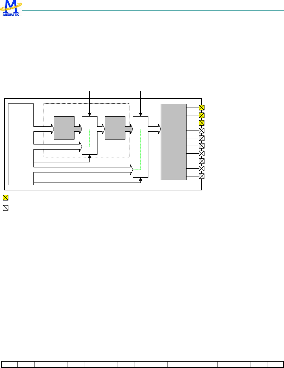
MT6235 GSM/GPRS Baseband Processor Data Sheet Revision 1.02
454/599 MediaTek Inc. Confidential
9.2 Baseband Parallel Interface
9.2.1 General Description
The Baseband Parallel Interface features 10 control pins, which are used for timing-critical external circuits. These pins
typically control front-end components which must be turned on or off at specific times during GSM operation, such as
transmit-enable, band switching, TR-switch, etc.
Event Register
APB I/F
Active
buffer
Write
buffer
Output
buffer
TDMA_EVTVAL
(from TDMA timer) TDMA_BPISTR (0~41)
(from TDMA timer)
BPI_BUS0
BPI_BUS1
BPI_BUS2
BPI_BUS3
BPI_BUS4
BPI_BUS5
BPI_BUS6
BPI_BUS7
MUX
MUX
Immediate mode
petev
BPI_BUS8
BPI_BUS9
The driving capability is configurable.
The driving capability is fixed.
Figure 71 Block diagram of BPI interface
The user can program 42 sets of 10-bit registers to set the output value of BPI_BUS0~BPI_BUS9. The data is stored in
the write buffers. The write buffers are then forwarded to the active buffers when the TDMA_EVTVAL signal is pulsed,
usually once per frame. Each of the 42 write buffers corresponds to an active buffer, as well as to a TDMA event.
Each TDMA_BPISTR event triggers the transfer of data in the corresponding active buffer to the output buffer, thus
changing the value of the BPI bus. The user can disable the events by programming the enable registers in the TDMA
timer. If the TDMA_BPISTR event is disabled, the corresponding signal TDMA_BPISTR is not pulsed, and the value on
the BPI bus remains unchanged.
For applications in which BPI signals serve as the switch, current-driving components are typically added to enhance
driving capability. Three configurable output pins provide current up to 8 mA, and help reduce the number of external
components. The output pins BPI_BUS6, BPI_BUS7, BPI_BUS8, and BPI_BUS9 are multiplexed with GPIO. Please
refer to the GPIO table for more detailed information.
9.2.2 Register Definitions
BPI+0000h BPI control register BPI_CON
Bit 15 14 13 12 11 10 9 8 7 6 5 4 3 2 1 0
MT6235 GSM/GPRS Baseband Processor Data Sheet Revision 1.02
455/599 MediaTek Inc. Confidential
Name PINM2 PINM1 PINM0 PETE
V
Type WO WO WO R/W
Reset 0 0 0 0
This register is the control register of the BPI unit. The register controls the direct access mode of the active buffer and
the current driving capability for the output pins.
The driving capabilities of BPI_BUS0, BPI_BUS1 and BPI_BUS2 can be 2 mA or 8 mA, determined by the value of
PINM0, PINM1 and PINM2 respectively. These output pins provide a higher driving capability and save on external
current-driving components. In addition to the configurable pins, pins BPI_BUS3 to BPI_BUS9 provide a driving
capability of 2 mA (fixed).
PETEV Enables direct access to the active buffer.
0 The user writes data to the write buffer. The data is latched in the active buffer after the TDMA_EVTVAL
signal is pulsed.
1 The user directly writes data to the active buffer without waiting for the TDMA_EVTVAL signal.
PINM0 Controls the driving capability of BPI_BUS0.
0 The output driving capability is 2mA.
1 The output driving capability is 8mA.
PINM1 Controls the driving capability of BPI_BUS1.
0 The output driving capability is 2mA.
1 The output driving capability is 8mA.
PINM2 Controls the driving capability of BPI_BUS2.
0 The output driving capability is 2mA.
1 The output driving capability is 8mA.
BPI +0004h BPI data register 0 BPI_BUF0
Bit 15 14 13 12 11 10 9 8 7 6 5 4 3 2 1 0
Name PO9 PO8 PO7 PO6 PO5 PO4 PO3 PO2 PO1 PO0
Type R/W R/W R/W R/W R/W R/W R/W R/W R/W R/W
This register defines the BPI signals that are associated with the event TDMA_BPI0.
Table 44 lists 42 registers of the same structure, each of which is associated with one specific event signal from the TDMA
timer. The data registers are all double-buffered. When PETEV is set to 0, the data register links to the write buffer.
When PETEV is set to 1, the data register links to the active buffer.
One register, BPI_BUFI, is dedicated for use in immediate mode. Writing a value to that register effects an immediate
change in the corresponding BPI signal and bus.
POx This flag defines the corresponding signals for BPIx after the TDMA event 0 takes place.
The overall data register definition is listed in Table 44.
Register Address Register Function Acronym
BPI +0004h BPI pin data for event TDMA_BPI 0 BPI_BUF0
BPI +0008h BPI pin data for event TDMA_BPI 1 BPI_BUF1
BPI +000Ch BPI pin data for event TDMA_BPI 2 BPI_BUF2
BPI +0010h BPI pin data for event TDMA_BPI 3 BPI_BUF3

MT6235 GSM/GPRS Baseband Processor Data Sheet Revision 1.02
456/599 MediaTek Inc. Confidential
BPI +0014h BPI pin data for event TDMA_BPI 4 BPI_BUF4
BPI +0018h BPI pin data for event TDMA_BPI 5 BPI_BUF5
BPI +001Ch BPI pin data for event TDMA_BPI 6 BPI_BUF6
BPI +0020h BPI pin data for event TDMA_BPI 7 BPI_BUF7
BPI +0024h BPI pin data for event TDMA_BPI 8 BPI_BUF8
BPI +0028h BPI pin data for event TDMA_BPI 9 BPI_BUF9
BPI +002Ch BPI pin data for event TDMA_BPI 10 BPI_BUF10
BPI +0030h BPI pin data for event TDMA_BPI 11 BPI_BUF11
BPI +0034h BPI pin data for event TDMA_BPI 12 BPI_BUF12
BPI +0038h BPI pin data for event TDMA_BPI 13 BPI_BUF13
BPI +003Ch BPI pin data for event TDMA_BPI 14 BPI_BUF14
BPI +0040h BPI pin data for event TDMA_BPI 15 BPI_BUF15
BPI +0044h BPI pin data for event TDMA_BPI 16 BPI_BUF16
BPI +0048h BPI pin data for event TDMA_BPI 17 BPI_BUF17
BPI +004Ch BPI pin data for event TDMA_BPI 18 BPI_BUF18
BPI +0050h BPI pin data for event TDMA_BPI 19 BPI_BUF19
BPI +0054h BPI pin data for event TDMA_BPI 20 BPI_BUF20
BPI +0058h BPI pin data for event TDMA_BPI 21 BPI_BUF21
BPI +005Ch BPI pin data for event TDMA_BPI 22 BPI_BUF22
BPI +0060h BPI pin data for event TDMA_BPI 23 BPI_BUF23
BPI +0064h BPI pin data for event TDMA_BPI 24 BPI_BUF24
BPI +0068h BPI pin data for event TDMA_BPI 25 BPI_BUF25
BPI +006Ch BPI pin data for event TDMA_BPI 26 BPI_BUF26
BPI +0070h BPI pin data for event TDMA_BPI 27 BPI_BUF27
BPI +0074h BPI pin data for event TDMA_BPI 28 BPI_BUF28
BPI +0078h BPI pin data for event TDMA_BPI 29 BPI_BUF29
BPI +007Ch BPI pin data for event TDMA_BPI 30 BPI_BUF30
BPI +0080h BPI pin data for event TDMA_BPI 31 BPI_BUF31
BPI +0084h BPI pin data for event TDMA_BPI 32 BPI_BUF32
BPI +0088h BPI pin data for event TDMA_BPI 33 BPI_BUF33
BPI +008Ch BPI pin data for event TDMA_BPI 34 BPI_BUF34
BPI +0090h BPI pin data for event TDMA_BPI 35 BPI_BUF35
BPI +0094h BPI pin data for event TDMA_BPI 36 BPI_BUF36
BPI +0098h BPI pin data for event TDMA_BPI 37 BPI_BUF37
BPI +009Ch BPI pin data for event TDMA_BPI 38 BPI_BUF38
BPI +00A0h BPI pin data for event TDMA_BPI 39 BPI_BUF39
BPI +00A4h BPI pin data for event TDMA_BPI 40 BPI_BUF40
BPI +00A8h BPI pin data for event TDMA_BPI 41 BPI_BUF41
BPI +00ACh BPI pin data for immediate mode BPI_BUFI

MT6235 GSM/GPRS Baseband Processor Data Sheet Revision 1.02
457/599 MediaTek Inc. Confidential
Table 44 BPI Data Registers.
BPI +00B0h BPI event enable register 0 BPI_ENA0
Bit 15 14 13 12 11 10 9 8 7 6 5 4 3 2 1 0
Name BEN15 BEN14 BEN13 BEN12 BEN11 BEN10 BEN9 BEN8 BEN7 BEN6 BEN5 BEN4 BEN3 BEN2 BEN1 BEN0
Type R/W R/W R/W R/W R/W R/W R/W R/W R/W R/W R/W R/W R/W R/W R/W R/W
Reset 1 1 1 1 1 1 1 1 1 1 1 1 1 1 1 1
This register enables the events that are signaled by the TDMA timer: by clearing a register bit, the corresponding event
signal is ignored. After a hardware reset, all the enable bits default to 1 (enabled). Upon receiving a TDMA_EVTVAL
pulse, all register bits are also set to 1 (enabled).
BENn This flag indicates whether event n signals are heeded or ignored.
0 Event n is disabled (ignored).
1 Event n is enabled.
BPI+00B4h BPI event enable register 1 BPI_ENA1
Bit 15 14 13 12 11 10 9 8 7 6 5 4 3 2 1 0
Name BEN31 BEN30 BEN29 BEN28 BEN27 BEN26 BEN25 BEN24 BEN23 BEN22 BEN21 BEN20 BEN19 BEN18 BEN17 BEN16
Type R/W R/W R/W R/W R/W R/W R/W R/W R/W R/W R/W R/W R/W R/W R/W R/W
Reset 0 0 0 0 0 0 0 0 0 0 0 0 0 0 0 0
This register enables the events that are signaled by the TDMA timing generator: by clearing a register bit, the
corresponding event signal is ignored. After a hardware reset, all the enable bits default to 1 (enabled). Upon receiving
the TDMA_EVTVAL pulse, all register bits are also set to 1 (enabled).
BENn This flag indicates whether event n signals are heeded or ignored.
0 Event n is disabled (ignored).
1 Event n is enabled.
BPI+00B8h BPI event enable register 2 BPI_ENA2
Bit 15 14 13 12 11 10 9 8 7 6 5 4 3 2 1 0
Name BEN41 BEN40 BEN39 BEN38 BEN37 BEN36 BEN35 BEN34 BEN33 BEN32
Type R/W R/W R/W R/W R/W R/W R/W R/W R/W R/W
Reset 0 0 0 0 0 0 0 0 0 0
The register is used to enable the events that are signaled by the TDMA timing generator. After hardware reset, all the
enable bits defaults to be 1 (enabled). Upon receiving the TDMA_EVTVAL pulse, those bits are also set to 1 (enabled).
BENn The flag controls the function of event n.
0 The event n is disabled.
1 The event n is enabled.
9.3 Automatic Power Control (APC) Unit
9.3.1 General Description
The Automatic Power Control (APC) unit controls the Power Amplifier (PA) module. Through APC unit, the proper
transmit power level of the handset can be set to ensure that burst power ramping requirements are met. In one TDMA
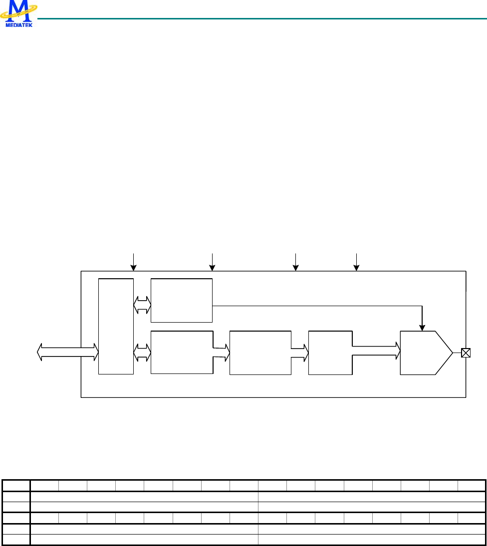
MT6235 GSM/GPRS Baseband Processor Data Sheet Revision 1.02
458/599 MediaTek Inc. Confidential
frame, up to 7 TDMA events can be enabled to support multi-slot transmission. In practice, 5 banks of ramp profiles are
used in one frame to make up 4 consecutive transmission slots.
The shape and magnitude of the ramp profiles are configurable to fit ramp-up (ramp up from zero), intermediate ramp
(ramp between transmission windows), and ramp-down (ramp down to zero) profiles. Each bank of the ramp profile
consists of 16 8-bit unsigned values, which are adjustable for different conditions.
The entries from one bank of the ramp profile are partitioned into two parts, with 8 values in each half. In normal
operation, the entries in the left half are multiplied by a 10-bit left scaling factor, and the entries in the right half are
multiplied by a 10-bit right scaling factor. The values are then truncated to form 16 10-bit intermediate values. Finally
the intermediate ramp profile are linearly interpolated into 32 10-bit values and sequentially used to update the D/A
converter. The block diagram of the APC unit is shown in Figure 72 .
The APB bus interface is 32 bits wide. Four write accesses are required to program each bank of ramp profile. The
detailed register allocations are listed in Table 45.
z
Ramp profile,
scaling factor,
& offset
Multiplier &
interpolator
APB
I/F
APB BUS
(32bits
data bus)
APC_BUS
(10 bits)
DAC_PU
DAC
Power and
clock
control
Output
buffer
TDMA_APCEN
( from TDMA timer ) TDMA_APCSTR (0~6)
( from TDMA timer) QBIT_EN
APC unit
PDN_APC
( from global
control)
Figure 72 Block diagram of APC unit.
9.3.2 Register Definitions
APC+0000h APC 1st ramp profile #0 APC_PFA0
Bit 31 30 29 28 27 26 25 24 23 22 21 20 19 18 17 16
Name ENT3 ENT2
Type R/W R/W
Bit 15 14 13 12 11 10 9 8 7 6 5 4 3 2 1 0
Name ENT1 ENT0
Type R/W R/W
The register stores the first four entries of the first power ramp profile. The first entry resides in the least significant byte
[7:0], the second entry in the second byte [15:8], the third entry in the third byte [23:16], and the fourth in the most
significant byte [31:24]. Since this register provides no hardware reset, the programmer must configure it before any APC
event takes place.
ENT3 The field signifies the 4th entry of the 1st ramp profile.
ENT2 The field signifies the 3rd entry of the 1st ramp profile.

MT6235 GSM/GPRS Baseband Processor Data Sheet Revision 1.02
459/599 MediaTek Inc. Confidential
ENT1 The field signifies the 2nd entry of the 1st ramp profile.
ENT0 The field signifies the 1st entry of the 1st ramp profile.
The overall ramp profile register definition is listed in Table 45.
Register Address Register Function Acronym
APC +0000h APC 1st ramp profile #0 APC_PFA0
APC +0004h APC 1st ramp profile #1 APC_PFA1
APC +0008h APC 1st ramp profile #2 APC_PFA2
APC +000Ch APC 1st ramp profile #3 APC_PFA3
APC +0020h APC 2nd ramp profile #0 APC_PFB0
APC +0024h APC 2nd ramp profile #1 APC_PFB1
APC +0028h APC 2nd ramp profile #2 APC_PFB2
APC +002Ch APC 2nd ramp profile #3 APC_PFB3
APC +0040h APC 3rd ramp profile #0 APC_PFC0
APC +0044h APC 3rd ramp profile #1 APC_PFC1
APC +0048h APC 3rd ramp profile #2 APC_PFC2
APC +004Ch APC 3rd ramp profile #3 APC_PFC3
APC +0060h APC 4th ramp profile #0 APC_PFD0
APC +0064h APC 4th ramp profile #1 APC_PFD1
APC +0068h APC 4th ramp profile #2 APC_PFD2
APC +006Ch APC 4th ramp profile #3 APC_PFD3
APC +0080h APC 5th ramp profile #0 APC_PFE0
APC +0084h APC 5th ramp profile #1 APC_PFE1
APC +0088h APC 5th ramp profile #2 APC_PFE2
APC +008Ch APC 5th ramp profile #3 APC_PFE3
APC +00A0h APC 6th ramp profile #0 APC_PFF0
APC +00A4h APC 6th ramp profile #1 APC_PFF1
APC +00A8h APC 6th ramp profile #2 APC_PFF2
APC +00ACh APC 6th ramp profile #3 APC_PFF3
APC +00C0h APC 7th ramp profile #0 APC_PFG0
APC +00C4h APC 7th ramp profile #1 APC_PFG1
APC +00C8h APC 7th ramp profile #2 APC_PFG2
APC +00CCh APC 7th ramp profile #3 APC_PFG3
Table 45 APC ramp profile registers
APC +0010h APC 1st ramp profile left scaling factor APC_SCAL0L
Bit 15 14 13 12 11 10 9 8 7 6 5 4 3 2 1 0
Name SF
Type R/W
Reset 1_0000_0000
The register stores the left scaling factor of the 1st ramp profile. This factor multiplies the first 8 entries of the 1st ramp
profile to provide the scaled profile, which is then interpolated to control the D/A converter.
MT6235 GSM/GPRS Baseband Processor Data Sheet Revision 1.02
460/599 MediaTek Inc. Confidential
After a hardware reset, the initial value of the register is 256. In this case, no scaling is done (each entry of the ramp
profile is multiplied by 1), because the 8 least significant bits are truncated after multiplication.
The overall scaling factor register definition is listed in Table 46 .
SF Scaling factor. After a hardware reset, the value is 256.
APC +0014h APC 1st ramp profile right scaling factor APC_SCAL0R
Bit 15 14 13 12 11 10 9 8 7 6 5 4 3 2 1 0
Name SF
Type R/W
Reset 1_0000_0000
The register stores the right scaling factor of the 1st ramp profile. This factor multiplies the last 8 entries of the 1st ramp
profile to provide the scaled profile, which is then interpolated to control the D/A converter.
After a hardware reset, the initial value of the register is 256. In this case, no scaling is done (each entry of the ramp
profile is multiplied by 1), because the 8 least significant bits are truncated after multiplication.
The overall scaling factor register definition is listed in Table 46 .
SF Scaling factor. After a hardware reset, the value is 256.
APC+0018h APC 1st ramp profile offset value APC_OFFSET0
Bit 15 14 13 12 11 10 9 8 7 6 5 4 3 2 1 0
Name OFFSET
Type R/W
Reset 0
There are 7 offset values for the corresponding ramp profile.
The 1st offset value also serves as the pedestal value. The value is used to power up the APC D/A converter before the RF
signals start to transmit. The D/A converter is then biased on the value, to provide the initial control voltage for the
external control loop. The exact value depends on the characteristics of the external components. The timing to output
the pedestal value is configurable through the TDMA_BULCON2 register of the timing generator; its valid range is 0~127
quarter-bits of time after the baseband D/A converter is powered up.
OFFSET Offset value for the corresponding ramp profile. After a hardware reset, the default value is 0.
The overall offset register definition is listed in Table 46.
Register Address Register Function Acronym
APC +0010h APC 1st ramp profile left scaling factor APC_SCAL0L
APC +0014h APC 1st ramp profile right scaling factor APC_SCAL0R
APC +0018h APC 1st ramp profile offset value APC_OFFSET0
APC +0030h APC 2nd ramp profile left scaling factor APC_SCAL1L
APC +0034h APC 2nd ramp profile right scaling factor APC_SCAL1R
APC +0038h APC 2nd ramp profile offset value APC_OFFSET1
APC +0050h APC 3rd ramp profile left scaling factor APC_SCAL2L
APC +0054h APC 3rd ramp profile right scaling factor APC_SCAL2R
APC +0058h APC 3rd ramp profile offset value APC_OFFSET2
MT6235 GSM/GPRS Baseband Processor Data Sheet Revision 1.02
461/599 MediaTek Inc. Confidential
APC +0070h APC 4th ramp profile left scaling factor APC_SCAL3L
APC +0074h APC 4th ramp profile right scaling factor APC_SCAL3R
APC +0078h APC 4th ramp profile offset value APC_OFFSET3
APC +0090h APC 5th ramp profile left scaling factor APC_SCAL4L
APC +0094h APC 5th ramp profile right scaling factor APC_SCAL4R
APC +0098h APC 5th ramp profile offset value APC_OFFSET4
APC +00B0h APC 6th ramp profile left scaling factor APC_SCAL5L
APC +00B4h APC 6th ramp profile right scaling factor APC_SCAL5R
APC +00B8h APC 6th ramp profile offset value APC_OFFSET5
APC +00D0h APC 7th ramp profile left scaling factor APC_SCAL6L
APC +00D4h APC 7th ramp profile right scaling factor APC_SCAL6R
APC +00D8h APC 7th ramp profile offset value APC_OFFSET6
Table 46 APC scaling factor and offset value registers
APC+00E0h APC control register APC_CON
Bit 15 14 13 12 11 10 9 8 7 6 5 4 3 2 1 0
Name GSM FPU
Type R/W R/W
Reset 1 0
GSM Defines the operation mode of the APC module. In GSM mode, each frame has only one slot, thus only one
scaling factor and one offset value must be configured. If the GSM bit is set, the programmer needs only to
configure APC_SCAL0L and APC_OFFSET0. If the bit is not set, the APC module is operating in GPRS mode.
0 The APC module is operating in GPRS mode.
1 The APC module is operating in GSM mode. Default value.
FPU Forces the APC D/A converter to power up. Test only.
0 The APC D/A converter is not forced to power up. The converter is only powered on when the transmission
window is opened. Default value.
1 The APC D/A converter is forced to power up.
9.3.3 Ramp Profile Programming
The first value of the first normalized ramp profile must be written in the least significant byte of the APC_PFA0 register.
The second value must be written in the second least significant byte of the APC_PFA0, and so on.
Each ramp profile can be programmed to form an arbitrary shape.
The start of ramping is triggered by one of the TDMA_APCSTR signals. The timing relationship between
TDMA_APCSTR and TDMA slots is depicted in Figure 73 for 4 consecutive time slots case. The power ramping profile
must comply with the timing mask defined in GSM SPEC 05.05. The timing offset values for 7 ramp profiles are stored
in the TDMA timer register from TDMA_APC0 to TDMA_APC6.
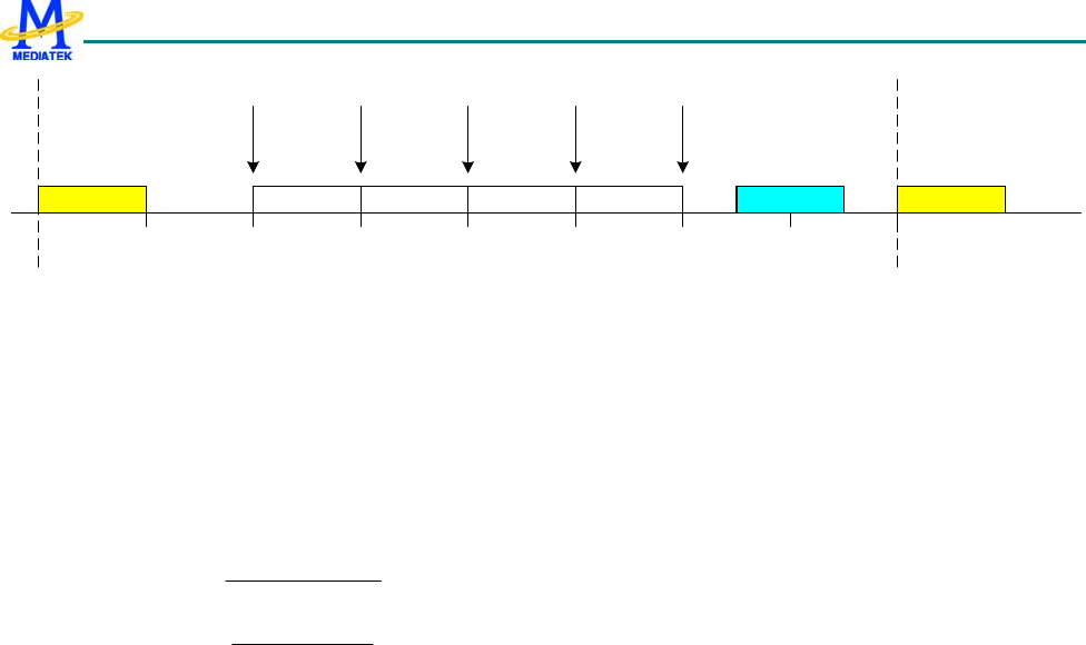
MT6235 GSM/GPRS Baseband Processor Data Sheet Revision 1.02
462/599 MediaTek Inc. Confidential
RX MXTX RX
TDMA_APCSTR0 TDMA_APCSTR1
TXTX TX
TDMA_APCSTR2 TDMA_APCSTR3 TDMA_APCSTR4
Figure 73 Timing diagram of TDMA_APCSTR.
Because the APC unit provides more than 5 ramp profiles, up to 4 consecutive transmission slots can accommodated. The
2 additional ramp profiles are useful particularly when the timing between the last 2 transmission time slots and CTIRQ is
uncertain; software can begin writing the ramp profiles for the succeeding frame during the current frame, alleviating the
risk of not writing the succeeding frame’s profile data in time.
In GPRS mode, to fit the intermediate ramp profile between different power levels, a simple scaling scheme is used to
synthesize the ramp profile. The equation is as follows:
8 15 if 1,
0 8 if 0,
0,1,...,15,DNSOFFDA
,...,151 ,
2
DN DN
S OFFDA
2
DN DN
S OFFDA
12
1
2
0,15
00
⎩
⎨
⎧
≥≥
≥>
=
=⋅+=
=
+
⋅+=
+
⋅+=
+
−
k
k
l
k
k
klk
kk
lk
pre
where DA = the data to present to the D/A converter,
DN = the normalized data which is stored in the register APC_PFn,
S0 = the left scaling factor stored in register APC_SCALnL,
S1 = the right scaling factor stored in register APC_SCALnR, and
OFF = the offset value stored in the register APC_OFFSETn.
The subscript n denotes the index of the ramp profile.
The ramp calculation before interpolation is as depicted in Figure 74.
During each ramp process, each word of the normalized profile is first multiplied by 10-bit scaling factors and added to an
offset value to form a bank of 18-bit words. The first 8 words (in the left half part as in Figure 74) are multiplied by the
left scaling factor S0 and the last 8 words (in the right half part as in Figure 74) are multiplied by the right scaling factor S1.
The lowest 8 bits of each word are then truncated to get a 10-bit result. The scaling factor is 0x100, which represents no
scaling on reset. A value smaller than 0x100 scales the ramp profile down, and a value larger than 100 scales the ramp
profile up.
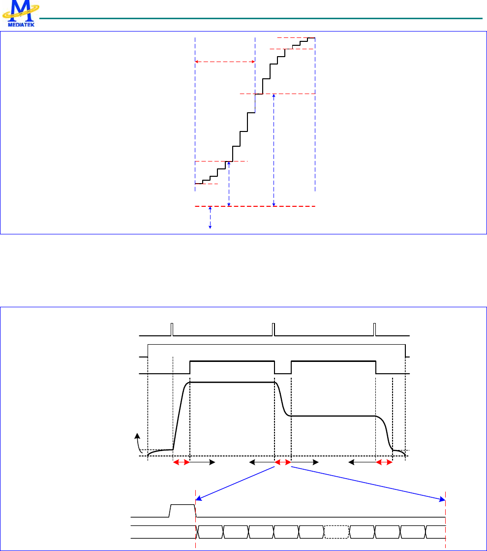
MT6235 GSM/GPRS Baseband Processor Data Sheet Revision 1.02
463/599 MediaTek Inc. Confidential
z
DN0 * S0 + OFF
DN4 * S0 + OFF
DN8 * S1 + OFF
DN12 * S1 + OFF
DN15 * S1 + OFF
16 Qb
DN4 * S0DN8 * S1
OFF
Figure 74 The timing diagram of the APC ramp.
The 16 10-bit words are linearly interpolated into 32 10-bit words. A 10-bit D/A converter is then used to convert these 32
ramp values at a rate of 1.0833 MHz, that is, at quarter-bit rate. The timing diagram is shown in Figure 75 and the final
value is retained on the output until the next event occurs.
z
TX TX
TX Burst TX Burst
TDMA_APCSTR0
Ramp ProfileRamp Profile Ramp Profile
TDMA_APCSTR2
TDMA_APCSTR1
~29.5us ~29.5us
APC_DATA
TDMA_APCSTR1
1
0
32 29 30 31
TDMA_APCEN
TDMA_APCSTRx
~29.5us
offset
Figure 75 Timing diagram of the APC ramping.
The APC unit is only powered up when the APC window is open. The APC window is controlled by configuring the
TDMA registers TDMA_BULCON1 and TDMA_BULCON2. Please refer to the TDMA timer unit for more detailed
information.
MT6235 GSM/GPRS Baseband Processor Data Sheet Revision 1.02
464/599 MediaTek Inc. Confidential
The first offset value stored in the register APC_OFFSET0 also serves as the pedestal value, which is used to provide the
initial power level for the PA.
Since the profile is not double-buffered, the timing to write the ramping profile is critical. The programmer must be
restricted from writing to the data buffer during the ramping process, otherwise the ramp profile may be incorrect and lead
to a malfunction.
9.4 Automatic Frequency Control (AFC) Unit
9.4.1 General description
The Automatic Frequency Control (AFC) unit provides the direct control of the oscillator for frequency offset and Doppler
shift compensation. The block diagram is of the AFC unit depicted in Figure 76. The module utilizes a 13-bit D/A
converter to achieve high-resolution control. Two modes of operation provide flexibility when controlling the oscillator;
they are described as follows.
Active
buffer
Power
control
APB
BUS
TDMA_AFC
( from TDMA timer )
Write
buffer
AFC_BU
S
Control
register
TDMA_EVTVAL
( from TDMA timer )
DAC
oscillator
PDN_AFC
( from global control )
VC
AFC unit
Immediate write
Output
buffer
PDN_DAC
F_MODE
I_MODE
AFC
H_MODE HOLDN_DAC
Figure 76 The block diagram of the AFC controller
In timer-triggered mode, the TDMA timer controls the AFC enabling events. Each TDMA frame can pulse at most four
events. Double buffer architecture is supported. AFC values can be written to the write buffers. When the signal
TDMA_EVTVAL is received, the values in the write buffers are latched into the active buffers. However, AFC values can
also be written to the active buffers directly. Each event is associated with an active buffer sharing the same index.
When a TDMA event is triggered by TDMA_AFC, the value in the corresponding active buffer takes effect. Figure 77
shows a timing diagram of AFC events with respect to TX/RX/MX windows. In this mode, the D/A converter can stay
powered on or be powered on for a programmable duration (256 quarter-bits, by default). The latter option is for power
saving.
RX MX MXTX
AFC_STR0 AFC_STR3AFC_STR2AFC_STR1
Figure 77 Timing Diagram for the AFC Controller

MT6235 GSM/GPRS Baseband Processor Data Sheet Revision 1.02
465/599 MediaTek Inc. Confidential
In immediate mode, the MCU can directly control the AFC value without event-triggering. The value written by the MCU
takes effect immediately. In this mode, the D/A converter must be powered on continuously. When transitioning from
immediate mode into timer-triggered mode (by setting flag I_MODE in the register AFC_CON to be 0), the D/A converter
is kept powered on for a programmable duration (256 quarter-bits by default) if a TDMA_AFC is not been pulsed. The
duration is prolonged upon receiving events.
9.4.2 Register Definitions
AFC+0000h AFC control register AFC_CON
Bit 15 14 13 12 11 10 9 8 7 6 5 4 3 2 1 0
Name H_MO
DE RDAC
T F_MO
DE FETE
NV I_MO
DE
Type R/w R/W R/W R/W R/W
Reset 0 0 0 0 0
Four control modes are defined and can be controlled through the AFC control register. F_MODE enables the force power
up mode. FETENV enables the direct write operation to the active buffer. I_MODE enables the immediate mode. RDACT
enables the direct read operation from the active buffer. HOLD_ON enables the AFC DAC hold mode.
RDACT The flag enables the direct read operation from the active buffer. Note the control flag is only applicable to the four
data buffer including AFC_DAT0, AFC_DAT1, AFC_DAT2, and AFC_DAT3.
0 APB read from the write buffer.
1 APB read from the active buffer.
FETENV The flag enables the direct write operation to the active buffer. Note the control flag is only applicable to the
for data buffer including AFC_DAT0, AFC_DAT1, AFC_DAT2, and AFC_DAT3.
0 APB write to the write buffer.
1 APB write to the active buffer.
F_MODE The flag enables the force power up mode.
0 The force power up mode is not enabled.
1 The force power up mode is enabled.
I_MODE The flag enables the immediate mode. To enable the immediate mode also enable the force power up mode.
0 The immediate mode is not enabled.
1 The immediate mode is enabled.
H_MODE The flag enables the hold mode of AFC DAC. If this mode is enabled, the DAC will keep the previous voltage
level instead of power down.
0 The hold mode is not enabled.
1 The hold mode is enabled.
While SRCLKENAI = 1’b1, AFC DAC will be turned on at the normal mode. SRCLKENAI is a gpio_mux pin. Make sure
that the gpio mode is configured at the correct mode before BB enters the sleep mode.
AFC +0004h AFC data register 0 AFC_DAT0
Bit 15 14 13 12 11 10 9 8 7 6 15 4 3 2 1 0
Name AFCD
Type R/W
MT6235 GSM/GPRS Baseband Processor Data Sheet Revision 1.02
466/599 MediaTek Inc. Confidential
The register stores the AFC value for the event 0 triggered by the TDMA timer in timer-triggered mode. When the
RDACT or FETENV bit (of the AFC_CON register) is set, the data transfer operates on the active buffer. When neither
flag is set, the data transfer operates on the write buffer.
AFCD The AFC sample for the D/A converter.
Four registers (AFC_DAT0, AFC_DAT1, AFC_DAT2, AFC_DAT3) of the same type correspond to the event triggered by
the TDMA timer. The four registers are summarized in Table 1.
Register Address Register Function Acronym
AFC +0004h AFC control value 0 AFC_DAT0
AFC +0008h AFC control value 1 AFC_DAT1
AFC +000Ch AFC control value 2 AFC_DAT2
AFC +0010h AFC control value 3 AFC_DAT3
Table 1 AFC Data Registers
Immediate mode can only use AFC_DAT0. In this mode, only the control value in the AFC_DAT0 write buffer is used to
control the D/A converter. Unlike timer-triggered mode, the control value in AFC_DAT0 write buffer can bypass the
active buffer stage and be directly coupled to the output buffer in immediate mode. To use immediate mode, program the
AFC_DAT0 in advance and then enable immediate mode by setting the I_MODE flag in the AFC_CON register.
The registers AFC_DATA0, AFC_DAT1, AFC_DAT2, and AFC_DAT3 have no initial values, thus the register must be
programmed before any AFC event takes place. The AFC value for the D/A converter, i.e., the output buffer value, is
initially 0 after power up before any event occurs.
AFC +0014h AFC power up period AFC_PUPER
Bit 15 14 13 12 11 10 9 8 7 6 5 4 3 2 1 0
Name PU_PER
Type R/W
Reset ff
This register stores the AFC power up period, which is 13 bits wide. The value ranges from 0 to 8191. If the I_MODE
or F_MODE flag is set, this register has no effect since the D/A converter is powered up continuously. If neither flag is set,
the register controls the power up duration of the D/A converter. During that period, the signal PDN_DAC in Figure 76 is
set to 1(power up).
PU_PER Stores the AFC power up period. After hardware power up, the field is initialized to 255.

MT6235 GSM/GPRS Baseband Processor Data Sheet Revision 1.02
467/599 MediaTek Inc. Confidential
10 Baseband Front End
Baseband Front End is a modem interface between TX/RX mixed-signal modules and digital signal processor (DSP). We
can divide this block into two parts (see Figure 78). The first is the uplink (transmitting) path, which converts bit-stream
from DSP into digital in-phase (I) and quadrature (Q) signals for TX mixed-signal module. The second part is the downlink
(receiving) path, which receives digital in-phase (I) and quadrature (Q) signals from RX mixed-signal module, performs
FIR filtering and then sends results to DSP. Figure 78 illustrates interconnection around Baseband Front End. In the figure
the shadowed blocks compose Baseband Front End.
To enhance the capability of data processing of mobile phone and base station, the Enhanced Data for GSM Evolution
(EDGE), which used 8PSK Modulation rather than GMSK Modulation in GSM system may provide the triple data
transmission rate of 384 kbps for system to supply the solution of voice, data, Internet linkage, and other kinds of mutual
linkage, while 3bits per symbols in 8PSK Modulation and 1 bit per symbol in GMSK Modulation.
The uplink path is mainly composed of GMSK Modulator or 8PSK Modulator and uplink parts of Baseband Serial Ports,
and the downlink path is mainly composed of RX digital FIR filter and downlink parts of Baseband Serial Ports. Baseband
Serial Ports is a serial interface used to communicate with DSP. In addition, there is a set of control registers in Baseband
Front End that is intended for control of TX/RX mixed-signal modules, inclusive of several compensation
circuit :calibration of I/Q DC offset, I/Q Quadrature Phase Compensation and I/Q Gain Mismatch of uplink
analog-to-digital (D/A) converters as well as I/Q Gain Mismatch for downlink digital-to-analog (A/D) converters in TX/RX
mixed-signal modules. The timing of bit streaming through Baseband Front End is completely under control of TDMA
timer. Usually only either of uplink and downlink paths is active at one moment. However, both of the uplink and downlink
paths will be active simultaneously when Baseband Front End is in loopback mode.
When either of TX windows in TDMA timer is opened, the uplink path in Baseband Front End will be activated.
Accordingly components on the uplink path such as GMSK Modulator or 8PSK Modulator will be powered on, and then
TX mixed-signal module is also powered on. The subblock Baseband Serial Ports will sink TX data bits from DSP and then
forward them to GMSK Modulator or 8PSK Modulator. The outputs from GMSK Modulator or 8PSK Modulator are sent to
TX mixed-signal module in format of I/Q signals. Finally D/A conversions are performed in TX mixed-signal module and
the output analog signal is output to RF module. Additionally, 8PSK Modulation intrinsically extends the bursts window
and reports in 8MVD (8PSK Modulation Valid) in BFE_STA status register.
Similarly, while either of RX windows in TDMA timer is opened, the downlink path in Baseband Front End will be
activated. Accordingly components on the downlink path such as RX mixed-signal module and RX digital FIR filter are
then powered on. First A/D conversions are performed in RX mixed-signal module, and then the results in format of I/Q
signals are sourced to Low Pass Filtering with different bandwidth (Narrow one about Fc = 90 khz, Wide one about FC =
110khz), Interference Detection Circuit to determine which Filter to be used by judging receiving power on current burst,
Additionally, “I/Q Compensation Circuit” is an option in data path for modifying Receiving I/Q pair gain mismatch..
Finally the results will be sourced to DSP through Baseband Serial Ports.
MT6235 GSM/GPRS Baseband Processor Data Sheet Revision 1.02
468/599 MediaTek Inc. Confidential
Figure 78 Block Diagram Of Baseband Front End
10.1 Baseband Serial Ports
10.1.1 General Description
Baseband Front End communicates with DSP through the sub block of Baseband Serial Ports. Baseband Serial Ports
interfaces with DSP in serial manner. This implies that DSP must be configured carefully in order to have Baseband Serial
Ports cooperate with DSP core correctly.
If downlink path is programmed in bypass-filter mode (NOT bypass-filter loopback mode), behavior of Baseband Serial
Ports will be completely be different from that in normal function mode. The special mode is for testing purpose. Please see
the subsequent section of Downlink Path for more details.
TX and RX windows are under control of TDMA timer. Please refer to functional specification of TDMA timer for the
details on how to open/close a TX/RX window. Opening/Closing of TX/RX windows have two major effects on Baseband
Front End : power on/off of corresponding components and data souring/sinking. It is worth noticing that Baseband Serial
Ports is only intended for sinking TX data from DSP or sourcing data to DSP. It does not involve power on/off of TX/RX
mixed-signal modules.
As far as downlink path is concerned, if a RX window is opened by TDMA timer Baseband Front End will have RX
mixed-signal module proceed to make A/D conversion, two parallel RX digital filter proceed to performiltering and
Baseband Serial Ports be activated to source data from RX digital filter to Master DSP while Power Measurement through
Baseband Serial Ports to Slave DSP no matter the data is meaningful or not However, the interval between the moment that

MT6235 GSM/GPRS Baseband Processor Data Sheet Revision 1.02
469/599 MediaTek Inc. Confidential
RX mixed-signal module is powered on and the moment that data proceed to be dumped by Baseband Serial Ports can be
well controlled in TDMA timer. Let us denote RX enable window as the interval that RX mixed-signal module is powered
on and denote RX dump window as the interval that data is dumped by Baseband Serial Ports. If the first samples from RX
digital filter desire to be discarded, the corresponding RX enable window must cover the corresponding RX dump window.
Note that RX dump windows always win over RX enable windows. It means that a RX dump window will always raise a
RX enable window. RX enable windows can be raised by TDMA timer or by programming RX power-down bit in global
control registers to be ‘0’. This is useful in debugging environment.
Similarly, a TX dump window refers to the interval that Baseband Serial Ports sinks data from DSP on uplink path and a
TX enable window refers to the interval that TX mixed-signal module is powered on. A TX window controlled by TDMA
timer involves a TX dump window and a TX enable window simultaneously. The interval between the moment that TX
mixed-signal module is powered on and the moment that data proceed to be forwarded from DSP to GMSK or 8PSK
modulator by Baseband Serial Ports can be well controlled in TDMA timer. TX dump windows always win over TX enable
windows. It means that a TX dump window will always raise a TX enable window. TX enable windows can be raised by
TDMA timer or by programming TX power-down bit in global control registers to be ‘0’. It is useful in debugging
environment.
Accordingly, Baseband Serial Ports are only under the control of TX/RX dump window. Note that if TX/RX dump window
is not integer multiplies of bit-time it will be extended to be integer multiplies of bit-time. For example, if TX/RX dump
window has interval of 156.25 bit-times then it will be extended to 157 bit-times in Baseband Serial Ports.
For uplink path, if uplink path is enabled, then the bit BULEN (Baseband Up-Link Enable) will be ‘1’. Otherwise the bit
BULEN will be 0.
The MDSEL( Modulation Mode Select[3:0]) in TX_CONF control register needs to be latched in MDSEL shadow register
according to the rising edge of TDMA Event Validate signal from TDMA controller, which used to indicate the modulation
scheme selection between 8PSK or GMSK modulator for four transmit Burst.
Generally there will at most 4 sequential Bursts, 1st Burst, 2nd Burst, 3rd Bursts, and 4th Bursts, which are not necessary to be
all turn on in a burst sequence. The BTXEN1, BTXEN2, BTXEN3, BTXEN4 will be asserted prior to each Bursts, and
their rising edge will update the Mode selection control bit to select appropriate Modulation type for current input data
symbols in each bursts. Additionally, this Mode selection status for each bursts will be stored in BFE_STA status register,
including MDSTS1(MoDulation mode StatuS1) , MDSTS2(MoDulation mode StatuS2), MDSTS3(MoDulation mode
StatuS3), MDSTS4(MoDulation mode StatuS4), respectively.(Figure 79 Uplink Modulation Mode Selection Status Timing
Diagram)
During these 4 bursts valid period, the bit BULFS (Baseband Uplink Frame Sync) in BFE_STA status register will be ‘1’.
Otherwise will be ‘0’. Meanwhile, uplink path will forward TX bit from DSP to GMSK modulator or 8PSK
Modulation
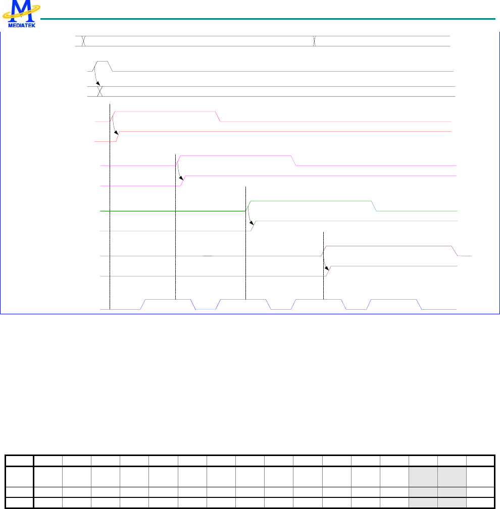
MT6235 GSM/GPRS Baseband Processor Data Sheet Revision 1.02
470/599 MediaTek Inc. Confidential
BULTXEN4
BULTXEN3
BULTXEN2
BULTXEN1
MDSTS1
MDSTS2
MDSTS3
MDSTS4
BULFS 1st Burst 2nd Burst 3rd Burst 4th Burst
for 4th Burst
for 3rd Burst
for 2nd Burst
for 1st Burst
MDSEL1
TDMA Event
VAlidate
4'b1111
MDSEL Shadow
Register
MDSEL from
APB Bus
Figure 79 Uplink Modulation Mode Selection Status Timing Diagram
For downlink path, if BDLEN(Baseband DownLink Enable) is enabled, RX mixed-signal module will also be powered on.
Similarly, once uplink path is enabled, TX mixed-signal module will also be powered on. Furthermore, enabling
BDLFS(Baseband Down-Link FrameSync)Baseband Serial Ports for downlink path refers to dumping results from RX
digital FIR filter to DSP.
10.1.2 Register Definitions
BFE+0000h Base-band Common Control Register BFE_CON
Bit 15 14 13 12 11 10 9 8 7 6 5 4 3 2 1 0
Name BCIE
N
Type R/W
Reset 0
This register is for common control of Baseband Front End. It consists of ciphering encryption control.
BCIEN The bit is for ciphering encryption control. If the bit is set to ‘1’, XOR will be performed on some TX bits
(payload of Normal Burst) and ciphering pattern bit from DSP, and then the result is forwarded to GMSK
Modulator only. Meanwhile, Baseband Front End will generate signals to drive DSP ciphering process and
produce corresponding ciphering pattern bits if the bit is set to ‘1’. If the bit is set to ‘0’, the TX bit from DSP will
be forwarded to GMSK modulator directly. Baseband Front End will not activate DSP ciphering process.
0 Disable ciphering encryption.
1 Enable ciphering encryption.

MT6235 GSM/GPRS Baseband Processor Data Sheet Revision 1.02
471/599 MediaTek Inc. Confidential
BFE +0004h Base-band Common Status Register BFE_STA
Bit 15 14 13 12 11 10 9 8 7 6 5 4 3 2 1 0
Name
MDST
S4 MDST
S3 MDST
S2 MDST
S1 BULE
N4 BULE
N3 BULE
N2 BULE
N1 BULF
S4 BULF
S3 BULF
S2 BULF
S1 BDLF
S BDLE
N
Type RO RO RO RO RO RO RO RO RO RO RO RO RO RO
Reset 0 0 0 0 0 0 0 0 0 0 0 0 0 0
This register indicates status of Baseband Front End This register indicates status of Baseband Front End. Under control of
TDMA timer, Baseband Front End can be driven in several statuses. If downlink path is enabled, then the bit BDLEN will
be ‘1’. Otherwise the bit BDLEN will be ‘0’. If downlink parts of Baseband Serial Ports is enabled, the bit BDLFS will be
‘1’. Otherwise the bit BDLFS will be ‘0’. If uplink path is enabled, then the bit BULEN will be ‘1’. Otherwise the bit
BULEN will be 0. If uplink parts of Baseband Serial Ports is enabled, the bit BULFS will be ‘1’. Otherwise the bit BULFS
will be ‘0’. Once downlink path is enabled, RX mixed-signal module will also be powered on. Similarly, once uplink path
is enabled, TX mixed-signal module will also be powered on. Furthermore, enabling Baseband Serial Ports for downlink
path refers to dumping results from RX digital FIR filter to DSP. Similarly, enabling Baseband Serial Ports for uplink path
refers to forwarding TX bit from DSP to GMSK modulator. BDLEN stands for “Baseband DownLink Enable”. BULEN
stands for “Baseband UpLink Enable”. BDLFS stands for “Baseband DownLink FrameSync”. BULFS stands for
“Baseband UpLink FrameSync”.
BDLEN Indicate if downlink path is enabled.
0 Disabled
1 Enabled
BDLFS Indicate if Baseband Serial Ports for downlink path is enabled.
0 Disabled
1 Enabled
BULFS1 Indicate if Baseband Serial Ports for uplink path is enabled in 1st burst
0 Disabled
1 Enabled
BULFS2 Indicate if Baseband Serial Ports for uplink path is enabled in 2nd burst
0 Disabled
1 Enabled
BULFS3 Indicate if Baseband Serial Ports for uplink path is enabled in 3rd burst
0 Disabled
1 Enabled
BULFS4 Indicate if Baseband Serial Ports for uplink path is enabled in 4th burst
0 Disabled
1 Enabled
BULEN1 Indicate if uplink path is enabled in 1st burst.
0 Disabled
1 Enabled
BULEN2 Indicate if uplink path is enabled in 2nd burst.
0 Disabled
1 Enabled
BULEN3 Indicate if uplink path is enabled in 3rd burst.
0 Disabled

MT6235 GSM/GPRS Baseband Processor Data Sheet Revision 1.02
472/599 MediaTek Inc. Confidential
1 Enabled
BULEN4 Indicate if uplink path is enabled in 4th burst.
0 Disabled
1 Enabled
MDSTS1 Indicate the current Modulation Mode Selection in 1st burst
0 GMSK Modulation
1 8PSK Modulation
MDSTS2 Indicate the current Modulation Mode Selection in 2nd burst
0 GMSK Modulation
1 8PSK Modulation
MDSTS3 Indicate the current Modulation Mode Selection in 3rd burst
0 GMSK Modulation
1 8PSK Modulation
MDSTS4 Indicate the current Modulation Mode Selection in 4th burst
0 GMSK Modulation
1 8PSK Modulation
10.2 Downlink Path (RX Path)
10.2.1 General Description
On the downlink path, the sub-block between RX mixed-signal module and Baseband Serial Ports is RX Path. It mainly
consists of two parallel digital FIR filter with programmable tap number, two sets of multiplexing paths for loopback modes,
interface for RX mixed-signal module, Interference Detection Circuit, I/Q Gain Mismatch compensation circuit, and
interface for Baseband Serial Ports. The block diagram is shown in Figure 80 Block Diagram of RX Path.
While RX enable windows are open, RX Path will issue control signals to have RX mixed-signal module proceed to make
A/D conversion. As each conversion is finished, one set of I/Q signals will be latched. There exists a digital FIR filter for
these I/Q signals. The result of filtering will be dumped to Baseband Serial Ports whenever RX dump windows are opened.

MT6235 GSM/GPRS Baseband Processor Data Sheet Revision 1.02
473/599 MediaTek Inc. Confidential
BBRX
I/Q Mismatch
Comp CKT
Master DSP
RX Sports1
BBRX
Interference
Detection
Slave DSP
RX Sport1
PWR Measurement
Output
BBRX
Baseband
Serial Port
Receiving I/Q Pair
BBRX A/D
RX Dump Window
RX Enable Window
Loopback Path
from BBTX
BBRX
Narrow Filter
(Fc= 90khz)
BBRX
Wide Filter
(Fc= 110khz)
Loopback Path
bypass FIR
Loopback Path
thru FIR
Figure 80 Block Diagram of RX Path
10.2.2 Comb Filter
The comb filter which takes the 2-bit A/D converter as input, and output the 18-bit I/Q data words to the baseband receiving
path. The system is designed as 48X over-sampling with symbol period 541.7 kHz, thus the data inputs are 26MHz 2-bit
signal. The input 2-bit signals are formed in (sign, magnitude) manner; that is, total 3 values are permitted as input: (-1, 0,
+1).
The data path is mainly a decimation filter which contains the integration stages and the decimation stages. For a 3rd order
design with 48X over-sampling, gain of the data path is 483 = 110592, which locates between 216 and 217. Thus the internal
word-length must be set to 18-bit to avoid overflow in the integration process.
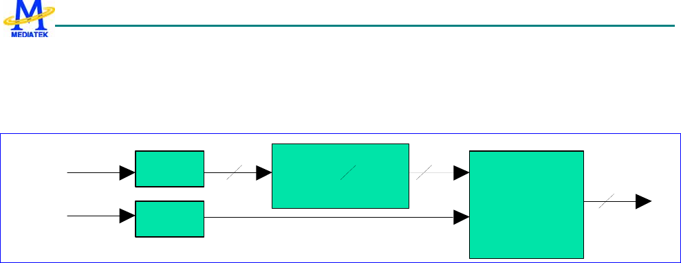
MT6235 GSM/GPRS Baseband Processor Data Sheet Revision 1.02
474/599 MediaTek Inc. Confidential
10.2.3 Compensation Circuit - I/Q Gain Mismatch
In order to compensate I/Q Gain Mismatch , configure IGAINSEL(I Gain Selection) in RX_CON control register, the I
over Q ratio can be compensate for 0.3 dB/step, totally 11 steps resulted in dynamic range up to +/-1.5dB.
RX_filter
I/Q mismatch
compensation
14
1414
Q
IA/D
A/D
16
Figure 81 I/Q Mismatch Compensation Block Diagram
The I/Q swap functionality can be setting “1” for SWAP(I/Q Swapping) in RX_CFG control register, which is used to swap
I/Q channel signals from RX mixed-signal module before they are latched into RX digital FIR filter. It is intended to
provide flexibility for I/Q connection with RF modules
10.2.4 Phase De-rotation Circuit
Phase De-rotation Mode will usually turn on during FCB Detection for down conversion the wide spread receiving power
to 67.7khz single tone.
Two separate control for implement this mode on data path through NarrowFIR filter or WideFIR filter by setting ‘1’ to
PHROEN_N(Phase Rotate Enable for NarrowFIR) or PHROEN_W(Phase Rotate Enable for WideFIR) in RX_CON
control register, respectively.
10.2.5 Adaptive Bandwidth & Programmable Digital FIR Filter
For the two parallel digital FIR Filter, the total tap number is programmable by FIRTPNO(FIR Tap number) in RX_CFG
control register, which will configure the filter with different tap buffer depth.
10.2.5.1 Programmable tap & programmable Coefficient for FIR
In order to satisfy the signal requirements in both of idle and traffic modes, two sets of coefficients must be provided for the
RX digital FIR filter. Therefore, the RX digital FIR filter is implemented as a FIR filter with programmable coefficients
which can be accessed on the APB bus. The coefficient number can be programmable, range from from 1~31. Each
coefficient is ten-bit wide and coded in 2’s complement.
Take 21 Tap Coefficient for example, based on assumption that the FIR filter has symmetric coefficients, only 11
coefficients are implemented as programmable registers to save gate count. Denoting these digital filter coefficients as
RX_RAM0_CS0 ~ RX_RAM0_CS11(RX_RAM0 Coefficient Set 0~11), and these tap registers for I/Q channel signals as
I/QTAPR [0:20], then the RX digital FIR filtering can be represented as the following equation:

MT6235 GSM/GPRS Baseband Processor Data Sheet Revision 1.02
475/599 MediaTek Inc. Confidential
11,...,1,0],20[][
0])20[][(*][]11[*]11[
4mn at time
0][*][)(
0
])20[][(*][]11[*]11[
4mn at time
20
0
][*][)(
1120
11
=−=
∑
=−++=
+
∑
=
=
∑
=−++=
+
∑
=
=
iiBDLDFCRiBDLDFCR
iiQTAPRiQTAPRiBDLDFCRQTAPRBDLDFCR
iiQTAPRiBDLDFCRm
out
Q
iiITAPRiITAPRiBDLDFCRITAPRBDLDFCR
iiITAPRiBDLDFCRm
out
I
where ITAPR [0] and QTAPR [0] are the latest samples for I- and Q-channel respectively and assume )0(),0( outout QI
are obtained based on the content of tap registers at time moment n. From the equation above it follows that the digital RX
FIR filter will produce one output every four data conversions out of A/D converters. That is, filtering and decimation are
performed simultaneously to achieve low power design.
However, different “Coefficient Set ID“(CS ID) will be dump to Slave DSP RX buffer to represent the current selecting of
coefficient Set from either 2 ROM table or 2 set of programmable RAM table according to different burst mode, while
ROM table are fixed coefficient and RAM table can be programmed through 2set of 16 control register (RX_RAM0_CS0~
RX_RAM_CS15, (RX_RAM1_CS0~RX_RAM1_CS15). Generally, CSID = 0 represent ROM table selection, while
CSID 2~ CSID 15 represent RAM table selection. Please be noted that the total coefficient number in a RAM table should
be greater than half of the FIRTPNO(total FIR Tap number) and smaller than half of maximum tap number(15) since the
FIR function in symmetric behavior.
Additionally, the data sequence of two parallel FIR filter output will dump to Master DSP RX buffer in following order :
“I channel output from Narrow FIR”=> “ I channel output from Wide FIR””=>“Q channel output from Narrow FIR=>” Q
channel output from Wide FIR.
10.2.5.1.1 Coefficient Set Selection
The Coefficient Set used for digital FIR can be changed during different burst mode switching. For example, during Normal
Burst while no FB_STROBE (Frequency Burst Strobe, comes from TDMA controller) assertion, defined as “State B”,
“Coefficient Set ID” ( CS ID) selection for both Narrow/Wide filter can be configured by ST_B_WCOF_SEL(State B Wide
FIR Coefficient Selection) and “ST_B_NCOF_SEL” (State B Narrow FIR Coefficient Selection) on RX_FIR_CSID_CON
control register, respectively. Usually during State B, Layer 1 software will select RAM table confidence from either RAM0
or RAM1 table in condition I for Narrow FIR and Wide FIR, respectively. The CS ID for both Narrow / Wide FIR filter be
stored at Slave DSP RX buffer once TDMA trigger RX interrupt to DSP..ST_A_NCOF_SEL” (State A Narrow FIR
Coefficient Selection) on RX_FIR_CSID_CON control register.
During FCB detection, MCU will notice TDMA controller by assertion FB_STROBE, defined as “StateA”. “Coefficient Set
ID” ( CS ID) selection for both Narrow/Wide filter can be configured by ST_A_WCOF_SEL(State A Wide FIR Coefficient
Selection) and “ST_A_NCOF_SEL” (State A Narrow FIR Coefficient Selection) on RX_FIR_CSID_CON control register,
respectively. Usually during State B, Layer 1 software will select CS ID 2 and CSID 3 from either ROM0 or ROM1 table or
RAM0 or RAM1 table in Condition II for Narrow FIR and Wide FIR, respectively.
10.2.5.2 Interference Detection Circuit for Adaptive Bandwidth Scheme
Used to compare the power of Co-channel Interference and Adjacent-channel Interference for determine if WideFIR filter is
needed rather than default NarrowFIR filter. Two parallel path of power measurement for evaluating Co-channel effect or
Adjacent Channel Effect by analyzing power after High Pass Filter(HPF) or Band Pass Filter(BPF), respectively. If
Co-channel effect is worse than Adjacent Channel effect, WideFIR filter is needed.

MT6235 GSM/GPRS Baseband Processor Data Sheet Revision 1.02
476/599 MediaTek Inc. Confidential
The power measurement is accumulate I/Q Root Mean Square (RMS) power over the whole RX burst window, while exact
accumulation period within the burst can be adjusted the starting point offset and duration length.. The “starting point
Offset” and be configured by “RXID_PWR_OFF[7:0]” ( RX Interference Detection Power Starting Point Offset) and
duration period by “ RXID_PWR_PER[7:0]”(RX Interference Detection Power Duration Period) in RX_PM_CON control
register, while default value for starting offset is 11 and duration period is 141. The two accumulated power measurement
output for Co-channel and Adjacent-channel will be dump to Slave DSP RX buffer alternatively at the end of the duration
period within a burst. However, if the duration period is longer than the RX Dump Window, the accumulated measurement
output will be dump out at falling edge of RX_DUMP_Window rather than the end of configured duration priod.
Additionally, the power measurement data sequence at Slave DSP RX buffer will be “Coefficient Set ID for NarrowFIR
filter”=> “Coefficient Set ID for WideFIR filter”=>“Power output of HPF(Co-channel)=>”Power output of
BPF(Adjacent-channel), while the coefficient Set ID (CSID) is for DSP debug purpose.
The power result can be further scale down by control the PWR_SHFT_NO( power right Shift Number) in RX_CON
control register. E.g. set to “1” will divied the power output by two.
10.2.6 Debug Mode
10.2.6.1 Normal Mode bypass Filter
By setting “1” for BYPFLTR(Bypass Filter) in RX_CFG control register, the ADC outputs out of RX mixed-signal module
will be directed into Baseband Serial Ports directly without through FIR. Limited by bandwidth of the serial interface
between Baseband Serial Ports and DSP, only ADC outputs which are from either I-channel or Q-channel ADC can be
dumped into DSP. Both I- and Q-channel ADC outputs cannot be dumped simultaneously. Which channel will be dumped is
controlled by the register bit SWAP of the control register RX_CFG when downlink path is programmed in “Bypass RX
digital FIR filter” mode. See register definition below for more details. The mode is for measurement of performance of
A/D converters in RX mixed-signal module.
10.2.6.2 TX-RX Digital Loopback Mode (Debug Mode)
In addition to normal function, there are two loopback modes in RX Path. One is bypass-filter loopback mode, and the other
is through-filter loopback mode. They are intended for verification of DSP firmware and hardware. The bypass-filter
loopback mode refers to that RX digital FIR filter is not on the loopback path. However, the through-filter loopback mode
refers to that RX digital FIR filter is on the loopback path, while “ thru-Filter Loopback Mode” can be configured by setting
“2’b10” for BLPEN(Baseband Loopback Enable) or “bypass-Filter Loopback Mode” by setting “ 2’b01” for BLPEN in
RX_CON control register.
10.2.7 Register Definitions
10.2.7.1 APB Register
BFE +0010h RX Configuration Register RX_CFG
Bit 15 14 13 12 11 10 9 8 7 6 5 4 3 2 1 0
Name FIRTPNO BYPF
LTR SWA
P
Type R/W R/W R/W
Reset 000000 0 0

MT6235 GSM/GPRS Baseband Processor Data Sheet Revision 1.02
477/599 MediaTek Inc. Confidential
This register is for configuration of downlink path, inclusive of configuration of RX mixed-signal module and RX path in
Baseband Front End.
SWAP This register bit is for control of whether I/Q channel signals need to swap before they are inputted to Baseband
Front End. It provides flexibility flexible of connection of I/Q channel signals between RF module and baseband
module. The register bit has another purpose when the register bit “BYPFLTR” is set to 1. Please see description
for the register bit “BYPFLTR”.
0 I- and Q-channel signals are not swapped
1 I- and Q-channel signals are swapped
BYPFLTR Bypass RX FIR filter control. The register bit is used to configure Baseband Front End in the state called
“Bypass RX FIR filter state” or not. Once the bit is set to ‘1’, RX FIR filter will be bypassed. That is, ADC outputs
of RX mixed-signal module that are has 14-bit resolution and at sampling rate of 571 kHz can be dumped into
DSP by Baseband Serial Ports and RX FIR filtering will not be performed on them.
0 Not bypass RX FIR filter
1 Bypass RX FIR filter
FIRTPNO RX FIR filter tap no. select. This control register will control the two parallel digital filter with different tap
buffer depth since the FIR function in symmetric behavior. The maximum tap number is 31, minimum is 1., ODD
number only.
BFE+0014h RX Control Register RX_CON
Bit 15 14 13 12 11 10 9 8 7 6 5 4 3 2 1 0
Name PWR_SHFT_NO IGAINSEL PH_R
OEN_
N
PH_R
OEN_
W BLPEN
Type R/W R/W R/W R/W R/W
Reset 0000 0000 0 0 00
This register is for control of downlink path, inclusive of control of RX mixed-signal module and RX path in Baseband
Front End module.
BLPEN The register field is for loopback configuration selection in Baseband Front End.
00 Configure Baseband Front End in normal function mode
01 Configure Baseband Front End in bypass-filter loopback mode
10 Configure Baseband Front End in through-filter loopback mode
11 Reserved
PH_ROEN_W Enable for I/Q pair Phase De-rotation in Wide FIR Data Path,
0 Disable Phase De-rotation for I/Q pair
1 Enable Phase De-rotation for I/Q pair
PH_ROEN_N Enable for I/Q pair Phase De-rotation in Narrow FIR Data Path,
0 Disable Phase De-rotation for I/Q pair.
1 Enable Phase De-rotation for I/Q pair
IGAINSEL RX I data Gain Compensation Select. 0.3dB/step, totally 11 steps and dynamic range up to +/-1.5dB for
0000 compensate 0dB for I/Q
0001 compensate 0.3dB for I/Q
0010 compensate 0.6dB for I/Q
0011 compensate 0.9dB for I/Q
MT6235 GSM/GPRS Baseband Processor Data Sheet Revision 1.02
478/599 MediaTek Inc. Confidential
0100 compensate 1.2dB for I/Q
0101 compensate 1.5dB for I/Q
1001 compensate –0.3dB for I/Q
1010 compensate -0.6dB for I/Q
1011 compensate –0.9dB for I/Q
1100 compensate –1.2dB for I/Q
1101 compensate –1.5dB for I/Q
Default no compensation for I/Q
PWR_SHFT_NO Power measuring Result Right Shift Number. The Power level measurement result can be right shift
from 0 to 16 bits.
BFE+0018h RX Interference Detection Power Measurement
Control Register RX_PM_CON
Bit 15 14 13 12 11 10 9 8 7 6 5 4 3 2 1 0
Name RXID_PWR_PER RXID_PWR_OFF
Type R/W R/W
Reset 8D b
RXID_PWR_OFF RX Interference Detection Power Measurement Starting Offset. Setting this register will delay the
starting time of Interference Detection Power Measurement in symbol time unit. Maximum value is 156, while
default value is 11 (0xB).
RXID_PWR_PER RX Interference Detection Power Measurement Accumulation Period. By setting this control
register will determine the length of accumulation duration for power Measurement. Minimum value is 0,
Maximum value is 156, while default value is 141(0x8D). Please notice that RXID_PWR_OFF +
RXID_PWR_PER should less than 154 due to hardware implementation limitation.
BFE+001Ch RX FIR Coefficient Set ID Control Register RX_FIR_CSID_C
ON
Bit 15 14 13 12 11 10 9 8 7 6 5 4 3 2 1 0
Name ST_A_NCOF_SEL ST_B_NCOF_SEL ST_B_WCOF_SEL
Type R/W R/W R/W
Reset 0000 0010 0011
These three set of Coefficient Set ID will be dump to slave DSP RX Buffer for indicating the current selection of FIR
coefficient from either RAM or ROM table, while CSID= 0 represents ROM table selection, and CSID2~CSID15
represent RAM table selection.
ST_B_WCOF_SEL State B Coefficient Set Selection for Wide FIR.
ST_B_NCOF_SEL State B Coefficient Set Selection for Narrow FIR.
ST_A_NCOF_SEL State A Coefficient Set Selection for Narrow FIR.
BFE +0070h RX RAM0Coefficient Set 0Register RX_RAM0_CS0
Bit 15 14 13 12 11 10 9 8 7 6 5 4 3 2 1 0
Name RX_RAM0_CS0
Type R/W
Reset 000000000
MT6235 GSM/GPRS Baseband Processor Data Sheet Revision 1.02
479/599 MediaTek Inc. Confidential
This register is 1st of the 16 coefficient in RAM0 table, Coefficient Set ID 2 or 4. The content is coded in 2’s complement.
That is, its maximum is 255 and its minimum is –256, while the total coefficient number in this Coefficient Set has to be
greater than half of TAPNO(programmable Tap no.) and smaller than half of maximum tap no(15).
Register Address Register Function Acronym
BFE +0070h RX RAM0Coefficient Set 0 Register RX_RAM0_CS0
BFE +0074h RX RAM0Coefficient Set 1 Register RX_RAM0_CS1
BFE +0078h RX RAM0Coefficient Set 2 Register RX_RAM0_CS2
BFE +007Ch RX RAM0Coefficient Set 3 Register RX_RAM0_CS3
BFE +0080h RX RAM0Coefficient Set 4 Register RX_RAM0_CS4
BFE +0084h RX RAM0Coefficient Set 5 Register RX_RAM0_CS5
BFE +0088h RX RAM0Coefficient Set 6 Register RX_RAM0_CS6
BFE +008Ch RX RAM0Coefficient Set 7 Register RX_RAM0_CS7
BFE +0090h RX RAM0Coefficient Set 8 Register RX_RAM0_CS8
BFE +0094h RX RAM0Coefficient Set 9 Register RX_RAM0_CS9
BFE +0098h RX RAM0Coefficient Set 10 Register RX_RAM0_CS10
BFE +009Ch RX RAM0Coefficient Set 11Register RX_RAM0_CS11
BFE +00a0h RX RAM0Coefficient Set 12Register RX_RAM0_CS12
BFE +00a4h RX RAM0Coefficient Set 13Register RX_RAM0_CS13
BFE +00a8h RX RAM0Coefficient Set 14 Register RX_RAM0_CS14
BFE +00aCh RX RAM0Coefficient Set 15 Register RX_RAM0_CS15
BFE +0020h RX RAM1 Coefficient Set 0 Register RX_RAM1_CS0
Bit 15 14 13 12 11 10 9 8 7 6 5 4 3 2 1 0
Name RX_RAM1_CS0
Type R/W
Reset 000000000
This register is 1st of the 16 coefficient in RAM1 table, Coefficient Set ID 2 or 4. The content is coded in 2’s complement.
That is, its maximum is 255 and its minimum is –256, while the total coefficient number in this Coefficient Set has to be
greater than half of TAPNO(programmable Tap no.) and smaller than half of maximum tap no(15).
Register Address Register Function Acronym
BFE +0020h RX RAM1 Coefficient Set 0 Register RX_RAM1_CS0
BFE +0024h RX RAM1 Coefficient Set 1Register RX_RAM1_CS1
BFE +0028h RX RAM1 Coefficient Set 2 Register RX_RAM1_CS2
BFE +002Ch RX RAM1 Coefficient Set 3 Register RX_RAM1_CS3
BFE +0030h RX RAM1 Coefficient Set 4 Register RX_RAM1_CS4
BFE +0034h RX RAM1 Coefficient Set 5 Register RX_RAM1_CS5
BFE +0038h RX RAM1 Coefficient Set 6 Register RX_RAM1_CS6
BFE +003Ch RX RAM1 Coefficient Set 7 Register RX_RAM1_CS7
BFE +0040h RX RAM1 Coefficient Set 8 Register RX_RAM1_CS8
BFE +0044h RX RAM1 Coefficient Set 9 Register RX_RAM1_CS9
BFE +0048h RX RAM1 Coefficient Set 10 Register RX_RAM1_CS10

MT6235 GSM/GPRS Baseband Processor Data Sheet Revision 1.02
480/599 MediaTek Inc. Confidential
BFE +004Ch RX RAM1 Coefficient Set 11 Register RX_RAM1_CS11
BFE +0050h RX RAM1 Coefficient Set 12 Register RX_RAM1_CS12
BFE +0054h RX RAM1 Coefficient Set 13 Register RX_RAM1_CS13
BFE +0058h RX RAM1 Coefficient Set 14 Register RX_RAM1_CS14
BFE +005Ch RX RAM1 Coefficient Set 15 Register RX_RAM1_CS15
BFE+00B0h RX Interference Detection HPF Power
Register RX_HPWR_ST
S
Bit 15 14 13 12 11 10 9 8 7 6 5 4 3 2 1 0
Name RX_PWR_HPF
Type R/O
Reset 0000000000000000
This register is for read the power measurement result of the HPF interference detection filter.
RX_PWR_HPF Value of the power measurement result for the outband interference detection.
BFE+00B4h RX Interference Detection BPF Power Register RX_BPWR_STS
Bit 15 14 13 12 11 10 9 8 7 6 5 4 3 2 1 0
Name RX_PWR_BPF
Type R/O
Reset 0000000000000000
This register is for read the power measurement result of the BPF interference detection filter.
RX_PWR_BPF Value of the power measurement result for the inband interference detection
10.3 Uplink Path (TX Path)
10.3.1 General Description
The purpose of the uplink path inside Baseband Front End is to sink TX symbols, from DSP, then perform GMSK
modulation or 8PSK Modulation on them, then perform offset cancellation on I/Q digital signals, and finally control TX
mixed-signal module to make D/A conversion on I/Q signals out of GMSK Modulator or 8PSK Modulator with offset
cancellation. Accordingly, the uplink path is composed of uplink parts of Baseband Serial Ports, GSM Encryptor, GMSK
Modulator, 8PSK Modulator and several compensation circuit including I/Q DC offset, I/Q Quadrature Phase
Compensation, and I/Q Gain Mismatch. The block diagram of uplink path is shownas followed.
GMSK
Modulator
GSM
Encryptor Uplink
Patrts
Of
Baseband
Serial
Ports
DSP
Offset
Cancellation 1-bit TX
1-bit TX1-bit TX
GSM TX
Mixed-
Signal
Module
I/Q
8PSK
Modulator 3-bit TX SymbolI/Q
Figure 82 Block Diagram Of Uplink Path

MT6235 GSM/GPRS Baseband Processor Data Sheet Revision 1.02
481/599 MediaTek Inc. Confidential
On uplink path, the content of a burst, including tail bits, data bits, and training sequence bits is sent from DSP. DSP outputs
will be t Translated by either GMSK Modulator or 8PSK Modulator. The Modulation Mode Selection is controlled by
MDSEL1 (Modulation Mode Select1) MDSEL2, MDSEL3, MDSEL4 in TX_CFG control register, and these translated bits
after modulation will become I/Q digital signals with certain latency.
TDMA timer having a quarter-bit timing accuracy gives the timing windows for uplink operation. Uplink operation is
controlled by TX enable window and TX dump window of TDMA timer. Usually, TX enable window is opened earlier than
TX dump window. When TX enable window of TDMA timer is opened, uplink path in Baseband Front End will power-on
GSK TX mixed-signal module and thus drive valid outputs to RF module. However, uplink parts of Baseband Serial Ports
still do not sink data from DSP through the serial interface between Baseband Serial Ports and DSP until TX dump window
of TDMA timer is opened.
10.3.2 Compensation Circuit
10.3.2.1 Quadrature Phase
For 8PSK Modulation, in order to improve the EVM performance, use PHSEL[2:0](Phase Select) in TX_CFG control
register to compensate the quadrature phase. 6 steps, 1degree/step, up to +/3 degree dynamic range.
10.3.2.2 DC offset Cancellation
Offset cancellation will be performed on these I/Q digital signals to compensate offset error of D/A converters (DAC) in TX
mixed-signal module. Finally the generated I/Q digital signals will be input to TX mixed-signal module that contains two
DAC for I/Q signal respectively.
10.3.3 Auxiliary Calibration Circuit - 540khz Sine Tone Generator
By setting ‘1’ to SGEN(Sine Tone Generation) in TX_CFG control register, the BBTX output will become 540khz single
sine tone, which is used for Factory Calibration scheme for Mixed Signal Low Pass Filter Cut-off Frequency Accuracy.
10.3.4 GSM Encryptor
When uplink parts of Baseband Serial Ports pass a TX symbol to GSM Encryptor, GSM Encryptor will perform encryption
on the TX symbol if set ‘1’ to BCIEN(Baseband Ciphering Encryption) in BFE_CON register. Otherwise, the TX symbol
will be directed to GMSK modulator directly.
10.3.5 Modulation
10.3.5.1 GMSK Modulation
GMSK Modulator is used to convert bit stream of GSM bursts into in-phase and quadrature-phase outputs by means of
GMSK modulation scheme. It consists of a ROM table, timing control logic and some state registers for GMSK modulation
scheme. GMSK Modulator is activated when TX dump window is opened. There is latency between assertion of TX dump
window and the first valid output of GMSK Modulator. The reason is because the bit rate of TX symbols is 270.833 KHz
and the output rate of GMSK Modulator is 4.333 MHz, and therefore timing synchronization is necessary between the two
rates.
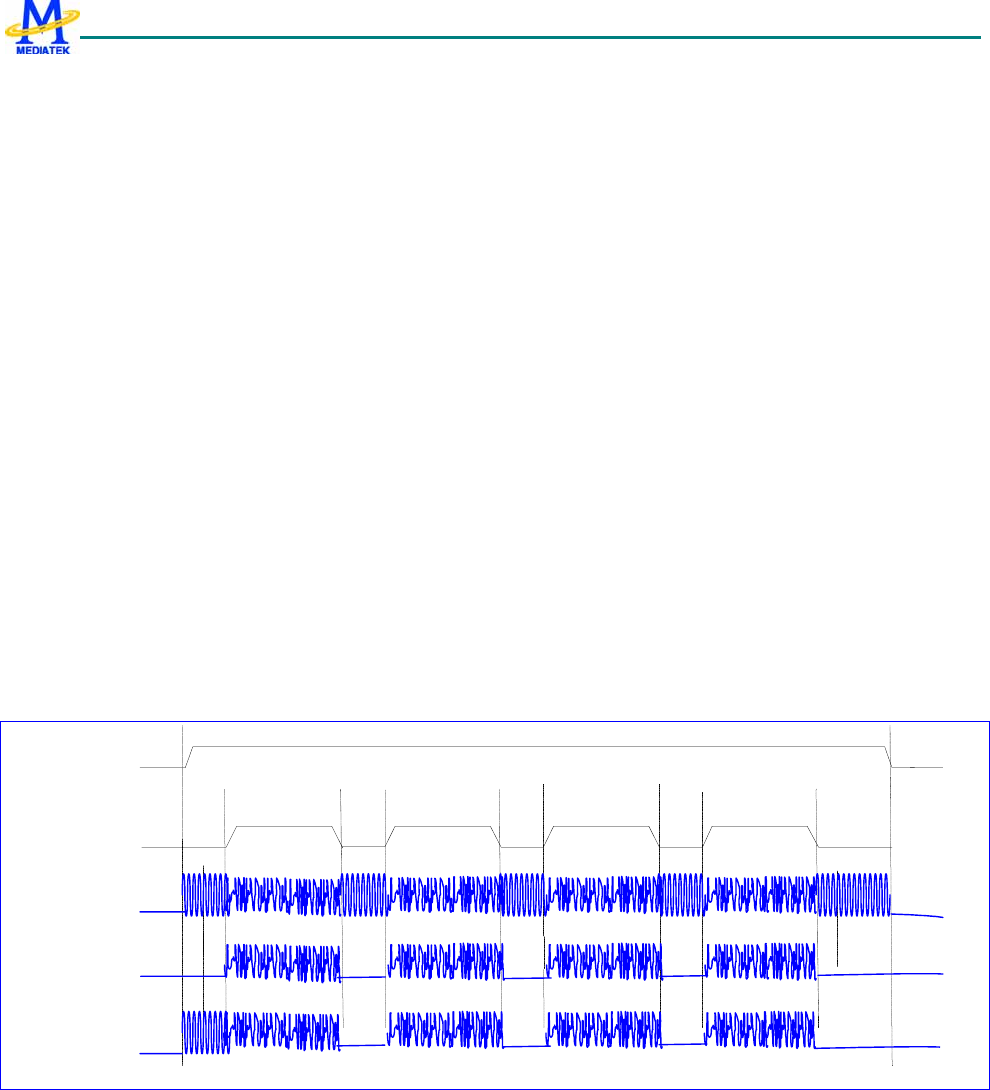
MT6235 GSM/GPRS Baseband Processor Data Sheet Revision 1.02
482/599 MediaTek Inc. Confidential
Additionally, in order to prevent phase discontinuity in between the multiple-burst Mode, the GMSK modulator will output
continuous 67.7khs sine tone outside the burst once RX DAC Enable window is still asserted. Once RX DAC Enable
window is disserted, GMSK modulator will park at DC level.
10.3.5.2 8PSK Modulation
8PSK Modulator is used to convert bit stream of EDGE bursts into basically 8 phase I/Q pair output by means of 8PSK
modulation scheme. It consists of ROM table, timing control logic and some state registers for 8PSK modulation scheme.
The conversion is based on 5 sequential symbol and performed moving average from the ROM table lookup. 8PSK
Modulator is activated when TX dump window is opened. There is one clock delay between assertion of TX dump window
and the first valid output of 8PSK Modulator. The reason is because the bit rate of TX symbols is 270.833 KHz and the
output rate of 8PSK Modulator is 4.333 MHz, and therefore timing synchronization is necessary between the two rates.
10.3.5.2.1 8PSK Ramp Profile
During 8PSKModulation, there will be 3 Ramp Profile to select to choose the BBTX I/Q output during the guard period,
where the DAC_ON is asserted while TX_WINDOW is de-asserted. This control register is an option to adjust the
transmitter performance on “Modulation Transient Spectrum” requirement of ETSI SPEC if different companion Power
Amplifier solution is chosen
By setting RPSEL (Ramp Profile Select) in TX_CFG control register to ‘0’will configured 8PSK Modulator to Ramp
Profile I and I/Q output will be about 50 kHz Sine-tone before the first rising edge of BULFS, after the last falling edge of
BULFS, and in between the bursts. For Ramp Profile II, BBTX I/Q output will be quiescent low DC (null-DC) level during
the guard period.
For Ramp Profile III, initial guard period will be 50 kHz sine-tone, while the reset guard period will be null-DC level.
Ramp Profile I
BULFS
BTXEN
Ramp Profile II
Ramp Profile III
Figure 83 Ramp Profile I/II/III in 8PSK Modulation for Multi-Bursts configuration..
10.3.5.3 I/Q Swap
By setting ‘1’ to IQSWP in TX_CFG control register, phase on I/Q plane will rotate in inverse direction. This option is to
meet the different requirement form RF chip regarding I/Q plane. This control signal is for GMSK Modulation only.

MT6235 GSM/GPRS Baseband Processor Data Sheet Revision 1.02
483/599 MediaTek Inc. Confidential
10.3.5.4 Modulation Output Latency Adjustment
For Multiple bursts, there maybe are consecutive bursts with different modulation mode. (E.g. switch GMSK to 8PSK or
vice versa). However, there are about 8 to 10 QB output latencies for either GMSK/8PSKmodulation output. In order to
match the transition timing of power ramp control in the power amplifier outside the baseband chip, we have to precisely
control the SW_QBCNT (modulation Switching Quarter Bit CouNT) in TX_CFG control register. , which will program the
mode switching timing in QB count unit during the inter-slot period. Normally the inter-slot period is about 33 QB Count,
and the default value to switch the modulation mode is 24 QB count (8 QB count after the middle point)
Additionally, by programming GMSK_DTAP_SYM(GMSK Delay Tap) in TX_CFG and GMSK_DTAP_QB in TX_CON
control register, the output latency for GMSK modulation output can be adjust to compensate the offset between
GMSK/8PSK modulator. The GMSK_DTAP_SYM adjust the output latency in symbol time(3.69us), while
GMSK_DTA_QB adjust in Quarter Bit(QB) Time ( 0.92us).Default value is delay 1 symbol ( 3.69us) of GMSK modulator
output.
10.3.5.5 Modulation Mode Switching
By setting ‘1’ to INTEN(Interpolation Enable) in TX_CFG control register, if two consecutive bursts belongs to 8PSK
Modulation and GMSK Modulation, or vice versa, 32 steps interpolation between two Modulator outputs for 4quater bit
long in guard period..
10.3.5.6 Debug Mode
10.3.5.6.1 Modulation Bypass Mode
For DSP debug purpose, set both ‘1’ for MDBYP(Modulator Bypass) in TX_CFG control register and BYPFLR(Bypass
RX Filter) in RX_CFG control register for directly loopback DSP 16-bits data ( 10bits valid data plus sign or zero extension)
through DAC only.
10.3.5.6.2 Force GMSK/8PSK Modulator turn on
By setting ‘1’ to APNDEN(Append Enable) bit in TX CFG control register, both GMSK and 8PSK modulator will park on
constant DC level during the non-burst period, while the I/Q pair output phase maybe discontinuous since both modulator
will be reset at the beginning of the burst. However, the reset of the modulator will be helpful for the debugging purpose.
10.3.6 Register Definitions
BFE +0060h TX Configuration Register TX_CFG
Bit 15 14 13 12 11 10 9 8 7 6 5 4 3 2 1 0
Name GMSK_DTAP
_SYM SW_QBCNT ALL_10_EN SGEN MDBY
P INTEN RPSEL APND
EN
Type R/W RW RW R/W R/W R/W R/WR/W R/W
Reset 00 18 00 0 0 0 00 0
This register is for configuration of uplink path, inclusive of configuration of TX mixed-signal module and TX path in
Baseband Front End.
APNDEN Appending Bits Enable.(For DSP digital loopback debug mode) The register bit is used to control the ending
scheme of GPRS Mode GMSK modulation only.

MT6235 GSM/GPRS Baseband Processor Data Sheet Revision 1.02
484/599 MediaTek Inc. Confidential
0 Suitable for GPRS /EDGE mode. If a TX enable window contains several TX dump window, then GMSK
modulator will still output in the intervals between two TX dump window and all 1’s will be fed into GMSK
modulator. In the other word, mainly used PA to perform the power ramp up/down, while Modulator output
low amplitude sinewave. Note that when the bit is set to ‘0’, the interval between the moment at which
TX enable window is activated and the moment at which TX dump window is activated must be
multiples of one bit time.
1 Suitable for GSM only. After a TX dump window, GMSK modulator will only output for some bit time.
RPSEL Ramp Profile Select for 8PSK Modulation. The register bit is used to select either Ramp Profile I / Ramp Profile II
for EDGE Mode 8PSK Modulation only.
0 Ramp Profile I. Generate 50Khz sine tone during the guard period among BBTX bursts by repeated input
pattern [7 7 7 7]
1 Ramp Profile II. Generate null DC I/Q output during guard period among BBTX bursts
2 Reserved
3 Ramp Profile III , Generate 50 kHz sine tone after DAC_ON asserted and before TX_WIDNOW asserted if 1st
burst is 8PSK modulation, while the reset guard period always output null DC I/Q output. If the 1st burst is
GMSK modulation, the I/Q output will be always null DC as Ramp Profile II.
INTEN Interpolation Enable. During Multi-bursts Mode, if two consecutive bursts belongs to 8PSK Modulation and
GMSK Modulation, and vise versa or vice versa, set this bit to select either takes 32 steps interpolation between
two Modulator outputs in guard period..
0 Regular Transition Mode.
1 Interpolation Transition Mode.
MDBYP Modulator Bypass (For DSP Debug Mode) Select. The register bit is used to select the bypass mode for I/Q
pair outputs bypassed both the GMSK/8PSK modulator
0 Regular Modulation Mode
1 Bypass Modulator Mode (DSP Debug Mode).
SGEN SineTone Generator Enable.(For Factory Calibration Purpose). The register bit is used to select the TX modulator
output switch to 540 kHz Sine Tone.
0 BBTX output from regulator modulator output.
1 BBTX output switch to 540 kHz sine Tone
ALL_10GEN For Debug mode of BBTX. Generate all 1’s or zero’s input during BBTX valid burst. For GMSK
modulation, set 2’b1 or 2’b10 will generate 67.7 kHz sine tone, while 8PSK modulator will generate 50khz sine
tone. Default value 2’b00 is normal mode.
0 Normal Mode, regular modulator input from Slave DSP TX Buffer.
1 Debug Mode, All zero’s input pattern generated; GMSK modulator will generate 67.7 kHz sine tone. 8PSK
modulator will generate 50 kHz sine tone.
2 Debug Mode All 1’s input pattern generated; GMSK modulator will generate 67.7 kHz sine tone. 8PSK
modulator will generate 50 kHz sine tone.
SW_QBCNT Control the mode switching timing in the inter-slot period in Quarter Bit Count for modulation mode
switching in multiple bursts. Normally the inter-slot period is about 33 QB Count, and the default value to switch the
modulation mode is 24 QB count (8 QB count after the middle point). Program range from “5~31”, while default value is
24.
GMSK_DTAP_SYM Control the GMSK modulator output latency in symbol time (3.69us/symbol) in order to match the
output latency offset between 8PSK /GMSK modulator
0 Delay 1 TAP for GMSK modulator output

MT6235 GSM/GPRS Baseband Processor Data Sheet Revision 1.02
485/599 MediaTek Inc. Confidential
1 No delay for GMSK modulator output
2 Delay 2 TAP for GMSK modulator output
BFE +0064h TX Control Register TX_CON
Bit 15 14 13 12 11 10 9 8 7 6 5 4 3 2 1 0
Name
GMSK_DTAP
_QB PHSEL MDSE
L4 MDSE
L3 MDSE
L2 MDSE
L1 IQSW
P
Type R/W R/W R/W R/W R/W R/W R/W
Reset 00 0000 0 0 0 0 0
This register is for control of uplink path, inclusive of control of TX mixed-signal module and TX path in Baseband Front
End.
IQSWP The register bit is for control of I/Q swapping. When the bit is set to ‘1’, phase on I/Q plane will rotate in inverse
direction. Moreover, this register is double buffered by EVENT_VALIDATE.
0 I and Q are not swapped.
1 I and Q are swapped.
MDSEL1 Modulation Mode Select for 1st Burst. The register bit is used to select either GMSK or 8PSK Modulation for
GSM/GPRS mode or EDGE mode.
0 GMSK Modulation for GSM/GPRS mode.
1 8PSK Modulation for EDGE mode.
MDSEL2 Modulation Mode Select for 2nd Burst. The register bit is used to select either GMSK or 8PSK Modulation for
GSM/GPRS mode or EDGE mode.
0 GMSK Modulation for GSM/GPRS mode.
1 8PSK Modulation for EDGE mode.
MDSEL3 Modulation Mode Select for 3rd Burst. The register bit is used to select either GMSK or 8PSK Modulation for
GSM/GPRS mode or EDGE mode.
0 GMSK Modulation for GSM/GPRS mode.
1 8PSK Modulation for EDGE mode.
MDSEL4 Modulation Mode Select for 4th Burst. The register bit is used to select either GMSK or 8PSK Modulation for
GSM/GPRS mode or EDGE mode.
0 GMSK Modulation for GSM/GPRS mode.
1 8PSK Modulation for EDGE mode.
PHSEL Quadrature phase compensation select
0000: 0 degree compensation.
0001: 1 degree compensation.
0010: 2 degree compensation.
0011: 3 degree compensation.
0100: 4 degree compensation.
0101: 5 degree compensation.
1010: -5 degree compensation.
1011: -4 degree compensation.
1100: -3 degree compensation.
1101: -2 degree compensation.
1110: -1 degree compensation.
1111: 0 degree compensation.

MT6235 GSM/GPRS Baseband Processor Data Sheet Revision 1.02
486/599 MediaTek Inc. Confidential
GMSK_DTAP_QB Control the GMSK modulator output latency in Quarter Bit(QB) Time (0.92us/QB) in order to
match the output latency offset between 8PSK /GMSK modulator
0 No Delay GMSK modulator output
1 Delay 1QB for GMSK modulator output
2 Delay 2 QB for GMSK modulator output
3 Delay 3QB for GMSK modulator output
BFE +0068h TX I/Q Channel Offset Compensation Register TX_OFF
Bit 15 14 13 12 11 10 9 8 7 6 5 4 3 2 1 0
Name OFF_
TYP OFFQ[5:0] OFFI[5:0]
Type R/W R/W R/W
Reset 0 000000 000000
The register is for offset cancellation of I-channel DAC in TX mixed-signal module. It is for compensation of offset error
caused by I/Q-channel DAC in TX mixed-signal module. It is coded in 2’s complement, that is, with maximum 31 and
minimum –32.
OFFI Value of offset cancellation for I-channel DAC in TX mixed-signal module
OFFQ Value of offset cancellation for Q-channel DAC in TX mixed-signal module
OFF_TYP Type of the OFFI and OFFQ register. While OFF_TYP = 1, the offset values are double buffered and can be
chaneged burst by burst after EVENT_VALIDATE comes. Otherwise, the offset values would change immidately
after the coming of APB commands, which can't be adjusted burst by burst.
0 No double buffer
1 Double buffered
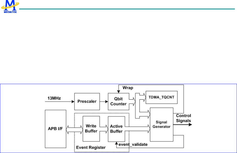
MT6235 GSM/GPRS Baseband Processor Data Sheet Revision 1.02
487/599 MediaTek Inc. Confidential
11 Timing Generator
Timing is the most critical issue in GSM/GPRS applications. The TDMA timer provides a simple interface for the MCU to
program all the timing-related events for receive event control, transmit event control and the timing adjustment. Detailed
descriptions are mentioned in Section 11.1.
11.1 TDMA timer
The TDMA timer unit is composed of three major blocks: Quarter bit counter, Signal generator and Event registers.
Figure 84 The block diagram of TDMA timer
By default, the quarter-bit counter continuously counts from 0 to the wrap position. In order to apply to cell synchronization
and neighboring cell monitoring, the wrap position can be changed by the MCU to shorten or lengthen a TDMA frame. The
wrap position is held in the TDMA_WRAP register and the current value of the TDMA quarter bit counter may be read by
the MCU via the TDMA_TQCNT register.
The signal generator handles the overall comparing and event-generating processes. When a match has occurred between
the quarter bit counter and the event register, a predefined control signal is generated. These control signals may be used for
on-chip and off-chip purposes. Signals that change state more than once per frame make use of more than one event
register.
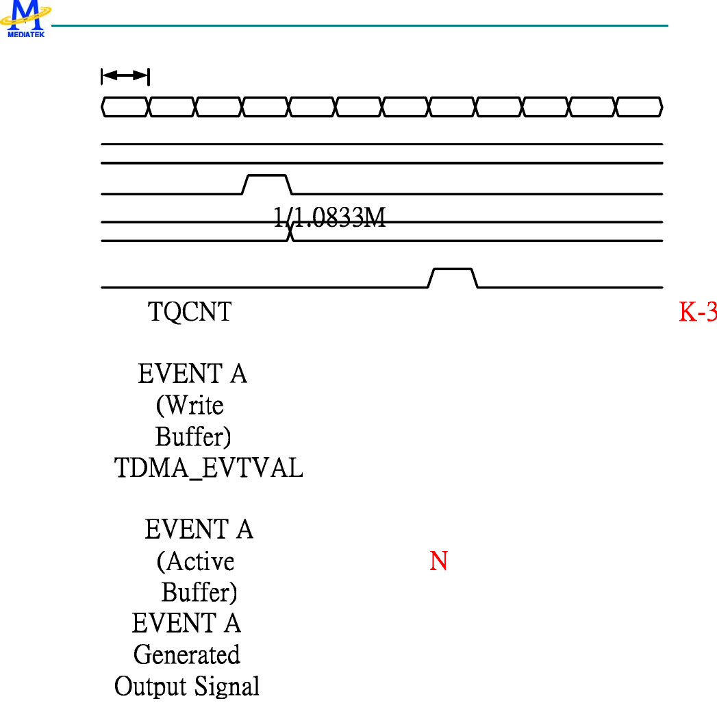
MT6235 GSM/GPRS Baseband Processor Data Sheet Revision 1.02
488/599 MediaTek Inc. Confidential
The event registers are programmed to contain the quarter bit position of the event that is to occur. The event registers are
double buffered. The MCU writes into the write buffers of the registers, and the event TDMA_EVTVAL trigger HW to
transfer the data from the write buffers to the active buffers. Caution: values in the active buffers are updated at the end of
qbit count (TDMA_EVTVAL). The TDMA_EVTVAL signal itself may be programmed at any quarter bit position. These
event registers could be classified into four groups:
On-chip Control Events
TDMA_EVTVAL
This event allows the data values written by the MCU to pass through to the active buffers.
TDMA_WRAP
TDMA quarter bit counter wrap position. This sets the position at which the TDMA quarter bit counter resets back to zero.
The default value is 4999, changing this value will advance or retard the timing events in the frame following the next
TDMA_EVTVAL signal. Caution: The wrap value of the first frame after the sleep mode will refer to TQWRAP_SM value
if SW enables turbo sleep mode.
TDMA_DTIRQ
DSP TDMA interrupt requests. DTIRQ triggers the DSP to read the command from the MCU/DSP Shard RAM to schedule
the activities that will be executed in the current frame.
TDMA_CTIRQ1/CTIRQ2
MCU TDMA interrupt requests. CTIRQx triggers the ARM to schedule the activities that will be executed in the next
frame.
TDMA_AUXADC [1:0]
This signal triggers the monitoring ADC to measure the voltage, current, temperature, device id etc..
TDMA_AFC [3:0]
This signal powers up the automatic frequency control DAC for a programmed duration after this event.
Note: For both MCU and DSP TDMA interrupt requests, these signals are all active Low during one quarter bit duration
and they should be used as edge sensitive events by the respective interrupt controllers.
On-chip Receive Events
TDMA_BDLON [5:0]
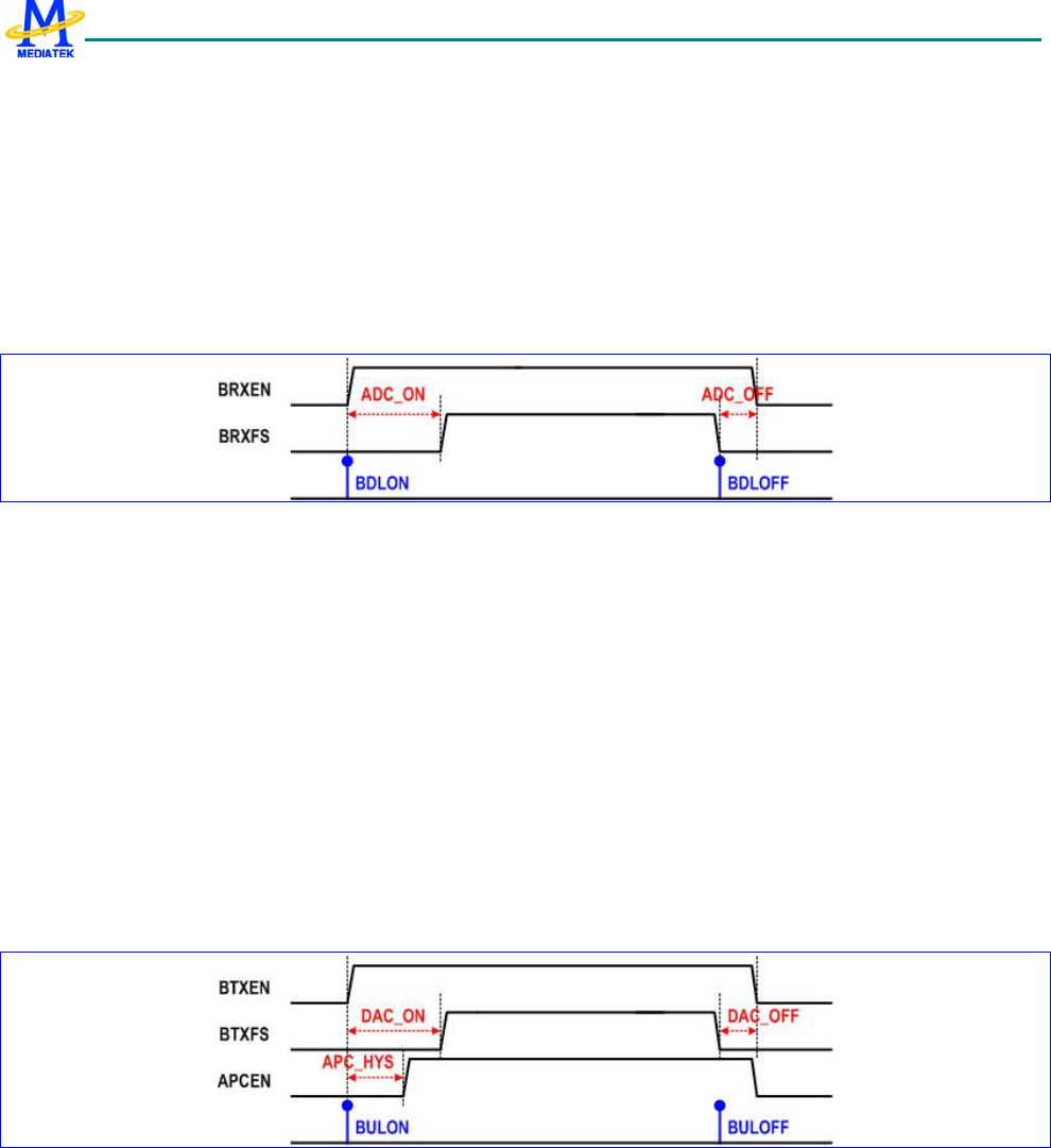
MT6235 GSM/GPRS Baseband Processor Data Sheet Revision 1.02
489/599 MediaTek Inc. Confidential
These registers are a set of six which contain the quarter bit event that initiates the receive window assertion sequence
which powers up and enables the receive ADC, and then enables loading of the receive data into the receive buffer.
TDMA_BDLOFF [5:0]
These registers are a set of six which contain the quarter bit event that initiates the receive window de-assertion sequence
which disables loading of the receive data into the receive buffer, and then powers down the receive ADC.
TDMA_RXWIN[5:0]
DSP TDMA interrupt requests. TDMA_RXWIN is usually used to initiate the related RX processing including two modes.
In single-shot mode, TDMA_RXWIN is generated when the BRXFS signal is de-asserted. In repetitive mode,
TDMA_RXWIN will be generated both regularly with a specific interval after BRXFS signal is asserted and when the
BRXFS signal is de-asserted.
Figure 85 The timing diagram of BRXEN and BRXFS
Note: TDMA_BDLON/OFF event registers, together with TDMA_BDLCON register, generate the corresponding BRXEN
and BRXFS window used to power up/down baseband downlink path and control the duration of data transmission to the
DSP, respectively.
On-chip Transmit Events
TDMA_APC [6:0]
These registers initiate the loading of the transmit burst shaping values from the transmit burst shaping RAM into the
transmit power control DAC.
TDMA_BULON [3:0]
This register contains the quarter bit event that initiates the transmit window assertion sequence which powers up the
modulator DAC and then enables reading of bits from the transmit buffer into the GMSK modulator.
TDMA_BULOFF [3:0]
This register contains the quarter bit event that initiates the transmit window de-assertion sequence which disables the
reading of bits from the transmit buffer into the GMSK modulator, and then power down the modulator DAC.
Figure 86 The timing diagram of BTXEN and BTXFS
Note: TDMA_BULON/OFF event registers, together with TDMA_BULCON1, TDMA_BULCON2 register, generate the
corresponding BTXEN, BTXFS and APCEN window used to power up/down the baseband uplink path, control the duration
of data transmission from the DSP and power up/down the APC DAC, respectively.
Off-chip Control Events
TDMA_BSI [19:0]
MT6235 GSM/GPRS Baseband Processor Data Sheet Revision 1.02
490/599 MediaTek Inc. Confidential
The quarter bit positions of these 20 BSI events are used to initiate the transfer of serial words to the transceiver and
synthesizer for gain control and frequency adjustment.
TDMA_BPI [41:0]
The quarter bit positions of these 30 BPI events are used to generate changes of state on the output pins to control the
external radio components.
11.1.1 Register Definitions
0x82000150 Event Enable Register 0 TDMA_EVTENA
0
Bit 15 14 13 12 11 10 9 8 7 6 5 4 3 2 1 0
Name AFC3 AFC2 AFC1 AFC0 BDL5 BDL4 BDL3 BDL2 BDL1 BDL0 CTIRQ
2 CTIRQ
1 DTIR
Q
Type R/W R/W R/W R/W R/W R/W R/W R/W R/W R/W R/W R/W R/W
Reset 0 0 0 0 0 0 0 0 0 0 0 0 0
DTIRQ Enable TDMA_DTIRQ
CTIRQn Enable TDMA_CTIRQn
AFCn Enable TDMA_AFCn
BDLn Enable TDMA_BDLONn and TDMA_BDLOFFn
For all these bits,
0 function is disabled
1 function is enabled
0x82000154h Event Enable Register 1 TDMA_EVTENA
1
Bit 15 14 13 12 11 10 9 8 7 6 5 4 3 2 1 0
Name GPRS BUL3 BUL2 BUL1 BUL0 APC6 APC5 APC4 APC3 APC2 APC1 APC0
Type R/W R/W R/W R/W R/W R/W R/W R/W R/W R/W R/W R/W
Reset 0 0 0 0 0 0 0 0 0 0 0 0
GPRS Indicate which mode is on-going.
0 TDMA_APC0 & TDMA_APC1 events are controlled by APC0 & APC1 in the register TDMA_EVTENA1 &
TDMA_DTXCON. (GSM mode)
1 TDMA_APC0 & TDMA_APC1 events are controlled by APC0 & APC1 in the register TDMA_EVTENA1
only. (GPRS mode)
APCn Enable TDMA_APCn
BULn Enable TDMA_BULONn and TDMA_BULOFFn
For all these bits,
0 function is disabled
1 function is enabled
0x82000158 Event Enable Register 2 TDMA_EVTENA
2
Bit 15 14 13 12 11 10 9 8 7 6 5 4 3 2 1 0
Name BSI15 BSI14 BSI13 BSI12 BSI11 BSI10 BSI9 BSI8 BSI7 BSI6 BSI5 BSI4 BSI3 BSI2 BSI1 BSI0
MT6235 GSM/GPRS Baseband Processor Data Sheet Revision 1.02
491/599 MediaTek Inc. Confidential
Type R/W R/W R/W R/W R/W R/W R/W R/W R/W R/W R/W R/W R/W R/W R/W R/W
Reset 0 0 0 0 0 0 0 0 0 0 0 0 0 0 0 0
0x8200015C Event Enable Register 3 TDMA_EVTENA
3
Bit 15 14 13 12 11 10 9 8 7 6 5 4 3 2 1 0
Name BSI19 BSI18 BSI17 BSI16
Type R/W R/W R/W R/W
Reset 0 0 0 0
BSIn BSI event enable control
0 Disable TDMA_BSIn
1 Enable TDMA_BSIn
0x82000160 Event Enable Register 4 TDMA_EVTENA
4
Bit 15 14 13 12 11 10 9 8 7 6 5 4 3 2 1 0
Name BPI15 BPI14 BPI13 BPI12 BPI11 BPI10 BPI9 BPI8 BPI7 BPI6 BPI5 BPI4 BPI3 BPI2 BPI1 BPI0
Type R/W R/W R/W R/W R/W R/W R/W R/W R/W R/W R/W R/W R/W R/W R/W R/W
Reset 0 0 0 0 0 0 0 0 0 0 0 0 0 0 0 0
0x82000164 Event Enable Register 5 TDMA_EVTENA
5
Bit 15 14 13 12 11 10 9 8 7 6 5 4 3 2 1 0
Name BPI31 BPI30 BPI29 BPI28 BPI27 BPI26 BPI25 BPI24 BPI23 BPI22 BPI21 BPI20 BPI19 BPI18 BPI17 BPI16
Type R/W R/W R/W R/W R/W R/W R/W R/W R/W R/W R/W R/W R/W R/W R/W R/W
Reset 0 0 0 0 0 0 0 0 0 0 0 0 0 0 0 0
BPIn BPI event enable control
0 Disable TDMA_BPIn
1 Enable TDMA_BPIn
0x82000168 Event Enable Register 6 TDMA_EVTENA
6
Bit 15 14 13 12 11 10 9 8 7 6 5 4 3 2 1 0
Name BPI41 BPI40 BPI39 BPI38 BPI37 BPI36 BPI35 BPI34 BPI33 BPI32
Type R/W R/W R/W R/W R/W R/W R/W R/W R/W R/W
Reset 0 0 0 0 0 0 0 0 0 0
BPIn BPI event enable control
0 Disable TDMA_BPIn
1 Enable TDMA_BPIn
MT6235 GSM/GPRS Baseband Processor Data Sheet Revision 1.02
492/599 MediaTek Inc. Confidential
0x8200016C Event Enable Register 7 TDMA_EVTENA
7
Bit 15 14 13 12 11 10 9 8 7 6 5 4 3 2 1 0
Name AUX1 AUX0
Type R/W R/W
Reset 0 0
AUX Auxiliary ADC event enable control
0 Disable Auxiliary ADC event
1 Enable Auxiliary ADC event
0x82000170 Qbit Timer Offset Control Register TDMA_WRAPOF
S
Bit 15 14 13 12 11 10 9 8 7 6 5 4 3 2 1 0
Name TOI[1:0]
Type R/W
Reset 0
TOI This register defines the value used to advance the Qbit timer in unit of 1/4 quarter bit; the timing advance will be
take place as soon as the TDMA_EVTVAL is occurred, and it will be cleared automatically.
0x82000174 Qbit Timer Biasing Control Register TDMA_REGBIA
S
Bit 15 14 13 12 11 10 9 8 7 6 5 4 3 2 1 0
Name TQ_BIAS[13:0]
Type R/W
Reset 0
TQ_BIAS This register defines the Qbit offset value which will be added to the registers being programmed. It only
takes effects on AFC, BDLON/OFF, BULON/OFF, APC, AUXADC, BSI and BPI event registers.
0x82000180 DTX Control Register TDMA_DTXCON
Bit 15 14 13 12 11 10 9 8 7 6 5 4 3 2 1 0
Name DTX3 DTX2 DTX1 DTX0
Type R/W R/W R/W R/W
DTX DTX flag is used to disable the associated transmit signals
0 BULON0~3, BULOFF0~3, APC_EV0 & APC_EV1 are controlled by TDMA_EVTENA1 register
1 BULON0~3, BULOFF0~3, APC_EV0 & APC_EV1 are disabled
0x82000184 Receive Interrupt Control Register TDMA_RXCON
Bit 15 14 13 12 11 10 9 8 7 6 5 4 3 2 1 0
Name MOD5 MOD4 MOD3 MOD2 MOD1 MOD0 RXINTCNT[9:0]
Type R/W R/W R/W R/W R/W R/W R/W
MT6235 GSM/GPRS Baseband Processor Data Sheet Revision 1.02
493/599 MediaTek Inc. Confidential
RXINTCNT TDMA_RXWIN interrupt generation interval in quarter bit unit
MODn Mode of Receive Interrupts
0 Single shot mode for the corresponding receive window
1 Repetitive mode for the corresponding receive window
0x82000188 Baseband Downlink Control Register TDMA_BDLCON
Bit 15 14 13 12 11 10 9 8 7 6 5 4 3 2 1 0
Name ADC_ON ADC_OFF
Type R/W R/W
ADC_ON BRXEN to BRXFS setup up time in quarter bit unit.
ADC_OFF BRXEN to BRXFS hold up time in quarter bit unit.
0x8200018C Baseband Uplink Control Register 1 TDMA_BULCON
1
Bit 15 14 13 12 11 10 9 8 7 6 5 4 3 2 1 0
Name DAC_ON DAC_OFF
Type R/W R/W
DAC_ON BTXEN to BTXFS setup up time in quarter bit unit.
DAC_OFF BTXEN to BTXFS hold up time in quarter bit unit.
0x82000190 Baseband Uplink Control Register 2 TDMA_BULCON
2
Bit 15 14 13 12 11 10 9 8 7 6 5 4 3 2 1 0
Name APC_HYS
Type R/W
APC_HYS APCEN to BTXEN hysteresis time in quarter bit unit.
0x82000194 Frequency Burst Indication Register TDMA_FB_FLA
G
Bit 15 14 13 12 11 10 9 8 7 6 5 4 3 2 1 0
Name FBDL
5 FBDL
4 FBDL
3 FBDL
2 FBDL
1 FBDL
0
Type R/W R/W R/W R/W R/W R/W
FBDLn Indication of frequency burst for RX window n
The register is double-buffered. The value at the write buffers will be auto-cleared at the next event-validate
(TDMA_EVTVAL) and its value will be at the same time loaded to the active buffer. The exact FB indication comes from
the active buffer and the corresponding mode in register TDMA_RXCON (Bit15~Bit10). It will be asserted after
TDMA_EVTVAL signals if the corresponding FBDLx & TDMA_RXCON[x+10] are set to 1. The FB indication
de-assertion only depends TDMA_FB_CLRI and the falling edge of the corresponding RX window.

MT6235 GSM/GPRS Baseband Processor Data Sheet Revision 1.02
494/599 MediaTek Inc. Confidential
0x82000198 Direct Frequency Burst Closing TDMA_FB_CLRI
Bit 15 14 13 12 11 10 9 8 7 6 5 4 3 2 1 0
Name
Type
As long as the register is written, active buffer for FB indication will be reset then therefore the frequency burst indication
will be forced to 0.
Address Type Width Reset Value Name Description
0x80000000 R [13:0] — TDMA_TQCNT Read quarter bit counter
0x82000004 R/W [13:0] 0x1387 TDMA_WRAP Latched Qbit counter reset position
0x82000008 R/W [13:0] 0x1387 TDMA_WRAPIMD Direct Qbit counter reset position
0x8200000C R/W [13:0] 0x0000 TDMA_EVTVAL Event latch position
0x82000010 R/W [13:0] — TDMA_DTIRQ DSP software control
0x82000014 R/W [13:0] — TDMA_CTIRQ1 MCU software control 1
0x82000018 R/W [13:0] — TDMA_CTIRQ2 MCU software control 2
0x82000020 R/W [13:0] — TDMA_AFC0 The 1st AFC control
0x82000024 R/W [13:0] — TDMA_AFC1 The 2nd AFC control
0x82000028 R/W [13:0] — TDMA_AFC2 The 3rd AFC control
0x8200002C R/W [13:0] — TDMA_AFC3 The 4th AFC control
0x82000030 R/W [13:0] — TDMA_BDLON0
0x82000034 R/W [13:0] — TDMA_BDLOFF0 Data serialization of the 1st RX block
0x82000038 R/W [13:0] — TDMA_BDLON1
0x8200003C R/W [13:0] — TDMA_BDLOFF1 Data serialization of the 2nd RX block
0x82000040 R/W [13:0] — TDMA_BDLON2
0x82000044 R/W [13:0] — TDMA_BDLOFF2 Data serialization of the 3rd RX block
0x82000048 R/W [13:0] — TDMA_BDLON3
0x8200004C R/W [13:0] — TDMA_BDLOFF3 Data serialization of the 4th RX block
0x82000050 R/W [13:0] — TDMA_BDLON4
0x82000054 R/W [13:0] — TDMA_BDLOFF4 Data serialization of the 5th RX block
0x82000058 R/W [13:0] — TDMA_BDLON5
0x8200005C R/W [13:0] — TDMA_BDLOFF5 Data serialization of the 6th RX block
0x82000060 R/W [13:0] — TDMA_BULON0
0x82000064 R/W [13:0] — TDMA_BULOFF0 Data serialization of the 1st TX slot
0x82000068 R/W [13:0] — TDMA_BULON1
0x8200006C R/W [13:0] — TDMA_BULOFF1 Data serialization of the 2nd TX slot
0x82000070 R/W [13:0] — TDMA_BULON2
0x82000074 R/W [13:0] — TDMA_BULOFF2 Data serialization of the 3rd TX slot
0x82000078 R/W [13:0] — TDMA_BULON3
0x8200007C R/W [13:0] — TDMA_BULOFF3 Data serialization of the 4th TX slot

MT6235 GSM/GPRS Baseband Processor Data Sheet Revision 1.02
495/599 MediaTek Inc. Confidential
0x82000090 R/W [13:0] — TDMA_APC0 The 1st APC control
0x82000094 R/W [13:0] — TDMA_APC1 The 2nd APC control
0x82000098 R/W [13:0] — TDMA_APC2 The 3rd APC control
0x8200009C R/W [13:0] — TDMA_APC3 The 4th APC control
0x820000A0 R/W [13:0] — TDMA_APC4 The 5th APC control
0x820000A4 R/W [13:0] — TDMA_APC5 The 6th APC control
0x820000A8 R/W [13:0] — TDMA_APC6 The 7th APC control
0x820000B0 R/W [13:0] — TDMA_BSI0 BSI event 0
0x820000B4 R/W [13:0] — TDMA_BSI1 BSI event 1
0x820000B8 R/W [13:0] — TDMA_BSI2 BSI event 2
0x820000BC R/W [13:0] — TDMA_BSI3 BSI event 3
0x820000C0 R/W [13:0] — TDMA_BSI4 BSI event 4
0x820000C4 R/W [13:0] — TDMA_BSI5 BSI event 5
0x820000C8 R/W [13:0] — TDMA_BSI6 BSI event 6
0x820000CC R/W [13:0] — TDMA_BSI7 BSI event 7
0x820000D0 R/W [13:0] — TDMA_BSI8 BSI event 8
0x820000D4 R/W [13:0] — TDMA_BSI9 BSI event 9
0x820000D8 R/W [13:0] — TDMA_BSI10 BSI event 10
0x820000DC R/W [13:0] — TDMA_BSI11 BSI event 11
0x820000E0 R/W [13:0] — TDMA_BSI12 BSI event 12
0x820000E4 R/W [13:0] — TDMA_BSI13 BSI event 13
0x820000E8 R/W [13:0] — TDMA_BSI14 BSI event 14
0x820000EC R/W [13:0] — TDMA_BSI15 BSI event 15
0x820000F0 R/W [13:0] — TDMA_BSI16 BSI event 16
0x820000F4 R/W [13:0] — TDMA_BSI17 BSI event 17
0x820000F8 R/W [13:0] — TDMA_BSI18 BSI event 18
0x820000FC R/W [13:0] — TDMA_BSI19 BSI event 19
0x82000100 R/W [13:0] — TDMA_BPI0 BPI event 0
0x82000104 R/W [13:0] — TDMA_BPI1 BPI event 1
0x82000108 R/W [13:0] — TDMA_BPI2 BPI event 2
0x8200010C R/W [13:0] — TDMA_BPI3 BPI event 3
0x82000110 R/W [13:0] — TDMA_BPI4 BPI event 4
0x82000114 R/W [13:0] — TDMA_BPI5 BPI event 5
0x82000118 R/W [13:0] — TDMA_BPI6 BPI event 6
0x8200011C R/W [13:0] — TDMA_BPI7 BPI event 7
0x82000120 R/W [13:0] — TDMA_BPI8 BPI event 8
0x82000124 R/W [13:0] — TDMA_BPI9 BPI event 9
0x82000128 R/W [13:0] — TDMA_BPI10 BPI event 10
0x8200012C R/W [13:0] — TDMA_BPI11 BPI event 11

MT6235 GSM/GPRS Baseband Processor Data Sheet Revision 1.02
496/599 MediaTek Inc. Confidential
0x82000130 R/W [13:0] — TDMA_BPI12 BPI event 12
0x82000134 R/W [13:0] — TDMA_BPI13 BPI event 13
0x82000138 R/W [13:0] — TDMA_BPI14 BPI event 14
0x8200013C R/W [13:0] — TDMA_BPI15 BPI event 15
0x82000140 R/W [13:0] — TDMA_BPI16 BPI event 16
0x82000144 R/W [13:0] — TDMA_BPI17 BPI event 17
0x82000148 R/W [13:0] — TDMA_BPI18 BPI event 18
0x8200014C R/W [13:0] — TDMA_BPI19 BPI event 19
0x820001A0 R/W [13:0] — TDMA_BPI20 BPI event 20
0x820001A4 R/W [13:0] — TDMA_BPI21 BPI event 21
0x820001A8 R/W [13:0] — TDMA_BPI22 BPI event 22
0x820001AC R/W [13:0] — TDMA_BPI23 BPI event 23
0x820001B0 R/W [13:0] — TDMA_BPI24 BPI event 24
0x820001B4 R/W [13:0] — TDMA_BPI25 BPI event 25
0x820001B8 R/W [13:0] — TDMA_BPI26 BPI event 26
0x820001BC R/W [13:0] — TDMA_BPI27 BPI event 27
0x820001C0 R/W [13:0] — TDMA_BPI28 BPI event 28
0x820001C4 R/W [13:0] — TDMA_BPI29 BPI event 29
0x820001C8 R/W [13:0] — TDMA_BPI30 BPI event 30
0x820001CC R/W [13:0] — TDMA_BPI31 BPI event 31
0x820001D0 R/W [13:0] — TDMA_BPI32 BPI event 32
0x820001D4 R/W [13:0] — TDMA_BPI33 BPI event 33
0x820001D8 R/W [13:0] — TDMA_BPI34 BPI event 34
0x820001DC R/W [13:0] — TDMA_BPI35 BPI event 35
0x820001E0 R/W [13:0] — TDMA_BPI36 BPI event 36
0x820001E4 R/W [13:0] — TDMA_BPI37 BPI event 37
0x820001E8 R/W [13:0] — TDMA_BPI38 BPI event 38
0x820001EC R/W [13:0] — TDMA_BPI39 BPI event 39
0x820001F0 R/W [13:0] — TDMA_BPI40 BPI event 40
0x820001F4 R/W [13:0] — TDMA_BPI41 BPI event 41
0x82000400 R/W [13:0] — TDMA_AUXEV0 Auxiliary ADC event 0
0x82000404 R/W [13:0] — TDMA_AUXEV1 Auxiliary ADC event 1
0x82000150 R/W [15:0] 0x0000 TDMA_EVTENA0 Event Enable Control 0
0x82000154 R/W [15:0] 0x0000 TDMA_EVTENA1 Event Enable Control 1
0x82000158 R/W [15:0] 0x0000 TDMA_EVTENA2 Event Enable Control 2
0x8200015C R/W [3:0] 0x0000 TDMA_EVTENA3 Event Enable Control 3
0x82000160 R/W [15:0] 0x0000 TDMA_EVTENA4 Event Enable Control 4
0x82000164 R/W [13:0] 0x0000 TDMA_EVTENA5 Event Enable Control 5
0x82000168 R/W [1:0] 0x0000 TDMA_EVTENA6 Event Enable Control 6
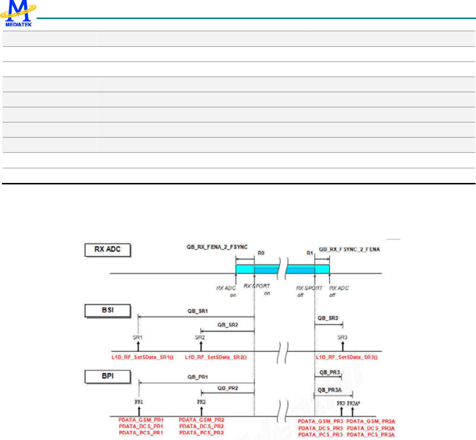
MT6235 GSM/GPRS Baseband Processor Data Sheet Revision 1.02
497/599 MediaTek Inc. Confidential
0x8200016C R/W [11:0] 0x0000 TDMA_EVTENA7 Event Enable Control 7
0x82000170 R/W [1:0] 0x0000 TDMA_WRAPOFS TQ Counter Offset Control Register
0x82000174 R/W [13:0] 0x0000 TDMA_REGBIAS Biasing Control Register
0x82000180 R/W [3:0] — TDMA_DTXCON DTX Control Register
0x82000184 R/W [15:0] — TDMA_RXCON Receive Interrupt Control Register
0x82000188 R/W [15:0] — TDMA_BDLCON Downlink Control Register
0x8200018C R/W [15:0] — TDMA_BULCON1 Uplink Control Register 1
0x82000190 R/W [7:0] — TDMA_BULCON2 Uplink Control Register 2
0x82000194 R/W [5:0] — TDMA_FB_FLAG FB indicator
0x82000198 W — TDMA_FB_CLRI Direct clear of FB indicator
Table 47 TDMA Timer Register Map
11.1.2 Application Note
Figure 87 RX Timing Set Example
The TDMA timing and data setting are described in 2 parts. One part is that before turning on RX SPORT to receiving I/Q
data. And the other part is after turning off RX SPORT to finish receiving I/Q data. To describe these two parts easily, the
timing of turning on RX SPORT is taken as one base named R0. And the timing of turning off RX SPORT is taken as one
base named R1.
RX ADC part:
To setup the timing of RX ADC and SPORT, 2 timings need to be defined in l1d_custom_rf.h. The time from RX ADC
enabling to RX SPORT turning on (R0) is defined as QB_RX_FENA_2_FSYNC.The time from RX SPORT turning on
(R1) to RX ADC disabling is defined as QB_RX_FSYNC_2_FENA. The value of this two aliases should be positive or
zero. These two values is defined in the register TDMA_BDLCON.
BSI part:
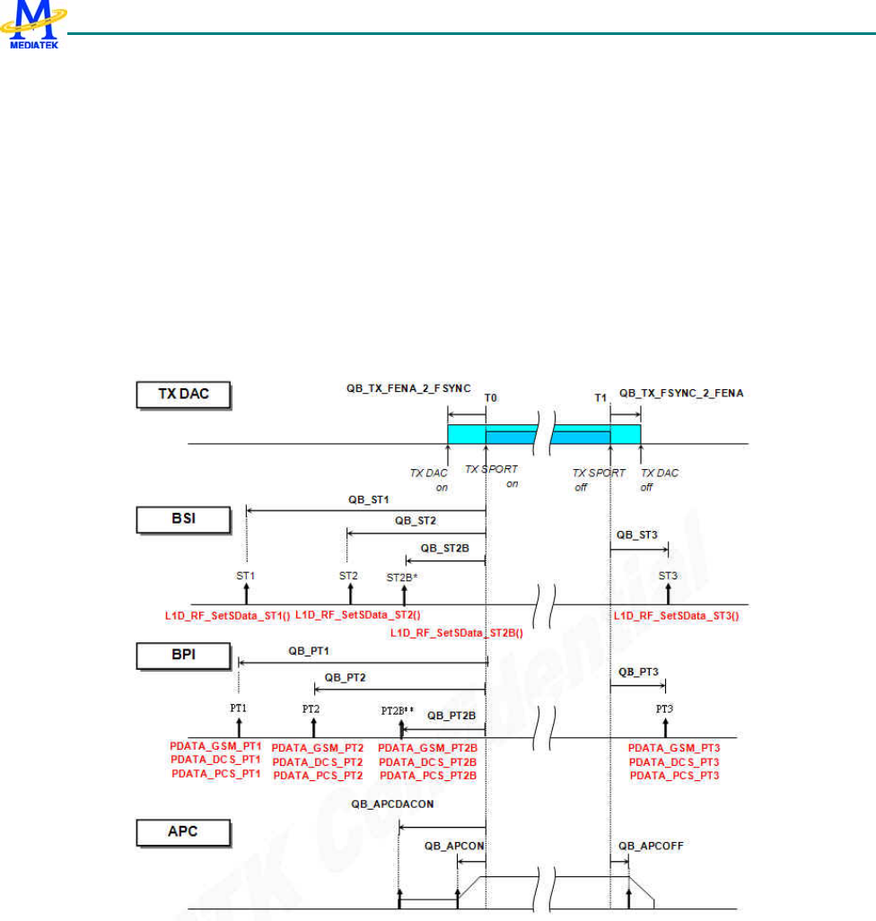
MT6235 GSM/GPRS Baseband Processor Data Sheet Revision 1.02
498/599 MediaTek Inc. Confidential
BSI data and events need to be set in serial to a 3-wire base RF module. Each RX window is allocated 3 BSI events.
Usually 1'st BSI event is used to warm up the synthesizer and set its N-counter to lock the operation frequency. The 2'nd
BSI is used to set the receiving amplifier gain of transceiver. The 3'rd BSI is used to command transceiver entering idle
mode. BSI events are defined in the registers TDMA_BSI0~19.
BPI part:
The connection of HW signals of BPI data bus and RF module is flexible and depends on customer's design. The setting
timing and data setting of BPI bus are used to specify at what time and which BPI states are changed. The BPI data may be
varied by the operation band, so the dedicate BPI data of each band should be defined. The states transient of BPI signals
are decided by the time of event, therefore the active time and the BPI states for each band shall be defined. BPI events are
defined in the registers TDMA_BPI0~41.
TX ADC part:
To setup the timing of TX DAC and SPORT, 2 timings need to be defined in l1d_custom.h. The time from TX DAC
enabling to TX SPORT turning on (T0) is defined as QB_TX_FENA_2_FSYNC.The time from TX SPORT turning on
(T1) to TX DAC disabling is defined as QB_TX_FSYNC_2_FENA. The value of this two aliases should be positive or
zero. These two values is defined in the register TDMA_BULCON1.
BSI part:
BSI data and events need to be set in order to sent serial data to 3-wire devices on RF module. Each TX window is
allocated 3 BSI events. Usually 1'st BSI event is used to warm up the set synthesizer and set its N-counter to lock the
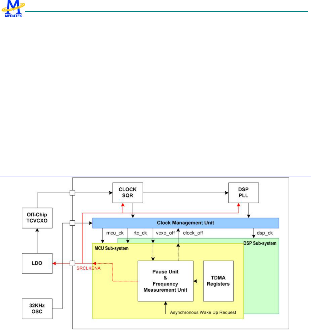
MT6235 GSM/GPRS Baseband Processor Data Sheet Revision 1.02
499/599 MediaTek Inc. Confidential
operation frequency. The 2'nd BSI is used to set the transmit command and indicate the operation band. The 3'rd BSI is
used to command transceiver entering idle mode. BSI events are defined in the registers TDMA_BSI0~19.
BPI parts:
The setting of BPI bus includes timing and data setting to specify at what time what BPI states are changed. The BPI data
may be varied by operation band, so the BPI data of each band should be defined. The 1'st BPI event is usually used to
activate the RF components on RF module in transmit mode. The 2'nd BPI event is usually used to select band and switch
R/TX. The 3'rd BPI event is usually used to force the RF module into idle mode. BPI events are defined in the registers
TDMA_BPI0~41.
APC parts:
In addition to TX DAC, TX SPORT, BSI, BPI unit needs to be set, the control of PA is important for TX window. The PA is
control by the APC unit of MT62xx. Before the data transmission, APC ramps up the PA to the indicated power level. Data
is transmitted at that level. After finishing transmission, APC ramps down the PA. Before PA ramping up, A DC offset of PA
is performed to let PA ramp up smoothly. APC events are defined in the registers TDMA_APC0~6.
11.2 Slow Clocking Unit
Figure 88 The block diagram of the slow clocking unit
The slow clocking unit is provided to maintain the synchronization to the base-station timing using a 32KHz crystal
oscillator while the 13MHz reference clock is switched off. As shown in Figure 88, this unit is composed of frequency
measurement unit, pause unit, and clock management unit.
Because of the inaccuracy of the 32KHz oscillator, a frequency measurement unit is provided to calibrate the 32KHz crystal
taking the accurate 13MHz source as the reference. The calibration procedure always takes place prior to the pause period.

MT6235 GSM/GPRS Baseband Processor Data Sheet Revision 1.02
500/599 MediaTek Inc. Confidential
The pause unit is used to initiate and terminate the pause mode procedure and it also works as a coarse time-base during the
pause period.
The clock management unit is used to control the system clock while switching between the normal mode and the pause
mode. SRCLKENA is used to turn on/off the clock squarer, DSP PLL and off-chip TCVCXO. CLOCK_OFF signal is used
for gating the main MCU and DSP clock, and VCXO_OFF is used as the acknowledgement signal of the CLOCK_OFF
request.
11.2.1 Register Definitions
0x82000218 Slow clocking unit control register SM_CON
Bit 15 14 13 12 11 10 9 8 7 6 5 4 3 2 1 0
Name PAUSE_STA
RT FM_STAR
T
Type W W
Reset 0 0
FM_START Initiate the frequency measurement procedure
PAUSE_START Initiate the pause mode procedure at the next timer wrap position
0x8200021C Slow clocking unit status register SM_STA
Bit 15 14 13 12 11 10 9 8
Name PAUSE_ABO
RT
Type R
Bit 7 6 5 4 3 2 1 0
Name SETTLE_CP
L PAUSE_CPL PAUSE_INT PAUSE_RQS
T FM_CPL FM_RQST
Type R R R R R R
FM_RQST Frequency measurement procedure is requested
FM_CPL Frequency measurement procedure is completed
PAUSE_RQST Pause mode procedure is requested
PAUSE_INT Asynchronous wake up from pause mode
PAUSE_CPL Pause period is completed
SETTLE_CPL Settling period is completed
PAUSE_ABORT Pause mode is aborted because of the reception of interrupt prior to entering pause mode
0x8200022C Slow clocking unit configuration register SM_CNF
Bit 15 14 13 12 11 10 9 8 7 6 5 4 3 2 1 0
Name TP MSDC RTC EINT KP SM FM
Type R/W R/W R/W R/W R/W R/W R/W
Reset 0 0 0 0 0 1 1
FM Enable interrupt generation upon completion of frequency measurement procedure
SM Enable interrupt generation upon completion of pause mode procedure
KP Enable asynchronous wake-up from pause mode by key press
EINT Enable asynchronous wake-up from pause mode by external interrupt
RTC Enable asynchronous wake-up from pause mode by real time clock interrupt
MSDC Enable asynchronous wake-up from pause mode by memory card insertion interrupt

MT6235 GSM/GPRS Baseband Processor Data Sheet Revision 1.02
501/599 MediaTek Inc. Confidential
TP Enable asynchronous wake-up from pause mode by touch panel press
0x82000238 WAKE_PLL_SETTING (TIME & ENABLE) WAKE_PLL_
SETTING
Bit 15 14 13 12 11 10 9 8 7 6 5 4 3 2 1 0
Name EN TIME
Type R/W R/W R/W R/W R/W R/W R/W R/W R/W R/W R/W R/W R/W R/W R/W
Reset 1 0 0 0 0 0 0 0 0 1 0 0 0 0 0
TIME The time sleep control generates a reset signal for PLL in the clk setting time.
EN Enable the generation of the reset signal
0 Disable
1 Enable
Address Type Width
Reset
Value Name Description
0x82000200 R/W [2:0] — SM_PAUSE_M MSB of pause duration
0x82000204 R/W [15:0] — SM_PAUSE_L 16 LSB of pause duration
0x82000208 R/W [13:0] — SM_CLK_SETTLE Off-chip VCXO settling duration
0x8200020C R [2:0] — SM_FINAL_PAUSE_M MSB of final pause count
0x82000210 R [15:0] — SM_FINAL_PAUSE_L 16 LSB of final pause count
0x82000214 R [13:0] — SM_QBIT_START TQ_ COUNT value at the start of the pause
0x82000218 W [1:0] 0x0000 SM_CON SM control register
0x8200021C R [7:3,1:0] 0x0000 SM_STA SM status register
0x82000220 R/W [15:0] — SM_FM_DURATION 32KHz measurement duration
0x82000224 R [9:0] — SM_FM_RESULT_M 10 MSB of frequency measurement result
0x82000228 R [15:0] — SM_FM_RESULT_L 16 LSB of frequency measurement result
0x8200022C R/W [4:0] 0x0000 SM_CNF SM configuration register
0x82000230 R [23:0] 0x000000 RTCCOUNT RTC count

MT6235 GSM/GPRS Baseband Processor Data Sheet Revision 1.02
502/599 MediaTek Inc. Confidential
0x82000238 R/W [15:0] 0x8020 WAKE_PLL_SETTING PLL RST time in the clk settling time.
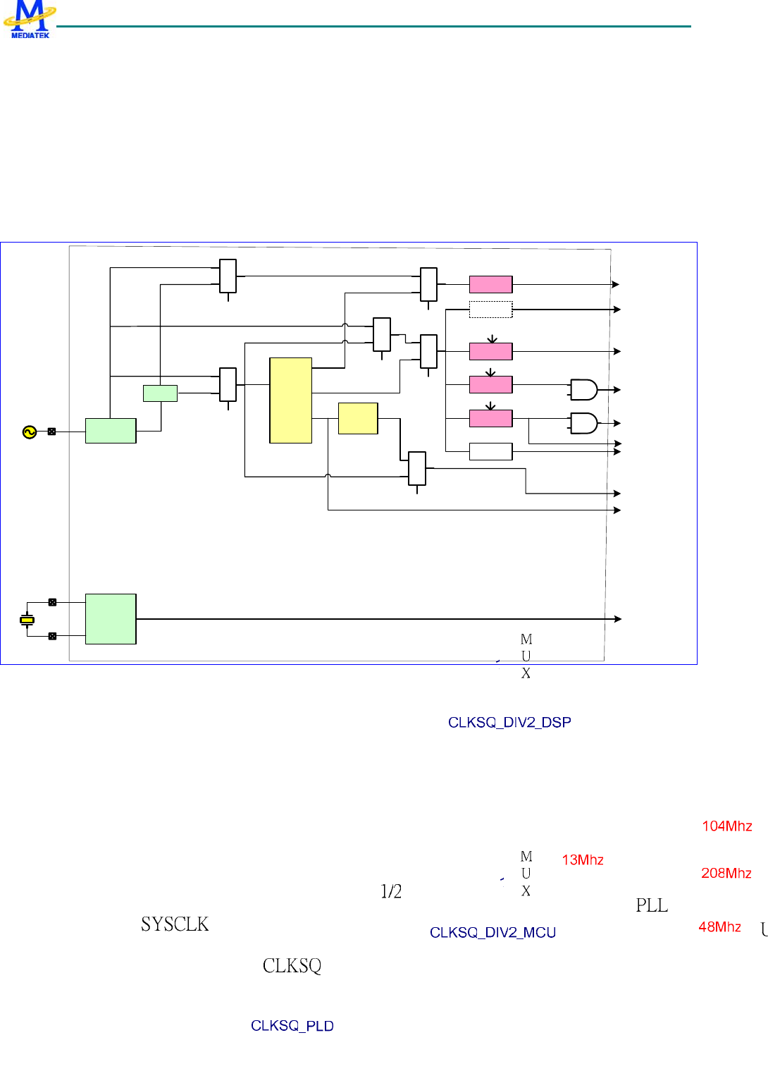
MT6235 GSM/GPRS Baseband Processor Data Sheet Revision 1.02
503/599 MediaTek Inc. Confidential
12 Power, Clocks and Reset
12.1 Clocks
There are two major time bases in the MT6235. For the faster one is the 13 MHz clock originating from an off-chip
temperature-compensated voltage controlled oscillator (TCVCXO) that can be either 13MHz or 26MHz. This signal is the
input from the SYSCLK pad then is converted to the square-wave signal. The other time base is the 32768 Hz clock
generated by an on-chip oscillator connected to an external crystal. Figure 89 shows the clock sources as well as their
utilizations inside the chip.
Figure 89 Clock distributions inside the MT6235
12.1.1 32.768 KHz Time Base
The 32768 Hz clock is always running. It’s mainly used as the time base of the Real Time Clock (RTC) module, which
maintains time and date with counters. Therefore, both the 32768Hz oscillator and the RTC module is powered by separate
voltage supplies that shall not be powered down when the other supplies do.
In low power mode, the 13 MHz time base is turned off, so the 32768 Hz clock shall be employed to update the critical
TDMA timer and Watchdog Timer. This time base is also used to clocks the keypad scanner logic.
12.1.2 13 MHz Time Base
One 1/2-dividers for PLL existing to allow using 26 or 13 MHz TCVCXO.

MT6235 GSM/GPRS Baseband Processor Data Sheet Revision 1.02
504/599 MediaTek Inc. Confidential
One phase-locked loops (PLL) to generate 624Mhz clock output, then a frequency divider futher divide 6, 3, 13 to generate
104Mhz, 208Mhz, 48Mhz for three primary clocks, DSP_CLOCK, MCU_CLOCK and USB_CLOCK, respectively. These
three primary clocks then feed to DSP Clock Domain and MCU Clock Domain and USB, respectively. The PLL require no
off-chip components for operations and can be turn off in order to save power. After power-on, the PLLs are off by default
and the source clock signal is selected through multiplexers. The software shall take cares of the PLL lock time while
changing the clock selections. The PLL and usages are listed below.
PLL supplies three clock source
DSP system clock, DSP_CLOCK. The outputted 104MHz clock is connected to DSP DCM (dynamic clock
manager) for dynamically adjusting clock rate by digital clock divider.
MCU system clock, MCU_CLOCK, which paces the operations of the MCU cores, MCU memory system, and
MCU peripherals as well. The outputted 208MHz clock is connected to ARM DCM and AHB DCM for
dynamically adjusting clock rate by digital clock divider. The usage of DCM is described in MCUCLK_CON
registers of CONFIG.
USB system clock, USB_CLOCK. The 48MHz is sent to USB module for its operation.
Note that PLL need some time to become stable after being powered up. The software shall take cares of the PLL lock time
before switching them to the proper frequency. Usually, a software loop longer than the PLL lock time is employed to deal
with the problem.
For power management, the MCU software program may stop MCU Clock by setting the Sleep Control Register. Any
interrupt requests to MCU can pause the sleep mode, and thus MCU return to the running mode.
AHB also can be stop by setting the Sleep Control Register. However the behavior of AHB in sleep mode is a little different
from that of MCU. After entering Sleep Mode, it can be temporarily waken up by any “hreq” (bus request), and then goes
back to sleep automatically after all “hreqs” de-assert. Any transactions can take place as usual in sleep mode, and it can
save power while there is no transaction on it. However the penalty is losing a little system efficiency for switching on and
off bus clock, but the impact is small.
12.1.3 Dynamic Clock Switch of MCU Clock
Dynamic Clock Manager is implemented to allow MCU and DSP switching clock dynamically without any jitter, and
enabling signal drift, and system can operate stably during any clock rate switch.
Please note that PLL must be enabled and the frequency shall be set as 624MHz, therefore the required MCU/DSP/USB
clocks can be generated from 624MHz. Before switching to 52MHz clock rate, the clock from the CLKSQ will feed
through the dynamic clock manager (DCM) directly. That means if CLKSQ divider is enabled (MPLL_DIV2=1) and PLL
clock is bypassed (MPLL_SEL=00), the internal clock rate is the half of SYSCLK. Contrarily, the internal clock rate is
identical to SYSCLK.
However, the settings of some hardware modules is required to be changed before or after clock rate change. Software has
the responsibility to change them at proper timing. The following table is list of hardware modules needed to be changed
their setting during clock rate change.
EMI clock is always fixed at 104Mhz when MCU clock is dynamically changed.
Module Name Programming Sequence
NAND 1. Low clock speed -> high clock speed

MT6235 GSM/GPRS Baseband Processor Data Sheet Revision 1.02
505/599 MediaTek Inc. Confidential
Changing wait state before clock change. New wait state will not take effect until
current EMI access is complete. Software should insert a period of time before
switching clock.
2. High clock speed -> low clock speed
Changing wait state after clock change.
LCD Change wait state while LCD in IDLE state.
Table 48 Programming sequence during clock switch
12.1.4 Standard PLL Power-on Sequence
// 0x8300001C, Power on DSP_DIV2, MPLL, DPLL, MCU_DIV2, and CLKSQ
*(volatile kal_uint16 *)PDN_CON = 0x0000;
// 0x83000108, Switch to 13MHz input for PLL reference clock
*(volatile kal_uint16 *)CLK_CON = 0x0003;
// After power-on PLL.....
*PLL = 0x0080; // 0x83000000, reset PLL
*PLL = 0x0000; // 0x83000000, reset release, and wait for PLL output stable
for (i=0;i<200;i++);
*PLL = 0x0070; // 0x83000000, select PLL output
12.1.5 Register Definitions
PLL_CLKSQ+0
000h MPLL(DPLL, UPLL) Frequency Register1 PLL
Bit 15 14 13 12 11 10 9 8 7 6 5 4 3 2 1 0
Name CALI RST UPLL
SEL DPLL
SEL MPLLSEL PLLVCOSEL
Type R/W R/W R/W R/W R/W R/W
Reset 0 0 0 0 0 00
PLLVCOSEL Selects VCO in PLL frequency for PLL debug purpose. Default value is 0x0.
MPLLSEL Select MCU Clock source. Using this mux to gate out unstable clock output from PLL after system boot up
00 PLL bypassed, using CLK from CLKSQ, default value after chip power up.
01 PLL bypassed, using CLK from SYSCLK
10 Using PLL Clock for MCU

MT6235 GSM/GPRS Baseband Processor Data Sheet Revision 1.02
506/599 MediaTek Inc. Confidential
11 Reserved
DPLLSEL Select DSP Clock source. Using this mux to gate out unstable clock output from PLL after system boot up
0 PLL bypassed, using CLK from CLKSQ
1 Using PLL Clock for DSP
UPLLSEL Select USB Clock source. Using this mux to gate out unstable clock output from PLL after system boot up
0 PLL bypassed, using CLK from CLKSQ
1 Using PLL Clock for USB
RST Reset Control of PLL
0 Normal Operation
1 Reset the PLL
CALI Calibration Control for PLL
PLL_CLKSQ
+0004h MPLL(DPLL, UPLL) Frequency Register2 PLL2
Bit 15 14 13 12 11 10 9 8 7 6 5 4 3 2 1 0
Name PLL_DIVCTRL PLL_TEST
Type R/W R/W
Reset 1110 0
PLL_TEST Entering test mode
PLL_DIVCTRL Just for test purpose. Fine tune the 624MHz main frequency of VCO in PLL
(PLL_DIVCTRL + 2) x 3 x13 = 624
PLL_CLKSQ+0
018h Clock Control Register CLK_CON
Bit 15 14 13 12 11 10 9 8 7 6 5 4 3 2 1 0
Name CLKS
Q_TE
ST SRCC
LK CLKS
Q_PL
D
CLKS
Q_DIV
2_MC
U
CLKS
Q_DIV
2_DS
P
Type R/W R/W R/W R/W R/W
Reset 0 1 0 0 0
CLKSQ_DIV2_DSP Control the clock divider for DSP clock domain
0 Divider bypassed
1 Divider not bypassed
CLKSQ_DIV2_MCU Control the x2 clock divider for MCU clock domain
0 Divider bypassed
1 Divider not bypassed
CLKSQ_PLD Pull Down Control
0 Disable
MT6235 GSM/GPRS Baseband Processor Data Sheet Revision 1.02
507/599 MediaTek Inc. Confidential
1 Enables
CLKSQ_TEST CLKSQ test mode
SRCCLK Indicate the frequency of SYSCLK
0 13MHz
1 26MHz
PLL_CLKSQ+0
01Ch Power-down control PDN_CON
Bit 15 14 13 12 11 10 9 8 7 6 5 4 3 2 1 0
Name DSP_
DIV2 PLL
MCU_
DIV2 CLKS
Q
Type R/W R/W R/W R/W
Reset 1 1 1 0
CLKSQ Control CLKSQ power-down
MCU_DIV2 Control CLKSQ divide-by-2 power-down for MCU clock
DSP_DIV2 Control CLKSQ divide-by-2 power-down for DSP clock
PLL Control MPLL(including DPLL and UPLL) power-down
12.2 Reset Generation Unit (RGU)
Figure 90 shows the reset scheme used in MT6235. MT6235 provides three kinds of resets: hardware reset, watchdog
reset, and software reset.
Watchdog Timer
Peri. Soft Reset
DSP Soft Reset
SYSRST#
WATCHDOG#
R1
R2
R3
R4
MCU
Subsystem
MCU
Peripheral
DSP
Subsystem
DSP
Coprocessor
R12
R123
R124
Figure 90 Reset Scheme Used in MT6235

MT6235 GSM/GPRS Baseband Processor Data Sheet Revision 1.02
508/599 MediaTek Inc. Confidential
12.2.1 General Description
12.2.1.1 Hardware Reset
This reset is input through the SYSRST# pin, which is driven low during power-on. The hardware reset has a global
effect on the chip: all digital and analog circuits are initialized, except the Real Time Clock module. The initial states of
the MT6235 sub-blocks are as follows:.
• All analog circuits are turned off.
• All PLLs are turned off and bypassed. The 13 MHz system clock is the default time base.
12.2.1.2 Watchdog Reset
A watchdog reset is generated when the Watchdog Timer expires: the MCU software failed to re-program the timer counter
in time. This situation is typically induced by abnormal software execution, which can be aborted by a hardwired
watchdog reset. Hardware blocks that are affected by the watchdog reset are:
• MCU subsystem,
• DSP subsystem, and
• External components (trigged by software).
12.2.1.3 Software Resets
Software resets are local reset signals that initialize specific hardware components. For example, if hardware failures are
detected, the MCU or DSP software may write to software reset trigger registers to reset those specific hardware modules to
their initial states.
The following modules have software resets.
• DSP Core
• DSP Coprocessors
12.2.2 Register Definitions
RGU +0000h Watchdog Timer Control Register WDT_MODE
Bit 15 14 13 12 11 10 9 8 7 6 5 4 3 2 1 0
Name KEY[7:0] AUTO
-REST
ART IRQ EXTE
N EXTP
OL ENAB
LE
Type WO R/W R/W R/W R/W R/W
Reset 0 0 0 0 1
ENABLE Enables the Watchdog Timer.
0 Disables the Watchdog Timer.
1 Enables the Watchdog Timer.
EXTPOL Defines the polarity of the external watchdog pin.
0 Active low.
1 Active high.

MT6235 GSM/GPRS Baseband Processor Data Sheet Revision 1.02
509/599 MediaTek Inc. Confidential
EXTEN Specifies whether or not to generate an external watchdog reset signal.
0 The watchdog does not generate an external watchdog reset signal.
1 If the watchdog counter reaches zero, an external watchdog signal is generated.
IRQ Issues an interrupt instead of a Watchdog Timer reset. For debug purposes, RGU issues an interrupt to the MCU
instead of resetting the system.
0 Disable.
1 Enable.
AUTO-RESTART Restarts the Watchdog Timer counter with the value of WDT_LENGTH while task ID is written
into Software Debug Unit.
0 Disable. The counter restarts by writing KEY into the WDT_RESTART register.
1 Enable. The counter restarts by writing KEY into the WDT_RESTART register or by writing task ID into
the software debug unit.
KEY Write access is allowed if KEY=0x22.
RGU +0004h Watchdog Time-Out Interval Register WDT_LENGTH
Bit 15 14 13 12 11 10 9 8 7 6 5 4 3 2 1 0
Name TIMEOUT[10:0] KEY[4:0]
Type R/W WO
Reset 111_1111_1111b
KEY Write access is allowed if KEY=08h.
TIMEOUT The counter is restarted with {TIMEOUT [10:0], 1_1111_1111b}. Thus the Watchdog Timer time-out period
is a multiple of 512*T32k=15.6ms.
RGU +0008h Watchdog Timer Restart Register WDT_RESTART
Bit 15 14 13 12 11 10 9 8 7 6 5 4 3 2 1 0
Name KEY[15:0]
Type WO
Reset
KEY Restart the counter if KEY=1971h.
RGU +000Ch Watchdog Timer Status Register WDT_STA
Bit 15 14 13 12 11 10 9 8 7 6 5 4 3 2 1 0
Name WDT SW_W
DT
Type RO RO
Reset 0 0
WDT Indicates the cause of the watchdog reset.
0 Reset not due to Watchdog Timer.
1 Reset because the Watchdog Timer time-out period expired.
SW_WDT Indicates if the watchdog was triggered by software.
0 Reset not due to software-triggered Watchdog Timer.
1 Reset due to software-triggered Watchdog Timer.
NOTE: A system reset does not affect this register. This bit is cleared when the WTU_MODE register ENABLE bit is
written.
MT6235 GSM/GPRS Baseband Processor Data Sheet Revision 1.02
510/599 MediaTek Inc. Confidential
RGU +0010h CPU Peripheral Software Reset Register SW_PERIPH_RS
TN
Bit 15 14 13 12 11 10 9 8 7 6 5 4 3 2 1 0
Name DMAR
ST KEY
Type R/W WO
Reset 0
KEY Write access is allowed if KEY=37h.
DMARST Reset the DMA peripheral.
0 No reset.
1 Invoke a reset.
RGU +0014h DSP Software Reset Register SW_DSP_RSTN
Bit 15 14 13 12 11 10 9 8 7 6 5 4 3 2 1 0
Name RST
Type R/W
Reset 0
RST Controls the DSP System Reset Control.
0 No reset.
1 Invoke a reset.
RGU +0018h Watchdog Timer Reset Signal Duration Register WDT_RSTINTRE
VAL
Bit 15 14 13 12 11 10 9 8 7 6 5 4 3 2 1 0
Name LENGTH[ 11:0]
Type R/W
Reset FFFh
LENGTH This register indicates the reset duration when Watchdog Timer times out. However, if the WDT_MODE
register IRQ bit is set to 1, an interrupt is issued instead of a reset.
RGU+001Ch Watchdog Timer Software Reset Register WDT_SWRST
Bit 15 14 13 12 11 10 9 8 7 6 5 4 3 2 1 0
Name KEY[15:0]
Type WO
Reset
Software-triggered Watchdog Timer reset. If the register content matches the KEY, a watchdog reset is issued. However,
if the WDT_MODE register IRQ bit is set to 1, an interrupt is issued instead of a reset.
KEY 1209h

MT6235 GSM/GPRS Baseband Processor Data Sheet Revision 1.02
511/599 MediaTek Inc. Confidential
12.3 Global Configuration Registers
12.3.1 Register Definitions
CONFG+0000h Hardware Version Register HW_VERSION
Bit 15 14 13 12 11 10 9 8 7 6 5 4 3 2 1 0
Name EXTP MAJREV MINREV HFIX
Type RO RO RO RO
Reset 8 A 0 0
This register is useful for software program to determine the hardware version of the chip. It will have a new value
whenever each metal fix or major step is performed. All these values are incremented by a step of 1.
HFIX Iteration to fix a hardware bug, in case of some layer mask fixed
MINREV Minor Revision of the chip, in case of all layer masks changed
MAJREV Major Revision of the chip
EXTP This field shows the existence of Hardware Code Register that presents the Hardware ID while the value is
other than zero.
CONFG+0004h Firmware Version Register FW_VERSION
Bit 15 14 13 12 11 10 9 8 7 6 5 4 3 2 1 0
Name EXTP MAJREV MINREV FFIX
Type RO RO RO RO
Reset 8 A 0 0
This register is useful for software program to determine the Firmware ROM version that is included in this chip. All these
values are incremented by a step of 1.
FFIX Iteration to fix a firmware bug
MINREV Minor Revision of the firmware
MAJREV Major Revision of the firmware
EXTP This field shows the existence of Hardware Code Register that presents the Hardware ID when the value is
other than zero.
CONFG+0008h Hardware Code Register HW_CODE
Bit 15 14 13 12 11 10 9 8 7 6 5 4 3 2 1 0
Name CODE3 CODE2 CODE1 CODE0
Type RO RO RO RO
Reset 6 2 3 5
This register presents the Hardware ID.
CONFG+114h Sleep Control Register SLEEP_CON
Bit 15 14 13 12 11 10 9 8 7 6 5 4 3 2 1 0
Name DSP2 DSP1 AHB MCU

MT6235 GSM/GPRS Baseband Processor Data Sheet Revision 1.02
512/599 MediaTek Inc. Confidential
Type WO WO WO RO
Reset 0 0 0 0
MCU Interrupt status. This bit represents if any irq or fiq occurs.
0 There is irq or firq
1 There is no irq and firq
To make MCU clock off, this bit should in 1 state and an instruction should be executed .
MCR p15,0,<Rd>,c7,c0,4
AHB Stops the AHB Bus Clock to force the entire bus to enter sleep mode. AHB clock resumes as long as there is an
interrupt request or system is reset.
0 AHB Bus Clock is running
1 AHB Bus Clock is stopped
DSP1 Stops the DSP1 Clock.
0 DSP1 Bus Clock is running
1 DSP1 Bus Clock is stopped
DSP2 Stops the DSP2Clock.
0 DSP2 Bus Clock is running
1 DSP2 Bus Clock is stopped
CODE This version of chip is coded as 6235h.
CONFG+0118h MCU Clock Control Register MCUCLK_CON
Bit 15 14 13 12 11 10 9 8 7 6 5 4 3 2 1 0
Name EMICLK ARMCLK AHBX4CLK AHBX8CLK
Type R R/W R/W R/W
Reset 0111 0111 0011 0111
The register specifies MCU Subsystem and ARM clock frequency.
ARMCLK is used for ARM926 MCU processor. AHBX8CLK is used for 104Mhz AHB bus system and AHBX4CLK is
used for 52Mhz AHB bus system. EMICLK must be 0111 for normal operation and other settings are only used for debug
purpose. The clock rate must be ARM CLOCK > AHBX8CLK > AHBX4CLK. The max operation frequency for
ARMCLK is 208Mhz (1111), for AHBX8CLK is 104Mhz (0111), for AHBX4CLK is 52Mhz.
MCUCLK_CON control register is only active when internal PLL is enabled. Be sure to turn MCUCLK_CON to its default
setting before turn clock source from PLL to clock squarer.
ARMCLK Select the Output Clock Rate for ARM926
0000 13Mhz
0001 13MHz x 2
0010 reserved
0011 13MHz x 4
0100 reserved
0101 reserved
0110 reserved
0111 13MHz x 8
MT6235 GSM/GPRS Baseband Processor Data Sheet Revision 1.02
513/599 MediaTek Inc. Confidential
1111 13MHz x 16
OTHERS reserved
AHBX8CLK Select the Clock Rate for 104Mhz Bus clock
0000 13Mhz
0001 13MHz x 2
0010 reserved
0011 13MHz x 4
0100 reserved
0101 reserved
0110 reserved
0111 13MHz x 8
1111 reserved
OTHERS reserved
AHBX4CLK Select the Clock Rate for 52Mhz Bus clock
0000 13Mhz
0001 13MHz x 2
0010 reserved
0011 13MHz x 4
0100 reserved
0101 reserved
0110 reserved
0111 reserved
1111 reserved
OTHERS reserved
CONFG+011Ch DSP Clock Control Register DSPCLK_CON
Bit 15 14 13 12 11 10 9 8 7 6 5 4 3 2 1 0
Name SPDS SPDM
Type R/W R/W
Reset 0000 0000
SPDM, SPDS Select the Output Clock Rate for Master/Slave DSPCLK
0000 power down
0001 13MHz x 2
0010 13MHz x 3
0011 13MHz x 4
0100 13MHz x 5
0101 13MHz x 6
0110 13MHz x 7
0111 13MHz x 8
CONFG+0200h Internal Debug Select Register IDN_SEL
Bit 15 14 13 12 11 10 9 8 7 6 5 4 3 2 1 0

MT6235 GSM/GPRS Baseband Processor Data Sheet Revision 1.02
514/599 MediaTek Inc. Confidential
Name TV_E
XTCK
DSP_
EXTC
K IRWIN ROM_
WAIT AHB_
SLEE
P
RESE
RVED TDMA CLKS
Q MPLL
Type R/W R/W R/W R/W R/W R/W R/W R/W R/W
Reset 0 0 0 0 0 0 0 0 0
TV_EXTCK Use EINT3 as clock source of TV logic instead of internal PLL
DSP_EXTCK Use EINT2 as clock source of DSP logic instead of internal PLL
IRWIN IRDMA has highest priority at DMA AMBA bus
ROM_WAIT Controls the wait cycle of SYSROM when bus is run at 104Mhz
AHB_SLEEP When this bit is 0, then AHB Clock only can stop when the MCU is in idle power down mode
TDMA TDMA Internal Debug Signal
MPLL MCU PLL Internal Debug Signal
CONFG+300h Power Down Control 0 Register PDN_CON0
Bit 15 14 13 12 11 10 9 8 7 6 5 4 3 2 1 0
Name
IRDB
G2 IRDB
G1 SIM2 PWM PWM3 IR SEJ WAVE
TABL
E GCU USB DMA
Type R R R R R R R R R R R
Reset 1 1 1 1 1 1 1 1 1 1 1
DMA Controls the DMA Controller Power Down
USB Controls the USB Controller Power Down
GCU Controls the GCU Controller Power Down
WAVETALBE Controls the DSP WaveTable DMA Power Down
SEJ Controls the Secure Engine Power Down
IR Controls the IR (IR DMA) Power Down
PWM3 Controls the the 3rd PWM Generator Power Down
PWM Controls the Main PWM Generator Power Down. Only set this bit when all PWM are in power down.
SIM2 Controls the second SIM Controller Power Down
IRDBG1 Controls the IRDBG1 Power Down
IRDBG2 Controls the IRDBG2 Power Down
CONFG +304h Power Down Control 1 Register PDN_CON1
Bit 15 14 13 12 11 10 9 8 7 6 5 4 3 2 1 0
Name IRDA UART
3 NFI PWM2 TP MSDC UART
2 LCD PWM1 SIM UART
1 GPIO KP GPT
Type R R R R R R R R R R R R R R
Reset 1 1 1 1 1 1 1 1 1 1 0 1 1 1
GPT Controls the General Purpose Timer Power Down
KP Controls the Keypad Scanner Power Down

MT6235 GSM/GPRS Baseband Processor Data Sheet Revision 1.02
515/599 MediaTek Inc. Confidential
GPIO Controls the GPIO Power Down
UART1 Controls the UART1 Controller Power Down
SIM Controls the SIM Controller Power Down
PWM1 Controls the 1st PWM Generator Power Down
LCD Controls the Serial LCD Controller Power Down
UART2 Controls the UART2 Controller Power Down
MSDC Controls the MS/SD Controller Power Down
TP Controls the Touch Panel Power Down
PWM2 Controls the 2nd PWM Generator Power Down
NFI Controls the NAND FLASH Interface Power Down
UART3 Controls the UART3 Controller Power Down
IRDA Controls the IrDA Framer Power Down
CONFG +308h Power Down Control 2 Register PDN_CON2
Bit 15 14 13 12 11 10 9 8 7 6 5 4 3 2 1 0
Name GMSK BBRX I2C AAFE DIV GCC BFE VAFE AUXA
D FCS APC AFC BPI BSI RTC TDMA
Type R R R R R R R R R R R R R R R R
Reset 1 1 1 1 1 1 1 1 1 1 1 1 1 1 1 1
TDMA Controls the TDMA Power Down
RTC Controls the RTC Power Down
BSI Controls the BSI Power Down. This control will not be updated until both tdma_evtval and qbit_en are asserted.
BPI Controls the BPI Power Down. This control will not be updated until both tdma_evtval and qbit_en are asserted.
AFC Controls the AFC Power Down. This control will not be updated until both tdma_evtval and qbit_en are asserted.
APC Controls the APC Power Down. This control will not be updated until both tdma_evtval and qbit_en are asserted.
FCS Controls the FCS Power Down
AUXAD Controls the AUX ADC Power Down
VAFE Controls the Audio Front End of VBI Power Down
BFE Controls the Base-Band Front End Power Down
GCU Controls the GCU Power Down
DIV Controls the Divider Power Down
AAFE Controls the Audio Front End of MP3 Power Down
I2C Controls the I2C Power Down
BBRX Controls the BB RX Power Down
GMSK Controls the GMSK Power Down
CONFG +30Ch Power Down Control 3 Register PDN_CON3
Bit 15 14 13 12 11 10 9 8 7 6 5 4 3 2 1 0
Name ISP G2D GCMQ CRZ
Type R R R R
Reset 1 1 1 1
CRZ Controls CRZ Power Down
GCMQ Controls the Graphic Command Queue Power Down
G2D Controls the 2D Accelerator Power Down
ISP Controls the Image Signal Processor Power Down
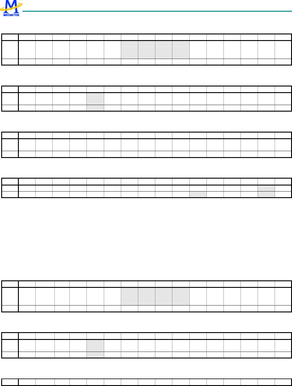
MT6235 GSM/GPRS Baseband Processor Data Sheet Revision 1.02
516/599 MediaTek Inc. Confidential
CONFG+0310h Power Down Set 0 Register PDN_SET0
Bit 15 14 13 12 11 10 9 8 7 6 5 4 3 2 1 0
Name
IRDB
G2 IRDB
G1 SIM2 PWM PWM3 IR SEJ WAVE
TABL
E GCU USB DMA
Type W1S W1S W1S W1S W1S W1S W1S W1S W1S W1S W1S W1S W1S W1S W1S W1S
CONFG+0314h Power Down Set 1 Register PDN_SET1
Bit 15 14 13 12 11 10 9 8 7 6 5 4 3 2 1 0
Name IRDA UART
3 NFI PWM2 TP MSDC UART
2 LCD ALTE
R PWM1 SIM UART
1 GPIO KP GPT
Type W1S W1S W1S W1S W1S W1S W1S W1S W1S W1S W1S W1S W1S W1S W1S W1S
CONFG+0318h Power Down Set 2 Register PDN_SET2
Bit 15 14 13 12 11 10 9 8 7 6 5 4 3 2 1 0
Name GMSK BBRX I2C AAFE DIV GCC BFE VAFE AUXA
D FCS APC AFC BPI BSI RTC TDMA
Type W1S W1S W1S W1S W1S W1S W1S W1S W1S W1S W1S W1S W1S W1S W1S W1S
CONFG+031Ch Power Down Set 3 Register PDN_SET3
Bit 15 14 13 12 11 10 9 8 7 6 5 4 3 2 1 0
Name ISP G2D GCMQ CRZ
Type W1S W1S W1S W1S W1S W1S W1S W1S W1S W1S W1S W1S W1S W1S W1S
These registers are used to individually set power down control bit. Only the bits set to 1 are in effect. Setting the bits to 1
also sets the corresponding power down control bits will to 1. Otherwise, the bits keep their original value. However, the
control bits APC, AFC, BPI and BSI in PDN_SET2 register will NOT be updated until both tdma_evtval and qbit_en are
asserted.
EACH BIT Set the Associated Power Down Control Bit to 1.
0 no effect
1 Set corresponding bit to 1
CONFG+0320h Power Down Clear 0 Register PDN_CLR0
Bit 15 14 13 12 11 10 9 8 7 6 5 4 3 2 1 0
Name
IRDB
G2 IRDB
G1 SIM2 PWM PWM3 IR SEJ WAVE
TABL
E GCU USB DMA
Type W1C W1C W1C W1C W1C W1C W1C W1C W1C W1C W1C W1C W1C W1C W1C W1C
CONFG+0324h Power Down Clear 1 Register PDN_CLR1
Bit 15 14 13 12 11 10 9 8 7 6 5 4 3 2 1 0
Name IRDA UART3 NFI PWM2 TP MSDC UART
2 LCD ALTE
R PWM1 SIM UART
1 GPIO KP GPT
Type W1C W1C W1C W1C W1C W1C W1C W1C W1C W1C W1C W1C W1C W1C W1C W1C
CONFG+0328h Power Down Clear 2 Register PDN_CLR2
Bit 15 14 13 12 11 10 9 8 7 6 5 4 3 2 1 0
MT6235 GSM/GPRS Baseband Processor Data Sheet Revision 1.02
517/599 MediaTek Inc. Confidential
Name GMSK BBRX I2C AAFE DIV GCC BFE VAFE AUXA
D FCS APC AFC BPI BSI RTC TDMA
Type W1C W1C W1C W1C W1C W1C W1C W1C W1C W1C W1C W1C W1C W1C W1C W1C
CONFG+032Ch Power Down Clear 3 Register PDN_CLR3
Bit 15 14 13 12 11 10 9 8 7 6 5 4 3 2 1 0
Name ISP G2D GCMQ CRZ
Type W1C W1C W1C W1C W1C W1C W1C W1C W1C W1C W1C W1C W1C W1C W1C
These registers are used to individually clear power down control bit. Only the bits set to 1 are in effect. Setting the bits to 1
also sets the corresponding power down control bits to 0. Otherwise, the bits keep their original value. However, the control
bits APC, AFC, BPI and BSI in PDN_SET2 register will NOT be updated until both tdma_evtval and qbit_en are asserted.
EACH BIT Clear the Associated Power Down Control Bit.
0 no effect
1 Set corresponding bit to 0
CONFG +330h Power Down Control 4 Register PDN_CON4
Bit 15 14 13 12 11 10 9 8 7 6 5 4 3 2 1 0
Name APCAFC BPI BSI
Type WO WO WO WO
Reset 1 1 1 1
BSI Controls the BSI Power Down. This control will be updated immediately.
BPI Controls the BPI Power Down. This control will be updated immediately.
AFC Controls the AFC Power Down. This control will be updated immediately.
APC Controls the APC Power Down. This control will be updated immediately.
CONFG+334 Power Down Set 4 Register PDN_SET4
Bit 15 14 13 12 11 10 9 8 7 6 5 4 3 2 1 0
Name APCAFC BPI BSI
Type W1SW1S W1S W1S
Reset 1 1 1 1
EACH BIT Set the Associated Power Down Control Bit to 1. This control will be updated immediately
0 no effect
1 Set corresponding bit to 1
CONFG+338 Power Down Clear 4 Register PDN_CLR4
Bit 15 14 13 12 11 10 9 8 7 6 5 4 3 2 1 0
Name APCAFC BPI BSI
Type W1C W1C W1C W1C
Reset 1 1 1 1
EACH BIT Clear the Associated Power Down Control Bit to 1. This control will be updated immediately
0 no effect
1 Set corresponding bit to 0
MT6235 GSM/GPRS Baseband Processor Data Sheet Revision 1.02
518/599 MediaTek Inc. Confidential
CONFG+0404h APB Bus Control Register APB_CON
Bit 15 14 13 12 11 10 9 8 7 6 5 4 3 2 1 0
Name APBW
4 APBW
3 APBW
2 APBW
1 APBW
0 APBR
4 APBR
3 APBR
2 APBR
1 APBR
0
Type R/W R/W R/W R/W R/W R/W R/W R/W R/W R/W
Reset 0 0 0 0 0 1 1 1 1 1
This register is used to control the timing of Read Cycle and Write Cycle on APB Bus. Note that APB Bridge 2 is
different from other bridges. The access time is varied, and access is not completed until acknowledge signal from
APB slave is asserted and must be configured as 2-Cycle Read/Write Access.
APBR0-APBR4 Read Access Time on APB Bus
0 1-Cycle Access
1 2-Cycle Access
APBW0-APBW4 Write Access Time on APB Bus
0 1-Cycle Access
1 2-Cycle Access
CONFG+0408h Slow Down Control Register SLOWDN_CON
Bit 15 14 13 12 11 10 9 8 7 6 5 4 3 2 1 0
Name DIS
Type R/W
Reset 0
DIS Slow Down Disable Control
0 Others
1 Disable all slow down functionality.
CONFG+040C
h IRDMA CON IRDMA_CON
Bit 15 14 13 12 11 10 9 8 7 6 5 4 3 2 1 0
Name WAVETABLE_SD IRDMA_SD
Type
Reset
IRDMA_SD IRDMA Slow Down Limit Count
WAVETABLE_SD Wavetable Slow Down Limit Count
CONFG+0700h Analog Chip Interface Control Register 0 ACIF_CON0
Bit 15 14 13 12 11 10 9 8 7 6 5 4 3 2 1 0
Name NLI_OD NAND_OD LCD_OD
CMPC
LK_S
MT CMMCLK_OD
Type R/W R/W R/W RW R/W
Reset 000 000 000 0 000
The register specifies IO driving capability of external interface.
MT6235 GSM/GPRS Baseband Processor Data Sheet Revision 1.02
519/599 MediaTek Inc. Confidential
CONFG+0704h Analog Chip Interface Control Register 1 ACIF_CON1
Bit 15 14 13 12 11 10 9 8 7 6 5 4 3 2 1 0
Name UR2_OD UR1_OD SDA_OD SCL_OD
Type R/W R/W R/W R/W
Reset 000 000 000 000
The register specifies IO driving capability of external interface.
UR2_OD UART2 output driving control
UR1_OD UART1 output driving control
SDA1_OD PAD SDA output driving control
SCL_OD PAD SCL output driving control
CONFG+0708h Analog Chip Interface Control Register 2 ACIF_CON2
Bit 15 14 13 12 11 10 9 8 7 6 5 4 3 2 1 0
Name CMVR
EF_P
D_B
CMHR
EF_P
D_B
CMPC
LK_P
D_B
CMDA
T_PU
_B
EWAI
T_PD
_B
MFIQ_
PU_B PWM2
_OD PWM3
_OD ED_C
LK_B
DIS EADMUX_OD
Type R/W R/W R/W R/W R/W R/W R/W R/W
Reset 0 0 0 0 0 0 0 0000
CMVREF_PD_B Pull down enable of CMVREF (0: enable, 1: disable)
CMHREF_PD_B Pull down enable of CMHREF(0: enable, 1: disable)
CMPCLK_PD_B Pull down enable of CMPCLK(0: enable, 1: disable)
CMDAT_PU_B Pull down enable of CMDAT[9:0] (0: enable, 1: disable)
EADMUX_OD Pad EADMUX output driving control
ED_CLK_B DIS ED_CLK_B output enable control (0: enable output 1:disable output)
The following 28 registers specify the setting of the sense amplifier delay for MediaTek in-house made ROM and RAM
macros.
CONFG+0900h MCU ROM Setting Control Register 0 ROM_DELSEL
0
Bit 15 14 13 12 11 10 9 8 7 6 5 4 3 2 1 0
Name MDSP_MCN0 MCUROM
Type R/W R/W
Reset 00001100 00001100
CONFG+0904h ROM Setting Control Register 1 ROM_DELSEL
1
Bit 15 14 13 12 11 10 9 8 7 6 5 4 3 2 1 0
Name MDSP_MPN0 MDSP_MCN1
Type R/W R/W
Reset 00000011 00001100
MT6235 GSM/GPRS Baseband Processor Data Sheet Revision 1.02
520/599 MediaTek Inc. Confidential
CONFG+0908h ROM Setting Control Register 2 ROM_DELSEL
2
Bit 15 14 13 12 11 10 9 8 7 6 5 4 3 2 1 0
Name SDSP_SDC20 SDSP_SC21
Type R/W R/W
Reset 00001100 00001100
CONFG+090Ch ROM Setting Control Register 3 ROM_DELSEL
3
Bit 15 14 13 12 11 10 9 8 7 6 5 4 3 2 1 0
Name SDSP_SC10 SDSP_SC11
Type R/W R/W
Reset 00001100 00001100
CONFG+0910h ROM Setting Control Register 4 ROM_DELSEL
4
Bit 15 14 13 12 11 10 9 8 7 6 5 4 3 2 1 0
Name SDSP_SC00 SDSP_SC01
Type R/W R/W
Reset 00001100 00001100
CONFG+0914h ROM Setting Control Register 5 ROM_DELSEL
5
Bit 15 14 13 12 11 10 9 8 7 6 5 4 3 2 1 0
Name SDSP_SC51 SDSP_SC60
Type R/W R/W
Reset 00001100 00001100
CONFG+0918h ROM Setting Control Register 6 ROM_DELSEL
6
Bit 15 14 13 12 11 10 9 8 7 6 5 4 3 2 1 0
Name SDSP_SC31 SDSP_SC50
Type R/W R/W
Reset 00001100 00001100
CONFG+091Ch ROM Setting Control Register 7 ROM_DELSEL
7
Bit 15 14 13 12 11 10 9 8 7 6 5 4 3 2 1 0
Name SDSP_SP10 SDSP_SC30
Type R/W R/W
Reset 00001100 00001100

MT6235 GSM/GPRS Baseband Processor Data Sheet Revision 1.02
521/599 MediaTek Inc. Confidential
CONFG+0920h ROM Setting Control Register 8 ROM_DELSEL
8
Bit 15 14 13 12 11 10 9 8 7 6 5 4 3 2 1 0
Name SDSP_SP31 SDSP_SP00
Type R/W R/W
Reset 00000011 00000011
CONFG+0924h ROM Setting Control Register 9 ROM_DELSEL
9
Bit 15 14 13 12 11 10 9 8 7 6 5 4 3 2 1 0
Name SDSP_SP50 SDSP_SP40
Type R/W R/W
Reset 00001100 00001100
CONFG+0A00h MCU RAM Setting Control Register 0 RAM_DELSEL
0
Bit 15 14 13 12 11 10 9 8 7 6 5 4 3 2 1 0
Name MDSP_MPN1 MDSP_MCN2 MDSP_MD00 L2CACHE
Type R/W R/W R/W R/W
Reset 0001 0001 0001 0101
CONFG+0A04h RAM Setting Control Register 1 RAM
_DELSEL1
Bit 15 14 13 12 11 10 9 8 7 6 5 4 3 2 1 0
Name SDSP_SP30 SDSP_SC40 MDSP_MD02 MDSP_MD01
Type R/W R/W R/W R/W
Reset 0101 0011 0101 0001
CONFG+0A08h RAM Setting Control Register 2 RAM
_DELSEL2
Bit 15 14 13 12 11 10 9 8 7 6 5 4 3 2 1 0
Name SDSP_SD10 SDSP_SD20 SDSP_SD11 SDSP_SPN1
Type R/W R/W R/W R/W
Reset 0001 0101 0001 0001
CONFG+0A0Ch RAM Setting Control Register 3 RAM
_DELSEL3
Bit 15 14 13 12 11 10 9 8 7 6 5 4 3 2 1 0
Name SDSP_SD12 SDSP_SD30 SDSP_SD01 SDSP_SDN3
Type R/W R/W R/W R/W
Reset 0001 0101 0001 0001
CONFG+0A10h RAM Setting Control Register 4 RAM
_DELSEL4
Bit 15 14 13 12 11 10 9 8 7 6 5 4 3 2 1 0

MT6235 GSM/GPRS Baseband Processor Data Sheet Revision 1.02
522/599 MediaTek Inc. Confidential
Name BSI_RAM SHARE_RAM2 SHARE_RAM1 VTB_MEM
Type R/W R/W R/W R/W
Reset 0001 0001 0001 0001
CONFG+0A14h RAM Setting Control Register 5 RAM
_DELSEL5
Bit 15 14 13 12 11 10 9 8 7 6 5 4 3 2 1 0
Name ISP_AWB ISP_SHAD RESZ_LB_RAM IMG_RAM PRF_RAM EQ_RAM AFE_RAM
Type R/W R/W R/W R/W R/W R/W R/W
Reset 01 01 0001 01 01 01 01
CONFG+0A18h RAM Setting Control Register 6 RAM
_DELSEL6
Bit 15 14 13 12 11 10 9 8 7 6 5 4 3 2 1 0
Name LCD_RAM TVC_RAM ISP_COLOR
Type R/W R/W R/W
Reset 0001 0001 00010101
CONFG+0A1Ch RAM Setting Control Register 7 RAM
_DELSEL7
Bit 15 14 13 12 11 10 9 8 7 6 5 4 3 2 1 0
Name ISP_DM0[7:4] ISP_DM[3:0] USB RAM GMC_RAM
Type R/W R/W R/W R/W
Reset 0001 0001 0001 0001
CONFG+0A20h RAM Setting Control Register 8 RAM_DELSEL
8
Bit 15 14 13 12 11 10 9 8 7 6 5 4 3 2 1 0
Name ISP_DM0[23:20] ISP_DM0[19:16] ISP_DM0[15:12] ISP_DM0[11:8]
Type R/W R/W R/W R/W
Reset 0001 0001 0001 0001
CONFG+0A24h RAM Setting Control Register 9 RAM_DELSEL
9
Bit 15 14 13 12 11 10 9 8 7 6 5 4 3 2 1 0
Name ISP_DM1[15:0]
Type R/W R/W R/W R/W
Reset 0001 0001 0001 0001
CONFG+0A28h RAM Setting Control Register10 RAM_DELSEL
10
Bit 15 14 13 12 11 10 9 8 7 6 5 4 3 2 1 0
Name ISP_NR11[15:0]
Type R/W R/W R/W R/W
Reset 0001 0001 0001 0001

MT6235 GSM/GPRS Baseband Processor Data Sheet Revision 1.02
523/599 MediaTek Inc. Confidential
CONFG+0A2Ch RAM Setting Control Register 11 RAM
_DELSEL11
Bit 15 14 13 12 11 10 9 8 7 6 5 4 3 2 1 0
Name ARM_M32[3:0] ARM_M31[3:
2] ISP_AWBSB ISP_AWBSG ISP_AWBSR ISP_AEHI ISP_3A
Type R/W R/W R/W R/W R/W R/W R/W
Reset 0001 00 01 01 01 01 01
CONFG+0A30 RAM Setting Control Register12 RAM_DELSEL
12
Bit 15 14 13 12 11 10 9 8 7 6 5 4 3 2 1 0
Name ARM_M6 ARM_M5 ARM_M4 ARM_M3 ARM_M2 ARM_M1 ARM_M0
Type R/W R/W R/W R/W R/W R/W R/W
Reset 01 0001 01 01 01 01 01
CONFG+0A34 RAM Setting Control Register13 RAM_DELSEL
13
Bit 15 14 13 12 11 10 9 8 7 6 5 4 3 2 1 0
Name ARM_M10 ARM_M9 ARM_M8 ARM_M7 ARM_M6
Type R/W R/W R/W R/W R/W
Reset 01 0001 0001 0001 00
CONFG+0A38 RAM Setting Control Register14 RAM_DELSEL
14
Bit 15 14 13 12 11 10 9 8 7 6 5 4 3 2 1 0
Name ARM_M15 ARM_M14 ARM_M13 ARM_M12 ARM_M11 ARM_M10
Type R/W R/W R/W R/W R/W R/W
Reset 01 01 01 0001 0001 00
CONFG+0A3C RAM Setting Control Register15 RAM_DELSEL
15
Bit 15 14 13 12 11 10 9 8 7 6 5 4 3 2 1 0
Name ARM_M23 ARM_M22 ARM_M21 ARM_M20 ARM_M19 ARM_M18 ARM_M17 ARM_M16
Type R/W R/W R/W R/W R/W R/W R/W R/W
Reset 01 01 01 01 01 01 01 01
CONFG+0A40 RAM Setting Control Register16 RAM_DELSEL
16
Bit 15 14 13 12 11 10 9 8 7 6 5 4 3 2 1 0
Name ARM_M27 ARM_M26 ARM_M25 ARM_M24 ARM_M23
Type R/W R/W R/W R/W R/W
Reset 01 0001 0001 0001 00
CONFG+0A44 RAM Setting Control Register17 RAM_DELSEL
17
Bit 15 14 13 12 11 10 9 8 7 6 5 4 3 2 1 0
Name ARM_M31[1:
0] ARM_M30 ARM_M29 ARM_M28 ARM_M27
Type R/W R/W R/W R/W R/W

MT6235 GSM/GPRS Baseband Processor Data Sheet Revision 1.02
524/599 MediaTek Inc. Confidential
Reset 01 0001 0001 0001 00

MT6235 GSM/GPRS Baseband Processor Data Sheet Revision 1.02
525/599 MediaTek Inc. Confidential

MT6235 GSM/GPRS Baseband Processor Data Sheet Revision 1.02
526/599 MediaTek Inc. Confidential
13 Analog Front-end & Analog Blocks
13.1 General Description
To communicate with analog blocks, a common control interface for all analog blocks is implemented. In addition,
there are some dedicated interfaces for data transfer. The common control interface translates APB bus write and read
cycle for specific addresses related to analog front-end control. During writing or reading of any of these control
registers, there is a latency associated with transferring of data to or from the analog front-end. Dedicated data
interface of each analog block is implemented in the corresponding digital block. The Analog Blocks includes the
following analog function for complete GSM/GPRS base-band signal processing:
1. Base-band RX: For I/Q channels base-band A/D conversion
2. Base-band TX: For I/Q channels base-band D/A conversion and smoothing filtering, DC level
shifting
3. RF Control: Two DACs for automatic power control (APC) and automatic frequency control
(AFC) are included. Their outputs are provided to external RF power amplifier and VCXO),
respectively.
4. Auxiliary ADC: Providing an ADC for battery and other auxiliary analog function monitoring
5. Audio mixed-signal blocks: It provides complete analog voice signal processing including
microphone amplification, A/D conversion, D/A conversion, earphone driver, and etc.
Besides, dedicated stereo D/A conversion and amplification for audio signals are included).
6. Clock Generation: A clock squarer for shaping system clock, and three PLLs that provide
clock signals to DSP, MCU, and USB units are included
7. XOSC32: It is a 32-KHz crystal oscillator circuit for RTC application Analog Block
Descriptions
13.1.1 BBRX
13.1.1.1 Block Descriptions
The receiver (RX) performs base-band I/Q channels downlink analog-to-digital conversion:
1. Analog input multiplexer: For each channel, a 4-input multiplexer that supports offset and gain
calibration is included.
2. A/D converter: Two 14-bit sigma-delta ADCs perform I/Q digitization for further digital signal
processing.
13.1.1.2 Functional Specifications
The functional specifications of the base-band downlink receiver are listed in the following table.
Symbol Parameter Min Typical Max Unit

MT6235 GSM/GPRS Baseband Processor Data Sheet Revision 1.02
527/599 MediaTek Inc. Confidential
N Resolution 14 Bit
FC Clock Rate 26 MHz
FS Output Sampling Rate 13/12 MSPS
Input Swing
When GAIN=’0’
When GAIN=’1’
0.8*AVDD
0.4*AVDD
Vpk
Vpk
OE Offset Error +/- 10 mV
FSE Full Swing Error +/- 30 mV
I/Q Gain Mismatch 0.5 dB
SINAD Signal to Noise and Distortion Ratio
- 45kHz sine wave in [0:90] kHz bandwidth
- 145kHz sine wave in [10:190] kHz
bandwidth
65
65
dB
dB
ICN Idle channel noise
- [0:90] kHz bandwidth
- [10:190] kHz bandwidth
-74
-70
dB
dB
DR Dynamic Range
- [0:90] kHz bandwidth
- [10:190] kHz bandwidth
74
70
dB
dB
RIN Input Resistance 75 k
DVDD Digital Power Supply 1.1 1.2 1.3 V
AVDD Analog Power Supply 2.5 2.8 3.1 V
T Operating Temperature -20 80 ℃
Current Consumption
Power-up
Power-Down
5
5
mA
µA
Table 49 Base-band Downlink Specifications
13.1.2 BBTX
13.1.2.1 Block Descriptions
The transmitter (TX) performs base-band I/Q channels up-link digital-to-analog conversion. Each channel includes:
1. 10-Bits D/A Converter: It converts digital GMSK modulated signals to analog domain. The input to the DAC
is sampled at 4.33-MHz rate with 10-bits resolution.
2. Smoothing Filter: The low-pass filter performs smoothing function for DAC output signals with a 350-kHz
2nd-order Butterworth frequency response.

MT6235 GSM/GPRS Baseband Processor Data Sheet Revision 1.02
528/599 MediaTek Inc. Confidential
13.1.2.2 Function Specifications
The functional specifications of the base-band uplink transmitter are listed in the following table.
Symbol Parameter Min Typical Max Unit
N Resolution 10 Bit
FS Sampling Rate 4.33 MSPS
SINAD Signal to Noise and Distortion Ratio 57 60 dB
Output Swing 0.18*AVDD 0.89*AVDD V
VOCM Output CM Voltage 0.34*AVDD 0.5*AVDD 0.62*AVDD V
Output Capacitance 20 PF
Output Resistance 10 K
DNL Differential Nonlinearity +/- 0.5 LSB
INL Integral Nonlinearity +/- 1.0 LSB
OE Offset Error +/- 15 mV
FSE Full Swing Error +/- 30 mV
FCUT Filter –3dB Cutoff Frequency 300 350 400 KHz
ATT Filter Attenuation at
100-KHz
270-KHz
4.33-MHz
0.01
1.81
69.4
0.0
0.85
65.7
0.0
0.39
61.9
dB
dB
dB
I/Q Gain Mismatch +/- 0.5 dB
I/Q Gain Mismatch Correction Range -0.96 +0.84 dB
DVDD Digital Power Supply 1.1 1.2 1.3 V
AVDD Analog Power Supply 2.5 2.8 3.1 V
T Operating Temperature -20 80 ℃
Current Consumption
Power-up
Power-Down
5
5
mA
µA
Table 50 Base-band Uplink Transmitter Specifications
13.1.3 AFC-DAC
13.1.3.1 Block Descriptions
As shown in the following figure, together with a 2nd-oder digital sigma-delta modulator,
AFC-DAC is designed to produce a single-ended output signal at AFC pin. AFC pin should be
connected to an external 1st-order R-C low pass filter to meet the 13-bits resolution (DNL)
requirement1.
1 DNL performance depends on external output RC filter bandwidth: the narrower the bandwidth, the better the DNL. Thus,
there exists a tradeoff between output setting speed and DNL performance
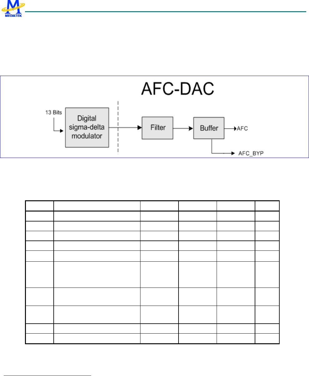
MT6235 GSM/GPRS Baseband Processor Data Sheet Revision 1.02
529/599 MediaTek Inc. Confidential
The AFC_BYP pin is the mid-tap of a resistor divider inside the chip to offer the AFC output
common-mode level. Nominal value of this common-mode voltage is half the analog power supply,
and typical value of output impedance of AFC_BYP pin is about 21k. To suppress the noise on
common mode level, it is suggested to add an external capacitance between AFC_BYP pin and
ground. The value of the bypass capacitor should be chosen as large as possible but still meet the
settling time requirement set by overall AFC algorithm2.
Figure 91 Block diagram of AFC-DAC
13.1.3.2 Functional Specifications
The following table gives the electrical specification of AFC-DAC.
Symbol Parameter Min Typical Max Unit
N Resolution 13 Bit
FS Sampling Rate 1083.3 KHz
DVDD Digital Power Supply 1.08 1.2 1.32 V
AVDD Analog Power Supply 2.6 2.8 3.1 V
T Operating Temperature -20 80 ℃
Current Consumption
Power-up
Power-Down
0.3
1
mA
µA
Output Swing @GAINSEL=0
Output Swing @GAINSEL=1
0.75*AVDD
AV D D
V
Output Resistor
(in AFC output RC network)
1 K
DNL Differential Nonlinearity +1/-1 LSB
INL Integral Nonlinearity +4.0/-4.0 LSB
Table 51 Functional specification of AFC-DAC
2 AFC_BYP output impedance and bypass capacitance determine the common-mode settling RC time constant. Insufficient
common-mode settling will affect the INL performance. A typical value of 1nF is suggested.

MT6235 GSM/GPRS Baseband Processor Data Sheet Revision 1.02
530/599 MediaTek Inc. Confidential
13.1.4 APC-DAC
13.1.4.1 Block Descriptions
The APC-DAC is a 10-bits DAC with output buffer aimed for automatic power control. Here blow
are its analog pin assignment and functional specification tables.
13.1.4.2 Function Specifications
Symbol Parameter Min Typical Max Unit
N Resolution 10 Bit
FS Sampling Rate 1.0833 MSPS
SINAD Signal to Noise and Distortion Ratio
(10-KHz Sine with 1.0V Swing & 100-KHz BW)
50 dB
99% Settling Time (Full Swing on Maximal Capacitance) 5 µS
Output Swing AVDD-0.2 V
Output Capacitance 200 pF
Output Resistance 10 K
DNL Differential Nonlinearity +/- 0.5 LSB
INL Integral Nonlinearity +/- 1.0 LSB
OE Offset Error +/- 10 mV
FSE Full Swing Error +/- 10 mV
DVDD Digital Power Supply 1.1 1.2 1.3 V
AVDD Analog Power Supply 2.5 2.8 3.1 V
T Operating Temperature -20 80 ℃
Current Consumption
Power-up
Power-Down
400
1
µA
µA
Table 52 APC-DAC Specifications
13.1.5 Auxiliary ADC
13.1.5.1 Block Descriptions
The auxiliary ADC includes the following functional blocks:
1. Analog Multiplexer: The analog multiplexer selects signal from one of the seven auxiliary input pins. Real word
message to be monitored, like temperature, should be transferred to the voltage domain.
2. 10 bits A/D Converter: The ADC converts the multiplexed input signal to 10-bit digital data.
13.1.5.2 Function Specifications
The functional specifications of the auxiliary ADC are listed in the following table.
Symbol Parameter Min Typical Max Unit

MT6235 GSM/GPRS Baseband Processor Data Sheet Revision 1.02
531/599 MediaTek Inc. Confidential
N Resolution 10 Bit
FC Clock Rate 0.1 1.0833 5 MHz
FS Sampling Rate @ N-Bit 5/(N+1) MSPS
Input Swing 1.0 AVDD V
VREFP Positive Reference Voltage
(Defined by AUX_REF pin)
1.0 AVDD V
CIN Input Capacitance
Unselected Channel
Selected Channel
50
1.2
fF
pF
RIN Input Resistance
Unselected Channel
Selected Channel
10
1.8
M
M
RS Resistor String Between AUX_REF pin & ground
Power Up
Power Down
35
10
50
65
K
M
Clock Latency 11 1/FC
DNL Differential Nonlinearity +0.5/-0.5 LSB
INL Integral Nonlinearity +1.0/-1.0 LSB
OE Offset Error +/- 10 mV
FSE Full Swing Error +/- 10 mV
SINAD Signal to Noise and Distortion Ratio (10-KHz Full
Swing Input & 13-MHz Clock Rate)
50 dB
DVDD Digital Power Supply 1.1 1.2 1.3 V
AVDD Analog Power Supply 2.5 2.8 3.1 V
T Operating Temperature -20 80 ℃
Current Consumption
Power-up
Power-Down
150
1
µA
µA
Table 53 The Functional specification of Auxiliary ADC
13.1.6 Audio mixed-signal blocks
13.1.6.1 Block Descriptions
Audio mixed-signal blocks (AMB) integrate complete voice uplink/downlink and audio playback
functions. As shown in the following figure, it includes mainly three parts. The first consists of
stereo audio DACs and speaker amplifiers for audio playback. The second is the voice downlink
path, including voice-band DACs and amplifiers, which produces voice signal to earphone or other
auxiliary output device. Amplifiers in these two blocks are equipped with multiplexers to accept
signals from internal audio/voice or external radio sources. The last is the voice uplink path, which
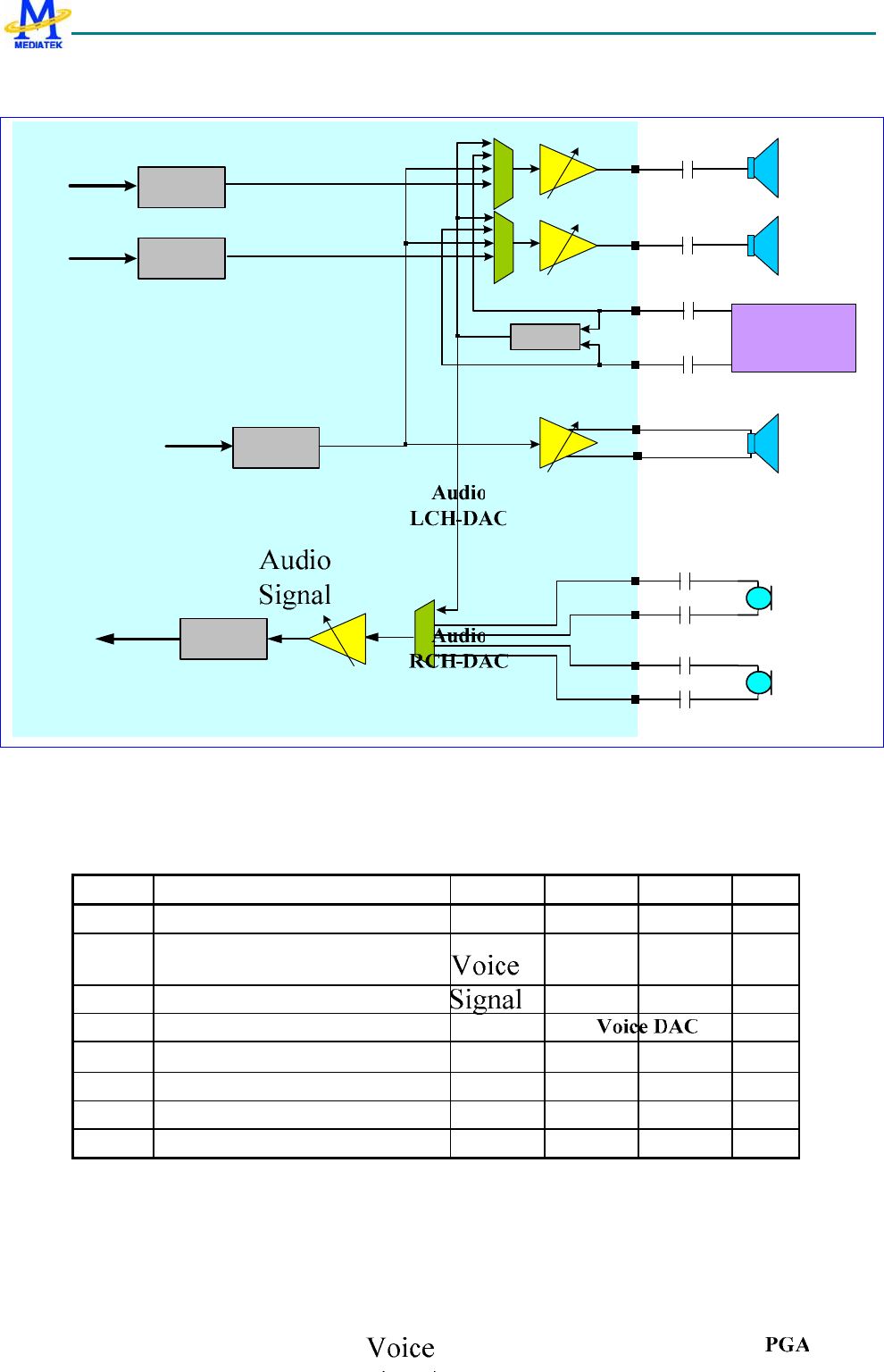
MT6235 GSM/GPRS Baseband Processor Data Sheet Revision 1.02
532/599 MediaTek Inc. Confidential
is the interface between microphone (or other auxiliary input device) input and MT6235 DSP. A set
of bias voltage is provided for external electret microphone..
MUXMUX
MUX
Figure 92 Block diagram of audio mixed-signal blocks.
13.1.6.2 Functional Specifications
The following table gives functional specifications of voice-band uplink/downlink blocks.
Symbol Parameter Min Typical Max Unit
FS Sampling Rate 6500 KHz
CREF Decoupling Cap Between AU_VREF_P
And AU_VREF_N
47 NF
DVDD Digital Power Supply 1.08 1.2 1.32 V
AVDD Analog Power Supply 2.5 2.8 3.1 V
T Operating Temperature -20 80 ℃
IDC Current Consumption 5 mA
VMIC Microphone Biasing Voltage 1.9 V
IMIC Current Draw From Microphone Bias 2 mA
MT6235 GSM/GPRS Baseband Processor Data Sheet Revision 1.02
533/599 MediaTek Inc. Confidential
Pins
Uplink Path3
SINAD Signal to Noise and Distortion Ratio
Input Level: -40 dbm0
Input Level: 0 dbm0
2
9
69
dB
dB
RIN Input Impedance (Differential) 13 20 27 K
ICN Idle Channel Noise -67 dBm0
XT Crosstalk Level -66 dBm0
Downlink Path4
SINAD Signal to Noise and Distortion Ratio
Input Level: -40 dBm0
Input Level: 0 dBm0
2
9
69
dB
dB
RLOAD Output Resistor Load (Differential) 28
CLOAD Output Capacitor Load 200 pF
ICN Idle Channel Noise of Transmit Path -67 dBm0
XT Crosstalk Level on Transmit Path -66 dBm0
Table 54 Functional specifications of analog voice blocks
Functional specifications of the audio blocks are described in the following.
Symbol Parameter Min Typical Max Unit
FCK Clock Frequency 6.5 MHz
Fs Sampling Rate 32 44.1 48 KHz
AVDD Power Supply 2.6 2.8 3.1 V
T Operating Temperature -20 80 ℃
IDC Current Consumption 5 mA
PSNR Peak Signal to Noise Ratio 80 dB
DR Dynamic Range 80 dB
VOUT Output Swing for 0dBFS Input Level 0.85 Vrms
THD Total Harmonic Distortion
45mW at 16 Load
-40
dB
dB
3 For uplink-path, not all gain setting of VUPG meets the specification listed on table, especially for the several highest
gains. The maximum gain that meets the specification is to be determined.
4 For downlink-path, not all gain setting of VDPG meets the specification listed on table, especially for the several lowest
gains. The minimum gain that meets the specification is to be determined.
MT6235 GSM/GPRS Baseband Processor Data Sheet Revision 1.02
534/599 MediaTek Inc. Confidential
22mW at 32 Load -60
RLOAD Output Resistor Load (Single-Ended) 16
CLOAD Output Capacitor Load 200 pF
XT L-R Channel Cross Talk TBD dB
Table 55 Functional specifications of the analog audio blocks
13.1.7 Clock Squarer
13.1.7.1 Block Descriptions
For most VCXO, the output clock waveform is sinusoidal with too small amplitude (about several
hundred mV) to make MT6235 digital circuits function well. Clock squarer is designed to convert
such a small signal to a rail-to-rail clock signal with excellent duty-cycle. It provides also a
pull-down function when the circuit is powered-down.
13.1.7.2 Function Specifications
The functional specification of clock squarer is shown in Table 56.
Symbol Parameter Min Typical Max Unit
Fin Input Clock Frequency 13 MHz
Fout Output Clock Frequency 13 MHz
Vin Input Signal Amplitude 500 AVDD mVpp
DcycIN Input Signal Duty Cycle 50 %
DcycOUT Output Signal Duty Cycle DcycIN-5 DcycIN+5 %
TR Rise Time on Pin CLKSQOUT 5 ns/pF
TF Fall Time on Pin CLKSQOUT 5 ns/pF
DVDD Digital Power Supply 1.08 1.2 1.32 V
AVDD Analog Power Supply 2.6 2.8 3.0 V
T Operating Temperature -20 80
℃
Current Consumption TBD A
Table 56 The Functional Specification of Clock Squarer
13.1.7.3 Application Notes
Here below in the figure is an equivalent circuit of the clock squarer. Please be noted that the clock
squarer is designed to accept a sinusoidal input signal. If the input signal is not sinusoidal, its
harmonic distortion should be low enough to not produce a wrong clock output. As an reference, for
a 13MHz sinusoidal signal input with amplitude of 0.2V the harmonic distortion should be smaller
than 0.02V.
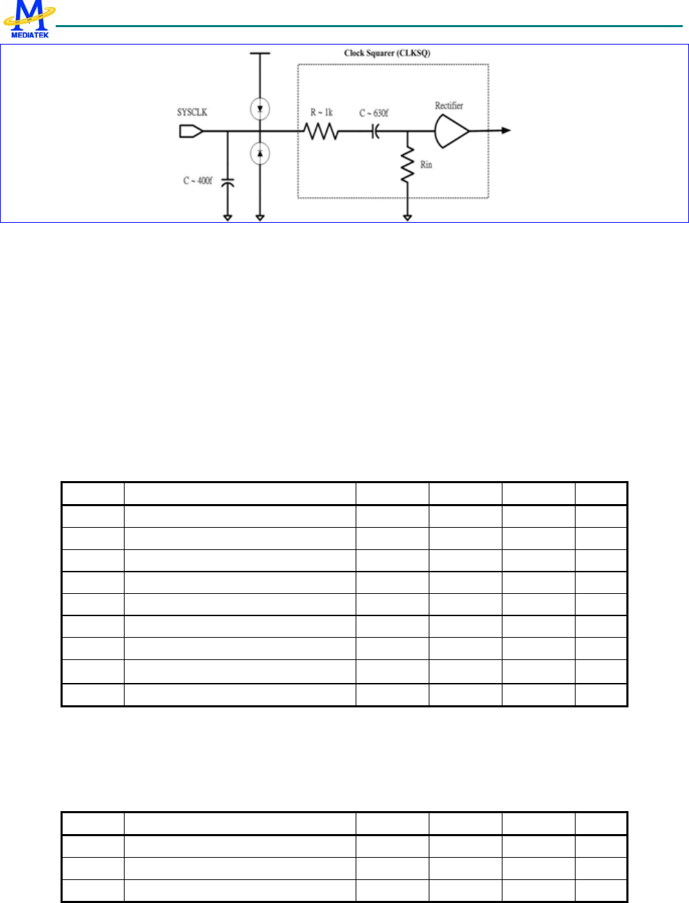
MT6235 GSM/GPRS Baseband Processor Data Sheet Revision 1.02
535/599 MediaTek Inc. Confidential
Figure 93 Equivalent circuit of Clock Squarer.
13.1.8 Phase Locked Loop
13.1.8.1 Block Descriptions
MT6235 includes three PLLs: DSP PLL, MCU PLL, and USB PLL. DSP PLL and MCU PLL are
identical and programmable to provide 104MHz and 208 MHz output clock while accepts 13MHz
signal. USB PLL is designed to also accept 13MHz input clock signal and provides 48MHz output
clock.
13.1.8.2 Function Specifications
The functional specification of DSP/MCU PLL is shown in the following table.
Symbol Parameter Min Typical Max Unit
Fin Input Clock Frequency 13 MHz
Fout Output Clock Frequency 208 MHz
Lock-in Time TBD s
Output Clock Duty Cycle 40 50 60 %
Output Clock Jitter 650 ps
DVDD Digital Power Supply 1.08 1.2 1.32 V
AVDD Analog Power Supply 2.6 2.8 3.0 V
T Operating Temperature -20 80 ℃
Current Consumption TBD µA
Table 57 The Functional Specification of DSP/MCU PLL
The functional specification of USB PLL is shown below.
Symbol Parameter Min Typical Max Unit
Fin Input Clock Frequency 13 MHz
Fout Output Clock Frequency 48 MHz
Lock-in Time TBD µs
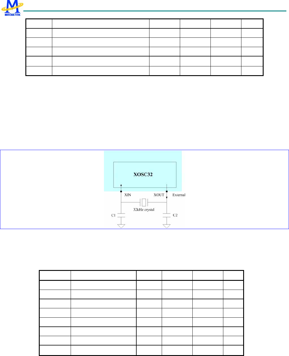
MT6235 GSM/GPRS Baseband Processor Data Sheet Revision 1.02
536/599 MediaTek Inc. Confidential
Output Clock Duty Cycle 40 50 60 %
Output Clock Jitter 650 ps
DVDD Digital Power Supply 1.08 1.2 1.32 V
AVDD Analog Power Supply 2.5 2.8 3.1 V
T Operating Temperature -20 80 ℃
Current Consumption TBD µA
Table 58 The Functional Specification of USB PLL
13.1.9 32-KHz Crystal Oscillator
13.1.9.1 Block Descriptions
The low-power 32-KHz crystal oscillator XOSC32 is designed to work with an external
piezoelectric 32.768kHz crystal and a load composed of two functional capacitors, as shown in the
following figure.
Figure 94 Block diagram of XOSC32
13.1.9.2 Functional specifications
The functional specification of XOSC32 is shown in the following table.
Symbol Parameter Min Typical Max Unit
AVDDRTC Analog power supply 1.08 1.2 1.32 V
Tosc Start-up time 5 sec
Dcyc Duty cycle 50 %
TR Rise time on XOSCOUT TBD ns/pF
TF Fall time on XOSCOUT TBD ns/pF
Current consumption 5 µA
Leakage current 1 µA
T Operating temperature -20 80
℃
Table 59 Functional Specification of XOSC32
Here below are a few recommendations for the crystal parameters for use with XOSC32.
MT6235 GSM/GPRS Baseband Processor Data Sheet Revision 1.02
537/599 MediaTek Inc. Confidential
Symbol Parameter Min Typical Max Unit
F Frequency range 32768 Hz
GL Drive level 5 uW
f/f Frequency tolerance +/- 20 Ppm
ESR Series resistance 50 K
C0 Static capacitance 1.6 pF
CL5 Load capacitance 6 12.5 pF
Table 60 Recommended Parameters of the 32kHz crystal
13.2 MCU Register Definitions
13.2.1 BBRX
MCU APB bus registers for BBRX ADC are listed as followings.
0x83010300 BBRX ADC Analog-Circuit Control Register BBRX_AC_CON
Bit 15 14 13 12 11 10 9 8 7 6 5 4 3 2 1 0
Name DITHE
N QSEL ISEL RSV
GAIN CALBIAS
Type R/W R/W R/W R/W
R/W R/W
Reset 0 00 00 0 00 00000
Set this register for analog circuit configuration controls.
CALBIAS The register field is for control of biasing current in BBRX mixed-signal module. It is coded in 2’s complement.
That is, its maximum is 15 and minimum is –16. Biasing current in BBRX mixed-signal module has impact on
the performance of A/D conversion. The larger the value of the register field, the larger the biasing current in
BBRX mixed-signal module, and the larger the SNR.
GAIN The register bit is for configuration of gain control of analog inputs in GSM RX mixed-signal module.
00 Input range is 0.8x AVDD for analog inputs in GSM RX mixed-signal module.
01 Input range is 0.4x AVDD for analog inputs in GSM RX mixed-signal module.
10 Input range is 0.57x AVDD for analog inputs in GSM RX mixed-signal module.
11 Input range is 0.33x AVDD for analog inputs in GSM RX mixed-signal module.
ISEL Loopback configuration selection for I-channel in BBRX mixed-signal module
00 Normal mode
01 Loopback TX analog I
10 Loopback TX analog Q
11 Select the grounded input
QSEL Loopback configuration selection for Q-channel in BBRX mixed-signal module
00 Normal mode
01 Loopback TX analog Q
5 CL is the parallel combination of C1 and C2 in the block diagram.

MT6235 GSM/GPRS Baseband Processor Data Sheet Revision 1.02
538/599 MediaTek Inc. Confidential
10 Loopback TX analog I
11 Select the grounded input
DITHDIS Dither feature Disable control register, which can effectively reduce the THD ( total harmonic distortion) of
the BBRX ADC.
0 turn on the dither (default value)
1 Disable the dither
13.2.2 BBTX
MCU APB bus registers for BBTX DAC are listed as followings.
0x83010400 BBTX DAC Analog-Circuit Control Register 0 BBTX_AC_CON
0
Bit 15 14 13 12 11 10 9 8 7 6 5 4 3 2 1 0
Name CALR
CDON
E
STAR
TCAL
RC GAIN CALRCSEL TRIMI TRIMQ
Type R R/W R/W R/W R/W R/W
Reset 0 0 000 000 0000 0000
Set this register for analog circuit configuration controls. The procedure to perform calibration processing for smoothing
filter in BBTX mixed-signal module is as follows:
1. Write 1 to the register bit STARTCALRC. Start calibration process.
2. Read the register bit CALRCDONE. If read as 1, then calibration process finished. Otherwise
repeat the step.
3. Write 0 to the register bit STARTCALRC. Stop calibration process.
4. The result of calibration process can be read from the register field CALRCOUT of the register
BBTX_AC_CON1. Software can set the value to the register field CALRCSEL for 3-dB cutoff
frequency selection of smoothing filter in DAC of BBTX.
Remember to set the register field CALRCCONT of the register BBTX_AC_CON1 to 0xb before the calibration process. It
only needs to be set once.
TRIMQ The register field is used to control gain trimming of Q-channel DAC in BBTX mixed-signal module. It is coded
in 2’s complement, that is, with maximum 7 and minimum –8.
TRIMI The register field is used to control gain trimming of I-channel DAC in BBTX mixed-signal module. It is coded in
2’s complement, that is, with maximum 7 and minimum –8.
CALRCSEL The register field is for selection of cutoff frequency of smoothing filter in BBTX mixed-signal module.
It is coded in 2’s complement. That is, its maximum is 3 and minimum is –4.
GAIN The register field is used to control gain of DAC in BBTX mixed-signal module. It has impact on both of I- and
Q-channel DAC in BBTX mixed-signal module. It is coded in 2’s complement, that is, with maximum 3 and
minimum –4.
STARTCALRC Whenever 1 is writing to the bit, calibration process for smoothing filter in BBTX mixed-signal module
will be triggered. Once the calibration process is completed, the register bit CARLDONE will be read as 1.
MT6235 GSM/GPRS Baseband Processor Data Sheet Revision 1.02
539/599 MediaTek Inc. Confidential
CALRCDONE The register bit indicates if calibration process for smoothing filter in BBTX mixed-signal module has
finished. When calibration processing finishes, the register bit will be 1. When the register bit STARTCALRC is
set to 0, the register bit becomes 0 again.
0x83010404 BBTX DAC Analog-Circuit Control Register 1 BBTX_AC_CON
1
Bit 15 14 13 12 11 10 9 8 7 6 5 4 3 2 1 0
Name CALRCOUT FLOA
T CALRCCNT
CALBIAS
CMV
Type R/O R/W R/W R./W R/W
Reset - 0 00000 0000 000
Set this register for analog circuit configuration controls.
CMV The register field is used to control common voltage in BBTX mixed-signal module. It is coded in 2’s complement,
that is, with maximum 3 and minimum –4.
CALBIAS The register field is for control of biasing current in BBTX mixed-signal module. It is coded in 2’s
complement. That is, its maximum is 7 and minimum is –8. Biasing current in BBTX mixed-signal module has
impact on performance of D/A conversion. Larger the value of the register field, the larger the biasing current in
BBTX mixed-signal module.
CALRCCNT Parameter for calibration process of smoothing filter in BBTX mixed-signal module. Default value is ‘22’.
Note that it is NOT coded in 2’s complement. Therefore the range of its value is from 0 to 31. Remember to set it
to 0x16 before BBTX calibration process if clock sent to BBTX is 26Mhz. Otherwise set to 0xb if clock is 13Mhz.
It only needs to be set once. In MT6235, only 26MHz clock is available
FLOAT The register field is used to have the outputs of DAC in BBTX mixed-signal module float or not.
CALRCOUT After calibration processing for smoothing filter in BBTX mixed-signal module, a set of 3-bit value is
obtained. It is coded in 2’s complement.
0x83010408 BBTX DAC Analog-Circuit Control Register 2 BBTX_AC_CON
2
Bit 15 14 13 12 11 10 9 8 7 6 5 4 3 2 1 0
Name
DCCOARSE
Q DCCOARSEI DAC_PTR
DWAE
N COARSE CALR
CAUT
OL
CALR
COPE
N
Type R/W R/W R/W R/W R/W R/W R/W
Reset 00 00 000 0 0 0 0
Set this register for analog circuit configuration controls.
CALRCOPEN The register field is used to control normal Mode( close loop) or debug mode (open loop) for BBTX
comparator in mixed signal
0 normal Mode (close loop)
1 debug Mode (open Loop)
CALRCAUTO The register field is used to control the result of calibration process of smoothing filter can automatically
load to control the smoothing filter or not.
0 Not auto load, need manual load (default)

MT6235 GSM/GPRS Baseband Processor Data Sheet Revision 1.02
540/599 MediaTek Inc. Confidential
1 Auto load
COARSE The register field is used to control the central nominal value of BBTX DAC output
00 central nominal @ 1V
01 central nominal @ 1V –0.2V
10 reserved
11 central nominal @ 1V +0.2V
DWAEN The register field is used to turn on the DWA scheme of the BBTX DAC,
0 DWA scheme off (default)
1 DWA scheme on
DACPTR The register field is used to configured the staring pointer of 1 hot pulling of LSB[7:0] signal to BBTX
DAC, range from 0~7. There is two different configuration. For DWAEN = 0, pointer always starts from the configuration
value (e.g. if DACPTR = 3’b1, 1 hot will start pulling from LSB[1]). However, for DWAEN=1, the initial starting pointer
will follow the configuration, while the pointer will move to most significant 1 hot pointer + 1 from the last LSB[7:0] input.
( e.g. if DACPTR = 3’b1,and LSB[7:0] maybe 8’b00001110, then the next starting poiter will starts from LSB[4].). Defulat
value is 0h.
DCCOARSEI The register field is used to control the central nominal value of BBTX DAC for I channel offset
00 central nominal @ +0mV
01 central nominal @ +30mV
11 central nominal @ - 30mV
10 reserved
DCCOARSEQ The register field is used to control the central nominal value of BBTX DAC for Q channel offset
00 central nominal @ +0mV
01 central nominal @ +30mV
11 central nominal @ - 30mV
10 reserved
13.2.3 AFC DAC
MCU APB bus registers for AFC DAC are listed as follows.
0x83010500 AFC DAC Analog-Circuit Control Register AFC_AC_CON
Bit 15 14 13 12 11 10 9 8 7 6 5 4 3 2 1 0
Name GAIN
SEL 11BS CALI
Type R/W R/W R/W
Reset 0 0 0
Set this register for analog circuit configuration controls. Please refer to analog functional specification for more details.

MT6235 GSM/GPRS Baseband Processor Data Sheet Revision 1.02
541/599 MediaTek Inc. Confidential
GAINSEL gain selection of output swing
0 3/4VDD
1 Full VDD
11BS Test purpose. Degrade the resolution of AFC from 13 bits to 11 bits
CALI biasing current control
13.2.4 APC DAC
MCU APB bus registers for APC DAC are listed as followings.
CALI biasing
current
control
13.2.4 APC
DAC
MCU APB bus
registers for APC
DAC are listed as
followings.
0x83010600
APC DAC Analog-Circuit Control Register APC_AC_CON
Bit 15 14 13 12 11 10 9 8 7 6 5 4 3 2 1 0
Name BYP CALI
Type R/W R/W
Reset 0 0
Set this register for analog circuit configuration controls. Please refer to analog functional specification for more details.
BYP bypass output buffer
CALI biasing current control
13.2.5 Auxiliary ADC
MCU APB bus registers for AUX ADC are listed as followings.
0x83010700 Auxiliary ADC Analog-Circuit Control Register AUX_AC_CON
Bit 15 14 13 12 11 10 9 8 7 6 5 4 3 2 1 0
Name ENB CALI
Type R/W R/W
Reset 0 0
Set this register for analog circuit configuration controls. Please refer to analog functional specification for more details.
CALI Biasing current control

MT6235 GSM/GPRS Baseband Processor Data Sheet Revision 1.02
542/599 MediaTek Inc. Confidential
ENB Comparator switch enable signal.
13.2.6 Voice Front-end
MCU APB bus registers for speech are listed as followings.
0x83010100 AFE Voice Analog Gain Control Register AFE_VAG_CON
Bit 15 14 13 12 11 10 9 8 7 6 5 4 3 2 1 0
Name VUPG VDPG0
VAGC
_GAI
N_ST
EP
Type R/W R/W R/W
Reset 000000 0000 0
Set this register for analog PGA gains. VUPG is set for microphone input volume control. And VDPG0 and VDPG1 are set
for two output volume controls
VAGC_GAIN_STEP Gain step for old AGC.
0 1 dB
1 2 dB
VUPG voice-band up-link PGA gain control bits. For VCFG[3] = 1, it is only valid for INPUT 1.
VCFG[3] = 0 Gain value = VUPG - 20
VCFG[3] = 1 Gain value fixed at 0dB
VCFG [3] =’0’ VCFG [3] =’1’
VUPG [5:0] Gain VUPG [5:0] Gain
111111 43 dB XXXXXX 0dB
111110 42 dB
111101 41 dB
111100 40 dB
111011 39 dB
111010 38 dB
111001 37 dB
111000 36 dB
110111 35 dB
110110 34 dB
110101 33 dB
110100 32 dB
110011 31dB
110010 30 dB

MT6235 GSM/GPRS Baseband Processor Data Sheet Revision 1.02
543/599 MediaTek Inc. Confidential
110001 29 dB
110000 28 dB
101111 27 dB
101110 26 dB
101101 25 dB
101100 24 dB
1101011 23 dB
101010 22 dB
101001 21 dB
101000 20 dB
100111 19 dB
100110 18 dB
100101 17 dB
100100 16 dB
100011 15 dB
100010 14 dB
100001 13 dB
100000 12 dB
011111 11 dB
011110 10 dB
011101 9 dB
011100 8 dB
011011 7 dB
011010 6 dB
011001 5 dB
011000 4 dB
010111 3 dB
010110 2 dB
010101 1 dB
010100 0 dB
010011 -1dB
010010 -2 dB
010001 -3 dB
010000 -4 dB
001111 -5 dB
001110 -6 dB
001101 -7 dB
001100 -8 dB
0101011 -9 dB
MT6235 GSM/GPRS Baseband Processor Data Sheet Revision 1.02
544/599 MediaTek Inc. Confidential
001010 -10 dB
001001 -11 dB
001000 -12 dB
000111 -13 dB
000110 -14 dB
000101 -15 dB
000100 -16 dB
000011 -17 dB
000010 -18 dB
000001 -19 dB
000000 -20 dB
VDPG0 voice-band down-link PGA0 gain control bits
VDPG0 [3:0] Gain
1111 8dB
1110 6dB
1101 4dB
1100 2dB
1011 0dB
1010 -2dB
1001 -4dB
1000 -6dB
0111 -8dB
0110 -10dB
0101 -12dB
0100 -14dB
0011 -16dB
0010 -18dB
0001 -20dB
0000 -22dB
0x83010104 AFE Voice Analog-Circuit Control Register 0 AFE_VAC_CON0
Bit 15 14 13 12 11 10 9 8 7 6 5 4 3 2 1 0
Name VDC_
COUP
LE
VMIC_
SHOR
T VMIC_VREF VCFG VDSE
ND0 VCALI
Type R/W R/W R/W R/W R/W R/W
Reset 0 0 00 00000 0 00000
Set this register for analog circuit configuration controls.
VDC_COUPLE Selectively choose DC couple microphone sense.

MT6235 GSM/GPRS Baseband Processor Data Sheet Revision 1.02
545/599 MediaTek Inc. Confidential
0 Disable DC couple sense of microphone
1 Enable DC couple sense of microphone
VMIC_SHORT Selectively short AU_MICBIASP / AU_MICBIASN.
0 float MIC_BIASN and short it to MIC_BIASP when handsfree mode mic is plugged in
1 short MIC_BIASN to ground when handsfree mode mic is plugged in. In this mode, differential mic has
current leakage and cause power loss.
VMIC_VREF Tuning MICBIASP DC voltage.
00 1.9V
01 2.0V
10 2.1V
11 2.2V
VCFG[4] microphone biasing control
0 differential biasing
1 single-ended biasing
VCFG[3] gain mode control. This control register is only valid to input 1. Others can be amplification mode only.
0 amplification
1 attenuation
VCFG[2] coupling control
0 AC
1 DC
VCFG[1:0] input select control
00 input 0
01 input 1
10 FM
11 reserved
VDSEND0 single-ended configuration control for out0
VCALI biasing current control, in 2’s complement format
0x83010108 AFE Voice Analog-Circuit Control Register 1 AFE_VAC_CON1
Bit 15 14 13 12 11 10 9 8 7 6 5 4 3 2 1 0
Name VUPO
P_EN VBIAS_EN
VOC_
EN VBG_CTRL VIBO
OT VFLO
AT VRSD
ON VGBO
OT
VADC
_DVR
EF_C
AL
VADC
_DEN
B
VDIFF
_BIAS
VADC
INMO
DE
VDAC
INMO
DE
Type R/W R/W R/W R/W R/W R/W R/W R/W R/W R/W R/W R/W R/W
Reset 0 0 0 000 1 0 0 0 0 0 0 0 0
Set this register for analog circuit configuration controls. There are several loop back modes and test modes implemented
for test purposes. Suggested value is 0280h.
VUPOP_EN de-pop noise enable
0: disable
1: enable
VBIAS_EN voice downlink buffer bias current control
1: normal bias current
0: increase bias current

MT6235 GSM/GPRS Baseband Processor Data Sheet Revision 1.02
546/599 MediaTek Inc. Confidential
VOC_EN voice downlink buffer over current protection
0: disable
1: enable
VBG_CTRL voice-band bandgap control
IBOOT voice downlink DAC bias current control
0: increase bias current
1: normal bias current
VFLOAT voice-band output driver float
0: normal operating mode
1: float mode
VRSDON voice-band redundant signed digit function on
0: 1-bit 2-level mode
1: 2-bit 3-level mode
VGBOOT VBI DAC Gain boost
0 2X
1 1X
VADC_DVREF_CAL ADC Dither Reference Voltage Calibration
VADC_DENB ADC Dither Enable
VDIFF_BIAS Differential Bandgap Reference Activated Register
0: Single-ended reference
1: Differential reference
VADCINMODE Voice-band ADC output mode.
0: normal operating mode
1: the ADC input from the DAC output
VDACINMODE Voice-band DAC input mode.
0: normal operating mode
1: the DAC input from the ADC output
0x8301010C AFE Voice Analog Power Down Control Register AFE_VAPDN_C
ON
Bit 15 14 13 12 11 10 9 8 7 6 5 4 3 2 1 0
Name VPDN
_BIAS VPDN
_LNA VPDN
_ADC VPDN
_DAC VPDN
_OUT
0
Type R/W R/W R/W R/W R/W
Reset 0 0 0 0 0
Set this register to power up analog blocks. 0: power down, 1: power up.
VPDN_BIAS bias block
VPDN_LNA low noise amplifier block
VPDN_ADC ADC block
VPDN_DAC DAC block
VPDN_OUT0 OUT0 buffer block

MT6235 GSM/GPRS Baseband Processor Data Sheet Revision 1.02
547/599 MediaTek Inc. Confidential
0x83010110 AFE Voice AGC Control Register AFE_VAGC_CO
N
Bit 15 14 13 12 11 10 9 8 7 6 5 4 3 2 1 0
Name AGC_
MODE AAGC
EN AGCT
EST RELNOIDUR
SEL RELNOILEV
SEL FRELCKSEL SRELCKSEL ATTTHDCAL ATTC
KSEL HYST
EREN DAGC
EN
Type R/W R/W R/W R/W R/W R/W R/W R/W R/W R/W R/W
Reset 0 0 0 00 00 00 00 00 0 0 0
Set this register for analog circuit configuration controls. There are several loop back modes and test modes implemented
for test purposes. Suggested value is 4dcfh.
DAGCEN Digital AGC function enable. The loop-back path of AGC comprises analog comparators and digital gain
control circuitry. This control register is used to enable the digital gain control circuitry. For normal function, DAGCEN
and AAGCEN shall be set to “1” to enable voice AGC function.
HYSTEREN AGC hysteresis function enable
ATTCKSEL attack clock selection
0: 16 KHz
1: 32 KHz
ATTTHDCAL attack threshold calibration
SRELCKSEL release slow clock selection
00: 1000/512 Hz
01: 1000/256 Hz
10: 1000/128 Hz
11: 1000/64 Hz
FRELCKSEL release fast clock selection
00: 1000/64 Hz
01: 1000/32 Hz
10: 1000/16 Hz
11: 1000/8 Hz
RELNOILEVSEL release noise level selection
00: -8 dB
01: -14 dB
10: -20 dB
11: -26 dB
RELNOIDURSEL release noise duration selection
00: 64 ms
01: 32 ms
10: 16 ms
11: 8 ms, 32768/4096
AAGCEN Analog AGC function enable. This control bit is used to enable the comparators of AGC loop-back path.
AGC_MODE AGC algorithm selection.
0 New digital algorithm.
1 Original analog algorithm.
MT6235 GSM/GPRS Baseband Processor Data Sheet Revision 1.02
548/599 MediaTek Inc. Confidential
13.2.7 Audio Front-end
MCU APB bus registers for audio are listed as followings.
0x83010200 AFE Audio Analog Gain Control Register AFE_AAG_CON
Bit 15 14 13 12 11 10 9 8 7 6 5 4 3 2 1 0
Name AMUT
ER AMUT
EL APGR APGL
Type R/W R/W R/W R/W
Reset 0 0 0000 0000
Set this register for analog PGA gains.
AMUTER audio PGA L-channel mute control
AMUTEL audio PGA R-channel mute control
APGR audio PGA R-channel gain control
APGL audio PGA L-channel gain control
APGR [3:0] / APGL [3:0] Gain
1111 23dB
1110 20dB
1101 17dB
1100 14dB
1011 13dB
1010 8dB
1001 5dB
1000 2dB
0111 -1dB
0110 -4dB
0101 -7dB
0100 -10dB
0011 -13dB
0010 -16dB
0001 -19dB
0000 -22dB
0x83010204 AFE Audio Analog-Circuit Control Register AFE_AAC_CON
Bit 15 14 13 12 11 10 9 8 7 6 5 4 3 2 1 0
Name APRO
_SC ADEP
OP ABUFSELR ABUFSELL ACALI
Type R/W R/W R/W R/W R/W
Reset 0 0 000 000 00000
Set this register for analog circuit configuration controls.
APRO_SC Short circuit protection.

MT6235 GSM/GPRS Baseband Processor Data Sheet Revision 1.02
549/599 MediaTek Inc. Confidential
0 disable
1 enable
ADEPOP De-POP noise.
0 disable
1 enable
ABUFSELR audio buffer R-channel input selection
00X: audio DAC R-channel output
010: voice DAC output
100: external FM R/L-channel radio output, stereo to mono
101: external FM R-channel radio output
OTHERS: reserved.
ABUFSELL audio buffer L-channel input selection
00X: audio DAC L-channel output
010: voice DAC output
100: external FM R/L-channel radio output, stereo to mono
101: external FM L-channel radio output
OTHERS: reserved.
ACALI audio bias current control, in 2’s complement format
0x83010208 AFE Audio Analog Power Down Control Register AFE_AAPDN_C
ON
Bit 15 14 13 12 11 10 9 8 7 6 5 4 3 2 1 0
Name APDN
_BIAS
APDN
_DAC
R
APDN
_DAC
L
APDN
_OUT
R
APDN
_OUT
L
Type R/W R/W R/W R/W R/W
Reset 0 0 0 0 0
Set this register to power up analog blocks. 0: power down, 1: power up. Suggested value is 00ffh.
APDN_BIAS BIAS block
APDN_DACR R-channel DAC block
APDN_DACL L-channel DAC block
APDN_OUTR R-channel OUT buffer block
APDN_OUTL L-channel OUT buffer block
0x8301020C Enhanced Audio Analog Front End Control &
Parameters AFE_AAC_NEW
Bit 15 14 13 12 11 10 9 8 7 6 5 4 3 2 1 0
Name BUF_BIAS MUX VCM_
MODE
Type R/W R/W R/W
Reset 0 0
MT6235 ehnahced audio DAC application circuitry selection and control parameters.
BUF_BIAS Select buffer quasi-current.
00 Nominal bias current
01 Larger bias current

MT6235 GSM/GPRS Baseband Processor Data Sheet Revision 1.02
550/599 MediaTek Inc. Confidential
10 Smallest bias current
11 Smaller bias current
MUX Mux audio DAC output to DM R/L pins.
00 FM input
01 FM input
10 Left channel DAC
11 Right channel O/P
VCM_MODE Change common mode generation circuitry.
0 New VCM circuitry
1 Old VCM circuitry
13.2.8 Register setting path
0x8301000C Switch the register configuring path CCI_WR_PATH
Bit 15 14 13 12 11 10 9 8 7 6 5 4 3 2 1 0
Name
AD_IN
F_PA
TH
PMIC_
WR_P
ATH
MODE
M_WR
_PAT
H
VBI_
WR_P
ATH
ABI_
WR_P
ATH
Type R/W R/W R/W R/W R/W
Reset 0 0 0 0 0
WR_PATH
0 Switch the register setting to MCU side
1 Switch the register setting to manually control by TRACE32 through JTAG
The bit is to facilitate ACD members for verifying purpose; the hardware supports write path switching, without being
disturbed by existing MCU load. However, when with manually control, all register address are offset by 0x1000. For
example, MCU configures AFE_AAC_NEW through the address 0x8301020c, while the manually control path take effect
when configuring 0x8301120c. Notice that before finishing manual control, the register must be reset to be 0. The modem
part includes BBRX, BBTX, APC, AFC, and AUXADC.
AD_INF_PATH The register bit decides the input/output path of the mixed-mode module. For ABI and VBI, it can be
configured to feed the pattern from AFE or from CHIP I/O (shared with A_FUNC_MODE). For BBTX, APC, and
AFC, the input selection interface is divided at either MIX_DIG or CHIP I/O (also shared with A_FUNC_MODE).
As for the BBRX, the output pattern can be bypass to CHIPIO with this register bit being true. The bit is for
convenient debug-use in normal mode, such that the data pattern can be observed or be feed-in by external device,
while control register setting still comes from the chip internally(By use of JTAG). It should be notice that this
special debug mode should be accompanied by proper setting of GPIO, which decides the PAD OE when in
normal function.
0 data pattern comes from chip internally, and the output data cannot be bypassed to chip I/O
1 analog debug mode in normal function

MT6235 GSM/GPRS Baseband Processor Data Sheet Revision 1.02
551/599 MediaTek Inc. Confidential
13.2.9 Power Management Control
Power management unit, so called PMU, is integrated into analog part. To facilitate software control and interface design,
PMU control share the CCI interface along with other analog parts, such as BBTX, BBRX, and ABI, etc.
13.2.9.1 Block Description
Low Dropout Regulators ( LDOs ), Buck converterand Reference
The PMU Integrates 12 LDOs that are optimized for their given functions by balancing quiescent current, dropout voltage,
line/load regulation, ripple rejection, and output noise.
RF LDO (Vrf)
The RF LDO is a linear regulator that could source 250mA (max) with 2.8V output voltage. It supplies the RF circuitry of the
handset. The LDO is optimized for high performance and adequate quiescent current.
Digital Core Buck Converter (Vcore)
The digital core regulator is a DC-DC step-down converter (Buck converter) that could source 350mA (max) with 1.2V to 0.9V
programmable output voltage based on software register setting. It supplies the baseband circuitry of the SoC. The buck converter
is optimized for high efficiency and low quiescent current.
Digital IO LDO (Vio)
The digital IO LDO is a linear regulator that could source 100mA (max) with 2.8V output voltage. It supplies the baseband
circuitry of the SoC. The LDO is optimized for very low quiescent current and turns on automatically together with Vm/Va LDOs.
Analog LDO (Va)
The analog LDO is a linear regulator that could source 125mA (max) with 2.8V output voltage. It supplies the analog sections of
the SoC. The LDO is optimized for low frequency ripple rejection in order to reject the ripple coming from the burst at 217Hz of
RF power amplifier.
TCXO LDO (Vtcxo)
The TCXO LDO is a linear regulator that could source 40mA (max) with 2.8V output voltage. It supplies the temperature compensated
crystal oscillator, which needs ultra low noise supply with very good ripple rejection.
Two-Step RTC LDO (Vrtc)
The two-step RTC LDO is a set of regulators that could source 600µA (max) with 1.2V output voltage. The first-step LDO
charges up a capacitor-type backup coin cell to 2.6V; the second-step LDO utilizes the backup coin to regulate the 1.2V Vrtc
which supplies the real-time clock module even at the absence of the battery. The first-step LDO features the reverse current
protection and the second-step LDO is optimized for ultra low quiescent current while sustaining the RTC function as long as
possible.

MT6235 GSM/GPRS Baseband Processor Data Sheet Revision 1.02
552/599 MediaTek Inc. Confidential
Memory LDO (Vm)
The memory LDO is a linear regulator that could source 300mA (max) with 1.8V or 2.8V output voltage selection based on the
supply specification of memory chips. It supplies the memory circuitry in the handset. The LDO is optimized for very low
quiescent current with wide output loading range.
SIM LDO (Vsim)
The SIM LDO is a linear regulator that could source 80mA (max) with 1.8V or 3.0V output voltage selection based on the supply
specs of subscriber identity modules (SIM) card. It supplies the SIM card and SIM level shifter circuitry in the handset. The Vsim
LDO is controlled independently by the register named VSIM_EN.
SIM2 LDO (Vsim2)
The SIM2 LDO is a linear regulator that could source 20mA (max) with 1.8V or 3.0V output voltage selection based on the supply
specs of the 2nd subscriber identity modules (SIM) card. It supplies the 2nd SIM card and SIM level shifter circuitry in the handset.
The Vsim2 LDO is controlled independently by the register named VSIM2_EN.
USB LDO (Vusb)
The USB LDO is a linear regulator that could source 75mA (max) with 3.3V output dedicated for USB circuitry. It is controlled
independently by the register named VUSB_EN.
Memory Card / Bluetooth LDO (Vbt)
The VBT LDO is a linear regulator that could source 100mA (max) with 2.8V or 3.0V output for memory card or Bluetooth
module. It is controlled independently by the register named VBT_EN.
Analog Camera LDO (Vcam_a)
The VCAM_A LDO is a linear regulator that could source 250mA (max) with 1.5V, 1.8V, 2.5V or 2.8V output which is selected
by the register named VCAM_A_SEL[1:0]. It supplies the analog power of the camera module. VCAM_A is controlled
independently by the register named VCAM_A_EN.
Digital Camera LDO (Vcam_d)
The VCAM_D LDO is a linear regulator that could source 75mA (max) with 1.3V, 1.5V, 1.8V or 2.8V output which is selected by
the register named VCAM_D_SEL[1:0]. It supplies the digital power of the camera module. VCAM_D is controlled
independently by the register named VCAM_D_EN.

MT6235 GSM/GPRS Baseband Processor Data Sheet Revision 1.02
553/599 MediaTek Inc. Confidential
Reference Voltage Output (Vref)
The reference voltage output is a low noise, high PSRR and high precision reference with a guaranteed accuracy of 1.5% over
temperature. It is used as the voltage reference in PMU internally. For the sake of accuracy, special care should be taken for the Vref
output. Avoid loading the reference voltage and bypass Vref to GND with 100 nF minimum.
SIM Card Interface
There are two SIM card interface modules to support two SIM cards simultaneously. The SIM card interface circuitry of PMU
meets all ETSI and IMT-2000 SIM interface requirements. It provides level shifting needs for low voltage GSM controller to
communicate with either 1.8V or 3V SIM cards. All SIM cards contain a clock input, a reset input, and a bi-directional data
input/output. The clock and reset inputs to SIM cards are level shifted from the supply of digital IO (Vio) of baseband chipset to
the SIM supply (Vsim). The bi-directional data bus is internal pull high to Vsim via 10kohm resistor.
The 2nd SIM card interface can be used for supporting another SIM card or mobile TV. The interface pins such as
SIO2/SRST2/SCLK2 can be configured as GPIO when there is no need to use the 2nd SIM card interface.
All pins that connect to the SIM card (Vsim, SRST, SCLK, SIO) withstand over ??(5kV) of human body mode ESD. In order to
ensure proper ESD protection, careful board layout is required.
Vibrator and Keypad LED Switches
Two built-in open-drain output switches drive the vibrator motor and Keypad LED in the handset. Each switch is controlled by
baseband with enable registers. The switch of keypad LED can sink 150mA. The switch of vibrator can sink 250mA. And both the
open-drain output switches are high impedance when disabled.
Power-on Sequence and Protection Logic
The PMU handles the powering ON and OFF of the handset. There are three ways to power-on the handset system :
Push PWRKEY (Pull the PWRKEY pin to the low level)
RTC module generate PWRBB to wakeup the system
Valid charger plug-in (CHRIN voltage is within the valid range)
Pulling PWRKEY low is the typical way to turn on the handset. The Vcore buck converter will be turned-on first, and then Va/Vio/Vm LDOs turn-on at
the same time. After that, the supplies for the baseband are ready and it will send the PWRBB signal back to PMU for acknowledgement. To successfully
power-on the handset, PWRKEY should be kept low until PMU receives the PWRBB from BB. Besides, the system reset ends at the moment when the
Vcore/Va/Vio/Vm are fully turned-on to ensure the correct timing and function.
If the RTC module is scheduled to wakeup the handset at some time, the PWRBB signal will directly control the PMU. In this case, PWRBB becomes
high at the specific moment and let PMU power-on just like the on-sequence described above. This is the case named RTC alarm.
Charger plugging-in will also turn on the handset if the charger is a valid charger. However, if the battery voltage is too low to power-on the handset
(UVLO state), the system won’t be turned-on by any of the three ways. In this case, charger will charge the battery first and the handset will be
powered-on automatically as long as the battery voltage is high enough.
Table 1 shows states of the handset and the regulators
Table 1. States of Mobile Handset and regulator

MT6235 GSM/GPRS Baseband Processor Data Sheet Revision 1.02
554/599 MediaTek Inc. Confidential
Phone State CHRON UVLO PWRKEY && (~PWRBB) Vrtc
(1st step)
Vcore, Vio, Vm,
Va Vtcxo, Vrf
No Battery or Vbat < 2.5V X H X Off Off Off
2.5V < Vbat < 3.2V L H X On Off Off
Pre-Charging H H X On Off Off
Charger-on (Vbat>3.2V) H L X On On On
Switched off L L H On Off Off
Stand-by L L L On On Off
Active L L L On On On
Under-voltage Lockout (UVLO)
The UVLO state in the PMU prevents startup if the initial voltage of the main battery is below the 3.2V threshold. It ensures that
the handset is powered-on with the battery in good condition. The UVLO function is performed by a hysteretic comparator which
can ensure the smooth power-on sequence. In addition, when the battery voltage is getting lower and lower, it will enter UVLO
state and the PMU will be turned-off by itself, except for Vrtc LDO, to prevent further discharging.
Once the PMU enters UVLO state, it draws low quiescent current. The 1st-step RTC LDO is still working until the DDLO disables
it.
Deep Discharge Lockout (DDLO)
PMU will enter to the deep discharge lockout (DDLO) state when the battery voltage drops below 2.5V. In this state, the 1st step
Vrtc LDO will be shutdown. Besides, it draws very low quiescent current to prevent further discharging or even damage to the
cells.
Reset
The PMU contains a reset control circuit which takes effect at both power-up and power-down. The SYSRST pin is held at low in
the beginning of power-up and returns to high after the pre-determined delay time. The delay is set by an external capacitor on
RSTCAP:
RSTCAPDelay C
nF
ms
t×= 2 (1)
At power-off, RESET will return to low immediately without any delay.

MT6235 GSM/GPRS Baseband Processor Data Sheet Revision 1.02
555/599 MediaTek Inc. Confidential
Over-temperature Protection
If the die temperature of PMU exceeds 150°C, the PMU will automatically disable all the LDOs except the Vrtc. Once the
over-temperature state is resolved, a new power on sequence is required to enable the LDOs.
Battery Charger
The battery charger is optimized for the Li-ion batteries. The typical charging procedure can be divided into three phases:
pre-charging, constant current mode charging, and constant voltage mode charging. Figure 2 shows the flow chart of the charging
procedure. Most of the charger circuits are integrated in the PMU except for one PMOS, one diode and one accurate resistor for
current sensing. Those components should be applied externally.
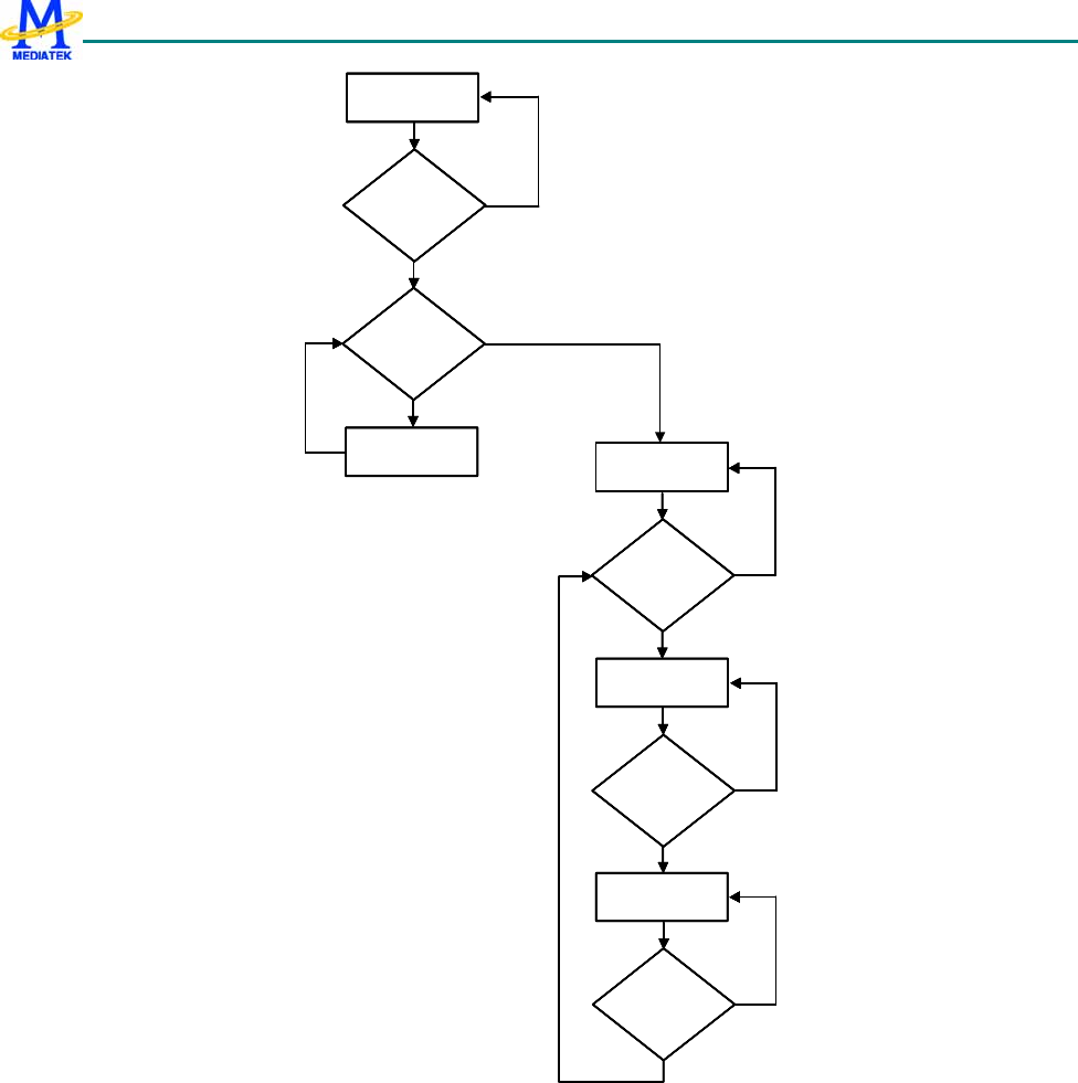
MT6235 GSM/GPRS Baseband Processor Data Sheet Revision 1.02
556/599 MediaTek Inc. Confidential
NO-CHARGING
CHARGER
DETECTOR
CHRIN > BATSNS
VBAT > 3.2V
PRE-CHARGING
YES
YES
CONSTANT
CURRENT MODE
VBAT > 4.2V
YES
NO
VBAT < 4.3V
CHARGER
OFF
VBAT > 4.3V
(OV)
YES
CONSTANT
VOLTAGE MODE
YES
NO
NO
NO
NO
NO-CHARGING
CHARGER
DETECTOR
CHRIN > BATSNS
VBAT > 3.2V
PRE-CHARGING
YES
YES
CONSTANT
CURRENT MODE
VBAT > 4.2V
YES
NO
NO
VBAT < 4.3V
CHARGER
OFF
VBAT > 4.3V
(OV)
YES
CONSTANT
VOLTAGE MODE
YES
NO
NO
NO
NO
NO
NO
NO-CHARGING
CHARGER
DETECTOR
CHRIN > BATSNS
VBAT > 3.2V
PRE-CHARGING
YES
YES
CONSTANT
CURRENT MODE
VBAT > 4.2V
YES
NO
VBAT < 4.3V
CHARGER
OFF
VBAT > 4.3V
(OV)
YES
CONSTANT
VOLTAGE MODE
YES
NO
NO
NO
NO
NO-CHARGING
CHARGER
DETECTOR
CHRIN > BATSNS
VBAT > 3.2V
PRE-CHARGING
YES
YES
CONSTANT
CURRENT MODE
VBAT > 4.2V
YES
NO
NO
VBAT < 4.3V
CHARGER
OFF
VBAT > 4.3V
(OV)
YES
CONSTANT
VOLTAGE MODE
YES
NO
NO
NO
NO
NO
NO
Figure 2. Battery Charger Flow Chart
Charge Detection
The PMU charger block has a detection circuit that senses the charger plug-in/out and provides the correct information to the
baseband. If the CHRIN voltage is over 7V, the detection circuit reports invalid charger and CHRDET signal goes low to stop
charging.
Pre-Charging mode
When the battery voltage is below the UVLO threshold, the charging status is in the pre-charging mode. There are two steps in
this mode. While the battery voltage is deeply discharged below 2V, a 10mA trickle current generated internally charges the
battery. When the battery voltage exceeds 2V, the closed-loop pre-charge mode is enabled, which allows 10mV (typically) voltage
drop across the external current sense resistor. The pre-charge current can be calculated:

MT6235 GSM/GPRS Baseband Processor Data Sheet Revision 1.02
557/599 MediaTek Inc. Confidential
SENSESENSE
SENSE
CHARGINGPRE R
mV
R
V
I10
_== (2)
Constant Current Charging Mode
Once the battery voltage has exceeded the UVLO threshold, the charger will switch to the constant current charging mode. It
allows up to 800mA constant charging current which is controlled by the registers. The relation between the voltage drop across
the external current sense resistor and the charging current is as follows,
SENSE
SENSE
CONSTANT R
V
I= (3)
Before the battery voltage reaches 4.2V, the charger will be in the constant current charging mode.
Constant Voltage Charging Mode
If the battery voltage has reached 4.2V, a constant voltage is applied to the battery and keeps it at 4.2V. As the charger is kept in
the constant voltage charging mode, the charging current will be lower and lower until the charge completion. The charge
termination is determined by the baseband, which will set the register CHR_EN to stop the charger.
Once the battery voltage exceeds 4.3V, a hardware over voltage protection (OV) should be activated and turn off the charger
immediately.
External Components Selection
Input Capacitor Selection
For each of input pins (VBAT) of PMU, a local bypass capacitor is recommended. Use a 10µF, low ESR capacitor. MLCC
capacitors provide the best combination of low ESR and small size. Using a 10µF Tantalum capacitor with a small (1µF or 2.2µF)
ceramic in parallel is an alternative low cost solution.
For charger input pin (CHRIN), a bypass 1µF ceramic capacitor is recommended.
LDO/Buck converter Capacitor/inductor Selection
The analog and RF LDOs require a 4.7µF capacitor, the digital core buck converter requires a 2.2uF capacitor??, and the other
LDOs require a 1µF capacitor. Large value capacitor may be used for desired noise or PSRR requirement. But the acceptable
settling time should be taken into consideration. The MLCC X5R type capacitors must be used with VRF, VTCXO, VCAM_A
and VA LDOs for good system performance. For other LDOs, MLCC X5R type capacitors are also recommended to use.

MT6235 GSM/GPRS Baseband Processor Data Sheet Revision 1.02
558/599 MediaTek Inc. Confidential
RESET Capacitor Selection
RESET is held low at power-up until a delay time when LDOs are on. The delay is set by an external capacitor on RESCAP pin. It
can be determined by the Eq.(1).
For example, a 100nF capacitor can produce 200ms delay.
Setting the Charge Current
PMU is capable of charging battery. The charging current is controlled with an external sense resistor, Rsense. It is calculated as
the Eq.(3). If the charge current is pre-defined, Rsense can be determined.
Accurate sense resistors are available from the following vendors: Vishay Dale, IRC, Panasonic.
Charger FET Selection
The PMOS FET selection used in charger should consider the minimum drain-source breakdown voltage (BVDS), the minimum
turn-on threshold voltage (VGS), and heat-dissipating ability.
These specifications can be calculated as below:
VGS = VCHRIN - VGATEDRV
VDS = VCHRIN - VDIODE - VSENSE - VBAT
VDS
RDS(ON) =
ICHR
PDISS = ( VCHRIN-VDIODE-VSENSE-VBAT) x ICHR
Appropriate PMOS FETs are available from the following vendors: Siliconix, IR, Fairchild.
Charger Diode Selection
The diode is used to prevent the battery from discharging through the PMOS’s body diode into the charger’s internal circuits.
Choose a diode with sufficient current rating to handle the battery charging current and voltage rating greater than Vbat.
Layout Guideline
Use the general guidelines listed below to design the printed circuit boards:
1. Split battery connection to the VBAT, VBATRF and AVBAT pins for PMU. Place the input capacitor as close to the power pins
as possible.
2. Va and Vtcxo capacitors should be returned to AGND. Vrf capacitor should be returned to AGND_RF.
3. Split the ground connection. Use separate traces or planes for the analog, digital, and power grounds (i.e. AGND, AGND_RF,
DGND, PGND pins of PMU, respectively) and tie them together at a single point, preferably close to battery return.
4. Place a separate trace from the BATSNS pin to the battery input to prevent voltage drop error when sensing the battery voltage.
5. Kelvin-connect the charge current sense resistor by placing separate traces to the BATSNS and ISENSE pins. Make sure that
the traces are terminated as close to the resistor’s body as possible.
6. Careful use of copper area, weight, and multi-layer construction will help to improve thermal performance.
13.2.9.2 Functional Specification
13.2.9.2.1 Electrical Characteristics
VBAT = 3 V ~ 5 V, minimum loads applied on all outputs, unless other noted. Typical values are at TA = 25 °C.

MT6235 GSM/GPRS Baseband Processor Data Sheet Revision 1.02
559/599 MediaTek Inc. Confidential
Parameter Conditions Min. Typical Max. Unit
Switch-Off Mode: Supply Current
VBAT < 2.5 V RTC LDO OFF TBD µA
2.5 V < VBAT < 3.3 V VBAT=3.3V
TBD µA
3.3 V < VBAT VBAT=4.2V
TBD µA
Operation: Supply Current
All outputs on VBAT=4.2V TBD µA
VSIM, VSIM2, VTXCO, VRF, VUSB,
VCAM_A, VCAM_D, VBT off; all others
on
VBAT=4.2V
TBD µA
Under Voltage (UV)
Under voltage falling threshold 1 UV_SEL[1:0] = 00 2.85 2.9 2.95 V
Under voltage falling threshold 2 UV_SEL[1:0] = 01 2.7 2.75 2.8 V
Under voltage falling threshold 3 UV_SEL[1:0] = 10 2.55 2.6 2.65 V
Under voltage falling threshold 4 UV_SEL[1:0] = 11 2.35 2.5 2.65 V
Under voltage rising threshold UV_SEL[1:0] = xx 3.1 3.2 3.3 V
Reset Generator
Output High VIO-0.5 V
Output Low 0.2 V
Output Current TBD mA
On Delay Time per Unit Capacitance 1.5 2.5 4 ms/nF
Power Key Input
High Voltage 0.7*VBAT V
Low Voltage 0.3*VBAT V
Control Input Voltage
Other Control Input High 2.0 V
Other Control Input Low 0.5
Thermal Shutdown
Threshold 150 degree
Hysteresis 40 degree
LDO Enable Response Time 250 µs
13.2.9.2.2 Regulator Output
Parameter Conditions Min. Typical Max. Unit
Digital Core Voltage
Register VOSEL=0 1.7 1.8 1.9 V
1.4 1.5 1.6 V
Output voltage (V_D)
Register VO_SEL=1 1.1 1.2 1.3 V
Output current (Id_max) 350 mA

MT6235 GSM/GPRS Baseband Processor Data Sheet Revision 1.02
560/599 MediaTek Inc. Confidential
Line regulation TBD mV
Load regulation TBD mV
Digital IO Voltage
Output voltage (V_IO) 2.7 2.8 2.9 V
Output current (Iio_max) 100 mA
Line regulation TBD mV
Load regulation TBD mV
RF Voltage
Output voltage (V_A) 2.7 2.8 2.9 V
Output current (Ia_max) 250 mA
Line regulation TBD mV
Load regulation TBD mV
Output noise voltage f = 1k Hz to 100 kHz 40 uVrms
Ripple rejection at 1kHz 65 dB
Analog Voltage
Output voltage (V_A) 2.7 2.8 2.9 V
Output current (Ia_max) 125 mA
Line regulation TBD mV
Load regulation TBD mV
Output noise voltage f = 10 Hz to 100 kHz 50 uVrms
10 Hz < freq. < 3 kHz 65 dB
Ripple rejection
3 kHz < freq. < 1 MHz 40 dB
VTCXO Voltage
Output voltage (V_TCXO) 2.7 2.8 2.9 V
Output current (Itcxo_max) 40 mA
Line regulation TBD mV
Load regulation TBD mV
Output noise voltage f = 10 Hz to 100 kHz 50 µVrms
10 Hz < freq. < 3 kHz 65 dB
Ripple rejection
3 kHz < freq. < 1 MHz 40 dB
RTC Voltage
1st stage output voltage 2.5 2.6 TBD V
2nd stage output voltage (V_RTC) RTC_SEL=H TBD 1.2 TBD V
Output current limit (Irtc_max) 1st stage RTC 0.6 mA
Off reverse input current 1 µA
External Memory Voltage
VMSEL=L 1.7 1.8 1.9 V Output voltage (V_M)
VMSEL=H 2.7 2.8 2.9 V
Output current (Im_max) 300 mA
Line regulation TBD mV
Load regulation TBD mV
SIM Voltage
Output voltage (V_SIM) Register VSIM_SEL=L 1.71 1.8 1.89 V

MT6235 GSM/GPRS Baseband Processor Data Sheet Revision 1.02
561/599 MediaTek Inc. Confidential
Register VSIM_SEL=H 2.82 3.0 3.18 V
Output current (Isim_max) 80 mA
Line regulation TBD mV
Load regulation TBD mV
SIM2 Voltage
Output voltage (V_SIM2) Register VSIM2_SEL=L 1.71 1.8 1.89 V
Register VSIM2_SEL=H 2.82 3.0 3.18 V
Output current (Isim2_max) 20 mA
Line regulation TBD mV
Load regulation TBD mV
Memory card/Blue-Tooth Voltage
Output voltage (V_BT) Register VBT_SEL=L 2.7 2.8 2.9 V
Register VBT_SEL=H 2.8 3.0 3.2 V
Output current (Ibt_max) 100 mA
Line regulation TBD mV
Load regulation TBD mV
USB Voltage
Output voltage (V_USB) 2.97 3.3 3.63 V
Output current (Iusb_max) 75 mA
Line regulation TBD mV
Load regulation TBD mV
Digital Camera Voltage
Output voltage (V_CAM_D) Register
VCAM_D_SEL=00 1.4 1.5 1.6 V
Register
VCAM_D_SEL=01 1.7 1.8 1.9 V
Register
VCAM_D_SEL=10 2.4 2.5 2.6 V
Register
VCAM_D_SEL=11 2.7 2.8 2.9 V
Output current (Icamera_max) 75 mA
Line regulation TBD mV
Load regulation TBD mV
Analog Camera Voltage
Output voltage (V_CAM_A) Register
VCAM_A_SEL=00 1.2 1.3 1.4 V
Register
VCAM_A_SEL=01 1.4 1.5 1.6 V
Register
VCAM_A_SEL=10 1.7 1.8 1.9 V
Register
VCAM_A_SEL=11 2.7 2.8 2.9 V
Output current (Icamera_max) 250 mA
Line regulation TBD mV
Load regulation TBD mV

MT6235 GSM/GPRS Baseband Processor Data Sheet Revision 1.02
562/599 MediaTek Inc. Confidential
LED /Vibrator Driver
Sink Current of Key-Pad LED Driver Von<0.5V 150 mA
Sink Current of Vibrator Driver Von<0.5V 250 mA
13.2.9.2.3 SIM interface
Parameter Conditions Min. Typical Max. Unit
Interface to 3 V SIM Card
Volrst I = 20 µA 0.4 V
Vo h r s t I = - 2 0 0 µA 0.9*VSI
M V
Vo l c l k I = 2 0 µA 0.4 V
Vo h c l k I = - 2 0 0 µA 0.9*VSI
M V
Vihsio , Vohsio I = ±20 µA VSIM-0.4 V
Iil Vil = 0 V -1 mA
Vol Iol = 1 mA 0.15*VSI
M V
Interface to 1.8 V SIM Card
Volrst I = 20 µA
0.2*VSI
M V
Vo h r s t I = - 2 0 0 µA 0.9*VSI
M V
Vo l c l k I = 2 0 µA
0.2*VSI
M V
Vo h c l k I = - 2 0 0 µA 0.9*VSI
M V
Vil
0.15*VSI
M V
Vihsio , Vohsio I = ±20 µA VSIM-0.4 V
Iil Vil = 0 V -1 mA
Vol Iol = 1 mA 0.15*VSI
M V
SIM Card Interface Timing
SIO pull-up resistance to VSIM 8 10 12 k
SRST, SIO rise/fall times VSIM = 3, 1.8 V, load with 30 pF 1 µs
VSIM = 3 V, CLK load with
30 pF 18 ns
SCLK rise/fall times
VSIM = 1.8 V, CLK load with
30 pF 50 ns
SCLK frequency CLK load with 30 pF 5 MHz
SCLK duty cycle SIMCLK Duty = 50%, fsimclk =
5 MHz 47 53 %

MT6235 GSM/GPRS Baseband Processor Data Sheet Revision 1.02
563/599 MediaTek Inc. Confidential
SCLK propagation delay 30 50 ns
13.2.9.2.4 Charger Circuit
Parameter Conditions Min. Typical Max. Unit
AC charger input voltage 4.2 8
V
AC charger detect on threshold (Vchg_on) VBAT<3.2V 4.2 7 V
VBAT>=3.2V VBAT
+120mV 7 V
Maximum charging current (AC charging) VBAT>=3.2V 0.16 / Rsense A
VBAT<2.3V 10 mA
Pre-charging current
VBAT>=2.3V TBD 100 TBD mA
Pre-charging off threshold 3.2 V
Pre-charging off hysteresis 0.3 V
CC mode to CV mode threshold 4.15 4.2 4.25 V
BAT_ON (Vih) 2.4 2.6 V
GATEDRV rising time (Tr) BAT_ON, or OV 1 5 µs
Over voltage protection threshold (OV) 4.3 V
13.2.9.2.5 Regulators and Drivers
Item LDO Voltage Current Description
1 VCORE 1.8V/1.2V / 0.9V 350 mA Digital core
2 VIO 2.8V 100 mA Digital IO
3 VRF 2.8V 250 mA RF chip
4 VA 2.8V 125 mA Analog baseband
5 VRTC 1.2V 0.6 mA Real-time clock
6 VM 1.8V / 2.8V 300 mA External memory, selectable
7 VSIM 1.8V / 3.0V 80 mA SIM card, selectable
8 VTCXO 2.8V 40 mA 13/26 MHz reference clock
9 VSIM2 1.8V / 3.0V 20 mA SIM2 card, selectable
10 VUSB 3.3V 75 mA USB

MT6235 GSM/GPRS Baseband Processor Data Sheet Revision 1.02
564/599 MediaTek Inc. Confidential
11 VBT 2.8V / 3.0V 100 mA Memory card or Bluetooth
12 VCAM_A 1.5V / 1.8V / 2.5V / 2.8V 250 mA Analog camera power
13 VCAM_D 1.3V / 1.5V / 1.8V / 2.8V 75 mA Digital camera power
Driver Type Current Description
LED Open-drain NMOS switch 150 mA Drives the keypad LEDs
VIBRATOR Open-drain NMOS switch 250 mA Drives the vibrator
The output current ratings for the above drivers already include a 50% margin on their nominal current
consumption, e.g. if a regulator output is listed as 150 mA, the peak consumption current is 100 mA. In the active
state, the phone consumes peak output current at each driver, which must be considered for the thermal design.
13.2.9.2.6 Register Setting
0x83010800 Control LDO of VRF and test setting PMIC_CON0
Bit 15 14 13 12 11 10 9 8 7 6 5 4 3 2 1 0
Name TPSEL
VRF_
ON_S
EL VRF_CAL ICALRF_EN
VRF_
PLNM
OS_DI
S
VRF_
EN_F
ORCE
VRF_
EN
VRF_
STAT
US
Type R/W R/W R/W R/W R/W R/W R/W RO
Reset 0 0 0 0 0 0 0 0
VRF_STATUS RF LDO ON/OFF Status excluding Force-Enable
VRF_EN RF LDO Enable Control Signal
0 Disable
1 Enable
VRF_EN_FORCE RF LDO Force-Enable Control Signal
0 Disable
1 Enable
VRF_PLNMOS_DIS RF LDO Pull-low NMOS disable Signal
0 Enable pull-low
1 Disable pull-low
ICALRF_EN RF LDO Bias Current Calibration Code
0 x1
1 x0.5
2 x2
3 x3
VRF_CAL RF LDO Output Voltage Calibration Code in monotonic transfer function
0000 maximum value
1111 minimum value
VRF_ON_SEL RF LDO Enable Control Signal
0 enable with VTCXO_EN(equivalent to “PMIC_CON4[2] | SRCLKENA”)
MT6235 GSM/GPRS Baseband Processor Data Sheet Revision 1.02
565/599 MediaTek Inc. Confidential
1 enable with VRF_EN
TPSEL Internal Node-set Selection for Mux-out on LED PAD. Reserved for the testing purpose.
0x83010804 Control LDO of VCORE , VRTC, and status of VIO and VM PMIC_CON1
Bit 15 14 13 12 11 10 9 8 7 6 5 4 3 2 1 0
Name VM_S
TATU
S
VIO_S
TATU
S
VRTC
_EN_
FORC
E
VRTC
_STA
TUS ACC_OUT_INIT PWM
B
FAST
_SLO
W
ADC_I
N_ED
GE
VCOR
E_EN
_FOR
CE
Type RO RO R/W RO R/W R/W R/W R/W R/W
Reset 0 0 0 0 1100 1 1 0 0
VCORE_EN_FORCE VCORE LDO Force-Enable Control Signal for MCU write. When being read, this register returns
the value of VCORE_STATUS, which is quite different from other LDO’s force enable bit
0 Disable
1 Enable
ADC_IN_EDGE use positive/ negative edge as ADC_COUNTER input
0 negative
1 positive
FAST_SLOW PWM switching frequency
0 26MHz divided by 32
1 26MHz divided by 16
PWMB select PWM bit resolution
0 3 bits
1 4 bits
ACC_OUT_INIT PID compensator integrator initial value setup
VRTC_STATUS VRTC LDO ON/OFF Status excluding Force-Enable
VRTC_EN_FORCE VRTC LDO Force-Enable Control Signal
0 Disable
1 Enable
VIO_STATUS VIO LDO ON/OFF Status excluding Force-Enable
VM_STATUS VM LDO ON/OFF Status excluding Force-Enable
0x83010808 Control LDO of VIO and VM PMIC_CON2
Bit 15 14 13 12 11 10 9 8 7 6 5 4 3 2 1 0
Name VM_CAL ANTIU
DSH_
M_DN ICALM_EN VM_E
N_FO
RCE VIO_CAL ANTIU
DSH_I
O_DN ICALIO_EN VIO_E
N_FO
RCE
Type R/W R/W R/W R/W R/W R/W R/W R/W
Reset 0 0 0 0 0 0 0 0
VIO_EN_FORCE VIO LDO Force-Enable Control Signal
0 Disable
1 Enable
ICALIO_EN VIO LDO Bias Current Calibration Code
MT6235 GSM/GPRS Baseband Processor Data Sheet Revision 1.02
566/599 MediaTek Inc. Confidential
0 x1
1 x0.5
2 x2
3 x3
ANTIUDSH_IO_DN VIO LDO Anti-Undershoot Disable Control Signal
0 Enable function
1 Disable function
VIO_CAL VIO LDO Output Voltage Calibration Code
0000 maximum
1111 minimum
VM_EN_FORCE VM LDO Force-Enable Control Signal
0 Disable
1 Enable
ICALM_EN VM LDO Bias Current Calibration Code
0 x1
1 x0.5
2 x2
3 x3
ANTIUDSH_M_DN VM LDO Anti-Undershoot Disable Control Signal
0 Enable function
1 Disable function
VM_CAL VM LDO Output Voltage Calibration Code in monotonic transfer function
0000 maximum
1111 minimum
0x8301080C Control and Status of LDO of VSIM, Calibration of VRTC PMIC_CON3
Bit 15 14 13 12 11 10 9 8 7 6 5 4 3 2 1 0
VRTC_STEP2_CAL VRTC_STEP1_CAL VSIM_CAL
VSIM_
PLNM
OS_DI
S
ANTIU
DSH_
SIM_D
N
ICALSIM_EN VSIM_
EN_F
ORCE
VSIM_
STAT
US
Type R/W R/W R/W R/W R/W R/W R/W RO
Reset 0 0 0 0 0 0 0 0
VSIM_STATUS VSIM LDO ON/OFF Status excluding Force-Enable
VSIM_EN_FORCE VSIM LDO Force-Enable Control Signal
0 Disable
1 Enable
ICALSIM_EN VSIM LDO Bias Current Calibration Code
0 x1
1 x0.5
2 x2
3 x3
ANTIUDSH_SIM_DN VSIM LDO Anti-Undershoot Disable Control Signal
0 Enable function

MT6235 GSM/GPRS Baseband Processor Data Sheet Revision 1.02
567/599 MediaTek Inc. Confidential
1 Disable function
VSIM_PLNMOS_DIS VSIM LDO Pull-low NMOS disable Signal
0 Enable pull low
1 Disable pull low
VSIM_CAL VSIM LDO Output Voltage Calibration Code in monotonic transfer function
0000 maximum value
1111 minimum value
VRTC_STEP1_CAL VRTC LDO1 Output Voltage Calibration Code in 2's complements monotonic transfer
function for the 1st step. Configuration of the register must be followed by toggling
VRTC_CAL_LATCH_EN (VRTC_STEP1_CAL -> VRTC_CAL_LATCH_EN “TRUE” ->
VRTC_CAL_LATCH_EN “FALSE”)
000 nominal value
111 minimum value
011 maximum value
VRTC_STEP2_CAL VRTC LDO2 Output Voltage Calibration Code in 2's complement monotonic transfer
function for the 2nd step. Configuration of the register must be followed by toggling
VRTC_CAL_LATCH_EN(VRTC_STEP2_CAL -> VRTC_CAL_LATCH_EN “TRUE” ->
VRTC_CAL_LATCH_EN “FALSE”)
000 nominal value
111 minimum value
111 maximum value
0x83010810 Control and Status of LDO of VTCXO and VA PMIC_CON4
Bit 15 14 13 12 11 10 9 8 7 6 5 4 3 2 1 0
Name
VRTC
_CAL
_LAT
CH_E
N
VA_CAL VA_E
N_SE
L
VA_E
N_FO
RCE
VA_S
TATU
S VTCXO_CAL
VTCX
O_PL
NMOS
_DIS
RG_V
TCXO
_EN
VTCX
O_EN
_FOR
CE
VTCX
O_ST
ATUS
Type R/W R/W R/W R/W RO R/W R/W R/W R/W RO
Reset 0 0 0 0 0 0 0 0 0 0
VCTXP_STATUS VTCXO LDO ON/OFF Status excluding Force-Enable
VCTXO_EN_FORCE VTCXO LDO Force-Enable Control Signal
0 Disable
1 Enable
RG_VCTXO_EN VTCXO LDO Enable Control Signal
0 Disable
1 Enable. Will force VCTXO LDO enabled discarding sleep mode control (SRCLKENA)
VCTXO_PLNMOS_DIS VTCXO LDO Pull-low NMOS disable Signal
0 Enable pull low
1 Disable pull low
VCTXO_CAL VTCXO LDO Output Voltage Calibration Code in monotonic transfer function
0000 maximum value
1111 minimum value

MT6235 GSM/GPRS Baseband Processor Data Sheet Revision 1.02
568/599 MediaTek Inc. Confidential
VA_STATUS VA LDO ON/OFF Status excluding Force-Enable
VA_EN_FORCE VA LDO Force-Enable Control Signal
0 Disable
1 Enable
VA_EN_SEL VA LDO Enable Control Selection
VA_CAL VA LDO Output Voltage Calibration Code
0000 maximum value
1111 minimum value
VRTC_CAL_LATCH_EN Latch enable for the VRTC calibration bits. To stabilize the VRTC right after VCORE
power-on, analog PMIC unit needs to latch the VRTC_STEP1_CAL and VRTC_STEP2_CAL in advance (before
VCORE power off).
0 Disable
1 Enable
0x83010814 Driver Control and Charger Status PMIC_CON5
Bit 15 14 13 12 11 10 9 8 7 6 5 4 3 2 1 0
Name CHRG
_DIS CV AC_D
ET BAT_
ON CHR_
DET OVP VSIM_
SEL VSIM_
EN INT_NODE_MUX BLED
_EN GLED
_EN RLED
_EN KPLE
D_EN VIBR_
EN
Type RO RO RO RO RO RO R/W R/W R/W R/W R/W R/W R/W R/W
Reset 0 0 0 0 0 0 0 0 0 0 0 0 0 0
VIBR_EN Vibrator Driver Enable Control Signal
0 Disable.
1 Enable. Controlled by hardware PWM2 output signal
KPLED_EN KPLED Driver Enable Control Signal
0 Disable.
1 Enable. Controlled by hardware PWM1 output signal
RLED_EN Reserved
GLED_EN Reserved
BLED_EN Reserved
VSIM_EN Only valid for analog test mode. For normal operation, this LDO enable is actually connected to
“simvcc” port of SIM hardware.
0 Disable
1 Enable
VSIM_SEL Only valid for analog test mode. For normal operation, this LDO voltage select is actually
connected to “simsel” port of SIM hardware. VSIM LDO voltage selection
0 1.8V
1 1.3V
OVP Charger OV occurred
0 AC<7V
1 AC>7V
CHR_DET Charger detected
0 No charger
MT6235 GSM/GPRS Baseband Processor Data Sheet Revision 1.02
569/599 MediaTek Inc. Confidential
1 With charger. The signal is connected to EINT8(active low), acting as an internal interrupt, and can wakeup
baseband chip even in sleep mode
BAT_ON Battery is connected
0 Battery is connected
1 Battery is removed
AC_DET AC power detected. Reserved
CV CV mode Indication
0 Not in CV mode
1 In CV mode
CHRG_DIS Not in Charging. Reserved. This register is used by PMU to indicate the test mode when being true.
Under the test mode, the system reset, power key, and SIM card data input would come from external PMIC,
rather than from PMU.
INT_NODE_MUX MUX the PMU internal nodes, to be monitored by AUXADC. The function is reserved for the
testing purpose.
000 GND (Reserved)
001 GND (Reserved)
010 GND (Reserved)
011 VREG12D_DCV (DC-DC internal LDO voltage)
100 internal charger BGR voltage
101 Ratioed Battery voltage
110 Ratioed ISENSE voltage
111 Ratioed CHRIN voltage
0x83010818 Charger and GPIO Control PMIC_CON6
Bit 15 14 13 12 11 10 9 8 7 6 5 4 3 2 1 0
Name GPIO_
DRV MTV_
EN CV_TUNE CV_RT
CHRO
N_FO
RCE CLASS_D CHOFST
CHR_
EN
Type R/W R/W R/W R/W R/W R/W R/W R/W
Reset 0 0 0 0 0 0 0 0
CHR_EN Enable Charging (CC and CV mode)
0 Disable
1 Enable
CHOFST Charging Current Offset (for CC mode current calibration)
000 No offset
001 plus 1 step
010 plus 2 step
011 No offset
100 No offset
101 No offset
110 minus 2 step
111 minus 1 step

MT6235 GSM/GPRS Baseband Processor Data Sheet Revision 1.02
570/599 MediaTek Inc. Confidential
CLASS_D CC mode charge current level
000 50mA
001 87.5mA
010 150mA
011 225mA
100 300mA
101 450mA
110 650mA
111 800mA
CHRON_FORCE Charger Force-Enable Control Signal
0 Disable (normal)
1 Enable (force charge on)
CV_RT Coarse tune the CV voltage according to VREF
CV_TUNE Fine tune the CV voltage according to VREF
000 VBG = 1.2V
001 VBG = 1.205V
010 VBG = 1.210V
011 VBG = 1.215V
100 VBG = 1.18V
101 VBG = 1.185V
110 VBG = 1.190V
111 VBG = 1.195V
MTV_EN Define Mobile TV application, the register is only for test purpose. If GPIO in normal function is intended,
please refer to “General-purpose IO” chapter
0 Non-Mobile-TV application, SCLK2/SRST2/SIO2 are used as GPIO pins
1 Mobile-TV application, SCLK2/SRST2/SIO2 are used as SIM2 interface
GPIO_DRV SCLK2/SRST2/SIO2 GPIO Driving Strength Control
0 8mA
1 4mA
0x8301081C Start Up PMIC_CON7
Bit 15 14 13 12 11 10 9 8 7 6 5 4 3 2 1 0
Name PWRK
EY_D
EB OV_T
H_FR
EEZE
OV_H
YS_E
NB
BIAS_
GEN_
FORC
E
IBIASSEL CKSE
L OSCE
N IBGSEL RBGSEL UV_SEL
Type RO R/W R/W R/W R/W R/W R/W R/W R/W R/W
Reset 0 0 0 0 0 0 0 0 0 0
UV_SEL UVLO High to Low Threshold Selection
00 2.9V

MT6235 GSM/GPRS Baseband Processor Data Sheet Revision 1.02
571/599 MediaTek Inc. Confidential
01 2.75V
10 2.6V
11 Follow DDLO
RBGSEL Bandgap T.C. fine tuning
000 initial setting
001 plus 1 step
010 plus 2 step
011 plus 3 step
100 minus 4 step
101 minus 3 step
110 minus 2 step
111 minus 1 step
IBGSEL Current setting for bandgap and oscillator
00 initial setting
01 plus 1 step
10 minus 2 step
11 minus 1 step
OSCEN Enable the oscillator in bandgap block
0 Disable
1 Enable
CKSEL Setting the clock rate of CKMON
0 ~10kHz
1 ~5kHz
VBSSEL Internal reference current tuning (global bias of PMU)
00 VBG/1200K
01 VBG/1320K
10 VBG/960K
11 VBG/1080K
BIAS_GEN_EN_FORCE Force the IBIAS/VBIAS Generator ON in the Testmode
0 Normal
1 Force on
OV_TH_HIGH Set the OV threshold when RG_OV_THFREEZE=1
0 Lower
1 Higher
OV_TH_FREEZE OV threshold freeze at 4.3V
0 OV threshold auto tuning
1 Fixed OV threshold
PWRKEY_DEB De-bounced PWRKEY signal
0x83010820 DC-DC controller for VCORE PMIC_CON8
Bit 15 14 13 12 11 10 9 8 7 6 5 4 3 2 1 0

MT6235 GSM/GPRS Baseband Processor Data Sheet Revision 1.02
572/599 MediaTek Inc. Confidential
Name SDM_
FB_E
N
VOSE
L DUTY_INIT GAIN_D GAIN GAIN_P
SDM_
ORDE
R
Type R/W R/W R/W R/W R/W R/W R/W
Reset 1 1 1000 010 100 010 1
SDM_ORDER select SDM order
0 1
st order
1 2
nd order
GAIN_P PID proportional gain select
MSB:
00 0.25
01 0.5
01 1
11 2
LSB: x 1.5
GAIN PID integration gain select
MSB:
00 0.015625
01 0.03125
01 0.0625
11 0.125
LSB: x 1.5
GAIN_D PID derivative gain select
MSB:
00 2
01 4
01 8
11 16
LSB: x 1.5
DUTY_INIT DCV test mode monitor select
VOSEL vcore voltage select
0 1.8V
1 1.2V
SDM_FB_EN SDM feedback path enable
0 Disable
1 Enable
0x83010824 DC-DC controller for VCORE PMIC_CON9
Bit 15 14 13 12 11 10 9 8 7 6 5 4 3 2 1 0
Name DCV_
TEST
_EN
MODE
SEL1
A
MODE
CMP MODE
EN[0] MODE
SET ADJCKSEL ISEL
DCV_
CK_S
EL
DIRE
CT_C
TRL_
EN
VFBADJ
Type R/W R/W R/W R/W R/W R/W R/W R/W R/W R/W
Reset 0 1 0 1 1 100 10 1 0 1000

MT6235 GSM/GPRS Baseband Processor Data Sheet Revision 1.02
573/599 MediaTek Inc. Confidential
VFBADJ output voltage soft adjustment(4 bits resolution)“0000” ~ “1111” 16 step, 50mV/step when not in sleep
mode(SRLKENA high)
0000 minimum: 0.8V
1111 maximum: 1.6V
DIRECT_CTRL_EN voltage feedback direct feed through
0 DVFS
1 direct feed through
DCV_CK_SEL DCV digital PWM clock source select
0 internal free run ring oscillator
1 CLK_TCXO
ISEL reference gen bias current select
00 0.25X
01 1.5X
10 1X
11 2X
ADJCKSEL internal free run ring oscilltor frequency adjustment, 000~111
MODESET Manual mode setting
0 PFM mode
1 PWM mode
MODEEN Enable auto mode change, bit 1 is located at PMIC_CONB[11]
0 Manual change
1 Auto mode change
MODECMP select comparator entering PWM mode
0 low offset comparator
1 auto-zero comparator
MODESEL1A Select average current mode
0 NCD mode
1 average current mode
DCV_TEST_EN DCV test mode enable
0 normal mode
1 test mode
0x83010828 DC-DC controller for VCORE PMIC_CONA
Bit 15 14 13 12 11 10 9 8 7 6 5 4 3 2 1 0
Name RSEL IASEL DCVTRIM NCDOF PFMSEL
Type R/W R/W R/W R/W R/W
Reset 01 01 011 10 0000110
PFMSEL[3:0] PFM max load current select (constant bias)
3 160mA
2 80mA
MT6235 GSM/GPRS Baseband Processor Data Sheet Revision 1.02
574/599 MediaTek Inc. Confidential
1 40mA
0 20mA
PFMSEL[6:4] PFM max load current select (proportional to Vin)
6 50ohm
5 100phm
4 200ohm
NCDOF NCD comparator offset
00 -3mV
01 5mV
10 12mV
11 17mV
DCVTRIM reference voltage trimming . Each step = 10mV (for Vout=1.2V )
IASEL select vavgl
00 50mV
01 100mV
10 150mV
11 200mV
RSEL curdet bias current select
00 32k
01 28k
10 24k
11 18k
0x8301082C Control and Status of LDO of VUSB PMIC_CONB
Bit 15 14 13 12 11 10 9 8 7 6 5 4 3 2 1 0
Name VFBADJ_SLP MODE
N[1] VUSB_CAL
VUSB
_PLN
MOS_
DIS
ANTIU
DSH_
USB_
DN
ICALUSB_E
N VUSB
_EN
VSUB
_EN_
FORC
E
VUSB
_STA
TUS
Type R/W R/W R/W R/W R/W R/W R/W R/W RO
Reset 0000 0 0 0 0 0 0 0 0
VUSB_STATUS VUSB LDO ON/OFF Status excluding Force-Enable
VUSB_EN_FORCE VUSB LDO Force-Enable Control Signal
0 Disable
1 Enable
VUSB_EN VUSB LDO Enable Control Signal
0 Disable
1 Enable
ICALUSB_EN VUSB LDO Bias Current Calibration Code
0 x1
1 x0.5
2 x2
3 x3
ANTIUDSH_USB_DN VUSB LDO Anti-Undershoot Disable Control Signal

MT6235 GSM/GPRS Baseband Processor Data Sheet Revision 1.02
575/599 MediaTek Inc. Confidential
0 Enable function
1 Disable function
VUSB_PLNMOS_DIS VUSB LDO Pull-low NMOS disable Signal
0 Enable pull low
1 Disable pull low
VUSB_CAL VUSB LDO Output Voltage Calibration Code in monotonic transfer function
0000 maximum value
1111 minimum value
VFBADJ_SLP output voltage soft adjustment(4 bits resolution)“0000” ~ “1111” 16 step, 50mV/step when in sleep
mode(SRLKENA low)
0000 minimum: 0.8V
1111 maximum: 1.6V
0x83010830 Control and Status of LDO of VSIM2 PMIC_CONC
Bit 15 14 13 12 11 10 9 8 7 6 5 4 3 2 1 0
VSIM2
_SEL VSIM2
_EN
VSIM_
PWR_
SAVIN
G
VTCX
O_ON
_SEL
CLK_
SOUR
CE_S
EL
VSIM2_CAL
VSIM2
_PLN
MOS_
DIS
ANTIU
DSH_
SIM2_
DN
ICALSIM2_E
N
VSIM2
_EN_
FORC
E
VSIM2
_STA
TUS
Type R/W R/W R/W R/W R/W R/W R/W R/W R/W R/W RO
Reset 0 0 0 0 0 0 0 0 0 0 0
CLK_SOURCE_SEL Select 26MHz clock source for VCORE PWM control
0 2.8V 26MHz directly from CLKSQ
1 1.2V 26MHz clock from TCXO26M_CK
VTCXO_ON_SEL VTCXO LDO enable control signal
0 Enable with VTCXO_EN (equivalent to “PMIC_CON4[2] | SRCLKENA”)
1 Enable with RG_VTCXO_EN(PMIC_CON4[2])
VSIM2_STATUS VSIM LDO ON/OFF Status excluding Force-Enable
VSIM2_EN_FORCE VSIM LDO Force-Enable Control Signal
0 Disable
1 Enable
ICALSIM2_EN VSIM LDO Bias Current Calibration Code
0 x1
1 x0.5
2 x2
3 x3
ANTIUDSH_SIM2_DN VSIM LDO Anti-Undershoot Disable Control Signal
0 Enable function
1 Disable function
VSIM2_PLNMOS_DIS VSIM LDO Pull-low NMOS disable Signal
0 Disable pull low
1 Enable pull low

MT6235 GSM/GPRS Baseband Processor Data Sheet Revision 1.02
576/599 MediaTek Inc. Confidential
VSIM2_CAL VSIM LDO Output Voltage Calibration Code in monotonic transfer function
0000 maximum value
1111 minimum value
VSIM2_EN Only valid for analog test mode. For normal operation, this LDO enable is actually connected to
“simvcc” port of SIM hardware.
0 Disable
1 Enable
VSIM2_SEL Only valid for analog test mode. For normal operation, this LDO voltage select is actually
connected to “simsel” port of SIM hardware. VSIM LDO voltage selection
0 1.8V
1 1.3V
VSIM_PWR_SAVING Used for power saving. Since design topology of SIM LS, SIM data out path tends to conduct
leakage current when VSIM LDO is not enable if default SIM data output is kept low. If the power saving is
enabled, SIM data output will keep high before VSIM LDO is turned on.
0 Disable
1 Enable
0x83010834 Control and Status of LDO of VBT PMIC_COND
Bit 15 14 13 12 11 10 9 8 7 6 5 4 3 2 1 0
VBT_
SEL VBT_
EN VBT_CAL
VBT_
PLNM
OS_DI
S
ANTIU
DSH_
BT_D
N
ICALBT_EN VBT_
EN_F
ORCE
VBT_
STAT
US
Type R/W R/W R/W R/W R/W R/W R/W RO
Reset 0 0 0 0 0 0 0 0
VBT_STATUS VBT LDO ON/OFF Status excluding Force-Enable
VBT_EN_FORCE VBT LDO Force-Enable Control Signal
0 Disable
1 Enable
ICALBT_EN VBT LDO Bias Current Calibration Code
0 x1
1 x0.5
2 x2
3 x3
ANTIUDSH_BT_DN VBT LDO Anti-Undershoot Disable Control Signal
0 Enable function
1 Disable function
VBT_PLNMOS_DIS VBT LDO Pull-low NMOS disable Signal
0 Enable pull low
1 Disable pull low
VBT_CAL VBT LDO Output Voltage Calibration Code in monotonic transfer function

MT6235 GSM/GPRS Baseband Processor Data Sheet Revision 1.02
577/599 MediaTek Inc. Confidential
0000 maximum value
1111 minimum value
VBT_EN VBT LDO Enable Control Signal
0 Disable
1 Enable
VBT_SEL VBT LDO Voltage Selection
0 2.8V
1 1.3V
0x83010838 Control and Status of LDO of Vcam_d PMIC_CONE
Bit 15 14 13 12 11 10 9 8 7 6 5 4 3 2 1 0
VCAM_D_SE
L
VCAM
_D_E
N DCV_SLEW_CTRL VCAM_D_CAL
VCAM
_D_P
LNMO
S_DIS
ANTIU
DSH_
CAM_
D_DN
ICALCAM_D
_EN
VCAM
_D_E
RA_E
N_FO
RCE
VCAM
_D_E
RA_S
TATU
S
Type R/W R/W R/W R/W R/W R/W R/W R/W RO
Reset 0 0 0 0 0 0 0 0 0
VCAM_D_STATUS VCAM_D LDO ON/OFF Status excluding Force-Enable
VCAM_D_EN_FORCE VCAM_D LDO Force-Enable Control Signal
0 Disable
1 Enable
ICALCAM_D_EN VCAM_D LDO Bias Current Calibration Code
0 x1
1 x0.5
2 x2
3 x3
ANTIUDSH_CAM_D_DN VCAM_D LDO Anti-Undershoot Disable Control Signal
0 Enable function
1 Disable function
VCAM_D_PLNMOS_DIS VCAM_D LDO Pull-low NMOS disable Signal
0 Enable pull low
1 Disable pull low
VCAM_D_CAL VCAM_D LDO Output Voltage Calibration Code in monotonic transfer function
0000 maximum value
1111 minimum value
VCAM_D_EN VCAM_D LDO Enable Control Signal
0 Disable
1 Enable
VCAM_D_SEL VCAM_D LDO Voltage Selection
0 2.8V
1 1.3V
DCV_SLEW_CTRL DCV power slew-rate control

MT6235 GSM/GPRS Baseband Processor Data Sheet Revision 1.02
578/599 MediaTek Inc. Confidential
0x8301083C Control and Status of LDO of Vcam_a , Vtcxo , and Va PMIC_CONF
Bit 15 14 13 12 11 10 9 8 7 6 5 4 3 2 1 0
OC_F
OLD_
EN
VCAM
_A_E
N
ICALTCXO_E
N ICALA_EN VCAM_A_CAL VCAM_A_SE
L ICALCAM_A
_EN
VCAM
_A_E
N_FO
RCE
VCAM
_A_S
TATU
S
Type R/W R/W R/W R/W R/W R/W R/W R/W RO
Reset 0 0 0 0 0 0 0 0 0
VCAM_A_STATUS VCAM_A LDO ON/OFF Status excluding Force-Enable
VCAM_A_EN_FORCE VCAM_A LDO Force-Enable Control Signal
0 Disable
1 Enable
ICALCAM_A_EN VCAM_A LDO Bias Current Calibration Code
0 x1
1 x0.5
2 x2
3 x3
VCAM_A_CAL VCAM_A LDO Output Voltage Calibration Code in monotonic transfer function
0000 maximum value
1111 minimum value
VCAM_A_EN VCAM_A LDO Enable Control Signal
0 Disable
1 Enable
VCAN_A_SEL VCAM_A LDO Voltage Selection
0 2.8V
1 1.3V
ICALTCXO_EN VTCXO LDO Bias Current Calibration Code
0 x1
1 x0.5
2 x2
3 x3
ICALA_EN VA LDO Bias Current Calibration Code
0 x1
1 x0.5
2 x2
3 x3
OC_FOLD_EN Reserved
0x83010840 Start Up & AUXADC Related Control Register 2 PMIC_CONG
Bit 15 14 13 12 11 10 9 8 7 6 5 4 3 2 1 0

MT6235 GSM/GPRS Baseband Processor Data Sheet Revision 1.02
579/599 MediaTek Inc. Confidential
Name
VBAT
_OUT
_EN
ISENS
E_OU
T_EN TPSEL_LED
LDO_
SOFT
_ST THR_SEL VREF_BG
Type R/W R/W R/W R/W R/W R/W R/W R/W
Reset 0 0 0 0 0 0 0 0
VREF_BG Reference voltage fine tuning according to VBG
000 initial setting
001 plus 1 step
010 plus 2 step
011 plus 3 step
100 minus 4 step
101 minus 3 step
110 minus 2 step
111 minus 1 step
THR_SEL Thermal shut-down threshold fine tuning
00 Initial setting
01 +10˚C
10 -20˚C
11 -10˚C
LDO_SOFT_ST Disable the LDO soft-start function
0 VM/VIO/VA/VTCXO has soft-start function when turning-on
1 VM/VIO/VA/VTCXO has no soft-start function when turning-on
TPSEL_LED Internal Node-set Selection for Mux-out on SCLK/SRST/SCLK2/SRST2. It’s reserved for testing
purpose.
ISENSE_OUT_EN Pass ISENSE voltage to one of the AUXADC channel
0 Disable
1 Enable
VBAT_OUT_EN Pass Battery voltage to one of the AUXADC channel
0 Disable
1 Enable
13.3 Programming Guide
13.3.1 BBRX Register Setup
The register used to control analog base-band receiver is BBRX_AC_CON.
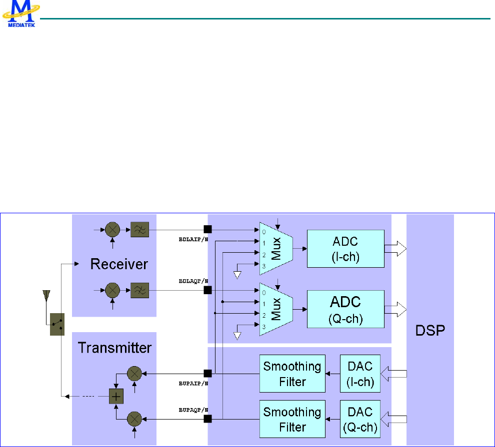
MT6235 GSM/GPRS Baseband Processor Data Sheet Revision 1.02
580/599 MediaTek Inc. Confidential
13.3.1.1 Programmable Biasing Current
To maximize the yield in modern digital process, the receiver features providing 5-bit 32-level
programmable current to bias internal analog blocks. The 5-bits registers CALBIAS [4:0] is coded with
2’s complement format.
13.3.1.2 Offset / Gain Calibration
The base-band downlink receiver (RX), together with the base-band uplink transmitter (TX) introduced
in the next section, provides necessary analog hardware for DSP algorithm to correct the mismatch and
offset error. The connection for measurement of both RX/TX mismatch and gain error is shown in
Figure 95, and the corresponding calibration procedure is described below.
Figure 95 Base-band A/D and D/A Offset and Gain Calibration
13.3.1.3 Downlink RX Offset Error Calibration
The RX offset measurement is achieved by selecting grounded input to A/D converter (set ISEL [1:0]
=’11’ and QSEL [1:0] =’11’ to select channel 3 of the analog input multiplexer, as shown in Figure 96.
The output of the ADC is sent to DSP for further offset cancellation. The offset cancellation accuracy
depends on the number of samples being converted. That is, more accurate measurement can be
obtained by collecting more samples followed by averaging algorithm.
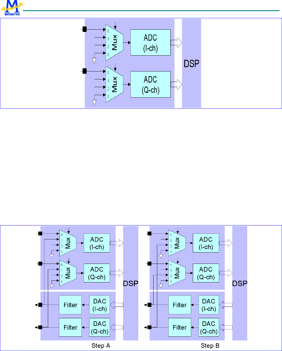
MT6235 GSM/GPRS Baseband Processor Data Sheet Revision 1.02
581/599 MediaTek Inc. Confidential
Figure 96 Downlink ADC Offset Error Measurement
13.3.1.4 Downlink RX and Uplink TX Gain Error Calibration
To measure the gain mismatch error, both I/Q uplink TXs should be programmed to produce full-scale
pure sinusoidal waves output. Such signals are then fed to downlink RX for A/D conversion, in the
following two steps.
A. The uplink I-channel output are connected to the downlink I-channel input, and the uplink Q-channel output are
connected to the downlink Q-channel input. This can be achieved by setting ISEL [1:0] =’01’ and QSEL [1:0] =’01’
(shown in Figure 97 (A))..
B. The uplink I-channel output are then connected to the downlink Q-channel input, and the uplink Q-channel output are
connected to the downlink I-channel input. This can be achieved by setting ISEL [1:0] =’10’ and QSEL [1:0] =’10’
(shown in Figure 97 (B)).
Figure 97 Downlink RX and Up-link TX Gain Mismatch Measurement (A) I/Q TX connect to I/Q RX (B) I/Q TX connect
to Q/I RX

MT6235 GSM/GPRS Baseband Processor Data Sheet Revision 1.02
582/599 MediaTek Inc. Confidential
Once above successive procedures are completed, RX/TX gain mismatch could be easily obtained because the amplitude
mismatch on RX digitized result in step A and B is the sum and difference of RX and TX gain mismatch, respectively.
The gain error of the downlink RX can be corrected in the DSP section and the uplink TX gain error can be corrected by the
gain trimming facility that TX block provide.
13.3.1.5 Uplink TX Offset Error Calibration
Once the offset of the downlink RX is known and corrected, the offset of the uplink TX alone could be
easily estimated. The offset error of TX should be corrected in the digital domain by means of the
programmable feature of the digital GMSK modulator.
Finally, it is important that above three calibration procedures should be exercised in order, that is,
correct the RX offset first, then RX/TX gain mismatch, and finally TX offset. This is owing to that
analog gain calibration in TX will affect its offset, while the digital offset correction has no effect on
gain.
13.3.2 BBTX Register Setup
The register used to control analog base-band transmitter is BBTX_AC_CON0 and
BBTX_AC_CON1.
13.3.2.1 Output Gain Control
The output swing of the uplink transmitter is controlled by register GAIN [2:0] coded in 2’s
complement with about 2dB step. When TRIMI [3:0] / TRIMQ [3:0] = 0 the swing is listed in Table
61, defined to be the difference between positive and negative output signal.
GAIN [2:0] Output Swing For AVDD=2.8 (V)
+3 (011) AVDD*0.453 (+2.0 dB) 1.27
+2 (010) AVDD*0.418 (+1.3 dB) 1.17
+1 (001) AVDD*0.386 (+0.6 dB) 1.08
+0 (000) AVDD*0.360 (+0.00 dB) 1
-1 (111) AVDD*0.336 (-0.6dB) 0.94
-2 (110) AVDD*0.310 (-1.3 dB) 0.87
-3 (101) AVDD*0.286 (-2.0 dB) 0.80
-4 (100) AVDD*0.267 (-2.6 dB) 0.74
Table 61 Output Swing Control Table

MT6235 GSM/GPRS Baseband Processor Data Sheet Revision 1.02
583/599 MediaTek Inc. Confidential
13.3.2.2 Output Gain Trimming
I/Q channels can also be trimmed separately to compensate gain mismatch in the base-band transmitter
or the whole transmission path including RF module. The gain trimming is adjusted in 16 steps spread
from -0.96dB to +0.84dB (Table 62), compared to the full-scale range set by GAIN [2:0].
TRIMI [3:0] / TRIMQ [3:0] Gain Step (dB)
+7 (0111) 0.84
+6 (0110) 0.72
+5 (0101) 0.60
+4 (0100) 0.48
+3 (0011) 0.36
+2 (0010) 0.24
+1 (0001) 0.12
+0 (0000) 0.00
-1 (1111) -0.12
-2 (1110) -0.24
-3 (1101) -0.36
-4 (1100) -0.48
-5 (1011) -0.60
-6 (1010) -0.72
-7 (1001) -0.84
-8 (1000) -0.96
Table 62 Gain Trimming Control Table
13.3.2.3 Output Common-Mode Voltage
The output common-mode voltage is controlled by CMV [2:0] with about 0.08*AVDD step, as listed
in the following table.
CMV [2:0] Common-Mode Voltage
+3 (011) AVDD*0.62
+2 (010) AVDD*0.58
+1 (001) AVDD*0.54
+0 (000) AVDD*0.50
-1 (111) AVDD*0.46
-2 (110) AVDD*0.42
-3 (101) AVDD*0.38
-4 (100) AVDD*0.34
Table 63 Output Common-Mode Voltage Control Table

MT6235 GSM/GPRS Baseband Processor Data Sheet Revision 1.02
584/599 MediaTek Inc. Confidential
13.3.2.4 Programmable Biasing Current
The transmitter features providing 5-bit 32-level programmable current to bias internal analog blocks.
The 5-bits registers CALBIAS [4:0] is coded with 2’s complement format.
13.3.2.5 Smoothing Filter Characteristic
The 2nd –order Butterworth smoothing filter is used to suppress the image at DAC output: it provides
more than 40dB attenuation at the 4.44MHz sampling frequency. To tackle with the digital process
component variation, programmable cutoff frequency control bits CALRCSEL [2:0] are included. User
can directly change the filter cut-off frequency by different CALRCSEL value (coded with 2’s
complement format and with a default value 0). In addition, an internal calibration process is provided,
by setting START CALRC to high and CALRCCNT to an appropriate value (default is 11). After the
calibration process, the filter cut-off frequency is calibrated to 350kHz +/- 50 kHz and a new
CALRCOUT value is stored in the register. During the calibration process, the output of the cell is
high-impedance.
13.3.3 AFC-DAC Register Setup
The register used to control the APC DAC is AFC_AC_CON, which providing 5-bit 32-level
programmable current to bias internal analog blocks. The 5-bits registers CALI [4:0] is coded with 2’s
complement format.
13.3.4 APC-DAC Register Setup
The register used to control the APC DAC is AFC_AC_CON, which providing 5-bit 32-level
programmable current to bias internal analog blocks. The 5-bits registers CALI [4:0] is coded with 2’s
complement format.
13.3.5 Auxiliary A/D Conversion Register Setup
The register used to control the Aux-ADC is AUX_AC_CON. For this register, which providing 5-bit 32-level
programmable current to bias internal analog blocks. The 5-bits registers CALI [4:0] is coded with 2’s complement format.
13.3.6 Voice-band Blocks Register Setup
The registers used to control AMB are AFE_VAG_CON, AFE_VAC_CON0, AFE_VAC_CON1, and
AFE_VAPDN_CON. For these registers, please refer to chapter “Analog Chip Interface”
13.3.6.1 Reference Circuit
The voice-band blocks include internal bias circuits, a differential bandgap voltage reference circuit

MT6235 GSM/GPRS Baseband Processor Data Sheet Revision 1.02
585/599 MediaTek Inc. Confidential
and a differential microphone bias circuit. Internal bias current could be calibrated by varying
VCALI[4:0] (coded with 2’s complement format).
The differential bandgap circuit generates a low temperature dependent voltage for internal use. For
proper operation, there should be an external 47nF capacitor connected between differential output
pins AU_VREFP and AU_VREFN. The bandgap voltage (~1.24V6, typical) also defines the dBm0
reference level through out the audio mixed-signal blocks. The following table illustrates typical
0dBm0 voltage when uplink/downlink programmable gains are unity. For other gain setting, 0dBm0
reference level should be scaled accordingly.
Symbol Parameter Min Typical Max Unit
V0dBm0,UP 0dBm0 Voltage for Uplink Path, Applied
Differentially Between Positive and
Negative Microphone Input Pins
0.2V V-rms
V0dBm0,Dn 0dBm0 voltage for Downlink Path,
Appeared Differentially Between Positive
and Negative Power Amplifier Output Pins
0.6V V-rms
Table 64 0dBm0 reference level for unity uplink/downlink gain
The microphone bias circuit generates a differential output voltage between AU_MICBIAS_P and
AU_MICBIAS_N for external electret type microphone. Typical output voltage is 1.9 V. In
singled-ended mode, by set VCFG[3] =1, AU_MICBIAS_N is pull down while output voltage is
present on AU_MICBIAS_P, respect to ground. The max current supplied by microphone bias circuit
is 2mA.
13.3.6.2 Uplink Path
Uplink path of voice-band blocks includes an uplink programmable gain amplifier and a sigma-delta modulator.
13.3.6.2.1 Uplink Programmable Gain Amplifier
Input to the PGA is a multiplexer controlled by VCFG [3:0], as described in the following table. In
normal operation, both input AC and DC coupling are feasible for attenuation the input signal (gain <=
0dB). However, only AC coupling is suggested if amplification of input signal is desired (gain>=0dB).
Control
Signal
Function Descriptions
VCFG [0] Input Selector 0: Input 0 (From AU_VIN0_P / AU_VIN0_N) Is Selected
1: Input 1 (From AU_VIN1_P / AU_VIN1_N) Is Selected
6 The bandgap voltage could be calibrated by adjusting control signal VBG_CTRL[1:0]. Its default value is [00].
VBG_CTRL not only adjust the bandgap voltage but also vary its temperature dependence. Optimal value of VBG_CTRL
is to be determined.

MT6235 GSM/GPRS Baseband Processor Data Sheet Revision 1.02
586/599 MediaTek Inc. Confidential
VCFG [1] Coupling Mode 0: AC Coupling
1: DC Coupling
VCFG [2] Gain Mode 0: Amplification Mode (gain >= 0 dB)
1: Attenuation Mode (gain <= 0dB)
VCFG [3] Microphone
Biasing
0: Differential Biasing (Take Bias Voltage Between AU_MICBIAS_P
and AU_MICBIAS_N)
1: Signal-Ended Biasing (Take Bias Voltage From AU_MICBIAS_P
Respected to Ground. AU_MICBIAS_N Is Connected to Ground)
Table 65 Uplink PGA input configuration setting
The PGA itself provides programmable gain (through VUPG [3:0]) with step of 3dB, as listed in the
following table.
VCFG [2] =’0’ VCFG [2] =’1’
VUPG [3:0] Gain VUPG [3:0] Gain
1111 NA X111 -21dB
1110 42dB X110 -18dB
1101 39dB X101 -15dB
1100 36dB X100 -12dB
1011 33dB X011 -9dB
1010 30dB X010 -6dB
1001 27dB X001 -3dB
1000 24dB X000 0dB
0111 21dB
0110 18dB
0101 15dB
0100 12dB
0011 9dB
0010 6dB
0001 3dB
0000 0dB
Table 66 Uplink PGA gain setting (VUPG [3:0])
The following table illustrates typically the 0dBm0 voltage applied at the microphone inputs,
differentially, for several gain settings.
VCFG [2] =’0’ VCFG [2] =’1’
VUPG [3:0] 0dBm0 (V-rms) VUPG [3:0] 0dBm0 (V-rms)
1100 3.17mV X110 1.59V
1000 12.6mV X100 0.8V
0100 50.2mV X010 0.4V

MT6235 GSM/GPRS Baseband Processor Data Sheet Revision 1.02
587/599 MediaTek Inc. Confidential
0000 0.2V X000 0.2V
Table 67 0dBm0 voltage at microphone input pins
13.3.6.2.2 Sigma-Delta Modulator
Analog-to-digital conversion in uplink path is made with a second-order sigma-delta modulator (SDM)
whose sampling rate is 4096kHz. Output signals are coded in either one-bit or RSD format, optionally
controlled by VRSDON register.
For test purpose, one can set VADCINMODE to HI to form a look-back path from downlink DAC
output to SDM input. The default value of VADCINMODE is zero.
13.3.6.3 Downlink Path
Downlink path of voice-band blocks includes a digital to analog converter (DAC) and two programmable output power
amplifiers.
13.3.6.3.1 Digital to Analog Converter
The DAC converts input bit-stream to analog signal by sampling rate of 4096kHz. . Besides, it
performs a 2nd-order 40kHz butterworth filtering. The DAC receives input signals from MT6235 DSP
by set VDACINMODE = 0. It can also take inputs from SDM output by setting VDACINMODE = 1.
13.3.6.3.2 Downlink Programmable Power Amplifier
Voice-band analog blocks include two identical output power amplifiers with programmable gain.
Amplifier 0 and amplifier 1 can be configured to either differential or single-ended mode by adjusting
VDSEND [0] and VDSEND [1], respectively. In single-ended mode, when VDSEND[0] =1, output
signal is present at AU_VOUT0_P pin respect to ground. Same as VDSEND[1] for AU_VOUT1_P
pin.
For the amplifier itself, programmable gain setting is described in the following table.
VDPG0 [3:0] / VDPG1 [3:0] Gain
1111 8dB
1110 6dB
1101 4dB
1100 2dB
1011 0dB
1010 -2dB
1001 -4dB
1000 -6dB
0111 -8dB
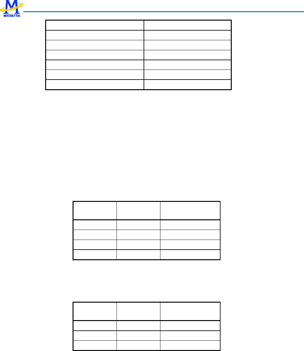
MT6235 GSM/GPRS Baseband Processor Data Sheet Revision 1.02
588/599 MediaTek Inc. Confidential
0110 -10dB
0101 -12dB
0100 -14dB
0011 -16dB
0010 -18dB
0001 -20dB
0000 -22dB
Table 68 Downlink power amplifier gain setting
Control signal VFLOAT, when set to ‘HI’, is used to make output nodes totally floating in power down
mode. If VFLOAT is set to ‘LOW” in power down mode, there will be a resistor of 50k ohm (typical)
between AU_VOUT0_P and AU_VOUT0_N, as well as between AU_VOUT0_P and AU_VOUT0_N.
The amplifiers deliver signal power to drive external earphone. The minimum resistive load is 28 ohm
and the upper limit of the output current is 50mA. On the basis that 3.14dBm0 digital input signal into
downlink path produces DAC output differential voltage of 0.87V-rms (typical), the following table
illustrates the power amplifier output signal level (in V-rms) and signal power for an external 32 ohm
resistive load.
VDPG Output Signal
Level (V-rms)
Output Signal Power
(mW / dBm)
0010 0.11 0.37/-4.3
0110 0.27 2.28/3.6
1010 0.69 14.8/11.7
1110 1.74 94.6/19.8
Table 69 Output signal level/power for 3.14dBm0 input. External resistive load = 32 ohm
The following table illustrates the output signal level and power for different resistive load when
VDPG =1110.
RLOAD Output Signal
Level (V-rms)
Output Signal Power
(mW / dBm)
30 1.74 101/20
100 1.74 30.3/14.8
600 1.74 5/7
Table 70 Output signal level/power for 3.14dBm0 input, VDPG =1110
13.3.6.4 Power Down Control
MT6235 GSM/GPRS Baseband Processor Data Sheet Revision 1.02
589/599 MediaTek Inc. Confidential
Each block inside audio mixed-signal blocks features dedicated power-down control, as illustrated in
the following table.
Control
Signal
Descriptions
VPDN_BIAS Power Down Reference Circuits (Active Low)
VPDN_LNA Power Down Uplink PGA (Active Low)
VPDN_ADC Power Down Uplink SDM (Active Low)
VPDN_DAC Power Down DAC (Active Low)
VPDN_OUT0 Power Down Downlink Power Amp 0 (Active Low)
VPDN_OUT1 Power Down Downlink Power Amp 1 (Active Low)
Table 71 Voice-band blocks power down control
13.3.7 Audio-band Blocks Register Setup
The registers used to control audio blocks are AFE_AAG_CON, AFE_AAC_CON, and
AFE_AAPDN_CON. For these registers, please refer to chapter “Analog Chip Interface”
13.3.7.1 Output Gain Control
Audio blocks include stereo audio DACs and programmable output power amplifiers. The DACs convert input bit-stream
to analog signal by sampling rate of Fs*128 where Fs could be 32kHz, 44.1kHz, or 48kHz. Besides, it performs a 2nd-order
butterworth filtering. The two identical output power amplifiers with programmable gain are designed to driving external
AC-coupled single-end speaker. The minimum resistor load is 16 ohm and the maximum driving current is 50mA. The
programmable gain setting, controlled by APGR[] and APGL[], is the same as that of the voice-band amplifiers.
Unlike voice signals, 0dBFS defines the full-scale audio signals amplitude. Based on bandgap
reference voltage again, the following table illustrates the power amplifier output signal level (in V-rms)
and signal power for an external 16 ohm resistive load.
APGR[]/
APGL[]
Output Signal
Level (V-rms)
Output Signal Power
(mW / dBm)
0010 0.055 0.19/-7.2
0110 0.135 1.14/0.6
1010 0.345 7.44/8.7
1110 0.87 47.3/16.7
Table 72 Output signal level/power for 0dBFS input. External resistive load = 16 ohm

MT6235 GSM/GPRS Baseband Processor Data Sheet Revision 1.02
590/599 MediaTek Inc. Confidential
13.3.7.2 Mute Function and Power Down Control
By setting AMUTER (AMUTEL) to high, right (Left) channel output will be muted.
Each block inside audio mixed-signal blocks features dedicated power-down control, as illustrated in
the following table.
Control Signal Descriptions
APDN_BIAS Power Down Reference Circuits (Active Low)
APDN_DACL Power Down L-Channel DAC (Active Low)
APDN_DACR Power Down R-Channel DAC (Active Low)
APDN_OUTL Power Down L-Channel Audio Amplifier (Active Low)
APDN_OUTR Power Down R-Channel Audio Amplifier (Active Low)
Table 73 Audio-band blocks power down control
13.3.8 Multiplexers for Audio and Voice Amplifiers
The audio/voice amplifiers feature accepting signals from various signal sources including AU_FMINR/AU_FMINL pins,
that aimed to receive stereo AM/FM signal from external radio chip:
1) Voice-band amplifier 0 accepts signals from voice DAC output only.
2) Voice-band amplifier 1 accepts signal from either voice DAC, audio DAC, or AM/FM radio input pins (controlled
by register VBUF1SEL[] ). For the last two cases, left and right channel signals will be summed together to form a
mono signal first.
3) Audio left/right channel amplifiers receive signals from either voice DAC, audio DAC, or AM/FM radio input pins
(controlled by registers ABUFSELL[] and ABUFSELR[] ), too. Left and right channel amplifiers will produce
identical output waveforms when receiving mono signals from voice DAC.
13.3.9 Preferred Microphone and Earphone Connections
In this section, preferred microphone and earphone connections are discussed.
Differential connection of microphone is shown below. This is the preferred method to obtain the
possible best performance. C1 and Rin form an AC coupling and high-pass network. C1*Rin should be
chosen such that the in-band signal will not be attenuated too much. For differential minimum
resistance of 13k ohm, minimum value of C1 is 170nF for less than 1dB attenuation at 300Hz. R2 is
determined by microphone sensitivity. C2 and R2 form another low-pass filter to filtering noise coming
from microphone bias pins. Pole frequency less than 50Hz is recommended.
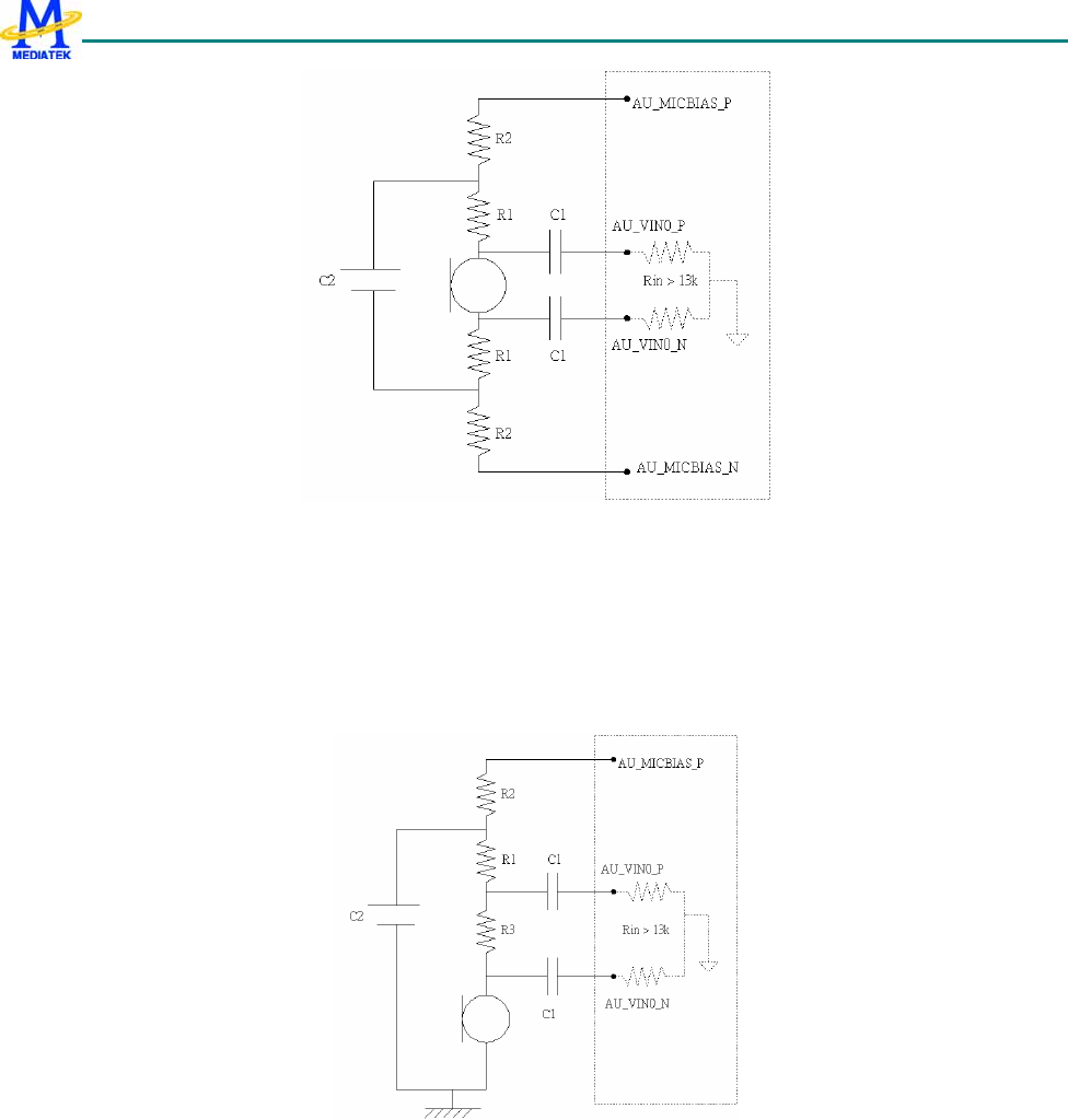
MT6235 GSM/GPRS Baseband Processor Data Sheet Revision 1.02
591/599 MediaTek Inc. Confidential
Figure 6 Differential Microphone Connection
For reference, single-ended connection method of microphone is shown below. R1 and R3 are chosen
based on microphone sensitivity requirement. C1 and Rin form an AC coupling and high-pass network.
R2 and C2 constitute a low-pass network for filtering out noise from microphone bias pins.
Figure 7 Single-ended Microphone Connection
For earphone, both differential and single-ended connections can be used. Advantage of differential
connection includes lower cost and better click-noise immunity. For single-ended connection, an
additional AC-coupling capacitor is necessary to not provide DC voltage to earphone. The high-pass
cut-off frequency formed by AC-coupling capacitor and earphone equivalent load should be low
enough (e.g. < 300 Hz).

MT6235 GSM/GPRS Baseband Processor Data Sheet Revision 1.02
592/599 MediaTek Inc. Confidential
13.3.10 Clock Squarer Register Setup
The register used to control clock squarer is CLK_CON. For this register, please refer to chapter
“Clocks”
CLKSQ_PLD is used to bypass the clock squarer.
13.3.11 Phase-Locked Loop Register Setup
For registers control the PLL, please refer to chapter “Clocks” and “Software Power Down Control”
13.3.11.1 Frequency Setup
The DSP/MCU PLL itself could be programmable to output either 52MHz or 78MHz clocks. Accompanied with additional
digital dividers, 13/26/39/52/65/78 MHz clock outputs are supported.
13.3.11.2 Programmable Biasing Current
The PLLs feature providing 5-bit 32-level programmable current to bias internal analog blocks. The
5-bits registers CALI [4:0] is coded with 2’s complement format.
13.3.12 32-khz Crystal Oscillator Register Setup
For registers that control the oscillator, please refer to chapter “Real Time Clock” and “Software Power Down Control”.

MT6235 GSM/GPRS Baseband Processor Data Sheet Revision 1.02
593/599 MediaTek Inc. Confidential
14 Digital Pin Electrical Characteristics
z Based on I/O power supply (VDD33) = 3.3 V
z Vil (max) = 0.8 V
z Vih (min) = 2.0 V
PU/PD Resistor
Ball
13x13 Name Dir
Driving Iol &
Ioh Typ (mA) Vol at Iol Max
(V) Voh at Ioh Min
(V) Min Typ Max
Pull Cin
(pF)
JTAG Port
G4 JTRST_B I 40K 75K 190K PD 2
G3 JTCK I 40K 75K 190K PU 2
G2 JTDI I 40K 75K 190K PU 2
G1 JTMS I 40K 75K 190K PU 2
H1 JTDO IO 2/4 0.4 2.4
H2 JRTCK IO 2/4 0.4 2.4
RF Parallel Control Unit
AE6 BPI_BUS0 IO 2/4/6/8 0.4 2.4
AD7 BPI_BUS1 IO 2/4/6/8 0.4 2.4
AC7 BPI_BUS2 IO 2/4/6/8 0.4 2.4
AC6 BPI_BUS3 IO 2 0.4 2.4 40K 75K 190K PU/PD 2
AE8 BPI_BUS4 IO 2 0.4 2.4
AD8 BPI_BUS5 IO 2 0.4 2.4
AC8 BPI_BUS6 IO 2 0.4 2.4 40K 75K 190K PU/PD 2
AB8 BPI_BUS7 IO 2 0.4 2.4 40K 75K 190K PU/PD 2
AE9 BPI_BUS8 IO 2 0.4 2.4 40K 75K 190K PU/PD 2
AD9 BPI_BUS9 IO 2 0.4 2.4 40K 75K 190K PU/PD 2
RF Serial Control Unit
AC9 BSI_CS0 IO 2 0.4 2.4
AE10 BSI_DATA IO 2/4/6/8 0.4 2.4
AD10 BSI_CLK IO 2 0.4 2.4
PWM Interface
AC10 PWM0 IO 2/4/6/8 0.4 2.4 40K 75K 190K PU/PD 2
AB10 PWM1 IO 2 0.4 2.4 40K 75K 190K PU/PD 2
AC5 PWM2 IO 4/8 40K 75K 190K PU/PD 2
AE5 PWM3 IO 4/8 0.4 2.4 40K 75K 190K PU/PD 2
Camera Control Interface
AE4 SCL IO 4/8/12/16 0.4 2.4 40K 75K 190K PU/PD 2
AD5 SDA IO 4/8/12/16 0.4 2.4 40K 75K 190K PU/PD 2
Serial LCD/PM IC Interface

MT6235 GSM/GPRS Baseband Processor Data Sheet Revision 1.02
594/599 MediaTek Inc. Confidential
AC11 LSCK IO 2/4/6/8 0.4 2.4 40K 75K 190K PU/PD 2
U11 LSA0 IO 2/4/6/8 0.4 2.4 40K 75K 190K PU/PD 2
AD12 LSDA IO 2/4/6/8 0.4 2.4 40K 75K 190K PU/PD 2
AE12 LSCE0B IO 2/4/6/8 0.4 2.4 40K 75K 190K PU/PD 2
AC12 LSCE1B IO 2/4/6/8 0.4 2.4 40K 75K 190K PU/PD 2
Parallel LCD/NAND-Flash
Interface
AB12 LPCE1B IO 2/4/6/8 0.4 2.4 40K 75K 190K PU/PD 2
U12 LPCE0B IO 2/4/6/8 0.4 2.4
AE13 LPTE IO 2/4/6/8 0.4 2.4 40K 75K 190K PU/PD 2
AC13 LRSTB IO 2/4/6/8 0.4 2.4
AD13 LRDB IO 2/4/6/8 0.4 2.4
U13 LPA0 IO 2/4/6/8 0.4 2.4
AE14 LWRB IO 2/4/6/8 0.4 2.4
AD14 NLD17 IO 2/4/6/8 0.4 2.4 40K 75K 190K PU/PD 2
AC14 NLD16 IO 2/4/6/8 0.4 2.4 40K 75K 190K PU/PD 2
AB14 NLD15 IO 2/4/6/8 0.4 2.4 40K 75K 190K PD 2
U14 NLD14 IO 2/4/6/8 0.4 2.4 40K 75K 190K PD 2
AE15 NDL13 IO 2/4/6/8 0.4 2.4 40K 75K 190K PD 2
AD15 NLD12 IO 2/4/6/8 0.4 2.4 40K 75K 190K PD 2
AC15 NLD11 IO 2/4/6/8 0.4 2.4 40K 75K 190K PD 2
AB15 NLD10 IO 2/4/6/8 0.4 2.4 40K 75K 190K PD 2
AE16 NLD9 IO 2/4/6/8 0.4 2.4 40K 75K 190K PD 2
AD16 NLD8 IO 2/4/6/8 0.4 2.4 40K 75K 190K PD 2
AC16 NLD7 IO 2/4/6/8 0.4 2.4 40K 75K 190K PD 2
AB16 NLD6 IO 2/4/6/8 0.4 2.4 40K 75K 190K PD 2
U16 NLD5 IO 2/4/6/8 0.4 2.4 40K 75K 190K PD 2
AE17 NLD4 IO 2/4/6/8 0.4 2.4 40K 75K 190K PD 2
AD17 NLD3 IO 2/4/6/8 0.4 2.4 40K 75K 190K PD 2
AC17 NLD2 IO 2/4/6/8 0.4 2.4 40K 75K 190K PD 2
AE18 NLD1 IO 2/4/6/8 0.4 2.4 40K 75K 190K PD 2
AD18 NLD0 IO 2/4/6/8 0.4 2.4 40K 75K 190K PD 2
AC18 NRNB IO 2/4/6/8 0.4 2.4 40K 75K 190K PU/PD 2
AB18 NCLE IO 2/4/6/8 0.4 2.4 40K 75K 190K PU/PD 2
AE19 NALE IO 2/4/6/8 0.4 2.4 40K 75K 190K PU/PD 2

MT6235 GSM/GPRS Baseband Processor Data Sheet Revision 1.02
595/599 MediaTek Inc. Confidential
AD19 NWEB IO 2/4/6/8 0.4 2.4 40K 75K 190K PU/PD 2
AC19 NREB IO 2/4/6/8 0.4 2.4 40K 75K 190K PU/PD 2
AB19 NCEB IO 2/4/6/8 0.4 2.4 40K 75K 190K PU/PD 2
USB Interface
AD20 USB_XTALI IO
AE20 USB_XTALO IO
AE21 VSSCA_USB IO
AD22 VSSCD_USB IO
AC21 VRT IO
AD23 VSS33_USB IO
AE22 USB_DP IO
AE23 USB_DM IO
Miscellaneous
F25 SYSRST_B I 40K 75K 190K PU 2
G23 WATCHDOG IO 2 0.4 2.4
U10 SRCLKENAN IO 2 0.4 2.4 40K 75K 190K PU/PD 2
AE11 SRCLKENA IO 2 0.4 2.4 40K 75K 190K PU/PD 2
AD11 SRCLKENAI IO 2 0.4 2.4 40K 75K 190K PU/PD 2
B14 TESTMODE I 40K 75K 190K PD 2
Y4 VCCQ I
AA1 FSOURCE I
AD6 SECU_EN I
AE7 XBOOT I 40K 75K 190K PD 2
Keypad Interface
A22 KCOL7 IO 2/4 0.4 2.4 40K 75K 190K PU/PD 2
B22 KCOL6 IO 2/4 0.4 2.4 40K 75K 190K PU/PD 2
A21 KCOL5 IO 2/4/6/8 0.4 2.4 40K 75K 190K PU 2
B21 KCOL4 IO 2/4/6/8 0.4 2.4 40K 75K 190K PU 2
C21 KCOL3 IO 2/4/6/8 0.4 2.4 40K 75K 190K PU 2
D21 KCOL2 IO 2/4/6/8 0.4 2.4 40K 75K 190K PU 2
A20 KCOL1 IO
2/4/6/8 0.4 2.4 40K 75K 190K PU 2
B20 KCOL0 IO 2/4/6/8 0.4 2.4 40K 75K 190K PU 2
C20 KROW7 IO 2/4/6/8 0.4 2.4 40K 75K 190K PU/PD 2
D20 KROW6 IO 2/4/6/8 0.4 2.4 40K 75K 190K PU/PD 2

MT6235 GSM/GPRS Baseband Processor Data Sheet Revision 1.02
596/599 MediaTek Inc. Confidential
A19 KROW5 IO 2/4/6/8 0.4 2.4
B19 KROW4 IO 2/4/6/8 0.4 2.4
C19 KROW3 IO 2/4/6/8 0.4 2.4
A18 KROW2 IO 2 0.4 2.4
B18 KROW1 IO 2 0.4 2.4
C18 KROW0 IO 2 0.4 2.4
External Interrupt Interface
F24 EINT0 IO 2 0.4 2.4 40K 75K 190K PU 2
F23 EINT1 IO 2 0.4 2.4 40K 75K 190K PU 2
E25 EINT2 IO 2 0.4 2.4 40K 75K 190K PU 2
E24 EINT3 IO 2/4/6/8 0.4 2.4 40K 75K 190K PU/PD 2
E23 EINT4 IO 2 0.4 2.4 40K 75K 190K PU/PD 2
D23 EINT5 IO 2/4/6/8 0.4 2.4 40K 75K 190K PU/PD 2
D25 EINT6 IO 2 0.4 2.4 40K 75K 190K PU/PD 2
D24 EINT7 IO 2 0.4 2.4 40K 75K 190K PU/PD 2
K17 MFIQ IO 2 0.4 2.4 40K 75K 190K PU/PD 2
External Memory Interface
G24 ED0 IO 2~16 0.4 2.4
G22 ED1 IO 2~16 0.4 2.4
G25 ED2 IO 2~16 0.4 2.4
H24 ED3 IO 2~16 0.4 2.4
H23 ED4 IO 2~16 0.4 2.4
J23 ED5 IO 2~16 0.4 2.4
J24 ED6 IO 2~16 0.4 2.4
K22 ED7 IO 2~16 0.4 2.4
H25 ED8 IO 2~16 0.4 2.4
J25 ED9 IO 2~16 0.4 2.4
K23 ED10 IO 2~16 0.4 2.4
K24 ED11 IO 2~16 0.4 2.4
K25 ED12 IO 2~16 0.4 2.4
L17 ED13 IO 2~16 0.4 2.4
L23 ED14 IO 2~16 0.4 2.4
L24 ED15 IO 2~16 0.4 2.4
M25 ERD_B IO 2~16 0.4 2.4
N17 EWR_B IO 2~16 0.4 2.4
L25 ECS0_B IO 2~16 0.4 2.4
M17 ECS1_B IO 2~16 0.4 2.4
M23 ECS2_B IO 2~16 0.4 2.4
M24 ECS3_B IO 2~16 0.4 2.4

MT6235 GSM/GPRS Baseband Processor Data Sheet Revision 1.02
597/599 MediaTek Inc. Confidential
R25 EWAIT IO 2~16 0.4 2.4 40K 75K 190K PD 2
N25 ECAS_B IO 2~16 0.4 2.4
P24 ERAS_B IO 2~16 0.4 2.4
P23 ECKE IO 2~16 0.4 2.4
N22 ED_CLK O 2~16 0.4 2.4
T17 EADMUX IO 2~16 0.4 2.4 40K 75K 190K PU/PD 2
R17 EDQM1 IO 2~16 0.4 2.4
P25 EDQM0 IO 2~16 0.4 2.4
P17 EADV_B O 2~16 0.4 2.4
N24 EC_CLK O 2~16 0.4 2.4
T23 EA0 IO 2~16 0.4 2.4
T22 EA1 IO 2~16 0.4 2.4
T24 EA2 IO 2~16 0.4 2.4
T25 EA3 IO 2~16 0.4 2.4
U23 EA4 IO 2~16 0.4 2.4
U24 EA5 IO 2~16 0.4 2.4
U25 EA6 IO 2~16 0.4 2.4
V23 EA7 IO 2~16 0.4 2.4
V24 EA8 IO 2~16 0.4 2.4
V25 EA9 IO 2~16 0.4 2.4
W22 EA10 IO 2~16 0.4 2.4
W23 EA11 IO 2~16 0.4 2.4
W24 EA12 IO 2~16 0.4 2.4
W25 EA13 IO 2~16 0.4 2.4
Y23 EA14 IO 2~16 0.4 2.4
Y24 EA15 IO 2~16 0.4 2.4
Y25 EA16 IO 2~16 0.4 2.4
AA23 EA17 IO 2~16 0.4 2.4

MT6235 GSM/GPRS Baseband Processor Data Sheet Revision 1.02
598/599 MediaTek Inc. Confidential
AA24 EA18 IO 2~16 0.4 2.4
AA25 EA19 IO 2~16 0.4 2.4
AB24 EA20 IO 2~16 0.4 2.4
AB25 EA21 IO 2~16 0.4 2.4
AC23 EA22 IO 2~16 0.4 2.4
AC24 EA23 IO 2~16 0.4 2.4
AC25 EA24 IO 2~16 0.4 2.4
AD24 EA25 IO 2~16 0.4 2.4
AD25 EA26 IO 2~16 0.4 2.4 40K 75K 190K PU/PD 2
Memory Card Interface
B16 MCCM0 IO 4/8/12/16 0.4 2.4 40K 75K 190K PU/PD 2
C16 MCDA0 IO 4/8/12/16 0.4 2.4 40K 75K 190K PU/PD 2
D16 MCDA1 IO 4/8/12/16 0.4 2.4 40K 75K 190K PU/PD 2
J16 MCDA2 IO 4/8/12/16 0.4 2.4 40K 75K 190K PU/PD 2
C15 MCDA3 IO 4/8/12/16 0.4 2.4 40K 75K 190K PU/PD 2
D15 MCCK IO 4/8/12/16 0.4 2.4 40K 75K 190K PU/PD 2
J15 MCPWRON IO 4/8/12/16 0.4 2.4 40K 75K 190K PU/PD 2
C14 MCWP IO 4/8/12/16 0.4 2.4 40K 75K 190K PU/PD 2
D14 MCINS IO 4 0.4 2.4 40K 75K 190K PU/PD 2
UART/IrDA Interface
C25 URXD1 IO 4/8/12/16 0.4 2.4 40K 75K 190K PU 2
C24 UTXD1 IO 4/8/12/16 0.4 2.4
C23 UCTS1 IO 4/8/12/16 0.4 2.4 40K 75K 190K PU/PD 2
B25 URTS1 IO 4/8/12/16 0.4 2.4 40K 75K 190K PU/PD 2
A24 URXD2 IO 4/8/12/16 0.4 2.4 40K 75K 190K PU/PD 2
B24 UTXD2 IO 4/8/12/16 0.4 2.4 40K 75K 190K PU/PD 2
A23 URXD3 IO 4/8/12/16 0.4 2.4 40K 75K 190K PU/PD 2
B23 UTXD3 IO 4/8/12/16 0.4 2.4 40K 75K 190K PU/PD 2
Digital Audio Interface
D18 DAICLK IO 2/4 0.4 2.4 40K 75K 190K PU/PD 2
A17 DAIPCMOUT IO 2/4 0.4 2.4 40K 75K 190K PU/PD 2

MT6235 GSM/GPRS Baseband Processor Data Sheet Revision 1.02
599/599 MediaTek Inc. Confidential
B17 DAIPCMIN IO 2/4 0.4 2.4 40K 75K 190K PU/PD 2
C17 DAIRST IO 2/4/6/8 0.4 2.4 40K 75K 190K PU/PD 2
D17 DAISYNC IO 2/4/6/8 0.4 2.4 40K 75K 190K PU/PD 2
CMOS Sensor Interface
AA2 CMRST IO 4 0.4 2.4 40K 75K 190K PU/PD 2
AA3 CMPDN IO 4 0.4 2.4 40K 75K 190K PU/PD 2
AB3 CMVREF IO 4/8/12/16 0.4 2.4 40K 75K 190K PU/PD 2
AB2 CMHREF IO 4/8/12/16 0.4 2.4 40K 75K 190K PU/PD 2
AA4 CMPCLK IO 4/8/12/16 0.4 2.4 40K 75K 190K PU/PD 2
AB6 CMMCLK IO 4/8/12/16 0.4 2.4 40K 75K 190K PU/PD 2
AC2 CMDAT7 IO 4/8/12/16 0.4 2.4 40K 75K 190K PU/PD 2
AC3 CMDAT6 IO 4/8/12/16 0.4 2.4 40K 75K 190K PU/PD 2
AC1 CMDAT5 IO 4/8/12/16 0.4 2.4 40K 75K 190K PU/PD 2
AD1 CMDAT4 IO 4/8/12/16 0.4 2.4 40K 75K 190K PU/PD 2
AE2 CMDAT3 IO 4 0.4 2.4 40K 75K 190K PU/PD 2
AD3 CMDAT2 IO 4 0.4 2.4 40K 75K 190K PU/PD 2
AD4 CMDAT1 IO 4 0.4 2.4 40K 75K 190K PU/PD 2
AE3 CMDAT0 IO 4 0.4 2.4 40K 75K 190K PU/PD 2
AC4 CMFLASH IO 4 0.4 2.4 40K 75K 190K PU/PD 2