MTP5103N3 Datasheet. Www.s Manuals.com. Cystek
User Manual: Marking of electronic components, SMD Codes 51, 51**, 51***, 5103, 51031, 5108, 51117, 51123, 51123A, 51125, 5121*, 51216, 51219, 5121M, 51225, 5160x, 51716, 5173, 5193, 5198NL, 5199NL, 51A, 51AC30B, 51AC33, 51AC33B, 51Y. Datasheets 1.5SMC51AT3, AT5160TP1U, BZV49-C51, CS51031, FX011Z, G5108RDU, G5111T11, G5121TB1U, G5173R41U, G5193R41U, KB4312B-GRE, LP2951ACSDX-3.3, LP2951CSD-3.0, LP2951CSD-3.3, MM5Z2V7, MTP5103N3, PJ5121EMR, PJ5121EQFN, SST5198NL, SST5199NL, TPS51117PW, TPS51117RGY, TPS51123ARGER, TPS51123
Open the PDF directly: View PDF ![]() .
.
Page Count: 9

CYStech Electronics Corp.
Spec. No. : C400N3
Issued Date : 2011.11.28
Revised Date : 2012.04.18
Page No. : 1/8
MTP5103N3 CYStek Product Specification
P-Channel Enhancement Mode MOSFET BVDSS -30V
MTP5103N3 ID -4.5A
VGS=-10V, ID=-4.5A 41mΩ
RDSON(TYP)
VGS=-4.5V, ID=-3.5A 60mΩ
Features
• Low gate charge
• Compact and low profile SOT-23 package
• Advanced trench process technology
• High density cell design for ultra low on resistance
• Pb-free lead plating and halogen-free package
Equivalent Circuit Outline
Absolute Maximum Ratings (Ta=25°C)
Parameter Symbol Limits Unit
Drain-Source Voltage VDS -30 V
Gate-Source Voltage VGS ±20 V
Continuous Drain Current @TA=25°C ID -4.5 A
Continuous Drain Current @TA=70°C ID -3.5 A
Pulsed Drain Current @VGS=10V (Notes 1, 2) IDM -20 A
TA=25°C 1.38 W
Maximum Power Dissipation (Note 3) TA=75°C PD 0.83 W
Operating Junction and Storage Temperature Tj, Tstg -55~+150
°C
Note : 1. Pulse width limited by maximum junction temperature.
2. Pulse width≤ 300μs, duty cycle≤2%.
3. Surface mounted on 1 in² copper pad of FR-4 board.
MTP5103N3 SOT-23
D
S
G:Gate G
S:Source
D:Drain

CYStech Electronics Corp.
Spec. No. : C400N3
Issued Date : 2011.11.28
Revised Date : 2012.04.18
Page No. : 2/8
MTP5103N3 CYStek Product Specification
Thermal Performance
Parameter Symbol Limit Unit
Thermal Resistance, Junction-to-Ambient Rth,ja 90 °C/W
Note : Surface mounted on 1 in² copper pad of FR-4 board, 270°C/W when mounted on minimum copper pad.
Electrical Characteristics (Tj=25°C, unless otherwise specified)
Symbol Min. Typ. Max. Unit Test Conditions
Static
BVDSS -30 - - V VGS=0, ID=-250µA
VGS(th) -1.0 -1.4 -2.5 V VDS=VGS, ID=-250µA
IGSS - - ±100 nA VGS=±20V, VDS=0
IDSS - - -1 µA VDS=-24V, VGS=0
IDSS - - -10 µA VDS=-24V, VGS=0, Tj=125°C
- 41 50 ID=-4.5A, VGS=-10V
*RDS(ON) - 60 70
mΩ ID=-3.5A, VGS=-4.5V
*GFS - 4.3 - S VDS=-10V, ID=-4.5A
Dynamic
Ciss - 885 -
Coss - 86 -
Crss - 81 -
pF VDS=-10V, VGS=0, f=1MHz
*td(ON) - 8 -
*tr - 12 -
*td(OFF) - 30 -
*tf - 23 -
ns VDS=-15V, ID=-1A, VGS=-10V, RD=15Ω,
RG=6Ω
*Qg - 15 -
*Qgs - 3 -
*Qgd - 7 -
nC VDS=-15V, ID=-4.5A, VGS=-10V
Source-Drain Diode
*IS - - -4.5
*ISM - - -18
A
*VSD - - -1.2 V VGS=0V, IS=-1A
*trr - 32 - ns
*Qrr - 13.5 - nC
IF=-4.5A, dIF/dt=100A/μs
*Pulse Test : Pulse Width ≤300µs, Duty Cycle≤2%
Ordering Information
Device Package Shipping Marking
MTP5103N3 SOT-23
(Pb-free lead plating and halogen-free package) 3000 pcs / Tape & Reel 5103
CYStech Electronics Corp.
Spec. No. : C400N3
Issued Date : 2011.11.28
Revised Date : 2012.04.18
Page No. : 3/8
MTP5103N3 CYStek Product Specification
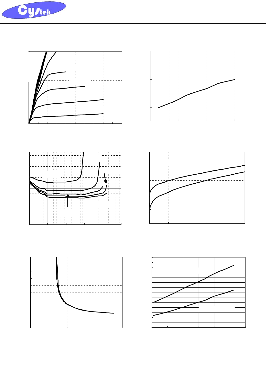
Typical Characteristics
Typical Output Characteristics
0
5
10
15
20
25
012345678910
-VDS, Drain-Source Voltage(V)
-ID, Drain Current (A)
10V
9V
8V
7V
6V
5V
-
V
GS
=
2.5V
-VGS=3V
-VGS=3.5V
-VGS=4V
-VGS=4.5V
Brekdown Voltage vs Ambient Temperature
30
32
34
36
38
40
-75 -50 -25 0 25 50 75 100 125 150 175
Tj, Junction Temperature(°C)
-BVDSS, Drain-Source Breakdown Voltage
(V)
ID=-250μA,
V
GS
=0V
Static Drain-Source On-State resistance vs Drain Current
10
100
1000
0.001 0.01 0.1 1 10 100
-ID, Drain Current(A)
RDS(on), Static Drain-Source On-State
Resistance(mΩ)
VGS=-3V
VGS=-2.5V
VGS=-10V
VGS=-4V
VGS=-4.5V
Reverse Drain Current vs Source-Drain Voltage
0.2
0.4
0.6
0.8
1
1.2
024681
-IDR, Reverse Drain Current (A)
-VSD, Source-Drain Voltage(V)
0
Tj=25°C
Tj=150°C
VGS=0V
Static Drain-Source On-State Resistance vs Gate-Source
Voltage
0
20
40
60
80
100
120
140
160
180
200
024681
0
Drain-Source On-State Resistance vs Junction Tempearture
20
25
30
35
40
45
50
55
60
65
70
75
80
85
90
-60 -20 20 60 100 140 180
Tj, Junction Temperature(°C)
RDS( ON), Static Drain-Source On-State
Resistance(mΩ)
VGS=-4.5V, ID=-4A
VGS=-10V, ID=-5A
-VGS, Gate-Source Voltage(V)
RDS( ON) , Static Drain-Source On-
State Resistance(mΩ)
ID=-4.5A
ID=-3.5A
CYStech Electronics Corp.
Spec. No. : C400N3
Issued Date : 2011.11.28
Revised Date : 2012.04.18
Page No. : 4/8
MTP5103N3 CYStek Product Specification
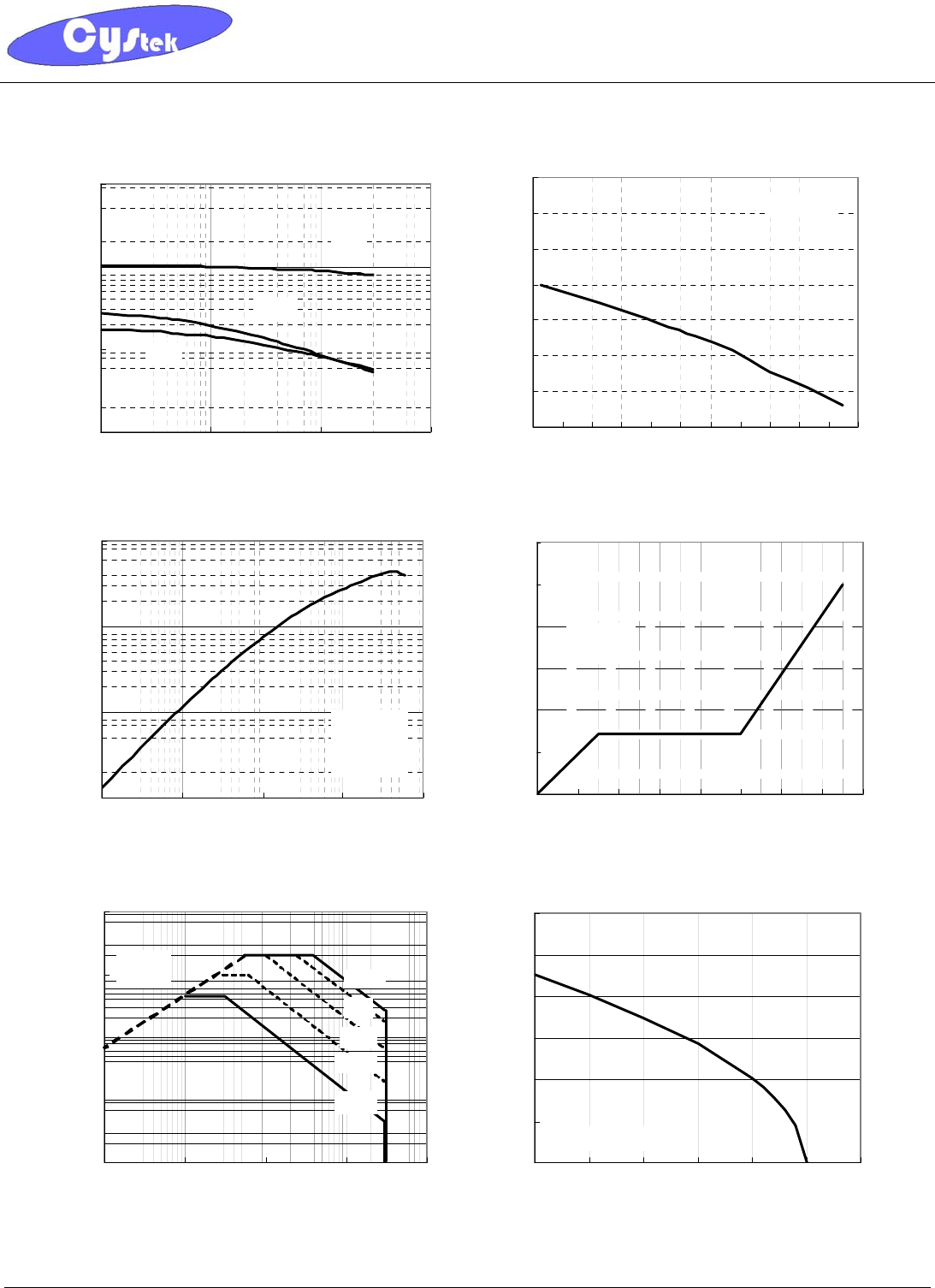
Typical Characteristics(Cont.)
Capacitance vs Drain-to-Source Voltage
10
100
1000
10000
0.1 1 10 100
-VDS, Drain-Source Voltage(V)
Capacitance---(pF)
Coss
Ciss
Crss
Threshold Voltage vs Junction Tempearture
0.8
1
1.2
1.4
1.6
1.8
2
2.2
-60 -40 -20 0 20 40 60 80 100 120 140 160
Tj, Junction Temperature(°C)
-VGS( th),Threshold Voltage-(V)
ID=-250uA
Forward Transfer Admittance vs Drain Current
0.01
0.1
1
10
0.001 0.01 0.1 1 10
-ID, Drain Current(A)
GFS, Forward Transfer Admittance-(S)
VDS=-10V
Pulsed
Ta=25°C
Gate Charge Characteristics
0
2
4
6
8
10
12
0246810121416
Qg, Total Gate Charge(nC)
-VGS, Gate-Source Voltage(V)
VDS=-15V
ID=-4.5A
Maximum Safe Operating Area
0.01
0.1
1
10
100
0.01 0.1 1 10 100
-VDS, Drain-Source Voltage(V)
-ID, Drain Current (A)
DC
10ms
100ms
1ms
100μs
RDS( ON)
Limited
Maximum Drain Current vs JunctionTemperature
0
1
2
3
4
5
6
25 50 75 100 125 150 175
Tj, Junction Temperature(°C)
-ID, Maximum Drain Current(A)
TA=25°C, VGS=-10V
CYStech Electronics Corp.
Spec. No. : C400N3
Issued Date : 2011.11.28
Revised Date : 2012.04.18
Page No. : 5/8
MTP5103N3 CYStek Product Specification
Typical Characteristics(Cont.)
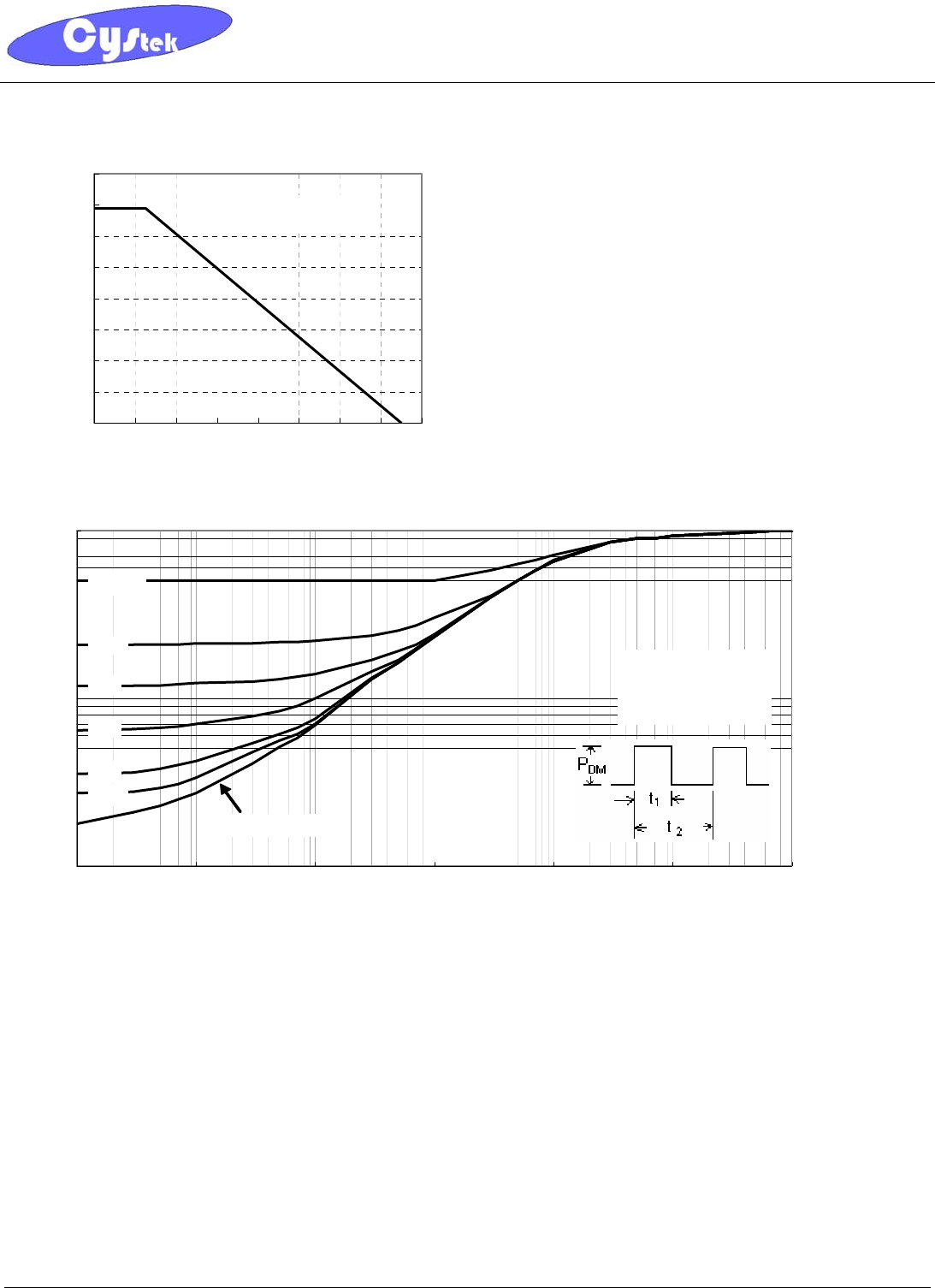
Power Derating Curve
0
0.2
0.4
0.6
0.8
1
1.2
1.4
1.6
0 20 40 60 80 100 120 140 160
TA, Ambient Temperature(℃)
PD, Power Dissipation(W)
Mounted on FR-4 board
with 1 in²
p
ad area
Transient Thermal Response Curves
0.01
0.1
1
1.E-04 1.E-03 1.E-02 1.E-01 1.E+00 1.E+01 1.E+02
t1, Square Wave Pulse Duration(s)
Normalized Transient Thermal Resistance
Single Pulse
0.01
0.02
0.05
0.1
0.2
D=0.5
1.RθJA(t)=r(t)*RθJA
2.Duty Factor, D=t1/t2
3.TJM-TC=PDM*ZθJC
(t)
4.RθJA=90°C/W
CYStech Electronics Corp.
Spec. No. : C400N3
Issued Date : 2011.11.28
Revised Date : 2012.04.18
Page No. : 6/8
MTP5103N3 CYStek Product Specification
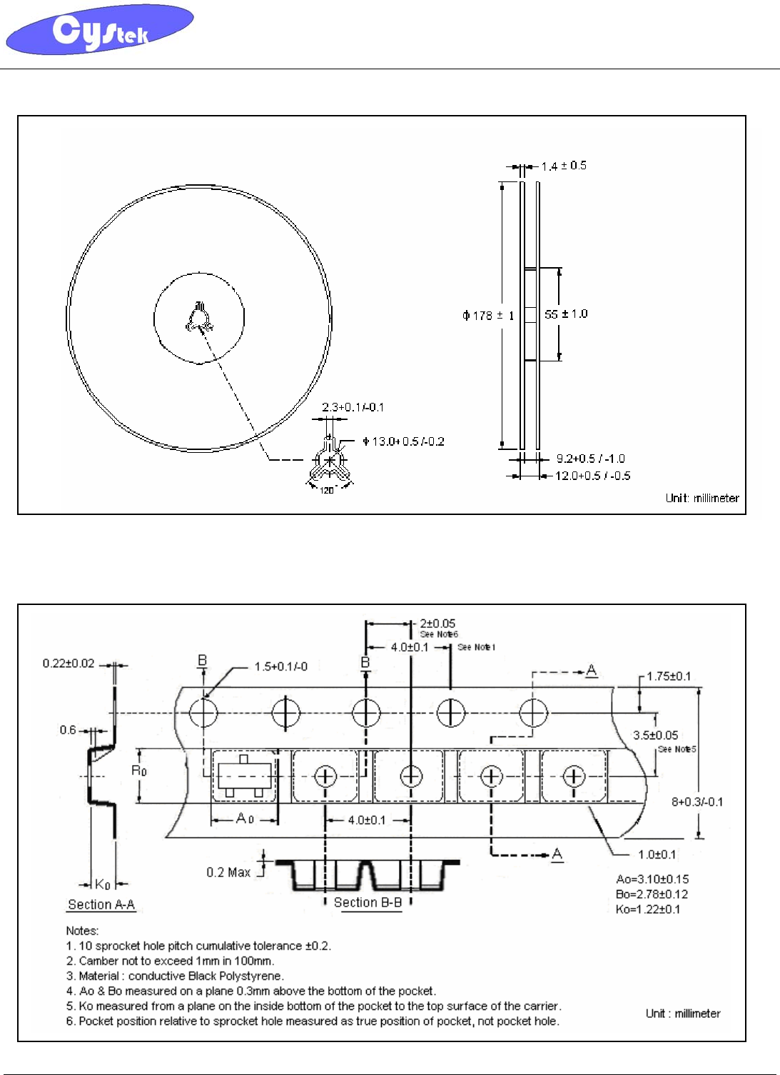
Reel Dimension
Carrier Tape Dimension
CYStech Electronics Corp.
Spec. No. : C400N3
Issued Date : 2011.11.28
Revised Date : 2012.04.18
Page No. : 7/8
MTP5103N3 CYStek Product Specification
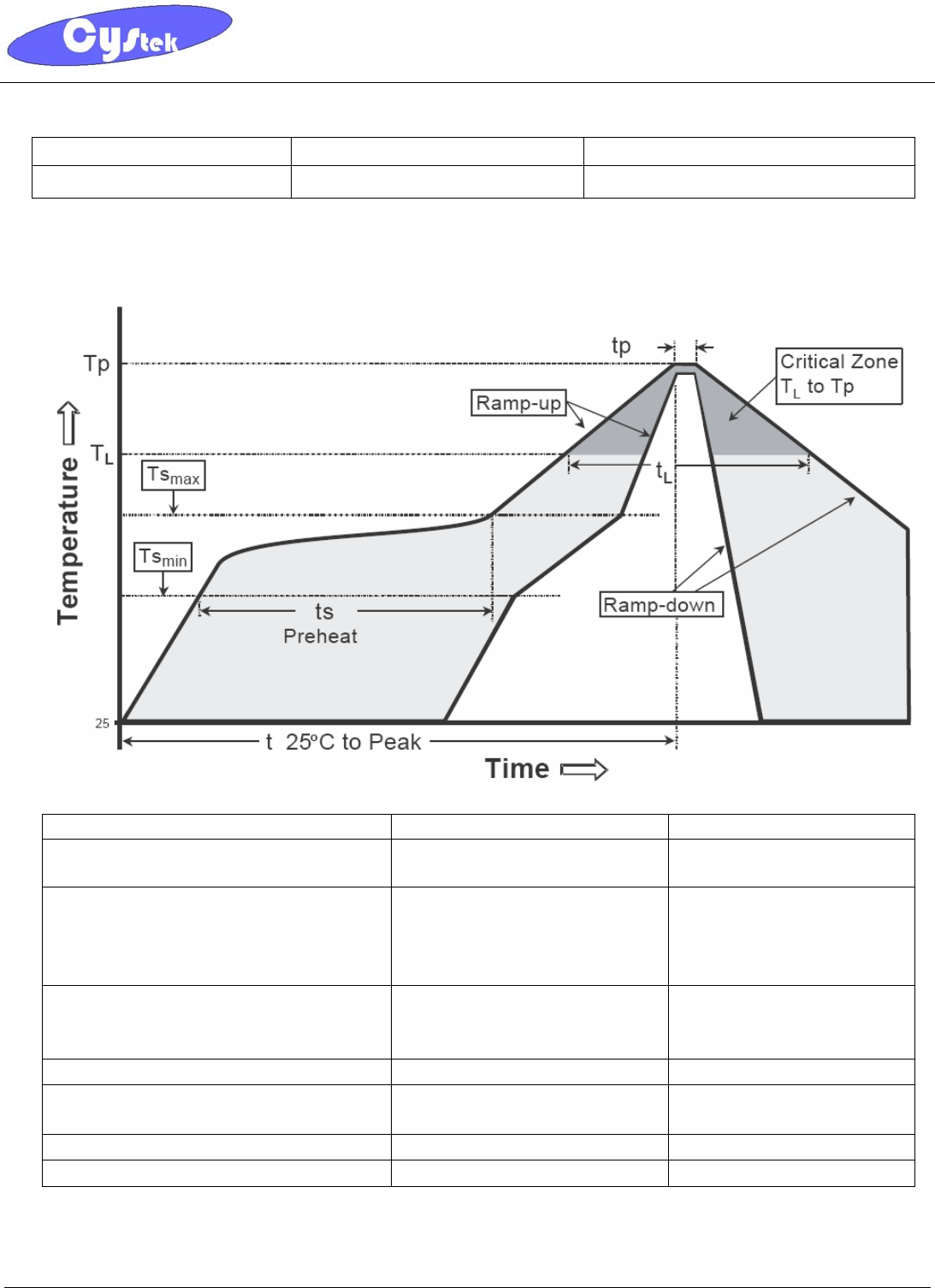
Recommended wave soldering condition
Product Peak Temperature Soldering Time
Pb-free devices 260 +0/-5 °C 5 +1/-1 seconds
Recommended temperature profile for IR reflow
Profile feature Sn-Pb eutectic Assembly Pb-free Assembly
Average ramp-up rate
(Tsmax to Tp) 3°C/second max. 3°C/second max.
Preheat
−Temperature Min(TS min)
−Temperature Max(TS max)
−Time(ts min to ts max)
100°C
150°C
60-120 seconds
150°C
200°C
60-180 seconds
Time maintained above:
−Temperature (TL)
− Time (tL)
183°C
60-150 seconds
217°C
60-150 seconds
Peak Temperature(TP) 240 +0/-5 °C 260 +0/-5 °C
Time within 5°C of actual peak
temperature(tp) 10-30 seconds 20-40 seconds
Ramp down rate 6°C/second max. 6°C/second max.
Time 25 °C to peak temperature 6 minutes max. 8 minutes max.
Note : All temperatures refer to topside of the package, measured on the package body surface.
CYStech Electronics Corp.
Spec. No. : C400N3
Issued Date : 2011.11.28
Revised Date : 2012.04.18
Page No. : 8/8
MTP5103N3 CYStek Product Specification
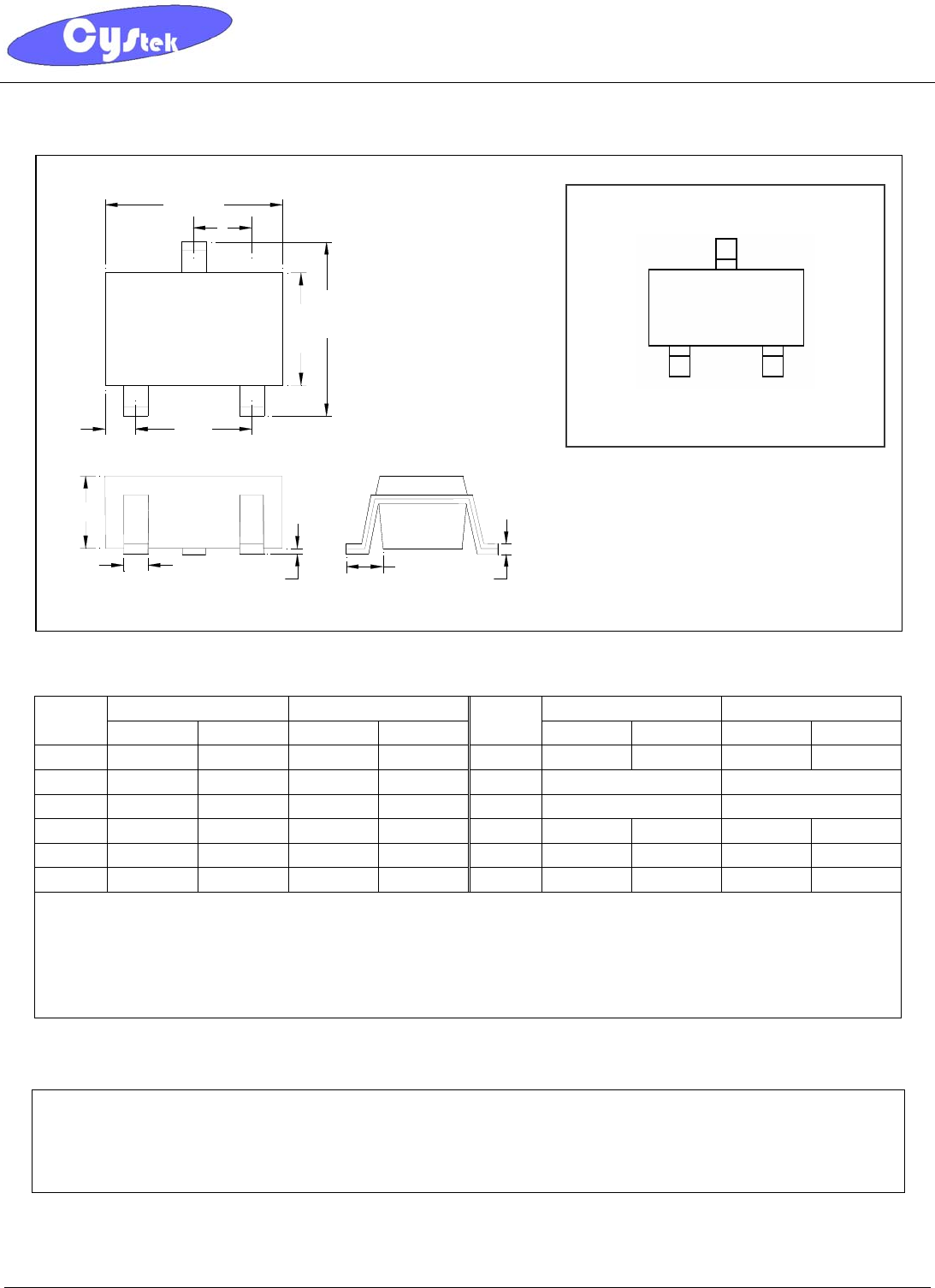
SOT-23 Dimension
*:Typical
Inches
Marking:
5103
HJ
K
D
A
L
G
V
C
B
3
2
1
S
Style : Pin 1.Gate 2.Source 3.Drain
3-Lead SOT-23 Plastic
Surface Mounted Package
CYStek Package Code: N3
Millimeters Inches Millimeters
DIM Min. Max. Min. Max.
DIM Min. Max. Min. Max.
A 0.1102 0.1204 2.80 3.04 J 0.0035 0.0071 0.09 0.18
B 0.0472 0.0669 1.20 1.70 K 0.0276 REF 0.70 REF
C 0.0335 0.0512 0.89 1.30 L 0.0374* 0.95*
D 0.0118 0.0197 0.30 0.50 S 0.0830 0.1161 2.10 2.95
G 0.0669 0.0910 1.70 2.30 V 0.0098 0.0256 0.25 0.65
H 0.0004 0.0040 0.01 0.10
Notes : 1.Controlling dimension : millimeters.
2.Maximum lead thickness includes lead finish thickness, and minimum lead thickness is the minimum thickness of base material.
3.If there is any question with packing specification or packing method, please contact your local CYStek sales office.
Material :
• Lead : Pure tin plated.
• Mold Compound : Epoxy resin family, flammability solid burning class:UL94V-0.
Important Notice:
• All rights are reserved. Reproduction in whole or in part is prohibited without the prior written approval of CYStek.
• CYStek reserves the right to make changes to its products without notice.
• CYStek semiconductor products are not warranted to be suitable for use in Life-Support Applications, or systems.
• CYStek assumes no liability for any consequence of customer product design, infringement of patents, or application assistance.