Nokia 6085 Rm 198 6086 188 Service Manual 34 V2
User Manual: Phone Nokia 6086 RM-188 - Service manuals and Schematics, Disassembly / Assembly. Free.
Open the PDF directly: View PDF ![]() .
.
Page Count: 296 [warning: Documents this large are best viewed by clicking the View PDF Link!]
- Amendment Record Sheet
- Copyright
- Warnings and cautions
- ESD protection
- Care and maintenance
- Company Policy
- Battery information
- Nokia 6085; Nokia 6086 Service Manual Structure
- 1 General Information
- 2 Parts Lists and Component Layouts
- 3 Service Software Instructions
- Phoenix installation steps in brief
- Installing Phoenix
- Updating Phoenix installation
- Uninstalling Phoenix
- Repairing Phoenix installation
- Phone data package overview
- Installing phone data package
- Uninstalling phone data package
- Configuring users in Phoenix
- Managing connections in Phoenix
- Installing flash support files for FPS-10
- Updating FPS-10 flash prommer software
- 4 Service Tools and Service Concepts
- 5 Disassembly / Reassembly Instructions
- 6 BB Troubleshooting and Manual Tuning Guide
- Baseband troubleshooting
- General power checking troubleshooting
- Clocking troubleshooting
- Battery current measuring fault troubleshooting
- Flash programming fault troubleshooting
- COMBO memory troubleshooting
- Keyboard troubleshooting
- USB troubleshooting
- Backup battery troubleshooting
- Charging troubleshooting
- Dead or jammed troubleshooting
- MR sensor troubleshooting
- Vibra troubleshooting
- MicroSD troubleshooting
- SIM troubleshooting
- Display module troubleshooting
- Camera troubleshooting
- Bluetooth troubleshooting
- Audio troubleshooting
- Audio troubleshooting test instructions
- Internal earpiece troubleshooting
- Internal microphone troubleshooting
- IHF speaker troubleshooting
- External microphone troubleshooting
- External earpiece troubleshooting
- Introduction to acoustics troubleshooting
- Earpiece troubleshooting
- IHF troubleshooting
- Microphone troubleshooting
- Baseband manual tuning guide
- 7 RF Troubleshooting and Manual Tuning Guide
- 8 System Module
- Baseband description
- System module block diagram
- Baseband functional description
- Absolute maximum ratings
- Phone modes of operation
- Power distribution
- Bluetooth
- USB
- RM-188 WLAN
- MR sensor
- FM radio
- Camera
- Backup battery
- CBUS interface
- FBUS
- ACI interface
- VOUT interface
- Charger interface
- MicroSD interface
- SIM/USIM
- Battery interface
- User interface
- ASICs
- Device memories
- Audio concept
- Baseband technical specifications
- External interfaces
- Pop-portTM connector
- VOUT electrical characteristics
- CBUS connections and electrical characteristics
- USB/FBUS connections and electrical characteristics
- Audio signal electrical characteristics
- Charger connector and charging interface connections & electrical characteristics
- Battery connector and interface connections & electrical characteristics
- Internal interfaces
- Upper block connectors
- Back-up battery interface connections and electrical characteristics
- RF description
- Frequency mappings
- Baseband description
- 9 RM-188/198 schematics
- Glossary

Service Manual
RM-188; RM-198 (Nokia 6085; Nokia 6086)
Mobile Terminal
Part No: 9254881 (Issue 2)
Nokia Customer Care
COMPANY CONFIDENTIAL
Copyright © 2007 Nokia. All rights reserved.

Amendment Record Sheet
Amendment No Date Inserted By Comments
Issue 1 10/2006 ET
Issue 2 02/2007 ET Added the RM-188 information.
RM-188; RM-198
Nokia Customer Care Amendment Record Sheet
Page ii COMPANY CONFIDENTIAL Issue 2
Copyright © 2007 Nokia. All rights reserved.

Copyright
Copyright © 2007 Nokia. All rights reserved.
Reproduction, transfer, distribution or storage of part or all of the contents in this document in any form
without the prior written permission of Nokia is prohibited.
Nokia, Nokia Connecting People, and Nokia X and Y are trademarks or registered trademarks of Nokia
Corporation. Other product and company names mentioned herein may be trademarks or tradenames of
their respective owners.
Nokia operates a policy of continuous development. Nokia reserves the right to make changes and
improvements to any of the products described in this document without prior notice.
Under no circumstances shall Nokia be responsible for any loss of data or income or any special, incidental,
consequential or indirect damages howsoever caused.
The contents of this document are provided "as is". Except as required by applicable law, no warranties of
any kind, either express or implied, including, but not limited to, the implied warranties of merchantability
and fitness for a particular purpose, are made in relation to the accuracy, reliability or contents of this
document. Nokia reserves the right to revise this document or withdraw it at any time without prior notice.
The availability of particular products may vary by region.
IMPORTANT
This document is intended for use by qualified service personnel only.
RM-188; RM-198
Copyright Nokia Customer Care
Issue 2 COMPANY CONFIDENTIAL Page iii
Copyright © 2007 Nokia. All rights reserved.

Warnings and cautions
Warnings
• IF THE DEVICE CAN BE INSTALLED IN A VEHICLE, CARE MUST BE TAKEN ON INSTALLATION IN VEHICLES FITTED
WITH ELECTRONIC ENGINE MANAGEMENT SYSTEMS AND ANTI-SKID BRAKING SYSTEMS. UNDER CERTAIN FAULT
CONDITIONS, EMITTED RF ENERGY CAN AFFECT THEIR OPERATION. IF NECESSARY, CONSULT THE VEHICLE DEALER/
MANUFACTURER TO DETERMINE THE IMMUNITY OF VEHICLE ELECTRONIC SYSTEMS TO RF ENERGY.
•THE PRODUCT MUST NOT BE OPERATED IN AREAS LIKELY TO CONTAIN POTENTIALLY EXPLOSIVE ATMOSPHERES,
FOR EXAMPLE, PETROL STATIONS (SERVICE STATIONS), BLASTING AREAS ETC.
• OPERATION OF ANY RADIO TRANSMITTING EQUIPMENT, INCLUDING CELLULAR TELEPHONES, MAY INTERFERE
WITH THE FUNCTIONALITY OF INADEQUATELY PROTECTED MEDICAL DEVICES. CONSULT A PHYSICIAN OR THE
MANUFACTURER OF THE MEDICAL DEVICE IF YOU HAVE ANY QUESTIONS. OTHER ELECTRONIC EQUIPMENT MAY
ALSO BE SUBJECT TO INTERFERENCE.
• BEFORE MAKING ANY TEST CONNECTIONS, MAKE SURE YOU HAVE SWITCHED OFF ALL EQUIPMENT.
Cautions
• Servicing and alignment must be undertaken by qualified personnel only.
• Ensure all work is carried out at an anti-static workstation and that an anti-static wrist strap is worn.
• Ensure solder, wire, or foreign matter does not enter the telephone as damage may result.
• Use only approved components as specified in the parts list.
• Ensure all components, modules, screws and insulators are correctly re-fitted after servicing and
alignment.
• Ensure all cables and wires are repositioned correctly.
•During testing never activate the GSM transmitter without a proper antenna load, otherwise GSM PA may
be damaged.
RM-188; RM-198
Nokia Customer Care Warnings and cautions
Page iv COMPANY CONFIDENTIAL Issue 2
Copyright © 2007 Nokia. All rights reserved.

ESD protection
Nokia requires that service points have sufficient ESD protection (against static electricity) when servicing
the phone.
Any product of which the covers are removed must be handled with ESD protection. The SIM card can be
replaced without ESD protection if the product is otherwise ready for use.
To replace the covers ESD protection must be applied.
All electronic parts of the product are susceptible to ESD. Resistors, too, can be damaged by static electricity
discharge.
All ESD sensitive parts must be packed in metallized protective bags during shipping and handling outside
any ESD Protected Area (EPA).
Every repair action involving opening the product or handling the product components must be done under
ESD protection.
ESD protected spare part packages MUST NOT be opened/closed out of an ESD Protected Area.
For more information and local requirements about ESD protection and ESD Protected Area, contact your local
Nokia After Market Services representative.
RM-188; RM-198
ESD protection Nokia Customer Care
Issue 2 COMPANY CONFIDENTIAL Page v
Copyright © 2007 Nokia. All rights reserved.

Care and maintenance
This product is of superior design and craftsmanship and should be treated with care. The suggestions below
will help you to fulfil any warranty obligations and to enjoy this product for many years.
• Keep the phone and all its parts and accessories out of the reach of small children.
•Keep the phone dry. Precipitation, humidity and all types of liquids or moisture can contain minerals that
will corrode electronic circuits.
• Do not use or store the phone in dusty, dirty areas. Its moving parts can be damaged.
•Do not store the phone in hot areas. High temperatures can shorten the life of electronic devices, damage
batteries, and warp or melt certain plastics.
• Do not store the phone in cold areas. When it warms up (to its normal temperature), moisture can form
inside, which may damage electronic circuit boards.
• Do not drop, knock or shake the phone. Rough handling can break internal circuit boards.
• Do not use harsh chemicals, cleaning solvents, or strong detergents to clean the phone.
• Do not paint the phone. Paint can clog the moving parts and prevent proper operation.
• Use only the supplied or an approved replacement antenna. Unauthorised antennas, modifications or
attachments could damage the phone and may violate regulations governing radio devices.
All of the above suggestions apply equally to the product, battery, charger or any accessory.
RM-188; RM-198
Nokia Customer Care Care and maintenance
Page vi COMPANY CONFIDENTIAL Issue 2
Copyright © 2007 Nokia. All rights reserved.

Company Policy
Our policy is of continuous development; details of all technical modifications will be included with service
bulletins.
While every endeavour has been made to ensure the accuracy of this document, some errors may exist. If
any errors are found by the reader, NOKIA MOBILE PHONES Business Group should be notified in writing/e-
mail.
Please state:
• Title of the Document + Issue Number/Date of publication
• Latest Amendment Number (if applicable)
• Page(s) and/or Figure(s) in error
Please send to:
NOKIA CORPORATION
Nokia Mobile Phones Business Group
Nokia Customer Care
PO Box 86
FIN-24101 SALO
Finland
E-mail: Service.Manuals@nokia.com
RM-188; RM-198
Company Policy Nokia Customer Care
Issue 2 COMPANY CONFIDENTIAL Page vii
Copyright © 2007 Nokia. All rights reserved.

Battery information
Note: A new battery's full performance is achieved only after two or three complete charge and
discharge cycles!
The battery can be charged and discharged hundreds of times but it will eventually wear out. When the
operating time (talk-time and standby time) is noticeably shorter than normal, it is time to buy a new battery.
Use only batteries approved by the phone manufacturer and recharge the battery only with the chargers
approved by the manufacturer. Unplug the charger when not in use. Do not leave the battery connected to
a charger for longer than a week, since overcharging may shorten its lifetime. If left unused a fully charged
battery will discharge itself over time.
Temperature extremes can affect the ability of your battery to charge.
For good operation times with Ni-Cd/NiMh batteries, discharge the battery from time to time by leaving the
product switched on until it turns itself off (or by using the battery discharge facility of any approved accessory
available for the product). Do not attempt to discharge the battery by any other means.
Use the battery only for its intended purpose.
Never use any charger or battery which is damaged.
Do not short-circuit the battery. Accidental short-circuiting can occur when a metallic object (coin, clip or
pen) causes direct connection of the + and - terminals of the battery (metal strips on the battery) for example
when you carry a spare battery in your pocket or purse. Short-circuiting the terminals may damage the battery
or the connecting object.
Leaving the battery in hot or cold places, such as in a closed car in summer or winter conditions, will reduce
the capacity and lifetime of the battery. Always try to keep the battery between 15°C and 25°C (59°F and 77°
F). A phone with a hot or cold battery may temporarily not work, even when the battery is fully charged.
Batteries' performance is particularly limited in temperatures well below freezing.
Do not dispose of batteries in a fire!
Dispose of batteries according to local regulations (e.g. recycling). Do not dispose as household waste.
RM-188; RM-198
Nokia Customer Care Battery information
Page viii COMPANY CONFIDENTIAL Issue 2
Copyright © 2007 Nokia. All rights reserved.

Nokia 6085; Nokia 6086 Service Manual Structure
1 General Information
2 Parts Lists and Component Layouts
3 Service Software Instructions
4 Service Tools and Service Concepts
5 Disassembly / Reassembly Instructions
6 BB Troubleshooting and Manual Tuning Guide
7 RF Troubleshooting and Manual Tuning Guide
8 System Module
9 RM-188/198 schematics
Glossary
RM-188; RM-198
Nokia 6085; Nokia 6086 Service Manual Structure Nokia Customer Care
Issue 2 COMPANY CONFIDENTIAL Page ix
Copyright © 2007 Nokia. All rights reserved.

RM-188; RM-198
Nokia Customer Care Nokia 6085; Nokia 6086 Service Manual Structure
(This page left intentionally blank.)
Page x COMPANY CONFIDENTIAL Issue 2
Copyright © 2007 Nokia. All rights reserved.

1 — General Information
Nokia Customer Care
Issue 2 COMPANY CONFIDENTIAL Page 1 –1
Copyright © 2007 Nokia. All rights reserved.

RM-188; RM-198
Nokia Customer Care General Information
(This page left intentionally blank.)
Page 1 –2 COMPANY CONFIDENTIAL Issue 2
Copyright © 2007 Nokia. All rights reserved.

Table of Contents
RM-188/198 product selection..............................................................................................................................1–5
RM-188/198 product features and sales package...............................................................................................1–5
Product and module list ........................................................................................................................................1–7
Mobile enhancements............................................................................................................................................1–7
Technical specifications.........................................................................................................................................1–9
Transceiver general specifications ..................................................................................................................1–9
Main RF characteristics for GSM850/900/1800/1900 (quadband) and EDGE phones .................................1–9
Battery endurance.......................................................................................................................................... 1–10
Environmental conditions ............................................................................................................................. 1–10
List of Tables
Table 1 RM-188/198 ...............................................................................................................................................1–7
Table 2 Audio..........................................................................................................................................................1–7
Table 3 Battery and chargers ................................................................................................................................1–8
Table 4 Car...............................................................................................................................................................1–8
Table 5 Carrying......................................................................................................................................................1–8
Table 6 Data ............................................................................................................................................................1–8
Table 7 Music ..........................................................................................................................................................1–9
List of Figures
Figure 1 View of RM-188/198................................................................................................................................1–5
RM-188; RM-198
General Information Nokia Customer Care
Issue 2 COMPANY CONFIDENTIAL Page 1 –3
Copyright © 2007 Nokia. All rights reserved.

RM-188; RM-198
Nokia Customer Care General Information
(This page left intentionally blank.)
Page 1 –4 COMPANY CONFIDENTIAL Issue 2
Copyright © 2007 Nokia. All rights reserved.
RM-188/198 product selection
Nokia RM-188/198 supports 850/900/1800/1900 MHz bands. RM-188/198 will support EGPRS packet data
connection (EDGE) in all these bands. Supported multislot class for both GPRS and EGPRS is MSC 10. RM-188/198
is based on G3.1S, RAP GSM engine.
Note: The RM-188 also supports WLAN 802.11 b/g 2.4 Ghz for UMA (Unlicensed Mobile Access), with
automatic switching between WLAN and cellular networks.
According to GSM standard 05.05, it responds to class 4 (max. 2W) in EGSM 900, class 1 (1W) in GSM 1800 and
class 1 in GSM 1900. It also supports Bluetooth 2.0 + EDR standard. The handset has a full phase 2 Type Approval
and it complies with the GSM Type Approval. RM-188/198 also has a full CE approval and FCC approval.
The main handset display is a 1.8” CSTN passive LCD display that supports up to 262,144 colors (128 x 160
pixels). The mini cover display is a 1” FSTN black-and-white screen with blue LEDs (96 x 68 pixels). The device
also has a VGA camera with a 4x digital post zoom.
RM-188/198 has a FM stereo radio and music player, and it supports microSD card with hotswap possibility.
The MMS implementation follows the OMA MMS 1.2, AMR and SMIL.
WAP 2.0 compatible XHTML browser over HTTP/TCP/IP stack communicates with a gateway in network.
The supported user interface is S40, that is, RM-188/198 software is based on ISA platform.
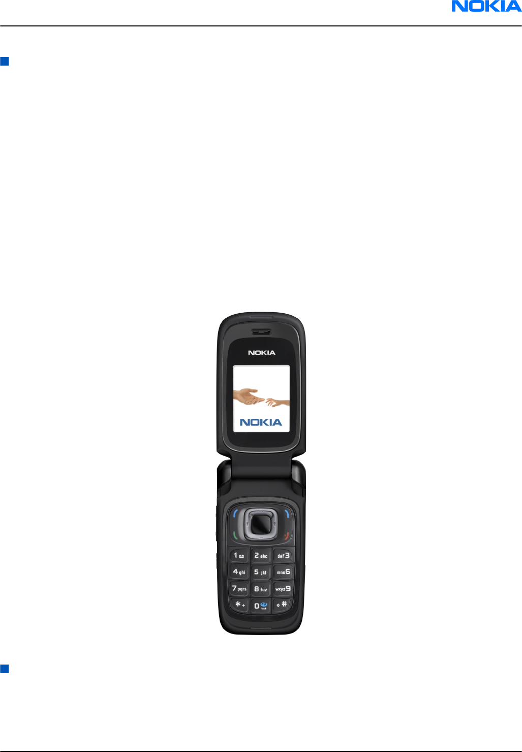
Figure 1 View of RM-188/198
RM-188/198 product features and sales package
Imaging
• VGA camera (resolution 648 X 488 pixels) with dedicated camera button, and 4x digital zoom
• Phone main display used as viewfinder: use to take normal pictures and videos.
RM-188; RM-198
General Information Nokia Customer Care
Issue 2 COMPANY CONFIDENTIAL Page 1 –5
Copyright © 2007 Nokia. All rights reserved.

• Standard, night, and sequential shot modes; self-timer
• Gallery for storing and editing images
• Three image-quality options: high, normal, basic
• Integrated video recorder: 3GPP spec (H.263 video and AMR audio packed in .3gp format)
• Video resolution: QCIF (176 x 144 Pixel), 15 frames per second
• Video capture time: Up to 5 min
Bearers & transport
• Quadband GSM/EDGE 850/900/1800/1900
• Automatic switching between bands
Software platform
• SW platform: Nokia Series 40
Connectivity
• WLAN 802.11 b/g 2.4 Ghz for UMA, with automatic switching between WLAN and cellular networks
Note: RM-188 only.
• USB 2.0 full-speed
• Bluetooth 2.0
• Pop-Port™ connector with ACI
• Support for SIM Access Profile (SAP)
• Remote or local synchronization with a PC or other compatible device
Productivity
• PIM (Calendar & Contacts)
• XHTML browser over TCP/IP
• Video streaming (3GPP)
• Logs (last calls , timers and history list)
• Audio messaging
•JavaTM MIDP 2.0, CLDC 1.13D API, PIM API, File access API
• MP3
• Data Transfer
• Settings Wizard/Access Point Configurator
Sales package
• Transceiver RM-188/198
• Nokia BL-5C battery
• Nokia compact charger AC-3
• Nokia headset HS-5
• User guide and quick guide
RM-188; RM-198
Nokia Customer Care General Information
Page 1 –6 COMPANY CONFIDENTIAL Issue 2
Copyright © 2007 Nokia. All rights reserved.
Product and module list
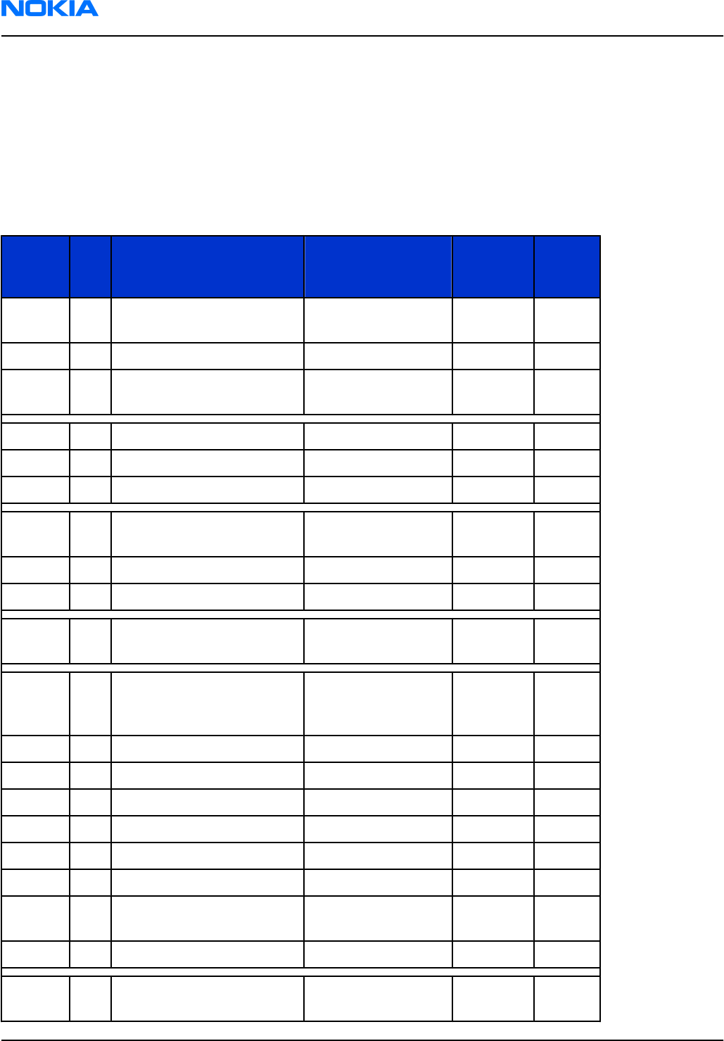
Table 1 RM-188/198
Module name Type code Notes
Upper Module 1WJ Connectors for display, UI PWB,
HWA camera, and earpiece.
Lower Module 1VZ Main PWB with components.
Flex Cable 1WK The flex between the upper and
lower module.
Mobile enhancements
Table 2 Audio
Enhancement Type
Audio adapter AD-46
Display headset HS-69
Wired headset HDB-4
HS-23
HS-3
HS-31
HS-5
HS-8
Wireless headset HDW-3
HS-12W
HS-13W
HS-24W
HS-25W
HS-26W
HS-34W
HS-38W
HS-39W
HS-50W
HS-51W
HS-57W
HS-58W
HS-59W
HS-71W
RM-188; RM-198
General Information Nokia Customer Care
Issue 2 COMPANY CONFIDENTIAL Page 1 –7
Copyright © 2007 Nokia. All rights reserved.
Table 3 Battery and chargers
Type Name
Note: This phone is charged through the smaller Nokia standard interface (2.0 mm plug). The 3.5 mm
standard charger can be used together with the CA-44 charger adapter.
Battery 970 mAh Li-Ion BL-5C
Charger adapter (from 3.5 mm -> 2
mm)
CA-44
Compact charger AC-3
Travel charger AC-4, AC-5
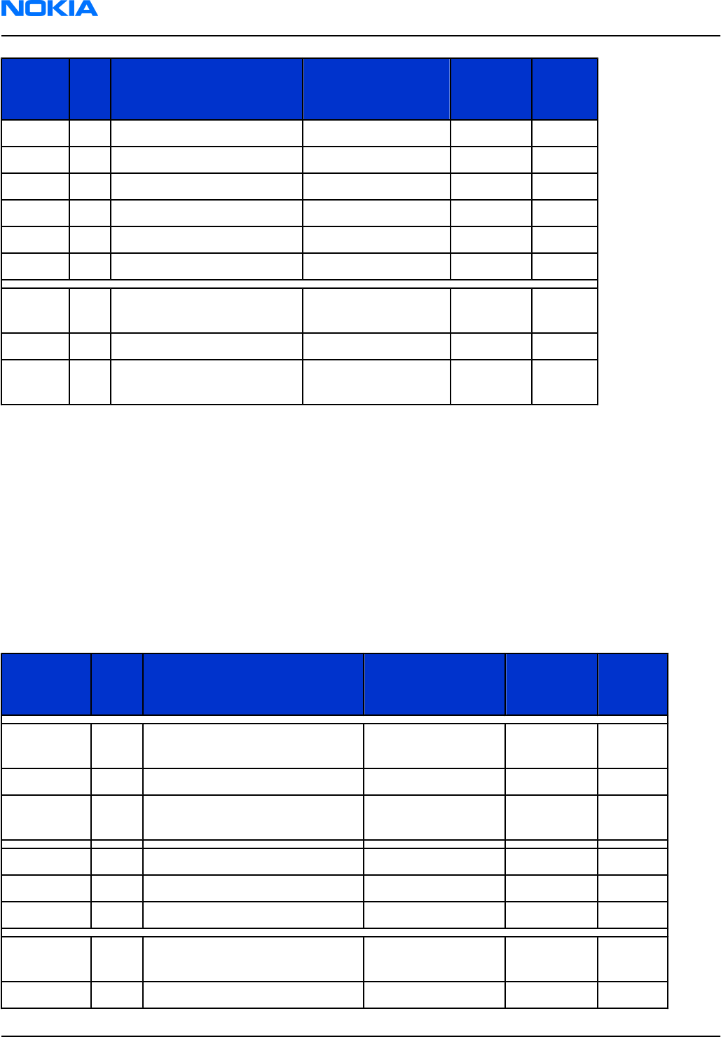
Table 4 Car
Enhancement Type
Car kit CK-1W
CK-7Wi
CK-20W
N610
N616
Car handsfree BHF-3
HF-3
HF-33
HF-6W
Microphone MP-2
Mobile charger DC-4
Mobile holder CR-39
Mobile holder easy mount HH-12
Table 5 Carrying
Enhancement Type
Carrying case CP-57
CP-109
CP-145
Table 6 Data
Enhancement Type
Connectivity cable CA-53
128 MB µSD card MU-26
RM-188; RM-198
Nokia Customer Care General Information
Page 1 –8 COMPANY CONFIDENTIAL Issue 2
Copyright © 2007 Nokia. All rights reserved.
Enhancement Type
256 MB µSD card MU-27
512 MB µSD card MU-28
1 GB µSD card MU-22
Table 7 Music
Enhancement Type
Audio gateway AD-42W
Mini speakers MD-2
MD-4
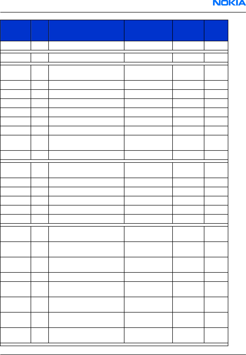
Technical specifications
Transceiver general specifications
Unit Dimensions (L x W x T) Weight (g) Volume (cm3)
Transceiver with BL-5C
battery
92x46x23mm 84g (without battery) 84
Main RF characteristics for GSM850/900/1800/1900 (quadband) and EDGE phones
Parameter Unit
Cellular system GSM850, EGSM900, GSM1800/1900 and EDGE
Rx frequency band GSM850: 869 - 890 MHz
EGSM900: 925 - 960 MHz
GSM1800: 1805 - 1880 MHz
GSM1900: 1930 - 1990 MHz
Tx frequency band GSM850: 824 - 849 MHz
EGSM900: 880 - 915 MHz
GSM1800: 1710 - 1785 MHz
GSM1900: 1850 - 1910 MHz
Output power GSM850: +5 … +33dBm/3.2mW … 2W
GSM900: +5 … +33dBm/3.2mW … 2W
GSM1800: +0 … +30dBm/1.0mW … 1W
GSM1900: +0 … +30dBm/1.0mW … 1W
RM-188; RM-198
General Information Nokia Customer Care
Issue 2 COMPANY CONFIDENTIAL Page 1 –9
Copyright © 2007 Nokia. All rights reserved.
Parameter Unit
EDGE output power EDGE850: +5 … +29dBm/3.2mW … 2W
EDGE900: +5 … +29dBm/3.2mW … 2W
EDGE1800: +0 … +26dBm/1.0mW … 1W
EDGE1900:+0 … +26dBm/1.0mW … 1W
Number of RF channels GSM850: 124
GSM900: 194
GSM1800: 374
GSM1900: 299
Channel spacing 200 kHz
Number of Tx power levels GSM850: 15
GSM900: 15
GSM1800: 16
GSM1900: 16
Number of EDGE Tx power levels GSM850 EDGE: 12
GSM900 EDGE: 12
GSM1800 EDGE: 14
GSM1900 EDGE: 14
Battery endurance
Battery Capacity (mAh) Talk time Stand-by
BL-5C 970mAh Pure GSM: up to 5h.
UMA: up to 6h.
Pure GSM: up to 10 days.
UMA: up to 4 days.
Charging times
AC-3
Up to 3hrs 30 mins
Environmental conditions
Environmental condition Ambient temperature Notes
Normal operation -15oC...+55oCSpecifications fulfilled
Reduced performance -25oC...-15oC
+55oC...+70oC
Operational for shorts periods
only
Intermittent operation -40oC...-15oC
+70oC...+85 oC
Operation not guaranteed but an
attempt to operate does not
damage the phone.
RM-188; RM-198
Nokia Customer Care General Information
Page 1 –10 COMPANY CONFIDENTIAL Issue 2
Copyright © 2007 Nokia. All rights reserved.

Environmental condition Ambient temperature Notes
No operation or storage <-40oC...>+85oCNo storage or operation: an
attempt may damage the phone.
Charging allowed -25oC...+50oC
Long term storage conditions 0oC...+85oC
RM-188; RM-198
General Information Nokia Customer Care
Issue 2 COMPANY CONFIDENTIAL Page 1 –11
Copyright © 2007 Nokia. All rights reserved.

RM-188; RM-198
Nokia Customer Care General Information
(This page left intentionally blank.)
Page 1 –12 COMPANY CONFIDENTIAL Issue 2
Copyright © 2007 Nokia. All rights reserved.

2 — Parts Lists and Component
Layouts
Nokia Customer Care
Issue 2 COMPANY CONFIDENTIAL Page 2 –1
Copyright © 2007 Nokia. All rights reserved.

RM-188; RM-198
Nokia Customer Care Parts Lists and Component Layouts
(This page left intentionally blank.)
Page 2 –2 COMPANY CONFIDENTIAL Issue 2
Copyright © 2007 Nokia. All rights reserved.

Table of Contents
Exploded view.........................................................................................................................................................2–5
Exploded view ...................................................................................................................................................2–5
General recycling recommendation ................................................................................................................2–6
Mechanical spare parts overview ....................................................................................................................2–6
Parts lists.................................................................................................................................................................2–7
RM-188 mechanical spare parts list.................................................................................................................2–7
RM-198 mechanical spare parts list.............................................................................................................. 2–10
Lower (engine) block ..................................................................................................................................... 2–12
RM-188 lower block component parts list (1VZ_12d)............................................................................ 2–12
RM-198 lower block component parts list (1VZ_12b)............................................................................ 2–32
Upper block..................................................................................................................................................... 2–50
RM-188/198 upper block component parts list (1WJ_10b)................................................................... 2–50
RM-198 upper block component parts list with HAC (1WJ_10c) ........................................................... 2–52
Component layouts ............................................................................................................................................. 2–54
Lower (engine) block ..................................................................................................................................... 2–54
RM-188 lower block component layout - top (1VZ_12d)....................................................................... 2–54
RM-188 lower block component layout - bottom (1VZ_12d)................................................................ 2–54
RM-198 lower block component layout - top (1VZ_12b)....................................................................... 2–56
RM-198 lower block component layout - bottom (1VZ_12b)................................................................ 2–57
Upper block..................................................................................................................................................... 2–58
RM-188/198 upper block component layout - top (1WJ_10b).............................................................. 2–58
RM-188/198 upper block component layout - bottom (1WJ_10b)....................................................... 2–59
RM-198 upper block component layout with HAC - top (1WJ_10c) ...................................................... 2–60
RM-198 upper block component layout with HAC - bottom (1WJ_10c) ............................................... 2–61
RM-188; RM-198
Parts Lists and Component Layouts Nokia Customer Care
Issue 2 COMPANY CONFIDENTIAL Page 2 –3
Copyright © 2007 Nokia. All rights reserved.

RM-188; RM-198
Nokia Customer Care Parts Lists and Component Layouts
(This page left intentionally blank.)
Page 2 –4 COMPANY CONFIDENTIAL Issue 2
Copyright © 2007 Nokia. All rights reserved.
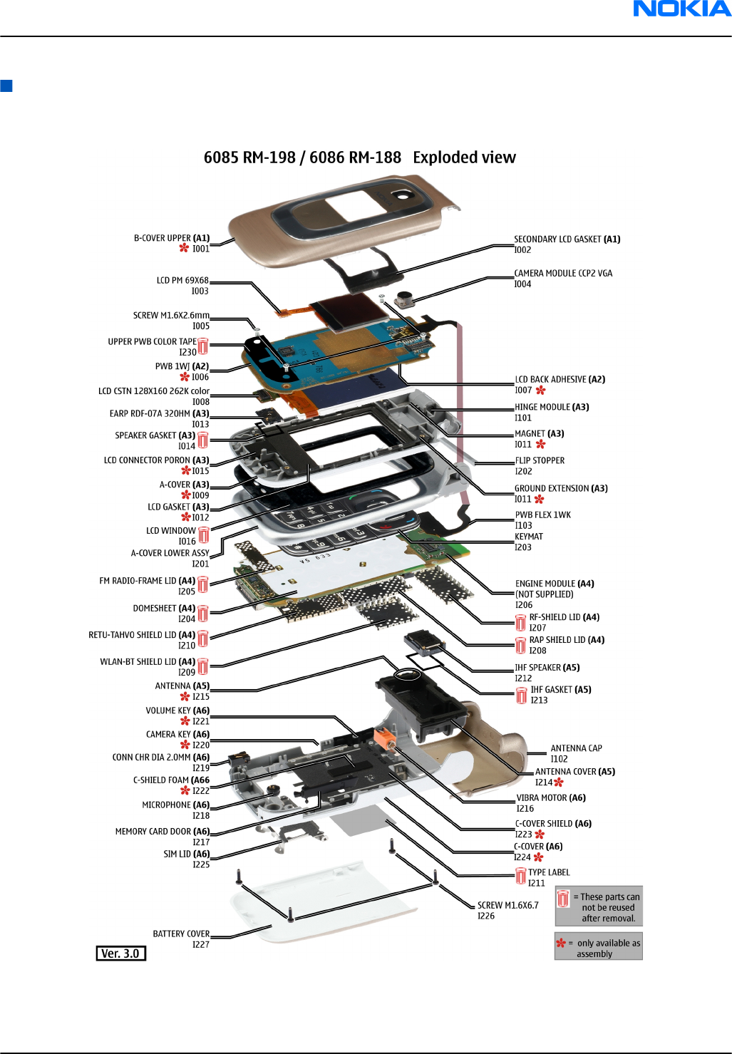
Exploded view
Exploded view
RM-188; RM-198
Parts Lists and Component Layouts Nokia Customer Care
Issue 2 COMPANY CONFIDENTIAL Page 2 –5
Copyright © 2007 Nokia. All rights reserved.
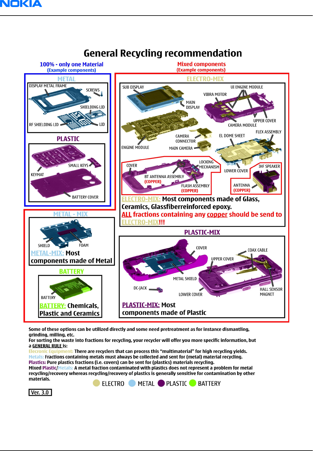
General recycling recommendation
RM-188; RM-198
Nokia Customer Care Parts Lists and Component Layouts
Page 2 –6 COMPANY CONFIDENTIAL Issue 2
Copyright © 2007 Nokia. All rights reserved.
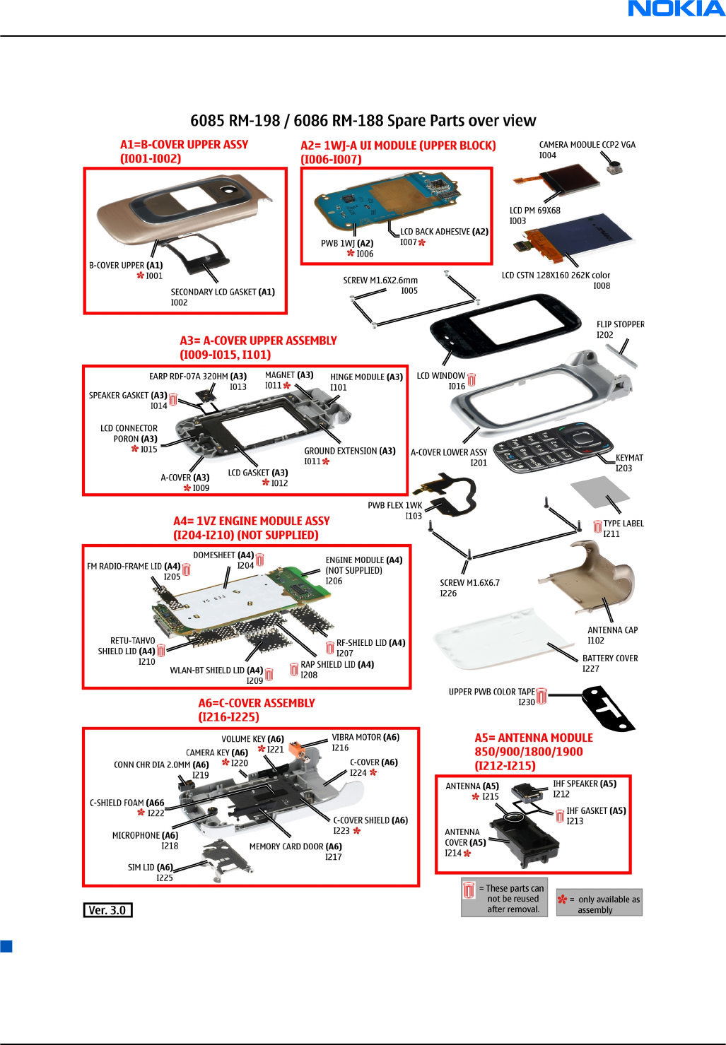
Mechanical spare parts overview
Parts lists
RM-188 mechanical spare parts list
Note: For Nokia product codes, please refer to the latest Service Bulletins on the Partner Website (PWS).
RM-188; RM-198
Parts Lists and Component Layouts Nokia Customer Care
Issue 2 COMPANY CONFIDENTIAL Page 2 –7
Copyright © 2007 Nokia. All rights reserved.
To ensure you are always using the latest codes, please check the PWS on a daily basis.
Ax and in bold = ASSY
"-" = NOT AVAILABLE
"XXXXXXX" = VARIANTS
"???????" = Code available in Bulletin
I0xx = ITEM codes for upper or mono block
I1xx = ITEM codes for hinge block
I2xx = ITEM codes for lower block
I3xx = ITEM codes for soldered spare parts on the upper, hinge or lower block and not exchangable
ITEM/
CIRCUIT
REF. QTY SPARE PART DESCRIPTION NOTE ACTIVITY LEVEL
A1 1 B-COVER UPPER ASSY
(I001 - I002) - 1
I001 1 B-COVER MR -
I002 1 SECONDARY LCD GASKET
Cannot be reused
when removed MR 1
I003 1 LCD PM 69X68 MR 1
I004 1 CAMERA MODULE CCP2 VGA MR 1
I005 4 SCREWS M1,6 x 2,6mm MR 1
A2 1 1WJ-A UI MODULE (UPPER
BLOCK) (I006 - I007) - 1
I006 1 PWB 1WJ MR -
I007 1 LCD BACK ADHESIVE MR -
I008 1
LCD CSTN 128x160
262Kcolor MR 1
A3 1 A-COVER UPPER
ASSEMBLY (I009 - I015,
I101) - 1
I009 1 A-COVER MR -
I010 1 MAGNET MR -
I011 1 GROUND EXTENSION MR -
I101 1 HINGE MODULE MR 1
I012 1 LCD GASKET MR -
I013 1 EARP RDF-07A 32OHM MR 1
I014 1 SPEAKER GASKET
Cannot be reused
when removed MR 1
I015 1 LCD CONNECTOR PORON MR -
I016 1 LCD WINDOW
Cannot be reused
when removed MR 1
RM-188; RM-198
Nokia Customer Care Parts Lists and Component Layouts
Page 2 –8 COMPANY CONFIDENTIAL Issue 2
Copyright © 2007 Nokia. All rights reserved.
ITEM/
CIRCUIT
REF. QTY SPARE PART DESCRIPTION NOTE ACTIVITY LEVEL
I102 ANTENNA CAP MR 1
I103 1 PWB FLEX 1WK MR 1
I201 1 A-COVER LOWER ASSY MR 1
I202 1 FLIP STOPPER MR 1
I203 1 KEYMAT MR 1
A4 1 1VZ ENGINE MODULE
ASSY (I204 - I210) - -
I204 1 DOME SHEET
Cannot be reused
when removed MR 1
I205 1 FM RADIO-FRAME LID
Cannot be reused
when removed MR 1
I206 1 ENGINE MODULE MR -
I207 1 RF-SHIELD LID
Cannot be reused
when removed MR 1
I208 1 RAP SHIELD LID
Cannot be reused
when removed MR 1
I209 1 WLAN-BT SHIELD LID
Cannot be reused
when removed MR 1
I210 1 RETU-TAHVO SHIELD LID
Cannot be reused
when removed MR 1
I211 1 TYPE LABEL
Cannot be reused
when removed MR 3
A5 1 ANTENNA MODULE
850/900/1800/1900
(I212 - I215) - 1
I212 1 IHF SPEAKER MR 1
I213 1 IHF GASKET
Cannot be reused
when removed MR 1
I214 1 ANTENNA COVER MR -
I215 1 ANTENNA MR -
A6 1 C-COVER ASSEMBLY (I216
- I225) - 3
I216 1 VIBRA MOTOR MR 1
I217 1 MEMORY CARD DOOR MR 1
I218 1 MICROPHONE MR 1
I219 1 CONN CHR DIA 2.0MM MR 1
RM-188; RM-198
Parts Lists and Component Layouts Nokia Customer Care
Issue 2 COMPANY CONFIDENTIAL Page 2 –9
Copyright © 2007 Nokia. All rights reserved.
ITEM/
CIRCUIT
REF. QTY SPARE PART DESCRIPTION NOTE ACTIVITY LEVEL
I220 1 CAMERA KEY MR -
I221 1 VOLUME KEY MR -
I222 1 C-SHIELD FOAM MR -
I223 1 C-COVER SHIELD MR -
I224 1 C-COVER MR -
I225 1 SIM LID MR 1
I226 4 SCREW M1.6X6.7
Cannot be reused
when removed MR 1
I227 1 BATTERY COVER MO 1
I230 1 UPPER PWB COLOR TAPE
Cannot be reused
when removed MR 1
RM-198 mechanical spare parts list
Note: For Nokia product codes, please refer to the latest Service Bulletins on the Partner Website (PWS).
To ensure you are always using the latest codes, please check the PWS on a daily basis.
Ax and in bold = ASSY
"-" = NOT AVAILABLE
"XXXXXXX" = VARIANTS
"???????" = Code available in Bulletin
I0xx = ITEM codes for upper or mono block
I1xx = ITEM codes for hinge block
I2xx = ITEM codes for lower block
I3xx = ITEM codes for soldered spare parts on the upper, hinge or lower block and not exchangable
ITEM/
CIRCUIT
REF. QTY SPARE PART DESCRIPTION NOTE ACTIVITY LEVEL
A1 1 B-COVER UPPER ASSY (I001 -
I002) - 1
I001 1 B-COVER MR -
I002 1 SECONDARY LCD GASKET
Cannot be reused
when removed MR 1
I003 1 LCD PM 69X68 MR 1
I004 1 CAMERA MODULE CCP2 VGA MR 1
I005 4 SCREWS M1,6 x 2,6mm MR 1
A2 1 1WJ-A UI MODULE (UPPER
BLOCK) (I006 - I007) - 1
I006 1 PWB 1WJ MR -
RM-188; RM-198
Nokia Customer Care Parts Lists and Component Layouts
Page 2 –10 COMPANY CONFIDENTIAL Issue 2
Copyright © 2007 Nokia. All rights reserved.
ITEM/
CIRCUIT
REF. QTY SPARE PART DESCRIPTION NOTE ACTIVITY LEVEL
I007 1 LCD BACK ADHESIVE MR -
I008 1 LCD CSTN 128x160 262Kcolor MR 1
A3 1 A-COVER UPPER ASSEMBLY
(I009 - I015, I101) - 1
I009 1 A-COVER MR -
I010 1 MAGNET MR -
I011 1 GROUND EXTENSION MR -
I101 1 HINGE MODULE MR 1
I012 1 LCD GASKET MR -
I013 1 EARP RDF-07A 32OHM MR 1
I014 1 SPEAKER GASKET
Cannot be reused
when removed MR 1
I015 1 LCD CONNECTOR PORON MR -
I016 1 LCD WINDOW
Cannot be reused
when removed MR 1
I102 ANTENNA CAP MR 1
I103 1 PWB FLEX 1WK MR 1
I201 1 A-COVER LOWER ASSY MR 1
I202 1 FLIP STOPPER MR 1
I203 1 KEYMAT MR 1
A4 1 1VZ ENGINE MODULE ASSY
(I204 - I210) - -
I204 1 DOME SHEET
Cannot be reused
when removed MR 1
I205 1 FM RADIO-FRAME LID
Cannot be reused
when removed MR 1
I206 1 ENGINE MODULE MR -
I207 1 RF-SHIELD LID
Cannot be reused
when removed MR 1
I208 1 RAP SHIELD LID
Cannot be reused
when removed MR 1
I209 1 WLAN-BT SHIELD LID
Cannot be reused
when removed MR 1
I210 1 RETU-TAHVO SHIELD LID
Cannot be reused
when removed MR 1
RM-188; RM-198
Parts Lists and Component Layouts Nokia Customer Care
Issue 2 COMPANY CONFIDENTIAL Page 2 –11
Copyright © 2007 Nokia. All rights reserved.
ITEM/
CIRCUIT
REF. QTY SPARE PART DESCRIPTION NOTE ACTIVITY LEVEL
I211 1 TYPE LABEL
Cannot be reused
when removed MR 3
A5 1 ANTENNA MODULE
850/900/1800/1900 (I212 -
I215) - 1
I212 1 IHF SPEAKER MR 1
I213 1 IHF GASKET
Cannot be reused
when removed MR 1
I214 1 ANTENNA COVER MR -
I215 1 ANTENNA MR -
A6 1 C-COVER ASSEMBLY (I216 -
I225) - 3
I216 1 VIBRA MOTOR MR 1
I217 1 MEMORY CARD DOOR MR 1
I218 1 MICROPHONE MR 1
I219 1 CONN CHR DIA 2.0MM MR 1
I220 1 CAMERA KEY MR -
I221 1 VOLUME KEY MR -
I222 1 C-SHIELD FOAM MR -
I223 1 C-COVER SHIELD MR -
I224 1 C-COVER MR -
I225 1 SIM LID MR 1
I226 4 SCREW M1.6X6.7
Cannot be reused
when removed MR 1
I227 1 BATTERY COVER MO 1
I230 1 UPPER PWB COLOR TAPE
Cannot be reused
when removed MR 1
Lower (engine) block
RM-188 lower block component parts list (1VZ_12d)
Item Side Grid Description and value
A2000 Top I 6
SHIELD_040_0
27333
RAP SHIELD ASSY
P3046 ~ ~
A2100 Top D 1 1WN_RIGID
PWB RIGID 1WN
11.9X2.5X2.1 D2 ~ ~
RM-188; RM-198
Nokia Customer Care Parts Lists and Component Layouts
Page 2 –12 COMPANY CONFIDENTIAL Issue 2
Copyright © 2007 Nokia. All rights reserved.
Item Side Grid Description and value
A2102 Top E 7 PWB_1QD
PWB 1QD
10X4.6X1.5 ~ ~
A2400 Top N 6
SHIELD_040_0
13002
RETU-TAHVO
AHIELD
ASSEMBLY ~ ~
A6000 Top J 3
SHIELD_040_0
27328
WLAN-BT SHIELD
ASSY P3046 ~ ~
A6100 Bottom R 5
SHIELD_040_0
08558
FM RADIO ASSY
040-008558
P2348 ~ ~
A7000 Top C 5
SHIELD_040_0
13089
RF SHIELD
ASSEMBLY WITH
TAPE P3046 ~ ~
B2200 Top P 6
CRYSTAL_3.3X
1.6_H0.9
CRYSTAL
32.768KHZ
+-30PPM 12.5PF 32.768kHz ~
C2000 Top N 8 0402C Chipcap 5% NP0 27p 50V
C2002 Bottom R 4 0603C
CHIPCAP X5R 2U2
K 6V3 0603 2u2 6V3
C2003 Bottom R 4 0402C
CHIPCAP X7R 33N
K 10V 0402 33n 10V
C2004 Bottom R 4 0402C
CHIPCAP X7R 33N
K 10V 0402 33n 10V
C2005 Bottom R 3 0402C
Chipcap X7R 10%
16V 0402 10n 16V
C2006 Bottom R 3 0402C
Chipcap X7R 10%
16V 0402 10n 16V
C2007 Top Q 2 0402C
Chipcap X7R 10%
16V 0402 10n 16V
C2008 Top Q 3 0402C
Chipcap X7R 10%
16V 0402 10n 16V
C2009 Top Q 3 0402C
Chipcap X7R 10%
16V 0402 10n 16V
C2010 Top Q 3 0402C
Chipcap X7R 10%
16V 0402 10n 16V
C2011 Bottom R 3 0402C Chipcap 5% NP0 10p 50V
C2012 Bottom R 3 0402C Chipcap 5% NP0 10p 50V
C2013 Bottom R 3 0402C Chipcap 5% NP0 10p 50V
C2014 Bottom R 3 0402C Chipcap 5% NP0 10p 50V
C2015 Top Q 4 0402C
CHIPCAP NP0
220P J 25V 0402 220p 25V
RM-188; RM-198
Parts Lists and Component Layouts Nokia Customer Care
Issue 2 COMPANY CONFIDENTIAL Page 2 –13
Copyright © 2007 Nokia. All rights reserved.
Item Side Grid Description and value
C2016 Top P 8 0603C_H0.95
CHIPCAP X5R
470N K 25V 0603 470n 25V
C2071 Top G 3 0402C Chipcap 5% NP0 27p 50V
C2072 Top P 2 0402C Chipcap 5% NP0 27p 50V
C2073 Top E 5
TANT_C_6.2X3.
4_H1.7
CHIPTCAP 150U M
10V 6X3.2X1.5 150u_10V 10V
C2074 Top F 2 0402C Chipcap 5% NP0 10p 50V
C2100 Top Q 2 0402C
CHIPCAP X7R 33N
K 10V 0402 33n 10V
C2101 Top Q 2 0402C
CHIPCAP X7R 33N
K 10V 0402 33n 10V
C2102 Top Q 2 0603C
CHIPCAP X5R 2U2
K 6V3 0603 2u2 6V3
C2103 Top E 8 0402C Chipcap 5% NP0 10p 50V
C2104 Top E 8 0402C Chipcap 5% NP0 10p 50V
C2105 Bottom D 2 0402C Chipcap 5% NP0 27p 50V
C2106 Bottom C 2 0402C Chipcap 5% NP0 27p 50V
C2200 Top O 5 0603C
CHIPCAP X5R 1U K
6V3 0603 1u0 6.3V
C2201 Top P 7 0603C
CHIPCAP X5R 1U K
6V3 0603 1u0 6.3V
C2202 Top P 8 0402C
Chipcap X7R 10%
50V 0402 1n0 50V
C2203 Top P 6 0402C
Chipcap X7R 10%
50V 0402 1n0 50V
C2204 Top P 6 0402C
Chipcap X7R 10%
50V 0402 1n0 50V
C2205 Top P 5 0402C
Chipcap X7R 10%
50V 0402 1n0 50V
C2206 Top P 6 0402C
Chipcap X7R 10%
50V 0402 1n0 50V
C2207 Top P 7 0402C
Chipcap X7R 10%
50V 0402 1n0 50V
C2208 Top Q 6 0402C Chipcap 5% NP0 27p 50V
C2209 Top Q 6 0402C Chipcap 5% NP0 22p 50V
C2210 Top N 7 0603C
CHIPCAP X5R 1U K
16V 0603 1u0 16V
C2211 Top N 7 0805C
CHIPCAP X5R 4U7
K 10V 0805 4u7 10V
RM-188; RM-198
Nokia Customer Care Parts Lists and Component Layouts
Page 2 –14 COMPANY CONFIDENTIAL Issue 2
Copyright © 2007 Nokia. All rights reserved.
Item Side Grid Description and value
C2212 Top N 6 0402C
CHIPCAP X5R 1U5
K 4V 0402 1u5 4V
C2213 Top O 7 0402C
CHIPCAP X5R 1U5
K 4V 0402 1u5 4V
C2214 Top O 7 0402C
CHIPCAP X5R 1U5
K 4V 0402 1u5 4V
C2215 Top O 7 0402C
CHIPCAP X5R 1U5
K 4V 0402 1u5 4V
C2216 Top O 7 0402C
CHIPCAP X5R 1U5
K 4V 0402 1u5 4V
C2217 Top P 7 0402C
CHIPCAP X5R 1U5
K 4V 0402 1u5 4V
C2218 Top P 6 0402C
Chipcap X7R 10%
50V 0402 1n0 50V
C2219 Top P 7 0402C
CHIPCAP X5R 1U5
K 4V 0402 1u5 4V
C2220 Top N 6 0402C
CHIPCAP X5R 1U5
K 4V 0402 1u5 4V
C2221 Top N 8 0603C
CHIPCAP X5R 1U K
6V3 0603 1u0 6.3V
C2222 Top N 7 0603C
CHIPCAP X5R 1U K
6V3 0603 1u0 6.3V
C2223 Top O 5 0402C
Chipcap X7R 10%
16V 0402 10n 16V
C2224 Top P 5 0402C
Chipcap X7R 10%
16V 0402 10n 16V
C2225 Top P 7 0603C
CHIPCAP X5R 1U K
6V3 0603 1u0 6.3V
C2226 Top O 7 0603C
CHIPCAP X5R 1U K
6V3 0603 1u0 6.3V
C2227 Top N 6 0603C
CHIPCAP X5R 1U K
6V3 0603 1u0 6.3V
C2228 Top O 7 0603C
CHIPCAP X5R 1U K
6V3 0603 1u0 6.3V
C2230 Top P 7 0603C
CHIPCAP X5R 1U K
6V3 0603 1u0 6.3V
C2231 Top N 5 0603C
CHIPCAP X5R
10UF 6V3 0603 10u 4V
C2232 Top O 7 0603C
CHIPCAP X5R 1U K
6V3 0603 1u0 6.3V
RM-188; RM-198
Parts Lists and Component Layouts Nokia Customer Care
Issue 2 COMPANY CONFIDENTIAL Page 2 –15
Copyright © 2007 Nokia. All rights reserved.

Item Side Grid Description and value
C2233 Top G 4 0603C
CHIPCAP X5R
10UF 6V3 0603 10u 4V
C2270 Top O 5 0402C
Chipcap X7R 10%
50V 0402 1n0 50V
C2271 Top O 5 0402C
Chipcap X7R 10%
50V 0402 1n0 50V
C2272 Top O 5 0402C
Chipcap X7R 10%
50V 0402 1n0 50V
C2273 Top N 6 0402C
Chipcap X7R 10%
50V 0402 1n0 50V
C2274 Top N 6 0402C Chipcap 5% NP0 27p 50V
C2275 Top N 5 0402C Chipcap 5% NP0 27p 50V
C2281 Top O 8 0603C
CHIPCAP X5R 1U K
6V3 0603 1u0 6.3V
C2300 Top M 5 0402C
Chipcap X7R 10%
16V 0402 10n 16V
C2301 Top L 5 0805C
CHIPCAP X5R 22U
M 6V3 0805 22u 6V3
C2302 Top N 5 0805C
CHIPCAP X5R 22U
M 6V3 0805 22u 6V3
C2303 Top L 7 0603C
CHIPCAP X5R 1U K
6V3 0603 1u0 6.3V
C2304 Top N 6 0402C
Chipcap X7R 10%
16V 0402 10n 16V
C2305 Top L 8 0603C
CHIPCAP X5R 1U K
6V3 0603 1u0 6.3V
C2306 Top M 4 0603C
CHIPCAP X5R 1U K
6V3 0603 1u0 6.3V
C2307 Top L 6 0603C
CHIPCAP X5R 1U K
6V3 0603 1u0 6.3V
C2309 Top L 5 0805C
CHIPCAP X5R 22U
M 6V3 0805 22u 6V3
C2310 Top L 6 0603C
CHIPCAP X5R
10UF 6V3 0603 10u 4V
C2312 Top L 6 0603C
CHIPCAP X5R 1U K
6V3 0603 1u0 6.3V
C2313 Top L 7 0603C
CHIPCAP X5R 1U K
6V3 0603 1u0 6.3V
C2314 Top M 7 0805C
CHIPCAP X5R 4U7
K 10V 0805 4u7 10V
RM-188; RM-198
Nokia Customer Care Parts Lists and Component Layouts
Page 2 –16 COMPANY CONFIDENTIAL Issue 2
Copyright © 2007 Nokia. All rights reserved.
Item Side Grid Description and value
C2315 Top N 8 0805C
CHIPCAP X5R 4U7
M 25V 0805 4u7 25V
C2317 Top O 8 0402C Chipcap 5% NP0 27p 50V
C2400 Top N 4 0402C Chipcap 5% NP0 22p 50V
C2401 Top N 4 0402C Chipcap 5% NP0 22p 50V
C2402 Bottom D 7 0402C
Chipcap X7R 10%
16V 0402 10n 16V
C2406 Bottom C 3 0603C
CHIPCAP X5R 1U K
6V3 0603 1u0 6.3V
C2407 Bottom D 3 0603C
CHIPCAP X5R 1U K
6V3 0603 1u0 6.3V
C2412 Top N 6 0402C Chipcap 5% NP0 27p 50V
C2413 Bottom C 7 0402C
Chipcap X7R 10%
16V 0402 10n 16V
C2700 Top Q 3 0402C_H0.6
CHIPCAP X5R
100N K 16V 0402 100n 16V
C2800 Top H 8 0402C_H0.6
CHIPCAP X5R
100N K 16V 0402 100n 16V
C2801 Top F 7 0402C_H0.6
CHIPCAP X5R
100N K 16V 0402 100n 16V
C2803 Top H 8 0402C_H0.6
CHIPCAP X5R
100N K 16V 0402 100n 16V
C2805 Top F 7 0402C_H0.6
CHIPCAP X5R
100N K 16V 0402 100n 16V
C2806 Top F 8 0402C_H0.6
CHIPCAP X5R
100N K 16V 0402 100n 16V
C2807 Top I 5 0603C
CHIPCAP X5R 1U K
6V3 0603 1u0 6.3V
C2808 Top G 8 0402C_H0.6
CHIPCAP X5R
100N K 16V 0402 100n 16V
C2809 Top G 8 0402C_H0.6
CHIPCAP X5R
100N K 16V 0402 100n 16V
C2812 Top H 8 0402C_H0.6
CHIPCAP X5R
100N K 16V 0402 100n 16V
C2813 Top F 5 0402C_H0.6
CHIPCAP X5R
100N K 16V 0402 100n 16V
C2814 Top G 8 0402C_H0.6
CHIPCAP X5R
100N K 16V 0402 100n 16V
C2816 Top I 5 0402C_H0.6
CHIPCAP X5R
100N K 16V 0402 100n 16V
RM-188; RM-198
Parts Lists and Component Layouts Nokia Customer Care
Issue 2 COMPANY CONFIDENTIAL Page 2 –17
Copyright © 2007 Nokia. All rights reserved.

Item Side Grid Description and value
C2819 Top I 5 0402C_H0.6
CHIPCAP X5R
100N K 16V 0402 100n 16V
C2820 Top F 6 0402C_H0.6
CHIPCAP X5R
100N K 16V 0402 100n 16V
C2822 Top F 5 0402C_H0.6
CHIPCAP X5R
100N K 16V 0402 100n 16V
C2823 Top I 6 0402C_H0.6
CHIPCAP X5R
100N K 16V 0402 100n 16V
C2824 Top J 5 0402C_H0.6
CHIPCAP X5R
100N K 16V 0402 100n 16V
C2825 Top F 7 0402C
Chipcap X7R 10%
50V 0402 1n0 50V
C2826 Top I 7 0402C_H0.6
CHIPCAP X5R
100N K 16V 0402 100n 16V
C2828 Top I 7 0402C Chipcap 5% NP0 27p 50V
C2829 Top G 8 0402C_H0.6
CHIPCAP X5R
100N K 16V 0402 100n 16V
C2830 Top H 5 0402C_H0.6
CHIPCAP X5R
100N K 16V 0402 100n 16V
C2831 Top I 7 0402C Chipcap 5% NP0 27p 50V
C2833 Top I 6 0402C_H0.6
CHIPCAP X5R
100N K 16V 0402 100n 16V
C3000 Top K 5 0402C_H0.6
CHIPCAP X5R
100N K 16V 0402 100n 16V
C3001 Top J 5 0402C
Chipcap X7R 10%
16V 0402 10n 16V
C3002 Top K 5 0402C_H0.6
CHIPCAP X5R
100N K 16V 0402 100n 16V
C3003 Top J 8 0402C
Chipcap X7R 10%
16V 0402 10n 16V
C3004 Top J 8 0402C_H0.6
CHIPCAP X5R
100N K 16V 0402 100n 16V
C3005 Top J 8 0402C_H0.6
CHIPCAP X5R
100N K 16V 0402 100n 16V
C3006 Top K 8 0402C_H0.6
CHIPCAP X5R
100N K 16V 0402 100n 16V
C3007 Top K 8 0402C
Chipcap X7R 10%
16V 0402 10n 16V
C3008 Top J 8 0402C_H0.6
CHIPCAP X5R
100N K 16V 0402 100n 16V
RM-188; RM-198
Nokia Customer Care Parts Lists and Component Layouts
Page 2 –18 COMPANY CONFIDENTIAL Issue 2
Copyright © 2007 Nokia. All rights reserved.

Item Side Grid Description and value
C3009 Top K 8 0402C_H0.6
CHIPCAP X5R
100N K 16V 0402 100n 16V
C3200 Top L 2 0402C_H0.6
CHIPCAP X5R
100N K 16V 0402 100n 16V
C3201 Top G 2 0603C
CHIPCAP X5R 1U K
6V3 0603 1u0 6.3V
C3202 Top G 3 0402C
Chipcap X7R 10%
16V 0402 10n 16V
C3203 Top H 3 0603C
CHIPCAP X5R 1U K
6V3 0603 1u0 6.3V
C3204 Top L 4 0402C_H0.6
CHIPCAP X5R
100N K 16V 0402 100n 16V
C3205 Top G 3 0402C Chipcap 5% NP0 27p 50V
C6031 Top I 2 0402C
CHIPCAP N150
18P J 50V 0402 18p 50V
C6032 Top H 2 0402C Chipcap 5% NP0 100p 50V
C6033 Top H 4 0402C
Chipcap X7R 10%
16V 0402 10n 16V
C6034 Top H 3 0402C
Chipcap X7R 10%
16V 0402 10n 16V
C6035 Top I 4 0402C
Chipcap X7R 10%
16V 0402 10n 16V
C6036 Top H 4 0402C
Chipcap X7R 10%
16V 0402 10n 16V
C6037 Top H 4 0402C
CHIPCAP X5R 1U5
K 4V 0402 1u5 4V
C6038 Top H 4 0402C
Chipcap X7R 10%
16V 0402 10n 16V
C6039 Top H 3 0402C
CHIPCAP N150
18P J 50V 0402 18p 50V
C6040 Top I 4 0402C
CHIPCAP X5R 1U K
6V3 0402 1u0 6.3V
C6051 Top H 3 0402C
Chipcap
+-0.25pF NP0 2p7 50V
C6052 Top I 3 0402C
Chipcap
+-0.25pF NP0 2p7 50V
C6055 Top H 2 0402C
CHIPCAP X5R 1U K
6V3 0402 1u0 6.3V
C6157 Bottom Q 4 0402C
Chipcap X7R 10%
16V 0402 10n 16V
RM-188; RM-198
Parts Lists and Component Layouts Nokia Customer Care
Issue 2 COMPANY CONFIDENTIAL Page 2 –19
Copyright © 2007 Nokia. All rights reserved.
Item Side Grid Description and value
C6158 Bottom Q 5 0402C_H0.6
CHIPCAP X5R
100N K 16V 0402 100n 16V
C6164 Bottom Q 5 0402C_H0.6
CHIPCAP X5R
100N K 16V 0402 100n 16V
C6165 Bottom R 6 0402C_H0.6
CHIPCAP X5R
100N K 16V 0402 100n 16V
C6168 Bottom Q 6 0402C_H0.6
CHIPCAP X5R
100N K 16V 0402 100n 16V
C6170 Bottom R 5 0402C
CHIPCAP X5R 1U5
K 4V 0402 1u5 4V
C6176 Bottom R 6 0402C Chipcap 5% NP0 100p 50V
C6178 Bottom R 6 0402C Chipcap 5% NP0 27p 50V
C6179 Bottom Q 6 0402C Chipcap 5% NP0 47p 50V
C6188 Bottom Q 6 0402C_H0.6
CHIPCAP X5R
100N K 16V 0402 100n 16V
C6189 Bottom Q 6 0402C_H0.6
CHIPCAP X5R
100N K 16V 0402 100n 16V
C6190 Top P 5 0402C_H0.6
CHIPCAP X5R
100N K 16V 0402 100n 16V
C6191 Top P 5 0402C_H0.6
CHIPCAP X5R
100N K 16V 0402 100n 16V
C6300 Top K 4 0603C
CHIPCAP X5R
10UF 6V3 0603 10u 4V
C6301 Top K 3 0402C
CHIPCAP X5R 1U5
K 4V 0402 1u5 4V
C6303 Top K 4 0603C
CHIPCAP X5R 2U2
K 6V3 0603 2u2 6V3
C6307 Top J 2 0402C
CHIPCAP X5R 1U K
6V3 0402 1u0 6.3V
C6308 Top J 4 0402C
Chipcap
+-0.25pF NP0 6p8 50V
C6329 Top J 1 0402C
Chipcap
+-0.25pF NP0 6p8 50V
C6330 Top I 1 0603C
CHIPCAP X5R 2U2
K 6V3 0603 2u2 6V3
C6331 Top K 4 0402C
CHIPCAP X5R 1U5
K 4V 0402 1u5 4V
C6335 Top J 1 0402C
CHIPCAP NP0
220P J 25V 0402 220p 25V
C6338 Top I 1 0402C Chipcap 5% NP0 47p 50V
RM-188; RM-198
Nokia Customer Care Parts Lists and Component Layouts
Page 2 –20 COMPANY CONFIDENTIAL Issue 2
Copyright © 2007 Nokia. All rights reserved.
Item Side Grid Description and value
C6341 Top I 2 0402C
Chipcap
+-0.25pF NP0 6p8 50V
C6343 Top I 2 0402C
Chipcap
+-0.25pF NP0 6p8 50V
C6381 Top K 3 0402C
CHIPCAP X5R 1U5
K 4V 0402 1u5 4V
C6382 Top K 3 0402C
CHIPCAP X5R 1U5
K 4V 0402 1u5 4V
C6383 Top I 2 0402C
CHIPCAP X5R 1U5
K 4V 0402 1u5 4V
C6396 Top I 2 0402C
Chipcap
+-0.25pF NP0 6p8 50V
C6397 Top I 2 0402C
Chipcap
+-0.25pF NP0 6p8 50V
C6398 Top J 2 0402C
Chipcap
+-0.25pF NP0 6p8 50V
C6399 Top J 2 0402C
Chipcap
+-0.25pF NP0 6p8 50V
C7501 Top B 4 0402C
Chipcap
+-0.25pF NP0 2p7 50V
C7502 Top D 4 0402C Chipcap 5% NP0 10p 50V
C7503 Top D 3 0603C
CHIPCAP X5R 1U K
6V3 0603 1u0 6.3V
C7504 Top B 4 0603C
CHIPCAP X5R 1U K
6V3 0603 1u0 6.3V
C7505 Top D 3 0402C
CHIPCAP X5R 1U K
6V3 0402 1u0 6.3V
C7506 Top D 3 0603C
CHIPCAP X5R 1U K
6V3 0603 1u0 6.3V
C7507 Top D 3 0402C
Chipcap X7R 10%
16V 0402 10n 16V
C7508 Top D 3 0402C Chipcap 5% NP0 18p 50V
C7509 Top D 3 0402C Chipcap 5% NP0 10p 50V
C7510 Top D 4 0402C Chipcap 5% NP0 27p 50V
C7511 Top C 3 0603C
CHIPCAP NP0 2N2
G 16V 0603 2n2 16V
C7513 Top D 3 0402C
Chipcap X7R 10%
16V 0402 10n 16V
C7514 Top D 3 0402C
CHIPCAP X7R 33N
K 10V 0402 33n 10V
RM-188; RM-198
Parts Lists and Component Layouts Nokia Customer Care
Issue 2 COMPANY CONFIDENTIAL Page 2 –21
Copyright © 2007 Nokia. All rights reserved.

Item Side Grid Description and value
C7515 Top B 3 0402C
Chipcap
+-0.25pF NP0 4p7 50V
C7516 Top C 3 0402C
CHPCAP NP0
470P J 50V 0402 470p 50V
C7518 Top D 4 0402C
CHIPCAP X5R
100N K 10V 0402 100n 10V
C7520 Top B 7 0402C
Chipcap
+-0.25pF NP0 3p3 50V
C7522 Top D 6 0402C
Chipcap
+-0.25pF NP0 1p8 50V
C7524 Top D 6 0402C
Chipcap
+-0.25pF NP0 1p8 50V
C7525 Top D 8 0402C Chipcap 5% NP0 18p 50V
C7586 Top D 5 0402C
Chipcap X7R 10%
16V 0402 10n 16V
C7590 Top K 1 0402C Chipcap 5% NP0 100p 50V
C7592 Top J 1 0402C
CHIPCAP X5R
100N K 10V 0402 100n 10V
D2200 Top O 6 TFBGA_108
RETU 3.02
TSA1GJWE
TFBGA108 ~ ~
D2420 Top G 4 PDSO_G5
OR-GATE 2INPUT
74LVC1G32
SC70-5 ~ ~
D2800 Top H 6 uBGA_289
RAPGSM V1.1 PA
uBGA289 ~ ~
D3000 Top J 6
FBGA133_11.1
X10.1
COMBO 256M
NOR + 128M DDR
DRAM FBGA133
256MNOR
+128MDDR ~
F2000 Top P 8
0603_FUSE_AV
X2MATS
SM FUSE F 2.0A
32V 2A ~
G2200 Top G 4 BATTER_EECEP
RTC BACUP CAPAC
311 SIZE FOR
2.6V 4UAH 2.6V ~
G7500 Top B 3 VCO_DCS02733
VCO
3296-3980MHZ
4-BAND
MATSUSHITA
3296-3980M
Hz ~
G7501 Top D 2
NKG3176B_H1
.0
VCTCXO 38.4MHZ
2.5V 2MA 38.4MHz ~
RM-188; RM-198
Nokia Customer Care Parts Lists and Component Layouts
Page 2 –22 COMPANY CONFIDENTIAL Issue 2
Copyright © 2007 Nokia. All rights reserved.

Item Side Grid Description and value
L2000 Top O 8 0603_BLM
FERR.BEAD 220R/
100M 2A 0R05
0603
220R/
100MHz ~
L2001 Bottom Q 3 0405_2_H1.0
CHIP BEAD ARRAY
2X1000R 0405
2x1000R/
100MHz ~
L2002 Bottom Q 3 0405_2_H1.0
CHIP BEAD ARRAY
2X1000R 0405
2x1000R/
100MHz ~
L2003 Bottom R 3 0405_2_H1.0
CHIP BEAD ARRAY
2X1000R 0405
2x1000R/
100MHz ~
L2004 Bottom R 3 COIL_LK_1608
CHIP COIL 68NH J
Q12/100MHZ
0603 68nH ~
L2100 Bottom D 2
COIL_LQW160
8
CHIP COIL 56N J
Q38/200MHZ
0603 56nH ~
L2101 Bottom C 2
COIL_LQW160
8
CHIP COIL 56N J
Q38/200MHZ
0603 56nH ~
L2202 Top P 8 0603_BLM
FERR.BEAD 220R/
100M 2A 0R05
0603
220R/
100MHz ~
L2205 Top P 8 0603_BLM
FERR.BEAD 220R/
100M 2A 0R05
0603
220R/
100MHz ~
L2211 Top N 5 0603_BLM
FERR.BEAD 220R/
100M 2A 0R05
0603
220R/
100MHz ~
L2212 Top N 6 0603_BLM
FERR.BEAD 220R/
100M 2A 0R05
0603
220R/
100MHz ~
L2270 Top O 5 0603_BLM
FERR.BEAD 220R/
100M 2A 0R05
0603
220R/
100MHz ~
L2271 Top O 5 0603_BLM
FERR.BEAD 220R/
100M 2A 0R05
0603
220R/
100MHz ~
L2301 Top L 5 0603_BLM
FERR.BEAD 220R/
100M 2A 0R05
0603
220R/
100MHz ~
L2302 Top M 5
CHOKE_SER400
_H1.2
INDUCT WW
10UH 0A65 0R35
4X4X1.2 10uH ~
RM-188; RM-198
Parts Lists and Component Layouts Nokia Customer Care
Issue 2 COMPANY CONFIDENTIAL Page 2 –23
Copyright © 2007 Nokia. All rights reserved.
Item Side Grid Description and value
L2304 Top M 7
CHOKE_SER300
_H1.5
CHOKE 22U M 0R7
0.35A
3.0x3.0x1.5 22uH ~
L2305 Top L 7 0603_BLM
FERRITE BEAD
0R5 600R/
100MHZ 0603
600R/
100MHz ~
L2306 Top M 4 0603_BLM
FERRITE BEAD
0R5 600R/
100MHZ 0603
600R/
100MHz ~
L2401 Bottom B 3 FERRITE_0402
FERRITE BEAD
0.6R 600R/
100MHZ 0402
600R/
100MHz ~
L2402 Bottom D 2 FERRITE_0402
FERRITE BEAD
0.6R 600R/
100MHZ 0402
600R/
100MHz ~
L2406 Top I 8 0402L
FERRITE BEAD
0.6R 33R/
100MHZ 0402 33R/100MHZ ~
L2407 Top I 8 0402L
FERRITE BEAD
0.6R 33R/
100MHZ 0402 33R/100MHZ ~
L2408 Top I 8 0402L
FERRITE BEAD
0.6R 33R/
100MHZ 0402 33R/100MHZ ~
L2409 Top I 8 0402L
FERRITE BEAD
0.6R 33R/
100MHZ 0402 33R/100MHZ ~
L3200 Top L 2 FERRITE_0402
FERRITE BEAD
0.6R 600R/
100MHZ 0402
600R/
100MHz ~
L6030 Top H 3 0402L
CHIP COIL 2N7
+-0N3 Q29/800M
0402 2n7H ~
L6031 Top I 3 0402L
CHIP COIL 2N7
+-0N3 Q29/800M
0402 2n7H ~
L6032 Top I 4 0402L
CHIP COIL 22N J
Q28/800M 0402 22nH ~
L6156 Bottom R 5 0402LQW
CHIP COIL 47N
+-3%
Q25/200MHZ
0402 47nH ~
RM-188; RM-198
Nokia Customer Care Parts Lists and Component Layouts
Page 2 –24 COMPANY CONFIDENTIAL Issue 2
Copyright © 2007 Nokia. All rights reserved.

Item Side Grid Description and value
L6176 Bottom R 6
COIL_LQW160
8
CHIP COIL 120N J
Q32/150MHZ
0603 120nH ~
L7500 Top C 5 0402L
CHIP COIL 12N J
Q31/800M 0402 12nH ~
L7501 Top C 5 0402L
CHIP COIL 8N2 J
Q28/800MHZ
0402 8n2H ~
L7502 Top D 4 FERRITE_0402
FERRITE BEAD
0.6R 600R/
100MHZ 0402
600R/
100MHz ~
L7504 Top C 5 0402L
CHIP COIL 22N J
Q28/800M 0402 22nH ~
L7505 Top C 5 0402L
CHIP COIL 22N J
Q28/800M 0402 22nH ~
L7515 Top C 3 0402L
CHIP COIL 15N J
Q30/800M 0402 15nH ~
N2300 Top M 6
TFBGA_84_6.1
5X6.15
TAHVO V5.2 LF
TFBGA84 ~ ~
N2301 Top M 8
USMD8_1.69X
1.69
WHITE LED
DRIVER 4LEDS
500MW 8BUMP
USMD8 ~ ~
N2402 Bottom D 7 SENSOR_MR10
MAGNETO
RESISTIVE
SENSOR
MRUS71D SOT4 ~ ~
N3200 Top G 3
USMD16_2.03
X2.03
VREG & LEVEL
SHIFT LP3928
USMD16 ~ 2.8V
N6030 Top H 3
CSP_47_3.85X
4.05 BC4-ROM1.0RDL ~ ~
N6156 Bottom Q 5
WLCSP25_3.1X
2.9
FM RECEIVER
TEA5760 N1C ~ ~
N6300 Top J 3 LFBGA240
WLAN MCM
STLC4550
LFBGA240 ~ ~
N6301 Top J 1 RF5924
WLAN RF5924
ES3.5 ~ ~
N7505 Top C 4 TFBGA144
AHNE401A
TRANCEIVER
TFBGA144 ~ ~
RM-188; RM-198
Parts Lists and Component Layouts Nokia Customer Care
Issue 2 COMPANY CONFIDENTIAL Page 2 –25
Copyright © 2007 Nokia. All rights reserved.
Item Side Grid Description and value
N7520 Top C 7 RF9282E3.6
PA RF9282E6.5
GSM/EDGE
850/900/1800/1
900 ~ ~
R2000 Bottom Q 4 0402R
Resistor 5%
63mW 220R ~
R2001 Bottom Q 4
uBGA11_2.15X
1.65
ASIP MIC W/ESD
RES+CAP+ZDI
BGA11 ~ ~
R2002 Top Q 3 0402R
Resistor 5%
63mW 10R ~
R2003 Top Q 3 0402R
Resistor 5%
63mW 10R ~
R2004 Top Q 2 0402R
Resistor 5%
63mW 10R ~
R2005 Top Q 3 0402R
Resistor 5%
63mW 10R ~
R2006 Bottom Q 3 uBGA5
ASIP 4XESD **PB-
FREE** BGA5 ~ ~
R2007 Top Q 4
uBGA11_1.6X2
.15
ASIP SILIC USB
OTG / ESD BGA11 ~ ~
R2008 Top Q 4 0404_RP
RES NETWORK
0W06 220K/
120K J 0404 220k/120k ~
R2009 Top Q 4 0402R
Resistor 5%
63mW 220R ~
R2070 Top P 2 0402_NTH5
NTC RES 47K J
B=4050+-3%
0402 47k ~
R2071 Top E 3 0402_VAR
CHIP VARISTOR
VWM14V VC50V
0402 14V/50V ~
R2100 Top Q 2
FLIP_CHIP_8_1.
7X1.7
ASIP SINGLE
ENDED
MICROPHONE
INTERF BGA8 ~ ~
R2101 Top P 2 0402R
Resistor 5%
63mW 220R ~
R2200 Top P 8 0402R
Resistor 5%
63mW 100k ~
R2201 Top P 7 0402R
Resistor 5%
63mW 120k ~
RM-188; RM-198
Nokia Customer Care Parts Lists and Component Layouts
Page 2 –26 COMPANY CONFIDENTIAL Issue 2
Copyright © 2007 Nokia. All rights reserved.
Item Side Grid Description and value
R2212 Top O 5 0402R
Resistor 5%
63mW 470R ~
R2213 Top P 7 0402R
Resistor 5%
63mW 4k7 ~
R2214 Top P 8 0402R
Resistor 5%
63mW 4k7 ~
R2216 Top Q 7 0402R
CHIPRES 0W06
2M2 J 0402 2M2 ~
R2301 Top M 8 0402R
Resistor 5%
63mW 3k3 ~
R2307 Top L 4 0402R
Resistor 5%
63mW 100R ~
R2402 Bottom D 7 0402R
Resistor 5%
63mW 100k ~
R2403 Top N 6 0402R
Resistor 5%
63mW 4k7 ~
R2409 Top N 8 0402R
Resistor 5%
63mW 390R ~
R2410 Bottom D 4 0402R
Resistor 5%
63mW 39R ~
R2411 Top N 7 0402R
Resistor 5%
63mW 390R ~
R2416 Bottom B 3 0402R
Resistor 5%
63mW 1k0 ~
R2420 Top H 4 0402R
Resistor 5%
63mW 100k ~
R2421 Top G 4 0402R
Resistor 5%
63mW 100k ~
R2700 Top Q 4
uBGA8_1.47X1
.47
ASIP SIM
INTERFACE
**LOW
CAP**BGA8 ~ ~
R2801 Bottom D 3 0402R
Resistor 5%
63mW 1k0 ~
R2802 Bottom D 3 0402R
Resistor 5%
63mW 1k0 ~
R2803 Top I 8 0402R
Resistor 5%
63mW 100R ~
R2804 Top H 8 0402R
Resistor 5%
63mW 100R ~
R2806 Top F 6 0402R
Resistor 5%
63mW 68k ~
RM-188; RM-198
Parts Lists and Component Layouts Nokia Customer Care
Issue 2 COMPANY CONFIDENTIAL Page 2 –27
Copyright © 2007 Nokia. All rights reserved.

Item Side Grid Description and value
R3000 Top J 5 0402R
Resistor 5%
63mW 4k7 ~
R3002 Top H 8 0402R
Resistor 5%
63mW 10R ~
R3003 Top I 8 0402R
Resistor 5%
63mW 4k7 ~
R3004 Top K 7 0402R
Resistor 5%
63mW 4k7 ~
R3200 Top L 1
uBGA11_1.62X
2.12
ASIP EMIF04-
MMC02F2**PB-
FREE** ~ ~
R3201 Top G 4 0402R
Resistor 5%
63mW 100k ~
R3202 Top G 3 0402R
Resistor 5%
63mW 22k ~
R3203 Top K 5 0402R
Resistor 5%
63mW 100k ~
R3204 Top L 4 0402R
Resistor 5%
63mW 2k2 ~
R3205 Top G 3 0402R
Resistor 5%
63mW 33R ~
R3206 Top G 4 0402R
Resistor 5%
63mW 33R ~
R6030 Top H 4 0402R
Resistor 5%
63mW 10k ~
R6031 Top H 4 0402R
Resistor 5%
63mW 10k ~
R6032 Top I 4 0402R
CHIPRES 0W06
2R2 J 0402 2R2 ~
R6034 Top H 3 0402R
Resistor 5%
63mW 10k ~
R6035 Top H 4 0402R
Resistor 5%
63mW 100k ~
R6156 Bottom Q 4 0402R
Resistor 5%
63mW 10R ~
R6157 Bottom R 6 0402R
Resistor 5%
63mW 22R ~
R6159 Bottom R 5 0402R
Resistor 5%
63mW 10k ~
R6160 Bottom R 4 0402R
Resistor 5%
63mW 100k ~
RM-188; RM-198
Nokia Customer Care Parts Lists and Component Layouts
Page 2 –28 COMPANY CONFIDENTIAL Issue 2
Copyright © 2007 Nokia. All rights reserved.

Item Side Grid Description and value
R6300 Top J 2 0402R
CHIPRES 0W06
1M F 100PPM
0402 1M0 ~
R6301 Top K 3 0402R
Resistor 5%
63mW 10k ~
R6302 Top J 4 0402R
Resistor 5%
63mW 100R ~
R6303 Top G 5 0402R
Resistor 5%
63mW 100R ~
R6304 Top I 4 0402R
Resistor 5%
63mW 100R ~
R6305 Top J 2 0402R
Resistor 5%
63mW 68R ~
R7501 Top C 3 0402R
Resistor 5%
63mW 2k2 ~
R7502 Top B 4 0402R
CHIPRES 0W06
10K F 0402 10k ~
R7503 Top D 4 0402R
Resistor 5%
63mW 4k7 ~
R7505 Top C 3 0402R
CHIPRES 0W06
8K2 F 0402 8k2 ~
R7506 Top D 3 0402R
Resistor 5%
63mW 10R ~
R7507 Top B 4 0402R
Resistor 5%
63mW 10R ~
R7508 Top D 3 0402R
Resistor 5%
63mW 10R ~
R7509 Top D 3 0402R
Resistor 5%
63mW 22k ~
R7510 Top D 7 0402R
Resistor 5%
63mW 15R ~
R7522 Top D 7 0402R
CHIPRES 0W06
27K F 0402 27k ~
R7590 Top K 1 0402R
Resistor 5%
63mW 22k ~
R7591 Top K 1 0402R
Resistor 5%
63mW 68k ~
R7592 Top K 2 0402R
Resistor 5%
63mW 1k0 ~
R7593 Top J 1 0402R
Chipres 0W06
jumper 0402 0R ~
RM-188; RM-198
Parts Lists and Component Layouts Nokia Customer Care
Issue 2 COMPANY CONFIDENTIAL Page 2 –29
Copyright © 2007 Nokia. All rights reserved.

Item Side Grid Description and value
S2416 Top F 8
SWITCH_EVQ5
P701K
SM SW TACT SPST
12V SIDE KEY 3N ~ ~
S2417 Top H 8
SWITCH_EVQ5
P701K
SM SW TACT SPST
12V SIDE KEY 3N ~ ~
S2423 Top K 8
SWITCH_EVQ5
P701K
SM SW TACT SPST
12V SIDE KEY 3N ~ ~
S3200 Top O 1
SWITCH_SPVM
110201
SWITCH SPST NO
5V 1MA ~ ~
T6030 Top H 2 TRANS_LDB10
BALUN 2450
+-50MHZ 1DB
1.7X0.9 ~ ~
T7501 Top C 2
TRANS_HHM15
17A2
TRANSF BALUN
3800+-550MHZ
0805 ~ ~
T7520 Top B 7 TRANS_LDB15
TRANSF BALUN
1800+-100mhz
2x1.25 ~ ~
V2000 Top O 8 BGA_4 ASIP TVS BGA4 ~ ~
V2302 Top L 4 SOD323F
SCH DI 30V 2A
SOD323F ~ ~
V2400 Bottom O 6
LED_48_21SYG
C
LED WHITE
140MCD 5MA
0603 ~ ~
V2401 Bottom I 6
LED_48_21SYG
C
LED WHITE
140MCD 5MA
0603 ~ ~
V2402 Bottom I 3
LED_48_21SYG
C
LED WHITE
140MCD 5MA
0603 ~ ~
V2403 Bottom O 3
LED_48_21SYG
C
LED WHITE
140MCD 5MA
0603 ~ ~
V2404 Top N 7 SOT_666
TRX2+RX4 N
4K7/47K SOT666 ~ ~
V7590 Top K 1 SOT323
Tr NPN 12V 35mA
SOT323 ~ ~
X2000 Top R 4
SYSCON_MQ20
2_NK_14R3
SM SYSTEM
CONNECTOR
14POL ~ ~
X2060 Bottom B 6
TRACEABILITY_
PAD
MODULE ID
COMPONENT
2.8X1.8X0.3 ~ ~
RM-188; RM-198
Nokia Customer Care Parts Lists and Component Layouts
Page 2 –30 COMPANY CONFIDENTIAL Issue 2
Copyright © 2007 Nokia. All rights reserved.

Item Side Grid Description and value
X2070 Top F 3
LYNX_BATT_CO
NN_H7.0
SM BATTERY
CONN 3POL SPR
12V 2A ~ ~
X2400 Bottom C 3
CON_DF30FC_4
0DS_0.4V
SM B2B 2X20
P0.4 F 30V 0.3A
DF30FC-40DS-0.4
V ~ ~
X2701 Top P 3
SIM_CONN_470
192001
SM SIM CONN
6POL P2.54 ~ ~
X3200 Top M 2
MOLEX_50087
3_0801
CONN TRF/
MICROSD 12POL
P0.5 10V ~ ~
X6300 Top G 2
RF_SWITCH_MS
_156
SM CONN RF JACK
50R 2W 6GHZ ~ ~
X7505 Bottom C 8
RF_SWITCH_MS
_156
SM CONN RF JACK
50R 2W 6GHZ ~ ~
Z2000 Top Q 5 FERRITE_0402
FERRITE BEAD
0.6R 600R/
100MHZ 0402
600R/
100MHz ~
Z2001 Top Q 4 FERRITE_0402
FERRITE BEAD
0.6R 600R/
100MHZ 0402
600R/
100MHz ~
Z2003 Top Q 5 FERRITE_0402
FERRITE BEAD
0.6R 600R/
100MHZ 0402
600R/
100MHz ~
Z2400 Bottom D 6
uBGA25_2.47X
2.47
ASIP 10-CH ESD
EMI FILTER
BGA25 ~ ~
Z2403 Bottom C 4
uBGA25_2.47X
2.47
ASIP 10-CH ESD
EMI FILTER
BGA25 ~ ~
Z2404 Bottom C 2
uBGA25_2.47X
2.47
ASIP 10-CH ESD
EMI FILTER
BGA25 ~ ~
Z6300 Top H 2
LFB2H2G45SG
FB868
CER FILT 2450
+-50MHZ 2.5X2.0 2450MHz ~
Z6302 Top F 1
ANT_RENM050
41
BT/WLAN 1.0 TP
ANTENNA
RELEASE ~ ~
Z7501 Top C 6
FILTER_2.1X1.
7_10P_H0.6
DUAL RX SAW
FILTER
1800/1900MHZ
2016
1800/1900M
Hz ~
RM-188; RM-198
Parts Lists and Component Layouts Nokia Customer Care
Issue 2 COMPANY CONFIDENTIAL Page 2 –31
Copyright © 2007 Nokia. All rights reserved.
Item Side Grid Description and value
Z7503 Top D 5
MODULE_SP_L
MZ_137
TX SAW MODULE
GSM
850/900MHZ
4.5X3.2 850/900MHz ~
Z7504 Top C 6
FILTER_2.1X1.
7_10P_H0.65
DUAL RX SAW
FILTER
850/900MHZ
2016 850/900MHz ~
Z7520 Top B 6
FERRITE_FBMJ
1608
FERRITE BEAD
0R01 28R/
100MHZ 0603 28R/100MHz ~
Z7521 Top B 7
FILTER_LFTC10
N
CER FILT
LFL181699TC1
2400-2483MHZ
1.6
2400-2483M
Hz ~
RM-198 lower block component parts list (1VZ_12b)
Item Side Grid Description and value
A2000 Top I 6
SHIELD_040_0
27333
RAP SHIELD ASSY
P3046 ~ ~
A2100 Top D 1 1WN_RIGID
PWB RIGID 1WN
11.9X2.5X2.1 D2 ~ ~
A2102 Top E 7 PWB_1QD
PWB 1QD
10X4.6X1.5 ~ ~
A2400 Top N 6
SHIELD_040_0
13002
RETU-TAHVO
AHIELD
ASSEMBLY ~ ~
A6000 Top J 3
SHIELD_040_0
27328
WLAN-BT SHIELD
ASSY P3046 ~ ~
A6100 Bottom R 5
SHIELD_040_0
08558
FM RADIO ASSY
040-008558
P2348 ~ ~
A7000 Top C 5
SHIELD_040_0
13089
RF SHIELD
ASSEMBLY WITH
TAPE P3046 ~ ~
B2200 Top P 6
CRYSTAL_3.3X
1.6_H0.9
CRYSTAL
32.768KHZ
+-30PPM 12.5PF 32.768kHz ~
C2000 Top N 8 0402C Chipcap 5% NP0 27p 50V
C2002 Bottom R 4 0603C
CHIPCAP X5R 2U2
K 6V3 0603 2u2 6V3
C2003 Bottom R 4 0402C
CHIPCAP X7R 33N
K 10V 0402 33n 10V
RM-188; RM-198
Nokia Customer Care Parts Lists and Component Layouts
Page 2 –32 COMPANY CONFIDENTIAL Issue 2
Copyright © 2007 Nokia. All rights reserved.

Item Side Grid Description and value
C2004 Bottom R 4 0402C
CHIPCAP X7R 33N
K 10V 0402 33n 10V
C2005 Bottom R 3 0402C
Chipcap X7R 10%
16V 0402 10n 16V
C2006 Bottom R 3 0402C
Chipcap X7R 10%
16V 0402 10n 16V
C2007 Top Q 2 0402C
Chipcap X7R 10%
16V 0402 10n 16V
C2008 Top Q 3 0402C
Chipcap X7R 10%
16V 0402 10n 16V
C2009 Top Q 3 0402C
Chipcap X7R 10%
16V 0402 10n 16V
C2010 Top Q 3 0402C
Chipcap X7R 10%
16V 0402 10n 16V
C2011 Bottom R 3 0402C Chipcap 5% NP0 10p 50V
C2012 Bottom R 3 0402C Chipcap 5% NP0 10p 50V
C2013 Bottom R 3 0402C Chipcap 5% NP0 10p 50V
C2014 Bottom R 3 0402C Chipcap 5% NP0 10p 50V
C2015 Top Q 4 0402C
CHIPCAP NP0
220P J 25V 0402 220p 25V
C2016 Top P 8 0603C_H0.95
CHIPCAP X5R
470N K 25V 0603 470n 25V
C2071 Top G 3 0402C Chipcap 5% NP0 27p 50V
C2072 Top P 2 0402C Chipcap 5% NP0 27p 50V
C2073 Top E 5
TANT_C_6.2X3.
4_H1.7
CHIPTCAP 150U M
10V 6X3.2X1.5 150u_10V 10V
C2074 Top F 2 0402C Chipcap 5% NP0 10p 50V
C2100 Top Q 2 0402C
CHIPCAP X7R 33N
K 10V 0402 33n 10V
C2101 Top Q 2 0402C
CHIPCAP X7R 33N
K 10V 0402 33n 10V
C2102 Top Q 2 0603C
CHIPCAP X5R 2U2
K 6V3 0603 2u2 6V3
C2103 Top E 8 0402C Chipcap 5% NP0 10p 50V
C2104 Top E 8 0402C Chipcap 5% NP0 10p 50V
C2105 Bottom D 2 0402C Chipcap 5% NP0 27p 50V
C2106 Bottom C 2 0402C Chipcap 5% NP0 27p 50V
C2200 Top O 5 0603C
CHIPCAP X5R 1U K
6V3 0603 1u0 6.3V
RM-188; RM-198
Parts Lists and Component Layouts Nokia Customer Care
Issue 2 COMPANY CONFIDENTIAL Page 2 –33
Copyright © 2007 Nokia. All rights reserved.
Item Side Grid Description and value
C2201 Top P 7 0603C
CHIPCAP X5R 1U K
6V3 0603 1u0 6.3V
C2202 Top P 8 0402C
Chipcap X7R 10%
50V 0402 1n0 50V
C2203 Top P 6 0402C
Chipcap X7R 10%
50V 0402 1n0 50V
C2204 Top P 6 0402C
Chipcap X7R 10%
50V 0402 1n0 50V
C2205 Top P 5 0402C
Chipcap X7R 10%
50V 0402 1n0 50V
C2206 Top P 6 0402C
Chipcap X7R 10%
50V 0402 1n0 50V
C2207 Top P 7 0402C
Chipcap X7R 10%
50V 0402 1n0 50V
C2208 Top Q 6 0402C Chipcap 5% NP0 27p 50V
C2209 Top Q 6 0402C Chipcap 5% NP0 22p 50V
C2210 Top N 7 0603C
CHIPCAP X5R 1U K
16V 0603 1u0 16V
C2211 Top N 7 0805C
CHIPCAP X5R 4U7
K 10V 0805 4u7 10V
C2212 Top N 6 0402C
CHIPCAP X5R 1U5
K 4V 0402 1u5 4V
C2213 Top O 7 0402C
CHIPCAP X5R 1U5
K 4V 0402 1u5 4V
C2214 Top O 7 0402C
CHIPCAP X5R 1U5
K 4V 0402 1u5 4V
C2215 Top O 7 0402C
CHIPCAP X5R 1U5
K 4V 0402 1u5 4V
C2216 Top O 7 0402C
CHIPCAP X5R 1U5
K 4V 0402 1u5 4V
C2217 Top P 7 0402C
CHIPCAP X5R 1U5
K 4V 0402 1u5 4V
C2218 Top P 6 0402C
Chipcap X7R 10%
50V 0402 1n0 50V
C2219 Top P 7 0402C
CHIPCAP X5R 1U5
K 4V 0402 1u5 4V
C2220 Top N 6 0402C
CHIPCAP X5R 1U5
K 4V 0402 1u5 4V
C2221 Top N 8 0603C
CHIPCAP X5R 1U K
6V3 0603 1u0 6.3V
RM-188; RM-198
Nokia Customer Care Parts Lists and Component Layouts
Page 2 –34 COMPANY CONFIDENTIAL Issue 2
Copyright © 2007 Nokia. All rights reserved.
Item Side Grid Description and value
C2222 Top N 7 0603C
CHIPCAP X5R 1U K
6V3 0603 1u0 6.3V
C2223 Top O 5 0402C
Chipcap X7R 10%
16V 0402 10n 16V
C2224 Top P 5 0402C
Chipcap X7R 10%
16V 0402 10n 16V
C2225 Top P 7 0603C
CHIPCAP X5R 1U K
6V3 0603 1u0 6.3V
C2226 Top O 7 0603C
CHIPCAP X5R 1U K
6V3 0603 1u0 6.3V
C2227 Top N 6 0603C
CHIPCAP X5R 1U K
6V3 0603 1u0 6.3V
C2228 Top O 7 0603C
CHIPCAP X5R 1U K
6V3 0603 1u0 6.3V
C2230 Top P 7 0603C
CHIPCAP X5R 1U K
6V3 0603 1u0 6.3V
C2231 Top N 5 0603C
CHIPCAP X5R
10UF 6V3 0603 10u 4V
C2232 Top O 7 0603C
CHIPCAP X5R 1U K
6V3 0603 1u0 6.3V
C2233 Top G 4 0603C
CHIPCAP X5R
10UF 6V3 0603 10u 4V
C2270 Top O 5 0402C
Chipcap X7R 10%
50V 0402 1n0 50V
C2271 Top O 5 0402C
Chipcap X7R 10%
50V 0402 1n0 50V
C2272 Top O 5 0402C
Chipcap X7R 10%
50V 0402 1n0 50V
C2273 Top N 6 0402C
Chipcap X7R 10%
50V 0402 1n0 50V
C2274 Top N 6 0402C Chipcap 5% NP0 27p 50V
C2275 Top N 5 0402C Chipcap 5% NP0 27p 50V
C2281 Top O 8 0603C
CHIPCAP X5R 1U K
6V3 0603 1u0 6.3V
C2300 Top M 5 0402C
Chipcap X7R 10%
16V 0402 10n 16V
C2301 Top L 5 0805C
CHIPCAP X5R 22U
M 6V3 0805 22u 6V3
C2302 Top N 5 0805C
CHIPCAP X5R 22U
M 6V3 0805 22u 6V3
RM-188; RM-198
Parts Lists and Component Layouts Nokia Customer Care
Issue 2 COMPANY CONFIDENTIAL Page 2 –35
Copyright © 2007 Nokia. All rights reserved.

Item Side Grid Description and value
C2303 Top L 7 0603C
CHIPCAP X5R 1U K
6V3 0603 1u0 6.3V
C2304 Top N 6 0402C
Chipcap X7R 10%
16V 0402 10n 16V
C2305 Top L 8 0603C
CHIPCAP X5R 1U K
6V3 0603 1u0 6.3V
C2306 Top M 4 0603C
CHIPCAP X5R 1U K
6V3 0603 1u0 6.3V
C2307 Top L 6 0603C
CHIPCAP X5R 1U K
6V3 0603 1u0 6.3V
C2309 Top L 5 0805C
CHIPCAP X5R 22U
M 6V3 0805 22u 6V3
C2310 Top L 6 0603C
CHIPCAP X5R
10UF 6V3 0603 10u 4V
C2312 Top L 6 0603C
CHIPCAP X5R 1U K
6V3 0603 1u0 6.3V
C2313 Top L 7 0603C
CHIPCAP X5R 1U K
6V3 0603 1u0 6.3V
C2314 Top M 7 0805C
CHIPCAP X5R 4U7
K 10V 0805 4u7 10V
C2315 Top N 8 0805C
CHIPCAP X5R 4U7
M 25V 0805 4u7 25V
C2317 Top O 8 0402C Chipcap 5% NP0 27p 50V
C2400 Top N 4 0402C Chipcap 5% NP0 22p 50V
C2401 Top N 4 0402C Chipcap 5% NP0 22p 50V
C2402 Bottom D 7 0402C
Chipcap X7R 10%
16V 0402 10n 16V
C2406 Bottom C 3 0603C
CHIPCAP X5R 1U K
6V3 0603 1u0 6.3V
C2407 Bottom D 3 0603C
CHIPCAP X5R 1U K
6V3 0603 1u0 6.3V
C2412 Top N 6 0402C Chipcap 5% NP0 27p 50V
C2413 Bottom C 7 0402C
Chipcap X7R 10%
16V 0402 10n 16V
C2700 Top Q 3 0402C_H0.6
CHIPCAP X5R
100N K 16V 0402 100n 16V
C2800 Top H 8 0402C_H0.6
CHIPCAP X5R
100N K 16V 0402 100n 16V
C2801 Top F 7 0402C_H0.6
CHIPCAP X5R
100N K 16V 0402 100n 16V
RM-188; RM-198
Nokia Customer Care Parts Lists and Component Layouts
Page 2 –36 COMPANY CONFIDENTIAL Issue 2
Copyright © 2007 Nokia. All rights reserved.

Item Side Grid Description and value
C2803 Top H 8 0402C_H0.6
CHIPCAP X5R
100N K 16V 0402 100n 16V
C2805 Top F 7 0402C_H0.6
CHIPCAP X5R
100N K 16V 0402 100n 16V
C2806 Top F 8 0402C_H0.6
CHIPCAP X5R
100N K 16V 0402 100n 16V
C2807 Top I 5 0603C
CHIPCAP X5R 1U K
6V3 0603 1u0 6.3V
C2808 Top G 8 0402C_H0.6
CHIPCAP X5R
100N K 16V 0402 100n 16V
C2809 Top G 8 0402C_H0.6
CHIPCAP X5R
100N K 16V 0402 100n 16V
C2812 Top H 8 0402C_H0.6
CHIPCAP X5R
100N K 16V 0402 100n 16V
C2813 Top F 5 0402C_H0.6
CHIPCAP X5R
100N K 16V 0402 100n 16V
C2814 Top G 8 0402C_H0.6
CHIPCAP X5R
100N K 16V 0402 100n 16V
C2816 Top I 5 0402C_H0.6
CHIPCAP X5R
100N K 16V 0402 100n 16V
C2819 Top I 5 0402C_H0.6
CHIPCAP X5R
100N K 16V 0402 100n 16V
C2820 Top F 6 0402C_H0.6
CHIPCAP X5R
100N K 16V 0402 100n 16V
C2822 Top F 5 0402C_H0.6
CHIPCAP X5R
100N K 16V 0402 100n 16V
C2823 Top I 6 0402C_H0.6
CHIPCAP X5R
100N K 16V 0402 100n 16V
C2824 Top J 5 0402C_H0.6
CHIPCAP X5R
100N K 16V 0402 100n 16V
C2825 Top F 7 0402C
Chipcap X7R 10%
50V 0402 1n0 50V
C2826 Top I 7 0402C_H0.6
CHIPCAP X5R
100N K 16V 0402 100n 16V
C2828 Top I 7 0402C Chipcap 5% NP0 27p 50V
C2829 Top G 8 0402C_H0.6
CHIPCAP X5R
100N K 16V 0402 100n 16V
C2830 Top H 5 0402C_H0.6
CHIPCAP X5R
100N K 16V 0402 100n 16V
C2831 Top I 7 0402C Chipcap 5% NP0 27p 50V
RM-188; RM-198
Parts Lists and Component Layouts Nokia Customer Care
Issue 2 COMPANY CONFIDENTIAL Page 2 –37
Copyright © 2007 Nokia. All rights reserved.

Item Side Grid Description and value
C2833 Top I 6 0402C_H0.6
CHIPCAP X5R
100N K 16V 0402 100n 16V
C3000 Top K 5 0402C_H0.6
CHIPCAP X5R
100N K 16V 0402 100n 16V
C3001 Top J 5 0402C
Chipcap X7R 10%
16V 0402 10n 16V
C3002 Top K 5 0402C_H0.6
CHIPCAP X5R
100N K 16V 0402 100n 16V
C3003 Top J 8 0402C
Chipcap X7R 10%
16V 0402 10n 16V
C3004 Top J 8 0402C_H0.6
CHIPCAP X5R
100N K 16V 0402 100n 16V
C3005 Top J 8 0402C_H0.6
CHIPCAP X5R
100N K 16V 0402 100n 16V
C3006 Top K 8 0402C_H0.6
CHIPCAP X5R
100N K 16V 0402 100n 16V
C3007 Top K 8 0402C
Chipcap X7R 10%
16V 0402 10n 16V
C3008 Top J 8 0402C_H0.6
CHIPCAP X5R
100N K 16V 0402 100n 16V
C3009 Top K 8 0402C_H0.6
CHIPCAP X5R
100N K 16V 0402 100n 16V
C3200 Top L 2 0402C_H0.6
CHIPCAP X5R
100N K 16V 0402 100n 16V
C3201 Top G 2 0603C
CHIPCAP X5R 1U K
6V3 0603 1u0 6.3V
C3202 Top G 3 0402C
Chipcap X7R 10%
16V 0402 10n 16V
C3203 Top H 3 0603C
CHIPCAP X5R 1U K
6V3 0603 1u0 6.3V
C3204 Top L 4 0402C_H0.6
CHIPCAP X5R
100N K 16V 0402 100n 16V
C3205 Top G 3 0402C Chipcap 5% NP0 27p 50V
C6031 Top I 2 0402C
CHIPCAP N150
18P J 50V 0402 18p 50V
C6032 Top H 2 0402C Chipcap 5% NP0 100p 50V
C6033 Top H 4 0402C
Chipcap X7R 10%
16V 0402 10n 16V
C6034 Top H 3 0402C
Chipcap X7R 10%
16V 0402 10n 16V
RM-188; RM-198
Nokia Customer Care Parts Lists and Component Layouts
Page 2 –38 COMPANY CONFIDENTIAL Issue 2
Copyright © 2007 Nokia. All rights reserved.
Item Side Grid Description and value
C6035 Top I 4 0402C
Chipcap X7R 10%
16V 0402 10n 16V
C6036 Top H 4 0402C
Chipcap X7R 10%
16V 0402 10n 16V
C6037 Top H 4 0402C
CHIPCAP X5R 1U5
K 4V 0402 1u5 4V
C6038 Top H 4 0402C
Chipcap X7R 10%
16V 0402 10n 16V
C6039 Top H 3 0402C
CHIPCAP N150
18P J 50V 0402 18p 50V
C6040 Top I 4 0402C
CHIPCAP X5R 1U K
6V3 0402 1u0 6.3V
C6051 Top H 3 0402C
Chipcap
+-0.25pF NP0 2p7 50V
C6052 Top I 3 0402C
Chipcap
+-0.25pF NP0 2p7 50V
C6055 Top H 2 0402C
CHIPCAP X5R 1U K
6V3 0402 1u0 6.3V
C6157 Bottom Q 4 0402C
Chipcap X7R 10%
16V 0402 10n 16V
C6158 Bottom Q 5 0402C_H0.6
CHIPCAP X5R
100N K 16V 0402 100n 16V
C6164 Bottom Q 5 0402C_H0.6
CHIPCAP X5R
100N K 16V 0402 100n 16V
C6165 Bottom R 6 0402C_H0.6
CHIPCAP X5R
100N K 16V 0402 100n 16V
C6168 Bottom Q 6 0402C_H0.6
CHIPCAP X5R
100N K 16V 0402 100n 16V
C6170 Bottom R 5 0402C
CHIPCAP X5R 1U5
K 4V 0402 1u5 4V
C6176 Bottom R 6 0402C Chipcap 5% NP0 100p 50V
C6178 Bottom R 6 0402C Chipcap 5% NP0 27p 50V
C6179 Bottom Q 6 0402C Chipcap 5% NP0 47p 50V
C6188 Bottom Q 6 0402C_H0.6
CHIPCAP X5R
100N K 16V 0402 100n 16V
C6189 Bottom Q 6 0402C_H0.6
CHIPCAP X5R
100N K 16V 0402 100n 16V
C6190 Top P 5 0402C_H0.6
CHIPCAP X5R
100N K 16V 0402 100n 16V
C6191 Top P 5 0402C_H0.6
CHIPCAP X5R
100N K 16V 0402 100n 16V
RM-188; RM-198
Parts Lists and Component Layouts Nokia Customer Care
Issue 2 COMPANY CONFIDENTIAL Page 2 –39
Copyright © 2007 Nokia. All rights reserved.

Item Side Grid Description and value
C6340 Top I 2 0402C
Chipcap
+-0.25pF NP0 6p8 50V
C6342 Top I 2 0402C
Chipcap
+-0.25pF NP0 6p8 50V
C7501 Top B 4 0402C
Chipcap
+-0.25pF NP0 2p7 50V
C7502 Top D 4 0402C Chipcap 5% NP0 10p 50V
C7503 Top D 3 0603C
CHIPCAP X5R 1U K
6V3 0603 1u0 6.3V
C7504 Top B 4 0603C
CHIPCAP X5R 1U K
6V3 0603 1u0 6.3V
C7505 Top D 3 0402C
CHIPCAP X5R 1U K
6V3 0402 1u0 6.3V
C7506 Top D 3 0603C
CHIPCAP X5R 1U K
6V3 0603 1u0 6.3V
C7507 Top D 3 0402C
Chipcap X7R 10%
16V 0402 10n 16V
C7508 Top D 3 0402C Chipcap 5% NP0 18p 50V
C7509 Top D 3 0402C Chipcap 5% NP0 10p 50V
C7510 Top D 4 0402C Chipcap 5% NP0 27p 50V
C7511 Top C 3 0603C
CHIPCAP NP0 2N2
G 16V 0603 2n2 16V
C7513 Top D 3 0402C
Chipcap X7R 10%
16V 0402 10n 16V
C7514 Top D 3 0402C
CHIPCAP X7R 33N
K 10V 0402 33n 10V
C7515 Top B 3 0402C
Chipcap
+-0.25pF NP0 4p7 50V
C7516 Top C 3 0402C
CHPCAP NP0
470P J 50V 0402 470p 50V
C7518 Top D 4 0402C
CHIPCAP X5R
100N K 10V 0402 100n 10V
C7520 Top B 7 0402C
Chipcap
+-0.25pF NP0 3p3 50V
C7522 Top D 6 0402C
Chipcap
+-0.25pF NP0 1p8 50V
C7524 Top D 6 0402C
Chipcap
+-0.25pF NP0 1p8 50V
C7525 Top D 8 0402C Chipcap 5% NP0 18p 50V
RM-188; RM-198
Nokia Customer Care Parts Lists and Component Layouts
Page 2 –40 COMPANY CONFIDENTIAL Issue 2
Copyright © 2007 Nokia. All rights reserved.
Item Side Grid Description and value
C7586 Top D 5 0402C
Chipcap X7R 10%
16V 0402 10n 16V
C7590 Top K 1 0402C Chipcap 5% NP0 100p 50V
C7592 Top J 1 0402C
CHIPCAP X5R
100N K 10V 0402 100n 10V
D2200 Top O 6 TFBGA_108
RETU 3.02
TSA1GJWE
TFBGA108 ~ ~
D2800 Top H 6 uBGA_289
RAPGSM V1.1 PA
uBGA289 ~ ~
D3000 Top J 6
FBGA133_11.1
X10.1
COMBO 256M
NOR + 128M DDR
DRAM FBGA133
256MNOR
+128MDDR ~
F2000 Top P 8
0603_FUSE_AV
X2MATS
SM FUSE F 2.0A
32V 2A ~
G2200 Top G 4 BATTER_EECEP
RTC BACUP CAPAC
311 SIZE FOR
2.6V 4UAH 2.6V ~
G7500 Top B 3 VCO_DCS02733
VCO
3296-3980MHZ
4-BAND
MATSUSHITA
3296-3980M
Hz ~
G7501 Top D 2
NKG3176B_H1
.0
VCTCXO 38.4MHZ
2.5V 2MA 38.4MHz ~
L2000 Top O 8 0603_BLM
FERR.BEAD 220R/
100M 2A 0R05
0603
220R/
100MHz ~
L2001 Bottom Q 3 0405_2_H1.0
CHIP BEAD ARRAY
2X1000R 0405
2x1000R/
100MHz ~
L2002 Bottom Q 3 0405_2_H1.0
CHIP BEAD ARRAY
2X1000R 0405
2x1000R/
100MHz ~
L2003 Bottom R 3 0405_2_H1.0
CHIP BEAD ARRAY
2X1000R 0405
2x1000R/
100MHz ~
L2004 Bottom R 3 COIL_LK_1608
CHIP COIL 68NH J
Q12/100MHZ
0603 68nH ~
L2100 Bottom D 2
COIL_LQW160
8
CHIP COIL 56N J
Q38/200MHZ
0603 56nH ~
L2101 Bottom C 2
COIL_LQW160
8
CHIP COIL 56N J
Q38/200MHZ
0603 56nH ~
RM-188; RM-198
Parts Lists and Component Layouts Nokia Customer Care
Issue 2 COMPANY CONFIDENTIAL Page 2 –41
Copyright © 2007 Nokia. All rights reserved.

Item Side Grid Description and value
L2202 Top P 8 0603_BLM
FERR.BEAD 220R/
100M 2A 0R05
0603
220R/
100MHz ~
L2205 Top P 8 0603_BLM
FERR.BEAD 220R/
100M 2A 0R05
0603
220R/
100MHz ~
L2211 Top N 5 0603_BLM
FERR.BEAD 220R/
100M 2A 0R05
0603
220R/
100MHz ~
L2212 Top N 6 0603_BLM
FERR.BEAD 220R/
100M 2A 0R05
0603
220R/
100MHz ~
L2270 Top O 5 0603_BLM
FERR.BEAD 220R/
100M 2A 0R05
0603
220R/
100MHz ~
L2271 Top O 5 0603_BLM
FERR.BEAD 220R/
100M 2A 0R05
0603
220R/
100MHz ~
L2301 Top L 5 0603_BLM
FERR.BEAD 220R/
100M 2A 0R05
0603
220R/
100MHz ~
L2302 Top M 5
CHOKE_SER400
_H1.2
INDUCT WW
10UH 0A65 0R35
4X4X1.2 10uH ~
L2304 Top M 7
CHOKE_SER300
_H1.5
CHOKE 22U M 0R7
0.35A
3.0x3.0x1.5 22uH ~
L2305 Top L 7 0603_BLM
FERRITE BEAD
0R5 600R/
100MHZ 0603
600R/
100MHz ~
L2306 Top M 4 0603_BLM
FERRITE BEAD
0R5 600R/
100MHZ 0603
600R/
100MHz ~
L2401 Bottom B 3 FERRITE_0402
FERRITE BEAD
0.6R 600R/
100MHZ 0402
600R/
100MHz ~
L2402 Bottom D 2 FERRITE_0402
FERRITE BEAD
0.6R 600R/
100MHZ 0402
600R/
100MHz ~
L2406 Top I 8 0402L
FERRITE BEAD
0.6R 33R/
100MHZ 0402 33R/100MHZ ~
RM-188; RM-198
Nokia Customer Care Parts Lists and Component Layouts
Page 2 –42 COMPANY CONFIDENTIAL Issue 2
Copyright © 2007 Nokia. All rights reserved.
Item Side Grid Description and value
L2407 Top I 8 0402L
FERRITE BEAD
0.6R 33R/
100MHZ 0402 33R/100MHZ ~
L2408 Top I 8 0402L
FERRITE BEAD
0.6R 33R/
100MHZ 0402 33R/100MHZ ~
L2409 Top I 8 0402L
FERRITE BEAD
0.6R 33R/
100MHZ 0402 33R/100MHZ ~
L3200 Top L 2 FERRITE_0402
FERRITE BEAD
0.6R 600R/
100MHZ 0402
600R/
100MHz ~
L6030 Top H 3 0402L
CHIP COIL 2N7
+-0N3 Q29/800M
0402 2n7H ~
L6031 Top I 3 0402L
CHIP COIL 2N7
+-0N3 Q29/800M
0402 2n7H ~
L6032 Top I 4 0402L
CHIP COIL 22N J
Q28/800M 0402 22nH ~
L6156 Bottom R 5 0402LQW
CHIP COIL 47N
+-3%
Q25/200MHZ
0402 47nH ~
L6176 Bottom R 6
COIL_LQW160
8
CHIP COIL 120N J
Q32/150MHZ
0603 120nH ~
L7500 Top C 5 0402L
CHIP COIL 12N J
Q31/800M 0402 12nH ~
L7501 Top C 5 0402L
CHIP COIL 8N2 J
Q28/800MHZ
0402 8n2H ~
L7502 Top D 4 FERRITE_0402
FERRITE BEAD
0.6R 600R/
100MHZ 0402
600R/
100MHz ~
L7504 Top C 5 0402L
CHIP COIL 22N J
Q28/800M 0402 22nH ~
L7505 Top C 5 0402L
CHIP COIL 22N J
Q28/800M 0402 22nH ~
L7515 Top C 3 0402L
CHIP COIL 15N J
Q30/800M 0402 15nH ~
N2300 Top M 6
TFBGA_84_6.1
5X6.15
TAHVO V5.2 LF
TFBGA84 ~ ~
RM-188; RM-198
Parts Lists and Component Layouts Nokia Customer Care
Issue 2 COMPANY CONFIDENTIAL Page 2 –43
Copyright © 2007 Nokia. All rights reserved.
Item Side Grid Description and value
N2301 Top M 8
USMD8_1.69X
1.69
WHITE LED
DRIVER 4LEDS
500MW 8BUMP
USMD8 ~ ~
N2402 Bottom D 7 SENSOR_MR10
MAGNETO
RESISTIVE
SENSOR
MRUS71D SOT4 ~ ~
N3200 Top G 3
USMD16_2.03
X2.03
VREG & LEVEL
SHIFT LP3928
USMD16 ~ 2.8V
N6030 Top H 3
CSP_47_3.85X
4.05 BC4-ROM1.0RDL ~ ~
N6156 Bottom Q 5
WLCSP25_3.1X
2.9
FM RECEIVER
TEA5760 N1C ~ ~
N7505 Top C 4 TFBGA144
AHNE401A
TRANCEIVER
TFBGA144 ~ ~
N7520 Top C 7 RF9282E3.6
PA RF9282E6.5
GSM/EDGE
850/900/1800/1
900 ~ ~
R2000 Bottom Q 4 0402R
Resistor 5%
63mW 220R ~
R2001 Bottom Q 4
uBGA11_2.15X
1.65
ASIP MIC W/ESD
RES+CAP+ZDI
BGA11 ~ ~
R2002 Top Q 3 0402R
Resistor 5%
63mW 10R ~
R2003 Top Q 3 0402R
Resistor 5%
63mW 10R ~
R2004 Top Q 2 0402R
Resistor 5%
63mW 10R ~
R2005 Top Q 3 0402R
Resistor 5%
63mW 10R ~
R2006 Bottom Q 3 uBGA5
ASIP 4XESD **PB-
FREE** BGA5 ~ ~
R2007 Top Q 4
uBGA11_1.6X2
.15
ASIP SILIC USB
OTG / ESD BGA11 ~ ~
R2008 Top Q 4 0404_RP
RES NETWORK
0W06 220K/
120K J 0404 220k/120k ~
RM-188; RM-198
Nokia Customer Care Parts Lists and Component Layouts
Page 2 –44 COMPANY CONFIDENTIAL Issue 2
Copyright © 2007 Nokia. All rights reserved.

Item Side Grid Description and value
R2009 Top Q 4 0402R
Resistor 5%
63mW 220R ~
R2070 Top P 2 0402_NTH5
NTC RES 47K J
B=4050+-3%
0402 47k ~
R2071 Top E 3 0402_VAR
CHIP VARISTOR
VWM14V VC50V
0402 14V/50V ~
R2100 Top Q 2
FLIP_CHIP_8_1.
7X1.7
ASIP SINGLE
ENDED
MICROPHONE
INTERF BGA8 ~ ~
R2101 Top P 2 0402R
Resistor 5%
63mW 220R ~
R2200 Top P 8 0402R
Resistor 5%
63mW 100k ~
R2201 Top P 7 0402R
Resistor 5%
63mW 120k ~
R2212 Top O 5 0402R
Resistor 5%
63mW 470R ~
R2213 Top P 7 0402R
Resistor 5%
63mW 4k7 ~
R2214 Top P 8 0402R
Resistor 5%
63mW 4k7 ~
R2216 Top Q 7 0402R
CHIPRES 0W06
2M2 J 0402 2M2 ~
R2301 Top M 8 0402R
Resistor 5%
63mW 3k3 ~
R2307 Top L 4 0402R
Resistor 5%
63mW 100R ~
R2402 Bottom D 7 0402R
Resistor 5%
63mW 100k ~
R2403 Top N 6 0402R
Resistor 5%
63mW 4k7 ~
R2409 Top N 8 0402R
Resistor 5%
63mW 390R ~
R2410 Bottom D 4 0402R
Resistor 5%
63mW 39R ~
R2411 Top N 7 0402R
Resistor 5%
63mW 390R ~
R2416 Bottom B 3 0402R
Resistor 5%
63mW 1k0 ~
RM-188; RM-198
Parts Lists and Component Layouts Nokia Customer Care
Issue 2 COMPANY CONFIDENTIAL Page 2 –45
Copyright © 2007 Nokia. All rights reserved.

Item Side Grid Description and value
R2420 Top H 4 0402R
Resistor 5%
63mW 100k ~
R2422 Top G 4 0402R
Chipres 0W06
jumper 0402 0R ~
R2700 Top Q 4
uBGA8_1.47X1
.47
ASIP SIM
INTERFACE
**LOW
CAP**BGA8 ~ ~
R2801 Bottom D 3 0402R
Resistor 5%
63mW 1k0 ~
R2802 Bottom D 3 0402R
Resistor 5%
63mW 1k0 ~
R2803 Top I 8 0402R
Resistor 5%
63mW 100R ~
R2804 Top H 8 0402R
Resistor 5%
63mW 100R ~
R2806 Top F 6 0402R
Resistor 5%
63mW 68k ~
R3000 Top J 5 0402R
Resistor 5%
63mW 4k7 ~
R3002 Top H 8 0402R
Resistor 5%
63mW 10R ~
R3003 Top I 8 0402R
Resistor 5%
63mW 4k7 ~
R3004 Top K 7 0402R
Resistor 5%
63mW 4k7 ~
R3200 Top L 1
uBGA11_1.62X
2.12
ASIP EMIF04-
MMC02F2**PB-
FREE** ~ ~
R3201 Top G 4 0402R
Resistor 5%
63mW 100k ~
R3202 Top G 3 0402R
Resistor 5%
63mW 22k ~
R3203 Top K 5 0402R
Resistor 5%
63mW 100k ~
R3204 Top L 4 0402R
Resistor 5%
63mW 2k2 ~
R3205 Top G 3 0402R
Resistor 5%
63mW 33R ~
R3206 Top G 4 0402R
Resistor 5%
63mW 33R ~
RM-188; RM-198
Nokia Customer Care Parts Lists and Component Layouts
Page 2 –46 COMPANY CONFIDENTIAL Issue 2
Copyright © 2007 Nokia. All rights reserved.

Item Side Grid Description and value
R6030 Top H 4 0402R
Resistor 5%
63mW 10k ~
R6031 Top H 4 0402R
Resistor 5%
63mW 10k ~
R6032 Top I 4 0402R
CHIPRES 0W06
2R2 J 0402 2R2 ~
R6034 Top H 3 0402R
Resistor 5%
63mW 10k ~
R6035 Top H 4 0402R
Resistor 5%
63mW 100k ~
R6156 Bottom Q 4 0402R
Resistor 5%
63mW 10R ~
R6157 Bottom R 6 0402R
Resistor 5%
63mW 22R ~
R6159 Bottom R 5 0402R
Resistor 5%
63mW 10k ~
R6160 Bottom R 4 0402R
Resistor 5%
63mW 100k ~
R7501 Top C 3 0402R
Resistor 5%
63mW 2k2 ~
R7502 Top B 4 0402R
CHIPRES 0W06
10K F 0402 10k ~
R7503 Top D 4 0402R
Resistor 5%
63mW 4k7 ~
R7505 Top C 3 0402R
CHIPRES 0W06
8K2 F 0402 8k2 ~
R7506 Top D 3 0402R
Resistor 5%
63mW 10R ~
R7507 Top B 4 0402R
Resistor 5%
63mW 10R ~
R7508 Top D 3 0402R
Resistor 5%
63mW 10R ~
R7509 Top D 3 0402R
Resistor 5%
63mW 22k ~
R7510 Top D 7 0402R
Resistor 5%
63mW 15R ~
R7522 Top D 7 0402R
CHIPRES 0W06
27K F 0402 27k ~
R7590 Top K 1 0402R
Resistor 5%
63mW 22k ~
RM-188; RM-198
Parts Lists and Component Layouts Nokia Customer Care
Issue 2 COMPANY CONFIDENTIAL Page 2 –47
Copyright © 2007 Nokia. All rights reserved.
Item Side Grid Description and value
R7591 Top K 1 0402R
Resistor 5%
63mW 68k ~
R7592 Top K 2 0402R
Resistor 5%
63mW 1k5 ~
R7593 Top J 1 0402R
Chipres 0W06
jumper 0402 0R ~
S2416 Top F 8
SWITCH_EVQ5
P701K
SM SW TACT SPST
12V SIDE KEY 3N ~ ~
S2417 Top H 8
SWITCH_EVQ5
P701K
SM SW TACT SPST
12V SIDE KEY 3N ~ ~
S2423 Top K 8
SWITCH_EVQ5
P701K
SM SW TACT SPST
12V SIDE KEY 3N ~ ~
S3200 Top O 1
SWITCH_SPVM
110201
SWITCH SPST NO
5V 1MA ~ ~
T6030 Top H 2 TRANS_LDB10
BALUN 2450
+-50MHZ 1DB
1.7X0.9 ~ ~
T7501 Top C 2
TRANS_HHM15
17A2
TRANSF BALUN
3800+-550MHZ
0805 ~ ~
T7520 Top B 7 TRANS_LDB15
TRANSF BALUN
1800+-100mhz
2x1.25 ~ ~
V2000 Top O 8 BGA_4 ASIP TVS BGA4 ~ ~
V2302 Top L 4 SOD323F
SCH DI 30V 2A
SOD323F ~ ~
V2400 Bottom O 6
LED_48_21SYG
C
LED WHITE
140MCD 5MA
0603 ~ ~
V2401 Bottom I 6
LED_48_21SYG
C
LED WHITE
140MCD 5MA
0603 ~ ~
V2402 Bottom I 3
LED_48_21SYG
C
LED WHITE
140MCD 5MA
0603 ~ ~
V2403 Bottom O 3
LED_48_21SYG
C
LED WHITE
140MCD 5MA
0603 ~ ~
V2404 Top N 7 SOT_666
TRX2+RX4 N
4K7/47K SOT666 ~ ~
V7590 Top K 1 SOT323
Tr NPN 12V 35mA
SOT323 ~ ~
RM-188; RM-198
Nokia Customer Care Parts Lists and Component Layouts
Page 2 –48 COMPANY CONFIDENTIAL Issue 2
Copyright © 2007 Nokia. All rights reserved.

Item Side Grid Description and value
X2000 Top R 4
SYSCON_MQ20
2_NK_14R3
SM SYSTEM
CONNECTOR
14POL ~ ~
X2060 Bottom B 6
TRACEABILITY_
PAD
MODULE ID
COMPONENT
2.8X1.8X0.3 ~ ~
X2070 Top F 3
LYNX_BATT_CO
NN_H7.0
SM BATTERY
CONN 3POL SPR
12V 2A ~ ~
X2400 Bottom C 3
CON_DF30FC_4
0DS_0.4V
SM B2B 2X20
P0.4 F 30V 0.3A
DF30FC-40DS-0.4
V ~ ~
X2701 Top P 3
SIM_CONN_470
192001
SM SIM CONN
6POL P2.54 ~ ~
X3200 Top M 2
MOLEX_50087
3_0801
CONN TRF/
MICROSD 12POL
P0.5 10V ~ ~
X6300 Top G 2
RF_SWITCH_MS
_156
SM CONN RF JACK
50R 2W 6GHZ ~ ~
X7505 Bottom C 8
RF_SWITCH_MS
_156
SM CONN RF JACK
50R 2W 6GHZ ~ ~
Z2000 Top Q 5 FERRITE_0402
FERRITE BEAD
0.6R 600R/
100MHZ 0402
600R/
100MHz ~
Z2001 Top Q 4 FERRITE_0402
FERRITE BEAD
0.6R 600R/
100MHZ 0402
600R/
100MHz ~
Z2003 Top Q 5 FERRITE_0402
FERRITE BEAD
0.6R 600R/
100MHZ 0402
600R/
100MHz ~
Z2400 Bottom D 6
uBGA25_2.47X
2.47
ASIP 10-CH ESD
EMI FILTER
BGA25 ~ ~
Z2403 Bottom C 4
uBGA25_2.47X
2.47
ASIP 10-CH ESD
EMI FILTER
BGA25 ~ ~
Z2404 Bottom C 2
uBGA25_2.47X
2.47
ASIP 10-CH ESD
EMI FILTER
BGA25 ~ ~
Z6300 Top H 2
LFB2H2G45SG
FB868
CER FILT 2450
+-50MHZ 2.5X2.0 2450MHz ~
RM-188; RM-198
Parts Lists and Component Layouts Nokia Customer Care
Issue 2 COMPANY CONFIDENTIAL Page 2 –49
Copyright © 2007 Nokia. All rights reserved.
Item Side Grid Description and value
Z6302 Top F 1
ANT_RENM050
41
BT/WLAN 1.0 TP
ANTENNA
RELEASE ~ ~
Z7501 Top C 6
FILTER_2.1X1.
7_10P_H0.6
DUAL RX SAW
FILTER
1800/1900MHZ
2016
1800/1900M
Hz ~
Z7503 Top D 5
MODULE_SP_L
MZ_137
TX SAW MODULE
GSM
850/900MHZ
4.5X3.2 850/900MHz ~
Z7504 Top C 6
FILTER_2.1X1.
7_10P_H0.65
DUAL RX SAW
FILTER
850/900MHZ
2016 850/900MHz ~
Z7520 Top B 6
FERRITE_FBMJ
1608
FERRITE BEAD
0R01 28R/
100MHZ 0603 28R/100MHz ~
Z7521 Top B 7
FILTER_LFTC10
N
CER FILT
LFL181699TC1
2400-2483MHZ
1.6
2400-2483M
Hz ~
Upper block
RM-188/198 upper block component parts list (1WJ_10b)
Note
This component parts list applies to all RM-188 units and those RM-198 units, which are assembled without
the HAC (Hearing Aid Coil). Note that the RM-198 can be assembled with or without the HAC.
Item Side Grid Description and value
C1000 Top D 6 0603C
CHIPCAP X5R 4U7
K 6V3 0603 4u7 6.3V
C1001 Top D 8 0603C
CHIPCAP X5R 4U7
K 6V3 0603 4u7 6.3V
C1600 Top N 5 0402C Chipcap 5% NP0 27p 50V
C2000 Top N 4 0603C
CHIPCAP X5R 4U7
K 6V3 0603 4u7 6.3V
C2001 Top N 4 0402C
CHIPCAP X5R
100N K 10V 0402 100n 10V
C2100 Top L 3 0402C
CHIPCAP X5R
100N K 10V 0402 100n 10V
RM-188; RM-198
Nokia Customer Care Parts Lists and Component Layouts
Page 2 –50 COMPANY CONFIDENTIAL Issue 2
Copyright © 2007 Nokia. All rights reserved.
Item Side Grid Description and value
C2101 Top M 3 0402C
CHIPCAP X5R
100N K 10V 0402 100n 10V
C3000 Top D 3 0402C
Chipcap X5R
10% 6.3V 0402 220n 6.3V
C3001 Top D 6 0402C
CHIPCAP X5R
100N K 10V 0402 100n 10V
C3002 Top D 3 0603C
CHIPCAP X5R 4U7
K 6V3 0603 4u7 6.3V
C3010 Top C 3 0402C Chipcap 5% NP0 10p 50V
C3011 Top C 6 0402C Chipcap 5% NP0 10p 50V
L1010 Top D 6 FERRITE_0402
FERRITE BEAD
600R 300MA
0.6R 0402 600R/300mA ~
L1011 Top C 8 FERRITE_0402
FERRITE BEAD
600R 300MA
0.6R 0402 600R/300mA ~
L1600 Top N 6 0405_2_H1.0
CHIP BEAD ARRAY
2X1000R 0405
2x1000R/
100MHz ~
R1101 Top K 5 0402R
Resistor 5%
63mW 22k ~
R1600 Top N 5 0402_VAR
CHIP VARISTOR
VWM14V VC50V
0402 14V/50V ~
R1601 Top N 5 0402_VAR
CHIP VARISTOR
VWM14V VC50V
0402 14V/50V ~
R1701 Top N 6 0402R
Resistor 5%
63mW 10R ~
V1101 Top L 6 SOT_666
TRX2+RX4 N
4K7/47K SOT666 ~ ~
V1102 Top L 5 VMT3_R
TRANS N 30V 0A2
0W15 2K2/10K
HFE140 VMT3 ~ ~
X1000 Top C 7
CON_DF30FC_4
0DS_0.4V
SM B2B 2X20
P0.4 F 30V 0.3A
DF30FC-40DS-0.
4V ~ ~
X2000 Bottom O 4
CON_DF23NC_2
2DS
SM CONN 2X11F
P0.5 30V 0.3A
PWB/PWB ~ ~
X2100 Top M 3
CON_DF23C_10
DS
SM CONN BTB
2X5 F P0.5 ~ ~
RM-188; RM-198
Parts Lists and Component Layouts Nokia Customer Care
Issue 2 COMPANY CONFIDENTIAL Page 2 –51
Copyright © 2007 Nokia. All rights reserved.
Item Side Grid Description and value
X3000 Top C 5
SOCKET_T_051
104_TB3
SOCKET SMIA65
THROUGH BOARD
P0.95 ~ ~
RM-198 upper block component parts list with HAC (1WJ_10c)
Note
This component parts list applies to those RM-198 units, which are assembled with the HAC (Hearing Aid
Coil). Note that the RM-198 can be assembled with or without the HAC.
C1000 Top D 6 0603C
CHIPCAP X5R 4U7
K 6V3 0603 4u7 6.3V
C1001 Top D 8 0603C
CHIPCAP X5R 4U7
K 6V3 0603 4u7 6.3V
C1600 Top N 5 0402C Chipcap 5% NP0 27p 50V
C2000 Top N 4 0603C
CHIPCAP X5R 4U7
K 6V3 0603 4u7 6.3V
C2001 Top N 4 0402C
CHIPCAP X5R
100N K 10V 0402 100n 10V
C2100 Top L 3 0402C
CHIPCAP X5R
100N K 10V 0402 100n 10V
C2101 Top M 3 0402C
CHIPCAP X5R
100N K 10V 0402 100n 10V
C3000 Top D 3 0402C
Chipcap X5R 10%
6.3V 0402 220n 6.3V
C3001 Top D 6 0402C
CHIPCAP X5R
100N K 10V 0402 100n 10V
C3002 Top D 3 0603C
CHIPCAP X5R 4U7
K 6V3 0603 4u7 6.3V
C3010 Top C 3 0402C Chipcap 5% NP0 10p 50V
C3011 Top C 6 0402C Chipcap 5% NP0 10p 50V
L1010 Top D 6 FERRITE_0402
FERRITE BEAD
600R 300MA
0.6R 0402 600R/300mA ~
L1011 Top C 8 FERRITE_0402
FERRITE BEAD
600R 300MA
0.6R 0402 600R/300mA ~
L1600 Top N 6 0405_2_H1.0
CHIP BEAD ARRAY
2X1000R 0405
2x1000R/
100MHz ~
RM-188; RM-198
Nokia Customer Care Parts Lists and Component Layouts
Page 2 –52 COMPANY CONFIDENTIAL Issue 2
Copyright © 2007 Nokia. All rights reserved.
L1700 Bottom P 4
INDUCTOR_HA
C_MS20K
CASE SYMBOL FOR
INDUCTOR
PRINTED IN PWB ~ ~
R1101 Top K 5 0402R
Resistor 5%
63mW 22k ~
R1600 Top N 5 0402_VAR
CHIP VARISTOR
VWM14V VC50V
0402 14V/50V ~
R1601 Top N 5 0402_VAR
CHIP VARISTOR
VWM14V VC50V
0402 14V/50V ~
V1101 Top L 6 SOT_666
TRX2+RX4 N
4K7/47K SOT666 ~ ~
V1102 Top L 5 VMT3_R
TRANS N 30V 0A2
0W15 2K2/10K
HFE140 VMT3 ~ ~
X1000 Top C 7
CON_DF30FC_4
0DS_0.4V
SM B2B 2X20
P0.4 F 30V 0.3A
DF30FC-40DS-0.4
V ~ ~
X2000 Bottom O 4
CON_DF23NC_
22DS
SM CONN 2X11F
P0.5 30V 0.3A
PWB/PWB ~ ~
X2100 Top M 3
CON_DF23C_10
DS
SM CONN BTB 2X5
F P0.5 ~ ~
X3000 Top C 5
SOCKET_T_051
104_TB3
SOCKET SMIA65
THROUGH BOARD
P0.95 ~ ~
RM-188; RM-198
Parts Lists and Component Layouts Nokia Customer Care
Issue 2 COMPANY CONFIDENTIAL Page 2 –53
Copyright © 2007 Nokia. All rights reserved.
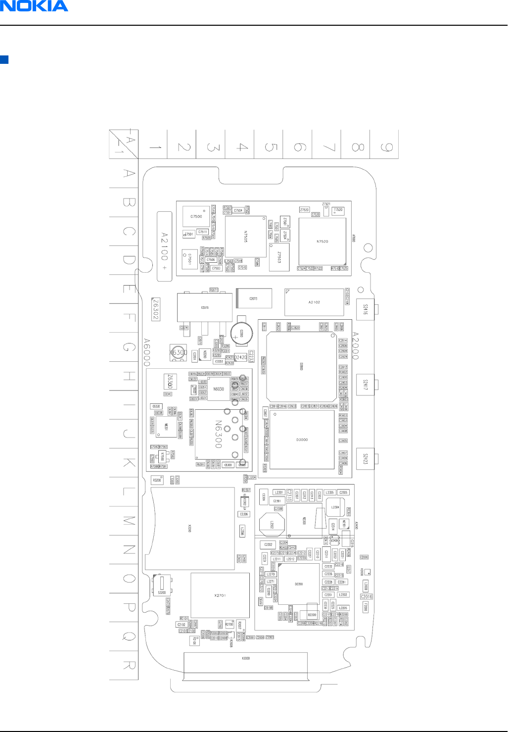
Component layouts
Lower (engine) block
RM-188 lower block component layout - top (1VZ_12d)
RM-188; RM-198
Nokia Customer Care Parts Lists and Component Layouts
Page 2 –54 COMPANY CONFIDENTIAL Issue 2
Copyright © 2007 Nokia. All rights reserved.
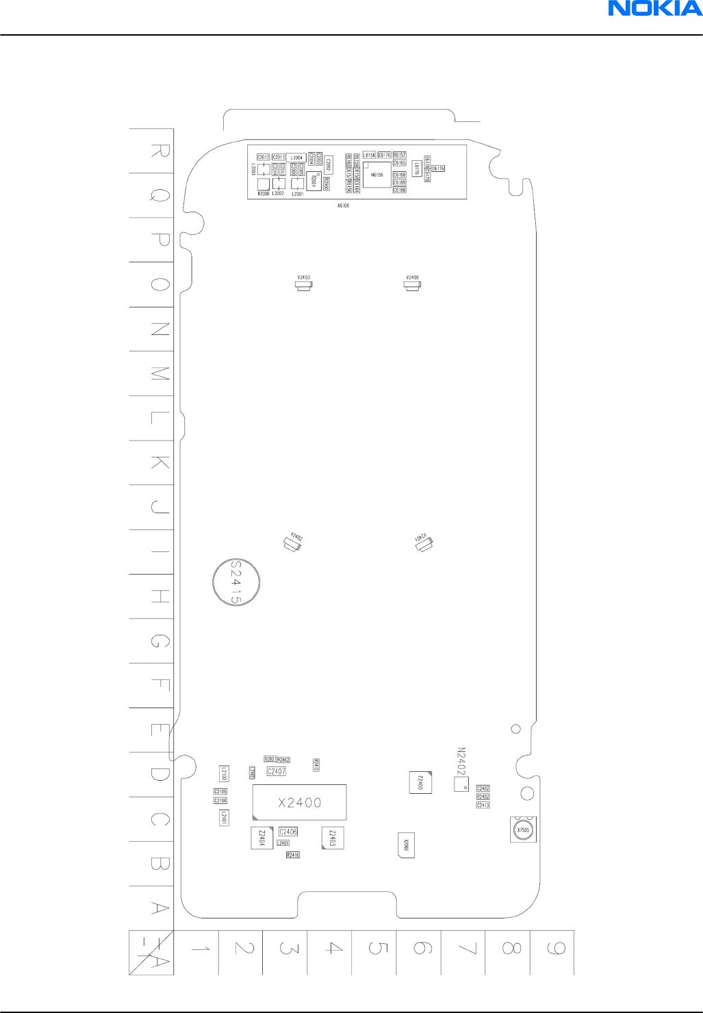
RM-188 lower block component layout - bottom (1VZ_12d)
RM-188; RM-198
Parts Lists and Component Layouts Nokia Customer Care
Issue 2 COMPANY CONFIDENTIAL Page 2 –55
Copyright © 2007 Nokia. All rights reserved.
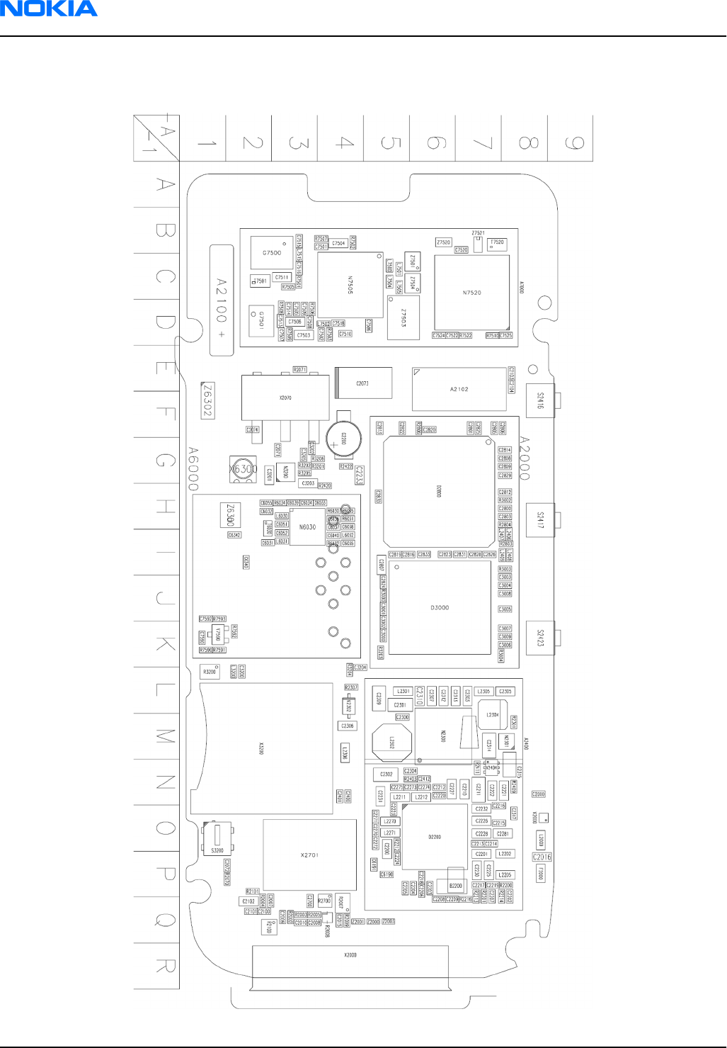
RM-198 lower block component layout - top (1VZ_12b)
RM-188; RM-198
Nokia Customer Care Parts Lists and Component Layouts
Page 2 –56 COMPANY CONFIDENTIAL Issue 2
Copyright © 2007 Nokia. All rights reserved.

RM-198 lower block component layout - bottom (1VZ_12b)
RM-188; RM-198
Parts Lists and Component Layouts Nokia Customer Care
Issue 2 COMPANY CONFIDENTIAL Page 2 –57
Copyright © 2007 Nokia. All rights reserved.
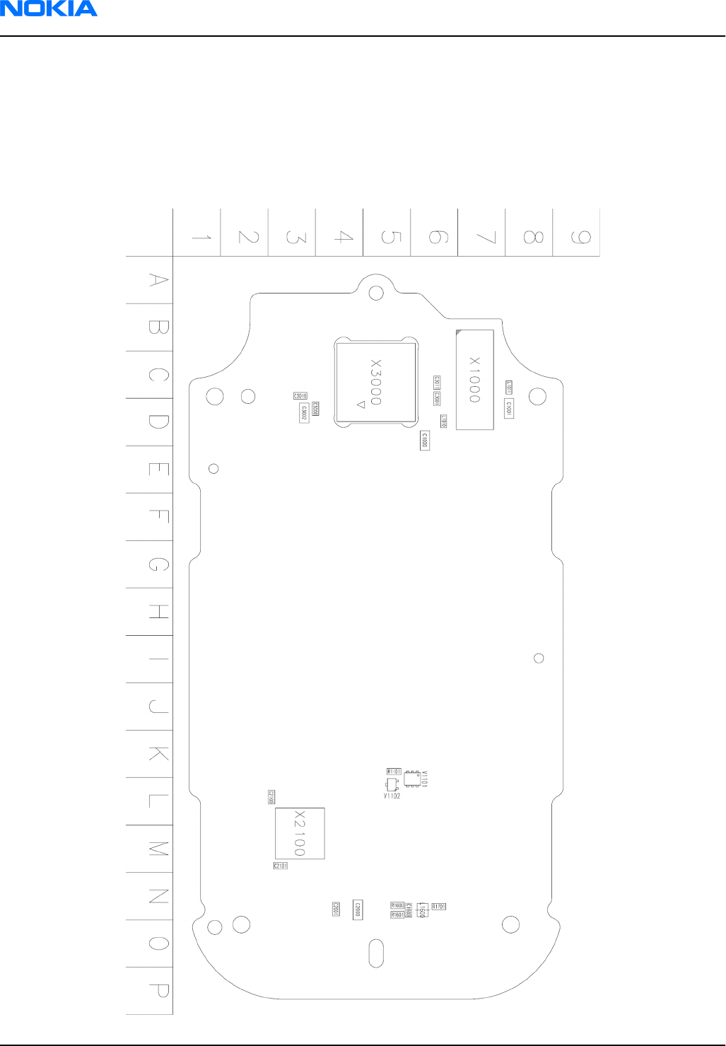
Upper block
RM-188/198 upper block component layout - top (1WJ_10b)
Note: This component layout applies to all RM-188 units and those RM-198 units, which are
assembled without the HAC (Hearing Aid Coil). Note that the RM-198 can be assembled with or
without the HAC.
RM-188; RM-198
Nokia Customer Care Parts Lists and Component Layouts
Page 2 –58 COMPANY CONFIDENTIAL Issue 2
Copyright © 2007 Nokia. All rights reserved.
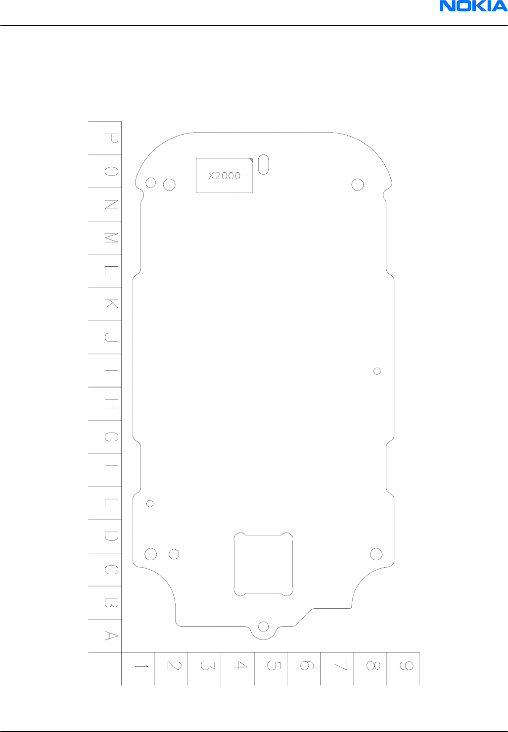
RM-188/198 upper block component layout - bottom (1WJ_10b)
Note: This component layout applies to all RM-188 units and those RM-198 units, which are
assembled without the HAC (Hearing Aid Coil). Note that the RM-198 can be assembled with or
without the HAC.
RM-188; RM-198
Parts Lists and Component Layouts Nokia Customer Care
Issue 2 COMPANY CONFIDENTIAL Page 2 –59
Copyright © 2007 Nokia. All rights reserved.
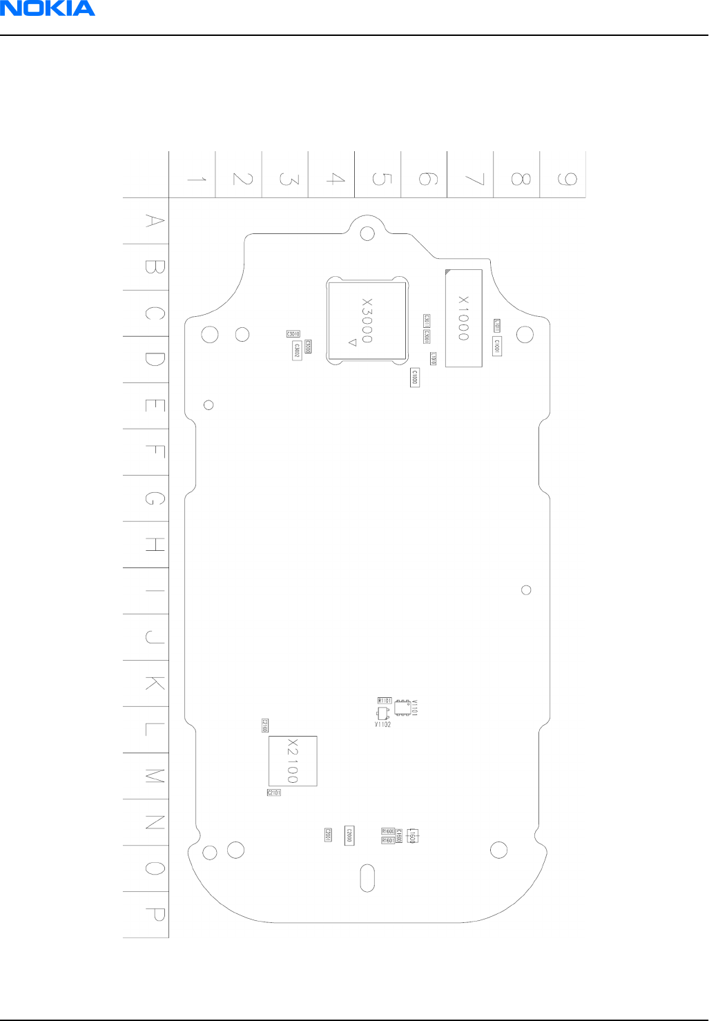
RM-198 upper block component layout with HAC - top (1WJ_10c)
Note: This component layout applies to those RM-198 units, which are assembled with the HAC
(Hearing Aid Coil). Note that the RM-198 can be assembled with or without the HAC.
RM-188; RM-198
Nokia Customer Care Parts Lists and Component Layouts
Page 2 –60 COMPANY CONFIDENTIAL Issue 2
Copyright © 2007 Nokia. All rights reserved.
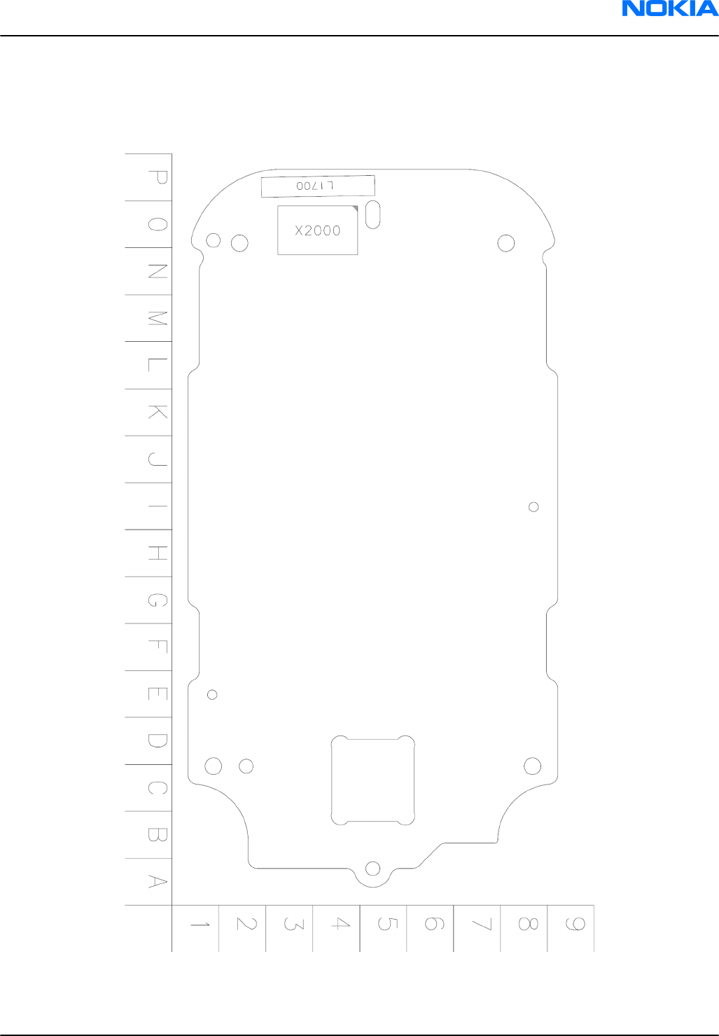
RM-198 upper block component layout with HAC - bottom (1WJ_10c)
Note: This component layout applies to those RM-198 units, which are assembled with the HAC
(Hearing Aid Coil). Note that the RM-198 can be assembled with or without the HAC.
RM-188; RM-198
Parts Lists and Component Layouts Nokia Customer Care
Issue 2 COMPANY CONFIDENTIAL Page 2 –61
Copyright © 2007 Nokia. All rights reserved.

RM-188; RM-198
Nokia Customer Care Parts Lists and Component Layouts
(This page left intentionally blank.)
Page 2 –62 COMPANY CONFIDENTIAL Issue 2
Copyright © 2007 Nokia. All rights reserved.

3 — Service Software
Instructions
Nokia Customer Care
Issue 2 COMPANY CONFIDENTIAL Page 3 –1
Copyright © 2007 Nokia. All rights reserved.

RM-188; RM-198
Nokia Customer Care Service Software Instructions
(This page left intentionally blank.)
Page 3 –2 COMPANY CONFIDENTIAL Issue 2
Copyright © 2007 Nokia. All rights reserved.

Table of Contents
Phoenix installation steps in brief........................................................................................................................3–5
Installing Phoenix ..................................................................................................................................................3–6
Updating Phoenix installation ..............................................................................................................................3–8
Uninstalling Phoenix..............................................................................................................................................3–9
Repairing Phoenix installation .......................................................................................................................... 3–11
Phone data package overview........................................................................................................................... 3–11
Installing phone data package .......................................................................................................................... 3–12
Uninstalling phone data package...................................................................................................................... 3–15
Configuring users in Phoenix ............................................................................................................................. 3–17
Managing connections in Phoenix..................................................................................................................... 3–17
Installing flash support files for FPS-10 ............................................................................................................ 3–19
Updating FPS-10 flash prommer software........................................................................................................ 3–22
List of Figures
Figure 2 Dongle not found ....................................................................................................................................3–6
Figure 3 Disclaimer text.........................................................................................................................................3–7
Figure 4 InstallShield Wizard Complete ...............................................................................................................3–8
Figure 5 Installation interrupted..........................................................................................................................3–9
Figure 6 Remove program.................................................................................................................................. 3–10
Figure 7 Finish uninstallation ............................................................................................................................ 3–10
Figure 8 Repair program .................................................................................................................................... 3–11
Figure 9 Data package setup information ........................................................................................................ 3–13
Figure 10 Data package destination folder ...................................................................................................... 3–14
Figure 11 InstallShield Wizard Complete.......................................................................................................... 3–15
Figure 12 Uninstalling phone data package..................................................................................................... 3–16
Figure 13 Finishing data package uninstallation............................................................................................. 3–16
Figure 14 Phoenix login...................................................................................................................................... 3–17
Figure 15 New user configured.......................................................................................................................... 3–17
Figure 16 Select mode: Manual.......................................................................................................................... 3–18
Figure 17 Connections list .................................................................................................................................. 3–19
Figure 18 Connection information .................................................................................................................... 3–19
Figure 19 Product support module information (example from RM-1)......................................................... 3–19
Figure 20 Flash update welcome dialog........................................................................................................... 3–20
Figure 21 Flash installation interrupted ........................................................................................................... 3–20
Figure 22 Flash destination folder..................................................................................................................... 3–21
Figure 23 Finish flash update............................................................................................................................. 3–22
Figure 24 Prommer SW update finished........................................................................................................... 3–23
Figure 25 Prommer maintenance window....................................................................................................... 3–23
Figure 26 Flash directory window..................................................................................................................... 3–24
RM-188; RM-198
Service Software Instructions Nokia Customer Care
Issue 2 COMPANY CONFIDENTIAL Page 3 –3
Copyright © 2007 Nokia. All rights reserved.

RM-188; RM-198
Nokia Customer Care Service Software Instructions
(This page left intentionally blank.)
Page 3 –4 COMPANY CONFIDENTIAL Issue 2
Copyright © 2007 Nokia. All rights reserved.

Phoenix
installation steps in brief
Prerequisites
Recommended hardware requirements:
• Computer processor: Pentium 700 MHz or higher
• RAM 256 MB
• Disk space 100-300 MB
Supported operating systems:
•
Windows 2000
Service Pack 3 or higher
•
Windows XP
Service Pack 1 or higher
Context
Phoenix
is a service software for reprogramming, testing and tuning phones.
Phoenix
installation contains:
• Service software support for all phone models included in the package
• Flash update package files for programming devices
• All needed drivers for:
• PKD-1 (DK2) dongle
• DKU-2 USB cable
Note: Separate installation packages for flash update files and drivers are also available, but it is
not necessary to use them unless there are updates between
Phoenix
service software releases. If
separate update packages are used, they should be used after
Phoenix
and data packages have been
installed.
The phone model specific data package includes all changing product specific data:
• Product software binary files
• Files for type label printing
• Validation file for the faultlog repair data reporting system
• All product specific configuration files for
Phoenix
software components
Note:
Phoenix
and phone data packages should only be used as complete installation packages.
Uninstallation should be made from the
Windows
Control Panel.
To use
Phoenix
, you need to:
Steps
1. Connect a PKD-1 (DK2) dongle to the computer parallel port.
2. Install
Phoenix
.
3. Install the phone-specific data package.
4. Configure users.
5. Manage connection settings (depends on the tools you are using).
• Update FPS-10 software
Note: There is no need to activate FPS-10.
• Activate SX-4 smart card, if you need tuning and testing functions.
Note: When FPS-10 is used only for product software updates, SX-4 smart card is not needed.
RM-188; RM-198
Service Software Instructions Nokia Customer Care
Issue 2 COMPANY CONFIDENTIAL Page 3 –5
Copyright © 2007 Nokia. All rights reserved.
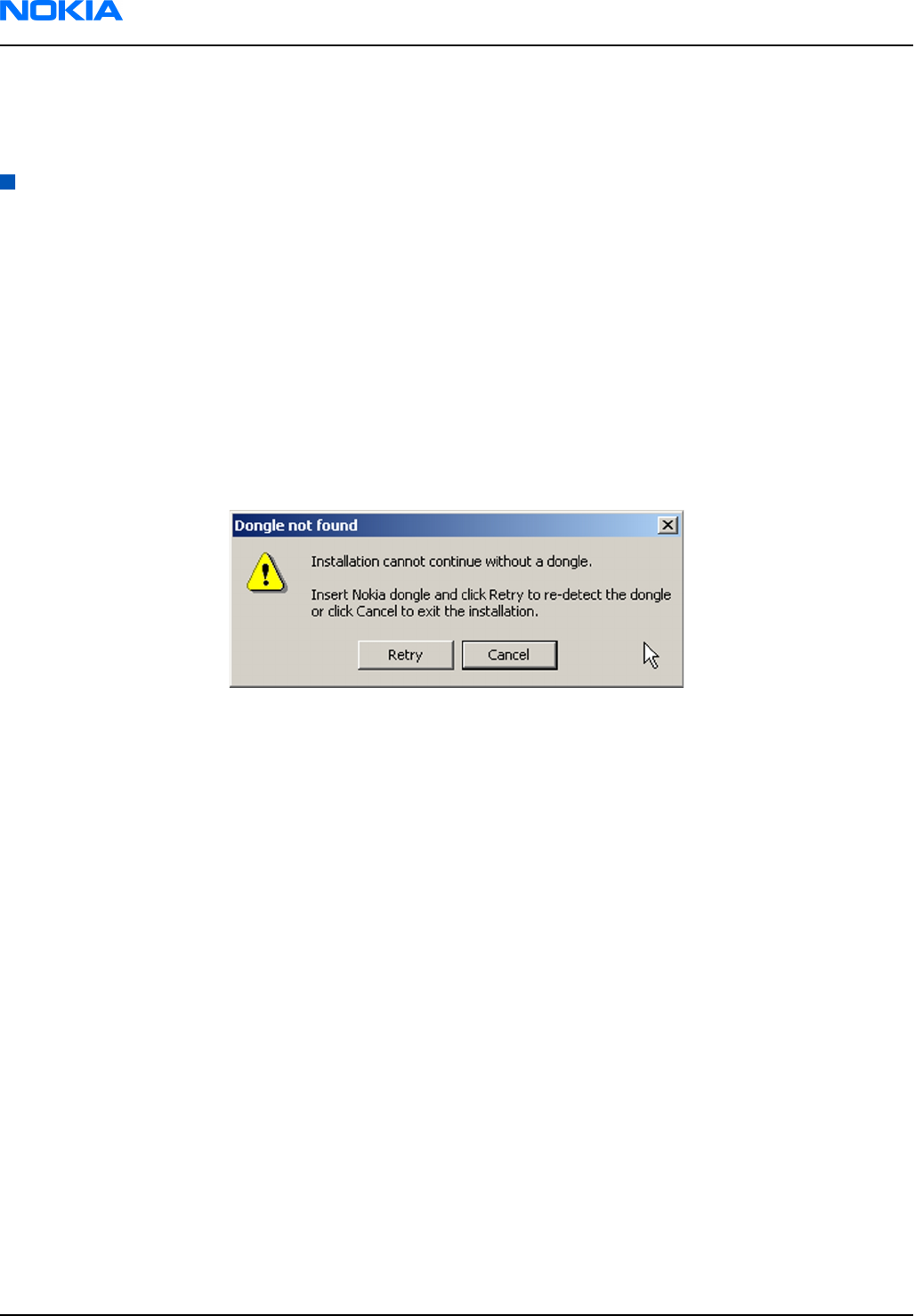
Results
Phoenix
is ready to be used with FPS-10 flash prommer and other service tools.
Installing
Phoenix
Prerequisites
• Check that a dongle is attached to the parallel port of your computer.
• Download the
Phoenix
installation package (for example,
phoenix_service_sw_2004_39_x_xx.exe
) to your
computer (in
C:\TEMP
, for instance).
• Close all other programs.
• Depending on your operating system, administrator rights may be required to install
Phoenix
.
• If uninstalling or rebooting is needed at any point, you will be prompted by the InstallShield program.
Context
At some point during the installation procedure, you may get the following message:
Figure 2 Dongle not found
This may be a result of a defective or too old PKD-1 dongle.
Check the COM/parallel ports used. After correcting the problem, you can restart the installation.
For more detailed information, please refer to
Phoenix
Help files.
Tip: Each feature in
Phoenix
has its own Help function, which can be activated while running the
program. Press the F1 key or the feature’s Help button to activate a Help file.
Steps
1. To start the installation, run the application file (for example,
phoenix_service_sw_2004_39_x_xx.exe
).
2. In the
Welcome
dialogue, click Next.
RM-188; RM-198
Nokia Customer Care Service Software Instructions
Page 3 –6 COMPANY CONFIDENTIAL Issue 2
Copyright © 2007 Nokia. All rights reserved.
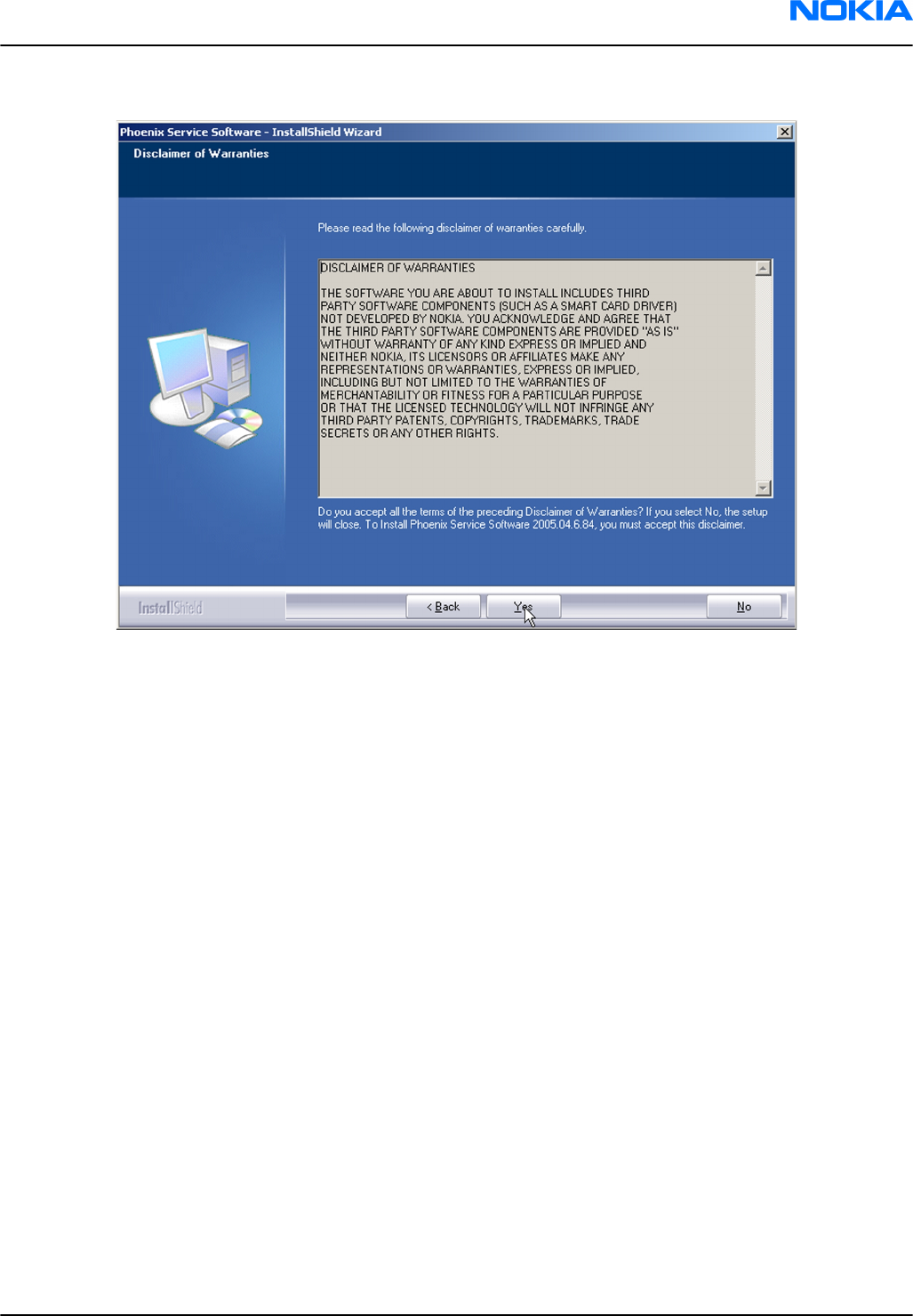
3. Read the disclaimer text carefully and click Yes.
Figure 3 Disclaimer text
4. Choose the destination folder.
The default folder
C:\ProgramFiles\Nokia\Phoenix
is recommended.
5. To continue, click Next.
To choose another location, click Browse (not recommended).
6. Wait for the components to be copied.
The progress of the installation is shown in the
Setup Status
window.
7. Wait for the drivers to be installed and updated.
The process may take several minutes to complete.
If the operating system does not require rebooting, the PC components are registered right away.
If the operating system requires restarting your computer, the Install Shield Wizard will notifies about it.
Select Yes... to reboot the PC immediately or No... to reboot the PC manually afterwards.
After the reboot, all components are registered.
Note:
Phoenix
does not work, if the components have not been registered.
RM-188; RM-198
Service Software Instructions Nokia Customer Care
Issue 2 COMPANY CONFIDENTIAL Page 3 –7
Copyright © 2007 Nokia. All rights reserved.
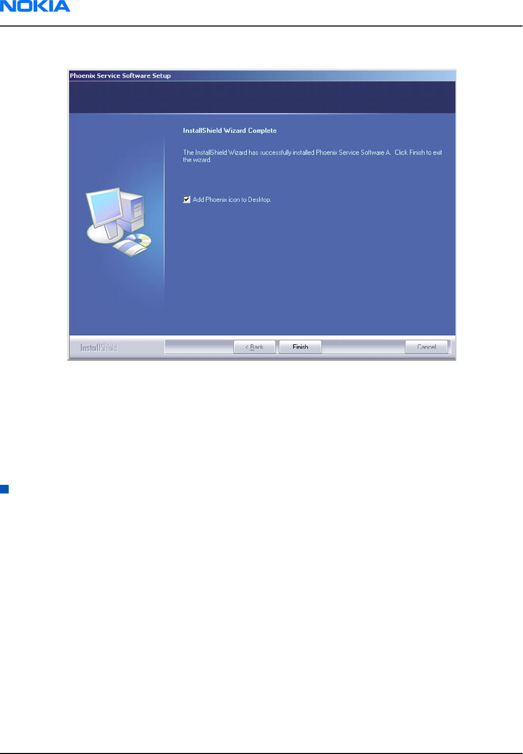
8. To end the installation, click Finish.
Figure 4 InstallShield Wizard Complete
Next actions
After the installation,
Phoenix
can be used after:
• installing phone model specific data package for
Phoenix
• configuring users and connections
FPS-10 flash prommer can be used after updating their flash update package files.
Updating
Phoenix
installation
Context
• If you already have the
Phoenix
service software installed on your computer, you need to update the
software when new versions are released.
• To update
Phoenix
, you need to follow the same steps as when installing it for the first time.
•When you are updating, for example, from version a14_2004_16_4_47 to a15_2004_24_7_55, the update
will take place automatically without uninstallation.
•Always use the latest available versions of both
Phoenix
and the phone-specific data package. Instructions
can be found in the phone model specific Technical Bulletins and phone data package
readme.txt
files
(shown during installation).
•If you try to update
Phoenix
with the same version you already have (for example, a15_2004_24_7_55 to
a15_2004_24_7_55), you are asked if you want to uninstall the existing version. In this case you can choose
between a total uninstallation or a repair installation in a similar way when choosing to uninstall the
application from the
Windows
Control Panel.
• If you try to install an older version (for example, downgrade from a15_2004_24_7_55 to
a14_2004_16_4_47), installation will be interrupted.
RM-188; RM-198
Nokia Customer Care Service Software Instructions
Page 3 –8 COMPANY CONFIDENTIAL Issue 2
Copyright © 2007 Nokia. All rights reserved.
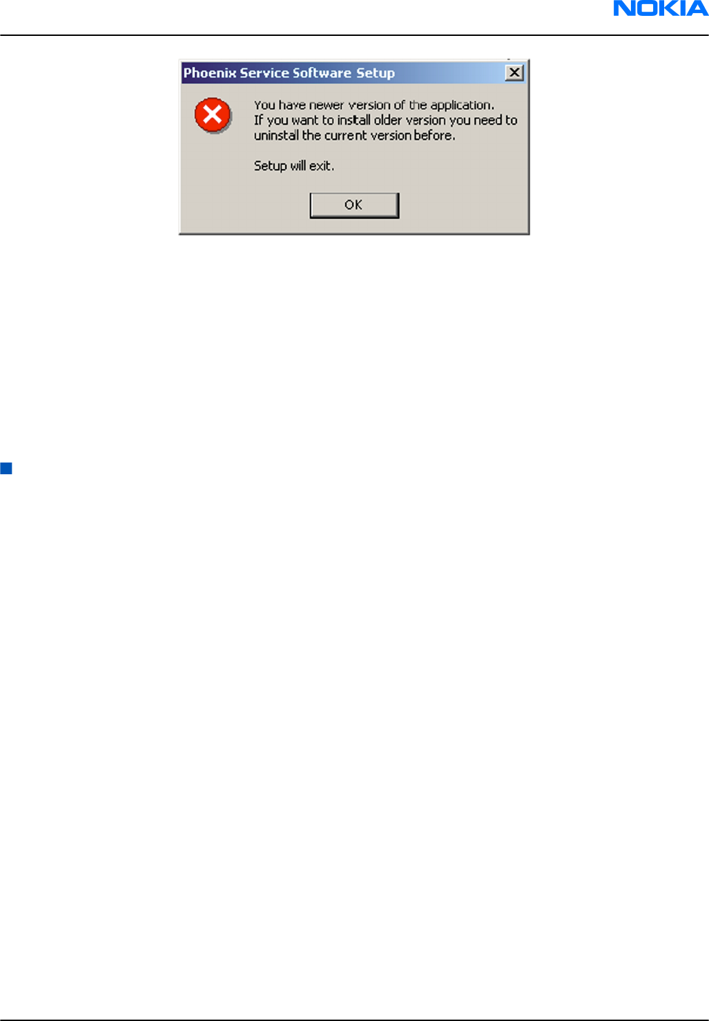
Figure 5 Installation interrupted
• Always follow the instructions on the screen.
Steps
1. Download the installation package to your computer hard disk.
2. Close all other programs.
3. Run the application file (for example,
phoenix_service_sw_2004_39_x_xx.exe
).
Results
A new
Phoenix
version is installed and driver versions are checked and updated.
Uninstalling
Phoenix
Context
You can uninstall
Phoenix
service software manually from the
Windows
Control Panel.
Steps
1. Open the Windows Control Panel, and choose Add/Remove Programs.
RM-188; RM-198
Service Software Instructions Nokia Customer Care
Issue 2 COMPANY CONFIDENTIAL Page 3 –9
Copyright © 2007 Nokia. All rights reserved.
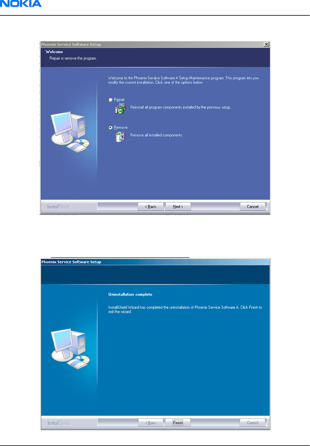
2. To uninstall
Phoenix
, choose Phoenix Service Software→Change/Remove→Remove .
Figure 6 Remove program
The progress of the uninstallation is shown.
3. If the operating system does not require rebooting, click Finish to complete.
Figure 7 Finish uninstallation
RM-188; RM-198
Nokia Customer Care Service Software Instructions
Page 3 –10 COMPANY CONFIDENTIAL Issue 2
Copyright © 2007 Nokia. All rights reserved.
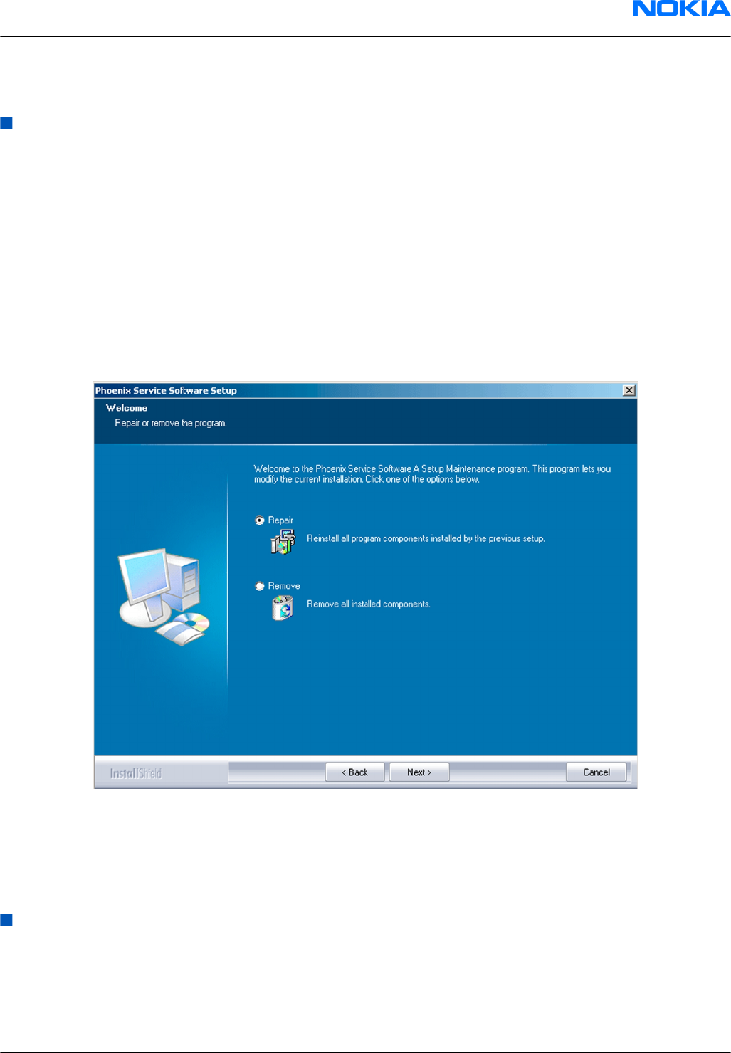
If the operating system requires rebooting, InstallShield Wizard will notify you. Select Yes... to reboot the
PC immediately and No... to reboot the PC manually afterwards.
Repairing
Phoenix
installation
Context
If you experience any problems with the service software or suspect that files have been lost, use the repair
function before completely reinstalling
Phoenix
.
Note: The original installation package (for example,
phoenix_service_sw_a15_2004_24_7_55.exe
)
must be found on your PC when you run the repair setup.
Steps
1. Open Windows Control Panel→Add/Remove Programs .
2. Choose Phoenix Service Software→Change/Remove .
3. In the following view, select Repair.
Figure 8 Repair program
Phoenix
reinstalls components and registers them.
The procedure is the same as when updating
Phoenix
.
4. To complete the repair, click Finish.
Phone data package overview
Each product has its own data package (DP). The product data package contains all product-specific data files
to make the Phoenix service software and tools usable with a certain phone model.
The phone data package contains the following:
• Product software binary files
RM-188; RM-198
Service Software Instructions Nokia Customer Care
Issue 2 COMPANY CONFIDENTIAL Page 3 –11
Copyright © 2007 Nokia. All rights reserved.

• Files for type label printing
• Validation file for the fault log repair data reporting system
• All product-specific configuration files for Phoenix software components
Data files are stored in C:\Program Files\Nokia\Phoenix (default).
Installing phone data package
Prerequisites
•A phone-specific data package contains all data required for the
Phoenix
service software and service tools
to be used with a certain phone model.
• Check that a dongle is attached to the parallel port of your computer.
• Install
Phoenix
service software.
•Download the installation package (for example,
XX-XX_dp_EA_v_1_0.exe
) to your computer (for example,
in C:\TEMP).
• Close all other programs.
(XX-XX = type designator of the product)
If you already have
Phoenix
installed on your computer, you will need to update it when a new version is
released.
Note: Often
Phoenix
and the phone-specific data package come in pairs, meaning that a certain
version of
Phoenix
can only be used with a certain version of a data package. Always use the latest
available versions of both. Instructions can be found in phone-specific Technical Bulletins and
readme.txt
files of data packages.
Steps
1. To start the installation, run the application file (for example,
XX-XX_dp_EA_ v_1_0.exe
),
Wait for the installation files to be extracted.
RM-188; RM-198
Nokia Customer Care Service Software Instructions
Page 3 –12 COMPANY CONFIDENTIAL Issue 2
Copyright © 2007 Nokia. All rights reserved.
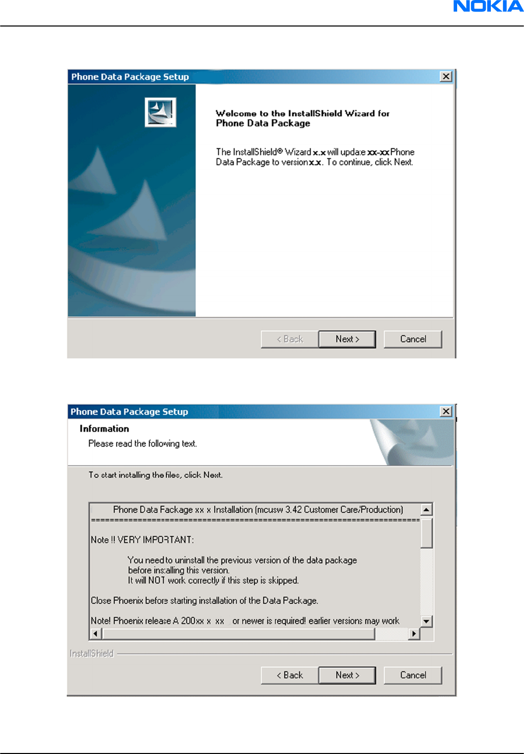
2. Click Next.
3. In the following view you can see the contents of the data package. Read the text carefully. There is
information about the
Phoenix
version required with this data package.
Figure 9 Data package setup information
4. To continue, click Next.
RM-188; RM-198
Service Software Instructions Nokia Customer Care
Issue 2 COMPANY CONFIDENTIAL Page 3 –13
Copyright © 2007 Nokia. All rights reserved.
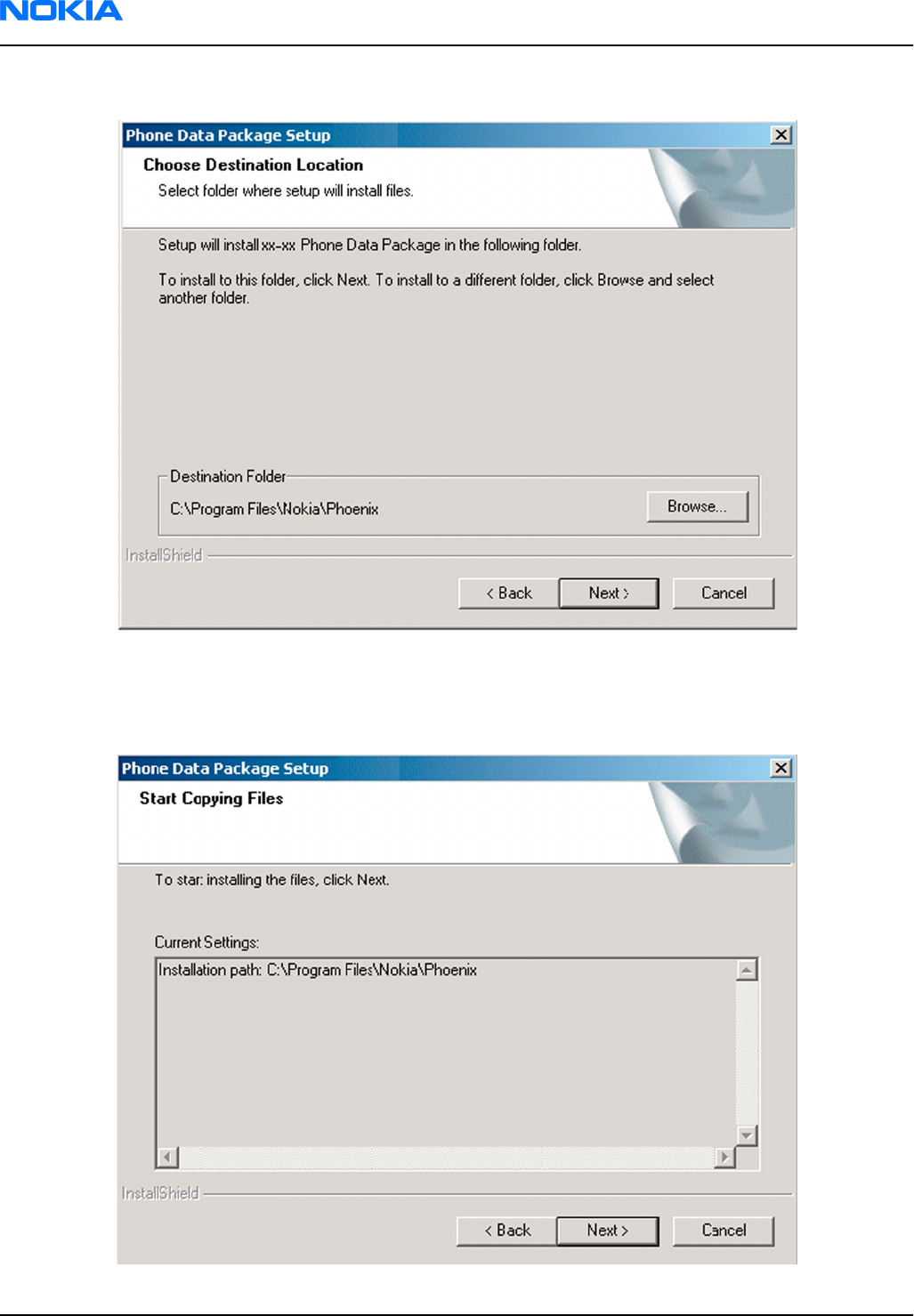
5. Choose the destination folder, and click Next to continue.
Figure 10 Data package destination folder
The InstallShield Wizard checks where
Phoenix
is installed, and the directory is shown.
6. To start copying the files, click Next.
RM-188; RM-198
Nokia Customer Care Service Software Instructions
Page 3 –14 COMPANY CONFIDENTIAL Issue 2
Copyright © 2007 Nokia. All rights reserved.
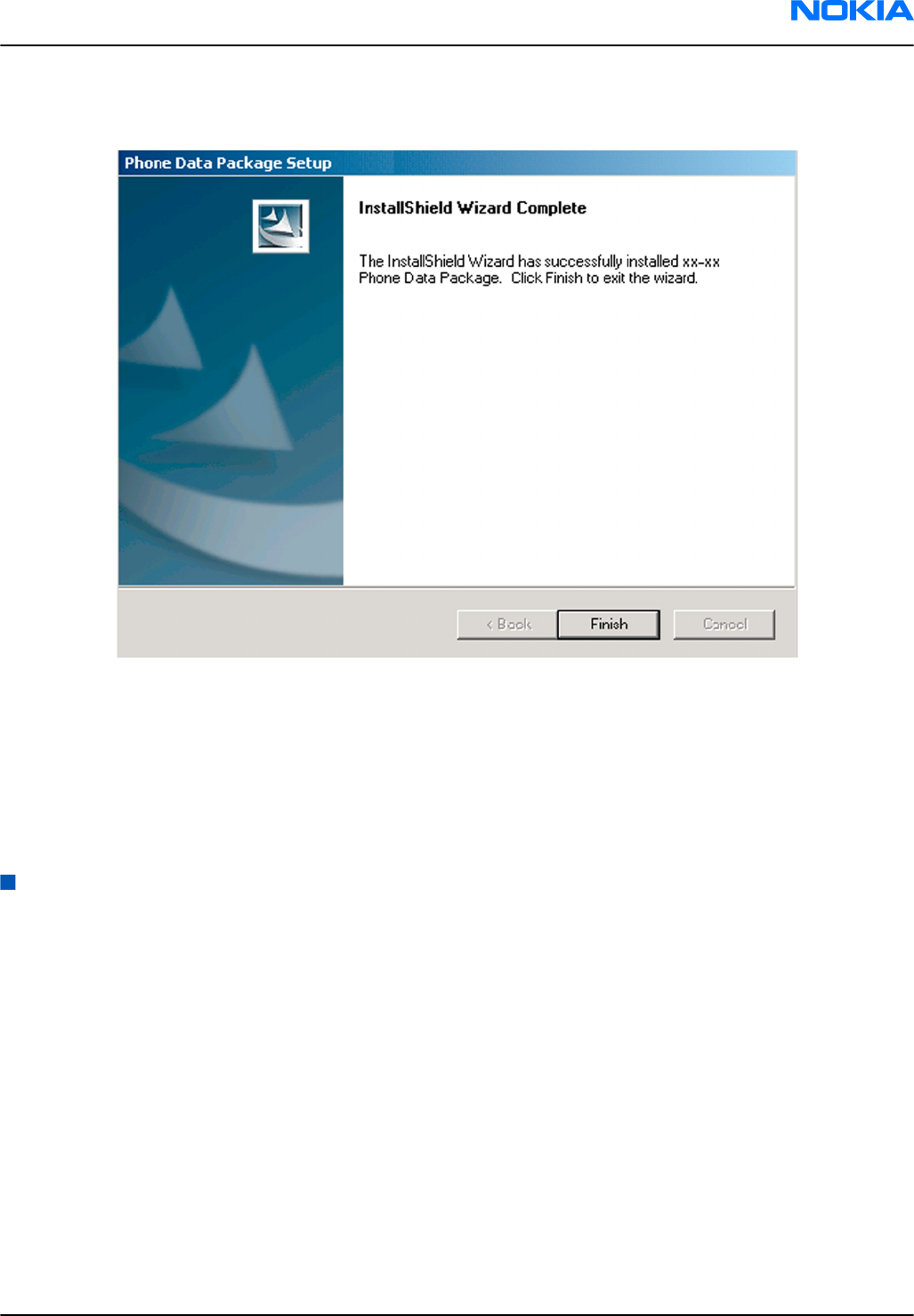
Phone model specific files are installed. Please wait.
7. To complete the installation, click Finish.
Figure 11 InstallShield Wizard Complete
Next actions
Phoenix
can be used for flashing phones and printing type labels after:
• Configuring users
• Managing connections
FPS-10 can be used after updating their flash update package files.
Uninstalling phone data package
Context
There is no need to uninstall an older version of a data package, unless instructions to do so are given in the
readme.txt
file of the data package and bulletins related to the release.
Please read all related documents carefully.
Steps
1. Locate the data package installation file (e.g.
XX-XX_dp_EA_v_1_0.exe
) from your computer.
2. To start the uninstallation procedure, double-click the data package installation file.
RM-188; RM-198
Service Software Instructions Nokia Customer Care
Issue 2 COMPANY CONFIDENTIAL Page 3 –15
Copyright © 2007 Nokia. All rights reserved.
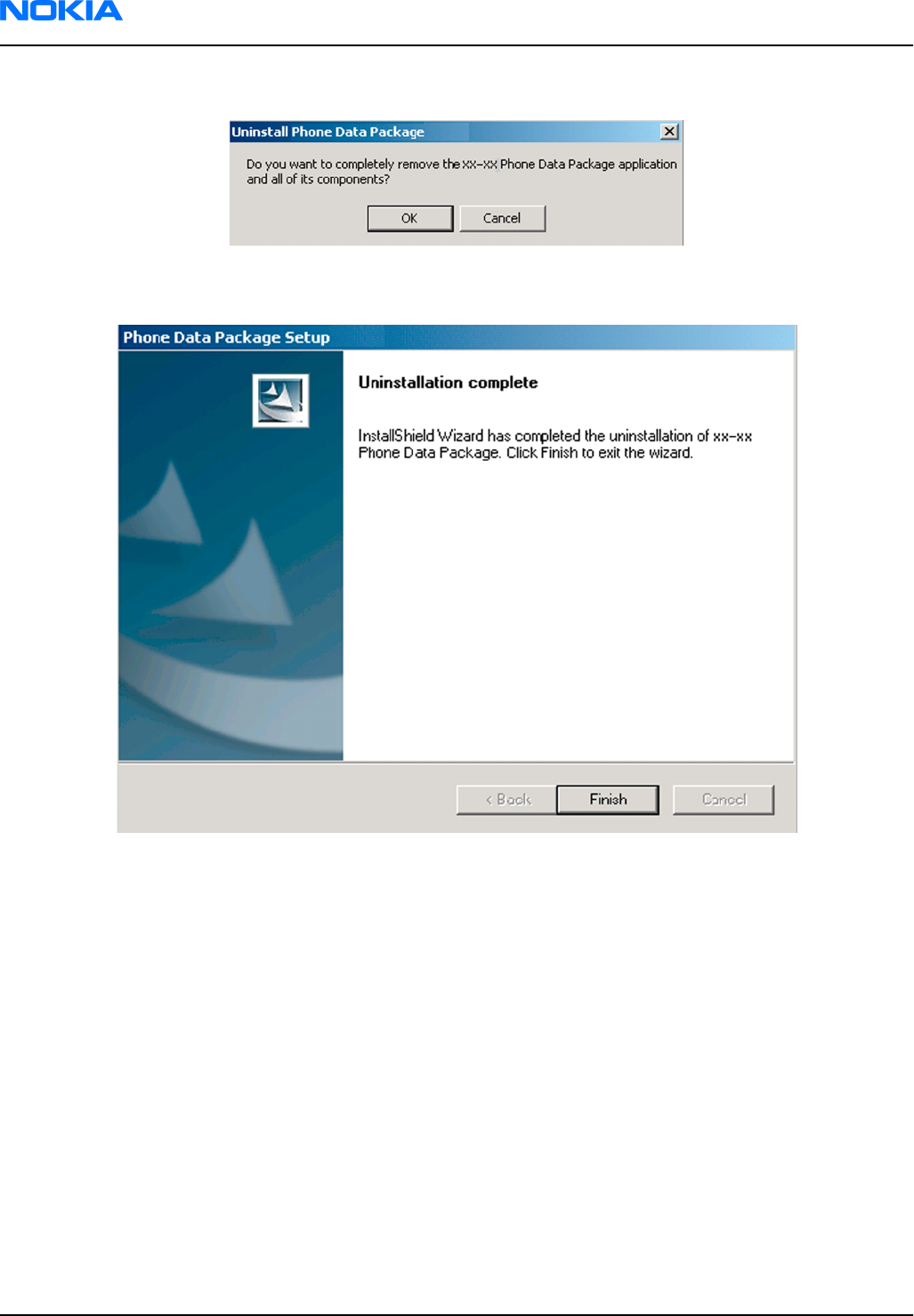
3. To uninstall the data package, click OK or to interrupt the uninstallation, click Cancel.
Figure 12 Uninstalling phone data package
4. When the data package is uninstalled, click Finish.
Figure 13 Finishing data package uninstallation
Alternative steps
• You can also uninstall the data package manually from
Control Panel→Add/Remove Programs→xx-xx* Phone Data Package . (*= type designator of the
phone).
RM-188; RM-198
Nokia Customer Care Service Software Instructions
Page 3 –16 COMPANY CONFIDENTIAL Issue 2
Copyright © 2007 Nokia. All rights reserved.
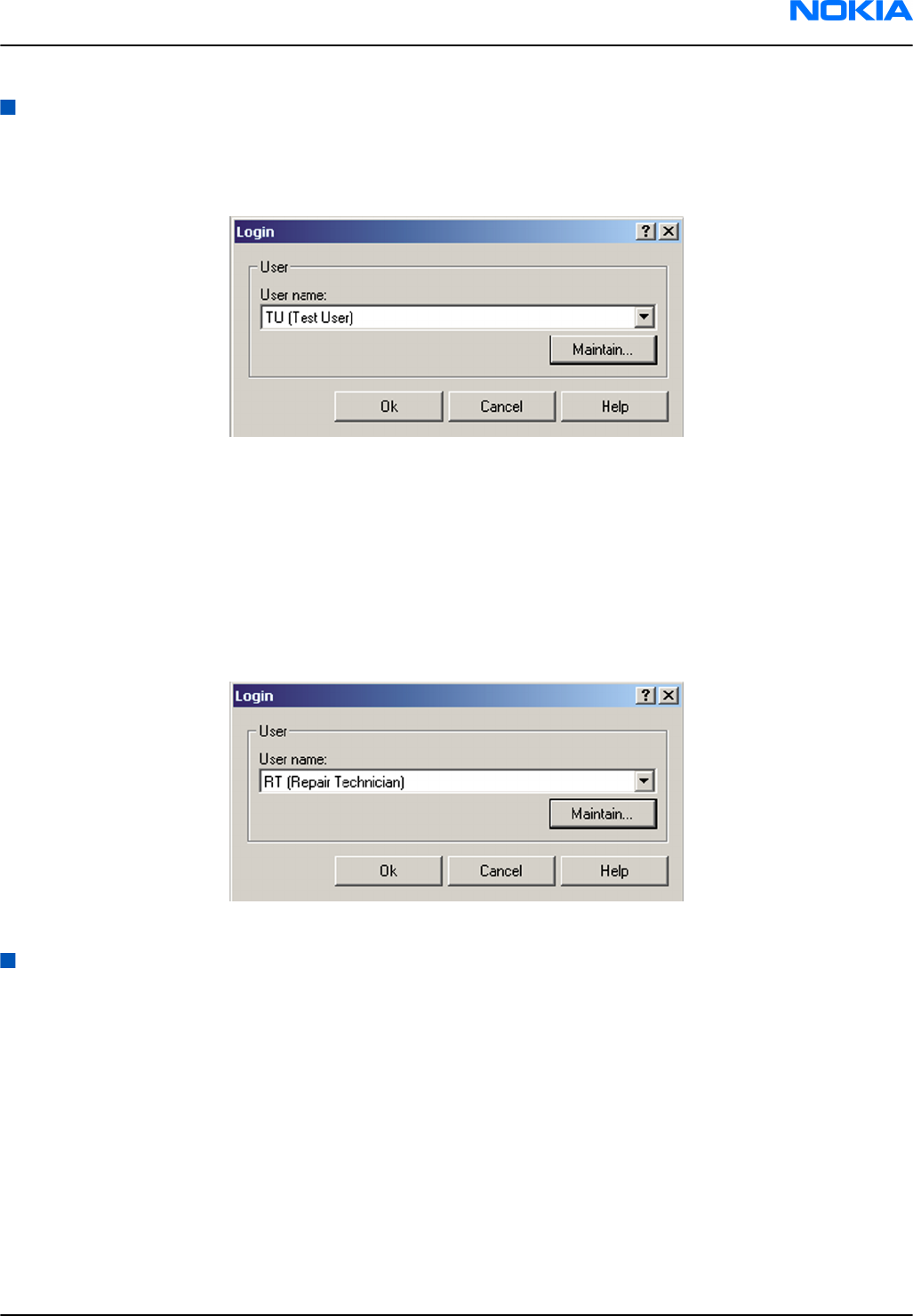
Configuring users in
Phoenix
Steps
1. Start
Phoenix
service software, and log in.
Figure 14 Phoenix login
If the user ID is already configured, select s/he from the
User name
drop-down list, and click OK.
2. To add a new user, or to edit existing ones, click Maintain.
3. To add a new user, click New.
4. Type in the name and initials of the user, and click OK.
The user is added to the user name list.
5. Select the desired user from the
User name
drop-down list, and click OK.
Figure 15 New user configured
Managing connections in
Phoenix
Context
With the Manage Connections feature you can edit and delete existing connections or create new ones.
Note: After choosing the desired connection, and connecting the phone to a PC for the first time,
allow the PC to install the USB device drivers first. Please note that this may take some time to
complete.
If there are problems after the driver installation, check that the USB connection is active from the
Windows Control Panel. If the problem persists, contact the local PC support.
Steps
1. Start
Phoenix
, and log in.
2. Choose File→Manage Connections... .
RM-188; RM-198
Service Software Instructions Nokia Customer Care
Issue 2 COMPANY CONFIDENTIAL Page 3 –17
Copyright © 2007 Nokia. All rights reserved.
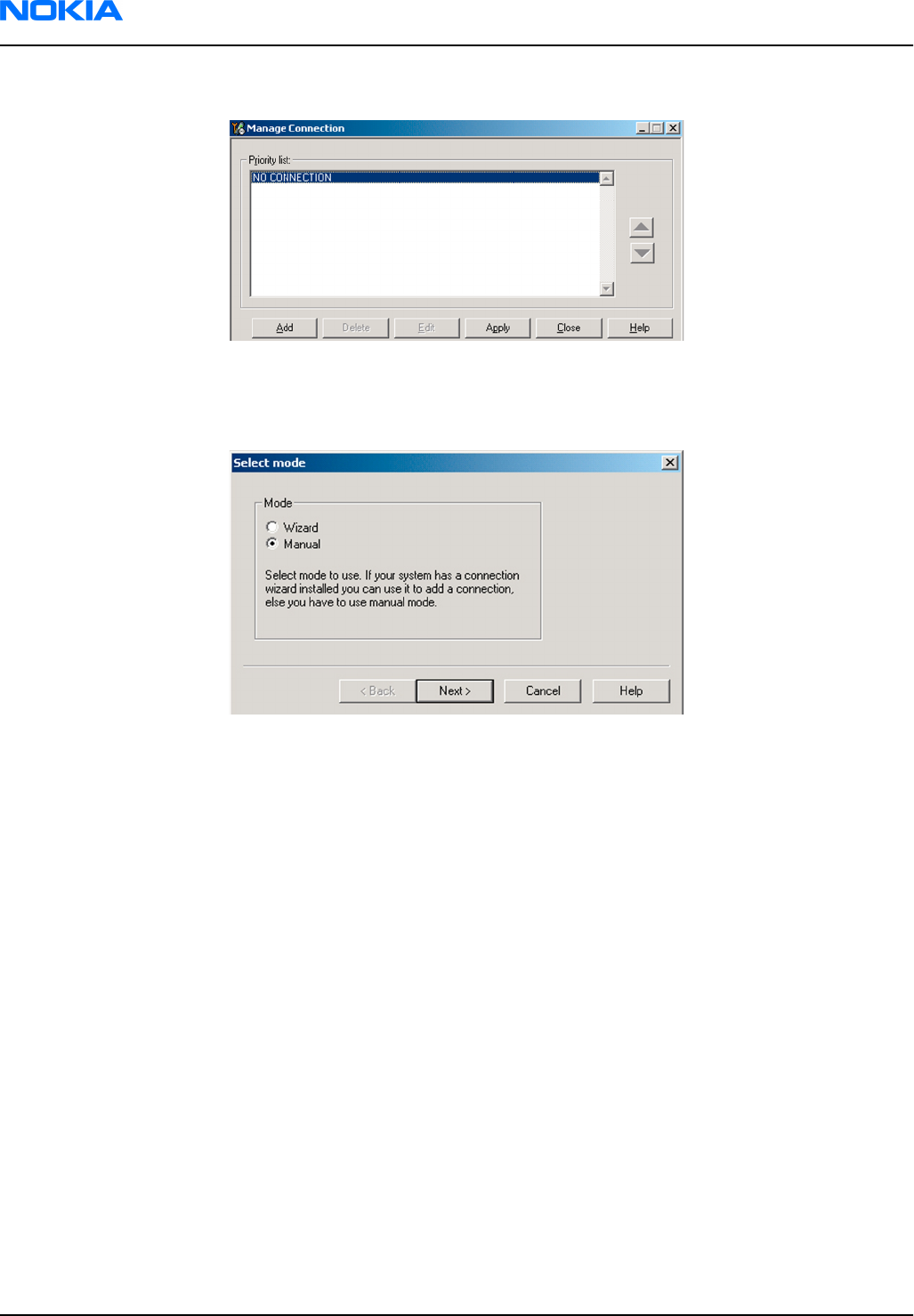
3. To add a new connection, click Add.
4. Select Manual mode, and click Next to continue.
If you want to create the connection using the Connection Wizard, connect the tools and a phone to your
PC. The wizard will automatically try to configure the correct connection.
Figure 16 Select mode: Manual
i For an FPS-10 flash prommer with a USB Connection, choose the following connection settings:
• Media: FPS-10 USB
• DEVICE_INDEX: 0
• SERIAL_NUM: See Serial No from the label attached to the bottom of FPS-10
• ACTIVE_MEDIA: USB
ii For an FPS-10 flash prommer with a LAN connection, choose the following connection settings:
• Media: FPS-10 TCP/IP
• NET_SERV_NAME: Click Scan.... Choose your own FPS-10 device based on the correct MAC address.
See Serial No from the label attached to the bottom of your FPS-10.
• PORT_NUM: Use the default value, and click Next.
• PROTOCOL_FAMILY: Use the default value, and click Next.
• SOCKET TYPE: Use the default value, and click Next.
• TX_BUFFER_SIZE: Use the default value, and click Next.
• RX_BUFFER_SIZE: Use the default value, and click Next.
iii For an FPS-8 flash prommer, choose the following connection settings:
• Media: FPS-8
• PORT_NUM: COM Port where FPS-8 is connected
• COMBOX_DEF_MEDIA: FBUS
RM-188; RM-198
Nokia Customer Care Service Software Instructions
Page 3 –18 COMPANY CONFIDENTIAL Issue 2
Copyright © 2007 Nokia. All rights reserved.
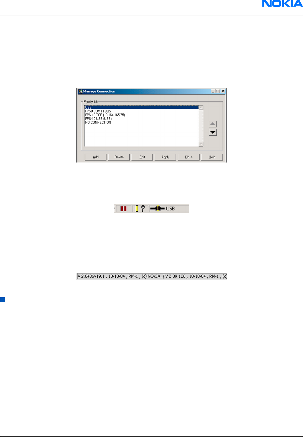
iv For a plain USB connection, choose the following connection settings:
Note: First connect the DKU-2 USB cable between the PC USB port and phone.
• Media: USB
5. To complete the configuration, click Finish.
6. Click the connection you want to activate. Use the up/down arrows located on the right hand side to move
it on top of the list, then click Apply.
Figure 17 Connections list
The connection is activated, and it can be used after closing the
Manage Connection
window.
The connection information is shown at the right hand bottom corner of the screen.
Figure 18 Connection information
7. To use the connection, connect the phone to your PC with correct service tools. Make sure the phone is
switched on, and then choose File→Scan Product .
Results
The product support module information appears in the status bar:
Figure 19 Product support module information (example from RM-1)
Installing flash support files for FPS-10
Prerequisites
Note: You need to install flash support files for FPS-10 only, if you don’t have the latest Phoenix
available or the flash support files have changed after the latest Phoenix release.
•Flash support files are installed automatically, when you install Phoenix. Use Phoenix packages later than
June 2006.
• Normally it is enough to install Phoenix and the phone-specific data package because the Phoenix
installation always includes the latest flash update package files for FPS-10.
•A separate installation package for flash support files is available, and the files can be updated according
to this instruction, if updates appear between new Phoenix / data package releases
Context
If you are not using a separate installation package, you can skip this section and continue with updating
FPS-10 flash prommer software after installing a new phone data package.
RM-188; RM-198
Service Software Instructions Nokia Customer Care
Issue 2 COMPANY CONFIDENTIAL Page 3 –19
Copyright © 2007 Nokia. All rights reserved.
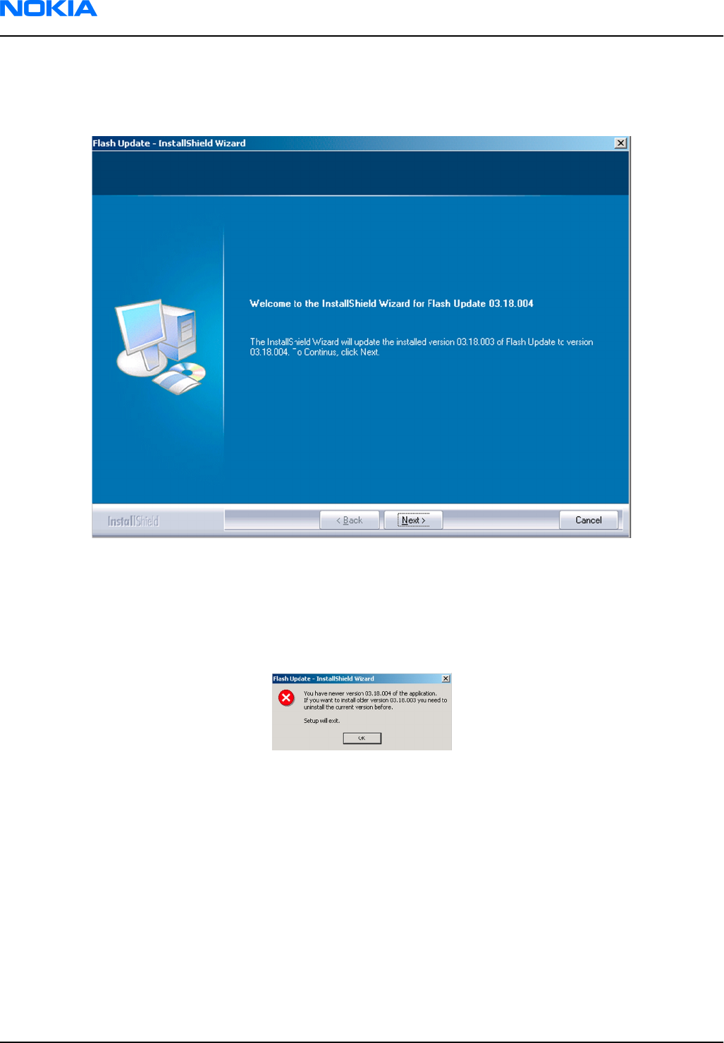
Steps
1. To begin installation, double- click
flash_update_x_yy.exe
.
Figure 20 Flash update welcome dialog
If the same version of Flash Update package already exists, and you want to reinstall it, the previous
package is first uninstalled. Restart installation again after that.
2. If you try to downgrade the existing version to older ones, the setup will be aborted. If you really want
to downgrade, uninstall newer files manually from Control Panel and then rerun the installation again.
Figure 21 Flash installation interrupted
If an older version exists on your PC and it needs to be updated, click Next to continue installation.
RM-188; RM-198
Nokia Customer Care Service Software Instructions
Page 3 –20 COMPANY CONFIDENTIAL Issue 2
Copyright © 2007 Nokia. All rights reserved.
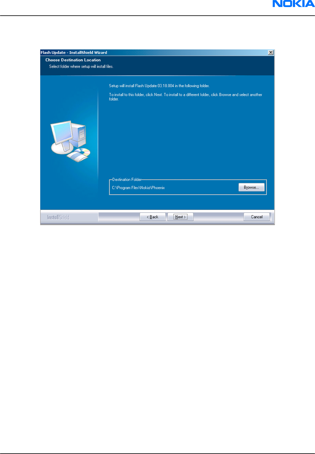
3. It is highly recommended to install the files to the default destination folder
C:\Program Files\Nokia
\Phoenix
. Click Next to continue.
Figure 22 Flash destination folder
When installing the flash update files for the first time you may choose another location by selecting
Browse. However, this is not recommended.
RM-188; RM-198
Service Software Instructions Nokia Customer Care
Issue 2 COMPANY CONFIDENTIAL Page 3 –21
Copyright © 2007 Nokia. All rights reserved.

4. To complete the installation procedure, click Finish .
Figure 23 Finish flash update
Next actions
FPS-10 flash prommers must be updated using Phoenix!
Updating FPS-10 flash prommer software
Steps
1. Start
Phoenix Service Software
and log in, manage connection correctly for your flash prommer.
2. Choose Flashing→Prommer maintenance .
3. When the new flash update package is installed to the computer you will be asked to update the files to
your Prommer. To update the files, click Yes. Click OK if the computer informs you about an unsafe removal
of the device.
4. Alternatively you can update the FPS-10 flash prommer software by clicking the Update button.
RM-188; RM-198
Nokia Customer Care Service Software Instructions
Page 3 –22 COMPANY CONFIDENTIAL Issue 2
Copyright © 2007 Nokia. All rights reserved.
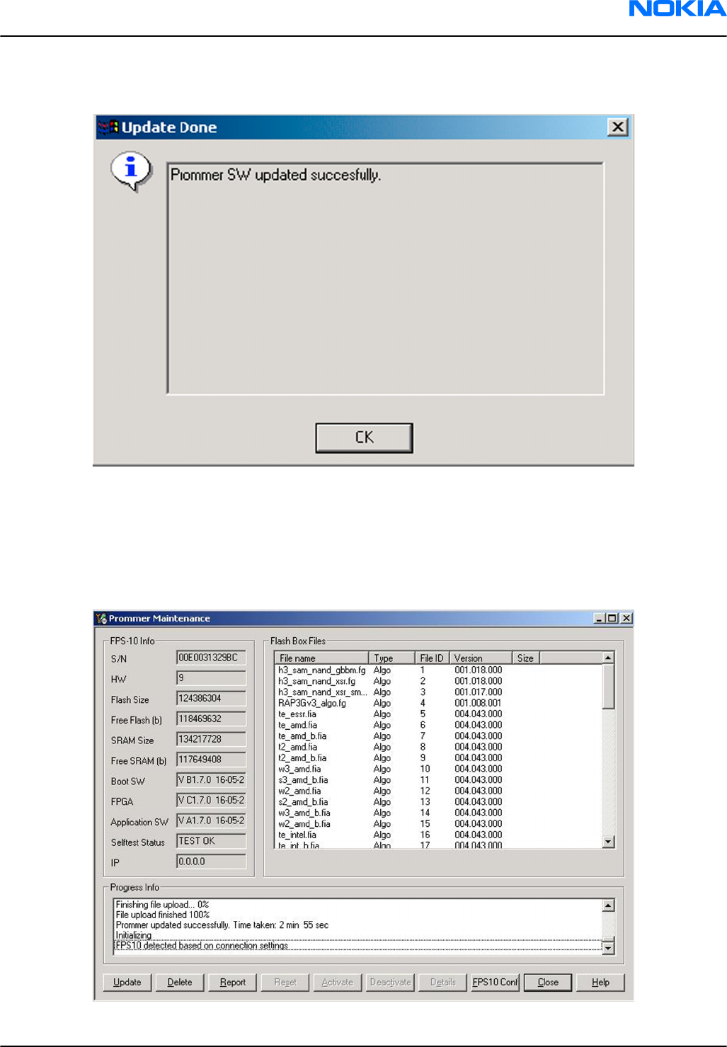
5. Wait until you are notified that update has been successful; the procedure will take a couple of minutes.
Click OK to close the
Update Done
window.
Figure 24 Prommer SW update finished
6. If you are using the FPS-10 flash prommer, check that it is detected from the progress info. Check also the
status leds in the FPS-10. The MODE2 led (green), VBAT and POWER leds (red) should be lit. If you are using
LAN connection, the LAN led (yellow) should be blinking.
7. Check that your FPS-10 flash prommer has enough memory. Flashing the SU-18 with FPS-10 needs at least
128 MB of SRAM memory in the prommer.
Figure 25 Prommer maintenance window
RM-188; RM-198
Service Software Instructions Nokia Customer Care
Issue 2 COMPANY CONFIDENTIAL Page 3 –23
Copyright © 2007 Nokia. All rights reserved.
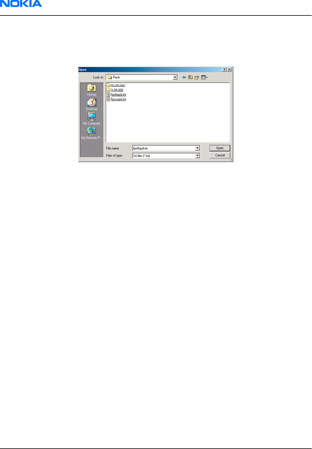
Alternative steps
•You can update FPS-10 SW by clicking the Update button and selecting the appropriate fpsxupd.ini file in
C:\Program Files\Nokia\Phoenix\Flash
.
Figure 26 Flash directory window
• All files can be loaded separately to the prommer used. To do this, click the right mouse button in the
Flash box files
window and select the file type to be loaded.
More information can be found in Phoenix Help.
RM-188; RM-198
Nokia Customer Care Service Software Instructions
Page 3 –24 COMPANY CONFIDENTIAL Issue 2
Copyright © 2007 Nokia. All rights reserved.

4 — Service Tools and Service
Concepts
Nokia Customer Care
Issue 2 COMPANY CONFIDENTIAL Page 4 –1
Copyright © 2007 Nokia. All rights reserved.

RM-188; RM-198
Nokia Customer Care Service Tools and Service Concepts
(This page left intentionally blank.)
Page 4 –2 COMPANY CONFIDENTIAL Issue 2
Copyright © 2007 Nokia. All rights reserved.

Table of Contents
Service tools............................................................................................................................................................4–5
Product specific tools........................................................................................................................................4–5
FS-10..............................................................................................................................................................4–5
MJ-111 ...........................................................................................................................................................4–5
RJ-154 ............................................................................................................................................................4–5
SA-87..............................................................................................................................................................4–6
SA-94..............................................................................................................................................................4–6
SS-104............................................................................................................................................................4–7
General tools......................................................................................................................................................4–7
ACP-8E............................................................................................................................................................4–7
CU-4................................................................................................................................................................4–8
FLS-4S ............................................................................................................................................................4–9
FPS-10............................................................................................................................................................4–9
PKD-1 .............................................................................................................................................................4–9
SS-46..............................................................................................................................................................4–9
SS-62........................................................................................................................................................... 4–10
SS-88........................................................................................................................................................... 4–10
SX-4............................................................................................................................................................. 4–10
Cables............................................................................................................................................................... 4–10
CA-35S......................................................................................................................................................... 4–10
CA-53........................................................................................................................................................... 4–11
DAU-9S........................................................................................................................................................ 4–11
PCS-1........................................................................................................................................................... 4–11
XCS-4........................................................................................................................................................... 4–11
XRS-6........................................................................................................................................................... 4–12
Service concepts .................................................................................................................................................. 4–12
POS (Point of Sale) flash concept .................................................................................................................. 4–12
Flash concept with FPS-10............................................................................................................................. 4–13
CU-4 flash concept with FPS-10..................................................................................................................... 4–14
Module jig service concept............................................................................................................................ 4–15
RF testing concept with RF coupler .............................................................................................................. 4–16
Service concept for RF testing and RF/BB tuning........................................................................................ 4–17
List of Tables
Table 8 Attenuation values for inductive RF coupler SA-94 - fold open ...........................................................4–6
Table 9 Attenuation values for inductive RF coupler SA-94 - fold closed .........................................................4–6
List of Figures
Figure 27 POS flash concept ............................................................................................................................... 4–12
Figure 28 Basic flash concept with FPS-10........................................................................................................ 4–13
Figure 29 CU-4 flash concept with FPS-10......................................................................................................... 4–14
Figure 30 Module jig service concept................................................................................................................ 4–15
Figure 31 RF testing concept with RF coupler.................................................................................................. 4–16
Figure 32 Service concept for RF testing and RF/BB tuning............................................................................ 4–17
RM-188; RM-198
Service Tools and Service Concepts Nokia Customer Care
Issue 2 COMPANY CONFIDENTIAL Page 4 –3
Copyright © 2007 Nokia. All rights reserved.

RM-188; RM-198
Nokia Customer Care Service Tools and Service Concepts
(This page left intentionally blank.)
Page 4 –4 COMPANY CONFIDENTIAL Issue 2
Copyright © 2007 Nokia. All rights reserved.
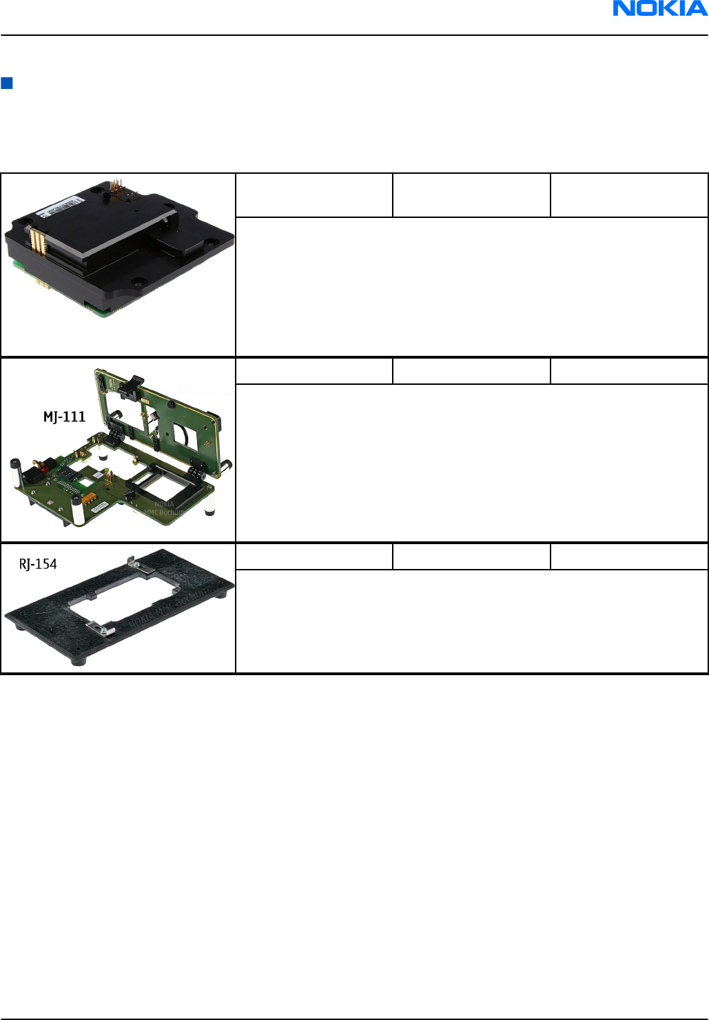
Service tools
Product specific tools
The table below gives a short overview of service tools that can be used for testing, error analysis and repair
of product RM-188; RM-198, refer to various concepts.
FS-10 product specific
adapter
Flash adapter FS-10 is used for phone testing and flashing. FS-10 is
used with the generic flash adapter base and control Unit CU-4 or
interface adapter.
When flashing or system testing the phone, the adapter is attached to
replace the phone own battery. All functions (as well as the calibration
voltages, current and the protections for over voltages, over current
and voltage polarity), are performed by CU-4.
MJ-111 Module jig
MJ-111 is meant for component level troubleshooting.
RJ-154 Soldering jig
RJ-154 is used as a soldering jig for the engine module.
RM-188; RM-198
Service Tools and Service Concepts Nokia Customer Care
Issue 2 COMPANY CONFIDENTIAL Page 4 –5
Copyright © 2007 Nokia. All rights reserved.
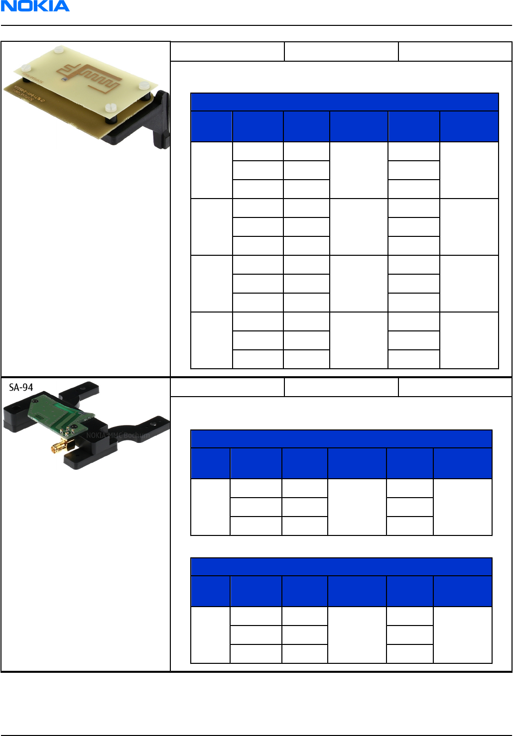
SA-87 RF coupler
SA-87 is a coupler for GSM RF testing. It is used together with FS-10
flash adapter.
•Attenuation values for inductive RF coupler SA-87
Band Channel Att. RX Tolerance
RX Att. TX Tolerance
TX
GSM
850
Low 4,8
+/-2dB
5,4
+/-2dBMid 5,0 5,0
High 5, 3 4,8
GSM
900
Low 5,0
+/-2dB
5,0
+/-2dBMid 5,3 5,5
High 5,8 6,2
GSM
1800
Low 10,3
+/-3dB
11,3
+/-3dBMid 9,3 11,5
High 9,3 10,8
GSM
1900
Low 10,0
+/-3dB
9,5
+/-3dBMid 9,5 9,8
High 9,5 9,5
SA-94 RF coupler
SA-94 is a coupler for Bluetooth and WLAN testing.
•Table 8 Attenuation values for inductive RF coupler SA-94 - fold open
Attenuation values for inductive RF coupler SA-94
Band Channel Att. RX Tolerance
RX Att. TX Tolerance
TX
WLA
N/ BT
Low 17,0
+/-3dB
17,0
+/-3dBMid 17,0 17,0
High 17,0 17,0
•Table 9 Attenuation values for inductive RF coupler SA-94 - fold closed
Attenuation values for inductive RF coupler SA-94
Band Channel Att. RX Tolerance
RX Att. TX Tolerance
TX
WLA
N/BT
Low 18,0
+/-3dB
18,0
+/-3dBMid 18,0 18,0
High 18,0 18,0
RM-188; RM-198
Nokia Customer Care Service Tools and Service Concepts
Page 4 –6 COMPANY CONFIDENTIAL Issue 2
Copyright © 2007 Nokia. All rights reserved.
SS-104 Domesheet and
display alignment jig
SS-104 is used for domesheet and display alignment.
General tools
The table below gives a short overview of service tools that can be used for testing, error analysis and repair
of product RM-188; RM-198, refer to various concepts.
ACP-8E Charger 0675195
Charger (for Europe)
Output: 5.3V DC, 500 mA.
RM-188; RM-198
Service Tools and Service Concepts Nokia Customer Care
Issue 2 COMPANY CONFIDENTIAL Page 4 –7
Copyright © 2007 Nokia. All rights reserved.
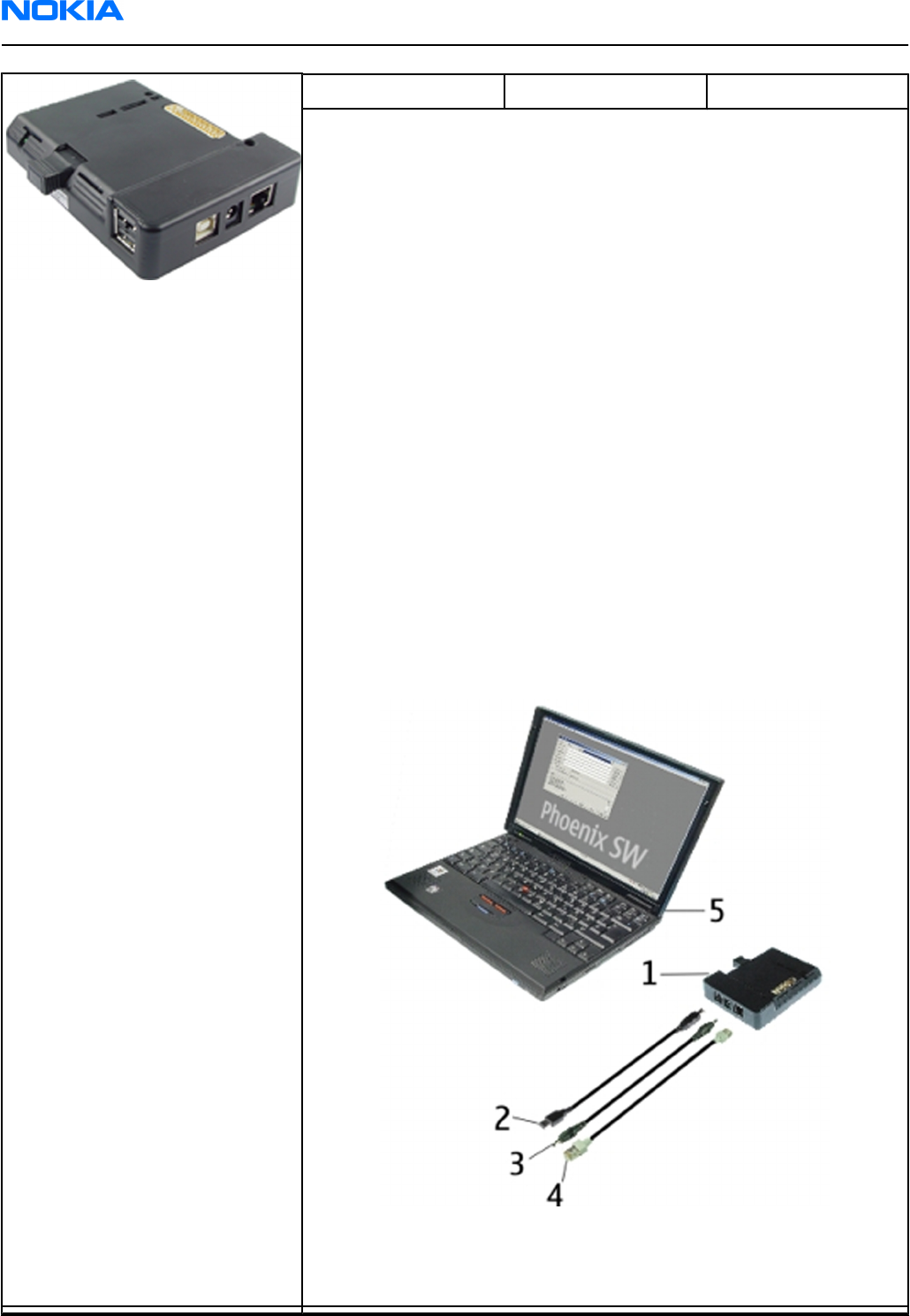
CU-4 Control unit
CU-4 is a general service tool used with a module jig and/or a flash
adapter. It requires an external 12 V power supply.
The unit has the following features:
• software controlled via USB
• EM calibration function
• Forwards FBUS/Flashbus traffic to/from terminal
• Forwards USB traffic to/from terminal
• software controlled BSI values
• regulated VBATT voltage
• 2 x USB2.0 connector (Hub)
• FBUS and USB connections supported
When using CU-4, note the special order of connecting cables and
other service equipment:
Instructions
1 Connect a service tool (jig, flash adapter) to CU-4.
2 Connect CU-4 to your PC with a USB cable.
3 Connect supply voltage (12 V)
4 Connect an FBUS cable (if necessary).
5 Start Phoenix service software.
Note: Phoenix enables CU-4 regulators via USB when it is
started.
Reconnecting the power supply requires a Phoenix restart.
RM-188; RM-198
Nokia Customer Care Service Tools and Service Concepts
Page 4 –8 COMPANY CONFIDENTIAL Issue 2
Copyright © 2007 Nokia. All rights reserved.
FLS-4S Flash device
FLS-4S is a dongle and flash device incorporated into one package,
developed specifically for POS use.
FPS-10 Flash prommer
FPS-10 interfaces with:
• PC
• Control unit
• Flash adapter
• Smart card
FPS-10 flash prommer features:
• Flash functionality for BB5 and DCT-4 terminals
• Smart Card reader for SX-2 or SX-4
• USB traffic forwarding
• USB to FBUS/Flashbus conversion
• LAN to FBUS/Flashbus and USB conversion
• Vusb output switchable by PC command
FPS-10 sales package includes:
• FPS-10 prommer
• Power Supply with 5 country specific cords
• USB cable
PKD-1 SW security device
SW security device is a piece of hardware enabling the use of the
service software when connected to the parallel (LPT) port of the PC.
Without the device, it is not possible to use the service software.
Printer or any such device can be connected to the PC through the
device if needed.
SS-46 Interface adapter
SS-46 acts as an interface adapter between the flash adapter and
FPS-10.
RM-188; RM-198
Service Tools and Service Concepts Nokia Customer Care
Issue 2 COMPANY CONFIDENTIAL Page 4 –9
Copyright © 2007 Nokia. All rights reserved.
SS-62 Flash adapter base
Generic base for flash adapters and couplers.
SS-88 Camera removal tool
The camera removal tool SS-88 is used to remove/attach the front
camera module from/to the socket.
SX-4 Smart card
SX-4 is a BB5 security device used to protect critical features in tuning
and testing.
SX-4 is also needed together with FPS-10 when DCT-4 phones are
flashed.
Cables
The table below gives a short overview of service tools that can be used for testing, error analysis and repair
of product RM-188; RM-198, refer to various concepts.
CA-35S Power cable
CA-35S is a power cable for connecting, for example, the FPS-10 flash
prommer to the Point-Of-Sales (POS) flash adapter.
RM-188; RM-198
Nokia Customer Care Service Tools and Service Concepts
Page 4 –10 COMPANY CONFIDENTIAL Issue 2
Copyright © 2007 Nokia. All rights reserved.
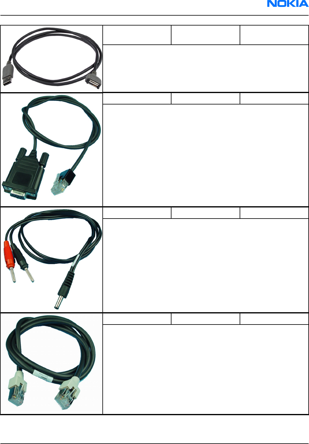
CA-53 USB connectivity
cable
USB to system connector cable.
DAU-9S MBUS cable
The MBUS cable DAU-9S has a modular connector and is used, for
example, between the PC's serial port and module jigs, flash adapters
or docking station adapters.
Note: Docking station adapters valid for DCT4 products.
PCS-1 Power cable
The PCS-1 power cable (DC) is used with a docking station, a module
jig or a control unit to supply a controlled operating voltage.
XCS-4 Modular cable
XCS-4 is a shielded (one specially shielded conductor) modular cable
for flashing and service purposes.
RM-188; RM-198
Service Tools and Service Concepts Nokia Customer Care
Issue 2 COMPANY CONFIDENTIAL Page 4 –11
Copyright © 2007 Nokia. All rights reserved.
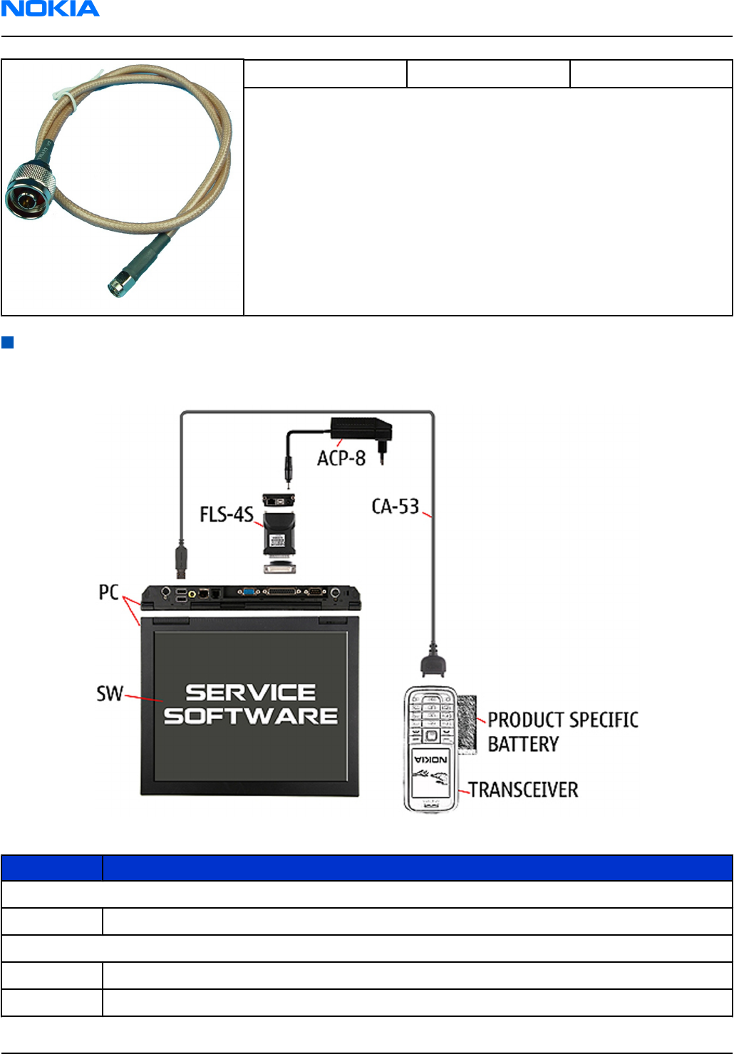
XRS-6 RF cable
The RF cable is used to connect, for example, a module repair jig to
the RF measurement equipment.
SMA to N-Connector approximately 610 mm.
Attenuation for:
• GSM850/900: 0.3+-0.1 dB
• GSM1800/1900: 0.5+-0.1 dB
• WLAN: 0.6+-0.1dB
Service concepts
POS (Point of Sale) flash concept
Figure 27 POS flash concept
Type Description
Product specific tools
BL-5C Battery
Other tools
ACP-8 Power adapter
FLS-4S POS flash dongle
RM-188; RM-198
Nokia Customer Care Service Tools and Service Concepts
Page 4 –12 COMPANY CONFIDENTIAL Issue 2
Copyright © 2007 Nokia. All rights reserved.
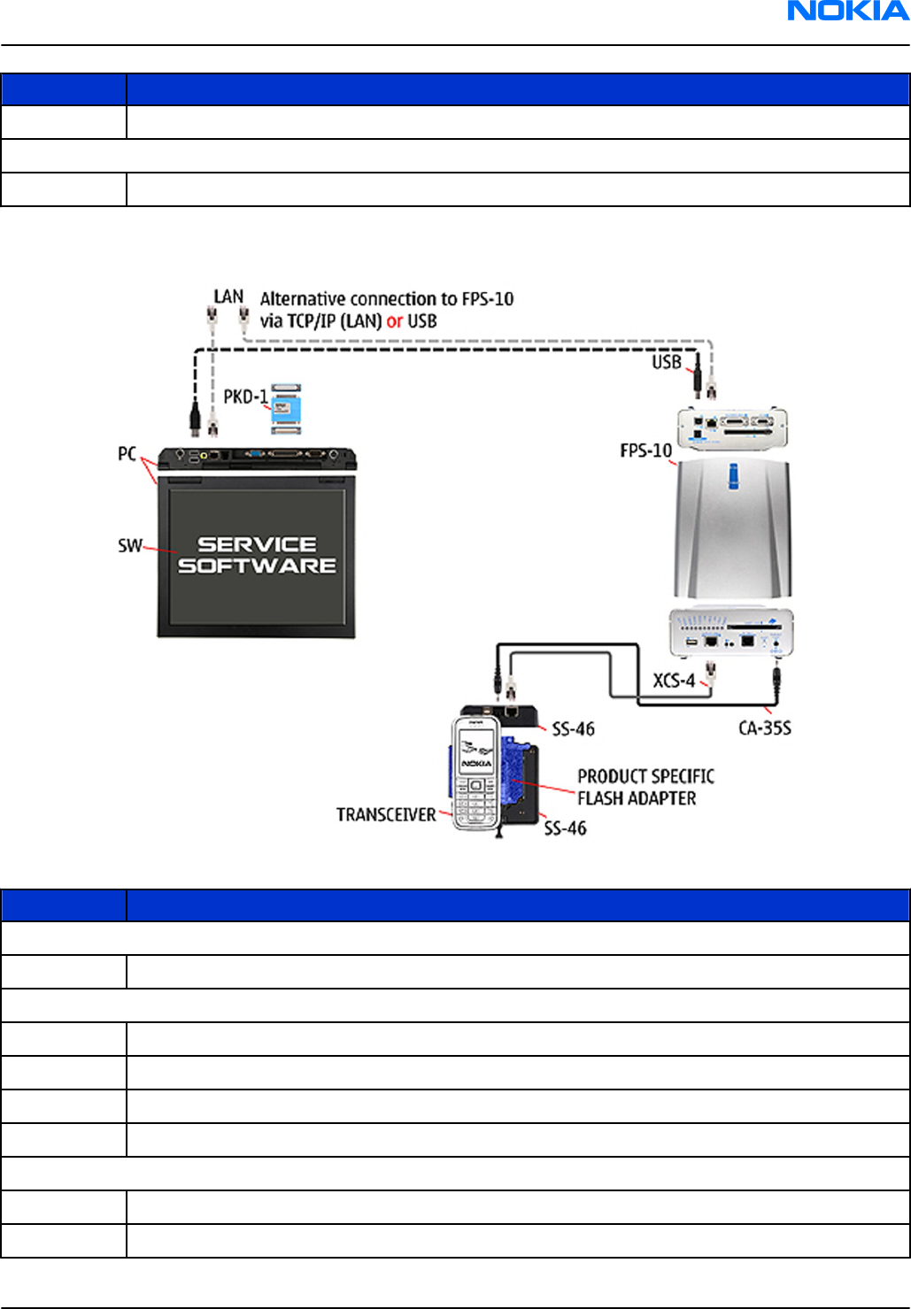
Type Description
PC with Phoenix service software
Cables
CA-53 USB connectivity cable
Flash concept with FPS-10
Figure 28 Basic flash concept with FPS-10
Type Description
Product specific tools
FS-10 Flash adapter
Other tools
FPS-10 Flash prommer box
PKD-1/PK-1 SW security device
SS-46 Interface adapter
PC with Phoenix service software
Cables
XCS-4 Modular cable
CA-35S Power cable
RM-188; RM-198
Service Tools and Service Concepts Nokia Customer Care
Issue 2 COMPANY CONFIDENTIAL Page 4 –13
Copyright © 2007 Nokia. All rights reserved.
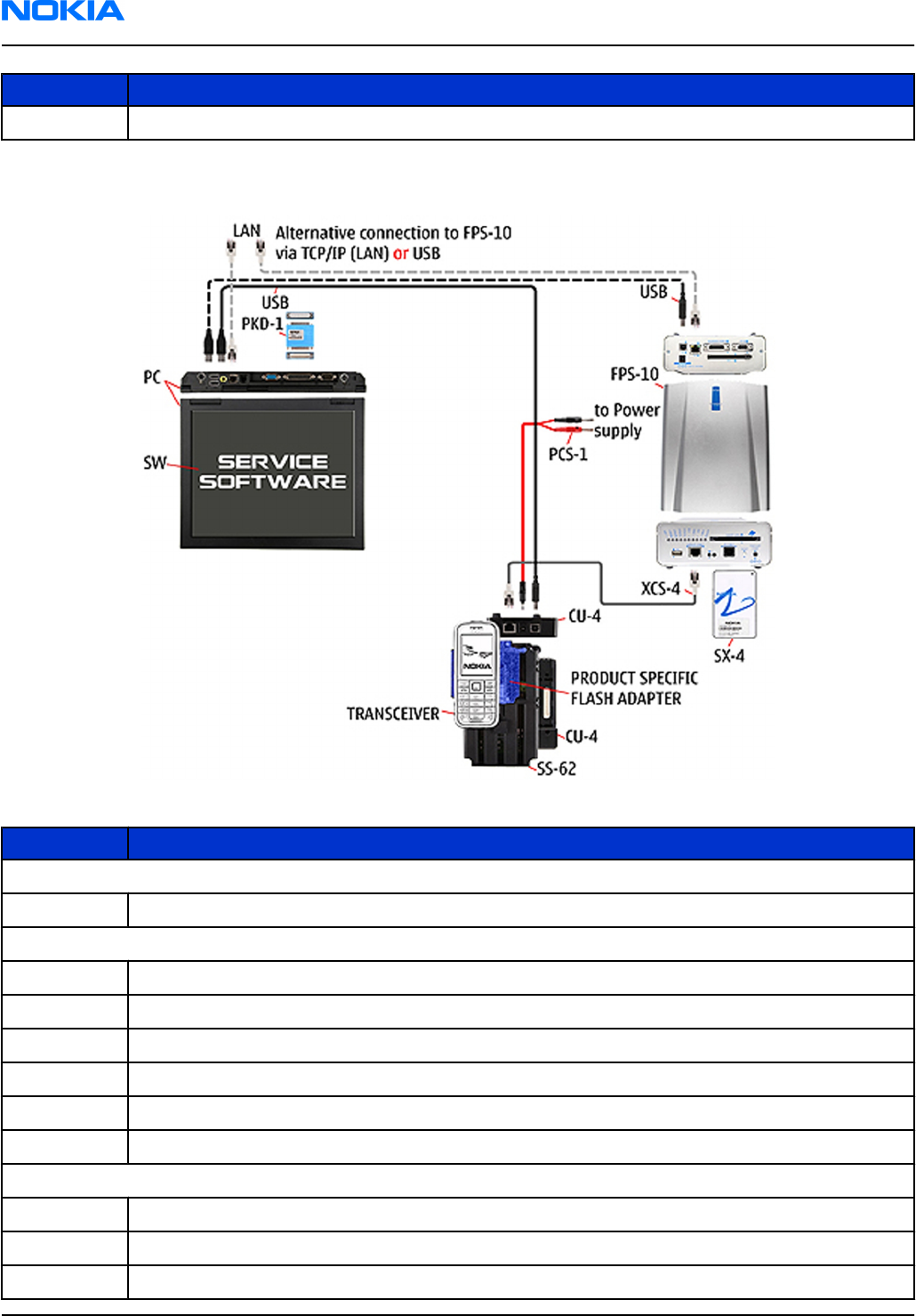
Type Description
USB cable
CU-4 flash concept with FPS-10
Figure 29 CU-4 flash concept with FPS-10
Type Description
Product specific tools
FS-10 Flash adapter
Other tools
CU-4 Control unit
FPS-10 Flash prommer box
PKD-1/PK-1 SW security device
SS-62 Flash adapter base
SX-4 Smart card
PC with Phoenix service software
Cables
PCS-1 Power cable
XCS-4 Modular cable
Standard USB cable
RM-188; RM-198
Nokia Customer Care Service Tools and Service Concepts
Page 4 –14 COMPANY CONFIDENTIAL Issue 2
Copyright © 2007 Nokia. All rights reserved.
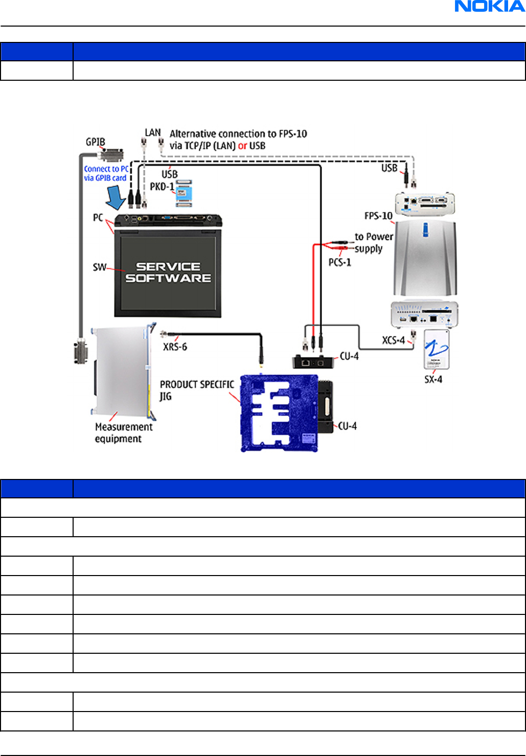
Type Description
USB cable
Module jig service concept
Figure 30 Module jig service concept
Type Description
Phone specific tools
MJ-111 Module jig
Other tools
CU-4 Control unit
FPS-10 Flash prommer box
PKD-1/PK-1 SW security device
SX-4 Smart card
PC with Phoenix service software
Measurement equipment
Cables
PCS-1 DC power cable
XCS-4 Modular cable
RM-188; RM-198
Service Tools and Service Concepts Nokia Customer Care
Issue 2 COMPANY CONFIDENTIAL Page 4 –15
Copyright © 2007 Nokia. All rights reserved.
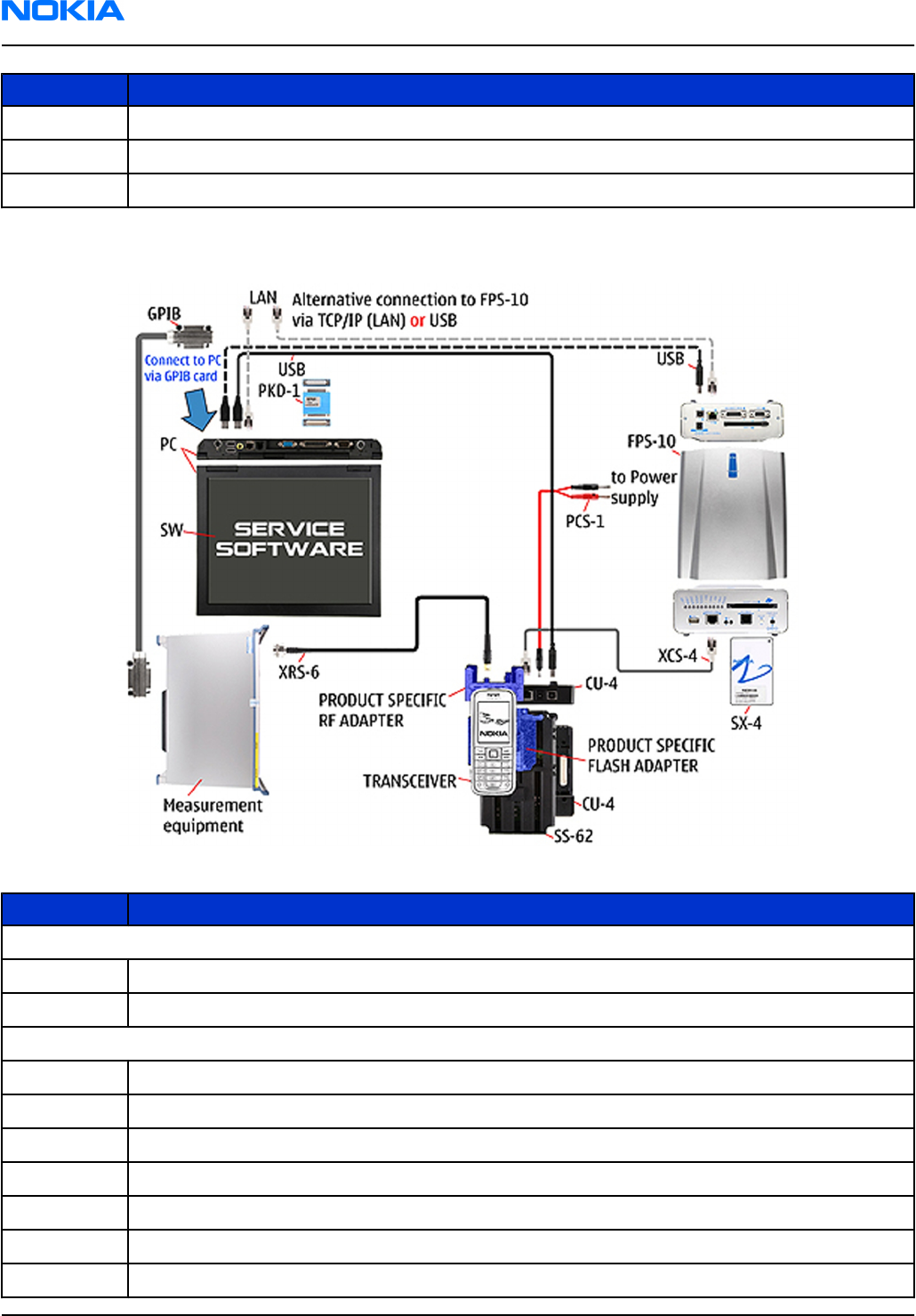
Type Description
XRS-6 RF cable
USB cable
GPIB control cable
RF testing concept with RF coupler
Figure 31 RF testing concept with RF coupler
Type Description
Product specific tools
FS-10 Flash adapter
SA-87 RF coupler
Other tools
CU-4 Control unit
SX-4 Smart card
FPS-10 Flash prommer box
PKD-1/PK-1 SW security device
SS-62 Flash adapter base
Measurement equipment
PC with Phoenix service software
RM-188; RM-198
Nokia Customer Care Service Tools and Service Concepts
Page 4 –16 COMPANY CONFIDENTIAL Issue 2
Copyright © 2007 Nokia. All rights reserved.
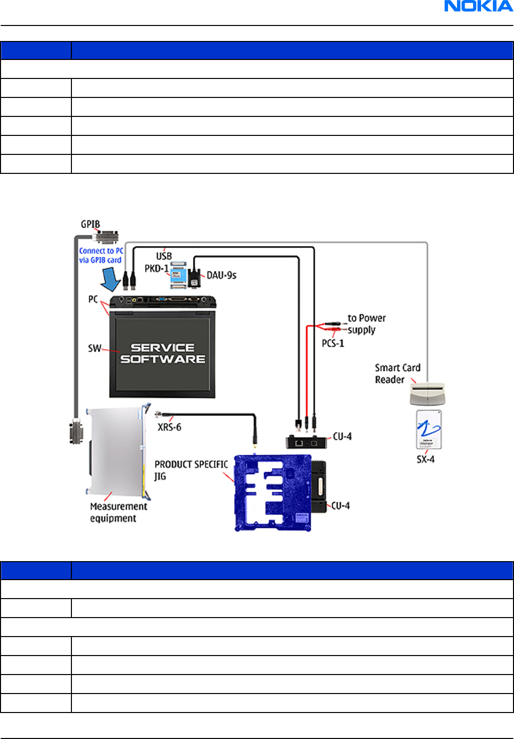
Type Description
Cables
PCS-1 Power cable
XCS-4 Modular cable
XRS-6 RF cable
GPIB control cable
USB cable
Service concept for RF testing and RF/BB tuning
Figure 32 Service concept for RF testing and RF/BB tuning
Type Description
Product specific tools
MJ-111 Module jig
Other tools
CU-4 Control unit
PKD-1/PK-1 SW security device
SX-4 Smart card
Measurement equipment
RM-188; RM-198
Service Tools and Service Concepts Nokia Customer Care
Issue 2 COMPANY CONFIDENTIAL Page 4 –17
Copyright © 2007 Nokia. All rights reserved.

Type Description
Smart card reader
PC with Phoenix service software
Cables
DAU-9s MBUS cable
PCS-1 DC power cable
XRS-6 RF cable
GPIB control cable
USB cable
RM-188; RM-198
Nokia Customer Care Service Tools and Service Concepts
Page 4 –18 COMPANY CONFIDENTIAL Issue 2
Copyright © 2007 Nokia. All rights reserved.

5 — Disassembly / Reassembly
Instructions
Nokia Customer Care
Issue 2 COMPANY CONFIDENTIAL Page 5 –1
Copyright © 2007 Nokia. All rights reserved.

RM-188; RM-198
Nokia Customer Care Disassembly / Reassembly Instructions
(This page left intentionally blank.)
Page 5 –2 COMPANY CONFIDENTIAL Issue 2
Copyright © 2007 Nokia. All rights reserved.

Table of Contents
Upper block disassembly.......................................................................................................................................5–5
Upper block assembly......................................................................................................................................... 5–10
Lower block disassembly.................................................................................................................................... 5–18
Lower block assembly......................................................................................................................................... 5–22
RM-188; RM-198
Disassembly / Reassembly Instructions Nokia Customer Care
Issue 2 COMPANY CONFIDENTIAL Page 5 –3
Copyright © 2007 Nokia. All rights reserved.

RM-188; RM-198
Nokia Customer Care Disassembly / Reassembly Instructions
(This page left intentionally blank.)
Page 5 –4 COMPANY CONFIDENTIAL Issue 2
Copyright © 2007 Nokia. All rights reserved.
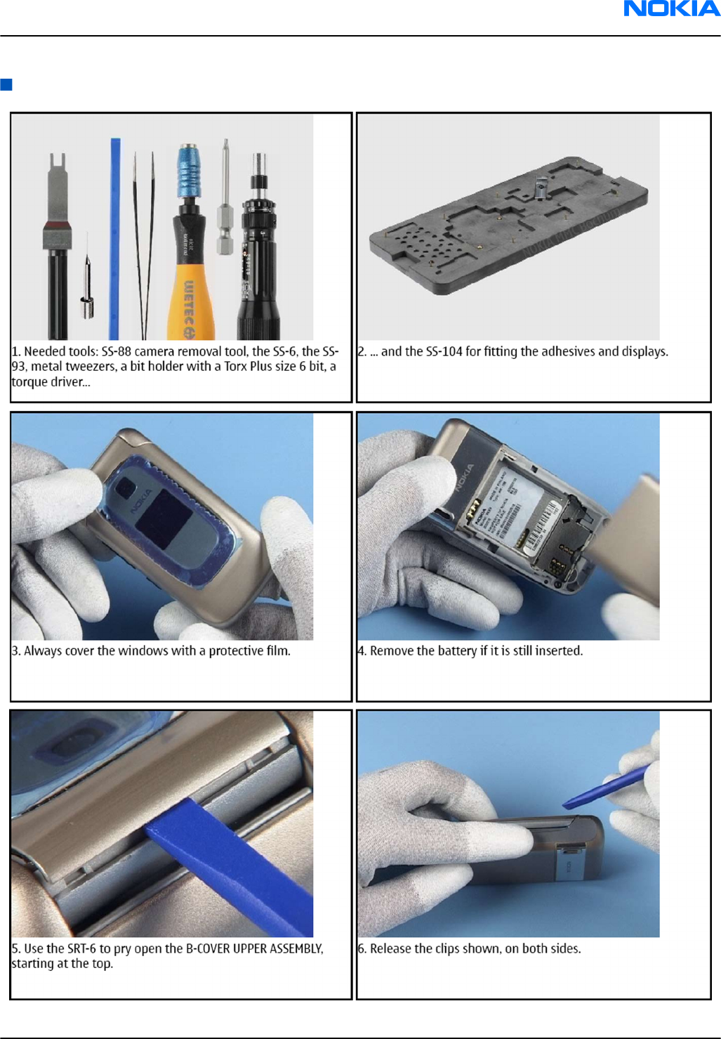
Upper block disassembly
RM-188; RM-198
Disassembly / Reassembly Instructions Nokia Customer Care
Issue 2 COMPANY CONFIDENTIAL Page 5 –5
Copyright © 2007 Nokia. All rights reserved.
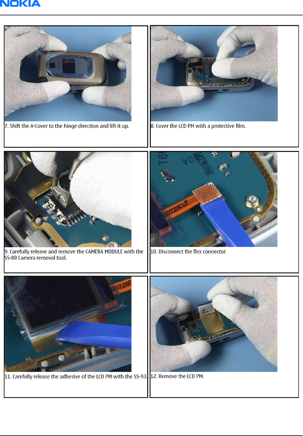
RM-188; RM-198
Nokia Customer Care Disassembly / Reassembly Instructions
Page 5 –6 COMPANY CONFIDENTIAL Issue 2
Copyright © 2007 Nokia. All rights reserved.
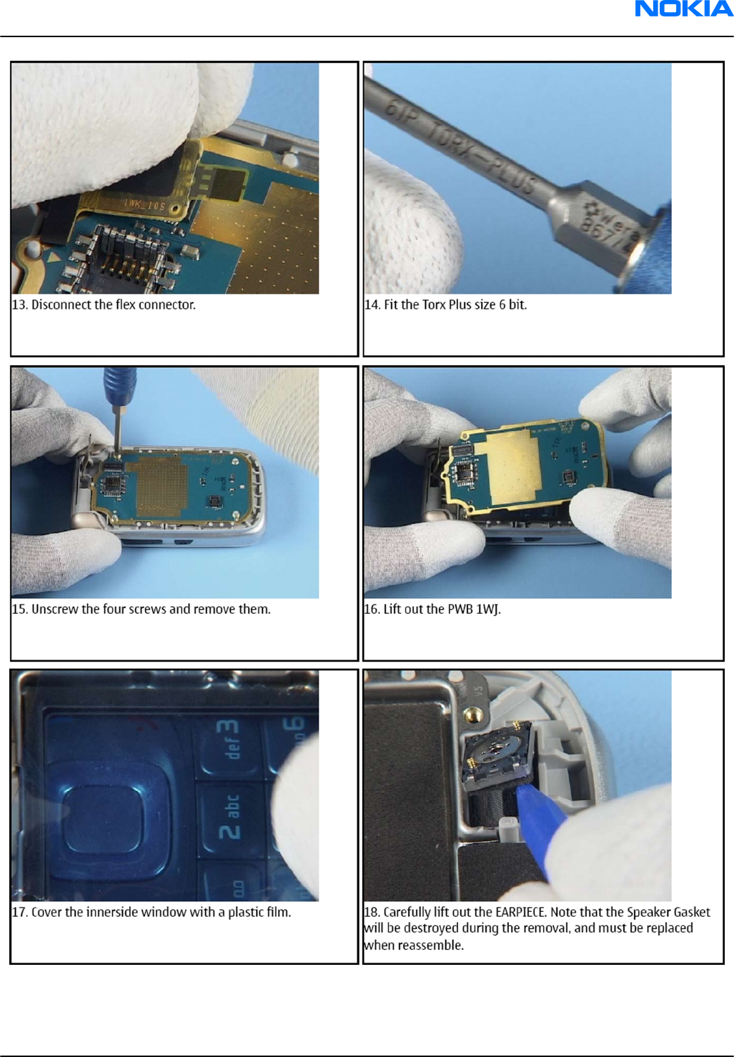
RM-188; RM-198
Disassembly / Reassembly Instructions Nokia Customer Care
Issue 2 COMPANY CONFIDENTIAL Page 5 –7
Copyright © 2007 Nokia. All rights reserved.
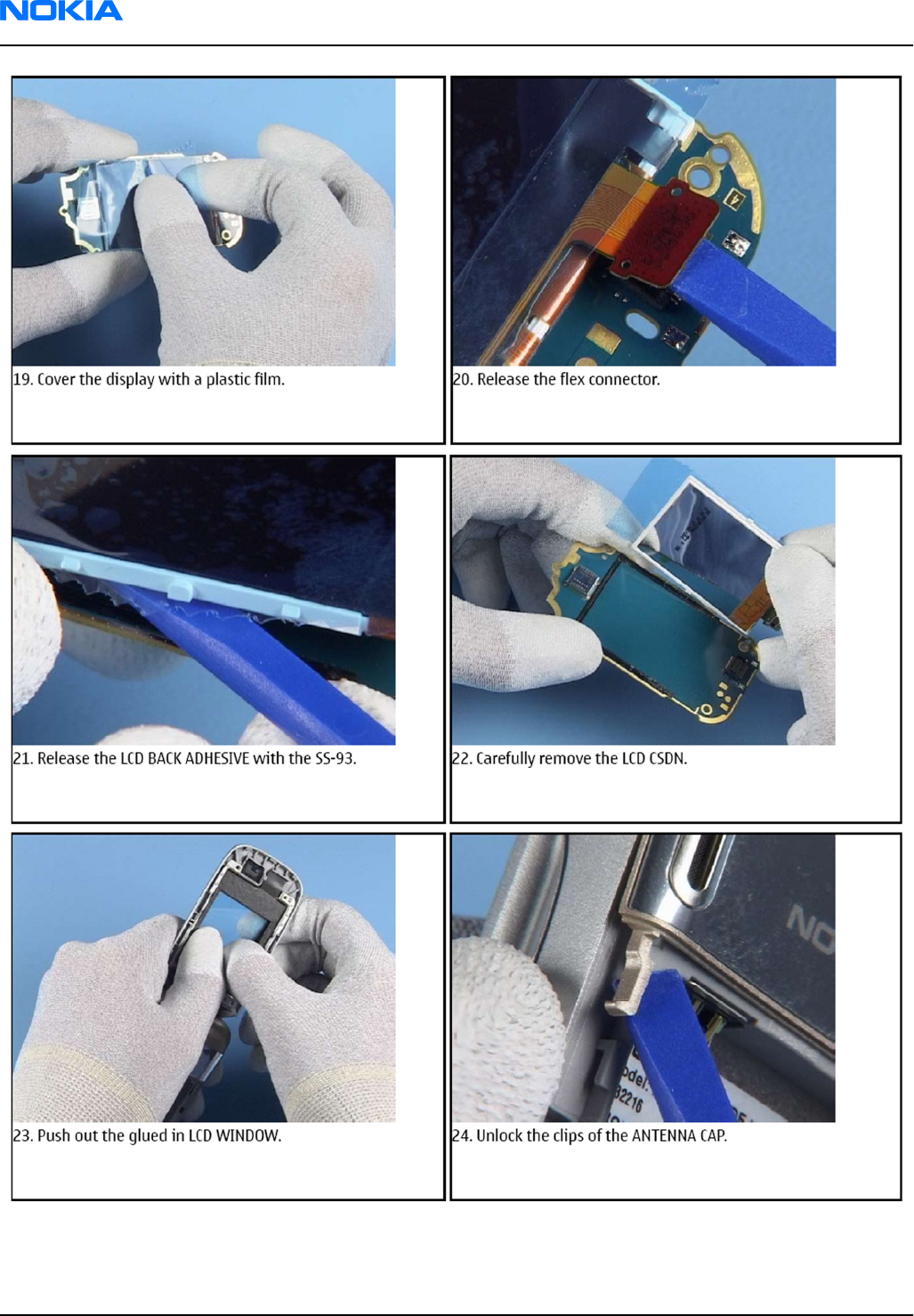
RM-188; RM-198
Nokia Customer Care Disassembly / Reassembly Instructions
Page 5 –8 COMPANY CONFIDENTIAL Issue 2
Copyright © 2007 Nokia. All rights reserved.
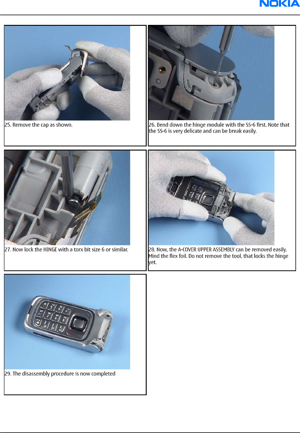
RM-188; RM-198
Disassembly / Reassembly Instructions Nokia Customer Care
Issue 2 COMPANY CONFIDENTIAL Page 5 –9
Copyright © 2007 Nokia. All rights reserved.
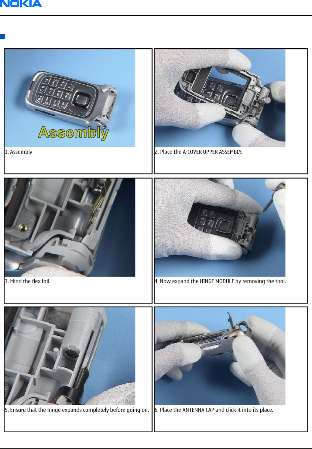
Upper block assembly
RM-188; RM-198
Nokia Customer Care Disassembly / Reassembly Instructions
Page 5 –10 COMPANY CONFIDENTIAL Issue 2
Copyright © 2007 Nokia. All rights reserved.
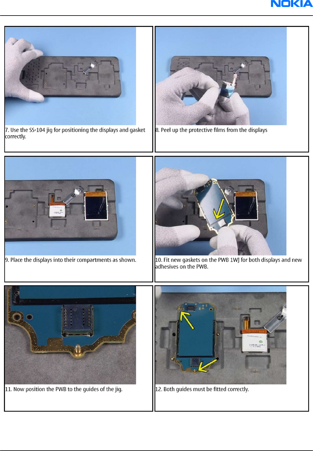
RM-188; RM-198
Disassembly / Reassembly Instructions Nokia Customer Care
Issue 2 COMPANY CONFIDENTIAL Page 5 –11
Copyright © 2007 Nokia. All rights reserved.
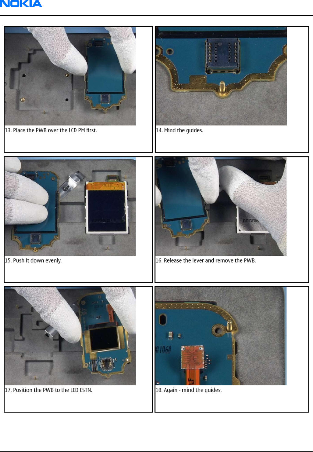
RM-188; RM-198
Nokia Customer Care Disassembly / Reassembly Instructions
Page 5 –12 COMPANY CONFIDENTIAL Issue 2
Copyright © 2007 Nokia. All rights reserved.
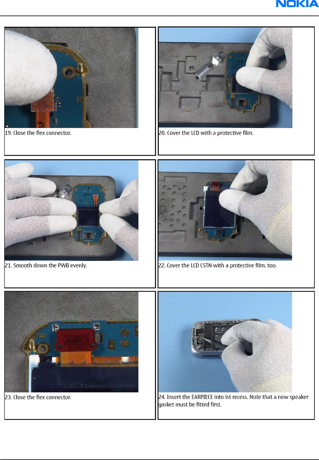
RM-188; RM-198
Disassembly / Reassembly Instructions Nokia Customer Care
Issue 2 COMPANY CONFIDENTIAL Page 5 –13
Copyright © 2007 Nokia. All rights reserved.
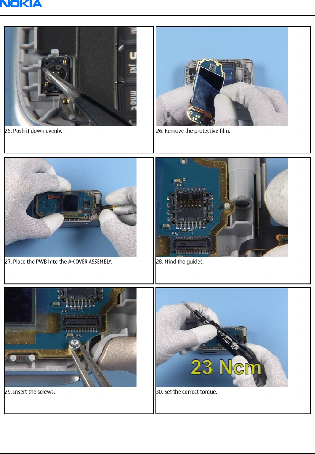
RM-188; RM-198
Nokia Customer Care Disassembly / Reassembly Instructions
Page 5 –14 COMPANY CONFIDENTIAL Issue 2
Copyright © 2007 Nokia. All rights reserved.
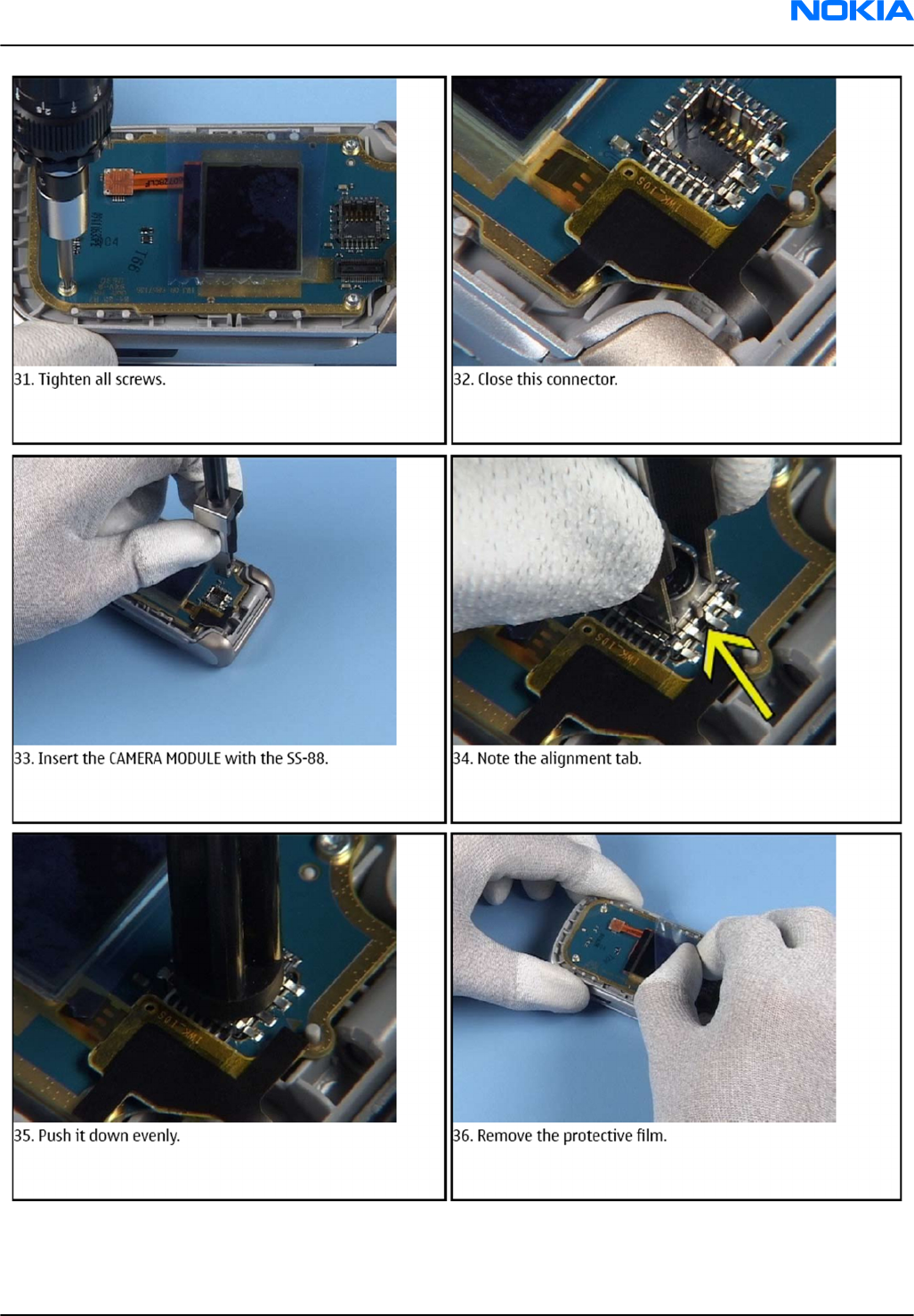
RM-188; RM-198
Disassembly / Reassembly Instructions Nokia Customer Care
Issue 2 COMPANY CONFIDENTIAL Page 5 –15
Copyright © 2007 Nokia. All rights reserved.
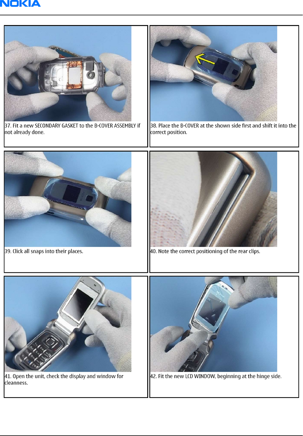
RM-188; RM-198
Nokia Customer Care Disassembly / Reassembly Instructions
Page 5 –16 COMPANY CONFIDENTIAL Issue 2
Copyright © 2007 Nokia. All rights reserved.
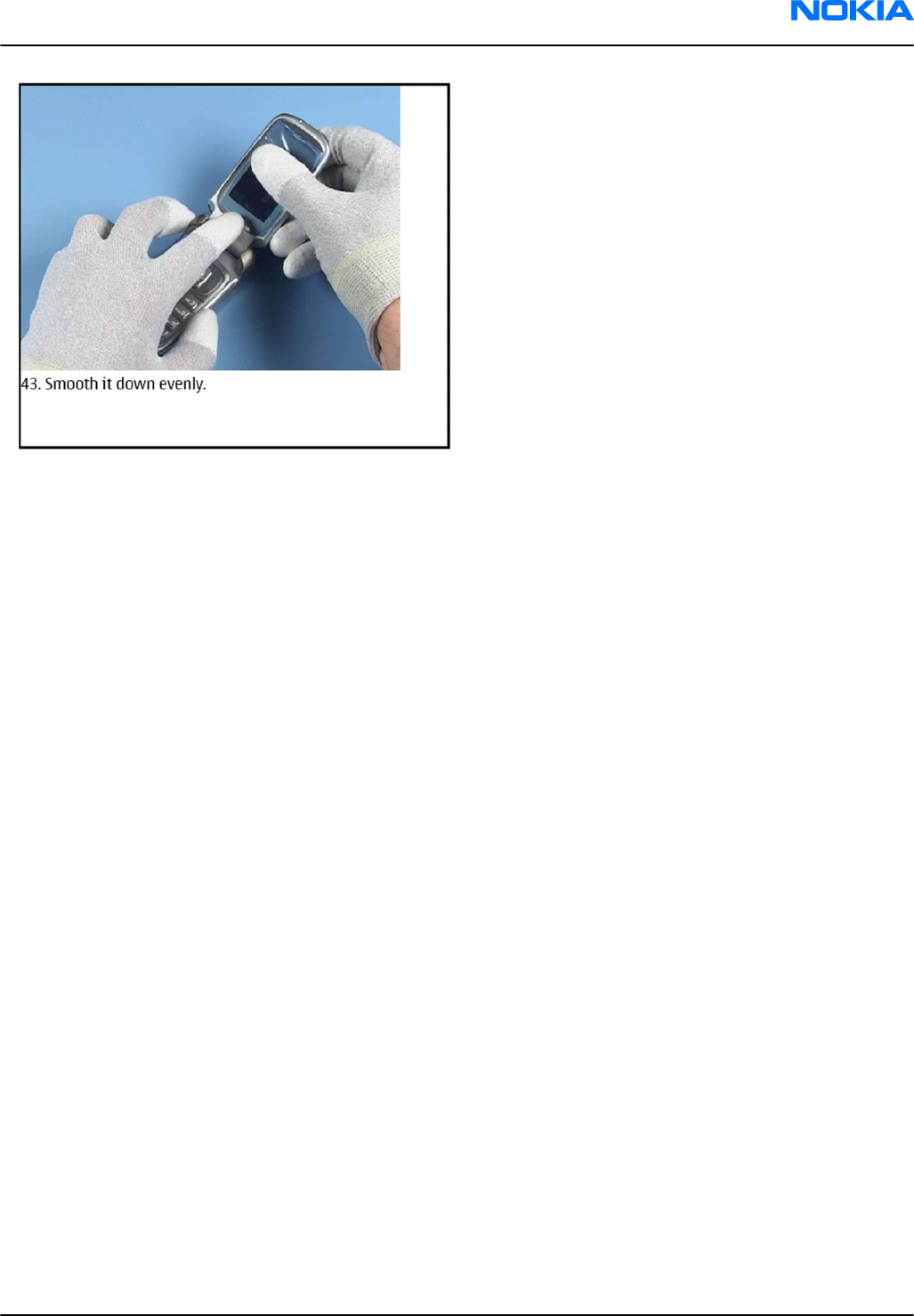
RM-188; RM-198
Disassembly / Reassembly Instructions Nokia Customer Care
Issue 2 COMPANY CONFIDENTIAL Page 5 –17
Copyright © 2007 Nokia. All rights reserved.
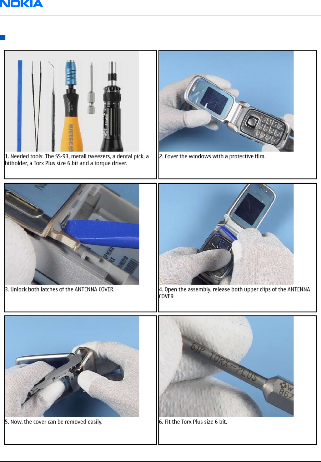
Lower block disassembly
RM-188; RM-198
Nokia Customer Care Disassembly / Reassembly Instructions
Page 5 –18 COMPANY CONFIDENTIAL Issue 2
Copyright © 2007 Nokia. All rights reserved.
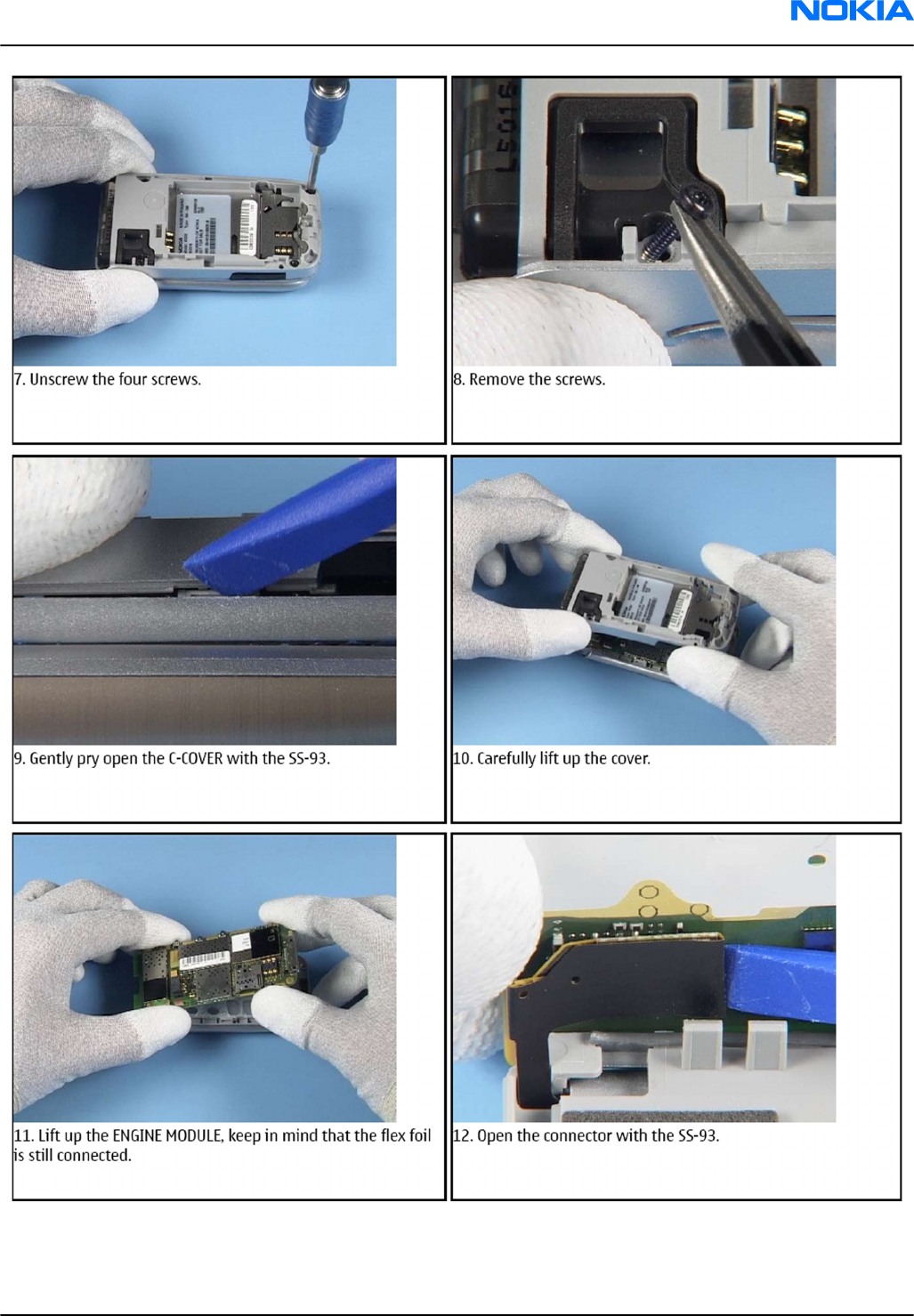
RM-188; RM-198
Disassembly / Reassembly Instructions Nokia Customer Care
Issue 2 COMPANY CONFIDENTIAL Page 5 –19
Copyright © 2007 Nokia. All rights reserved.
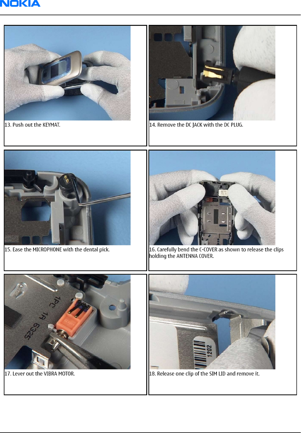
RM-188; RM-198
Nokia Customer Care Disassembly / Reassembly Instructions
Page 5 –20 COMPANY CONFIDENTIAL Issue 2
Copyright © 2007 Nokia. All rights reserved.
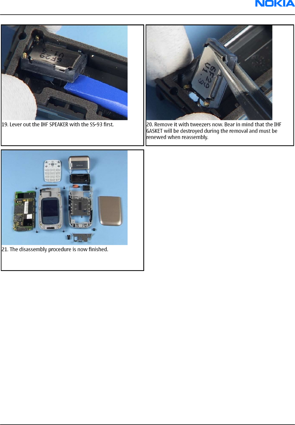
RM-188; RM-198
Disassembly / Reassembly Instructions Nokia Customer Care
Issue 2 COMPANY CONFIDENTIAL Page 5 –21
Copyright © 2007 Nokia. All rights reserved.
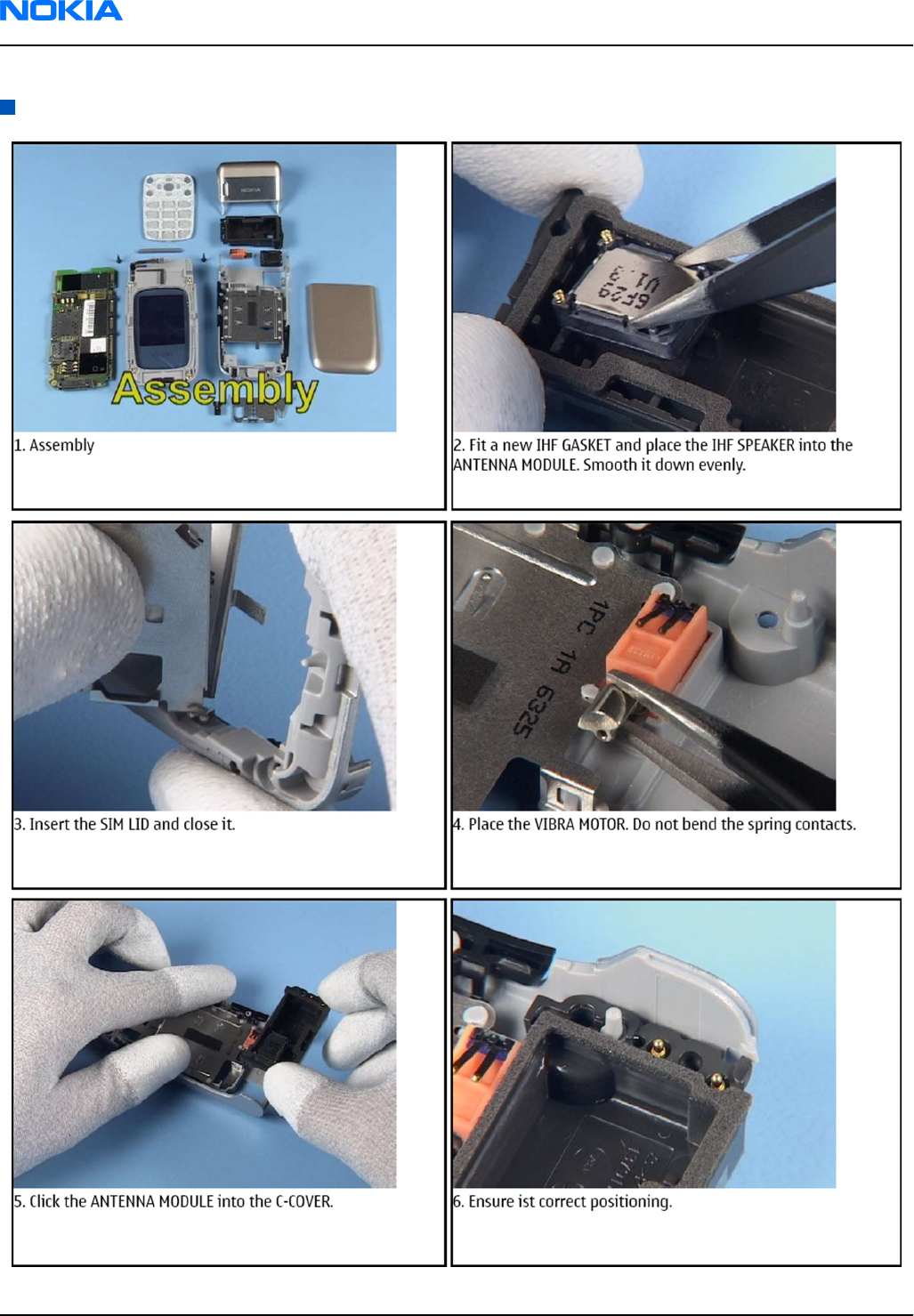
Lower block assembly
RM-188; RM-198
Nokia Customer Care Disassembly / Reassembly Instructions
Page 5 –22 COMPANY CONFIDENTIAL Issue 2
Copyright © 2007 Nokia. All rights reserved.
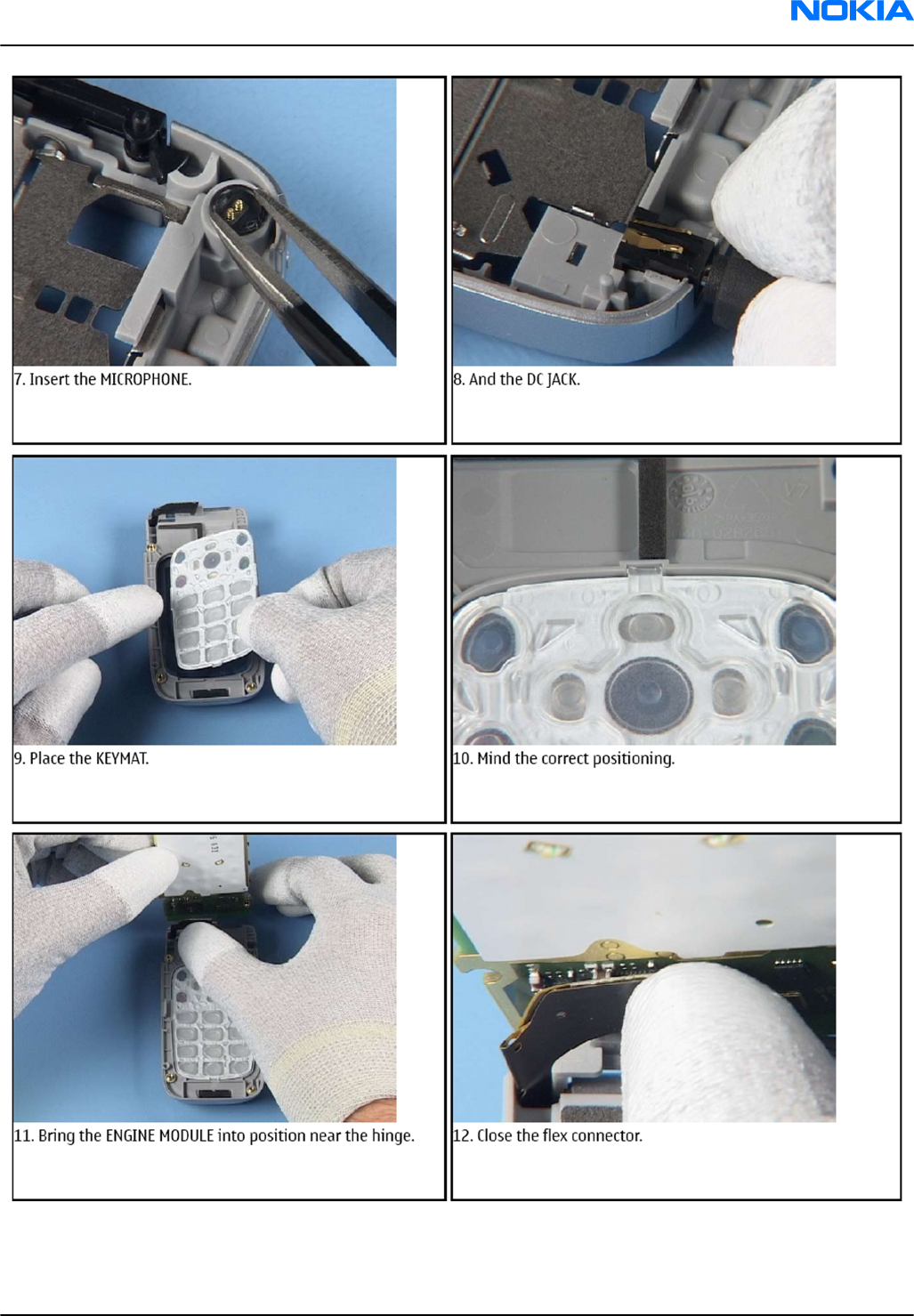
RM-188; RM-198
Disassembly / Reassembly Instructions Nokia Customer Care
Issue 2 COMPANY CONFIDENTIAL Page 5 –23
Copyright © 2007 Nokia. All rights reserved.
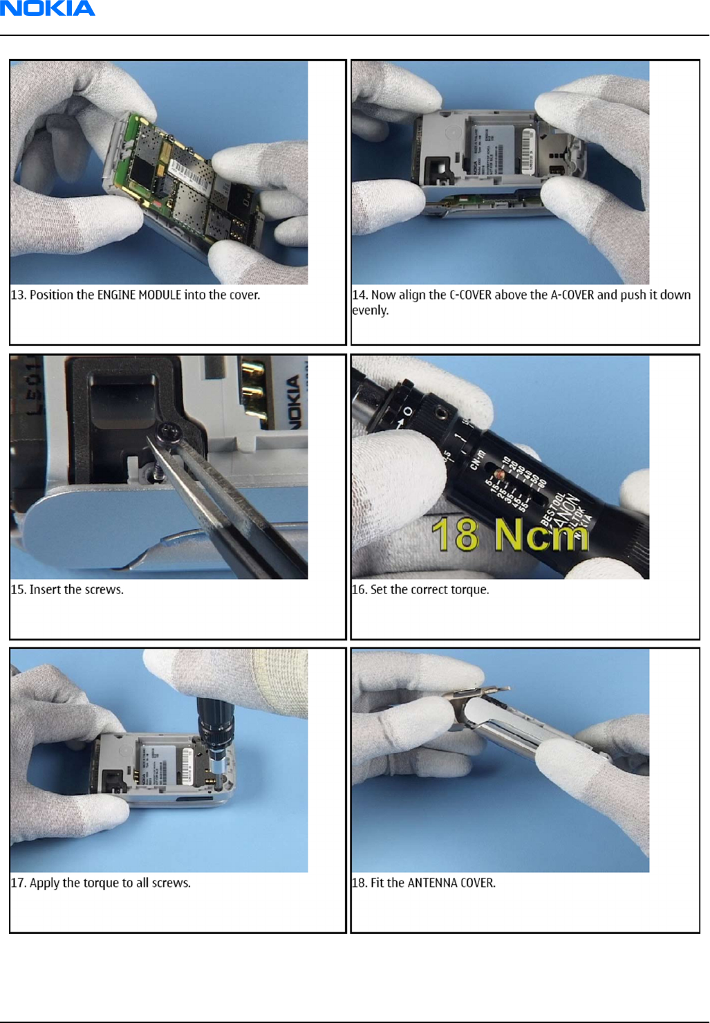
RM-188; RM-198
Nokia Customer Care Disassembly / Reassembly Instructions
Page 5 –24 COMPANY CONFIDENTIAL Issue 2
Copyright © 2007 Nokia. All rights reserved.
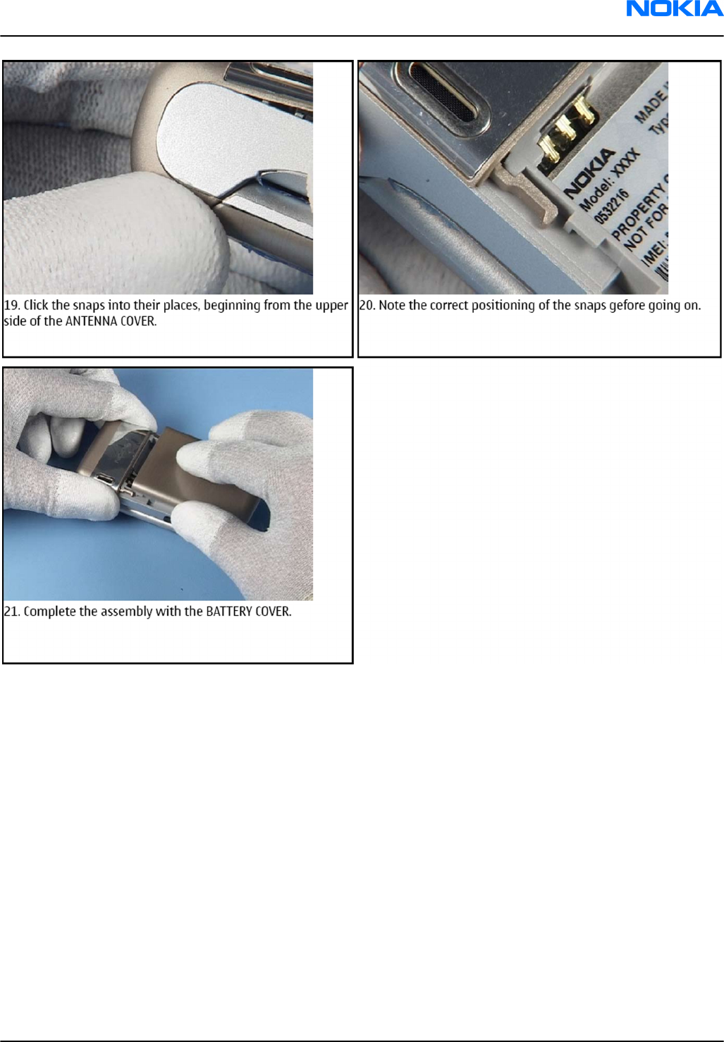
RM-188; RM-198
Disassembly / Reassembly Instructions Nokia Customer Care
Issue 2 COMPANY CONFIDENTIAL Page 5 –25
Copyright © 2007 Nokia. All rights reserved.

RM-188; RM-198
Nokia Customer Care Disassembly / Reassembly Instructions
(This page left intentionally blank.)
Page 5 –26 COMPANY CONFIDENTIAL Issue 2
Copyright © 2007 Nokia. All rights reserved.

6 — BB Troubleshooting and
Manual Tuning Guide
Nokia Customer Care
Issue 2 COMPANY CONFIDENTIAL Page 6 –1
Copyright © 2007 Nokia. All rights reserved.

RM-188; RM-198
Nokia Customer Care BB Troubleshooting and Manual Tuning Guide
(This page left intentionally blank.)
Page 6 –2 COMPANY CONFIDENTIAL Issue 2
Copyright © 2007 Nokia. All rights reserved.

Table of Contents
Baseband troubleshooting....................................................................................................................................6–5
General power checking troubleshooting ...........................................................................................................6–7
Clocking troubleshooting ......................................................................................................................................6–8
Battery current measuring fault troubleshooting ........................................................................................... 6–10
Flash programming fault troubleshooting....................................................................................................... 6–11
COMBO memory troubleshooting ...................................................................................................................... 6–12
Keyboard troubleshooting ................................................................................................................................. 6–12
USB troubleshooting ........................................................................................................................................... 6–14
Backup battery troubleshooting........................................................................................................................ 6–15
Charging troubleshooting .................................................................................................................................. 6–16
Dead or jammed troubleshooting..................................................................................................................... 6–17
MR sensor troubleshooting ................................................................................................................................ 6–18
Vibra troubleshooting......................................................................................................................................... 6–19
MicroSD troubleshooting.................................................................................................................................... 6–20
SIM troubleshooting............................................................................................................................................ 6–21
Display module troubleshooting ....................................................................................................................... 6–22
General instructions for display troubleshooting....................................................................................... 6–22
Display fault troubleshooting (main and second displays) ....................................................................... 6–24
Displays and keyboard backlight troubleshooting..................................................................................... 6–25
LED driver troubleshooting ........................................................................................................................... 6–26
Camera troubleshooting..................................................................................................................................... 6–28
Introduction to camera troubleshooting .................................................................................................... 6–28
Taking and evaluating test pictures............................................................................................................. 6–28
Camera hardware failure message troubleshooting.................................................................................. 6–29
Camera hardware troubleshooting.............................................................................................................. 6–30
Front camera viewfinder troubleshooting .................................................................................................. 6–31
Front camera bad image quality troubleshooting ..................................................................................... 6–32
Bluetooth troubleshooting................................................................................................................................. 6–33
Introduction to Bluetooth/FM Radio troubleshooting ............................................................................... 6–33
Bluetooth settings for Phoenix..................................................................................................................... 6–34
Bluetooth self tests in Phoenix..................................................................................................................... 6–35
Bluetooth BER failure troubleshooting........................................................................................................ 6–37
BT audio failure troubleshooting ................................................................................................................. 6–39
FM Radio troubleshooting............................................................................................................................. 6–40
Audio troubleshooting........................................................................................................................................ 6–41
Audio troubleshooting test instructions...................................................................................................... 6–41
Internal earpiece troubleshooting ............................................................................................................... 6–44
Internal microphone troubleshooting......................................................................................................... 6–44
IHF speaker troubleshooting......................................................................................................................... 6–46
External microphone troubleshooting......................................................................................................... 6–47
External earpiece troubleshooting............................................................................................................... 6–48
Introduction to acoustics troubleshooting ................................................................................................. 6–49
Earpiece troubleshooting.............................................................................................................................. 6–50
IHF troubleshooting....................................................................................................................................... 6–51
Microphone troubleshooting ........................................................................................................................ 6–52
Baseband manual tuning guide......................................................................................................................... 6–53
Energy management calibration.................................................................................................................. 6–53
List of Tables
RM-188; RM-198
BB Troubleshooting and Manual Tuning Guide Nokia Customer Care
Issue 2 COMPANY CONFIDENTIAL Page 6 –3
Copyright © 2007 Nokia. All rights reserved.

Table 10 Display module troubleshooting cases ............................................................................................. 6–22
Table 11 Pixel defects ......................................................................................................................................... 6–23
Table 12 Calibration value limits ....................................................................................................................... 6–53
List of Figures
Figure 33 SleepCLK .................................................................................................................................................6–9
Figure 34 SYSCLK.....................................................................................................................................................6–9
Figure 35 Flashing pic 1. Take single trig measurement for the rise of the BSI signal................................ 6–11
Figure 36 Flashing pic 2. Take single trig measurement for the rise of the BSI signal................................ 6–11
Figure 37 Charging backup battery ................................................................................................................... 6–15
Figure 38 Discharging backup battery .............................................................................................................. 6–15
Figure 39 RM-188 Bluetooth .............................................................................................................................. 6–33
Figure 40 RM-198 Bluetooth .............................................................................................................................. 6–34
Figure 41 RM-188/198 FM radio......................................................................................................................... 6–34
Figure 42 BER test result..................................................................................................................................... 6–35
Figure 43 Bluetooth self tests in Phoenix......................................................................................................... 6–36
Figure 44 Single-ended output waveform of the Ext_in_HP_out measurement when earpiece is
connected. ................................................................................................................................................. 6–43
Figure 45 Differential output waveform of the Ext_in_IHF_out out loop measurement when speaker is
connected. ................................................................................................................................................. 6–43
Figure 46 Single-ended output waveform of the HP_in_Ext_out loop when microphone is connected....
6–43
RM-188; RM-198
Nokia Customer Care BB Troubleshooting and Manual Tuning Guide
Page 6 –4 COMPANY CONFIDENTIAL Issue 2
Copyright © 2007 Nokia. All rights reserved.

Baseband troubleshooting
Context
This section is intended to be a guide for localising and repairing electrical faults. The fault repairing is divided
into troubleshooting paths.
The following main troubleshooting tree describes the different baseband troubleshooting paths to be
followed in fault situations.
RM-188; RM-198
BB Troubleshooting and Manual Tuning Guide Nokia Customer Care
Issue 2 COMPANY CONFIDENTIAL Page 6 –5
Copyright © 2007 Nokia. All rights reserved.
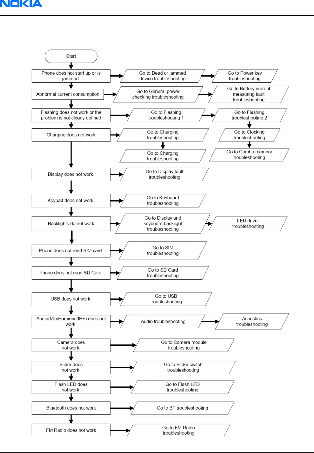
Troubleshooting flow
RM-188; RM-198
Nokia Customer Care BB Troubleshooting and Manual Tuning Guide
Page 6 –6 COMPANY CONFIDENTIAL Issue 2
Copyright © 2007 Nokia. All rights reserved.
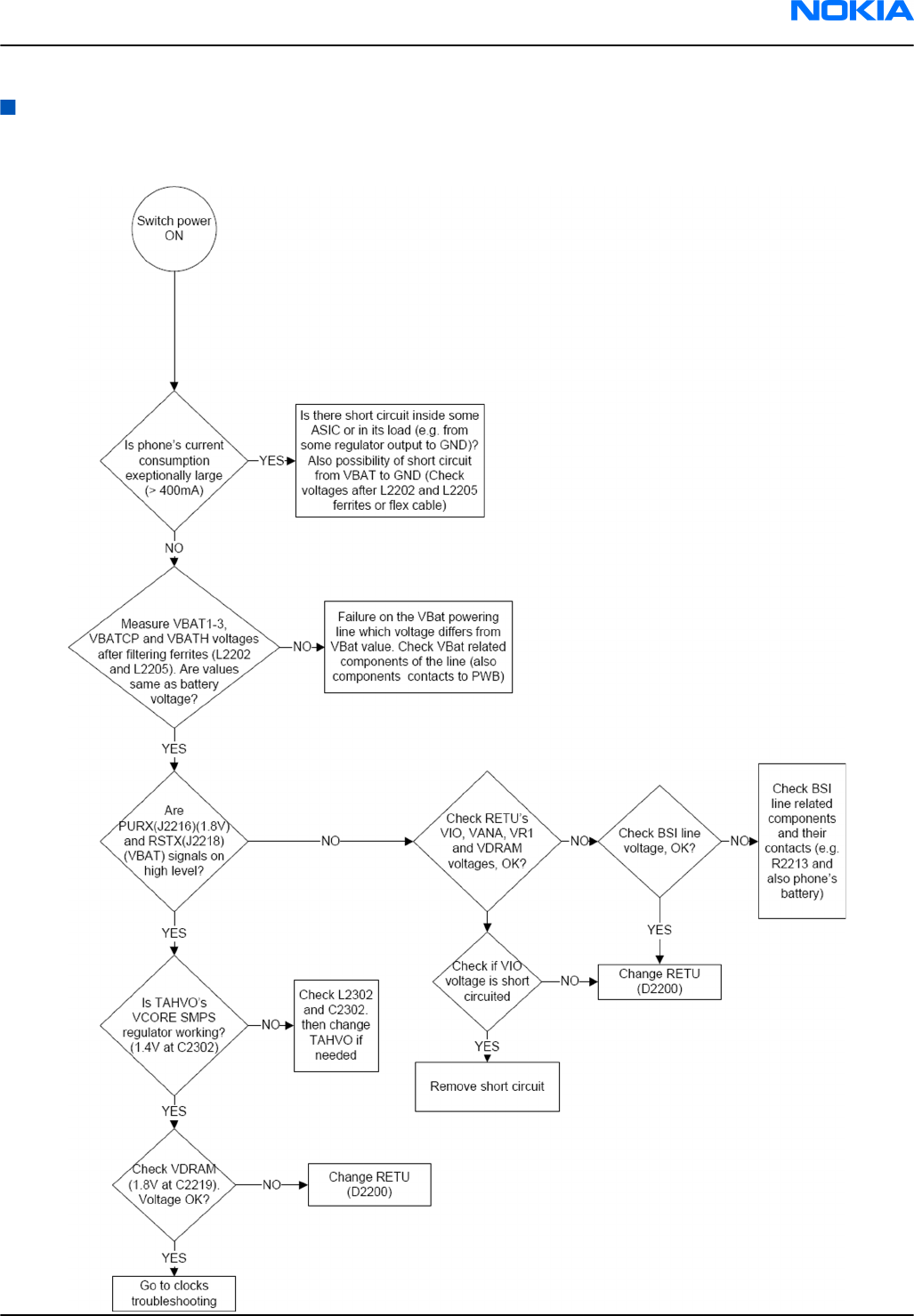
General power checking troubleshooting
Troubleshooting flow
RM-188; RM-198
BB Troubleshooting and Manual Tuning Guide Nokia Customer Care
Issue 2 COMPANY CONFIDENTIAL Page 6 –7
Copyright © 2007 Nokia. All rights reserved.
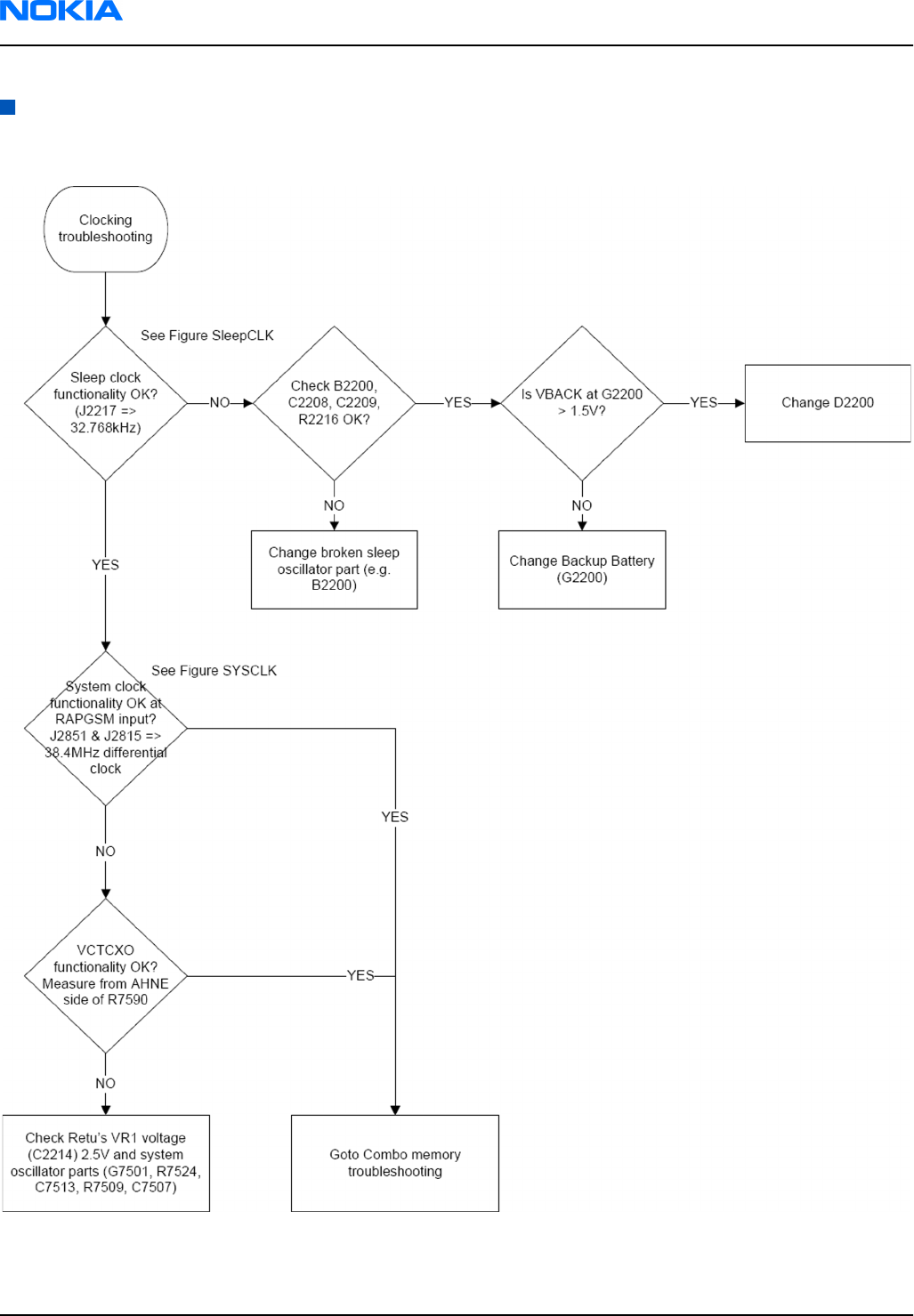
Clocking troubleshooting
Troubleshooting flow
RM-188; RM-198
Nokia Customer Care BB Troubleshooting and Manual Tuning Guide
Page 6 –8 COMPANY CONFIDENTIAL Issue 2
Copyright © 2007 Nokia. All rights reserved.
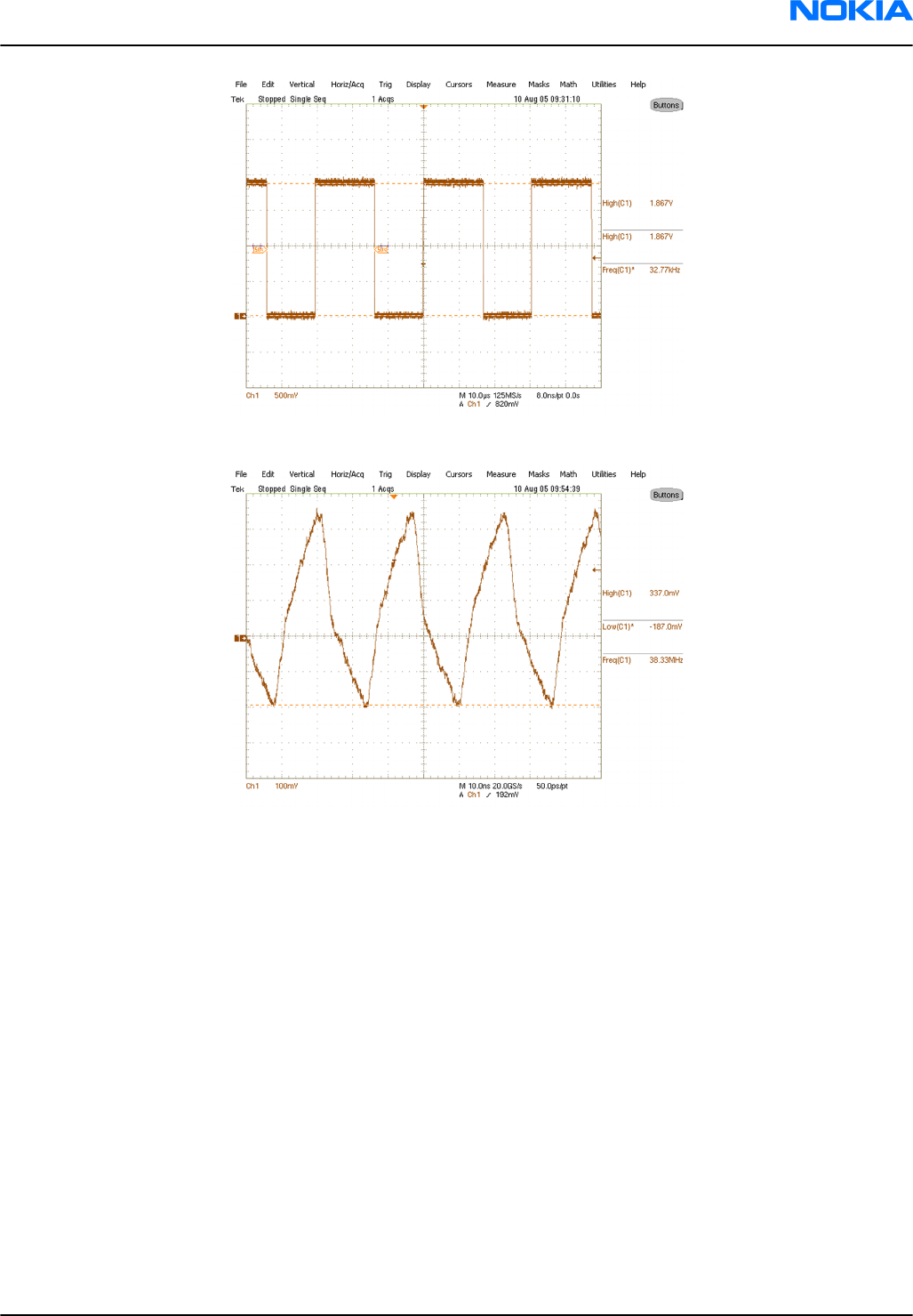
Figure 33 SleepCLK
Figure 34 SYSCLK
RM-188; RM-198
BB Troubleshooting and Manual Tuning Guide Nokia Customer Care
Issue 2 COMPANY CONFIDENTIAL Page 6 –9
Copyright © 2007 Nokia. All rights reserved.
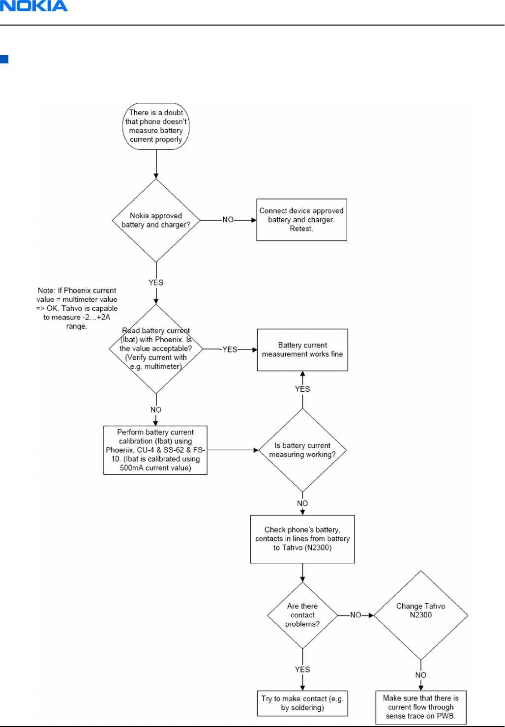
Battery current measuring fault troubleshooting
Troubleshooting flow
RM-188; RM-198
Nokia Customer Care BB Troubleshooting and Manual Tuning Guide
Page 6 –10 COMPANY CONFIDENTIAL Issue 2
Copyright © 2007 Nokia. All rights reserved.
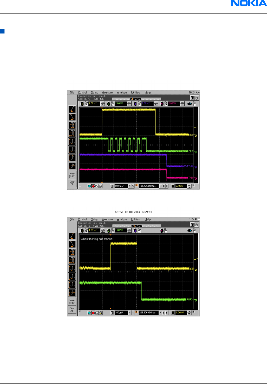
Flash programming fault troubleshooting
Troubleshooting flow
Figure 35 Flashing pic 1. Take single trig measurement for the rise of the BSI signal.
Figure 36 Flashing pic 2. Take single trig measurement for the rise of the BSI signal.
RM-188; RM-198
BB Troubleshooting and Manual Tuning Guide Nokia Customer Care
Issue 2 COMPANY CONFIDENTIAL Page 6 –11
Copyright © 2007 Nokia. All rights reserved.
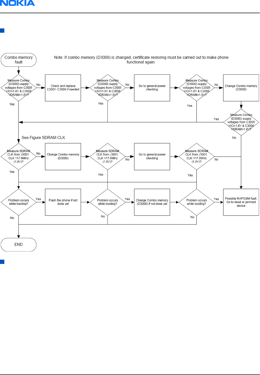
COMBO memory troubleshooting
Troubleshooting flow
Keyboard troubleshooting
Context
There are two possible failure modes in the keyboard: a) One or more keys can be stuck, so that the key does
not react when a keydome is pressed. This kind of failure is caused by mechanical reasons (dirt, rust), b)
Malfunction of several keys at the same time; this happens when one or more rows or columns are failing
(shortcut or open connection).
For a more detailed description of the keyboard and keymatrix, see section Keyboard. If the failure mode is
not clear, start with the Keyboard Test in Phoenix.
RM-188; RM-198
Nokia Customer Care BB Troubleshooting and Manual Tuning Guide
Page 6 –12 COMPANY CONFIDENTIAL Issue 2
Copyright © 2007 Nokia. All rights reserved.
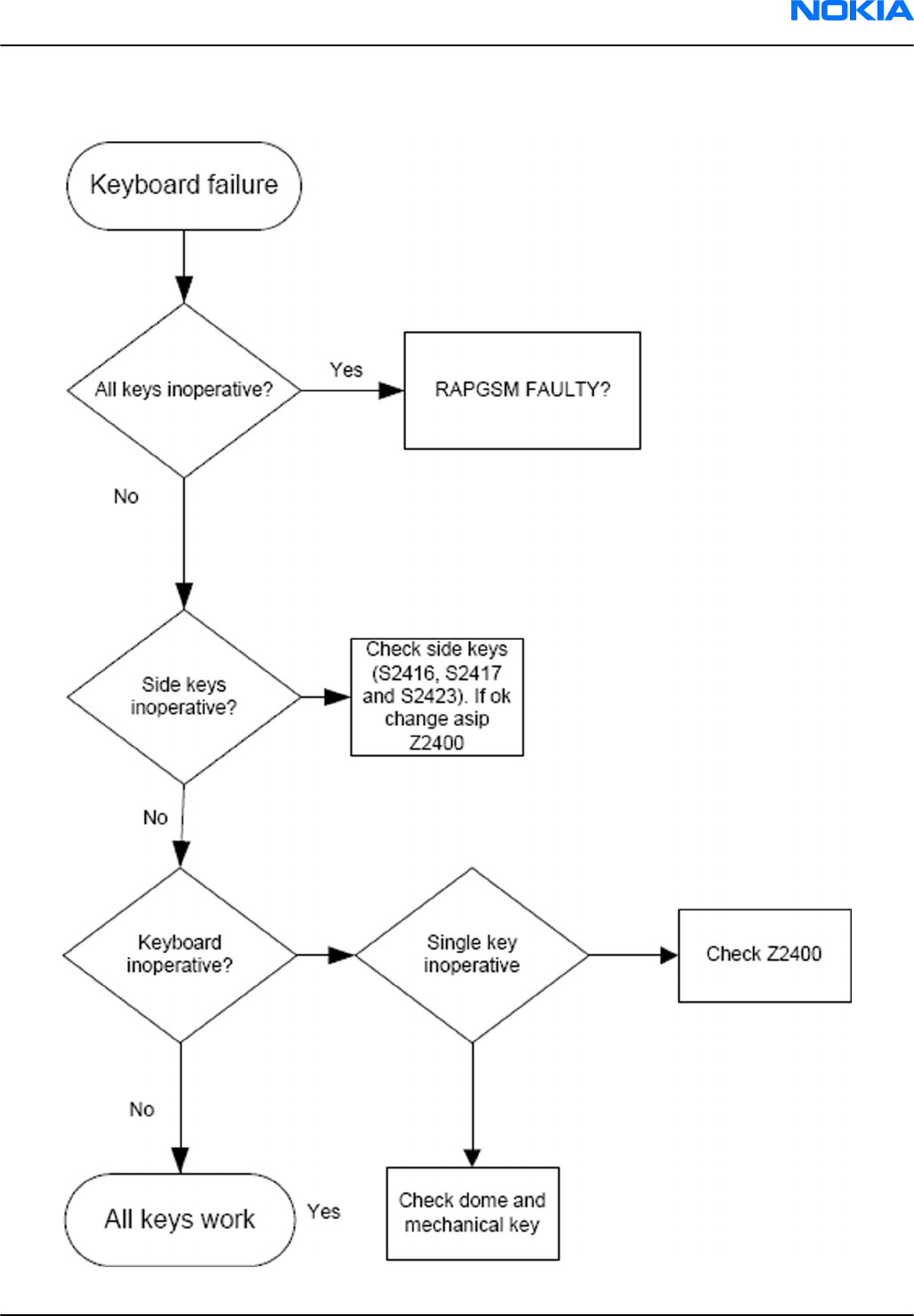
Troubleshooting flow
RM-188; RM-198
BB Troubleshooting and Manual Tuning Guide Nokia Customer Care
Issue 2 COMPANY CONFIDENTIAL Page 6 –13
Copyright © 2007 Nokia. All rights reserved.
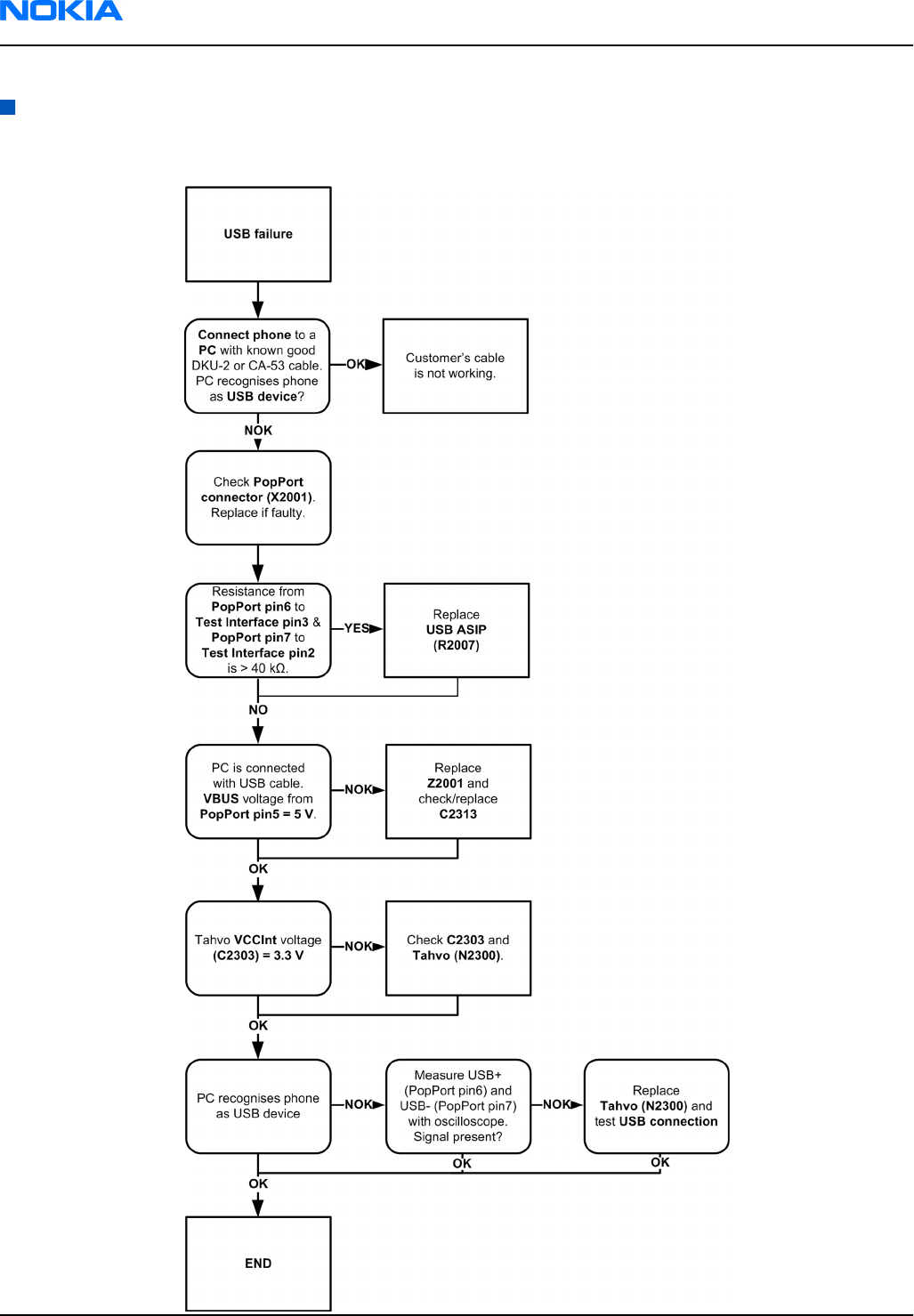
USB troubleshooting
Troubleshooting flow
RM-188; RM-198
Nokia Customer Care BB Troubleshooting and Manual Tuning Guide
Page 6 –14 COMPANY CONFIDENTIAL Issue 2
Copyright © 2007 Nokia. All rights reserved.
Backup battery troubleshooting
Verify that the backup battery is empty (U<1V). Switch the phone on. Measure voltage of the battery when
the main battery is connected to the phone and the phone is switched on.
Wait a few minutes and monitor that the backup battery voltage rises. Switch off the phone, disconnect the
main battery and monitor that the voltage of the backup battery fills up. Normal behaviour of the voltage is
described in the figures below.
Figure 37 Charging backup battery
Figure 38 Discharging backup battery
If the voltage rises and falls quickly, check whether C2233 is broken or short-circuited. Backup battery can
be also dead. If the voltage stays ~0V, check resistance VBACK against GND. If there is no short-circuit, RETU
is faulty. Replace RETU.
RM-188; RM-198
BB Troubleshooting and Manual Tuning Guide Nokia Customer Care
Issue 2 COMPANY CONFIDENTIAL Page 6 –15
Copyright © 2007 Nokia. All rights reserved.
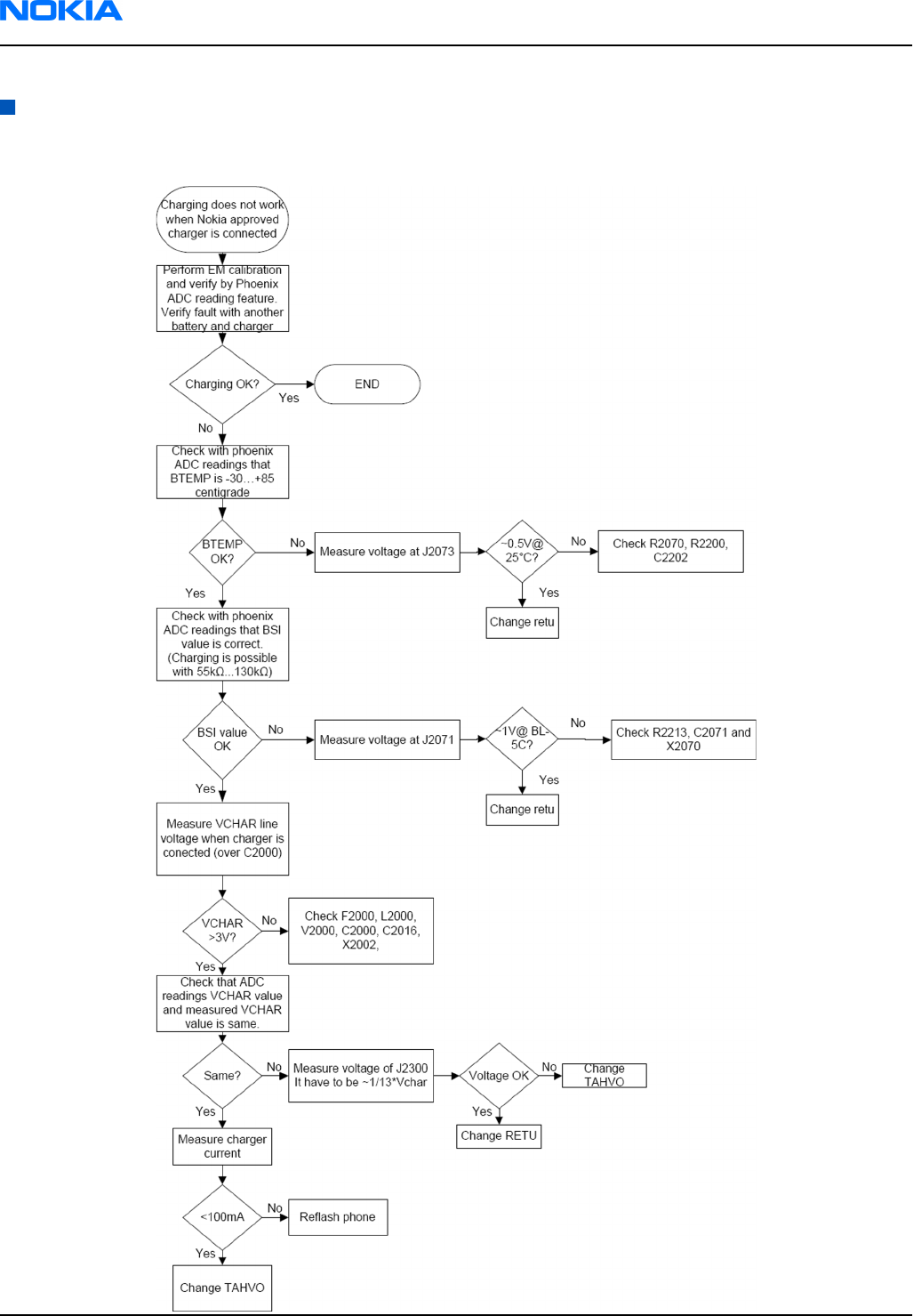
Charging troubleshooting
Troubleshooting flow
RM-188; RM-198
Nokia Customer Care BB Troubleshooting and Manual Tuning Guide
Page 6 –16 COMPANY CONFIDENTIAL Issue 2
Copyright © 2007 Nokia. All rights reserved.
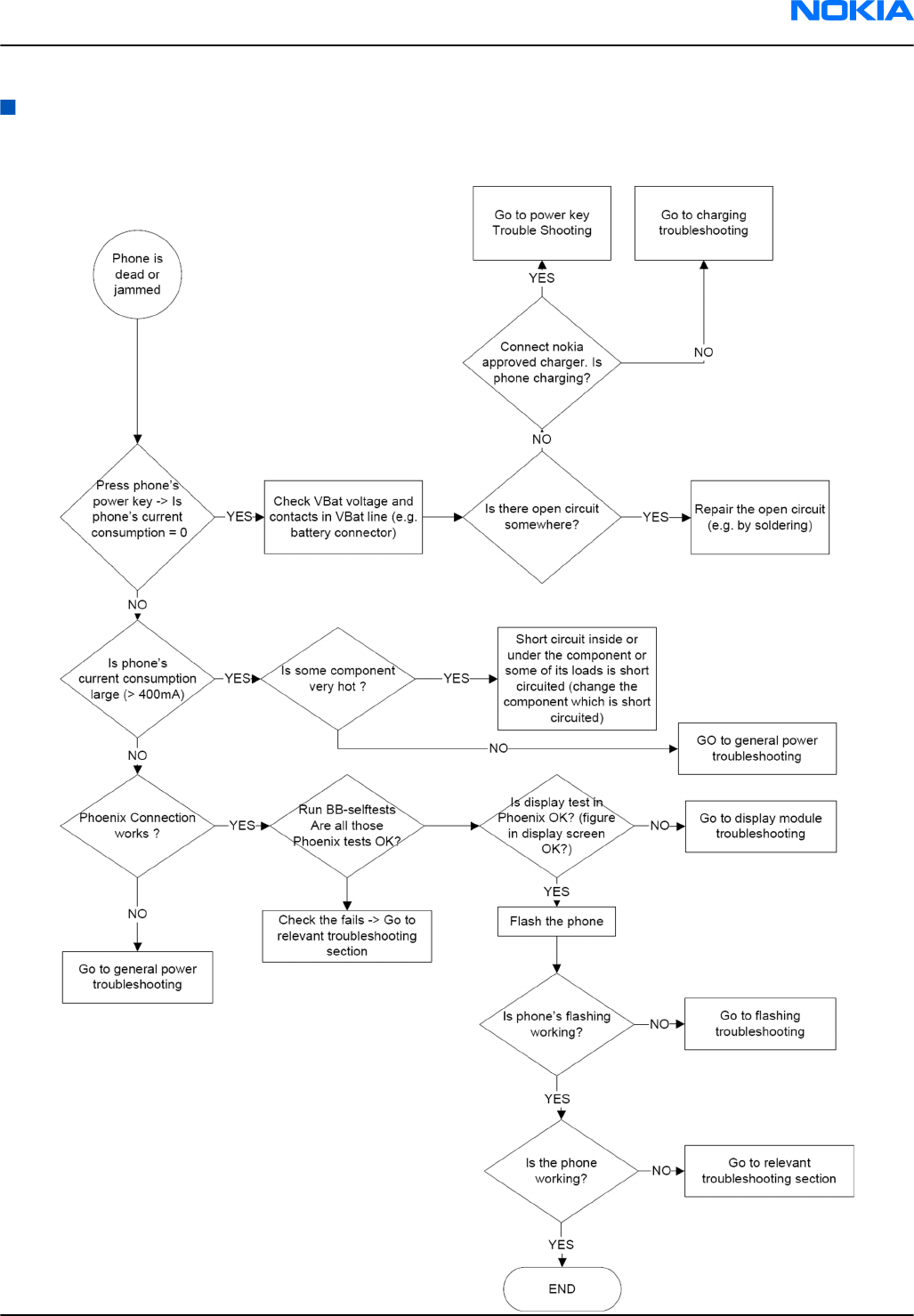
Dead or jammed troubleshooting
Troubleshooting flow
RM-188; RM-198
BB Troubleshooting and Manual Tuning Guide Nokia Customer Care
Issue 2 COMPANY CONFIDENTIAL Page 6 –17
Copyright © 2007 Nokia. All rights reserved.
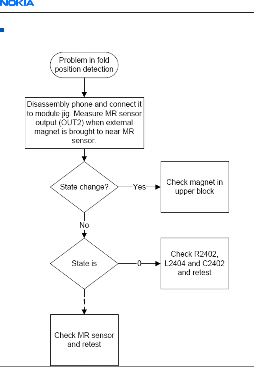
MR sensor troubleshooting
Troubleshooting flow
RM-188; RM-198
Nokia Customer Care BB Troubleshooting and Manual Tuning Guide
Page 6 –18 COMPANY CONFIDENTIAL Issue 2
Copyright © 2007 Nokia. All rights reserved.
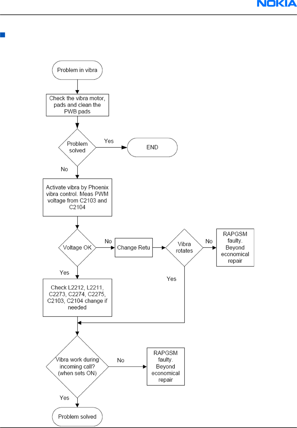
Vibra troubleshooting
Troubleshooting flow
RM-188; RM-198
BB Troubleshooting and Manual Tuning Guide Nokia Customer Care
Issue 2 COMPANY CONFIDENTIAL Page 6 –19
Copyright © 2007 Nokia. All rights reserved.
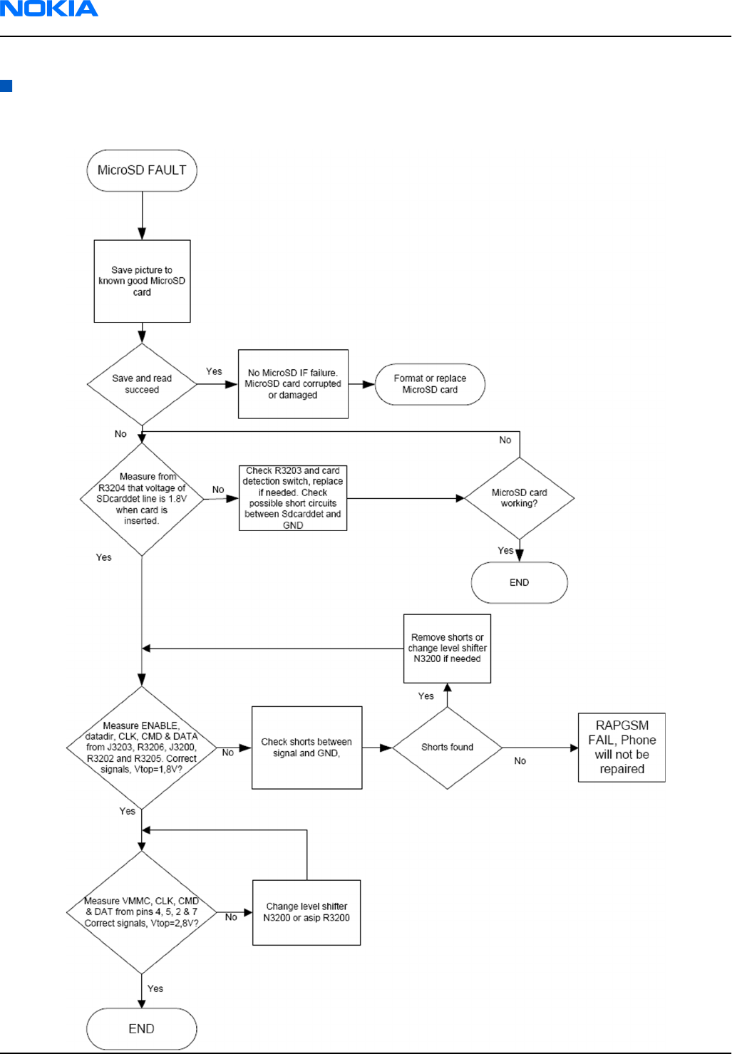
MicroSD troubleshooting
Troubleshooting flow
RM-188; RM-198
Nokia Customer Care BB Troubleshooting and Manual Tuning Guide
Page 6 –20 COMPANY CONFIDENTIAL Issue 2
Copyright © 2007 Nokia. All rights reserved.
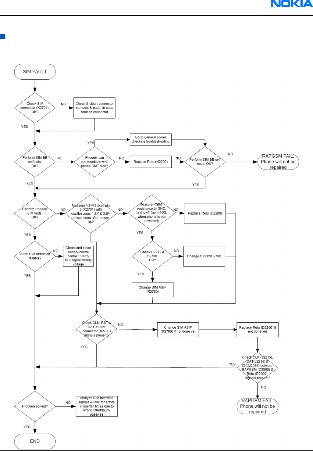
SIM troubleshooting
Troubleshooting flow
RM-188; RM-198
BB Troubleshooting and Manual Tuning Guide Nokia Customer Care
Issue 2 COMPANY CONFIDENTIAL Page 6 –21
Copyright © 2007 Nokia. All rights reserved.
Display module troubleshooting
General instructions for display troubleshooting
The first step is to verify with a working display that the fault is not on the display module itself. The display
module cannot be repaired.
The second step is to check that the cellular engine is working normally. This can be done by connecting the
phone to a docking station and starting Phoenix service software. With the help of Phoenix read the phone
information to check that also the application engine is functioning normally (you should be able to read the
APE ID).
After these checks proceed to the display troubleshooting flowcharts. Use the Display Test tool in Phoenix to
find the detailed fault mode.
Operating modes of the display
The display is in a normal mode when the phone is in active use.
The display is in a partial idle mode when the phone is in the screen saver mode.
The operating modes of the display can be controlled with the help of Phoenix.
Table 10 Display module troubleshooting cases
Display blank There is no image on the display. The display looks
the same when the phone is on as it does when the
phone is off. Because the main display is
transmissive type only, the backlight of the main
display must be ON when checking the display's
functionality.
Image on the display not correct Image on the display can be corrupted or a part of
the image can be missing. If a part of the image is
missing, change the display module. If the image is
otherwise corrupted, follow the appropriate
troubleshooting diagram.
Backlight dim or not working at all Backlight LED components are inside the display
module. Backlight failure can also be in the
connector or in the backlight power source in the
main engine of the phone. Backlight is also
controlled automatically by the ambient light
sensor.
This means that in case the display is working
(image OK), but the backlight is not, follow the
Display and Keyboard Backlight troubleshooting.
Visual defects (pixel) Pixel defects can be checked by controlling the
display with Phoenix. Use both colours, black and
white, on a full screen.
The display may have some random pixel defects
that are acceptable for this type of display. The
criteria when pixel defects are regarded as a display
failure, resulting in a replacement of the display, are
presented the following table.
RM-188; RM-198
Nokia Customer Care BB Troubleshooting and Manual Tuning Guide
Page 6 –22 COMPANY CONFIDENTIAL Issue 2
Copyright © 2007 Nokia. All rights reserved.

Table 11 Pixel defects
Item White dot defect Black dot
defect Total
1Defect
counts
R G B White
Dot
Total
1 1
1 1 1 1
2 Combine
d defect
counts
Not allowed.
Two single dot defects that are within 5 mm of each other should
be interpreted as combined dot defect.
Note: Blinking pixels are not allowed in normal operating temperatures and light conditions. 2nd
display is two-colored, black and white with blue LEDs.
RM-188; RM-198
BB Troubleshooting and Manual Tuning Guide Nokia Customer Care
Issue 2 COMPANY CONFIDENTIAL Page 6 –23
Copyright © 2007 Nokia. All rights reserved.
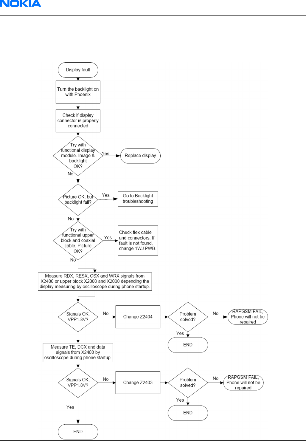
Display fault troubleshooting (main and second displays)
Troubleshooting flow
RM-188; RM-198
Nokia Customer Care BB Troubleshooting and Manual Tuning Guide
Page 6 –24 COMPANY CONFIDENTIAL Issue 2
Copyright © 2007 Nokia. All rights reserved.

Displays and keyboard backlight troubleshooting
Context
The device has one LED driver that provides current for both displays and keyboard backlights. The driver
gets the PWM signal from Tahvo. Because of the main display is transmissive, HW light dimming (controlled
by TAHVO GENOUT01) is also implemented. There is also a switch for selecting which display is lit on. It is not
possible to turn on both displays’ lights at the same time. The backlight brightness can be adjusted manually
in Phoenix.
RM-188; RM-198
BB Troubleshooting and Manual Tuning Guide Nokia Customer Care
Issue 2 COMPANY CONFIDENTIAL Page 6 –25
Copyright © 2007 Nokia. All rights reserved.
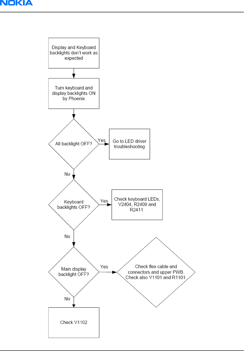
Troubleshooting flow
RM-188; RM-198
Nokia Customer Care BB Troubleshooting and Manual Tuning Guide
Page 6 –26 COMPANY CONFIDENTIAL Issue 2
Copyright © 2007 Nokia. All rights reserved.
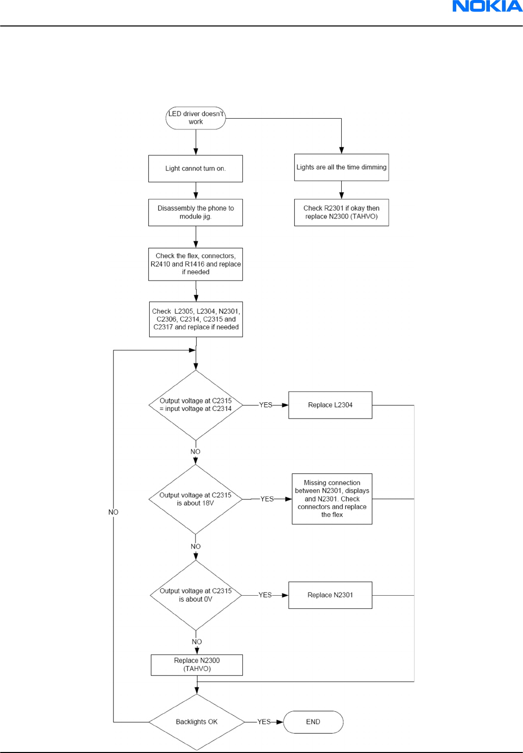
LED driver troubleshooting
Troubleshooting flow
RM-188; RM-198
BB Troubleshooting and Manual Tuning Guide Nokia Customer Care
Issue 2 COMPANY CONFIDENTIAL Page 6 –27
Copyright © 2007 Nokia. All rights reserved.

Camera troubleshooting
Introduction to camera troubleshooting
Bad conditions often cause bad pictures. Therefore, the camera operation has to be checked in constant
conditions or by using a second, known-to-be-good Nokia device as reference. Image quality is hard to
measure quantitatively, and the difference between a good and a bad picture can be small. Some training
or experience may be needed to detect what is actually wrong.
When checking for possible errors in camera functionality, knowing what error is suspected significantly
helps the testing by narrowing down the amount of test cases. The following types of image quality problems
are common:
• Dust (black spots)
• Lack of sharpness
• Bit errors
Taking and evaluating test pictures
When
taking
a test picture, remember the following:
• Avoid bright fluorescent light, 50/60Hz electrical network or high artificial illumination levels
• If the phone is hot, let it rest for a while before taking the picture
• Make sure the optical system is clean
• Use highest possible resolution
• Make sure the light is suffiecient (bright office lightning)
• Do not take the picture towards light source
• Be as still as possible when taking the picture
• Distance should be at least 40cm, 1-2m is recommended
When
evaluating
a test picture, remember the following:
• The center of the picture is sharper than the edges
• The image may be blurred, though it does not show in the viewfinder
• Analyse the picture from your PC monitor, full colour setting is recommended
• If possible, compare with a picture of the same motive taken with a similar Nokia device
RM-188; RM-198
Nokia Customer Care BB Troubleshooting and Manual Tuning Guide
Page 6 –28 COMPANY CONFIDENTIAL Issue 2
Copyright © 2007 Nokia. All rights reserved.
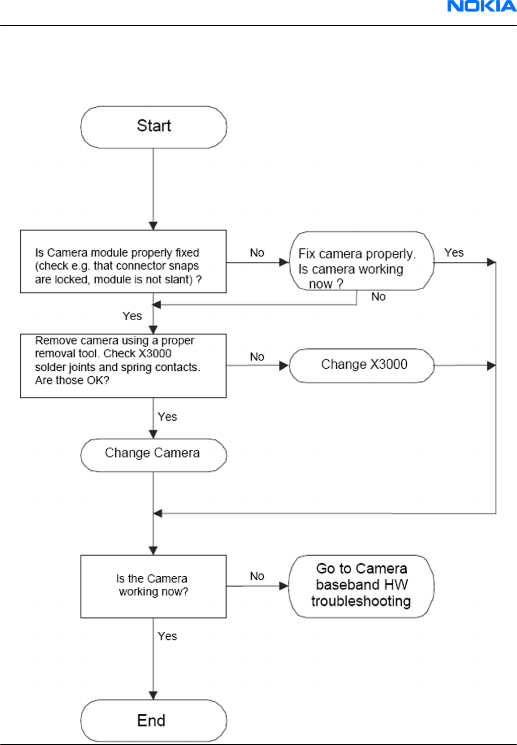
Camera hardware failure message troubleshooting
Troubleshooting flow
RM-188; RM-198
BB Troubleshooting and Manual Tuning Guide Nokia Customer Care
Issue 2 COMPANY CONFIDENTIAL Page 6 –29
Copyright © 2007 Nokia. All rights reserved.
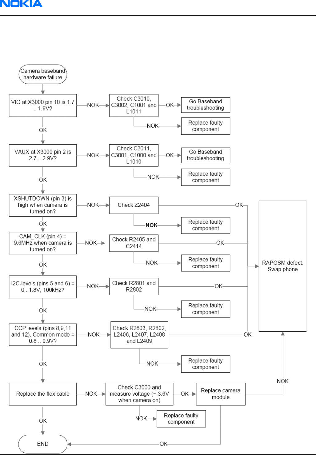
Camera hardware troubleshooting
Camera hardware troubleshooting
RM-188; RM-198
Nokia Customer Care BB Troubleshooting and Manual Tuning Guide
Page 6 –30 COMPANY CONFIDENTIAL Issue 2
Copyright © 2007 Nokia. All rights reserved.
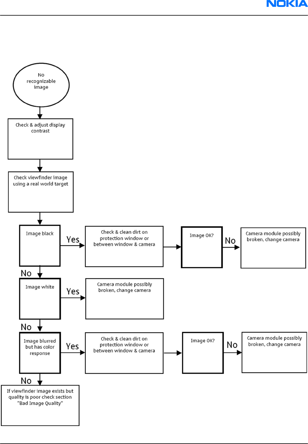
Front camera viewfinder troubleshooting
Troubleshooting flow
RM-188; RM-198
BB Troubleshooting and Manual Tuning Guide Nokia Customer Care
Issue 2 COMPANY CONFIDENTIAL Page 6 –31
Copyright © 2007 Nokia. All rights reserved.
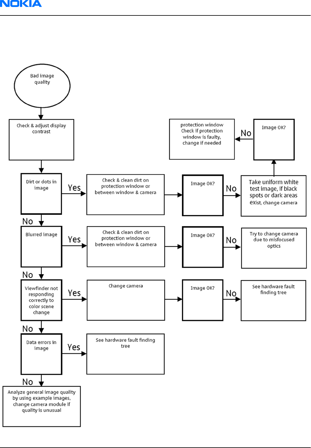
Front camera bad image quality troubleshooting
Troubleshooting flow
RM-188; RM-198
Nokia Customer Care BB Troubleshooting and Manual Tuning Guide
Page 6 –32 COMPANY CONFIDENTIAL Issue 2
Copyright © 2007 Nokia. All rights reserved.
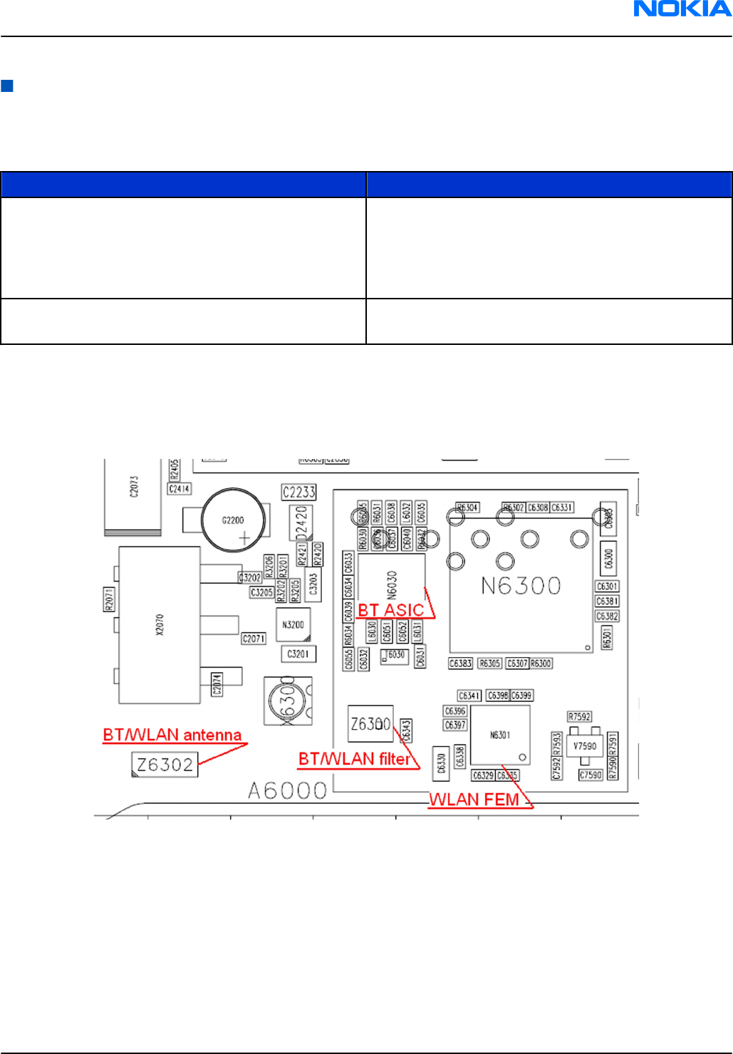
Bluetooth troubleshooting
Introduction to Bluetooth/FM Radio troubleshooting
There are two main Bluetooth problems that can occur:
Problem Description
Detachment of the BT antenna. This would most likely happen if the device has
been dropped repeatedly to the ground. It could
cause the BT antenna to become loose or partially
detached from the PWB. (see next page for details
about BT antenna HW and Mechanics)
A malfunction in the BT ASIC, BB ASICs or Phone’s BT
SMD components.
This is unpredictable and could have many causes
i.e. SW or HW related.
The main issue is to find out if the problem is related to the BT antenna or related to the BT system or the
phone’s BB and then replace/fix the faulty component.
Bluetooth/FM Radio component layout
Figure 39 RM-188 Bluetooth
RM-188; RM-198
BB Troubleshooting and Manual Tuning Guide Nokia Customer Care
Issue 2 COMPANY CONFIDENTIAL Page 6 –33
Copyright © 2007 Nokia. All rights reserved.
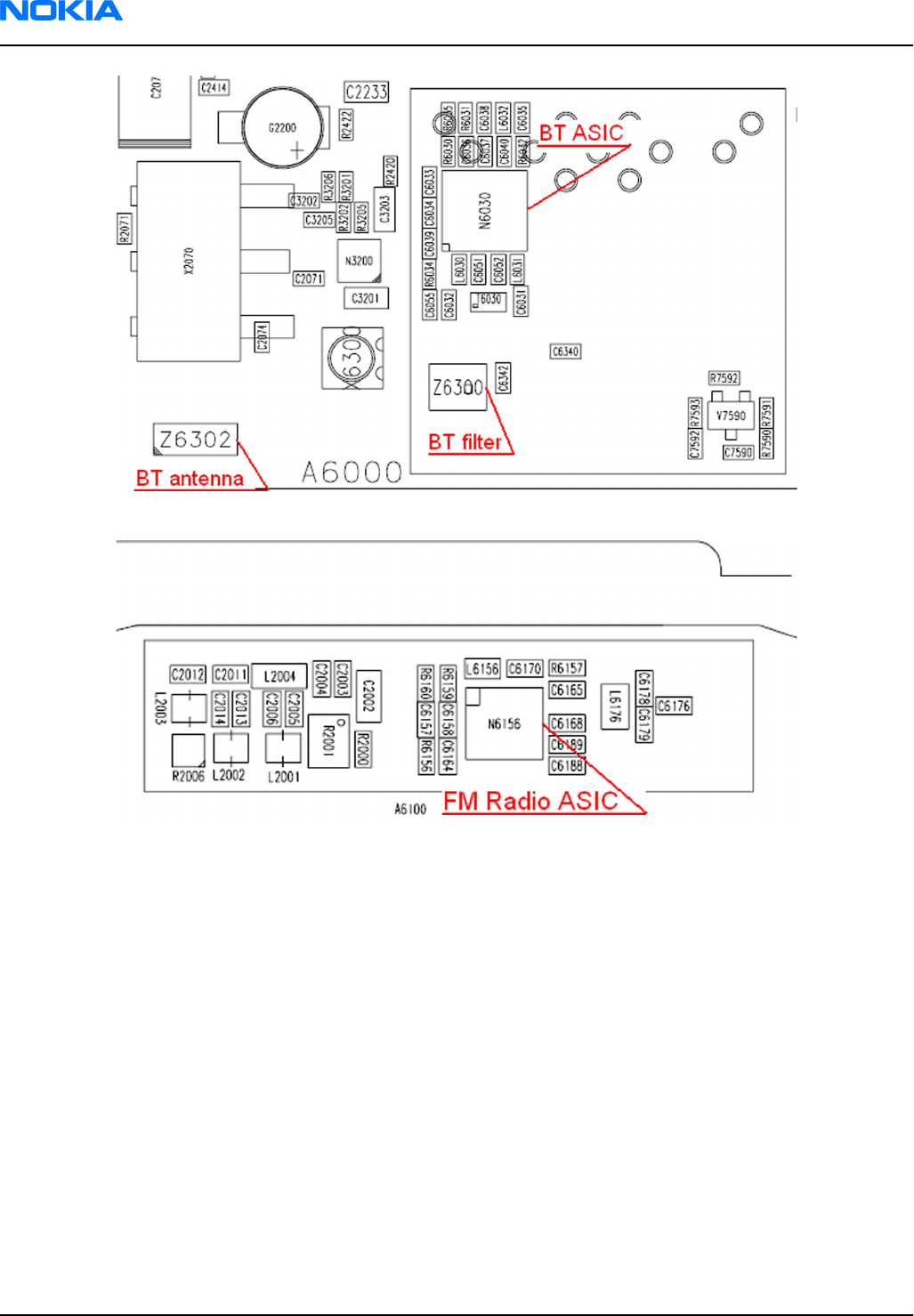
Figure 40 RM-198 Bluetooth
Figure 41 RM-188/198 FM radio
Bluetooth settings for Phoenix
Steps
1. Start
Phoenix
service software.
2. From the File menu, choose Open Product, and then choose the correct type designator from the
Product list.
3. Place the phone to a flash adapter in the local mode.
4. Choose Testing→Bluetooth LOCALS .
5. Locate JBT-9’s serial number (12 digits) found in the type label on the back of JBT-9.
In addition to JBT-9, also SB-6, JBT-3 and JBT-6 Bluetooth test boxes can be used.
6. In the
Bluetooth LOCALS
window, write the 12-digit serial number on the
Counterpart BT Device Address line.
This needs to be done only once provided that JBT-9 is not changed.
7. Place the JBT-9 box near (within 10 cm) the BT antenna and click Run BER Test.
RM-188; RM-198
Nokia Customer Care BB Troubleshooting and Manual Tuning Guide
Page 6 –34 COMPANY CONFIDENTIAL Issue 2
Copyright © 2007 Nokia. All rights reserved.
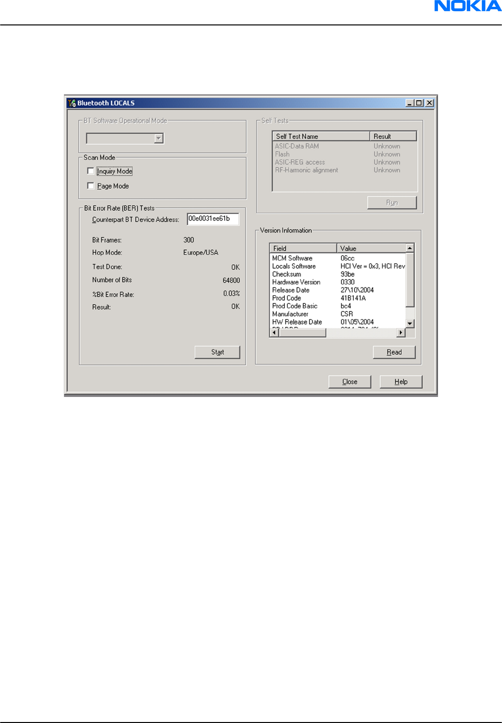
Results
Bit Error Rate test result is displayed in the
Bit Error Rate (BER) Tests
pane in the
Bluetooth LOCALS
window.
Figure 42 BER test result
Bluetooth self tests in Phoenix
Steps
1. Start
Phoenix
service software.
2. ChooseFile→Scan Product.
3. Place the phone to a flash adapter.
4. From the Mode drop-down menu, set mode to Local.
5. Choose Testing→Self Tests.
6. In the
Self Tests
window check the following Bluetooth related tests:
•ST_LPRF_IF_TEST
•ST_LPRF_AUDIO_LINES_TEST
•ST_BT_WAKEUP_TEST
RM-188; RM-198
BB Troubleshooting and Manual Tuning Guide Nokia Customer Care
Issue 2 COMPANY CONFIDENTIAL Page 6 –35
Copyright © 2007 Nokia. All rights reserved.
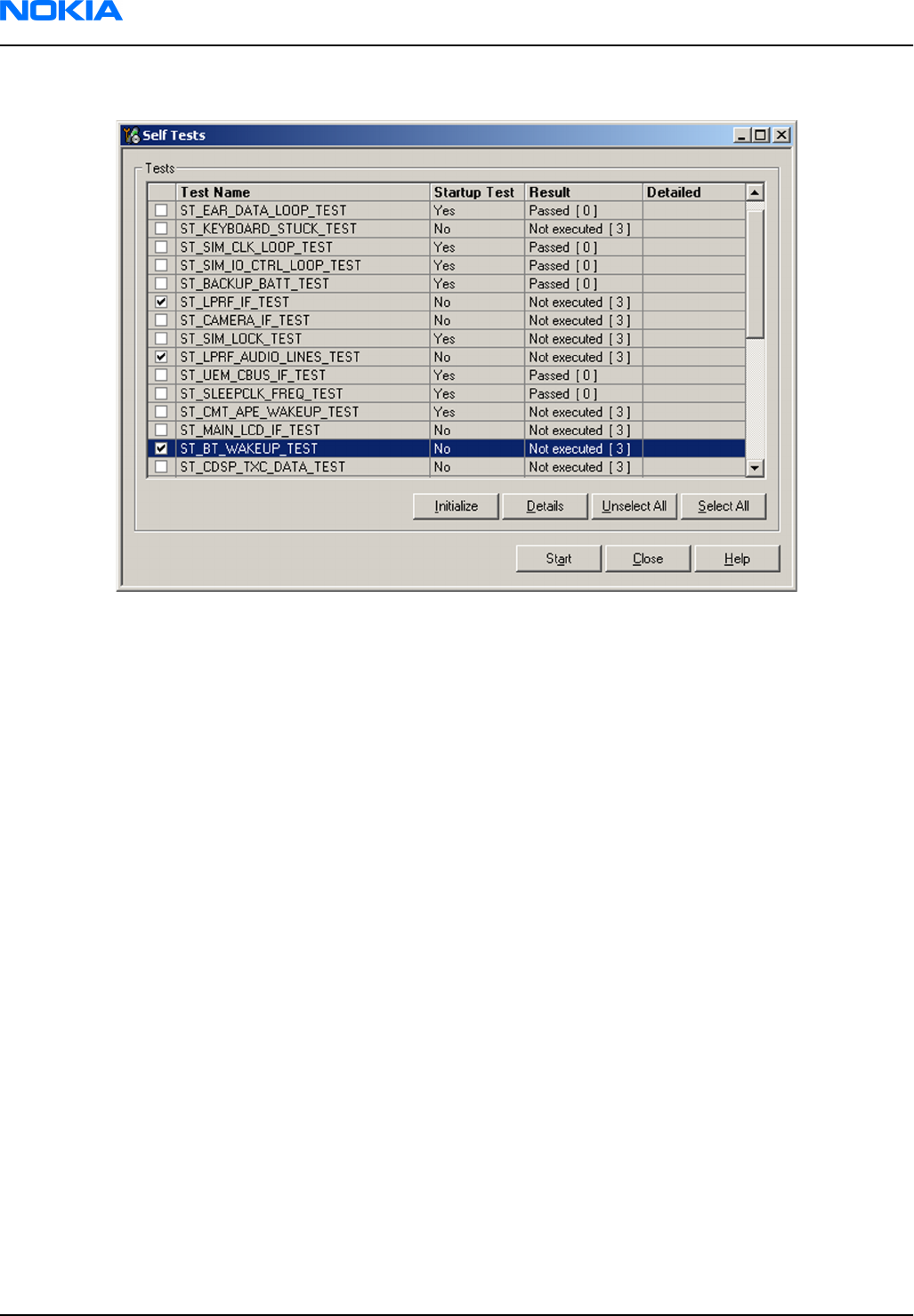
7. To run the tests, click Start.
Figure 43 Bluetooth self tests in
Phoenix
RM-188; RM-198
Nokia Customer Care BB Troubleshooting and Manual Tuning Guide
Page 6 –36 COMPANY CONFIDENTIAL Issue 2
Copyright © 2007 Nokia. All rights reserved.
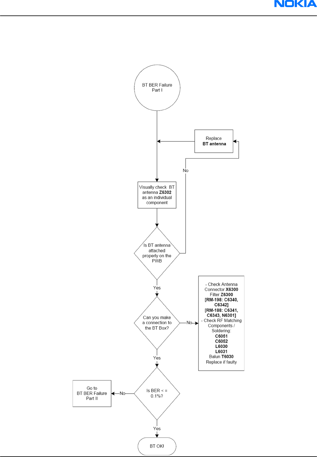
Bluetooth BER failure troubleshooting
Troubleshooting flow
RM-188; RM-198
BB Troubleshooting and Manual Tuning Guide Nokia Customer Care
Issue 2 COMPANY CONFIDENTIAL Page 6 –37
Copyright © 2007 Nokia. All rights reserved.
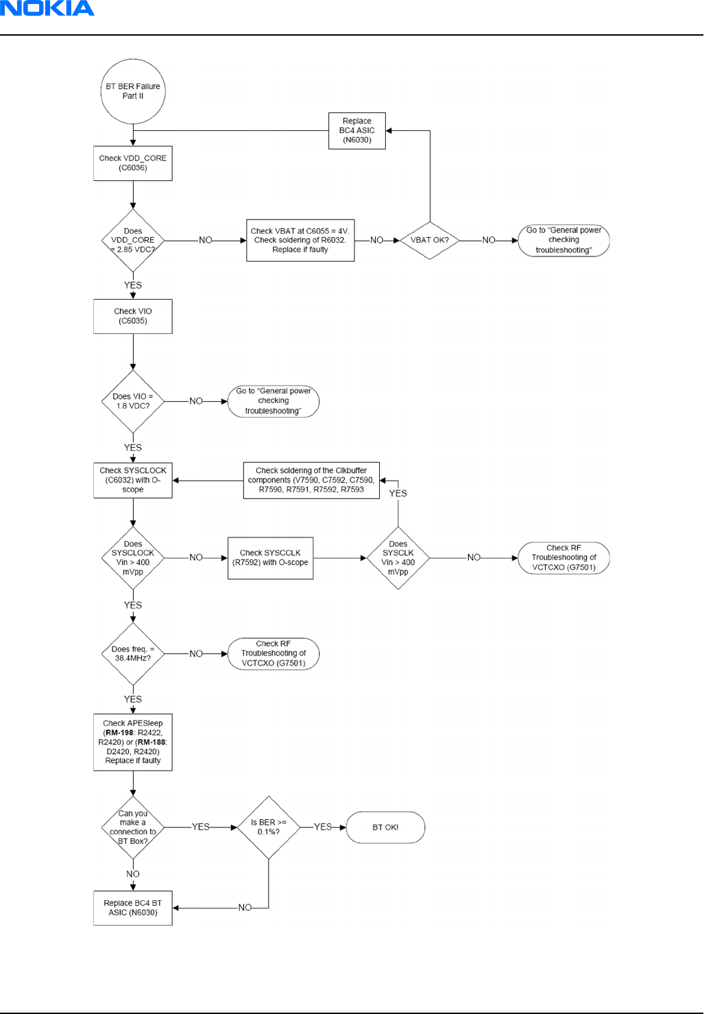
RM-188; RM-198
Nokia Customer Care BB Troubleshooting and Manual Tuning Guide
Page 6 –38 COMPANY CONFIDENTIAL Issue 2
Copyright © 2007 Nokia. All rights reserved.
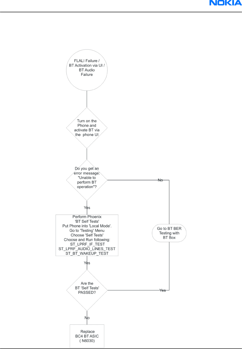
BT audio failure troubleshooting
Troubleshooting flow
RM-188; RM-198
BB Troubleshooting and Manual Tuning Guide Nokia Customer Care
Issue 2 COMPANY CONFIDENTIAL Page 6 –39
Copyright © 2007 Nokia. All rights reserved.
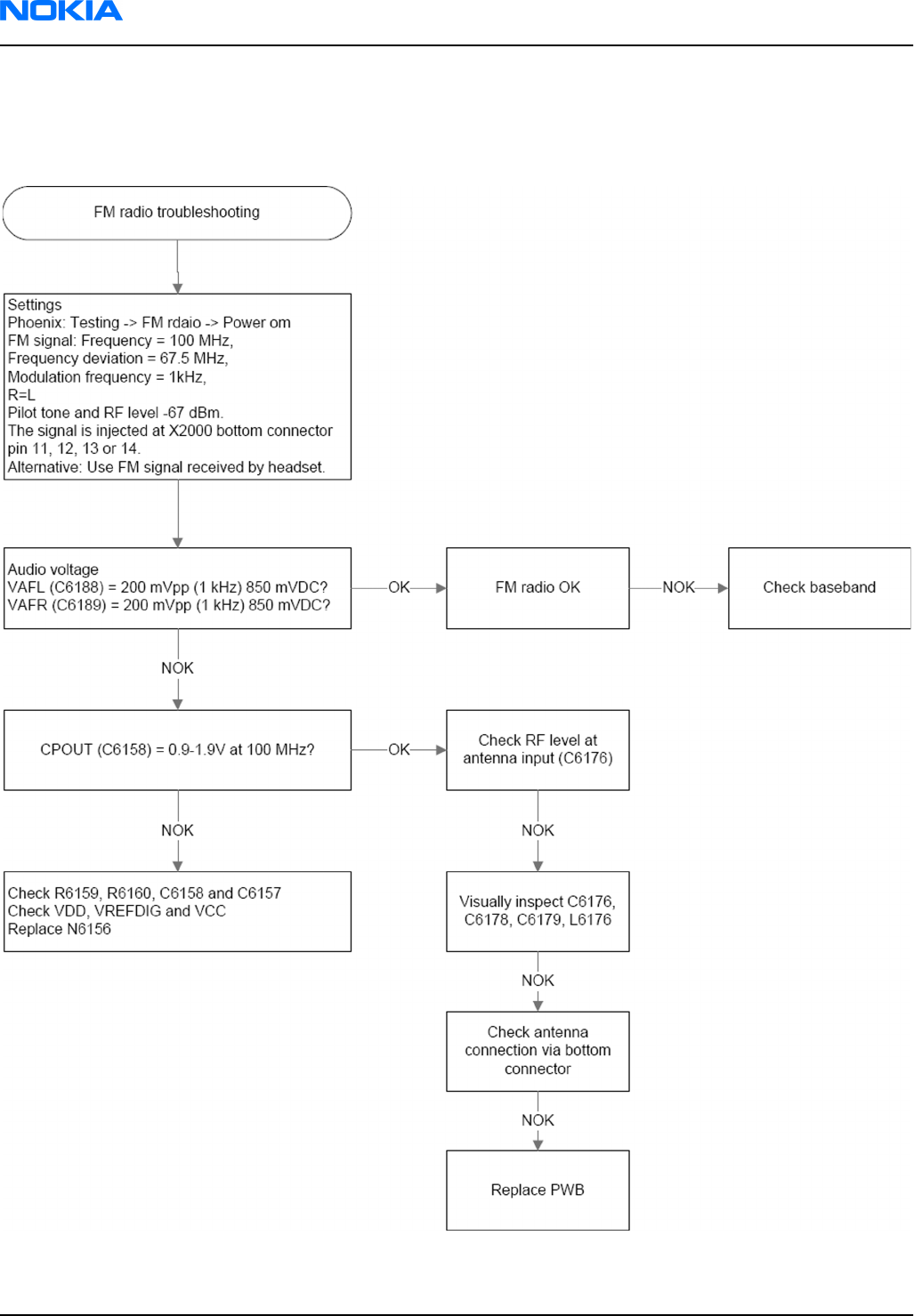
FM Radio troubleshooting
Troubleshooting flow
RM-188; RM-198
Nokia Customer Care BB Troubleshooting and Manual Tuning Guide
Page 6 –40 COMPANY CONFIDENTIAL Issue 2
Copyright © 2007 Nokia. All rights reserved.

Audio troubleshooting
Audio troubleshooting test instructions
Differential external earpiece and internal earpiece outputs can be measured either with a single-ended or
a differential probe.
When measuring with a single-ended probe each output is measured against the ground.
Internal handsfree output is measured using a current probe, if a special low-pass filter designed for
measuring a digital amplifier is not available. Note also that when using a current probe, the input signal
frequency must be set to 2kHz.
The input signal for each loop test can be either single-ended or differential.
Required equipment
The following equipment is needed for the tests:
• Oscilloscope
• Function generator (sine waveform)
• Current probe (Internal handsfree PWM output measurement)
• Phoenix service software
• Battery voltage 3.7V
Test procedure
Audio can be tested using the Phoenix audio routings option. Three different audio loop paths can be
activated:
• External microphone to Internal earpiece
• External microphone to Internal handsfree speaker
• Internal microphone to External earpiece
Each audio loop sets routing from the specified input to the specified output enabling a quick in-out test.
Loop path gains are fixed and they cannot be changed using Phoenix. Correct pins and signals for each test
are presented in the following table.
Phoenix audio loop tests and test results
The results presented in the table apply when no accessory is connected and battery voltage is set to 3.7V.
Earpiece, internal microphone and speaker are in place during measurement. Applying a headset accessory
during measurement causes a significant drop in measured quantities.
The gain values presented in the table apply for a differential output vs. single-ended/differential input.
RM-188; RM-198
BB Troubleshooting and Manual Tuning Guide Nokia Customer Care
Issue 2 COMPANY CONFIDENTIAL Page 6 –41
Copyright © 2007 Nokia. All rights reserved.
Loop test Input terminal Output
terminal Path
gain
[dB]
(fixed)
Input
volta
ge
[mVp-
p]
Differen
tial
output
voltage
[mVp-p]
Outpu
t DC
level
[V]
Outp
ut
curre
nt
[mA]
External Mic to External
Earpiece
XMICP and GND HSEAR R P,
HSEAR R N
and GND
-2.9 1000 720 1.2 NA
HSEAR P,
HSEAR N and
GND
XMICN and GND HSEAR R P,
HSEAR R N
and GND
HSEAR P,
HSEAR N and
GND
External Mic to Internal
Earpiece
XMICP and GND EarP and GND -4.5 1000 600 1.2 NA
EarN and
GND
XMICN and GND EarP and GND
EarN and
GND
External Mic to Internal
handsfree
XMICP and GND B2102 pads -5 1000 560 0 25m
A
(calc
.)
XMICN and GND B2102 pads
Internal Mic to External
Earpiece
B2100 (OUT/
GND)
HSEAR R P,
HSEAR R N
and GND
22.7 100 1360 1.2 NA
HSEAR P,
HSEAR N and
GND
HSEAR R P,
HSEAR R N
and GND
HSEAR P,
HSEAR N and
GND
RM-188; RM-198
Nokia Customer Care BB Troubleshooting and Manual Tuning Guide
Page 6 –42 COMPANY CONFIDENTIAL Issue 2
Copyright © 2007 Nokia. All rights reserved.
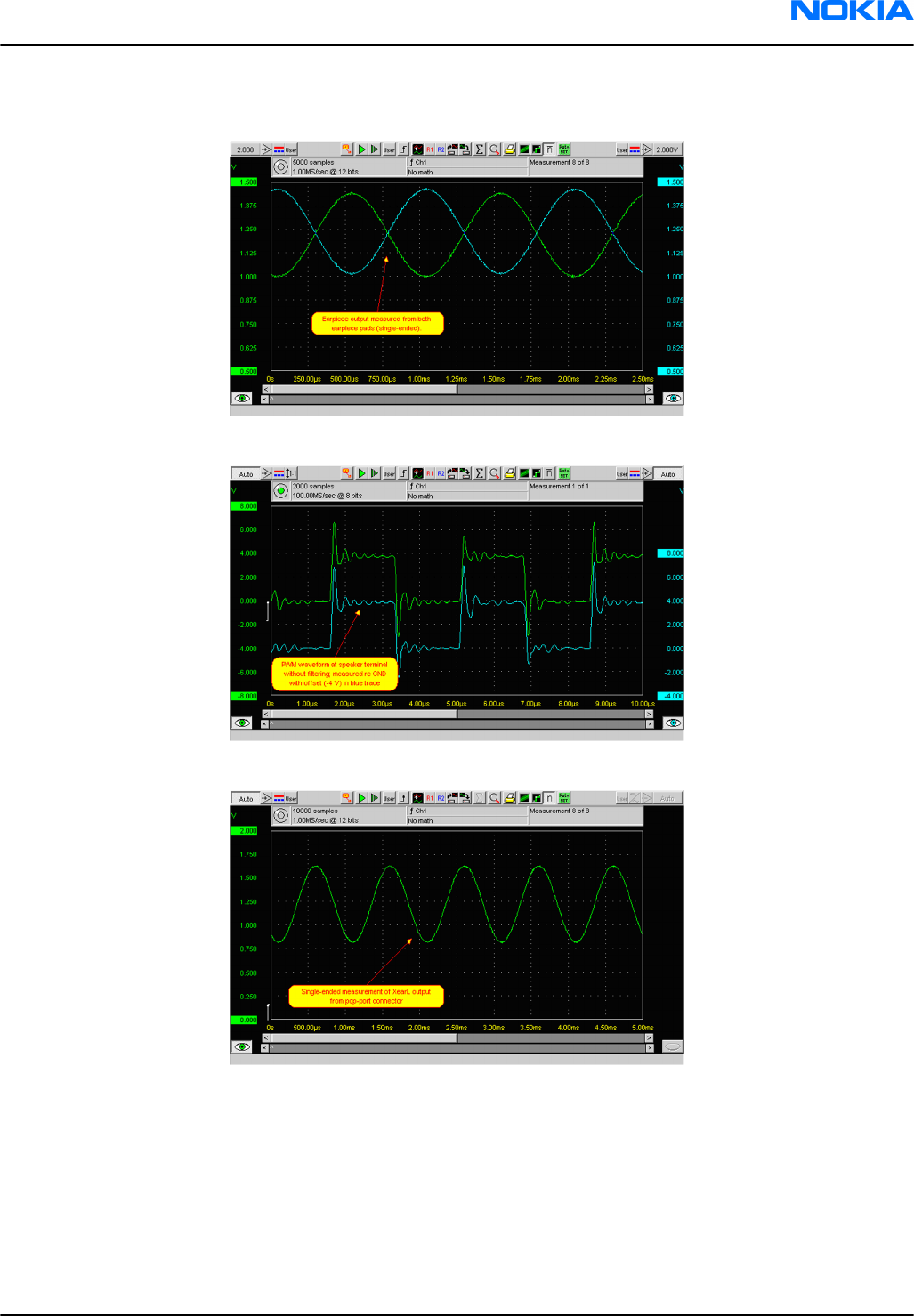
Measurement data
Figure 44 Single-ended output waveform of the Ext_in_HP_out measurement when earpiece is connected.
Figure 45 Differential output waveform of the Ext_in_IHF_out out loop measurement when speaker is connected.
Figure 46 Single-ended output waveform of the HP_in_Ext_out loop when microphone is connected.
RM-188; RM-198
BB Troubleshooting and Manual Tuning Guide Nokia Customer Care
Issue 2 COMPANY CONFIDENTIAL Page 6 –43
Copyright © 2007 Nokia. All rights reserved.
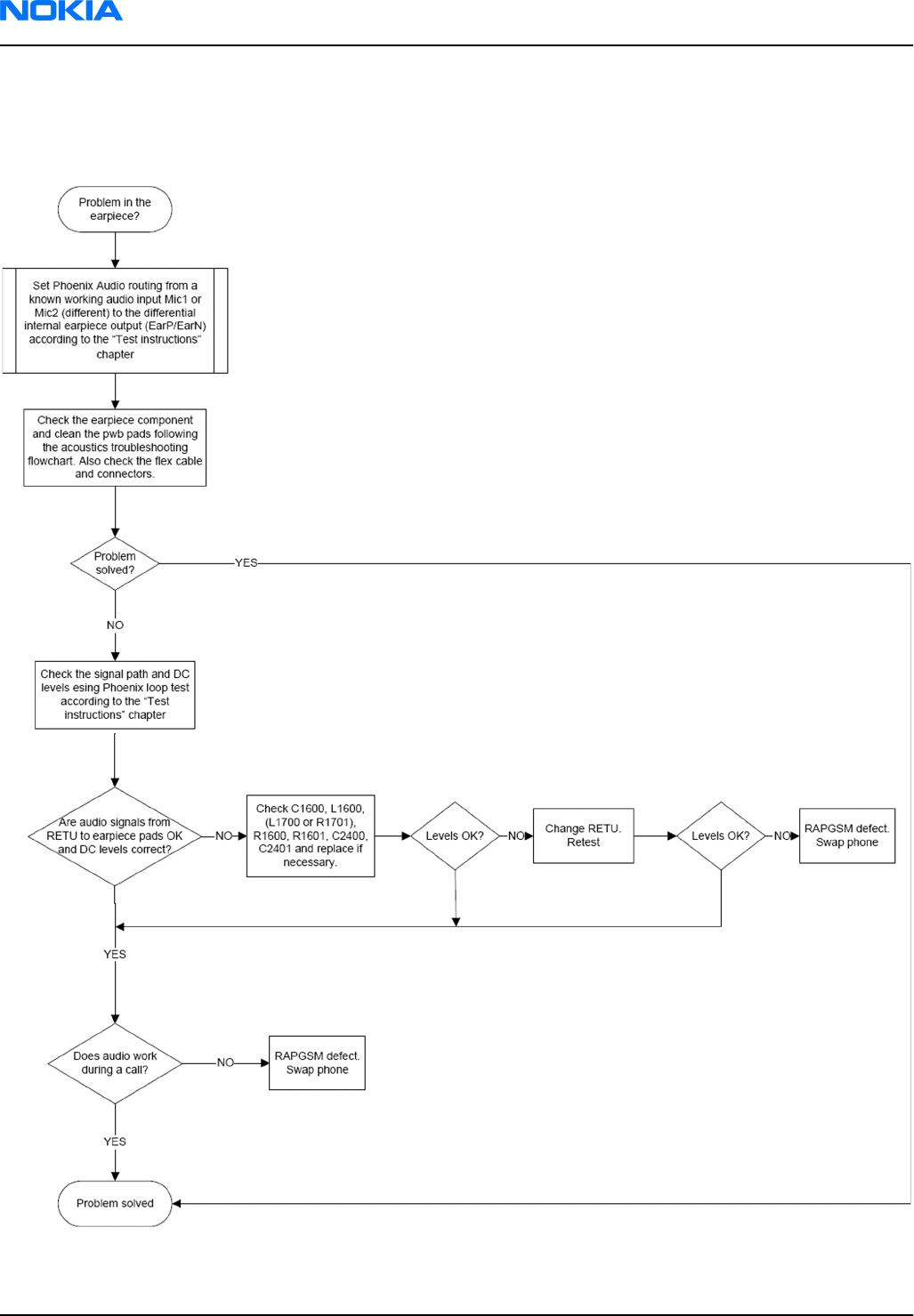
Internal earpiece troubleshooting
Troubleshooting flow
RM-188; RM-198
Nokia Customer Care BB Troubleshooting and Manual Tuning Guide
Page 6 –44 COMPANY CONFIDENTIAL Issue 2
Copyright © 2007 Nokia. All rights reserved.
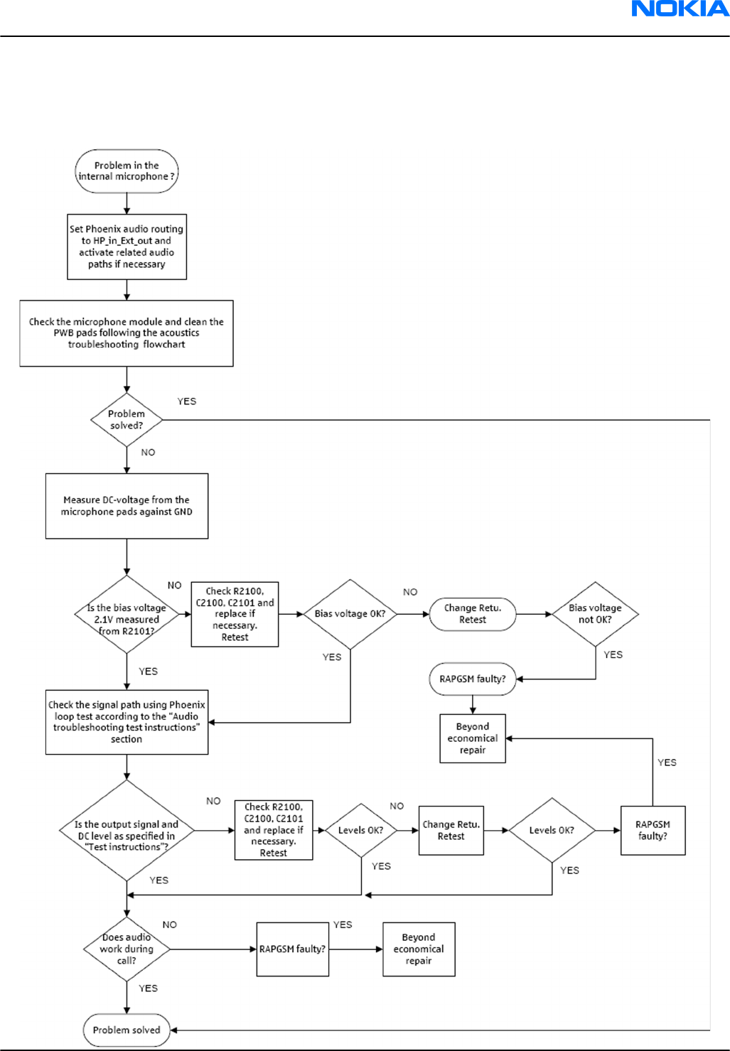
Internal microphone troubleshooting
Troubleshooting flow
RM-188; RM-198
BB Troubleshooting and Manual Tuning Guide Nokia Customer Care
Issue 2 COMPANY CONFIDENTIAL Page 6 –45
Copyright © 2007 Nokia. All rights reserved.
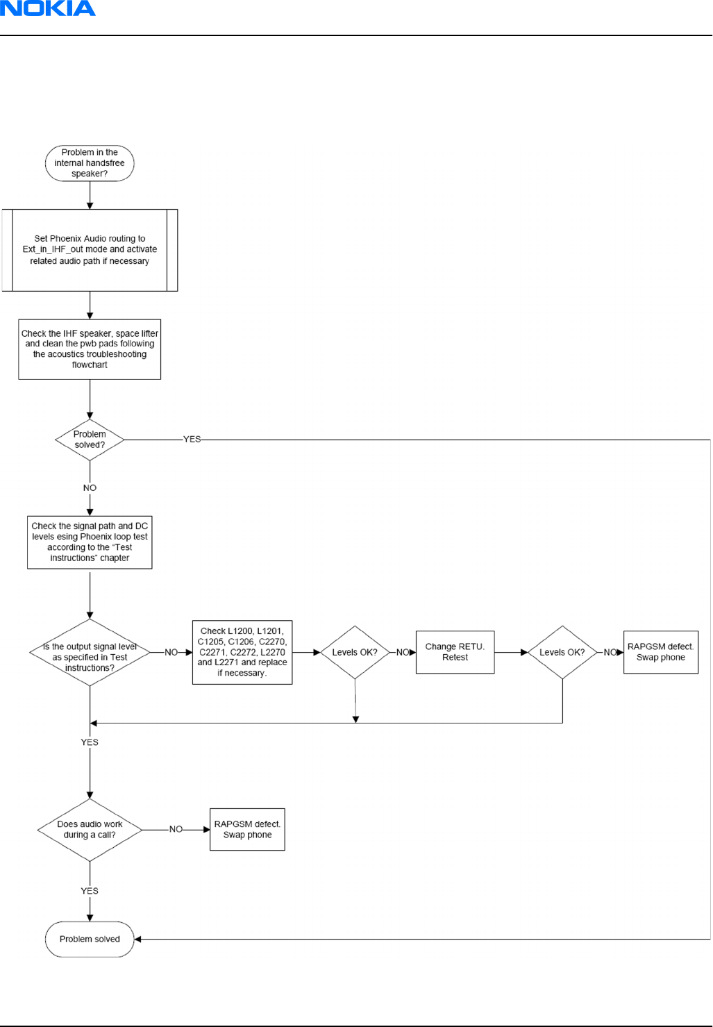
IHF speaker troubleshooting
Troubleshooting flow
RM-188; RM-198
Nokia Customer Care BB Troubleshooting and Manual Tuning Guide
Page 6 –46 COMPANY CONFIDENTIAL Issue 2
Copyright © 2007 Nokia. All rights reserved.
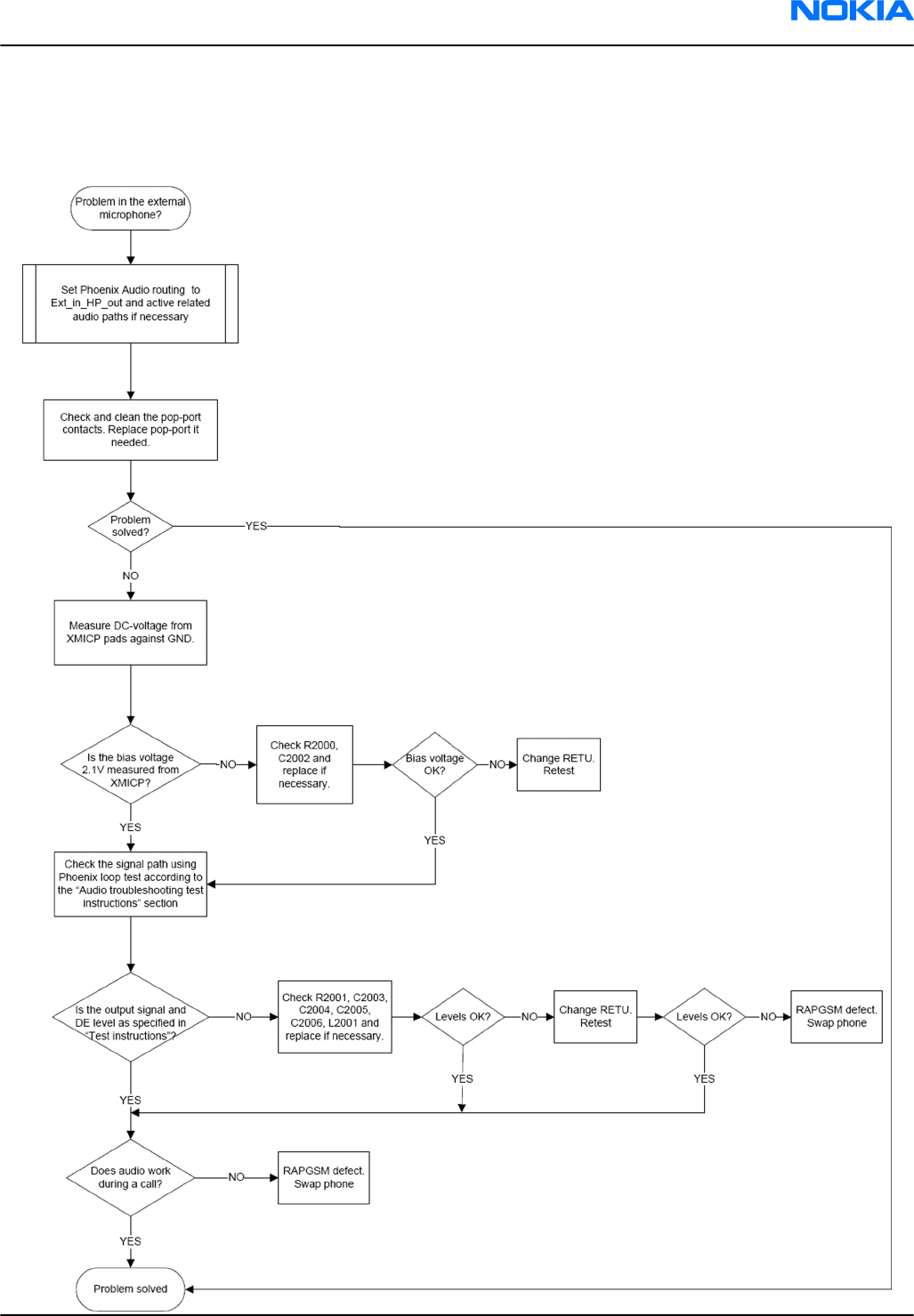
External microphone troubleshooting
Troubleshooting flow
RM-188; RM-198
BB Troubleshooting and Manual Tuning Guide Nokia Customer Care
Issue 2 COMPANY CONFIDENTIAL Page 6 –47
Copyright © 2007 Nokia. All rights reserved.
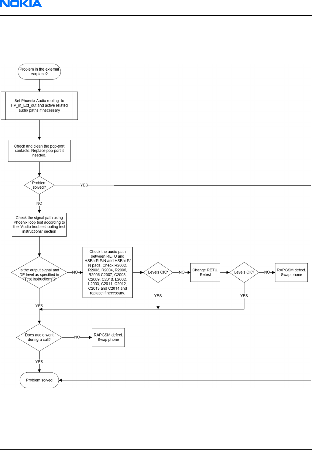
External earpiece troubleshooting
Troubleshooting flow
RM-188; RM-198
Nokia Customer Care BB Troubleshooting and Manual Tuning Guide
Page 6 –48 COMPANY CONFIDENTIAL Issue 2
Copyright © 2007 Nokia. All rights reserved.

Introduction to acoustics troubleshooting
Acoustics troubleshooting
Acoustics design ensures that the sound is detected correctly with a microphone and properly radiated to
the outside of the device by speaker(s). The acoustics of the phone includes three basic systems: earpiece,
Integrated Hands Free (IHF) and microphone.
The sound reproduced from the earpiece radiates through a single hole on the front cover (A-cover). The
sound reproduced from the IHF speakers radiates through a single hole on the Antenna cap (Antenna assy).
Microphone is located at the bottom, next to the system connector.
For a correct functionality of the phone, all sound holes must be always open. When the phone is used, care
must be taken not to close any of those holes with a hand or fingers. The phone should be dry and clean,
and no objects must be located in such a way that they close any of the holes.
RM-188; RM-198
BB Troubleshooting and Manual Tuning Guide Nokia Customer Care
Issue 2 COMPANY CONFIDENTIAL Page 6 –49
Copyright © 2007 Nokia. All rights reserved.
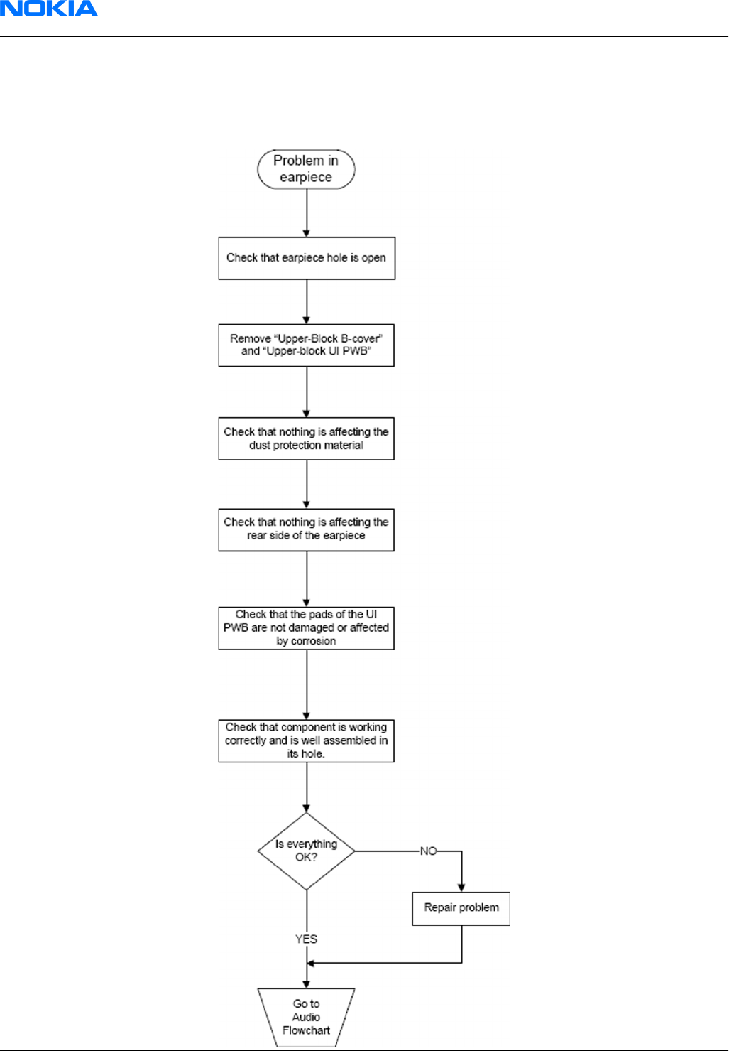
Earpiece troubleshooting
Troubleshooting flow
RM-188; RM-198
Nokia Customer Care BB Troubleshooting and Manual Tuning Guide
Page 6 –50 COMPANY CONFIDENTIAL Issue 2
Copyright © 2007 Nokia. All rights reserved.
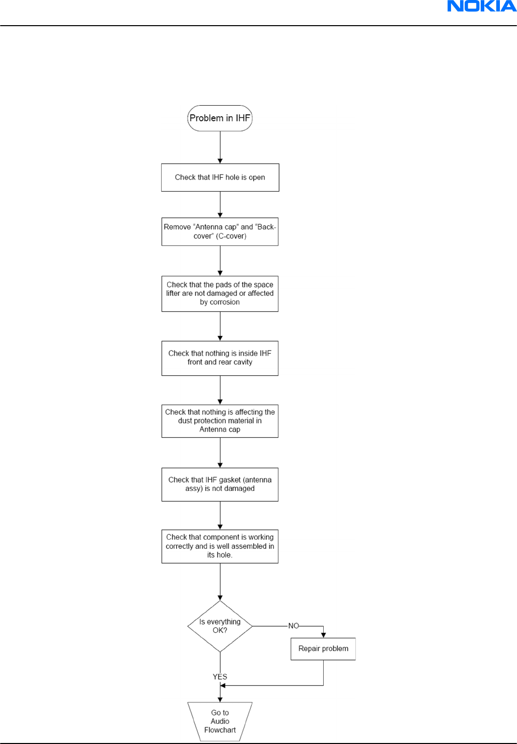
IHF troubleshooting
Troubleshooting flow
RM-188; RM-198
BB Troubleshooting and Manual Tuning Guide Nokia Customer Care
Issue 2 COMPANY CONFIDENTIAL Page 6 –51
Copyright © 2007 Nokia. All rights reserved.
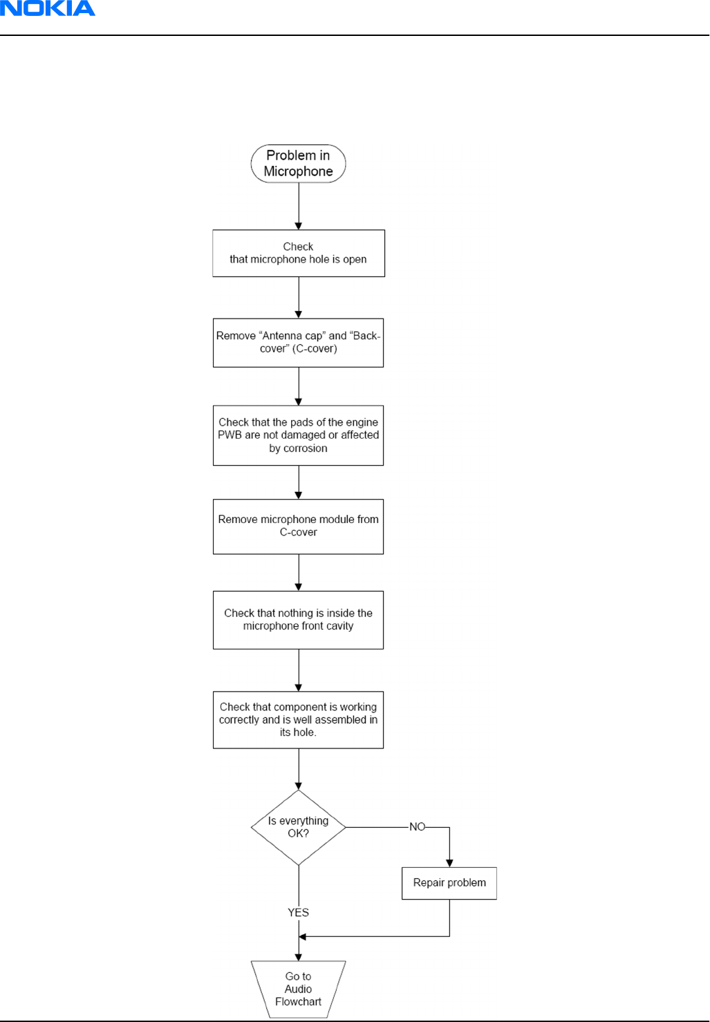
Microphone troubleshooting
Troubleshooting flow
RM-188; RM-198
Nokia Customer Care BB Troubleshooting and Manual Tuning Guide
Page 6 –52 COMPANY CONFIDENTIAL Issue 2
Copyright © 2007 Nokia. All rights reserved.
Baseband manual tuning guide
Energy management calibration
Prerequisites
Energy Management (EM) calibration is performed to calibrate the setting (gain and offset) of AD converters
in several channels (that is, battery voltage, BSI, battery current) to get an accurate AD conversion result.
Hardware setup:
• An external power supply is needed.
• Supply 12V DC from an external power supply to CU-4 to power up the phone.
• The phone must be connected to a CU-4 control unit with a product-specific flash adapter.
Steps
1. Place the phone to the docking station adapter (CU-4 is connected to the adapter).
2. Start
Phoenix
service software.
3. Choose File→ Scan Product.
4. Choose Tuning→Energy Management Calibration.
5. To show the current values in the phone memory, click Read, and check that communication between
the phone and CU-4 works.
6. Check that the CU-4 used check box is checked.
7. Select the item(s) to be calibrated.
Note: ADC calibration has to be performed before other item(s). However, if all calibrations are
selected at the same time, there is no need to perform the ADC calibration first.
8. Click Calibrate.
The calibration of the selected item(s) is carried out automatically.
The candidates for the new calibration values are shown in the
Calculated values
column. If the new
calibration values seem to be acceptable (please refer to the following "Calibration value limits" table),
click Write to store the new calibration values to the phone permanent memory.
Table 12 Calibration value limits
Parameter Min. Max.
ADC Offset -20 20
ADC Gain 12000 14000
BSI Gain 1100 1300
VBAT Offset 2400 2650
VBAT Gain 19000 23000
IBAT (ICal) Gain 6200 15600
9. Click Read, and confirm that the new calibration values are stored in the phone memory correctly. If the
values are not stored to the phone memory, click Write and/or repeat the procedure again.
10. To end the procedure, close the
Energy Management Calibration
window.
RM-188; RM-198
BB Troubleshooting and Manual Tuning Guide Nokia Customer Care
Issue 2 COMPANY CONFIDENTIAL Page 6 –53
Copyright © 2007 Nokia. All rights reserved.

RM-188; RM-198
Nokia Customer Care BB Troubleshooting and Manual Tuning Guide
(This page left intentionally blank.)
Page 6 –54 COMPANY CONFIDENTIAL Issue 2
Copyright © 2007 Nokia. All rights reserved.

7 — RF Troubleshooting and
Manual Tuning Guide
Nokia Customer Care
Issue 2 COMPANY CONFIDENTIAL Page 7 –1
Copyright © 2007 Nokia. All rights reserved.

RM-188; RM-198
Nokia Customer Care RF Troubleshooting and Manual Tuning Guide
(This page left intentionally blank.)
Page 7 –2 COMPANY CONFIDENTIAL Issue 2
Copyright © 2007 Nokia. All rights reserved.

Table of Contents
Introduction to RF troubleshooting .....................................................................................................................7–5
RF key component placement...............................................................................................................................7–5
Receiver troubleshooting ......................................................................................................................................7–6
Introduction to RX troubleshooting................................................................................................................7–6
General instructions for RX troubleshooting..................................................................................................7–7
Synthesizer troubleshooting............................................................................................................................7–9
RX GSM850 troubleshooting.......................................................................................................................... 7–10
RX GSM900 troubleshooting.......................................................................................................................... 7–11
RX GSM1800 troubleshooting........................................................................................................................ 7–12
RX GSM1900 troubleshooting........................................................................................................................ 7–13
GSM Rx chain activation for manual measurements / GSM RSSI measurement....................................... 7–14
Transmitter troubleshooting ............................................................................................................................. 7–14
General instructions for TX troubleshooting............................................................................................... 7–14
TX 850/900 troubleshooting......................................................................................................................... 7–17
TX 1800/1900 troubleshooting..................................................................................................................... 7–18
Checking antenna functionality.................................................................................................................... 7–19
RF tunings ............................................................................................................................................................ 7–19
Introduction to RF tunings............................................................................................................................ 7–19
RF autotuning................................................................................................................................................. 7–20
System mode independent manual tunings .................................................................................................... 7–22
Rf channel filter calibration........................................................................................................................... 7–22
PA (power amplifier) detection .................................................................................................................... 7–23
GSM receiver tunings........................................................................................................................................... 7–24
Rx calibration (GSM) ....................................................................................................................................... 7–24
Rx band filter response compensation (GSM).............................................................................................. 7–27
GSM transmitter tunings..................................................................................................................................... 7–32
Tx IQ tuning (GSM).......................................................................................................................................... 7–32
Tx power level tuning (GSM) ......................................................................................................................... 7–34
RM-188 WLAN troubleshooting.......................................................................................................................... 7–38
Introduction to WLAN troubleshooting ....................................................................................................... 7–38
WLAN functionality test using SB-7 and Phoenix........................................................................................ 7–41
WLAN failure troubleshooting ...................................................................................................................... 7–42
List of Tables
Table 13 Rf channel filter calibration tuning limits......................................................................................... 7–23
Table 14 RF tuning limits in Rx calibration....................................................................................................... 7–26
List of Figures
Figure 47 RM-188/198 RF key component placement........................................................................................7–6
Figure 48 RF Controls window ..............................................................................................................................7–8
Figure 49 RSSI Reading window........................................................................................................................ 7–14
Figure 50 RF Controls window ........................................................................................................................... 7–16
Figure 51 BT/WLAN antenna, feed and GND spots of the main antenna....................................................... 7–19
Figure 52 Rf channel filter calibration typical values ...................................................................................... 7–23
Figure 53 WLAN layout part 1 ............................................................................................................................ 7–39
Figure 54 WLAN layout part 2 ............................................................................................................................ 7–39
RM-188; RM-198
RF Troubleshooting and Manual Tuning Guide Nokia Customer Care
Issue 2 COMPANY CONFIDENTIAL Page 7 –3
Copyright © 2007 Nokia. All rights reserved.

RM-188; RM-198
Nokia Customer Care RF Troubleshooting and Manual Tuning Guide
(This page left intentionally blank.)
Page 7 –4 COMPANY CONFIDENTIAL Issue 2
Copyright © 2007 Nokia. All rights reserved.

Introduction to RF troubleshooting
All measurements should be done using:
• spectrum analyser with a high-frequency high-impedance passive probe (LO-/reference frequencies and
RF power levels)
• oscilloscope with a 10:1 probe (DC-voltages and low frequency signals)
Caution: Also all measurements with an RF coupler should be performed in RF shielded environment
because nearby base stations can disturb sensitive receiver measurements. If there is no possibility
to use RF shielded environment, it should be checked that there are no transmissions on the same
frequencies as used in the tests.
The RF section of the phone is build around one RF ASIC: ASIC N7505.
Note: Before changing N7505, please check the following things: supply voltages and serial
communication coming from baseband toN7505 are OK. Please note that the grounding of the Frond
End Module (FEM) is directly below FEM so it is difficult to check or change.
Most RF semiconductors are static discharge sensitive! ESD protection must be taken care of during repair
(ground straps and ESD soldering irons). N7505 and FEM are moisture sensitive, so parts must be pre-baked
prior to soldering.
In addition to key components, there are lot of discrete components (resistors, inductors and capacitors)
which troubleshooting is done mainly by checking if the soldering of the component is done properly.
Capacitor can be checked for shorts and resistors for value by means of an ohmmeter, but be aware in-circuit
measurements should be evaluated carefully as other components connected to the same node can change
the seen resistance.
Keep in mind that all measured voltages or RF levels depicted in the service manual are rough figures.
Especially RF levels vary because of different measuring equipment or different grounding of the probe used.
When using an RF probe, use a pair of metallic tweezers to connect the probe ground to the PWB ground as
close to the measurement point as possible. If measurements are performed in a product specific module
jig, then “GND” pads should be used for the probe ground.
RF key component placement
The RF section of the phone is build around one RF ASIC: ASIC N7505.
RM-188; RM-198
RF Troubleshooting and Manual Tuning Guide Nokia Customer Care
Issue 2 COMPANY CONFIDENTIAL Page 7 –5
Copyright © 2007 Nokia. All rights reserved.
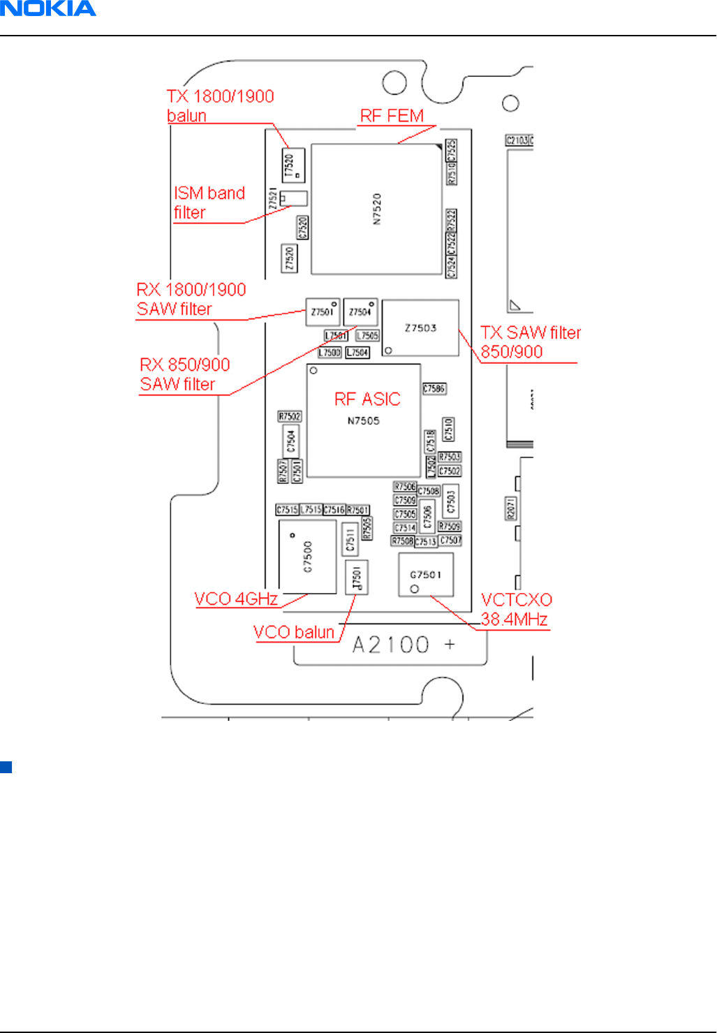
Figure 47 RM-188/198 RF key component placement
Receiver troubleshooting
Introduction to RX troubleshooting
Rx can be tested by making a phone call or in the local mode. For the local mode testing, use Phoenix service
software.
The main Rx troubleshooting measurement is RSSI measurement. This test measures the signal strength of
the received signal. I and Q branches can be measured separately.
In GSM, the input signal can be either a real GSM signal or a CW signal that is 67.771kHz up from the carrier
frequency.
For service tool usage instructions, refer to section Service Tools and Service Concepts.
RM-188; RM-198
Nokia Customer Care RF Troubleshooting and Manual Tuning Guide
Page 7 –6 COMPANY CONFIDENTIAL Issue 2
Copyright © 2007 Nokia. All rights reserved.
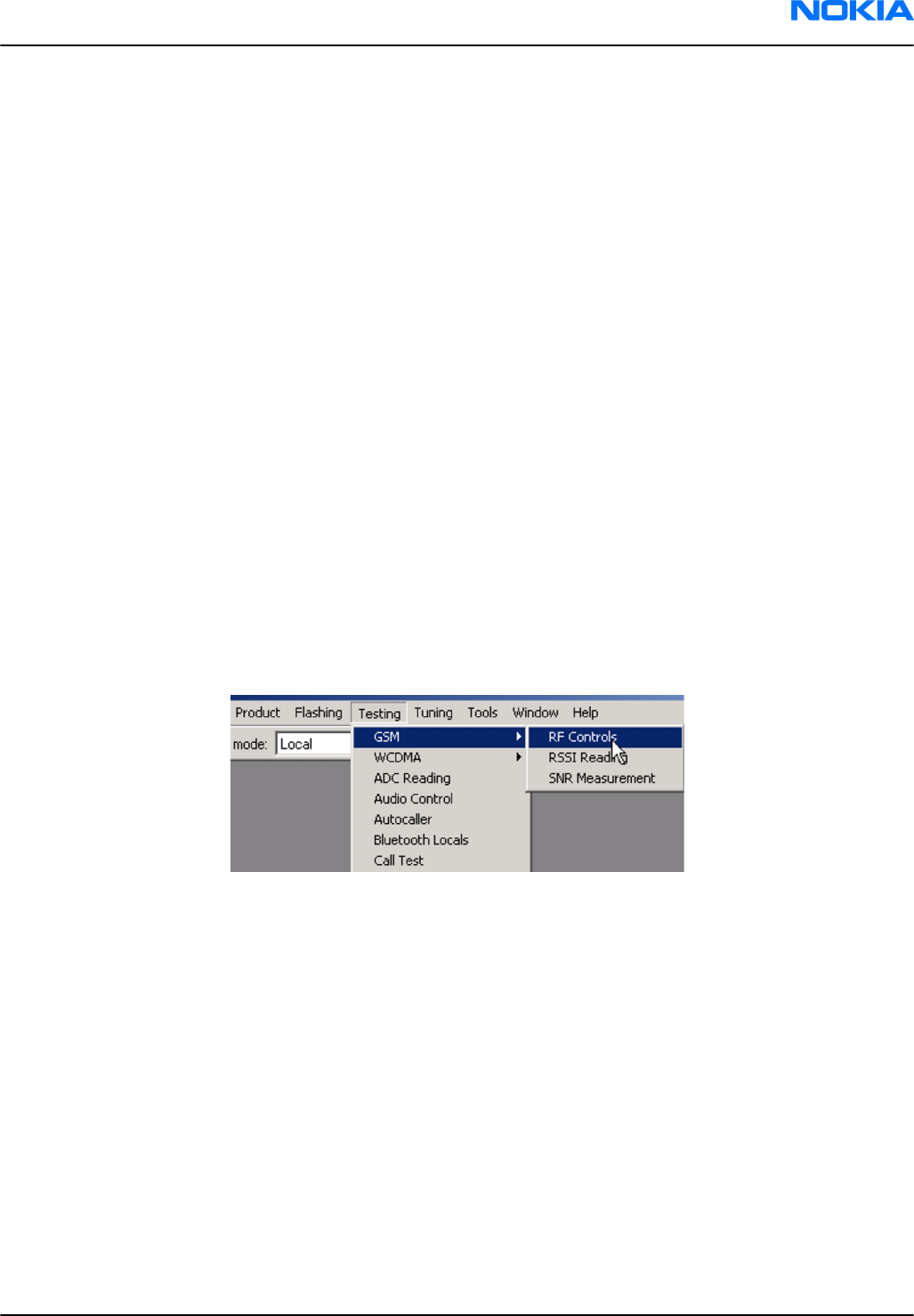
General instructions for RX troubleshooting
Steps
1. Connect a test jig to a computer with a DKU-2 cable or to a FPS-10 flash prommer with a modular cable
(XCS-4).
Make sure that you have a PKD-1 dongle connected to the computer's parallel port.
2. Connect a DC power supply to a module test jig (MJ-111).
Note: Set the DC supply voltage to 12 V and set the jumper connector on the test jig's reg.pass
switch to “ON” position.
3. Connect an RF cable between the RF connector of the phone and measurement equipment or alternatively
use a 50 ohms (at least 2W) dummy, otherwise GSM may be damaged.
Note: Make sure that all connections are made to the correct RF connector and correct type of RF
probe is used.
4. Set Rx on.
i Set the phone module to the test jig and start
Phoenix service software
.
ii Initialize connection to the phone. (With FPS-10 use FBUS driver when using DKU-2 and COMBOX driver).
iii From the File menu, choose product: File -> Choose Product -> xx-x* (* = type designator of the
phone, scan product).
iv From the toolbar, set operating mode to “Local”.
5. EGSM900, GSM850/1800/1900 troubleshooting
i From the Testing menu, activate the
RF Controls
window: Testing -> GSM -> RF Controls .
ii In the
RF Controls
window:
• Select band "GSM850", “GSM900” or “GSM1800” or “GSM1900” (Default = “GSM850”).
• Set Active unit to “Rx” (Default = “Rx”).
• Set Operation mode to “Burst” (Default = “Burst”).
•Set Rx/Tx channel to 190 on GSM850, 37 on GSM900 band or 700 on GSM1800 band or 661 on GSM1900
(Defaults).
• Set Edge to “Off” (Default). (Not active in RXmode).
• Set Tx PA mode to “Free” (Default). (Not active in RXmode).
•Apply 942.46771 MHz (channel 37 + 67.710 kHz offset), 881.66771MHz (channel 190 + 67.710 kHz),
1842.86771 MHz (channel 700 + 67.710 kHz offset) or 1960.06771 MHz (channel 661 + 67.71 kHz) –
90 dBm signal to the RF-connector (remember to compensate for cable attenuation).
RM-188; RM-198
RF Troubleshooting and Manual Tuning Guide Nokia Customer Care
Issue 2 COMPANY CONFIDENTIAL Page 7 –7
Copyright © 2007 Nokia. All rights reserved.
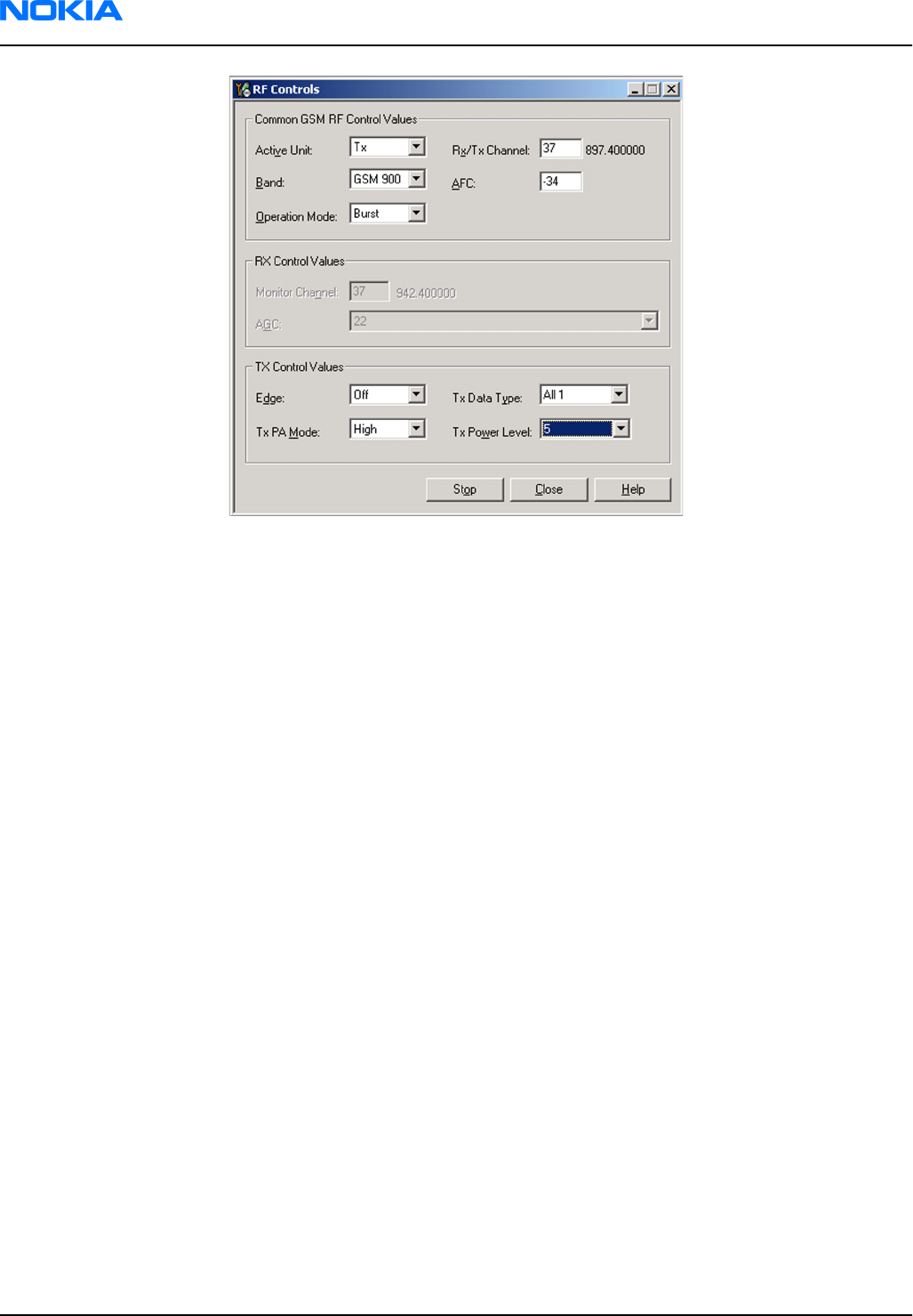
Figure 48 RF Controls window
RM-188; RM-198
Nokia Customer Care RF Troubleshooting and Manual Tuning Guide
Page 7 –8 COMPANY CONFIDENTIAL Issue 2
Copyright © 2007 Nokia. All rights reserved.
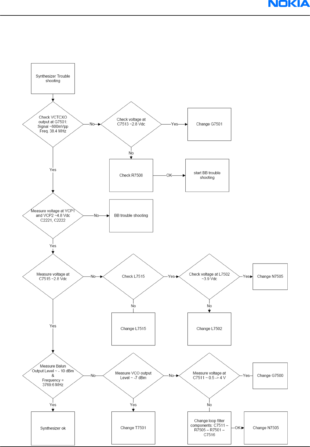
Synthesizer troubleshooting
Troubleshooting flow
RM-188; RM-198
RF Troubleshooting and Manual Tuning Guide Nokia Customer Care
Issue 2 COMPANY CONFIDENTIAL Page 7 –9
Copyright © 2007 Nokia. All rights reserved.

RX GSM850 troubleshooting
Troubleshooting flow
RM-188; RM-198
Nokia Customer Care RF Troubleshooting and Manual Tuning Guide
Page 7 –10 COMPANY CONFIDENTIAL Issue 2
Copyright © 2007 Nokia. All rights reserved.

RX GSM900 troubleshooting
Troubleshooting flow
RM-188; RM-198
RF Troubleshooting and Manual Tuning Guide Nokia Customer Care
Issue 2 COMPANY CONFIDENTIAL Page 7 –11
Copyright © 2007 Nokia. All rights reserved.
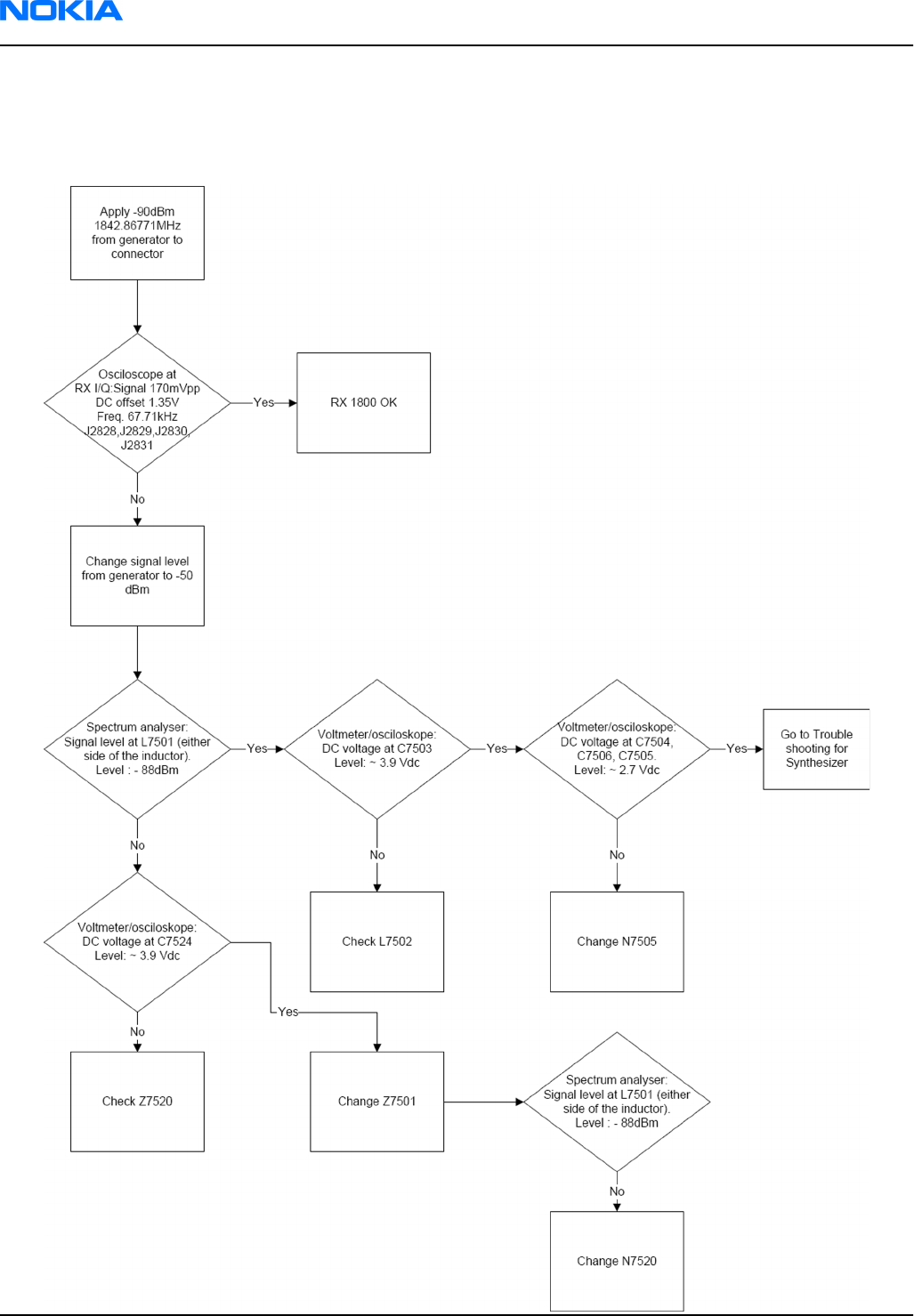
RX GSM1800 troubleshooting
Troubleshooting flow
RM-188; RM-198
Nokia Customer Care RF Troubleshooting and Manual Tuning Guide
Page 7 –12 COMPANY CONFIDENTIAL Issue 2
Copyright © 2007 Nokia. All rights reserved.
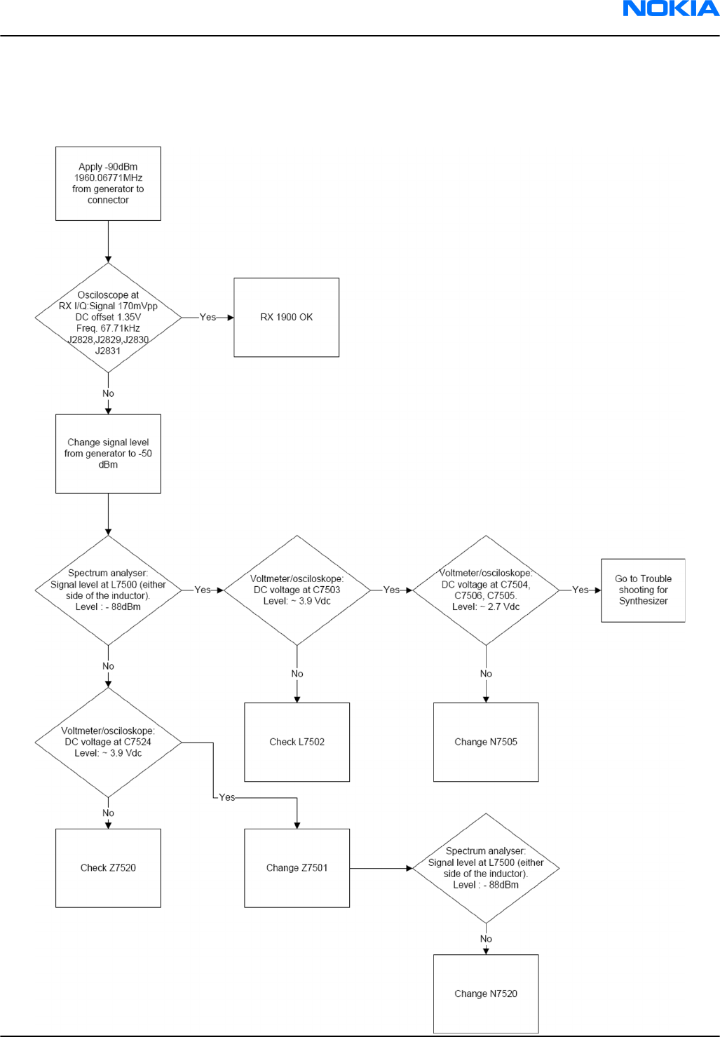
RX GSM1900 troubleshooting
Troubleshooting flow
RM-188; RM-198
RF Troubleshooting and Manual Tuning Guide Nokia Customer Care
Issue 2 COMPANY CONFIDENTIAL Page 7 –13
Copyright © 2007 Nokia. All rights reserved.
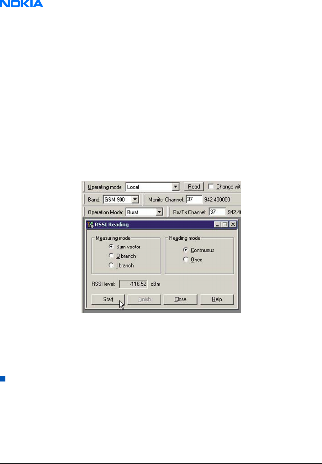
GSM Rx chain activation for manual measurements / GSM RSSI measurement
Context
RSSI signal measurement is the main Rx troubleshooting measurement. The test measures the strength of
the received signal.
I and Q branches can be measured separately. In GSM, the input signal can be either a real GSM signal or a
CW (Continuous Wave) signal that is 67.771 kHz above the carrier frequency.
Steps
1. Start
Phoenix
service software.
2. Choose Testing→GSM→RSSI Reading .
3. Set the RF signal generator for a channel frequency +67.771 kHz in CW mode with a –80 dBm signal level.
Alternatively set the cellular tester downlink channel to the appropriate channel. Make sure that the tester
is set to continuous mode, not to burst mode.
4. In the
RSSI Reading
window, select the appropriate band and channel.
Figure 49
RSSI Reading
window
5. To start the measurement, activate GSM Rx chain, click Start.
Results
RSSI reading values of the selected band and channel are displayed. The RSSI level must be the same value
as that which is set at the signal generator (-80 dBm).
Transmitter troubleshooting
General instructions for TX troubleshooting
Context
• Tx troubleshooting requires Tx operation.
• Do not transmit on frequencies that are in use!
• Transmitter can be controlled in the local mode for diagnostic purposes.
• The most useful Phoenix tool for GSM transmitter testing is "RF Controls".
RM-188; RM-198
Nokia Customer Care RF Troubleshooting and Manual Tuning Guide
Page 7 –14 COMPANY CONFIDENTIAL Issue 2
Copyright © 2007 Nokia. All rights reserved.
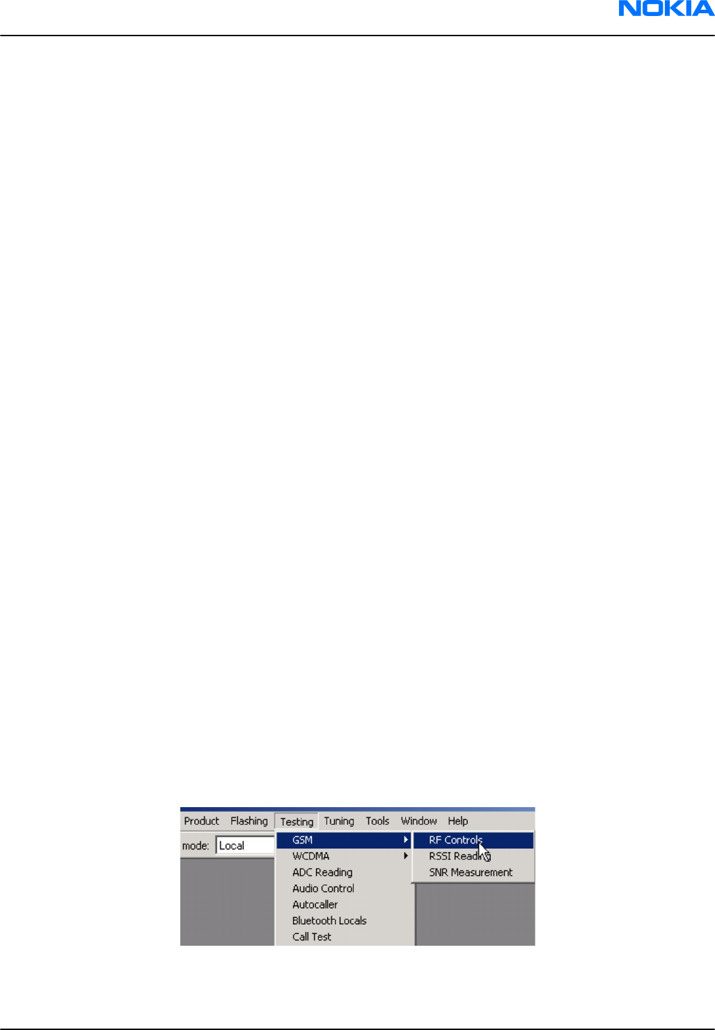
• Tx IQ tuning and Tx power tuning can be also used in some cases.
• Remember that retuning is not a fix! Phones are tuned correctly in production.
The first set of steps instructs how to assemble the test setup. This setup is general for all Tx troubleshooting
tasks.
Alternative steps provide specific troubleshooting instructions for
Phoenix
service software.
Caution: Never activate the GSM transmitter without a proper antenna load. There should be always
50 ohm load connected to the RF connector (antenna, RF-measurement equipment or at least 2
watts dummy load), otherwise GSM PA may be damaged.
Steps
1. Connect a test jig to a computer with a DKU-2 cable or to a FPS-10 flash prommer with a modular cable
(XCS-4).
Make sure that you have a PKD-1 dongle connected to the computer's parallel port.
2. Connect a DC power supply to a module jig (MJ-111).
Note: When repairing or tuning a transmitter, use an external DC supply with at least 3 A current
capability.
Set the DC supply voltage to 12V and set the jumper connector on the test jig's reg.pass switch to
“ON” position.
3. Connect an RF cable between the RF connector of the phone and measurement equipment or alternatively
use a 50 ohms (at least 2 W) dummy, otherwise GSM may be damaged.
Note: Make sure that all connections are made to the correct RF connector and correct type of RF
probe is used.
Normally a spectrum analyser is used as measurement equipment.
Note: The maximum input power of a spectrum analyser is +30 dBm.
To prevent any damage, it is recommended to use 10 dB attenuator on the spectrum analyzer input.
4. Set Tx on.
i Set the phone module to the test jig and start
Phoenix service software
.
ii Initialize connection to the phone. (With FPS-10 use FBUS driver when using DAU-9S and COMBOX
driver).
iii From the File menu, choose product: File -> Choose Product -> xx-x* (* = type designator of the
phone).
iv From the toolbar, set operating mode to “Local”.
5. EGSM900, GSM850/1800/1900 troubleshooting
i From the Testing menu, activate the
RF Controls
window: Testing -> GSM -> RF Controls .
ii In the
RF Controls
window:
• Select band "GSM850", “GSM900” or “GSM1800” or “GSM1900” (Default = “GSM850”).
RM-188; RM-198
RF Troubleshooting and Manual Tuning Guide Nokia Customer Care
Issue 2 COMPANY CONFIDENTIAL Page 7 –15
Copyright © 2007 Nokia. All rights reserved.
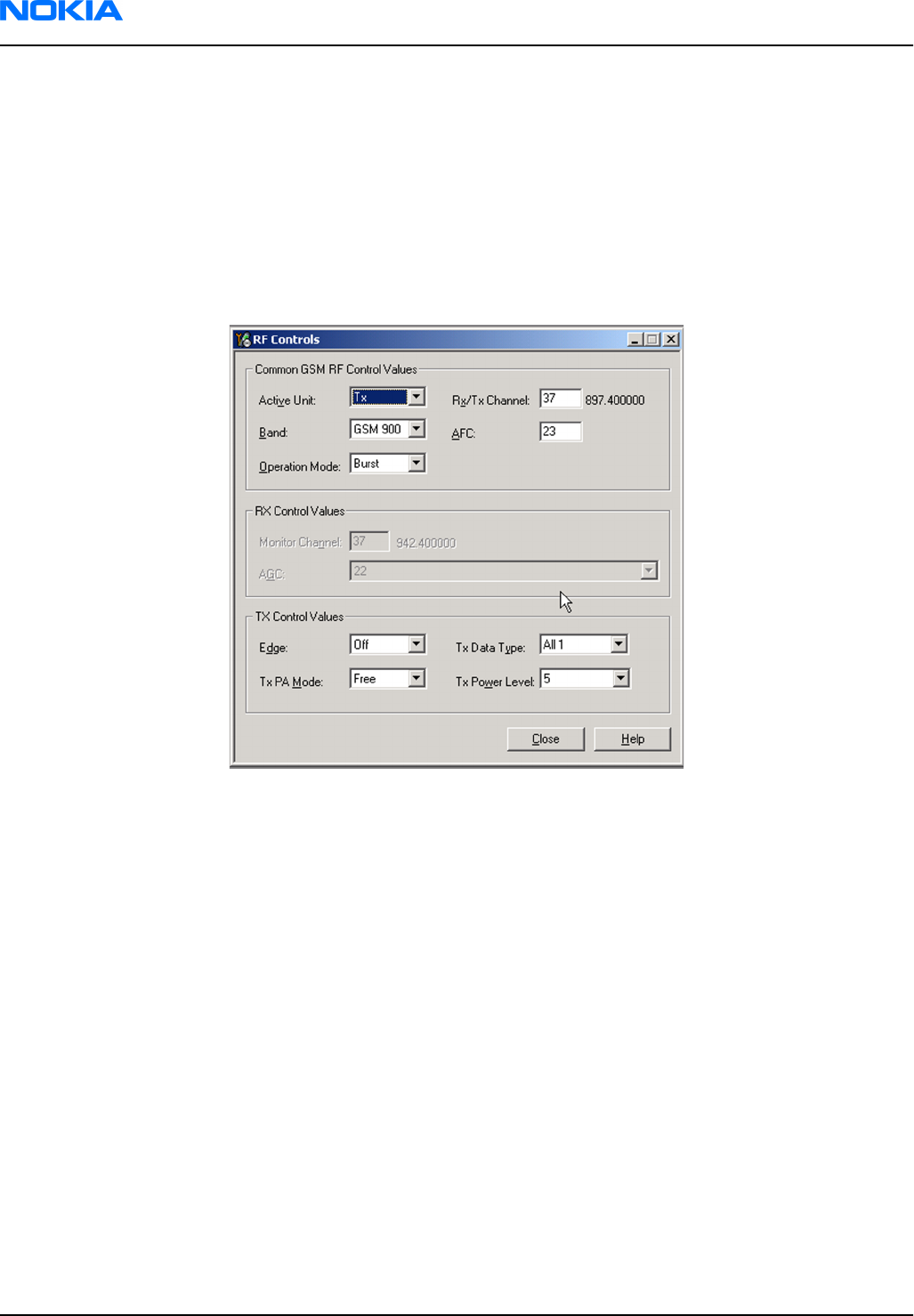
• Set Active unit to “Tx” (Default = “Rx”).
• Set Operation mode to “Burst” (Default = “Burst”).
• Set Tx data type to “Random” (Default = “All1”).
•Set Rx/Tx channel to 190 on GSM850, 37 on GSM900 band or 700 on GSM1800 band or 661 on GSM1900
(Defaults).
• Set Edge to “Off” (Default).
• Set Tx PA mode to “Free” (Default).
• Set power level to 5 (Default = 19) on GSM850/900 or to 0 (Default = 15) on GSM1800 or GSM1900.
Figure 50 RF Controls window
RM-188; RM-198
Nokia Customer Care RF Troubleshooting and Manual Tuning Guide
Page 7 –16 COMPANY CONFIDENTIAL Issue 2
Copyright © 2007 Nokia. All rights reserved.
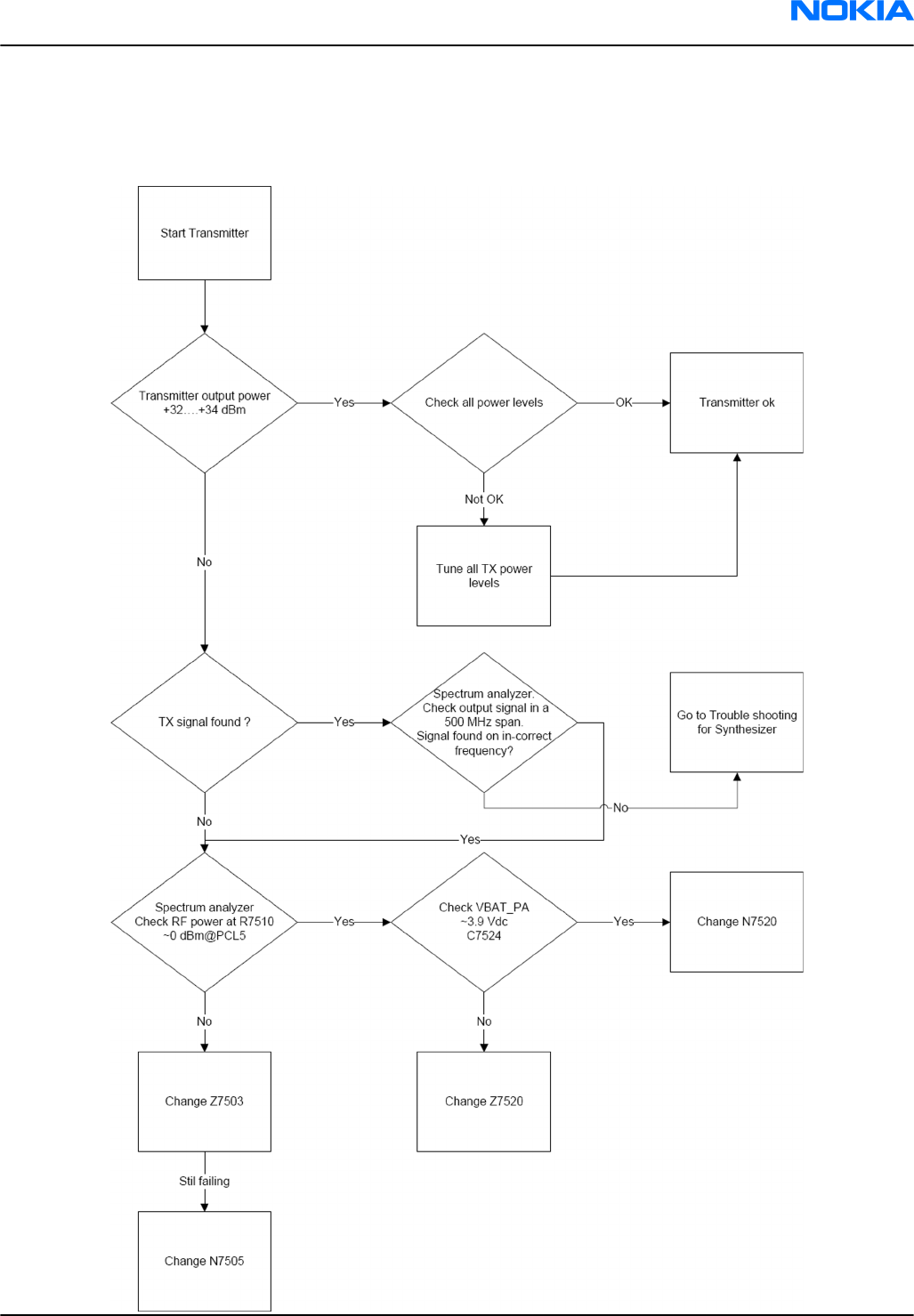
TX 850/900 troubleshooting
Troubleshooting flow
RM-188; RM-198
RF Troubleshooting and Manual Tuning Guide Nokia Customer Care
Issue 2 COMPANY CONFIDENTIAL Page 7 –17
Copyright © 2007 Nokia. All rights reserved.
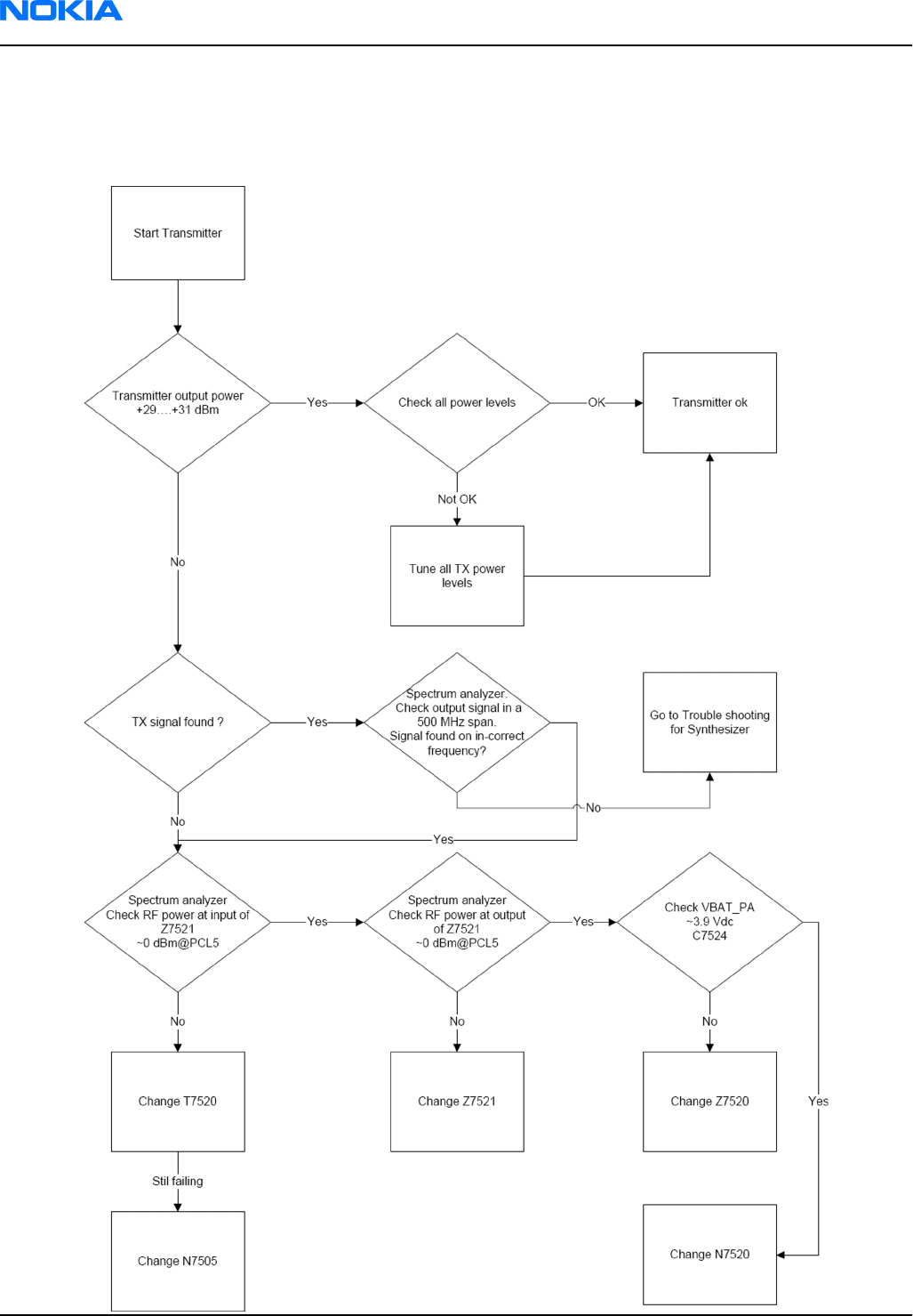
TX 1800/1900 troubleshooting
Troubleshooting flow
RM-188; RM-198
Nokia Customer Care RF Troubleshooting and Manual Tuning Guide
Page 7 –18 COMPANY CONFIDENTIAL Issue 2
Copyright © 2007 Nokia. All rights reserved.
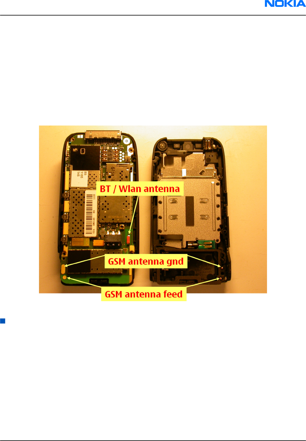
Checking antenna functionality
Main antenna
The main antenna has one antenna: GSM.
In the GSM antenna, there is one feed and one GND contact.
The antenna is functioning normally when it is visually intact and the antenna pins are intact.
BT/WLAN antenna
BT/WLAN antenna is a ceramic SMD antenna. The antenna is functioning normally when the contacts function
(RDC = 0 ohm) and the antenna is visually intact.
Figure 51 BT/WLAN antenna, feed and GND spots of the main antenna
RF tunings
Introduction to RF tunings
Important: Only perform RF tunings if:
• one or more of the RF components is changed
• flash Memory chip is changed or otherwise corrupted.
RF calibration is always performed with the help of a product-specific module jig, never with an RF coupler.
Using an RF coupler in the calibration phase will cause a complete mistuning of the RF side.
Important: After RF component changes, always use autotuning. Manual tunings are only required
in rare cases.
RM-188; RM-198
RF Troubleshooting and Manual Tuning Guide Nokia Customer Care
Issue 2 COMPANY CONFIDENTIAL Page 7 –19
Copyright © 2007 Nokia. All rights reserved.
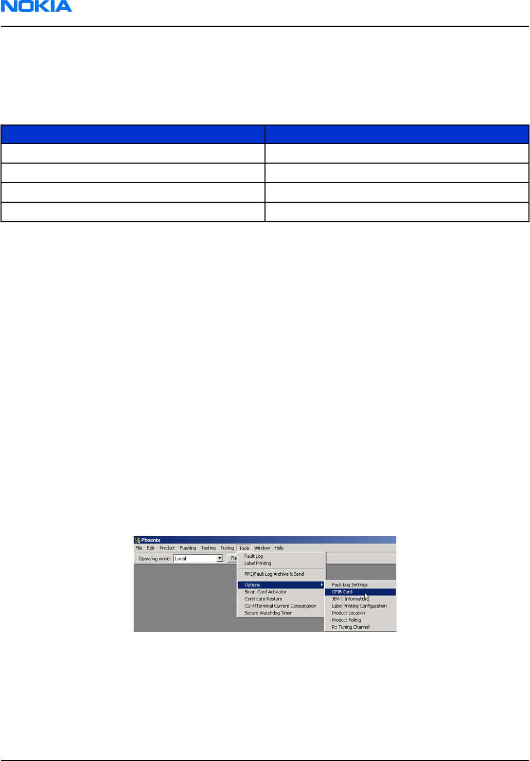
Cable and adapter losses
RF cables and adapters have some losses. They have to be taken in account when the phone is tuned. As all
the RF losses are frequency dependent, the user have to be very careful and understand the measurement
setup. In the following table there are RF attenuations of the module jig:
Band Attenuation
GSM850 0.2 dB
GSM900 0.2 dB
GSM1800 0.3 dB
GSM1900 0.3 dB
RF autotuning
Prerequisites
For information on the recommended test set-up, refer to the corresponding information on PWS/NOL.
Before you can use the auto-tune feature, the GPIB driver from the GPIB card vendor must be installed and
running.
The autotune .ini file must be in a correct place: C:\Program Files\Nokia\Phoenix\products\xx-x*
\autotune_xx-x*.ini (
*= indicates the type designator of the phone, e.g. RM-1
)
Context
RF autotuning is performed with the aid of Digital Radio Communication Tester. Autotuning covers all RF
tunings that are needed to perform after RF component repairs.
Note: Do not perform RF autotuning without a proper reason. Phones are tuned in production and
an RF tuning may be performed only after component repairs or if the RF tuning information is lost.
Steps
1. Connect the communication tester to the GPIB bus.
2. Start Phoenix service software.
3. From the Tools menu, choose Options -> GPIB Card.
4. In the Card Type line, select CEC8Bit, then click Start.
After clicking Start, the name of the communication tester appears in the list of found Listeners.
RM-188; RM-198
Nokia Customer Care RF Troubleshooting and Manual Tuning Guide
Page 7 –20 COMPANY CONFIDENTIAL Issue 2
Copyright © 2007 Nokia. All rights reserved.
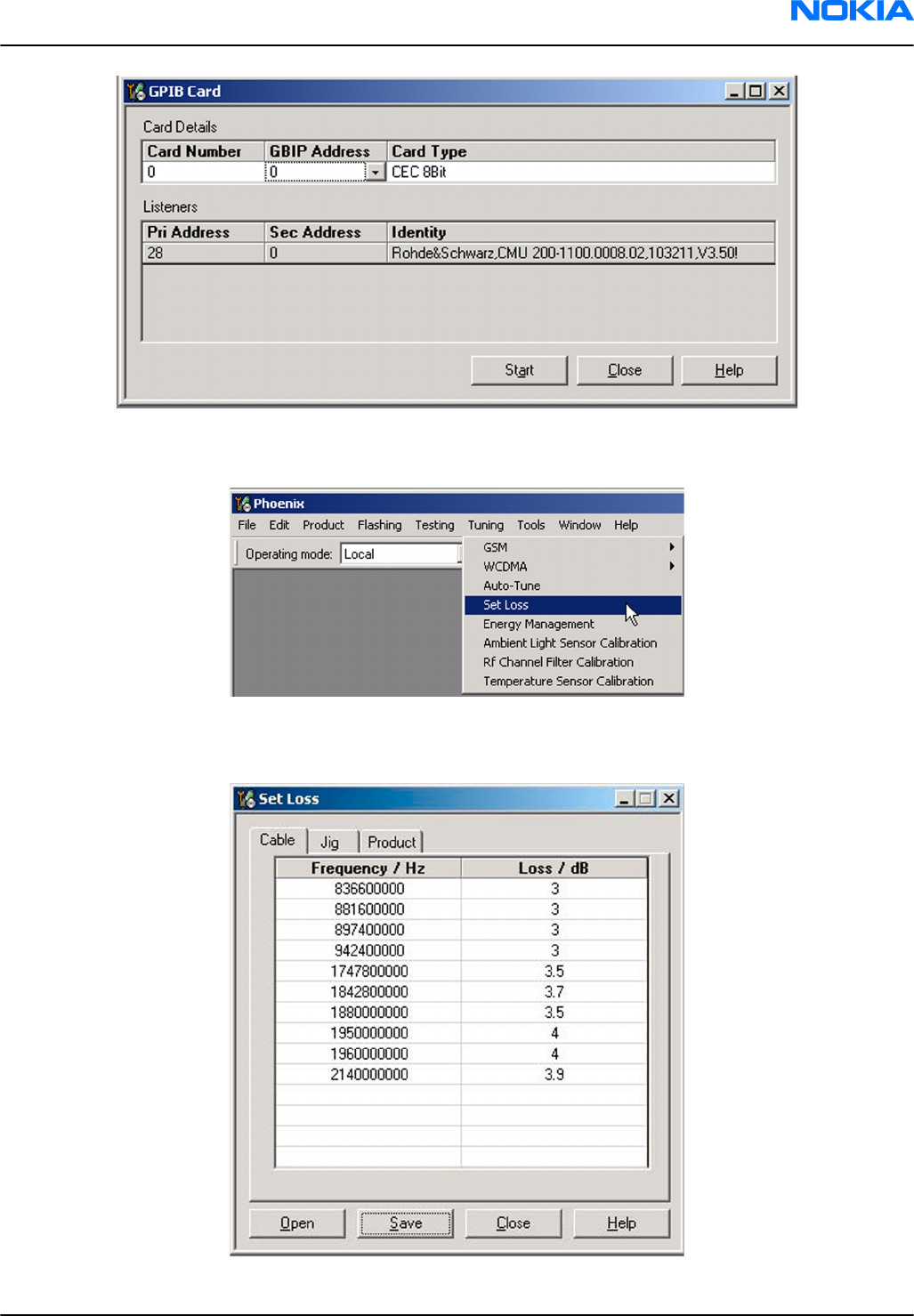
5. To specify the cable loss from module jig to the communication tester, choose "Set Loss" from the Tuning
menu.
6. Click the Cable tab and add the extra cable attenuation.
Note: Cable losses have to be determined on the basis of a cable used.
RM-188; RM-198
RF Troubleshooting and Manual Tuning Guide Nokia Customer Care
Issue 2 COMPANY CONFIDENTIAL Page 7 –21
Copyright © 2007 Nokia. All rights reserved.
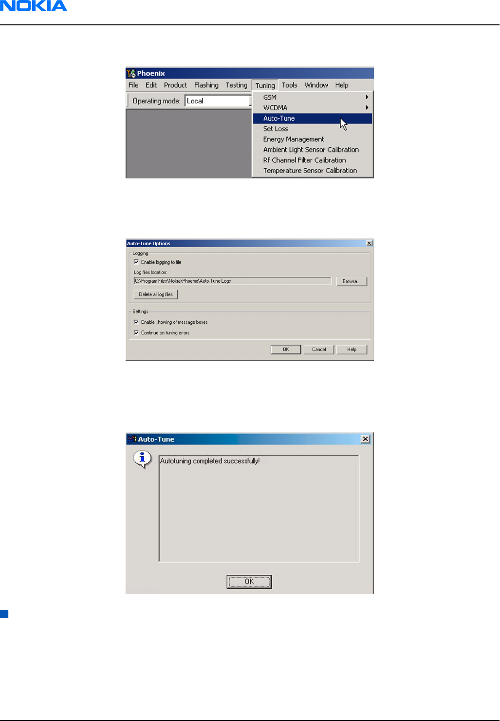
7. To start autotuning, choose Auto-Tune from the Tuning menu.
8. In the Auto-Tune window, click Options.
9. In the Auto-Tune options window, see that the "Enable showing of messages" check box is checked,
then click OK.
10. To complete the RF autotuning, click OK.
Results
"Autotuning completed successfully" message appears.
System mode independent manual tunings
Rf channel filter calibration
Context
Rf channel filter calibration tunes the internal low pass filters of Rx and Tx ASICs that limit the bandwidth of
BB IQ signals.
RM-188; RM-198
Nokia Customer Care RF Troubleshooting and Manual Tuning Guide
Page 7 –22 COMPANY CONFIDENTIAL Issue 2
Copyright © 2007 Nokia. All rights reserved.
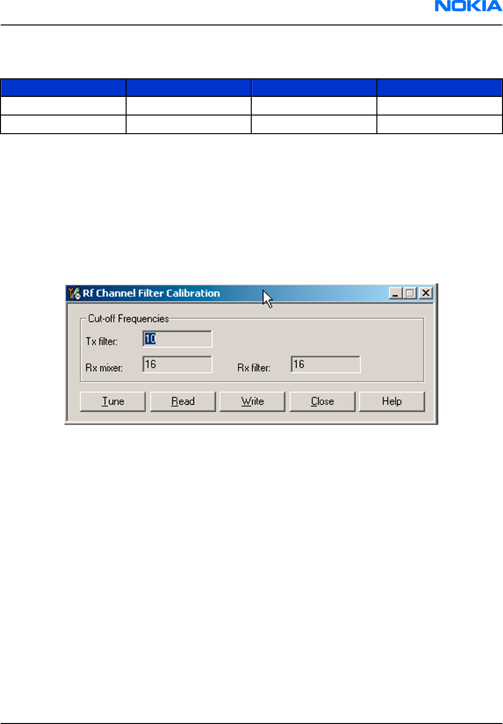
One common calibration is made for GSM.
Table 13 Rf channel filter calibration tuning limits
Min Typ Max
Tx filter 0 10 31
Rx filter 0 16 31
Steps
1. From the Operating mode drop-down menu, set mode to Local.
2. Choose Tuning→Rf Channel Filter Calibration .
3. Click Tune.
4. To save the values to the PMM (Phone Permanent Memory) area, click Write.
5. To close the
Rf Channel Filter Calibration
window, click Close.
Results
Figure 52 Rf channel filter calibration typical values
PA (power amplifier) detection
Context
The PA detection procedure detects which PA manufacturer is used for phone PAs.
If a PA is changed or if the permanent memory (PMM) data is corrupted, PA detection has to be performed
before Tx tunings.
Steps
1. From the Operating mode drop-down menu, set mode to Local.
2. Choose Tuning→PA Detection .
3. Click Tune.
4. Check that the detected PA manufacturers are corresponding to the actual chips on the board.
5. To end the procedure, click Close.
RM-188; RM-198
RF Troubleshooting and Manual Tuning Guide Nokia Customer Care
Issue 2 COMPANY CONFIDENTIAL Page 7 –23
Copyright © 2007 Nokia. All rights reserved.
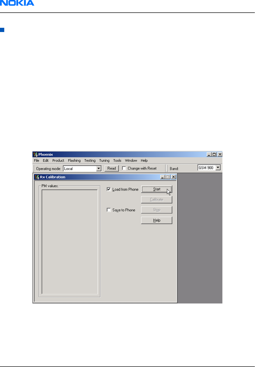
GSM receiver tunings
Rx calibration (GSM)
Context
Rx Calibration is used to find out the real gain values of the GSM Rx AGC system and tuning response of the
AFC system (AFC D/A init value and AFC slope)
Steps
1. Connect the GSM connector of the module jig to a signal generator.
2. Start
Phoenix
service software.
3. From the Operating mode drop-down menu, set mode to Local.
4. Choose Tuning→GSM→Rx Calibration .
5. Check the Load from Phone check box, and uncheck Save to Phone.
6. From the Band drop-down menu, choose e.g. GSM900.
7. Click Start.
RM-188; RM-198
Nokia Customer Care RF Troubleshooting and Manual Tuning Guide
Page 7 –24 COMPANY CONFIDENTIAL Issue 2
Copyright © 2007 Nokia. All rights reserved.
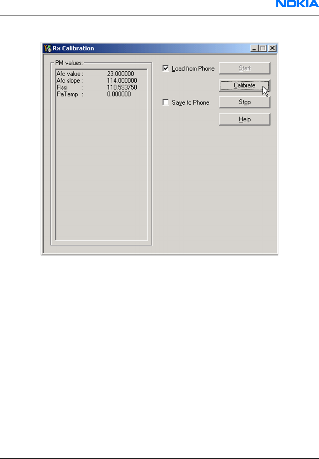
8. Click Calibrate.
9. Connect the signal generator to the phone, and set frequency and amplitude as instructed in the
Rx Calibration with band EGSM900 pop-up window.
Important: The calibration uses a non-modulated CW signal. Increase the signal generator level by
cable attenuation and module jig probe attenuation.
RM-188; RM-198
RF Troubleshooting and Manual Tuning Guide Nokia Customer Care
Issue 2 COMPANY CONFIDENTIAL Page 7 –25
Copyright © 2007 Nokia. All rights reserved.
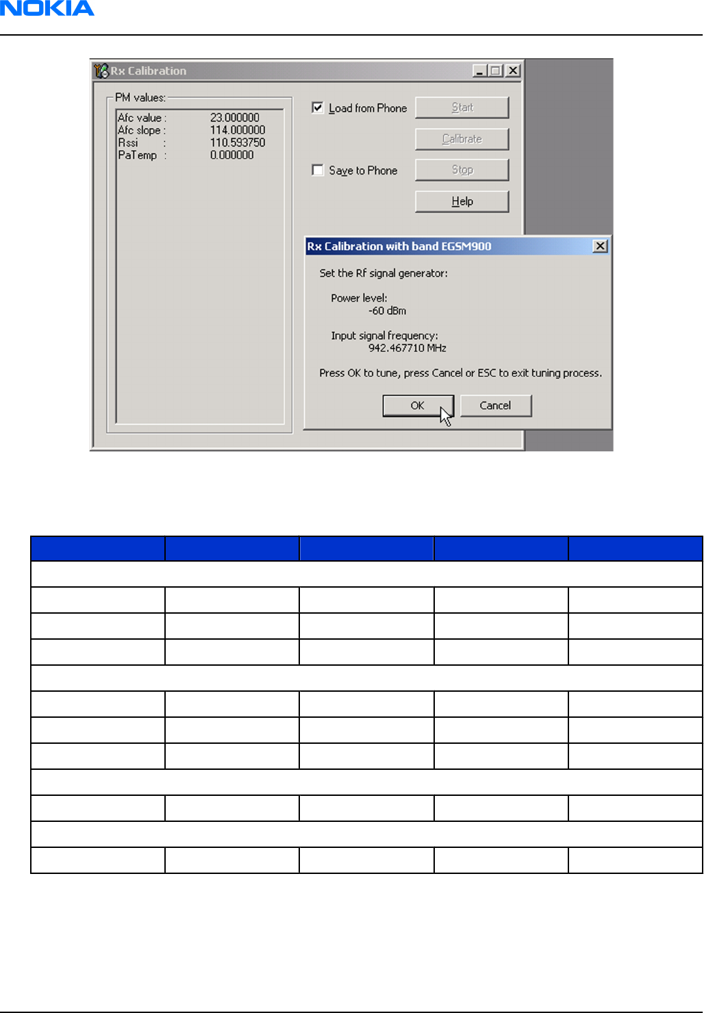
10. To perform the tuning, click OK.
11. Check that the tuning values are within the limits specified in the following table:
Table 14 RF tuning limits in Rx calibration
Min Typ Max Unit
GSM850
AFC Value -200 -105...62 200
AFC slope 0 122 200
RSSI0 106 107...110 114 dB
GSM900
AFC Value -200 -105...62 200
AFC slope 0 122 200
RSSI0 106 107...110 114 dB
GSM1800
RSSI0 104 104...109 114 dB
GSM1900
RSSI0 104 104...109 114 dB
RM-188; RM-198
Nokia Customer Care RF Troubleshooting and Manual Tuning Guide
Page 7 –26 COMPANY CONFIDENTIAL Issue 2
Copyright © 2007 Nokia. All rights reserved.
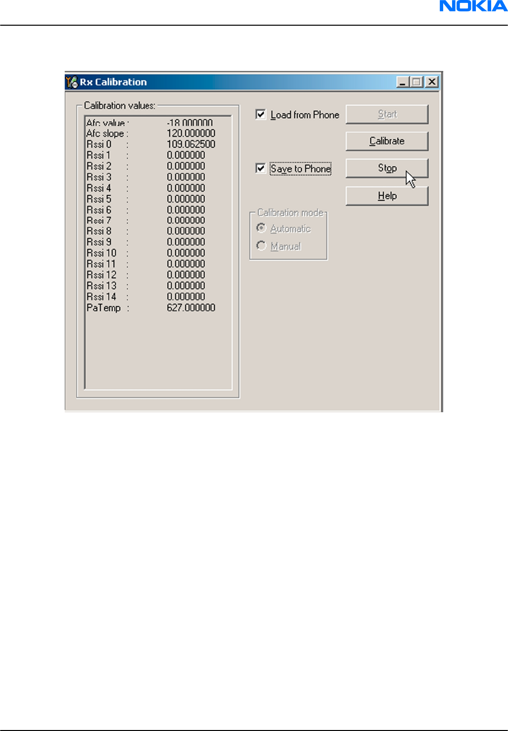
12. To save values to the phone, check the Save to Phone check box, and click Stop.
Next actions
Repeat steps 3 to 8 for GSM850, GSM1800 and GSM1900
Rx band filter response compensation (GSM)
Prerequisites
Rx calibration must be done before the Rx Band Filter Response Compensation
Context
In each GSM Rx band, there’s a band rejecting filter in front of RF ASIC front end. The amplitude ripple caused
by these filters causes ripple to the RSSI measurement and therefore calibration is needed.
The calibration has to be repeated for each GSM band.
Steps
1. Connect module jig’s GSM connector to signal generator.
2. From the dropdown menus, set "Operating mode" to Local, "System mode" to GSM, and Band to GSM900.
RM-188; RM-198
RF Troubleshooting and Manual Tuning Guide Nokia Customer Care
Issue 2 COMPANY CONFIDENTIAL Page 7 –27
Copyright © 2007 Nokia. All rights reserved.
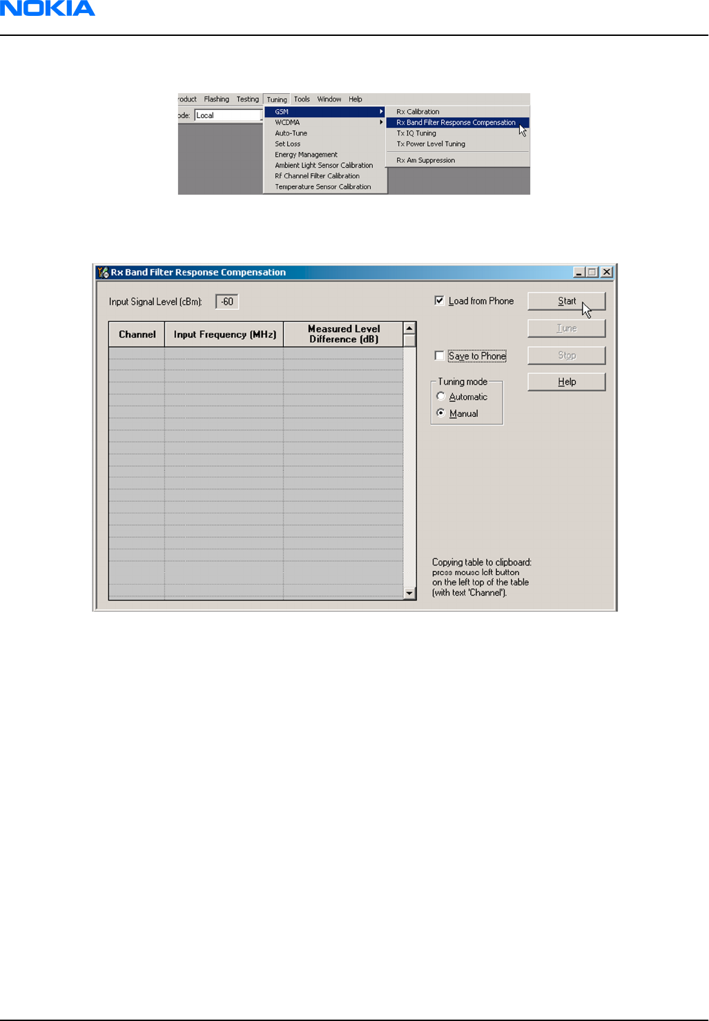
3. From the Tuning menu, choose GSM -> Rx Band Filter Response Compensation.
4. Check “Manual” and “Load from Phone” check boxes. Clear “Save to Phone” check box
5. Click Start.
RM-188; RM-198
Nokia Customer Care RF Troubleshooting and Manual Tuning Guide
Page 7 –28 COMPANY CONFIDENTIAL Issue 2
Copyright © 2007 Nokia. All rights reserved.
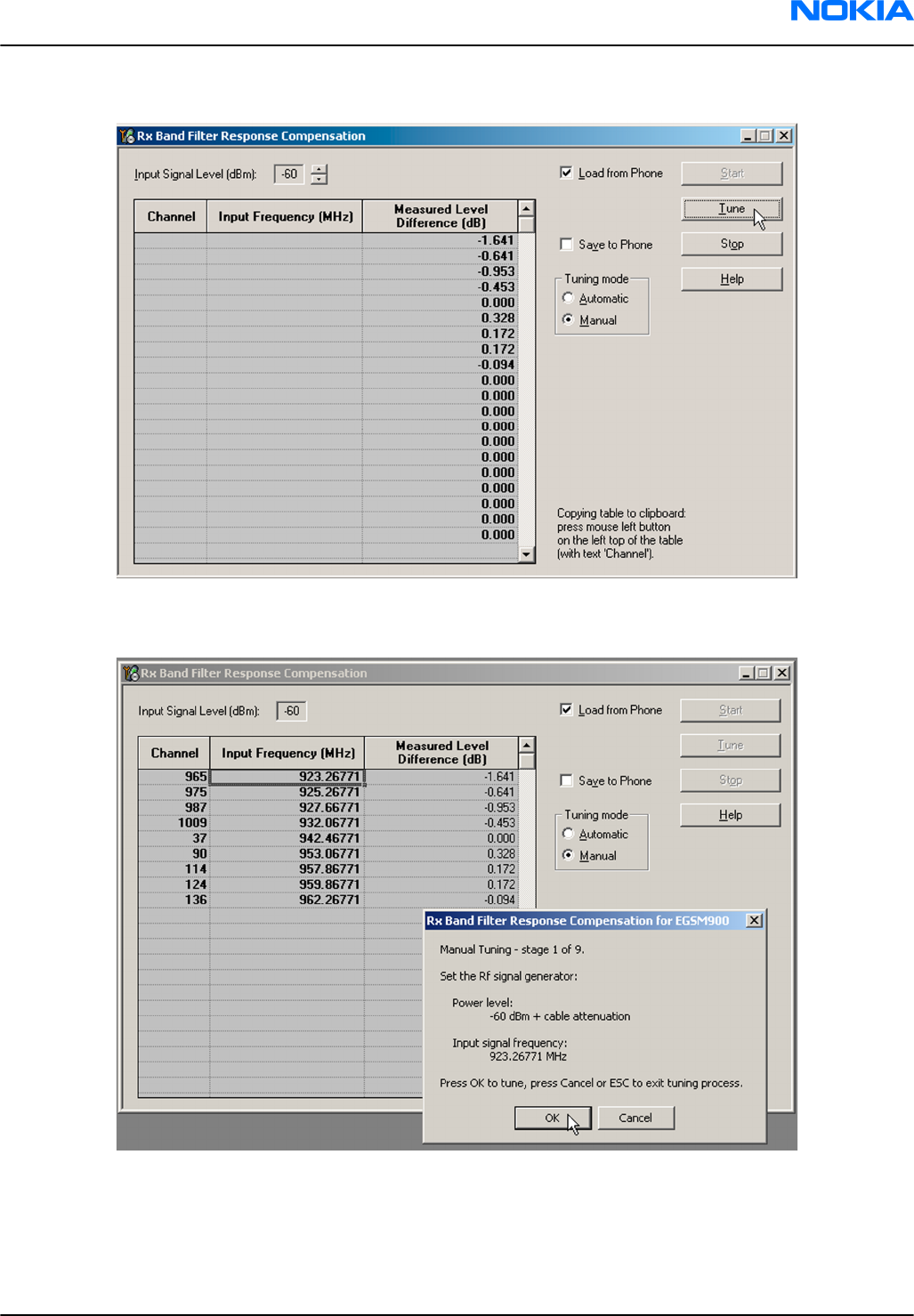
6. Click Tune.
7. Connect signal generator to the phone and set frequency and amplitude as instructed in the "Rx Band
Filter Response Compensation for EGSM900" popup window.
8. To perform tuning, click OK.
9. Go through all 9 frequencies.
RM-188; RM-198
RF Troubleshooting and Manual Tuning Guide Nokia Customer Care
Issue 2 COMPANY CONFIDENTIAL Page 7 –29
Copyright © 2007 Nokia. All rights reserved.
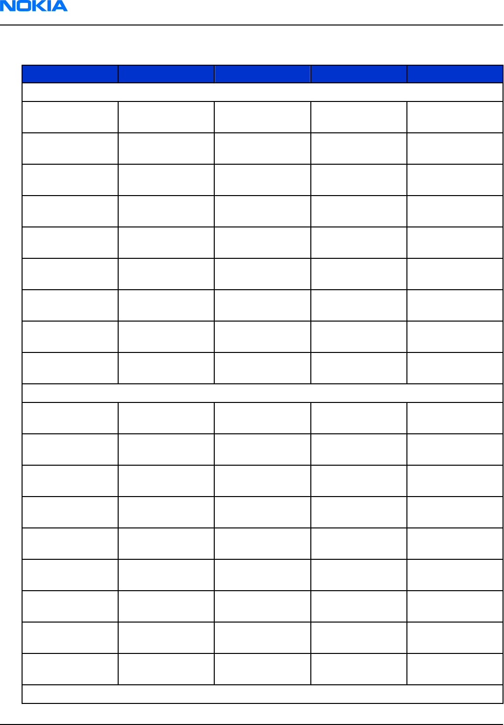
10. Check that the tuning values are within the limits specified in this table:
Min Typ Max Unit
GSM850
Ch. 118 /
867.26771 MHz
-10 -1 5 dB
Ch. 128 /
869.26771 MHz
-3 0 5 dB
Ch. 140 /
871.66771 MHz
-3 0 5 dB
Ch. 172 /
878.06771 MHz
-3 0 5 dB
Ch. 190 /
881.66771 MHz
-3 0 5 dB
Ch. 217 /
887.06771 MHz
-3 0 5 dB
Ch. 241 /
891.86771 MHz
-3 0 5 dB
Ch. 251 /
893.86771 MHz
-3 0 5 dB
Ch. 261/
895.86771 MHz
-10 -1 5 dB
GSM900
Ch. 965 /
923.26771 MHz
-10 -1 5 dB
Ch. 975 /
925.26771 MHz
-3 0 5 dB
Ch. 987 /
927.66771 MHz
-3 0 5 dB
Ch. 1009 /
932.06771 MHz
-3 0 5 dB
Ch. 37 /
942.46771 MHz
-3 0 5 dB
Ch. 90 /
953.06771 MHz
-3 0 5 dB
Ch. 114 /
957.86771 MHz
-3 0 5 dB
Ch. 124 /
959.86771 MHz
-3 0 5 dB
Ch. 136 /
962.26771 MHz
-10 -1 5 dB
GSM1800
RM-188; RM-198
Nokia Customer Care RF Troubleshooting and Manual Tuning Guide
Page 7 –30 COMPANY CONFIDENTIAL Issue 2
Copyright © 2007 Nokia. All rights reserved.
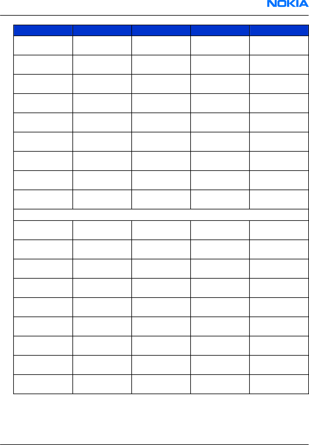
Min Typ Max Unit
Ch. 497 /
1802.26771 MHz
-10 -1 5 dB
Ch. 512 /
1805.26771 MHz
-3 0 5 dB
Ch. 535 /
1809.86771 MHz
-3 0 5 dB
Ch. 606 /
1824.06771 MHz
-3 0 5 dB
Ch. 700 /
1842.86771 MHz
-3 0 5 dB
Ch. 791 /
1861.06771 MHz
-3 0 5 dB
Ch. 870 /
1876.86771 MHz
-3 0 5 dB
Ch. 885 /
1879.86771 MHz
-3 0 5 dB
Ch. 908 /
1884.46771 MHz
-10 -1 5 dB
GSM1900
Ch. 496 /
1927.06771 MHz
-10 -1 5 dB
Ch. 512 /
1930.26771 MHz
-3 0 5 dB
Ch. 537 /
1935.26771 MHz
-3 0 5 dB
Ch. 586 /
1945.06771 MHz
-3 0 5 dB
Ch. 661 /
1960.06771 MHz
-3 0 5 dB
Ch. 736 /
1975.06771 MHz
-3 0 5 dB
Ch. 794 /
1986.66771 MHz
-3 0 5 dB
Ch. 810 /
1989.86771 MHz
-3 0 5 dB
Ch. 835 /
1994.86771 MHz
-10 -1 5 dB
RM-188; RM-198
RF Troubleshooting and Manual Tuning Guide Nokia Customer Care
Issue 2 COMPANY CONFIDENTIAL Page 7 –31
Copyright © 2007 Nokia. All rights reserved.
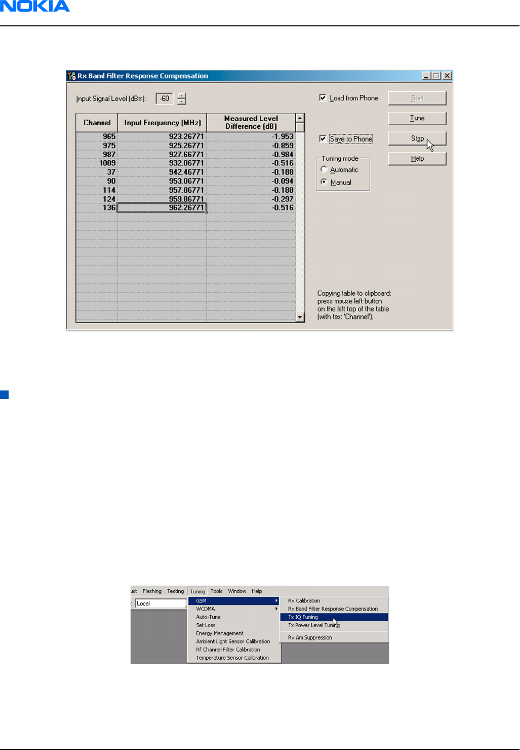
11. Check the "Save to Phone" check box and click Stop if the values are within the limits.
Next actions
Repeat the steps 4 to 10 for GSM850, GSM1800 and GSM1900.
GSM transmitter tunings
Tx IQ tuning (GSM)
Context
The Tx path branches to I and Q signals at RF I/Q modulator. Modulator and analog hardware located after
it cause unequal amplitude and phase disturbance to I and Q signal paths. Tx IQ tuning tuning balances the
I and Q branches.
Tx IQ tuning must be performed on all GSM bands. .
Steps
1. From the dropdown menus, set "Operating mode" to Local, "System mode" to GSM, and Band to GSM900.
2. From the Tuning menu, choose GSM -> Tx IQ Tuning.
3. Set Mode to Automatic and Edge to Off.
4. Click Start.
Wait until automatic tuning has finished and moved the sliders.
Values are written to the phone memory automatically.
RM-188; RM-198
Nokia Customer Care RF Troubleshooting and Manual Tuning Guide
Page 7 –32 COMPANY CONFIDENTIAL Issue 2
Copyright © 2007 Nokia. All rights reserved.
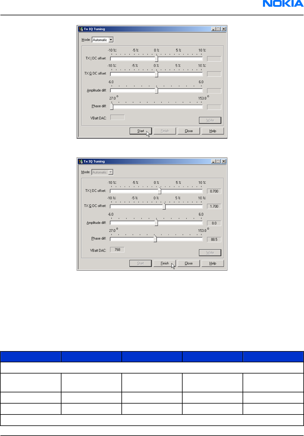
5. When the values have been written to the phone memory, click the Finish button to end the tuning.
6. Change band to GSM850 and repeat steps 4 to 5.
7. Change band to GSM1800 and repeat steps 4 to 5.
8. Change band to GSM1900 and repeat steps 4 to 5.
9. To close the tuning window, click Close.
Next actions
Tuning sliders should be close to the center of the scale after the tuning and within the limits specified in
the table below. If they are not within the limits, check Tx IQ quality manually.
Min Typ Max Unit
GSM850
I DC offset / Q DC
offset
-6 -4 6 %
Ampl -1 0 1 dB
Phase 85 90 95 ○
GSM900
RM-188; RM-198
RF Troubleshooting and Manual Tuning Guide Nokia Customer Care
Issue 2 COMPANY CONFIDENTIAL Page 7 –33
Copyright © 2007 Nokia. All rights reserved.
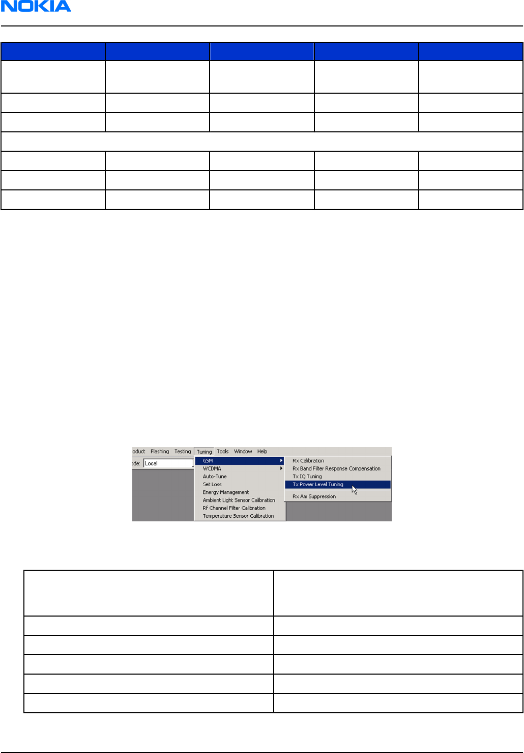
Min Typ Max Unit
I DC offset / Q DC
offset
-6 -4 6 %
Ampl -1 0 1 dB
Phase 85 90 95 ○
GSM1800/GSM1900
I/Q DC -6 0.5 6 %
Ampl -1 0 1 dB
Phase 95 100 110 ○
Tx power level tuning (GSM)
Context
Because of variations at IC process and discrete component values, actual transmitter RF gain of each phone
is different. Tx power level tuning is used to find out mapping factors called 'power coefficients’. These adjust
the GSM transmitter output power to fulfill the specifications.
For EDGE transmission the bias settings of the FEM are adjusted in order to improve linearity. This affects the
PA gain and hence the power levels have to be aligned separately for EDGE transmission.
Tx power level tuning has to be performed on all GSM bands.
Steps
1. Connect the phone to a spectrum analyzer.
2. From the dropdown menus, set "Operating mode" to Local, "System mode" to GSM, and Band to GSM900.
3. From the Tuning menu, choose GSM -> Tx Power Level Tuning.
4. Set Mode to Automatic and Edge to Off.
5. Set the spectrum analyzer for power level tuning:
Frequency channel frequency (836.6MHz GSM850, 897.4MHz
GSM900, 1747.8MHz GSM1800, 1880MHz
GSM1900)
Span 0 Hz
Sweep time 2ms
Trigger Video triggering (-10dBm)
Resolution BW 3MHz
Video BW 3MHz
RM-188; RM-198
Nokia Customer Care RF Troubleshooting and Manual Tuning Guide
Page 7 –34 COMPANY CONFIDENTIAL Issue 2
Copyright © 2007 Nokia. All rights reserved.
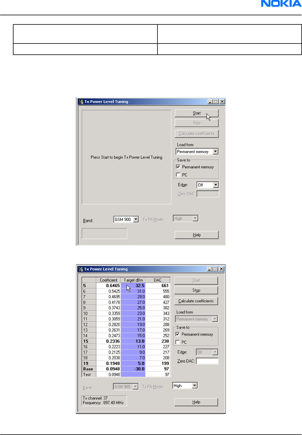
Reference level offset sum cable attenuation with module jig
attenuation
Reference level 33dBm
A power meter with a peak power detector can be also used. Remember to take the attenuations in the
account!
6. Click Start.
7. Adjust power levels 5, 15 and 19 to correspond the "Target dBm" column by pressing + or – keys.
RM-188; RM-198
RF Troubleshooting and Manual Tuning Guide Nokia Customer Care
Issue 2 COMPANY CONFIDENTIAL Page 7 –35
Copyright © 2007 Nokia. All rights reserved.
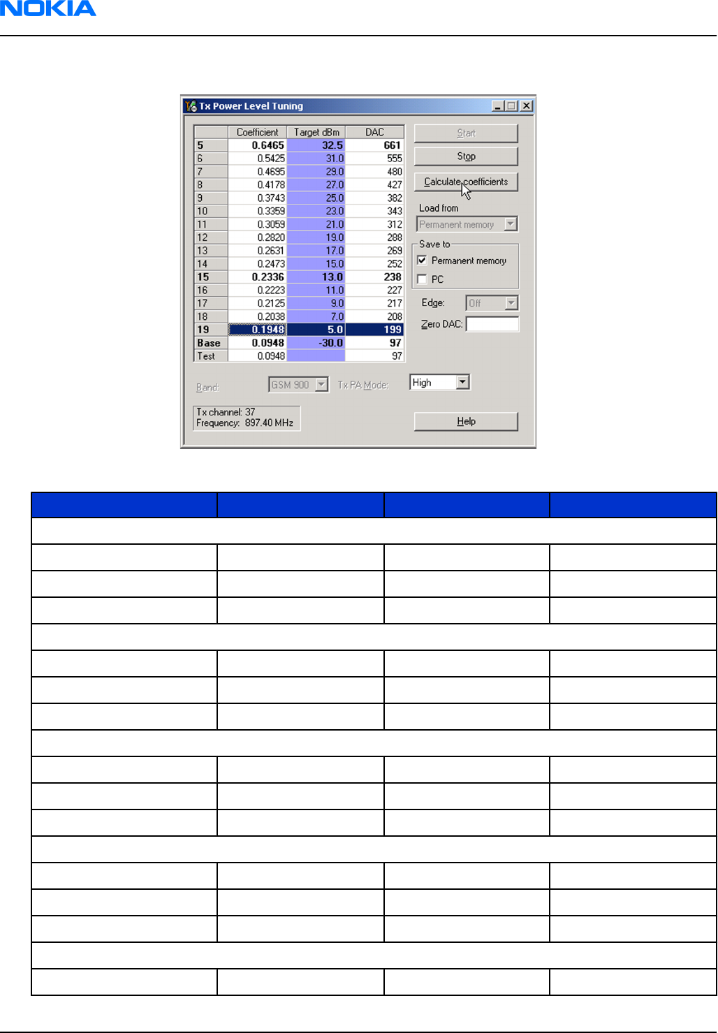
8. Click Calculate Coefficients.
9. Check that the coeffiecient values are within the limits specified in the following table.
Min Typ Max
GSM850 EDGE off
PL5 coefficient 0.45 0.626 0.73
PL15 coefficient 0.234
PL19 coefficient 0.12 0.195 0.3
GSM850 EDGE on
PL8 coefficient 0.35 0.419 0.6
PL15 coefficient 0.247
PL19 coefficient 0.12 0.204 0.3
GSM900 EDGE off
PL5 coefficient 0.45 0.626 0.73
PL15 coefficient 0.234
PL19 coefficient 0.12 0.195 0.3
GSM900 EDGE on
PL8 coefficient 0.35 0.419 0.6
PL15 coefficient 0.247
PL19 coefficient 0.12 0.204 0.3
GSM1800 EDGE off
PL0 coefficient 0.45 0.51 0.7
RM-188; RM-198
Nokia Customer Care RF Troubleshooting and Manual Tuning Guide
Page 7 –36 COMPANY CONFIDENTIAL Issue 2
Copyright © 2007 Nokia. All rights reserved.
Min Typ Max
PL11 coefficient 0.219
PL15 coefficient 0.12 0.185 0.3
GSM1800 EDGE on
PL2 coefficient 0.35 0.394 0.6
PL11 coefficient 0.23
PL15 coefficient 0.12 0.194 0.3
GSM1900 EDGE off
PL0 coefficient 0.45 0.482 0.7
PL11 coefficient 0.218
PL15 coefficient 0.12 0.184 0.3
GSM1900 EDGE on
PL2 coefficient 0.35 0.377 0.6
PL11 coefficient 0.23
PL15 coefficient 0.12 0.193 0.3
If the values are within the limits, check that the "Save to Phone Permanent Memory" check box is
checked and click Stop.
RM-188; RM-198
RF Troubleshooting and Manual Tuning Guide Nokia Customer Care
Issue 2 COMPANY CONFIDENTIAL Page 7 –37
Copyright © 2007 Nokia. All rights reserved.
10. Set Edge mode on and start tuning again. Change video averaging to 50.
11. Tune EDGE power levels to the corresponding target power levels.
Only power levels 8, 15 and 19 are tuned in GSM900 and 2, 10 and 15 in GSM1800/1900. The rest are
calculated by clicking the Calculate Coefficients button. Check the coefficients against the RF tuning limits
table presented in Step 9.
12. When the tuning is completed, click Stop.
Next actions
Repeat steps 4 to 9 for GSM1800 and GSM1900. On those bands only power levels 0, 11 and 15 need to be
tuned.
RM-188 WLAN troubleshooting
Introduction to WLAN troubleshooting
The main problem that can occur is malfunction in WLAN or WLAN ASICs or WLAN SMD components. Such
problems are unpredictable and may have many causes, either HW or SW related.
Note: While WLAN power tuning is not possible without power meter especially capable for
measuring WLAN wideband power, WLAN ICs (WLAN IC and WLAN front-end module) shall not be
changed.
RM-188; RM-198
Nokia Customer Care RF Troubleshooting and Manual Tuning Guide
Page 7 –38 COMPANY CONFIDENTIAL Issue 2
Copyright © 2007 Nokia. All rights reserved.
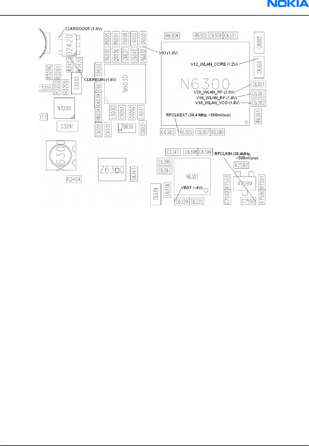
Figure 53 WLAN layout part 1
RM-188; RM-198
RF Troubleshooting and Manual Tuning Guide Nokia Customer Care
Issue 2 COMPANY CONFIDENTIAL Page 7 –39
Copyright © 2007 Nokia. All rights reserved.
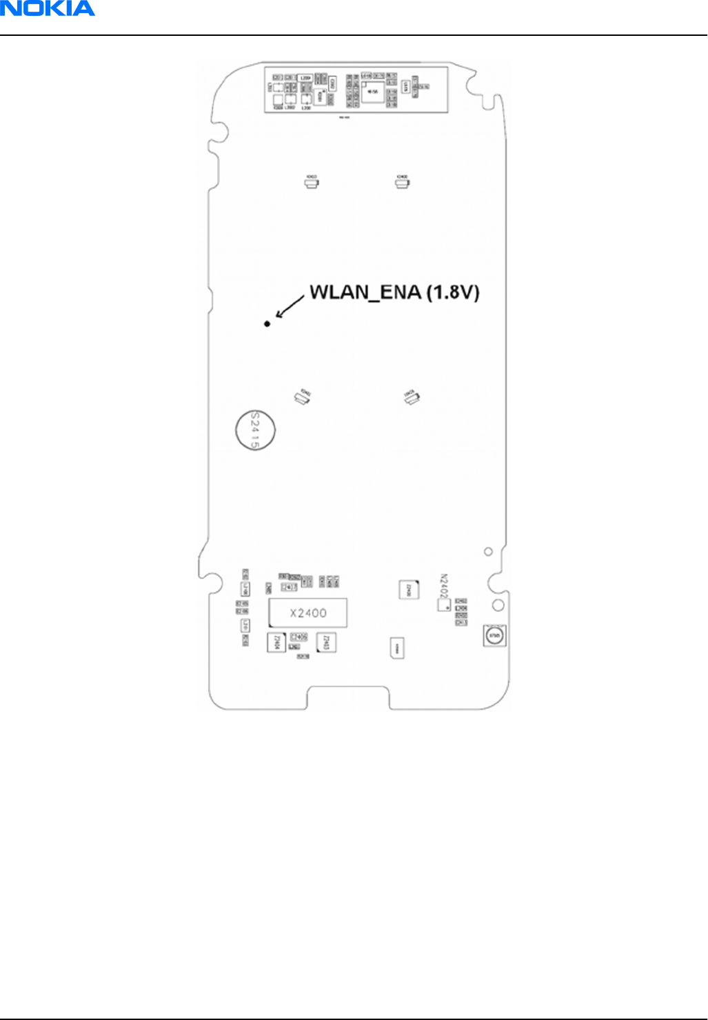
Figure 54 WLAN layout part 2
RM-188; RM-198
Nokia Customer Care RF Troubleshooting and Manual Tuning Guide
Page 7 –40 COMPANY CONFIDENTIAL Issue 2
Copyright © 2007 Nokia. All rights reserved.
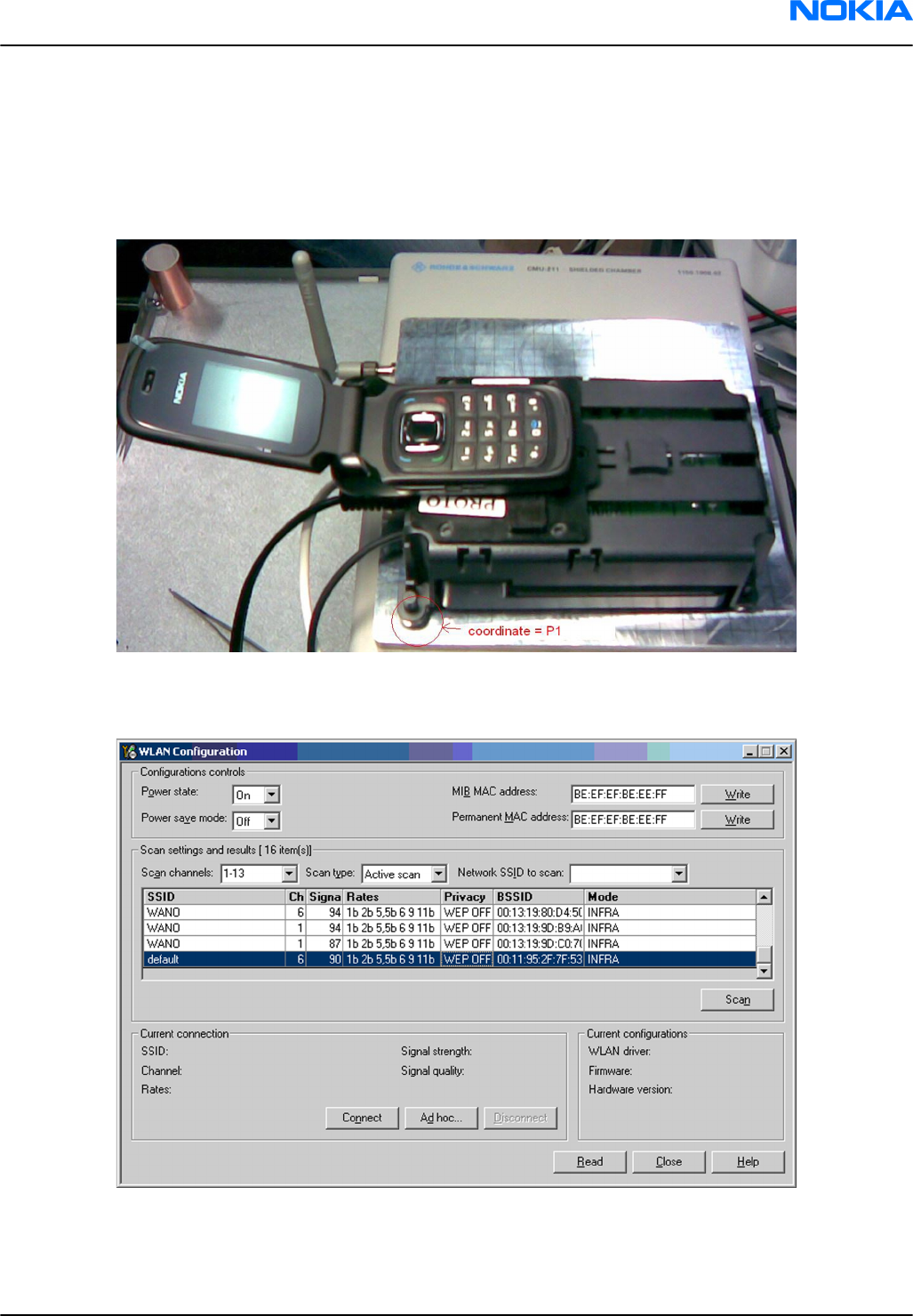
WLAN functionality test using SB-7 and Phoenix
Steps
1. Place the phone on the SB-7 WLAN test box (see figure below). The coordinates are P1 (upper left corner
of SS-62), G1, O15 and G15.
2. Start
Phoenix
service software and turn the phone to the local mode.
3. From the Testing menu, choose WLAN Configuration. The following window should come up:
4. Turn the Power state: On and press Scan.
5. After few seconds, a list of found WLAN networks should be updated. If WLAN is working, at least a station
with an SSID name default should be found.
RM-188; RM-198
RF Troubleshooting and Manual Tuning Guide Nokia Customer Care
Issue 2 COMPANY CONFIDENTIAL Page 7 –41
Copyright © 2007 Nokia. All rights reserved.
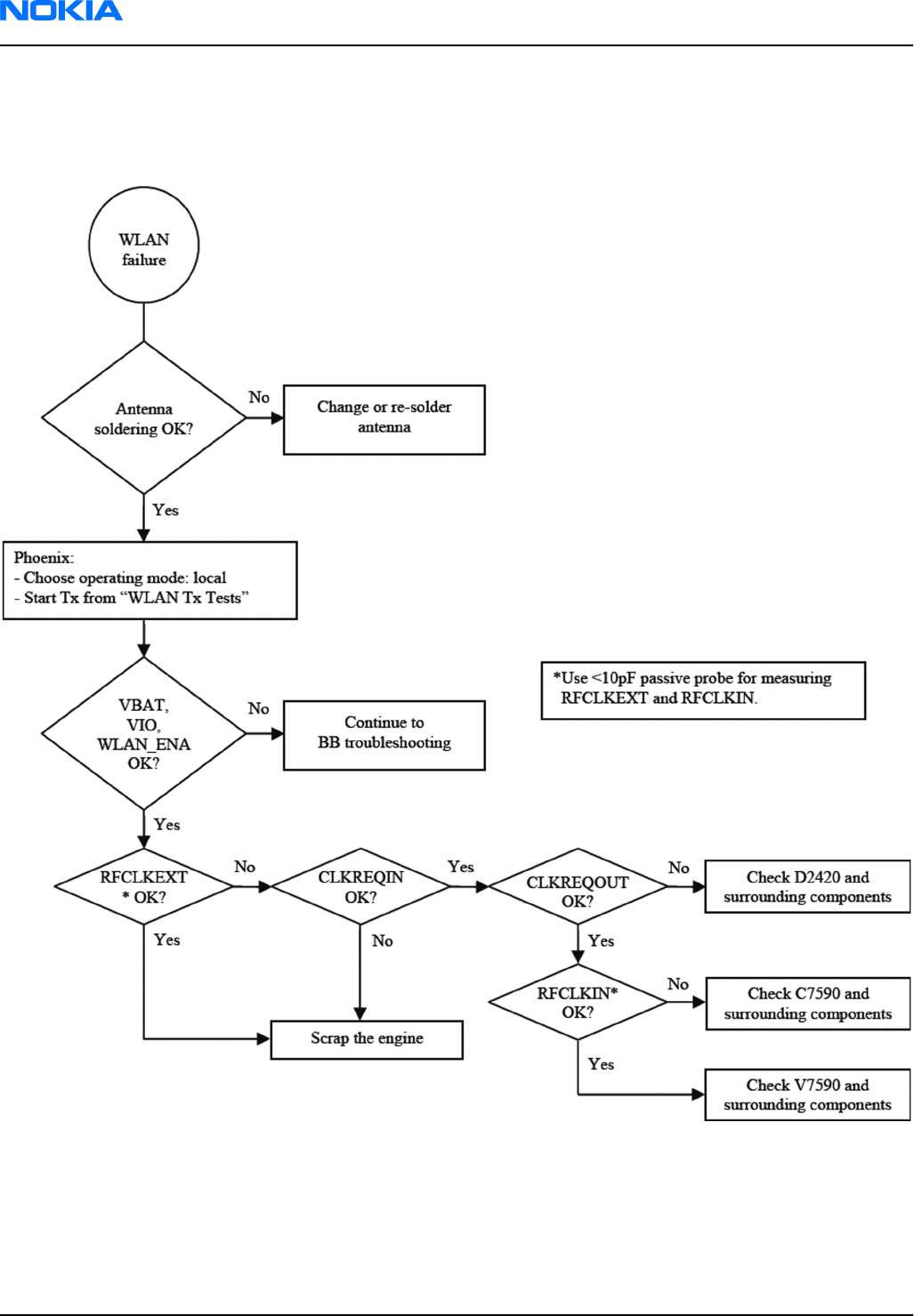
WLAN failure troubleshooting
Troubleshooting flow
RM-188; RM-198
Nokia Customer Care RF Troubleshooting and Manual Tuning Guide
Page 7 –42 COMPANY CONFIDENTIAL Issue 2
Copyright © 2007 Nokia. All rights reserved.

8 — System Module
Nokia Customer Care
Issue 2 COMPANY CONFIDENTIAL Page 8 –1
Copyright © 2007 Nokia. All rights reserved.

RM-188; RM-198
Nokia Customer Care System Module
(This page left intentionally blank.)
Page 8 –2 COMPANY CONFIDENTIAL Issue 2
Copyright © 2007 Nokia. All rights reserved.

Table of Contents
Baseband description ............................................................................................................................................8–5
System module block diagram ........................................................................................................................8–5
Baseband functional description.....................................................................................................................8–6
Absolute maximum ratings..............................................................................................................................8–7
Phone modes of operation...............................................................................................................................8–7
Power distribution............................................................................................................................................8–8
Bluetooth ...........................................................................................................................................................8–8
USB......................................................................................................................................................................8–9
RM-188 WLAN.....................................................................................................................................................8–9
MR sensor........................................................................................................................................................ 8–10
FM radio........................................................................................................................................................... 8–11
Camera............................................................................................................................................................. 8–11
Backup battery................................................................................................................................................ 8–11
CBUS interface................................................................................................................................................. 8–11
FBUS ................................................................................................................................................................. 8–11
ACI interface.................................................................................................................................................... 8–11
VOUT interface ................................................................................................................................................ 8–11
Charger interface............................................................................................................................................ 8–11
MicroSD interface............................................................................................................................................ 8–11
SIM/USIM.......................................................................................................................................................... 8–11
Battery interface............................................................................................................................................. 8–12
User interface.................................................................................................................................................. 8–13
Main display............................................................................................................................................... 8–13
Cover display.............................................................................................................................................. 8–14
Keyboard.................................................................................................................................................... 8–14
Backlights................................................................................................................................................... 8–14
ASICs................................................................................................................................................................. 8–15
RAP ASIC...................................................................................................................................................... 8–15
EM ASIC (N2200)......................................................................................................................................... 8–15
EM ASIC (N2300)......................................................................................................................................... 8–15
Device memories............................................................................................................................................ 8–15
RAPGSM memories NOR flash and SDRAM ............................................................................................... 8–15
Audio concept...................................................................................................................................................... 8–15
Audio HW architecture................................................................................................................................... 8–15
Internal microphone...................................................................................................................................... 8–16
External microphone...................................................................................................................................... 8–16
Internal earpiece............................................................................................................................................ 8–17
Internal speakers............................................................................................................................................ 8–17
External earpiece............................................................................................................................................ 8–17
Vibra circuitry ................................................................................................................................................. 8–18
Baseband technical specifications..................................................................................................................... 8–18
External interfaces ......................................................................................................................................... 8–18
Pop-portTM connector ................................................................................................................................... 8–19
VOUT electrical characteristics ...................................................................................................................... 8–20
CBUS connections and electrical characteristics.......................................................................................... 8–20
USB/FBUS connections and electrical characteristics.................................................................................. 8–21
Audio signal electrical characteristics.......................................................................................................... 8–21
Charger connector and charging interface connections & electrical characteristics .............................. 8–21
Battery connector and interface connections & electrical characteristics ............................................... 8–22
Internal interfaces.......................................................................................................................................... 8–22
RM-188; RM-198
System Module Nokia Customer Care
Issue 2 COMPANY CONFIDENTIAL Page 8 –3
Copyright © 2007 Nokia. All rights reserved.

Upper block connectors ................................................................................................................................. 8–23
Back-up battery interface connections and electrical characteristics ...................................................... 8–24
RF description ...................................................................................................................................................... 8–24
Introduction to receiver functionality.......................................................................................................... 8–24
GSM receiver.................................................................................................................................................... 8–24
Introduction to transmitter functionality.................................................................................................... 8–25
GSM transmitter.............................................................................................................................................. 8–25
GSM FEM (front end module) ......................................................................................................................... 8–26
Frequency synthesizers ................................................................................................................................. 8–26
Regulators....................................................................................................................................................... 8–26
Frequency mappings........................................................................................................................................... 8–27
GSM850 frequencies....................................................................................................................................... 8–27
EGSM900 frequencies..................................................................................................................................... 8–27
GSM1800 frequencies..................................................................................................................................... 8–28
GSM1900 frequencies..................................................................................................................................... 8–30
List of Tables
Table 15 Battery interface connections ............................................................................................................ 8–12
Table 16 Audio connector pin assignments ..................................................................................................... 8–19
Table 17 Charging interface connections ......................................................................................................... 8–21
Table 18 Charging IF electrical characteristics ................................................................................................. 8–22
Table 19 Battery interface connections ............................................................................................................ 8–22
Table 20 Battery IF electrical characteristics.................................................................................................... 8–22
Table 21 Back-up battery connections.............................................................................................................. 8–24
Table 22 Back-up battery electrical characteristics ......................................................................................... 8–24
List of Figures
Figure 55 System level block diagram .................................................................................................................8–6
Figure 56 RM-188/198 functional block diagram ...............................................................................................8–7
Figure 57 RM-188 WLAN block description....................................................................................................... 8–10
Figure 58 MR sensor connection........................................................................................................................ 8–10
Figure 59 Battery pin order................................................................................................................................ 8–12
Figure 60 Main display LCD module................................................................................................................... 8–13
Figure 61 Cover display LCD module.................................................................................................................. 8–14
Figure 62 Audio block diagram.......................................................................................................................... 8–16
Figure 63 Internal microphone circuitry........................................................................................................... 8–16
Figure 64 Internal earpiece circuitry................................................................................................................. 8–17
Figure 65 Internal speaker circuitry .................................................................................................................. 8–17
Figure 66 External earpiece circuitry (Pop-Port connected on the right)...................................................... 8–18
Figure 67 Vibra circuitry ..................................................................................................................................... 8–18
Figure 68 External audio connector .................................................................................................................. 8–19
Figure 69 Battery connector............................................................................................................................... 8–22
Figure 70 GSM transmitter.................................................................................................................................. 8–25
RM-188; RM-198
Nokia Customer Care System Module
Page 8 –4 COMPANY CONFIDENTIAL Issue 2
Copyright © 2007 Nokia. All rights reserved.

Baseband description
System module block diagram
RM-188/RM-198 has two blocks, upper block and lower block. The upper block consists of upper PWB module.
The lower block consists of Engine (BB/RF) PWB module.
The upper block is connected to the lower block (BB/RF module) via a 40-pin connector and a flex cable.
Most of the BB parts (also IHF, RF, WLAN and BT) are on the topside of the Engine Module. FM parts, external
audio small components, MR sensor, upper block connector and keyboard are on the backside of the Engine
Module. Accessories and charger can be connected via the Pop-Port™ connector and the charger connector
at the bottom of the phone.
Upper PWB Module consists of two Displays, Earpiece, Camera, HWA, two DC/DC converters and one regulator
and connector to Engine Module.
Note: In this description, user interface HW (UI HW) covers display, camera, keyboard and keyboard
backlight.
The RM-188 includes WLAN, but it does not include the HAC (Hearing Aid Coil).
The RM-198 does not include WLAN, and it can be assembled with or without the HAC.
RM-188; RM-198
System Module Nokia Customer Care
Issue 2 COMPANY CONFIDENTIAL Page 8 –5
Copyright © 2007 Nokia. All rights reserved.
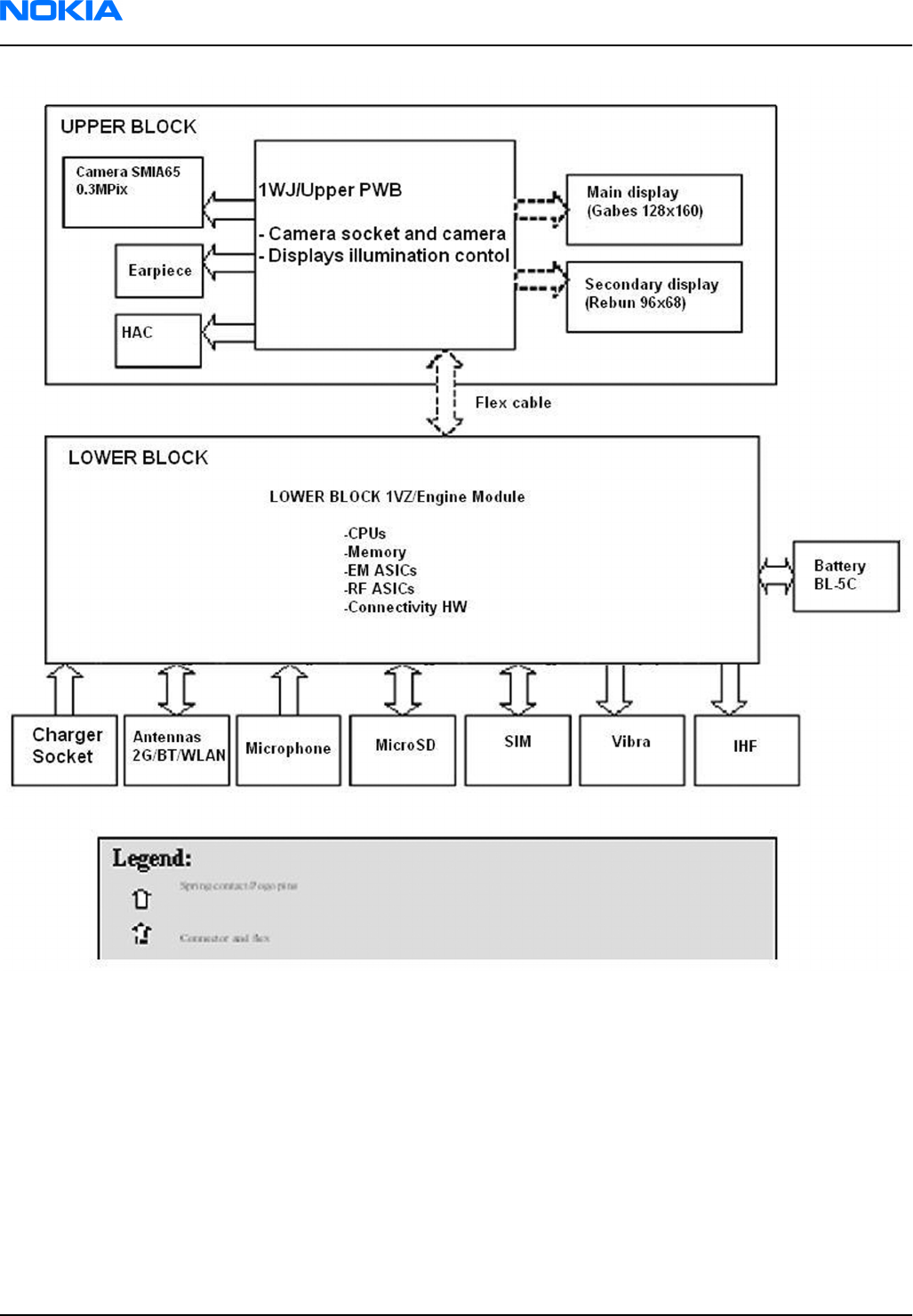
Figure 55 System level block diagram
Baseband functional description
Digital baseband consists of ISA based modem and application sections. Modem functionality is in RAPGSM
ASIC.
The modem section consists of RAPGSM ASIC and NOR Flash and DRAM memory as the core. NOR Flash and
DRAM memories are in one package (Combo) RAPGSM supports cellular protocols of GSM (minimum EDGE glass
10, GPRS phase2). Modem DRAM memory has 128Mbits of memory and NOR flash has 256Mbits of memory.
RAPGSM operates with the system clock of 38.4 MHz, which comes from the VCTCXO.
RM-188; RM-198
Nokia Customer Care System Module
Page 8 –6 COMPANY CONFIDENTIAL Issue 2
Copyright © 2007 Nokia. All rights reserved.
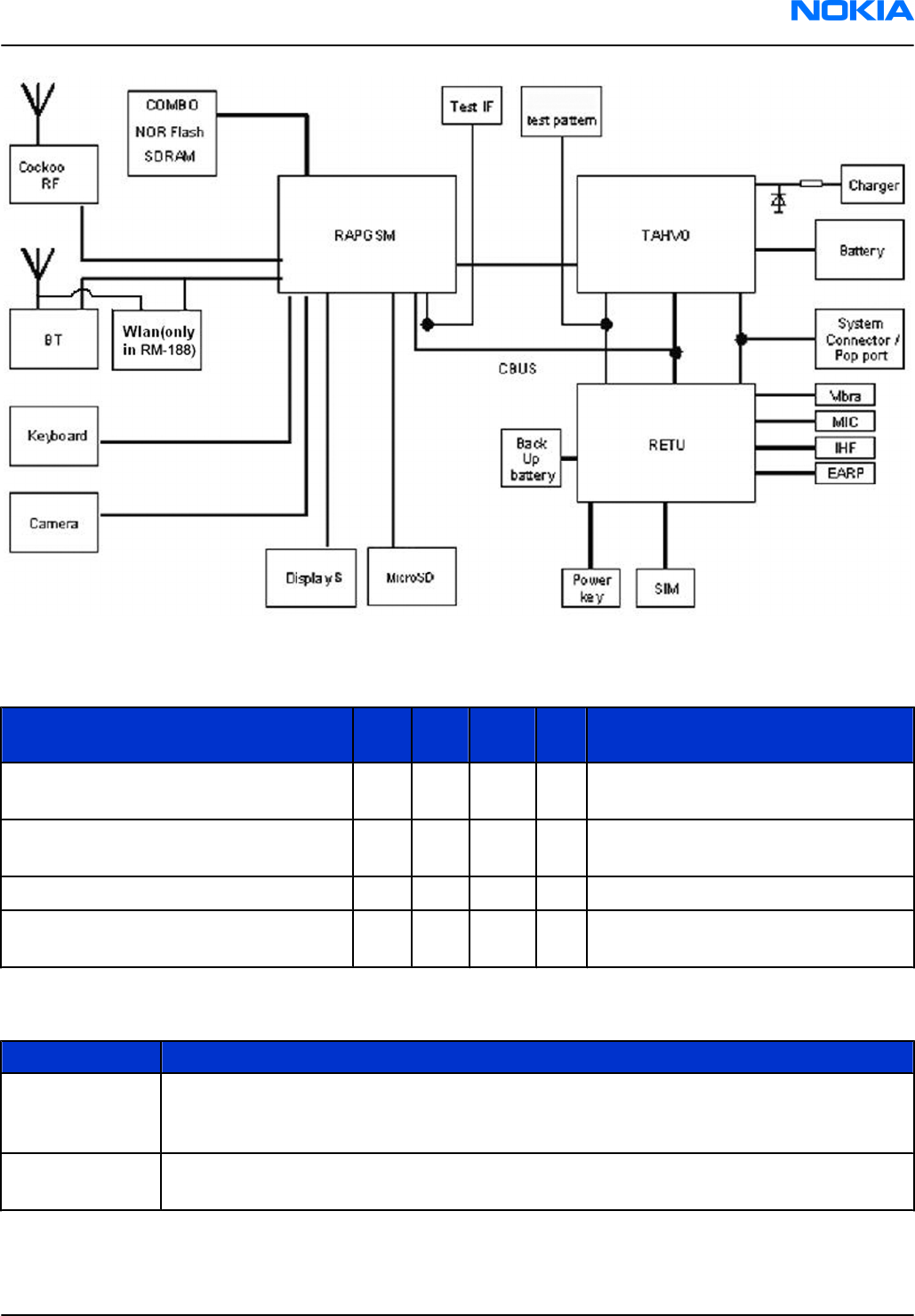
Figure 56 RM-188/198 functional block diagram
Absolute maximum ratings
Signal Min Nom Max Uni
tNotes
Battery voltage (idle) -0.3 +4.5 V Battery voltage maximum value is
specified during charging is active
Battery voltage (Call) +4.3 V Battery voltage maximum value is
specified during charging is active
Charger input voltage -0.3 +16V V
Back-Up supply voltage 0 2.5 2.7 V Maximum capacity of the backup
power supply assumed to be 4 µAh.
Phone modes of operation
Mode Description
NO_SUPPLY (dead) mode means that the main battery is not present or its voltage is too low (below
EM ASIC (N2200) master reset threshold) and that the back-up battery voltage is too
low.
BACK_UP The main battery is not present or its voltage is too low but back-up battery voltage is
adequate and the 32kHz oscillator is running (RTC is on).
RM-188; RM-198
System Module Nokia Customer Care
Issue 2 COMPANY CONFIDENTIAL Page 8 –7
Copyright © 2007 Nokia. All rights reserved.
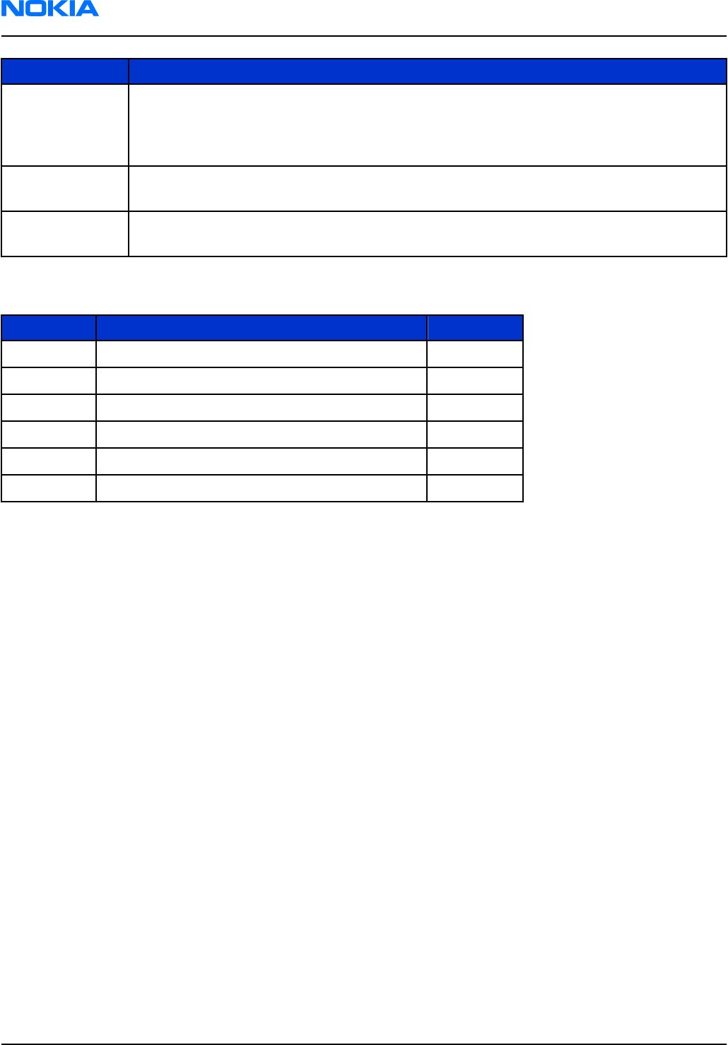
Mode Description
PWR_OFF In this mode (warm), the main battery is present and its voltage is over EM ASIC (N2200)
master reset threshold. All regulators are disabled, PurX is on low state, the RTC is on
and the oscillator is on. PWR_OFF (cold) mode is almost the same as PWR_OFF (warm),
but the RTC and the oscillator are off.
RESET RESET mode is a synonym for start-up sequence. RESET mode uses 32kHz clock to count
the REST mode delay (typically 16ms).
SLEEP SLEEP mode is entered only from PWR_ON mode with the aid of SW when the system’s
activity is low.
Voltage limits
Parameter Description Value
VMSTR Master reset threshold (EM ASIC N2200) 2.2V (typ.)
VMSTR+ Threshold for charging, rising (EM ASIC N2300) 2.1V (typ.)
VMSTR- Threshold for charging, falling (EM ASIC N2300) 1.9V (typ.)
VCOFF+ Hardware cutoff (rising) 2.9V (typ.)
VCOFF- Hardware cutoff (falling) 2.6V (typ.)
SWCOFF SW cutoff limit ~3.2V
Power key
The system boots up when power key is pressed (adequate battery voltage, VBAT, present).
Power down can be initiated by pressing the power key again (the system is powered down with the aid of
SW).
Power distribution
Power supply components:
• RETU
• TAHVO
• BT LDO
• MicroSD LDO
• backlight SMPSs
All the above are powered by the main battery voltage.
Battery voltage is also used on the RF side for power amplifiers (GSM PA) and for RF ASIC Ahne.
Discrete power supplies are used to generate 1.8V for the camera module, 2.85V for MicroSD card and max.
18V for backlight LEDs.
The device supports both 1.8V/3V SIM cards.
Bluetooth
Bluetooth provides a fully digital link for communication between a master unit and one or more slave units.
The system provides a radio link that offers a high degree of flexibility to support various applications and
product scenarios. Data and control interface for a low power RF module is provided. Data rate is regulated
between the master and the slave.
The device Bluetooth is based on BC4 ROM1.0RDL BT chip.
RM-188; RM-198
Nokia Customer Care System Module
Page 8 –8 COMPANY CONFIDENTIAL Issue 2
Copyright © 2007 Nokia. All rights reserved.

USB
USB (Universal Serial Bus) provides a wired connectivity between host PC and peripheral devices.
USB is a differential serial bus for USB devices. USB controller (RAP) supports USB specification revision 2.0
with full speed USB (12 Mbps). The device is connected to the USB host through the system connector. The
USB bus is hot plugged capable, which means that USB devices may be plugged in/out at any time.
RM-188 WLAN
WLAN is divided to STLC4550 WLAN transceiver module and radio front-end module RF5924.
STMicroelectronics STLC4550 is a three-die multichip module with passive components, partitioned to radio,
baseband and energy management die.
STLC4550 implements 802.11b/g WLAN radio, which conforms to the IEEE 802.11b/g protocols operating in
2.4 GHz band and supporting OFDM data rates of 54, 48, 36, 24, 18, 12, 9, and 6 Mbps, CCK data rates of 11
and 5.5 Mbps, and legacy data rates of 2 and 1 Mbps. IEEE802.11e/i protocol extensions are included to
implement Quality of Service (QoS) and security functions.
STLC4550 has a fully integrated radio chip including a direct-conversion transceiver, RF synthesizer and VCO,
and high-speed data converters. Digital interface is used for transferring the sampled data between radio
and baseband chip.
The baseband chip implements OFDM/CCK digital baseband processor and ARM9-based MAC with internal
SRAM memories. The baseband includes required logic and interfaces to enable time-shared simultaneous
use of BT and WLAN.
The energy management unit integrates the required power management functions to operate the system
from VBAT (3.0 – 5.5 V). The EM unit generates 1.2 V digital core voltage, two 1.8 V supplies for RF and 2.8 V
LDO for PA bias supply. The EM unit integrates the power-on reset circuitry and level-shifters for RF front-end
GaAs switches.
The host interface is provided by a flexible serial interface (SPI).
The system uses 38.4 MHz reference clock. Low-power sleep mode operation is enabled by low-speed 32 kHz
clock (32768 Hz), and energy management unit low-current stand-by mode.
The RFMD RF5924 Front-End Module (FEM) is a single integrated module. The FEM has integrated b/g power
amplifier, power detector, RX balun and TX filtering.
RM-188; RM-198
System Module Nokia Customer Care
Issue 2 COMPANY CONFIDENTIAL Page 8 –9
Copyright © 2007 Nokia. All rights reserved.
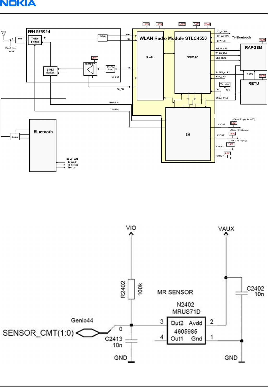
Figure 57 RM-188 WLAN block description
MR sensor
MR sensor is used to monitor the position of the upper block in fold construction.
MR sensor detects the fold position. There is a magnet in fold mechanics under the display module and when
the fold is closed MR sensor is in magnetic field.
Figure 58 MR sensor connection
RM-188; RM-198
Nokia Customer Care System Module
Page 8 –10 COMPANY CONFIDENTIAL Issue 2
Copyright © 2007 Nokia. All rights reserved.

FM radio
The FM radio circuitry is implemented using a highly integrated radio TEA5760 N1C.
The antenna of the FM Radio is created with the headset. The wires of the headset are used as poles of the
antenna.
Camera
The device uses SMIA65 camera module. SMIA65 is 0.3Mpixel with sensor resolution of 656 x 496.
The camera is powered by using VIO(1.8V) and VAUX(2.78V) voltages from the engine board.
Backup battery
When the main battery is not attached EM ASIC (N2200) goes in backup mode using back-up battery that
supplies voltage to RTC in EM ASIC (N2200).
CBUS interface
CBUS is a "main" system control bus in BB5.0. RAP controls the functionality of EM ASIC (N2200) and EM ASIC
(N2300) ASICs with CBUS.
CBUS is a four-wire half-duplex master-slave interface. In BB5.0 CBUS clock frequency is 2.4 MHz.
FBUS
USB and FBUS have multiplexed interface between EM ASIC (2300) and RAP.
ACI interface
The ACI (Accessory Control Interface) is a point-to-point, bi-directional, single line serial bus.
It has two main features: the insertion and removal detection of an accessory device and acting as a data
bus between phone and accessory, intended for control purposes. A third function of ACI is to identify and
authenticate the accessory.
VOUT interface
Accessory power is supplied by VOUT, a linear low drop-out regulator in EM ASIC (N2300) providing 2.5V at
90mA maximum when active (0.5mA in sleep).
Charger interface
Charging control and charge switch are situated in EM ASIC (N2300).
If the temperature rises too high and the thermal protection is activated, EM ASIC (N2300) goes to protection
mode.
MicroSD interface
The MicroSD card interface is electrically and functionally compatible with the SD card interface.
SIM/USIM
The device has one SIM (Subscriber Identification Module) interface and the SIM card locates under the battery.
SIM interface consists of internal interface between RAP and EM ASIC (N2200) and an external interface
between Retu and SIM contacts.
EM ASIC (N2200) external SIM IF connections and electrical characteristics between ASICs are shown in the
picture.
RM-188; RM-198
System Module Nokia Customer Care
Issue 2 COMPANY CONFIDENTIAL Page 8 –11
Copyright © 2007 Nokia. All rights reserved.
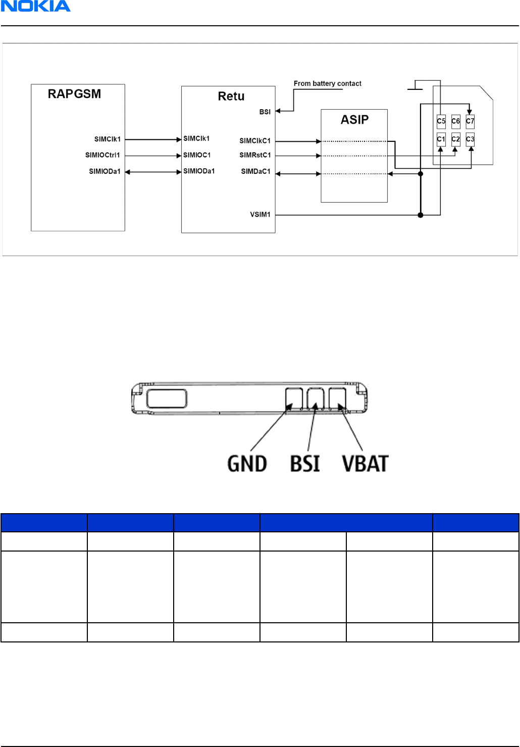
SIM interface voltage is first 1.8V when the SIM card is inserted and if the card does not response to the ATR
(answer to reset) 3V interface voltage is used.
Battery interface
The battery interface supports a 3-pole battery interface. The interface consists of three connectors: VBAT,
BSI and GND.
The BSI line is used to recognize the battery capacity by a battery internal pull down resistor.
Figure 59 Battery pin order
Table 15 Battery interface connections
Pin Signal I/O Engine connection Notes
1 VBAT -> EM ASIC N2200 VBAT Battery voltage
2 BSI -> EM ASIC N2200 BSI Battery size
indication
(fixed resistor
inside the
battery pack)
3 GND GND Ground
Battery temperature is estimated by measuring separate battery temperature NTC via the BTEMP line, which
is located on the transceiver PWB, at a place where the phone temperature is most stable.
For service purposes, the device SW can be forced into local mode by using pull down resistors connected to
the BSI line.
RM-188; RM-198
Nokia Customer Care System Module
Page 8 –12 COMPANY CONFIDENTIAL Issue 2
Copyright © 2007 Nokia. All rights reserved.
User interface
Main display
Figure 60 Main display LCD module
Display features:
• Main display: 128x160 262k CSTN passive LCD.
• Transmissive type, screen is 'black' when display illumination is OFF.
• Active area is 28.032 mm x 35.040 mm.
• Partial display function Power saving by pausing display process on part of the screen.
• Build-in RAM capacity 128x160x18bit
RM-188; RM-198
System Module Nokia Customer Care
Issue 2 COMPANY CONFIDENTIAL Page 8 –13
Copyright © 2007 Nokia. All rights reserved.
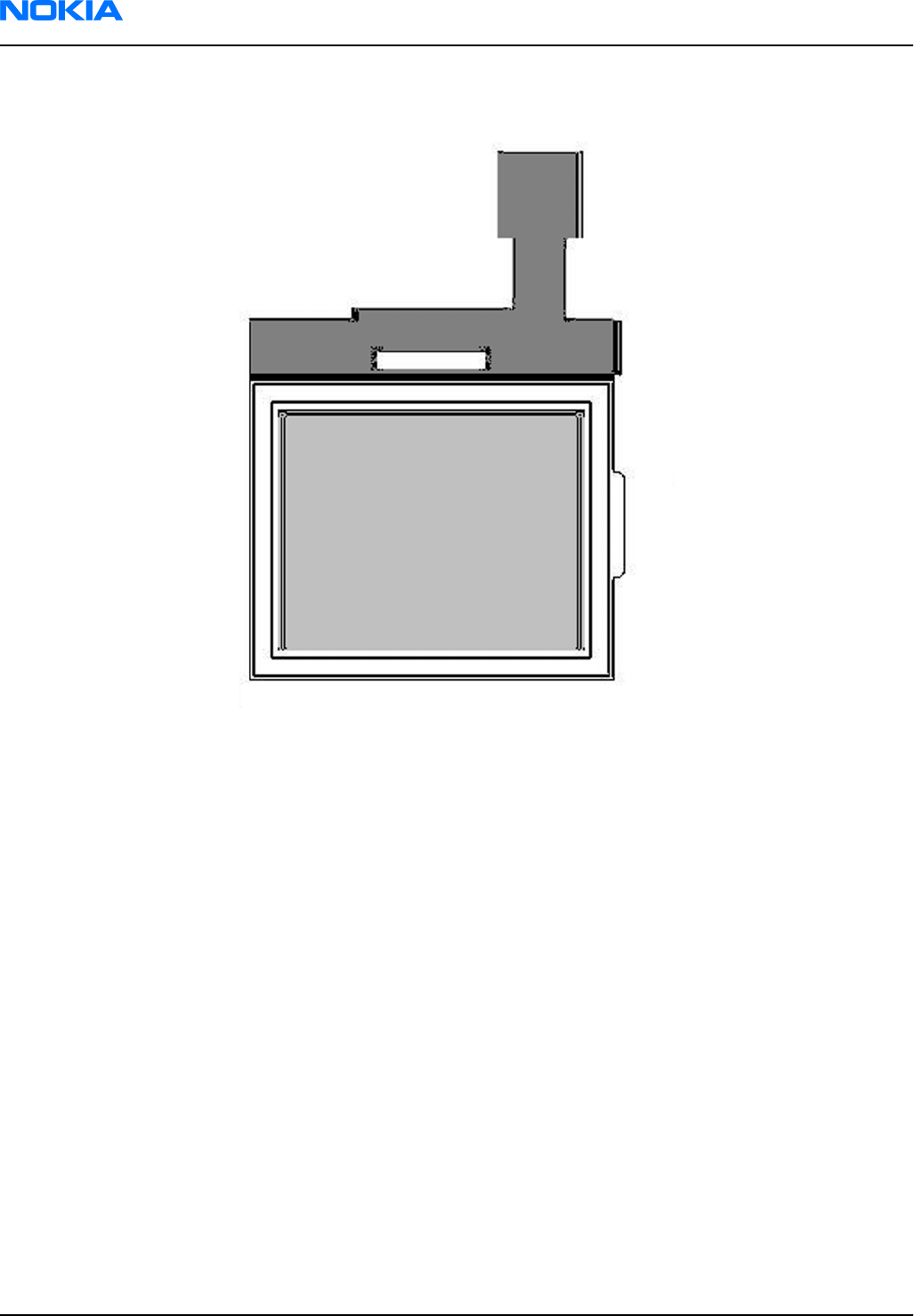
Cover display
Figure 61 Cover display LCD module
Display features:
• Module size (width x height x thickness): 26.0 mm x 26.0 mm x 2.6 mm.
• 96x68 FSTN, 2 colors black & white with blue LEDs.
• Transflective, normally black, inverted.
• Partial display function; power saving by pausing display process on part of the screen.
• 68 x 96 bits RAM.
The display module does not require any tunings in service.
Keyboard
The device keyboard consists of 24 separate keys.
The keyboard is implemented as a matrix keyboard, which is connected directly to the dedicated keyboard
GENIO lines. The power-on key is the same key as the "END" key (when pressed longer -> power OFF or ON).
The keymatrix has six rows and four columns.
Backlights
The main display has two white LEDs and the secondary display has two blue LEDs for display backlight inside
of the display module. Voltage source for backlights is implemented using a white LED driver on the lower
block, which is also used for keyboard backlight.
There is NPN digital transistor which controls which display is lighted at the time. The transistor is controlled
by GENIO03. There is no possibility to turn both display backlights on in the same time.
The driver increases battery voltage up to 18V.
RM-188; RM-198
Nokia Customer Care System Module
Page 8 –14 COMPANY CONFIDENTIAL Issue 2
Copyright © 2007 Nokia. All rights reserved.

There are four LEDs in two series for keyboard backlight.
ASICs
RAP ASIC
RAP is a GSM EDGE chip (modem ASIC) with lots of peripheral features:
• processor subsystem (PSS) that includes ARM926 MCU as a main processor
• DSP and related functions
• ASIC clock and reset control
• MCU peripherals e.g. CBUS IF, USB IF and SIM IF
• DSP peripherals e.g. speech codec
• RF codec
EM ASIC (N2200)
EM ASIC (N2200) includes the following functional blocks:
• Start up logic and reset control
• Charger detection
• Battery voltage monitoring
• 32.768 kHz clock with external crystal
• Real time clock with external backup battery
• SIM card interface
• Stereo audio codecs and amplifiers
• A/D converter
• Regulators
• Vibra interface
• Digital interface (CBUS)
EM ASIC (N2300)
EM ASIC (N2300) is intended for energy management control, supply voltage generation and charge control
of mobile phone.
Device memories
RAPGSM memories NOR flash and SDRAM
Modem memory consists of 128Mbit SDRAM and 256 Mbit NOR flash memory.
Audio concept
Audio HW architecture
The functional core of the audio hardware is built around two ASICs: RAPGSM engine ASIC and the mixed-
signal ASIC Retu.
There are three audio transducers:
• 7x11 mm dynamic earpiece
• one 11x15 mm dynamic speaker
• electret microphone module
Note: The RM-188 does not include the HAC (Hearing Aid Coil).
RM-188; RM-198
System Module Nokia Customer Care
Issue 2 COMPANY CONFIDENTIAL Page 8 –15
Copyright © 2007 Nokia. All rights reserved.
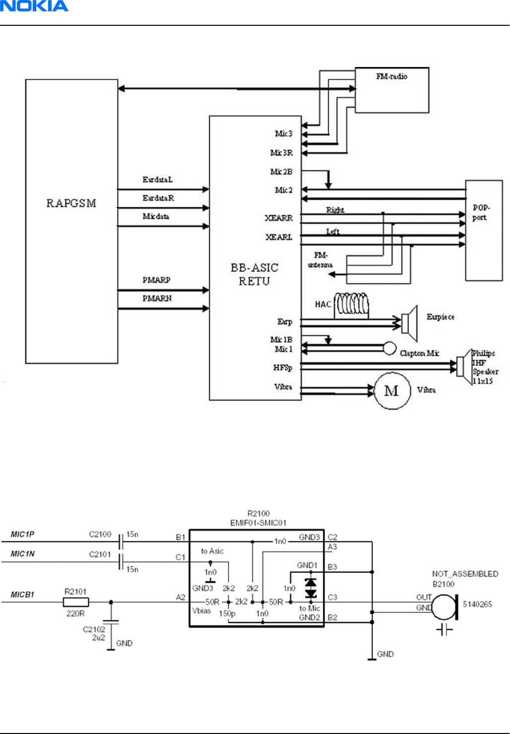
The RM-198 can be assembled with or without the HAC.
Figure 62 Audio block diagram
Internal microphone
Internal microphone is used for HandPortable (HP) and Internal HandsFree (IHF) call modes.
An analogue electret microphone is connected to N2200 Mic1P and Mic1N inputs via asymmetric electrical
connection.
Figure 63 Internal microphone circuitry
External microphone
Galvanic accessories are connected to the system connector.
RM-188; RM-198
Nokia Customer Care System Module
Page 8 –16 COMPANY CONFIDENTIAL Issue 2
Copyright © 2007 Nokia. All rights reserved.
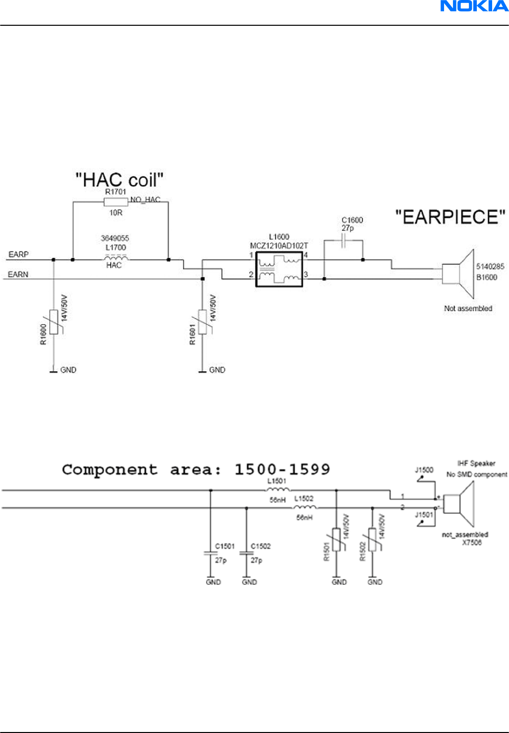
The accessory audio mode is automatically enabled/disabled during connection/disconnection of dedicated
phone accessories.
Internal earpiece
Internal earpiece is used for the HandPortable (HP) call mode. A dynamic 8mm earpiece capsule is connected
to EM ASIC’s (N2200) differential output EarP and EarN.
Note: The RM-188 does not include the HAC (Hearing Aid Coil).
The RM-198 can be assembled with or without the HAC.
Figure 64 Internal earpiece circuitry
Internal speakers
Internal speakers are used for Internal HandsFree (IHF) call mode, ringing tones, FM-radio and music listening.
The dynamic 11x15mm speaker is connected to Retu ASIC’s outputs HFSp P/N.
Figure 65 Internal speaker circuitry
External earpiece
All galvanic accessories are connected to the system connector (Pop-Port™).
The accessory audio mode is automatically enabled/disabled during connection/disconnection of dedicated
phone accessories.
Xear lines have 10 Ω series resistors in each line.
RM-188; RM-198
System Module Nokia Customer Care
Issue 2 COMPANY CONFIDENTIAL Page 8 –17
Copyright © 2007 Nokia. All rights reserved.
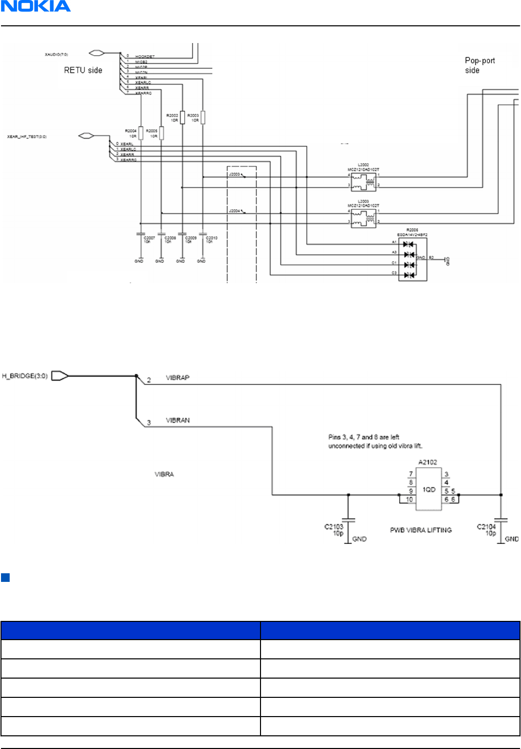
Figure 66 External earpiece circuitry (Pop-Port™ connected on the right)
Vibra circuitry
Vibra is used for vibra-alarm function.
A vibra lifter is used to connect the vibra to the main PWB. The vibra underlay is a simple PWB piece.
Figure 67 Vibra circuitry
Baseband technical specifications
External interfaces
Name of Connection Connector reference
USB X2000
Charger X2002 and X2000
SIM X2701
MicroSD X3200
Battery connector X2070
RM-188; RM-198
Nokia Customer Care System Module
Page 8 –18 COMPANY CONFIDENTIAL Issue 2
Copyright © 2007 Nokia. All rights reserved.
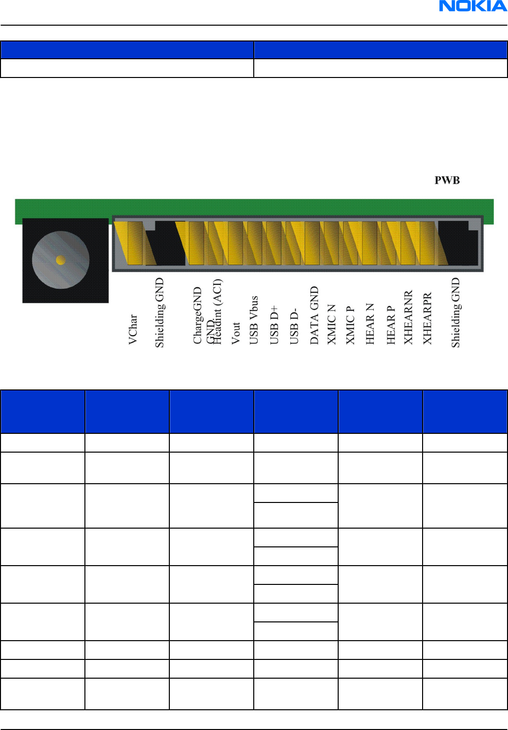
Name of Connection Connector reference
SIM X2701
Pop-portTM connector
Pop-PortTM connector provides a fully differential 4–wire stereo line-level output connection and fully
differential 2-wire mono line-level or microphone level input connection.
The earpiece and headset signals are multiplexed so that the outputs cannot be used simultaneously.
Figure 68 External audio connector
Table 16 Audio connector pin assignments
Pin #/ Signal
name Signal
description Spectral range Voltage/
Current levels Max or
nominal serial
impedance
Notes
1/ Charge V Charge DC 0-9V/ 0.85A
2/ GND Charge GND - 0.85A 100mΩ (PWB+
conn.)
3/ ACI ACI 1kbits/s Digital 0 / 47Ω Insertion &
removal
detection
2.5-2.78V
4/ Vout DC out DC 2.78V 70 mA 100mΩ (PWB+
conn.)
200mW
2.5V 90mA
9 / XMIC N Audio in 300-8k 1Vpp &
2.5-2.78VDC
10 / XMIC P Audio in 300-8k 1Vpp &
2.5-2.78VDC
11 / HEAR N Audio out 20-20k 1Vpp 22Ω
12 / HEAR P Audio out 20-20k 1Vpp 22Ω
13 / HEAR R N Audio out 20-20k 1Vpp 22Ω Not conn. in
mono
RM-188; RM-198
System Module Nokia Customer Care
Issue 2 COMPANY CONFIDENTIAL Page 8 –19
Copyright © 2007 Nokia. All rights reserved.
Pin #/ Signal
name Signal
description Spectral range Voltage/
Current levels Max or
nominal serial
impedance
Notes
14 / HEAR R P Audio out 20-20k 1Vpp 22Ω Not conn. in
mono
VOUT electrical characteristics
Description Parameter Min Max Typical Unit Notes
Vout regulator for
external
accessories
VOUT 2.43 2.57 2.5 V Max load 90mA
CBUS connections and electrical characteristics
CBUS connections
Pin name I/O Connection Notes
RAPGSM CbusDa <-> Retu Serdata Cbus data
Tahvo/FM-
radio
CbusData
RAPGSM CbusClk -> Retu SerClk Cbus clock, 2.4
MHz
Tahvo/FM-
radio
CbusClk
RAPGSM CbusEn1X -> Retu Sersel Cbus enable
CBUS electrical characteristics
Description Parameter Min Typ Max Unit Notes
High-level
input voltage
VIH 0.7 x VDDS VDDS V RAPGSM specific
(VDDS = 1.8V)
Low-level
input voltage
VIL 0 0.3 x
VDDS
V
High-level
output
voltage
VOH 0.8 x VDDS VDDS V
Low-level
output
voltage
VOL 0 0.22 x
VDDS
V
Frequency,
CbusClk
f 1 2.4 2.5 MHz
RM-188; RM-198
Nokia Customer Care System Module
Page 8 –20 COMPANY CONFIDENTIAL Issue 2
Copyright © 2007 Nokia. All rights reserved.
Description Parameter Min Typ Max Unit Notes
Rise and fall
time
tR/tF Tahvo specific
CLK, DaOut,
EnX
6 ns
DaIn 25 ns
USB/FBUS connections and electrical characteristics
The USB operates in the low-power bus-mode only. The USB host provides VBUS voltage (5V, 100mA at
maximum) to USB device.
Audio signal electrical characteristics
Description Parameter Typ Unit Notes
XMIC N Audio in 1 Vpp DC Offset 2.5-2.78V
XMIC P Audio in 1 Vpp DC Offset 2.5-2.78V
HSEAR N Audio out 1 Vpp 22Ω nominal serial
impedance
HSEAR P Audio out 1 Vpp 22Ω nominal serial
impedance
HSEAR R N Audio out 1 Vpp 22Ω nominal serial
impedance
Not connected in
mono
HSEAR R P Audio out 1 Vpp 22Ω nominal serial
impedance
Not connected in
mono
Charger connector and charging interface connections & electrical characteristics
Table 17 Charging interface connections
Pin Signal I/O Engine connection Notes
1 Vchar In EM ASIC
(N2300)
VCharIn1, 2 Charging
voltage /
charger
detection,
Center pin
2 Charge GND Ground Charger
ground
RM-188; RM-198
System Module Nokia Customer Care
Issue 2 COMPANY CONFIDENTIAL Page 8 –21
Copyright © 2007 Nokia. All rights reserved.
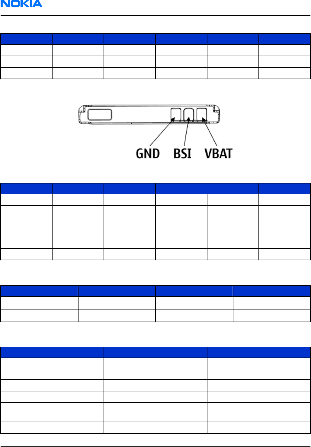
Table 18 Charging IF electrical characteristics
Description Parameter Min Max Unit Notes
Vchar V Charge 0 16 V Center pin
Vchar I Charge 0.95 A Center pin
Charge GND 0.85 A
Battery connector and interface connections & electrical characteristics
Figure 69 Battery connector
Table 19 Battery interface connections
Pin Signal I/O Engine connection Notes
1 VBAT -> EM ASIC N2200 VBAT Battery voltage
2 BSI -> EM ASIC N2200 BSI Battery size
indication
(fixed resistor
inside the
battery pack)
3 GND GND Ground
Table 20 Battery IF electrical characteristics
Description Parameter Max Unit
Operation voltage VIN 4.23 VDC
Current rating IIN 0.9 A
Internal interfaces
Name of Connection Connector reference Notes
UI connector X2400
X1000
Lower block
Upper block
Display Suez X1100 Upper block
Display Naxos X1101 Upper block
Camera X1470 Upper block (through hole
socket)
Vibra A2102 Lower block
RM-188; RM-198
Nokia Customer Care System Module
Page 8 –22 COMPANY CONFIDENTIAL Issue 2
Copyright © 2007 Nokia. All rights reserved.
Name of Connection Connector reference Notes
Microphone B2100 Lower block
Earpiece B1200 Upper block
IHF speaker X7506 Upper block
Upper block connectors
Pin number,
connector X1000 Destination Name of the
line/signal NOTES
2-5 Main display, X2000 Messi0-3, Data
lines
7 Earpiece, B1600 EARP
8 Earpiece, B1600 EARN
10 Main display, X2000 LCDTE
11 X3000, X2100,
X2000
VAUX, analogue
power supply
2.8V
12 Camera, X3000 CAM_ENABLE,
shutdown
12 Secondary display,
X2100
LCDCS2X, Chip
select
14 Main (X2000) and
secondary (X2100)
display
LCD_RESX, Reset
16 Camera, X3000 CAM_CLK, clock 9.6MHz
17 Camera, X3000 CCISCL, serial
clock
18 Camera, X3000 CCISDA, serial
data
21 Main (X2000) and
secondary (X2100)
display
VLEDOUT1,
display lights
supply
6-11V
depends on
display
22 Main (X2000) and
secondary (X2100)
display
SETCURR1,
display light
return current
24 Camera, X3000 CCPDataP Differential
data line
25 Camera, X3000 CCPDataN Differential
data line
27 Camera, X3000 CCPCLKP Differential
data line
28 Camera, X3000 CCPCLKN Differential
data line
RM-188; RM-198
System Module Nokia Customer Care
Issue 2 COMPANY CONFIDENTIAL Page 8 –23
Copyright © 2007 Nokia. All rights reserved.
Pin number,
connector X1000 Destination Name of the
line/signal NOTES
30 X3000, X2100,
X2000
VIO, digital
power supply
1.8V
31 Main (X2000) and
secondary (X2100)
display
WRX/SDA, Clock
for main and
Data for
secondary
display
WRx 9.6Mhz
33 Main display, X2000 DIFRDx, read
select
34 Main display, X2000 DIFCSx, Chip
select
35 Main (X2000) and
secondary (X2100)
display
DIFDCx / SCL,
data/command
main and clock
for secondary
display
36-39 Main display, X2000 Messi7-4, Data
lines
Back-up battery interface connections and electrical characteristics
Table 21 Back-up battery connections
Pin name I/O Connection Notes
VBack -> N2200,
VBack
Table 22 Back-up battery electrical characteristics
Description Parameter Min Typ Max Unit
Back-Up
Battery
Voltage
Vback 0 2.5 2.7 V
RF description
Introduction to receiver functionality
Receiver functions are implemented in RF ASIC N7505.
The receiver is a linear direct conversion receiver consisting of separate front ends (LNA (Low Noise Amplifier)
and demodulator) for each supported system. After the demodulators, the signal paths are combined to one
common BB path.
GSM receiver
As GSM850, GSM900, GSM1800, GSM1900 Rx branches are functionally identical, the following description is
applicable to all of them.
RM-188; RM-198
Nokia Customer Care System Module
Page 8 –24 COMPANY CONFIDENTIAL Issue 2
Copyright © 2007 Nokia. All rights reserved.
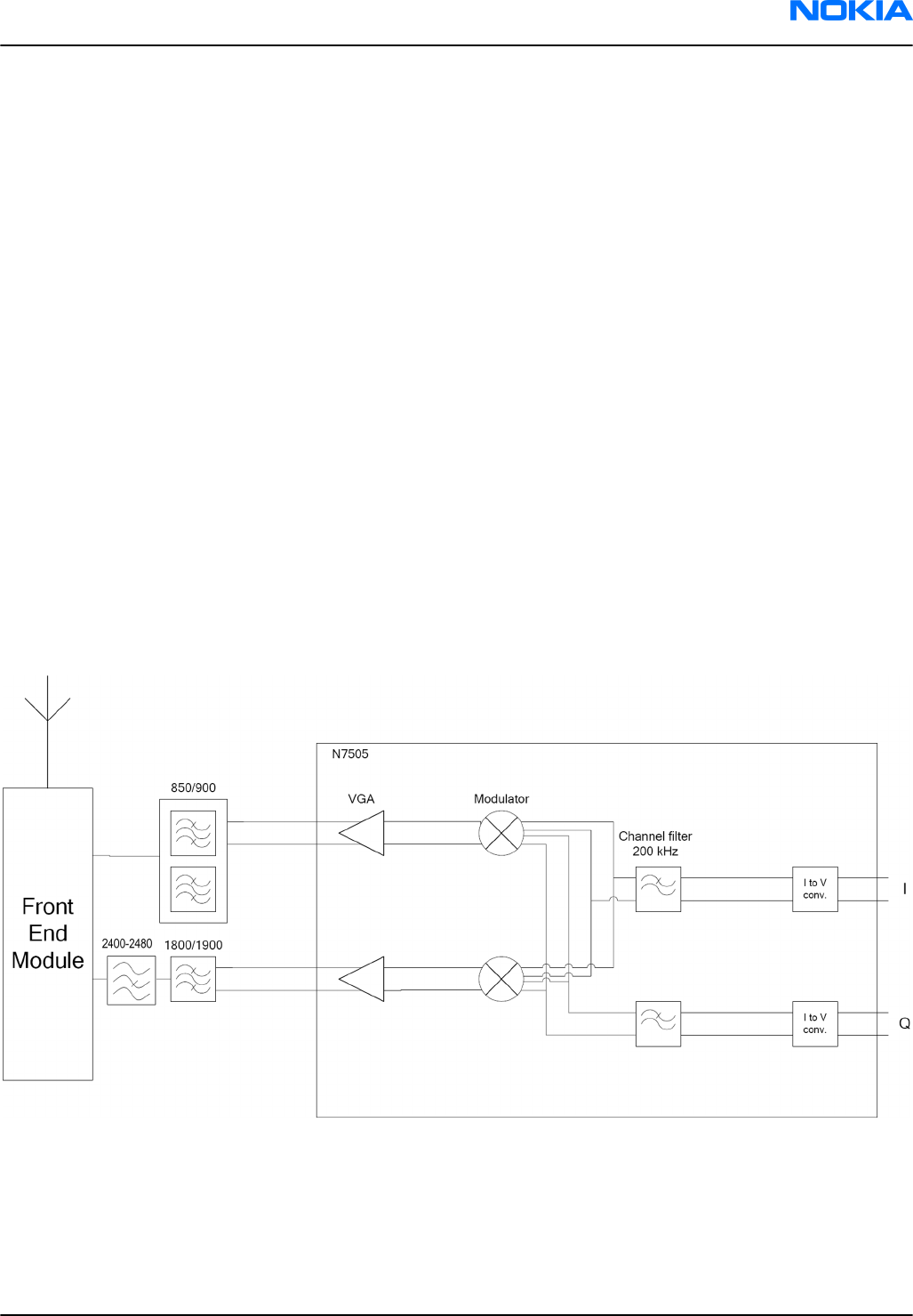
The received signal goes from the GSM antenna to the front end module (FEM) which includes switches from
band selection. FEM is followed by dedicated SAW filters which are dual packaged so that one holds SAWs for
850 and 900 and the other for 1800 and 1900 bands. The SAW filters are followed by integrated LNAs residing
in N7505.
The LNAs are followed by demodulators which downconvert the signal to baseband I and Q signals.
The channel select filter is set to 115 kHz in the GSM mode.
Introduction to transmitter functionality
Transmitter functions are implemented in the RF ASIC N7505. The ASIC contains a BB frequency low pass filter,
which is tunable according to the signal bandwidth of the system in use.
GSM transmitter
N7505 receives an analogue IQ modulated signal from digital BB, which is first low pass filtered with filter
corner frequency set to approximately 200 kHz. After the filter, the signal is routed to the GSM modulator.
The amplifier gives 40 dB of power control dynamic range.
The appropriate routing after the modulator is selected by biasing either EGSM900 (/GSM850) or
GSM1800/1900 variable gain amplifier. The amplifier gives 40 dB of power control dynamic range.
After the VGA stage the signal exits N7505. In case of GSM1800/1900 the signal goes directly to the FEM thru
a balun, which converts single ended signal into balanced signal needed to feed the FEM. In case of GSM850
and EGSM900 the PA module is preceded by a SAW filter.
TX SAW Z7503 is also dual packaged so that the correct band is selected with control voltage coming from
N7505. SAW also performs the unbalanced to balanced signal transformation. After the filter, the signal is
fed to FEM. Finally the signal is routed to the antenna.
Figure 70 GSM transmitter
GSM power control
A closed control loop comprise an integrated power detector (in FEM) and an error amplifier. The error
amplifier resides in N7505 and it controls the transmitter power of GSM.
RM-188; RM-198
System Module Nokia Customer Care
Issue 2 COMPANY CONFIDENTIAL Page 8 –25
Copyright © 2007 Nokia. All rights reserved.

GSM FEM (front end module)
A single GSM/EDGE FEM contains two separate amplifier chains, one for EGSM900 and GSM850 and another
for GSM1800/1900.
Frequency synthesizers
RF ASIC N7505 has a single synthesizer that is used to generate right frequencies for both TX and RX.
Reference oscillators
A 38.4MHz VCTCXO is used as a reference oscillator for the frequency synthesizers.
Regulators
N7505 contains integrated regulators to supply regulated voltages for their internal circuitry and other RF
parts.
RM-188; RM-198
Nokia Customer Care System Module
Page 8 –26 COMPANY CONFIDENTIAL Issue 2
Copyright © 2007 Nokia. All rights reserved.
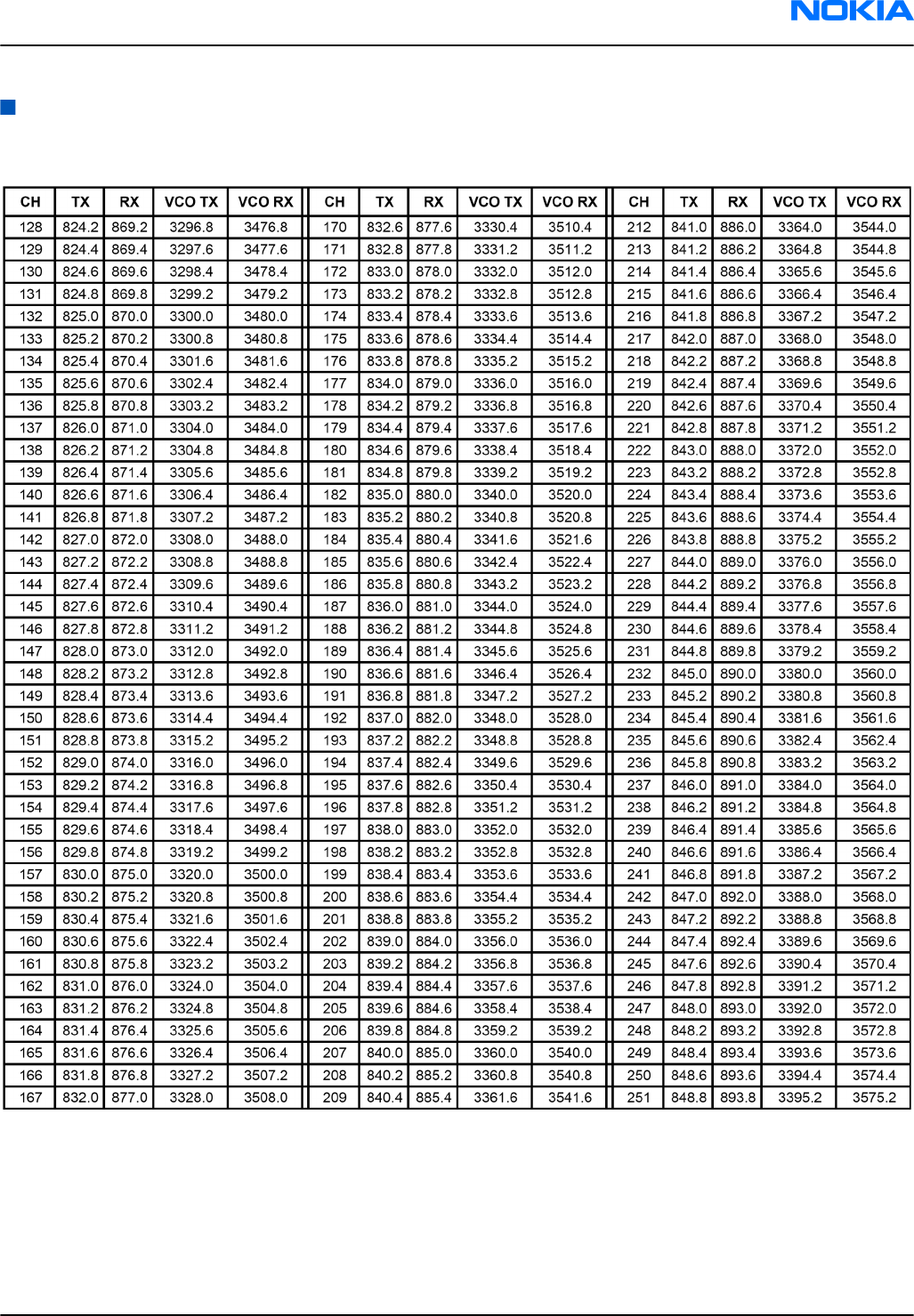
Frequency mappings
GSM850 frequencies
RM-188; RM-198
System Module Nokia Customer Care
Issue 2 COMPANY CONFIDENTIAL Page 8 –27
Copyright © 2007 Nokia. All rights reserved.
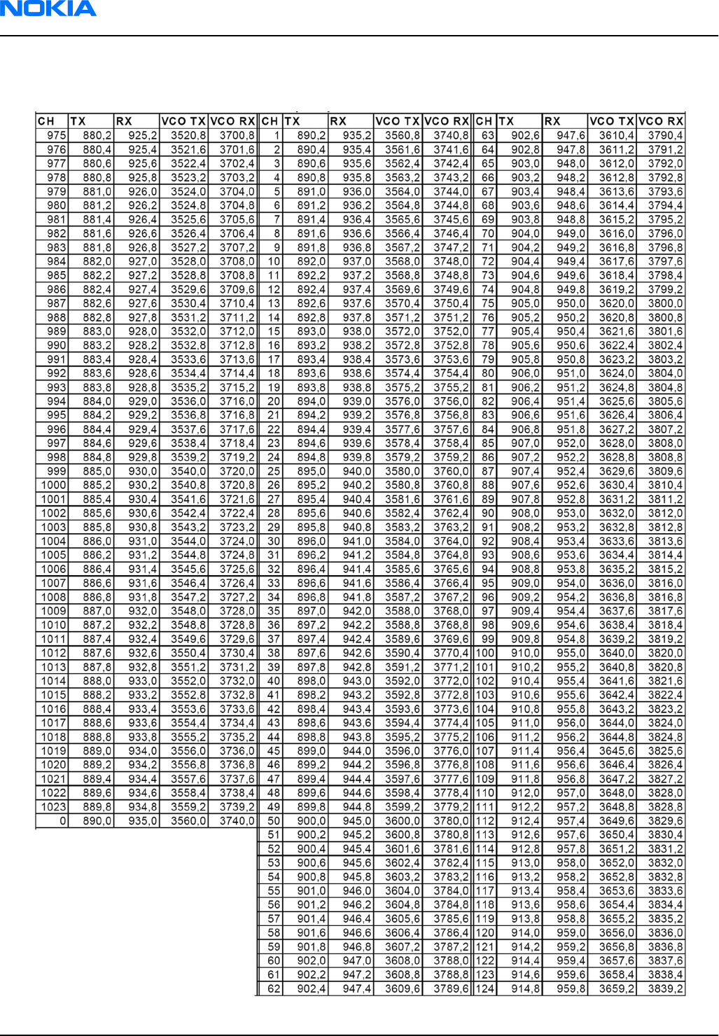
EGSM900 frequencies
RM-188; RM-198
Nokia Customer Care System Module
Page 8 –28 COMPANY CONFIDENTIAL Issue 2
Copyright © 2007 Nokia. All rights reserved.
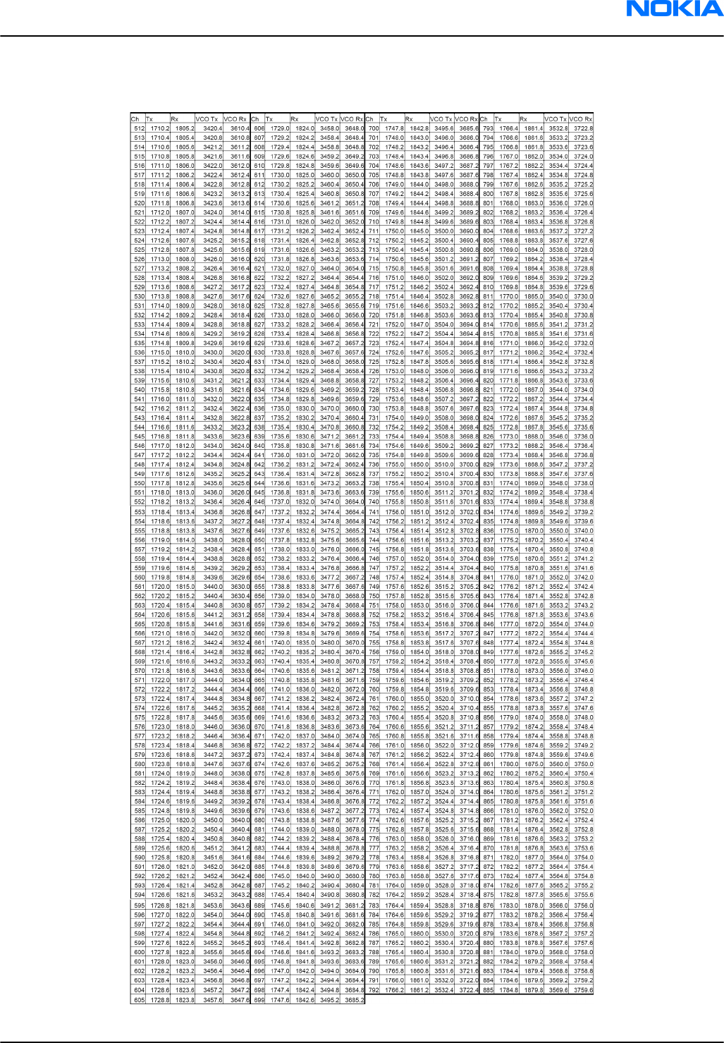
GSM1800 frequencies
RM-188; RM-198
System Module Nokia Customer Care
Issue 2 COMPANY CONFIDENTIAL Page 8 –29
Copyright © 2007 Nokia. All rights reserved.
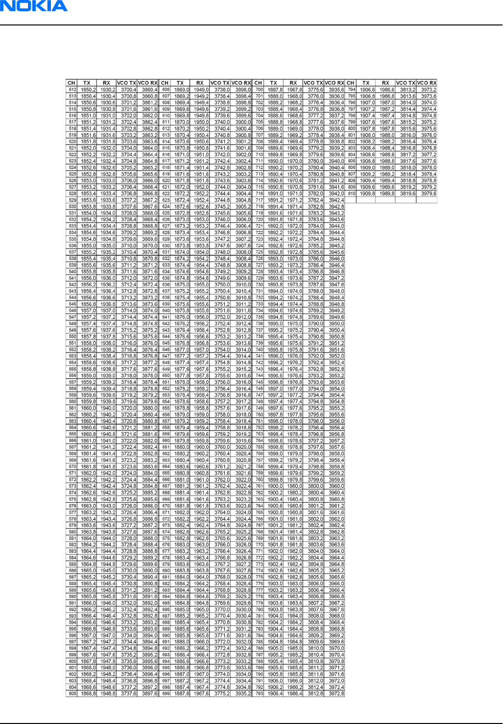
GSM1900 frequencies
RM-188; RM-198
Nokia Customer Care System Module
Page 8 –30 COMPANY CONFIDENTIAL Issue 2
Copyright © 2007 Nokia. All rights reserved.

9 — RM-188/198 schematics
Nokia Customer Care
Issue 2 COMPANY CONFIDENTIAL Page 9 –1
Copyright © 2007 Nokia. All rights reserved.

RM-188; RM-198
Nokia Customer Care RM-188/198 schematics
(This page left intentionally blank.)
Page 9 –2 COMPANY CONFIDENTIAL Issue 2
Copyright © 2007 Nokia. All rights reserved.

Table of Contents
RM-188/198 system connector .............................................................................................................................9–4
RM-188/198 Retu, Tahvo, LED driver ....................................................................................................................9–5
RM-188/198 RAPGSM, memories, FM radio, microSD..........................................................................................9–6
RM-188/198 WLAN, Bluetooth...............................................................................................................................9–7
RM-188/198 user interface....................................................................................................................................9–8
RM-188/198 flip PWB .............................................................................................................................................9–9
RM-188/198 RF part............................................................................................................................................. 9–10
RM-188/198 signal overview.............................................................................................................................. 9–11
RM-188/198 component finder.......................................................................................................................... 9–12
RM-188; RM-198
RM-188/198 schematics Nokia Customer Care
Issue 2 COMPANY CONFIDENTIAL Page 9 –3
Copyright © 2007 Nokia. All rights reserved.
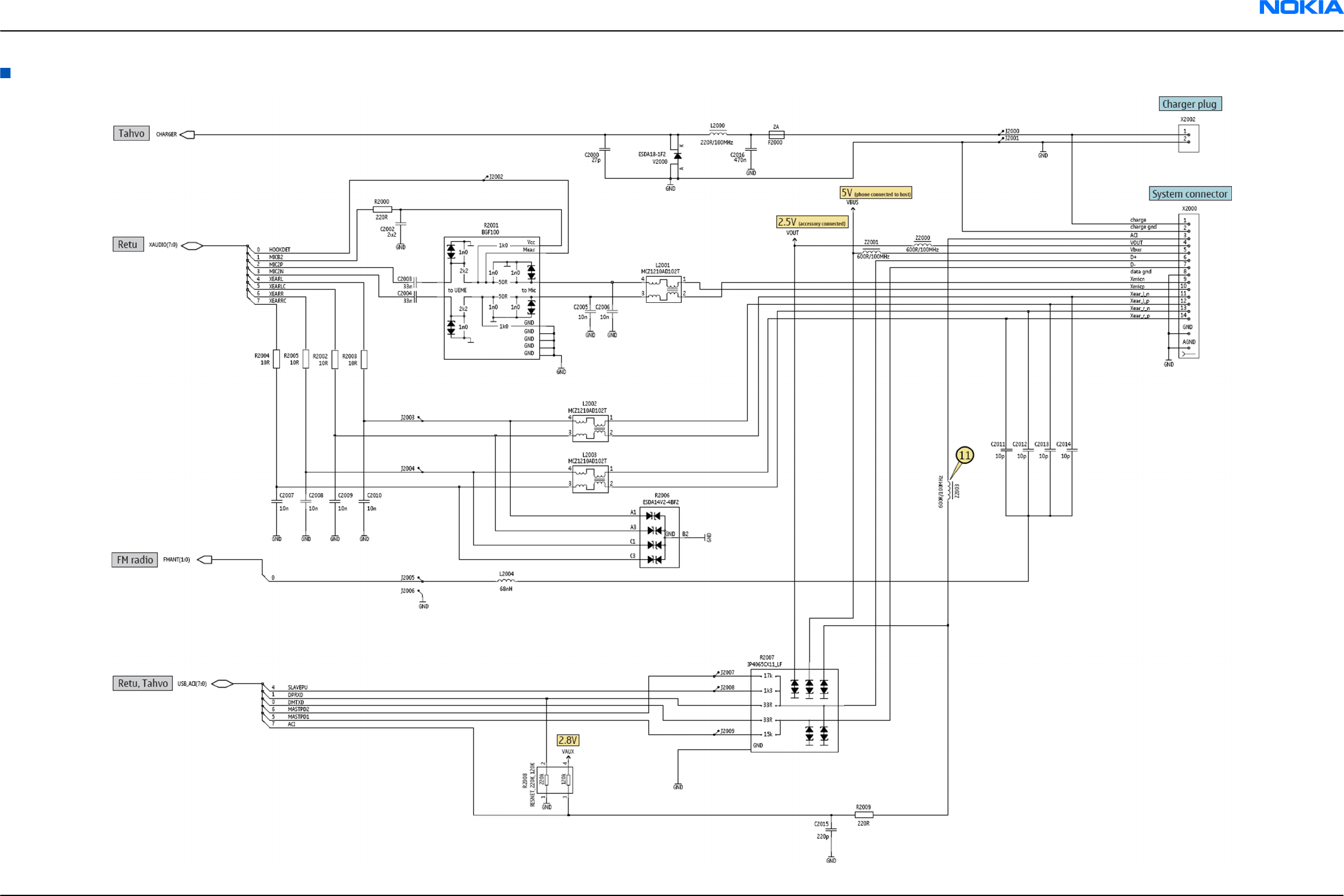
RM-188/198 system connector
RM-188; RM-198
RM-188/198 schematics Nokia Customer Care
Issue 2 COMPANY CONFIDENTIAL Page 9 –4
Copyright © 2007 Nokia. All rights reserved.
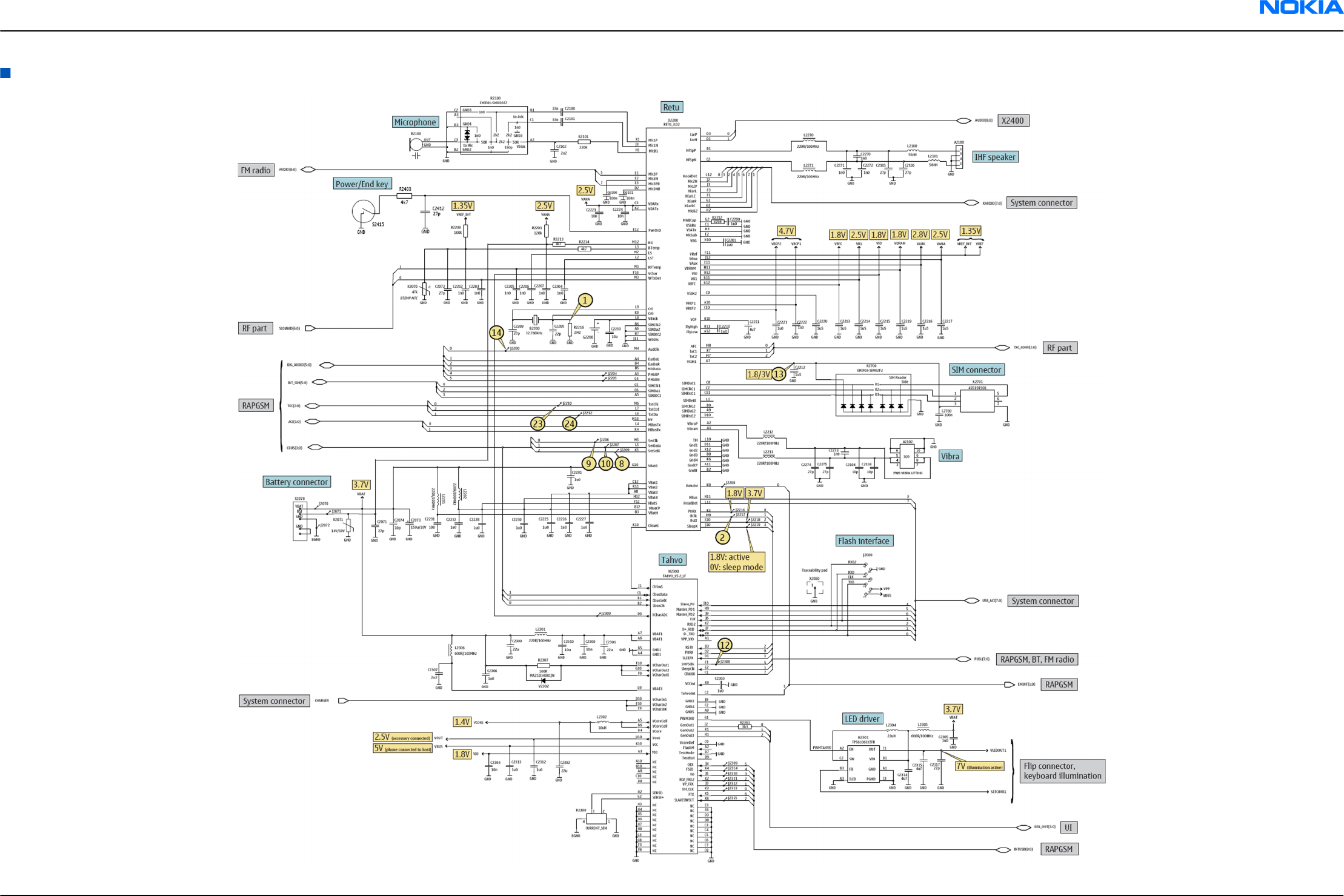
RM-188/198 Retu, Tahvo, LED driver
RM-188; RM-198
RM-188/198 schematics Nokia Customer Care
Issue 2 COMPANY CONFIDENTIAL Page 9 –5
Copyright © 2007 Nokia. All rights reserved.
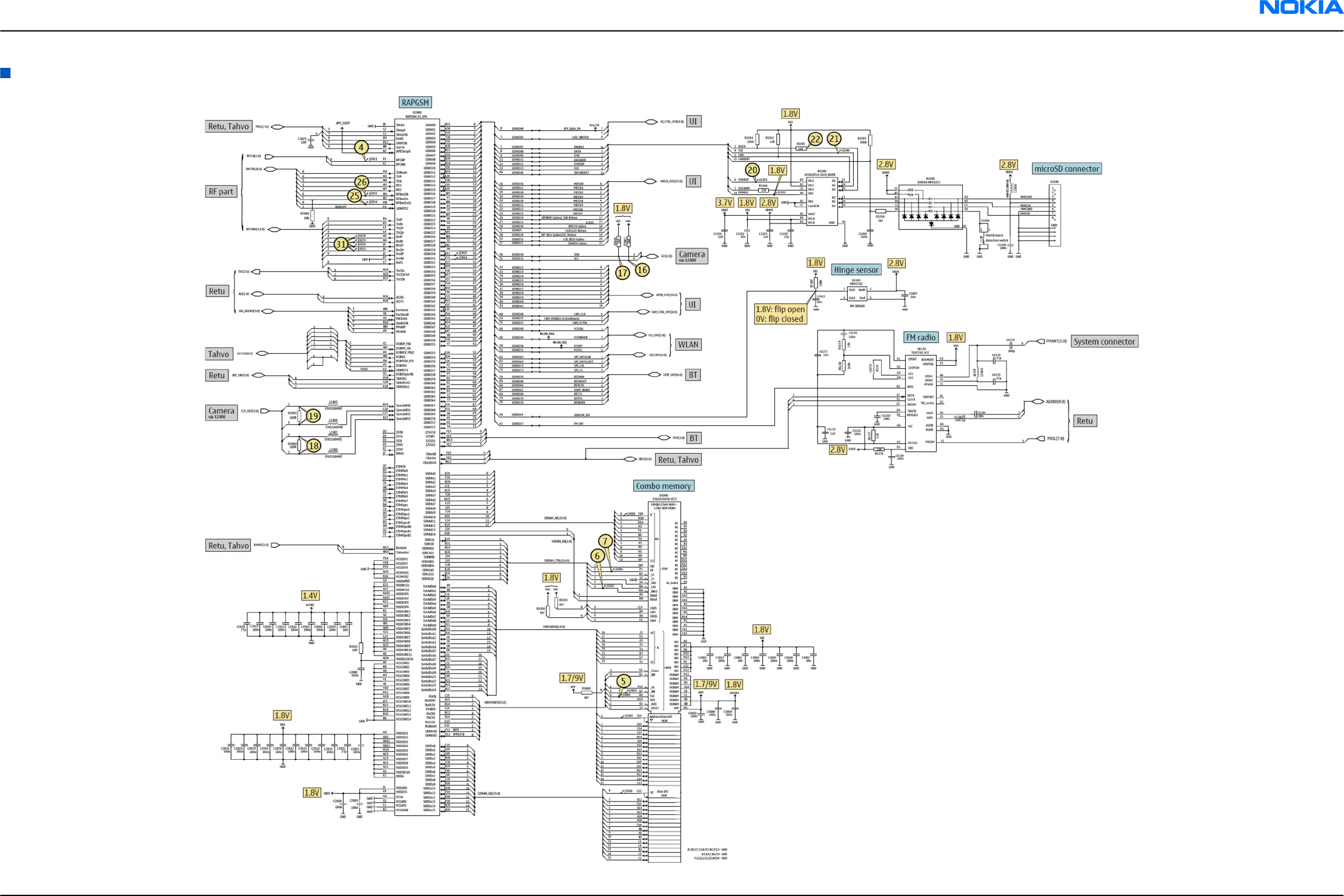
RM-188/198 RAPGSM, memories, FM radio, microSD
RM-188; RM-198
RM-188/198 schematics Nokia Customer Care
Issue 2 COMPANY CONFIDENTIAL Page 9 –6
Copyright © 2007 Nokia. All rights reserved.
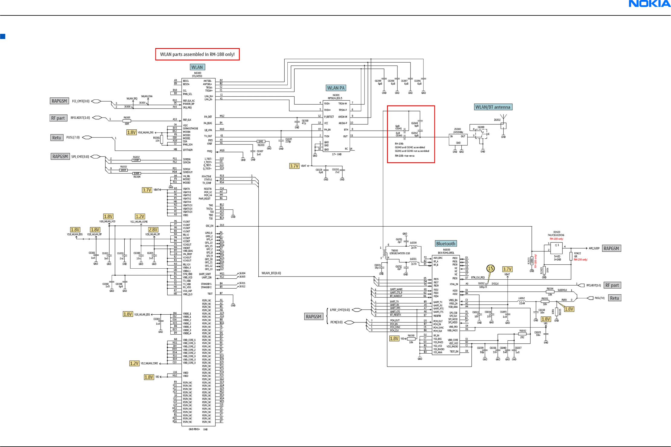
RM-188/198 WLAN, Bluetooth
RM-188; RM-198
RM-188/198 schematics Nokia Customer Care
Issue 2 COMPANY CONFIDENTIAL Page 9 –7
Copyright © 2007 Nokia. All rights reserved.
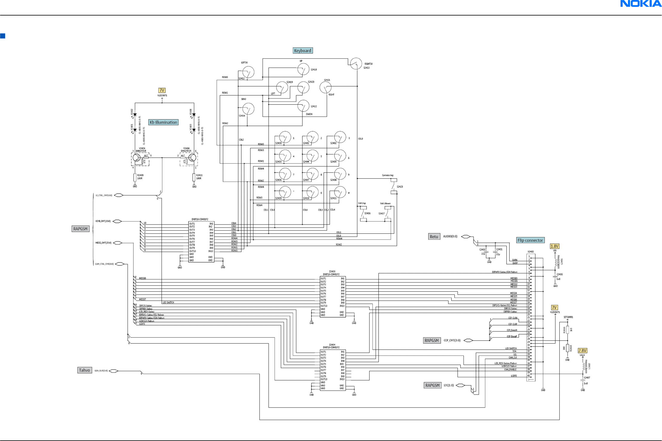
RM-188/198 user interface
RM-188; RM-198
RM-188/198 schematics Nokia Customer Care
Issue 2 COMPANY CONFIDENTIAL Page 9 –8
Copyright © 2007 Nokia. All rights reserved.
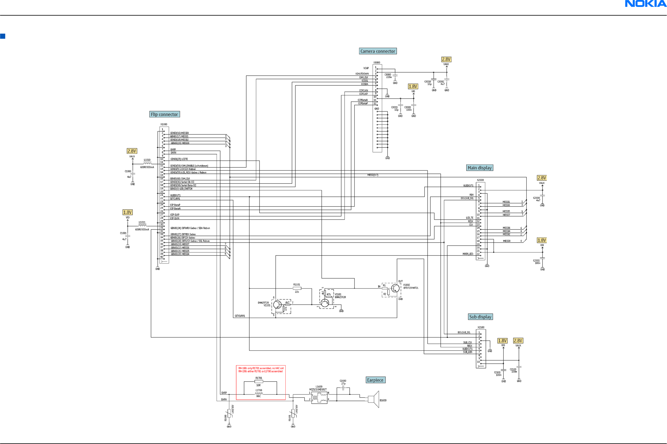
RM-188/198 flip PWB
RM-188; RM-198
RM-188/198 schematics Nokia Customer Care
Issue 2 COMPANY CONFIDENTIAL Page 9 –9
Copyright © 2007 Nokia. All rights reserved.
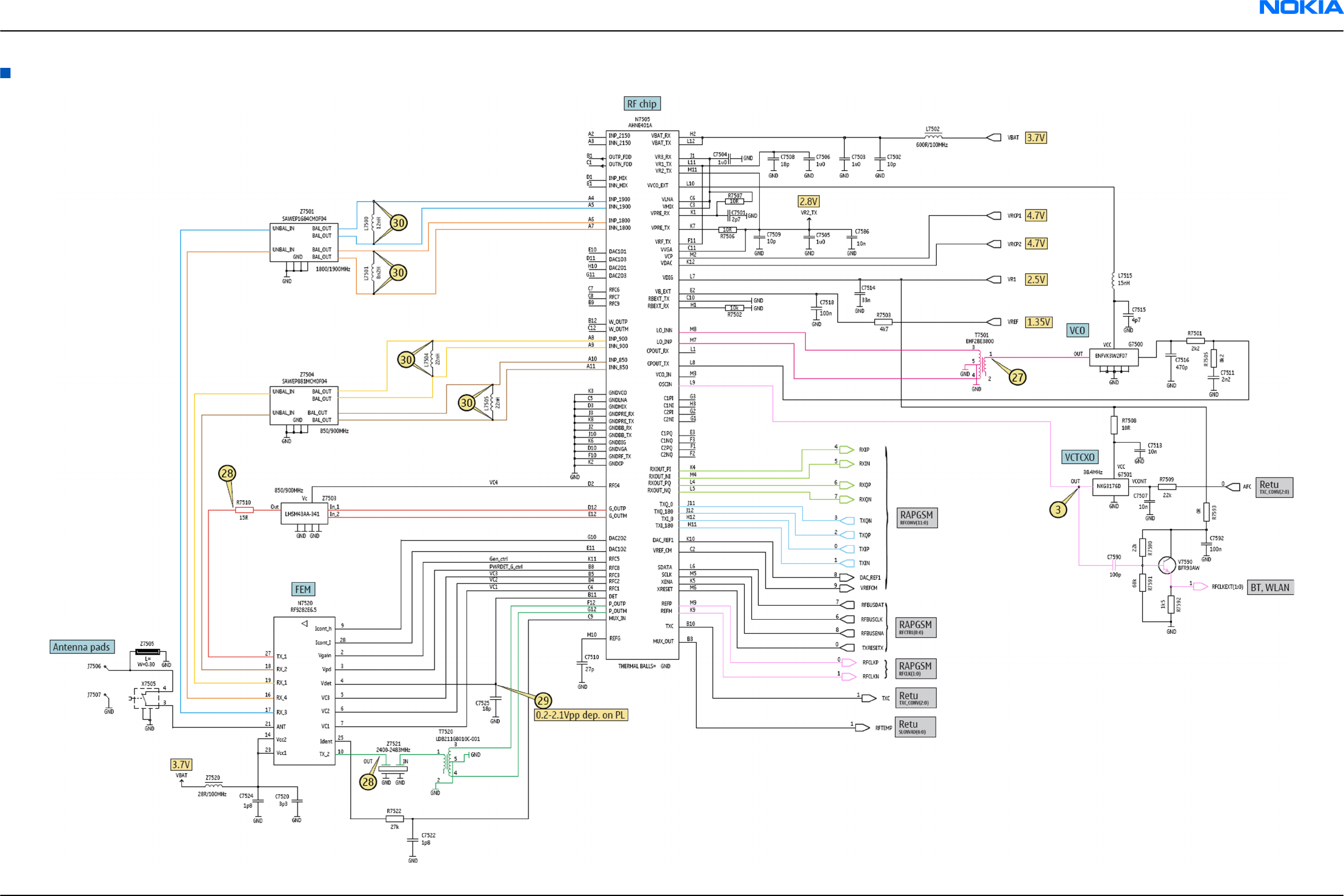
RM-188/198 RF part
RM-188; RM-198
RM-188/198 schematics Nokia Customer Care
Issue 2 COMPANY CONFIDENTIAL Page 9 –10
Copyright © 2007 Nokia. All rights reserved.
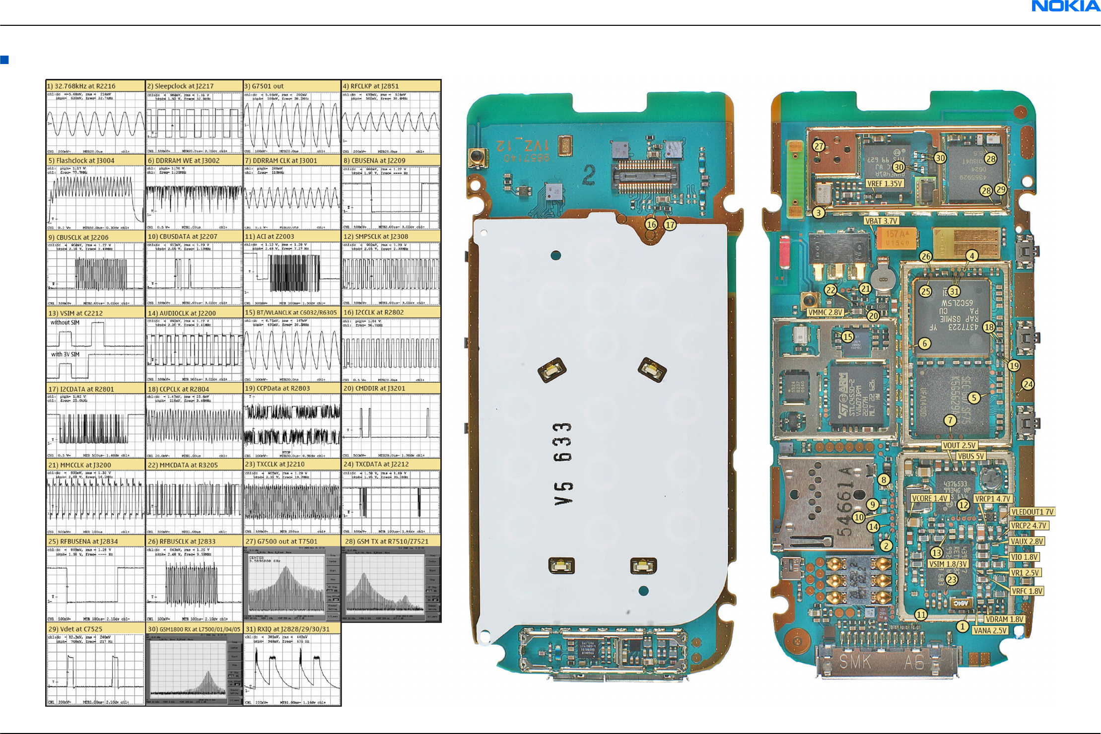
RM-188/198 signal overview
RM-188; RM-198
RM-188/198 schematics Nokia Customer Care
Issue 2 COMPANY CONFIDENTIAL Page 9 –11
Copyright © 2007 Nokia. All rights reserved.
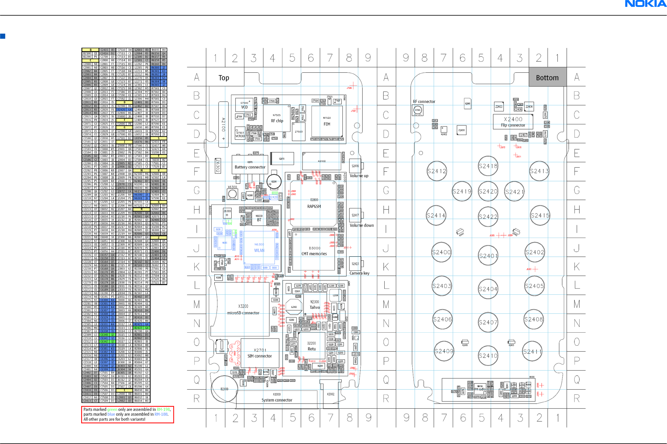
RM-188/198 component finder
RM-188; RM-198
RM-188/198 schematics Nokia Customer Care
Issue 2 COMPANY CONFIDENTIAL Page 9 –12
Copyright © 2007 Nokia. All rights reserved.

Glossary
Nokia Customer Care
Issue 2 COMPANY CONFIDENTIAL Page Glossary–1
Copyright © 2007 Nokia. All rights reserved.

RM-188; RM-198
Nokia Customer Care Glossary
(This page left intentionally blank.)
Page Glossary–2 COMPANY CONFIDENTIAL Issue 2
Copyright © 2007 Nokia. All rights reserved.
A/D-converter Analog-to-digital converter
ACI Accessory Control Interface
ADC Analog-to-digital converter
ADSP Application DPS (expected to run high level tasks)
AGC Automatic gain control (maintains volume)
ALS Ambient light sensor
AMSL After Market Service Leader
ARM Advanced RISC Machines
ARPU Average revenue per user (per month or per year)
ASIC Application Specific Integrated Circuit
ASIP Application Specific Interface Protector
B2B Board to board, connector between PWB and UI board
BB Baseband
BC02 Bluetooth module made by CSR
BIQUAD Bi-quadratic ,type of filter function)
BSI Battery Size Indicator
BT Bluetooth
CBus MCU controlled serial bus connected to UPP_WD2,UEME and Zocus
CCP Compact Camera Port
CDSP Cellular DSP (expected to run at low levels)
CLDC Connected limited device configuration
CMOS Complimentary metal-oxide semiconductor circuit (low power consumption)
COF Chip on Foil
COG Chip on Glass
CPU Central Processing Unit
CSR cambridge silicon radio
CSTN Color Super Twisted Nematic
CTSI Clock Timing Sleep and interrupt block of Tiku
CW Continuous wave
D/A-converter Digital-to-analouge converter
DAC Digital-to-analouge converter
DBI Digital Battery Interface
DBus DSP controlled serial bus connected between UPP_WD2 and Helgo
DCT-4 Digital Core Technology
DMA Direct memory access
DP Data Package
RM-188; RM-198
Glossary Nokia Customer Care
Issue 2 COMPANY CONFIDENTIAL Page Glossary–3
Copyright © 2007 Nokia. All rights reserved.
DPLL Digital Phase Locked Loop
DSP Digital Signal Processor
DtoS Differential to Single ended
EDGE Enhanced data rates for global/GSM evaluation
EGSM Extended GSM
EM Energy management
EMC Electromagnetic compability
EMI Electromagnetic interference
ESD Electrostatic discharge
FCI Functional cover interface
FPS Flash Programming Tool
FR Full rate
FSTN Film compensated super twisted nematic
GND Ground, conductive mass
GPIB General-purpose interface bus
GPRS General Packet Radio Service
GSM Group Special Mobile/Global System for Mobile communication
HF Hands free
HFCM Handsfree Common
HS Handset
HSCSD High speed circuit switched data (data transmission connection faster than GSM)
HW Hardware
I/O Input/Output
IBAT Battery current
IC Integrated circuit
ICHAR Charger current
IF Interface
IHF Integrated hands free
IMEI International Mobile Equipment Identity
IR Infrared
IrDA Infrared Data Associasion
ISA Intelligent software architecture
JPEG/JPG Joint Photographic Experts Group
LCD Liquid Crystal Display
LDO Low Drop Out
LED Light-emitting diode
RM-188; RM-198
Nokia Customer Care Glossary
Page Glossary–4 COMPANY CONFIDENTIAL Issue 2
Copyright © 2007 Nokia. All rights reserved.
LPRF Low Power Radio Frequency
MCU Micro Controller Unit (microprocessor)
MCU Multiport control unit
MIC, mic Microphone
MIDP Mobile Information Device Profile
MIN Mobile identification number
MIPS Million instructions per second
MMC Multimedia card
MMS Multimedia messaging service
NTC Negative temperature coefficient, temperature sensitive resistor used as a
temperature sensor
OMA Object management architechture
OMAP Operations, maintenance, and administartion part
Opamp Operational Amplifier
PA Power amplifier
PDA Pocket Data Application
PDA Personal digital assistant
PDRAM Program/Data RAM (on chip in Tiku)
Phoenix Software tool of DCT4.x
PIM Personal Information Management
PLL Phase locked loop
PM (Phone) Permanent memory
PUP General Purpose IO (PIO), USARTS and Pulse Width Modulators
PURX Power-up reset
PWB Printed Wiring Board
PWM Pulse width modulation
RC-filter Resistance-Capacitance filter
RF Radio Frequency
RF PopPort TM Reduced function PopPortTM interface
RFBUS Serial control Bus For RF
RSK Right Soft Key
RS-MMC Reduced size Multi Media Card
RSSI Receiving signal strength indicator
RST Reset Switch
RTC Real Time Clock (provides date and time)
RX Radio Receiver
RM-188; RM-198
Glossary Nokia Customer Care
Issue 2 COMPANY CONFIDENTIAL Page Glossary–5
Copyright © 2007 Nokia. All rights reserved.
SARAM Single Access RAM
SAW filter Surface Acoustic Wave filter
SDRAM Synchronous Dynamic Random Access Memory
SID Security ID
SIM Subscriber Identity Module
SMPS Switched Mode Power Supply
SNR Signal-to-noice ratio
SPR Standard Product requirements
SRAM Static random access memory
STI Serial Trace Interface
SW Software
SWIM Subscriber/Wallet Identification Module
TCXO Temperature controlled Oscillator
Tiku Finnish for Chip, Successor of the UPP
TX Radio Transmitter
UART Universal asynchronous receiver/transmitter
UEME Universal Energy Management chip (Enhanced version)
UEMEK See UEME
UI User Interface
UPP Universal Phone Processor
UPP_WD2 Communicator version of DCT4 system ASIC
USB Universal Serial Bus
VBAT Battery voltage
VCHAR Charger voltage
VCO Voltage controlled oscillator
VCTCXO Voltage Controlled Temperature Compensated Crystal Oscillator
VCXO Voltage Controlled Crystal Oscillator
Vp-p Peak-to-peak voltage
VSIM SIM voltage
WAP Wireless application protocol
WD Watchdog
XHTML Extensible hypertext markup language
Zocus Current sensor, (used to monitor the current flow to and from the battery)
RM-188; RM-198
Nokia Customer Care Glossary
Page Glossary–6 COMPANY CONFIDENTIAL Issue 2
Copyright © 2007 Nokia. All rights reserved.
