Nokia 6233 Rm 145 6234 123 Service Manual 34 V1
User Manual: Phone Nokia 6233 RM-145 - Service manuals and Schematics, Disassembly / Assembly. Free.
Open the PDF directly: View PDF ![]() .
.
Page Count: 214 [warning: Documents this large are best viewed by clicking the View PDF Link!]
- Amendment Record Sheet
- Copyright
- Warnings and cautions
- For your safety
- Care and maintenance
- ESD protection
- Battery information
- Company Policy
- Nokia 6233; Nokia 6234 Service Manual Structure
- 1 General information
- 2 Parts and layouts
- 3 Service Software Instructions
- Phoenix installation steps in brief
- Installing Phoenix
- Updating Phoenix installation
- Uninstalling Phoenix
- Repairing Phoenix installation
- Phone data package overview
- Installing phone data package
- Uninstalling phone data package
- Configuring users in Phoenix
- Managing connections in Phoenix
- Installing flash support files for FPS-8 and FPS-10
- Updating FPS-8 and FPS-10 flash prommer software
- Activating FPS-8
- Deactivating FPS-8
- 4 Service Tools and Service Concepts
- 5 Disassembly and reassembly instructions
- 6 BB Troubleshooting and Manual Tuning Guide
- 7 RF troubleshooting
- 8 System Module
- 9 Schematics
- Glossary

Service Manual
RM-123; RM-145 (Nokia 6233; Nokia 6234)
Mobile Terminal
Part No: 9249152 (Issue 1)
Nokia Customer Care
COMPANY CONFIDENTIAL
Copyright © 2006 Nokia. All rights reserved.

Amendment Record Sheet
Amendment No Date Inserted By Comments
Original issue 04/2006 J Bryman
RM-123; RM-145
Nokia Customer Care Amendment Record Sheet
Page ii COMPANY CONFIDENTIAL Issue 1
Copyright © 2006 Nokia. All rights reserved.

Copyright
Copyright © 2006 Nokia. All rights reserved.
Reproduction, transfer, distribution or storage of part or all of the contents in this document in any form
without the prior written permission of Nokia is prohibited.
Nokia, Nokia Connecting People, and Nokia X and Y are trademarks or registered trademarks of Nokia
Corporation. Other product and company names mentioned herein may be trademarks or tradenames of
their respective owners.
Nokia operates a policy of continuous development. Nokia reserves the right to make changes and
improvements to any of the products described in this document without prior notice.
Under no circumstances shall Nokia be responsible for any loss of data or income or any special, incidental,
consequential or indirect damages howsoever caused.
The contents of this document are provided "as is". Except as required by applicable law, no warranties of
any kind, either express or implied, including, but not limited to, the implied warranties of merchantability
and fitness for a particular purpose, are made in relation to the accuracy, reliability or contents of this
document. Nokia reserves the right to revise this document or withdraw it at any time without prior notice.
The availability of particular products may vary by region.
IMPORTANT
This document is intended for use by qualified service personnel only.
RM-123; RM-145
Copyright Nokia Customer Care
Issue 1 COMPANY CONFIDENTIAL Page iii
Copyright © 2006 Nokia. All rights reserved.

Warnings and cautions
Warnings
• IF THE DEVICE CAN BE INSTALLED IN A VEHICLE, CARE MUST BE TAKEN ON INSTALLATION IN VEHICLES FITTED
WITH ELECTRONIC ENGINE MANAGEMENT SYSTEMS AND ANTI-SKID BRAKING SYSTEMS. UNDER CERTAIN FAULT
CONDITIONS, EMITTED RF ENERGY CAN AFFECT THEIR OPERATION. IF NECESSARY, CONSULT THE VEHICLE DEALER/
MANUFACTURER TO DETERMINE THE IMMUNITY OF VEHICLE ELECTRONIC SYSTEMS TO RF ENERGY.
•THE PRODUCT MUST NOT BE OPERATED IN AREAS LIKELY TO CONTAIN POTENTIALLY EXPLOSIVE ATMOSPHERES,
FOR EXAMPLE, PETROL STATIONS (SERVICE STATIONS), BLASTING AREAS ETC.
• OPERATION OF ANY RADIO TRANSMITTING EQUIPMENT, INCLUDING CELLULAR TELEPHONES, MAY INTERFERE
WITH THE FUNCTIONALITY OF INADEQUATELY PROTECTED MEDICAL DEVICES. CONSULT A PHYSICIAN OR THE
MANUFACTURER OF THE MEDICAL DEVICE IF YOU HAVE ANY QUESTIONS. OTHER ELECTRONIC EQUIPMENT MAY
ALSO BE SUBJECT TO INTERFERENCE.
• BEFORE MAKING ANY TEST CONNECTIONS, MAKE SURE YOU HAVE SWITCHED OFF ALL EQUIPMENT.
Cautions
• Servicing and alignment must be undertaken by qualified personnel only.
• Ensure all work is carried out at an anti-static workstation and that an anti-static wrist strap is worn.
• Ensure solder, wire, or foreign matter does not enter the telephone as damage may result.
• Use only approved components as specified in the parts list.
• Ensure all components, modules, screws and insulators are correctly re-fitted after servicing and
alignment.
• Ensure all cables and wires are repositioned correctly.
•Never test a mobile phone WCDMA transmitter with full Tx power, if there is no possibility to perform the
measurements in a good performance RF-shielded room. Even low power WCDMA transmitters may disturb
nearby WCDMA networks and cause problems to 3G cellular phone communication in a wide area.
• During testing never activate the GSM or WCDMA transmitter without a proper antenna load, otherwise
GSM or WCDMA PA may be damaged.
RM-123; RM-145
Nokia Customer Care Warnings and cautions
Page iv COMPANY CONFIDENTIAL Issue 1
Copyright © 2006 Nokia. All rights reserved.

For your safety
QUALIFIED SERVICE
Only qualified personnel may install or repair phone equipment.
ACCESSORIES AND BATTERIES
Use only approved accessories and batteries. Do not connect incompatible products.
CONNECTING TO OTHER DEVICES
When connecting to any other device, read its user’s guide for detailed safety instructions. Do not connect
incompatible products.
RM-123; RM-145
For your safety Nokia Customer Care
Issue 1 COMPANY CONFIDENTIAL Page v
Copyright © 2006 Nokia. All rights reserved.

Care and maintenance
This product is of superior design and craftsmanship and should be treated with care. The suggestions below
will help you to fulfil any warranty obligations and to enjoy this product for many years.
• Keep the phone and all its parts and accessories out of the reach of small children.
•Keep the phone dry. Precipitation, humidity and all types of liquids or moisture can contain minerals that
will corrode electronic circuits.
• Do not use or store the phone in dusty, dirty areas. Its moving parts can be damaged.
•Do not store the phone in hot areas. High temperatures can shorten the life of electronic devices, damage
batteries, and warp or melt certain plastics.
• Do not store the phone in cold areas. When it warms up (to its normal temperature), moisture can form
inside, which may damage electronic circuit boards.
• Do not drop, knock or shake the phone. Rough handling can break internal circuit boards.
• Do not use harsh chemicals, cleaning solvents, or strong detergents to clean the phone.
• Do not paint the phone. Paint can clog the moving parts and prevent proper operation.
• Use only the supplied or an approved replacement antenna. Unauthorised antennas, modifications or
attachments could damage the phone and may violate regulations governing radio devices.
All of the above suggestions apply equally to the product, battery, charger or any accessory.
RM-123; RM-145
Nokia Customer Care Care and maintenance
Page vi COMPANY CONFIDENTIAL Issue 1
Copyright © 2006 Nokia. All rights reserved.

ESD protection
Nokia requires that service points have sufficient ESD protection (against static electricity) when servicing
the phone.
Any product of which the covers are removed must be handled with ESD protection. The SIM card can be
replaced without ESD protection if the product is otherwise ready for use.
To replace the covers ESD protection must be applied.
All electronic parts of the product are susceptible to ESD. Resistors, too, can be damaged by static electricity
discharge.
All ESD sensitive parts must be packed in metallized protective bags during shipping and handling outside
any ESD Protected Area (EPA).
Every repair action involving opening the product or handling the product components must be done under
ESD protection.
ESD protected spare part packages MUST NOT be opened/closed out of an ESD Protected Area.
For more information and local requirements about ESD protection and ESD Protected Area, contact your local
Nokia After Market Services representative.
RM-123; RM-145
ESD protection Nokia Customer Care
Issue 1 COMPANY CONFIDENTIAL Page vii
Copyright © 2006 Nokia. All rights reserved.

Battery information
Note: A new battery's full performance is achieved only after two or three complete charge and
discharge cycles!
The battery can be charged and discharged hundreds of times but it will eventually wear out. When the
operating time (talk-time and standby time) is noticeably shorter than normal, it is time to buy a new battery.
Use only batteries approved by the phone manufacturer and recharge the battery only with the chargers
approved by the manufacturer. Unplug the charger when not in use. Do not leave the battery connected to
a charger for longer than a week, since overcharging may shorten its lifetime. If left unused a fully charged
battery will discharge itself over time.
Temperature extremes can affect the ability of your battery to charge.
For good operation times with Ni-Cd/NiMh batteries, discharge the battery from time to time by leaving the
product switched on until it turns itself off (or by using the battery discharge facility of any approved accessory
available for the product). Do not attempt to discharge the battery by any other means.
Use the battery only for its intended purpose.
Never use any charger or battery which is damaged.
Do not short-circuit the battery. Accidental short-circuiting can occur when a metallic object (coin, clip or
pen) causes direct connection of the + and - terminals of the battery (metal strips on the battery) for example
when you carry a spare battery in your pocket or purse. Short-circuiting the terminals may damage the battery
or the connecting object.
Leaving the battery in hot or cold places, such as in a closed car in summer or winter conditions, will reduce
the capacity and lifetime of the battery. Always try to keep the battery between 15°C and 25°C (59°F and 77°
F). A phone with a hot or cold battery may temporarily not work, even when the battery is fully charged.
Batteries' performance is particularly limited in temperatures well below freezing.
Do not dispose of batteries in a fire!
Dispose of batteries according to local regulations (e.g. recycling). Do not dispose as household waste.
RM-123; RM-145
Nokia Customer Care Battery information
Page viii COMPANY CONFIDENTIAL Issue 1
Copyright © 2006 Nokia. All rights reserved.

Company Policy
Our policy is of continuous development; details of all technical modifications will be included with service
bulletins.
While every endeavour has been made to ensure the accuracy of this document, some errors may exist. If
any errors are found by the reader, NOKIA MOBILE PHONES Business Group should be notified in writing/e-
mail.
Please state:
• Title of the Document + Issue Number/Date of publication
• Latest Amendment Number (if applicable)
• Page(s) and/or Figure(s) in error
Please send to:
NOKIA CORPORATION
Nokia Mobile Phones Business Group
Nokia Customer Care
PO Box 86
FIN-24101 SALO
Finland
E-mail: Service.Manuals@nokia.com
RM-123; RM-145
Company Policy Nokia Customer Care
Issue 1 COMPANY CONFIDENTIAL Page ix
Copyright © 2006 Nokia. All rights reserved.

RM-123; RM-145
Nokia Customer Care Company Policy
(This page left intentionally blank.)
Page x COMPANY CONFIDENTIAL Issue 1
Copyright © 2006 Nokia. All rights reserved.

Nokia 6233; Nokia 6234 Service Manual Structure
1 General information
2 Parts and layouts
3 Service Software Instructions
4 Service Tools and Service Concepts
5 Disassembly and reassembly instructions
6 BB Troubleshooting and Manual Tuning Guide
7 RF troubleshooting
8 System Module
9 Schematics
Glossary
RM-123; RM-145
Nokia 6233; Nokia 6234 Service Manual Structure Nokia Customer Care
Issue 1 COMPANY CONFIDENTIAL Page xi
Copyright © 2006 Nokia. All rights reserved.

RM-123; RM-145
Nokia Customer Care Nokia 6233; Nokia 6234 Service Manual Structure
(This page left intentionally blank.)
Page xii COMPANY CONFIDENTIAL Issue 1
Copyright © 2006 Nokia. All rights reserved.

1 — General information
Nokia Customer Care
Issue 1 COMPANY CONFIDENTIAL Page 1 –1
Copyright © 2006 Nokia. All rights reserved.

RM-123; RM-145
Nokia Customer Care General information
(This page left intentionally blank.)
Page 1 –2 COMPANY CONFIDENTIAL Issue 1
Copyright © 2006 Nokia. All rights reserved.

Table of Contents
Product selection....................................................................................................................................................1–5
Phone features........................................................................................................................................................1–6
Software and User interface features...................................................................................................................1–6
Accessories..............................................................................................................................................................1–9
Technical specifications.......................................................................................................................................1–10
General specifications.....................................................................................................................................1–10
Main RF characteristics for triple GSM band and WCDMA band phones (Europe).....................................1–11
Battery endurance...........................................................................................................................................1–11
Environmental conditions..............................................................................................................................1–12
List of Tables
Table 1 Battery and chargers................................................................................................................................1–9
Table 2 Car accessories..........................................................................................................................................1–9
Table 3 Audio..........................................................................................................................................................1–9
Table 4 Connectivity.............................................................................................................................................1–10
Table 5 Imaging and lifestyle..............................................................................................................................1–10
Table 6 Messaging................................................................................................................................................1–10
Table 7 Music........................................................................................................................................................1–10
RM-123; RM-145
General information Nokia Customer Care
Issue 1 COMPANY CONFIDENTIAL Page 1 –3
Copyright © 2006 Nokia. All rights reserved.

RM-123; RM-145
Nokia Customer Care General information
(This page left intentionally blank.)
Page 1 –4 COMPANY CONFIDENTIAL Issue 1
Copyright © 2006 Nokia. All rights reserved.
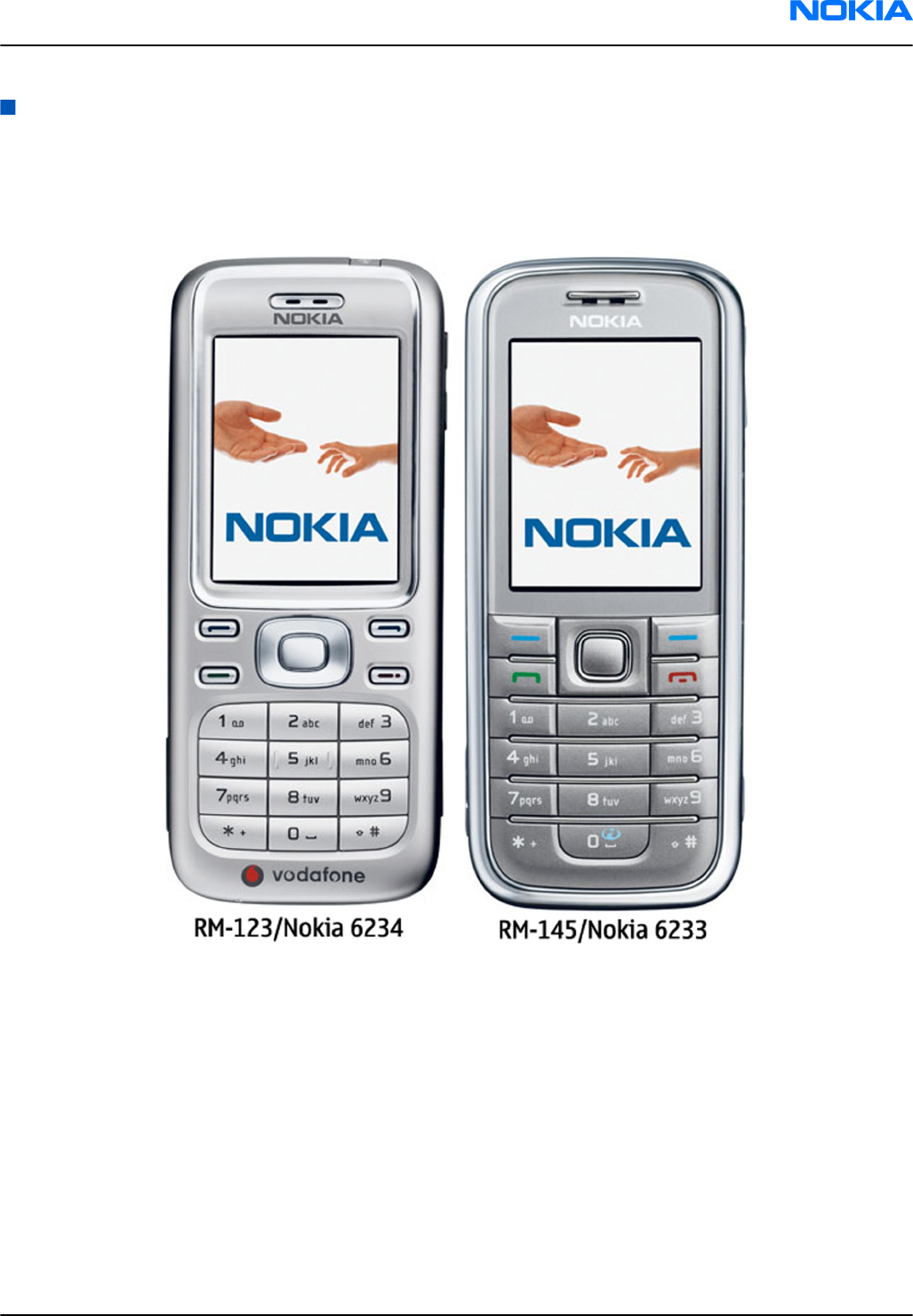
Product selection
RM-123 (Nokia 6234) and RM-145 (Nokia 6233) are both WCDMA/GSM dual mode phones, supporting WCDMA
2100 (UMTS) and EGSM900/1800/1900 bands.
RM-123 is a special Vodafone customised model. Even though the appearance is different, they both use the
same PWB and offer the same features.
Key Features:
• Stereo speakers and 3D sound effects
• Up to 70 MB total memory for storing pictures, messages, etc.
• 2-megapixel camera with 8x digital zoom and landscape mode
• Stereo FM radio supporting visual radio
• Music player
• Enhanced Java email client
• Video, MP3, eACC+, and polyphonic ringing tones
• FM visual stereo radio with integrated 3D stereo speakers
RM-123; RM-145
General information Nokia Customer Care
Issue 1 COMPANY CONFIDENTIAL Page 1 –5
Copyright © 2006 Nokia. All rights reserved.

Phone features
Display and keypad features
• 262 K colour QVGA 240 x 320 pixels display
• Active TFT display
• Side volume keys with zoom functionality
• Dedicated camera key
Hardware features
• 2-megapixel camera landscape mode and 8x digital zoom
• PopPortTM™
• 2 mm charger plug interface
• Bluetooth
• USB
• FM radio
• MP3 player
• Internal vibrator
• Plug-in SIM (1.8 V and 3.0 V)
• Real time clock
RF features
• WCDMA 2100
• GSM/EDGE 900/1800/1900
• EDGE*: Class 10
• GPRS: Class 10
• HSCSD
Software and User interface features
Software features
• ISA OS 8.0s Platform
• Nokia Series 40 User interface (UI): Java MIDP 2.0
UI features
Integrated digital camera • 2-megapixel camera with 8x smooth, digital zoom and dedicated key
• Landscape support mode
• Full screen viewfinder
• Print images directly from the phone over a Bluetooth connection or
using an MMC (depending on the printer)
RM-123; RM-145
Nokia Customer Care General information
Page 1 –6 COMPANY CONFIDENTIAL Issue 1
Copyright © 2006 Nokia. All rights reserved.
Multimedia • Integrated video player for download and playback or for streaming:
3GPP, H.263 video, MPEG-4, and AMR
• Add video and music to your caller ID
• Interactive 3D games with multi-player support
• Music player supports MP3, MP4, eAAC+ and AAC music files
• Use pre-loaded polyphonic midi ring tones, MP3, eAAC+, and message
alerts
• OTA download of ringing tones, themes, wallpapers
• Download/upload images and video clips
• Kodak Photo services for high-quality, easy printing
• Stereo FM Radio
• Video Sharing
• 3GPP streaming for mobile access to the latest sports, weather,
entertainment, and news information
Messaging • Common inbox (MMS, SMS, e-mail)
• Full MMS 1.2 functionality for sending and receiving messages including
video, photos, and music
• Improved Java email client with easy settings and spam filter
• Email: supports SMTP, POP3, and IMAP4 protocols
• Text messaging: supports concatenated SMS and picture messaging
• Presence: includes Wireless Village and Dynamic phonebook; know
someone's status before you call
Memory functions • Up to 70MB total memory (6MB internal + 64MB memory card)
• Supports up to 2GB of expandable, microSD memory
• Back up important files such as presentations and documents, or just
store images on your personal mobile storage device
Games • Nokia World Cup, 3D Street Racer, and 3D Snake
• Download new Java games
Applications • Enhanced Java email client with easy settings and spam filter
• Data synchronization
• Visual Radio
• Wireless presenter
• Notepad and voice memo recorder
• Translator
• World Clock II
• Converter II
• Java MIDP 2.0 with Bluetooth API makes downloading new applications
easy
• Active standby mode
RM-123; RM-145
General information Nokia Customer Care
Issue 1 COMPANY CONFIDENTIAL Page 1 –7
Copyright © 2006 Nokia. All rights reserved.
Connectivity • Transfer images, video clips, audio files, and other files
• Bluetooth wireless technology: wide range of profiles and APIs for
seamless connectivity
• Infrared
• USB port
•Easy remote or local synchronization with a PC or other compatible device
• OMA DRM 1.0 protects copyrighted material
•Push to talk over cellular (PoC) lets you use your phone like a walkie-talkie
Browsing • WAP 2.0, XHTML browser over HTTP/TCP/IP stack HSCSD
• HSCSD, CSD for browsing and as data modem
• 3GPP video streaming
Data transfer • EDGE Class 10 (4+1, 3+2): speed up to 236.8 kbps
• GPRS (General Packet Radio Service) class 10 (4+1, 3+2)
• HSCSD (High-Speed Circuit-Switched Data) transfer up to 43.2 kbps in
HSCSD networks
• DRM 1.0 for secure content downloading
• Speech codec support for FR, EFR, AMR
• TCP/IP
Call management • Speed dialing: up to 9 names
• Last-number redial from dialed calls list (Dial key brings up the dialed
calls list)
• Automatic redial (max 10 attempts)
• Automatic answer (works with headset or car kit only)
• Call waiting, call hold, call divert, call timer
• Automatic and manual network selection
• Caller identification with image
• Closed User Group
• Fixed Dialing Number, allows calls only to predefined numbers
• Conference call (up to 5 participants)
• Vibrating alert
Voice features • Nokia Push to Talk with dedicated key
• Two effect speakers (each 15mm x 11mm)
• 3D effect sound
• Nokia Express Audio Messaging
• 16 voice commands
• Integrated Handsfree speakers
• Voice dialing, 25 presets
RM-123; RM-145
Nokia Customer Care General information
Page 1 –8 COMPANY CONFIDENTIAL Issue 1
Copyright © 2006 Nokia. All rights reserved.
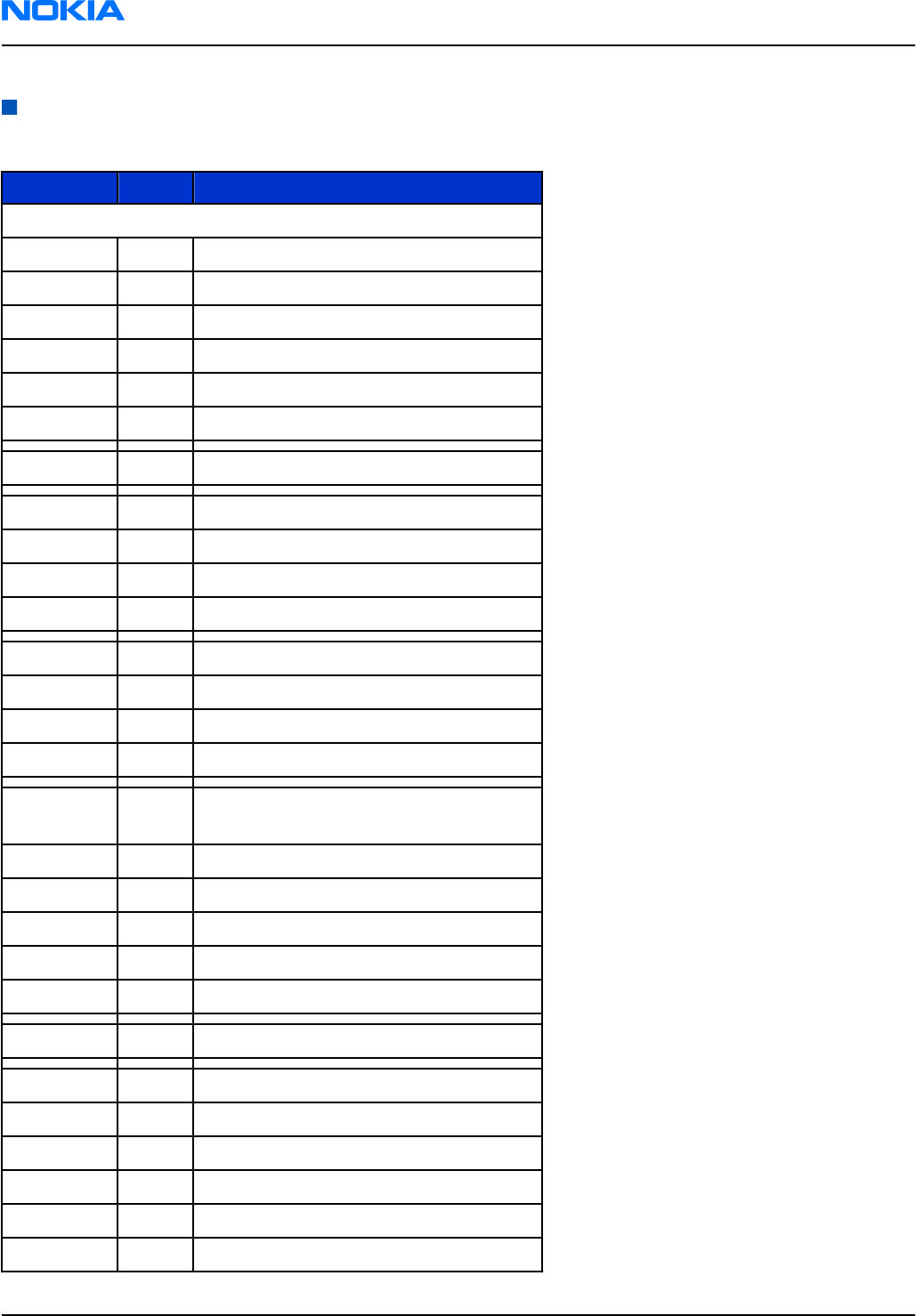
Accessories
Table 1 Battery and chargers
Type Name
Note: This phone is charged through the smaller Nokia standard interface (2.0 mm plug). The 3.5 mm
standard charger can be used together with the CA-44 charger adapter.
AC-3 Compact charger
AC-4 Travel performance charger
BP-6M-S Battery 1100 mAh Li-Ion
CA-44 Charger adapter (from 3.5 mm -> 2 mm)
Table 2 Car accessories
Type Name
BHF-3 Headrest handsfree
CA-55 Converter
CARK-91 Advanced HF car kit
CK-1W Wireless car kit
CK-7W Advanced Car Kit
CK-10 Car kit
CR-56 Mobile holder
DC-4 Mobile charger
HF-3 Plug-in car handsfree
HF-6W Wireless plug-in handsfree
N616 Car kit
Nokia universal holder
Table 3 Audio
Type Name
HDA-10 Phone adapter
HDB-4 Boom headset
HDS-3 Stereo headset
HDW-3 Wireless headset
HS-3 Stereo headset: fashion
HS-4W Wireless boom headset
HS-5 Headset
HS-6 Display headset
RM-123; RM-145
General information Nokia Customer Care
Issue 1 COMPANY CONFIDENTIAL Page 1 –9
Copyright © 2006 Nokia. All rights reserved.
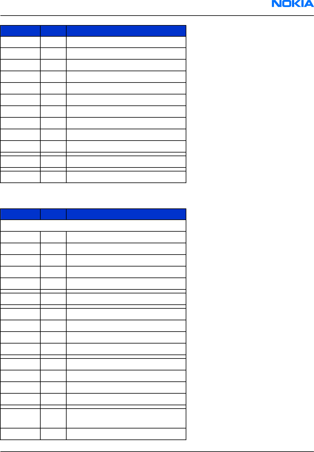
Type Name
HS-11W Wireless headset
HS-21W Wireless clip-on headset
HS-23 Stereo headset
HS-26W Wireless headset
HS-31 Fashion stereo headset
HS-36W Wireless headset
LPS-4 Loopset
MD-1 Music stand
Table 4 Connectivity
Type Name
CA-53 USB cable
Table 5 Imaging and lifestyle
Type Name
PT-6 Remote camera
Table 6 Messaging
Type Name
SU-1B Digital pen
Table 7 Music
Type Name
MD-1 Music stand
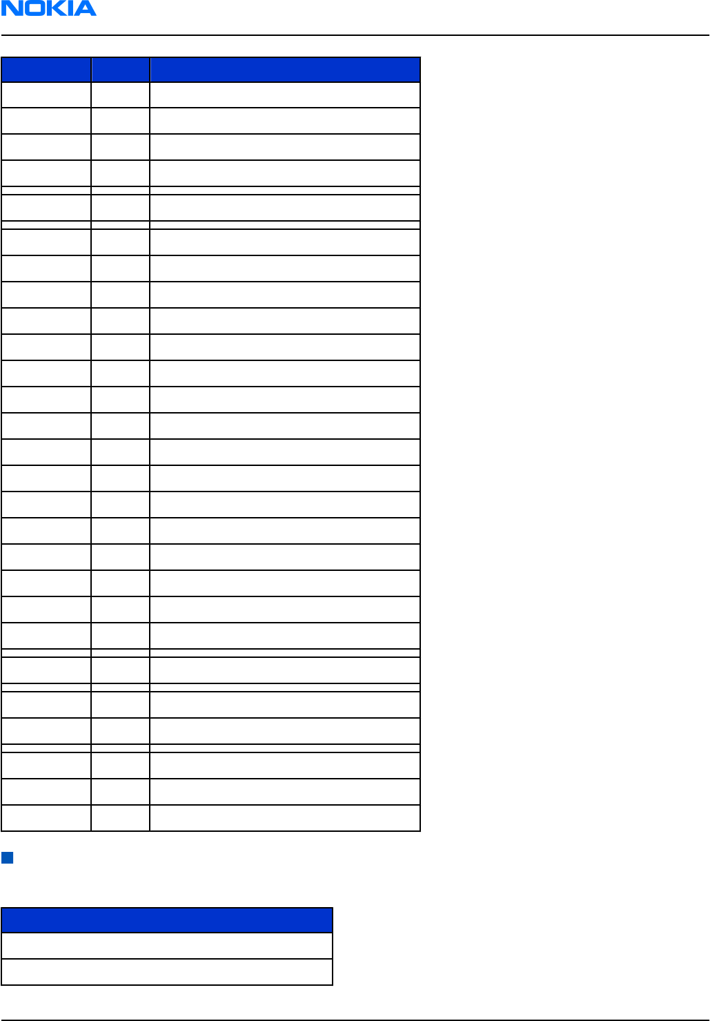
Technical specifications
General specifications
Unit Dimension (mm) Weight (g) Volume (cc)
RM-123 Transceiver
with BP-6M-S 1100 mAh
Li-Ion battery pack
108x46.5x17.5 100 76
RM-145 Transceiver
with BP-6M-S 1100 mAh
Li-Ion battery pack
108x46.5x18 110 81
RM-123; RM-145
Nokia Customer Care General information
Page 1 –10 COMPANY CONFIDENTIAL Issue 1
Copyright © 2006 Nokia. All rights reserved.
Main RF characteristics for triple GSM band and WCDMA band phones (Europe)
Parameter Unit
Cellular system GSM/EGSM900,GSM1800/1900
WCDMA2100
Rx frequency band EGSM900: 925 - 935 MHz
GSM900: 935 - 960 MHz
GSM1800: 1805 - 1880 MHz
GSM1900: 1930 - 1990 MHz
WCDMA: 2110- 2170 MHz
Tx frequency band EGSM900: 880 - 890 MHz
GSM900: 890 - 915 MHz
GSM1800: 1710 - 1785 MHz
GSM1900: 1850 - 1910 MHz
WCDMA: 1920 - 1980 MHz
Output power GSM900: +5 … +32.5 dBm
GSM1800: +0 … +30 dBm
GSM1900: +0 ... +30 dBm
WCDMA2100: 0 ...+24 dBm
Number of RF channels GSM900: 125
GSM1800: 375
GSM1900: 300
WCDMA2100: 8
Channel spacing GSM 200 KHz
WCDMA 4.8 MHz
Number of Tx power levels GSM900: 15
GSM1800: 16
GSM1900: 16
WCDMA2100: 12
Battery endurance
Battery Talk time Standby time
BP-6M-S 1100 mAh Li-ion GSM: up to 4 hours
WCDMA: up to 3.1 hours
Up to 340 hours
RM-123; RM-145
General information Nokia Customer Care
Issue 1 COMPANY CONFIDENTIAL Page 1 –11
Copyright © 2006 Nokia. All rights reserved.
Note: Variation in operation times will occur depending on SIM card, network settings and usage.
Talk time is increased by up to 30% if half rate is active, and reduced by 5% if enhanced full rate is
active.
Environmental conditions
Environmental
condition Ambient temperature Notes
Normal operation 15 oC ... +55 oCSpecifications fulfilled
Reduced performance 55 oC ... +70 oCOperational only for short periods
Intermittent or no
operation -40 oC ... -15 oC and +70 oC ... +85oCOperation not guaranteed but an
attempt to operate will not damage
the phone
No operation or
storage <-40 oC and >+85 oCNo storage. An attempt to operate
may cause permanent damage
Charging allowed -15 oC ... +55 oC
Long term storage
conditions 0 oC ... +85 oC
Humidity and water
resistance
Relative humidity range is 5 to 95%.
Condensed or dripping water may
cause intermittent malfunctions.
Protection against dripping water
has to be implemented in (enclosure)
mechanics.
Continuous dampness will cause
permanent damage to the module.
RM-123; RM-145
Nokia Customer Care General information
Page 1 –12 COMPANY CONFIDENTIAL Issue 1
Copyright © 2006 Nokia. All rights reserved.

2 — Parts and layouts
Nokia Customer Care
Issue 1 COMPANY CONFIDENTIAL Page 2 –1
Copyright © 2006 Nokia. All rights reserved.

RM-123; RM-145
Nokia Customer Care Parts and layouts
(This page left intentionally blank.)
Page 2 –2 COMPANY CONFIDENTIAL Issue 1
Copyright © 2006 Nokia. All rights reserved.

Table of Contents
Exploded view.........................................................................................................................................................2–5
Mechanical parts list...............................................................................................................................................2–6
Swap units...............................................................................................................................................................2–8
Component parts list..............................................................................................................................................2–9
Component layouts..............................................................................................................................................2–21
List of Tables
Table 8 RM-123 Mechanical parts list...................................................................................................................2–6
Table 9 RM-145 Mechanical parts list...................................................................................................................2–7
Table 10 RM-123 Swap units.................................................................................................................................2–8
Table 11 RM-145 Swap units.................................................................................................................................2–9
Table 12 ..................................................................................................................................................................2–9
List of Figures
Figure 1 Main board layout, bottom side (1rra_08a)........................................................................................2–21
Figure 2 Main board layout, top side (1rra_08a)...............................................................................................2–21
RM-123; RM-145
Parts and layouts Nokia Customer Care
Issue 1 COMPANY CONFIDENTIAL Page 2 –3
Copyright © 2006 Nokia. All rights reserved.

RM-123; RM-145
Nokia Customer Care Parts and layouts
(This page left intentionally blank.)
Page 2 –4 COMPANY CONFIDENTIAL Issue 1
Copyright © 2006 Nokia. All rights reserved.
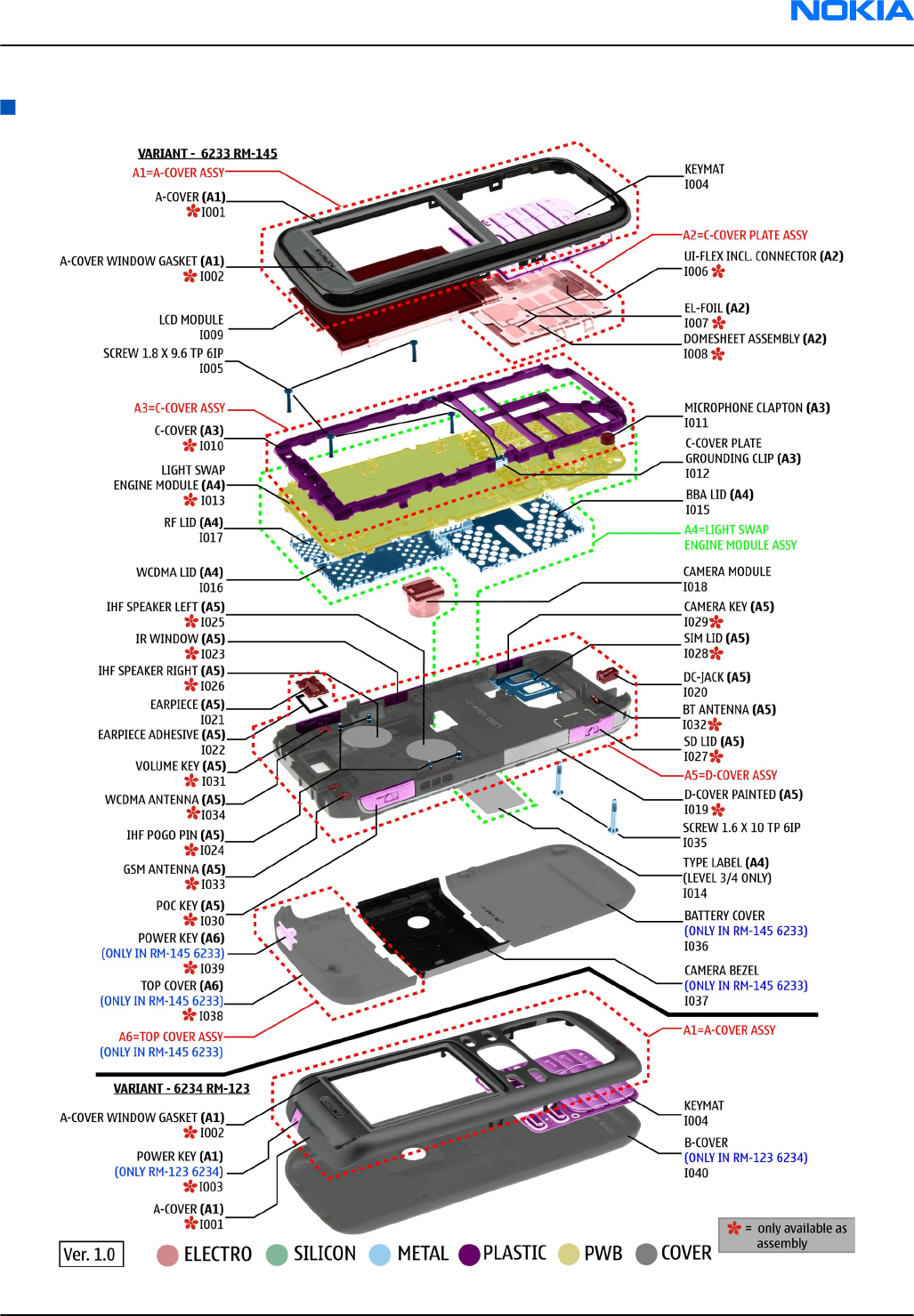
Exploded view
RM-123; RM-145
Parts and layouts Nokia Customer Care
Issue 1 COMPANY CONFIDENTIAL Page 2 –5
Copyright © 2006 Nokia. All rights reserved.
Mechanical parts list
Table 8 RM-123 Mechanical parts list
Item Qty Description
* = Not available as spare part
A1 A-cover assy
I001* 1 A-cover (A1)
I002* 1 A-cover window gasket
I003* 1 Power key
I004 1 Keymat
I009 1 LCD module
I005 1 Screw 1.8 x 9.6 TP 6IP
A2 Cover plate assembly
I006* 1 UI flex incl connector (A2)
I007* 1 EL-foil (a2)
I008* 1 Domesheet assembly (A2)
A3 C-cover assembly
I010* 1 C-cover (A3)
I011 1 Microphone Clapton
I012 1 C-cover plate grounding clip
A4 Light swap engine module
assembly
I013* 1 Light swap engine module
I014 1 Type label (Level 3/4 only)
I015 1 BBA lid (A4)
I016 1 WCDMA lid
I017 1 RF lid
I018 1 Camera module
A5 D-cover assembly
I019* 1 D-cover painted
I020 1 DC jack
I021 1 Earpiece
I022 1 Earpiece adhesive
I023* 1 IR window
RM-123; RM-145
Nokia Customer Care Parts and layouts
Page 2 –6 COMPANY CONFIDENTIAL Issue 1
Copyright © 2006 Nokia. All rights reserved.
Item Qty Description
I024* 1 IHF pogo pin
I025* 1 IHF speaker left
I026* 1 IHF speaker right
I028* 1 SIM lid
I029* 1 Camera key
I030* 1 POC key
I031 1 Volume key
I032* 1 BT antenna
I033* 1 GSM antenna
I034* 1 WCDMA antenna
I035 1 Screw 1.8 x 10 TP 6IP
I040 1 B-cover
Table 9 RM-145 Mechanical parts list
Item Qty Description
* = Not available as spare part
A1 A-cover assy
I001* 1 A-cover (A1)
I002* 1 A-cover window gasket
I004 1 Keymat
I009 1 LCD module
I005 1 Screw 1.8 x 9.6 TP 6IP
A2 Cover plate assembly
I006* 1 UI flex incl connector (A2)
I007* 1 EL-foil (a2)
I008* 1 Domesheet assembly (A2)
A3 C-cover assembly
I010* 1 C-cover (A3)
I011 1 Microphone Clapton
I012 1 C-cover plate grounding clip
A4 Light swap engine module
assembly
I013* 1 Light swap engine module
RM-123; RM-145
Parts and layouts Nokia Customer Care
Issue 1 COMPANY CONFIDENTIAL Page 2 –7
Copyright © 2006 Nokia. All rights reserved.
Item Qty Description
I014 1 Type label (Level 3/4 only)
I015 1 BBA lid (A4)
I016 1 WCDMA lid
I017 1 RF lid
I018 1 Camera module
A5 D-cover assembly
I019* 1 D-cover painted
I020 1 DC jack
I021 1 Earpiece
I022 1 Earpiece adhesive
I023* 1 IR window
I024* 1 IHF pogo pin
I025* 1 IHF speaker left
I026* 1 IHF speaker right
I028* 1 SIM lid
I029* 1 Camera key
I030* 1 POC key
I031* 1 Volume key
I032* 1 BT antenna
I033* 1 GSM antenna
I034* 1 WCDMA antenna
I035 1 Screw 1.8 x 10 TP 6IP
I036 1 Battery cover
I037 1 Camera bezel
A6 Top cover assembly
I038* 1 Top cover
I039* 1 Power key
Swap units
Table 10 RM-123 Swap units
Swap units for RM-123
RM-123 SWAP SOFT BLACK LATIN EURO-C
RM-123 SWAP SOFT BLACK LATIN EURO-C ZA
RM-123; RM-145
Nokia Customer Care Parts and layouts
Page 2 –8 COMPANY CONFIDENTIAL Issue 1
Copyright © 2006 Nokia. All rights reserved.
Swap units for RM-123
RM-123 SWAP SOFT BLACK LATIN EURO-C FR
RM-123 SWAP SOFT BLACK LATIN EURO-D
RM-123 SWAP SOFT BLACK GREEK EURO-H
RM-123 SWAP SOFT BLACK ARABIC EURO-G
Table 11 RM-145 Swap units
Swap units for RM-145
RM-145 SWAP SILVER ALLOY CYRIL RUSSIA
RM-145 SWAP SILVER ALLOY CYRIL UKRAINE
RM-145 SWAP SILVER ALLOY EU-C TURKEY
RM-145 SWAP SILVER ALLOY LATIN EU-C FRA
RM-145 SWAP SILVER ALLOY LATIN EU-C ZA
RM-145 SWAP CLASSIC BLACK CYRIL UKRAINE
RM-145 SWAP CLASSIC BLACK CYRIL RUS
RM-145 SWAP SILVER ALLOY LATIN EURO-C
RM-145 SWAP CLASSIC BLACK LATIN TURKEY
RM-145 SWAP CLASSIC BLACK LATIN EU-C FRA
RM-145 SWAP CLASSIC BLACK LATIN EU-C ZA
RM-145 SWAP CLASSIC BLACK LATIN EURO-C
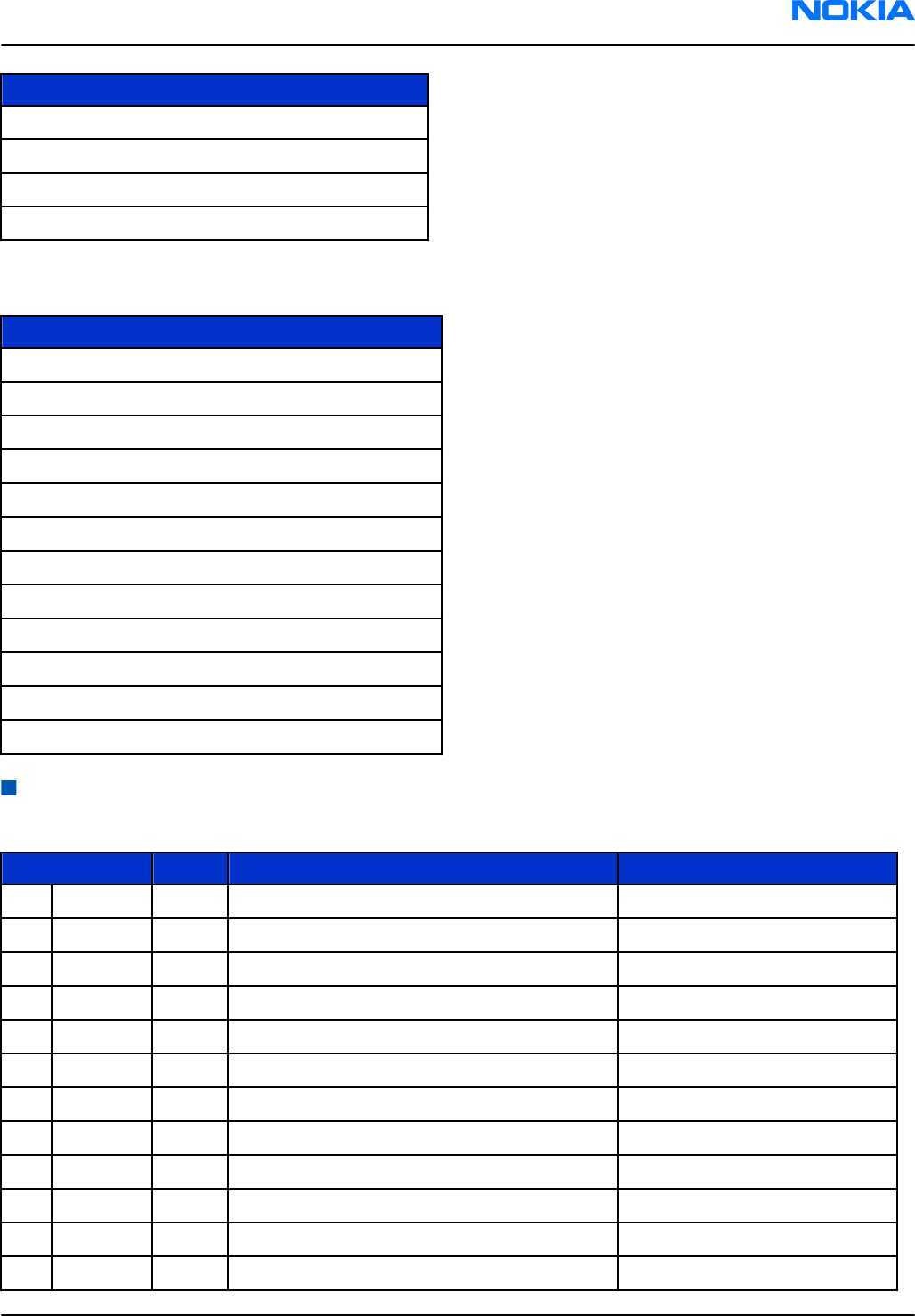
Component parts list
Table 12
Item ref Side Object Name Type
A1000 T BB SHIELD ASSEMBLY Shield Assembly
A 1001 T SIM SUPPORT SHIELD CuNi 18Zn20 F610 Shield
A 1050 B GE SHIELD Shield
A 7000 T RF SHIELD ASSEMBLY Shield Assembly
A 7001 T WCDMA SHIELD ASSEMBLY Shield Assembly
B 2200 T CRYSTAL 32.768KHZ +/-30PPM 12.5PF Crystal
C 1000 T CHIPCAP X5R 1U K 6V3 0603 Ceramic Capacitor
C 1001 T CHIPCAP X5R 100N K 10V 0402 Ceramic Capacitor
C 1002 T CHIP ARRAY X5R 2X1U (2x1U2) K 6V3 0405 Ceramic Capacitor
C 1008 T CHIPCAP X5R 1U K 6V3 0603 Ceramic Capacitor
C 1009 T CHIPCAP NP0 27P J 50V 0402 Ceramic Capacitor
C 1010 T CHIPCAP NP0 27P J 50V 0402 Ceramic Capacitor
RM-123; RM-145
Parts and layouts Nokia Customer Care
Issue 1 COMPANY CONFIDENTIAL Page 2 –9
Copyright © 2006 Nokia. All rights reserved.
Item ref Side Object Name Type
C1052 B CHIPCAP X5R 100N K 10V 0402 Ceramic Capacitor
C 1053 B CHIPCAP X7R 10N K 16V 0402 Ceramic Capacitor
C 1054 B CHIPCAP X5R 100N K 10V 0402 Ceramic Capacitor
C 1055 B CHIPCAP X5R 1U K 6V3 0402 Ceramic Capacitor
C 1056 B CHIPCAP X5R 100N K 10V 0402 Ceramic Capacitor
C 1060 T CHIPCAP X5R 220N K 6.3V 0402 Ceramic Capacitor
C 1061 B CHIPCAP X5R 220N K 6.3V 0402 Ceramic Capacitor
C 1062 B CHIPCAP X5R 4U7 K 6.3V 0603 Ceramic Capacitor
C 1063 B CHIPCAP X5R 4U7 K 6V3 0805 Ceramic Capacitor
C 1064 B CHIPCAP X5R 4U7 K 6V3 0805 Ceramic Capacitor
C 1065 B CHIPCAP X7R 10N K 16V 0402 Ceramic Capacitor
C 1066 B CHIPCAP X5R 1U K 6V3 0603 Ceramic Capacitor
C 1069 B CHIPCAP X7R 10N K 16V 0402 Ceramic Capacitor
C 1070 B CHIPCAP NP0 27P J 50V 0402 Ceramic Capacitor
C 1071 B CHIPCAP NP0 27P J 50V 0402 Ceramic Capacitor
C 1072 B CHIPCAP NP0 27P J 50V 0402 Ceramic Capacitor
C 2000 B CHIPCAP NP0 27P J 50V 0402 Ceramic Capacitor
C 2001 B CHIPCAP X5R 470N K 25V 0603 Ceramic Capacitor
C 2002 B CHIPCAP X7R 1N0 K 50V 0402 Ceramic Capacitor
C 2003 B CHIPCAP FEEDTHRU 100N M 25V 0805 Ceramic Capacitor
C 2004 B CHIPCAP X5R 4U7 K 6.3V 0603 Ceramic Capacitor
C 2005 B CHIPCAP X7R 33N K 10V 0402 Ceramic Capacitor
C 2006 T CHIPCAP X7R 33N K 10V 0402 Ceramic Capacitor
C 2007 B CHIPCAP X7R 10N K 16V 0402 Ceramic Capacitor
C 2008 B CHIPCAP X7R 10N K 16V 0402 Ceramic Capacitor
C 2009 B CHIPCAP X7R 10N K 16V 0402 Ceramic Capacitor
C 2010 B CHIPCAP X7R 10N K 16V 0402 Ceramic Capacitor
C 2011 B CHIPCAP NP0 10P J 50V 0402 Ceramic Capacitor
C 2012 B CHIPCAP NP0 10P J 50V 0402 Ceramic Capacitor
C 2013 B CHIPCAP NP0 10P J 50V 0402 Ceramic Capacitor
C 2014 B CHIPCAP NP0 10P J 50V 0402 Ceramic Capacitor
C 2015 B CHIPCAP NP0 270P J 50V 0402 Ceramic Capacitor
C 2016 B CHIPCAP X7R 33N K 10V 0402 Ceramic Capacitor
C 2020 B CHIPCAP X5R 100N K 10V 0402 Ceramic Capacitor
C 2021 B CHIPCAP X5R 100N K 10V 0402 Ceramic Capacitor
RM-123; RM-145
Nokia Customer Care Parts and layouts
Page 2 –10 COMPANY CONFIDENTIAL Issue 1
Copyright © 2006 Nokia. All rights reserved.
Item ref Side Object Name Type
C2071 T CHIPCAP NP0 27P J 50V 0402 Ceramic Capacitor
C 2100 T CHIPCAP X7R 33N K 10V 0402 Ceramic Capacitor
C 2101 T CHIPCAP X7R 33N K 10V 0402 Ceramic Capacitor
C 2102 T CHIPCAP X5R 4U7 K 6.3V 0603 Ceramic Capacitor
C 2106 T CHIPCAP NP0 22P J 50V 0402 Ceramic Capacitor
C 2107 T CHIPCAP NP0 22P J 50V 0402 Ceramic Capacitor
C 2108 T CHIPCAP X7R 1N0 K 50V 0402 Ceramic Capacitor
C 2109 T CHIPCAP X7R 1N0 K 50V 0402 Ceramic Capacitor
C 2110 T CHIPCAP X7R 1N0 K 50V 0402 Ceramic Capacitor
C 2111 T CHIPCAP NP0 22P J 50V 0402 Ceramic Capacitor
C 2112 T CHIPCAP NP0 22P J 50V 0402 Ceramic Capacitor
C 2117 T CHIPCAP X7R 33N K 10V 0402 Ceramic Capacitor
C 2118 T CHIPCAP X7R 33N K 10V 0402 Ceramic Capacitor
C 2119 T CHIPCAP X7R 33N K 10V 0402 Ceramic Capacitor
C 2120 T CHIPCAP X7R 33N K 10V 0402 Ceramic Capacitor
C 2124 T CHIPCAP X5R 100N K 10V 0402 Ceramic Capacitor
C 2127 T CHIPCAP X5R 1U K 6V3 0603 Ceramic Capacitor
C 2132 T CHIPCAP X7R 1N0 K 50V 0402 Ceramic Capacitor
C 2200 T CHIPCAP X5R 1U K 6V3 0402 Ceramic Capacitor
C 2201 T CHIPCAP X5R 1U K 6V3 0603 Ceramic Capacitor
C 2202 T CHIPCAP X7R 1N0 K 50V 0402 Ceramic Capacitor
C 2203 T CHIPCAP X7R 1N0 K 50V 0402 Ceramic Capacitor
C 2204 T CHIPCAP X7R 1N0 K 50V 0402 Ceramic Capacitor
C 2205 T CHIPCAP X7R 1N0 K 50V 0402 Ceramic Capacitor
C 2206 T CHIPCAP X7R 1N0 K 50V 0402 Ceramic Capacitor
C 2207 T CHIPCAP X7R 1N0 K 50V 0402 Ceramic Capacitor
C 2208 T CHIPCAP NP0 27P J 50V 0402 Ceramic Capacitor
C 2209 T CHIPCAP NP0 22P J 50V 0402 Ceramic Capacitor
C 2210 T CHIPCAP X5R 1U K 16V 0603 Ceramic Capacitor
C 2211 T CHIPCAP X5R 4U7 K 10V 0805 Ceramic Capacitor
C 2212 T CHIPCAP X5R 1U K 6V3 0603 Ceramic Capacitor
C 2215 T CHIP ARRAY X5R 2X1U (2x1U2) K 6V3 0405 Ceramic Capacitor
C 2217 T CHIP ARRAY X5R 2X1U (2x1U2) K 6V3 0405 Ceramic Capacitor
C 2220 T CHIP ARRAY X5R 2X1U (2x1U2) K 6V3 0405 Ceramic Capacitor
C 2221 T CHIP ARRAY X5R 2X1U (2x1U2) K 6V3 0405 Ceramic Capacitor
RM-123; RM-145
Parts and layouts Nokia Customer Care
Issue 1 COMPANY CONFIDENTIAL Page 2 –11
Copyright © 2006 Nokia. All rights reserved.

Item ref Side Object Name Type
C2222 T CHIP ARRAY X5R 2X1U (2x1U2) K 6V3 0405 Ceramic Capacitor
C 2223 T CHIPCAP X7R 10N K 16V 0402 Ceramic Capacitor
C 2224 T CHIPCAP X7R 10N K 16V 0402 Ceramic Capacitor
C 2225 T CHIP ARRAY X5R 2X1U (2x1U2) K 6V3 0405 Ceramic Capacitor
C 2226 T CHIP ARRAY X5R 2X1U (2x1U2) K 6V3 0405 Ceramic Capacitor
C 2230 T CHIP ARRAY X5R 2X1U (2x1U2) K 6V3 0405 Ceramic Capacitor
C 2231 T CHIPCAP X5R 10U M 6V3 0805 Ceramic Capacitor
C 2236 T CHIPCAP X7R 1N0 K 50V 0402 Ceramic Capacitor
C 2300 T CHIPCAP X7R 10N K 16V 0402 Ceramic Capacitor
C 2301 T CHIPCAP X5R 22U M 6V3 0805 Ceramic Capacitor
C 2302 T CHIPCAP X5R 22U M 6V3 0805 Ceramic Capacitor
C 2303 T CHIP ARRAY X5R 2X1U (2x1U2) K 6V3 0405 Ceramic Capacitor
C 2304 T CHIPCAP X7R 10N K 16V 0402 Ceramic Capacitor
C 2307 T CHIP ARRAY X5R 2X1U (2x1U2) K 6V3 0405 Ceramic Capacitor
C 2309 T CHIPCAP X5R 22U M 6V3 0805 Ceramic Capacitor
C 2313 T CHIPCAP X5R 1U K 6V3 0603 Ceramic Capacitor
C 2405 B CHIPCAP X5R 1U K 6V3 0603 Ceramic Capacitor
C 2406 B CHIPCAP X5R 1U K 6V3 0603 Ceramic Capacitor
C 2412 B CHIP ARRAY X5R 2X1U (2x1U2) K 6V3 0405 Ceramic Capacitor
C 2414 B CHIPCAP NP0 27P J 50V 0402 Ceramic Capacitor
C 2415 B CHIPCAP NP0 56P J 50V 0402 Ceramic Capacitor
C 2416 B CHIPCAP X7R 6N8 K 25V 0402 Ceramic Capacitor
C 2418 B CHIPCAP X5R 1U K 6V3 0402 Ceramic Capacitor
C 2420 B CHIPCAP NP0 1N0 K 200V 1206 Ceramic Capacitor
C 2500 B CHIPCAP X5R 100N M 16V 0402 Ceramic Capacitor
C 2501 B CHIPCAP NP0 27P J 50V 0402 Ceramic Capacitor
C 2502 B CHIPCAP X5R 4U7 K 6.3V 0603 Ceramic Capacitor
C 2503 B CHIPCAP X5R 1U K 25V 0603 Ceramic Capacitor
C 2581 T CHIPCAP X7R 10N K 16V 0402 Ceramic Capacitor
C 2600 T CHIPCAP X5R 4U7 K 10V 0805 Ceramic Capacitor
C 2601 T CHIPCAP NP0 22P J 50V 0402 Ceramic Capacitor
C 2602 T CHIPCAP X5R 100N K 10V 0402 Ceramic Capacitor
C 2603 T CHIPCAP X5R 100N K 10V 0402 Ceramic Capacitor
C 2700 T CHIPCAP X5R 100N K 10V 0402 Ceramic Capacitor
C 2701 T CHIPCAP NP0 27P J 50V 0402 Ceramic Capacitor
RM-123; RM-145
Nokia Customer Care Parts and layouts
Page 2 –12 COMPANY CONFIDENTIAL Issue 1
Copyright © 2006 Nokia. All rights reserved.

Item ref Side Object Name Type
C2800 T CHIPCAP X5R 100N K 10V 0402 Ceramic Capacitor
C 2801 T CHIPCAP X5R 100N K 10V 0402 Ceramic Capacitor
C 2802 T CHIPCAP X5R 100N K 10V 0402 Ceramic Capacitor
C 2803 T CHIPCAP X5R 100N K 10V 0402 Ceramic Capacitor
C 2804 T CHIPCAP X5R 100N K 10V 0402 Ceramic Capacitor
C 2805 T CHIPCAP X5R 100N K 10V 0402 Ceramic Capacitor
C 2806 T CHIPCAP X5R 100N K 10V 0402 Ceramic Capacitor
C 2807 T CHIPCAP X5R 1U K 6V3 0603 Ceramic Capacitor
C 2808 T CHIPCAP X5R 100N K 10V 0402 Ceramic Capacitor
C 2809 T CHIPCAP X5R 100N K 10V 0402 Ceramic Capacitor
C 2810 T CHIPCAP X5R 100N K 10V 0402 Ceramic Capacitor
C 2811 T CHIPCAP X5R 100N K 10V 0402 Ceramic Capacitor
C 2812 T CHIPCAP X5R 100N K 10V 0402 Ceramic Capacitor
C 2813 T CHIPCAP X5R 100N K 10V 0402 Ceramic Capacitor
C 2814 T CHIPCAP X5R 100N K 10V 0402 Ceramic Capacitor
C 2815 T CHIPCAP X7R 10N K 16V 0402 Ceramic Capacitor
C 2819 T CHIPCAP NP0 27P J 50V 0402 Ceramic Capacitor
C 3000 T CHIPCAP X5R 100N M 16V 0402 Ceramic Capacitor
C 3001 T CHIPCAP X7R 10N K 16V 0402 Ceramic Capacitor
C 3002 T CHIPCAP X5R 220N K 6.3V 0402 Ceramic Capacitor
C 3003 T CHIPCAP X7R 10N K 16V 0402 Ceramic Capacitor
C 3004 T CHIPCAP X5R 220N K 6.3V 0402 Ceramic Capacitor
C 3005 T CHIPCAP X7R 10N K 16V 0402 Ceramic Capacitor
C 3006 T CHIPCAP X7R 10N K 16V 0402 Ceramic Capacitor
C 3007 T CHIPCAP X5R 220N K 6.3V 0402 Ceramic Capacitor
C 3008 T CHIPCAP X5R 220N K 6.3V 0402 Ceramic Capacitor
C 3009 T CHIPCAP X7R 10N K 16V 0402 Ceramic Capacitor
C 3010 T CHIPCAP X7R 10N K 16V 0402 Ceramic Capacitor
C 3100 T CHIPCAP NP0 27P J 50V 0402 Ceramic Capacitor
C 3200 B CHIPCAP X5R 100N K 10V 0402 Ceramic Capacitor
C 3201 B CHIPCAP X5R 1U K 6V3 0603 Ceramic Capacitor
C 3202 B CHIPCAP X7R 10N K 16V 0402 Ceramic Capacitor
C 3203 B CHIPCAP X5R 1U K 6V3 0603 Ceramic Capacitor
C 3221 T CHIPCAP NP0 27P J 50V 0402 Ceramic Capacitor
C 6000 B CHIPCAP X5R 100N M 16V 0402 Ceramic Capacitor
RM-123; RM-145
Parts and layouts Nokia Customer Care
Issue 1 COMPANY CONFIDENTIAL Page 2 –13
Copyright © 2006 Nokia. All rights reserved.

Item ref Side Object Name Type
C6001 B CHIPCAP X5R 100N M 16V 0402 Ceramic Capacitor
C 6002 B CHIPCAP X5R 1U K 6V3 0603 Ceramic Capacitor
C 6003 B CHIPCAP X5R 1U K 6V3 0603 Ceramic Capacitor
C 6004 B CHIPCAP X5R 100N M 16V 0402 Ceramic Capacitor
C 6005 B CHIPCAP X5R 100N M 16V 0402 Ceramic Capacitor
C 6010 B CHIPCAP NP0 4P7 C 50V 0402 Ceramic Capacitor
C 6011 B CHIPCAP NP0 5P6 C 50V 0402 Ceramic Capacitor
C 6050 B CHIPCAP X5R 1U K 6V3 0603 Ceramic Capacitor
C 6051 B CHIPCAP X5R 1U K 6V3 0603 Ceramic Capacitor
C 6052 B CHIPCAP NP0 15P J 50V 0402 Ceramic Capacitor
C 7500 T CHIPCAP X5R 4U7 K 6.3V 0603 Ceramic Capacitor
C 7501 T CHIPCAP X5R 4U7 K 6.3V 0603 Ceramic Capacitor
C 7502 T CHIPCAP X5R 4U7 K 6.3V 0603 Ceramic Capacitor
C 7503 T CHIPCAP X5R 4U7 K 6.3V 0603 Ceramic Capacitor
C 7504 T CHIPCAP X7R 3N9 J 50V 0402 Ceramic Capacitor
C 7505 T CHIPCAP X7R 10N K 16V 0402 Ceramic Capacitor
C 7506 T CHIPCAP NP0 47P J 50V 0402 Ceramic Capacitor
C 7507 T CHIPCAP X5R 100N M 16V 0402 Ceramic Capacitor
C 7508 T CHIPCAP NP0 10P J 50V 0402 Ceramic Capacitor
C 7509 T CHIPCAP X5R 100N M 16V 0402 Ceramic Capacitor
C 7510 T CHIPCAP NP0 470P J 6V3 0402 Ceramic Capacitor
C 7511 T CHIPCAP X7R 33N K 10V 0402 Ceramic Capacitor
C 7512 T CHIPCAP NP0 2N2 G 16V 0603 Ceramic Capacitor
C 7514 T CHIPCAP NP0 2P2 C 50V 0402 Ceramic Capacitor
C 7515 T CHIPCAP NP0 2P7 C 50V 0402 Ceramic Capacitor
C 7516 T CHIPCAP NP0 0P5 C 50V 0402 Ceramic Capacitor
C 7521 T CHIPCAP X5R 4U7 K 6.3V 0603 Ceramic Capacitor
C 7541 T CHIPCAP X5R 4U7 K 6.3V 0603 Ceramic Capacitor
C 7542 T CHIPCAP X5R 4U7 K 6.3V 0603 Ceramic Capacitor
C 7543 T CHIPCAP X5R 4U7 K 6.3V 0603 Ceramic Capacitor
C 7544 T CHIPCAP X7R 22N K 16V 0402 Ceramic Capacitor
C 7545 T CHIPCAP NP0 10P J 50V 0402 Ceramic Capacitor
C 7547 T CHIPCAP NP0 2P7 C 50V 0402 Ceramic Capacitor
C 7597 T CHIPTCAP 150U M 10V 6X3.2X1.5 Electrolytic Capacitor
D 3000 T SDRAM 8MX16 1.8V/1.8V FBGA60 PBFREE Memory IC
RM-123; RM-145
Nokia Customer Care Parts and layouts
Page 2 –14 COMPANY CONFIDENTIAL Issue 1
Copyright © 2006 Nokia. All rights reserved.

Item ref Side Object Name Type
D6000 B BTHFM1.0 ES4 Module Hybrid
F 2000 B SM FUSE F 2.0A 32V 0603 Fuse And Protector
G 2200 T RTC BACKUP CAPAC 311 SIZE FOR 2.6V 4UAH Battery And Battery Cell
L 1000 T FERRITE BEAD 0.6R 600R/100MZ 0402 EMC Component
L 1001 T FERRITE BEAD 0.6R 600R/100MZ 0402 EMC Component
L 1050 B INDUCT WW 2.2UH 1A2 310 case size Fixed Inductor
L 1051 B FERR.BEAD 220R/100M 2A 0R05 0603 EMC Component
L 1067 B INDUCT WW 2.2UH 1A2 310 case size Fixed Inductor
L 2002 B CHIP BEAD ARRAY 2X1000R 0405 EMC Component
L 2003 B CHIP BEAD ARRAY 2X1000R 0405 EMC Component
L 2004 B CHIP BEAD ARRAY 2X1000R 0405 EMC Component
L 2006 B CHIP COIL 68NH J Q12/100MHZ 0603 Fixed Inductor
L 2100 B CHIP BEAD ARRAY 2X1000R 0405 EMC Component
L 2101 T FERR.BEAD 220R/100M 2A 0R05 0603 EMC Component
L 2102 T CHIP COIL 30nH J Q65/500MHz 0805 Fixed Inductor
L 2103 T CHIP COIL 30nH J Q65/500MHz 0805 Fixed Inductor
L 2104 T FERR.BEAD 220R/100M 2A 0R05 0603 EMC Component
L 2105 T FERR.BEAD 220R/100M 2A 0R05 0603 EMC Component
L 2107 T FERR.BEAD 220R/100M 2A 0R05 0603 EMC Component
L 2108 T FERR.BEAD 220R/100M 2A 0R05 0603 EMC Component
L 2109 T CHIP COIL 30nH J Q65/500MHz 0805 Fixed Inductor
L 2110 T FERR.BEAD 220R/100M 2A 0R05 0603 EMC Component
L 2111 T FERRITE BEAD 0.6R 600R/100MZ 0402 EMC Component
L 2112 T CHIP COIL 30nH J Q65/500MHz 0805 Fixed Inductor
L 2120 T CHIP BEAD ARRAY 2X1000R 0405 EMC Component
L 2202 T FERR.BEAD 220R/100M 2A 0R05 0603 EMC Component
L 2203 T FERRITE BEAD 0.6R 600R/100MZ 0402 EMC Component
L 2204 T FERRITE BEAD 0.6R 600R/100MZ 0402 EMC Component
L 2205 T FERR.BEAD 220R/100M 2A 0R05 0603 EMC Component
L 2206 T FERRITE BEAD 0.6R 600R/100MZ 0402 EMC Component
L 2301 T FERR.BEAD 220R/100M 2A 0R05 0603 EMC Component
L 2302 T INDUCT WW 10U 0A65 0R35 4X4X1.2 Fixed Inductor
L 2303 T FERR.BEAD 0R03 42R/100MHZ 3A 0805 EMC Component
L 2304 T FERRITE BEAD 0.6R 600R/100MZ 0402 EMC Component
L 2400 B FERRITE BEAD 0.6R 600R/100MZ 0402 EMC Component
RM-123; RM-145
Parts and layouts Nokia Customer Care
Issue 1 COMPANY CONFIDENTIAL Page 2 –15
Copyright © 2006 Nokia. All rights reserved.
Item ref Side Object Name Type
L2401 B FERRITE BEAD 0.6R 600R/100MZ 0402 EMC Component
L 2412 B COIL 0.47MH 50MA 3.3X3.4X1.4MM Fixed Inductor
L 2500 B FERR.BEAD 0R03 42R/100MHZ 3A 0805 EMC Component
L 2501 B CHOKE 22U M 0R7 0.35A 3.0X3.0X1.5 Fixed Inductor
L 3200 B FERRITE BEAD 0.6R 600R/100MZ 0402 EMC Component
L 7500 T FERRITE BEAD 0.6R 600R/100MZ 0402 EMC Component
L 7501 T CHIP COIL 10N J Q30/800MHZ 0402 Fixed Inductor
L 7502 T CHIP COIL 10N J Q30/800MHZ 0402 Fixed Inductor
L 7520 T FERRITE BEAD 0R01 28R/100MHZ 0603 EMC Component
L 7540 T CHOKE 3U3 1.2A 0R096 3X3X1.5 Fixed Inductor
L 7542 T CHIP COIL 2N2 +-0N1 Q40/1GHZ 0402 Fixed Inductor
L 7543 T CHIP COIL 3N9 +-0N3 Q28/800M 0402 Fixed Inductor
M 2100 T SMD VIBRA MOTOR 1.3V 90MA 9000RPM Vibrator
N 1050 B DC/DC CONV TPS62311YZD 1.5V CSP8 Power Management IC
N 1051 B OMAP DM290 GoldenEye nFBGA Processor IC
N 1060 T VREG 2.85/150MA(LP3987-2.85)USMD5 Analog IC
N 2000 B TI Analog Switch TS5A3159DCKR Interface And Controller IC
N 2001 B TI Analog Switch TS5A3159DCKR Interface And Controller IC
N 2101 T AF AMP TPA2012D2 77DB/217HZ WCSP16 Analog IC
N 2413 B EL DRIVER D381B 2-7V MSOP-10 Power Management IC
N 2500 B
WHITE LED DRIVER 4LEDS 500mW 8bump
USMD8 Power Management IC
N 2600 T IRDA 1.15Mbps 2.2mm RoHS Infrared
N 3200 B VREG & LEVELSHIFT(LP3928)USMD16 Other IC
N 6050 B VREG & LEVELSHIFT(LP3928)USMD16 Other IC
N 7500 T RF SYSTEM MODULE PIHI2.22 9.0 x 9.0 x 1 Hybrid
N 7520 T
PW AMP PF89001 EGSM850/900/DCS/PCS
Cut12 Power Amplifier
N 7540 T PW AMP QCPM-8883 K4-06 WCDMA 2100 Power Amplifier
N 7541 T DC CONV LM3202TLX NOPB revB µSMD8 Power Management IC
R 1000 T CHIPRES 0W06 33R J 0402 Fixed Resistor
R 1001 T CHIPRES 0W06 100R J 0402 Fixed Resistor
R 1051 B CHIPRES 0W06 100R J 0402 Fixed Resistor
R 1052 B CHIPRES 0W06 100R J 0402 Fixed Resistor
R 1065 B CHIPRES 0W06 33R J 0402 Fixed Resistor
RM-123; RM-145
Nokia Customer Care Parts and layouts
Page 2 –16 COMPANY CONFIDENTIAL Issue 1
Copyright © 2006 Nokia. All rights reserved.

Item ref Side Object Name Type
R1072 B CHIPRES 0W06 10K J 0402 Fixed Resistor
R 1078 B CHIPRES 0W06 33R J 0402 Fixed Resistor
R 1080 B CHIPRES 0W06 10K J 0402 Fixed Resistor
R 2000 B ASIP MIC W/ESD RES+CAP+ZDI BGA11 Integrated Discretes
R 2001 B CHIPRES 0W06 10K J 0402 Fixed Resistor
R 2002 B CHIPRES 0W06 220R J 0402 Fixed Resistor
R 2003 B VAR.ARRAY 2X16V 824-915MHZ 0405 Variable Resistor
R 2004 B CHIPRES 0W06 33K J 0402 Fixed Resistor
R 2005 B RES NETWORK 0W06 2X22R J 0404 Resistor Network
R 2006 B RES NETWORK 0W06 2X22R J 0404 Resistor Network
R 2009 B VAR.ARRAY 2X16V 824-915MHZ 0405 Variable Resistor
R 2010 B VAR.ARRAY 2X16V 824-915MHZ 0405 Variable Resistor
R 2011 B ASIP SILIC USB OTG / ESD BGA11 Integrated Discretes
R 2012 B RES NETWORK 0W06 220K/120K J 0404 Resistor Network
R 2013 B CHIPRES 0W06 100R J 0402 Fixed Resistor
R 2015 B CHIPRES 0W06 10R J 0402 Fixed Resistor
R 2016 B CHIP VARISTOR VWM14V VC50V 0402 Variable Resistor
R 2017 T CHIPRES 0W06 4K7 J 0402 Fixed Resistor
R 2018 T CHIPRES JUMPER 0R0 0402 Fixed Resistor
R 2022 B CHIP VARISTOR VWM14V VC50V 0402 Variable Resistor
R 2023 T CHIPRES JUMPER 0R0 0403 Fixed Resistor
R 2069 T CHIPRES JUMPER 0R0 0404 Fixed Resistor
R 2070 T NTC RES 0W1 47K J B 4050+-3% 0402 Variable Resistor
R 2071 T CHIP VARISTOR VWM15V VC50V 0402 Variable Resistor
R 2100 T ASIP MIC W/ESD RES+CAP+ZDI BGA11 Integrated Discretes
R 2101 T CHIPRES 0W06 220R J 0402 Fixed Resistor
R 2102 T CHIPRES 0W06 33K J 0402 Fixed Resistor
R 2103 B VAR.ARRAY 2X16V 824-915MHZ 0405 Variable Resistor
R 2104 T RES NETWORK 0W06 2X10R J 0404 Resistor Network
R 2117 T VAR.ARRAY 2X16V 824-915MHZ 0405 Variable Resistor
R 2118 T VAR.ARRAY 2X16V 824-915MHZ 0405 Variable Resistor
R 2119 T VAR.ARRAY 2X16V 824-915MHZ 0405 Variable Resistor
R 2121 T CHIPRES JUMPER 0R0 0405 Fixed Resistor
R 2124 T CHIPRES JUMPER 0R0 0406 Fixed Resistor
R 2200 T CHIPRES 0W06 100K J 0402 Fixed Resistor
RM-123; RM-145
Parts and layouts Nokia Customer Care
Issue 1 COMPANY CONFIDENTIAL Page 2 –17
Copyright © 2006 Nokia. All rights reserved.

Item ref Side Object Name Type
R2201 T CHIPRES 0W06 120K J 0402 Fixed Resistor
R 2203 T CHIPRES 0W06 2M2 J 0402 Fixed Resistor
R 2206 T CHIPRES 0W06 470R J 0402 Fixed Resistor
R 2223 T CHIPRES 0W06 220R J 0402 Fixed Resistor
R 2400 B CHIPRES 0W06 100K J 0402 Fixed Resistor
R 2412 B CHIPRES JUMPER 0R0 0407 Fixed Resistor
R 2415 B CHIPRES 0W06 120K J 0402 Fixed Resistor
R 2500 B CHIPRES 0W06 10K J 0402 Fixed Resistor
R 2501 B CHIPRES 0W06 33R J 0402 Fixed Resistor
R 2580 T CHIPRES 0W06 10K J 0402 Fixed Resistor
R 2600 T CHIPRES 0W125 4R7 J 0805 Fixed Resistor
R 2700 T ASIP SIM INTERFACE **low cap** BGA8 Integrated Discretes
R 2800 T CHIPRES 0W06 100K J 0402 Fixed Resistor
R 3000 T CHIPRES 0W06 4K7 J 0402 Fixed Resistor
R 3200 B ASIP MMC FILTER *** PB-FREE *** Integrated Discretes
R 3205 B CHIPRES 0W06 680R J 0402 Fixed Resistor
R 3221 T CHIPRES 0W06 100R J 0402 Fixed Resistor
R 6010 B CHIPRES 0W06 10K J 0402 Fixed Resistor
R 6011 B CHIPRES 0W06 8K2 J 0402 Fixed Resistor
R 6020 B CHIPRES JUMPER 0R0 0408 Fixed Resistor
R 6050 T CHIPRES JUMPER 0R0 0409 Fixed Resistor
R 7500 T CHIPRES 0W06 22K J 0402 Fixed Resistor
R 7501 T CHIPRES 0W06 4K7 J 0402 Fixed Resistor
R 7503 T CHIPRES 0W06 1K0 F 200PPM 0402 Fixed Resistor
R 7504 T CHIPRES 0W06 8K2 F 0402 Fixed Resistor
R 7505 T CHIPRES 0W06 5R6 J 0402 Fixed Resistor
R 7520 T CHIPRES 0W06 27K F 0402 Fixed Resistor
R 7522 T CHIPRES JUMPER 0R0 0410 Fixed Resistor
R 7540 T CHIPRES 0W06 47K F 200PPM 0402 Fixed Resistor
R 7541 T CHIPRES 0W06 1K2 F 250PPM 0402 Fixed Resistor
R 7542 T CHIPRES JUMPER 0R0 0411 Fixed Resistor
R 7543 T CHIPRES 0W06 10K J 0402 Fixed Resistor
R 7544 T CHIPRES 0W06 10R J 0402 Fixed Resistor
S 2580 T SM SW TACT SPST 12V SIDE KEY 2.2N Switch And Knob
S 2596 T SM SW TACT SPST 12V SIDE KEY 2.2N Switch And Knob
RM-123; RM-145
Nokia Customer Care Parts and layouts
Page 2 –18 COMPANY CONFIDENTIAL Issue 1
Copyright © 2006 Nokia. All rights reserved.

Item ref Side Object Name Type
S2597 T SM SW TACT SPST 12V SIDE KEY 2.2N Switch And Knob
S 2598 T SM SW TACT SPST 12V SIDE KEY 2.2N Switch And Knob
S 2599 T SM SW TACT SPST 12V SIDE KEY 2.2N Switch And Knob
T 7500 T TRANSF BALUN 2134 +/- 30MHZ 0805 Balun
T 7501 T TRANSF BALUN 3800 +/- 550MHZ 0805 Balun
V 2000 B ASIP TVS BGA4 Integrated Discretes
V 2412 B DI FAST 1SS400 75V 0A1 4NS SOD523 Diode
V 2413 B DI ZEN 100V 6% 0W2 SOD323 Diode
V 2414 B DI ZEN 100V 6% 0W2 SOD323 Diode
X 1000 T SM CAMERA MOD SKT 2X8F Socket
X 2000 T CONN SYST SM 14POL System Connector
X 2070 T SM BATTERY CONN 3POL SPR 12V 2A Battery Connector
X 2400 B SM CONN 2X12F P0.4 30V.3A PWB/PWB Board To Board Connector
X 2411 B C-SPRING EL FOIL SUS301 Spring
X 2412 B C-SPRING EL FOIL SUS301 Spring
X 2580 B SM CONN 2X12F P0.5 PWB/PWB Multipole Connector
X 2700 T SM SIM CONN 6POL P2.54 H1.8 Multipole Connector
X 3200 T CONN SMC TRANSFLASH MMC Smartcard Connector
X 8000 T SM CONN RF JACK 50R 2W 6GHZ Coaxial Connector
X 8001 T C-SPRING ANTENNA ( active ) Spring
X 8002 T C-SPRING ANTENNA Spring
X 8003 T SM CONN RF JACK 50R 2W 6GHZ Coaxial Connector
X 8004 T C-SPRING ANTENNA ( active ) Spring
X 8005 T C-SPRING ANTENNA Spring
X 8006 T C-SPRING ANTENNA Spring
X 8007 B C-SPRING FOR DISPLAY CAN GROUNDING Spring
X 8008 B C-SPRING FOR DISPLAY CAN GROUNDING Spring
X 8009 B C-SPRING FOR DISPLAY CAN GROUNDING Spring
X 8010 B C-SPRING FOR DISPLAY CAN GROUNDING Spring
X 8011 B C-SPRING FOR DISPLAY CAN GROUNDING Spring
X 8012 B C-SPRING FOR DISPLAY CAN GROUNDING Spring
X 8013 B C-SPRING FOR DISPLAY CAN GROUNDING Spring
X 8014 B C-SPRING FOR DISPLAY CAN GROUNDING Spring
X 8015 B C-SPRING FOR DISPLAY CAN GROUNDING Spring
X 8016 B C-SPRING FOR DISPLAY CAN GROUNDING Spring
RM-123; RM-145
Parts and layouts Nokia Customer Care
Issue 1 COMPANY CONFIDENTIAL Page 2 –19
Copyright © 2006 Nokia. All rights reserved.
Item ref Side Object Name Type
X8017 B C-SPRING FOR DISPLAY CAN GROUNDING Spring
X 8018 B C-SPRING FOR DISPLAY CAN GROUNDING Spring
X 8019 B C-SPRING FOR DISPLAY CAN GROUNDING Spring
X 8020 B C-SPRING FOR DISPLAY CAN GROUNDING Spring
X 8021 B C-SPRING FOR DISPLAY CAN GROUNDING Spring
X 8023 B
C-SPRING GROUNDING C-COVER PLATE
SUS301 Spring
Z 2000 B FERRITE BEAD 0.6R 600R/100MZ 0402 EMC Component
Z 2001 B FERRITE BEAD 0.6R 600R/100MZ 0402 EMC Component
Z 2005 B FERRITE BEAD 0.6R 600R/100MZ 0402 EMC Component
Z 2403 B ASIP 10-CH ESD EMI FILTER BGA25 Integrated Discretes
Z 2404 B ASIP 10-CH ESD EMI FILTER BGA25 Integrated Discretes
Z 2580 B ASIP 10-CH ESD EMI FILTER BGA25 Integrated Discretes
Z 2581 B ASIP 10-CH ESD EMI FILTER BGA25 Integrated Discretes
Z 2597 T ASIP EMI/ESD FILTER BGA6 Integrated Discretes
Z 2598 T ASIP EMI/ESD FILTER BGA6 Integrated Discretes
Z 2599 T ASIP EMI/ESD FILTER BGA6 Integrated Discretes
Z 2600 T ASIP EMI/ESD FILTER BGA6 Integrated Discretes
Z 7520 T CER FILT LFL181699TC1 2400-2483MHz 1.6 Ceramic Filter
Z 7540 T
DUPL SAW 1920-1980/2110-2170MHZ
3.8x3.8 Duplexer
CHIPRES 0W06 180K J 0402 Fixed Resistor
CHIPCAP NP0 1P2 C 50V 0402 Ceramic Capacitor
RM-123; RM-145
Nokia Customer Care Parts and layouts
Page 2 –20 COMPANY CONFIDENTIAL Issue 1
Copyright © 2006 Nokia. All rights reserved.
Component layouts
Figure 1 Main board layout, bottom side (1rra_08a)
Figure 2 Main board layout, top side (1rra_08a)
RM-123; RM-145
Parts and layouts Nokia Customer Care
Issue 1 COMPANY CONFIDENTIAL Page 2 –21
Copyright © 2006 Nokia. All rights reserved.

RM-123; RM-145
Nokia Customer Care Parts and layouts
(This page left intentionally blank.)
Page 2 –22 COMPANY CONFIDENTIAL Issue 1
Copyright © 2006 Nokia. All rights reserved.

3 — Service Software
Instructions
Nokia Customer Care
Issue 1 COMPANY CONFIDENTIAL Page 3 –1
Copyright © 2006 Nokia. All rights reserved.

RM-123; RM-145
Nokia Customer Care Service Software Instructions
(This page left intentionally blank.)
Page 3 –2 COMPANY CONFIDENTIAL Issue 1
Copyright © 2006 Nokia. All rights reserved.

Table of Contents
Phoenix installation steps in brief........................................................................................................................3–5
Installing Phoenix...................................................................................................................................................3–6
Updating Phoenix installation..............................................................................................................................3–8
Uninstalling Phoenix..............................................................................................................................................3–9
Repairing Phoenix installation...........................................................................................................................3–11
Phone data package overview............................................................................................................................3–11
Installing phone data package...........................................................................................................................3–12
Uninstalling phone data package.......................................................................................................................3–15
Configuring users in Phoenix..............................................................................................................................3–17
Managing connections in Phoenix......................................................................................................................3–17
Installing flash support files for FPS-8 and FPS-10...........................................................................................3–19
Updating FPS-8 and FPS-10 flash prommer software.......................................................................................3–22
Activating FPS-8....................................................................................................................................................3–23
Deactivating FPS-8................................................................................................................................................3–24
List of Figures
Figure 3 Dongle not found.....................................................................................................................................3–6
Figure 4 Disclaimer text.........................................................................................................................................3–7
Figure 5 InstallShield Wizard Complete...............................................................................................................3–8
Figure 6 Installation interrupted..........................................................................................................................3–9
Figure 7 Remove program...................................................................................................................................3–10
Figure 8 Finish uninstallation.............................................................................................................................3–10
Figure 9 Repair program.....................................................................................................................................3–11
Figure 10 Data package setup information.......................................................................................................3–13
Figure 11 Data package destination folder.......................................................................................................3–14
Figure 12 InstallShield Wizard Complete...........................................................................................................3–15
Figure 13 Uninstalling phone data package......................................................................................................3–16
Figure 14 Finishing data package uninstallation..............................................................................................3–16
Figure 15 Phoenix login.......................................................................................................................................3–17
Figure 16 New user configured..........................................................................................................................3–17
Figure 17 Select mode: Manual...........................................................................................................................3–18
Figure 18 Connections list...................................................................................................................................3–19
Figure 19 Connection information.....................................................................................................................3–19
Figure 20 Product support module information (example from RM-1)..........................................................3–19
Figure 21 Flash update welcome dialog............................................................................................................3–20
Figure 22 Flash installation interrupted............................................................................................................3–20
Figure 23 Flash destination folder......................................................................................................................3–21
Figure 24 Finish flash update..............................................................................................................................3–22
Figure 25 Flash directory window......................................................................................................................3–22
Figure 26 Prommer software update finished..................................................................................................3–23
Figure 27 Prommer Maintenance window........................................................................................................3–23
Figure 28 Box activation......................................................................................................................................3–24
Figure 29 Deactivation warning.........................................................................................................................3–24
RM-123; RM-145
Service Software Instructions Nokia Customer Care
Issue 1 COMPANY CONFIDENTIAL Page 3 –3
Copyright © 2006 Nokia. All rights reserved.

RM-123; RM-145
Nokia Customer Care Service Software Instructions
(This page left intentionally blank.)
Page 3 –4 COMPANY CONFIDENTIAL Issue 1
Copyright © 2006 Nokia. All rights reserved.

Phoenix
installation steps in brief
Prerequisites
Recommended hardware requirements:
• Computer processor: Pentium 700 MHz or higher
• RAM 256 MB
• Disk space 100-300 MB
Supported operating systems:
•
Windows 2000
Service Pack 3 or higher
•
Windows XP
Service Pack 1 or higher
Context
Phoenix
is a service software for reprogramming, testing and tuning phones.
Phoenix
installation contains:
• Service software support for all phone models included in the package
• Flash update package files for programming devices
• All needed drivers for:
• PKD-1 (DK2) dongle
• DKU-2 USB cable
Note: Separate installation packages for flash update files and drivers are also available, but it is
not necessary to use them unless there are updates between
Phoenix
service software releases. If
separate update packages are used, they should be used after
Phoenix
and data packages have been
installed.
The phone model specific data package includes all changing product specific data:
• Product software binary files
• Files for type label printing
• Validation file for the faultlog repair data reporting system
• All product specific configuration files for
Phoenix
software components
Note:
Phoenix
and phone data packages should only be used as complete installation packages.
Uninstallation should be made from the
Windows
Control Panel.
To use
Phoenix
, you need to:
Steps
1. Connect a PKD-1 (DK2) dongle to the computer parallel port.
2. Install
Phoenix
.
3. Install the phone-specific data package.
4. Configure users.
5. Manage connection settings (depends on the tools you are using).
If you use FPS-8: • Update FPS-8 software
• Activate FPS-8
RM-123; RM-145
Service Software Instructions Nokia Customer Care
Issue 1 COMPANY CONFIDENTIAL Page 3 –5
Copyright © 2006 Nokia. All rights reserved.
If you use FPS-10: • Update FPS-10 software
Note: There is no need to activate FPS-10.
•Activate SX-4 smart card, if you need tuning and
testing functions.
Note: When FPS-10 is used only for
product software updates, SX-4 smart
card is not needed.
Results
Phoenix
is ready to be used with FPS-8 or FPS-10 flash prommers and other service tools.
Installing
Phoenix
Prerequisites
• Check that a dongle is attached to the parallel port of your computer.
• Download the
Phoenix
installation package (for example,
phoenix_service_sw_2004_39_x_xx.exe
) to your
computer (in
C:\TEMP
, for instance).
• Close all other programs.
• Depending on your operating system, administrator rights may be required to install
Phoenix
.
• If uninstalling or rebooting is needed at any point, you will be prompted by the InstallShield program.
Context
At some point during the installation procedure, you may get the following message:
Figure 3 Dongle not found
This may be a result of a defective or too old PKD-1 dongle.
Check the COM/parallel ports used. After correcting the problem, you can restart the installation.
For more detailed information, please refer to
Phoenix
Help files.
Tip: Each feature in
Phoenix
has its own Help function, which can be activated while running the
program. Press the F1 key or the feature’s Help button to activate a Help file.
Steps
1. To start the installation, run the application file (for example,
phoenix_service_sw_2004_39_x_xx.exe
).
2. In the
Welcome
dialogue, click Next.
RM-123; RM-145
Nokia Customer Care Service Software Instructions
Page 3 –6 COMPANY CONFIDENTIAL Issue 1
Copyright © 2006 Nokia. All rights reserved.
3. Read the disclaimer text carefully and click Yes.
Figure 4 Disclaimer text
4. Choose the destination folder.
The default folder
C:\ProgramFiles\Nokia\Phoenix
is recommended.
5. To continue, click Next.
To choose another location, click Browse (not recommended).
6. Wait for the components to be copied.
The progress of the installation is shown in the
Setup Status
window.
7. Wait for the drivers to be installed and updated.
The process may take several minutes to complete.
If the operating system does not require rebooting, the PC components are registered right away.
If the operating system requires restarting your computer, the Install Shield Wizard will notifies about it.
Select Yes... to reboot the PC immediately or No... to reboot the PC manually afterwards.
After the reboot, all components are registered.
Note:
Phoenix
does not work, if the components have not been registered.
RM-123; RM-145
Service Software Instructions Nokia Customer Care
Issue 1 COMPANY CONFIDENTIAL Page 3 –7
Copyright © 2006 Nokia. All rights reserved.
8. To end the installation, click Finish.
Figure 5 InstallShield Wizard Complete
Next actions
After the installation,
Phoenix
can be used after:
• installing phone model specific data package for
Phoenix
• configuring users and connections
FPS-8 and FPS-10 flash prommers can be used after updating their flash update package files.
Updating
Phoenix
installation
Context
• If you already have the
Phoenix
service software installed on your computer, you need to update the
software when new versions are released.
• To update
Phoenix
, you need to follow the same steps as when installing it for the first time.
•When you are updating, for example, from version a14_2004_16_4_47 to a15_2004_24_7_55, the update
will take place automatically without uninstallation.
•Always use the latest available versions of both
Phoenix
and the phone-specific data package. Instructions
can be found in the phone model specific Technical Bulletins and phone data package
readme.txt
files
(shown during installation).
• If you try to update
Phoenix
with the same version you already have (for example, a15_2004_24_7_55
to a15_2004_24_7_55), you are asked if you want to uninstall the existing version. In this case you can
choose between a total uninstallation or a repair installation in a similar way when choosing to uninstall
the application from the
Windows
Control Panel.
• If you try to install an older version (for example, downgrade from a15_2004_24_7_55 to
a14_2004_16_4_47), installation will be interrupted.
RM-123; RM-145
Nokia Customer Care Service Software Instructions
Page 3 –8 COMPANY CONFIDENTIAL Issue 1
Copyright © 2006 Nokia. All rights reserved.
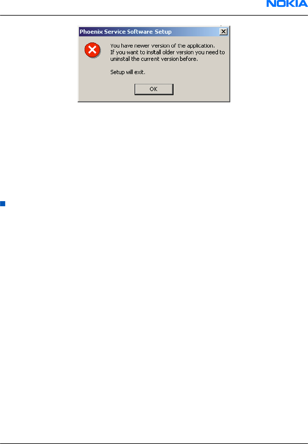
Figure 6 Installation interrupted
• Always follow the instructions on the screen.
Steps
1. Download the installation package to your computer hard disk.
2. Close all other programs.
3. Run the application file (for example,
phoenix_service_sw_2004_39_x_xx.exe
).
Results
A new
Phoenix
version is installed and driver versions are checked and updated.
Uninstalling
Phoenix
Context
You can uninstall
Phoenix
service software manually from the
Windows
Control Panel.
Steps
1. Open the Windows Control Panel, and choose Add/Remove Programs.
RM-123; RM-145
Service Software Instructions Nokia Customer Care
Issue 1 COMPANY CONFIDENTIAL Page 3 –9
Copyright © 2006 Nokia. All rights reserved.
2. To uninstall
Phoenix
, choose Phoenix Service Software→Change/Remove→Remove .
Figure 7 Remove program
The progress of the uninstallation is shown.
3. If the operating system does not require rebooting, click Finish to complete.
Figure 8 Finish uninstallation
RM-123; RM-145
Nokia Customer Care Service Software Instructions
Page 3 –10 COMPANY CONFIDENTIAL Issue 1
Copyright © 2006 Nokia. All rights reserved.
If the operating system requires rebooting, InstallShield Wizard will notify you. Select Yes... to reboot the
PC immediately and No... to reboot the PC manually afterwards.
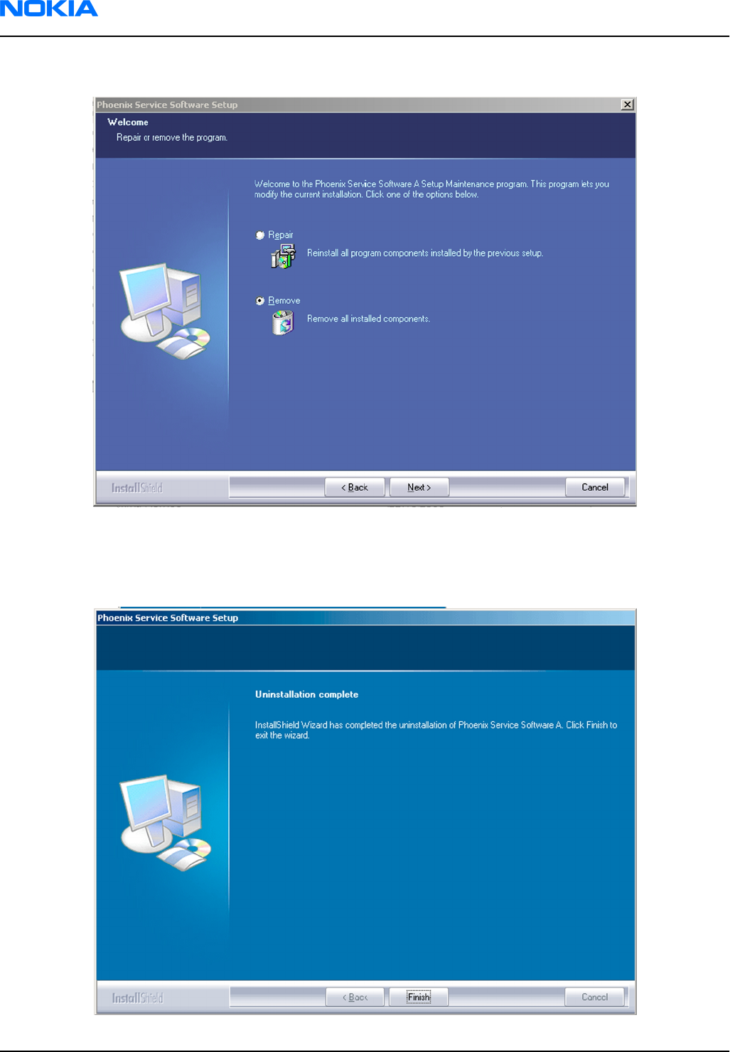
Repairing
Phoenix
installation
Context
If you experience any problems with the service software or suspect that files have been lost, use the repair
function before completely reinstalling
Phoenix
.
Note: The original installation package (for example,
phoenix_service_sw_a15_2004_24_7_55.exe
)
must be found on your PC when you run the repair setup.
Steps
1. Open Windows Control Panel→Add/Remove Programs .
2. Choose Phoenix Service Software→Change/Remove .
3. In the following view, select Repair.
Figure 9 Repair program
Phoenix
reinstalls components and registers them.
The procedure is the same as when updating
Phoenix
.
4. To complete the repair, click Finish.
Phone data package overview
Each product has its own data package (DP). The product data package contains all product-specific data files
to make the Phoenix service software and tools usable with a certain phone model.
The phone data package contains the following:
• Product software binary files
RM-123; RM-145
Service Software Instructions Nokia Customer Care
Issue 1 COMPANY CONFIDENTIAL Page 3 –11
Copyright © 2006 Nokia. All rights reserved.

• Files for type label printing
• Validation file for the fault log repair data reporting system
• All product-specific configuration files for Phoenix software components
Data files are stored in C:\Program Files\Nokia\Phoenix (default).
Installing phone data package
Prerequisites
•A phone-specific data package contains all data required for the
Phoenix
service software and service tools
to be used with a certain phone model.
• Check that a dongle is attached to the parallel port of your computer.
• Install
Phoenix
service software.
•Download the installation package (for example,
XX-XX_dp_EA_v_1_0.exe
) to your computer (for example,
in C:\TEMP).
• Close all other programs.
(XX-XX = type designator of the product)
If you already have
Phoenix
installed on your computer, you will need to update it when a new version is
released.
Note: Often
Phoenix
and the phone-specific data package come in pairs, meaning that a certain
version of
Phoenix
can only be used with a certain version of a data package. Always use the latest
available versions of both. Instructions can be found in phone-specific Technical Bulletins and
readme.txt
files of data packages.
Steps
1. To start the installation, run the application file (for example,
XX-XX_dp_EA_ v_1_0.exe
),
Wait for the installation files to be extracted.
RM-123; RM-145
Nokia Customer Care Service Software Instructions
Page 3 –12 COMPANY CONFIDENTIAL Issue 1
Copyright © 2006 Nokia. All rights reserved.
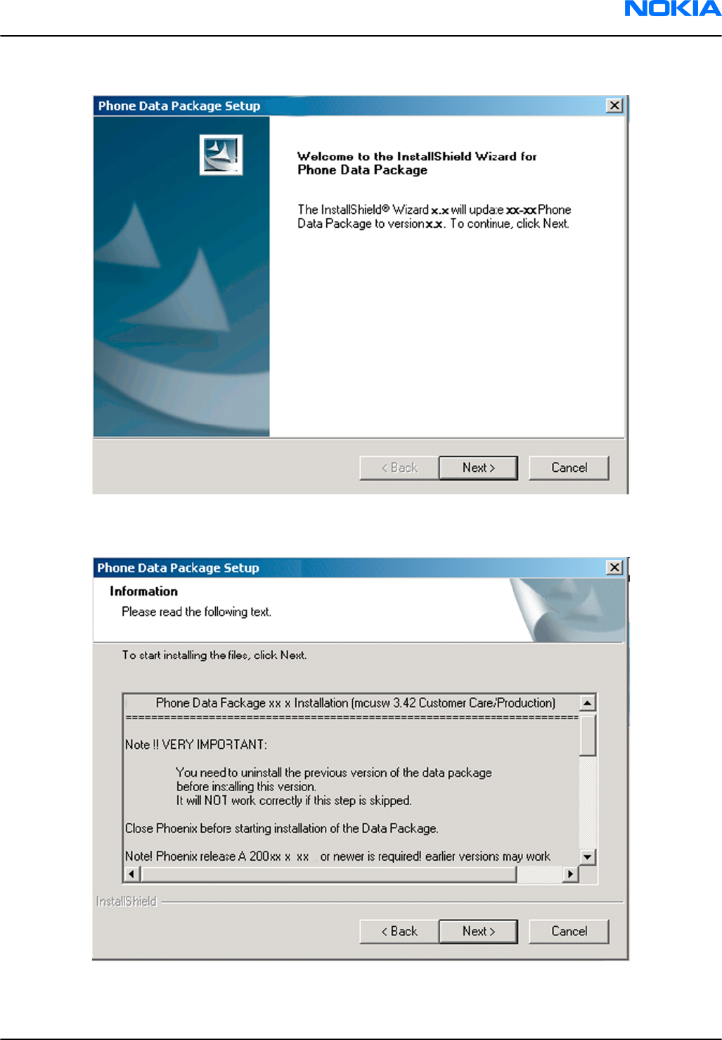
2. Click Next.
3. In the following view you can see the contents of the data package. Read the text carefully. There is
information about the
Phoenix
version required with this data package.
Figure 10 Data package setup information
4. To continue, click Next.
RM-123; RM-145
Service Software Instructions Nokia Customer Care
Issue 1 COMPANY CONFIDENTIAL Page 3 –13
Copyright © 2006 Nokia. All rights reserved.
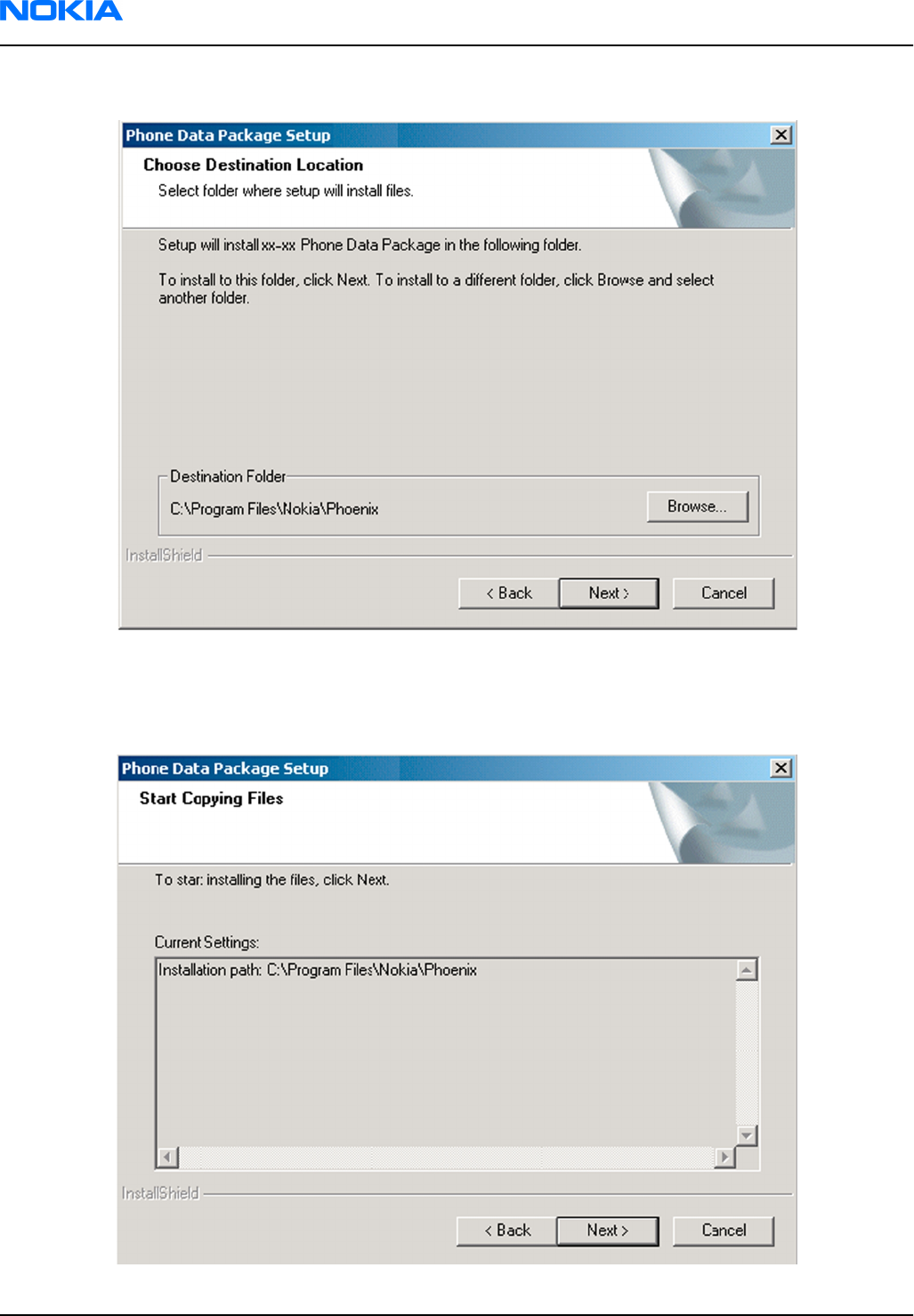
5. Choose the destination folder, and click Next to continue.
Figure 11 Data package destination folder
The InstallShield Wizard checks where
Phoenix
is installed, and the directory is shown.
6. To start copying the files, click Next.
RM-123; RM-145
Nokia Customer Care Service Software Instructions
Page 3 –14 COMPANY CONFIDENTIAL Issue 1
Copyright © 2006 Nokia. All rights reserved.
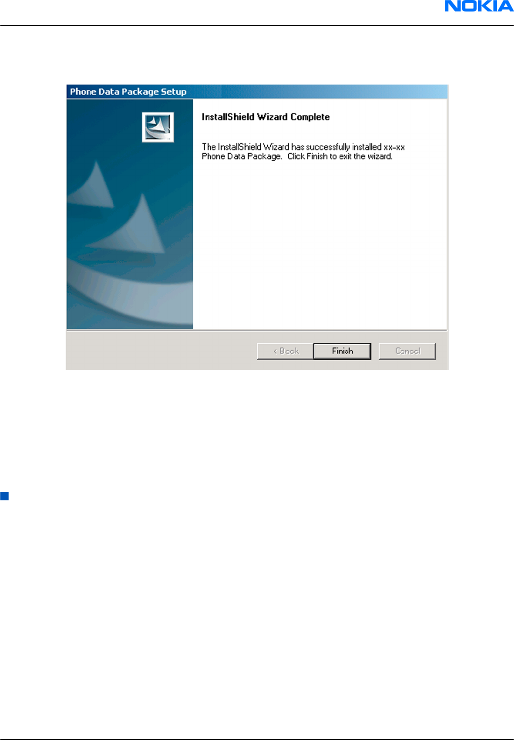
Phone model specific files are installed. Please wait.
7. To complete the installation, click Finish.
Figure 12 InstallShield Wizard Complete
Next actions
Phoenix
can be used for flashing phones and printing type labels after:
• Configuring users
• Managing connections
FPS-8 and FPS-10 can be used after updating their flash update package files.
Uninstalling phone data package
Context
There is no need to uninstall an older version of a data package, unless instructions to do so are given in
the
readme.txt
file of the data package and bulletins related to the release.
Please read all related documents carefully.
Steps
1. Locate the data package installation file (e.g.
XX-XX_dp_EA_v_1_0.exe
) from your computer.
2. To start the uninstallation procedure, double-click the data package installation file.
RM-123; RM-145
Service Software Instructions Nokia Customer Care
Issue 1 COMPANY CONFIDENTIAL Page 3 –15
Copyright © 2006 Nokia. All rights reserved.
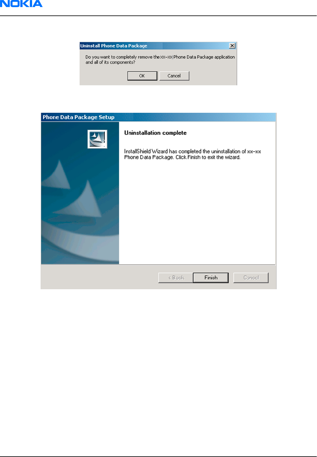
3. To uninstall the data package, click OK or to interrupt the uninstallation, click Cancel.
Figure 13 Uninstalling phone data package
4. When the data package is uninstalled, click Finish.
Figure 14 Finishing data package uninstallation
Alternative steps
• You can also uninstall the data package manually from
Control Panel→Add/Remove Programs→xx-xx* Phone Data Package . (*= type designator of the
phone).
RM-123; RM-145
Nokia Customer Care Service Software Instructions
Page 3 –16 COMPANY CONFIDENTIAL Issue 1
Copyright © 2006 Nokia. All rights reserved.
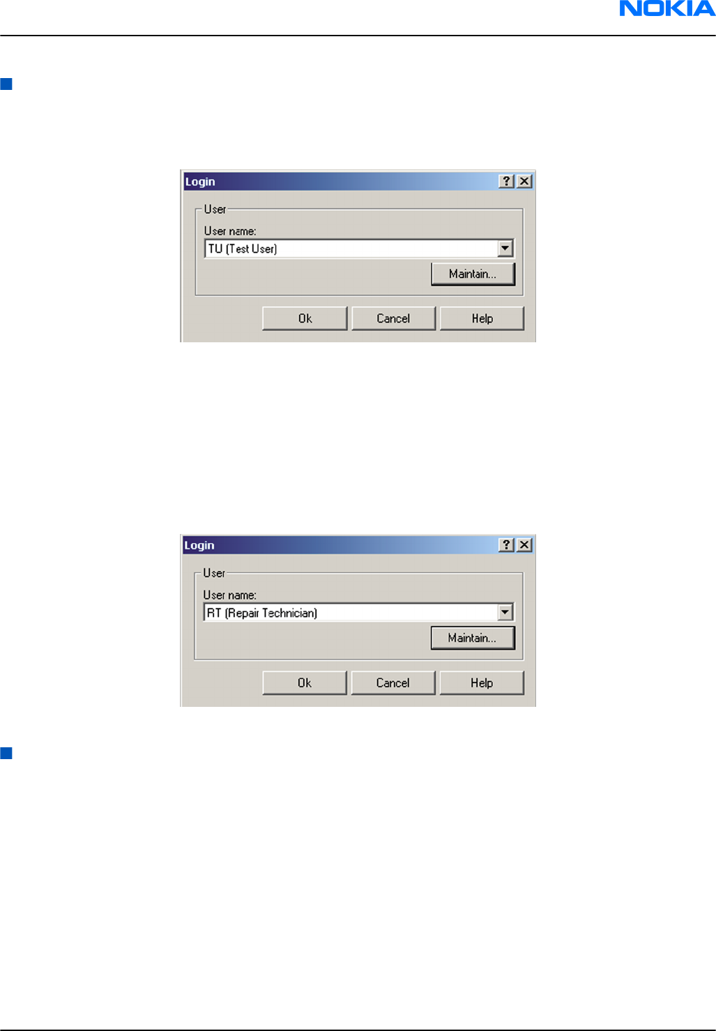
Configuring users in
Phoenix
Steps
1. Start
Phoenix
service software, and log in.
Figure 15 Phoenix login
If the user ID is already configured, select s/he from the
User name
drop-down list, and click OK.
2. To add a new user, or to edit existing ones, click Maintain.
3. To add a new user, click New.
4. Type in the name and initials of the user, and click OK.
The user is added to the user name list.
5. Select the desired user from the
User name
drop-down list, and click OK.
Figure 16 New user configured
Managing connections in
Phoenix
Context
With the Manage Connections feature you can edit and delete existing connections or create new ones.
Note: After choosing the desired connection, and connecting the phone to a PC for the first time,
allow the PC to install the USB device drivers first. Please note that this may take some time to
complete.
If there are problems after the driver installation, check that the USB connection is active from
the Windows Control Panel. If the problem persists, contact the local PC support.
Steps
1. Start
Phoenix
, and log in.
2. Choose File→Manage Connections... .
RM-123; RM-145
Service Software Instructions Nokia Customer Care
Issue 1 COMPANY CONFIDENTIAL Page 3 –17
Copyright © 2006 Nokia. All rights reserved.
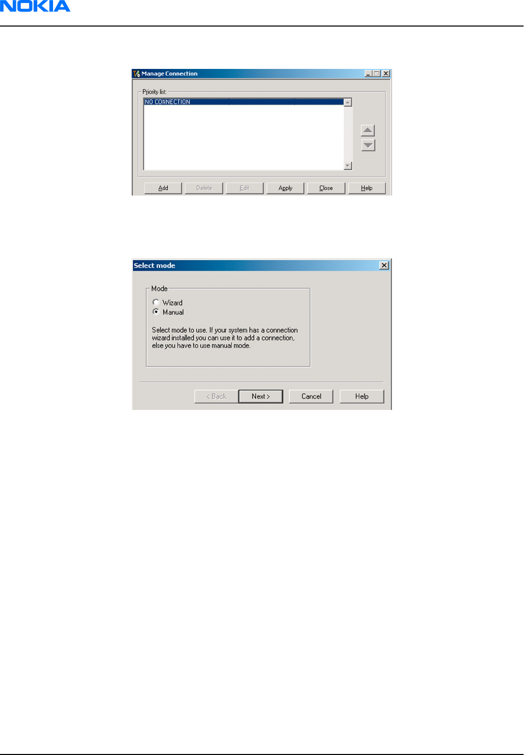
3. To add a new connection, click Add.
4. Select Manual mode, and click Next to continue.
If you want to create the connection using the Connection Wizard, connect the tools and a phone to your
PC. The wizard will automatically try to configure the correct connection.
Figure 17 Select mode: Manual
i For an FPS-10 flash prommer with a USB Connection, choose the following connection settings:
• Media: FPS-10 USB
• DEVICE_INDEX: 0
• SERIAL_NUM: See Serial No from the label attached to the bottom of FPS-10
• ACTIVE_MEDIA: USB
ii For an FPS-10 flash prommer with a LAN connection, choose the following connection settings:
• Media: FPS-10 TCP/IP
• NET_SERV_NAME: Click Scan.... Choose your own FPS-10 device based on the correct MAC address.
See Serial No from the label attached to the bottom of your FPS-10.
• PORT_NUM: Use the default value, and click Next.
• PROTOCOL_FAMILY: Use the default value, and click Next.
• SOCKET TYPE: Use the default value, and click Next.
• TX_BUFFER_SIZE: Use the default value, and click Next.
• RX_BUFFER_SIZE: Use the default value, and click Next.
iii For an FPS-8 flash prommer, choose the following connection settings:
• Media: FPS-8
• PORT_NUM: COM Port where FPS-8 is connected
• COMBOX_DEF_MEDIA: FBUS
RM-123; RM-145
Nokia Customer Care Service Software Instructions
Page 3 –18 COMPANY CONFIDENTIAL Issue 1
Copyright © 2006 Nokia. All rights reserved.
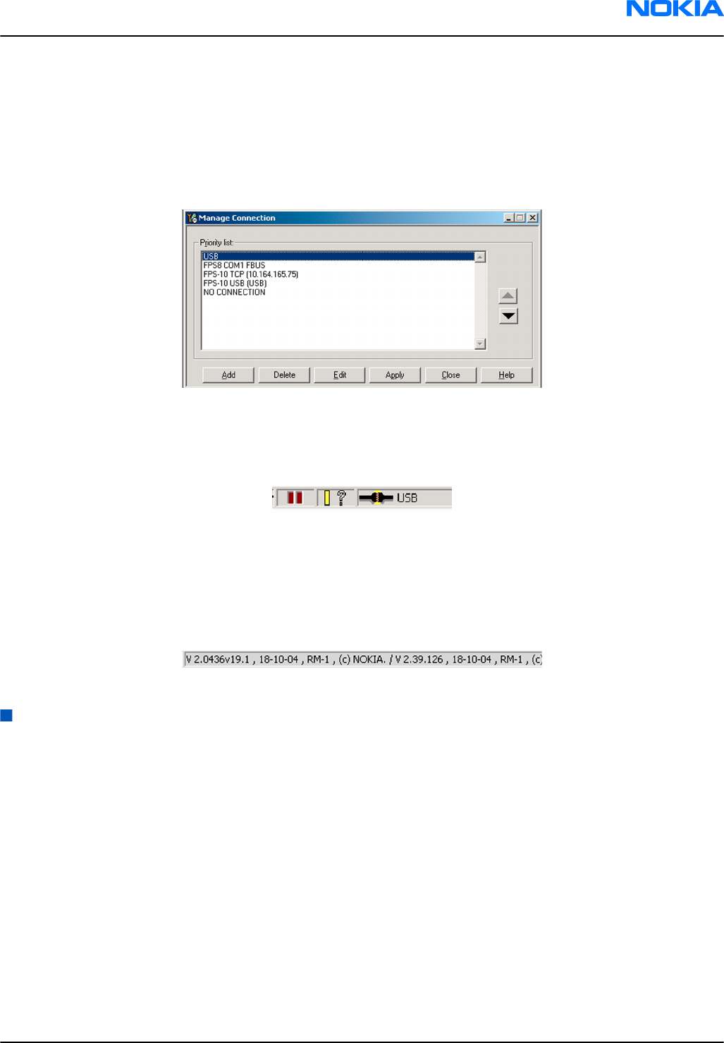
iv For a plain USB connection, choose the following connection settings:
Note: First connect the DKU-2 USB cable between the PC USB port and phone.
• Media: USB
5. To complete the configuration, click Finish.
6. Click the connection you want to activate. Use the up/down arrows located on the right hand side to move
it on top of the list, then click Apply.
Figure 18 Connections list
The connection is activated, and it can be used after closing the
Manage Connection
window.
The connection information is shown at the right hand bottom corner of the screen.
Figure 19 Connection information
7. To use the connection, connect the phone to your PC with correct service tools. Make sure the phone is
switched on, and then choose File→Scan Product .
Results
The product support module information appears in the status bar:
Figure 20 Product support module information (example from RM-1)
Installing flash support files for FPS-8 and FPS-10
Prerequisites
• Install
Phoenix
service software.
• Install phone model specific data package for
Phoenix
.
• If you want to update the flash support files, they are delivered in the same installation package with
Phoenix
or newer
Phoenix
packages beginning from December 2004.
In case you want to update the MCU files, install the latest data package (see Technical Bulletins for
information on the latest one).
Normally, it is enough to install
Phoenix
and the phone-specific data package because the installation
always includes the latest flash update package files for FPS-8 and FPS-10.
• A separate installation package for flash support files is available. The files can be updated according to
these instructions, if updates appear between
Phoenix
data package releases.
RM-123; RM-145
Service Software Instructions Nokia Customer Care
Issue 1 COMPANY CONFIDENTIAL Page 3 –19
Copyright © 2006 Nokia. All rights reserved.
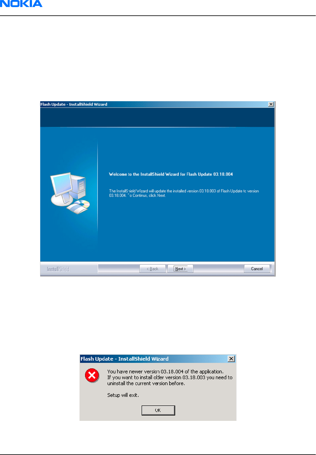
Context
If you are not using a separate installation package, you can skip this section and continue with "Updating
FPS-8 and FPS-10 flash prommer software" (page 3–22) after installing a new phone data package.
Steps
1. To begin the installation, double-click the flash update file (for example,
flash_update_03_183_0014.exe
).
Figure 21 Flash update welcome dialog
If the same version of the flash update package already exists, and you want to reinstall it, the previous
package is first uninstalled.
Restart installation again after the uninstallation.
2. If you try to downgrade the existing version to older ones, the setup will be aborted. If there is a need to
downgrade the version, uninstall newer files manually from the Windows Control Panel, and then rerun
the installation.
Figure 22 Flash installation interrupted
If an older version exists on your PC and it needs to be updated, click Next to continue installation.
RM-123; RM-145
Nokia Customer Care Service Software Instructions
Page 3 –20 COMPANY CONFIDENTIAL Issue 1
Copyright © 2006 Nokia. All rights reserved.
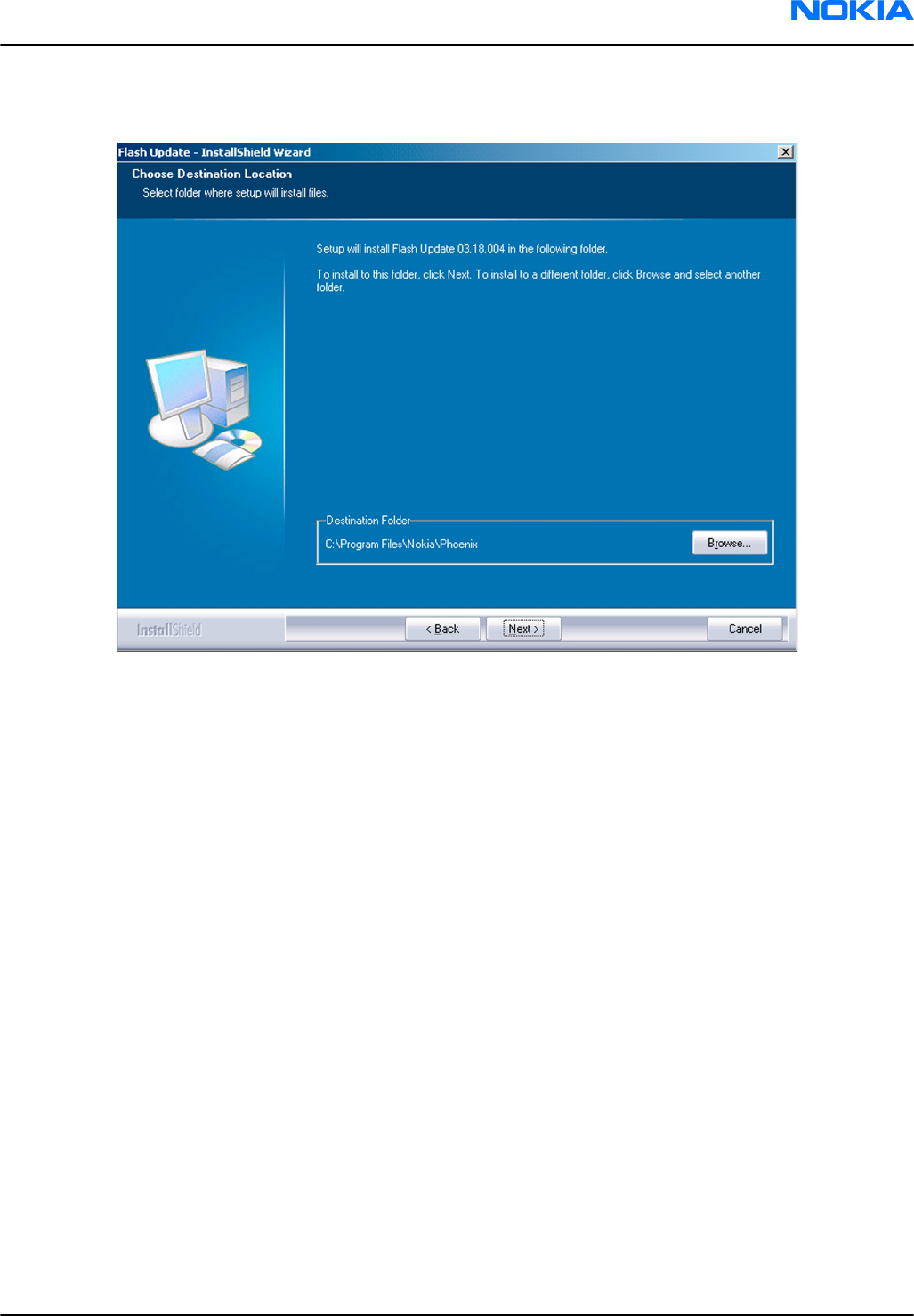
3. It is recommended to install the files to the default destination folder
C:\Program Files\Nokia\Phoenix
.
To continue, click Next.
Figure 23 Flash destination folder
When installing the flash update files for the first time, you may choose another location by selecting
Browse (not recommended).
RM-123; RM-145
Service Software Instructions Nokia Customer Care
Issue 1 COMPANY CONFIDENTIAL Page 3 –21
Copyright © 2006 Nokia. All rights reserved.
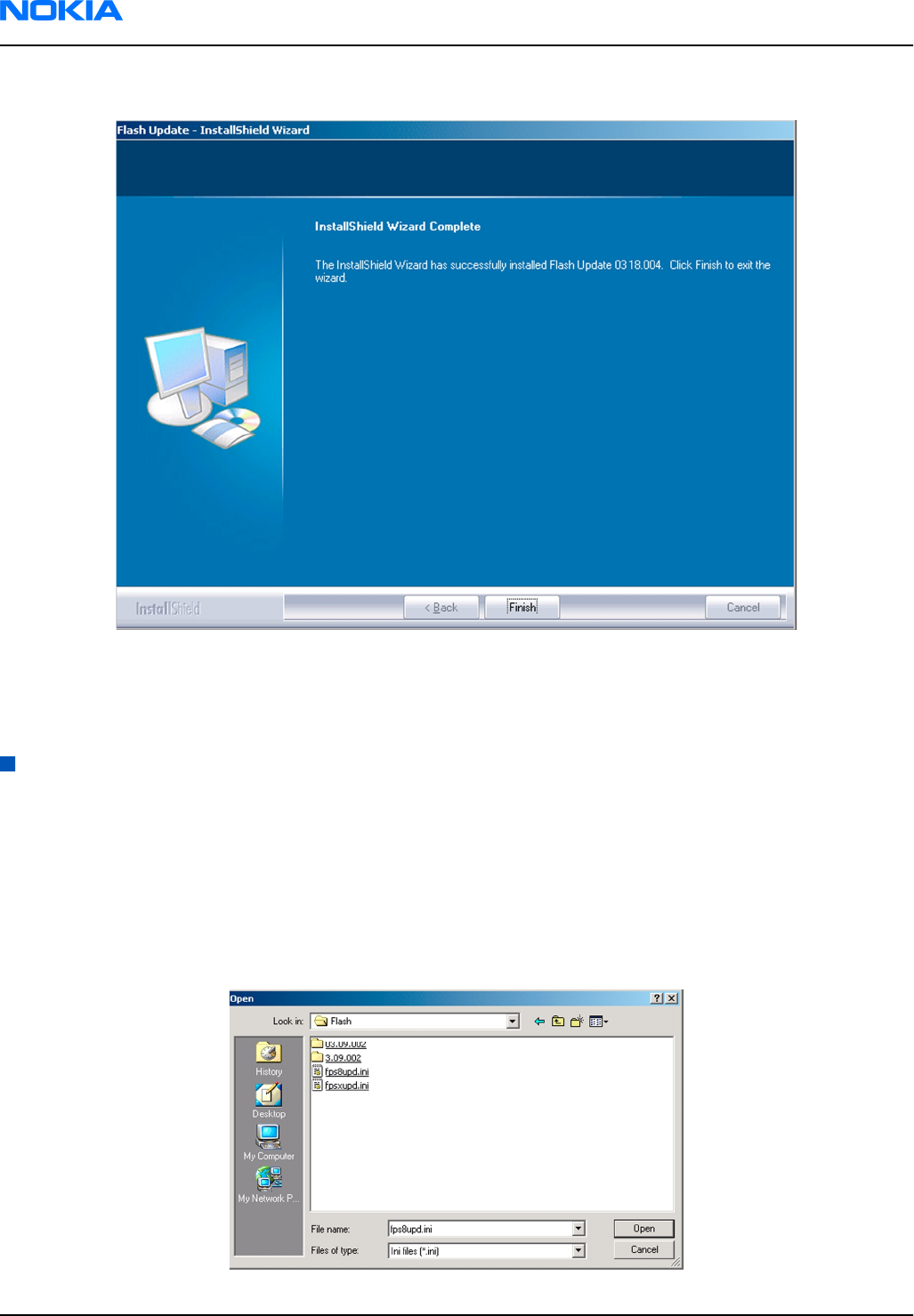
4. To complete the installation procedure, click Finish .
Figure 24 Finish flash update
Next actions
FPS-8 and FPS-10 flash prommers must be updated using
Phoenix
.
Updating FPS-8 and FPS-10 flash prommer software
Steps
1. Start
Phoenix
service software, and log in.
2. Choose the correct connection for your flash prommer: File→Manage Connections...
3. Choose Flashing→Prommer maintenance .
4. To update the FPS-8/FPS-10 software, click Update, and select the appropriate file
fps8upd.ini
(for FPS-8)
or
fpsxupd.ini
(for FPS-10) from
C:\Program Files\Nokia\Phoenix\Flash
.
Figure 25 Flash directory window
RM-123; RM-145
Nokia Customer Care Service Software Instructions
Page 3 –22 COMPANY CONFIDENTIAL Issue 1
Copyright © 2006 Nokia. All rights reserved.
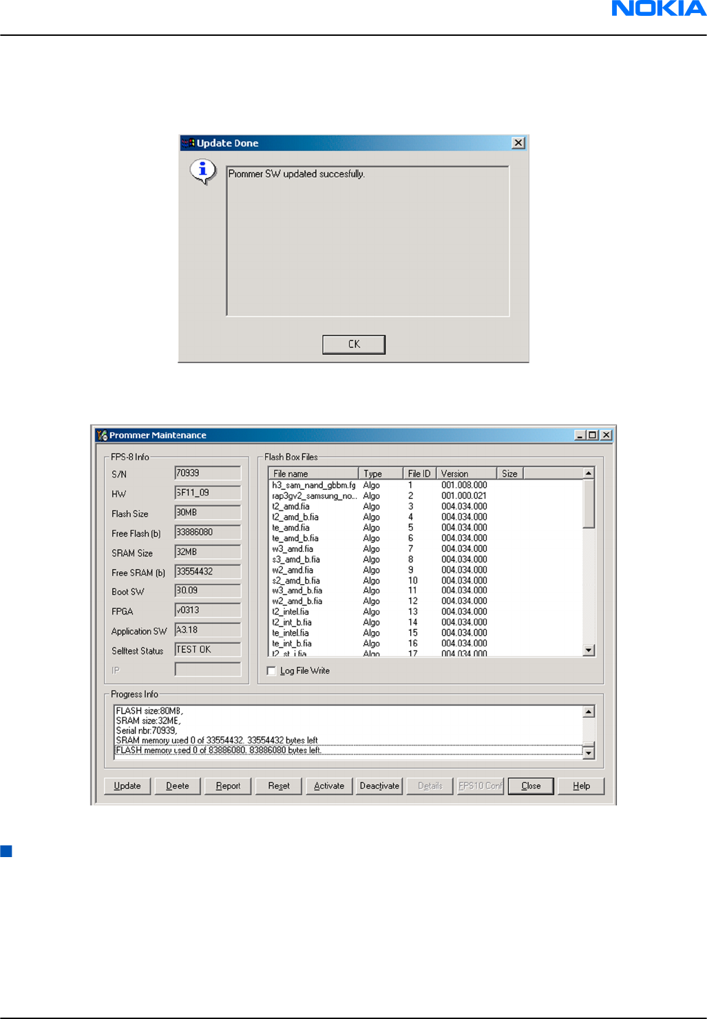
Tip: All files can be loaded separately to the prommer used. To do this, click the right mouse button
in the
Flash Box Files
pane and select the file type(s) to be loaded.
5. Click OK.
Figure 26 Prommer software update finished
6. To close the
Prommer Maintenance
window, click Close.
Figure 27
Prommer Maintenance
window
Activating FPS-8
Context
Before FPS-8 can be successfully used for phone programming, it must first be activated.
First fill in the
FPS-8 activation request
sheet in the FPS-8 sales package, and follow the instructions given.
When activation file is received (for example,
00000.in
), copy it to the
C:\ProgramFiles\Nokia\Phoenix
\BoxActivation
directory on your computer (this directory is created when
Phoenix
is installed).
RM-123; RM-145
Service Software Instructions Nokia Customer Care
Issue 1 COMPANY CONFIDENTIAL Page 3 –23
Copyright © 2006 Nokia. All rights reserved.
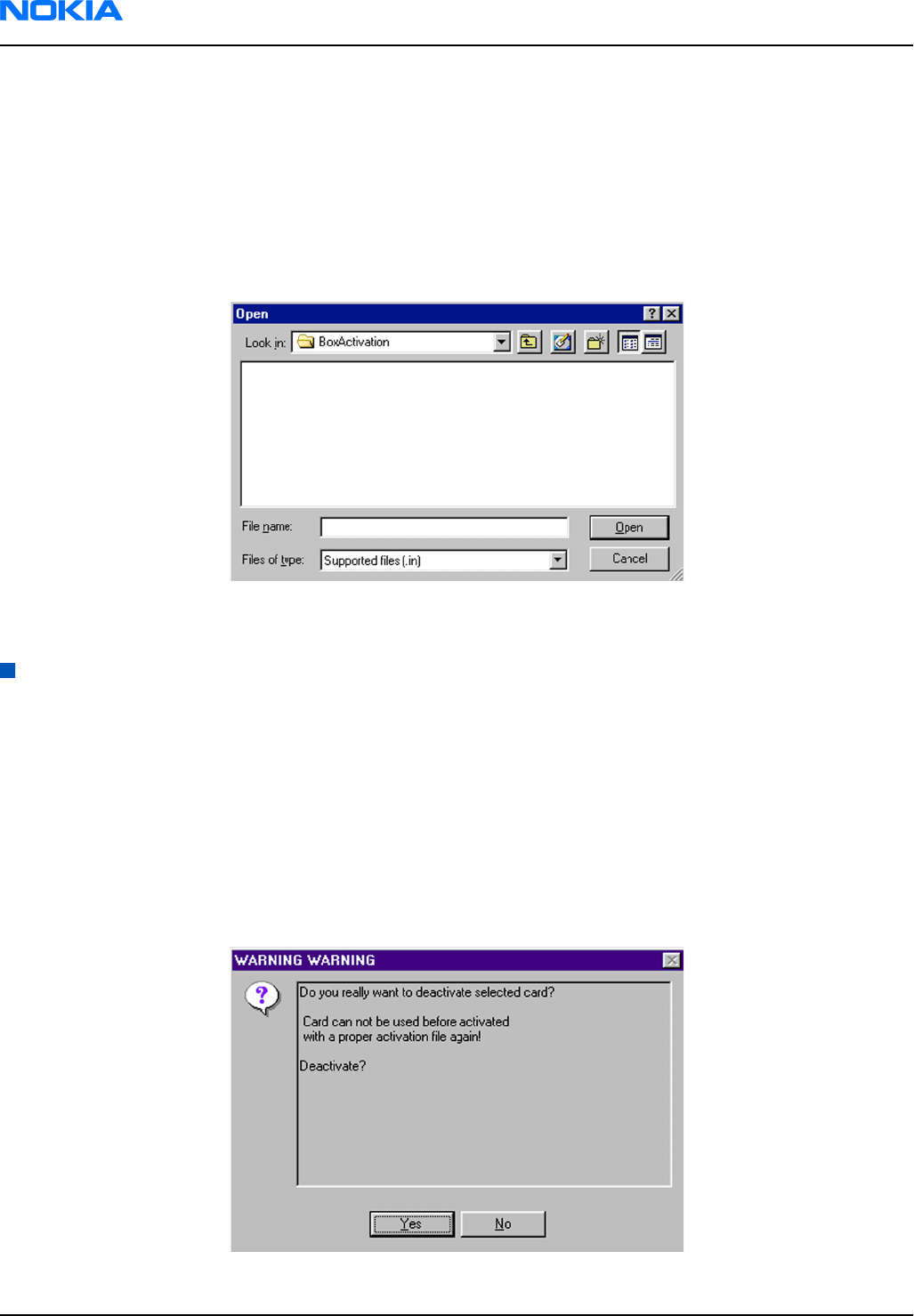
Steps
1. Start
Phoenix
service software.
2. Choose Flashing→Prommer Maintenance .
3. In the
Prommer Maintenance
window, click Activate.
4. To find the activation file, click Browse.
5. To activate the prommer, select the activation file and click Open.
Figure 28 Box activation
6. To complete the activation, restart FPS-8.
Deactivating FPS-8
Context
If there is, for example, a need to send the FPS-8 box for repair, it must be deactivated first.
Steps
1. Start
Phoenix
service software.
2. Choose Flashing→Prommer Maintenance .
3. In the
Prommer Maintenance
window, click Deactivate.
4. To confirm the deactivation, click Yes.
Figure 29 Deactivation warning
RM-123; RM-145
Nokia Customer Care Service Software Instructions
Page 3 –24 COMPANY CONFIDENTIAL Issue 1
Copyright © 2006 Nokia. All rights reserved.

The box is deactivated.
5. To complete the deactivation, restart FPS-8.
RM-123; RM-145
Service Software Instructions Nokia Customer Care
Issue 1 COMPANY CONFIDENTIAL Page 3 –25
Copyright © 2006 Nokia. All rights reserved.

RM-123; RM-145
Nokia Customer Care Service Software Instructions
(This page left intentionally blank.)
Page 3 –26 COMPANY CONFIDENTIAL Issue 1
Copyright © 2006 Nokia. All rights reserved.

4 — Service Tools and Service
Concepts
Nokia Customer Care
Issue 1 COMPANY CONFIDENTIAL Page 4 –1
Copyright © 2006 Nokia. All rights reserved.

RM-123; RM-145
Nokia Customer Care Service Tools and Service Concepts
(This page left intentionally blank.)
Page 4 –2 COMPANY CONFIDENTIAL Issue 1
Copyright © 2006 Nokia. All rights reserved.

Table of Contents
Service tools............................................................................................................................................................4–5
CA-31D................................................................................................................................................................4–5
CA-35S.................................................................................................................................................................4–5
CA-53...................................................................................................................................................................4–5
CU-4.....................................................................................................................................................................4–6
FLS-4S..................................................................................................................................................................4–7
FPS-10.................................................................................................................................................................4–7
FS-31...................................................................................................................................................................4–7
JBT-9....................................................................................................................................................................4–7
JXS-1....................................................................................................................................................................4–8
MJ-91...................................................................................................................................................................4–8
PCS-1...................................................................................................................................................................4–8
PKD-1..................................................................................................................................................................4–8
RJ-104.................................................................................................................................................................4–9
RJ-108.................................................................................................................................................................4–9
RJ-114.................................................................................................................................................................4–9
RJ-57...................................................................................................................................................................4–9
RJ-93...................................................................................................................................................................4–9
SA-103..............................................................................................................................................................4–10
SPS-1.................................................................................................................................................................4–10
SRT-6.................................................................................................................................................................4–10
SS-45.................................................................................................................................................................4–11
SS-46.................................................................................................................................................................4–11
SS-51.................................................................................................................................................................4–11
SS-62.................................................................................................................................................................4–11
ST-37.................................................................................................................................................................4–11
ST-40.................................................................................................................................................................4–12
ST-41.................................................................................................................................................................4–12
ST-44.................................................................................................................................................................4–12
SX-4...................................................................................................................................................................4–12
XCS-4.................................................................................................................................................................4–12
XRF-1.................................................................................................................................................................4–13
Service concepts...................................................................................................................................................4–13
Flash concept with FPS-10..............................................................................................................................4–13
Module jig concept..........................................................................................................................................4–14
POS (Point of Sale) flash concept...................................................................................................................4–15
RF testing and BB testing...............................................................................................................................4–16
CU-4 flash concept with FPS-10......................................................................................................................4–17
Service concept for RF/BB testing and tuning..............................................................................................4–18
LAN connection flash concept........................................................................................................................4–19
List of Figures
Figure 30 Basic flash concept with FPS-10.........................................................................................................4–13
Figure 31 Module jig service concept.................................................................................................................4–14
Figure 32 POS flash concept................................................................................................................................4–15
Figure 33 RF testing and BB testing...................................................................................................................4–16
Figure 34 CU-4 flash concept with FPS-10..........................................................................................................4–17
Figure 35 Service concept for RF/BB testing and tuning..................................................................................4–18
Figure 36 LAN connection flash concept............................................................................................................4–19
RM-123; RM-145
Service Tools and Service Concepts Nokia Customer Care
Issue 1 COMPANY CONFIDENTIAL Page 4 –3
Copyright © 2006 Nokia. All rights reserved.

RM-123; RM-145
Nokia Customer Care Service Tools and Service Concepts
(This page left intentionally blank.)
Page 4 –4 COMPANY CONFIDENTIAL Issue 1
Copyright © 2006 Nokia. All rights reserved.
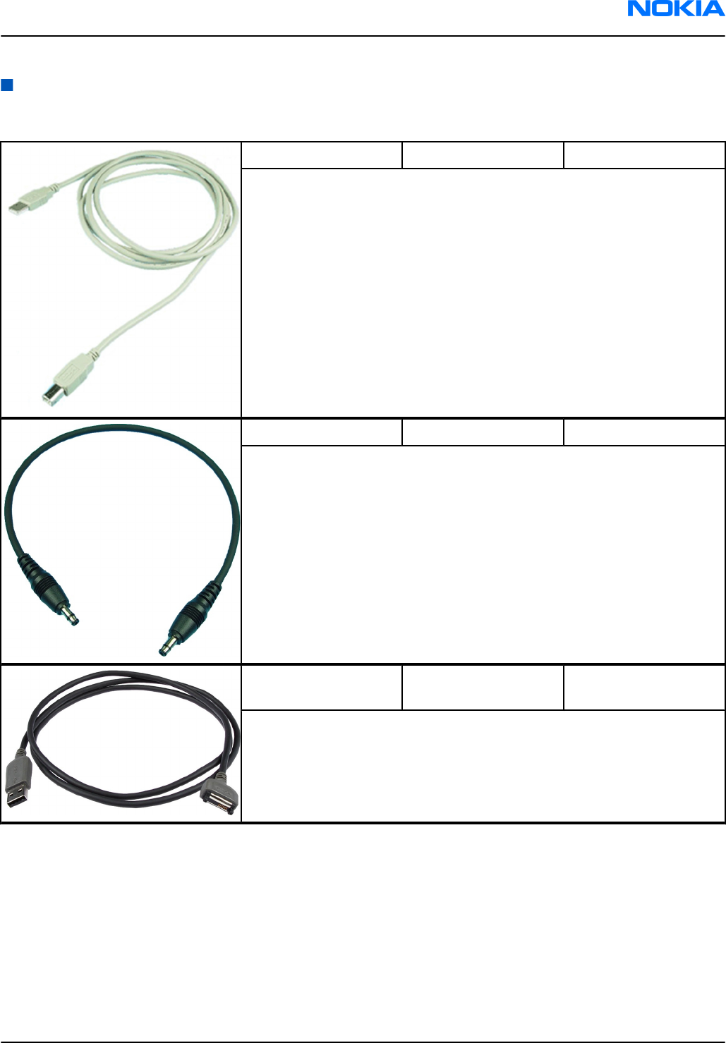
Service tools
The table below gives a short overview of service tools that can be used for testing, error analysis and repair
of product RM-123; RM-145, refer to various concepts.
CA-31D USB cable
The CA-31D USB cable is used to connect FPS-10 or FPS-11 to a PC. It is
included in the FPS-10 and FPS-11 sales packages.
CA-35S Power cable
CA-35S is a power cable for connecting, for example, the FPS-10 flash
prommer to the Point-Of-Sales (POS) flash adapter.
CA-53 USB connectivity
cable
USB to system connector cable.
RM-123; RM-145
Service Tools and Service Concepts Nokia Customer Care
Issue 1 COMPANY CONFIDENTIAL Page 4 –5
Copyright © 2006 Nokia. All rights reserved.
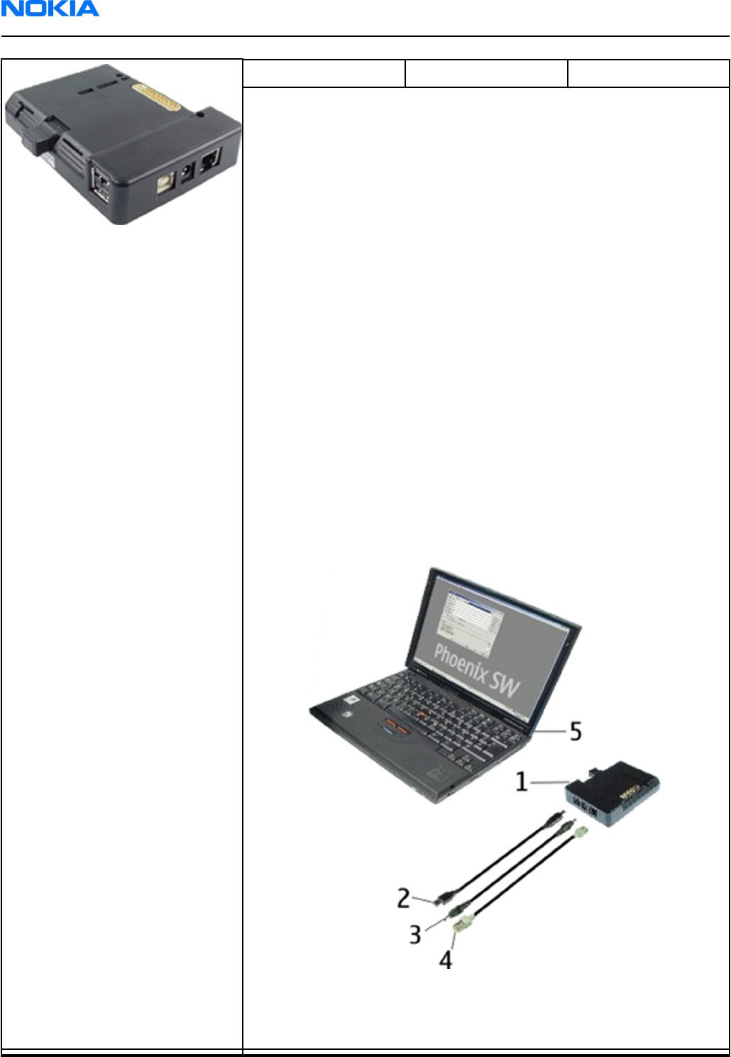
CU-4 Control unit
CU-4 is a general service tool used with a module jig and/or a flash
adapter. It requires an external 12 V power supply.
The unit has the following features:
• software controlled via USB
• EM calibration function
• Forwards FBUS/Flashbus traffic to/from terminal
• Forwards USB traffic to/from terminal
• software controlled BSI values
• regulated VBATT voltage
• 2 x USB2.0 connector (Hub)
• FBUS and USB connections supported
When using CU-4, note the special order of connecting cables and
other service equipment:
Instructions
1 Connect a service tool (jig, flash adapter) to CU-4.
2 Connect CU-4 to your PC with a USB cable.
3 Connect supply voltage (12 V)
4 Connect an FBUS cable (if necessary).
5 Start Phoenix service software.
Note: Phoenix enables CU-4 regulators via USB when it is
started.
Reconnecting the power supply requires a Phoenix restart.
RM-123; RM-145
Nokia Customer Care Service Tools and Service Concepts
Page 4 –6 COMPANY CONFIDENTIAL Issue 1
Copyright © 2006 Nokia. All rights reserved.
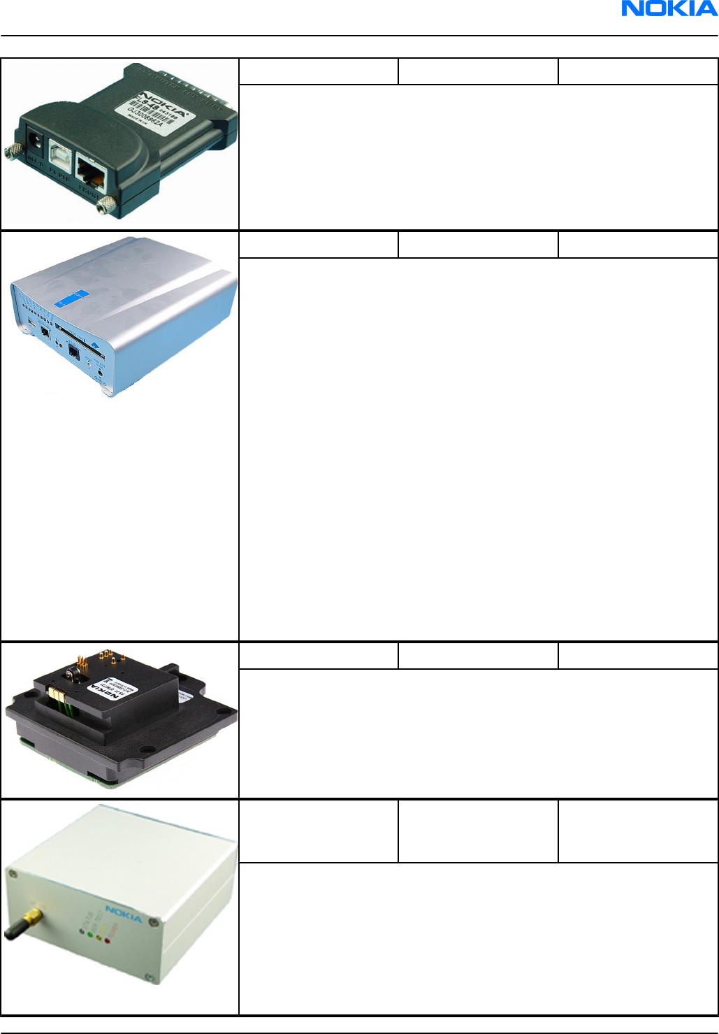
FLS-4S Flash device
FLS-4S is a dongle and flash device incorporated into one package,
developed specifically for POS use.
FPS-10 Flash prommer
FPS-10 interfaces with:
• PC
• Control unit
• Flash adapter
• Smart card
FPS-10 flash prommer features:
• Flash functionality for BB5 and DCT-4 terminals
• Smart Card reader for SX-2 or SX-4
• USB traffic forwarding
• USB to FBUS/Flashbus conversion
• LAN to FBUS/Flashbus and USB conversion
• Vusb output switchable by PC command
FPS-10 sales package includes:
• FPS-10 prommer
• Power Supply with 5 country specific cords
• USB cable
FS-31 Flash adapter
• FS-31 is equipped with a clip interlock system
• provides standardised interface towards Control Unit
• provides RF connection using coupler
• multiplexing between USB and FBUS media, controlled by VUSB
JBT-9 Bluetooth test and
interface box (sales
package)
The JBT-9 test box is a generic service device used to perform
Bluetooth bit error rate (BER) testing, and establishing cordless FBUS
connection via Bluetooth. An ACP-8x charger is needed for BER testing
and an AXS-4 cable in case of cordless interface usage testing .
Sales package includes:
• JBT-9 test box
• Installation and warranty information
RM-123; RM-145
Service Tools and Service Concepts Nokia Customer Care
Issue 1 COMPANY CONFIDENTIAL Page 4 –7
Copyright © 2006 Nokia. All rights reserved.
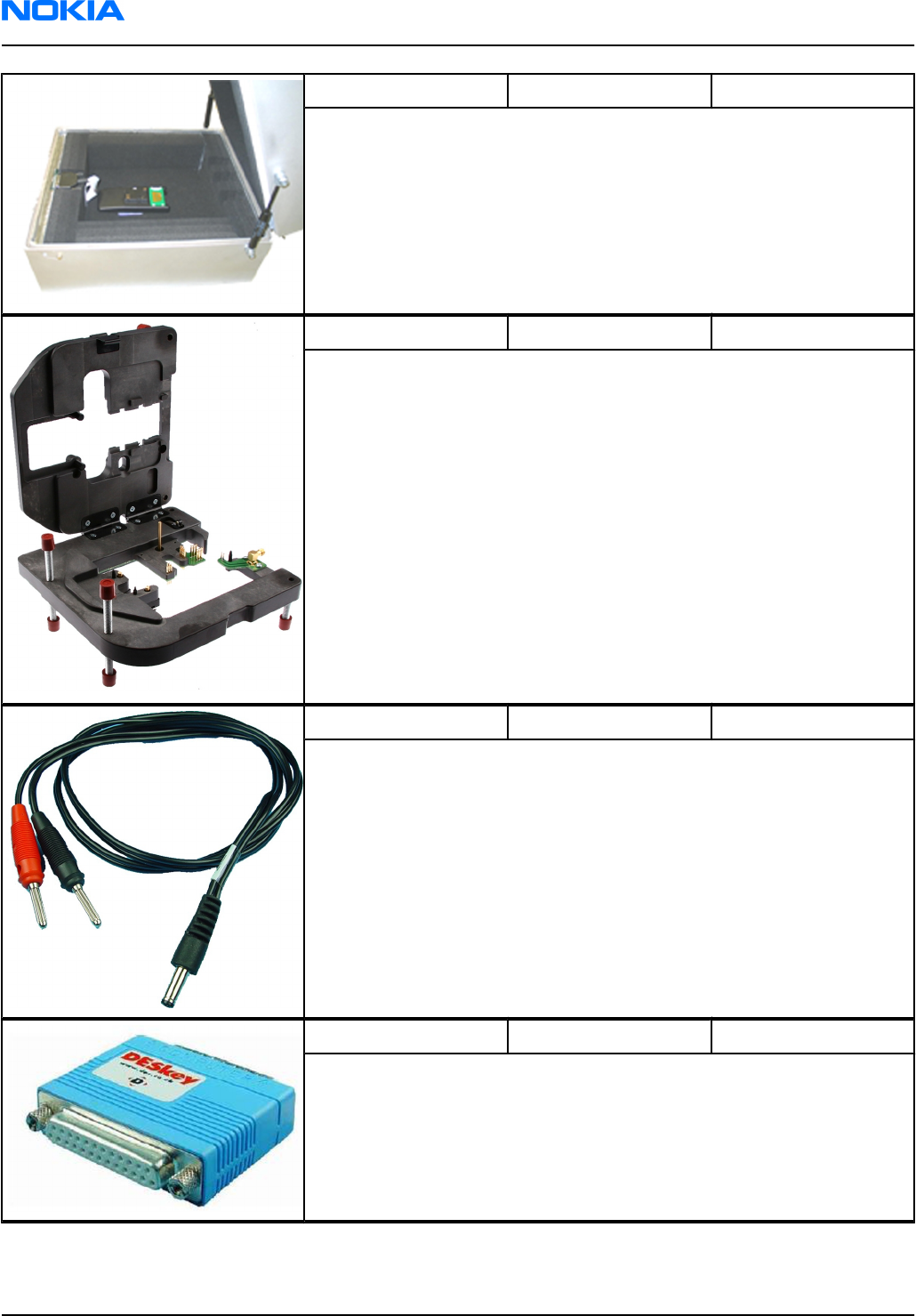
JXS-1 RF shield box
Because the WCDMA network disturbs the RX side testing of the WCDMA
phone and the Tx signal of the WCDMA phone can severely disturb the
WCDMA network, a shield box is needed in all testing, tuning and fault
finding which requires WCDMA RF signal.
The shield box is not an active device, it contains only passive filtering
components for RF attenuation.
MJ-91 Module jig
MJ-91 is meant for component level troubleshooting.
The jig includes an RF interface for GSM, WCDMA and Bluetooth. In
addition, it has the following features:
• Provides mechanical interface with the engine module
• Provides galvanic connection to all needed test pads in module
• Multiplexing between USB and FBUS media, controlled by Vusb
• MMC interface
• Duplicated SIM connector
• Connector for control unit
•Access for Pop-PortTM system connector
Note: Be careful when closing the jig, not to harm the display
with the screws on the jig!
PCS-1 Power cable
The PCS-1 power cable (DC) is used with a docking station, a module
jig or a control unit to supply a controlled operating voltage.
PKD-1 SW security device
SW security device is a piece of hardware enabling the use of the
service software when connected to the parallel (LPT) port of the PC.
Without the device, it is not possible to use the service software.
Printer or any such device can be connected to the PC through the
device if needed.
RM-123; RM-145
Nokia Customer Care Service Tools and Service Concepts
Page 4 –8 COMPANY CONFIDENTIAL Issue 1
Copyright © 2006 Nokia. All rights reserved.
RJ-104 BTHFM rework jig
RJ-104 is a rework jig used when servicing the BTHFM module. It is
used together with rework stencil ST-37.
RJ-108 Soldering jig
RJ-108 is a soldering jig used for soldering and as a rework jig for the
engine module.
RJ-114 Rework jig
RJ-114 is a rework jig used with ST-41.
RJ-57 Rework jig
RJ-57 is a rework jig used with ST-22.
RJ-93 Rework jig
RJ-93 is used as a rework jig for the engine module.
This stencil takes the front end module (FEM) or power amplifier (PA)
module for spreading the soldering paste to the component. Must be
used together with the ST-40 stencil.
RM-123; RM-145
Service Tools and Service Concepts Nokia Customer Care
Issue 1 COMPANY CONFIDENTIAL Page 4 –9
Copyright © 2006 Nokia. All rights reserved.

SA-103 RF coupler
SA-103 is an RF coupler for WCDMA and GSM RF testing. It is used
together with the product-specific flash adapter.
The following table shows attenuations from the antenna pads of the
mobile terminal to the SMA connectors of SA-103:
•Frequency Att. (dB)
GSM900 TX 2,7 dB +/- 0,5 dB
GSM900 RX 2,6 dB +/- 0,7 dB
GSM1800 TX 8,2 dB +/- 2,0 dB
GSM1800 RX 5,3 dB +/- 0,4 dB
GSM1900 TX 5,1 dB +/- 0,1dB
GSM1900 RX 5,2 dB +/- 0,6 dB
WCDMA2100 TX 10,0 dB +/- 0,9dB
WCDMA2100 RX 6,8 dB +/- 0,4 dB
SPS-1 Soldering Paste
Spreader
SRT-6 Opening tool
SRT-6 is used to open phone covers and B-to-B connectors.
RM-123; RM-145
Nokia Customer Care Service Tools and Service Concepts
Page 4 –10 COMPANY CONFIDENTIAL Issue 1
Copyright © 2006 Nokia. All rights reserved.
SS-45 Front camera
removal tool
The front camera removal tool SS-45 is used to remove/attach the
front camera module from/to the socket.
SS-46 Interface adapter
SS-46 acts as an interface adapter between the flash adapter and
FPS-10.
SS-51 Front camera
removal tool
The front camera removal tool SS-51 is used to remove/attach a front
camera module from/to the camera socket of the phone PWB.
SS-62 Generic flash adapter
base for BB5
• generic base for flash adapters and couplers
• SS-62 equipped with a clip interlock system
• provides standardised interface towards Control Unit
• provides RF connection using galvanic connector or coupler
• multiplexing between USB and FBUS media, controlled by VUSB
ST-37 BTHFM rework stencil
ST-37 stencil is used with RJ-104 BTHFM rework jig.
RM-123; RM-145
Service Tools and Service Concepts Nokia Customer Care
Issue 1 COMPANY CONFIDENTIAL Page 4 –11
Copyright © 2006 Nokia. All rights reserved.
ST-40 PA rework stencil
This stencil is to be used together with RJ-93 and covering FEM module.
ST-41 Rework stencil
ST-41 is a rework stencil used with rework jig RJ-114.
ST-44 Rework stencil
ST-44 is a rework stencil used with rework jig RJ-57.
SX-4 Smart card
SX-4 is a BB5 security device used to protect critical features in tuning
and testing.
SX-4 is also needed together with FPS-10 when DCT-4 phones are
flashed.
XCS-4 Modular cable
XCS-4 is a shielded (one specially shielded conductor) modular cable
for flashing and service purposes.
RM-123; RM-145
Nokia Customer Care Service Tools and Service Concepts
Page 4 –12 COMPANY CONFIDENTIAL Issue 1
Copyright © 2006 Nokia. All rights reserved.
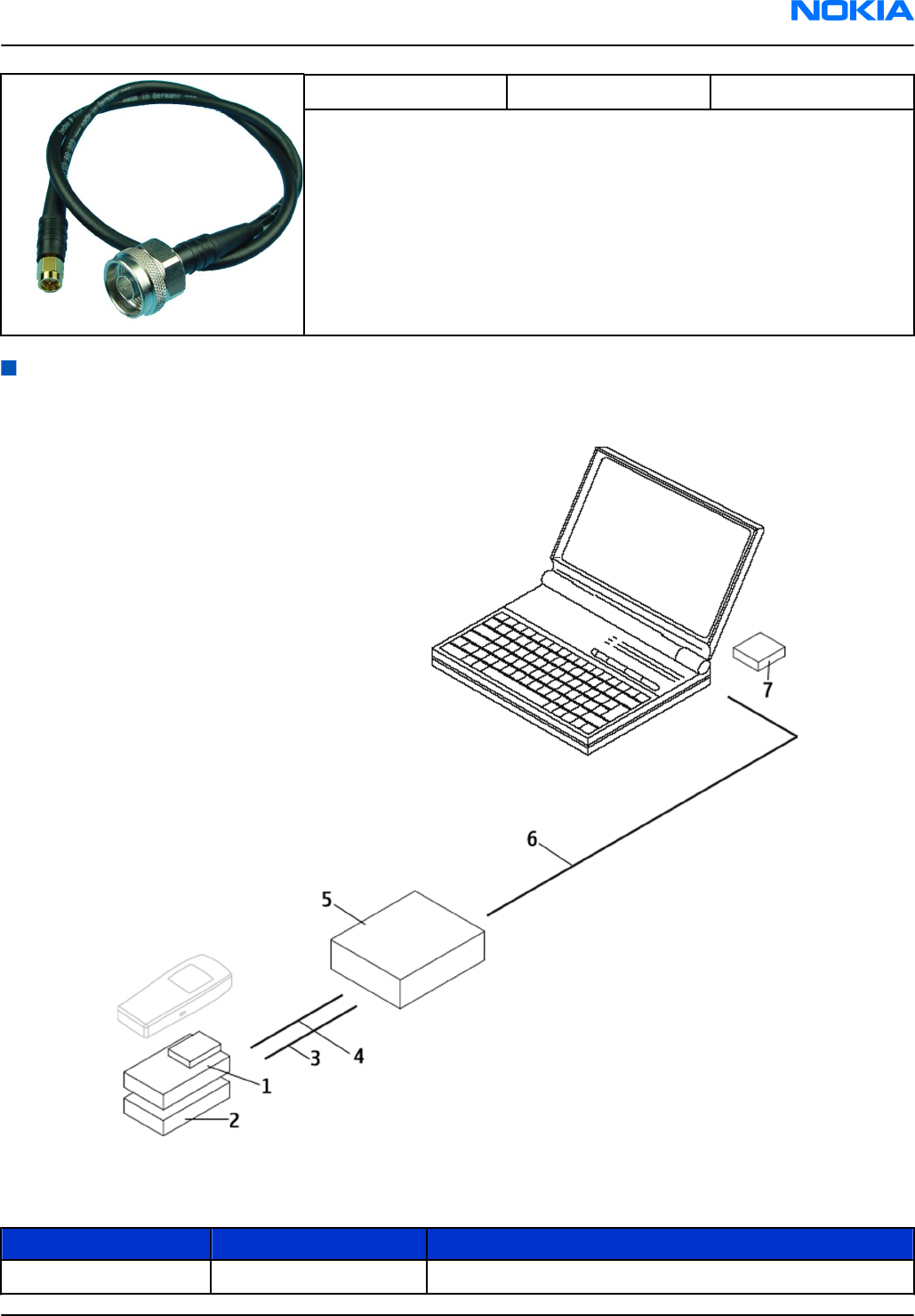
XRF-1 RF cable
The RF cable is used to connect, for example, a module repair jig to
the RF measurement equipment.
SMA to N-Connector ca. 610mm.
Attenuation for:
• GSM850/900: 0.3+-0.1 dB
• GSM1800/1900: 0.5+-0.1 dB
• WLAN: 0.6+-0.1dB
Service concepts
Flash concept with FPS-10
Figure 30 Basic flash concept with FPS-10
Note: FPS-8 concept can also be used for flashing.
Item Type Description
1 FS-31 Flash adapter
RM-123; RM-145
Service Tools and Service Concepts Nokia Customer Care
Issue 1 COMPANY CONFIDENTIAL Page 4 –13
Copyright © 2006 Nokia. All rights reserved.
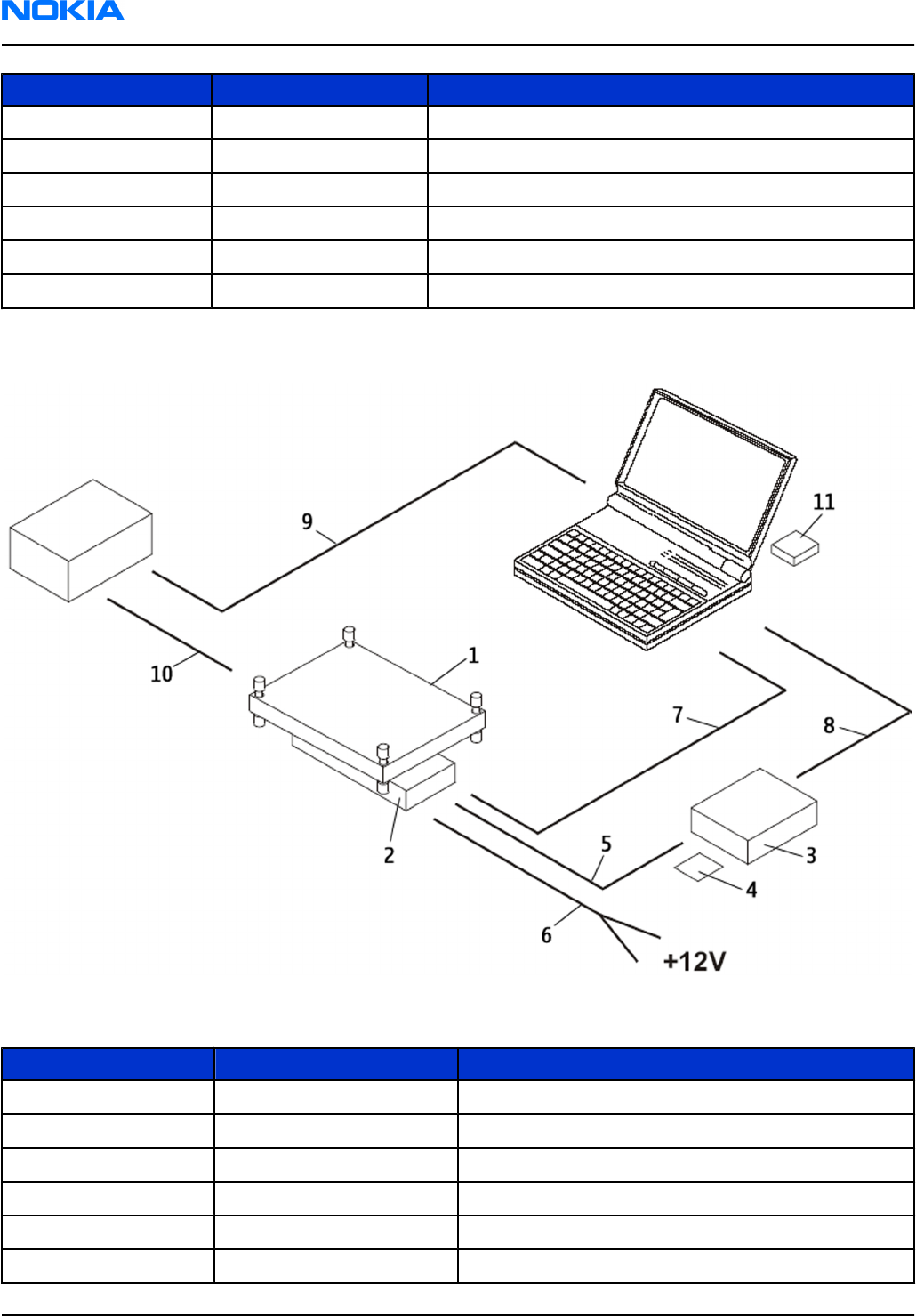
Item Type Description
2 SS-46 Interface adapter
3 CA-35S Power cable
4 XCS-4 Modular cable
5 FPS-10 Flash prommer box
6 Standard USB cable
7 PKD-1 SW security device
Module jig concept
Module jig concept is meant for BB / RF testing + tuning and for flashing purposes.
Figure 31 Module jig service concept
Item Type Description
1 MJ-91 Module jig
2 CU-4 Control unit
3 FPS-10 Flash prommer box
4 SX-4 Smart card
5 XCS-4 Modular cable
6 PCS-1 DC power cable
RM-123; RM-145
Nokia Customer Care Service Tools and Service Concepts
Page 4 –14 COMPANY CONFIDENTIAL Issue 1
Copyright © 2006 Nokia. All rights reserved.
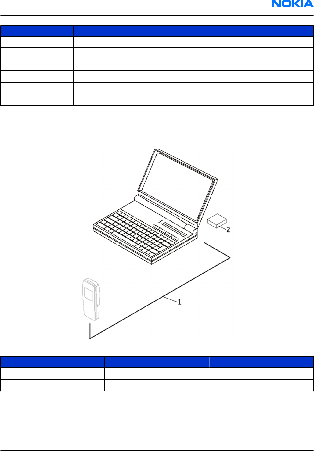
Item Type Description
7 Standard USB cable
8 Standard USB cable
9 GPIB control cable
10 XRS-6 RF cable
11 PKD-1 SW security device
12 RF shield box
Note: Item 12 not shown in the picture.
POS (Point of Sale) flash concept
Figure 32 POS flash concept
Item Type Description
1 CA-53 USB connectivity cable
2 FLS-4S POS flash device
RM-123; RM-145
Service Tools and Service Concepts Nokia Customer Care
Issue 1 COMPANY CONFIDENTIAL Page 4 –15
Copyright © 2006 Nokia. All rights reserved.
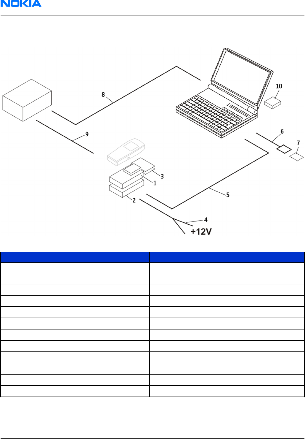
RF testing and BB testing
Figure 33 RF testing and BB testing
Item Type Description
1 SS-62
SA-103
Flash adapter base
Flash adapter
2 CU-4 Control unit
3 SA-103 RF coupler
4 PCS-1 Power cable
5 Standard USB cable
6 Standard USB cable + smart card reader
7 SX-4 Smart card
8 GPIB control cable
9 XRS-6 RF cable
10 PKD-1 SW security device
11 RF shield box
Note: Item 11 is not shown in the figure.
RM-123; RM-145
Nokia Customer Care Service Tools and Service Concepts
Page 4 –16 COMPANY CONFIDENTIAL Issue 1
Copyright © 2006 Nokia. All rights reserved.
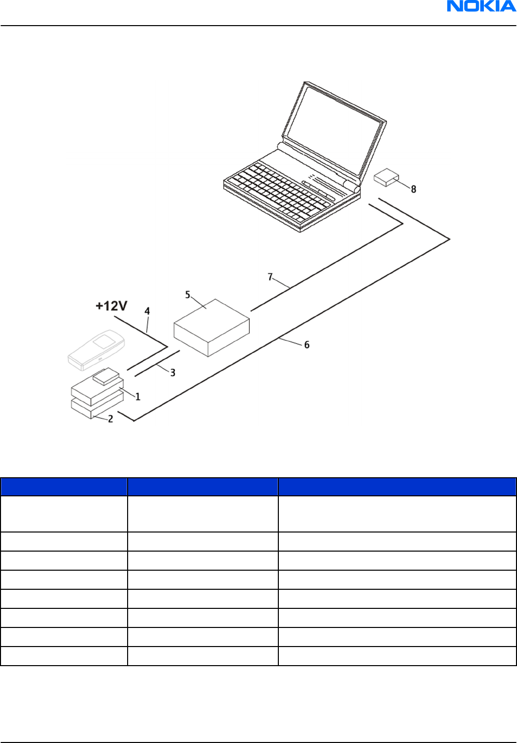
CU-4 flash concept with FPS-10
Figure 34 CU-4 flash concept with FPS-10
Note: FPS-8 concept can also be used for flashing.
Item Type Description
1 SS-62
FS-31
Flash adapter base
Flash adapter
2 CU-4 Control unit
3 XCS-4 Modular cable
4 PCS-1 Power cable
5 FPS-10 Flash prommer box
6 Standard USB cable
7 Standard USB cable
8 PKD-1 SW security device
RM-123; RM-145
Service Tools and Service Concepts Nokia Customer Care
Issue 1 COMPANY CONFIDENTIAL Page 4 –17
Copyright © 2006 Nokia. All rights reserved.
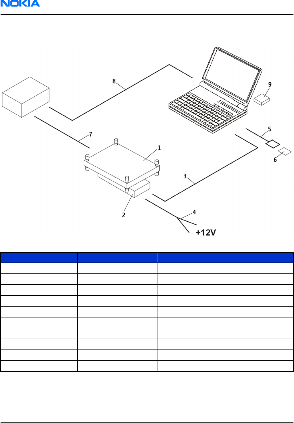
Service concept for RF/BB testing and tuning
Figure 35 Service concept for RF/BB testing and tuning
Item Type Description
1 MJ-91 Module jig
2 CU-4 Control unit
3 Standard USB cable
4 PCS-1 DC power cable
5 Standard USB cable + smart card reader
6 SX-4 Smart card
7 XRS-6 RF cable
8 GPIB control cable
9 PKD-1 SW security device
10 RF shield box
Note: Item 10 not shown in the picture.
RM-123; RM-145
Nokia Customer Care Service Tools and Service Concepts
Page 4 –18 COMPANY CONFIDENTIAL Issue 1
Copyright © 2006 Nokia. All rights reserved.
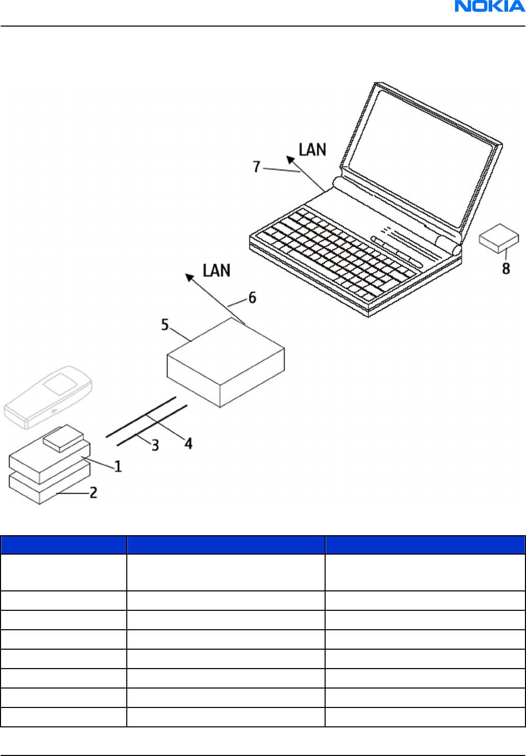
LAN connection flash concept
Figure 36 LAN connection flash concept
Item Type Description
1 SS-62
FS-31
Flash adapter base
Flash adapter
2 SS-46 Interface adapter
3 CA-35S Power cable
4 XCS-4 Modular cable
5 FPS-10 Flash prommer box
6 LAN cable
7 LAN cable
8 PKD-1 SW security device
RM-123; RM-145
Service Tools and Service Concepts Nokia Customer Care
Issue 1 COMPANY CONFIDENTIAL Page 4 –19
Copyright © 2006 Nokia. All rights reserved.

RM-123; RM-145
Nokia Customer Care Service Tools and Service Concepts
(This page left intentionally blank.)
Page 4 –20 COMPANY CONFIDENTIAL Issue 1
Copyright © 2006 Nokia. All rights reserved.

5 — Disassembly and
reassembly instructions
Nokia Customer Care
Issue 1 COMPANY CONFIDENTIAL Page 5 –1
Copyright © 2006 Nokia. All rights reserved.

RM-123; RM-145
Nokia Customer Care Disassembly and reassembly instructions
(This page left intentionally blank.)
Page 5 –2 COMPANY CONFIDENTIAL Issue 1
Copyright © 2006 Nokia. All rights reserved.

Table of Contents
Disassembly instructions.......................................................................................................................................5–5
Reassembly instructions......................................................................................................................................5–16
RM-123; RM-145
Disassembly and reassembly instructions Nokia Customer Care
Issue 1 COMPANY CONFIDENTIAL Page 5 –3
Copyright © 2006 Nokia. All rights reserved.

RM-123; RM-145
Nokia Customer Care Disassembly and reassembly instructions
(This page left intentionally blank.)
Page 5 –4 COMPANY CONFIDENTIAL Issue 1
Copyright © 2006 Nokia. All rights reserved.
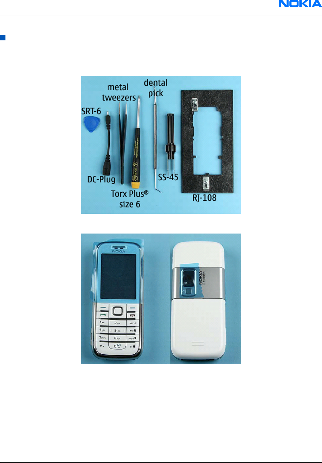
Disassembly instructions
Steps
1. You will need these tools:
2. Protect the window with a protective film.
RM-123; RM-145
Disassembly and reassembly instructions Nokia Customer Care
Issue 1 COMPANY CONFIDENTIAL Page 5 –5
Copyright © 2006 Nokia. All rights reserved.
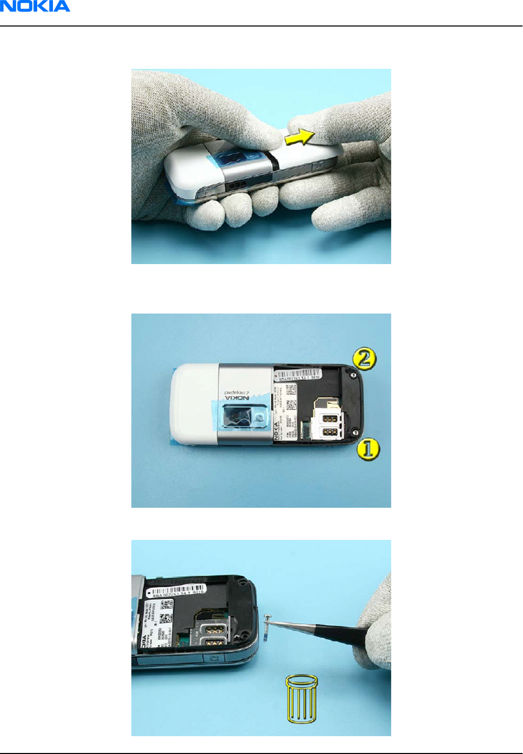
3. Open the battery cover and ensure that a battery is inserted..
4. Undo the Torx Plus size 6 screws in the shown order.
Note: For assembly, use the reverse order and a torque of 15 Ncm.
5. Discard the screws and always use new ones because of the locking compound.
RM-123; RM-145
Nokia Customer Care Disassembly and reassembly instructions
Page 5 –6 COMPANY CONFIDENTIAL Issue 1
Copyright © 2006 Nokia. All rights reserved.

6. This picture shows the position of the holding clips on the left side unit.
7. This picture shows the position of the holding clips on the right side of the unit.
8. Bring the SRT-6 exactly to the position over the (invisible) clips.
Note: A little sliding motion could be needed (like a 'credit card') when releasing the snaps. Do not
damage the edges of the A-cover.
RM-123; RM-145
Disassembly and reassembly instructions Nokia Customer Care
Issue 1 COMPANY CONFIDENTIAL Page 5 –7
Copyright © 2006 Nokia. All rights reserved.
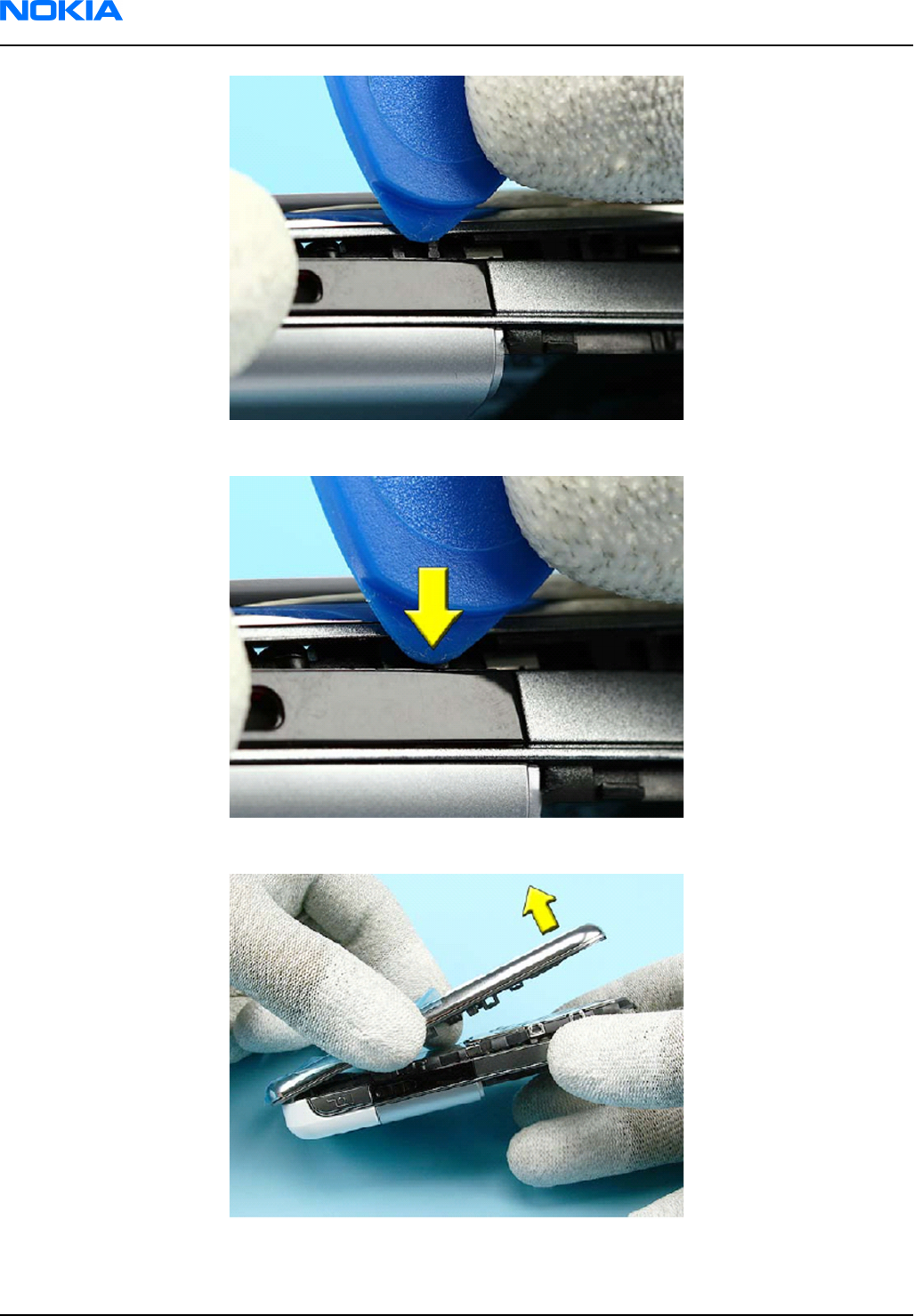
9. Stick the SRT-6 between the covers and release the four clips.
10. Remove the A-cover and protect the inner window with a protective film.
RM-123; RM-145
Nokia Customer Care Disassembly and reassembly instructions
Page 5 –8 COMPANY CONFIDENTIAL Issue 1
Copyright © 2006 Nokia. All rights reserved.
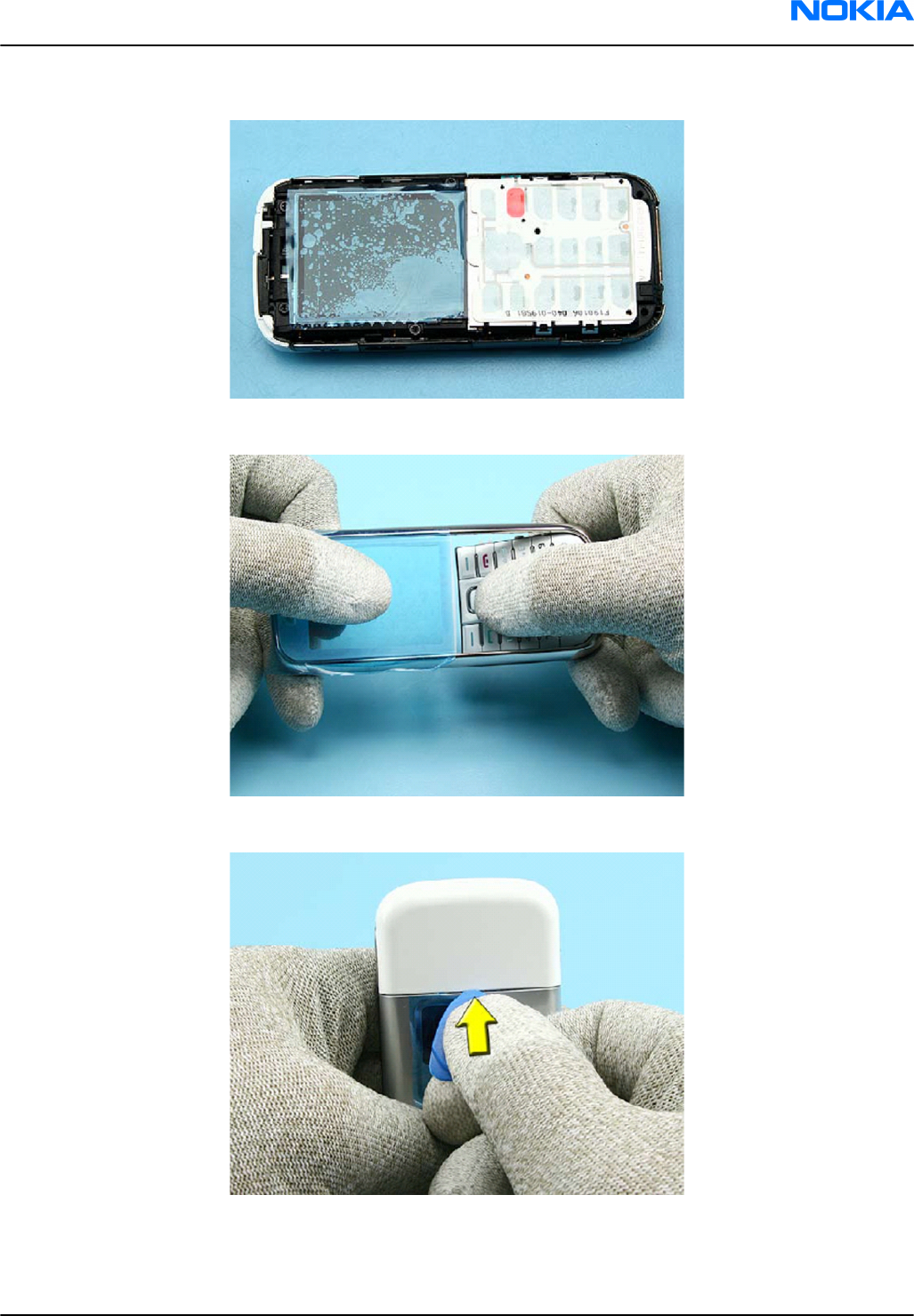
11. Protect the LCD module with a protective film.
12. Press out the keymat.
13. Stick the SRT-6 into between the top cover and the camera bezel and release the top cover.
RM-123; RM-145
Disassembly and reassembly instructions Nokia Customer Care
Issue 1 COMPANY CONFIDENTIAL Page 5 –9
Copyright © 2006 Nokia. All rights reserved.
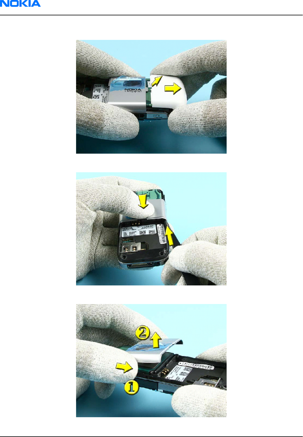
14. Now, remove the top cover.
15. To release the camera bezel, stick the closed tweezers between the camera bezel and the D-cover.
16. Now, remove the camera bezel.
RM-123; RM-145
Nokia Customer Care Disassembly and reassembly instructions
Page 5 –10 COMPANY CONFIDENTIAL Issue 1
Copyright © 2006 Nokia. All rights reserved.
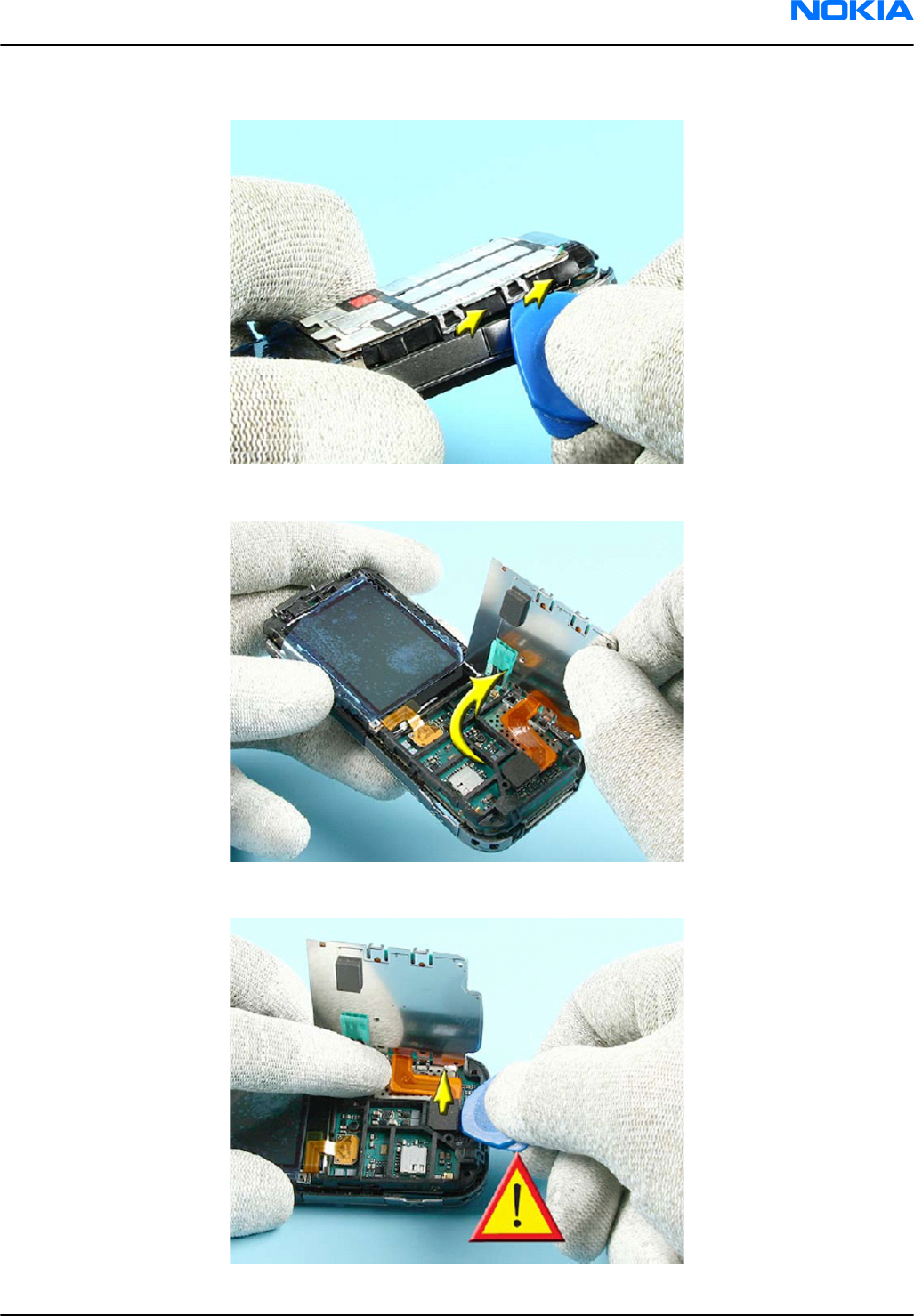
17. Unlock the four clips of the C-cover plate assy and loosen it.
18. Flip over the C-cover plate assy and pay attention to the flex foil.
19. Carefully open the flex connector with the SRT-6.
RM-123; RM-145
Disassembly and reassembly instructions Nokia Customer Care
Issue 1 COMPANY CONFIDENTIAL Page 5 –11
Copyright © 2006 Nokia. All rights reserved.
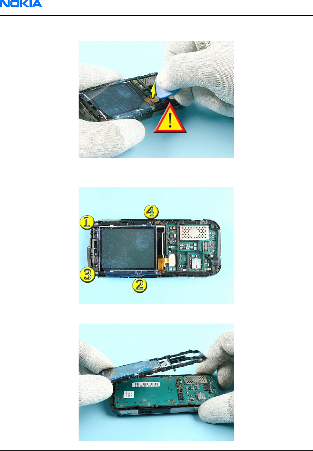
20. Now, also open the flex connector of the LCD module.
21. Open the Torx Plus size 6 screws in the shown order.
Note: For assembly, use the reverse order and a torque of 17 Ncm.
22. Take off the C-cover assy with the LCD module.
RM-123; RM-145
Nokia Customer Care Disassembly and reassembly instructions
Page 5 –12 COMPANY CONFIDENTIAL Issue 1
Copyright © 2006 Nokia. All rights reserved.
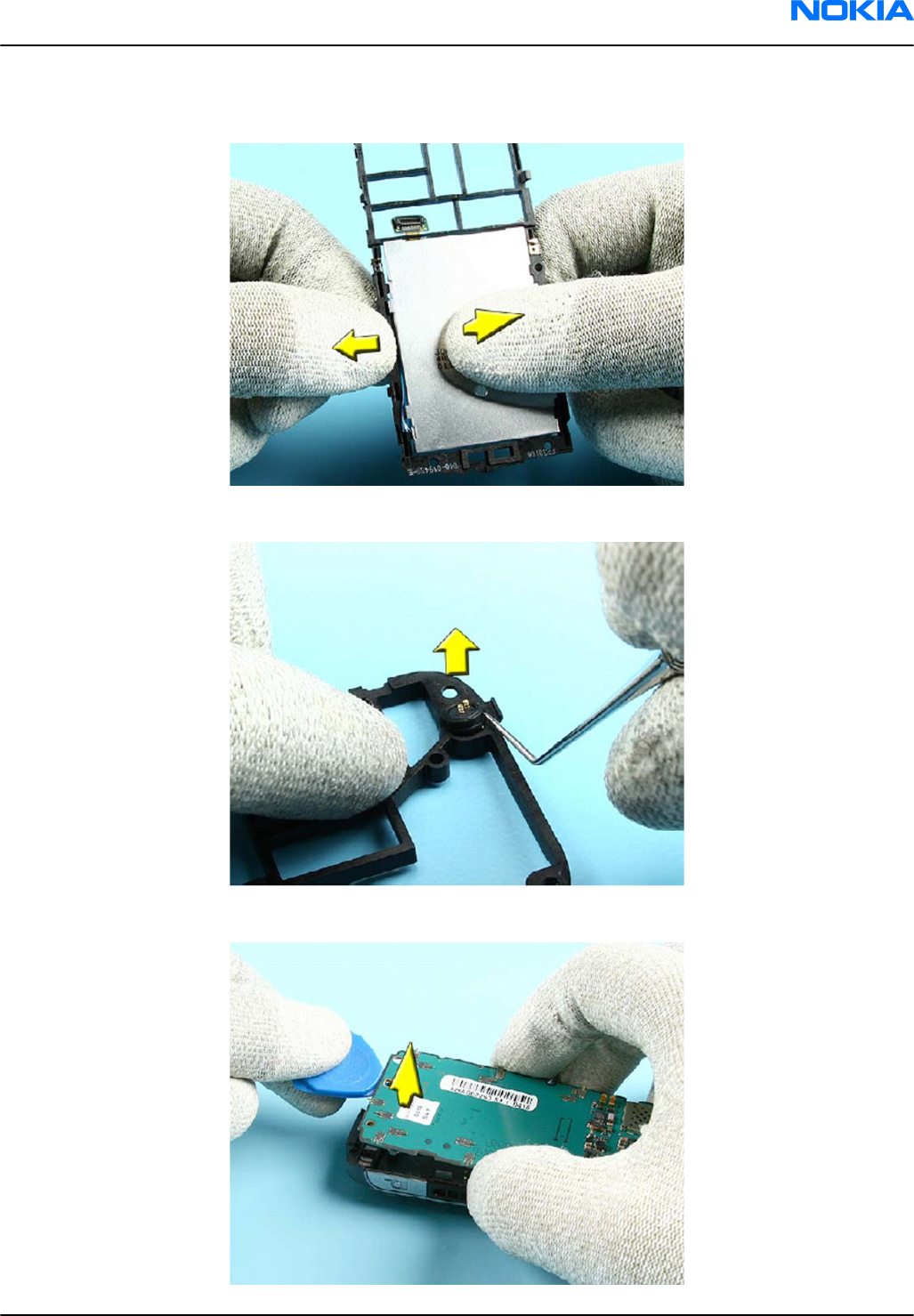
23. Release the LCD module from the C-cover assy by pushing the edges outwards first. Mind the grounding
clips.
24. Remove the microphone clapton with the dental pick.
25. Use the SRT-6 as an aid to lift out the engine module from the D-cover assy.
RM-123; RM-145
Disassembly and reassembly instructions Nokia Customer Care
Issue 1 COMPANY CONFIDENTIAL Page 5 –13
Copyright © 2006 Nokia. All rights reserved.
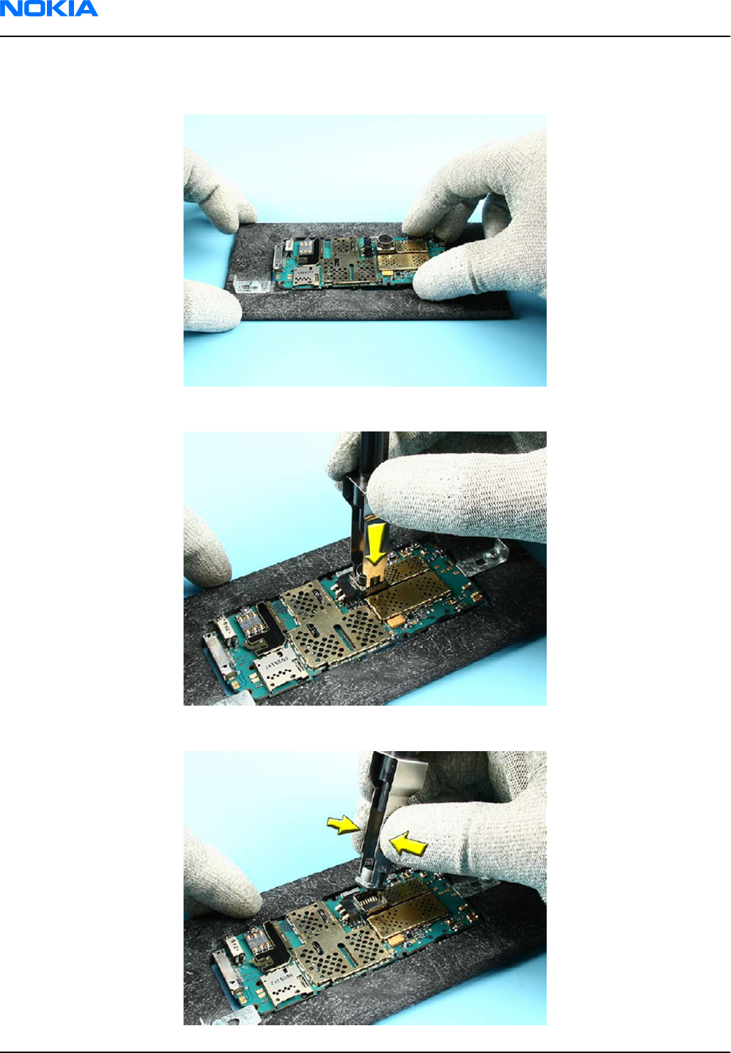
26. Use the soldering jig RJ-108 as a support when working on the camera module. This prevents damaging
or soiling the underneath spring contacts.
27. Take the SS-45 and fit it between the camera module and the shielding.
28. Press the tool and pull out the camera module.
RM-123; RM-145
Nokia Customer Care Disassembly and reassembly instructions
Page 5 –14 COMPANY CONFIDENTIAL Issue 1
Copyright © 2006 Nokia. All rights reserved.
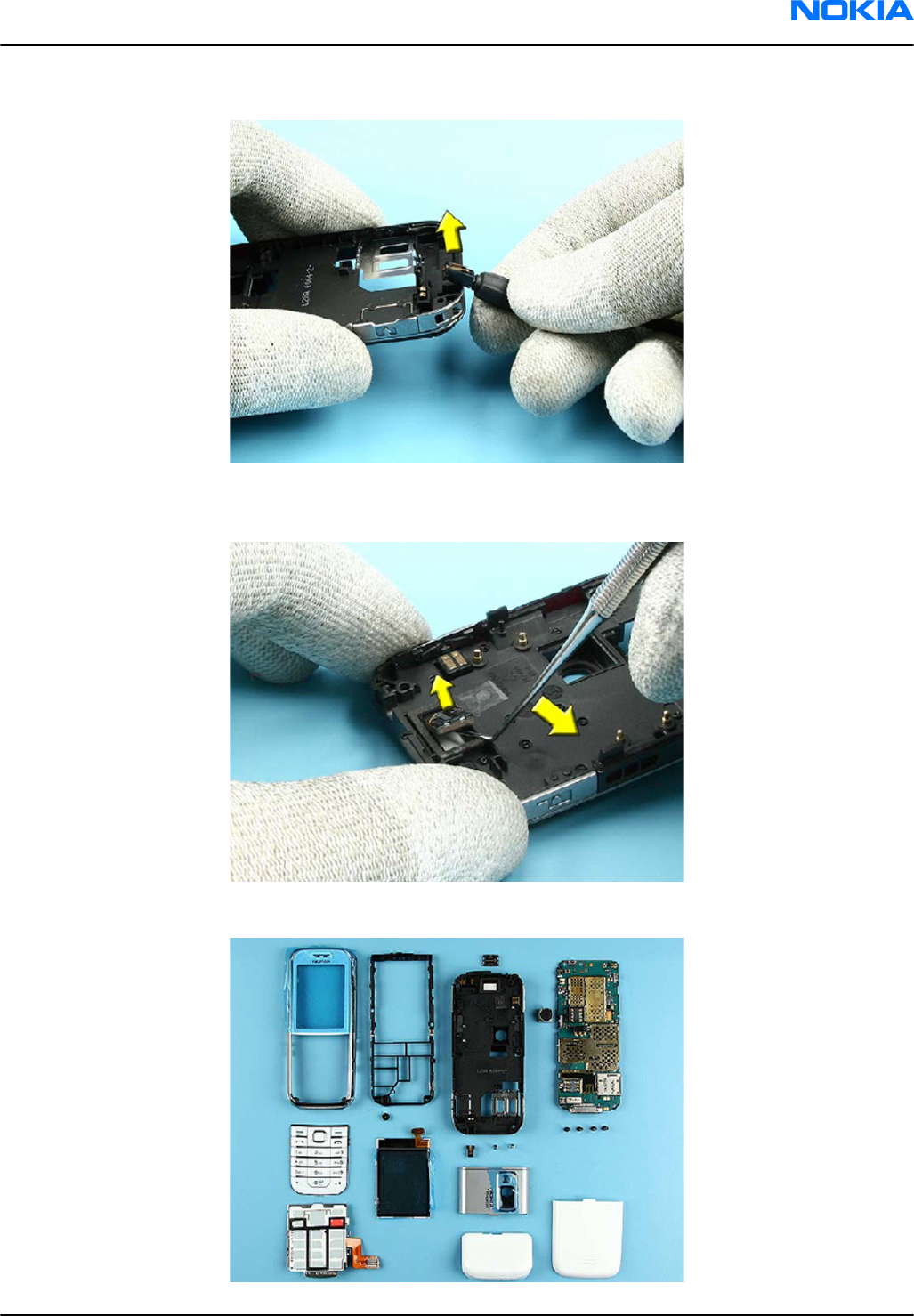
29. Remove the DC-jack with a DC-plug.
30. Carefully remove the earpiece with a dental tool. Always use a new adhesive tape when replacing
the earpiece.
31. The disassembly procedure is now finished.
RM-123; RM-145
Disassembly and reassembly instructions Nokia Customer Care
Issue 1 COMPANY CONFIDENTIAL Page 5 –15
Copyright © 2006 Nokia. All rights reserved.

Reassembly instructions
Steps
1. Follow the disassembly instructions
in reversed order
.
Note: Pay special attention to step 21 and step 4!
RM-123; RM-145
Nokia Customer Care Disassembly and reassembly instructions
Page 5 –16 COMPANY CONFIDENTIAL Issue 1
Copyright © 2006 Nokia. All rights reserved.

6 — BB Troubleshooting and
Manual Tuning Guide
Nokia Customer Care
Issue 1 COMPANY CONFIDENTIAL Page 6 –1
Copyright © 2006 Nokia. All rights reserved.

RM-123; RM-145
Nokia Customer Care BB Troubleshooting and Manual Tuning Guide
(This page left intentionally blank.)
Page 6 –2 COMPANY CONFIDENTIAL Issue 1
Copyright © 2006 Nokia. All rights reserved.

Table of Contents
Troubleshooting overview....................................................................................................................................6–5
Power and charging troubleshooting..................................................................................................................6–6
Dead or jammed device troubleshooting.......................................................................................................6–6
General power checking...................................................................................................................................6–8
Golden eye troubleshooting.............................................................................................................................6–9
Charging troubleshooting..............................................................................................................................6–10
Interface troubleshooting...................................................................................................................................6–11
Flash programming fault troubleshooting...................................................................................................6–11
CMT SDRAM memory troubleshooting...........................................................................................................6–13
CMT NOR flash fault troubleshooting............................................................................................................6–14
SD card troubleshooting.................................................................................................................................6–15
USB interface troubleshooting.......................................................................................................................6–17
SIM card troubleshooting...............................................................................................................................6–19
User interface troubleshooting...........................................................................................................................6–21
Power key troubleshooting............................................................................................................................6–21
Key troubleshooting.......................................................................................................................................6–21
Display module troubleshooting...................................................................................................................6–22
General instructions for display troubleshooting...................................................................................6–22
Display troubleshooting............................................................................................................................6–25
Display and top keyboard backlight troubleshooting............................................................................6–26
Main keyboard backlight troubleshooting..............................................................................................6–26
Camera module troubleshooting........................................................................................................................6–27
Introduction to camera troubleshooting.....................................................................................................6–27
Taking and evaluating test pictures..............................................................................................................6–27
Camera hardware failure message troubleshooting...................................................................................6–28
Camera baseband HW troubleshooting........................................................................................................6–29
Camera viewfinder troubleshooting.............................................................................................................6–30
Bad camera image quality troubleshooting.................................................................................................6–31
Audio troubleshooting.........................................................................................................................................6–32
Audio troubleshooting test instructions......................................................................................................6–32
Internal earpiece troubleshooting................................................................................................................6–36
Internal microphone troubleshooting..........................................................................................................6–37
IHF troubleshooting........................................................................................................................................6–38
External microphone troubleshooting..........................................................................................................6–39
External earpiece troubleshooting................................................................................................................6–40
Vibra troubleshooting....................................................................................................................................6–41
Baseband manual tuning guide.........................................................................................................................6–41
Certificate restoring for BB5.0 products.......................................................................................................6–41
Energy management calibration...................................................................................................................6–47
List of Tables
Table 13 Display module troubleshooting cases..............................................................................................6–23
Table 14 Pixel defects..........................................................................................................................................6–23
Table 15 Calibration value limits........................................................................................................................6–47
List of Figures
Figure 37 Flashing pic 1. Take single trig measurement for the rise of the BSI signal.................................6–12
Figure 38 Flashing pic 2. Take single trig measurement for the rise of the BSI signal.................................6–13
RM-123; RM-145
BB Troubleshooting and Manual Tuning Guide Nokia Customer Care
Issue 1 COMPANY CONFIDENTIAL Page 6 –3
Copyright © 2006 Nokia. All rights reserved.

Figure 39 NOR CLK from J3004............................................................................................................................6–14
Figure 40 SD card initialization from pin J3206................................................................................................6–16
Figure 41 USB 1: D-TXD (PopPort TM pin 6) and D+RXD (PopPort TM pin 7) voltage levels when USB is
connected...................................................................................................................................................6–18
Figure 42 SIM interface signals...........................................................................................................................6–19
Figure 43 Single-ended output waveform of the Ext_in_HP_out measurement when earpiece is
connected...................................................................................................................................................6–34
Figure 44 Differential output waveform of the Ext_in_IHF_out out loop measurement when speaker is
connected...................................................................................................................................................6–34
Figure 45 Single-ended output waveform of the HP_in_Ext_out loop when microphone is connected....
6–35
RM-123; RM-145
Nokia Customer Care BB Troubleshooting and Manual Tuning Guide
Page 6 –4 COMPANY CONFIDENTIAL Issue 1
Copyright © 2006 Nokia. All rights reserved.
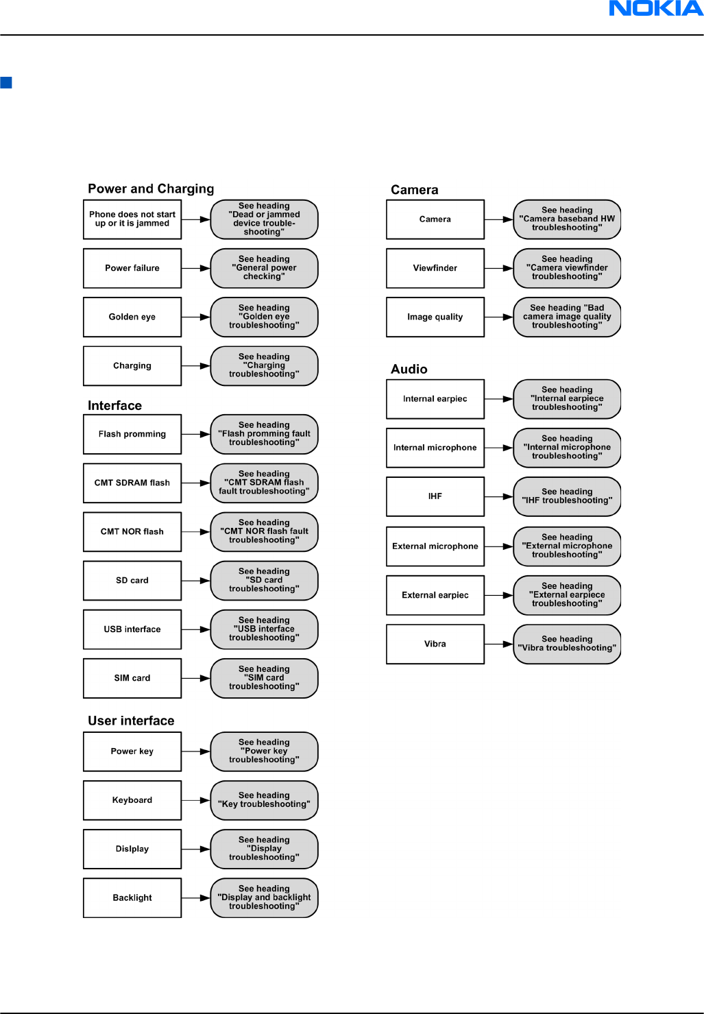
Troubleshooting overview
For practical reasons, troubleshooting is divided into two sections;
• Baseband troubleshooting, including camera
• RF troubleshooting, including FM radio and Bluetooth
RM-123; RM-145
BB Troubleshooting and Manual Tuning Guide Nokia Customer Care
Issue 1 COMPANY CONFIDENTIAL Page 6 –5
Copyright © 2006 Nokia. All rights reserved.
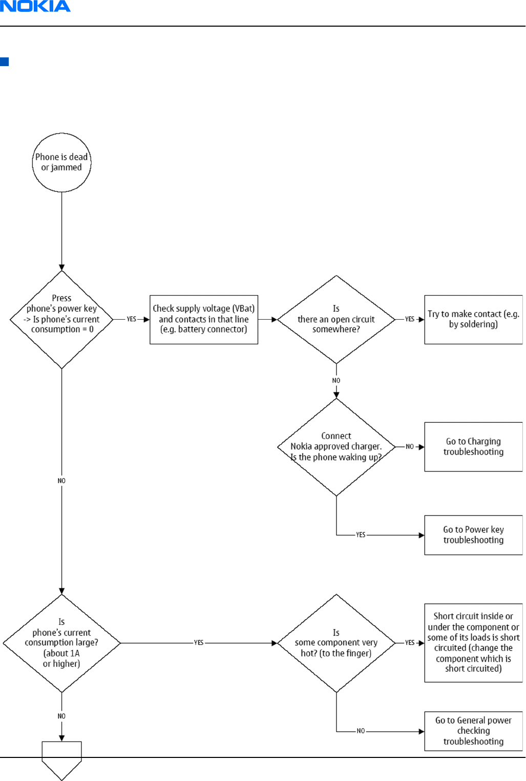
Power and charging troubleshooting
Dead or jammed device troubleshooting
Troubleshooting flow
RM-123; RM-145
Nokia Customer Care BB Troubleshooting and Manual Tuning Guide
Page 6 –6 COMPANY CONFIDENTIAL Issue 1
Copyright © 2006 Nokia. All rights reserved.
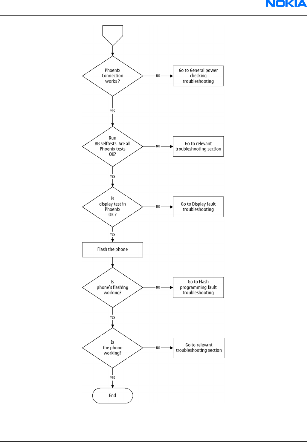
RM-123; RM-145
BB Troubleshooting and Manual Tuning Guide Nokia Customer Care
Issue 1 COMPANY CONFIDENTIAL Page 6 –7
Copyright © 2006 Nokia. All rights reserved.
General power checking
Voltages
Check the following voltages:
Signal
Rename Regulator Sleep Idle Nominal
voltage Main user Notes
VIO RETU ON ON 1.82 Memory, I/Os,
IrDA, Display
VBACK RETU ON ON 2.5 Back-up
battery
VSIM1 RETU ON ON 1.8/3.0 SIM card
VSIM2 RETU OFF OFF 3.0 Keyboard
backlight
EL-foil driver
VDRAM RETU ON ON 1.82 SDRAM
VAUX RETU OFF OFF 2.5 IrDA IrDA active
VANA RETU ON ON 2.5 Audio, some
pull-ups
VR1 RETU OFF ON 2.5 Crystal
oscillators
VRFC RETU OFF ON 1.8 RAP3G
converters
VRCP1 RETU 4.5 To RF parts RF active
VRCP2 RETU 4.5 To RF parts RF active
VREF RETU ON ON 1.35 RF reference
VCORE TAHVO ON ON 1.4 RAP3G digital
VOUT TAHVO OFF OFF 2.5 Accessory
connected
VCAM_2V8 LP3987ITLX-2.
85/N1060
OFF OFF 2.85 Camera Camera ON
VCAM_1V8 LM3671TLX-1.
82/N1080
OFF OFF 1.8 Camera Camera ON
VCAM_1V5 TPS62311YZD
R/N1050
OFF OFF 1.5 Camera Camera ON
2V8_FM_LCD LP3985ITLX-2.
85/N6050
ON ON 2.85 FM, LCD, Hall
sensor
VMMC LP3928TLX-18
28/N3200
OFF OFF 3.0 MCC card
LCD_LED_OUT 4w_LED_DRIVE
R
OFF OFF LCD Backlight
RM-123; RM-145
Nokia Customer Care BB Troubleshooting and Manual Tuning Guide
Page 6 –8 COMPANY CONFIDENTIAL Issue 1
Copyright © 2006 Nokia. All rights reserved.

Golden eye troubleshooting
Context
Golden eye is placed under a non removable shield and cannot be replaced.
Please swap the board.
RM-123; RM-145
BB Troubleshooting and Manual Tuning Guide Nokia Customer Care
Issue 1 COMPANY CONFIDENTIAL Page 6 –9
Copyright © 2006 Nokia. All rights reserved.
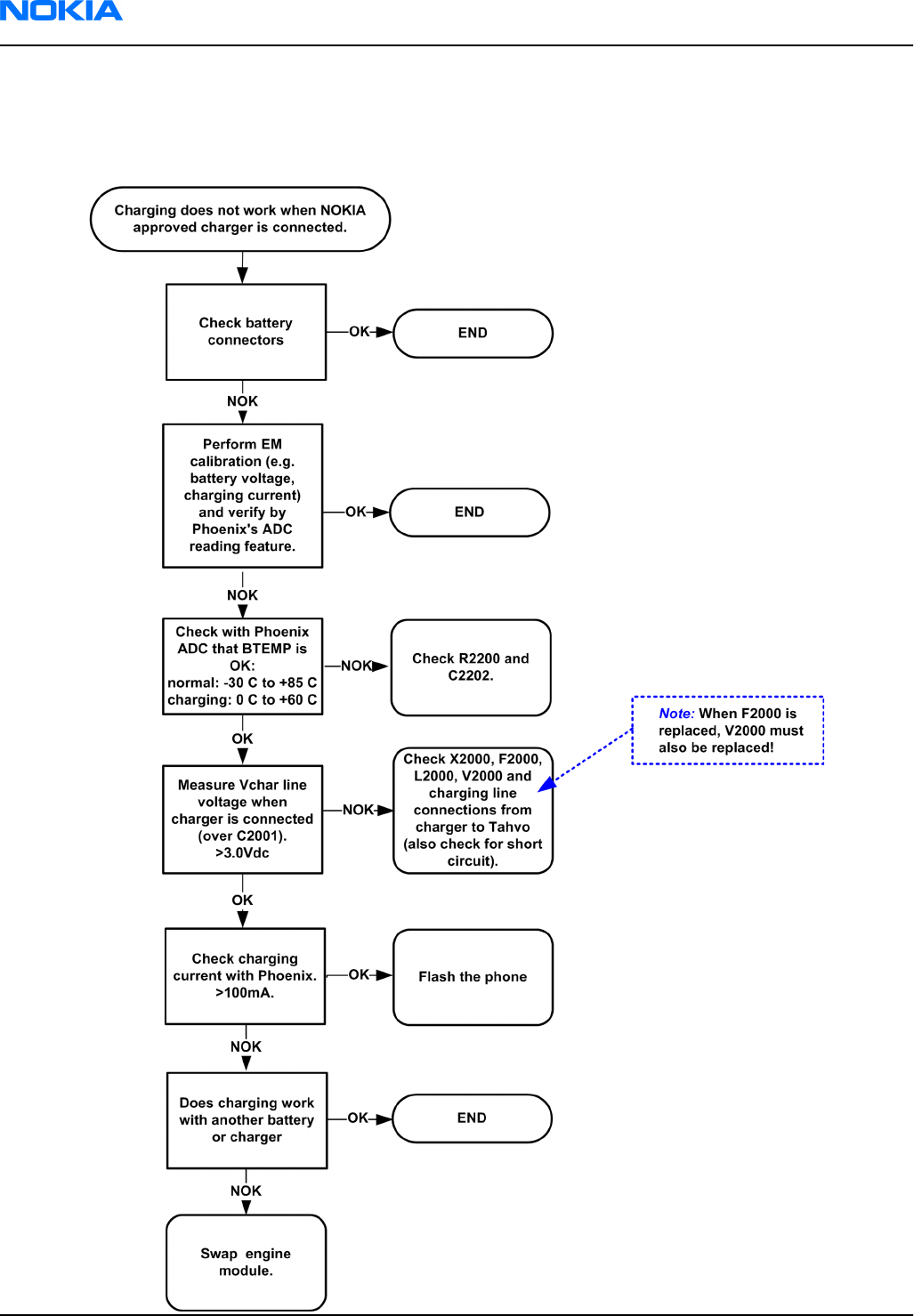
Charging troubleshooting
Troubleshooting flow
RM-123; RM-145
Nokia Customer Care BB Troubleshooting and Manual Tuning Guide
Page 6 –10 COMPANY CONFIDENTIAL Issue 1
Copyright © 2006 Nokia. All rights reserved.
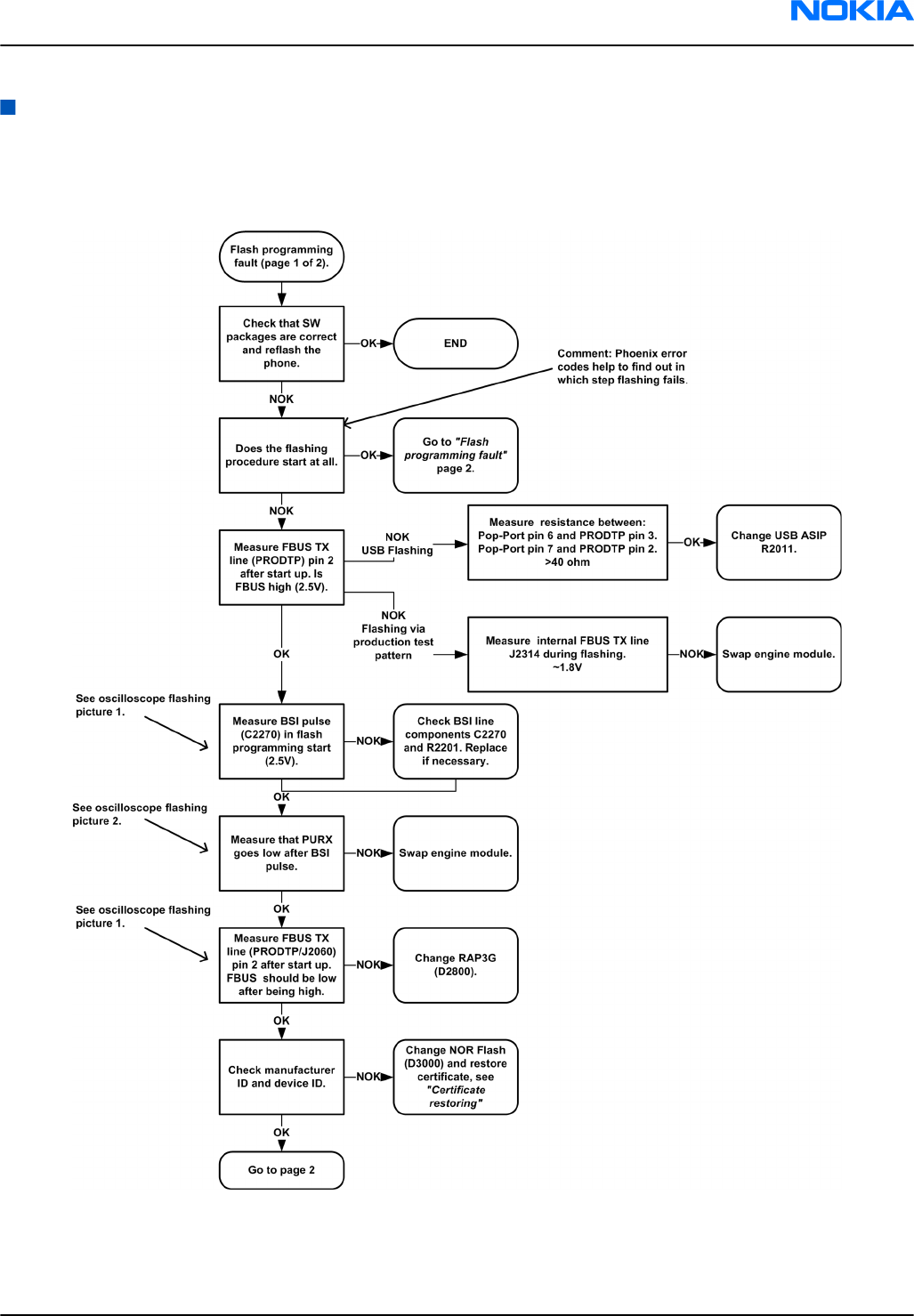
Interface troubleshooting
Flash programming fault troubleshooting
Part 1
RM-123; RM-145
BB Troubleshooting and Manual Tuning Guide Nokia Customer Care
Issue 1 COMPANY CONFIDENTIAL Page 6 –11
Copyright © 2006 Nokia. All rights reserved.
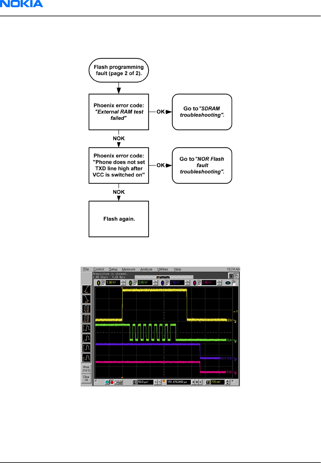
Part 2
Figure 37 Flashing pic 1. Take single trig measurement for the rise of the BSI signal.
RM-123; RM-145
Nokia Customer Care BB Troubleshooting and Manual Tuning Guide
Page 6 –12 COMPANY CONFIDENTIAL Issue 1
Copyright © 2006 Nokia. All rights reserved.
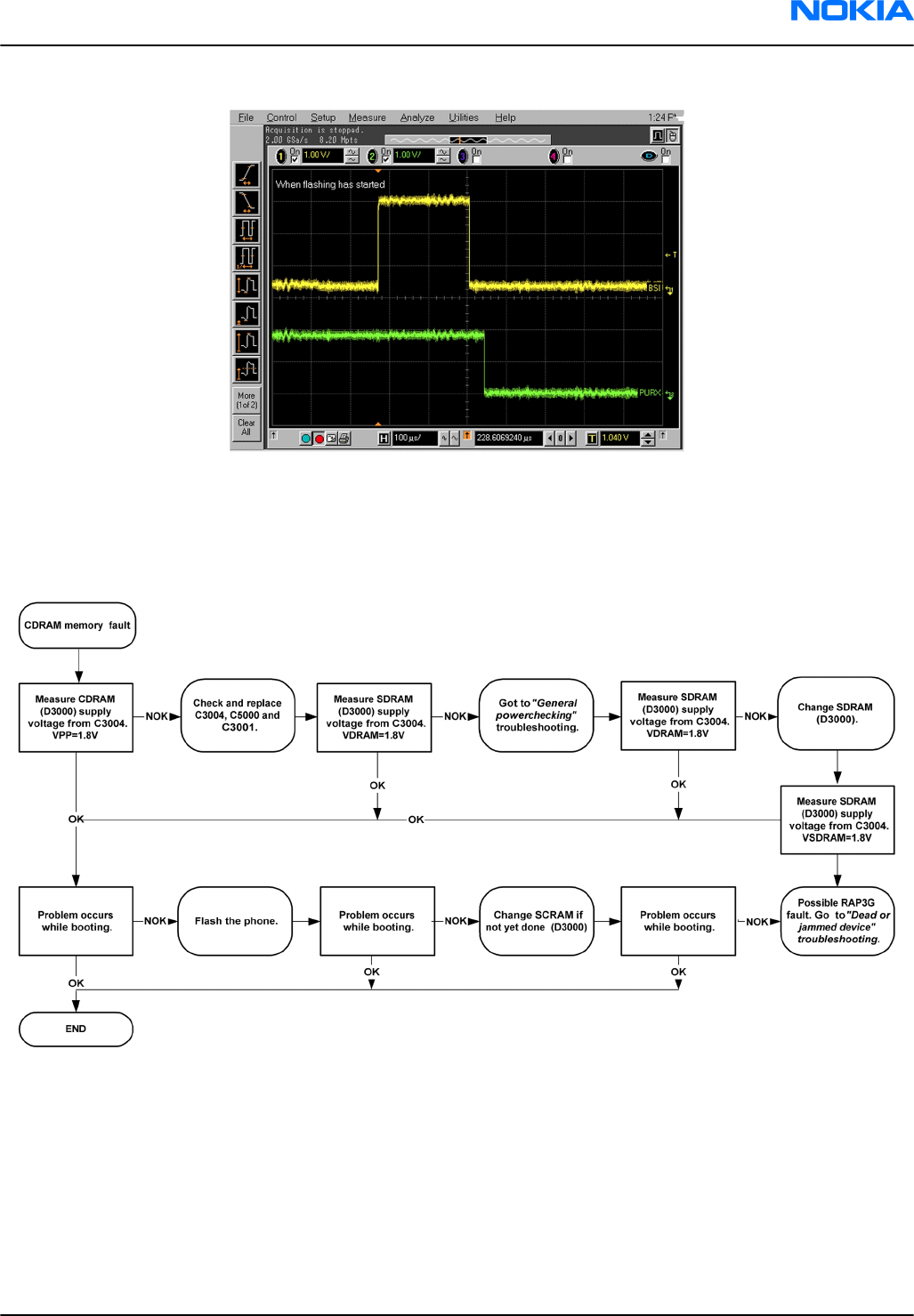
Figure 38 Flashing pic 2. Take single trig measurement for the rise of the BSI signal.
CMT SDRAM memory troubleshooting
Troubleshooting flow
RM-123; RM-145
BB Troubleshooting and Manual Tuning Guide Nokia Customer Care
Issue 1 COMPANY CONFIDENTIAL Page 6 –13
Copyright © 2006 Nokia. All rights reserved.
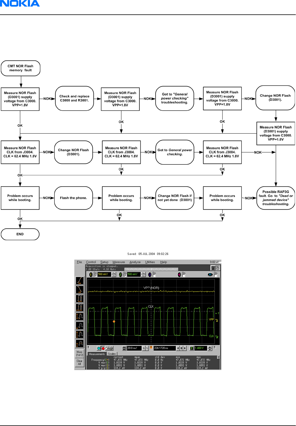
CMT NOR flash fault troubleshooting
Troubleshooting flow
Figure 39 NOR CLK from J3004
RM-123; RM-145
Nokia Customer Care BB Troubleshooting and Manual Tuning Guide
Page 6 –14 COMPANY CONFIDENTIAL Issue 1
Copyright © 2006 Nokia. All rights reserved.
SD card troubleshooting
Troubleshooting flow
RM-123; RM-145
BB Troubleshooting and Manual Tuning Guide Nokia Customer Care
Issue 1 COMPANY CONFIDENTIAL Page 6 –15
Copyright © 2006 Nokia. All rights reserved.
Take single trig measurement on the rising edge of the DAT signal.
Figure 40 SD card initialization from pin J3206
RM-123; RM-145
Nokia Customer Care BB Troubleshooting and Manual Tuning Guide
Page 6 –16 COMPANY CONFIDENTIAL Issue 1
Copyright © 2006 Nokia. All rights reserved.
USB interface troubleshooting
Troubleshooting flow
RM-123; RM-145
BB Troubleshooting and Manual Tuning Guide Nokia Customer Care
Issue 1 COMPANY CONFIDENTIAL Page 6 –17
Copyright © 2006 Nokia. All rights reserved.
Figure 41 USB 1: D-TXD (PopPort TM™ pin 6) and D+RXD (PopPort TM™ pin 7) voltage levels when USB is connected.
RM-123; RM-145
Nokia Customer Care BB Troubleshooting and Manual Tuning Guide
Page 6 –18 COMPANY CONFIDENTIAL Issue 1
Copyright © 2006 Nokia. All rights reserved.
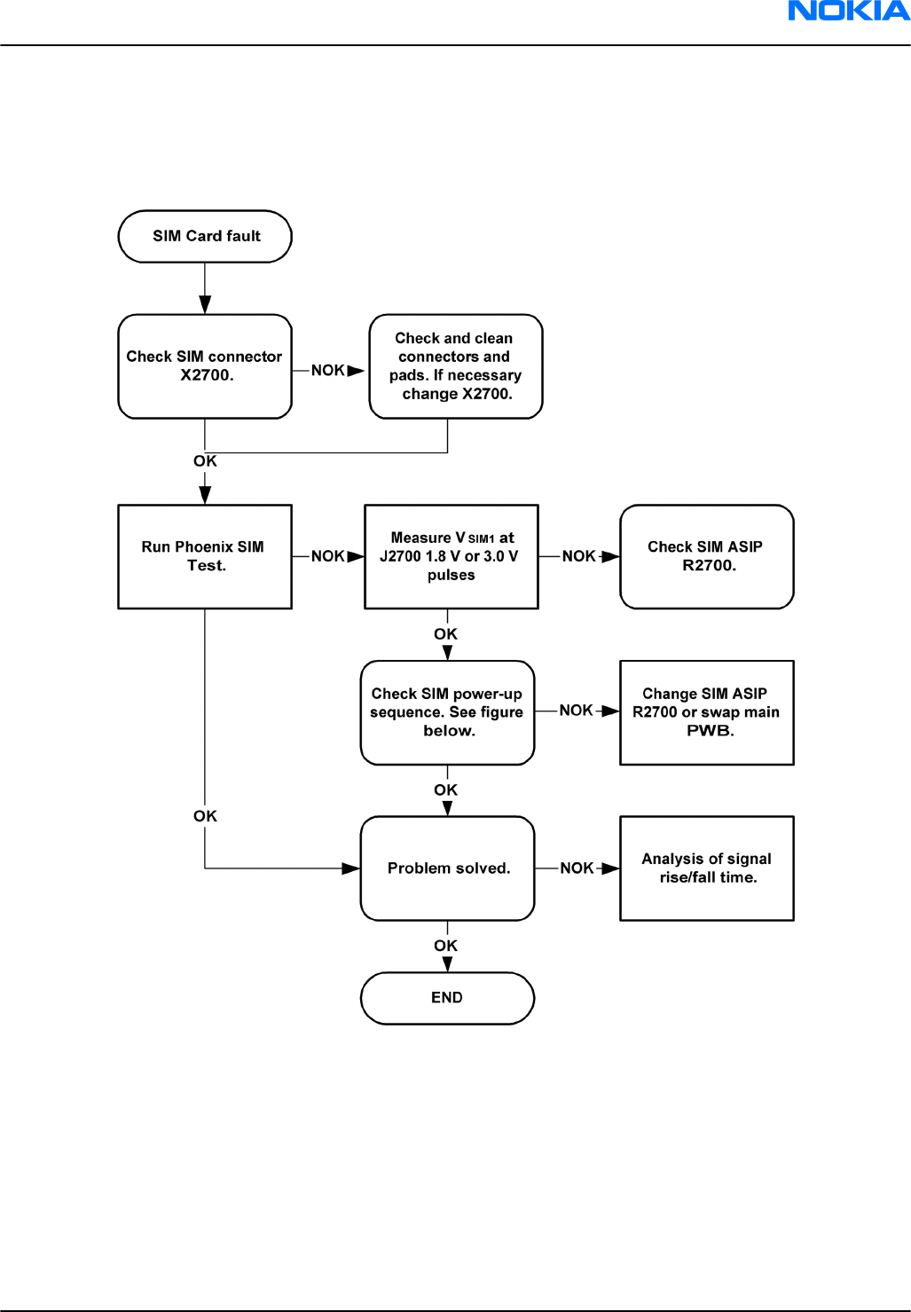
SIM card troubleshooting
Troubleshooting flow
RM-123; RM-145
BB Troubleshooting and Manual Tuning Guide Nokia Customer Care
Issue 1 COMPANY CONFIDENTIAL Page 6 –19
Copyright © 2006 Nokia. All rights reserved.
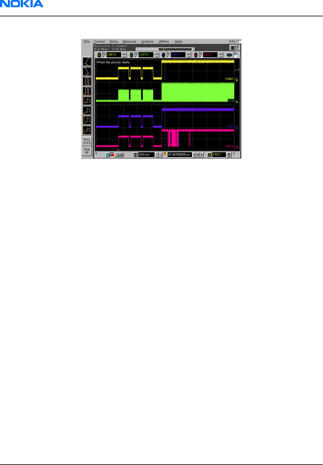
SIM CLK frequency = 3.2MHz (Take single triggered measurement in boot on the VSIM1 line).
Figure 42 SIM interface signals
RM-123; RM-145
Nokia Customer Care BB Troubleshooting and Manual Tuning Guide
Page 6 –20 COMPANY CONFIDENTIAL Issue 1
Copyright © 2006 Nokia. All rights reserved.
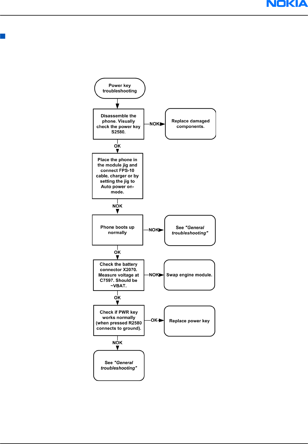
User interface troubleshooting
Power key troubleshooting
Troubleshooting flow
Key troubleshooting
Context
There are two possible failure modes in the keyboard module:
RM-123; RM-145
BB Troubleshooting and Manual Tuning Guide Nokia Customer Care
Issue 1 COMPANY CONFIDENTIAL Page 6 –21
Copyright © 2006 Nokia. All rights reserved.
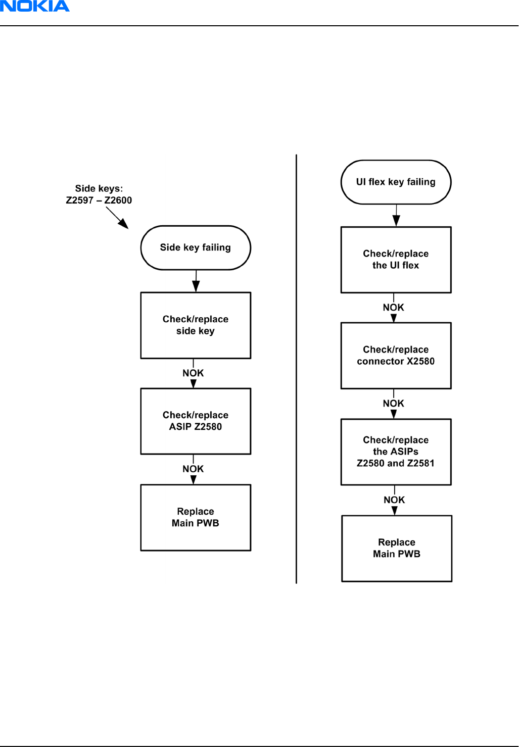
•One or more keys are stuck, so that the key does not react when a keydome or a side key is pressed. This
kind of failure is caused by mechanical reasons (dirt, rust, mechanical damage, etc.)
•Malfunction of several keys at the same time; this happens when one or more rows or columns in the key
matrix are failing (shortcut or open connection).
If the failure mode is not clear, start with the Keyboard test in Phoenix.
Troubleshooting flow
Display module troubleshooting
General instructions for display troubleshooting
Context
• The display is in a normal mode when the phone is in active use.
• Display is in a partial idle mode when the phone is in the screen saver mode.
• The operating modes of the display can be controlled with the help of
Phoenix
.
RM-123; RM-145
Nokia Customer Care BB Troubleshooting and Manual Tuning Guide
Page 6 –22 COMPANY CONFIDENTIAL Issue 1
Copyright © 2006 Nokia. All rights reserved.

Table 13 Display module troubleshooting cases
Display blank There is no image on the display. The display looks
the same when the phone is on as it does when the
phone is off. The backlight can be on in some cases.
Image on the display not correct Image on the display can be corrupted or a part of
the image can be missing. If a part of the image is
missing, change the display module. If the image is
otherwise corrupted, follow the appropriate
troubleshooting diagram.
Backlight dim or not working at all Backlight LED components are inside the display
module. Backlight failure can also be in the
connector or in the backlight power source in the
main engine of the phone.
This means that in case the display is working
(image OK), the backlight is faulty.
Visual defects (pixel) Pixel defects can be checked by controlling the
display with Phoenix. Use both colours, black and
white, on a full screen.
The display may have some random pixel defects
that are acceptable for this type of display. The
criteria when pixel defects are regarded as a display
failure, resulting in a replacement of the display, are
presented the following table.
Table 14 Pixel defects
Item White dot defect Black dot
defect Total
1Defect
counts
R G B White
Dot
Total
1 1
1 1 1 1
2 Combine
d defect
counts
Not allowed.
Two single dot defects that are within 5 mm of each other should
be interpreted as combined dot defect.
Steps
1. Verify with a working display that the fault is not on the display module itself.
The display module cannot be repaired.
2. Check that the cellular engine is working normally.
i To check the functionality, connect the phone to a docking station.
ii Start
Phoenix
service software.
iii Read the phone information to check that also the application engine is functioning normally (you
should be able to read the APE ID).
RM-123; RM-145
BB Troubleshooting and Manual Tuning Guide Nokia Customer Care
Issue 1 COMPANY CONFIDENTIAL Page 6 –23
Copyright © 2006 Nokia. All rights reserved.

3. Proceed to the display troubleshooting flowcharts.
Use the Display Test tool in
Phoenix
to find the detailed fault mode.
RM-123; RM-145
Nokia Customer Care BB Troubleshooting and Manual Tuning Guide
Page 6 –24 COMPANY CONFIDENTIAL Issue 1
Copyright © 2006 Nokia. All rights reserved.
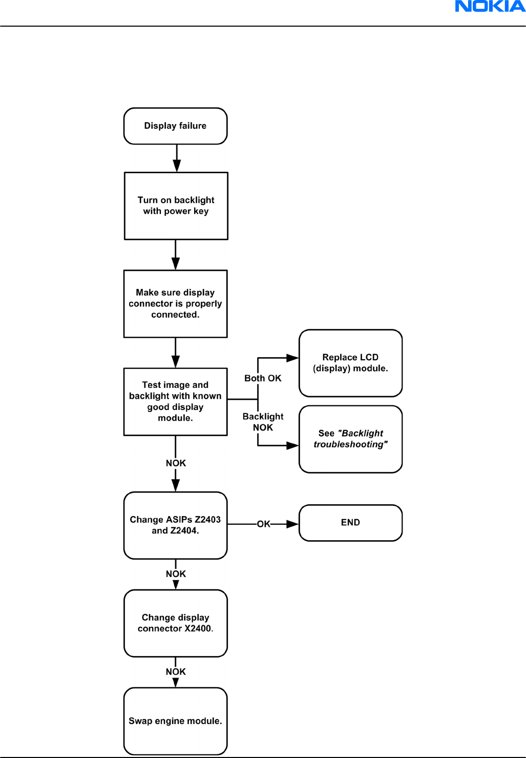
Display troubleshooting
Troubleshooting flow
RM-123; RM-145
BB Troubleshooting and Manual Tuning Guide Nokia Customer Care
Issue 1 COMPANY CONFIDENTIAL Page 6 –25
Copyright © 2006 Nokia. All rights reserved.
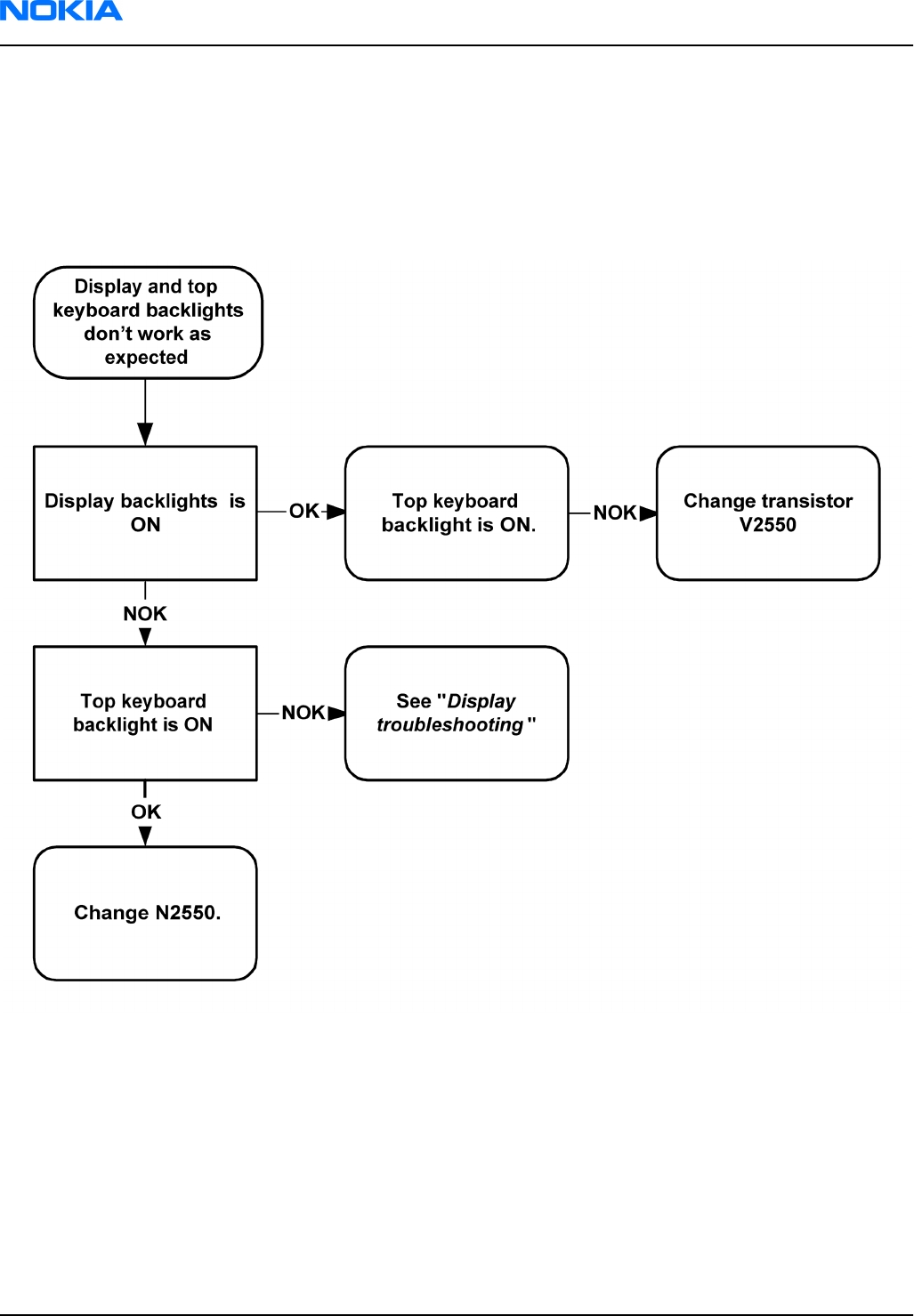
Display and top keyboard backlight troubleshooting
Context
The device has one LED driver that provides current for both display and keyboard backlights.
Troubleshooting flow
Main keyboard backlight troubleshooting
Context
The device has one LED driver that provides current for the main keyboard backlights.
RM-123; RM-145
Nokia Customer Care BB Troubleshooting and Manual Tuning Guide
Page 6 –26 COMPANY CONFIDENTIAL Issue 1
Copyright © 2006 Nokia. All rights reserved.
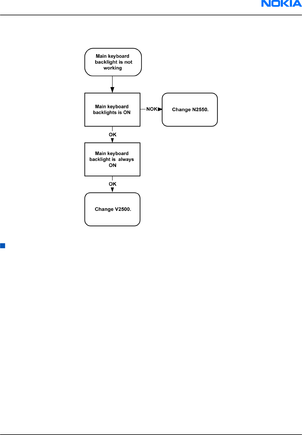
Troubleshooting flow
Camera module troubleshooting
Introduction to camera troubleshooting
Bad conditions often cause bad pictures. Therefore, the camera operation has to be checked in constant
conditions or by using a second, known-to-be-good Nokia device as reference. Image quality is hard to
measure quantitatively, and the difference between a good and a bad picture can be small. Some training
or experience may be needed to detect what is actually wrong.
When checking for possible errors in camera functionality, knowing what error is suspected significantly
helps the testing by narrowing down the amount of test cases. The following types of image quality problems
are common:
• Dust (black spots)
• Lack of sharpness
• Bit errors
Taking and evaluating test pictures
When
taking
a test picture, remember the following:
• Avoid bright fluorescent light, 50/60Hz electrical network or high artificial illumination levels
• If the phone is hot, let it rest for a while before taking the picture
• Make sure the optical system is clean
• Use highest possible resolution
• Make sure the light is suffiecient (bright office lightning)
RM-123; RM-145
BB Troubleshooting and Manual Tuning Guide Nokia Customer Care
Issue 1 COMPANY CONFIDENTIAL Page 6 –27
Copyright © 2006 Nokia. All rights reserved.
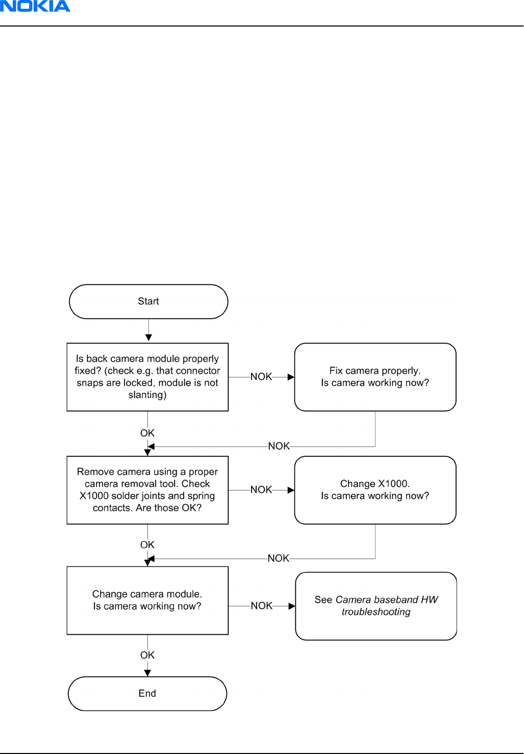
• Do not take the picture towards light source
• Be as still as possible when taking the picture
• Distance should be at least 40cm, 1-2m is recommended
When
evaluating
a test picture, remember the following:
• The center of the picture is sharper than the edges
• The image may be blurred, though it does not show in the viewfinder
• Analyse the picture from your PC monitor, full colour setting is recommended
• If possible, compare with a picture of the same motive taken with a similar Nokia device
Camera hardware failure message troubleshooting
Context
If you get a hardware failure message when using the camera, follow the next troubleshooting flowchart.
Troubleshooting flow
Note: Make sure that the phone has the latest software before continuing.
RM-123; RM-145
Nokia Customer Care BB Troubleshooting and Manual Tuning Guide
Page 6 –28 COMPANY CONFIDENTIAL Issue 1
Copyright © 2006 Nokia. All rights reserved.
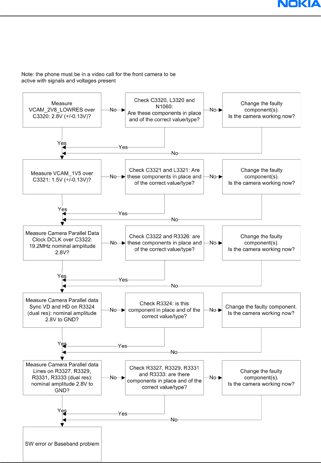
Camera baseband HW troubleshooting
Troubleshooting flow
RM-123; RM-145
BB Troubleshooting and Manual Tuning Guide Nokia Customer Care
Issue 1 COMPANY CONFIDENTIAL Page 6 –29
Copyright © 2006 Nokia. All rights reserved.
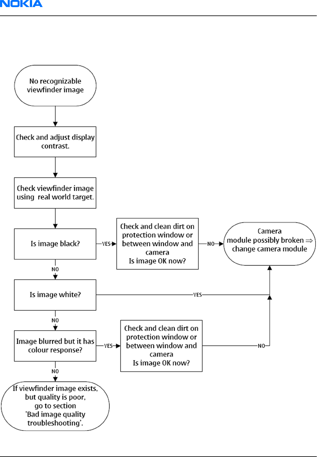
Camera viewfinder troubleshooting
Troubleshooting flow
RM-123; RM-145
Nokia Customer Care BB Troubleshooting and Manual Tuning Guide
Page 6 –30 COMPANY CONFIDENTIAL Issue 1
Copyright © 2006 Nokia. All rights reserved.
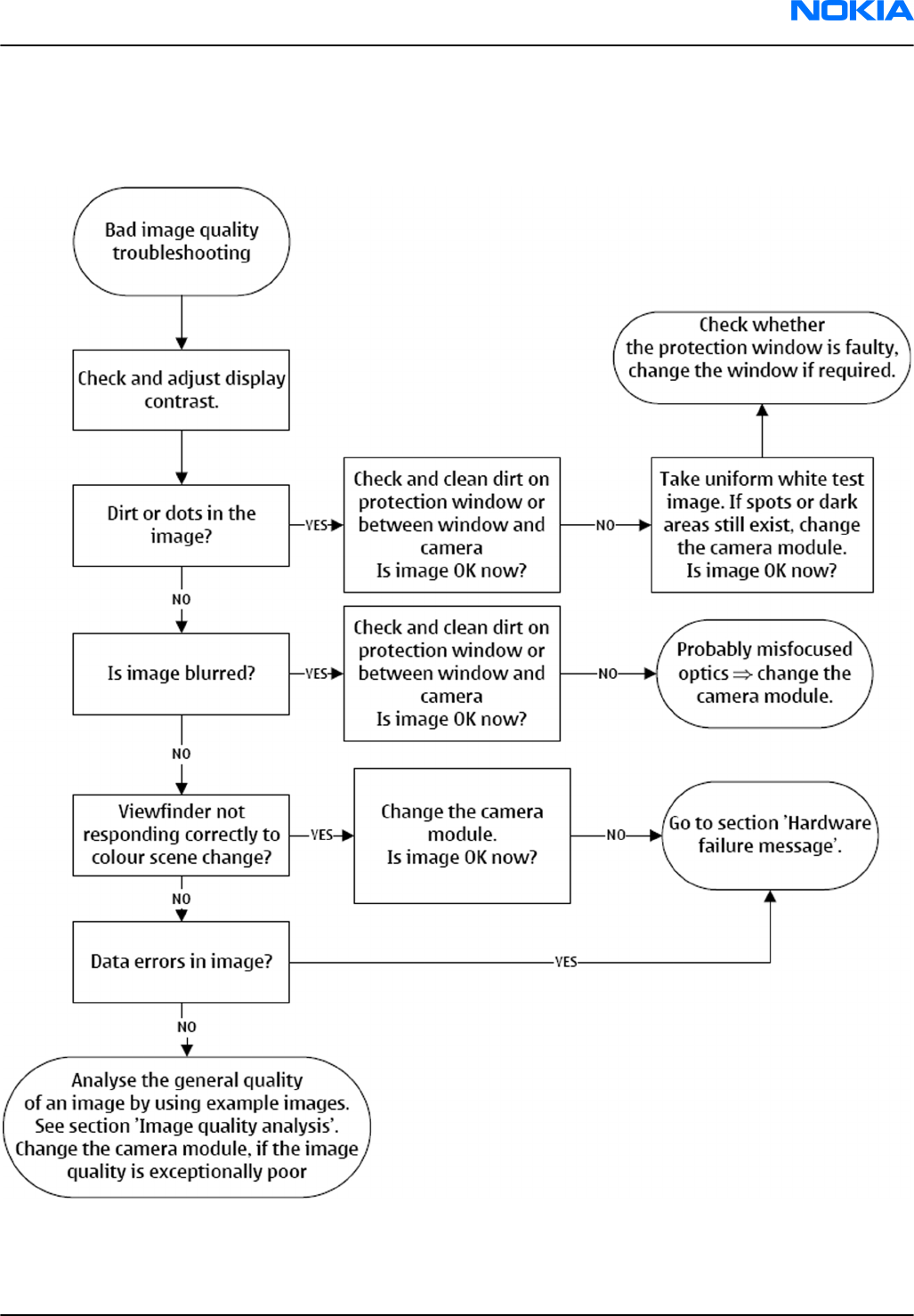
Bad camera image quality troubleshooting
Troubleshooting flow
RM-123; RM-145
BB Troubleshooting and Manual Tuning Guide Nokia Customer Care
Issue 1 COMPANY CONFIDENTIAL Page 6 –31
Copyright © 2006 Nokia. All rights reserved.

Audio troubleshooting
Audio troubleshooting test instructions
Differential external earpiece and internal earpiece outputs can be measured either with a single-ended or
a differential probe.
When measuring with a single-ended probe each output is measured against the ground.
Internal handsfree output is measured using a current probe, if a special low-pass filter designed for
measuring a digital amplifier is not available. Note also that when using a current probe, the input signal
frequency must be set to 2kHz.
The input signal for each loop test can be either single-ended or differential.
Required equipment
The following equipment is needed for the tests:
• Oscilloscope
• Function generator (sine waveform)
• 'Active speaker' or 'speaker and power amplifier'
• Sound level meter
• Current probe (Internal handsfree DPMA output measurement)
• Phoenix service software
• Battery voltage 3.7V
Test procedure
Audio can be tested using the Phoenix audio routings option. Three different audio loop paths can be
activated:
• External microphone to Internal earpiece
• External microphone to Internal handsfree speaker
• Internal microphone to External earpiece
Each audio loop sets routing from the specified input to the specified output enabling a quick in-out test.
Loop path gains are fixed and they cannot be changed using Phoenix. Correct pins and signals for each test
are presented in the following table.
Phoenix audio loop tests and test results
The results presented in the table apply when no accessory is connected and battery voltage is set to 3.7V.
Earpiece, internal microphone and speaker are in place during measurement. Applying a headset accessory
during measurement causes a significant drop in measured quantities.
The gain values presented in the table apply for a differential output vs. single-ended/differential input.
RM-123; RM-145
Nokia Customer Care BB Troubleshooting and Manual Tuning Guide
Page 6 –32 COMPANY CONFIDENTIAL Issue 1
Copyright © 2006 Nokia. All rights reserved.
Loop test Input
terminal Output
terminal Path
gain [dB]
(fixed)
Input
voltage
[mVp-p]
Differential
output
voltage
[mVp-p]
Output
DC level
[V]
Output
current
[mA]
External Mic to
External Earpiece
XMICP and
GND
HSEAR R P,
HSEAR R N
and GND
-2.9 1000 720 1.2 NA
HSEAR P,
HSEAR N
and GND
XMICN and
GND
HSEAR R P,
HSEAR R N
and GND
HSEAR P,
HSEAR N
and GND
External Mic to
Internal Earpiece
XMICP and
GND
EarP and
GND
-4.5 1000 600 1.2 NA
EarN and
GND
XMICN and
GND
EarP and
GND
EarN and
GND
External Mic to
Internal
handsfree
XMICP and
GND
B2102 pads -5 1000 560 0 25mA
(calc.)
XMICN and
GND
B2102 pads
Internal Mic to
External Earpiece
B2100
(OUT/GND)
HSEAR R P,
HSEAR R N
and GND
22.7 100 1360 1.2 NA
HSEAR P,
HSEAR N
and GND
HSEAR R P,
HSEAR R N
and GND
HSEAR P,
HSEAR N
and GND
RM-123; RM-145
BB Troubleshooting and Manual Tuning Guide Nokia Customer Care
Issue 1 COMPANY CONFIDENTIAL Page 6 –33
Copyright © 2006 Nokia. All rights reserved.
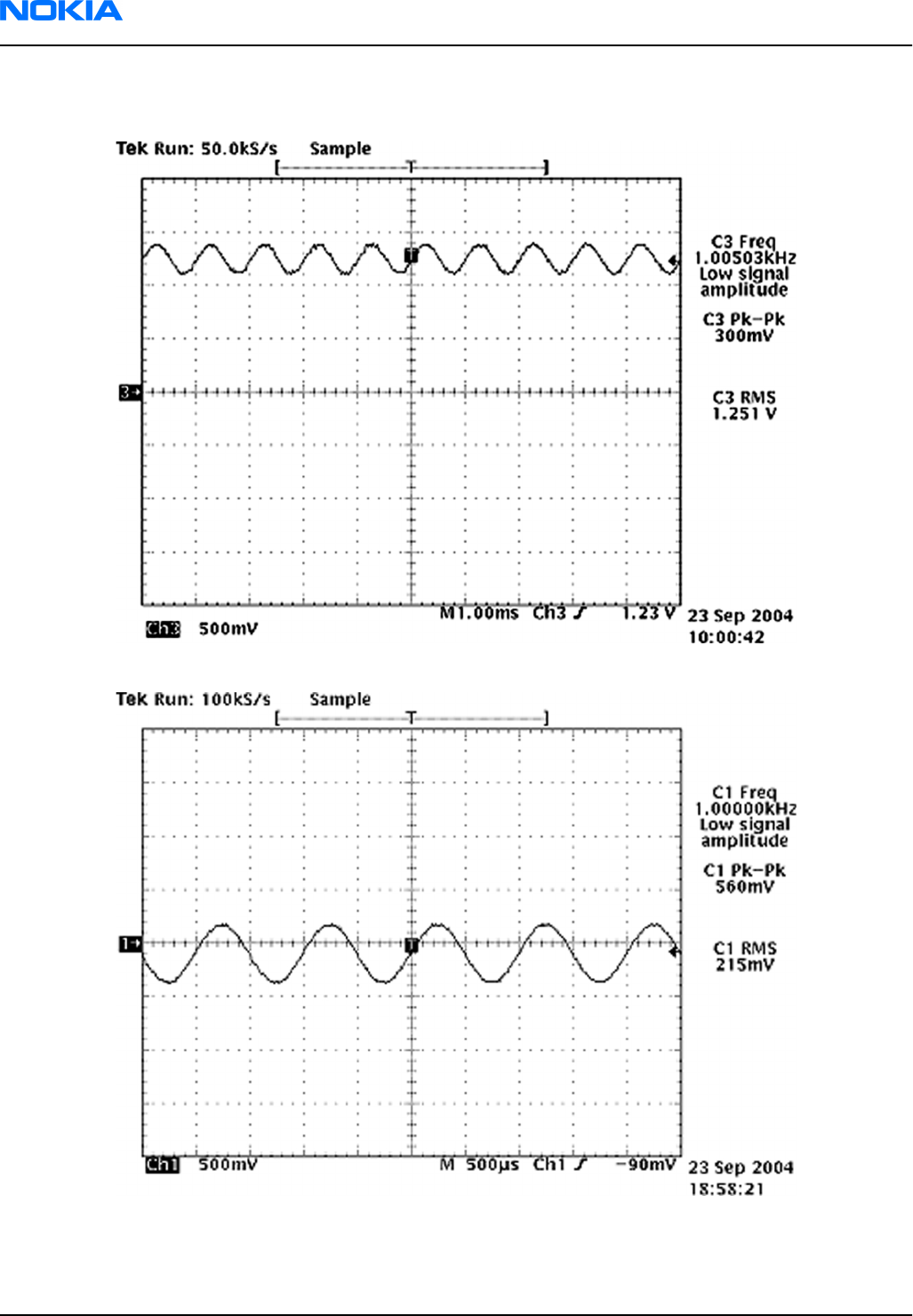
Measurement data
Figure 43 Single-ended output waveform of the Ext_in_HP_out measurement when earpiece is connected.
If a special low-pass filter designed for measuring digital amplifiers is unavailable, the measurement must be performed with a
current probe and the input signal frequency must be 2kHz.
Figure 44 Differential output waveform of the Ext_in_IHF_out out loop measurement when speaker is connected.
RM-123; RM-145
Nokia Customer Care BB Troubleshooting and Manual Tuning Guide
Page 6 –34 COMPANY CONFIDENTIAL Issue 1
Copyright © 2006 Nokia. All rights reserved.
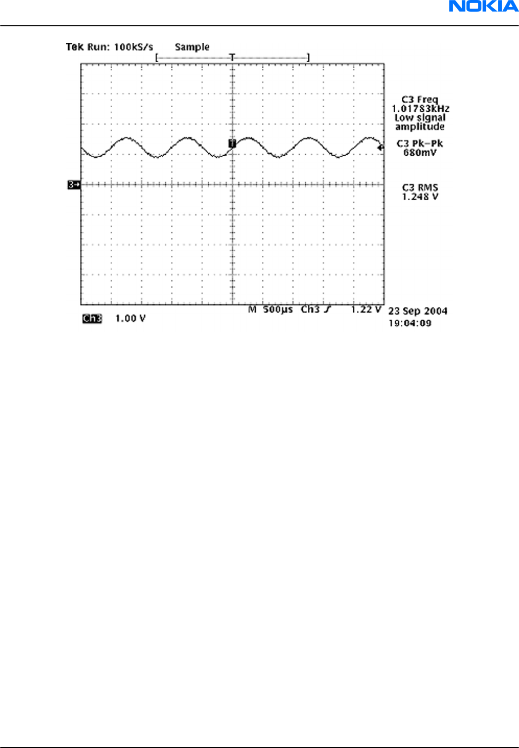
Figure 45 Single-ended output waveform of the HP_in_Ext_out loop when microphone is connected.
RM-123; RM-145
BB Troubleshooting and Manual Tuning Guide Nokia Customer Care
Issue 1 COMPANY CONFIDENTIAL Page 6 –35
Copyright © 2006 Nokia. All rights reserved.
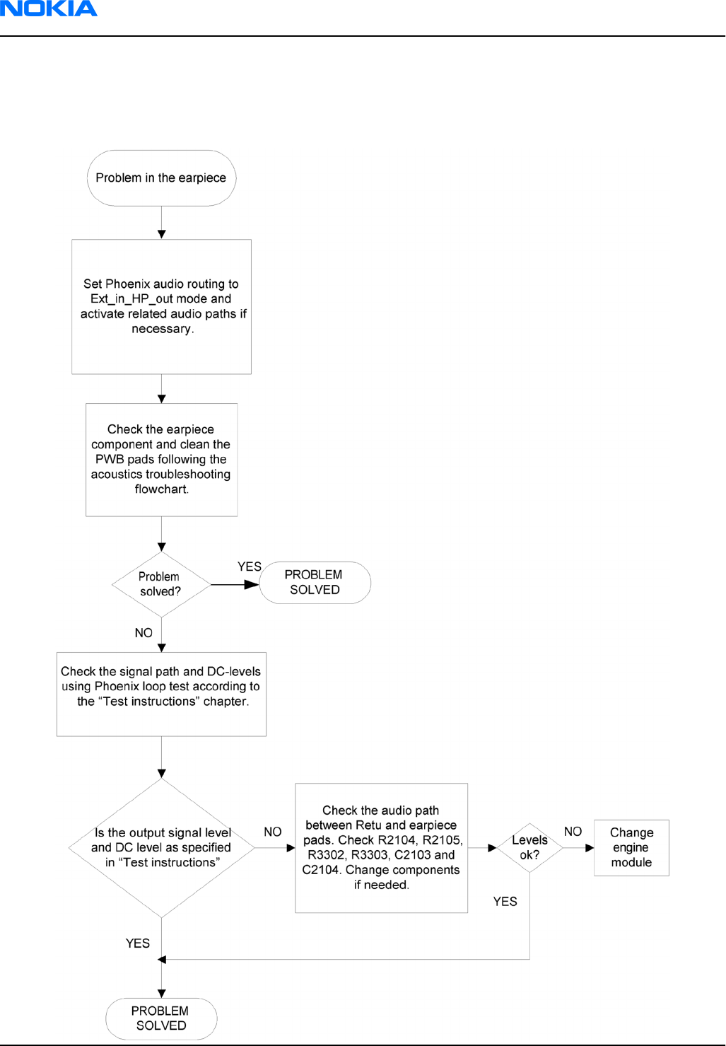
Internal earpiece troubleshooting
Troubleshooting flow
RM-123; RM-145
Nokia Customer Care BB Troubleshooting and Manual Tuning Guide
Page 6 –36 COMPANY CONFIDENTIAL Issue 1
Copyright © 2006 Nokia. All rights reserved.
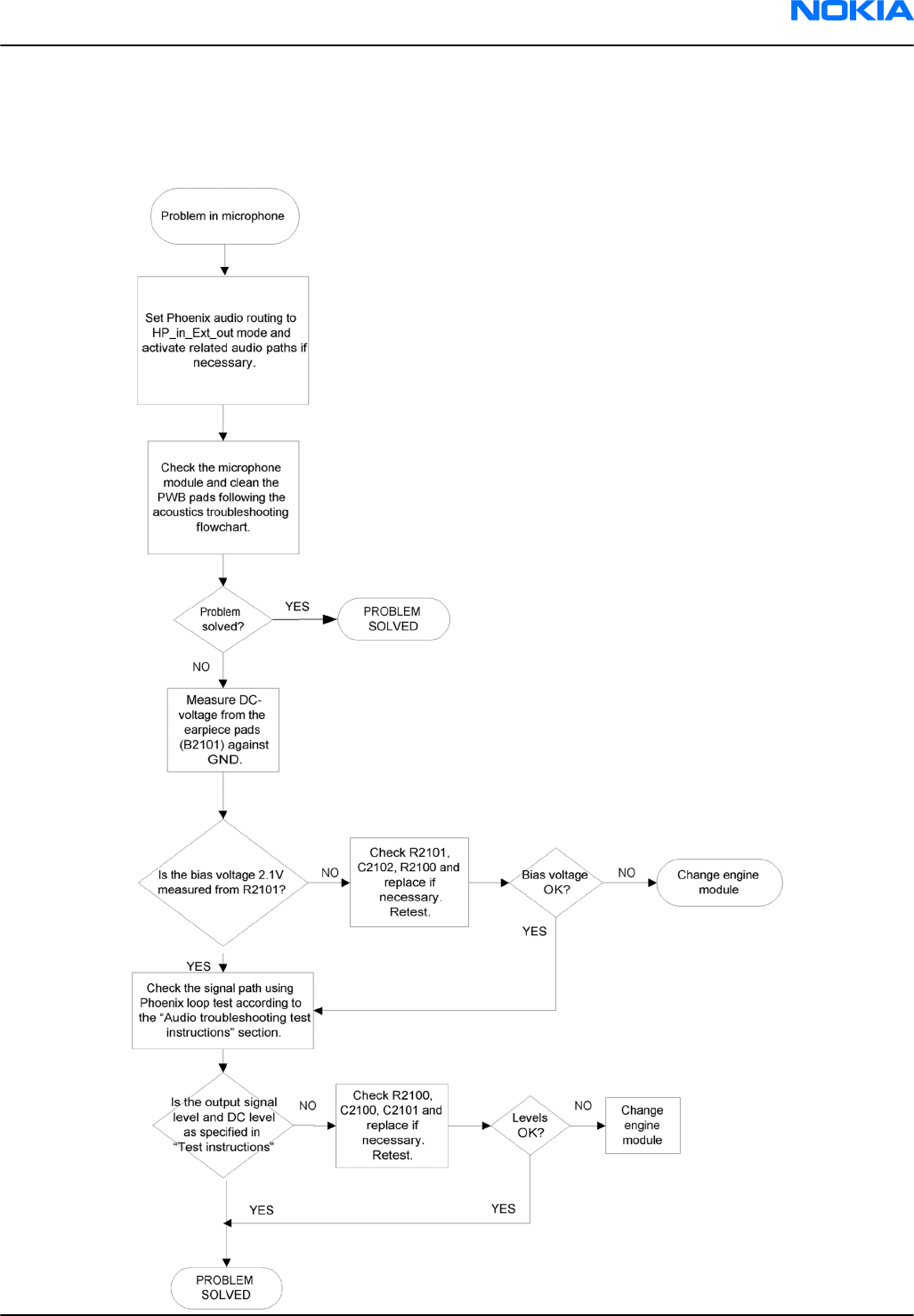
Internal microphone troubleshooting
Troubleshooting flow
RM-123; RM-145
BB Troubleshooting and Manual Tuning Guide Nokia Customer Care
Issue 1 COMPANY CONFIDENTIAL Page 6 –37
Copyright © 2006 Nokia. All rights reserved.
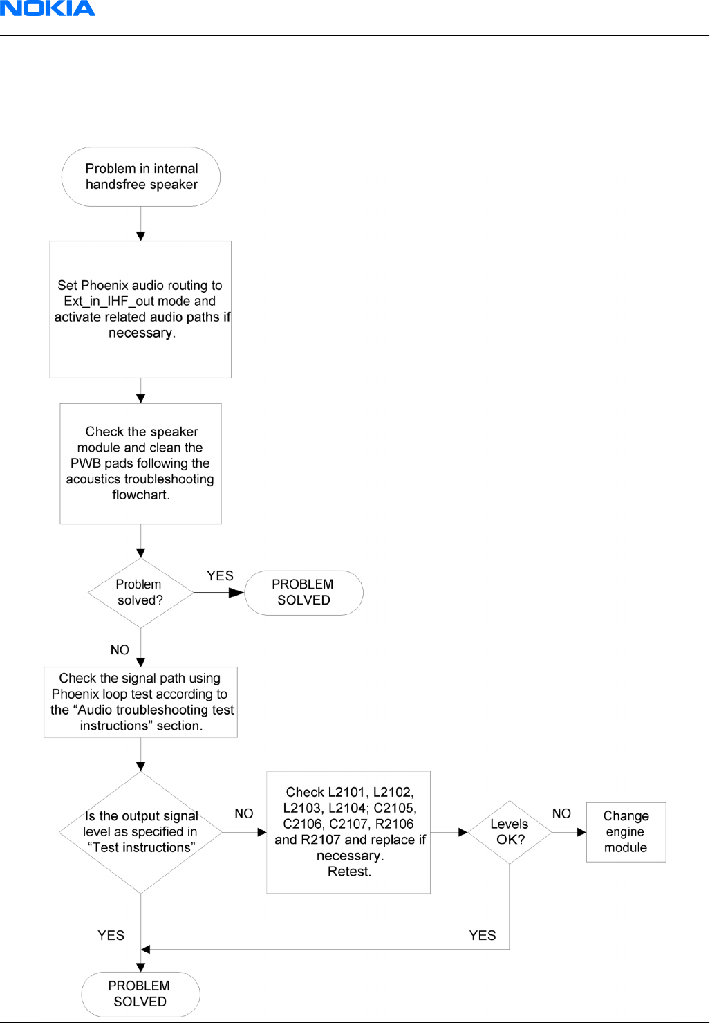
IHF troubleshooting
Troubleshooting flow
RM-123; RM-145
Nokia Customer Care BB Troubleshooting and Manual Tuning Guide
Page 6 –38 COMPANY CONFIDENTIAL Issue 1
Copyright © 2006 Nokia. All rights reserved.
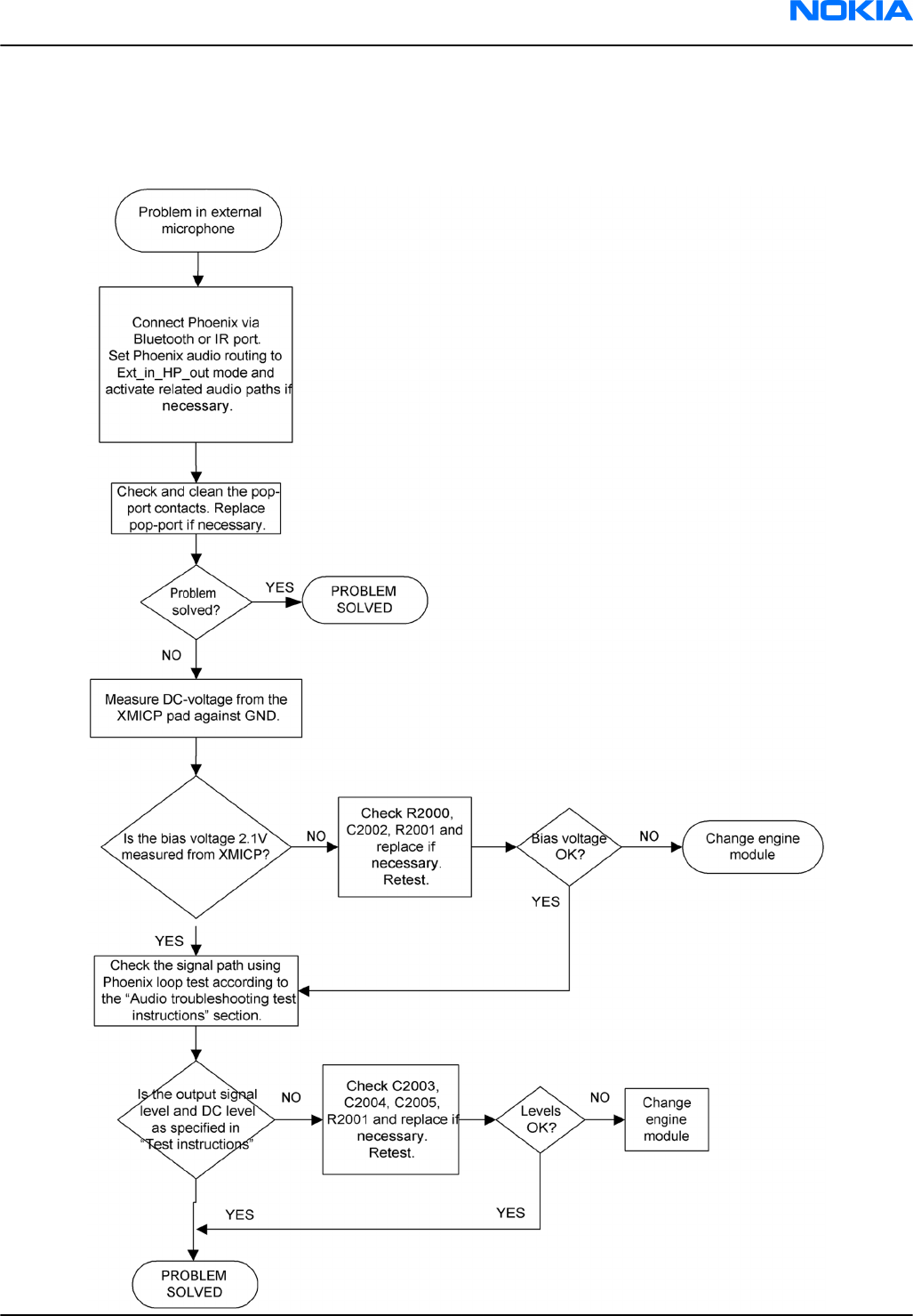
External microphone troubleshooting
Troubleshooting flow
RM-123; RM-145
BB Troubleshooting and Manual Tuning Guide Nokia Customer Care
Issue 1 COMPANY CONFIDENTIAL Page 6 –39
Copyright © 2006 Nokia. All rights reserved.
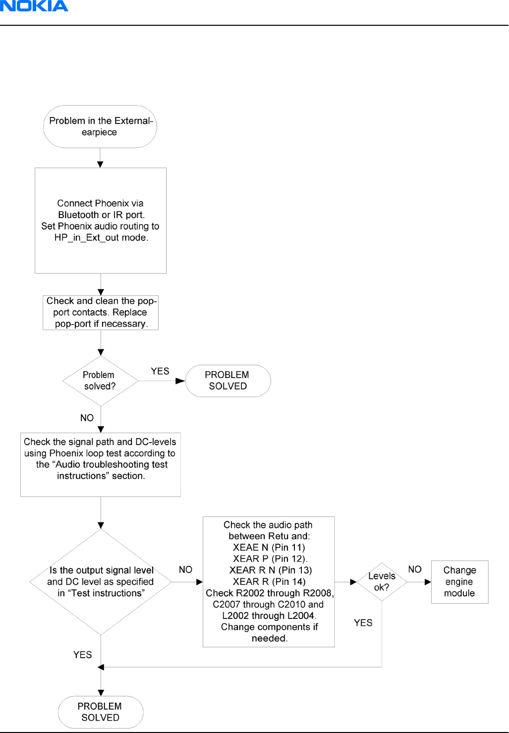
External earpiece troubleshooting
Troubleshooting flow
RM-123; RM-145
Nokia Customer Care BB Troubleshooting and Manual Tuning Guide
Page 6 –40 COMPANY CONFIDENTIAL Issue 1
Copyright © 2006 Nokia. All rights reserved.
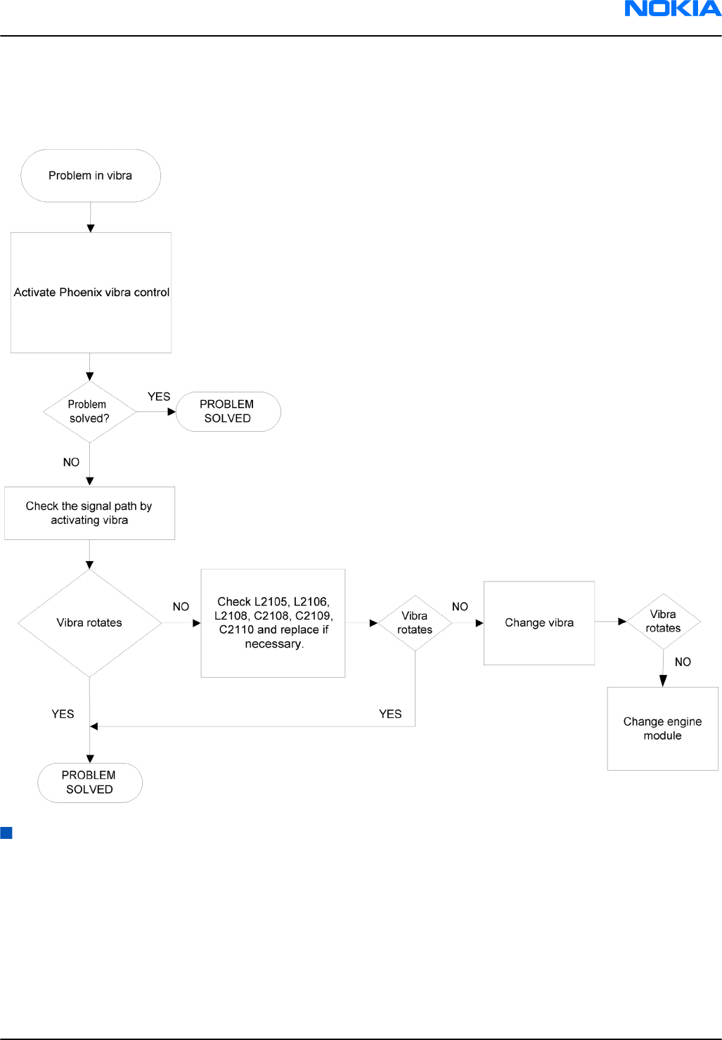
Vibra troubleshooting
Troubleshooting flow
Baseband manual tuning guide
Certificate restoring for BB5.0 products
Context
This procedure is performed when the device certificate is corrupted for some reason.
All tunings (RF & Baseband, UI) must be done after performing the certificate restoring procedure.
The procedure for certificate restoring is the following:
• Flash the phone with the latest available software using FPS-8 or FPS-10.
RM-123; RM-145
BB Troubleshooting and Manual Tuning Guide Nokia Customer Care
Issue 1 COMPANY CONFIDENTIAL Page 6 –41
Copyright © 2006 Nokia. All rights reserved.

Note: USB flashing does not work for a dead BB5.0 phone.
• Create a request file.
• Send the file to Nokia by e-mail. Use the following addresses depending on your location:
• APAC: sydney.service@nokia.com
• CHINA: repair.ams@nokia.com
• E&A: salo.repair@nokia.com
• AMERICAS: fls1.usa@nokia.com
• When you receive a reply from Nokia, carry out certificate restoring.
• Tune the phone completely.
Note: SX-4 smart card is needed.
• If the phone resets after certificate restoring, reflash the phone again.
Required equipment and setup:
•
Phoenix
service software v 2004.39.7.70 or newer.
• The latest phone model specific
Phoenix
data package.
• PKD-1 dongle
• SX-4 smart card (Enables BB5.0 testing and tuning features)
• External smart card reader
Note: The smart card reader is only needed when FPS-8 is used. FPS-10 has an integrated smart card
reader.
• Activated FPS-8 flash prommer OR FPS-10 flash prommer
• Flash update package 03.18.004 or newer for FPS-8 or FPS-10 flash prommers
• CU-4 control unit
• USB cable from PC USB Port to CU-4 control unit
• Phone model specific adapter for CU-4 control unit
• PCS-1 cable to power CU-4 from external power supply
• XCS-4 modular cable between flash prommer and CU-4
Note: CU-4 must be supplied with +12 V from an external power supply in all steps of certificate
restoring.
Steps
1. Program the phone software.
i Start
Phoenix
and login. Make sure the connection has been managed correctly for FPS-8 or FPS-10.
ii Update the phone MCU software to the latest available version.
If the new flash is empty and the phone cannot communicate with
Phoenix
, reflash the phone.
iii Choose the product manually from File→Open Product , and click OK.
Wait for the phone type designator (e.g. “RM-1” ) to be displayed in the status bar.
iv Go to Flashing→SW Update and wait until
Phoenix
reads the product data as shown in the following
picture.
RM-123; RM-145
Nokia Customer Care BB Troubleshooting and Manual Tuning Guide
Page 6 –42 COMPANY CONFIDENTIAL Issue 1
Copyright © 2006 Nokia. All rights reserved.
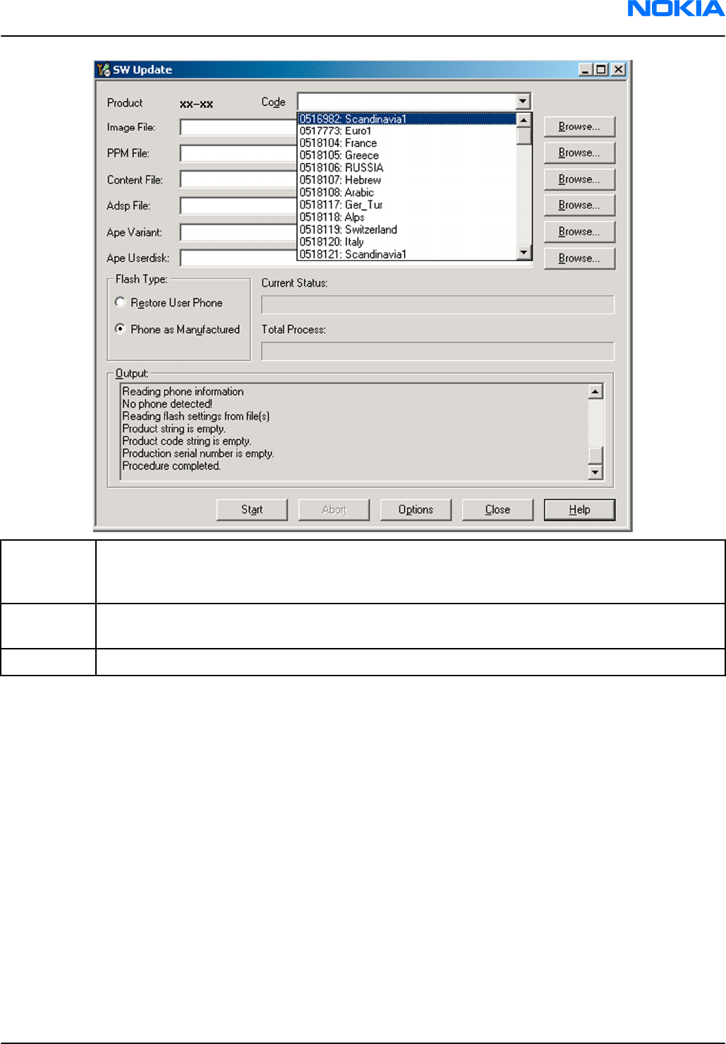
Product is automatically set according to the phone support module which was opened manually,
but the flash files cannot be found because the correct data cannot be read from the phone
automatically.
Code must be chosen manually, it determines the correct flash files to be used. Please choose the
correct product code (can be seen in the phone type label) from the dropdown list.
Flash Type must be set to Phone as Manufactured.
v To continue, click Start.
Progress bars and messages on the screen show actions during phone programming, please wait.
RM-123; RM-145
BB Troubleshooting and Manual Tuning Guide Nokia Customer Care
Issue 1 COMPANY CONFIDENTIAL Page 6 –43
Copyright © 2006 Nokia. All rights reserved.
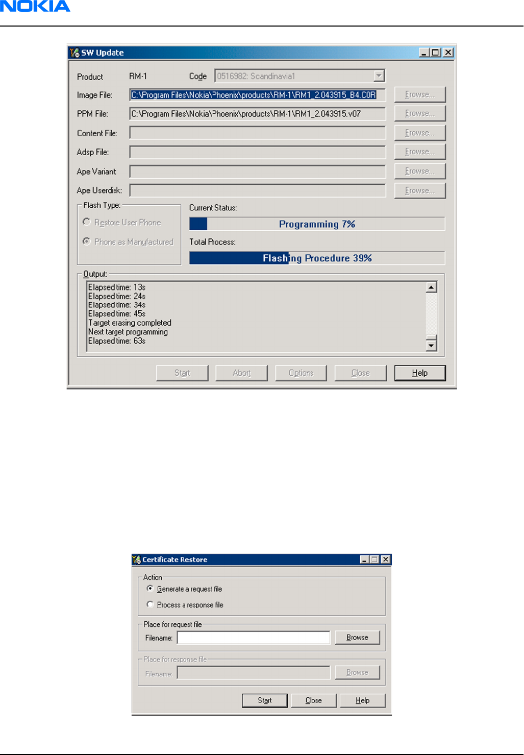
Programming is completed when
Flashing Completed
message is displayed.
The product type designator and MCU SW version are displayed in the status bar.
vi Close the
SW Update
window and then choose File→Close Product .
2. Create a
Request
file.
For this procedure, you must supply +12 V to CU-4 from an external power supply.
i To connect the phone with
Phoenix
, choose File→Scan Product .
ii Choose Tools→Certificate Restore .
iii To choose a location for the request file, click Browse.
RM-123; RM-145
Nokia Customer Care BB Troubleshooting and Manual Tuning Guide
Page 6 –44 COMPANY CONFIDENTIAL Issue 1
Copyright © 2006 Nokia. All rights reserved.
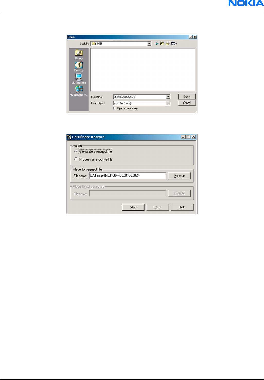
iv Name the file so that you can easily identify it, and click Open.
The name of the file and its location are shown.
v To create the
Request
file, click Start.
vi When the file for certificate restore has been created, send it to Nokia as an e-mail attachment.
3. Restore certificate.
For this procedure, you must supply +12 V to CU-4 from an external power supply.
i Save the reply file sent by Nokia to your computer.
ii Start
Phoenix
service software.
iii Choose File→Scan Product .
RM-123; RM-145
BB Troubleshooting and Manual Tuning Guide Nokia Customer Care
Issue 1 COMPANY CONFIDENTIAL Page 6 –45
Copyright © 2006 Nokia. All rights reserved.
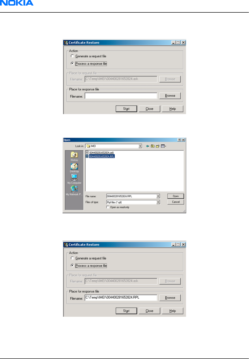
iv From the Tools menu, choose Certificate Restore and select Process a response file in the
Action
pane.
v To choose the location where response file is saved, click Browse.
vi Click Open.
The name of the file and the path where it is located are shown.
vii To write the file to phone, click Start.
Next actions
After a successful rewrite, you must retune the phone completely by using
Phoenix
tuning functions.
Important: Perform all tunings: RF, BB, and UI.
RM-123; RM-145
Nokia Customer Care BB Troubleshooting and Manual Tuning Guide
Page 6 –46 COMPANY CONFIDENTIAL Issue 1
Copyright © 2006 Nokia. All rights reserved.

Energy management calibration
Prerequisites
Energy Management (EM) calibration is performed to calibrate the setting (gain and offset) of AD converters
in several channels (that is, battery voltage, BSI, battery current) to get an accurate AD conversion result.
Hardware setup:
• An external power supply is needed.
• Supply 12V DC from an external power supply to CU-4 to power up the phone.
• The phone must be connected to a CU-4 control unit with a product-specific flash adapter.
Steps
1. Place the phone to the docking station adapter (CU-4 is connected to the adapter).
2. Start
Phoenix
service software.
3. Choose File→ Scan Product.
4. Choose Tuning→Energy Management Calibration.
5. To show the current values in the phone memory, click Read, and check that communication between
the phone and CU-4 works.
6. Check that the CU-4 used check box is checked.
7. Select the item(s) to be calibrated.
Note: ADC calibration has to be performed before other item(s). However, if all calibrations are
selected at the same time, there is no need to perform the ADC calibration first.
8. Click Calibrate.
The calibration of the selected item(s) is carried out automatically.
The candidates for the new calibration values are shown in the
Calculated values
column. If the new
calibration values seem to be acceptable (please refer to the following "Calibration value limits" table),
click Write to store the new calibration values to the phone permanent memory.
Table 15 Calibration value limits
Parameter Min. Max.
ADC Offset -20 20
ADC Gain 12000 14000
BSI Gain 1100 1300
VBAT Offset 2400 2650
VBAT Gain 19000 23000
VCHAR Gain N/A N/A
IBAT (ICal) Gain 7750 12250
9. Click Read, and confirm that the new calibration values are stored in the phone memory correctly. If the
values are not stored to the phone memory, click Write and/or repeat the procedure again.
10. To end the procedure, close the
Energy Management Calibration
window.
RM-123; RM-145
BB Troubleshooting and Manual Tuning Guide Nokia Customer Care
Issue 1 COMPANY CONFIDENTIAL Page 6 –47
Copyright © 2006 Nokia. All rights reserved.

RM-123; RM-145
Nokia Customer Care BB Troubleshooting and Manual Tuning Guide
(This page left intentionally blank.)
Page 6 –48 COMPANY CONFIDENTIAL Issue 1
Copyright © 2006 Nokia. All rights reserved.

7 — RF troubleshooting
Nokia Customer Care
Issue 1 COMPANY CONFIDENTIAL Page 7 –1
Copyright © 2006 Nokia. All rights reserved.

RM-123; RM-145
Nokia Customer Care RF troubleshooting
(This page left intentionally blank.)
Page 7 –2 COMPANY CONFIDENTIAL Issue 1
Copyright © 2006 Nokia. All rights reserved.

Table of Contents
General RF troubleshooting...................................................................................................................................7–5
General RF troubleshooting.............................................................................................................................7–5
RF key components...........................................................................................................................................7–6
Auto tuning for BB5.0............................................................................................................................................7–6
GSM Receivers.........................................................................................................................................................7–7
GSM RX Troubleshooting...................................................................................................................................7–7
GSM Transmitters....................................................................................................................................................7–8
GSM900/1800/1900 TX Troubleshooting........................................................................................................7–8
WCDMA Receiver...................................................................................................................................................7–10
WCDMA RX Troubleshooting...........................................................................................................................7–10
WCDMA Transmitter.............................................................................................................................................7–11
WCDMA TX Troubleshooting...........................................................................................................................7–11
Synthesizer troubleshooting ..............................................................................................................................7–12
PIHI (N7500) Troubleshooting.......................................................................................................................7–12
Synthesizer Troubleshooting.........................................................................................................................7–13
Bluetooth and FM radio.......................................................................................................................................7–15
Bluetooth troubleshooting............................................................................................................................7–15
FM radio troubleshooting...............................................................................................................................7–16
List of Figures
Figure 46 Auto tuning concept with CMU200......................................................................................................7–7
Figure 47 GSM900/1800/1900 RX test points......................................................................................................7–8
Figure 48 GSM900/1800/1900 TX test points......................................................................................................7–9
Figure 49 WCDMA RX test points.........................................................................................................................7–11
Figure 50 WCDMA TX test points.........................................................................................................................7–12
Figure 51 PIHI (N7500) test points.....................................................................................................................7–13
Figure 52 Synthesizer test points.......................................................................................................................7–14
Figure 53 Troubleshooting diagram: Bluetooth...............................................................................................7–15
Figure 54 Troubleshooting diagram: FM radio.................................................................................................7–16
RM-123; RM-145
RF troubleshooting Nokia Customer Care
Issue 1 COMPANY CONFIDENTIAL Page 7 –3
Copyright © 2006 Nokia. All rights reserved.

RM-123; RM-145
Nokia Customer Care RF troubleshooting
(This page left intentionally blank.)
Page 7 –4 COMPANY CONFIDENTIAL Issue 1
Copyright © 2006 Nokia. All rights reserved.

General RF troubleshooting
General RF troubleshooting
Most RF semiconductors are static discharge sensitive
Two types of measurements are used in the following. It will be specified if the measurement type is "RF" or
"LF".
• RF measurements are done with a Spectrum Analyzer and a high-frequency 500 ohm passive probe, for
example HP54006A. (Note that when measuring with the 500 ohm probe the signal will be around 20 dB
attenuated. The values in the following will have these 20 dB subtracted and represent the real value seen
on the spectrum analyzer). Note that the testing have some losses which must be taken into consideration
when calibrating the test system.
•LF (Low frequency) and DC measurements should be done with a 10:1 probe and an oscilloscope. The probe
used in the following is 10 Mohm/8pF passive probe. If using another probe then bear in mind that the
voltages displayed may be slightly different. Always make sure the measurement set-up is calibrated when
measuring RF parameters on the antenna pad. Remember to include the loss in the module repair jig when
realigning the phone.
So ESD protection must be applied during repair (ground straps and ESD soldering irons). RF IC N7500 and
Frond end module (N7520) are moisture sensitive so parts must be pre-baked prior to soldering. Apart from
key-components described in this document there are a lot of discrete components (resistors, inductors and
capacitors) for which troubleshooting is done by checking if soldering of the component is done properly
and checking if the component is missing from PWB. Capacitors can be checked for short-circuiting and
resistors for value by means of an ohmmeter, but be aware in-circuit measurements should be evaluated
carefully. In the following both the name EGSM and GSM 900 will be used for the lower band and both PCN
and GSM 1800 will be used for the upper band.
RM-123; RM-145
RF troubleshooting Nokia Customer Care
Issue 1 COMPANY CONFIDENTIAL Page 7 –5
Copyright © 2006 Nokia. All rights reserved.
RF key components
Auto tuning for BB5.0
This phone can be tuned automatically.
Autotune is designed to align the phone's RF part easier and faster. It performs calibrations, tunings and
measurements of RX and TX. The results are displayed and logged in a result file, if initiated.
Hardware set up
Hardware requirements for auto tuning:
• PC (Windows 2000/XP) with GPIB card
• Power supply
• Product specific module jig
RM-123; RM-145
Nokia Customer Care RF troubleshooting
Page 7 –6 COMPANY CONFIDENTIAL Issue 1
Copyright © 2006 Nokia. All rights reserved.
• Cables: XRF-1 (RF cable), USB cable, GBIP cable and DAU-9S
• Signal analyser (TX), signal generator (RX) and RF-splitter
or
one device including all.
Figure 46 Auto tuning concept with CMU200
Phoenix preparations
Install the phone specific data package, for example
RM-123/145_dp_1.78_sw_sh3.26.exe
. This defines phone
specific settings..
Auto tuning procedure
1 Make sure the phone (in the jig) is connected to the equipment. Else, some menus will not be shown in
Phoenix.
2 To go to autotune, select
Tuning (Alt-U)
>
Auto-Tune (Alt-A)
from the menu.
3 Start autotuning, clicking the
Tune
button.
GSM Receivers
GSM RX Troubleshooting
Preparations
Make the following settings:
Setting GSM900 GSM1800 GSM1900
Phoenix RF Control
Phoenix channel
Continues RX and AGC gain step 14
37 700 661
Signal generator to
antenna connector
942.46771 MHz
(67.71kHz offset) at
-60dBm
1842.86771MHz
(67.71kHz offset) at
-60dBm
1960.06771MHz
(67.71kHz offset) at
-60dBm
Spectrum analyzer
Centre frequency
RBW=500kHz, VBW=500kHz, span=20kHz
942MHz 1840MHz 1960MHz
Check the following
Check the levels in the steps below.
RM-123; RM-145
RF troubleshooting Nokia Customer Care
Issue 1 COMPANY CONFIDENTIAL Page 7 –7
Copyright © 2006 Nokia. All rights reserved.
NO. Signal Name Test point GSM900 GSM1800 GSM1900
1RXIP (out) J7515 124mVpp,
730mVDC
106mVpp,
760mVDC
100mVpp,
780mVDC
2 RXQP (OUT) J7517 124mVpp,
730mVDC
106mVpp,
690mVDC
100mVpp,
690mVDC
3 VC1_TXFEM J7530 0V 0V 0V
4 VC2_TXFEM J7531 0V 2.7VDC 2.7VDC
5 VC3_TXFEM J7532 0V 0V 2.7VDC
1 Measure RXIP
1
and RXQP
2
.
2 Measure front end module control signal voltages
3, 4 and 5
.
Figure 47 GSM900/1800/1900 RX test points
GSM Transmitters
GSM900/1800/1900 TX Troubleshooting
Preparations
Make the following settings:
RM-123; RM-145
Nokia Customer Care RF troubleshooting
Page 7 –8 COMPANY CONFIDENTIAL Issue 1
Copyright © 2006 Nokia. All rights reserved.

Setting GSM900 GSM1800 GSM1900
Phoenix RF Control
Phoenix Tx Power level
Operational mode = Burst
Tx data type = Random
10 5 5
Check the following
Check the voltages in the steps below.
NO. Signal Name Test point GSM900 GSM1800 GSM1900
1V_Det_GSM J7533 730mVDC 660mVDC 690mVDC
2 PA_supply-VBAT C7521 3.8VDC 3.8VDC 3.8VDC
3 RF level-ANT_GSM Conn. 23dBm 20dBm 20dBm
4 Sw cont-VC1_TXFEM J7530 2.75VDC 2.75VDC 2.75VDC
5 Sw con-VC2_TXFEM J7531 0V 2.75VDC 2.75VDC
6 Sw con-VC3_TXFEM J7532 2.75VDC 2.75VDC 2.75VDC
7 Tx-1 R7522 897.4MHz/-28.7
dBm
- -
Figure 48 GSM900/1800/1900 TX test points
RM-123; RM-145
RF troubleshooting Nokia Customer Care
Issue 1 COMPANY CONFIDENTIAL Page 7 –9
Copyright © 2006 Nokia. All rights reserved.
WCDMA Receiver
WCDMA RX Troubleshooting
Preparations
Set Phoenix to RF local mode WCDMA RX.
Equipment/Settinig Unit
Phoenix
WCDMA FDD
RF channel 2140MHz ~10700
Frequency offset +0.000kHz
Output channel power -60dBm
P-sch~ -2dB
S-sch~ -2dB
P-cc pch~ -2dB
DPDch~ -7dB
AGCMod* Algorithm
Channel* 10700
BB AGC* 0dB
Spectrum analyzer*
Span ~ 20MHz
Centre frequency 2140MHz
VBW 500kHz
RBW 500kHz
Output channel power -30dB
RF AH ~ 30dB
Check the following
Check the levels in the steps below.
NO. Signal Name Test point Check
1PXIP (out) J7515 720mVpp single ended
2 RXQP (OUT) J7517 720mVpp single ended
RM-123; RM-145
Nokia Customer Care RF troubleshooting
Page 7 –10 COMPANY CONFIDENTIAL Issue 1
Copyright © 2006 Nokia. All rights reserved.
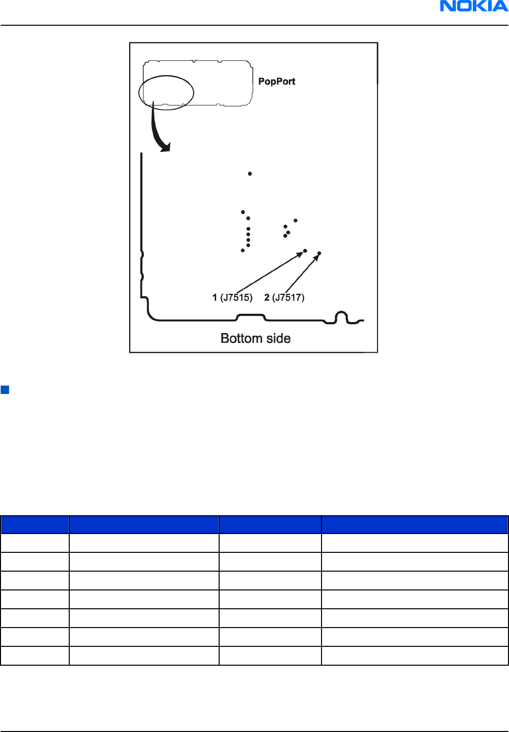
Figure 49 WCDMA RX test points
WCDMA Transmitter
WCDMA TX Troubleshooting
Preparations
Set Phoenix to RF local mode WCDMA TX (Channel 9737, 0 dBm output).
Check the following
Check the levels in the steps below.
NO. Signal Name Test point Check
1WTXDET C7544 115mVDC
2 VBAT C7542 3.82VDC
3 PA supply - Vreg C7543 ~1.3 VDC @ 0dBm
4 RF level - ANT_WCDMA X8003 0dBm on antenna
6 WDET C7545 2.75 VDC
7 DAC101 R7541 300 mVDC
8 DAC201 J7538 1.5 VDC
RM-123; RM-145
RF troubleshooting Nokia Customer Care
Issue 1 COMPANY CONFIDENTIAL Page 7 –11
Copyright © 2006 Nokia. All rights reserved.
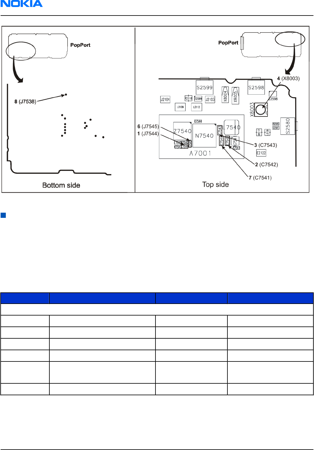
Figure 50 WCDMA TX test points
Synthesizer troubleshooting
PIHI (N7500) Troubleshooting
Preparations
Set Phoenix to RF local mode RX burst.
Check the following
Check the voltages in the steps below.
NO. Signal Name Test point Check GSM900
Suppliers
1 VBATRF (in) L7500 3.8VDC
2 VR1_RX (out) C7503 2.8VDC
3 VR1_TX (out) C7502 2.8VDC
4 VR2_TX (out) C7501 2.8VDC
5 VREFRF01 (in)
VB_EXT
R7501 1.36VDC
6 VCP1 (in) C2221 4.76VDC
RM-123; RM-145
Nokia Customer Care RF troubleshooting
Page 7 –12 COMPANY CONFIDENTIAL Issue 1
Copyright © 2006 Nokia. All rights reserved.
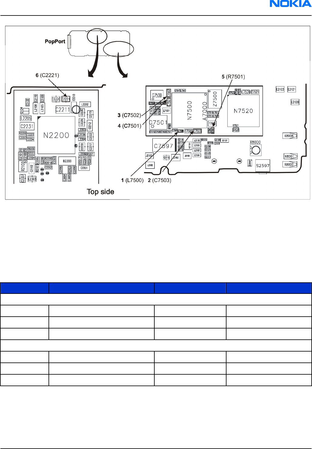
Figure 51 PIHI (N7500) test points
Synthesizer Troubleshooting
Preparations
Set Phoenix to RF local mode RX continuous.
Check the following
Check the levels in the steps below.
NO. Signal Name Test point Check
VCTCXO
1 VXO (in) C7504 2.4VDC
2 OSCIN G7500 85mVpp at 38.4MHz
3 AFC (in) R7500 1.2VDC
VCO
4 VVCO_EXT R7505 2.72VDC
5 VCO Output T7501 -17dBm at 3769.6MHz
6 VCO Control C7510 2.7VDC
RM-123; RM-145
RF troubleshooting Nokia Customer Care
Issue 1 COMPANY CONFIDENTIAL Page 7 –13
Copyright © 2006 Nokia. All rights reserved.
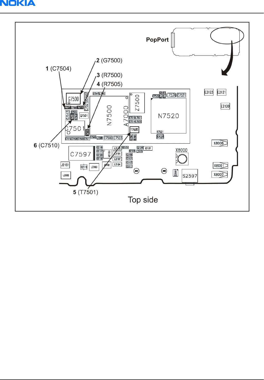
Figure 52 Synthesizer test points
RM-123; RM-145
Nokia Customer Care RF troubleshooting
Page 7 –14 COMPANY CONFIDENTIAL Issue 1
Copyright © 2006 Nokia. All rights reserved.
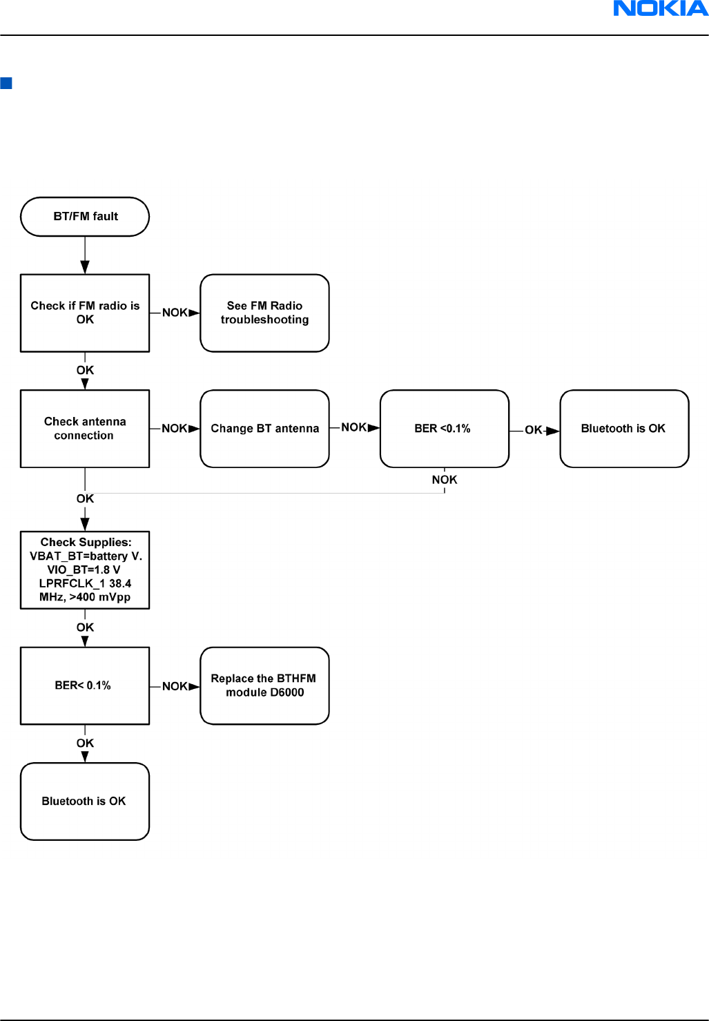
Bluetooth and FM radio
Bluetooth troubleshooting
Troubleshooting flow
Figure 53 Troubleshooting diagram: Bluetooth
RM-123; RM-145
RF troubleshooting Nokia Customer Care
Issue 1 COMPANY CONFIDENTIAL Page 7 –15
Copyright © 2006 Nokia. All rights reserved.
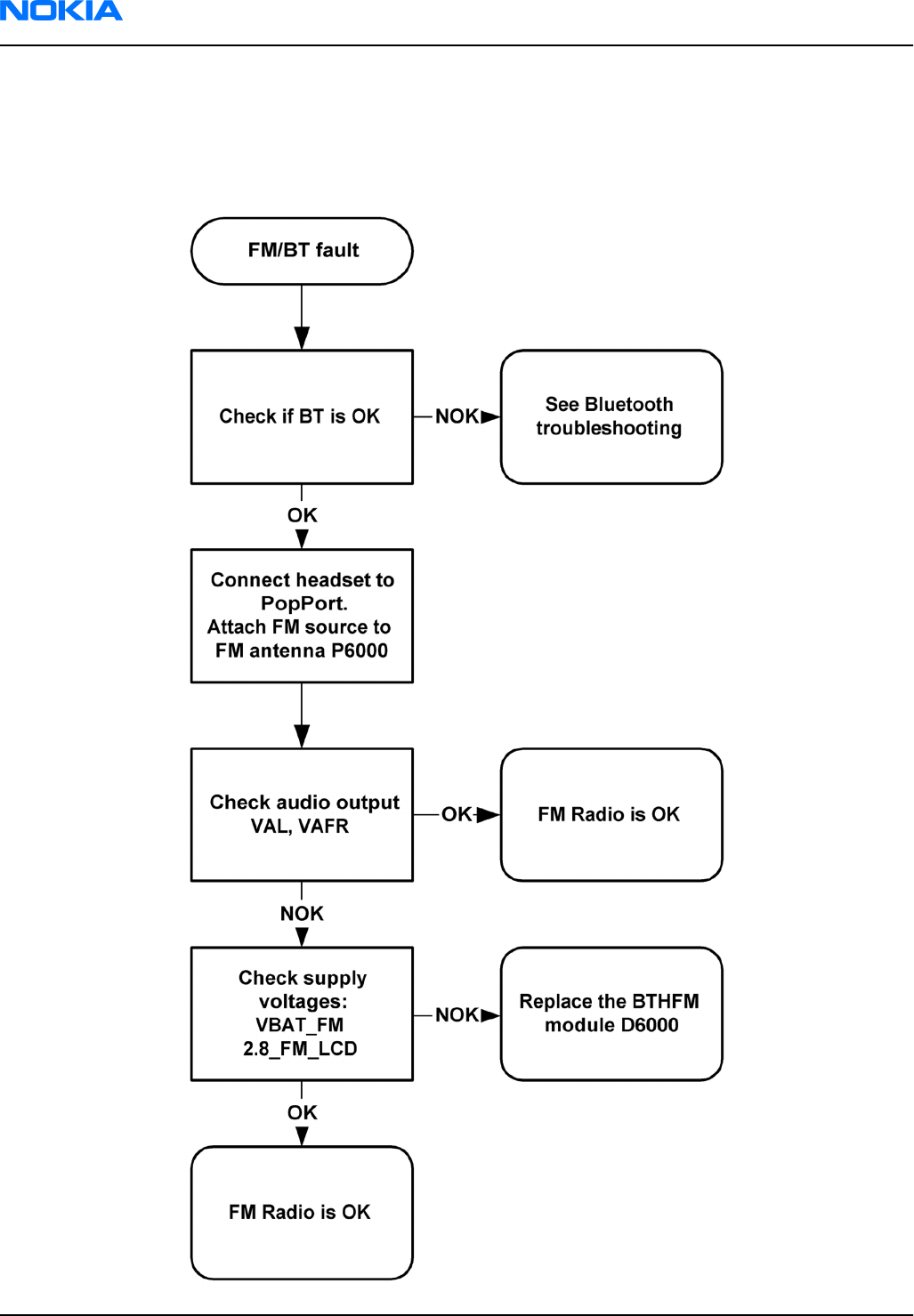
FM radio troubleshooting
Troubleshooting flow
Figure 54 Troubleshooting diagram: FM radio
RM-123; RM-145
Nokia Customer Care RF troubleshooting
Page 7 –16 COMPANY CONFIDENTIAL Issue 1
Copyright © 2006 Nokia. All rights reserved.

8 — System Module
Nokia Customer Care
Issue 1 COMPANY CONFIDENTIAL Page 8 –1
Copyright © 2006 Nokia. All rights reserved.

RM-123; RM-145
Nokia Customer Care System Module
(This page left intentionally blank.)
Page 8 –2 COMPANY CONFIDENTIAL Issue 1
Copyright © 2006 Nokia. All rights reserved.

Table of Contents
Introduction............................................................................................................................................................8–5
Block diagram....................................................................................................................................................8–5
Energy management..............................................................................................................................................8–7
Battery and interface........................................................................................................................................8–7
Normal and extreme voltages.........................................................................................................................8–7
Power key and system power-up....................................................................................................................8–8
Modes of operation...........................................................................................................................................8–8
Power distribution............................................................................................................................................8–9
Clocking scheme................................................................................................................................................8–9
USB, SIM, MMC.......................................................................................................................................................8–10
USB....................................................................................................................................................................8–10
SIM interface....................................................................................................................................................8–10
µSD card interface...........................................................................................................................................8–11
Camera...................................................................................................................................................................8–11
Camera.............................................................................................................................................................8–11
User interface........................................................................................................................................................8–12
Display interface..............................................................................................................................................8–12
Keyboard and side keys..................................................................................................................................8–12
Backlight and illumination.............................................................................................................................8–13
Audio concept.......................................................................................................................................................8–14
Audio hardware architecture.........................................................................................................................8–14
Internal microphone.......................................................................................................................................8–15
External microphone.......................................................................................................................................8–16
Internal earpiece.............................................................................................................................................8–16
Internal speaker..............................................................................................................................................8–17
External earpiece.............................................................................................................................................8–17
Vibra circuitry..................................................................................................................................................8–18
Pop-portTM connector....................................................................................................................................8–18
Bluetooth and FM radio.......................................................................................................................................8–19
Bluetooth.........................................................................................................................................................8–19
FM radio............................................................................................................................................................8–20
RF description.......................................................................................................................................................8–21
Introduction to receiver functionality...........................................................................................................8–21
WCDMA receiver functionality........................................................................................................................8–21
GSM receiver functionality..............................................................................................................................8–21
Introduction to transmitter functionality.....................................................................................................8–21
WCDMA transmitter functionality..................................................................................................................8–21
GSM transmitter functionality........................................................................................................................8–22
Frequency synthesizers..................................................................................................................................8–23
Regulators........................................................................................................................................................8–23
List of Tables
Table 16 Nominal voltages....................................................................................................................................8–7
Table 17 Pop-PortTMpin and signal table..........................................................................................................8–18
List of Figures
Figure 55 Block diagram........................................................................................................................................8–6
Figure 56 Battery pin order...................................................................................................................................8–7
RM-123; RM-145
System Module Nokia Customer Care
Issue 1 COMPANY CONFIDENTIAL Page 8 –3
Copyright © 2006 Nokia. All rights reserved.

Figure 57 Power regulator diagram.....................................................................................................................8–9
Figure 58 Clocking scheme..................................................................................................................................8–10
Figure 59 SIM interface........................................................................................................................................8–11
Figure 60 LCD module..........................................................................................................................................8–12
Figure 61 Audio block diagram...........................................................................................................................8–15
Figure 62 Internal microphone circuitry............................................................................................................8–16
Figure 63 External microphone circuitry (Pop-Port connects to the right side)............................................8–16
Figure 64 Internal earpiece circuitry..................................................................................................................8–16
Figure 65 Internal speaker circuitry...................................................................................................................8–17
Figure 66 External earpiece circuitry (system connector connected on the right).......................................8–17
Figure 67 Vibra circuitry......................................................................................................................................8–18
Figure 68 System connector pin layout.............................................................................................................8–18
Figure 69 Bluetooth interface.............................................................................................................................8–20
Figure 70 FM interface.........................................................................................................................................8–20
Figure 71 GSM transmitter...................................................................................................................................8–22
Figure 72 RF supply connections from the BB mixed mode ASIC....................................................................8–24
RM-123; RM-145
Nokia Customer Care System Module
Page 8 –4 COMPANY CONFIDENTIAL Issue 1
Copyright © 2006 Nokia. All rights reserved.

Introduction
Block diagram
RAP3G is the main digital baseband ASIC in the phone. It contains functionality for both WCDMA and GSM EDGA
and the Golden Eye is used as a co-processor.
Retu is mainly the audio ASIC in the phone and Tahvo is basically the energy management controller for the
phone.
Bluetooth and stereo FM Radio is integrated in one single ASIC.
RM-123; RM-145
System Module Nokia Customer Care
Issue 1 COMPANY CONFIDENTIAL Page 8 –5
Copyright © 2006 Nokia. All rights reserved.
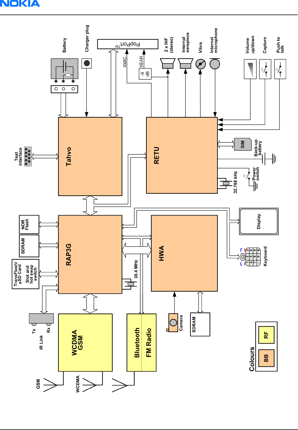
Figure 55 Block diagram
RM-123; RM-145
Nokia Customer Care System Module
Page 8 –6 COMPANY CONFIDENTIAL Issue 1
Copyright © 2006 Nokia. All rights reserved.
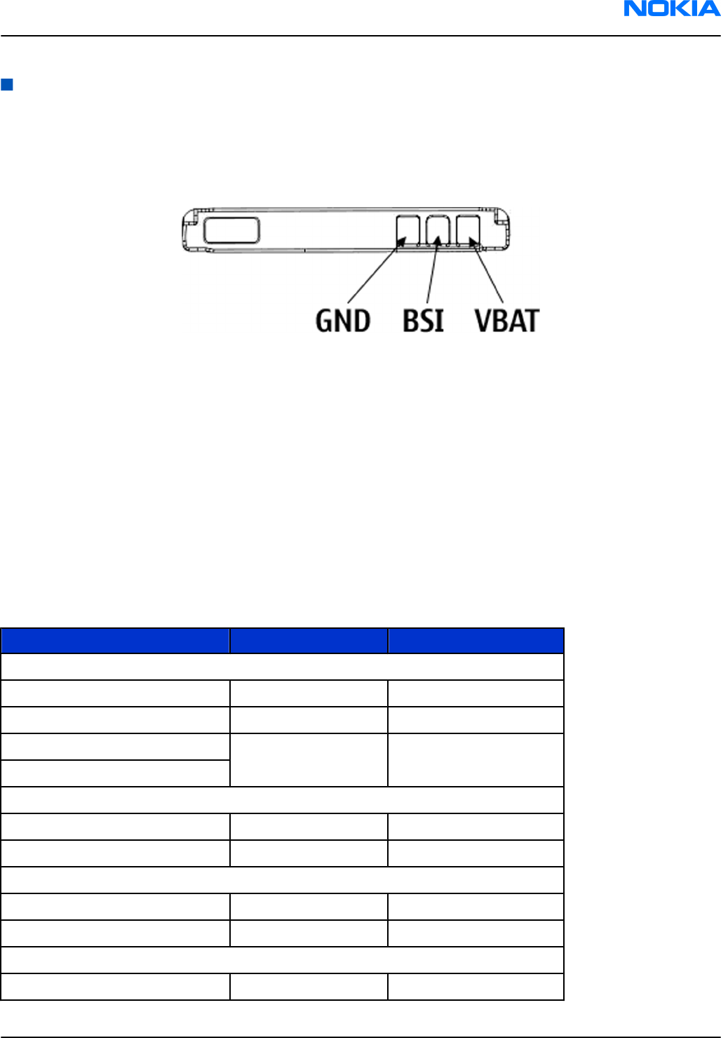
Energy management
Battery and interface
The phone i powered by a 3-pole BP-6M S-pack 1100 mAh battery. The three poles are named VBAT, BSI and
GND where the BSI line is used to recognize the battery capacity. This is done by means of an internal battery
pull down resistor.
Figure 56 Battery pin order
Battery temperature is estimated by measuring separate battery temperature NTC via the BTEMP line, which
is located on the main PWB, at a place where the phone temperature is most stabile.
The connection from the charger connector to the charger is established via a charger adaptor type CA-44.
For service purposes, the device SW can be forced into local mode by using pull down resistors connected to
the BSI line.
Normal and extreme voltages
Energy management is mainly carried out in the two Application Specific Integrated Circuits (ASICs) RETU and
TAHVO. These two circuits contains a number of regulators. In addition there are some external regulators
too.
In the table below normal and extreme voltages are shown when a BP-6M S-pack battery is used.
Table 16 Nominal voltages
Voltage Voltage [V] Condition
General Conditions
Nominal voltage 3.9
Lower extreme voltage 3.215
Higher extreme voltage
4.23(fast charging)
HW Shutdown Voltages
Vmstr+ 2.1 ± 0.1 Off to on
Vmstr- 1.9 ± 0.1 On to off
SW Shutdown Voltages
Sw shutdown 3.1 In call
Sw shutdown 3.2 In idle
Min Operating Voltage
Vcoff+ 2.9 ± 0.1 Off to on
RM-123; RM-145
System Module Nokia Customer Care
Issue 1 COMPANY CONFIDENTIAL Page 8 –7
Copyright © 2006 Nokia. All rights reserved.

Voltage Voltage [V] Condition
Vcoff- 2.6 ± 0.1 On to off
Power key and system power-up
When the battery is placed in the phone the power key circuits are energized. When the power key is pressed,
the system boots up (if an adequate battery voltage is present).
Power down can be initiated by pressing the power key again (the system is powered down with the aid of
SW). The power key is connected to RETU ASIC via PWRONX signal.
Different power-up conditions
Power up can be caused by the following reasons:
• Power key is pressed
• Charger is connected
• RTC alarm occurs
• MBUS wake-up
After that:
• RETU activates sleep clock and VANA, VDRAM, VIO and VR1 regulators.
• Voltage appearing at RETU’s RSTX pin is used for enabling TAHVO ASIC.
• TAHVO enables VCORE regulator and its internal RC-oscillator (600kHz).
• VCTCXO regulator is set ON and RF clock (main system clock) is started to produce.
• RETU will release PURX ~ 16ms after power up is enabled (the RF clock is then stable enough).
• Synchronizing clock (2.4MHz) for TAHVO is started to be produced. After PURX is released and two rising
edges of 2.4MHz synchronous clock have been detected in SMPSClk input TAHVO is starting to use that
instead of 600kHz internal RC-oscillator.
• HW start-up procedure has been finalized and the system is up and running. Now it is possible for SW to
switch ON other needed regulators.
Modes of operation
Mode Description
NO_SUPPLY (dead) mode means that the main battery is not present or its voltage is too low (below
RETU master reset threshold) and that the back-up battery voltage is too low.
BACK_UP The main battery is not present or its voltage is too low but back-up battery voltage is
adequate and the 32kHz oscillator is running (RTC is on).
PWR_OFF In this mode (warm), the main battery is present and its voltage is over RETU master
reset threshold. All regulators are disabled, PurX is on low state, the RTC is on and the
oscillator is on. PWR_OFF (cold) mode is almost the same as PWR_OFF (warm), but the
RTC and the oscillator are off.
RESET RESET mode is a synonym for start-up sequence. RESET mode uses 32kHz clock to count
the REST mode delay (typically 16ms).
SLEEP SLEEP mode is entered only from PWR_ON mode with the aid of SW when the system’s
activity is low.
FLASHING FLASHING mode is for SW downloading.
RM-123; RM-145
Nokia Customer Care System Module
Page 8 –8 COMPANY CONFIDENTIAL Issue 1
Copyright © 2006 Nokia. All rights reserved.
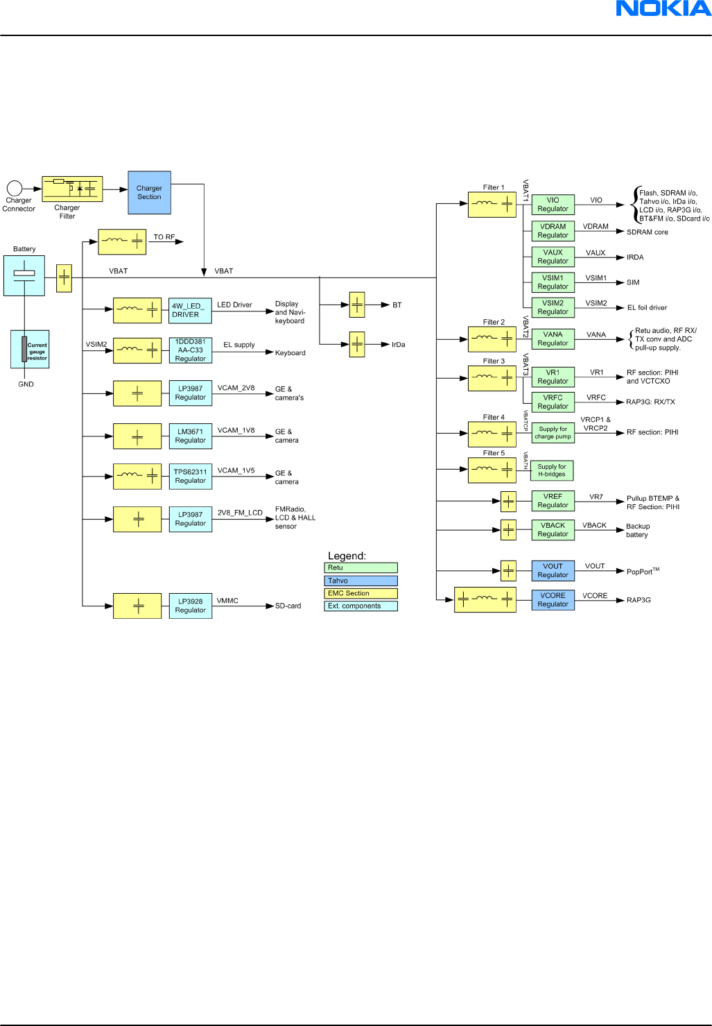
Power distribution
The power distribution is shown in the diagram below. Current consumption is measured via the Current
Gauge Resistor and the battery voltage is stabilized by means of a capacitor. The tables below specifies the
voltages.
Figure 57 Power regulator diagram
Clocking scheme
In BB5.0, two main clocks are provided to the system: 38.4MHz RF clock produced by VCTCXO in RF section
and 32.768kHz sleep clock produced by RETU with an external crystal.
32k Sleep Clock is always powered on after startup. Sleep clock is used by RAP3G and OMAP for low-power
operation.
SMPS Clk is 2.4MHz clock line from RAP3G to TAHVO. In deep sleep mode, when VCTCXO is off, this signal is
set to '0'-state.
BT Clk is 38.4MHz signal from HINKU ASIC to BT module.
CLK600 is 600KHz signal from TAHVO to APE VCORE SMPS. The clock source is internal RC oscillator in TAHVO
(during the power-up sequence) or RAP3G SMPS Clk.
RM-123; RM-145
System Module Nokia Customer Care
Issue 1 COMPANY CONFIDENTIAL Page 8 –9
Copyright © 2006 Nokia. All rights reserved.
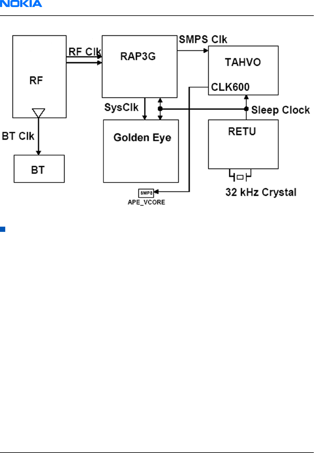
Figure 58 Clocking scheme
USB, SIM, MMC
USB
USB (Universal Serial Bus) provides a wired connectivity between a USB host PC and peripheral devices.
USB is a differential serial bus for USB devices. USB controller supports USB specification revision 2.0 with full
speed USB (12 Mbps). The device is connected to the USB host through the system connector. The USB bus is
hot plugged capable, which means that USB devices may be plugged in/out at any time.
SIM interface
The device has one SIM (Subscriber Identification Module) interface. It is only accessible if battery is removed.
The SIM interface consists of an internal interface between RAP and EM ASIC (N2200), and of an external
interface between N2200 and SIM contacts.
The SIM IF is shown in the following figure:
RM-123; RM-145
Nokia Customer Care System Module
Page 8 –10 COMPANY CONFIDENTIAL Issue 1
Copyright © 2006 Nokia. All rights reserved.
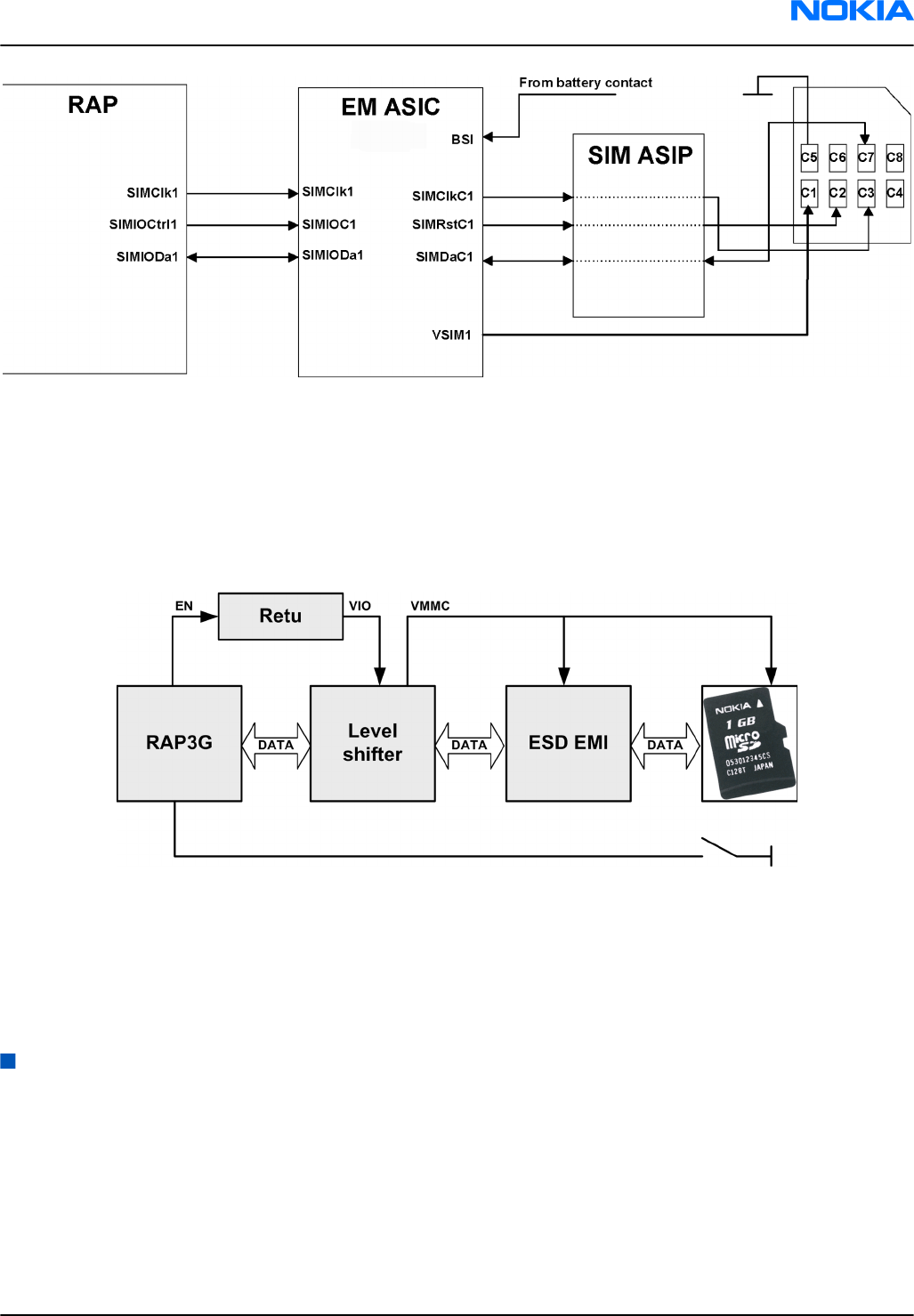
Figure 59 SIM interface
The EM ASIC handles the detection of the SIM card. The detection method is based in the BSI line. Because of
the location of the SIM card, removing the battery causes a quick power down of the SIM IF.
The EM ASIC SIM1 interface supports both 1.8 V and 3.0 V SIM cards. The SIM interface voltage is first 1.8 V
when the SIM card is inserted, and if the card does not response to the ATR a 3 V interface voltage is used.
µSD card interface
The µSD card is connected to the engine by an external level shifter and ESD protection filter. Supplied
voltages:
• VMMC: 2.85 V (from level shifter)
• VIO: 1.8 V (from Retu)
The card removal is detected by a push detect switch.
Camera
Camera
The camera uses a 2.0 megapixel camera module with a sensor resolution of 1600 x 1200.
RM-123; RM-145
System Module Nokia Customer Care
Issue 1 COMPANY CONFIDENTIAL Page 8 –11
Copyright © 2006 Nokia. All rights reserved.
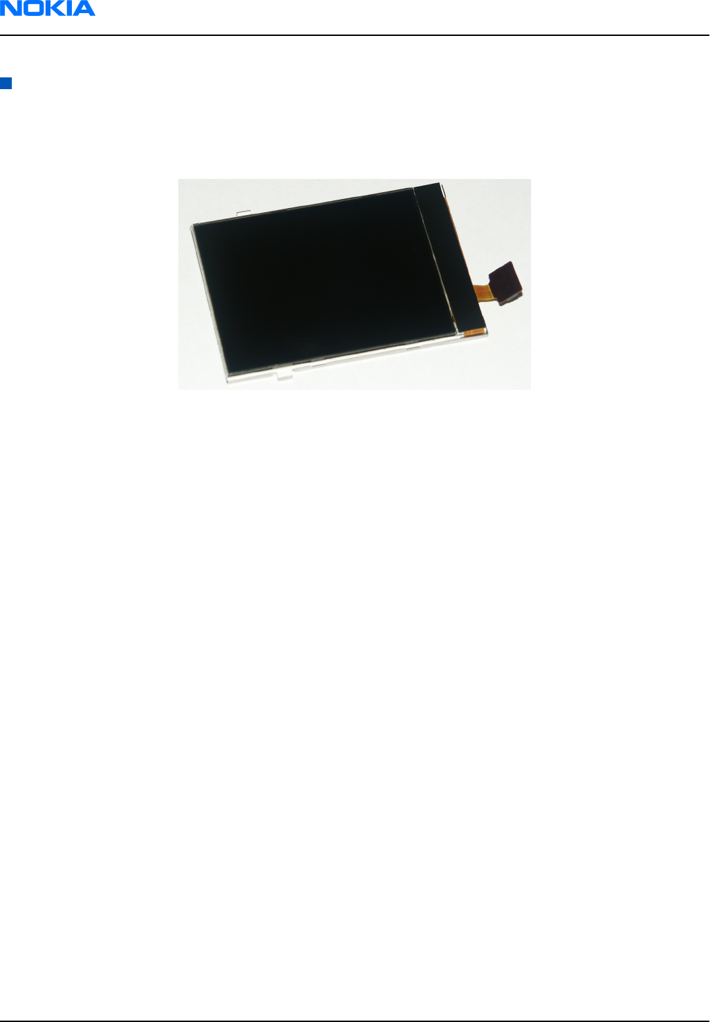
User interface
Display interface
Display module mechanical concept
Figure 60 LCD module
Display features:
• 262 k colours
• Partial display function Power saving by pausing display process on part of the screen.
• Built-in RAM capacity 176rows×208lines×16bit = 585,728 bits
The display has two different operating modes:
1 Normal mode, Full screen, 262k colours
2 Normal Partial mode, 262k colours but only part of the display is active
The interconnection between the LCD module and the Nokia engine is implemented with a 24-pin board-to-
board connector.
The display module does not require any tuning in service.
Keyboard and side keys
The side keys are placed on the main PWB. The numerical keys and the navigation keys are included in the
UI flex on top of the phone.
The numerical keys and the side keys are included in the 4x4 scan matrix. The navigation keys are individually
routed.
RM-123; RM-145
Nokia Customer Care System Module
Page 8 –12 COMPANY CONFIDENTIAL Issue 1
Copyright © 2006 Nokia. All rights reserved.
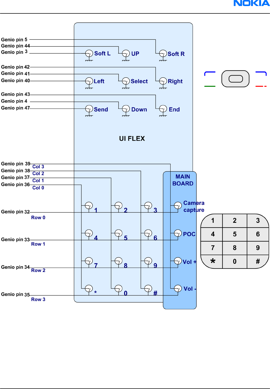
Backlight and illumination
There is backlight illuminating the display.
Behind the keypad there is an electroluminescent (EL) foil, giving the keys a blue lamaninate. The EL foil
backlight the keys with blue light for numeric soft keys and green/red for Send/End keys.
RM-123; RM-145
System Module Nokia Customer Care
Issue 1 COMPANY CONFIDENTIAL Page 8 –13
Copyright © 2006 Nokia. All rights reserved.
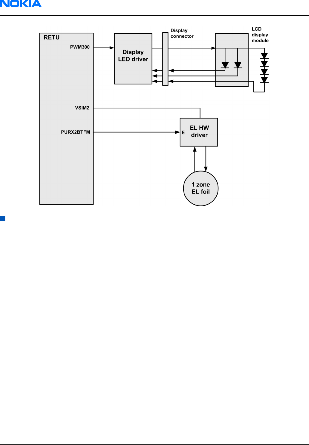
Audio concept
Audio hardware architecture
The functional core of the audio hardware is built around two ASICs: RAPGSM engine ASIC and the mixed-
signal ASIC Retu.
Retu provides an interface for the transducers and the accessory connector. Integrated hands free stereo
speakers are driven by a D-class audio amplifier.
There are four audio transducers:
• Dynamic earpiece
• Two dynamic speakers
• Microphone module
In addition to the audio transducers, Retu also provides an output for the dynamic vibra component.
RM-123; RM-145
Nokia Customer Care System Module
Page 8 –14 COMPANY CONFIDENTIAL Issue 1
Copyright © 2006 Nokia. All rights reserved.
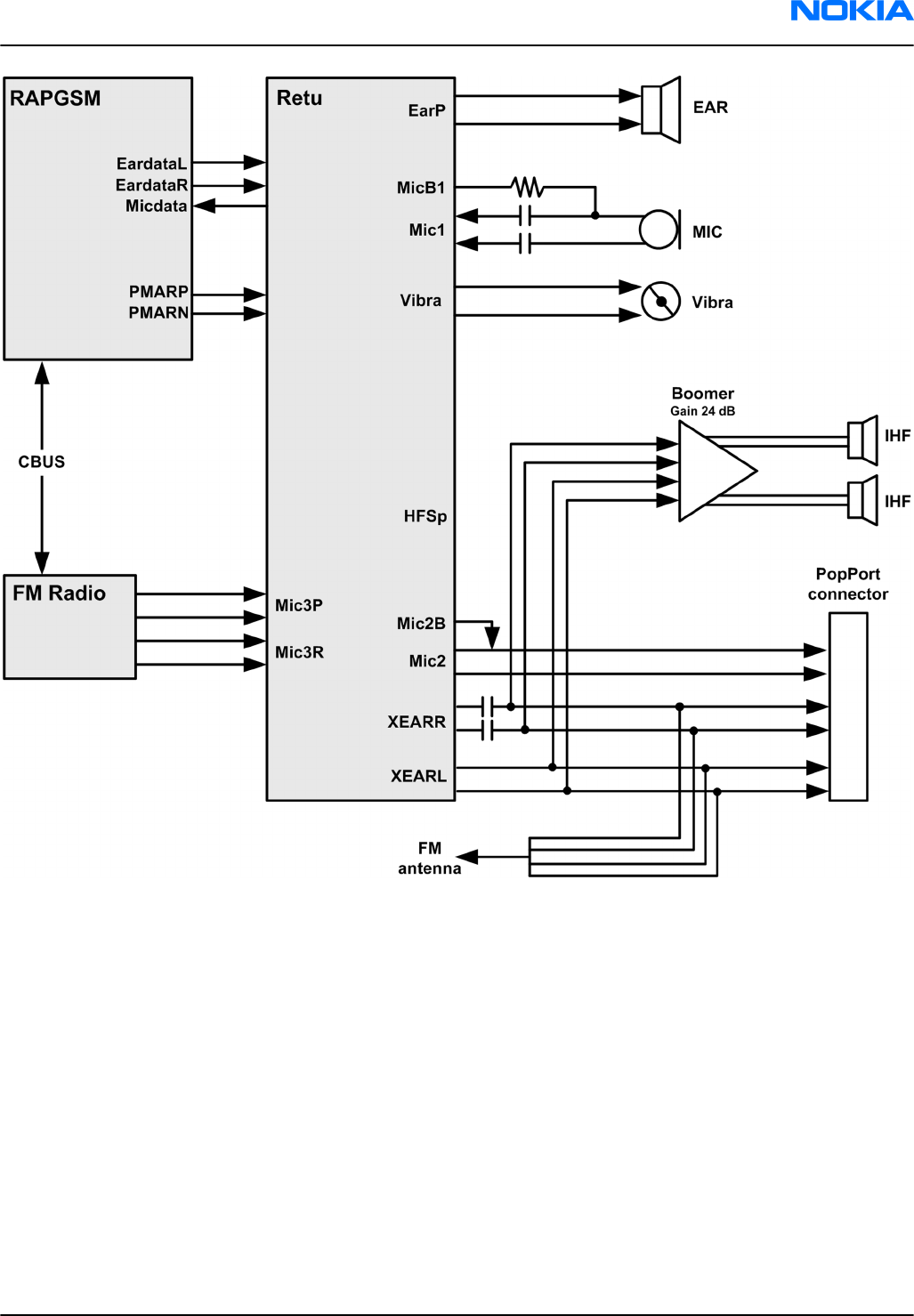
Figure 61 Audio block diagram
Internal microphone
Internal microphone is used for HandPortable (HP) and Internal HandsFree (IHF) call modes.
An analogue electret microphone is connected to N2200 Mic1P and Mic1N inputs via asymmetric electrical
connection.
The microphone is biased by N2200 MicB1 bias voltage output.
RM-123; RM-145
System Module Nokia Customer Care
Issue 1 COMPANY CONFIDENTIAL Page 8 –15
Copyright © 2006 Nokia. All rights reserved.
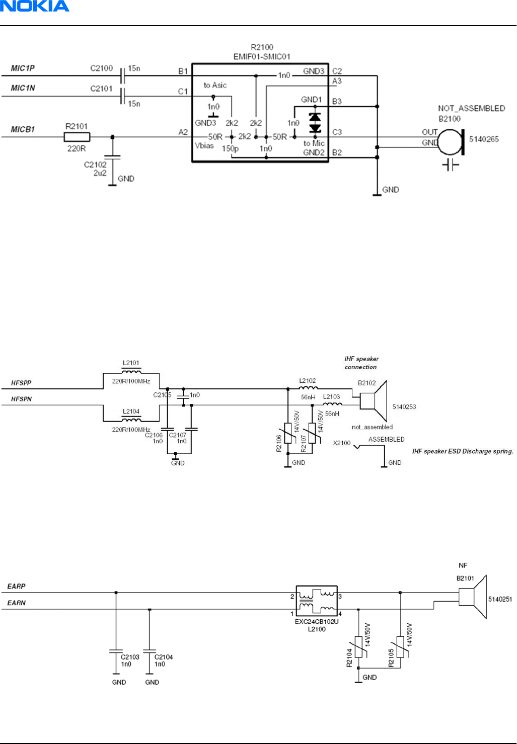
Figure 62 Internal microphone circuitry
External microphone
Galvanic accessories are connected to the system connector.
The accessory audio mode is automatically enabled/disabled during connection/disconnection of dedicated
phone accessories.
External microphone circuitry is biased by N2200 MicB2 bias voltage output. The circuitry provides a
symmetrical connection for the microphone from the system connector connections, XMICN and XMICP, to
N2200 inputs, Mic2P and Mic2N.
Figure 63 External microphone circuitry (Pop-Port™ connects to the right side)
Internal earpiece
The internal earpiece is used in the HandPortable (HP) call mode. A dynamic 8 mm earpiece capsule is
connected to N2200 differential outputs EarP and EarN.
Figure 64 Internal earpiece circuitry
RM-123; RM-145
Nokia Customer Care System Module
Page 8 –16 COMPANY CONFIDENTIAL Issue 1
Copyright © 2006 Nokia. All rights reserved.
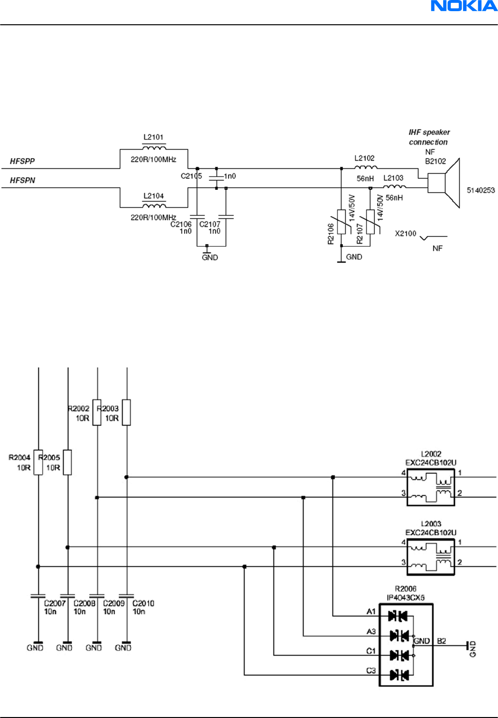
Internal speaker
The internal speaker is used in Internal HandsFree (IHF) call mode.
A dynamic 16 mm speaker is connected to N2200 outputs HFSpP and HFSpN.
The IHF amplifier integrated in N2200 is a Digital Pulse Modulated Amplifier (DPMA).
Figure 65 Internal speaker circuitry
External earpiece
All galvanic accessories are connected to the system connector.
The accessory audio mode is automatically enabled/disabled during connection/disconnection of dedicated
phone accessories.
Figure 66 External earpiece circuitry (system connector connected on the right)
RM-123; RM-145
System Module Nokia Customer Care
Issue 1 COMPANY CONFIDENTIAL Page 8 –17
Copyright © 2006 Nokia. All rights reserved.
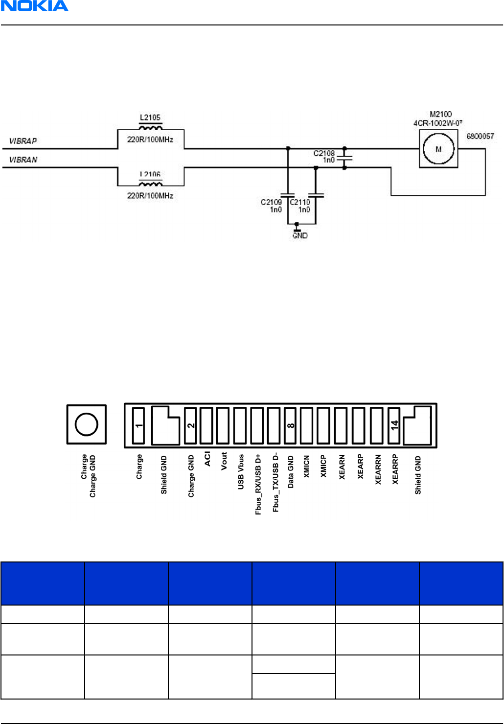
Vibra circuitry
The vibra circuitry is used for the vibra-alarm function.
The vibra motor is connected to the EM ASIC (N2200) VibraP and VibraN Pulse Width Modulated (PWM) outputs.
Figure 67 Vibra circuitry
Pop-portTM connector
Pop-PortTM connector provides a fully differential 4–wire stereo line-level output connection and fully
differential 2-wire mono line-level or microphone level input connection.
The handsfree driver in Retu is meant for the headset.
The output is driven in a fully differential mode. In the fully differential mode, the handsfree pin is the
negative output and the HFCM pin is the positive output. The gain of the handsfree driver in the differential
mode is 6 dB.
The earpiece and headset signals are multiplexed so that the outputs cannot be used simultaneously.
Figure 68 System connector pin layout
Table 17 Pop-PortTMpin and signal table
Pin #/ Signal
name Signal
description Spectral range Voltage/
Current levels Max or
nominal serial
impedance
Notes
1/ Charge V Charge DC 0-9V/ 0.85A
2/ GND Charge GND - 0.85A 100mΩ (PWB+
conn.)
3/ ACI ACI 1kbits/s Digital 0 / 47Ω Insertion &
removal
detection
2.5-2.78V
RM-123; RM-145
Nokia Customer Care System Module
Page 8 –18 COMPANY CONFIDENTIAL Issue 1
Copyright © 2006 Nokia. All rights reserved.
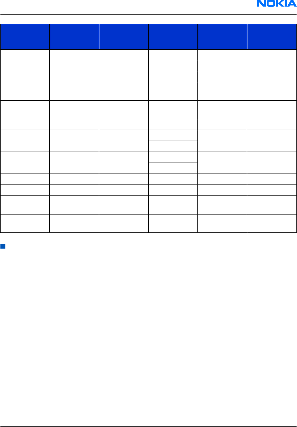
Pin #/ Signal
name Signal
description Spectral range Voltage/
Current levels Max or
nominal serial
impedance
Notes
4/ Vout DC out DC 2.78V 70 mA 100mΩ (PWB+
conn.)
200mW
2.5V 90mA
5/USB Vbus USB power 4.375-5.25VDC 115.2kbit
6/Fbus_RX/USB
D+
Data
connection
115.2kbit
7/Fbus_TX/USB
D+
Data
connection
115.2kbit
8/Data GND USB Ground 115.2kbit
9 / XMIC N Audio in 300-8k 1Vpp &
2.5-2.78VDC
10 / XMIC P Audio in 300-8k 1Vpp &
2.5-2.78VDC
11 / XEAR N Audio out 20-20k 1Vpp 10Ω
12 / XEAR P Audio out 20-20k 1Vpp 10Ω
13 / XEAR R N Audio out 20-20k 1Vpp 10Ω Not conn. in
mono
14 / XEAR R P Audio out 20-20k 1Vpp 10Ω Not conn. in
mono
Bluetooth and FM radio
Bluetooth
Bluetooth provides a fully digital link for communication between a master unit (the phone) and one or more
slave units (e.g. a wireless headset). Data and control interface for a low power RF module is provided by the
module.
The Bluetooth is physically integrated with the FM radio into one single module. From a functional point of
view they, however, have nothing in common.
RM-123; RM-145
System Module Nokia Customer Care
Issue 1 COMPANY CONFIDENTIAL Page 8 –19
Copyright © 2006 Nokia. All rights reserved.
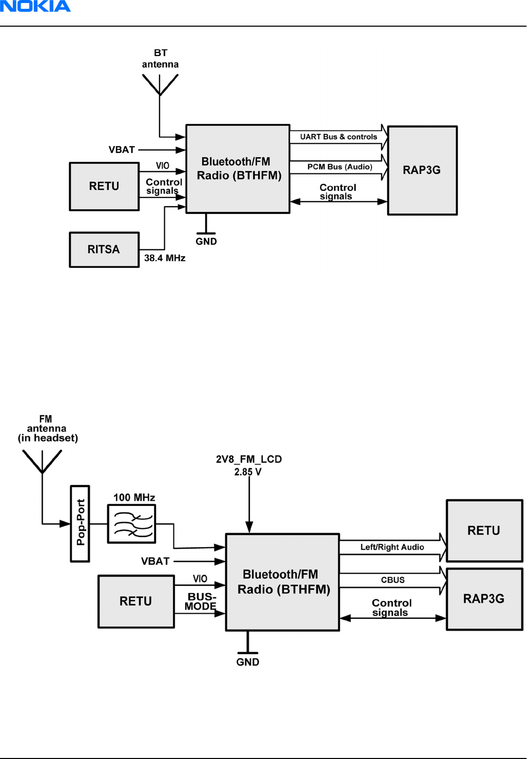
Figure 69 Bluetooth interface
The Bluetooth has a separate built in antenna and is powered by VBAT and the regulated voltage VIO. For
audio applications the Bluetooth has a PCM data bus. In addition a UART (universal asynchronous receiver/
transmitter) is used for data communication and controls.
FM radio
The FM radio is physically integrated with the Bluetooth into one single module. From a functional point of
view they, however, have nothing in common.
Figure 70 FM interface
The FM radio is an integrated circuit, controlled by MCU software through a serial bus interface. The wires of
the headset are used as poles of the antenna, and no other antenna is needed for FM radio reception.
In addition to the Bluetooth unit the FM radio is provided with LDO (low drop out) voltage 2V8_FM_LCD.
RM-123; RM-145
Nokia Customer Care System Module
Page 8 –20 COMPANY CONFIDENTIAL Issue 1
Copyright © 2006 Nokia. All rights reserved.

The radio has an automatic band search function, which can search for a strong write/read signal from a
certain frequency. When this is found, data is transmitted to the radio. When the signal strength is low, the
RETU can read data, which is available until the signal is strong again.
RF description
Introduction to receiver functionality
Receiver functions are implemented in an RF ASIC.
The receiver is a linear direct conversion receiver consisting of separate front ends (LNA (Low Noise Amplifier)
and demodulator) for each supported system. After the demodulators, the signal paths are combined to one
common BB path.
WCDMA receiver functionality
In the WCDMA mode, the received signal is fed from the antenna to a duplex filter. After the duplex filter the
signal goes via a balun to an LNA (Low Noise Amplifier) residing in N7500. From the LNA, the signal goes
trough a band pass filter.
After filtering, the signal goes to the down conversion mixer, which converts the signal to baseband I and Q
signals. At the BB frequency the signal is amplified, and fed to a low pass filter. The Rx channel filter must be
calibrated with an automatic routine whenever the Rx ASIC IC is changed to a phone.
In the WCDMA mode, the corner frequency of the filter is set to approximately 2.1 MHz. The filter is followed
by an AGC (Automatic Gain Control) amplifier with an adjustable gain. The signal is further amplified before
it is fed to balanced analogue IQ output pins. The analogue output pins are accompanied by reference voltage
output, which sets the DC level for the AD converter in the BB ASIC RAP.
The last stage of the RF Rx chain is an output buffer which feeds the signal and a reference voltage (VREFCM)
to the BB ASIC.
GSM receiver functionality
As GSM Rx branches are functionally identical, the following description is applicable to all of them.
The received signal goes from the GSM antenna to the antenna switch module.
The antenna switch module is followed by integrated LNAs residing in the Rx ASIC.
The LNAs are followed by demodulators which downconvert the signal to baseband I and Q signals.
After the down conversion mixer, the Rx chain is similar to the WCDMA Rx. The channel select filter is set to
115 kHz in the GSM mode.
Introduction to transmitter functionality
Transmitter functions are implemented in an RF ASIC. The ASIC contains a BB frequency low pass filter, which
is tunable according to the signal bandwidth of the system in use.
In addition, the ASIC contains separate RF paths comprising a final frequency IQ modulator and VGA amplifiers.
WCDMA transmitter functionality
In the transmitter side, an analogue I/Q modulated signal is received from digital baseband into an RF ASIC
and fed through a low pass filter. After the filter the signal is fed to the IQ modulator, which converts the
signal to final Tx frequency. There are two separate I/Q modulators: one for WCDMA and another for GSM
signals. The signal then exits the RF ASIC via a balanced line. Next, the signal is band pass filtered by a SAW
filter before it is fed to the WCDMA PA module. After the PA, the transmitted WCDMA signal is fed through an
isolator and a duplex filter to the antenna.
RM-123; RM-145
System Module Nokia Customer Care
Issue 1 COMPANY CONFIDENTIAL Page 8 –21
Copyright © 2006 Nokia. All rights reserved.
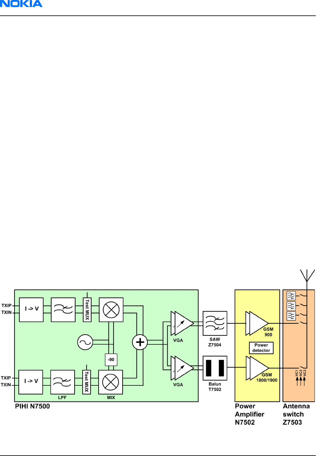
WCDMA power control
WCDMA Tx power control is accomplished by the two VGA amplifier stages in the Tx ASIC.
The VGAs have a common temperature compensation circuit and one voltage mode analogue input for gain
control (TXC).
Another function of the detector voltage is to steer the DC/DC converter, which is providing a variable supply
voltage for the WCDMA PA.
WCDMA PA module
The WCDMA PA is housed in a separate module having:
• a variable supply voltage input for the amplifier stages (Vcc11),
• a battery supply voltage for the bias circuits (Vcc12),
• and two bias current inputs.
Bias currents are generated by 5-bit DA converters in the RF ASIC.
If a different manufacturer's PA is changed to the phone, this setting must be set again.
PA DC/DC converter
The control of the DC/DC converter is fed back from the power detector circuit.
GSM transmitter functionality
An RF ASIC receives an analogue IQ modulated signal from digital BB, which is first low pass filtered with
filter corner frequency set to approximately 200 kHz. After the filter, the signal is routed to the GSM modulator.
The amplifier gives 40 dB of power control dynamic range.
After the VGA stage the signal exits the RF ASIC. In case of GSM1800/1900 the signal goes via a balun to the
GSM PA module. In case of GSM900, the PA module is preceded by a SAW filter. After the filter, the signal is
fed to the GSM front end module (FEM). Finally, the signal is routed via FEM to the antenna.
Figure 71 GSM transmitter
RM-123; RM-145
Nokia Customer Care System Module
Page 8 –22 COMPANY CONFIDENTIAL Issue 1
Copyright © 2006 Nokia. All rights reserved.

GSM power control
A closed control loop comprise an integrated power detector (in PA module) and an error amplifier. The error
amplifier resides in N7500, and it controls the transmitter power of GSM.
GSM PA module
A single GSM/EDGE PA module contains two separate amplifier chains, one for GSM900 and another for
GSM1800/1900. Both amplifiers have a battery supply connection and two bias current inputs.
Frequency synthesizers
RF has separate synthesizers for Rx and Tx. Both synthesizers consist of:
• PLL (Phase-Locked Loop)
• loop filter
• VCO (Voltage Controlled Oscillator)
• balun
The VCO frequencies are locked by PLLs into a reference oscillator, VCTCXO (Voltage Controlled Temperature
Compensated Crystal Oscillator).
The PLLs are located in RF ASICs and controlled via RFBus.
Reference oscillators
A 38.4MHz VCTCXO is used as a reference oscillator for the frequency synthesizers.
Regulators
RF ASIC contain integrated regulators to supply regulated voltages for their internal circuitry and other RF
parts. Rx VCO supply is got via a switch from an RF ASIC VR1 regulator. VCO can be switched on and off by
controlling the switch via RFBus.
Supply voltage for the VCTCXO is provided by a BB mixed mode ASIC. The same supply is used for reference
clock input buffers, output buffers and for the digital control blocks of both RF ASICs.
Other supplies, like 4.7 V supply for PLL charge pumps and bias reference (VREFRF01) are also provided by
the BB mixed mode ASIC.
RM-123; RM-145
System Module Nokia Customer Care
Issue 1 COMPANY CONFIDENTIAL Page 8 –23
Copyright © 2006 Nokia. All rights reserved.
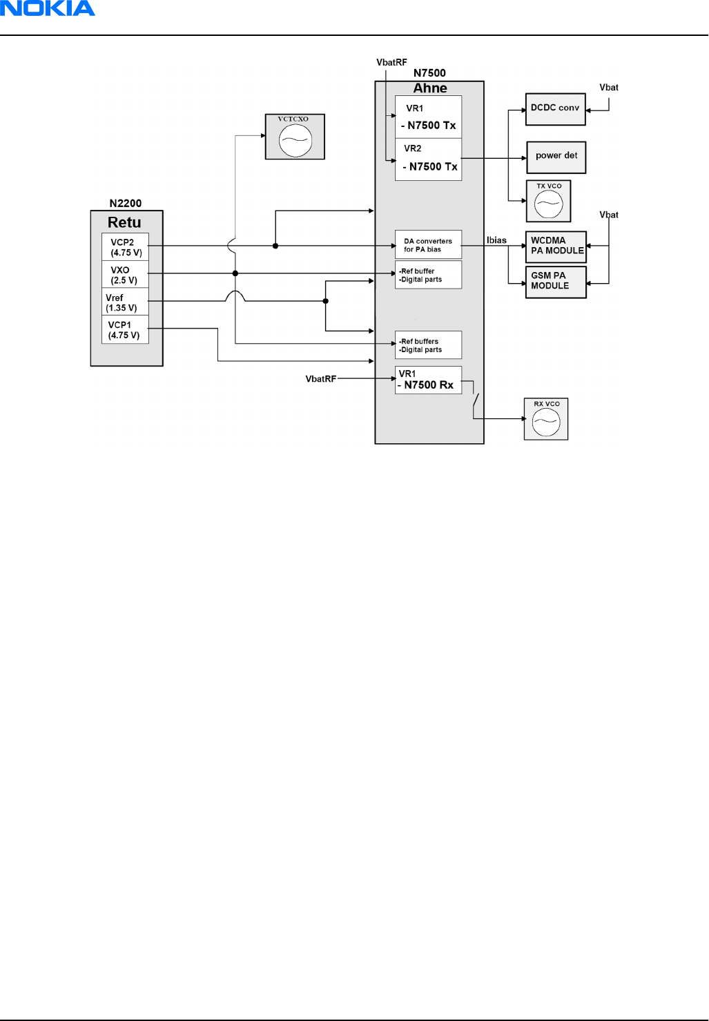
Figure 72 RF supply connections from the BB mixed mode ASIC
RM-123; RM-145
Nokia Customer Care System Module
Page 8 –24 COMPANY CONFIDENTIAL Issue 1
Copyright © 2006 Nokia. All rights reserved.

9 — Schematics
Nokia Customer Care
Issue 1 COMPANY CONFIDENTIAL Page 9 –1
Copyright © 2006 Nokia. All rights reserved.

RM-123; RM-145
Nokia Customer Care Schematics
(This page left intentionally blank.)
Page 9 –2 COMPANY CONFIDENTIAL Issue 1
Copyright © 2006 Nokia. All rights reserved.

Table of Contents
Schematics..............................................................................................................................................................9–4
RM-123; RM-145
Schematics Nokia Customer Care
Issue 1 COMPANY CONFIDENTIAL Page 9 –3
Copyright © 2006 Nokia. All rights reserved.
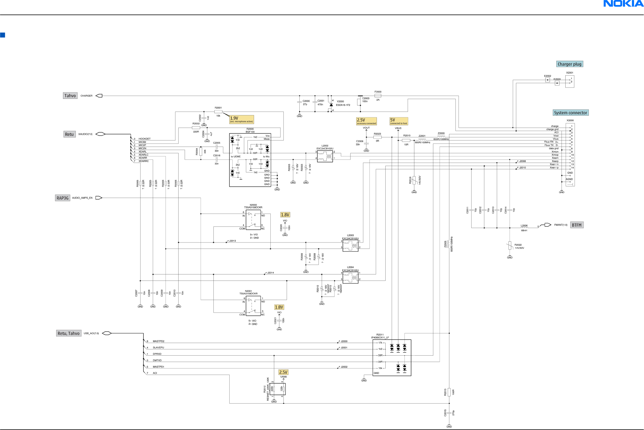
Schematics
System connector
RM-123; RM-145
Schematics Nokia Customer Care
Issue 1 COMPANY CONFIDENTIAL Page 9 –4
Copyright © 2006 Nokia. All rights reserved.
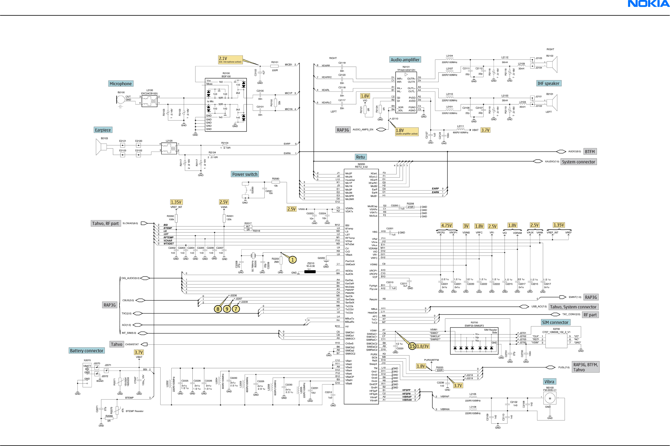
RETU, SIM, Audio
RM-123; RM-145
Schematics Nokia Customer Care
Issue 1 COMPANY CONFIDENTIAL Page 9 –5
Copyright © 2006 Nokia. All rights reserved.
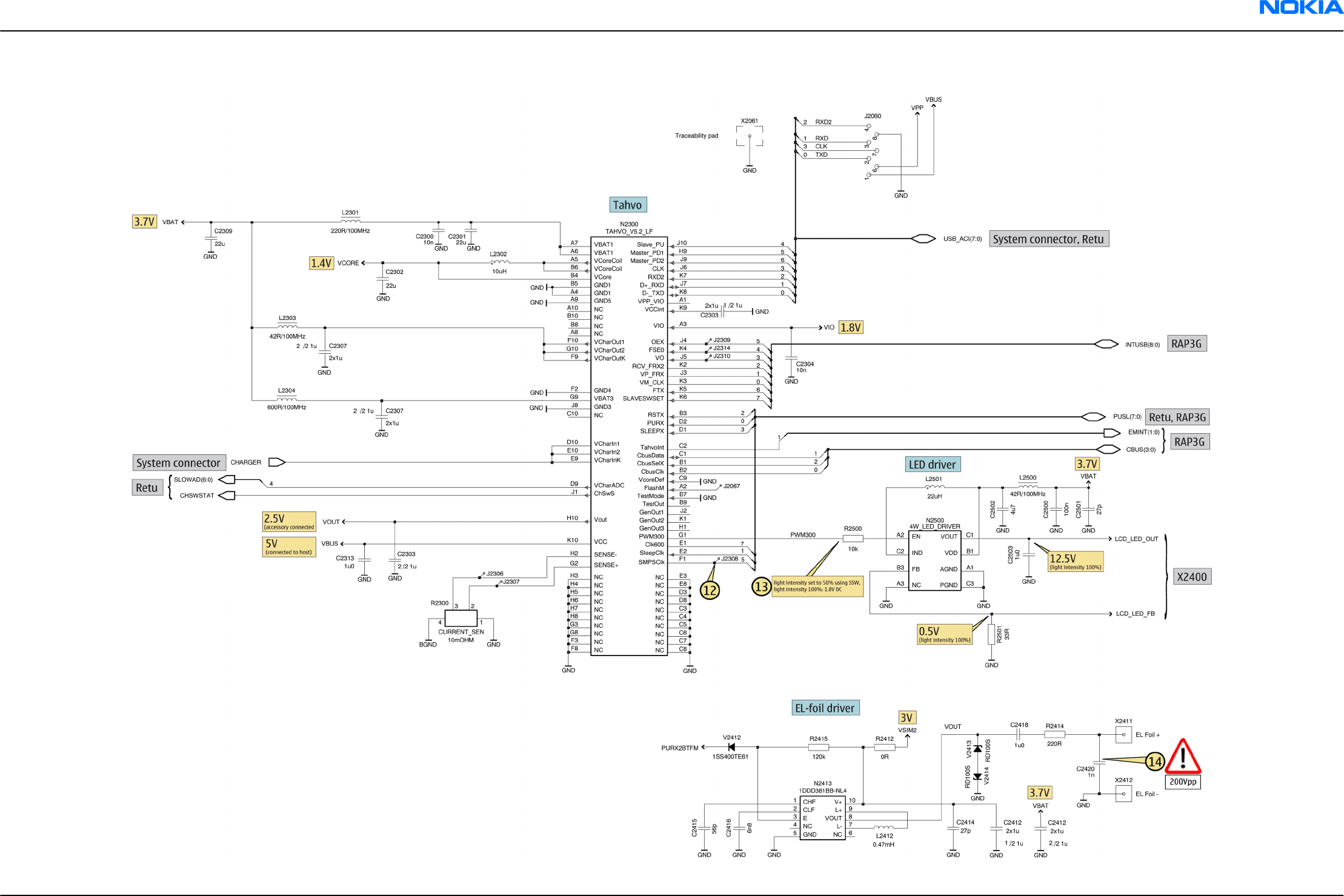
TAHVO and LED/EL driver
RM-123; RM-145
Schematics Nokia Customer Care
Issue 1 COMPANY CONFIDENTIAL Page 9 –6
Copyright © 2006 Nokia. All rights reserved.
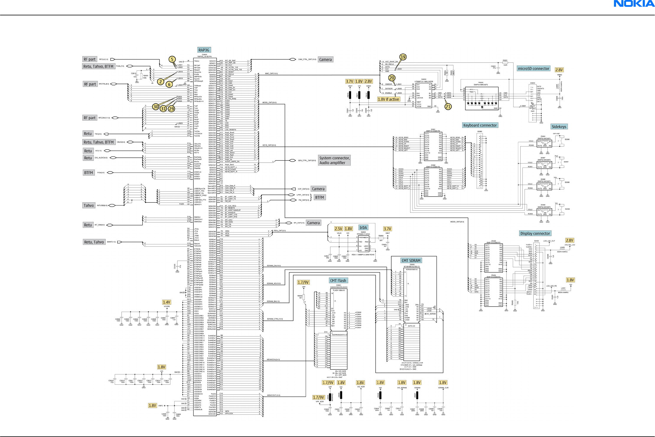
RAPGSM, Memory, µSD
RM-123; RM-145
Schematics Nokia Customer Care
Issue 1 COMPANY CONFIDENTIAL Page 9 –7
Copyright © 2006 Nokia. All rights reserved.
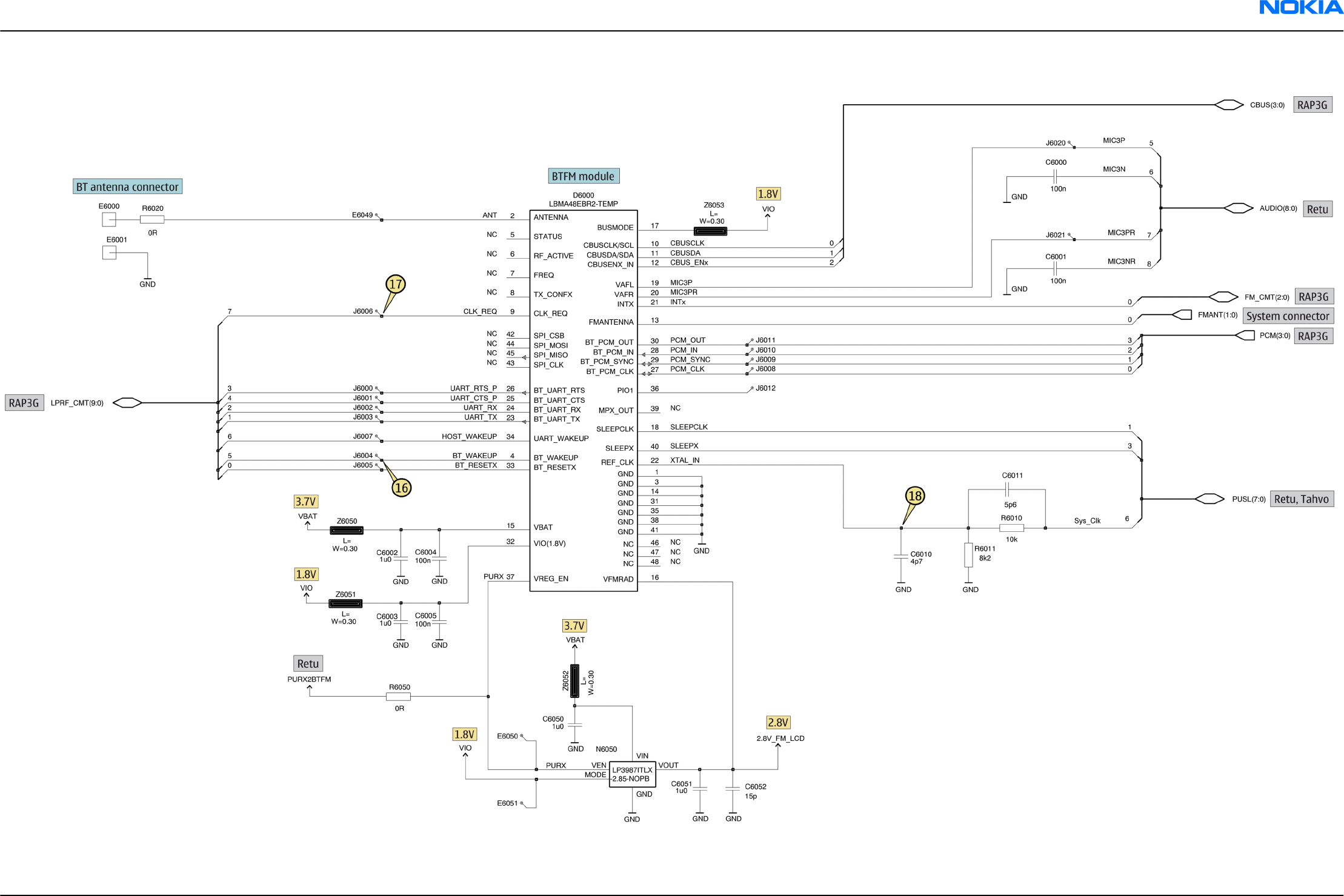
FM radio, Bluetooth
RM-123; RM-145
Schematics Nokia Customer Care
Issue 1 COMPANY CONFIDENTIAL Page 9 –8
Copyright © 2006 Nokia. All rights reserved.
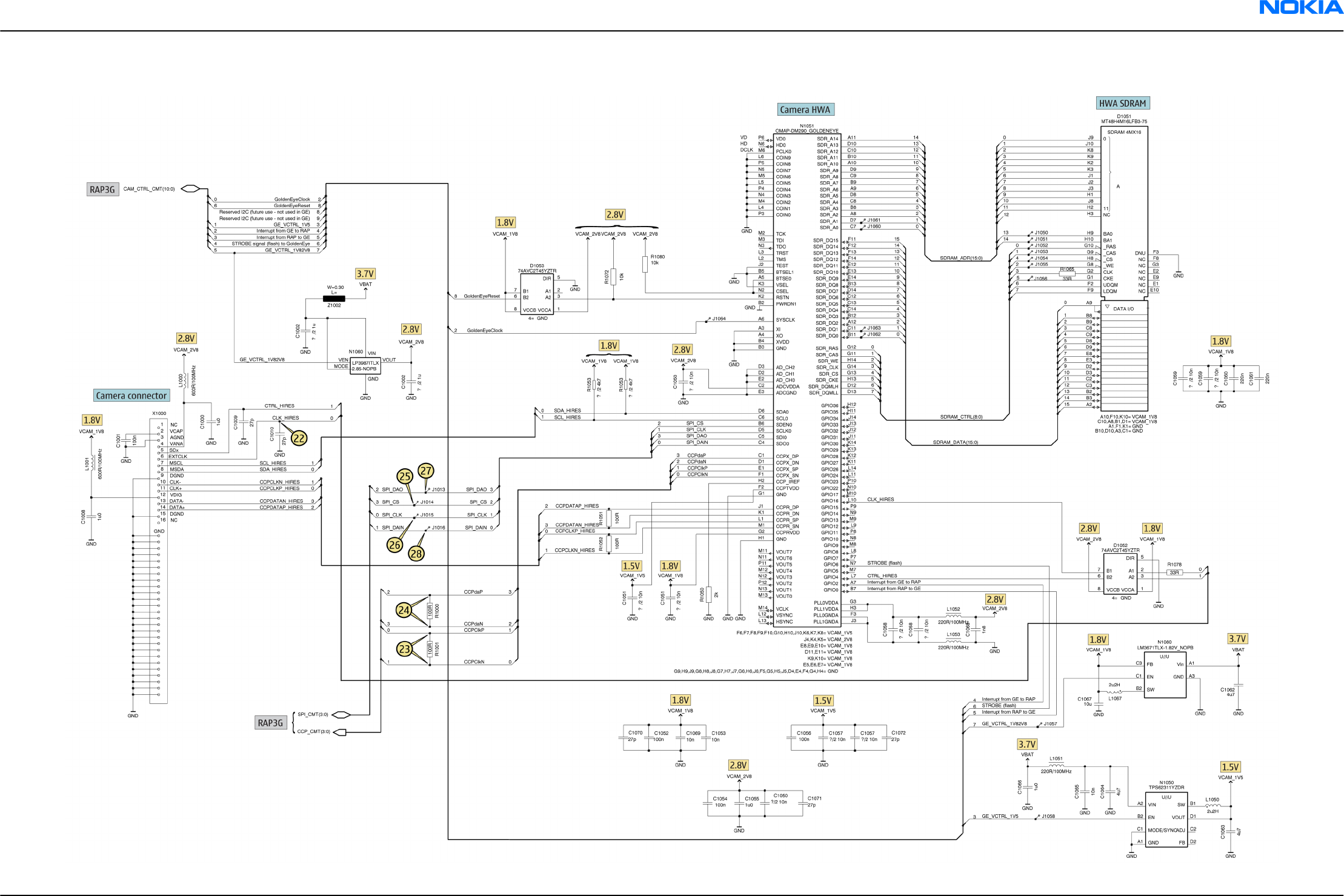
Camera
RM-123; RM-145
Schematics Nokia Customer Care
Issue 1 COMPANY CONFIDENTIAL Page 9 –9
Copyright © 2006 Nokia. All rights reserved.
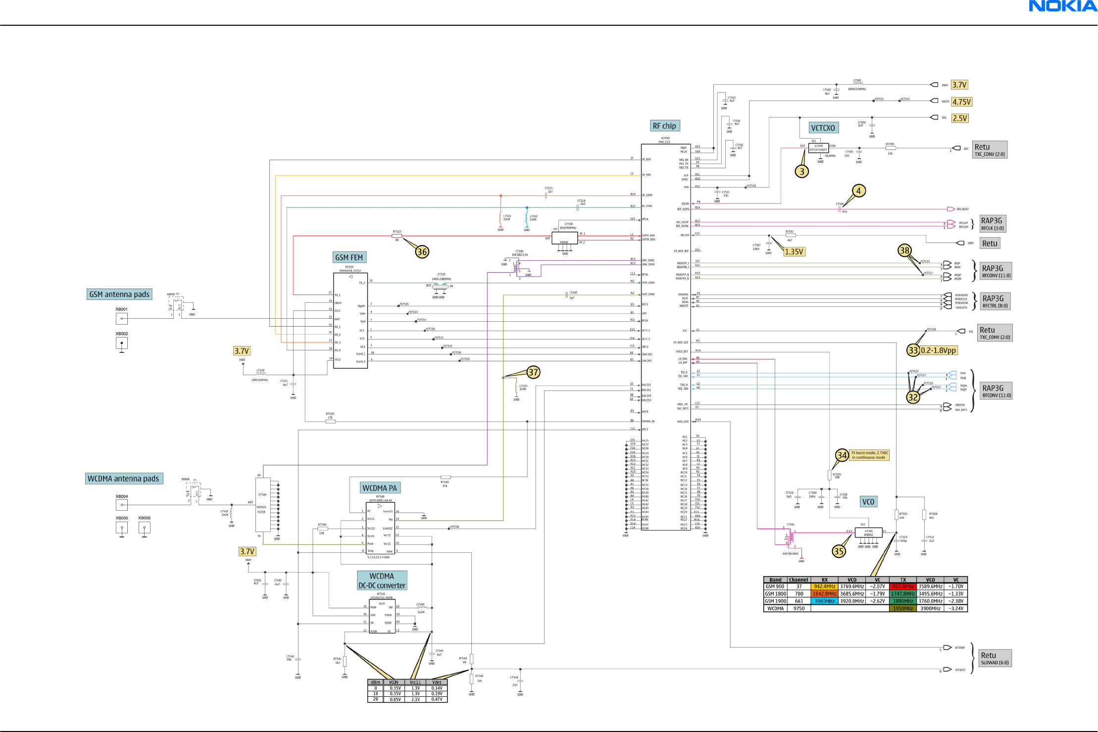
RF part
RM-123; RM-145
Schematics Nokia Customer Care
Issue 1 COMPANY CONFIDENTIAL Page 9 –10
Copyright © 2006 Nokia. All rights reserved.
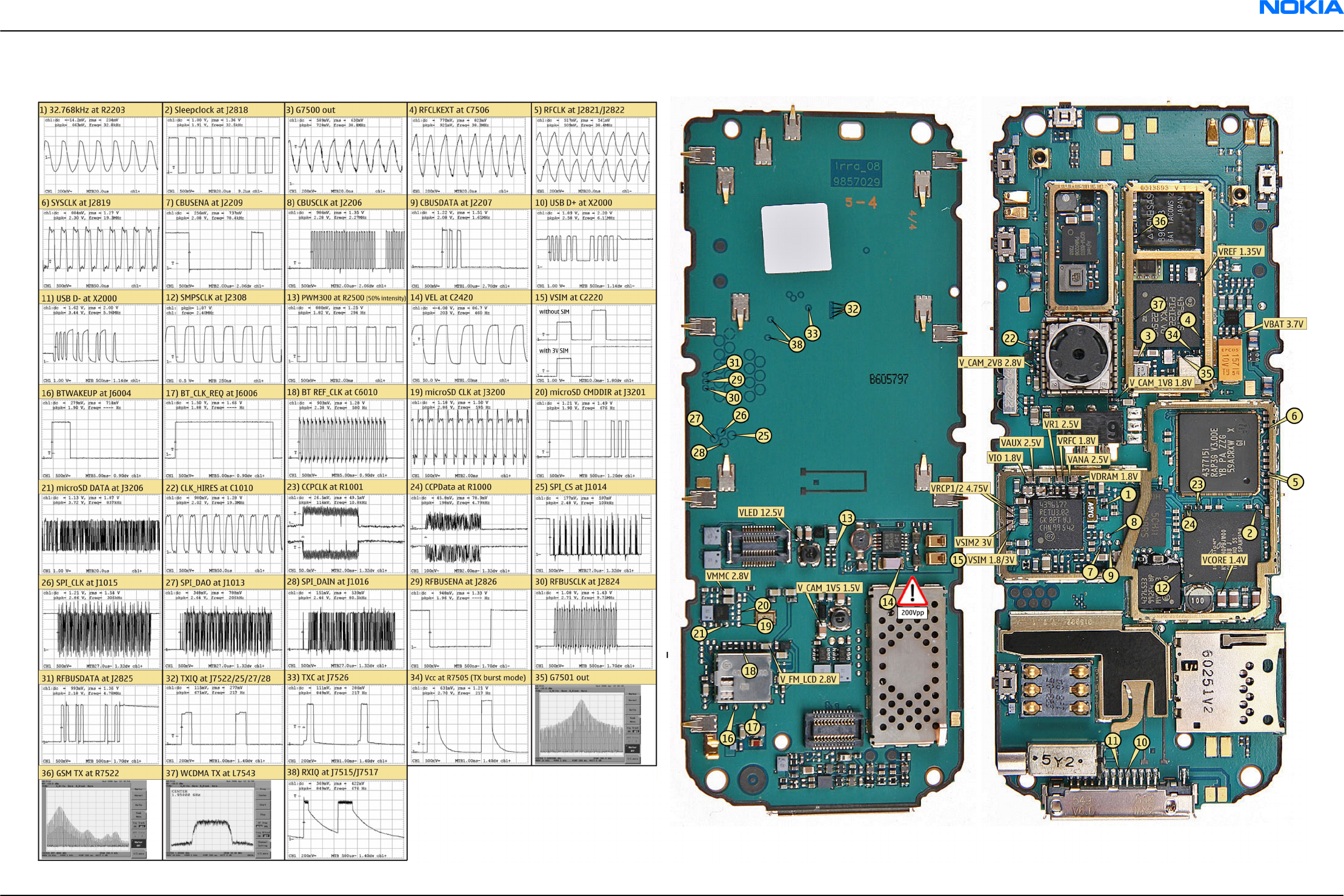
Signal overview
RM-123; RM-145
Schematics Nokia Customer Care
Issue 1 COMPANY CONFIDENTIAL Page 9 –11
Copyright © 2006 Nokia. All rights reserved.
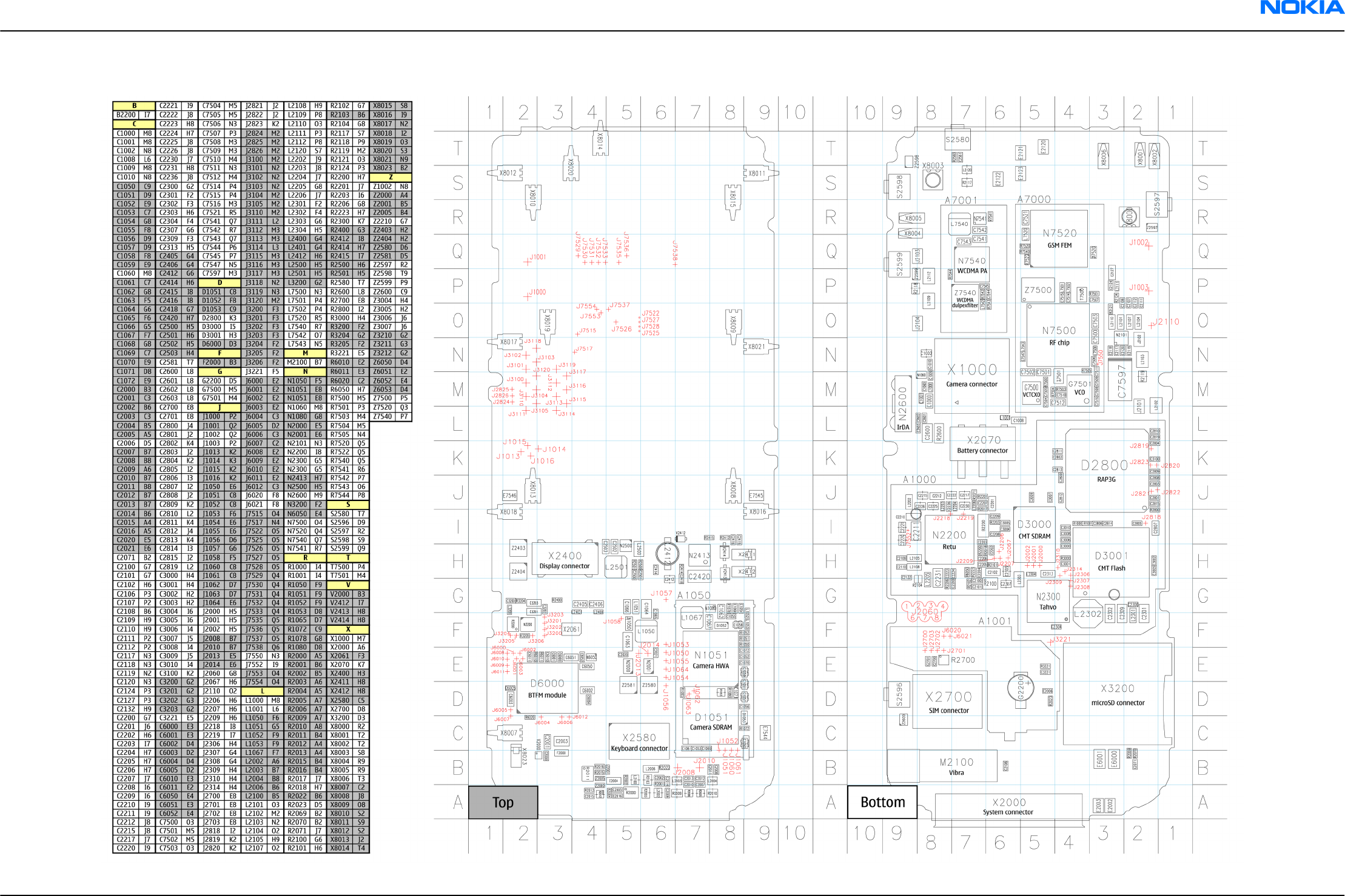
Component finder
RM-123; RM-145
Schematics Nokia Customer Care
Issue 1 COMPANY CONFIDENTIAL Page 9 –12
Copyright © 2006 Nokia. All rights reserved.

Glossary
Nokia Customer Care
Issue 1 COMPANY CONFIDENTIAL Page Glossary–1
Copyright © 2006 Nokia. All rights reserved.

RM-123; RM-145
Nokia Customer Care Glossary
(This page left intentionally blank.)
Page Glossary–2 COMPANY CONFIDENTIAL Issue 1
Copyright © 2006 Nokia. All rights reserved.
A/D-converter Analog-to-digital converter
ACI Accessory Control Interface
ADC Analog-to-digital converter
ADSP Application DPS (expected to run high level tasks)
AGC Automatic gain control (maintains volume)
ALS Ambient light sensor
AMSL After Market Service Leader
ARM Advanced RISC Machines
ARPU Average revenue per user (per month or per year)
ASIC Application Specific Integrated Circuit
ASIP Application Specific Interface Protector
B2B Board to board, connector between PWB and UI board
BB Baseband
BC02 Bluetooth module made by CSR
BIQUAD Bi-quadratic ,type of filter function)
BSI Battery Size Indicator
BT Bluetooth
CBus MCU controlled serial bus connected to UPP_WD2,UEME and Zocus
CCP Compact Camera Port
CDSP Cellular DSP (expected to run at low levels)
CLDC Connected limited device configuration
CMOS Complimentary metal-oxide semiconductor circuit (low power consumption)
COF Chip on Foil
COG Chip on Glass
CPU Central Processing Unit
CSR cambridge silicon radio
CSTN Color Super Twisted Nematic
CTSI Clock Timing Sleep and interrupt block of Tiku
CW Continuous wave
D/A-converter Digital-to-analouge converter
DAC Digital-to-analouge converter
DBI Digital Battery Interface
DBus DSP controlled serial bus connected between UPP_WD2 and Helgo
DCT-4 Digital Core Technology
DMA Direct memory access
DP Data Package
RM-123; RM-145
Glossary Nokia Customer Care
Issue 1 COMPANY CONFIDENTIAL Page Glossary–3
Copyright © 2006 Nokia. All rights reserved.
DPLL Digital Phase Locked Loop
DSP Digital Signal Processor
DtoS Differential to Single ended
EDGE Enhanced data rates for global/GSM evaluation
EGSM Extended GSM
EM Energy management
EMC Electromagnetic compability
EMI Electromagnetic interference
ESD Electrostatic discharge
FCI Functional cover interface
FPS Flash Programming Tool
FR Full rate
FSTN Film compensated super twisted nematic
GND Ground, conductive mass
GPIB General-purpose interface bus
GPRS General Packet Radio Service
GSM Group Special Mobile/Global System for Mobile communication
HF Hands free
HFCM Handsfree Common
HS Handset
HSCSD High speed circuit switched data (data transmission connection faster than GSM)
HW Hardware
I/O Input/Output
IBAT Battery current
IC Integrated circuit
ICHAR Charger current
IF Interface
IHF Integrated hands free
IMEI International Mobile Equipment Identity
IR Infrared
IrDA Infrared Data Associasion
ISA Intelligent software architecture
JPEG/JPG Joint Photographic Experts Group
LCD Liquid Crystal Display
LDO Low Drop Out
LED Light-emitting diode
RM-123; RM-145
Nokia Customer Care Glossary
Page Glossary–4 COMPANY CONFIDENTIAL Issue 1
Copyright © 2006 Nokia. All rights reserved.

LPRF Low Power Radio Frequency
MCU Micro Controller Unit (microprocessor)
MCU Multiport control unit
MIC, mic Microphone
MIDP Mobile Information Device Profile
MIN Mobile identification number
MIPS Million instructions per second
MMC Multimedia card
MMS Multimedia messaging service
NTC Negative temperature coefficient, temperature sensitive resistor used as a
temperature sensor
OMA Object management architechture
OMAP Operations, maintenance, and administartion part
Opamp Operational Amplifier
PA Power amplifier
PDA Pocket Data Application
PDA Personal digital assistant
PDRAM Program/Data RAM (on chip in Tiku)
Phoenix Software tool of DCT4.x
PIM Personal Information Management
PLL Phase locked loop
PM (Phone) Permanent memory
PUP General Purpose IO (PIO), USARTS and Pulse Width Modulators
PURX Power-up reset
PWB Printed Wiring Board
PWM Pulse width modulation
RC-filter Resistance-Capacitance filter
RF Radio Frequency
RF PopPort TM Reduced function PopPortTM interface
RFBUS Serial control Bus For RF
RSK Right Soft Key
RS-MMC Reduced size Multi Media Card
RSSI Receiving signal strength indicator
RST Reset Switch
RTC Real Time Clock (provides date and time)
RX Radio Receiver
RM-123; RM-145
Glossary Nokia Customer Care
Issue 1 COMPANY CONFIDENTIAL Page Glossary–5
Copyright © 2006 Nokia. All rights reserved.
SARAM Single Access RAM
SAW filter Surface Acoustic Wave filter
SDRAM Synchronous Dynamic Random Access Memory
SID Security ID
SIM Subscriber Identity Module
SMPS Switched Mode Power Supply
SNR Signal-to-noice ratio
SPR Standard Product requirements
SRAM Static random access memory
STI Serial Trace Interface
SW Software
SWIM Subscriber/Wallet Identification Module
TCXO Temperature controlled Oscillator
Tiku Finnish for Chip, Successor of the UPP, Official Tiku3G
TX Radio Transmitter
UART Universal asynchronous receiver/transmitter
UEME Universal Energy Management chip (Enhanced version)
UEMEK See UEME
UI User Interface
UPP Universal Phone Processor
UPP_WD2 Communicator version of DCT4 system ASIC
USB Universal Serial Bus
VBAT Battery voltage
VCHAR Charger voltage
VCO Voltage controlled oscillator
VCTCXO Voltage Controlled Temperature Compensated Crystal Oscillator
VCXO Voltage Controlled Crystal Oscillator
Vp-p Peak-to-peak voltage
VSIM SIM voltage
WAP Wireless application protocol
WD Watchdog
XHTML Extensible hypertext markup language
Zocus Current sensor, (used to monitor the current flow to and from the battery)
RM-123; RM-145
Nokia Customer Care Glossary
Page Glossary–6 COMPANY CONFIDENTIAL Issue 1
Copyright © 2006 Nokia. All rights reserved.
