Nokia 6260 Rm 25 Service Manual
User Manual: Smartphone Nokia 6260 RM-25 - Service manuals and Schematics, Disassembly / Assembly. Free.
Open the PDF directly: View PDF ![]() .
.
Page Count: 316 [warning: Documents this large are best viewed by clicking the View PDF Link!]
- Service Manual RM-25
- Nokia 6260 Service Manual Structure
- 1 General information
- 2 Parts and layouts
- 3 Phoenix service software
- 4 Service tools
- 5 Disassembly and reassembly instructions
- 6 Baseband troubleshooting
- Troubleshooting baseband
- Troubleshooting dead or jammed phone
- BB self test tools
- Troubleshooting flash programming
- General power troubleshooting
- Baseband serial interface troubleshooting
- Troubleshooting charger interface
- Energy management calibration
- Baseband troubleshooting tips
- Backup battery troubleshooting
- Troubleshooting USB interface
- SIM card fault
- “Insert SIM Card” in device display although card is inserted
- Troubleshooting keypad interface
- Troubleshooting the display
- Troubleshooting display and keyboard backlight
- Troubleshooting MMC interface
- Audio troubleshooting
- Troubleshooting accessory detection
- Troubleshooting IrDA
- Troubleshooting FM radio
- Tuning baseband
- Testing and tuning BB after component replacement
- 7 RF troubleshooting
- Introduction to RF troubleshooting
- RF key component placement
- Receiver
- Receiver troubleshooting
- Measuring Rx/IQ signals using RSSI
- Measuring RX performance using SNR measurement
- Measuring Rx module manually using oscilloscope and spectrum analyzer (EGSM900)
- Measuring Rx module manually using oscilloscope and spectrum analyzer (GSM1800)
- Measuring Rx module manually using oscilloscope and spectrum analyzer (GSM1900)
- RM-25 measurement points in the receiver
- Calibrating RX Channel Select Filter
- Calibrating RX
- Transmitter
- Introduction to RM-25 transmitter troubleshooting
- Preparing for transmitter troubleshooting
- Troubleshooting TX-BB interface and control signals
- Troubleshooting RF side of transmitter
- Introduction to transmitter tuning
- Tuning TX/IQ
- Tuning TX power level
- Introduction to synthesizer troubleshooting
- Preparing for synthesizer troubleshooting
- Measuring the synthesizer manually using spectrum analyzer
- Bluetooth
- 8 Camera module troubleshooting
- 9 System module
- System module block diagram
- Functional description
- BB description
- Modes of operation
- Clocking scheme
- Power distribution, control and reset
- Back-up battery and real time clock
- Baseband measurement A/D converter
- ZOCUS
- Bluetooth
- USB
- SIM interface
- IrDA interface
- MMC interface
- Pop-PortTM
- Audio concept
- Camera interface
- FM radio
- Flashing
- Mode sensing
- Testing interfaces
- Extreme voltages
- RF description
- 10 Schematics
- RF BB module top level
- BB top level
- Production test pattern
- Power supplier top level
- Aux_power
- UEME/UEMEK
- Card interface
- Card interface module
- FM radio top level
- FM radio module
- Pop-portTM and microphone
- UPP_WD2
- IR module
- User interface (top part and keyboard)
- User interface (camera)
- User interface (empty)
- USB
- USB module
- Memory
- Bluetooth
- Bluetooth module
- BB-RF Interface
- Testpad
- RF top level
- HELGO
- RF9204 power amplifier and power detection
- RX front end and antenna switch
- Component layout, bottom
- Component layout, top
- Glossary

Service Manual
RM-25 (Nokia 6260)
Mobile Terminal
Part No: (9235618 (Issue 2))
Nokia Customer Care
Company Confidential
Copyright ©2005 Nokia. All Rights Reserved.
Amendment Record Sheet
Amendment No Date Inserted By Comments
Original issue 08/2004 MHa, TSa MODE Service Information Pilot
Project
Issue 2 02/2005 J Bryman 01 General information:Variants
(product and modules) corrected
02 Parts and layouts: Exploded view
corrected, lists and layouts updated,
SWAP units added
04 Service tools and concepts:
Prommers FPS-10&11 added, RJ-24
and ST-5 added.
06 Baseband: Tuning baseband
updated
07 RF troubleshooting: Baseband
and digital IQs, RF key components, RX
Calibration, Tuning TX power level,
Test points main board updated.
10 Schematics: 1fsa_11 schematics
added
RM-25
Nokia Customer Care Amendment Record Sheet
Page ii Company Confidential 9235618 (Issue 2)
Copyright ©2005 Nokia. All Rights Reserved.

Introduction to Issue 2
This is the updated issue of the RM-25 service manual. The parts of the manual that have been changed are
presented on the Amendment record sheet. However, some major hardware updates worth mentioning are:
• Latest build is 1fsa_11a
• UEMEK is used instead of UEME (though the name has not been updated in this manual)
• Helgo 85G is used instead of Helgo 86LB
For the latest version of the parts lists, please refer to the Service bulletins.
RM-25
Introduction to Issue 2 Nokia Customer Care
9235618 (Issue 2) Company Confidential Page iii
Copyright ©2005 Nokia. All Rights Reserved.

Copyright
Copyright © 2005 Nokia. All rights reserved.
Reproduction, transfer, distribution or storage of part or all of the contents in this document in any form without
the prior written permission of Nokia is prohibited.
Nokia, Nokia Connecting People, and Nokia X and Y are trademarks or registered trademarks of Nokia
Corporation. Other product and company names mentioned herein may be trademarks or tradenames of their
respective owners.
Nokia operates a policy of continuous development. Nokia reserves the right to make changes and
improvements to any of the products described in this document without prior notice.
Under no circumstances shall Nokia be responsible for any loss of data or income or any special, incidental,
consequential or indirect damages howsoever caused.
The contents of this document are provided “as is”. Except as required by applicable law, no warranties of any
kind, either express or implied, including, but not limited to, the implied warranties of merchantability and
fitness for a particular purpose, are made in relation to the accuracy, reliability or contents of this document.
Nokia reserves the right to revise this document or withdraw it at any time without prior notice.
The availability of particular products may vary by region.
IMPORTANT
This document is intended for use by qualified service personnel only.
RM-25
Nokia Customer Care Copyright
Page iv Company Confidential 9235618 (Issue 2)
Copyright ©2005 Nokia. All Rights Reserved.

Warnings and cautions
Warnings
•IF THE DEVICE CAN BE INSTALLED IN A VEHICLE, CARE MUST BE TAKEN ON INSTALLATION IN VEHICLES FITTED WITH
ELECTRONIC ENGINE MANAGEMENT SYSTEMS AND ANTI-SKID BRAKING SYSTEMS. UNDER CERTAIN FAULT
CONDITIONS, EMITTED RF ENERGY CAN AFFECT THEIR OPERATION. IF NECESSARY, CONSULT THE VEHICLE DEALER/
MANUFACTURER TO DETERMINE THE IMMUNITY OF VEHICLE ELECTRONIC SYSTEMS TO RF ENERGY.
• THE PRODUCT MUST NOT BE OPERATED IN AREAS LIKELY TO CONTAIN POTENTIALLY EXPLOSIVE ATMOSPHERES, FOR
EXAMPLE, PETROL STATIONS (SERVICE STATIONS), BLASTING AREAS ETC.
• OPERATION OF ANY RADIO TRANSMITTING EQUIPMENT, INCLUDING CELLULAR TELEPHONES, MAY INTERFERE WITH
THE FUNCTIONALITY OF INADEQUATELY PROTECTED MEDICAL DEVICES. CONSULT A PHYSICIAN OR THE
MANUFACTURER OF THE MEDICAL DEVICE IF YOU HAVE ANY QUESTIONS. OTHER ELECTRONIC EQUIPMENT MAY ALSO
BE SUBJECT TO INTERFERENCE.
• BEFORE MAKING ANY TEST CONNECTIONS, MAKE SURE YOU HAVE SWITCHED OFF ALL EQUIPMENT.
Cautions
• Servicing and alignment must be undertaken by qualified personnel only.
• Ensure all work is carried out at an anti-static workstation and that an anti-static wrist strap is worn.
• Ensure solder, wire, or foreign matter does not enter the telephone as damage may result.
• Use only approved components as specified in the parts list.
• Ensure all components, modules, screws and insulators are correctly re-fitted after servicing and alignment.
Ensure all cables and wires are repositioned correctly.
Use only approved components as specified in the parts list.
• Never test a mobile phone WCDMA transmitter with full Tx power, if there is no possibility to perform the
measurements in a good performance RF-shielded room. Even low power WCDMA transmitters may disturb
nearby WCDMA networks and cause problems to 3G cellular phone communication in a wide area.
• During testing never activate the GSM or WCDMA transmitter without a proper antenna load, otherwise GSM
or WCDMA PA may be damaged.
RM-25
Warnings and cautions Nokia Customer Care
9235618 (Issue 2) Company Confidential Page v
Copyright ©2005 Nokia. All Rights Reserved.

For your safety
QUALIFIED SERVICE
Only qualified personnel may install or repair phone equipment.
ACCESSORIES AND BATTERIES
Use only approved accessories and batteries. Do not connect incompatible products.
CONNECTING TO OTHER DEVICES
When connecting to any other device, read its user’s guide for detailed safety instructions. Do not connect
incompatible products.
RM-25
Nokia Customer Care For your safety
Page vi Company Confidential 9235618 (Issue 2)
Copyright ©2005 Nokia. All Rights Reserved.

Care and maintenance
This product is of superior design and craftsmanship and should be treated with care. The suggestions below
will help you to fulfil any warranty obligations and to enjoy this product for many years.
• Keep the phone and all its parts and accessories out of the reach of small children.
• Keep the phone dry. Precipitation, humidity and all types of liquids or moisture can contain minerals that
will corrode electronic circuits.
• Do not use or store the phone in dusty, dirty areas. Its moving parts can be damaged.
• Do not store the phone in hot areas. High temperatures can shorten the life of electronic devices, damage
batteries, and warp or melt certain plastics.
• Do not store the phone in cold areas. When it warms up (to its normal temperature), moisture can form
inside, which may damage electronic circuit boards.
• Do not drop, knock or shake the phone. Rough handling can break internal circuit boards.
• Do not use harsh chemicals, cleaning solvents, or strong detergents to clean the phone.
• Do not paint the phone. Paint can clog the moving parts and prevent proper operation.
• Use only the supplied or an approved replacement antenna. Unauthorised antennas, modifications or
attachments could damage the phone and may violate regulations governing radio devices.
All of the above suggestions apply equally to the product, battery, charger or any accessory.
RM-25
Care and maintenance Nokia Customer Care
9235618 (Issue 2) Company Confidential Page vii
Copyright ©2005 Nokia. All Rights Reserved.

ESD protection
Nokia requires that service points have sufficient ESD protection (against static electricity) when servicing the
phone.
Any product of which the covers are removed must be handled with ESD protection. The SIM card can be replaced
without ESD protection if the product is otherwise ready for use.
To replace the covers ESD protection must be applied.
All electronic parts of the product are susceptible to ESD. Resistors, too, can be damaged by static electricity
discharge.
All ESD sensitive parts must be packed in metallized protective bags during shipping and handling outside any
ESD Protected Area (EPA).
Every repair action involving opening the product or handling the product components must be done under
ESD protection.
ESD protected spare part packages MUST NOT be opened/closed out of an ESD Protected Area.
For more information and local requirements about ESD protection and ESD Protected Area, contact your local
Nokia After Market Services representative.
RM-25
Nokia Customer Care ESD protection
Page viii Company Confidential 9235618 (Issue 2)
Copyright ©2005 Nokia. All Rights Reserved.

Battery information
Note: A new battery's full performance is achieved only after two or three complete charge and
discharge cycles!
The battery can be charged and discharged hundreds of times but it will eventually wear out. When the
operating time (talk-time and standby time) is noticeably shorter than normal, it is time to buy a new battery.
Use only batteries approved by the phone manufacturer and recharge the battery only with the chargers
approved by the manufacturer. Unplug the charger when not in use. Do not leave the battery connected to a
charger for longer than a week, since overcharging may shorten its lifetime. If left unused a fully charged battery
will discharge itself over time.
Temperature extremes can affect the ability of your battery to charge.
For good operation times with Ni-Cd/NiMh batteries, discharge the battery from time to time by leaving the
product switched on until it turns itself off (or by using the battery discharge facility of any approved accessory
available for the product). Do not attempt to discharge the battery by any other means.
Use the battery only for its intended purpose.
Never use any charger or battery which is damaged.
Do not short-circuit the battery. Accidental short-circuiting can occur when a metallic object (coin, clip or pen)
causes direct connection of the + and - terminals of the battery (metal strips on the battery) for example when
you carry a spare battery in your pocket or purse. Short-circuiting the terminals may damage the battery or the
connecting object.
Leaving the battery in hot or cold places, such as in a closed car in summer or winter conditions, will reduce the
capacity and lifetime of the battery. Always try to keep the battery between 15°C and 25°C (59°F and 77°F). A
phone with a hot or cold battery may temporarily not work, even when the battery is fully charged. Batteries'
performance is particularly limited in temperatures well below freezing.
Do not dispose of batteries in a fire!
Dispose of batteries according to local regulations (e.g. recycling). Do not dispose as household waste.
RM-25
Battery information Nokia Customer Care
9235618 (Issue 2) Company Confidential Page ix
Copyright ©2005 Nokia. All Rights Reserved.

Company Policy
Our policy is of continuous development; details of all technical modifications will be included with service
bulletins.
While every endeavour has been made to ensure the accuracy of this document, some errors may exist. If any
errors are found by the reader, NOKIA MOBILE PHONES Business Group should be notified in writing.
Please state:
• Title of the Document + Issue Number/Date of publication
• Latest Amendment Number (if applicable)
• Page(s) and/or Figure(s) in error
Please send to:
NOKIA CORPORATION
Nokia Mobile Phones Business Group
Nokia Customer Care
PO Box 86
FIN-24101 SALO
Finland
RM-25
Nokia Customer Care Company Policy
Page x Company Confidential 9235618 (Issue 2)
Copyright ©2005 Nokia. All Rights Reserved.

Nokia 6260 Service Manual Structure
1 General information
2 Parts and layouts
3 Phoenix service software
4 Service tools
5 Disassembly and reassembly instructions
6 Baseband troubleshooting
7 RF troubleshooting
8 Camera module troubleshooting
9 System module
10 Schematics
Glossary
RM-25
Nokia 6260 Service Manual Structure Nokia Customer Care
9235618 (Issue 2) Company Confidential Page xi
Copyright ©2005 Nokia. All Rights Reserved.

RM-25
Nokia Customer Care Nokia 6260 Service Manual Structure
(This page left intentionally blank.)
Page xii Company Confidential 9235618 (Issue 2)
Copyright ©2005 Nokia. All Rights Reserved.
1 — General information
Nokia Customer Care
9235618 (Issue 2) Company Confidential Page 1–1
Copyright ©2005 Nokia. All Rights Reserved.

RM-25
Nokia Customer Care General information
(This page left intentionally blank.)
Page 1–2 Company Confidential 9235618 (Issue 2)
Copyright ©2005 Nokia. All Rights Reserved.

Table of Contents
Product selection............................................................................................................................................................................1–5
Display and keypad features......................................................................................................................................................1–5
Features.............................................................................................................................................................................................1–5
Hardware features...................................................................................................................................................................1–5
Software features.....................................................................................................................................................................1–6
UI features..................................................................................................................................................................................1–6
Variants (product and modules)...............................................................................................................................................1–7
Mobile enhancements..................................................................................................................................................................1–8
Technical specifications.............................................................................................................................................................1–10
General specifications..........................................................................................................................................................1–10
Main RF characteristics for triple-band phones (Europe)..........................................................................................1–10
Battery endurance.................................................................................................................................................................1–10
Environmental conditions...................................................................................................................................................1–11
List of Tables
Table 1 Imaging...............................................................................................................................................................................1–6
Table 2 Messaging...........................................................................................................................................................................1–6
Table 3 Personal Information Management (PIM)................................................................................................................1–6
Table 4 Synchronization................................................................................................................................................................1–7
Table 5 Phone...................................................................................................................................................................................1–7
Table 6 Games..................................................................................................................................................................................1–7
Table 7 Java.......................................................................................................................................................................................1–7
Table 8 Browser...............................................................................................................................................................................1–7
Table 9 Personalization.................................................................................................................................................................1–7
Table 10 Location Based Services..............................................................................................................................................1–7
Table 11 M-Commerce...................................................................................................................................................................1–7
List of Figures
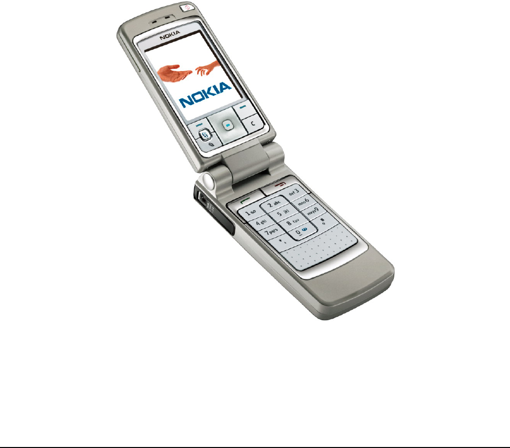
Figure 1 RM-25.................................................................................................................................................................................1–5
RM-25
General information Nokia Customer Care
9235618 (Issue 2) Company Confidential Page 1–3
Copyright ©2005 Nokia. All Rights Reserved.

RM-25
Nokia Customer Care General information
(This page left intentionally blank.)
Page 1–4 Company Confidential 9235618 (Issue 2)
Copyright ©2005 Nokia. All Rights Reserved.
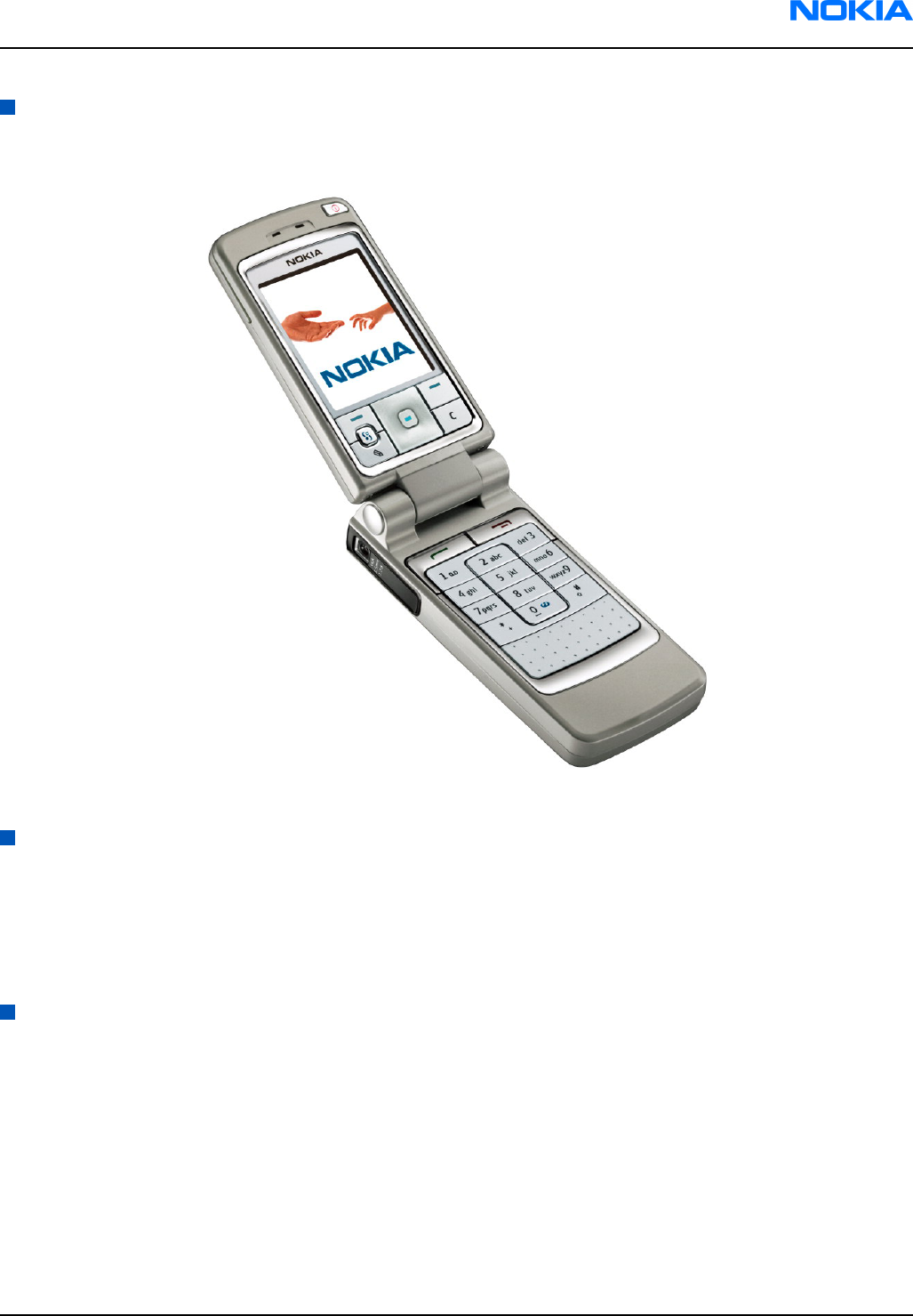
Product selection
The RM-25 is a triple band transceiver unit designed for the GSM900 (including EGSM), GSM1800 and GSM1900
networks.
Figure 1 RM-25
Display and keypad features
• Large high resolution TFT color display (176x208 pixels) with 65,536 colors.
• 4-way navigation key, 3 selection keys, Application key, Edit key and Clear key.
• State-of-the-art ribless numeric keymat, ITU layout.
• Three side keys: Vol Up, Vol Down and PoC (Push To Talk).
• The PoC key is also the camera capture key
Features
Hardware features
• Three side keys: Vol up, Vol down and PoC (Push To Talk)
• Tri-band GSM E900/1800/1900
• Internal antenna
• Speech codecs: HR, FR, EFR, AMR
• HSCSD: Multiclass 6.
• GPRS: Multislot Class 6, 1+1, 2+2, 2+1, 3+1, class B. Max DL=43.2kbps UL=28.8kbps
• VGA Camera
• 5 MByte internal user memory
RM-25
General information Nokia Customer Care
9235618 (Issue 2) Company Confidential Page 1–5
Copyright ©2005 Nokia. All Rights Reserved.
• Memory card slot for additional user memory (1.8V/3V Reduced Size MMC)
•Bluetooth and USB through PopPortTM connector
• Internal vibrator
• Integrated handsfree speaker
• Plug-in SIM (1.8 and 3.0 V)
• Real time clock
• FM Radio
• IrDA
Software features
• Symbian OS 7.0s Platform
• Nokia Series 60 UI : C++ and Java SDKs
UI features
Table 1 Imaging
Capture • Camera with 2 modes (Standard/Night) and x2 Digital Zoom
• Video Recorder supporting QCIF(176x144) and subQCIF(128x96) sizes
Share • Sending via Bluetooth, USB, MMS, e-mail, IrDA
• Media Player
Organize • Media Gallery
• Uploader
Table 2 Messaging
Messaging • Multimedia Messaging with Presentations
• Concatenated SMS (MO/MT)
• Picture Messaging
• E-mail (SMTP, IMAP4, POP3)
• Instant Messaging (Wireless Village)
• T9 predictive text input
Table 3 Personal Information Management (PIM)
PIM • Contacts with thumbnail images
• Presence Enhanced Contact
• Calendar
• To-do list
• Notes
• Voice Recorder
• Calculator
• Clock
• Converter
RM-25
Nokia Customer Care General information
Page 1–6 Company Confidential 9235618 (Issue 2)
Copyright ©2005 Nokia. All Rights Reserved.
Table 4 Synchronization
Local (using PC Suite) • Data: Calendar, Contacts
• PC Applications: Microsoft Outlook (97, 98, 2000, 2002), Lotus Organizer
(5.0, 6.0), Lotus Notes (5.0/5.02/6.0)
Remote (with SyncML
server)
Data: Calendar, Contacts
Table 5 Phone
Phone • GSM phase 2+ features
• Voice dialling
• Voice commands
• CPHS spec. (version 4.2)
Table 6 Games
Games None
Table 7 Java
Midp 2.0 • Mobile Media API (JSR 135)
• Bluetooth API (JSR 82)
• Wireless Messaging API (JSR 120)
Table 8 Browser
Browser WAP 2.0 HTML and xHTML browser
Table 9 Personalization
Personalization • Themes
• SP-MIDI, True Tones
Table 10 Location Based Services
Location Based Services Cell broadcast
Table 11 M-Commerce
M-Commerce Mobile Wallet 2.0
Variants (product and modules)
Name Material code/module type Module code
Basic Transceiver, EMEA, silver 0516711
Basic Transceiver, EMEA, black 0518060
Basic Transceiver, Chinese, silver 0518059
RM-25
General information Nokia Customer Care
9235618 (Issue 2) Company Confidential Page 1–7
Copyright ©2005 Nokia. All Rights Reserved.
Name Material code/module type Module code
Basic Transceiver, Chinese, black 0518061
UI flex assy 0264017
A2 Cover Assembly, silver 0266026
A2 Cover Assembly, black 0266239
B1 Cover Assembly, silver 0266027
B1 Cover Assembly, black 0266241
RM-25 Mechanical sub-assembly,
silver 0267016
RM-25 Mechanical sub-assembly,
black 0267030
Assembled PWB 0202282 1FS-A
SW Module (basic SW), English 8459669
SW Module (basic SW), Chinese 8459671
Top UI PWB 0202408 1fs-f
Mobile enhancements
Power Type Product code
Battery 760 mAh Li-Ion BL-4C 0670386
Retractable charger AC-1 027xxxx (variants)
Charger ACP-7 0675144
Charger ACP-8 0675195
Charger ACP-9 0675149
Charger ACP-12 0675294
Mobile charger LCH-8 0675231
Mobile charger LCH-9 0675120
Mobile charger LCH-12 0675328
Car accessories Type Product code
Headrest handsfree BHF-1 0694102
Headrest handsfree BHF-3 0694158
Wireless car kit CK-1W 0080774
Wireless car kit CARK112 0085112
Car kit CARK126 008xxxx (variants)
Universal car kit CK-7 008xxxx (variants)
Mobile charger LCH-12 0675328
RM-25
Nokia Customer Care General information
Page 1–8 Company Confidential 9235618 (Issue 2)
Copyright ©2005 Nokia. All Rights Reserved.
Audio Type Product code
Boom Headset HDB-4 0694094
Fashion stereo headset HS-3 0694156
Stereo headset (APAC) HDS-3 0694153 (APAC)
Activity headset HS-8 06941xx (variants)
Headset HS-5 0694121
Retractable headset HS-10 0694126 (EMEA) / 0694125 (APAC)
Inductive loopset LPS-4 0630443
Wireless headset HDW-2 0274141
Wireless clip-on headset HS-3W 0694135
Wireless boom headset HS-4W 0694160
Data accessories Type Product code
Connectivity Cable DKU-2 0730238
Reduced size MMC 4346053
Imaging and lifestyle
accessories
Type Product code
Image viewer SU-2 0263167
Image viewer SU-5 0710003
Image frame SU-4 0710001
Image frame SU-7 0710002
Image Album RX-15 00808xx (variants)
Medallion I RX-3 0630702
Medallion II RX-4 0710008
Kaleidoscope I RX-11 0710009
Messaging accessories Type Product code
Nokia digital pen SU-1B 0710000
Wireless keyboard SU-8 0xxxxxx (variants, codes not ready
before manual deadline)
RM-25
General information Nokia Customer Care
9235618 (Issue 2) Company Confidential Page 1–9
Copyright ©2005 Nokia. All Rights Reserved.
Technical specifications
General specifications
Unit Dimension (mm) Weight (g) Volume (cc)
Transceiver with BL-4C
760mAh Li-Ion battery
pack
102x493x21/23 125 109
Main RF characteristics for triple-band phones (Europe)
Parameter Unit
Cellular system GSM/EGSM900,GSM1800/1900
Rx frequency band EGSM900: 925 - 935 MHz
GSM900: 935 - 960MHz
GSM1800: 1805 - 1880 MHz
GSM1900: 1930 - 1990 MHz
Tx frequency band EGSM900: 880 - 890MHz
GSM900: 890 - 915MHz
GSM1800: 1710 - 1785 MHz
GSM1900: 1850 - 1910 MHz
Output power GSM900: +5 … +33dBm/3.2mW … 2W
GSM1800: +0 … +30dBm/1.0mW … 1W
GSM1900: +0 … +30dBm/1.0mW … 1W
Number of RF channels GSM900: 125
GSM1800: 375
GSM1900: 300
Channel spacing 200KHz
Number of Tx power levels GSM900: 15
GSM1800: 16
GSM1900: 16
Battery endurance
Nokia measurements of operation times in GSM900/1800
Talk time
Battery: BL-4C 760mAh Up to 2-4 hours
RM-25
Nokia Customer Care General information
Page 1–10 Company Confidential 9235618 (Issue 2)
Copyright ©2005 Nokia. All Rights Reserved.
Standby time
Battery: BL-4C 760mAh Up to 100-150 hours
Note: Variation in operation times will occur depending on SIM card, network settings and usage. Talk
time is increased by up to 30% if half rate is active and reduced by 5% if enhanced full rate is active.
Environmental conditions
Environmental
condition
Ambient temperature Notes
Normal operation 15 oC ... +55 oCSpecifications fulfilled
Reduced performance 55 oC ... +70 oCOperational only for short periods
Intermittent or no
operation
-40 oC ... -15 oC and +70 oC ... +85oCOperation not guaranteed but an
attempt to operate will not damage
the phone
No operation or
storage
<-40 oC and >+85 oCNo storage. An attempt to operate
may cause permanent damage
Charging allowed -15 oC ... +55 oC
Long term storage
conditions
0 oC ... +85 oC
Humidity and water
resistance
Relative humidity range is 5 to 95%.
Condensed or dripping water may
cause intermittent malfunctions.
Protection against dripping water has
to be implemented in (enclosure)
mechanics.
Continuous dampness will cause
permanent damage to the module.
RM-25
General information Nokia Customer Care
9235618 (Issue 2) Company Confidential Page 1–11
Copyright ©2005 Nokia. All Rights Reserved.

RM-25
Nokia Customer Care General information
(This page left intentionally blank.)
Page 1–12 Company Confidential 9235618 (Issue 2)
Copyright ©2005 Nokia. All Rights Reserved.

2 — Parts and layouts
Nokia Customer Care
9235618 (Issue 2) Company Confidential Page 2–1
Copyright ©2005 Nokia. All Rights Reserved.

RM-25
Nokia Customer Care Parts and layouts
(This page left intentionally blank.)
Page 2–2 Company Confidential 9235618 (Issue 2)
Copyright ©2005 Nokia. All Rights Reserved.

Table of Contents
Exploded view.................................................................................................................................................................................2–5
Mechanical parts.............................................................................................................................................................................2–6
Swap units........................................................................................................................................................................................2–9
Component parts.........................................................................................................................................................................2–10
Component layouts.....................................................................................................................................................................2–33
List of Tables
Table 12 List of all mechanical parts.........................................................................................................................................2–6
Table 13 Mechanical spare parts list.........................................................................................................................................2–7
Table 14 SWAP units.......................................................................................................................................................................2–9
Table 15 Component parts list for build 1fsa_09a..............................................................................................................2–10
Table 16 Component parts for 1fsa_11a................................................................................................................................2–18
List of Figures
Figure 2 Exploded view of RM-25...............................................................................................................................................2–5
Figure 3 Component layout for 1fsa_09a, bottom.............................................................................................................2–33
Figure 4 Component layout for 1fsa_11a, bottom.............................................................................................................2–34
Figure 5 Component layout for 1fsa_09a, top.....................................................................................................................2–34
Figure 6 Component layout for 1fsa_11a, top.....................................................................................................................2–35
RM-25
Parts and layouts Nokia Customer Care
9235618 (Issue 2) Company Confidential Page 2–3
Copyright ©2005 Nokia. All Rights Reserved.

RM-25
Nokia Customer Care Parts and layouts
(This page left intentionally blank.)
Page 2–4 Company Confidential 9235618 (Issue 2)
Copyright ©2005 Nokia. All Rights Reserved.

Exploded view
Figure 2 Exploded view of RM-25
RM-25
Parts and layouts Nokia Customer Care
9235618 (Issue 2) Company Confidential Page 2–5
Copyright ©2005 Nokia. All Rights Reserved.
Mechanical parts
Table 12 List of all mechanical parts
* = Not available as spare part
ITEM/CIRCUIT REF. QTY PART NAME
1A2 COVER ASSY
I001* 1 A2 COVER
I002* 1 POWER KEY
I003 1 FUNCTION KEY MAT
I004 2 SCREW 1.8X5
I005 1 LCD SHIELD
I006 1 EARPIECE
I007 1 LCD MODULE
MECHANICAL SUB ASSY
I008 4 SCREW 1.0X4
I009* 1 DOMESHEET
I010* 1 UI MODULE
I011* 1 IHF SPEAKER GASKET
I012* 1 IHF SPEAKER
I013* 1 IHF SPEAKER ADHESIVE
I014* 1 MAGNET
I015* 1 IHF BOX
I016* 1 B2 COVER
I101* 1 HINGE FLEX
I102* 1 HINGE COVER 1
I103* 1 HINGE
I104* 1 HINGE COVER 2
I105* 1 HINGE CAP LEFT
I106* 1 HINGE CAP RIGHT
I201* 1 A1 COVER
I202 1 MICROPHONE
1 FRAME ASSY (I0203 - I204)
I203* 1 CAMERA WINDOW
I204* 1 FRAME
RM-25
Nokia Customer Care Parts and layouts
Page 2–6 Company Confidential 9235618 (Issue 2)
Copyright ©2005 Nokia. All Rights Reserved.

ITEM/CIRCUIT REF. QTY PART NAME
I205 1 SIDE KEY
I301* 1 POWER SWITCH
I206 1 KEYMAT
I207 1 PANEL
1 UI FLEX ASSY
I208* 1 DOMESHEET
I209* 1 UI FLEX
I210 1 SHIELD
CAMERA MODULE ASSY
I211* 1 VGA CAMERA
I212* 1 CAMERA FLEX
I213* 1 ENGINE MODULE
I214 1 TYPE LABEL
1 B1 COVER ASSY
I215 1 DC JACK
I216* 1 ANTENNA
I217 1 VIBRA
I218* 1 BATTERY RELEASE
I219* 1 B1 COVER
I220 6 SCREW 1.8X7
1 Battery LID ASSY
I221* 1 Battery LID
I222* 1 Battery PAD
Table 13 Mechanical spare parts list
Refs Description
E
M
E
A
A
P
A
C
C
H
I
N
A
L
T
A
N
A
M
A300 HELGO SHIELD ASSY DMC06934 R1024 x x x x
A400 PA SHIELD ASSY DMC06935 R1024 x x x x
I003 FUNC KEYMAT HARD TOP SILVER x x x x
I003 FUNC KEYMAT HARD BLACK x x x x
RM-25
Parts and layouts Nokia Customer Care
9235618 (Issue 2) Company Confidential Page 2–7
Copyright ©2005 Nokia. All Rights Reserved.
Refs Description
E
M
E
A
A
P
A
C
C
H
I
N
A
L
T
A
N
A
M
I004 Screw 1.8x5.0 DIN8015 FH FeZn black x x x x
I005 LCD Shield x x x x
I006 EARPIECE 105+-3DB 32R D8.1X2.25 x x x x
I007 LCD MOD 176X208 AM 64KCO GDAF6007 Halti2 x x x x
I202 MIC+BOOT ASSY -42+-3DB D7.7X3MM x x x x
I205 Sidekey Hard Top Silver x x x x
I205 Sidekey Hard Top Black P2103 x x x x
I206 NUM KEYMAT HARD TOP LATIN SILVER x x x
I206 NUM KEYMAT HARD TOP LATIN BLACK x x x
I206 NUM KEYMAT HARD TOP ARABIC SILVER x
I206 NUM KEYMAT HARD TOP ARABIC BLACK x
I206 NUM KEYMAT HARD TOP GREEK SILVER x
I206 NUM KEYMAT HARD TOP GREEK BLACK x
I206 NUM KEYMAT HARD TOP RUSSIA SILVER x
I206 NUM KEYMAT HARD TOP RUSSIA BLACK x
I206 NUM KEYMAT HARD TOP HEBREW SILVER x
I206 NUM KEYMAT HARD TOP HEBREW BLACK x
I206 NUM KEYMAT HARD TOP BoPo SILVER x
I206 NUM KEYMAT HARD TOP BoPo BLACK x
I206 NUM KEYMAT HARD TOP STROKE SILVER x x
I206 NUM KEYMAT HARD TOP STROKE BLACK x x
I207 Panel painted Silver P2103 x x x x
I207 Panel painted Black P2103 x x x x
I210 BB Shield DNS09299 P2103 x x x x
I214 BLANK LABEL 32.5X50.5 BRADY x x x x
I215 DC-Jack Low Profile P2103 x x x x
I217 VIBRA ASSY 1.0V 80MA 9000RPM x x x x
I220 Screw 1.8x7.0 DIN8015 FH FeZn black x x x x
UI flex assy 040-000388 P2103 x x x x
Frame Service Assembly P2103 x x x x
A2 cover assembly Silver Sand P2103 x x x x
B1 cover assembly Silver Sand x x x x
RM-25
Nokia Customer Care Parts and layouts
Page 2–8 Company Confidential 9235618 (Issue 2)
Copyright ©2005 Nokia. All Rights Reserved.
Refs Description
E
M
E
A
A
P
A
C
C
H
I
N
A
L
T
A
N
A
M
A2 cover assembly Black Coffee x x x x
B1 cover assembly Black Coffee x x x x
RM-25 Mech sub-assembly Silver SandP2103 x x x x
RM-25 Mech sub-assembly Black CoffeP2103 x x x x
Camera Service Assembly x x x x
Battery lid assy Silver Sand P2103 x x x x
Battery lid assy Black Coffee P2103 x x x x
HELGO LID DMD11312 R1024 x x x x
PA LID DMD11314 R1024 x x x x
Swap units
Table 14 SWAP units
SWAP units
N6260 RM-25 SWAP ENGINE E&A BLACK
N6260 RM-25 SWAP ENGINE E&A SILVER
N6260 RM-25 SWAP ENGINE FRANCE BLACK
N6260 RM-25 SWAP ENGINE FRANCE SILVER
N6260 RM-25 SWAP ENGINE RUSSIA BLACK
N6260 RM-25 SWAP ENGINE RUSSIA SILVER
N6260 RM-25 SWAP ENGINE S-AFRICA BLACK
N6260 RM-25 SWAP ENGINE S-AFRICA SILVER
N6260 RM-25 SWAP ENGINE TURKEY BLACK
N6260 RM-25 SWAP ENGINE TURKEY SILVER
N6260 RM-25 SWAP ENGINE UKRAINA BLACK
N6260 RM-25 SWAP ENGINE UKRAINA SILVER
N6260 RM-25 SWAP ENGINE E&A BLACK
N6260 RM-25 SWAP ENGINE E&A SILVER
N6260 RM-25 SWAP ENGINE FRANCE BLACK
N6260 RM-25 SWAP ENGINE FRANCE SILVER
N6260 RM-25 SWAP ENGINE RUSSIA BLACK
N6260 RM-25 SWAP ENGINE RUSSIA SILVER
RM-25
Parts and layouts Nokia Customer Care
9235618 (Issue 2) Company Confidential Page 2–9
Copyright ©2005 Nokia. All Rights Reserved.
SWAP units
N6260 RM-25 SWAP ENGINE S-AFRICA BLACK
N6260 RM-25 SWAP ENGINE S-AFRICA SILVER
Component parts
Note: For the latest Component parts list, please refer to the Service bulletin.
Table 15 Component parts list for build 1fsa_09a
Refs Type Object Name
PWB
Position,
X/Y
Assy Side
Earpiece EARPIECE 105+-3DB 32R D8.1X2.25
Shield Assembly UI flex assy 040-000388 P2103
Shield LCD Shield 040-000237 P2103
Cover Assembly B1 cover assembly Black Coffee P2103
X816 Board To Board
Connector
SM CONN B2B 2X8 F P0.4, camera connector on
main PWB
R313,
R371,
R642,
R861
Fixed Resistor CHIPRES 0W06 18K J 0402
C659,
C662,
C664,
C671,
C673,
C673,
C698,
C862
Ceramic Capacitor CHIPCAP X7R 22N K 16V 0402
Cover Assembly A2 cover assembly Black Coffee
Cover Assembly A2 cover assembly Silver Sand P2103
Plate Panel painted Silver P2103
Cover Battery lid assy Black Coffee P2103
Label And Sticker BLANK LABEL 30.0X22.0 DMD07217
Cover Battery lid assy Silver Sand P2103
Cover B2 bezel printed Black 040-002071 P2103
Tape And Foil And
Film
UI adhesive 040-000074 P2103
Tape And Foil And
Film
B2 bezel adhesive DMD12641 P2103
RM-25
Nokia Customer Care Parts and layouts
Page 2–10 Company Confidential 9235618 (Issue 2)
Copyright ©2005 Nokia. All Rights Reserved.
Refs Type Object Name
PWB
Position,
X/Y
Assy Side
Gasket And Seal IHF net 040-000076 P2103
Frame B2 bezel printed Silver 040-002071 P2103
Speaker SPEAKER IHF 77.3DB 7R D16X4.40
Tape And Foil And
Film
IHF speaker adhesive 040-001415 P2103
Gasket And Seal IHF gasket with net 040-000071 P2103
Dome Sheet Top UI domesheet 040-0000176 P2103
Vibrator VIBRA ASSY 1.0V 80MA 9000RPM
Cover Assembly B1 cover assembly Silver Sand P2103
Service Device SA-38 RF COUPLER
Service Device RJ-33 SOLDERING JIG
Service Device MJ-30 MODULE JIG P2103
Service Device DA-25 DOCKING ADAPTER P2103
Service Device SF-27 FLASH ADAPTER
After Sales Kit SK-8 LGA COMPONENT REWORK KIT
After Sales Kit SK-9 PA COMPONENT REWORK KIT
Service Device SS-34 OPENING TOOL
Production Device SK-5 LGA COMPONENT REWORK KIT
Service Device RJ-46 REWORK JIG HDJ12
Service Device ST-15 REWORK STENCIL
Cover Panel painted Black P2103
Keymat And Key NUM KEYMAT HARD TOP LATIN BLACK
Keymat And Key NUM KEYMAT HARD TOP ARABIC SILVER
Keymat And Key NUM KEYMAT HARD TOP LATIN SILVER
Keymat And Key NUM KEYMAT HARD TOP ARABIC BLACK
Keymat And Key NUM KEYMAT HARD TOP GREEK SILVER
Keymat And Key NUM KEYMAT HARD TOP GREEK BLACK
Keymat And Key NUM KEYMAT HARD TOP RUSS SILVER
Keymat And Key NUM KEYMAT HARD TOP RUSSIA BLACK
Keymat And Key NUM KEYMAT HARD TOP HEBREW SILVER
Keymat And Key NUM KEYMAT HARD TOP HEBREW BLACK
Keymat And Key NUM KEYMAT HARD TOP BoPo SILVER
Keymat And Key NUM KEYMAT HARD TOP BoPo BLACK
Keymat And Key NUM KEYMAT HARD TOP STROKE SILVER
RM-25
Parts and layouts Nokia Customer Care
9235618 (Issue 2) Company Confidential Page 2–11
Copyright ©2005 Nokia. All Rights Reserved.
Refs Type Object Name
PWB
Position,
X/Y
Assy Side
Keymat And Key NUM KEYMAT HARD TOP STROKE BLACK
Keymat And Key FUNC KEYMAT HARD TOP SILVER
Keymat And Key FUNC KEYMAT HARD BLACK
Display LCD MOD 176X208 AM 64KCO GDAF6007
D460 Combo Memory NOR 128M + 128M 1.8/1.8V FGBA44 PBFREE
Shield BB Shield DNS09299 P2103
Other Assembly RM-25 Mech sub-assembly Black CoffeP2103
Other Assembly RM-25 Mech sub-assembly Silver SandP2103
G502 Battery And
Battery Cell
CELL CAPACITOR 0.015MAH 3V3
Screw Screw 1.8x7.0 DIN8015 FH FeZn black, B1 cover
screws
Screw Screw 1.8x5.0 DIN8015 FH FeZn black, A2 cover
screws
Screw Screw 1.0x4.0, Top UI board screws
Electronic
Assembly
1FS-F TOP-UI
Speaker SPEAKER HF 69+-2DB 8R D16X4.36
Gasket And Seal IHF speaker gasket P2103
Fixed Resistor CHIPRES 0W06 22R J 0402
Ceramic Capacitor CHIPCAP X5R 1U0 K 25V T 1.0 1206
R873,
R402,
R492,
R864,
R871
Fixed Resistor CHIPRES 0W06 100R J 0402
R315 Integrated
Discretes
ASIP MMC-INTERFACE ESD FILT BGA11
R644,
R675
Fixed Resistor CHIPRES 0W06 27K J 0402
R513,
R514
Fixed Resistor CHIPRES 0W06 15K J 0402
V402 Diode SCH DIODE 30V 200MA VF 0V5 SOD523
R806 Resistor Network RES NETWORK 0W06 2X100R J 0404
LED LED WHITE 90-345MCD 10MA 90DEG
RM-25
Nokia Customer Care Parts and layouts
Page 2–12 Company Confidential 9235618 (Issue 2)
Copyright ©2005 Nokia. All Rights Reserved.
Refs Type Object Name
PWB
Position,
X/Y
Assy Side
C406,
C407,
C501
Ceramic Capacitor CHIPCAP NP0 3P3 C 50V 0402
A300 Shield Assembly HELGO SHIELD ASSY DMC06934 R1024 F7 TOP
A400 Shield Assembly PA SHIELD ASSY DMC06935 R1024 F3 TOP
B250 Crystal CRYSTAL 32.768KHZ+-20PPM 12.5PF I8 TOP
B440 Crystal CER.RESON 6MHZ+0.11%-0.09% 4.5X2.0 Q8 TOP
C132 Ceramic Capacitor CHIPCAP X5R 1U K 6V3 0603 P2 BOTTOM
C133 Electrolytic
Capacitor
CHIPTCAP 100U M 10V 6.0X3.2X1.5
L3
TOP
C134 Ceramic Capacitor CHIPCAP X7R 10N K 50V 0603 S5 BOTTOM
C135 Ceramic Capacitor CHIPCAP NP0 27P J 50V 0402 T5 BOTTOM
C138 Ceramic Capacitor CHIPCAP X7R 10N K 16V 0402 L7 TOP
C190 Ceramic Capacitor CHIPCAP NP0 15P J 50V 0402 H4 TOP
C191 Ceramic Capacitor CHIPCAP NP0 2P2 C 50V 0402 I3 TOP
C193 Ceramic Capacitor CHIPCAP NP0 100P J 50V 0402 K2 TOP
C199 Ceramic Capacitor CHIPCAP X5R 2U2 K 6V3 0603 TOP
C200 Ceramic Capacitor CHIPCAP X7R 330P J 50V 0402 I3 TOP
C222 Ceramic Capacitor CHIPCAP X5R 10U M 6V3 0805 I5 TOP
C231 Ceramic Capacitor CHIPCAP NP0 47P J 50V 0402 P5 TOP
C241 Ceramic Capacitor CHIPCAP X5R 100N K 10V 0402 L9 TOP
C253 Ceramic Capacitor CHIPCAP NP0 10P J 50V 0402 I7 TOP
C260 Ceramic Capacitor CHIPCAP NP0 22P J 50V 0402 J8 TOP
C270 Ceramic Capacitor CHIPCAP NP0 270P J 50V 0402 L8 TOP
C315 Ceramic Capacitor CHIPCAP X5R 2U2 K 10V 0805 D3 BOTTOM
C405 Ceramic Capacitor CHIPCAP X5R 4U7 K 6V3 0805 P3 TOP
C444 Ceramic Capacitor CHIPCAP X5R 1U K 16V 0603 R8 TOP
C460 Ceramic Capacitor CHIPCAP X7R 100N K 16V 0603 Q9 TOP
C463 Ceramic Capacitor CHIPCAP X5R 470N K 10V 0603 P7 TOP
C502 Ceramic Capacitor CHIPCAP NP0 180P J 25V 0402 D7 TOP
C503 Ceramic Capacitor CHIPCAP NP0 2N7 J 25V 0805 D7 TOP
C505 Ceramic Capacitor CHIPCAP NP0 2N2 J 16V 0603 G8 TOP
C510 Ceramic Capacitor CHIPCAP NP0 56P J 50V 0402 F8 TOP
C511 Ceramic Capacitor CHIPCAP NP0 1P2 C 50V 0402 F7 TOP
RM-25
Parts and layouts Nokia Customer Care
9235618 (Issue 2) Company Confidential Page 2–13
Copyright ©2005 Nokia. All Rights Reserved.

Refs Type Object Name
PWB
Position,
X/Y
Assy Side
C512 Ceramic Capacitor CHIPCAP NP0 18P J 50V 0402 F8 TOP
C523 Ceramic Capacitor CHIP ARRAY NP0 4X470P J 16V 0612 E5 TOP
C528 Ceramic Capacitor CHIPCAP NP0 82P J 50V 0402 G6 TOP
C617 Ceramic Capacitor CHIPCAP X7R 3N3 J 50V 0402 T7 BOTTOM
C620 Ceramic Capacitor CHIPCAP X7R 560P J 50V 0402 Q2 TOP
C621 Ceramic Capacitor CHIPCAP NP0 68P J 50V 0402 Q3 TOP
C657 Ceramic Capacitor CHIPCAP X7R 10N J 16V 0402 M4 TOP
C658 Ceramic Capacitor CHIPCAP X7R 47N K 10V 0402 M4 TOP
C663 Other Capacitor CHIP ARRAY X5R 2X47N K 10V 0405 O4 TOP
C665 Other Capacitor CHIP ARRAY X5R 2X33N M 10V 0405 O3 TOP
C670 Ceramic Capacitor CHIPCAP X7R 4N7 K 25V 0402 M4 TOP
C701 Ceramic Capacitor CHIPCAP X7R 1N0 J 50V 0402 G3 TOP
C937 Fixed Resistor CHIPRES 0W06 33K J 0402 TOP
D190 Mixed Signal ASIC TJA4 BLUETOOTH DEVICE J4 TOP
D191 Logic IC 1XINV 1.8-5.5V SC70-5 J3 TOP
D400 Power
Management IC
DC/DC CONV 350MA(TK11851)SOP8
P3
TOP
D440 Interface IC KAEDE V1.0 ISP1182 HVQFN32 Q9 TOP
D461 DRAM Memory SDRAM 8MX16 1.8V/1.8V WBGA60 PBFREE P6 TOP
D462 FLASH Memory FLASH 4MX16 1.8/1.8V FBGA44 PBFREE M9 TOP
F130 Fuse And
Protector
SM FUSE F 1.5A 32V ROHS-FREE 0603
T4
BOTTOM
G500 VCO VCO 3296-3980MHZ 4-BAND Matsushita D6 TOP
G501 VCTCXO VCTCXO 26MHZ+-3PPM 2.7V 1.3MA GSM E8 TOP
L131 EMC Component FERR.BEAD 240R/100M 0.4A 0R3 0402 S5 BOTTOM
L190 Fixed Inductor CHIP COIL 22N J Q28/800MHZ 0402 I4 TOP
L191 Fixed Inductor CHIP COIL 2N7 +-0N3 Q29/800M 0402 I4 TOP
L222 EMC Component FERRITE BEAD 0R5 600R/100MHZ 0603 I5 TOP
L230 Fixed Inductor CHOKE 10uH M 0.53A 0R48 4.8x4.8x1.2 Q5 TOP
L401 Fixed Inductor CHOKE 22U M 0.33A 1R5 3.3X3.3X1.3 P4 TOP
L441 Fixed Inductor CHIP COIL 56N J Q21/800MHZ 0402 T6 BOTTOM
L500 Fixed Inductor CHIP COIL 5N6 +-0N3 Q7/100M 0402 F8 TOP
L502 Fixed Inductor CHIP COIL 3N3 +-0N1 Q30/1GHZ 0402 F8 TOP
L504 Fixed Inductor CHIP COIL 3N9 +-0N1 Q28/1GHZ 0402 F7 TOP
RM-25
Nokia Customer Care Parts and layouts
Page 2–14 Company Confidential 9235618 (Issue 2)
Copyright ©2005 Nokia. All Rights Reserved.
Refs Type Object Name
PWB
Position,
X/Y
Assy Side
L622 Fixed Inductor CHIP COIL 68NH J Q12/100MHZ 0603 S7 BOTTOM
L656 Fixed Inductor CHIP COIL 33N G Q40/250MHZ 0603 M3 TOP
L658 Fixed Inductor CHIP COIL 120N G Q32/150MHZ 0603 N4 TOP
L677 EMC Component CHIP BEAD ARRAY 2X1000R 0405 T6 BOTTOM
L700 EMC Component FERR.BEAD 0R03 42R/100MHZ 3A 0805 G4 TOP
L702 Fixed Inductor CHIP COIL 33N J Q23/800MHZ 0402 G7 TOP
L800 Fixed Inductor CHIP COIL 3N3 +-0N3 Q28/800M 0402 D3 TOP
L802 Fixed Inductor CHIP COIL 4N7 +-0N1 Q29/1GHZ 0402 F6 TOP
L804 Fixed Inductor CHIP COIL 18N J Q29/800MHZ 0402 F6 TOP
L807 Fixed Inductor CHIP COIL 8N2 J Q28/800MHZ 0402 G6 TOP
N130 Power
Management IC
CURRNT SENS LM3820 USMD10 PB-FREE
P2
BOTTOM
N230 Power
Management IC
DC/DC 1.8V/1.5V(LM2608-1.8)USMD10
P4
TOP
N233 Power
Management IC
REG+MAS9161B2GB06 2.8V 80MA TSOT5
O4
TOP
N500 RF ASIC HELGO85G PBFREE TFBGA88 F7 TOP
N656 Other IC FM RECEIVER(TEA5767HN) LQFP40 N3 TOP
N661 Other IC VREG & LEVELSHIFT(LP3928)USMD16 L5 TOP
N662 Analog IC AF AMP 0.4W LM4890/NCP2890 PBFREE Q3 TOP
N700 Power Amplifier PW AMP RF9250E4.1 Micro GSM/EDGE F3 TOP
N750 Infrared IRDA CIM-50M5A **** RESERVED **** P10 BOTTOM
R130 Fixed Resistor CHIPRES 0W06 2K2 J 0402 Q2 BOTTOM
R132 Variable Resistor NTC RES 0W1 47K J B 4050+-3% 0402 K10 BOTTOM
R133 Fixed Resistor CHIPRES 0W06 100K J 0402 L7 TOP
R192 Fixed Resistor CHIPRES 0W06 2K7 J 0402 I3 TOP
R193 Fixed Resistor CHIPRES 0W06 10K J 0402 J3 TOP
R194 Fixed Resistor CHIPRES 0W06 2R2 J 0402 I3 TOP
R253 Fixed Resistor CHIPRES 0W06 100K F 200PPM 0402 L8 TOP
R257 Fixed Resistor CHIPRES 0W06 220R J 0402 L7 TOP
R259 Fixed Resistor CHIPRES 0W25 0R22 J 0805 I6 TOP
R260 Fixed Resistor CHIPRES 0W06 27K F 0402 K6 TOP
R261 Integrated
Discretes
ASIP 4XESD *** PB-FREE *** BGA5
L10
BOTTOM
RM-25
Parts and layouts Nokia Customer Care
9235618 (Issue 2) Company Confidential Page 2–15
Copyright ©2005 Nokia. All Rights Reserved.
Refs Type Object Name
PWB
Position,
X/Y
Assy Side
R265 Fixed Resistor CHIPRES JUMPER 0R0 0603 K8 TOP
R270 Fixed Resistor CHIPRES 0W06 4K7 J 0402 I8 TOP
R310 Integrated
Discretes
ASIP SIM INTERFACE ** PB-FREE **
E4
BOTTOM
R315 Integrated
Discretes
ASIP MMC FILTER *** PB-FREE ***
E5
BOTTOM
R403 Variable Resistor CHIP VARISTOR VWM15V VC50V 0402 S2 TOP
R420 Fixed Resistor CHIPRES 0W06 3K9 J 0402 M5 TOP
R422 Fixed Resistor CHIPRES 0W06 100R F 200PPM 0402 M8 TOP
R446 Fixed Resistor CHIPRES 0W06 33R J 0402 T5 BOTTOM
R448 Fixed Resistor CHIPRES 0W06 68R J 0402 R8 TOP
R451 Integrated
Discretes
ASIP USB2 FILTER BGA10 PBFREE
S5
BOTTOM
R452 Fixed Resistor CHIPRES 0W06 220K J 0402 R9 TOP
R491 Fixed Resistor CHIPRES 0W06 680R J 0402 O5 TOP
R501 Fixed Resistor CHIPRES 0W06 5K6 J 0402 D7 TOP
R502 Fixed Resistor CHIPRES 0W06 6K8 F 0402 D7 TOP
R503 Resistor Network RES NETWORK 0W04 2DB ATT 0404 D7 TOP
R506 Fixed Resistor CHIPRES 0W06 22K J 0402 G8 TOP
R512 Fixed Resistor CHIPRES 0W06 5K6 F 0402 E6 TOP
R515 Resistor Network RES NETWORK 0W06 4X5K6 J 0804 E7 TOP
R516 Fixed Resistor CHIPRES 0W06 10R J 0402 F8 TOP
R602 Fixed Resistor CHIPRES 0W06 1K0 J 0402 K9 TOP
R604 Fixed Resistor CHIPRES 0W06 470R J 0402 J9 TOP
R634 Resistor Network RES NETWORK 0W06 2X10R J 0404 S7 BOTTOM
R635 Integrated
Discretes
ASIP MIC W/ESD RES+CAP+ZDI BGA11
S6
BOTTOM
R645 Variable Resistor VAR.ARRAY 2X16V 824-915MHZ 0405 T4 TOP
R650 Resistor Network RES NETWORK 0W06 2X220R J 0404 T4 TOP
R651 Resistor Network RES NETWORK 0W03 4X22R J 0804 L10 BOTTOM
R656 Fixed Resistor CHIPRES 0W06 12R J 0402 M2 TOP
R658 Fixed Resistor CHIPRES 0W06 47R J 0402 M3 TOP
R662 Fixed Resistor CHIPRES 0W06 5R6 J 0402 N4 TOP
R667 Fixed Resistor CHIPRES 0W06 18K F 100PPM 0603 N4 TOP
RM-25
Nokia Customer Care Parts and layouts
Page 2–16 Company Confidential 9235618 (Issue 2)
Copyright ©2005 Nokia. All Rights Reserved.
Refs Type Object Name
PWB
Position,
X/Y
Assy Side
R693 Fixed Resistor CHIPRES 0W06 1M0 J 0402 J3 TOP
R717 Resistor Network RES NETWORK 0W04 1DB ATT 0404 G3 TOP
R750 Fixed Resistor CHIPRES 0W5 4R7 J 200PPM 1210 O10 BOTTOM
R800 Fixed Resistor CHIPRES 0W06 3K3 J 0402 D4 TOP
R802 Fixed Resistor CHIPRES 0W06 560R J 0402 E4 TOP
R862 Ceramic Capacitor CHIPCAP X7R 33N K 10V 0402 TOP
S001 Switch And Knob MMC Switch E2 BOTTOM
T500 Balun TRANSF BALUN 3290-3980MHZ D7 TOP
T700 Balun TRANSF BALUN 1800+-100MHZ 2X1.25 G7 TOP
T800 Transformer TRANSF BALUN 1.9GHZ+-100MHZ2X1.25 G5 TOP
V130 Diode TVS DI 1PMT16AT3 16V 175W PWRMITE T4 BOTTOM
V400 Integrated
Discretes
ASIP EMI/ESD FILTER BGA6
T2
TOP
V800 Bipolar Transistor
BJT
TR BGA428 LNA1.8GHZ 19.5DB SOT363
D4
TOP
V801 Bipolar Transistor
BJT
TR 2SC5658QRS N 50V 0A1 0W15 VMT3
Q4
TOP
X131 Battery Connector SM BATTERY CONN 3POLE SPR S4 BOTTOM
X132 System Connector SM SYSTEM CONNECTOR 14POL U6 BOTTOM
X400 Board To Board
Connector
SM CONN 2X11 SPR 50V 0.5A PCB/PCB
S5
TOP
X816 Fixed Resistor CHIPRES JUMPER 0R0 0201 S7 TOP
X817 Board To Board
Connector
SM CONN B2B 2X25 M P0.4
T3
TOP
X820 Other Customized
Connector
SIM/MMC combo reader P2103
F6
BOTTOM
X822 Coaxial Connector SM CONN RF JACK 50R 2W 6GHZ E2 TOP
X823 Other Customized
Connector
SM CONN VIBRA SPACER PAD 2.8X1.8
C2
BOTTOM
X825 Spring UI SPRING T2 TOP
Z191 Ceramic Filter CER FILT 2441+-41.75MHZ 2.7X2.2 I3 TOP
Z192 Balun TRANSF BALUN 2400+/-100MHZ I4 TOP
Z401 Integrated
Discretes
ASIP 10-CH ESD EMI FILTER BGA25
Q3
TOP
Z700 SAW Filter SAW FILT 897.5+-17.5MHZ/3DB 2X1.6 G7 TOP
Z800 Antenna Switch DIPL+3SW824-960/1710-1990MHZ5.4*4 E3 TOP
RM-25
Parts and layouts Nokia Customer Care
9235618 (Issue 2) Company Confidential Page 2–17
Copyright ©2005 Nokia. All Rights Reserved.
Refs Type Object Name
PWB
Position,
X/Y
Assy Side
Z801 SAW Filter SAW FILT 1960+-30MHZ/3.5DB 2X1.6 D3 TOP
Z802 SAW Filter SAW FILT 1842.5+-37.5MHZ 2X1.6 F5 TOP
Z803 SAW Filter SAW FILT 942.5+-17.5MHZ/3DB 2X1.6 F5 TOP
Table 16 Component parts for 1fsa_11a
Ref Type Name Side XY E
M
E
A
A
P
A
C
C
h
i
n
a
L
T
A
N
A
M
A300 Shield Assembly HELGO SHIELD ASSY DMC06934 R1024 T F7 x x x x
A400 Shield Assembly PA SHIELD ASSY DMC06935 R1024 T F3 x x x x
B250 Crystal CRYSTAL 32.768KHZ+-20PPM 12.5PF T I8 x x x x
B440 Crystal CER.RESON 6MHZ+0.11%-0.09% 4.5X2.0 T Q8 x x x x
C1 Ceramic Capacitor CHIPCAP X7R 10N K 16V 0402 x x x x
C100 Ceramic Capacitor CHIPCAP X7R 33N K 10V 0402 x x x x
C101 Ceramic Capacitor CHIPCAP X7R 33N K 10V 0402 x x x x
C102 Ceramic Capacitor CHIPCAP X7R 33N K 10V 0402 x x x x
C103 Ceramic Capacitor CHIPCAP X7R 33N K 10V 0402 x x x x
C132 Ceramic Capacitor CHIPCAP X5R 1U K 6V3 0603 B P2 x x x x
C133 Electrolytic Capacitor CHIPTCAP 100U M 10V 6.0X3.2X1.5 T L3 x x x x
C134 Ceramic Capacitor CHIPCAP X7R 10N K 50V 0603 B S5 x x x x
C135 Ceramic Capacitor CHIPCAP NP0 27P J 50V 0402 B T5 x x x x
C190 Ceramic Capacitor CHIPCAP NP0 15P J 50V 0402 T H4 x x x x
C191 Ceramic Capacitor CHIPCAP NP0 2P2 C 50V 0402 T I3 x x x x
C192 Ceramic Capacitor CHIPCAP NP0 2P2 C 50V 0402 T I4 x x x x
C193 Ceramic Capacitor CHIPCAP NP0 100P J 50V 0402 T K2 x x x x
C194 Ceramic Capacitor CHIPCAP NP0 2P2 C 50V 0402 T J3 x x x x
C197 Ceramic Capacitor CHIPCAP NP0 15P J 50V 0402 T I4 x x x x
C199 Ceramic Capacitor CHIPCAP X5R 2U2 K 6V3 0603 T K4 x x x x
C200 Ceramic Capacitor CHIPCAP X7R 330P J 50V 0402 T I3 x x x x
C203 Ceramic Capacitor CHIPCAP X5R 1U K 6V3 0603 T K3 x x x x
C220 Ceramic Capacitor CHIPCAP X5R 1U K 6V3 0603 T I5 x x x x
C221 Ceramic Capacitor CHIPCAP X5R 1U K 6V3 0603 T I5 x x x x
C222 Ceramic Capacitor CHIPCAP X5R 10U M 6V3 0805 T I5 x x x x
RM-25
Nokia Customer Care Parts and layouts
Page 2–18 Company Confidential 9235618 (Issue 2)
Copyright ©2005 Nokia. All Rights Reserved.

Ref Type Name Side XY E
M
E
A
A
P
A
C
C
h
i
n
a
L
T
A
N
A
M
C230 Ceramic Capacitor CHIPCAP X5R 10U M 6V3 0805 T P4 x x x x
C231 Ceramic Capacitor CHIPCAP NP0 47P J 50V 0402 T P5 x x x x
C232 Ceramic Capacitor CHIPCAP X5R 10U M 6V3 0805 T P5 x x x x
C233 Ceramic Capacitor CHIPCAP X5R 10U M 6V3 0805 T P5 x x x x
C239 Ceramic Capacitor CHIPCAP X5R 1U K 6V3 0603 T O5 x x x x
C240 Ceramic Capacitor CHIPCAP X5R 1U K 6V3 0603 T O4 x x x x
C250 Ceramic Capacitor CHIPCAP X5R 1U K 6V3 0603 T I6 x x x x
C251 Ceramic Capacitor CHIPCAP X5R 1U K 6V3 0603 T J6 x x x x
C252 Ceramic Capacitor CHIPCAP X5R 1U K 6V3 0603 T L8 x x x x
C253 Ceramic Capacitor CHIPCAP NP0 10P J 50V 0402 T I7 x x x x
C254 Ceramic Capacitor CHIPCAP NP0 10P J 50V 0402 T I8 x x x x
C255 Ceramic Capacitor CHIPCAP X5R 1U K 6V3 0603 T H8 x x x x
C256 Ceramic Capacitor CHIPCAP X5R 1U K 6V3 0603 T I7 x x x x
C257 Ceramic Capacitor CHIPCAP X5R 1U K 6V3 0603 T I8 x x x x
C259 Ceramic Capacitor CHIPCAP X5R 1U K 6V3 0603 T J9 x x x x
C260 Ceramic Capacitor CHIPCAP NP0 22P J 50V 0402 T J8 x x x x
C261 Ceramic Capacitor CHIPCAP NP0 22P J 50V 0402 T K9 x x x x
C262 Ceramic Capacitor CHIPCAP NP0 22P J 50V 0402 T K9 x x x x
C263 Ceramic Capacitor CHIPCAP NP0 22P J 50V 0402 T I8 x x x x
C264 Ceramic Capacitor CHIPCAP NP0 22P J 50V 0402 T J9 x x x x
C265 Ceramic Capacitor CHIPCAP NP0 22P J 50V 0402 T J9 x x x x
C270 Ceramic Capacitor CHIPCAP NP0 270P J 50V 0402 T L8 x x x x
C272 Ceramic Capacitor CHIPCAP X7R 1N0 K 50V 0402 T H8 x x x x
C273 Ceramic Capacitor CHIPCAP X7R 1N0 K 50V 0402 T H8 x x x x
C274 Ceramic Capacitor CHIPCAP X5R 1U K 6V3 0603 T I6 x x x x
C276 Ceramic Capacitor CHIPCAP X7R 1N0 K 50V 0402 T I6 x x x x
C278 Ceramic Capacitor CHIPCAP X5R 1U K 6V3 0603 T I7 x x x x
C279 Ceramic Capacitor CHIPCAP X5R 1U K 6V3 0603 T I6 x x x x
C280 Ceramic Capacitor CHIPCAP X5R 1U K 6V3 0603 T H6 x x x x
C281 Ceramic Capacitor CHIPCAP X5R 1U K 6V3 0603 T J5 x x x x
C282 Ceramic Capacitor CHIPCAP X5R 1U K 6V3 0603 T K8 x x x x
C284 Ceramic Capacitor CHIPCAP X5R 1U K 6V3 0603 T L8 x x x x
RM-25
Parts and layouts Nokia Customer Care
9235618 (Issue 2) Company Confidential Page 2–19
Copyright ©2005 Nokia. All Rights Reserved.

Ref Type Name Side XY E
M
E
A
A
P
A
C
C
h
i
n
a
L
T
A
N
A
M
C287 Ceramic Capacitor CHIPCAP X5R 1U K 6V3 0603 T K5 x x x x
C288 Ceramic Capacitor CHIPCAP X5R 1U K 6V3 0603 T K5 x x x x
C289 Ceramic Capacitor CHIPCAP X5R 1U K 6V3 0603 T K6 x x x x
C290 Ceramic Capacitor CHIPCAP X5R 1U K 6V3 0603 T K5 x x x x
C291 Ceramic Capacitor CHIPCAP X5R 1U K 6V3 0603 T L5 x x x x
C294 Ceramic Capacitor CHIPCAP X5R 1U K 6V3 0603 T J5 x x x x
C295 Ceramic Capacitor CHIPCAP X5R 1U K 6V3 0603 T J6 x x x x
C296 Ceramic Capacitor CHIPCAP X5R 1U K 6V3 0603 T J6 x x x x
C297 Ceramic Capacitor CHIPCAP X5R 1U K 6V3 0603 T K6 x x x x
C298 Ceramic Capacitor CHIPCAP X5R 1U K 6V3 0603 T K5 x x x x
C299 Ceramic Capacitor CHIPCAP X5R 1U K 6V3 0603 T K5 x x x x
C3 Ceramic Capacitor CHIPCAP X5R 100N K 10V 0402 x x x x
C300 Ceramic Capacitor CHIPCAP X5R 1U K 6V3 0603 T J5 x x x x
C301 Ceramic Capacitor CHIPCAP X5R 1U K 6V3 0603 T K6 x x x x
C302 Ceramic Capacitor CHIPCAP X5R 1U K 6V3 0603 T K5 x x x x
C314 Ceramic Capacitor CHIPCAP X5R 1U K 6V3 0603 B E3 x x x x
C315 Ceramic Capacitor CHIPCAP X5R 2U2 K 10V 0805 B D3 x x x x
C340 Ceramic Capacitor CHIPCAP NP0 22P J 50V 0402 T Q2 x x x x
C341 Ceramic Capacitor CHIPCAP NP0 100P J 50V 0402 T Q2 x x x x
C354 Ceramic Capacitor CHIPCAP NP0 22P J 50V 0402 T T2 x x x x
C355 Ceramic Capacitor CHIPCAP NP0 22P J 50V 0402 T S2 x x x x
C356 Ceramic Capacitor CHIPCAP NP0 22P J 50V 0402 T T2 x x x x
C4 Ceramic Capacitor CHIPCAP X5R 100N K 10V 0402 x x x x
C404 Ceramic Capacitor CHIPCAP NP0 47P J 50V 0402 T P2 x x x x
C405 Ceramic Capacitor CHIPCAP X5R 4U7 K 6V3 0805 T P3 x x x x
C406 Ceramic Capacitor CHIPCAP X5R 1U0 K 25V T 1.0 1206 T O3 x x x x
C407 Ceramic Capacitor CHIPCAP X5R 1U0 K 25V T 1.0 1206 T O2 x x x x
C444 Ceramic Capacitor CHIPCAP X5R 1U K 16V 0603 T R8 x x x x
C445 Ceramic Capacitor CHIPCAP NP0 22P J 50V 0402 B T5 x x x x
C446 Ceramic Capacitor CHIPCAP NP0 22P J 50V 0402 B T5 x x x x
C447 Ceramic Capacitor CHIPCAP NP0 22P J 50V 0402 B T5 x x x x
C450 CHIPCAP NP0 12P J 50V 0402 T Q7 x x x x
RM-25
Nokia Customer Care Parts and layouts
Page 2–20 Company Confidential 9235618 (Issue 2)
Copyright ©2005 Nokia. All Rights Reserved.
Ref Type Name Side XY E
M
E
A
A
P
A
C
C
h
i
n
a
L
T
A
N
A
M
C451 Ceramic Capacitor CHIPCAP NP0 22P J 50V 0402 T U2 x x x x
C460 Ceramic Capacitor CHIPCAP X7R 100N K 16V 0603 T Q9 x x x x
C463 Ceramic Capacitor CHIPCAP X5R 470N K 10V 0603 T P7 x x x x
C464 Ceramic Capacitor CHIPCAP X7R 10N K 50V 0603 T P7 x x x x
C465 Ceramic Capacitor CHIPCAP X5R 470N K 10V 0603 T Q7 x x x x
C466 Ceramic Capacitor CHIPCAP X7R 10N K 50V 0603 T Q7 x x x x
C470 Ceramic Capacitor CHIPCAP X7R 100N K 16V 0603 T Q9 x x x x
C490 Ceramic Capacitor CHIPCAP NP0 100P J 50V 0402 T L6 x x x x
C491 Ceramic Capacitor CHIPCAP NP0 10P J 50V 0402 T O5 x x x x
C500 Ceramic Capacitor CHIPCAP X5R 1U K 6V3 0603 T D6 x x x x
C501 Ceramic Capacitor CHIPCAP NP0 3P3 C 50V 0402 T D6 x x x x
C502 Ceramic Capacitor CHIPCAP NP0 180P J 25V 0402 T D7 x x x x
C503 Ceramic Capacitor CHIPCAP NP0 2N7 J 25V 0805 T D7 x x x x
C504 Ceramic Capacitor CHIPCAP NP0 270P J 50V 0402 T D7 x x x x
C505 Ceramic Capacitor CHIPCAP NP0 2N2 J 16V 0603 T G8 x x x x
C506 Ceramic Capacitor CHIPCAP NP0 100P J 50V 0402 T G8 x x x x
C510 Ceramic Capacitor CHIPCAP NP0 56P J 50V 0402 T F8 x x x x
C511 Ceramic Capacitor CHIPCAP NP0 1P2 C 50V 0402 T F7 x x x x
C512 Ceramic Capacitor CHIPCAP NP0 18P J 50V 0402 T F8 x x x x
C516 Ceramic Capacitor CHIPCAP NP0 27P J 50V 0402 T F8 x x x x
C518 Ceramic Capacitor CHIPCAP NP0 10P J 50V 0402 T E6 x x x x
C520 Ceramic Capacitor CHIPCAP NP0 56P J 50V 0402 T G6 x x x x
C523 Ceramic Capacitor CHIP ARRAY NP0 4X470P J 16V 0612 T E5 x x x x
C525 Ceramic Capacitor CHIPCAP NP0 100P J 50V 0402 T E7 x x x x
C528 Ceramic Capacitor CHIPCAP NP0 82P J 50V 0402 T G6 x x x x
C529 Ceramic Capacitor CHIPCAP NP0 47P J 50V 0402 T E7 x x x x
C530 Ceramic Capacitor CHIPCAP NP0 47P J 50V 0402 T E7 x x x x
C531 Ceramic Capacitor CHIPCAP NP0 18P J 50V 0402 T G6 x x x x
C532 Ceramic Capacitor CHIPCAP NP0 27P J 50V 0402 T G6 x x x x
C600 Ceramic Capacitor CHIPCAP X5R 1U K 6V3 0603 T L9 x x x x
C605 Ceramic Capacitor CHIPCAP X5R 10U M 6V3 0805 T J9 x x x x
C608 Ceramic Capacitor CHIPCAP X7R 1N0 K 50V 0402 T K9 x x x x
RM-25
Parts and layouts Nokia Customer Care
9235618 (Issue 2) Company Confidential Page 2–21
Copyright ©2005 Nokia. All Rights Reserved.

Ref Type Name Side XY E
M
E
A
A
P
A
C
C
h
i
n
a
L
T
A
N
A
M
C609 Ceramic Capacitor CHIPCAP X7R 1N0 K 50V 0402 T K9 x x x x
C611 Ceramic Capacitor CHIPCAP NP0 10P J 50V 0402 B T7 x x x x
C612 Ceramic Capacitor CHIPCAP NP0 10P J 50V 0402 B T7 x x x x
C613 Ceramic Capacitor CHIPCAP NP0 10P J 50V 0402 B T7 x x x x
C614 Ceramic Capacitor CHIPCAP NP0 10P J 50V 0402 B T7 x x x x
C617 Ceramic Capacitor CHIPCAP X7R 3N3 J 50V 0402 B T7 x x x x
C620 Ceramic Capacitor CHIPCAP X7R 560P J 50V 0402 T Q2 x x x x
C621 Ceramic Capacitor CHIPCAP NP0 68P J 50V 0402 T Q3 x x x x
C622 Ceramic Capacitor CHIPCAP X5R 470N K 10V 0603 T Q2 x x x x
C625 Ceramic Capacitor CHIPCAP X7R 560P J 50V 0402 T Q3 x x x x
C629 Ceramic Capacitor CHIPCAP X7R 3N3 J 50V 0402 B S6 x x x x
C630 Ceramic Capacitor CHIPCAP X7R 3N3 J 50V 0402 B T6 x x x x
C632 Ceramic Capacitor CHIPCAP X5R 10U M 6V3 0805 T J9 x x x x
C638 Ceramic Capacitor CHIPCAP X7R 3N3 J 50V 0402 B T6 x x x x
C639 Ceramic Capacitor CHIPCAP X7R 3N3 J 50V 0402 B T6 x x x x
C657 Ceramic Capacitor CHIPCAP X7R 10N J 16V 0402 T M4 x x x x
C658 Ceramic Capacitor CHIPCAP X7R 47N K 10V 0402 T M4 x x x x
C659 Ceramic Capacitor CHIPCAP X7R 22N K 16V 0402 T M2 x x x x
C661 Ceramic Capacitor CHIPCAP X7R 1N0 K 50V 0402 T O2 x x x x
C662 Ceramic Capacitor CHIPCAP X7R 22N K 16V 0402 T M3 x x x x
C663 Other Capacitor CHIP ARRAY X5R 2X47N K 10V 0405 T O4 x x x x
C664 Ceramic Capacitor CHIPCAP X7R 22N K 16V 0402 T N2 x x x x
C665 Other Capacitor CHIP ARRAY X5R 2X33N M 10V 0405 T O3 x x x x
C666 Ceramic Capacitor CHIPCAP X7R 47N K 10V 0402 T O4 x x x x
C667 Ceramic Capacitor CHIPCAP NP0 100P J 50V 0402 T N4 x x x x
C670 Ceramic Capacitor CHIPCAP X7R 4N7 K 25V 0402 T M4 x x x x
C671 Ceramic Capacitor CHIPCAP X7R 22N K 16V 0402 T N4 x x x x
C672 Ceramic Capacitor CHIPCAP X5R 1U K 6V3 0603 T N4 x x x x
C673 Ceramic Capacitor CHIPCAP X7R 22N K 16V 0402 T O2 x x x x
C674 Ceramic Capacitor CHIPCAP NP0 100P J 50V 0402 T N2 x x x x
C678 Ceramic Capacitor CHIPCAP NP0 27P J 50V 0402 T N4 x x x x
C679 Ceramic Capacitor CHIPCAP NP0 47P J 50V 0402 T M4 x x x x
RM-25
Nokia Customer Care Parts and layouts
Page 2–22 Company Confidential 9235618 (Issue 2)
Copyright ©2005 Nokia. All Rights Reserved.
Ref Type Name Side XY E
M
E
A
A
P
A
C
C
h
i
n
a
L
T
A
N
A
M
C693 Ceramic Capacitor CHIPCAP X7R 3N3 J 50V 0402 B T7 x x x x
C696 Ceramic Capacitor CHIPCAP NP0 22P J 50V 0402 B E5 x x x x
C698 Ceramic Capacitor CHIPCAP X7R 22N K 16V 0402 T Q3 x x x x
C701 Ceramic Capacitor CHIPCAP X7R 1N0 J 50V 0402 T G3 x x x x
C702 Ceramic Capacitor CHIPCAP X7R 1N0 J 50V 0402 T F3 x x x x
C705 Ceramic Capacitor CHIPCAP X5R 4U7 K 6V3 0805 T G3 x x x x
C706 Ceramic Capacitor CHIPCAP NP0 27P J 50V 0402 T G4 x x x x
C707 Ceramic Capacitor CHIPCAP NP0 1P2 C 50V 0402 T G3 x x x x
C709 Ceramic Capacitor CHIPCAP X7R 1N0 J 50V 0402 T G4 x x x x
C710 Ceramic Capacitor CHIPCAP X7R 1N0 J 50V 0402 T F4 x x x x
C713 Ceramic Capacitor CHIPCAP NP0 15P J 50V 0402 T G7 x x x x
C714 Ceramic Capacitor CHIPCAP NP0 15P J 50V 0402 T G7 x x x x
C750 Ceramic Capacitor CHIPCAP X5R 4U7 K 6V3 0805 B O10 x x x x
C751 Ceramic Capacitor CHIPCAP NP0 22P J 50V 0402 B Q10 x x x x
C800 Ceramic Capacitor CHIPCAP NP0 100P J 50V 0402 T D4 x x x x
C801 Ceramic Capacitor CHIPCAP NP0 2P2 C 50V 0402 T D3 x x x x
C803 Ceramic Capacitor CHIPCAP NP0 15P J 50V 0402 T D4 x x x x
C804 Ceramic Capacitor CHIPCAP NP0 1P2 C 50V 0402 T E4 x x x x
C805 Ceramic Capacitor CHIPCAP NP0 15P J 50V 0402 T G6 x x x x
C806 Ceramic Capacitor CHIPCAP NP0 15P J 50V 0402 T G6 x x x x
C862 Ceramic Capacitor CHIPCAP X7R 22N K 16V 0402 x x x x
C863 Ceramic Capacitor CHIPCAP NP0 100P J 50V 0402 T Q2 x x x x
C905 Ceramic Capacitor CHIPCAP NP0 10P J 50V 0402 T M7 x x x x
C933 Ceramic Capacitor CHIPCAP NP0 22P J 50V 0402 T T4 x x x x
C934 Ceramic Capacitor CHIPCAP NP0 22P J 50V 0402 T U4 x x x x
C935 Ceramic Capacitor CHIPCAP NP0 22P J 50V 0402 T Q9 x x x x
C936 Ceramic Capacitor CHIPCAP NP0 270P J 50V 0402 B S5 x x x x
C940 Ceramic Capacitor CHIPCAP X5R 1U K 6V3 0603 T L7 x x x x
D190 Mixed Signal ASIC TJA4 BLUETOOTH DEVICE T J4 x x x x
D191 Logic IC 1XINV 1.8-5.5V SC70-5 T J3 x x x x
D400
Power Management
IC DC/DC CONV 350MA(TK11851)SOP8 T P3 x x x x
RM-25
Parts and layouts Nokia Customer Care
9235618 (Issue 2) Company Confidential Page 2–23
Copyright ©2005 Nokia. All Rights Reserved.
Ref Type Name Side XY E
M
E
A
A
P
A
C
C
h
i
n
a
L
T
A
N
A
M
D440 Interface IC KAEDE V1.0 ISP1182 HVQFN32 T Q9 x x x x
D460 Combo Memory NOR 128M + 128M 1.8/1.8V FGBA44 PBFREE T O9 x x x x
D460 NOR 128M + 128M 1.8/1.8V FGBA44 PBFREE T O9 x x x x
D461 DRAM Memory SDRAM 8MX16 1.8V/1.8V FBGA60 PBFREE T P6 x x x x
D462 FLASH Memory FLASH 4MX16 1.8/1.8V FBGA44 PBFREE T M9 x x x x
D462 FLASH 4MX16 1.8/1.8V VFBGA44 PBFREE T M9 x x x x
F130 Fuse And Protector SM FUSE F 1.5A 32V ROHS-FREE 0603 B T4 x x x x
G500 VCO VCO 3296-3980MHZ 4-BAND Matsushita T D6 x x x x
G501 VCTCXO VCTCXO 26MHZ+-3PPM 2.7V 1.3MA GSM T E8 x x x x
G502
Battery And Battery
Cell CELL CAPACITOR 0.015MAH 3V3 B T8 x x x x
I003 Keymat And Key FUNC KEYMAT HARD BLACK x x x x
I003 Keymat And Key FUNC KEYMAT HARD TOP SILVER x x x x
I004 Screw Screw 1.8x5.0 DIN8015 FH FeZn black x x x x
I005 Shield LCD Shield x x x x
I006 Earpiece EARPIECE 105+-3DB 32R D8.1X2.25 x x x x
I007 Display
LCD MOD 176X208 AM 64KCO GDAF6007
Halti2 x x x x
I202 Microphone Assembly MIC+BOOT ASSY -42+-3DB D7.7X3MM x x x x
I205 Keymat And Key Sidekey Hard Top Black P2103 x x x x
I205 Keymat And Key Sidekey Hard Top Silver x x x x
I206 Keymat And Key NUM KEYMAT HARD TOP LATIN BLACK x x x
I206 Keymat And Key NUM KEYMAT HARD TOP STROKE BLACK x x
I206 Keymat And Key NUM KEYMAT HARD TOP STROKE SILVER x x
I206 Keymat And Key NUM KEYMAT HARD TOP BoPo BLACK x
I206 Keymat And Key NUM KEYMAT HARD TOP BoPo SILVER x
I206 Keymat And Key NUM KEYMAT HARD TOP HEBREW BLACK x
I206 Keymat And Key NUM KEYMAT HARD TOP HEBREW SILVER x
I206 Keymat And Key NUM KEYMAT HARD TOP RUSSIA BLACK x
I206 Keymat And Key NUM KEYMAT HARD TOP RUSSIA SILVER x
I206 Keymat And Key NUM KEYMAT HARD TOP GREEK BLACK x
I206 Keymat And Key NUM KEYMAT HARD TOP GREEK SILVER x
RM-25
Nokia Customer Care Parts and layouts
Page 2–24 Company Confidential 9235618 (Issue 2)
Copyright ©2005 Nokia. All Rights Reserved.

Ref Type Name Side XY E
M
E
A
A
P
A
C
C
h
i
n
a
L
T
A
N
A
M
I206 Keymat And Key NUM KEYMAT HARD TOP ARABIC SILVER x
I206 Keymat And Key NUM KEYMAT HARD TOP ARABIC BLACK x
I206 Keymat And Key NUM KEYMAT HARD TOP LATIN SILVER x x x
I207 Plate Panel painted Black P2103 x x x x
I207 Plate Panel painted Silver P2103 x x x x
I210 Shield BB Shield DNS09299 P2103 x x x x
I214 Label And Sticker BLANK LABEL 32.5X50.5 BRADY x x x x
I215 Charger Connector DC-Jack Low Profile P2103 x x x x
I217 Vibrator VIBRA ASSY 1.0V 80MA 9000RPM x x x x
I220 Screw Screw 1.8x7.0 DIN8015 FH FeZn black x x x x
L130 EMC Component FERR.BEAD 0R03 42R/100MHZ 3A 0805 B T4 x x x x
L131 EMC Component FERR.BEAD 240R/100M 0.4A 0R3 0402 B S5 x x x x
L133 EMC Component FERR.BEAD 240R/100M 0.4A 0R3 0402 B S5 x x x x
L190 Fixed Inductor CHIP COIL 22N J Q28/800MHZ 0402 T I4 x x x x
L191 Fixed Inductor CHIP COIL 2N7 +-0N3 Q29/800M 0402 T I4 x x x x
L192 Fixed Inductor CHIP COIL 2N7 +-0N3 Q29/800M 0402 T I4 x x x x
L193 Fixed Inductor CHIP COIL 22N J Q28/800MHZ 0402 T I3 x x x x
L194 Fixed Inductor CHIP COIL 22N J Q28/800MHZ 0402 T I3 x x x x
L222 EMC Component FERRITE BEAD 0R5 600R/100MHZ 0603 T I5 x x x x
L230 Fixed Inductor CHOKE 10uH M 0.53A 0R48 4.8x4.8x1.2 T Q5 x x x x
L400 EMC Component FERRITE BEAD 0R5 600R/100MHZ 0603 T P3 x x x x
L401 Fixed Inductor CHOKE 22U M 0.33A 1R5 3.3X3.3X1.3 T P4 x x x x
L440 EMC Component FERR.BEAD 240R/100M 0.4A 0R3 0402 B T5 x x x x
L441 Fixed Inductor CHIP COIL 56N J Q21/800MHZ 0402 B T6 x x x x
L442 Fixed Inductor CHIP COIL 56N J Q21/800MHZ 0402 B T5 x x x x
L500 Fixed Inductor CHIP COIL 5N6 +-0N3 Q7/100M 0402 T F8 x x x x
L501 Fixed Inductor CHIP COIL 5N6 +-0N3 Q7/100M 0402 T F8 x x x x
L502 Fixed Inductor CHIP COIL 3N3 +-0N1 Q30/1GHZ 0402 T F8 x x x x
L503 Fixed Inductor CHIP COIL 3N3 +-0N1 Q30/1GHZ 0402 T F8 x x x x
L504 Fixed Inductor CHIP COIL 3N9 +-0N1 Q28/1GHZ 0402 T F7 x x x x
L622 Fixed Inductor CHIP COIL 68NH J Q12/100MHZ 0603 B S7 x x x x
L656 Fixed Inductor CHIP COIL 33N G Q40/250MHZ 0603 T M3 x x x x
RM-25
Parts and layouts Nokia Customer Care
9235618 (Issue 2) Company Confidential Page 2–25
Copyright ©2005 Nokia. All Rights Reserved.

Ref Type Name Side XY E
M
E
A
A
P
A
C
C
h
i
n
a
L
T
A
N
A
M
L657 Fixed Inductor CHIP COIL 33N G Q40/250MHZ 0603 T M3 x x x x
L658 Fixed Inductor CHIP COIL 120N J Q16/100MHZ 0603 T N4 x x x x
L677 EMC Component CHIP BEAD ARRAY 2X1000R 0405 B T6 x x x x
L678 EMC Component CHIP BEAD ARRAY 2X1000R 0405 B T7 x x x x
L679 EMC Component CHIP BEAD ARRAY 2X1000R 0405 B T6 x x x x
L700 EMC Component FERR.BEAD 0R03 42R/100MHZ 3A 0805 T G4 x x x x
L702 Fixed Inductor CHIP COIL 33N J Q23/800MHZ 0402 T G7 x x x x
L800 Fixed Inductor CHIP COIL 3N3 +-0N3 Q28/800M 0402 T D3 x x x x
L801 Fixed Inductor CHIP COIL 3N3 +-0N3 Q28/800M 0402 T E4 x x x x
L802 Fixed Inductor CHIP COIL 4N7 +-0N1 Q29/1GHZ 0402 T F6 x x x x
L803 Fixed Inductor CHIP COIL 4N7 +-0N1 Q29/1GHZ 0402 T F6 x x x x
L804 Fixed Inductor CHIP COIL 18N J Q29/800MHZ 0402 T F6 x x x x
L805 Fixed Inductor CHIP COIL 18N J Q29/800MHZ 0402 T F6 x x x x
L807 Fixed Inductor CHIP COIL 8N2 J Q28/800MHZ 0402 T G6 x x x x
L825 Fixed Inductor CHIP COIL 33N G Q40/250MHZ 0603 T S2 x x x x
L836 EMC Component CHIP BEAD ARRAY 2X1000R 0405 T T2 x x x x
N100 Magnetic Sensor HALL IC SWITCH SH248CSP VCC x x x x
N101 Magnetic Sensor HALL IC SWITCH SH248CSP VCC x x x x
N130
Power Management
IC CURRNT SENS LM3820 USMD10 PB-FREE B P2 x x x x
N230
Power Management
IC DC/DC 1.8V/1.5V(LM2608-1.8)USMD10 T P4 x x x x
N233
Power Management
IC REG+MAS9161B2GB06 2.8V 80MA TSOT5 T O4 x x x x
N310 Other IC VREG & LEVELSHIFT(LP3928)USMD16 B D3 x x x x
N500 RF ASIC HELGO86 LB T F7 x x x x
N656 Other IC FM RECEIVER(TEA5767HN) LQFP40 T N3 x x x x
N661 Other IC VREG & LEVELSHIFT(LP3928)USMD16 T L5 x x x x
N662 Analog IC AF AMP 0.4W LM4890/NCP2890 PBFREE T Q3 x x x x
N700 Power Amplifier PW AMP RF9250E4.1 Micro GSM/EDGE T F3 x x x x
N750 Infrared IRDA CIM-50M5A **** RESERVED **** B P10 x x x x
R1 Fixed Resistor CHIPRES 0W06 10K J 0402 x x x x
R105 Variable Resistor CHIP VARISTOR VWM15V VC50V 0402 x x x x
RM-25
Nokia Customer Care Parts and layouts
Page 2–26 Company Confidential 9235618 (Issue 2)
Copyright ©2005 Nokia. All Rights Reserved.

Ref Type Name Side XY E
M
E
A
A
P
A
C
C
h
i
n
a
L
T
A
N
A
M
R106 Variable Resistor CHIP VARISTOR VWM15V VC50V 0402 x x x x
R130 Fixed Resistor CHIPRES 0W06 2K2 J 0402 B Q2 x x x x
R131 Fixed Resistor CHIPRES 0W06 2K2 J 0402 B Q2 x x x x
R132 Variable Resistor NTC RES 0W1 47K J B 4050+-3% 0402 B K10 x x x x
R133 Fixed Resistor CHIPRES 0W06 100K J 0402 T L7 x x x x
R134 Fixed Resistor CHIPRES 0W06 100K J 0402 B S5 x x x x
R192 Fixed Resistor CHIPRES 0W06 2K7 J 0402 T I3 x x x x
R194 Fixed Resistor CHIPRES 0W06 2R2 J 0402 T I3 x x x x
R200 Fixed Resistor CHIPRES JUMPER 0R0 0402 T K3 x x x x
R252 Fixed Resistor CHIPRES 0W06 100K J 0402 T L8 x x x x
R253 Fixed Resistor CHIPRES 0W06 100K F 200PPM 0402 T L8 x x x x
R254 Fixed Resistor CHIPRES 0W06 100K F 200PPM 0402 T I8 x x x x
R255 Variable Resistor NTC RES 0W1 47K J B 4050+-3% 0402 T H8 x x x x
R257 Fixed Resistor CHIPRES 0W06 220R J 0402 T L7 x x x x
R259 Fixed Resistor CHIPRES 0W25 0R22 J 0805 T I6 x x x x
R260 Fixed Resistor CHIPRES 0W06 27K F 0402 T K6 x x x x
R261 Integrated Discretes ASIP 4XESD *** PB-FREE *** BGA5 B L10 x x x x
R265 Fixed Resistor CHIPRES JUMPER 0R0 0603 T K8 x x x x
R270 Fixed Resistor CHIPRES 0W06 4K7 J 0402 T I8 x x x x
R310 Integrated Discretes ASIP SIM INTERFACE ** PB-FREE ** B E4 x x x x
R313 Fixed Resistor CHIPRES 0W06 18K J 0402 B E4 x x x x
R315 Integrated Discretes ASIP MMC FILTER *** PB-FREE *** B E5 x x x x
R371 Fixed Resistor CHIPRES 0W06 18K J 0402 T M7 x x x x
R402 Fixed Resistor CHIPRES 0W06 100R J 0402 T T2 x x x x
R419 Fixed Resistor CHIPRES 0W06 100K J 0402 T Q3 x x x x
R420 Fixed Resistor CHIPRES 0W06 3K9 J 0402 T M5 x x x x
R421 Fixed Resistor CHIPRES 0W06 3K9 J 0402 T M5 x x x x
R422 Fixed Resistor CHIPRES 0W06 100R F 200PPM 0402 T M8 x x x x
R423 Fixed Resistor CHIPRES 0W06 100R F 200PPM 0402 T M8 x x x x
R426 Fixed Resistor CHIPRES 0W06 2K7 J 0402 T M7 x x x x
R436 Fixed Resistor CHIPRES JUMPER 0R0 0402 T R7 x x x x
R440 Fixed Resistor CHIPRES JUMPER 0R0 0402 T R8 x x x x
RM-25
Parts and layouts Nokia Customer Care
9235618 (Issue 2) Company Confidential Page 2–27
Copyright ©2005 Nokia. All Rights Reserved.

Ref Type Name Side XY E
M
E
A
A
P
A
C
C
h
i
n
a
L
T
A
N
A
M
R442 Fixed Resistor CHIPRES JUMPER 0R0 0402 T P9 x x x x
R446 Fixed Resistor CHIPRES 0W06 33R J 0402 B T5 x x x x
R447 Fixed Resistor CHIPRES 0W06 68R J 0402 T R8 x x x x
R448 Fixed Resistor CHIPRES 0W06 68R J 0402 T R8 x x x x
R451 Integrated Discretes ASIP USB2 FILTER BGA10 PBFREE B S5 x x x x
R452 Fixed Resistor CHIPRES 0W06 220K J 0402 T R9 x x x x
R465 Fixed Resistor CHIPRES 0W06 4K7 J 0402 T N5 x x x x
R470 Fixed Resistor CHIPRES JUMPER 0R0 0402 T L8 x x x x
R471 Fixed Resistor CHIPRES JUMPER 0R0 0402 T P9 x x x x
R491 Fixed Resistor CHIPRES 0W06 680R J 0402 T O5 x x x x
R492 Fixed Resistor CHIPRES 0W06 100R J 0402 T O5 x x x x
R500 Fixed Inductor CHIP COIL 3N3 +-0N1 Q30/1GHZ 0402 T D6 x x x x
R501 Fixed Resistor CHIPRES 0W06 5K6 J 0402 T D7 x x x x
R502 Fixed Resistor CHIPRES 0W06 6K8 F 0402 T D7 x x x x
R503 Resistor Network RES NETWORK 0W04 2DB ATT 0404 T D7 x x x x
R504 Fixed Resistor CHIPRES 0W06 4K7 J 0402 T G8 x x x x
R505 Fixed Resistor CHIPRES 0W06 4K7 J 0402 T G8 x x x x
R506 Fixed Resistor CHIPRES 0W06 22K J 0402 T G8 x x x x
R511 Fixed Resistor CHIPRES 0W06 4K7 J 0402 T E5 x x x x
R512 Fixed Resistor CHIPRES 0W06 5K6 F 0402 T E6 x x x x
R513 Fixed Resistor CHIPRES 0W06 15K J 0402 T D8 x x x x
R514 Fixed Resistor CHIPRES 0W06 15K J 0402 T G6 x x x x
R515 Resistor Network RES NETWORK 0W06 4X5K6 J 0804 T E7 x x x x
R516 Fixed Resistor CHIPRES 0W06 10R J 0402 T F8 x x x x
R519 Fixed Resistor CHIPRES JUMPER 0R0 0402 T F8 x x x x
R600 Fixed Resistor CHIPRES JUMPER 0R0 0402 T L9 x x x x
R601 Fixed Resistor CHIPRES JUMPER 0R0 0402 T L9 x x x x
R602 Fixed Resistor CHIPRES 0W06 1K0 J 0402 T K9 x x x x
R603 Fixed Resistor CHIPRES 0W06 1K0 J 0402 T K9 x x x x
R604 Fixed Resistor CHIPRES 0W06 470R J 0402 T J9 x x x x
R605 Fixed Resistor CHIPRES 0W06 2K2 J 0402 T K9 x x x x
R606 Fixed Resistor CHIPRES 0W06 2K2 J 0402 T K9 x x x x
RM-25
Nokia Customer Care Parts and layouts
Page 2–28 Company Confidential 9235618 (Issue 2)
Copyright ©2005 Nokia. All Rights Reserved.

Ref Type Name Side XY E
M
E
A
A
P
A
C
C
h
i
n
a
L
T
A
N
A
M
R607 Fixed Resistor CHIPRES 0W06 1K0 J 0402 T K9 x x x x
R608 Fixed Resistor CHIPRES 0W06 1K0 J 0402 T J9 x x x x
R627 Fixed Resistor CHIPRES JUMPER 0R0 0402 B S6 x x x x
R628 Fixed Resistor CHIPRES 0W06 470R J 0402 T I8 x x x x
R629 Fixed Resistor CHIPRES 0W06 1K0 J 0402 T J9 x x x x
R630 Fixed Resistor CHIPRES 0W06 1K0 J 0402 T J9 x x x x
R631 Fixed Resistor CHIPRES 0W06 100K J 0402 T I9 x x x x
R634 Resistor Network RES NETWORK 0W06 2X10R J 0404 B S7 x x x x
R635 Integrated Discretes ASIP MIC W/ESD RES+CAP+ZDI BGA11 B S6 x x x x
R640 Fixed Resistor CHIPRES 0W06 1K0 J 0402 T K3 x x x x
R642 Fixed Resistor CHIPRES 0W06 18K J 0402 T Q3 x x x x
R644 Fixed Resistor CHIPRES 0W06 27K J 0402 T R3 x x x x
R645 Variable Resistor VAR.ARRAY 2X16V 824-915MHZ 0405 T T4 x x x x
R646 Variable Resistor VAR.ARRAY 2X16V 824-915MHZ 0405 T T2 x x x x
R648 Variable Resistor VAR.ARRAY 2X16V 824-915MHZ 0405 B S7 x x x x
R649 Variable Resistor VAR.ARRAY 2X16V 824-915MHZ 0405 B S6 x x x x
R650 Resistor Network RES NETWORK 0W06 2X220R J 0404 T T4 x x x x
R651 Resistor Network RES NETWORK 0W03 4X22R J 0804 B L10 x x x x
R652 Fixed Resistor CHIPRES 0W06 220R J 0402 B K10 x x x x
R653 Resistor Network RES NETWORK 0W06 2X10R J 0404 B S6 x x x x
R654 Variable Resistor VAR.ARRAY 2X16V 824-915MHZ 0405 T S2 x x x x
R655 Variable Resistor VAR.ARRAY 2X16V 824-915MHZ 0405 T T5 x x x x
R656 Fixed Resistor CHIPRES 0W06 12R J 0402 T M2 x x x x
R657 Fixed Resistor CHIPRES 0W06 33K J 0402 T M3 x x x x
R658 Fixed Resistor CHIPRES 0W06 47R J 0402 T M3 x x x x
R660 Fixed Resistor CHIPRES 0W06 100K J 0402 T M4 x x x x
R662 Fixed Resistor CHIPRES 0W06 5R6 J 0402 T N4 x x x x
R664 Fixed Resistor CHIPRES 0W06 220K J 0402 T N2 x x x x
R665 Fixed Resistor CHIPRES 0W06 100K J 0402 T N2 x x x x
R667 Fixed Resistor CHIPRES 0W06 18K F 100PPM 0603 T N4 x x x x
R669 Fixed Resistor CHIPRES 0W06 33K J 0402 T N2 x x x x
R671 Fixed Resistor CHIPRES 0W06 100K J 0402 T O5 x x x x
RM-25
Parts and layouts Nokia Customer Care
9235618 (Issue 2) Company Confidential Page 2–29
Copyright ©2005 Nokia. All Rights Reserved.
Ref Type Name Side XY E
M
E
A
A
P
A
C
C
h
i
n
a
L
T
A
N
A
M
R672 Fixed Resistor CHIPRES 0W06 100K J 0402 T O4 x x x x
R673 Fixed Resistor CHIPRES 0W06 100K J 0402 T N5 x x x x
R675 Fixed Resistor CHIPRES 0W06 27K J 0402 T Q3 x x x x
R676 Fixed Resistor CHIPRES 0W06 100K J 0402 T N5 x x x x
R677 Fixed Resistor CHIPRES 0W06 100K J 0402 T O5 x x x x
R689 Fixed Resistor CHIPRES JUMPER 0R0 0402 T L4 x x x x
R690 Fixed Resistor CHIPRES JUMPER 0R0 0402 T L4 x x x x
R691 Fixed Resistor CHIPRES JUMPER 0R0 0402 T L4 x x x x
R692 Fixed Resistor CHIPRES JUMPER 0R0 0402 T L4 x x x x
R693 Fixed Resistor CHIPRES 0W06 1M0 J 0402 T J3 x x x x
R695 Fixed Resistor CHIPRES JUMPER 0R0 0402 T K5 x x x x
R697 Resistor Network RES NETWORK 0W06 2X10R J 0404 T S2 x x x x
R701 Fixed Resistor CHIPRES 0W06 1K0 J 0402 T F3 x x x x
R702 Fixed Resistor CHIPRES 0W06 4K7 J 0402 T F4 x x x x
R703 Fixed Resistor CHIPRES JUMPER 0R0 0402 T F4 x x x x
R711 Fixed Resistor CHIPRES JUMPER 0R0 0402 T G7 x x x x
R712 Fixed Resistor CHIPRES JUMPER 0R0 0402 T G7 x x x x
R713 Fixed Resistor CHIPRES 0W06 33R J 0402 T G3 x x x x
R715 Fixed Resistor CHIPRES 0W06 33R J 0402 T G3 x x x x
R717 Resistor Network RES NETWORK 0W04 1DB ATT 0404 T G3 x x x x
R718 Resistor Network RES NETWORK 0W04 1DB ATT 0404 T G4 x x x x
R750 Fixed Resistor CHIPRES 0W5 4R7 J 200PPM 1210 B O10 x x x x
R800 Fixed Resistor CHIPRES 0W06 3K3 J 0402 T D4 x x x x
R801 Fixed Resistor CHIPRES 0W06 10R J 0402 T E4 x x x x
R802 Fixed Resistor CHIPRES 0W06 560R J 0402 T E4 x x x x
R803 Fixed Resistor CHIPRES JUMPER 0R0 0402 T R7 x x x x
R804 Fixed Resistor CHIPRES 0W06 1K0 J 0402 T P4 x x x x
R806 Resistor Network RES NETWORK 0W06 2X100R J 0404 T T5 x x x x
R807 Fixed Resistor CHIPRES 0W06 1M0 J 0402 T Q6 x x x x
R808 Fixed Resistor CHIPRES 0W06 100K J 0402 T Q6 x x x x
R809 Variable Resistor VAR.ARRAY 2X16V 824-915MHZ 0405 T U5 x x x x
R859 Fixed Resistor CHIPRES 0W06 33K J 0402 T J9 x x x x
RM-25
Nokia Customer Care Parts and layouts
Page 2–30 Company Confidential 9235618 (Issue 2)
Copyright ©2005 Nokia. All Rights Reserved.

Ref Type Name Side XY E
M
E
A
A
P
A
C
C
h
i
n
a
L
T
A
N
A
M
R861 Fixed Resistor CHIPRES 0W06 18K J 0402 T Q3 x x x x
R864 Fixed Resistor CHIPRES 0W06 47R J 0402 T Q4 x x x x
R865 Fixed Resistor CHIPRES 0W06 220R J 0402 T Q4 x x x x
R866 Fixed Resistor CHIPRES 0W06 100K J 0402 B E3 x x x x
R867 Fixed Resistor CHIPRES JUMPER 0R0 0603 T I6 x x x x
R870 Fixed Resistor CHIPRES 0W06 220R J 0402 B K10 x x x x
R871 Fixed Resistor CHIPRES 0W06 100R J 0402 B S5 x x x x
R872 Fixed Resistor CHIPRES 0W06 470R J 0402 T J9 x x x x
R873 Fixed Resistor CHIPRES 0W06 22R J 0402 T T5 x x x x
R937 Fixed Resistor CHIPRES 0W06 33K J 0402 T K9 x x x x
S001 Switch And Knob MMC Switch B E2 x x x x
T500 Balun TRANSF BALUN 3290-3980MHZ T D7 x x x x
T700 Balun TRANSF BALUN 1800+-100MHZ 2X1.25 T G7 x x x x
T800 Transformer TRANSF BALUN 1.9GHZ+-100MHZ2X1.25 T G5 x x x x
V100 LED LED WHITE 90-345MCD 10MA 90DEG ? ? x x x
V101 LED LED WHITE 90-345MCD 10MA 90DEG ? ? x x x
V130 Diode TVS DI 1PMT16AT3 16V 175W PWRMITE B T4 x x x x
V400 Integrated Discretes ASIP EMI/ESD FILTER BGA6 T T2 x x x x
V402 Diode SCH DIODE 30V 200MA VF 0V5 SOD523 T P3 x x x x
V656 Diode CAP.DI BB202 CT 2.5 FM 0R8 SOD523 T M4 x x x x
V657 Diode CAP.DI BB202 CT 2.5 FM 0R8 SOD523 T M4 x x x x
V800 Bipolar Transistor BJT TR BGA428 LNA1.8GHZ 19.5DB SOT363 T D4 x x x x
V801 Bipolar Transistor BJT TR 2SC5658QRS N 50V 0A1 0W15 VMT3 T Q4 x x x x
X131 Battery Connector SM BATTERY CONN 3POLE SPR B S4 x x x x
X132 System Connector SM SYSTEM CONNECTOR 14POL B U6 x x x x
X400
Board To Board
Connector SM CONN 2X11 SPR 50V 0.5A PCB/PCB T S5 x x x x
X816
Board To Board
Connector SM CONN B2B 2X8 F P0.4 T S7 x x x x
X817
Board To Board
Connector SM CONN B2B 2X25 M P0.4 T T3 x x x x
X820
Other Customized
Connector SIM/MMC combo reader P2103 B F6 x x x x
RM-25
Parts and layouts Nokia Customer Care
9235618 (Issue 2) Company Confidential Page 2–31
Copyright ©2005 Nokia. All Rights Reserved.
Ref Type Name Side XY E
M
E
A
A
P
A
C
C
h
i
n
a
L
T
A
N
A
M
X822 Coaxial Connector SM CONN RF JACK 50R 2W 6GHZ T E2 x x x x
X823
Other Customized
Connector SM CONN VIBRA SPACER PAD 2.8X1.8 B C2 x x x x
X825 Spring UI SPRING T T2 x x x x
Z191 Ceramic Filter CER FILT 2441+-41.75MHZ 2.7X2.2 T I3 x x x x
Z192 Balun TRANSF BALUN 2400+/-100MHZ T I4 x x x x
Z200 EMC Component FERRITE BEAD 0R5 600R/100MHZ 0603 T I5 x x x x
Z221 EMC Component FERRITE BEAD 0R5 600R/100MHZ 0603 T I5 x x x x
Z401 Integrated Discretes ASIP 10-CH ESD EMI FILTER BGA25 T Q3 x x x x
Z402 Integrated Discretes ASIP 10-CH ESD EMI FILTER BGA25 T Q4 x x x x
Z700 SAW Filter SAW FILT 897.5+-17.5MHZ/3DB 2X1.6 T G7 x x x x
Z800 Antenna Switch DIPL+3SW824-960/1710-1990MHZ5.4*4 T E3 x x x x
Z801 SAW Filter SAW FILT 1960+-30MHZ/3.5DB 2X1.6 T D3 x x x x
Z802 SAW Filter SAW FILT 1842.5+-37.5MHZ 2X1.6 T F5 x x x x
Z803 SAW Filter SAW FILT 942.5+-17.5MHZ/3DB 2X1.6 T F5 x x x x
Z814 Integrated Discretes ASIP 10-CH ESD EMI FILTER BGA25 T Q6 x x x x
After Sales Kit N6260 RM-25 SWAP ENGINE E&A BLACK x
Shield PA LID DMD11314 R1024 x x x x
Shield HELGO LID DMD11312 R1024 x x x x
Other Assembly Camera Service Assembly x x x x
Other Assembly
RM-25 Mech sub-assembly Black
CoffeP2103 x x x x
Cover Assembly B1 cover assembly Black Coffee x x x x
Cover Assembly B1 cover assembly Silver Sand x x x x
Cover Battery lid assy Black Coffee P2103 x x x x
Cover Battery lid assy Silver Sand P2103 x x x x
Shield Assembly UI flex assy 040-000388 P2103 x x x x
Frame And Chassis
Assembly Frame Service Assembly P2103 x x x x
Cover Assembly A2 cover assembly Silver Sand P2103 x x x x
Cover Assembly A2 cover assembly Black Coffee x x x x
Other Assembly
RM-25 Mech sub-assembly Silver
SandP2103 x x x x
RM-25
Nokia Customer Care Parts and layouts
Page 2–32 Company Confidential 9235618 (Issue 2)
Copyright ©2005 Nokia. All Rights Reserved.
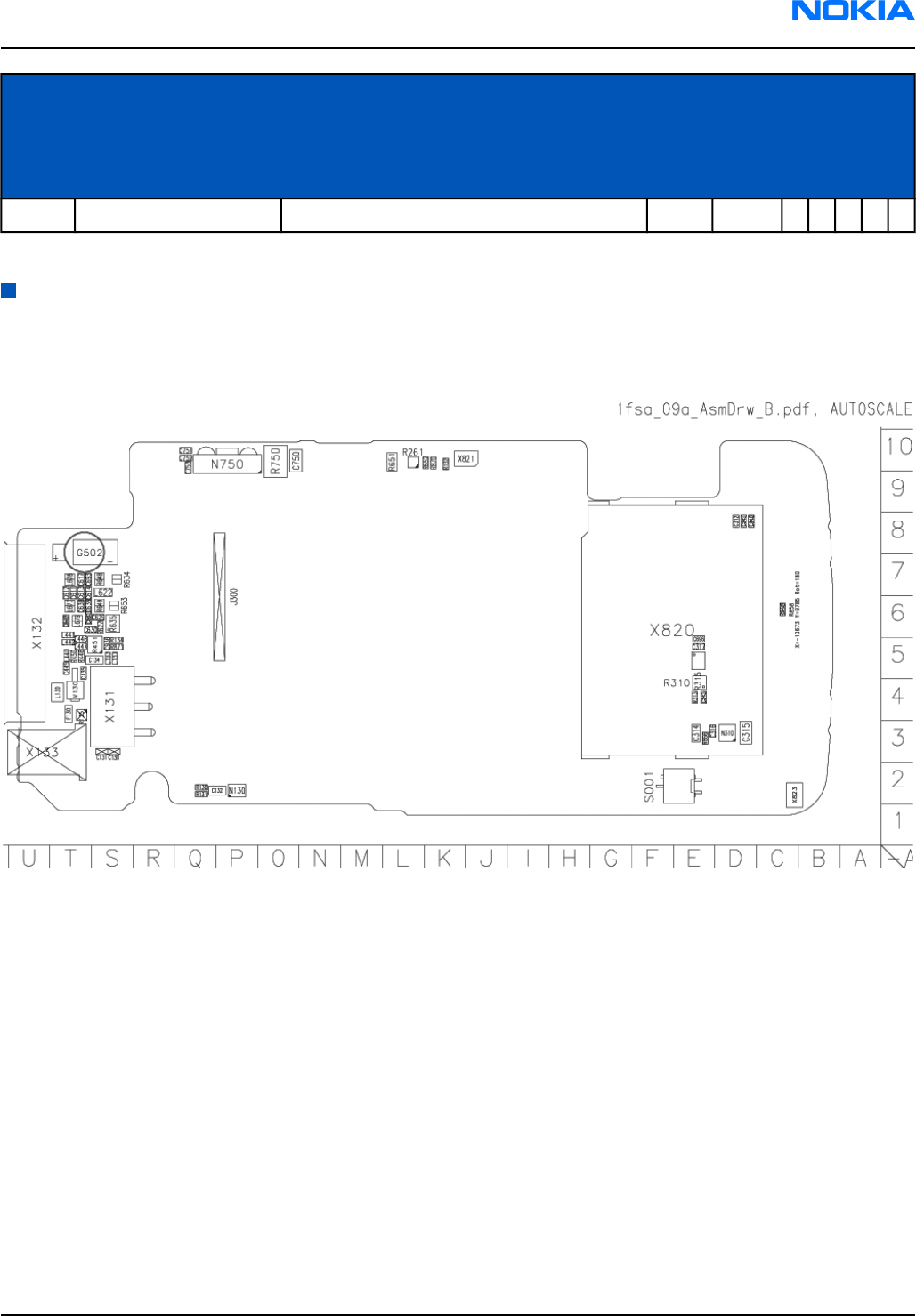
Ref Type Name Side XY E
M
E
A
A
P
A
C
C
h
i
n
a
L
T
A
N
A
M
32MB DV-RS-Multi Media Card x
Component layouts
Note: See also A3 size layouts in Schematics chapter.
Component layout, bottom
Figure 3 Component layout for 1fsa_09a, bottom
RM-25
Parts and layouts Nokia Customer Care
9235618 (Issue 2) Company Confidential Page 2–33
Copyright ©2005 Nokia. All Rights Reserved.
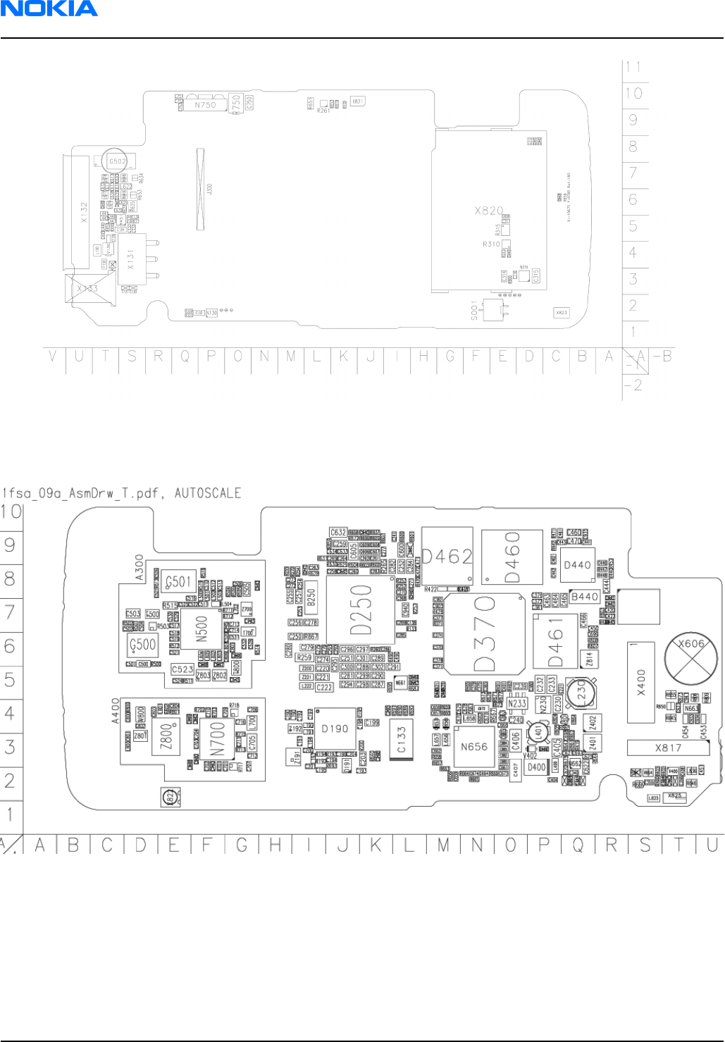
Figure 4 Component layout for 1fsa_11a, bottom
Component layout, top
Figure 5 Component layout for 1fsa_09a, top
RM-25
Nokia Customer Care Parts and layouts
Page 2–34 Company Confidential 9235618 (Issue 2)
Copyright ©2005 Nokia. All Rights Reserved.
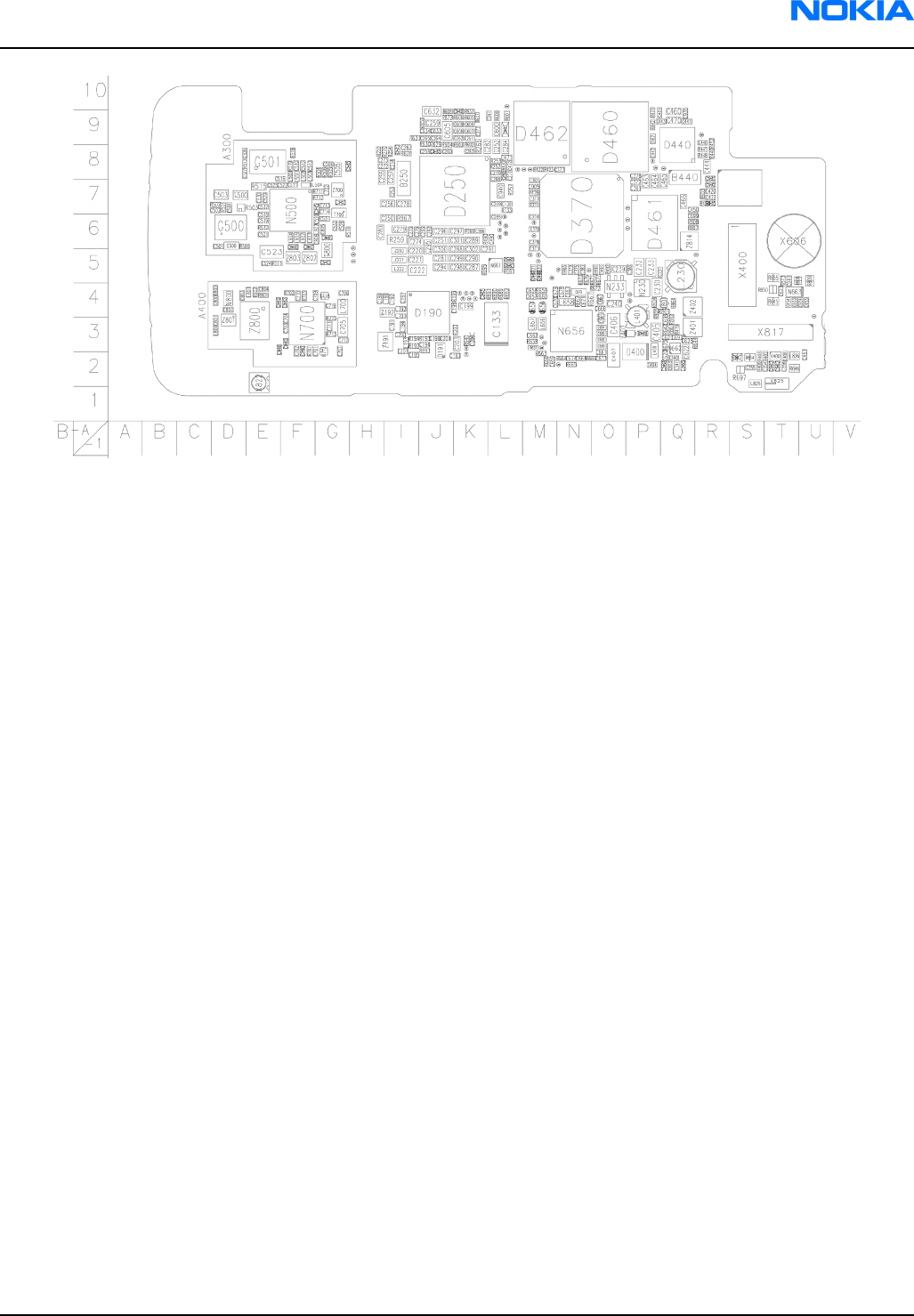
Figure 6 Component layout for 1fsa_11a, top
RM-25
Parts and layouts Nokia Customer Care
9235618 (Issue 2) Company Confidential Page 2–35
Copyright ©2005 Nokia. All Rights Reserved.

RM-25
Nokia Customer Care Parts and layouts
(This page left intentionally blank.)
Page 2–36 Company Confidential 9235618 (Issue 2)
Copyright ©2005 Nokia. All Rights Reserved.

3 — Phoenix service software
Nokia Customer Care
9235618 (Issue 2) Company Confidential Page 3–1
Copyright ©2005 Nokia. All Rights Reserved.

RM-25
Nokia Customer Care Phoenix service software
(This page left intentionally blank.)
Page 3–2 Company Confidential 9235618 (Issue 2)
Copyright ©2005 Nokia. All Rights Reserved.

Table of Contents
Service software installation......................................................................................................................................................3–5
Phoenix installation steps in brief......................................................................................................................................3–5
Installing Phoenix....................................................................................................................................................................3–5
Phoenix update installation...............................................................................................................................................3–11
Uninstalling Phoenix.............................................................................................................................................................3–12
Repairing Phoenix installation..........................................................................................................................................3–13
Phoenix service software data package overview......................................................................................................3–14
Installing Phoenix data package......................................................................................................................................3–14
Uninstalling Phoenix data package.................................................................................................................................3–18
Service software instructions..................................................................................................................................................3–19
Configuring users in Phoenix.............................................................................................................................................3–19
Managing connections in Phoenix...................................................................................................................................3–20
Installing Flash support files for FPS-8* and FLS-4*...................................................................................................3–23
Updating FPS-8 Flash prommer software......................................................................................................................3–26
Activating FPS-8......................................................................................................................................................................3–28
Deactivating FPS-8.................................................................................................................................................................3–29
Updating JBV-1 docking station software......................................................................................................................3–30
Service software concepts........................................................................................................................................................3–35
Flash concept...........................................................................................................................................................................3–35
POS flash concept...................................................................................................................................................................3–36
JBV-1 flash concept................................................................................................................................................................3–36
Module jig flash concept......................................................................................................................................................3–37
Module jig service concept.................................................................................................................................................3–38
JBV-1 service concept............................................................................................................................................................3–39
List of Figures
Figure 7 Dongle not found...........................................................................................................................................................3–6
Figure 8 Preparing setup..............................................................................................................................................................3–6
Figure 9 Welcome dialogue.........................................................................................................................................................3–7
Figure 10 Disclaimer text..............................................................................................................................................................3–7
Figure 11 Destination folder........................................................................................................................................................3–8
Figure 12 Installation status 1....................................................................................................................................................3–8
Figure 13 Installation status 2....................................................................................................................................................3–9
Figure 14 Registering components 1........................................................................................................................................3–9
Figure 15 Restart computer.......................................................................................................................................................3–10
Figure 16 Registering components 2.....................................................................................................................................3–10
Figure 17 Finish installation......................................................................................................................................................3–11
Figure 18 Installation interrupted...........................................................................................................................................3–12
Figure 19 Remove program.......................................................................................................................................................3–12
Figure 20 Finish uninstallation.................................................................................................................................................3–13
Figure 21 Repair program..........................................................................................................................................................3–14
Figure 22 Extracting files............................................................................................................................................................3–15
Figure 23 Continue data package installation.....................................................................................................................3–15
Figure 24 Data package setup information..........................................................................................................................3–16
Figure 25 Data package destination folder..........................................................................................................................3–16
Figure 26 Start copying files......................................................................................................................................................3–17
Figure 27 Data package installation status..........................................................................................................................3–17
Figure 28 Finish data package installation..........................................................................................................................3–18
Figure 29 Uninstalling Phoenix data package.....................................................................................................................3–18
RM-25
Phoenix service software Nokia Customer Care
9235618 (Issue 2) Company Confidential Page 3–3
Copyright ©2005 Nokia. All Rights Reserved.

Figure 30 Finishing data package uninstallation...............................................................................................................3–19
Figure 31 Login..............................................................................................................................................................................3–19
Figure 32 Login, user configured.............................................................................................................................................3–20
Figure 33 Phoenix icon...............................................................................................................................................................3–20
Figure 34 Manage connections................................................................................................................................................3–20
Figure 35 Connections list..........................................................................................................................................................3–21
Figure 36 Select mode: Manual................................................................................................................................................3–21
Figure 37 FLS virtual port icon..................................................................................................................................................3–21
Figure 38 Connections list..........................................................................................................................................................3–22
Figure 39 Connection information..........................................................................................................................................3–22
Figure 40 Scan product...............................................................................................................................................................3–22
Figure 41 Product support module information................................................................................................................3–23
Figure 42 Flash update welcome dialog...............................................................................................................................3–23
Figure 43 Uninstall flash update package.............................................................................................................................3–24
Figure 44 Flash installation interrupted................................................................................................................................3–24
Figure 45 Continue flash update..............................................................................................................................................3–24
Figure 46 Flash destination folder..........................................................................................................................................3–25
Figure 47 Flash installation status..........................................................................................................................................3–25
Figure 48 Finish flash update....................................................................................................................................................3–26
Figure 49 Phoenix icon...............................................................................................................................................................3–26
Figure 50 FPS-8 maintenance...................................................................................................................................................3–26
Figure 51 Prommer SW update................................................................................................................................................3–27
Figure 52 Prommer SW update done.....................................................................................................................................3–27
Figure 53 FPS-8 info window....................................................................................................................................................3–28
Figure 54 Flash directory window...........................................................................................................................................3–28
Figure 55 Prommer maintenance...........................................................................................................................................3–29
Figure 56 Box activation.............................................................................................................................................................3–29
Figure 57 Deactivation warning..............................................................................................................................................3–30
Figure 58 Extracting JBV-1 update files.................................................................................................................................3–31
Figure 59 JBV-1 update information.......................................................................................................................................3–31
Figure 60 JBV-1 update destination folder...........................................................................................................................3–31
Figure 61 Select installation: Full.............................................................................................................................................3–32
Figure 62 Select program folder..............................................................................................................................................3–32
Figure 63 Finish JBV-1 update installation...........................................................................................................................3–33
Figure 64 Checking JBV-1 SW version.....................................................................................................................................3–33
Figure 65 JBV-1 update directory window...........................................................................................................................3–34
Figure 66 JBV-1 SW update done.............................................................................................................................................3–34
Figure 67 JBV-1 SW status..........................................................................................................................................................3–34
Figure 68 Flash concept..............................................................................................................................................................3–35
Figure 69 POS flash concept......................................................................................................................................................3–36
Figure 70 JBV-1 flash concept...................................................................................................................................................3–36
Figure 71 Module jig flash concept.........................................................................................................................................3–37
Figure 72 Module jig service concept.....................................................................................................................................3–38
Figure 73 JBV-1 service concept...............................................................................................................................................3–39
RM-25
Nokia Customer Care Phoenix service software
Page 3–4 Company Confidential 9235618 (Issue 2)
Copyright ©2005 Nokia. All Rights Reserved.

Service software installation
Phoenix installation steps in brief
Phoenix is the DCT-4 generation service software for reprogramming, testing and tuning the phone.
To install Phoenix, you need to:
• Connect a DK2 Dongle or FLS-4S POS Flash Device
• Install the Phoenix Service SW
• Install the Data Package for Phoenix
• Configure users
• Manage connection settings (depends on the tools you are using)
Phoenix is now ready for FLS-4S Point Of Sales Flash Device use.
If you use FPS-8:
• Update FPS-8 SW
• Activate FPS-8
• Update JBV-1 Docking Station SW (only when needed)
Phoenix is now ready to be used with FPS-8 flash prommer and other tools as well.
The Phoenix Service Software installation contains:
• Service software support for all phone models included in the package
• Flash update package files for FPS-8* and FLS-4S programming devices
• All needed drivers for:
• DK2 dongle
• FLS-4S point of sales flash device
• USB devices
Note: Separate installation packages for flash update files and drivers are also available, but it is not
necessary to use them unless updates appear between Phoenix Service SW releases. If separate update
packages are used, they should be used after Phoenix and data packages have been installed.
Supported operating systems
• Windows 2000 and XP.
Hardware requirements for using Phoenix
• Minimum: Processor 300 MHz, RAM memory 64 MB, disk space 100 MB.
• Recommended for Windows 2000: Processor 700 MHz, RAM memory 256 MB, disk space 150 MB.
Installing Phoenix
Before you begin
• Check that a Dongle is attached to the parallel port of your computer.
• Download the installation package (for example, phoenix_service_sw_a15_2004_24_7_55.exe) to your
computer (in C:\TEMP, for instance).
• Close all other programs.
• Run the application file (for example, phoenix_service_sw_a15_2004_24_7_55.exe) and follow the instructions
on the screen.
• Administrator rights may be required to be able to install Phoenix depending on the operating system.
• If uninstalling or rebooting is needed at any point, you will be prompted by the Install Shield program.
RM-25
Phoenix service software Nokia Customer Care
9235618 (Issue 2) Company Confidential Page 3–5
Copyright ©2005 Nokia. All Rights Reserved.
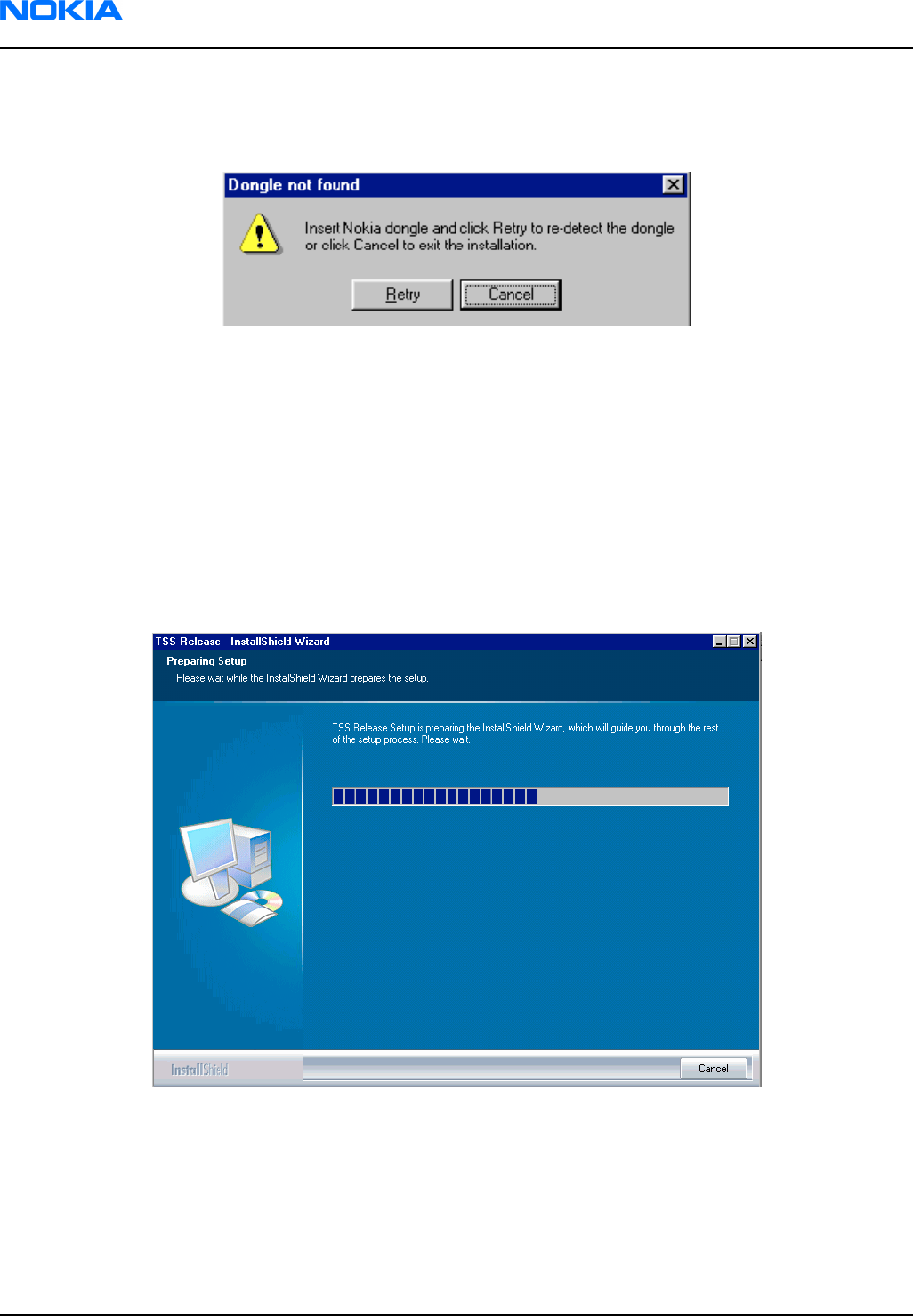
Context
If at any point during installation you get this message, Dongle is not found and installation cannot continue:
Figure 7 Dongle not found
Possible reasons may be defective or too old PKD-1 Dongle (five digit serial number Dongle when used with
FPS-8 Prommer) or that the FLS-4S POS Flash Dongle is defective or power to it is not supplied by external charger.
Check the COM/parallel ports used first! After correcting the problem Installation can be restarted.
For more detailed information, please refer to Phoenix Help files. Each feature in Phoenix has its own Help
function, which can be activated while running the program. Press the F1 key or the feature’s Help button to
activate a Help file.
Steps
1. Run the phoenix_service_sw_a15_2004_24_7_55.exe to start installation.
Figure 8 Preparing setup
Install Shield will prepare.
RM-25
Nokia Customer Care Phoenix service software
Page 3–6 Company Confidential 9235618 (Issue 2)
Copyright ©2005 Nokia. All Rights Reserved.
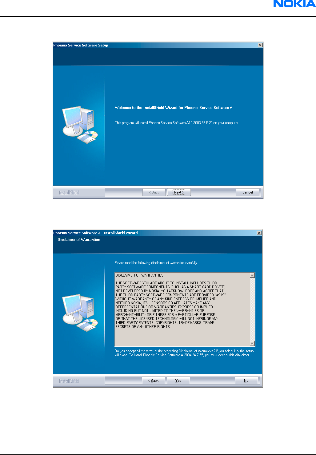
2. Click Next in Welcome dialog to continue.
Figure 9 Welcome dialogue
3. Read the disclaimer carefully.
Figure 10 Disclaimer text
RM-25
Phoenix service software Nokia Customer Care
9235618 (Issue 2) Company Confidential Page 3–7
Copyright ©2005 Nokia. All Rights Reserved.
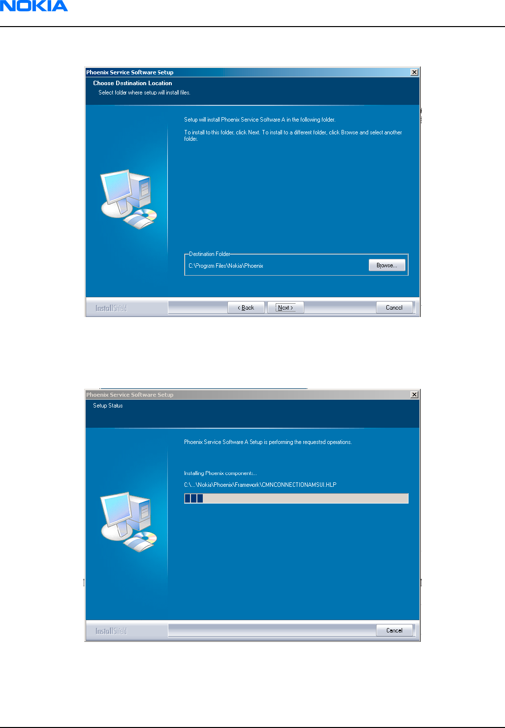
4. Choose destination folder. The default folder C:\ProgramFiles\Nokia\Phoenix is recommended.
Figure 11 Destination folder
Click Next to continue. You may choose another location by selecting Browse (not recommended).
5. Wait for the components to be copied.
Figure 12 Installation status 1
Progress of the setup is shown in the Setup Status window.
RM-25
Nokia Customer Care Phoenix service software
Page 3–8 Company Confidential 9235618 (Issue 2)
Copyright ©2005 Nokia. All Rights Reserved.
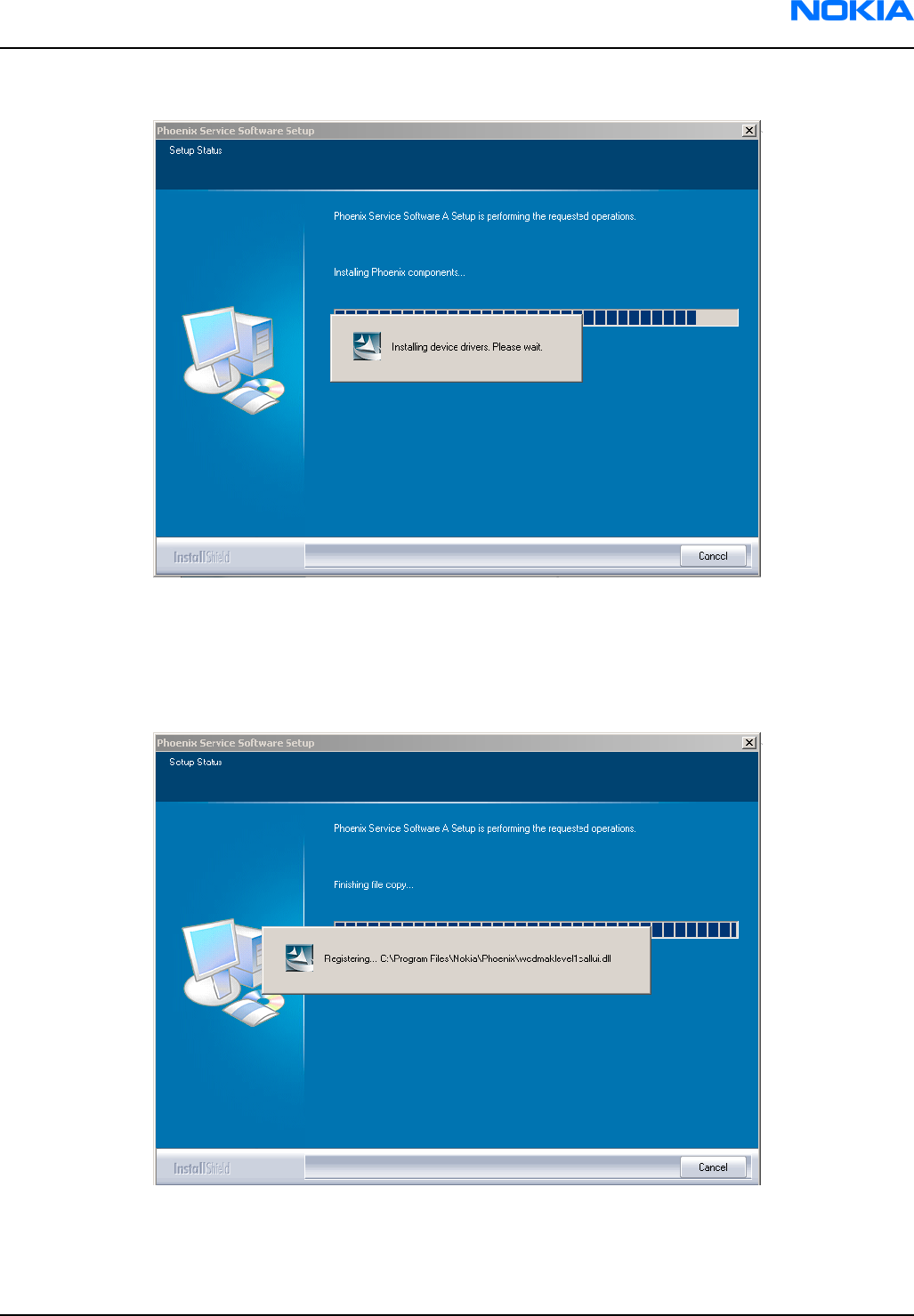
6. Wait for the drivers to be installed and updated.
Figure 13 Installation status 2
The process may take several minutes to complete.
If the operating system does not require rebooting (Windows 2000, XP) the PC components are registered
right away.
Figure 14 Registering components 1
If the operating system used requires restarting your computer (Windows 98, SE, ME) the Install Shield Wizard
will tell you about it. Select Yes... to reboot the PC immediately and No... to reboot the PC manually afterwards.
RM-25
Phoenix service software Nokia Customer Care
9235618 (Issue 2) Company Confidential Page 3–9
Copyright ©2005 Nokia. All Rights Reserved.
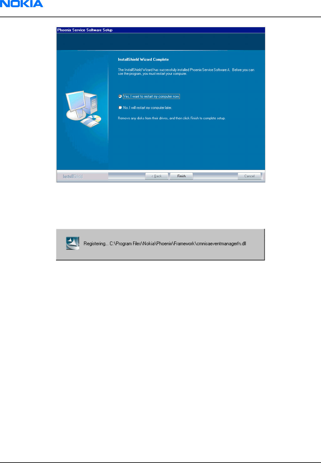
Figure 15 Restart computer
After the reboot, components are registered and Phoenix is ready for use.
Note: Phoenix does not work, if components have not been registered.
Figure 16 Registering components 2
RM-25
Nokia Customer Care Phoenix service software
Page 3–10 Company Confidential 9235618 (Issue 2)
Copyright ©2005 Nokia. All Rights Reserved.
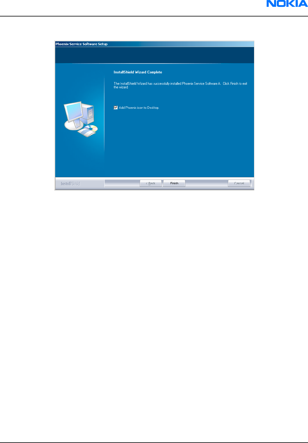
7. Click Finish to end installation.
Figure 17 Finish installation
Phoenix is now ready for use.
Next action
After the installation, Phoenix service software can be used after:
• installing phone model specific data package for Phoenix, and
• configuring users and connections.
FLS-4S can be used right away.
FPS-8* can be used after updating its Flash Update Package files.
Phoenix update installation
If you already have the Phoenix Service SW installed on your computer, sooner or later there will be need to
update it when new versions are released.
Always use the latest available versions of both the Phoenix Service SW and the phone-specific Data Package.
Instructions can be found in phone model specific Technical Bulletins and Phone Data Package readme.txt files
(shown during installation).
To update the Phoenix you need to take exactly the same steps as when installing it for the first time:
• Download the installation package to your computer hard disk.
• Close all other programs.
• Run the application file (for example, phoenix_service_sw_a15_2004_24_7_55.exe).
• New version of Phoenix will be installed.
• Driver versions will be checked and updated.
When you update the Phoenix from old to new version (for example, a14_2004_16_4_47 to a15_2004_24_7_55),
the update will take place automatically without uninstallation.
RM-25
Phoenix service software Nokia Customer Care
9235618 (Issue 2) Company Confidential Page 3–11
Copyright ©2005 Nokia. All Rights Reserved.
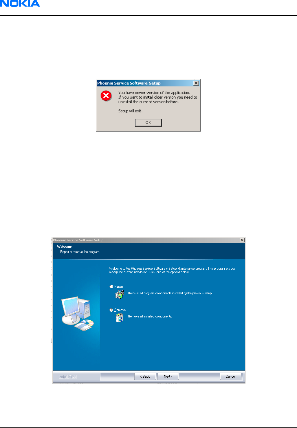
If you try to update the Phoenix with the same version that you already have (for example, a15_2004_24_7_55
to a15_2004_24_7_55) you are asked if you want to uninstall the version of Phoenix you have on your PC. In this
case you can choose between total uninstallation and repair just like when you choose to uninstall Phoenix
service software from the Windows Control panel.
If you try to install an older version (for example, downgrade from a15_2004_24_7_55 to a14_2004_16_4_47),
installation will be interrupted.
Figure 18 Installation interrupted
Always follow the instructions on the screen.
Uninstalling Phoenix
Context
You can uninstall Phoenix service software manually from the Windows Control Panel.
Steps
1. Open the Windows Control Panel and choose Add/Remove Programs.
2. To uninstall Phoenix, choose Phoenix Service Software -> Change/Remove -> Remove.
Figure 19 Remove program
The progress of the uninstallation is shown.
RM-25
Nokia Customer Care Phoenix service software
Page 3–12 Company Confidential 9235618 (Issue 2)
Copyright ©2005 Nokia. All Rights Reserved.
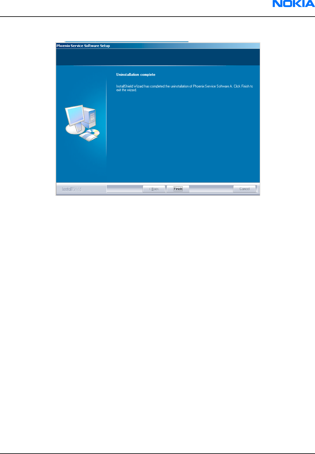
3. If the operating system does not require rebooting, click Finish to complete.
Figure 20 Finish uninstallation
If the operating system requires rebooting, InstallShield Wizard will notify you. Select Yes... to reboot the PC
immediately and No... to reboot the PC manually afterwards.
Repairing Phoenix installation
Context
If you experience any problems with the service software or suspect that files have been lost, you can use the
repair function before completely reinstalling Phoenix.
Note: The original installation package (for example, phoenix_service_sw_a15_2004_24_7_55.exe) must
be found on your PC when you run the repair setup.
Steps
1. Open Windows Control Panel -> Add/Remove Programs.
2. Select Phoenix Service Software -> Change/Remove.
RM-25
Phoenix service software Nokia Customer Care
9235618 (Issue 2) Company Confidential Page 3–13
Copyright ©2005 Nokia. All Rights Reserved.
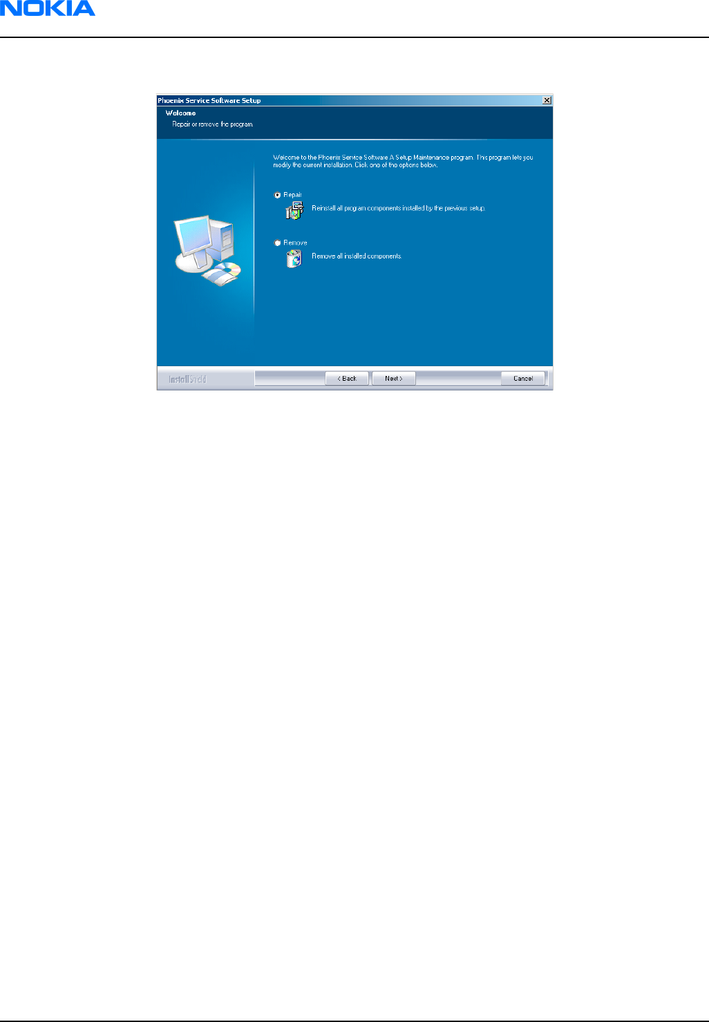
3. In the following view, select Repair.
Figure 21 Repair program
Phoenix will now reinstall components and register them.
The procedure is the same as when updating Phoenix.
4. To complete the repair, click Finish.
Phoenix service software data package overview
Each product has its own data package (DP). The product data package contains all product-specific data files
to make the Phoenix service software and tools usable with a certain phone model.
The data package contains the following:
• Product software Binary files
• Files for type label printing
• Validation file for the Faultlog repair data reporting system
• All product-specific configuration files for Phoenix software components
Data files are stored under C:\Program Files\Nokia\Phoenix (default).
Installing Phoenix data package
Before you begin
• Product data package contains all product-specific data to make the Phoenix Service Software and tools
usable with a certain phone model.
• Check that the dongle is attached to the parallel port of your computer.
• Install Phoenix Service SW.
• Download the installation package (for example, RM-25_dp_EA_v_1_0.exe) to your computer (for example, in
C:\TEMP).
• Close all other programs.
• Run the application file (for example, RM-25_dp_EA_ v_1_0.exe) and follow the instructions on the screen.
If you already have the Phoenix Service SW installed on your computer, you will need to update it when a new
version is released.
RM-25
Nokia Customer Care Phoenix service software
Page 3–14 Company Confidential 9235618 (Issue 2)
Copyright ©2005 Nokia. All Rights Reserved.
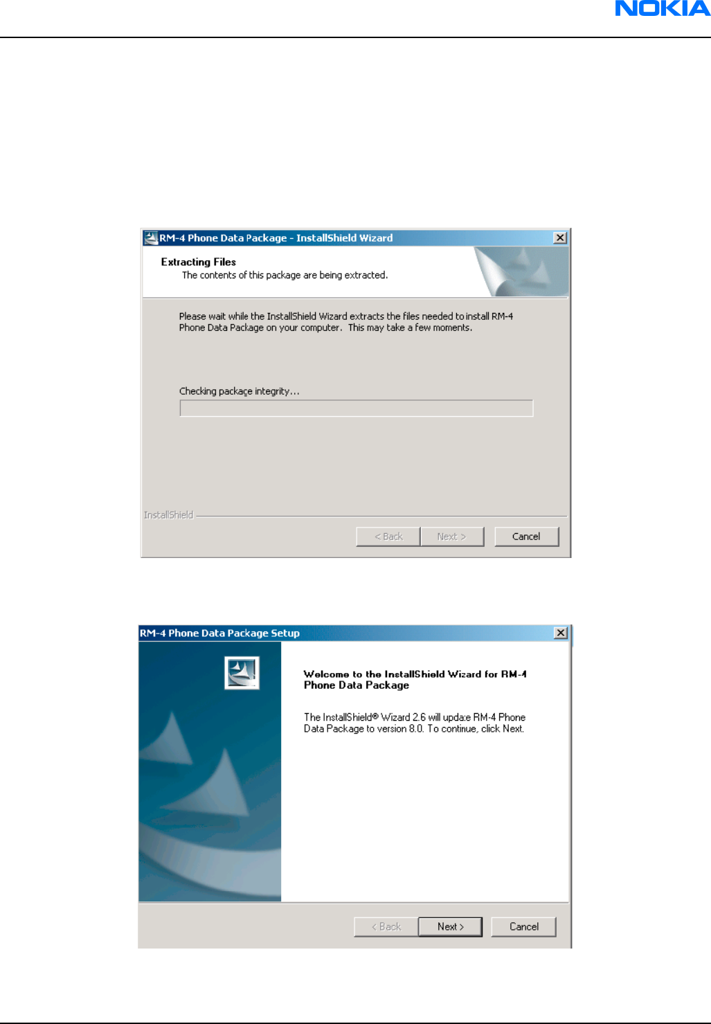
Note: Very often the Phoenix Service SW and the phone-specific data package for Phoenix come in
pairs, meaning that a certain version of Phoenix can only be used with a certain version of the data
package. Always use the latest available versions of both. Instructions can be found in phone model
specific Technical Bulletins and readme.txt files of the data packages.
Steps
1. To start installation, run the application file (for example, RM-25_dp_EA_ v_1_0.exe).
2. Click Next, and wait for the installation files to be extracted.
Figure 22 Extracting files
3. Click Next to continue.
Figure 23 Continue data package installation
RM-25
Phoenix service software Nokia Customer Care
9235618 (Issue 2) Company Confidential Page 3–15
Copyright ©2005 Nokia. All Rights Reserved.
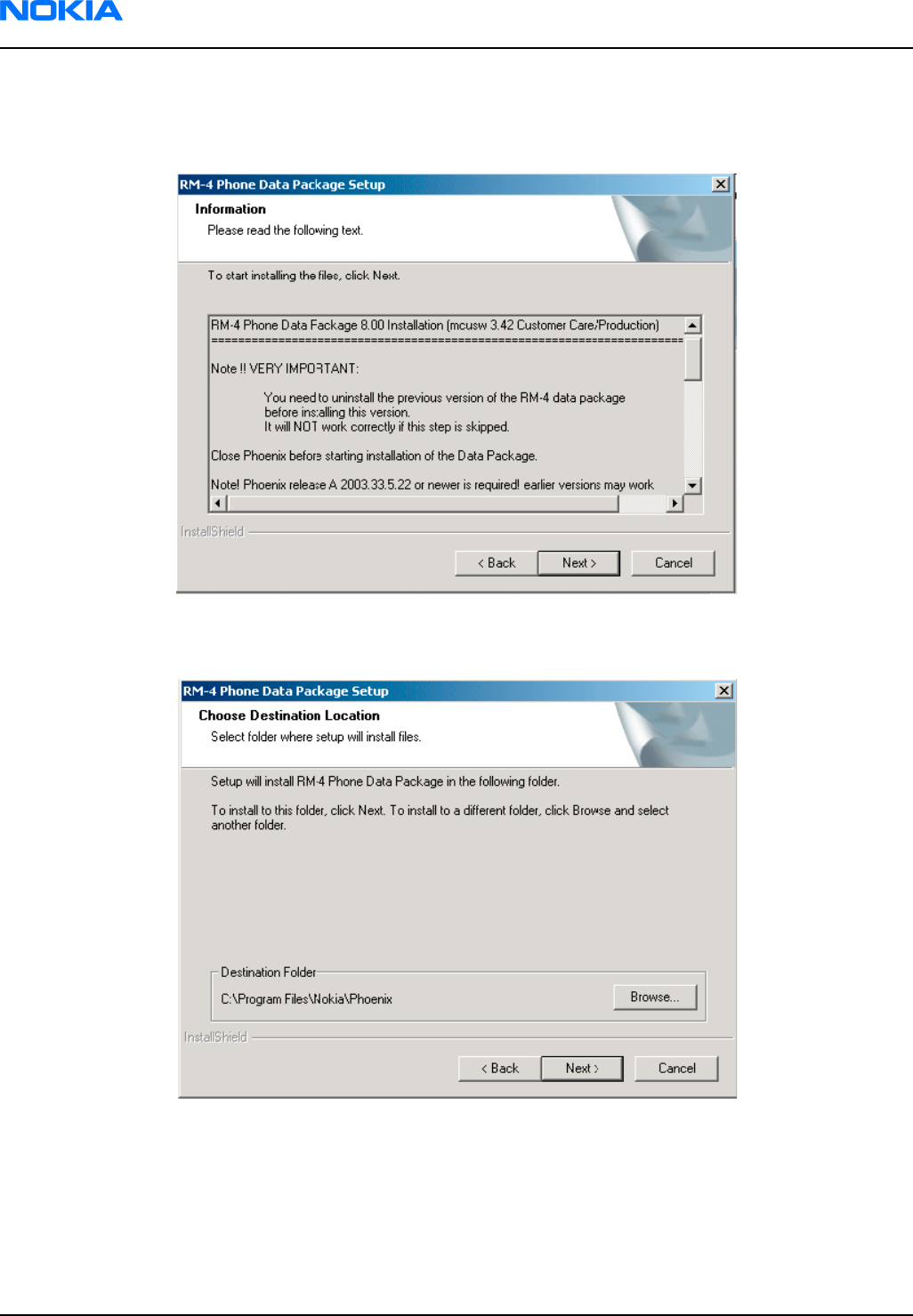
In this view you can see the contents of the data package. Read the text carefully. There should be information
about the Phoenix version required with this data package.
Click Next to continue.
Figure 24 Data package setup information
4. Confirm location and click Next to continue.
Figure 25 Data package destination folder
The install shield checks where the Phoenix application is installed and the directory is shown.
Click Next to continue.
RM-25
Nokia Customer Care Phoenix service software
Page 3–16 Company Confidential 9235618 (Issue 2)
Copyright ©2005 Nokia. All Rights Reserved.
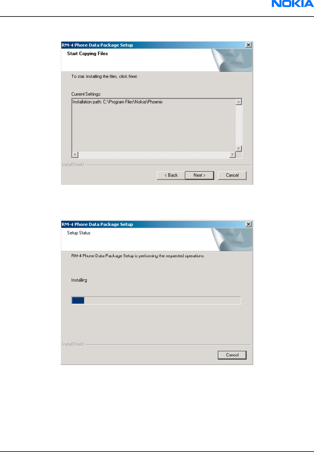
5. Click Next to start copying the files.
Figure 26 Start copying files
Phone model specific files will be installed. Please wait.
Figure 27 Data package installation status
RM-25
Phoenix service software Nokia Customer Care
9235618 (Issue 2) Company Confidential Page 3–17
Copyright ©2005 Nokia. All Rights Reserved.
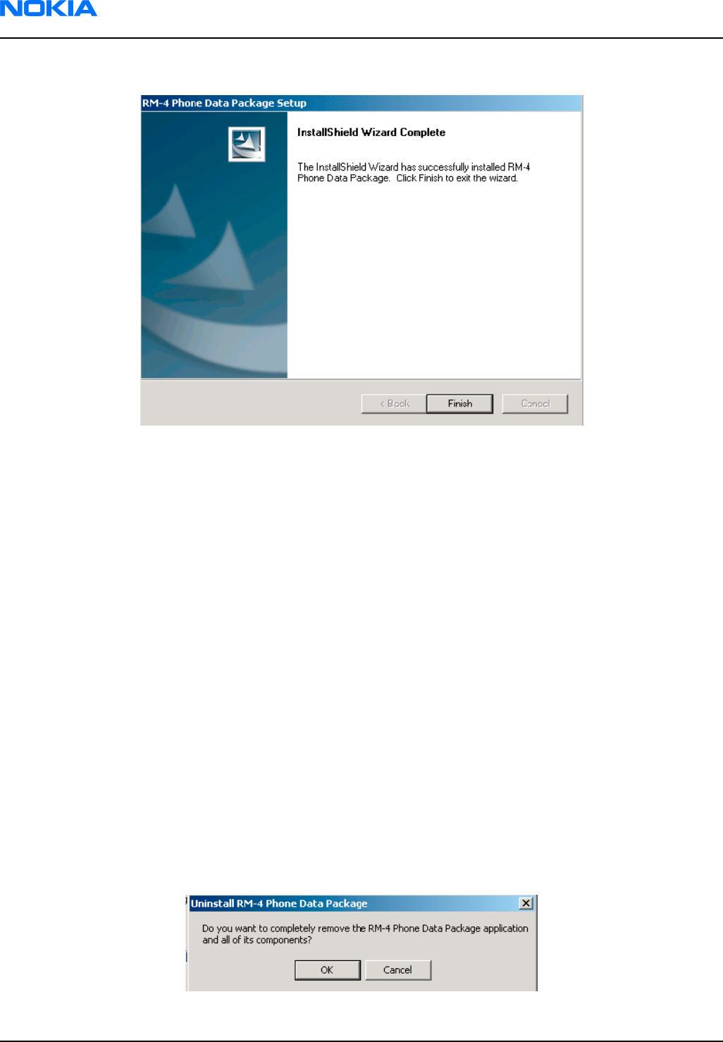
6. Click Finish to complete the installation.
Figure 28 Finish data package installation
You now have all phone model specific files installed in your Phoenix Service SW.
Next action
Phoenix can be used, for example, for flashing phones and printing type labels after:
• configuring users, and
• managing connections.
FLS-4S can be used right away.
FPS-8* can be used after updating Flash Update Package files.
Uninstalling Phoenix data package
Context
If you try to install the same version of the Phoenix data package that you already have, you are asked if you
want to uninstall the existing version.
There is no need to uninstall the older version of a data package, unless instructions to do so are given in
the readme.txt file of the data package and bulletins related to the release.
Please read all related documents carefully.
Steps
1. To uninstall the data package, click OK Cancel to interrupt the uninstallation.
Figure 29 Uninstalling Phoenix data package
RM-25
Nokia Customer Care Phoenix service software
Page 3–18 Company Confidential 9235618 (Issue 2)
Copyright ©2005 Nokia. All Rights Reserved.
2. Once the previously installed data package is uninstalled, click Finish.
Figure 30 Finishing data package uninstallation
Alternative steps
• You can also uninstall the data package manually from Windows Control Panel -> Add/Remove
Programs -> xx-xx * Phone Data Package. (*= type designator of the phone)
Next action
Run the installation package again to continue installation from the beginning.
Service software instructions
Configuring users in Phoenix
Steps
1. Start Phoenix Service SW and log in.
Figure 31 Login
If the user ID is already configured, choose it from the dropdown list and click OK.
To add a new user or edit existing ones, click Maintain.
2. To add information for a new user, click New.
RM-25
Phoenix service software Nokia Customer Care
9235618 (Issue 2) Company Confidential Page 3–19
Copyright ©2005 Nokia. All Rights Reserved.
3. Type in the name and initials of the user and click OK.
A new user is now created.
4. Click OK.
You are now able to login with the user name created.
5. Click OK.
Figure 32 Login, user configured
Managing connections in Phoenix
Steps
1. Start Phoenix Service SW and log in.
Figure 33 Phoenix icon
2. Choose File -> Manage Connections.
Figure 34 Manage connections
Existing connections can be selected, edited, deleted, and new ones created by using this dialog.
RM-25
Nokia Customer Care Phoenix service software
Page 3–20 Company Confidential 9235618 (Issue 2)
Copyright ©2005 Nokia. All Rights Reserved.
Figure 35 Connections list
3. Click Add to add a new connection, and select if you want to create it manually or by using the Connection
Wizard.
In the following dialogs you will be asked to select settings for the connection. If you use the Wizard, connect
the tools and a phone to your PC and the wizard will automatically try to configure the correct connection.
4. Select Manual mode, and click Next to continue.
Figure 36 Select mode: Manual
i For FLS-4S POS Flash Device, choose the following connection settings:
• Media: FBUS
• COM Port: Virtual COM Port used by FLS-4
Note: ALWAYS check this. Go to Windows -> Control Panel -> FLS Virtual Port -> Configuration.
Figure 37 FLS virtual port icon
RM-25
Phoenix service software Nokia Customer Care
9235618 (Issue 2) Company Confidential Page 3–21
Copyright ©2005 Nokia. All Rights Reserved.
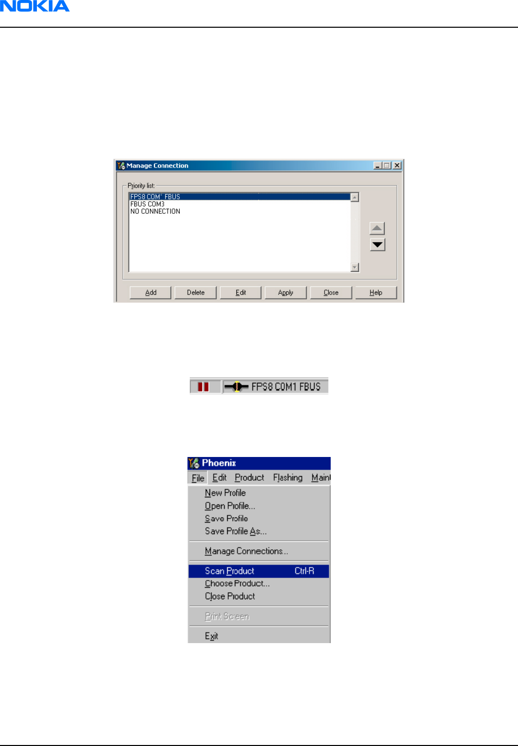
ii For FPS-8 Flash Prommer, choose the following connection settings:
• Media: FPS-8
• Port Num: COM Port where FPS-8 is connected
• COMBOX_DEF_MEDIA: FBUS
5. Click Finish to complete the configuration.
6. Activate the connection you want to use by clicking it, use up/down arrows to move it on top of the list, and
click Apply.
Figure 38 Connections list
The connection is now selected and can be used after closing the Manage Connections window.
Selected connection will be shown on the right hand bottom corner of the screen.
Figure 39 Connection information
7. To use the selected connection, connect the phone to Phoenix with correct service tools, make sure that it
is switched on and select Scan Product.
Figure 40 Scan product
When a product is found, Phoenix will load product support. Name of the loaded product support module
and its version information will be shown on the bottom of the screen.
RM-25
Nokia Customer Care Phoenix service software
Page 3–22 Company Confidential 9235618 (Issue 2)
Copyright ©2005 Nokia. All Rights Reserved.
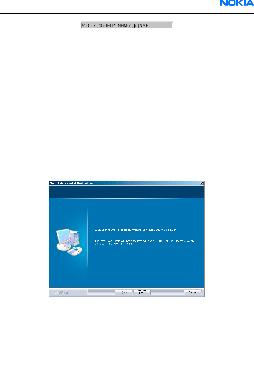
Figure 41 Product support module information
Installing Flash support files for FPS-8* and FLS-4*
Before you begin
Note: Only separate installation package.
• Install Phoenix Service SW.
• Install phone model specific data package for Phoenix.
• The flash support files are delivered in the same installation package with Phoenix data packages or newer
Phoenix packages beginning from September 2003.
• Normally it is enough to install Phoenix and the phone-specific data package because the Phoenix installation
always includes the latest flash update package files for FLS-4S/FPS-8*.
• A separate installation package for flash support files is available, and the files can be updated according to
this instruction if updates appear between Phoenix/data package releases.
Context
If you are not using a separate installation package, you can skip this section and continue with FPS-8 Flash
prommer SW update (Page 3–26) after installing a new phone data package.
Steps
1. Start by double clicking flash_update_03_13_001.exe to begin installation.
Figure 42 Flash update welcome dialog
RM-25
Phoenix service software Nokia Customer Care
9235618 (Issue 2) Company Confidential Page 3–23
Copyright ©2005 Nokia. All Rights Reserved.
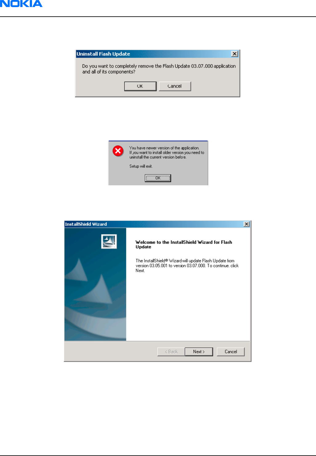
2. If the same version of Flash Update package already exists, and you want to reinstall it, the previous package
is first uninstalled. Restart installation again after that.
Figure 43 Uninstall flash update package
If you try to downgrade the existing version to older ones, the setup will be aborted. If you really want to
downgrade, uninstall newer files manually from Control Panel and then rerun the installation again.
Figure 44 Flash installation interrupted
If an older version exists on your PC and it needs to be updated, click Next to continue installation.
Figure 45 Continue flash update
RM-25
Nokia Customer Care Phoenix service software
Page 3–24 Company Confidential 9235618 (Issue 2)
Copyright ©2005 Nokia. All Rights Reserved.
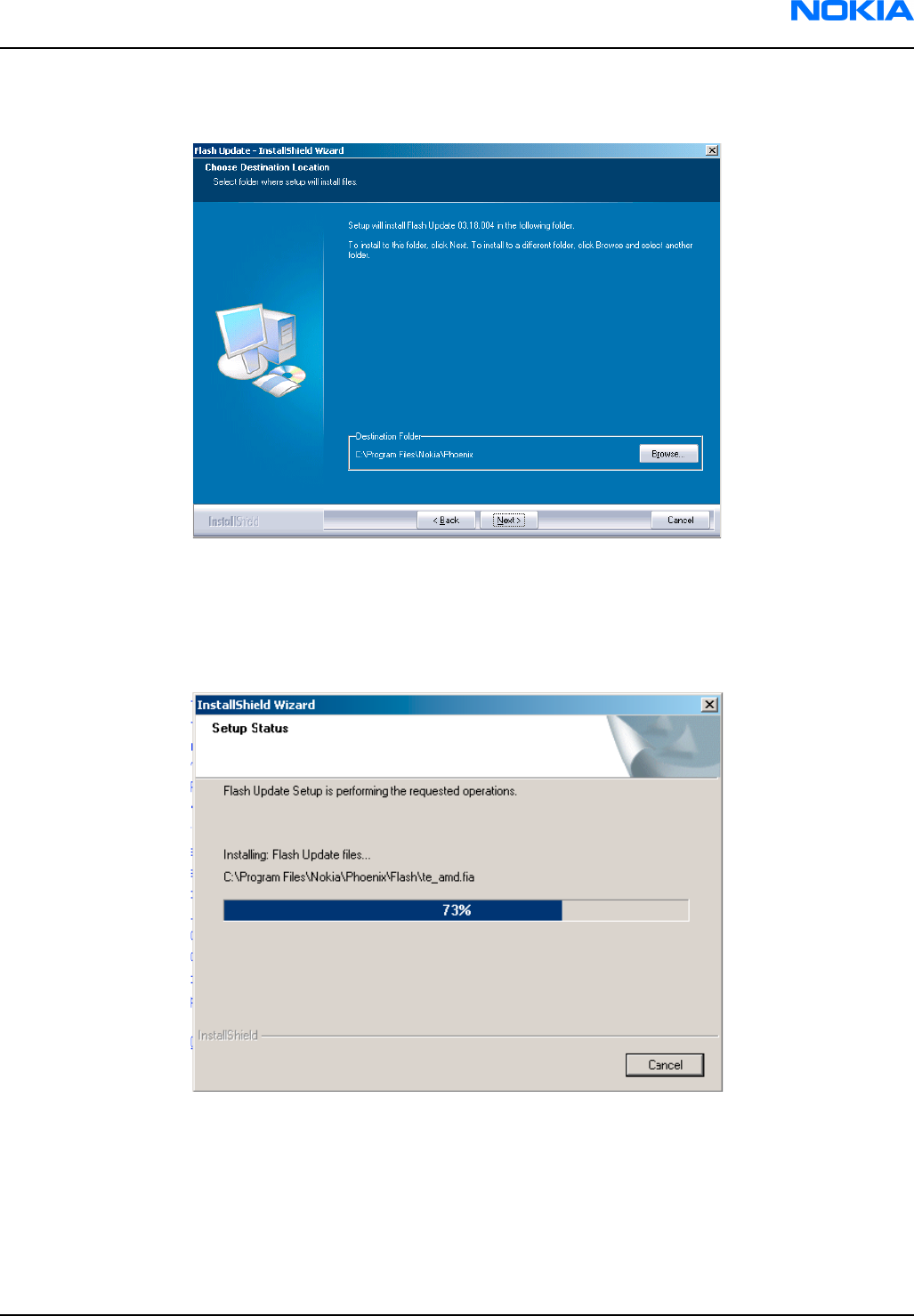
3. It is highly recommended to install the files to the default destination folder C:\Program Files\Nokia
\Phoenix. Click Next to continue.
Figure 46 Flash destination folder
When installing the flash update files for the first time you may choose another location by selecting
Browse. However, this is not recommended.
Installation will continue.
Figure 47 Flash installation status
RM-25
Phoenix service software Nokia Customer Care
9235618 (Issue 2) Company Confidential Page 3–25
Copyright ©2005 Nokia. All Rights Reserved.
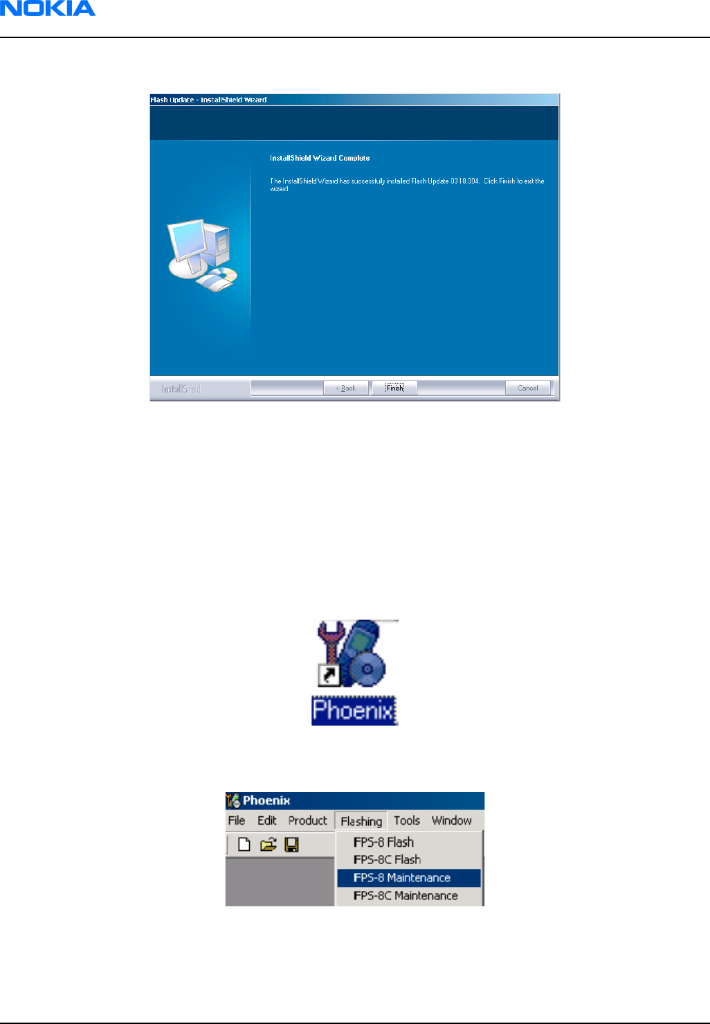
4. Choose Finish to complete the installation procedure.
Figure 48 Finish flash update
Next action
FLS-4 can be used right after the Flash Update Package is installed.
FPS-8* flash prommer must be updated using Phoenix!
Updating FPS-8 Flash prommer software
Steps
1. Start Phoenix Service Software and log in, manage connection correctly for the FPS-8* flash prommer.
Figure 49 Phoenix icon
2. Choose Flashing -> FPS-8 maintenance.
Figure 50 FPS-8 maintenance
RM-25
Nokia Customer Care Phoenix service software
Page 3–26 Company Confidential 9235618 (Issue 2)
Copyright ©2005 Nokia. All Rights Reserved.
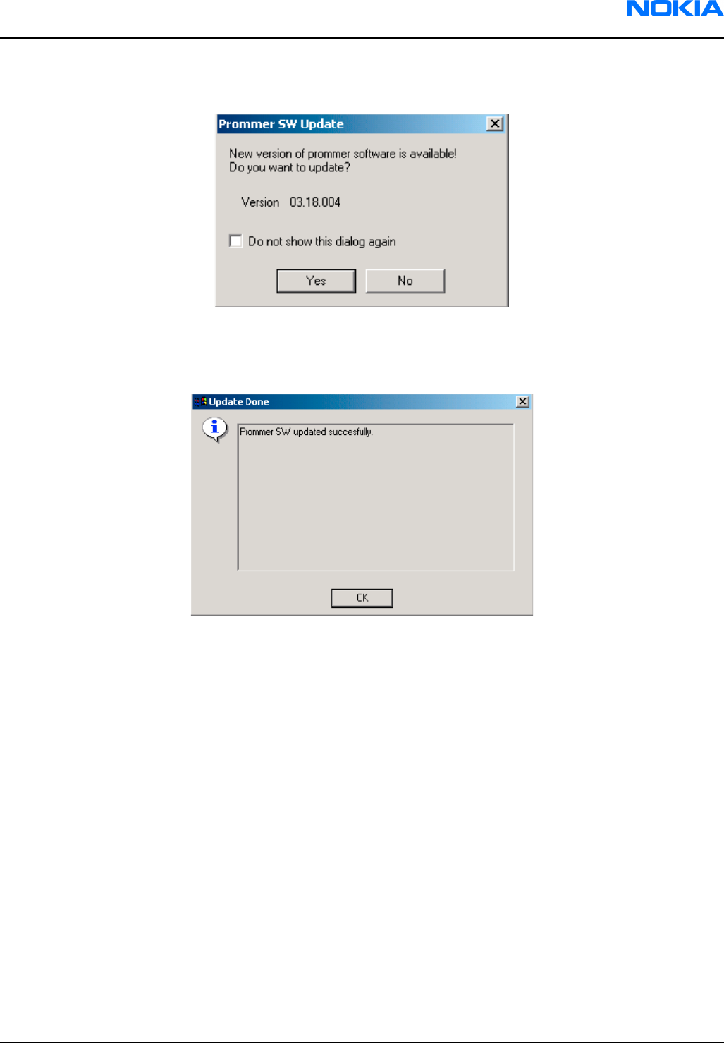
3. When the new FPS-8 flash update package is installed to computer you will be asked to update the files to
your FPS-8 Prommer. Select Yes to update files.
Figure 51 Prommer SW update
4. Wait until you are notified that update has been successful; the procedure will take a couple of minutes.
Click OK to close the FPS-8 Maintenance window.
Figure 52 Prommer SW update done
View after successful prommer software update:
RM-25
Phoenix service software Nokia Customer Care
9235618 (Issue 2) Company Confidential Page 3–27
Copyright ©2005 Nokia. All Rights Reserved.
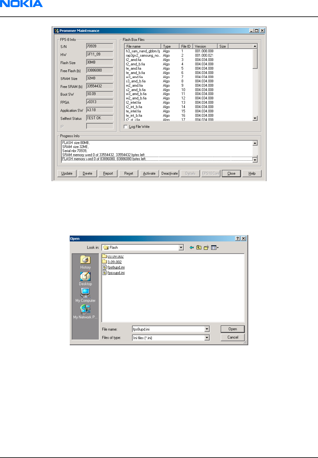
Figure 53 FPS-8 info window
Alternative steps
• FPS-8 SW can also be updated by pressing Update button and selecting appropriate fps8upd.ini file in C:
\Program Files\Nokia\Phoenix\Flash.
Figure 54 Flash directory window
• All files can be loaded separately to FPS-8. To do this, just press the right mouse button in the Flash box
files window and select the file type to be loaded.
More information can be found in Phoenix Help.
Activating FPS-8
Context
Before FPS-8 can be successfully used for phone programming, it must first be activated.
First fill in the FPS-8 activation request sheet in the FPS-8 sales package and follow the instructions given.
RM-25
Nokia Customer Care Phoenix service software
Page 3–28 Company Confidential 9235618 (Issue 2)
Copyright ©2005 Nokia. All Rights Reserved.
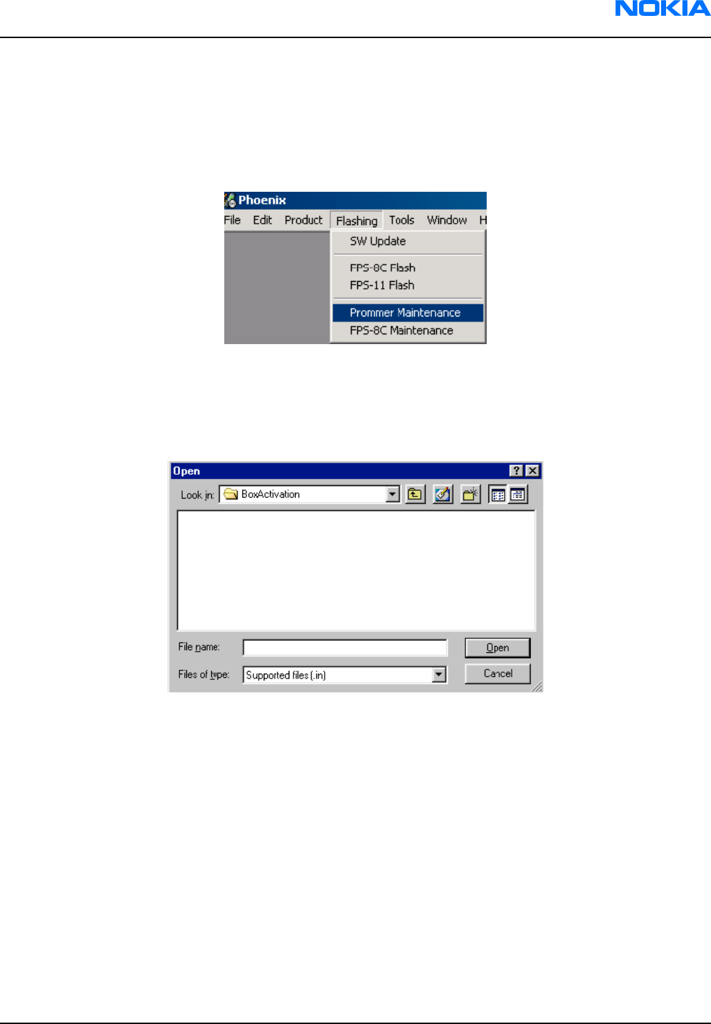
When activation file is received (for example, 00000.in), copy it to the C:\ProgramFiles\Nokia\Phoenix
\BoxActivation directory on your computer (this directory is created when Phoenix is installed).
Steps
1. Start Phoenix Service Software.
2. Choose Maintenance -> Prommer Maintenance.
Figure 55 Prommer maintenance
3. In the Prommer Maintenance window, click Activate.
4. To find the activation file if you saved it to some other directory on your PC, click Browse.
5. To activate the prommer, select the activation file and click Open.
Figure 56 Box activation
6. To complete the activation, restart FPS-8.
Deactivating FPS-8
Context
If there is, for example, a need to send the FPS-8 box for repair, it must be deactivated first.
Steps
1. Start Phoenix Service Software.
2. Choose Maintenance -> Prommer Maintenance.
3. In the Prommer Maintenance window, click Deactivate.
RM-25
Phoenix service software Nokia Customer Care
9235618 (Issue 2) Company Confidential Page 3–29
Copyright ©2005 Nokia. All Rights Reserved.
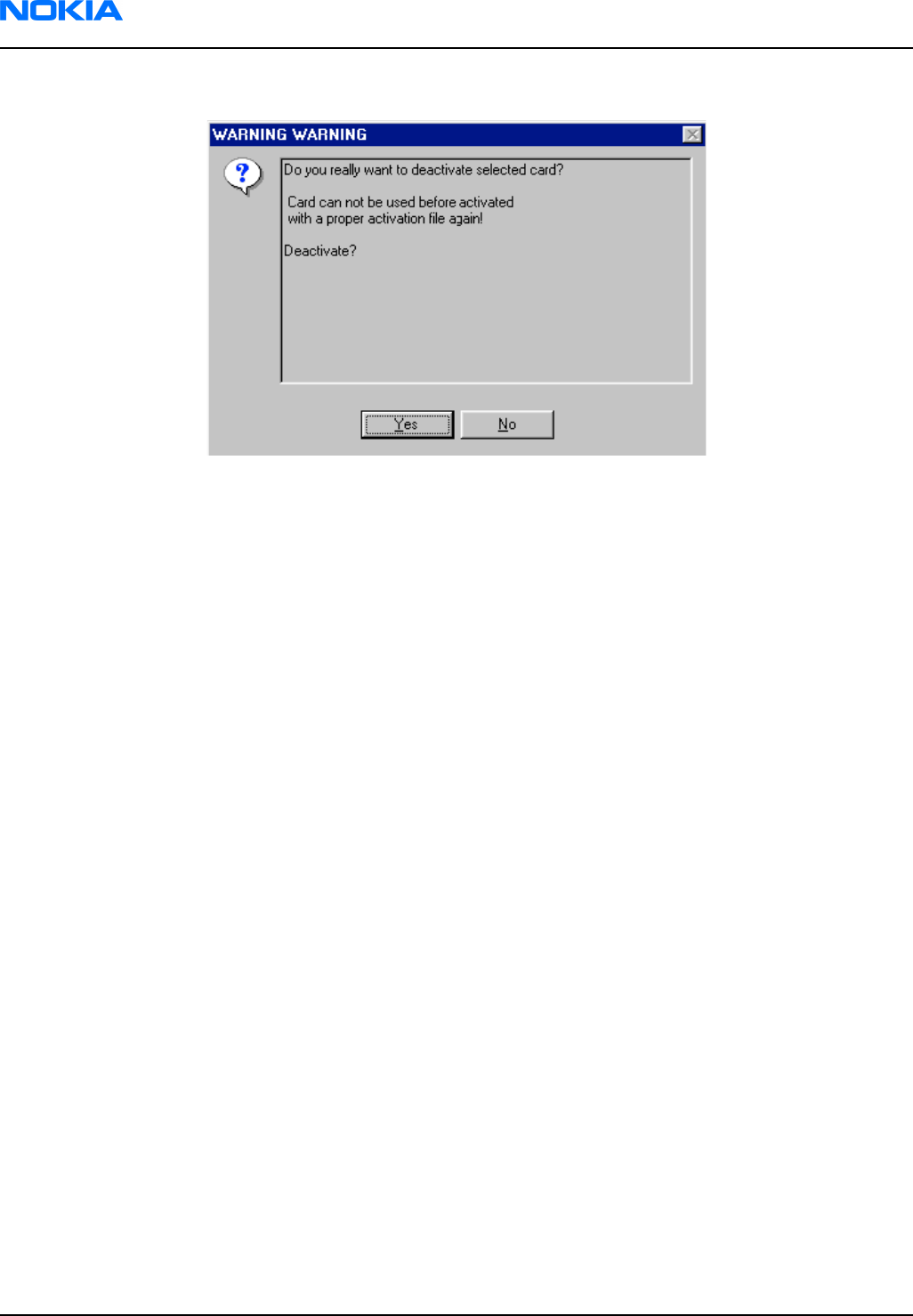
4. To confirm the deactivation, click Yes.
Figure 57 Deactivation warning
The box is deactivated.
5. To complete the deactivation, restart FPS-8.
Updating JBV-1 docking station software
Before you begin
The JBV-1 docking station contains software (firmware) which can be updated. You need the following
equipment to update the software:
• PC with USB connection
• operating system supporting USB (Not Win 95 or NT)
• USB Cable (can be purchased from shops or suppliers providing PC hardware and accessories)
• JBV-1 docking station
• external power supply (11-16V)
Before installation:
• Download Jbv1_18_update.zip file to your computer (in C:\TEMP for example) from your download web site.
• Close all other programs.
• Follow instructions on the screen.
Context
The JBV-1 docking station is a common tool for all DCT-4 generation products. In order to make the JBV-1 usable
with different phone models, a phone-specific docking station adapter is used.
Steps
1. Run Jbv1_18_update.zip file and start software installation by double clicking Setup.exe.
Note: DO NOT CONNECT THE USB CABLE/JBV-1 TO YOUR COMPUTER YET!
RM-25
Nokia Customer Care Phoenix service software
Page 3–30 Company Confidential 9235618 (Issue 2)
Copyright ©2005 Nokia. All Rights Reserved.
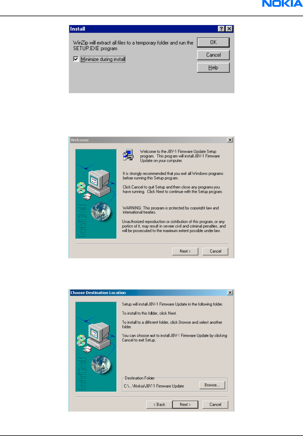
Figure 58 Extracting JBV-1 update files
Files needed for JBV-1 package setup program will be extracted.
2. Read the instructions in the dialog box and click Next to continue.
Figure 59 JBV-1 update information
3. Accept the suggested destination folder for installing the JBV-1 SW Package, and click Next to continue.
Figure 60 JBV-1 update destination folder
RM-25
Phoenix service software Nokia Customer Care
9235618 (Issue 2) Company Confidential Page 3–31
Copyright ©2005 Nokia. All Rights Reserved.

4. Select Full installation and click Next to continue.
Figure 61 Select installation: Full
5. A program folder is created and the software files are installed there. Click Next to continue.
Figure 62 Select program folder
RM-25
Nokia Customer Care Phoenix service software
Page 3–32 Company Confidential 9235618 (Issue 2)
Copyright ©2005 Nokia. All Rights Reserved.
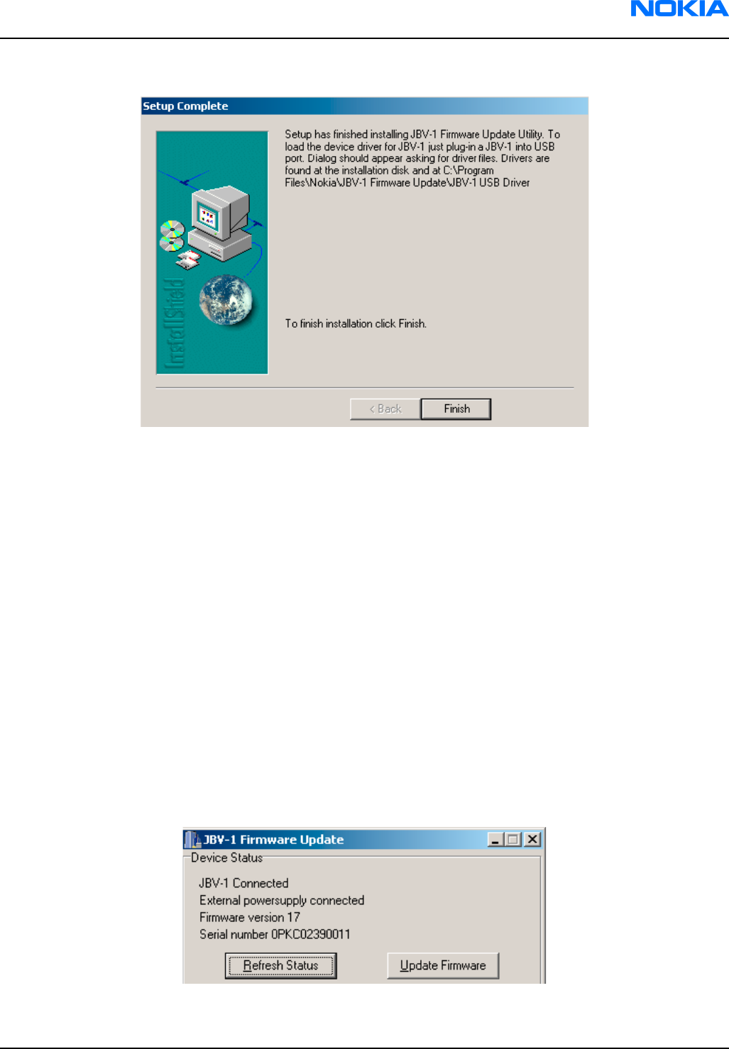
6. Click Finish to complete the installation.
Figure 63 Finish JBV-1 update installation
7. Connect the USB cable/JBV-1 to your computer. Connect power to JBV-1 (11-16V DC) from an external power
supply, then connect the USB Cable between the JBV-1 USB connector and the PC.
8. Install or update the JBV-1 USB drivers which are delivered with the JBV-1 SW installation package.
The drivers can be found in C:\Program Files\Nokia\ JBV-1 Firmware Update\JBV-1USB driver
•If there is no previously installed JBV-1 Firmware update package installed on your computer, Windows
will detect connected USB cable and detect drivers for new HW. You will be prompted about this, please
follow the instructions and allow Windows to search and install the best drivers available.
• If there is a previously installed JBV-1 Firmware update package (v.17 or older) on your computer, please
update the JBV-1 USB driver. Please see the readme.txt file in C:\Program Files\Nokia\JBV-1 Firmware
Update\JBV-1USB driver folder for instructions on how to update the JBV-1 USB Driver.
After you have installed or updated the JBV-1 USB driver, the actual JBV-1 SW update can begin.
9. Go to folder C:\Program Files\Nokia\JBV-1 Firmware Update\JBV-1 Firmware Update and start JBV-1 Update
SW by double clicking fwup.exe.
JBV-1 Firmware update starts and shows current status of the connected JBV-1. If firmware version read
from your JBV-1 is not the latest one available (v.17 or older), it needs to be updated to version 18 by
clicking Update Firmware.
10. Choose Refresh Status to check the SW version.
Figure 64 Checking JBV-1 SW version
RM-25
Phoenix service software Nokia Customer Care
9235618 (Issue 2) Company Confidential Page 3–33
Copyright ©2005 Nokia. All Rights Reserved.
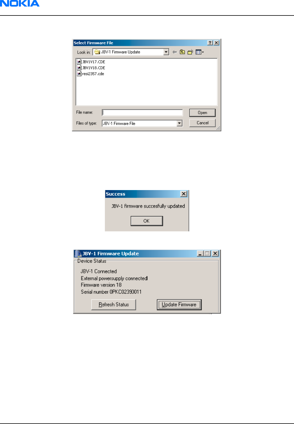
11. Choose file JBV1v18.CDE and click Open to update your JBV-1 to a new version (v.18).
Figure 65 JBV-1 update directory window
Wait until you hear a "click" from the JBV-1.
The older SW file JBV1v17.CDE is visible in this view only if the previous JBV-1 SW package has been installed
on your computer.
12. Click OK to see the current JBV-1 status (after a successful update).
Figure 66 JBV-1 SW update done
Figure 67 JBV-1 SW status
You have now updated the software of your JBV-1 docking station and it is ready for use.
Next action
If you have several docking stations you need to update, disconnect the power and USB cables from the previous
one and connect them to the next docking station. First, click Refresh Status to see the current SW version and
then Update Firmware to update the software.
After you have updated all docking stations, close the JBV-1 Firmware Update dialog box.
RM-25
Nokia Customer Care Phoenix service software
Page 3–34 Company Confidential 9235618 (Issue 2)
Copyright ©2005 Nokia. All Rights Reserved.
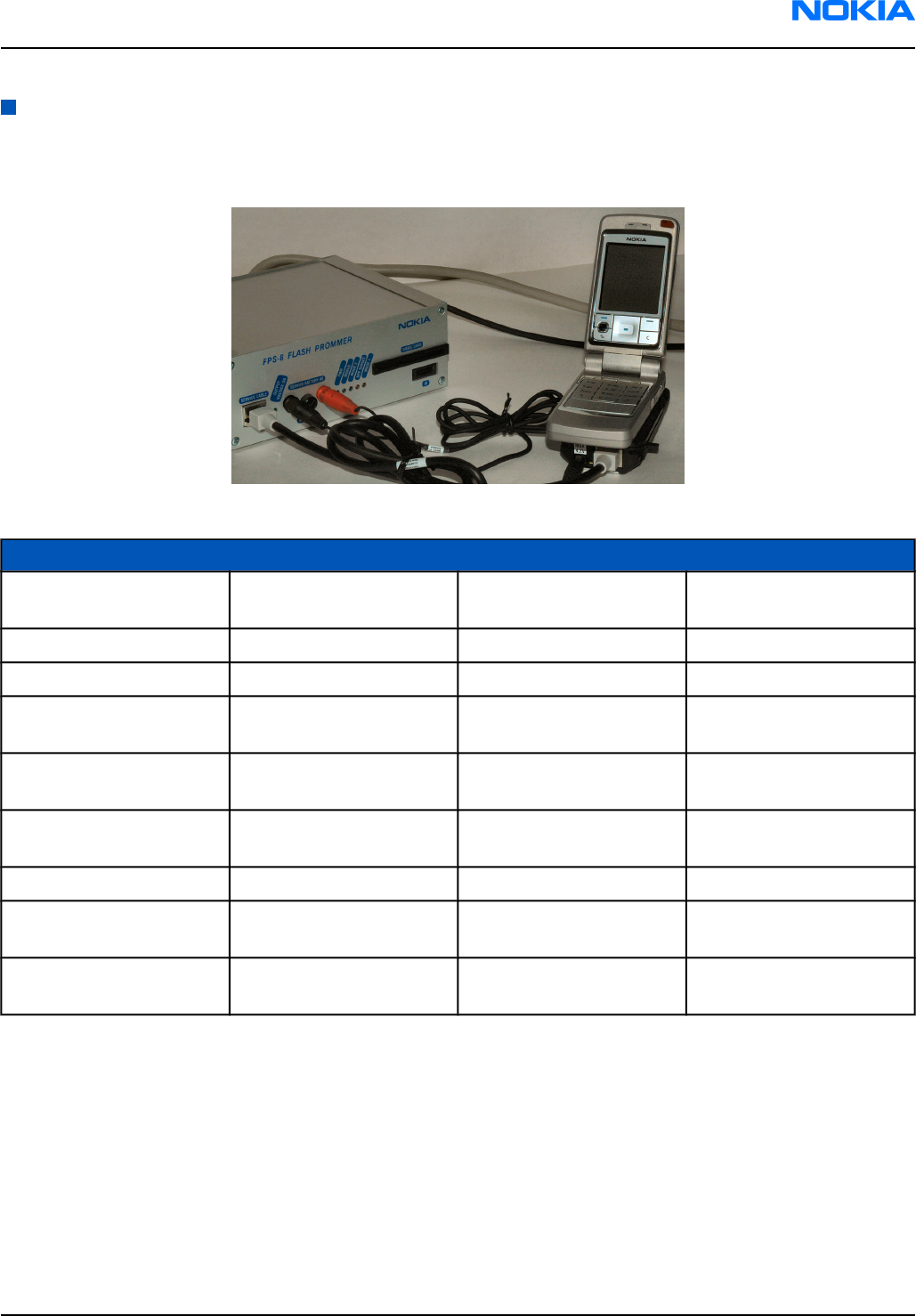
Service software concepts
Flash concept
Figure 68 Flash concept
Item Description Type Code
1Point of Sales flash
loading adapter
SF-27 0780375
2 Power cable FLC-2 0730185
3 Modular cable XCS-4 0730178
4 Flash prommer box sales
pack
FPS-8 0080321
5 Printer cable AXP-8, included in FPS-8
sales pack
Not available as spare
part
6 D9 – D9 cable AXS-4, included in FPS-8
sales pack
0730090
7 Software protection key PKD-1 0750018
8 AC Charger ACF-8, included in FPS-8
sales pack
0680032
9 SRAM Module (3 pcs
needed inside FPS-8)
SF12 0080346 (Code includes
one SRAM module)
Note: More than 32MB SRAM required in FPS-8.
RM-25
Phoenix service software Nokia Customer Care
9235618 (Issue 2) Company Confidential Page 3–35
Copyright ©2005 Nokia. All Rights Reserved.
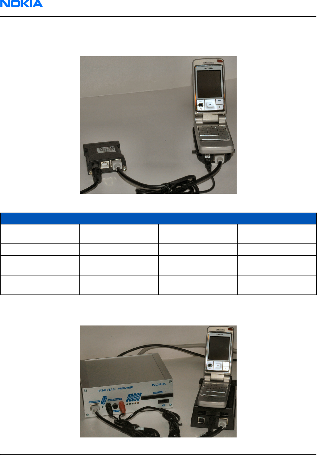
POS flash concept
Figure 69 POS flash concept
Item Description Type Code
1Point of Sales flash
loading adapter
SF-27 0780375
2 Service cable XCS-1 0730218
3a FLS-4S sales pack for
EMEA
FLS-4S 0080541
3b FLS-4S sales pack for
APAC
FLS-4S 0080542
JBV-1 flash concept
Figure 70 JBV-1 flash concept
RM-25
Nokia Customer Care Phoenix service software
Page 3–36 Company Confidential 9235618 (Issue 2)
Copyright ©2005 Nokia. All Rights Reserved.
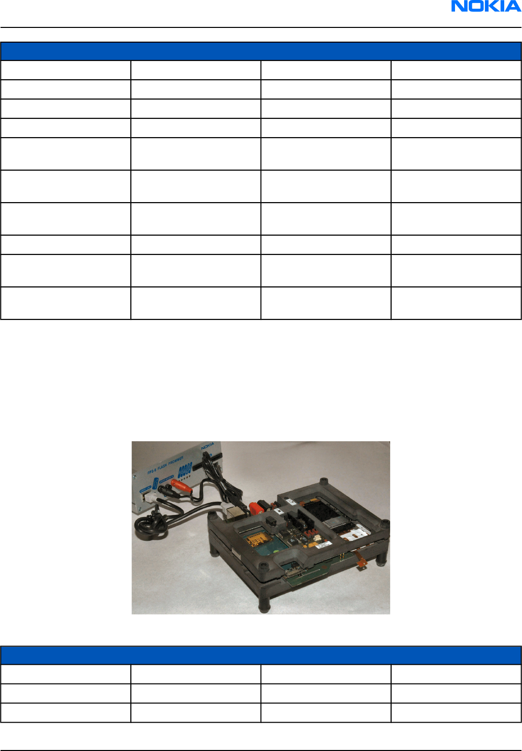
Item Description Type Code
1Docking station adapter DA-25 0780373
2 Docking station JBV-1 0770298
3 Power cable PCS-1 0730012
4 Modular cable XCS-4 0730178
5 Flash prommer box sales
pack
FPS-8 0080321
6 Printer cable AXP-8, included in FPS-8
sales pack
Not available as spare
part
7 D9 – D9 cable AXS-4, included in FPS-8
sales pack
0730090
8 Software protection key PKD-1 0750018
9 AC Charger ACF-8, included in FPS-8
sales pack
0680032
10 SRAM Module (3 pcs
needed inside FPS-8)
SF12 0080346 (Code includes
one SRAM module)
Note: More than 32MB SRAM required in FPS-8.
Module jig flash concept
Flashing with MJ-30 is recommended in local mode.
The following equipment is required for RM-25 AMS SW update when the system module is placed in the module
jig MJ-30 and connected through an FPS-8 set-up:
Figure 71 Module jig flash concept
Item Description Type Code
1Module jig MJ-30 0780376
2 Power cable PCS-1 0730012
3 Modular cable XCS-4 0730178
RM-25
Phoenix service software Nokia Customer Care
9235618 (Issue 2) Company Confidential Page 3–37
Copyright ©2005 Nokia. All Rights Reserved.
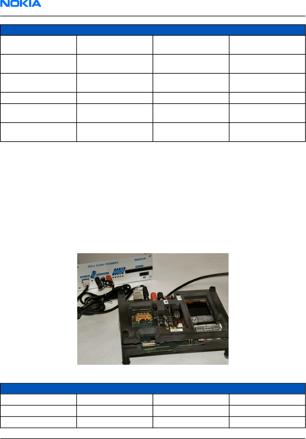
Item Description Type Code
4Flash prommer box sales
pack
FPS-8 0080321
5 Printer cable AXP-8, included in FPS-8
sales pack
Not available as spare
part
6 D9 – D9 cable AXS-4, included in FPS-8
sales pack
0730090
7 Software protection key PKD-1 0750018
8 AC Charger ACF-8, included in FPS-8
sales pack
0680032
9 SRAM Module (3 pcs
needed inside FPS-8)
SF12 0080346 (Code includes
one SRAM module)
Note: More than 32MB SRAM required in FPS-8.
Module jig service concept
This concept is for troubleshooting and RF calibration.
MJ-30 is intended for use with an external power supply.
MJ-30 input voltage: normal +6V, maximum +12V.
Ensure that the jumper is set open for voltage regulation before the external power supply is connected.
When FPS-8 is used as the power supply (4V), the jumper should be set close to bypass regulator.
EM calibrations including Zocus are only done with JBV-1. Module jig MJ-30 does not support Zocus calibration
in RM-25.
Figure 72 Module jig service concept
Item Description Type Code
1Module jig MJ-30 0780376
2 RF cable XRF-1 0730085
3 Power cable PCS-1 0730012
RM-25
Nokia Customer Care Phoenix service software
Page 3–38 Company Confidential 9235618 (Issue 2)
Copyright ©2005 Nokia. All Rights Reserved.
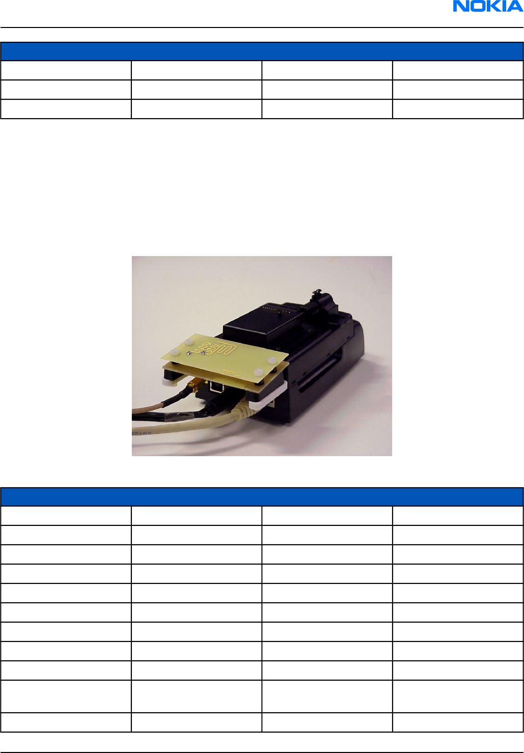
Item Description Type Code
4MBUS cable DAU-9S 0730108
5 Software protection key PKD-1 0750018
6 External DC power supply
JBV-1 service concept
This concept is for BB and RF calibration.
EM calibration including Zocus should be carried out in JBV-1 and DA-25.
Power to JBV-1 should be supplied from an external DC power supply, NOT FPS-8.
JBV-1 input voltage: normal +12V, maximum +16V.
A-cover and RF antenna module need to be removed from the phone when SA-38 is attached.
Figure 73 JBV-1 service concept
Item Description Type Code
1Docking station adapter DA-25 0780373
2 Docking station JBV-1 0770298
3 RF coupler SA-38 0780405
4 RF cable XRF-1 0730085
5 Power cable PCS-1 0730012
6 DC cable SCB-3 0730114
7 MBUS cable DAU-9S 0730108
8 Software protection key PKD-1 0750018
9 External DC power supply
10 Soldering jig for uBGA
components
RJ-33 0780406
11 LGA rework kit for Kaede SK-8 0274550
RM-25
Phoenix service software Nokia Customer Care
9235618 (Issue 2) Company Confidential Page 3–39
Copyright ©2005 Nokia. All Rights Reserved.

Item Description Type Code
12 LGA rework kit for
microPA
SK-9 0274819
13 Flex opening tool SS-34 0780396
RM-25
Nokia Customer Care Phoenix service software
Page 3–40 Company Confidential 9235618 (Issue 2)
Copyright ©2005 Nokia. All Rights Reserved.

4 — Service tools
Nokia Customer Care
9235618 (Issue 2) Company Confidential Page 4–1
Copyright ©2005 Nokia. All Rights Reserved.

RM-25
Nokia Customer Care Service tools
(This page left intentionally blank.)
Page 4–2 Company Confidential 9235618 (Issue 2)
Copyright ©2005 Nokia. All Rights Reserved.

Table of Contents
ACF-8....................................................................................................................................................................................................4–5
AXP-8...................................................................................................................................................................................................4–5
AXS-4...................................................................................................................................................................................................4–5
CA-5S....................................................................................................................................................................................................4–6
DA-25...................................................................................................................................................................................................4–6
DAU-9S................................................................................................................................................................................................4–6
FLC-2....................................................................................................................................................................................................4–6
FLS-4S..................................................................................................................................................................................................4–7
FPS-10.................................................................................................................................................................................................4–7
FPS-11.................................................................................................................................................................................................4–7
FPS-8....................................................................................................................................................................................................4–8
Fuse and protector..........................................................................................................................................................................4–8
JBT-9....................................................................................................................................................................................................4–8
JBV-1....................................................................................................................................................................................................4–8
MJ-30...................................................................................................................................................................................................4–9
PCS-1.................................................................................................................................................................................................4–10
PKD-1.................................................................................................................................................................................................4–10
RJ-24..................................................................................................................................................................................................4–10
RJ-33..................................................................................................................................................................................................4–10
RJ-46..................................................................................................................................................................................................4–10
SA-38.................................................................................................................................................................................................4–11
SF-12.................................................................................................................................................................................................4–12
SF-27.................................................................................................................................................................................................4–12
SK-8...................................................................................................................................................................................................4–13
SK-9...................................................................................................................................................................................................4–14
Spare part for SF-27.....................................................................................................................................................................4–14
Spare part module (LCD-UIB PWB)...........................................................................................................................................4–14
Spare part for SF-27.....................................................................................................................................................................4–14
Spare part module (KeyPad-UIB PWB)...................................................................................................................................4–14
SPS-1.................................................................................................................................................................................................4–15
SRT-6.................................................................................................................................................................................................4–15
SS-34.................................................................................................................................................................................................4–15
ST-15.................................................................................................................................................................................................4–15
ST-5....................................................................................................................................................................................................4–16
Test pins...........................................................................................................................................................................................4–16
Test pins (RF pogo).......................................................................................................................................................................4–16
Test pins (SC-0-J-3.2-DG) for DA-25 (10pcs/bag).................................................................................................................4–16
XCS-1.................................................................................................................................................................................................4–16
XCS-4.................................................................................................................................................................................................4–16
XRF-1.................................................................................................................................................................................................4–17
List of Tables
Table 17 Display test pin list........................................................................................................................................................4–9
Table 18 Upper keypad signals...................................................................................................................................................4–9
Table 19 Lower keypad signals...................................................................................................................................................4–9
Table 20 TX (db)............................................................................................................................................................................4–11
Table 21 RX (db)............................................................................................................................................................................4–11
RM-25
Service tools Nokia Customer Care
9235618 (Issue 2) Company Confidential Page 4–3
Copyright ©2005 Nokia. All Rights Reserved.

RM-25
Nokia Customer Care Service tools
(This page left intentionally blank.)
Page 4–4 Company Confidential 9235618 (Issue 2)
Copyright ©2005 Nokia. All Rights Reserved.
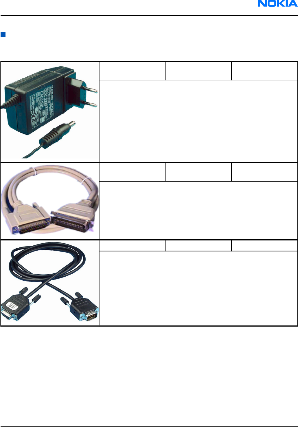
List of Service Tools
The table below gives a short overview of service tools that can be used for testing, error analysis and repair
of product , refer to various concepts.
ACF-8 Universal power
supply
0680032
ACF-8 universal power supply is used to power FPS-8. ACF-8 has 6V DC
and 2.1A output.
AXP-8 Parallel bi-directional
printer cable
0730298
This cable is used to connect the PC to a flash prommer.
The cable is part of the FPS-8 sales package.
AXS-4 Service cable 0730090
The AXS-4 D9-D9 service cable is used to connect two 9 pin D connectors
for example between PC and FPS-8.
The cable length is 2 meters.
RM-25
Service tools Nokia Customer Care
9235618 (Issue 2) Company Confidential Page 4–5
Copyright ©2005 Nokia. All Rights Reserved.
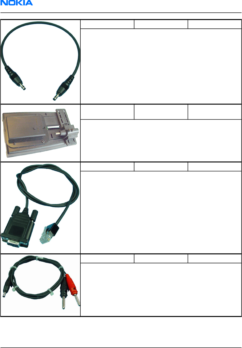
CA-5S DC cable 0730283
The DC cable CA-5S is used to connect JBV-1 to the phone charger jack
for ADC/VCHAR/ICHAR calibration
Note: Old SCB-3 can be used as well.
DA-25 Docking station
adapter
0780373
The DA-25 docking station adapter makes signal connections to the
phone. JBV-1 and DA-25 are used as one unit.
DAU-9S MBUS cable 0730108
The MBUS cable DAU-9S has a modular connector and is used, for
example, between the PC's serial port and module jigs, flash adapters or
docking station adapters.
FLC-2 DC cable 0730185
FLC-2 is used with a flash adapter to supply a controlled operating
voltage.
RM-25
Nokia Customer Care Service tools
Page 4–6 Company Confidential 9235618 (Issue 2)
Copyright ©2005 Nokia. All Rights Reserved.
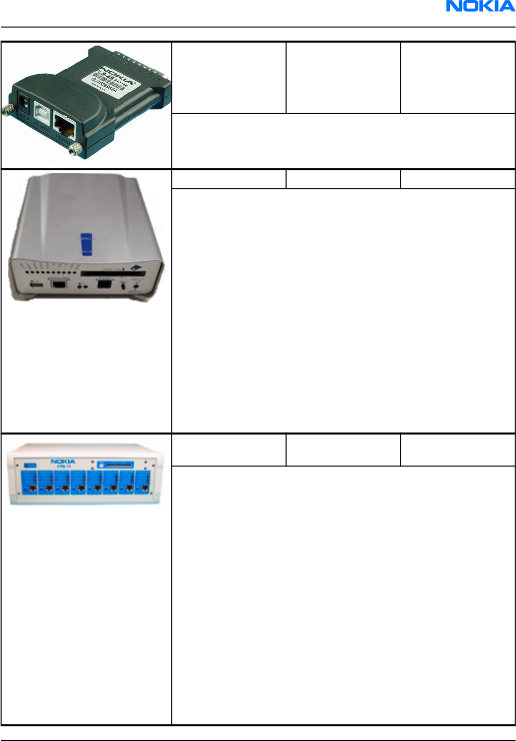
FLS-4S Flash device FLS-4S sales pack –
Europe/
Africa:0080541,
APAC:0080542,
Americas:0080543
FLS-4S is a dongle and flash device incorporated into one package,
developed specifically for POS use.
FPS-10 Flash prommer 0086189
FPS-10 interfaces with:
• PC
• Control unit
• Flash adapter
• Smart card
FPS-10 flash prommer features:
• Provides flash functionality for BB5 terminals
• Smart Card reader for SX-2 or SX-4
• Forwards USB traffic through it
• Provides USB to FBUS/Flashbus conversion
• Provides LAN to FBUS/Flashbus and USB conversion
• Vusb output switchable by PC command
FPS-10 sales package includes:
• FPS-10 prommer (0770503)
• Power Supply with 5 country specific cords (0675525)
• USB cable (0730322)
FPS-11 Parallel flash
prommer
0770758
FPS-11 interfaces with:
• PC
• Control unit
• Flash adapter
• Smart card
FPS-11 flash prommer features:
• Can flash up to 8 phones at a time, controlled by one PC
• Communication method between PC and FPS-11 is single USB2.0
• No need for external power for powering up phones
• Smart Card reader for SX-2 and SX-4
• Updates software
• Future feature: will support all DCT-4 protocols and models
FPS-11 sales package includes:
• FPS-11
• Power Supply for FPS-11
• EUR, UK, USA Power cords
• USB2.0 cable
RM-25
Service tools Nokia Customer Care
9235618 (Issue 2) Company Confidential Page 4–7
Copyright ©2005 Nokia. All Rights Reserved.
FPS-8 FLASH prommer 0080321
The flash prommer FPS-8 is used for example with flash adapters,
docking station adapters and flash/docking stations. Power is supplied
to FPS-8 from the universal power supply, ACF-8.
The sales pack includes:
• FPS-8 flash prommer (0750123)
• FPS-8 activation sheet (9359289)
• ACF-8 universal power supply (0680032)
• AXS-4 service cable (D9-D9) (0730090)
• Printer cable (0730029)
Fuse and protector 0770622
JBT-9 Bluetooth test and
interface box (sales
pack)
0081490
The JBT-9 testbox is a generic device to perform Bluetooth bit error rate
testing and doing cordless FBUS connection via Bluetooth. An ACP-8x
charger is needed for BER testing and AXS-4 cable in case of cordless
testing interface usage.
• JBT-9 testbox (0770336)
• Installation and warranty information (9360613)
JBV-1 Docking station 0770298
The JBV-1 docking station has been designed for calibration and
software update use.
The docking station is used together with the DA-25 docking station
adapter.
JBV-1 main electric functions are:
• adjustable VBAT calibration voltage, current measurement limit
voltage “VCHAR”, current measurement calibration current “ICHAR”
• adjustable ADC calibration voltage via BSI signal
• BSI calibration resistor
• signals from FBUS to the phone via parallel jig
• control via FBUS or USB
• Flash OK/FAIL indication
In calibration mode JBV-1 is powered by external power supply 11-16V
DC. In flashing, power for the phone can be taken from FPS-8 or external
power supply 11-16V DC.
RM-25
Nokia Customer Care Service tools
Page 4–8 Company Confidential 9235618 (Issue 2)
Copyright ©2005 Nokia. All Rights Reserved.
MJ-30 Module jig 0780376
The MJ-30 module jig is used for testing the following modules:
• User interface
• Baseband and RF on system module
Note: The nominal supply voltage for MJ-25 is +6.0 V. The
supply voltage must not exceed +12.0 V (min. 5.0 V).
Supply the power to jig only when the jumper is open =
regulated.
•Table 17 Display test pin list
Pin Signal
name
Pin Signal
name
Pin Signal
name
1GND 9 VDDI 17
2 WRX 10 VDD 18 D7
3 11 19 D6
4 D0 12 LED IN 20 D5
5 D1 13 LED OUT 21 D4
6 D2 14 22
7 D3 15 CSX 23 RDX
8 16 D/CX 24 RESX
•Table 18 Upper keypad signals
Pin Signal
name
Pin Signal
name
Pin Signal
name
7ROW2 17 Key LED - 22 Rocker3
8 ROW0 18 ROW1 23 Rocker2
9 COL1 19 COL0 24 Rocker1
11 GND 20 Rocker5
15 Key LED + 21 Rocker4
•Table 19 Lower keypad signals
Pin Signal
name
Pin Signal
name
Pin Signal
name
5COL2 9 ROW3 17 COL5
6 COL4 13 ROW2 18 COL3
7 LED
SUPPLY
14 COL0 19 ROW4
8 LED
SUPPLY
15 ROW5 20 GND
RM-25
Service tools Nokia Customer Care
9235618 (Issue 2) Company Confidential Page 4–9
Copyright ©2005 Nokia. All Rights Reserved.
PCS-1 Power cable 0730012
The PCS-1 power cable (DC) is used with a docking station, a module jig
or a control unit to supply a controlled operating voltage.
PKD-1 SW security device 0750018
SW security device is a piece of hardware enabling the use of the service
software when connected to the parallel (LPT) port of the PC.
Without the device, it is not possible to use the service software.
Printer or any such device can be connected to the PC through the device
if needed.
RJ-24 Rework jig 0770688
RJ-24 is a soldering jig used for soldering and as a rework jig for the
engine module.
RJ-33 Soldering jig 0780406
The soldering jig RJ-33 is used for soldering and as a rework jig for system
module. It is made of lead-free rework compatible material.
RJ-46 Antenna switch
rework jig
0780374
RM-25
Nokia Customer Care Service tools
Page 4–10 Company Confidential 9235618 (Issue 2)
Copyright ©2005 Nokia. All Rights Reserved.
SA-38 RF Coupler 0780405
SA-38 RF Coupler is used for Go/No-Go test after changing components
in the RF part of the phone.
The SA-38 is mounted on the docking station adapter, after which the
phone can be placed in the docking station adapter.
RF attenuations:
•Table 20 TX (db)
Band Channel New coupler
900 955 (-8.5 +/- 0.5)
39 (-8,9 +/- 0,5)
124 (-10,0 +/- 0,5)
1800 512 (-8,3 +/- 1,1)
690 (7,3 +/- 1,3)
885 (-7,5 +/- 0,8)
1900 535* (-8,1 +/- 1,3)
711* (-8,2 +/- 1,2)
810* (-8,4 +/- 1,3)
Table 21 RX (db)
Band Channel New coupler
900 955 (-13,2 +/- 0,2)
39 (-11,7 +/- 0,7)
124 (-13,0 +/- 0,8)
1800 512 (-12,1 +/- 0,6)
690 (-12,3 +/- 0,3)
885 (-12,5 +/- 0,5)
1900 535* (-15,4 +/- 2,3)
711* (-16,3 +/- 1,8)
810* (-17,5 +/- 1,2)
RM-25
Service tools Nokia Customer Care
9235618 (Issue 2) Company Confidential Page 4–11
Copyright ©2005 Nokia. All Rights Reserved.
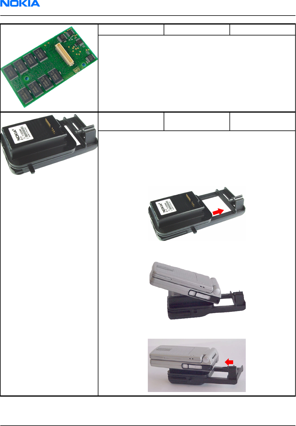
SF-12 SRAM Module for FPS-8 0080346
SF-27 POS (point of sales)
flash adapter
0780375
The POS flash adapter SF-27 is used in the place of phone’s normal
battery during service to supply a controlled operating voltage and to
connect to flash pads.
Instructions
1 Open the locking slide.
2 Insert the adapter to the phone from the battery connector side.
3 Lock the adapter with DC jack.
RM-25
Nokia Customer Care Service tools
Page 4–12 Company Confidential 9235618 (Issue 2)
Copyright ©2005 Nokia. All Rights Reserved.
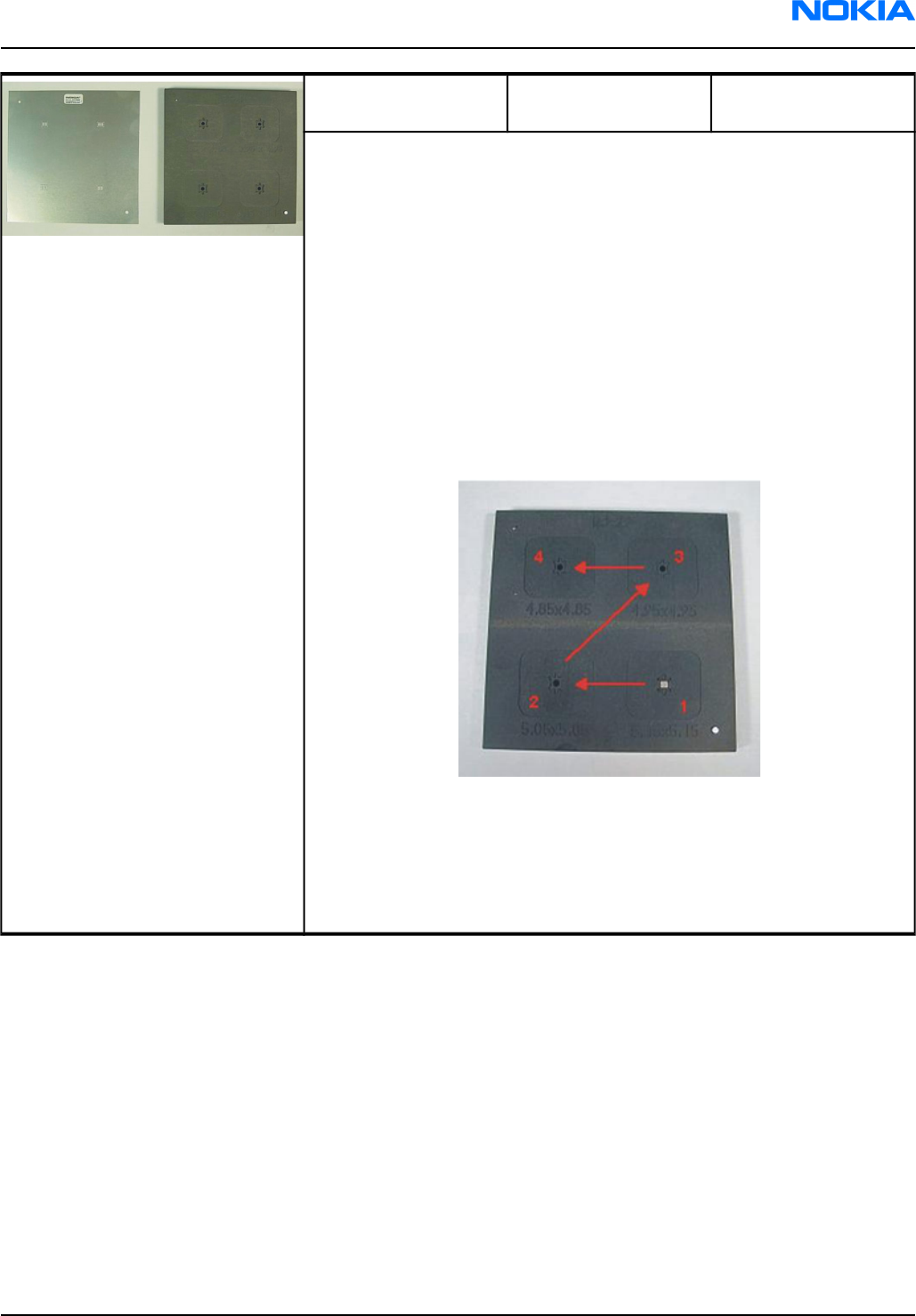
SK-8 LGA rework kit for
Kaede
0274550
SK-8 is used to print solder paste on Kaede USB component (NMP code:
4342163) when the component is reworked.
SK-8 consists of ST-9 (NMP code: 0770727) Stencil and RJ-29 (NMP code:
0770728) rework jig.
Due to the large mechanical tolerance of the component, the following
procedure is necessary:
Instructions
1 Put the component into the rework jig. The component should be
placed in the best fit location which is determined by placing the
component in the largest location first, and if this is too large, re-
position it to the next location. This should be carried out until the
best fit location is found.
2 Once the best fit location has been found, leave the component there
and put the stencil on top of the jig and the component.
3 Put soldering paste on the component properly.
4 Remove the stencil and the component from the jig.
5 Start the soldering process.
RM-25
Service tools Nokia Customer Care
9235618 (Issue 2) Company Confidential Page 4–13
Copyright ©2005 Nokia. All Rights Reserved.
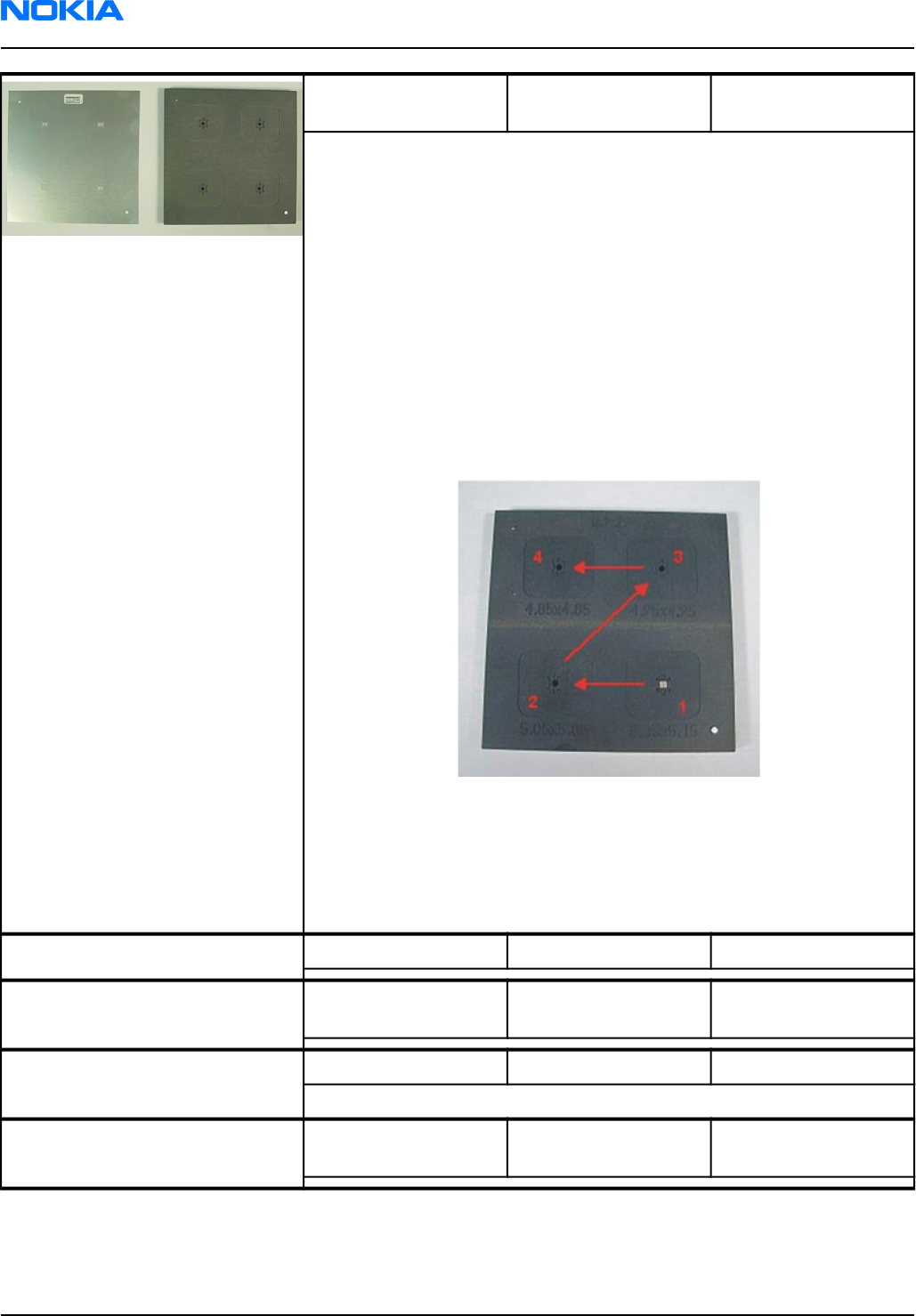
SK-9 LGA rework kit for
MicroPA
0274819
SK-9 is used to print solder paste on MicroPA component (NMP code:
4355641) when the component is reworked.
SK-9 consists of ST-13 (NMP code: 0770848) stencil and RJ-21 (NMP code:
0770849) rework jig.
Due to the large mechanical tolerance of the component, the following
procedure is necessary:
Instructions
1 Put the component into the rework jig. The component should be
placed in the best fit location which is determined by placing the
component in the largest location first, and if this is too large, re-
position it to the next location. This should be carried out until the
best fit location is found.
2 Once the best fit location has been found, leave the component there
and put the stencil on top of the jig and the component.
3 Put soldering paste on the component properly.
4 Remove the stencil and the component from the jig.
5 Start the soldering process.
Spare part for SF-27 Test pin module 0780357
Spare part module
(LCD-UIB PWB)
0780356
Spare part for SF-27 Test pins 0770754
Soldering required
Spare part module
(KeyPad-UIB PWB)
0780355
RM-25
Nokia Customer Care Service tools
Page 4–14 Company Confidential 9235618 (Issue 2)
Copyright ©2005 Nokia. All Rights Reserved.
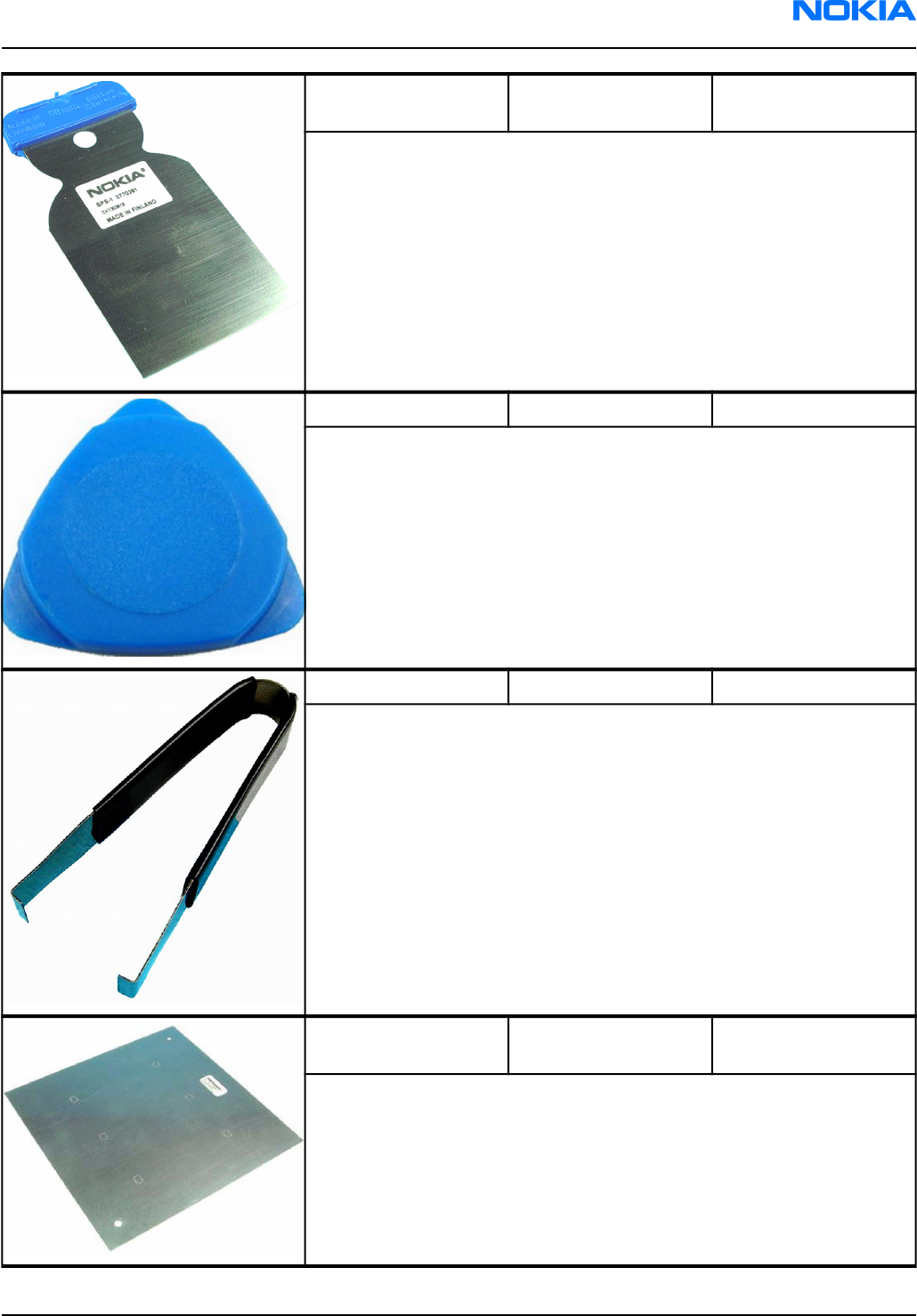
SPS-1 Soldering Paste
Spreader
0770381
SRT-6 Opening tool 0770431
SS-34 Flex opening tool 0780396
ST-15 Antenna switch
rework stencil
0780412
RM-25
Service tools Nokia Customer Care
9235618 (Issue 2) Company Confidential Page 4–15
Copyright ©2005 Nokia. All Rights Reserved.
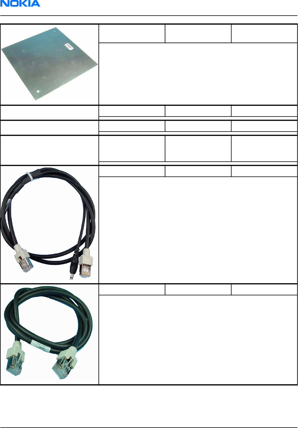
ST-5 Antenna switch
rework stencil
0770691
Test pins 0770879
Test pins (RF pogo) 077876
Test pins (SC-0-J-3.2-
DG) for DA-25 (10pcs/
bag)
0770617
XCS-1 Service cable 0730218
The XCS-1 service cable is used to connect FLS-4S to the POS flash adapter
for supplying a controlled operating voltage and data connection.
XCS-4 Modular cable 0730178
XCS-4 is a shielded (one specially shielded conductor) modular cable for
flashing and service purposes.
RM-25
Nokia Customer Care Service tools
Page 4–16 Company Confidential 9235618 (Issue 2)
Copyright ©2005 Nokia. All Rights Reserved.

XRF-1 RF cable 0730085
The RF cable is used to connect, for example, a module repair jig to the
RF measurement equipment.
SMA to N-Connector ca. 610mm.
Attenuation for:
• GSM850/900: 0.3+-0.1 dB
• GSM1800/1900: 0.5+-0.1 dB
• WLAN: 0.6+-0.1dB
RM-25
Service tools Nokia Customer Care
9235618 (Issue 2) Company Confidential Page 4–17
Copyright ©2005 Nokia. All Rights Reserved.

RM-25
Nokia Customer Care Service tools
(This page left intentionally blank.)
Page 4–18 Company Confidential 9235618 (Issue 2)
Copyright ©2005 Nokia. All Rights Reserved.

5 — Disassembly and
reassembly instructions
Nokia Customer Care
9235618 (Issue 2) Company Confidential Page 5–1
Copyright ©2005 Nokia. All Rights Reserved.

RM-25
Nokia Customer Care Disassembly and reassembly instructions
(This page left intentionally blank.)
Page 5–2 Company Confidential 9235618 (Issue 2)
Copyright ©2005 Nokia. All Rights Reserved.

Table of Contents
Disassembly instructions lower block (see the video clips on care point also).........................................................5–5
Disassembly instructions upper block (see the video clips on care point also).........................................................5–8
RM-25
Disassembly and reassembly instructions Nokia Customer Care
9235618 (Issue 2) Company Confidential Page 5–3
Copyright ©2005 Nokia. All Rights Reserved.

RM-25
Nokia Customer Care Disassembly and reassembly instructions
(This page left intentionally blank.)
Page 5–4 Company Confidential 9235618 (Issue 2)
Copyright ©2005 Nokia. All Rights Reserved.
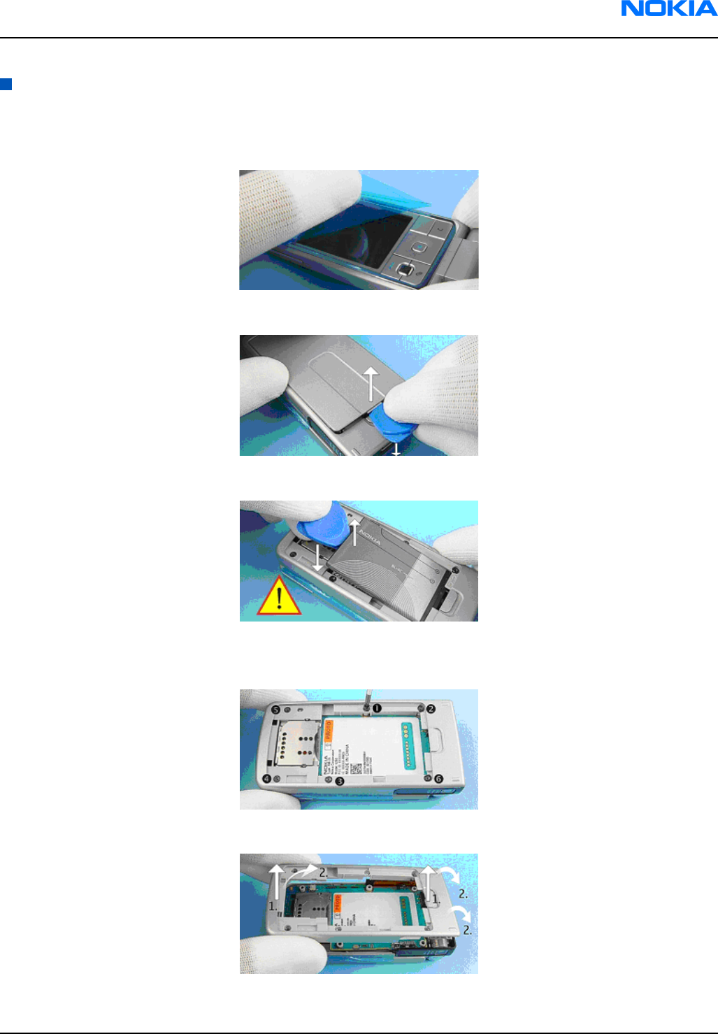
Disassembly instructions lower block (see the video clips on care point also)
Steps
1. Protect the window with a film to avoid dust and scratches.
2. Remove the battery cover.
3. Always remove the battery before continuing disassembly.
4. Unscrew the six Torx Plus® size 6 screws.
Note: For assembly, the reverse order and a Torx Plus® driver with a torque of 20 Ncm has to be used.
5. Remove the B1 cover and place it upside down on the table like shown in the picture.
6. Remove the vibra motor with tweezers.
RM-25
Disassembly and reassembly instructions Nokia Customer Care
9235618 (Issue 2) Company Confidential Page 5–5
Copyright ©2005 Nokia. All Rights Reserved.
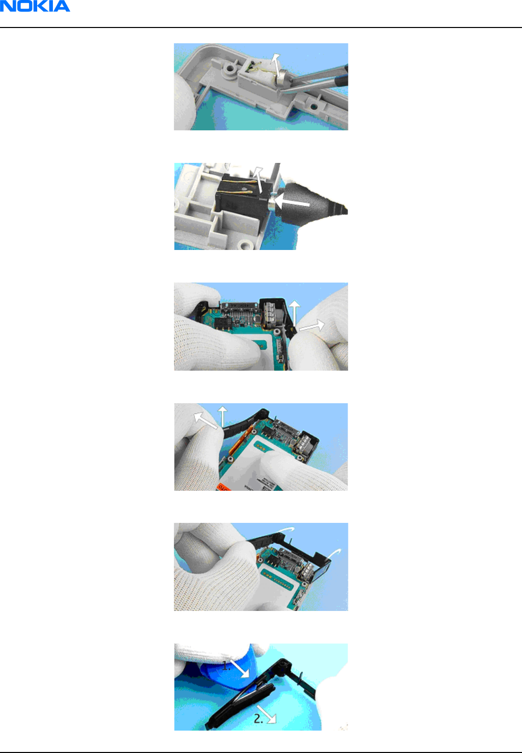
7. Remove the DC jack with a charger plug.
8. For disassembling the frame, move the right side slightly up and to the right.
9. Move the left side of the frame up and to the left.
10. Now remove the frame.
11. Disassemble the side key with, for example, SRT-6 tool.
RM-25
Nokia Customer Care Disassembly and reassembly instructions
Page 5–6 Company Confidential 9235618 (Issue 2)
Copyright ©2005 Nokia. All Rights Reserved.
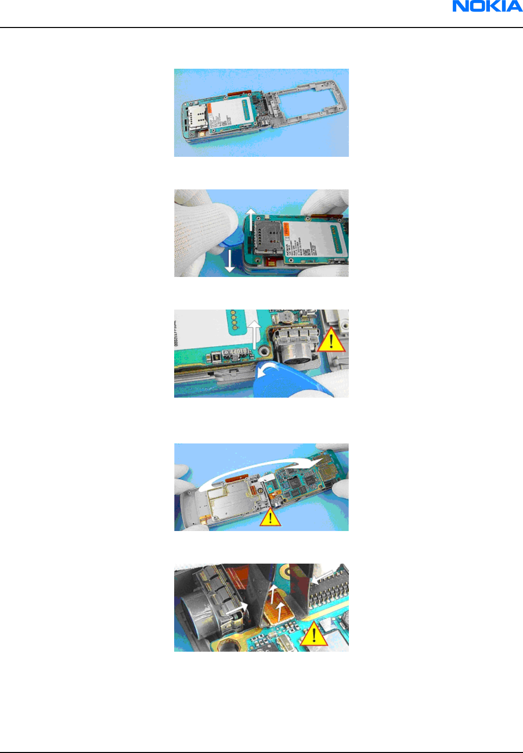
12. Use the B1 cover as a support for engine module to avoid damaging the hinge flex.
13. Now remove the engine module. First lift up the left side (near SIM, MMC connector) with SRT-6 and then…
14. …the right side nearby the camera module. Be careful with the camera module.
15. The engine module is connected to the lower block via hinge flex connector. Be careful when placing the
engine module on the B1 cover.
16. Open the camera connector by using the SS-34 tool and remove the camera module.
17. Open the hinge flex connector by using the SS-34 and take away the B1 cover with engine module.
RM-25
Disassembly and reassembly instructions Nokia Customer Care
9235618 (Issue 2) Company Confidential Page 5–7
Copyright ©2005 Nokia. All Rights Reserved.
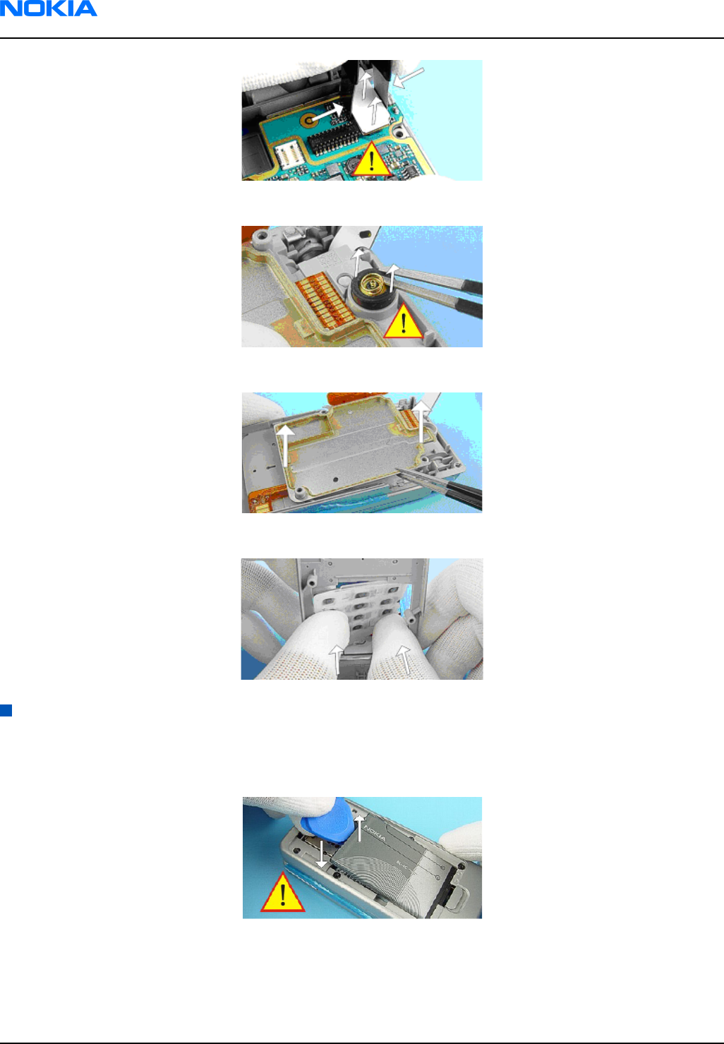
18. Remove the microphone with tweezers. Be careful not to damage the spring contacts.
19. Remove the UI flex assy by using tweezers like shown in the picture.
20. Finally, disassemble the keymat by pressing it slightly from the inside to the outside.
Disassembly instructions upper block (see the video clips on care point also)
Steps
1. Remove the battery before disassembling the upper block.
2. Open the phone and turn around the upper block 180 degrees.
RM-25
Nokia Customer Care Disassembly and reassembly instructions
Page 5–8 Company Confidential 9235618 (Issue 2)
Copyright ©2005 Nokia. All Rights Reserved.
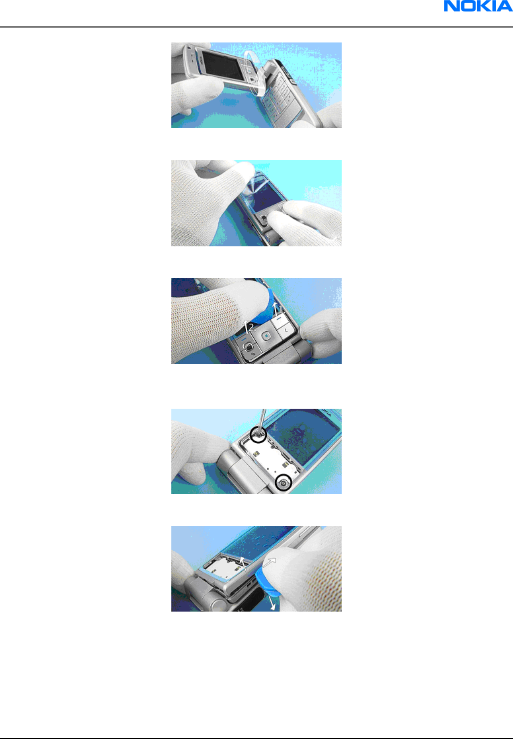
3. Protect the window with a film to avoid dust and scratches.
4. Remove the function keymat.
5. Unscrew the two Torx Plus® size 6 screws. For assembly, a Torx Plus® driver with a torque of 15Ncm has
to be used.
6. Open the A2 cover at one side first and then…
7. …at the other side. Remove the A2 cover.
RM-25
Disassembly and reassembly instructions Nokia Customer Care
9235618 (Issue 2) Company Confidential Page 5–9
Copyright ©2005 Nokia. All Rights Reserved.
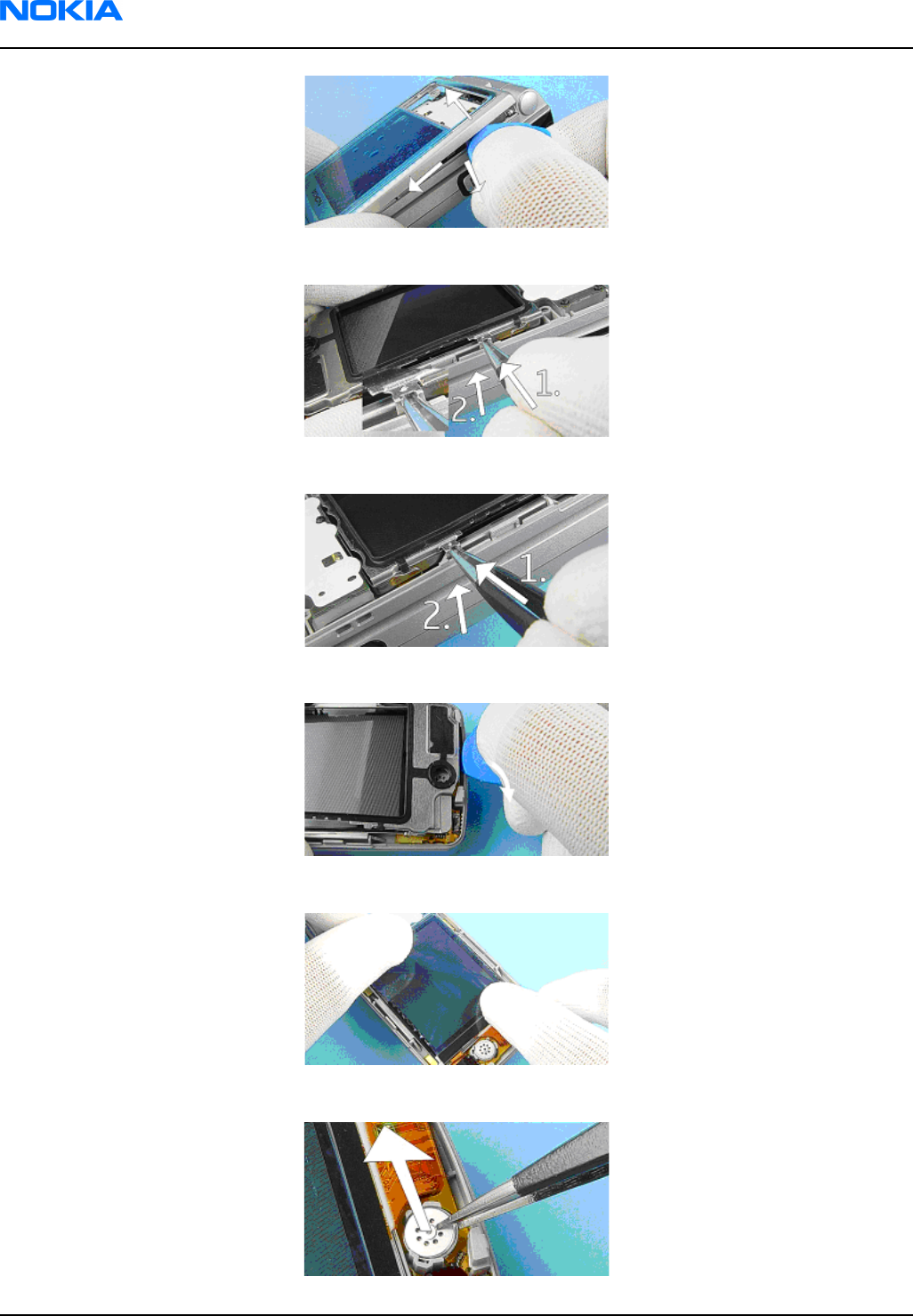
8. Use tweezers to remove the LCD shield. Start at one side and then…
9. …on the other side.
10. Now remove the LCD shield with the SRT-6 tool.
11. Protect the LCD with a film to avoid dust and scratches.
12. Remove the earpiece with tweezers.
RM-25
Nokia Customer Care Disassembly and reassembly instructions
Page 5–10 Company Confidential 9235618 (Issue 2)
Copyright ©2005 Nokia. All Rights Reserved.
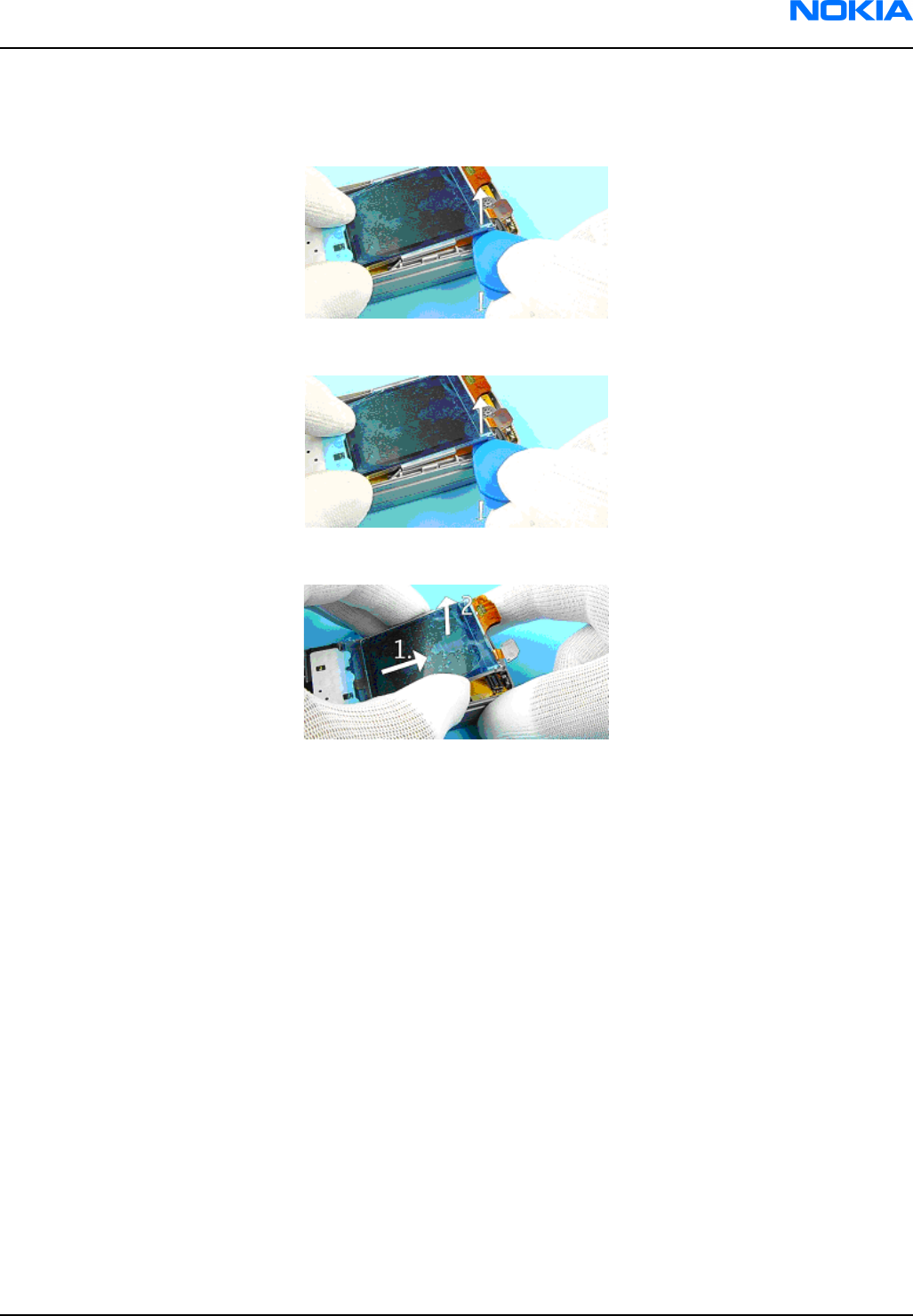
13. To open the LCD connector, hold the flex foil down with the Torx driver and lever up the LCD connector
with a slotted screwdriver carefully. Be careful not to damage the flex foil, connector or surrounding
components.
14. Lever up the right corner of the LCD with SRT-6.
15. Remove the LCD like shown in the picture.
RM-25
Disassembly and reassembly instructions Nokia Customer Care
9235618 (Issue 2) Company Confidential Page 5–11
Copyright ©2005 Nokia. All Rights Reserved.

RM-25
Nokia Customer Care Disassembly and reassembly instructions
(This page left intentionally blank.)
Page 5–12 Company Confidential 9235618 (Issue 2)
Copyright ©2005 Nokia. All Rights Reserved.

6 — Baseband troubleshooting
Nokia Customer Care
9235618 (Issue 2) Company Confidential Page 6–1
Copyright ©2005 Nokia. All Rights Reserved.

RM-25
Nokia Customer Care Baseband troubleshooting
(This page left intentionally blank.)
Page 6–2 Company Confidential 9235618 (Issue 2)
Copyright ©2005 Nokia. All Rights Reserved.

Table of Contents
Troubleshooting baseband.........................................................................................................................................................6–5
Troubleshooting dead or jammed phone..............................................................................................................................6–6
BB self test tools.............................................................................................................................................................................6–7
Troubleshooting flash programming......................................................................................................................................6–7
General power troubleshooting.............................................................................................................................................6–10
Baseband serial interface troubleshooting ........................................................................................................................6–11
CBUS interface.........................................................................................................................................................................6–11
FBUS interface.........................................................................................................................................................................6–13
MBUS interface........................................................................................................................................................................6–14
Troubleshooting charger interface........................................................................................................................................6–15
Energy management calibration............................................................................................................................................6–17
Baseband troubleshooting tips...............................................................................................................................................6–17
Backup battery troubleshooting.............................................................................................................................................6–18
Troubleshooting USB interface...............................................................................................................................................6–19
SIM card fault................................................................................................................................................................................6–20
“Insert SIM Card” in device display although card is inserted.......................................................................................6–22
Troubleshooting keypad interface.........................................................................................................................................6–24
Troubleshooting the display....................................................................................................................................................6–25
Troubleshooting display and keyboard backlight............................................................................................................6–26
Troubleshooting MMC interface..............................................................................................................................................6–27
Audio troubleshooting...............................................................................................................................................................6–29
Troubleshooting internal microphone...........................................................................................................................6–29
Troubleshooting external microphone..........................................................................................................................6–30
Troubleshooting internal earpiece..................................................................................................................................6–31
Troubleshooting external earpiece..................................................................................................................................6–32
Troubleshooting IHF.............................................................................................................................................................6–33
Troubleshooting accessory detection...................................................................................................................................6–35
Troubleshooting IrDA.................................................................................................................................................................6–37
Troubleshooting FM radio.........................................................................................................................................................6–38
Tuning baseband.........................................................................................................................................................................6–39
Testing and tuning BB after component replacement....................................................................................................6–41
List of Tables
Table 22 Maximum tolerances.................................................................................................................................................6–18
Table 23 Calibration value limits.............................................................................................................................................6–41
List of Figures
Figure 74 Main troubleshooting diagram...............................................................................................................................6–5
Figure 75 Dead or jammed phone troubleshooting............................................................................................................6–6
Figure 76 BB self tests....................................................................................................................................................................6–7
Figure 77 Flash programming troubleshooting, part 1......................................................................................................6–8
Figure 78 Flash programming troubleshooting, part 2......................................................................................................6–9
Figure 79 General power troubleshooting...........................................................................................................................6–10
Figure 80 CBusClk test point......................................................................................................................................................6–11
Figure 81 CBUS test points.........................................................................................................................................................6–12
Figure 82 CBUS waveform..........................................................................................................................................................6–13
Figure 83 Flash interface layout (FBUS/MBUS test pads layout)....................................................................................6–14
Figure 84 "Not charging" on display......................................................................................................................................6–15
RM-25
Baseband troubleshooting Nokia Customer Care
9235618 (Issue 2) Company Confidential Page 6–3
Copyright ©2005 Nokia. All Rights Reserved.

Figure 85 No charging.................................................................................................................................................................6–16
Figure 86 ADC reading window in Phoenix..........................................................................................................................6–18
Figure 87 USB interface troubleshooting..............................................................................................................................6–19
Figure 88 UPP_WD2 and UEME SIM connections (simplified)..........................................................................................6–20
Figure 89 SIM power up waveform.........................................................................................................................................6–21
Figure 90 SIM answer to reset waveform.............................................................................................................................6–22
Figure 91 “Insert SIM Card” in device display although card is inserted....................................................................6–23
Figure 92 Troubleshooting keypad interface......................................................................................................................6–24
Figure 93 Display troubleshooting..........................................................................................................................................6–25
Figure 94 Troubleshooting display and keyboard backlight..........................................................................................6–26
Figure 95 Troubleshooting MMC interface............................................................................................................................6–28
Figure 96 Troubleshooting internal microphone...............................................................................................................6–29
Figure 97 Troubleshooting external microphone..............................................................................................................6–30
Figure 98 Troubleshooting internal earpiece......................................................................................................................6–31
Figure 99 Troubleshooting external earpiece.....................................................................................................................6–32
Figure 100 Troubleshooting IHF..............................................................................................................................................6–33
Figure 101 Troubleshooting IHF (continued)......................................................................................................................6–34
Figure 102 Troubleshooting accessory detection..............................................................................................................6–35
Figure 103 Troubleshooting accessory detection (continued)......................................................................................6–36
Figure 104 Troubleshooting IrDA............................................................................................................................................6–37
Figure 105 Troubleshooting FM radio....................................................................................................................................6–39
Figure 106 EM calibration window.........................................................................................................................................6–40
RM-25
Nokia Customer Care Baseband troubleshooting
Page 6–4 Company Confidential 9235618 (Issue 2)
Copyright ©2005 Nokia. All Rights Reserved.
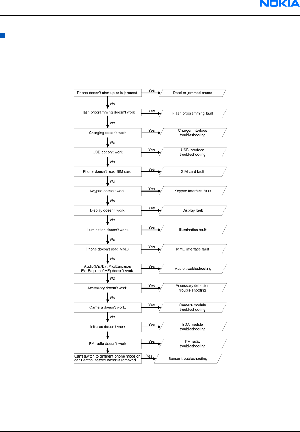
Troubleshooting baseband
Context
This section is intended to be a guide for localising and repairing electrical faults.
The fault repairing is divided into troubleshooting paths. The following diagram describes the different
baseband troubleshooting paths to be followed in fault situations.
Figure 74 Main troubleshooting diagram
RM-25
Baseband troubleshooting Nokia Customer Care
9235618 (Issue 2) Company Confidential Page 6–5
Copyright ©2005 Nokia. All Rights Reserved.
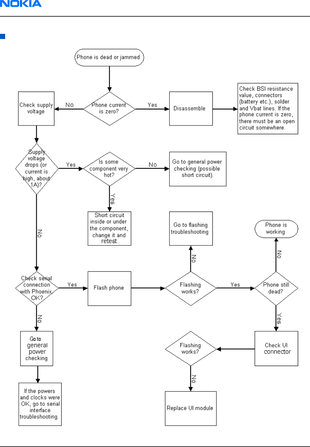
Troubleshooting dead or jammed phone
Figure 75 Dead or jammed phone troubleshooting
RM-25
Nokia Customer Care Baseband troubleshooting
Page 6–6 Company Confidential 9235618 (Issue 2)
Copyright ©2005 Nokia. All Rights Reserved.
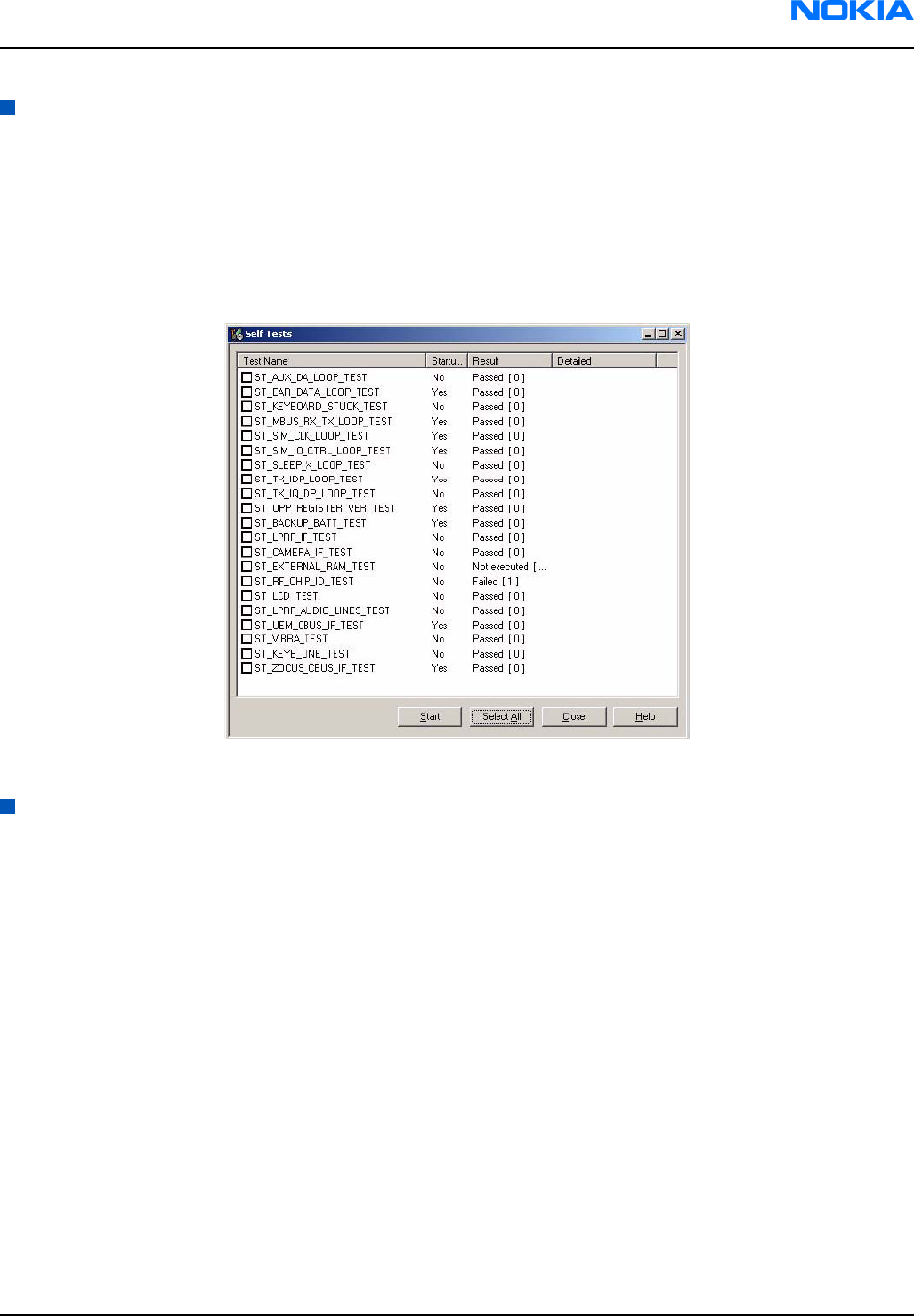
BB self test tools
Self test functions are executed when the phone is powered on, and if one or more self test functions fail, the
message “Self test failed. Contact Service.” is displayed. However, in this kind of situation the software is able
to run and thus the watchdog of UEME can be served.
The MCU selftest case can be split into two categories: the ones that are executed during power up and the ones
that are executed only with a PC connected.
These tests and the items included are as follows:
Figure 76 BB self tests
Troubleshooting flash programming
Context
Note: The Phoenix error message C101 Boot timeout in the flowchart refers to a message that is shown
when there are problems in the phone flash programming when using FPS-8.
RM-25
Baseband troubleshooting Nokia Customer Care
9235618 (Issue 2) Company Confidential Page 6–7
Copyright ©2005 Nokia. All Rights Reserved.
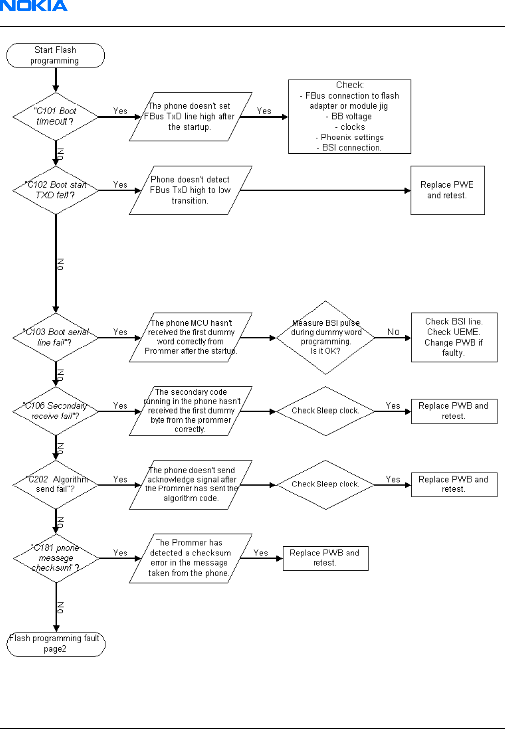
Figure 77 Flash programming troubleshooting, part 1
RM-25
Nokia Customer Care Baseband troubleshooting
Page 6–8 Company Confidential 9235618 (Issue 2)
Copyright ©2005 Nokia. All Rights Reserved.
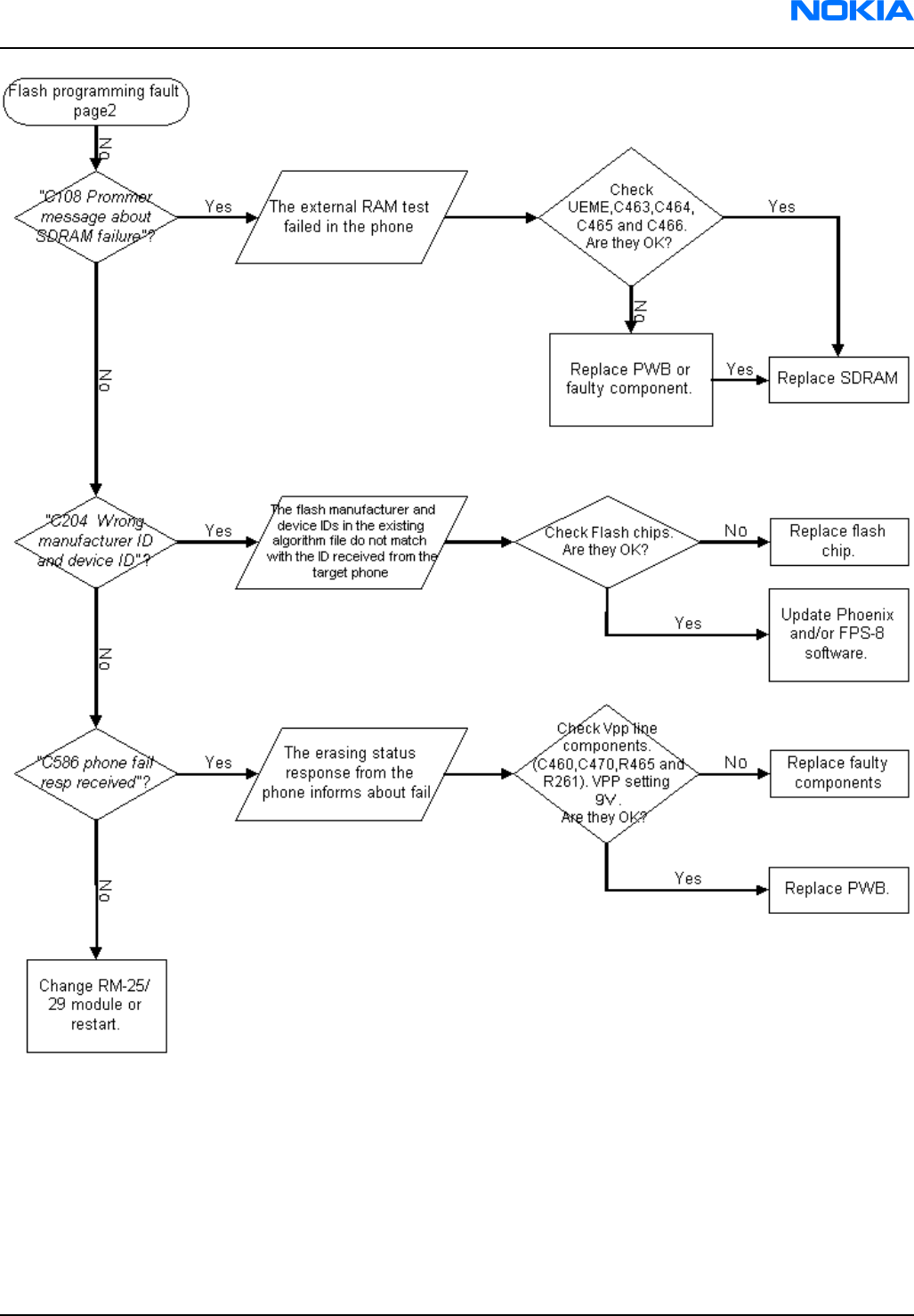
Figure 78 Flash programming troubleshooting, part 2
RM-25
Baseband troubleshooting Nokia Customer Care
9235618 (Issue 2) Company Confidential Page 6–9
Copyright ©2005 Nokia. All Rights Reserved.
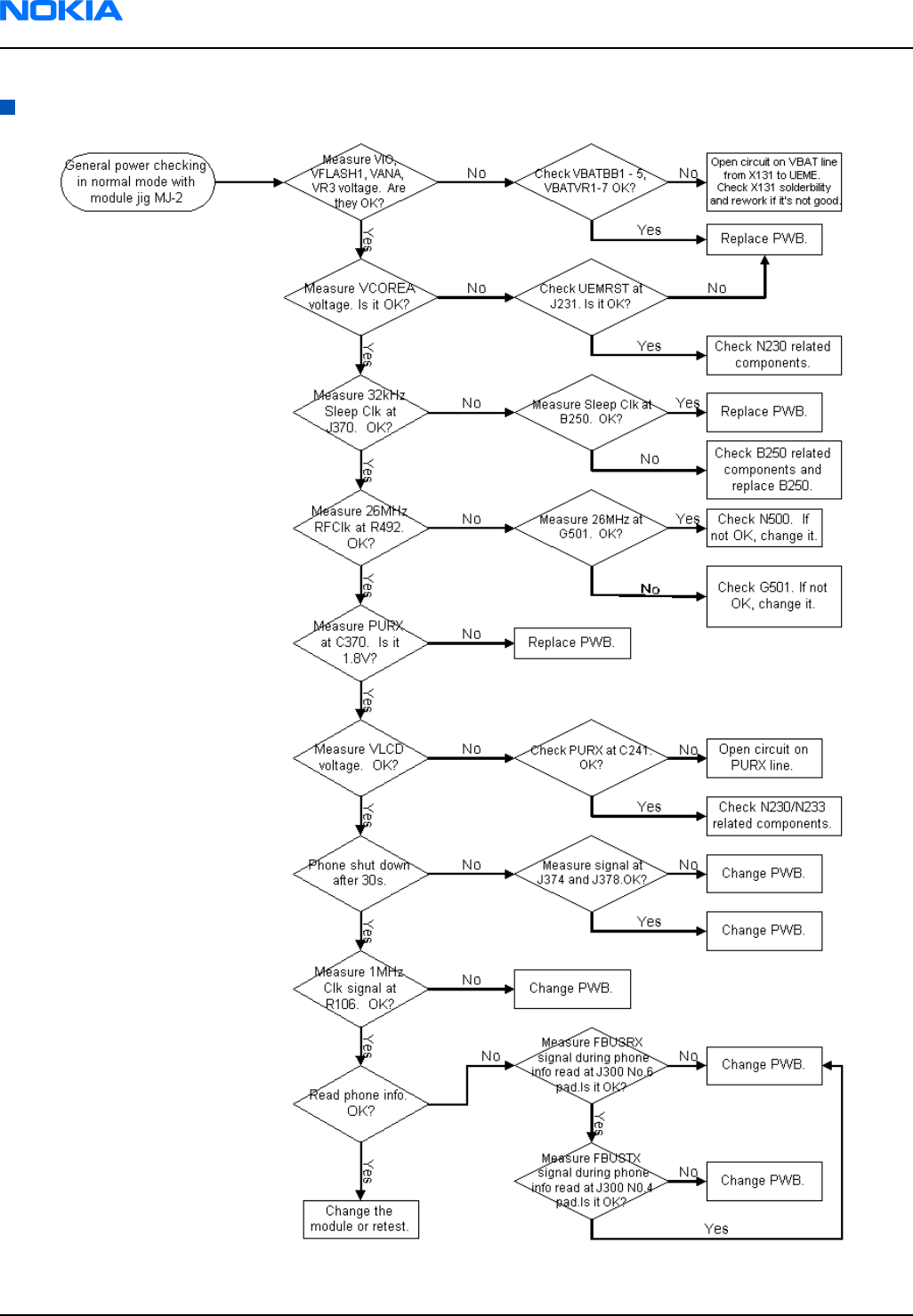
General power troubleshooting
Figure 79 General power troubleshooting
RM-25
Nokia Customer Care Baseband troubleshooting
Page 6–10 Company Confidential 9235618 (Issue 2)
Copyright ©2005 Nokia. All Rights Reserved.
Baseband serial interface troubleshooting
CBUS interface
CBUS is a three-wire serial interface between the main baseband components.
The bus consists of data, clock and bus_enable signals. The bus is connected between UPP_WD2, UEME and ZOCUS.
UPP_WD2 takes care of controlling the traffic on the bus.
If the interface is faulty from the UPP_WD2’s end, the phone does not boot properly as powering configurations
do not work.
Traffic on the bus can be monitored at the following test point and pins.
• R640 (test point J193 side)
• CBusEN1X J378 Pad
• CBusDA J377 Pad
The pads and pins are shown in the figures below.
CBUS test points
Figure 80 CBusClk test point
RM-25
Baseband troubleshooting Nokia Customer Care
9235618 (Issue 2) Company Confidential Page 6–11
Copyright ©2005 Nokia. All Rights Reserved.
Figure 81 CBUS test points
The CBUS traffic is shown in the figure below (read command to ZOCUS, LM3820, N130).
RM-25
Nokia Customer Care Baseband troubleshooting
Page 6–12 Company Confidential 9235618 (Issue 2)
Copyright ©2005 Nokia. All Rights Reserved.
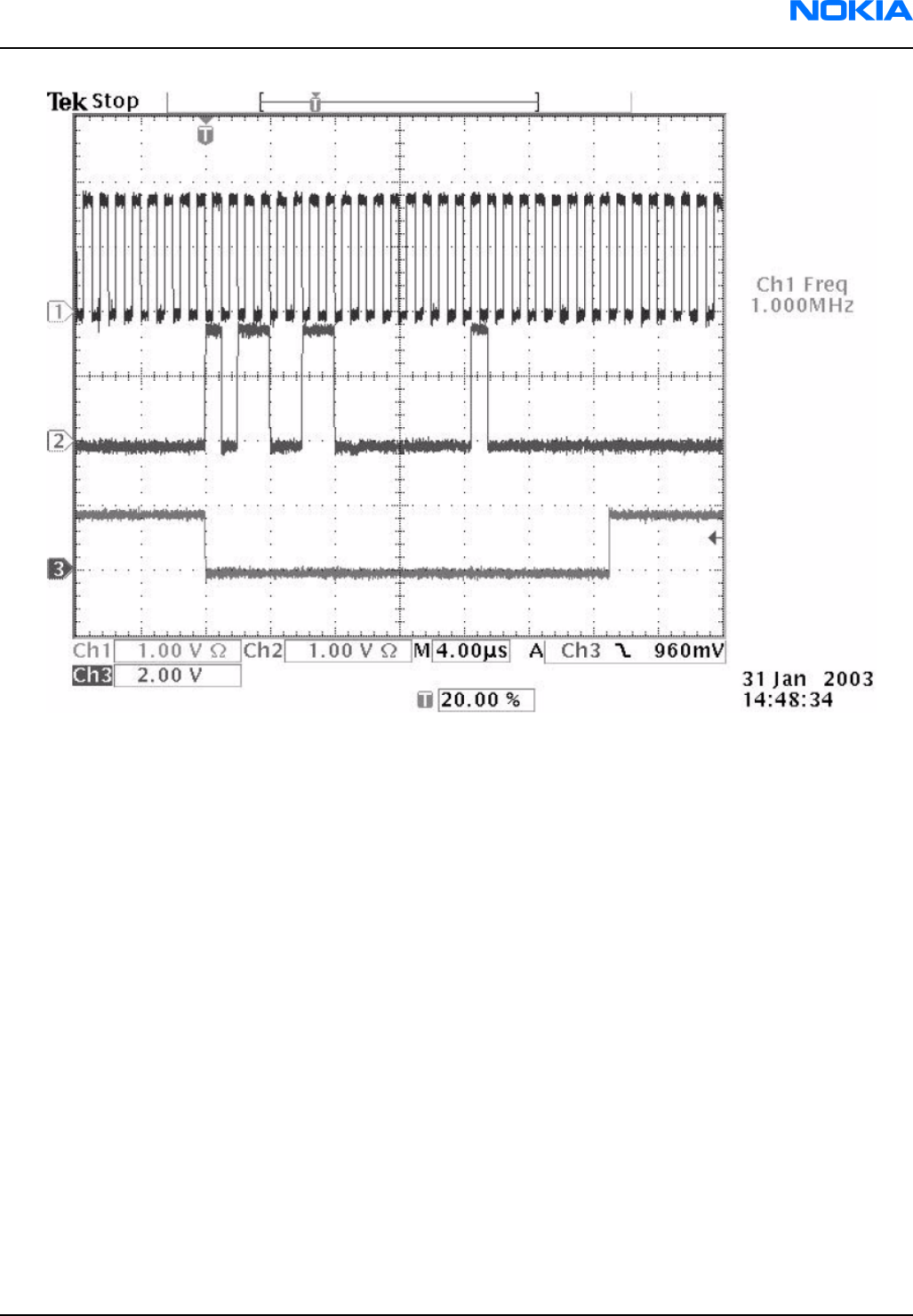
Figure 82 CBUS waveform
CBusCLk is connected to Ch1, CBusDa to CH2 and CBusEnx to Ch3.
If you are able to get the phone to boot up and can reach Phoenix BB self test feature, it is possible to test the
functionality of each component attached to CBus. Use:
• ST_UEM_CBUS_IF_TEST to test the UEME CBus interface
• ST_ZOCUS_CBUS_IF_TEST to test the ZOCUS CBus interface.
If an error is found in testing any of the above components, you should replace or re-solder the failed component.
FBUS interface
FBUS is a two-wire Rx and Tx interface between UPP_WD2 and flash/test interface. The bus goes through UEME,
which adjusts the voltage levels to suit UPP_WD2.
The interface voltage level on the phone flash/test pad pattern is 2.7V and on the UPP_WD2 end it is 1.8V.
The functionality of this interface should not affect the device boot into NORMAL, LOCAL or TEST modes.
Phoenix tests can be performed through the MBUS interface in the case of a failure in the FBUS interface. Flashing
is not possible if there is a problem in the FBUS interface. Fbus signals located in the flashing test pads and the
pad layout is shown in the figure below.
RM-25
Baseband troubleshooting Nokia Customer Care
9235618 (Issue 2) Company Confidential Page 6–13
Copyright ©2005 Nokia. All Rights Reserved.
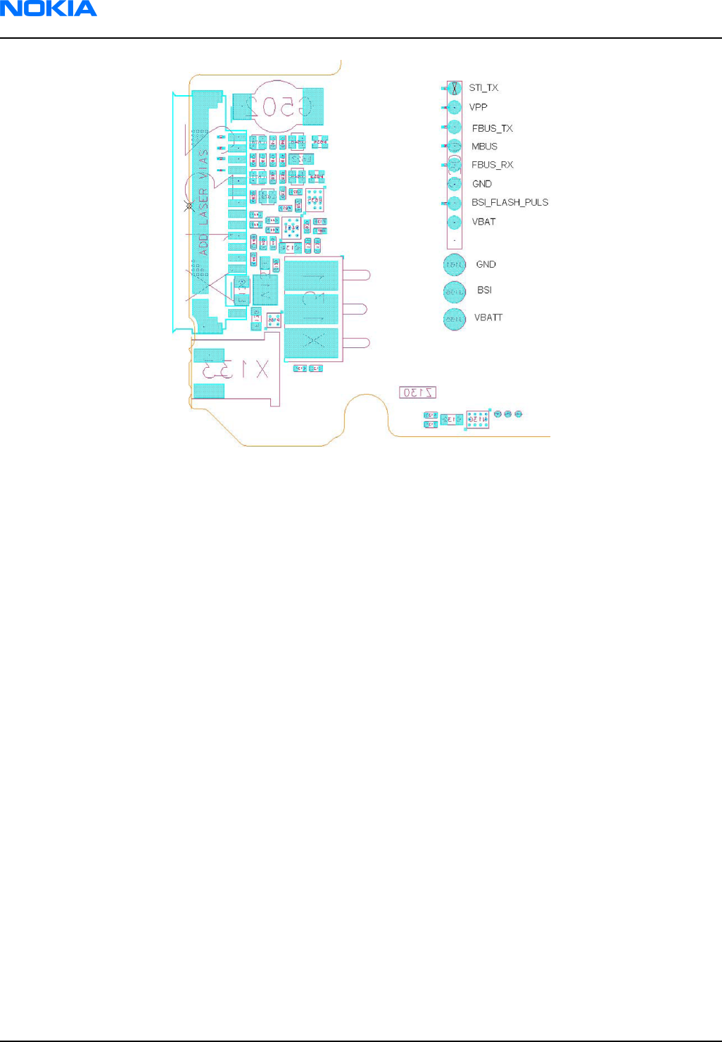
Figure 83 Flash interface layout (FBUS/MBUS test pads layout)
MBUS interface
MBUS is a two-wire RX and TX interface between UPP_WD2 and UEME. From UEME the interface continues to
flash/test interface as one-wire interface. UEME adjusts the voltage levels.
The interface voltage level on the phone flash/test pad pattern is 2.78V and on the UPP_WD2 end it is 1.8V.
MBUS traffic between UPP_WD2 and UEME can be tested with Phoenix (ST_MBUS_RX_TX_LOOP_TEST).
Flashing is not possible if there is a problem in MBUS. For the location of the MBUS signal in the test pads and
the pad layout, see figure Flash interface layout (Page 6–14).
RM-25
Nokia Customer Care Baseband troubleshooting
Page 6–14 Company Confidential 9235618 (Issue 2)
Copyright ©2005 Nokia. All Rights Reserved.
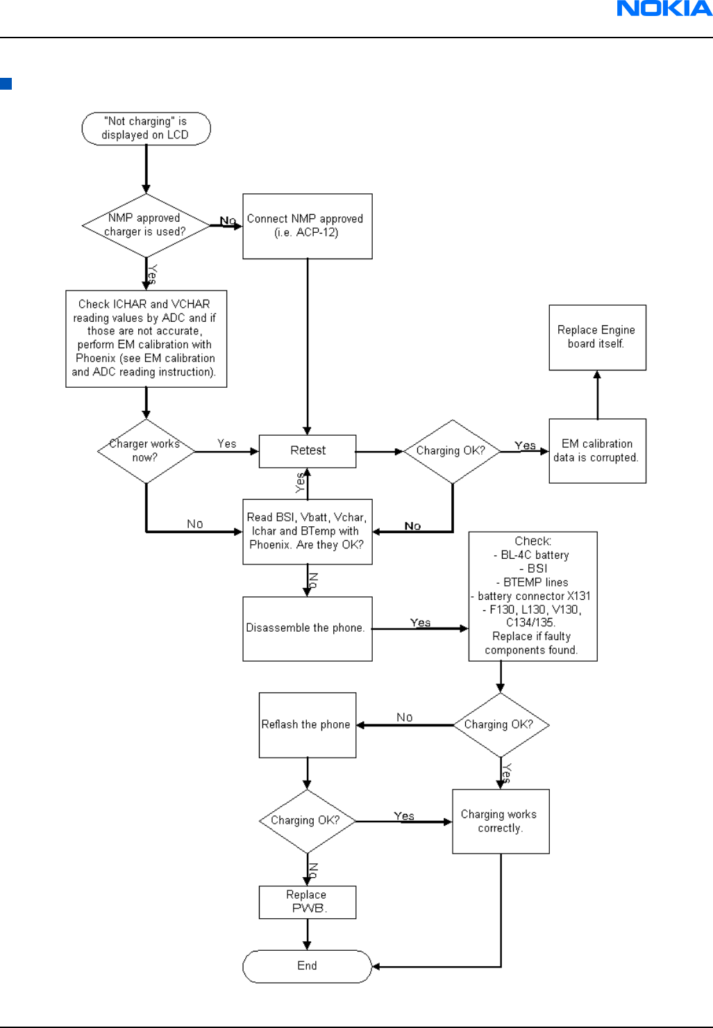
Troubleshooting charger interface
Figure 84 "Not charging" on display
RM-25
Baseband troubleshooting Nokia Customer Care
9235618 (Issue 2) Company Confidential Page 6–15
Copyright ©2005 Nokia. All Rights Reserved.
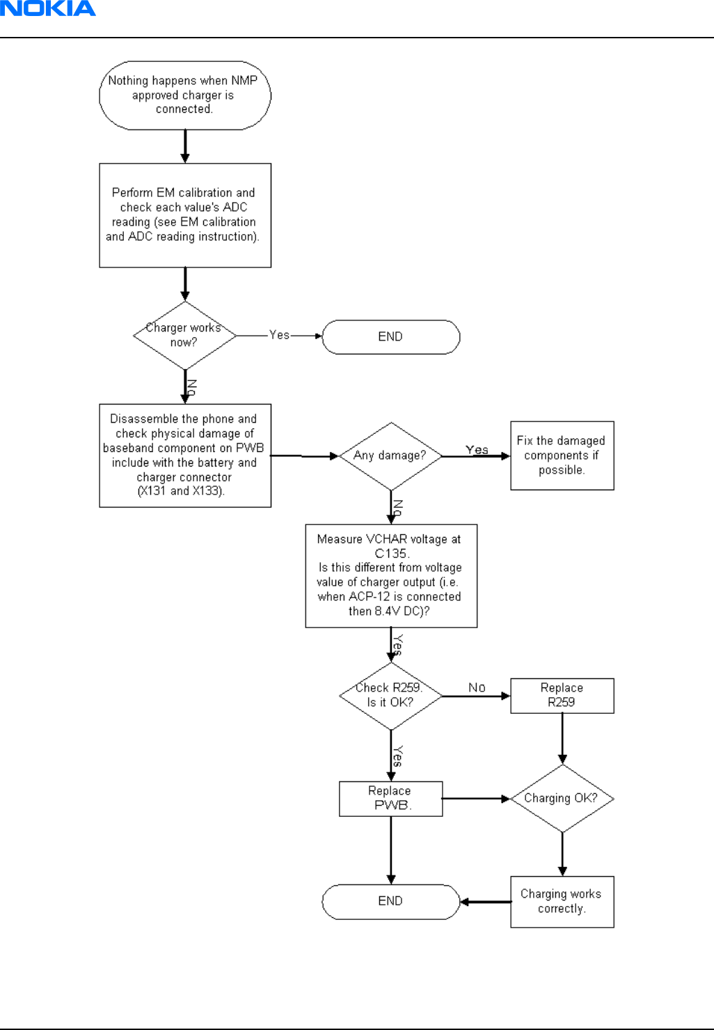
Figure 85 No charging
RM-25
Nokia Customer Care Baseband troubleshooting
Page 6–16 Company Confidential 9235618 (Issue 2)
Copyright ©2005 Nokia. All Rights Reserved.

Energy management calibration
EM calibrations should be carried out with a JBV-1 docking station attached to a DA-25 docking station adapter.
Power to JBV-1 should be supplied from an external DC power supply. JBV-1 input voltages: nominal + 12 VDC,
maximum +16VDC.
On the JBV-1, A/D converter, BSI, BTEMP, battery voltage (VBAT), charger voltage (VCHAR), charger current (ICHAR)
and battery current (IBAT) are calibrated.
For detailed information and instructions, see energy management calibration instructions (Page 6–39).
Baseband troubleshooting tips
ADC-offset over limits
Inspect the BSI line and its components. Note that the BSI resistance line of the battery is connected to the AD
input of the UEME labelled LS (not the BSI input). If these are OK, change PWB.
BSI gain over limits
Inspect the BSI line and its components. Note that the BSI resistance line of the battery is connected to the AD
input of the UEME labelled LS (not the BSI input). If these are OK, change PWB.
Vbatt offset and gain
Inspect Vbatt lines and its components.
VCHAR over limits
Inspect components that are connected to VCHAR line: filtering capacitors C134, C135, TVS V130, L130 and fuse
F130. If those are OK, change PWB.
ICHAR over limits
Inspect components that are connected to VCHAR line: filtering capacitors C134, C135, TVS V130, L130 and fuse
F130. If those are OK, change the current sense resistor R259 first. If calibration is still not successful, change PWB.
Calibration can be checked using the ADC reading. Known voltages, currents and resistances are fed to and read
by the ADC reading. The read values can then be compared with the known values.
ADC reading
Divided and scaled battery voltage, battery current, charger voltage, charger current and BSI values can be read
by this tool. Read values a few times until you can be sure that results are accurate.
RM-25
Baseband troubleshooting Nokia Customer Care
9235618 (Issue 2) Company Confidential Page 6–17
Copyright ©2005 Nokia. All Rights Reserved.
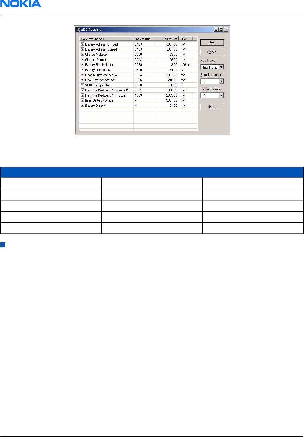
Figure 86 ADC reading window in Phoenix
Table 22 Maximum tolerances
Reading Check point Tolerance
Vbatt SCAL 4.2V ±25mV
Vchar 8.4V ±40mV
lchar 500mA ±20mV
BSI 75k (BL-4C) ±1.3kohm
Btemp 273K (47k) +5K
Backup battery troubleshooting
A symptom of a backup battery fault is that Real Time Clock loses the correct time during short battery removal.
The same symptom can also be seen when the backup battery is empty. About 30 minutes is needed to fully
charge the backup battery in the device.
Note: The backup battery is only charged at the same time as the main battery or when the device is
in the LOCAL or TEST mode.
Always check the backup battery visually for any leakage or any other visual defect.
Check that the backup battery is correctly mounted in the device before closing the cover.
Check with Phoenix that the backup battery is OK.
Measure the voltage of the backup battery.
• Normal operation when the voltage is > 2.0V.
• Fully charged when the voltage is about 3.2V.
Enable the backup battery charging (start to charge the main battery or boot the device to LOCAL or TEST mode).
Measure the voltage of the backup battery during charging, it should rise if it is not 3.2V yet.
When the voltage is over 2.0V for certain, check the backup battery with Phoenix.
RM-25
Nokia Customer Care Baseband troubleshooting
Page 6–18 Company Confidential 9235618 (Issue 2)
Copyright ©2005 Nokia. All Rights Reserved.
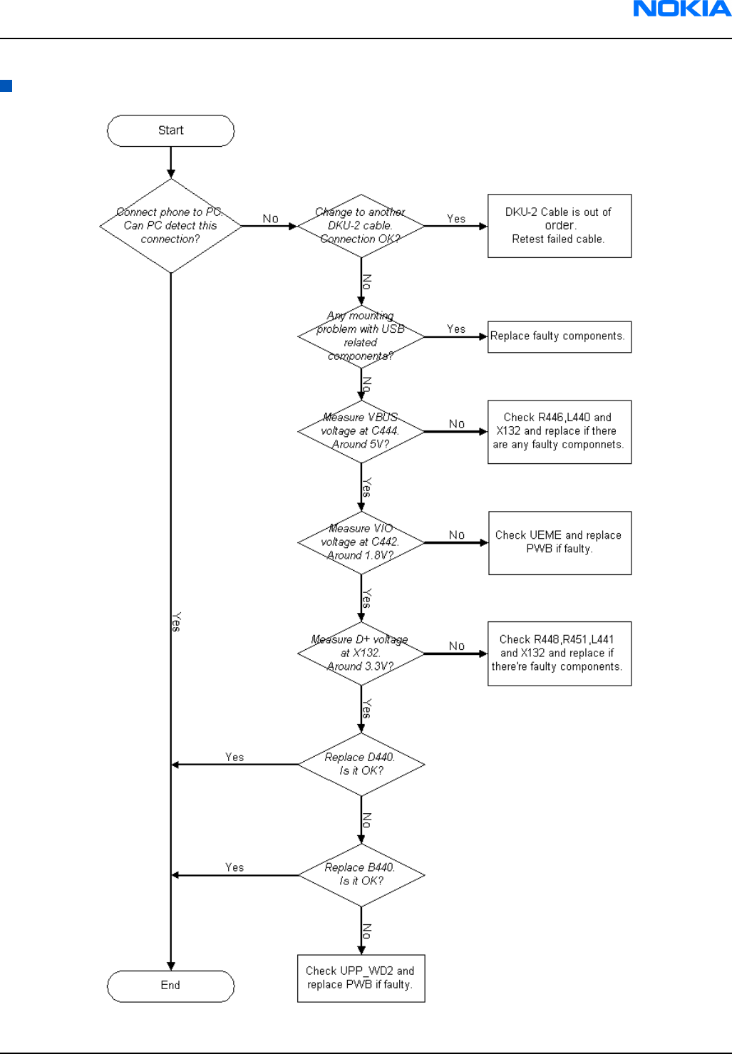
Troubleshooting USB interface
Figure 87 USB interface troubleshooting
RM-25
Baseband troubleshooting Nokia Customer Care
9235618 (Issue 2) Company Confidential Page 6–19
Copyright ©2005 Nokia. All Rights Reserved.
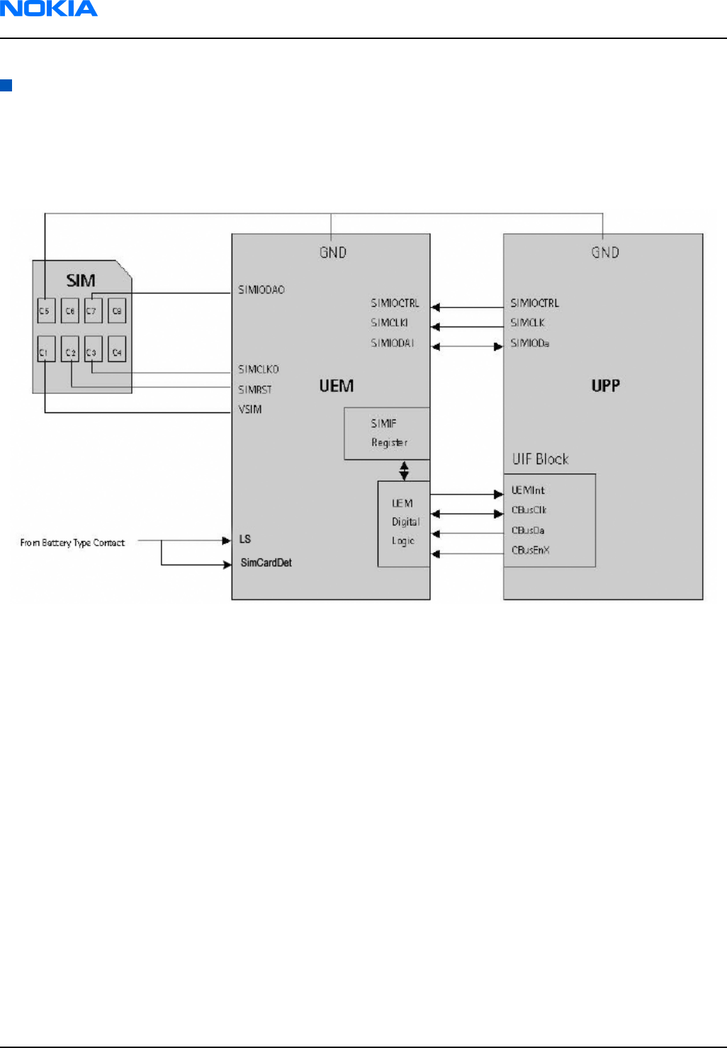
SIM card fault
The whole SIM interface is located in two chips: UPP_WD2 and UEME. UEME contains the SIM interface logic level
shifting. UPP_WD2 provides SIMClk through UEME to the SIM. The SIM interface supports both 3V and 1.8V SIMs.
There is an EMIF component (3 lines EMI filter) between the SIM card and the UEME which isn’t shown in the
figure below.
Figure 88 UPP_WD2 and UEME SIM connections (simplified)
The SIM power up/down sequence is generated in the UEME. This means that the UEME generates the RST signal
to the SIM. The card detection is taken from the BSI signal, which detects the removal of the battery. A comparator
inside the UEME monitors the BSI signal from the SimCardDet input. The threshold voltage is calculated from
the battery size specifications.
First, the SW attempts to power up the SIM with 1.8V. If this does not succeed, power up is repeated with VSIM
switched to 3V.
The data communication between the card and the phone is asynchronous half duplex. The clock supplied to
the card is in GSM system 1.083MHz or 3.25MHz. The data baud rate is SIM card clock frequency divided by 372
(by default), 64, 32, or 16.
RM-25
Nokia Customer Care Baseband troubleshooting
Page 6–20 Company Confidential 9235618 (Issue 2)
Copyright ©2005 Nokia. All Rights Reserved.
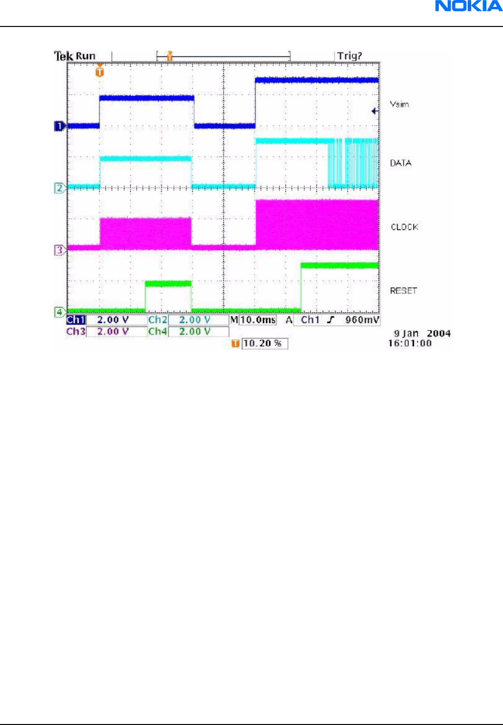
Figure 89 SIM power up waveform
RM-25
Baseband troubleshooting Nokia Customer Care
9235618 (Issue 2) Company Confidential Page 6–21
Copyright ©2005 Nokia. All Rights Reserved.
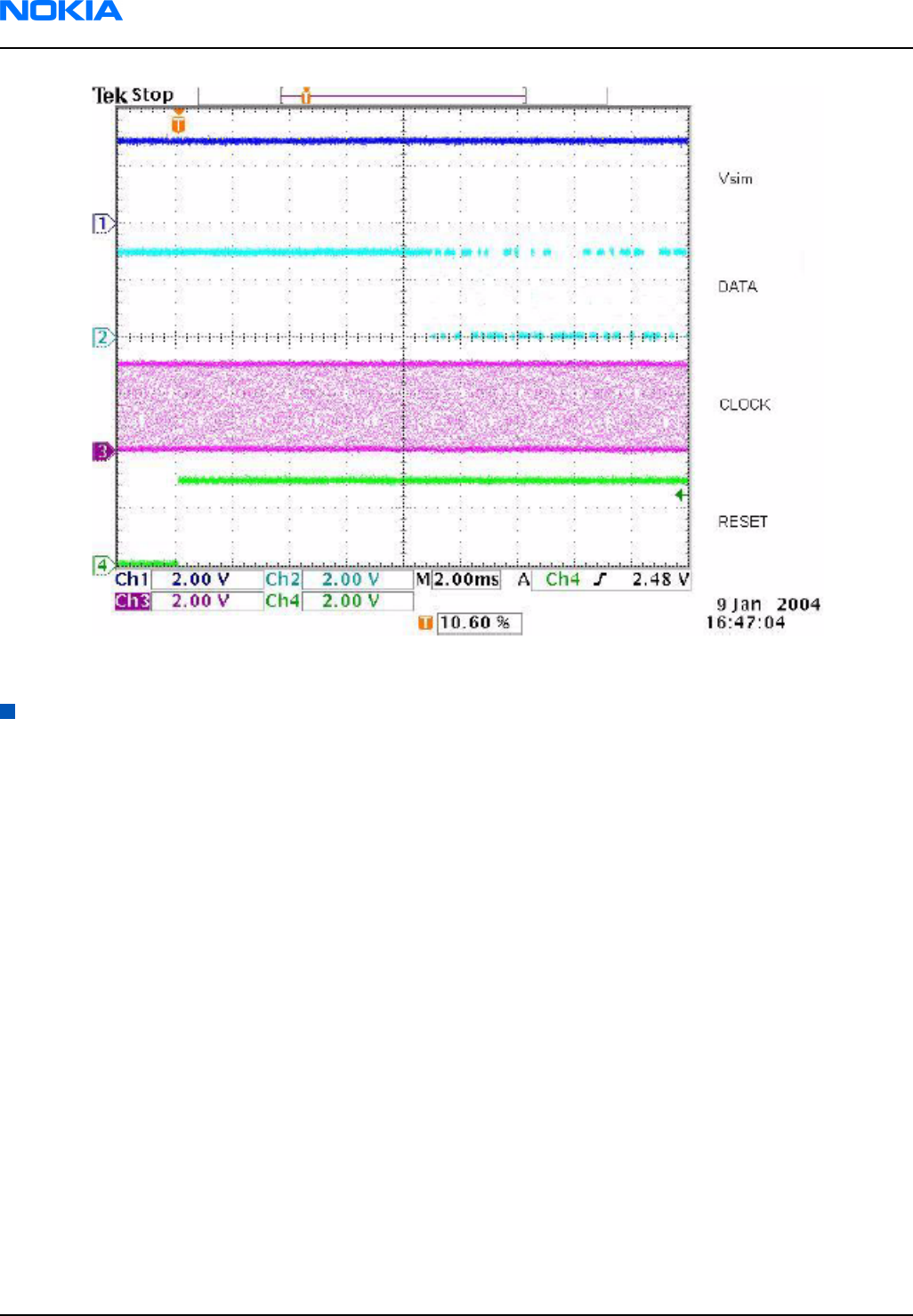
Figure 90 SIM answer to reset waveform
“Insert SIM Card” in device display although card is inserted
RM-25
Nokia Customer Care Baseband troubleshooting
Page 6–22 Company Confidential 9235618 (Issue 2)
Copyright ©2005 Nokia. All Rights Reserved.
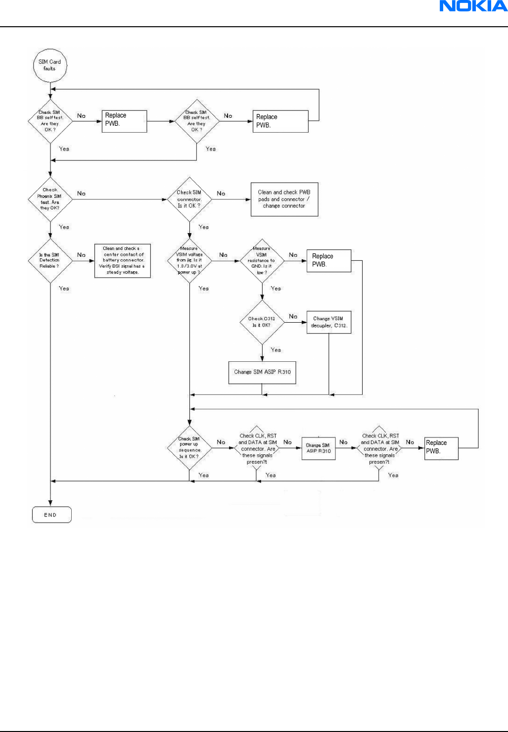
Figure 91 “Insert SIM Card” in device display although card is inserted
RM-25
Baseband troubleshooting Nokia Customer Care
9235618 (Issue 2) Company Confidential Page 6–23
Copyright ©2005 Nokia. All Rights Reserved.
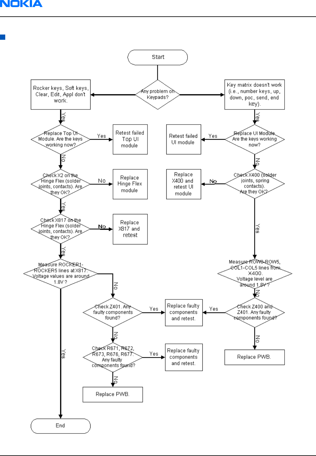
Troubleshooting keypad interface
Figure 92 Troubleshooting keypad interface
RM-25
Nokia Customer Care Baseband troubleshooting
Page 6–24 Company Confidential 9235618 (Issue 2)
Copyright ©2005 Nokia. All Rights Reserved.
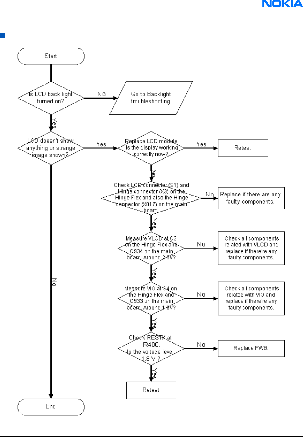
Troubleshooting the display
Figure 93 Display troubleshooting
RM-25
Baseband troubleshooting Nokia Customer Care
9235618 (Issue 2) Company Confidential Page 6–25
Copyright ©2005 Nokia. All Rights Reserved.
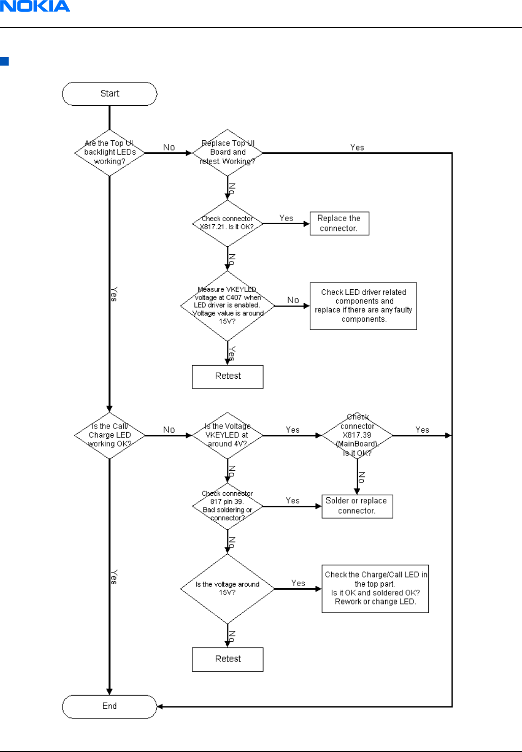
Troubleshooting display and keyboard backlight
Figure 94 Troubleshooting display and keyboard backlight
RM-25
Nokia Customer Care Baseband troubleshooting
Page 6–26 Company Confidential 9235618 (Issue 2)
Copyright ©2005 Nokia. All Rights Reserved.

Troubleshooting MMC interface
Context
Use a known working MMC to save the photo test. Target devices to replace are N310 Lester, R315 ASIP and
X820 MMC connector. The MMC card itself might be broken, and it should be checked as well.
RM-25
Baseband troubleshooting Nokia Customer Care
9235618 (Issue 2) Company Confidential Page 6–27
Copyright ©2005 Nokia. All Rights Reserved.
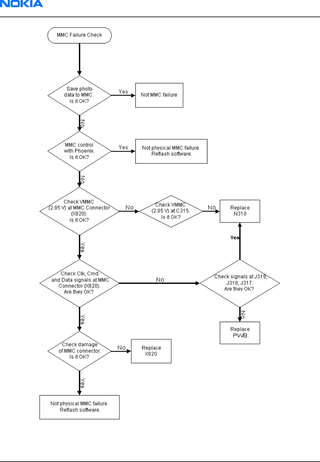
Figure 95 Troubleshooting MMC interface
RM-25
Nokia Customer Care Baseband troubleshooting
Page 6–28 Company Confidential 9235618 (Issue 2)
Copyright ©2005 Nokia. All Rights Reserved.

Audio troubleshooting
Troubleshooting internal microphone
Figure 96 Troubleshooting internal microphone
RM-25
Baseband troubleshooting Nokia Customer Care
9235618 (Issue 2) Company Confidential Page 6–29
Copyright ©2005 Nokia. All Rights Reserved.
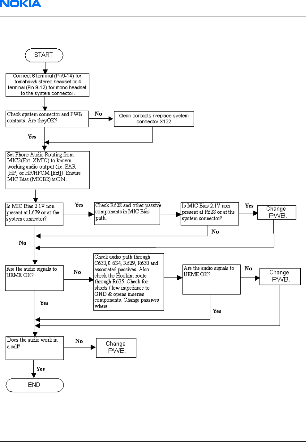
Troubleshooting external microphone
Figure 97 Troubleshooting external microphone
RM-25
Nokia Customer Care Baseband troubleshooting
Page 6–30 Company Confidential 9235618 (Issue 2)
Copyright ©2005 Nokia. All Rights Reserved.
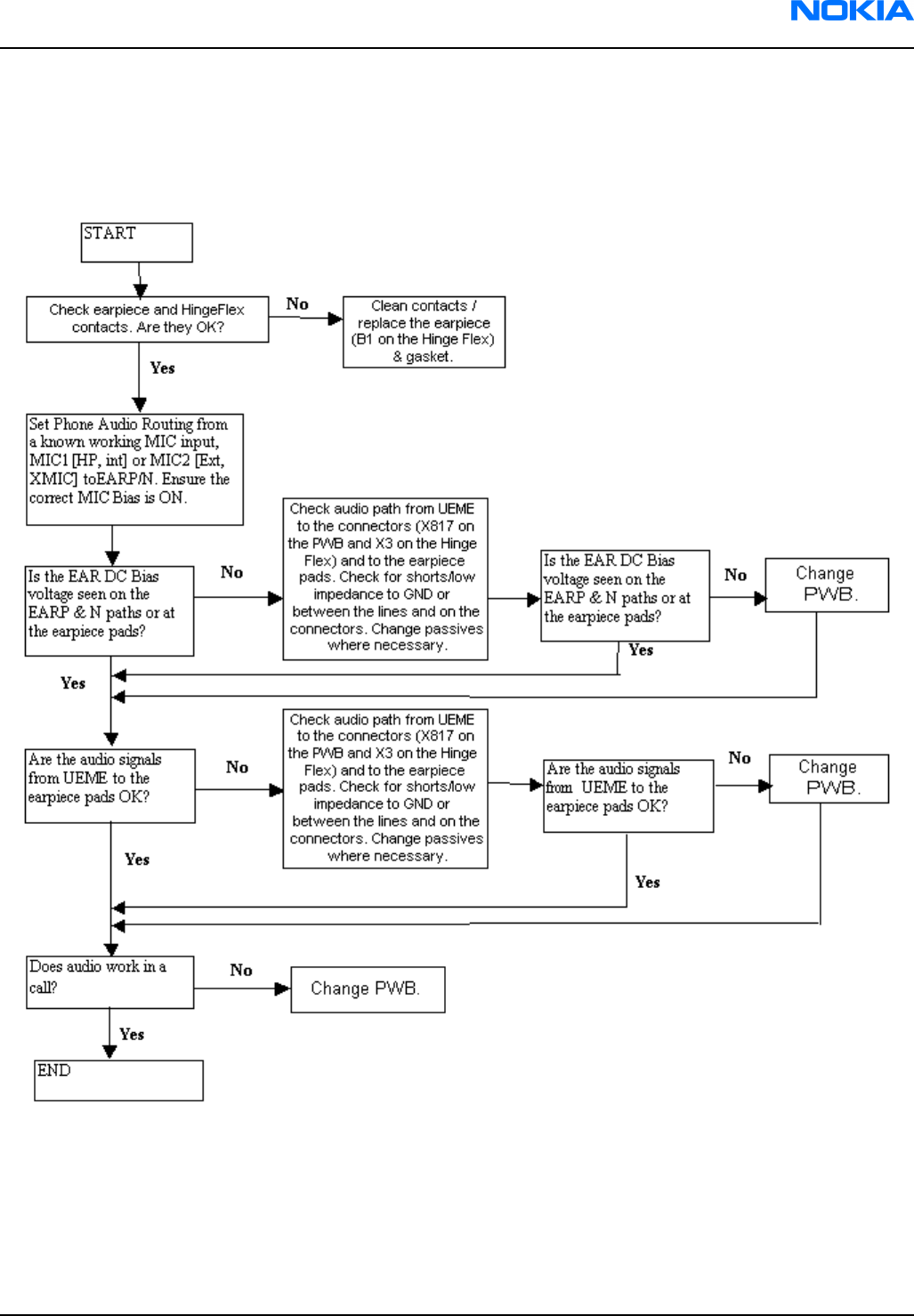
Troubleshooting internal earpiece
Before you begin
Check that holes in earpiece are not coated or covered.
Figure 98 Troubleshooting internal earpiece
RM-25
Baseband troubleshooting Nokia Customer Care
9235618 (Issue 2) Company Confidential Page 6–31
Copyright ©2005 Nokia. All Rights Reserved.
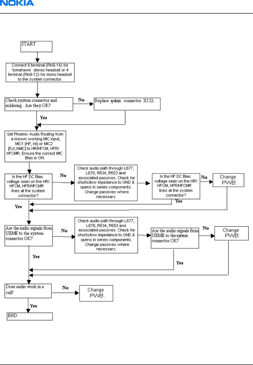
Troubleshooting external earpiece
Figure 99 Troubleshooting external earpiece
RM-25
Nokia Customer Care Baseband troubleshooting
Page 6–32 Company Confidential 9235618 (Issue 2)
Copyright ©2005 Nokia. All Rights Reserved.
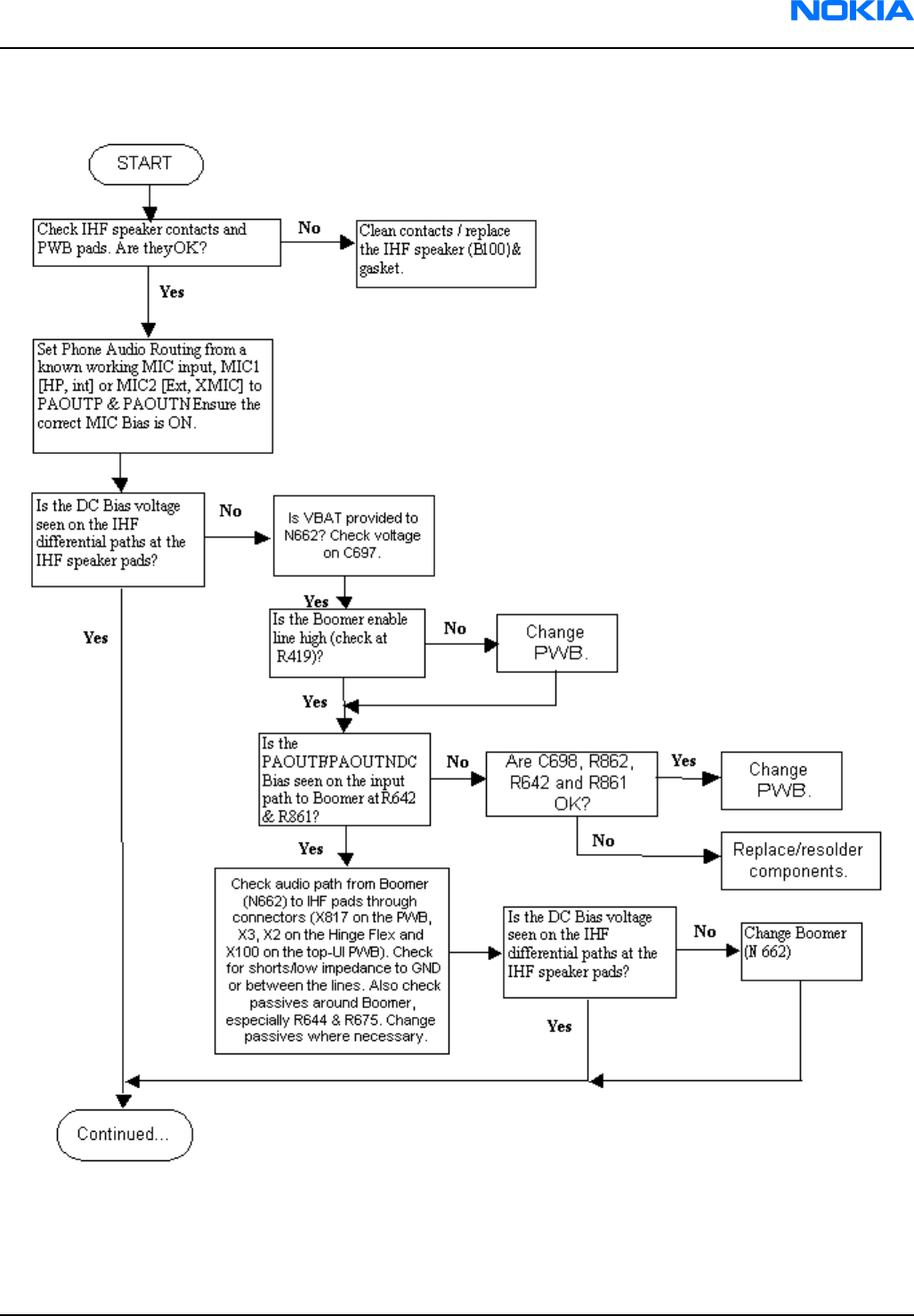
Troubleshooting IHF
Figure 100 Troubleshooting IHF
See also the following chart.
RM-25
Baseband troubleshooting Nokia Customer Care
9235618 (Issue 2) Company Confidential Page 6–33
Copyright ©2005 Nokia. All Rights Reserved.
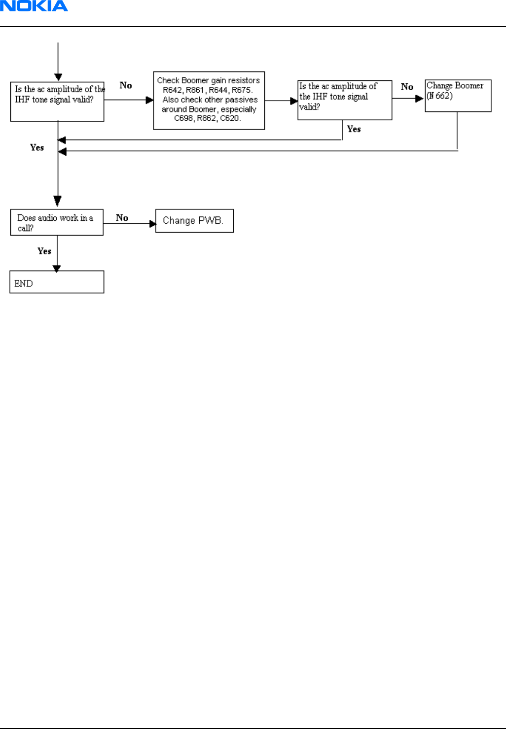
Figure 101 Troubleshooting IHF (continued)
RM-25
Nokia Customer Care Baseband troubleshooting
Page 6–34 Company Confidential 9235618 (Issue 2)
Copyright ©2005 Nokia. All Rights Reserved.
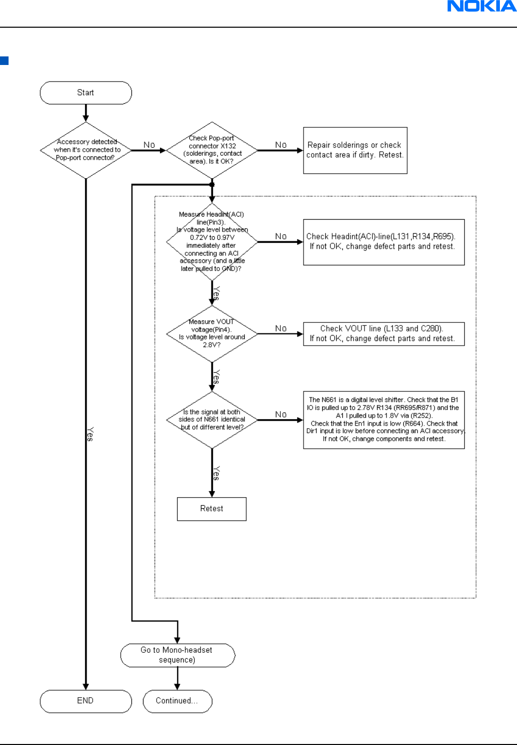
Troubleshooting accessory detection
Figure 102 Troubleshooting accessory detection
RM-25
Baseband troubleshooting Nokia Customer Care
9235618 (Issue 2) Company Confidential Page 6–35
Copyright ©2005 Nokia. All Rights Reserved.
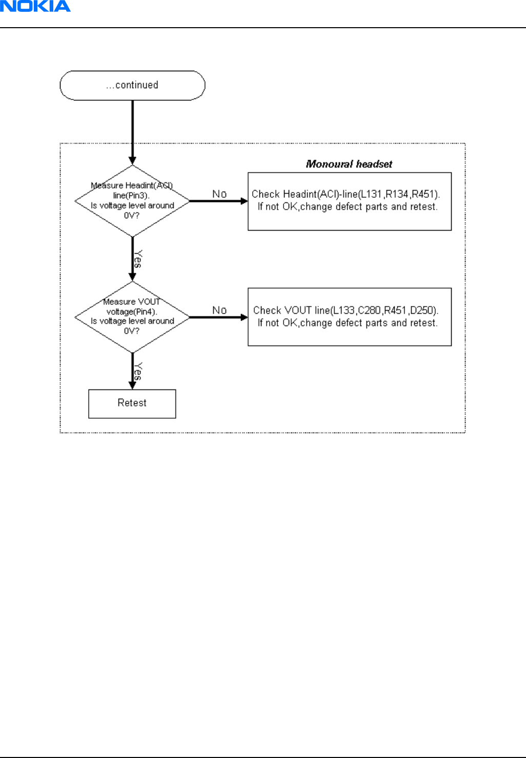
See also the following flow chart.
Figure 103 Troubleshooting accessory detection (continued)
RM-25
Nokia Customer Care Baseband troubleshooting
Page 6–36 Company Confidential 9235618 (Issue 2)
Copyright ©2005 Nokia. All Rights Reserved.
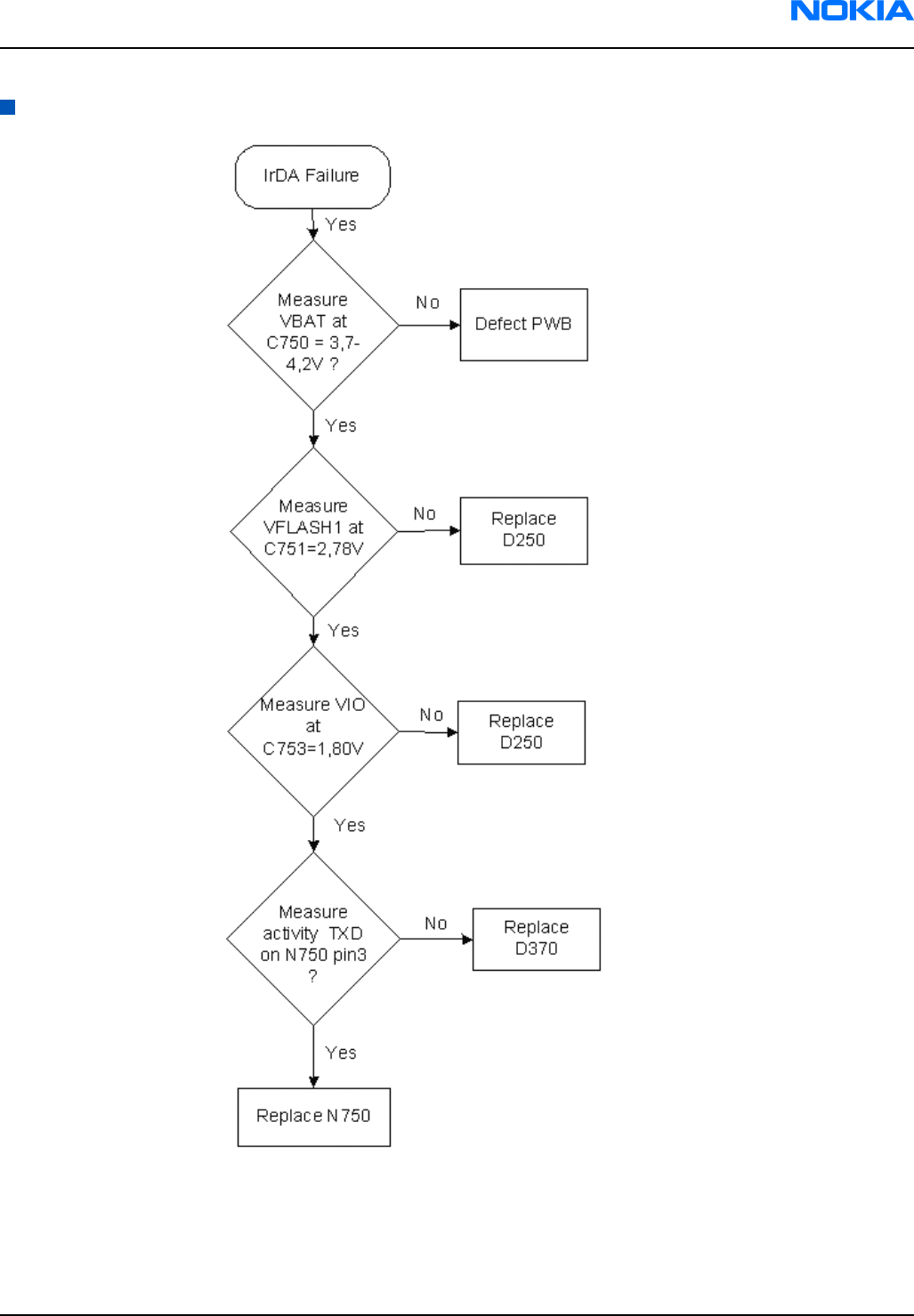
Troubleshooting IrDA
Figure 104 Troubleshooting IrDA
RM-25
Baseband troubleshooting Nokia Customer Care
9235618 (Issue 2) Company Confidential Page 6–37
Copyright ©2005 Nokia. All Rights Reserved.

Troubleshooting FM radio
Before you begin
In Phoenix: choose Testing -> FM radio -> Power on.
For FM signal:
• Use FM signal received by headset,
or
• use FM signal generator: Frequency = 100MHz, frequency deviation = 67.5kHz, modulation frequency = 1kHz,
R = L, pilot tone on and RF level = -67dBm.
RM-25
Nokia Customer Care Baseband troubleshooting
Page 6–38 Company Confidential 9235618 (Issue 2)
Copyright ©2005 Nokia. All Rights Reserved.
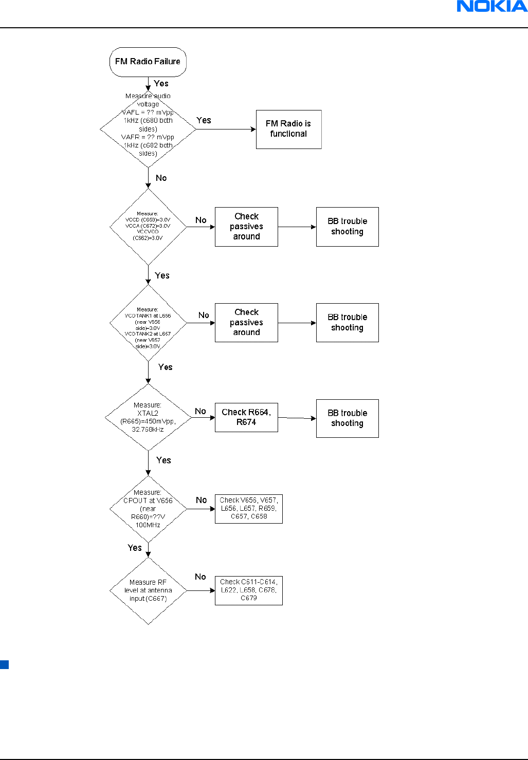
Figure 105 Troubleshooting FM radio
Tuning baseband
Before you begin
EM (Energy Management) calibration is performed to calibrate the setting (gain and offset) of AD converters in
several channels (that is, battery voltage, BSI, charger voltage, charger current) to get an accurate AD conversion
result.
RM-25
Baseband troubleshooting Nokia Customer Care
9235618 (Issue 2) Company Confidential Page 6–39
Copyright ©2005 Nokia. All Rights Reserved.
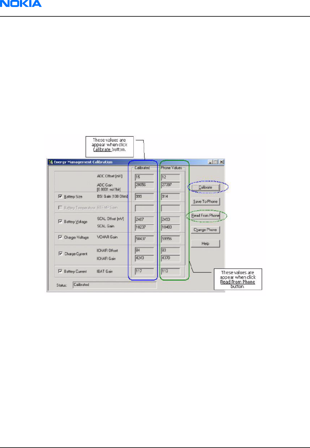
HW setup:
• An external power supply is needed.
• The RM-25 phone must be connected to JBV-1 (docking station) with DA-25 (docking station adapter).
a Connect SCB-3 (DC-DC cable) between JBV-1 and charger connector of phone for charger channel
calibration.
b Supply 11-16V DC from an external power supply to JBV-1 to power up phone.
Phoenix SW setup:
• Start Phoenix service software.
• Select FBUS connection.
• Choose: Main -> Product -> RM-25.
• Choose: Tuning -> Energy Management Calibration.
Figure 106 EM calibration window
Steps
1. Select “Read from phone” to show the current values in the phone memory, and then check that the
communication with the phone works.
2. Select “JBV-1 used” check box.
3. Select the item(s) you try to calibrate.
Note: ADC has to be calibrated before other item(s). If the ADC value is correct or you calibrate ADC and
other items at the same time, that’s OK.
4. Select “Calibrate”.
Calibration is carried out automatically regarding the calibration item(s) that you selected.
5. The candidate of the new calibration values is shown in the “calculated” field. If the new calibration values
seem to be reasonable (please refer to the calibration value limit table), select Write to PM to store the new
calibration value in the phone permanent memory.
RM-25
Nokia Customer Care Baseband troubleshooting
Page 6–40 Company Confidential 9235618 (Issue 2)
Copyright ©2005 Nokia. All Rights Reserved.
Table 23 Calibration value limits
Parameter Min. Max.
ADC Gain 26500 28500
ADC Offset -50 50
BSI Gain 600 1100
VBAT Gain 10000 11000
VBAT Offset 2300 2900
VCHAR Gain 58000 62000
ICHAR Gain 3500 4400
ICHAR Offset -80 +80
IBAT Gain 50 160
6. Select “Read from phone” and confirm that the new calibration values are stored in the phone memory
correctly. If not, please try to store by selecting “Write to PM” again.
7. Close the Energy Management Calibration window.
Testing and tuning BB after component replacement
Context
The replacement of certain components which influences the energy management in the phone should be
followed by a calibration.
Steps
1. Calibrate R133, the UEME - D250, the ZOCUS - N130 and R259.
RM-25
Baseband troubleshooting Nokia Customer Care
9235618 (Issue 2) Company Confidential Page 6–41
Copyright ©2005 Nokia. All Rights Reserved.

RM-25
Nokia Customer Care Baseband troubleshooting
(This page left intentionally blank.)
Page 6–42 Company Confidential 9235618 (Issue 2)
Copyright ©2005 Nokia. All Rights Reserved.

7 — RF troubleshooting
Nokia Customer Care
9235618 (Issue 2) Company Confidential Page 7–1
Copyright ©2005 Nokia. All Rights Reserved.

RM-25
Nokia Customer Care RF troubleshooting
(This page left intentionally blank.)
Page 7–2 Company Confidential 9235618 (Issue 2)
Copyright ©2005 Nokia. All Rights Reserved.

Table of Contents
Introduction to RF troubleshooting.........................................................................................................................................7–5
RF key component placement....................................................................................................................................................7–5
Receiver.............................................................................................................................................................................................7–8
Receiver troubleshooting......................................................................................................................................................7–8
Measuring Rx/IQ signals using RSSI....................................................................................................................................7–9
Measuring RX performance using SNR measurement...............................................................................................7–10
Measuring Rx module manually using oscilloscope and spectrum analyzer (EGSM900)................................7–10
Measuring Rx module manually using oscilloscope and spectrum analyzer (GSM1800)...............................7–13
Measuring Rx module manually using oscilloscope and spectrum analyzer (GSM1900)...............................7–14
RM-25 measurement points in the receiver..................................................................................................................7–17
Calibrating RX Channel Select Filter.................................................................................................................................7–18
Calibrating RX..........................................................................................................................................................................7–19
Transmitter....................................................................................................................................................................................7–22
Introduction to RM-25 transmitter troubleshooting..................................................................................................7–22
Preparing for transmitter troubleshooting...................................................................................................................7–23
Troubleshooting TX-BB interface and control signals................................................................................................7–25
Troubleshooting RF side of transmitter.........................................................................................................................7–27
Introduction to transmitter tuning..................................................................................................................................7–28
Tuning TX/IQ............................................................................................................................................................................7–28
Tuning TX power level..........................................................................................................................................................7–32
Introduction to synthesizer troubleshooting...............................................................................................................7–40
Preparing for synthesizer troubleshooting...................................................................................................................7–42
Measuring the synthesizer manually using spectrum analyzer ............................................................................7–44
Bluetooth........................................................................................................................................................................................7–45
Bluetooth component placement....................................................................................................................................7–45
Bluetooth settings for Phoenix.........................................................................................................................................7–45
Troubleshooting Bluetooth................................................................................................................................................7–47
List of Tables
Table 24 RF retuning after changing a component.............................................................................................................7–6
Table 25 RX calibration settings..............................................................................................................................................7–20
Table 26 Spectrum analyzer settings.....................................................................................................................................7–28
Table 27 RF Control window settings.....................................................................................................................................7–30
Table 28 Spectrum analyzer settings for Tx power level tuning...................................................................................7–33
Table 29 Spectrum analyzer settings for Tx level tuning.................................................................................................7–34
List of Figures
Figure 107 RF key component placement...............................................................................................................................7–6
Figure 108 RF key components (left)........................................................................................................................................7–7
Figure 109 RF key components (right).....................................................................................................................................7–7
Figure 110 Receiver signal paths...............................................................................................................................................7–8
Figure 111 Troubleshooting flowchart for EGSM900.........................................................................................................7–12
Figure 112 Probed Rx I/Q signals J730, J731........................................................................................................................7–13
Figure 113 Troubleshooting flowchart for EGSM1800......................................................................................................7–14
Figure 114 Troubleshooting flowchart for EGSM1900......................................................................................................7–16
Figure 115 Measurement points at RX frontend - part 1.................................................................................................7–17
Figure 116 Measurement points at RX frontend - part 2.................................................................................................7–18
Figure 117 Measurement points at baseband and digital IQs.......................................................................................7–18
RM-25
RF troubleshooting Nokia Customer Care
9235618 (Issue 2) Company Confidential Page 7–3
Copyright ©2005 Nokia. All Rights Reserved.

Figure 118 RX Channel Select Filter Calibration...................................................................................................................7–19
Figure 119 RX calibration (Example)......................................................................................................................................7–20
Figure 120 RX calibration with band EGSM900 (Example)...............................................................................................7–21
Figure 121 RX calibration values (Example).........................................................................................................................7–21
Figure 122 TX RF block diagram...............................................................................................................................................7–22
Figure 123 Upper and lower shielding cans.........................................................................................................................7–23
Figure 124 Preparing for transmitter troubleshooting....................................................................................................7–24
Figure 125 TX-BB interface troubleshooting and control signals.................................................................................7–25
Figure 126 Oscilloscope screen shots.....................................................................................................................................7–26
Figure 127 RF side of transmitter troubleshooting...........................................................................................................7–27
Figure 128 Oscilloscope screen shots (RF)............................................................................................................................7–28
Figure 129 RF controls.................................................................................................................................................................7–29
Figure 130 Tx IQ tuning..............................................................................................................................................................7–29
Figure 131 Phoenix set-up (Tx IQ Tuning windows).........................................................................................................7–30
Figure 132 Spectrum analyzer screen shot when performing IQ tuning, part 1......................................................7–31
Figure 133 Spectrum analyzer screen shot when performing IQ tuning, part 2......................................................7–32
Figure 134 Phoenix menu select (Tx Power Level Tuning menu).................................................................................7–33
Figure 135 Phoenix Power Level Tuning menu..................................................................................................................7–34
Figure 136 Phoenix screen shot (Tx Power Level Tuning)...............................................................................................7–35
Figure 137 Spectrum analyzer screen shot during power level tuning......................................................................7–36
Figure 138 Testpoints of the main board 1fsa_09a, top part.........................................................................................7–37
Figure 139 Testpoints of the main board 1fsa_11a, top part.........................................................................................7–38
Figure 140 Testpoints of the main board, bottom part...................................................................................................7–39
Figure 141 Synthesizer block diagram..................................................................................................................................7–40
Figure 142 Rf key component...................................................................................................................................................7–41
Figure 143 Synthesizer key components without shielding frames............................................................................7–42
Figure 144 Preparation for troubleshooting using Phoenix RF control setup..........................................................7–43
Figure 145 Troubleshooting chart for synthesizer............................................................................................................7–44
Figure 146 Bluetooth component placement.....................................................................................................................7–45
Figure 147 Phoenix settings for Bluetooth troubleshooting..........................................................................................7–46
Figure 148 Bluetooth troubleshooting..................................................................................................................................7–47
RM-25
Nokia Customer Care RF troubleshooting
Page 7–4 Company Confidential 9235618 (Issue 2)
Copyright ©2005 Nokia. All Rights Reserved.

Introduction to RF troubleshooting
This document describes RF troubleshooting and tuning. In general, two types of measurements have to be
done during troubleshooting and repair of phones:
• RF measurements shall be done with a spectrum analyzer, either connected directly to the RF connector of
the RF adapter board SA-38, or used together with a high-frequency probe to measure RF signals at points
along the TX or RX chain.
• LF (Low-Frequency) and DC measurements shall be done either with a multimeter, or with an oscilloscope
together with a 10:1 probe.
All tuning must be done with Phoenix Service Software _a15_2004_7_55.exe, or later.
Always make sure that the measurement set-up has been calibrated when measuring RF parameters at the RF
connector. Remember to include the correct losses in the module repair jig and the connecting cable when
realigning the phone.
Most RF semiconductors are static discharge sensitive. ESD protection must be taken into account during repair
(ground straps and ESD soldering irons).
RF calibration done via Phoenix software is temperature sensitive because of calibration of 26MHz reference
oscillator (VCXO). According to the Helgo specification, the ambient temperature has to be in the range of 22 to
38C.
Note: In this text the following terms are used interchangeably:
• GSM900 = EGSM900 = EGSM
• GSM1800 = DCS band = PCN band
• GSM1900 = PCS band
The first step of fault-finding should always be a visual inspection. Carefully inspect the RF area using a
microscope and look for solder bridges, missing components, short circuits, components that have partially
come off and other anomalies. Capacitors can be checked to see that they are not short-circuited, and inductors
that they are not open circuits. Also check that power supply lines are not short-circuited, i.e. not 0Ω to ground.
Instruments needed for troubleshooting (minimum requirement):
• oscilloscope
• multimeter
• spectrum analyzer (SA)
Note: Always use an attenuator at the spectrum analyzer input to ensure that the SA will not become
damaged by excessive input power from the phone. Check the spectrum analyzer for maximum
allowable input power.
For example, when transmitting in the EGSM band at max power level, the output power will be around
+33dBm. By using a 10dB attenuator the actual input to the SA will then be +23dBm. Also adjust the
internal attenuator so that the transmitted signal is reduced to less than around -10dBm in order to
avoid saturation of SA input stage.
• power supply that can deliver at least 2Adc
• Nokia MJ-30 module jig (also called test jig)
• RF adapter SA-38
• PC with Phoenix installed
• PKD-1 deskey dongle for Phoenix
RF key component placement
The following figure shows the key components of the RF section:
RM-25
RF troubleshooting Nokia Customer Care
9235618 (Issue 2) Company Confidential Page 7–5
Copyright ©2005 Nokia. All Rights Reserved.
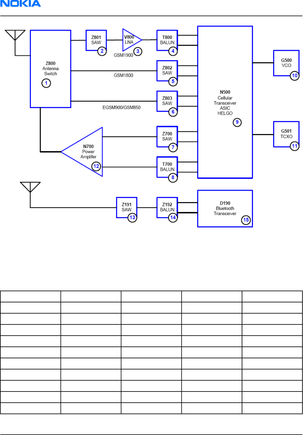
Figure 107 RF key component placement
• Adjust the RX chain after repairing or changing the parts marked RX.
• Adjust the TX chain after repair or changing the parts marked TX.
• The numbering refers to the RF-overview and non-RF-overview pictures.
Table 24 RF retuning after changing a component
1N500 Helgo RF ASIC RX TX
2 G500 VCO RX TX
3 G501 VCTCXO RX
4 Z800 RX/TX Switch RX TX
5 N700 PA TX
6 V800 LNA1900 RX
7 Z803 RX SAW 900 RX
8 Z802 RX SAW 1800 RX
9 Z801 RX SAW 1900 RX
10 T800 RX Balun 1900 RX
11 Z700 TX SAW 900 TX
RM-25
Nokia Customer Care RF troubleshooting
Page 7–6 Company Confidential 9235618 (Issue 2)
Copyright ©2005 Nokia. All Rights Reserved.
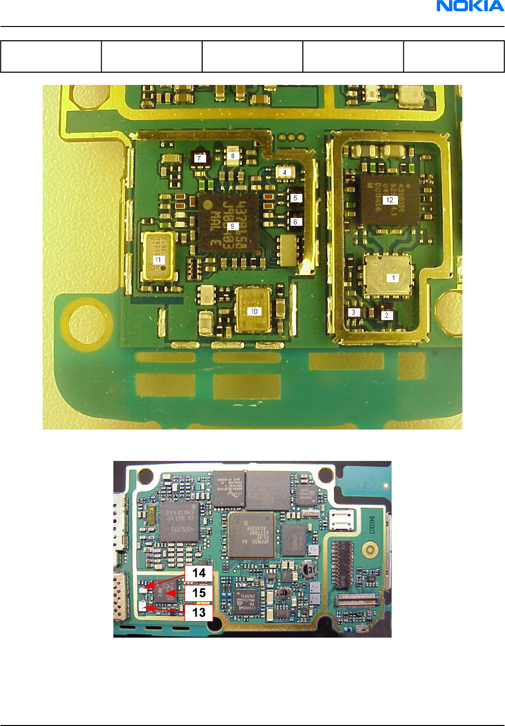
12 T700 TX Balun 1800/
1900
TX
Figure 108 RF key components (left)
Figure 109 RF key components (right)
RM-25
RF troubleshooting Nokia Customer Care
9235618 (Issue 2) Company Confidential Page 7–7
Copyright ©2005 Nokia. All Rights Reserved.

Receiver
Receiver troubleshooting
Figure 110 Receiver signal paths
Each receiver path is a direct conversion linear receiver. From the antenna, the received RF signal is fed to a
front end module where a diplexer first divides the signal to two separate paths according to the band of
operation: either lower, EGSM900 or upper, GSM1800/1900 path.
At each of the paths follows a pin-diode switch, which is used to select either a receive- or transmit mode. At
the upper band in the receive mode either GSM1800 or 1900 path is further selected by another pin-diode
switch. The selections are controlled by Helgo, which obtains the mode/band and timing information through
the RFBus.
After the switches an external bandpass filter follows each receiver paths. Thereafter, the signal is fed to the
LNA's. EGSM900 and GSM1800 LNA's are integrated in Helgo, while the GSM1900 LNA is a discrete component
placed between SAW filter and balun. In GSM1900, the amplified signal is fed to a pre-gain stage of the mixer.
EGSM900 and GSM1800 LNA's are connected directly to the pregain stages. The pregain stages as well as all the
following receiver blocks are integrated in Helgo. The LNA's have three gain levels. The first one is the maximum
gain, the second one is about 30 dB below the maximum, and the last one is the off state.
After the pregain stages there are demodulator mixers at each signal path to convert the RF signal directly down
to baseband I and Q signals. Local oscillator signals for the mixers are generated by an external VCO. The
frequency is divided by two in GSM1800 and GSM1900 and by four in EGSM900. Those frequency dividers are
integrated in Helgo and in addition to the division they also provide accurate phase shifting by 90 degrees
which is needed for the demodulator mixers.
The demodulator output signals are all differential. After the demodulators there are amplifiers called DtoS
(differential to single ended) which convert the differential signals to single ended. Before that, they combine
the signals from the three demodulators to a single path which means that from the output of the demodulators
to the baseband interface are just two signal paths (I and Q), which are common to all the frequency bands of
operation. In addition, the DtoS amplifiers perform the first part of the channel filtering and AGC (automatic
gain control). They have two gain stages, the first one with a constant gain of 12 dB and -3 dB bandwidth of
85 kHz and the second one with a switchable gain of ±6 dB. The filters in the DtoS blocks are active RC filters.
The rest of the analog channel filtering is provided by blocks called BIQUAD which include modified Sallen-Key
biquad filters.
RM-25
Nokia Customer Care RF troubleshooting
Page 7–8 Company Confidential 9235618 (Issue 2)
Copyright ©2005 Nokia. All Rights Reserved.
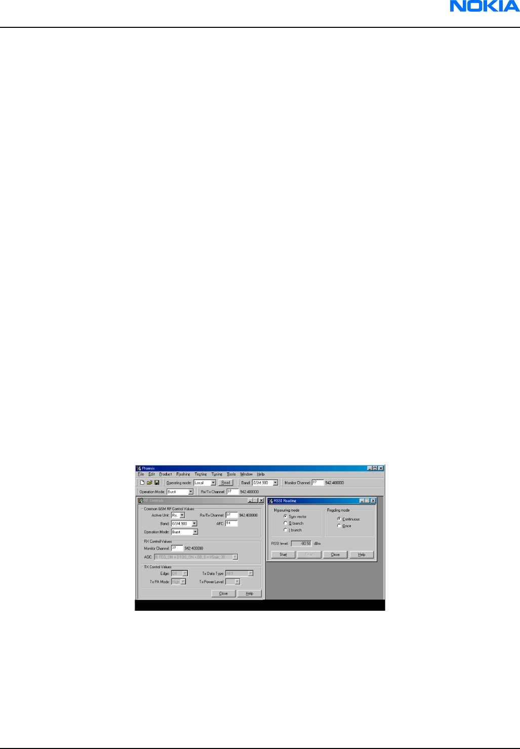
After the DtoS and BIQUAD blocks, there is another AGC-amplifier which provides a gain control range of 42 dB
in 6 dB steps. The correlation between the gain steps and the absolute received power levels is found by a
calibration routine in the production for each assembled phone.
In addition to the AGC steps, the last AGC stage also performs the real time DC offset compensation, which is
needed in a direct conversion receiver to cancel out the effect of the local oscillator leakage. DC offset
compensation is performed during an operation called DCN1. DCN1 is carried out by charging capacitors at the
input of the last AGC stages to a voltage, which causes a zero DC offset. To improve the accuracy a DC level
alignment possibility has been added to Helgo.
After the last AGC stages the single ended and filtered I- and Q-signals are fed to the RX ADCs. The maximum
peak-to-peak voltage swing for the ADCs is 1.45 V.
Measuring Rx/IQ signals using RSSI
Context
Steps
1. Start Phoenix service software.
2. Establish a connection to the phone.
From the File menu, choose "Open Product".
From the list, select RM-25.
3. From the Testing menu, choose RF Controls.
4. In the RF Controls window:
• Select Band: GSM900/GSM1800/GSM1900.
• Set Active unit to Rx.
• Set Operation mode to Burst.
• Set Rx/Tx channel in the following way: EGSM900: 37, GSM1800: 700 and GSM1900:661.
5. From the Testing menu, choose RSSI Reading.
The setup now looks like this:
6. Apply a signal frequency of:
• EGSM900: 942.4677MHz (channel 37 + 67.7KHz offset)
• GSM1800: 1842.8677MHz (channel 700 + 67.7KHz offset)
• GSM1900: 1960.0677MHz (channel 661 + 67.7 KHz)
7. In RSSI reading, click Read now.
Results
The resulting RSSI level should be -80dBm in each band.
RM-25
RF troubleshooting Nokia Customer Care
9235618 (Issue 2) Company Confidential Page 7–9
Copyright ©2005 Nokia. All Rights Reserved.
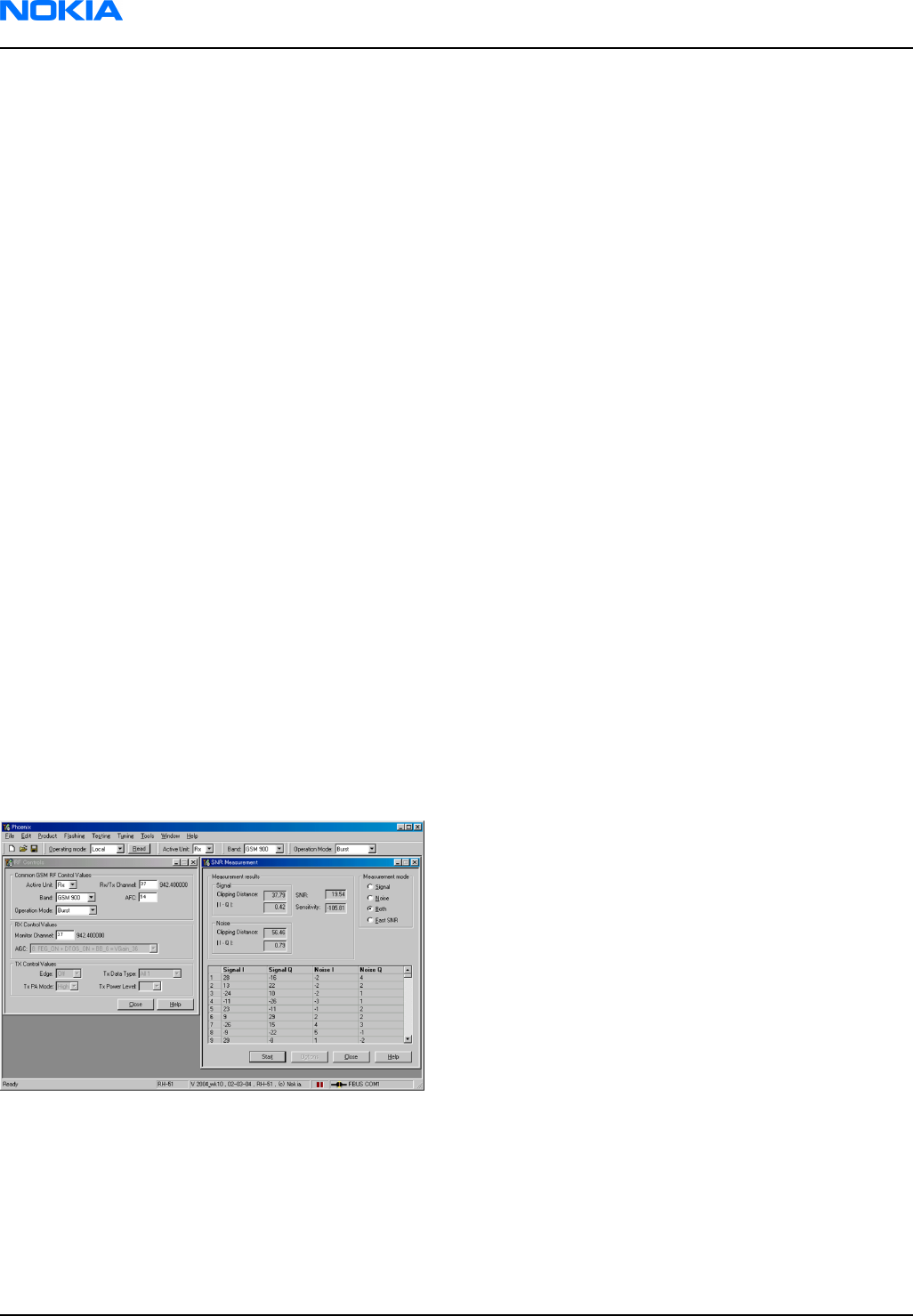
Measuring RX performance using SNR measurement
Context
Note: This measurement also provides an indication of the conducted sensitivity.
Steps
1. Start Phoenix Service Software
2. Establish connection to the phone.
From the File menu, choose "Open Product".
From the list, select RM-25.
3. From the Testing menu, choose RF Controls.
4. In the RF Controls window:
i Select Band: GSM900/GSM1800/GSM1900
ii Set Active unit to RX.
iii Set Operation mode to Burst
iv Set Rx/Tx channel in the following way: EGSM900: 37, GSM1800: 700 and GSM1900: 661
5. From the testing menu (T) select SNR measurement (M). Then select Both.
6. Choose respective band, EGSM900, GSM1800 or GSM1900.
Press Start.
7. Follow the instructions for Signal generator set-up in the pop-up window.
Press OK.
Results
Read the SNR result. SNR should be > 18dB.
Check the sensitivity value.
The set-up should now look like this (the pop-up window also included in the picture for reference):
Measuring Rx module manually using oscilloscope and spectrum analyzer (EGSM900)
Context
Spectrum analyzer level values depend on the probe type and should be validated using a known good sample.
The levels that are given here are measured using a high frequency probe.
Measuring with an oscilloscope at test points RXI (J730) or RXQ (J731) ) and RXID (J261) or RXQD (J262) is
recommended only if RSSI reading does not provide enough information.
RM-25
Nokia Customer Care RF troubleshooting
Page 7–10 Company Confidential 9235618 (Issue 2)
Copyright ©2005 Nokia. All Rights Reserved.

Steps
1. Start Phoenix Service software.
2. Establish connection to the phone.
From the File menu, choose Open Product.
From the list, choose RM-25.
3. From the Testing menu, choose RF Controls.
4. In the RF Controls window:
i Select Band EGSM900.
ii Set Active unit to RX.
iii Set Operation mode to Continuous.
iv Set RX/TX channel to 37.
v Set AGC to 12.
Set the frequency and level of the signal generator to 942.4677MHz and -60dBm.
Note: Because DC compensation does not work during continuous mode, DC offset level at RXI and
RXQ will gradually shift from the optimized level.
To have the most reliable result, it is highly advisable to set the operation mode from burst to
continuous just before measuring values and complete measurement within no longer than 30
seconds.
RM-25
RF troubleshooting Nokia Customer Care
9235618 (Issue 2) Company Confidential Page 7–11
Copyright ©2005 Nokia. All Rights Reserved.
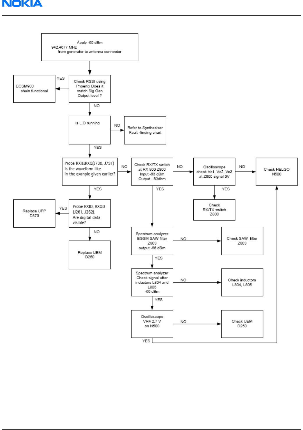
Figure 111 Troubleshooting flowchart for EGSM900
RM-25
Nokia Customer Care RF troubleshooting
Page 7–12 Company Confidential 9235618 (Issue 2)
Copyright ©2005 Nokia. All Rights Reserved.
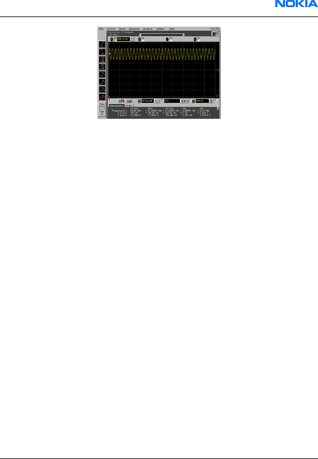
Figure 112 Probed Rx I/Q signals J730, J731
• Signal amplitude: 180 ~ 600mVpp
• DC offset: 1.2 ~ 1.4V
• Frequency: approximately 67KHz
Measuring Rx module manually using oscilloscope and spectrum analyzer (GSM1800)
Context
Spectrum analyzer level values depend on the probe type and should be validated using a known good sample.
The levels that are given here are measured using a high frequency probe.
Measuring with an oscilloscope at test points RXI (730) or RXQ (J731) ) and RXID (J261) or RXQD (J262) is
recommended only if RSSI reading does not provide enough information.
Steps
1. Start Phoenix Service software.
2. Establish connection to the phone.
From the File menu, choose Open Product.
From the list, choose RM-25.
3. From the Testing menu, choose RF Controls.
4. In the RF Controls window:
i Select Band GSM1800.
ii Set Active unit to Rx.
iii Set Operation mode to Continuous.
iv Set RX/TX channel to 700.
v Set AGC to 12.
The frequency or level of signal generator is 1842.8677MHz, -60dBm.
Note: Because DC compensation does not work during continuous mode, DC offset level at RXI and
RXQ will gradually shift from the optimized level.
To have the most reliable result, it is highly advisable to set the operation mode from burst to
continuous just before measuring values and complete measurement within no longer than 30
seconds.
RM-25
RF troubleshooting Nokia Customer Care
9235618 (Issue 2) Company Confidential Page 7–13
Copyright ©2005 Nokia. All Rights Reserved.
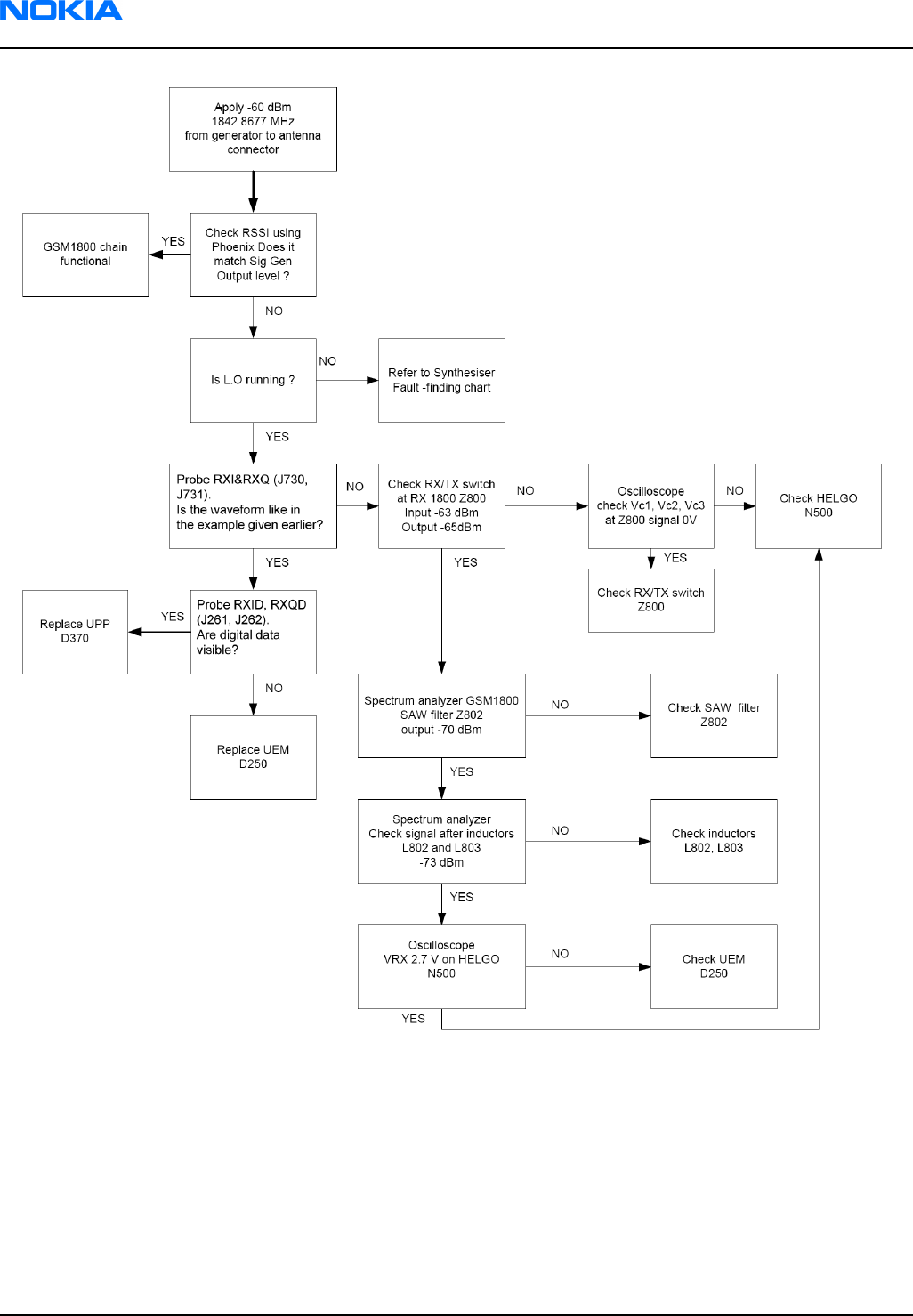
Figure 113 Troubleshooting flowchart for EGSM1800
Measuring Rx module manually using oscilloscope and spectrum analyzer (GSM1900)
Context
Spectrum analyzer level values depend on the probe type and should be validated using a known good sample.
The levels that are given here are measured using a high frequency probe.
Measuring with an oscilloscope at test points RXI (J827) or RXQ (J828) ) and RXID (J261) or RXQD (J262) is
recommended only if RSSI reading does not provide enough information.
RM-25
Nokia Customer Care RF troubleshooting
Page 7–14 Company Confidential 9235618 (Issue 2)
Copyright ©2005 Nokia. All Rights Reserved.

Steps
1. Start Phoenix Service software.
2. Establish connection to the phone.
From the File menu, choose Open Product.
From the list, choose RM-25.
3. From the Testing menu, choose RF Controls.
4. In the RF Controls window:
i Select Band GSM1900.
ii Set Active unit to Rx.
iii Set Operation mode to Continuous.
iv Set RX/TX channel to 661.
v Set AGC to 12.
The frequency or level of signal generator is 1960.0677MHz, -60dBm.
Note: Because DC compensation does not work during continuous mode, DC offset level at RXI and
RXQ will gradually shift from the optimized level.
To have the most reliable result, it is highly advisable to set the operation mode from burst to
continuous just before measuring values and complete measurement within no longer than 30
seconds.
RM-25
RF troubleshooting Nokia Customer Care
9235618 (Issue 2) Company Confidential Page 7–15
Copyright ©2005 Nokia. All Rights Reserved.
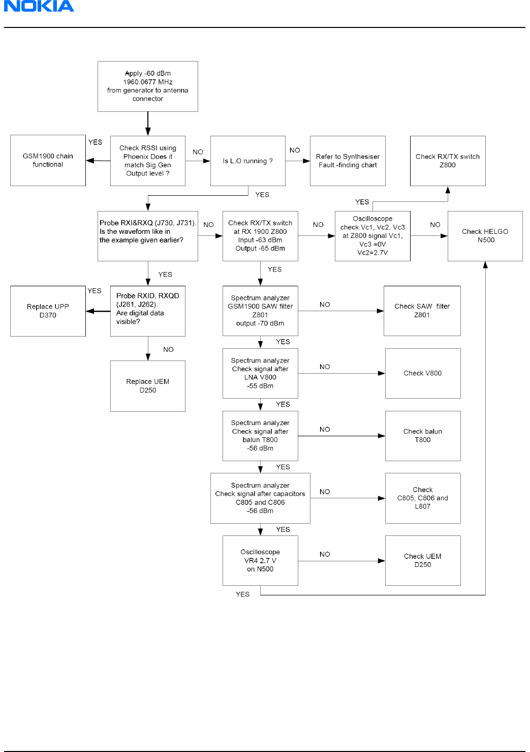
Figure 114 Troubleshooting flowchart for EGSM1900
RM-25
Nokia Customer Care RF troubleshooting
Page 7–16 Company Confidential 9235618 (Issue 2)
Copyright ©2005 Nokia. All Rights Reserved.
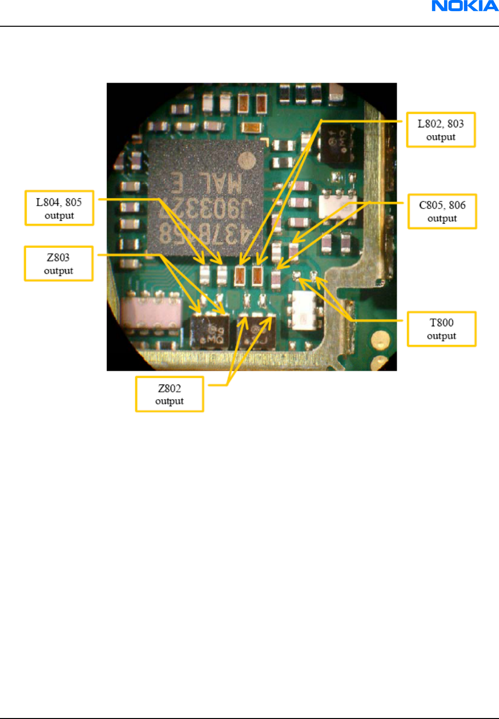
RM-25 measurement points in the receiver
Figure 115 Measurement points at RX frontend - part 1
RM-25
RF troubleshooting Nokia Customer Care
9235618 (Issue 2) Company Confidential Page 7–17
Copyright ©2005 Nokia. All Rights Reserved.
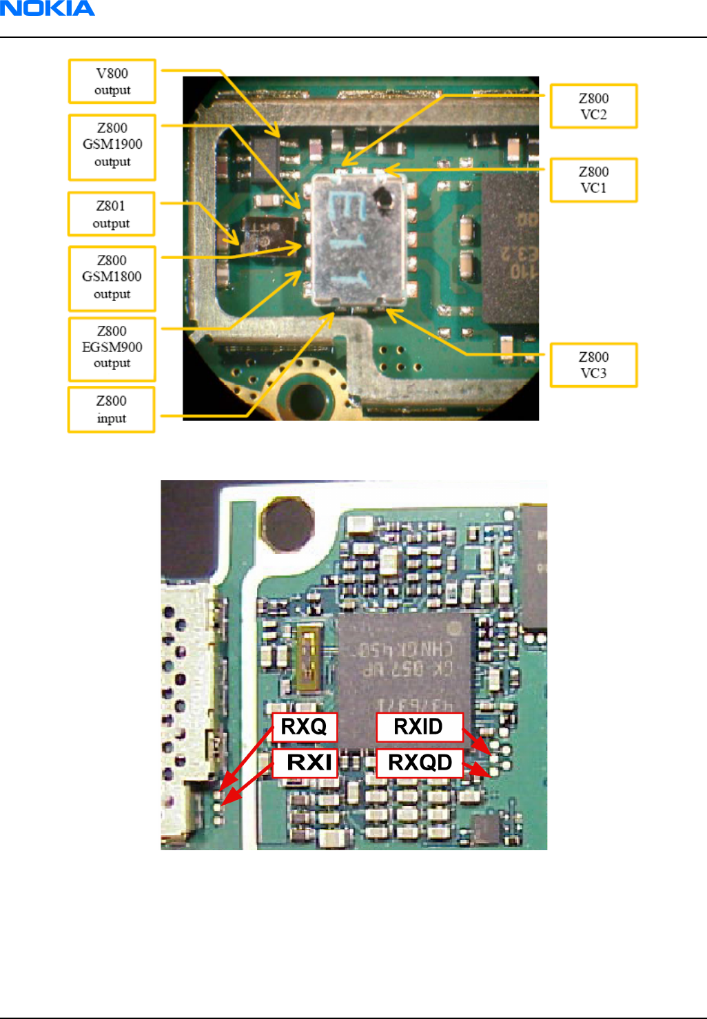
Figure 116 Measurement points at RX frontend - part 2
Figure 117 Measurement points at baseband and digital IQs
Calibrating RX Channel Select Filter
Context
This calibration is for the baseband filter inside Helgo ASIC. The calibration is done by internally measuring a
prototype filter. For this reason, the calibration is done only once, not separately for 3 bands.
RM-25
Nokia Customer Care RF troubleshooting
Page 7–18 Company Confidential 9235618 (Issue 2)
Copyright ©2005 Nokia. All Rights Reserved.
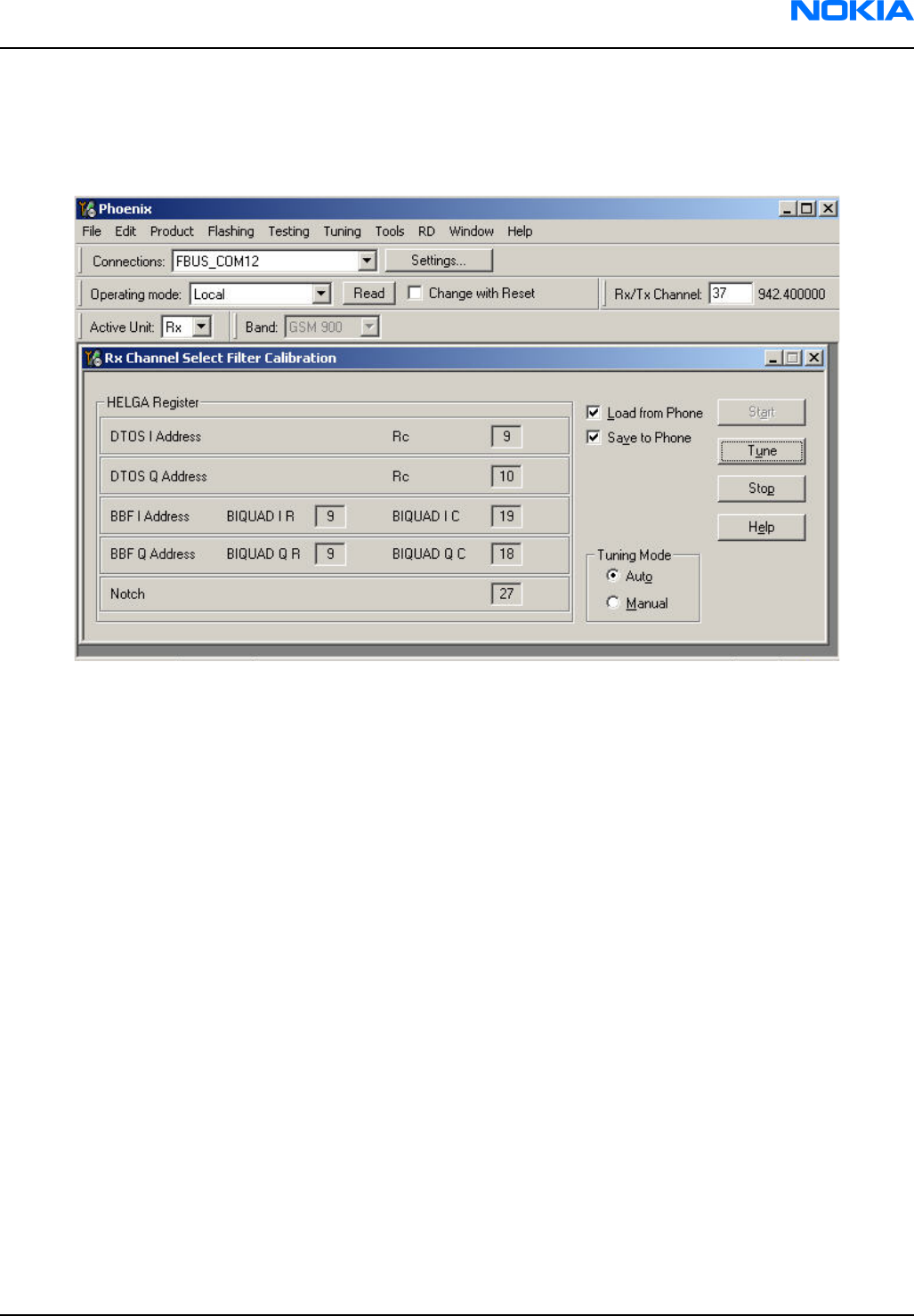
This tuning doesn’t require RF input from an external signal generator.
Steps
1. Select Tuning -> RX Channel Select Filter Calibration
Figure 118 RX Channel Select Filter Calibration
i Check Save to Phone
ii Press Tune
iii Press Stop to store the data to the phone
Results
RX channel select filter calibration is finished.
Calibrating RX
Context
RX calibration is used to determine gain at different gain settings for front-end and the Helgo ASIC and it needs
to be done in all three bands.
RX calibration requires an external signal generator.
Steps
1. Select Tuning -> RX calibration
RM-25
RF troubleshooting Nokia Customer Care
9235618 (Issue 2) Company Confidential Page 7–19
Copyright ©2005 Nokia. All Rights Reserved.
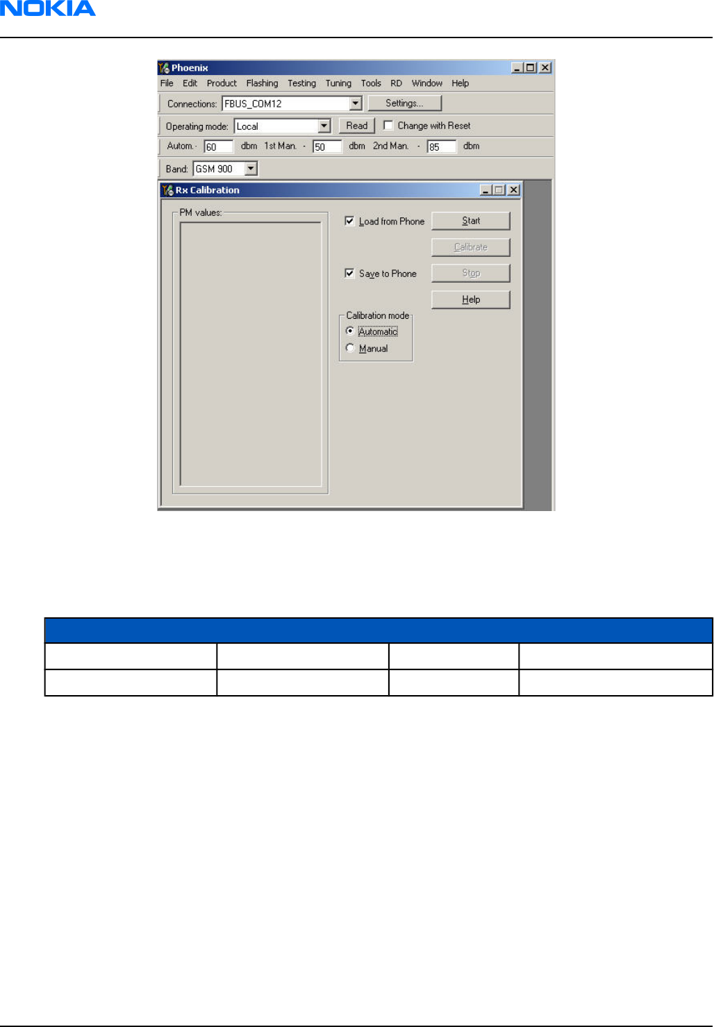
Figure 119 RX calibration (Example)
i Make sure you have made the following settings:
Table 25 RX calibration settings
Band Calibration mode 1st Manual [dbm] 2nd Manual [dbm]
GSM 900 Automatic -50 -85
GSM 1800/1900 Automatic -50 -85
ii Check Load from phone and Save to phone.
iii Press Start
Initial data will be loaded from the phone and calibration starts.
The following banner pops up:
RM-25
Nokia Customer Care RF troubleshooting
Page 7–20 Company Confidential 9235618 (Issue 2)
Copyright ©2005 Nokia. All Rights Reserved.

Figure 120 RX calibration with band EGSM900 (Example)
iv Follow the instructions in the pop–up window and set frequency and level of the signal generator.
v Press OK
vi Press “Save & Continue”
Figure 121 RX calibration values (Example)
Results
Calibration data will be stored to the phone.
Next action
Continue to next band.
RM-25
RF troubleshooting Nokia Customer Care
9235618 (Issue 2) Company Confidential Page 7–21
Copyright ©2005 Nokia. All Rights Reserved.
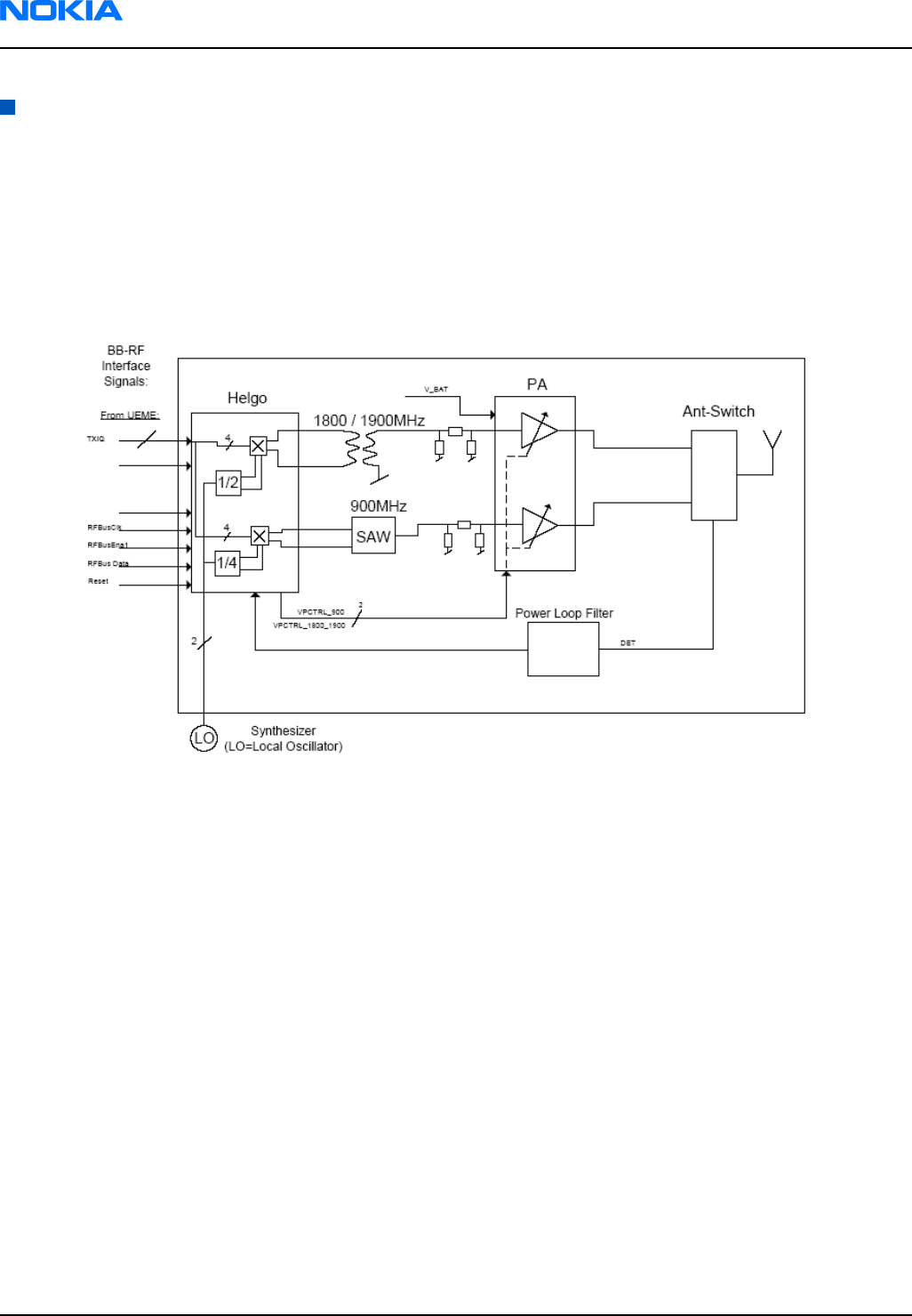
Transmitter
Introduction to RM-25 transmitter troubleshooting
A simple block diagram of the TX part of the phone is shown in the following figure. The voice or data signals
to be transmitted come from the UEME IC in the BB (baseband) area, and go to the Helgo IC, where they are up-
converted to RF. The TX signals going from UEME to Helgo are called the IQ-signals, and consist of two balanced
signals {TXIN, TXIP} and {TXQN, TXQP}, i.e. a total of four signal lines. In addition to the IQ signals, there are also
control signals going between BB and RF.
Figure 122 TX RF block diagram
The following picture shows the two shielding cans where the TX circuitry is located (the lids have been
removed). The upper shielding can contains BB-RF interface circuitry, the Helgo RF system IC, a SAW filter for
the GSM/EGSM band, and a balun for the DCS/PCS band. The lower shielding can contains the power amplifier
(PA) and the antenna switch module (ASM).
RM-25
Nokia Customer Care RF troubleshooting
Page 7–22 Company Confidential 9235618 (Issue 2)
Copyright ©2005 Nokia. All Rights Reserved.
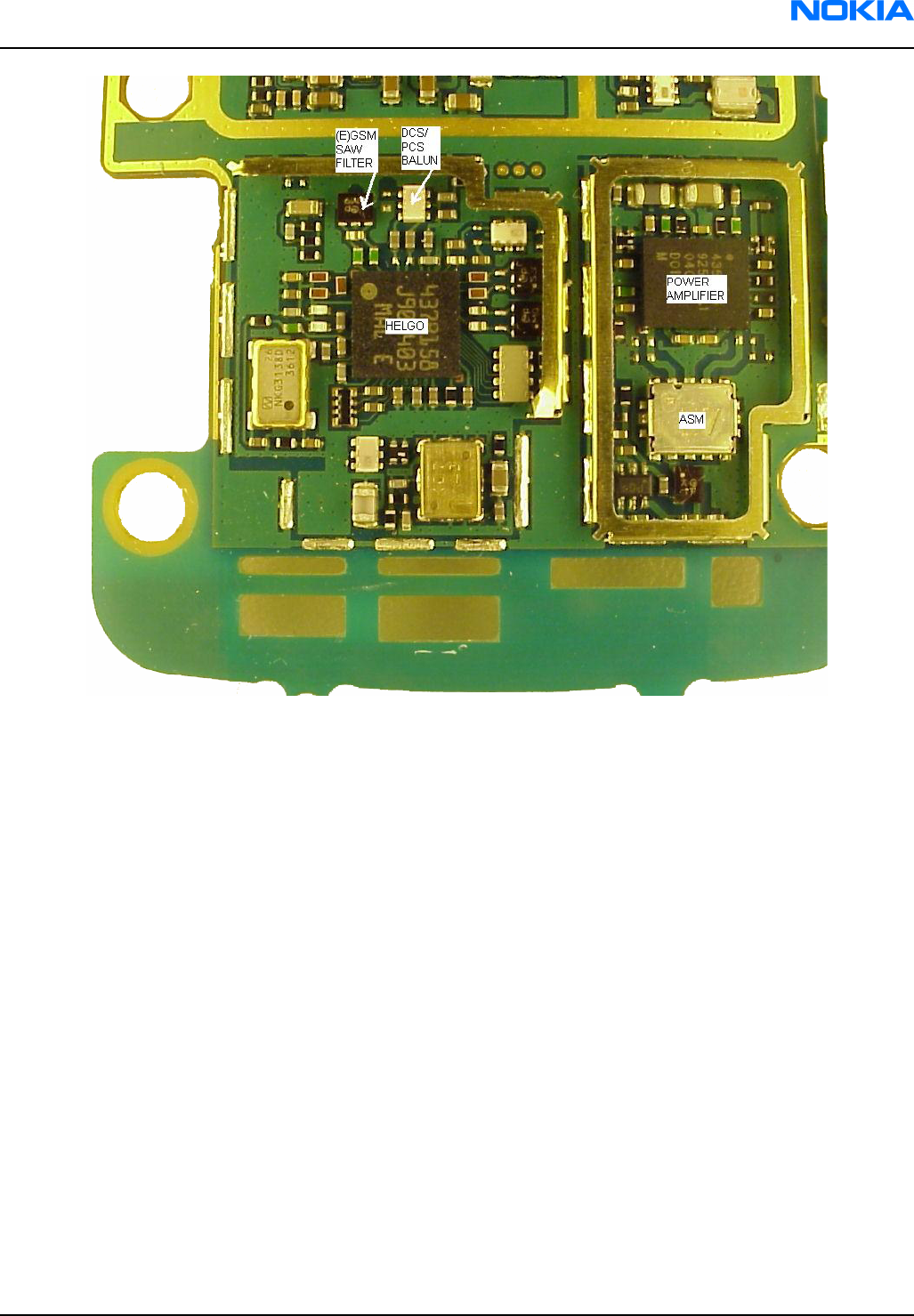
Figure 123 Upper and lower shielding cans
Preparing for transmitter troubleshooting
Steps
1. Place the phone (mechanics removed) on module jig.
2. Connect the module jig to PC via a DAU-9P cable.
3. Connect the module jig to a power supply (4.2V).
4. Connect the RF output to a spectrum analyzer or another measurement instrument. Use a 10dB attenuator
at the input to spectrum analyzer to avoid damaging it.
5. Make sure the dongle is connected and start Phoenix.
6. In Phoenix, choose: File -> Open Product -> RM-25 Product Menu.
7. Select Testing -> RF Controls.
8. In the toolbar: set Operating Mode to Local.
9. Select Band: GSM900, GSM1800 or GSM1900.
10. Set Operation Mode to Burst.
11. Set Active Unit to Tx.
12. Set Tx Data Type to All 1.
13. Set Rx/Tx Channel to 37 for GSM900, 700 for GSM1800, or 661 for GSM1900.
14. Set Tx PA Mode to Free.
15. Set Tx Power Level to 5 for GSM900, otherwise to 0.
RM-25
RF troubleshooting Nokia Customer Care
9235618 (Issue 2) Company Confidential Page 7–23
Copyright ©2005 Nokia. All Rights Reserved.
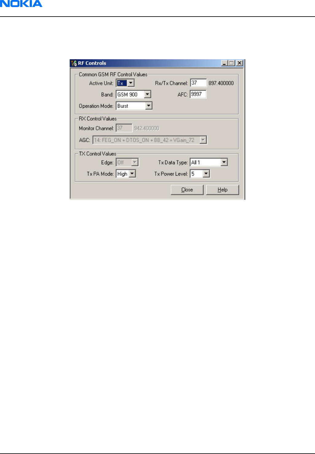
Results
Phoenix should now look like this:
Figure 124 Preparing for transmitter troubleshooting
RM-25
Nokia Customer Care RF troubleshooting
Page 7–24 Company Confidential 9235618 (Issue 2)
Copyright ©2005 Nokia. All Rights Reserved.

Troubleshooting TX-BB interface and control signals
Figure 125 TX-BB interface troubleshooting and control signals
RM-25
RF troubleshooting Nokia Customer Care
9235618 (Issue 2) Company Confidential Page 7–25
Copyright ©2005 Nokia. All Rights Reserved.
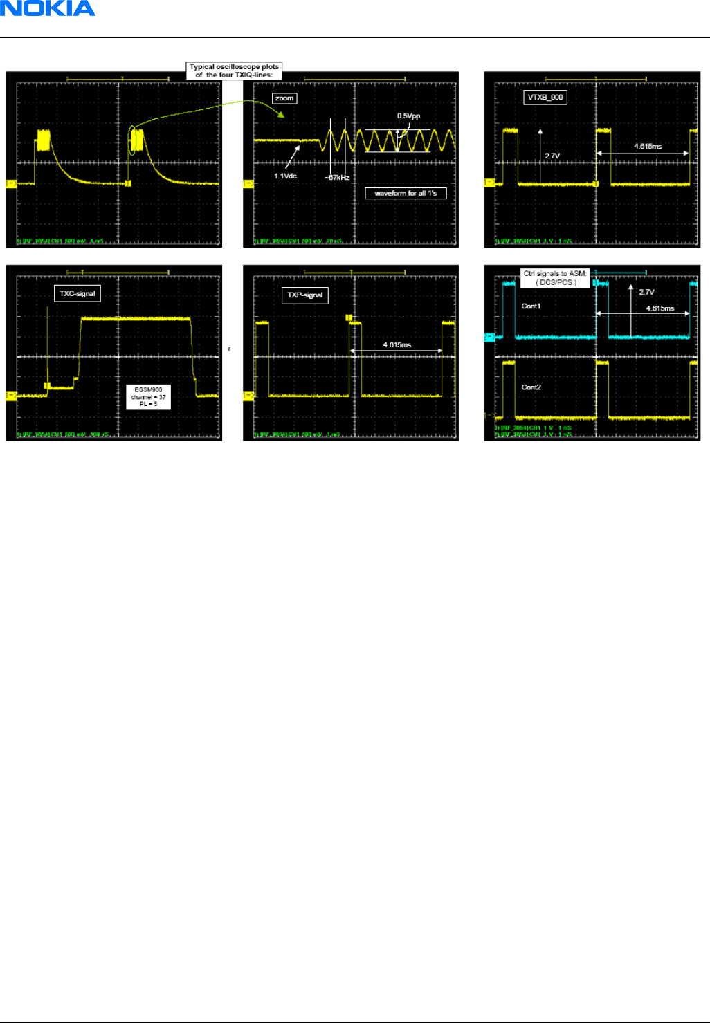
Figure 126 Oscilloscope screen shots
RM-25
Nokia Customer Care RF troubleshooting
Page 7–26 Company Confidential 9235618 (Issue 2)
Copyright ©2005 Nokia. All Rights Reserved.

Troubleshooting RF side of transmitter
Figure 127 RF side of transmitter troubleshooting
RM-25
RF troubleshooting Nokia Customer Care
9235618 (Issue 2) Company Confidential Page 7–27
Copyright ©2005 Nokia. All Rights Reserved.
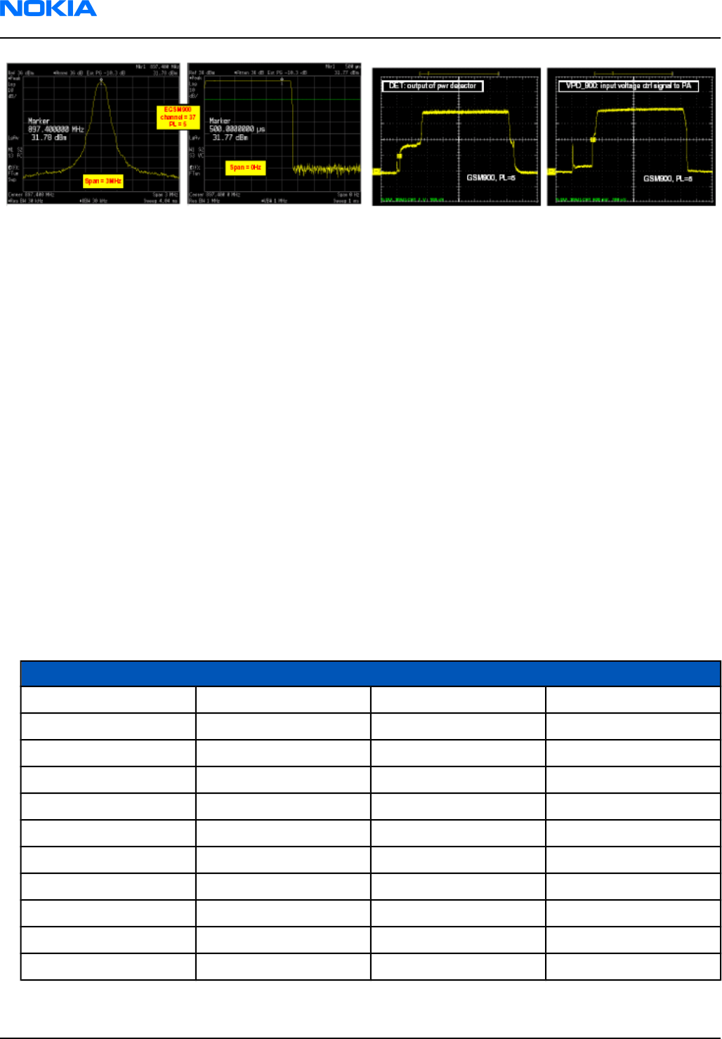
Figure 128 Oscilloscope screen shots (RF)
Introduction to transmitter tuning
In the transmitter, there are two kinds of tunings that can be done: IQ tuning and power level tuning. In general,
different repairs require different tunings. In order to decide which tuning is necessary after a repair, it is
important to understand the functionality of the repaired circuit. In general, it is recommended that if any TX
component is changed, both these tunings be done. All tunings are done in local mode using Phoenix to control
the phone.
As the RM-25 doesn’t support the EDGE feature, you don’t need to consider operating/tuning the phones in EDGE
mode although Phoenix sometimes has a control selection box to enable EDGE.
Tuning TX/IQ
Context
The tuning must be carried out in all three bands. In addition to Phoenix, a spectrum analyzer (SA) is needed.
Steps
1. Connect the spectrum analyzer (SA) to the RF connector of the module jig. The settings of the SA will depend
on the band to be tuned. The following table summarizes the settings for each of the three bands.
Table 26 Spectrum analyzer settings
GSM900 GSM1800 GSM1900
Center frequency 897.4MHz 1747.8MHz 1880MHz
Frequency span 300kHz 300kHz 300kHz
Resolution Bandwidth 3kHz 3kHz 3kHz
Video Bandwidth 3kHz 3kHz 3kHz
Sweep Time 3 sec 3 sec 3 sec
Trace Type Clear/Write Clear/Write Clear/Write
Detector Type Max Peak Max Peak Max Peak
Reference Level 35dBm 35dBm 35dBm
Marker 1 897.33229 MHz 1747.73229 MHz 1879.93229 MHz
Marker 2 897.4MHz 1747.8MHz 1880MHz
Marker 3 897.46771MHz 1747.86771MHz 1880.06771MHz
2. Open the following two windows in Phoenix:
RM-25
Nokia Customer Care RF troubleshooting
Page 7–28 Company Confidential 9235618 (Issue 2)
Copyright ©2005 Nokia. All Rights Reserved.
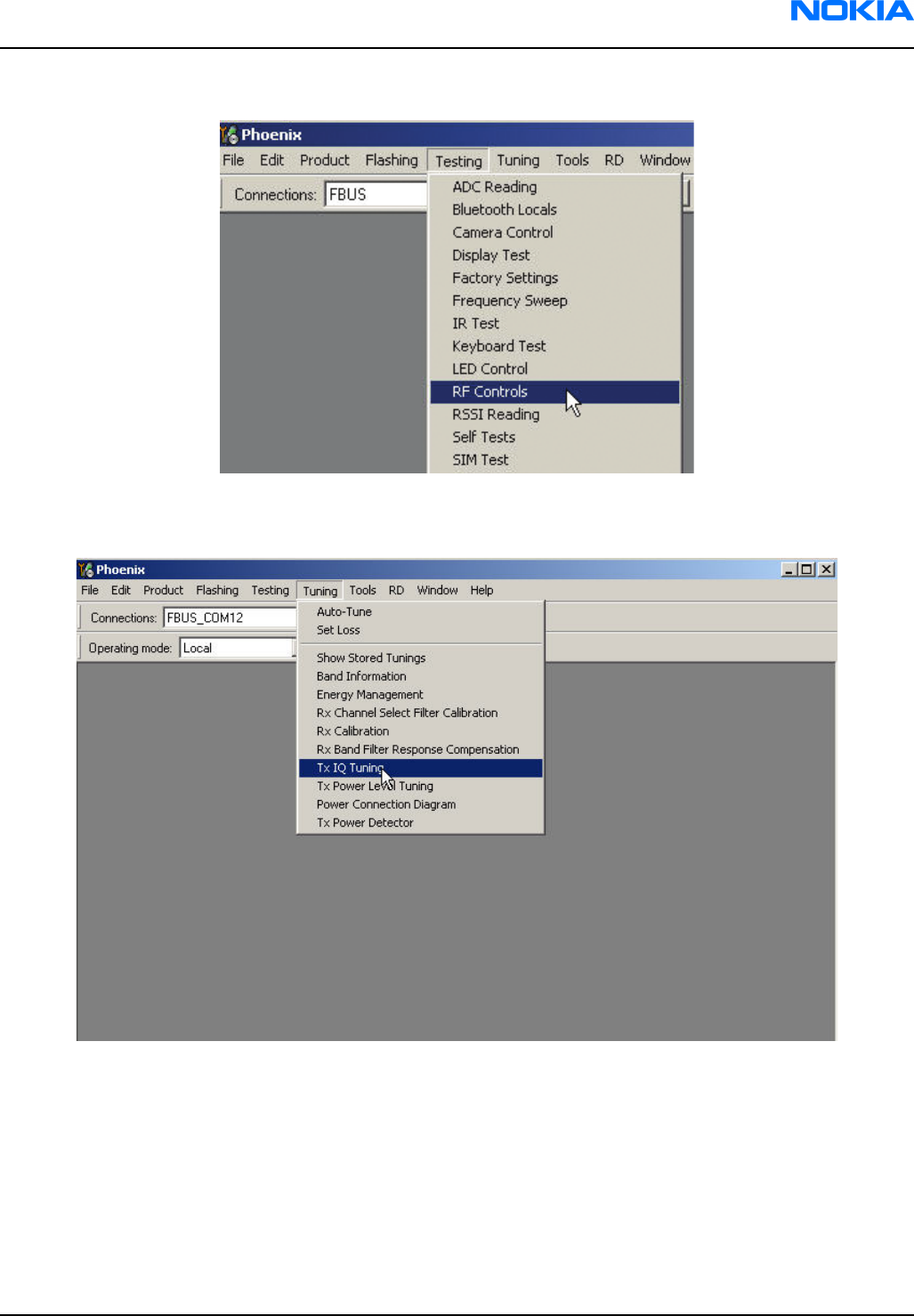
i select Testing -> RF Controls
Figure 129 RF controls
ii select Tuning -> TX IQ Tuning.
Figure 130 Tx IQ tuning
After opening the two windows, Phoenix should look like this:
RM-25
RF troubleshooting Nokia Customer Care
9235618 (Issue 2) Company Confidential Page 7–29
Copyright ©2005 Nokia. All Rights Reserved.
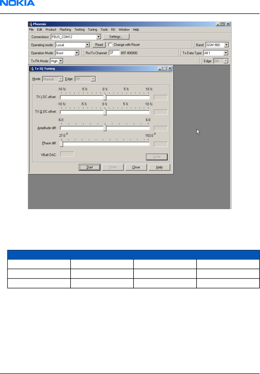
Figure 131 Phoenix set-up (Tx IQ Tuning windows)
3. Select correct settings for the band you are tuning. The following table summarises the settings of the RF
control window for IQ tuning of the three bands.
Table 27 RF Control window settings
Band TX Data Type TX Power Level RX/TX Channel
GSM900 All 1 5 37
GSM1800 All 1 0 700
GSM1900 All 1 0 661
4. Start IQ tuning by pressing Start button in the TX IQ Tuning window.
The purpose of this tuning is to reduce the frequency components at marker 2 (carrier leakage) and marker
3 (+67kHz/upper sideband) as much as possible.
RM-25
Nokia Customer Care RF troubleshooting
Page 7–30 Company Confidential 9235618 (Issue 2)
Copyright ©2005 Nokia. All Rights Reserved.
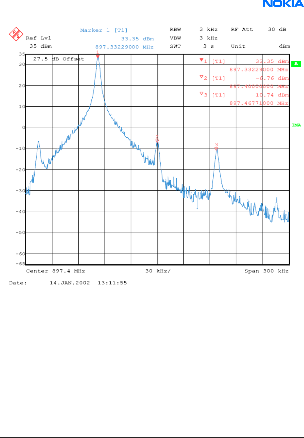
Figure 132 Spectrum analyzer screen shot when performing IQ tuning, part 1
5. Adjust the ‘TXI DC Offset’ and the ‘TXQ DC Offset’ buttons in the TX IQ Tuning window so that the carrier level
(marker 2) reaches a minimum.
After this adjustment is done, the carrier (marker 2) should be at least 40dB below the lower side band
(marker 1).
6. Use the ‘Amplitude difference’ and the ‘Phase difference’ buttons in the TX IQ Tuning window to adjust the
upper side band (marker 3) to a minimum.
Now, marker 3 should also be at least 40dB below marker 1.
At this point, the spectrum analyzer screen should look similar to that of the figure below.
RM-25
RF troubleshooting Nokia Customer Care
9235618 (Issue 2) Company Confidential Page 7–31
Copyright ©2005 Nokia. All Rights Reserved.
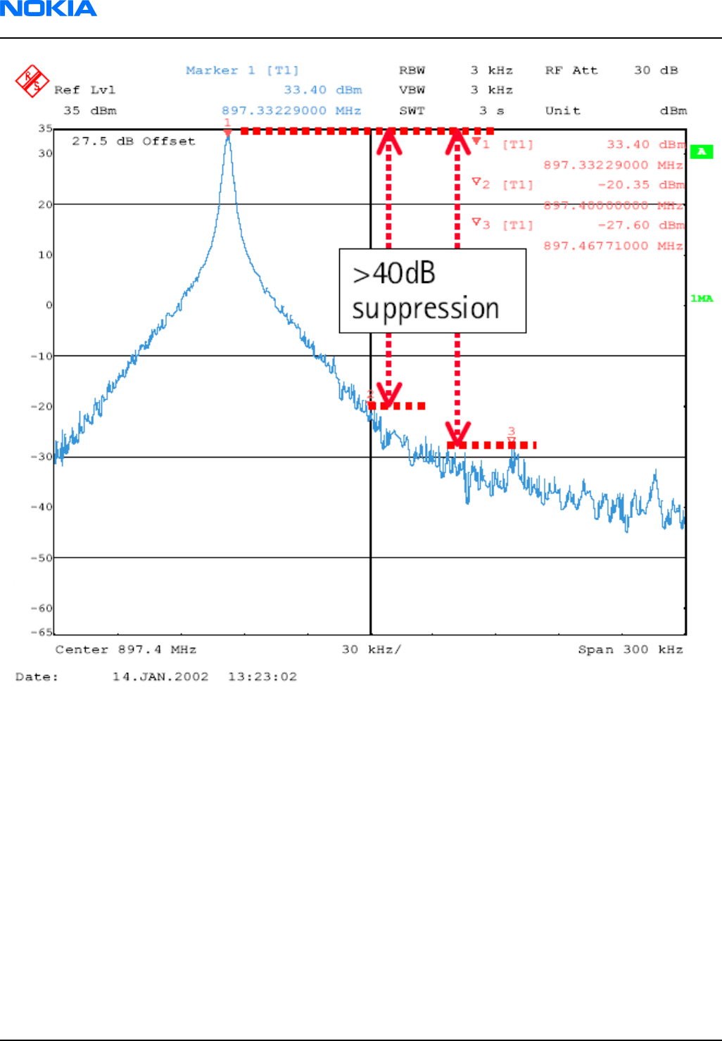
Figure 133 Spectrum analyzer screen shot when performing IQ tuning, part 2
7. After reducing the amplitude of the frequency components at marker 2 and 3 to a minimum, press Save &
Continue.
The EGSM tuning has now been completed.
Next action
Now, using the spectrum analyzer settings listed in Table “Spectrum analyzer settings” and the RF control
settings listed in Table “RF Control window settings”, follow exactly the same procedure to perform IQ tuning
in the GSM1800 and GSM1900 bands.
Tuning TX power level
Context
This tuning is done separately in all three bands, and requires a spectrum analyzer to measure the burst power
of the GSM RF signal. When measuring the RF output (burst) power on a spectrum analyzer, use the settings
found in the following table:
RM-25
Nokia Customer Care RF troubleshooting
Page 7–32 Company Confidential 9235618 (Issue 2)
Copyright ©2005 Nokia. All Rights Reserved.
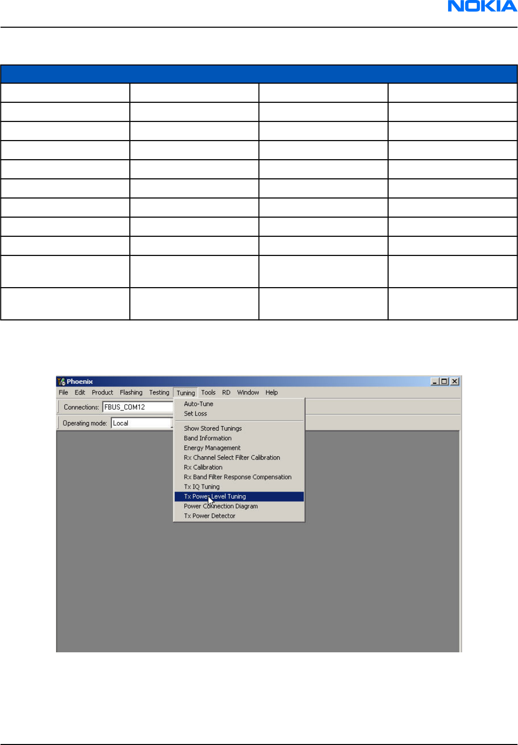
Table 28 Spectrum analyzer settings for Tx power level tuning
GSM900 GSM1800 GSM1900
Center frequency 897.4MHz 1747.8MHz 1880MHz
Frequency span Zero-span Zero-span Zero-span
Resolution Bandwidth 1MHz 1MHz 1MHz
Video Bandwidth 1MHz 1MHz 1MHz
Sweep Time 1ms 1ms 1ms
Trigger Type Video Video Video
Video trigger level Target pwr – 10dB Target pwr – 10dB Target pwr – 10dB
Trace Type Clear/Write Clear/Write Clear/Write
Detector Type Max Peak Max Peak Max Peak
Reference Level Target power level +
10dB
Target power level +
10dB
Target power level +
10dB
Internal Attenuation Target power level +
10dB
Target power level +
10dB
Target power level +
10dB
Steps
1. In Phoenix, select Tuning -> TX Power Level Tuning.
Figure 134 Phoenix menu select (Tx Power Level Tuning menu)
Phoenix should now look similar to the figure below.
RM-25
RF troubleshooting Nokia Customer Care
9235618 (Issue 2) Company Confidential Page 7–33
Copyright ©2005 Nokia. All Rights Reserved.
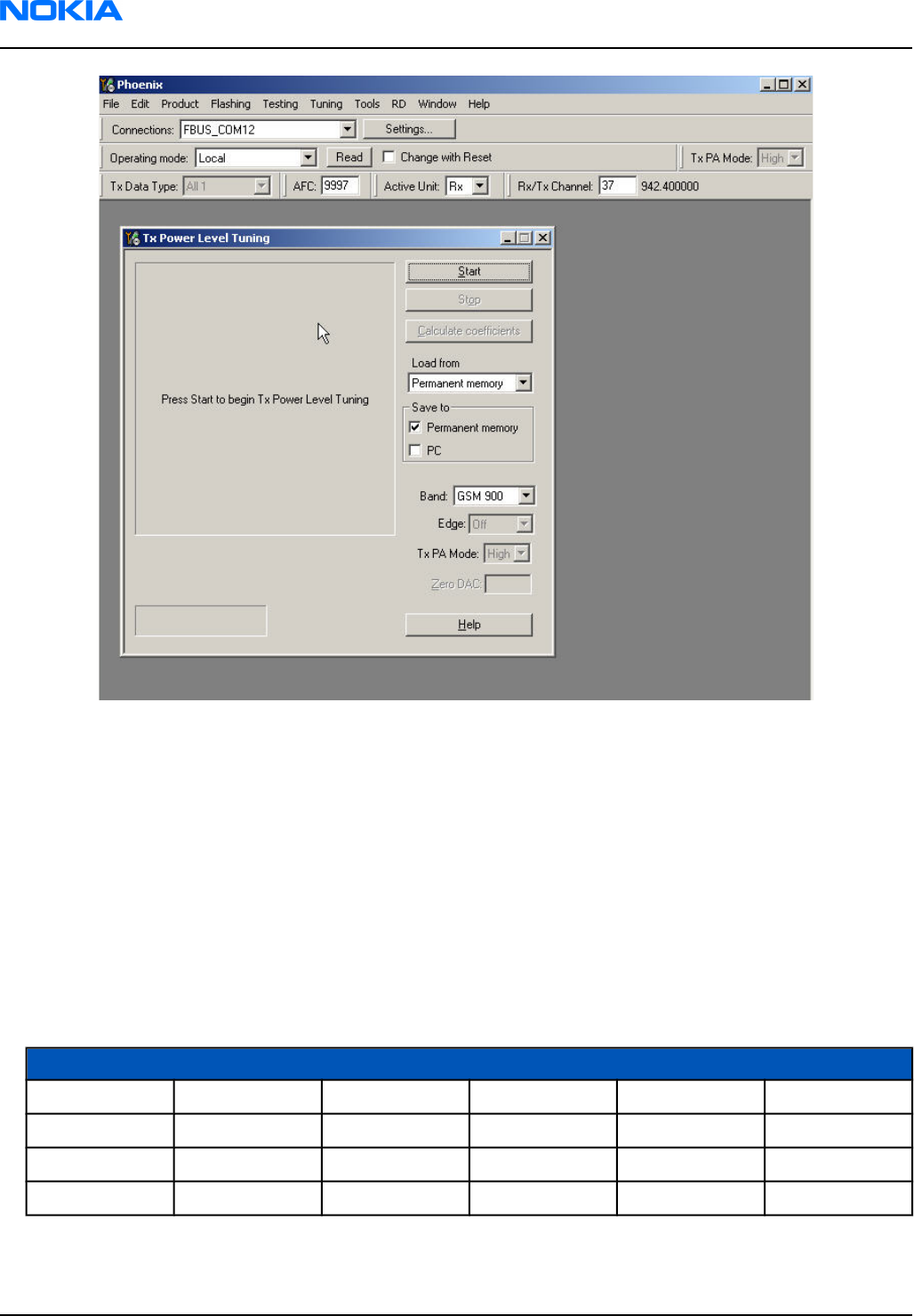
Figure 135 Phoenix Power Level Tuning menu
2. Select data source and band, then press Start. It is recommended to have saved data from a known good
phone to the PC.
3. Connect the module jig RF output to the measurement instrument. The power must be tuned in only high
TX PA mode in all bands of GSM900, GSM1800 and GSM1900.
4. For each band, tune the power by adjusting the coefficient in the Tx Power Level Tuning window in Phoenix
until the target level is reached (measured on the spectrum analyzer). Remember to take into account the
external power loss, that is, the loss of the cable and the external attenuator at the spectrum analyzer input.
The coefficient must be tuned for the base level and other power levels (PL) marked with bold letters in
Phoenix (GSM900: PL19 / 15 / 5, GSM1800/1900: PL15, 11, 0). The target power levels are specified as listed
in the following table:
Table 29 Spectrum analyzer settings for Tx level tuning
GSM900 GSM1800 GSM1900
PL 5 32.5 dBm PL 0 29.5 dBm PL 0 29.5 dBm
PL 15 13.0 dBm PL 11 8.0 dBm PL 11 8. 0dBm
PL 19 5.0 dBm PL 15 0.0 dBm PL 15 0.0 dBm
Base PL -30.0 dBm Base PL -30.0 dBm Base PL -30.0 dBm
5. When the tuning for the levels marked with bold letters has been completed, press Calculate coefficients to
calculate the other power levels with non-bold letters.
RM-25
Nokia Customer Care RF troubleshooting
Page 7–34 Company Confidential 9235618 (Issue 2)
Copyright ©2005 Nokia. All Rights Reserved.
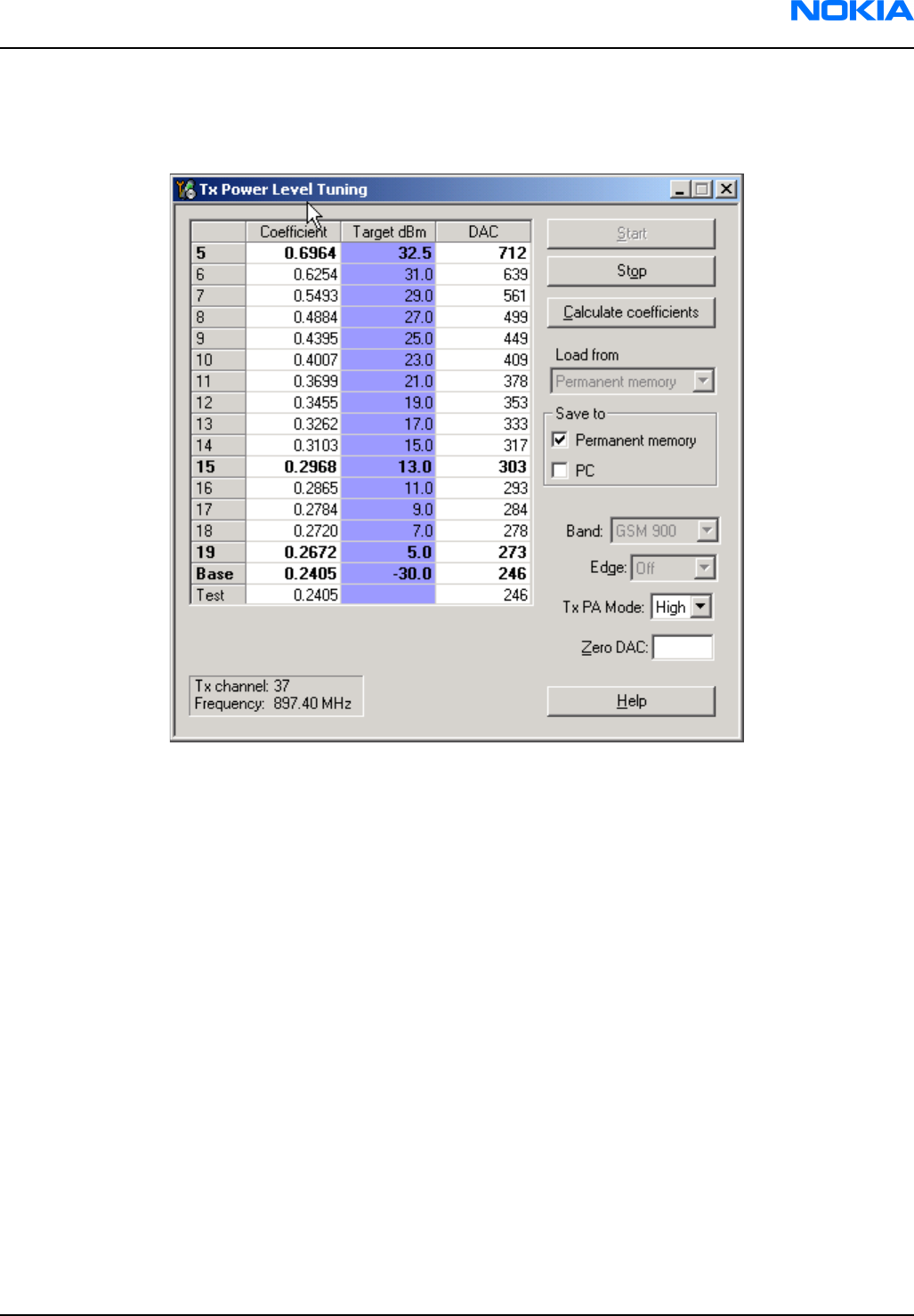
6. When the coefficient calculation has been successfully done, press Save & Continue to save the new tuning
values into the phone memory.
The following figure shows the power level tuning at the GSM900 band.
Figure 136 Phoenix screen shot (Tx Power Level Tuning)
The figure below shows one example from the spectrum analyzer screen during measuring the Tx power
level.
RM-25
RF troubleshooting Nokia Customer Care
9235618 (Issue 2) Company Confidential Page 7–35
Copyright ©2005 Nokia. All Rights Reserved.
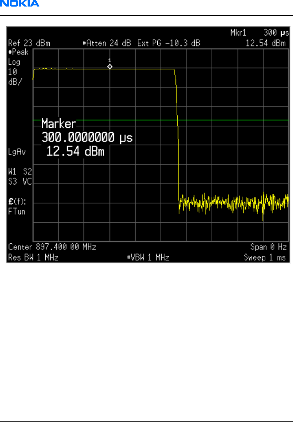
Figure 137 Spectrum analyzer screen shot during power level tuning
RM-25
Nokia Customer Care RF troubleshooting
Page 7–36 Company Confidential 9235618 (Issue 2)
Copyright ©2005 Nokia. All Rights Reserved.
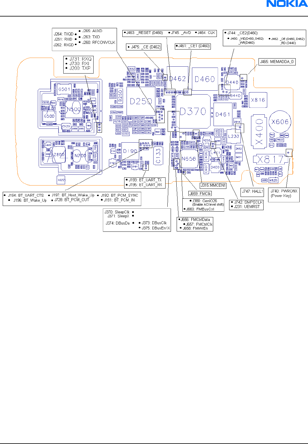
Figure 138 Testpoints of the main board 1fsa_09a, top part
RM-25
RF troubleshooting Nokia Customer Care
9235618 (Issue 2) Company Confidential Page 7–37
Copyright ©2005 Nokia. All Rights Reserved.
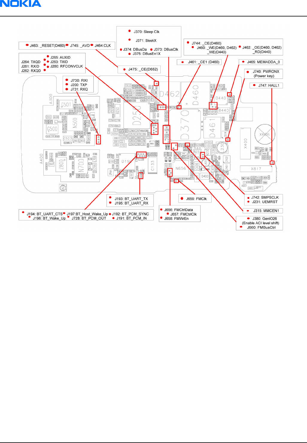
Figure 139 Testpoints of the main board 1fsa_11a, top part
RM-25
Nokia Customer Care RF troubleshooting
Page 7–38 Company Confidential 9235618 (Issue 2)
Copyright ©2005 Nokia. All Rights Reserved.

Figure 140 Testpoints of the main board, bottom part
RM-25
RF troubleshooting Nokia Customer Care
9235618 (Issue 2) Company Confidential Page 7–39
Copyright ©2005 Nokia. All Rights Reserved.
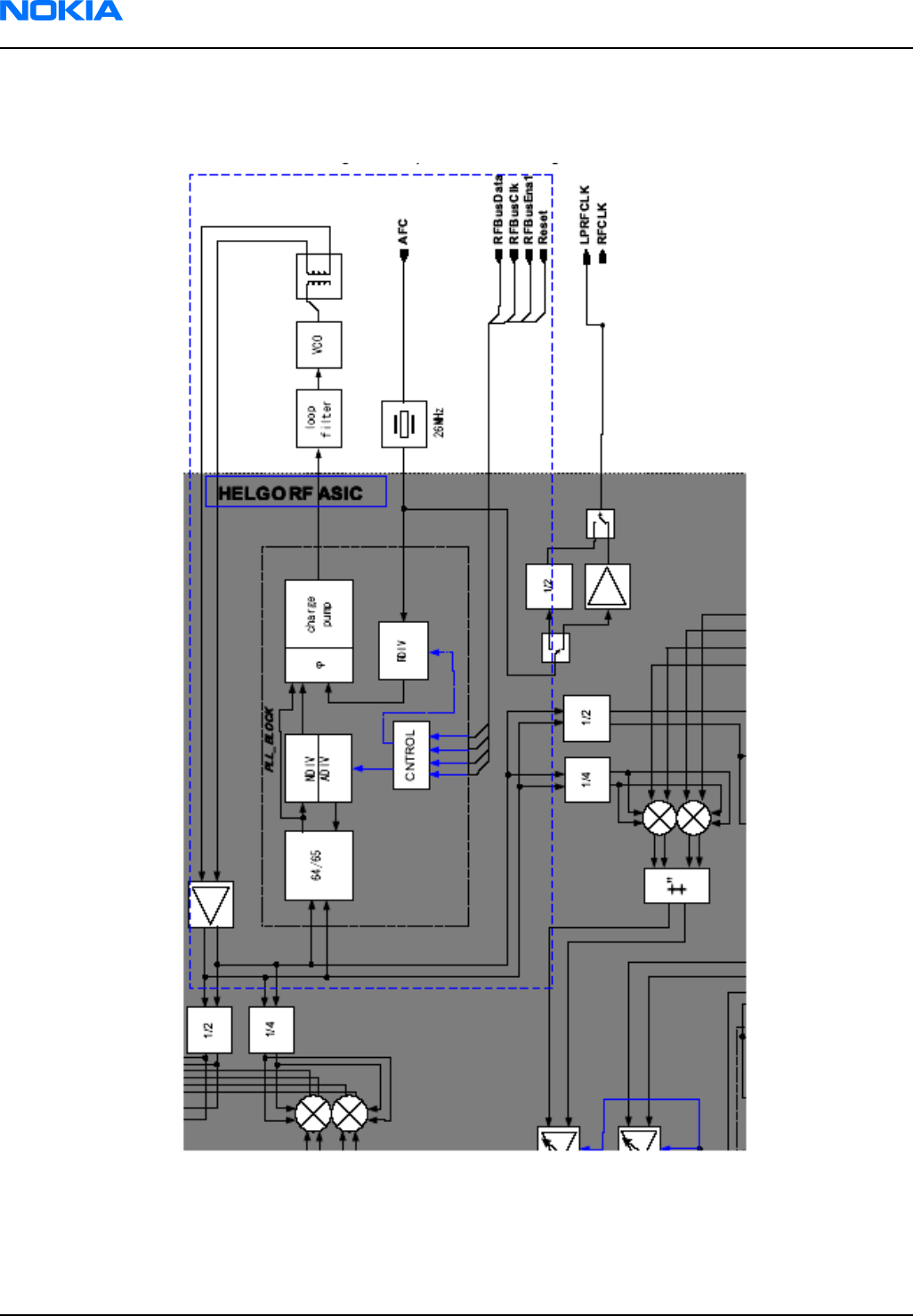
Introduction to synthesizer troubleshooting
Figure 141 Synthesizer block diagram
RM-25
Nokia Customer Care RF troubleshooting
Page 7–40 Company Confidential 9235618 (Issue 2)
Copyright ©2005 Nokia. All Rights Reserved.

The VCO frequency is locked by a PLL (phase locked loop) into a stable frequency source given by a VCTCXO, which
is running at 26 MHz. The frequency of the VCTCXO is in turn locked into the frequency of the base station with
the help of an AFC (automatic frequency control) voltage, which is generated in UEME by an 11-bit D/A (digital-
to-analog) converter.
The PLL is capable of tuning frequency range for GSM bands 900/1800/1900. It is integrated in Helgo and
controlled through the RFBus. The PLL consists of a 64/65 (P/P+1) prescaler, N- and A-divider, reference divider,
phase detector and a charge pump for the external loop filter.
The 4 GHz oscillator signal, generated by the VCO, is fed through a 180 degrees balanced phase shifter to the
prescaler and the output of the prescaler is fed to the N- and A-divider, which produces the input to the phase
detector. The phase detector compares this signal to the reference signal, which is divided by the reference
divider from the VCTCXO frequency.
The frequency of the reference signal is 400 kHz. The output of the phase detector is connected to the charge
pump, which charges or discharges the integrator capacitor in the loop filter depending on the phase of the
measured frequency compared to the reference frequency.
The integrator output voltage is finally connected to the control input of the VCO. The VCO operates at the
channel frequency multiplied by two in GSM1800/1900 and by four in EGSM900.
The required frequency dividers for modulator and demodulator mixers are integrated in Helgo.
Loop filter filters out the comparison pulses of the phase detector and generates a DC control voltage to the
VCO. The loop filter determines the step response of the PLL (settling time) and contributes to the stability of
the loop.
Other filter components are for sideband rejection.
The dividers are controlled via the RFBus. RFBusData is for the data, RFBusClk is a serial clock for the bus and
RFBusEna1X is a latch enable, which stores the new data into the dividers.
Figure 142 Rf key component
RM-25
RF troubleshooting Nokia Customer Care
9235618 (Issue 2) Company Confidential Page 7–41
Copyright ©2005 Nokia. All Rights Reserved.
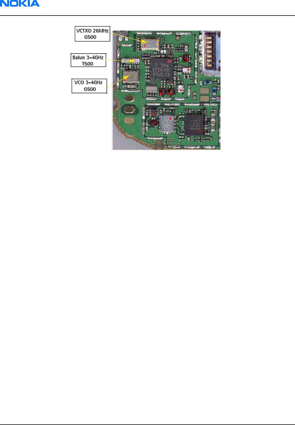
Figure 143 Synthesizer key components without shielding frames
Assumption
• No soldering or component failure for simple SMD components such as resistors, inductors and capacitors
• Failure in one particular operating GSM channel, whether Tx or Rx, in which the synthesizer is the cause of
the failure, causes failure in all other GSM channels in Tx/Rx.
Preparing for synthesizer troubleshooting
Steps
1. Place the phone (mechanics removed) on module jig.
2. Connect the module jig to the PC via a DAU-9P cable.
3. Connect the module jig to a power supply (4.2V).
4. Connect the RF output to a spectrum analyzer or another measurement instrument.
5. Use a 10dB attenuator at the input to spectrum analyzer to avoid damage.
6. Make sure the dongle is connected and start Phoenix.
7. In Phoenix, select File -> Open Product -> RM-25 (Nokia 6260) Product Menu.
8. Select Testing -> RF Controls.
9. In the toolbar: set Operating Mode -> Local.
10. Select Band -> GSM 1800.
11. Set Operation Mode -> Continuous.
12. Set Active Unit -> Rx.
RM-25
Nokia Customer Care RF troubleshooting
Page 7–42 Company Confidential 9235618 (Issue 2)
Copyright ©2005 Nokia. All Rights Reserved.
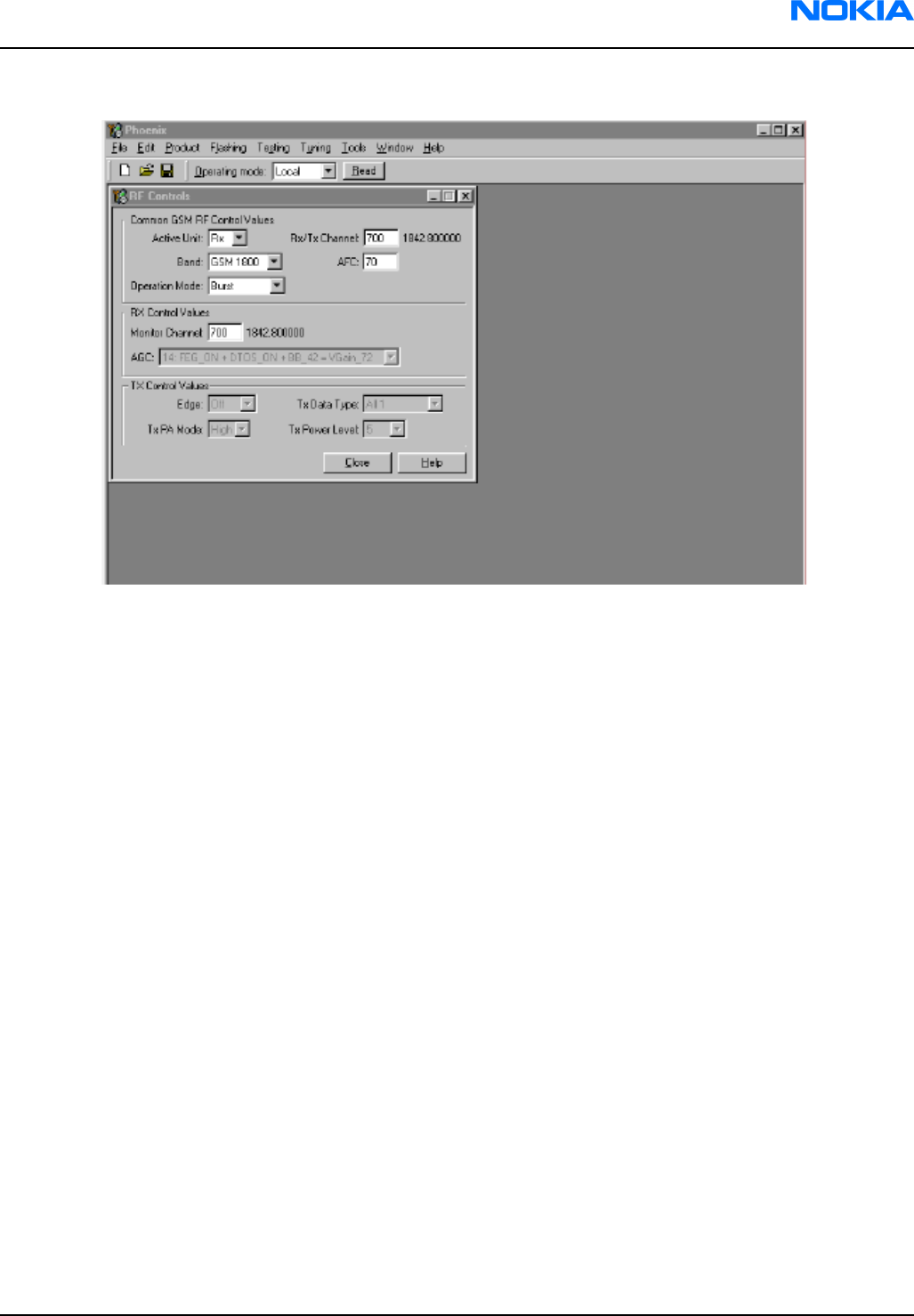
13. Set Rx/Tx Channel -> 700.
Figure 144 Preparation for troubleshooting using Phoenix RF control setup
RM-25
RF troubleshooting Nokia Customer Care
9235618 (Issue 2) Company Confidential Page 7–43
Copyright ©2005 Nokia. All Rights Reserved.
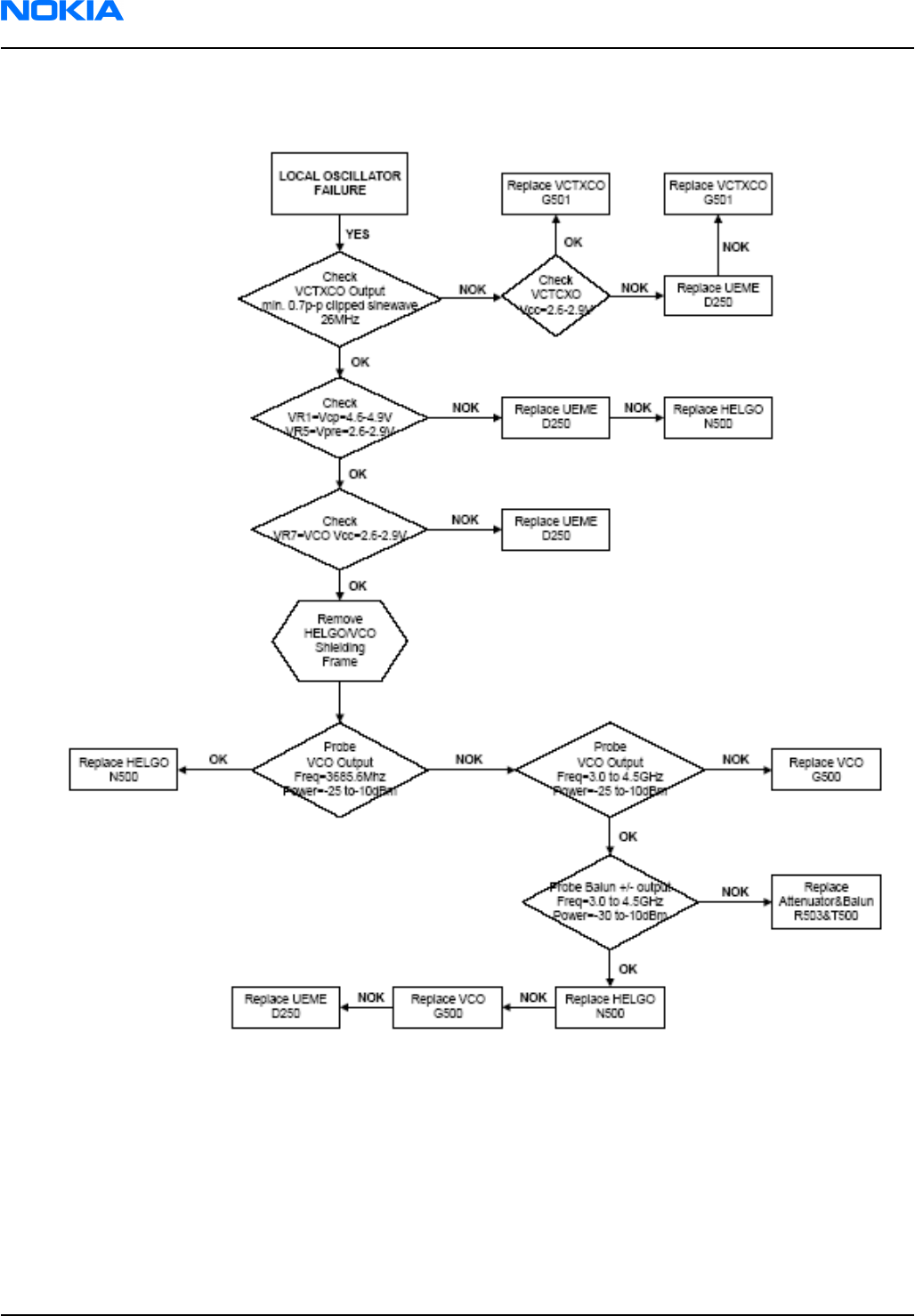
Measuring the synthesizer manually using spectrum analyzer
Figure 145 Troubleshooting chart for synthesizer
Spectrum analyzer level values depend on the probe type and should be validated using a known good sample.
The levels that are given here are measured using a high frequency probe. Spectrum analyzer should be at least
capable of measuring signal upto 4.5 GHz.
RM-25
Nokia Customer Care RF troubleshooting
Page 7–44 Company Confidential 9235618 (Issue 2)
Copyright ©2005 Nokia. All Rights Reserved.
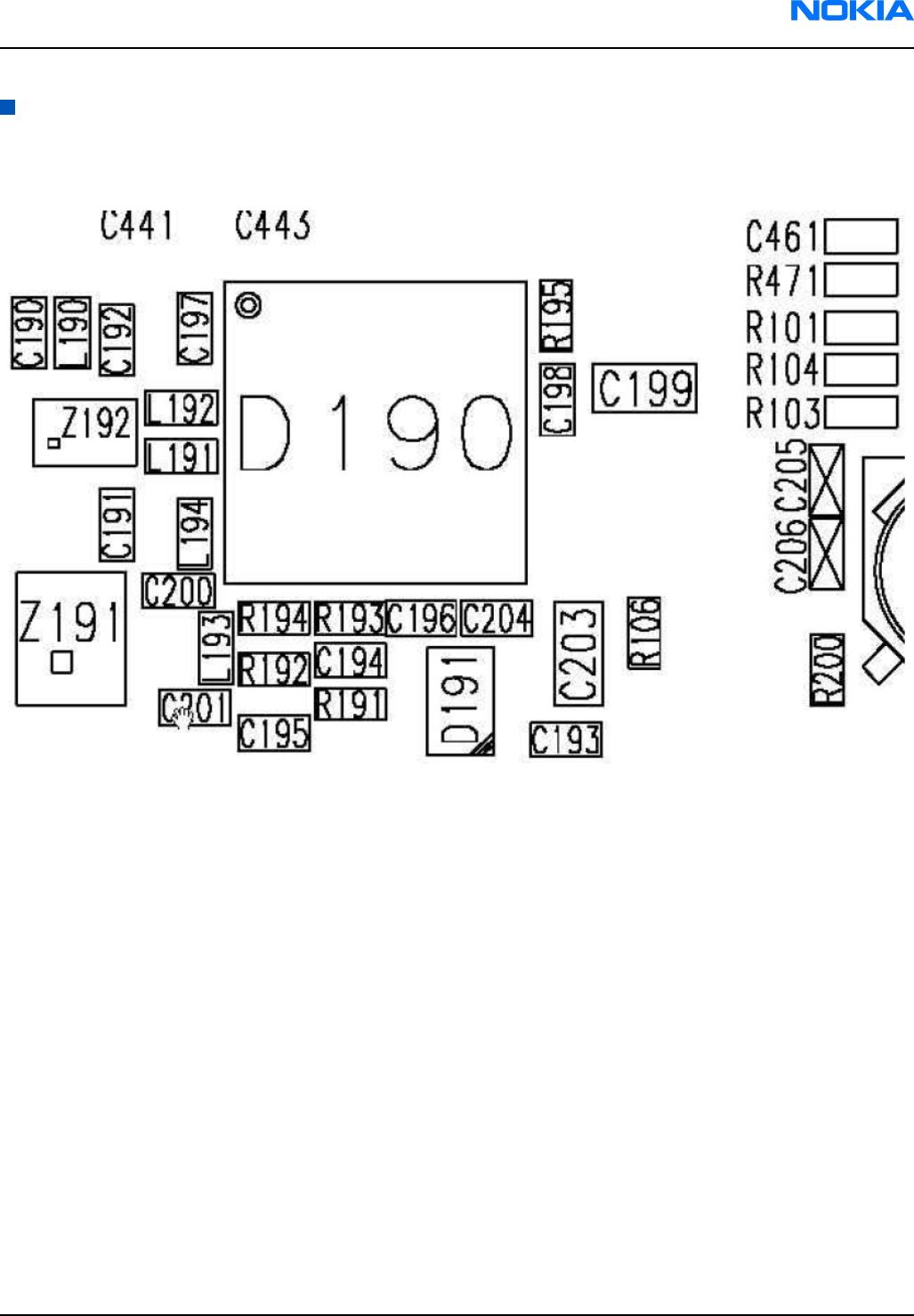
Bluetooth
Bluetooth component placement
Figure 146 Bluetooth component placement
Note: This component placement is taken from a B3 prototype and is subject to change in the future.
Bluetooth settings for Phoenix
Steps
1. Start Phoenix service software.
2. From the File menu, choose Open Product, and then choose the correct type designator from the Product list.
3. Connect the phone to a docking station in the local mode.
4. From the Testing menu, choose Bluetooth LOCALS.
5. Locate JBT-9’s serial number (12 digits) found in the type label on the back of JBT-9.
6. In the Bluetooth LOCALS window, write the 12-digit serial number on the "Counterpart BT Device Address"
line.
This needs to be done only once provided that JBT-9 is not changed.
7. Place the JBT-9 box near (within 10 cm) the BT antenna and click Run BER Test.
RM-25
RF troubleshooting Nokia Customer Care
9235618 (Issue 2) Company Confidential Page 7–45
Copyright ©2005 Nokia. All Rights Reserved.
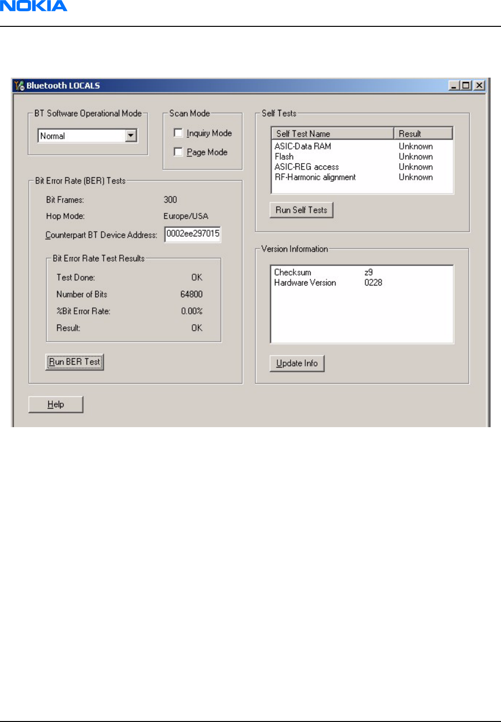
Results
Figure 147 Phoenix settings for Bluetooth troubleshooting
RM-25
Nokia Customer Care RF troubleshooting
Page 7–46 Company Confidential 9235618 (Issue 2)
Copyright ©2005 Nokia. All Rights Reserved.
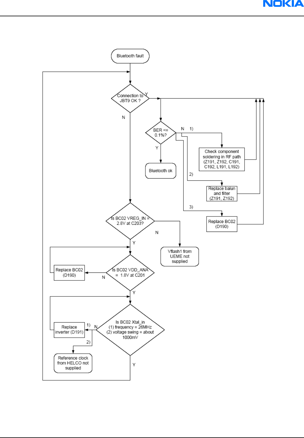
Troubleshooting Bluetooth
Figure 148 Bluetooth troubleshooting
RM-25
RF troubleshooting Nokia Customer Care
9235618 (Issue 2) Company Confidential Page 7–47
Copyright ©2005 Nokia. All Rights Reserved.

RM-25
Nokia Customer Care RF troubleshooting
(This page left intentionally blank.)
Page 7–48 Company Confidential 9235618 (Issue 2)
Copyright ©2005 Nokia. All Rights Reserved.

8 — Camera module
troubleshooting
Nokia Customer Care
9235618 (Issue 2) Company Confidential Page 8–1
Copyright ©2005 Nokia. All Rights Reserved.

RM-25
Nokia Customer Care Camera module troubleshooting
(This page left intentionally blank.)
Page 8–2 Company Confidential 9235618 (Issue 2)
Copyright ©2005 Nokia. All Rights Reserved.

Table of Contents
Introduction to camera module troubleshooting...............................................................................................................8–5
The effect of image taking conditions on image quality..................................................................................................8–6
Image quality analysis ..............................................................................................................................................................8–10
Testing for dust in camera module..................................................................................................................................8–10
Testing camera image sharpness.....................................................................................................................................8–11
Image bit errors.....................................................................................................................................................................8–12
Camera troubleshooting flowcharts......................................................................................................................................8–13
Camera hardware troubleshooting.................................................................................................................................8–13
Camera hardware failure troubleshooting....................................................................................................................8–15
Bad image quality troubleshooting.................................................................................................................................8–16
List of Figures
Figure 149 Sharpness of the picture is worse on the edges than in the center.........................................................8–6
Figure 150 Blurring caused by shaking hands. Geometrical barrel distortion in the background.......................8–7
Figure 151 Near objects get skewed when taking images from a moving vehicle...................................................8–7
Figure 152 Noisy image taken in +70 degrees Celsius........................................................................................................8–8
Figure 153 Image taken against light......................................................................................................................................8–8
Figure 154 Flicker in an image; object illuminated by strong fluorescent light.........................................................8–9
Figure 155 A lens reflection effect caused by sunshine......................................................................................................8–9
Figure 156 Good image taken indoors..................................................................................................................................8–10
Figure 157 Good image taken outdoors...............................................................................................................................8–10
Figure 158 Effects of dust on optical path............................................................................................................................8–11
Figure 159 Bit errors caused by JPEG compression............................................................................................................8–13
RM-25
Camera module troubleshooting Nokia Customer Care
9235618 (Issue 2) Company Confidential Page 8–3
Copyright ©2005 Nokia. All Rights Reserved.

RM-25
Nokia Customer Care Camera module troubleshooting
(This page left intentionally blank.)
Page 8–4 Company Confidential 9235618 (Issue 2)
Copyright ©2005 Nokia. All Rights Reserved.
Introduction to camera module troubleshooting
Background, tools and terminology
Faults or complaints in camera operation can be roughly categorised into three subgroups:
1 Camera is not functional at all; no image can be taken.
2 Images can be taken but there is nothing recognizable in them.
3 Images can be taken and they are recognizable but for some reason the quality of images is seriously
degraded.
Image quality is very hard to measure quantitatively, and even comparative measurements are difficult
(comparing two images) to do, if the difference is small. Especially if the user is not satisfied with his/her device's
image quality, and tells, for example, that the images are not sharp, it is fairly difficult to accurately test the
device and get an exact figure which would tell whether the device is functioning properly.
Often subjective evaluation has to be used for finding out if a certain property of the camera is acceptable or
not. Some training or experience of a correctly operating reference device may be needed in order to detect
what actually is wrong.
It is easy for the user to take bad images in bad conditions. Therefore the camera operation has to be checked
always in constant conditions (lighting, temperature) or by using a second, known-to-be good device as
reference.
When checking for possible errors in camera functionality, knowing what error is suspected significantly helps
the testing by narrowing down the amount of test cases. The following types of image quality problems may
be expected to appear:
• Dust (black spots)
• Lack of sharpness
• Bit errors
Terms
Dynamic range Camera's ability to capture details in dark and bright areas of the scene
simultaneously.
Exposure time Camera modules use silicon sensor to collect light and for forming an image.
The imaging process roughly corresponds to traditional film photography,
in which exposure time means the time during which the film is exposed to
light coming through optics. Increasing the time will allow for more light
hitting the film and thus results in brighter image. The operation principle
is exactly the same with silicon sensor, but the shutter functionality is
handled electronically i.e. there is no mechanical moving parts like in film
cameras.
Flicker Phenomenon, which is caused by pulsating in scene lighting, typically
appearing as wide horizontal stripes in an image.
Noise Variation of response between pixels with same level of input illumination.
Resolution Usually the amount of pixels in the camera sensor; for example, RM-1 has a
1280 x 960 pixel sensor resolution. In some occasions the term resolution is
used for describing the sharpness of the images.
Sensitivity Camera module's sensitivity to light. In equivalent illumination conditions,
a less sensitive camera needs a longer exposure time to gather enough light
in forming a good image. Analogous to ISO speed in photographic film.
RM-25
Camera module troubleshooting Nokia Customer Care
9235618 (Issue 2) Company Confidential Page 8–5
Copyright ©2005 Nokia. All Rights Reserved.
Sharpness Good quality images are 'sharp' or 'crisp', meaning that image details are
well visible in the picture. However, certain issues, such as non-idealities in
optics, cause image blurring, making objects in picture to appear 'soft'. Each
camera type typically has its own level of performance.
The effect of image taking conditions on image quality
There are some factors, which may cause poor image quality, if not taken into account by the end user when
shooting images, and thus may result in complaints. The items listed are normal to camera operation and are
not a reason for changing the camera module.
Distance to target
The lens in the module is specified to operate satisfactorily from 40 cm to infinite distance of scene objects. In
practice, the operation is such that close objects may be noticed to get more blurred when distance to them is
shorter than 40 cm. The lack of sharpness is first visible in full resolution images. If observing just the viewfinder,
even very close objects may seem to appear sharp.
Sharpness of picture edges
The lens performance degrades in image edges, and generally the image is sharpest in the center part.
Particularly this applies to distant objects (> 1 meter).
See the following figure.
Figure 149 Sharpness of the picture is worse on the edges than in the center
Geometrical distortion
The camera lens causes some amount of so called barrel distortion in images.
In practice, this appears as bending of straight objects on the edges of an image. See figure Blurring caused by
shaking hands (Page 8–7) (wall in the background).
The amount of light available
In dim conditions camera runs out of sensitivity. The exposure time is long (especially in the night mode) and
the risk of getting shaken (= blurred) images increases. In addition, image noise level grows. The maximum
exposure time in the night mode is ¼ seconds. Therefore, images need to be taken with extreme care and by
supporting the phone when the amount of light reflected from the target is low. Because of the longer exposure
time and larger gain value, noise level increases in low light conditions. Sometimes blurring may even occur in
daytime, if the image is taken very carelessly. See the figure below for an example.
RM-25
Nokia Customer Care Camera module troubleshooting
Page 8–6 Company Confidential 9235618 (Issue 2)
Copyright ©2005 Nokia. All Rights Reserved.
Figure 150 Blurring caused by shaking hands. Geometrical barrel distortion in the background.
Movement in bright light
If an image is taken of moving objects or if the device is used in a moving vehicle, object 'skewing' or 'tilting'
may occur. This phenomenon is fundamental to most CMOS camera types, and usually cannot be avoided. The
movement of camera or object sometimes cause blurring indoors or in dim lighting conditions because of long
exposure time.
Figure 151 Near objects get skewed when taking images from a moving vehicle
Temperature
High temperatures inside the mobile phone cause more noise to appear in images. For example, in +70 degrees
(Celsius), the noise level may be very high, and it further grows if the conditions are dim. If the phone processor
has been heavily loaded for a long time before taking an image, the phone might have considerably higher
temperature inside than in the surrounding environment. This is also normal to camera operation; do not
change the camera module.
RM-25
Camera module troubleshooting Nokia Customer Care
9235618 (Issue 2) Company Confidential Page 8–7
Copyright ©2005 Nokia. All Rights Reserved.
Figure 152 Noisy image taken in +70 degrees Celsius
Phone display
If the display contrast is set too dark, the image quality degrades: the images may be very dark depending on
the setting. If the display contrast is set too bright, image contrast appears bad and "faint". This problem is
solved by setting the display contrast correctly.
Basic rules of photography (especially shooting against light)
Because of dynamic range limitations, taking images against bright light might cause either saturated image
or the actual target appear too dark. In practice, this means that when taking an image indoors and having, for
example, a window behind the object, the result is usually poor.
Figure 153 Image taken against light
Flicker
In some occasions a bright fluorescent light may cause flicker in the viewfinder and captured image. This
phenomenon may also be a result, if images are taken indoors under the mismatch of 50/60 Hz electricity
network frequency. The electricity frequency used is automatically detected by the camera module. In some
very few countries, both 50 and 60 Hz networks are present and thus probability for the phenomenon increases.
Flickering occurs also under high artificial illumination level.
RM-25
Nokia Customer Care Camera module troubleshooting
Page 8–8 Company Confidential 9235618 (Issue 2)
Copyright ©2005 Nokia. All Rights Reserved.
Figure 154 Flicker in an image; object illuminated by strong fluorescent light
Bright light outside of image view
Especially the sun can cause clearly visible lens glare phenomenon and poor contrast in images. This happens
because of undesired reflections inside the camera optics. Generally this kind of reflections are common in all
optical systems.
Figure 155 A lens reflection effect caused by sunshine
RM-25
Camera module troubleshooting Nokia Customer Care
9235618 (Issue 2) Company Confidential Page 8–9
Copyright ©2005 Nokia. All Rights Reserved.
Examples of good quality images
Figure 156 Good image taken indoors
Figure 157 Good image taken outdoors
Image quality analysis
Testing for dust in camera module
Context
For detecting these kinds of problems, take an image of a uniform white surface and analyse it in full resolution.
A good quality PC monitor is preferred for analysis. Search carefully, since finding these defects is not always
easy. Figure "Effects of dust on optical path" is an example image containing easily detectable dust problems.
When taking a white image, use uniformly lightened white paper or white wall. One possibility is to use uniform
light but in this case make sure that the camera image is not flickering when taking the test image. In case
flickering happens, try to reduce illumination level. Use JPEG image format for analysing, and set the image
quality parameter to ‘High Quality’.
Black spots in an image are caused by dirt particles trapped inside the optical system. Clearly visible and sharp
edged black dots in an image are typically dust particles on the image sensor. These spots are searched for in
the manufacturing phase, but it is possible that the camera body cavity contains a particle, which may move
RM-25
Nokia Customer Care Camera module troubleshooting
Page 8–10 Company Confidential 9235618 (Issue 2)
Copyright ©2005 Nokia. All Rights Reserved.
onto the image sensor active surface, for example, when the phone is dropped. Thus it is also possible that the
problem will disappear before the phone is brought to service. The camera should be replaced if the problem
is present when the service technician analyses the phone.
If a dust particle is lying on the infrared filter surface on either side, they are hard to locate because they are
out of focus, and appear in the image as large, grayish and fading-edge 'blobs'. Sometimes they are invisible
to the eye, and thus the user probably does not notice them at all. However, it is possible that a larger particle
disturbs the user, causing need for service.
Figure 158 Effects of dust on optical path
If large dust particles get trapped on top of the lens surface in the cavity between camera window and lens,
they will cause image blurring and poor contrast. The dust gasket between the window and lens should prevent
any particles from getting into the cavity after the manufacturing phase.
If dust particles are found on the sensor, this is classified as a manufacturing error of the module and the camera
should be replaced. Any particles inside the cavity between the protection window and lens have most probably
been trapped there in the assembly phase at a Nokia factory. Unauthorized disassembling of the product can
also be the root of the problem. However, in most cases it should be possible to remove the particle(s) by using
clean compressed air. Never wipe the lens surface before trying compressed air; the possibility of damaging
the lens is substantial. Always check the image sharpness after removing dust.
See Also
•Testing camera image sharpness (Page 8–11)
Testing camera image sharpness
Context
If pictures taken with a device are claimed to be blurry, there are six possible sources for the problem:
1 The protection window is fingerprinted, soiled, dirty, visibly scratched or broken.
RM-25
Camera module troubleshooting Nokia Customer Care
9235618 (Issue 2) Company Confidential Page 8–11
Copyright ©2005 Nokia. All Rights Reserved.

2 The photographed object is too close – the camera lens operates with distances from 40 cm to infinity. This
is no cause to replace camera module.
3 User has tried to take pictures in too dark conditions, and images are blurred due to handshake or movement.
This is no cause to replace camera module.
4 There is dirt between the protection window and camera lens.
5 The protection window is defective. This can be either a manufacturing failure or caused by the user. The
window should be changed.
6 The camera lens is misfocused because of a manufacturing error.
A quantitative analysis of sharpness is very difficult to conduct in any other environment than optics laboratory.
Therefore, subjective analysis should be used.
If no visible defects (items 1-4) are found, a couple of test images should be taken. Generally, a well-illuminated
typical indoor scene can be used as a target. The main considerations are:
• The protection window has to be clean.
• The amount of light (300 – 600 lux (bright office lighting)) is sufficient.
• The scene should contain, for example, small objects for checking sharpness. Their distance should be 1 – 2
meters.
• If possible, compare the image to another image of the same scene, taken with a different device. Note that
the reference device has to be a similar Nokia phone.
Steps
1. Take several images of small objects in the distance of 1-2 metres.
2. Analyse the images on a PC screen at 100% scaling with the reference images.
Pay attention to the computer display settings: at least 65000 colors (16-bit) have to be used. True colour
(24-bit, 16 million colours) or 32-bit (full colour) setting is recommended.
Next action
If there appears to be a clearly noticeable difference between the reference image and the test images, the
module might have a misfocused lens -> change the module.
Re-check the resolution after changing the camera module.
If the changed module produces the same result, the fault is probably in the camera window. Check the window
by looking carefully through it when replacing the module.
See Also
•Testing for dust in camera module (Page 8–10)
•Dirty camera protection window (Page )
Image bit errors
Bit errors are image defects caused by data transmission errors between the camera module and the phone
baseband and/or errors inside the module.
Usually bit errors can be easily detected in images, and they are best visible in full resolution images. A good
practice is to use a uniform white test target when analysing these errors. The errors are clearly visible, colourful
sharp dots or lines in camera images. See the following figure.
RM-25
Nokia Customer Care Camera module troubleshooting
Page 8–12 Company Confidential 9235618 (Issue 2)
Copyright ©2005 Nokia. All Rights Reserved.
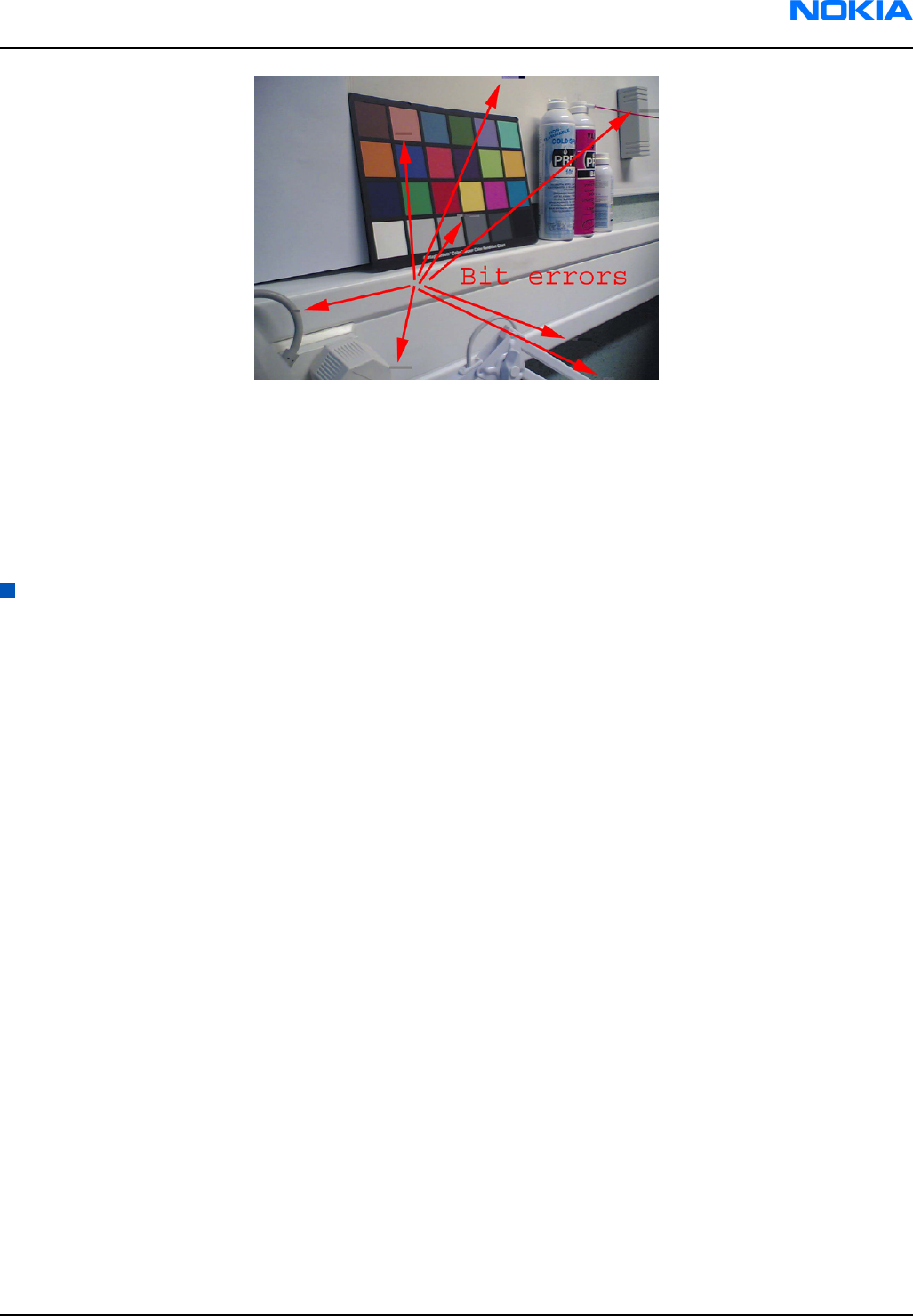
Figure 159 Bit errors caused by JPEG compression
One type of bit error is a lack of bit depth. In this case, the image is almost totally black under normal conditions,
and only senses something in very highly illuminated environments. Typically this is a contact problem between
the camera module and the phone main PWB. You should check the camera assembly and connector contacts.
If the fault is in the camera module, bit errors are typically visible only when using some specific image
resolution. For example, in case of a viewfinder fault, the error might exist but is not visible in a full size image.
Camera troubleshooting flowcharts
Camera hardware troubleshooting
Context
If camera related hardware is faulty, follow the troubleshooting flowchart below.
RM-25
Camera module troubleshooting Nokia Customer Care
9235618 (Issue 2) Company Confidential Page 8–13
Copyright ©2005 Nokia. All Rights Reserved.
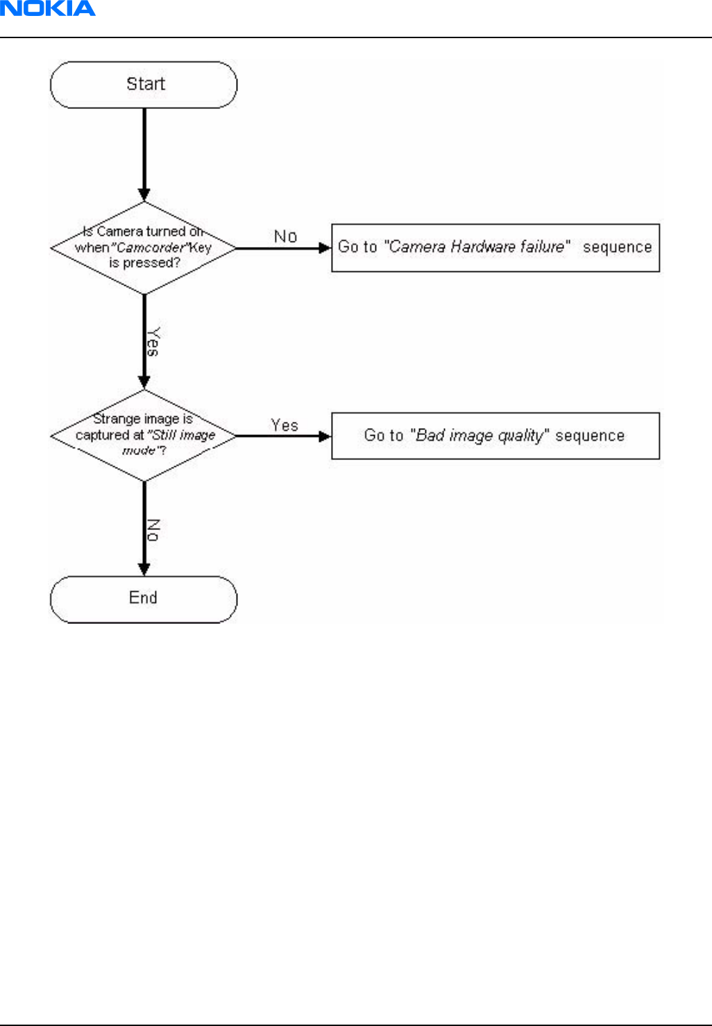

Camera hardware failure troubleshooting
RM-25
Camera module troubleshooting Nokia Customer Care
9235618 (Issue 2) Company Confidential Page 8–15
Copyright ©2005 Nokia. All Rights Reserved.
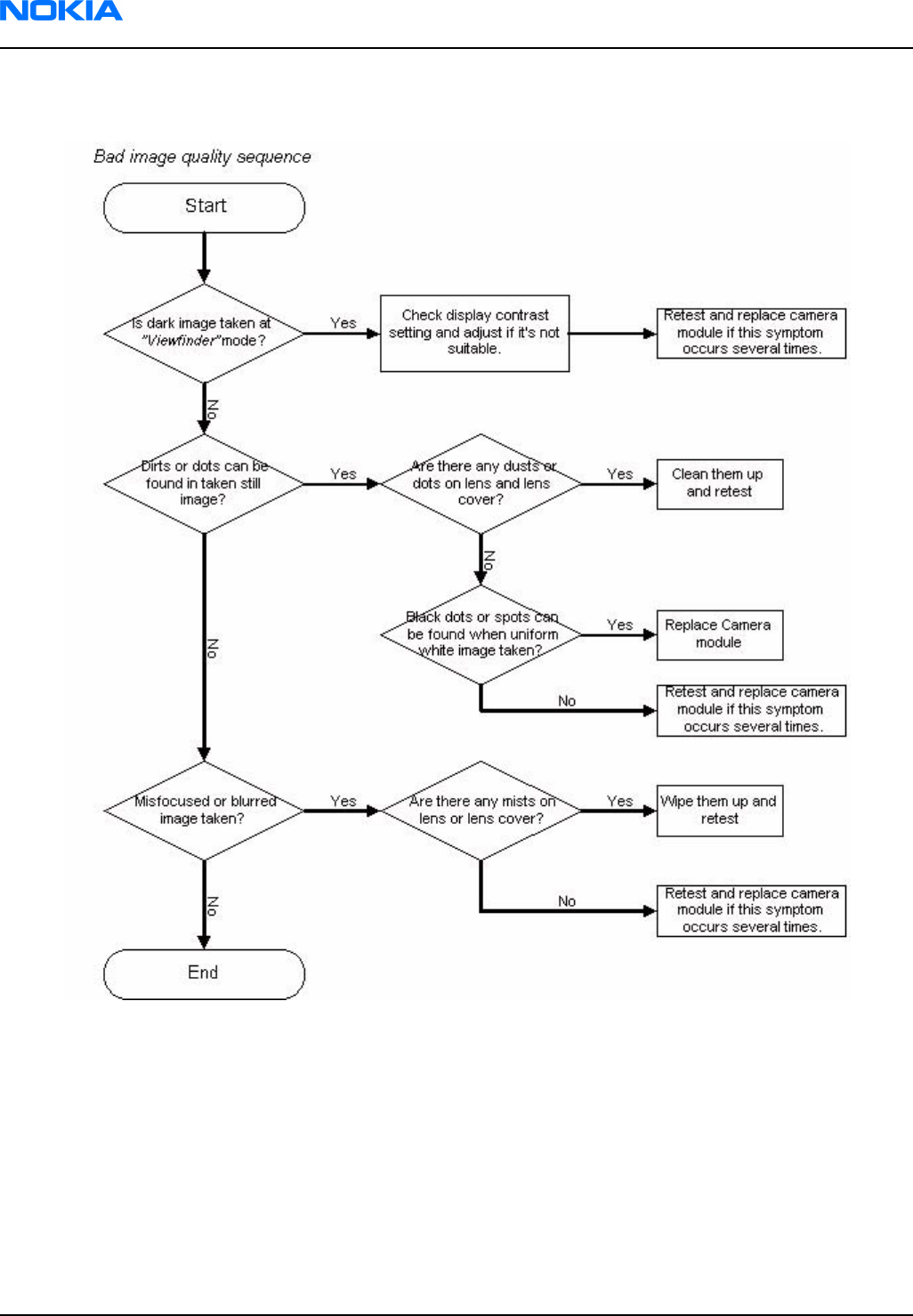
Bad image quality troubleshooting
RM-25
Nokia Customer Care Camera module troubleshooting
Page 8–16 Company Confidential 9235618 (Issue 2)
Copyright ©2005 Nokia. All Rights Reserved.

9 — System module
Nokia Customer Care
9235618 (Issue 2) Company Confidential Page 9–1
Copyright ©2005 Nokia. All Rights Reserved.

RM-25
Nokia Customer Care System module
(This page left intentionally blank.)
Page 9–2 Company Confidential 9235618 (Issue 2)
Copyright ©2005 Nokia. All Rights Reserved.

Table of Contents
System module block diagram..................................................................................................................................................9–5
Functional description..................................................................................................................................................................9–5
BB description.................................................................................................................................................................................9–6
Modes of operation.......................................................................................................................................................................9–6
Clocking scheme.............................................................................................................................................................................9–7
Power distribution, control and reset.....................................................................................................................................9–9
Back-up battery and real time clock......................................................................................................................................9–10
Baseband measurement A/D converter...............................................................................................................................9–10
ZOCUS...............................................................................................................................................................................................9–11
Bluetooth........................................................................................................................................................................................9–11
USB...................................................................................................................................................................................................9–11
SIM interface..................................................................................................................................................................................9–11
IrDA interface................................................................................................................................................................................9–11
MMC interface................................................................................................................................................................................9–11
Pop-PortTM....................................................................................................................................................................................9–11
Audio concept...............................................................................................................................................................................9–12
Camera interface..........................................................................................................................................................................9–14
FM radio..........................................................................................................................................................................................9–14
Flashing...........................................................................................................................................................................................9–14
Mode sensing................................................................................................................................................................................9–14
Testing interfaces........................................................................................................................................................................9–14
Extreme voltages.........................................................................................................................................................................9–16
RF description...............................................................................................................................................................................9–16
List of Tables
Table 30 Testing and flashing interface electrical specifications..................................................................................9–15
List of Figures
Figure 160 Module block diagram.............................................................................................................................................9–5
Figure 161 RM-25 clocking...........................................................................................................................................................9–8
Figure 162 RM-25 audio blocks................................................................................................................................................9–12
Figure 163 External audio connector.....................................................................................................................................9–13
RM-25
System module Nokia Customer Care
9235618 (Issue 2) Company Confidential Page 9–3
Copyright ©2005 Nokia. All Rights Reserved.

RM-25
Nokia Customer Care System module
(This page left intentionally blank.)
Page 9–4 Company Confidential 9235618 (Issue 2)
Copyright ©2005 Nokia. All Rights Reserved.
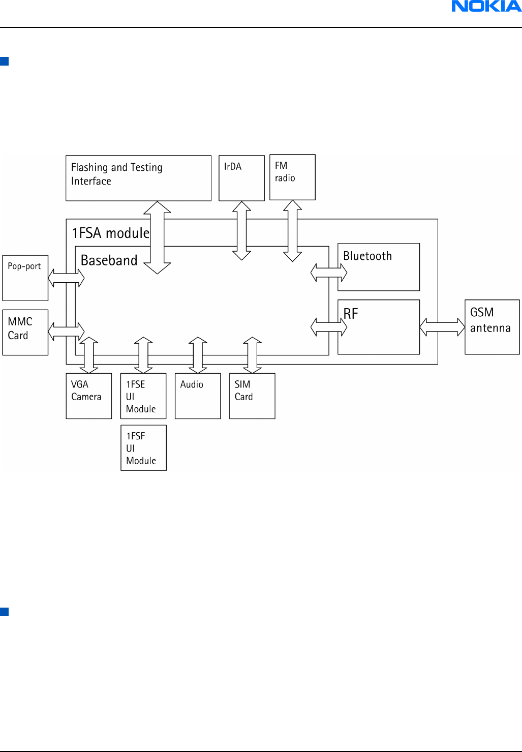
System module block diagram
The main board, 1FSA, consists of a radio frequency part and a baseband part. The User Interface parts are
mainly situated at the UI flex, 1FSE, and the Top UI part, 1FSF. The UI flex is connected to the main board through
a connector. The Top UI part is connected to the main board through the Hinge Flex part, 1FSD.
The 1FSA is the system module of the RM-25 phone.
Figure 160 Module block diagram
The RM-25 has IrDA and Bluetooth wireless local interfaces. It features a full function PopPortTM implementation.
The port includes stereo audio interface and ACI bus support. The HW will communicate with ACI accessories.
The SW may not support all ACI accessories.
The PopPortTM supports USB but does not support FBUS.
The implementation of the ACI bus in RM-25 has been made possible by implementing the BSI, Battery Size
Indication, a little different from most Nokia phones.
Functional description
The heart of the BB is UPP_WD2, which includes the MCU, DSP and Digital Control Logic. Power is supplied by the
UEME ASIC and a number of discrete regulators. Memory comprises of 2 x 128Mbit Stacked and 64Mbit flash
memory devices and 128 Mbit (16 Mbytes) SDRAM.
There are two audio transducers (earpiece 8 mm and IHF speaker 16 mm) and external galvanic headset
(PopPortTM) interface. The IHF speaker is also used to handle the ring tone. The IHF speaker is driven by a discrete
audio amplifier. In RM-25, there is only one microphone for both HS and IHF modes.
For data connectivity there is USB v2.0 full-speed, Bluetooth and RS-MMC card.
RM-25
System module Nokia Customer Care
9235618 (Issue 2) Company Confidential Page 9–5
Copyright ©2005 Nokia. All Rights Reserved.

The display is an TFT type colour display with 65536 colours and 176x208 pixels with backlighting. The UI module
features a function keymat with a 4-way navigation key with a centre selection key.
For imaging purposes, BB supports a VGA camera via the CCP interface, which is integrated in UPP_WD2.
BB description
The BB core is based on UPP_WD2 CPU, which is a PDA version of the DCT4 UPP ASIC. UPP_WD2 takes care of all
the signal processing and operation controlling tasks of the phone as well as all PDA tasks.
For power management, there is one main ASIC for controlling charging and supplying power UEME plus some
discrete power supplies. The main reset for the system is generated by the UEME.
The interface to the RF and audio sections is also handled by the UEME. This ASIC provides A/D and D/A conversion
of the in-phase and quadrature receive and transmit signal paths and also A/D and D/A conversions of received
and transmitted audio signals. Data transmission between UEME and RF and the UPP_WD2 is implemented using
different serial connections (CBUS, DBUS and RFBUS). Digital speech processing is handled by UPP_WD2 ASIC.
A real time clock function is integrated into UEME, which utilizes the same 32kHz-clock source as the sleep clock.
A rechargeable battery provides backup power to run the RTC when the main battery is removed. Backup time
is approximately 5 Hours.
Memory configuration
RM-25 uses two kinds of memories, Flash and SDRAM. These memories have their own dedicated bus interfaces
to UPP_WD2.
Synchronous DRAM is used as the working memory. Interface is 16 bit wide data and 14 bit address. Memory
clocking speed is 123.5 MHz. The SDRAM size is 128Mbits.
SDRAM I/O is 1.8 V and core 1.8 V supplied by UEME regulator VIO. All memory contents are lost if the supply
voltage is switched off.
Multiplexed flash memory interface is used to store the MCU program code and user data. The memory interface
is a burst type FLASH with multiplexed address/data bus, running at 123.5/3MHz.
Configuration of flash memory is a 2x128Mbit stacked flash memory and a 64Mbit flash memory.
Both flash I/O and core voltage are 1.8 V supplied by UEME’s VIO.
Energy management
The master of EM control is UEME and with SW it has the main control of the system voltages and operating
modes.
Modes of operation
RM-25 employs several hardware and software controlled operation modes. Main modes are described below.
• NO_SUPPLY mode means that the main battery is not present or its voltage is too low (below UEME master
reset threshold) and back-up battery voltage is too low.
• In BACK_UP mode the main battery is not present or its voltage is too low but the back-up battery has sufficient
charge in it.
• In PWR_OFF mode the main battery is present and its voltage is over the UEME master reset threshold. All
regulators are disabled.
• RESET mode is a synonym for start-up sequence and contains in fact several modes. In this mode, regulators
and oscillators are enabled and after they have stabilized system reset is released and PWR_ON mode entered.
• In PWR_ON mode SW is running and controlling the system.
• SLEEP mode is entered from PWR_ON mode when the system’s activity is low (SLEEPX controlled by SW).
• FLASHING mode is for production SW download.
RM-25
Nokia Customer Care System module
Page 9–6 Company Confidential 9235618 (Issue 2)
Copyright ©2005 Nokia. All Rights Reserved.
Voltage limits
The voltage limits of the system are listed in the following table. These are also controlling system states.
Parameter Description Value
VMSTR+ Master reset threshold (rising) 2.1 V (typ.)
VMSTR- Master reset threshold (falling) 1.9 V (typ.)
VCOFF+ Hardware cutoff (rising) 3.1 V (typ.)
VCOFF- Hardware cutoff (falling) 2.8 V (typ.)
V_BUCOFF+ Back-up battery cutoff (rising) 2.1 V (typ.)
V_BUCOFF- Back-up battery cutoff (falling) 2.0 V (typ.)
SWCOFF SW cutoff limit (> regulator drop-
out limit) MIN!
3.4 V SW changeable
The master reset threshold controls the internal reset of UEME. If battery voltage is above VMSTR, UEME’s charging
control logic is alive. Also, RTC is active and supplied from the main battery. Above VMSTR UEME allows the system
to be powered on although this may not succeed due to voltage drops during start-up. SW can also consider
battery voltage too low for operation and power down the system.
Clocking scheme
A 26 MHz VCXO is used as system clock generator in GSM. During the system start-up, UEME RC-oscillators generate
timing for state machines. All clock signals of the engine are illustrated in following figure.
Bluetooth uses a 26 MHz clock.
FM radio uses 32kHz, the SleepClk.
In SLEEP mode, the VCXO is off. UEME generates low frequency clock signal (32.768 kHz) that is fed to UPP_WD2,
Bluetooth and ZOCUS.
RM-25
System module Nokia Customer Care
9235618 (Issue 2) Company Confidential Page 9–7
Copyright ©2005 Nokia. All Rights Reserved.
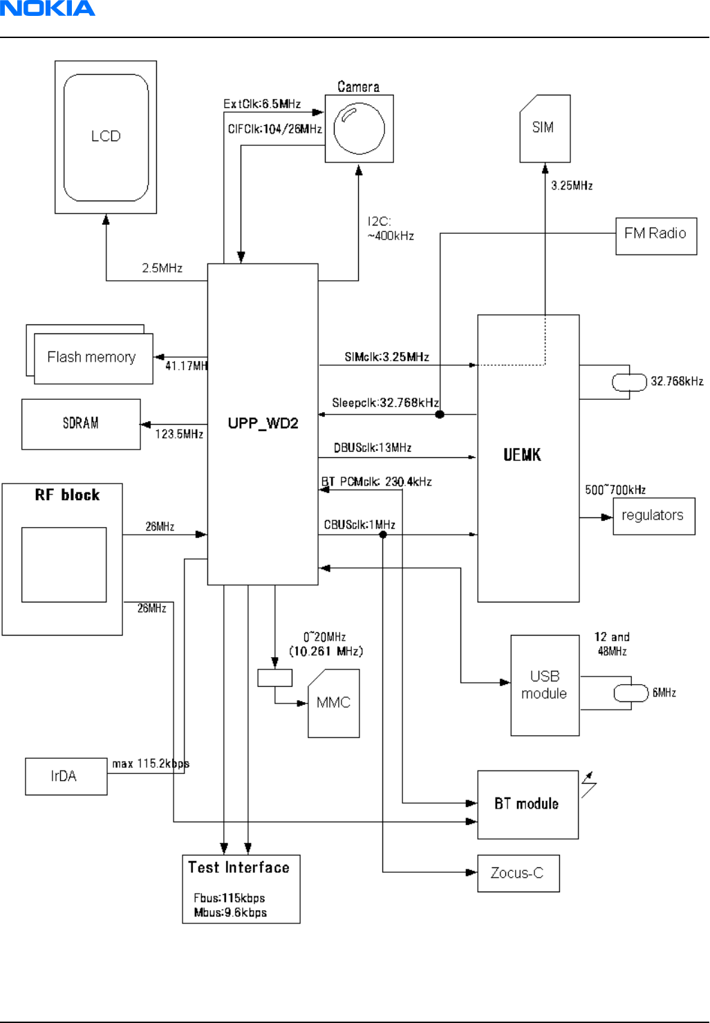
Figure 161 RM-25 clocking
RM-25
Nokia Customer Care System module
Page 9–8 Company Confidential 9235618 (Issue 2)
Copyright ©2005 Nokia. All Rights Reserved.

UPP_WD2 voltage/clock frequency adjusting
No external clock is available for UPP_WD2 before VCXO starts. As reset is released, the VCXO is running and MCU
uses the 26 MHz clock while DSP is in reset. There are three identical DPLL's, for MCU, for DSP and for accessory
interfaces, which can be controlled independently. The clock for MCU can be up to 130 MHz and 156 MHz is
maximum clock frequency for the DSP. These clock signals are used either directly (SDRAM IF) or divided down
for the interfaces (e.g. flash IF).
Power distribution, control and reset
All power (except backup battery power) is drawn from the BL-4C Li-Ion battery located in the B cover. Current
flows through ZOCUS current sense resister which is used for current measurement by ZOCUS and thus for
remaining operating time estimation.
1FSA board contains one power ASIC, UEME and discrete regulators needed for generating the different
operating voltages. The discrete regulators consist of an SMPS to power UPP_WD2 voltage core. In addition,
there is a SMPS in 1FSA generating the operating voltage for display module backlighting. In 1FSA, the keyboard
backlight is powered with a charge pump regulator.
There is also a “soft watchdog” in UPP_WD2. It is used to reset the chip in case software gets stuck for any reason.
Power-up sequence (reset mode)
RESET mode can be entered in four ways: by inserting the battery or charger, by RTC alarm or by pressing the
power key. The VCXO is powered by UEME. After a 220 ms delay, regulators are configured and UEME enters
PWR_ON mode and system reset PURX is released.
During the system start-up, in RESET state, the regulators are enabled, and each regulator charges the capacitor
(s) at the output with the maximum current (short circuit current) it can deliver. This results in battery voltage
dropping during start-up. When a battery with a voltage level just above the hardware cutoff limit is inserted,
the system may not start due to excessive voltage dipping. Dropping below 2.8 V for longer than 5 us forces
the system to PWR_OFF state.
Powering off
Controlled powering off is done when the user requests it by pressing the power-key or when the battery voltage
falls too low. Uncontrolled powering off happens when the battery is suddenly removed or if over-temperature
condition is detected in regulator block while in RESET mode. Then all UEME’s regulators are disabled
immediately and discrete regulators are disabled as Vbat supply disappears.
Controlled powering off
For RM-25, powering off is initiated by pressing the power key and power off sequence is activated in UEME and
SW. Basically, the power key causes UEME interrupt to UPP_WD2 and SW sets watchdog time value to zero and
as this happens, PURX is forced low and all regulators are disabled.
If the battery voltage falls below the very last SW-cutoff level, SW will power off the system by letting the UEME’s
watchdog elapse.
If thermal shutdown limit in the UEME regulator block is exceeded, the system is powered off. System reset
PURX is forced low.
Uncontrolled powering off
This happens when the battery is suddenly removed. UEME’s state machine notices battery removal after the
battery voltage has been below VCOFF- for 5 us and enters PWR_OFF mode. PURX is set low and all UEME’s
regulators are disabled.
RM-25
System module Nokia Customer Care
9235618 (Issue 2) Company Confidential Page 9–9
Copyright ©2005 Nokia. All Rights Reserved.

Watchdogs
There are three watchdogs in UEME. The first one is for controlling system power-on and power-down
sequences. The initial time for this watchdog after reset is 32 s and the watchdog can not be disabled. The time
can be set using a register. This watchdog is used for powering the system off in a controlled manner. The other
one is for security block and is used during IMEI code setting. The third one is a power key watchdog. It is used
to power off the system in case SW is stuck and the user presses the power key. This WD is SW configurable.
Charging
Charging control and charge switch is in UEME. There are two different charging modes; charging an empty
battery (start-up charge mode), and SW controlled charging.
UEME digital part takes care of charger detection (generates interrupt to UPP_WD2), pulse width modulated
charging control (for internal charge switch) and over voltage and current detection. SW using registers controls
all these.
Chargers
RM-25 BB supports a standard charger (two wires); ACP-12 and cigarette charger LCH-12 officially.
Battery
RM-25 battery is a detachable, semi-fixed lithium-Ion BL-4C battery. The nominal voltage is thus 3.7 V (max
charging voltage 4.2 V).
The interface consists of three pins: VBAT, GND and BSI. A pull-down resistor inside the batteries (BSI signal)
recognizes the battery types. The voltage level at BSI line is measured using UEME's AD-converter.
Back-up battery and real time clock
The real time clock (RTC), crystal oscillator and back-up battery circuitry reside in UEME. A register in UEME controls
back-up battery charging and charging is possible only in POWER_ON State.
Baseband measurement A/D converter
UEME contains an 11 channels A/D converter, which is used for different baseband measurement purposes. The
resolution of the A/D converter is 10 bits. The converter uses the CBUS interface clock signal for the conversion.
An interrupt will be given to the MCU at the end of the measurements. The converter is used for following
purposes.
• VBATADC, battery voltage
• BSI, in RM-25 this input is connected to ACI bus and the BSI_PULS. The BSI_PULS is delivered by the flashing
equipment when flashing the phone.
• BTEMP, battery temp
• PATEMP, power amplifier temp
• VCXOTEMP, oscilaotor temp
• Headint
• Hookint
• ALCO/LS, in RM-25 this input is used to determine the value of the BSI resisor of the Battery and thus the
battery type (and local, test modes)
• Headint2, not supported by SW, not used
• AuxDet, not used
• VBACK, test the voltage of backup battery
RM-25
Nokia Customer Care System module
Page 9–10 Company Confidential 9235618 (Issue 2)
Copyright ©2005 Nokia. All Rights Reserved.

ZOCUS
The ZOCUS device is a current sensor used for the battery bar display and for determining whether the phone
is in a high current consuming mode. The ZOCUS device measures the voltage drop across a sense resistor in
the battery voltage line. This sense resistor is formed from a PWB track and is on an internal layer of the PWB.
The sense resistor must be located close to the battery terminals so that all of the phones current flow through
it. The nominal value of the sense resistor is 3.0m-ohm. ZOCUS reports the current measurement to UPP_WD2
via the Cbus interface.
Bluetooth
Bluetooth provides a fully digital link for communication between a master unit and one or more slave units.
The system provides a radio link that offers a high degree of flexibility to support various applications and
product scenarios. Data and control interface for a low power RF module is provided. Data rate is regulated
between the master and the slave.
USB
USB provides a wired connectivity between host PC and peripheral devices. RM-25 complies with USB 2.0,
supporting data transfer at full-speed (max. 12Mbps). The USB functionality of RM-25 is implemented by a newly
developed USB interface device, Kaede (B440), which is connected to UPP_WD2 via flash memory interfaces. A
6MHz ceramic resonator, Ceralock (D440), is used for USB clock generation.
SIM interface
The SIM interface is located in two chips (UPP_WD2 and UEME). In UEME there is support only for one SIM card.
The interfaces support both 1.8 V and 3 V SIM cards. Adjustable SIM regulator (1.8V/3.0V) is located in UEME and
can be controlled by SW.
The data communication between the card and the phone is asynchronous half duplex. The clock supplied to
the card is 3.25 MHz. The data baudrate is SIM card clock frequency divided by 372 (by default), 64, 32 or 16.
IrDA interface
RM-25 supports data connectivity via the Infra Red link. The IR interface is integrated into the UPP_WD2 and the
main external component is the IR module. The data rates supported are up to 115.2 kbits/s.
The logics section is powered by 1V8, VIO while the transmitter LED is powered directly by the battery via a
power limiting resistor.
The maximum distance in the Lightning configuration is approximately 20 centimetres (30 cm used with an
accompanying 1 m device).
MMC interface
The MMC interface consists of a block in UPP_WD2 plus a level shifting device known as “Lester” and an EMC
protection ASIP. The MMC interface comprises 3 lines clock, data and command and runs at 10.26 MHz. The Lester
device also incorporates a 2.85V regulator to power the MMC card.
Pop-PortTM
The ACI bus is level-shifted between the accessory part and the BSI/DBI port of the UEME.
RM-25
System module Nokia Customer Care
9235618 (Issue 2) Company Confidential Page 9–11
Copyright ©2005 Nokia. All Rights Reserved.
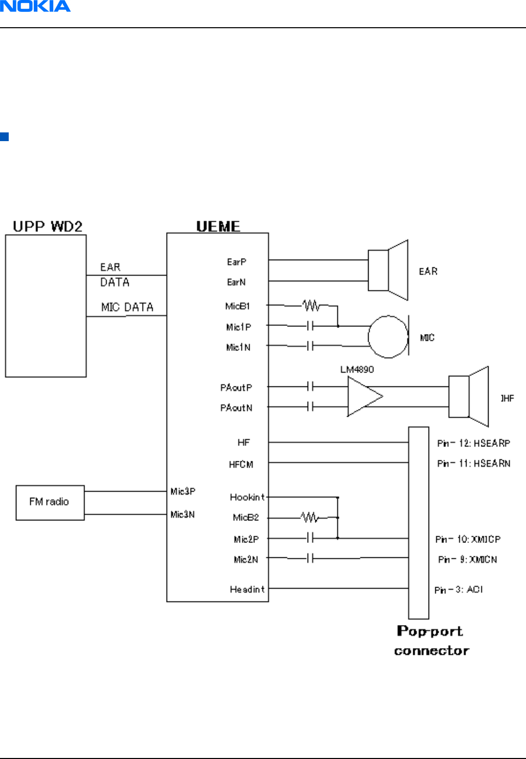
Parallel to this pin of the UEME is connected the Test/Flash pad BSI_PULS used when the phone is flashed.
The BSI connection of the battery, BSI_BATT pad of the Flsh/Test interface, is connected to the LS/ALCO AD input
of the UEME. Via this AD converter the Battery Size Indication resistor value is determined.
The BSI connection of the battery is also connected to the SIMCardDet input of the UEME. When the BSI of the
battery is disconnected the UEME will close the SIM bus down immediately, in a well-controlled manner.
Audio concept
RM-25 audio includes an earpiece, a microphone, and a Pop-PortTM connector for headset and integrated
handsfree (IHF). Audio is based on ASIC's UPP_WD2, UEME and a discrete amplifier for the handsfree speaker
known as “boomer”.
Figure 162 RM-25 audio blocks
Between UPP_WD2 and UEME, the audio signals are transferred in digital format using signals MICDATA and
EARDATA. Ringing tones and warning/info tones are to be produced to the IHF speaker.
RM-25
Nokia Customer Care System module
Page 9–12 Company Confidential 9235618 (Issue 2)
Copyright ©2005 Nokia. All Rights Reserved.
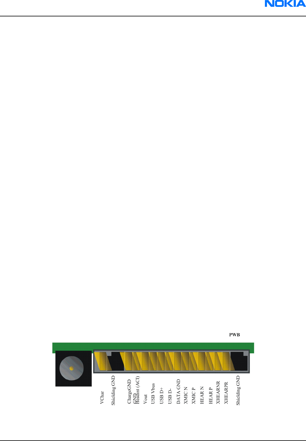
Earpiece
The earpiece to be used in RM-25 is an 8-mm Pico earpiece produced by Philips Speaker Systems. It has 32ohm
continuous impedance and continuous power 8 mWatts. It is driven by differential signals from UEME (EARP &
EARN). It makes contact with the PWB via spring contacts.
Microphone
The microphone module for RM-25 is used Pop-PortTM microphone module. Its sensitivity is -42dB Nominal.
Contacts are done by springs.
Two inputs are used from UEME, one for the normal internal microphone and the other for the headset. The
third microphone input is not used, so it is connected to ground via capacitors. Microphone bias block in UEME
generates bias voltages for handportable and handsfree/headset microphones. For both microphone bias
outputs (MICB1 & MICB2), the minimum output voltage is 2.0 Volts and maximum output current is 600 mA.
Microphone bias block also includes a low pass filter for the reference voltage used as an input for the MICB1&2
amplifiers.
IHF amplifier and speaker
The speaker to be used in RM-25 is a 16mm 8ohm speaker. It can handle 0.3 Watts nominal power and short
trem peak power of 0.8 Watts. The component is housed in the antenna housing and connects to the PWB via
spring contacts.
PAOUTP and PAOUTN lines of UEME are use to drive Boomer IHF amplifier.
Power amplifier is a differential opamp. The differential output drives the HandsFree speaker. HandsFree
amplifier load impedance is 8 ohm.
The outputs go into a high impedance state when powered down. The amplifier can be enabled and shut down
using a GENIO line from UPP_WD2.
SW controls IHF, headset and earpiece volume via UEME. Gain setting can be done in 2 dB steps, from –40 to +6
dB. The output sound pressure level of the internal HandsFree speaker is controlled by SW (CBus is used for
controlling).
The schematic around the Boomer IHF amplifier is presented in RM-25 schematics. The schematic shows all the
filtering needed and also protection components against ESD and EMC. The EMC and ESD filtering component
must be as near as possible to the earphone pads of the phone.
The supply voltage for the IHF amplifier is taken directly from the battery voltage.
External audio interface
In RM-25 there is a Pop-PortTM connector which is fully differential 4–wire connection.
Figure 163 External audio connector
RM-25
System module Nokia Customer Care
9235618 (Issue 2) Company Confidential Page 9–13
Copyright ©2005 Nokia. All Rights Reserved.

The handsfree (HF) driver in UEME is meant for the headset. In RM-25, the output is driven in fully differential
mode. In the fully differential mode, the HF pin is the negative output and the HFCM pin is the positive output.
The gain of the handsfree driver in the differential mode is 6 dB. The earpiece (EARP, EARN) and headset (HF,
HFCM) signals are multiplexed so that the outputs can not be used simultaneously. The HF and HFCM amplifiers
include a transient suppression circuitry, which prevents unwanted spikes in HF and HFCM outputs when
switching on and off the amplifiers.
The HeadInt line will be pulled up to 2.7V by the internal resistor when the accessory is connected. When not
having the accessory inserted the voltage in the HeadInt line will be <0.8 V caused by internal pull down resistor
in the HF line.
Camera interface
RM-25 has a digital camera with viewfinder function. The camera resolution is VGA (640 x 480 pixels) . The
camera module is connected by means of a soldered on connector to the PWB.
The camera interface is a serial CCP, which is an unidirectional interface; the control information to camera is
transmitted through I2C bus. The I2C bus is implemented purely by the SW using general purpose I/Os.
The CCP interface consists of differential clock and data signals. The CCP enables the use of high data rates with
low EMI; maximum transfer capacity is 104Mbit/s, which means that transferring YUV VGA(640 x 480) images
at 15fps is possible.
The camera needs two power sources, 2.8V for analog circuit voltage VDD and 1.8V for digital circuit voltage
VDDI. VDD is provided from same discrete regulator as LCD and VDDI is fed from UEME’s Vcore.
FM radio
FM radio circuitry is implemented using the highly integrated FM radio ASIC, TEA5767. The MCU SW controls the
FM radio circuitry through a proprietary 3-wire bus.
The stereo output is fed to the UEME via one of the microphone inputs, MIC3.
The antenna of the FM Radio is created with the headset. The wires of the headset are used as antenna.
The data bus on the radio will be disabled when not used, in order to save current (BUSENABLE).
The VAUX1 regulator of the UEME will power the FM radio at nominal 3V.
The reference clock for the FM radio is the SleepClk signal picked up through a resistive divider.
Flashing
SW download in service is implemented by custom tools and SW; kindly refer to Phoenix service software
instructions (Page 3–5) and Service Tools (Page ) sections of the manual.
Mode sensing
The RM-25 has different operational modes depending on the positions of the top and bottom parts.
There are five switches to sense the mechanical position of the two parts. A cam disk in the swivel activates a
pair of switches, and three Hall switches activated by magnets sense the position of the hinge.
The actual phone mode is interpreted from the position sensors and the phone is controlled accordingly.
Testing interfaces
RM-25 has a testing interface that is easy to access by service battery. The following signals are allocated on
test pads.
RM-25
Nokia Customer Care System module
Page 9–14 Company Confidential 9235618 (Issue 2)
Copyright ©2005 Nokia. All Rights Reserved.
Table 30 Testing and flashing interface electrical specifications
Pad
No
Name Dir Parameter Min Typ Max Unit Notes
1STI_T
x
-> Vo 0.22*VIO V
Voh 0.8*VIO V
2 VPP To Phone 0 / 2.8 / 9 +/-3% V Prommer Select
3 FBusT
x
-> Vol 0 2.7 0.3*VFlash
1
V
Voh 0.7*VFlash1 2.7 VFlash1 V
4 MBUS <-> Vol 0 0.2 0.3*VFlash
1
V
Vil (From
prommer)
0 0.2 0.3*VFlash
1
V
Voh 0.7*VFlash1 2.7 0.7*VFlash
1
V
Vih(From
prommer)
0.7*VFlash1 2.7 VFlash1 V
5 FBusR
x
<- Vil (From
prommer)
0 2.7 0.3*VFlash
1
V
Vih(From
prommer)
1.89 2.7 VFlash1 V
Abs. Max.
Voltage to
Test Pad
Referenced
to GND
-0.3V 3.0 V Absolute Max
Voltage limits to
MBUS/FBUS
6 GND 0 V VBAT GROUND
7 BSI_P
ULS
Vol 0 2.7 0.3*VFlash
1
V Supplied from the
flash programming
device
Voh 0.7*VFlash1 2.7 VFlash1 V
8 ZOCUS Used for
manufacturing
Note: VFlash1 = 2.78 +/-3%, VIO = 1.8 +/-4.5%
Pin Name Min Typ Max Unit Notes
VBAT 0 3.6 5.1 V
BSI_BATT 0 2.78 VFlash1 V Internal
pullup
GND 0 V
RM-25
System module Nokia Customer Care
9235618 (Issue 2) Company Confidential Page 9–15
Copyright ©2005 Nokia. All Rights Reserved.

Extreme voltages
Lithium-Ion battery BL-4C (1 cell):
• Nominal voltage is 3.7V
• Lower extreme voltage is 2.8V (cut off voltage)
• Higher extreme voltage is 4.2V (charging high limit voltage)
RF description
The BC02 solution is used for Bluetooth. The ASIC and components are placed on the bottom side of the 1FSA
system module, underneath the shield can with UPP_WD2.
The RF module of RM-25 has 2 SAW filters, a capacitor on the 1FSA system module, and an antenna module.
The main ASIC of RF is Helgo 85G, and power amplifier is RFMD RF9250, a so called microPA. RM-25 does not
support EDGE, even though the RF module itself has the capacity for it.
For more information, see Introduction to RF Troubleshooting (Page 7–5).
RM-25
Nokia Customer Care System module
Page 9–16 Company Confidential 9235618 (Issue 2)
Copyright ©2005 Nokia. All Rights Reserved.

10 — Schematics
Nokia Customer Care
9235618 (Issue 2) Company Confidential Page 10–1
Copyright ©2005 Nokia. All Rights Reserved.

RM-25
Nokia Customer Care Schematics
(This page left intentionally blank.)
Page 10–2 Company Confidential 9235618 (Issue 2)
Copyright ©2005 Nokia. All Rights Reserved.

Table of Contents
RF BB module top level..............................................................................................................................................................10–5
BB top level....................................................................................................................................................................................10–6
Production test pattern.............................................................................................................................................................10–9
Power supplier top level.........................................................................................................................................................10–10
Aux_power...................................................................................................................................................................................10–13
UEME/UEMEK................................................................................................................................................................................10–15
Card interface.............................................................................................................................................................................10–17
Card interface module.............................................................................................................................................................10–18
FM radio top level......................................................................................................................................................................10–20
FM radio module........................................................................................................................................................................10–21
Pop-portTM and microphone................................................................................................................................................10–23
UPP_WD2......................................................................................................................................................................................10–26
IR module....................................................................................................................................................................................10–29
User interface (top part and keyboard).............................................................................................................................10–29
User interface (camera)...........................................................................................................................................................10–32
User interface (empty).............................................................................................................................................................10–34
USB.................................................................................................................................................................................................10–34
USB module.................................................................................................................................................................................10–35
Memory.........................................................................................................................................................................................10–35
Bluetooth.....................................................................................................................................................................................10–38
Bluetooth module.....................................................................................................................................................................10–39
BB-RF Interface...........................................................................................................................................................................10–41
Testpad.........................................................................................................................................................................................10–44
RF top level..................................................................................................................................................................................10–45
HELGO............................................................................................................................................................................................10–47
RF9204 power amplifier and power detection...............................................................................................................10–50
RX front end and antenna switch........................................................................................................................................10–51
Component layout, bottom....................................................................................................................................................10–54
Component layout, top............................................................................................................................................................10–56
List of Figures
Figure 164 1fsa_09a, v.1.1, ed. 54.......................................................................................................................................10–0
Figure 165 1fsa_11a, v.1.1, ed. 57.......................................................................................................................................10–0
Figure 166 1fsa_09a, v. 8.0, ed. 138...................................................................................................................................10–0
Figure 167 1fsa_11a, v. 8.0, ed. 142...................................................................................................................................10–0
Figure 168 1fsa_09a. v. 6.0, ed. 39......................................................................................................................................10–0
Figure 169 1fsa_11a. v. 6.0, ed. 41......................................................................................................................................10–0
Figure 170 1fsa_09a, v. 8.0, ed. 79......................................................................................................................................10–0
Figure 171 1fsa_11a, v. 8.0, ed. 82......................................................................................................................................10–0
Figure 172 1fsa_09a, v. 8.0, ed. 84......................................................................................................................................10–0
Figure 173 1fsa_11a, v. 8.0, ed. 86......................................................................................................................................10–0
Figure 174 1fsa_09a, v. 6.0, ed. 96......................................................................................................................................10–0
Figure 175 1fsa_11a, v. 11.0, ed. 100.................................................................................................................................10–0
Figure 176 1fsa_09a, v. 8.0, ed. 73......................................................................................................................................10–0
Figure 177 1fsa_11a, v. 8.0, ed. 76......................................................................................................................................10–0
Figure 178 1fsa_09a, v. 8.0, ed. 88......................................................................................................................................10–0
Figure 179 1fsa_11a, v. 8.0, ed. 92......................................................................................................................................10–0
Figure 180 1fsa_09a, v.8.0, ed. 19.......................................................................................................................................10–0
Figure 181 1fsa_11a, v.8.0, ed. 21.......................................................................................................................................10–0
RM-25
Schematics Nokia Customer Care
9235618 (Issue 2) Company Confidential Page 10–3
Copyright ©2005 Nokia. All Rights Reserved.

Figure 182 1fsa_09a, v. 6.0, ed. 25......................................................................................................................................10–0
Figure 183 1fsa_11a, v. 11.0, ed. 30...................................................................................................................................10–0
Figure 184 1fsa_09a, v. 6.0, ed. 110...................................................................................................................................10–0
Figure 185 1fsa_11a, v. 6.0, ed. 113...................................................................................................................................10–0
Figure 186 1fsa_09a, v. 6.0, ed. 49......................................................................................................................................10–0
Figure 187 1fsa_11a, v. 6.0, ed. 52......................................................................................................................................10–0
Figure 188 1fsa_09a, v. 6.0, ed. 93......................................................................................................................................10–0
Figure 189 1fsa_11a, v. 6.0, ed. 96......................................................................................................................................10–0
Figure 190 1fsa_09a, v. 8.1, ed. 140...................................................................................................................................10–0
Figure 191 1fsa_11a, v. 11.1, ed. 147.................................................................................................................................10–0
Figure 192 1fsa_09a, v. 8.0, ed. 74......................................................................................................................................10–0
Figure 193 1fsa_11a, v. 11.1, ed. 79...................................................................................................................................10–0
Figure 194 1fsa_09a, v. 8.0, ed. 84......................................................................................................................................10–0
Figure 195 1fsa_11a, v. 11.1, ed. 88...................................................................................................................................10–0
Figure 196 1fsa_09a, v. 8.0, ed. 44......................................................................................................................................10–0
Figure 197 1fsa_11a, v. 8.0, ed. 47......................................................................................................................................10–0
Figure 198 1fsa_09a, v. 6.0, ed. 57......................................................................................................................................10–0
Figure 199 1fsa_11a, v. 6.0, ed. 60......................................................................................................................................10–0
Figure 200 1fsa_09a, v. 8.0, ed. 68......................................................................................................................................10–0
Figure 201 1fsa_11a, v. 11.1, ed. 96...................................................................................................................................10–0
Figure 202 1fsa_09a, v. 8.0, ed. 49......................................................................................................................................10–0
Figure 203 1fsa_11a, v. 8.0, ed. 52......................................................................................................................................10–0
Figure 204 1fsa_09a, v. 6.0, ed. 71......................................................................................................................................10–0
Figure 205 1fsa_11a, v. 6.0, ed. 76......................................................................................................................................10–0
Figure 206 1fsa_09a, v. 6.0, ed. 9........................................................................................................................................10–0
Figure 207 1fsa_11a, v. 6.0, ed. 12......................................................................................................................................10–0
Figure 208 1fsa_09a, v. 5.1, ed. 49......................................................................................................................................10–0
Figure 209 1fsa_11a, v. 5.1, ed. 52......................................................................................................................................10–0
Figure 210 1fsa_09a, v. 8.0, ed. 63......................................................................................................................................10–0
Figure 211 1fsa_11a, v. 8.0, ed. 67......................................................................................................................................10–0
Figure 212 1fsa_09a, v. 8.0, ed. 57......................................................................................................................................10–0
Figure 213 1fsa_11a, v. 11.0, ed. 64...................................................................................................................................10–0
Figure 214 1fsa_09a, v. 8.0, ed. 63......................................................................................................................................10–0
Figure 215 1fsa_11a, v. 8.0, ed. 66......................................................................................................................................10–0
Figure 216 1fsa_09a, v. 6.0, ed. 60......................................................................................................................................10–0
Figure 217 1fsa_11a, v. 6.0, ed. 63......................................................................................................................................10–0
RM-25
Nokia Customer Care Schematics
Page 10–4 Company Confidential 9235618 (Issue 2)
Copyright ©2005 Nokia. All Rights Reserved.
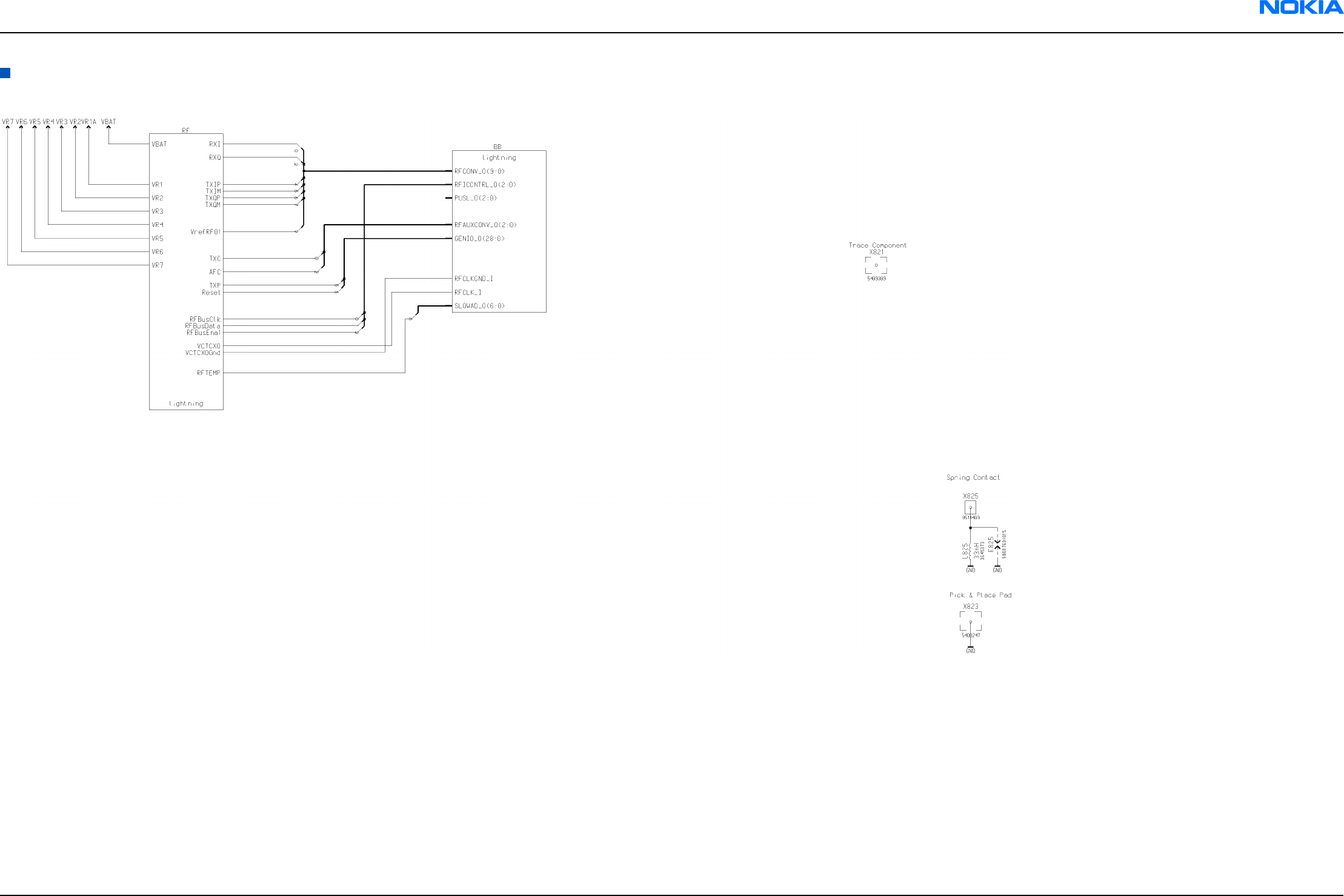
RF BB module top level
Figure 164 1fsa_09a, v.1.1, ed. 54
Figure 165 1fsa_11a, v.1.1, ed. 57
RM-25
Schematics Nokia Customer Care
9235618 (Issue 2) Company Confidential Page 10–5
Copyright ©2005 Nokia. All Rights Reserved.
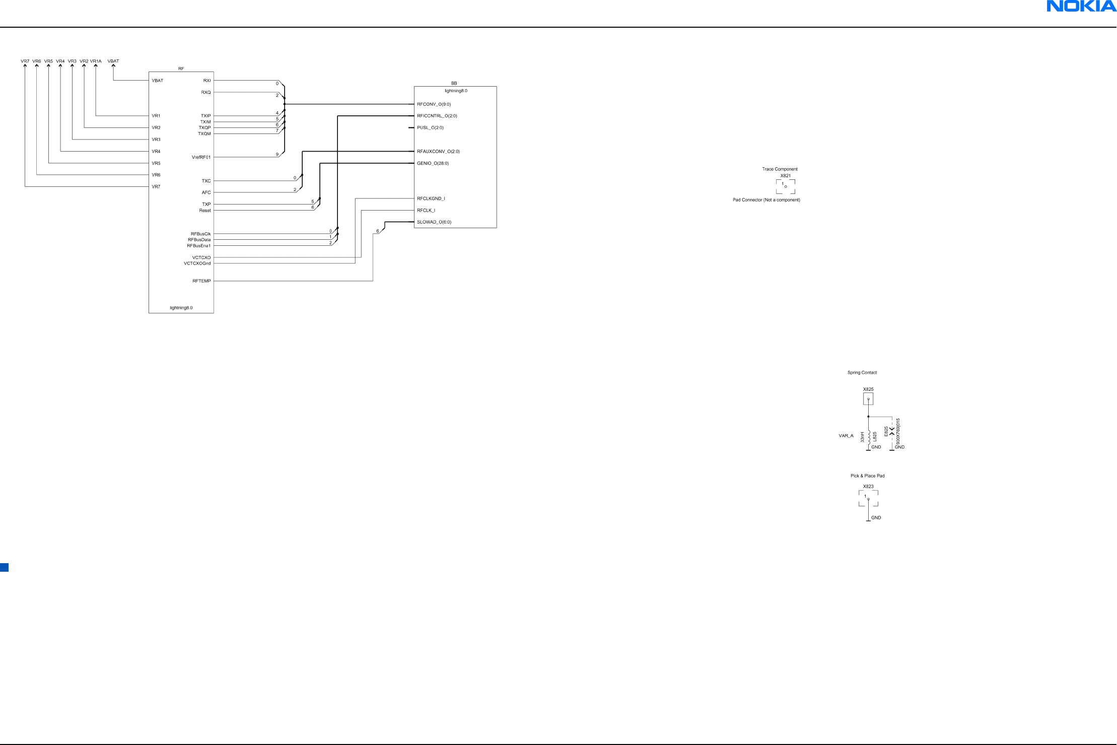
BB top level
Figure 166 1fsa_09a, v. 8.0, ed. 138
RM-25
Schematics Nokia Customer Care
9235618 (Issue 2) Company Confidential Page 10–6
Copyright ©2005 Nokia. All Rights Reserved.
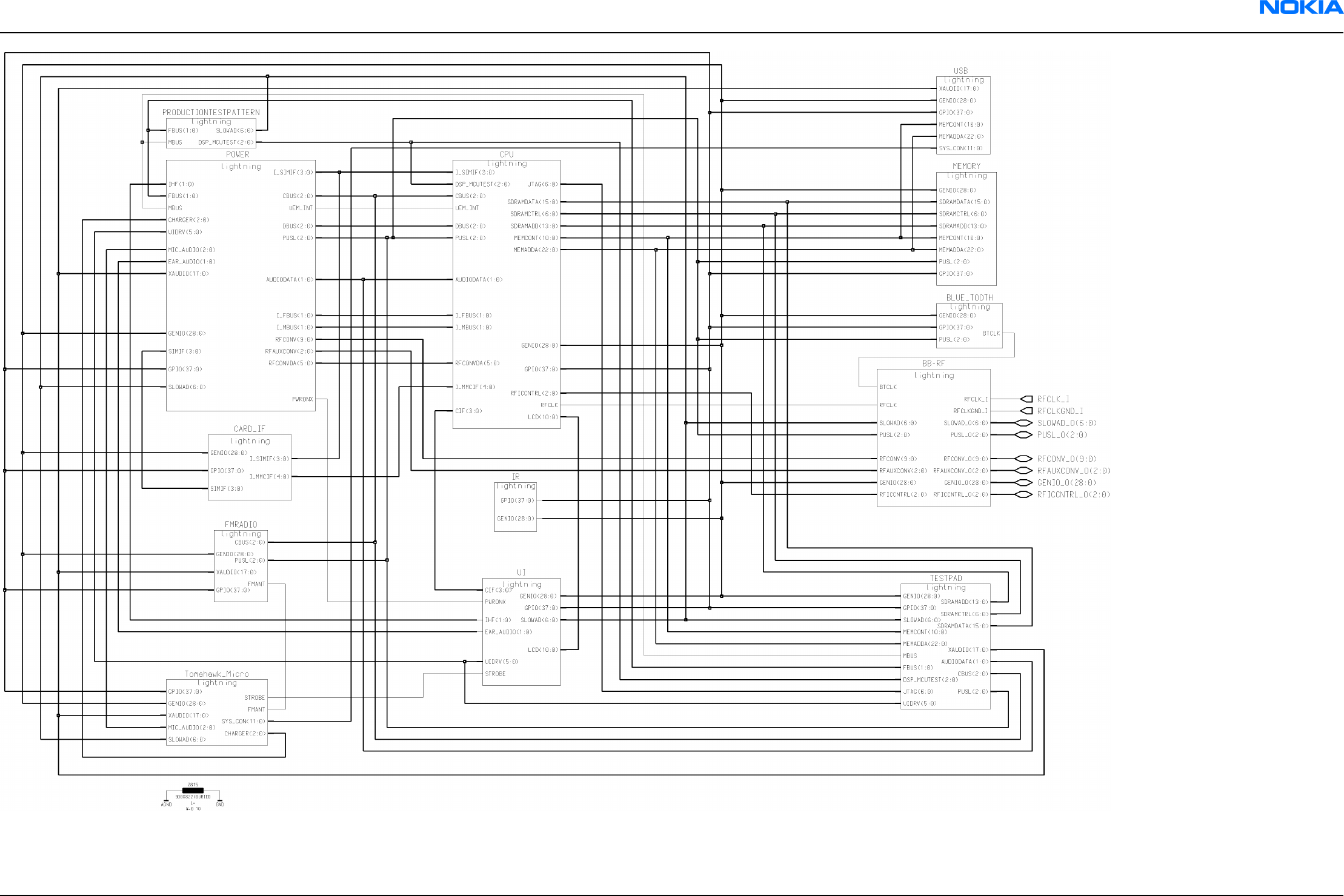
Figure 167 1fsa_11a, v. 8.0, ed. 142
RM-25
Schematics Nokia Customer Care
9235618 (Issue 2) Company Confidential Page 10–7
Copyright ©2005 Nokia. All Rights Reserved.
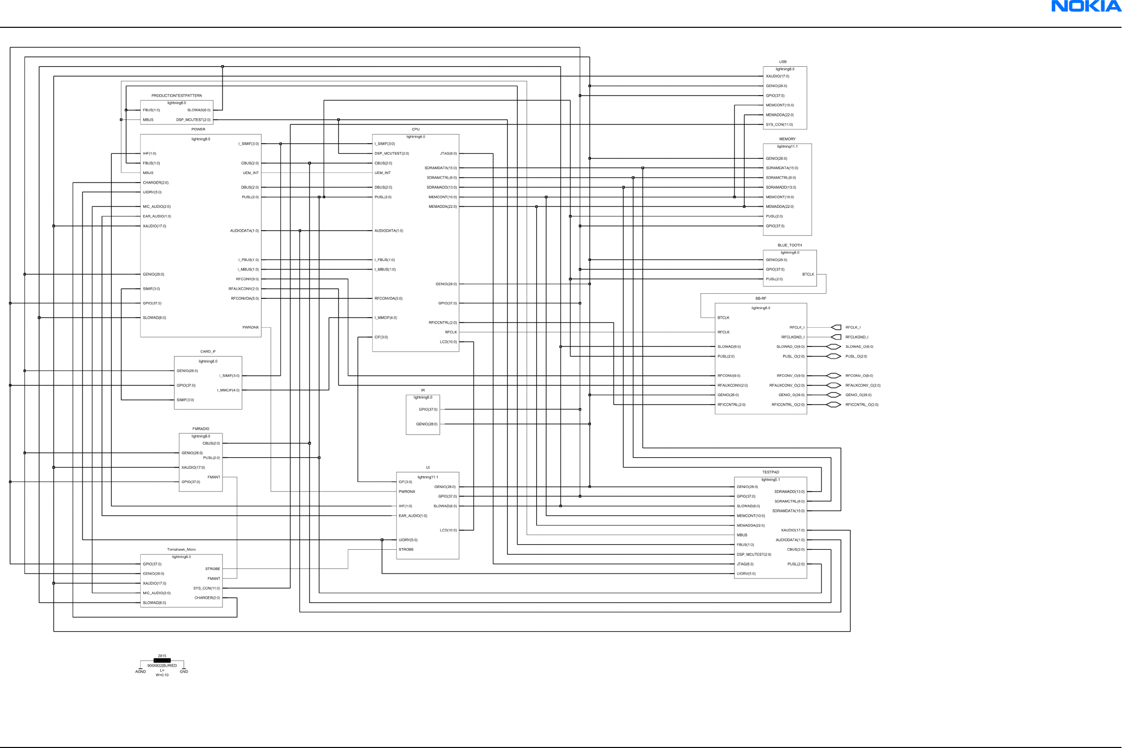
RM-25
Schematics Nokia Customer Care
9235618 (Issue 2) Company Confidential Page 10–8
Copyright ©2005 Nokia. All Rights Reserved.
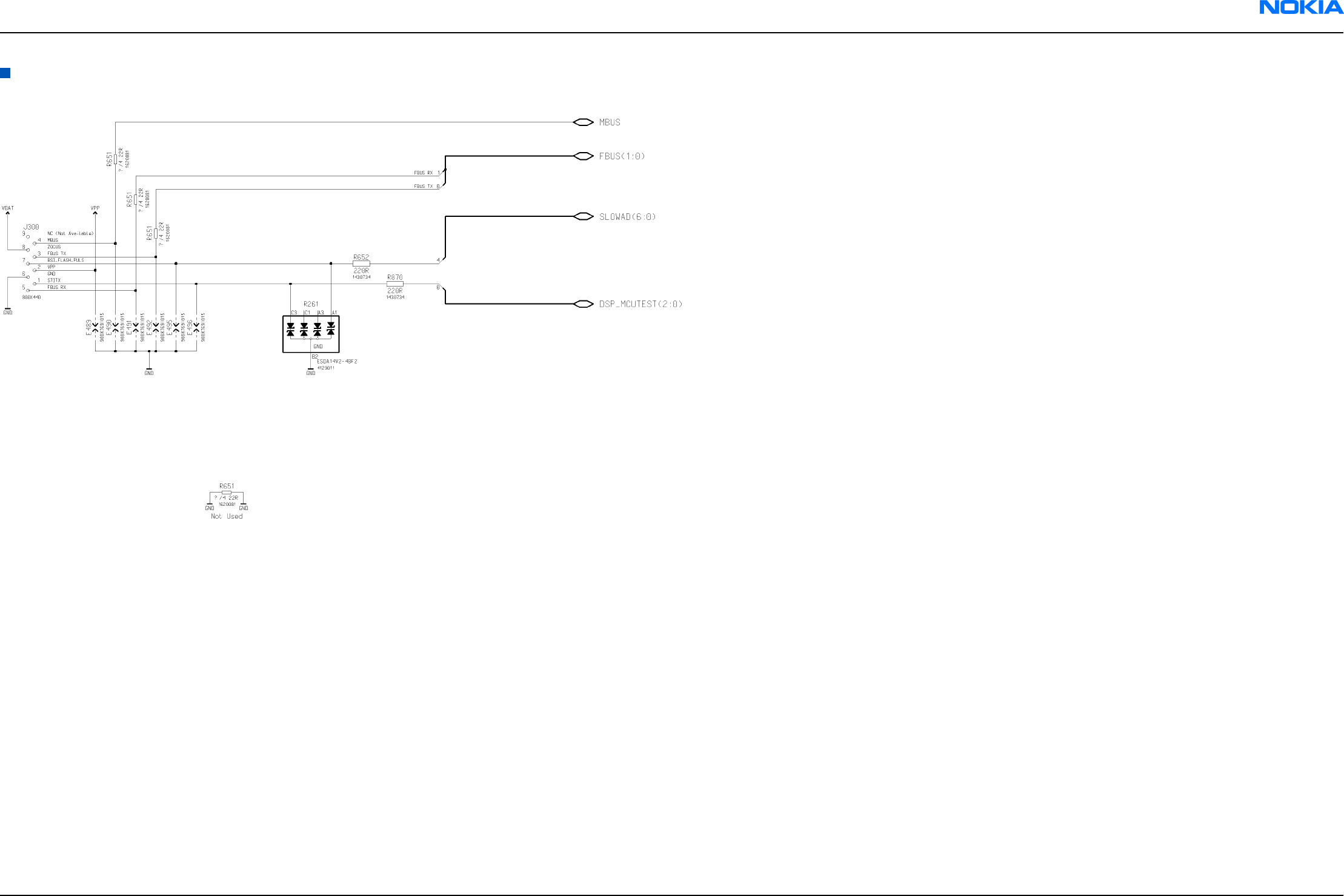
Production test pattern
Figure 168 1fsa_09a. v. 6.0, ed. 39
Figure 169 1fsa_11a. v. 6.0, ed. 41
RM-25
Schematics Nokia Customer Care
9235618 (Issue 2) Company Confidential Page 10–9
Copyright ©2005 Nokia. All Rights Reserved.
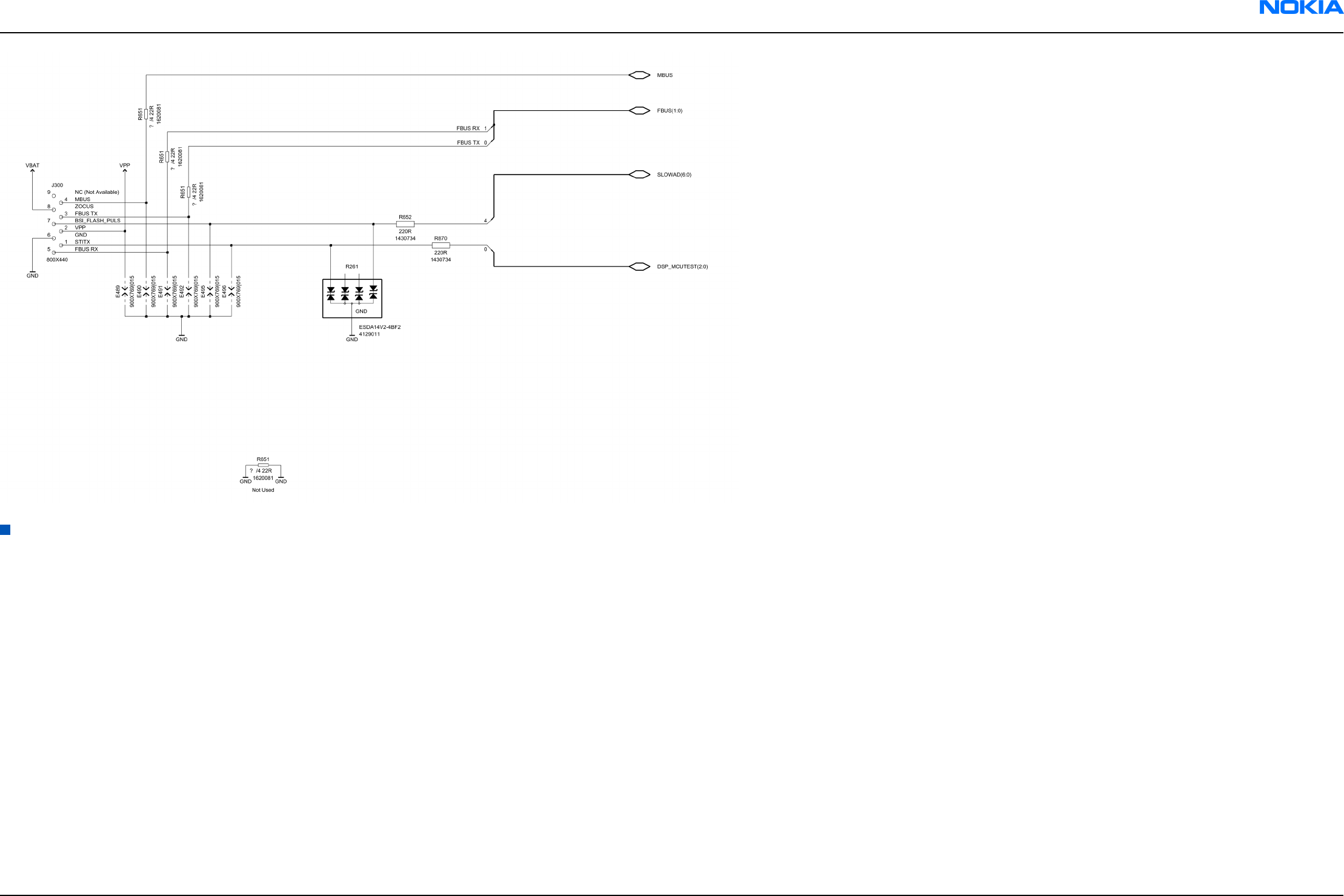
Power supplier top level
Figure 170 1fsa_09a, v. 8.0, ed. 79
RM-25
Schematics Nokia Customer Care
9235618 (Issue 2) Company Confidential Page 10–10
Copyright ©2005 Nokia. All Rights Reserved.
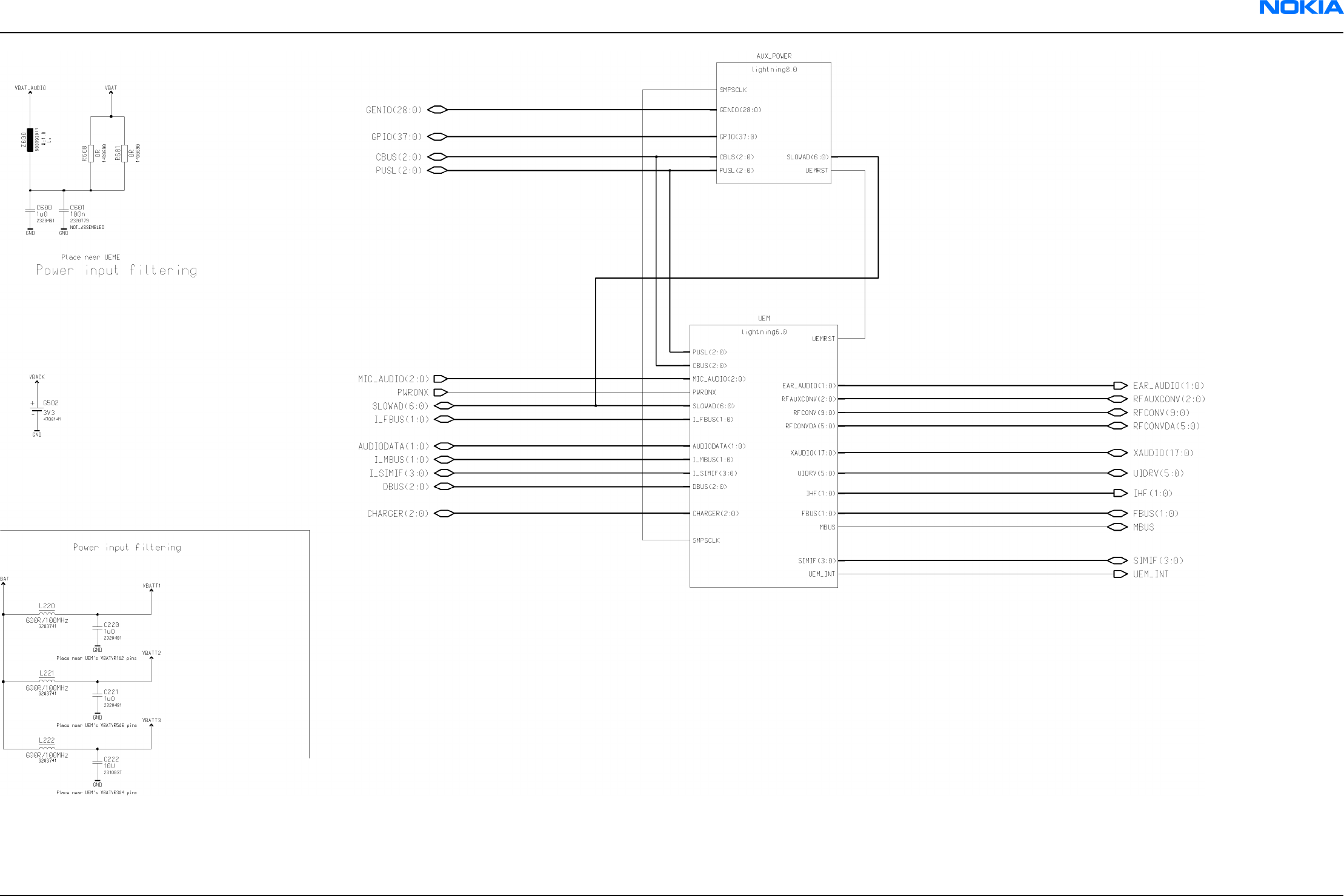
Figure 171 1fsa_11a, v. 8.0, ed. 82
RM-25
Schematics Nokia Customer Care
9235618 (Issue 2) Company Confidential Page 10–11
Copyright ©2005 Nokia. All Rights Reserved.
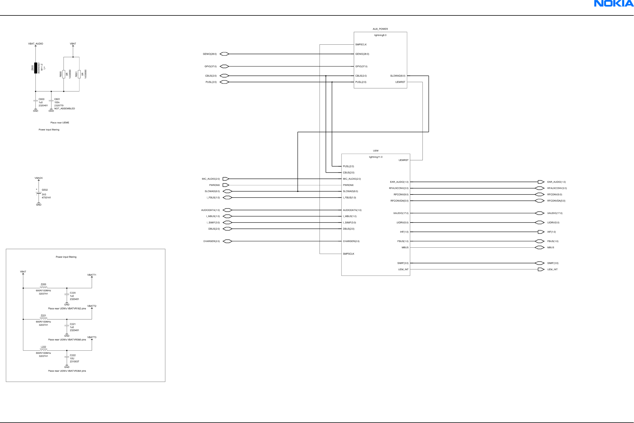
RM-25
Schematics Nokia Customer Care
9235618 (Issue 2) Company Confidential Page 10–12
Copyright ©2005 Nokia. All Rights Reserved.
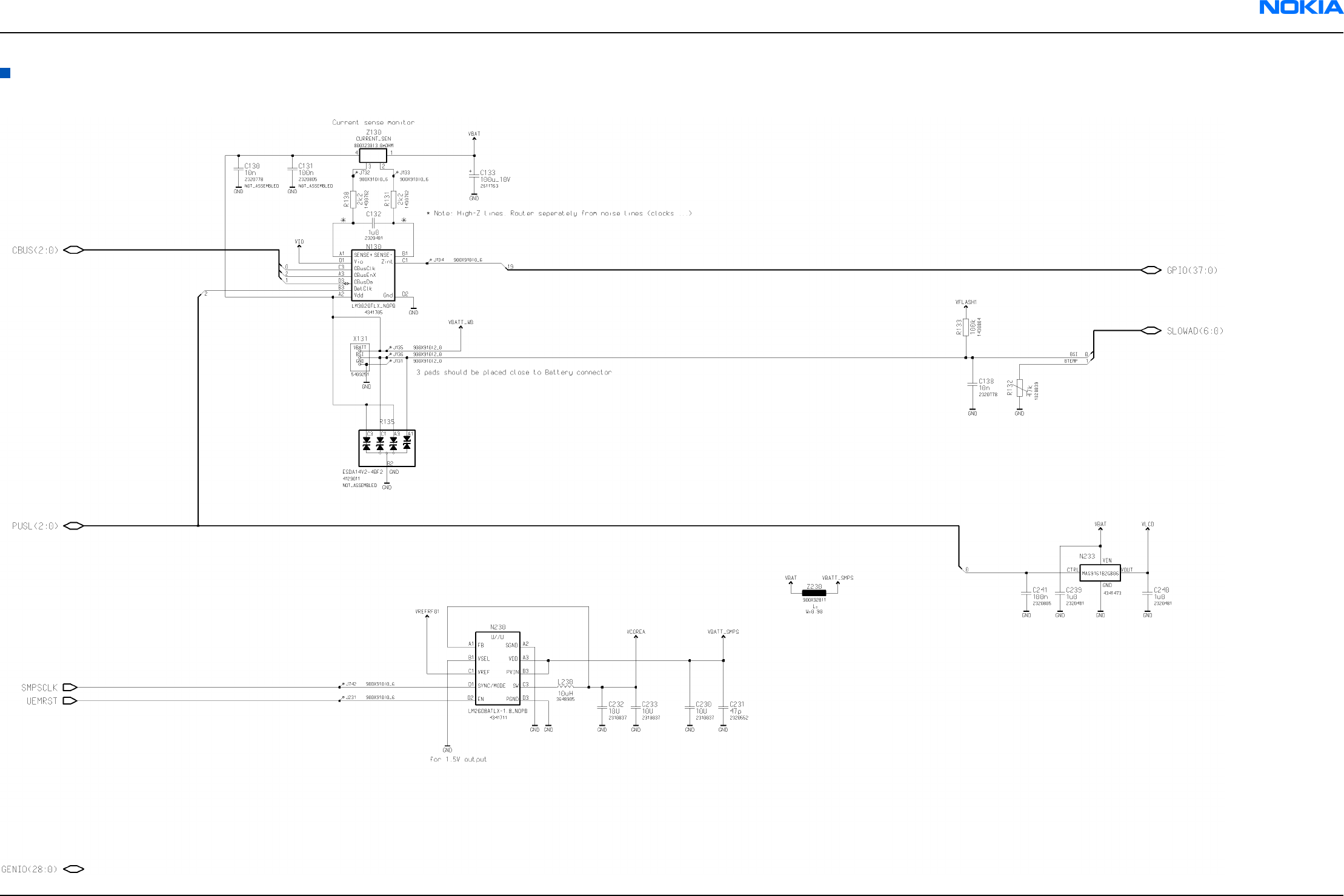
Aux_power
Figure 172 1fsa_09a, v. 8.0, ed. 84
RM-25
Schematics Nokia Customer Care
9235618 (Issue 2) Company Confidential Page 10–13
Copyright ©2005 Nokia. All Rights Reserved.
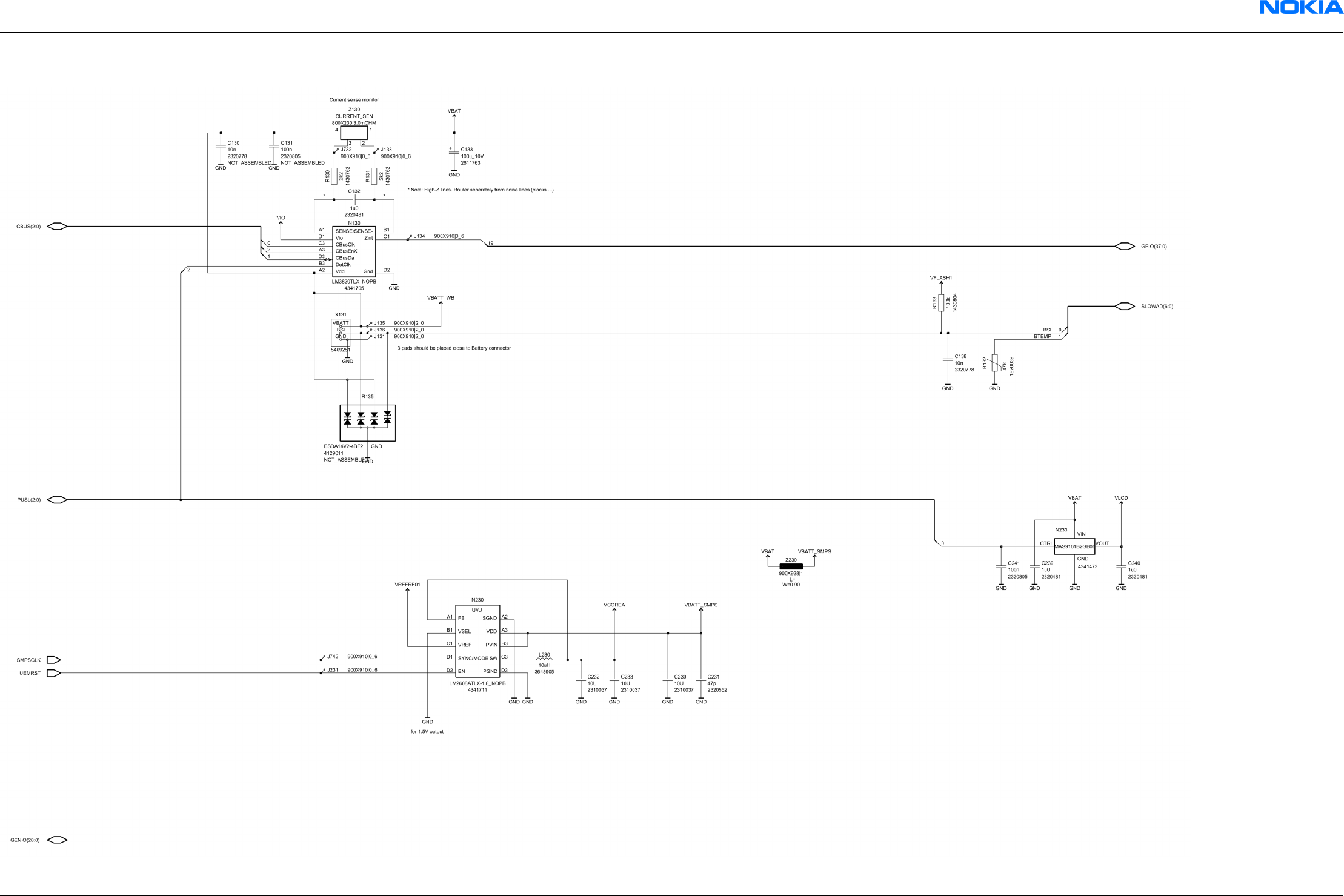
Figure 173 1fsa_11a, v. 8.0, ed. 86
RM-25
Schematics Nokia Customer Care
9235618 (Issue 2) Company Confidential Page 10–14
Copyright ©2005 Nokia. All Rights Reserved.

UEME/UEMEK
Figure 174 1fsa_09a, v. 6.0, ed. 96
RM-25
Schematics Nokia Customer Care
9235618 (Issue 2) Company Confidential Page 10–15
Copyright ©2005 Nokia. All Rights Reserved.
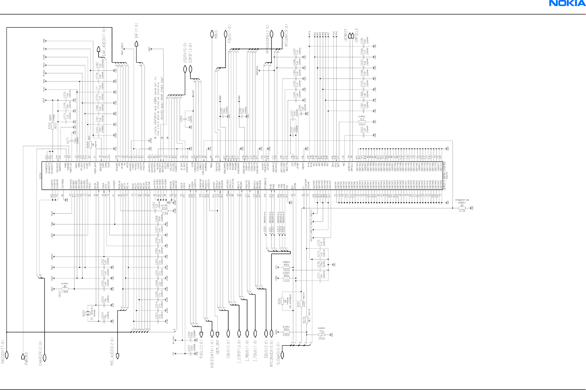
RM-25
Schematics Nokia Customer Care
9235618 (Issue 2) Company Confidential Page 10–16
Copyright ©2005 Nokia. All Rights Reserved.
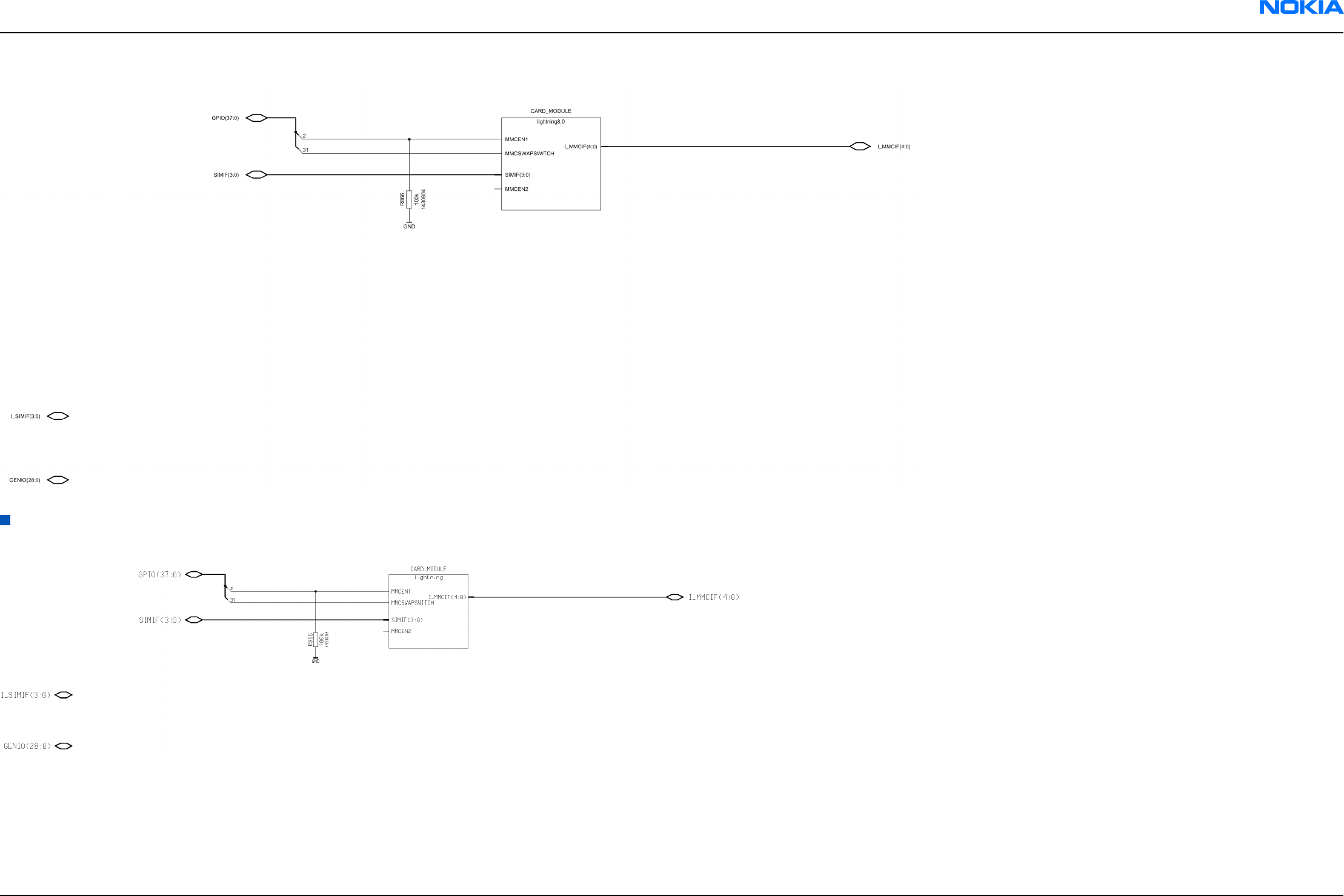
Figure 175 1fsa_11a, v. 11.0, ed. 100
Card interface
Figure 176 1fsa_09a, v. 8.0, ed. 73
Figure 177 1fsa_11a, v. 8.0, ed. 76
RM-25
Schematics Nokia Customer Care
9235618 (Issue 2) Company Confidential Page 10–17
Copyright ©2005 Nokia. All Rights Reserved.
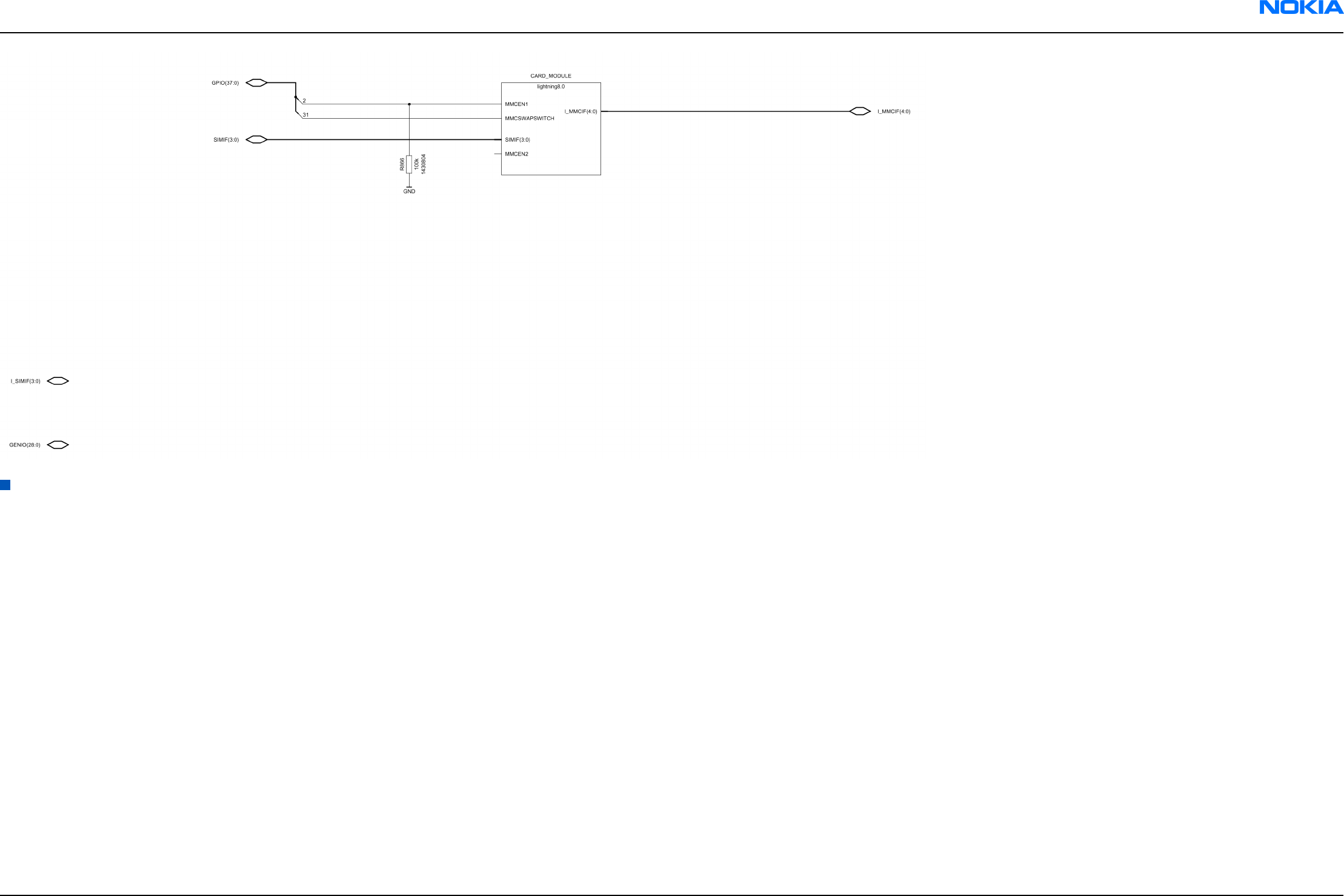
Card interface module
Figure 178 1fsa_09a, v. 8.0, ed. 88
RM-25
Schematics Nokia Customer Care
9235618 (Issue 2) Company Confidential Page 10–18
Copyright ©2005 Nokia. All Rights Reserved.
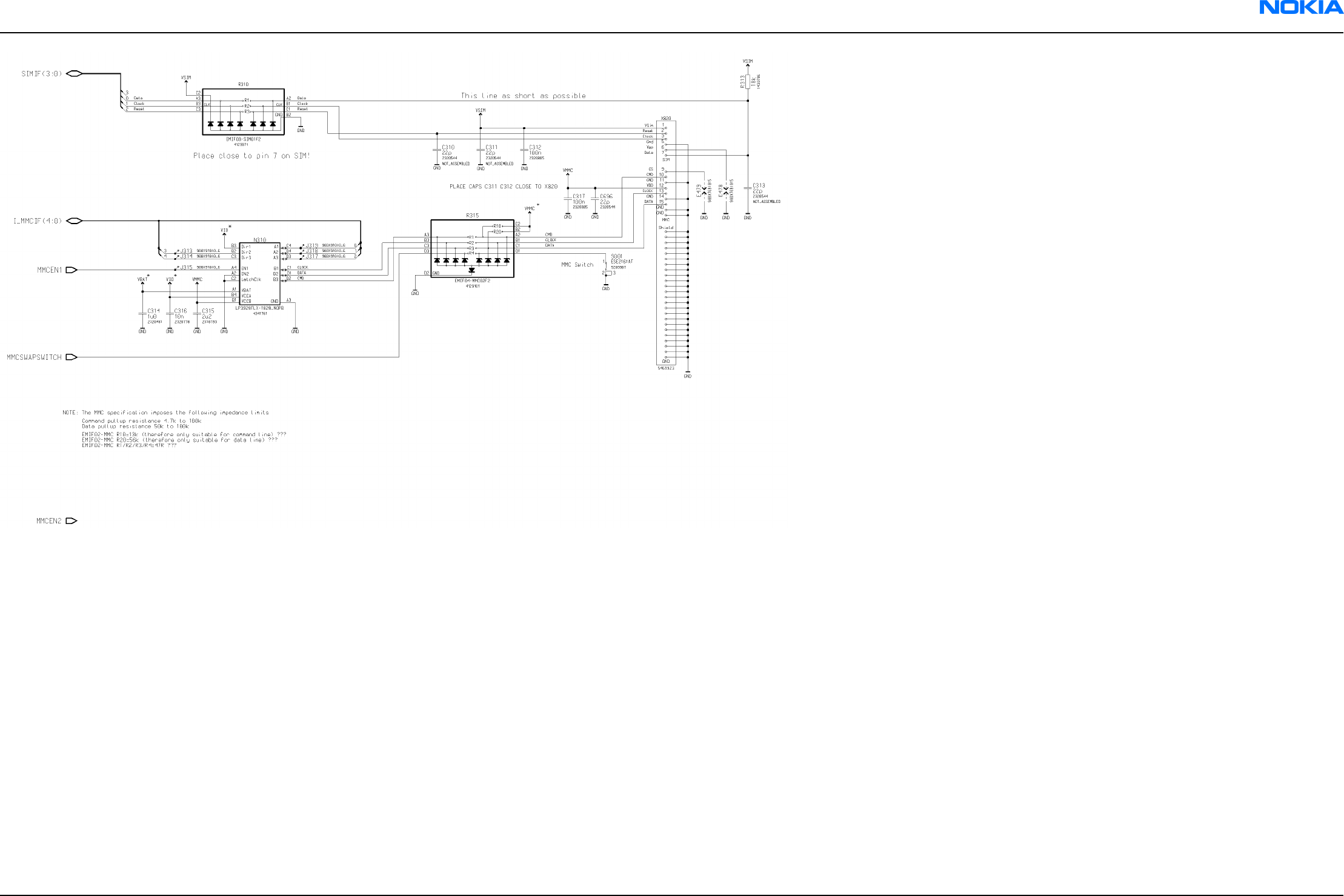
Figure 179 1fsa_11a, v. 8.0, ed. 92
RM-25
Schematics Nokia Customer Care
9235618 (Issue 2) Company Confidential Page 10–19
Copyright ©2005 Nokia. All Rights Reserved.
FM radio top level
Figure 180 1fsa_09a, v.8.0, ed. 19
RM-25
Schematics Nokia Customer Care
9235618 (Issue 2) Company Confidential Page 10–20
Copyright ©2005 Nokia. All Rights Reserved.
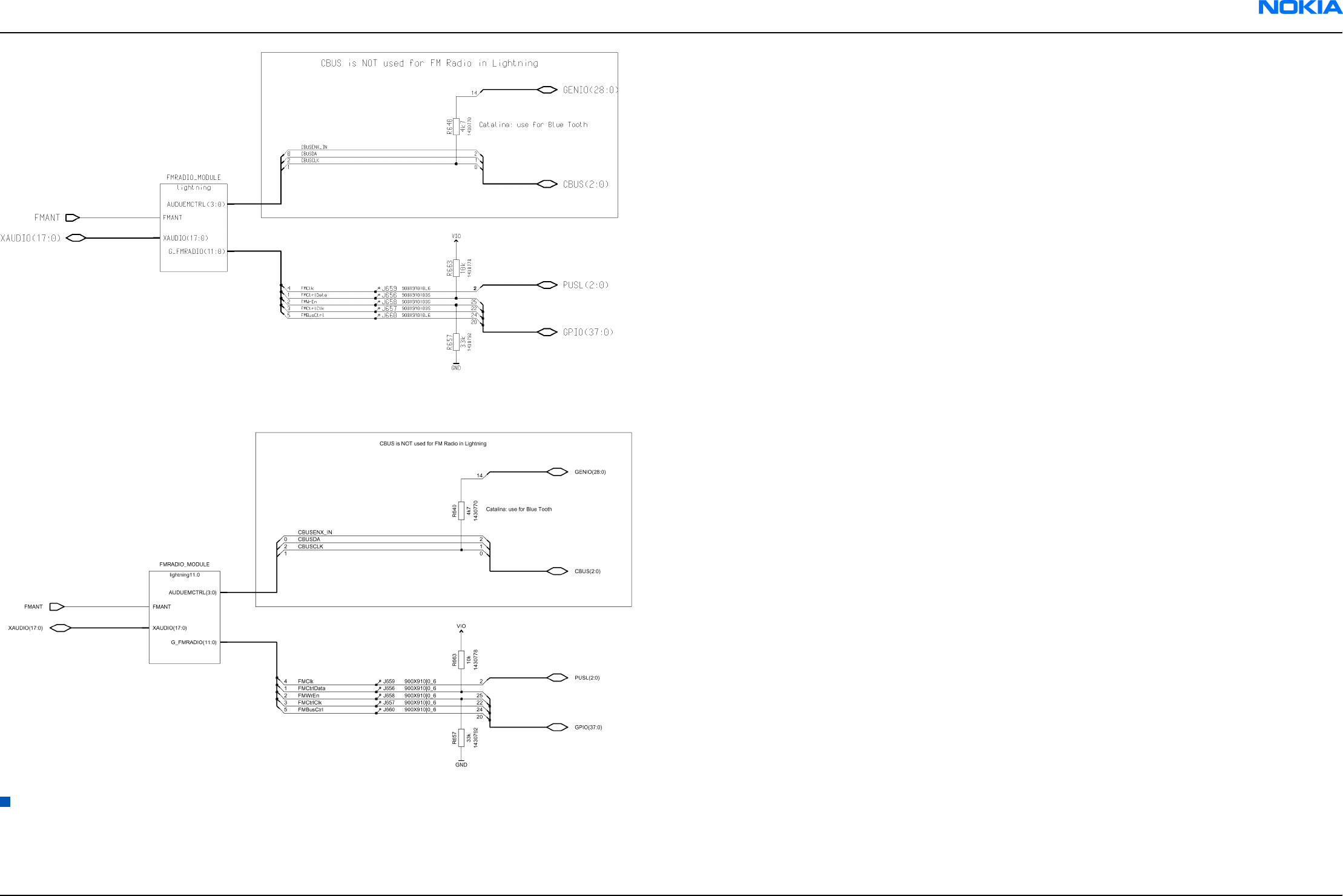
Figure 181 1fsa_11a, v.8.0, ed. 21
FM radio module
Figure 182 1fsa_09a, v. 6.0, ed. 25
RM-25
Schematics Nokia Customer Care
9235618 (Issue 2) Company Confidential Page 10–21
Copyright ©2005 Nokia. All Rights Reserved.
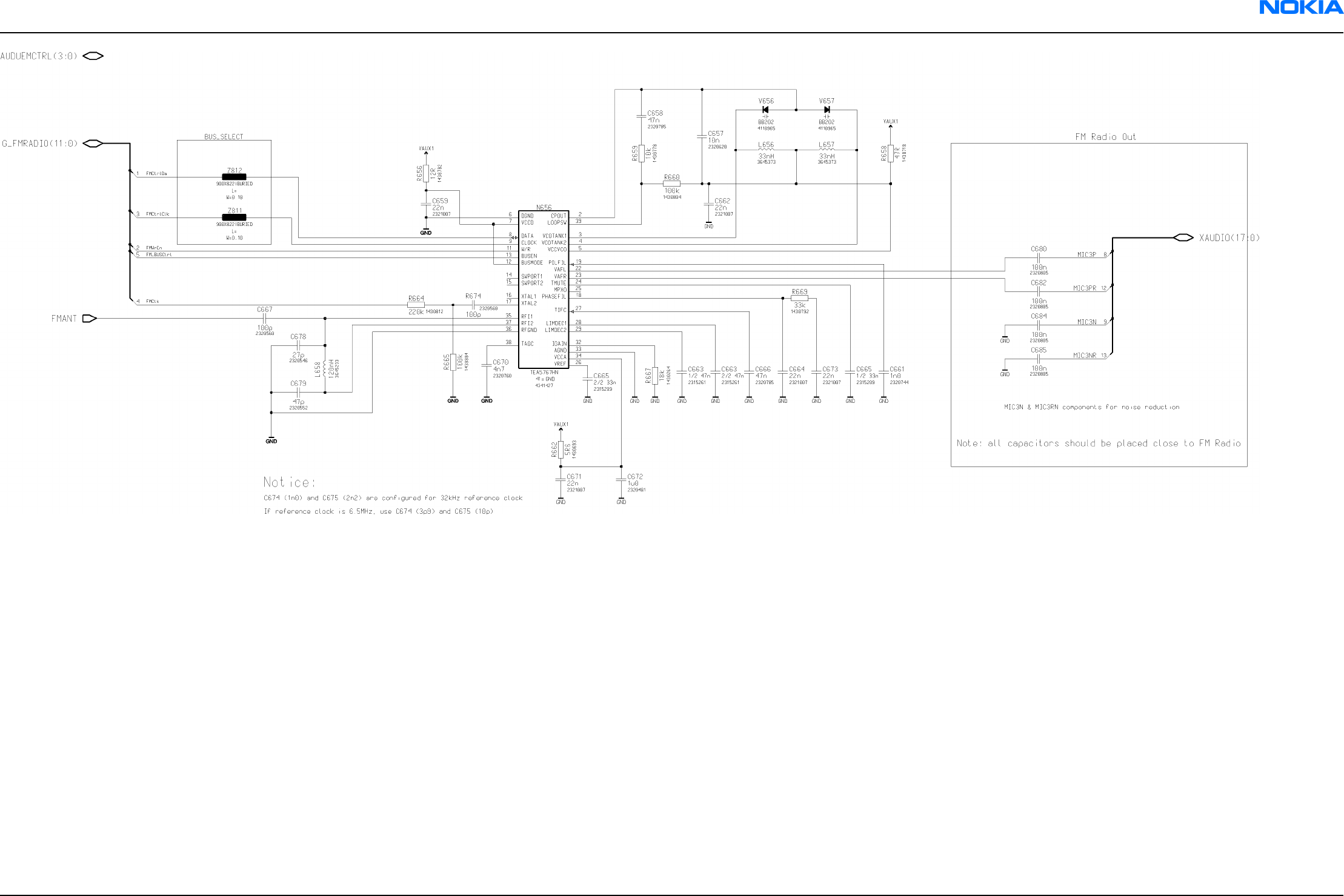
Figure 183 1fsa_11a, v. 11.0, ed. 30
RM-25
Schematics Nokia Customer Care
9235618 (Issue 2) Company Confidential Page 10–22
Copyright ©2005 Nokia. All Rights Reserved.
Pop-portTM and microphone
Figure 184 1fsa_09a, v. 6.0, ed. 110
RM-25
Schematics Nokia Customer Care
9235618 (Issue 2) Company Confidential Page 10–23
Copyright ©2005 Nokia. All Rights Reserved.
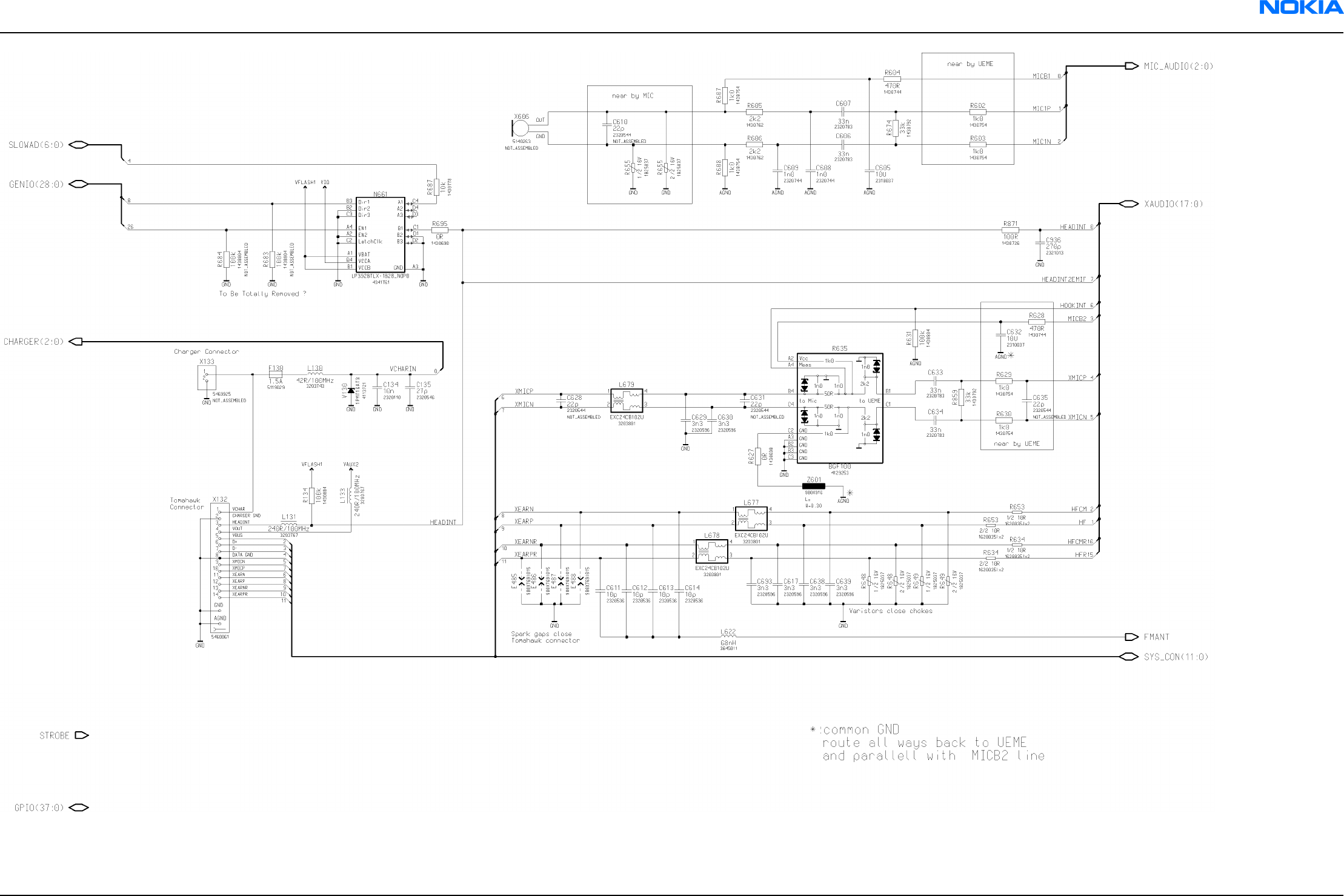
Figure 185 1fsa_11a, v. 6.0, ed. 113
RM-25
Schematics Nokia Customer Care
9235618 (Issue 2) Company Confidential Page 10–24
Copyright ©2005 Nokia. All Rights Reserved.
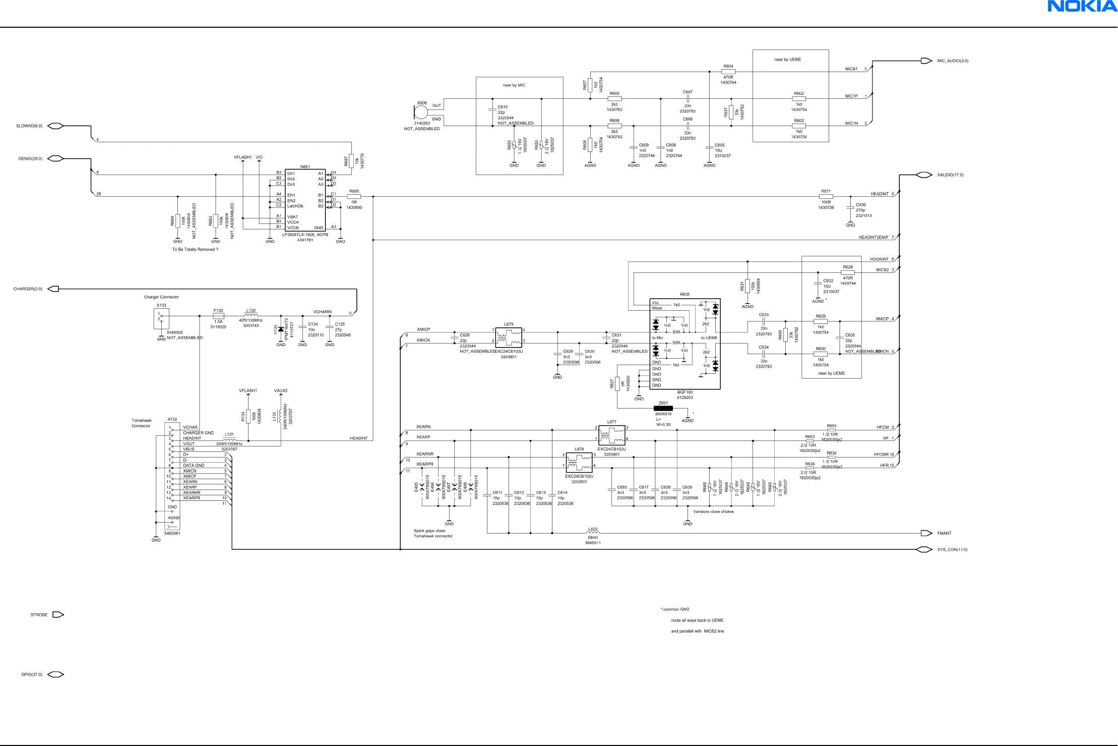
RM-25
Schematics Nokia Customer Care
9235618 (Issue 2) Company Confidential Page 10–25
Copyright ©2005 Nokia. All Rights Reserved.

UPP_WD2
Figure 186 1fsa_09a, v. 6.0, ed. 49
RM-25
Schematics Nokia Customer Care
9235618 (Issue 2) Company Confidential Page 10–26
Copyright ©2005 Nokia. All Rights Reserved.
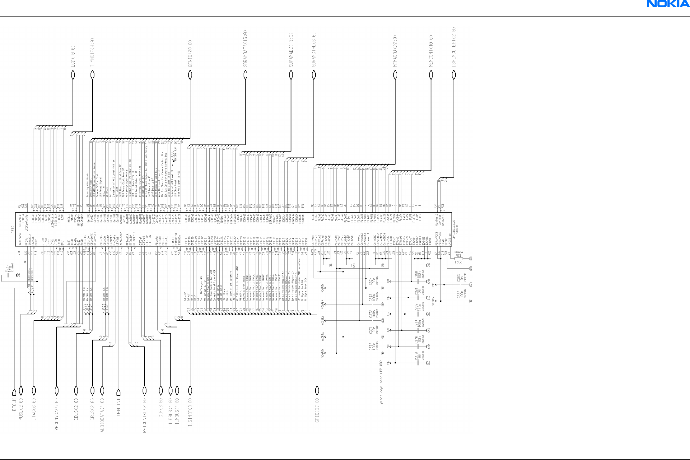
Figure 187 1fsa_11a, v. 6.0, ed. 52
RM-25
Schematics Nokia Customer Care
9235618 (Issue 2) Company Confidential Page 10–27
Copyright ©2005 Nokia. All Rights Reserved.
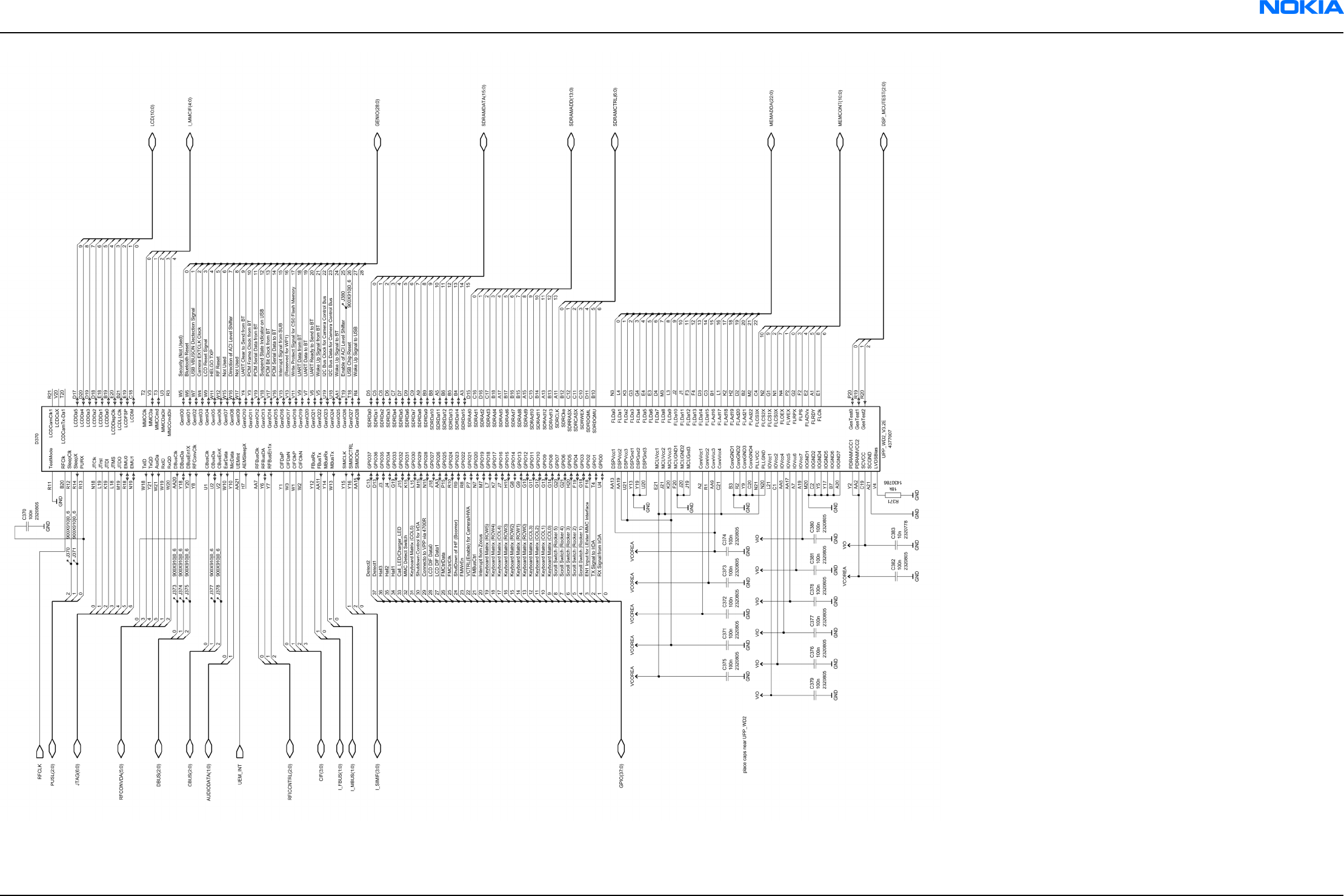
RM-25
Schematics Nokia Customer Care
9235618 (Issue 2) Company Confidential Page 10–28
Copyright ©2005 Nokia. All Rights Reserved.
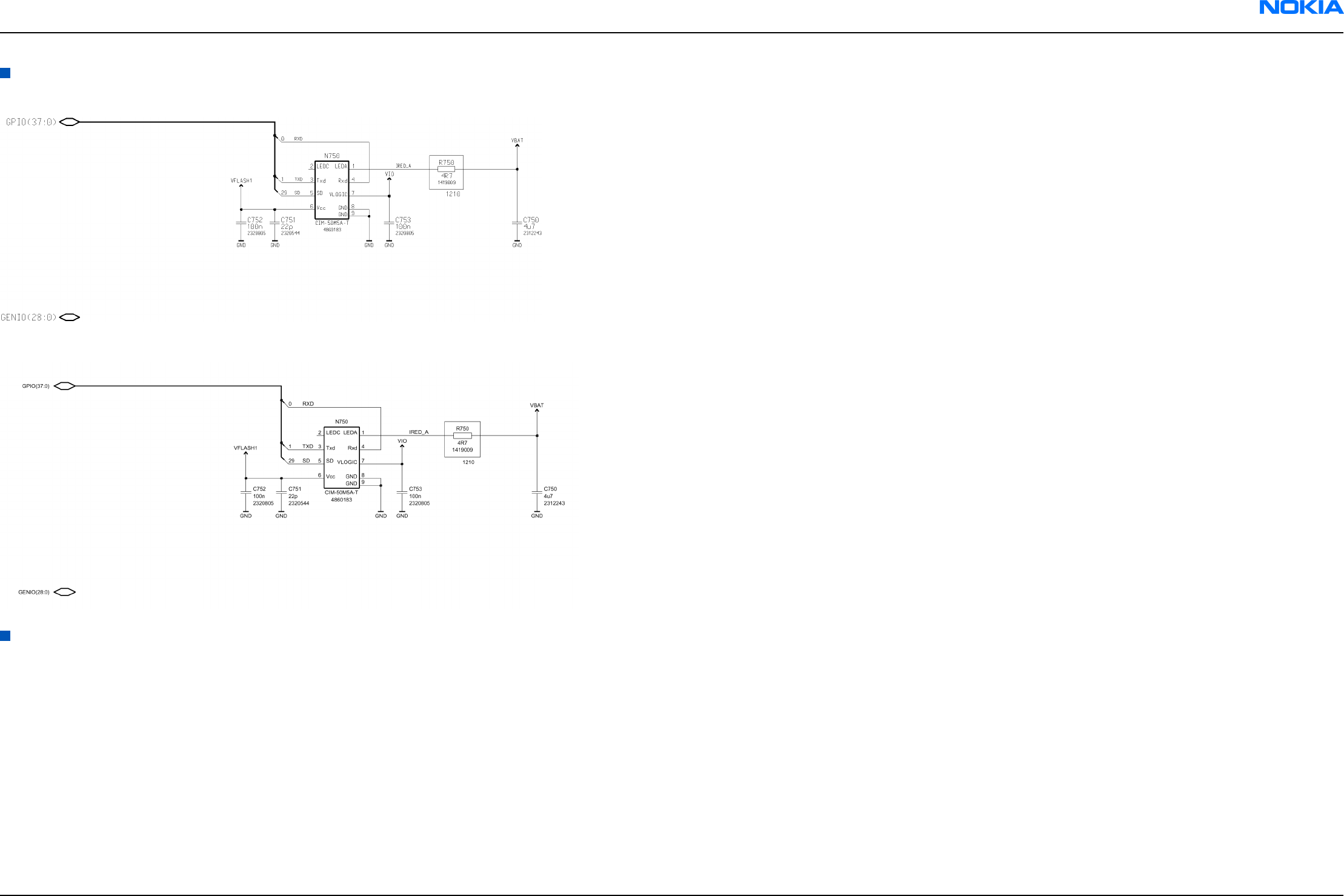
IR module
Figure 188 1fsa_09a, v. 6.0, ed. 93
Figure 189 1fsa_11a, v. 6.0, ed. 96
User interface (top part and keyboard)
Figure 190 1fsa_09a, v. 8.1, ed. 140
RM-25
Schematics Nokia Customer Care
9235618 (Issue 2) Company Confidential Page 10–29
Copyright ©2005 Nokia. All Rights Reserved.
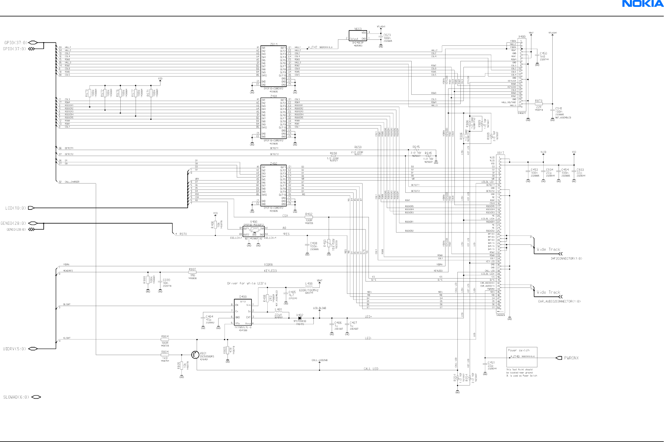
Figure 191 1fsa_11a, v. 11.1, ed. 147
RM-25
Schematics Nokia Customer Care
9235618 (Issue 2) Company Confidential Page 10–30
Copyright ©2005 Nokia. All Rights Reserved.
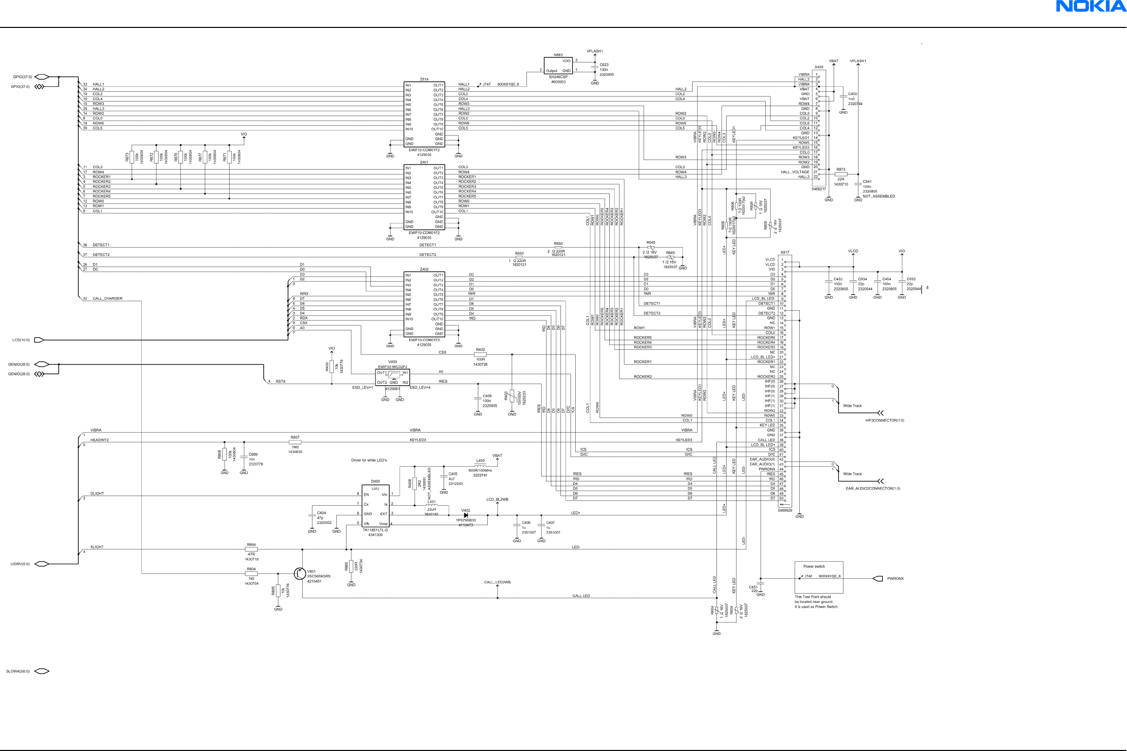
RM-25
Schematics Nokia Customer Care
9235618 (Issue 2) Company Confidential Page 10–31
Copyright ©2005 Nokia. All Rights Reserved.

User interface (camera)
Figure 192 1fsa_09a, v. 8.0, ed. 74
Figure 193 1fsa_11a, v. 11.1, ed. 79
RM-25
Schematics Nokia Customer Care
9235618 (Issue 2) Company Confidential Page 10–32
Copyright ©2005 Nokia. All Rights Reserved.
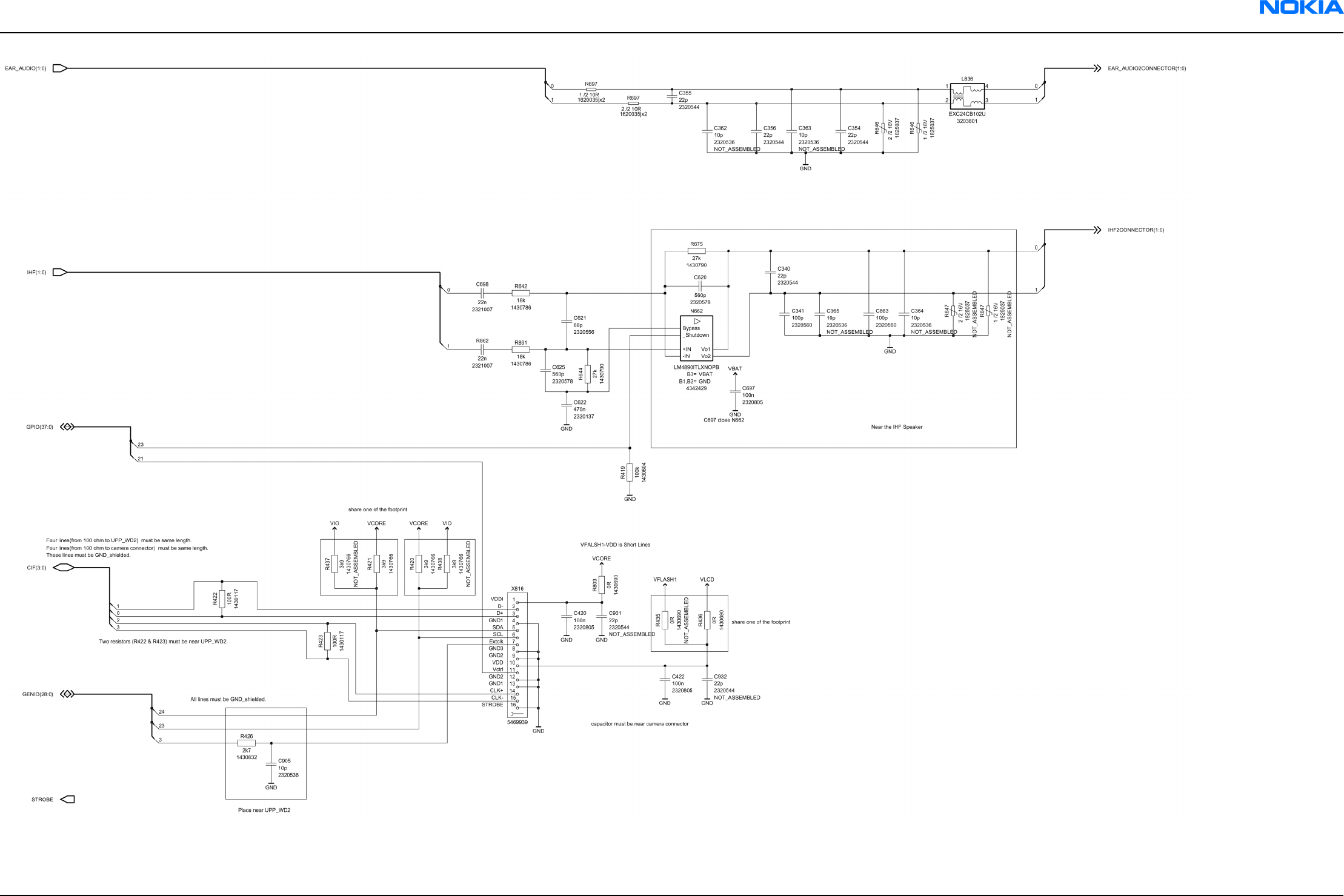
RM-25
Schematics Nokia Customer Care
9235618 (Issue 2) Company Confidential Page 10–33
Copyright ©2005 Nokia. All Rights Reserved.
User interface (empty)
Figure 194 1fsa_09a, v. 8.0, ed. 84
Figure 195 1fsa_11a, v. 11.1, ed. 88
USB
Figure 196 1fsa_09a, v. 8.0, ed. 44
Figure 197 1fsa_11a, v. 8.0, ed. 47
RM-25
Schematics Nokia Customer Care
9235618 (Issue 2) Company Confidential Page 10–34
Copyright ©2005 Nokia. All Rights Reserved.
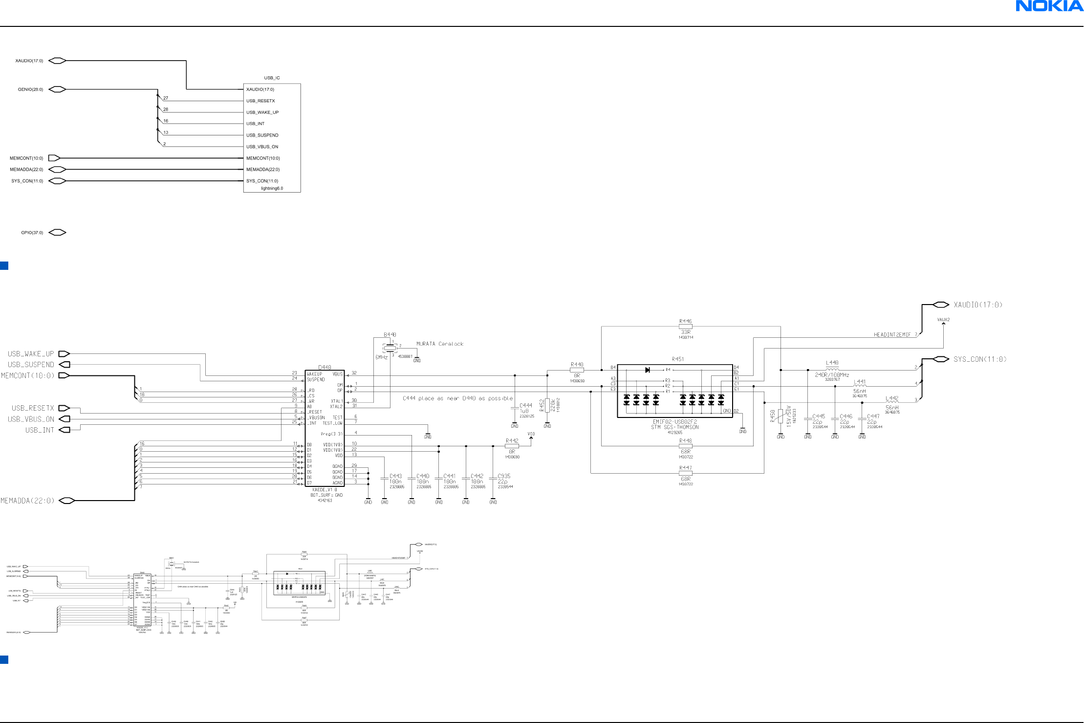
USB module
Figure 198 1fsa_09a, v. 6.0, ed. 57
Figure 199 1fsa_11a, v. 6.0, ed. 60
Memory
Figure 200 1fsa_09a, v. 8.0, ed. 68
RM-25
Schematics Nokia Customer Care
9235618 (Issue 2) Company Confidential Page 10–35
Copyright ©2005 Nokia. All Rights Reserved.
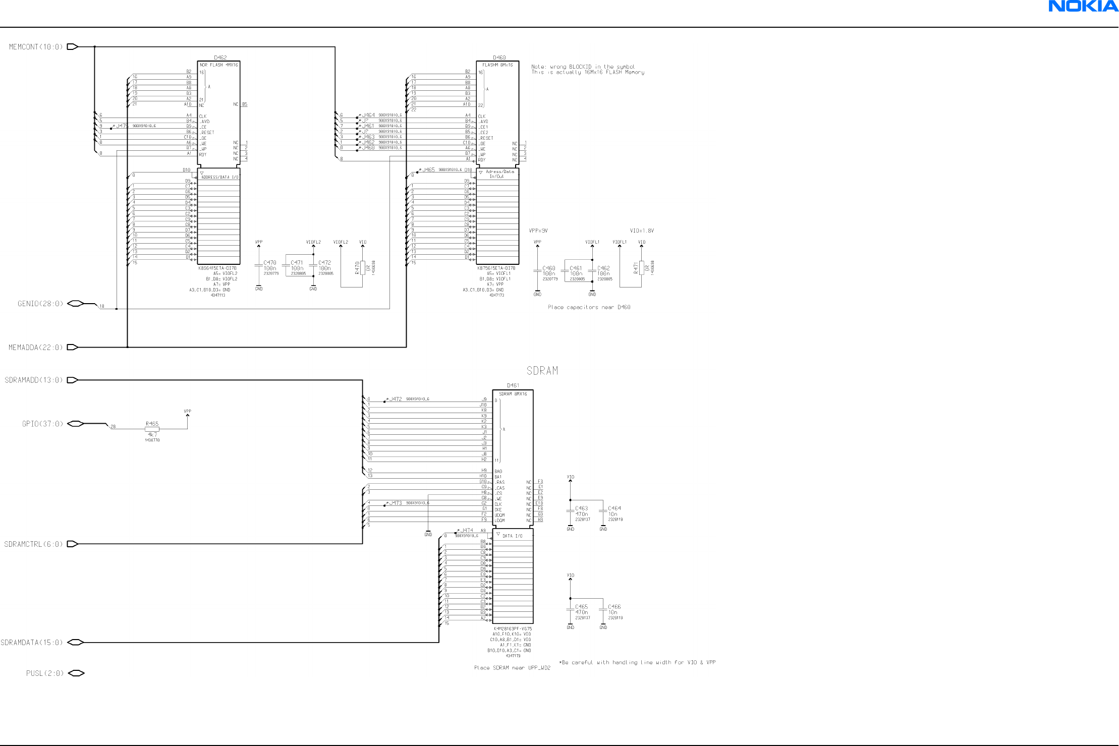
Figure 201 1fsa_11a, v. 11.1, ed. 96
RM-25
Schematics Nokia Customer Care
9235618 (Issue 2) Company Confidential Page 10–36
Copyright ©2005 Nokia. All Rights Reserved.
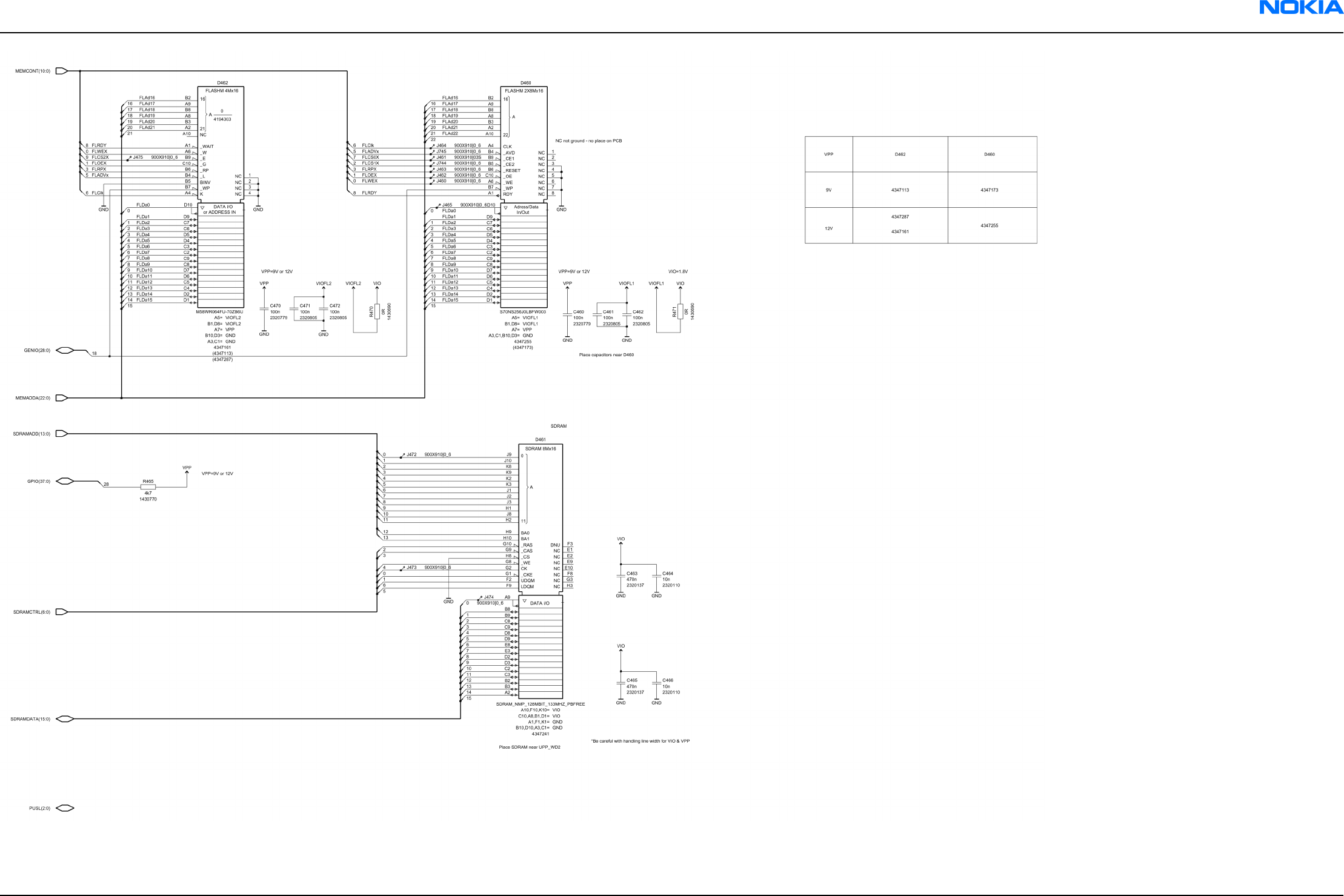
RM-25
Schematics Nokia Customer Care
9235618 (Issue 2) Company Confidential Page 10–37
Copyright ©2005 Nokia. All Rights Reserved.
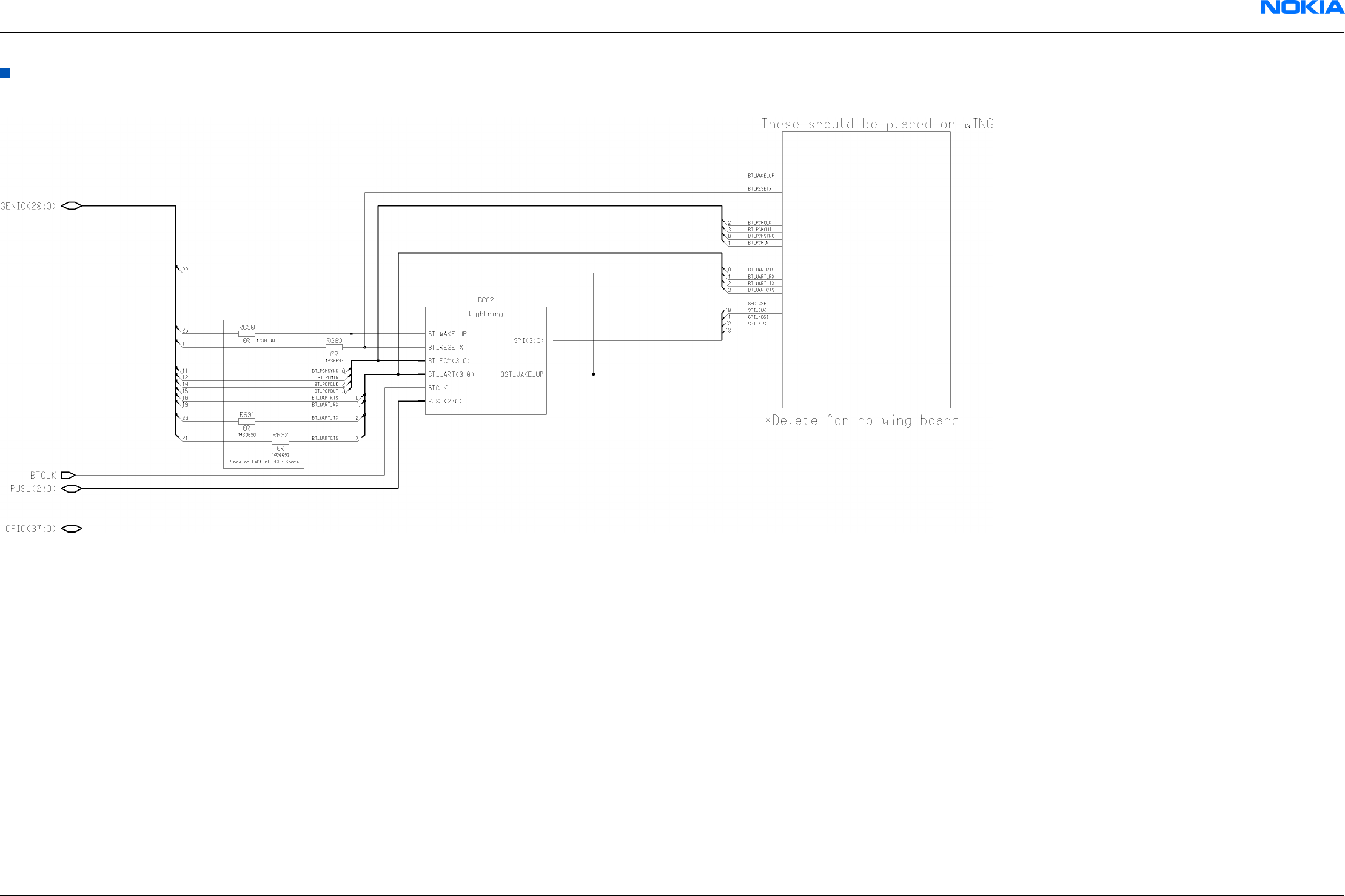
Bluetooth
Figure 202 1fsa_09a, v. 8.0, ed. 49
Figure 203 1fsa_11a, v. 8.0, ed. 52
RM-25
Schematics Nokia Customer Care
9235618 (Issue 2) Company Confidential Page 10–38
Copyright ©2005 Nokia. All Rights Reserved.
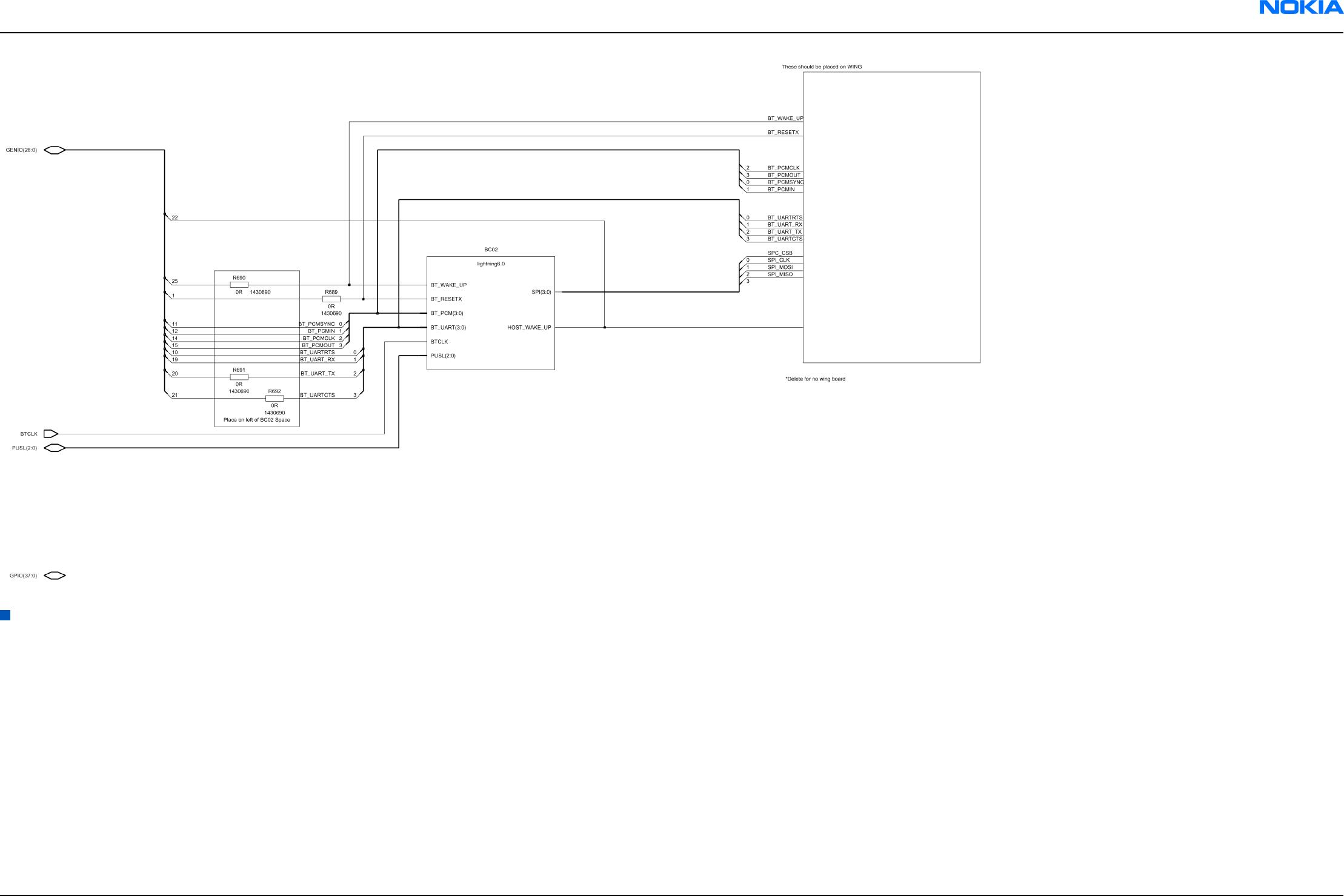
Bluetooth module
Figure 204 1fsa_09a, v. 6.0, ed. 71
RM-25
Schematics Nokia Customer Care
9235618 (Issue 2) Company Confidential Page 10–39
Copyright ©2005 Nokia. All Rights Reserved.
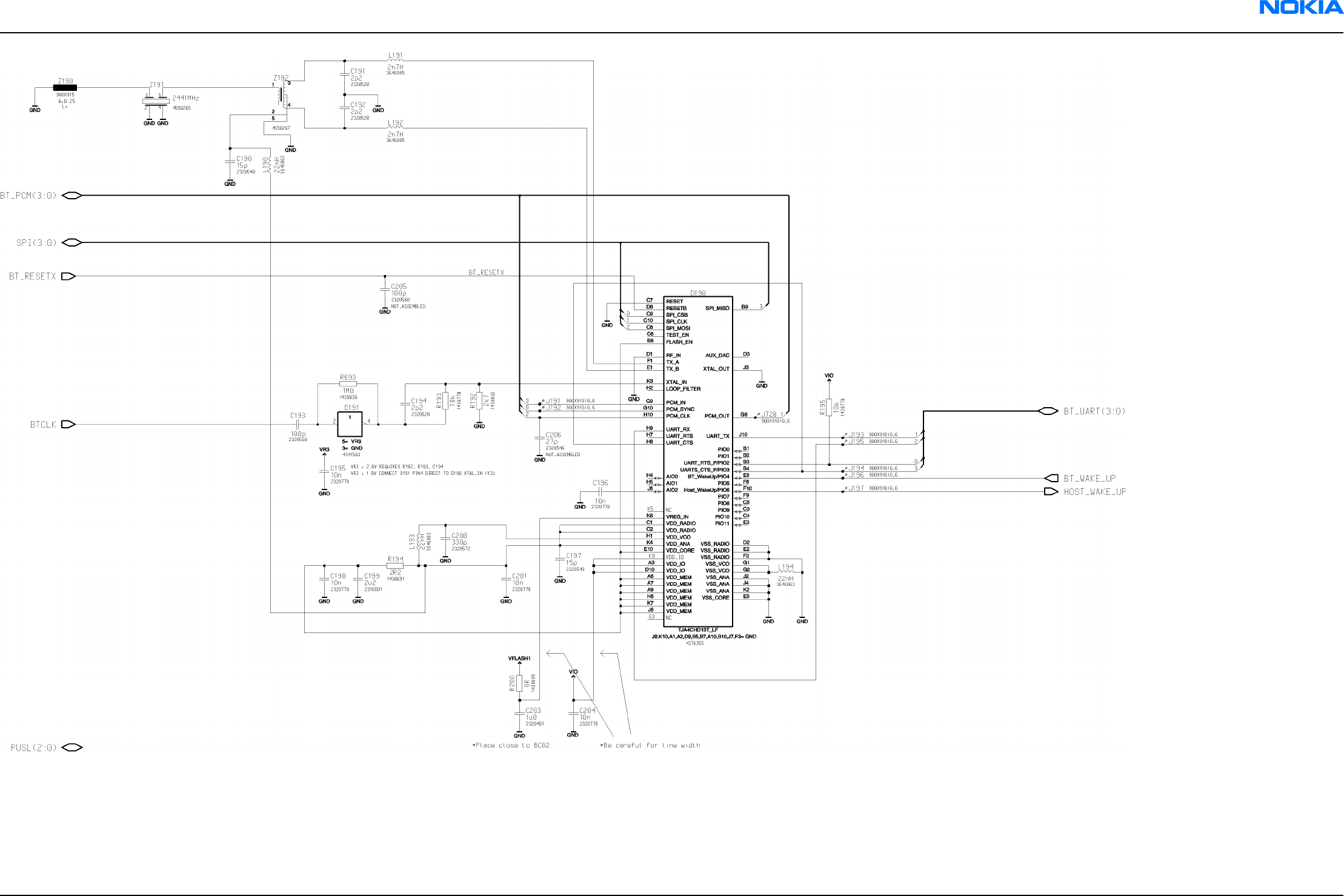
Figure 205 1fsa_11a, v. 6.0, ed. 76
RM-25
Schematics Nokia Customer Care
9235618 (Issue 2) Company Confidential Page 10–40
Copyright ©2005 Nokia. All Rights Reserved.
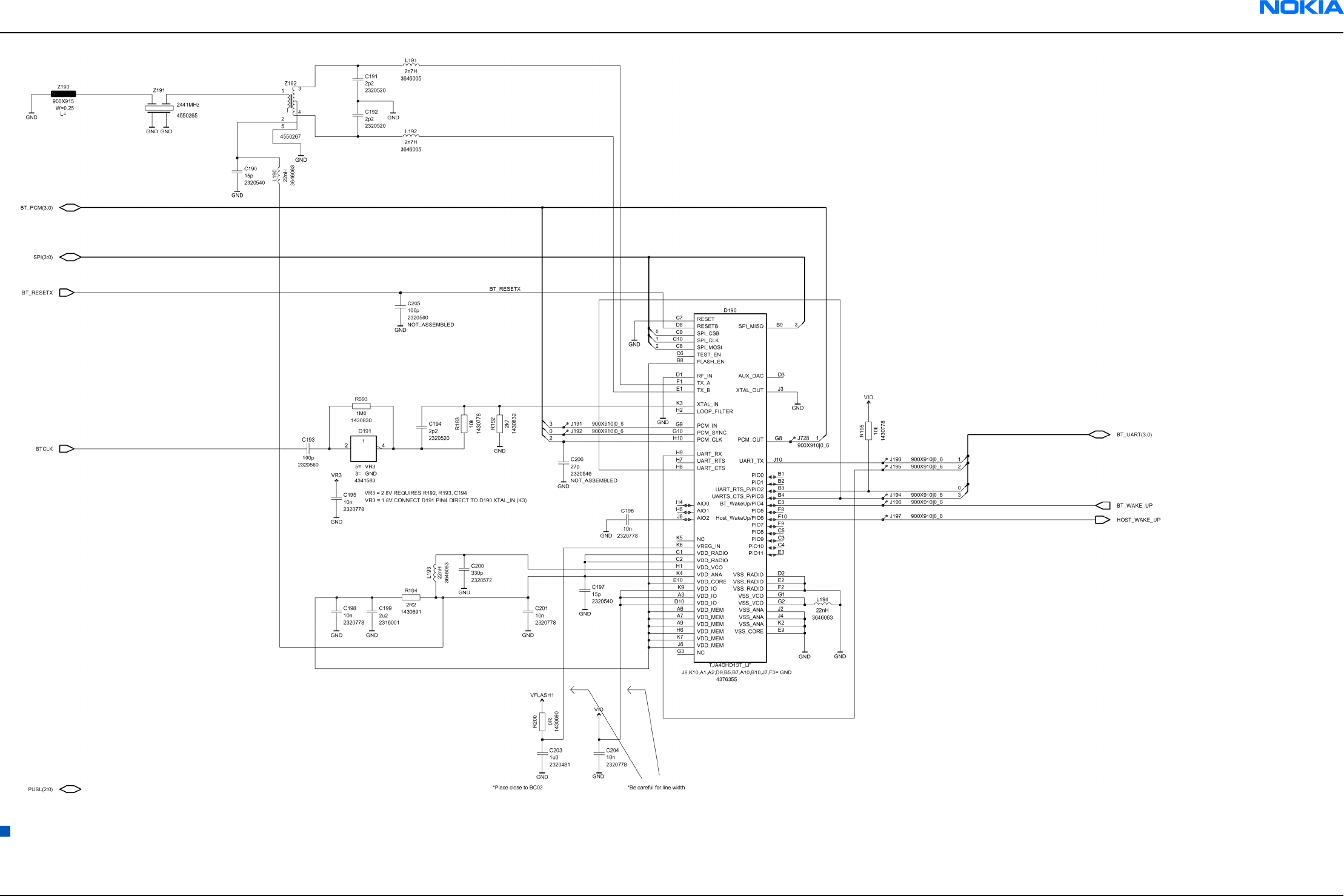
BB-RF Interface
Figure 206 1fsa_09a, v. 6.0, ed. 9
RM-25
Schematics Nokia Customer Care
9235618 (Issue 2) Company Confidential Page 10–41
Copyright ©2005 Nokia. All Rights Reserved.
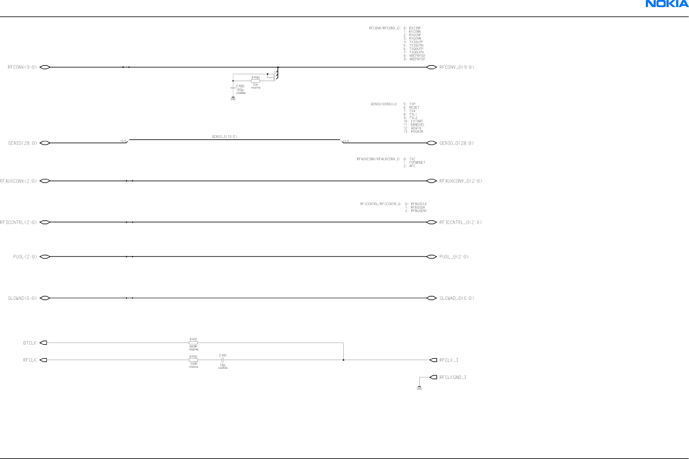
Figure 207 1fsa_11a, v. 6.0, ed. 12
RM-25
Schematics Nokia Customer Care
9235618 (Issue 2) Company Confidential Page 10–42
Copyright ©2005 Nokia. All Rights Reserved.
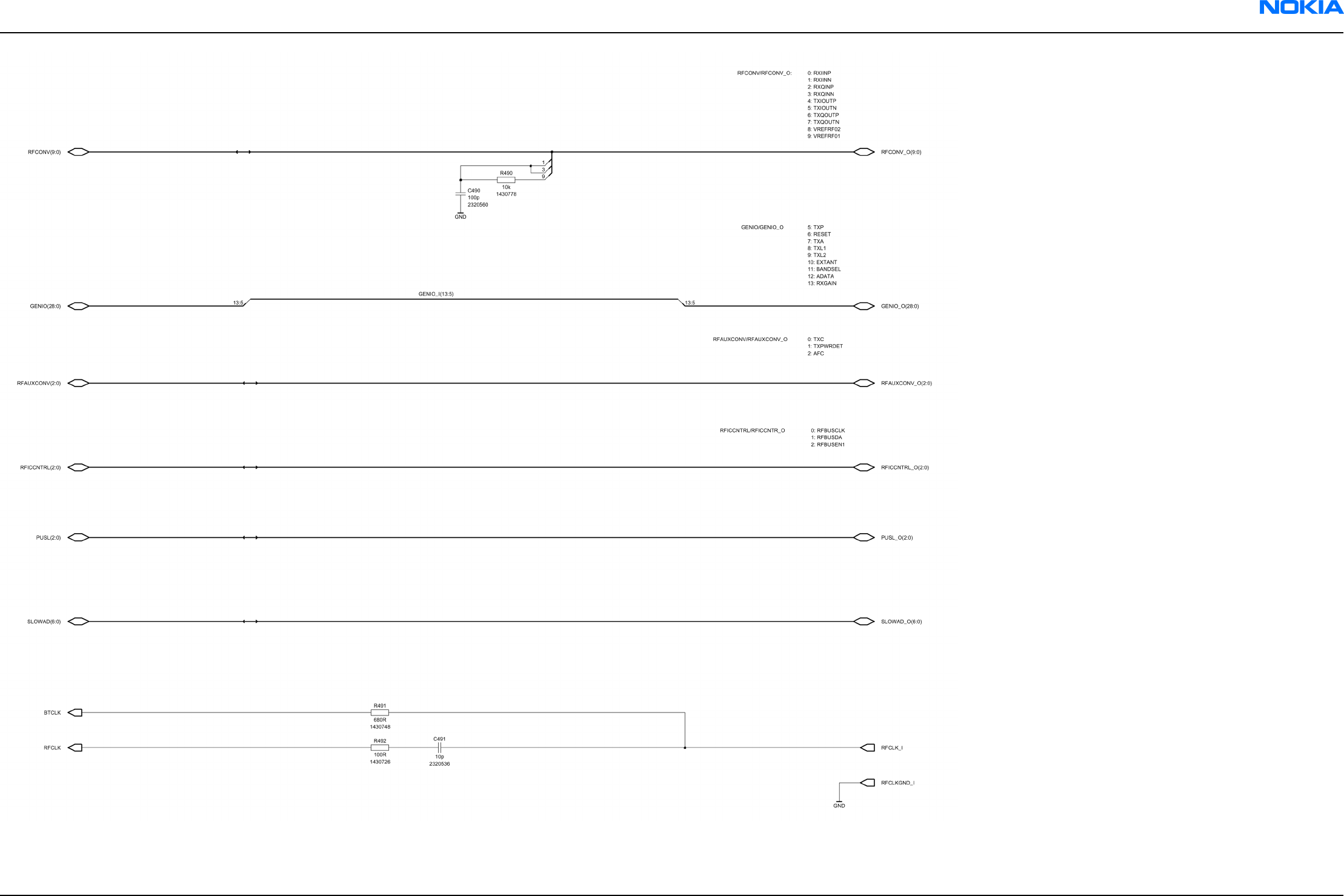
RM-25
Schematics Nokia Customer Care
9235618 (Issue 2) Company Confidential Page 10–43
Copyright ©2005 Nokia. All Rights Reserved.
Testpad
Figure 208 1fsa_09a, v. 5.1, ed. 49
Figure 209 1fsa_11a, v. 5.1, ed. 52
RM-25
Schematics Nokia Customer Care
9235618 (Issue 2) Company Confidential Page 10–44
Copyright ©2005 Nokia. All Rights Reserved.
RF top level
Figure 210 1fsa_09a, v. 8.0, ed. 63
RM-25
Schematics Nokia Customer Care
9235618 (Issue 2) Company Confidential Page 10–45
Copyright ©2005 Nokia. All Rights Reserved.
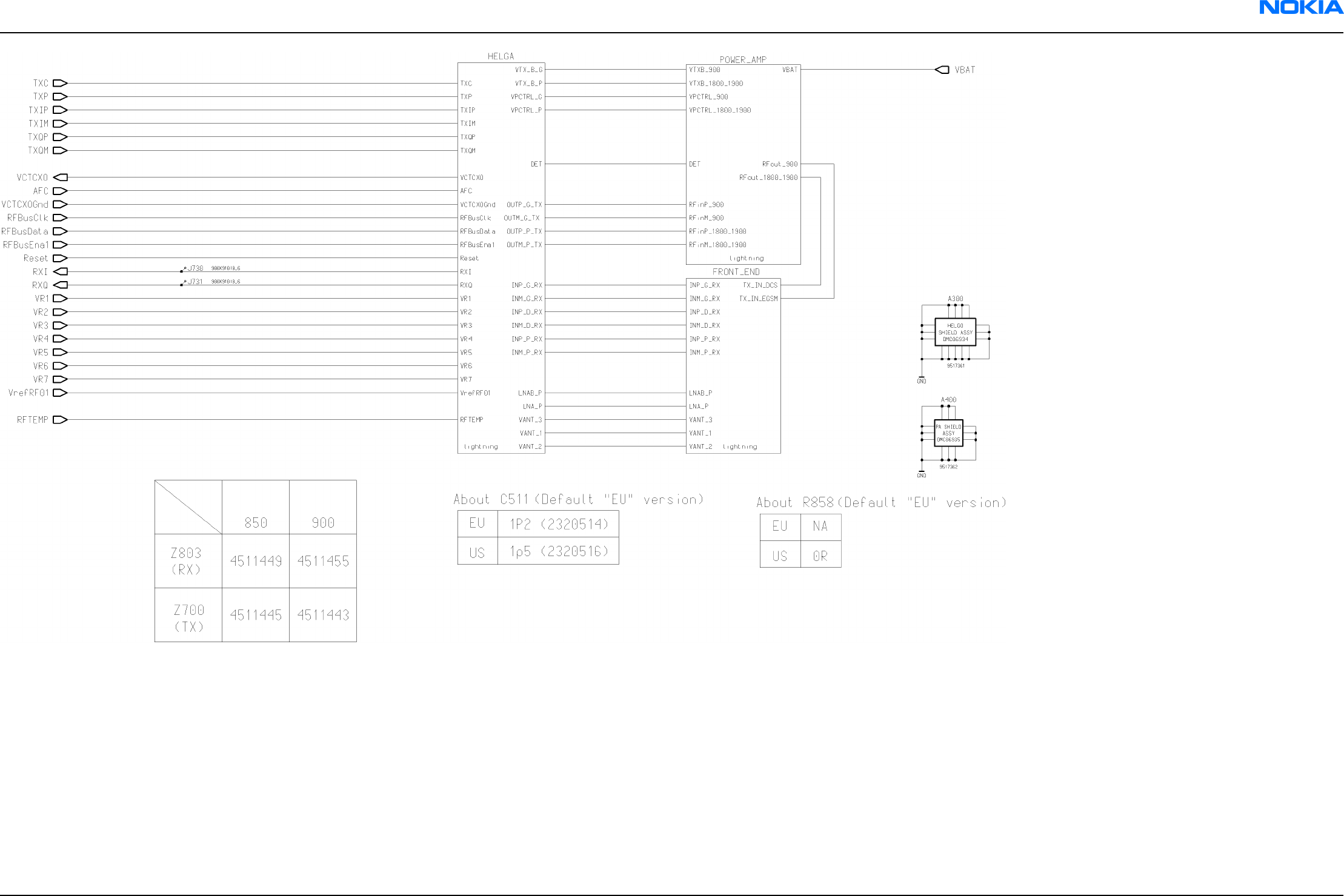
Figure 211 1fsa_11a, v. 8.0, ed. 67
RM-25
Schematics Nokia Customer Care
9235618 (Issue 2) Company Confidential Page 10–46
Copyright ©2005 Nokia. All Rights Reserved.
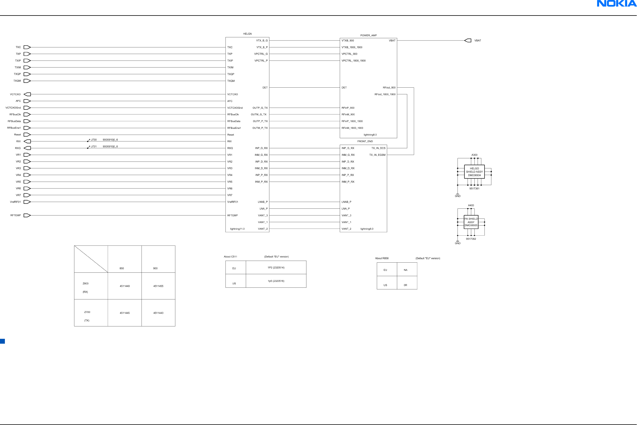
HELGO
Figure 212 1fsa_09a, v. 8.0, ed. 57
RM-25
Schematics Nokia Customer Care
9235618 (Issue 2) Company Confidential Page 10–47
Copyright ©2005 Nokia. All Rights Reserved.
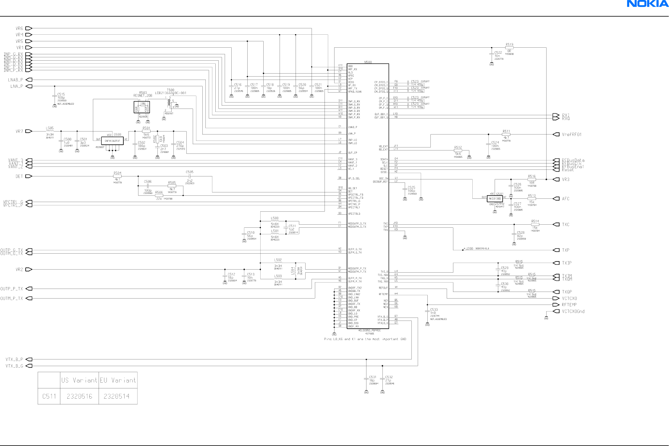
Figure 213 1fsa_11a, v. 11.0, ed. 64
RM-25
Schematics Nokia Customer Care
9235618 (Issue 2) Company Confidential Page 10–48
Copyright ©2005 Nokia. All Rights Reserved.
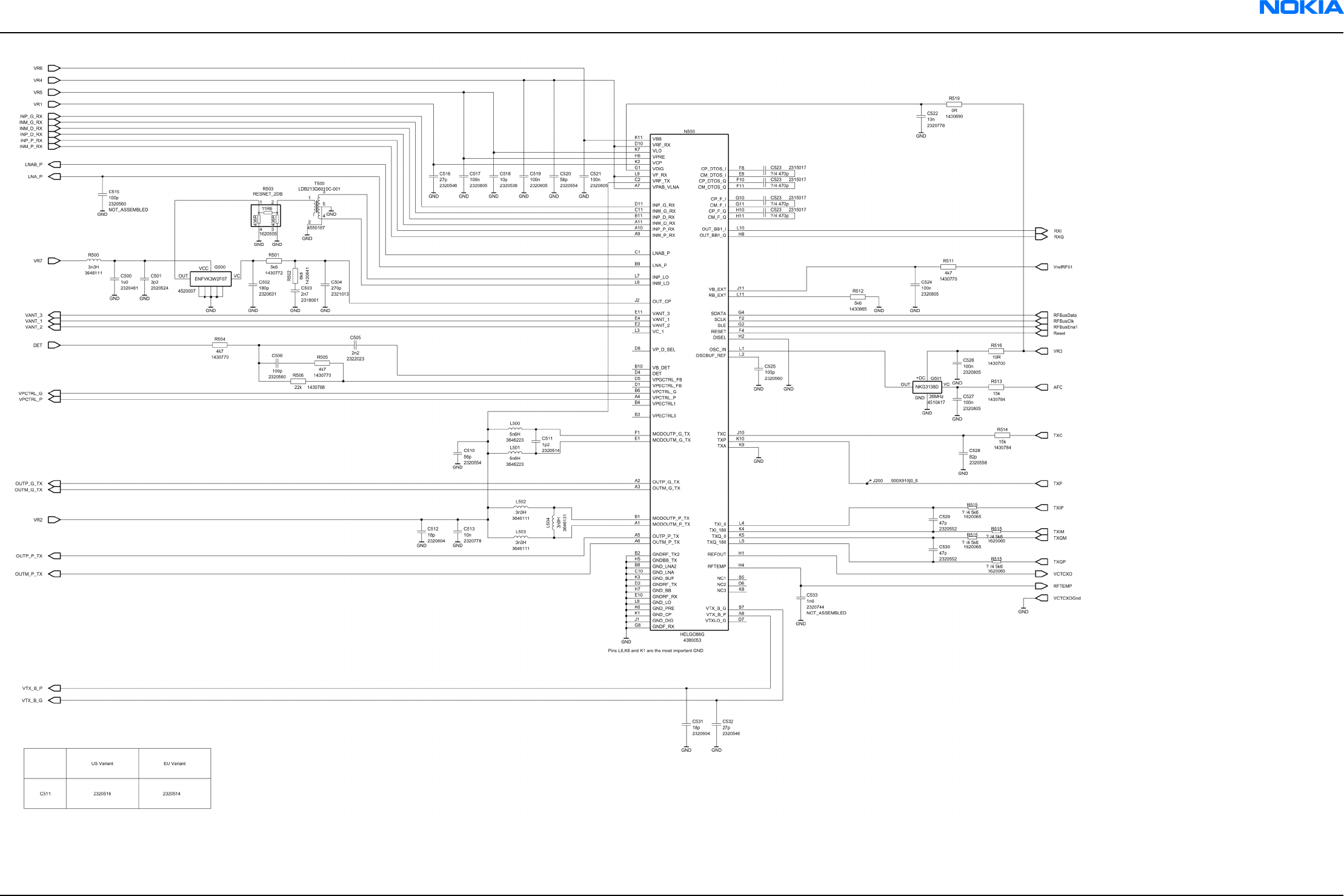
RM-25
Schematics Nokia Customer Care
9235618 (Issue 2) Company Confidential Page 10–49
Copyright ©2005 Nokia. All Rights Reserved.
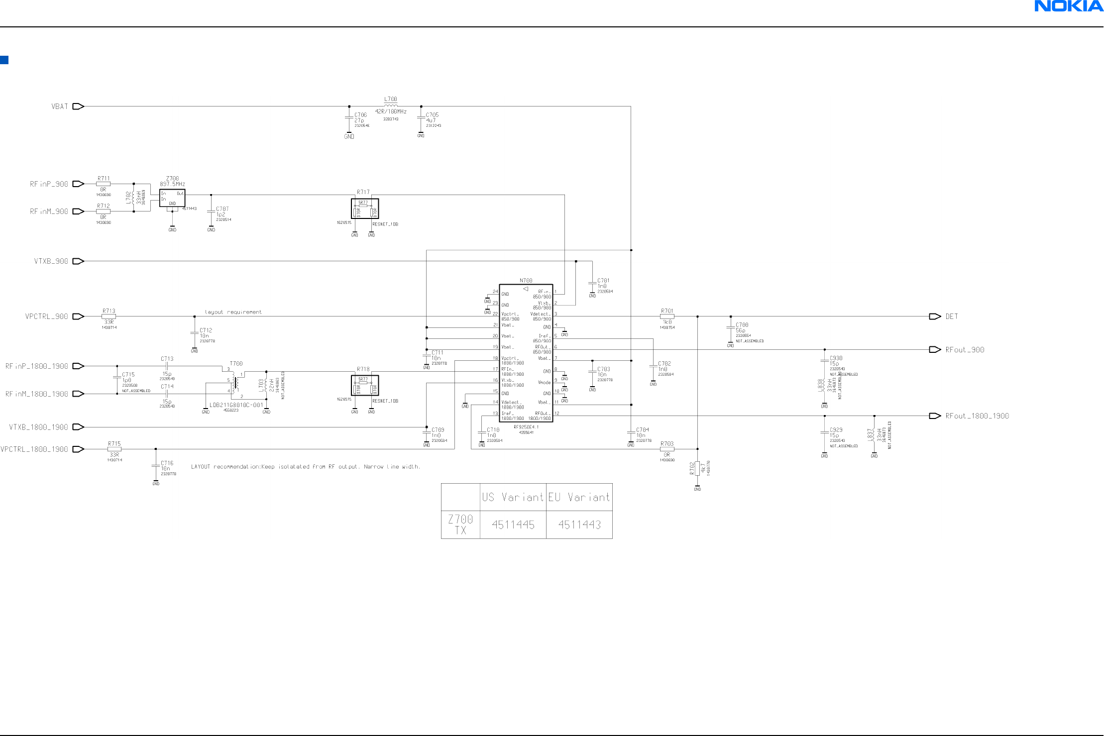
RF9204 power amplifier and power detection
Figure 214 1fsa_09a, v. 8.0, ed. 63
Figure 215 1fsa_11a, v. 8.0, ed. 66
RM-25
Schematics Nokia Customer Care
9235618 (Issue 2) Company Confidential Page 10–50
Copyright ©2005 Nokia. All Rights Reserved.
RX front end and antenna switch
Figure 216 1fsa_09a, v. 6.0, ed. 60
RM-25
Schematics Nokia Customer Care
9235618 (Issue 2) Company Confidential Page 10–51
Copyright ©2005 Nokia. All Rights Reserved.
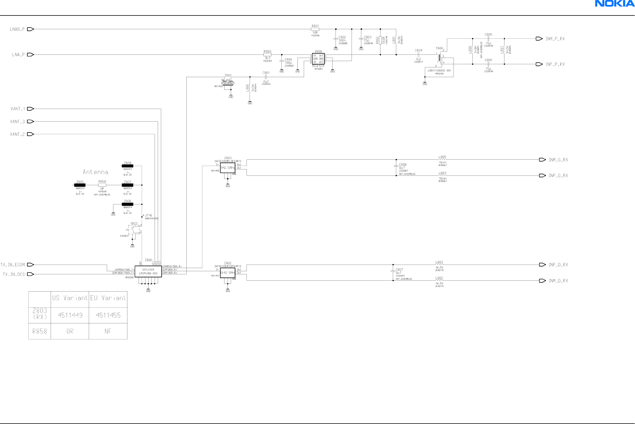
Figure 217 1fsa_11a, v. 6.0, ed. 63
RM-25
Schematics Nokia Customer Care
9235618 (Issue 2) Company Confidential Page 10–52
Copyright ©2005 Nokia. All Rights Reserved.
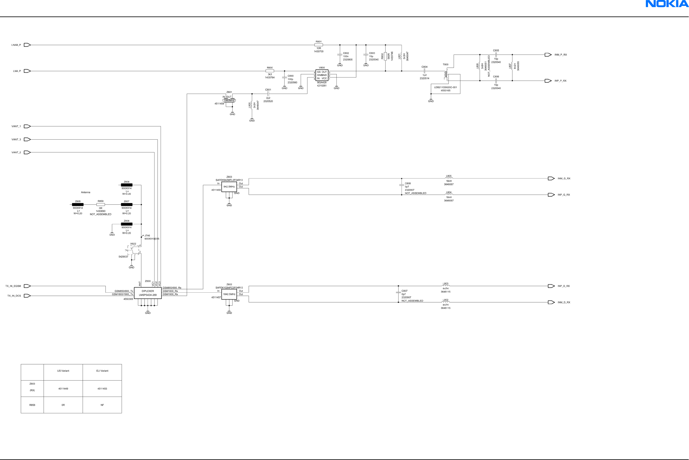
RM-25
Schematics Nokia Customer Care
9235618 (Issue 2) Company Confidential Page 10–53
Copyright ©2005 Nokia. All Rights Reserved.
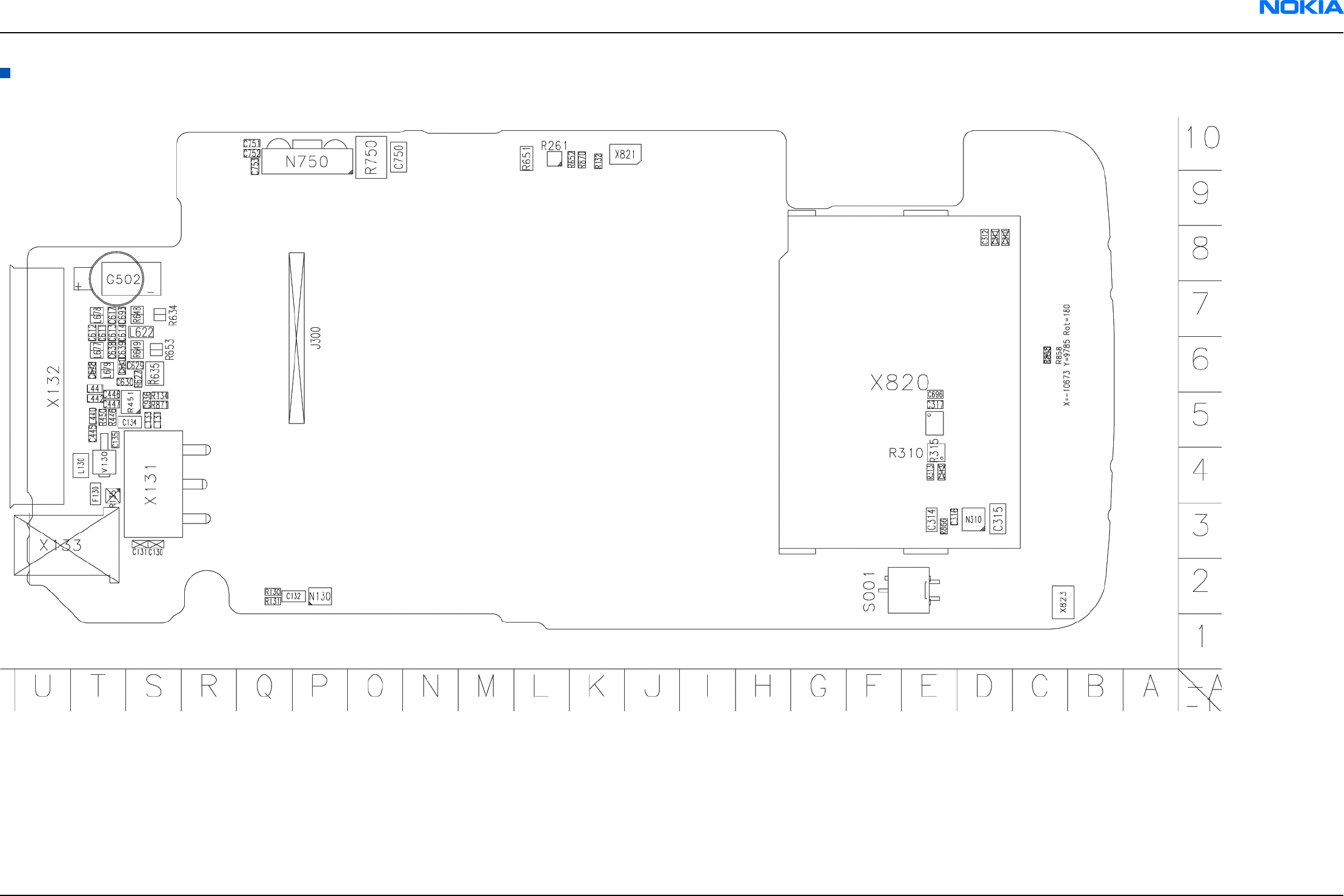
Component layout, bottom
1fsa_09a
RM-25
Schematics Nokia Customer Care
9235618 (Issue 2) Company Confidential Page 10–54
Copyright ©2005 Nokia. All Rights Reserved.

1fsa_11a
RM-25
Schematics Nokia Customer Care
9235618 (Issue 2) Company Confidential Page 10–55
Copyright ©2005 Nokia. All Rights Reserved.
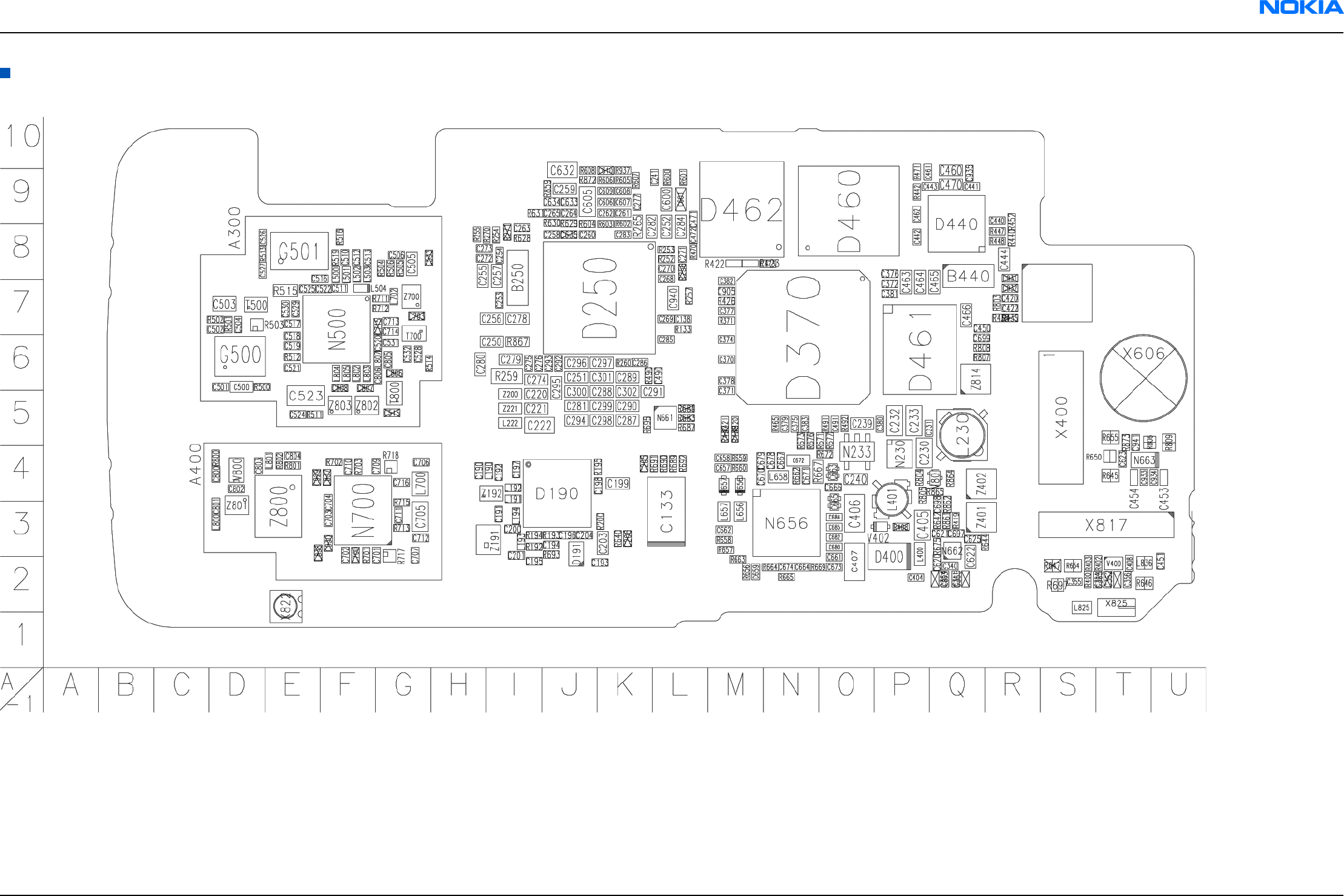
Component layout, top
1fsa_09a
RM-25
Schematics Nokia Customer Care
9235618 (Issue 2) Company Confidential Page 10–56
Copyright ©2005 Nokia. All Rights Reserved.
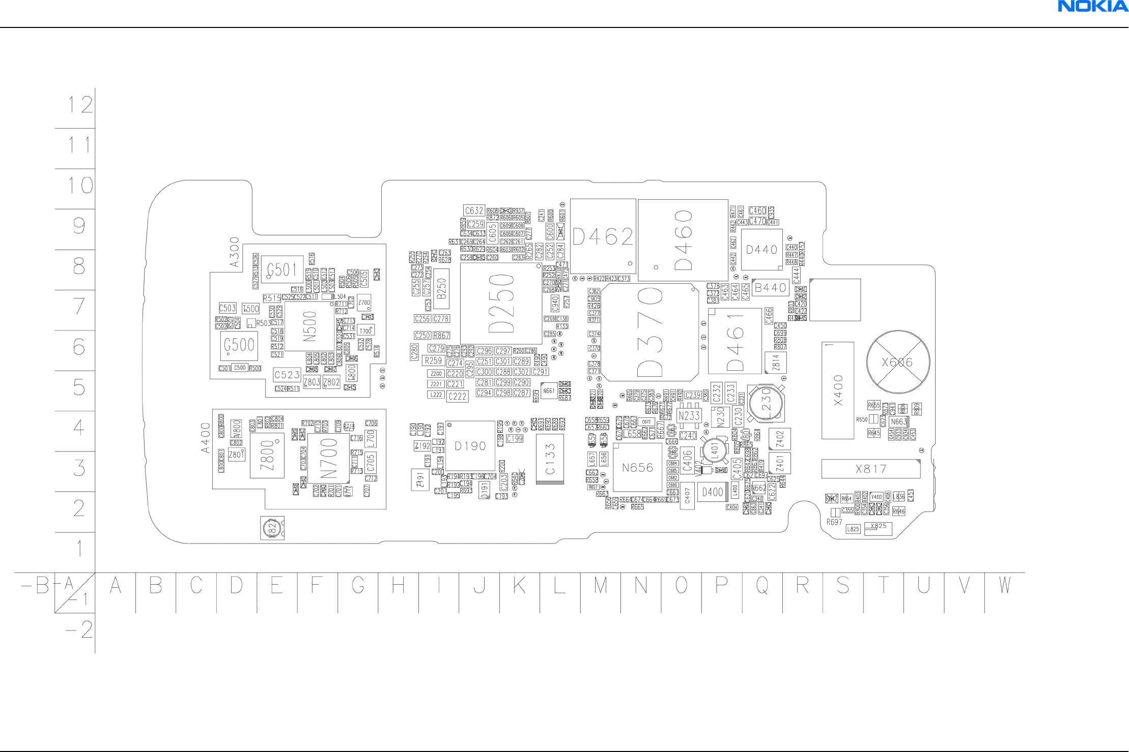
1fsa_11a
RM-25
Schematics Nokia Customer Care
9235618 (Issue 2) Company Confidential Page 10–57
Copyright ©2005 Nokia. All Rights Reserved.

RM-25
Schematics Nokia Customer Care
9235618 (Issue 2) Company Confidential Page 10–58
Copyright ©2005 Nokia. All Rights Reserved.

Glossary
Nokia Customer Care
9235618 (Issue 2) Company Confidential Page Glossary–1
Copyright ©2005 Nokia. All Rights Reserved.

RM-25
Nokia Customer Care Glossary of terms
(This page left intentionally blank.)
Page Glossary–2 Company Confidential 9235618 (Issue 2)
Copyright ©2005 Nokia. All Rights Reserved.
Table 31
A/D-converter Analog-to-digital converter
ACI Accessory control interface
ACI Adjacent channel interference
ADC Analog-to-digital converter
ADSP Application DSP (expected to run high level task, see also CDSP)
AGC Automatic gain control (maintains volume)
ARM Advanced RISC machines
ARPU Average revenue per user (per month or per year)
ASIC Application specific integrated circuit
ASIP Application specific interface protector
BB Baseband
BC02 Bluetooth module made by CSR
BIQUAD Bi-quadratic (filter function)
BSI Battery size indicator
BT Bluetooth
CBus MCU controlled serial bus connected to UPP, UEME and Zocus
CCP Compact camera port
CDSP Cellular DSP (expected to run at low levels, see also ADSP)
CMOS Complimentary metal-oxide semiconductor circuit (low power consumption)
COF Chip on foil
COG Chip on glass
CPU Central processing unit
CSR Cambridge silicon radio
CSTN Color super twisted nematic, see also FSTN
CTSI Clock timing sleep and interrupt block of Tiku
DBI Digital battery interface
DBus DSP controlled serial bus connected between UPP and Helgo
DCT-4 Digital core technology
DP Data package
DPLL Digital phase locked loop
DSP Digital signal processor
DtoS Differential to single ended
EDGE Enhanced data rates for global/GSM evaluation
RM-25
Glossary of terms Nokia Customer Care
9235618 (Issue 2) Company Confidential Page Glossary–3
Copyright ©2005 Nokia. All Rights Reserved.
EGSM Extended GSM
EM Energy management
EMC Electromagnetic compability
EMI Electromagnetic interference
ESD Electrostatic discharge
FBUS Nokia specific serial bus
FCI Functional cover interface
FPS Flash programming tool
FR Full rate
FSTN Film compensated super twisted nematic, see also CSTN
GND Ground, conductive mass
GPRS General packet radio service
GSM Global system for mobile communication
Helgo RF ASIC, small signal
RX, TX and synthesizer blocks
HF Hands free
HFCM Handsfree common
HS Handset
HSCSD High speed circuit switched data (data transmission connection faster than GSM)
HW Hardware
I/O Input/Output
IBAT Battery current
IC Integrated circuit
ICHAR Charger current
IF Interface
IHF Integrated hands free
IMEI International mobile equipment identity
IR Infrared
IrDA Infrared data association (Function: IR)
JPEG Joint photographic experts group (image file format)
LCD Liquid crystal display
LDO Low drop out
LED Light-emitting diode
LPRF Low power radio frequency (Bluetooth)
MBUS Nokia specific serial bus
MCU Micro controller unit
RM-25
Nokia Customer Care Glossary of terms
Page Glossary–4 Company Confidential 9235618 (Issue 2)
Copyright ©2005 Nokia. All Rights Reserved.
MIC, mic Microphone
MMC Multimedia card
NTC Negative temperature coefficient (temperature sensitive resistor used as a
temperature sensor)
OMA Object management architecture
Opamp Operational amplifier
PA Power amplifier
PDA Pocket data application
PDRAM Program/Data RAM
Phoenix Service software tool
PLL Phase locked loop
PM (Phone) Permanent memory
PUP General Purpose IO (PIO), USARTS and Pulse Width Modulators
PURX Power-up reset
PWB Printed wiring board (Printed circuit board)
RC-filter Resistance-Capacitance filter
RF Radio frequency
RFBUS Serial control bus For RF
RISC Reduced instruction-set computer
RSK Right soft key
RS-MMC Reduced size multimedia card
RSSI Receiving signal strength indicator
RST Reset switch
RTC Real time clock (provides date and time)
RX Radio receiver
SARAM Single access random access memory
SDRAM Synchronous dynamic random access memory
SIM Subscriber identity module
SMPS Switched mode power supply
SNR Signal-to-noice ratio
SPR Standard product requirements
STI Serial trace interface
SW Software
SWIM Subscriber/Wallet identification module
TCXO Temperature controlled oscillator
Tiku See ASIC
RM-25
Glossary of terms Nokia Customer Care
9235618 (Issue 2) Company Confidential Page Glossary–5
Copyright ©2005 Nokia. All Rights Reserved.
TX Radio transmitter
UEME Universal energy management chip (enhanced version)
UEMEK See UEME
UI User interface
UPP Universal phone processor
UPP_WD2 Communicator version of DCT-4 system ASIC
USB Universal serial bus
VBAT Battery voltage
VCHAR Charger voltage
VCO Voltage controlled oscillator
VCTCXO Voltage controlled temperature compensated crystal oscillator
VCXO Voltage controlled crystal oscillator
VSIM SIM voltage
WD Watchdog
Zocus Current sensor (used to monitor the current flow to and from the battery)
RM-25
Nokia Customer Care Glossary of terms
Page Glossary–6 Company Confidential 9235618 (Issue 2)
Copyright ©2005 Nokia. All Rights Reserved.
