N91 Schematics Nokia E61 Rm 89 Service
User Manual: Smartphone Nokia E61 RM-89 - Service manuals and Schematics, Disassembly / Assembly. Free.
Open the PDF directly: View PDF ![]() .
.
Page Count: 4
Service Schematics
RM-89
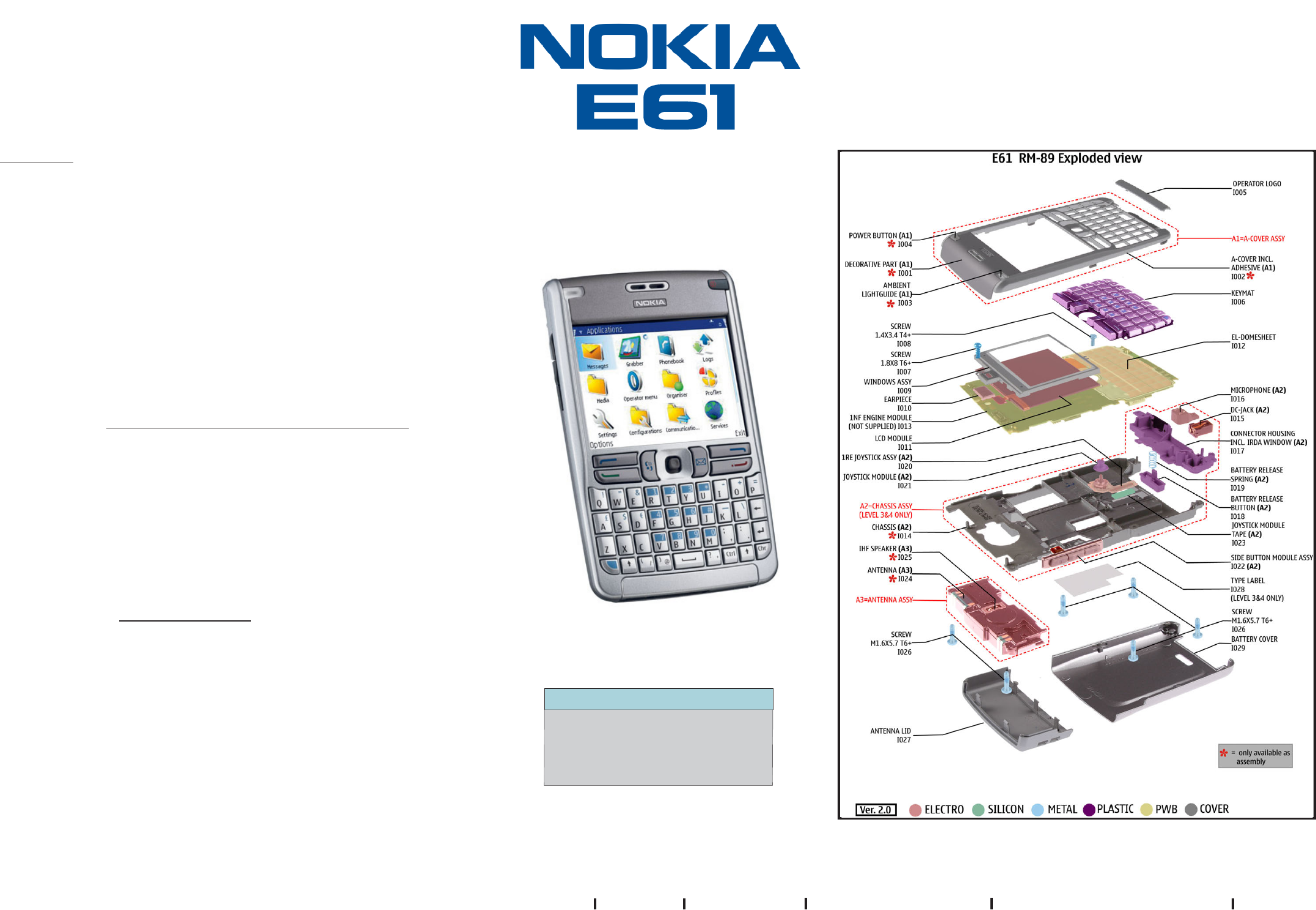
Exploded view and component disposal
IMPORTANT:
This document is intended for use by authorized NOKIA service centers only.
Introduction
“Service Schematics” was created with focus on customer care.
The purpose of this document is to provide further technical repair information for
NOKIA mobile phones on Level 3/4 service activities.
The “Signal overview” page gives a good and fast overview about the most
important signals and voltages on board.
Saving process time and improving the repair quality is the aim of this document.
It is to be used additionally to the service manual and other training
or service information such as Service Bulletins.
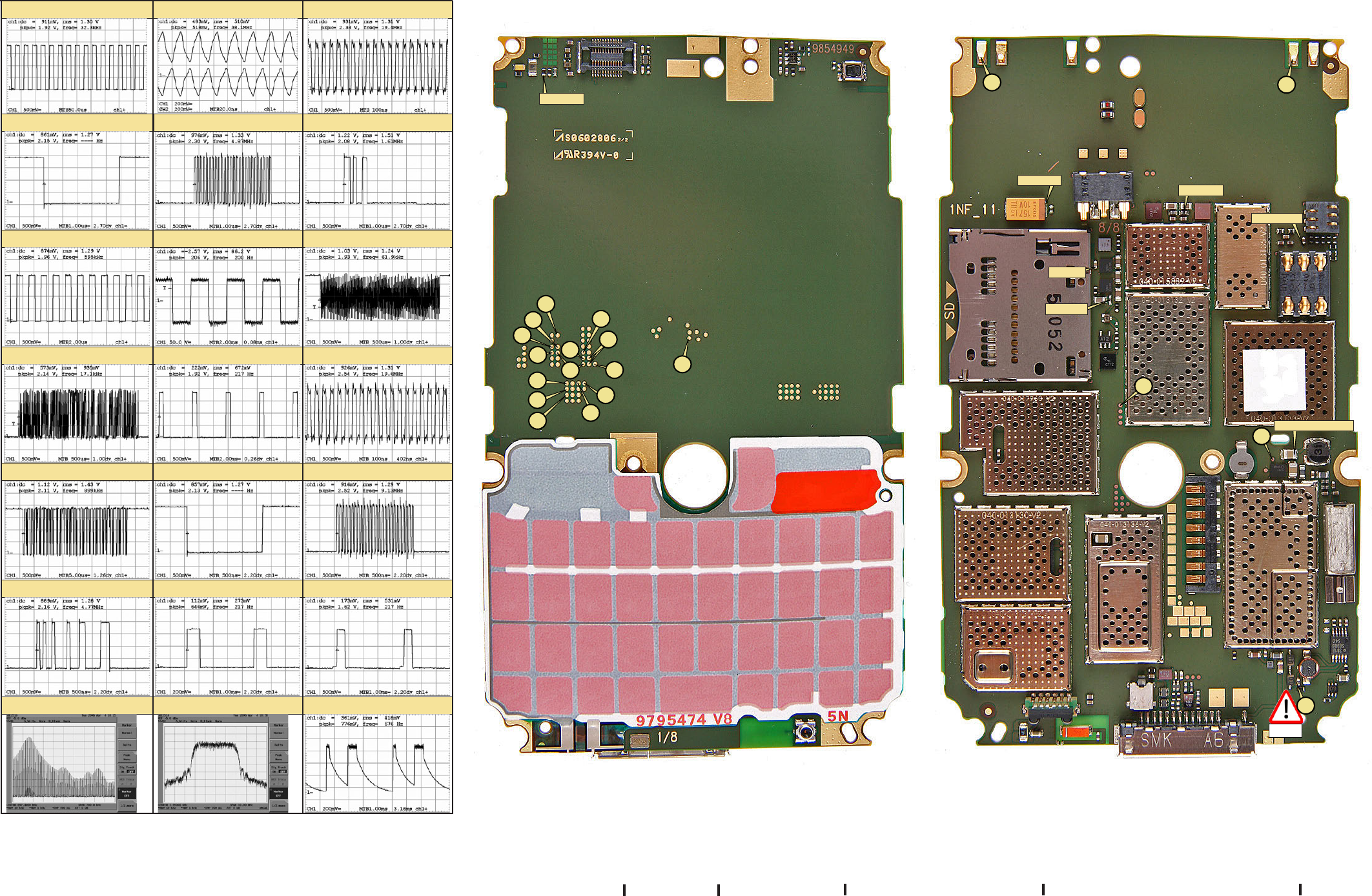
All measurements were made using following equipment:
Nokia repair SW : Phoenix version 2006.04.6.130
Oscilloscope : Fluke PM 3380A/B
Spectrum Analyzer : Advantest R3162 with an analog probe
RF-Generator / GSM Tester : Rhode & Schwarz CMU 200
Multimeter : Fluke 73 Series II
While every endeavour has been made to ensure the accuracy of this document, some
errors may exist. If the reader finds any errors, NOKIA shall be notified in writing.
Please send E-Mail to: training.sace@nokia.com
Copyright © NOKIA
This material, including documentation and any related computer programs is protected
by copyright, controlled by NOKIA. All rights are reserved. Copying, including reproducing,
modifying, storing, adapting or translating any or all of this material requires the prior
written consent of NOKIA. This material also contains companyconfidential information,
which may not be disclosed to others without the prior written consent of NOKIA.
Page 1 (4)
Front page
Customer Care / Training & Vendor Development / Content Creation Team
Confidential - Copyright © 2006 NOKIA Only for training and service purposes
Version: 1.0 10.04.2006E61 / RM-89
Board version: 1NF_11
Table of Content
1
2
3
4
Schematics
Front page
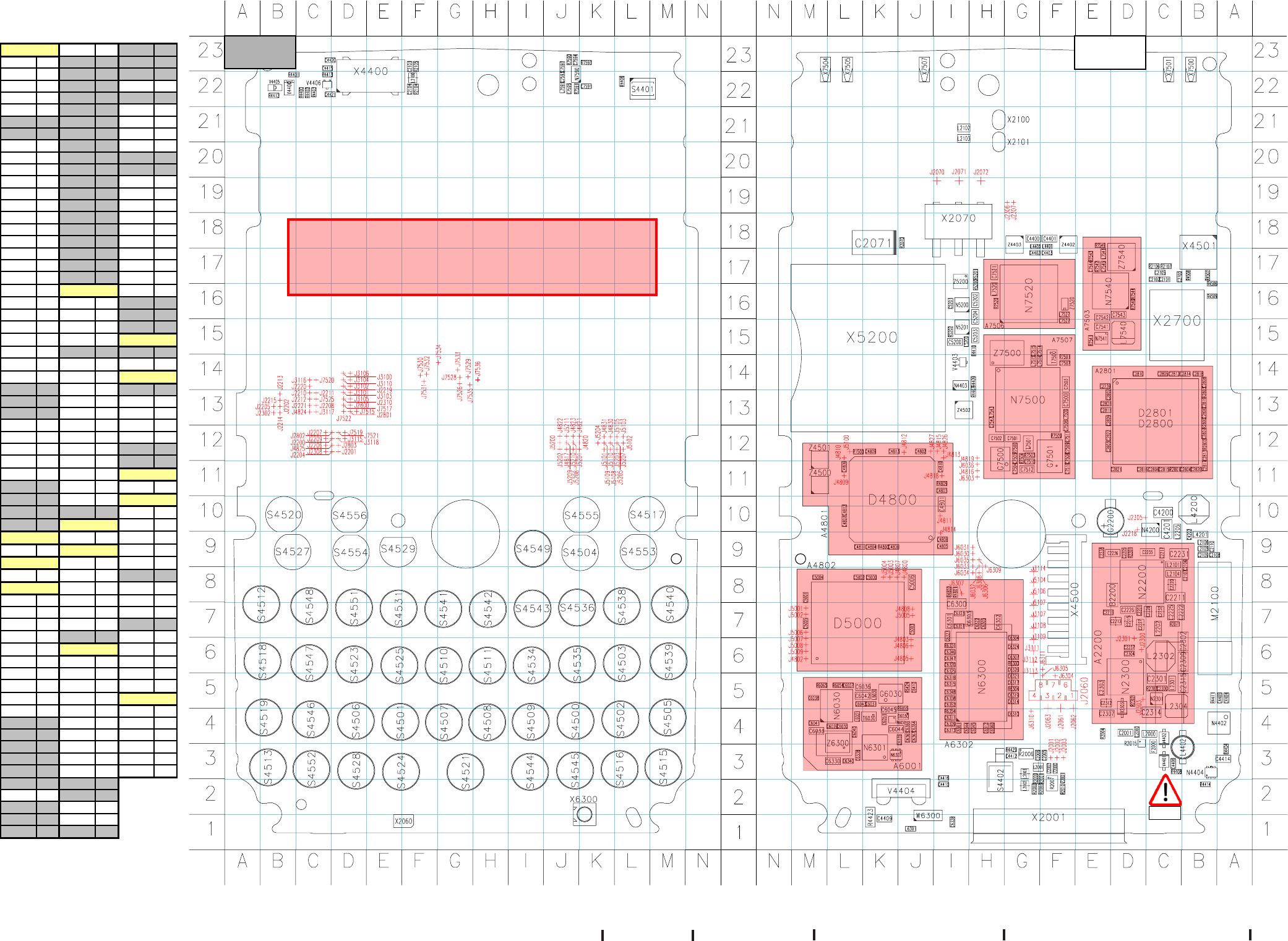
Signal overview
Component finder
Page
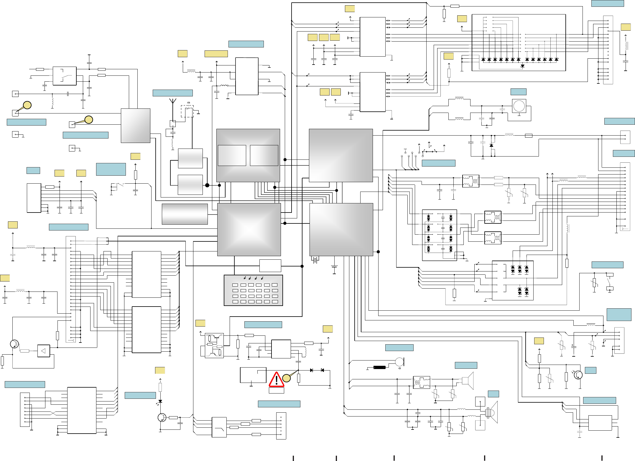
Schematics
Page 2 (4)
Customer Care / Training & Vendor Development / Content Creation Team
Confidential - Copyright © 2006 NOKIA Only for training and service purposes
Version: 1.0 10.04.2006E61 / RM-89
Board version: 1NF_11
RAP3GS
OMAP1710
NAND/DDR
COMBO
NOR
FLASH SDRAM
BT
BETTY
VILMA
QWERTY- KEYBOARD
RF
LED
DRIVER
WLAN
EARP
EARN
MIC1P
R2105
14V/50V
Z2100
W=0.10
L=
1
2 3
4
GND
EXC24CB102U
L2100
0
1
4
GND
GND
B2100
OUT
B2101
R2104
14V/50V
GND
1n0
C2104
GND
AUDIO(8:0)
C2103
1n0
Xear_l_p
Xear_l_n
D+
ACI
D-
D+
Xear_r_n
Xear_l_p
Xmicn
DMTXD
MASTPD2
ACI
Xear_r_p
Xmicp
Vbus
XEARRC
MIC2N
XEARR Data gnd
VOUT
D-
Xmicn
XEARLC
XEARL
Xmicp
Xear_r_p
Xear_l_n
Charge gnd
Charge
Xear_r_n
MIC2P
MASTPD1
C3
D1
D2
D3
3
2
SLAVEPU
DPRXD
C
R
R
R2006
IP5040CX11_LF
C
A1
A2
GND
A3
3B1B
C1
C2
2A
GND
VOUT
C
R
R
C
F2000
GND
C2000
27p
15k
IP4065CX11_LF
R2007
1k3
17k
33R
33R
100R
R2004
C2005
10n
L2001
EXC24CB102U
1
23
4
GND
EXC24CB102U
L2002
1
23
4
C2006
7
X2000
1
2
10n
6
470n
C2001
L2000
5
GND
220R/100MHz
K
A
Z2000
600R/100MHz
GND
AGND
2
3
4
5
6
7
8
9
R2015
ESDA18-1F2
X2001
1
10
11
12
13
14
600R/100MHz
Z2003
R2010
220k
GND
GND
R2000
10R
R2003
R2001
10R
5.6V/15V/0.05J
GND
R2002
5.6V/15V/0.05J
4
J2003
J2002
6
5
J2001
7
GND
L2003
EXC24CB102U
1
23
4
1
0
Z2001
600R/100MHz
XAUDIO(7:0)
USB_ACI(7:0)
4
VBUS
GND
GND
WRX
D3
D2
D1
LEDOUT
GND
CSX
VDD
D/CX
LEDIN
RESX
GND
RDX
GND
D0
D4
TE
GND
GND
D7
D6
GND
VDDL
D5
27p
C4421
GND
GND
C4420
27p
GND
18
1
2SC5658QRS
V4403
20
7
GND
R4409
33R
VIO
VLEDOUT2
C4401
1u0
27p
C4402
600R/100MHz
5
6
7
8
9
VLEDOUT1
L4400
16
17
18
19
2
20
21
22
23
24
3
4
X4400
1
10
11
12
13
14
15
600R/100MHz
L4401
SETCURR1
R4407
18R
1u0
C4400
1k0
R4410
+
1
-
3
4
5
19
21
GND2=
VAUX5=
N4403
LMV321M7X_NOPB
GND
3
0
GND
VAUX
GND
C5
OUT6 D1
OUT7 D2
OUT8 D3
OUT9 D4
OUT10 D5
OUT1 E1
OUT2 E2
OUT3 E3
OUT4 E4
OUT5 E5
IN5
A5
IN6
B1
IN7
B2
IN8
B3
IN9
B4
IN10
B5
C1 GND
GND
C2
GND C3
GND C4
GND
GND
Z4402
EMIF10-COM01F2
A1 IN1
IN2
A2
IN3
A3
IN4
A4
17
E1
OUT2 E2
OUT3 E3
OUT4 E4
OUT5 E5
C1 GND
GND
C2
GND C3
GND C4
GND C5
OUT6 D1
OUT7 D2
OUT8 D3
OUT9 D4
D5
OUT10
OUT1
EMIF10-COM01F2
IN1
A1
IN2
A2
IN3
A3
IN4
A4
IN5
A5
IN6
B1
IN7
B2
IN8
B3
IN9
B4
IN10
B5
Z4403
GND
2
4
6
GND
C4403
27p
16
MESSI_VIDEO(25:0)
GND
GND
10n
C4202
VDD VSEL B1
PVIN
B3 C1
ISEL
C3 SW D1
SYNC/MODE
EN D2
PGND
D3
VBAT
GND GND
U//U
N4200
LM3661TLX-1.40_NOPB
A1 FB A2
A3
10uH
4
22u
C4200
L4200
220R/100MHz
L4201
22u
C4201
GND
7
PUSL(7:0)
VCOREA
GND
2
SGND
CL-191WB-D-T
V4405
7
R4412
VBAT
V4406
2SC5658QRS
680R
1n0
C4415
GND
R4413
1k0
1C1
2C2
3C3
5
C5 6
C6 7
C7
GND GND
X2700
SM SIM CONN 2X3POL P2.54 H4.6
1
0
2
100n
C2700
GND
GND
100p
C7591
C7597
1p2
0R
R7591
X7501
0R
R7593
8p2
C7593
X7507
X7504
L7591
6n8H
X7500
X7505
N7590
UPG2155TB-E4
OUT1
1
GND
2
OUT2 43 Vcont2
5
IN
6
Vcont1
0R
R7590
12p
C7594
C7595
12p
GND
BTEMP NTC
-t
47k
X2070
VBATT
BSI
GND
GND
R2071
R2070
GND
3 2
J2072
14V/50V
BGND
VBAT
J2071
GND
J2070
SLOWAD(6:0)
150u_10V
C2071
GND
VBATH
L2205
220R/100MHz
G2200
GND
VBACK
CLK
J2063
TXD
RXD
RXD2
J2062
J2061
130
GND
VPP
2
FLASHM
6J2060
1
VBUS
2
3
4
7
8
R4406
14V/50V
GND GND
S4401
PWRONX
C
E
V4400
PT202MR0MP
R4403
47k
6
5
GND GND
470k
R4402
VANA
R4401
100k
R4400
470k
GND
GND
DATA1
DATA3
DATA3
CLK
CMD
DATA0
DATA1
DATA2
1.8V level
2.8V level
2.8V level
1.8V level
DATA_DIR0
CLK
CMD
DATA0
DATA1
DATA2
DATA3
CLK
CLK_FB
CMD
DATA0
1
2
15
3
DATA2
DATA_DIR1
CMD_DIR
LS_ENABLE
LS_ENABLE
C4
A1
D1
B2
D2
B3
D3
A3
D4
A2
6
7
0
A4 EN1
B1 VCCB
Dir2
B2
B3 Dir1
B4 VCCA
B1 C1
LatchClk
C2
C3 Dir3
J5204
LP3928TLX-1828_NOPB
N5201
VBAT
A1
EN2
A2
A3
GND
J5205
J5207
VIO
GND
GND
VBATVIO
GND
R5202
100k
C5203
C2 LatchClk
Dir3
C3
A1 C4
B2 D1
B3 D2
A3 D3
A2 D4
1u0
A2 EN2
GND A3
EN1
A4
VCCB
B1
B2 Dir2
Dir1
B3
VCCA
B4
C1
B1
J5200
N5200
LP3928TLX-1828_NOPB
A1 VBAT
J5201
J5202
J5203
680R
R5200
GND
1k2
R5201
VIO
10
GND
GND
GND
VBAT
1u0
C5202
GND
C5204
1u0
C5201
10n
5
6
7
8
9
V_SD
V_SD
10
11
12
13
GND
2
3
4
MMCdat1
MMCdat0C4
D1dat3
GNDD2
D3 MMCdat3
MMCdat2D4
X5200
1
A1cmd
clk A2
Vdd/
A3 Vmmc
MMCclkA4
B1dat1
dat0 B2
GNDB3
B4 MMCcmd
dat2 C1
C2 GND
C3
GND
R4
R3
R2
Z5200
EMIF06-HMC01F2
R6
R7
R5
R14
R13
R12
R11
R10
600R/100MHz
GND
C5200
GND
L5200
1u0
J5208
J5209
VIO
SD_LS_ENABLE
J5210
J5211
4
511
HFSPN
HFSPP
1n0
C2106
0
1
R2106
14V/50V
R2107
14V/50V
GND
68p
68p
1n0
C2105
1
GND
GND
X2100
1
X2101
L2102
56nH
L2103
56nH
C2107
1n0
VSIM1
SIMIF(6:0)
C2101 C2102
VBAT
GND
4R7
R4423
C4409
4u7
0
1
27p
GND
C4416
VAUX
GND
GND
LEDA
TXD
RXD
SD
VCC
GND
GND
GND
CIM-138M7-T
V4404
2
100n
C4410
IR(7:0)
VIO
100k
R4429
GND
C4412
1n0
S4402
1
2
34
GND
3
D5 OUT10
OUT1
E1
OUT2
E2
OUT3
E3
OUT4
E4
OUT5
E5
B4
IN10 B5
C1
GND
GND C2
GND
C3
GND
C4
GND
C5
OUT6
D1
OUT7
D2
OUT8
D3
OUT9
D4
Z4502
EMIF10-COM01F2
IN1 A1
IN2 A2
IN3 A3
IN4 A4
IN5 A5
IN6 B1
IN7 B2
IN8 B3
IN9
5
6
7
1
2
3
0
4
JOYSTICK(7:0)
Up
Down
Right
Common
Left
Enter
GND
6
7
8
X4500
1
2
3
4
5
GND GND
VIBRAN
VIBRAP
C2110
1n0
M
M2100
KHN4NX1RA
-
+
L2106
220R/100MHz
GND
220R/100MHz
L2105
C2108
1n0
1n0
2
3
C2109 GND
EL Lamp
GND
GND
R4414
100k
L4402
0.47MH
C4404
68p
VBAT
2CLF
3E
4NC
5GND 6
NC
7
L-
8
VOUT
9
L+
0R
R4404
1DDD381BB-NL4
N4402
CHF
1V+ 10
V4401
RD100S
C4414
1u0
J4421
R4411
J4420
82k
GND
PEMD9
N4404
1
2
34
5
6
GND
GND
C4405
15n
VBAT
3M3
R4408
1u0
C4406
RD100S
V4402
Vol Up
Voice
Vol Down
R4506
0R
X4501
1
2
3
4
5
6
R4509
0R
0R
R4508
0R
R4507
KEYB(19:0)
EMIF10
kbc_2
kbc_0
kbr_0
9
0
8
10
kbc_1
IrDA
GSM antenna clips
WCDMA antenna clips
APE Vcore SMPS
Battery cover
detection
miniSD reader
Vibra
Charger plug
Pop port
Power switch
Battery
connector
ALS
SIM connector
Earpiece
IHF
Microphone
Display connector
Flash interface
Joystick connector
Side key connector
EL lamp & driver
Indicator LED
W6300
1n2H
L6301
In C
1
In R
2
X6300
1p5
C6328
GND
GND
BT/WLAN antenna
200Vpp
3.7V
1.05/1.35V
3.7V
1.8V
2.8V
V_SD
GND
3.7V
1.8V
1.8V
2.8V
3.7V
2.8V
1.8V
3.7V
3.7V
3.7V
1.8V
2.8V
2.8V
2.5V
1.8V
8
19
20
4) CBUSENA at J2209
1) Sleepclock at J2310 3) SYSCLK at J4819
5) CBUSCLK at J2206
2) RFCLK at J2800/J2801
6) CBUSDATA at J2207
7) CLK600 at J2305 8) VEL at C4406 9) WRX at TPs of service jig
TXCCTRL at J2211)
1
1
Data0 at TPs of service jig)
01 12) TXCCLK at J2210
RFBUSENA at J7521
)41
TXCDATA at J2212)
31 15) RFBUSCLK at J7520
TXIQ at J7522/J7525
)71
RFBUSDATA at J7519)
61 18) TXC at J7526
WCDMA TX at X7501
)02
GSM TX at X7504)
91 21) RXIQ at J7515/J7517
Signal overview
Page 3 (4)
Customer Care / Training & Vendor Development / Content Creation Team
Confidential - Copyright © 2006 NOKIA Only for training and service purposes
Version: 1.0 10.04.2006E61 / RM-89
Board version: 1NF_11
200Vpp
1
2
3
4
5
6
7
8
11
12
13
14
15
16
17 18
19 20
21
21
VBAT 3.7V
VAUX 2.8V
VSIM 1.8/3V
VIO 1.8V
V_SD 2.8V
VCOREA 1.05/1.35V
VANA 2.5V
J4819 H12 R4401 B22
C2000 D4 J5200 J12 R4402 C22
C2001 D4 J5201 K12 R4403 C22
C2005 F3 J5202 J12 R4404 A3
C2006 G3 J5203 L12 R4406 L22
C2071 K18 J5204 K12 R4407 H13
C2103 F23 J5205 L12 R4409 H14
C2104 F22 J5207 L12 R4410 H15
C2105 C17 J5208 J12 R4411 B5
C2106 B9 J5209 J12 R4412 B22
C2107 B8 J5210 J12 R4413 C22
C2108 B9 J5211 J12 R4414 B2
C2109 B9 J7515 D13 R4423 K1
C2110 B9 J7517 D13 R4429 G3
C2700 C17 J7519 D12 R4506 B17
C4200 C10 J7520 C14 R4507 B17
C4201 C10 J7521 D12 R4508 B17
C4202 B9 J7522 D13 R4509 B16
C4400 G18 J7525 C13 R5200 H16
C4401 F18 J7526 G14 R5201 H17
C4402 G17 R5202 I15
C4403 F17 L2000 C4 R7590 J23
C4404 A5 L2001 G3 R7591 J22
C4405 A5 L2002 G2 R7593 K23
C4409 K1 L2003 G3
C4410 I2 L2100 F22 S4401 L22
C4412 G3 L2101 C9 S4402 H3
C4414 A3 L2102 I21
C4415 C23 L2103 I21 V4400 B22
C4420 C23 L2104 C8 V4401 C3
C4421 C22 L2105 B9 V4402 C4
C5200 I15 L2106 B9 V4403 I14
C5201 I16 L4200 B10 V4404 J2
C5202 H16 L4201 B9 V4405 B22
C5203 H15 L4400 G18 V4406 C22
C5204 H16 L4401 F18
C7591 K22 L5200 I15 W6300 J1
C7593 J22 L7541 E17
C7594 J23 L7591 J22 X2001 F1
C7595 J22 X2070 I18
M2100 B7 X2100 H21
F2000 C3 X2101 H21
N4200 C10 X2700 C15
G2200 E10 N4402 A4 X4400 E22
N4403 I14 X4500 F8
J2001 F3 N4404 B3 X4501 B17
J2002 F3 N5200 I16 X5200 K15
J2003 F3 N5201 I15 X6300 K2
J2060 F5 N7590 J22 X7500 B23
J2061 F5 X7501 C23
J2062 F5 R2000 G3 X7504 M23
J2063 F5 R2001 F3 X7505 L23
J2070 I19 R2002 G2 X7507 J23
J2071 I19 R2003 F2
J2072 H19 R2004 E4 Z2000 F3
J2206 C12 R2006 G3 Z2001 F3
J2207 C12 R2007 F2 Z2003 F3
J2209 C12 R2010 F2 Z4402 F18
J2210 C13 R2015 D4 Z4403 G18
J2211 C13 R2070 J18 Z5200 I17
J2212 C13 R2104 F22
J2305 D10 R2105 F23
J2310 D13 R2106 C17
J2800 D13 R2107 C17
J2801 D13 R4400 C22
M
N
R
S
C
F
G
L
J
V
W
X
Z
Component finder
Page 4 (4)
Customer Care / Training & Vendor Development / Content Creation Team
Confidential - Copyright © 2006 NOKIA Only for training and service purposes
Version: 1.0 10.04.2006E61 / RM-89
Board version: 1NF_11
200Vpp
Battery connector
WCDMA antenna pads
GSM antenna pads
Display connector
Power switch
IHF pads
SIM connector
Side keys
connector
miniSD connector
System connector
Vibra
Top Bottom
Please note:
Due to soldered shielding cans rework is not possible within red shaded areas.
Also the component list on the left is reduced to reworkable parts only!
