Nokia N8 00 RM 596 Service Manual Level 3&4. Www.s Manuals.com. 3,4 V2.0
User Manual: Smartphone Nokia N8-00 RM-596 - Service manuals and Schematics, Disassembly / Assembly. Free.
Open the PDF directly: View PDF ![]() .
.
Page Count: 253 [warning: Documents this large are best viewed by clicking the View PDF Link!]
- Amendment Record Sheet
- Copyright
- Warnings and cautions
- For your safety
- ESD protection
- Care and maintenance
- Company policy
- Battery information
- Nokia N8-00; L3&4 Service Manual Structure
- 1 General Information
- 2 Service Tools and Service Concepts
- 3 BB Troubleshooting and Manual Tuning Guide
- Baseband main troubleshooting
- Power and charging troubleshooting
- Interface troubleshooting
- IVE troubleshooting
- TV out troubleshooting
- Display module troubleshooting
- Keyboard troubleshooting
- Sensors troubleshooting
- Audio troubleshooting
- Connectivity module troubleshooting
- Introduction to connectivity module troubleshooting
- Bluetooth/FM radio and WLAN troubleshooting
- Bluetooth and FM radio self tests in Phoenix
- WLAN self test in Phoenix
- Bluetooth BER test in Phoenix
- FMRX radio receiver testing
- FMTX transmitter antenna connectivity test in Phoenix
- FMTX transmitter tuning and power measurement in Testing and Tuning Tool
- WLAN TX and RX testing in Phoenix
- WLAN TX BiP testing procedure in Phoenix
- WLAN TX BiP testing procedure in Testing and Tuning Tool
- Bluetooth troubleshooting
- FMRX receiver troubleshooting
- FMTX transmitter troubleshooting
- WLAN troubleshooting
- GPS troubleshooting
- Baseband manual tuning guide
- 4 Cellular RF troubleshooting
- General instructions for cellular RF troubleshooting
- Cellular RF key components
- Cellular RF main troubleshooting
- RF tuning and testing
- Antenna
- 5 Camera Module Troubleshooting
- 6 System Module
- Glossary

Service Manual
RM-596 (Nokia N8-00; L3&4)
Mobile Terminal
Part No: (Issue 2)
Nokia Customer Care
COMPANY CONFIDENTIAL
Copyright © 2010 Nokia. All rights reserved.

Amendment Record Sheet
Amendment No Date Inserted By Comments
Issue 1 07/2010 MT
Issue 2 08/2010 MT A minor update has been made to
section
Product selection
.
RM-596
Amendment Record Sheet
Page ii COMPANY CONFIDENTIAL Issue 2
Copyright © 2010 Nokia. All rights reserved.

Copyright
Copyright © 2010 Nokia. All rights reserved.
Reproduction, transfer, distribution or storage of part or all of the contents in this document in any form
without the prior written permission of Nokia is prohibited.
Nokia, Nokia Connecting People, and Nokia X and Y are trademarks or registered trademarks of Nokia
Corporation. Other product and company names mentioned herein may be trademarks or tradenames of
their respective owners.
Nokia operates a policy of continuous development. Nokia reserves the right to make changes and
improvements to any of the products described in this document without prior notice.
Under no circumstances shall Nokia be responsible for any loss of data or income or any special, incidental,
consequential or indirect damages howsoever caused.
The contents of this document are provided "as is". Except as required by applicable law, no warranties of
any kind, either express or implied, including, but not limited to, the implied warranties of merchantability
and fitness for a particular purpose, are made in relation to the accuracy, reliability or contents of this
document. Nokia reserves the right to revise this document or withdraw it at any time without prior notice.
The availability of particular products may vary by region.
IMPORTANT
This document is intended for use by qualified service personnel only.
RM-596
Copyright
Issue 2 COMPANY CONFIDENTIAL Page iii
Copyright © 2010 Nokia. All rights reserved.

Warnings and cautions
Warnings
•IF THE DEVICE CAN BE INSTALLED IN A VEHICLE, CARE MUST BE TAKEN ON INSTALLATION IN VEHICLES FITTED
WITH ELECTRONIC ENGINE MANAGEMENT SYSTEMS AND ANTI-SKID BRAKING SYSTEMS. UNDER CERTAIN FAULT
CONDITIONS, EMITTED RF ENERGY CAN AFFECT THEIR OPERATION. IF NECESSARY, CONSULT THE VEHICLE DEALER/
MANUFACTURER TO DETERMINE THE IMMUNITY OF VEHICLE ELECTRONIC SYSTEMS TO RF ENERGY.
•THE PRODUCT MUST NOT BE OPERATED IN AREAS LIKELY TO CONTAIN POTENTIALLY EXPLOSIVE ATMOSPHERES,
FOR EXAMPLE, PETROL STATIONS (SERVICE STATIONS), BLASTING AREAS ETC.
•OPERATION OF ANY RADIO TRANSMITTING EQUIPMENT, INCLUDING CELLULAR TELEPHONES, MAY INTERFERE
WITH THE FUNCTIONALITY OF INADEQUATELY PROTECTED MEDICAL DEVICES. CONSULT A PHYSICIAN OR THE
MANUFACTURER OF THE MEDICAL DEVICE IF YOU HAVE ANY QUESTIONS. OTHER ELECTRONIC EQUIPMENT MAY
ALSO BE SUBJECT TO INTERFERENCE.
•BEFORE MAKING ANY TEST CONNECTIONS, MAKE SURE YOU HAVE SWITCHED OFF ALL EQUIPMENT.
Cautions
•Servicing and alignment must be undertaken by qualified personnel only.
•Ensure all work is carried out at an anti-static workstation and that an anti-static wrist strap is worn.
•Ensure solder, wire, or foreign matter does not enter the telephone as damage may result.
•Use only approved components as specified in the parts list.
•Ensure all components, modules, screws and insulators are correctly re-fitted after servicing and
alignment.
•Ensure all cables and wires are repositioned correctly.
•Never test a mobile phone WCDMA transmitter with full Tx power, if there is no possibility to perform the
measurements in a good performance RF-shielded room. Even low power WCDMA transmitters may disturb
nearby WCDMA networks and cause problems to 3G cellular phone communication in a wide area.
•During testing never activate the GSM or WCDMA transmitter without a proper antenna load, otherwise
GSM or WCDMA PA may be damaged.
RM-596
Warnings and cautions
Page iv COMPANY CONFIDENTIAL Issue 2
Copyright © 2010 Nokia. All rights reserved.

For your safety
QUALIFIED SERVICE
Only qualified personnel may install or repair phone equipment.
ACCESSORIES AND BATTERIES
Use only approved accessories and batteries. Do not connect incompatible products.
CONNECTING TO OTHER DEVICES
When connecting to any other device, read its user’s guide for detailed safety instructions. Do not connect
incompatible products.
RM-596
For your safety
Issue 2 COMPANY CONFIDENTIAL Page v
Copyright © 2010 Nokia. All rights reserved.

ESD protection
Nokia requires that service points have sufficient ESD protection (against static electricity) when servicing
the phone.
Any product of which the covers are removed must be handled with ESD protection. The SIM card can be
replaced without ESD protection if the product is otherwise ready for use.
To replace the covers ESD protection must be applied.
All electronic parts of the product are susceptible to ESD. Resistors, too, can be damaged by static electricity
discharge.
All ESD sensitive parts must be packed in metallized protective bags during shipping and handling outside
any ESD Protected Area (EPA).
Every repair action involving opening the product or handling the product components must be done under
ESD protection.
ESD protected spare part packages MUST NOT be opened/closed out of an ESD Protected Area.
For more information and local requirements about ESD protection and ESD Protected Area, contact your local
Nokia After Market Services representative.
RM-596
ESD protection
Page vi COMPANY CONFIDENTIAL Issue 2
Copyright © 2010 Nokia. All rights reserved.

Care and maintenance
This product is of superior design and craftsmanship and should be treated with care. The suggestions below
will help you to fulfil any warranty obligations and to enjoy this product for many years.
•Keep the phone and all its parts and accessories out of the reach of small children.
•Keep the phone dry. Precipitation, humidity and all types of liquids or moisture can contain minerals that
will corrode electronic circuits.
•Do not use or store the phone in dusty, dirty areas. Its moving parts can be damaged.
•Do not store the phone in hot areas. High temperatures can shorten the life of electronic devices, damage
batteries, and warp or melt certain plastics.
•Do not store the phone in cold areas. When it warms up (to its normal temperature), moisture can form
inside, which may damage electronic circuit boards.
•Do not drop, knock or shake the phone. Rough handling can break internal circuit boards.
•Do not use harsh chemicals, cleaning solvents, or strong detergents to clean the phone.
•Do not paint the phone. Paint can clog the moving parts and prevent proper operation.
•Use only the supplied or an approved replacement antenna. Unauthorised antennas, modifications or
attachments could damage the phone and may violate regulations governing radio devices.
All of the above suggestions apply equally to the product, battery, charger or any accessory.
RM-596
Care and maintenance
Issue 2 COMPANY CONFIDENTIAL Page vii
Copyright © 2010 Nokia. All rights reserved.

Company policy
Our policy is of continuous development; details of all technical modifications will be included with service
bulletins.
While every endeavour has been made to ensure the accuracy of this document, some errors may exist. If
any errors are found by the reader, NOKIA MOBILE PHONES Business Group should be notified in writing/e-
mail.
Please state:
•Title of the Document + Issue Number/Date of publication
•Latest Amendment Number (if applicable)
•Page(s) and/or Figure(s) in error
Please send to:
NOKIA CORPORATION
Nokia Mobile Phones Business Group
Nokia Customer Care
PO Box 86
FIN-24101 SALO
Finland
E-mail: Service.Manuals@nokia.com
RM-596
Company policy
Page viii COMPANY CONFIDENTIAL Issue 2
Copyright © 2010 Nokia. All rights reserved.

Battery information
Note: A new battery's full performance is achieved only after two or three complete charge and
discharge cycles!
The battery can be charged and discharged hundreds of times but it will eventually wear out. When the
operating time (talk-time and standby time) is noticeably shorter than normal, it is time to buy a new battery.
Use only batteries approved by the phone manufacturer and recharge the battery only with the chargers
approved by the manufacturer. Unplug the charger when not in use. Do not leave the battery connected to
a charger for longer than a week, since overcharging may shorten its lifetime. If left unused a fully charged
battery will discharge itself over time.
Temperature extremes can affect the ability of your battery to charge.
For good operation times with Li-Ion batteries, discharge the battery from time to time by leaving the product
switched on until it turns itself off (or by using the battery discharge facility of any approved accessory
available for the product). Do not attempt to discharge the battery by any other means.
Use the battery only for its intended purpose.
Never use any charger or battery which is damaged.
Do not short-circuit the battery. Accidental short-circuiting can occur when a metallic object (coin, clip or
pen) causes direct connection of the + and - terminals of the battery (metal strips on the battery) for example
when you carry a spare battery in your pocket or purse. Short-circuiting the terminals may damage the battery
or the connecting object.
Leaving the battery in hot or cold places, such as in a closed car in summer or winter conditions, will reduce
the capacity and lifetime of the battery. Always try to keep the battery between 15°C and 25°C (59°F and 77°
F). A phone with a hot or cold battery may temporarily not work, even when the battery is fully charged.
Batteries' performance is particularly limited in temperatures well below freezing.
Do not dispose of batteries in a fire!
Dispose of batteries according to local regulations (e.g. recycling). Do not dispose as household waste.
RM-596
Battery information
Issue 2 COMPANY CONFIDENTIAL Page ix
Copyright © 2010 Nokia. All rights reserved.

RM-596
Battery information
(This page left intentionally blank.)
Page x COMPANY CONFIDENTIAL Issue 2
Copyright © 2010 Nokia. All rights reserved.

Nokia N8-00; L3&4 Service Manual Structure
1 General Information
2 Service Tools and Service Concepts
3 BB Troubleshooting and Manual Tuning Guide
4 Cellular RF troubleshooting
5 Camera Module Troubleshooting
6 System Module
Glossary
RM-596
Nokia N8-00; L3&4 Service Manual Structure
Issue 2 COMPANY CONFIDENTIAL Page xi
Copyright © 2010 Nokia. All rights reserved.

RM-596
Nokia N8-00; L3&4 Service Manual Structure
(This page left intentionally blank.)
Page xii COMPANY CONFIDENTIAL Issue 2
Copyright © 2010 Nokia. All rights reserved.

1 — General Information
Nokia Customer Care
Issue 2 COMPANY CONFIDENTIAL Page 1 – 1
Copyright © 2010 Nokia. All rights reserved.

RM-596
General Information
(This page left intentionally blank.)
Page 1 – 2 COMPANY CONFIDENTIAL Issue 2
Copyright © 2010 Nokia. All rights reserved.

Table of Contents
Product selection................................................................................................................................................... 1–5
Product features and sales package.................................................................................................................... 1–5
Product and module list ....................................................................................................................................... 1–9
Mobile enhancements........................................................................................................................................... 1–9
Technical specifications..................................................................................................................................... 1–11
Transceiver general specifications .............................................................................................................. 1–11
Main RF characteristics for GSM850/900/1800/1900 and WCDMA VIII/V/IV/II/I phones........................ 1–11
Battery endurance......................................................................................................................................... 1–13
Environmental conditions ............................................................................................................................ 1–13
List of Tables
Table 1 Audio......................................................................................................................................................... 1–9
Table 2 Car........................................................................................................................................................... 1–10
Table 3 Data ........................................................................................................................................................ 1–10
Table 4 Messaging.............................................................................................................................................. 1–11
Table 5 Power..................................................................................................................................................... 1–11
List of Figures
Figure 1 View of RM-596....................................................................................................................................... 1–5
RM-596
General Information
Issue 2 COMPANY CONFIDENTIAL Page 1 – 3
Copyright © 2010 Nokia. All rights reserved.

RM-596
General Information
(This page left intentionally blank.)
Page 1 – 4 COMPANY CONFIDENTIAL Issue 2
Copyright © 2010 Nokia. All rights reserved.
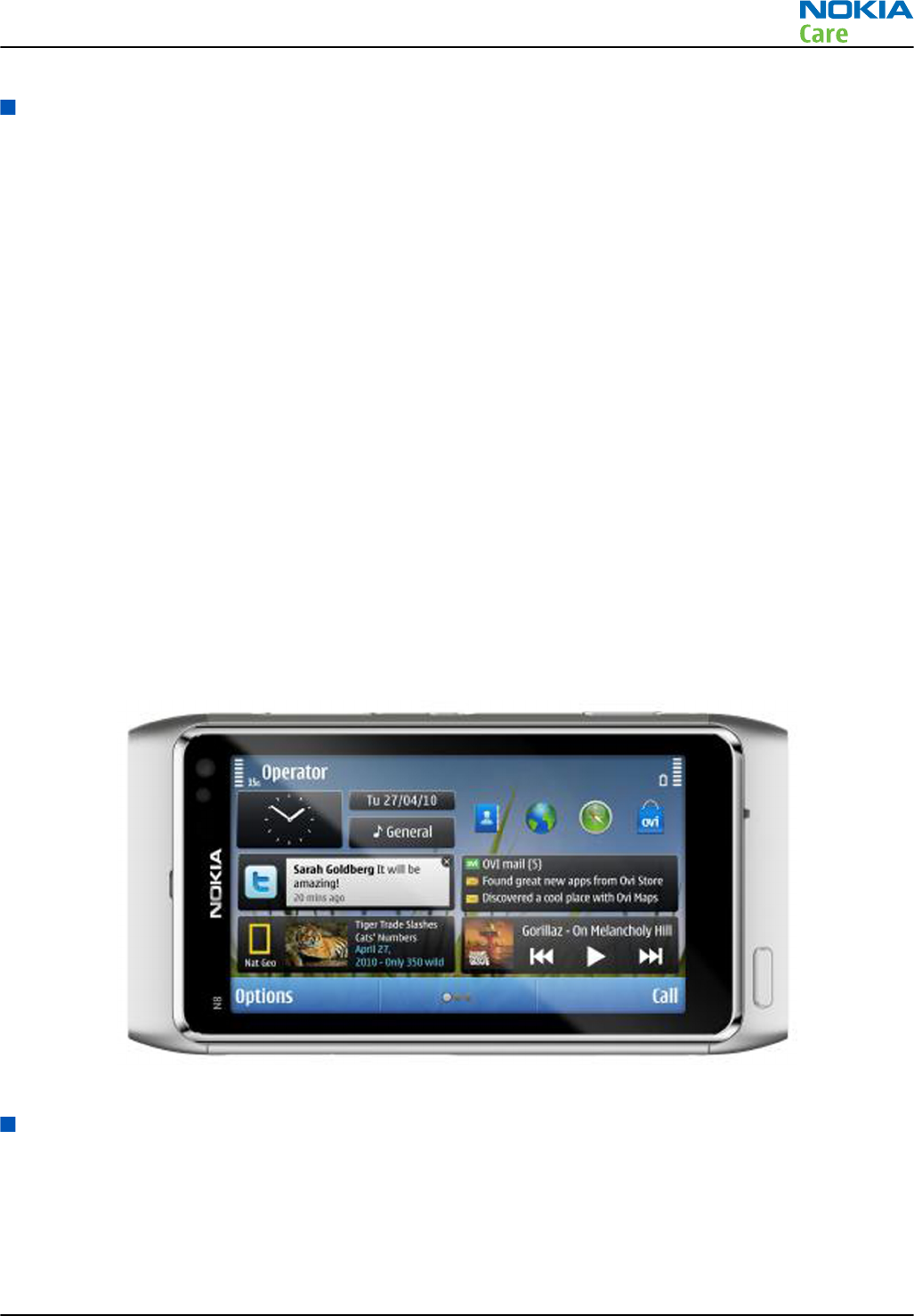
Product selection
RM-596 is a GSM/WCDMA dual-mode handportable monoblock multimedia computer with a capacitive touch
UI, integrated GPS (A-GPS OMA SUPL), WLAN and a TV-out connection. It supports GSM 850/900/1800/1900
and WCDMA I/II/IV/V/VIII bands, GPRS/EGPRS and WCDMA/HSDPA/HSUPA data bearers.
For WCDMA the maximum bit rate is up to 384 kbit/s for downlink and 384 kbit/s for uplink with simultaneous
CS speech or CS video (max. 64 kbit/s). RM-596 supports HSDPA category 9 with downlink peak data rate up
to 10.2 Mbit/s (in limited use cases), HSUPA belongs to category 5 with uplink peak data rate up to 2.0 Mbit/
s (in limited use cases).
In PS/CS mode, RM-596 supports DTM with multi slot class 32 (max. 5 RX + 3 TX, sum 6). With EGPRS this means
maximum download speed of up to 236.8 kbit/s simultaneously with speech. With GPRS this means maximum
download speed of up to 85.6 kbit/s simultaneously with speech.
In PS only mode, RM-596 supports MSC 33 (max. 5 Rx + 4 TX, sum 6) timeslots resulting in maximum download
speed of up to 296 kbit/s with EGPRS, and up to 107 kbit/s with GPRS.
RM-596 has a large AMOLED nHD 3.5” (640 x 360 pixels) colour display (active area 43.2 mm x 76.8 mm) with
16 million colors. It also has a 12 megapixel autofocus camera with Carl Zeiss optics, 2 x digital zoom and an
integrated Xenon flash. The device supports two-way video calls with two integrated cameras, one on the
front and one on the back.
The MMS implementation follows the OMA MMS standard release 1.3. The browser is a highly advanced
Internet browser also capable of viewing operator domain XHTML Mobile Profile (MP) content. The device
also supports Bluetooth 2.1 EDR standard.
RM-596 uses Symbian ^3 for Nokia devices operating system, and supports the full Web Browser for S60,
which brings desktop-like Web browsing experience to mobile devices. It also supports MIDP Java 2.1 ,
providing a good platform for compelling 3rd party applications.
Figure 1 View of RM-596
Product features and sales package
Imaging
Main camera:
•Sensor: 12 megapixel
•Carl Zeiss Optics: Tessar ™ lens
RM-596
General Information
Issue 2 COMPANY CONFIDENTIAL Page 1 – 5
Copyright © 2010 Nokia. All rights reserved.

•F number/Aperture: F2.8
•Digital zoom: 2x
•Auto focus: Two-stage capture key
•Focal length: 28 mm (35 mm equivalent)
•Focus range: 10 cm ~ infinity
•Flash: Integrated Xenon flash
•Macro focus distance: 10-50 cm
•Shutter speed: Mechanical shutter 1/1000~1/4 s
Secondary camera:
•Sensor: VGA (640 x 480 pixels)
•F number/Aperture: F2.8
•Fixed focus
Video:
•Video resolution: nHD 25 fps (720p)
•Audio recording: AAC (AMR for MMS)
•Video stabilization
•Video clip length: Max. 90 min
•Video file format: .mp4 (default), .3gp (for MMS)
•White balance: automatic, sunny, cloudy, incandescent, fluorescent
•Scene: Auto, Night
•Colour tone: normal, sepia, B&W, vivid, negative
•Zoom (digital): 3x
•Video recording indicator
Photo:
•Aspect ratio: 16:9 (9Mpix) , 4:3 (12Mpix)
•View finder: Full screen view finder
•Still image resolutions: up to 12 megapixel: 4000 x 3000
•Still image file format: JPEG/EXIF
•Auto exposure: center weighted AE
•Image orientation: automatic
•Exposure compensation: +2 ~ -2EV at 0.5 step
•White balance: automatic, sunny, cloudy, incandescent, fluorescent
•Scene: auto, sports, portrait, close-up, landscape, night, user defined
•Colour tone: normal, sepia, B&W, vivid, negative
•Zoom (digital): 2x
Edit
•On device Photo editor and Video editor (manual & automatic)
View
•3.5” nHD (640 x 360 pixels) colour display (active area 43.2 mm x 76.8 mm), up to 16M colors, 16:9 aspect
ratio
RM-596
General Information
Page 1 – 6 COMPANY CONFIDENTIAL Issue 2
Copyright © 2010 Nokia. All rights reserved.

•Digital Ambient Light Sensor (ALS) – used to optimize display/key brightness and power consumption
•Slideshow from Gallery
Share
•Nokia XpressShare - share effortlessly from Gallery or after capture via Email, Bluetooth or MMS
•Direct connection to TV via cable or WLAN (UPnP)
•Video call and video sharing support. (WCDMA services)
•Online Album: Image/Video uploading from Gallery
Print
•Nokia XpressPrint – direct printing via USB (PictBridge), Bluetooth (BPP), and WLAN (UPnP), from memory
card or via online printing
Store
•16 GB internal user memory
•Nokia XpressTransfer – easy to transfer and organize photos and video between your device and a
compatible PC
•Nokia Lifeblog (mobile & PC)
Music
•Digital music player: supports MP3/ AAC/ eAAC/ eAAC+/ WMA/ AMR-NB/ AMR-WB with playlists, equalizer
and album art
•Synchronise music with Microsoft Windows Media Player 10 & 11
•One click CD ripping, converting and transferring music to your device using Nokia Music Manager
•Stereo FM radio (87.5-108 MHz /76-90 MHz) with Visual Radio™ support
•Bluetooth speakers
•Integrated handsfree speaker
•Nokia Music Headset (WH-701), inbox
Media
•Full-screen video playback to view downloaded, streamed or recorded video clips
•Supported video formats: MPEG-4 , H.264/AVC, H.263/3GPP, VC-1, Real Video 10, ON2 VP6, Flash video
Productivity
Context management:
•OMA DRM version 2.0
•OTA provisioning & over the air SW update (FOTA)
•Ovi Suite
•Web Browser (OSS), Java ™ MIDP 2.1, XHTML browsing over TCP/IP
Messaging:
•E-mail (SMTP, IMAP4, POP3), MMS, SMS, unified editor
•IM client
Office applications:
•Viewing of email attachments – .doc, .xls, .ppt, .pdf, .zip
RM-596
General Information
Issue 2 COMPANY CONFIDENTIAL Page 1 – 7
Copyright © 2010 Nokia. All rights reserved.

•Mail for Exchange
PIM:
•Contacts, calendar, to-do, notes, recorder, calculator, clock, converter
Synchronization:
•Local/Remote (using SyncML)
•Data: Calendar, Contacts, To-do, Notes, E-mail
•PC Applications: Microsoft Outlook (98, 2000, 2002, 2003), Outlook Express, Lotus Organizer (5.0, 6.0),
Lotus Notes (5.0, 6.0)
Call management:
•Call logs, speed dial, voice dialling (with SIND) and voice commands
•Nokia Push to Talk (PoC)
Connectivity
•Integrated GPS (A-GPS OMA SUPL)
•Nokia Maps 3.0, including Friend Finder
•WLAN - IEEE802.11 g/b/n with UPnP support
•HDMI type C connector
•Micro USB interface with USB 2.0 high speed
•Bluetooth wireless technology 2.1 + EDR + A2DP
•FM transmitter
•MicroSD memory card - support up to 32 GB
•Nokia 3.5 mm AV connector
•2.0 mm DC connector
Add-on software framework
•Symbian ^3 for Nokia devices
•Java: MIDP2.1
•C++ and Java SDKs
•Flash Lite 4.0
Additional technical specifications
•Vibrating alert
•3GPP Rel 5/6 WCDMA , Rel 4 EGSM compliant
•Speech codecs supported: AMR, NB AMR, WB AMR, FR, EFR
•GPRS/EGPRS Class B, Multi slot class 33
•Dual Transfer Mode (DTM) class A, multi slot class 32
•WCDMA DL 384 kbit/s, UL 384 kbit/s
•HSDPA up to 10.2 Mbps, HSUPA 2 Mbps
Sales package
•Transceiver RM-596
•Charger (AC-15)
•Battery (BL-4D)
RM-596
General Information
Page 1 – 8 COMPANY CONFIDENTIAL Issue 2
Copyright © 2010 Nokia. All rights reserved.
•Music headset (WH-701)
•Connectivity cable (CA-101)
•HDMI adapter (CA-157)
•Micro USB OTG to USB adapter (CA-156)
•CD-ROM
•User Guide
Product and module list
Module name Type code Notes
System/RF module PWB 3CE
Upper flex module
UI flex module
Flash flex module
Mobile enhancements
Table 1 Audio
Enhancement Type
Music headset WH-701
Nokia Wireless Stereo Gateway AD-42W
Mini speakers MD-8
MD-9
Hearing aids HDA-12
LPS-5
Wired headsets WH-205
WH-502
WH-700
WH-701
WH-800
WH-900
RM-596
General Information
Issue 2 COMPANY CONFIDENTIAL Page 1 – 9
Copyright © 2010 Nokia. All rights reserved.
Enhancement Type
Bluetooth headsets BH-103
BH-214
BH-215
BH-500
BH-501
BH-503
BH-504
BH-505
BH-606
BH-607
BH-702
BH-704
BH-804
BH-805
BH-900
BH-902
BH-904
BH-905
Bluetooth speakers MD-5W
MD-7W
Table 2 Car
Enhancement Type
Nokia Universal Mobile Holder CR-99
Speakerphone HF-310
HF-510
Mobile charger DC-9
DC-10
DC-11
Table 3 Data
Enhancement Type
Connectivity cable CA-101
CA-101D
RM-596
General Information
Page 1 – 10 COMPANY CONFIDENTIAL Issue 2
Copyright © 2010 Nokia. All rights reserved.
Enhancement Type
Micro USB OTG to USB adapter cable CA-156
HDMI adapter cable CA-157
MicroSD card MU-43, 8GB
MU-44, 16GB
MU-xx 32GB
Table 4 Messaging
Enhancement Type
Other multimedia peripherals SU-33W
Stylus STYLUS PEN ASSY
Table 5 Power
Enhancement Type
Battery 1200 mAh Li-ion BL-4D
Travel charger AC-6
AC-8
AC-10
AC-15
Technical specifications
Transceiver general specifications
Unit Dimensions (L x W x T)
(mm) Weight (g) Volume (cm3)
Transceiver with BL-4D
1200 mAh Li-ion battery
pack
113.5 x 59.0 x 12.9 135 86
Main RF characteristics for GSM850/900/1800/1900 and WCDMA VIII/V/IV/II/I phones
Parameter Unit
Cellular system GSM850, EGSM900, GSM1800/1900, WCDMA VIII (900), WCDMA V
(850), WCDMA IV (1700/2100), WCDMA II (1900) and WCDMA I
(2100)
RM-596
General Information
Issue 2 COMPANY CONFIDENTIAL Page 1 – 11
Copyright © 2010 Nokia. All rights reserved.
Parameter Unit
Rx frequency band GSM850: 869 - 894MHz
EGSM900: 925 - 960 MHz
GSM1800: 1805 - 1880 MHz
GSM1900: 1930 - 1990 MHz
WCDMA VIII (900): 925 - 960 MHz
WCDMA V (850): 869 - 894 MHz
WCDMA IV (1700/2100): 2110 - 2155 MHz
WCDMA II (1900): 1930 - 1990 MHz
WCDMA I (2100): 2110 - 2170 MHz
Tx frequency band GSM850: 824 - 849 MHz
EGSM900: 880 - 915 MHz
GSM1800: 1710 - 1785 MHz
GSM1900: 1850 - 1910 MHz
WCDMA VIII (900): 880 - 915 MHz
WCDMA V (850): 824 - 849 MHz
WCDMA IV (1700/2100): 1710 - 1755 MHz
WCDMA II (1900): 1850 - 1910 MHz
WCDMA I (2100): 1920 - 1980 MHz
Output power GSM850: +5 ...+33 dBm/3.2 mW ... 2 W
GSM900: +5 … +33 dBm/3.2 mW … 2 W
GSM1800: +0 … +30 dBm/1.0 mW … 1 W
GSM1900: +0 … +30 dBm/1.0 mW … 1 W
WCDMA VIII (900): -50 ... +24 dBm/0.01 μW ... 251 mW
WCDMA V (850): -50 ... +24 dBm/0.01 μW ... 251 mW
WCDMA IV (1700/2100): -50 ... +24 dBm/0.01 μW ... 251 mW
WCDMA II (1900): -50 ... +21 dBm/0.01 μW ... 126 mW
WCDMA I (2100): -50 ... +24 dBm/0.01 μW ... 251 mW
EDGE output power EDGE850: +5 … +27 dBm/3.2 mW … 501 mW
EDGE900: +5 … +27 dBm/3.2 mW … 501 mW
EDGE1800: +0 … +26 dBm/1.0 mW … 398 mW
EDGE1900:+0 … +26d Bm/1.0 mW … 398 mW
RM-596
General Information
Page 1 – 12 COMPANY CONFIDENTIAL Issue 2
Copyright © 2010 Nokia. All rights reserved.
Parameter Unit
Number of RF channels GSM850: 124
GSM900: 174
GSM1800: 374
GSM1900: 299
WCDMA VIII (900): 152
WCDMA V (850): 108
WCDMA IV (1700/2100): 211
WCDMA II (1900): 289
WCDMA I (2100): 277
Channel spacing 200 kHz (WCDMA II, IV and V 100/200 kHz)
Number of Tx power levels GSM850: 15
GSM900: 15
GSM1800: 16
GSM1900: 16
WCDMA VIII (900): 75
WCDMA V (850): 75
WCDMA IV (1700/2100): 75
WCDMA II (1900): 75
WCDMA I (2100): 75
Battery endurance
Battery Capacity
(mAh) Talk time Stand-by Music playback Video playback
H.264 720p 30fps
BL-4D 1200 Up to 12 h
(GSM)
Up to 6 h
(WCDMA)
Up to 390 h
(GSM)
Up to 400 h
(WCDMA)
Up to 50 h Up to 7 h
Environmental conditions
Temperature conditions
Environmental condition Ambient temperature Notes
Normal operation -15oC...+55oCSpecifications fulfilled
Reduced performance -25oC...-15oC
+55oC...+70oC
Operational for shorts periods
only
RM-596
General Information
Issue 2 COMPANY CONFIDENTIAL Page 1 – 13
Copyright © 2010 Nokia. All rights reserved.

Environmental condition Ambient temperature Notes
Intermittent operation -40oC...-15oC
+70oC...+85 oC
Operation not guaranteed but an
attempt to operate does not
damage the phone.
No operation or storage <-40oC...>+85oCNo storage or operation: an
attempt may damage the phone.
Charging allowed -10oC...+60oCBTemp measurement range for
charging.
Long term storage conditions 0oC...+85oC
Humidity
Relative humidity range is 5...95%.
The HW module is not protected against water. Condensed or splashed water might cause malfunction. Any
submersion of the phone will cause permanent damage. Long-term high humidity, with condensation, will
cause permanent damage because of corrosion.
Vibration
The module should withstand the following vibrations:
•5 - 10 Hz; +10dB / octave
•10 - 50 Hz; 5.58 m2 / s3 (0.0558 g2/ Hz)
•50 - 300 Hz; - 10 dB / octave
ESD strength
Conducted discharge is 8 kV (>10 discharges) and air contact 15 kV ( >10 discharges ).
The standard for electrostatic discharge is IEC 61000-4-2, and this device fulfils level 4 requirements.
RoHS
This device uses RoHS compliant components and lead-free soldering process.
RM-596
General Information
Page 1 – 14 COMPANY CONFIDENTIAL Issue 2
Copyright © 2010 Nokia. All rights reserved.

2 — Service Tools and Service
Concepts
Nokia Customer Care
Issue 2 COMPANY CONFIDENTIAL Page 2 – 1
Copyright © 2010 Nokia. All rights reserved.

RM-596
Service Tools and Service Concepts
(This page left intentionally blank.)
Page 2 – 2 COMPANY CONFIDENTIAL Issue 2
Copyright © 2010 Nokia. All rights reserved.

Table of Contents
Service tools........................................................................................................................................................... 2–5
Product specific tools....................................................................................................................................... 2–5
MJ-241 .......................................................................................................................................................... 2–5
RJ-233 ........................................................................................................................................................... 2–5
SD-60 ............................................................................................................................................................ 2–6
General tools..................................................................................................................................................... 2–6
AC-35............................................................................................................................................................. 2–6
ACF-8............................................................................................................................................................. 2–6
CU-4............................................................................................................................................................... 2–7
FLS-5 ............................................................................................................................................................. 2–8
FPS-21........................................................................................................................................................... 2–8
JXS-1.............................................................................................................................................................. 2–9
PK-1............................................................................................................................................................... 2–9
SB-6............................................................................................................................................................... 2–9
SB-7............................................................................................................................................................... 2–9
SRT-6.......................................................................................................................................................... 2–10
SS-182........................................................................................................................................................ 2–10
SS-93.......................................................................................................................................................... 2–10
SX-4............................................................................................................................................................ 2–10
Cables.............................................................................................................................................................. 2–10
CA-101 ....................................................................................................................................................... 2–11
CA-158RS ................................................................................................................................................... 2–11
CA-31D ....................................................................................................................................................... 2–11
CA-89DS ..................................................................................................................................................... 2–12
DAU-9S....................................................................................................................................................... 2–12
PCS-1.......................................................................................................................................................... 2–12
XRS-6.......................................................................................................................................................... 2–13
Service concepts ................................................................................................................................................. 2–13
POS (Point of Sale) flash concept ................................................................................................................. 2–13
Flashing, certificate restore and product code change option 2 ............................................................. 2–14
Module jig service concept........................................................................................................................... 2–15
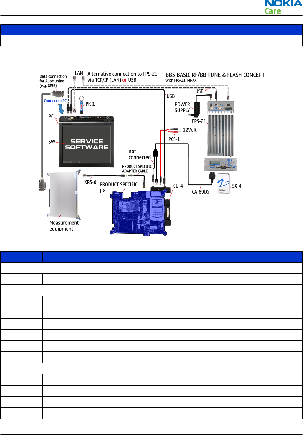
RF testing and BB/RF tuning concept with module jig.............................................................................. 2–16
List of Figures
Figure 2 POS flash concept ................................................................................................................................ 2–13
Figure 3 Flashing, certificate restore and product code change................................................................... 2–14
Figure 4 Module jig service concept ................................................................................................................. 2–15
Figure 5 RF testing and BB/RF tuning concept with module jig.................................................................... 2–16
RM-596
Service Tools and Service Concepts
Issue 2 COMPANY CONFIDENTIAL Page 2 – 3
Copyright © 2010 Nokia. All rights reserved.

RM-596
Service Tools and Service Concepts
(This page left intentionally blank.)
Page 2 – 4 COMPANY CONFIDENTIAL Issue 2
Copyright © 2010 Nokia. All rights reserved.
Service tools
Product specific tools
The table below gives a short overview of service devices that can be used for testing, error analysis, and
repair of product RM-596. For the correct use of the service devices, and the best effort of workbench setup,
please refer to various concepts.
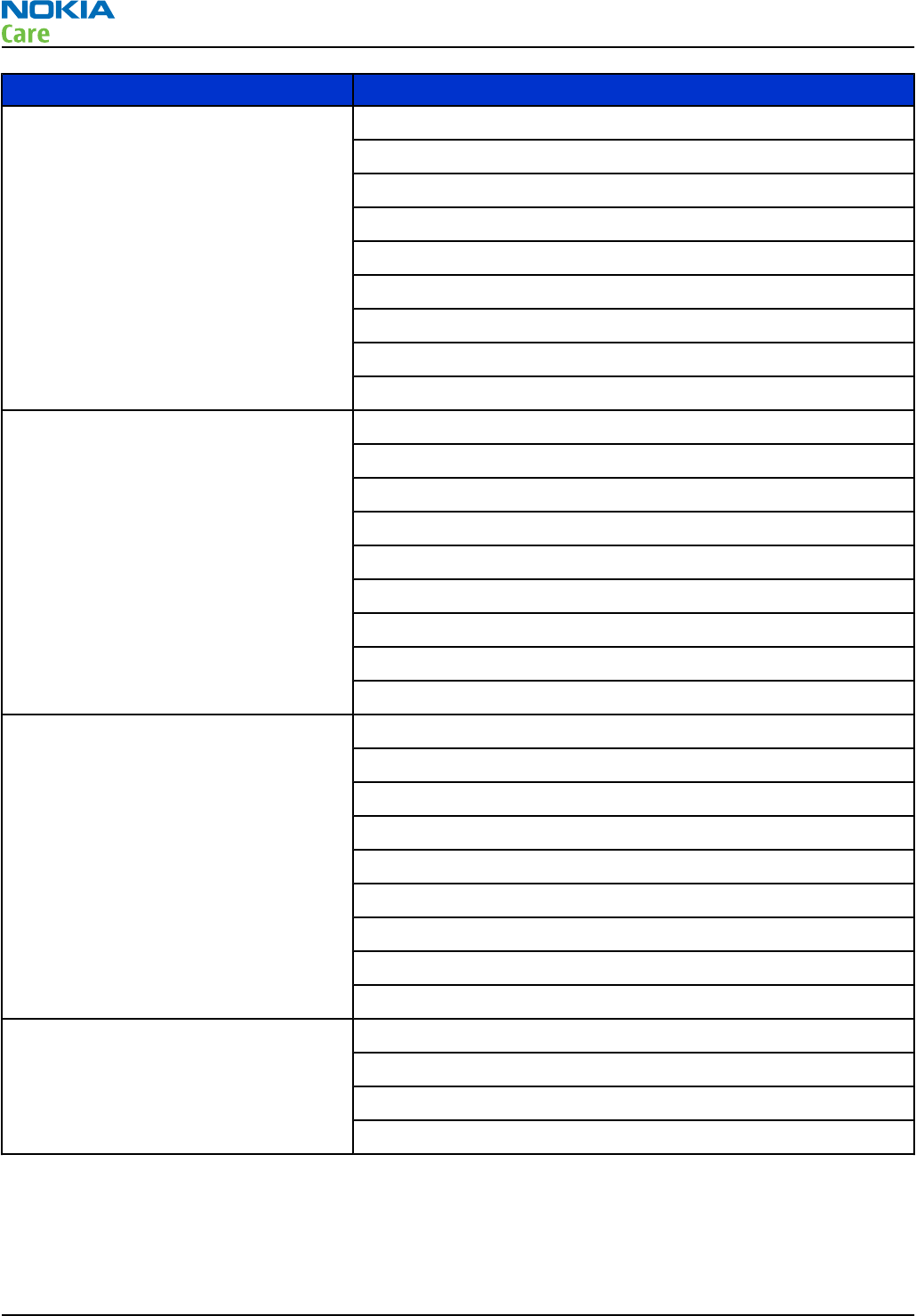
MJ-241 Module jig
MJ-241 is meant for troubleshooting, testing, tuning and flashing on
the engine level (CU-4 supported).
The jig includes the following features:
•Provides mechanical interface with the engine module
•Provides galvanic connection to all needed test pads in module
•Connector for control unit
•Access for AV- and USB connectors
•CA-158RS cable is used together with this jig for RF testing
•Attenuation values for galvanic RF connection MJ-241
Band Default f/
MHz RX Att. RX Default f/
MHz TX Att. TX
GSM 850 881.6 0.1 836.6 0.1
GSM 900 942.4 0.1 897.4 0.1
GSM 1800 1842.8 0.2 1747.8 0.2
GSM 1900 1960.0 0.2 1880.0 0.2
WCDMA I 2140.0 0.2 1950.0 0.2
WCDMA II 1960.0 0.2 1880.0 0.2
WCDMA IV 2140.0 0.2 1740.0 0.2
WCDMA V 880.0 0.1 835.0 0.1
WCDMA VIII 942.6 0.1 897.6 0.1
WLAN n / a n / a 2442.0 0.3
FM / Tx n / a n / a
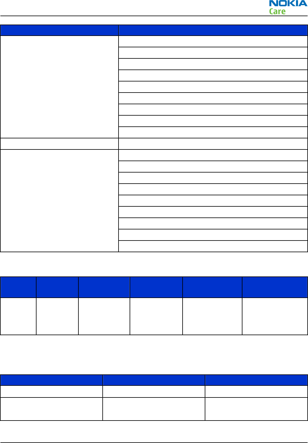
RJ-233 Soldering jig
RJ-233 is a soldering jig used for soldering and as a rework jig for the
engine module.
RM-596
Service Tools and Service Concepts
Issue 2 COMPANY CONFIDENTIAL Page 2 – 5
Copyright © 2010 Nokia. All rights reserved.
SD-60 Dummy battery
SD-60 dummy battery is meant for component level troubleshooting..
General tools
The table below gives a short overview of service devices that can be used for testing, error analysis, and
repair of product RM-596. For the correct use of the service devices, and the best effort of workbench setup,
please refer to various concepts.
AC-35 Power supply
Universal power supply for FPS-21; included in the FPS-21 sales
package.
Input 100V…230V 50Hz…60Hz, output voltage of 12 V and output
current up to 3 A.
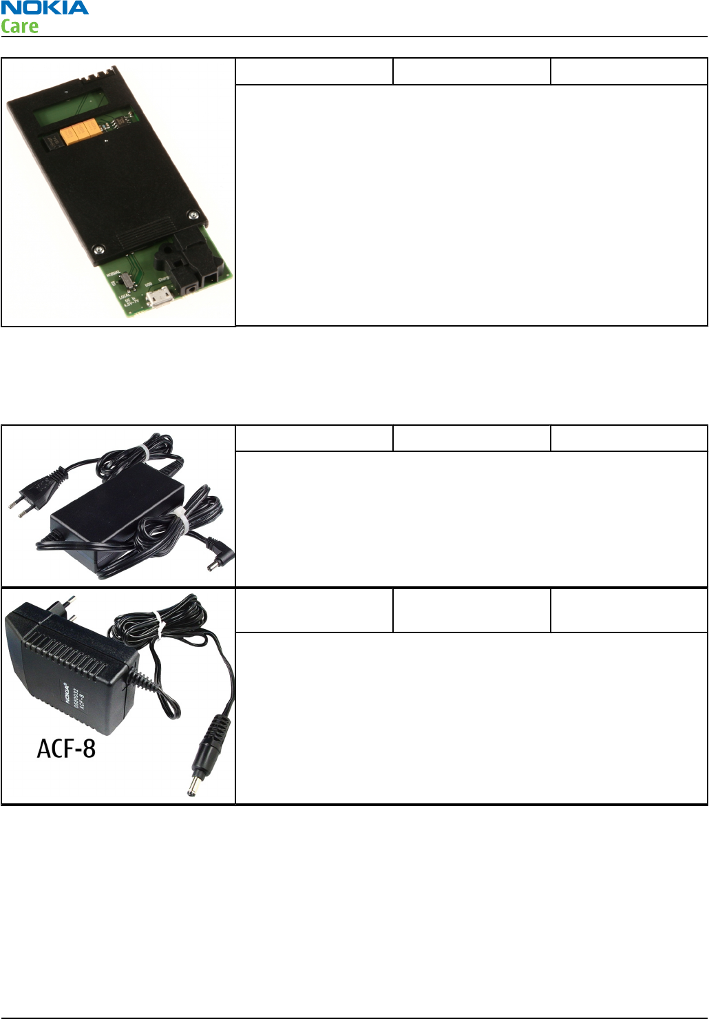
ACF-8 Universal power
supply
The ACF-8 universal power supply is used to power FLS-5.
RM-596
Service Tools and Service Concepts
Page 2 – 6 COMPANY CONFIDENTIAL Issue 2
Copyright © 2010 Nokia. All rights reserved.
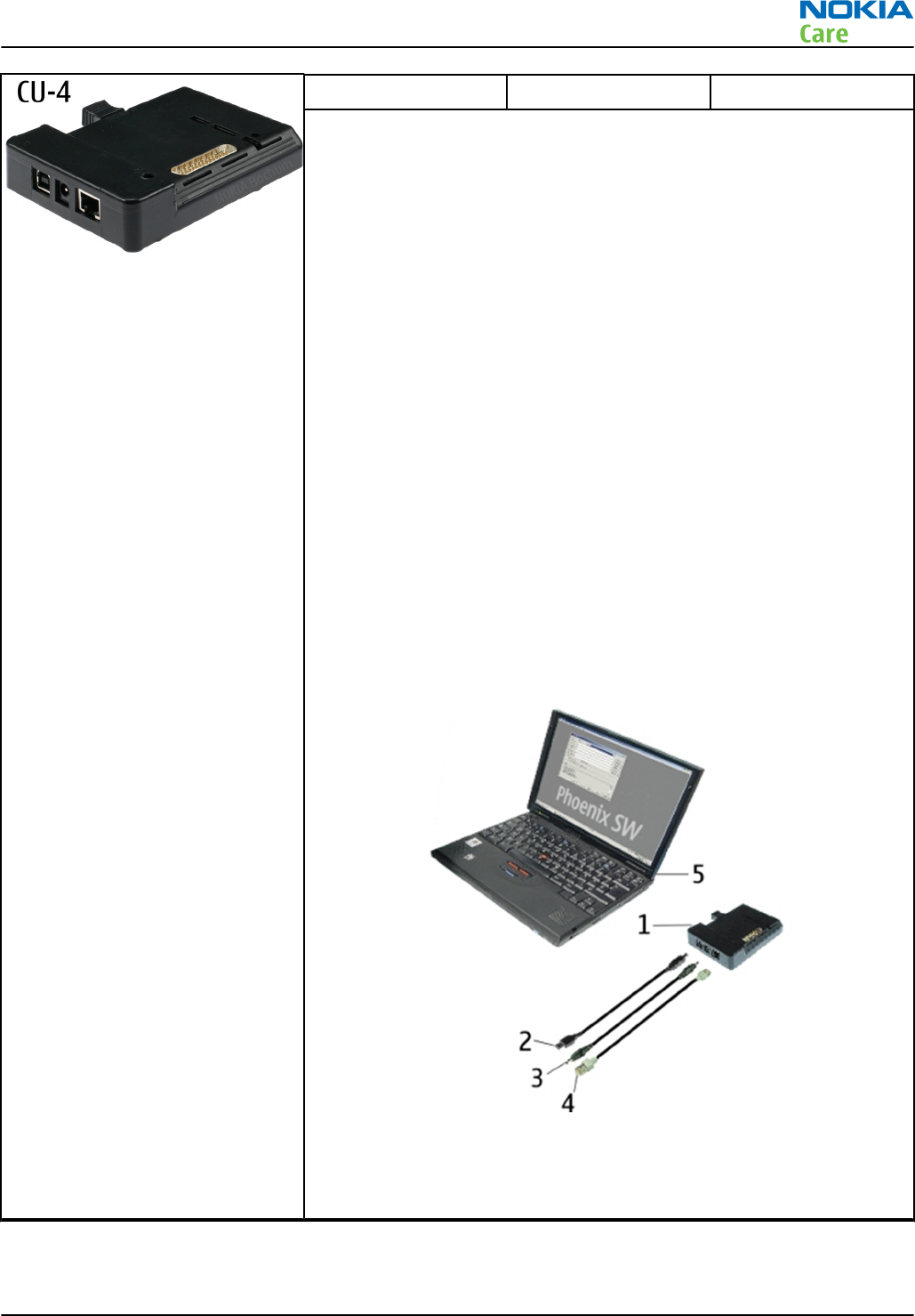
CU-4 Control unit
CU-4 is a general service tool used with a module jig and/or a flash
adapter. It requires an external 12 V power supply.
The unit has the following features:
•software controlled via USB
•EM calibration function
•Forwards FBUS/Flashbus traffic to/from terminal
•Forwards USB traffic to/from terminal
•software controlled BSI values
•regulated VBATT voltage
•2 x USB2.0 connector (Hub)
•FBUS and USB connections supported
When using CU-4, note the special order of connecting cables and
other service equipment:
Instructions
1 Connect a service tool (jig, flash adapter) to CU-4.
2 Connect CU-4 to your PC with a USB cable.
3 Connect supply voltage (12 V)
4 Connect an FBUS cable (if necessary).
5 Start Phoenix service software.
Note: Phoenix enables CU-4 regulators via USB when it is
started.
Reconnecting the power supply requires a Phoenix restart.
RM-596
Service Tools and Service Concepts
Issue 2 COMPANY CONFIDENTIAL Page 2 – 7
Copyright © 2010 Nokia. All rights reserved.
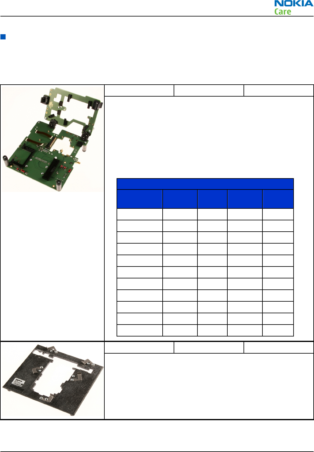
FLS-5 Flash device
FLS-5 is a dongle and flash device incorporated into one package,
developed specifically for POS use.
Note: FLS-5 can be used as an alternative to PK-1.
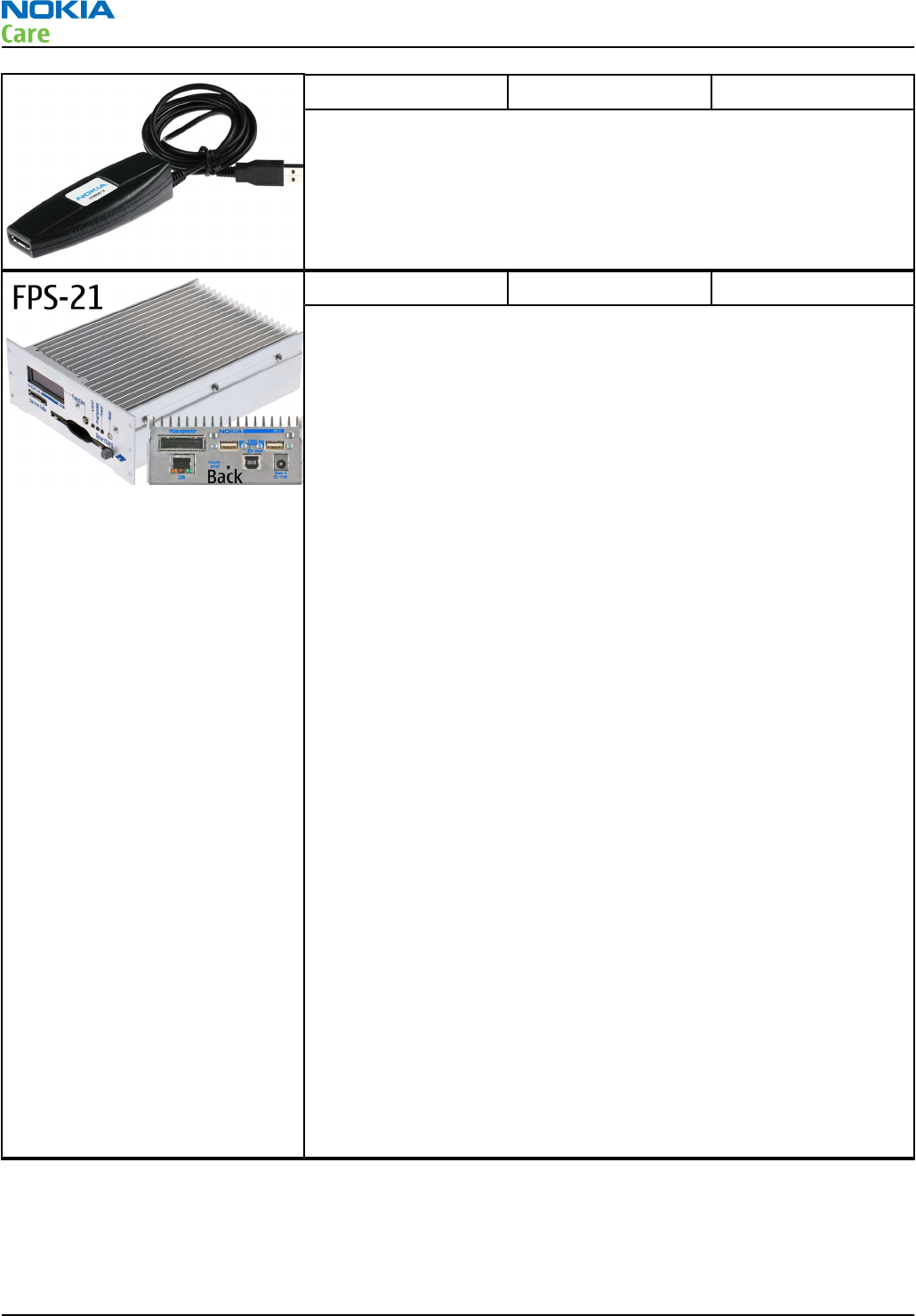
FPS-21 Flash prommer
FPS-21 sales package:
•FPS-21 prommer
•AC-35 power supply
•CA-31D USB cable
FPS-21 interfaces:
Front
•Service cable connector
Provides Flashbus, USB and VBAT connections to a mobile device.
•SmartCard socket
A SmartCard is needed to allow DCT-4 generation mobile device
programming.
Rear
•DC power input
For connecting the external power supply (AC-35).
•Two USB A type ports (USB1/USB3)
Can be used, for example, for connecting external storage memory
devices or mobile devices
•One USB B type device connector (USB2)
For connecting a PC.
•Phone connector
Service cable connection for connecting Flashbus/FLA.
•Ethernet RJ45 type socket (LAN)
For connecting the FPS-21 to LAN.
Inside
•Four SD card memory slots
For internal storage memory.
Note: In order to access the SD memory card slots inside
FPS-21, the prommer needs to be opened by removing the
front panel, rear panel and heatsink from the prommer body.
RM-596
Service Tools and Service Concepts
Page 2 – 8 COMPANY CONFIDENTIAL Issue 2
Copyright © 2010 Nokia. All rights reserved.
JXS-1 RF shield box
Because the WCDMA network disturbs the RX side testing of the WCDMA
phone and the Tx signal of the WCDMA phone can severely disturb the
WCDMA network, a shield box is needed in all testing, tuning and fault
finding which requires WCDMA RF signal.
The shield box is not an active device, it contains only passive filtering
components for RF attenuation.
PK-1 Software protection
key
PK-1 is a hardware protection key with a USB interface. It has the same
functionality as the PKD-1 series dongle.
PK-1 is meant for use with a PC that does not have a series interface.
To use this USB dongle for security service functions please register
the dongle in the same way as the PKD-1 series dongle.
SB-6 Bluetooth test and
interface box (sales
package)
The SB-6 test box is a generic service device used to perform Bluetooth
bit error rate (BER) testing, and establishing cordless FBUS connection
via Bluetooth. An ACP-8x charger is needed for BER testing and an
AXS-4 cable in case of cordless interface usage testing .
Sales package includes:
•SB-6 test box
•Installation and warranty information
SB-7 WLAN test box
WLAN test requires defined position for the device.
RM-596
Service Tools and Service Concepts
Issue 2 COMPANY CONFIDENTIAL Page 2 – 9
Copyright © 2010 Nokia. All rights reserved.
SRT-6 Opening tool
SRT-6 is used to open phone covers.
Note: The SRT-6 is included in the Nokia Standard Toolkit.
SS-182 Camera removal tool
The camera removal tool SS-182 is used to remove/attach a camera
module from/to the camera socket of the phone PWB.
SS-93 Opening tool
SS-93 is used for opening JAE connectors.
Note: The SS-93 is included in Nokia Standard Toolkit.
SX-4 Smart card
SX-4 is a BB5 security device used to protect critical features in tuning
and testing.
SX-4 is also needed together with FPS-21 when DCT-4 phones are
flashed.
Cables
The table below gives a short overview of service devices that can be used for testing, error analysis, and
repair of product RM-596. For the correct use of the service devices, and the best effort of workbench setup,
please refer to various concepts.
RM-596
Service Tools and Service Concepts
Page 2 – 10 COMPANY CONFIDENTIAL Issue 2
Copyright © 2010 Nokia. All rights reserved.
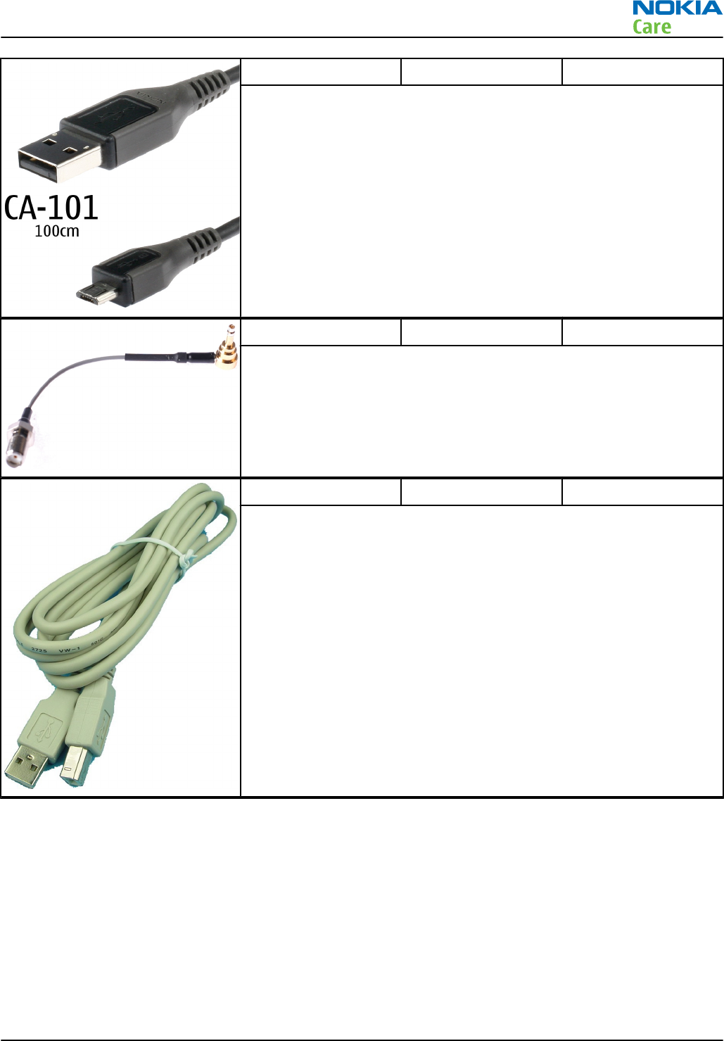
CA-101 Micro USB cable
The CA-101 is a USB-to-microUSB data cable that allows connections
between the PC and the phone.
CA-158RS RF tuning cable
Product-specific adapter cable for RF tuning.
CA-31D USB cable
The CA-31D USB cable is used to connect FPS-21 to a PC. It is included
in the FPS-21 sales package.
RM-596
Service Tools and Service Concepts
Issue 2 COMPANY CONFIDENTIAL Page 2 – 11
Copyright © 2010 Nokia. All rights reserved.
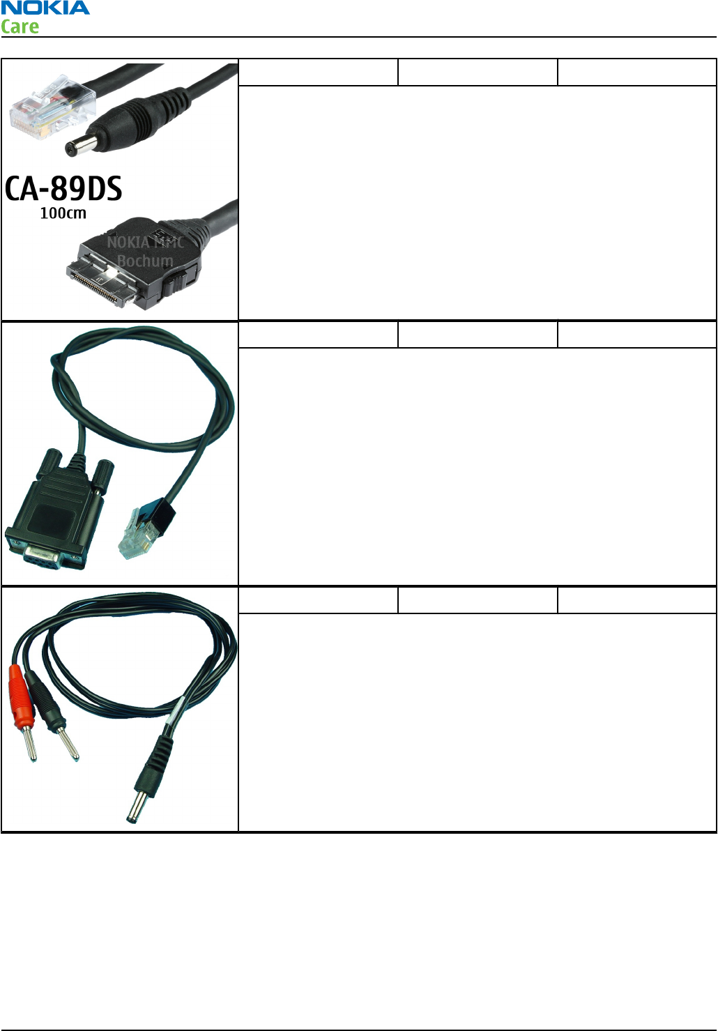
CA-89DS Cable
Provides VBAT and Flashbus connections to mobile device
programming adapters.
DAU-9S MBUS cable
The MBUS cable DAU-9S has a modular connector and is used, for
example, between the PC's serial port and module jigs, flash adapters
or docking station adapters.
Note: Docking station adapters valid for DCT4 products.
PCS-1 Power cable
The PCS-1 power cable (DC) is used with a docking station, a module
jig or a control unit to supply a controlled voltage.
RM-596
Service Tools and Service Concepts
Page 2 – 12 COMPANY CONFIDENTIAL Issue 2
Copyright © 2010 Nokia. All rights reserved.
XRS-6 RF cable
The RF cable is used to connect, for example, a module repair jig to
the RF measurement equipment.
SMA to N-Connector approximately 610 mm.
Attenuation for:
•GSM850/900: 0.3+-0.1 dB
•GSM1800/1900: 0.5+-0.1 dB
•WCDMA/WLAN: 0.6+-0.1dB
Service concepts
POS (Point of Sale) flash concept
Figure 2 POS flash concept
Type Description
Product specific tools
BL-4D Battery
Other tools
FLS-5 POS flash dongle
PC with service software
RM-596
Service Tools and Service Concepts
Issue 2 COMPANY CONFIDENTIAL Page 2 – 13
Copyright © 2010 Nokia. All rights reserved.
Type Description
Cables
CA-101 Micro USB cable
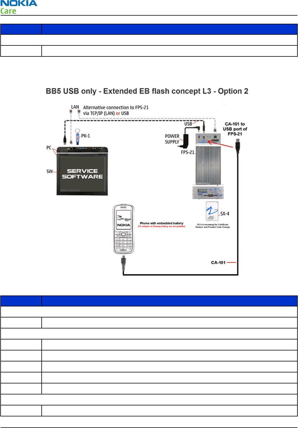
Flashing, certificate restore and product code change option 2
Figure 3 Flashing, certificate restore and product code change
Type Description
Product specific devices
BL-4D Battery
Other devices
FPS-21 Flash prommer box
AC-35 Power supply
PK-1 SW security device
SX-4 Smart card
PC with service software
Cables
CA-101 Micro USB cable
RM-596
Service Tools and Service Concepts
Page 2 – 14 COMPANY CONFIDENTIAL Issue 2
Copyright © 2010 Nokia. All rights reserved.
Type Description
USB cable
Module jig service concept
Figure 4 Module jig service concept
Type Description
Phone specific devices
MJ-241 Module jig
Other devices
CU-4 Control unit
FPS-21 Flash prommer box
PK-1 SW security device
SX-4 Smart card
PC with VPOS and service software
Measurement equipment
Cables
CA-89DS Service cable
PCS-1 DC power cable
XRS-6 RF cable
USB cable
RM-596
Service Tools and Service Concepts
Issue 2 COMPANY CONFIDENTIAL Page 2 – 15
Copyright © 2010 Nokia. All rights reserved.
Type Description
GPIB control cable
CA-158RS Product specific RF adapter cable
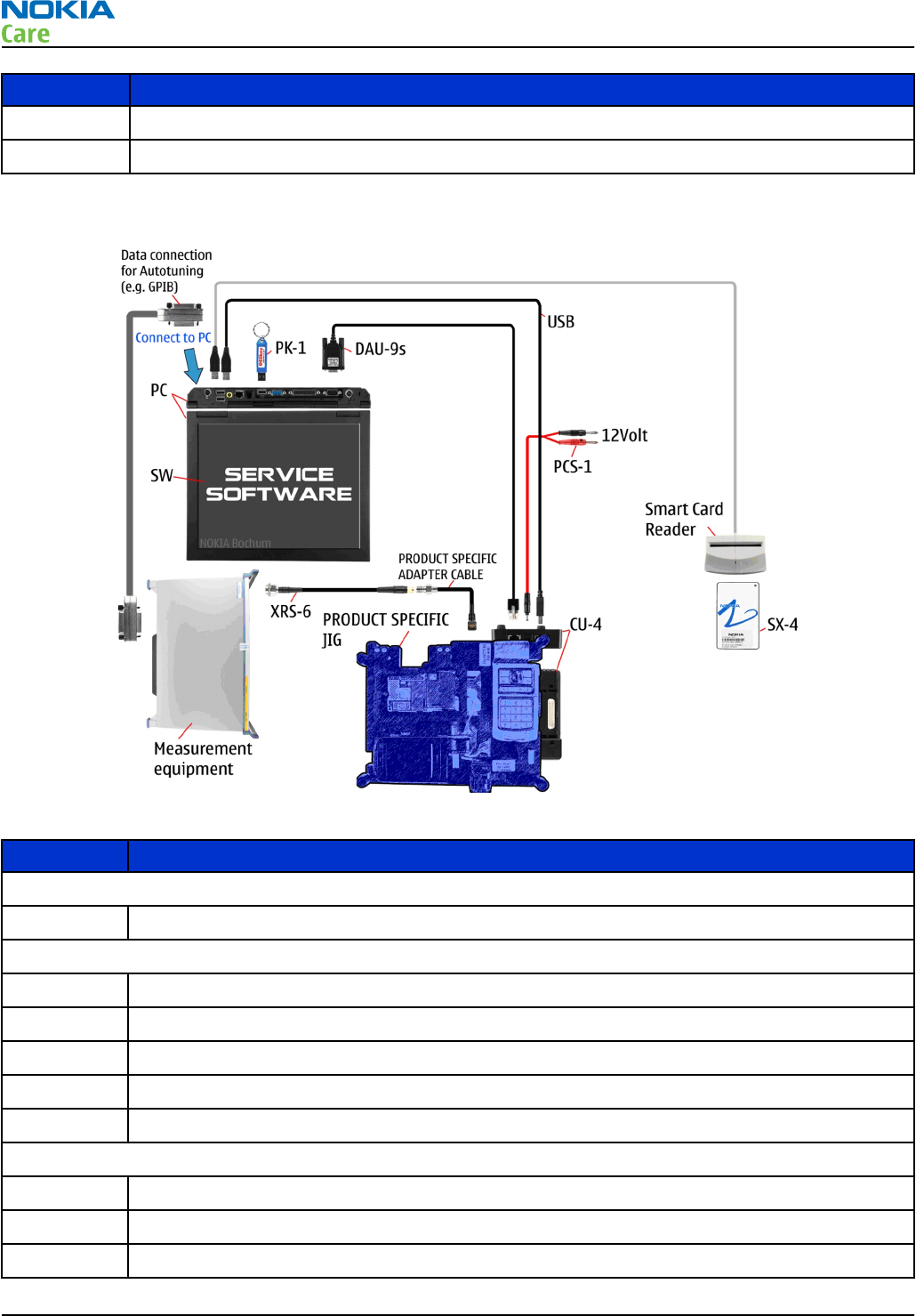
RF testing and BB/RF tuning concept with module jig
Figure 5 RF testing and BB/RF tuning concept with module jig
Type Description
Product specific tools
MJ-241 Module jig
Other tools
CU-4 Control unit
PK-1 SW security device
SX-4 Smart card
PC with service software
Smart card reader
Cables
DAU-9S MBUS cable
PCS-1 Power cable
XRS-6 RF cable
RM-596
Service Tools and Service Concepts
Page 2 – 16 COMPANY CONFIDENTIAL Issue 2
Copyright © 2010 Nokia. All rights reserved.

Type Description
USB cable
CA-158RS Product specific RF adapter cable
RM-596
Service Tools and Service Concepts
Issue 2 COMPANY CONFIDENTIAL Page 2 – 17
Copyright © 2010 Nokia. All rights reserved.

RM-596
Service Tools and Service Concepts
(This page left intentionally blank.)
Page 2 – 18 COMPANY CONFIDENTIAL Issue 2
Copyright © 2010 Nokia. All rights reserved.

3 — BB Troubleshooting and
Manual Tuning Guide
Nokia Customer Care
Issue 2 COMPANY CONFIDENTIAL Page 3 – 1
Copyright © 2010 Nokia. All rights reserved.

RM-596
BB Troubleshooting and Manual Tuning Guide
(This page left intentionally blank.)
Page 3 – 2 COMPANY CONFIDENTIAL Issue 2
Copyright © 2010 Nokia. All rights reserved.

Table of Contents
Baseband main troubleshooting......................................................................................................................... 3–7
Power and charging troubleshooting.............................................................................................................. 3–10
Backup battery troubleshooting.................................................................................................................. 3–10
Battery current measuring fault troubleshooting ..................................................................................... 3–11
General power checking troubleshooting .................................................................................................. 3–12
Dead or jammed device troubleshooting................................................................................................... 3–13
Dynamo charging troubleshooting ............................................................................................................. 3–14
Clocking troubleshooting ............................................................................................................................. 3–15
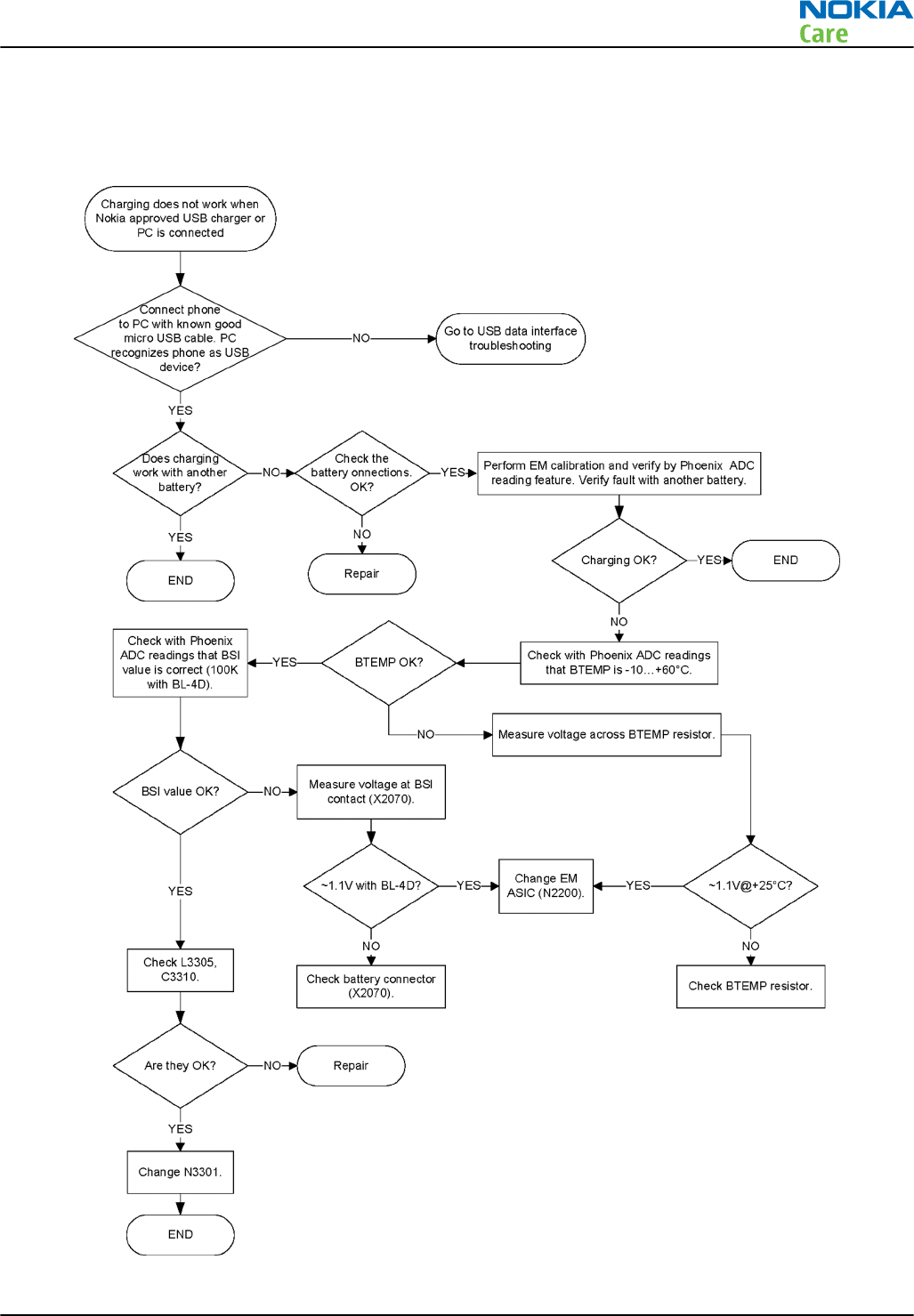
USB charging troubleshooting..................................................................................................................... 3–17
Interface troubleshooting ................................................................................................................................. 3–18
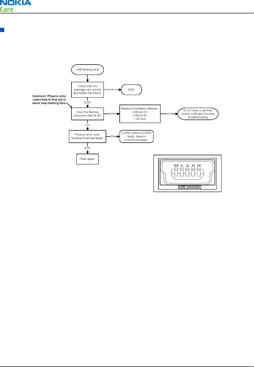
USB flashing fault troubleshooting ............................................................................................................. 3–18
USB data interface troubleshooting............................................................................................................ 3–19
SIM card troubleshooting ............................................................................................................................. 3–19
Memory troubleshooting.............................................................................................................................. 3–23
MicroSD card troubleshooting ................................................................................................................ 3–23
External memory eMMC troubleshooting .............................................................................................. 3–23
NOR troubleshooting ............................................................................................................................... 3–25
SDRAM troubleshooting........................................................................................................................... 3–26
IVE troubleshooting ........................................................................................................................................... 3–27
Introduction to IVE troubleshooting........................................................................................................... 3–27
IVE troubleshooting ...................................................................................................................................... 3–28
TV out troubleshooting...................................................................................................................................... 3–29
Introduction to HDTV and SDTV troubleshooting ...................................................................................... 3–29
HDTV out troubleshooting............................................................................................................................ 3–31
SDTV out troubleshooting ............................................................................................................................ 3–31
Display module troubleshooting ...................................................................................................................... 3–34
General instructions for display troubleshooting...................................................................................... 3–34
Introduction to display troubleshooting.................................................................................................... 3–35
Display fault troubleshooting ...................................................................................................................... 3–37
Touch panel troubleshooting....................................................................................................................... 3–37
Illumination troubleshooting ...................................................................................................................... 3–39
Charging illumination troubleshooting................................................................................................. 3–39
Menu key backlight troubleshooting ..................................................................................................... 3–40
Keyboard troubleshooting ................................................................................................................................ 3–41
Keys troubleshooting.................................................................................................................................... 3–41
Power key troubleshooting.......................................................................................................................... 3–41
Sensors troubleshooting ................................................................................................................................... 3–43
Accelerometer troubleshooting................................................................................................................... 3–43
Magnetometer troubleshooting.................................................................................................................. 3–44
Proximity sensor troubleshooting............................................................................................................... 3–46
ALS technical description and troubleshooting ......................................................................................... 3–46
Ambient Light Sensor (ALS)..................................................................................................................... 3–46
ALS functionality check............................................................................................................................ 3–47
Re-tuning ALS ........................................................................................................................................... 3–48
ALS troubleshooting ................................................................................................................................ 3–49
Audio troubleshooting....................................................................................................................................... 3–50
Audio troubleshooting test instructions..................................................................................................... 3–50
External earpiece troubleshooting.............................................................................................................. 3–52
External microphone troubleshooting........................................................................................................ 3–52
Internal earpiece troubleshooting .............................................................................................................. 3–54
RM-596
BB Troubleshooting and Manual Tuning Guide
Issue 2 COMPANY CONFIDENTIAL Page 3 – 3
Copyright © 2010 Nokia. All rights reserved.

Internal handsfree (IHF) troubleshooting................................................................................................... 3–55
Internal microphone troubleshooting........................................................................................................ 3–56
Vibra troubleshooting................................................................................................................................... 3–57
Connectivity module troubleshooting ............................................................................................................. 3–57
Introduction to connectivity module troubleshooting ............................................................................. 3–57
Bluetooth/FM radio and WLAN troubleshooting........................................................................................ 3–59
Introduction to Bluetooth/FM radio troubleshooting.......................................................................... 3–59
Introduction to WLAN troubleshooting ................................................................................................. 3–62
Bluetooth and FM radio self tests in Phoenix............................................................................................. 3–63
WLAN self test in Phoenix............................................................................................................................. 3–64
Bluetooth BER test in Phoenix ..................................................................................................................... 3–64
FMRX radio receiver testing.......................................................................................................................... 3–65
FMTX transmitter antenna connectivity test in Phoenix........................................................................... 3–66
FMTX transmitter tuning and power measurement in Testing and Tuning Tool................................... 3–67
WLAN TX and RX testing in Phoenix ............................................................................................................ 3–70
WLAN TX BiP testing procedure in Phoenix................................................................................................ 3–71
WLAN TX BiP testing procedure in Testing and Tuning Tool .................................................................... 3–72
Bluetooth troubleshooting .......................................................................................................................... 3–75
FMRX receiver troubleshooting.................................................................................................................... 3–76
FMTX transmitter troubleshooting.............................................................................................................. 3–77
WLAN troubleshooting ................................................................................................................................. 3–78
GPS troubleshooting .......................................................................................................................................... 3–78
Introduction to GPS troubleshooting.......................................................................................................... 3–78
GPS settings for Phoenix............................................................................................................................... 3–80
Quick Test window................................................................................................................................... 3–80
GPS control................................................................................................................................................ 3–80
GPS failure troubleshooting......................................................................................................................... 3–81
GPS basic checks troubleshooting ............................................................................................................... 3–82
Baseband manual tuning guide........................................................................................................................ 3–84
Certificate restoring for BB5 products......................................................................................................... 3–84
Energy management calibration................................................................................................................. 3–89
List of Tables
Table 6 Display module troubleshooting cases............................................................................................... 3–34
Table 7 Pixel defects .......................................................................................................................................... 3–35
Table 8 Defects table.......................................................................................................................................... 3–35
Table 9 Antenna tuning value limits for RM-596 ............................................................................................ 3–67
Table 10 Calibration value limits ...................................................................................................................... 3–89
List of Figures
Figure 6 BufSleepClk and SleepClk signals on R2808 pads. The resistor is not assembled......................... 3–16
Figure 7 Expected Crystal clock input to BCM2727B on Oscilloscope ............................................................ 3–28
Figure 8 Expected SDTV CVBS PAL signal on Oscilloscope............................................................................... 3–33
Figure 9 Expected SDTV CVBS NTSC signal on Oscilloscope............................................................................. 3–34
Figure 10 Ambient Light Sensor ....................................................................................................................... 3–47
Figure 11 Hardware connections between BB and BOB1.0M-b..................................................................... 3–58
Figure 12 Bluetooth/WLAN/GPS antenna......................................................................................................... 3–58
Figure 13 Connectivity module's component layout, bottom side ............................................................... 3–59
Figure 14 Connectivity module's component layout, top side ...................................................................... 3–59
Figure 15 Bluetooth and FM radio self tests in Phoenix................................................................................. 3–64
RM-596
BB Troubleshooting and Manual Tuning Guide
Page 3 – 4 COMPANY CONFIDENTIAL Issue 2
Copyright © 2010 Nokia. All rights reserved.

Figure 16 Bluetooth BER test in Phoenix ......................................................................................................... 3–65
Figure 17 FMTX transmitter antenna connectivity test in Phoenix............................................................... 3–66
Figure 18 Component layout, bottom side...................................................................................................... 3–79
Figure 19 GPS layout and basic test points...................................................................................................... 3–79
Figure 20 GPS Quick Test window .................................................................................................................... 3–80
Figure 21 GPS Control dialogue box ................................................................................................................. 3–81
RM-596
BB Troubleshooting and Manual Tuning Guide
Issue 2 COMPANY CONFIDENTIAL Page 3 – 5
Copyright © 2010 Nokia. All rights reserved.

RM-596
BB Troubleshooting and Manual Tuning Guide
(This page left intentionally blank.)
Page 3 – 6 COMPANY CONFIDENTIAL Issue 2
Copyright © 2010 Nokia. All rights reserved.

Baseband main troubleshooting
Context
Always start the troubleshooting procedure by running the Phoenix self tests. If a test fails, please follow the
diagrams below. If the phone is dead and you cannot perform the self tests, go to
Dead or jammed device
troubleshooting
.
RM-596
BB Troubleshooting and Manual Tuning Guide
Issue 2 COMPANY CONFIDENTIAL Page 3 – 7
Copyright © 2010 Nokia. All rights reserved.
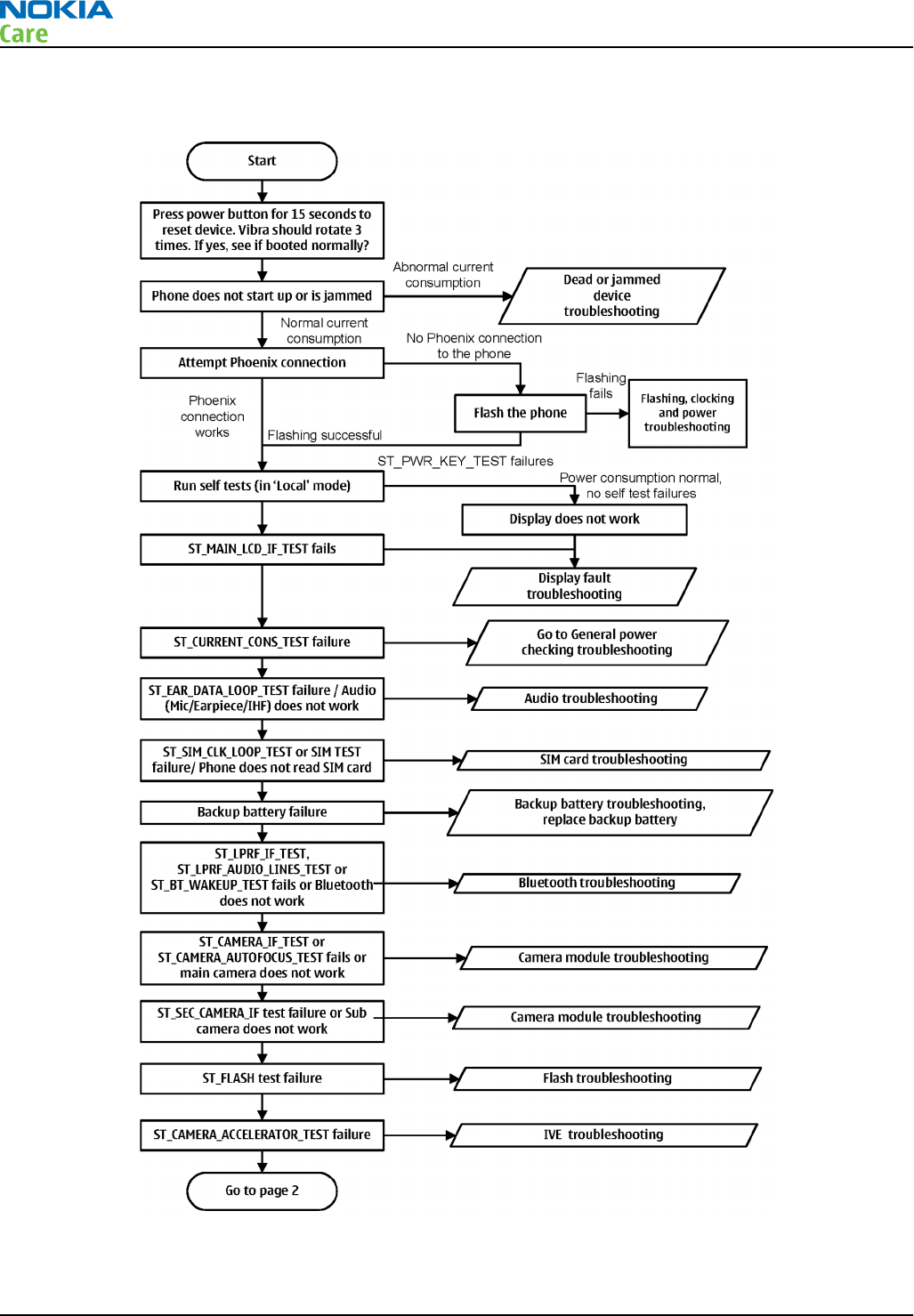
Troubleshooting flow - Page 1 of 3
RM-596
BB Troubleshooting and Manual Tuning Guide
Page 3 – 8 COMPANY CONFIDENTIAL Issue 2
Copyright © 2010 Nokia. All rights reserved.
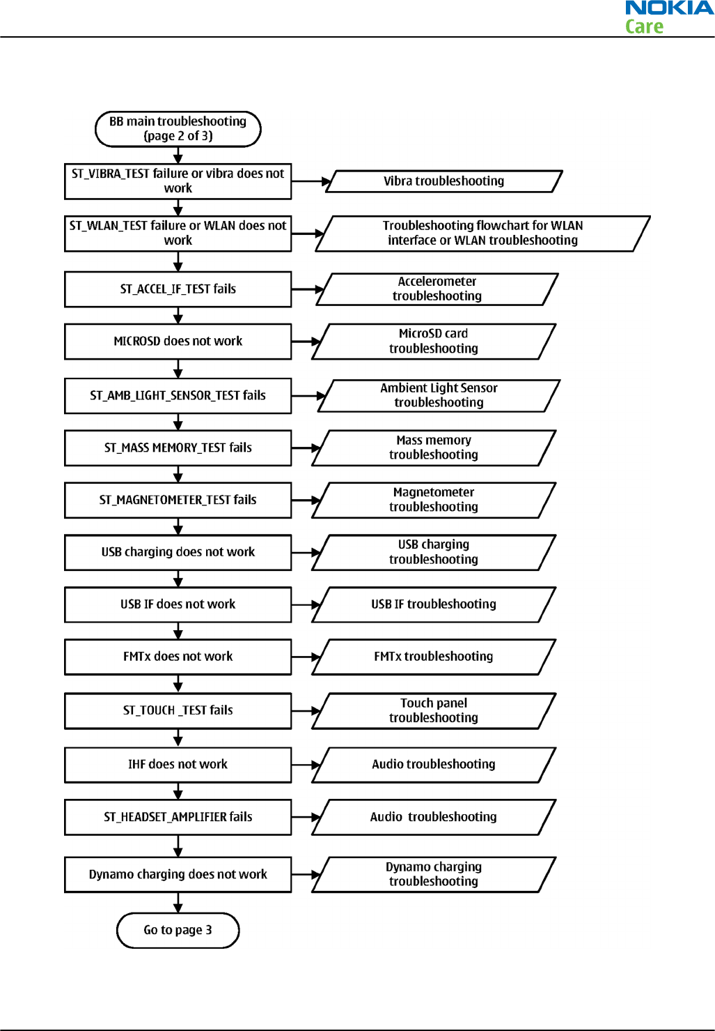
Troubleshooting flow - Page 2 of 3
RM-596
BB Troubleshooting and Manual Tuning Guide
Issue 2 COMPANY CONFIDENTIAL Page 3 – 9
Copyright © 2010 Nokia. All rights reserved.
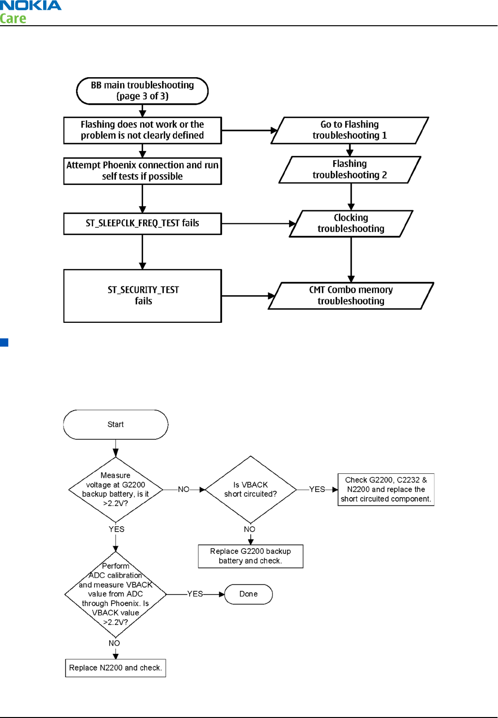
Troubleshooting flow - Page 3 of 3
Power and charging troubleshooting
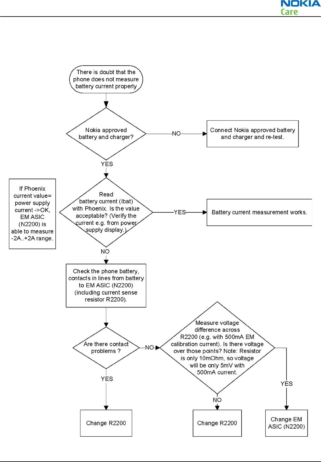
Backup battery troubleshooting
Troubleshooting flow
RM-596
BB Troubleshooting and Manual Tuning Guide
Page 3 – 10 COMPANY CONFIDENTIAL Issue 2
Copyright © 2010 Nokia. All rights reserved.
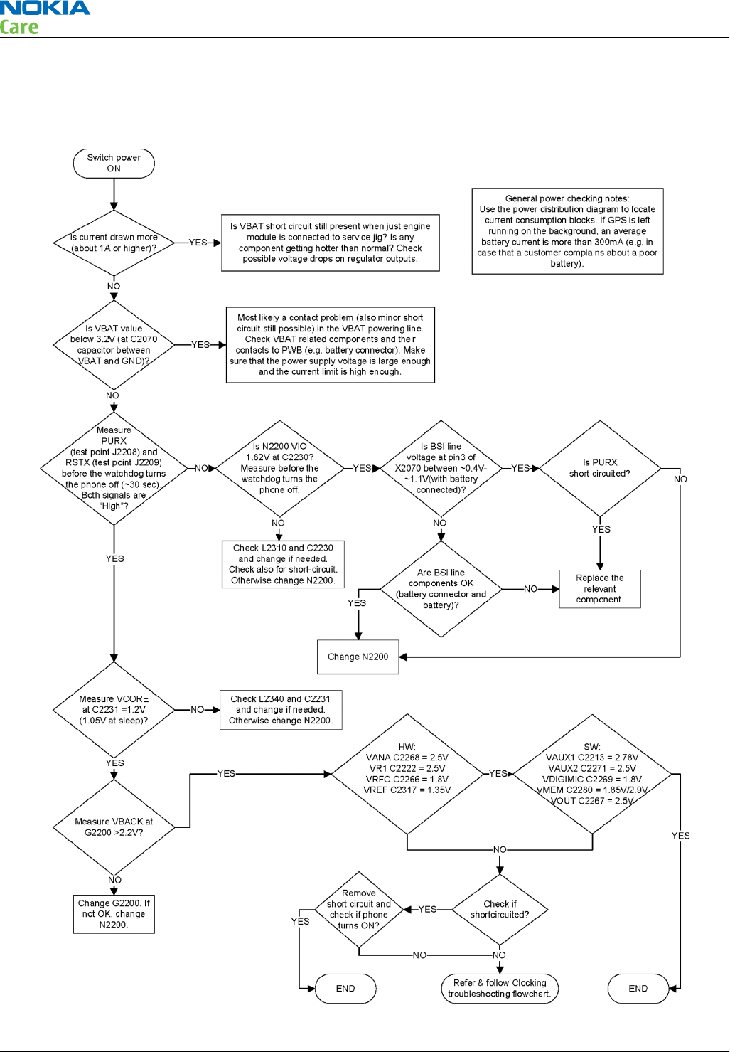
Battery current measuring fault troubleshooting
Troubleshooting flow
RM-596
BB Troubleshooting and Manual Tuning Guide
Issue 2 COMPANY CONFIDENTIAL Page 3 – 11
Copyright © 2010 Nokia. All rights reserved.
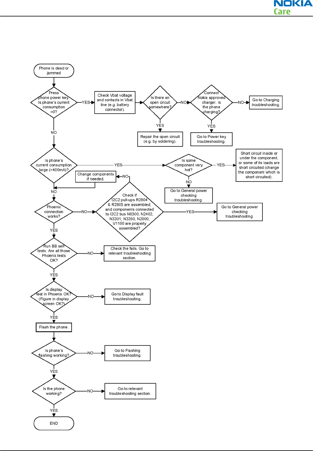
General power checking troubleshooting
Troubleshooting flow
RM-596
BB Troubleshooting and Manual Tuning Guide
Page 3 – 12 COMPANY CONFIDENTIAL Issue 2
Copyright © 2010 Nokia. All rights reserved.
Dead or jammed device troubleshooting
Troubleshooting flow
RM-596
BB Troubleshooting and Manual Tuning Guide
Issue 2 COMPANY CONFIDENTIAL Page 3 – 13
Copyright © 2010 Nokia. All rights reserved.

Dynamo charging troubleshooting
Troubleshooting flow
RM-596
BB Troubleshooting and Manual Tuning Guide
Page 3 – 14 COMPANY CONFIDENTIAL Issue 2
Copyright © 2010 Nokia. All rights reserved.
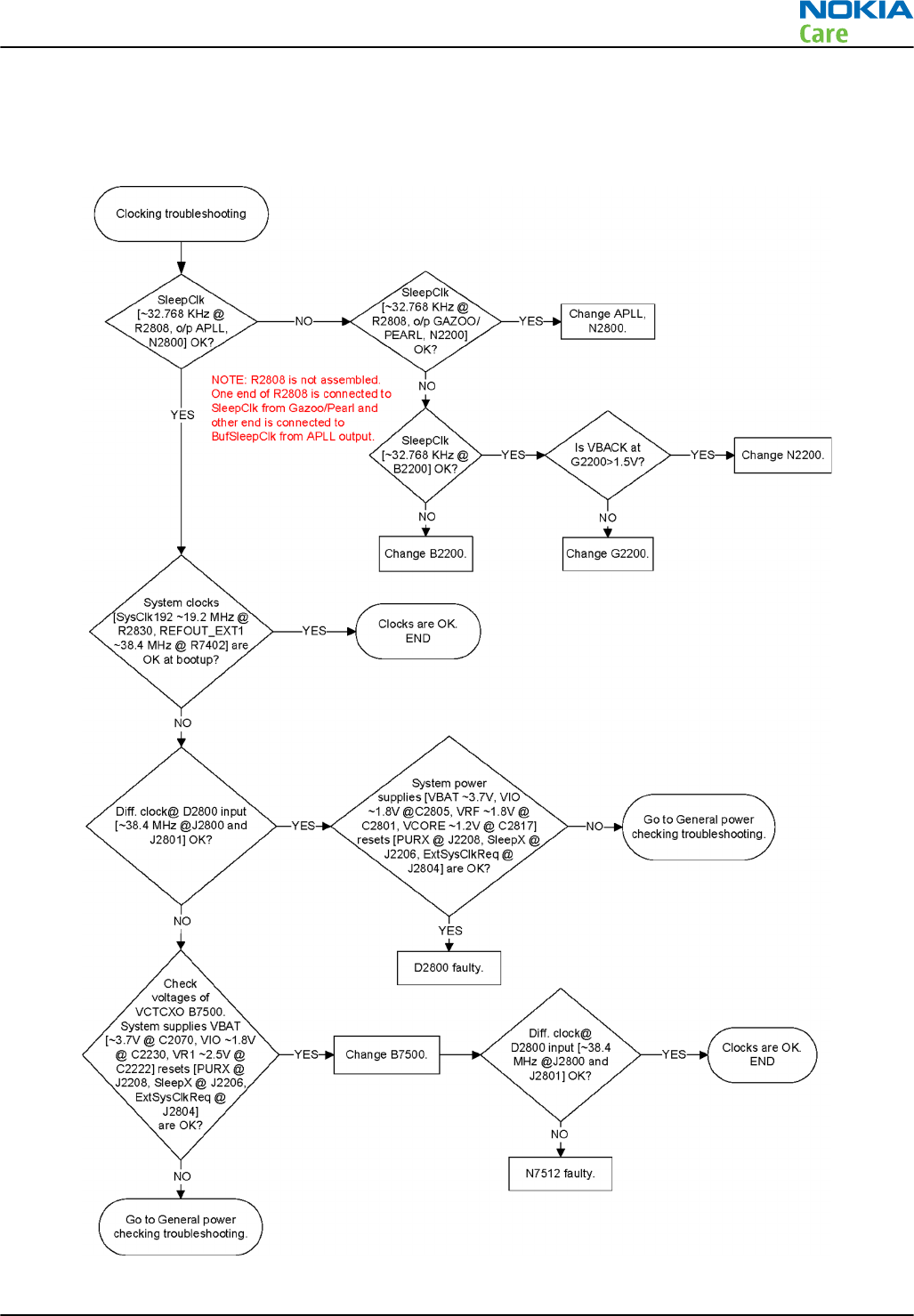
Clocking troubleshooting
Troubleshooting flow
RM-596
BB Troubleshooting and Manual Tuning Guide
Issue 2 COMPANY CONFIDENTIAL Page 3 – 15
Copyright © 2010 Nokia. All rights reserved.
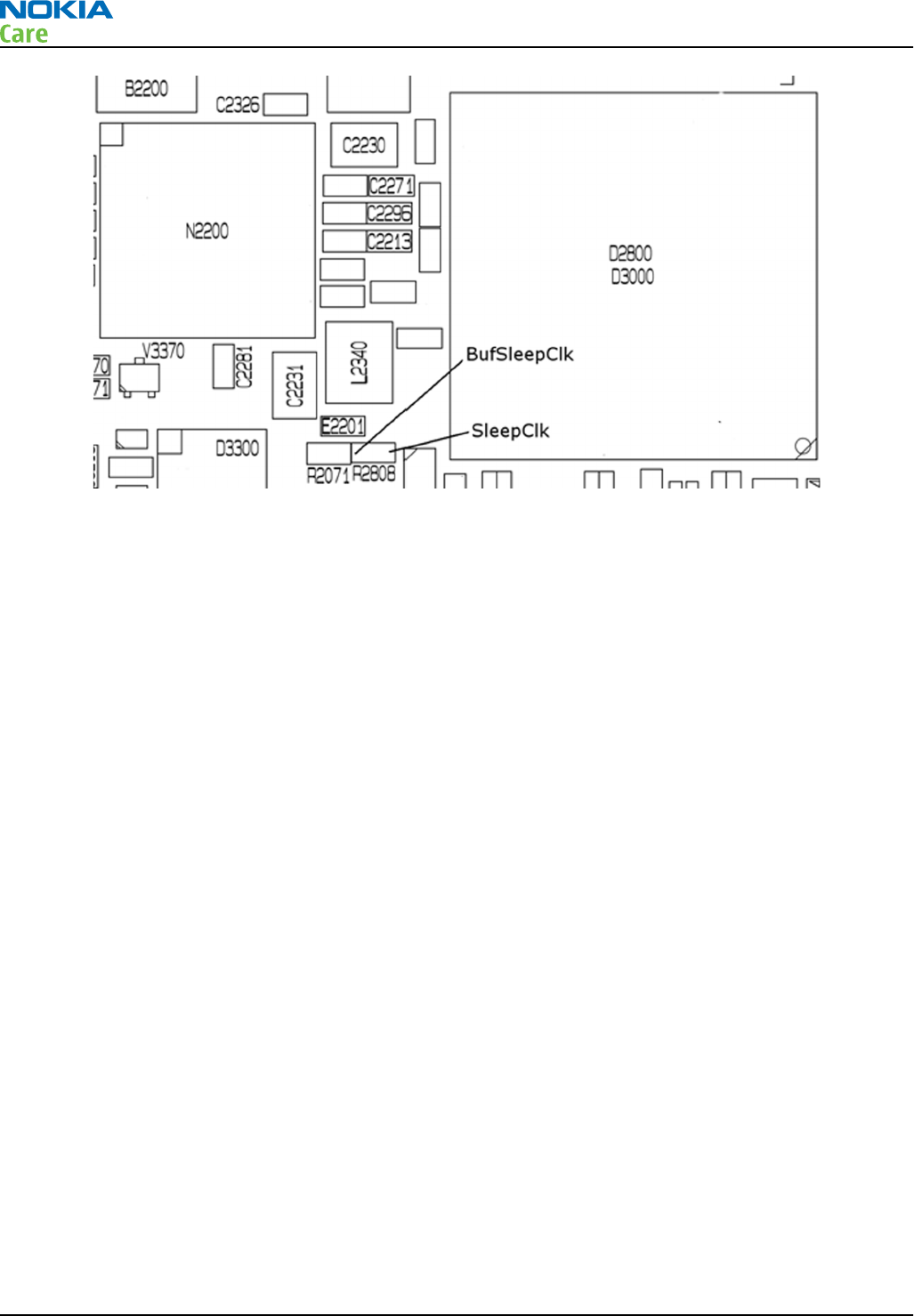
Figure 6 BufSleepClk and SleepClk signals on R2808 pads. The resistor is not assembled.
RM-596
BB Troubleshooting and Manual Tuning Guide
Page 3 – 16 COMPANY CONFIDENTIAL Issue 2
Copyright © 2010 Nokia. All rights reserved.
USB charging troubleshooting
Troubleshooting flow
RM-596
BB Troubleshooting and Manual Tuning Guide
Issue 2 COMPANY CONFIDENTIAL Page 3 – 17
Copyright © 2010 Nokia. All rights reserved.
Interface troubleshooting
USB flashing fault troubleshooting
Troubleshooting flow
RM-596
BB Troubleshooting and Manual Tuning Guide
Page 3 – 18 COMPANY CONFIDENTIAL Issue 2
Copyright © 2010 Nokia. All rights reserved.
USB data interface troubleshooting
Troubleshooting flow
RM-596
BB Troubleshooting and Manual Tuning Guide
Issue 2 COMPANY CONFIDENTIAL Page 3 – 19
Copyright © 2010 Nokia. All rights reserved.
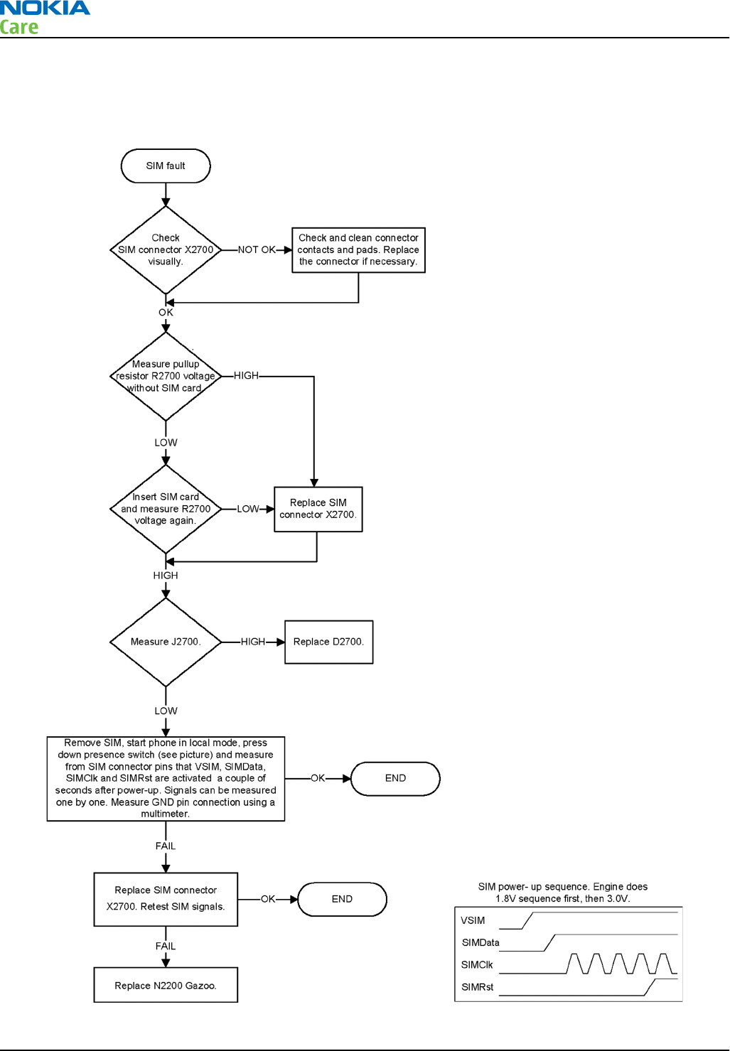
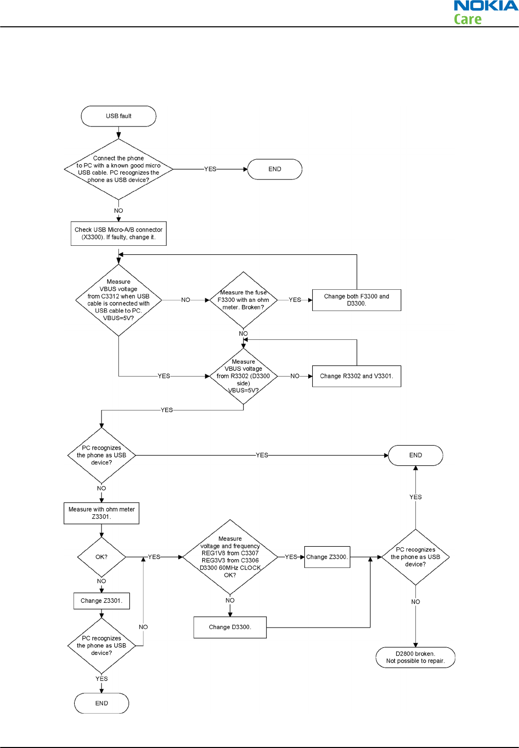
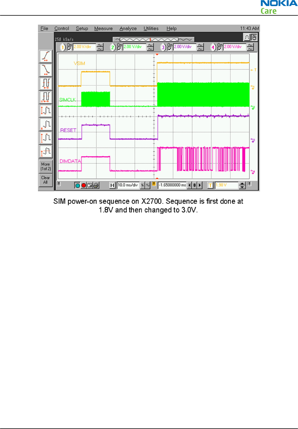
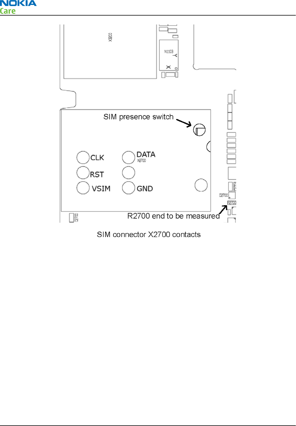
SIM card troubleshooting
Troubleshooting flow
RM-596
BB Troubleshooting and Manual Tuning Guide
Page 3 – 20 COMPANY CONFIDENTIAL Issue 2
Copyright © 2010 Nokia. All rights reserved.
RM-596
BB Troubleshooting and Manual Tuning Guide
Issue 2 COMPANY CONFIDENTIAL Page 3 – 21
Copyright © 2010 Nokia. All rights reserved.
RM-596
BB Troubleshooting and Manual Tuning Guide
Page 3 – 22 COMPANY CONFIDENTIAL Issue 2
Copyright © 2010 Nokia. All rights reserved.

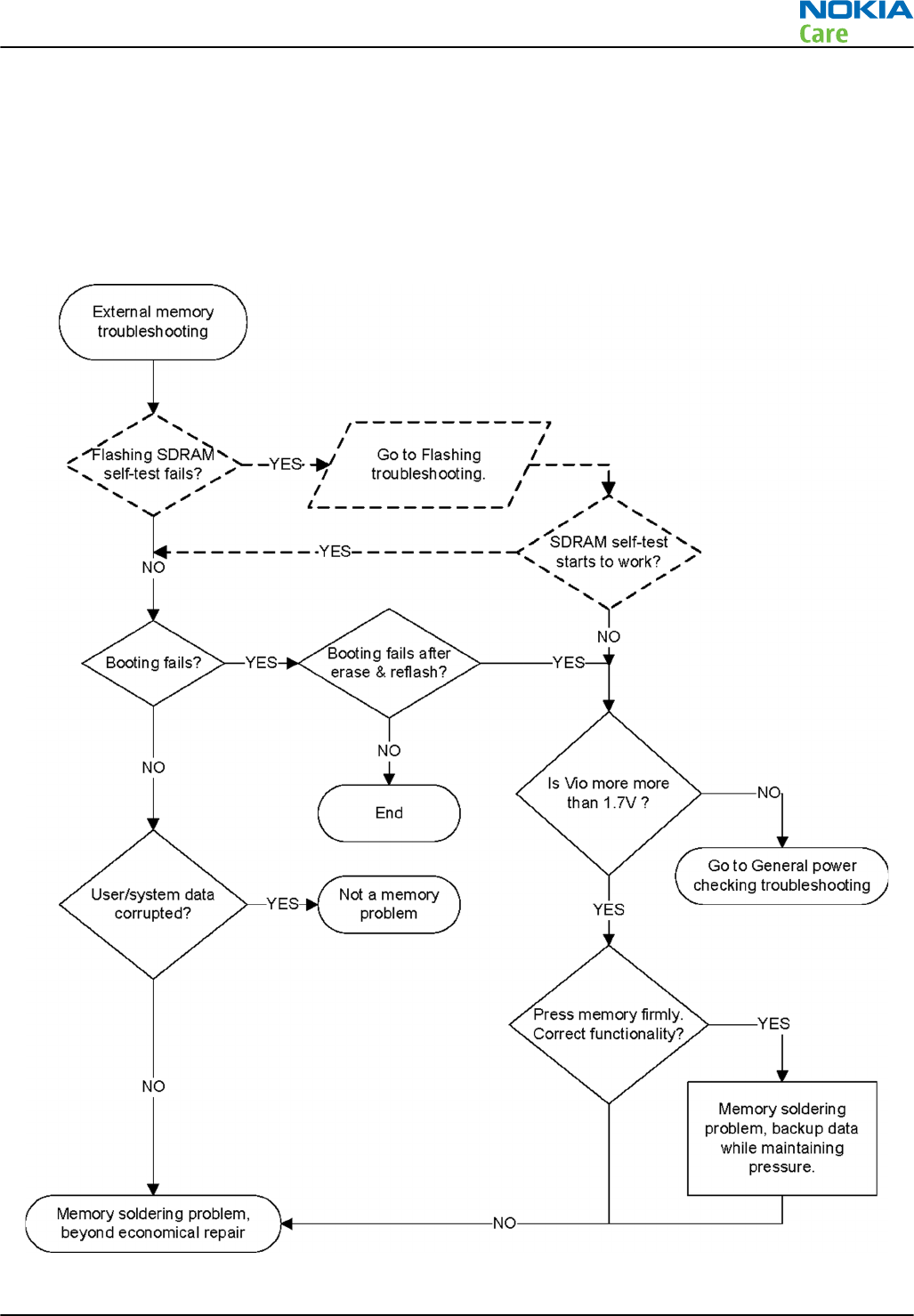
Memory troubleshooting
MicroSD card troubleshooting
Troubleshooting flow
RM-596
BB Troubleshooting and Manual Tuning Guide
Issue 2 COMPANY CONFIDENTIAL Page 3 – 23
Copyright © 2010 Nokia. All rights reserved.
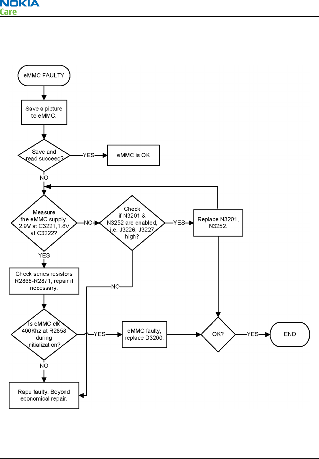
External memory eMMC troubleshooting
Troubleshooting flow
RM-596
BB Troubleshooting and Manual Tuning Guide
Page 3 – 24 COMPANY CONFIDENTIAL Issue 2
Copyright © 2010 Nokia. All rights reserved.
NOR troubleshooting
Context
NOR flash interface is an electrical interface between the memory and the digital ASIC. It is used for accessing
the memory IC for SW instructions and data.
Troubleshooting flow
RM-596
BB Troubleshooting and Manual Tuning Guide
Issue 2 COMPANY CONFIDENTIAL Page 3 – 25
Copyright © 2010 Nokia. All rights reserved.
SDRAM troubleshooting
Context
SDRAM interface is an electrical interface between the memory and the digital Asic. It is used for accessing
the memory IC for SW instructions and data.
Troubleshooting flow
RM-596
BB Troubleshooting and Manual Tuning Guide
Page 3 – 26 COMPANY CONFIDENTIAL Issue 2
Copyright © 2010 Nokia. All rights reserved.
IVE troubleshooting
Introduction to IVE troubleshooting
The IVE engine is a next generation imaging and video engine based on BCM2727B. The BCM2727B acts as
imaging, video, display, and HDTV and SDTV hardware accelerator.
The following references on the PWB help in the effective debugging and troubleshooting of IVE.
Sr. No Reference Description
1 B1400 19.2MHz Crystal
2 D1400 IVE/BCM2727B IC
The following test points on the PWB help in the effective debugging and troubleshooting.
Sr. No Signal name Measuring point Description
1 VIVE_2V5_FILT C1419/C1417 2.5V supply to BCM2727B
2 VIVE_2V8_FILT C1414 2.8V supply to BCM2727B
3 VIVE_1V8_FILT L1402/C1450 1.8V supply to BCM2727B
4 VBAT L1403/C1466 VBAT supply to BCM2727B
5 RUN J1425 Enable signal to IVE. This needs to be
High for IVE to be Up.
6 XIN C1448 19.2MHz clock to IVE
RM-596
BB Troubleshooting and Manual Tuning Guide
Issue 2 COMPANY CONFIDENTIAL Page 3 – 27
Copyright © 2010 Nokia. All rights reserved.
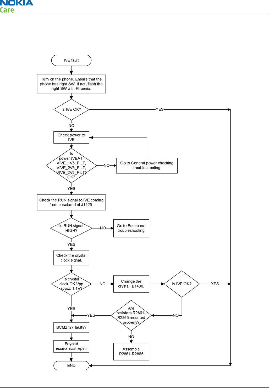
IVE troubleshooting
Troubleshooting flow
RM-596
BB Troubleshooting and Manual Tuning Guide
Page 3 – 28 COMPANY CONFIDENTIAL Issue 2
Copyright © 2010 Nokia. All rights reserved.
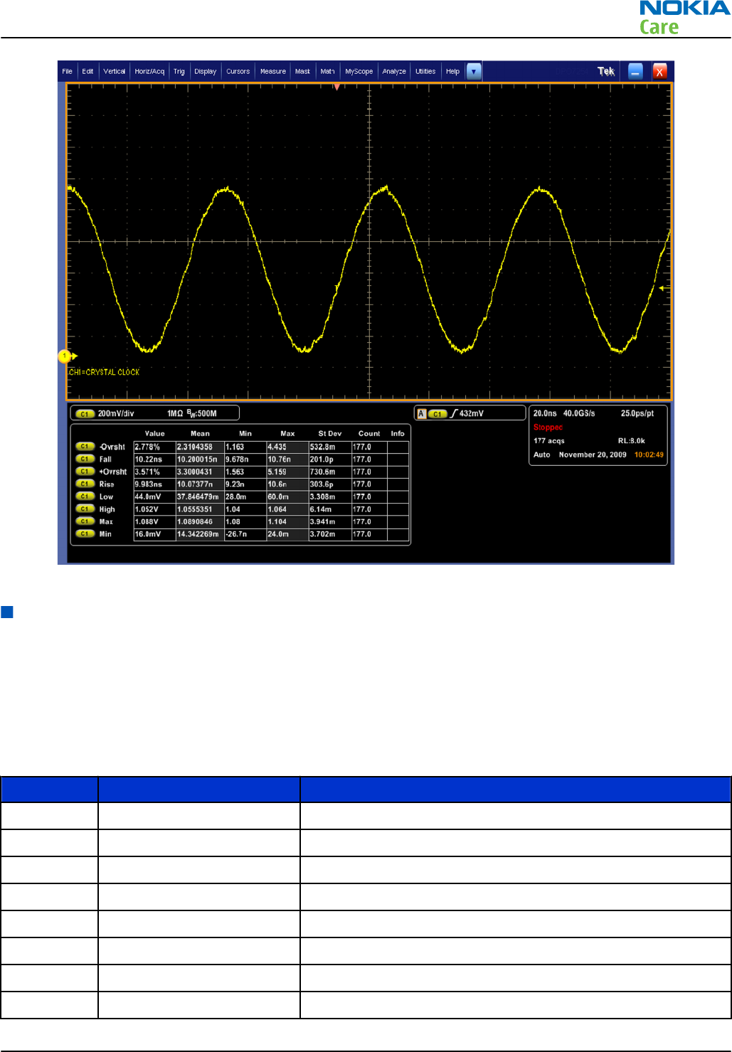
Figure 7 Expected Crystal clock input to BCM2727B on Oscilloscope
TV out troubleshooting
Introduction to HDTV and SDTV troubleshooting
HDTV
The phone has HDTV capability. The phone can be connected to an HDTV through a Type A to Type C HDMI
cable.
The following references on the PWB help in the effective debugging and troubleshooting of HDTV Out.
Sr. No Reference Description
1 X1650 HDMI connector
2 N1653 HDMI connector ASIP on HDMI bus
3 N1654 HDMI bus ASIP on control bus
4 Z1650 to Z1653 Common mode choke on HDMI bus
5 N1651 HDMI 5V regulator
6 D1400 BCM2727B IC
7 D1653 HPD signal buffer
8 V1657 HDMI +5V ESD protection
RM-596
BB Troubleshooting and Manual Tuning Guide
Issue 2 COMPANY CONFIDENTIAL Page 3 – 29
Copyright © 2010 Nokia. All rights reserved.
The following test points on the PWB help in the effective debugging and troubleshooting.
Sr No Signal name Measuring point Description
1 HDMI_REG_EN R1672 Enable signal for VHDMI_5V0 regulator. This
signal needs to be High for regulator to be On.
2 VHDMI_5V0 L1653/C1657 5V supply to HDMI sink.
3 HDMI_CABLE_DET SW1.X1650 HDMI cable detect signal to HDMI source. This
signal goes Low when a cable is inserted.
4 HDMI_HPD 19.X1650 Hot Plug Detect signal to HDMI source. This
signal goes High when a cable is inserted.
5 HDMI_I2C(1:0) 15.X1650
16.X1650
I2C signals for HDMI.
SDTV
The phone has SDTV capability. The phone can be connected to an analog TV through a TV Out cable.
The following references on the PWB help in the effective debugging and troubleshooting of SDTV Out.
Sr. No Reference Description
1 R1419 DAC termination resistor. Resistor value 15 OHMS.
2 D1400 BCM2727B IC
3 N2001 Analog switch
4 L2001 Ferrite bead on the CVBS signal
5 X2001 AV connector
The following test points on the PWB help in the effective debugging and troubleshooting.
Sr No Signal name Measuring point Description
1 CVBS X2001.1/J2002 SDTV signal
RM-596
BB Troubleshooting and Manual Tuning Guide
Page 3 – 30 COMPANY CONFIDENTIAL Issue 2
Copyright © 2010 Nokia. All rights reserved.
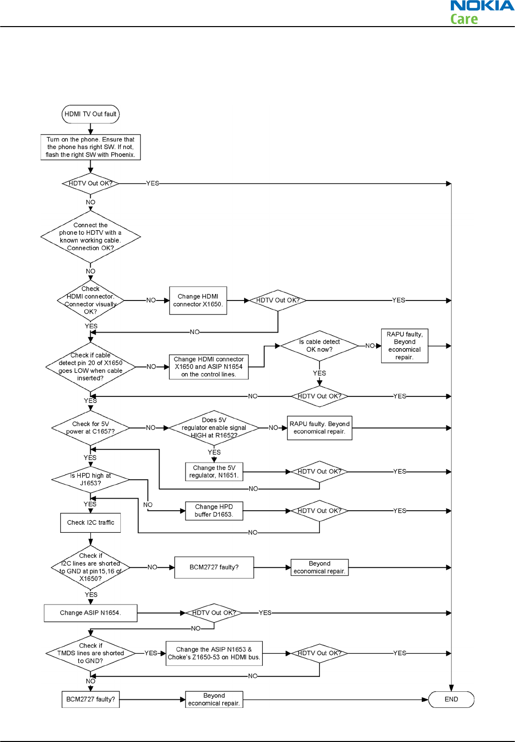
HDTV out troubleshooting
Troubleshooting flow
RM-596
BB Troubleshooting and Manual Tuning Guide
Issue 2 COMPANY CONFIDENTIAL Page 3 – 31
Copyright © 2010 Nokia. All rights reserved.
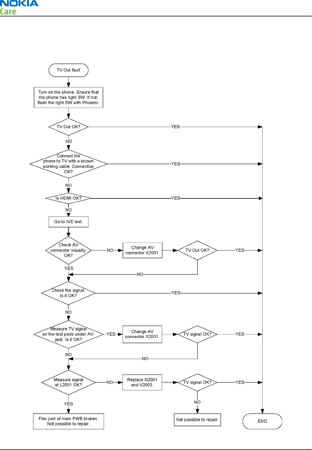
SDTV out troubleshooting
Troubleshooting flow
RM-596
BB Troubleshooting and Manual Tuning Guide
Page 3 – 32 COMPANY CONFIDENTIAL Issue 2
Copyright © 2010 Nokia. All rights reserved.
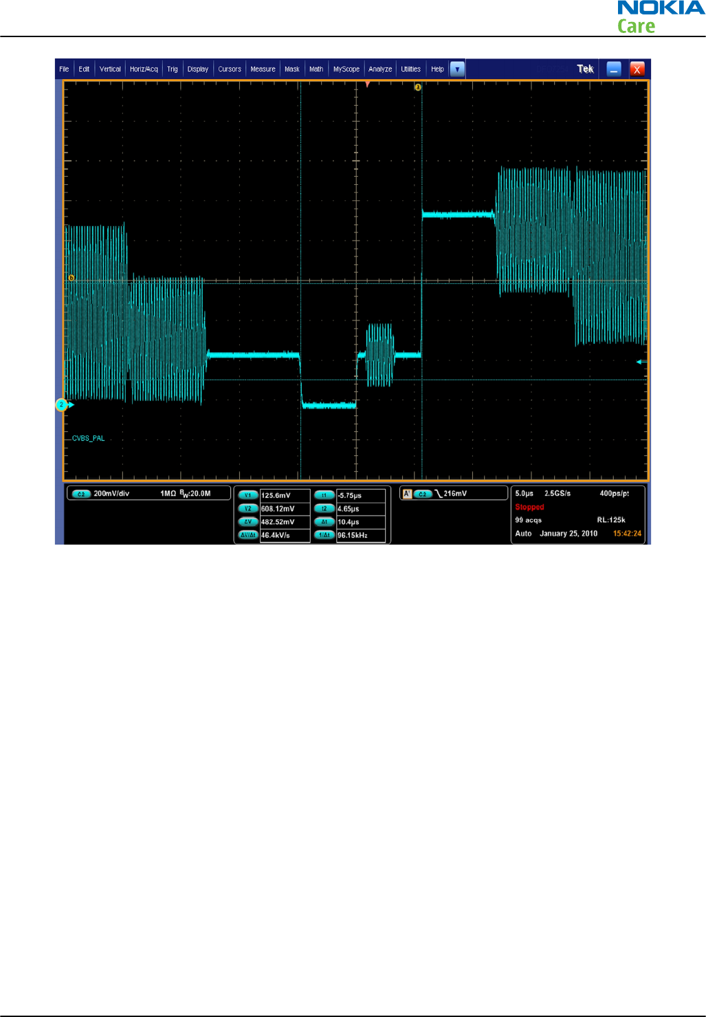
Figure 8 Expected SDTV CVBS PAL signal on Oscilloscope
RM-596
BB Troubleshooting and Manual Tuning Guide
Issue 2 COMPANY CONFIDENTIAL Page 3 – 33
Copyright © 2010 Nokia. All rights reserved.
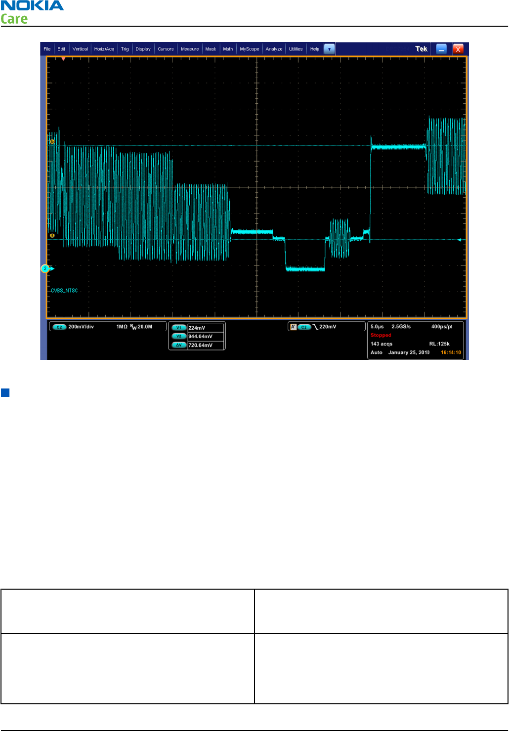
Figure 9 Expected SDTV CVBS NTSC signal on Oscilloscope
Display module troubleshooting
General instructions for display troubleshooting
The first step is to verify with a working display that the fault is not on the display module itself. The display
module cannot be repaired.
The second step is to check that the engine is working normally. This can be done by connecting the phone
to a docking station and starting Phoenix service software. With the help of Phoenix read the phone
information to check that also the application engine is functioning normally (you should be able to read the
APE ID).
After these checks proceed to the display troubleshooting flowcharts. Use the Display Test tool in Phoenix to
find the detailed fault mode.
Pixel defects
Table 6 Display module troubleshooting cases
Display blank There is no image on the display. The display looks
the same when the phone is on as it does when the
phone is off.
Image on the display not correct Image on the display can be corrupted or a part of
the image can be missing. If a part of the image is
missing, change the display module. If the image is
otherwise corrupted, follow the appropriate
troubleshooting diagram.
RM-596
BB Troubleshooting and Manual Tuning Guide
Page 3 – 34 COMPANY CONFIDENTIAL Issue 2
Copyright © 2010 Nokia. All rights reserved.
Visual defects (pixel) Pixel defects can be checked by controlling the
display with Phoenix. Use both colors, black and
white, on a full screen. R, G, B are also helpful.
The display may have some random pixel defects
that are acceptable for this type of display. The
criteria when pixel defects are regarded as a display
failure, resulting in a replacement of the display, are
presented in the following table.
Table 7 Pixel defects
Bright sub-pixels (sometimes called on-pixels or stuck-on) are
characterized by the appearance of bright/colored
pixels in, for example, black full screen picture.
Dark sub-pixels (sometimes called off-pixels, stuck-off, or black
pixels) are characterized by the appearance of dark
pixels in white, red, green, or blue full-screen
picture.
Combined sub-pixel defects are characterized by at least two sub-pixels
defects (bright or dim) being closer than 5 mm to
each other.
Temporal sub-pixels (sometimes called blinking defects) exhibit
temporal variations not related to any steady-state
video input. Temporal sub-pixel defects may be
intermittent, exhibit a sudden change of state, or
be flickering.
Table 8 Defects table
Item Bright dot (sub-
pixel) defect Dark dot (sub-
pixel) defect Total
1Defect counts Not allowed
2 Combined sub-
pixel defect
Not allowed
3 Temporal sub-
pixel defect
Not allowed
Note: Blinking pixels are not allowed in normal operating temperatures and light conditions.
Introduction to display troubleshooting
The display module used is based on AM OLED technology and supports display format of 360 columns x 640
rows. The dimension of the display module is 47.8 mm x 86.3 mm x 2.12 mm. The module will interface to
the phone via FPC with a 20 pins board to board connector.
The following references on the PWB help in the effective debugging and troubleshooting of the display.
RM-596
BB Troubleshooting and Manual Tuning Guide
Issue 2 COMPANY CONFIDENTIAL Page 3 – 35
Copyright © 2010 Nokia. All rights reserved.
Sr No Reference Description
1 X1600 Display connector
2 Z1600, Z1601 Common Mode Choke on DSI bus
3 R1601/C1605 Series resistor on display Reset line. Reset signal needs to be
High for the display to be Up.
4 D1400 BCM2727B IC
The following test points on the PWB help in the effective debugging and troubleshooting.
Sr. No Signal name Measuring point Description
1 VIO L1600/C1600 1.8V supply to display
2 VBAT L1601/C1602 VBAT supply to display
3 TE0 R1600 Tearing effect signal from display module.
RM-596
BB Troubleshooting and Manual Tuning Guide
Page 3 – 36 COMPANY CONFIDENTIAL Issue 2
Copyright © 2010 Nokia. All rights reserved.
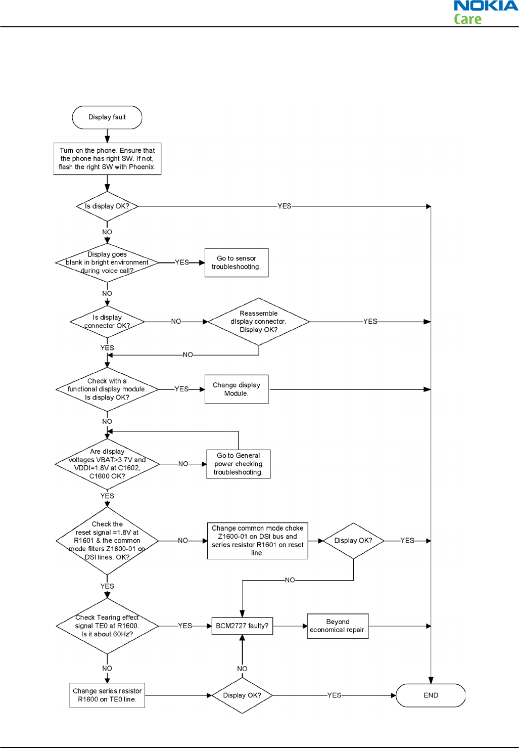
Display fault troubleshooting
Troubleshooting flow
RM-596
BB Troubleshooting and Manual Tuning Guide
Issue 2 COMPANY CONFIDENTIAL Page 3 – 37
Copyright © 2010 Nokia. All rights reserved.
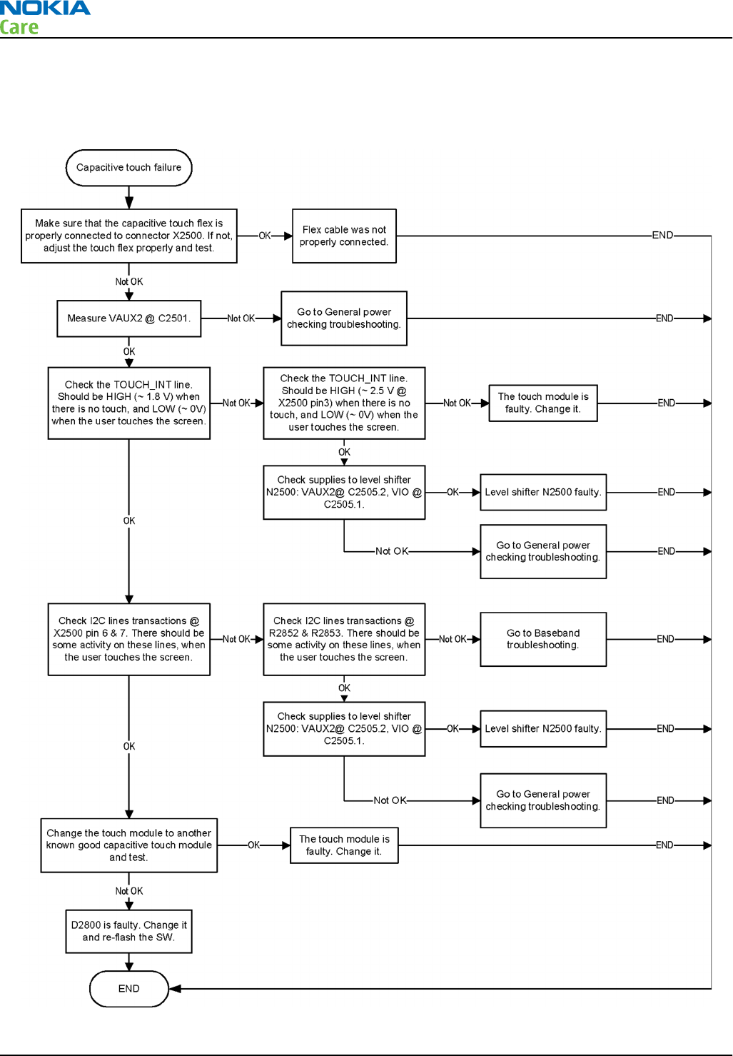
Touch panel troubleshooting
Troubleshooting flow
RM-596
BB Troubleshooting and Manual Tuning Guide
Page 3 – 38 COMPANY CONFIDENTIAL Issue 2
Copyright © 2010 Nokia. All rights reserved.
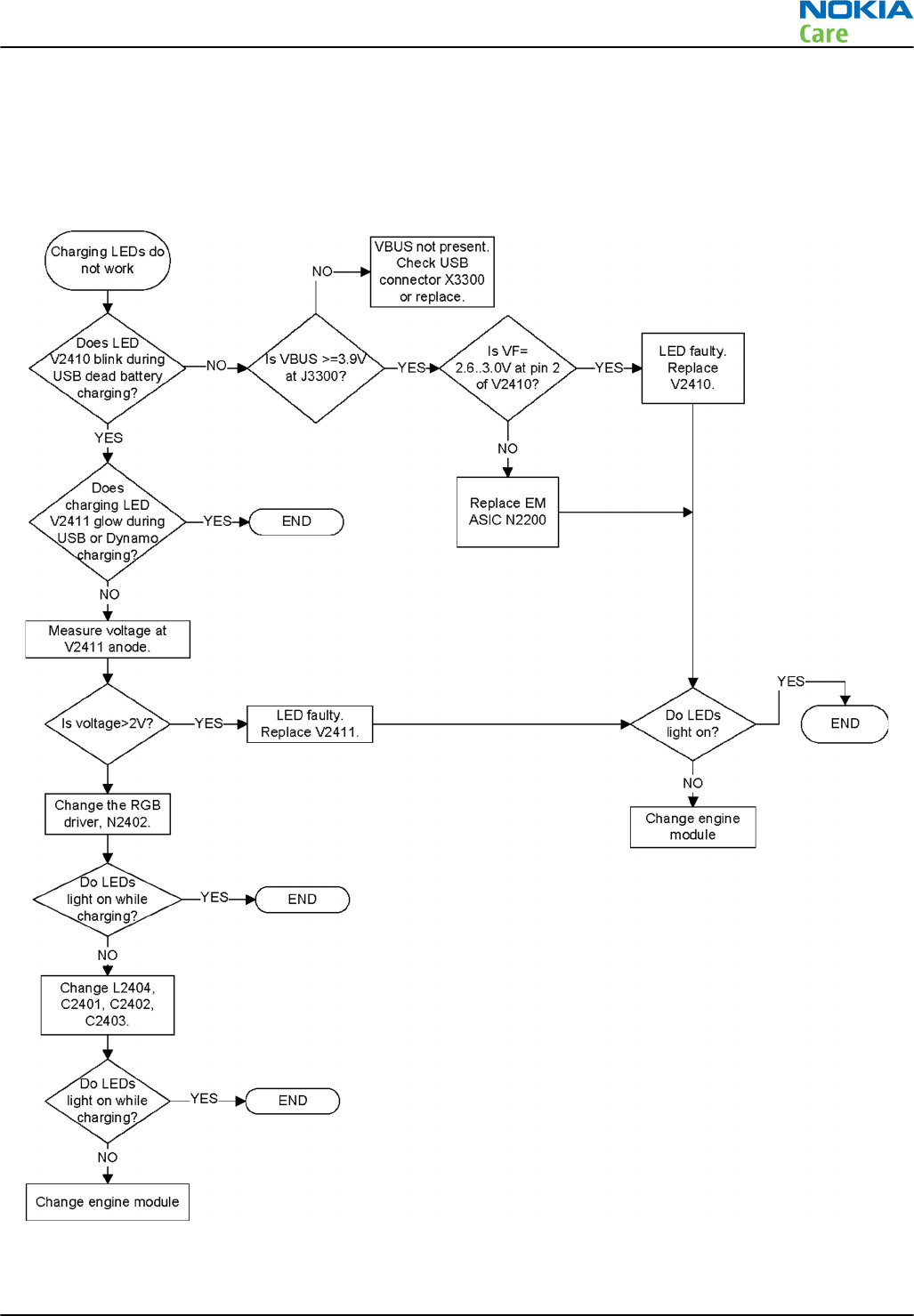
Illumination troubleshooting
Charging illumination troubleshooting
Troubleshooting flow
RM-596
BB Troubleshooting and Manual Tuning Guide
Issue 2 COMPANY CONFIDENTIAL Page 3 – 39
Copyright © 2010 Nokia. All rights reserved.
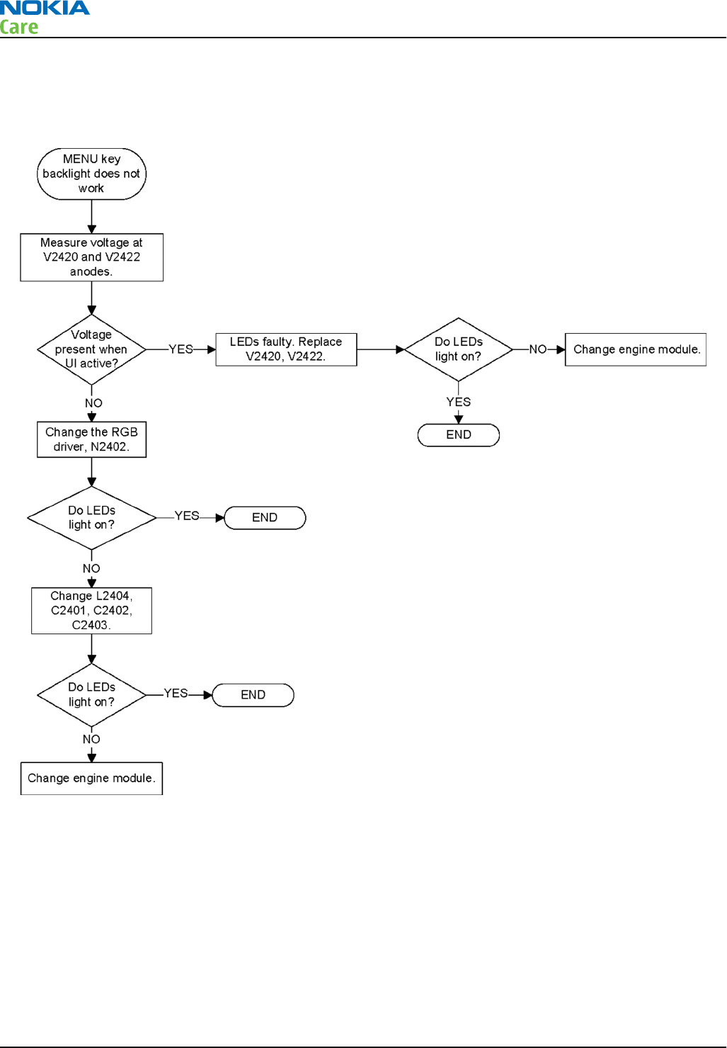
Menu key backlight troubleshooting
Troubleshooting flow
RM-596
BB Troubleshooting and Manual Tuning Guide
Page 3 – 40 COMPANY CONFIDENTIAL Issue 2
Copyright © 2010 Nokia. All rights reserved.
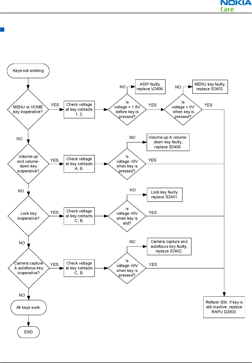
Keyboard troubleshooting
Keys troubleshooting
Troubleshooting flow
RM-596
BB Troubleshooting and Manual Tuning Guide
Issue 2 COMPANY CONFIDENTIAL Page 3 – 41
Copyright © 2010 Nokia. All rights reserved.
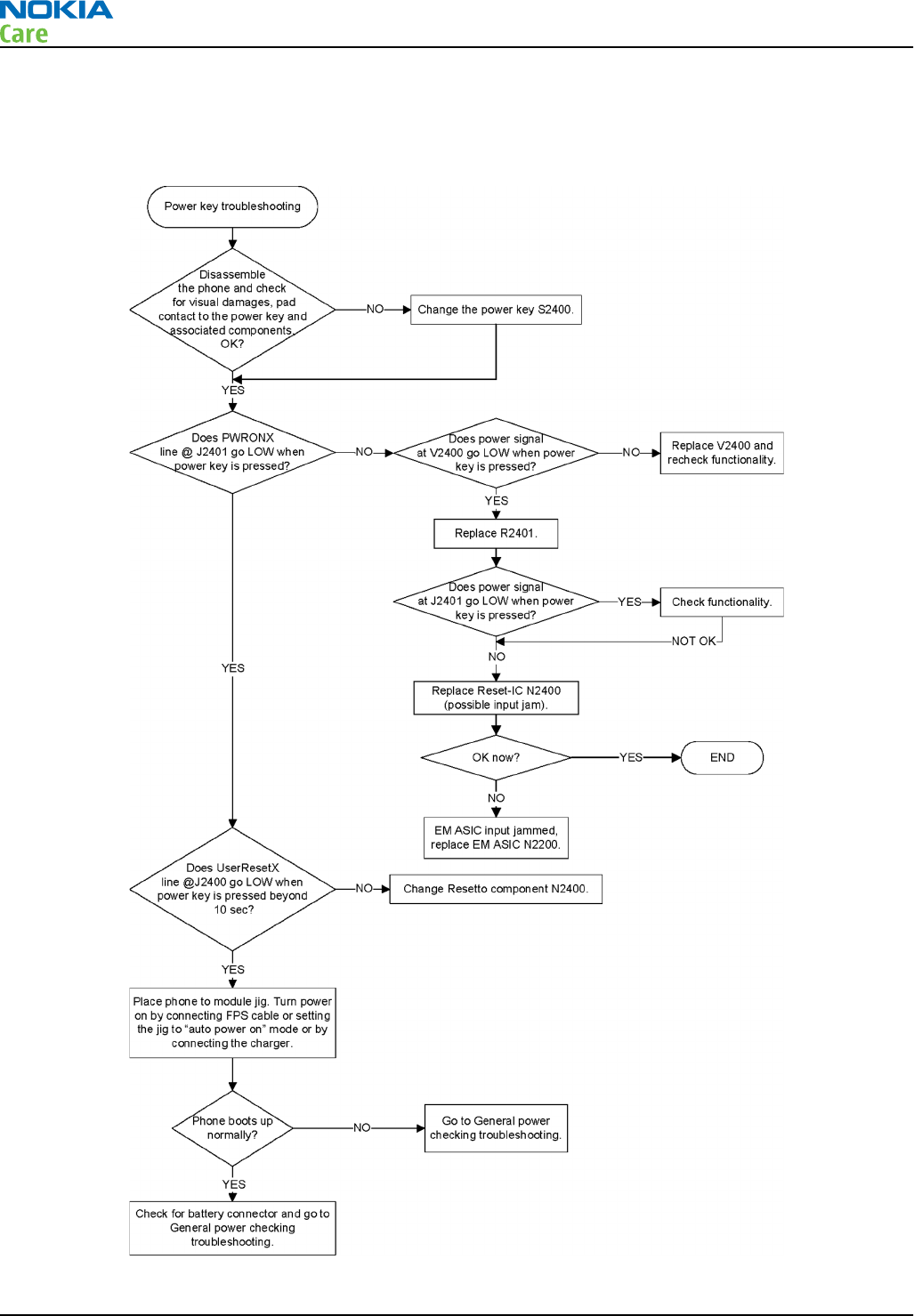
Power key troubleshooting
Troubleshooting flow
RM-596
BB Troubleshooting and Manual Tuning Guide
Page 3 – 42 COMPANY CONFIDENTIAL Issue 2
Copyright © 2010 Nokia. All rights reserved.
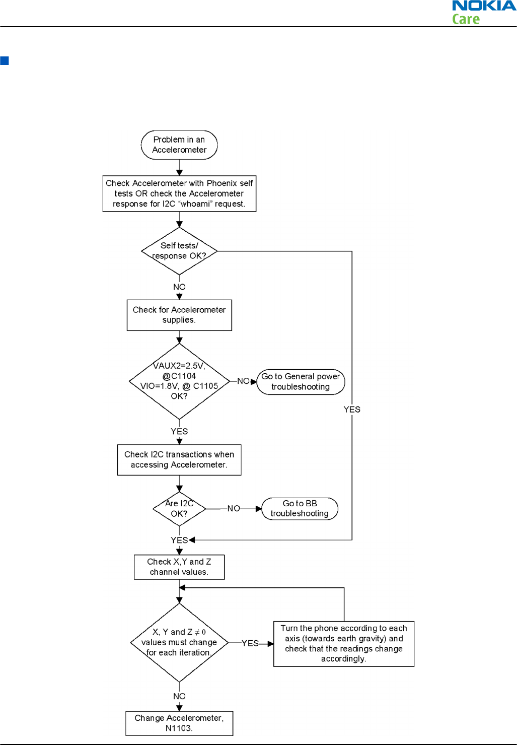
Sensors troubleshooting
Accelerometer troubleshooting
Troubleshooting flow
RM-596
BB Troubleshooting and Manual Tuning Guide
Issue 2 COMPANY CONFIDENTIAL Page 3 – 43
Copyright © 2010 Nokia. All rights reserved.

Magnetometer troubleshooting
Equipment
•Non-magnetic, horizontal table
•nearest ferromagnetic part, distance more than 50 cm
•Traditional needle type compass for reference
•Rotating platform (sheet of wood or plastic)
•PC with Phoenix
Preparation of phone
•Set the rotating platform to the table
•Set the phone and reference compass to the rotating platform
•Connect the phone to the PC and start Phoenix
Tests
•General troubleshooting test
•Self-test (ST)
•Azimuth check test
RM-596
BB Troubleshooting and Manual Tuning Guide
Page 3 – 44 COMPANY CONFIDENTIAL Issue 2
Copyright © 2010 Nokia. All rights reserved.
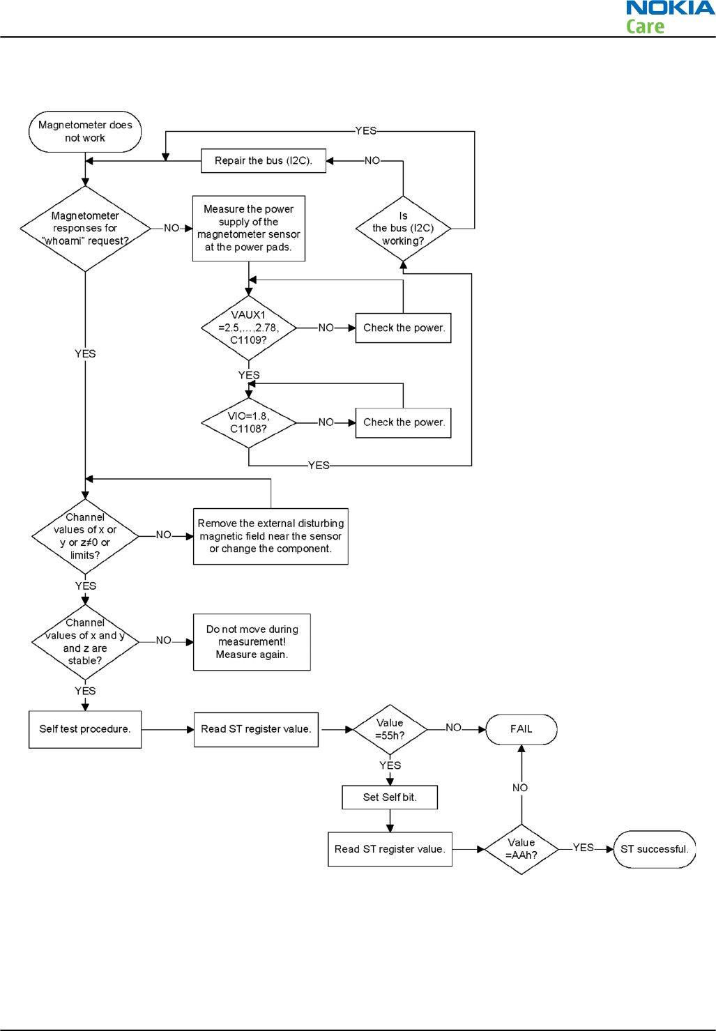
Magnetometer general troubleshooting flow
Azimuth check
•Search magnetically quiet place for the test table
•No disturbing elements near the table, such as motors, coils, electric currents or similar
•Calibrate the phone as described in the user manual
•The indicator must be GREEN
RM-596
BB Troubleshooting and Manual Tuning Guide
Issue 2 COMPANY CONFIDENTIAL Page 3 – 45
Copyright © 2010 Nokia. All rights reserved.
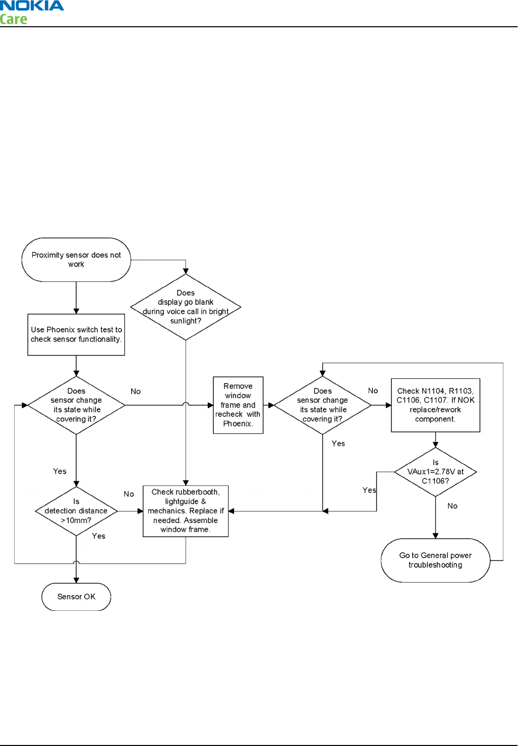
•Rotate the platform manually one round on the horizontal table with steps of approximately 15° degrees
•The reference angle direction value from the reference compass = REF(angle)
•Read the phone value = ACT(angle)
•Calculate for every step (24 steps)
•Result(angle) = REF(angle) - ACT(angle)
•The result is the real angle difference of angles in a 360° degrees continuous round
•Criteria:
•If the Result(angle) value < 15° degrees GO, otherwise NOGO
Proximity sensor troubleshooting
Troubleshooting flow
ALS technical description and troubleshooting
Ambient Light Sensor (ALS)
Pupumon V1100 is a digital Ambient Light Sensor (ALS) which is connected to RAPU via I2C_2 bus. It does not
have an interrupt signal as in Augumon ALS. Power supply voltage is provided from VAUX2 output of EM ASIC.
ALS is used in backlight control system to measure the amount of ambient light reaching display surface so
that it is possible to adjust the display (and keypad) brightness in order to achieve good user experience.
This also helps in saving power.
RM-596
BB Troubleshooting and Manual Tuning Guide
Page 3 – 46 COMPANY CONFIDENTIAL Issue 2
Copyright © 2010 Nokia. All rights reserved.
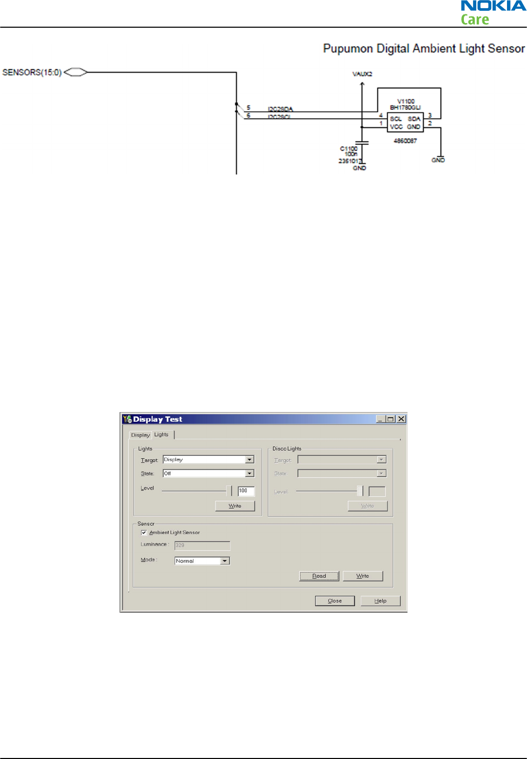
Figure 10 Ambient Light Sensor
ALS functionality check
Steps
1. Connect the phone to Phoenix and set the phone (e.g. on the table) so that the amount of ambient light
seen by ALS is as stabile as possible.
2. Start
Phoenix
.
3. Choose File -> Scan product .
4. Choose Testing -> Display Test .
5. Open the Lights tab, check Ambient Light Sensor check box, click Read , cover the sensor and click
Read again. When covered, Luminance reading should be less than after clicking Read without covering
the sensor.
6. If the component does not give any reading or reading does not change when the sensor is/is not covered,
replace the part.
•After replacing the ALS, if the calibration values of the new sensor are lost or for some other reason,
ALS re-tuning is required.
•When doing the ALS calibration procedure, it is required to have a reference phone which includes a
calibrated ALS. ALS re-tuning instructions show why the reference phone is needed.
RM-596
BB Troubleshooting and Manual Tuning Guide
Issue 2 COMPANY CONFIDENTIAL Page 3 – 47
Copyright © 2010 Nokia. All rights reserved.
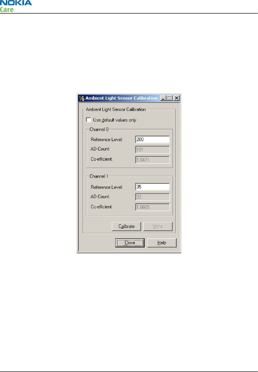
Re-tuning ALS
Steps
1. Connect reference phone to Phoenix and set the phone (e.g. on the table) so that the amount of ambient
light seen by ALS is as stable as possible.
2. Start Phoenix.
3. Choose File→Scan Product.
4. Choose Tuning -> Ambient Light Sensor Calibration. You should see the following window:
5. Read AD-count values for Channel 0 and Channel 1 by click Read button and write them down.
6. Repeat 1-5 for the phone to be calibrated and make sure the phone to be calibrated is located in the
same place as reference phone was when luminance reading was taken.
7. Calculate co-efficient from reference phone and phone to be calibrated AD-count values by division: Co-
efficient = AD-count(reference phone) / AD-count(phone to be calibrated), write down the calculated co-
efficient values.
8. -> Iterate by changing Channel 0 and Channel 1 (reference level) values (remove cross from ‘Use default
values only’). After writing some value to Channel 0 and Channel 1 (reference value), calibrate button
must be pressed. Stop iterating when Co-efficient is equal to Co-efficient calculated in step 7. Note that
decimal numbers should be used in the iteration in order to achieve enough precision (e.g. 200.2455)
9. After having same Co-efficient value in “Co-efficient” textbox as the calculated value, make sure that
ambient light values (read using Testing → Display Test → “Luminance” textbox) are almost the same
in reference phone and calibrated phone. Remember that illuminance readings for reference and
calibrated phones must be done in the same ambient light conditions. If illuminance values differs a lot
(difference max. +- 10%), repeat whole ALS re-tuning procedure.
RM-596
BB Troubleshooting and Manual Tuning Guide
Page 3 – 48 COMPANY CONFIDENTIAL Issue 2
Copyright © 2010 Nokia. All rights reserved.
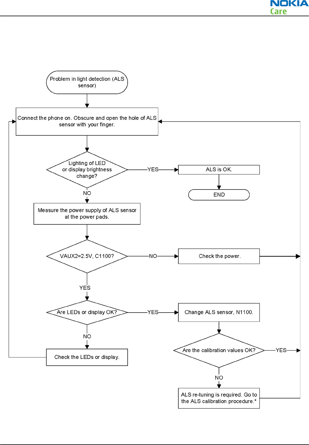
10. To end the calibration, click Close.
ALS troubleshooting
Troubleshooting flow
RM-596
BB Troubleshooting and Manual Tuning Guide
Issue 2 COMPANY CONFIDENTIAL Page 3 – 49
Copyright © 2010 Nokia. All rights reserved.

Audio troubleshooting
Audio troubleshooting test instructions
Single-ended external earpiece and differential internal earpiece outputs can be measured either with a
single-ended or a differential probe.
When measuring with a single-ended probe each output is measured against the ground.
Internal handsfree output is measured using a current probe, if a special low-pass filter designed for
measuring a digital amplifier is not available. Note also that when using a current probe, the input signal
frequency must be set to 2 kHz.
The input signal for each loop test can be either single-ended or differential. Exception to this is a digital
microphone which needs input signal from an external sound source (laptop speaker) to playback, eg. 1 kHz
sine wave from 5 cm distance.
Required equipment
The following equipment is needed for the tests:
•Oscilloscope
•Function generator (sine waveform)
•Current probe (Internal handsfree DPMA output measurement)
•Phoenix service software
•Battery voltage 3.7V
•Sound source (laptop speaker or B&K type 4231 calibrator)
Test procedure
Audio can be tested using the Phoenix audio routings option. Three different audio loop paths can be
activated:
•External headset mic to earpiece
•External headset mic to IHF mono
•Internal digital microphone to headset
Each audio loop sets routing from the specified input to the specified output enabling a quick in-out test.
Loop path gains are fixed and they cannot be changed using Phoenix. Correct pins and signals for each test
are presented in the following table.
Phoenix audio loop tests and test results
The results presented in the table apply when no accessory is connected and battery voltage is set to 3.7V.
Earpiece, internal microphone and speaker are in place during measurement. Applying a headset accessory
during measurement causes a significant drop in measured quantities.
The gain values presented in the table apply for a differential output vs. single-ended/differential input.
Loop test Input
terminal Output
terminal Path gain
[dB]
(fixed)
Input
voltage
[mVp-p]
Output DC
level [V] Output
voltage
[mVp-p]
External
headset
mic to
earpiece
HS_MIC &
GND
EAR 1 &
GND
0 300 1.35 300
EAR 0 &
GND
RM-596
BB Troubleshooting and Manual Tuning Guide
Page 3 – 50 COMPANY CONFIDENTIAL Issue 2
Copyright © 2010 Nokia. All rights reserved.

Loop test Input
terminal Output
terminal Path gain
[dB]
(fixed)
Input
voltage
[mVp-p]
Output DC
level [V] Output
voltage
[mVp-p]
External
headset
mic to IHF
mono
HS_MIC &
GND
L4855 &
L4856
10 200 630
L4857 &
L4858
Internal
digital
micropho
ne to
headset
Acoustica
l Input,
1kHz sine
wave
HS_L &
GND
NA 94 dBSPL 70
HS_R &
GND
RM-596
BB Troubleshooting and Manual Tuning Guide
Issue 2 COMPANY CONFIDENTIAL Page 3 – 51
Copyright © 2010 Nokia. All rights reserved.
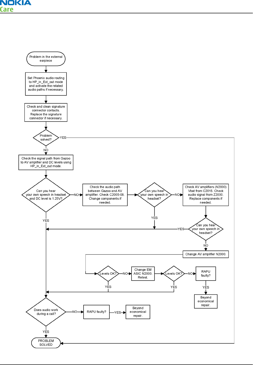
External earpiece troubleshooting
Troubleshooting flow
RM-596
BB Troubleshooting and Manual Tuning Guide
Page 3 – 52 COMPANY CONFIDENTIAL Issue 2
Copyright © 2010 Nokia. All rights reserved.
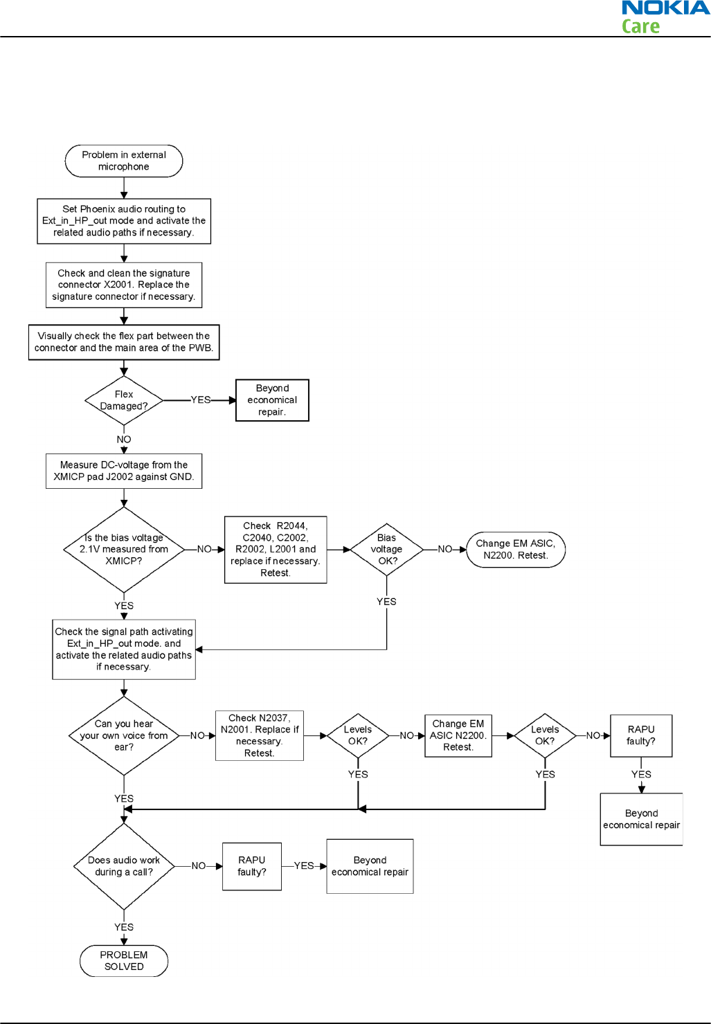
External microphone troubleshooting
Troubleshooting flow
RM-596
BB Troubleshooting and Manual Tuning Guide
Issue 2 COMPANY CONFIDENTIAL Page 3 – 53
Copyright © 2010 Nokia. All rights reserved.
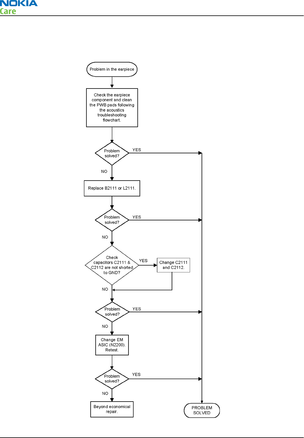
Internal earpiece troubleshooting
Troubleshooting flow
RM-596
BB Troubleshooting and Manual Tuning Guide
Page 3 – 54 COMPANY CONFIDENTIAL Issue 2
Copyright © 2010 Nokia. All rights reserved.
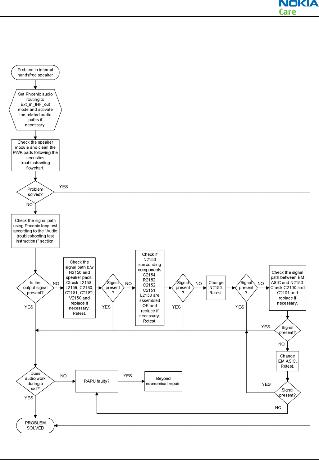
Internal handsfree (IHF) troubleshooting
Troubleshooting flow
RM-596
BB Troubleshooting and Manual Tuning Guide
Issue 2 COMPANY CONFIDENTIAL Page 3 – 55
Copyright © 2010 Nokia. All rights reserved.
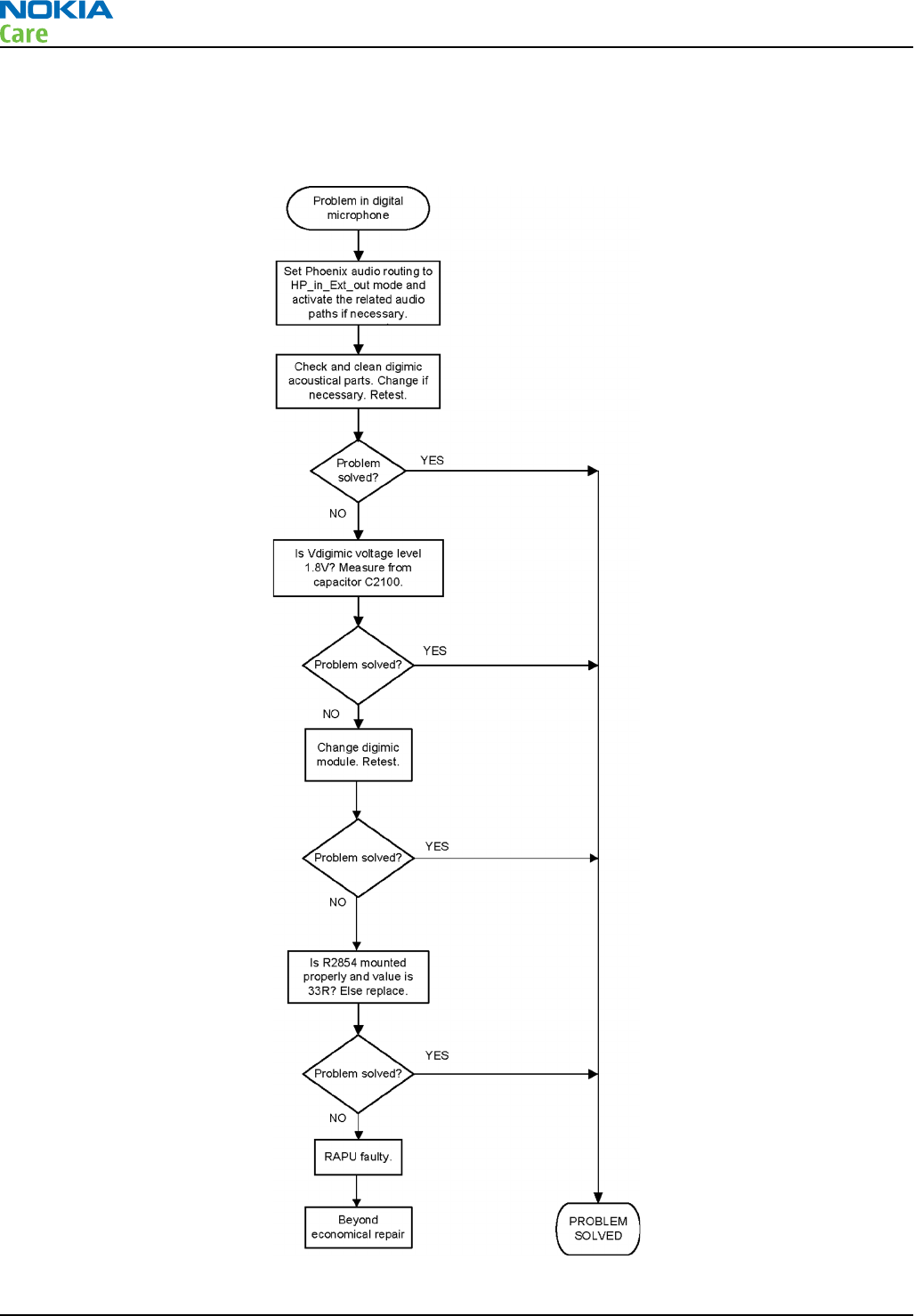
Internal microphone troubleshooting
Troubleshooting flow
RM-596
BB Troubleshooting and Manual Tuning Guide
Page 3 – 56 COMPANY CONFIDENTIAL Issue 2
Copyright © 2010 Nokia. All rights reserved.
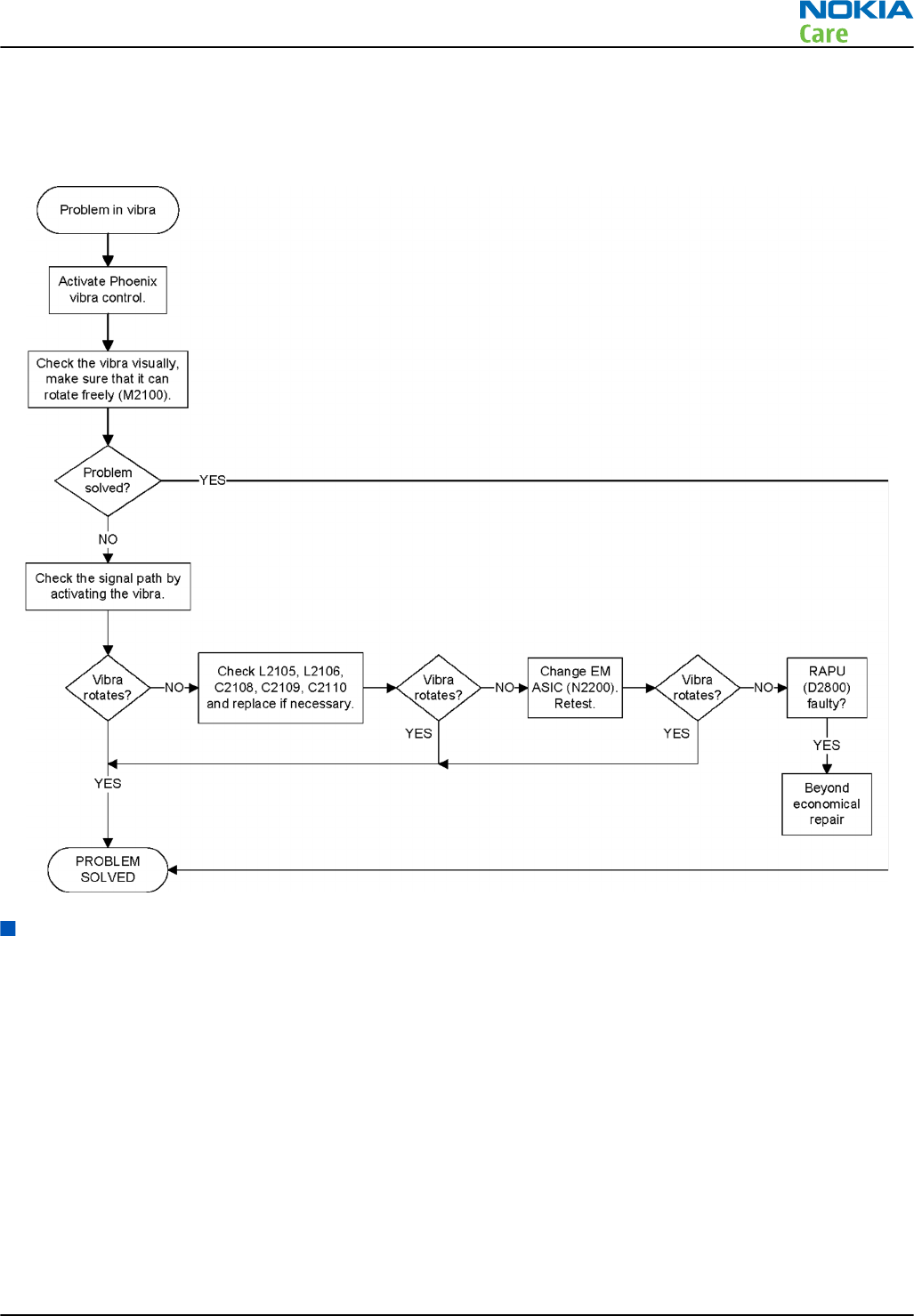
Vibra troubleshooting
Troubleshooting flow
Connectivity module troubleshooting
Introduction to connectivity module troubleshooting
The BOB1.0M-b module supports WLAN, BT, FMRX and FMTX. From a troubleshooting point of view, WLAN is
tested separately, but BT, FMRX and FMTX are checked in parallel.
REFOUT_EXT1 single ended 38.4 MHz analog clock from Linko RF is provided to BOB1.0M-b. The clock request
for the reference clock in the BOB1.0M-b module is shared between WLAN and BT blocks. When either system
requires a clock, this signal will be active. The CLK_REQ is connected to ExtSysClkReq pin of RAPU. The SLEEPCLK
input of 32.768 KHz clock from EM ASIC is used for power management and for FM in low power mode. The
internal SMPS supplies the whole BOB1.0M-b solution from the phone battery supply, VBAT, apart from VIO
which is needed for interface signal reference levels.
The following figure shows a top level block diagram of the BOB1.0M-b module.
RM-596
BB Troubleshooting and Manual Tuning Guide
Issue 2 COMPANY CONFIDENTIAL Page 3 – 57
Copyright © 2010 Nokia. All rights reserved.
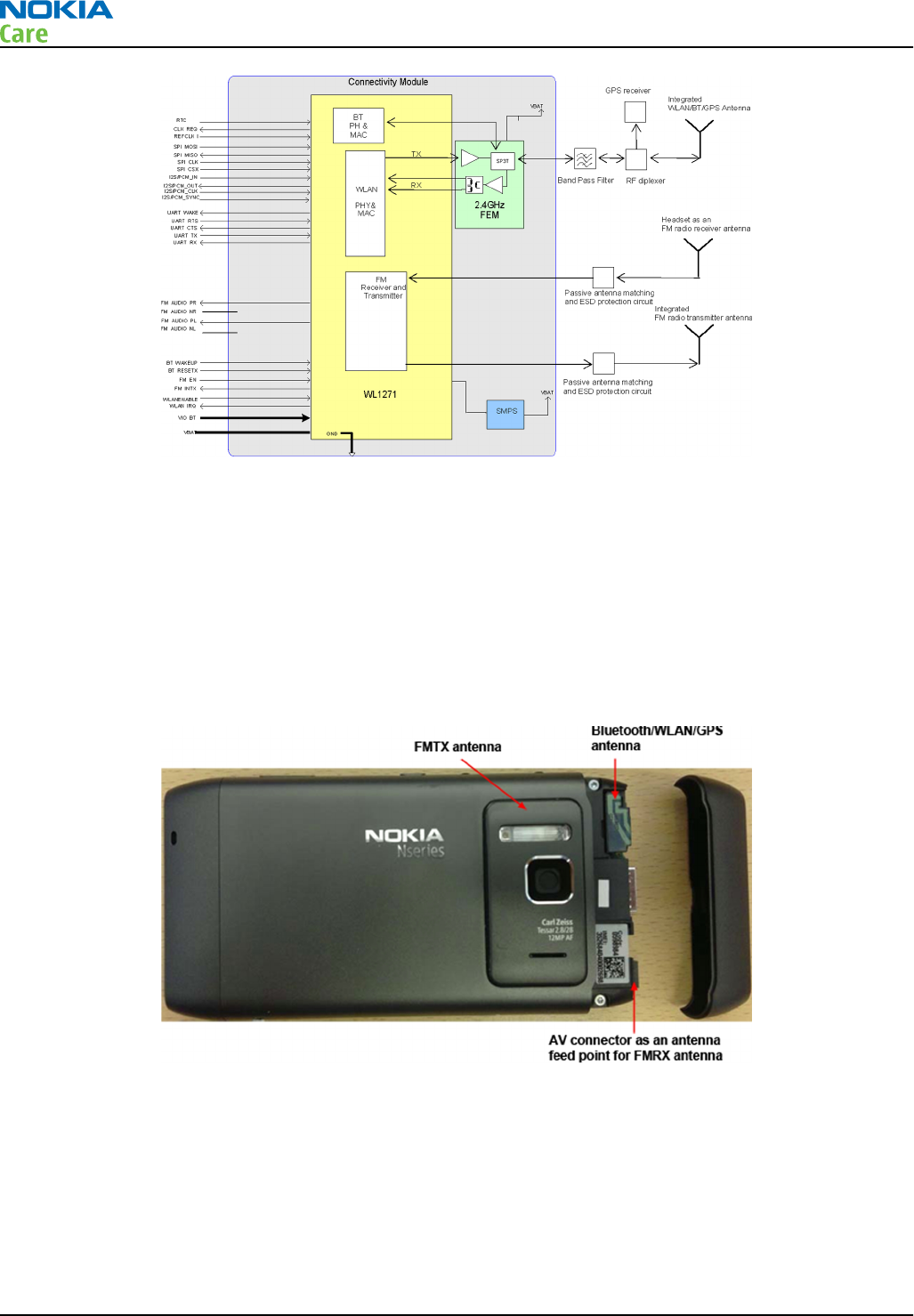
Figure 11 Hardware connections between BB and BOB1.0M-b
Bluetooth/WLAN/GPS antenna
The Bluetooth/WLAN/GPS antenna is product specific (antenna integrated into phone's top cap). On phones
with WLAN, the Bluetooth RF signal is routed from the connectivity module through the RF diplexer and a
shared Bluetooth/WLAN/GPS antenna is used. The FM receiver RF signal is routed through a product specific
FM antenna matching circuit to the phone headset connector. The FM radio audio signal is routed to the
headset connector through the BB ASIC shared by the phone audio functions. The camera plate in the back
cover works as an FM transmitter antenna.
The antenna positions are presented in the following figure.
Figure 12 Bluetooth/WLAN/GPS antenna
RM-596
BB Troubleshooting and Manual Tuning Guide
Page 3 – 58 COMPANY CONFIDENTIAL Issue 2
Copyright © 2010 Nokia. All rights reserved.
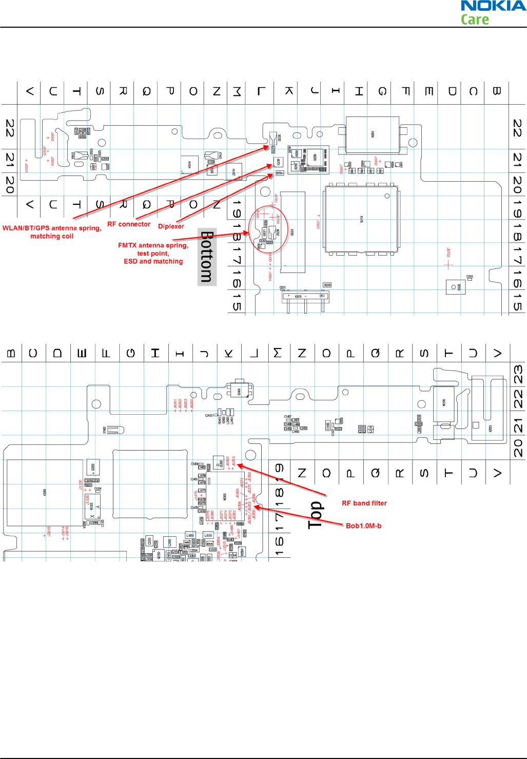
Component layout and test points of the connectivity module
Figure 13 Connectivity module's component layout, bottom side
Figure 14 Connectivity module's component layout, top side
Bluetooth/FM radio and WLAN troubleshooting
Introduction to Bluetooth/FM radio troubleshooting
The Bluetooth and FM radio receiver/transmitter functions are combined so these features are checked when
troubleshooting.
The following problems can occur with the Bluetooth and FM radio hardware:
RM-596
BB Troubleshooting and Manual Tuning Guide
Issue 2 COMPANY CONFIDENTIAL Page 3 – 59
Copyright © 2010 Nokia. All rights reserved.
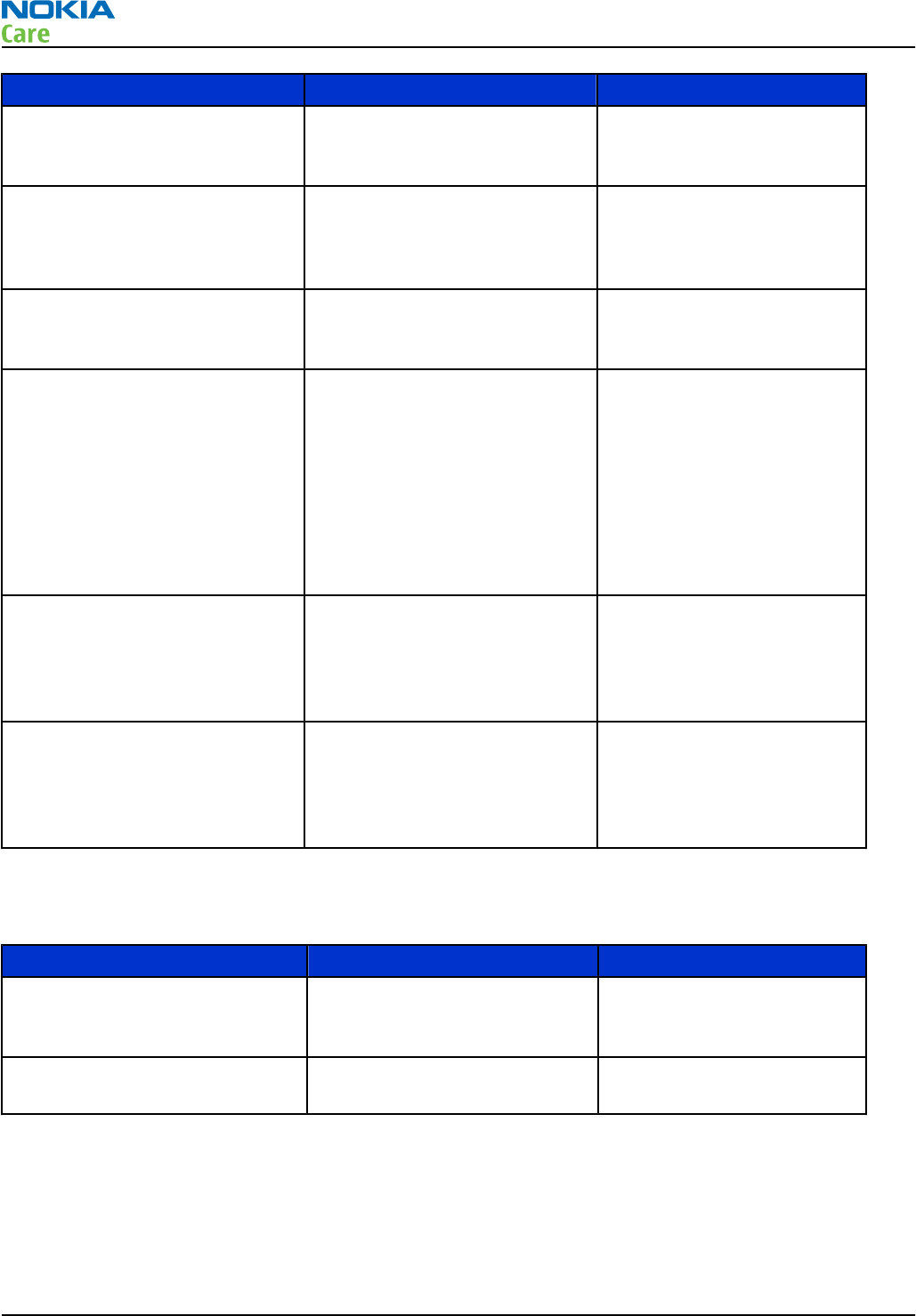
Symptom Problem Repair solution
Unable to switch on Bluetooth on
phone user interface
Open circuit solder joints or
component failure of BOB
module or SMD components
Replacement of BOB module
Able to send data file to another
Bluetooth device, but unable to
hear audio through functional
Bluetooth headset
Open circuit solder joints or
component failure of BOB
module (PCM interface)
Replacement of BOB module
Able to switch on Bluetooth on
phone user interface, but unable
to detect other Bluetooth devices
Open circuit solder joints or
detached component in
Bluetooth antenna circuit
Repair of Bluetooth antenna
circuit
Problems connecting to specific
manufacturer/model Bluetooth
accessory (specific Bluetooth
profile supported by phone and
accessory in product
specification)
Possible interoperability issue
with accessory fixed in recent
Nokia phone software release
(check Nokia Service Bulletin for
the latest information)
Update phone software to
the latest version if advised
in Nokia Service Bulletin
Note: The phone
Bluetooth Address and
software version are
displayed by pressing
*#2820# when Bluetooth
is on.
Able to turn on FM radio and
Bluetooth on phone user
interface, but unable to detect
local FM radio stations with FM
headset inserted
Open circuit solder joints or
detached component in FM
antenna circuit
Repair of FM receiver antenna
circuit
Able to perform scans to detect
local FM radio stations with
functional FM headset inserted,
but unable to hear FM audio
through headset
Open circuit solder joints or
detached component in FM
receiver audio path between
Bluetooth/FM ASIC and headset
Repair of FM audio circuit
Users may experience the following problems resulting in functional phones being returned to the repair
centre:
Symptom Problem Repair solution
Bluetooth feature does not
operate as desired with another
Bluetooth device
Bluetooth Profile implemented
in Bluetooth accessory not
supported in Nokia phone
Use Bluetooth accessory with
Bluetooth profiles supported
by phone
Poor FM radio reception (unable
to detect many radio stations)
Nokia headset not being used Use Nokia headset
RM-596
BB Troubleshooting and Manual Tuning Guide
Page 3 – 60 COMPANY CONFIDENTIAL Issue 2
Copyright © 2010 Nokia. All rights reserved.
Symptom Problem Repair solution
Poor FM transmitter range (for
example with car radio)
Large path loss between the
phone FM transmitter antenna
and external FM radio aerial (for
example, FM aerial routing
inside car is very well screened
or greater than 3 metre
distance between the phone
and FM radio)
Change the setup of aerial on
FM radio used for listening to
audio
BT and FM radio test coverage
The tests listed in the table below should be performed to verify whether the Bluetooth and FM receiver and
transmitter are functional. The use of self tests is described in section
Bluetooth and FM radio self tests in
Phoenix
.
Test Test Coverage Repair solution
Blueooth Self Test: ST_LPRF_IF_TEST Bluetooth-FM ASIC UART interface
(controls Bluetooth and FM
receiver and transmitter)
Replacement of BOB module
(or repair of phone BB)
Bluetooth Self Test:
ST_BT_WAKEUP_TEST
Bluetooth ASIC interrupt control
interface
Replacement of BOB module
(or repair of phone BB)
Bluetooth Self Test:
ST_LPRF_AUDIO_LINES_TEST
Bluetooth ASIC PCM interface Replacement of BOB module
(or repair of phone BB)
Bluetooth Functional Test: BER test
with BT-Box or functional test with
other Bluetooth device
Bluetooth antenna circuit Repair of Bluetooth antenna
circuit (including RF filter or
WLAN switch if fitted)
FM Radio Functional Test: Perform
scan for local radio stations and
check station list displayed on
phone
FM receiver antenna circuit Repair of FM antenna circuit
(between BTHFMWLAN ASIC
and headset connector)
FM Radio Functional Test: Listen to
local radio station
FM receiver audio circuit Repair of FM receiver audio
circuit (between BTHFMWLAN
ASIC and headset connector)
FM Transmitter Antenna Test: Read
Antenna Tuning Values in Phoenix
or functional test transmitting
music to nearby radio
FM transmitter antenna circuit and
antenna
Replacement of FM transmitter
circuit or antenna
The self tests run from Phoenix software are used for fault diagnosis.
If Phoenix software is not available, the functional tests with phone accessories are sufficient to verify the
functionality of Bluetooth and FM radio receiver and transmitter.
If Bob1.0M-b module has been replaced, the WLAN tuning must be performed to ensure that the
output complies with ETSI/ FCC legal limits.
FMTX troubleshooting faults
Possible faults
RM-596
BB Troubleshooting and Manual Tuning Guide
Issue 2 COMPANY CONFIDENTIAL Page 3 – 61
Copyright © 2010 Nokia. All rights reserved.
Expected fault reports relating to the FMTx 2.1 implementation may consist of one or more of the following;
1 No left audio
2 No right audio
3 No audio
4 Can’t start FMTx
5 Can’t locate FM transmission on an FM receiver or no FM transmission
6 Distortion on audio
7 Poor reception on FM receiver
8 No RDS information
Initial fault analysis
Where possible, attempt to reproduce and verify the reported fault. Intermittent problems are likely to be
due to bad connections or broken components/solder joints. Any faults relating to poor FM transmitter
performance or frequent failure to locate usable frequencies when performing a scan are likely to be due to
some kind of antenna issues.
In handsets that utilise an antenna solution in a removable cover it is likely that the connecting interface
pins are either damaged, dirty or that the cover fits poorly perhaps due to broken tabs/latching lugs. Poor
audio fault reports may also be due to the above antenna issues.
Introduction to WLAN troubleshooting
The following problems can occur with the WLAN hardware:
Symptom Problem Repair solution
Unable to switch on WLAN on
phone user interface
Open circuit solder joints or
component failure of BOB
module
Replacement of BOB module
or Host
Able to turn on WLAN via phone
user interface, but unable to
detect any WLAN APs or other
WLAN devices
Open circuit solder joints or
component failure of BOB
module or filter
Replacement of BOB module
or filter
Able to turn on WLAN via phone
user interface and find APs and
other WLAN devices, but not able
to connect
Problem with TX part of WLAN
circuit
Replacement of BOB module
Slow download speed when
using WLAN as connection
method
System clock possibly degraded Change system clock source
Users may experience the following problems resulting in functional phones being returned to the repair
centre:
Symptom Problem Repair solution
WLAN does not operate as desired
with another WLAN device
Other WLAN device is not
conforming to ETSI/FCC
specifications
Use only certified WLAN
products
RM-596
BB Troubleshooting and Manual Tuning Guide
Page 3 – 62 COMPANY CONFIDENTIAL Issue 2
Copyright © 2010 Nokia. All rights reserved.
WLAN test coverage
The tests listed in the table below should be performed to verify whether WLAN is functional. WLAN should
be re-tested after repair.
Test Test Coverage Repair solution
WLAN Self Test: ST_WLAN_TEST WLAN SPI and control interface
(data interface and control of
WLAN)
Replacement of BOB module
Bluetooth Functional Test: BER test
with BT-Box or functional test with
another Bluetooth device
Antenna connection from module,
including filter
Replacement of BOB module or
antenna components
WLAN TX Tuning Checks WLAN TX path up to
module output and calibrates the
new module if fitted
Replacement of BOB module or
antenna components
The self tests run from Phoenix software are used for fault diagnosis.
If Phoenix software is not available, the functional tests with phone accessories are sufficient to verify the
functionality of WLAN.
Bluetooth and FM radio self tests in Phoenix
Prerequisites
A flash adapter (or phone data cable) connected to a PC with Phoenix service software is required.
Steps
1. Place the phone in the flash adapter or connect data cable to phone.
2. Start
Phoenix
service software.
3. Choose File → Scan Product.
4. From the Mode drop-down menu, set mode to Local.
5. Choose Testing → Self Tests.
6. In the
Self Tests
window check the following Bluetooth and FM radio related tests:
•ST_LPRF_IF_TEST
•ST_LPRF_AUDIO_LINES_TEST
•ST_BT_WAKEUP_TEST
RM-596
BB Troubleshooting and Manual Tuning Guide
Issue 2 COMPANY CONFIDENTIAL Page 3 – 63
Copyright © 2010 Nokia. All rights reserved.
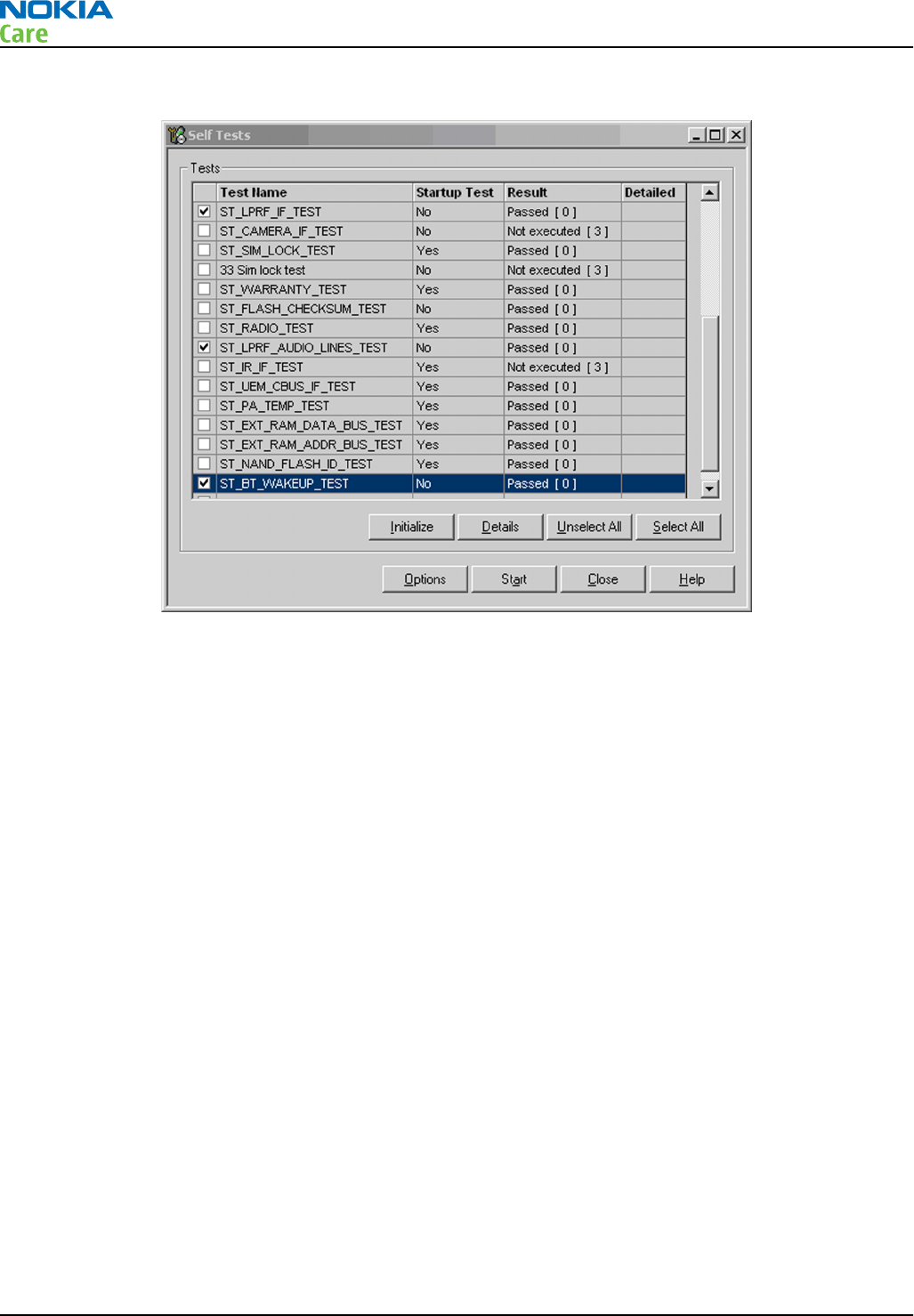
7. To run the tests, click Start.
Figure 15 Bluetooth and FM radio self tests in
Phoenix
WLAN self test in Phoenix
Prerequisites
A flash adapter (or phone data cable) connected to a PC with Phoenix service software is required.
Steps
1. Place the phone in the flash adapter or connect data cable to phone.
2. Start
Phoenix
service software.
3. Choose File → Scan Product.
4. From the Mode drop-down menu, set mode to Local.
5. Choose Testing → Self Tests.
6. In the
Self Tests
window check the following WLAN test:
•ST_WLAN_TEST
7. To run the test, click Start.
Bluetooth BER test in Phoenix
Prerequisites
JBT-9, or SB-6 Bluetooth test box (BT-box) is required to perform a BER test. If a BT-box is not available,
Bluetooth functionality can be checked by transferring a file to another Bluetooth phone.
Steps
1. Connect data cable to phone.
2. Start
Phoenix
service software.
RM-596
BB Troubleshooting and Manual Tuning Guide
Page 3 – 64 COMPANY CONFIDENTIAL Issue 2
Copyright © 2010 Nokia. All rights reserved.
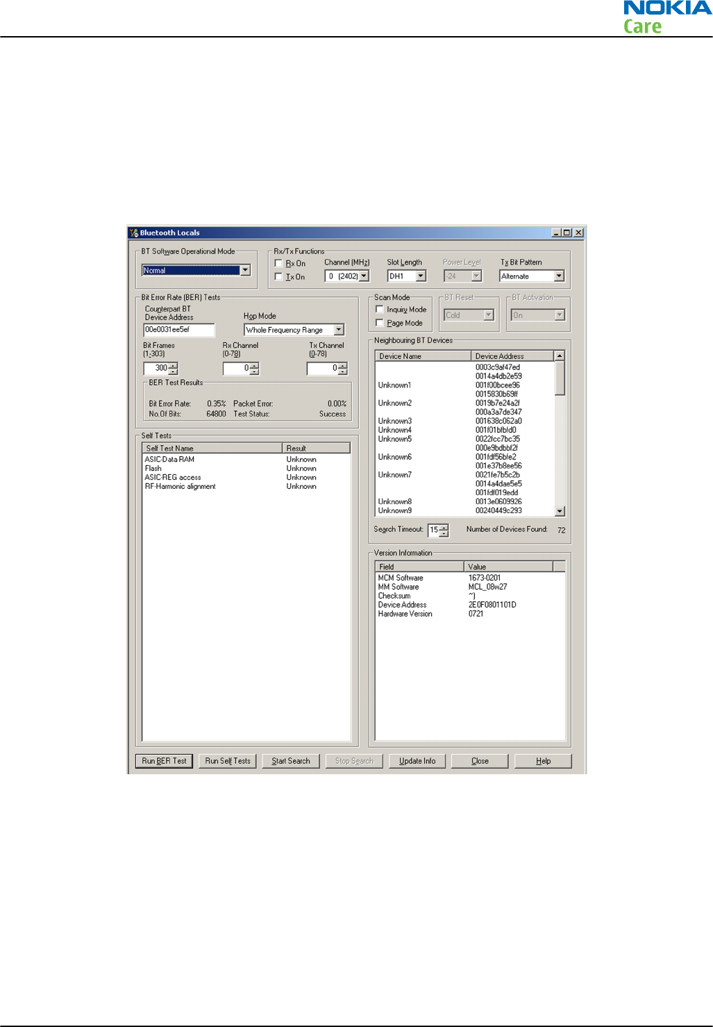
3. Choose File → Scan Product.
4. Choose Testing → Bluetooth LOCALS .
5. Locate the BT-box serial number (12 digits) found in the type label on the back of the JBT-9, or SB-6
Bluetooth test box.
6. In the Bluetooth
LOCALS
window, write the 12-digit serial number on the
Counterpart BT Device
Address
line.
7. Place the BT-box near (within 10 cm) of the phone and click Start BER Test.
Figure 16 Bluetooth BER test in Phoenix
FMRX radio receiver testing
Steps
1. Set signal generator parameters:
•FM modulation on
•Frequency 100MHz
•FM deviation 22kHz
•Modulation frequency 1kHz
•RF level should be varied during the test to obtain good audio signal quality
RM-596
BB Troubleshooting and Manual Tuning Guide
Issue 2 COMPANY CONFIDENTIAL Page 3 – 65
Copyright © 2010 Nokia. All rights reserved.
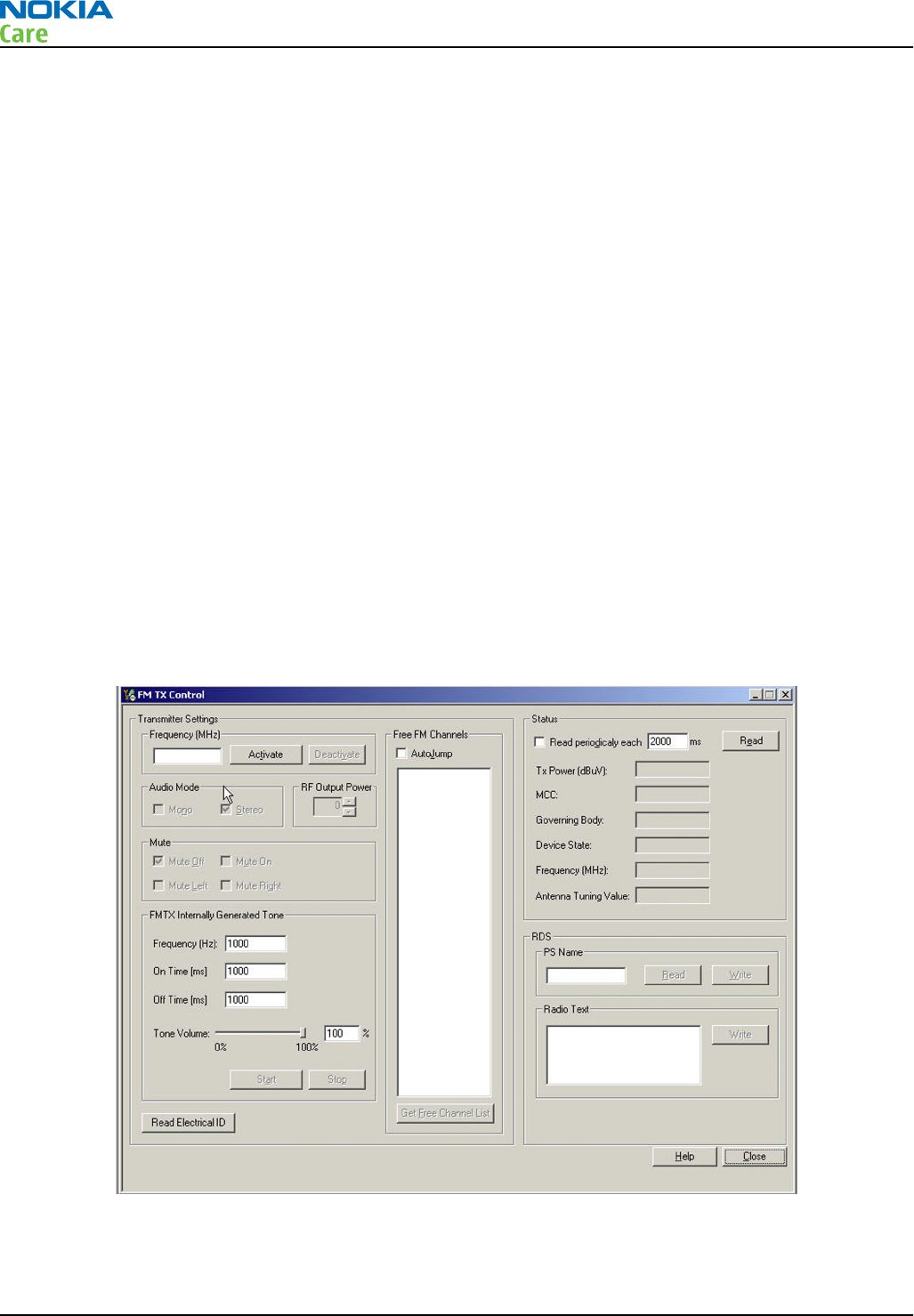
•Connect suitable antenna to signal generator
Note: You may alternately use a known good FM radio broadcast as a test signal.
2. Attach the Nokia headset to the phone’s AV connector.
3. Use Scroll button to autotune to the radio frequency.
4. Set volume to suitable level.
5. Check audio quality with a headset.
FMTX transmitter antenna connectivity test in Phoenix
Context
The purpose is to check the connectivity between the FM TX antenna and Bob ASIC. The FM transmitter antenna
can be checked by reading the ‘Antenna Tuning Values’ displayed in the FM TX Control test display in Phoenix.
This test can be performed with the product specific FM TX antenna assembled. Alternatively, this test can
be performed with the FM antenna pins terminated with the external impedance provided by the MJ-241 test
jig, but then this test will not test the phone’s own FMTX antenna connectivity anymore.
Steps
1. Connect data cable to phone including FM transmitter antenna.
2. Start
Phoenix
service software.
3. Choose File → Scan Product .
4. Choose Testing → FMTX Control .
5. Set frequency to near the bottom of the band (92 MHz) and press the Activate button.
Figure 17 FMTX transmitter antenna connectivity test in Phoenix
6. Set the ‘RF Output Power’ to 120uV.
7. Press the Read button and record ‘Antenna Tuning Value’.
RM-596
BB Troubleshooting and Manual Tuning Guide
Page 3 – 66 COMPANY CONFIDENTIAL Issue 2
Copyright © 2010 Nokia. All rights reserved.

8. Set frequency to near the top of the band (107 MHz) and press the Activate button again.
9. Press the Read button and record ‘Antenna Tuning Value’.
Results
The test limits for the antenna tuning varactor value are product specific.
Table 9 Antenna tuning value limits for RM-596
Antenna tuning value
Frequency Low limit High limit
92 MHz 80 126
107 MHz 35 1
The default value (displayed when there is no antenna present) is 0…2. If both values are 0…2, this
indicates there is a poor connection between the FMTX antenna and the Bob ASIC.
FMTX transmitter tuning and power measurement in Testing and Tuning Tool
Context
Note: RF cables and adapters have some losses. They have to be taken into account when the FMTX
is measured. Approximately, the FMTX RF loss in the MJ-241 test jig is around 24 dB. Cable
attenuations have to be taken into account separately.
FMTX has been tuned correctly in production. There is no reason to do re-calibration unless the memory
(D3000) is corrupted. But it is a good way to ensure the RF performance by these tuning and power
measurements.
FMTX can be tuned and measured automatically with Testing and Tuning Tool. Actually it performs output
power level writings and measurements for FMTX. The results are displayed and logged in a result file, if
initiated.
For hardware requirements for auto tuning, please refer to
RF testing and BB/RF tuning concept with module
jig
in section 'Service Tools and Service Concepts'.
Steps
1. Make sure the phone is connected to the PC.
2. Connect the RF cable between the MJ-241 test jig (SMA RF connector located next to the BT/WLAN/GPS
antenna connector) and the communication tester.
RM-596
BB Troubleshooting and Manual Tuning Guide
Issue 2 COMPANY CONFIDENTIAL Page 3 – 67
Copyright © 2010 Nokia. All rights reserved.
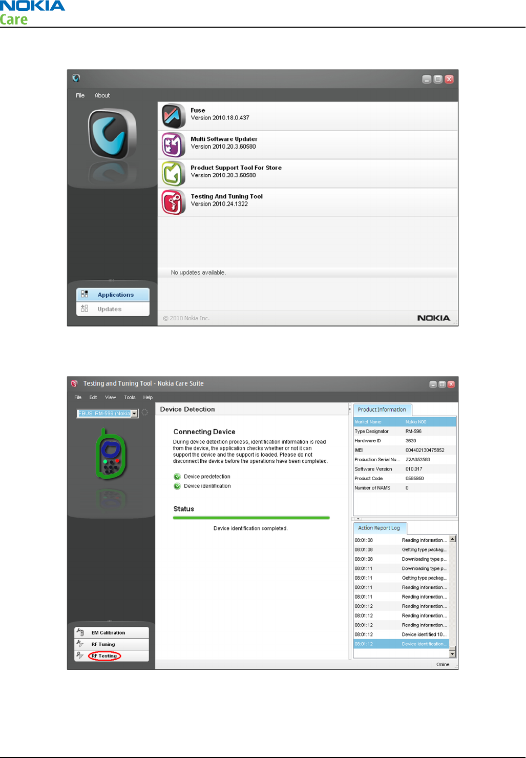
3. Start
Nokia Care Suite
application.
4. To open the application, double-click the Testing And Tuning Tool icon.
5. If the application is able to find a connected phone, the following view will open:
RM-596
BB Troubleshooting and Manual Tuning Guide
Page 3 – 68 COMPANY CONFIDENTIAL Issue 2
Copyright © 2010 Nokia. All rights reserved.
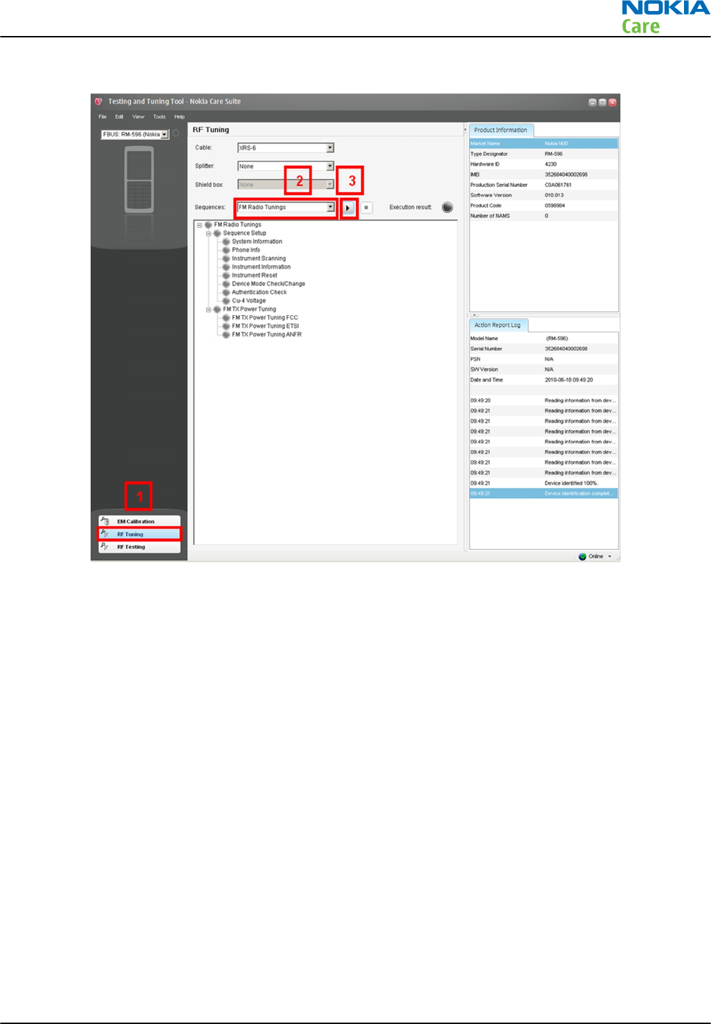
6. Click on the RF Tuning button and select from the drop-down menu:
RM-596
BB Troubleshooting and Manual Tuning Guide
Issue 2 COMPANY CONFIDENTIAL Page 3 – 69
Copyright © 2010 Nokia. All rights reserved.
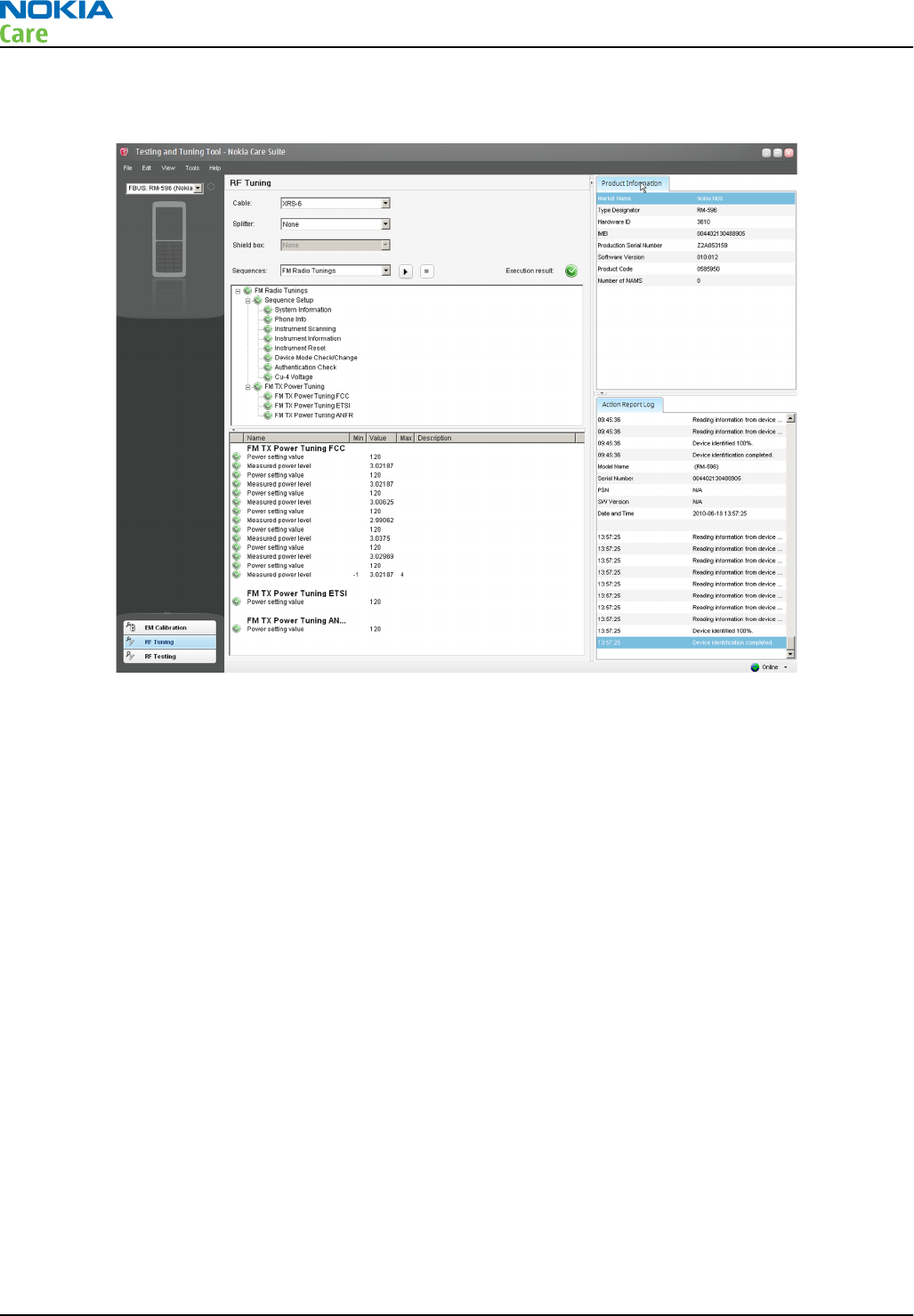
7. RF tunings will be ready when all the tunings and measurements are green in the tool window and no
errors occur.
WLAN TX and RX testing in Phoenix
Context
The basic WLAN RX and TX functionality can be checked with Phoenix.
Steps
1. Place the phone in the flash adapter or connect data cable to phone.
2. Start
Phoenix
service software.
3. Choose File → Scan Product.
RM-596
BB Troubleshooting and Manual Tuning Guide
Page 3 – 70 COMPANY CONFIDENTIAL Issue 2
Copyright © 2010 Nokia. All rights reserved.
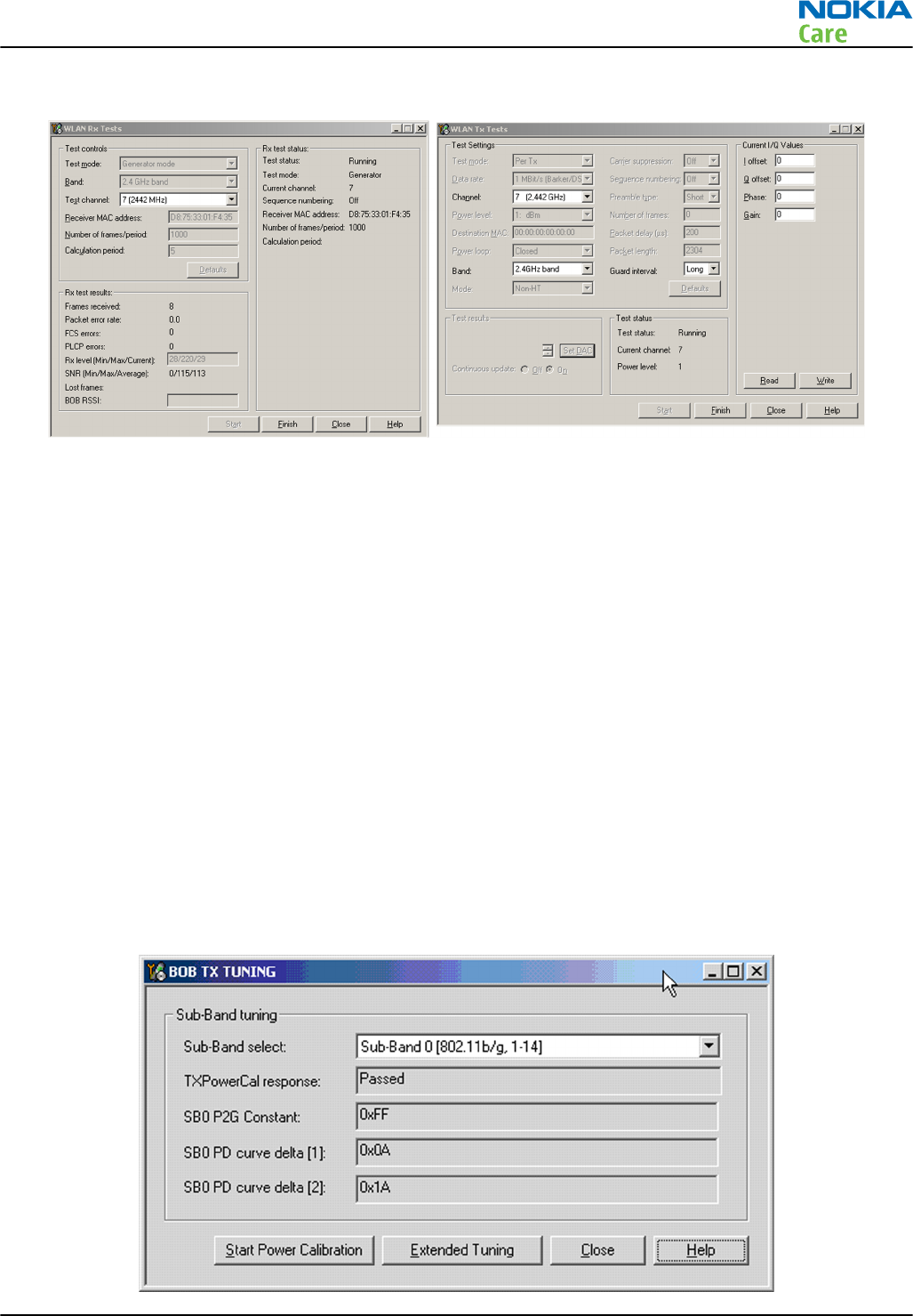
4. Choose Testing → WLAN RX Tests or WLAN TX Tests. See the following figures.
WLAN TX BiP testing procedure in Phoenix
Context
Note: This is an alternative procedure to tune the WLAN TX. The other, recommended procedure is
described in chapter WLAN TX BiP testing procedure in Testing and Tuning Tool (page 3–72 ) .
Note: No external measurement equipment is required as the calibration is completely handled
internally. RF cable and adapter losses do not need to be taken into account while WLAN TX tuning
is proceeded.
WLAN TX has been BiP (Build in Prduction line testing) tuned correctly in production. There is no reason to
do re-calibration unless the Bob1.0M-b (N6300) is changed or memory (D3000) is corrupted.
WLAN TX can be tuned automatically with Testing and Tuning Tool. It performs calibrations and tunings of
WLAN TX. The results are displayed and logged in a result file, if initiated.
Steps
1. Place the phone in the flash adapter or connect data cable to phone.
2. Start
Phoenix
service software.
3. Choose File → Scan Product.
4. Choose Tuning → WLAN_TX_TUNING. See the following figure.
RM-596
BB Troubleshooting and Manual Tuning Guide
Issue 2 COMPANY CONFIDENTIAL Page 3 – 71
Copyright © 2010 Nokia. All rights reserved.
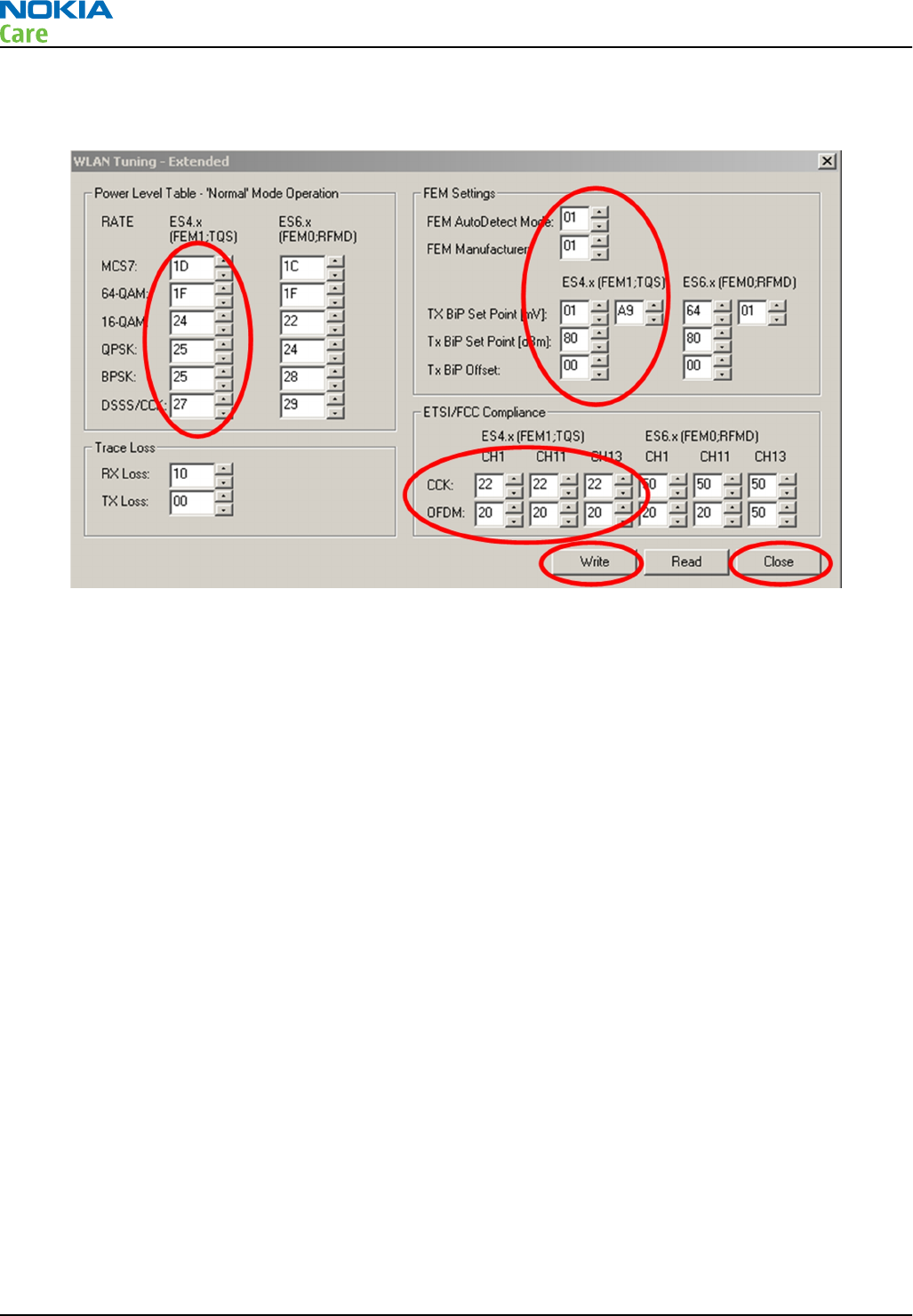
5. Select “Sub-Band 0” as indicated in the figure.
6. Open the Extended Tuning menu. See the following figure.
7. Type the correct tuning values. The values are circled in the figure above.
8. Click Write and Close.
9. Click Start Power Calibration and read the result from the Result box.
10. If TXPowerCal response returns ‘Passed’ results, the WLAN TX BiP test is successful.
WLAN TX BiP testing procedure in Testing and Tuning Tool
Context
Note: No external measurement equipment is required as the calibration is completely handled
internally. RF cable and adapter losses do not need to be taken into account while WLAN TX tuning
is proceeded.
WLAN TX has been BiP (Build in Prduction line testing) tuned correctly in production. There is no reason to
do re-calibration unless the Bob1.0M-b (N6300) is changed or memory (D3000) is corrupted.
WLAN TX can be tuned automatically with Testing and Tuning Tool. It performs calibrations, tunings and
measurements of WLAN TX. The results are displayed and logged in a result file, if initiated.
Steps
1. Make sure the phone is connected to the PC.
RM-596
BB Troubleshooting and Manual Tuning Guide
Page 3 – 72 COMPANY CONFIDENTIAL Issue 2
Copyright © 2010 Nokia. All rights reserved.
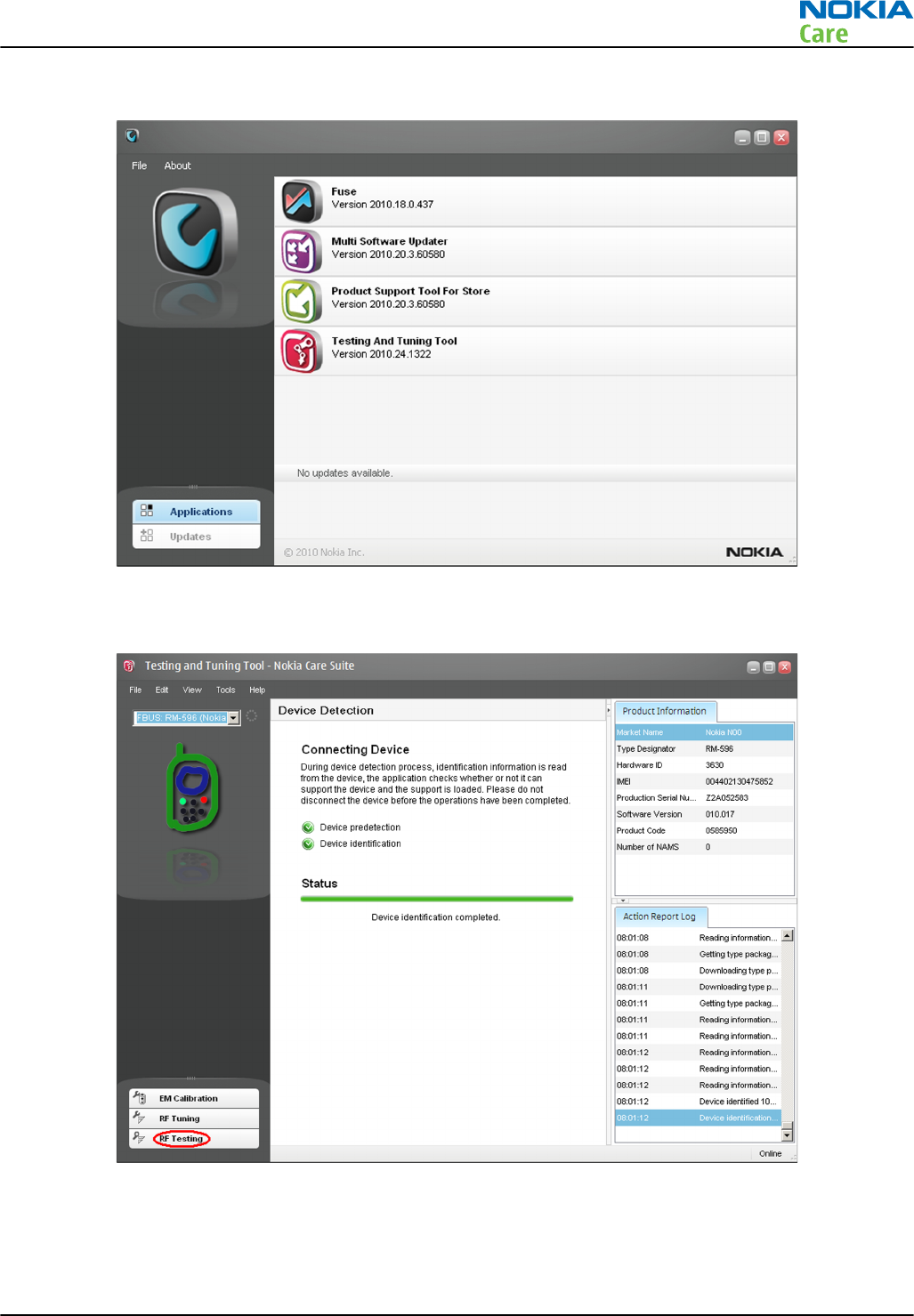
2. Start
Nokia Care Suite
application.
3. To open the application, double-click the Testing And Tuning Tool icon.
4. If the application is able to find a connected phone, the following view will open:
RM-596
BB Troubleshooting and Manual Tuning Guide
Issue 2 COMPANY CONFIDENTIAL Page 3 – 73
Copyright © 2010 Nokia. All rights reserved.
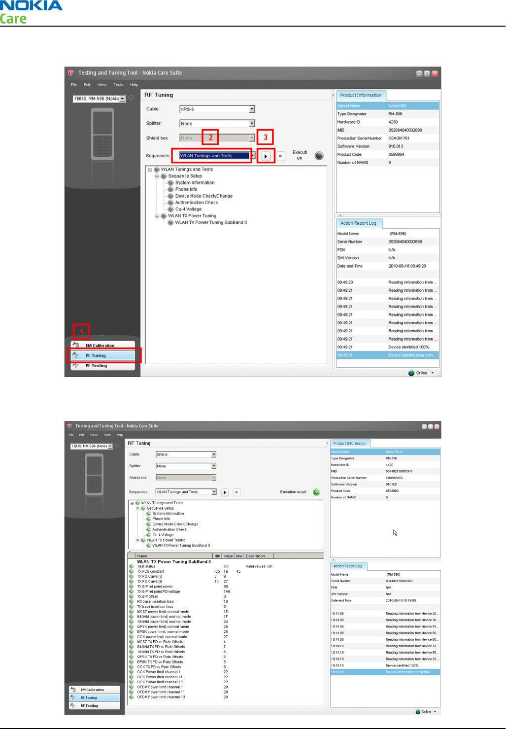
5. Click on the RF Tuning button and select from the drop-down menu:
6. RF tunings will be ready when all the tunings and measurements are green in the tool window and no
errors occur.
RM-596
BB Troubleshooting and Manual Tuning Guide
Page 3 – 74 COMPANY CONFIDENTIAL Issue 2
Copyright © 2010 Nokia. All rights reserved.
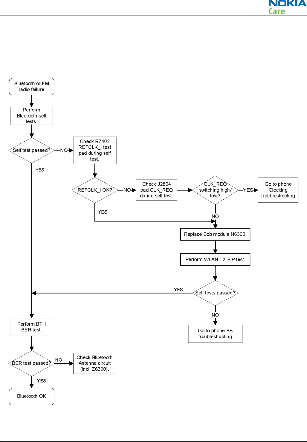
7. If errors do happen, failed tuning/testing steps are marked with a red color and more detailed results are
shown on the screen.
Bluetooth troubleshooting
Troubleshooting flow
RM-596
BB Troubleshooting and Manual Tuning Guide
Issue 2 COMPANY CONFIDENTIAL Page 3 – 75
Copyright © 2010 Nokia. All rights reserved.
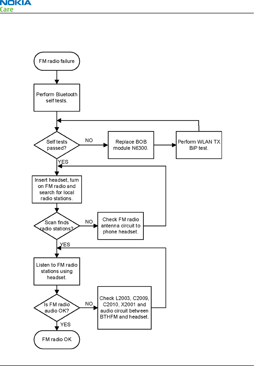
FMRX receiver troubleshooting
Troubleshooting flow
RM-596
BB Troubleshooting and Manual Tuning Guide
Page 3 – 76 COMPANY CONFIDENTIAL Issue 2
Copyright © 2010 Nokia. All rights reserved.
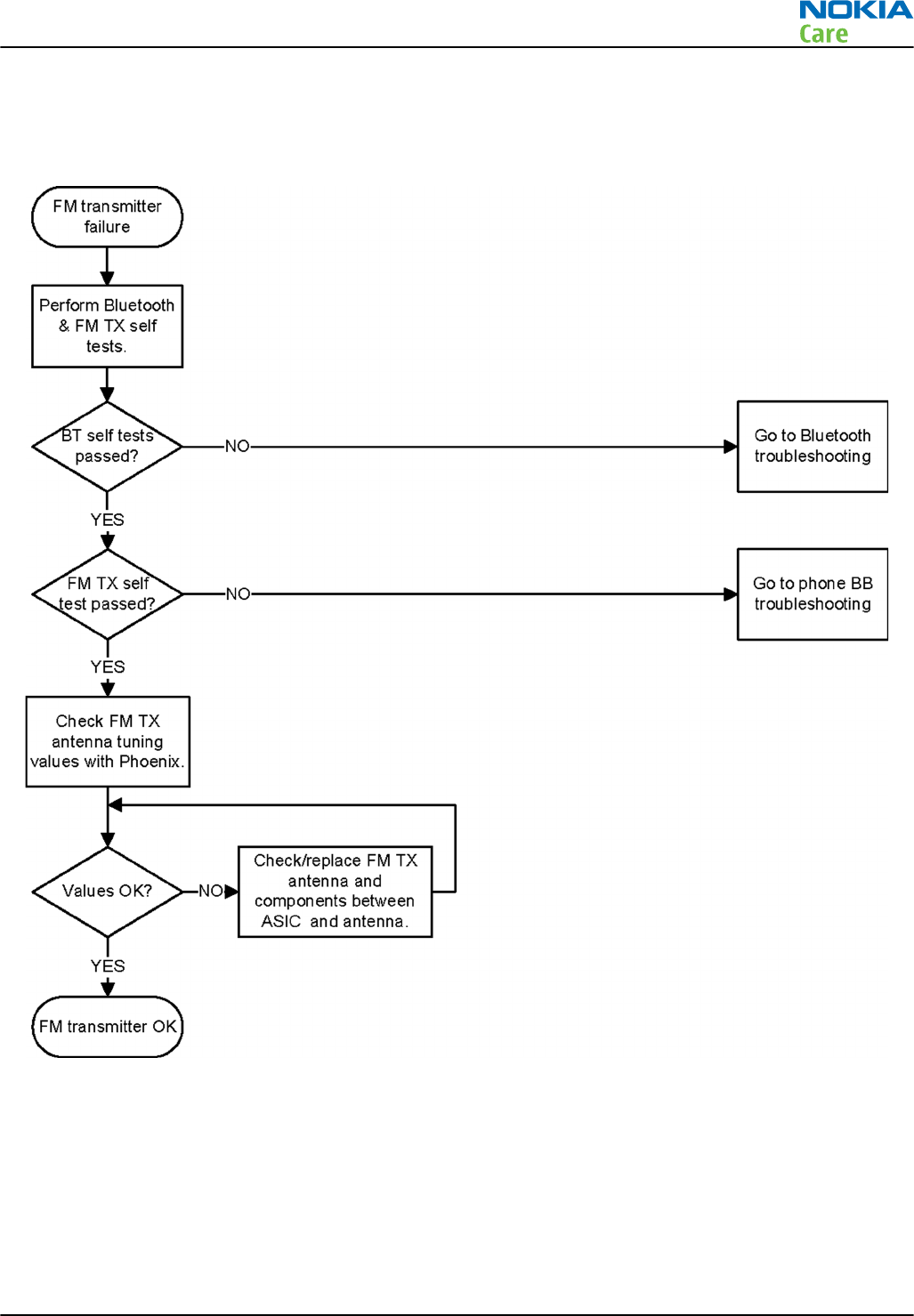
FMTX transmitter troubleshooting
Troubleshooting flow
RM-596
BB Troubleshooting and Manual Tuning Guide
Issue 2 COMPANY CONFIDENTIAL Page 3 – 77
Copyright © 2010 Nokia. All rights reserved.
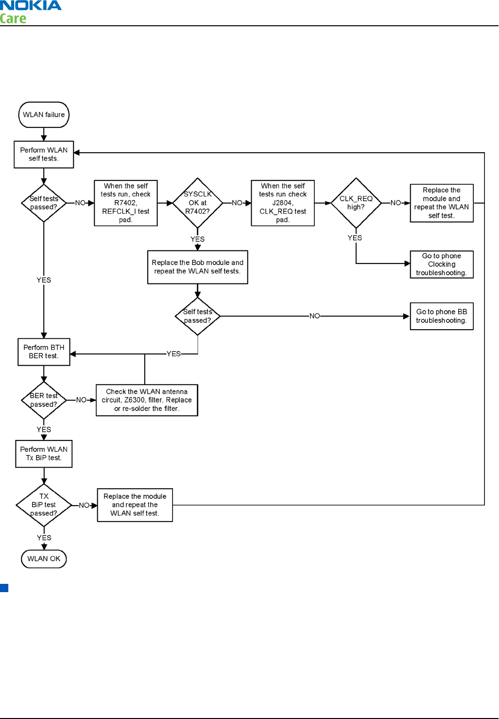
WLAN troubleshooting
Troubleshooting flow
GPS troubleshooting
Introduction to GPS troubleshooting
GPSCost4.1D is a single chip GPS receiver, comprising both RF and BB blocks integrated in a single digital die.
GPSCost4.1D is connected to RAPU ASIC via I2C_1 and some GENIOs. GPSCost4.1 D operates in Multi-master
mode and the REF clock is requested via AGPS_CLK_REQ signal connected to RAPU genio46. REFOUT_EXT2 single
ended 38.4 MHz analog clock from Linko RF is provided to GPSCost4.1D.
RM-596
BB Troubleshooting and Manual Tuning Guide
Page 3 – 78 COMPANY CONFIDENTIAL Issue 2
Copyright © 2010 Nokia. All rights reserved.
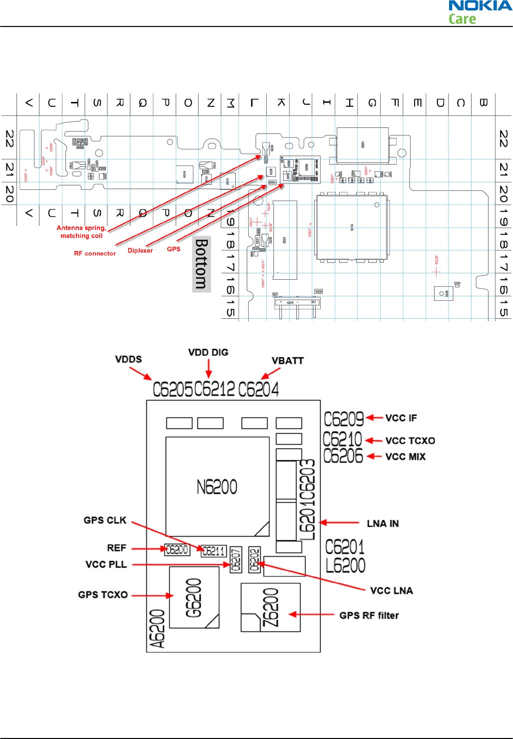
The GPS components are located on the bottom side of the PWB. Satellite signals are picked up by the
Bluetooth/WLAN/GPS antenna in the top end cap. The signal is then routed through a diplexer before being
processed by the GPS5350 receiver ASIC.
Figure 18 Component layout, bottom side
Figure 19 GPS layout and basic test points
RM-596
BB Troubleshooting and Manual Tuning Guide
Issue 2 COMPANY CONFIDENTIAL Page 3 – 79
Copyright © 2010 Nokia. All rights reserved.
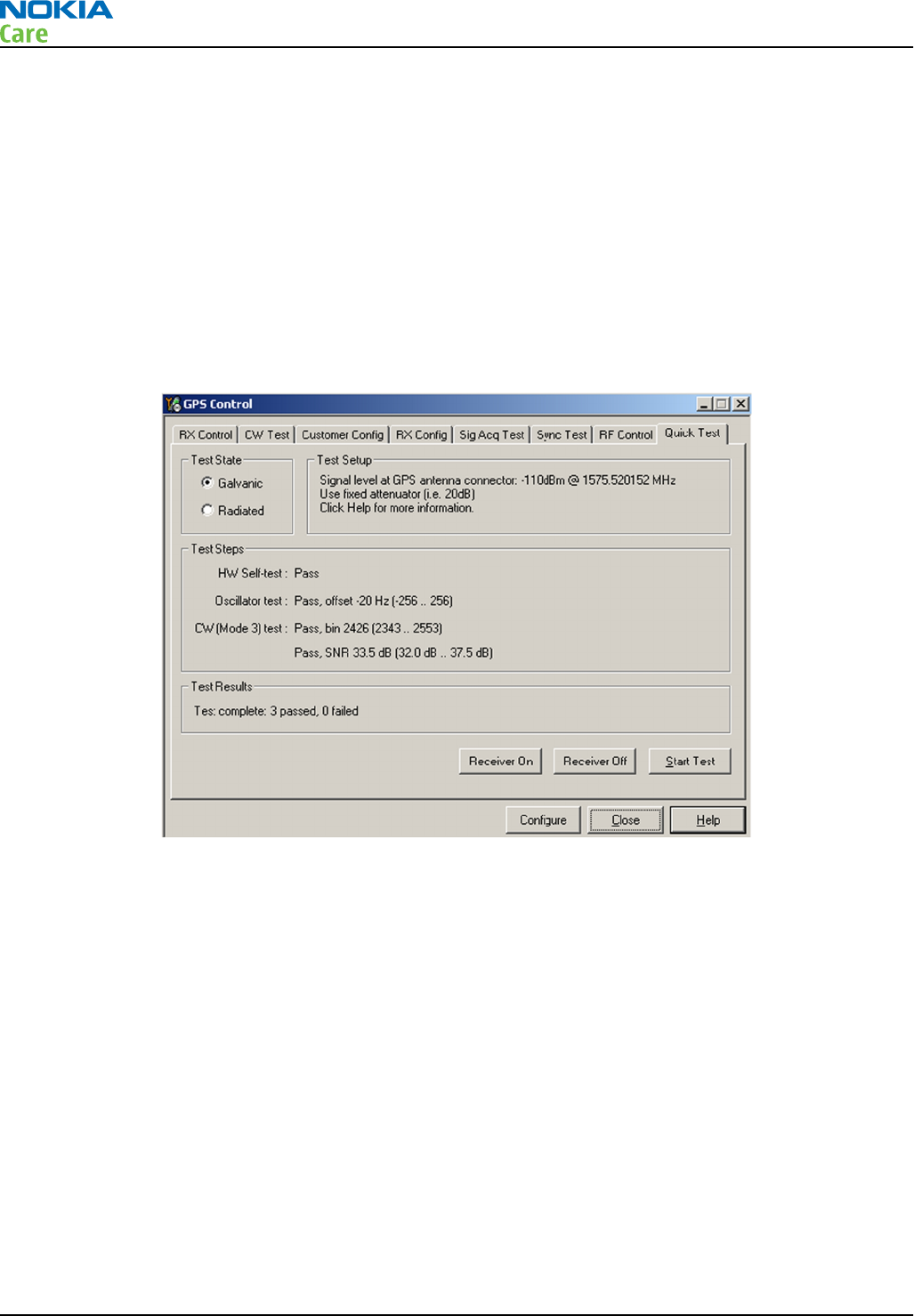
GPS settings for Phoenix
Quick Test window
This test will perform 3 tests in one: Self test, Oscillator Test and CW Test and will provide a Pass/Fail Response
for each. The HW Self Test confirms basic communication with the GPS ASIC. The oscillator test confirms the
frequency accuracy of the GPS TCXO against the Ref_Clk. The CW Test confirms end-to-end connectivity
between the GPS antenna and the GPS ASIC. It also contains a receive button.
Before this test is performed a known good phone should be tested in order to calibrate the setup. The signal
level of the Signal Generator should be adjusted so a reading of SNR 35 dB is achieved with the reference
unit. A good starting point is to set up the signal generator to -50 dBm.
These checks are part of
GPS failure troubleshooting
.
Figure 20 GPS Quick Test window
GPS control
Prerequisites
A flash adapter with RF connector connected to a PC with Phoenix service software is required. The GPS signal
should be connected to the RF connector. Calibrate the signal level with a known good phone. Signal level
will be high (approx -45 dBm) because it is a leakage connection.
Context
Use the following to test GPS using Phoenix.
Steps
1. Place phone to Flash Adaptor.
2. Start Phoenix service software.
3. From the File menu, select Scan Product and check that the correct product version is displayed.
RM-596
BB Troubleshooting and Manual Tuning Guide
Page 3 – 80 COMPANY CONFIDENTIAL Issue 2
Copyright © 2010 Nokia. All rights reserved.
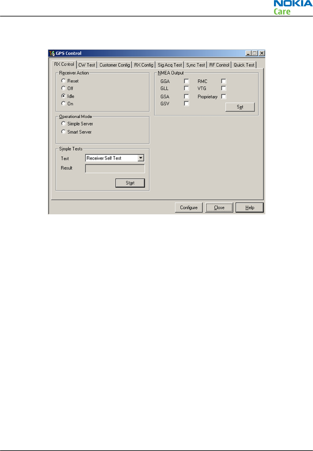
4. From the Testing menu, select GPS Control. This opens up
GPS Control
dialogue box, as shown in the
figure below, and enables the GPS.
Figure 21 GPS Control dialogue box
Select Idle to confirm the GPS is enabled and is in idle mode; at this point all clocks should be present,
GPS_En_Reset & SleepX should be high, and Vdd_Dig, Vcc_TCXO & Vcc_PLL/VCO will be present.
Receiver On turns on all RF sections of the ASIC and so all LDOs will be on.
GPS failure troubleshooting
Context
GPS troubleshooting is broken down into two parts: general GPS failure troubleshooting and GPS basic checks
troubleshooting. The GPS failure troubleshooting flow can be followed and, where applicable, will feed into
the GPS basic checks troubleshooting flow.
RM-596
BB Troubleshooting and Manual Tuning Guide
Issue 2 COMPANY CONFIDENTIAL Page 3 – 81
Copyright © 2010 Nokia. All rights reserved.
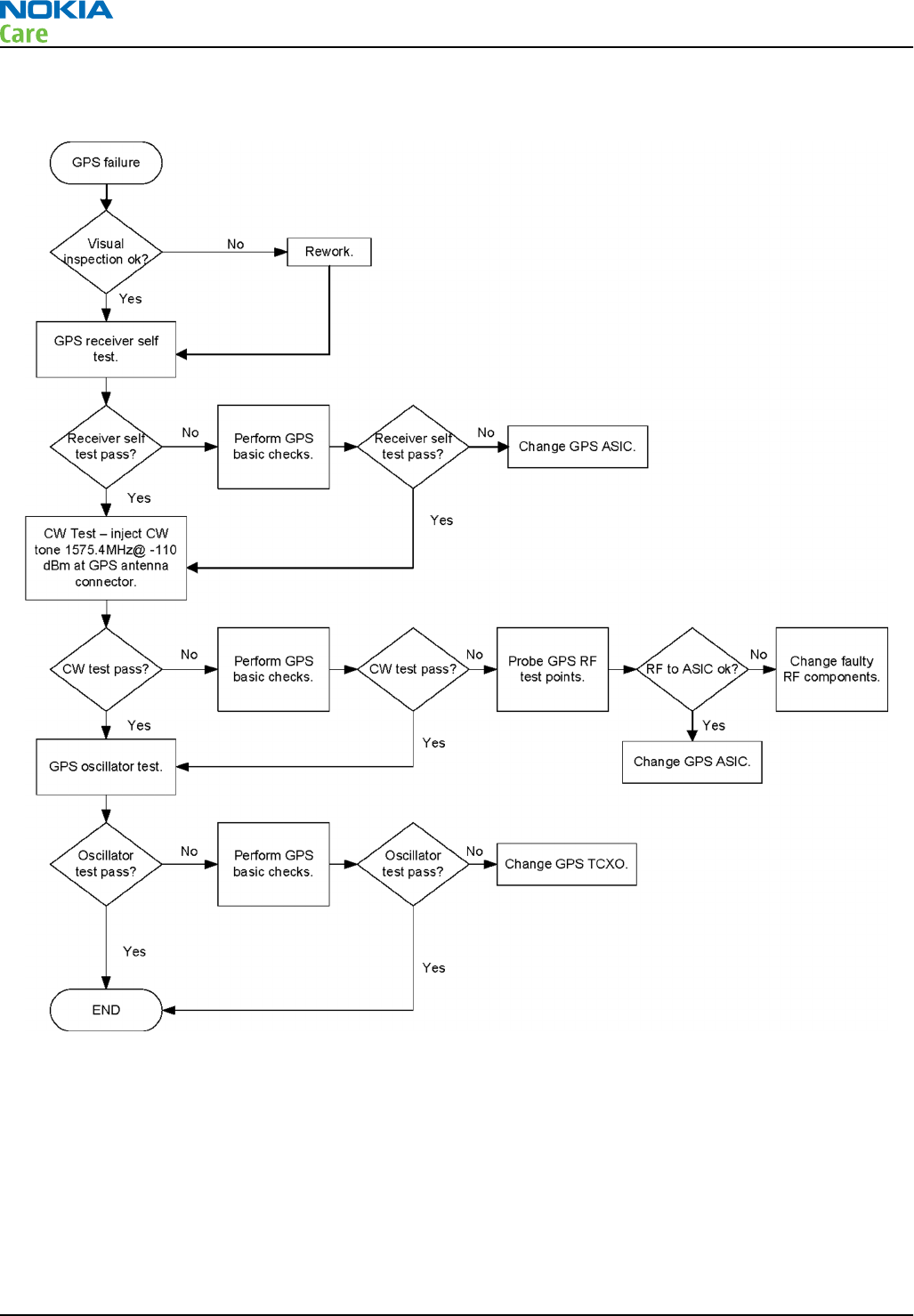
Troubleshooting flow
RM-596
BB Troubleshooting and Manual Tuning Guide
Page 3 – 82 COMPANY CONFIDENTIAL Issue 2
Copyright © 2010 Nokia. All rights reserved.
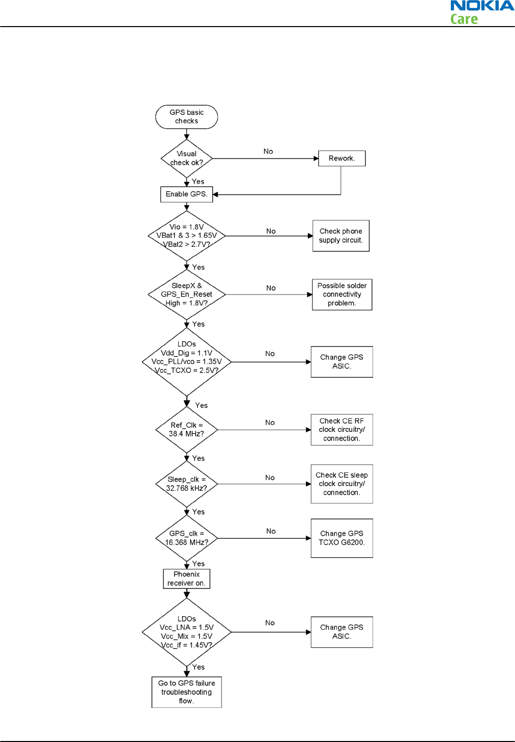
GPS basic checks troubleshooting
Troubleshooting flow
RM-596
BB Troubleshooting and Manual Tuning Guide
Issue 2 COMPANY CONFIDENTIAL Page 3 – 83
Copyright © 2010 Nokia. All rights reserved.

Baseband manual tuning guide
Certificate restoring for BB5 products
Context
This procedure is performed when the device certificate is corrupted for some reason.
All tunings (RF & Baseband, UI) must be done after performing the certificate restoring procedure.
The procedure for certificate restoring is the following:
•Flash the phone with the latest available software using FPS-20 or FPS-21.
•Create a request file.
•Send the file to Nokia by e-mail. Use the following addresses depending on your location:
•APAC: sydney.service@nokia.com
•CHINA: repair.ams@nokia.com
•E&A: salo.repair@nokia.com
•AMERICAS: fls1.usa@nokia.com
•When you receive a reply from Nokia, carry out certificate restoring.
•Tune the phone completely.
Note: SX-4 smart card is needed.
•If the phone resets after certificate restoring, reflash the phone again.
Required equipment and setup:
•
Phoenix
service software v 2009.41 or newer.
•The latest phone model specific
Phoenix
data package.
•Care dongle
•SX-4 smart card (Enables BB5 testing and tuning features)
•Activated FPS-20 flash prommer OR FPS-21 flash prommer
•Flash update package 08.30.012 or newer for FPS-20 or FPS-21 flash prommers
•CU-4 control unit
•USB cable from PC USB Port to CU-4 control unit
•Phone model specific adapter for CU-4 control unit
•PCS-1 cable to power CU-4 from external power supply
•Service cable between flash prommer and CU-4
Note: CU-4 must be supplied with +12 V from an external power supply in all steps of certificate
restoring.
Steps
1. Program the phone software.
i Start
Phoenix
and login. Make sure the connection has been managed correctly for FPS-20 or FPS-21.
ii Update the phone MCU software to the latest available version.
If the new flash is empty and the phone cannot communicate with
Phoenix
, reflash the phone.
iii Choose the product manually from File → Open Product , and click OK.
Wait for the phone type designator (e.g. “RM-1” ) to be displayed in the status bar.
RM-596
BB Troubleshooting and Manual Tuning Guide
Page 3 – 84 COMPANY CONFIDENTIAL Issue 2
Copyright © 2010 Nokia. All rights reserved.
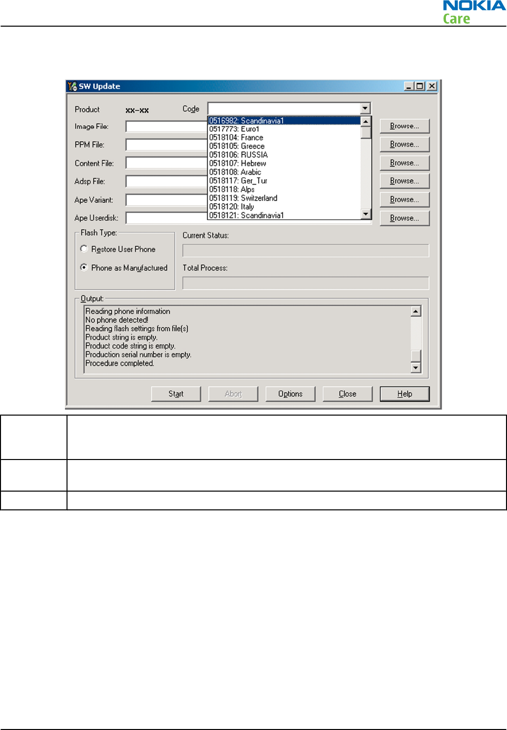
iv Go to Flashing → SW Update and wait until
Phoenix
reads the product data as shown in the following
picture.
Product is automatically set according to the phone support module which was opened manually,
but the flash files cannot be found because the correct data cannot be read from the phone
automatically.
Code must be chosen manually, it determines the correct flash files to be used. Please choose the
correct product code (can be seen in the phone type label) from the dropdown list.
Flash Type must be set to Phone as Manufactured.
v To continue, click Start.
Progress bars and messages on the screen show actions during phone programming, please wait.
RM-596
BB Troubleshooting and Manual Tuning Guide
Issue 2 COMPANY CONFIDENTIAL Page 3 – 85
Copyright © 2010 Nokia. All rights reserved.
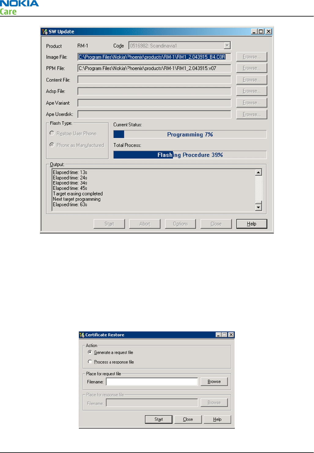
Programming is completed when Flashing Completed message is displayed.
The product type designator and MCU SW version are displayed in the status bar.
vi Close the
SW Update
window and then choose File → Close Product .
2. Create a
Request
file.
For this procedure, you must supply +12 V to CU-4 from an external power supply.
i To connect the phone with
Phoenix
, choose File → Scan Product .
ii Choose Tools → Certificate Restore .
iii To choose a location for the request file, click Browse.
RM-596
BB Troubleshooting and Manual Tuning Guide
Page 3 – 86 COMPANY CONFIDENTIAL Issue 2
Copyright © 2010 Nokia. All rights reserved.
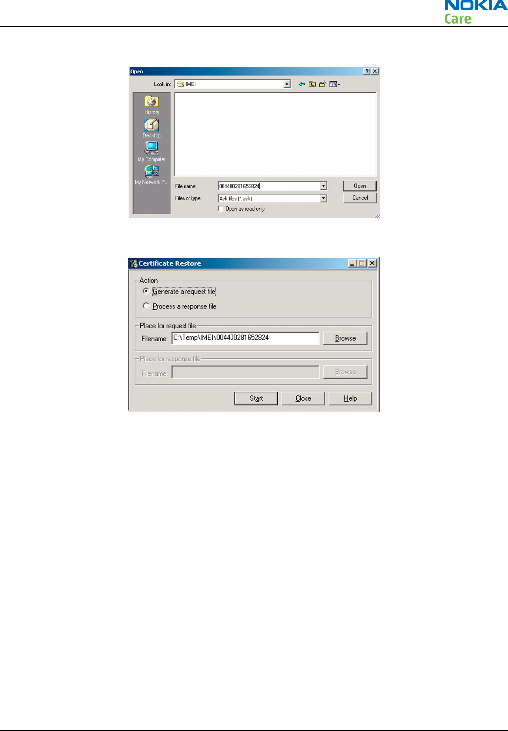
iv Name the file so that you can easily identify it, and click Open.
The name of the file and its location are shown.
v To create the
Request
file, click Start.
vi When the file for certificate restore has been created, send it to Nokia as an e-mail attachment.
3. Restore certificate.
For this procedure, you must supply +12 V to CU-4 from an external power supply.
i Save the reply file sent by Nokia to your computer.
ii Start
Phoenix
service software.
iii Choose File → Scan Product .
RM-596
BB Troubleshooting and Manual Tuning Guide
Issue 2 COMPANY CONFIDENTIAL Page 3 – 87
Copyright © 2010 Nokia. All rights reserved.
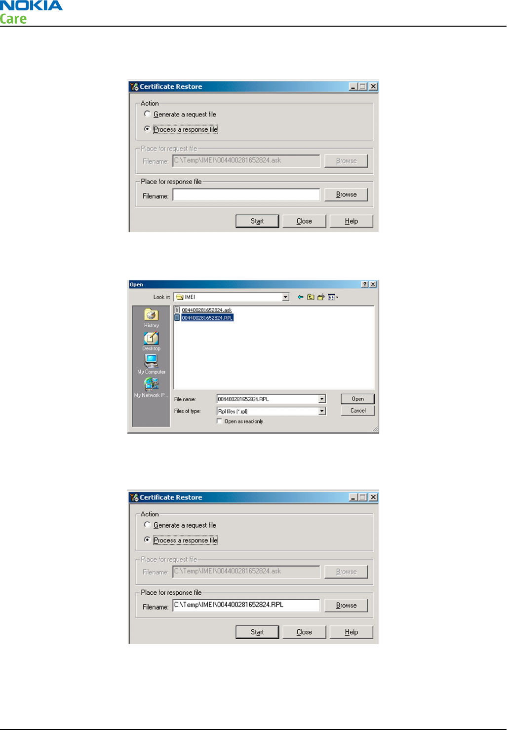
iv From the Tools menu, choose Certificate Restore and select Process a response file in the
Action
pane.
v To choose the location where response file is saved, click Browse.
vi Click Open.
The name of the file and the path where it is located are shown.
vii To write the file to phone, click Start.
Next actions
After a successful rewrite, you must retune the phone completely by using
Phoenix
tuning functions.
Important: Perform all tunings: RF, BB, and UI.
RM-596
BB Troubleshooting and Manual Tuning Guide
Page 3 – 88 COMPANY CONFIDENTIAL Issue 2
Copyright © 2010 Nokia. All rights reserved.
Energy management calibration
Prerequisites
Energy Management (EM) calibration is performed to calibrate the setting (gain and offset) of AD converters
in several channels (that is, battery voltage, BSI, battery current) to get an accurate AD conversion result.
Hardware setup:
•An external power supply is needed.
•Supply 12V DC from an external power supply to CU-4 to power up the phone.
•The phone must be connected to a CU-4 control unit with a product-specific flash adapter.
Steps
1. Place the phone to the docking station adapter (CU-4 is connected to the adapter).
2. Start
Phoenix
service software.
3. Choose File → Scan Product.
4. Choose Tuning → Energy Management Calibration.
5. To show the current values in the phone memory, click Read, and check that communication between
the phone and CU-4 works.
6. Check that the CU-4 used check box is checked.
7. Select the item(s) to be calibrated.
Note: ADC calibration has to be performed before other item(s). However, if all calibrations are
selected at the same time, there is no need to perform the ADC calibration first.
8. Click Calibrate.
The calibration of the selected item(s) is carried out automatically.
The candidates for the new calibration values are shown in the
Calculated values
column. If the new
calibration values seem to be acceptable (please refer to the following "Calibration value limits" table),
click Write to store the new calibration values to the phone permanent memory.
Table 10 Calibration value limits
Parameter Min. Max.
ADC Offset -30 +40
ADC Gain 12000 14000
BSI Gain 1100 1350
VBAT Offset 2635 2755
VBAT Gain 14900 15900
VCHAR Gain N/A N/A
IBAT (ICal) Gain 7750 12250
9. Click Read, and confirm that the new calibration values are stored in the phone memory correctly. If the
values are not stored to the phone memory, click Write and/or repeat the procedure again.
10. To end the procedure, close the
Energy Management Calibration
window.
RM-596
BB Troubleshooting and Manual Tuning Guide
Issue 2 COMPANY CONFIDENTIAL Page 3 – 89
Copyright © 2010 Nokia. All rights reserved.

RM-596
BB Troubleshooting and Manual Tuning Guide
(This page left intentionally blank.)
Page 3 – 90 COMPANY CONFIDENTIAL Issue 2
Copyright © 2010 Nokia. All rights reserved.

4 — Cellular RF
troubleshooting
Nokia Customer Care
Issue 2 COMPANY CONFIDENTIAL Page 4 – 1
Copyright © 2010 Nokia. All rights reserved.

RM-596
Cellular RF troubleshooting
(This page left intentionally blank.)
Page 4 – 2 COMPANY CONFIDENTIAL Issue 2
Copyright © 2010 Nokia. All rights reserved.

Table of Contents
General instructions for cellular RF troubleshooting......................................................................................... 4–5
Cellular RF key components.................................................................................................................................. 4–6
Cellular RF main troubleshooting ........................................................................................................................ 4–7
Cellular RF main troubleshooting................................................................................................................... 4–7
Self test troubleshooting.............................................................................................................................. 4–10
Troubleshooting with RF Self tests......................................................................................................... 4–10
RF-BB interface self test troubleshooting.............................................................................................. 4–11
RF supply self test troubleshooting........................................................................................................ 4–12
VBAT level.................................................................................................................................................. 4–13
VXO level.................................................................................................................................................... 4–14
VIO level..................................................................................................................................................... 4–15
VREF level .................................................................................................................................................. 4–15
VHIA (Vhi) level ......................................................................................................................................... 4–16
VDCDCA (Vlow) level ................................................................................................................................. 4–16
VPA level.................................................................................................................................................... 4–17
RF tuning and testing ........................................................................................................................................ 4–17
RF auto tuning and testing with Nokia Care Suite..................................................................................... 4–17
RF auto tuning procedure ............................................................................................................................ 4–18
Automatic RF testing with Nokia Care Suite............................................................................................... 4–22
Troubleshooting with Testing And Tuning Tool ........................................................................................ 4–23
Manual transmitter (TX) testing with Phoenix........................................................................................... 4–26
General instructions for transmitter (TX) activation ............................................................................ 4–26
GSM transmitter activation...................................................................................................................... 4–26
WCDMA transmitter activation................................................................................................................ 4–29
Manual receiver (RX) testing with Phoenix ................................................................................................ 4–30
General instructions for manual receiver testing................................................................................. 4–30
GSM RX chain activation for manual measurements/GSM RSSI measurement .................................. 4–31
WCDMA RX chain activation for manual measurement........................................................................ 4–31
WCDMA RSSI measurement ..................................................................................................................... 4–32
Antenna............................................................................................................................................................... 4–33
Antenna overview ......................................................................................................................................... 4–33
Antenna troubleshooting............................................................................................................................. 4–35
List of Figures
Figure 22 Linko shields......................................................................................................................................... 4–7
Figure 23 GSM/WCDMA antenna connection pads........................................................................................... 4–35
Figure 24 Pogo pins for GSM/WCDMA antenna................................................................................................ 4–35
Figure 25 Cellular antenna fail situation.......................................................................................................... 4–36
Figure 26 C-clip for WLAN/BT/GPS antenna ..................................................................................................... 4–36
Figure 27 C-clip for FM TX antenna ................................................................................................................... 4–37
Figure 28 GND pogo pin for FM TX antenna..................................................................................................... 4–37
RM-596
Cellular RF troubleshooting
Issue 2 COMPANY CONFIDENTIAL Page 4 – 3
Copyright © 2010 Nokia. All rights reserved.

RM-596
Cellular RF troubleshooting
(This page left intentionally blank.)
Page 4 – 4 COMPANY CONFIDENTIAL Issue 2
Copyright © 2010 Nokia. All rights reserved.

General instructions for cellular RF troubleshooting
Most RF semiconductors are static sensitive
ESD protection must be applied during repair (ground straps and ESD soldering irons).
Measuring equipment
All measurements should be done using:
•An oscilloscope for low frequency and DC measurements. Recommended probe: 10:1, 10 Mohm//8 pF.
•Willtek 440x/3100, Rohde & Schwarz CMU-200 or CMW-500 radio communication tester.
Note: A mobile phone WCDMA transmitter should never be tested with full TX power (permitted
only if measurements and tests are performed in an RF-shielded environment). Even low power
WCDMA transmitters may disturb nearby WCDMA networks and cause problems to 3G cellular
communication in a wide area.
Note: All measurements with an RF coupler should be performed in an RF-shielded environment
because nearby base stations can disturb sensitive receiver measurements. If there is no possibility
to use an RF-shielded environment, testing at frequencies of nearby base stations should be avoided.
Note: All communication test set screen dumps are from CMU-200. Other testers are different.
RF auto tune
Cellular RF parameters should always be re-tuned by means of Testing and Tuning Tool if one or more of the
RF components have been changed or memory (D3000) is corrupted.
RF shield cans
Once a peel-off type RF shield can is opened, a repair lid (Nokia code 9501325) should always be installed.
RF shielding does not work at all if RF shield cans are left open.
Level of repair
The scope of this guideline is to verify functionality of the cellular RF block as well as possible without
removing RF shields.
RM-596
Cellular RF troubleshooting
Issue 2 COMPANY CONFIDENTIAL Page 4 – 5
Copyright © 2010 Nokia. All rights reserved.
Cellular RF key components
Linko RF has the following key components:
•Älli N7512 (Transceiver RF ASIC)
•Aura N7509 (RF power management ASIC)
•UKKO N7510 (Power amplifier, PA)
•QuBBE Z7513 (Front end module)
Linko RF has separate RF shielding cans for:
•Älli N7512 + surroundings (Shield C)
•QuBBE Z7513 + Ukko PA N7510 (Shield B)
•Aura N7509 + surroundings (Shield A)
RM-596
Cellular RF troubleshooting
Page 4 – 6 COMPANY CONFIDENTIAL Issue 2
Copyright © 2010 Nokia. All rights reserved.
Figure 22 Linko shields
RF shield A is peel-off type and can be opened for repair purposes. The other two RF shield cans (B and C) are
solid and should not be opened in service centers.
The maximum height of the shields is 1.70 mm.
Cellular RF main troubleshooting
Cellular RF main troubleshooting
Context
Always start the cellular RF related troubleshooting procedure by following the diagram below.
RM-596
Cellular RF troubleshooting
Issue 2 COMPANY CONFIDENTIAL Page 4 – 7
Copyright © 2010 Nokia. All rights reserved.
Troubleshooting flow — Page 1 of 2
RM-596
Cellular RF troubleshooting
Page 4 – 8 COMPANY CONFIDENTIAL Issue 2
Copyright © 2010 Nokia. All rights reserved.
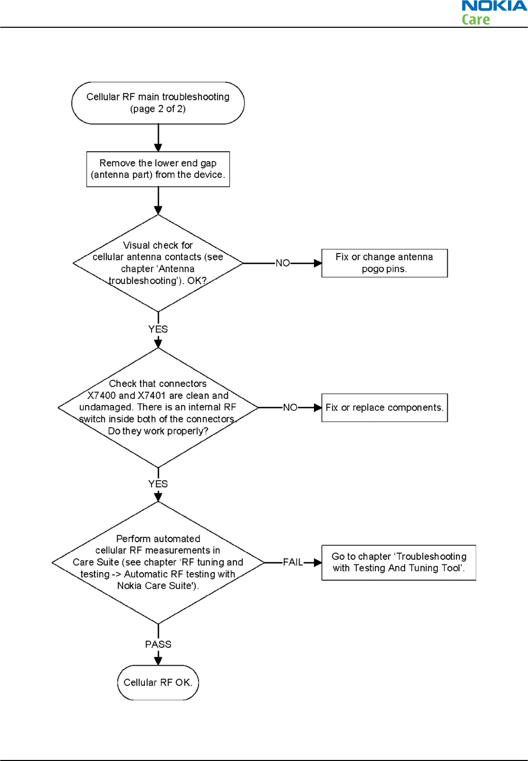
Troubleshooting flow — Page 2 of 2
RM-596
Cellular RF troubleshooting
Issue 2 COMPANY CONFIDENTIAL Page 4 – 9
Copyright © 2010 Nokia. All rights reserved.

Self test troubleshooting
Troubleshooting with RF Self tests
Context
ÄLLI (N7512) RF ASIC contains test structures that can be used to detect certain RF related errors. In order to
use these self tests the most efficient way, it is very important that the tests are performed in a certain order,
or at least that the error data is analyzed in this order. The tests are designed so that by going through them
in this order it is easy to find the problem component without any redundant checks. The flowcharts
presented in this document are based on that idea.
The testing order recommended and used in this troubleshooting guide is the following:
1 ST_CDSP_RF_BB_IF test (ID hex. 56)
•Tests the functionality of the BB/Linko serial interface & reset lines.
•If this test fails, it means that there is a problem in programming of the N7512 and all of the following
tests cannot give correct data.
2 ST_CDSP_RF_SUPPLY_TEST (ID hex. 53)
•Tests the functionality of N7512 bias block, regulators, reference voltage line and supply connections,
as well as almost all Aura (N7509) regulator voltages..
•If this test fails, all other N7512 tests can/will fail.
3 ST_CDSP_DIGI_RXTX_IF_TEST (ID hex. 7D)
•Test checks that the digital RX and TX lines between BB and N7512 are properly connected.
4 ST_CDSP_STROBE_TEST (ID hex. 7C)
•Tests the functionality of the RFStrobe signal..
5 ST_CDSP_PA_ID_PIN_TEST (ID hex. 7F)
•The purpose of this test is to identify the PAs of the different vendors.
•Tests also the functionality of the temperature sensor V7502.
6 ST_CDSP_TX_WCDMA_POWER_TEST (ID hex. 4B)
•Tests the basic functionality of the WCDMA transmitter.
To get the best out of these instructions you need to be have the valid schematics at hand.
RM-596
Cellular RF troubleshooting
Page 4 – 10 COMPANY CONFIDENTIAL Issue 2
Copyright © 2010 Nokia. All rights reserved.
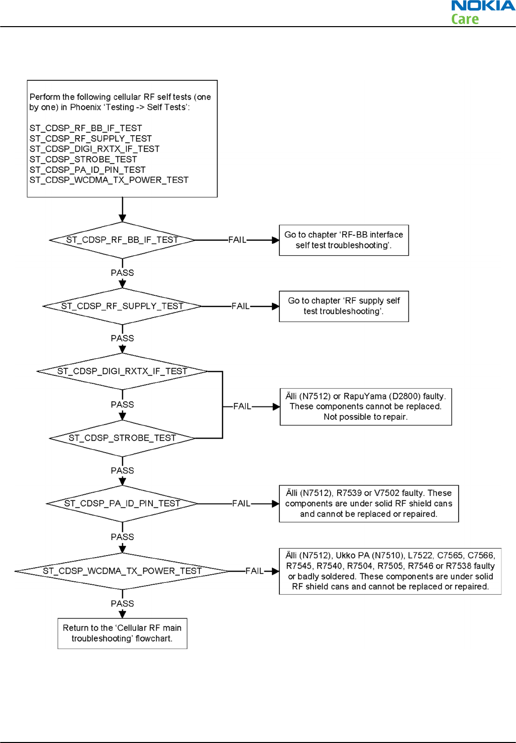
Troubleshooting flow
RM-596
Cellular RF troubleshooting
Issue 2 COMPANY CONFIDENTIAL Page 4 – 11
Copyright © 2010 Nokia. All rights reserved.
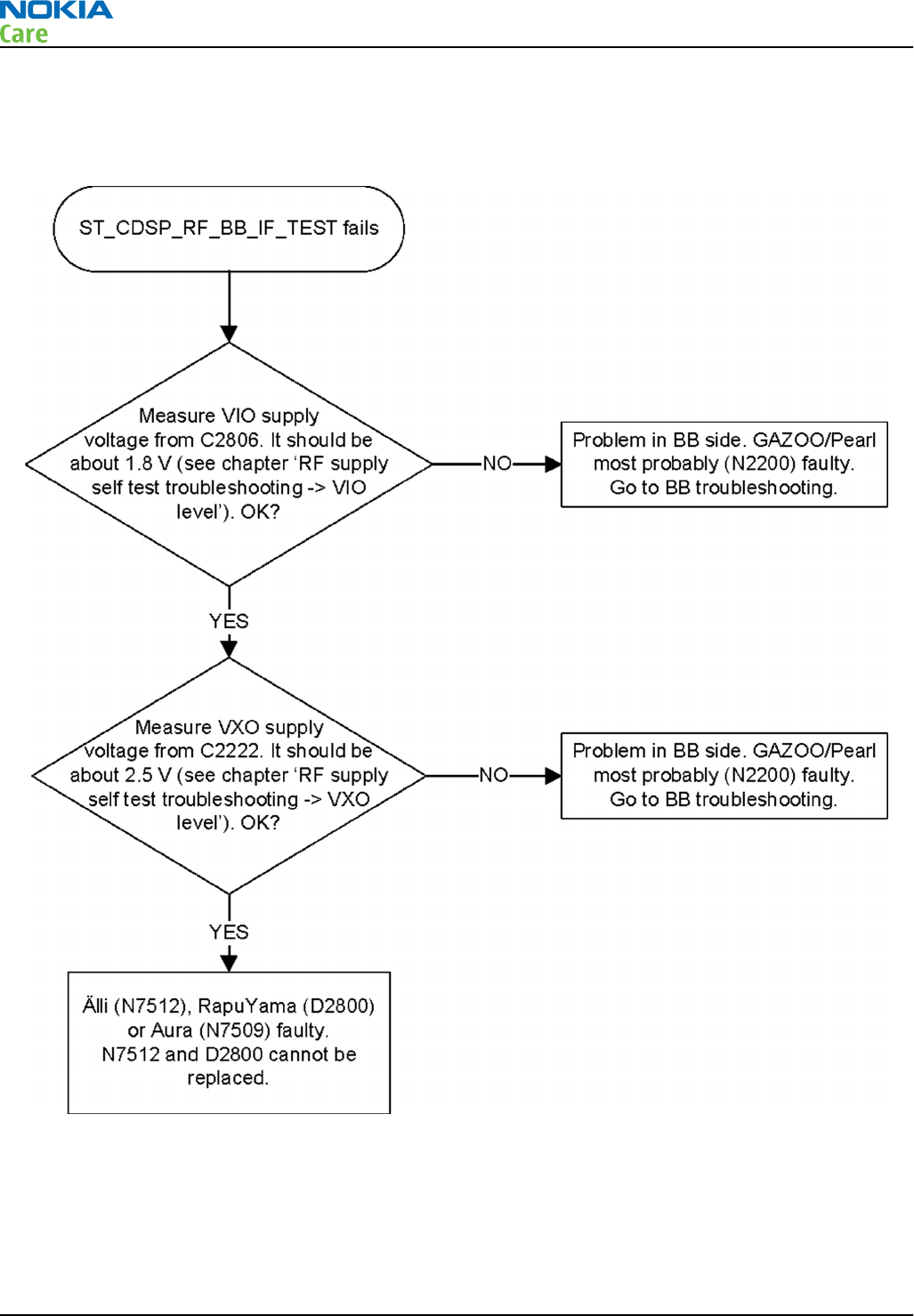
RF-BB interface self test troubleshooting
Troubleshooting flow
RM-596
Cellular RF troubleshooting
Page 4 – 12 COMPANY CONFIDENTIAL Issue 2
Copyright © 2010 Nokia. All rights reserved.
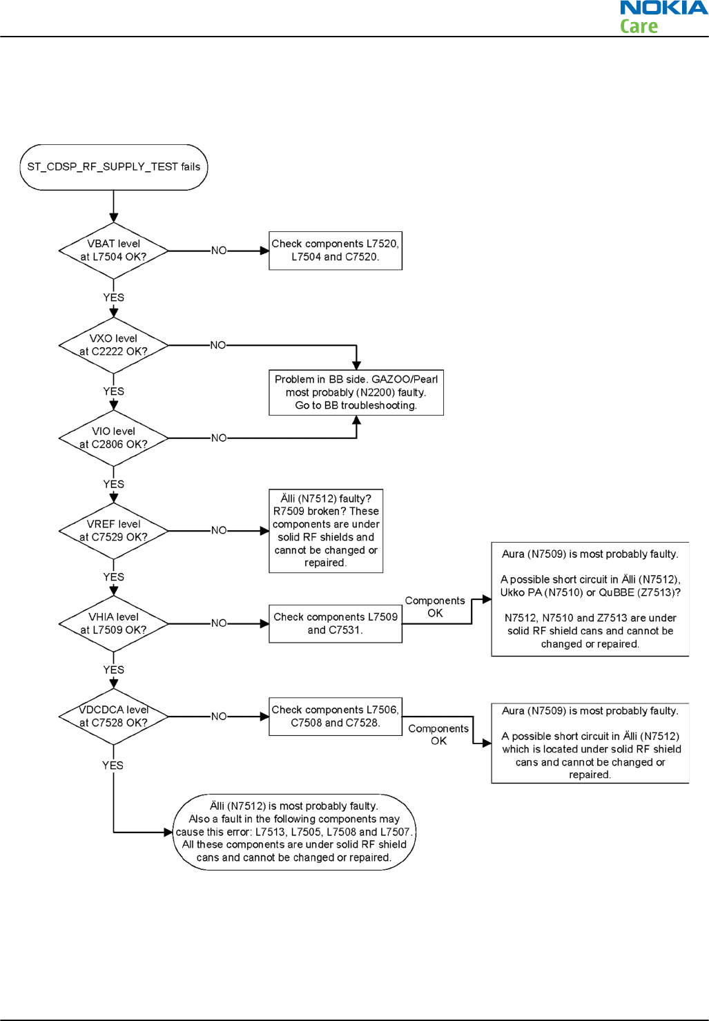
RF supply self test troubleshooting
Troubleshooting flow
RM-596
Cellular RF troubleshooting
Issue 2 COMPANY CONFIDENTIAL Page 4 – 13
Copyright © 2010 Nokia. All rights reserved.
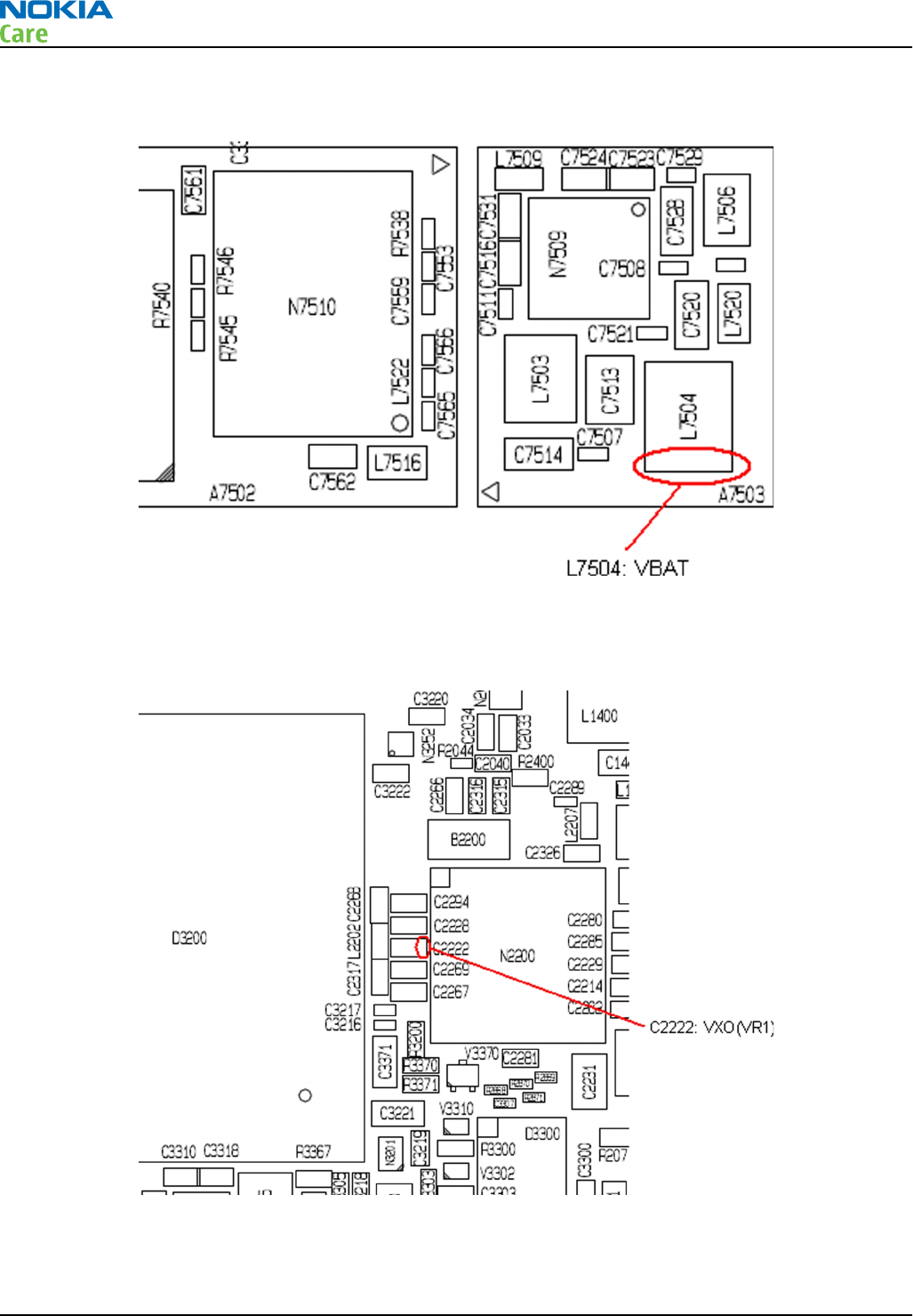
VBAT level
Check the VBAT level at the L7504. The level should be the same as the battery voltage and always on.
VXO level
Check the VXO level (2.5V) at C2222. The signal is always on when the phone is in local mode.
RM-596
Cellular RF troubleshooting
Page 4 – 14 COMPANY CONFIDENTIAL Issue 2
Copyright © 2010 Nokia. All rights reserved.
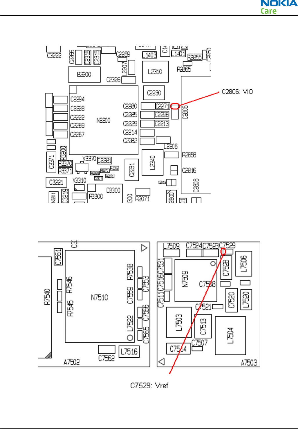
VIO level
Check the VIO level (1.8V) at C2806. The signal is always on when the phone is in local mode.
VREF level
Check the Vref level (1.2 V) at C7529.
RM-596
Cellular RF troubleshooting
Issue 2 COMPANY CONFIDENTIAL Page 4 – 15
Copyright © 2010 Nokia. All rights reserved.
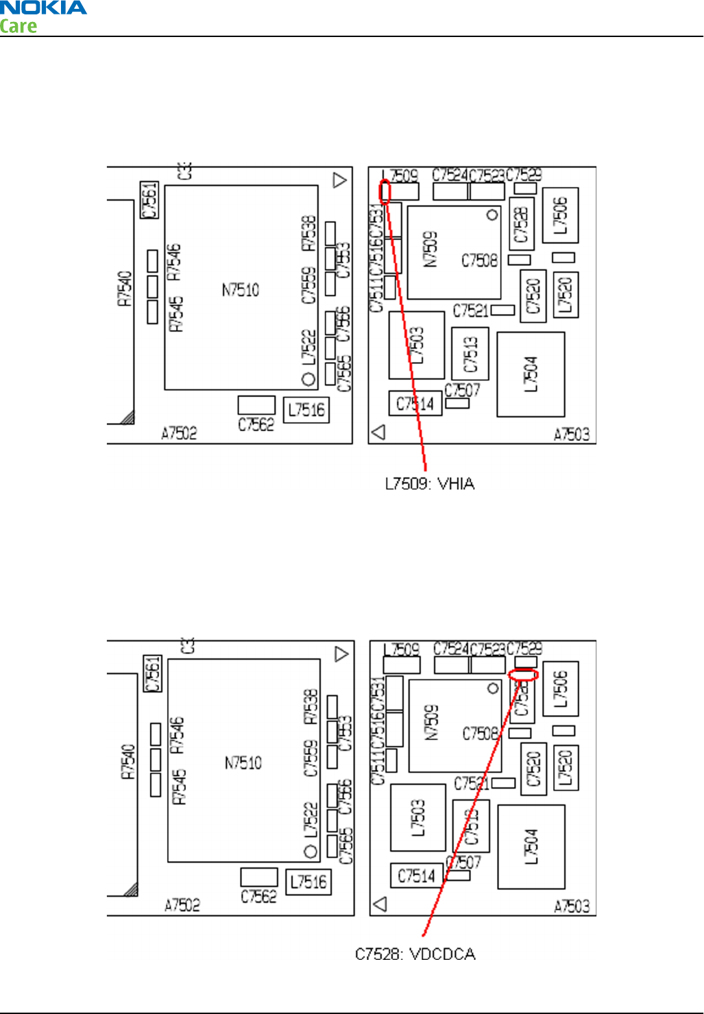
The GSM or WCDMA transmitter (or receiver) has to be activated before the Vref supply voltage can be
measured. Follow the instructions given in chapter 'Manual transmitter (TX) testing with Phoenix → GSM
transmitter activation' or 'WCDMA transmitter activation'.
VHIA (Vhi) level
Check the VHIA level (2.6 V) at L7509.
The GSM or WCDMA transmitter (or receiver) has to be activated before the VPA supply voltage can be
measured. Follow the instructions given in chapter 'Manual transmitter (TX) testing with Phoenix → GSM
transmitter activation' or 'WCDMA transmitter activation'.
VDCDCA (Vlow) level
Check the VDCDCA level (1.5 V) at C7528.
RM-596
Cellular RF troubleshooting
Page 4 – 16 COMPANY CONFIDENTIAL Issue 2
Copyright © 2010 Nokia. All rights reserved.

The WCDMA transmitter has to be activated before the VDCDCA supply voltage can be measured. Follow the
instructions given in chapter 'Manual transmitter (TX) testing with Phoenix → 'WCDMA transmitter activation'.
Note: The VDCDCA signal is continuously on when WCDMA TX is activated.
VPA level
The GSM or WCDMA transmitter has to be activated before the VPA supply voltage can be measured. Follow
the instructions given in chapter 'Manual transmitter (TX) testing with Phoenix → GSM transmitter activation'
or 'WCDMA transmitter activation'.
Check the VPA voltage level at C7514.
In WCDMA mode, the voltage levels should be:
•0.4…0.8 V @ Start level 0 dBm
•0.8…1.3 V @ Start level 10 dBm
•3.0…4.2 V @ Start level 24 dBm
In GSM mode, the voltage levels should be:
•0.1…0.5 V @ GSM 900 & Tx Power Level 19
•0.5…1.1 V @ GSM 900 & Tx Power Level 12
•3.5…4.3 V @ GSM 900 & Tx Power Level 5
Note: The VPA signal is continuously on when WCDMA TX is activated, but has a pulsed nature in
GSM TX mode (the signal is on only when a GSM TX burst is transmitted).
Note: The VPA signal is not tested by ST_CDSP_RF_SUPPLY_TEST.
RF tuning and testing
RF auto tuning and testing with Nokia Care Suite
Introduction to cellular RF tunings
RM-596 cellular RF engine has been tuned correctly in production. There is no reason to do re-calibration
unless one or more of the RF components are changed or memory (D3000) is corrupted.
RM-596
Cellular RF troubleshooting
Issue 2 COMPANY CONFIDENTIAL Page 4 – 17
Copyright © 2010 Nokia. All rights reserved.
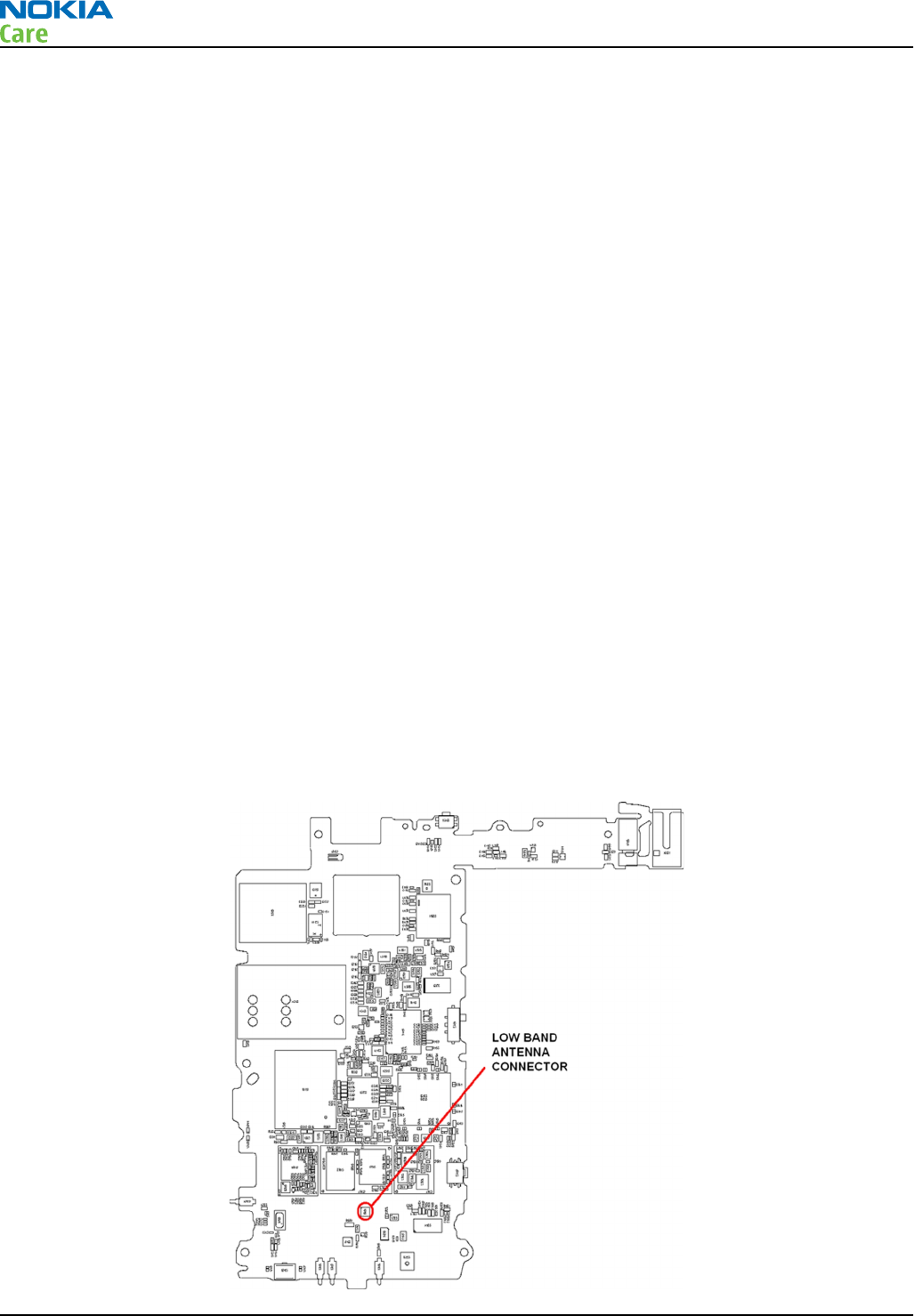
RM-596 can be tuned automatically. Auto tuning is designed to align the phone's RF part easily and faster. It
performs calibrations, tunings and measurements of RX and TX. The results are displayed and logged in a
result file, if initiated.
Note: Always perform RF tuning with the help of the module jig MJ-241, never with RF couplers.
Using an RF coupler in the tuning phase will cause a complete mistuning of the RF part.
Important: After RF component changes, always perform cellular RF auto tuning.
Cable and adapter losses
RF cables and adapters have some losses. They have to be taken into account when the phone is tuned. As
all the RF losses are frequency dependent, the user has to act very carefully and understand the measurement
setup. For RF attenuations of the CA-158RS RF cable, please refer to section 'Service Tools and Service
Concepts'.
Hardware set up
For hardware requirements for auto tuning, please refer to
RF testing and BB/RF tuning concept with module
jig
in section 'Service Tools and Service Concepts'.
Nokia Care Suite preparations
Install Testing And Tuning Tool add-on application to Nokia Care Suite. Automatic RF testing and tuning is
not possible without this application. There is no more support in Phoenix to auto tune RM-596 product.
Install the phone specific data package, for example
Nokia_firmware_RM-596_EUROPE_10.014_v41.0.exe
. This
defines phone specific settings.
RF auto tuning procedure
Note: If RF splitter is in use, skip steps 10, 11 and 12.
1 Make sure the phone (in the module jig) is connected to the PC.
2Connect the RF cable between the phone (low band antenna connector) and the communication tester.
If an RF splitter is in use, connect both low and high band antenna cables.
RM-596
Cellular RF troubleshooting
Page 4 – 18 COMPANY CONFIDENTIAL Issue 2
Copyright © 2010 Nokia. All rights reserved.
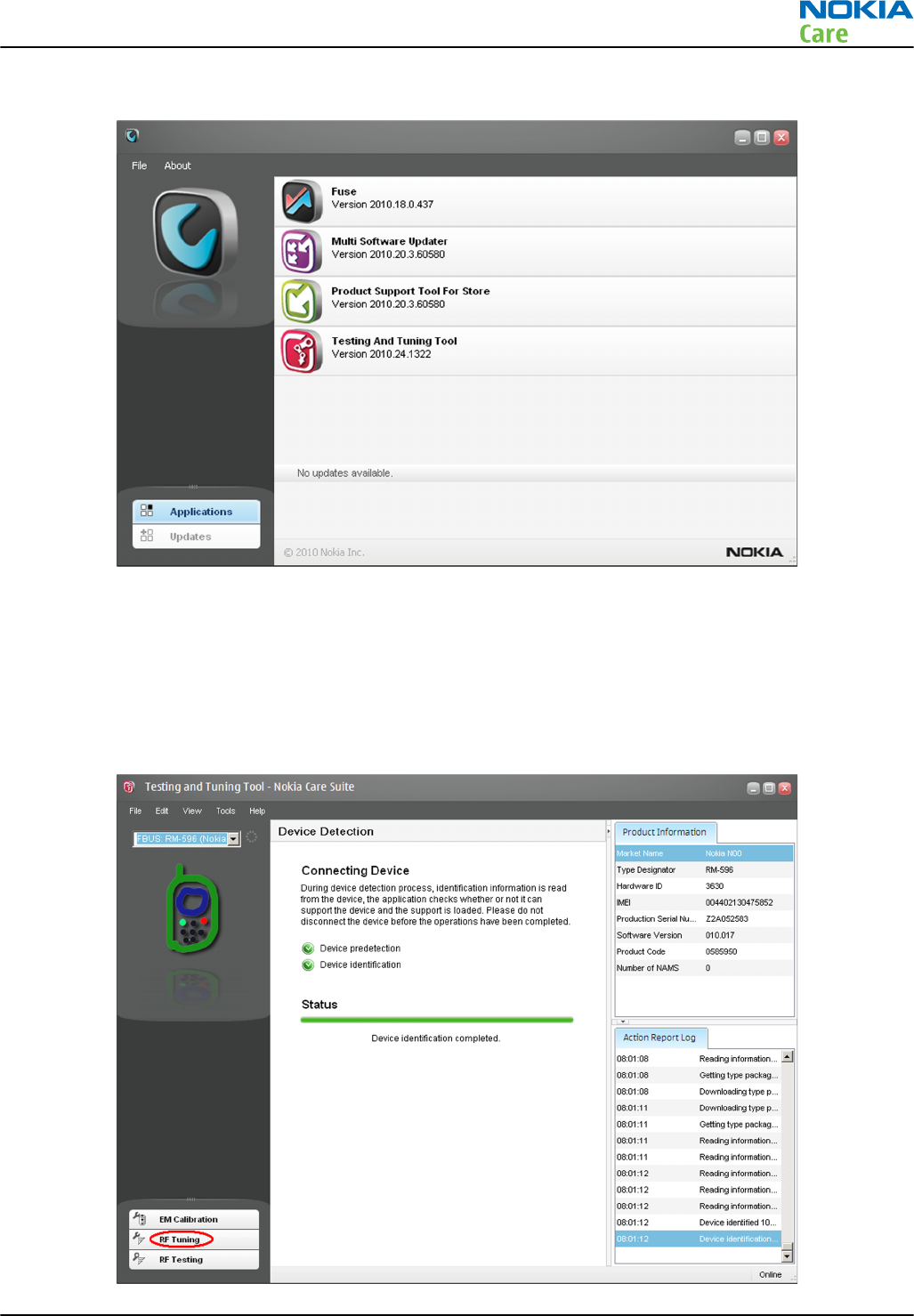
3 Start
Nokia Care Suite
application. The following window opens:
Note: The window appearance may differ depending on the
Nokia Care Suite
version.
Note:
Fuse, Multi Software Updater, Product Support Tool For Store
and
Testing And Tuning Tool
are Care Suite add-on applications. The list is different if there are different add-on applications
installed.
4 To open the application, double-click Testing And Tuning Tool icon.
5 If the application is able to find a connected phone, the following view will open:
RM-596
Cellular RF troubleshooting
Issue 2 COMPANY CONFIDENTIAL Page 4 – 19
Copyright © 2010 Nokia. All rights reserved.
Note: The window appearance may differ depending on the
Nokia Care Suite
and
Testing And Tuning
Tool
versions
6 Click on the RF Tuning button. The following view opens:
Note: The window appearance may differ depending on the
Nokia Care Suite
and
Testing And Tuning
Tool
versions
7 Select Cellular RF Tunings and Tests from the drop-down menu.
8 Select the RF cable used (and possible RF splitter / RF shield box) from the drop-down menu. CA-158RS
attenuation values are always taken automatically into account when RM-596 product is connected to
Nokia Care Suite
tool.
9 Click the Run button.
RM-596
Cellular RF troubleshooting
Page 4 – 20 COMPANY CONFIDENTIAL Issue 2
Copyright © 2010 Nokia. All rights reserved.
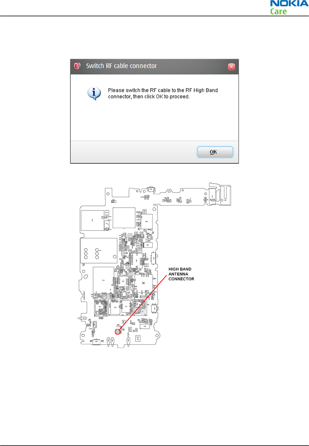
Note: The window appearance may differ depending on the
Nokia Care Suite
and
Testing And Tuning
Tool
versions
10 If no critical errors happen during the low band RF tuning procedure, the following window will pop up:
11 Change the CA-158RS cable to the high band RF connector on the phone PWB.
12 Click OK and RF tunings will automatically be performed for high cellular bands.
13 RF tunings will be ready when all the tunings and measurements are green in the tool window and no
errors occur.
14 If errors do happen, failed tuning/testing steps are marked with a red color and more detailed results
are shown on the screen. An example fail case is shown below:
RM-596
Cellular RF troubleshooting
Issue 2 COMPANY CONFIDENTIAL Page 4 – 21
Copyright © 2010 Nokia. All rights reserved.
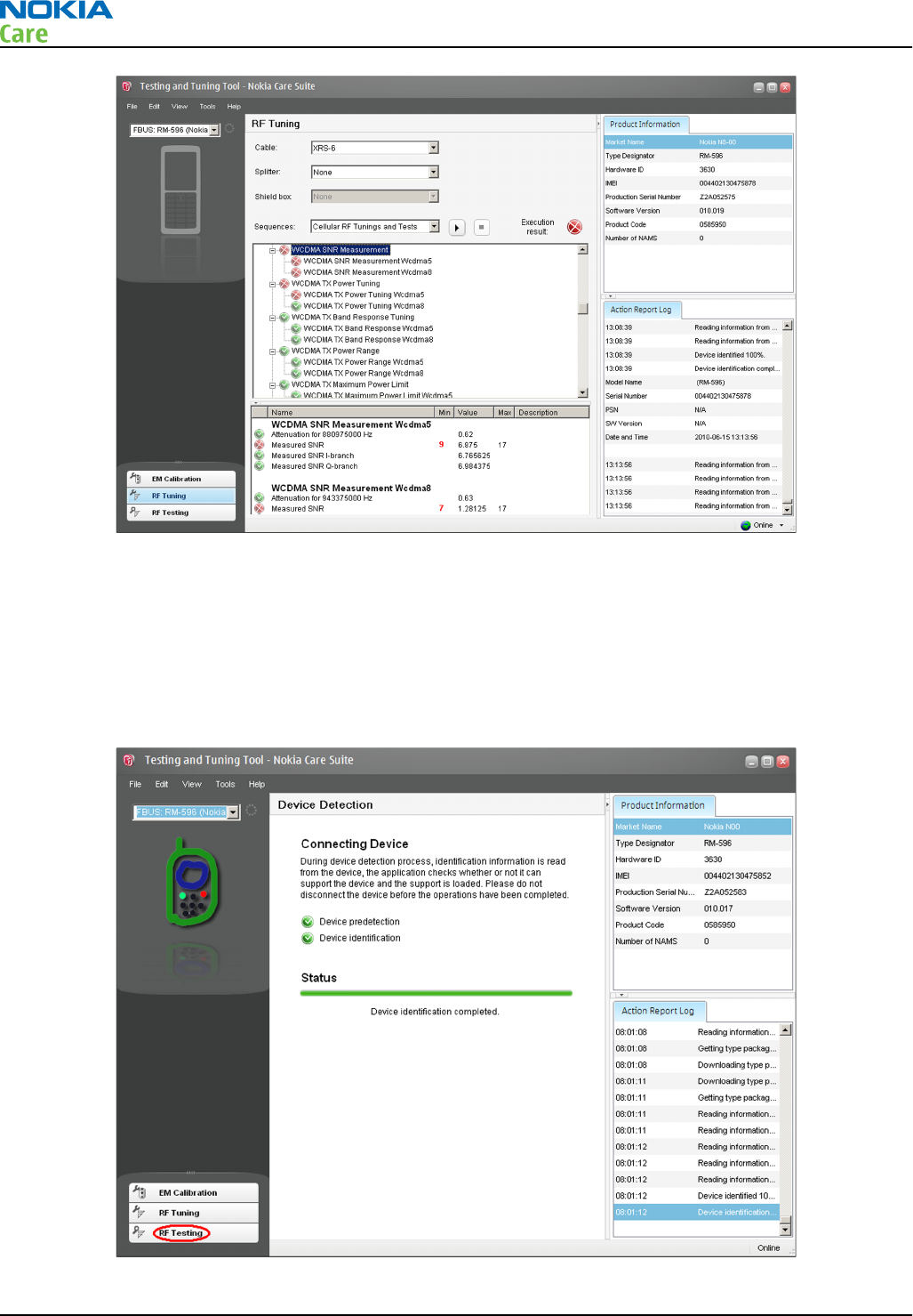
Note: The window appearance may differ depending on the
Nokia Care Suite
and
Testing And Tuning
Tool
versions
Automatic RF testing with Nokia Care Suite
Testing And Tuning Tool
add-on application can be used also for non-signalling RF tests. The automatic RF
testing procedure is the same as explained in the chapter
RF auto tuning procedure
, but RF Testing should
be selected in the
Testing And Tuning Tool
main window instead of RF Tuning .
RM-596
Cellular RF troubleshooting
Page 4 – 22 COMPANY CONFIDENTIAL Issue 2
Copyright © 2010 Nokia. All rights reserved.
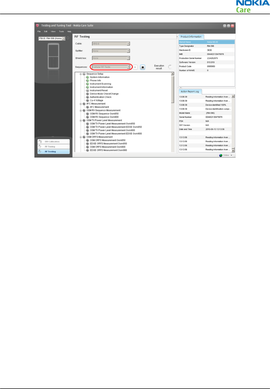
Note: The window appearance may differ depending on the
Nokia Care Suite
and
Testing And Tuning
Tool
versions.
RF Testing selection does all the same measurements as RF Tuning , but does not perform any tunings.
RF Testing
is a safe way to check the basic cellular RF performance of the phone. The following test cases will
be performed (the complete set of measurements may differ depending on the data package content):
•GSM SNR
•GSM RSSI
•GSM / EDGE TX Power Level
•GSM Modulation & Switching spectrum
•GSM EDGE EVM
•GSM Burst Template
•GSM Phase Error
•WCDMA RSSI
•WCDMA SNR
•WCDMA TX Power Range
•WCDMA TX Max Output Power
•WCDMA ACP
•WCDMA EVM
Troubleshooting with Testing And Tuning Tool
Context
If limit fails occur while RF tests are performed with Testing And Tuning Tool, the user has to be very careful
to understand the measurement results. Fails may occur because of many reasons:
1 RF attenuation between the phone and the communication tester is something else as expected by the
Testing And Tuning Tool
. Please check that cable, splitter and shield box selections are correct in the
Testing And Tuning Tool
main window.
RM-596
Cellular RF troubleshooting
Issue 2 COMPANY CONFIDENTIAL Page 4 – 23
Copyright © 2010 Nokia. All rights reserved.
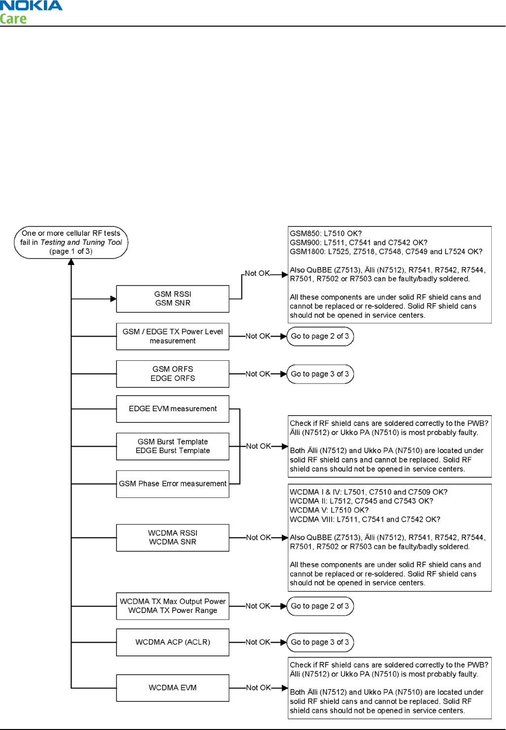
2 Test limits (specified in the product specific data package) are quite tight. Small limit violations do not
always mean that the tested product is broken, but the RF performance may not be as good as it should
be.
3 RX measurements (RSSI, SNR) may fail because of strong signals from base stations nearby. It is
recommended to always perform RF measurements in an RF-shielded environment (in an RF-shield box
or room).
4 The phone is really broken and needs more specific troubleshooting. Typical for these cases is that
RF
Testing
gives measurement results which are far from the test limits.
Note: Start the more specific troubleshooting always from the chapter Cellular RF main
troubleshooting (page 4–7 ) . The troubleshooting flow below may be misleading if followed
without upper level instructions.
Troubleshooting flow — Page 1 of 3
RM-596
Cellular RF troubleshooting
Page 4 – 24 COMPANY CONFIDENTIAL Issue 2
Copyright © 2010 Nokia. All rights reserved.
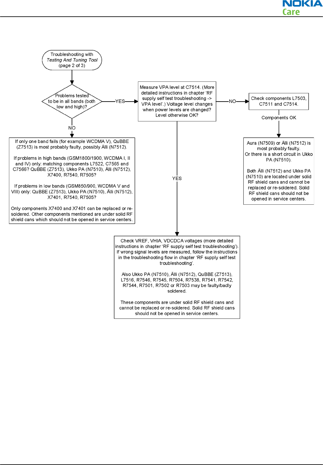
Troubleshooting flow — Page 2 of 3
RM-596
Cellular RF troubleshooting
Issue 2 COMPANY CONFIDENTIAL Page 4 – 25
Copyright © 2010 Nokia. All rights reserved.
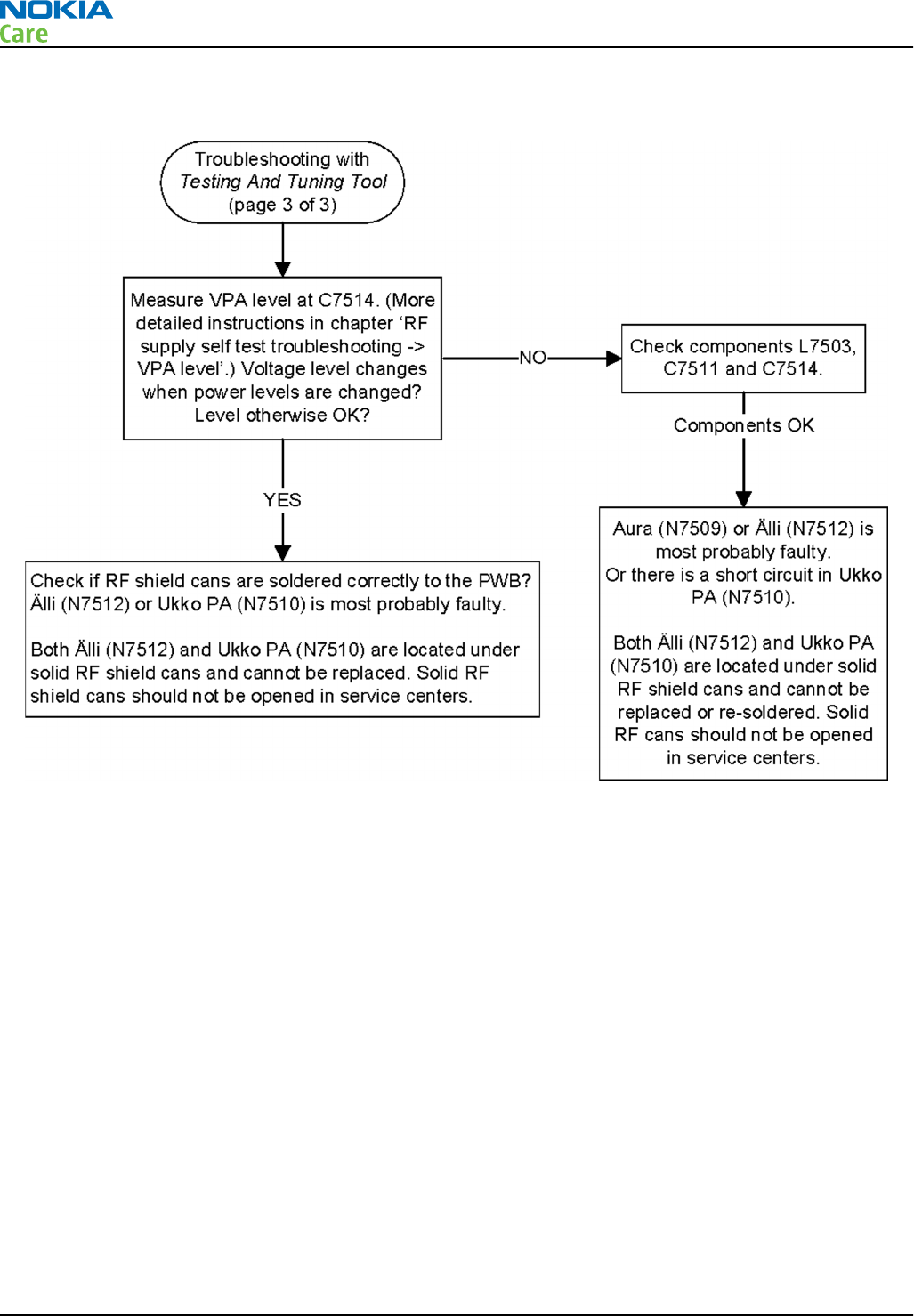
Troubleshooting flow — Page 3 of 3
Manual transmitter (TX) testing with Phoenix
General instructions for transmitter (TX) activation
Please note the following before performing transmitter tests:
•TX troubleshooting requires TX operation
•Do not transmit on frequencies that are in use
•The transmitter can be controlled in local mode for diagnostic purposes
•The most useful Phoenix tool for GSM transmitter testing is “RF Controls”, in WCDMA transmitter testing
the best tool is “TX Control”
Note: Never activate the GSM or WCDMA transmitter without a proper antenna load. Always connect
a 50 Ω load to the RF connector (antenna, RF measurement equipment or at least a 2 W dummy
load), otherwise the power amplifier (PA) may be damaged.
GSM transmitter activation
Steps
1. Set the phone to local mode.
2. Activate the RF controls tool in Phoenix ( Testing → GSM → RF Controls ).
RM-596
Cellular RF troubleshooting
Page 4 – 26 COMPANY CONFIDENTIAL Issue 2
Copyright © 2010 Nokia. All rights reserved.
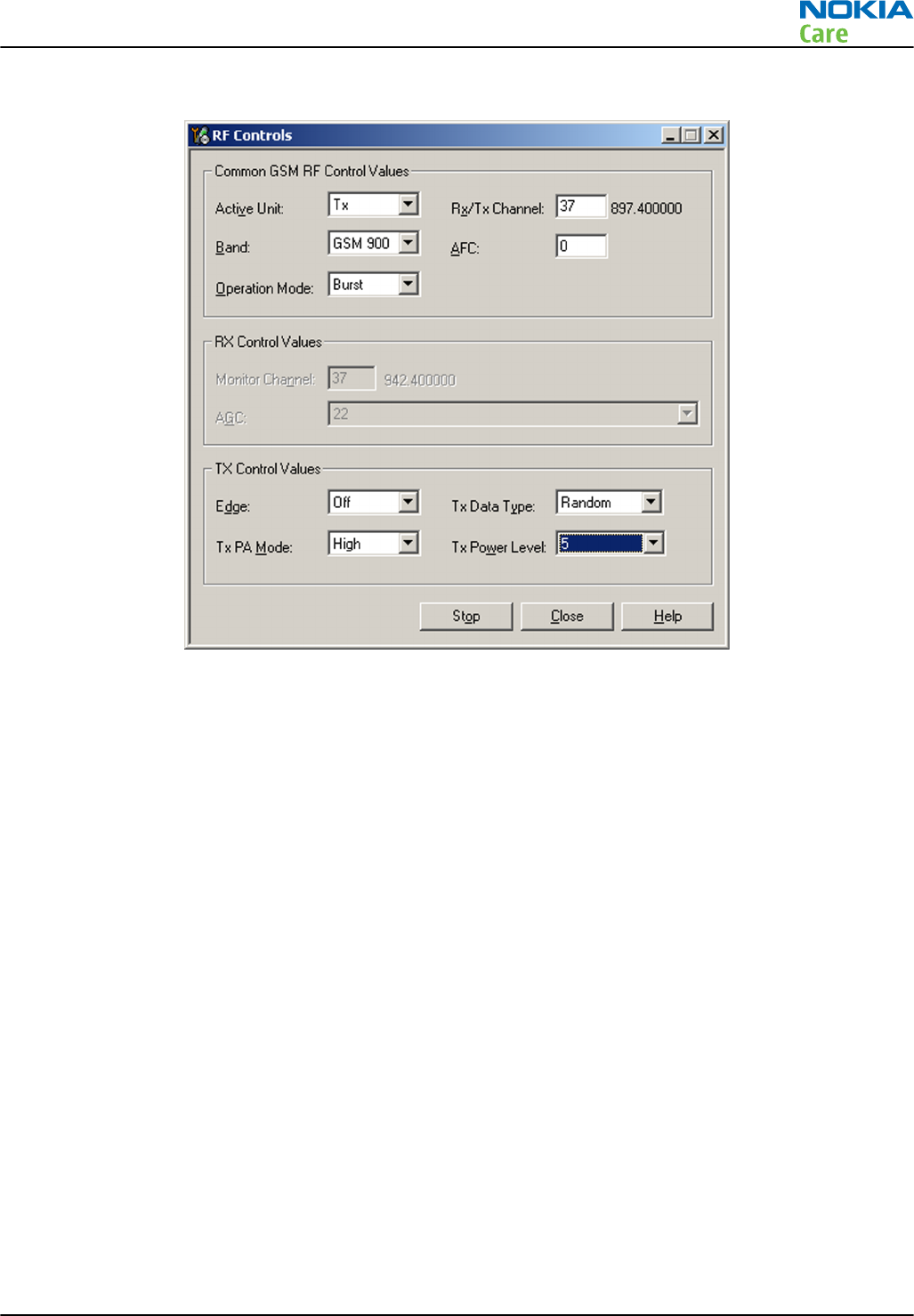
3. Make settings as shown in the figure:
4. GSM transmitter is activated when Active Unit is set to “Tx”. Aura (N7509) supply voltages are on for
measurement purposes after this step is completed.
5.
Optional step (not needed if GSM TX activation only required):
Check the basic TX parameters (i.e. power,
phase error, modulation and switching spectrum) manually, using a communication analyzer (for example
CMU–200). Change power level (in “RF Controls” tool) and make sure the power reading follows
accordingly.
RM-596
Cellular RF troubleshooting
Issue 2 COMPANY CONFIDENTIAL Page 4 – 27
Copyright © 2010 Nokia. All rights reserved.
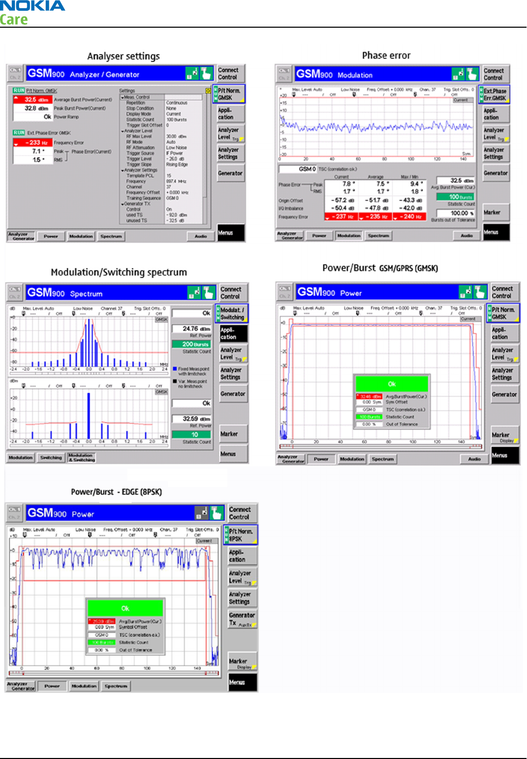
RM-596
Cellular RF troubleshooting
Page 4 – 28 COMPANY CONFIDENTIAL Issue 2
Copyright © 2010 Nokia. All rights reserved.
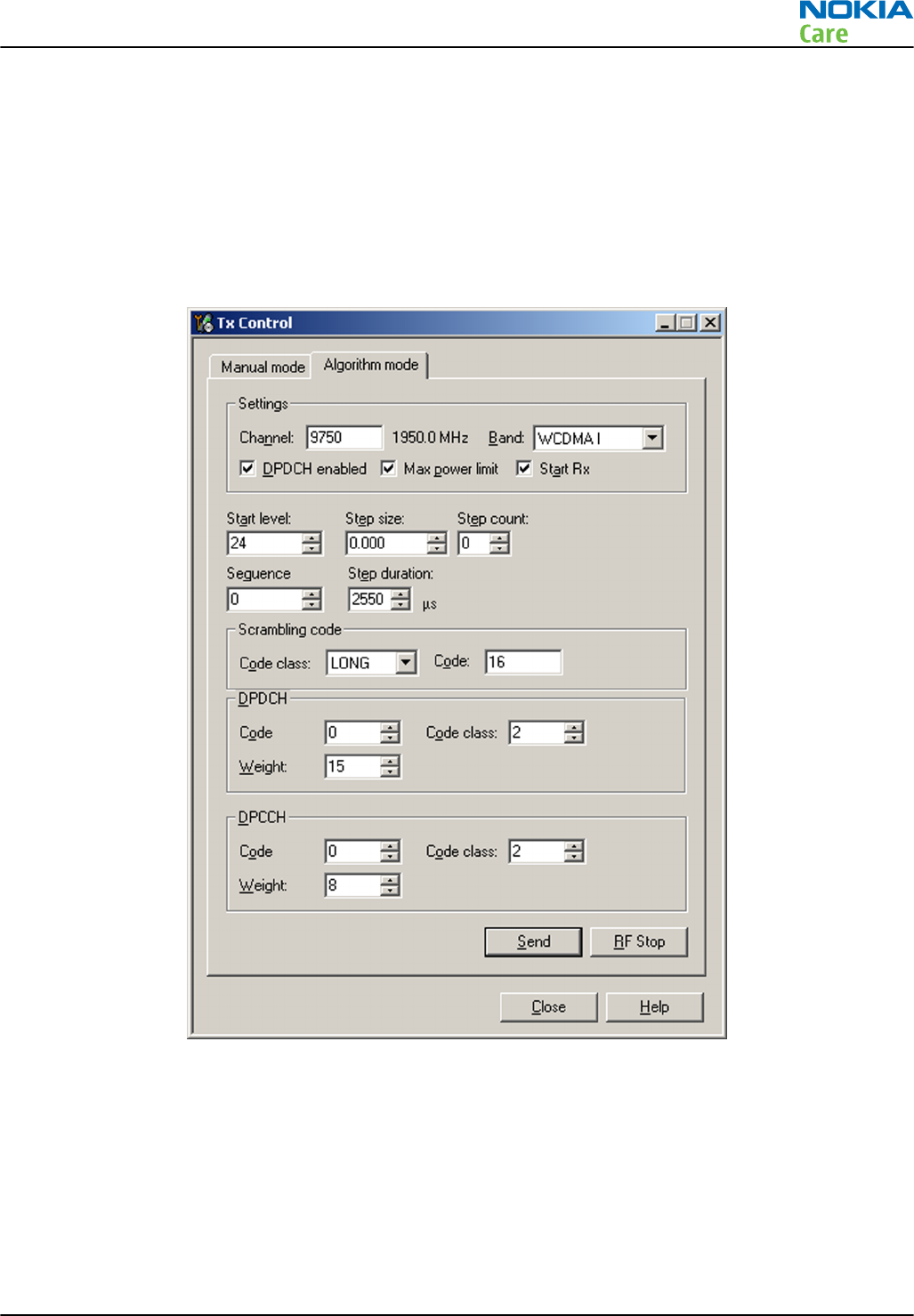
WCDMA transmitter activation
Steps
1. Set the phone to local mode.
2. In Phoenix, select Testing → WCDMA → TX Control .
3. Select Algorithm mode tab.
4. In the TX Control window, make settings as in the figure:
5. Click Send to enable the settings and activate TX. If settings are changed (e.g. new channel or power level),
you have to click RF Stop and Send again. Aura (N7509) supply voltages are on for measurement purposes
after this step is completed.
6.
Optional step (not needed if WCDMA TX activation only required):
Check the basic TX parameters using a
communication analyzer (for example CMU–200).
Note: RM-596 WCDMA TX power classes: WCDMA I, IV, V and VIII class 3 (maximum output power
+24 dBm), WCDMA II class 4 (maximum output power +21 dBm).
RM-596
Cellular RF troubleshooting
Issue 2 COMPANY CONFIDENTIAL Page 4 – 29
Copyright © 2010 Nokia. All rights reserved.
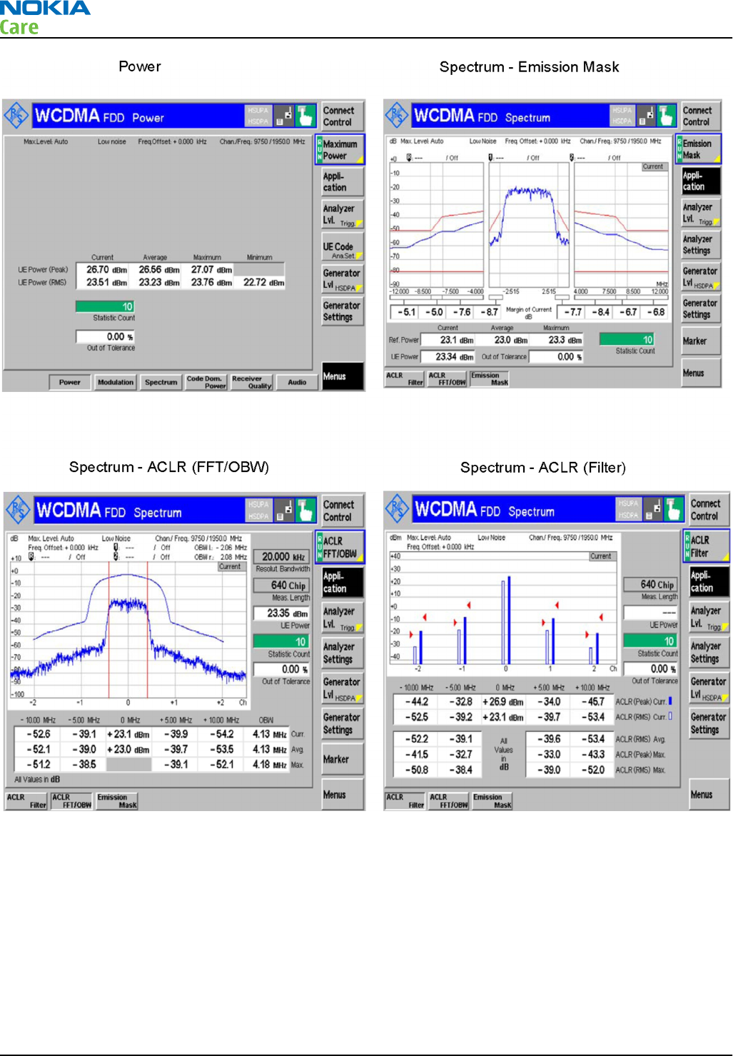
Manual receiver (RX) testing with Phoenix
General instructions for manual receiver testing
RX can be tested manually by making a phone call or in local mode. For the local mode testing, use Phoenix
service software.
The most important RX measurement in local mode is RSSI reading. This test measures the signal strength
of the received signal. For GSM RSSI measurements, see chapter
GSM RX chain activation for manual
measurements/GSM RSSI measurement
. For a similar test in WCDMA mode, see chapter
WCDMA RSSI
measurement
.
RM-596
Cellular RF troubleshooting
Page 4 – 30 COMPANY CONFIDENTIAL Issue 2
Copyright © 2010 Nokia. All rights reserved.
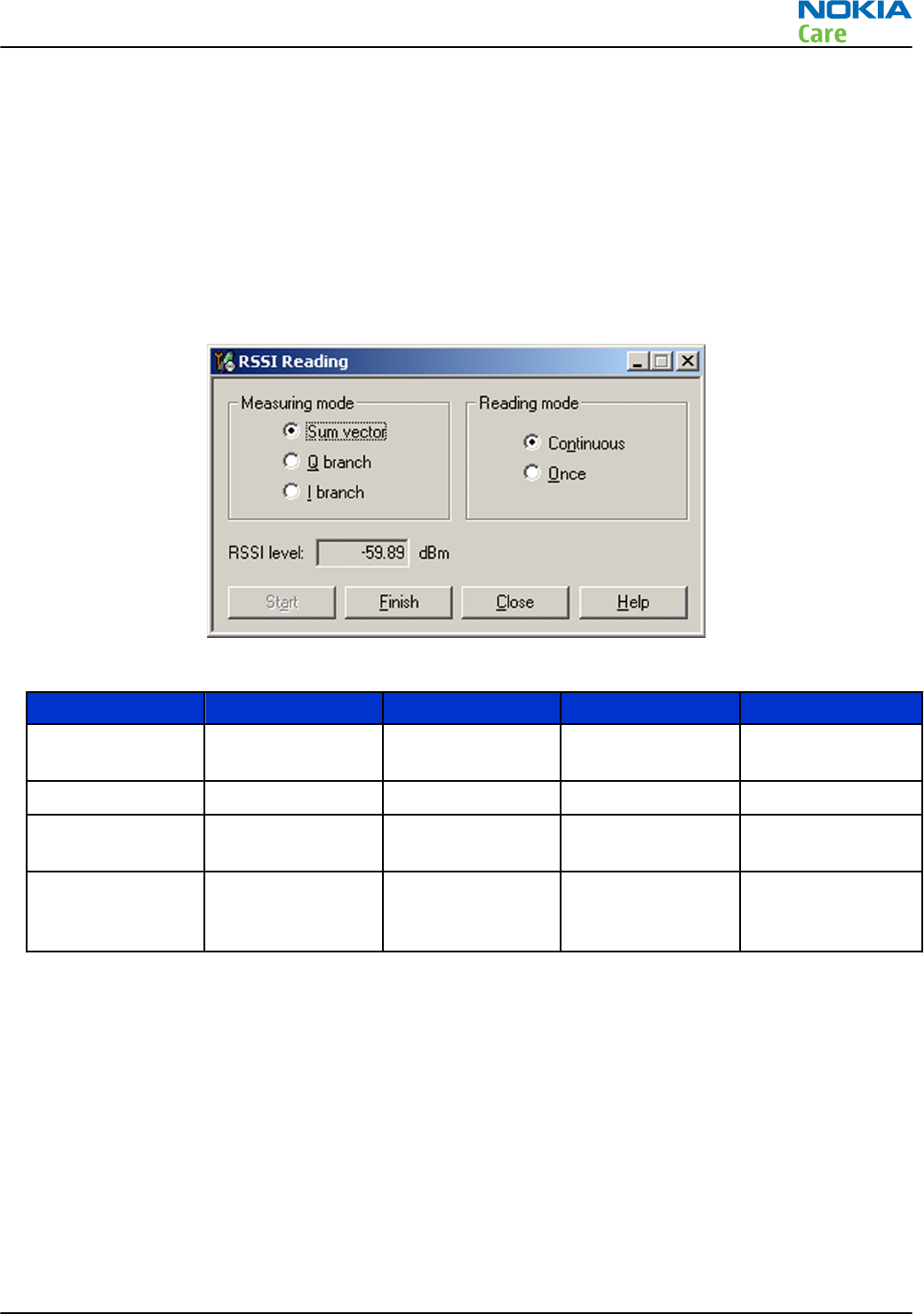
GSM RX chain activation for manual measurements/GSM RSSI measurement
Prerequisites
Connect a signal generator to a proper RF connector on the phone PWB (note: there are two antenna
connectors for cellular RF on the phone PWB, one for low bands and one for high bands).
Steps
1. Set the phone to local mode.
2. Activate GSM RSSI reading in Phoenix ( Testing → GSM → RSSI Reading )
3. Use the following frequrencies and RF levels in RF generator for different GSM bands:
Setting GSM850 GSM900 GSM1800 GSM1900
Phoenix:
Monitor
Channel
190 37 700 661
RF frequency 881.6 MHz 942.4 MHz 1842.8 MHz 1960.0 MHz
Signal generator
frequency
881.66771 MHz 942.46771 MHz 1842.86771 MHz 1960.06771 MHz
Signal generator
RF level (CW
signal)
-60dBm -60dBm -60dBm -60dBm
Results
The
RSSI level
reading should reflect the level of the signal generator (- losses) +/- 5 dB.
When varying the level in the range of -30 to -102 dBm, the reading should follow within +/-5 dB.
WCDMA RX chain activation for manual measurement
Steps
1. Set the phone to local mode.
2. Activate
RX Control
tool in Phoenix (Testing —> WCDMA —> RX Control) .
3. In the RX Control window, make the following settings:
RM-596
Cellular RF troubleshooting
Issue 2 COMPANY CONFIDENTIAL Page 4 – 31
Copyright © 2010 Nokia. All rights reserved.
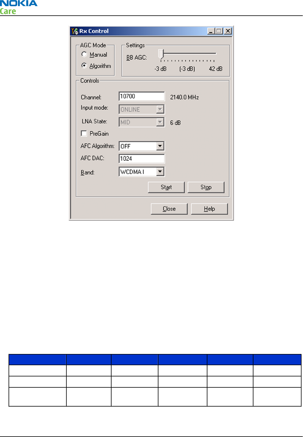
4. Click Start to activate the WCDMA RX. If the settings are changed later on (for example, change of channel)
you have to click Stop and Start again.
Note: Channels for testing: WCDMA I 10700, II 9800, IV 1637, V 4408, VIII 3012.
Note: Clicking Stop also disables TX control if it was active.
WCDMA RSSI measurement
Prerequisites
WCDMA RX must be activated before RSSI can be measured. For instructions, please refer to chapter
WCDMA
RX chain activation for manual measurement
. Connect a signal generator to a proper RF connector on the
phone PWB (note: there are two antenna connectors for cellular RF on the phone PWB, one for low bands
and one for high bands).
Steps
1. Use the following frequencies and RF levels in RF generator for different WCDMA bands:
Setting WCDMA I WCDMA II WCDMA IV WCDMA V WCDMA VIII
Phoenix:
Channel
10700 9800 1637 4408 3012
RX frequency 2140.0 MHz 1960.0 MHz 2132.4 MHz 881.6 MHz 942.4 MHz
Signal generator
frequency
2141.0 MHz 1961.0 MHz 2133.4 MHz 882.6 MHz 943.4 MHz
RM-596
Cellular RF troubleshooting
Page 4 – 32 COMPANY CONFIDENTIAL Issue 2
Copyright © 2010 Nokia. All rights reserved.
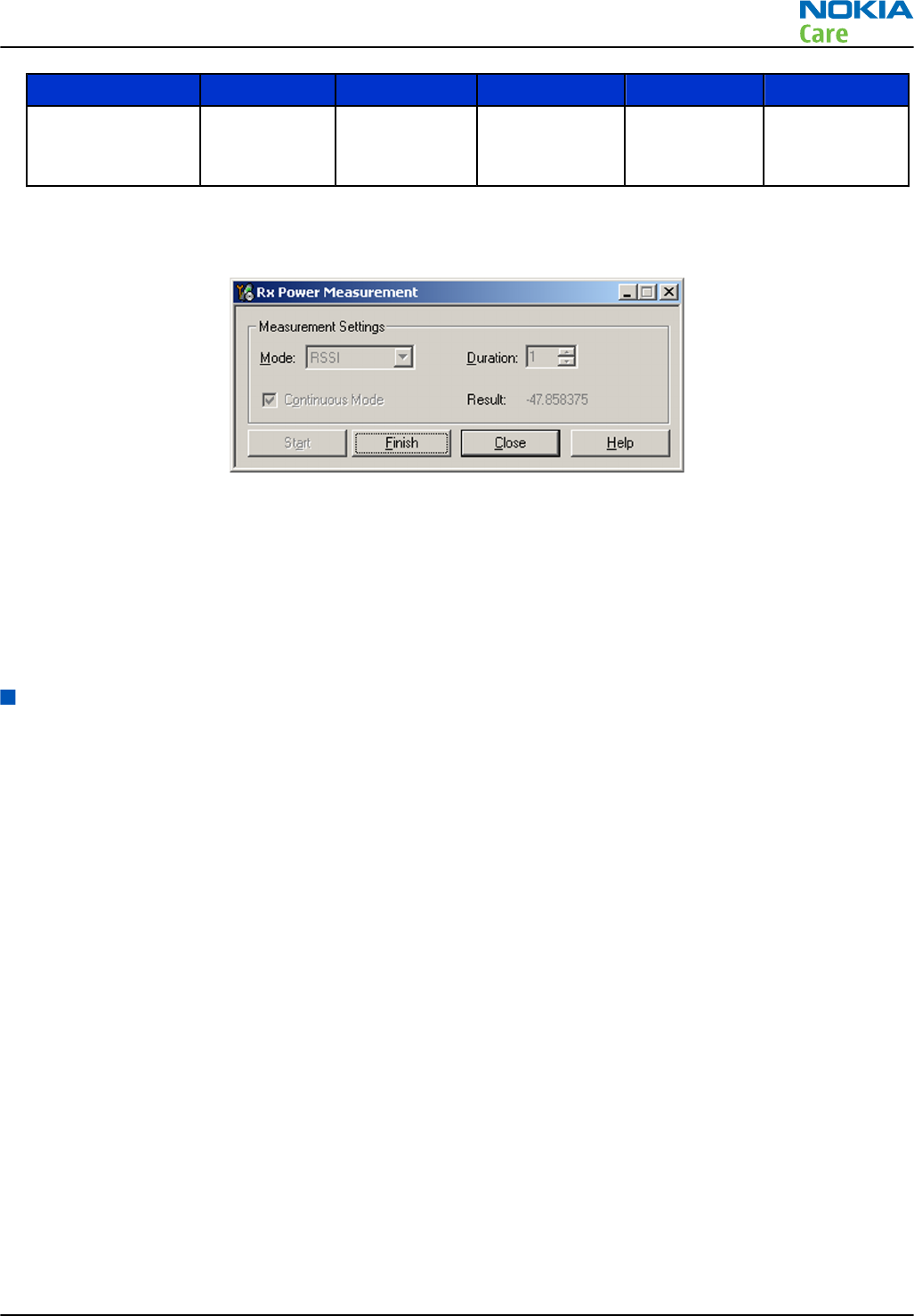
Setting WCDMA I WCDMA II WCDMA IV WCDMA V WCDMA VIII
Signal generator
RF level (CW
signal)
-48 dBm -48 dBm -48 dBm -48 dBm -48 dBm
2. Activate WCDMA RSSI reading in Phoenix (Testing —> WCDMA —> Rx Power Measurement) .
3. In the Rx Power Measurement window, make the following settings:
4. Click Start to perform the measurement.
Results
The
Result
reading should reflect the level of the signal generator (- losses) +/- 5 dB.
When varying the level in the range of -40 to -100 dB, the reading should follow within +/- 5 dB.
Note: In some versions of the Phoenix service tool, the
WCDMA Rx Power Measurement
tool does
not work as it should. In these cases, the result is something really small (for example -8387684.9).
Antenna
Antenna overview
RM–596 has three internal antennas:
•The main antenna which is integrated to the lower end gap of the phone
•GPS/WLAN/Bluetooth antenna below the upper end gap of the phone
•FM TX antenna which is integrated to the decoration part surrounding the main camera
The main antenna covers GSM and WCDMA bands and has separate antenna feeds for low and high bands.
Connection from the phone PWB to the antenna flex is implemented by pogo pins (3pcs). The main antenna
consists of an antenna flex which is integrated between two plastic parts in the lower end gap of the phone.
RM-596
Cellular RF troubleshooting
Issue 2 COMPANY CONFIDENTIAL Page 4 – 33
Copyright © 2010 Nokia. All rights reserved.
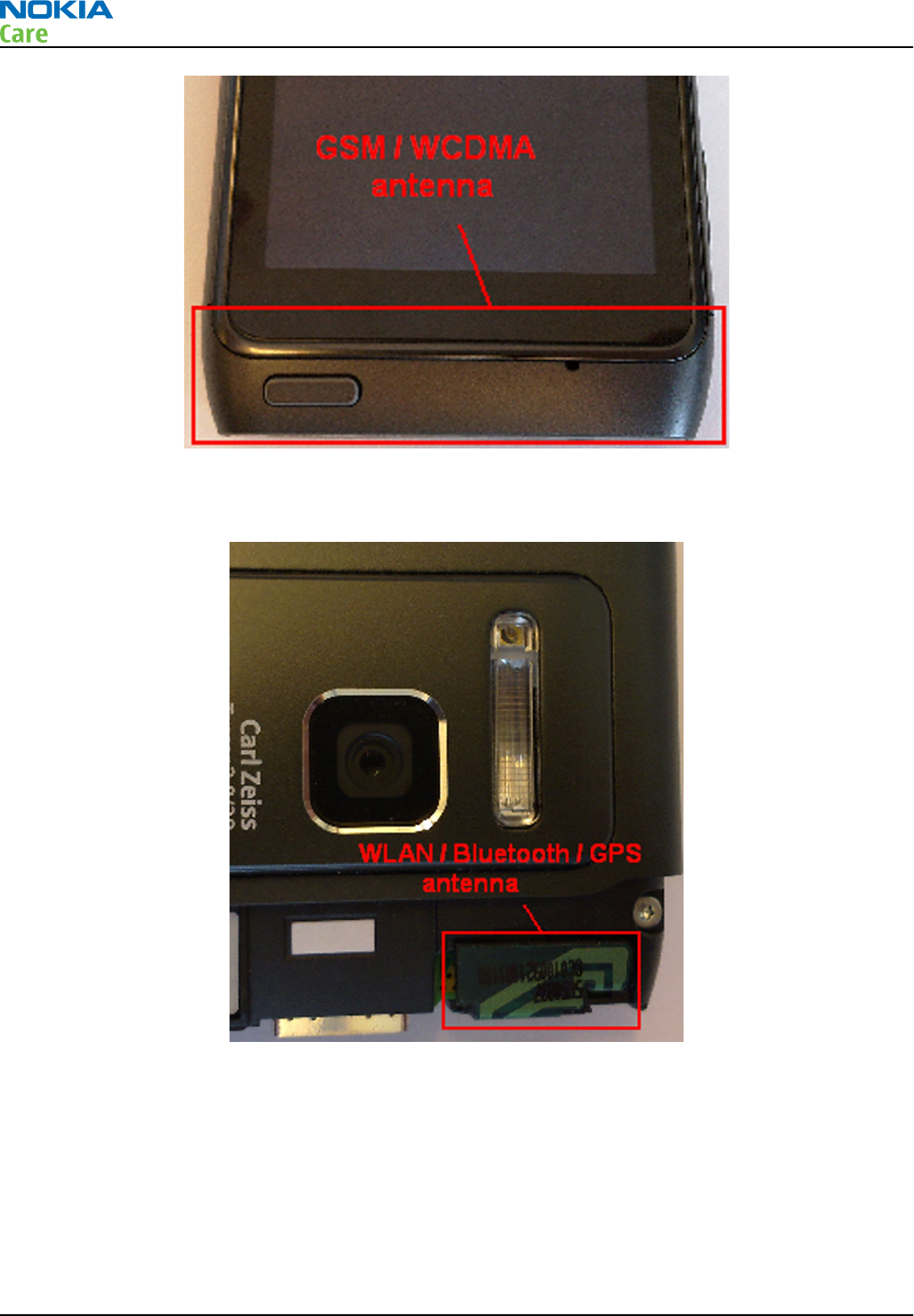
GPS, BT and WLAN RF interfaces are connected to one common antenna. RF feed from the phone PWB to the
antenna is made by one spring clip.
The FM TX antenna is a metallic decoration part at the top of the camera bumb. RF feed from the PWB is
implemented by a spring contact and a GND connection to the PWB by a pogo pin.
RM-596
Cellular RF troubleshooting
Page 4 – 34 COMPANY CONFIDENTIAL Issue 2
Copyright © 2010 Nokia. All rights reserved.
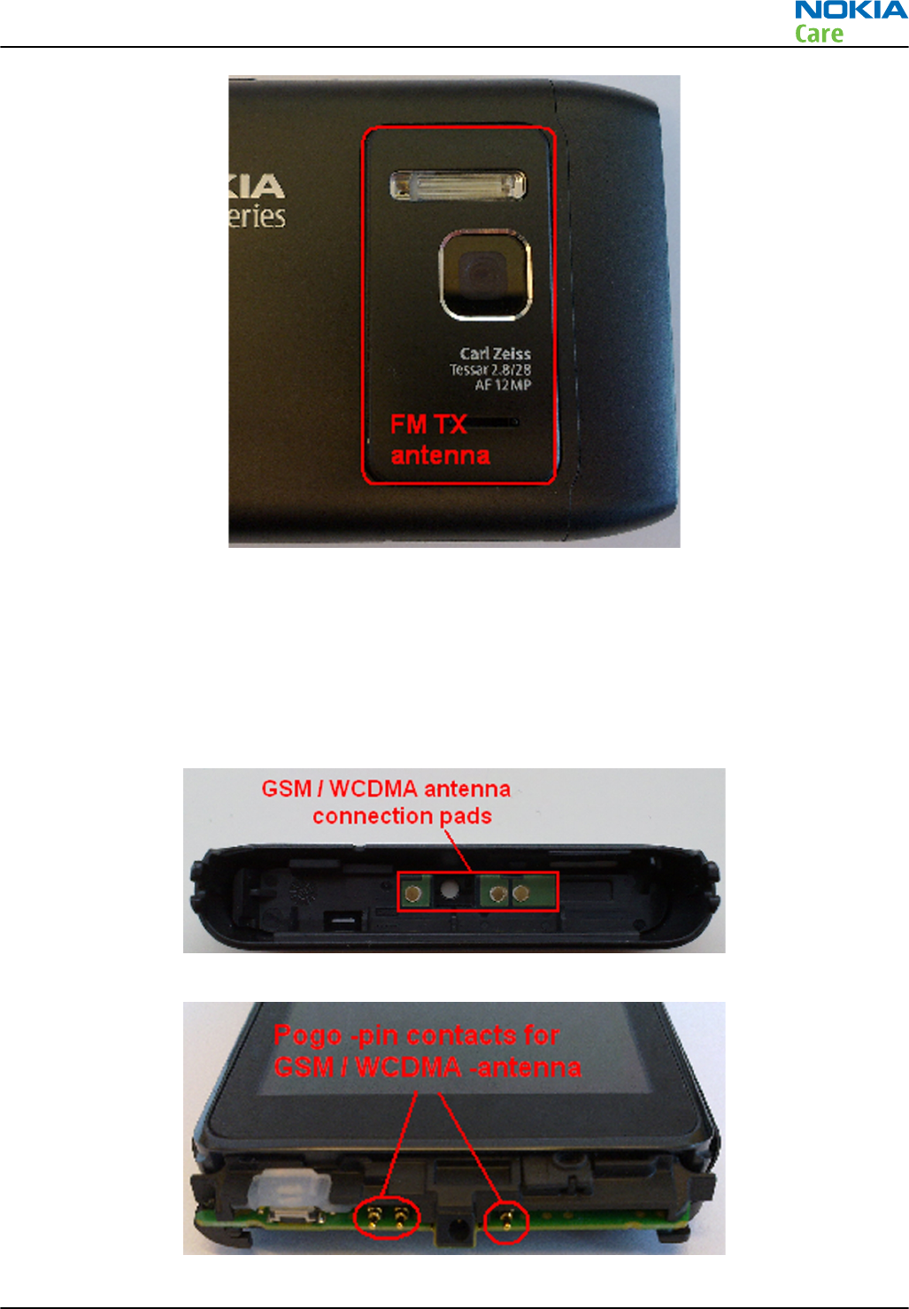
Antenna troubleshooting
Cellular antenna
The main antenna is functioning normally when the feed and GND pads take proper contact to the pogo pins
on the phone PWB, and the antenna part is visually intact.
The main antenna has three connection pads. Check that these pads have a proper contact to the pogo pins
on the phone PWB. Check also that all three pogo pins exist and work properly.
Figure 23 GSM/WCDMA antenna connection pads
Figure 24 Pogo pins for GSM/WCDMA antenna
RM-596
Cellular RF troubleshooting
Issue 2 COMPANY CONFIDENTIAL Page 4 – 35
Copyright © 2010 Nokia. All rights reserved.
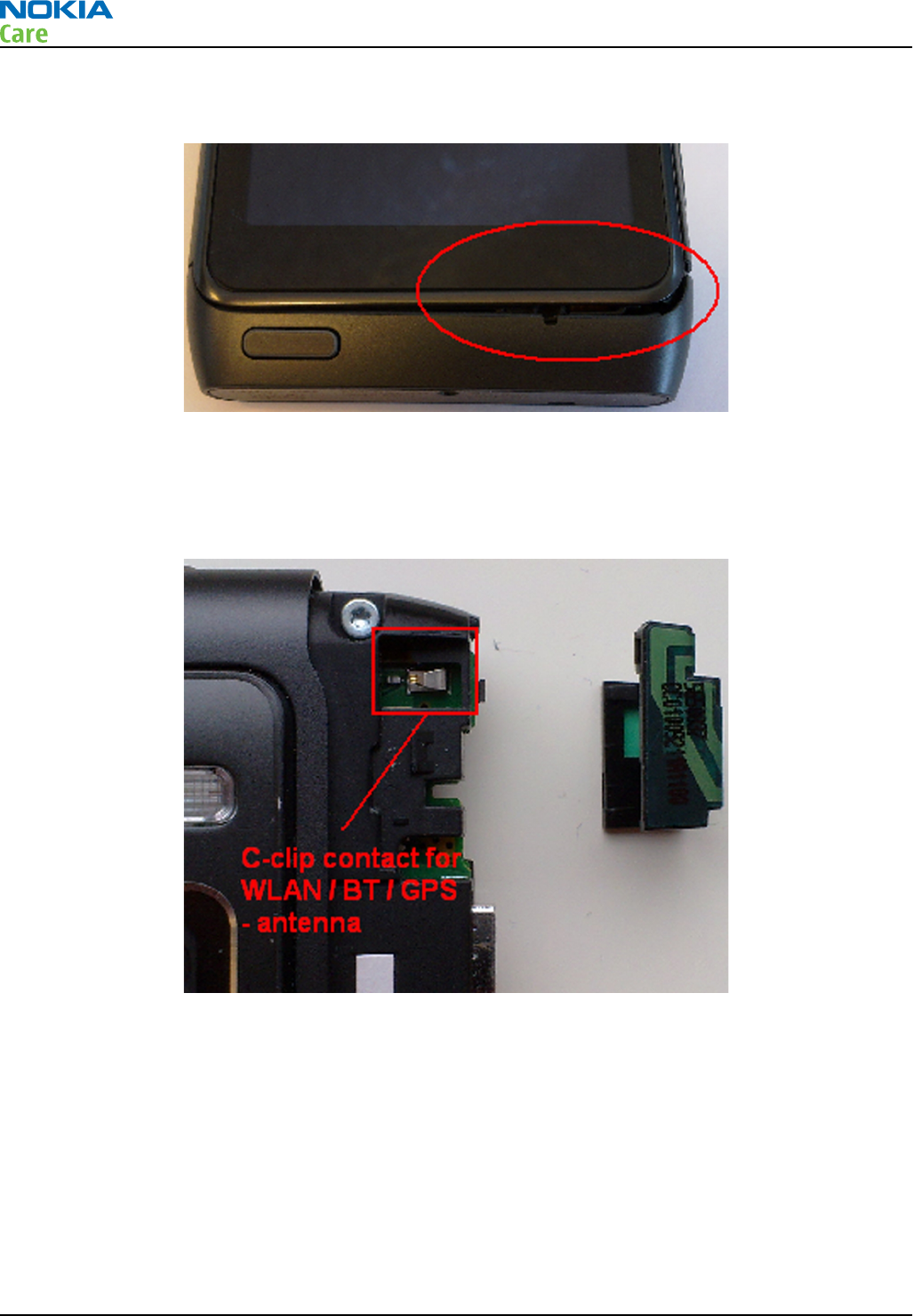
A typical fail situation is shown in the picture below. Cellular antenna fastenings are broken or screws holding
the end gap are loose. There is a visible gap between the phone and the antenna part.
Figure 25 Cellular antenna fail situation
WLAN/BT/GPS antenna
Check that the only pad in the WLAN/Bluetooth/GPS antenna takes a proper contact to the C-clip on the phone
PWB and the C-clip is clearly open.
Figure 26 C-clip for WLAN/BT/GPS antenna
FM TX antenna
Check that the pad in the FM TX antenna takes a proper contact to the C-clip on the phone PWB and the C-clip
is clearly open. Check also that a GND pogo pin exists in the phone mechanics and takes a proper contact to
the PWB.
RM-596
Cellular RF troubleshooting
Page 4 – 36 COMPANY CONFIDENTIAL Issue 2
Copyright © 2010 Nokia. All rights reserved.
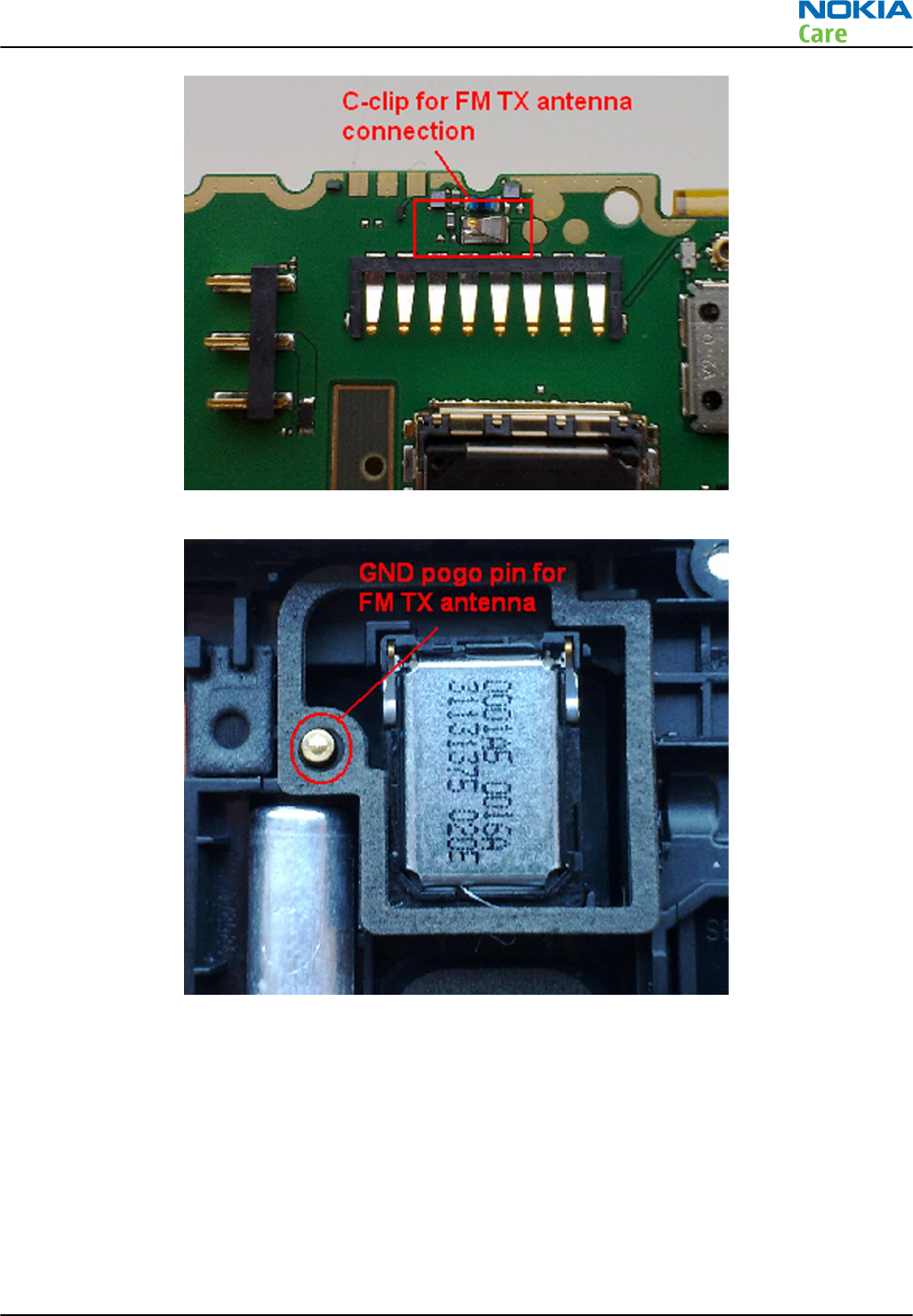
Figure 27 C-clip for FM TX antenna
Figure 28 GND pogo pin for FM TX antenna
RM-596
Cellular RF troubleshooting
Issue 2 COMPANY CONFIDENTIAL Page 4 – 37
Copyright © 2010 Nokia. All rights reserved.

RM-596
Cellular RF troubleshooting
(This page left intentionally blank.)
Page 4 – 38 COMPANY CONFIDENTIAL Issue 2
Copyright © 2010 Nokia. All rights reserved.

5 — Camera Module
Troubleshooting
Nokia Customer Care
Issue 2 COMPANY CONFIDENTIAL Page 5 – 1
Copyright © 2010 Nokia. All rights reserved.

RM-596
Camera Module Troubleshooting
(This page left intentionally blank.)
Page 5 – 2 COMPANY CONFIDENTIAL Issue 2
Copyright © 2010 Nokia. All rights reserved.

Table of Contents
Introduction to camera module troubleshooting ............................................................................................. 5–5
The effect of image taking conditions on image quality.................................................................................. 5–6
Image quality analysis ...................................................................................................................................... 5–10
Possible faults in image quality................................................................................................................... 5–10
Testing for dust in camera module ............................................................................................................. 5–11
Testing camera image sharpness................................................................................................................ 5–12
Effects of dirty or defective camera lens protection window................................................................... 5–13
Faulty pixels in images ................................................................................................................................. 5–14
Flash photography problems....................................................................................................................... 5–15
Main (back) camera troubleshooting flowcharts............................................................................................ 5–16
No recognizable viewfinder image ............................................................................................................. 5–16
Bad image quality troubleshooting ............................................................................................................ 5–17
Main camera troubleshooting...................................................................................................................... 5–18
Secondary camera troubleshooting ................................................................................................................. 5–20
Flash troubleshooting........................................................................................................................................ 5–22
List of Figures
Figure 29 Only center part of image is in focus due to limited depth of focus .............................................. 5–6
Figure 30 Blurring caused by shaking hands ..................................................................................................... 5–7
Figure 31 Near objects get skewed when taking images from a moving vehicle.......................................... 5–7
Figure 32 Noisy image taken in +70 degrees Celsius ........................................................................................ 5–8
Figure 33 Image taken against light................................................................................................................... 5–8
Figure 34 Flicker in an image; object illuminated by strong fluorescent light............................................... 5–9
Figure 35 A lens reflection effect caused by sunshine....................................................................................... 5–9
Figure 36 Good image taken indoors............................................................................................................... 5–10
Figure 37 Good image taken outdoors ............................................................................................................ 5–10
Figure 38 Effects of dust on optical path ......................................................................................................... 5–11
Figure 39 Image taken with clear protection window .................................................................................. 5–13
Figure 40 Image taken with greasy protection window ............................................................................... 5–13
Figure 41 Image of point light sources taken with a clean protective window.......................................... 5–14
Figure 42 Image of point light sources taken with a dirty (finger print) protective window ................... 5–14
Figure 43 Enlargement of a hot pixel............................................................................................................... 5–15
Figure 44 Light from the flash has reflected on particles in front of the camera ....................................... 5–15
RM-596
Camera Module Troubleshooting
Issue 2 COMPANY CONFIDENTIAL Page 5 – 3
Copyright © 2010 Nokia. All rights reserved.

RM-596
Camera Module Troubleshooting
(This page left intentionally blank.)
Page 5 – 4 COMPANY CONFIDENTIAL Issue 2
Copyright © 2010 Nokia. All rights reserved.
Introduction to camera module troubleshooting
Background, tools and terminology
Faults or complaints in camera operation can be roughly categorised into three subgroups:
1 Camera is not functional at all; no image can be taken.
2 Images can be taken but there is nothing recognizable in them.
3 Images can be taken and they are recognizable but for some reason the quality of images is seriously
degraded, or customer complains about image quality.
Image quality is very hard to measure quantitatively, and even comparative measurements are difficult
(comparing two images) to do, if the difference is small. Especially if the user is not satisfied with his/her
device's image quality, and tells, for example, that the images are not sharp, it is fairly difficult to accurately
test the device and get an exact figure which would tell whether the device is functioning properly.
Often subjective evaluation has to be used for finding out if a certain property of the camera is acceptable
or not. Some training or experience of a correctly operating reference device may be needed in order to
detect what actually is wrong, or is there anything wrong at all.
It is easy for the user to take bad images in bad conditions. Therefore the camera operation has to be checked
always in constant conditions (lighting, temperature) or by using a second, known-to-be good device as
reference. Experience helps significantly in analysing image quality.
Terms
Autofocus Camera module contains lens movement mechanics for focus adjustment.
Autofocus enables camera to take sharp images of objects positioned
between 10cm to infinity. During AF the viewfinder image will be
momentarily blurred as the camera searches for the right focus setting.
Digital zoom Digital zoom is done by first cropping the image by the zoom ratio and
then upscaling it to the output resolution. This will decrease the image
quality especially with high zoom ratios.
Dynamic range Camera's ability to capture details in dark and bright areas of the scene
simultaneously.
Exposure time Camera modules use silicon sensor to collect light and for forming an
image. The imaging process roughly corresponds to traditional film
photography, in which exposure time means the time during which the
film is exposed to light coming through optics. Increasing the time will
allow for more light hitting the film and thus results in brighter image. The
operation principle is exactly the same with silicon sensor, but the shutter
functionality is handled electronically.
Flicker Phenomenon, which is caused by pulsating in scene lighting, typically
appearing as wide horizontal stripes in an image.
ND-filter Neutral density filter is a filter which is used in very bright conditions to
reduce the amount of light hitting the sensor. The filter is built into the
camera module and applied automatically when needed.
Noise Variation of response between pixels with same level of input illumination.
Resolution Usually the amount of pixels in the camera sensor. In some occasions the
term resolution is used for describing the sharpness of the images.
RM-596
Camera Module Troubleshooting
Issue 2 COMPANY CONFIDENTIAL Page 5 – 5
Copyright © 2010 Nokia. All rights reserved.
Sensitivity Camera module's sensitivity to light. In equivalent illumination conditions,
a less sensitive camera needs a longer exposure time to gather enough
light in forming a good image. Analogous to ISO speed in photographic
film.
Sharpness Good quality images are 'sharp' or 'crisp', meaning that image details are
well visible in the picture. However, certain issues, such as non-idealities
in optics, cause image blurring, making objects in picture to appear 'soft'.
Each camera type typically has its own level of performance.
Shutter The electronic shutter is used when short exposure times are needed and
in video. When the mechanical shutter is used a black sheet will cover the
lens after the exposure.
The effect of image taking conditions on image quality
There are some factors, which may cause poor image quality, if not taken into account by the end user when
shooting images, and thus may result in complaints. The items listed are normal to camera operation and
are not a reason for changing the camera module.
Autofocus
When the camera is focusing a lens is moved inside the module to give the sharpest possible image. This
camera module is specified to operate satisfactorily from 10 cm to infinite distance of scene objects. Trying
to photograph objects closer than 10 cm is likely to result in a blurred out of focus image. The lack of sharpness
is first visible in full resolution images. Images taken very close to the subject, a limited depth of focus will
be visible, that is the upper or lower parts of the image may be out of focus. This is normal; do not change
the camera module.
Figure 29 Only center part of image is in focus due to limited depth of focus
The amount of light available
In dim conditions camera runs out of sensitivity. The exposure time is long (especially in the night mode)
and the risk of getting shaken (= blurred) images increases. In addition, image noise level grows. The
maximum exposure time in the night mode is ¼ seconds. Therefore, images need to be taken with extreme
care and by supporting the phone when the amount of light reflected from the target is low. Because of the
longer exposure time and larger gain value, noise level increases in low light conditions. Sometimes blurring
may even occur in daytime, if the image is taken very carelessly. See the figure below for an example. This
is normal; do not change the camera module.
RM-596
Camera Module Troubleshooting
Page 5 – 6 COMPANY CONFIDENTIAL Issue 2
Copyright © 2010 Nokia. All rights reserved.
Figure 30 Blurring caused by shaking hands
Movement in bright light
If an image is taken of moving objects or if the device is used in a moving vehicle, object 'skewing' or 'tilting'
may occur. This phenomenon is fundamental to most CMOS camera types, and may happen when using the
electronic shutter. The movement of camera or object sometimes cause blurring indoors or in dim lighting
conditions because of long exposure time. This is normal; do not change the camera module.
Figure 31 Near objects get skewed when taking images from a moving vehicle
Temperature
High temperatures inside the mobile phone cause more noise to appear in images. For example, in +70
degrees (Celsius), the noise level may be very high, and it further grows if the conditions are dim. If the phone
processor has been heavily loaded for a long time before taking an image, the phone might have considerably
higher temperature inside than in the surrounding environment. This is also normal to camera operation;
do not change the camera module.
RM-596
Camera Module Troubleshooting
Issue 2 COMPANY CONFIDENTIAL Page 5 – 7
Copyright © 2010 Nokia. All rights reserved.
Figure 32 Noisy image taken in +70 degrees Celsius
Phone display
If the display contrast is set too dark, the image quality degrades: the images may be very dark depending
on the setting. If the display contrast is set too bright, image contrast appears bad and "faint". This problem
is solved by setting the display contrast correctly. This is normal behaviour; do not change the camera module.
Basic rules of photography (especially shooting against light)
Because of dynamic range limitations, taking images against bright light might cause either saturated image
or the actual target appear too dark. In practice, this means that when taking an image indoors and having,
for example, a window behind the object, the result is usually poor. This is normal behaviour; do not change
the camera module.
Figure 33 Image taken against light
Flicker
In some occasions a bright fluorescent light may cause flicker in the viewfinder and captured image. This
phenomenon may also be a result, if images are taken indoors under the mismatch of 50/60 Hz electricity
network frequency. The electricity frequency used is automatically detected by the camera module. In some
very few countries, both 50 and 60 Hz networks are present and thus probability for the phenomenon
increases. Flickering occurs also under high artificial illumination level. Flickering only occurs when the rolling
shutter is used. This is normal behaviour; do not change the camera module.
RM-596
Camera Module Troubleshooting
Page 5 – 8 COMPANY CONFIDENTIAL Issue 2
Copyright © 2010 Nokia. All rights reserved.
Figure 34 Flicker in an image; object illuminated by strong fluorescent light
Bright light outside of image view
Especially the sun can cause clearly visible lens glare phenomenon and poor contrast in images. This happens
because of undesired reflections inside the camera optics. Generally this kind of reflections are common in
all optical systems. This is normal behaviour; do not change the camera module.
Figure 35 A lens reflection effect caused by sunshine
RM-596
Camera Module Troubleshooting
Issue 2 COMPANY CONFIDENTIAL Page 5 – 9
Copyright © 2010 Nokia. All rights reserved.
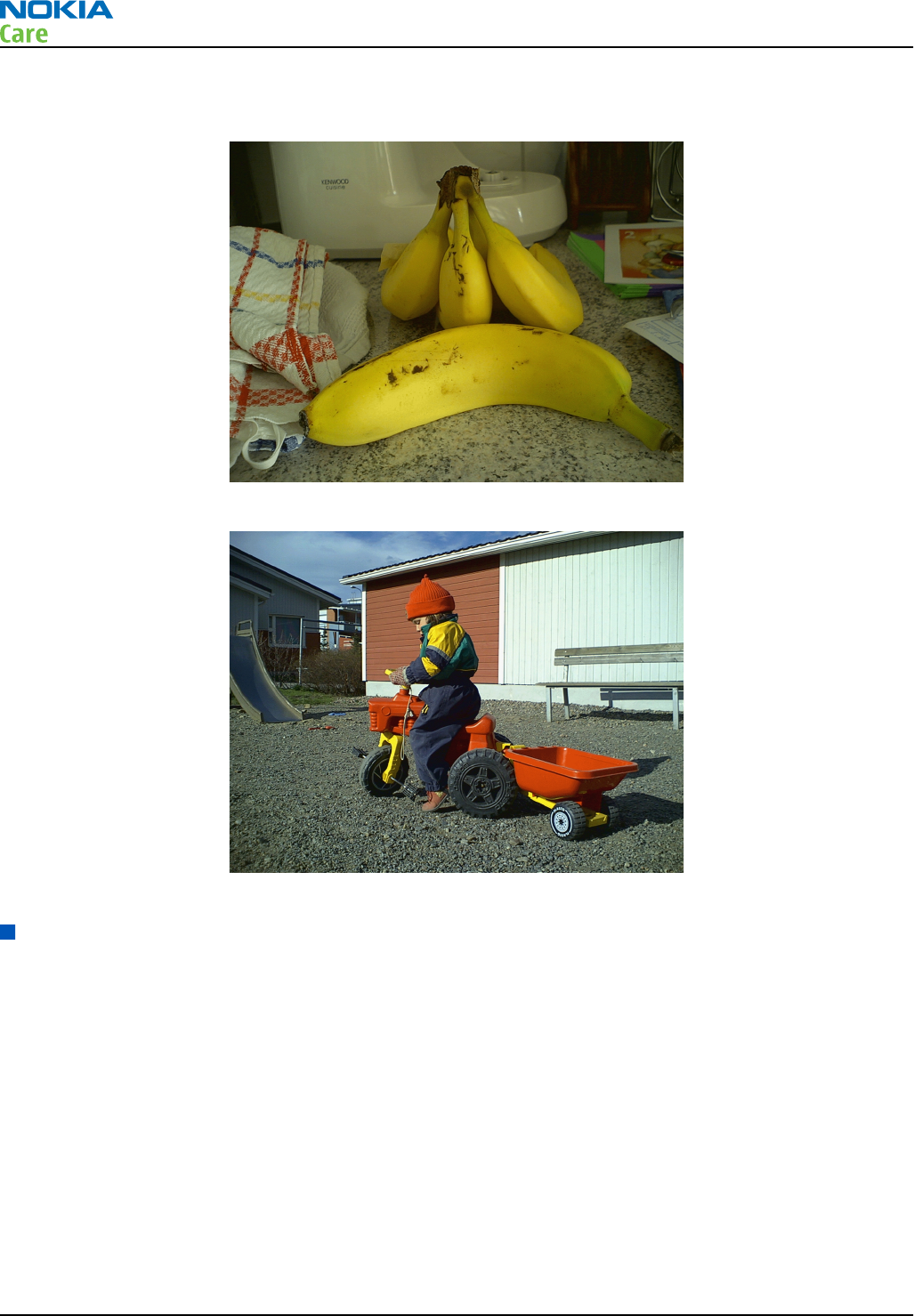
Examples of good quality images
Figure 36 Good image taken indoors
Figure 37 Good image taken outdoors
Image quality analysis
Possible faults in image quality
When checking for possible errors in camera functionality, knowing what error is suspected significantly
helps the testing by narrowing down the amount of test cases. The following types of image quality problems
may be expected to appear:
•Dust (black spots)
•Lack of sharpness
•Bit errors
In addition, there are many other kinds of possibilities for bad image quality, but those are ruled out from
the scope of this document since the probability of their appearance is small.
RM-596
Camera Module Troubleshooting
Page 5 – 10 COMPANY CONFIDENTIAL Issue 2
Copyright © 2010 Nokia. All rights reserved.
Testing for dust in camera module
Symptoms and diagnosis
For detecting these kinds of problems, take an image of a uniform white surface and analyse it in full
resolution. A good quality PC monitor is preferred for analysis. Search carefully, since finding these defects
is not always easy. Figure "Effects of dust on optical path" is an example image containing easily detectable
dust problems.
When taking a white image, use uniformly lightened white paper or white wall. One possibility is to use
uniform light but in this case make sure that the camera image is not flickering when taking the test image.
In case flickering happens, try to reduce illumination level. Use JPEG image format for analysing, and set the
image quality parameter to ‘High Quality’.
Black spots in an image are caused by dirt particles trapped inside the optical system. Clearly visible and
sharp edged black dots in an image are typically dust particles on the image sensor. These spots are searched
for in the manufacturing phase, but it is possible that the camera body cavity contains a particle, which may
move onto the image sensor active surface, for example, when the phone is dropped. Thus it is also possible
that the problem will disappear before the phone is brought to service. The camera should be replaced if the
problem is present when the service technician analyses the phone.
If a dust particle is lying on the infrared filter surface on either side, they are hard to locate because they are
out of focus, and appear in the image as large, grayish and fading-edge 'blobs'. Sometimes they are invisible
to the eye, and thus the user probably does not notice them at all. However, it is possible that a larger particle
disturbs the user, causing need for service.
Figure 38 Effects of dust on optical path
If large dust particles get trapped on top of the lens surface in the cavity between camera window and lens,
they will cause image blurring and poor contrast. The dust gasket between the window and lens should
prevent any particles from getting into the cavity after the manufacturing phase.
If dust particles are found on the sensor, this is classified as a manufacturing error of the module and the
camera should be replaced. Any particles inside the cavity between the protection window and lens have
most probably been trapped there in the assembly phase at a Nokia factory. Unauthorized disassembling of
the product can also be the root of the problem. However, in most cases it should be possible to remove the
particle(s) by using clean compressed air. Never wipe the lens surface before trying compressed air; the
possibility of damaging the lens is substantial. Always check the image sharpness after removing dust.
RM-596
Camera Module Troubleshooting
Issue 2 COMPANY CONFIDENTIAL Page 5 – 11
Copyright © 2010 Nokia. All rights reserved.

Testing camera image sharpness
Symptoms and diagnosis
If pictures taken with a device are claimed to be blurry, there are five possible sources for the problem:
1 The protection window is fingerprinted, soiled, dirty, visibly scratched or broken.
2 The camera module has failed to focus correctly, producing a blurred image.
3 User has tried to take pictures in too dark conditions and images are blurred due to handshake or
movement. This is not a cause to replace camera module.
4 There is dirt between the protection window and the camera lens.
5The protection window is defective. This can be either a manufacturing failure or caused by the user. The
window should be changed.
A quantitative analysis of sharpness is very difficult to conduct in any other environment than optics
laboratory. Therefore, subjective analysis should be used.
If no visible defects (items 1-4) are found, a couple of test images should be taken. Generally, a well-
illuminated typical indoor scene, such as the one in Figure "Good image taken indoors", can be used as a
target. The main considerations are:
•The camera module has to be given time to focus correctly. Correct focusing is normally indicated with a
flashing icon or green bracket in the viewfinder. During focusing, the image in the viewfinder moves
slightly back and forth, this is normal and shows that the lens unit is moving. During the movement a faint
sound can be heard from the camera head.
•The protection window has to be clean.
•The amount of light (300 – 600 lux (bright office lighting)) is sufficient.
•The scene should contain, for example, small objects for checking sharpness. Their distance should be 1
– 2 meters.
•If possible, compare the image to another image of the same scene, taken with a different device. Note
that the reference device has to be a similar Nokia phone.
There are several conditions in which AF operation is challenging for the camera module, i.e. failing from
time to time. These include:
•Low light scenes and night mode
•Scenes with low contrast
•Fast-moving objects
AF operation is disabled on purpose in "night", "landscape", and "sports" modes.
When using these modes the lens is set to a predetermined focal position and is not moved during use.
The AF lens is fixed in hyper focal in video mode.
Under low light and night mode the AF function is slower than under good light, it may even fail to find
correct focus position. Low contrast scenes or fast moving objects may also slow down or cause AF to fail.
This is normal operation, and is not a cause to replace camera.
The operation of AF can be tested by taking images of objects at different distances. Good distances are 20
cm, 60 cm and infinity (>3 m). Any LED or xenon flashes should not be used while taking the images.
The taken images should be analysed on PC screen at 100% scaling simultaneously with a reference image.
Pay attention to the computer display settings; at least 65000 colors (16 bit) have to be used. 256 (8-bit)
color setting is not sufficient; true color (24 bit, 16 million colors) or 32 bit (full color) setting is recommended.
If the differences are noticeable at a glance and also if the one under investigation is significantly inferior,
the module might have a faulty lens. In this case, the module should be changed. Always re-check the
resolution after changing the camera module. If a different module produces a clearly noticeable quality gap,
RM-596
Camera Module Troubleshooting
Page 5 – 12 COMPANY CONFIDENTIAL Issue 2
Copyright © 2010 Nokia. All rights reserved.
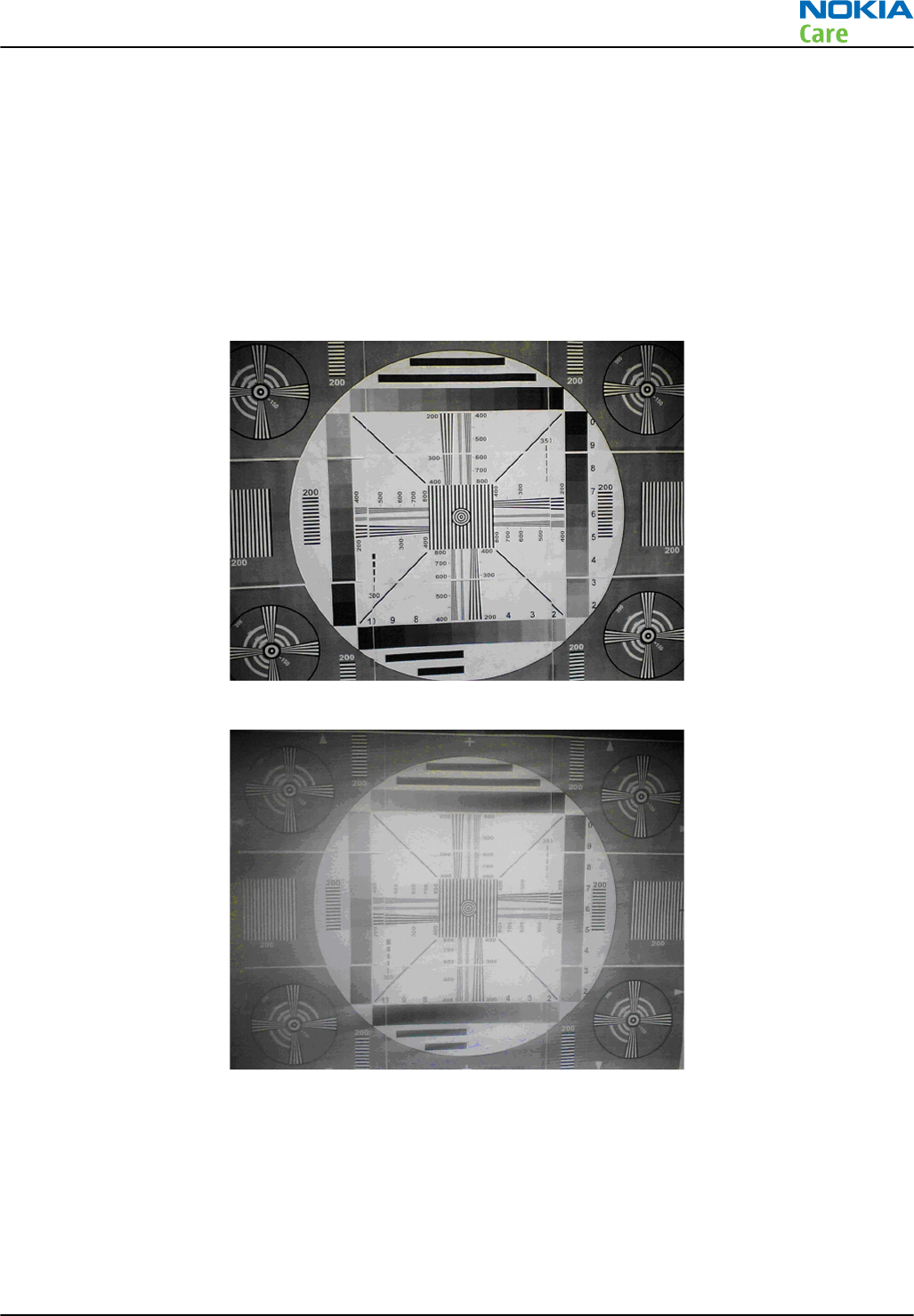
the fault is probably in the camera window. Check the window by looking carefully through it when replacing
the module. As references Figure "Good image taken indoors" and Figure "Good image taken outdoors" can
be used. Another possibility is to use a service point comparison phone, if available.
Effects of dirty or defective camera lens protection window
The following series of images demonstrates the effects of fingerprints on the camera protection window.
Note: The effects of any dirt in images can vary very much; it may be difficult to judge if the window
has been dirty when some image has been taken or if something else has been wrong. That is why
the cleanness of the protection window should always be checked and the window should be wiped
clean with a suitable cloth.
Figure 39 Image taken with clear protection window
Figure 40 Image taken with greasy protection window
Bright point light sources might cause images that have flares around the light source if the protection
window is dirty. A smeared fingerprint may be hard to see on the protective window but if will affect the
image quality. These flares can be avoided by cleaning the window with a suitable cloth.
RM-596
Camera Module Troubleshooting
Issue 2 COMPANY CONFIDENTIAL Page 5 – 13
Copyright © 2010 Nokia. All rights reserved.
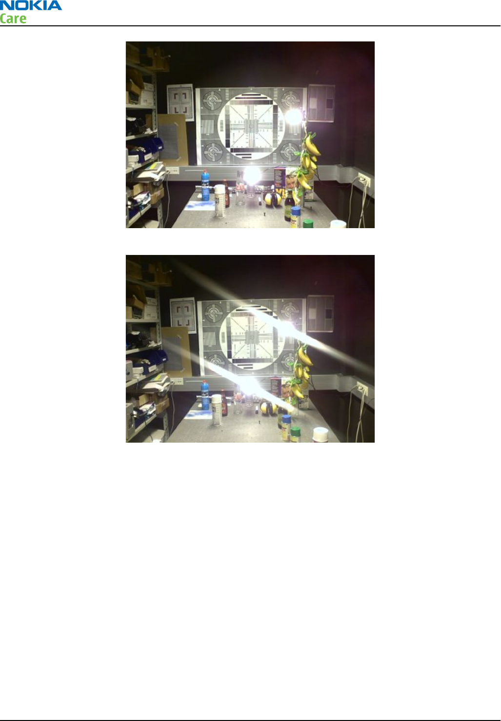
Figure 41 Image of point light sources taken with a clean protective window
Figure 42 Image of point light sources taken with a dirty (finger print) protective window
Faulty pixels in images
Faulty pixels are pixels that do not respond to light in the same way as the pixels around them. There are
three main types of faulty pixels, dead, stuck and hot pixels.
Dead pixels are always black or significantly darker than their surrounding. Dead pixels appear as black spots
in all lightning conditions. Camera modules producing images with dead pixels that are clearly noticeable
should be replaced.
If the pixel remains always saturated to its maximum value it is stuck. Stuck pixels may appear as red, green,
blue or white spots in all lightning conditions. Camera modules producing images with one or more stuck
pixels should be replaced.
Hot pixels are pixels that easily saturate in dim light conditions. It is normal to get a lot of noise and hot
pixels in night conditions or otherwise dark conditions. The hot pixels should disappear when the ambient
light is increased, but may still appear in darker areas of an otherwise well illuminated scene. This is normal
behavior, do not change the camera.
When examining an image for defect pixels, test images should be viewed as 100% enlargements on a PC
monitor.
RM-596
Camera Module Troubleshooting
Page 5 – 14 COMPANY CONFIDENTIAL Issue 2
Copyright © 2010 Nokia. All rights reserved.
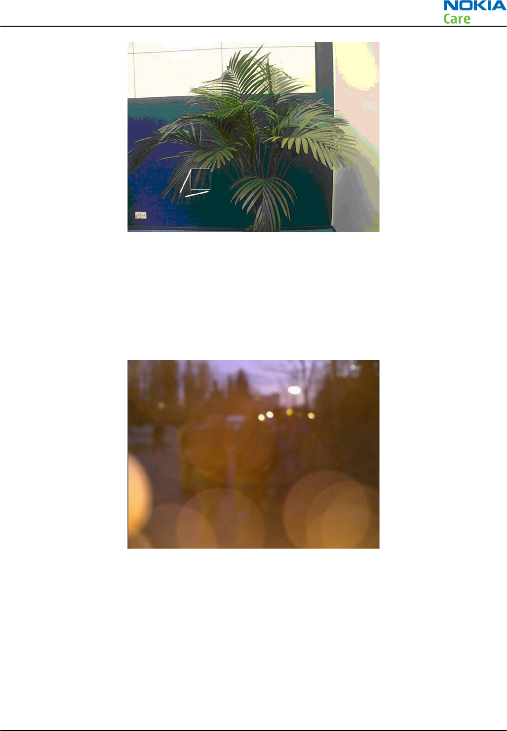
Figure 43 Enlargement of a hot pixel
Flash photography problems
Use of flash device may affect the image in many ways.
•White balance errors. The image may get a wrong tone due to mixing of flash colour temperature and
ambient lightning. This is unwanted but normal feature.
•Dust reflections. Dust or water drops in front of the flash unit may reflect strongly to the camera sensor.
See the following figure.
Figure 44 Light from the flash has reflected on particles in front of the camera
RM-596
Camera Module Troubleshooting
Issue 2 COMPANY CONFIDENTIAL Page 5 – 15
Copyright © 2010 Nokia. All rights reserved.
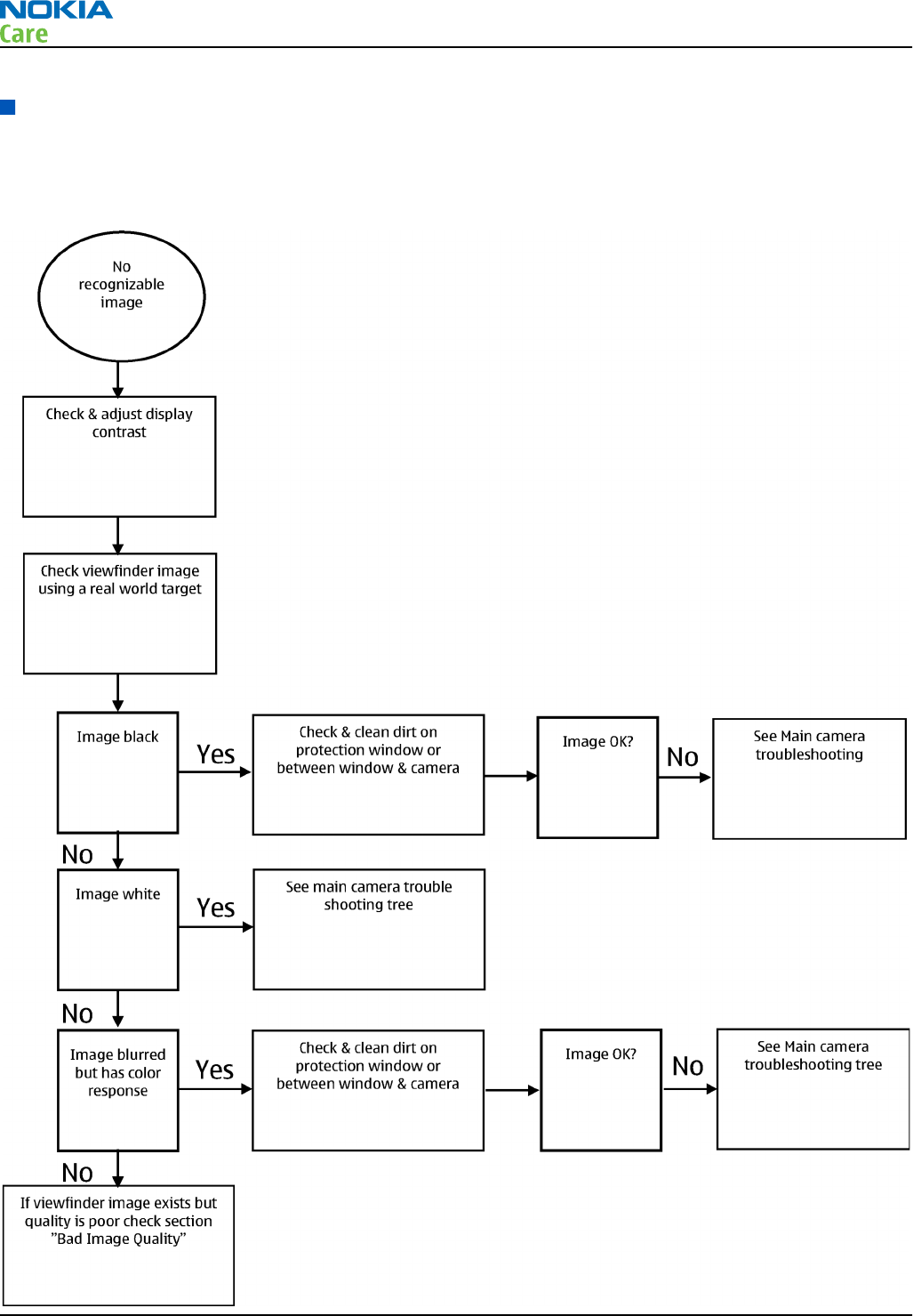
Main (back) camera troubleshooting flowcharts
No recognizable viewfinder image
Troubleshooting flow
RM-596
Camera Module Troubleshooting
Page 5 – 16 COMPANY CONFIDENTIAL Issue 2
Copyright © 2010 Nokia. All rights reserved.
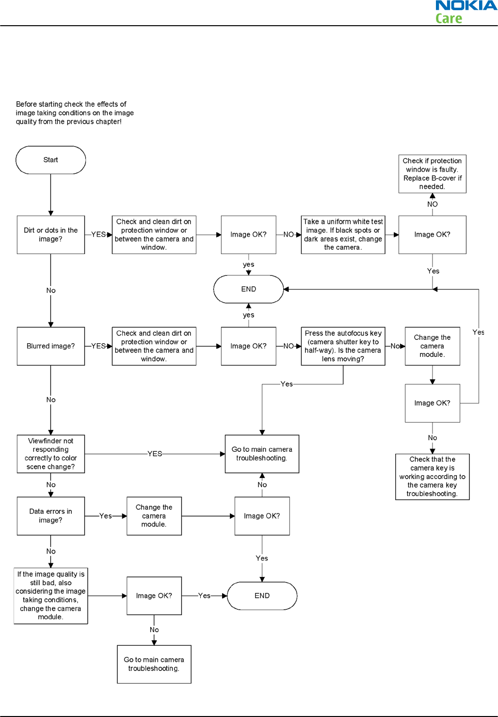
Bad image quality troubleshooting
Troubleshooting flow
RM-596
Camera Module Troubleshooting
Issue 2 COMPANY CONFIDENTIAL Page 5 – 17
Copyright © 2010 Nokia. All rights reserved.
Main camera troubleshooting
Context
The following references on the PWB help in the effective debugging and troubleshooting of the main/
primary camera.
Sr. No Reference Description
1 X1476 Primary camera socket
2 R1477, R1478 Pull-up resistors on primary camera I2C lines. Resistor value 4.7
KOHMS.
3 D1400 BCM2727B IC
4 N1515 VCAM_1V8 regulator
5 N1517 VCAM_2V8 regulator
The following test points on the PWB help in the effective debugging and troubleshooting.
Sr. No Signal name Measuring point Description
1 VBAT L1476/C1476 VBAT supply to primary camera
2 VCAM_1V8 L1477/C1479 1.8V supply to primary camera
3 VCAM_2V8 L1478/C1482 2.8V supply to primary camera
4 VDIG_ENABLE J1515 Enable signal for VCAM_1V8 regulator. This
signal needs to be High for the regulator to
be On.
5 VANA_ENABLE J1516 Enable signal for VCAM_2V8 regulator. This
signal needs to be High for the regulator to
be On.
6 PRI_CAM_CLK J1476 External clock signal to primary camera
7 PRI_CAM_SHUTDO
WN
J1477 Shutdown signal to primary camera. This
needs to be High for the camera to be Up.
8 PRI_CAM_I2C(1:0) R1477, R1478 I2C signals for primary camera
RM-596
Camera Module Troubleshooting
Page 5 – 18 COMPANY CONFIDENTIAL Issue 2
Copyright © 2010 Nokia. All rights reserved.
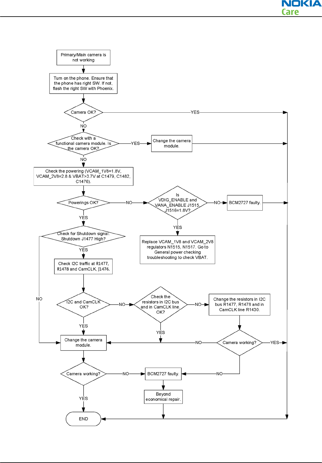
Troubleshooting flow
RM-596
Camera Module Troubleshooting
Issue 2 COMPANY CONFIDENTIAL Page 5 – 19
Copyright © 2010 Nokia. All rights reserved.
Secondary camera troubleshooting
Context
The following references on the PWB help in the effective debugging and troubleshooting of the secondary
camera.
Sr. No Reference Description
1 H1487 Secondary camera
2 R1487, R1488 Pull-up resistors on the secondary camera I2C lines. Resistor value
4.7 KOHMS.
3 D1400 BCM2727B IC
4 N1515 VCAM_1V8 regulator
5 N1517 VCAM_2V8 regulator
The following test points on the PWB help in the effective debugging and troubleshooting.
Sr. No Signal name Measuring point Description
1 VCAM_1V8 L1487/C1488 1.8V supply to secondary camera
2 VCAM_2V8 L1488/C1491 2.8V supply to secondary camera
3 VDIG_ENABLE J1515 Enable signal for VCAM_1V8 regulator. This signal
needs to be High for the regulator to be On.
4 VANA_ENABLE J1516 Enable signal for VCAM_2V8 regulator. This signal
needs to be High for the regulator to be On.
5 SEC_CAM_CLK J1487 External clock signal to secondary camera
6 SEC_CAM_SHUTDOW
N
J1488 Shutdown signal to secondary camera. This
needs to be High for the camera to be Up.
7 SEC_CAM_I2C(1:0) R1487, R1488 I2C signals for secondary camera
RM-596
Camera Module Troubleshooting
Page 5 – 20 COMPANY CONFIDENTIAL Issue 2
Copyright © 2010 Nokia. All rights reserved.
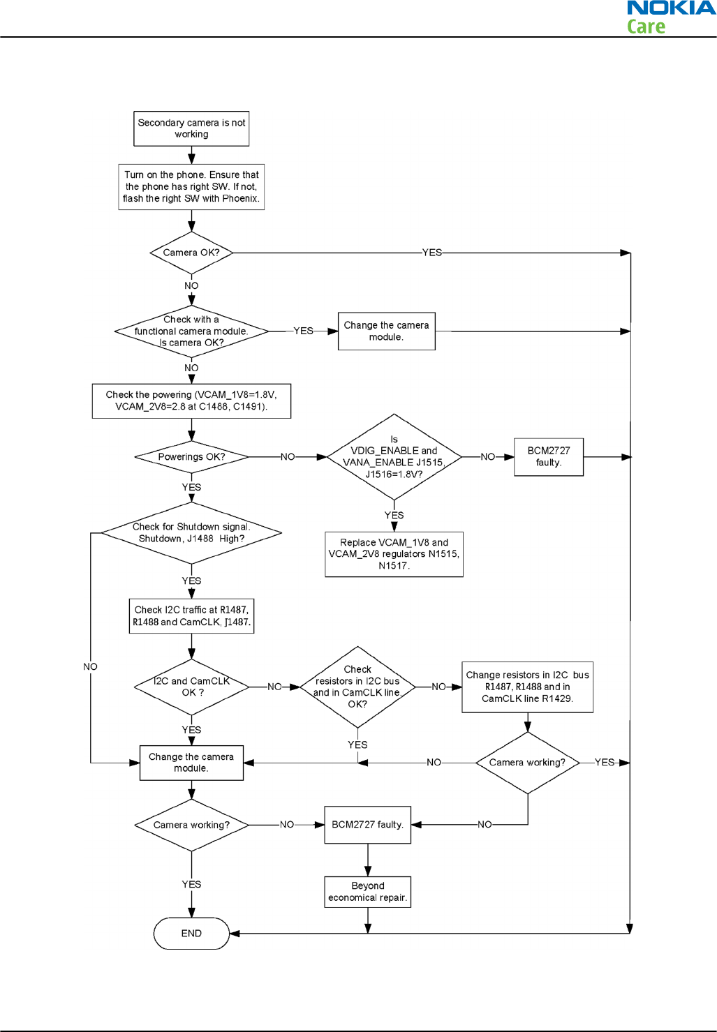
Troubleshooting flow
RM-596
Camera Module Troubleshooting
Issue 2 COMPANY CONFIDENTIAL Page 5 – 21
Copyright © 2010 Nokia. All rights reserved.
Flash troubleshooting
Context
The following references on the PWB help in the effective debugging and troubleshooting of the flash.
Sr. No Reference Description
1 N1504 Flash driver
2 X1505 Habanero flash connector
3 D1400 BCM2727B IC
The following test points on the PWB help in the effective debugging and troubleshooting of the flash.
Sr. No Signal name Measuring point Description
1 VBAT L1507/pin3 of X1505 VBAT supply to flash and flash driver
2 FLASH_READY_XE J1430 Ready signal from flash module
3 FLASH_CHARGE_XE J1504 Charge signal to flash module. This needs to
be High for the charging to start.
4 CAM_FLASH_STROBE J1503 Strobe signal to flash module. This needs to
be High for flashing.
5 FLASH_INDICATOR_XE R1508 Flash indicator signal to flash driver
6 FLASH_AFASSIST_XE J1506 Flash auto focus signal to flash driver
RM-596
Camera Module Troubleshooting
Page 5 – 22 COMPANY CONFIDENTIAL Issue 2
Copyright © 2010 Nokia. All rights reserved.
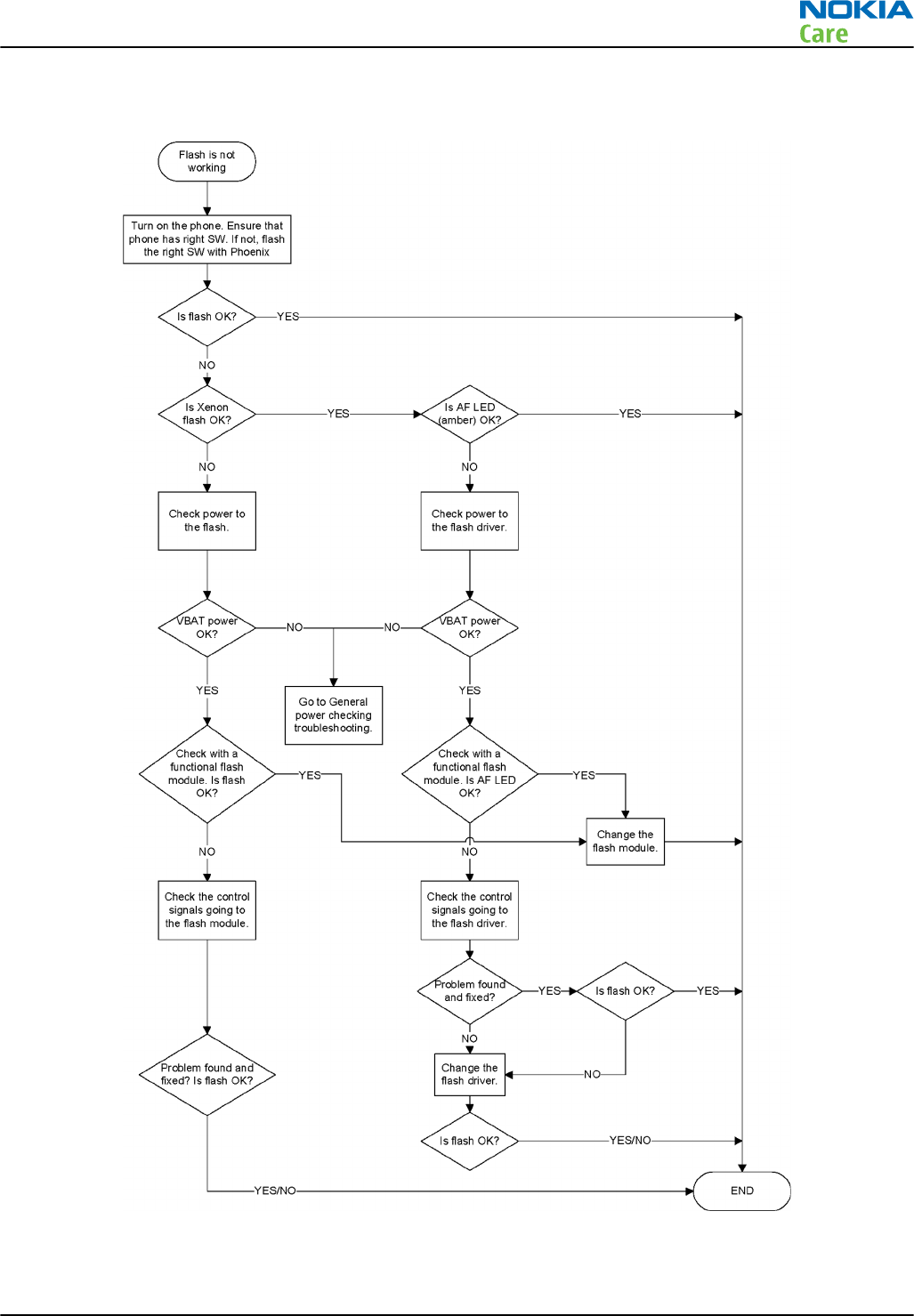
Troubleshooting flow
RM-596
Camera Module Troubleshooting
Issue 2 COMPANY CONFIDENTIAL Page 5 – 23
Copyright © 2010 Nokia. All rights reserved.

RM-596
Camera Module Troubleshooting
(This page left intentionally blank.)
Page 5 – 24 COMPANY CONFIDENTIAL Issue 2
Copyright © 2010 Nokia. All rights reserved.

6 — System Module
Nokia Customer Care
Issue 2 COMPANY CONFIDENTIAL Page 6 – 1
Copyright © 2010 Nokia. All rights reserved.

RM-596
System Module
(This page left intentionally blank.)
Page 6 – 2 COMPANY CONFIDENTIAL Issue 2
Copyright © 2010 Nokia. All rights reserved.

Table of Contents
Introduction........................................................................................................................................................... 6–5
Phone description ............................................................................................................................................ 6–5
Energy management.......................................................................................................................................... 6–11
Battery and charging .................................................................................................................................... 6–11
Normal and extreme voltages ..................................................................................................................... 6–11
Power key and system power up ................................................................................................................ 6–12
Modes of operation....................................................................................................................................... 6–12
Power distibution ......................................................................................................................................... 6–13
Clocking scheme............................................................................................................................................ 6–14
SIM interface ....................................................................................................................................................... 6–15
Device memory................................................................................................................................................... 6–16
BOB1.0M-b module............................................................................................................................................. 6–16
GPS interface....................................................................................................................................................... 6–18
USB....................................................................................................................................................................... 6–19
USB interface and charging.......................................................................................................................... 6–19
MicroUSB connector ...................................................................................................................................... 6–19
Charger interface................................................................................................................................................ 6–20
User interface...................................................................................................................................................... 6–20
Touch module................................................................................................................................................ 6–20
Proximity sensor ........................................................................................................................................... 6–21
Imaging and video........................................................................................................................................ 6–22
Multimedia application processor.......................................................................................................... 6–22
Display module......................................................................................................................................... 6–22
TV-out interface........................................................................................................................................ 6–22
Cameras..................................................................................................................................................... 6–23
Illumination ................................................................................................................................................... 6–24
Keyboard interface........................................................................................................................................ 6–25
Ambient Light Sensor (ALS).......................................................................................................................... 6–25
Accelerometer................................................................................................................................................ 6–26
Magnetometer............................................................................................................................................... 6–27
Audio concept..................................................................................................................................................... 6–28
Audio HW architecture.................................................................................................................................. 6–28
Internal earpiece........................................................................................................................................... 6–30
Internal handsfree (IHF) speakers ............................................................................................................... 6–30
Internal microphones ................................................................................................................................... 6–30
External earpiece and microphone ............................................................................................................. 6–31
Vibra ............................................................................................................................................................... 6–31
AV connector.................................................................................................................................................. 6–32
Cellular RF technical description....................................................................................................................... 6–32
RF block .......................................................................................................................................................... 6–32
QuBBE ............................................................................................................................................................. 6–33
Receiver (RX).................................................................................................................................................. 6–33
Synthesizer..................................................................................................................................................... 6–33
Transmitter (TX) ............................................................................................................................................ 6–33
Frequency mappings.......................................................................................................................................... 6–35
GSM850 frequencies...................................................................................................................................... 6–35
EGSM900 frequencies.................................................................................................................................... 6–35
GSM1800 frequencies.................................................................................................................................... 6–36
GSM1900 frequencies.................................................................................................................................... 6–38
WCDMA I (2100) Rx frequencies ................................................................................................................... 6–39
RM-596
System Module
Issue 2 COMPANY CONFIDENTIAL Page 6 – 3
Copyright © 2010 Nokia. All rights reserved.

WCDMA I (2100) Tx frequencies ................................................................................................................... 6–40
WCDMA II (1900) frequencies....................................................................................................................... 6–41
WCDMA IV (1700/2100) frequencies............................................................................................................ 6–42
WCDMA V (850) frequencies ......................................................................................................................... 6–43
WCDMA VIII (900) frequencies...................................................................................................................... 6–44
List of Tables
Table 11 Nominal voltages................................................................................................................................ 6–11
List of Figures
Figure 45 Battery pin order............................................................................................................................... 6–11
Figure 46 Blade battery connector ................................................................................................................... 6–11
Figure 47 Power distribution diagram ............................................................................................................ 6–13
Figure 48 SIM interface ...................................................................................................................................... 6–15
Figure 49 Puzzle SIM connector circuitry ........................................................................................................ 6–16
Figure 50 BOB1.0M-b module block diagram and application circuit........................................................... 6–17
Figure 51 BOB1.0M-b interface in RM-596 ....................................................................................................... 6–18
Figure 52 GPS interface...................................................................................................................................... 6–18
Figure 53 USB interface...................................................................................................................................... 6–19
Figure 54 MicroUSB connector .......................................................................................................................... 6–19
Figure 55 Charger interface............................................................................................................................... 6–20
Figure 56 Touch system block diagram ........................................................................................................... 6–21
Figure 57 Proximity sensor ............................................................................................................................... 6–21
Figure 58 BCM2727B block diagram................................................................................................................. 6–22
Figure 59 Primary camera interface................................................................................................................. 6–23
Figure 60 Secondary camera interface............................................................................................................. 6–24
Figure 61 Illumination ....................................................................................................................................... 6–25
Figure 62 Ambient Light Sensor ....................................................................................................................... 6–26
Figure 63 Accelerometer.................................................................................................................................... 6–27
Figure 64 Magnetometer................................................................................................................................... 6–28
Figure 65 RM-596 Audio block diagram........................................................................................................... 6–29
Figure 66 Internal earpiece diagram................................................................................................................ 6–30
Figure 67 Internal handsfree (IHF) speaker diagram ..................................................................................... 6–30
Figure 68 Internal microphones diagram........................................................................................................ 6–31
Figure 69 Vibra diagram.................................................................................................................................... 6–31
Figure 70 AV connector...................................................................................................................................... 6–32
Figure 71 Linko RF block diagram .................................................................................................................... 6–32
RM-596
System Module
Page 6 – 4 COMPANY CONFIDENTIAL Issue 2
Copyright © 2010 Nokia. All rights reserved.
Introduction
Phone description
RAPUYAMA is the main digital baseband ASIC in the phone. It contains functionality for both WCDMA and GSM
EDGE. The hardware accelerator is used for imaging and video.
GAZOO/PEARL (N2200) is the main audio and energy management controller for the phone.
Key components
Function Description Item ref
Main PWB 3CE
Upper flex module
UI flex module
Flash flex module
Baseband ASIC EM ASIC GAZOO/PEARL N2200
RF ASIC ÄLLI N7512
Processor RAPUYAMA D2800
GSM/WCDMA PA UKKO
GSM850/900/1800/1900
WCDMA I, II, IV, V and VIII
N7510
Oscillators VCTCXO
TCXO 16.368 MHZ
Crystal 32.768KHZ
Crystal 38.4 MHZ
Crystal 19.2 MHZ
G7500
G6200
B2200
B7500
B1400
CMT memory Combo POP4 2G DDR + 4G M3 NAND (stacked with RAPU) D3000
Back-up capacitor RTC back-up capacitor G2200
WLAN/ Bluetooth/ FM
radio/ FM transmitter
BOB 1.0M-b module N6300
GPS GPSCost4.1 N6200
Battery BL-4D
Battery connector Tabby blade interface X2070
UI flex connector Board-to board connector for UI flex module X2500
Display connector Board-to-board connector X1600
RF connectors X6701
X7500
X7501
USB transceiver D3300
MicroSD connector X3200
RM-596
System Module
Issue 2 COMPANY CONFIDENTIAL Page 6 – 5
Copyright © 2010 Nokia. All rights reserved.
Function Description Item ref
eMMC 16GB internal mass memory D3200
USB connector Micro USB-AB X3300
SIM connector X2700
Resetto HW reset with power key N2400
IVE Imaging processor D1400
AV connector Standard 3.5mm X2001
Charging connector Dynamo X3350
HDMI connector X1650
Earpiece Petra B2111
Microphone Knopfler B2100
B2101
IHF Donau B2150
Vibra M2105
Accelerometer 3-axis accelerometer Ahti N1103
Magnetometer 3-axis magnetic sensor N1105
Digital Ambient Light
Sensor
Pupumon V1100
Dynamo charging circuit N3350
USB charging circuit N3301
Camera socket X1476
Xenon flash connector X1505
Front camera H1487
RM-596
System Module
Page 6 – 6 COMPANY CONFIDENTIAL Issue 2
Copyright © 2010 Nokia. All rights reserved.
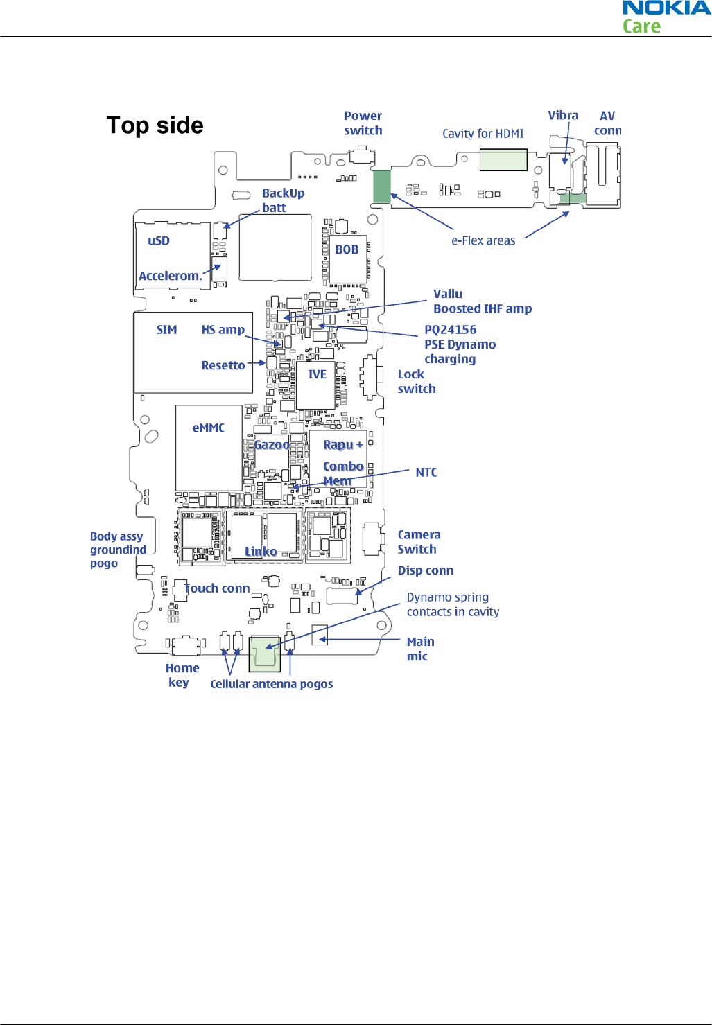
Key component placement
RM-596
System Module
Issue 2 COMPANY CONFIDENTIAL Page 6 – 7
Copyright © 2010 Nokia. All rights reserved.
RM-596
System Module
Page 6 – 8 COMPANY CONFIDENTIAL Issue 2
Copyright © 2010 Nokia. All rights reserved.
System module block diagram
RM-596
System Module
Issue 2 COMPANY CONFIDENTIAL Page 6 – 9
Copyright © 2010 Nokia. All rights reserved.
Board and module connections
RM-596
System Module
Page 6 – 10 COMPANY CONFIDENTIAL Issue 2
Copyright © 2010 Nokia. All rights reserved.
Energy management
Battery and charging
BP-4L battery
The phone is powered by a 3-pole BL-4D battery 1200 mAh battery. The three poles are named VBAT, BSI and
GND where the BSI line is used to recognize the battery capacity. This is done by means of an internal battery
pull down resistor.
Figure 45 Battery pin order
The battery temperature is estimated by measuring separate temperature NTC resistor via the BTEMP line of
EM ASIC N2200. This is located on the main PWB, near the battery connector.
Battery connector
The battery connector is a blade connector. It has three blades;
•BSI (Battery size indicator)
•GND (Ground)
•VBAT (Battery voltage)
Figure 46 Blade battery connector
Charging
The phone is charged through the 2 mm Nokia standard interface charger plug. Charging is controlled by
dynamo charging IC BQ24156 (N3350). Dynamo charger detection is handled by EM ASIC (N2200) and external
components are needed to protect the baseband module against EMC, reverse polarity and transient
frequency deviation. For charger detection, a pulse of duration 15ms is sent to EM ASIC via V3370 MOSFET.
Normal and extreme voltages
Energy management is mainly carried out in the EM ASIC (N2200) that contains a number of regulators. In
addition, there are also some external regulators.
In the table below normal and extreme voltages are shown when a BL-4D battery is used.
Table 11 Nominal voltages
Voltage Voltage [V] Condition
General Conditions
Nominal voltage 3.700
RM-596
System Module
Issue 2 COMPANY CONFIDENTIAL Page 6 – 11
Copyright © 2010 Nokia. All rights reserved.
Voltage Voltage [V] Condition
Higher extreme voltage
(fast charging) 4.230
HW Shutdown Voltages
Vmstr+ 2.1 ± 0.1 Off to on
Vmstr- 1.9 ± 0.1 On to off
SW Shutdown Voltages
Sw shutdown 3.15 In call
Sw shutdown 3.25 In idle
Min Operating Voltage
Vcoff+ 2.9 ± 0.1 Off to on
Vcoff- 2.6 ± 0.1 On to off
Power key and system power up
When the battery is placed in the phone, the power key circuits are energized. When the power key is pressed,
the system boots up (if an adequate battery voltage is present).
Power down can be initiated by pressing the power key again and the system is powered down with the aid
of SW. The power key is connected to EM ASIC (N2200) via the PWRONX signal.
The PWRONX line cannot be detected when SW hangs. For that reason, the user has to remove the battery.
Because the semi-fixed battery is difficult to remove, a fixed delay circuit Resetto IC (N2400) is used. The
PWRONX is also connected to Resetto. When the user presses the power key beyond 7.5 secs, it generates a
reset which is connected to EM ASIC’s UserResetX line. The UserResetX is entirely HW controlled, so even when
SW hangs, the phone can be powered down by pressing the power key beyond 7.5 sec.
Modes of operation
Mode Description
NO_SUPPLY (Dead) mode means that the main battery is not present or its voltage is too low (below
N2200 master reset threshold) and that the back-up battery voltage is too low.
BACK_UP The main battery is not present or its voltage is too low but back-up battery is adequate
and the 32 kHz oscillator is running.
PWR_OFF In this mode (warm), the main battery is present and its voltage is over N2200 master
reset threshold. All regulators are disabled, PURX is on low state, the RTC is on and the
oscillator is on. PWR_OFF (cold) mode is almost the same as PWR_OFF (warm), but the
RTC and the oscillator are off.
RESET RESET mode is a synonym for start-up sequence. RESET mode uses 32 kHz clock to count
the RESET mode delay (typically 16ms).
SLEEP SLEEP mode is entered only from PWR_ON mode with the aid of SW when the system’s
activity is low.
FLASHING FLASHING mode is for SW downloading.
RM-596
System Module
Page 6 – 12 COMPANY CONFIDENTIAL Issue 2
Copyright © 2010 Nokia. All rights reserved.
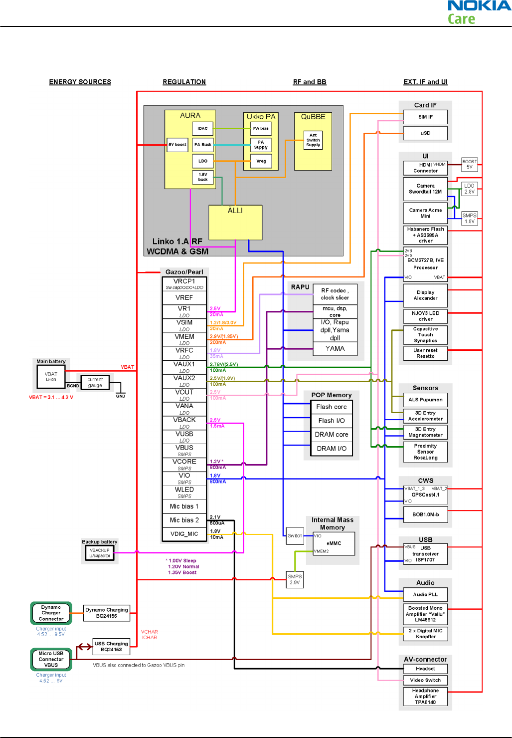
Power distibution
Figure 47 Power distribution diagram
RM-596
System Module
Issue 2 COMPANY CONFIDENTIAL Page 6 – 13
Copyright © 2010 Nokia. All rights reserved.
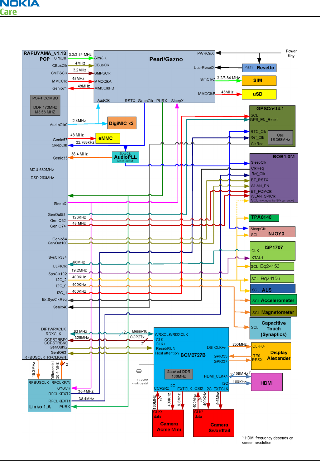
Clocking scheme
RM-596
System Module
Page 6 – 14 COMPANY CONFIDENTIAL Issue 2
Copyright © 2010 Nokia. All rights reserved.
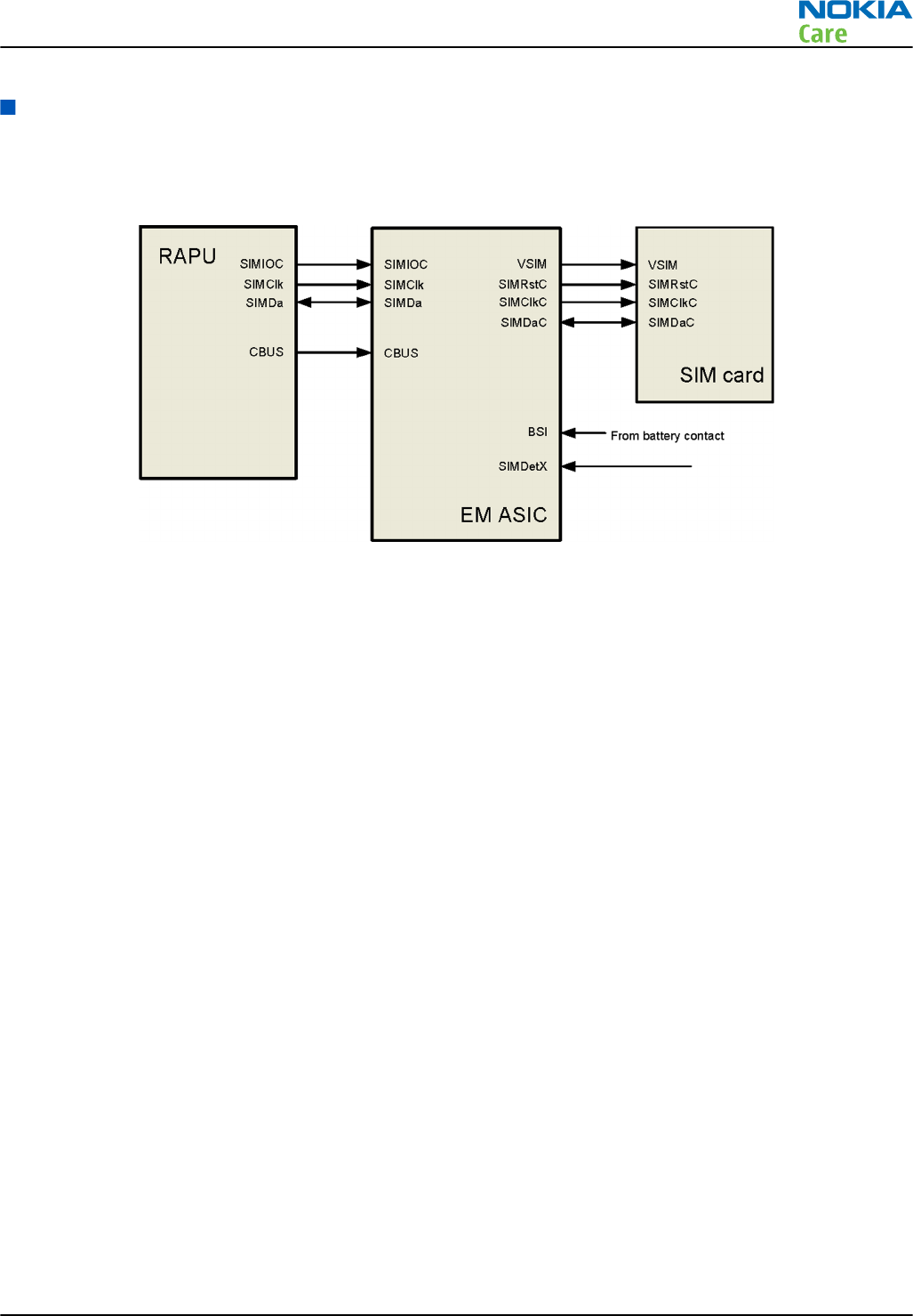
SIM interface
The phone has a SIM (Subscriber Identification Module) interface including a SIM connector.
The SIM interface consists of an internal interface between RAPU and EM ASIC (N2200), and an external
interface between EM ASIC and SIM contacts.
Figure 48 SIM interface
As the phone does not have a traditional battery cover due to semi-fixed battery concept, the SIM card can
be removed and inserted without removing the battery. For safe SIM card functionality, a new Puzzle push-
push SIM reader with card detection and removal pre-warning switches is used.
Pre-warning and card detect signals are connected together in the Puzzle layout symbol, so there is only one
switch connection in the schematics symbol. The combined switch signal is connected through an inverter
to Gazoo/Pearl SimDetX input. The following figure shows the principle of SIM circuitry with the Puzzle.
RM-596
System Module
Issue 2 COMPANY CONFIDENTIAL Page 6 – 15
Copyright © 2010 Nokia. All rights reserved.
Figure 49 Puzzle SIM connector circuitry
The SIM interface supports both 1.8V and 3.0V SIM cards. The SIM interface voltage is first 1.8 V when the SIM
card is inserted, and if the card does not response to the ATR (Answer to Request), 3V interface voltage is
used.
Device memory
The memory components of the device are internal COMBO POP4 2Gb DDR + 4Gb M3 (NAND), a card reader for
MicroSD, and 16GB eMMC memory which is non-removable and internal to the phone.
The MicroSD is used as a user’s data storage memory. The µSD card is connected to RAPU via EM ASIC which
has an internal level shifter with an ESD protection filter. The μSD card door state is detected by a detect
switch connected to RAPU Genio25. When the door is open, the uSD card is powered off. Hot swap is supported,
which means that the card may be plugged in/out at any time, without removing the battery.
The device uses 16GB eMMC (D3200) external memory. The eMMC interface is a 6-wire serial/parallel data bus
which includes a clock (CLK), 4 data signals (DAT), and command (CMD) wires. The eMMC interface is completely
formed of the GENIOs of RAPU. The eMMC consists of an internal NAND controller and an MMC controller for I/
O interface. It is a dual supply device which requires VCC of 2.9V for the NAND core and VCCQ of 1.8V for the
MMC I/O interface.
BOB1.0M-b module
The BOB1.0M-b module provides full 802.11b,g & n WLAN, BT 2.1 + EDR, FM RDS and FM TX connectivity.
RM-596
System Module
Page 6 – 16 COMPANY CONFIDENTIAL Issue 2
Copyright © 2010 Nokia. All rights reserved.
BOB is the name given to a generic technology release that combines WLAN, Bluetooth, FM Rx and FM TX radio
on a single monolithic IC. RM-596 uses BOB1.0M-b module that consists of a single chip transceiver WL1271,
plus a separate RF front end (FE) device. The BOB1.0M-b release operates in the 2.4GHz (ISM) and the
76-108MHz FM bands.
Figure 50 BOB1.0M-b module block diagram and application circuit
From a troubleshooting point of view, WLAN is tested separately, but BTH, FMRX and FMTX are checked in
parallel.
REFOUT_EXT1 single ended 38.4 MHz analog clock from Linko RF is provided to BOB1.0M-b. The clock request
for the reference clock in the BOB1.0M-b module is shared between WLAN and BTHFM blocks. When either
system requires a clock, this signal will be active. The CLK_REQ is connected to ExtSysClkReq pin of RAPU. The
SLEEPCLK input of 32.768 KHz clock from EM ASIC is used for power management and for FM in low power
mode.
The internal SMPS supplies the whole BOB1.0M-b solution from the phone battery supply, VBAT, apart from
VIO, which is needed for interface signal reference levels.
RM-596
System Module
Issue 2 COMPANY CONFIDENTIAL Page 6 – 17
Copyright © 2010 Nokia. All rights reserved.
Figure 51 BOB1.0M-b interface in RM-596
GPS interface
RM-596 includes an inbuilt single chip GPS receiver GPSCost4.1D, comprising both RF and BB blocks integrated
in a single digital die. GPSCost4.1D is connected to RAPU ASIC via I2C_1 and some GENIOs. GPSCost4.1 D operates
in Multi-master mode and the REF clock is requested via AGPS_CLK_REQ signal connected to RAPU genio46.
REFOUT_EXT2 single ended 38.4 MHz analog clock from Linko RF is provided to GPSCost4.1D.
Figure 52 GPS interface
RM-596
System Module
Page 6 – 18 COMPANY CONFIDENTIAL Issue 2
Copyright © 2010 Nokia. All rights reserved.
USB
USB interface and charging
The phone has an interface for USB (Universal Serial Bus). USB is a differential serial bus that provides a wired
connectivity between a PC and peripheral devices, as in this case a mobile phone.
Figure 53 USB interface
The phone supports USB 2.0 with High-Speed (480 Mbps).
Hot swap is supported, which means that USB devices may be plugged in and out at any time.
MicroUSB connector
This phone is provided with a specific connector for microUSB.
Figure 54 MicroUSB connector
RM-596
System Module
Issue 2 COMPANY CONFIDENTIAL Page 6 – 19
Copyright © 2010 Nokia. All rights reserved.
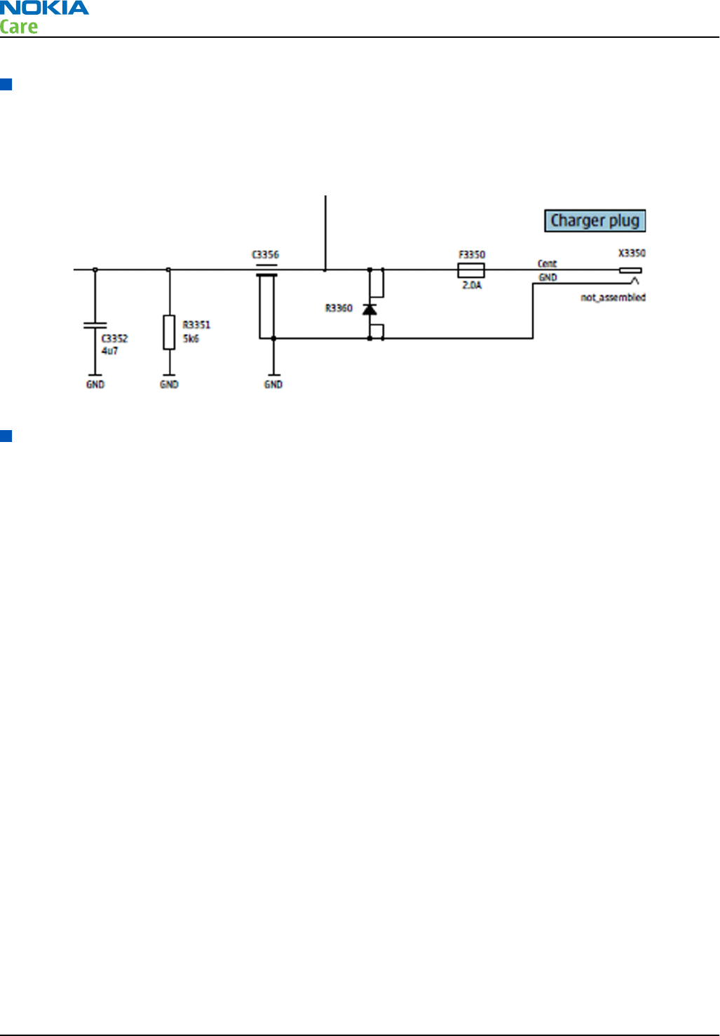
Charger interface
The charger interface is a 2 mm Dynamo charger plug. Older chargers with a 3.5 mm plug are supported via
the charger adapter cable CA-44.
Charging is controlled by Dynamo charging SMPS circuit. EM ASIC is used only for waking up the system when
the charger is connected.
Figure 55 Charger interface
User interface
Touch module
This phone uses Synaptic capacitive touch series 2000 for displays.
The Synaptics DT touch module is interfaced to I2C0 bus of RAPU via level shifter (N2500). RAPU’s GenIO123
is used for Touch INT. The level shifter is used in between the RAPU and Synaptics touch module for level
translation from 1.8V to 2.5V and vice versa.
The Synaptics DT touch module operates with VAUX2 -supply output from EMASIC. VIO is used for port-A supply
and VAUX2 is used for port-B supplies of the level shifter. The OE signal of the level shifter is tied to VAUX2 so
that the interfaces would be enabled once VAUX2 is available.
Whenever the user touches the touch screen, the controller raises an interrupt to RAPU which initiates I2C
transactions to identify the locations the user touches on the display.
RM-596
System Module
Page 6 – 20 COMPANY CONFIDENTIAL Issue 2
Copyright © 2010 Nokia. All rights reserved.
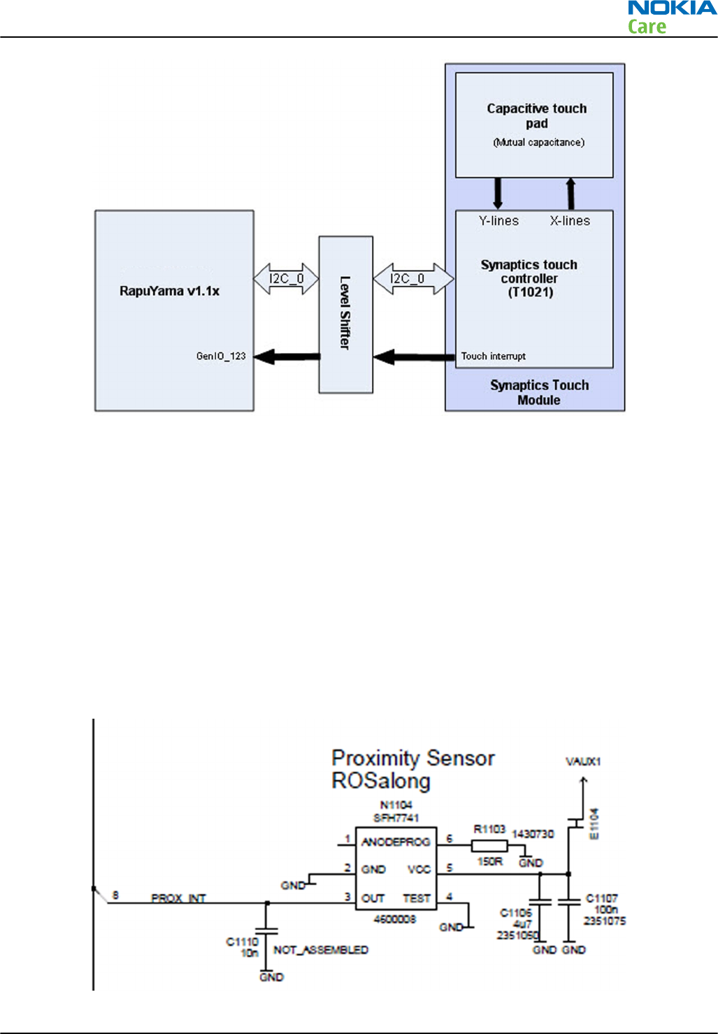
Figure 56 Touch system block diagram
Proximity sensor
Proximity sensor (N1104) Rosa Long is connected to RAPU via a single GenIO. Power supply voltage is provided
from VAUX1 output of EM ASIC. The proximity sensor is an optical reflective sensor mainly comprising of an
optical transmitter LED and optical receiver photo transistor. The proximity sensor is used is to detect indirect
impulses from the transmitter to the receiver to measure reflections from the reflective surface.
One of the typical applications of the proximity sensor is for using the proximity INT output as an indication
to SW of a phone being present near to human ear while attending a call. In such a case, the human body
will act as a reflector, due to which more IR rays fall on the photo transistor of the proximity sensor and the
o/p of the proximity sensor goes from LOW to HIGH. This LOW to HIGH transition is used as an indication to
SW of the presence of a reflector (human body in this case). SW can then switch off the display as the user is
not looking at it while attending the call. This helps in current saving. Similarly, when the user moves the
phone away from the ear, the proximity o/p goes from HIGH to LOW. This is an indication to SW that there
is no reflector nearby and the display should be switched on.
Figure 57 Proximity sensor
RM-596
System Module
Issue 2 COMPANY CONFIDENTIAL Page 6 – 21
Copyright © 2010 Nokia. All rights reserved.
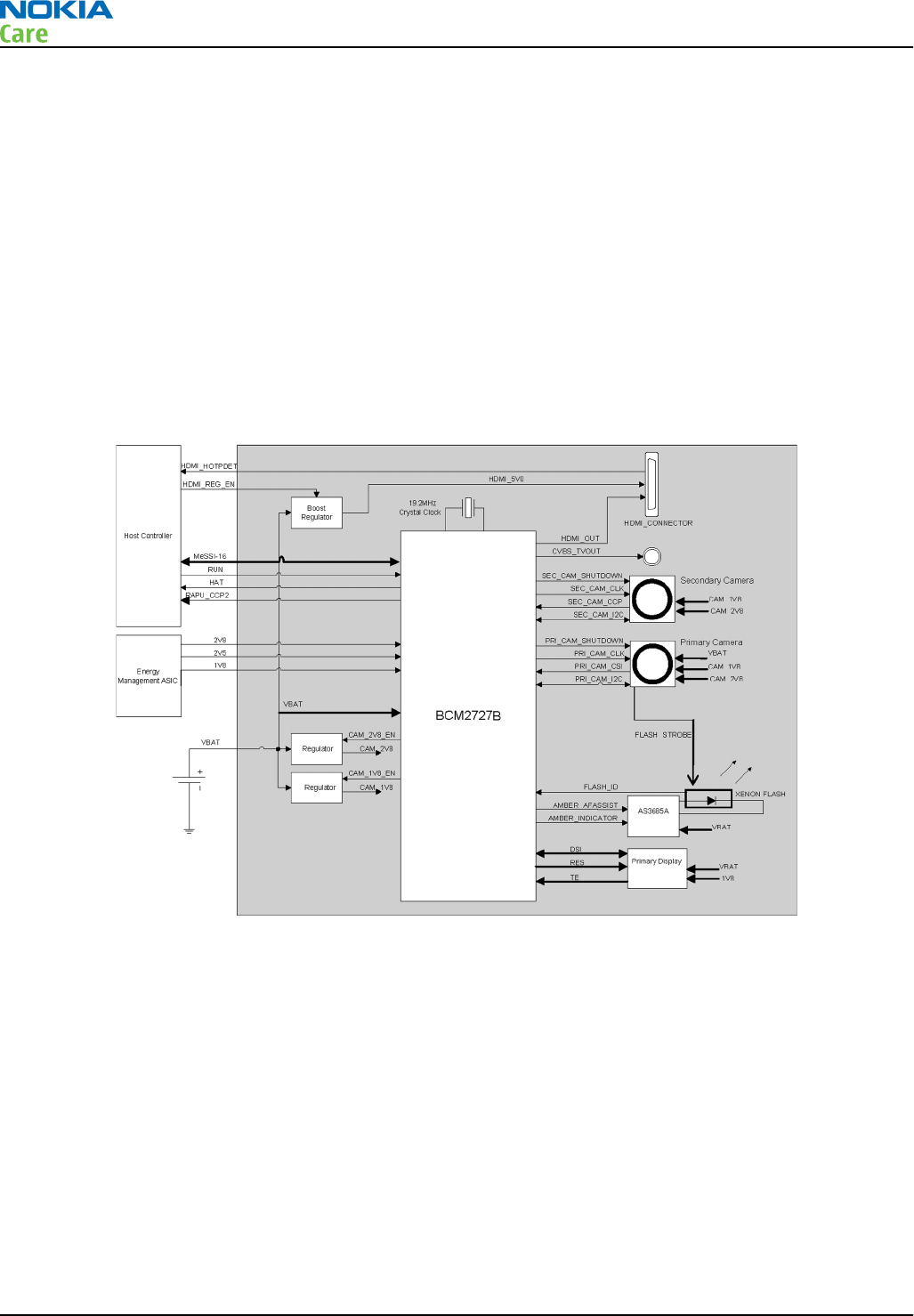
Imaging and video
Multimedia application processor
Multimedia application processor, BCM2727B, is used as a HW accelerator for imaging and video graphics.
The key features of BCM2727B are:
•12MPIx primary camera
•Secondary camera
•Xenon flash
•nHD OLED DSI display
•720p HDMI or NTSC/PAL analog TV-out
MeSSI-16 and CCP2-Tx are the key interfaces between RapuYama and BCM2727B. BCM2727B has in-build
256Mb stacked SDRAM.
Figure 58 BCM2727B block diagram
Display module
This phone uses a 3.5’’ OLED type nHD Alexander display with 16 million colors. The display module supports
the display format of 640 rows x 360 columns . The dimension of the display module is 47.8 mm x 86.3 mm
x 2.12 mm. The module interfaces to the phone via FPC with a 20 pins board to board connector.
The primary display is controlled by BCM2727B over DSI interface. The DSI Interface is used for data transfer
and control. Other display signals, RESET and TE, are interfaced to BCM2727B.
TV-out interface
The phone has HDTV and SDTV capability. The phone can be connected to HDTV through Type A to Type C HDMI
cable, and to analog TV through a TV-out cable.
BCM2727B supports both 720p 30fps HDMI and Analog PAL/NTSC TV-out.
For the HDMI interface, both audio and video data is passed from the host to BCM2727B over MeSSI-16
interface and BCM2727B sends the data to the HDMI connector.
RM-596
System Module
Page 6 – 22 COMPANY CONFIDENTIAL Issue 2
Copyright © 2010 Nokia. All rights reserved.
For the Analog TV-out, video data is passed from the host to the BCM2727B over MeSSI-16 interface and
BCM2727B sends it to the AV connector. Audio is routed separately by the host to the AV connector.
Cameras
This phone has two cameras, a 12 MPix resolution main camera and a VGA resolution secondary camera.
Xenon flash is used for the main camera.
Primary camera (Swordtail)
The primary camera is a 12 Megapixel auto focus camera module. The module size is 12.5 mm x 12.5 mm x
9 mm and it fits into the 20-pin camera socket on the phone. The camera module is SMIA profile 2 compliant
and is configured by the BCM2727B using I2C control bus. Image data is transferred to the BCM2727B for
furher processing over CSI-2 (PRI_CAM_CSI).
Figure 59 Primary camera interface
Secondary camera (VGA Acme mini)
The secondary camera is a 0.3 Megapixel fixed focus camera module. It is SMIA compliant and is configured
by the BCM2727B using I2C control bus. Image data is transferred to the BCM2727B for further processing
over a CCP based bus (SEC_CAM_CCP).
RM-596
System Module
Issue 2 COMPANY CONFIDENTIAL Page 6 – 23
Copyright © 2010 Nokia. All rights reserved.
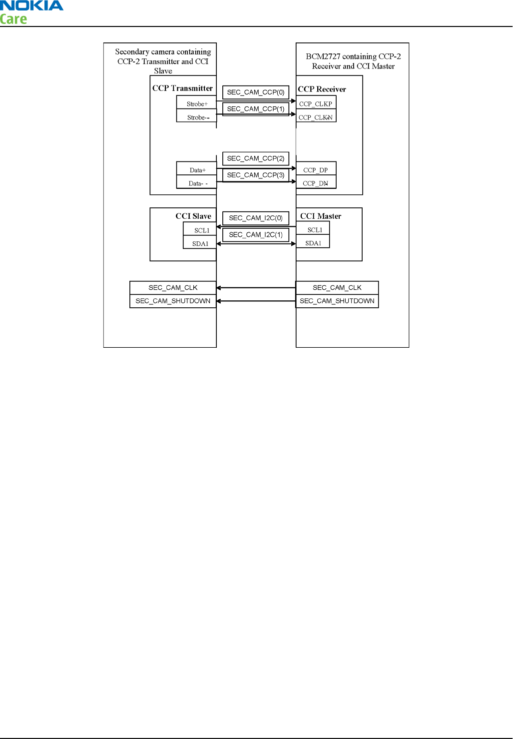
Figure 60 Secondary camera interface
Flash (Xenon)
The Xenon flash module consists of a flash lamp, capacitor bank and a LED. The flash lamp is used for flash
and pre-flash operations. The capacitor is used to store the electrical energy for discharge of the flash lamp.
Xenon flash is controlled from BCM2727B via AS3685A flash driver which is used to drive the LED in the flash
module for auto focus and indication operations. The driver has GPIO control for STROBE, ENABLE and auto
focus assist.
Illumination
Key illumination
Only MENU or HOME key illumination is supported and is handled by RGB 3 channel LED driver NJOY-3. 2 white
LEDS, V2420 and V2422, are used for MENU key illumination. These LEDs are connected in parallel to R output
of NJOY-3 LED driver.
Charging illumination
2 white LEDs are used for charging indication.
One white LED (V2410) is connected to EM ASIC “ChInd” pin and blinks only during dead battery USB charging
in intervals of 1.5s. This LED is OFF during Dynamo dead battery charging and when the charging is taking
place under SW control.
The second white LED (V2411) is connected to B output of NJOY-3 LED driver and glows for indicating USB or
Dynamo charging controlled by SW. This LED is OFF during dead battery Dynamo and USB charging. Neither
LED V2410 nor V2411 glows during Dynamo dead battery charging case.
RM-596
System Module
Page 6 – 24 COMPANY CONFIDENTIAL Issue 2
Copyright © 2010 Nokia. All rights reserved.

Figure 61 Illumination
Keyboard interface
MENU key (Home key), Volume-up and Volume-down key, Lock key, and Camera Capture and auto focus key
are directly connected to RAPU BB ASIC.
Ambient Light Sensor (ALS)
Pupumon V1100 is a digital Ambient Light Sensor (ALS) which is connected to RAPU via I2C_2 bus. It does not
have an interrupt signal as in Augumon ALS. Power supply voltage is provided from VAUX2 output of EM ASIC.
ALS is used in backlight control system to measure the amount of ambient light reaching display surface so
that it is possible to adjust the display (and keypad) brightness in order to achieve good user experience.
This also helps in saving power.
RM-596
System Module
Issue 2 COMPANY CONFIDENTIAL Page 6 – 25
Copyright © 2010 Nokia. All rights reserved.
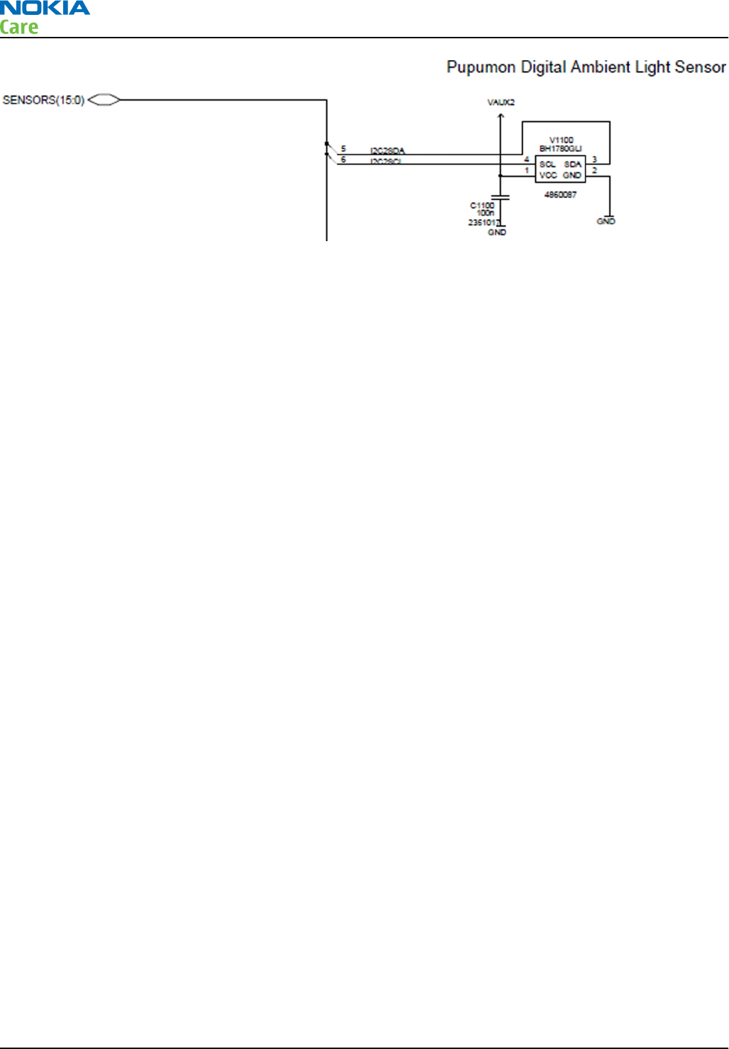
Figure 62 Ambient Light Sensor
Accelerometer
Accelerometer is a geometric type component which can be configured either to generate an inertial wake-
up interrupt signal when a programmable acceleration threshold is exceeded along one of the three axes (x,
y, and z), or to detect a free-fall event. Each axis has its own sensor and those can measure positive and
negative directions.
The 3D accelerometer (N1103) Ahti_A sensor is connected to RAPU via two GENIOs ie Genio12 and Genio44
and I2C_0 bus. Power supply voltage is provided from VIO & VAUX2 output of EM ASIC.
It has the following features:
•2.16V to 3.6V supply voltage
•1.8V compatible IOs
•Low power consumption
•±2g/±8g dynamically selectable scale
•I2C/SPI digital output interface
•Embedded self test
•10000g high shock survivability
•Pb free/RoHS compliancy
RM-596
System Module
Page 6 – 26 COMPANY CONFIDENTIAL Issue 2
Copyright © 2010 Nokia. All rights reserved.
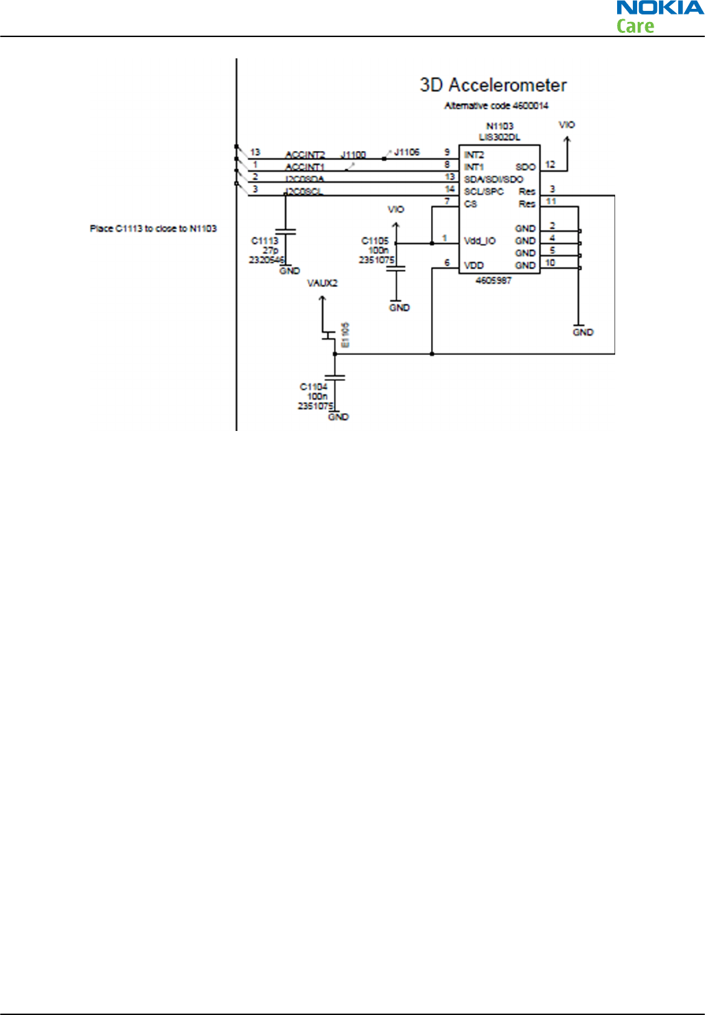
Figure 63 Accelerometer
Magnetometer
3D magnetometer sensor (N1105) is connected to RAPU via two GENIOs ie Genio40 and Genio41 and I2C_0
bus. Power supply voltage is provided from VIO & VAUX1 output of EM ASIC. The magnetometer is used as a
city compass sensor. It detects the earth magnetic field density and composes bearing information for
navigation applications.
The magnetometer has the following features:
•3-axis magnetometer device suitable for compass application
•Built-in A to D converter for magnetometer data out
•Self test function
•I2C bus interface
•Power modes: OFF mode, stand-by mode and active mode
•DRDY function for measurement data ready
•INT function to inform exceeding magnetic field strength threshold.
The operating temperature is -20°C to +85°C.
The operating supply voltages are:
•Analogue supply +2.4V to +3.6V
•Digital interface supply +1.70V to analogue supply voltage.
RM-596
System Module
Issue 2 COMPANY CONFIDENTIAL Page 6 – 27
Copyright © 2010 Nokia. All rights reserved.
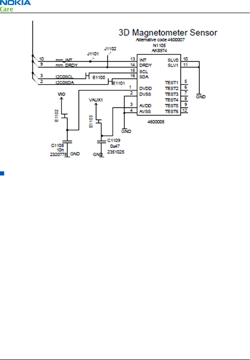
Figure 64 Magnetometer
Audio concept
Audio HW architecture
TPA6140 (N2000), BoostMono (N2150) along with mixed-signal ASIC Gazoo/Pearl provides the analogue audio
output interfaces and RAPU provides the digital audio output interface support.
RM-596
System Module
Page 6 – 28 COMPANY CONFIDENTIAL Issue 2
Copyright © 2010 Nokia. All rights reserved.
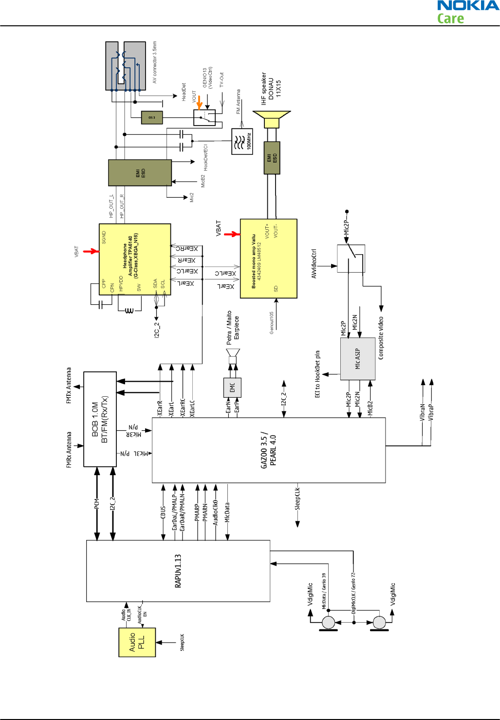
Figure 65 RM-596 Audio block diagram
RM-596
System Module
Issue 2 COMPANY CONFIDENTIAL Page 6 – 29
Copyright © 2010 Nokia. All rights reserved.
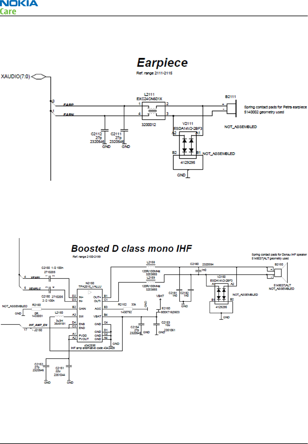
Internal earpiece
The internal earpiece used is Petra (8X12) and is connected to EM ASIC EARP and EARN lines.
Figure 66 Internal earpiece diagram
Internal handsfree (IHF) speakers
IHF speakers used are Donau and are connected to BoostMono Vallu N2150. Vallu is a mono D-class speaker
amplifier with an integrated inductive boost converter. Vallu’s differential audio inputs are connected to EM
ASIC Gazoo/Pearl XEarL, XEarLC and it can be enabled/disabled by Genout105 from Rapu.
Figure 67 Internal handsfree (IHF) speaker diagram
Internal microphones
Digital microphones used are Knopfler and are connected to Rapu. DigiMic CLK is connected to RAPU Genio72
and DigiMic DATA is connected to Rapu Genio39.
RM-596
System Module
Page 6 – 30 COMPANY CONFIDENTIAL Issue 2
Copyright © 2010 Nokia. All rights reserved.
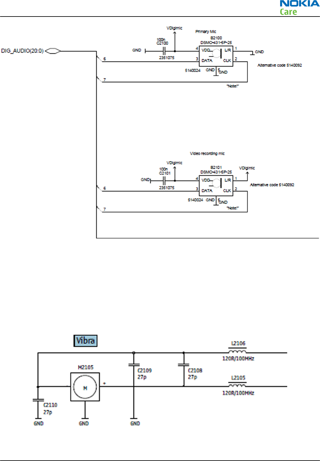
Figure 68 Internal microphones diagram
External earpiece and microphone
The AV headset earpiece is connected to TPA6140 audio amplifier which is used for high quality audio output
and to guarantee long playback time for accessory use. TPA6140 is connected to Gazoo/Pearl XEarL, XEarLC,
XEarR, XEarRC lines for audio and is controlled via I2C_2 bus by RAPU.
The AV headset microphone line is connected to EM ASIC Gazoo/Pearl Mic2 line via AV switch N2001.
Vibra
Vibra is connected to VibraN and VibraP lines of EM ASIC Gazoo/Pearl.
Figure 69 Vibra diagram
RM-596
System Module
Issue 2 COMPANY CONFIDENTIAL Page 6 – 31
Copyright © 2010 Nokia. All rights reserved.
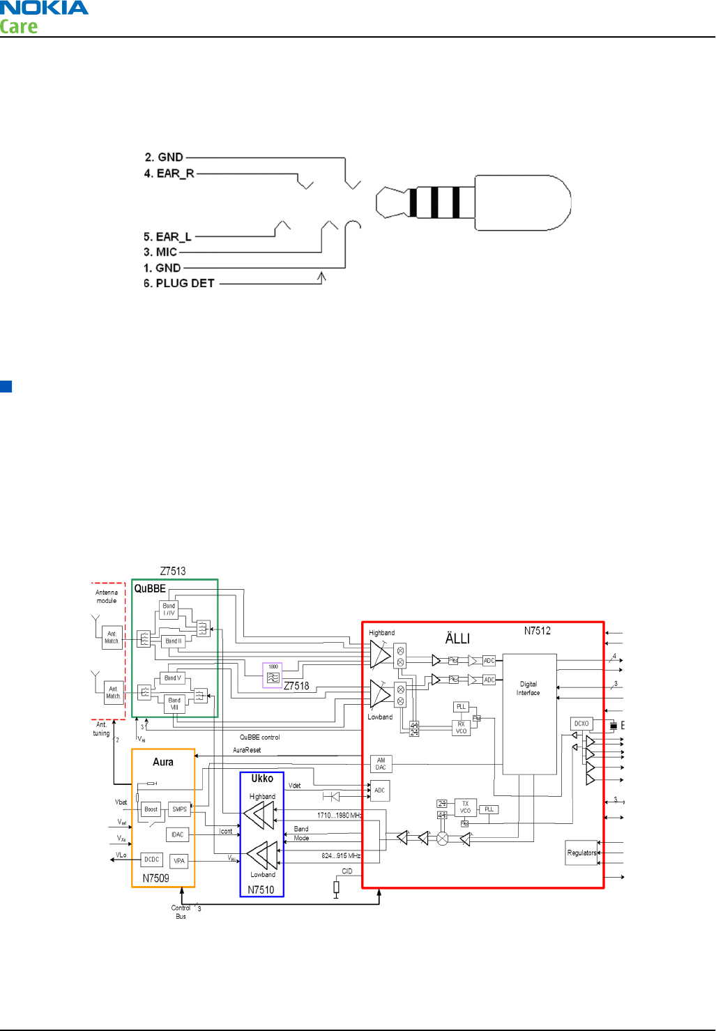
AV connector
The AV connector handles both audio and video signals output. It has audio left and right signals separately
(pins 4 and 5) and the microphone signal wired to pin 3.
Figure 70 AV connector
The AVVideoControl signal handles microphone usage of the AV connector. The plug detection signal handles
the AV connector plug detection with HeadDet signal from EM ASIC.
Cellular RF technical description
RF block
Linko RF consists of the following key components:
•Älli (Transceiver RF Asic)
•Aura (RF power management Asic)
•Ukko PA
•QuBBE (Front end module)
Figure 71 Linko RF block diagram
The RF block uses RF ASIC N7512 that performs the RF back-end functions of receive and transmit function of
the cellular transceiver.
RM-596
System Module
Page 6 – 32 COMPANY CONFIDENTIAL Issue 2
Copyright © 2010 Nokia. All rights reserved.

QuBBE
The front end module called QuBBE contains the needed front end filters and the switches. QuBBE contains:
•3 duplexers (Band II, V, VIII)
•1 triplexer (Band I, IV)
•12 switches with the control
•Low and high band GSM TX low bass filters
•50 ohms low and high and antenna interface
The control signals for the switches come from Älli.
Receiver (RX)
Linko RF has higher integration level compared to previous RF generations and especially more digital design
blocks have been integrated to Älli, RF Asic.
Älli contains the receiver chain from LNAs to digital base band interface. Digital RX baseband interface
contains four data and one clk signals. The data rate and clock frequency depend on the use case.
The main blocks in Älli are:
•LNAs: Balanced inputs for 850, 900, 1800, 1900, 2100 bands
•Passive mixer
•Analog baseband: Programmable for different modes
•ADC: Programmable Sigma Delta Modulator topology ADC
•RX Digital Front End (RXDFE): Contains for example digital filtering, DC offset compensation, wide/
narrowband power measurement blocks
There is integrated external LNA matching on the bands 900, 1800, 1900 and 2100. On 850 band, there is an
integrated matching.
Synthesizer
The synthesizer has separate highly integrated 4GHz VCOs for RX and TX. The integrator capacitors of the loop
filter are outside of the IC. The PLLs are fractional type of dividers.
The reference oscillator is an on-chip 38.4 MHz digitally controlled oscillator. The 38.4 MHz crystal is outside
of Älli. DCXO delivers the internal clock to Älli, differential clock signal to BB, and two single mode clock signals
to NCW modules. Älli delivers a clk signal to diversity RX. The oscillator is controlled via RFBus with AFC signal.
Temperature compensation of the oscillator is running by the SW in Älli. The temperature sensor itself is
outside of Älli.
Transmitter (TX)
The main features of Linko1 transmitter are:
•Common PA for GSM and WCDMA
•High and low band signal paths
•Low band: 824 - 915 MHz
•High band: 1710 - 1980 MHz
•Two operation modes in PA
•Saturation mode in GMSK usage
•Linear mode in Edge and WCDMA usage
•No TX filter between PA and Älli
RM-596
System Module
Issue 2 COMPANY CONFIDENTIAL Page 6 – 33
Copyright © 2010 Nokia. All rights reserved.

•Common regulators for GSM and WCDMA
•Boost and SMPS regulators in Aura
•Feeding the supply voltage to PA
•Operation frequency varies depending on the used system
Frequency SMPS Boost DCDC
WCDMA 3.0 MHz (typ) 4.5 MHz (typ) 1.3 MHz (typ)
GSM 9.5 MHz 7.5 MHz 2.7 MHz
•Digital interface to baseband
•WCDMA mode
•Digital IQ interface
•3 data and 1 clk signals
•GSM mode
•GSM TX data bits are sourced from baseband via RFBus to Älli
In GMSK mode, the output level of Älli is kept high with all power levels, and the output power is adjusted
by altering the collector voltage of PA. In practice, the output level of Älli is also slightly changed (optimized)
in the highest power level to keep the PA compression level more constant, which results in better overall
efficiency and performance.
In WCDMA and EDGE mode, the output power is tuned by output level of Älli. The supply voltage in WCDMA
mode is adjusted in power levels to optimize the current consumption.
RM-596
System Module
Page 6 – 34 COMPANY CONFIDENTIAL Issue 2
Copyright © 2010 Nokia. All rights reserved.
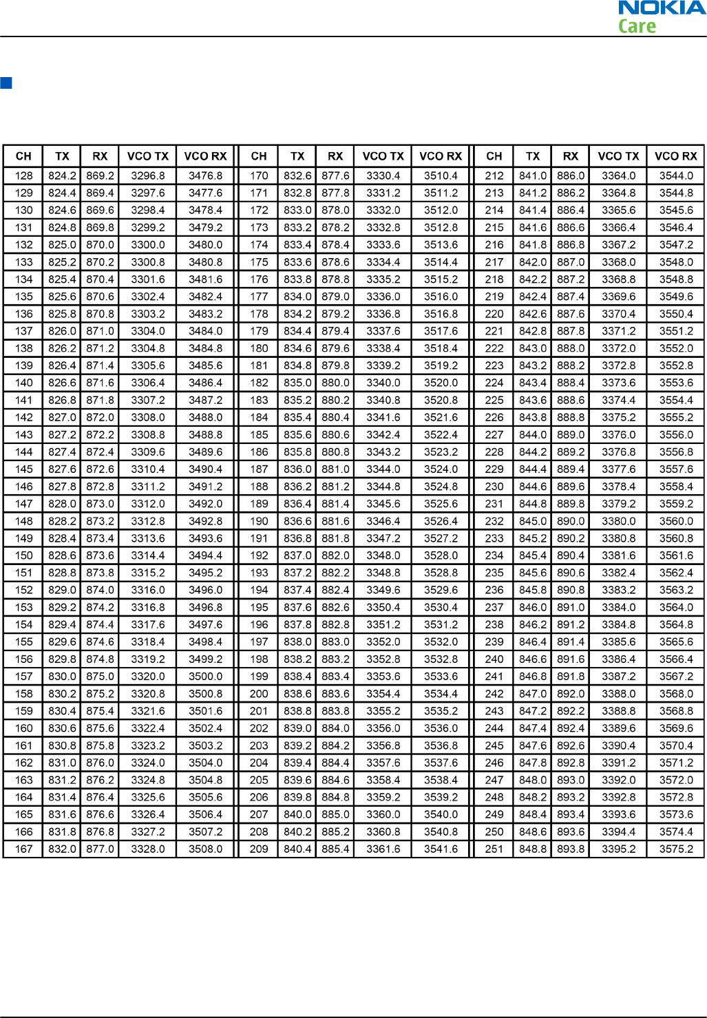
Frequency mappings
GSM850 frequencies
RM-596
System Module
Issue 2 COMPANY CONFIDENTIAL Page 6 – 35
Copyright © 2010 Nokia. All rights reserved.
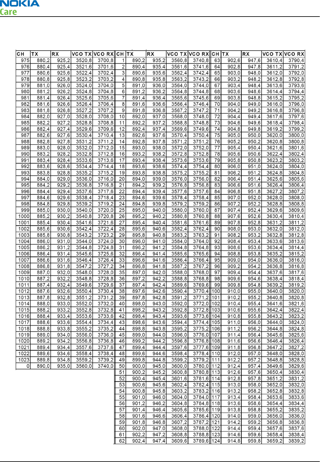
EGSM900 frequencies
RM-596
System Module
Page 6 – 36 COMPANY CONFIDENTIAL Issue 2
Copyright © 2010 Nokia. All rights reserved.
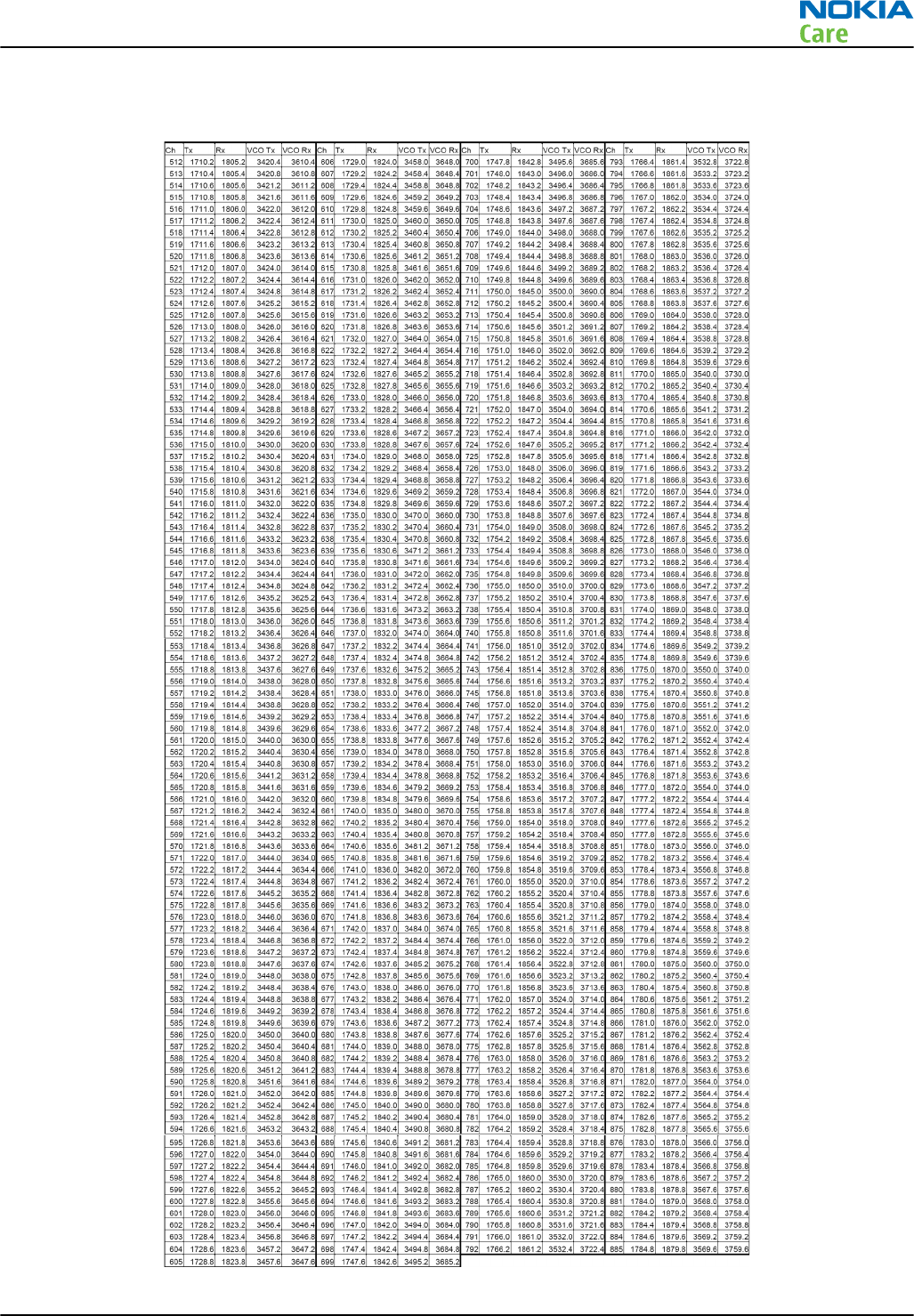
GSM1800 frequencies
RM-596
System Module
Issue 2 COMPANY CONFIDENTIAL Page 6 – 37
Copyright © 2010 Nokia. All rights reserved.
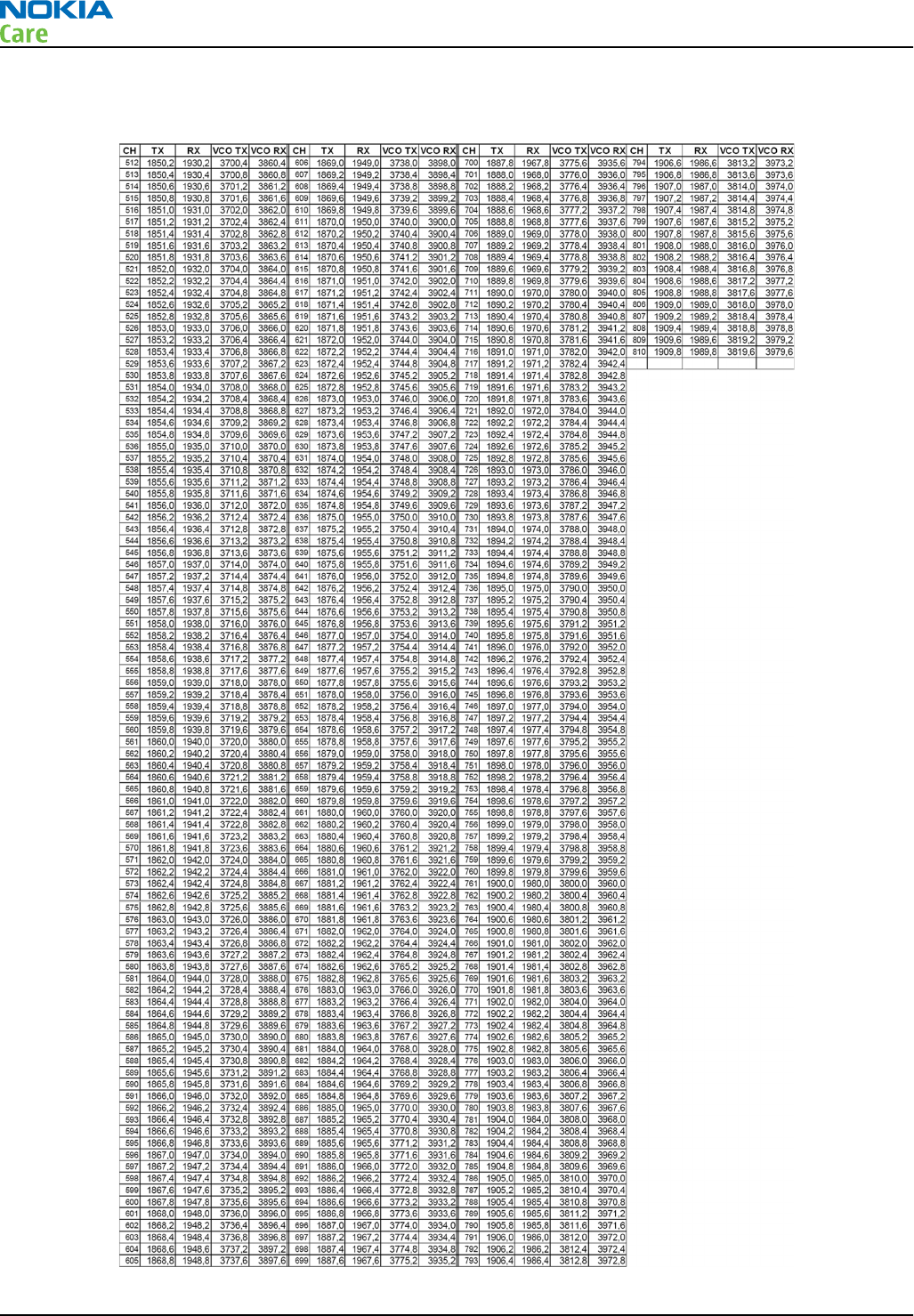
GSM1900 frequencies
RM-596
System Module
Page 6 – 38 COMPANY CONFIDENTIAL Issue 2
Copyright © 2010 Nokia. All rights reserved.
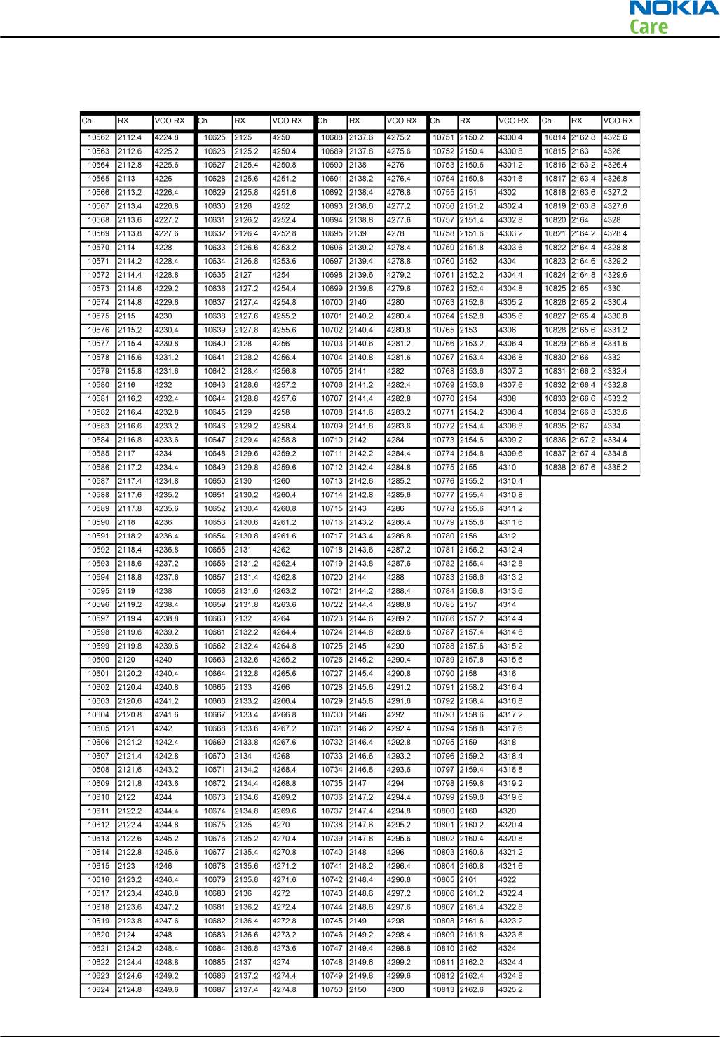
WCDMA I (2100) Rx frequencies
RM-596
System Module
Issue 2 COMPANY CONFIDENTIAL Page 6 – 39
Copyright © 2010 Nokia. All rights reserved.
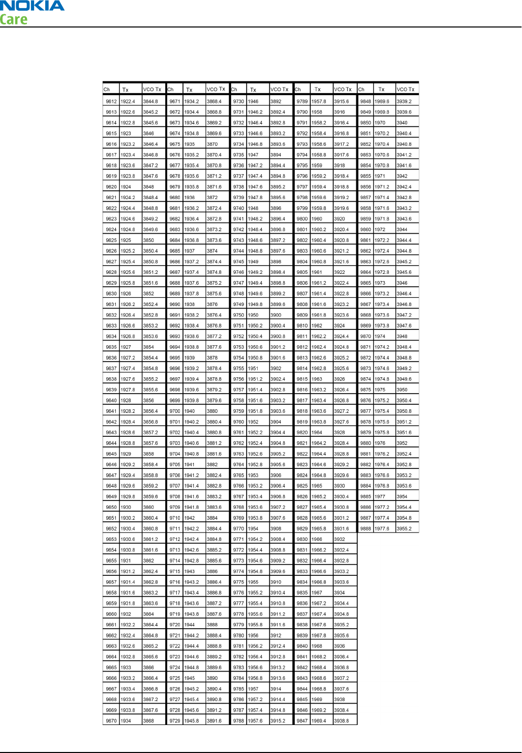
WCDMA I (2100) Tx frequencies
RM-596
System Module
Page 6 – 40 COMPANY CONFIDENTIAL Issue 2
Copyright © 2010 Nokia. All rights reserved.
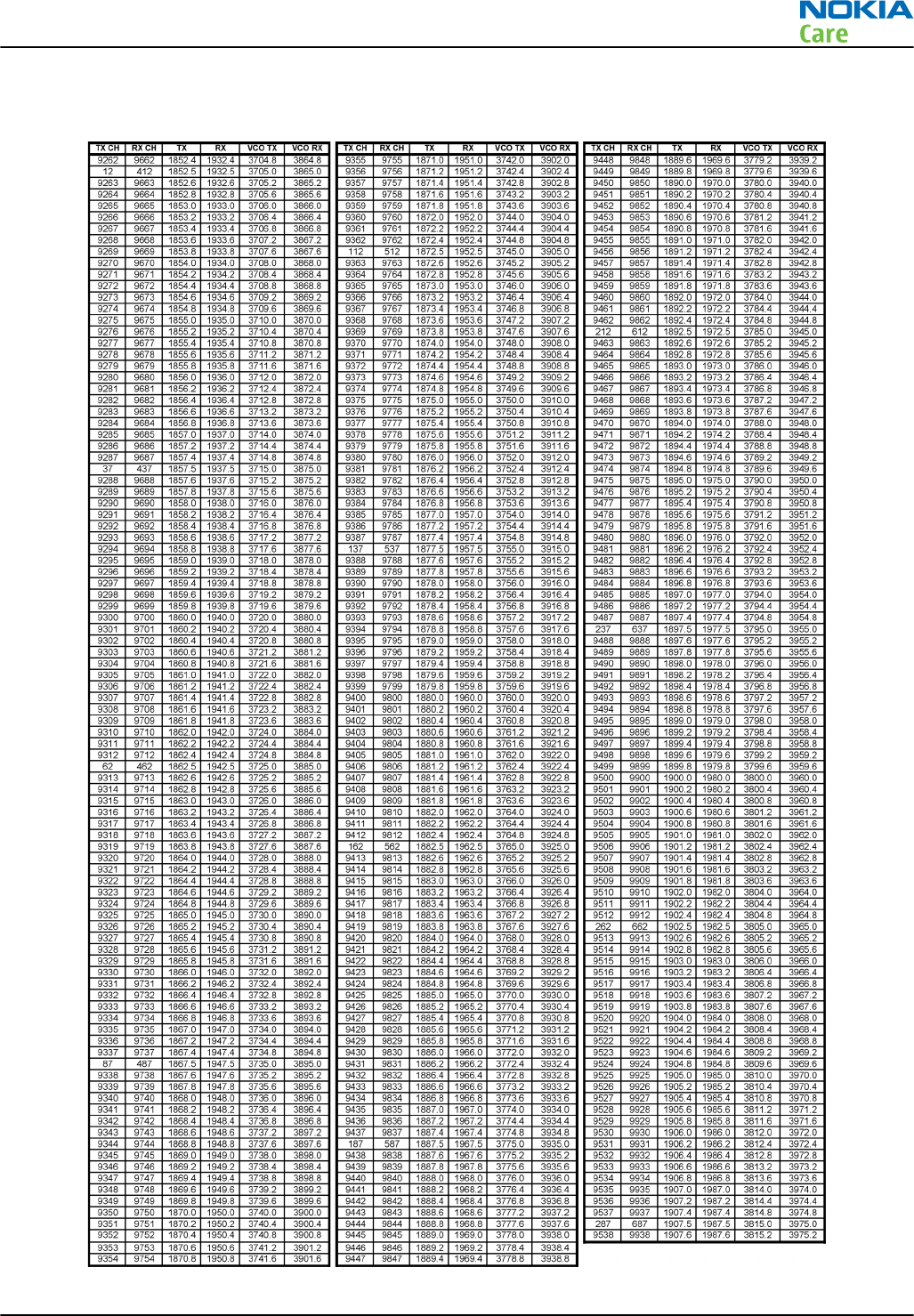
WCDMA II (1900) frequencies
RM-596
System Module
Issue 2 COMPANY CONFIDENTIAL Page 6 – 41
Copyright © 2010 Nokia. All rights reserved.
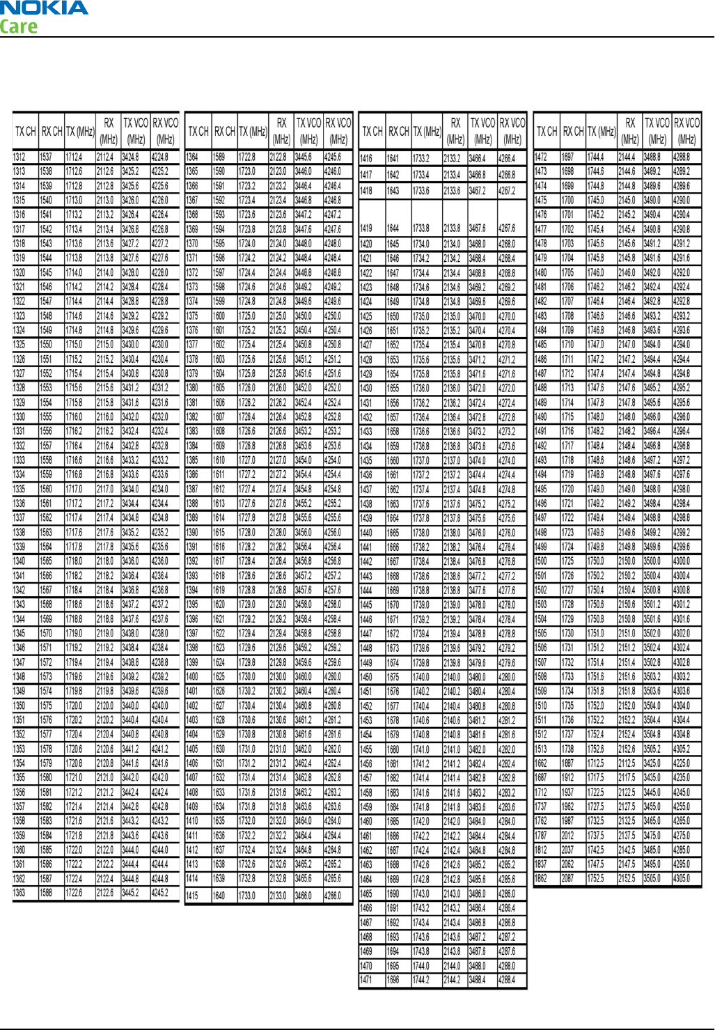
WCDMA IV (1700/2100) frequencies
RM-596
System Module
Page 6 – 42 COMPANY CONFIDENTIAL Issue 2
Copyright © 2010 Nokia. All rights reserved.
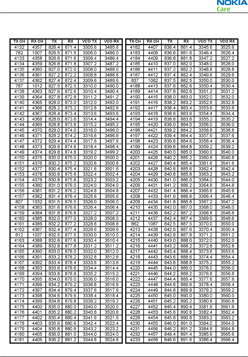
WCDMA V (850) frequencies
RM-596
System Module
Issue 2 COMPANY CONFIDENTIAL Page 6 – 43
Copyright © 2010 Nokia. All rights reserved.
WCDMA VIII (900) frequencies
Uplink CH (TX) Freq (MHz) VCO (MHz) Downlink CH (RX) Freq (MHz) VCO (MHz)
2712 882,4 3529,6 2937 927,4 3709,6
2713 882,6 3530,4 2938 927,6 3710,4
2714 882,8 3531,2 2939 927,8 3711,2
2715 883 3532 2940 928 3712
2716 883,2 3532,8 2941 928,2 3712,8
2717 883,4 3533,6 2942 928,4 3713,6
2718 883,6 3534,4 2943 928,6 3714,4
2719 883,8 3535,2 2944 928,8 3715,2
2720 884 3536 2945 929 3716
2721 884,2 3536,8 2946 929,2 3716,8
2722 884,4 3537,6 2947 929,4 3717,6
2723 884,6 3538,4 2948 929,6 3718,4
2724 884,8 3539,2 2949 929,8 3719,2
2725 885 3540 2950 930 3720
2726 885,2 3540,8 2951 930,2 3720,8
2727 885,4 3541,6 2952 930,4 3721,6
2728 885,6 3542,4 2953 930,6 3722,4
2729 885,8 3543,2 2954 930,8 3723,2
2730 886 3544 2955 931 3724
2731 886,2 3544,8 2956 931,2 3724,8
2732 886,4 3545,6 2957 931,4 3725,6
2733 886,6 3546,4 2958 931,6 3726,4
2734 886,8 3547,2 2959 931,8 3727,2
2735 887 3548 2960 932 3728
2736 887,2 3548,8 2961 932,2 3728,8
2737 887,4 3549,6 2962 932,4 3729,6
2738 887,6 3550,4 2963 932,6 3730,4
2739 887,8 3551,2 2964 932,8 3731,2
2740 888 3552 2965 933 3732
2741 888,2 3552,8 2966 933,2 3732,8
2742 888,4 3553,6 2967 933,4 3733,6
2743 888,6 3554,4 2968 933,6 3734,4
2744 888,8 3555,2 2969 933,8 3735,2
RM-596
System Module
Page 6 – 44 COMPANY CONFIDENTIAL Issue 2
Copyright © 2010 Nokia. All rights reserved.
Uplink CH (TX) Freq (MHz) VCO (MHz) Downlink CH (RX) Freq (MHz) VCO (MHz)
2745 889 3556 2970 934 3736
2746 889,2 3556,8 2971 934,2 3736,8
2747 889,4 3557,6 2972 934,4 3737,6
2748 889,6 3558,4 2973 934,6 3738,4
2749 889,8 3559,2 2974 934,8 3739,2
2750 890 3560 2975 935 3740
2751 890,2 3560,8 2976 935,2 3740,8
2752 890,4 3561,6 2977 935,4 3741,6
2753 890,6 3562,4 2978 935,6 3742,4
2754 890,8 3563,2 2979 935,8 3743,2
2755 891 3564 2980 936 3744
2756 891,2 3564,8 2981 936,2 3744,8
2757 891,4 3565,6 2982 936,4 3745,6
2758 891,6 3566,4 2983 936,6 3746,4
2759 891,8 3567,2 2984 936,8 3747,2
2760 892 3568 2985 937 3748
2761 892,2 3568,8 2986 937,2 3748,8
2762 892,4 3569,6 2987 937,4 3749,6
2763 892,6 3570,4 2988 937,6 3750,4
2764 892,8 3571,2 2989 937,8 3751,2
2765 893 3572 2990 938 3752
2766 893,2 3572,8 2991 938,2 3752,8
2767 893,4 3573,6 2992 938,4 3753,6
2768 893,6 3574,4 2993 938,6 3754,4
2769 893,8 3575,2 2994 938,8 3755,2
2770 894 3576 2995 939 3756
2771 894,2 3576,8 2996 939,2 3756,8
2772 894,4 3577,6 2997 939,4 3757,6
2773 894,6 3578,4 2998 939,6 3758,4
2774 894,8 3579,2 2999 939,8 3759,2
2775 895 3580 3000 940 3760
2776 895,2 3580,8 3001 940,2 3760,8
2777 895,4 3581,6 3002 940,4 3761,6
2778 895,6 3582,4 3003 940,6 3762,4
2779 895,8 3583,2 3004 940,8 3763,2
RM-596
System Module
Issue 2 COMPANY CONFIDENTIAL Page 6 – 45
Copyright © 2010 Nokia. All rights reserved.
Uplink CH (TX) Freq (MHz) VCO (MHz) Downlink CH (RX) Freq (MHz) VCO (MHz)
2780 896 3584 3005 941 3764
2781 896,2 3584,8 3006 941,2 3764,8
2782 896,4 3585,6 3007 941,4 3765,6
2783 896,6 3586,4 3008 941,6 3766,4
2784 896,8 3587,2 3009 941,8 3767,2
2785 897 3588 3010 942 3768
2786 897,2 3588,8 3011 942,2 3768,8
2787 897,4 3589,6 3012 942,4 3769,6
2788 897,6 3590,4 3013 942,6 3770,4
2789 897,8 3591,2 3014 942,8 3771,2
2790 898 3592 3015 943 3772
2791 898,2 3592,8 3016 943,2 3772,8
2792 898,4 3593,6 3017 943,4 3773,6
2793 898,6 3594,4 3018 943,6 3774,4
2794 898,8 3595,2 3019 943,8 3775,2
2795 899 3596 3020 944 3776
2796 899,2 3596,8 3021 944,2 3776,8
2797 899,4 3597,6 3022 944,4 3777,6
2798 899,6 3598,4 3023 944,6 3778,4
2799 899,8 3599,2 3024 944,8 3779,2
2800 900 3600 3025 945 3780
2801 900,2 3600,8 3026 945,2 3780,8
2802 900,4 3601,6 3027 945,4 3781,6
2803 900,6 3602,4 3028 945,6 3782,4
2804 900,8 3603,2 3029 945,8 3783,2
2805 901 3604 3030 946 3784
2806 901,2 3604,8 3031 946,2 3784,8
2807 901,4 3605,6 3032 946,4 3785,6
2808 901,6 3606,4 3033 946,6 3786,4
2809 901,8 3607,2 3034 946,8 3787,2
2810 902 3608 3035 947 3788
2811 902,2 3608,8 3036 947,2 3788,8
2812 902,4 3609,6 3037 947,4 3789,6
2813 902,6 3610,4 3038 947,6 3790,4
2814 902,8 3611,2 3039 947,8 3791,2
RM-596
System Module
Page 6 – 46 COMPANY CONFIDENTIAL Issue 2
Copyright © 2010 Nokia. All rights reserved.

Uplink CH (TX) Freq (MHz) VCO (MHz) Downlink CH (RX) Freq (MHz) VCO (MHz)
2815 903 3612 3040 948 3792
2816 903,2 3612,8 3041 948,2 3792,8
2817 903,4 3613,6 3042 948,4 3793,6
2818 903,6 3614,4 3043 948,6 3794,4
2819 903,8 3615,2 3044 948,8 3795,2
2820 904 3616 3045 949 3796
2821 904,2 3616,8 3046 949,2 3796,8
2822 904,4 3617,6 3047 949,4 3797,6
2823 904,6 3618,4 3048 949,6 3798,4
2824 904,8 3619,2 3049 949,8 3799,2
2825 905 3620 3050 950 3800
2826 905,2 3620,8 3051 950,2 3800,8
2827 905,4 3621,6 3052 950,4 3801,6
2828 905,6 3622,4 3053 950,6 3802,4
2829 905,8 3623,2 3054 950,8 3803,2
2830 906 3624 3055 951 3804
2831 906,2 3624,8 3056 951,2 3804,8
2832 906,4 3625,6 3057 951,4 3805,6
2833 906,6 3626,4 3058 951,6 3806,4
2834 906,8 3627,2 3059 951,8 3807,2
2835 907 3628 3060 952 3808
2836 907,2 3628,8 3061 952,2 3808,8
2837 907,4 3629,6 3062 952,4 3809,6
2838 907,6 3630,4 3063 952,6 3810,4
2839 907,8 3631,2 3064 952,8 3811,2
2840 908 3632 3065 953 3812
2841 908,2 3632,8 3066 953,2 3812,8
2842 908,4 3633,6 3067 953,4 3813,6
2843 908,6 3634,4 3068 953,6 3814,4
2844 908,8 3635,2 3069 953,8 3815,2
2845 909 3636 3070 954 3816
2846 909,2 3636,8 3071 954,2 3816,8
2847 909,4 3637,6 3072 954,4 3817,6
2848 909,6 3638,4 3073 954,6 3818,4
2849 909,8 3639,2 3074 954,8 3819,2
RM-596
System Module
Issue 2 COMPANY CONFIDENTIAL Page 6 – 47
Copyright © 2010 Nokia. All rights reserved.
Uplink CH (TX) Freq (MHz) VCO (MHz) Downlink CH (RX) Freq (MHz) VCO (MHz)
2850 910 3640 3075 955 3820
2851 910,2 3640,8 3076 955,2 3820,8
2852 910,4 3641,6 3077 955,4 3821,6
2853 910,6 3642,4 3078 955,6 3822,4
2854 910,8 3643,2 3079 955,8 3823,2
2855 911 3644 3080 956 3824
2856 911,2 3644,8 3081 956,2 3824,8
2857 911,4 3645,6 3082 956,4 3825,6
2858 911,6 3646,4 3083 956,6 3826,4
2859 911,8 3647,2 3084 956,8 3827,2
2860 912 3648 3085 957 3828
2861 912,2 3648,8 3086 957,2 3828,8
2862 912,4 3649,6 3087 957,4 3829,6
2863 912,6 3650,4 3088 957,6 3830,4
RM-596
System Module
Page 6 – 48 COMPANY CONFIDENTIAL Issue 2
Copyright © 2010 Nokia. All rights reserved.

Glossary
Nokia Customer Care
Issue 2 COMPANY CONFIDENTIAL Page Glossary– 1
Copyright © 2010 Nokia. All rights reserved.

RM-596
Glossary
(This page left intentionally blank.)
Page Glossary– 2 COMPANY CONFIDENTIAL Issue 2
Copyright © 2010 Nokia. All rights reserved.
A/D-converter Analogue-to-digital converter
ACI Accessory Control Interface
ADC Analogue-to-digital converter
ADSP Application DPS (expected to run high level tasks)
AGC Automatic gain control (maintains volume)
ALS Ambient light sensor
AMSL After Market Service Leader
ARM Advanced RISC Machines
ARPU Average revenue per user (per month or per year)
ASIC Application Specific Integrated Circuit
ASIP Application Specific Interface Protector
B2B Board to board, connector between PWB and UI board
BA Board Assembly
BB Baseband
BC02 Bluetooth module made by CSR
BIQUAD Bi-quadratic (type of filter function)
BSI Battery Size Indicator
BT Bluetooth
CBus MCU controlled serial bus connected to UPP_WD2, UEME and Zocus
CCP Compact Camera Port
CDMA Code division multiple access
CDSP Cellular DSP (expected to run at low levels)
CLDC Connected limited device configuration
CMOS Complimentary metal-oxide semiconductor circuit (low power consumption)
COF Chip on Foil
COG Chip on Glass
CPU Central Processing Unit
CSD Circuit-switched data
CSR Cambridge silicon radio
CSTN Colour Super Twisted Nematic
CTSI Clock Timing Sleep and interrupt block of Tiku
CW Continuous wave
D/A-converter Digital-to-analogue converter
DAC Digital-to-analogue converter
DBI Digital Battery Interface
DBus DSP controlled serial bus connected between UPP_WD2 and Helgo
RM-596
Glossary
Issue 2 COMPANY CONFIDENTIAL Page Glossary– 3
Copyright © 2010 Nokia. All rights reserved.

DCT-4 Digital Core Technology
DMA Direct memory access
DP Data Package
DPLL Digital Phase Locked Loop
DSP Digital Signal Processor
DTM Dual Transfer Mode
DtoS Differential to Single ended
EDGE Enhanced data rates for global/GSM evolution
EGSM Extended GSM
EM Energy management
EMC Electromagnetic compatibility
EMI Electromagnetic interference
ESD Electrostatic discharge
FCI Functional cover interface
FM Frequency Modulation
FPS Flash Programming Tool
FR Full rate
FSTN Film compensated super twisted nematic
GMSK Gaussian Minimum Shift Keying
GND Ground, conductive mass
GPIB General-purpose interface bus
GPRS General Packet Radio Service
GSM Group Special Mobile/Global System for Mobile communication
HSDPA High-speed downlink packet access
HF Hands free
HFCM Handsfree Common
HS Handset
HSCSD High speed circuit switched data (data transmission connection faster than GSM)
HW Hardware
I/O Input/Output
IBAT Battery current
IC Integrated circuit
ICHAR Charger current
IF Interface
IHF Integrated hands free
IMEI International Mobile Equipment Identity
RM-596
Glossary
Page Glossary– 4 COMPANY CONFIDENTIAL Issue 2
Copyright © 2010 Nokia. All rights reserved.
IR Infrared
IrDA Infrared Data Association
ISA Intelligent software architecture
JPEG/JPG Joint Photographic Experts Group
LCD Liquid Crystal Display
LDO Low Drop Out
LED Light-emitting diode
LPRF Low Power Radio Frequency
MCU Micro Controller Unit (microprocessor)
MCU Multiport control unit
MIC, mic Microphone
MIDP Mobile Information Device Profile
MIN Mobile identification number
MIPS Million instructions per second
MMC Multimedia card
MMS Multimedia messaging service
MP3 Compressed audio file format developed by Moving Picture Experts Group
MTP Multipoint-to-point connection
NFC Near field communication
NTC Negative temperature coefficient, temperature sensitive resistor used as a
temperature sensor
OMA Object management architecture
OMAP Operations, maintenance, and administration part
Opamp Operational Amplifier
PA Power amplifier
PCM Pulse Code Modulation
PDA Pocket Data Application
PDA Personal digital assistant
PDRAM Program/Data RAM (on chip in Tiku)
Phoenix Software tool of DCT4.x and BB5
PIM Personal Information Management
PLL Phase locked loop
PM (Phone) Permanent memory
PUP General Purpose IO (PIO), USARTS and Pulse Width Modulators
PURX Power-up reset
PWB Printed Wiring Board
RM-596
Glossary
Issue 2 COMPANY CONFIDENTIAL Page Glossary– 5
Copyright © 2010 Nokia. All rights reserved.
PWM Pulse width modulation
RC-filter Resistance-Capacitance filter
RDS Radio Data Service
RF Radio Frequency
RF PopPort ™ Reduced function PopPort ™ interface
RFBUS Serial control Bus For RF
RSK Right Soft Key
RS-MMC Reduced size Multimedia Card
RSS Web content Syndication Format
RSSI Receiving signal strength indicator
RST Reset Switch
RTC Real Time Clock (provides date and time)
RX Radio Receiver
SARAM Single Access RAM
SAW filter Surface Acoustic Wave filter
SDRAM Synchronous Dynamic Random Access Memory
SID Security ID
SIM Subscriber Identity Module
SMPS Switched Mode Power Supply
SNR Signal-to-noise ratio
SPR Standard Product requirements
SRAM Static random access memory
STI Serial Trace Interface
SW Software
SWIM Subscriber/Wallet Identification Module
TCP/IP Transmission control protocol/Internet protocol
TCXO Temperature controlled Oscillator
Tiku Finnish for Chip, Successor of the UPP
TX Radio Transmitter
UART Universal asynchronous receiver/transmitter
UEME Universal Energy Management chip (Enhanced version)
UEMEK See UEME
UI User Interface
UPnP Universal Plug and Play
UPP Universal Phone Processor
UPP_WD2 Communicator version of DCT4 system ASIC
RM-596
Glossary
Page Glossary– 6 COMPANY CONFIDENTIAL Issue 2
Copyright © 2010 Nokia. All rights reserved.
USB Universal Serial Bus
VBAT Battery voltage
VCHAR Charger voltage
VCO Voltage controlled oscillator
VCTCXO Voltage Controlled Temperature Compensated Crystal Oscillator
VCXO Voltage Controlled Crystal Oscillator
VF View Finder
Vp-p Peak-to-peak voltage
VSIM SIM voltage
WAP Wireless application protocol
WCDMA Wideband code division multiple access
WD Watchdog
WLAN Wireless local area network
XHTML Extensible hypertext markup language
Zocus Current sensor (used to monitor the current flow to and from the battery)
RM-596
Glossary
Issue 2 COMPANY CONFIDENTIAL Page Glossary– 7
Copyright © 2010 Nokia. All rights reserved.

RM-596
Glossary
(This page left intentionally blank.)
Page Glossary– 8 COMPANY CONFIDENTIAL Issue 2
Copyright © 2010 Nokia. All rights reserved.