Xilinx PG047 LogiCORE IP Ethernet 1000BASE X PCS/PMA Or SGMII V11.4, Product Guide Gig Eth Pcs Pma
User Manual: 1000BASE-X
Open the PDF directly: View PDF ![]() .
.
Page Count: 474 [warning: Documents this large are best viewed by clicking the View PDF Link!]
- LogiCORE IP Ethernet 1000BASE-X PCS/PMA or SGMII v11.4
- Table of Contents
- Section I: Summary
- IP Facts
- Overview
- Product Specification
- Designing with the Core
- The Ten-Bit Interface
- 1000BASE-X with Transceivers
- Transceiver Logic
- Clock Sharing Across Multiple Cores with Transceivers
- Example Design for 1000BASE-X with Transceivers
- Top-Level Example Design HDL
- Block Level HDL
- Transceiver Files for Zynq-7000, Virtex-7, Kintex-7, Artix-7 and Devices
- Transceiver Files for Spartan-6 Devices
- Transceiver Files for Virtex-6 Devices
- RocketIO Transceiver Files for Virtex-5 Devices
- Virtex-5 FPGA RocketIO GTX Transceiver Specific Files
- RocketIO Transceiver Files for Virtex-4 FX Devices
- Transmitter Elastic Buffer
- Demonstration Test Bench
- Customizing the Test Bench
- SGMII / Dynamic Standards Switching with Transceivers
- Receiver Elastic Buffer Implementations
- Logic Using the Transceiver Rx Elastic Buffer
- Transceiver Logic with the FPGA Logic Rx Elastic Buffer
- Virtex-4 Devices for SGMII or Dynamic Standards Switching
- Virtex-5 LXT or SXT Devices for SGMII or Dynamic Standards Switching
- Virtex-5 FXT and TXT Devices for SGMII or Dynamic Standards Switching
- Virtex-6 Devices for SGMII or Dynamic Standards Switching
- Spartan-6 LXT Devices for SGMII or Dynamic Standards Switching
- Virtex-7 Devices for SGMII or Dynamic Standards Switching
- Kintex-7 and Zynq-7000 Devices for SGMII or Dynamic Standards Switching
- Artix-7 Devices for SGMII or Dynamic Standards Switching
- Clock Sharing - Multiple Cores with Transceivers, FPGA Logic Elastic Buffer
- SGMII Example Design / Dynamic Switching Example Design Using a Transceiver
- Top-Level Example Design HDL
- Block Level HDL
- Transceiver Files for Zynq-7000, Virtex-7 Kintex-7, and Artix-7 Devices
- Transceiver Files for Spartan-6 Devices
- Transceiver Files for Virtex-6 Devices
- RocketIO Transceiver Files for Virtex-5 Devices
- RocketIO Transceiver Files for Virtex-4 FX Devices
- Receiver Elastic Buffer
- SGMII Adaptation Module
- Demonstration Test Bench
- Customizing the Test Bench
- SGMII over LVDS
- Using the Client-Side GMII Datapath
- Auto-Negotiation
- Dynamic Switching of 1000BASE-X and SGMII Standards
- GMII to PHY EDK Application for Zynq-7000 Device Processor Subsystem
- Interfacing to Other Cores
- Integration of the Tri-Mode Ethernet MAC for 1000BASE-X Operation
- Integration of the Tri-Mode Ethernet MAC for Tri-speed SGMII Operation
- Integration of the Tri-Mode Ethernet MAC to Provide SGMII (or Dynamic Switching) Functionality with TBI
- Integration of the Tri-Mode Ethernet MAC Using Device Specific Transceivers
- Integration of the Tri-Mode Ethernet MAC Using Asynchronous Oversampling over Virtex-6 LVDS
- Integration of the Tri-Mode Ethernet MAC Using Sync SGMII over Kintex-7/Virtex-7 LVDS
- Special Design Considerations
- Section II: Vivado Design Suite
- Section III: ISE Design Suite
- Customizing and Generating the Core
- Constraining the Core
- Device, Package, and Speed Grade Selection
- I/O Location Constraints
- Placement Constraints
- Virtex-4 FPGA MGT Transceivers for 1000BASE-X Constraints
- Virtex-4 FPGA RocketIO MGT Transceivers for SGMII or Dynamic Standards Switching Constraints
- Virtex-5 FPGA RocketIO GTP Transceivers for 1000BASE-X Constraints
- Virtex-5 FPGA RocketIO GTP Transceivers for SGMII or Dynamic Standards Switching Constraints
- Virtex-5 FPGA RocketIO GTX Transceivers for SGMII or Dynamic Standards Switching Constraints
- Virtex-6 FPGA GTX Transceivers for 1000BASE-X Constraints
- Virtex-6 FPGA GTX Transceivers for SGMII or Dynamic Standards Switching Constraints
- Spartan-6 FPGA GTP Transceivers for 1000BASE-X Constraints
- Spartan-6 FPGA GTP Transceivers for SGMII or Dynamic Standards Switching Constraints
- 7 Series and Zynq-7000 Device Transceivers for 1000BASE-X Constraints
- 7 Series and Zynq-7000 Device Transceivers for SGMII or Dynamic Standards Switching Constraints
- SGMII over LVDS Constraints
- Ten-Bit Interface Constraints
- Constraints When Implementing an External GMII
- Understanding Timing Reports for Setup/Hold Timing
- Implementing the Design
- Detailed Example Design
- Section IV: Appendices

LogiCORE IP Ethernet
1000BASE-X PCS/PMA or
SGMII v11.4
Product Guide
PG047 October 16, 2012

1000BASE-X PCS/PMA or SGMII v11.4 www.xilinx.com 2
PG047 October 16, 2012
Table of Contents
SECTION I: SUMMARY
IP Facts
Features . . . . . . . . . . . . . . . . . . . . . . . . . . . . . . . . . . . . . . . . . . . . . . . . . . . . . . . . . . . . . . . . . . . . . . . . 10
Chapter 1: Overview
Core Overview . . . . . . . . . . . . . . . . . . . . . . . . . . . . . . . . . . . . . . . . . . . . . . . . . . . . . . . . . . . . . . . . . . . 12
Recommended Design Experience . . . . . . . . . . . . . . . . . . . . . . . . . . . . . . . . . . . . . . . . . . . . . . . . . . . 19
System Requirements . . . . . . . . . . . . . . . . . . . . . . . . . . . . . . . . . . . . . . . . . . . . . . . . . . . . . . . . . . . . . 20
Applications . . . . . . . . . . . . . . . . . . . . . . . . . . . . . . . . . . . . . . . . . . . . . . . . . . . . . . . . . . . . . . . . . . . . . 20
Verification . . . . . . . . . . . . . . . . . . . . . . . . . . . . . . . . . . . . . . . . . . . . . . . . . . . . . . . . . . . . . . . . . . . . . . 22
Licensing and Ordering Information . . . . . . . . . . . . . . . . . . . . . . . . . . . . . . . . . . . . . . . . . . . . . . . . . . 23
Chapter 2: Product Specification
Overview of Ethernet Architecture. . . . . . . . . . . . . . . . . . . . . . . . . . . . . . . . . . . . . . . . . . . . . . . . . . . 24
Standards . . . . . . . . . . . . . . . . . . . . . . . . . . . . . . . . . . . . . . . . . . . . . . . . . . . . . . . . . . . . . . . . . . . . . . . 25
Performance. . . . . . . . . . . . . . . . . . . . . . . . . . . . . . . . . . . . . . . . . . . . . . . . . . . . . . . . . . . . . . . . . . . . . 26
Voltage Requirements . . . . . . . . . . . . . . . . . . . . . . . . . . . . . . . . . . . . . . . . . . . . . . . . . . . . . . . . . . . . . 27
Speed Grades . . . . . . . . . . . . . . . . . . . . . . . . . . . . . . . . . . . . . . . . . . . . . . . . . . . . . . . . . . . . . . . . . . . . 28
Resource Utilization. . . . . . . . . . . . . . . . . . . . . . . . . . . . . . . . . . . . . . . . . . . . . . . . . . . . . . . . . . . . . . . 28
Port Descriptions . . . . . . . . . . . . . . . . . . . . . . . . . . . . . . . . . . . . . . . . . . . . . . . . . . . . . . . . . . . . . . . . . 34
Register Space . . . . . . . . . . . . . . . . . . . . . . . . . . . . . . . . . . . . . . . . . . . . . . . . . . . . . . . . . . . . . . . . . . . 49
Chapter 3: Designing with the Core
General Design Guidelines . . . . . . . . . . . . . . . . . . . . . . . . . . . . . . . . . . . . . . . . . . . . . . . . . . . . . . . . . 89
Clocking. . . . . . . . . . . . . . . . . . . . . . . . . . . . . . . . . . . . . . . . . . . . . . . . . . . . . . . . . . . . . . . . . . . . . . . . . 92
Resets . . . . . . . . . . . . . . . . . . . . . . . . . . . . . . . . . . . . . . . . . . . . . . . . . . . . . . . . . . . . . . . . . . . . . . . . . . 93
Chapter 4: The Ten-Bit Interface
Ten-Bit-Interface Logic. . . . . . . . . . . . . . . . . . . . . . . . . . . . . . . . . . . . . . . . . . . . . . . . . . . . . . . . . . . . . 97
Clock Sharing across Multiple Cores with TBI . . . . . . . . . . . . . . . . . . . . . . . . . . . . . . . . . . . . . . . . . 113
Example Designs for the Ten-Bit Interface (TBI) . . . . . . . . . . . . . . . . . . . . . . . . . . . . . . . . . . . . . . . 114

1000BASE-X PCS/PMA or SGMII v11.4 www.xilinx.com 3
PG047 October 16, 2012
Chapter 5: 1000BASE-X with Transceivers
Transceiver Logic . . . . . . . . . . . . . . . . . . . . . . . . . . . . . . . . . . . . . . . . . . . . . . . . . . . . . . . . . . . . . . . . 131
Clock Sharing Across Multiple Cores with Transceivers . . . . . . . . . . . . . . . . . . . . . . . . . . . . . . . . . 148
Example Design for 1000BASE-X with Transceivers. . . . . . . . . . . . . . . . . . . . . . . . . . . . . . . . . . . . . 164
Chapter 6: SGMII / Dynamic Standards Switching with Transceivers
Receiver Elastic Buffer Implementations . . . . . . . . . . . . . . . . . . . . . . . . . . . . . . . . . . . . . . . . . . . . . 181
Logic Using the Transceiver Rx Elastic Buffer. . . . . . . . . . . . . . . . . . . . . . . . . . . . . . . . . . . . . . . . . . 184
Transceiver Logic with the FPGA Logic Rx Elastic Buffer . . . . . . . . . . . . . . . . . . . . . . . . . . . . . . . . . 184
Clock Sharing - Multiple Cores with Transceivers, FPGA Logic Elastic Buffer . . . . . . . . . . . . . . . . 206
SGMII Example Design / Dynamic Switching Example Design Using a Transceiver . . . . . . . . . . . 222
Chapter 7: SGMII over LVDS
Synchronous SGMII over Virtex7/Kintex 7 FPGA LVDS . . . . . . . . . . . . . . . . . . . . . . . . . . . . . . . . . . 239
SGMII Support Using Asynchronous Oversampling over Virtex-6 FPGA LVDS . . . . . . . . . . . . . . . 260
Chapter 8: Using the Client-Side GMII Datapath
Using the Core Netlist Client-side GMII for the 1000BASE-X Standard . . . . . . . . . . . . . . . . . . . . . 290
Using the Core Netlist Client-Side GMII for the SGMII Standard . . . . . . . . . . . . . . . . . . . . . . . . . . 296
Additional Client-Side SGMII Logic Provided in the Example Design . . . . . . . . . . . . . . . . . . . . . . . 299
Chapter 9: Auto-Negotiation
Overview of Operation . . . . . . . . . . . . . . . . . . . . . . . . . . . . . . . . . . . . . . . . . . . . . . . . . . . . . . . . . . . 306
Setting the Configurable Link Timer . . . . . . . . . . . . . . . . . . . . . . . . . . . . . . . . . . . . . . . . . . . . . . . . . 311
Using the Auto-Negotiation Interrupt . . . . . . . . . . . . . . . . . . . . . . . . . . . . . . . . . . . . . . . . . . . . . . . 312
Use of Clock Correction Sequences in Device Specific Transceivers (1000BASE-X Standard). . . . 312
Conclusion . . . . . . . . . . . . . . . . . . . . . . . . . . . . . . . . . . . . . . . . . . . . . . . . . . . . . . . . . . . . . . . . . . . . . 313
Chapter 10: Dynamic Switching of 1000BASE-X and SGMII Standards
Typical Application. . . . . . . . . . . . . . . . . . . . . . . . . . . . . . . . . . . . . . . . . . . . . . . . . . . . . . . . . . . . . . . 314
Operation of the Core . . . . . . . . . . . . . . . . . . . . . . . . . . . . . . . . . . . . . . . . . . . . . . . . . . . . . . . . . . . . 315
Chapter 11: GMII to PHY EDK Application for Zynq-7000 Device Processor
Subsystem
Overview . . . . . . . . . . . . . . . . . . . . . . . . . . . . . . . . . . . . . . . . . . . . . . . . . . . . . . . . . . . . . . . . . . . . . . 317
GMII to 1000BASEX . . . . . . . . . . . . . . . . . . . . . . . . . . . . . . . . . . . . . . . . . . . . . . . . . . . . . . . . . . . . . . 318
GMII to SGMII Using Zynq-7000 Device Gigabit Transceiver . . . . . . . . . . . . . . . . . . . . . . . . . . . . . 320
GMII to SGMII Using Zynq-7000 Device LVDS Transceiver . . . . . . . . . . . . . . . . . . . . . . . . . . . . . . . 322

1000BASE-X PCS/PMA or SGMII v11.4 www.xilinx.com 4
PG047 October 16, 2012
Chapter 12: Interfacing to Other Cores
Integration of the Tri-Mode Ethernet MAC for 1000BASE-X Operation . . . . . . . . . . . . . . . . . . . . 325
Integration of the Tri-Mode Ethernet MAC for Tri-speed SGMII Operation . . . . . . . . . . . . . . . . . 344
Chapter 13: Special Design Considerations
Power Management . . . . . . . . . . . . . . . . . . . . . . . . . . . . . . . . . . . . . . . . . . . . . . . . . . . . . . . . . . . . . 369
Start-up Sequencing. . . . . . . . . . . . . . . . . . . . . . . . . . . . . . . . . . . . . . . . . . . . . . . . . . . . . . . . . . . . . . 369
Loopback. . . . . . . . . . . . . . . . . . . . . . . . . . . . . . . . . . . . . . . . . . . . . . . . . . . . . . . . . . . . . . . . . . . . . . . 370
SECTION II: VIVADO DESIGN SUITE
Chapter 14: Customizing and Generating the Core
GUI . . . . . . . . . . . . . . . . . . . . . . . . . . . . . . . . . . . . . . . . . . . . . . . . . . . . . . . . . . . . . . . . . . . . . . . . . . . 373
Output Generation. . . . . . . . . . . . . . . . . . . . . . . . . . . . . . . . . . . . . . . . . . . . . . . . . . . . . . . . . . . . . . . 378
Chapter 15: Constraining the Core
Required Constraints . . . . . . . . . . . . . . . . . . . . . . . . . . . . . . . . . . . . . . . . . . . . . . . . . . . . . . . . . . . . . 379
Device, Package, and Speed Grade Selections. . . . . . . . . . . . . . . . . . . . . . . . . . . . . . . . . . . . . . . . . 379
Clock Frequencies . . . . . . . . . . . . . . . . . . . . . . . . . . . . . . . . . . . . . . . . . . . . . . . . . . . . . . . . . . . . . . . 380
I/O Standard and Placement. . . . . . . . . . . . . . . . . . . . . . . . . . . . . . . . . . . . . . . . . . . . . . . . . . . . . . . 381
Chapter 16: Detailed Example Design
Example Design . . . . . . . . . . . . . . . . . . . . . . . . . . . . . . . . . . . . . . . . . . . . . . . . . . . . . . . . . . . . . . . . . 382
Demonstration Test Bench . . . . . . . . . . . . . . . . . . . . . . . . . . . . . . . . . . . . . . . . . . . . . . . . . . . . . . . . 382
SECTION III: ISE DESIGN SUITE
Chapter 17: Customizing and Generating the Core
GUI . . . . . . . . . . . . . . . . . . . . . . . . . . . . . . . . . . . . . . . . . . . . . . . . . . . . . . . . . . . . . . . . . . . . . . . . . . . 384
Parameter Values in the XCO File . . . . . . . . . . . . . . . . . . . . . . . . . . . . . . . . . . . . . . . . . . . . . . . . . . . 389
Output Generation. . . . . . . . . . . . . . . . . . . . . . . . . . . . . . . . . . . . . . . . . . . . . . . . . . . . . . . . . . . . . . . 390
Chapter 18: Constraining the Core
Device, Package, and Speed Grade Selection . . . . . . . . . . . . . . . . . . . . . . . . . . . . . . . . . . . . . . . . . 391
I/O Location Constraints . . . . . . . . . . . . . . . . . . . . . . . . . . . . . . . . . . . . . . . . . . . . . . . . . . . . . . . . . . 392
Placement Constraints. . . . . . . . . . . . . . . . . . . . . . . . . . . . . . . . . . . . . . . . . . . . . . . . . . . . . . . . . . . . 392
Virtex-4 FPGA MGT Transceivers for 1000BASE-X Constraints . . . . . . . . . . . . . . . . . . . . . . . . . . . . 392
Virtex-4 FPGA RocketIO MGT Transceivers for SGMII or Dynamic Standards
Switching Constraints . . . . . . . . . . . . . . . . . . . . . . . . . . . . . . . . . . . . . . . . . . . . . . . . . . . . . . . . . 394

1000BASE-X PCS/PMA or SGMII v11.4 www.xilinx.com 5
PG047 October 16, 2012
Virtex-5 FPGA RocketIO GTP Transceivers for 1000BASE-X Constraints . . . . . . . . . . . . . . . . . . . . 394
Virtex-5 FPGA RocketIO GTP Transceivers for SGMII or Dynamic Standards
Switching Constraints . . . . . . . . . . . . . . . . . . . . . . . . . . . . . . . . . . . . . . . . . . . . . . . . . . . . . . . . . 395
Virtex-5 FPGA RocketIO GTX Transceivers for SGMII or Dynamic Standards
Switching Constraints . . . . . . . . . . . . . . . . . . . . . . . . . . . . . . . . . . . . . . . . . . . . . . . . . . . . . . . . . 397
Virtex-6 FPGA GTX Transceivers for 1000BASE-X Constraints . . . . . . . . . . . . . . . . . . . . . . . . . . . . 398
Virtex-6 FPGA GTX Transceivers for SGMII or Dynamic Standards Switching Constraints . . . . . . 399
Spartan-6 FPGA GTP Transceivers for 1000BASE-X Constraints . . . . . . . . . . . . . . . . . . . . . . . . . . . 400
Spartan-6 FPGA GTP Transceivers for SGMII or Dynamic Standards Switching Constraints . . . . 401
7 Series and Zynq-7000 Device Transceivers for 1000BASE-X Constraints . . . . . . . . . . . . . . . . . . 402
7 Series and Zynq-7000 Device Transceivers for SGMII or Dynamic Standards
Switching Constraints . . . . . . . . . . . . . . . . . . . . . . . . . . . . . . . . . . . . . . . . . . . . . . . . . . . . . . . . . 403
SGMII over LVDS Constraints . . . . . . . . . . . . . . . . . . . . . . . . . . . . . . . . . . . . . . . . . . . . . . . . . . . . . . 404
Ten-Bit Interface Constraints . . . . . . . . . . . . . . . . . . . . . . . . . . . . . . . . . . . . . . . . . . . . . . . . . . . . . . 404
Constraints When Implementing an External GMII. . . . . . . . . . . . . . . . . . . . . . . . . . . . . . . . . . . . . 411
Understanding Timing Reports for Setup/Hold Timing. . . . . . . . . . . . . . . . . . . . . . . . . . . . . . . . . . 418
Chapter 19: Implementing the Design
Pre-implementation Simulation . . . . . . . . . . . . . . . . . . . . . . . . . . . . . . . . . . . . . . . . . . . . . . . . . . . . 419
Using the Simulation Model . . . . . . . . . . . . . . . . . . . . . . . . . . . . . . . . . . . . . . . . . . . . . . . . . . . . . . . 419
Synthesis. . . . . . . . . . . . . . . . . . . . . . . . . . . . . . . . . . . . . . . . . . . . . . . . . . . . . . . . . . . . . . . . . . . . . . . 420
Implementation . . . . . . . . . . . . . . . . . . . . . . . . . . . . . . . . . . . . . . . . . . . . . . . . . . . . . . . . . . . . . . . . . 421
Post-Implementation Simulation . . . . . . . . . . . . . . . . . . . . . . . . . . . . . . . . . . . . . . . . . . . . . . . . . . . 422
Other Implementation Information . . . . . . . . . . . . . . . . . . . . . . . . . . . . . . . . . . . . . . . . . . . . . . . . . 423
Chapter 20: Detailed Example Design
Directory Structure . . . . . . . . . . . . . . . . . . . . . . . . . . . . . . . . . . . . . . . . . . . . . . . . . . . . . . . . . . . . . . 425
Directory and File Contents. . . . . . . . . . . . . . . . . . . . . . . . . . . . . . . . . . . . . . . . . . . . . . . . . . . . . . . . 426
Example Designs . . . . . . . . . . . . . . . . . . . . . . . . . . . . . . . . . . . . . . . . . . . . . . . . . . . . . . . . . . . . . . . . 430
Demonstration Test Bench . . . . . . . . . . . . . . . . . . . . . . . . . . . . . . . . . . . . . . . . . . . . . . . . . . . . . . . . 430
Implementation Scripts . . . . . . . . . . . . . . . . . . . . . . . . . . . . . . . . . . . . . . . . . . . . . . . . . . . . . . . . . . . 430
Simulation Scripts . . . . . . . . . . . . . . . . . . . . . . . . . . . . . . . . . . . . . . . . . . . . . . . . . . . . . . . . . . . . . . . 431
SECTION IV: APPENDICES
Appendix A: Verification, Compliance, and Interoperability
Simulation . . . . . . . . . . . . . . . . . . . . . . . . . . . . . . . . . . . . . . . . . . . . . . . . . . . . . . . . . . . . . . . . . . . . . 433
Hardware Testing. . . . . . . . . . . . . . . . . . . . . . . . . . . . . . . . . . . . . . . . . . . . . . . . . . . . . . . . . . . . . . . . 433
Verification . . . . . . . . . . . . . . . . . . . . . . . . . . . . . . . . . . . . . . . . . . . . . . . . . . . . . . . . . . . . . . . . . . . . . 434

1000BASE-X PCS/PMA or SGMII v11.4 www.xilinx.com 6
PG047 October 16, 2012
Appendix B: Migrating
Appendix C: 1000BASE-X State Machines
Introduction . . . . . . . . . . . . . . . . . . . . . . . . . . . . . . . . . . . . . . . . . . . . . . . . . . . . . . . . . . . . . . . . . . . . 436
Start of Frame Encoding . . . . . . . . . . . . . . . . . . . . . . . . . . . . . . . . . . . . . . . . . . . . . . . . . . . . . . . . . . 437
End of Frame Encoding . . . . . . . . . . . . . . . . . . . . . . . . . . . . . . . . . . . . . . . . . . . . . . . . . . . . . . . . . . . 440
Appendix D: Rx Elastic Buffer Specifications
Introduction . . . . . . . . . . . . . . . . . . . . . . . . . . . . . . . . . . . . . . . . . . . . . . . . . . . . . . . . . . . . . . . . . . . . 444
Rx Elastic Buffers: Depths and Maximum Frame Sizes . . . . . . . . . . . . . . . . . . . . . . . . . . . . . . . . . . 444
Clock Correction . . . . . . . . . . . . . . . . . . . . . . . . . . . . . . . . . . . . . . . . . . . . . . . . . . . . . . . . . . . . . . . . . 450
Maximum Frame Sizes for Sustained Frame Reception . . . . . . . . . . . . . . . . . . . . . . . . . . . . . . . . . 451
Jumbo Frame Reception . . . . . . . . . . . . . . . . . . . . . . . . . . . . . . . . . . . . . . . . . . . . . . . . . . . . . . . . . . 452
Appendix E: Implementing External GMII
GMII Transmitter Logic . . . . . . . . . . . . . . . . . . . . . . . . . . . . . . . . . . . . . . . . . . . . . . . . . . . . . . . . . . . 453
GMII Receiver Logic . . . . . . . . . . . . . . . . . . . . . . . . . . . . . . . . . . . . . . . . . . . . . . . . . . . . . . . . . . . . . . 460
Appendix F: Calculating the DCM Fixed Phase Shift or IODelay Tap Setting
DCM Usage . . . . . . . . . . . . . . . . . . . . . . . . . . . . . . . . . . . . . . . . . . . . . . . . . . . . . . . . . . . . . . . . . . . . . 462
IODelay Usage . . . . . . . . . . . . . . . . . . . . . . . . . . . . . . . . . . . . . . . . . . . . . . . . . . . . . . . . . . . . . . . . . . 464
Appendix G: Debugging
Solution Centers. . . . . . . . . . . . . . . . . . . . . . . . . . . . . . . . . . . . . . . . . . . . . . . . . . . . . . . . . . . . . . . . . 466
General Checks. . . . . . . . . . . . . . . . . . . . . . . . . . . . . . . . . . . . . . . . . . . . . . . . . . . . . . . . . . . . . . . . . . 466
Problems with the MDIO. . . . . . . . . . . . . . . . . . . . . . . . . . . . . . . . . . . . . . . . . . . . . . . . . . . . . . . . . . 466
Problems with Data Reception or Transmission . . . . . . . . . . . . . . . . . . . . . . . . . . . . . . . . . . . . . . . 467
Problems with Auto-Negotiation . . . . . . . . . . . . . . . . . . . . . . . . . . . . . . . . . . . . . . . . . . . . . . . . . . . 467
Problems in Obtaining a Link (Auto-Negotiation Disabled) . . . . . . . . . . . . . . . . . . . . . . . . . . . . . . 468
Problems with a High Bit Error Rate . . . . . . . . . . . . . . . . . . . . . . . . . . . . . . . . . . . . . . . . . . . . . . . . . 469
Appendix H: Additional Resources
Xilinx Resources . . . . . . . . . . . . . . . . . . . . . . . . . . . . . . . . . . . . . . . . . . . . . . . . . . . . . . . . . . . . . . . . . 471
References . . . . . . . . . . . . . . . . . . . . . . . . . . . . . . . . . . . . . . . . . . . . . . . . . . . . . . . . . . . . . . . . . . . . . 471
Additional Core Resources . . . . . . . . . . . . . . . . . . . . . . . . . . . . . . . . . . . . . . . . . . . . . . . . . . . . . . . . 472
Technical Support . . . . . . . . . . . . . . . . . . . . . . . . . . . . . . . . . . . . . . . . . . . . . . . . . . . . . . . . . . . . . . . 472
Feedback. . . . . . . . . . . . . . . . . . . . . . . . . . . . . . . . . . . . . . . . . . . . . . . . . . . . . . . . . . . . . . . . . . . . . . . 473
Revision History . . . . . . . . . . . . . . . . . . . . . . . . . . . . . . . . . . . . . . . . . . . . . . . . . . . . . . . . . . . . . . . . . 474
Notice of Disclaimer. . . . . . . . . . . . . . . . . . . . . . . . . . . . . . . . . . . . . . . . . . . . . . . . . . . . . . . . . . . . . . 474

1000BASE-X PCS/PMA or SGMII v11.4 www.xilinx.com 7
PG047 October 16, 2012
SECTION I: SUMMARY
IP Facts
Overview
Product Specification
Designing with the Core
The Ten-Bit Interface
1000BASE-X with Transceivers
SGMII / Dynamic Standards Switching with
Transceivers
SGMII over LVDS
Using the Client-Side GMII Datapath
Auto-Negotiation
GMII to PHY EDK Application for Zynq-7000
Device Processor Subsystem

1000BASE-X PCS/PMA or SGMII v11.4 www.xilinx.com 9
PG047 October 16, 2012 Product Specification
Introduction
The LogiCORE™ Ethernet 1000BASE-X
PCS/PMA or Serial Gigabit Media Independent
Interface (SGMII) core provides a flexible
solution for connection to an Ethernet Media
Access Controller (MAC) or other custom logic.
It supports two standards of operation that can
be dynamically selected:
• 1000BASE-X Physical Coding Sublayer (PCS)
and Physical Medium Attachment (PMA)
operation, as defined in the IEEE
802.3-2008 standard
• Gigabit Media Independent Interface (GMII)
to Serial-GMII (SGMII) bridge or SGMII to
GMII bridge, as defined in the Serial-GMII
specification (ENG-46158)
Features
• Supported physical interfaces for
1000BASE-X and SGMII standards:
• Integrated transceiver interface using one
of the following:
°Zynq™-7000 device GTX Transceiver
°Virtex®-7 FPGA GTH Transceiver
°Virtex-7 and Kintex™-7 FPGA GTX
Transceiver
°Artix ™-7 FPGA GTP Transceiver
°Virtex-6 FPGA GTX Transceiver
°Virtex-5 FPGA RocketIO™ GTP or GTX
Transceiver
°Virtex-4 FPGA RocketIO Multi-Gigabit
Transceiver (MGT)
°Spartan®-6 FPGA GTP Transceiver
IP Facts
LogiCORE IP Facts Table
Core Specifics
Supported
Device
Family(1)
1. For a complete listing of supported devices, see the
release notes for this core. For supported family
configurations see Table 2-1. For supported speed grades
see Speed Grades.
Zynq-7000(2), Virtex-7, Kintex-7, Artix-7
Virtex-6, Virtex-5, Virtex-4,
Spartan-6, Spartan-3, Spartan-3E,
Spartan-3A/3A DSP
2. Supported in ISE Design Suite implementations only.
Supported
User Interfaces GMII
Resources
See Table 2-2, Tab l e 2 - 3 , Ta b l e 2 -4,
Table 2-5, Table 2-7, Table 2-8, and
Table 2-9
Provided with Core
Design Files ISE®: VHDL and Verilog, NGC Netlist
Vivado™: Encrypted RTL
Example
Designs
1000BASE-X PCS/PMA using a transceiver
1000BASE-X PCS with Ten -Bi t Inter face (3)
GMII to SGMII Bridge for all supported
interfaces(3)
3. See Licensing and Ordering Information.
Test Bench Demonstration Test Bench
Constraints File User Constraints File (.ucf)
Simulation
Model Verilog and VHDL
Supported
S/W Driver NA
Tested Design Flows(4)
4. For the supported versions of the tools, see the Xilinx Design
Tools: Release Notes Guide. Also see Simulation for more
information.
Design Entry ISE® Design Suite 14.3
Vivado Design Suite 2012.3(5)
5. Supports only 7 series devices.
Simulation
Mentor Graphics ModelSim
Cadence Incisive Enterprise Simulator
Synopsys Verilog Compiled Simulator (VCS) and
VCS MX
Synthesis Xilinx Synthesis Technology (XST)
Vivado Synthesis
Support
Provided by Xilinx, Inc.@ www.xilinx.com/support
Voltage Requirements

1000BASE-X PCS/PMA or SGMII v11.4 www.xilinx.com 10
PG047 October 16, 2012 Product Specification
Features
Features
• Support for SGMII over Select Input/Output (I/O) Low Voltage Differential Signaling (LVDS) in
Virtex-7, Kintex-7 and Virtex-6 FPGA -2 and faster devices
• Configured and monitored through the serial Management Data Input/Output (MDIO)
Interface (MII Management), which can optionally be omitted from the core
• Supports 1000BASE-X Auto-Negotiation for information exchange with a link partner, which
can optionally be omitted from the core
• Supports SGMII Auto-Negotiation for communication with the external Physical-Side Interface
(PHY) device

1000BASE-X PCS/PMA or SGMII v11.4 www.xilinx.com 11
PG047 October 16, 2012
Chapter 1
Overview
This product guide provides information for generating a Xilinx Ethernet 1000BASE-X
Physical Coding Sublayer/Physical Medium Attachment (PCS/PMA) or Serial Gigabit Media
Independent Interface (SGMII) core, customizing and simulating the core using the
provided example design, and running the design files through implementation using the
Xilinx tools.
The Ethernet 1000BASE-X PCS/PMA or SGMII IP core is a fully-verified solution that
supports Verilog Hardware Description Language (HDL) and VHSIC Hardware Description
Language (VHDL.) In addition, the example design provided with the core supports both
Verilog and VHDL.
For detailed information about the core, see the Ethernet 100BASE-X PCS/PMA product
page.
Transceivers are defined by device family in the following way:
• Zynq™-7000 devices, GTX Transceivers
• For Virtex®-7 devices, GTX and GTH transceivers
• For Artix™-7 devices, GTP transceivers
• Kintex™-7 devices, GTX transceivers
• For Virtex-6 devices, GTX transceivers
• For Virtex-5 LXT and SXT devices, RocketIO™ GTP transceivers; Virtex-5 FXT and TXT
devices, RocketIO GTX transceivers
• For Virtex-4 devices, RocketIO Multi-Gigabit transceivers (MGT)
• For Spartan®-6 devices, GTP transceivers
1000BASE-X PCS/PMA or SGMII v11.4 www.xilinx.com 12
PG047 October 16, 2012
Chapter 1: Overview
Core Overview
This section contains the following subsections:
•Ethernet 1000BASE-X PCS/PMA or SGMII Support Using a Device Specific Transceiver
•Ethernet 1000BASE-X PCS/PMA or SGMII Support with Ten-Bit Interface
•SGMII over LVDS
Ethernet 1000BASE-X PCS/PMA or SGMII Support Using a
Device Specific Transceiver
Using the Ethernet 1000BASE-X PCS/PMA or SGMII core with the device-specific transceiver
provides the functionality to implement the 1000BASE-X PCS and PMA sublayers.
Alternatively, it can be used to provide a GMII to SGMII bridge.
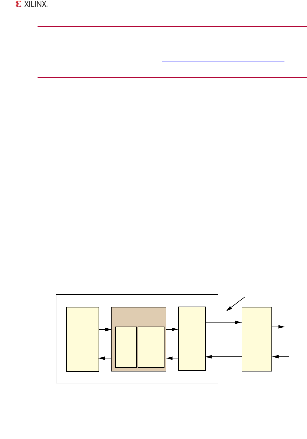
The core interfaces to a device-specific transceiver, which provides some of the PCS layer
functionality such as 8B/10B encoding/decoding, the PMA Serializer/Deserializer (SerDes),
and clock recovery. Figure 1-1 illustrates the remaining PCS sublayer functionality and the
major functional blocks of the core. A description of the functional blocks and signals is
provided in subsequent sections.
X-Ref Target - Figure 1-1
Figure 1-1: Ethernet 1000BASE-X PCS/PMA or SGMII Core Using a Device-Specific Transceiver
3&6 7UDQVPLW(QJLQH
3&65HFHLYH(QJLQH
DQG6\QFKURQL]DWLRQ
7UDQVFHLYHU
2SWLRQDO3&6
0DQDJHPHQW
*0,,
WR0$&
0',2
,QWHUIDFH
2SWLRQDO
$XWR1HJRWLDWLRQ 7R30'
6XEOD\HU
*0,,%ORFN
/RJL&25((WKHUQHW%$6(;3&630$RU6*0,,&RUH
7UDQVFHLYHU,)%ORFN
8

1000BASE-X PCS/PMA or SGMII v11.4 www.xilinx.com 13
PG047 October 16, 2012
Chapter 1: Overview
GMII Block
The core provides a client-side GMII. This can be used as an internal interface for
connection to an embedded Ethernet MAC or other custom logic. Alternatively, the core
GMII can be routed to device Input/Output Blocks (IOBs) to provide an off-chip GMII.
Virtex-7 devices support GMII at 3.3 V or lower only in certain parts and packages; see the
7 Series FPGAs SelectIO Resources User Guide. Virtex-6 devices support GMII at 2.5 V only;
see the Virtex-6 FPGA Data Sheet: DC and Switching Characteristics. Kintex-7, Artix-7,
Spartan-6, Virtex-5, Virtex-4 and Spartan-3 devices support GMII at 3.3 V or lower.
PCS Transmit Engine
The PCS transmit engine converts the GMII data octets into a sequence of ordered sets by
implementing the state diagrams of IEEE 802.3-2008 (Figures 36-5 and 36-6).
PCS Receive Engine and Synchronization
The synchronization process implements the state diagram of IEEE 802.3-2008 (Figure
36-9). The PCS receive engine converts the sequence of ordered sets to GMII data octets by
implementing the state diagrams of IEEE 802.3-2008 (Figures 36-7a and 36-7b).
Optional Auto-Negotiation Block
IEEE 802.3-2008 clause 37 describes the 1000BASE-X Auto-Negotiation function that allows
a device to advertise the supported modes of operation to a device at the remote end of a
link segment (link partner), and to detect corresponding operational modes that the link
partner might be advertising. Auto-Negotiation is controlled and monitored through the
PCS Management registers.
Optional PCS Management Registers
Configuration and status of the core, including access to and from the optional
Auto-Negotiation function, is performed with the 1000BASE-X PCS Management registers
as defined in IEEE 802.3-2008 clause 37. These registers are accessed through the serial
Management Data Input/Output Interface (MDIO), defined in IEEE 802.3-2008 clause 22, as
if it were an externally connected PHY.
An additional configuration interface is provided to program Control register (Register 0)
and Auto-Negotiation advertisement (Register 4) independent of the MDIO interface.
The PCS Management registers can be omitted from the core when the core is performing
the 1000BASE-X standard. In this situation, configuration and status is made possible by
using additional configuration vector and status signals. When the core is performing the
SGMII standard, PCS Management registers become mandatory and information in the
registers takes on a different interpretation.
1000BASE-X PCS/PMA or SGMII v11.4 www.xilinx.com 14
PG047 October 16, 2012
Chapter 1: Overview
Transceiver Interface Block
The interface block enables the core to connect to a device-specific transceiver.
Ethernet 1000BASE-X PCS/PMA or SGMII Support with Ten-Bit
Interface
When used with the TBI, the Ethernet 1000BASE-X PCS/PMA or SGMII core provides the
functionality to implement the 1000BASE-X PCS sublayer (or to provide SGMII support) with
use of an external SerDes.
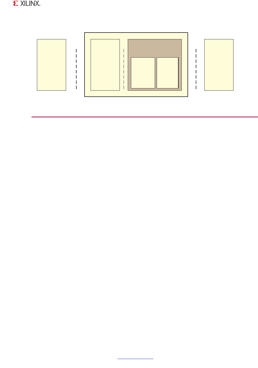
The optional TBI is used in place of the device-specific transceiver to provide a parallel
interface for connection to an external PMA SerDes device, allowing an alternative
implementation for families without device-specific transceivers. In this implementation,
additional logic blocks are required in the core to replace some of the device-specific
transceiver functionality. These blocks are surrounded by a dashed line (see Figure 1-2).
Other blocks are identical to those previously defined.
Zynq-7000, Artix-7 and Virtex-7 devices do not support TBI. Virtex-6 devices support TBI at
2.5 V only; see the Virtex-6 FPGA Data Sheet: DC and Switching Characteristics. Kintex-7,
Spartan-6, Virtex-5, Virtex-4 and Spartan-3 devices support TBI at 3.3 V or lower.
8B/10B Encoder
8B/10B encoding, as defined in IEEE 802.3-2008 specification (Tables 36-1a to 36-1e and
Table 36-2), is implemented in a block SelectRAM™ memory, configured as ROM, and used
as a large look-up table.
X-Ref Target - Figure 1-2
Figure 1-2: Functional Block Diagram of the Ethernet 1000BASE-X PCS/PMA or
SGMII Core with TBI
3&6 7UDQVPLW(QJLQH
3&65HFHLYH(QJLQH
DQG6\QFKURQL]DWLRQ
2SWLRQDO3&6
0DQDJHPHQW
*0,,
WR0$&
0',2
,QWHUIDFH
2SWLRQDO
$WXRQHJRWLDWLRQ
*0,,%ORFN
%%
(QFRGHU
%%
'HFRGHU
5;
(ODVWLF
%XIIHU
7%,%ORFN
/RJL&25((WKHUQHW%$6(;3&630$RU6*0,,&RUH
,2%V
4")
TOEXTERNAL
3%2$%3
8

1000BASE-X PCS/PMA or SGMII v11.4 www.xilinx.com 15
PG047 October 16, 2012
Chapter 1: Overview
8B/10B Decoder
8B/10B decoding, as defined in IEEE 802.3-2008 specification (Tables 36-1a to 36-1e and
Table 36-2), is implemented in a block SelectRAM memory, configured as ROM, and used as
a large look-up table.
Receiver Elastic Buffer
The Receiver Elastic Buffer enables the 10-bit parallel TBI data, received from the PMA
sublayer synchronously to the TBI receiver clocks, to be transferred onto the core internal
125 MHz clock domain.
The Receiver Elastic Buffer is an asynchronous First In First Out (FIFO) implemented in
internal RAM. The operation of the Receiver Elastic Buffer attempts to maintain a constant
occupancy by inserting or removing Idle sequences as necessary. This causes no corruption
to the frames of data.
TBI Block
The core provides a TBI interface, which should be routed to device IOBs to provide an
off-chip TBI.
SGMII over LVDS
Synchronous SGMII over Virtex7/Kintex7 LVDS
Kintex-7/Virtex-7 devices, -2 speed grade or higher on HR Banks and -1 or higher for HP
Banks, can fully support SGMII using standard LVDS SelectIO™ technology logic resources.
This enables direct connection to external PHY devices without the use of an FPGA
Transceiver. This implementation is illustrated in Figure 1-3.
1000BASE-X PCS/PMA or SGMII v11.4 www.xilinx.com 16
PG047 October 16, 2012
Chapter 1: Overview
The core netlist in this implementation remains identical to that of Figure 1-1 and all core
netlist blocks are identical to those described in Ethernet 1000BASE-X PCS/PMA or SGMII
Support Using a Device Specific Transceiver.
As illustrated in Figure 1-3, the Hardware Description Language (HDL) example design for
this implementation provides additional logic to form the "LVDS transceiver." The LVDS
transceiver block fully replaces the functionality otherwise provided by a 7 series FPGA
GTX/GTH transceiver. This is only possible at a serial line rate of 1.25 Gb/s. See Figure 1-4
for a block diagram of the LVDS transceiver.
X-Ref Target - Figure 1-3
Figure 1-3: Functional Block Diagram of the Core with Standard SelectIO Technology Support
for SGMII
#LOCKING,OGIC
REFCLK?P
REFCLK?N
CLKCLK CLK CLK
,6$34RANSCEIVER
RXN
RXP
TXN
TXP
COMPONENT?NAME?BLOCK
COMPONENT?NAME?EXAMPLE?DESIGN
%THERNET
3'-))
0#30-!#ORE
3'-))!DAPTATION
-ODULE
'-))3TYLE
BIT)&
8

1000BASE-X PCS/PMA or SGMII v11.4 www.xilinx.com 17
PG047 October 16, 2012
Chapter 1: Overview
The following subsections describe design requirements.
SGMII Only
The interface implemented using this method supports SGMII between the FPGA and an
external PHY device; the interface cannot directly support 1000BASE-X.
Supported Devices
• Kintex-7 devices, -2 speed grade or faster for devices with HR Banks or -1 speed grade
or faster for devices with HP banks.
• Virtex-7 devices, -2 speed grade or faster for devices with HR Banks or -1 speed grade
or faster for devices with HP banks.
Recommended for Chip-to-Chip Copper Implementations Only
This interface supports an SGMII link between the FPGA and an external PHY device across
a single PCB; keep the SGMII copper signal lengths to a minimum.
SGMII Support Using Asynchronous Oversampling over 7 Series FPGAs LVDS
See XAPP523 LVDS 4x Asynchronous Oversampling Using 7 Series FPGAs for information
about 7 series devices using asynchronous oversampling.
X-Ref Target - Figure 1-4
Figure 1-4: LVDS Transceiver Block Level Representation
""
%NCODER
""
'EARBOX
""
$ECODER
""
'EARBOX
)3%2$%3%
-ONITOR
3ERIALBITS
)3%2$%3%
$ATA
3ERIALBITS
%YE-ONITOR
O?RX?MON
O?RX?DATA?B
0HY
#ALLIBRATION
/3%2$%3%
BITS3ERIAL
)$%,!9%
)$%,!9%
/"5&$3
)"5&$3?$)&&
?/54
RXN
RXP
TXN
TXP
)"
)
/"
/
/"
/
)
COMPONENT?NAME?SGMII?PHY?IOB
COMPONENT?NAME?GPIO?SGMII?TOP
COMPONENT?NAME?LVDS?TRANSCEIVER
&ROM#ORE
4O#ORE
BITDATA
BITDATA
8

1000BASE-X PCS/PMA or SGMII v11.4 www.xilinx.com 18
PG047 October 16, 2012
Chapter 1: Overview
SGMII Support Using Asynchronous Oversampling over Virtex-6 FPGA LVDS
Virtex-6 devices, -2 speed grade or higher, can fully support SGMII using standard LVDS
SelectIO™ technology logic resources. This enables direct connection to external PHY
devices without the use of a Virtex-6 FPGA GTX transceiver.
This implementation is illustrated in Figure 1-5.
The core netlist in this implementation remains identical to that of Figure 1-1 and all core
netlist blocks are identical to those described in Ethernet 1000BASE-X PCS/PMA or SGMII
Support Using a Device Specific Transceiver.
As illustrated in Figure 1-5, the Hardware Description Language (HDL) example design for
this implementation provides additional logic to form the “LVDS transceiver” block which
fully replaces the functionality otherwise provided by a Virtex-6 FPGA GTX transceiver. The
LVDS transceiver block contains IODELAY and ISERDES elements along with a Data Recovery
Unit (DRU). This block uses the Virtex-6 FPGA ISERDES elements in a new asynchronous
oversampling mode as described in XAPP881 1.25Gbs 4x Asynchronous Oversampling over
Virtex-6 LVDS. The full transceiver functionality is then completed with Comma Alignment,
8B/10B Decoder and Rx Elastic buffer blocks.
X-Ref Target - Figure 1-5
Figure 1-5: Functional Block Diagram of the Core with Standard SelectIO Technology Support
for SGMII
0#3 4RANSMIT%NGINE
0#32ECEIVE%NGINE
AND3YNCHRONIZATION
/PTIONAL0#3
-ANAGEMENT
'-))
TO-!#
-$)/
)NTERFACE
/PTIONAL
!UTO.EGOTIATION 3ERIAL3'-))
TO
EXTERNAL0(9
'-))"LOCK
,OGI#ORENETLIST
4RANSCEIVER)&"LOCK
%%
(QFRGHU /3%2$%3
)/$%,!9
)3%2$%3
$25
#OMMA
!LIGNMENT
4X
0HASE
"UFFER
""
$ECODER
)/$%,!9
)3%2$%3
,6$3TRANSCEIVER
--#-
CLOCK
ALIGNMENT
STATE
MACHINE
CLOCKBUFFERS
VARIOUSCLOCK
FREQUENCIES
ANDPHASES
/3%2$%3
)3%2$%3
)/"ANK#LOCKING
2X
%LASTIC
"UFFER
8

1000BASE-X PCS/PMA or SGMII v11.4 www.xilinx.com 19
PG047 October 16, 2012
Chapter 1: Overview
Figure 1-5 also illustrates the inclusion of the “I/O Bank Clocking.” This block creates all of
the clock frequencies and clock phases that are required by the LVDS transceiver block. As
the name of the block suggests, this logic can be shared across a single Virtex-6 FPGA I/O
bank. This I/O bank can be used for multiple instances of the core with LVDS I/O to create
several independent SGMII ports.
The following four subsections describe design requirements.
SGMII Only
The interface implemented using this asynchronous oversampling method supports SGMII
between the FPGA and an external PHY device; the interface cannot directly support
1000BASE-X.
Supported in Virtex-6 Devices, -2 Speed Grade or Faster
The SGMII LVDS implementation has only been characterized in the -2 speed grade and
faster Virtex-6 devices.
Timing closure of this interface is challenging; perform the layout and placement steps
described in Layout and Placement in Chapter 7.
Receiver UI Specification
The DRU must have at least two valid sampling points per data bit, requiring 0.5 UI of
opening. The settings of the FPGA add 0.125 UI of requirement making a total opening
requirement at the receiver of 0.625 UI.
Recommended for Chip-to-Chip Copper Implementations Only
This interface supports an SGMII link between the FPGA and an external PHY device across
a single PCB; keep the SGMII copper signal lengths to a minimum.
Recommended Design Experience
Although the Ethernet 1000BASE-X PCS/PMA or SGMII core is a fully-verified solution, the
challenge associated with implementing a complete design varies depending on the
configuration and functionality of the application. For best results, previous experience
building high-performance, pipelined Field Programmable Gate Array (FPGA) designs using
Xilinx implementation software and the User Constraint Files (UCF) is recommended.
Contact your local Xilinx representative for a closer review and estimation for your specific
requirements.
1000BASE-X PCS/PMA or SGMII v11.4 www.xilinx.com 20
PG047 October 16, 2012
Chapter 1: Overview
System Requirements
For a list of System Requirements, see the Xilinx Design Tools: Release Notes Guide.
Applications
Typical applications for the Ethernet 1000BASE-X PCS/PMA or SGMII core include the
following:
•Ethernet 1000BASE-X
•Serial-GMII
EDK specific applications targeting Gigabit Ethernet MAC (GEM) embedded in Zynq™-7000
devices is shown in Chapter 11, GMII to PHY EDK Application for Zynq-7000 Device
Processor Subsystem.
Ethernet 1000BASE-X
Figure 1-6 illustrates a typical application for the Ethernet 1000BASE-X PCS/PMA or SGMII
core with the core operating to the 1000BASE-X standard using a device-specific
transceiver to provide the Physical Coding Sublayer (PCS) and Physical Medium Attachment
(PMA) sublayers for 1-Gigabit Ethernet.
• The PMA is connected to an external off-the-shelf Gigabit Interface Converter (GBIC) or
Small Form-Factor Pluggable (SFP) optical transceiver to complete the Ethernet port.
• The GMII of the Ethernet 1000BASE-X PCS/PMA is connected to an embedded Ethernet
Media Access Controller (MAC), for example, the Xilinx Tri-Mode Ethernet MAC core.
X-Ref Target - Figure 1-6
Figure 1-6: Typical 1000BASE-X Application
(WKHUQHW%$6(;
3&630$RU6*0,,
&RUH
8VHU/RJLF
(WKHUQHW
0HGLD
$FFHVV
&RQWUROOHU
,QWHUQDO
*0,,
7UDQVFHLYHU
,QWHUIDFH
7;37;1
5;35;1
*%,&
RU
6)3
2SWLFDO
7UDQVFHLYHU
2SWLFDO
)LEHU
30$
7UDQVFHLYHU
8ILINX&0'!
8

1000BASE-X PCS/PMA or SGMII v11.4 www.xilinx.com 21
PG047 October 16, 2012
Chapter 1: Overview
Serial-GMII
Ethernet 1000BASE-X PCS/PMA or SGMII core can operate in two modes as shown in the
following subsections.
GMII to SGMII Bridge
Figure 1-7 illustrates a typical application for the Ethernet 1000BASE-X PCS/PMA or SGMII
core, which shows the core providing a GMII to SGMII bridge using a device-specific
transceiver to provide the serial interface.
• The device-specific transceiver is connected to an external off-the-shelf Ethernet PHY
device that also supports SGMII. (This can be a tri-mode PHY providing 10BASE-T,
100BASE-T, and 1000BASE-T operation.)
• The GMII of the Ethernet 1000BASE-X PCS/PMA or SGMII core is connected to an
embedded Ethernet MAC, for example, the Xilinx Tri-Mode Ethernet MAC core.
SGMII to GMII Bridge
Figure 1-8 illustrates a typical application for the Ethernet 1000BASE-X PCS/PMA or SGMII
core, which shows the core providing a SGMII to GMII bridge using a device-specific
transceiver to provide the serial interface.
• The device-specific transceiver is connected to an external off-the-shelf Ethernet MAC
device that also supports SGMII. (This can be a tri-mode MAC providing 10/100/1000
Mb/s operation, for example, the Xilinx Tri-Mode Ethernet MAC core connected to
1000BASE-X PCS/PMA or SGMII core operating in GMII to SGMII Mode)
• The GMII of the Ethernet 1000BASE-X PCS/PMA or SGMII core is connected to a
tri-mode PHY providing 10BASE-T, 100BASE-T, and 1000BASE-T operation.
X-Ref Target - Figure 1-7
Figure 1-7: Typical Application for GMII to SGMII Bridge Mode
(WKHUQHW%$6(;
3&630$RU6*0,,
/RJL&25(
7UDQVFHLYHU
8VHU/RJLF
(WKHUQHW
0HGLD
$FFHVV
&RQWUROOHU
,QWHUQDO
*0,,
7UDQVFHLYHU
,QWHUIDFH
7;37;1
5;35;1
7ZLVWHG
&RSSHU
3DLU
6*0,,
%$6(7
%$6(7
%$6(7
3+<
8ILINX&0'!
8
1000BASE-X PCS/PMA or SGMII v11.4 www.xilinx.com 22
PG047 October 16, 2012
Chapter 1: Overview
Verification
The Ethernet 1000BASE-X PCS/PMA or SGMII core has been verified with extensive
simulation and hardware verification.
Simulation
A highly parameterizable transaction-based test bench was used to test the core. The tests
included the following:
• Register access
• Loss of synchronization
• Auto-negotiation and error handling
• Frame transmission and error handling
• Frame reception and error handling
• Clock compensation in the elastic buffers
Zynq-7000, Virtex-7, Kintex-7, Artix-7, Virtex-6, Virtex-5, Virtex-4 and Spartan-6 device
designs incorporating a device-specific transceiver require a Verilog LRM-IEEE 1364-2005
encryption-compliant simulator. For VHDL simulation, a mixed Hardware Description
Language (HDL) license is required.
X-Ref Target - Figure 1-8
Figure 1-8: Typical Application for SGMII to GMII Bridge Mode
(WKHUQHW%DVH;
3&630$RU6*0,,
/RJL&25(
7UDQVFHLYHU
,QWHUIDFH
,QWHUQDO
*0,,
%$6(7
%$6(7
%$6(7
7UDQVFHLYHU
*0,,B5;
*0,,B7;
7ZLVWHG
&RSSHU
3DLU
;LOLQ[)3*$
7;37;1
5;35;1
7UL0RGH0$&
ZLWK6*0,,
6*0,,
3+<
*0,,

1000BASE-X PCS/PMA or SGMII v11.4 www.xilinx.com 23
PG047 October 16, 2012
Chapter 1: Overview
Hardware Verification
The core has been tested in several hardware test platforms at Xilinx to represent a variety
of parameterizations, including the following:
• The core used with a device-specific transceiver and performing the 1000BASE-X
standard has been tested with the Xilinx Tri-Mode Ethernet MAC core, which follows
the architecture shown in Figure 1-6. A test platform was built around these cores,
including a back-end FIFO capable of performing a simple ping function, and a test
pattern generator. Software running on the embedded PowerPC® processor provided
access to all configuration and status registers. Version 3.0 of this core was taken to the
University of New Hampshire Interoperability Lab (UNH IOL) where conformance and
interoperability testing was performed.
• The core used with a device-specific transceiver and performing the SGMII standard
has been tested with the LogiCORE Intellectual Property (IP) Tri-Mode Ethernet MAC
core. This was connected to an external PHY capable of performing 10BASE-T,
100BASE-T, and 1000BASE-T, and the system was tested at all three speeds. This follows
the architecture shown in Figure 1-7 and also includes the PowerPC-based processor
test platform described previously.
Licensing and Ordering Information
This Xilinx LogiCORE™ IP module is provided at no additional cost with the Xilinx Vivado™
Design Suite and ISE® Design Suite tools under the terms of the Xilinx End User License.
Information about this and other Xilinx LogiCORE IP modules is available at the Xilinx
Intellectual Property page. For information about pricing and availability of other Xilinx
LogiCORE IP modules and tools, contact your local Xilinx sales representative.
1000BASE-X PCS/PMA or SGMII v11.4 www.xilinx.com 24
PG047 October 16, 2012
Chapter 2
Product Specification
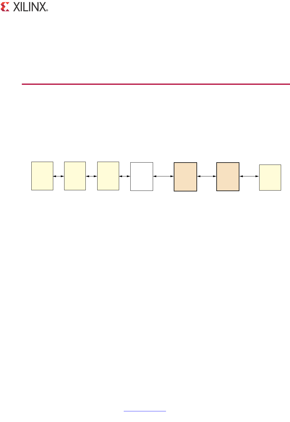
Overview of Ethernet Architecture
Figure 2-1 illustrates the 1-Gigabit Ethernet PCS and PMA sublayers provided by this core,
which are part of the Ethernet architecture. The part of this architecture, from the Ethernet
MAC to the right, is defined in the IEEE 802.3-2008 specification. This figure also shows
where the supported interfaces fit into the architecture.
MAC
The Ethernet Media Access Controller (MAC) is defined in IEEE 802.3-2008, clauses 2, 3, and
4. A MAC is responsible for the Ethernet framing protocols and error detection of these
frames. The MAC is independent of, and can connect to, any type of physical layer device.
GMII / SGMII
The Gigabit Media Independent Interface (GMII), a parallel interface connecting a MAC to
the physical sublayers (PCS, PMA, and PMD), is defined in IEEE 802.3-2008, clause 35. For a
MAC operating at a speed of 1 Gigabit per second (Gb/s), the full GMII is used; for a MAC
operating at a speed of 10 Mb/s or 100 Mb/s, the GMII is replaced with a Media
Independent Interface (MII) that uses a subset of the GMII signals.
The Serial-GMII (SGMII) is an alternative interface to the GMII/MII that converts the parallel
interface of the GMII/MII into a serial format capable of carrying traffic at speeds of
10 Mb/s, 100 Mb/s, and 1 Gb/s. This radically reduces the I/O count and for this reason is
often preferred by Printed Circuit Board (PCB) designers. The SGMII specification is closely
related to the 1000BASE-X PCS and PMA sublayers, which enables it to be offered in this
core.
X-Ref Target - Figure 2-1
Figure 2-1: Overview of Ethernet Architecture
4#0 )0 &)&/
)& -!# 0#3 0-! 0-$
'-))
3'-)) 4")
4RANSCEIVER
3ERIAL
0-$
8

1000BASE-X PCS/PMA or SGMII v11.4 www.xilinx.com 25
PG047 October 16, 2012
Chapter 2: Product Specification
PCS
The Physical Coding Sublayer (PCS) for 1000BASE-X operation is defined in IEEE 802.3-2008,
clauses 36 and 37, and performs these operations:
• Encoding (and decoding) of GMII data octets to form a sequence of ordered sets
• 8B/10B encoding (and decoding) of the sequence ordered sets
• 1000BASE-X Auto-Negotiation for information exchange with the link partner
Ten Bit Interface
The Ten-Bit-Interface (TBI), defined in IEEE 802.3-2008 clause 36 is a parallel interface
connecting the PCS to the PMA and transfers the 8B/10B encoded sequence-ordered sets.
The TBI should be used with an external SERDES device to implement the PMA functionality.
Physical Medium Attachment
The Physical Medium Attachment (PMA) for 1000BASE-X operation, defined in IEEE
802.3-2008 clause 36, performs the following:
• Serialization (and deserialization) of code-groups for transmission (and reception) on
the underlying serial Physical Medium Dependent (PMD)
• Recovery of the clock from the 8B/10B-coded data supplied by the PMD
The device-specific transceivers provide the serial interface required to connect the PMD.
Physical Medium Dependent
The PMD sublayer is defined in IEEE 802.3-2008 clause 38 for 1000BASE-LX and
1000BASE-SX (long and short wavelength laser). This type of PMD is provided by the
external GBIC or SFP optical transceivers. An alternative PMD for 1000BASE-CX (short-haul
copper) is defined in IEEE 802.3-2008 clause 39.
Standards
• Designed to Ethernet Standard 802.3-2008 Clauses 22, 35, 36 and 38.
•Serial-GMII Specification V1.7 (CISCO SYSTEMS, ENG-46158)

1000BASE-X PCS/PMA or SGMII v11.4 www.xilinx.com 26
PG047 October 16, 2012
Chapter 2: Product Specification
Performance
This section details the performance information for various core configurations.
Maximum Frequencies
1000Base-X PCS/PMA or SGMII core operates at 125 MHz.
Core Latency
The stand-alone core does not meet all the latency requirements specified in IEEE
802.3-2008 because of the latency of the Elastic Buffers in both TBI and device-specific
transceiver versions. However, the core can be used for backplane and other applications
where strict adherence to the IEEE latency specification is not required.
Where strict adherence to the IEEE 802.3-2008 specification is required, the core can be
used with an Ethernet MAC core that is within the IEEE specified latency for a MAC sublayer.
For example, when the core is connected to the Xilinx Tri-Mode Ethernet MAC core, the
system as a whole is compliant with the overall IEEE 802.3-2008 latency specifications.
Latency for 1000BASE-X PCS with TBI
The following measurements are for the core only and do not include any IOB registers or
the Transmitter Elastic Buffer added in the example design.
Transmit Path Latency
As measured from a data octet input into gmii_txd[7:0] of the transmitter side GMII
until that data appears on tx_code_group[9:0] on the TBI interface, the latency through
the core in the transmit direction is 5 clock periods of gtx_clk.
Receive Path Latency
Measured from a data octet input into the core on rx_code_group0[9:0] or
rx_code_group1[9:0] from the TBI interface (until that data appears on
gmii_rxd[7:0] of the receiver side GMII), the latency through the core in the receive
direction is equal to 16 clock periods of gtx_clk, plus an additional number of clock
cycles equal to the current value of the Receiver Elastic Buffer.
The Receiver Elastic Buffer is 32 words deep. The nominal occupancy will be at half-full,
thereby creating a nominal latency through the receiver side of the core equal to 16 + 16=
32 clock cycles of gtx_clk.

1000BASE-X PCS/PMA or SGMII v11.4 www.xilinx.com 27
PG047 October 16, 2012
Chapter 2: Product Specification
Latency for 1000BASE-X PCS and PMA Using a Transceiver
These measurements are for the core only; they do not include the latency through the
Virtex®-4 FPGA serial transceiver, Virtex-5 FPGA GTP transceiver, Virtex-5 FPGA GTX
RocketIO™ transceiver, Virtex-6 FPGA GTX transceiver, Spartan®-6 FPGA GTP transceiver,
Virtex-7 FPGA GTX/GTH transceiver, Zynq™-7000 or Kintex™-7 device GTX transceiver,
Artix™-7 FPGA GTP transceiver, or the Transmitter Elastic Buffer added in the example
design.
Transmit Path Latency
As measured from a data octet input into gmii_txd[7:0] of the transmitter side GMII
(until that data appears on txdata[7:0] on the serial transceiver interface), the latency
through the core in the transmit direction is 4 clock periods of userclk2.
Receive Path Latency
As measured from a data octet input into the core on rxdata[7:0] from the serial
transceiver interface (until that data appears on gmii_rxd[7:0] of the receiver side
GMII), the latency through the core in the receive direction is 6 clock periods of userclk2.
Latency for SGMII
When performing the SGMII standard, the core latency figures are identical to the Latency
for 1000BASE-X PCS and PMA using the serial transceiver. Again these figures do not
include the latency through the serial transceiver or any Elastic Buffers added in the
example design.
Throughput
1000BASE-X PCS and PMA or SGMII core operates at a full lane rate of 1.25 Gb/s
Voltage Requirements
Virtex-7 devices support GMII at 3.3 V or lower only in certain parts and packages; see the
7 Series FPGAs SelectIO Resources User Guide. Virtex-6 devices support TBI or GMII at 2.5 V
only; see the Virtex-6 FPGA Data Sheet: DC and Switching Characteristics. Kintex-7,
Spartan-6, Virtex-5, Virtex-4 and Spartan-3 devices support TBI and GMII at 3.3 V or lower.
Artix-7 and Zynq-7000 devices support GMII at 3.3 V or lower.
1000BASE-X PCS/PMA or SGMII v11.4 www.xilinx.com 28
PG047 October 16, 2012
Chapter 2: Product Specification
Speed Grades
Zynq-7000, Virtex-7, Kintex-7, Artix-7, Virtex-6, Virtex-5, Virtex-4 devices support speed
grade -1; Virtex-4 FPGA supports -10 speed grade; Spartan-6 FPGAs support -2 speed
grade. All other supported Spartan devices support -4 speed grade.
Resource Utilization
Resources required for this core have been estimated for the Zynq-7000, Virtex-7, Kintex-7,
Artix-7, Virtex-6, Virtex-5, and Spartan-6 devices, See Table 2- 2 through Tab le 2-9. These
values were generated using Xilinx® CORE Generator™ tools, v14.3. They are derived from
post-synthesis reports, and might change during MAP and PAR. Similar values are expected
for Vivado IP catalog v2012.3.
Table 2-1: Family Support for the 1000BASE-X PCS/PMA or SGMII Core
Device
Family
LogiCORE IP Functionality
1000BASE-X GMII to SGMII Bridge or
SGMII to GMII Bridge
1000BASE-X and SGMII
Standards with Dynamic
Switching
With TBI
Using
Device
Specific
Transceiver
With TBI
Using
Device
Specific
Transceiver
Using
Synchronous
LVDS
SelectIO
Using
Asynchronous
LVDS SelectIO With TBI
Using Device
Specific
Transceiver
Zynq-7000 Not
Supported Supported Not
Supported Supported Not
supported Not supported Not
Supported Supported
Virtex-7 Not
Supported Supported Not
Supported Supported
Supported
in -2 speed
grade and
faster parts for
HR banks; -1
speed grade
and faster for
HP banks
Available
through
XAPP523
Not
Supported Supported
Kintex-7 Supported Supported Supported Supported
Supported
in -2 speed
grade and
faster parts for
HR banks; -1
speed grade
and faster for
HP banks
Available
through
XAPP523
Supported Supported
Artix-7 Not
Supported Supported Not
Supported Supported Not
supported Not supported Not
Supported Supported
Virtex-6 Supported Supported Supported Supported Not
supported
Supported in -2
speed grade
and faster parts
Supported(1) Supported
1000BASE-X PCS/PMA or SGMII v11.4 www.xilinx.com 29
PG047 October 16, 2012
Chapter 2: Product Specification
Device Utilization
Zynq-7000, Virtex-7, Kintex-7, Artix-7, Virtex-6, Virtex-5 and Spartan-6 families contain six
input LUTs; all other families contain four input LUTs. For this reason, the device utilization
is listed separately. See one of the following for more information:
•Zynq-7000, Virtex-7, Kintex-7, Artix-7, Virtex-6, Virtex-5, and Spartan-6 Devices
•Other Device Families
Zynq-7000, Virtex-7, Kintex-7, Artix-7, Virtex-6, Virtex-5, and Spartan-6
Devices
Table 2-2, Tabl e 2-3, and Ta bl e 2- 4 provide approximate utilization figures for various core
options when a single instance of the core is instantiated in a Virtex-5 device.
Utilization figures are obtained by implementing the block-level wrapper for the core. This
wrapper is part of the example design and connects the core to the selected physical
interface.
Virtex-5 Supported Supported Supported Supported Not
supported Not Supported Supported Supported
Virtex-4 Supported Supported Supported Supported Not
supported Not Supported Supported Supported
Spartan-6 Supported Supported Supported Supported Not
supported Not Supported Supported Supported
Spartan-3 Supported Not
supported Supported Not
supported
Not
supported Not Supported Supported Not
supported
Spartan-3E Supported Not
supported Supported Not
supported
Not
supported Not Supported Supported Not
supported
Spartan-3
ASupported Not
supported Supported Not
supported
Not
supported Not Supported Supported Not
supported
1. Virtex-6 devices support TBI at 2.5 V only; see the Virtex-6 FPGA Data Sheet: DC and Switching Characteristics.
Table 2-1: Family Support for the 1000BASE-X PCS/PMA or SGMII Core (Cont’d)
Device
Family
LogiCORE IP Functionality
1000BASE-X GMII to SGMII Bridge or
SGMII to GMII Bridge
1000BASE-X and SGMII
Standards with Dynamic
Switching
With TBI
Using
Device
Specific
Transceiver
With TBI
Using
Device
Specific
Transceiver
Using
Synchronous
LVDS
SelectIO
Using
Asynchronous
LVDS SelectIO With TBI
Using Device
Specific
Transceiver
1000BASE-X PCS/PMA or SGMII v11.4 www.xilinx.com 30
PG047 October 16, 2012
Chapter 2: Product Specification
BUFG Usage
• BUFG usage does not consider multiple instantiations of the core, where clock
resources can often be shared.
• BUFG usage does not include the reference clock required for IDELAYCTRL. This clock
source can be shared across the entire device and is not core specific.
1000BASE-X
1. Auto-negotiation is only available when the MDIO Interface is selected.
2. These figures are for use with GTP transceivers; GTX transceivers require three BUFGs and one DCM.
3. Only two BUFGs might be required (see the User Guide)
SGMII Bridge
1. Auto-negotiation is only available when the MDIO Interface is selected.
2. These figures are for use with GTP transceivers; GTX transceivers require three BUFGs and one DCM.
3. Only two BUFGs might be required (see the User Guide)
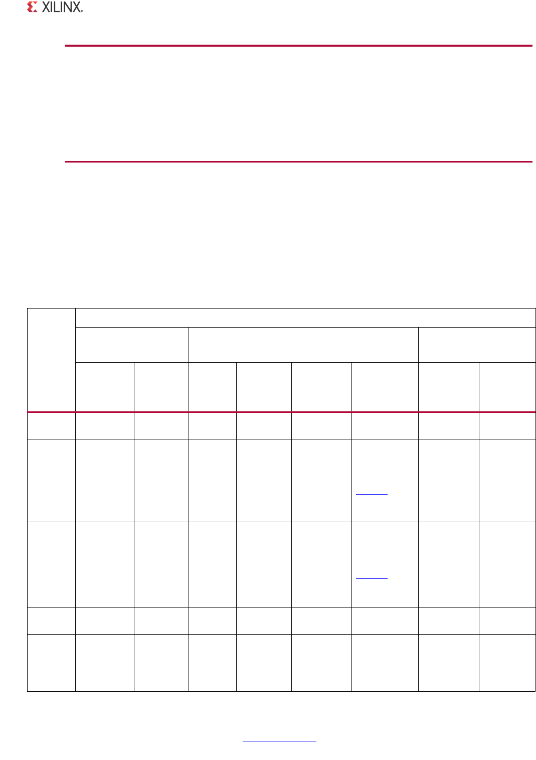
Table 2-2: Device Utilization for the 1000BASE-X Standard
Parameter Values Device Resources
Physical Interface MDIO
Interface
Auto-
Negotiation Slices LUTs FFs Block
RAMs BUFGs MMCMs
Transceiver TBI
Yes No Yes Yes 330 370 470 0 1(2) 0(2)
Yes No Yes No 190 215 240 0 1(2) 0(2)
Yes No No N/A(1) 140 170 180 0 1(2) 0(2)
No Yes Yes Yes 380 410 590 1 3(3) 0
No Yes Yes No 230 280 370 1 3(3) 0
No Yes No N/A(1) 190 230 315 1 3(3) 0
Table 2-3: Device Utilization for the GMII to SGMII or SGMII to GMII Bridge (Using Device
Specific Transceivers or TBI
Parameter Values Device Resources
Physical Interface MDIO
Interface
Auto-
Negotiation Slices LUTs FFs Block
RAMs BUFGs MMCMs
Transceiver TBI
Yes No Yes Yes 430 435 665 1 1(2) 0(2)
Yes No Yes No 310 330 500 1 1(2) 0(2)
Yes No No N/A(1) 280 270 450 1 1(2) 0(2)
No Yes Yes Yes 400 460 620 1 3(3) 0
No Yes Yes No 290 360 460 1 3(3) 0
No Yes No N/A(1) 240 320 410 1 3(3) 0
1000BASE-X PCS/PMA or SGMII v11.4 www.xilinx.com 31
PG047 October 16, 2012
Chapter 2: Product Specification
1000BASE-X and SGMII Standards with Dynamic Switching
1. Auto-negotiation is only available when the MDIO Interface is selected.
2. These figures are for use with GTP transceivers; GTX transceivers require three BUFGs and one DCM.
3. Only two BUFGs might be required (see the User Guide).
1. Auto-negotiation is only available when the MDIO Interface is selected.
2. The I/O Bank clocking logic is only required once for multiple SGMII cores that place their LVDS I/O in the same I/O
Bank. Any SGMII ports that are required to be placed in additional I/O Banks require a new instantiation of the I/O
Bank clocking logic for each I/O Bank utilized.
Table 2-4: Device Utilization for 1000BASE-X and SGMII Standards with Dynamic Switching
Parameter Values Device Resources
Physical Interface MDIO
Interface
Auto-
Negotiation Slices LUTs FFs Block
RAMs BUFGs MMCMs
Transceiver TBI
Yes No Yes Yes 445 510 745 1 1(2) 0(2)
Yes No Yes No 320 330 500 1 1(2) 0(2)
Yes No No N/A(1) 280 285 440 1 1(2) 0(2)
No Yes Yes Yes 405 530 700 1 3(3) 0
No Yes Yes No 275 365 460 1 3(3) 0
No Yes No N/A(1) 270 320 410 1 3(3) 0
Table 2-5: Device Utilization for the GMII to SGMII or SGMII to GMII Bridge over Select I/O
LVDS in V irtex-6 FPGAs
Parameter Values Device Resources
Logical
block
MDIO
Interface
Auto-
Negotiation Slices LUTs FFs Block
RAMs
Clock
Buffers MMCMs
I/O Bank
clocking
logic(2)
N/A 15 30 22 0
2 BUFIO
1 BUFR
3 BUFG
1
Per SGMII
port
Yes Yes 380 775 820 0 0 0
Yes No 310 640 660 0 0 0
No N/A(1) 265 590 615 0 0 0

1000BASE-X PCS/PMA or SGMII v11.4 www.xilinx.com 32
PG047 October 16, 2012
Chapter 2: Product Specification
• Auto-negotiation is only available when the MDIO Interface is selected.
• The clocking logic is only required once for multiple SGMII cores.
Other Device Families
Table 2-7, Tabl e 2-8, and Ta bl e 2- 9 provide approximate utilization figures for various core
options when a single instance of the core is instantiated in a Virtex-4 device. Other families
have similar utilization figures, except as indicated. Utilization figures are obtained by
implementing the block-level wrapper for the core. This wrapper is part of the example
design and connects the core to the selected physical interface.
When the physical interface is a Virtex-4 FPGA RocketIO™ transceiver, utilization figures
include GT11 Calibration blocks and GT11 initialization/reset circuitry.
BUFG Usage
BUFG usage does not consider multiple instantiations of the core, where clock resources
can often be shared.
Table 2-6: Device Utilization for GMII to SGMII or SGMII to GMII Bridge over Synchronous LVDS
in Virtex-7/Kintex-7 FPGAS
Parameter Values Device Resources
Logical Block MDIO
Interface
Auto-
Negotiation Slices LUTs FFs Block
RAMs
Clock
Buffers MMCMs
Clocking Logic N/A 0 0 0 0
5 BUFGs or
1 BUFG,
1 BUFIO
and 3
BUFRs or
1 BUFG
and 4
BUFHs
1
Per SGMII port
Yes Yes 462 884 985 0 0 0
Yes No 363 735 741 0 0 0
No N/A 337 670 693 0 0 0
1000BASE-X PCS/PMA or SGMII v11.4 www.xilinx.com 33
PG047 October 16, 2012
Chapter 2: Product Specification
1000BASE-X
1. Auto-negotiation is only available when the MDIO Interface is selected.
2. For Virtex-4 devices, this includes the clock shared between the Calibration Blocks and the GT11 Dynamic
Reconfiguration Port (DRP).
3. Only two BUFGs might be required (see the User Guide).
4. Spartan-3, Spartan-3E and Spartan-3A devices require two DCMs to meet TBI setup and hold times.
SGMII Bridge
1. Auto-negotiation is only available when the MDIO Interface is selected.
2. For Virtex-4 devices, this includes the clock shared between the Calibration Blocks and the GT11 Dynamic
Reconfiguration Port (DRP).
3. Only two BUFGs might be required.
4. Spartan-3, Spartan-3E and Spartan-3A devices require two DCMs to meet TBI setup and hold times.
Table 2-7: Device Utilization for the 1000BASE-X Standard
Parameter Values Device Resources
Physical Interface MDIO
Interface
Auto-
Negotiation Slices LUTs FFs Block
RAMs BUFGs DCMs
RocketIO TBI
Yes No Yes Yes 820 730 640 0 2(2) 0
Yes No Yes No 490 500 420 0 2(2) 0
Yes No No N/A(1) 430 440 360 0 2(2) 0
No Yes Yes Yes 650 640 600 2 3(3) 1(4)
No Yes Yes No 420 410 380 2 3(3) 1(4)
No Yes No N/A(1) 350 360 330 2 3(3) 1(4)
Table 2-8: Device Utilization for the GMII to SGMII or SGMII to GMII Bridge
Parameter Values Device Resources
Physical Interface MDIO
Interface
Auto-
Negotiation Slices LUTs FFs Block
RAMs BUFGs DCMs
RocketIO TBI
Yes No Yes Yes 970 780 860 1 2(2) 0
Yes No Yes No 730 620 670 1 2(2) 0
Yes No No N/A(1) 700 570 640 1 2(2) 0
No Yes Yes Yes 800 970 630 2 3(3) 1(4)
No Yes Yes No 610 830 470 2 3(3) 1(4)
No Yes No N/A(1) 560 770 420 2 3(3) 1(4)

1000BASE-X PCS/PMA or SGMII v11.4 www.xilinx.com 34
PG047 October 16, 2012
Chapter 2: Product Specification
1000BASE-X and SGMII Standards with Dynamic Switching
1. Auto-negotiation is only available when the MDIO Interface is selected.
2. For Virtex-4 devices, this includes the clock shared between the Calibration Blocks and the GT11 Dynamic
Reconfiguration Port (DRP).
3. Only two BUFGs might be required (see the User Guide).
4. Spartan-3, Spartan-3E and Spartan-3A devices require two DCMs to meet TBI setup and hold times.
Port Descriptions
All ports of the core are internal connections in FPGA logic. An HDL example design
(delivered with the core) connects the core, where appropriate, to a device-specific
transceiver, LVDS transceiver logic and/or add IBUFs, OBUFs. IOB flip-flops to the external
signals of the GMII and TBI. IOBs are added to the remaining unconnected ports to take the
example design through the Xilinx implementation software.
All clock management logic is placed in this example design, allowing you more flexibility in
implementation (such as designs using multiple cores). This example design is provided in
both VHDL and Verilog.
For more information on the example design provided, see one of the following chapters
depending on your chosen standard and physical interface.
•Chapter 4, The Ten-Bit Interface
•Chapter 5, 1000BASE-X with Transceivers
•Chapter 6, SGMII / Dynamic Standards Switching with Transceivers
•Chapter 7, SGMII over LVDS
Table 2-9: Device Utilization for the 1000BASE-X and SGMII Standards with Dynamic Switching
Parameter Values Device Resources
Physical Interface MDIO
Interface
Auto-
Negotiation Slices LUTs FFs Block
RAMs BUFGs DCMs
RocketIO TBI
Yes No Yes Yes 1100 900 940 1 2(2) 0
Yes No Yes No 780 640 700 1 2(2) 0
Yes No No N/A(1) 700 570 640 1 2(2) 0
No Yes Yes Yes 910 1090 710 2 3(3) 1(4)
No Yes Yes No 640 830 480 2 3(3) 1(4)
No Yes No N/A(1) 560 770 420 2 3(3) 1(4)
1000BASE-X PCS/PMA or SGMII v11.4 www.xilinx.com 35
PG047 October 16, 2012
Chapter 2: Product Specification
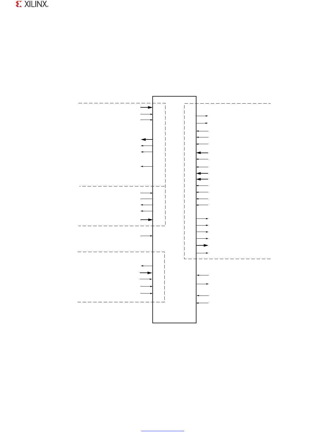
Figure 2-2 shows the pinout for the Ethernet 1000BASE-X PCS/PMA or SGMII core using a
device-specific transceiver, or LVDS transceiver logic, with the optional PCS Management
registers. The signals shown in the Auto-Negotiation box are included only when the core
includes the Auto-Negotiation functionality. For 7 series and Zynq-7000 devices, data width
of rxdata and txdata signals received from the device-specific transceiver is 16 bits. A
conversion logic is used to convert to 8 bits for core interface. For more information, see
Chapter 17, Customizing and Generating the Core.
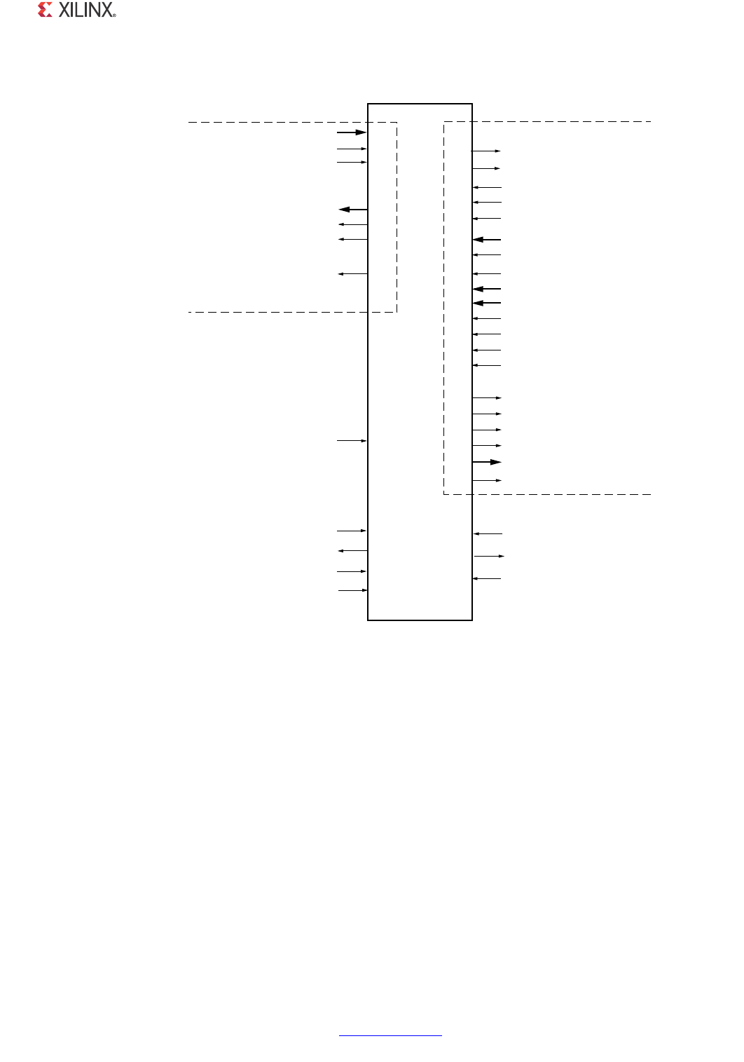
Figure 2-3 shows the pinout for the Ethernet 1000BASE-X PCS/PMA or SGMII core using a
device-specific transceiver, or LVDS transceiver logic without the optional PCS Management
registers For 7 series and Zynq-7000 devices, data width of rxdata and txdata signals
received from the device-specific transceiver is 16 bits. A conversion logic is used to
convert to 8 bits for core interface.
X-Ref Target - Figure 2-2
Figure 2-2: Component Pinout Using a Transceiver
with PCS Management Registers
PGF
PGLRBLQ
JPLLBU[G>@
JPLLBW[G>@
JPLLBW[BHQ PJWBU[BUHVHW
JPLLBW[BHU
UHVHW
JPLLBU[BGY
JPLLBU[BHU
*0,,
0',2
SK\DG>@
VLJQDOBGHWHFW
PGLRBRXW
PGLRBWUL
U[EXIVWDWXV>@
U[FKDULVFRPPD
U[FKDULVN
4RANSCEIVER)NTERFACE
JPLLBLVRODWH
OLQNBWLPHUBYDOXH>@
DQBLQWHUUXSW
$XWRB1HJRWLDWLRQ
PJWBW[BUHVHW
U[FONFRUFQW>@
U[GDWD>@
U[GLVSHUU
U[QRWLQWDEOH
U[UXQGLVS
W[EXIHUU
XVHUFON
GFPBORFNHG
XVHUFON
SRZHUGRZQ
W[FKDUGLVSPRGH
W[FKDUGLVSYDO
W[FKDULVN
W[GDWD
HQDEOHDOLJQ
STATUS?VECTOR;=
CONFIGURATION?VECTOR;=
CONFIGURATION?VALID
AN?ADV?CONFIG?VECTOR;=
AN?ADV?CONFIG?VAL
AN?RESTART?CONFIG
8
1000BASE-X PCS/PMA or SGMII v11.4 www.xilinx.com 36
PG047 October 16, 2012
Chapter 2: Product Specification
Figure 2-4 shows the pinout for the Ethernet 1000BASE-X PCS/PMA or SGMII core when
using the TBI with optional PCS Management registers. The signals shown in the
Auto-Negotiation box are included only when the core includes the Auto-Negotiation
functionality (see Chapter 17, Customizing and Generating the Core).
X-Ref Target - Figure 2-3
Figure 2-3: Component Pinout Using a Transceiver
without PCS Management Registers
PJWBU[BUHVHW
SIGNAL?DETECT
U[EXIVWDWXV>@
U[FKDULVFRPPD
U[FKDULVN
4RANSCEIVER)NTERFACE
PJWBW[BUHVHW
U[FONFRUFQW>@
U[GDWD>@
U[GLVSHUU
U[QRWLQWDEOH
U[UXQGLVS
W[EXIHUU
XVHUFON
GFPBORFNHG
XVHUFON
SRZHUGRZQ
W[FKDUGLVSPRGH
W[FKDUGLVSYDO
W[FKDULVN
W[GDWD
HQDEOHDOLJQ
JPLLBU[G>@
JPLLBW[G>@
JPLLBW[BHQ
JPLLBW[BHU
UHVHW
JPLLBU[BGY
JPLLBU[BHU
*0,,
JPLLBLVRODWH
STATUS?VECTOR;=
CONFIGURATION?VECTOR;=
AN?ADV?CONFIG?VECTOR;=
AN?RESTART?CONFIG
AN?INTERRUPT
LINK?TIMER?VALUE;=
8

1000BASE-X PCS/PMA or SGMII v11.4 www.xilinx.com 37
PG047 October 16, 2012
Chapter 2: Product Specification
X-Ref Target - Figure 2-4).
Figure 2-4: Component Pinout Using the Ten-Bit Interface
with PCS Management Registers
PGF
PGLRBLQ
JPLLBU[G>@
JPLLBW[G>@
JPLLBW[BHQ
W[BFRGHBJURXS>@
U[BFRGHBJURXS>@
JPLLBW[BHU
UHVHW
JPLLBU[BGY
JPLLBU[BHU
SPDBU[BFON
*0,,
0',2
SK\DG>@
JW[BFON VLJQDOBGHWHFW
PGLRBRXW
PGLRBWUL
ORFBUHI
HZUDS
SPDBU[BFON
HQBFGHW
U[BFRGHBJURXS>@
7HQ%LW,QWHUIDFH7%,
JPLLBLVRODWH
OLQNBWLPHUBYDOXH>@
DQBLQWHUUXSW
$XWRB1HJRWLDWLRQ STATUS?VECTOR;=
CONFIGURATION?VECTOR;=
CONFIGURATION?VALID
AN?ADV?CONFIG?VECTOR;=
AN?ADV?CONFIG?VAL
AN?RESTART?CONFIG
8
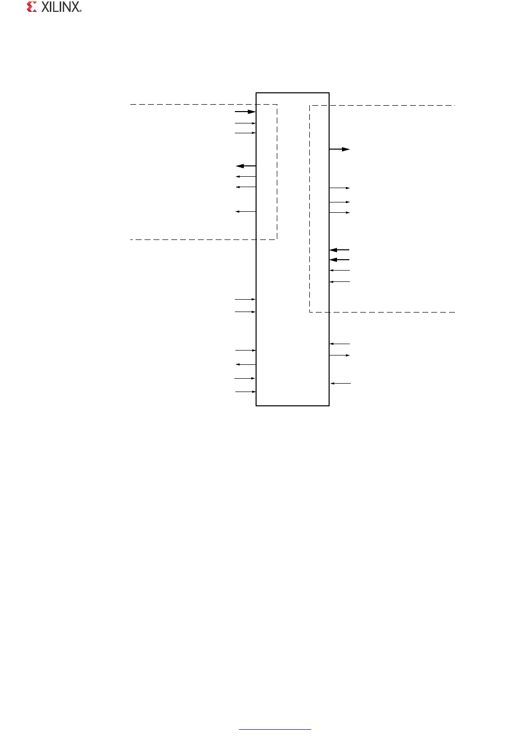
1000BASE-X PCS/PMA or SGMII v11.4 www.xilinx.com 38
PG047 October 16, 2012
Chapter 2: Product Specification
Figure 2-5 shows the pinout for the Ethernet 1000BASE-X PCS/PMA or SGMII core when
using a TBI without the optional PCS Management registers.
Figure 2-6 shows the pinout for the Ethernet 1000BASE-X PCS/PMA or SGMII core using the
optional dynamic switching logic (between 1000BASE-X and SGMII standards). This mode is
shown used with a device-specific transceiver interface. For 7 series and Zynq-7000 devices,
data width of rxdata and txdata signals received from the device-specific transceiver is
16 bits. A conversion logic is used to convert to 8 bits for core interface. For more
information, see Chapter 10, Dynamic Switching of 1000BASE-X and SGMII Standards.
X-Ref Target - Figure 2-5
Figure 2-5: Component Pinout Using Ten-Bit Interface
without PCS Management Registers
JPLLBU[G>@
JPLLBW[G>@
JPLLBW[BHQ
W[BFRGHBJURXS>@
U[BFRGHBJURXS>@
JPLLBW[BHU
UHVHW
JPLLBU[BGY
JPLLBU[BHU
SPDBU[BFON
*0,,
JW[BFON
VLJQDOBGHWHFW
ORFBUHI
HZUDS
SPDBU[BFON
HQBFGHW
U[BFRGHBJURXS>@
7HQ%LW,QWHUIDFH7%,
JPLLBLVRODWH
STATUS?VECTOR;=
CONFIGURATION?VECTOR;=
AN?ADV?CONFIG?VECTOR;=
AN?RESTART?CONFIG
AN?INTERRUPT
LINK?TIMER?VALUE;=
8
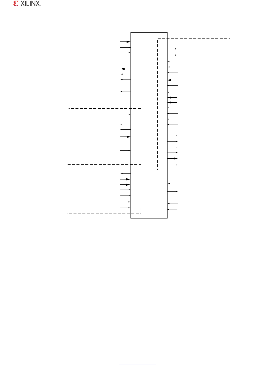
1000BASE-X PCS/PMA or SGMII v11.4 www.xilinx.com 39
PG047 October 16, 2012
Chapter 2: Product Specification
X-Ref Target - Figure 2-6
Client Side Interface
GMII Pinout
Table 2-10 describes the GMII-side interface signals of the core common to all
parameterizations of the core. These are typically attached to an Ethernet MAC, either
off-chip or internally integrated. The HDL example design delivered with the core connects
these signals to IOBs to provide a place-and-route example.
Figure 2-6: Component Pinout with the Dynamic Switching Logic
PGF
PGLRBLQ
JPLLBU[G>@
JPLLBW[G>@
JPLLBW[BHQ PJWBU[BUHVHW
JPLLBW[BHU
UHVHW
JPLLBU[BGY
JPLLBU[BHU
*0,,
0',2
SK\DG>@
VLJQDOBGHWHFW
PGLRBRXW
PGLRBWUL
U[EXIVWDWXV>@
U[FKDULVFRPPD
U[FKDULVN
4RANSCEIVER)NTERFACE
JPLLBLVRODWH
OLQNBWLPHUBEDVH[>@
DQBLQWHUUXSW
$XWRB1HJRWLDWLRQ
PJWBW[BUHVHW
U[FONFRUFQW>@
U[GDWD>@
U[GLVSHUU
U[QRWLQWDEOH
U[UXQGLVS
W[EXIHUU
XVHUFON
GFPBORFNHG
XVHUFON
SRZHUGRZQ
W[FKDUGLVSPRGH
W[FKDUGLVSYDO
W[FKDULVN
W[GDWD
HQDEOHDOLJQ
OLQNBWLPHUBVJPLL>@
EDVH[BRUBVJPLL STATUS?VECTOR;=
CONFIGURATION?VECTOR;=
CONFIGURATION?VALID
AN?ADV?CONFIG?VECTOR;=
AN?ADV?CONFIG?VAL
AN?RESTART?CONFIG
8
1000BASE-X PCS/PMA or SGMII v11.4 www.xilinx.com 40
PG047 October 16, 2012
Chapter 2: Product Specification
For more information, see Chapter 8, Using the Client-Side GMII Datapath.
Common Signal Pinout
Table 2-11 describes the remaining signals common to all parameterizations of the core.
Signals are synchronous to the core internal 125 MHz reference clock; userclk2 when
used with a device-specific transceiver; gtx_clk when used with TBI.
Table 2-10: GMII Interface Signal Pinout
Signal Direction Description
gmii_txd[7:0] (1) Input GMII Transmit data from MAC.
gmii_tx_en (1) Input GMII Transmit control signal from MAC.
gmii_tx_er (1) Input GMII Transmit control signal from MAC.
gmii_rxd[7:0](2) Output GMII Received data to MAC.
gmii_rx_dv (2) Output GMII Received control signal to MAC.
gmii_rx_er (2) Output GMII Received control signal to MAC.
gmii_isolate (2) Output
IOB 3-state control for GMII Isolation. Only of use when
implementing an External GMII as illustrated by the example
design HDL.
Notes:
1. When the Transmitter Elastic Buffer is present, these signals are synchronous to gmii_tx_clk. When the Transmitter
Elastic Buffer is omitted, see (2).
2. These signals are synchronous to the internal 125 MHz reference clock of the core. This is userclk2 when the core
is used with the device-specific transceiver; gtx_clk when the core is used with TBI.
Table 2-11: Other Common Signals
Signal Direction Clock Domain Description
reset Input n/a Asynchronous reset for the entire core. Active-High.
•Bit[0]: Link Status
This signal indicates the status of the link.
When high, the link is valid: synchronization of the link has
been obtained and Auto-Negotiation (if present and
enabled) has successfully completed.
When low, a valid link has not been established. Either link
synchronization has failed or Auto-Negotiation (if present
and enabled) has failed to complete.
When auto-negotiation is enabled, this signal is identical
to Status Register Bit 1.2: Link Status.
When auto-negotiation is disabled, this signal is identical
to status_vector Bit[1]. In this case, either of the bits can
be used.

1000BASE-X PCS/PMA or SGMII v11.4 www.xilinx.com 41
PG047 October 16, 2012
Chapter 2: Product Specification
•Bit[1]: Link Synchronization
This signal indicates the state of the synchronization state
machine (IEEE802.3 figure 36-9) which is based on the
reception of valid 8B/10B code groups. This signal is
similar to Bit[0] (Link Status), but is not qualified with
Auto-Negotiation.
When high, link synchronization has been obtained and in
the synchronization state machine, sync_status=OK.
When low, synchronization has failed.
•Bit[2]: RUDI(/C/)
The core is receiving /C/ ordered sets (Auto-Negotiation
Configuration sequences).
status_vector[15:0] Output See note •Bit[3]: RUDI(/I/)
The core is receiving /I/ ordered sets (Idles)
•Bit[4]: RUDI(INVALID)
The core has received invalid data while receiving/C/ or /I/
ordered set.
•Bit[5]: RXDISPERR
The core has received a running disparity error during the
8B/10B decoding function.
•Bit[6]: RXNOTINTABLE
The core has received a code group which is not
recognized from the 8B/10B coding tables.
•Bit[7]: PHY Link Status (SGMII mode only)
When operating in SGMII mode, this bit represents the
link status of the external PHY device attached to the
other end of the SGMII link (high indicates that the PHY
has obtained a link with its link partner; low indicates that
is has not linked with its link partner).
When operating in 1000BASE-X mode, this bit remains low
and should be ignored
• Bit[9:8]: Remote Fault Encoding
This signal indicates the remote fault encoding (IEEE802.3
table 37-3). This signal is validated by bit 13 of
status_vector and is only valid when Auto-Negotiation is
enabled.
This signal has no significance when the core is in SGMII
mode with PHY side implementation and indicates “00”. In
all the remaining modes the signal indicates the remote
fault encoding.
Table 2-11: Other Common Signals (Cont’d)
Signal Direction Clock Domain Description
1000BASE-X PCS/PMA or SGMII v11.4 www.xilinx.com 42
PG047 October 16, 2012
Chapter 2: Product Specification
MDIO Management Interface Pinout (Optional)
Table 2-12 describes the optional MDIO interface signals of the core that are used to access
the PCS Management registers. These signals are typically connected to the MDIO port of
a MAC device, either off-chip or to an internally integrated MAC core. For more information,
see Management Registers.
• Bit [11:10]: SPEED
This signal indicates the speed negotiated and is only
valid when Auto-Negotiation is enabled. The signal
encoding follows:
Bit[11] Bit[10]
1 1 Reserved
1 0 1000 Mb/s
0 1 100 Mb/s
0 0 10 Mb/s
status_vector[15:0]
(Continued) Output See note
• Bit[12]: Duplex Mode
This bit indicates the Duplex mode negotiated with the
link partner
1 = Full Duplex
0 = Half Duplex
• Bit[13] Remote Fault
When this bit is logic one, it indicates that a remote fault
is detected and the type of remote fault is indicated by
status_vector bits[9:8].
Note: This bit is only deasserted when a MDIO read is
made to status register (register1). This signal has no
significance in SGMII PHY mode.
• Bits[15;14]: Pause
These bits reflect the bits [8:7] of Register 5 (Link Partner
Base AN Register)
Bit[15] Bit[14]
0 0 No Pause
0 1 Symmetric Pause
1 0 Asymmetric Pause towards Link partner
1 1 Both Symmetric Pause and Asymmetric
Pause towards link partner
Table 2-11: Other Common Signals (Cont’d)
Signal Direction Clock Domain Description
1000BASE-X PCS/PMA or SGMII v11.4 www.xilinx.com 43
PG047 October 16, 2012
Chapter 2: Product Specification
Table 2-12: Optional MDIO Interface Signal Pinout
Signal Direction Clock Domain Description
mdc Input N/A Management clock (<= 2.5 MHz).
mdio_ina
a. These signals can be connected to a 3-state buffer to create a bidirectional mdio signal suitable for connection to
an external MDIO controller (for example, an Ethernet MAC).
Input mdc Input data signal for communication with MDIO
controller (for example, an Ethernet MAC). Tie high
if unused.
mdio_out(a) Output mdc Output data signal for communication with MDIO
controller (for example, an Ethernet MAC).
mdio_tri(a)
Output mdc 3-state control for MDIO signals; ‘0’ signals that the
value on mdio_out should be asserted onto the
MDIO interface.
phyad[4:0] Input N/A Physical Address of the PCS Management register
set. It is expected that this signal will be tied off to
a logical value.
1000BASE-X PCS/PMA or SGMII v11.4 www.xilinx.com 44
PG047 October 16, 2012
Chapter 2: Product Specification
Additional Configuration Vector Interface
Table 2-13 shows the additional interface to program Management Registers 0 and 4
irrespective of the optional MDIO interface.
Table 2-13: Additional Configuration and Status Vectors
Signal Direction Clock
Domain Description
configuration_vector[4:0] Input See note
•Bit[0]:
Unidirectional Enable
When set to 1, Enable Transmit irrespective of
state of RX (802.3ah). When set to 0, Normal
operation
•Bit[1]: Loopback Control
When the core with a device-specific
transceiver is used, this places the core into
internal loopback mode. With the TBI version,
Bit 1 is connected to ewrap. When set to 1, this
signal indicates to the external PMA module to
enter loopback mode.
•Bit[2]: Power Down
When the Zynq-7000, Virtex-7, Kintex-7,
Artix-7, Virtex-6, Virtex-5 or Spartan-6 device
transceivers are used and set to 1, the
device-specific transceiver is placed in a
low-power state. A reset must be applied to
clear. With the TBI version this bit is unused.
•Bit[3] Isolate
When set to 1, the GMII should be electrically
isolated. When set to 0, normal operation is
enabled.
•Bit[4] Auto-Negotiation Enable
This signal is valid only if the AN module is
enabled through the CORE Generator™ GUI).
When set to 1, the signal enables the AN
feature. When set to 0, AN is disabled.
configuration_valid Input See Note
This signal is valid only when the MDIO
interface is present. The rising edge of this
signal is the enable signal to overwrite the
Register 0 contents that were written from the
MDIO interface. For triggering a fresh update
of Register 0 through configuration_vector, this
signal should be deasserted and then
reasserted.
Note: Signals are synchronous to the core internal 125 MHz reference clock; userclk2 when used with a
device-specific transceiver; gtx_clk when used with TBI.
1000BASE-X PCS/PMA or SGMII v11.4 www.xilinx.com 45
PG047 October 16, 2012
Chapter 2: Product Specification
Auto-Negotiation Signal Pinout
Table 2-14 describes the signals present when the optional Auto-Negotiation functionality
is present. For more information, see Chapter 9, Auto-Negotiation.
Table 2-14: Optional Auto-Negotiation Interface Signal Pinout
Signal Direction Clock
Domain Description
link_timer_value[8:0] Input See note
Used to configure the duration of the Auto-Negotiation
function Link Timer. The duration of this timer is set to the
binary number input into this port multiplied by 4096 clock
periods of the 125 MHz reference clock (8 ns).
It is expected that this signal will be tied off to a logical value.
This port is replaced when using the dynamic switching mode.
In SGMII operating in MAC Mode, the AN_ADV register is hard
wired internally to “0x4001” and this bus has no effect. For
1000BaseX and SGMII operating in PHY mode, the AN_ADV
register is programmed by this bus as specified for the following
bits.
•Bit[0]:
For 1000 BASEX-Reserved.
For SGMII- Always 1
• Bits [4:1]: Reserved
•Bit [5]:
For 1000 BASEX- Full Duplex
1 = Full Duplex Mode is advertised
0 = Full Duplex Mode is not advertised
For SGMII- Reserved
an_adv_config_vector
[15:0] Input See
Note
•Bit [6]: Reserved
• Bits [8:7]:
For 1000 BASEX- Pause
0 0 No Pause
0 1 Symmetric Pause
1 0 Asymmetric Pause towards link partner
1 1 Both Symmetric Pause and Asymmetric Pause towards link
partner
For SGMII - Reserved
•Bit [9]: Reserved
• Bits [11:10]:
For 1000 BASEX- Reserved
For SGMII- Speed
1 1 Reserved
1 0 1000 Mb/s
0 1 100 Mb/s
0 0 10 Mb/s

1000BASE-X PCS/PMA or SGMII v11.4 www.xilinx.com 46
PG047 October 16, 2012
Chapter 2: Product Specification
an_adv_config_vector
[15:0] Input See
Note
• Bits [13:12]:
For 1000 BASEX- Remote Fault
0 0 No Error
0 1 Offline
1 0 Link Failure
1 1 Auto-Negotiation Error
For SGMII- Bit[13]: Reserved
• Bit[12]: Duplex Mode
1 Full Duplex
0 Half Duplex
• Bit [14]:
For 1000 BASEX- Reserved
For SGMII- Acknowledge
• Bit [15]:
For 1000 BASEX- Reserved
For SGMII- PHY Link Status
1 Link Up
0 Link Down
an_adv_config_val Input See
Note
This signal is valid only when the MDIO interface is present. The
rising edge of this signal is the enable signal to overwrite the
Register 4 contents that were written from the MDIO interface.
For triggering a fresh update of Register 4 through
an_adv_config_vector, this signal should be deasserted and then
reasserted.
an_restart_config Input See
Note
This signal is valid only when AN is present. The rising edge of
this signal is the enable signal to overwrite Bit 9 or Register 0.
For triggering a fresh AN Start, this signal should be deasserted
and then reasserted.
an_interrupt Output See
Note
When the MDIO module is selected through the GUI interface,
this signal indicates an active-High interrupt for
Auto-Negotiation cycle completion which needs to be cleared
though MDIO. This interrupt can be enabled/disabled and
cleared by writing to the appropriate PCS Management register.
See the Ethernet 1000BASE-X PCS/PMA or SGMII User Guide.
When the MDIO module is not selected, this signal indicates AN
Complete, which is asserted as long as the Auto-Negotiation is
complete and AN is not restarted and cannot be cleared.
Note: Signals are synchronous to the core internal 125 MHz reference clock, userclk2 when the core is used
with the device-specific transceiver, and gtx_clk when the core is used with TBI.
Table 2-14: Optional Auto-Negotiation Interface Signal Pinout (Cont’d)
Signal Direction Clock
Domain Description
1000BASE-X PCS/PMA or SGMII v11.4 www.xilinx.com 47
PG047 October 16, 2012
Chapter 2: Product Specification
Dynamic Switching Signal Pinout
Table 2-15 describes the signals present when the optional Dynamic Switching mode
(between 1000BASE-X and SGMII standards) is selected. In this case, the MDIO (Tabl e 2- 12)
and device-specific transceiver (Table 2-16) interfaces are always present.
Physical Side Interface
1000BASE-X PCS with PMA Using Transceiver Signal Pinout (Optional)
Table 2-16 describes the optional interface to the device-specific transceiver, or LVDS
transceiver logic. The core is connected to the chosen transceiver in the appropriate HDL
example design delivered with the core. For more information, see Appendix C, 1000BASE-X
State Machines.
•Chapter 5, 1000BASE-X with Transceivers
•Chapter 6, SGMII / Dynamic Standards Switching with Transceivers
•Chapter 7, SGMII over LVDS
Table 2-15: Optional Dynamic Standard Switching Signals
Signal Direction Description
link_timer_basex[8:0](1) Input
Used to configure the duration of the Auto-Negotiation Link
Timer period when performing the 1000BASE-X standard. The
duration of this timer is set to the binary number input into this
port multiplied by 4096 clock periods of the 125 MHz reference
clock (8 ns). It is expected that this signal will be tied off to a
logical value.
link_timer_sgmii[8:0](1) Input
Used to configure the duration of the Auto-Negotiation Link
Timer period when performing the SGMII standard. The
duration of this timer is set to the binary number input into this
port multiplied by 4096 clock periods of the 125 MHz reference
clock (8 ns). It is expected that this signal will be tied off to a
logical value.
basex_or_sgmii(1) Input
Used as the reset default to select the standard. It is expected
that this signal will be tied off to a logical value.
‘0’ signals that the core will come out of reset operating as
1000BASE-X.
‘1’ signals that the core will come out of reset operating as
SGMII.
Note: The standard can be set following reset through the
MDIO Management.
Notes:
1. Clock domain is userclk2.

1000BASE-X PCS/PMA or SGMII v11.4 www.xilinx.com 48
PG047 October 16, 2012
Chapter 2: Product Specification
Table 2-16: Optional Transceiver Interface Pinout
Signal Direction Description
mgt_rx_reset (1) Output
Reset signal issued by the core to the device-specific transceiver
receiver path. Connect to RXRESET signal of device-specific
transceiver.
mgt_tx_reset (1) Output
Reset signal issued by the core to the device-specific transceiver
transmitter path. Connect to TXRESET signal of device-specific
transceiver.
userclk Input Also connected to TXUSRCLK and RXUSRCLK of the
device-specific transceiver. Clock domain is not applicable.
userclk2 Input Also connected to TXUSRCLK2 and RXUSRCLK2 of the
device-specific transceiver. Clock domain is not applicable.
dcm_locked Input
A Digital Clock Manager (DCM) can be used to derive userclk and
userclk2. This is implemented in the HDL design example
delivered with the core. The core uses this input to hold the
device-specific transceiver in reset until the DCM obtains lock.
Clock domain is not applicable. If DCM is not used, this signal
should be tied to '1'.
rxbufstatus[1:0] (1) Input Connect to device-specific transceiver signal of the same name.
rxchariscomma (1) Input Connects to device-specific transceiver signal of the same name.
rxcharisk (1) Input Connects to device-specific transceiver signal of the same name.
rxclkcorcnt[2:0] (1) Input Connect to device-specific transceiver signal of the same name.
rxdata[7:0] (1) Input Connect to device-specific transceiver signal of the same name.
rxdisperr (1) Input Connects to device-specific transceiver signal of the same name.
rxnotintable (1) Input Connects to device-specific transceiver signal of the same name.
rxrundisp (1) Input Connects to device-specific transceiver signal of the same name.
txbuferr (1) Input Connects to device-specific transceiver signal of the same name.
powerdown (1) Output Connects to device-specific transceiver signal of the same name.
txchardispmode (1) Output Connects to device-specific transceiver signal of the same name.
txchardispval(1) Output Connects to device-specific transceiver signal of the same name.
txcharisk (1) Output Connects to device-specific transceiver signal of the same name.
txdata[7:0] (1) Output Connect to device-specific transceiver signal of the same name.
enablealign (1) Output
Allows the transceivers to serially realign to a comma character.
Connects to ENMCOMMAALIGN and ENPCOMMAALIGN of the
device-specific transceiver.
Notes:
1. When the core is used with a device-specific transceiver, userclk2 is used as the 125 MHz reference clock for the
entire core.

1000BASE-X PCS/PMA or SGMII v11.4 www.xilinx.com 49
PG047 October 16, 2012
Chapter 2: Product Specification
1000BASE-X PCS with TBI Pinout
Table 2-17 describes the optional TBI signals, used as an alternative to the transceiver
interfaces. The appropriate HDL example design delivered with the core connects these
signals to IOBs to provide an external TBI suitable for connection to an off-device PMA
SERDES device. When the core is used with the TBI, gtx_clk is used as the 125 MHz
reference clock for the entire core. For more information, see Chapter 4, The Ten-Bit
Interface.
Register Space
This section provides general guidelines for configuring and monitoring the Ethernet
1000BASE-X PCS/PMA or SGMII core, including a detailed description of the core
management registers. It also describes Configuration Vector and status signals, an
alternative to using the optional MDIO Management interface.
Table 2-17: Optional TBI Interface Signal Pinout
Signal Direction Clock Domain Description
gtx_clk Input N/A Clock signal at 125 MHz. Tolerance must be
within IEEE 802.3-2008 specification.
tx_code_group[9:0] Output gtx_clk 10-bit parallel transmit data to PMA Sublayer
(SERDES).
loc_ref Output N/A
Causes the PMA sublayer clock recovery unit
to lock to pma_tx_clk. This signal is currently
tied to Ground.
ewrap Output gtx_clk
When ’1,’ this indicates to the external PMA
SERDES device to enter loopback mode. When
’0,’ this indicates normal operation
rx_code_group0[9:0] Input pma_rx_clk0
10-bit parallel received data from PMA
Sublayer (SERDES). This is synchronous to
pma_rx_clk0.
rx_code_group1[9:0] Input pma_rx_clk1
10-bit parallel received data from PMA
Sublayer (SERDES). This is synchronous to
pma_rx_clk1.
pma_rx_clk0 Input N/A Received clock signal from PMA Sublayer
(SERDES) at 62.5 MHz.
pma_rx_clk1 Input N/A
Received clock signal from PMA Sublayer
(SERDES) at 62.5 MHz. This is 180 degrees out
of phase with pma_rx_clk0.
en_cdet Output gtx_clk
Enables the PMA Sublayer to perform comma
realignment. This is driven from the PCS
Receive Engine during the Loss-Of-Sync state.
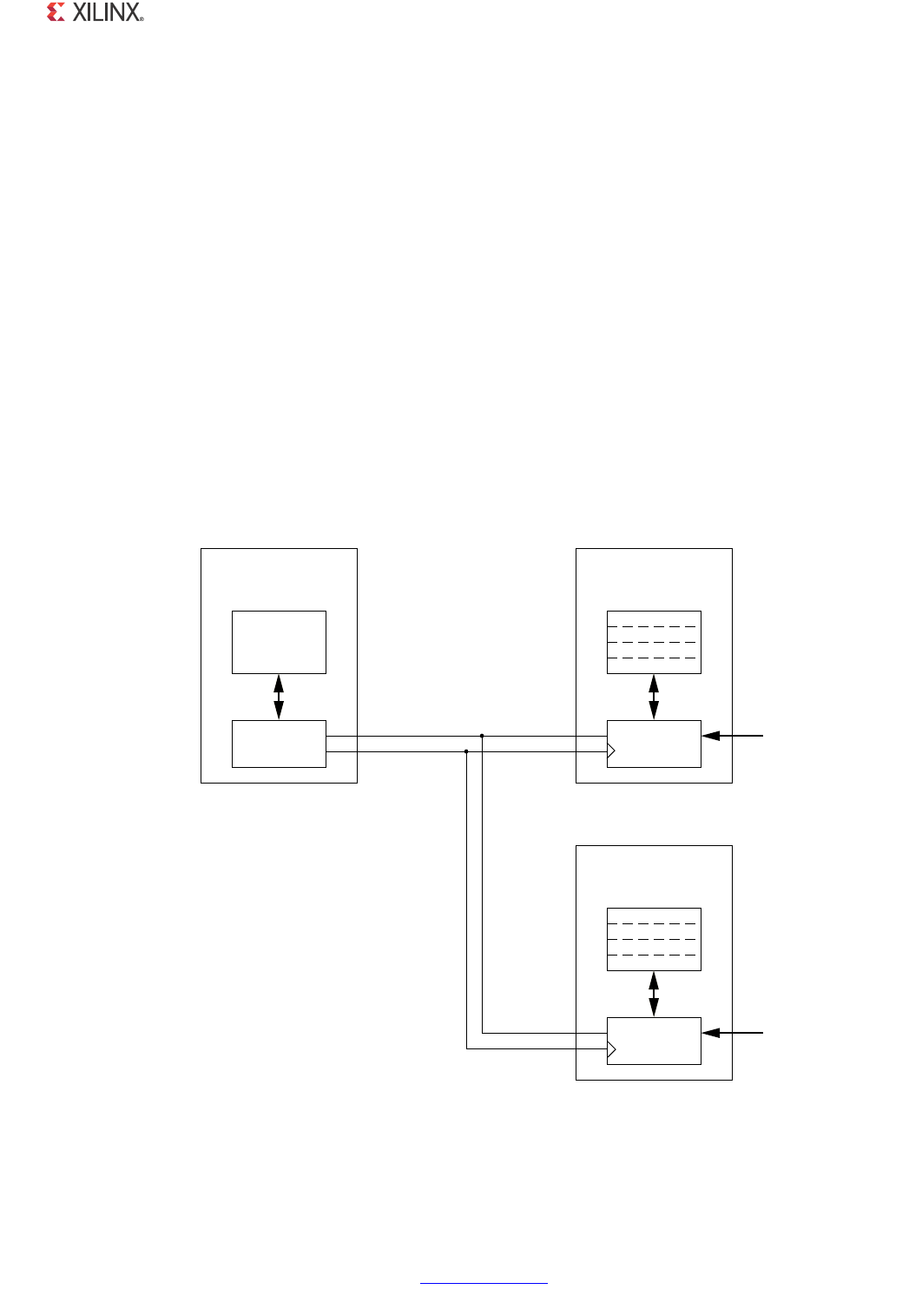
1000BASE-X PCS/PMA or SGMII v11.4 www.xilinx.com 50
PG047 October 16, 2012
Chapter 2: Product Specification
MDIO Management Interface
When the optional MDIO Management interface is selected, configuration and status of the
core is achieved by the Management registers accessed through the serial Management
Data Input/Output Interface (MDIO).
MDIO Bus System
The MDIO interface for 1 Gb/s operation (and slower speeds) is defined in IEEE 802.3-2008,
clause 22. Figure 2-7 illustrates an example MDIO bus system. This two-wire interface
consists of a clock (MDC) and a shared serial data line (MDIO). The maximum permitted
frequency of Management Data Clock (MDC) is set at 2.5 MHz. An Ethernet MAC is shown
as the MDIO bus master (the Station Management (STA) entity). Two PHY devices are shown
connected to the same bus, both of which are MDIO slaves (MDIO Managed Device (MMD)
entities).
X-Ref Target - Figure 2-7
Figure 2-7: A Typical MDIO-Managed System
#ONFIGURATION
2EGISTERSTO
2%'!$
-$)/SLAVE
8
0(9--$
0HYSICAL
!DDRESS
0(9!$
#ONFIGURATION
2EGISTERSTO
2%'!$
-$)/SLAVE
0(9--$
0HYSICAL
!DDRESS
0(9!$
-$)/
MASTER
-!#34!
-$#
-$)/
(OST
"US)&
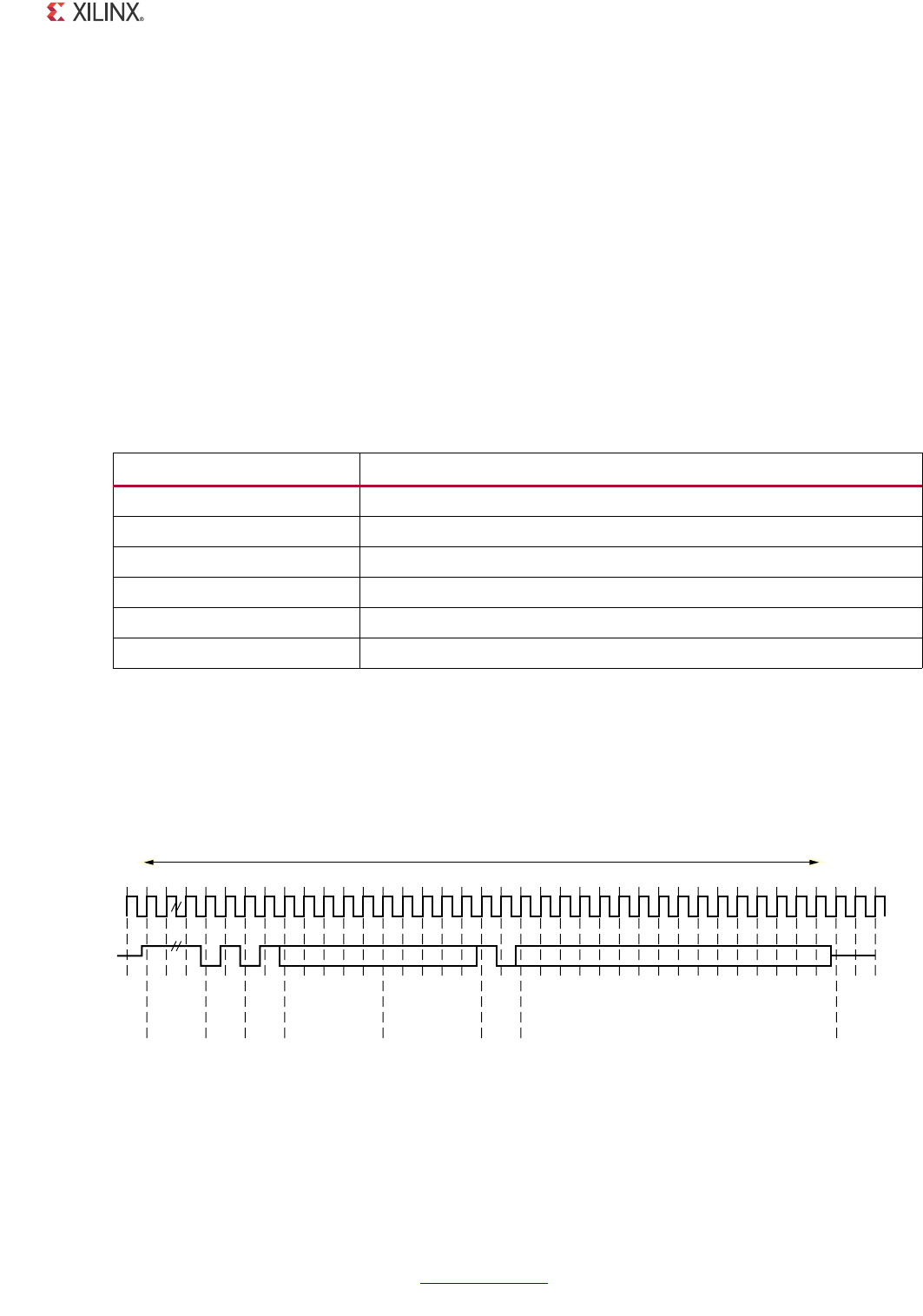
1000BASE-X PCS/PMA or SGMII v11.4 www.xilinx.com 51
PG047 October 16, 2012
Chapter 2: Product Specification
The MDIO bus system is a standardized interface for accessing the configuration and status
registers of Ethernet PHY devices. In the example illustrated, the Management Host Bus I/F
of the Ethernet MAC is able to access the configuration and status registers of two PHY
devices using the MDIO bus.
MDIO Transactions
All transactions, read or write, are initiated by the MDIO master. All MDIO slave devices,
when addressed, must respond. MDIO transactions take the form of an MDIO frame,
containing fields for transaction type, address and data. This MDIO frame is transferred
across the MDIO wire synchronously to MDC. The abbreviations are used in this section are
explained in Table 2-18.
Write Transaction
Figure 2-8 shows a write transaction across the MDIO, defined as OP=”01.” The addressed
PHY device (with physical address PHYAD) takes the 16-bit word in the Data field and writes
it to the register at REGAD.
Table 2-18: Abbreviations and Terms
Abbreviation Term
PRE Preamble
ST Start of frame
OP Operation code
PHYAD Physical address
REGAD Register address
TA Turnaround
X-Ref Target - Figure 2-8
Figure 2-8: MDIO Write Transaction
: 0 0 0 0 0 2 2 2 2 2 $
$
$
$
$
$
$
$
$
$
$
$
$
$
$
$
:::
MDC
MDIO
)$,% )$,%BITS
02%
34 /0 0(9!$ 2%'!$ 4! BIT72)4%$!4!
34!DRIVES-$)/
8

1000BASE-X PCS/PMA or SGMII v11.4 www.xilinx.com 52
PG047 October 16, 2012
Chapter 2: Product Specification
Read Transaction
Figure 2-9 shows a read transaction, defined as OP=”10.” The addressed PHY device (with
physical address PHYAD) takes control of the MDIO wire during the turnaround cycle and
then returns the 16-bit word from the register at REGAD.
MDIO Addressing
MDIO Addresses consists of two stages: Physical Address (PHYAD) and Register Address
(REGAD).
Physical Address (PHYAD)
As shown in Figure 2-7, two PHY devices are attached to the MDIO bus. Each of these has a
different physical address. To address the intended PHY, its physical address should be
known by the MDIO master (in this case an Ethernet MAC) and placed into the PHYAD field
of the MDIO frame (see MDIO Transactions).
The PHYAD field for an MDIO frame is a 5-bit binary value capable of addressing 32 unique
addresses. However, every MDIO slave must respond to physical address 0. This
requirement dictates that the physical address for any particular PHY must not be set to 0
to avoid MDIO contention. Physical Addresses 1 through to 31 can be used to connect up
to 31 PHY devices onto a single MDIO bus.
Physical Address 0 can be used to write a single command that is obeyed by all attached
PHYs, such as a reset or power-down command.
Register Address (REGAD)
Having targeted a particular PHY using PHYAD, the individual configuration or status
register within that particular PHY must now be addressed. This is achieved by placing the
individual register address into the REGAD field of the MDIO frame (see MDIO
Transactions).
X-Ref Target - Figure 2-9
Figure 2-9: MDIO Read Transaction
: 0 0 0 0 0 2 2 2 2 2 : $
$
$
$
$
$
$
$
$
$
$
$
$
$
$
$
:::
MDC
MDIO
)$,% )$,%BITS
02%
34 /0 0(9!$ 2%'!$ 4! BIT2%!$$!4!
34!DRIVES-$)/ !DDRESSED--$DRIVES-$)/
8
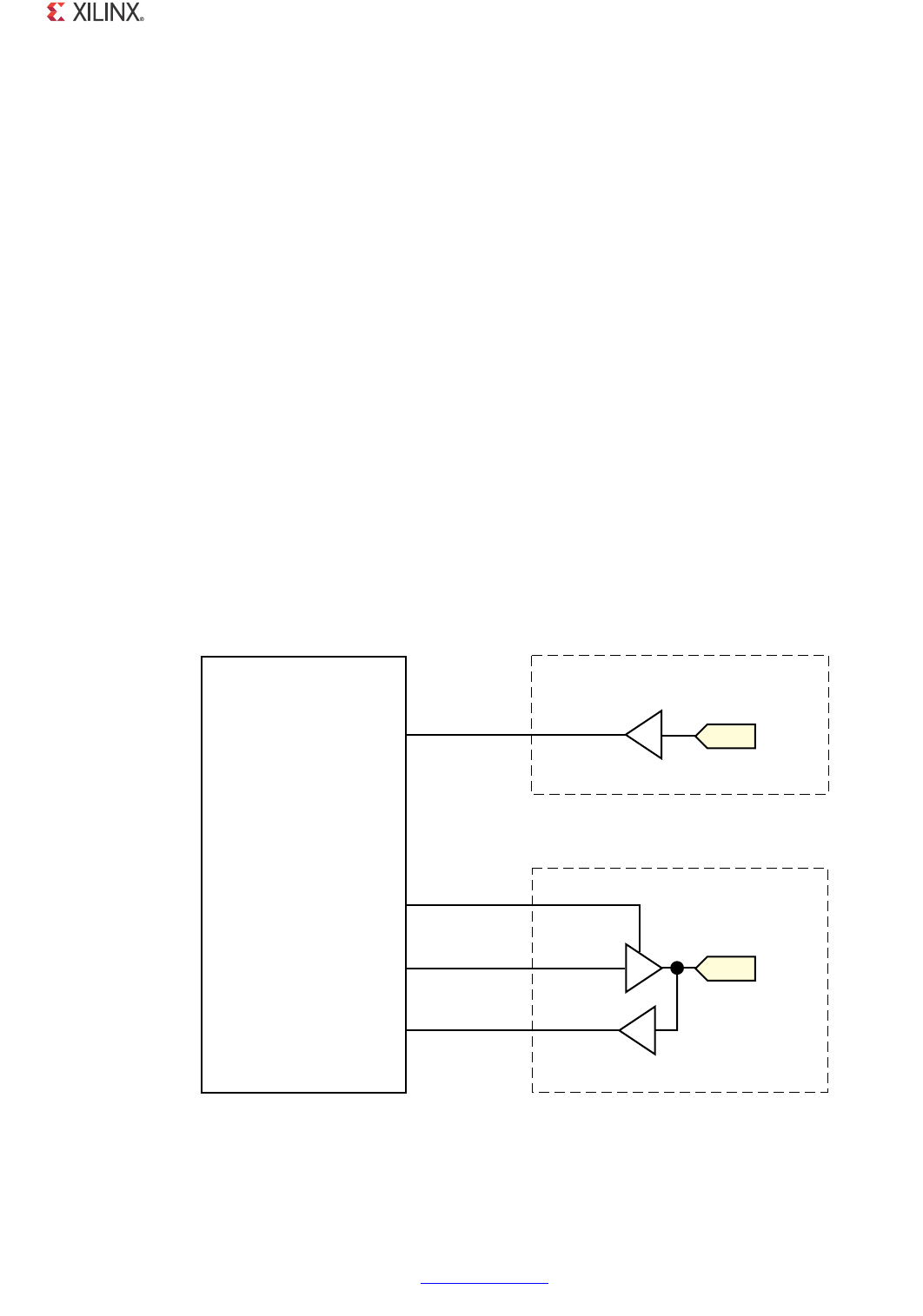
1000BASE-X PCS/PMA or SGMII v11.4 www.xilinx.com 53
PG047 October 16, 2012
Chapter 2: Product Specification
The REGAD field for an MDIO frame is a 5-bit binary value capable of addressing 32 unique
addresses. The first 16 of these (registers 0 to 15) are defined by the IEEE 802.3-2008. The
remaining 16 (registers 16 to 31) are reserved for PHY vendors own register definitions.
For details of the register map of PHY layer devices and a more extensive description of the
operation of the MDIO Interface, see IEEE 802.3-2008.
Connecting the MDIO to an Internally Integrated STA
The MDIO ports of the Ethernet 1000BASE-X PCS/PMA or SGMII core can be connected to
the MDIO ports of an internally integrated Station Management (STA) entity, such as the
MDIO port of the Tri-Mode Ethernet MAC core (see Chapter 12, Interfacing to Other Cores).
Connecting the MDIO to an External STA
Figure 2-10 shows the MDIO ports of the Ethernet 1000BASE-X PCS/PMA or SGMII core
connected to the MDIO of an external STA entity. In this situation, mdio_in, mdio_out,
and mdio_tri must be connected to a 3-state buffer to create a bidirectional wire, mdio.
This 3-state buffer can either be external to the FPGA or internally integrated by using an
IOB IOBUF component with an appropriate SelectIO™ interface standard suitable for the
external PHY.
X-Ref Target - Figure 2-10
Figure 2-10: Creating an External MDIO Interface
)"5&
)/",/')#
)0!$
/)
/
))/
4
)/0!$
)/",/')#
)/"5&
%THERNET"!3%80#30-!
OR3'-)),OGI#/2%
MDC
MDIO?TRI
MDIO?OUT
MDIO?IN
MDC
MDIO
8

1000BASE-X PCS/PMA or SGMII v11.4 www.xilinx.com 54
PG047 October 16, 2012
Chapter 2: Product Specification
Management Registers
The contents of the Management registers can be accessed using the REGAD field of the
MDIO frame. Contents will vary depending on the CORE Generator™ or Vivado™ IP catalog
tool options, and are defined in the following sections in this guide.
•1000BASE-X Standard Using the Optional Auto-Negotiation
•1000BASE-X Standard Without the Optional Auto-Negotiation
•SGMII Standard Using the Optional Auto-Negotiation
•SGMII Standard without the Optional Auto-Negotiation
•Both 1000BASE-X and SGMII Standards
The core can be reset three ways: reset, DCM_LOCKED and soft reset. All of these methods
reset all the registers to the default values.
1000BASE-X Standard Using the Optional Auto-Negotiation
More information on the 1000BASE-X PCS registers can be found in clause 22 and clause 37
of the IEEE 802.3-2006 specification. Registers at undefined addresses are read-only and
return 0s. The core can be reset three ways: reset, DCM_LOCKED and soft reset. All of these
methods reset all the registers to the default values.
Table 2-19: MDIO Registers for 1000BASE-X with Auto-Negotiation
Register Address Register Name
0Control Register
1 Status Register
2,3 PHY Identifier
4 Auto-Negotiation Advertisement Register
5 Auto-Negotiation Link Partner Ability Base Register
6 Auto-Negotiation Expansion Register
7 Auto-Negotiation Next Page Transmit Register
8 Auto-Negotiation Next Page Receive Register
15 Extended Status Register
16 Vendor Specific: Auto-Negotiation Interrupt Control

1000BASE-X PCS/PMA or SGMII v11.4 www.xilinx.com 55
PG047 October 16, 2012
Chapter 2: Product Specification
Register 0: Control Register
X-Ref Target - Figure 2-11
Figure 2-11: MDIO Register 0: Control Register
Table 2-20: Control Register (Register 0)
Bit(s) Name Description Attributes Default
Value
0.15 Reset 1 = Core Reset
0 = Normal Operation
Read/write
Self clearing 0
0.14 Loopback
1 = Enable Loopback Mode
0 = Disable Loopback Mode
When used with a device-specific
transceiver, the core is placed in internal
loopback mode.
With the TBI version, Bit 1 is connected to
ewrap. When set to ‘1,’ indicates to the
external PMA module to enter loopback
mode.
See Loopback.
Read/write 0
0.13 Speed Selection
(LSB)
Always returns a 0 for this bit. Together
with bit 0.6, speed selection of 1000 Mb/s
is identified
Returns 0 0
0.12 Auto-Negotiation
Enable
1 = Enable Auto-Negotiation Process
0 = Disable Auto-Negotiation Process Read/write 1
0.11 Power Down
1 = Power down
0 = Normal operation
With the PMA option, when set to ’1’ the
device-specific transceiver is placed in a
low-power state. This bit requires a reset
(see bit 0.15) to clear.
With the TBI version this register bit has
no effect.
Read/ write 0
0.10 Isolate 1 = Electrically Isolate PHY from GMII
0 = Normal operation Read/write 1
2%3%4
,//0"!#+
!54/.%'%.!",%
2%34!24!54/.%'
2%3%26%$
0/7%2$/7.
30%%$
30%%$
2EG
)3/,!4%
$50,%8-/$%
#/,,)3)/.4%34
5.)$)2%#4)/.!,%.!",%
8
1000BASE-X PCS/PMA or SGMII v11.4 www.xilinx.com 56
PG047 October 16, 2012
Chapter 2: Product Specification
Register 1: Status Register
0.9 Restart Auto-
Negotiation
1 = Restart Auto-Negotiation Process
0 = Normal Operation
Read/write
Self clearing 0
0.8 Duplex Mode Always returns a ‘1’ for this bit to signal
Full-Duplex Mode. Returns 1 1
0.7 Collision Test Always returns a ‘0’ for this bit to disable
COL test. Returns 0 0
0.6 Speed Selection
(MSB)
Always returns a ‘1’ for this bit. Together
with bit 0.13, speed selection of 1000
Mb/s is identified.
Returns 1 1
0.5 Unidirectional
Enable
Enable transmit regardless of whether a
valid link has been established. This
feature is only possible if
Auto-Negotiation Enable bit 0.12 is
disabled
Read/ write 0
0.4:0 Reserved Always return 0s, writes ignored. Returns 0s 00000
X-Ref Target - Figure 2-12
Figure 2-12: MDIO Register 1: Status Register
Table 2-21: Status Register (Register 1)
Bit(s) Name Description Attributes Default
Value
1.15 100BASE-T4 Always returns a ‘0’ as 100BASE-T4 is not
supported. Returns 0 0
1.14 100BASE-X Full Duplex Always returns a ‘0’ as 100BASE-X full duplex
is not supported. Returns 0 0
1.13 100BASE-X Half Duplex Always returns a ‘0’ as 100BASE-X half
duplex is not supported. Returns 0 0
Table 2-20: Control Register (Register 0) (Cont’d)
Bit(s) Name Description Attributes Default
Value
"!3%4
"!3%8&5,,$50,%8
-BS&5,,$50,%8
"!3%4(!,&$50,%8
,).+34!453
-BS(!,&$50,%8
"!3%8(!,&$50,%8
-&02%!-",%35002%33)/.
2EG
"!3%4&5,,$50,%8
%84%.$%$34!453
5.)$)2%#4)/.!,!.),)49
!54/.%'#/-0,%4%
2%-/4%&!5,4
!54/.%'!"),)49
*!""%2$%4%#4
%84%.$%$#!0!"),)49
8
1000BASE-X PCS/PMA or SGMII v11.4 www.xilinx.com 57
PG047 October 16, 2012
Chapter 2: Product Specification
Link Status
When high, the link is valid and has remained valid after this register was last read;
synchronization of the link has been obtained and Auto-Negotiation (if enabled) has
completed.
When low, either:
1.12 10 Mb/s Full Duplex Always returns a ‘0’ as 10 Mb/s full duplex is
not supported. Returns 0 0
1.11 10 Mb/s Half Duplex Always returns a ‘0’ as 10 Mb/s half duplex is
not supported Returns 0 0
1.10 100BASE-T2 Full
Duplex
Always returns a ‘0’ as 100BASE-T2 full
duplex is not supported. Returns 0 0
1.9 100BASE-T2 Half
Duplex
Always returns a ‘0’ as 100BASE-T2 Half
Duplex is not supported. Returns 0 0
1.8 Extended Status Always returns a ‘1’ to indicate the presence
of the Extended Register (Register 15). Returns 1 1
1.7 Unidirectional Ability Always returns a ‘1,’ writes ignored Returns 1 1
1.6 MF Preamble
Suppression
Always returns a ‘1’ to indicate that
Management Frame Preamble Suppression
is supported.
Returns 1 1
1.5 Auto- Negotiation
Complete
1 = Auto-Negotiation process completed
0 = Auto-Negotiation process not
completed
Read only 0
1.4 Remote Fault 1 = Remote fault condition detected
0 = No remote fault condition detected
Read only
Self-
clearing on
read
0
1.3 Auto- Negotiation
Ability
Always returns a ‘1’ for this bit to indicate
that the PHY is capable of Auto-Negotiation. Returns 1 1
1.2 Link Status
1 = Link is up
0 = Link is down (or has been down)
Latches '0' if Link Status goes down. Clears to
current Link Status on read.
See the following Link Status section for
further details.
Read only
Self
clearing on
read
0
1.1 Jabber Detect Always returns a ‘0’ for this bit because
Jabber Detect is not supported. Returns 0 0
1.0 Extended Capability Always returns a ‘0’ for this bit because no
extended register set is supported. Returns 0 0
Table 2-21: Status Register (Register 1) (Cont’d)
Bit(s) Name Description Attributes Default
Value
1000BASE-X PCS/PMA or SGMII v11.4 www.xilinx.com 58
PG047 October 16, 2012
Chapter 2: Product Specification
• A valid link has not been established: link synchronization has failed or
Auto-Negotiation (if enabled) has failed to complete.
OR
• Link synchronization was lost at some point after this register was previously read.
However, the current link status might be good. Therefore read this register a second
time to get confirmation of the current link status.
Regardless of whether Auto-Negotiation is enabled or disabled, there can be some delay to
the deassertion of Link Status following the loss of synchronization of a previously
successful link. This is due to the Auto-Negotiation state machine which requires that
synchronization is lost for an entire link timer duration before changing state. For more
information, see the 802.3 specification (the an_sync_status variable).
Registers 2 and 3: PHY Identifiers
X-Ref Target - Figure 2-13
Figure 2-13: Registers 2 and 3: PHY Identifiers
Table 2-22: PHY Identifier (Registers 2 and 3)
Bit(s) Name Description Attributes Default Value
2.15:0 Organizationally Unique
Identifier Always return 0s returns 0s 0000000000000000
3.15:10 Organizationally Unique
Identifier Always return 0s returns 0s 000000
3.9:4 Manufacturer model
number Always return 0s returns 0s 000000
3.3:0 Revision Number Always return 0s returns 0s 0000
/2'!.):%
5.)15%)$
2EG
2EG
/2'!.):%
5.)15%)$
-!5&!#452%2
-/$%,./
2%6)3)/../
8
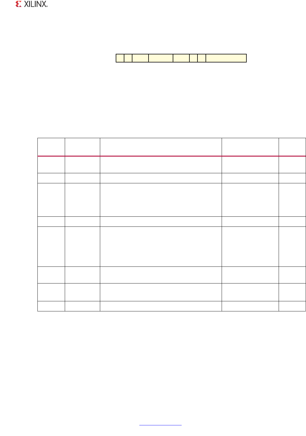
1000BASE-X PCS/PMA or SGMII v11.4 www.xilinx.com 59
PG047 October 16, 2012
Chapter 2: Product Specification
Register 4: Auto-Negotiation Advertisement
X-Ref Target - Figure 2-14
Figure 2-14: MDIO Register 4: Auto-Negotiation Advertisement
Table 2-23: Auto-Negotiation Advertisement Register (Register 4)
Bit(s) Name Description Attributes Default
Value
4.15 Next Page Core currently does not support Next Page.
Can be enabled, if requested. Writes ignored. read/write 0
4.14 Reserved Always returns ‘0,’ writes ignored returns 0 0
4.13:12 Remote
Fault
00 = No Error
01 = Offline
10 = Link Failure
11 = Auto-Negotiation Error
read/write
self clearing to 00
after
Auto-Negotiation
00
4.11:9 Reserved Always return 0s, writes ignored returns 0 0
4.8:7 Pause
00 = No PAUSE
01 = Symmetric PAUSE
10 = Asymmetric PAUSE towards link partner
11 = Both Symmetric PAUSE and Asymmetric
PAUSE towards link partner
read/write 11
4.6 Half Duplex Always returns a ‘0’ for this bit because Half
Duplex Mode is not supported returns 0 0
4.5 Full Duplex 1 = Full Duplex Mode is advertised
0 = Full Duplex Mode is not advertised read/write 1
4.4:0 Reserved Always return 0s , writes ignored returns 0s 00000
.%840!'%
2%3%26%$
2%3%26%$
2%-/4%&!5,4
(!,&$50,%8
2EG
2%3%26%$
0!53%
&5,,$50,%8
8
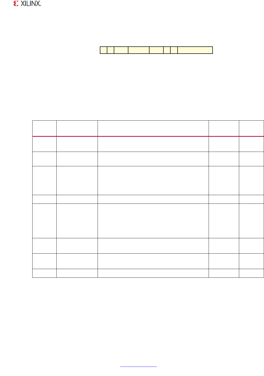
1000BASE-X PCS/PMA or SGMII v11.4 www.xilinx.com 60
PG047 October 16, 2012
Chapter 2: Product Specification
Register 5: Auto-Negotiation Link Partner Base
X-Ref Target - Figure 2-15
Figure 2-15: MDIO Register 5: Auto-Negotiation Link Partner Base
Table 2-24: Auto-Negotiation Link Partner Ability Base Register (Register 5)
Bit(s) Name Description Attributes Default
Value
5.15 Next Page 1 = Next Page functionality is supported
0 = Next Page functionality is not supported read only 0
5.14 Acknowledge Used by Auto-Negotiation function to indicate
reception of a link partner’s base or next page read only 0
5.13:12 Remote Fault
00 = No Error
01 = Offline
10 = Link Failure
11 = Auto-Negotiation Error
read only 00
5.11:9 Reserved Always return 0s returns 0s 000
5.8:7 Pause
00 = No PAUSE
01 = Symmetric PAUSE
10 = Asymmetric PAUSE towards link partner
11 = Both Symmetric PAUSE and Asymmetric
PAUSE supported
read only 00
5.6 Half Duplex 1 = Half Duplex Mode is supported
0 = Half Duplex Mode is not supported read only 0
5.5 Full Duplex 1 = Full Duplex Mode is supported
0 = Full Duplex Mode is not supported read only 0
5.4:0 Reserved Always return 0s returns 0s 00000
.%840!'%
!#+./7,%$'%
2%3%26%$
2%-/4%&!5,4
(!,&$50,%8
2EG
2%3%26%$
0!53%
&5,,$50,%8
8
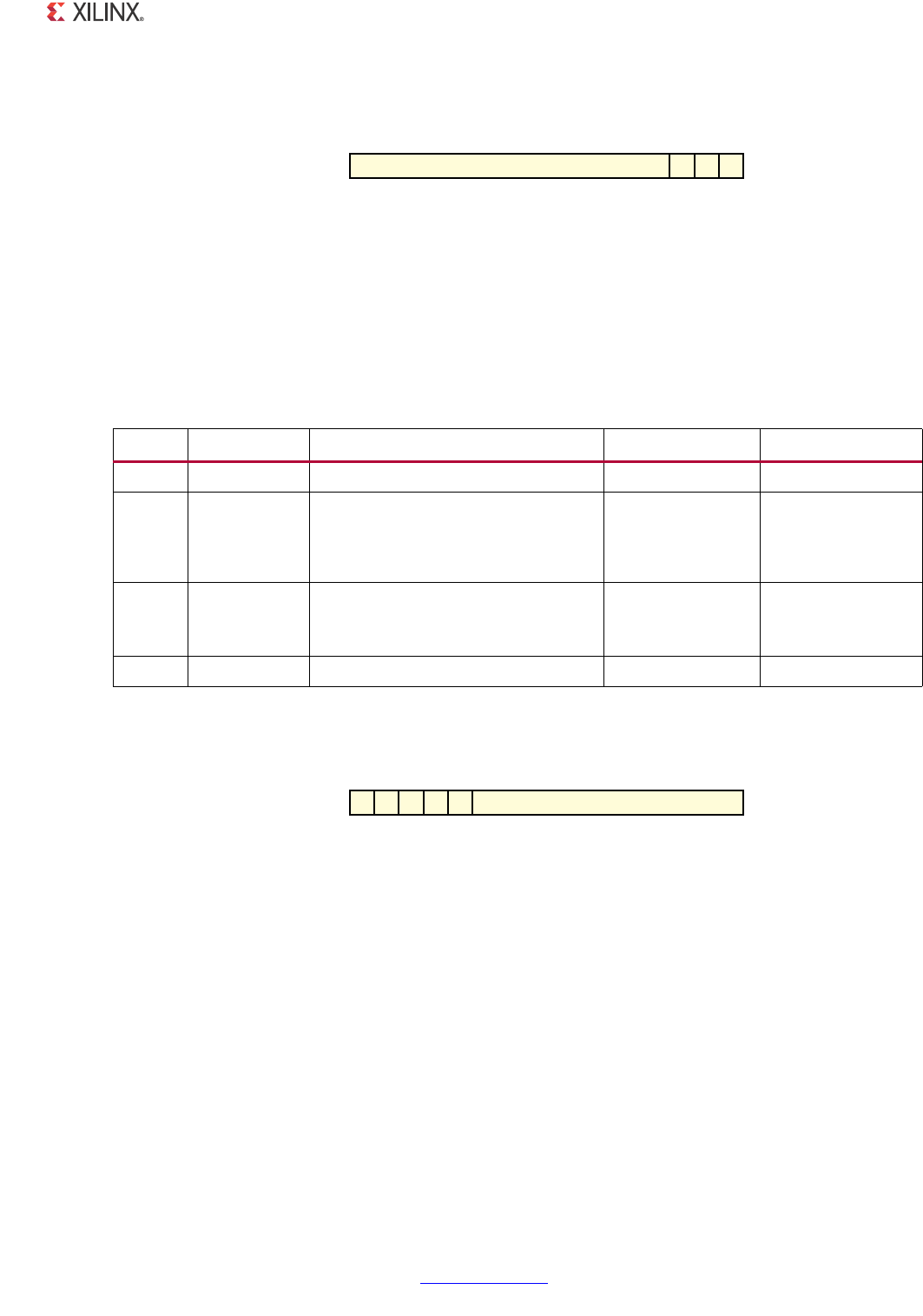
1000BASE-X PCS/PMA or SGMII v11.4 www.xilinx.com 61
PG047 October 16, 2012
Chapter 2: Product Specification
Register 6: Auto-Negotiation Expansion
Register 7: Next Page Transmit
X-Ref Target - Figure 2-16
Figure 2-16: MDIO Register 6: Auto-Negotiation Expansion
Table 2-25: Auto-Negotiation Expansion Register (Register 6)
Bit(s) Name Description Attributes Default Value
6.15:3 Reserved Always returns 0s returns 0s 0000000000000
6.2 Next Page
Able
This bit is ignored as the core
currently does not support next
page. This feature can be enabled on
request.
returns 1 1
6.1 Page
Received
1 = A new page has been received
0 = A new page has not been
received
read only
self clearing on
read
0
6.0 Reserved Always returns 0s returns 0s 0000000
X-Ref Target - Figure 2-17
Figure 2-17: MDIO Register 7: Next Page Transmit
.%840!'%!",%
0!'%2%#%)6%$
2%3%26%$
2EG
2%3%26%$
8
.%840!'%
2%3%26%$
-%33!'%0!'%
2EG
4/'',%
-%33!'%#/$%
!#+./7,%$'%
8
1000BASE-X PCS/PMA or SGMII v11.4 www.xilinx.com 62
PG047 October 16, 2012
Chapter 2: Product Specification
Register 8: Next Page Receive
Table 2-26: Auto-Negotiation Next Page Transmit (Register 7)
Bit(s) Name Description Attributes Default
Value1
7.15 Next Page 1 = Additional Next Page(s) will follow
0 = Last page
read/
write 0
7.14 Reserved Always returns ‘0’ returns 0 0
7.13 Message Page 1 = Message Page
0 = Unformatted Page
read/
write 1
7.12 Acknowledge 2 1 = Comply with message
0 = Cannot comply with message
read/
write 0
7.11 Toggle Value toggles between subsequent Next
Pages read only 0
7.10:0
Message /
Unformatted Code
Field
Message Code Field or Unformatted Page
Encoding as dictated by 7.13
read/
write
00000000001
(Null Message
Code)
Notes:
1. This register returns the default values as the core currently does not support next page. This feature can be
enabled on request.
X-Ref Target - Figure 2-18
Figure 2-18: MDIO Register 8: Next Page Receive
Table 2-27: Auto-Negotiation Next Page Receive (Register 8)
Bit(s) Name Description Attributes Default Value
8.15 Next Page 1 = Additional Next Page(s) will follow
0 = Last page read only 0
8.14 Acknowledge
Used by Auto-Negotiation function to
indicate reception of a link partner’s
base or next page
read only 0
8.13 Message Page 1 = Message Page
0 = Unformatted Page read only 0
.%840!'%
!#+./7,%$'%
-%33!'%0!'%
2EG
4/'',%
-%33!'%#/$%
!#+./7,%$'%
8
1000BASE-X PCS/PMA or SGMII v11.4 www.xilinx.com 63
PG047 October 16, 2012
Chapter 2: Product Specification
Register 15: Extended Status
8.12 Acknowledge 2 1 = Comply with message
0 = Cannot comply with message read only 0
8.11 Toggle Value toggles between subsequent
Next Pages read only 0
8.10:0
Message /
Unformatted Code
Field
Message Code Field or Unformatted
Page Encoding as dictated by 8.13 read only 00000000000
X-Ref Target - Figure 2-19
Figure 2-19: MDIO Register 15: Extended Status Register
Table 2-28: Extended Status Register (Register 15)
Bit(s) Name Description Attributes Default Value
15.15 1000BASE-X Full
Duplex
Always returns a ‘1’ for this bit because
1000BASE-X Full Duplex is supported returns 1 1
15.14 1000BASE-X Half
Duplex
Always returns a ‘0’ for this bit because
1000BASE-X Half Duplex is not
supported
returns 0 0
15.13 1000BASE-T Full
Duplex
Always returns a ‘0’ for this bit because
1000BASE-T Full Duplex is not
supported
returns 0 0
15.12 1000BASE-T Half
Duplex
Always returns a ‘0’ for this bit because
1000BASE-T Half Duplex is not
supported
returns 0 0
15:11:0 Reserved Always return 0s returns 0s 000000000000
Table 2-27: Auto-Negotiation Next Page Receive (Register 8) (Cont’d)
Bit(s) Name Description Attributes Default Value
"!3%8&5,,$50,%8
"!3%8(!,&$50,%8
"!3%4&5,,$50,%8
2EG
2%3%26%$
"!3%4(!,&$50,%8
8
1000BASE-X PCS/PMA or SGMII v11.4 www.xilinx.com 64
PG047 October 16, 2012
Chapter 2: Product Specification
Register 16: Vendor-Specific Auto-Negotiation Interrupt Control
1000BASE-X Standard Without the Optional Auto-Negotiation
It is not in the scope of this document to fully describe the 1000BASE-X PCS registers. See
clauses 22 and 37 of the IEEE 802.3-2008 specification for further information.
Registers at undefined addresses are read-only and return 0s. The core can be reset three
ways: reset, DCM_LOCKED and soft reset. All of these methods reset all the registers to the
default values.
X-Ref Target - Figure 2-20
Figure 2-20: MDIO Register 16: Vendor Specific Auto-Negotiation Interrupt Control
Table 2-29: Vendor Specific Register: Auto-Negotiation Interrupt Control Register (Register 16)
Bit(s) Name Description Attributes Default Value
16.15:2 Reserved Always return 0s returns 0s 00000000000000
16.1 Interrupt
Status
1 = Interrupt is asserted
0 = Interrupt is not asserted
If the interrupt is enabled, this bit is
asserted on the completion of an
Auto-Negotiation cycle; it is only
cleared by writing ‘0’ to this bit.
If the Interrupt is disabled, the bit is set
to ‘0.’
Note: The an_interrupt port of the
core is wired to this bit.
read/
write 0
16.0 Interrupt
Enable
1 = Interrupt enabled
0 = Interrupt disabled
read/
write 1
Table 2-30: MDIO Registers for 1000BASE-X without Auto-Negotiation
Register Address Register Name
0 Control Register
1Status Register
2,3 PHY Identifier
15 Extended Status Register
2EG
2%3%26%$
).4%2250434!453
).4%22504%.!",%
8
1000BASE-X PCS/PMA or SGMII v11.4 www.xilinx.com 65
PG047 October 16, 2012
Chapter 2: Product Specification
Register 0: Control Register
X-Ref Target - Figure 2-21
Figure 2-21: MDIO Register 0: Control Register
Table 2-31: Control Register (Register 0)
Bit(s) Name Description Attributes Default
Value
0.15 Reset 1 = PCS/PMA reset
0 = Normal Operation
read/write
self clearing 0
0.14 Loopback
1 = Enable Loopback Mode
0 = Disable Loopback Mode
When used with a device-specific
transceiver, the core is placed in internal
loopback mode.
With the TBI version, Bit 1 is connected to
ewrap. When set to ‘1’ indicates to the
external PMA module to enter loopback
mode.
See Loopback.
read/write 0
0.13 Speed Selection
(LSB)
Always returns a 0 for this bit. Together with
bit 0.6, speed selection of 1000 Mb/s is
identified.
returns 0 0
0.12 Auto-Negotiation
Enable
Ignore this bit because Auto-Negotiation is
not included. read/ write 1
0.11 Power Down
1 = Power down
0 = Normal operation
With the PMA option, when set to ’1’ the
device-specific transceiver is placed in a
low- power state. This bit requires a reset
(see bit 0.15) to clear.
With the TBI version this register bit has no
effect.
read/ write 0
0.10 Isolate 1 = Electrically Isolate PHY from GMII
0 = Normal operation read/write 1
0.9 Restart Auto-
Negotiation
Ignore this bit because Auto-Negotiation is
not included. read/ write 0
2%3%4
,//0"!#+
!54/.%'%.!",%
2%34!24!54/.%'
2%3%26%$
0/7%2$/7.
30%%$
30%%$
2EG
)3/,!4%
$50,%8-/$%
#/,,)3)/.4%34
5.)$)2%#4)/.!,%.!",%
8
1000BASE-X PCS/PMA or SGMII v11.4 www.xilinx.com 66
PG047 October 16, 2012
Chapter 2: Product Specification
Register 1: Status Register
0.8 Duplex Mode Always returns a ‘1’ for this bit to signal
Full-Duplex Mode. returns 1 1
0.7 Collision Test Always returns a ‘0’ for this bit to disable
COL test. returns 0 0
0.6 Speed Selection
(MSB)
Always returns a ‘1’ for this bit. Together with
bit 0.13, speed selection of 1000 Mb/s is
identified
returns 1 1
0.5 Unidirectional
Enable
Enables transmit irrespective of receive.
Unidirectional feature is enabled
automatically when this bit is set because
optional Auto-Negotiation is not present.
read/ write 0
0.4:0 Reserved Always return 0s , writes ignored. returns 0s 00000
X-Ref Target - Figure 2-22
Figure 2-22: MDIO Register 1: Status Register
Table 2-32: Status Register (Register 1)
Bit(s) Name Description Attributes Default
Value
1.15 100BASE-T4 Always returns a ‘0’ for this bit because
100BASE-T4 is not supported returns 0 0
1.14 100BASE-X Full Duplex Always returns a ‘0’ for this bit because
100BASE-X Full Duplex is not supported returns 0 0
1.13 100BASE-X Half Duplex Always returns a ‘0’ for this bit because
100BASE-X Half Duplex is not supported returns 0 0
1.12 10 Mb/s Full Duplex Always returns a ‘0’ for this bit because 10
Mb/s Full Duplex is not supported returns 0 0
Table 2-31: Control Register (Register 0) (Cont’d)
Bit(s) Name Description Attributes Default
Value
"!3%4
"!3%8&5,,$50,%8
-BS&5,,$50,%8
"!3%4(!,&$50,%8
,).+34!453
-BS(!,&$50,%8
"!3%8(!,&$50,%8
-&02%!-",%35002%33)/.
2EG
"!3%4&5,,$50,%8
%84%.$%$34!453
5.)$)2%#4)/.!,!.),)49
!54/.%'#/-0,%4%
2%-/4%&!5,4
!54/.%'!"),)49
*!""%2$%4%#4
%84%.$%$#!0!"),)49
8
1000BASE-X PCS/PMA or SGMII v11.4 www.xilinx.com 67
PG047 October 16, 2012
Chapter 2: Product Specification
Link Status
When high, the link is valid and has remained valid after this register was last read;
synchronization of the link has been obtained.
When low, either:
• A valid link has not been established; link synchronization has failed.
OR
1.11 10 Mb/s Half Duplex Always returns a ‘0’ for this bit because 10
Mb/ s Half Duplex is not supported returns 0 0
1.10 100BASE-T2 Full Duplex Always returns a ‘0’ for this bit because
100BASE-T2 Full Duplex is not supported returns 0 0
1.9 100BASE-T2 Half
Duplex
Always returns a ‘0’ for this bit because
100BASE-T2 Half Duplex is not supported returns 0 0
1.8 Extended Status
Always returns a ‘1’ for this bit to indicate the
presence of the Extended Register (Register
15)
returns 1 1
1.7 Unidirectional Ability Always returns 1, writes ignored returns 1 1
1.6 MF Preamble
Suppression
Always returns a ‘1’ for this bit to indicate
that Management Frame Preamble
Suppression is supported
returns 1 1
1.5 Auto- Negotiation
Complete
Ignore this bit because Auto-Negotiation is
not included. returns 1 1
1.4 Remote Fault Always returns a ‘0’ for this bit because
Auto-Negotiation is not included. returns 0 0
1.3 Auto- Negotiation
Ability
Ignore this bit because Auto-Negotiation is
not included. returns 0 0
1.2 Link Status
1 = Link is up
0 = Link is down
Latches '0' if Link Status goes down. Clears to
current Link Status on read.
See the following Link Status section for
further details.
read only
self
clearing on
read
0
1.1 Jabber Detect Always returns a ‘0’ for this bit because
Jabber Detect is not supported returns 0 0
1.0 Extended Capability Always returns a ‘0’ for this bit because no
extended register set is supported returns 0 0
Table 2-32: Status Register (Register 1) (Cont’d)
Bit(s) Name Description Attributes Default
Value
1000BASE-X PCS/PMA or SGMII v11.4 www.xilinx.com 68
PG047 October 16, 2012
Chapter 2: Product Specification
• Link synchronization was lost at some point after this register was previously read.
However, the current link status might be good. Therefore read this register a second
time to get confirmation of the current link status.
Registers 2 and 3: Phy Identifier
X-Ref Target - Figure 2-23
Figure 2-23: MDIO Registers 2 and 3: PHY Identifier
Table 2-33: PHY Identifier (Registers 2 and 3)
Bit(s) Name Description Attributes Default Value
2.15:0 Organizationally Unique
Identifier Always return 0s returns 0s 0000000000000000
3.15:10 Organizationally Unique
Identifier Always return 0s returns 0s 000000
3.9:4 Manufacturer model number Always return 0s returns 0s 000000
3.3:0 Revision Number Always return 0s returns 0s 0000
/2'!.):%
5.)15%)$
2EG
2EG
/2'!.):%
5.)15%)$
-!5&!#452%2
-/$%,./
2%6)3)/../
8
1000BASE-X PCS/PMA or SGMII v11.4 www.xilinx.com 69
PG047 October 16, 2012
Chapter 2: Product Specification
Register 15: Extended Status
SGMII Standard Using the Optional Auto-Negotiation
The registers provided for SGMII operation in this core are adaptations of those defined in
clauses 22 and 37 of the IEEE 802.3-2008 specification. In an SGMII implementation, two
different types of links exist. They are the SGMII link between the MAC and PHY (SGMII link)
and the link across the Ethernet Medium itself (Medium). See Figure 9-2.
Information regarding the state of both of these links is contained within the following
registers. Where applicable, the abbreviations SGMII link and Medium are used in the
register descriptions. Registers at undefined addresses are read-only and return 0s. The
core can be reset three ways: reset, DCM_LOCKED and soft reset. All of these methods reset
all the registers to the default values.
X-Ref Target - Figure 2-24
Figure 2-24: MDIO Register 15: Extended Status
Table 2-34: Extended Status (Register 15)
Bit(s) Name Description Attributes Default Value
15.15 1000BASE-X Full
Duplex
Always returns a ‘1’ because
1000BASE-X Full Duplex is
supported
returns 1 1
15.14 1000BASE-X Half
Duplex
Always returns a ‘0’ because
1000BASE-X Half Duplex is not
supported
returns 0 0
15.13 1000BASE-T Full
Duplex
Always returns a ‘0’ because
1000BASE-T Full Duplex is not
supported
returns 0 0
15.12 1000BASE-T Half
Duplex
Always returns a ‘0’ because
1000BASE-T Half Duplex is not
supported
returns 0 0
15:11:0 Reserved Always return 0s returns 0s 000000000000
"!3%8&5,,$50,%8
"!3%8(!,&$50,%8
"!3%4&5,,$50,%8
2EG
2%3%26%$
"!3%4(!,&$50,%8
8

1000BASE-X PCS/PMA or SGMII v11.4 www.xilinx.com 70
PG047 October 16, 2012
Chapter 2: Product Specification
.
Register 0: SGMII Control
Table 2-35: MDIO Registers for SGMII with Auto-Negotiation
Register Address Register Name
0SGMII Control Register
1 SGMII Status Register
2,3 PHY Identifier
4 SGMII Auto-Negotiation Advertisement Register
5 SGMII Auto-Negotiation Link Partner Ability Base Register
6 SGMII Auto-Negotiation Expansion Register
7 SGMII Auto-Negotiation Next Page Transmit Register
8 SGMII Auto-Negotiation Next Page Receive Register
15 SGMII Extended Status Register
16 SGMII Vendor Specific: Auto-Negotiation Interrupt Control
X-Ref Target - Figure 2-25
Figure 2-25: MDIO Register 0: SGMII Control
2%3%4
,//0"!#+
!54/.%'%.!",%
2%34!24!54/.%'
2%3%26%$
0/7%2$/7.
30%%$
30%%$
2EG
)3/,!4%
$50,%8-/$%
#/,,)3)/.4%34
5.)$)2%#4)/.!,%.!",%
8

1000BASE-X PCS/PMA or SGMII v11.4 www.xilinx.com 71
PG047 October 16, 2012
Chapter 2: Product Specification
Table 2-36: SGMII Control (Register 0)
Bit(s) Name Description Attributes Default
Value
0.15 Reset 1 = Core Reset
0 = Normal Operation
read/write
self clearing 0
0.14 Loopback
1 = Enable Loopback Mode
0 = Disable Loopback Mode
When used with a device-specific
transceiver, the core is placed in
internal loopback mode.
With the TBI version, Bit 1 is connected
to ewrap. When set to ‘1’ indicates to
the external PMA module to enter
loopback mode.
See Loopback.
read/write 0
0.13 Speed Selection
(LSB)
Always returns a ‘0’ for this bit.
Together with bit 0.6, speed selection
of 1000 Mb/s is identified
returns 0 0
0.12 Auto-Negotiation
Enable
1 = Enable SGMII Auto-Negotiation
Process
0 = Disable SGMII Auto-Negotiation
Process
read/write 1
0.11 Power Down
1 = Power down
0 = Normal operation
With the PMA option, when set to ’1’
the device-specific transceiver is
placed in a low-power state. This bit
requires a reset (see bit 0.15) to clear.
With the TBI version this register bit
has no effect.
read/ write 0
0.10 Isolate
1 = Electrically Isolate SGMII logic from
GMII
0 = Normal operation
read/write 1
0.9 Restart Auto-
Negotiation
1 = Restart Auto-Negotiation Process
across SGMII link
0 = Normal Operation
read/write
self clearing 0
0.8 Duplex Mode Always returns a ‘1’ for this bit to signal
Full-Duplex Mode returns 1 1
0.7 Collision Test Always returns a ‘0’ for this bit to
disable COL test returns 0 0
0.6 Speed Selection
(MSB)
Always returns a ‘1’ for this bit.
Together with bit 0.13, speed selection
of 1000 Mb/s is identified
returns 1 1
1000BASE-X PCS/PMA or SGMII v11.4 www.xilinx.com 72
PG047 October 16, 2012
Chapter 2: Product Specification
Register 1: SGMII Status
0.5 Unidirectional
Enable
Enable transmit regardless of whether
a valid link has been established. This
feature is only possible if
Auto-Negotiation Enable bit 0.12 is
disabled.
read/ write 0
0.4:0 Reserved Always return 0s , writes ignored returns 0s 00000
X-Ref Target - Figure 2-26
Figure 2-26: MDIO Register 1: SGMII Status
Table 2-37: SGMII Status (Register 1)
Bit(s) Name Description Attributes Default
Value
1.15 100BASE-T4 Always returns a ‘0’ for this bit because
100BASE-T4 is not supported returns 0 0
1.14 100BASE-X Full Duplex Always returns a ‘0’ for this bit because
100BASE-X Full Duplex is not supported returns 0 0
1.13 100BASE-X Half Duplex Always returns a ‘0’ for this bit because
100BASE-X Half Duplex is not supported returns 0 0
1.12 10 Mb/s Full Duplex Always returns a ‘0’ for this bit because 10
Mb/s Full Duplex is not supported returns 0 0
1.11 10 Mb/s Half Duplex Always returns a ‘0’ for this bit because 10
Mb/s Half Duplex is not supported returns 0 0
1.10 100BASE-T2 Full
Duplex
Always returns a ‘0’ for this bit because
100BASE-T2 Full Duplex is not supported returns 0 0
1.9 100BASE-T2 Half
Duplex
Always returns a ‘0’ for this bit because
100BASE-T2 Half Duplex is not supported returns 0 0
Table 2-36: SGMII Control (Register 0) (Cont’d)
Bit(s) Name Description Attributes Default
Value
"!3%4
"!3%8&5,,$50,%8
-BS&5,,$50,%8
"!3%4(!,&$50,%8
,).+34!453
-BS(!,&$50,%8
"!3%8(!,&$50,%8
-&02%!-",%35002%33)/.
2EG
"!3%4&5,,$50,%8
%84%.$%$34!453
5.)$)2%#4)/.!,!.),)49
!54/.%'#/-0,%4%
2%-/4%&!5,4
!54/.%'!"),)49
*!""%2$%4%#4
%84%.$%$#!0!"),)49
8
1000BASE-X PCS/PMA or SGMII v11.4 www.xilinx.com 73
PG047 October 16, 2012
Chapter 2: Product Specification
Link Status
When high, the link is valid and has remained valid after this register was last read:
synchronization of the link has been obtained and Auto-Negotiation (if enabled) has
completed.
When low, either:
• A valid link has not been established; link synchronization has failed or
Auto-Negotiation (if enabled) has failed to complete.
OR
1.8 Extended Status
Always returns a ‘1’ for this bit to indicate the
presence of the Extended Register (Register
15)
returns 1 1
1.7 Unidirectional Ability Always returns ‘1,’ writes ignored returns 1 1
1.6 MF Preamble
Suppression
Always returns a ‘1’ for this bit to indicate
that Management Frame Preamble
Suppression is supported
returns 1 1
1.5 Auto- Negotiation
Complete
1 = Auto-Negotiation process completed
across SGMII link
0 = Auto-Negotiation process not
completed across SGMII link
read only 0
1.4 Remote Fault
1 = A fault on the Medium has been
detected
0 = No fault of the Medium has been
detected
read only
self clearing
on read
0
1.3 Auto- Negotiation
Ability
Always returns a ‘1’ for this bit to indicate
that the SGMII core is capable of
Auto-Negotiation
returns 1 1
1.2 SGMII Link Status
1 = SGMII Link is up
0 = SGMII Link is down
Latches '0' if SGMII Link Status goes down.
Clears to current SGMII Link Status on read.
See the following Link Status section for
further details.
read only
self clearing
on read
0
1.1 Jabber Detect Always returns a ‘0’ for this bit because
Jabber Detect is not supported returns 0 0
1.0 Extended Capability Always returns a ‘0’ for this bit because no
extended register set is supported returns 0 0
Table 2-37: SGMII Status (Register 1) (Cont’d)
Bit(s) Name Description Attributes Default
Value

1000BASE-X PCS/PMA or SGMII v11.4 www.xilinx.com 74
PG047 October 16, 2012
Chapter 2: Product Specification
• Link synchronization was lost at some point when the register was previously read.
However, the current link status might be good. Therefore read this register a second
time to get confirmation of the current link status.
Regardless of whether Auto-Negotiation is enabled or disabled, there can be some delay to
the deassertion of Link Status following the loss of synchronization of a previously
successful link. This is due to the Auto-Negotiation state machine which requires that
synchronization is lost for an entire link timer duration before changing state. For more
information, see the 802.3 specification (the an_sync_status variable).
Registers 2 and 3: PHY Identifier
X-Ref Target - Figure 2-27
Figure 2-27: MDIO Registers 2 and 3: PHY Identifier
Table 2-38: PHY Identifier (Registers 2 and 3)
Bit(s) Name Description Attributes Default Value
2.15:0 Organizationally Unique
Identifier Always return 0s returns 0s 0000000000000000
3.15:10 Organizationally Unique
Identifier Always return 0s returns 0s 000000
3.9:4 Manufacturer model number Always return 0s returns 0s 000000
3.3:0 Revision Number Always return 0s returns 0s 0000
/2'!.):%
5.)15%)$
2EG
2EG
/2'!.):%
5.)15%)$
-!5&!#452%2
-/$%,./
2%6)3)/../
8
1000BASE-X PCS/PMA or SGMII v11.4 www.xilinx.com 75
PG047 October 16, 2012
Chapter 2: Product Specification
Register 4: SGMII Auto-Negotiation Advertisement
MAC Mode of Operation
PHY Mode of Operation
X-Ref Target - Figure 2-28
Figure 2-28: MDIO Register 4: SGMII Auto-Negotiation Advertisement
Table 2-39: SGMII Auto-Negotiation Advertisement (Register 4)
Bit(s) Name Description Attributes Default Value
4.15:0 All bits SGMII defined value sent from the
MAC to the PHY read only 0100000000000001
X-Ref Target - Figure 2-29
Figure 2-29: MDIO Register 4: SGMII Auto-Negotiation Advertisement
Table 2-40: SGMII Auto-Negotiation Advertisement in PHY Mode (Register 4)
Bit(s) Name Description Attributes Default
Value
4.15 PHY Link Status
This refers to the link status of the PHY with
its link partner across the Medium.
1 = Link Up
0 = Link Down
read/write 0
4.14 Acknowledge
Used by Auto-Negotiation function to
indicate reception of a link partner’s base or
next page
read/write 0
4.13 Reserved Always returns ‘0,’ writes ignored returns 0 0
.%840!'%
2%3%26%$
2%3%26%$
2%-/4%&!5,4
(!,&$50,%8
2EG
2%3%26%$
0!53%
&5,,$50,%8
8
0(9,).+34!453
!#+./7,%$'%
2%3%26%$
2%3%26%$
2EG
$50,%8-/$%
30%%$
2%3%26%$
8

1000BASE-X PCS/PMA or SGMII v11.4 www.xilinx.com 76
PG047 October 16, 2012
Chapter 2: Product Specification
Register 5: SGMII Auto-Negotiation Link Partner Ability
The Auto-Negotiation Ability Base Register (Register 5) contains information related to the
status of the link between the PHY and its physical link partner across the Medium.
4.12 Duplex Mode 1= Full Duplex
0 = Half Duplex read/write 0
4.11:10 Speed
11 = Reserved
10 = 1 Gb/s
01 = 100 Mb/s
00 = 10 Mb/s
read/write 00
4.9:1 Reserved Always return 0s returns 0s 000000000
4:0 Reserved Always returns ‘1’ returns 1 1
X-Ref Target - Figure 2-30
Figure 2-30: MDIO Register 5: SGMII Auto-Negotiation Link Partner Ability
Table 2-41: SGMII Auto-Negotiation Link Partner Ability Base (Register 5)
Bit(s) Name Description Attributes Default
Value
5.15 PHY Link Status
This refers to the link status of the PHY with
its link partner across the Medium.
1 = Link Up
0 = Link Down
read only 1
5.14 Acknowledge
Used by Auto-Negotiation function to
indicate reception of a link partner’s base or
next page
read only 0
5.13 Reserved Always returns ‘0,’ writes ignored returns 0 0
5.12 Duplex Mode 1= Full Duplex
0 = Half Duplex read only 0
5.11:10 Speed
11 = Reserved
10 = 1 Gb/s
01 = 100 Mb/s
00 = 10 Mb/s
read only 00
Table 2-40: SGMII Auto-Negotiation Advertisement in PHY Mode (Register 4) (Cont’d)
Bit(s) Name Description Attributes Default
Value
0(9,).+34!453
!#+./7,%$'%
2%3%26%$
2%3%26%$
2EG
$50,%8-/$%
30%%$
2%3%26%$
8
1000BASE-X PCS/PMA or SGMII v11.4 www.xilinx.com 77
PG047 October 16, 2012
Chapter 2: Product Specification
Register 6: SGMII Auto-Negotiation Expansion
5.9:1 Reserved Always return 0s returns 0s 000000000
5:0 Reserved Always returns ‘1’ returns 1 1
X-Ref Target - Figure 2-31
Figure 2-31: MDIO Register 6: SGMII Auto-Negotiation Expansion
Table 2-42: SGMII Auto-Negotiation Expansion (Register 6)
Bit(s) Name Description Attributes Default Value
6.15:3 Reserved Always return 0s returns 0s 0000000000000
6.2 Next Page
Able
This bit is ignored as the core
currently does not support next
page. This feature can be enabled on
request.
returns 1 1
6.1 Page
Received
1 = A new page has been received
0 = A new page has not been
received
read only
self clearing on
read
0
6.0 Reserved Always return 0s returns 0s 0000000
Table 2-41: SGMII Auto-Negotiation Link Partner Ability Base (Register 5) (Cont’d)
Bit(s) Name Description Attributes Default
Value
.%840!'%!",%
0!'%2%#%)6%$
2%3%26%$
2EG
2%3%26%$
8
1000BASE-X PCS/PMA or SGMII v11.4 www.xilinx.com 78
PG047 October 16, 2012
Chapter 2: Product Specification
Register 7: SGMII Auto-Negotiation Next Page Transmit
Register 8: SGMII Next Page Receive
X-Ref Target - Figure 2-32
Figure 2-32: MDIO Register 7: SGMII Auto-Negotiation Next Page Transmit
Table 2-43: SGMII Auto-Negotiation Next Page Transmit (Register 7)
Bit(s) Name Description Attributes Default Value(1)
7.15 Next Page 1 = Additional Next Page(s) will follow
0 = Last page
read/
write 0
7.14 Reserved Always returns ‘0’ returns 0 0
7.13 Message Page 1 = Message Page
0 = Unformatted Page
read/
write 1
7.12 Acknowledge 2 1 = Comply with message
0 = Cannot comply with message
read/
write 0
7.11 Toggle Value toggles between subsequent
Next Pages read only 0
7.10:0
Message /
Unformatted
Code Field
Message Code Field or Unformatted
Page Encoding as dictated by 7.13
read/
write
00000000001
(Null Message
Code)
Notes:
1. This register returns the default values because the core does not support next page. The feature can be enabled,
if requested.
X-Ref Target - Figure 2-33
Figure 2-33: MDIO Register 8: SGMII Next Page Receive
.%840!'%
2%3%26%$
-%33!'%0!'%
2EG
4/'',%
-%33!'%#/$%
!#+./7,%$'%
8
.%840!'%
!#+./7,%$'%
-%33!'%0!'%
2EG
4/'',%
-%33!'%#/$%
!#+./7,%$'%
8
1000BASE-X PCS/PMA or SGMII v11.4 www.xilinx.com 79
PG047 October 16, 2012
Chapter 2: Product Specification
Register 15: SGMII Extended Status
Table 2-44: SGMII Auto-Negotiation Next Page Receive (Register 8)
Bit(s) Name Description Attributes Default Value
8.15 Next Page 1 = Additional Next Page(s) will follow
0 = Last page read only 0
8.14 Acknowledge
Used by Auto-Negotiation function to
indicate reception of a link partner’s
base or next page
read only 0
8.13 Message Page 1 = Message Page
0 = Unformatted Page read only 0
8.12 Acknowledge 2 1 = Comply with message
0 = Cannot comply with message read only 0
8.11 Toggle Value toggles between subsequent
Next Pages read only 0
8.10:0
Message /
Unformatted Code
Field
Message Code Field or Unformatted
Page Encoding as dictated by 8.13 read only 00000000000
X-Ref Target - Figure 2-34
Figure 2-34: MDIO Register 15: SGMII Extended Status
Table 2-45: SGMII Extended Status Register (Register 15)
Bit(s) Name Description Attributes Default Value
15.15 1000BASE-X Full
Duplex
Always returns a ‘1’ for this bit because
1000BASE-X Full Duplex is supported returns 1 1
15.14 1000BASE-X Half
Duplex
Always returns a ‘0’ for this bit because
1000BASE-X Half Duplex is not
supported
returns 0 0
15.13 1000BASE-T Full
Duplex
Always returns a ‘0’ for this bit because
1000BASE-T Full Duplex is not
supported
returns 0 0
"!3%8&5,,$50,%8
"!3%8(!,&$50,%8
"!3%4&5,,$50,%8
2EG
2%3%26%$
"!3%4(!,&$50,%8
8
1000BASE-X PCS/PMA or SGMII v11.4 www.xilinx.com 80
PG047 October 16, 2012
Chapter 2: Product Specification
Register 16: SGMII Auto-Negotiation Interrupt Control
15.12 1000BASE-T Half
Duplex
Always returns a ‘0’ for this bit because
1000BASE-T Half Duplex is not
supported
returns 0 0
15:11:0 Reserved Always return 0s returns 0s 000000000000
X-Ref Target - Figure 2-35
Figure 2-35: MDIO Register 16: SGMII Auto-Negotiation Interrupt Control
Table 2-46: SGMII Auto-Negotiation Interrupt Control (Register 16)
Bit(s) Name Description Attributes Default Value
16.15:2 Reserved Always return 0s returns 0s 00000000000000
16.1 Interrupt
Status
1 = Interrupt is asserted
0 = Interrupt is not asserted
If the interrupt is enabled, this bit is
asserted on completion of an
Auto-Negotiation cycle across the
SGMII link; it is only cleared by writing
‘0’ to this bit.
If the Interrupt is disabled, the bit is set
to ‘0.’
The an_interrupt port of the core is
wired to this bit.
read/
write 0
16.0 Interrupt
Enable
1 = Interrupt enabled
0 = Interrupt disabled
read/
write 1
Table 2-45: SGMII Extended Status Register (Register 15)
Bit(s) Name Description Attributes Default Value
2EG
2%3%26%$
).4%2250434!453
).4%22504%.!",%
8
1000BASE-X PCS/PMA or SGMII v11.4 www.xilinx.com 81
PG047 October 16, 2012
Chapter 2: Product Specification
SGMII Standard without the Optional Auto-Negotiation
The registers provided for SGMII operation in this core are adaptations of those defined in
clauses 22 and 37 of the IEEE 802.3-2008 specification. In an SGMII implementation, two
different types of links exist. They are the SGMII link between the MAC and PHY (SGMII link)
and the link across the Ethernet Medium itself (Medium). See Figure 9-2. Information about
the state of the SGMII link is available in registers that follow.
The state of the link across the Ethernet Medium itself is not directly available when SGMII
Auto-Negotiation is not present. For this reason, the status of the link and the results of the
PHYs Auto-Negotiation (for example, Speed and Duplex mode) must be obtained directly
from the management interface of connected PHY module. Registers at undefined
addresses are read-only and return 0s.
The core can be reset three ways: reset, DCM_LOCKED and soft reset. All of these methods
reset all the registers to the default values.
Register 0: SGMII Control
Table 2-47: MDIO Registers for SGMII with Auto-Negotiation
Register Address Register Name
0 SGMII Control Register
1 SGMII Status Register
2,3 PHY Identifier
4 SGMII Auto-Negotiation Advertisement Register
15 SGMII Extended Status Register
X-Ref Target - Figure 2-36
Figure 2-36: MDIO Register 0: SGMII Control
2%3%4
,//0"!#+
!54/.%'%.!",%
2%34!24!54/.%'
2%3%26%$
0/7%2$/7.
30%%$
30%%$
2EG
)3/,!4%
$50,%8-/$%
#/,,)3)/.4%34
5.)$)2%#4)/.!,%.!",%
8

1000BASE-X PCS/PMA or SGMII v11.4 www.xilinx.com 82
PG047 October 16, 2012
Chapter 2: Product Specification
Table 2-48: SGMII Control (Register 0)
Bit(s) Name Description Attributes Default
Value
0.15 Reset 1 = Core Reset
0 = Normal Operation
read/write
self clearing 0
0.14 Loopback
1 = Enable Loopback Mode
0 = Disable Loopback Mode
When used with a device-specific
transceiver, the core is placed in
internal loopback mode.
With the TBI version, Bit 1 is connected
to ewrap. When set to ‘1’ indicates to
the external PMA module to enter
loopback mode.
See Loopback.
read/write 0
0.13 Speed Selection
(LSB)
Always returns a ‘0’ for this bit.
Together with bit 0.6, speed selection
of 1000 Mb/s is identified
returns 0 0
0.12 Auto-Negotiation
Enable
1 = Enable SGMII Auto-Negotiation
Process
0 = Disable SGMII Auto-Negotiation
Process
read/write 1
0.11 Power Down
1 = Power down
0 = Normal operation
With the PMA option, when set to ’1’
the device-specific transceiver is
placed in a low-power state. This bit
requires a reset (see bit 0.15) to clear.
With the TBI version this register bit
has no effect.
read/ write 0
0.10 Isolate
1 = Electrically Isolate SGMII logic from
GMII
0 = Normal operation
read/write 1
0.9 Restart Auto-
Negotiation
1 = Restart Auto-Negotiation Process
across SGMII link
0 = Normal Operation
read/write
self clearing 0
0.8 Duplex Mode Always returns a ‘1’ for this bit to signal
Full-Duplex Mode returns 1 1
0.7 Collision Test Always returns a ‘0’ for this bit to
disable COL test returns 0 0
0.6 Speed Selection
(MSB)
Always returns a ‘1’ for this bit.
Together with bit 0.13, speed selection
of 1000 Mb/s is identified
returns 1 1
0.5 Unidirectional
Enable
Enable transmit regardless of whether
a valid link has been established read/ write 0
0.4:0 Reserved Always return 0s , writes ignored returns 0s 00000
1000BASE-X PCS/PMA or SGMII v11.4 www.xilinx.com 83
PG047 October 16, 2012
Chapter 2: Product Specification
Register 1: SGMII Status
X-Ref Target - Figure 2-37
Figure 2-37: MDIO Register 1: SGMII Status
Table 2-49: SGMII Status (Register 1)
Bit(s) Name Description Attributes Default
Value
1.15 100BASE-T4 Always returns a ‘0’ for this bit because
100BASE-T4 is not supported returns 0 0
1.14 100BASE-X Full Duplex Always returns a ‘0’ for this bit because
100BASE-X Full Duplex is not supported returns 0 0
1.13 100BASE-X Half Duplex Always returns a ‘0’ for this bit because
100BASE-X Half Duplex is not supported returns 0 0
1.12 10 Mb/s Full Duplex Always returns a ‘0’ for this bit because 10
Mb/s Full Duplex is not supported returns 0 0
1.11 10 Mb/s Half Duplex Always returns a ‘0’ for this bit because 10
Mb/s Half Duplex is not supported returns 0 0
1.10 100BASE-T2 Full
Duplex
Always returns a ‘0’ for this bit because
100BASE-T2 Full Duplex is not supported returns 0 0
1.9 100BASE-T2 Half
Duplex
Always returns a ‘0’ for this bit because
100BASE-T2 Half Duplex is not supported returns 0 0
1.8 Extended Status
Always returns a ‘1’ for this bit to indicate the
presence of the Extended Register (Register
15)
returns 1 1
1.7 Unidirectional Ability Always returns ‘1,’ writes ignored returns 1 1
1.6 MF Preamble
Suppression
Always returns a ‘1’ for this bit to indicate
that Management Frame Preamble
Suppression is supported
returns 1 1
1.5 Auto-Negotiation
Complete
Ignore this bit because Auto-Negotiation is
not included. returns 1 0
"!3%4
"!3%8&5,,$50,%8
-BS&5,,$50,%8
"!3%4(!,&$50,%8
,).+34!453
-BS(!,&$50,%8
"!3%8(!,&$50,%8
-&02%!-",%35002%33)/.
2EG
"!3%4&5,,$50,%8
%84%.$%$34!453
5.)$)2%#4)/.!,!.),)49
!54/.%'#/-0,%4%
2%-/4%&!5,4
!54/.%'!"),)49
*!""%2$%4%#4
%84%.$%$#!0!"),)49
8
1000BASE-X PCS/PMA or SGMII v11.4 www.xilinx.com 84
PG047 October 16, 2012
Chapter 2: Product Specification
Link Status
When high, the link is valid and has remained valid after this register was last read;
synchronization of the link has been obtained.
When low, either:
• A valid link has not been established; link synchronization has failed.
OR
• Link synchronization was lost at some point when this register was previously read.
However, the current link status might be good. Therefore read this register a second
time to get confirmation of the current link status.
1.4 Remote Fault Ignore this bit because Auto-Negotiation is
not included returns 0 0
1.3 Auto-Negotiation
Ability
Ignore this bit because Auto-Negotiation is
not included returns 0 0
1.2 SGMII Link Status
1 = SGMII Link is up
0 = SGMII Link is down
Latches '0' if SGMII Link Status goes down.
Clears to current SGMII Link Status on read.
See the following Link Status section for
further details.
read only
self clearing
on read
0
1.1 Jabber Detect Always returns a ‘0’ for this bit because
Jabber Detect is not supported returns 0 0
1.0 Extended Capability Always returns a ‘0’ for this bit because no
extended register set is supported returns 0 0
Table 2-49: SGMII Status (Register 1) (Cont’d)
Bit(s) Name Description Attributes Default
Value

1000BASE-X PCS/PMA or SGMII v11.4 www.xilinx.com 85
PG047 October 16, 2012
Chapter 2: Product Specification
Registers 2 and 3: PHY Identifier
Register 4: SGMII Auto-Negotiation Advertisement
X-Ref Target - Figure 2-38
Figure 2-38: MDIO Registers 2 and 3: PHY Identifier
Table 2-50: PHY Identifier (Registers 2 and 3)
Bit(s) Name Description Attributes Default Value
2.15:0 Organizationally Unique
Identifier Always return 0s returns 0s 0000000000000000
3.15:10 Organizationally Unique
Identifier Always return 0s returns 0s 000000
3.9:4 Manufacturer model number Always return 0s returns 0s 000000
3.3:0 Revision Number Always return 0s returns 0s 0000
X-Ref Target - Figure 2-39
Figure 2-39: MDIO Register 4: SGMII Auto-Negotiation Advertisement
Table 2-51: SGMII Auto-Negotiation Advertisement (Register 4)
Bit(s) Name Description Attributes Default Value
4.15:0 All bits Ignore this register because
Auto-Negotiation is not included read only 0000000000000001
/2'!.):%
5.)15%)$
2EG
2EG
/2'!.):%
5.)15%)$
-!5&!#452%2
-/$%,./
2%6)3)/../
8
,/')#gS
2EG
,/')#
8
1000BASE-X PCS/PMA or SGMII v11.4 www.xilinx.com 86
PG047 October 16, 2012
Chapter 2: Product Specification
Register 15: SGMII Extended Status
Both 1000BASE-X and SGMII Standards
Table 2-53 describes Register 17, the vendor-specific Standard Selection Register. This
register is only present when the core is generated with the capability to dynamically switch
between 1000BASE-X and SGMII standards. The component name is used as the base name
of the output files generated for the core. See Component Name.
When this register is configured to perform the 1000BASE-X standard, registers 0 to 16
should be interpreted as per 1000BASE-X Standard Using the Optional Auto-Negotiation or
1000BASE-X Standard Without the Optional Auto-Negotiation.
When this register is configured to perform the SGMII standard, registers 0 to 16 should be
interpreted as per SGMII Standard Using the Optional Auto-Negotiation or 1000BASE-X
Standard Without the Optional Auto-Negotiation. This register can be written to at any
time. See Chapter 10, Dynamic Switching of 1000BASE-X and SGMII Standards for more
information.
X-Ref Target - Figure 2-40
Figure 2-40: MDIO Register 15: SGMII Extended Status
Table 2-52: SGMII Extended Status Register (Register 15)
Bit(s) Name Description Attributes Default Value
15.15 1000BASE-X Full
Duplex
Always returns a ‘1’ for this bit because
1000BASE-X Full Duplex is supported returns 1 1
15.14 1000BASE-X Half
Duplex
Always returns a ‘0’ for this bit because
1000BASE-X Half Duplex is not
supported
returns 0 0
15.13 1000BASE-T Full
Duplex
Always returns a ‘0’ for this bit because
1000BASE-T Full Duplex is not
supported
returns 0 0
15.12 1000BASE-T Half
Duplex
Always returns a ‘0’ for this bit because
1000BASE-T Half Duplex is not
supported
returns 0 0
15:11:0 Reserved Always return 0s returns 0s 000000000000
"!3%8&5,,$50,%8
"!3%8(!,&$50,%8
"!3%4&5,,$50,%8
2EG
2%3%26%$
"!3%4(!,&$50,%8
8
1000BASE-X PCS/PMA or SGMII v11.4 www.xilinx.com 87
PG047 October 16, 2012
Chapter 2: Product Specification
Register 17: Vendor-Specific Standard Selection Register
Additional Configuration Vector
Additional signals are brought out of the core to program Register 0 independent of the
MDIO Management Interface. These signals are bundled into the
CONFIGURATION_VECTOR signal as defined in Table 2-54.
Figure 2-40: Dynamic Switching (Register 17)
Table 2-53: Vendor-specific Register: Standard Selection Register (Register 17)
Bit(s) Name Description Attributes Default Value
17.15:1 Reserved Always return 0s Returns 0s 000000000000000
16.0 Standard
0 = Core performs to the 1000BASE-X
standard. Registers 0 to 16 behave as
per 1000BASE-X Standard Using the
Optional Auto-Negotiation
1= Core performs to the SGMII
standard. Registers 0 to 16 behave as
per SGMII Standard Using the
Optional Auto-Negotiation.
read/write Determined by the
basex_or_sgmii port
2EG
2%3%26%$
"!3%8/23'-))
8
1000BASE-X PCS/PMA or SGMII v11.4 www.xilinx.com 88
PG047 October 16, 2012
Chapter 2: Product Specification
These signals can be changed by the user application at any time. The Clock Domain
heading denotes the clock domain the configuration signal is registered in before use by
the core. It is not necessary to drive the signal from this clock domain.
Table 2-54: Optional Configuration and Status Vectors
Signal Direction Clock
Domain Description
configuration_vector[4:0] Input See note1
Bit[0]: Unidirectional Enable
When set to 1, Enable Transmit irrespective
of state of RX (802.3ah). When set to 0,
Normal operation
Bit[1]: Loopback Control
• When used with a device-specific
transceiver, the core is placed in internal
loopback mode.
• With the TBI version, Bit 1 is connected to
ewrap. When set to ‘1,’ this indicates to the
external PMA module to enter loopback
mode. See Loopback.
Bit[2]: Power Down
• When a device-specific transceiver is
used, a setting of ‘1’ places the
device-specific transceiver in a low-power
state. A reset must be applied to clear.
• With the TBI version, this bit is unused.
Bit[3]: Isolate
• When set to ‘1,’ the GMII should be
electrically isolated.
• When set to ‘0,’ normal operation is
enabled.
Bit[4] Auto-Negotiation Enable
• This signal is valid only if the AN module
is enabled through the CORE Generator or
Vivado IP catalog tool Graphical User
Interface (GUI).
• When set to 1, the signal enables the AN
feature. When set to 0, AN is disabled.
Notes:
1. Signals are synchronous to the internal 125 MHz reference clock of the core; this is userclk2 when used with a
device-specific transceiver; gtx_clk when used with TBI.

1000BASE-X PCS/PMA or SGMII v11.4 www.xilinx.com 89
PG047 October 16, 2012
Chapter 3
Designing with the Core
This chapter includes guidelines and additional information to make designing with the
core easier.
General Design Guidelines
Following are some design guidelines.
Understand the Features and Interfaces Provided by the Core
Netlist
Chapter 1, Overview introduces the features and interfaces that are present in the logic of
the Ethernet 1000BASE-X PCS/PMA or SGMII netlist. This chapter assumes a working
knowledge of the IEEE802.3-2008 Ethernet specification, in particular the Gigabit Ethernet
1000BASE-X sections: clauses 34 through to 37.
Customize and Generate the Core
ISE Design Tools
Generate the core with your desired options using the Xilinx CORE Generator™ tool, as
described in Chapter 17, Customizing and Generating the Core.
Vivado Design Suite
Generate the core with your desired options using Xilinx Vivado™ IP catalog, as described in
Chapter 14, Customizing and Generating the Core.
Examine the Example Design Provided with the Core
An HDL example design built around the core is provided through the CORE Generator tool
and Vivado tools that allow for a demonstration of core functionality using either a
simulation package or in hardware if placed on a suitable board.

1000BASE-X PCS/PMA or SGMII v11.4 www.xilinx.com 90
PG047 October 16, 2012
Chapter 3: Designing with the Core
Five different example designs are provided depending upon the core customization
options that have been selected. See the example design description in the appropriate
chapter:
•Example Design for 1000BASE-X with Transceivers
•Example Designs for the Ten-Bit Interface (TBI)
•SGMII Example Design / Dynamic Switching Example Design with Ten-Bit Interface
•SGMII Example Design / Dynamic Switching Example Design Using a Transceiver
•SGMII over LVDS
Before implementing the core in your application, examine the example design provided
with the core to identify the steps that can be performed:
1. Edit the HDL top level of the example design file to change the clocking scheme, add or
remove Input/Output Blocks (IOBs) as required, and replace the GMII IOB logic with
user-specific application logic (for example, an Ethernet MAC).
2. Synthesize the entire design.
3. Implement the entire design. After implementation is complete you can also create a
bitstream that can be downloaded to a Xilinx device.
4. Download the bitstream to a target device.
Implement the Ethernet 1000BASE-X PCS/PMA or SGMII Core
in Your Application
Before implementing your application, examine the example design delivered with the core
for information about the following:
• Instantiating the core from HDL
• Connecting the physical-side interface of the core (device-specific transceiver or TBI)
• Deriving the clock management logic
It is expected that the block level module from the example design will be instantiated
directly into customer designs rather than the core netlist itself. The block level contains the
core and a completed physical interface.

1000BASE-X PCS/PMA or SGMII v11.4 www.xilinx.com 91
PG047 October 16, 2012
Chapter 3: Designing with the Core
Write an HDL Application
After reviewing the example design delivered with the core, write an HDL application that
uses single or multiple instances of the block level module for the Ethernet 1000BASE-X
PCS/PMA or SGMII core. Client-side interfaces and operation of the core are described in
Chapter 8, Using the Client-Side GMII Datapath. See the following information for
additional details: using the Ethernet 1000BASE-X PCS/PMA or SGMII core in conjunction
with the Tri-Mode Ethernet MAC core in Chapter 12, Interfacing to Other Cores.
Synthesize your Design and Create a Bitstream
Synthesize your entire design using the desired synthesis tool.
IMPORTANT: Care must be taken to constrain the design correctly; the constraints provided with the
core should be used as the basis for your own. See the constraint chapters in either the Vivado Design
Suite or ISE Design Suite sections as appropriate.
Simulate and Download your Design
After creating a bitstream that can be downloaded to a Xilinx device, simulate the entire
design and download it to the desired device.
Know the Degree of Difficulty
An Ethernet 1000BASE-X PCS/PMA or SGMII core is challenging to implement in any
technology and as such, all Ethernet 1000BASE-X PCS/PMA or SGMII core applications
require careful attention to system performance requirements. Pipelining, logic mapping,
placement constraints, and logic duplication are all methods that help boost system
performance.
Keep it Registered
To simplify timing and to increase system performance in an FPGA design, keep all inputs
and outputs registered between the user application and the core. All inputs and outputs
from the user application should come from, or connect to, a flip-flop. While registering
signals might not be possible for all paths, it simplifies timing analysis and makes it easier
for the Xilinx tools to place and route the design.
Recognize Timing Critical Signals
The constraints provided with the example design for the core identifies the critical signals
and the timing constraints that should be applied. See Chapter 15, Constraining the Core
(Vivado tools) and Chapter 18, Constraining the Core (CORE Generator tool) for more
information.

1000BASE-X PCS/PMA or SGMII v11.4 www.xilinx.com 92
PG047 October 16, 2012
Chapter 3: Designing with the Core
Use Supported Design Flows
The core is pre-synthesized and is delivered as an NGC netlist. The example implementation
scripts provided currently uses ISE® v14.2 tools as the synthesis tool for the HDL example
design delivered with the core. Other synthesis tools can be used for the user application
logic. The core will always be unknown to the synthesis tool and should appear as a black
box. Post synthesis, only ISE v14.2 tools are supported.
Make Only Allowed Modifications
The Ethernet 1000BASE-X PCS/PMA or SGMII core should not be modified. Modifications
can have adverse effects on system timing and protocol compliance. Supported user
configurations of the Ethernet 1000BASE-X PCS/PMA or SGMII core can only be made by
selecting the options from within the CORE Generator or Vivado IP catalog tool when the
core is generated. See Chapter 17, Customizing and Generating the Core for Core Generator
tool and Chapter 14, Customizing and Generating the Core for Vivado Design Suite.
Clocking
For clocking frequencies for Vivado tools, see Clock Frequencies in Chapter 15 or
Chapter 18, Constraining the Core for CORE Generator tool.
For clocking information on client interface in SGMII mode, see Clock Generation in
Chapter 8.
For clocking information on Phy interface, see the following:
• For TBI Clocking, see Chapter 4, The Ten-Bit Interface.
• For 1000 Base-X, see Chapter 5, 1000BASE-X with Transceivers.
• For SGMII and Dynamic Switching, see Chapter 6, SGMII / Dynamic Standards Switching
with Transceivers.
• For Asynchronous Oversampling over LVDS for V6 devices see Clocking Logic in SGMII
Support Using Asynchronous Oversampling over Virtex-6 FPGA LVDS in Chapter 7.
• For System Synchronous SGMII over Virtex7/Kintex 7 LVDS, see Clocking Logic in
Synchronous SGMII over Virtex7/Kintex 7 FPGA LVDS in Chapter 7.

1000BASE-X PCS/PMA or SGMII v11.4 www.xilinx.com 93
PG047 October 16, 2012
Chapter 3: Designing with the Core
Resets
Due to the number of clock domains in this IP core, the reset structure is not simple and
involves several separate reset regions, with the number of regions being dependent upon
the particular parameterization of the core.
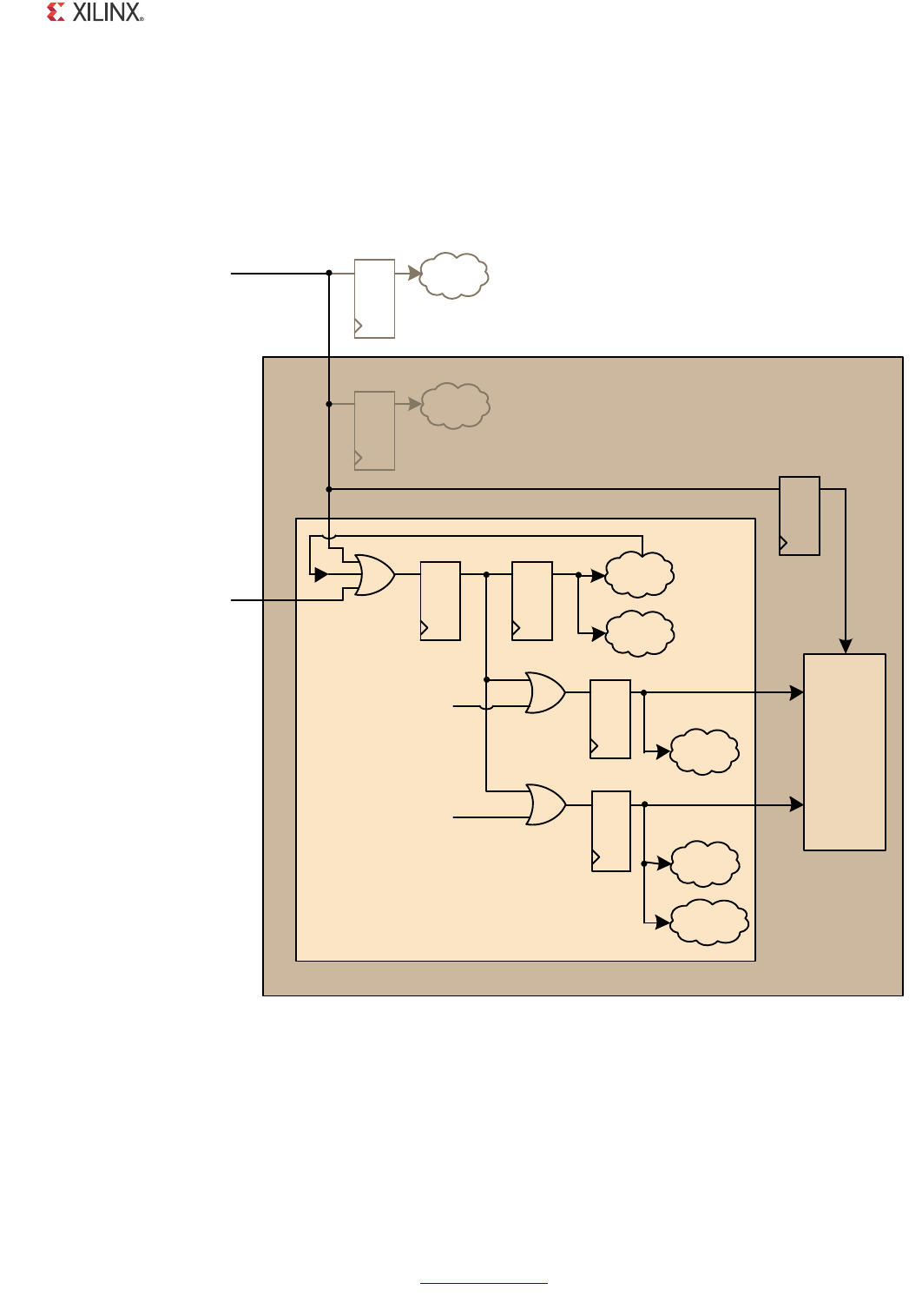
1000BASE-X PCS/PMA or SGMII v11.4 www.xilinx.com 94
PG047 October 16, 2012
Chapter 3: Designing with the Core
Reset Structure for Ethernet 1000BASE-X PCS/PMA or SGMII
core with Transceiver
Figure 3-1 shows the most common reset structure for the core connected to the serial or
LVDS Transceiver. The grayed out region of the figure indicates the logic that is activated
under certain conditions based on parameterization of the core.
X-Ref Target - Figure 3-1
Figure 3-1: Reset Structure for Ethernet 1000BASE-X PCS/PMA or SGMII Core with Transceiver
5HVHW
6\QF
,'(/$<
/2*,&
5HVHW
6\QF
6*0,,
$GDSW
QRW00&0BORFNHG 5HVHW
6\QF
5HVHW
6\QF
0DQDJHPHQW
/RJLF
$Q
/RJLF
VRIWBUHVHW
7[/RJLF
0*7B7;B5(6(7
7;%8)(55
)URP7UDQVFHLYHU 5HVHW
6\QF
5[/RJLF
5;%8)67$786 >@
)URP7UDQVFHLYHU 5HVHW
6\QF
0*7B5;B5(6(7
6\QFKURQL]DWLRQ
/RJLF
JSFVBSPDBJHQ
FRPSRQHQWBQDPHBEORFN
5(6(7
7UDQVFHLYHU
5HVHW
6\QF
30$B5(6(7
25
25
25
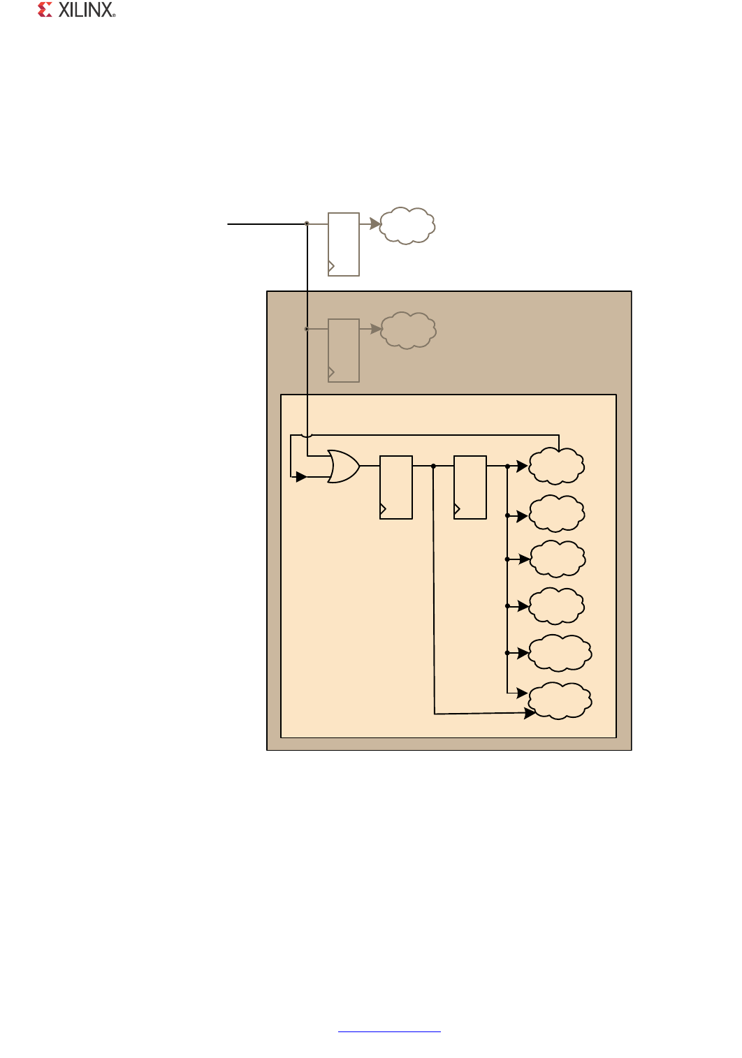
1000BASE-X PCS/PMA or SGMII v11.4 www.xilinx.com 95
PG047 October 16, 2012
Chapter 3: Designing with the Core
Reset Structure for Ethernet 1000BASE-X PCS/PMA or SGMII
core with TBI
Figure 3-2 shows the most common reset structure for the core with TBI. The grayed out
region of the figure indicates the logic that is activated under certain conditions based on
parameterization of the core.
X-Ref Target - Figure 3-2
Figure 3-2: Reset Structure for Ethernet 1000BASE-X PCS/PMA or SGMII core with TBI
5HVHW
6\QF
,'(/$<
/2*,&
5HVHW
6\QF
6*0,,
$GDSW
5HVHW
6\QF
5HVHW
6\QF
0DQDJHPHQW
/RJLF
$Q
/RJLF
VRIWBUHVHW
7[/RJLF
5[/RJLF
6\QFKURQL]DWLRQ
/RJLF
JSFVBSPDBJHQ
FRPSRQHQWBQDPHBEORFN
5(6(7
7%,/RJLF
25

1000BASE-X PCS/PMA or SGMII v11.4 www.xilinx.com 96
PG047 October 16, 2012
Chapter 4
The Ten-Bit Interface
This chapter provides general guidelines for creating 1000BASE-X, SGMII or Dynamic
Standards Switching designs using the Ten-Bit Interface (TBI).
This chapter is organized into the following main sections:
•Ten-Bit-Interface Logic
This section provides an explanation of the TBI physical interface logic in all supported
device families. This section is common to both 1000BASE-X and SGMII
implementations.
•Clock Sharing across Multiple Cores with TBI
Providing guidance for using several core instantiations; clock sharing should occur
whenever possible to save device resources.
•Example Designs for the Ten-Bit Interface (TBI)
Providing an introduction to the CORE Generator™ and Vivado™ IP catalog tools
example design deliverables, this section is split into the following two sub-sections:
°Example Design for 1000BASE-X with Ten-Bit Interface
°SGMII Example Design / Dynamic Switching Example Design with Ten-Bit Interface
This section also provides an overview of the demonstration test bench that is provided
with the example designs.
Virtex®-6 devices support TBI at 2.5 V only. See the Virtex-6 FPGA Data Sheet: DC and
Switching Characteristics for more information. Kintex™-7, Virtex-5, Virtex-4, Spartan®-6,
and Spartan-3 devices support TBI at 3.3 V or lower.

1000BASE-X PCS/PMA or SGMII v11.4 www.xilinx.com 97
PG047 October 16, 2012
Chapter 4: The Ten-Bit Interface
Ten-Bit-Interface Logic
The example design delivered with the core is split between two hierarchical layers, as
illustrated in both Figure 4-14 and Figure 4-16. The block level is designed so that it can be
instantiated directly into customer designs and provides the following functionality:
•Instantiates the core from HDL
• Connects the physical-side interface of the core to device IOBs, creating an external TBI
The TBI logic implemented in the block level is illustrated in all the figures in this chapter.
Transmitter Logic
Figure 4-1 illustrates the use of the physical transmitter interface of the core to create an
external TBI in a Virtex-5 device. The signal names and logic shown exactly match those
delivered with the example design when TBI is chosen. If other families are chosen,
equivalent primitives and logic specific to that family are automatically used in the example
design.
Figure 4-1 shows that the output transmitter datapath signals are registered in device IOBs
before driving them to the device pads. The logic required to forward the transmitter clock
is also shown. The logic uses an IOB output Double-Data-Rate (DDR) register so that the
clock signal produced incurs exactly the same delay as the data and control signals. This
clock signal, pma_tx_clk, is inverted with respect to gtx_clk so that the rising edge of
pma_tx_clk occurs in the center of the data valid window to maximize setup and hold
times across the interface.
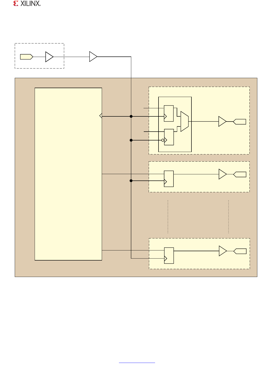
1000BASE-X PCS/PMA or SGMII v11.4 www.xilinx.com 98
PG047 October 16, 2012
Chapter 4: The Ten-Bit Interface
X-Ref Target - Figure 4-1
Figure 4-1: Ten-Bit Interface Transmitter Logic
,3$'
,%8)*
,2%/2*,&
JW[BFON
%8)*
JW[BFONBEXIJ
SPDBW[BFON
2%8)
)''556(
,2%/2*,&
23$'
'4
'4
SPDBW[BFONBREXI
'4
W[BFRGHBJURXS>@
2%8)
23$'
W[BFRGHBJURXSBUHJ>@
'4
W[BFRGHBJURXS>@
2%8)
23$'
W[BFRGHBJURXSBUHJ>@
(WKHUQHW%$6(;3&630$
RU6*0,,/RJL&25(
W[BFRGHBJURXSBLQW>@
W[BFRGHBJURXSBLQW>@
JW[BFON
W[BFRGHBJURXS>@
W[BFRGHBJURXS>@
COMPONENT?NAME?BLOCK"LOCK,EVELFROMEXAMPLEDESIGN
8
1000BASE-X PCS/PMA or SGMII v11.4 www.xilinx.com 99
PG047 October 16, 2012
Chapter 4: The Ten-Bit Interface
Receiver Logic
Figure 4-2 illustrates the input timing for the TBI interface as defined in IEEE802.3-2008
clause 36 (see also TBI Input Setup/Hold Timing for further information).
The important point is that the input TBI data bus, rx_code_group[9:0], is synchronous
to two clock sources: pma_rx_clk0 and pma_rx_clk1. As defined by the standard, the
TBI data should be sampled alternatively on the rising edge of pma_rx_clk0, then
pma_rx_clk1. Minimum setup and hold constraints are specified and apply to both clock
sources.
In the IEEE802.3-2008 specification, there is no exact requirement that pma_rx_clk0 and
pma_rx_clk1 be exactly 180 degrees out of phase with each other, so the safest approach
is to use both pma_rx_clk0 and pma_rx_clk1 clocks as the specification intends. This is
at the expense of clocking resources.
However, the data sheet for a particular external SERDES device that connects to the TBI
might well specify that this is the case; that pma_rx_clk0 and pma_rx_clk1 are exactly
180 degrees out of phase. If this is the case, the TBI receiver clock logic can be simplified by
ignoring the pma_rx_clk1 clock altogether, and simply using both the rising and falling
edges of pma_rx_clk0.
For this reason, the following sections describe two different alternatives methods for
implementing the TBI receiver clock logic: one which uses both pma_rx_clk0 and
pma_rx_clk1 clock, and a second which only uses pma_rx_clk0 (but both rising and
falling edges). Select the method carefully by referring to the data sheet of the external
SERDES.
The example designs provided with the core only provides one of these methods (which
vary on a family-by-family basis). However, the example HDL design can easily be edited to
convert to the alternative method.
X-Ref Target - Figure 4-2
Figure 4-2: Input TBI timing
T3%450
T(/,$
RX?CODE?GROUP;=
0-!?28?#,+
T3%450T(/,$
0-!?28?#,+
8
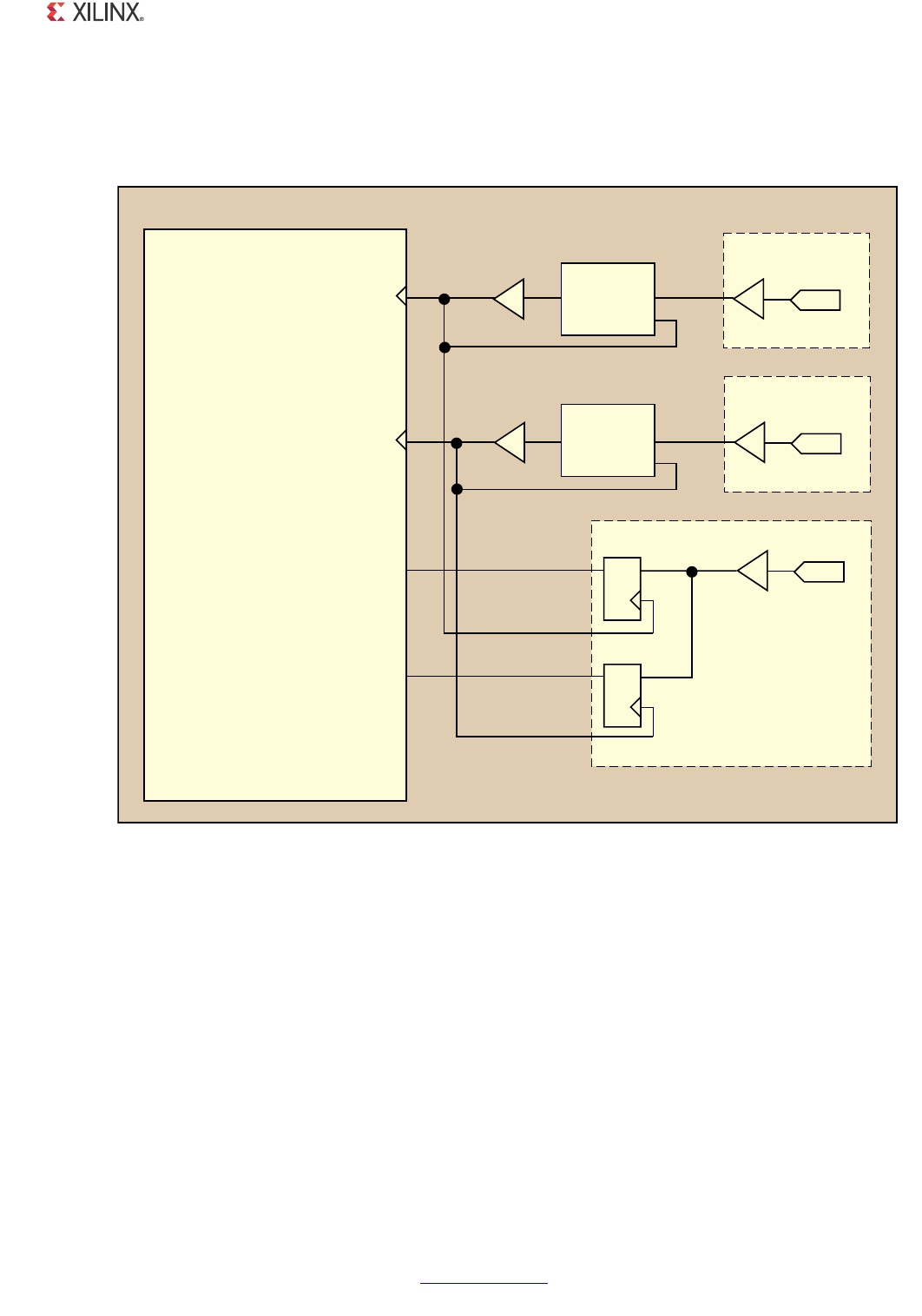
1000BASE-X PCS/PMA or SGMII v11.4 www.xilinx.com 100
PG047 October 16, 2012
Chapter 4: The Ten-Bit Interface
Spartan-3, Spartan-3E and Spartan-3A Devices
Method 1: Using Both pma_rx_clk0 and pma_rx_clk1 (Provided by the Example Design)
This is the implementation provided by the example design for the Spartan-3 families. This
uses the pma_rx_clk0 and pma_rx_clk1 clocks as intended by the TBI specification.
Contrast this with Method 2 which can save on clock resources if the external SERDES
devices guarantee that they provide pma_rx_clk0 and pma_rx_clk1 exactly 180
degrees out of phase with each other.
In this implementation, a DCM is used on both the pma_rx_clk0 and pma_rx_clk1 clock
paths (see Figure 4-3). Phase shifting should then be applied to the DCM to fine-tune the
setup and hold times at the TBI IOB input flip-flops. Fixed phase shift is applied to the DCM
using constraints in the example UCF for the example design. See Ten-Bit Interface
Constraints for more information.
X-Ref Target - Figure 4-3
Figure 4-3: TBI Receiver Logic for Spartan-3, Spartan-3E, and Spartan-3A Devices (Example Design)
COMPONENT?NAME?BLOCK"LOCK,EVELFROMEXAMPLEDESIGN
SPDBU[BFON
,%8)*
,2%/2*,&
,3$'
U[BFRGHBJURXS>@
,%8)
,3$'
U[BFRGHBJURXSBLEXI>@
'
4
(WKHUQHW%$6(;3&630$
RU6*0,,/RJL&25(
SPDBU[BFON
%8)*
,2%/2*,&
'
4
SPDBU[BFON
,%8)*
,2%/2*,&
,3$'
%8)*
SPDBU[BFON
U[BFRGHBJURXS>@
U[BFRGHBJURXS>@ U[BFRGHBJURXSBUHJ>@
U[BFRGHBJURXSBUHJ>@
'&0
&/.,1
&/.
)%
'&0
&/.,1
&/.
)%
SPDBU[BFONBEXIJ
0+]
SPDBU[BFONBEXIJ
0+]
8
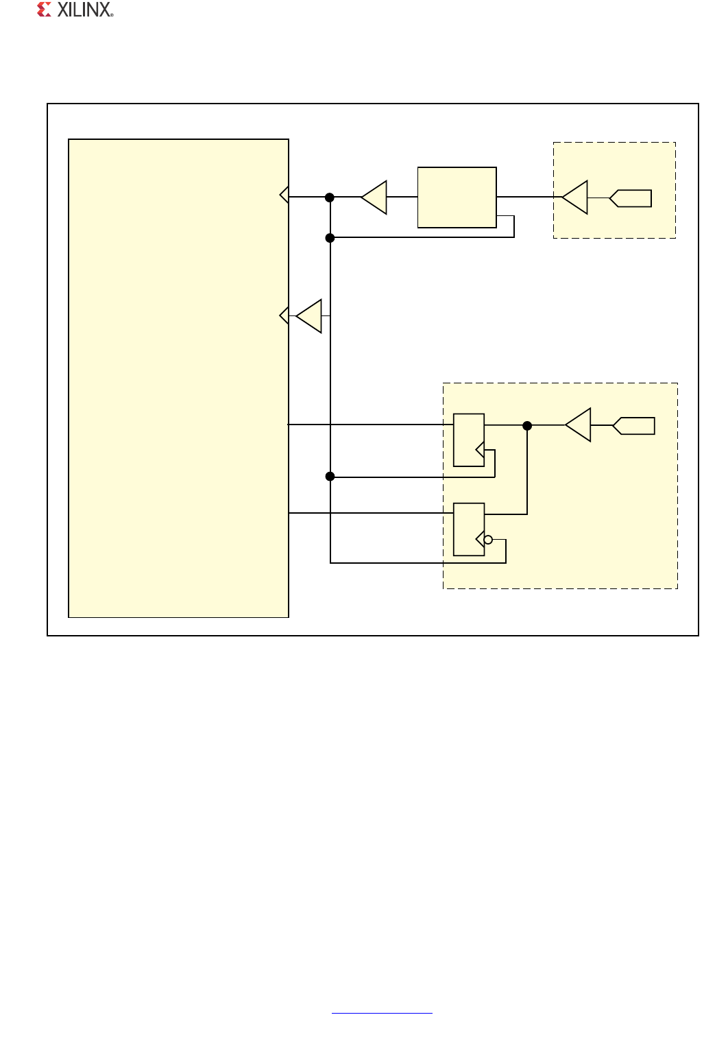
1000BASE-X PCS/PMA or SGMII v11.4 www.xilinx.com 101
PG047 October 16, 2012
Chapter 4: The Ten-Bit Interface
Method 2: An Alternative Using Only pma_rx_clk0
In this implementation, the falling edge of pma_rx_clk0 is used instead of pma_rx_clk1
(see Figure 4-4).
The DCM is used on the pma_rx_clk0 clock path. Phase shifting should then be applied to
the DCM to fine-tune the setup and hold times at the rx_code_group[9:0] IOB input
flip-flops.
The clock derived from the DCM should be inverted, as illustrated, before routing it to the
pma_rx_clk1 input of the core. This does not create a clock on local routing. Instead the
tools then use local clock inversion directly at the clock input of the flip-flops that this clock
is routed to.
X-Ref Target - Figure 4-4
Figure 4-4: TBI Receiver Logic for Spartan-3, Spartan-3E, and Spartan-3A Devices
SPDBU[BFON
,%8)*
,2%/2*,&
,3$'
U[BFRGHBJURXS>@
,%8)
,3$'
U[BFRGHBJURXSBLEXI>@
'
4
(WKHUQHW%$6(;3&630$
RU6*0,,/RJL&25(
SPDBU[BFON
%8)*
,2%/2*,&
'
4
,2%/2*,&
SPDBU[BFON
U[BFRGHBJURXS>@
U[BFRGHBJURXS>@ U[BFRGHBJURXSBUHJ>@
U[BFRGHBJURXSBUHJ>@
'&0
&/.,1
&/.
)%
SPDBU[BFONBEXIJ
0+]
)NVERT
8
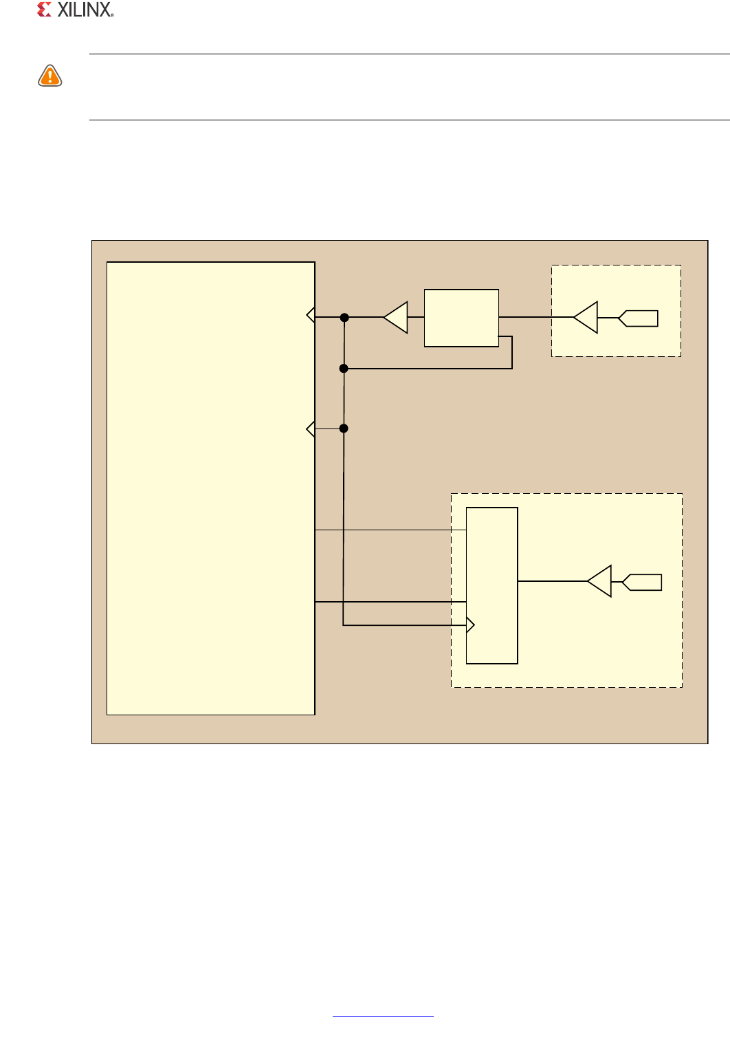
1000BASE-X PCS/PMA or SGMII v11.4 www.xilinx.com 102
PG047 October 16, 2012
Chapter 4: The Ten-Bit Interface
CAUTION! This logic relies on pma_rx_clk0 and pma_rx_clk1 being exactly 180 degrees out of phase
with each other because the falling edge of pma_rx_clk0 is used in place of pma_rx_clk1. See the data
sheet for the attached SERDES to verify that this is the case.
Virtex-4 Devices
Method 1: Using Only pma_rx_clk0 (Provided by the Example Design)
The Virtex-4 FPGA logic used by the example design delivered with the core is illustrated in
Figure 4-5. This shows a Virtex-4 device IDDR primitive used with the DDR_CLK_EDGE
attribute set to SAME_EDGE (see the Virtex-4 FPGA User Guide). This uses local inversion of
pma_rx_clk0 within the IOB logic to receive the rx_code_group[9:0] data bus on
both the rising and falling edges of pma_rx_clk0. The SAME_EDGE attribute causes the
IDDR to output both Q1 and Q2 data on the rising edge of pma_rx_clk0.
X-Ref Target - Figure 4-5
Figure 4-5: Ten-Bit Interface Receiver Logic - Virtex-4 Device (Example Design)
FRPSRQHQWBQDPHBEORFN%ORFN/HYHOIURPH[DPSOHGHVLJQ
SPDBU[BFON
,%8)*
,2%/2*,&
,3$'
U[BFRGHBJURXS>@
,%8)
,3$'
(WKHUQHW%$6(;3&630$
RU6*0,,/RJL&25(
SPDBU[BFON
%8)*
,2%/2*,&
SPDBU[BFON
U[BFRGHBJURXS>@
U[BFRGHBJURXS>@
U[BFRGHBJURXSBUHJ>@
U[BFRGHBJURXSBUHJ>@ ,''5
4
'
4
&
'&0
&/.,1
&/.
)%
8
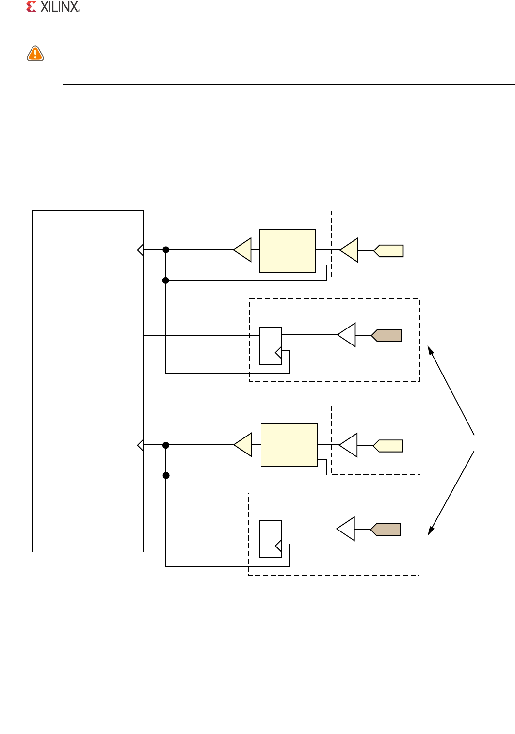
1000BASE-X PCS/PMA or SGMII v11.4 www.xilinx.com 103
PG047 October 16, 2012
Chapter 4: The Ten-Bit Interface
For this reason, pma_rx_clk0 can be routed to both pma_rx_clk0 and pma_rx_clk1 clock inputs of the core as illustrated. CAUTION! This logic relies on pma_rx_clk0 and pma_rx_clk1 being exactly 180 degrees out of phase
with each other because the falling edge of pma_rx_clk0 is used in place of pma_rx_clk1. See the data
sheet for the attached SERDES to verify that this is the case.
The DCM is used on the pma_rx_clk0 clock path. Phase shifting should then be applied to
the DCM to fine-tune the setup and hold times at the rx_code_group[9:0] IOB input
flip-flops. Fixed phase shift is applied to the DCM using constraints in the example UCF for
the example design. See Ten-Bit Interface Constraints for more information.
Method 2: An Alternative Using Both pma_rx_clk0 and pma_rx_clk1
X-Ref Target - Figure 4-6
Figure 4-6: Alternate Ten-Bit Interface Receiver Logic for Virtex-4 Devices
SPDBU[BFON
,%8)*
,2%/2*,&
,3$'
U[BFRGHBJURXS>@
,%8)
,3$'
(WKHUQHW%$6(;3&630$
RU6*0,,/RJL&25(
SPDBU[BFON
%8)*
,2%/2*,&
SPDBU[BFON
U[BFRGHBJURXS>@
U[BFRGHBJURXS>@
U[BFRGHBJURXSBUHJ>@ '
4
SPDBU[BFON
,%8)*
,2%/2*,&
,3$'
U[BFRGHBJURXS>@
,%8)
,3$'
,2%/2*,&
U[BFRGHBJURXSBUHJ>@ '
4
U[BFRGHBJURXS>@
SPDBU[BFONBEXIJ
0+]
SPDBU[BFONBEXIJ
0+]
%8)*
'&0
&/.,1
&/.
)%
'&0
&/.,1
&/.
)%
8
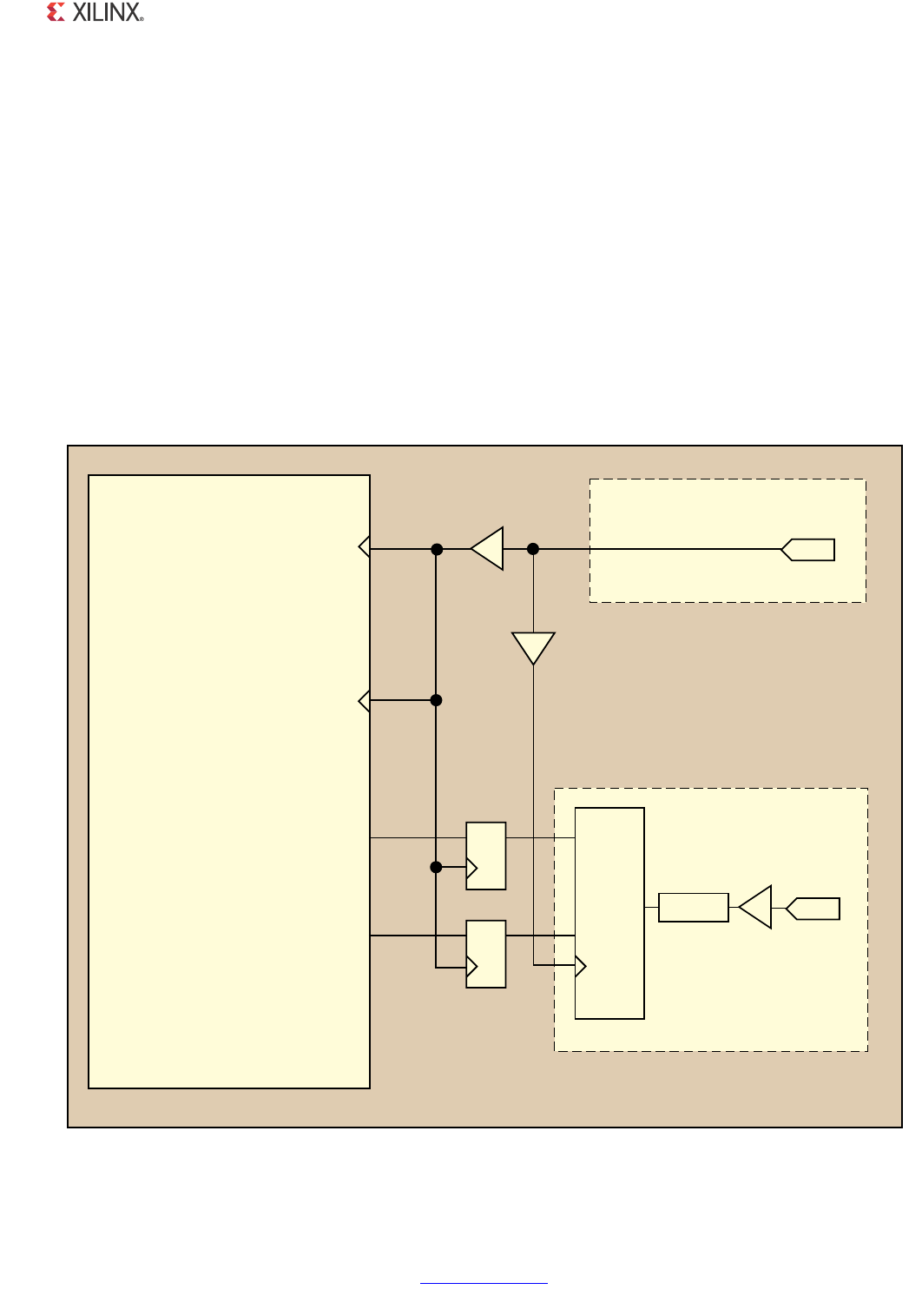
1000BASE-X PCS/PMA or SGMII v11.4 www.xilinx.com 104
PG047 October 16, 2012
Chapter 4: The Ten-Bit Interface
This logic from Method 1 relies on pma_rx_clk0 and pma_rx_clk1 being exactly 180
degrees out of phase with each other because the falling edge of pma_rx_clk0 is used in
place of pma_rx_clk1. See the data sheet for the attached SERDES to verify that this is the
case. If not, then the logic of Figure 4-6 illustrates an alternative implementation where
both pma_rx_clk0 and pma_rx_clk1 are used as intended. Each bit of
rx_code_group[9:0] must be routed to two separate device pads.
In this implementation, a DCM is used on both the pma_rx_clk0 and pma_rx_clk1 clock
paths (see Figure 4-6). Phase shifting should then be applied to the DCMs to fine-tune the
setup and hold times at the TBI IOB input flip-flops.
Virtex-5 Devices
Method 1: Using Only pma_rx_clk0 (Provided by the Example Design)
X-Ref Target - Figure 4-7
Figure 4-7: Ten-Bit Interface Receiver Logic - Virtex-5 Device (Example Design)
FRPSRQHQWBQDPHBEORFN%ORFN/HYHOIURPH[DPSOHGHVLJQ
SPDBU[BFON
%8),2
,2%/2*,&
,3$'
U[BFRGHBJURXS>@
,%8)
,3$'
(WKHUQHW%$6(;3&630$
RU6*0,,/RJL&25(
SPDBU[BFON
%8)5
,2%/2*,&
SPDBU[BFON
U[BFRGHBJURXS>@
U[BFRGHBJURXS>@
,''5
4
'
4
&
,2'(/$<
'
4
'
4
8

1000BASE-X PCS/PMA or SGMII v11.4 www.xilinx.com 105
PG047 October 16, 2012
Chapter 4: The Ten-Bit Interface
The Virtex-5 FPGA logic used by the example design delivered with the core is illustrated in
Figure 4-7. This shows a Virtex-5 device IDDR primitive used with the DDR_CLK_EDGE
attribute set to SAME_EDGE (see the Virtex-5 FPGA User Guide). This uses local inversion of
pma_rx_clk0 within the IOB logic to receive the rx_code_group[9:0] data bus on
both the rising and falling edges of pma_rx_clk0. The SAME_EDGE attribute causes the
IDDR to output both Q1 and Q2 data on the rising edge of pma_rx_clk0.
For this reason, pma_rx_clk0 can be routed to both pma_rx_clk0 and pma_rx_clk1
clock inputs of the core as illustrated.
CAUTION! This logic relies on pma_rx_clk0 and pma_rx_clk1 being exactly 180 degrees out of phase
with each other because the falling edge of pma_rx_clk0 is used in place of pma_rx_clk1. See the data
sheet for the attached SERDES to verify that this is the case.
Setup and Hold is achieved using a combination of IODELAY elements on the data, and
using BUFIO and BUFR regional clock routing for the pma_rx_clk0 input clock, as
illustrated in Figure 4-7.
This design provides a simpler solution than the DCM logic required for Virtex-4 devices
(see Figure 4-5). It has therefore been chosen as the example design from version 10.1 of
the core onwards. However, the Virtex-4 FPGA approach could alternatively be adopted.
In the Figure 4-7 implementation, a BUFIO is used to provide the lowest form of clock
routing delay from input clock to input rx_code_group[9:0] signal sampling at the
device IOBs. However, this creates placement constraints; a BUFIO capable clock input pin
must be selected for pma_rx_clk0, and all rx_code_group[9:0] input signals must be
placed in the respective BUFIO region. Consult the Virtex-5 FPGA User Guide.
The clock is then placed onto regional clock routing using the BUFR component and the
input rx_code_group[9:0] data immediately resampled as illustrated.
The IODELAY elements can be adjusted to fine-tune the setup and hold times at the TBI IOB
input flip-flops. The delay is applied to the IODELAY element using constraints in the UCF;
these can be edited if desired. See Ten-Bit Interface Constraints for more information.
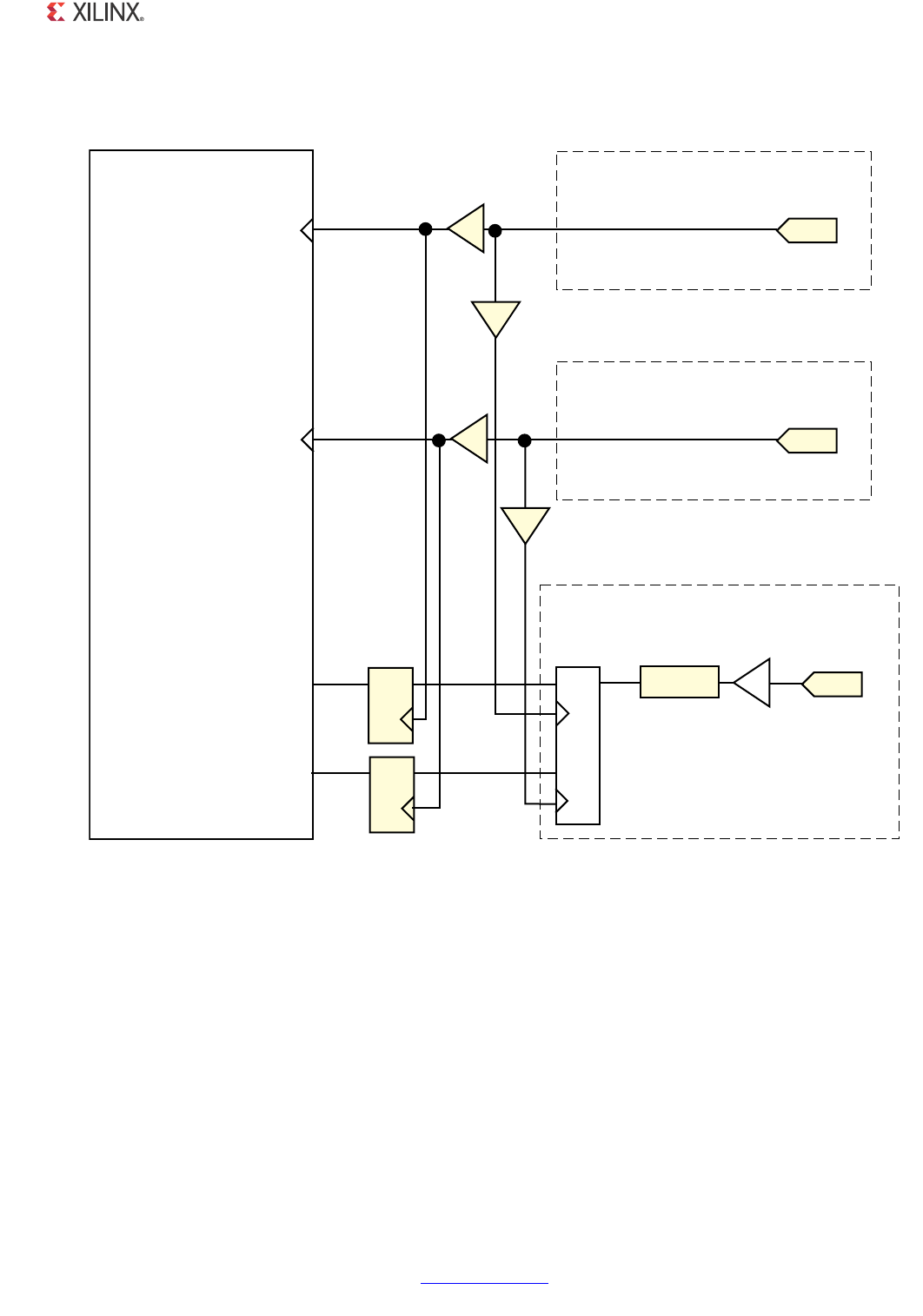
1000BASE-X PCS/PMA or SGMII v11.4 www.xilinx.com 106
PG047 October 16, 2012
Chapter 4: The Ten-Bit Interface
Method 2: An Alternative Using Both pma_rx_clk0 and pma_rx_clk1
The logic from Method 1 relies on pma_rx_clk0 and pma_rx_clk1 being exactly 180
degrees out of phase with each other because the falling edge of pma_rx_clk0 is used in
place of pma_rx_clk1. See the data sheet for the attached SERDES to verify that this is the
case. If not, the logic of Figure 4-8 illustrates an alternate implementation where both
pma_rx_clk0 and pma_rx_clk1 are used as intended.
In this method, the logic used on pma_rx_clk0 in Figure 4-7 is duplicated for
pma_rx_clk1. A IDDR_CLK2 primitive replaces the IDDR primitive; this contains two clock
inputs as illustrated.
X-Ref Target - Figure 4-8
Figure 4-8: Alternate Ten-Bit Interface Receiver Logic - Virtex-5 Devices
SPDBU[BFON
%8),2
,2%/2*,&
,3$'
U[BFRGHBJURXS>@
,%8)
,3$'
(WKHUQHW%$6(;3&630$
RU6*0,,/RJL&25(
SPDBU[BFON
%8)5
,2%/2*,&
SPDBU[BFON
U[BFRGHBJURXS>@
U[BFRGHBJURXS>@
'
4
SPDBU[BFONBEXIU
0+]
,2'(/$<
'
4
SPDBU[BFON
%8),2
,2%/2*,&
,3$'
%8)5
SPDBU[BFONBEXIU
0+]
,''5B&/.
4
'
4
&
&%
8
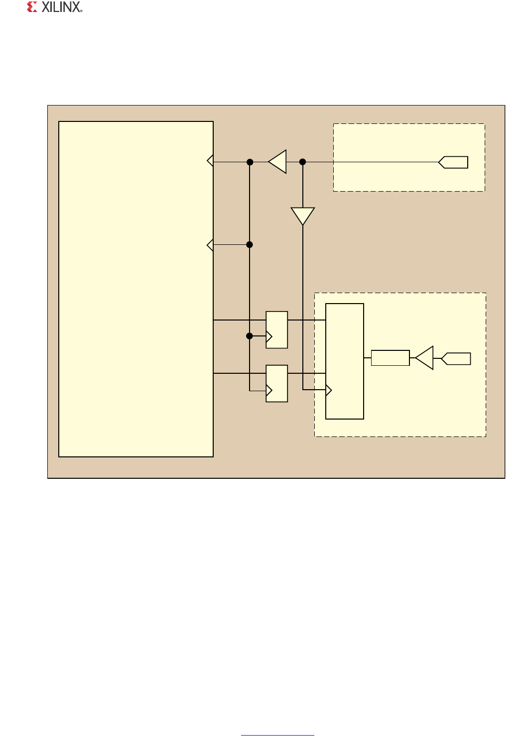
1000BASE-X PCS/PMA or SGMII v11.4 www.xilinx.com 107
PG047 October 16, 2012
Chapter 4: The Ten-Bit Interface
Kintex-7 and Virtex-6 Devices
Method 1: Using Only pma_rx_clk0 (Provided by the Example Design)
The FPGA logic used by the example design delivered with the core is illustrated in
Figure 4-7. This shows an IDDR primitive used with the DDR_CLK_EDGE attribute set to
SAME_EDGE. This uses local inversion of pma_rx_clk0 within the IOB logic to receive the
rx_code_group[9:0] data bus on both the rising and falling edges of pma_rx_clk0.
The SAME_EDGE attribute causes the IDDR to output both Q1 and Q2 data on the rising
edge of pma_rx_clk0.
For this reason, pma_rx_clk0 can be routed to both pma_rx_clk0 and pma_rx_clk1
clock inputs of the core as illustrated.
X-Ref Target - Figure 4-9
Figure 4-9: Ten-Bit Interface Receiver Logic - Kintex-7 and Virtex-6 Devices (Example Design)
FRPSRQHQWBQDPHBEORFN%ORFN/HYHOIURPH[DPSOHGHVLJQ
SPDBU[BFON
%8),2
,2%/2*,&
,3$'
U[BFRGHBJURXS>@
,%8)
,3$'
(WKHUQHW%$6(;3&630$
RU6*0,,/RJL&25(
SPDBU[BFON
%8)5
,2%/2*,&
SPDBU[BFON
U[BFRGHBJURXS>@
U[BFRGHBJURXS>@
,''5
4
'
4
&
,2'(/$<
'
4
'
4
8

1000BASE-X PCS/PMA or SGMII v11.4 www.xilinx.com 108
PG047 October 16, 2012
Chapter 4: The Ten-Bit Interface
CAUTION! This logic relies on pma_rx_clk0 and pma_rx_clk1 being exactly 180 degrees out of phase
with each other because the falling edge of pma_rx_clk0 is used in place of pma_rx_clk1. See the data
sheet for the attached SERDES to verify that this is the case.
Setup and Hold is achieved using a combination of IODELAY elements on the data and
using BUFIO and BUFR regional clock routing for the pma_rx_clk0 input clock, as
illustrated in Figure 4-9.
This design provides a simpler solution than the DCM logic required for Virtex-4 devices. It
has therefore been chosen as the example design for the Kintex-7 and Virtex-6 family.
However, the Virtex-4 FPGA approach could alternatively be adopted; simply replace the
DCM with a Mixed-Mode Clock Manager (MMCM) module (see Figure 4-5).
In the Figure 4-9 implementation, a BUFIO is used to provide the lowest form of clock
routing delay from input clock to input rx_code_group[9:0] signal sampling at the
device IOBs. However, this creates placement constraints; a BUFIO capable clock input pin
must be selected for pma_rx_clk0, and all rx_code_group[9:0] input signals must be
placed in the respective BUFIO region. Consult the FPGA user guides.
The clock is then placed onto regional clock routing using the BUFR component and the
input rx_code_group[9:0] data immediately resampled as illustrated.
The IODELAY elements can be adjusted to fine-tune the setup and hold times at the TBI IOB
input flip-flops. The delay is applied to the IODELAY element using constraints in the UCF;
these can be edited if desired. See Ten-Bit Interface Constraints for more information.
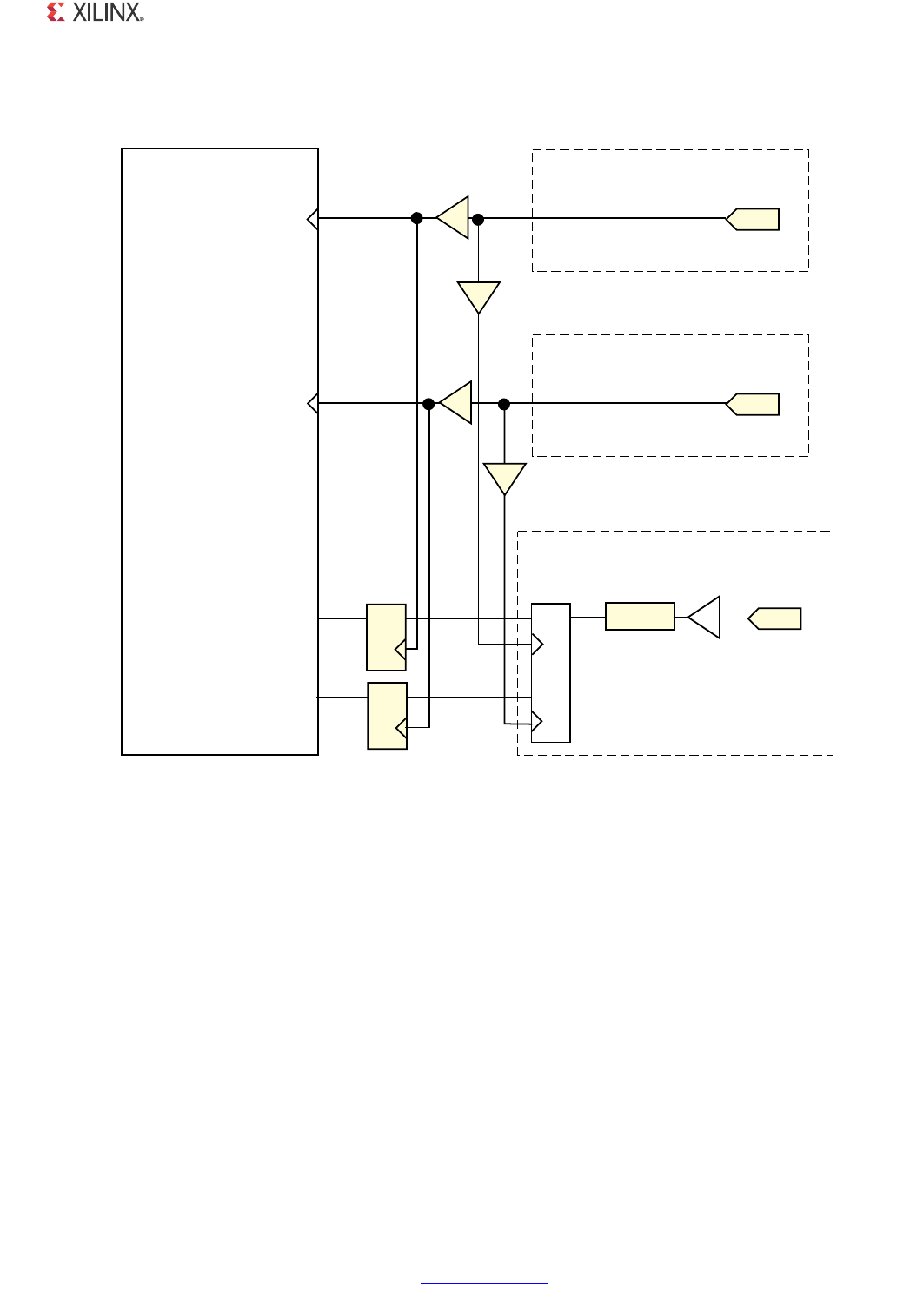
1000BASE-X PCS/PMA or SGMII v11.4 www.xilinx.com 109
PG047 October 16, 2012
Chapter 4: The Ten-Bit Interface
Method 2: An Alternative Using Both pma_rx_clk0 and pma_rx_clk1
This logic from Method 1 relies on pma_rx_clk0 and pma_rx_clk1 being exactly 180
degrees out of phase with each other because the falling edge of pma_rx_clk0 is used in
place of pma_rx_clk1. See the data sheet for the attached SERDES to verify that this is the
case. If not, the logic of Figure 4-10 illustrates an alternate implementation where both
pma_rx_clk0 and pma_rx_clk1 are used as intended. Each bit of
rx_code_group[9:0] must be routed to two separate device pads.
In this method, the logic used on pma_rx_clk0 in Figure 4-9 is duplicated for
pma_rx_clk1. A IDDR_CLK2 primitive replaces the IDDR primitive; this contains two clock
inputs as illustrated.
X-Ref Target - Figure 4-10
Figure 4-10: Alternate Ten-Bit Interface Receiver Logic - Kintex-7 and Virtex-6 Devices
SPDBU[BFON
%8),2
,2%/2*,&
,3$'
U[BFRGHBJURXS>@
,%8)
,3$'
(WKHUQHW%$6(;3&630$
RU6*0,,/RJL&25(
SPDBU[BFON
%8)5
,2%/2*,&
SPDBU[BFON
U[BFRGHBJURXS>@
U[BFRGHBJURXS>@
'
4
SPDBU[BFONBEXIU
0+]
,2'(/$<
'
4
SPDBU[BFON
%8),2
,2%/2*,&
,3$'
%8)5
SPDBU[BFONBEXIU
0+]
,''5B&/.
4
'
4
&
&%
8
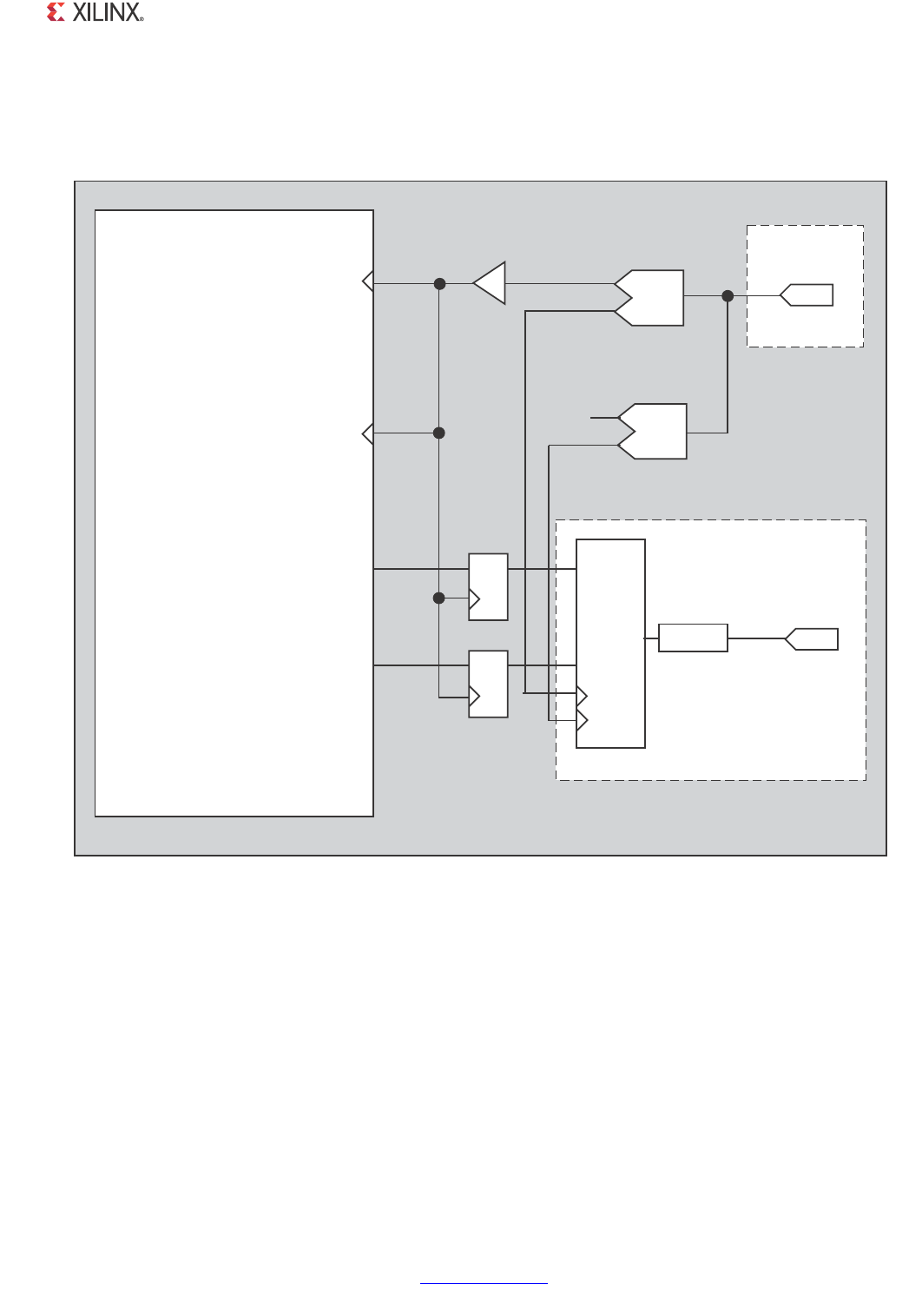
1000BASE-X PCS/PMA or SGMII v11.4 www.xilinx.com 110
PG047 October 16, 2012
Chapter 4: The Ten-Bit Interface
Spartan-6 Devices
Method 1: Using Only pma_rx_clk0 (Provided by the Example Design)
The Spartan-6 FPGA logic used by the example design delivered with the core is illustrated
in Figure 4-11. This figure shows a Spartan-6 device IDDR2 primitive used with the
DDR_ALIGNMENT attribute set to C0 (see the Spartan-6 FPGA User Guide). This
DDR_ALIGNMENT attribute causes the IDDR2 to output both Q1 and Q2 data on the rising
edge of pma_rx_clk0.
For this reason, pma_rx_clk0 can be routed to both pma_rx_clk0 and pma_rx_clk1
clock inputs of the core as illustrated.
X-Ref Target - Figure 4-11
Figure 4-11: Ten-Bit Interface Receiver Logic - Spartan-6 Device (Example Design)
FRPSRQHQWBQDPHBEORFN%ORFN/HYHOIURPH[DPSOHGHVLJQ
SPDBU[BFON
,2%/2*,&
,3$'
U[BFRGHBJURXS>@
,3$'
(WKHUQHW%$6(;3&630$
RU6*0,,/RJL&25(
SPDBU[BFON
%8)*
,2%/2*,&
SPDBU[BFON
U[BFRGHBJURXS>@
U[BFRGHBJURXS>@
,''5
4
4
'
4
&
,2'(/$<
'
4
'
4
&
',9&/.
,2&/.
%8),2
,B,19(57 758(
',9&/.
,2&/.
1&
%8),2
,B,19(57 )$/6(
8

1000BASE-X PCS/PMA or SGMII v11.4 www.xilinx.com 111
PG047 October 16, 2012
Chapter 4: The Ten-Bit Interface
CAUTION! This logic relies on pma_rx_clk0 and pma_rx_clk1 being exactly 180 degrees out of phase
with each other because the falling edge of pma_rx_clk0 is used in place of pma_rx_clk1. See the data
sheet for the attached SerDes to verify that this is the case.
Setup and Hold is achieved using a combination of IODELAY2 elements on the data and
using BUFIO2 elements and BUFG global clock routing for the pma_rx_clk0 input clock, as
illustrated in Figure 4-11.
This design provides a simpler solution than the DCM logic required for Virtex-4 devices. It
has therefore been chosen as the example design for the Spartan-6 family. However, the
Virtex-4 FPGA approach could alternatively be adopted; simply replace the DCM with a
MMCM module (see Figure 4-5).
In the Figure 4-11 implementation, two BUFIO2s are used to provide the lowest form of
clock routing delay from input clock to input rx_code_group[9:0] signal sampling at
the device IOBs. One BUFIO2 element is used for the rising edge logic; no clock inversion is
performed and the DIVCLK output connects to the BUFG to provide global clock routing;
the IOCLK output of this BUFIO2 is routed to the IDDR2 primitive to sample data on the
rising edge. The second BUFIO2 element is configured to invert the clock; the IOCLK output
is routed to the IDDR2 to effectively sample the data on the falling edge position of
pma_rx_clk0. The DIVCLK output of this BUFIO2 is not used and is left unconnected.
The IODELAY2 elements can be adjusted to fine-tune the setup and hold times at the TBI
IOB input flip-flops. The delay is applied to the IODELAY element using constraints in the
UCF; these can be edited if desired. See Ten-Bit Interface Constraints for more information.
However, this logic creates placement constraints; rx_code_group[9:0] input signals
must be placed in the respective half-bank region for the two BUFIO2 elements in use.
Consult the Spartan-6 FPGA User Guide.
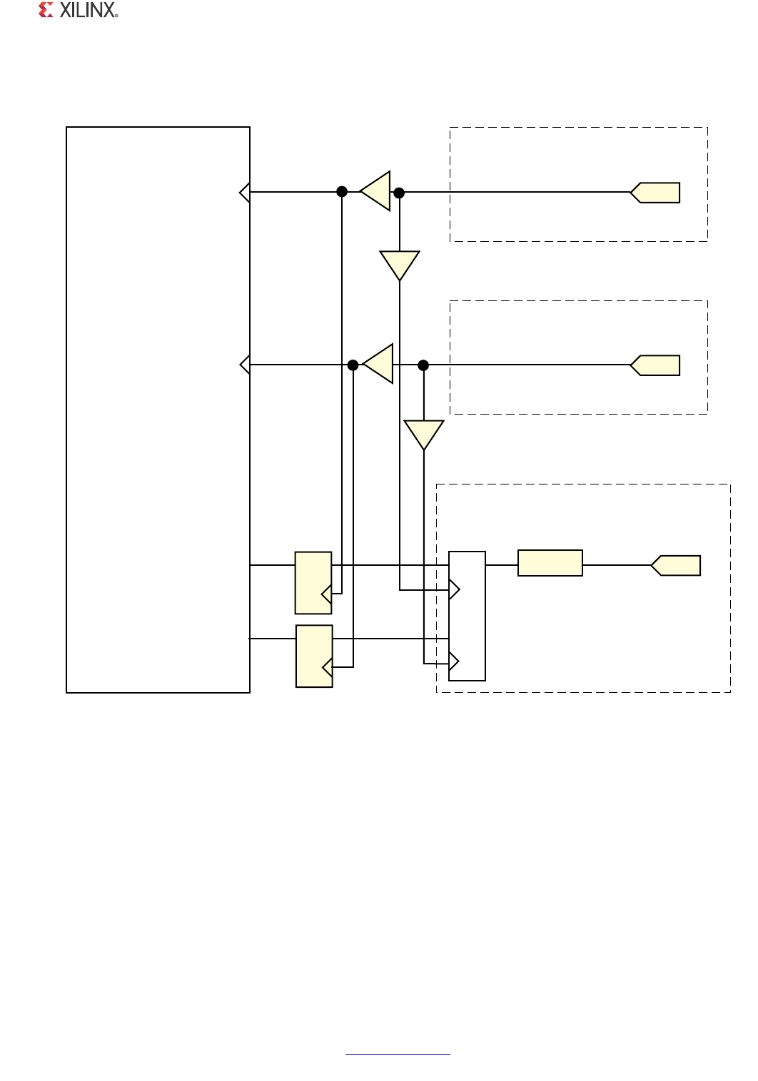
1000BASE-X PCS/PMA or SGMII v11.4 www.xilinx.com 112
PG047 October 16, 2012
Chapter 4: The Ten-Bit Interface
Method 2: An Alternative Using Both pma_rx_clk0 and pma_rx_clk1
This logic from Method 1 relies on pma_rx_clk0 and pma_rx_clk1 being exactly 180
degrees out of phase with each other because the falling edge of pma_rx_clk0 is used in
place of pma_rx_clk1. See the data sheet for the attached SERDES to verify that this is the
case. If not, the logic of Figure 4-12 illustrates an alternate implementation where both
pma_rx_clk0 and pma_rx_clk1 are used as intended. Each bit of
rx_code_group[9:0] must be routed to two separate device pads.
In this method, the logic used on pma_rx_clk0 in Figure 4-11 is duplicated for
pma_rx_clk1.
In the figure, a simplified view of the BUFIO2 elements are provided. The connected output
of each BUFIO is the IOCLK port. Other BUFIO2 output ports are unused and unconnected.
X-Ref Target - Figure 4-12
Figure 4-12: Alternate Ten-Bit Interface Receiver Logic - Spartan-6 Devices
SPDBU[BFON
%8),2
,2%/2*,&
,3$'
U[BFRGHBJURXS>@
,3$'
(WKHUQHW%$6(;3&630$
RU6*0,,/RJL&25(
SPDBU[BFON
%8)*
,2%/2*,&
SPDBU[BFON
U[BFRGHBJURXS>@
U[BFRGHBJURXS>@
'
4
SPDBU[BFONBEXIJ
0+]
,2'(/$<
'
4
SPDBU[BFON
%8),2
,2%/2*,&
,3$'
%8)*
SPDBU[BFONBEXIJ
0+]
,''5
4
'
4
&
&
8
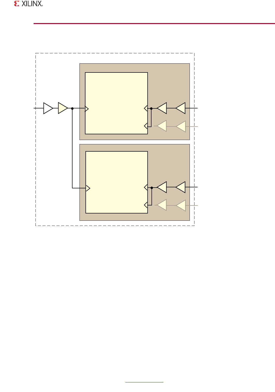
1000BASE-X PCS/PMA or SGMII v11.4 www.xilinx.com 113
PG047 October 16, 2012
Chapter 4: The Ten-Bit Interface
Clock Sharing across Multiple Cores with TBI
Figure 4-13 illustrates sharing clock resources across multiple instantiations of the core
when using the TBI. For all implementations, gtx_clk can be shared between multiple
cores, resulting in a common clock domain across the device.
The receiver clocks pma_rx_clk0 and pma_rx_clk1 (if used) cannot be shared. Each core
is provided with its own versions of these receiver clocks from its externally connected
SERDES.
Figure 4-13 illustrates only two cores. However, more can be added using the same
principle. This is done by instantiating the cores using the block level (from the example
design) and sharing gtx_clk across all instantiations. The receiver clock logic cannot be
shared and must be unique for every instance of the core.
X-Ref Target - Figure 4-13
Figure 4-13: Clock Management, Multiple Core Instances with Ten-Bit Interface
"LOCK,EVEL
"5&)/"5&2
SPDBU[BFON
(WKHUQHW%$6(;
3&630$
RU6*0,,&RUH
SPDBU[BFON
"5&2
SPDBU[BFON
SPDBU[BFON
&XVWRPHU'HVLJQ
JW[BFON
"5&2
SPDBU[BFON
(WKHUQHW%$6(;
3&630$
RU6*0,,&RUH
SPDBU[BFON
"5&2
SPDBU[BFON
SPDBU[BFON
JW[BFON
%8)*
,%8)*
"LOCK,EVEL
"5&)/
"5&)/
"5&)/
8

1000BASE-X PCS/PMA or SGMII v11.4 www.xilinx.com 114
PG047 October 16, 2012
Chapter 4: The Ten-Bit Interface
Example Designs for the Ten-Bit Interface (TBI)
Chapter 20, Detailed Example Design provides a full list and description of the directory and
file structure that is provided with the core, including the location of the HDL example
design provided.
Example Design for 1000BASE-X with Ten-Bit Interface
Figure 4-14 illustrates the example design for a top-level HDL with a 10-bit interface (TBI).
As illustrated, the example is split between two hierarchical layers. The block level is
designed so that it can be instantiated directly into customer designs and performs the
following functions:
•Instantiates the core from HDL
• Connects the physical-side interface of the core to device IOBs, creating an external
TBI.
X-Ref Target - Figure 4-14
Figure 4-14: Example Design HDL for the Ethernet 1000BASE-X PCS with TBI
(WKHUQHW
%$6(;
3&630$
&RUH
1HWOLVW
*0,,
,2%V
2XW
4")
)/"S
/UT
)/"S
)N
$$2
COMPONENT?NAME?EXAMPLE?DESIGN
COMPONENT?NAME?BLOCK
4X
%LASTIC
"UFFER
#LOCK
-ANAGEMENT
,OGIC
#ONNECTTO
#LIENT-!#
4")
#ONNECTTO
3%2$%3
,2%V
,Q
8

1000BASE-X PCS/PMA or SGMII v11.4 www.xilinx.com 115
PG047 October 16, 2012
Chapter 4: The Ten-Bit Interface
The top level of the example design creates a specific example that can be simulated,
synthesized, implemented, and if required, placed on a suitable board and demonstrated in
hardware. The top level of the example design performs the following functions:
• Instantiates the block level from HDL
• Derives the clock management logic for the core
• Implements an external GMII
The next few pages in this section describe each of the example design blocks (and
associated HDL files) in detail, and conclude with an overview of the demonstration test
bench provided for the design.
Top-Level Example Design HDL
The following files describe the top-level example design for the Ethernet 1000BASE-X
PCS/PMA core with TBI:
VHDL
ISE® Design Suite:
<project_dir>/<component_name>/example_design/<component_name>_example_design.vhd
Vivado™ Design Suite:
<project_dir>/<project_name>/<project_name>.srcs/sources1/ip/<component_name>/<comp
onent_name>/example_design/<component_name>_example_design.vhd
Verilog
ISE Design Suite:
<project_dir>/<component_name>/example_design/<component_name>_example_design.v
Vivado Design Suite:
<project_dir>/<project_name>/<project_name>.srcs/sources1/ip/<component_name>/
|<component_name>/example_design/<component_name>_example_design.v
The HDL example design top-level contains the following:
• An instance of the Ethernet 1000BASE-X PCS/PMA block level
• Clock management logic, including DCM and Global Clock Buffer instances, where
required
• A transmitter elastic buffer
• GMII interface logic, including IOB and DDR registers instances, where required

1000BASE-X PCS/PMA or SGMII v11.4 www.xilinx.com 116
PG047 October 16, 2012
Chapter 4: The Ten-Bit Interface
The example design HDL top level connects the GMII of the block level to external IOBs. This
allows the functionality of the core to be demonstrated using a simulation package as
described in this guide. The example design can also be synthesized and placed on a
suitable board and demonstrated in hardware, if required.
Block Level HDL
The following files describe the block level design for the Ethernet 1000BASE-X PCS/PMA
core with TBI:
VHDL
ISE Design Suite:
<project_dir>/<component_name>/example_design/<component_name>_block.vhd
Vivado Design Suite:
<project_dir>/<project_name>/<project_name>.srcs/sources1/ip/<component_name>/
<component_name>/example_design/<component_name>_block.vhd
Verilog
ISE Design Suite:
<project_dir>/<component_name>/example_design/<component_name>_block.v
Vivado Design Suite:
<project_dir>/<project_name>/<project_name>.srcs/sources1/ip/<component_name>/
<component_name>/example_design/<component_name>_block.v
The block level HDL contains the following:
• An instance of the Ethernet 1000BASE-X PCS/PMA core
• TBI interface logic, including IOB and DDR registers instances, where required
The block-level HDL connects the TBI of the core to external IOBs (the most useful part of
the example design) and should be instantiated in all customer designs that use the core.

1000BASE-X PCS/PMA or SGMII v11.4 www.xilinx.com 117
PG047 October 16, 2012
Chapter 4: The Ten-Bit Interface
Transmitter Elastic Buffer
The Transmitter Elastic Buffer is described in the following files:
VHDL
ISE Design Suite:
<project_dir>/<component_name>/example_design/
<component_name>_tx_elastic_buffer.vhd
Vivado Design Suite:
<project_dir>/<project_name>/<project_name>.srcs/sources1/ip/<component_name>/
<component_name>/example_design/<component_name>_tx_elastic_buffer.vhd
Verilog
ISE Design Suite:
<project_dir>/<component_name>/example_design/<component_name>_tx_elastic_buffer.v
Vivado Design Suite:
<project_dir>/<project_name>/<project_name>.srcs/sources1/ip/<component_name>/
<component_name>/example_design/<component_name>_tx_elastic_buffer.v
When the GMII is used externally (as in this example design), the GMII transmit signals
(inputs to the core from a remote Ethernet MAC at the other end of the interface) are
synchronous to a clock, which is likely to be derived from a different clock source to the
core. For this reason, GMII transmit signals must be transferred into the core main clock
domain before they can be used by the core. This is achieved with the Transmitter Elastic
Buffer, an asynchronous FIFO implemented in distributed RAM. The operation of the elastic
buffer is to attempt to maintain a constant occupancy by inserting or removing Idle
sequences as necessary. This causes no corruption to the frames of data.
When the GMII is used as an internal interface, it is expected that the entire interface will be
synchronous to a single clock domain, and the Transmitter Elastic Buffer should be
discarded.
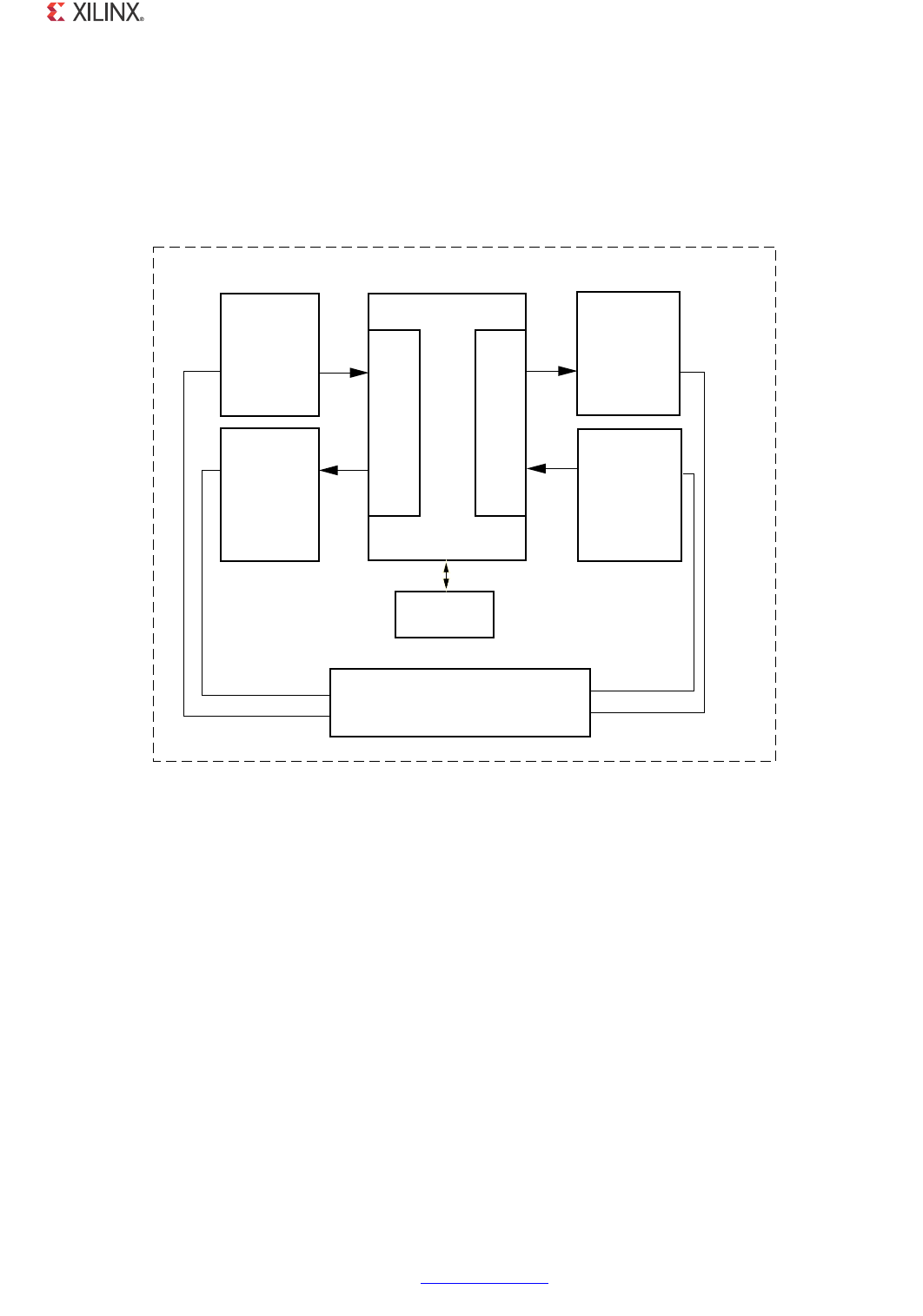
1000BASE-X PCS/PMA or SGMII v11.4 www.xilinx.com 118
PG047 October 16, 2012
Chapter 4: The Ten-Bit Interface
Demonstration Test Bench
Figure 4-15 illustrates the demonstration test bench for the Ethernet 1000BASE-X PCS with
TBI. The demonstration test bench is a simple VHDL or Verilog program to exercise the
example design and the core itself.
The top-level test bench entity instantiates the example design for the core, which is the
Device Under Test (DUT). A stimulus block is also instantiated and clocks, resets and test
bench semaphores are created. The following files describe the top-level of the
demonstration test bench:
VHDL
ISE Design Suite:
<project_dir>/<component_name>/simulation/demo_tb.vhd
Vivado Design Suite:
<project_dir>/<project_name>/<project_name>.srcs/sources1/ip/<component_name>/
<component_name>/simulation/demo_tb.vhd
X-Ref Target - Figure 4-15
Figure 4-15: Demonstration Test Bench for the Ethernet
1000BASE-X PCS with TBI
4")
-ONITOR
""
DECODING
4")
3TIMULUS
""
ENCODING
'-))
3TIMULUS
'-))
-ONITOR
'-)) 4")
$54
$EMONSTRATION4EST"ENCH
#ONTROLAND$ATA3TRUCTURES
#ONFIGURATION
3TIMULUS
8

1000BASE-X PCS/PMA or SGMII v11.4 www.xilinx.com 119
PG047 October 16, 2012
Chapter 4: The Ten-Bit Interface
Verilog
ISE Design Suite:
<project_dir>/<component_name>/simulation/demo_tb.v
Vivado Design Suite:
<project_dir>/<project_name>/<project_name>.srcs/sources1/ip/<component_name>/
<component_name>/simulation/demo_tb.v
The stimulus block entity, instantiated from within the test bench top level, creates the
Ethernet stimulus in the form of four Ethernet frames, which are injected into the GMII and
PHY interfaces of the DUT. The output from the DUT is also monitored for errors. The
following files describe the stimulus block of the demonstration test bench:
VHDL
ISE Design Suite:
<project_dir>/<component_name>/simulation/stimulus_tb.vhd
Vivado Design Suite:
<project_dir>/<project_name>/<project_name>.srcs/sources1/ip/<component_name>/
<component_name>/simulation/stimulus_tb.vhd
Verilog
ISE Design Suite:
<project_dir>/<component_name>/simulation/stimulus_tb.v
Vivado Design Suite:
<project_dir>/<project_name>/<project_name>.srcs/sources1/ip/<component_name>/
<component_name>/simulation/stimulus_tb.v
Together, the top-level test bench file and the stimulus block combine to provide the full
test bench functionality, described in the sections that follow.
Core with MDIO Interface
The demonstration test bench performs the following tasks:
• Input clock signals are generated.
• A reset is applied to the example design.
• The Ethernet 1000BASE-X PCS/PMA core is configured through the MDIO interface by
injecting an MDIO frame into the example design. This disables Auto-Negotiation (if
present) and takes the core out of the Isolate state.

1000BASE-X PCS/PMA or SGMII v11.4 www.xilinx.com 120
PG047 October 16, 2012
Chapter 4: The Ten-Bit Interface
• The following frames are injected into the GMII transmitter by the GMII stimulus block:
°the first is a minimum-length frame
°the second is a type frame
°the third is an errored frame
°the fourth is a padded frame
• The data received at the TBI transmitter interface is 8B/10B decoded. The resulting
frames are checked by the TBI Monitor against the stimulus frames injected into the
GMII transmitter to ensure data integrity.
• The same four frames are generated by the TBI Stimulus block. These are 8B/10B
encoded and injected into the TBI receiver interface.
• Data frames received at the GMII receiver are checked by the GMII Monitor against the
stimulus frames injected into the TBI receiver to ensure data integrity.
Core without MDIO Interface
The demonstration test bench performs the following tasks.
• Input clock signals are generated.
• A reset is applied to the example design.
• The Ethernet 1000BASE-X PCS/PMA core is configured through the Configuration
Vector to take the core out of the Isolate state.
• The following frames are injected into the GMII transmitter by the GMII stimulus block.
°the first is a minimum length frame
°the second is a type frame
°the third is an errored frame
°the fourth is a padded frame
• The data received at the TBI transmitter interface is 8B/10B decoded. The resultant
frames are checked by the TBI Monitor against the stimulus frames injected into the
GMII transmitter to ensure data is the same.
• The same four frames are generated by the TBI Stimulus block. These are 8B/10B
encoded and injected into the TBI receiver interface.
• Data frames received at the GMII receiver are checked by the GMII Monitor against the
stimulus frames injected into the TBI receiver to ensure data is the same.
Customizing the Test Bench
This section provides information about making modifications to the demonstration test
bench files.

1000BASE-X PCS/PMA or SGMII v11.4 www.xilinx.com 121
PG047 October 16, 2012
Chapter 4: The Ten-Bit Interface
Changing Frame Data
You can change the contents of the four frames used by the demonstration test bench by
changing the data and valid fields for each frame defined in the stimulus block. Frames can
be added by defining a new frame of data. Any modified frames are automatically updated
in both stimulus and monitor functions.
Changing Frame Error Status
Errors can be inserted into any of the predefined frames in any position by setting the error
field to ‘1’ in any column of that frame. Injected errors are automatically updated in both
stimulus and monitor functions.
Changing the Core Configuration
The configuration of the Ethernet 1000BASE-X PCS/PMA core used in the demonstration
test bench can be altered.
CAUTION! Certain configurations of the core can cause the test bench to fail or cause processes to run
indefinitely. For example, the demonstration test bench does not auto-negotiate with the design
example. Determine the configurations that can safely be used with the test bench.
If the MDIO interface option has been selected, the core can be reconfigured by editing the
injected MDIO frame in the demonstration test bench top level. Management Registers 0
and 4 can additionally be written though configuration_vector[4:0] and
an_adv_config_vector[15:0] interface signals respectively
If the MDIO interface option has not been selected, the core can be reconfigured by
modifying the configuration vector directly.

1000BASE-X PCS/PMA or SGMII v11.4 www.xilinx.com 122
PG047 October 16, 2012
Chapter 4: The Ten-Bit Interface
SGMII Example Design / Dynamic Switching Example Design
with Ten-Bit Interface
Figure 4-16 illustrates an example design for top-level HDL for the Ethernet 1000BASE-X
PCS/PMA or SGMII core in SGMII mode (or dynamic switching standard) with the TBI.
As illustrated, the example is split between two hierarchical layers. The block level is
designed so that it can be instantiated directly into customer designs and performs the
following functions:
•Instantiates the core from HDL
• Connects the physical-side interface of the core to device IOBs, creating an external
TBI.
• Connects the client side GMII of the core to an SGMII Adaptation Module, which
provides the functionality to operate at speeds of 1 Gb/s, 100 Mb/s and 10 Mb/s.
The top level of the example design creates a specific example which can be simulated,
synthesized and implemented. The top level of the example design performs the following
functions:
X-Ref Target - Figure 4-16
Figure 4-16: Example Design HDL for the Ethernet 1000BASE-X PCS/PMA or
SGMII Core in SGMII Mode with TBI
(WKHUQHW
%$6(;
3&630$
&RUH
1HWOLVW
*0,,
,2%V
,Q
,2%V
2XW
*0,,VW\OH
ELW,)
6*0,,
$GDSWDWLRQ
0RGXOH
&ORFN
0DQDJHPHQW
/RJLF
FRPSRQHQWBQDPHBH[DPSOHBGHVLJQ
FRPSRQHQWBQDPHBEORFN
7%,
,2%V
2XW
,2%V
,Q
''5
7%,
&RQQHFWWR
6(5'(6
8

1000BASE-X PCS/PMA or SGMII v11.4 www.xilinx.com 123
PG047 October 16, 2012
Chapter 4: The Ten-Bit Interface
• Instantiates the block level from HDL
• Derives the clock management logic for the core
• Implements an external GMII-style interface
The next few pages in this section describe each of the example design blocks (and
associated HDL files) in detail, and conclude with an overview of the demonstration test
bench provided for the design.
Top-Level Example Design HDL
The top-level example design for the Ethernet 1000BASE-X PCS/PMA core in SGMII mode is
described in the following files:
VHDL
ISE Design Suite:
<project_dir>/<component_name>/example_design/<component_name>_example_design.vhd
Vivado Design Suite:
<project_dir>/<project_name>/<project_name>.srcs/sources1/ip/<component_name>/
<component_name>/example_design/<component_name>_example_design.vhd
Verilog
ISE Design Suite:
<project_dir>/<component_name>/example_design/<component_name>_example_design.v
Vivado Design Suite
<project_dir>/<project_name>/<project_name>.srcs/sources1/ip/<component_name>/
<component_name>/example_design/<component_name>_example_design.v
The example design HDL top level contains the following:
• An instance of the SGMII block level
• Clock management logic, including DCM and Global Clock Buffer instances, where
required
• External GMII logic, including IOB and DDR register instances, where required
The example design HDL top level connects the GMII of the block level to external IOBs. This
allows the functionality of the core to be demonstrated using a simulation package, as
described in this guide.

1000BASE-X PCS/PMA or SGMII v11.4 www.xilinx.com 124
PG047 October 16, 2012
Chapter 4: The Ten-Bit Interface
Block Level HDL
The following files describe the block level for the Ethernet 1000BASE-X PCS/PMA core in
SGMII mode:
VHDL
ISE Design Suite:
<project_dir>/<component_name>/example_design/<component_name>_block.vhd
Vivado Design Suite:
<project_dir>/<project_name>/<project_name>.srcs/sources1/ip/<component_name>/
<component_name>/example_design/<component_name>_block.vhd
Verilog
ISE Design Suite:
<project_dir>/<component_name>/example_design/<component_name>_block.v
Vivado Design Suite:
<project_dir>/<project_name>/<project_name>.srcs/sources1/ip/<component_name>/
<component_name>/example_design/<component_name>_block.v
The block level contains the following:
• An instance of the Ethernet 1000BASE-X PCS/PMA core in SGMII mode.
• TBI interface logic, including IOB and DDR registers instances, where required.
• An SGMII adaptation module containing:
°The clock management logic required to enable the SGMII example design to
operate at 10 Mb/s, 100 Mb/s, and 1 Gb/s.
°GMII logic for both transmitter and receiver paths; the GMII style 8-bit interface is
run at 125 MHz for 1 Gb/s operation; 12.5 MHz for 100 Mb/s operation; 1.25 MHz
for 10 Mb/s operation.
The block level HDL connects the TBI of the core to external IOBs and the client side to
SGMII Adaptation logic as illustrated in Figure 4-16. This is the most useful part of the
example design and should be instantiated in all customer designs that use the core.

1000BASE-X PCS/PMA or SGMII v11.4 www.xilinx.com 125
PG047 October 16, 2012
Chapter 4: The Ten-Bit Interface
SGMII Adaptation Module
The SGMII Adaptation Module is described in the following files:
VHDL
ISE Design Suite:
<project_dir>/<component_name>/example_design/sgmii_adapt/
Vivado Design Suite:
<project_dir>/<project_name>/<project_name>.srcs/sources1/ip/<component_name>/
<component_name>/example_design/sgmii_adapt/
<component_name>_sgmii_adapt.vhd
<component_name>_clk_gen.vhd
<component_name>_johnson_cntr.vhd
<component_name>_tx_rate_adapt.vhd
<component_name>_rx_rate_adapt.vhd
Verilog
ISE Design Suite:
<project_dir>/<component_name>/example_design/sgmii_adapt/
Vivado Design Suite:
<project_dir>/<project_name>/<project_name>.srcs/sources1/ip/<component_name>/
<component_name>/example_design/sgmii_adapt/
<component_name>_sgmii_adapt.v
<component_name>_clk_gen.v
<component_name>_johnson_cntr.v
<component_name>_tx_rate_adapt.v
<component_name>_rx_rate_adapt.v
The GMII of the core always operates at 125 MHz. The core makes no differentiation
between the three speeds of operation; it always effectively operates at 1 Gb/s. However, at
100 Mb/s, every data byte run through the core should be repeated 10 times to achieve the
required bit rate; at 10 Mb/s, each data byte run through the core should be repeated 100
times to achieve the required bit rate. Dealing with this repetition of bytes is the function of
the SGMII adaptation module and its component blocks.
The SGMII adaptation module and component blocks are described in detail in Chapter 8,
Additional Client-Side SGMII Logic Provided in the Example Design.

1000BASE-X PCS/PMA or SGMII v11.4 www.xilinx.com 126
PG047 October 16, 2012
Chapter 4: The Ten-Bit Interface
Demonstration Test Bench
Figure 4-17 illustrates the demonstration test bench for the Ethernet 1000BASE-X PCS/PMA
or SGMII Core in SGMII mode with the TBI. The demonstration test bench is a simple VHDL
or Verilog program to exercise the example design and the core itself.
The top-level test bench entity instantiates the example design for the core, which is the
Device Under Test (DUT). A stimulus block is also instantiated and clocks, resets and test
bench semaphores are created. The following files describe the top-level of the
demonstration test bench.
VHDL
ISE Design Suite:
<project_dir>/<component_name>/simulation/demo_tb.vhd
Vivado Design Suite:
<project_dir>/<project_name>/<project_name>.srcs/sources1/ip/<component_name>/
<component_name>/simulation/demo_tb.vhd
X-Ref Target - Figure 4-17
Figure 4-17: Demonstration Test Bench for the Ethernet 1000BASE-X PCS/PMA
or SGMII Core in SGMII Mode with TBI
4")
-ONITOR
""
DECODING
4")
3TIMULUS
""
ENCODING
'-))
3TIMULUS
'-))
-ONITOR
'-)) 4")
$54
$EMONSTRATION4EST"ENCH
#ONTROLAND$ATA3TRUCTURES
#ONFIGURATION
3TIMULUS
8

1000BASE-X PCS/PMA or SGMII v11.4 www.xilinx.com 127
PG047 October 16, 2012
Chapter 4: The Ten-Bit Interface
Verilog
ISE Design Suite:
<project_dir>/<component_name>/simulation/demo_tb.v
Vivado Design Suite:
<project_dir>/<project_name>/<project_name>.srcs/sources1/ip/<component_name>/
<component_name>/simulation/demo_tb.v
The stimulus block entity, instantiated from within the top-level test bench, creates the
Ethernet stimulus in the form of four Ethernet frames, which are injected into GMII and TBI
interfaces of the DUT. The output from the DUT is also monitored for errors. The following
files describe the stimulus block of the demonstration test bench.
VHDL
ISE Design Suite:
<project_dir>/<component_name>/simulation/stimulus_tb.vhd
Vivado Design Suite:
<project_dir>/<project_name>/<project_name>.srcs/sources1/ip/<component_name>/
<component_name>/simulation/stimulus_tb.vhd
Verilog
ISE Design Suite:
<project_dir>/<component_name>/simulation/stimulus_tb.v
Vivado Design Suite:
<project_dir>/<project_name>/<project_name>.srcs/sources1/ip/<component_name>/
<component_name>/simulation/stimulus_tb.v
Together, the top-level test bench file and the stimulus block combine to provide the full
test bench functionality which is described in the sections that follow.
Test Bench Functionality
The demonstration test bench performs the following tasks:
• Input clock signals are generated.
• A reset is applied to the example design.
• The Ethernet 1000BASE-X PCS/PMA core is configured through the MDIO interface by
injecting an MDIO frame into the example design. This disables Auto-Negotiation and
takes the core out of Isolate state.

1000BASE-X PCS/PMA or SGMII v11.4 www.xilinx.com 128
PG047 October 16, 2012
Chapter 4: The Ten-Bit Interface
• The following frames are injected into the GMII transmitter by the GMII stimulus block
at 1 Gb/s.
°the first is a minimum length frame
°the second is a type frame
°the third is an errored frame
°the fourth is a padded frame
• The data received at the TBI transmitter interface is 8B/10B decoded. The resulting
frames are checked by the TBI Monitor against the stimulus frames injected into the
GMII transmitter to ensure data integrity.
• The same four frames are generated by the TBI Stimulus block. These are 8B/10B
encoded and injected into the TBI receiver interface.
• Data frames received at the GMII receiver are checked by the GMII Monitor against the
stimulus frames injected into the device-specific transceiver receiver to ensure data
integrity.
Customizing the Test Bench
Changing Frame Data
You can change the contents of the four frames used by the demonstration test bench by
changing the data and valid fields for each frame defined in the stimulus block. New frames
can be added by defining a new frame of data. Modified frames are automatically updated
in both stimulus and monitor functions.
Changing Frame Error Status
Errors can be inserted into any of the predefined frames in any position by setting the error
field to ‘1’ in any column of that frame. Injected errors are automatically updated in both
stimulus and monitor functions.
Changing the Core Configuration
The configuration of the Ethernet 1000BASE-X PCS/PMA core used in the demonstration
test bench can be altered.
CAUTION! Certain configurations of the core cause the test bench to fail or cause processes to run
indefinitely. For example, the demonstration test bench does not auto-negotiate with the design
example. Determine the configurations that can safely be used with the test bench.
The core can be reconfigured by editing the injected MDIO frame in the demonstration test
bench top level.

1000BASE-X PCS/PMA or SGMII v11.4 www.xilinx.com 129
PG047 October 16, 2012
Chapter 4: The Ten-Bit Interface
Changing the Operational Speed
SGMII can be used to carry Ethernet traffic at 10 Mb/s, 100 Mb/s or 1 Gb/s. By default, the
demonstration test bench is configured to operate at 1 Gb/s. The speed of both the
example design and test bench can be set to the desired operational speed by editing the
following settings, recompiling the test bench, then running the simulation again.
1 Gb/s Operation
set speed_is_10_100 to logic 0
100 Mb/s Operation
set speed_is_10_100 to logic 1
set speed_is_100 to logic 1
10 Mb/s Operation
set speed_is_10_100 to logic 1
set speed_is_100 to logic 0

1000BASE-X PCS/PMA or SGMII v11.4 www.xilinx.com 130
PG047 October 16, 2012
Chapter 5
1000BASE-X with Transceivers
This chapter provides general guidelines for creating 1000BASE-X designs that use
transceivers for Virtex®-4, Virtex-5, Virtex-6, Virtex-7, Kintex™-7, Artix ™-7, Zynq™-7000,
and Spartan®-6 devices. ISE® Design Suite supports Virtex-4, Virtex-5, Virtex-6, Virtex-7,
Kintex-7, Artix-7, Zynq-7000, and Spartan-6 devices. Vivado™ Design Suite supports only
Virtex-7, Kintex-7 and Artix-7 devices.
This chapter is organized into the following main sections, with each section being
organized into FPGA families:
•Transceiver Logic
Provides a more detailed look that the device-specific transceivers and their
connections to the netlist of the core.
•Clock Sharing Across Multiple Cores with Transceivers
Provides guidance for using several cores and transceiver instantiations; clock sharing
should occur whenever possible to save device resources.
•Example Design for 1000BASE-X with Transceivers
Introduces the CORE Generator™ tool example design deliverables.
Introduces the Vivado IP catalog tool example design deliverables.
This section also has an overview of the demonstration test bench that is provided with
the example design.

1000BASE-X PCS/PMA or SGMII v11.4 www.xilinx.com 131
PG047 October 16, 2012
Chapter 5: 1000BASE-X with Transceivers
Transceiver Logic
The example is split between two discrete hierarchical layers, as illustrated in Figure 5-18.
The block level is designed so that it can be instantiated directly into customer designs and
provides the following functionality:
•Instantiates the core from HDL
• Connects the physical-side interface of the core to a Virtex-4, Virtex-5, Virtex-6,
Virtex-7, Kintex-7, Artix-7, Zynq-7000, or Spartan-6 device transceiver
The logic implemented in the block level is illustrated in all the figures and described in
further detail for the remainder of this chapter.
Virtex-4 FX Devices
The core is designed to integrate with the Virtex-4 FPGA RocketIO™ MGT transceiver.
Figure 5-1 illustrates the connections and logic required between the core and MGT—the
signal names and logic in the figure precisely match those delivered with the example
design when an MGT is used.
Note: A small logic shim (included in the block-level wrapper) is required to convert between the
port differences of the Virtex-5 and Virtex-4 FPGA RocketIO transceivers.
The MGT clock distribution in Virtex-4 devices is column-based and consists of multiple
MGT tiles (each tile contains two MGTs). For this reason, the MGT wrapper delivered with
the core always contains two MGT instantiations, even if only a single MGT transceiver is in
use. Figure 5-1 illustrates a single MGT tile for clarity.
A GT11CLK_MGT primitive is also instantiated to derive the reference clocks required by the
MGT column-based tiles. See the UG076 Virtex-4 RocketIO Multi-Gigabit Transceiver User
Guide for information about layout and clock distribution.
The 250 MHz reference clock from the GT11CLK_MGT primitive is routed to the MGT
transceiver, configured to internally synthesize a 125 MHz clock. This is output on the
TXOUTCLK1 port of the MGT and after being placed onto global clock routing, can be used
by all core logic. This clock is input back into the MGT transceiver on the user interface clock
ports rxusrclk2 and txusrclk2. With the attribute settings applied to the MGT
transceiver from the example design, the txusrclk and rxusrclk ports are derived
internally within the MGT transceiver using the internal clock dividers and do not need to be
provided from the FPGA logic.
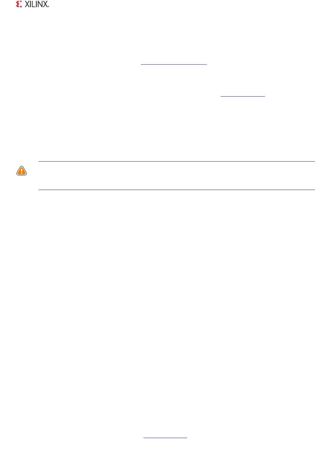
1000BASE-X PCS/PMA or SGMII v11.4 www.xilinx.com 132
PG047 October 16, 2012
Chapter 5: 1000BASE-X with Transceivers
The Virtex-4 FX FPGA RocketIO MGT transceivers require the inclusion of a calibration block
in the logic; the example design provided with the core instantiates calibration blocks as
required. Calibration blocks require a clock source of between 25 to 50 MHz that is shared
with the Dynamic Reconfiguration Port (DRP) of the MGT transceiver, which is named dclk
in the example design. See Xilinx Answer Record 22477 for more information.
Figure 5-1 also illustrates the TX_SIGNAL_DETECT and RX_SIGNAL_DETECT ports of the
calibration block, which should be driven to indicate whether or not dynamic data is being
transmitted and received through the MGT transceiver (see Virtex-4 Errata). However,
RX_SIGNAL_DETECT is connected to the signal_detect port of the example design.
signal_detect is intended to be connected to the optical transceiver to indicate the
presence of light. When light is detected, the optical transceiver provides dynamic data to
the Rx ports of the MGT transceiver. When no light is detected, the calibration block
switches the MGT into loopback to force dynamic data through the MGT transceiver
receiver path. Vivado IP Packager does not support Virtex-4 devices. Virtex-4 devices are
supported only through ISE design suite.
CAUTION! signal_detect is an optional port in the IEEE 802.3-2008 specification. If this is not used, the
RX_SIGNAL_DETECT port of the calibration block must be driven by an alternative method. See
XAPP732 for more information.

1000BASE-X PCS/PMA or SGMII v11.4 www.xilinx.com 133
PG047 October 16, 2012
Chapter 5: 1000BASE-X with Transceivers
X-Ref Target - Figure 5-1
Figure 5-1: 1000BASE-X Connection to Virtex-4 FPGA RocketIO MGT Transceiver
(WKHUQHW%$6(;
3&630$RU6*0,,
/RJL&25(
9LUWH[
*7
5RFNHW,2
XVHG
7;865&/.
7;865&/.
5;865&/.
5;865&/.
XVHUFON
XVHUFON
,3$'
,3$'
EUHIFONQ
0+]
U[EXIVWDWXV>@
U[FKDULVFRPPD
U[FKDULVN
U[FONFRUFQW>@
U[GDWD>@
U[UXQGLVS
SRZHUGRZQ
W[FKDUGLVSPRGH
W[FKDUGLVSYDO
W[FKDULVN
W[GDWD>@
HQDEOHDOLJQ
28#(!2)3#/--!;=
28#(!2)3+;=
28$!4!;=
2825.$)30;=
32:(5'2:1
7;&+$5',6302'(
7;&+$5',639$/
7;&+$5,6.
7;'$7$>@
(13&200$$/,*1
(10&200$$/,*1
9LUWH[
*7&/.B0*7
0*7&/.3
0*7&/.1
6<1&/.287
28$)30%22;=
U[GLVSHUU
EUHIFONS
0+]
5()&/.
V\QFON
gg
7;287&/.
&0'!
FABRIC
2X
%LASTIC
"UFFER
28./4).4!",%;=
RXNOTINTABLE
"5&2
282%##,+
gg
XVHUFON0+]
%8)*
COMPONENT?NAME?BLOCK
"LOCK,EVELFROM
EXAMPLEDESIGN
&DO%ORFNY
'&/.
'&/.
7;B6,*1$/B'(7(&7
5;B6,*1$/B'(7(&7
gg
VLJQDOBGHWHFW
GFON
%8)*
8

1000BASE-X PCS/PMA or SGMII v11.4 www.xilinx.com 134
PG047 October 16, 2012
Chapter 5: 1000BASE-X with Transceivers
Virtex-5 LXT and SXT Devices
The core is designed to integrate with the Virtex-5 FPGA RocketIO GTP transceiver.
Figure 5-2 illustrates the connections and logic required between the core and the GTP
transceiver— the signal names and logic in the figure precisely match those delivered with
the example design when a GTP transceiver is used.
A GTP transceiver tile consists of a pair of transceivers. For this reason, the GTP transceiver
wrapper delivered with the core always contains two GTP instantiations, even if only a single
GTP transceiver tile is in use. Figure 5-2 illustrates a single GTP transceiver tile.
The 125 MHz differential reference clock is routed directly to the GTP transceiver. The GTP
transceiver is configured to output a version of this clock on the REFCLKOUT port and after
placement onto global clock routing, can be used by all core logic. This clock is input back
into the GTP transceiver on the user interface clock ports rxusrclk, rxusrclk2,
txusrclk, and txusrclk2. Vivado IP Packager does not support Virtex-5 devices.
Virtex-5 devices are supported only through ISE design suite.
See also Virtex-5 FPGA RocketIO GTP Transceivers for 1000BASE-X Constraints.
Virtex-5 FPGA RocketIO GTX Wizard
The two wrapper files immediately around the GTP transceiver pair,
RocketIO_wrapper_gtp_tile and RocketIO_wrapper_gtp (see Figure 5-2), are
generated from the RocketIO GTP Wizard. These files apply all the gigabit Ethernet
attributes. Consequently, these files can be regenerated by customers and therefore be
easily targeted at ES or Production silicon. This core targets production silicon.
The CORE Generator tool log file (XCO file) which was created when the RocketIO GTP
Wizard project was generated is available in the following location:
<project_directory>/<component_name>/example_design/transceiver/
<component_name>_RocketIO_wrapper_gtp.xco
This file can be used as an input to the CORE Generator tool to regenerate the
device-specific RocketIO transceiver wrapper files. The XCO file itself contains a list of all of
the GTP transceiver wizard attributes that were used. For further information, see the
Virtex-5 FPGA RocketIO GTP Wizard Getting Started Guide (UG188) and the CORE Generator
Guide, at www.xilinx.com/support/software_manuals.htm
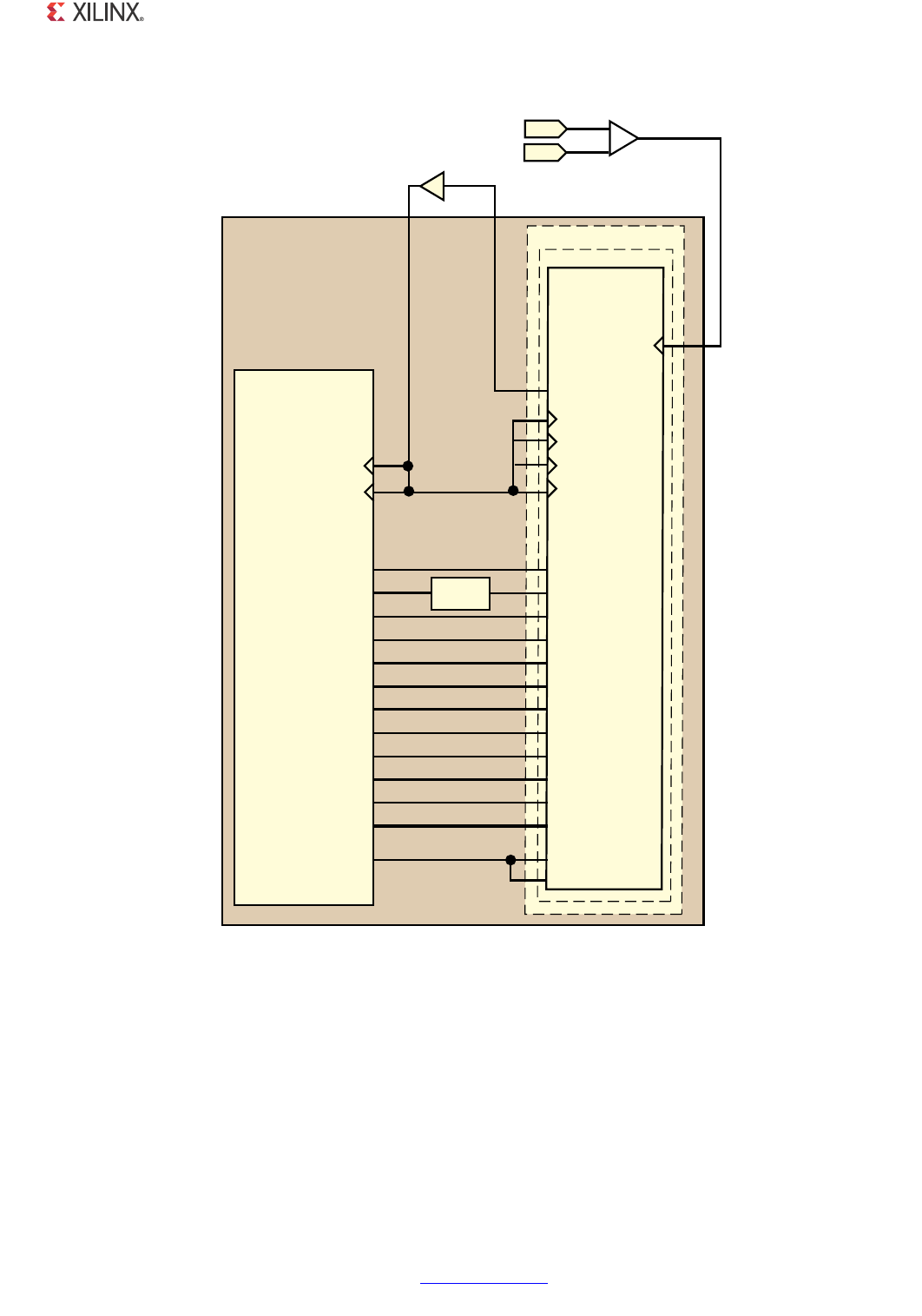
1000BASE-X PCS/PMA or SGMII v11.4 www.xilinx.com 135
PG047 October 16, 2012
Chapter 5: 1000BASE-X with Transceivers
X-Ref Target - Figure 5-2
Figure 5-2: 1000BASE-X Connection to Virtex-5 FPGA RocketIO GTP Transceivers
(WKHUQHW%$6(;
3&630$RU6*0,,
/RJL&25(
6IRTEX
'40
2OCKET)/
48532#,+
48532#,+
28532#,+
28532#,+
XVHUFON
XVHUFON
U[EXIVWDWXV>@
U[FKDULVFRPPD
U[FKDULVN
U[FONFRUFQW>@
U[GDWD>@
U[UXQGLVS
SRZHUGRZQ
W[FKDUGLVSPRGH
W[FKDUGLVSYDO
W[FKDULVN
W[GDWD>@
HQDEOHDOLJQ
28"5&%22
28#(!2)3#/--!
28#(!2)3+
28#,+#/2#.4;=
28$!4!;=
2825.$)30
0/7%2$/7.
48#(!2$)30-/$%
48#(!2$)306!,
48#(!2)3+
48$!4!;=
28%.-#/--!!,)'.
28%.0#/--!!,)'.
28$)30%22
U[GLVSHUU
/2*,&
6+,0
#,+).
2%&#,+/54
COMPONENT?NAME?BLOCK
"LOCK,EVELFROM
EXAMPLEDESIGN
CLKIN
-(Z
,%8)*'6
,3$'
EUHIFONS
,3$'
EUHIFONQ
ROCKETIO?WRAPPER?GTP?TILE
ROCKETIO?WRAPPER?GTP
XVHUFON0+]
%8)*
8

1000BASE-X PCS/PMA or SGMII v11.4 www.xilinx.com 136
PG047 October 16, 2012
Chapter 5: 1000BASE-X with Transceivers
Virtex-5 FXT and TXT Devices
The core is designed to integrate with the Virtex-5 FPGA RocketIO GTX transceiver.
Figure 5-3 illustrates the connections and logic required between the core and the GTX
transceiver—the signal names and logic in the figure precisely match those delivered with
the example design when a GTX transceiver is used.
A GTX transceiver tile consists of a pair of transceivers. For this reason, the GTX transceiver
wrapper delivered with the core always contains two GTX transceiver instantiations, even if
only a single GTX transceiver tile is in use. Figure 5-3 illustrates a single GTX transceiver tile.
The 125 MHz differential reference clock is routed directly to the GTX transceiver. The GTX
transceiver is configured to output a version of this clock on the REFCLKOUT port; this is
then routed to a DCM through a BUFG (global clock routing).
From the DCM, the CLK0 port (125 MHz) is placed onto global clock routing and can be
used as the 125 MHz clock source for all core logic; this clock is also input back into the GTX
transceiver on the user interface clock ports rxusrclk2 and txusrclk2.
From the DCM, the CLKDV port (62.5 MHz) is placed onto global clock routing and is input
back into the GTX transceiver on the user interface clock ports rxusrclk and txusrclk.
Vivado IP Packager does not support Virtex-5 devices. Virtex-5 devices are supported only
through the ISE design suite.
See also Virtex-5 FPGA RocketIO GTX Transceivers for 1000BASE-X Constraints.
Virtex-5 FPGA RocketIO GTX Wizard
The two wrapper files immediately around the GTX transceiver pair,
RocketIO_wrapper_gtx_tile and RocketIO_wrapper_gtx (see Figure 5-3), are
generated from the RocketIO GTX Wizard. These files apply all the gigabit Ethernet
attributes. Consequently, these files can be regenerated by customers and therefore be
easily targeted at ES or Production silicon. This core targets production silicon.
The CORE Generator tool log file (XCO file) that was created when the RocketIO GTX Wizard
project was generated is available in the following location:
<project_directory>/<component_name>/example_design/transceiver/
<component_name>_RocketIO_wrapper_gtx.xco
This file can be used as an input to the CORE Generator tool to regenerate the
device-specific RocketIO transceiver wrapper files. The XCO file itself contains a list of all of
the GTX transceiver wizard attributes that were used. For further information, see the
Virtex-5 FPGA RocketIO GTX Wizard Getting Started Guide and the CORE Generator Guide, at
www.xilinx.com/support/software_manuals.htm
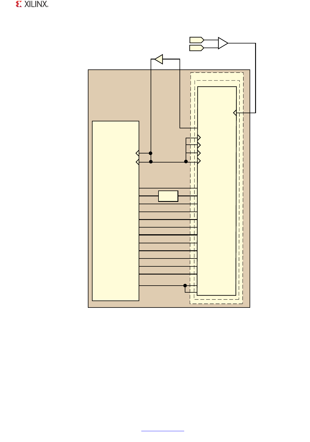
1000BASE-X PCS/PMA or SGMII v11.4 www.xilinx.com 137
PG047 October 16, 2012
Chapter 5: 1000BASE-X with Transceivers
X-Ref Target - Figure 5-3
Figure 5-3: 1000BASE-X Connection to Virtex-5 FPGA RocketIO GTX Transceivers
(WKHUQHW%$6(;
3&630$RU6*0,,
/RJL&25(
6IRTEX
'40
2OCKET)/
48532#,+
48532#,+
28532#,+
28532#,+
XVHUFON
XVHUFON
U[EXIVWDWXV>@
U[FKDULVFRPPD
U[FKDULVN
U[FONFRUFQW>@
U[GDWD>@
U[UXQGLVS
SRZHUGRZQ
W[FKDUGLVSPRGH
W[FKDUGLVSYDO
W[FKDULVN
W[GDWD>@
HQDEOHDOLJQ
28"5&%22
28#(!2)3#/--!
28#(!2)3+
28#,+#/2#.4;=
28$!4!;=
2825.$)30
0/7%2$/7.
48#(!2$)30-/$%
48#(!2$)306!,
48#(!2)3+
48$!4!;=
28%.-#/--!!,)'.
28%.0#/--!!,)'.
28$)30%22
U[GLVSHUU
/2*,&
6+,0
#,+).
2%&#,+/54
COMPONENT?NAME?BLOCK
"LOCK,EVELFROM
EXAMPLEDESIGN
CLKIN
-(Z
,%8)*'6
,3$'
EUHIFONS
,3$'
EUHIFONQ
ROCKETIO?WRAPPER?GTP?TILE
ROCKETIO?WRAPPER?GTP
XVHUFON0+]
%8)*
8

1000BASE-X PCS/PMA or SGMII v11.4 www.xilinx.com 138
PG047 October 16, 2012
Chapter 5: 1000BASE-X with Transceivers
Virtex-6 Devices
The core is designed to integrate with the Virtex-6 FPGA GTX transceiver. Figure 5-4
illustrates the connections and logic required between the core and the GTX
transceiver—the signal names and logic in the figure precisely match those delivered with
the example design.
The 125 MHz differential reference clock is routed directly to the GTX transceiver from the
specialized IBUFDS_GTXE1 primitive. The GTX transceiver is configured to output a version
of this clock on the TXOUTCLK port and after placement onto global clock routing, can be
used by all core logic. This clock is input back into the GTX transceiver on the user interface
clock ports rxusrclk2 and txusrclk2. The rxusrclk and txusrclk clocks are derived
internally and can be grounded. Vivado IP Packager does not support Virtex-6 devices.
Virtex-6 devices are supported only through ISE design suite.
Virtex-6 FPGA GTX Transceiver Wizard
The two wrapper files immediately around the GTX transceiver, gtx_wrapper_gtx and
gtx_wrapper (see Figure 5-4), are generated from the Virtex-6 FPGA GTX Transceiver
Wizard. These files apply all the gigabit Ethernet attributes. Consequently, these files can
be regenerated by customers and therefore be easily targeted at silicon/device versions.
The CORE Generator tool log file (XCO file) that was created when the Virtex-6 FPGA GTX
Transceiver Wizard project was generated is available in the following location:
<project_directory>/<component_name>/example_design/transceiver/
<component_name>_gtx_wrapper_gtx.xco
This file can be used as an input to the CORE Generator tool to regenerate the transceiver
wrapper files. The XCO file itself contains a list of all of the wizard attributes that were used.
For further information, see the Virtex-6 FPGA GTX Transceiver Wizard Getting Started Guide
and the CORE Generator Guide, at www.xilinx.com/support/software_manuals.htm.
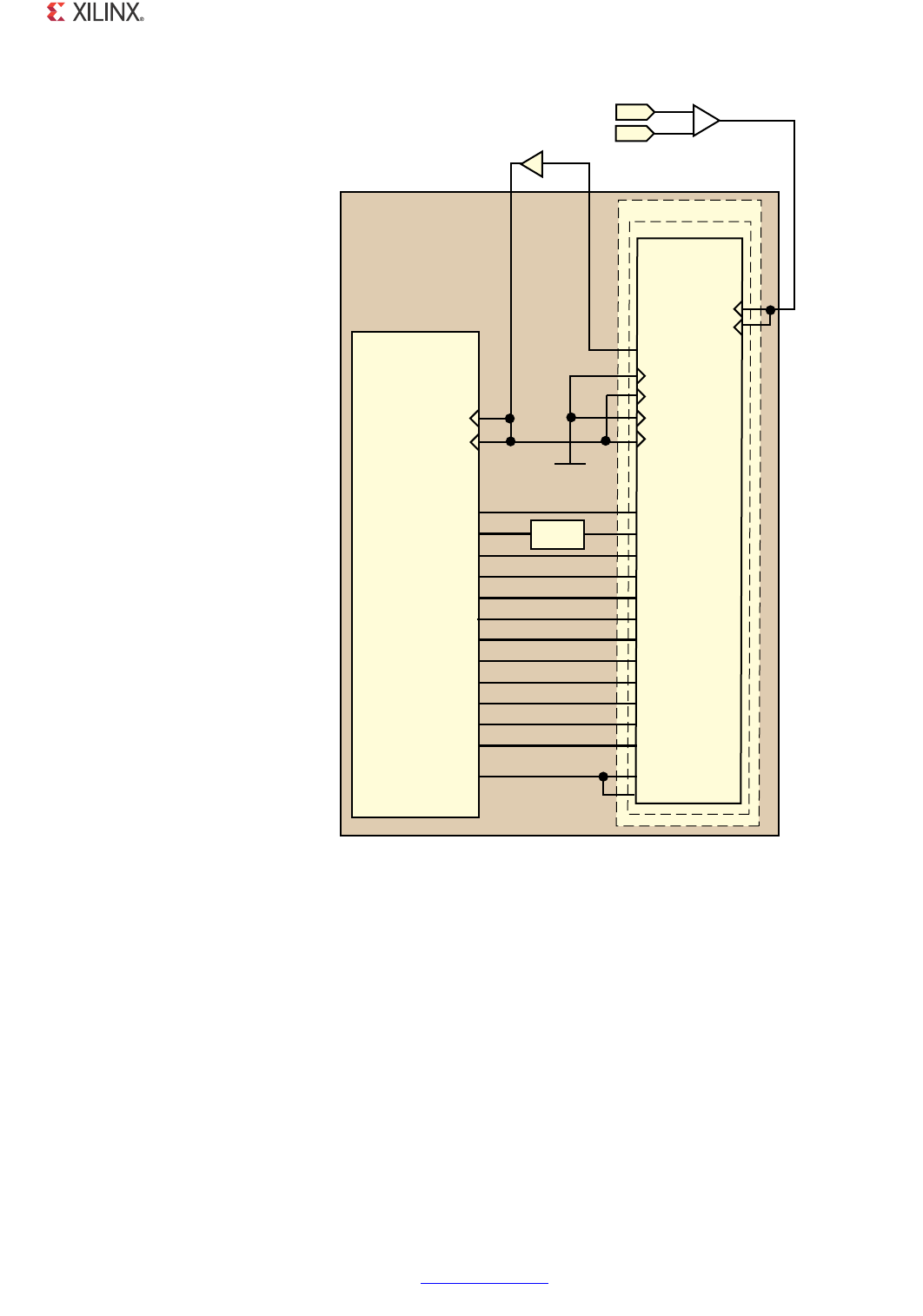
1000BASE-X PCS/PMA or SGMII v11.4 www.xilinx.com 139
PG047 October 16, 2012
Chapter 5: 1000BASE-X with Transceivers
X-Ref Target - Figure 5-4
Figure 5-4: 1000BASE-X Connection to Virtex-6 FPGA GTX Transceiver
(WKHUQHW%$6(;
3&630$RU6*0,,
/RJL&25(
6IRTEX
'48%
TRANSCEIVER
48532#,+
48532#,+
28532#,+
28532#,+
XVHUFON
XVHUFON
U[EXIVWDWXV>@
U[FKDULVFRPPD
U[FKDULVN
U[FONFRUFQW>@
U[GDWD>@
U[UXQGLVS
SRZHUGRZQ
W[FKDUGLVSPRGH
W[FKDUGLVSYDO
W[FKDULVN
W[GDWD>@
HQDEOHDOLJQ
28"5&%22
28#(!2)3#/--!
28#(!2)3+
28#,+#/2#.4;=
28$!4!;=
2825.$)30
0/7%2$/7.
48#(!2$)30-/$%
48#(!2$)306!,
48#(!2)3+
48$!4!;=
28%.-#/--!!,)'.
28%.0#/--!!,)'.
28$)30%22
U[GLVSHUU
/2*,&
6+,0
48/54#,+
COMPONENT?NAME?BLOCK
"LOCK,EVELFROM
EXAMPLEDESIGN
MGTREFCLK
-(Z
,%8)'6B*7;(
,3$'
PJWUHIFONBS
,3$'
PJWUHIFONBQ
GTX?WRAPPER?GTX
GTX?WRAPPER
XVHUFON0+]
%8)*
'.$
-'42%&#,+48;=
-'42%&#,+28;=
8

1000BASE-X PCS/PMA or SGMII v11.4 www.xilinx.com 140
PG047 October 16, 2012
Chapter 5: 1000BASE-X with Transceivers
Spartan-6 LXT Devices
The core is designed to integrate with the Spartan-6 FPGA GTP transceiver. Figure 5-5
illustrates the connections and logic required between the core and the GTP
transceiver—the signal names and logic in the figure precisely match those delivered with
the example design when a GTP transceiver is used.
A GTP transceiver tile consists of a pair of transceivers. For this reason, the GTP transceiver
wrapper delivered with the core always contains two GTP transceiver instantiations, even if
only a single GTP transceiver tile is in use. Figure 5-5 illustrates a single GTP transceiver tile.
The 125 MHz differential reference clock is routed directly to the GTP transceiver. The GTP
transceiver is configured to output a version of this clock on the GTPCLKOUT port and after
placement through a BUFIO2 and BUFG onto global clock routing, can be used by all core
logic. This clock is input back into the GTP transceiver on the user interface clock ports
rxusrclk, rxusrclk2, txusrclk, and txusrclk2.
Vivado IP Packager does not support Spartan-6 devices. Spartan-6 devices are supported
only through ISE design suite. See also Spartan-6 FPGA GTP Transceivers for 1000BASE-X
Constraints.
Spartan-6 FPGA GTP Transceiver Wizard
The two wrapper files immediately around the GTP transceiver pair, gtp_wrapper_tile
and gtp_wrapper (see Figure 5-5), are generated from the Spartan-6 FPGA GTP
Transceiver Wizard. These files apply all the gigabit Ethernet attributes. Consequently, these
files can be regenerated by customers and therefore be easily targeted at ES or Production
silicon. This core targets production silicon.
The CORE Generator tool log file (XCO file) that was created when the GTP Transceiver
Wizard project was generated is available in the following location:
<project_directory>/<component_name>/example_design/transceiver/gtp_wrapper.xco
This file can be used as an input to the CORE Generator tool to regenerate the
device-specific transceiver wrapper files. The XCO file itself contains a list of all of the GTP
transceiver wizard attributes that were used. For further information, see the Spartan-6
FPGA GTP Wizard Getting Started Guide and the CORE Generator Guide, at
www.xilinx.com/support/software_manuals.htm
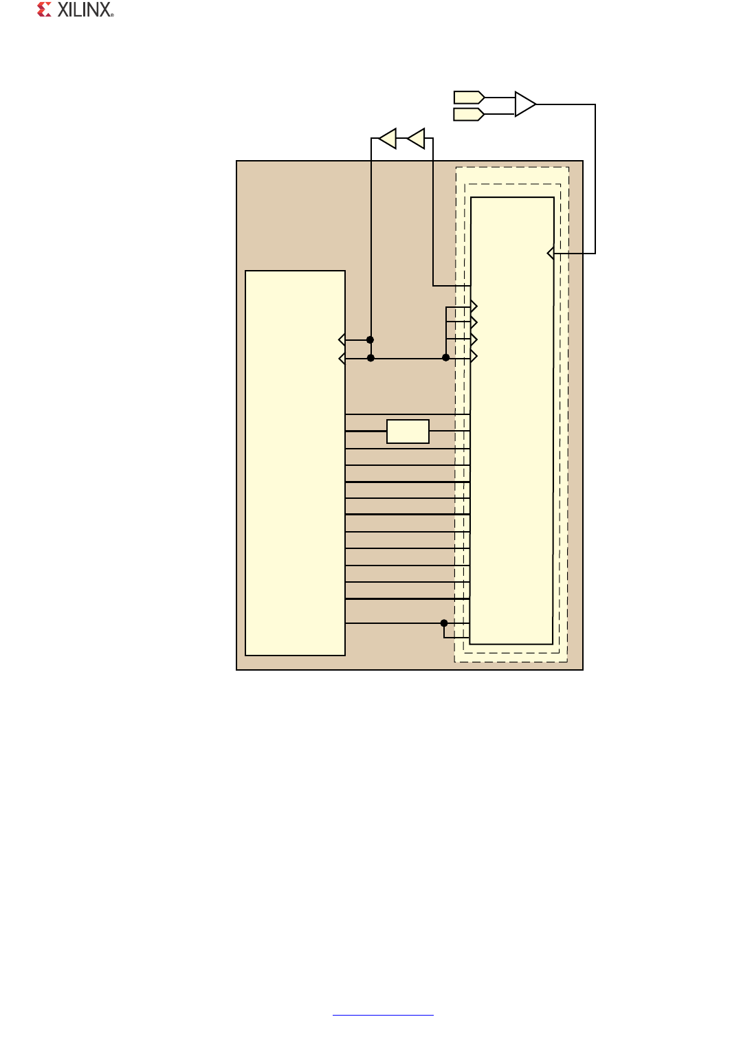
1000BASE-X PCS/PMA or SGMII v11.4 www.xilinx.com 141
PG047 October 16, 2012
Chapter 5: 1000BASE-X with Transceivers
X-Ref Target - Figure 5-5
Figure 5-5: 1000BASE-X Connection to Spartan-6 FPGA GTP Transceivers
(WKHUQHW%$6(;
3&630$RU6*0,,
/RJL&25(
48532#,+
48532#,+
28532#,+
28532#,+
XVHUFON
XVHUFON
U[EXIVWDWXV>@
U[FKDULVFRPPD
U[FKDULVN
U[FONFRUFQW>@
U[GDWD>@
U[UXQGLVS
SRZHUGRZQ
W[FKDUGLVSPRGH
W[FKDUGLVSYDO
W[FKDULVN
W[GDWD>@
HQDEOHDOLJQ
28"5&%22
28#(!2)3#/--!
28#(!2)3+
28#,+#/2#.4;=
28$!4!;=
2825.$)30
0/7%2$/7.
48#(!2$)30-/$%
48#(!2$)306!,
48#(!2)3+
48$!4!;=
28%.-#/--!!,)'.
28%.0#/--!!,)'.
28$)30%22
U[GLVSHUU
/2*,&
6+,0
#,+).
'40#,+/54
COMPONENT?NAME?BLOCK
"LOCK,EVELFROM
EXAMPLEDESIGN
CLKIN
-(Z
,%8)'6
,3$'
EUHIFONS
,3$'
EUHIFONQ
GTP?WRAPPER?TILE
GTP?WRAPPER
XVHUFON0+]
%8)*
6SDUWDQ
7UDQVFHLYHU
*73
%8),2
8

1000BASE-X PCS/PMA or SGMII v11.4 www.xilinx.com 142
PG047 October 16, 2012
Chapter 5: 1000BASE-X with Transceivers
Virtex-7 Devices
The core is designed to integrate with the 7 series FPGA transceiver. Figure 5-6 illustrates
the connections and logic required between the core and the transceiver—the signal names
and logic in the figure precisely match those delivered with the example design when a 7
series FPGA transceiver is used.
The 125 MHz differential reference clock is routed directly to the 7 series FPGA transceiver.
The transceiver is configured to output a version of this clock (62.5 MHz) on the TXOUTCLK
port; this is then routed to a MMCM. From the MMCM, the CLKOUT1 port (62.5 MHz) is
placed onto global clock routing and is input back into the GTXE2/GTHE2 transceiver on the
user interface clock ports rxusrclk, rxusrclk2, txusrclk, and txusrclk2. The CLKOUT0 port (125
MHz) of MMCM is placed onto global clock routing and can be used as the 125 MHz clock
source for all core logic. See also Chapter 18, 7 Series and Zynq-7000 Device Transceivers
for 1000BASE-X Constraints.
7 Series FPGA Transceiver Wizard
The two wrapper files immediately around the GTX/GTH transceiver pair, gtwizard and
gtwizard_gt (Figure 5-6), are generated from the 7 series FPGA Transceiver Wizard. These
files apply all the gigabit Ethernet attributes. Consequently, these files can be regenerated
by customers. The CORE Generator tool log file (XCO file) that was created when the 7 series
FPGA Transceiver Wizard project was generated is available in the following location:
ISE Design Suite
<project_dir>/<component_name>/example_design/transceiver/<component_name>_gtwizard
.xco
Vivado Design Suite
<project_dir>/<project_name>/<project_name>.srcs/sources1/ip/<component_name>/
<component_name>/example_design/transceiver/<component_name>_gtwizard.xco.
This file can be used as an input to the CORE Generator tool to regenerate the device
specific transceiver wrapper files. This file can be used as an input to Vivado project by
clicking <Add Sources> in the Flow Navigator task bar and selecting the XCO file. The XCO
file itself contains a list of all of the Transceiver Wizard attributes that were used. For further
information, see the 7 Series FPGAs GTX Transceivers User Guide and 7 Series FPGAs GTH
Transceivers User Guide.
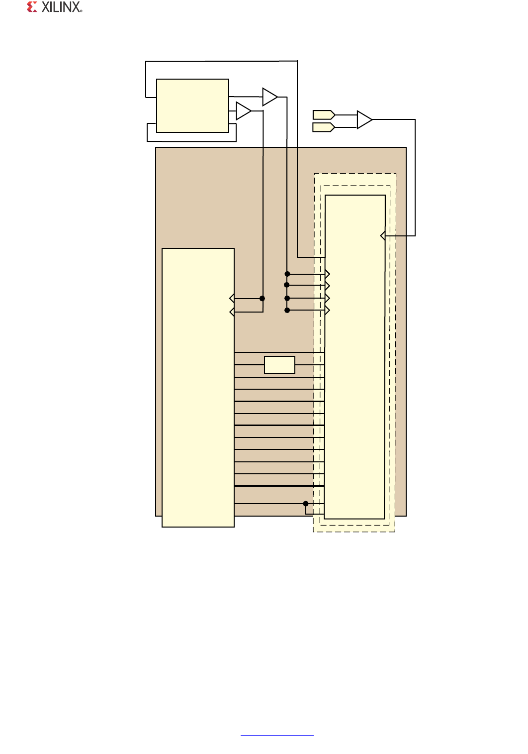
1000BASE-X PCS/PMA or SGMII v11.4 www.xilinx.com 143
PG047 October 16, 2012
Chapter 5: 1000BASE-X with Transceivers
X-Ref Target - Figure 5-6
Figure 5-6: 1000BASE-X Connection to Virtex-7 Transceivers
(WKHUQHW%$6(;
3&630$RU6*0,,
/RJL&25(
3ERIES
'48%?#(!..%,
'4(%?#(!..%,
4RANSCEIVER
48532#,+
48532#,+
28532#,+
28532#,+
XVHUFON
XVHUFON
U[EXIVWDWXV>@
U[FKDULVFRPPD
U[FKDULVN
U[FONFRUFQW>@
U[GDWD>@
U[UXQGLVS
SRZHUGRZQ
W[FKDUGLVSPRGH
W[FKDUGLVSYDO
W[FKDULVN
W[GDWD>@
HQDEOHDOLJQ
28"5&34!453
28#(!2)3#/--!
28#(!2)3+
28#,+#/2#.4;=
28$!4!;=
2825.$)30
0/7%2$/7.
48#(!2$)30-/$%
48#(!2$)306!,
48#(!2)3+
48$!4!;=
28-#/--!!,)'.%.
280#/--!!,)'.%.
28$)30%22
U[GLVSHUU
/2*,&
6+,0
48/54#,+
COMPONENT?NAME?BLOCK
"LOCK,EVELFROM
EXAMPLEDESIGN
GTREFCLK
-(Z
,%8)'6B*7(
,3$'
JWUHIFONBS
,3$'
JWUHIFONBQ
GTWIZARD?GT
GTWIZARD
%8)*
'42%&#,+4
--#-%?!$6
#,+/54
#,+/54
#,+).
#,+&"/54#,+&").
%8)*
-(Z
-(Z
-(Z
8

1000BASE-X PCS/PMA or SGMII v11.4 www.xilinx.com 144
PG047 October 16, 2012
Chapter 5: 1000BASE-X with Transceivers
Kintex-7 and Zynq-7000 Devices
The core is designed to integrate with the 7 series FPGA transceiver. Figure 5-7 illustrates
the connections and logic required between the core and the transceiver—the signal names
and logic in the figure precisely match those delivered with the example design when a 7
series FPGA transceiver is used.
The 125 MHz differential reference clock is routed directly to the 7 series FPGA transceiver.
The transceiver is configured to output a version of this clock (62.5 MHz) on the TXOUTCLK
port; this is then routed to a MMCM through a BUFG (global clock routing). From the
MMCM, the CLKOUT1 port (62.5 MHz) is placed onto global clock routing and is input back
into the GTXE2 transceiver on the user interface clock ports rxusrclk, rxusrclk2,
txusrclk and txusrclk2. The CLKOUT0 port (125 MHz) of MMCM is placed onto global
clock routing and can be used as the 125 MHz clock source for all core logic. See also 7
Series FPGA Transceivers for 1000BASE-X Constraints.
7 Series FPGA Transceiver Wizard
The two wrapper files immediately around the GTX transceiver pair, gtwizard and
gtwizard_gt (Figure 5-7), are generated from the 7 series FPGA Transceiver Wizard. These
files apply all the gigabit Ethernet attributes. Consequently, these files can be regenerated
by customers.
The CORE Generator tool log file (XCO file) that was created when the 7 series FPGA
Transceiver Wizard project was generated is available in the location:
ISE Design Suite
<project_dir>/<component_name>/example_design/transceiver/<component_name>_gtwizard
.xco
Vivado Design Suite
<project_dir>/<project_name>/<project_name>.srcs/sources1/ip/<component_name>/
<component_name>/example_design/transceiver/<component_name>_gtwizard.xco
This file can be used as an input to the CORE Generator tool to regenerate the device
specific transceiver wrapper files. This file can be used as an input to Vivado project by
clicking on <Add Sources> in the Flow Navigator task bar and selecting the XCO file. The
XCO file itself contains a list of all of the transceiver wizard attributes that were used. For
further information, see the 7 Series FPGAs GTX Transceivers User Guide.
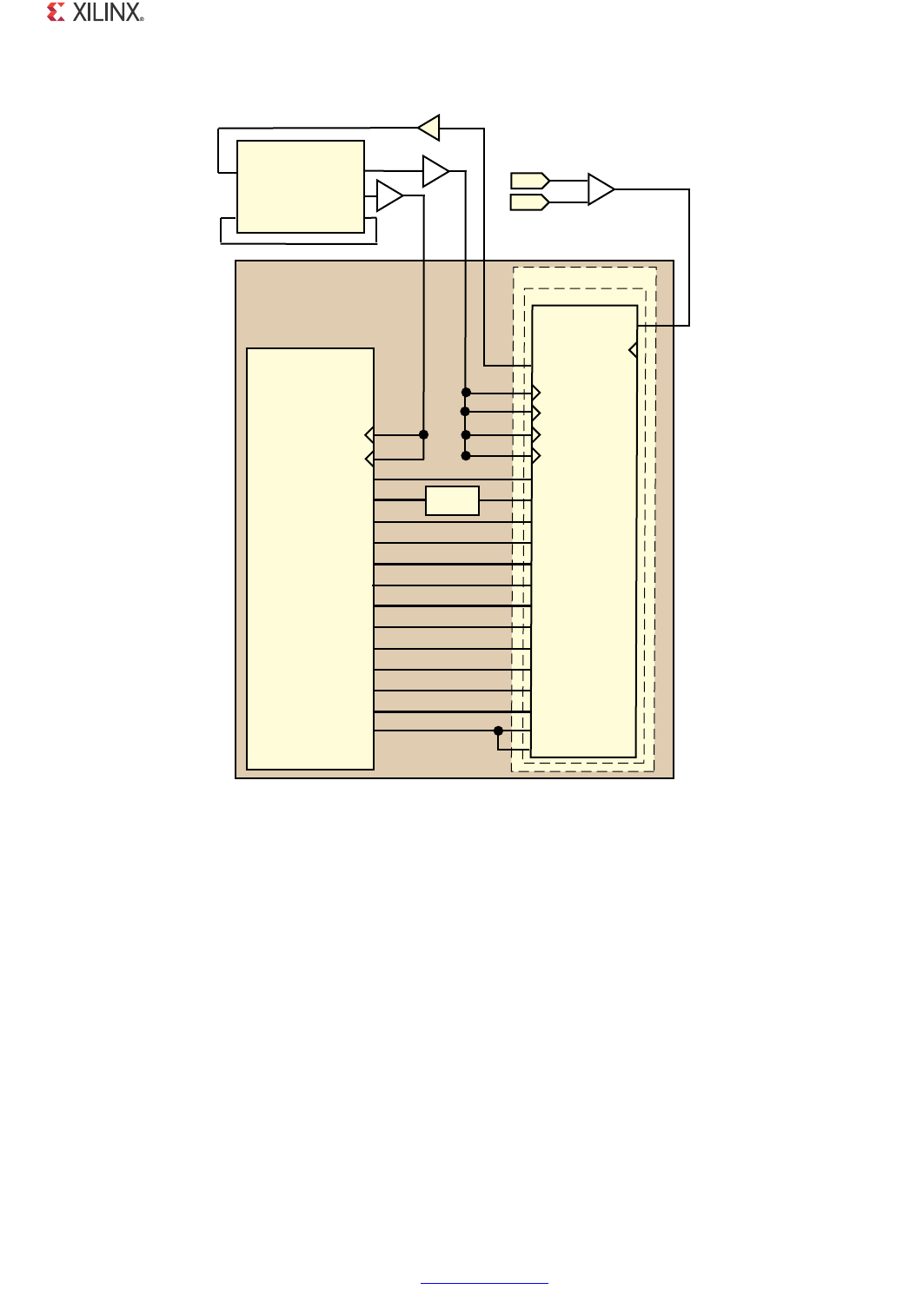
1000BASE-X PCS/PMA or SGMII v11.4 www.xilinx.com 145
PG047 October 16, 2012
Chapter 5: 1000BASE-X with Transceivers
X-Ref Target - Figure 5-7
Figure 5-7: 1000BASE-X Connection to Kintex-7 and Zynq-7000 Device Transceivers
(WKHUQHW%$6(;
3&630$RU6*0,,
/RJL&25(
3ERIES
'48%?#(!..%,
TRANSCEIVER
48532#,+
48532#,+
28532#,+
28532#,+
XVHUFON
XVHUFON
U[EXIVWDWXV>@
U[FKDULVFRPPD
U[FKDULVN
U[FONFRUFQW>@
U[GDWD>@
U[UXQGLVS
SRZHUGRZQ
W[FKDUGLVSPRGH
W[FKDUGLVSYDO
W[FKDULVN
W[GDWD>@
HQDEOHDOLJQ
28"5&34!453
28#(!2)3#/--!
28#(!2)3+
28#,+#/2#.4;=
28$!4!;=
2825.$)30
0/7%2$/7.
48#(!2$)30-/$%
48#(!2$)306!,
48#(!2)3+
48$!4!;=
28-#/--!!,)'.%.
280#/--!!,)'.%.
28$)30%22
U[GLVSHUU
/2*,&
6+,0
48/54#,+
COMPONENT?NAME?BLOCK
"LOCK,EVELFROM
EXAMPLEDESIGN
GTREFCLK
-(Z
,%8)'6B*7(
,3$'
JWUHIFONBS
,3$'
JWUHIFONBQ
GTWIZARD?GT
GTWIZARD
XVHUFON0+]
%8)*
'42%&#,+4
--#-%?!$6
#,+/54
#,+/54
#,+).
#,+&"/54#,+&").
%8)*
%8)*
-(Z
-(Z
-(Z
8

1000BASE-X PCS/PMA or SGMII v11.4 www.xilinx.com 146
PG047 October 16, 2012
Chapter 5: 1000BASE-X with Transceivers
Artix-7 Devices
The core is designed to integrate with the 7 series FPGA transceiver. Figure 5-8 illustrates
the connections and logic required between the core and the transceiver-the signal names
and logic in the figure precisely match those delivered with the example design when a
7 series FPGA transceiver is used.
The 125 MHz differential reference clock is routed directly to the 7 series FPGA transceiver.
The transceiver is configured to output a version of this clock (62.5 MHz) on the TXOUTCLK
port. The clock is then routed to a MMCM through a BUFG (global clock routing). From the
MMCM, the CLKOUT1 port (62.5 MHz) is placed onto global clock routing and is input back
into the GTPE2 transceiver on the user interface clock ports rxusrclk, rxusrclk2,
txusrclk and txusrclk2. The CLKOUT0 port (125 MHz) of MMCM is placed onto global
clock routing and can be used as the 125 MHz clock source for all core logic. See also 7
Series and Zynq-7000 Device Transceivers for 1000BASE-X Constraints in Chapter 18.
7 Series FPGA Transceiver Wizard
The two wrapper files immediately around the GTP transceiver pair, gtwizard and
gtwizard_gt (Figure 5-8), are generated from the 7 series FPGA Transceiver Wizard. These
files apply all the gigabit Ethernet attributes. Consequently, these files can be regenerated
by customers.
The CORE Generator tool log file (XCO file) that was created when the 7 series FPGA
Transceiver Wizard project was generated is available in the location:
ISE Design Suite
<project_dir>/<component_name>/example_design/transceiver/<component_name>_gtwizard
.xco
Vivado Design Suite
<project_dir>/<project_name>/<project_name>.srcs/sources1/ip/<component_name>/
<component_name>/example_design/transceiver/<component_name>_gtwizard.xco
This file can be used as an input to the CORE Generator tool to regenerate the device
specific transceiver wrapper files. This file can be used as an input to Vivado project by
clicking on <Add Sources> in the Flow Navigator task bar and selecting the XCO file.The
XCO file itself contains a list of all of the transceiver wizard attributes that were used. For
further information, see the 7 Series FPGAs GTP Transceivers User Guide.
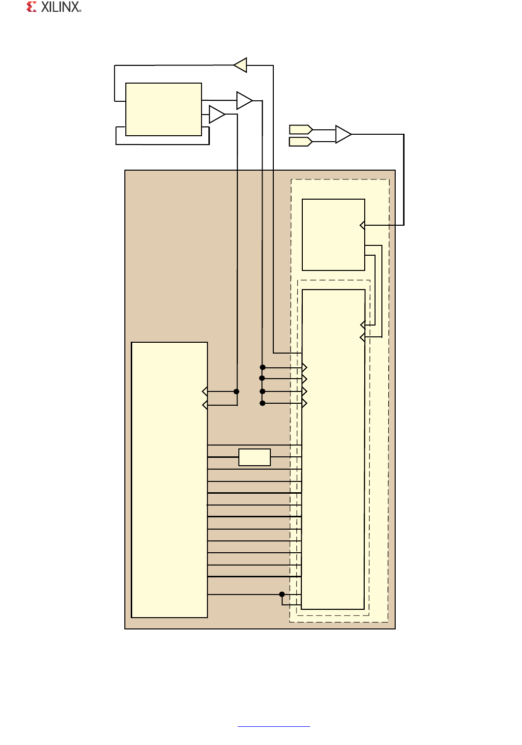
1000BASE-X PCS/PMA or SGMII v11.4 www.xilinx.com 147
PG047 October 16, 2012
Chapter 5: 1000BASE-X with Transceivers
X-Ref Target - Figure 5-8
Figure 5-8: 1000BASE-X Connection to Artix-7 Transceiver
(WKHUQHW%$6(;
3&630$RU6*0,,
/RJL&25(
3ERIES
'40%?#(!..%,
TRANSCEIVER
48532#,+
48532#,+
28532#,+
28532#,+
XVHUFON
XVHUFON
U[EXIVWDWXV>@
U[FKDULVFRPPD
U[FKDULVN
U[FONFRUFQW>@
U[GDWD>@
U[UXQGLVS
SRZHUGRZQ
W[FKDUGLVSPRGH
W[FKDUGLVSYDO
W[FKDULVN
W[GDWD>@
HQDEOHDOLJQ
28"5&34!453
28#(!2)3#/--!
28#(!2)3+
28#,+#/2#.4;=
28$!4!;=
2825.$)30
0/7%2$/7.
48#(!2$)30-/$%
48#(!2$)306!,
48#(!2)3+
48$!4!;=
28-#/--!!,)'.%.
280#/--!!,)'.%.
28$)30%22
U[GLVSHUU
/2*,&
6+,0
48/54#,+
COMPONENT?NAME?BLOCK
"LOCK,EVELFROM
EXAMPLEDESIGN
GTREFCLK
-(Z
,%8)'6B*7(
,3$'
JWUHIFONBS
,3$'
JWUHIFONBQ
GTWIZARD?GT
GTWIZARD
%8)*
0,,#,+?).
--#-%?!$6
#,+/54
#,+/54
#,+).
#,+&"/54#,+&").
%8)*
%8)*
-(Z
-(Z
-(Z
3ERIES
'40%?#/--/.
'42%&#,+
0,,/54#,+
0,,/542%&#,+
0,,2%&#,+?).
8

1000BASE-X PCS/PMA or SGMII v11.4 www.xilinx.com 148
PG047 October 16, 2012
Chapter 5: 1000BASE-X with Transceivers
Clock Sharing Across Multiple Cores with
Transceivers
Virtex-4 FX Devices
Figure 5-9 illustrates sharing clock resources across multiple instantiations of the core when
using MGTs. The example design, when using the Virtex-4 family, can be generated to
connect either a single instance of the core, or connect a pair of core instances to the
transceiver pair present in an MGT tile. Figure 5-9 shows two instantiations of the block
level, where each block contains a pair of cores, subsequently illustrating clock sharing
between four cores in total.
More cores can be added by continuing to instantiate extra block-level modules. Share
clocks only between the MGTs in a single column. For each column, use a single
brefclk_p and brefclk_n differential clock pair and connect this to a GT11CLK_MGT
primitive. The clock output from this primitive should be shared across all used RocketIO
transceiver tiles in the column. See the Virtex-4 RocketIO Multi-Gigabit Transceiver User
Guide (UG076) for more information.
To provide the 125 MHz clock for all core instances, select a TXOUTCLK1 port from any MGT.
This can be routed onto global clock routing using a BUFG as illustrated, and shared
between all cores and MGTs in the column. Although not illustrated in Figure 5-9, dclk (the
clock used for the calibration blocks and for the Dynamic Reconfiguration Port (DRP) of the
MGT transceivers) can also be shared.
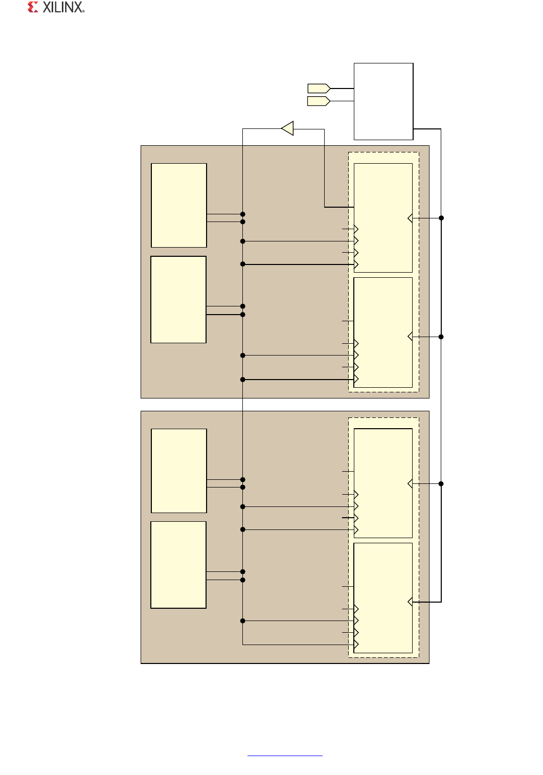
1000BASE-X PCS/PMA or SGMII v11.4 www.xilinx.com 149
PG047 October 16, 2012
Chapter 5: 1000BASE-X with Transceivers
X-Ref Target - Figure 5-9
Figure 5-9: Clock Management - Multiple Core Instances, MGT Transceivers for 1000BASE-X
(WKHUQHW%$6(;
3&630$RU
6*0,,FRUH
XVHUFON
XVHUFON
,3$'
BREFCLKP
-(Z
,3$'
BREFCLKN
-(Z
9LUWH[
*7&/.B0*7
0*7&/.3
0*7&/.1
6<1&/.287
6IRTEX
'4
2OCKET)/
!
5()&/.
0*7WLOH
6IRTEX
'4
2OCKET)/
"
5()&/.
7;287&/.
(WKHUQHW%$6(;
3&630$RU
6*0,,FRUH
XVHUFON
XVHUFON
1&
XVHUFON
0+]
%8)*
7;865&/.
7;865&/.
5;865&/.
5;865&/.
7;865&/.
7;865&/.
5;865&/.
5;865&/.
SYNCLK
-(Z
@
@
@
@
48/54#,+
COMPONENT?NAME?BLOCK
"LOCK,EVEL
(WKHUQHW%$6(;
3&630$RU
6*0,,FRUH
XVHUFON
XVHUFON
6IRTEX
'4
2OCKET)/
!
5()&/.
0*7WLOH
6IRTEX
'4
2OCKET)/
"
5()&/.
7;287&/.
(WKHUQHW%$6(;
3&630$RU
6*0,,FRUH
XVHUFON
XVHUFON
1&
7;865&/.
7;865&/.
5;865&/.
5;865&/.
7;865&/.
7;865&/.
5;865&/.
5;865&/.
@
@
@
@
48/54#,+
COMPONENT?NAME?BLOCK
"LOCK,EVEL
1&
8

1000BASE-X PCS/PMA or SGMII v11.4 www.xilinx.com 150
PG047 October 16, 2012
Chapter 5: 1000BASE-X with Transceivers
Virtex-5 LXT and SXT Devices
Figure 5-10 illustrates sharing clock resources across multiple instantiations of the core
when using Virtex-5 FPGA RocketIO GTP transceivers.
The example design can be generated to connect either a single instance of the core or
connect a pair of core instances to the transceiver pair present in a GTP transceiver tile.
Figure 5-10 illustrates two instantiations of the block level, and each block level contains a
pair of cores, consequently illustrating clock sharing between a total of four cores.
Additional cores can be added by continuing to instantiate extra block level modules. Share
the brefclk_p and brefclk_n differential clock pair. See the Virtex-5 FPGA RocketIO GTP
Transceiver User Guide (UG196) for more information.
To provide the 125 MHz clock for all core instances, select a REFCLKOUT port from any GTP
transceiver. This can be routed onto global clock routing using a BUFG as illustrated and
shared between all cores and GTP transceivers.
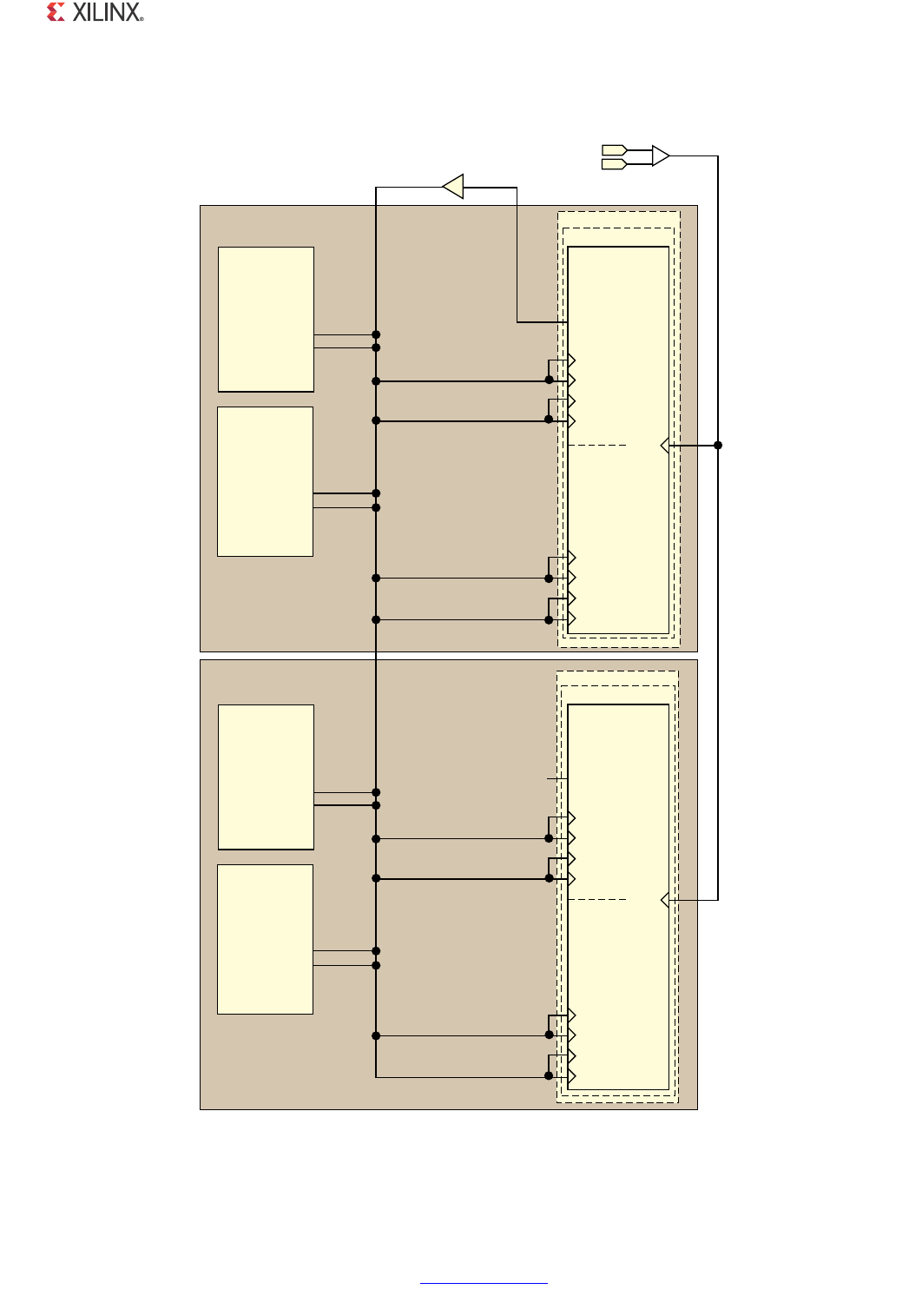
1000BASE-X PCS/PMA or SGMII v11.4 www.xilinx.com 151
PG047 October 16, 2012
Chapter 5: 1000BASE-X with Transceivers
X-Ref Target - Figure 5-11
X-Ref Target - Figure 5-10
Figure 5-10: Clock Management - Multiple Core Instances, Virtex-5 FPGA
RocketIO GTP Transceivers for 1000BASE-X
(WKHUQHW%$6(;
3&630$RU
6*0,,FRUH
XVHUFON
XVHUFON
6IRTEX
'40
2OCKET)/
#,+).
URFNHWLRBZUDSSHUBJWSBWLOH
6IRTEX
'40
2OCKET)/
(WKHUQHW%$6(;
3&630$RU
6*0,,FRUH
XVHUFON
XVHUFON
XVHUFON
0+]
%8)*
48532#,+
48532#,+
28532#,+
28532#,+
48532#,+
48532#,+
28532#,+
28532#,+
CLKIN
-(Z
2%&#,+/54
COMPONENT?NAME?BLOCK
"LOCK,EVEL
(WKHUQHW%$6(;
3&630$RU
6*0,,FRUH
XVHUFON
XVHUFON
6IRTEX
'40
2OCKET)/
6IRTEX
'40
2OCKET)/
(WKHUQHW%$6(;
3&630$RU
6*0,,FRUH
XVHUFON
XVHUFON
48532#,+
48532#,+
28532#,+
28532#,+
48532#,+
48532#,+
28532#,+
28532#,+
2%&#,+/54
COMPONENT?NAME?BLOCK
"LOCK,EVEL
1&
,%8)*'6
,3$'
EUHIFONS
,3$'
EUHIFONQ
#,+).
URFNHWLRBZUDSSHUBJWSBWLOH
URFNHWLRBZUDSSHUBJWS
URFNHWLRBZUDSSHUBJWS
8

1000BASE-X PCS/PMA or SGMII v11.4 www.xilinx.com 152
PG047 October 16, 2012
Chapter 5: 1000BASE-X with Transceivers
Virtex-5 FXT and TXT Devices
Figure 5-12 illustrates sharing clock resources across multiple instantiations of the core
when using Virtex-5 FPGA RocketIO GTX transceivers.
The example design can be generated to connect either a single instance of the core or
connect a pair of core instances to the transceiver pair present in a GTX transceiver tile.
Figure 5-12 illustrates two instantiations of the block level, and each block level contains a
pair of cores, consequently illustrating clock sharing between a total of four cores.
Additional cores can be added by continuing to instantiate extra block level modules. Share
the brefclk_p and brefclk_n differential clock pair. See the Virtex-5 FPGA RocketIO GTX
Transceiver User Guide for more information.
To provide the FPGA logic clocks for all core instances, select a REFCLKOUT port from any
GTX transceiver and route this to a single DCM through a BUFG (global clock routing). The
CLK0 (125 MHz) and CLKDV (62.5 MHz) outputs from this DCM, placed onto global clock
routing using BUFGs, can be shared across all core instances and GTX transceivers as
illustrated.
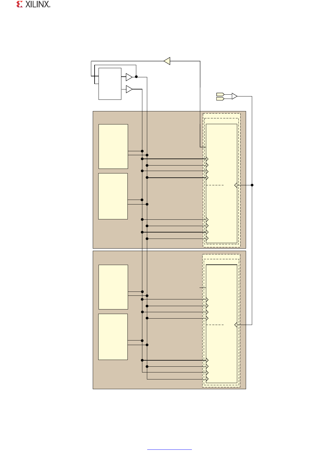
1000BASE-X PCS/PMA or SGMII v11.4 www.xilinx.com 153
PG047 October 16, 2012
Chapter 5: 1000BASE-X with Transceivers
X-Ref Target - Figure 5-12
Figure 5-12: Clock Management - Multiple Core Instances, Virtex-5 FPGA RocketIO GTX
Transceivers for 1000BASE-X
(WKHUQHW%$6(;
3&630$RU
6*0,,FRUH
XVHUFON
XVHUFON
6IRTEX
'48
2OCKET)/
#,+).
URFNHWLRBZUDSSHUBJW[BWLOH
6IRTEX
'48
2OCKET)/
(WKHUQHW%$6(;
3&630$RU
6*0,,FRUH
XVHUFON
XVHUFON
48532#,+
48532#,+
28532#,+
28532#,+
48532#,+
48532#,+
28532#,+
28532#,+
CLKIN
-(Z
2%&#,+/54
COMPONENT?NAME?BLOCK
"LOCK,EVEL
(WKHUQHW%$6(;
3&630$RU
6*0,,FRUH
XVHUFON
XVHUFON
6IRTEX
'48
2OCKET)/
6IRTEX
'48
2OCKET)/
(WKHUQHW%$6(;
3&630$RU
6*0,,FRUH
XVHUFON
XVHUFON
48532#,+
48532#,+
28532#,+
28532#,+
48532#,+
48532#,+
28532#,+
28532#,+
2%&#,+/54
COMPONENT?NAME?BLOCK
"LOCK,EVEL
1&
,%8)*'6
,3$'
EUHIFONS
,3$'
EUHIFONQ
#,+).
URFNHWLRBZUDSSHUBJW[BWLOH
URFNHWLRBZUDSSHUBJW[
URFNHWLRBZUDSSHUBJW[
XVHUFON0+]
'&0
&/.,1 &/.
)%
%8)*
&/.'9
%8)*
XVHUFON0+]
%8)*
8

1000BASE-X PCS/PMA or SGMII v11.4 www.xilinx.com 154
PG047 October 16, 2012
Chapter 5: 1000BASE-X with Transceivers
Virtex-6 Devices
Figure 5-13 illustrates sharing clock resources across two instantiations of the core when
using Virtex-6 FPGA GTX transceivers. Additional cores can be added by continuing to
instantiate extra block level modules.
Share the mgtrefclk_p and mgtrefclk_n differential clock pair clock source across all of
the transceivers in use. To provide the 125 MHz clock for all core instances, select a
TXOUTCLK port from any GTX transceiver. This can be routed onto global clock routing
using a BUFG as illustrated and shared between all cores and GTX transceivers.
See the Virtex-6 GTX Transceiver User Guide for more information on GTX transceiver clock
resources.
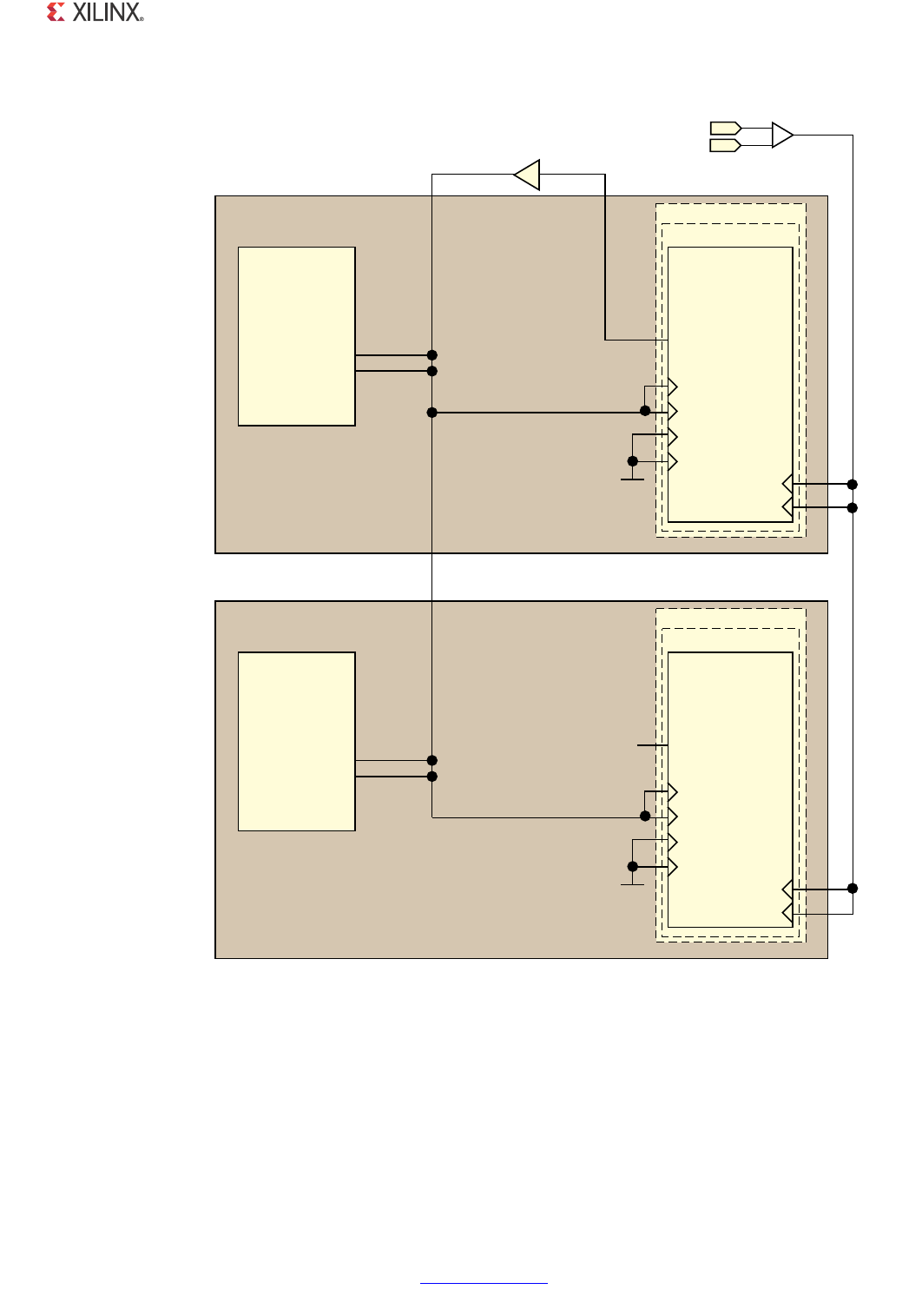
1000BASE-X PCS/PMA or SGMII v11.4 www.xilinx.com 155
PG047 October 16, 2012
Chapter 5: 1000BASE-X with Transceivers
X-Ref Target - Figure 5-13
Figure 5-13: Clock Management - Multiple Core Instances, Virtex-6 FPGA GTX Transceivers for
1000BASE-X
(WKHUQHW%$6(;
3&630$RU
6*0,,FRUH
XVHUFON
XVHUFON
6IRTEX
'48
4RANSCEIVER
JW[BZUDSSHUBJW[
XVHUFON
0+]
%8)*
48532#,+
28532#,+
48532#,+
28532#,+
MGTREFCLK
-(Z
COMPONENT?NAME?BLOCK
"LOCK,EVEL
,%8)'6B*7;(
,3$'
PJWUHIFONBS
,3$'
PJWUHIFONBQ
JW[BZUDSSHU
'.$
(WKHUQHW%$6(;
3&630$RU
6*0,,FRUH
XVHUFON
XVHUFON
6IRTEX
'48
4RANSCEIVER
JW[BZUDSSHUBJW[
XVHUFON
0+]
48532#,+
28532#,+
48532#,+
28532#,+
48/54#,+
COMPONENT?NAME?BLOCK
"LOCK,EVEL
JW[BZUDSSHU
'.$
48/54#,+
.#
-'42%&#,+48;=
-'42%&#,+28;=
-'42%&#,+48;=
-'42%&#,+28;=
8

1000BASE-X PCS/PMA or SGMII v11.4 www.xilinx.com 156
PG047 October 16, 2012
Chapter 5: 1000BASE-X with Transceivers
Spartan-6 LXT Devices
Figure 5-13 illustrates sharing clock resources across multiple instantiations of the core
when using Spartan-6 FPGA GTP transceivers.
The example design can be generated to connect either a single instance of the core or
connect a pair of core instances to the transceiver pair present in a GTP transceiver tile.
Figure 5-13 illustrates two instantiations of the block level, and each block level contains a
pair of cores, consequently illustrating clock sharing between a total of four cores.
Additional cores can be added by continuing to instantiate extra block level modules. Share
the brefclk_p and brefclk_n differential clock pair. See the Spartan-6 FPGA GTP
Transceiver User Guide for more information.
To provide the 125 MHz clock for all core instances, select a GTPCLKOUT port from any GTP
transceiver. This can be routed onto global clock routing using a BUFIO2 and BUFG as
illustrated and shared between all cores and GTP transceivers.
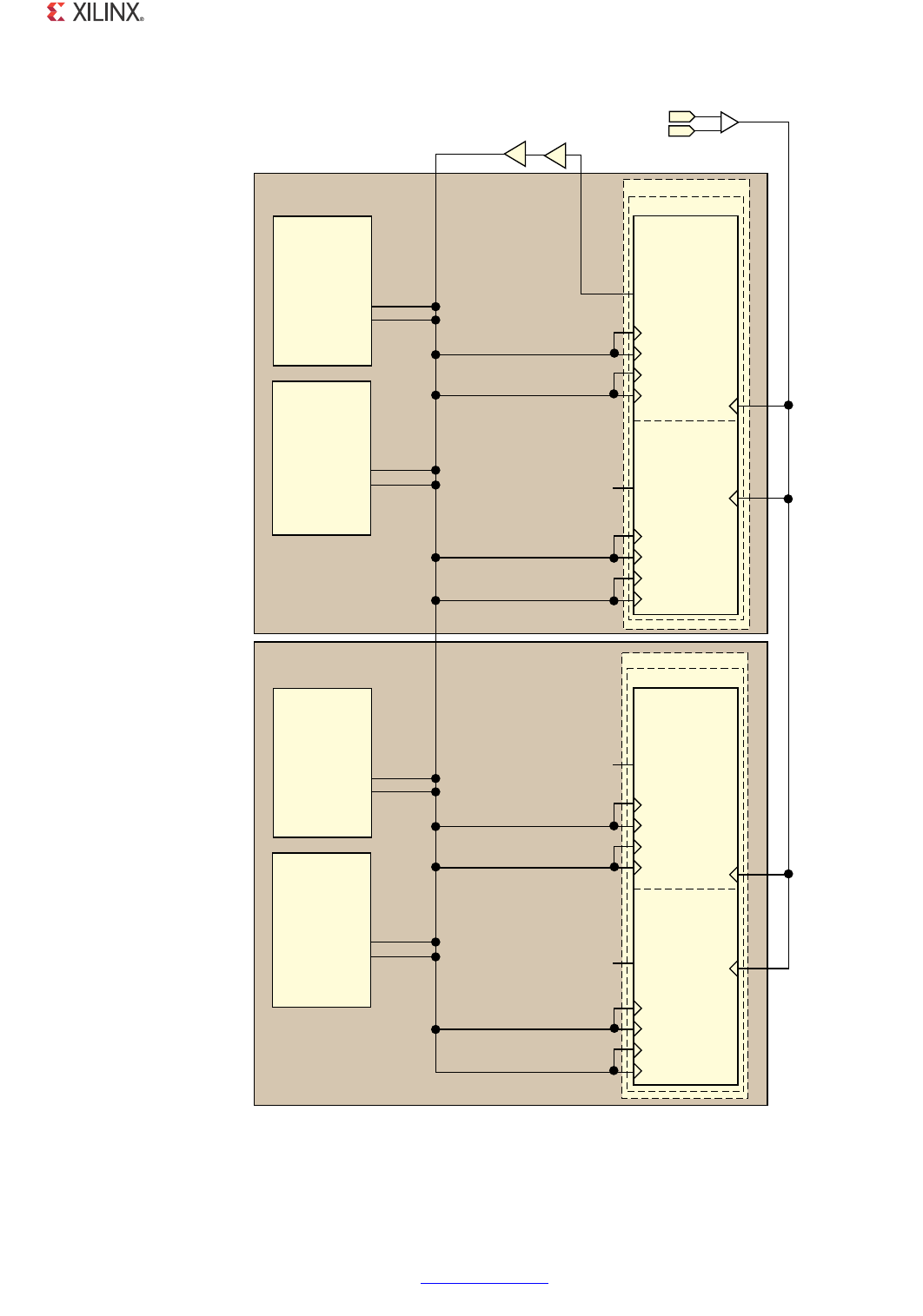
1000BASE-X PCS/PMA or SGMII v11.4 www.xilinx.com 157
PG047 October 16, 2012
Chapter 5: 1000BASE-X with Transceivers
X-Ref Target - Figure 5-14
Figure 5-14: Clock Management-Multiple Core Instances, Spartan-6 FPGA
GTP Transceivers for 1000BASE-X
(WKHUQHW%$6(;
3&630$RU
6*0,,FRUH
XVHUFON
XVHUFON
#,+).
JWSBZUDSSHUBWLOH
(WKHUQHW%$6(;
3&630$RU
6*0,,FRUH
XVHUFON
XVHUFON
XVHUFON
0+]
%8)*
48532#,+
48532#,+
28532#,+
28532#,+
48532#,+
48532#,+
28532#,+
28532#,+
CLKIN
-(Z
'40#,+/54
COMPONENT?NAME?BLOCK
"LOCK,EVEL
(WKHUQHW%$6(;
3&630$RU
6*0,,FRUH
XVHUFON
XVHUFON
(WKHUQHW%$6(;
3&630$RU
6*0,,FRUH
XVHUFON
XVHUFON
48532#,+
48532#,+
28532#,+
28532#,+
48532#,+
48532#,+
28532#,+
28532#,+
COMPONENT?NAME?BLOCK
"LOCK,EVEL
1&
,%8)'6
,3$'
EUHIFONS
,3$'
EUHIFONQ
JWSBZUDSSHUBWLOH
JWSBZUDSSHU
JWSBZUDSSHU
#,+).
3PARTAN
4RANSCEIVER
'40
3PARTAN
4RANSCEIVER
'40
3PARTAN
4RANSCEIVER
'40
3PARTAN
4RANSCEIVER
'40
#,+).
#,+).
'40#,+/54
'40#,+/54
1&
'40#,+/54
1&
%8),2
8

1000BASE-X PCS/PMA or SGMII v11.4 www.xilinx.com 158
PG047 October 16, 2012
Chapter 5: 1000BASE-X with Transceivers
Virtex-7 Devices
Figure 5-15 illustrates sharing clock resources across two instantiations of the core when
using 7 series FPGAs Transceivers. Additional cores can be added by continuing to
instantiate extra block level modules.
To provide the FPGA logic clocks for all core instances, select a TXOUTCLK port from any
transceiver and route this to a single MMCM. The CLKOUT0 (125 MHz) and CLKOUT1 (62.5
MHz) outputs from this MMCM, placed onto global clock routing using BUFGs, can be
shared across all core instances and transceivers as illustrated.
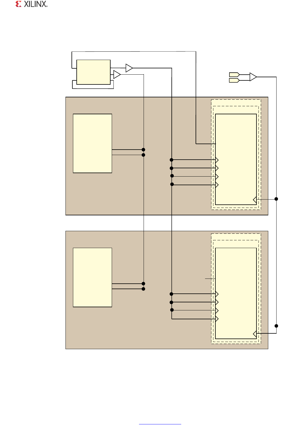
1000BASE-X PCS/PMA or SGMII v11.4 www.xilinx.com 159
PG047 October 16, 2012
Chapter 5: 1000BASE-X with Transceivers
X-Ref Target - Figure 5-15
Figure 5-15: Clock Management-Multiple Core Instances, Virtex-7 FPGA Transceivers for 1000BASE-X
(WKHUQHW%$6(;
3&630$RU
6*0,,FRUH
XVHUFON
XVHUFON
6IRTEX
'48'4(
4RANSCEIVER
JWZL]DUGBJW
48532#,+
28532#,+
48532#,+
28532#,+
GTREFCLK
-(Z
COMPONENT?NAME?BLOCK
"LOCK,EVEL
,3$'
,3$'
JWZL]DUG
(WKHUQHW%$6(;
3&630$RU
6*0,,FRUH
XVHUFON
XVHUFON
6IRTEX
'48'4(
4RANSCEIVER
JWZL]DUGBJW
XVHUFON
0+]
48532#,+
28532#,+
48532#,+
28532#,+
48/54#,+
COMPONENT?NAME?BLOCK
"LOCK,EVEL
JWZL]DUG
48/54#,+
.#
'42%&#,+
,%8)'6B*7(
JWUHIFONBS
JWUHIFONBQ
'42%&#,+
%8)*
--#-%?!$6
#,+/54
#,+/54
#,+).
#,+&"/54#,+&").
%8)*
-(Z
-(Z
8

1000BASE-X PCS/PMA or SGMII v11.4 www.xilinx.com 160
PG047 October 16, 2012
Chapter 5: 1000BASE-X with Transceivers
Kintex-7 and Zynq-7000 Devices
Figure 5-16 illustrates sharing clock resources across two instantiations of the core when
using 7 series FPGAs transceivers. Additional cores can be added by continuing to
instantiate extra block level modules.
To provide the FPGA logic clocks for all core instances, select a TXOUTCLK port from any
transceiver and route this to a single MMCM through a BUFG (global clock routing). The
CLKOUT0 (125 MHz) and CLKOUT1 (62.5 MHz) outputs from this MMCM, placed onto
global clock routing using BUFGs, can be shared across all core instances and transceivers as
illustrated.
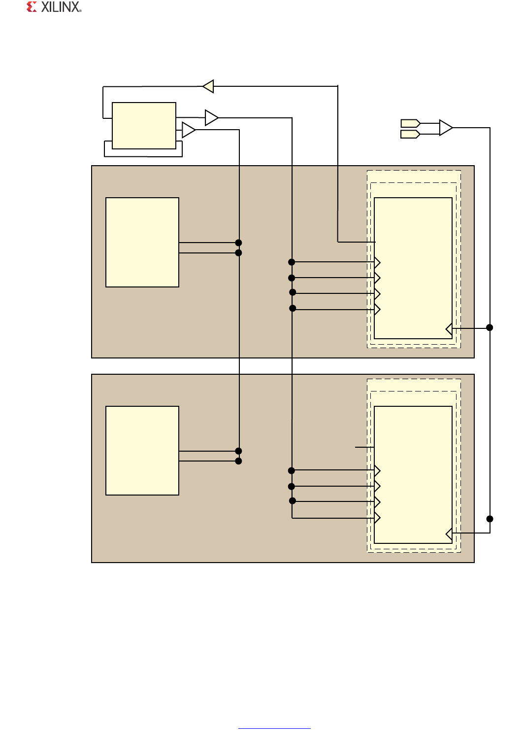
1000BASE-X PCS/PMA or SGMII v11.4 www.xilinx.com 161
PG047 October 16, 2012
Chapter 5: 1000BASE-X with Transceivers
X-Ref Target - Figure 5-16
Figure 5-16: Clock Management-Multiple Core Instances, Kintex-7/Zynq-7000 Device Transceivers for
1000BASE-X
(WKHUQHW%$6(;
3&630$RU
6*0,,FRUH
XVHUFON
XVHUFON
+INTEX:YNQ
'48
4RANSCEIVER
JWZL]DUGBJW
48532#,+
28532#,+
48532#,+
28532#,+
GTREFCLK
-(Z
COMPONENT?NAME?BLOCK
"LOCK,EVEL
,3$'
,3$'
JWZL]DUG
(WKHUQHW%$6(;
3&630$RU
6*0,,FRUH
XVHUFON
XVHUFON
JWZL]DUGBJW
XVHUFON
0+]
48532#,+
28532#,+
48532#,+
28532#,+
48/54#,+
COMPONENT?NAME?BLOCK
"LOCK,EVEL
JWZL]DUG
48/54#,+
.#
'42%&#,+
,%8)'6B*7(
JWUHIFONBS
JWUHIFONBQ
'42%&#,+
%8)*
--#-%?!$6
#,+/54
#,+/54
#,+).
#,+&"/54#,+&").
%8)*
%8)*
-(Z
-(Z
8
+INTEX:YNQ
'48
4RANSCEIVER

1000BASE-X PCS/PMA or SGMII v11.4 www.xilinx.com 162
PG047 October 16, 2012
Chapter 5: 1000BASE-X with Transceivers
Artix-7 Devices
Figure 5-17 illustrates sharing clock resources across two instantiations of the core when
using 7 series FPGAs Transceivers. Additional cores can be added by continuing to
instantiate extra block level modules.
To provide the FPGA logic clocks for all core instances, select a TXOUTCLK port from any
transceiver and route this to a single MMCM. The CLKOUT0 (125 MHz) and CLKOUT1 (62.5
MHz) outputs from this MMCM, placed onto global clock routing using BUFGs, can be
shared across all core instances and transceivers as illustrated.
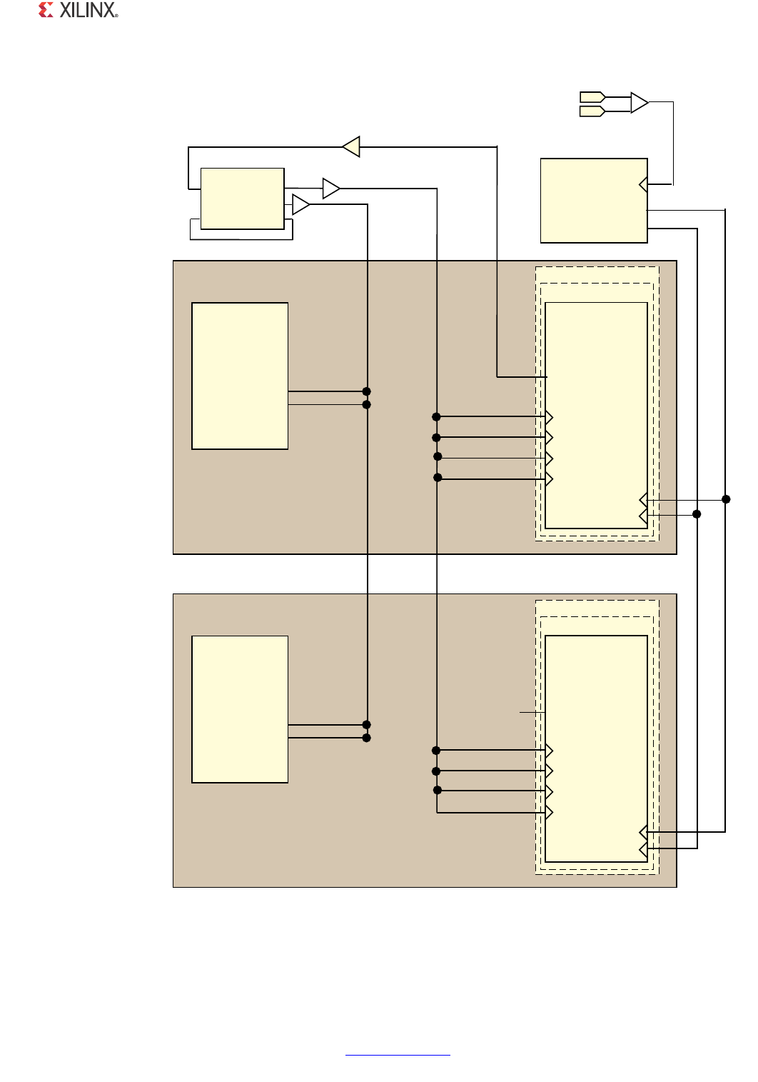
1000BASE-X PCS/PMA or SGMII v11.4 www.xilinx.com 163
PG047 October 16, 2012
Chapter 5: 1000BASE-X with Transceivers
X-Ref Target - Figure 5-17
Figure 5-17: Clock Management-Multiple Core Instances, Artix-7 FPGA Transceivers for
1000BASE-X
(WKHUQHW%$6(;
3&630$RU
6*0,,FRUH
XVHUFON
XVHUFON
!RTIX
'40%?#(!..%,
JWZL]DUGBJW
48532#,+
28532#,+
48532#,+
28532#,+
GTREFCLK
-(Z
COMPONENT?NAME?BLOCK
"LOCK,EVEL
,3$'
,3$'
JWZL]DUG
(WKHUQHW%$6(;
3&630$RU
6*0,,FRUH
XVHUFON
XVHUFON
!RTIX
'40%?#(!..%,
JWZL]DUGBJW
XVHUFON
0+]
48532#,+
28532#,+
48532#,+
28532#,+
48/54#,+
COMPONENT?NAME?BLOCK
"LOCK,EVEL
JWZL]DUG
48/54#,+
.#
0,,#,+?).
,%8)'6B*7(
JWUHIFONBS
JWUHIFONBQ
0,,#,+?).
%8)*
--#-%?!$6
#,+/54
#,+/54
#,+).
#,+&"/54#,+&").
%8)*
-(Z
-(Z
0,,2%&#,+?).
0,,2%&#,+?).
0,,2%&#,+?).
'40%?#/--/.
0,,/54#,+
0,,/542%&#,+
'42%&#,+
%8)*
8

1000BASE-X PCS/PMA or SGMII v11.4 www.xilinx.com 164
PG047 October 16, 2012
Chapter 5: 1000BASE-X with Transceivers
Example Design for 1000BASE-X with
Transceivers
Chapter 20, Detailed Example Design contains a full list and description of the directory and
file structure that is provided with the core, including the location of the HDL example
design.
Figure 5-18 illustrates the complete example design for the Ethernet 1000BASE-X PCS/PMA
using the transceiver specific to the target device (Virtex-4, Virtex-5, Virtex-6, Virtex-7,
Kintex-7, Artix-7, Zynq-7000 or Spartan-6). Virtex-7, Kintex-7, and Artix-7 devices support
Vivado tools. Other families support only ISE tool.
As illustrated, the example is split between two hierarchical layers. The block level is
designed so that it can be instantiated directly into your design and performs the following
functions:
•Instantiates the core from HDL
• Connects the physical-side interface of the core to a device-specific transceiver
The top level of the example design creates a specific example that can be simulated,
synthesized, implemented, and if required, placed on a suitable board and demonstrated in
hardware. The top level of the example design performs the following functions:
X-Ref Target - Figure 5-18
Figure 5-18: Example Design HDL for the Ethernet 1000BASE-X PCS/PMA
Using a Device-Specific Transceiver
(WKHUQHW
%$6(;
3&630$
&RUH
1HWOLVW
*0,,
,2%V
,Q
,2%V
2XW
&RQQHFWWR
&OLHQW0$
30$
&RQQHFWWR
2SWLFDO
7UDQVFHLYHU
COMPONENT?NAME?BLOCK
COMPONENT?NAME?EXAMPLE?DESIGN
7[
(ODVWLF
%XIIHU
4RANSCEIVER
#LOCK
-ANAGEMENT
,OGIC
$EVICE
3PECIFIC
4RANSCEIVER
8

1000BASE-X PCS/PMA or SGMII v11.4 www.xilinx.com 165
PG047 October 16, 2012
Chapter 5: 1000BASE-X with Transceivers
• Instantiates the block level from HDL
• Derives the clock management logic for a device-specific transceiver and the core
• Implements an external GMII
The next few pages in this section describe each of the example design blocks (and
associated HDL files) in detail, and conclude with an overview of the demonstration test
bench provided for the design.
Top-Level Example Design HDL
The following files describe the top-level example design for the Ethernet 1000BASE-X
PCS/PMA core using a transceiver specific to the desired device.
VHDL
ISE Design Suite:
<project_dir>/<component_name>/example_design/<component_name>_example_design.vhd
Vivado Design Suite:
<project_dir>/<project_name>/<project_name>.srcs/sources1/ip/<component_name>/
<component_name>/example_design/<component_name>_example_design.vhd
Verilog
ISE Design Suite:
<project_dir>/<component_name>/example_design/<component_name>_example_design.v
Vivado Design Suite:
<project_dir>/<project_name>/<project_name>.srcs/sources1/ip/<component_name>/
<component_name>/example_design/<component_name>_example_design.v
The example design HDL top level contains the following:
• An instance of the Ethernet 1000BASE-X PCS/PMA block level
• Clock management logic for the core and the device-specific transceiver, including
DCM (if required) and Global Clock Buffer instances
• A transmitter elastic buffer
• GMII interface logic, including IOB instances
The example design HDL top-level connects the GMII of the block level to external IOBs.
This configuration allows the functionality of the core to be demonstrated using a
simulation package as discussed in this guide. The example design can also be synthesized
and, if required, placed on a suitable board and demonstrated in hardware.

1000BASE-X PCS/PMA or SGMII v11.4 www.xilinx.com 166
PG047 October 16, 2012
Chapter 5: 1000BASE-X with Transceivers
Note: In the Virtex-4, Virtex-5 and Spartan-6 architectures, transceivers are provided in pairs. When
generated with the appropriate options, the example design is capable of connecting two instances
of the core to the transceiver pair.
Block Level HDL
The following files describe the block-level design for the Ethernet 1000BASE-X PCS/PMA
core using a device-specific transceiver specific to the target device.
VHDL
ISE Design Suite:
<project_dir>/<component_name>/example_design/<component_name>_block.vhd
Vivado Design Suite:
<project_dir>/<project_name>/<project_name>.srcs/sources1/ip/<component_name>/
<component_name>/example_design/<component_name>_block.vhd
Verilog
ISE Design Suite:
<project_dir>/<component_name>/example_design/<component_name>_block.v
Vivado Design Suite:
<project_dir>/<project_name>/<project_name>.srcs/sources1/ip/<component_name>/
<component_name>/example_design/<component_name>_block.v
The block-level HDL contains the following:
• An instance(s) of the Ethernet 1000BASE-X PCS/PMA core
• An instance(s) of a transceiver specific to a Virtex-4, Virtex-5, Virtex-6, Virtex-7,
Kintex-7, Artix-7, Zynq-7000 or Spartan-6 device
The block-level HDL connects the PHY side interface of the core to a device-specific
transceiver, as illustrated in Figure 5-18. This is the most useful part of the example design
and should be instantiated in all customer designs that use the core.
Note: In the Virtex-4, Virtex-5 and Spartan-6 architectures, transceivers are provided in pairs. When
generated with the appropriate options, the block level is capable of connecting two instances of the
core to the transceiver.

1000BASE-X PCS/PMA or SGMII v11.4 www.xilinx.com 167
PG047 October 16, 2012
Chapter 5: 1000BASE-X with Transceivers
Transceiver Files for Zynq-7000, Virtex-7, Kintex-7, Artix-7 and
Devices
Transceiver Wrapper
This device-specific transceiver wrapper is instantiated from the block-level HDL file of the
example design and is described in the following files:
VHDL
ISE Design Suite:
<project_dir>/<component_name>/example_design/transceiver/
<component_name>_transceiver.vhd
Vivado Design Suite:
<project_dir>/<project_name>/<project_name>.srcs/sources1/ip/<component_name>/
<component_name>/example_design/transceiver/<component_name>_transceiver.vhd
Verilog
ISE Design Suite:
<project_dir>/<component_name>/example_design/transceiver/
<component_name>_gtwizard_init.vhd
<project_dir>/<component_name>/example_design/transceiver/
<component_name>_tx_startup_fsm.vhd
<project_dir>/<component_name>/example_design/transceiver/
<component_name>_rx_startup_fsm.vhd
<project_dir>/<component_name>/example_design/transceiver/
<component_name>_transceiver.v
Vivado Design Suite:
<project_dir>/<project_name>/<project_name>.srcs/sources1/ip/<component_name>/
<component_name>/example_design/transceiver/<component_name>_transceiver.v
This file instances output source files from the transceiver wizard (used with Gigabit
Ethernet 1000BASE-X attributes).
Zynq-7000, Virtex-7, Kintex-7, and Artix-7 Device Transceiver Wizard Files
For Zynq-7000, Virtex-7, Kintex-7, and Artix-7 devices, the transceiver wrapper file directly
instantiates device-specific transceiver wrapper files created from the serial transceiver
Wizard. These files tie off (or leave unconnected) unused I/O for the transceiver and apply
the 1000BASE-X attributes. The files can be edited/tailored by re-running the wizard and
swapping these files. The files include the following:

1000BASE-X PCS/PMA or SGMII v11.4 www.xilinx.com 168
PG047 October 16, 2012
Chapter 5: 1000BASE-X with Transceivers
VHDL
ISE Design Suite:
<project_dir>/<component_name>/example_design/transceiver/
<component_name>_gtwizard_init.vhd
<project_dir>/<component_name>/example_design/transceiver/
<component_name>_tx_startup_fsm.vhd
<project_dir>/<component_name>/example_design/transceiver/
<component_name>_rx_startup_fsm.vhd
<project_dir>/<component_name>/example_design/transceiver/
<component_name>_gtwizard.vhd
<project_dir>/<component_name>/example_design/transceiver/
<component_name>_gtwizard_gt.vhd
Vivado Design Suite:
<project_dir>/<project_name>/<project_name>.srcs/sources1/ip/<component_name>/
<component_name>/example_design/transceiver/<component_name>_gtwizard_init.vhd
<project_dir>/<project_name>/<project_name>.srcs/sources1/ip/<component_name>/
<component_name>/example_design/transceiver/<component_name>_tx_startup_fsm.vhd
<project_dir>/<project_name>/<project_name>.srcs/sources1/ip/<component_name>/
<component_name>/example_design/transceiver/<component_name>_rx_startup_fsm.vhd
<project_dir>/<project_name>/<project_name>.srcs/sources1/ip/<component_name>/
<component_name>/example_design/transceiver/<component_name>_gtwizard.vhd
<project_dir>/<project_name>/<project_name>.srcs/sources1/ip/<component_name>/
<component_name>/example_design/transceiver/<component_name>_gtwizard_gt.vhd
Verilog
ISE Design Suite:
<project_dir>/<component_name>/example_design/transceiver/
<component_name>_gtwizard_init.v
<project_dir>/<component_name>/example_design/transceiver/
<component_name>_tx_startup_fsm.v
<project_dir>/<component_name>/example_design/transceiver/
<component_name>_rx_startup_fsm.v
<project_dir>/<component_name>/example_design/transceiver/
<component_name>_gtwizard.v
<project_dir>/<component_name>/example_design/transceiver/
<component_name>_gtwizard_gt.v
Vivado Design Suite:
<project_dir>/<project_name>/<project_name>.srcs/sources1/ip/<component_name>/
<component_name>/example_design/transceiver/<component_name>_gtwizard_init.v
<project_dir>/<project_name>/<project_name>.srcs/sources1/ip/<component_name>/
<component_name>/example_design/transceiver/<component_name>_tx_startup_fsm.v
<project_dir>/<project_name>/<project_name>.srcs/sources1/ip/<component_name>/
<component_name>/example_design/transceiver/<component_name>_rx_startup_fsm.v

1000BASE-X PCS/PMA or SGMII v11.4 www.xilinx.com 169
PG047 October 16, 2012
Chapter 5: 1000BASE-X with Transceivers
<project_dir>/<project_name>/<project_name>.srcs/sources1/ip/<component_name>/<comp
onent_name>/example_design/transceiver/<component_name>_gtwizard.v
<project_dir>/<project_name>/<project_name>.srcs/sources1/ip/<component_name>/
<component_name>/example_design/transceiver/<component_name>_gtwizard_gt.v
To re-run the transceiver wizard, a CORE Generator tool XCO file for the wizard is included.
This file defines all the required wizard attributes used to generate the preceding files. See
the CORE Generator tool documentation for further information about XCO files. The XCO
file is in the following location:
ISE Design Suite:
<project_dir>/<component_name>/example_design/transceiver/
<component_name>_gtwizard.xco
Vivado Design Suite:
<project_dir>/<project_name>/<project_name>.srcs/sources1/ip/<component_name>/
<component_name>/example_design/transceiver/<component_name>_gtwizard.xco
This file can be used as an input to Vivado project by clicking on <Add Sources> in the Flow
Navigator task bar and selecting the XCO file.
Transceiver Files for Spartan-6 Devices
Transceiver Wrapper
This device-specific transceiver wrapper is instantiated from the block-level HDL file of the
example design and is described in the following files:
VHDL
<project_dir>/<component_name>/example_design/transceiver/transceiver.vhd
Verilog
<project_dir>/<component_name>/example_design/transceiver/transceiver.v
This file instances output source files from the transceiver wizard (used with Gigabit
Ethernet 1000BASE-X attributes).
Spartan-6 FPGA GTP Transceiver Wizard Files
For Spartan-6 devices, the transceiver wrapper file directly instantiates device-specific
transceiver wrapper files created from the Spartan-6 FPGA GTP Transceiver Wizard. These
files tie off (or leave unconnected) unused I/O for the GTP, and apply the 1000BASE-X
attributes. The files can be edited/tailored by rerunning the wizard and swapping these
files. The files include the following:

1000BASE-X PCS/PMA or SGMII v11.4 www.xilinx.com 170
PG047 October 16, 2012
Chapter 5: 1000BASE-X with Transceivers
VHDL
<project_dir>/<component_name>/example_design/transceiver/s6_gtpwizard.vhd
<project_dir>/<component_name>/example_design/transceiver/s6_gtpwizard_tile.vhd
Verilog
<project_dir>/<component_name>/example_design/transceiver/s6_gtpwizard.v
<project_dir>/<component_name>/example_design/transceiver/s6_gtpwizard_tile.v
To re-run the Spartan-6 FPGA GTX Transceiver Wizard, a CORE Generator tool XCO file for
the wizard is included. This file defines all the required Wizard attributes used to generate
the preceding files. See the CORE Generator tool documentation for further information
about XCO files. The XCO file is in the following location:
<project_dir>/<component_name>/example_design/transceiver/s6_gtpwizard.xco
Transceiver Files for Virtex-6 Devices
Transceiver Wrapper
This device-specific transceiver wrapper is instantiated from the block-level HDL file of the
example design and is described in the following files:
VHDL
<project_dir>/<component_name>/example_design/transceiver/v6_gtxwizard_top.vhd
Verilog
<project_dir>/<component_name>/example_design/transceiver/v6_gtxwizard_top.v
This file instances output source files from the transceiver wizard (used with Gigabit
Ethernet 1000BASE-X attributes).
Virtex-6 FPGA GTX Transceiver Wizard Files
For Virtex-6 devices, the transceiver wrapper file directly instantiates device-specific
transceiver wrapper files created from the Virtex-6 FPGA GTX Transceiver Wizard. These
files tie off (or leave unconnected) unused I/O for the GTX transceiver, and apply the
1000BASE-X attributes. The files can be edited/tailored by rerunning the wizard and
swapping these files. The files include the following:
VHDL
<project_dir>/<component_name>/example_design/transceiver/v6_gtxwizard.vhd
<project_dir>/<component_name>/example_design/transceiver/v6_gtxwizard_gtx.vhd

1000BASE-X PCS/PMA or SGMII v11.4 www.xilinx.com 171
PG047 October 16, 2012
Chapter 5: 1000BASE-X with Transceivers
Verilog
<project_dir>/<component_name>/example_design/transceiver/v6_gtxwizard.v
<project_dir>/<component_name>/example_design/transceiver/v6_gtxwizard_gtx.v
To re-run the Virtex-6 FPGA GTX Transceiver Wizard, a CORE Generator tool XCO file for the
wizard is included. This file defines all the required wizard attributes used to generate the
preceding files. See the CORE Generator tool documentation for further information about
XCO files. The XCO file is in the following location:
<project_dir>/<component_name>/example_design/transceiver/v6_gtxwizard.xco
RocketIO Transceiver Files for Virtex-5 Devices
Transceiver Wrapper
This device-specific RocketIO™ transceiver wrapper is instantiated from the block-level HDL
file of the example design and is described in the following files:
VHDL
<project_dir>/<component_name>/example_design/transceiver/transceiver.vhd
Verilog
<project_dir>/<component_name>/example_design/transceiver/transceiver.v
This file instances output source files from the device-specific RocketIO Transceiver Wizard
(used with Gigabit Ethernet 1000BASE-X attributes).
In the Virtex-5 families, RocketIO transceivers are provided in pairs. When generated with
the appropriate options, the block level is capable of connecting two instances of the core
to the device-specific RocketIO transceiver pair. When only a single instance of the core is
requested, the unused device-specific RocketIO transceiver from the pair is still instantiated
from within this transceiver wrapper but left unconnected.
Virtex-5 FPGA RocketIO GTP Transceiver Specific Files
For Virtex-5 LXT and SXT devices, the transceiver wrapper file directly instantiates
device-specific RocketIO GTP transceiver wrapper files created from the Virtex-5 FPGA
RocketIO GTP Transceiver Wizard. These files tie off (or leave unconnected) unused I/O for
the GTP transceiver pair, and apply the 1000BASE-X attributes. The files can be
edited/tailored by rerunning the device-specific RocketIO GTP Transceiver Wizard and
swapping these files. The files include the following:
VHDL
<project_dir>/<component_name>/example_design/transceiver/v5_gtpwizard.vhd
<project_dir>/<component_name>/example_design/transceiver/v5_gtpwizard_tile.vhd

1000BASE-X PCS/PMA or SGMII v11.4 www.xilinx.com 172
PG047 October 16, 2012
Chapter 5: 1000BASE-X with Transceivers
Verilog
<project_dir>/<component_name>/example_design/transceiver/v5_gtpwizard.v
<project_dir>/<component_name>/example_design/transceiver/v5_gtpwizard_tile.v
To re-run the device-specific RocketIO GTP Transceiver Wizard, a CORE Generator tool XCO
file for the RocketIO GTP Transceiver Wizard is included. This file defines all the
device-specific RocketIO GTP Transceiver Wizard attributes used to generate the preceding
files. See the CORE Generator tool documentation for further information about XCO files.
The XCO file is in the following location:
<project_dir>/<component_name>/example_design/transceiver/v5_gtpwizard.xco
Virtex-5 FPGA RocketIO GTX Transceiver Specific Files
For Virtex-5 FXT and TXT devices, the transceiver wrapper file directly instantiates RocketIO
GTX transceiver wrapper files created from the Virtex-5 FPGA RocketIO GTX Transceiver
Wizard. These files tie off (or leave unconnected) unused I/O for the GTX transceiver pair,
and apply the 1000BASE-X attributes. The files can be edited/tailored by rerunning the
device-specific RocketIO GTX Transceiver Wizard and swapping these files, which include
the following:
VHDL
<project_dir>/<component_name>/example_design/transceiver/v5_gtxwizard.vhd
<project_dir>/<component_name>/example_design/transceiver/v5_gtxwizard_tile.vhd
Verilog
<project_dir>/<component_name>/example_design/transceiver/v5_gtxwizard.v
<project_dir>/<component_name>/example_design/transceiver/v5_gtxwizard_tile.v
To re-run the device-specific RocketIO GTX Transceiver Wizard, a CORE Generator tool XCO
file for the RocketIO GTX Transceiver Wizard has also been included. This file defines all the
device-specific RocketIO GTX Transceiver Wizard attributes used to generate the preceding
files. See the CORE Generator tool documentation for more information about XCO files.
The XCO file is in the following location:
<project_dir>/<component_name>/example_design/transceiver/v5_gtxwizard.xco
RocketIO Transceiver Files for Virtex-4 FX Devices
Transceiver Wrapper
This device-specific RocketIO transceiver wrapper is instantiated from the block-level HDL
file of the example design and is described in the following files:

1000BASE-X PCS/PMA or SGMII v11.4 www.xilinx.com 173
PG047 October 16, 2012
Chapter 5: 1000BASE-X with Transceivers
VHDL
<project_dir>/<component_name>/example_design/transceiver/transceiver.vhd
Verilog
<project_dir>/<component_name>/example_design/transceiver/transceiver.v
This file instances the device-specific RocketIO transceiver with Gigabit Ethernet
1000BASE-X attributes applied.
In the Virtex-4 FX devices, RocketIO transceivers are provided in pairs. When generated
with the appropriate options, the block level is capable of connecting two instances of the
core to the device-specific RocketIO transceiver pair. When only a single instance of the
core is requested, the unused device-specific RocketIO transceiver from the pair is still
instantiated from within this transceiver wrapper but left unconnected.
Calibration Blocks
For Virtex-4 FX devices only, calibration blocks are required. A calibration block is
connected to both GT11 A and B within the RocketIO transceiver tile. This occurs in the
transceiver wrapper file. See Answer Record 22477 for information about downloading the
Calibration Block User Guide. The calibration block is described in the following files:
VHDL
<project_dir>/<component_name>/example_design/transceiver/cal_block_v1_4_1.vhd
Verilog
<project_dir>/<component_name>/example_design/transceiver/cal_block_v1_4_1.v
GT11 Reset/Initialization Circuitry
Precise reset/initialization circuitry is required for the GT11 device-specific RocketIO
transceivers.
The reset circuitry for the device-specific RocketIO receiver is illustrated in Figure 2-18 of
the Virtex-4 FPGA RocketIO Multi-Gigabit Transceiver User Guide (UG076) and implemented
in the following files:
VHDL
<project_dir>/<component_name>/example_design/transceiver/gt11_init_rx.vhd
Verilog
<project_dir>/<component_name>/example_design/transceiver/gt11_init_rx.v

1000BASE-X PCS/PMA or SGMII v11.4 www.xilinx.com 174
PG047 October 16, 2012
Chapter 5: 1000BASE-X with Transceivers
The reset circuitry for the device-specific RocketIO transmitter is illustrated in Figure 2-13
of the Virtex-4 RocketIO Multi-Gigabit Transceiver User Guide (UG076) and implemented in
the following files:
VHDL
<project_dir>/<component_name>/example_design/transceiver/gt11_init_tx.vhd
Verilog
<project_dir>/<component_name>/example_design/transceiver/gt11_init_tx.v
Both receiver and transmitter reset circuitry entities are instantiated from within the block
level of the example design.
Transmitter Elastic Buffer
The Transmitter Elastic Buffer is described in the following files:
VHDL
ISE Design Suite:
<project_dir>/<component_name>/example_design/<component_name>_tx_elastic_buffer.
vhd
Vivado Design Suite:
<project_dir>/<project_name>/<project_name>.srcs/sources1/ip/<component_name>/
<component_name>/example_design/<component_name>_tx_elastic_buffer.vhd
Verilog
ISE Design Suite:
<project_dir>/<component_name>/example_design/<component_name>_tx_elastic_buffer.v
Vivado Design Suite:
<project_dir>/<project_name>/<project_name>.srcs/sources1/ip/<component_name>/
<component_name>/example_design/<component_name>_tx_elastic_buffer.v
When the GMII is used externally (as in this example design), the GMII transmit signals
(inputs to the core from a remote MAC at the other end of the interface) are synchronous to
a clock that is likely to be derived from a different clock source to the core. For this reason,
GMII transmit signals must be transferred into the core main clock domain before they can
be used by the core and device-specific transceiver. This is achieved with the Transmitter
Elastic Buffer, an asynchronous FIFO implemented in distributed RAM. The operation of the
elastic buffer is to attempt to maintain a constant occupancy by inserting or removing any
idle sequences. This causes no corruption to the frames of data.
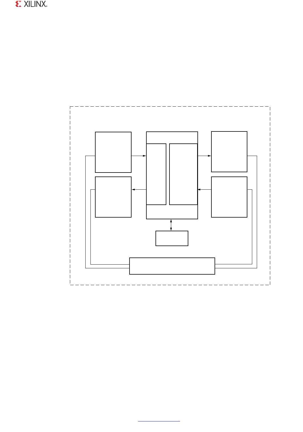
1000BASE-X PCS/PMA or SGMII v11.4 www.xilinx.com 175
PG047 October 16, 2012
Chapter 5: 1000BASE-X with Transceivers
When the GMII is used as an internal interface, it is expected that the entire interface will be
synchronous to a single clock domain, and the Transmitter Elastic Buffer should be
discarded.
Demonstration Test Bench
Figure 5-19 illustrates the demonstration test bench for the Ethernet 1000BASE-X PCS/PMA
using a device-specific transceiver. The demonstration test bench is a simple VHDL or
Verilog program to exercise the example design and the core.
The top-level test bench entity instantiates the example design for the core, which is the
Device Under Test (DUT). A stimulus block is also instantiated and clocks, resets, and test
bench semaphores are created. The following files describe the top level of the
demonstration test bench:
X-Ref Target - Figure 5-19
Figure 5-19: Demonstration Test Bench Using Device-Specific Transceiver
$EMONSTRATION4EST"ENCH
0-!
-ONITOR
3ERIALTO0ARALLEL
#ONVERSIONAND
""
$ECODING
0-!
3TIMULUS
""%NCODING
AND0ARALLELTO
3ERIAL
#ONVERSION
'-))
3TIMULUS
'-))
-ONITOR
'-))
$54
#ONTROLAND$ATA3TRUCTURES
#ONFIGURATION
3TIMULUS
$EVICE
3PECIFIC
4RANSCEIVER
8

1000BASE-X PCS/PMA or SGMII v11.4 www.xilinx.com 176
PG047 October 16, 2012
Chapter 5: 1000BASE-X with Transceivers
VHDL
ISE Design Suite:
<project_dir>/<component_name>/simulation/demo_tb.vhd
Vivado Design Suite:
<project_dir>/<project_name>/<project_name>.srcs/sources1/ip/<component_name>/
<component_name>/simulation/demo_tb.vhd
Verilog
ISE Design Suite:
<project_dir>/<component_name>/simulation/demo_tb.v
Vivado Design Suite:
<project_dir>/<project_name>/<project_name>.srcs/sources1/ip/<component_name>/
<component_name>/simulation/demo_tb.v
The stimulus block entity, instantiated from within the test bench top level, creates the
Ethernet stimulus in the form of four Ethernet frames, which are injected into the GMII and
PHY interfaces of the DUT. The output from the DUT is also monitored for errors. The
following files describe the stimulus block of the demonstration test bench.
VHDL
ISE Design Suite:
<project_dir>/<component_name>/simulation/stimulus_tb.vhd
Vivado Design Suite:
<project_dir>/<project_name>/<project_name>.srcs/sources1/ip/<component_name>/
<component_name>/simulation/stimulus_tb.vhd
Verilog
ISE Design Suite:
<project_dir>/<component_name>/simulation/stimulus_tb.v
Vivado Design Suite:
<project_dir>/<project_name>/<project_name>.srcs/sources1/ip/<component_name>/
<component_name>/simulation/stimulus_tb.v
Together, the top-level test bench file and the stimulus block combine to provide the full
test bench functionality, described in the sections that follow.

1000BASE-X PCS/PMA or SGMII v11.4 www.xilinx.com 177
PG047 October 16, 2012
Chapter 5: 1000BASE-X with Transceivers
Note: In the Virtex-4, Virtex-5 and Spartan-6 families, transceivers are provided in pairs. When
generated with the appropriate options, the example design is capable of connecting two instances
of the core to the transceiver pair. When this is the case, two stimulus blocks are instantiated from
the top-level test bench to independently exercise both cores.
Core with MDIO Interface
The demonstration test bench performs the following tasks:
• Input clock signals are generated.
• A reset is applied to the example design.
• The Ethernet 1000BASE-X PCS/PMA core is configured through the MDIO interface by
injecting an MDIO frame into the example design. This disables Auto-Negotiation (if
present) and takes the core out of the Isolate state.
• Four frames are injected into the GMII transmitter by the GMII stimulus block.
°the first frame is a minimum length frame
°the second frame is a type frame
°the third frame is an errored frame
°the fourth frame is a padded frame
• The serial data received at the device-specific transmitter interface is converted to
10-bit parallel data, then 8B/10B decoded. The resulting frames are checked by the
PMA Monitor against the stimulus frames injected into the GMII transmitter to ensure
data integrity.
• The same four frames are generated by the PMA Stimulus block. These are 8B/10B
encoded, converted to serial data, and injected into the device-specific transceiver
receiver interface.
• Data frames received at the GMII receiver are checked by the GMII Monitor against the
stimulus frames injected into the device-specific transceiver receiver to ensure data
integrity.
Core without MDIO Interface
The demonstration test bench performs the following tasks:
• Input clock signals are generated.
• A reset is applied to the example design.
• The Ethernet 1000BASE-X PCS/PMA core is configured using the Configuration Vector
to take the core out of the Isolate state.

1000BASE-X PCS/PMA or SGMII v11.4 www.xilinx.com 178
PG047 October 16, 2012
Chapter 5: 1000BASE-X with Transceivers
• Four frames are injected into the GMII transmitter by the GMII stimulus block.
°the first frame is a minimum length frame
°the second frame is a type frame
°the third frame is an errored frame
°the fourth frame is a padded frame
• The serial data received at the device-specific transmitter interface is converted to
10-bit parallel data, then 8B/10B decoded. The resultant frames are checked by the
PMA Monitor against the stimulus frames injected into the GMII transmitter to ensure
data integrity.
• The same four frames are generated by the PMA Stimulus block. These are 8B/10B
encoded, converted to serial data and injected into the device-specific receiver
interface.
• Data frames received at the GMII receiver are checked by the GMII Monitor against the
stimulus frames injected into the device-specific transceiver receiver to ensure data is
the same.
Customizing the Test Bench
Changing Frame Data
You can change the contents of the four frames used by the demonstration test bench by
changing the data and valid fields for each frame defined in the stimulus block. New frames
can be added by defining a new frame of data. Modified frames are automatically updated
in both stimulus and monitor functions.
Changing Frame Error Status
Errors can be inserted into any of the predefined frames in any position by setting the error
field to ‘1’ in any column of that frame. Injected errors are automatically updated in both
stimulus and monitor functions.
Changing the Core Configuration
The configuration of the Ethernet 1000BASE-X PCS/PMA core used in the demonstration
test bench can be altered.
CAUTION! Certain configurations of the core cause the test bench to fail or cause processes to run
indefinitely. For example, the demonstration test bench does not auto-negotiate with the example
design. Determine the configurations that can safely be used with the test bench.

1000BASE-X PCS/PMA or SGMII v11.4 www.xilinx.com 179
PG047 October 16, 2012
Chapter 5: 1000BASE-X with Transceivers
When the MDIO interface option is selected, the core can be reconfigured by editing the
injected MDIO frame in the demonstration test bench top level. Management Registers 0
and 4 can additionally be written through configuration_vector[4:0] and
an_adv_config_vector[15:0] interface signals respectively.
When the MDIO interface option is not selected, the core can be reconfigured by modifying
the configuration vector directly.

1000BASE-X PCS/PMA or SGMII v11.4 www.xilinx.com 180
PG047 October 16, 2012
Chapter 6
SGMII / Dynamic Standards Switching
with Transceivers
This chapter provides general guidelines for creating SGMII designs, and designs capable of
switching between 1000BASE-X and SGMII standards (Dynamic Standards Switching), using
a device-specific transceiver. Throughout this chapter, any reference to SGMII also applies
to the Dynamic Standards Switching implementation.
This chapter is organized into the following main sections:
•Receiver Elastic Buffer Implementations
The section provides an explanation of the two Receiver Elastic Buffer implementations;
one implementation uses the buffer present in the device-specific transceivers, and the
other uses a larger buffer, implemented in the FPGA logic.
•Transceiver Logic with the FPGA Logic Rx Elastic Buffer or Transceiver Logic with the
FPGA Logic Rx Elastic Buffer
After selecting the type of Receiver Elastic Buffer, see the relevant one of these two
sections to obtain an explanation of the device-specific transceiver and core logic in all
supported device families.
•Clock Sharing - Multiple Cores with Transceivers, FPGA Logic Elastic Buffer
The section provides guidance for using several cores and transceiver instantiations;
clock sharing should occur whenever possible to save device resources.
•SGMII Example Design / Dynamic Switching Example Design Using a Transceiver
This section introduces the CORE Generator™ tool example design deliverables.
This section also introduces the Vivado™ IP catalog tool example design deliverables.
This section also contains an overview of the demonstration test bench that is provided
with the example design. ISE Design Suite supports Virtex®-4, Virtex-5, Virtex-6,
Virtex-7, Kintex™-7, Artix™-7, Zynq™-7000, and Spartan®-6 devices. Vivado™ Design
Suite supports only Virtex-7, Kintex-7, and Artix-7 devices.

1000BASE-X PCS/PMA or SGMII v11.4 www.xilinx.com 181
PG047 October 16, 2012
Chapter 6: SGMII / Dynamic Standards Switching with Transceivers
Receiver Elastic Buffer Implementations
Selecting the Buffer Implementation from the GUI
The GUI provides two SGMII Capability options:
• 10/100/1000 Mb/s (clock tolerance compliant with Ethernet specification)
• 10/100/1000 Mb/s (restricted tolerance for clocks) OR 100/1000 Mb/s
The first option, 10/100/1000 Mb/s (clock tolerance compliant with Ethernet specification)
is the default and provides the implementation using the Receiver Elastic Buffer in FPGA
logic. This alternative Receiver Elastic Buffer uses a single block RAM to create a buffer twice
as large as the one present in the device-specific transceiver, for this reason consuming
extra logic resources. However, this default mode is reliable for all implementations using
standard Ethernet frame sizes. Further consideration must be made for jumbo frames.
The second option, 10/100/1000 Mb/s (restricted tolerance for clocks) or 100/1000 Mb/s,
uses the receiver elastic buffer present in the device-specific transceivers. This is half the
size and can potentially underflow or overflow during SGMII frame reception at 10 Mb/s
operation (see the next section). However, there are logical implementations where this can
be reliable and has the benefit of lower logic utilization.
The Requirement for the FPGA Logic Rx Elastic Buffer
Figure 6-1 illustrates a simplified diagram of a common situation where the core, in SGMII
mode, is interfaced to an external PHY device. Separate oscillator sources are used for the
FPGA and the external PHY. The Ethernet specification uses clock sources with a tolerance of
100 Parts Per Million (ppm). In Figure 6-1, the clock source for the PHY is slightly faster than
the clock source to the FPGA. For this reason, during frame reception, the receiver elastic
buffer (shown here as implemented in the device-specific transceiver) starts to fill.
Following frame reception, in the interframe gap period, idles are removed from the
received data stream to return the Rx Elastic Buffer to half-full occupancy. This is performed
by the clock correction circuitry (see the device-specific transceiver user guide for the
targeted device).
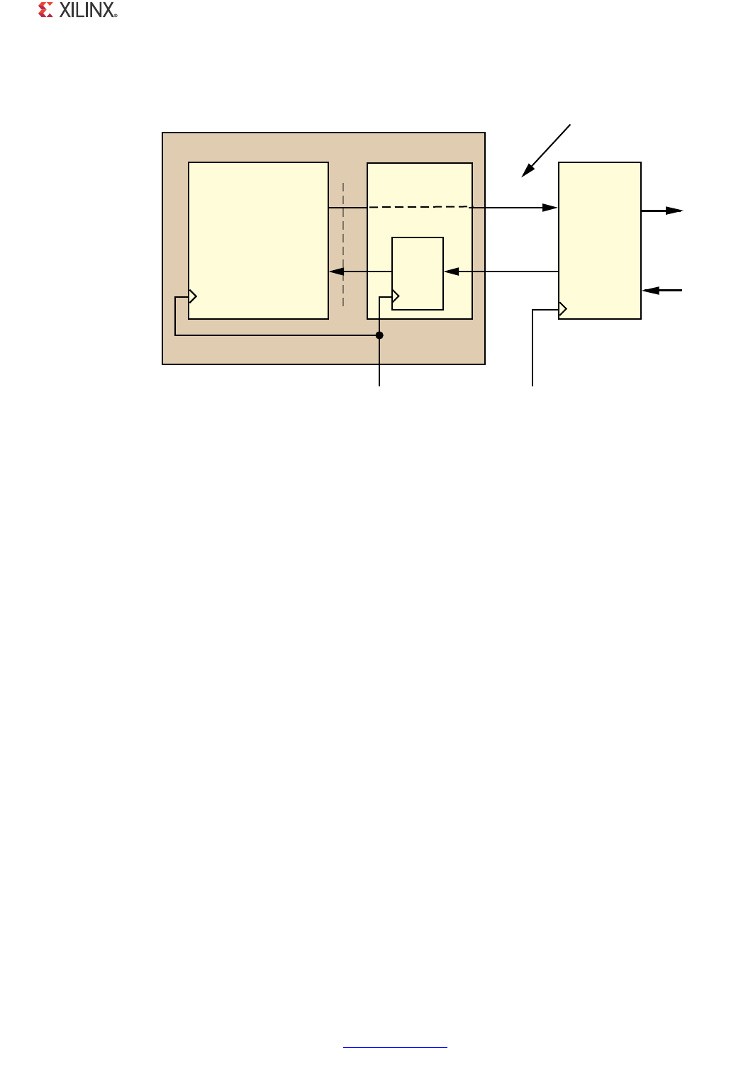
1000BASE-X PCS/PMA or SGMII v11.4 www.xilinx.com 182
PG047 October 16, 2012
Chapter 6: SGMII / Dynamic Standards Switching with Transceivers
Assuming separate clock sources, each of tolerance 100 ppm, the maximum frequency
difference between the two devices can be 200 ppm. It can be shown that this translates
into a full clock period difference every 5000 clock periods.
Relating this to an Ethernet frame, there is a single byte of difference for every 5000 bytes
of received frame data, which causes the Rx Elastic Buffer to either fill or empty by an
occupancy of one.
The maximum Ethernet frame size (non-jumbo) is 1522 bytes for a Virtual Local Area
Network (VLAN) frame.
• At 1 Gb/s operation, this translates into 1522 clock cycles.
• At 100 Mb/s operation, this translates into 15220 clock cycles (as each byte is repeated
10 times).
• At 10 Mb/s operation, this translates into 152200 clock cycles (as each byte is repeated
100 times).
Considering the 10 Mb/s case, you need 152200/5000 = 31 FIFO entries in the Elastic Buffer
above and below the half way point to guarantee that the buffer does not under or overflow
during frame reception. This assumes that frame reception begins when the buffer is exactly
half full.
The size of the Rx Elastic Buffer in the device-specific transceivers is 64 entries. However,
you cannot assume that the buffer is exactly half full at the start of frame reception.
Additionally, the underflow and overflow thresholds are not exact (see Appendix D, Rx
Elastic Buffer Specifications for more information).
X-Ref Target - Figure 6-1
Figure 6-1: SGMII Implementation using Separate Clock Sources
(WKHUQHW%$6(;
3&630$RU6*0,,
/RJL&25(
4RANSCEIVER
2X
%LASTIC
"UFFER
7;37;1
5;35;1
7ZLVWHG
&RSSHU
3DLU
3'-)),INK
%$6(7
%$6(7
%$6(7
3+<
&0'!
0+]SSP
-(ZPPM
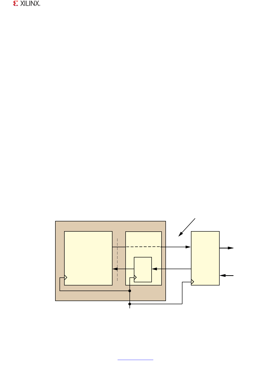
1000BASE-X PCS/PMA or SGMII v11.4 www.xilinx.com 183
PG047 October 16, 2012
Chapter 6: SGMII / Dynamic Standards Switching with Transceivers
To guarantee reliable SGMII operation at 10 Mb/s (non-jumbo frames), the device-specific
transceiver Elastic Buffer must be bypassed and a larger buffer implemented in the FPGA
logic. The FPGA logic buffer, provided by the example design, is twice the size of the
device-specific transceiver alternative. This has been proven to cope with standard (none
jumbo) Ethernet frames at all three SGMII speeds.
Appendix D, Rx Elastic Buffer Specifications provides further information about all Rx Elastic
Buffers used by the core. Information about the reception of jumbo frames is also provided.
The Transceiver Rx Elastic Buffer
The Elastic Buffer in the device-specific transceiver can be used reliably when the following
conditions are met:
• 10 Mb/s operation is not required. Both 1 Gb/s and 100 Mb/s operation can be
guaranteed.
• When the clocks are closely related (see the following section).
If there is any doubt, select the FPGA logic Rx Elastic Buffer Implementation.
Closely Related Clock Sources
Case 1
Figure 6-2 illustrates a simplified diagram of a common situation where the core, in SGMII
mode, is interfaced to an external PHY device. A common oscillator source is used for both
the FPGA and the external PHY.
X-Ref Target - Figure 6-2
Figure 6-2: SGMII Implementation using Shared Clock Sources
(WKHUQHW%$6(;
3&630$RU6*0,,
/RJL&25(
2X
%LASTIC
"UFFER
7;37;1
5;35;1
7ZLVWHG
&RSSHU
3DLU
3'-)),INK
%$6(7
%$6(7
%$6(7
3+<
&0'!
-(ZPPM
4RANSCEIVER
8

1000BASE-X PCS/PMA or SGMII v11.4 www.xilinx.com 184
PG047 October 16, 2012
Chapter 6: SGMII / Dynamic Standards Switching with Transceivers
If the PHY device sources the receiver SGMII stream synchronously from the shared
oscillator (check PHY data sheet), the device-specific transceiver receives data at exactly the
same rate as that used by the core. The receiver elastic buffer neither empties nor fills,
having the same frequency clock on either side.
In this situation, the receiver elastic buffer does not under or overflow, and the elastic buffer
implementation in the device-specific transceiver should be used to save logic resources.
Case 2
Consider again the case illustrated in Figure 6-1 with the following exception; assume that
the clock sources used are both 50 ppm. Now the maximum frequency difference between
the two devices is 100 ppm. It can be shown that this translates into a full clock period
difference every 10000 clock periods, resulting in a requirement for 16 FIFO entries above
and below the half-full point. This provides reliable operation with the device-specific
transceiver Rx Elastic Buffers. Again, however, check the PHY data sheet to ensure that the
PHY device sources the receiver SGMII stream synchronously to its reference oscillator.
Logic Using the Transceiver Rx Elastic Buffer
When the device-specific transceiver Rx Elastic Buffer implementation is selected, the
connections between the core and the device-specific transceiver as well as all clock
circuitry in the system are identical to the 1000BASE-X implementation. For a detailed
explanation, see the following sections in Chapter 5, 1000BASE-X with Transceivers:
•Transceiver Logic
•Clock Sharing Across Multiple Cores with Transceivers
Transceiver Logic with the FPGA Logic Rx Elastic
Buffer
The example design delivered with the core is split between two hierarchical layers, as
illustrated in Figure 6-15. The block level is designed so to be instantiated directly into
customer designs and provides the following functionality:
•Instantiates the core from HDL
• Connects the physical-side interface of the core to a Virtex-4, Virtex-5, Virtex-6,
Virtex-7, Kintex-7, Artix-7, Zynq-7000 or Spartan-6 device transceiver through the
FPGA logic Rx Elastic Buffer

1000BASE-X PCS/PMA or SGMII v11.4 www.xilinx.com 185
PG047 October 16, 2012
Chapter 6: SGMII / Dynamic Standards Switching with Transceivers
The logic implemented in the block level is illustrated in all figures throughout the
remainder of this chapter.
Virtex-4 Devices for SGMII or Dynamic Standards Switching
The core is designed to integrate with the Virtex-4 FPGA MGT transceiver. The connections
and logic required between the core and MGT transceiver are illustrated in Figure 6-3–the
signal names and logic in the figure precisely match those delivered with the example
design when an MGT transceiver is used.
Note: A small logic shim (included in the “block” level wrapper) is required to convert between the
port differences between the Virtex-5 and Virtex-4 FPGA serial transceivers. This is not illustrated in
Figure 6-3.
The MGT transceiver clock distribution in Virtex-4 devices is column-based and consists of
multiple MGT transceiver tiles (that contain two MGT transceivers each). For this reason, the
MGT transceiver wrapper delivered with the core always contains two MGT transceiver
instantiations, even if only a single MGT transceiver is in use. Figure 6-3 illustrates only a
single MGT transceiver for clarity.
A GT11CLK_MGT primitive is also instantiated to derive the reference clocks required by the
MGT transceiver column-based tiles. See the Virtex-4 FPGA RocketIO Multi-Gigabit
Transceiver User Guide (UG076) for more information about layout and clock distribution.
The 250 MHz reference clock from the GT11CLK_MGT primitive is routed to the MGT
transceiver, which is configured to internally synthesize a 125 MHz clock. This is output on
the TXOUTCLK1 port of the MGT transceiver and after being placed onto global clock
routing, can be used by all core logic. This clock is input back into the MGT transceiver on
the user interface clock port txusrclk2. With the attribute settings applied to the MGT
transceiver from the example design, the txusrclk port is derived internally within the
MGT transceiver using the internal clock dividers and does not need to be provided from
the FPGA logic.
It can be seen from Figure 6-3 that the Rx Elastic Buffer is implemented in the FPGA logic
between the MGT transceiver and the core. This replaces the Rx Elastic Buffer in the MGT
transceiver (which is bypassed).
This alternative Receiver Elastic Buffer uses a single block RAM to create a buffer twice as
large as the one present in the MGT transceiver. It is able to cope with larger frame sizes
before clock tolerances accumulate and result in emptying or filling of the buffer. This is
necessary to guarantee SGMII operation at 10 Mb/s where each frame size is effectively 100
times larger than the same frame would be at 1 Gb/s because each byte is repeated 100
times (see Chapter 8, Using the Core Netlist Client-Side GMII for the SGMII Standard).
1000BASE-X PCS/PMA or SGMII v11.4 www.xilinx.com 186
PG047 October 16, 2012
Chapter 6: SGMII / Dynamic Standards Switching with Transceivers
In bypassing the MGT transceiver Rx Elastic Buffer, data is clocked out of the MGT
transceiver synchronously to rxrecclk1. This clock can be placed on a BUFR component
and is used to synchronize the transfer of data between the MGT transceiver and the Elastic
Buffer, as illustrated in Figure 6-3. See also Virtex-4 FPGA RocketIO MGT Transceivers for
SGMII or Dynamic Standards Switching Constraints.
The MGT transceivers require a calibration block to be included in the FPGA logic. The
example design provided with the core instantiates calibration blocks as required.
Calibration blocks require a clock source of between 25 to 50 MHz, which is shared with the
Dynamic Reconfiguration Port (DRP) of the MGT transceiver, named dclk in the example
design. See Xilinx Answer Record 22477 for more information.
Figure 6-3 also illustrates the TX_SIGNAL_DETECT and RX_SIGNAL_DETECT ports of the
calibration block, which should be driven to indicate whether or not dynamic data is being
transmitted and received through the MGT transceiver (see Virtex-4 Errata). However,
RX_SIGNAL_DETECT is connected to the signal_detect port of the example design.
signal_detect is intended to indicate to the core that valid data is being received. When
not asserted, the calibration block switches the MGT transceiver into loopback to force
dynamic data through the MGT transceiver receiver path. Vivado IP Packager does not
support Virtex-4 devices. Virtex-4 devices are supported only through ISE design suite
CAUTION! The PHY connected through SGMII can always provide dynamic SGMII data (when powered
up). If not, and if signal_detect is not present, the RX_SIGNAL_DETECT port of the calibration block
must be driven by an alternative method. See XAPP732 for more information.
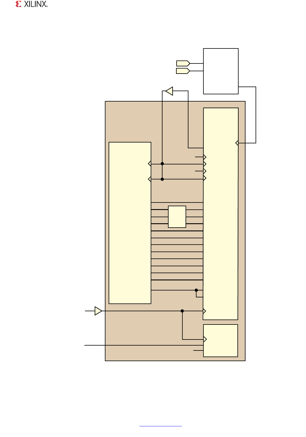
1000BASE-X PCS/PMA or SGMII v11.4 www.xilinx.com 187
PG047 October 16, 2012
Chapter 6: SGMII / Dynamic Standards Switching with Transceivers
X-Ref Target - Figure 6-3
Figure 6-3: SGMII Connection to a Virtex-4 FPGA RocketIO MGT Transceiver
(WKHUQHW%$6(;
3&630$RU6*0,,
/RJL&25(
9LUWH[
*7
5RFNHW,2
XVHG
7;865&/.
7;865&/.
5;865&/.
5;865&/.
XVHUFON
XVHUFON
XVHUFON0+]
,3$'
,3$'
EUHIFONQ
0+]
U[EXIVWDWXV>@
U[FKDULVFRPPD
U[FKDULVN
U[FONFRUFQW>@
U[GDWD>@
U[UXQGLVS
SRZHUGRZQ
W[FKDUGLVSPRGH
W[FKDUGLVSYDO
W[FKDULVN
W[GDWD>@
HQDEOHDOLJQ
5;%8)(55
5;&+$5,6&200$
5;&+$5,6.
5;67$786>@
5;'$7$>@
5;581',63
32:(5'2:1
7;&+$5',6302'(
7;&+$5',639$/
7;&+$5,6.
7;'$7$>@
(13&200$$/,*1
(10&200$$/,*1
%8)*
9LUWH[
*7&/.B0*7
0*7&/.3
0*7&/.1
6<1&/.287
5;',63(55
U[GLVSHUU
/2*,&
6+,0
&DO%ORFNY
EUHIFONS
0+]
5()&/.
V\QFON
gg
gg
7;287&/.
'&/.
'&/.
FRPSRQHQWBQDPHBEORFN
%ORFN/HYHOIURP
H[DPSOHGHVLJQ
7;B6,*1$/B'(7(&7
5;B6,*1$/B'(7(&7
gg
VLJQDOBGHWHFW
GFON
%8)*
8

1000BASE-X PCS/PMA or SGMII v11.4 www.xilinx.com 188
PG047 October 16, 2012
Chapter 6: SGMII / Dynamic Standards Switching with Transceivers
Virtex-5 LXT or SXT Devices for SGMII or Dynamic Standards
Switching
The core is designed to integrate with the Virtex-5 FPGA RocketIO™ GTP transceiver. The
connections and logic required between the core and GTP transceiver are illustrated in
Figure 6-4; the signal names and logic in the figure precisely match those delivered with the
example design when a GTP transceiver is used.
A GTP transceiver tile consists of a pair of transceivers. For this reason, the GTP transceiver
wrapper delivered with the core always contains two GTP transceiver instantiations, even if
only a single GTP transceiver is in use. Figure 6-4 illustrates only a single GTP transceiver for
clarity.
The 125 MHz differential reference clock is routed to the GTP transceiver, which is
configured to output a version of this clock on the REFCLKOUT port, and after being placed
onto global clock routing can be used by all core logic. This clock is input back into the GTP
transceiver on the user interface clock port txusrclk and txusrclk2.
It can be seen from Figure 6-4 that the Rx Elastic Buffer is implemented in the FPGA logic
between the GTP transceiver and the core; this replaces the Rx Elastic Buffer in the GTP
transceiver.
This alternative Receiver Elastic Buffer uses a single block RAM to create a buffer twice as
large as the one present in the GTP transceiver. It is able to cope with larger frame sizes
before clock tolerances accumulate and result in emptying or filling of the buffer. This is
necessary to guarantee SGMII operation at 10 Mb/s where each frame size is effectively 100
times larger than the same frame would be at 1 Gb/s because each byte is repeated 100
times (see Chapter 8, Using the Core Netlist Client-Side GMII for the SGMII Standard).
With this FPGA logic Rx Elastic Buffer implementation, data is clocked out of the GTP
transceiver synchronously to rxrecclk0. This clock can be placed on a BUFR component
and is used to synchronize the transfer of data between the GTP transceiver and the Elastic
Buffer, as illustrated in Figure 6-4. See also Virtex-5 FPGA RocketIO GTP Transceivers for
SGMII or Dynamic Standards Switching Constraints. Vivado IP Packager does not support
Virtex-5 devices. Virtex-5 devices are supported only through ISE design suite.
Virtex-5 FPGA RocketIO Transceiver GTP Wizard
The two wrapper files immediately around the GTP transceiver pair,
RocketIO_wrapper_gtp_tile and RocketIO_wrapper_gtp (see Figure 6-4), are generated from
the RocketIO GTP Transceiver Wizard. These files apply all the gigabit Ethernet attributes.
Consequently, these files can be regenerated by customers and therefore be easily targeted
at ES or Production silicon. This core targets production silicon.
The CORE Generator tool log file (XCO file) that was created when the RocketIO GTP Wizard
project was generated is available in the following location:
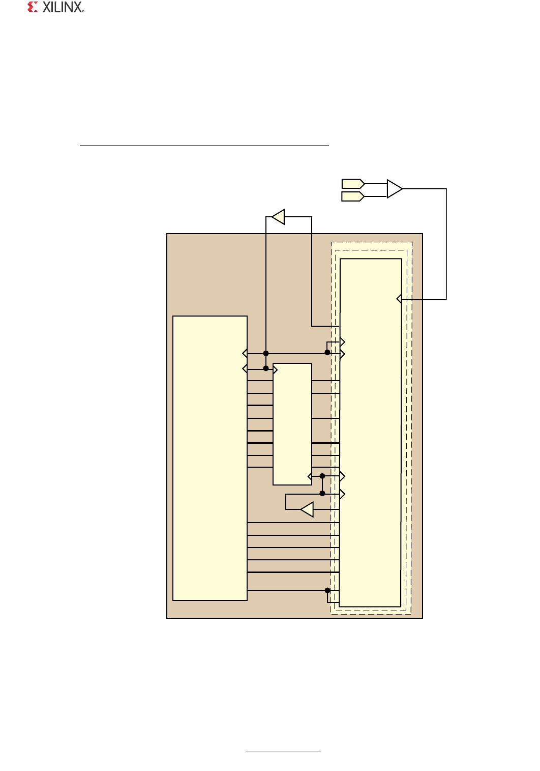
1000BASE-X PCS/PMA or SGMII v11.4 www.xilinx.com 189
PG047 October 16, 2012
Chapter 6: SGMII / Dynamic Standards Switching with Transceivers
<project_directory>/<component_name>/example_design/transceiver/
RocketIO_wrapper_gtp.xco
This file can be used as an input to the CORE Generator tool to regenerate the
device-specific RocketIO transceiver wrapper files. The XCO file itself contains a list of all of
the GTP transceiver wizard attributes that were used. For further information, see the
Virtex-5 RocketIO GTP Wizard Getting Started Guide (UG188) and the CORE Generator Guide,
at www.xilinx.com/support/software_manuals.htm.
X-Ref Target - Figure 6-4
Figure 6-4: SGMII Connection to a Virtex-5 FPGA RocketIO GTP Transceiver
(WKHUQHW%$6(;
3&630$RU6*0,,
/RJL&25(
9LUWH[
*73
5RFNHW,2
XVHG
48532#,+
48532#,+
28532#,+
XVHUFON
XVHUFON
U[EXIVWDWXV>@
U[FKDULVFRPPD
U[FKDULVN
U[FONFRUFQW>@
U[GDWD>@
U[UXQGLVS
SRZHUGRZQ
W[FKDUGLVSPRGH
W[FKDUGLVSYDO
W[FKDULVN
W[GDWD>@
HQDEOHDOLJQ
28#(!2)3#/--!
28#(!2)3+
28$!4!;=
2825.$)30
0/7%2$/7.
48#(!2$)30-/$%
48#(!2$)306!,
48#(!2)3+
48$!4!;=
28%.0#/--!!,)'.
28%.-#/--!!,)'.
28$)30%22
U[GLVSHUU
#,+).
2%&#,+/54
&0'!
FABRIC
2X
%LASTIC
"UFFER
28./4).4!",%
RXNOTINTABLE
"5&2
282%##,+
XVHUFON0+]
%8)*
COMPONENT?NAME?BLOCK
"LOCK,EVELFROM
EXAMPLEDESIGN
28532#,+
CLKIN
-(Z
,%8)*'6
,3$'
EUHIFONS
,3$'
EUHIFONQ
ROCKETIO?WRAPPER?GTP?TILE
ROCKETIO?WRAPPER?GTP
8

1000BASE-X PCS/PMA or SGMII v11.4 www.xilinx.com 190
PG047 October 16, 2012
Chapter 6: SGMII / Dynamic Standards Switching with Transceivers
Virtex-5 FXT and TXT Devices for SGMII or Dynamic Standards
Switching
The core is designed to integrate with the Virtex-5 FPGA RocketIO GTX transceiver. The
connections and logic required between the core and GTX transceiver are illustrated in
Figure 6-5. The signal names and logic in the figure precisely match those delivered with
the example design when a GTX transceiver is used.
A GTX transceiver tile consists of a pair of transceivers. For this reason, the GTX transceiver
wrapper delivered with the core always contains two GTX transceiver instantiations, even if
only a single GTX transceiver is in use. Figure 6-5 illustrates only a single GTX transceiver for
clarity.
The 125 MHz differential reference clock is routed directly to the GTX transceiver. The GTX
transceiver is configured to output a version of this clock on the REFCLKOUT port; this is
then routed to a DCM through a BUFG (global clock routing).
From the DCM, the CLK0 port (125 MHz) is placed onto global clock routing and can be
used as the 125 MHz clock source for all core logic; this clock is also input back into the GTX
transceiver on the user interface clock port txusrclk2.
From the DCM, the CLKDV port (62.5 MHz) is placed onto global clock routing and is input
back into the GTX transceiver on the user interface clock port txusrclk.
It can be seen from Figure 6-5 that the Rx Elastic Buffer is implemented in the FPGA logic
between the GTX transceiver and the core; this replaces the Rx Elastic Buffer in the GTX
transceiver.
This alternative Receiver Elastic Buffer uses a single block RAM to create a buffer twice as
large as the one present in the GTX transceiver. It is able to cope with larger frame sizes
before clock tolerances accumulate and result in emptying or filling of the buffer. This is
necessary to guarantee SGMII operation at 10 Mb/s where each frame size is effectively 100
times larger than the same frame would be at 1 Gb/s because each byte is repeated 100
times (see Chapter 8, Using the Core Netlist Client-Side GMII for the SGMII Standard).
With this FPGA logic Rx Elastic Buffer implementation, data is clocked out of the GTX
transceiver synchronously to rxrecclk0 (62.5 MHz) on a 16-bit interface. This clock can be
placed on a BUFR component and is used to synchronize the transfer of data between the
GTX transceiver and the Elastic Buffer, as illustrated in Figure 6-5. See also Virtex-5 FPGA
RocketIO GTX Transceivers for SGMII or Dynamic Standards Switching Constraints. Vivado IP
Packager does not support Virtex-5 devices. Virtex-5 devices are supported only through
ISE design suite.

1000BASE-X PCS/PMA or SGMII v11.4 www.xilinx.com 191
PG047 October 16, 2012
Chapter 6: SGMII / Dynamic Standards Switching with Transceivers
Virtex-5 FPGA RocketIO GTX Transceiver Wizard
The two wrapper files immediately around the GTX transceiver pair,
RocketIO_wrapper_gtx_tile and RocketIO_wrapper_gtx (see Figure 6-5), are generated from
the RocketIO GTP Transceiver Wizard. These files apply all the gigabit Ethernet attributes.
Consequently, these files can be regenerated by customers and therefore be easily targeted
at ES or Production silicon. This core targets production silicon.
The CORE Generator tool log file (XCO file) which was created when the RocketIO GTX
Transceiver Wizard project was generated is available in the following location:
<project_directory>/<component_name>/example_design/transceiver/
RocketIO_wrapper_gtx.xco
This file can be used as an input to the CORE Generator tool to regenerate the
device-specific RocketIO transceiver wrapper files. The XCO file itself contains a list of all of
the GTX Transceiver Wizard attributes which were used. For further information, see the
Virtex-5 FPGA RocketIO GTX Wizard Getting Started Guide and the CORE Generator Guide, at
www.xilinx.com/support/software_manuals.htm
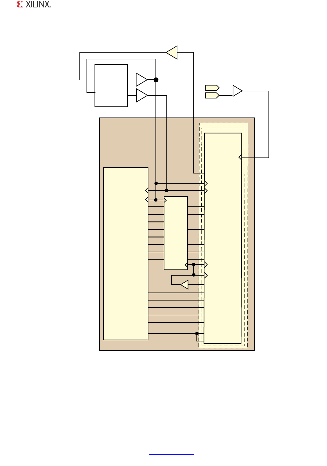
1000BASE-X PCS/PMA or SGMII v11.4 www.xilinx.com 192
PG047 October 16, 2012
Chapter 6: SGMII / Dynamic Standards Switching with Transceivers
X-Ref Target - Figure 6-5
Figure 6-5: SGMII Connection to a Virtex-5 FPGA RocketIO GTX Transceiver
(WKHUQHW%$6(;
3&630$RU6*0,,
/RJL&25(
9LUWH[
*7;
5RFNHW,2
XVHG
48532#,+
48532#,+
28532#,+
XVHUFON
XVHUFON
U[EXIVWDWXV>@
U[FKDULVFRPPD
U[FKDULVN
U[FONFRUFQW>@
U[GDWD>@
U[UXQGLVS
SRZHUGRZQ
W[FKDUGLVSPRGH
W[FKDUGLVSYDO
W[FKDULVN
W[GDWD>@
HQDEOHDOLJQ
28#(!2)3#/--!
28#(!2)3+
28$!4!;=
2825.$)30
0/7%2$/7.
48#(!2$)30-/$%
48#(!2$)306!,
48#(!2)3+
48$!4!;=
28%.0#/--!!,)'.
28%.-#/--!!,)'.
28$)30%22
U[GLVSHUU
#,+).
2%&#,+/54
&0'!
FABRIC
2X
%LASTIC
"UFFER
28./4).4!",%
RXNOTINTABLE
"5&2
282%##,+
COMPONENT?NAME?BLOCK
"LOCK,EVELFROM
EXAMPLEDESIGN
28532#,+
CLKIN
-(Z
,%8)*'6
,3$'
EUHIFONS
,3$'
EUHIFONQ
ROCKETIO?WRAPPER?GTX?TILE
ROCKETIO?WRAPPER?GTX
XVHUFON
0+]
'&0
&/.,1 &/.
)%
%8)*
&/.'9
%8)*
XVHUFON
0+]
%8)*
8

1000BASE-X PCS/PMA or SGMII v11.4 www.xilinx.com 193
PG047 October 16, 2012
Chapter 6: SGMII / Dynamic Standards Switching with Transceivers
Virtex-6 Devices for SGMII or Dynamic Standards Switching
The core is designed to integrate with the Virtex-6 FPGA GTX transceiver. The connections
and logic required between the core and GTP transceiver are illustrated in Figure 6-6; the
signal names and logic in the figure precisely match those delivered with the example
design when a Virtex-6 FPGA GTX transceiver is used.
The 125 MHz differential reference clock is routed to the GTX transceiver, which is
configured to output a version of this clock on the TXOUTCLK port, and after being placed
onto global clock routing can be used by all core logic. This clock is input back into the GTX
transceiver on the user interface clock port txusrclk2. The txusrclk clock signal is
derived internally in the GTX transceiver and so can be connected to ground.
It can be seen from Figure 6-6 that the Rx Elastic Buffer is implemented in the FPGA logic
between the GTX transceiver and the core; this replaces the Rx Elastic Buffer in the GTX
transceiver.
This alternative Receiver Elastic Buffer uses a single block RAM to create a buffer twice as
large as the one present in the GTX transceiver. It is able to cope with larger frame sizes
before clock tolerances accumulate and result in emptying or filling of the buffer. This is
necessary to guarantee SGMII operation at 10 Mb/s where each frame size is effectively 100
times larger than the same frame would be at 1 Gb/s because each byte is repeated 100
times (see Chapter 8, Using the Core Netlist Client-Side GMII for the SGMII Standard).
With this FPGA logic Rx Elastic Buffer implementation, data is clocked out of the GTX
transceiver synchronously to RXRECCLK. This clock can be placed on a BUFR component
and is used to synchronize the transfer of data between the GTX transceiver and the Elastic
Buffer, as illustrated in Figure 6-6. See also Virtex-6 FPGA GTX Transceivers for SGMII or
Dynamic Standards Switching Constraints. Vivado IP Packager does not support Virtex-6
devices. Virtex-6 devices are supported only through ISE design suite.
Virtex-6 FPGA GTX Transceiver Wizard
The two wrapper files immediately around the GTX transceiver, gtx_wrapper_gtx and
gtx_wrapper (see Figure 6-6), are generated from the Virtex-6 FPGA GTX Transceiver
Wizard. These files apply all the gigabit Ethernet attributes. Consequently, these files can
be regenerated by customers and therefore be easily targeted at silicon/device versions.
The CORE Generator tool log file (XCO file) which was created when the Virtex-6 FPGA GTX
Transceiver Wizard project was generated is available in the following location:
<project_directory>/<component_name>/example_design/transceiver/
gtx_wrapper_gtx.xco
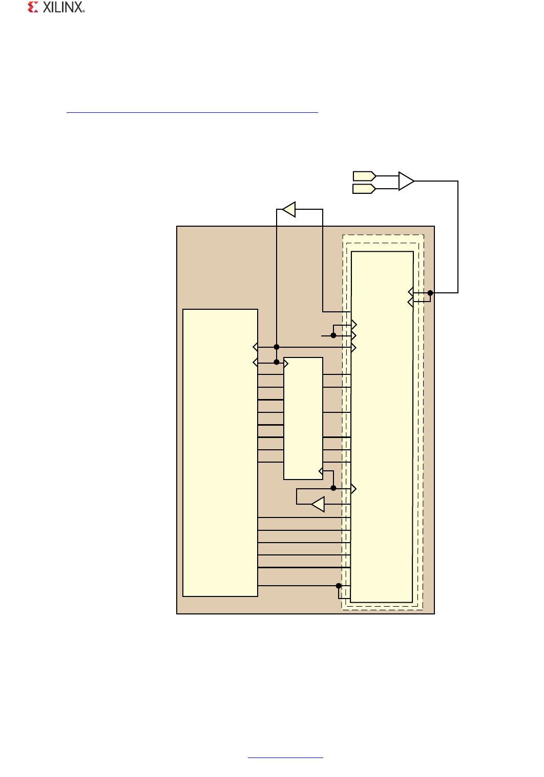
1000BASE-X PCS/PMA or SGMII v11.4 www.xilinx.com 194
PG047 October 16, 2012
Chapter 6: SGMII / Dynamic Standards Switching with Transceivers
This file can be used as an input to the CORE Generator tool to regenerate the
device-specific transceiver wrapper files. The XCO file itself contains a list of all of the
wizard attributes that were used. For further information, see the Virtex-6 FPGA GTX
Transceiver Wizard Getting Started Guide and the CORE Generator Guide, at
www.xilinx.com/support/software_manuals.htm.
X-Ref Target - Figure 6-6
Figure 6-6: SGMII Connection to a Virtex-6 FPGA GTX Transceiver
(WKHUQHW%$6(;
3&630$RU6*0,,
/RJL&25(
9LUWH[
*7;(
7UDQVFHLYHU
48532#,+
48532#,+
28532#,+
XVHUFON
XVHUFON
U[EXIVWDWXV>@
U[FKDULVFRPPD
U[FKDULVN
U[FONFRUFQW>@
U[GDWD>@
U[UXQGLVS
SRZHUGRZQ
W[FKDUGLVSPRGH
W[FKDUGLVSYDO
W[FKDULVN
W[GDWD>@
HQDEOHDOLJQ
28#(!2)3#/--!
28#(!2)3+
28$!4!;=
2825.$)30
0/7%2$/7.
48#(!2$)30-/$%
48#(!2$)306!,
48#(!2)3+
48$!4!;=
28%.0#/--!!,)'.
28%.-#/--!!,)'.
28$)30%22
U[GLVSHUU
48/54#,+
&0'!
FABRIC
2X
%LASTIC
"UFFER
28./4).4!",%
RXNOTINTABLE
"5&2
282%##,+
XVHUFON0+]
%8)*
COMPONENT?NAME?BLOCK
"LOCK,EVELFROM
EXAMPLEDESIGN
28532#,+
MGTREFCLK
-(Z
,%8)'6B*7;(
,3$'
PJWUHIFONBS
,3$'
PJWUHIFONBQ
GTX?WRAPPER?GTX
GTX?WRAPPER
'.$
-'42%&#,+48;=
-'42%&#,+28;=
8

1000BASE-X PCS/PMA or SGMII v11.4 www.xilinx.com 195
PG047 October 16, 2012
Chapter 6: SGMII / Dynamic Standards Switching with Transceivers
Spartan-6 LXT Devices for SGMII or Dynamic Standards
Switching
The core is designed to integrate with the Spartan-6 FPGA GTP transceiver. The connections
and logic required between the core and GTP transceiver are illustrated in Figure 6-7. The
signal names and logic in the figure precisely match those delivered with the example
design when a GTP transceiver is used.
A GTP transceiver tile consists of a pair of transceivers. For this reason, the GTP transceiver
wrapper delivered with the core always contains two GTP transceiver instantiations, even if
only a single GTP transceiver is in use. Figure 6-7 illustrates only a single GTP transceiver for
clarity.
The 125 MHz differential reference clock is routed to the GTP transceiver, which is
configured to output a version of this clock on the GTPCLKOUT port, then routed through
a BUFIO2 and BUFG to place onto global clock routing where it can be used by all core logic.
This clock is input back into the GTP transceiver on the user interface clock port txusrclk
and txusrclk2.
It can be seen from Figure 6-7 that the Rx Elastic Buffer is implemented in the FPGA logic
between the GTP transceiver and the core; this replaces the Rx Elastic Buffer in the GTP
transceiver.
This alternative Receiver Elastic Buffer uses a single block RAM to create a buffer twice as
large as the one present in the GTP transceiver. It is able to cope with larger frame sizes
before clock tolerances accumulate and result in emptying or filling of the buffer. This is
necessary to guarantee SGMII operation at 10 Mb/s where each frame size is effectively 100
times larger than the same frame would be at 1 Gb/s because each byte is repeated 100
times (see Chapter 8, Using the Core Netlist Client-Side GMII for the SGMII Standard).
With this FPGA logic Rx Elastic Buffer implementation, data is clocked out of the GTP
transceiver synchronously to rxrecclk0. This clock can be placed on a BUFG component
and is used to synchronize the transfer of data between the GTP transceiver and the Elastic
Buffer, as illustrated in Figure 6-4. See also Spartan-6 FPGA GTP Transceivers for SGMII or
Dynamic Standards Switching Constraints. Vivado IP Packager does not support Spartan-6
devices. Spartan-6 devices are supported only through ISE design suite.
Spartan-6 FPGA Transceiver GTP Wizard
The two wrapper files immediately around the GTP transceiver pair, gtp_wrapper_tile and
gtp_wrapper (see Figure 6-7), are generated from the GTP transceiver wizard. These files
apply all the gigabit Ethernet attributes. Consequently, these files can be regenerated by
customers and therefore be easily targeted at ES or Production silicon. This core targets
production silicon.
The CORE Generator tool log file (XCO file) that was created when the GTP Transceiver
Wizard project was generated is available in the following location:
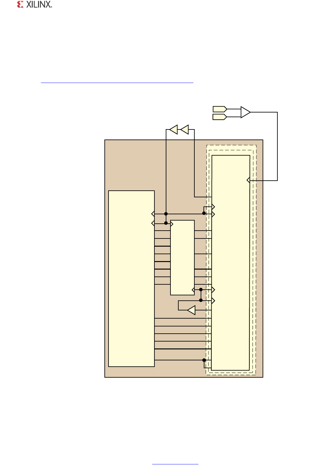
1000BASE-X PCS/PMA or SGMII v11.4 www.xilinx.com 196
PG047 October 16, 2012
Chapter 6: SGMII / Dynamic Standards Switching with Transceivers
<project_directory>/<component_name>/example_design/transceiver/gtp_wrapper.xco
This file can be used as an input to the CORE Generator tool to regenerate the
device-specific transceiver wrapper files. The XCO file itself contains a list of all of the GTP
transceiver wizard attributes which were used. For further information, see the Spartan-6
GTP Wizard Getting Started Guide and the CORE Generator Guide, at
www.xilinx.com/support/software_manuals.htm
X-Ref Target - Figure 6-7
Figure 6-7: SGMII Connection to a Spartan-6 FPGA GTP Transceiver
(WKHUQHW%$6(;
3&630$RU6*0,,
/RJL&25(
48532#,+
48532#,+
28532#,+
XVHUFON
XVHUFON
U[EXIVWDWXV>@
U[FKDULVFRPPD
U[FKDULVN
U[FONFRUFQW>@
U[GDWD>@
U[UXQGLVS
SRZHUGRZQ
W[FKDUGLVSPRGH
W[FKDUGLVSYDO
W[FKDULVN
W[GDWD>@
HQDEOHDOLJQ
28#(!2)3#/--!
28#(!2)3+
28$!4!;=
2825.$)30
0/7%2$/7.
48#(!2$)30-/$%
48#(!2$)306!,
48#(!2)3+
48$!4!;=
28%.0#/--!!,)'.
28%.-#/--!!,)'.
28$)30%22
U[GLVSHUU
#,+).
'40#,+/54
&0'!
FABRIC
2X
%LASTIC
"UFFER
28./4).4!",%
RXNOTINTABLE
"5&'
282%##,+
XVHUFON0+]
%8)*
COMPONENT?NAME?BLOCK
"LOCK,EVELFROM
EXAMPLEDESIGN
28532#,+
CLKIN
-(Z
,%8)'6
,3$'
EUHIFONS
,3$'
EUHIFONQ
GTP?WRAPPER?TILE
GTP?WRAPPER
6SDUWDQ
7UDQVFHLYHU
*73
%8),2
8

1000BASE-X PCS/PMA or SGMII v11.4 www.xilinx.com 197
PG047 October 16, 2012
Chapter 6: SGMII / Dynamic Standards Switching with Transceivers
Virtex-7 Devices for SGMII or Dynamic Standards Switching
The core is designed to integrate with the 7 series FPGA transceiver. The connections and
logic required between the core and GTX/GTH transceiver are illustrated in Figure 6-8; the
signal names and logic in the figure precisely match those delivered with the example
design when a GTX/GTH transceiver is used.
The 125 MHz differential reference clock is routed directly to the GTX/GTH transceiver. The
GTX/GTH transceiver is configured to output 62.5 MHz clock on the TXOUTCLK port; this is
then routed to an MMCM.
From the MMCM, the CLKOUT0 port (125 MHz) is placed onto global clock routing and can
be used as the 125 MHz clock source for all core logic.
From the MMCM, the CLKOUT1 port (62.5 MHz) is placed onto global clock routing and is
input back into the GTX/GTH transceiver on the user interface clock port txusrclk and
txusrclk2.
It can be seen from Figure 6-8 that the Rx Elastic Buffer is implemented in the FPGA logic
between the GTX transceiver and the core; this replaces the Rx Elastic Buffer in the GTX/GTH
transceiver.
This alternative Receiver Elastic Buffer uses a single block RAM to create a buffer twice as
large as the one present in the GTX/GTH transceiver. It is able to cope with larger frame
sizes before clock tolerances accumulate and result in emptying or filling of the buffer. This
is necessary to guarantee SGMII operation at 10 Mb/s where each frame size is effectively
100 times larger than the same frame would be at 1 Gb/s because each byte is repeated 100
times (see Chapter 8, Using the Core Netlist Client-Side GMII for the SGMII Standard).
With this FPGA logic Rx Elastic Buffer implementation, data is clocked out of the GTX
transceiver synchronously to RXOUTCLK. This clock can be placed on a BUFMR followed by
a BUFR component and is used to synchronize the transfer of data between the GTX
transceiver and the Elastic Buffer, as illustrated in Figure 6-8. See also 7 Series and
Zynq-7000 Device Transceivers for SGMII or Dynamic Standards Switching Constraints.
Virtex-7 FPGA GTX/GTH Transceiver Wizard
The two wrapper files immediately around the GTX/GTH transceiver, gtwizard_gt and
gtwizard (see Figure 6-8), are generated from the 7 series FPGA Transceiver Wizard. These
files apply all the gigabit Ethernet attributes. Consequently, these files can be regenerated
by customers and therefore be easily targeted at silicon/device versions.
The CORE Generator tool log file (XCO file) that was created when the 7 series FPGA
Transceiver Wizard project was generated is available in the following location:

1000BASE-X PCS/PMA or SGMII v11.4 www.xilinx.com 198
PG047 October 16, 2012
Chapter 6: SGMII / Dynamic Standards Switching with Transceivers
ISE Design Suite:
<project_dir>/<component_name>/example_design/transceiver/
<component_name>_gtwizard.xco
Vivado Design Suite:
<project_dir>/<project_name>/<project_name>.srcs/sources1/ip/<component_name>/
<component_name>/example_design/transceiver/<component_name>_gtwizard.xco
This file can be used as an input to the CORE Generator tool to regenerate the device
specific transceiver wrapper files. This file can be used as an input to Vivado project by
clicking on <Add Sources> in the Flow Navigator task bar and selecting the XCO file. The
XCO file itself contains a list of all of the wizard attributes that were used. For further
information, see the 7 Series FPGAs Transceivers User Guide and the CORE Generator Guide,
at www.xilinx.com/support/software_manuals.htm.
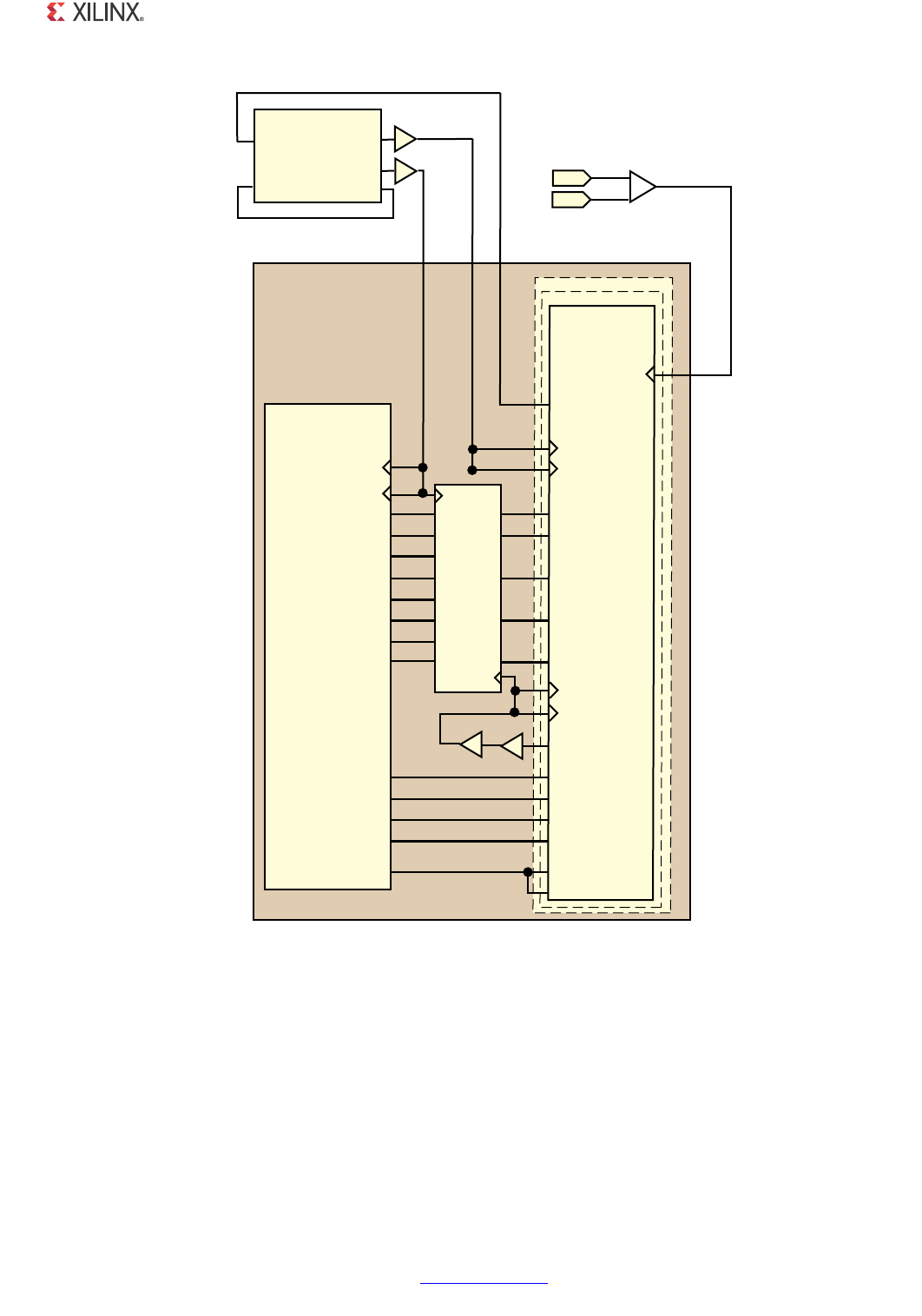
1000BASE-X PCS/PMA or SGMII v11.4 www.xilinx.com 199
PG047 October 16, 2012
Chapter 6: SGMII / Dynamic Standards Switching with Transceivers
X-Ref Target - Figure 6-8
Figure 6-8: SGMII Connection to a Virtex-7 FPGA Transceiver
(WKHUQHW%$6(;
3&630$RU6*0,,
/RJL&25(
9LUWH[
*7;(B&+$11(/
*7+(B&+$11(/
7UDQVFHLYHU
48532#,+
48532#,+
28532#,+
XVHUFON
XVHUFON
U[EXIVWDWXV>@
U[FKDULVFRPPD
U[FKDULVN
U[FONFRUFQW>@
U[GDWD>@
U[UXQGLVS
W[FKDUGLVSPRGH
W[FKDUGLVSYDO
W[FKDULVN
W[GDWD>@
HQDEOHDOLJQ
28#(!2)3#/--!
28#(!2)3+
28$!4!;=
48#(!2$)30-/$%
48#(!2$)306!,
48#(!2)3+
48$!4!;=
28%.0#/--!!,)'.
28%.-#/--!!,)'.
28$)30%22
U[GLVSHUU
48/54#,+
&0'!
FABRIC
2X
%LASTIC
"UFFER
28./4).4!",%
RXNOTINTABLE
"5&-2
28/54#,+
0+]
COMPONENT?NAME?BLOCK
"LOCK,EVELFROM
EXAMPLEDESIGN
GTREFCLK
-(Z
,%8)'6B*7(
,3$'
JWUHIFONBS
,3$'
JWUHIFONBQ
GTWIZARD?GT
GTWIZARD
'42%&#,+
--#-%?!$6
#,+/54
#,+/54
#,+).
#,+&"/54#,+&").
"5&'
28532#,+
"5&'
0+]
"5&2
8

1000BASE-X PCS/PMA or SGMII v11.4 www.xilinx.com 200
PG047 October 16, 2012
Chapter 6: SGMII / Dynamic Standards Switching with Transceivers
Kintex-7 and Zynq-7000 Devices for SGMII or Dynamic
Standards Switching
The core is designed to integrate with the 7 series FPGA transceiver. The connections and
logic required between the core and GTX transceiver are illustrated in Figure 6-9; the signal
names and logic in the figure precisely match those delivered with the example design
when a GTX transceiver is used.
The 125 MHz differential reference clock is routed directly to the GTX transceiver. The GTX
transceiver is configured to output 62.5 MHz clock on the TXOUTCLK port; this is then
routed to an MMCM via a BUFG (global clock routing).
From the MMCM, the CLKOUT0 port (125 MHz) is placed onto global clock routing and can
be used as the 125 MHz clock source for all core logic.
From the MMCM, the CLKOUT1 port (62.5 MHz) is placed onto global clock routing and is
input back into the GTX transceiver on the user interface clock port txusrclk and
txusrclk2.
It can be seen from Figure 6-9 that the Rx Elastic Buffer is implemented in the FPGA logic
between the GTX transceiver and the core; this replaces the Rx Elastic Buffer in the GTX
transceiver.
This alternative Receiver Elastic Buffer uses a single block RAM to create a buffer twice as
large as the one present in the GTX transceiver. It is able to cope with larger frame sizes
before clock tolerances accumulate and result in emptying or filling of the buffer. This is
necessary to guarantee SGMII operation at 10 Mb/s where each frame size is effectively 100
times larger than the same frame would be at 1 Gb/s because each byte is repeated 100
times (see Chapter 8, Using the Core Netlist Client-Side GMII for the SGMII Standard).
With this FPGA logic Rx Elastic Buffer implementation, data is clocked out of the GTX
transceiver synchronously to RXOUTCLK. This clock can be placed on a BUFG component
and is used to synchronize the transfer of data between the GTX transceiver and the Elastic
Buffer, as illustrated in Figure 6-9. See also 7 Series and Zynq-7000 Device Transceivers for
SGMII or Dynamic Standards Switching Constraints.
Kintex-7 and Zynq-7000 Device GTX Transceiver Wizard
The two wrapper files immediately around the GTX transceiver, gtwizard_gt and gtwizard
(Figure 6-9), are generated from the 7 series FPGA Transceiver Wizard. These files apply all
the gigabit Ethernet attributes. Consequently, these files can be regenerated by customers
and therefore be easily targeted at silicon/device versions.
The CORE Generator tool log file (XCO file) that was created when the 7 series FPGA
Transceiver Wizard project was generated is available in the following location:

1000BASE-X PCS/PMA or SGMII v11.4 www.xilinx.com 201
PG047 October 16, 2012
Chapter 6: SGMII / Dynamic Standards Switching with Transceivers
ISE Design Suite:
<project_dir>/<component_name>/example_design/transceiver/
<component_name>_gtwizard.xco
Vivado Design Suite:
<project_dir>/<project_name>/<project_name>.srcs/sources1/ip/<component_name>/
<component_name>/example_design/transceiver/<component_name>_gtwizard.xco
This file can be used as an input to the CORE Generator tool to regenerate the device
specific transceiver wrapper files. This file can be used as an input to Vivado tools project
by clicking on <Add Sources> in the Flow Navigator task bar and selecting the XCO file. The
XCO file itself contains a list of all of the wizard attributes which were used. For further
information, see the 7 Series FPGA Transceivers User Guide and the CORE Generator Guide,
at www.xilinx.com/support/software_manuals.htm

1000BASE-X PCS/PMA or SGMII v11.4 www.xilinx.com 202
PG047 October 16, 2012
Chapter 6: SGMII / Dynamic Standards Switching with Transceivers
X-Ref Target - Figure 6-9
Figure 6-9: SGMII Connection to a Kintex-7 or Zynq-7000 Device Transceiver
(WKHUQHW%$6(;
3&630$RU6*0,,
/RJL&25(
.LQWH[=\QT
*7;(B&+$11(/
7UDQVFHLYHU
48532#,+
48532#,+
28532#,+
XVHUFON
XVHUFON
U[EXIVWDWXV>@
U[FKDULVFRPPD
U[FKDULVN
U[FONFRUFQW>@
U[GDWD>@
U[UXQGLVS
W[FKDUGLVSPRGH
W[FKDUGLVSYDO
W[FKDULVN
W[GDWD>@
HQDEOHDOLJQ
28#(!2)3#/--!
28#(!2)3+
28$!4!;=
48#(!2$)30-/$%
48#(!2$)306!,
48#(!2)3+
48$!4!;=
28%.0#/--!!,)'.
28%.-#/--!!,)'.
28$)30%22
U[GLVSHUU
48/54#,+
&0'!
FABRIC
2X
%LASTIC
"UFFER
28./4).4!",%
RXNOTINTABLE
"5&'
28/54#,+
0+]
COMPONENT?NAME?BLOCK
"LOCK,EVELFROM
EXAMPLEDESIGN
GTREFCLK
-(Z
,%8)'6B*7(
,3$'
JWUHIFONBS
,3$'
JWUHIFONBQ
GTWIZARD?GT
GTWIZARD
'42%&#,+
--#-%?!$6
#,+/54
#,+/54
#,+).
#,+&"/54#,+&").
"5&'
28532#,+
"5&'
0+]
"5&'
8

1000BASE-X PCS/PMA or SGMII v11.4 www.xilinx.com 203
PG047 October 16, 2012
Chapter 6: SGMII / Dynamic Standards Switching with Transceivers
Artix-7 Devices for SGMII or Dynamic Standards Switching
The core is designed to integrate with the 7 series FPGA transceiver. The connections and
logic required between the core and GTP transceiver are illustrated in Figure 6-10. The
signal names and logic in the figure match those delivered with the example design when
a GTP transceiver is used.
The 125 MHz differential reference clock is routed directly to the GTP transceiver. The GTP
transceiver is conf igured to output 62.5 MHz clock on the TXOUTCLK port. This clock is then
routed to an MMCM using a BUFG (global clock routing).
From the MMCM, the CLKOUT0 port (125 MHz) is placed onto global clock routing and can
be used as the 125 MHz clock source for all core logic. From the MMCM, the CLKOUT1 port
(62.5 MHz) is placed onto global clock routing and is input back into the GTP transceiver on
the user interface clock port txusrclk and txusrclk2. Figure 6-10 shows that the Rx
Elastic Buffer is implemented in the FPGA logic between the GTP transceiver and the core;
this replaces the Rx Elastic Buffer in the GTP transceiver.
This alternative Receiver Elastic Buffer uses a single block RAM to create a buffer twice as
large as the one present in the GTP transceiver. It is able to cope with larger frame sizes
before clock tolerances accumulate and result in emptying or filling of the buffer. This is
necessary to guarantee SGMII operation at 10 Mb/s where each frame size is effectively 100
times larger than the same frame would be at 1 Gb/s because each byte is repeated 100
times (see Chapter 8, Using the Core Netlist Client-Side GMII for the SGMII Standard).
With this FPGA logic Rx Elastic Buffer implementation, data is clocked out of the GTP
transceiver synchronously to RXOUTCLK. This clock can be placed on a BUFG component
and is used to synchronize the transfer of data between the GTP transceiver and the Elastic
Buffer, as illustrated in Figure 6-10. See also 7 Series and Zynq-7000 Device Transceivers for
SGMII or Dynamic Standards Switching Constraints in Chapter 18.
Artix-7 FPGA GTP Transceiver Wizard
The two wrapper files immediately around the GTP transceiver, gtwizard_gt and gtwizard
(Figure 6-10), are generated from the 7 series FPGA Transceiver Wizard. These files apply all
the gigabit Ethernet attributes. Consequently, these files can be regenerated by customers
and therefore be easily targeted at silicon/device versions.
The CORE Generator tool log file (XCO file) that was created when the 7 series FPGA
Transceiver Wizard project was generated is available in the following location:
ISE Design Suite:
<project_dir>/<component_name>/example_design/transceiver/<component_name>_gtwizard
.xco

1000BASE-X PCS/PMA or SGMII v11.4 www.xilinx.com 204
PG047 October 16, 2012
Chapter 6: SGMII / Dynamic Standards Switching with Transceivers
Vivado Design Suite:
<project_dir>/<project_name>/<project_name>.srcs/sources1/ip/<component_name>/
<component_name>/example_design/transceiver/<component_name>_gtwizard.xco
This file can be used as an input to the CORE Generator tool to regenerate the device
specific transceiver wrapper files. This file can be used as an input to Vivado tools project
by clicking on <Add Sources> in the Flow Navigator task bar and selecting the XCO file. The
XCO file itself contains a list of all of the wizard attributes that were used. For further
information, see the 7 Series FPGAs Transceivers User Guide and the CORE Generator Guide,
at www.xilinx.com/support/software_manuals.htm.
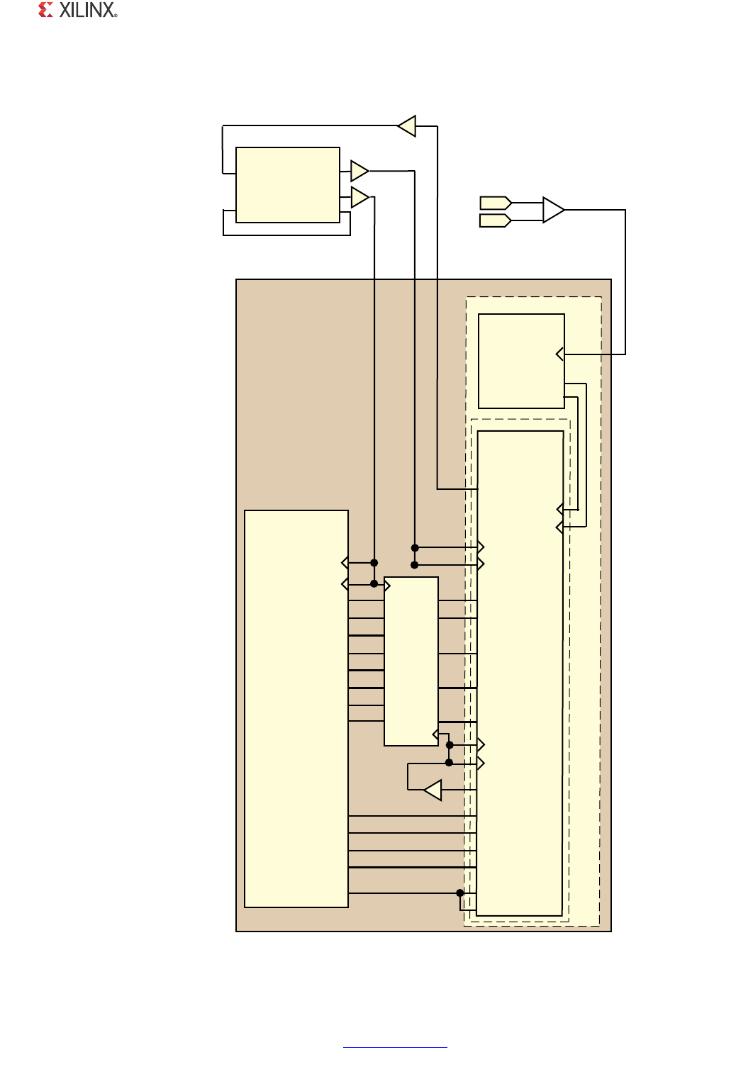
1000BASE-X PCS/PMA or SGMII v11.4 www.xilinx.com 205
PG047 October 16, 2012
Chapter 6: SGMII / Dynamic Standards Switching with Transceivers
X-Ref Target - Figure 6-10
Figure 6-10: SGMII Connection to Artix-7 FPGA Transceiver
(WKHUQHW%$6(;
3&630$RU6*0,,
/RJL&25(
$UWL[
*7;(B&+$11(/
7UDQVFHLYHU
48532#,+
48532#,+
28532#,+
XVHUFON
XVHUFON
U[EXIVWDWXV>@
U[FKDULVFRPPD
U[FKDULVN
U[FONFRUFQW>@
U[GDWD>@
U[UXQGLVS
W[FKDUGLVSPRGH
W[FKDUGLVSYDO
W[FKDULVN
W[GDWD>@
HQDEOHDOLJQ
28#(!2)3#/--!
28#(!2)3+
28$!4!;=
48#(!2$)30-/$%
48#(!2$)306!,
48#(!2)3+
48$!4!;=
28%.0#/--!!,)'.
28%.-#/--!!,)'.
28$)30%22
U[GLVSHUU
48/54#,+
&0'!
FABRIC
2X
%LASTIC
"UFFER
28./4).4!",%
RXNOTINTABLE
"5&'
28/54#,+
0+]
COMPONENT?NAME?BLOCK
"LOCK,EVELFROM
EXAMPLEDESIGN
GTREFCLK
-(Z
,%8)'6B*7(
,3$'
JWUHIFONBS
,3$'
JWUHIFONBQ
GTWIZARD?GT
GTWIZARD
--#-%?!$6
#,+/54
#,+/54
#,+).
#,+&"/54#,+&").
"5&'
28532#,+
"5&'
0+]
"5&'
!RTIX
'40%?#/--/.
'42%&#,+
0,,/54#,+
0,,/542%&#,+
0,,#,+?).
0,,2%&#,+?).
8

1000BASE-X PCS/PMA or SGMII v11.4 www.xilinx.com 206
PG047 October 16, 2012
Chapter 6: SGMII / Dynamic Standards Switching with Transceivers
Clock Sharing - Multiple Cores with Transceivers,
FPGA Logic Elastic Buffer
Virtex-4 FX Devices
Figure 6-11 illustrates sharing clock resources across multiple instantiations of the core
when using the Virtex-4 FPGA RocketIO MGT transceiver. The example design, when using
the Virtex-4 devices, can be generated to connect either a single instance of the core, or
connect a pair of core instances to the transceiver pair present in a MGT transceiver tile.
Figure 6-11 illustrates two instantiations of the block level, and each block level contains a
pair of cores, illustrating clock sharing between four cores.
More cores can be added by continuing to instantiate extra block level modules. Share
clocks only between the MGT transceivers in a single column. For each column, use a single
brefclk_p and brefclk_n differential clock pair and connect this to a GT11CLK_MGT
primitive. The clock output from this primitive should be shared across all used MGT
transceiver tiles in the column. See the Virtex-4 RocketIO Multi-Gigabit Transceiver User
Guide for more information.
To provide the 125 MHz clock for all core instances, select a TXOUTCLK1 port from any MGT
transceiver. This can be routed onto global clock routing using a BUFG as illustrated, and
shared between all cores and MGT transceivers in the column.
Each MGT transceiver and core pair instantiated has its own independent clock domain
synchronous to RXRECCLK1 which is placed on regional clock routing using a BUFR, as
illustrated in Figure 6-11. These cannot be shared across multiple MGT transceivers.
Although not illustrated in Figure 6-11, dclk (the clock used for the calibration blocks and
for the Dynamic Reconfiguration Port (DRP) of the MGT transceivers) can also be shared.
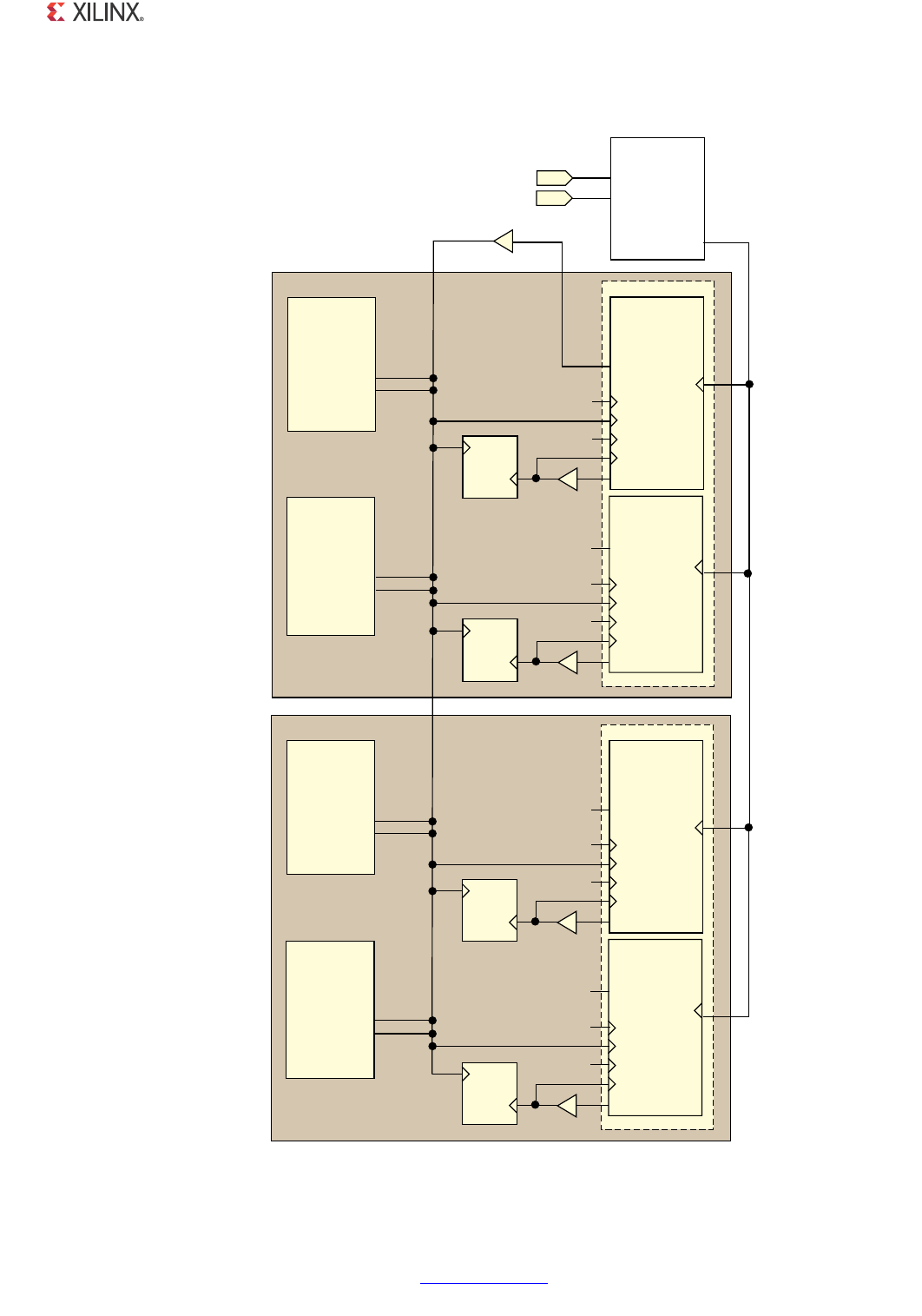
1000BASE-X PCS/PMA or SGMII v11.4 www.xilinx.com 207
PG047 October 16, 2012
Chapter 6: SGMII / Dynamic Standards Switching with Transceivers
X-Ref Target - Figure 6-11
Figure 6-11: Clock Management with Multiple Core Instances with Virtex-4 FPGA MGT
Transceivers for SGMII
COMPONENT?NAME?BLOCK
"LOCK,EVEL
(WKHUQHW%$6(;
3&630$RU
6*0,,FRUH
XVHUFON
XVHUFON
,3$'
BREFCLKP
-(Z
,3$'
BREFCLKN
-(Z
9LUWH[
*7&/.B0*7
0*7&/.3
0*7&/.1
6<1&/.287
6IRTEX
'4
2OCKET)/
!
5()&/.
0*7WLOH
(WKHUQHW%$6(;
3&630$RU
6*0,,FRUH
XVHUFON
XVHUFON
1&
XVHUFON
0+]
7;865&/.
7;865&/.
5;865&/.
5;865&/.
SYNCLK
-(Z
@
@
@
@
48/54#,+
282%##,+
&0'!
FABRIC
2X
%LASTIC
"UFFER
"5&2 6IRTEX
'4
2OCKET)/
"
5()&/.
7;865&/.
7;865&/.
5;865&/.
5;865&/.
48/54#,+
282%##,+
&0'!
FABRIC
2X
%LASTIC
"UFFER
"5&2
%8)*
COMPONENT?NAME?BLOCK
"LOCK,EVEL
(WKHUQHW%$6(;
3&630$RU
6*0,,FRUH
XVHUFON
XVHUFON
6IRTEX
'4
2OCKET)/
!
5()&/.
0*7WLOH
(WKHUQHW%$6(;
3&630$RU
6*0,,FRUH
XVHUFON
XVHUFON
1&
XVHUFON
0+]
7;865&/.
7;865&/.
5;865&/.
5;865&/.
@
@
@
@
48/54#,+
282%##,+
&0'!
FABRIC
2X
%LASTIC
"UFFER
"5&2 6IRTEX
'4
2OCKET)/
"
5()&/.
7;865&/.
7;865&/.
5;865&/.
5;865&/.
48/54#,+
282%##,+
&0'!
FABRIC
2X
%LASTIC
"UFFER
"5&2
1&
8

1000BASE-X PCS/PMA or SGMII v11.4 www.xilinx.com 208
PG047 October 16, 2012
Chapter 6: SGMII / Dynamic Standards Switching with Transceivers
Virtex-5 LXT and SXT Devices
Figure 6-12 illustrates sharing clock resources across multiple instantiations of the core
when using the Virtex-5 FPGA RocketIO GTP transceiver. The example design can be
generated to connect either a single instance of the core, or connect a pair of core instances
to the transceiver pair present in a GTP transceiver tile. Figure 6-12 illustrates two
instantiations of the block level, and each block level contains a pair of cores. Figure 6-12
illustrates clock sharing between four cores.
More cores can be added by instantiating extra block level modules. Share the brefclk_p
and brefclk_n differential clock pairs. See the Virtex-5 RocketIO GTP Transceiver User
Guide for more information.
To provide the 125 MHz clock for all core instances, select a REFCLKOUT port from any GTP
transceiver. This can be routed onto global clock routing using a BUFG as illustrated and
shared between all cores and GTP transceivers in the column.
Each GTP transceiver and core pair instantiated has its own independent clock domains
synchronous to RXRECCLK0 and RXRECCLK1. These are placed on regional clock routing
using a BUFR, as illustrated in Figure 6-12, and cannot be shared across multiple GTP
transceivers.
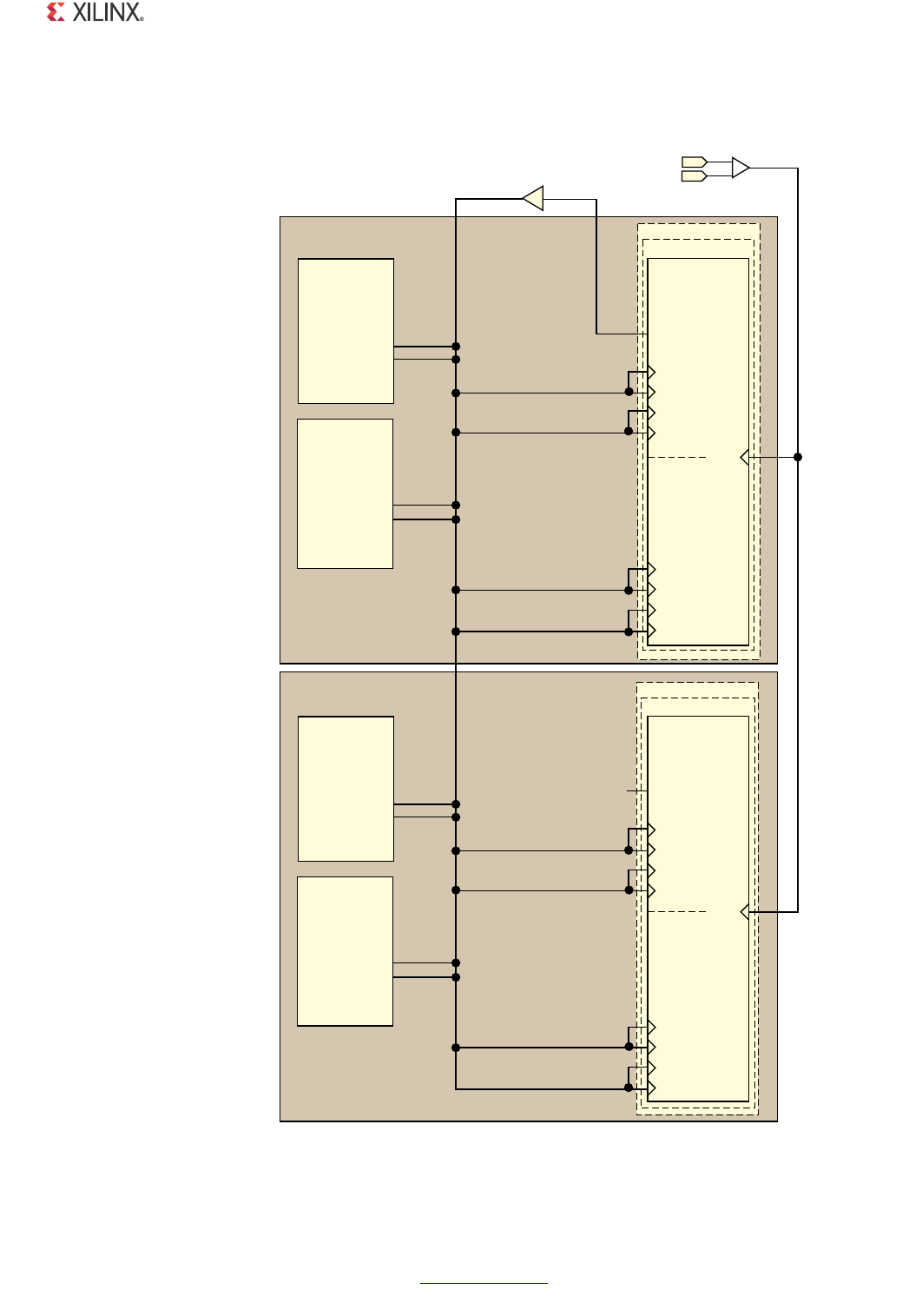
1000BASE-X PCS/PMA or SGMII v11.4 www.xilinx.com 209
PG047 October 16, 2012
Chapter 6: SGMII / Dynamic Standards Switching with Transceivers
X-Ref Target - Figure 6-12
Figure 6-12: Clock Management with Multiple Core Instances with Virtex-5 FPGA RocketIO GTP
Transceivers for SGMII
(WKHUQHW%$6(;
3&630$RU
6*0,,FRUH
XVHUFON
XVHUFON
6IRTEX
'40
2OCKET)/
#,+).
URFNHWLRBZUDSSHUBJWSBWLOH
6IRTEX
'40
2OCKET)/
(WKHUQHW%$6(;
3&630$RU
6*0,,FRUH
XVHUFON
XVHUFON
XVHUFON
0+]
%8)*
48532#,+
48532#,+
28532#,+
28532#,+
48532#,+
48532#,+
28532#,+
28532#,+
CLKIN
-(Z
2%&#,+/54
COMPONENT?NAME?BLOCK
"LOCK,EVEL
(WKHUQHW%$6(;
3&630$RU
6*0,,FRUH
XVHUFON
XVHUFON
6IRTEX
'40
2OCKET)/
6IRTEX
'40
2OCKET)/
(WKHUQHW%$6(;
3&630$RU
6*0,,FRUH
XVHUFON
XVHUFON
48532#,+
48532#,+
28532#,+
28532#,+
48532#,+
48532#,+
28532#,+
28532#,+
2%&#,+/54
COMPONENT?NAME?BLOCK
"LOCK,EVEL
1&
,%8)*'6
,3$'
EUHIFONS
,3$'
EUHIFONQ
#,+).
URFNHWLRBZUDSSHUBJWSBWLOH
URFNHWLRBZUDSSHUBJWS
URFNHWLRBZUDSSHUBJWS
8

1000BASE-X PCS/PMA or SGMII v11.4 www.xilinx.com 210
PG047 October 16, 2012
Chapter 6: SGMII / Dynamic Standards Switching with Transceivers
Virtex-5 FXT and TXT Devices
Figure 6-13 illustrates sharing clock resources across multiple instantiations of the core
when using the Virtex-5 FPGA RocketIO GTX transceiver. The example design can be
generated to connect either a single instance of the core, or connect a pair of core instances
to the transceiver pair present in a GTX transceiver tile. Figure 6-13 illustrates two
instantiations of the block level, and each block level contains a pair of cores. Figure 6-13
illustrates clock sharing between four cores.
More cores can be added by instantiating extra block level modules. Share the brefclk_p
and brefclk_n differential clock pairs. See the Virtex-5 RocketIO GTX Transceiver User
Guide for more information.
To provide the FPGA logic clocks for all core instances, select a REFCLKOUT port from any
GTX transceiver and route this to a single DCM through a BUFG (global clock routing). The
CLK0 (125 MHz) and CLKDV (62.5 MHz) outputs from this DCM, placed onto global clock
routing using BUFGs, can be shared across all core instances and GTX transceivers as
illustrated.
Each GTX transceiver and core pair instantiated has its own independent clock domains
synchronous to RXRECCLK0 and RXRECCLK1. These are placed on regional clock routing
using a BUFR, as illustrated in Figure 6-13, and cannot be shared across multiple GTX
transceivers.
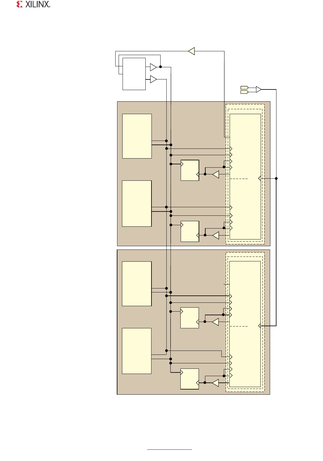
1000BASE-X PCS/PMA or SGMII v11.4 www.xilinx.com 211
PG047 October 16, 2012
Chapter 6: SGMII / Dynamic Standards Switching with Transceivers
X-Ref Target - Figure 6-13
Figure 6-13: Clock Management with Multiple Core Instances with Virtex-5 FPGA RocketIO GTX
Transceivers for SGMII
COMPONENT?NAME?BLOCK
"LOCK,EVEL
(WKHUQHW%$6(;
3&630$RU
6*0,,FRUH
XVHUFON
XVHUFON
6IRTEX
'48
2OCKET)/
(WKHUQHW%$6(;
3&630$RU
6*0,,FRUH
XVHUFON
XVHUFON
48532#,+
48532#,+
28532#,+
28532#,+
2%&#,+/54
282%##,+
&0'!
FABRIC
2X
%LASTIC
"UFFER
"5&2 6IRTEX
'48
2OCKET)/
48532#,+
48532#,+
28532#,+
28532#,+
282%##,+
&0'!
FABRIC
2X
%LASTIC
"UFFER
"5&2
COMPONENT?NAME?BLOCK
"LOCK,EVEL
(WKHUQHW%$6(;
3&630$RU
6*0,,FRUH
XVHUFON
XVHUFON
6IRTEX
'48
2OCKET)/
(WKHUQHW%$6(;
3&630$RU
6*0,,FRUH
XVHUFON
XVHUFON
XVHUFON
0+]
48532#,+
48532#,+
28532#,+
28532#,+
2%&#,+/54
282%##,+
&0'!
FABRIC
2X
%LASTIC
"UFFER
"5&2 6IRTEX
'48
2OCKET)/
#,+).
48532#,+
48532#,+
28532#,+
28532#,+
282%##,+
&0'!
FABRIC
2X
%LASTIC
"UFFER
"5&2
CLKIN
-(Z
,%8)*'6
,3$'
EUHIFONS
,3$'
EUHIFONQ
#,+).
1&
URFNHWLRBZUDSSHUBJW[BWLOH
URFNHWLRBZUDSSHUBJW[BWLOH
URFNHWLRBZUDSSHUBJW[
URFNHWLRBZUDSSHUBJW[
XVHUFON0+]
'&0
&/.,1 &/.
)%
%8)*
&/.'9
%8)*
XVHUFON0+]
%8)*
8

1000BASE-X PCS/PMA or SGMII v11.4 www.xilinx.com 212
PG047 October 16, 2012
Chapter 6: SGMII / Dynamic Standards Switching with Transceivers
Virtex-6 Devices
Figure 6-14 illustrates sharing clock resources across two instantiations of the core when
using the Virtex-6 FPGA GTX transceivers. Further cores can be added by instantiating extra
block level modules.
Share the mgtrefclk_p and mgtrefclk_n differential clock pair clock source across all of
the transceivers in use. To provide the 125 MHz clock for all core instances, select a
TXOUTCLK port from any GTX transceiver. This can be routed onto global clock routing
using a BUFG as illustrated and shared between all cores and GTX transceivers.
Each GTX transceiver and core pair instantiated has its own independent clock domains
synchronous to RXRECCLK. These are placed on regional clock routing using a BUFR, as
illustrated in Figure 6-14, and cannot be shared across multiple GTX transceivers.
See the Virtex-6 FPGA GTX Transceiver User Guide for more information on GTX transceiver
clock resources.

1000BASE-X PCS/PMA or SGMII v11.4 www.xilinx.com 213
PG047 October 16, 2012
Chapter 6: SGMII / Dynamic Standards Switching with Transceivers
X-Ref Target - Figure 6-14
Figure 6-14: Clock Management with Multiple Core Instances with Virtex-6 FPGA GTX
Transceivers for SGMII
COMPONENT?NAME?BLOCK
"LOCK,EVEL
(WKHUQHW%$6(;
3&630$RU
6*0,,FRUH
XVHUFON
XVHUFON
6IRTEX
'48
4RANSCEIVER
XVHUFON
0+]
48532#,+
48532#,+
28532#,+
28532#,+
282%##,+
&0'!
FABRIC
2X
%LASTIC
"UFFER
"5&2
%8)*
MGTREFCLK
-(Z
,%8)'6B*7;(
,3$'
PJWUHIFONBS
,3$'
PJWUHIFONBQ
JW[BZUDSSHUBJW[
JW[BZUDSSHU
-'42%&#,+48;=
-'42%&#,+28;=
48/54#,+
'.$
'.$
COMPONENT?NAME?BLOCK
"LOCK,EVEL
(WKHUQHW%$6(;
3&630$RU
6*0,,FRUH
XVHUFON
XVHUFON
6IRTEX
'48
4RANSCEIVER
XVHUFON
0+]
48532#,+
48532#,+
28532#,+
28532#,+
282%##,+
&0'!
FABRIC
2X
%LASTIC
"UFFER
"5&2
JW[BZUDSSHUBJW[
JW[BZUDSSHU
-'42%&#,+48;=
-'42%&#,+28;=
48/54#,+
'.$
'.$
.#
8

1000BASE-X PCS/PMA or SGMII v11.4 www.xilinx.com 214
PG047 October 16, 2012
Chapter 6: SGMII / Dynamic Standards Switching with Transceivers
Spartan-6 LXT Devices
Figure 6-15 illustrates sharing clock resources across multiple instantiations of the core
when using the Spartan-6 FPGA GTP transceiver. The example design can be generated to
connect either a single instance of the core, or connect a pair of core instances to the
transceiver pair present in a GTP transceiver tile. Figure 6-15 illustrates two instantiations of
the block level, and each block level contains a pair of cores. Figure 6-15 illustrates clock
sharing between four cores.
More cores can be added by instantiating extra block level modules. Share the brefclk_p
and brefclk_n differential clock pairs. See the Spartan-6 FPGA GTP Transceiver User Guide
for more information.
To provide the 125 MHz clock for all core instances, select a GTP transceiver CLKOUT port
from any GTP transceiver. This can be routed onto global clock routing using a BUFIO2 and
BUFG as illustrated and shared between all cores and GTP transceivers in the column.
Each GTP transceiver and core pair instantiated has its own independent clock domains
synchronous to RXRECCLK0 and RXRECCLK1. These are placed on global clock routing
using a BUFG, as illustrated in Figure 6-15, and cannot be shared across multiple GTP
transceivers.
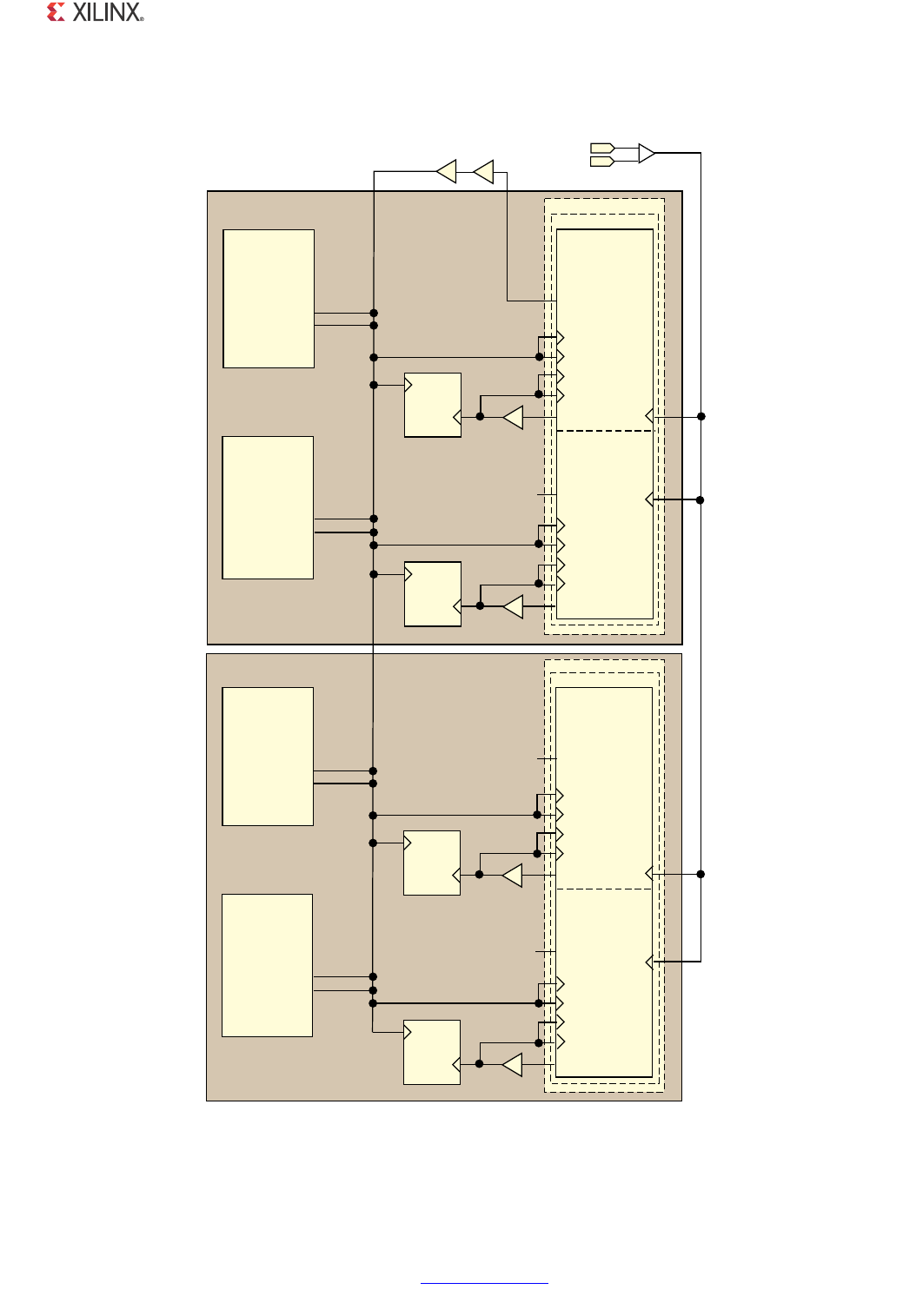
1000BASE-X PCS/PMA or SGMII v11.4 www.xilinx.com 215
PG047 October 16, 2012
Chapter 6: SGMII / Dynamic Standards Switching with Transceivers
X-Ref Target - Figure 6-15
Figure 6-15: Clock Management with Multiple Core Instances with Spartan-6 FPGA GTP
Transceivers for SGMII
COMPONENT?NAME?BLOCK
"LOCK,EVEL
(WKHUQHW%$6(;
3&630$RU
6*0,,FRUH
XVHUFON
XVHUFON
(WKHUQHW%$6(;
3&630$RU
6*0,,FRUH
XVHUFON
XVHUFON
XVHUFON
0+]
48532#,+
48532#,+
28532#,+
28532#,+
'40#,+/54
282%##,+
&0'!
FABRIC
2X
%LASTIC
"UFFER
"5&'
48532#,+
48532#,+
28532#,+
28532#,+
282%##,+
&0'!
FABRIC
2X
%LASTIC
"UFFER
"5&'
%8)*
COMPONENT?NAME?BLOCK
"LOCK,EVEL
(WKHUQHW%$6(;
3&630$RU
6*0,,FRUH
XVHUFON
XVHUFON
(WKHUQHW%$6(;
3&630$RU
6*0,,FRUH
XVHUFON
XVHUFON
XVHUFON
0+]
48532#,+
48532#,+
28532#,+
28532#,+
'40#,+/54
282%##,+
&0'!
FABRIC
2X
%LASTIC
"UFFER
"5&'
#,+).
48532#,+
48532#,+
28532#,+
28532#,+
282%##,+
&0'!
FABRIC
2X
%LASTIC
"UFFER
"5&'
CLKIN
-(Z
,%8)'6
,3$'
EUHIFONS
,3$'
EUHIFONQ
#,+).
1&
JWSBZUDSSHUBWLOH
JWSBZUDSSHUBWLOH
JWSBZUDSSHU
JWSBZUDSSHU
3PARTAN
4RANSCEIVER
'40
3PARTAN
4RANSCEIVER
'40
3PARTAN
2OCKET)/
'40
3PARTAN
2OCKET)/
'40
#,+).
#,+).
'40#,+/54
'40#,+/54
1&
1&
%8),2

1000BASE-X PCS/PMA or SGMII v11.4 www.xilinx.com 216
PG047 October 16, 2012
Chapter 6: SGMII / Dynamic Standards Switching with Transceivers
Virtex-7 Devices
Figure 6-17 illustrates sharing clock resources across multiple instantiations of the core
when using the 7 series FPGA transceiver. More cores can be added by instantiating extra
block level modules.
Share the gtrefclk_p and gtrefclk_n differential clock pairs. See the 7 Series GTX
Transceiver User Guide and the 7 Series GTH Transceiver User Guide for more information.
To provide the FPGA logic clocks for all core instances, select a TXOUTCLK port from any
GTX/GTH transceiver and route this to a single MMCM. The CLKOUT0 (125 MHz) and
CLKOUT1 (62.5 MHz) outputs from this MMCM, placed onto global clock routing using
BUFGs, can be shared across all core instances and GTX/GTH transceivers as illustrated.
Each GTX/GTH transceiver and core pair instantiated has its own independent clock
domains synchronous to RXOUTCLK. These are placed on BUFMR followed by regional clock
routing using a BUFR, as illustrated in Figure 6-17, and cannot be shared across multiple
GTX/GTH transceivers.
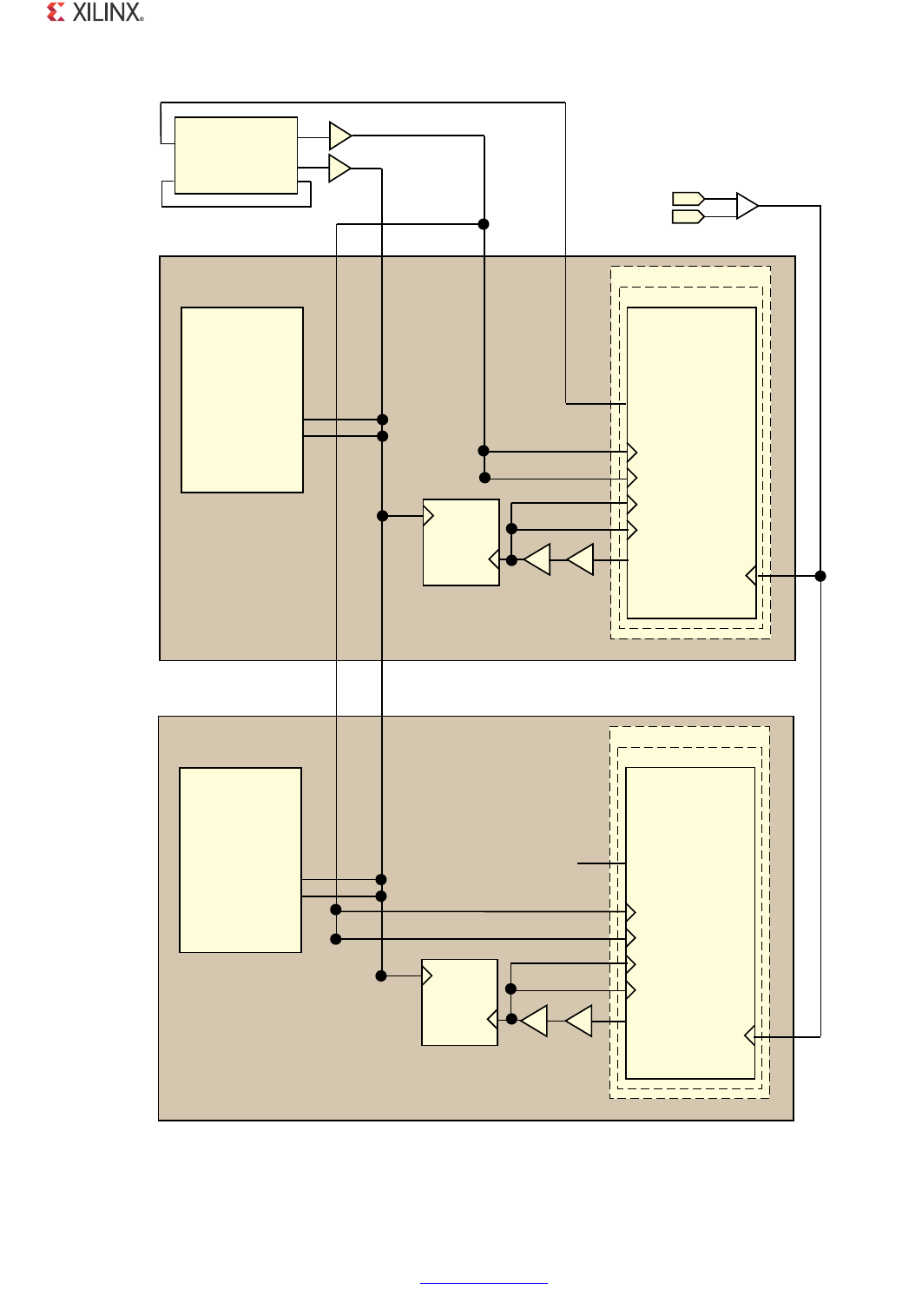
1000BASE-X PCS/PMA or SGMII v11.4 www.xilinx.com 217
PG047 October 16, 2012
Chapter 6: SGMII / Dynamic Standards Switching with Transceivers
X-Ref Target - Figure 6-16
Figure 6-16: Clock Management with Multiple Core Instances with Virtex-7 FPGA Transceivers for
SGMII
COMPONENT?NAME?BLOCK
"LOCK,EVEL
(WKHUQHW%$6(;
3&630$RU
6*0,,FRUH
XVHUFON
XVHUFON
6IRTEX
'48%?#(!..%,
'4(%?#(!..%,
4RANSCEIVER
XVHUFON
0+]
48532#,+
48532#,+
28532#,+
28532#,+
28/54#,+
&0'!
FABRIC
2X
%LASTIC
"UFFER
"5&2
GTREFCLK
-(Z
,%8)'6B*7(
,3$'
JWUHIFONBS
,3$'
JWUHIFONBQ
JWZL]DUGBJW
JWZL]DUG
'42%&#,+
48/54#,+
COMPONENT?NAME?BLOCK
"LOCK,EVEL
(WKHUQHW%$6(;
3&630$RU
6*0,,FRUH
XVHUFON
XVHUFON
XVHUFON
0+]
48532#,+
48532#,+
28532#,+
28532#,+
28/54#,+
&0'!
FABRIC
2X
%LASTIC
"UFFER
"5&2
JWZL]DUGBJW
JWZL]DUG
'42%&#,+
48/54#,+
.#
--#-%?!$6
#,+/54
#,+/54
#,+).
#,+&"/54#,+&").
"5&'
"5&'
XVHUFON
0+]
"5&-2
"5&-2
8

1000BASE-X PCS/PMA or SGMII v11.4 www.xilinx.com 218
PG047 October 16, 2012
Chapter 6: SGMII / Dynamic Standards Switching with Transceivers
Kintex-7 and Zynq-7000 Devices
Figure 6-17 illustrates sharing clock resources across multiple instantiations of the core
when using the 7 series FPGA GTX transceiver. More cores can be added by instantiating
extra block level modules.
Share the gtrefclk_p and gtrefclk_n differential clock pairs. See the 7 Series
Transceiver User Guide for more information.
To provide the FPGA logic clocks for all core instances, select a TXOUTCLK port from any
GTX transceiver and route this to a single MMCM through a BUFG (global clock routing).
The CLKOUT0 (125 MHz) and CLKOUT1 (62.5 MHz) outputs from this MMCM, placed onto
global clock routing using BUFGs, can be shared across all core instances and GTX
transceivers as illustrated.
Each GTX transceiver and core pair instantiated has its own independent clock domains
synchronous to RXOUTCLK. These are placed on global clock routing using a BUFG, as
illustrated in Figure 6-17, and cannot be shared across multiple GTX transceivers.
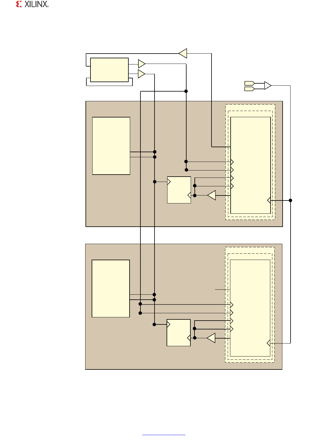
1000BASE-X PCS/PMA or SGMII v11.4 www.xilinx.com 219
PG047 October 16, 2012
Chapter 6: SGMII / Dynamic Standards Switching with Transceivers
X-Ref Target - Figure 6-17
Figure 6-17: Clock Management with Multiple Core Instances with Kintex-7 or Zynq-7000
Device Transceivers for SGMII
COMPONENT?NAME?BLOCK
"LOCK,EVEL
(WKHUQHW%$6(;
3&630$RU
6*0,,FRUH
XVHUFON
XVHUFON
+INTEX:YNQ
'48%?#(!..%,
4RANSCEIVER
XVHUFON
0+]
48532#,+
48532#,+
28532#,+
28532#,+
28/54#,+
&0'!
FABRIC
2X
%LASTIC
"UFFER
GTREFCLK
-(Z
,%8)'6B*7(
,3$'
JWUHIFONBS
,3$'
JWUHIFONBQ
JWZL]DUGBJW
JWZL]DUG
'42%&#,+
48/54#,+
COMPONENT?NAME?BLOCK
"LOCK,EVEL
(WKHUQHW%$6(;
3&630$RU
6*0,,FRUH
XVHUFON
XVHUFON
XVHUFON
0+]
48532#,+
48532#,+
28532#,+
28532#,+
28/54#,+
&0'!
FABRIC
2X
%LASTIC
"UFFER
JWZL]DUGBJW
JWZL]DUG
'42%&#,+
48/54#,+
.#
--#-%?!$6
#,+/54
#,+/54
#,+).
#,+&"/54#,+&").
"5&'
"5&'
XVHUFON
0+]
"5&'
"5&'
"5&'
'48%?#(!..%,
4RANSCEIVER
8
+INTEX:YNQ

1000BASE-X PCS/PMA or SGMII v11.4 www.xilinx.com 220
PG047 October 16, 2012
Chapter 6: SGMII / Dynamic Standards Switching with Transceivers
Artix-7 Devices
Figure 6-18 illustrates sharing clock resources across multiple instantiations of the core
when using the 7 series FPGA GTP transceiver. More cores can be added by instantiating
extra block level modules and sharing the gtrefclk_p and gtrefclk_n differential clock
pairs. See the 7 Series Transceiver User Guide for more information.
To provide the FPGA logic clocks for all core instances, select a TXOUTCLK port from any
GTP transceiver and route this to a single MMCM through a BUFG (global clock routing).
The CLKOUT0 (125 MHz) and CLKOUT1 (62.5 MHz) outputs from this MMCM, placed onto
global clock routing using BUFGs, can be shared across all core instances and GTP
transceivers as illustrated.
Each GTP transceiver and core pair instantiated has its own independent clock domains
synchronous to RXOUTCLK. These are placed on global clock routing using a BUFG, as
illustrated in Figure 6-18, and cannot be shared across multiple GTP transceivers.
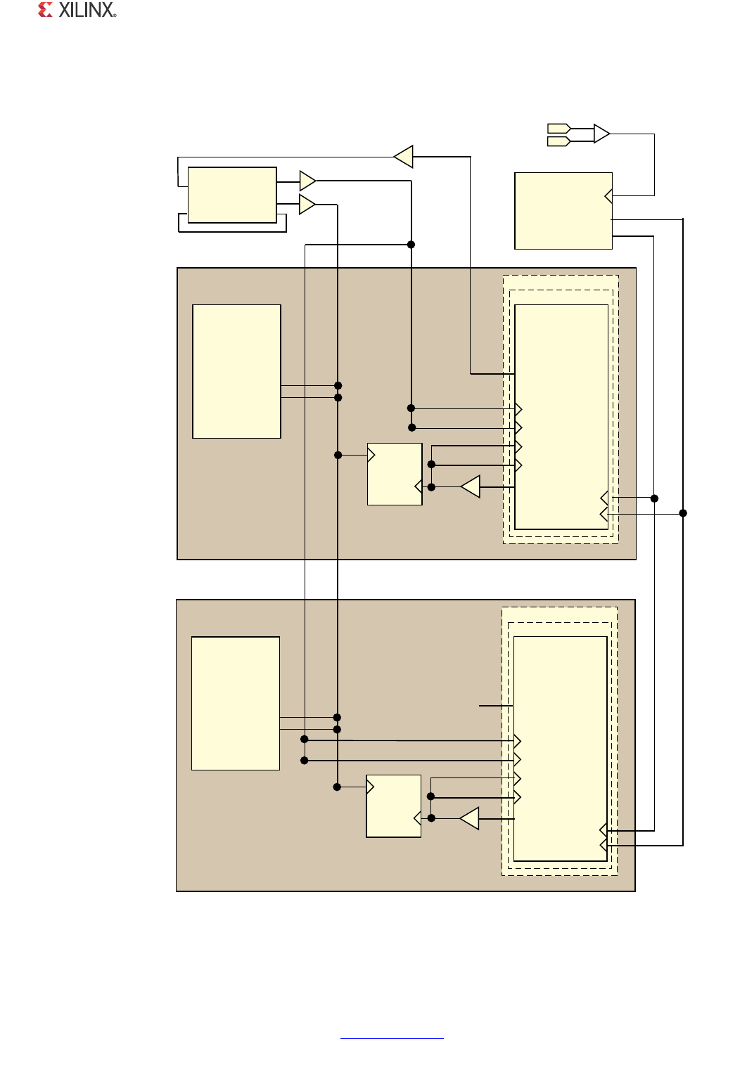
1000BASE-X PCS/PMA or SGMII v11.4 www.xilinx.com 221
PG047 October 16, 2012
Chapter 6: SGMII / Dynamic Standards Switching with Transceivers
X-Ref Target - Figure 6-18
Figure 6-18: Clock Management with Multiple Core Instances with Artix-7 FPGA Transceivers
for SGMII
COMPONENT?NAME?BLOCK
"LOCK,EVEL
(WKHUQHW%$6(;
3&630$RU
6*0,,FRUH
XVHUFON
XVHUFON
!RTIX
'40%?#(!..%,
4RANSCEIVER
XVHUFON
0+]
48532#,+
48532#,+
28532#,+
28532#,+
28/54#,+
&0'!
FABRIC
2X
%LASTIC
"UFFER
GTREFCLK
-(Z
,%8)'6B*7(
,3$'
JWUHIFONBS
,3$'
JWUHIFONBQ
JWZL]DUGBJW
JWZL]DUG
48/54#,+
COMPONENT?NAME?BLOCK
"LOCK,EVEL
(WKHUQHW%$6(;
3&630$RU
6*0,,FRUH
XVHUFON
XVHUFON
XVHUFON
0+]
48532#,+
48532#,+
28532#,+
28532#,+
28/54#,+
&0'!
FABRIC
2X
%LASTIC
"UFFER
JWZL]DUGBJW
JWZL]DUG
48/54#,+
.#
--#-%?!$6
#,+/54
#,+/54
#,+).
#,+&"/54#,+&").
"5&'
"5&'
XVHUFON
0+]
"5&'
"5&'
"5&'
!RTIX
'40%?#(!..%,
4RANSCEIVER
-(Z
'40%?#/--/.
0,,/54#,+
0,,/542%&#,+
'42%&#,+
0,,#,+?).
0,,2%&#,+?).
0,,#,+?).
0,,2%&#,+?).
8
1000BASE-X PCS/PMA or SGMII v11.4 www.xilinx.com 222
PG047 October 16, 2012
Chapter 6: SGMII / Dynamic Standards Switching with Transceivers
SGMII Example Design / Dynamic Switching
Example Design Using a Transceiver
Chapter 20, Detailed Example Design provides a full list and description of the directory and
file structure that is provided with the core, including the location of the HDL example
design provided.
Figure 6-19 illustrates an example design for top-level HDL for the Ethernet 1000BASE-X
PCS/PMA or SGMII in SGMII (or dynamic standards switching) mode using a device-specific
transceiver (Virtex-4, Virtex-5, Virtex-6, Virtex-7, Kintex-7, Artix-7, Zynq-7000 or
Spartan-6).
As illustrated, the example is split between two hierarchical layers. The block level is
designed so that it can be instantiated directly into customer designs and performs the
following functions:
•Instantiates the core from HDL
• Connects the physical-side interface of the core to a device-specific transceiver
X-Ref Target - Figure 6-19
Figure 6-19: Example Design HDL for the Ethernet 1000BASE-X PCS/PMA or SGMII Core in
SGMII Mode Using a Device-Specific Transceiver
(WKHUQHW
%$6(;
3&630$
&RUH
*0,,
,2%V
,Q
,2%V
2XW
'-))STYLE
BIT)&
3ERIAL'-))
3'-))
3'-))
!DAPTATION
-ODULE
#LOCK
-ANAGEMENT
,OGIC
4RANSCEIVER
&ABRIC
2X
%LASTIC
"UFFER
COMPONENT?NAME?EXAMPLE?DESIGN
COMPONENT?NAME?BLOCK
$EVICE
3PECIFIC
4RANSCEIVER
8

1000BASE-X PCS/PMA or SGMII v11.4 www.xilinx.com 223
PG047 October 16, 2012
Chapter 6: SGMII / Dynamic Standards Switching with Transceivers
• Connects the client side GMII of the core to an SGMII Adaptation Module, which
provides the functionality to operate at speeds of 1 Gb/s, 100 Mb/s and 10 Mb/s
The top level of the example design creates a specific example which can be simulated,
synthesized and implemented. The top level of the example design performs the following
functions:
• Instantiates the block level from HDL
• Derives the clock management logic for device-specific transceiver and the core
• Implements an external GMII-style interface
The next few pages in this section describe each of the example design blocks (and
associated HDL files) in detail, and conclude with an overview of the demonstration test
bench provided for the design.
Top-Level Example Design HDL
The top-level example design for the Ethernet 1000BASE-X PCS/PMA core in SGMII mode is
described in the following files:
VHDL
ISE Design Suite:
<project_dir>/<component_name>/example_design/<component_name>_example_design.vhd
Vivado Design Suite:
<project_dir>/<project_name>/<project_name>.srcs/sources1/ip/<component_name>/
<component_name>/example_design/<component_name>_example_design.vhd
Verilog
ISE Design Suite:
<project_dir>/<component_name>/example_design/<component_name>_example_design.v
Vivado Design Suite:
<project_dir>/<project_name>/<project_name>.srcs/sources1/ip/<component_name>/
<component_name>/example_design/<component_name>_example_design.v
The example design HDL top level contains the following:
• An instance of the SGMII block level
• Clock management logic for the core and the device-specific transceiver, including
DCM (if required) and Global Clock Buffer instances
• External GMII logic, including IOB and DDR register instances, where required

1000BASE-X PCS/PMA or SGMII v11.4 www.xilinx.com 224
PG047 October 16, 2012
Chapter 6: SGMII / Dynamic Standards Switching with Transceivers
The example design HDL top level connects the GMII of the block level to external IOBs. This
allows the functionality of the core to be demonstrated using a simulation package, as
described in this guide.
Note: In the Virtex-4, Virtex-5 and Spartan-6 families, transceivers are provided in pairs. When
generated with the appropriate options, the example design is capable of connecting two instances
of the core to the transceiver pair.
Block Level HDL
The following files describe the block level for the Ethernet 1000BASE-X PCS/PMA core in
SGMII mode:
VHDL
ISE Design Suite:
<project_dir>/<component_name>/example_design/<component_name>_block.vhd
Vivado Design Suite:
<project_dir>/<project_name>/<project_name>.srcs/sources1/ip/<component_name>/
<component_name>/example_design/<component_name>_block.vhd
Verilog
ISE Design Suite:
<project_dir>/<component_name>/example_design/<component_name>_block.v
Vivado Design Suite:
<project_dir>/<project_name>/<project_name>.srcs/sources1/ip/<component_name>/
<component_name>/example_design/<component_name>_block.v
The block level contains the following:
• An instance of the Ethernet 1000BASE-X PCS/PMA core in SGMII mode.
• An instance of a transceiver specific to the target device (Virtex-4, Virtex-5, Virtex-6,
Virtex-7, Kintex-7, Artix-7, Zynq-7000 or Spartan-6)
• An SGMII adaptation module containing:
°The clock management logic required to enable the SGMII example design to
operate at 10 Mb/s, 100 Mb/s, and 1 Gb/s.
°GMII logic for both transmitter and receiver paths; the GMII style 8-bit interface is
run at 125 MHz for 1 Gb/s operation; 12.5 MHz for 100 Mb/s operation; 1.25 MHz
for 10 Mb/s operation.

1000BASE-X PCS/PMA or SGMII v11.4 www.xilinx.com 225
PG047 October 16, 2012
Chapter 6: SGMII / Dynamic Standards Switching with Transceivers
The block-level HDL connects the PHY side interface of the core to a device-specific
transceiver instance and the client side to SGMII Adaptation logic as illustrated in
Figure 6-19. This is the most useful part of the example design and should be instantiated
in all customer designs that use the core.
Note: In the Virtex-4, Virtex-5 and Spartan-6 devices, transceivers are provided in pairs. When
generated with the appropriate options, the block level is capable of connecting two instances of the
core to the transceiver.
Transceiver Files for Zynq-7000, Virtex-7 Kintex-7, and Artix-7
Devices
Transceiver Wrapper
This device-specific transceiver wrapper is instantiated from the block-level HDL file of the
example design and is described in the following files:
VHDL
ISE Design Suite:
<project_dir>/<component_name>/example_design/transceiver/<component_name>_transcei
ver.vhd
Vivado Design Suite:
<project_dir>/<project_name>/<project_name>.srcs/sources1/ip/<component_name>/
<component_name>/example_design/transceiver/<component_name>_transceiver.vhd
Verilog
ISE Design Suite:
<project_dir>/<component_name>/example_design/transceiver/<component_name>_transcei
ver.v
Vivado Design Suite:
<project_dir>/<project_name>/<project_name>.srcs/sources1/ip/<component_name>/
<component_name>/example_design/transceiver/<component_name>_transceiver.v
This file instances output source files from the transceiver wizard (used with Gigabit
Ethernet 1000BASE-X attributes).

1000BASE-X PCS/PMA or SGMII v11.4 www.xilinx.com 226
PG047 October 16, 2012
Chapter 6: SGMII / Dynamic Standards Switching with Transceivers
Zynq-7000, Virtex-7, Kintex-7, and Artix-7 Device Transceiver Wizard Files
For Zynq-7000, Virtex-7, Kintex-7, and Artix-7 devices, the transceiver wrapper file directly
instantiates device-specific transceiver wrapper files created from the serial transceiver
wizard. These files tie off (or leave unconnected) unused I/O for the transceiver, and apply
the 1000BASE-X attributes. The files can be edited/tailored by rerunning the wizard and
swapping these files. The files include the following:
VHDL
ISE Design Suite:
<project_dir>/<component_name>/example_design/transceiver/
<component_name>_gtwizard_init.vhd
<project_dir>/<component_name>/example_design/transceiver/
<component_name>_tx_startup_fsm.vhd
<project_dir>/<component_name>/example_design/transceiver/
<component_name>_rx_startup_fsm.vhd
<project_dir>/<component_name>/example_design/transceiver/
<component_name>_gtwizard.vhd
<project_dir>/<component_name>/example_design/transceiver/
<component_name>_gtwizard_gt.vhd
Vivado Design Suite:
<project_dir>/<project_name>/<project_name>.srcs/sources1/ip/<component_name>/
<component_name>/example_design/transceiver/<component_name>_gtwizard_init.vhd
<project_dir>/<project_name>/<project_name>.srcs/sources1/ip/<component_name>/
<component_name>/example_design/transceiver/<component_name>_tx_startup_fsm.vhd
<project_dir>/<project_name>/<project_name>.srcs/sources1/ip/<component_name>/
<component_name>/example_design/transceiver/<component_name>_rx_startup_fsm.vhd
<project_dir>/<project_name>/<project_name>.srcs/sources1/ip/<component_name>/
<component_name>/example_design/transceiver/<component_name>_gtwizard.vhd
<project_dir>/<project_name>/<project_name>.srcs/sources1/ip/<component_name>/
<component_name>/example_design/transceiver/<component_name>_gtwizard_gt.vhd
Verilog
ISE Design Suite:
<project_dir>/<component_name>/example_design/transceiver/
<component_name>_gtwizard_init.v
<project_dir>/<component_name>/example_design/transceiver/
<component_name>_tx_startup_fsm.v
<project_dir>/<component_name>/example_design/transceiver/
<component_name>_rx_startup_fsm.v
<project_dir>/<component_name>/example_design/transceiver/
<component_name>_gtwizard.v
<project_dir>/<component_name>/example_design/transceiver/
<component_name>_gtwizard_gt.v

1000BASE-X PCS/PMA or SGMII v11.4 www.xilinx.com 227
PG047 October 16, 2012
Chapter 6: SGMII / Dynamic Standards Switching with Transceivers
Vivado Design Suite:
<project_dir>/<project_name>/<project_name>.srcs/sources1/ip/<component_name>/
<component_name>/example_design/transceiver/<component_name>_gtwizard_init.v
<project_dir>/<project_name>/<project_name>.srcs/sources1/ip/<component_name>/
<component_name>/example_design/transceiver/<component_name>_tx_startup_fsm.v
<project_dir>/<project_name>/<project_name>.srcs/sources1/ip/<component_name>/
<component_name>/example_design/transceiver/<component_name>_rx_startup_fsm.v
<project_dir>/<project_name>/<project_name>.srcs/sources1/ip/<component_name>/
<component_name>/example_design/transceiver/<component_name>_gtwizard.v
<project_dir>/<project_name>/<project_name>.srcs/sources1/ip/<component_name>/
<component_name>/example_design/transceiver/<component_name>_gtwizard_gt.v
To re-run the transceiver wizard, a CORE Generator tool XCO file for the wizard is included.
This file defines all the required wizard attributes used to generate the preceding files. See
the CORE Generator tool documentation for further information about XCO files. The XCO
file is in the following location:
ISE Design Suite:
<project_dir>/<component_name>/example_design/transceiver/<component_name>_gtwizard
.xco
Vivado Design Suite:
<project_dir>/<project_name>/<project_name>.srcs/sources1/ip/<component_name>/
<component_name>/example_design/transceiver/<component_name>_gtwizard.xco
This file can be used as an input to a Vivado tools project by clicking on <Add Sources> in
the Flow Navigator task bar and selecting the XCO file.
Transceiver Files for Spartan-6 Devices
Transceiver Wrapper
This device-specific transceiver wrapper is instantiated from the block-level HDL file of the
example design and is described in the following files:
VHDL
<project_dir>/<component_name>/example_design/transceiver/transceiver.vhd
Verilog
<project_dir>/<component_name>/example_design/transceiver/transceiver.v
This file instances output source files from the transceiver wizard (used with Gigabit
Ethernet 1000BASE-X attributes).

1000BASE-X PCS/PMA or SGMII v11.4 www.xilinx.com 228
PG047 October 16, 2012
Chapter 6: SGMII / Dynamic Standards Switching with Transceivers
Spartan-6 FPGA GTP Transceiver Wizard Files
For Spartan-6 devices, the transceiver wrapper file directly instantiates device-specific
transceiver wrapper files created from the Spartan-6 FPGA GTP Transceiver Wizard. These
files tie off (or leave unconnected) unused I/O for the GTP transceiver, and apply the
1000BASE-X attributes. The files can be edited/tailored by rerunning the wizard and
swapping these files. The files include the following:
VHDL
<project_dir>/<component_name>/example_design/transceiver/s6_gtpwizard.vhd
<project_dir>/<component_name>/example_design/transceiver/s6_gtpwizard_tile.vhd
Verilog
<project_dir>/<component_name>/example_design/transceiver/s6_gtpwizard.v
<project_dir>/<component_name>/example_design/transceiver/s6_gtpwizard_tile.v
To re-run the Spartan-6 FPGA GTX Transceiver Wizard, a CORE Generator tool XCO file for
the wizard is included. This file defines all the required wizard attributes used to generate
the preceding files. See the CORE Generator tool documentation for further information
about XCO files. The XCO file is in the following location:
<project_dir>/<component_name>/example_design/transceiver/s6_gtpwizard.xco
Transceiver Files for Virtex-6 Devices
Transceiver Wrapper
This device-specific transceiver wrapper is instantiated from the block-level HDL file of the
example design and is described in the following files:
VHDL
<project_dir>/<component_name>/example_design/transceiver/v6_gtxwizard_top.vhd
Verilog
<project_dir>/<component_name>/example_design/transceiver/v6_gtxwizard_top.v
This file instances output source files from the device-specific wizard (used with Gigabit
Ethernet 1000BASE-X attributes).

1000BASE-X PCS/PMA or SGMII v11.4 www.xilinx.com 229
PG047 October 16, 2012
Chapter 6: SGMII / Dynamic Standards Switching with Transceivers
Virtex-6 FPGA GTX Transceiver Wizard Files
For Virtex-6 devices, the transceiver wrapper file directly instantiates transceiver wrapper
files created from the Virtex-6 FPGA GTX Transceiver Wizard. These files tie off (or leaves
unconnected) unused I/O for the GTX transceiver, and apply the 1000BASE-X attributes. The
files can be edited/tailored by rerunning the wizard and swapping these files. The files
include the following:
VHDL
<project_dir>/<component_name>/example_design/transceiver/v6_gtxwizard.vhd
<project_dir>/<component_name>/example_design/transceiver/v6_gtxwizard_gtx.vhd
Verilog
<project_dir>/<component_name>/example_design/transceiver/v6_gtxwizard.v
<project_dir>/<component_name>/example_design/transceiver/v6_gtxwizard_gtx.v
To re-run the Virtex-6 FPGA GTX Transceiver Wizard, a CORE Generator tool XCO file for the
wizard is included. This file defines all the required wizard attributes used to generate the
preceding files. See the CORE Generator tool documentation for further information about
XCO files. The XCO file is in the following location:
<project_dir>/<component_name>/example_design/transceiver/v6_gtxwizard.xco
RocketIO Transceiver Files for Virtex-5 Devices
Transceiver Wrapper
This device-specific RocketIO transceiver wrapper is instantiated from the block-level HDL
file of the example design and is described in the following files:
VHDL
<project_dir>/<component_name>/example_design/transceiver/transceiver.vhd
Verilog
<project_dir>/<component_name>/example_design/transceiver/transceiver.v
This file instances output source files from the device-specific RocketIO Transceiver Wizard
(used with Gigabit Ethernet 1000BASE-X attributes).
In the Virtex-5 devices, RocketIO transceivers are provided in pairs. When generated with
the appropriate options, the block level is capable of connecting two instances of the core
to the RocketIO transceiver pair. When only a single instance of the core is requested, the
unused RocketIO transceiver from the pair is still instantiated from within this transceiver
wrapper but left unconnected.

1000BASE-X PCS/PMA or SGMII v11.4 www.xilinx.com 230
PG047 October 16, 2012
Chapter 6: SGMII / Dynamic Standards Switching with Transceivers
Virtex-5 FPGA RocketIO GTP Transceiver Specific Files
For Virtex-5 LXT and SXT devices, the transceiver wrapper file directly instantiates RocketIO
GTP transceiver wrapper files created from the Virtex-5 FPGA RocketIO GTP Transceiver
Wizard. These files tie off (or leave unconnected) unused I/O for the GTP transceiver pair,
and apply the 1000BASE-X attributes. The files can be edited/tailored by rerunning the
RocketIO GTP Transceiver Wizard and swapping these files. These are the following files:
VHDL
<project_dir>/<component_name>/example_design/transceiver/v5_gtpwizard.vhd
<project_dir>/<component_name>/example_design/transceiver/v5_gtpwizard_tile.vhd
Verilog
<project_dir>/<component_name>/example_design/transceiver/v5_gtpwizard.v
<project_dir>/<component_name>/example_design/transceiver/v5_gtpwizard_tile.v
To re-run the device-specific RocketIO Transceiver GTP Wizard, a CORE Generator tool XCO
file for the RocketIO Transceiver GTP Wizard has also been included. This file lists all of the
device-specific RocketIO Transceiver GTP Wizard attributes used to generate the preceding
files. See the CORE Generator tool documentation for more information about XCO files.
The XCO file is in the following location:
<project_dir>/<component_name>/example_design/transceiver/v5_gtpwizard.xco
Virtex-5 FPGA RocketIO GTX Transceiver Specific Files
For Virtex-5 FXT and TXT devices, the transceiver wrapper file directly instantiates RocketIO
GTX transceiver wrapper files created from the Virtex-5 FPGA RocketIO GTX Transceiver
Wizard. These files tie off (or leaves unconnected) unused I/O for the GTX transceiver pair
and apply the 1000BASE-X attributes. The files can be edited/tailored by rerunning the
RocketIO GTX Transceiver Wizard and swapping these files. These are the following files:
VHDL
<project_dir>/<component_name>/example_design/transceiver/v5_gtxwizard.vhd
<project_dir>/<component_name>/example_design/transceiver/v5_gtxwizard_gtx_tile.vhd
Verilog
<project_dir>/<component_name>/example_design/transceiver/v5_gtxwizard.v
<project_dir>/<component_name>/example_design/transceiver/v5_gtxwizard_gtx_tile.v

1000BASE-X PCS/PMA or SGMII v11.4 www.xilinx.com 231
PG047 October 16, 2012
Chapter 6: SGMII / Dynamic Standards Switching with Transceivers
To re-run the device-specific RocketIO GTX Transceiver Wizard, a CORE Generator tool XCO
file for the RocketIO GTX Transceiver Wizard has also been included. This file lists all of the
RocketIO GTX Transceiver Wizard attributes which were used in the generation of the
preceding files. See the CORE Generator tool documentation for further information about
XCO files. The XCO file is located:
<project_dir>/<component_name>/example_design/transceiver/v5_gtxwizard.xco
RocketIO Transceiver Files for Virtex-4 FX Devices
Transceiver Wrapper
This device-specific RocketIO transceiver wrapper is instantiated from the block-level HDL
file of the example design and is described in the following files:
VHDL
<project_dir>/<component_name>/example_design/transceiver/transceiver.vhd
Verilog
<project_dir>/<component_name>/example_design/transceiver/transceiver.v
This file instances the RocketIO transceiver with Gigabit Ethernet 1000BASE-X attributes
applied.
In the Virtex-4 FX devices RocketIO transceivers are provided in pairs. When generated with
the appropriate options, the block level is capable of connecting two instances of the core
to the RocketIO transceiver pair. When only a single instance of the core is requested, the
unused RocketIO transceiver from the pair is still instantiated from within this transceiver
wrapper but left unconnected.
Calibration Blocks
For Virtex-4 FX devices only, calibration blocks are required. A calibration block is
connected to both GT11 A and B within the RocketIO transceiver tile. This occurs in the
transceiver wrapper file. See Answer Record 22477 for information about downloading the
Calibration Block User Guide.
The calibration block is described in the following files:
VHDL
<project_dir>/<component_name>/example_design/transceiver/cal_block_v1_4_1.vhd
Verilog
<project_dir>/<component_name>/example_design/transceiver/cal_block_v1_4_1.v

1000BASE-X PCS/PMA or SGMII v11.4 www.xilinx.com 232
PG047 October 16, 2012
Chapter 6: SGMII / Dynamic Standards Switching with Transceivers
GT11 Reset/Initialization Circuitry
Precise reset/initialization circuitry is required for the GT11 device-specific RocketIO
transceivers.
The reset circuitry for the device-specific RocketIO receiver is illustrated in Figure 2-18 of
the Virtex-4 RocketIO Multi-Gigabit Transceiver User Guide (UG076). This is implemented in
the following files:
VHDL
<project_dir>/<component_name>/example_design/transceiver/gt11_init_rx.vhd
Verilog
<project_dir>/<component_name>/example_design/transceiver/gt11_init_rx.v
The reset circuitry for the RocketIO transceiver is illustrated in Figure 2-13 of the Virtex-4
FPGA RocketIO Multi-Gigabit Transceiver User Guide (UG076). This is implemented in the
following files:
VHDL
<project_dir>/<component_name>/example_design/transceiver/gt11_init_tx.vhd
Verilog
<project_dir>/<component_name>/example_design/transceiver/gt11_init_tx.v
Both receiver and transmitter reset circuitry entities are instantiated from within the block
level of the example design.
Receiver Elastic Buffer
The Receiver Elastic Buffer if present (see Receiver Elastic Buffer Implementations) is
described in the following files:
VHDL
ISE Design Suite:
<project_dir>/<component_name>/example_design/transceiver/
<component_name>_rx_elastic_buffer.vhd
Vivado Design Suite:
<project_dir>/<project_name>/<project_name>.srcs/sources1/ip/<component_name>/
<component_name>/example_design/transceiver/<component_name>_rx_elastic_buffer.vhd

1000BASE-X PCS/PMA or SGMII v11.4 www.xilinx.com 233
PG047 October 16, 2012
Chapter 6: SGMII / Dynamic Standards Switching with Transceivers
Verilog
ISE Design Suite:
<project_dir>/<component_name>/example_design/transceiver/
<component_name>_rx_elastic_buffer.v
Vivado Design Suite:
<project_dir>/<project_name>/<project_name>.srcs/sources1/ip/<component_name>/
<component_name>/example_design/transceiver/<component_name>_rx_elastic_buffer.v
In SGMII or Dynamic Switching modes, the Rx Buffer in the device-specific transceiver is
optionally bypassed. If bypassed, a larger buffer is implemented in the FPGA logic and
instantiated from within the transceiver wrapper.
This alternative Receiver Elastic Buffer uses a single block RAM to create a buffer twice as
large as the one present in the device-specific transceiver, which is able to cope with larger
frame sizes before clock tolerances accumulate and result in an emptying or filling of the
buffer.
SGMII Adaptation Module
The SGMII Adaptation Module is described in the following files:
VHDL
ISE Design Suite:
<project_dir>/<component_name>/example_design/sgmii_adapt/
<component_name>sgmii_adapt.vhd
<component_name>clk_gen.vhd
<component_name>johnson_cntr.vhd
<component_name>tx_rate_adapt.vhd
<component_name>rx_rate_adapt.vhd
Vivado Design Suite:
<project_dir>/<project_name>/<project_name>.srcs/sources1/ip/<component_name>/<comp
onent_name>/example_design/sgmii_adapt/
<component_name>sgmii_adapt.vhd
<component_name>clk_gen.vhd
<component_name>johnson_cntr.vhd
<component_name>tx_rate_adapt.vhd
<component_name>rx_rate_adapt.vhd

1000BASE-X PCS/PMA or SGMII v11.4 www.xilinx.com 234
PG047 October 16, 2012
Chapter 6: SGMII / Dynamic Standards Switching with Transceivers
Verilog
ISE Design Suite:
<project_dir>/<component_name>/example_design/sgmii_adapt/
<component_name>sgmii_adapt.v
<component_name>clk_gen.v
<component_name>johnson_cntr.v
<component_name>tx_rate_adapt.v
<component_name>rx_rate_adapt.v
Vivado Design Suite:
<project_dir>/<project_name>/<project_name>.srcs/sources1/ip/<component_name>/<comp
onent_name>/example_design/sgmii_adapt/
<component_name>sgmii_adapt.v
<component_name>clk_gen.v
<component_name>johnson_cntr.v
<component_name>tx_rate_adapt.v
<component_name>rx_rate_adapt.v
The GMII of the core always operates at 125 MHz. The core makes no differentiation
between the three speeds of operation; it always effectively operates at 1 Gb/s. However, at
100 Mb/s, every data byte run through the core should be repeated 10 times to achieve the
required bit rate; at 10 Mb/s, each data byte run through the core should be repeated 100
times to achieve the required bit rate. Dealing with this repetition of bytes is the function of
the SGMII adaptation module and its component blocks.
The SGMII adaptation module and component blocks are described in detail in the
Chapter 8, Additional Client-Side SGMII Logic Provided in the Example Design.

1000BASE-X PCS/PMA or SGMII v11.4 www.xilinx.com 235
PG047 October 16, 2012
Chapter 6: SGMII / Dynamic Standards Switching with Transceivers
Demonstration Test Bench
Figure 6-20 illustrates the demonstration test bench for the Ethernet 1000BASE-X PCS/PMA
or SGMII core in SGMII mode. The demonstration test bench is a simple VHDL or Verilog
program to exercise the example design and the core itself.
The top-level test bench entity instantiates the example design for the core, which is the
Device Under Test (DUT). A stimulus block is also instantiated and clocks, resets and test
bench semaphores are created. The following files describe the top-level of the
demonstration test bench.
VHDL
ISE Design Suite:
<project_dir>/<component_name>/simulation/demo_tb.vhd
Vivado Design Suite:
<project_dir>/<project_name>/<project_name>.srcs/sources1/ip/<component_name>/
<component_name>/simulation/demo_tb.vhd
X-Ref Target - Figure 6-20
Figure 6-20: Demonstration Test Bench for the Ethernet 1000BASE-X PCS/PMA or SGMII Core in
SGMII Mode Using Device-Specific Transceivers
$EMONSTRATION4EST"ENCH
0-!
-ONITOR
3ERIALTO0ARALLEL
#ONVERSIONAND
""
$ECODING
0-!
3TIMULUS
""%NCODING
AND0ARALLELTO
3ERIAL
#ONVERSION
'-))
3TIMULUS
'-))
-ONITOR
'-))
$54
#ONTROLAND$ATA3TRUCTURES
#ONFIGURATION
3TIMULUS
$EVICE
3PECIFIC
4RANSCEIVER
8

1000BASE-X PCS/PMA or SGMII v11.4 www.xilinx.com 236
PG047 October 16, 2012
Chapter 6: SGMII / Dynamic Standards Switching with Transceivers
Verilog
ISE Design Suite:
<project_dir>/<component_name>/simulation/demo_tb.v
Vivado Design Suite:
<project_dir>/<project_name>/<project_name>.srcs/sources1/ip/<component_name>/
<component_name>/simulation/demo_tb.v
The stimulus block entity, instantiated from within the top-level test bench, creates the
Ethernet stimulus in the form of four Ethernet frames, which are injected into GMII and PHY
interfaces of the DUT. The output from the DUT is also monitored for errors. The following
files describe the stimulus block of the demonstration test bench.
VHDL
ISE Design Suite:
<project_dir>/<component_name>/simulation/stimulus_tb.vhd
Vivado Design Suite:
<project_dir>/<project_name>/<project_name>.srcs/sources1/ip/<component_name>/
<component_name>/simulation/stimulus_tb.vhd
Verilog
ISE Design Suite:
<project_dir>/<component_name>/simulation/stimulus_tb.v
Vivado Design Suite:
<project_dir>/<project_name>/<project_name>.srcs/sources1/ip/<component_name>/
<component_name>/simulation/stimulus_tb.v
Together, the top-level test bench file and the stimulus block combine to provide the full
test bench functionality which is described in the sections that follow.
Note: In the Virtex-4, Virtex-5 and Spartan-6 devices, transceivers are provided in pairs. When
generated with the appropriate options, the example design is capable of connecting two instances
of the core to the device-specific transceiver pair. When this is the case, two stimulus blocks are
instantiated from the top level test bench to independently exercise both cores.

1000BASE-X PCS/PMA or SGMII v11.4 www.xilinx.com 237
PG047 October 16, 2012
Chapter 6: SGMII / Dynamic Standards Switching with Transceivers
Test Bench Functionality
The demonstration test bench performs the following tasks:
• Input clock signals are generated.
• A reset is applied to the example design.
• The Ethernet 1000BASE-X PCS/PMA core is configured through the MDIO interface by
injecting an MDIO frame into the example design. This disables Auto-Negotiation and
takes the core out of Isolate state.
• The following frames are injected into the GMII transmitter by the GMII stimulus block
at 1 Gb/s.
°the first is a minimum length frame
°the second is a type frame
°the third is an errored frame
°the fourth is a padded frame
• The serial data received at the device-specific transceiver transmitter interface is
converted to 10-bit parallel data, then 8B/10B decoded. The resulting frames are
checked by the PMA Monitor against the stimulus frames injected into the GMII
transmitter to ensure data integrity.
• The same four frames are generated by the PMA Stimulus block. These are 8B/10B
encoded, converted to serial data and injected into the device-specific transceiver
receiver interface at 1 Gb/s.
• Data frames received at the GMII receiver are checked by the GMII Monitor against the
stimulus frames injected into the device-specific transceiver receiver to ensure data
integrity.
Customizing the Test Bench
Changing Frame Data
You can change the contents of the four frames used by the demonstration test bench by
changing the data and valid fields for each frame defined in the stimulus block. New frames
can be added by defining a new frame of data. Modified frames are automatically updated
in both stimulus and monitor functions.
Changing Frame Error Status
Errors can be inserted into any of the predefined frames in any position by setting the error
field to ‘1’ in any column of that frame. Injected errors are automatically updated in both
stimulus and monitor functions.

1000BASE-X PCS/PMA or SGMII v11.4 www.xilinx.com 238
PG047 October 16, 2012
Chapter 6: SGMII / Dynamic Standards Switching with Transceivers
Changing the Core Configuration
The configuration of the Ethernet 1000BASE-X PCS/PMA core used in the demonstration
test bench can be altered.
CAUTION! Certain configurations of the core cause the test bench to fail or cause processes to run
indefinitely. For example, the demonstration test bench does not auto-negotiate with the design
example. Determine the configurations that can safely be used with the test bench.
The core can be reconfigured by editing the injected MDIO frame in the demonstration test
bench top level.
Changing the Operational Speed
SGMII can be used to carry Ethernet traffic at 10 Mb/s, 100 Mb/s or 1 Gb/s. By default, the
demonstration test bench is configured to operate at 1 Gb/s. The speed of both the
example design and test bench can be set to the desired operational speed by editing the
following settings, recompiling the test bench, then running the simulation again.
1 Gb/s Operation
set speed_is_10_100 to logic 0
100 Mb/s Operation
set speed_is_10_100 to logic 1
set speed_is_100 to logic 1
10 Mb/s Operation
set speed_is_10_100 to logic 1
set speed_is_100 to logic 0

1000BASE-X PCS/PMA or SGMII v11.4 www.xilinx.com 239
PG047 October 16, 2012
Chapter 7
SGMII over LVDS
This chapter provides the general guidelines for creating SGMII interfaces using Virtex-7,
Kintex-7 or Virtex-6 FPGA devices. The chapter contains two main sections:
• The first section describes Synchronous SGMII over Virtex7/Kintex 7 FPGA LVDS
• The second section describes SGMII Support Using Asynchronous Oversampling over
Virtex-6 FPGA LVDS.
Synchronous SGMII over Virtex7/Kintex 7 FPGA
LVDS
This section provides general guidelines for creating synchronous SGMII designs using
Virtex®-7/Kintex™-7 FPGA LVDS. Kintex-7 devices, -2 speed grade or higher on HR Banks
and -1 or higher for HP Banks, can fully support SGMII using standard LVDS SelectIO™
technology logic resources. This enables direct connection to external PHY devices without
the use of an FPGA Transceiver. This implementation is illustrated in Figure 7-1.
This section is organized into the following subsections:
•Design Requirements provides the prerequisites for the Synchronous SGMII solution.
•Clocking Logic discusses the clocking logic that is required for the synchronous SGMII
LVDS design.
•Layout and Placement provides guidelines for performing FPGA layout to guide the
tools through Place and Route (PAR) and to achieve timing success.
•Example Design Implementation describes the format of the example design provided,
a description of all blocks of the example design, and describes how the design can be
used to create your own custom implementation.
This section also contains an overview of the demonstration test bench that is provided
with the example design.
1000BASE-X PCS/PMA or SGMII v11.4 www.xilinx.com 240
PG047 October 16, 2012
Chapter 7: SGMII over LVDS
Users of the core in this mode can benefit from a detailed understanding of Kintex-7 FPGA
Clocking Resources and SelectIO Resources. See 7 Series FPGA SelectIO Resources User
Guide and 7 Series FPGA Clocking Resources User Guide.
Design Requirements
SGMII Only
The interface implemented using this method supports SGMII between the FPGA and an
external PHY device; the interface cannot directly support 1000BASE-X.
Supported Devices
• Kintex-7 Devices, -2 speed grade or faster for devices with HR Banks or -1 speed grade
or faster for devices with HP banks
• Virtex-7 Devices, -2 speed grade or faster for devices with HR Banks or -1 speed grade
or faster for devices with HP banks
Timing closure of this interface is challenging; perform the steps described in Layout and
Placement.
X-Ref Target - Figure 7-1
Figure 7-1: Example Design for Sync SGMII over LVDS solution for Virtex-7/Kintex-7 Devices
#LOCKING,OGIC
REFCLK?P
REFCLK?N
CLKCLK CLK CLK
,6$34RANSCEIVER
RXN
RXP
TXN
TXP
COMPONENT?NAME?BLOCK
COMPONENT?NAME?EXAMPLE?DESIGN
%THERNET
3'-))
0#30-!#ORE
3'-))!DAPTATION
-ODULE
'-))3TYLE
BIT)&
8

1000BASE-X PCS/PMA or SGMII v11.4 www.xilinx.com 241
PG047 October 16, 2012
Chapter 7: SGMII over LVDS
Clocking Logic
The SGMII LVDS solution is a synchronous implementation where an external clock is
provided to the design. In the example design this clock is assumed to be a 125 MHz
differential clock.
This 125 MHz differential clock is fed to IBUFDS and the output drives the input of MMCM.
MMCM is used to generate multiple clocks of 208 MHz, 625 MHz, 125 MHz, and 104 MHz.
A system clock of 200 MHz is given to the IDELAYCTRL module which calibrates IDELAY and
ODELAY using the user-supplied REFCLK. The 208 MHz clock output from MMCM can also
be used as a clock input to IDELAYCTRL module instead of the 200MHz system clock. See
details about IDELAYCTRL in the 7 Series FPGA SelectIO Resources User Guide.
Typical usage of synchronous LVDS solution involves multiple instances of LVDS solution
with single clocking block. Figure 7-2 provides a detailed illustration of the clocking logic.
Table 7-1 provides the list of all the clocks in the design and their usage.
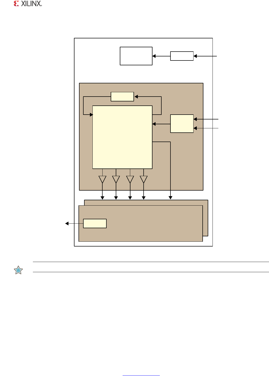
1000BASE-X PCS/PMA or SGMII v11.4 www.xilinx.com 242
PG047 October 16, 2012
Chapter 7: SGMII over LVDS
IMPORTANT: Important notes relating to Figure 7-2:
• The 125 MHz clock output from IBUFDS that is routed to the CLKIN1 pin of the MMCM
should enter the FPGA on a global clock pin. This enables the clock signal to be routed
to the device MMCM module using dedicated clock routing. The clock source should
confirm to ethernet specifications (100 ppm of accuracy).
•Figure 7-2 shows usage of 4 BUFGs. Instead a BUFIO can be used for the 625 MHz clock
and BUFR for the other three MMCM clock outputs or BUFHs on all four MMCM clock
outputs.
•The OSERDES primitives used by the LVDS transceiver must use the BUFG 625 MHz
clock source to provide the cleanest possible serial output. This necessitates that the
X-Ref Target - Figure 7-2
Figure 7-2: Synchronous LVDS Implementation Clocking Logic
%8)* LQGHSHQGHQWBFON
,'(/$<&75/
UHIFONBS
UHIFONBQ
,%8)'6
00&0
&/.,1
%8)*
&/.287
&/.287
&/.287
&/.287
FONFONFONFON
&/.)%287
&/.)%,1
FRPSRQHQWBQDPHBVJPLLBSK\BFONBJHQ
FRPSRQHQWBQDPHBEORFNLQVW
2''5VJPLLBFON
FRPSRQHQWBQDPHBH[DPSOHBGHVLJQ
PPFPBORFNHG
FRPSRQHQWBQDPHBEORFNLQVW
%8)* %8)* %8)* %8)*

1000BASE-X PCS/PMA or SGMII v11.4 www.xilinx.com 243
PG047 October 16, 2012
Chapter 7: SGMII over LVDS
Output Serializer/Deserializer (OSERDES) parallel clock (CLKDIV) must be provided
from a 208 MHz global clock buffer (BUFG) that is derived from the same MMCM. This
requirement is used to satisfy the parallel to serial clock phase relationships within the
OSERDES primitives. See the 7 Series FPGA SelectIO Resources User Guide and 7 Series
FPGA Clocking Resources User Guide.
• An IDELAY Controller module is provided in the Example Design module for use with
the IDELAYs required on the receiver input serial path. This is provided with a 200 MHz
clock source. Here it is assumed to be coming as an input to the example design from
the system. The 208 MHz clock output from MMCM can also be used instead of the 200
MHz source clock.
Table 7-1 provides the list of all the clocks in the design and their usage.
Table 7-1: List of Clocks in the Design
Clock Input/Generated/Output Description
independent_clk Input System Clock 200 MHz input system clock for driving IDELAYCTRL
primitive.
refclk125_p Differential input clock. Differential clock input to FPGA, synchronous to the
incoming serial data.
refclk125_n Differential input clock. Differential clock input to FPGA, synchronous to the
incoming serial data.
clk125_ibuf 125 MHz input clock. Clock derived from incoming differential clock by
IBUFGDS.This is the input clock for MMCM.
sgmii_clk Output Clock to MAC Clock for client MAC. This clock is derived from
sgmii_clk_r and sgmii_clk_f using ODDR primitive.
clk104 Generated by MMCM This clock is used in eye monitor and phy calibration
modules to process 12-bit wide data.
clk208 Generated by MMCM
On transmitter path OSERDES takes 6-bit parallel
data at this frequency and converts it to serial
data.Similarly on receiver path ISERDES converts
serial data into 6 bit parallel data at 208 MHz.Later
6 bit data is converted into 10-bit data through
gearbox.
clk625 Generated by MMCM
Used by ISERDES and OSERDES modules for input
data sampling and parallel to serial conversion
respectively.
clk125 Generated by MMCM Used inside the design as main clock.PCS/PMA core
and SGMII adaptation modules work at this clock.
sgmii_clk_r Generated in SGMII
adapter.
125 MHz or 12.5 MHz or 1.25 MHz depending on
data rate.
sgmii_clk_f Generated in SGMII
adapter.
125 MHz or 12.5 MHz or 1.25 MHz depending on
data rate.

1000BASE-X PCS/PMA or SGMII v11.4 www.xilinx.com 244
PG047 October 16, 2012
Chapter 7: SGMII over LVDS
Layout and Placement
A hands-on approach is required for placing this design. The steps provided here are a
useful guide, but other knowledge is assumed. To aid with these guidelines, users of the
core in this mode would benefit from:
• A detailed understanding of 7 Series FPGA Clocking Resources and SelectIO Resources.
See 7 Series FPGA User Guide (7 Series FPGA product page).
• A working knowledge of the Xilinx PlanAhead™ tool (or alternatively FPGA Editor) to
locate particular clock buffers and slices.
Following are some guidelines:
• Select an I/O Bank in your chosen device for use with for your transmitter and receiver
SGMII ports; see Clocking Logic.
• A single IDELAYCTRL is instantiated by the Block Level of the Example Design for use
with a single I/O Bank. This primitive needs to be associated with the various
IODELAYE2 elements used in that I/O Bank.
The following UCF syntax achieves this in the example design provided for the Kintex-7
device XC7V325T:
NET refclk125_p LOC = AD12;
NET refclk125_n LOC = AD11;
NET reset LOC = Y29 | IOSTANDARD = LVCMOS18;
NET rxp LOC = Y23;
NET rxn LOC = Y24;
NET txp LOC = L25;
NET txn LOC = K25;
The following XDC syntax achieves this in the example design provided for the Kintex-7
device XC7V325T:
set_property PACKAGE_PIN AD12 [get_ports refclk125_p]
set_property PACKAGE_PIN AD11 [get_ports refclk125_n]
set_property IOSTANDARD LVDS [get_ports refclk125_n]
set_property IOSTANDARD LVDS [get_ports refclk125_p]
set_property IOSTANDARD LVCMOS18 [get_ports reset]
set_property PACKAGE_PIN Y29 [get_ports reset]
set_property PACKAGE_PIN Y23 [get_ports rxp]
set_property PACKAGE_PIN Y24 [get_ports rxn]
set_property IOSTANDARD LVDS_25 [get_ports rxn]
set_property IOSTANDARD LVDS_25 [get_ports rxp]

1000BASE-X PCS/PMA or SGMII v11.4 www.xilinx.com 245
PG047 October 16, 2012
Chapter 7: SGMII over LVDS
set_property PACKAGE_PIN L25 [get_ports txp]
set_property PACKAGE_PIN K25 [get_ports txn]
set_property IOSTANDARD LVDS_25 [get_ports txn]
set_property IOSTANDARD LVDS_25 [get_ports txp]
Example Design Implementation
Figure 7-1 illustrates the HDL example design that is provided for the SGMII over
Virtex-7/Kintex-7 FPGA LVDS implementation. As illustrated, the example is split between
several hierarchical layers. The top level of the example design creates a specific example
that can be simulated, synthesized and implemented.
The core netlist in this implementation remains identical to that of Ethernet 1000BASE-X
PCS/PMA or SGMII Support Using a Device Specific Transceiver in Chapter 1
Also illustrated in Figure 7-3, the HDL example design for this implementation provides
additional logic to form the "LVDS transceiver" module, which fully replaces the
functionality otherwise provided by a 7 series FPGA GTX/GTH Transceiver. The LVDS
transceiver block uses the 7 Series OSERDES, IODELAYs and ISERDES elements. The full
transceiver functionality is then completed with Comma Alignment, 8B/10B Decoder,
8B/10B Encoder. The example design logical blocks and files are discussed in detail in the
next sections.
Example Design Top Level
The top-level example design for the core with SGMII using synchronous clocking over
Virtex-7/Kintex-7 FPGA is described in the following files:
VHDL
ISE Design Suite:
<project_dir>/<component_name>/example_design/<component_name>_example_design.vhd
Vivado Design Suite:
<project_dir>/<project_name>/<project_name>.srcs/sources1/ip/<component_name>/
<component_name>/example_design/<component_name>_example_design.vhd
Verilog
ISE Design Suite:
<project_dir>/<component_name>/example_design/<component_name>_example_design.v
Vivado Design Suite:
<project_dir>/<project_name>/<project_name>.srcs/sources1/ip/<component_name>/
<component_name>/example_design/<component_name>_example_design.v

1000BASE-X PCS/PMA or SGMII v11.4 www.xilinx.com 246
PG047 October 16, 2012
Chapter 7: SGMII over LVDS
The example design HDL top level contains the following:
• An instance of the I/O block level HDL and clocking logic
• External GMII logic, including IOB and DDR register instances, where required. This
module adds I/O logic to the GMII of the SGMII ports. This is included only to create a
standalone design that can be implemented in an FPGA and simulated in both
functional and timing simulation for the purposes of providing a complete SGMII
design example. Discard this level of hierarchy and instantiate the Block Level of the
Example Design in your own design.
Block Level of the Example Design
The following files describe the block level for the Ethernet 1000BASE-X PCS/PMA core in
SGMII mode:
VHDL
ISE® Design Suite:
<project_dir>/<component_name>/example_design/<component_name>_block.vhd
Vivado™ Design Suite:
<project_dir>/<project_name>/<project_name>.srcs/sources1/ip/<component_name>/
<component_name>/example_design/<component_name>_block.vhd
Verilog
ISE Design Suite:
<project_dir>/<component_name>/example_design/<component_name>_block.v
Vivado Design Suite:
<project_dir>/<project_name>/<project_name>.srcs/sources1/ip/<component_name>/
<component_name>/example_design/<component_name>_block.v
The block level of the example design connects together all of the components for a single
SGMII port. These are:
• A core netlist (introduced in Ethernet 1000BASE-X PCS/PMA or SGMII Support Using a
Device Specific Transceiver in Chapter 1).
•The LVDS Transceiver, connected to the PHY side of the core netlist, to perform the
SERDES functionality using the Synchronous LVDS Method. Containing:
°Functionality for I/O functionality and gearbox modules in transmit and receive
path for data width conversion.
°Functionality to find the right sampling point using eye monitor and phy calibration
modules.

1000BASE-X PCS/PMA or SGMII v11.4 www.xilinx.com 247
PG047 October 16, 2012
Chapter 7: SGMII over LVDS
•The SGMII Adaptation Module top level, connected to the Ethernet MAC (GMII) side of
the core netlist, containing:
°The clock management logic required to enable the SGMII example design to
operate at 10 Mb/s, 100 Mb/s, and 1 Gb/s.
°GMII logic for both transmitter and receiver paths; the GMII style 8-bit interface is
run at 125 MHz for 1 Gb/s operation; 12.5 MHz for 100 Mb/s operation; 1.25 MHz
for 10 Mb/s operation.
LVDS Transceiver
The LVDS transceiver block fully replaces the functionality otherwise provided by a Virtex-7
FPGA GTX/GTH or Kintex-7 FPGA GTX transceiver. This is only possible at a serial line rate of
1.25 Gb/s. See Figure 7-3 for a block diagram of the LVDS transceiver. This is split up into
several sub-blocks which are described in further detail in the following sections. On the
transmitter path, data sourced by the core netlist is routed through the 8B/10B Encoder to
translate the 8-bit code groups into 10-bit data. The 10-bit data is then passed through the
10B6B Gearbox, the parallel 6-bit data is then clocked out serially at a line rate of 1.25 Gb/s.
The receiver path has further complexity. Serial data received at 1.25 Gb/s is routed in
parallel to two IODELAYs and ISERDES elements as illustrated in Figure 7-4. There is a logic
to find the correct sampling point in eye monitor and phy calibration modules.
Then 6-bit parallel data is fed to the 6B10B gearbox which converts it into 10-bit parallel
data. Having recovered parallel data from the serial stream, the Comma Alignment module,
next on the receiver path, detects specific 8b/10b bit patterns (commas) and uses these to
realign the 10-bit parallel data to contain unique 8b/10b code groups. These code groups
are then routed through the 8B/10B Decoder module to obtain the unencoded 8-bit code
groups that the core netlist can accept.
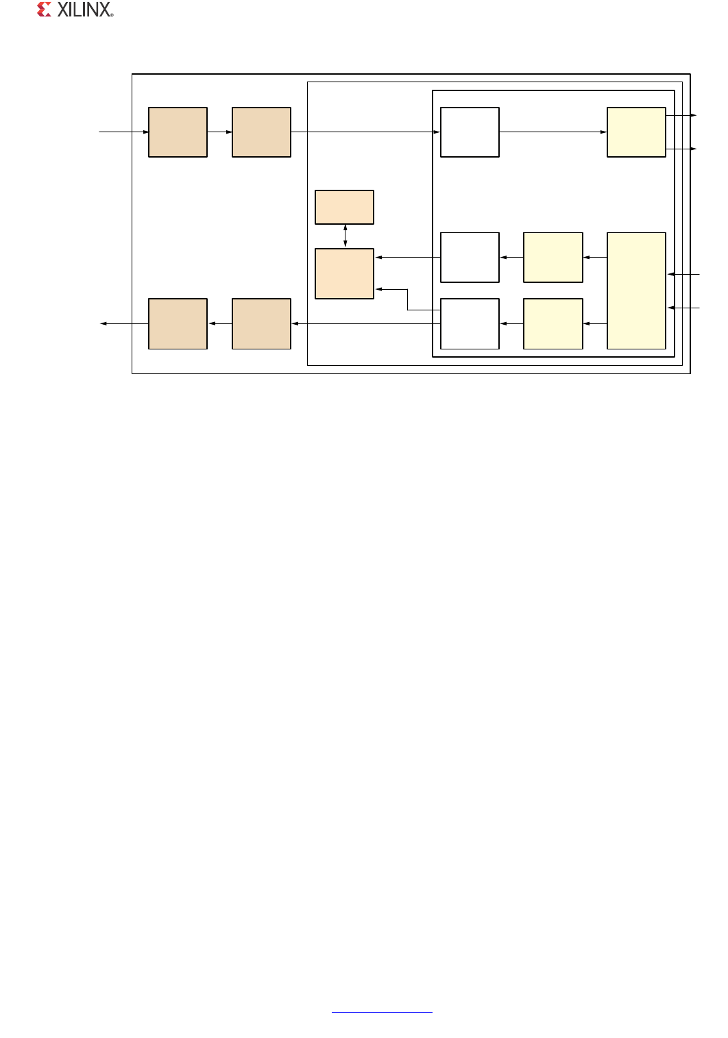
1000BASE-X PCS/PMA or SGMII v11.4 www.xilinx.com 248
PG047 October 16, 2012
Chapter 7: SGMII over LVDS
The following files describe the top level of the hierarchal levels of the LVDS transceiver:
VHDL
ISE Design Suite:
<project_dir>/<component_name>/example_design/lvds_transceiver/<component_name>_
lvds_transceiver.vhd
Vivado Design Suite:
<project_dir>/<project_name>/<project_name>.srcs/sources1/ip/<component_name>/
<component_name>/example_design/lvds_transceiver/
<component_name>_lvds_transceiver.vhd
Verilog
ISE Design Suite:
<project_dir>/<component_name>/example_design/lvds_transceiver/<component_name>_
lvds_transceiver.v
Vivado Design Suite:
<project_dir>/<project_name>/<project_name>.srcs/sources1/ip/<component_name>/
<component_name>/example_design/lvds_transceiver/
<component_name>_lvds_transceiver.v
X-Ref Target - Figure 7-3
Figure 7-3: LVDS Transceiver Block Level Representation
""
%NCODER
""
'EARBOX
""
$ECODER
""
'EARBOX
)3%2$%3%
-ONITOR
3ERIALBITS
)3%2$%3%
$ATA
3ERIALBITS
%YE-ONITOR
O?RX?MON
O?RX?DATA?B
0HY
#ALLIBRATION
/3%2$%3%
BITS3ERIAL
)$%,!9%
)$%,!9%
/"5&$3
)"5&$3?$)&&
?/54
RXN
RXP
TXN
TXP
)"
)
/"
/
/"
/
)
COMPONENT?NAME?SGMII?PHY?IOB
COMPONENT?NAME?GPIO?SGMII?TOP
COMPONENT?NAME?LVDS?TRANSCEIVER
&ROM#ORE
4O#ORE
BITDATA
BITDATA
8

1000BASE-X PCS/PMA or SGMII v11.4 www.xilinx.com 249
PG047 October 16, 2012
Chapter 7: SGMII over LVDS
8B/10B Encoder
The implemented 8B/10B coding scheme is an industry standard, DC-balanced,
byte-oriented transmission code ideally suited for high-speed local area networks and
serial data links. As such, the coding scheme is used in several networking standards,
including Ethernet. The 8B/10B Encoder block is taken from Xilinx Application Note
XAPP1122, Parameterizable 8b/10b Encoder. XAPP1122 provides two possible approaches: a
choice of a block RAM-based implementation or a LUT-based implementation. The SGMII
LVDS example design uses the LUT-based implementation, but XAPP1122 can be used to
swap this for the block RAM-based approach if this better suits device logic resources.
The following files describe the 8B/10B Encoder:
VHDL
ISE Design Suite:
<project_dir>/<component_name>/example_design/lvds_transceiver/tx/
<component_name>_encode_8b10b_pkg.vhd
<component_name>_encode_8b10b_lut_base.vhd
Vivado Design Suite:
<project_dir>/<project_name>/<project_name>.srcs/sources1/ip/<component_name>/
<component_name>/example_design/lvds_transceiver/
<component_name>_encode_8b10b_pkg.vhd
<component_name>_encode_8b10b_lut_base.vhd
Verilog
ISE Design Suite:
<project_dir>/<component_name>/example_design/lvds_transceiver/tx/
<component_name>_encode_8b10b_pkg.v
<component_name>_encode_8b10b_lut_base.v
Vivado Design Suite:
<project_dir>/<project_name>/<project_name>.srcs/sources1/ip/<component_name>/
<component_name>/example_design/lvds_transceiver/
<component_name>_encode_8b10b_pkg.v
<component_name>_encode_8b10b_lut_base.v
OSERDES
The OSERDES primitive (actually a MASTER-SLAVE pair of primitives) is used in a standard
mode; 6-bit input parallel data synchronous to a 208 MHz global clock buffer source (BUFG)
is clocked into the OSERDES. Internally within the OSERDES, the data is serialized and
output at a rate of 1.25 Gb/s. The clock source used for the serial data is a 625 MHz clock
source using a BUFG global clock buffer at double data rate.

1000BASE-X PCS/PMA or SGMII v11.4 www.xilinx.com 250
PG047 October 16, 2012
Chapter 7: SGMII over LVDS
• The 625 MHz BUFG and 208 MHz BUFG clocks for serial and parallel data are both
derived from the same MMCM so there is no frequency drift.
• The use of the BUFG global clock buffer for the parallel clock is a requirement of the
OSERDES; when using a BUFG clock for serial data, a BUFG clock source, derived from
the same MMCM source, must be used for the parallel data to satisfy clock phase
alignment constraints within the OSERDES primitives.
Gearbox 10b6b
This module is used to convert 10-bit data at 125 MHz to 6-bit data at 208 MHz. This data
is then given to OSERDES for serialization.
VHDL
ISE Design Suite:
<project_dir>/<component_name>/example_design/lvds_transceiver/<component_name>>
_gearbox_10b_6b.vhd
Vivado Design Suite:
<project_dir>/<project_name>/<project_name>.srcs/sources1/ip/<component_name>/<comp
onent_name>/example_design/lvds_transceiver/<component_name>_gearbox_10b_6b.vhd
Verilog
ISE Design Suite:
<project_dir>/<component_name>/example_design/lvds_transceiver/
<component_name>>_gearbox_10b_6b.v
Vivado Design Suite:
<project_dir>/<project_name>/<project_name>.srcs/sources1/ip/<component_name>/<comp
onent_name>/example_design/lvds_transceiver/<component_name>_gearbox_10b_6b.v
IODELAYs and ISERDES
This logic along with eye monitor and phy calibration is used to convert incoming serial
data into 6 bit parallel data. See IODELAYs and ISERDES in 7 Series FPGAs SelectIO Resources
User Guide (UG471) for more information on these primitives.
Eye Monitor and Phy Calibration
Both these modules have state machines and work in conjunction to find the right sampling
point for receive data coming from ISERDES. These modules work on 12-bit wide data at
104 MHz frequency. This data is the 6-bit parallel data (at 208 MHz) sampled at 104 MHz.
Eye monitor monitors the N-node IDELAY to determine the margin of current P-node (data)
IDELAY tap value.

1000BASE-X PCS/PMA or SGMII v11.4 www.xilinx.com 251
PG047 October 16, 2012
Chapter 7: SGMII over LVDS
The following file describes the eye monitor functionality:
VHDL
ISE Design Suite:
<project_dir>/<component_name>/example_design/lvds_transceiver/<component_name>_
sgmii_eye_monitor.vhd
Vivado Design Suite:
<project_dir>/<project_name>/<project_name>.srcs/sources1/ip/<component_name>/<comp
onent_name>/example_design/lvds_transceiver/<component_name>_sgmii_eye_monitor.vhd
Verilog
ISE Design Suite:
<project_dir>/<component_name>/example_design/lvds_transceiver/<component_name>_
sgmii_eye_monitor.v
Vivado Design Suite:
<project_dir>/<project_name>/<project_name>.srcs/sources1/ip/<component_name>/<comp
onent_name>/example_design/lvds_transceiver/<component_name>_sgmii_eye_monitor.v
Phy calibration module uses the eye monitor block to determine the optimal rx-data IDELAY
sampling point. The following file describes the phy calibration functionality:
VHDL
ISE Design Suite:
<project_dir>/<component_name>/example_design/lvds_transceiver/
<component_name>_sgmii_phy_calibration.vhd
Vivado Design Suite:
<project_dir>/<project_name>/<project_name>.srcs/sources1/ip/<component_name>/
<component_name>/example_design/lvds_transceiver/
<component_name>_sgmii_phy_calibration.vhd
Verilog
ISE Design Suite:
<project_dir>/<component_name>/example_design/lvds_transceiver/
<component_name>_sgmii_phy_calibration.v
Vivado Design Suite:
<project_dir>/<project_name>/<project_name>.srcs/sources1/ip/<component_name>/
<component_name>/example_design/lvds_transceiver/<component_name>_sgmii_phy_calibra
tion.v

1000BASE-X PCS/PMA or SGMII v11.4 www.xilinx.com 252
PG047 October 16, 2012
Chapter 7: SGMII over LVDS
Gearbox 6b10b
This module is used to convert 6-bit data recovered from ISERDES at 208 MHz to 10-bit data
at 125 MHz to be used by Comma Alignment and 8B/10B Decoder modules. Also it
implements bitslip logic based on input from comma alignment module.
VHDL
ISE Design Suite:
<project_dir>/<component_name>/example_design/lvds_transceiver/<component_name>_gea
rbox_6b_10b.vhd
Vivado Design Suite:
<project_dir>/<project_name>/<project_name>.srcs/sources1/ip/<component_name>/<comp
onent_name>/example_design/lvds_transceiver/<component_name>_gearbox_6b_10b.vhd
Verilog
ISE Design Suite:
<project_dir>/<component_name>/example_design/lvds_transceiver/
<component_name>_gearbox_6b_10b.v
Vivado Design Suite:
<project_dir>/<project_name>/<project_name>.srcs/sources1/ip/<component_name>/
<component_name>/example_design/lvds_transceiver/<component_name>_gearbox_6b_10b.v
Comma Alignment
Data received by comma alignment block is in parallel form, but the bits of the parallel bus
have not been aligned into correct 10-bit word boundaries. By detecting a unique 7-bit
serial sequence known as a 'comma' (however the commas can fall across the 10-bit parallel
words), the comma alignment logic controls bit shifting of the data so as to provide correct
alignment to the data leaving the module. The bitslip input of the gearbox_6b_10b is driven
by the comma alignment module's state machine, so the actual bit shift logic is performed
by the gearbox_6b_10b. In 8b/10b encoding, both +ve and -ve bit sequences exist for each
defined code group. The comma alignment logic is able to detect and control realignment
on both +ve and -ve comma versions.
The following files describe the Comma Alignment block:
VHDL
ISE Design Suite:
<project_dir>/<component_name>/example_design/lvds_transceiver/<component_name>_sgm
ii_comma_alignment.vhd

1000BASE-X PCS/PMA or SGMII v11.4 www.xilinx.com 253
PG047 October 16, 2012
Chapter 7: SGMII over LVDS
Vivado Design Suite:
<project_dir>/<project_name>/<project_name>.srcs/sources1/ip/<component_name>/
<component_name>/example_design/lvds_transceiver/
<component_name>_sgmii_comma_alignment.vhd
Verilog
ISE Design Suite:
<project_dir>/<component_name>/example_design/lvds_transceiver/<component_name>
_sgmii_comma_alignment.v
Vivado Design Suite:
<project_dir>/<project_name>/<project_name>.srcs/sources1/ip/<component_name>/<comp
onent_name>/example_design/lvds_transceiver/<component_name>_sgmii_comma_alignment.
v
8B/10B Decoder
The implemented 8b/10b coding scheme is an industry-standard, DC-balanced,
byte-oriented transmission code ideally suited for high-speed local area networks and
serial data links. As such, the coding scheme is used in several networking standards,
including Ethernet. The 8B/10B Decoder block is taken from Xilinx Application Note
XAPP1112, Parameterizable 8b10b Decoder. XAPP1112 provides two possible approaches: a
choice of a block RAM-based implementation or a LUT-based implementation.
The SGMII LVDS example design uses the LUT-based implementation, but XAPP1112 can be
used to swap this for the block RAM-based approach if this better suits device logic
resources.
The following files describe the 8B/10B Decoder:
VHDL
ISE Design Suite:
<project_dir>/<component_name>/example_design/lvds_transceiver/
<component_name>_decode_8b10b_pkg.vhd
<component_name>_decode_8b10b_lut_base.vhd
Vivado Design Suite:
<project_dir>/<project_name>/<project_name>.srcs/sources1/ip/<component_name>/
<component_name>/example_design/lvds_transceiver/
<component_name>_decode_8b10b_pkg.vhd
<component_name>_decode_8b10b_lut_base.vhd

1000BASE-X PCS/PMA or SGMII v11.4 www.xilinx.com 254
PG047 October 16, 2012
Chapter 7: SGMII over LVDS
Verilog
ISE Design Suite:
<project_dir>/<component_name>/example_design/lvds_transceiver/
<component_name>_decode_8b10b_pkg.v
<component_name>_ decode_8b10b_lut_base.v
Vivado Design Suite:
<project_dir>/<project_name>/<project_name>.srcs/sources1/ip/<component_name>/<comp
onent_name>/example_design/lvds_transceiver/
<component_name>_ decode_8b10b_pkg.v
<component_name>_ decode_8b10b_lut_base.v
GPIO SGMII TOP
This module is a hierarchical top including the eye monitor, phy calibration modules, and
the SGMII PHY IOB functionality. See Figure 7-3 for a detailed block diagram for LVDS
transceiver.
VHDL
ISE Design Suite:
<project_dir>/<component_name>/example_design/lvds_transceiver/<component_name>_gpi
o_sgmii_top.vhd
Vivado Design Suite:
<project_dir>/<project_name>/<project_name>.srcs/sources1/ip/<component_name>/
<component_name>/example_design/lvds_transceiver/
<component_name>_gpio_sgmii_top.vhd
Verilog
ISE Design Suite:
<project_dir>/<component_name>/example_design/lvds_transceiver/
<component_name>_gpio_sgmii_top.v
Vivado Design Suite:
<project_dir>/<project_name>/<project_name>.srcs/sources1/ip/<component_name>/
<component_name>/example_design/lvds_transceiver/<component_name>_gpio_sgmii_top.v
SGMII PHY IOB
This module is a hierarchical top including the ISERDES, OSERDES, and IDELAY modules. See
Figure 7-3 for a detailed block diagram for LVDS transceiver.

1000BASE-X PCS/PMA or SGMII v11.4 www.xilinx.com 255
PG047 October 16, 2012
Chapter 7: SGMII over LVDS
VHDL
ISE Design Suite:
<project_dir>/<component_name>/example_design/lvds_transceiver/<component_name>_
sgmii_phy_iob.vhd
Vivado Design Suite:
<project_dir>/<project_name>/<project_name>.srcs/sources1/ip/<component_name>/<comp
onent_name>/example_design/lvds_transceiver/<component_name>_sgmii_phy_iob.vhd
Verilog
ISE Design Suite:
<project_dir>/<component_name>/example_design/lvds_transceiver/<component_name>_
sgmii_phy_iob.v
Vivado Design Suite:
<project_dir>/<project_name>/<project_name>.srcs/sources1/ip/<component_name>/<comp
onent_name>/example_design/lvds_transceiver/<component_name>_sgmii_phy_iob.v
SGMII Adaptation Module
The SGMII Adaptation Module is described in the following files:
VHDL
ISE Design Suite:
<project_dir>/<component_name>/example_design/sgmii_adapt/
<component_name>_sgmii_adapt.vhd
<component_name>_clk_gen.vhd
<component_name>_johnson_cntr.vhd
<component_name>_tx_rate_adapt.vhd
<component_name>_rx_rate_adapt.vhd
Vivado Design Suite:
<project_dir>/<project_name>/<project_name>.srcs/sources1/ip/<component_name>/<comp
onent_name>/example_design/sgmii_adapt/
<component_name>_sgmii_adapt.vhd
<component_name>_clk_gen.vhd
<component_name>_johnson_cntr.vhd
<component_name>_tx_rate_adapt.vhd
<component_name>_rx_rate_adapt.vhd

1000BASE-X PCS/PMA or SGMII v11.4 www.xilinx.com 256
PG047 October 16, 2012
Chapter 7: SGMII over LVDS
Verilog
ISE Design Suite:
<project_dir>/<component_name>/example_design/sgmii_adapt/
<component_name>_sgmii_adapt.v
<component_name>_clk_gen.v
<component_name>_johnson_cntr.v
<component_name>_tx_rate_adapt.v
<component_name>_rx_rate_adapt.v
Vivado Design Suite:
<project_dir>/<project_name>/<project_name>.srcs/sources1/ip/<component_name>/<comp
onent_name>/example_design/sgmii_adapt/
<component_name>_sgmii_adapt.v
<component_name>_clk_gen.v
<component_name>_johnson_cntr.v
<component_name>_tx_rate_adapt.v
<component_name>_rx_rate_adapt.v
The GMII of the core always operates at 125 MHz. The core makes no differentiation
between the three speeds of operation; it always effectively operates at 1 Gb/s. However, at
100 Mb/s, every data byte run through the core should be repeated 10 times to achieve the
required bit rate; at 10 Mb/s, each data byte run through the core should be repeated 100
times to achieve the required bit rate. Dealing with this repetition of bytes is the function of
the SGMII adaptation module and its component blocks. The SGMII adaptation module and
component blocks are described in detail in the Additional Client-Side SGMII Logic
Provided in the Example Design in Chapter 8.
Demonstration Test Bench
Figure 7-4 illustrates the demonstration test bench for the Ethernet 1000BASE-X PCS/PMA
or SGMII core in SGMII mode with the LVDS solution over Virtex-7/Kintex™-7 FPGA. The
demonstration test bench is a simple VHDL or Verilog program to exercise the example
design and the core itself.
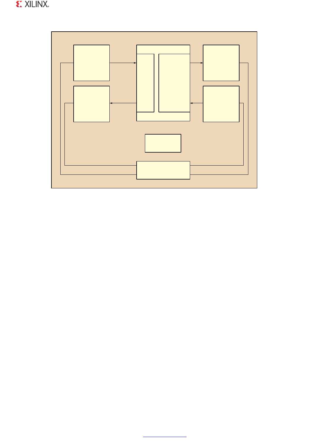
1000BASE-X PCS/PMA or SGMII v11.4 www.xilinx.com 257
PG047 October 16, 2012
Chapter 7: SGMII over LVDS
The top-level test bench entity instantiates the example design for the core, which is the
Device Under Test (DUT). A stimulus block (per SGMII port) is also instantiated and clocks,
resets and test bench semaphores are created. The following files describe the top-level of
the demonstration test bench.
VHDL
ISE Design Suite:
<project_dir>/<component_name>/simulation/demo_tb.vhd
Vivado Design Suite:
<project_dir>/<project_name>/<project_name>.srcs/sources1/ip/<component_name>/
<component_name>/simulation/demo_tb.vhd
Verilog
ISE Design Suite:
<project_dir>/<component_name>/simulation/demo_tb.v
Vivado Design Suite:
<project_dir>/<project_name>/<project_name>.srcs/sources1/ip/<component_name>/
<component_name>/simulation/demo_tb.v
X-Ref Target - Figure 7-4
Figure 7-4: Demonstration Test Bench for the SGMII Core in SGMII over LVDS Solution for
Virtex-7/Kintex-7 FPGA
'-))
3TIMULUS
'-))
-ONITOR
'-)) ,6$3
4RANSCEIVER
3'-))
-ONITOR
3ERIALTO0ARALLEL
#ONVERSIONAND
""$ECODING
3'-))
3TIMULUS
""%NCODING
AND0ARALLELTO
3ERIAL
#ONVERSION
#ONFIGURATION
3TIMULUS
#ONTROLAND$ATA3TRUCTURES
$EMONSTRATION4EST"ENCH
$54
8

1000BASE-X PCS/PMA or SGMII v11.4 www.xilinx.com 258
PG047 October 16, 2012
Chapter 7: SGMII over LVDS
The stimulus block entity, instantiated from within the top-level test bench, creates the
Ethernet stimulus in the form of four Ethernet frames, which are injected into GMII and
SGMII serial interfaces of the DUT. The output from the DUT is also monitored for errors.
The following files describe the stimulus block of the demonstration test bench.
VHDL
ISE Design Suite:
<project_dir>/<component_name>/simulation/stimulus_tb.vhd
Vivado Design Suite:
<project_dir>/<project_name>/<project_name>.srcs/sources1/ip/<component_name>/
<component_name>/simulation/stimulus_tb.vhd
Verilog
ISE Design Suite:
<project_dir>/<component_name>/simulation/stimulus_tb.v
Vivado Design Suite:
<project_dir>/<project_name>/<project_name>.srcs/sources1/ip/<component_name>/
<component_name>/simulation/stimulus_tb.v
Together, the top-level test bench file and the stimulus block combine to provide the full
test bench functionality which is described in the sections that follow.
Test Bench Functionality
The demonstration test bench performs the following tasks:
• Input clock signals are generated.
• A reset is applied to the example design.
• Then, for SGMII port instantiated in the example design:
°The core is configured through its MDIO interface by injecting an MDIO frame into
the example design. This disables Auto-Negotiation and takes the core out of
Isolate state.
°The following frames are injected into the GMII transmitter by the GMII stimulus
block at 1 Gb/s.
- the first is a minimum length frame
- the second is a type frame
-the third is an errored frame

1000BASE-X PCS/PMA or SGMII v11.4 www.xilinx.com 259
PG047 October 16, 2012
Chapter 7: SGMII over LVDS
- the fourth is a padded frame
°The data received at the SGMII serial LVDS transceiver interface is 8B/10B decoded.
The resulting frames are checked by the SGMII Monitor against the stimulus frames
injected into the GMII transmitter to ensure data integrity.
°The same four frames are generated by the SGMII Stimulus block. These are 8B/10B
encoded and injected into the SGMII serial LVDS transceiver interface.
°Data frames received at the GMII receiver are checked by the GMII Monitor against
the stimulus frames injected into the LVDS transceiver to ensure data integrity.
Customizing the Test Bench
Note:
a. The changes described in the following subsections are applied simultaneously to all
SGMII ports instantiated in the example design.
b. The port eye_mon_wait_time is given as in input to example design. This is given
a lower value for ease in simulation. Actual implementation can tie it to 12'hFFF.
Changing Frame Data
You can change the contents of the four frames used by the demonstration test bench by
changing the data and valid fields for each frame defined in the stimulus block. New frames
can be added by defining a new frame of data. Modified frames are automatically updated
in both stimulus and monitor functions.
Changing Frame Error Status
Errors can be inserted into any of the predefined frames in any position by setting the error
field to '1' in any column of that frame. Injected errors are automatically updated in both
stimulus and monitor functions.
Changing the Core Configuration
The configuration of the Ethernet 1000BASE-X PCS/PMA core used in the demonstration
test bench can be altered.
CAUTION! Certain configurations of the core cause the test bench to fail or cause processes to run
indefinitely. For example, the demonstration test bench does not auto-negotiate with the design
example. Determine the configurations that can safely be used with the test bench.
The core can be reconfigured by editing the injected MDIO frame in the demonstration test
bench top level. See Chapter 2, Product Specification for information about using the MDIO
interface.

1000BASE-X PCS/PMA or SGMII v11.4 www.xilinx.com 260
PG047 October 16, 2012
Chapter 7: SGMII over LVDS
Changing the Operational Speed
SGMII can be used to carry Ethernet traffic at 10 Mb/s, 100 Mb/s or 1 Gb/s. By default, the
demonstration test bench is configured to operate at 1 Gb/s. The speed of both the
example design and test bench can be set to the desired operational speed by editing the
following settings, recompiling the test bench, then running the simulation again.
1 Gb/s Operation
set speed_is_10_100 to logic 0
100 Mb/s Operation
set speed_is_10_100 to logic 1
set speed_is_100 to logic 1
10 Mb/s Operation
set speed_is_10_100 to logic 1
set speed_is_100 to logic 0
SGMII Support Using Asynchronous
Oversampling over Virtex-6 FPGA LVDS
This chapter provides general guidelines for creating SGMII designs using asynchronous
oversampling over Virtex-6 FPGA LVDS. Virtex-6 devices,-2 speed grade or higher, can fully
support SGMII using standard LVDS SelectIO™ technology logic resources. This enables
direct connection to external PHY devices without the use of a Virtex-6 FPGA GTX
Transceiver. This implementation is illustrated in Figure 7-8.
This chapter is organized into the following sections:
•Design Requirements provides the UI specifications for the SGMII receiver.
•Clocking Logic discusses the clocking logic that is required for the asynchronous
oversampling LVDS design.
•Layout and Placement provides guidelines for performing FPGA layout to guide the
tools through Place and Route (PAR) and to achieve timing success.
•Example Design Implementation describes the format of the example design provided,
a description of all blocks of the example design, and describes how the design can be
used to create your own custom implementation.
This section also contains an overview of the demonstration test bench that is provided
with the example design.

1000BASE-X PCS/PMA or SGMII v11.4 www.xilinx.com 261
PG047 October 16, 2012
Chapter 7: SGMII over LVDS
Users of the core in this mode can benefit from a detailed understanding of Virtex-6 FPGA
clocking resources and SelectIO™ interface resources. See Virtex-6 FPGA User Guide
(Virtex-6 FPGA product page).
Design Requirements
SGMII Only
The interface implemented using this asynchronous oversampling method supports SGMII
between the FPGA and an external PHY device; the interface cannot directly support
1000BASE-X.
Supported in Virtex-6 Devices, -2 Speed Grade or Faster
The SGMII LVDS implementation has only been characterized in the -2 speed grade and
faster Virtex-6 devices.
Timing closure of this interface is challenging; perform the steps described in Layout and
Placement.
Receiver UI Specification
The DRU must have at least two valid sampling points per data bit, requiring 0.5 UI of
opening. The settings of the FPGA add 0.125 UI of requirement making a total opening
requirement at the receiver of 0.625 UI.
Recommended for Chip-to-Chip Copper Implementations Only
This interface supports an SGMII link between the FPGA and an external PHY device across
a single PCB; keep the SGMII copper signal lengths to a minimum.
Clocking Logic
The HDL for the I/O Bank Level of the Example Design logical block contains the parameter
TX_AND_RX_SHARE_CLOCK; this value is set to true by default, implying that the Tx and Rx
logic of the SGMII ports will share the BUFIO clocks.
Setting the parameter TX_AND_RX_SHARE_CLOCK to true necessitates that the transmitter
and receiver ports of the SGMII are LOC-ed into the same Virtex-6 FPGA I/O bank. See
SGMII Tx and Rx Ports are in the Same I/O Bank.
Setting the parameter TX_AND_RX_SHARE_CLOCK to false will duplicate the clock circuitry
that is required by the transmitter, allowing the receiver and transmitter ports to be
separated and placed into different Virtex-6 FPGA I/O banks. See SGMII Tx and Rx Ports are
in Different I/O Banks.
Edit the HDL file for the I/O Bank Level of the Example Design directly to change the value
of the TX_AND_RX_SHARE_CLOCK parameter.
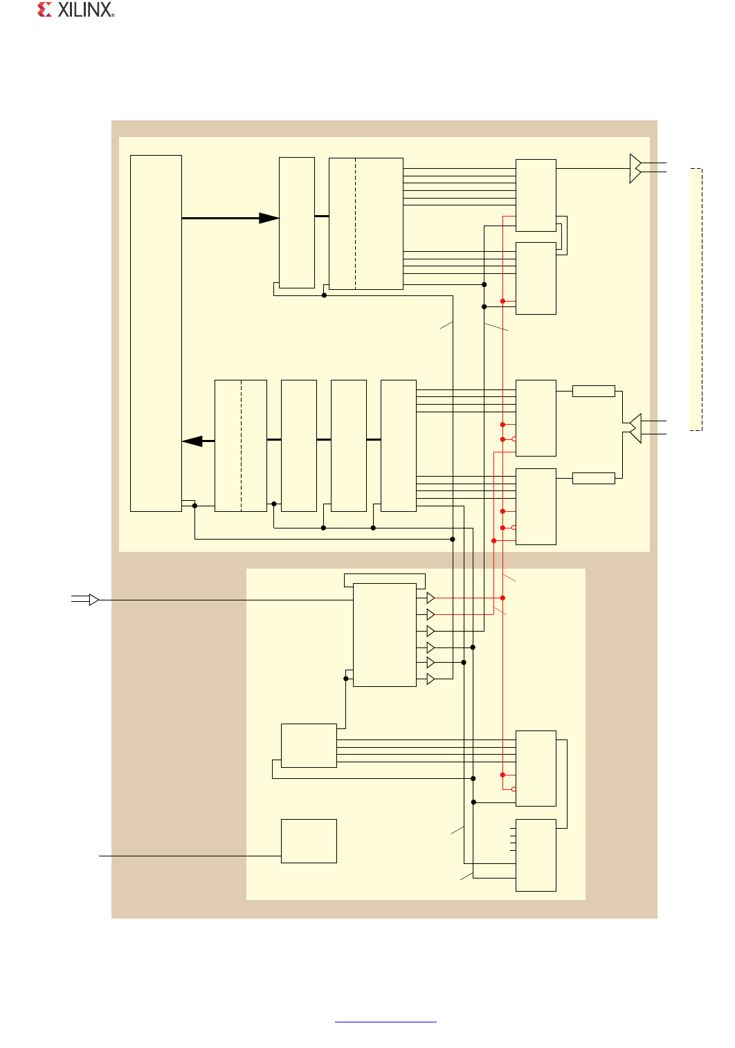
1000BASE-X PCS/PMA or SGMII v11.4 www.xilinx.com 262
PG047 October 16, 2012
Chapter 7: SGMII over LVDS
SGMII Tx and Rx Ports are in the Same I/O Bank
X-Ref Target - Figure 7-5
Figure 7-5: Asynchronous Oversampling LVDS Clocking Logic (Tx and Rx Placed in the Same I/O Bank)
--#-
,2%DQN&ORFNLQJ
/3%2$%3%
$
$
$
$
#,+
$)6#,+
/&"
)3%2$%3%
1
1
1
1
#,+
#,+"
$)6#,+
/&"
#LOCK!LIGNMENT
3TATE-ACHINE
).#
#,+&").
#,+).
03).#$%#
03%.
#,+&"/54
#,+/54
#,+/54
#,+/54
#,+/54
#,+/54
#,+/54
"5&)/
"5&)/
"5&2
"5&'
"5&'
"5&'
28#,+$)6
)$%,!9#42,
2%&#,+
)3%2$%3%
1
1
1
1
#,+
#,+"
/#,+
)3%2$%3%
1
1
1
1
#,+
#,+"
/#,+
$$,9
$$,9
)/$%,!9%
)/$%,!9%
)$%,!9?6!,5%
)$%,!9?6!,5%
RXP
RXN
)"5&$3?$)&&?/54
$25#OMMA!LIGNMENT""$ECODER
CLK CLK CLKP
2X%LASTIC"UFFER
RXRECCLKCLKM
/RJL&RUH1HWOLVW
USERCLK
USERCLK
""%NCODER
CLK
40HASE"UFFER
CLKM?TX?BUFRCLKM
/3%2$%3%
$
$
$
$
#,+
$)6#,+
/3%2$%3%
$
$
$
$
$
$
#,+
$)6#,+
/1
TXP
TXN
/"5&$3
REFCLK?P
REFCLK?N
-(ZCLOCKSOURCE
CLK
³%ORFN´/HYHO
h)/"ANKv,EVEL
-(Z
-(Z
-(Z
DEGREE
PHASESHIFT
-(Z
-(Z
-(Z
3AME
)/
"ANK
8

1000BASE-X PCS/PMA or SGMII v11.4 www.xilinx.com 263
PG047 October 16, 2012
Chapter 7: SGMII over LVDS
Figure 7-5 provides a detailed illustration of the clocking logic provided when the
TX_AND_RX_SHARE_CLOCK parameter is set to true. This necessitates that associated SGMII
Tx and Rx ports are placed into the same I/O Bank.
Only a single SGMII port is illustrated but the clocks are identically wired up to all SGMII
ports sharing the same I/O Bank.
A major component of the I/O Bank clocking logic is the MMCM module. This module
should be provided with a high quality 125 MHz clock reference as illustrated. The MMCM
is configured to provide the frequency related clocks defined in Tab le 7-2 which are used by
all SGMII ports within the respective I/O bank.
Table 7-2: MMCM Generated Clocks That Are Shared across the I/O Bank
MMCM
Output Frequency
Clock
Buffer
Used
HDL Clock name Description
CLKOUT0 625 MHz BUFIO clk625m_rx_bufio_0
A 625 MHz clock source with no phase shift. This is
provided on BUFIO clock routing to act as a clock
source for all ISERDES and OSERDES primitives.
The route from the MMCM to the ISERDES and
OSERDES primitives use high performance clock
routing (shown in red on Figure 7-5).
This clock output is not affected by the dynamic
MMCM phase shift.
CLKOUT1 625 MHz BUFIO clk625m_rx_bufio_90
A 625 MHz clock source with 90 degree phase shift
with respect to clk625m_rx_bufio_0. This is provided
on BUFIO clock routing to act as a clock source for the
ISERDES primitives.
The route from the MMCM to the ISERDES and
OSERDES primitives use high performance clock
routing (shown in red on Figure 7-5).
This clock output is not affected by the dynamic
MMCM phase shift.
CLKOUT2 125 MHz BUFR clk125m_tx_buf
A 125 MHz clock source with no phase shift relative to
clk625m_rx_bufio_0. This is used to satisfy the parallel
to serial clock phase relationships within the OSERDES
primitives used by the SGMII transmitter ports.
This clock output is not affected by the dynamic
MMCM phase shift.
CLKOUT3 312.5 MHz BUFG clk312p5m
A 312.5 MHz global clock source, used for the DRU
and the receiver path within the LVDS transceiver.
This clock output is affected by the dynamic MMCM
phase shift (performed by the Clock Alignment State
Machine).
CLKOUT4 625 MHz BUFG clk625m
A 625 MHz global clock source, required by the DRU
and Clock Alignment State Machines.
This clock output is affected by the dynamic MMCM
phase shift (performed by the Clock Alignment State
Machine).

1000BASE-X PCS/PMA or SGMII v11.4 www.xilinx.com 264
PG047 October 16, 2012
Chapter 7: SGMII over LVDS
Important notes relating to Figure 7-5:
• The differential 125 MHz clock (refclk125_p/n) that is routed to the CLKIN1 pin of
the MMCM should enter the FPGA on a global clock pin. This enables the clock signal
to be routed to any number of device MMCM modules using dedicated clock routing.
The clock source should confirm to ethernet specifications (100 ppm of accuracy).
• Routing from the MMCM to the BUFIOs should utilize High Performance Clocks
(illustrated in red). A given I/O Bank has a choice of MMCM primitives that can be
selected to utilize this routing; see the Virtex-6 FPGA Clocking Resources User Guide
(UG362).
• All BUFIOs used must be kept to a single clock region to minimize clock distortion.
Therefore, all SGMII Tx and Rx ports in use must be LOC-ed to a single I/O Bank. Any
SGMII ports that are required to be placed in additional I/O Banks require a new
instantiation of I/O Bank Level of the Example Design for each I/O Bank utilized,
thereby duplicating all of this clocking logic.
• The phase of the global 625 MHz clock source is automatically phase shifted by the
Clock Alignment State Machine, using the MMCM dynamic phase shifting function, to
correctly sample the received data from the oversampling ISERDES elements to the
FPGA logic flip-flops of the DRU.
°The BUFIO and BUFR clock sources must not be subjected to this dynamic phase
shifting to allow the global 625 MHz clock source to be shifted with respect to the
BUFIO 625MHz clock sources.
°Furthermore, to allow the ISE tools to meet setup and hold times across all global
clock buffer boundaries, this necessitates that the 312.5 MHz and 125 MHz global
clocks are also subjected to the same dynamic phase shifting as per the global 625
MHz clock source.
•The
OSERDES primitives used by the LVDS transceiver must use the BUFIO 625 MHz
clock source to provide the cleanest possible serial output (rather than using the global
625 MHz clock source). This necessitates that the OSERDES parallel clock (DIVCLK) must
be provided from a 125 MHz regional clock buffer (BUFR).
CLKOUT5 125 MHz BUFG clk125m
A 125 MHz global clock source, used as the 125 MHz
reference clock for the entire core netlist and the
transmitter path of the LVDS transceivers.
This clock output is affected by the dynamic MMCM
phase shift (performed by the Clock Alignment State
Machine).
CLKOUT6 Unused
Table 7-2: MMCM Generated Clocks That Are Shared across the I/O Bank (Cont’d)
MMCM
Output Frequency
Clock
Buffer
Used
HDL Clock name Description

1000BASE-X PCS/PMA or SGMII v11.4 www.xilinx.com 265
PG047 October 16, 2012
Chapter 7: SGMII over LVDS
This necessitates that the Output Serializer/Deserializer (OSERDES) parallel clock
(CLKDIV) must be provided from a 125 MHz regional clock buffer (BUFR) that is
derived from the same MMCM. This requirement is used to satisfy the parallel to serial
clock phase relationships within the OSERDES primitives. See the Virtex-6 FPGA User
Guide (Virtex-6 FPGA product page).
•The Tx Phase Buffer sits between the 125 MHz global and regional clock domains in the
LVDS transceiver. This buffer is used to reliably transfer the 10-bit data between these
domains as there is no fixed phase relationship between these two clock sources.
• An IDELAY Controller module is provided in the I/O Bank Clocking module for use with
the IDELAYs required on the receiver input serial path. This must be provided with a 310
MHz clock source.
°The top level of the example design creates a 310 MHz clock source using an
additional MMCM; this logic is not illustrated in Figure 7-5. However, customers can
source this clock source by other methods.
°The 310 MHz clock source does not need to be duplicated once per bank; a single
source can be provided on global clock routing and shared across the entire FPGA.
Clock Alignment State Machine
The remaining logical block illustrated in Figure 7-5 consists of a logical state machine to
dynamically control the variable phase shift which is applied to the global buffer MMCM
clock outputs. This is designed to deskew the clock domain crossing of the oversampled
data from the ISERDES elements, to the FPGA logic flip-flops of the DRU.
The calibration circuit used by the clock phase alignment state machine requires the use of
a single IOB from the I/O bank (which cannot then be used for any other I/O). Within this
consumed IOB, a known clock data pattern (0101) is routed through an OSERDES to provide
serial data synchronous to the 625 MHz global clock source. This serial data is then looped
back through an ISERDES to capture the serial data synchronously to the
clk625m_rx_bufio_0 BUFIO clock source. The phase alignment state machine looks for
the correct 01010 clock pattern and uses this to adjust the phase of the MMCM clock
outputs to phase align the global 625 MHz clock source with the clk625m_rx_bufio_0
BUFIO clock (as seen at the ISERDES of the calibration circuit). This results in the reliable
data transfer.
The consumed IOB used by the calibration circuitry uses internal loopback between the
OSERDES and ISERDES primitives; the loopback data does not appear on the physical pad of
the FPGA and no pad termination logic is required.
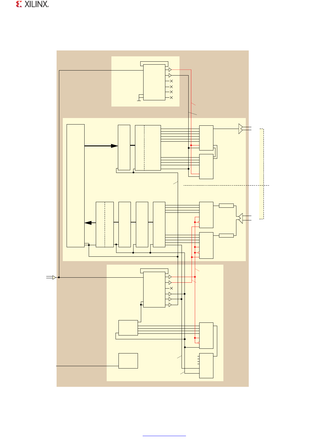
1000BASE-X PCS/PMA or SGMII v11.4 www.xilinx.com 266
PG047 October 16, 2012
Chapter 7: SGMII over LVDS
SGMII Tx and Rx Ports are in Different I/O Banks
X-Ref Target - Figure 7-6
Figure 7-6: Asynchronous Oversampling LVDS Clocking Logic (Tx and Rx Placed in Different I/O Banks)
--#-
,2%DQN&ORFNLQJ
UHFHLYH
/3%2$%3%
$
$
$
$
#,+
$)6#,+
/&"
)3%2$%3%
1
1
1
1
#,+
#,+"
$)6#,+
/&"
#LOCK!LIGNMENT
3TATE-ACHINE
).#
#,+&").
#,+).
03).#$%#
03%.
#,+&"/54
#,+/54
#,+/54
#,+/54
#,+/54
#,+/54
#,+/54
"5&)/
"5&)/
"5&'
"5&'
"5&'
28#,+$)6
)$%,!9#42,
2%&#,+
)3%2$%3%
1
1
1
1
#,+
#,+"
/#,+
)3%2$%3%
1
1
1
1
#,+
#,+"
/#,+
$$,9
$$,9
)/$%,!9%
)/$%,!9%
)$%,!9?6!,5%
)$%,!9?6!,5%
RXP
RXN
)"5&$3?$)&&?/54
$25#OMMA!LIGNMENT""$ECODER
CLK CLK CLKP
2X%LASTIC"UFFER
RXRECCLKCLKM
/RJL&RUH1HWOLVW
USERCLK
USERCLK
""%NCODER
CLK
40HASE"UFFER
CLKM?TX?BUFRCLKM
/3%2$%3%
$
$
$
$
#,+
$)6#,+
/3%2$%3%
$
$
$
$
$
$
#,+
$)6#,+
/1
TXP
TXN
/"5&$3
REFCLK?P
REFCLK?N
-(ZCLOCKSOURCE
CLK
³%ORFN´/HYHO
h)/"ANKv,EVEL
-(Z
-(Z
-(Z
DEGREE
PHASESHIFT
-(Z
-(Z
-(Z
$IFFERENT
)/
"ANKS
--#-
#,+&").
#,+).
03).#$%#
03%.
#,+&"/54
#,+/54
#,+/54
#,+/54
#,+/54
#,+/54
#,+/54
"5&)/
"5&2
'.$
-(Z
,2%DQN&ORFNLQJ
WUDQVPLW
8

1000BASE-X PCS/PMA or SGMII v11.4 www.xilinx.com 267
PG047 October 16, 2012
Chapter 7: SGMII over LVDS
Figure 7-6 provides a detailed illustration of the clocking logic provided when the
TX_AND_RX_SHARE_CLOCK parameter is set to false. This necessitates that associated
SGMII Tx and Rx ports are split up and placed into separate I/O Banks.
Only a single SGMII port is illustrated but the clocks are identically wired up to all SGMII
ports of which the Rx SGMII ports share one bank and the Tx SGMII ports share a different
I/O Bank.
Major components of the I/O Bank clocking logic are the two MMCM modules. These
should both be provided with the same high quality 125 MHz clock reference as illustrated.
The MMCMs are configured to provide the frequency related clocks defined in Table 7- 3
and Tab le 7-4 which are used by all SGMII ports using these Rx and Tx I/O banks.
Table 7-3: MMCM Generated Clocks That Are Shared across the Rx SGMII I/O Bank (plus global clocks)
MMCM
Output Frequency
Clock
Buffer
Used
HDL Clock name Description
CLKOUT0 625 MHz BUFIO clk625m_rx_bufio_0
A 625 MHz clock source with no phase shift. This is
provided on BUFIO clock routing to act as a clock
source for all ISERDES primitives (and the single
OSERDES of the Clock Alignment State Machine
calibration circuitry).
The route from the MMCM to the ISERDES and
OSERDES primitives use high performance clock
routing (shown in red on Figure 7-6).
This clock output is not affected by the dynamic
MMCM phase shift.
CLKOUT1 625 MHz BUFIO clk625m_rx_bufio_90
A 625 MHz clock source with 90 degree phase shift
with respect to clk625m_rx_bufio_0. This is provided
on BUFIO clock routing to act as a clock source for the
ISERDES primitives.
The route from the MMCM to the ISERDES primitives
uses high performance clock routing (shown in red on
Figure 7-6).
This clock output is not affected by the dynamic
MMCM phase shift.
CLKOUT2 Unused
CLKOUT3 312.5 MHz BUFG clk312p5m
A 312.5 MHz global clock source, used for the DRU
and the receiver path within the LVDS transceiver.
This clock output is affected by the dynamic MMCM
phase shift (performed by the Clock Alignment State
Machine.)
CLKOUT4 625 MHz BUFG clk625m
A 625 MHz global clock source, required by the DRU
and Clock Alignment State Machines.
This clock output is affected by the dynamic MMCM
phase shift (performed by the Clock Alignment State
Machine.)
1000BASE-X PCS/PMA or SGMII v11.4 www.xilinx.com 268
PG047 October 16, 2012
Chapter 7: SGMII over LVDS
Important notes relating to Figure 7-6:
• The differential 125 MHz clock (refclk125_p/n) that is routed to the CLKIN1 pin of
the MMCM should enter the FPGA on a global clock pin. This enables the clock signal
to be routed to any number of device MMCM modules using dedicated clock routing.
The clock source should confirm to Ethernet specifications (100 ppm of accuracy).
• Routing from the MMCM to the BUFIOs should utilize High Performance Clocks
(illustrated in red). A given I/O Bank has a choice of MMCM primitives that can be
selected to utilize this routing; see the Virtex-6 FPGA Clocking User Guide (UG362).
• All BUFIOs used must be kept to a single clock region to minimize clock distortion.
Therefore:
CLKOUT5 125 MHz BUFG clk125m
A 125 MHz global clock source, used as the 125 MHz
reference clock for the entire core netlist and the
transmitter path of the LVDS transceivers.
This clock output is affected by the dynamic MMCM
phase shift (performed by the Clock Alignment State
Machine.)
CLKOUT6 Unused
Table 7-3: MMCM Generated Clocks That Are Shared across the Rx SGMII I/O Bank (plus global clocks)
MMCM
Output Frequency
Clock
Buffer
Used
HDL Clock name Description
Table 7-4: MMCM Generated Clocks That Are Shared across the Tx I/O Bank
MMCM
Output Frequency
Clock
Buffer
used
HDL Clock Name Description
CLKOUT0 625 MHz BUFIO clk625m_tx_bufio
A 625 MHz clock source. This is provided on BUFIO
clock routing to act as a clock source for all OSERDES
primitives.
The route from the MMCM to the ISERDES and
OSERDES primitives use high performance clock routing
(shown in red on Figure 7-6).
CLKOUT1 125 MHz BUFR clk125m_tx_bufr
A 125 MHz clock source with no phase shift relative to
clk625m_tx_bufio. This is used to satisfy the parallel to
serial clock phase relationships within the OSERDES
primitives used by the SGMII transmitter ports.
CLKOUT2 Unused
CLKOUT3 Unused
CLKOUT4 Unused
CLKOUT5 Unused
CLKOUT6 Unused

1000BASE-X PCS/PMA or SGMII v11.4 www.xilinx.com 269
PG047 October 16, 2012
Chapter 7: SGMII over LVDS
°All Rx SGMII ports in use must be LOC-ed to a single I/O Bank and are serviced by
the clk625m_rx_bufio_0 and clk625m_rx_bufio_90 clock sources.
°All SGMII Tx ports used must be LOC-ed to a different I/O Bank and are serviced by
the clk625m_tx_bufio clock source.
• The phase of the global 625 MHz clock source (see Table 7-4) is automatically phase
shifted by the Clock Alignment State Machine, using the MMCM dynamic phase
shifting function, to correctly sample the received data from the oversampling ISERDES
elements to the FPGA logic flip-flops of the DRU.
°The clk625m_rx_bufio_0 and clk625m_rx_bufio_09 BUFIO clock sources
must not be subjected to this dynamic phase shifting to allow the global 625 MHz
clock source to be shifted with respect to these BUFIO 625 MHz clock sources.
°Furthermore, to allow the ISE tools to meet setup and hold times across all global
clock buffer boundaries, this necessitates that the 312.5 MHz and 125 MHz global
clocks of Table 7-4 are also subjected to the same dynamic phase shifting as per the
global 625 MHz clock source.
•The
OSERDES primitives used by the LVDS transceiver must use the
clk625m_tx_bufio BUFIO 625 MHz clock source to provide the cleanest possible
serial output (rather than using the global 625 MHz clock source). This necessitates that
the OSERDES parallel clock (DIVCLK) must be provided from a 125 MHz regional clock
(clk125m_tx_bufr). This necessitates that the OSERDES parallel clock (CLKDIV) must
be provided from a 125 MHz regional clock (clk125m_tx_bufr) that is derived from
the same MMCM. This requirement is used to satisfy the parallel to serial clock phase
relationships within the OSERDES primitives: see the Virtex-6 FPGA User Guide (Virtex-6
FPGA product page).
• This sits between the 125 MHz global and regional clock domains in the transmitter of
the LVDS transceiver. This buffer is used to reliably transfer the 10-bit data between
these domains because there is no fixed phase relationship between these two clock
sources.
• An IDELAY Controller module is provided in the I/O Bank Clocking module for use with
the IDELAYs required on the receiver input serial path. This must be provided with a 310
MHz clock source.
°The top level of the example design creates a 310 MHz clock source using an
additional MMCM; this logic is not illustrated in Figure 7-6. However, customers can
source this clock source by other methods.
°The 310 MHz clock source does not need to be duplicated once per bank; a single
source can be provided on global clock routing and shared across the entire FPGA.

1000BASE-X PCS/PMA or SGMII v11.4 www.xilinx.com 270
PG047 October 16, 2012
Chapter 7: SGMII over LVDS
Clock Alignment State Machine
The remaining logical block illustrated in Figure 7-6 consists of a logical state machine to
dynamically control the variable phase shift which is applied to the global buffer MMCM
clock outputs. This is designed to deskew the clock domain crossing of the oversampled
data from the ISERDES elements, to the FPGA logic flip-flops of the DRU.
The calibration circuit used by the clock phase alignment state machine requires the use of
a single IOB from the I/O bank (which cannot then be used for any other I/O). Within this
consumed IOB, a known clock data pattern (0101) is routed through an OSERDES to provide
serial data synchronous to the 625 MHz global clock source. This serial data is then looped
back through an ISERDES to capture the serial data synchronously to the
clk625m_rx_bufio_0 BUFIO clock source. The phase alignment state machine looks for
the correct 01010 clock pattern and uses this to adjust the phase of the MMCM clock
outputs to phase align the global 625 MHz clock source with the clk625m_rx_bufio_0
BUFIO clock (as seen at the ISERDES of the calibration circuit). This results in the reliable
data transfer.
The consumed IOB used by the calibration circuitry uses internal loopback between the
OSERDES and ISERDES primitives; the loopback data does not appear on the physical pad of
the FPGA and no pad termination logic is required.
Layout and Placement
A hands-on approach is required for placing this design. The steps provided here are a
useful guide, but other knowledge is assumed. To aid with these guidelines, users of the
core in this mode would benefit from:
• A detailed understanding of Virtex-6 FPGA Clocking Resources and SelectIO Resources.
See Virtex-6 FPGA User Guide (Virtex-6 FPGA product page).
• A working knowledge of the Xilinx PlanAhead™ tool (or alternatively FPGA Editor) in
order to locate particular clock buffers and slices.
Following are some guidelines:
1. Select an I/O Bank in your chosen device for use with for your transmitter and receiver
SGMII ports (this will be either in the same bank, or with the transmitter ports in a
separate bank; see Clocking Logic).
2. LOC down the BUFIO and BUFR clock buffers that are required:
a. Identify the precise BUFIOs and BUFRs that are associated with and available for the
chosen I/O Bank(s): there are four available BUFIOs per bank, and up to 8 available
BUFRs per bank.

1000BASE-X PCS/PMA or SGMII v11.4 www.xilinx.com 271
PG047 October 16, 2012
Chapter 7: SGMII over LVDS
b. LOC down the two 625 MHz clock BUFIO buffers that are required for the
clk625m_rx_bufio_0 and clk625m_rx_bufio_90 clock nets (see Table 7-2 or Ta b l e 7 - 3)
using two of the available BUFIOs. The following UCF syntax achieves this in the
example design provided:
INST "core_bank_wrapper/clock_logic_per_bank/clk625m_rx_bufio_0_inst" LOC
=BUFIODQS_X0Y1;
INST "core_bank_wrapper/clock_logic_per_bank/clk625m_rx_bufio_90_inst" LOC
=BUFIODQS_X0Y2;
If necessary (only when using the SGMII Tx and Rx Ports are in Different I/O Banks clocking
scheme) then LOC down the BUFIO for the clk625m_tx_bufio clock net (see Table 7-4 ) to
one of the BUFIOs associated with the transmitter I/O Bank. Use the following UCF syntax as
a guide:
INST "core_bank_wrapper/clock_logic_per_bank/*clk625m_tx_bufio_inst" LOC =
BUFIODQS_XxYy;
c. LOC down the BUFR buffer that is required for the clk125m_tx_buf clock net (see
Table 7-2 or Table 7-4) using just one of the available BUFRs. The following UCF syntax
achieves this in the example design provided:
INST "core_bank_wrapper/clock_logic_per_bank/*regional_oserdes_clk" LOC=BUFR_X0Y1;
3. A single IDELAYCTRL is instantiated by the I/O Bank Level of the Example Design for use
with a single I/O Bank. This primitive needs to be associated with the various IODELAYE1
elements used in that I/O Bank. The following UCF syntax achieves this in the example
design provided:
# Link the IDELAY Controller to the IODELAYs of the I/O Bank
INST "core_bank_wrapper/clock_logic_per_bank/dlyctrl" IODELAY_GROUP =
"oversample_bank12";
INST
"core_bank_wrapper/instantiate_ethernet_ports[*].core_wrapper/transceiver_inst/lvds
_rx/IODELAYE1_RXP"
IODELAY_GROUP = "oversample_bank12";
INST
"core_bank_wrapper/instantiate_ethernet_ports[*].core_wrapper/transceiver_inst/lvds
_rx/IODELAYE1_RXN"
IODELAY_GROUP = "oversample_bank12";
4. LOC down the RLOC origin of the DRU module to a particular slice for every SGMII port
in use.
The oversampled data is transferred from the ISERDESE1 oversampling elements into
the DRU module at 625 MHz; a proportion of the logic with the DRU is required to run
at 625 MHz. To help the tools achieve this, flip-flips of this logic are placed relatively to
each other using RLOC constraints integrated in the HDL of the DRU. It now remains for
you to LOC the origin of this RLOC group to a particular slice in the design.

1000BASE-X PCS/PMA or SGMII v11.4 www.xilinx.com 272
PG047 October 16, 2012
Chapter 7: SGMII over LVDS
The slice assigned to the RLOC origin for each SGMII port should be to the slice at the
lower left of the group of two slices that are immediately to the right of the
oversampling ISERDESE1 pair. In turn this ISERDESE1 pair will be immediately to the
right of the differential LVDS pair which is used for the receiver ports of the SGMII.
The following UCF syntax achieves this in the example design provided for the SGMII
numbered as 0:
# Tx
Net txp<2> LOC = AK33;
Net txn<2> LOC = AK32;
# Rx
Net rxp<2> LOC = AL31;
Net rxn<2> LOC = AK31;
# Place the critical 625MHz sampling flip-flops adjacent to the oversampling
ISERDESE1 elements
INST
"*core_bank_wrapper/instantiate_ethernet_ports[2].core_wrapper/transceiver_inst/lvd
s_rx/dynamic_realignment/ii_0" RLOC_ORIGIN=X0Y8;
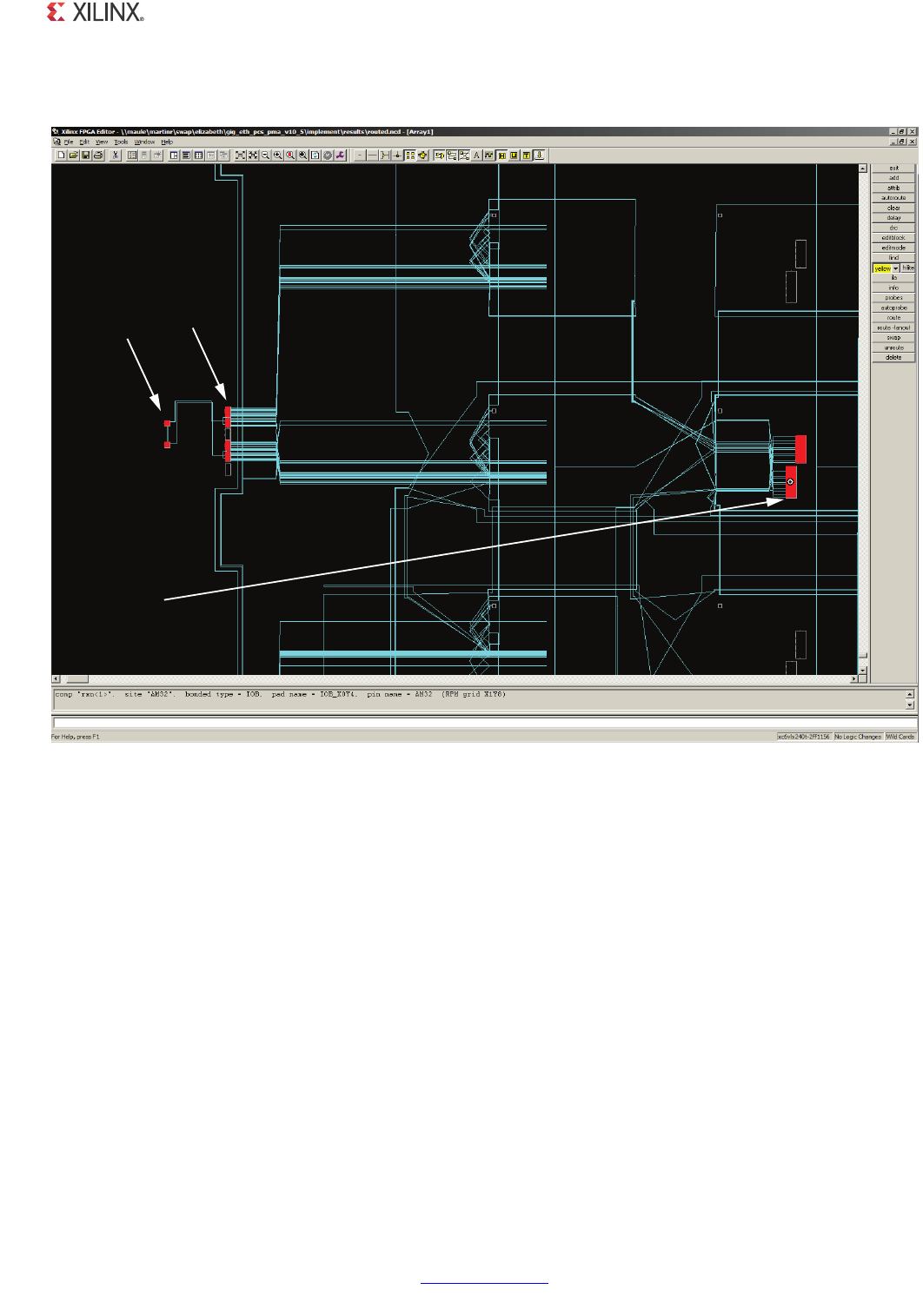
1000BASE-X PCS/PMA or SGMII v11.4 www.xilinx.com 273
PG047 October 16, 2012
Chapter 7: SGMII over LVDS
Figure 7-7 shows an FPGA Editor with an RLOC Origin description.
Example Design Implementation
Chapter 20, Detailed Example Design provides a full list and description of the directory and
file structure that is provided with the core, including the location of the HDL example
design provided.
Figure 7-8 illustrates the HDL example design that is provided for the SGMII Asynchronous
Oversampling over Virtex-6 FPGA LVDS implementation. As illustrated, the example is split
between several hierarchical layers.
The top level of the example design creates a specific example that can be simulated,
synthesized and implemented.
X-Ref Target - Figure 7-7R
Figure 7-7: RLOC Origin Slice Location Captured from FPGA Editor
DifferentialDifferential
LVDSLVDS
InputInput
ISERDESE1ISERDESE1
pairpair
RLOC OriginRLOC Origin
HEREHERE

1000BASE-X PCS/PMA or SGMII v11.4 www.xilinx.com 274
PG047 October 16, 2012
Chapter 7: SGMII over LVDS
The I/O Bank hierarchical level is designed so that it can be instantiated directly into
customer designs. As the name of the I/O Bank suggests, this logic can be shared across a
single Virtex-6 FPGA I/O Bank. This I/O Bank can be used for multiple instances of the core
with LVDS I/O to create several independent SGMII ports (four ports are delivered by the
example design by default as shown in Figure 7-8). Additional ports can be added to the I/O
Bank simply by editing a single parameter when instancing the I/O Bank hierarchical level in
your design.
The core netlist in this implementation remains identical to that of Ethernet 1000BASE-X
PCS/PMA or SGMII Support Using a Device Specific Transceiver, described in Chapter 1,
Overview.
Also illustrated in Figure 7-8, the HDL example design for this implementation provides
additional logic to form the "LVDS transceiver" module, which fully replaces the
functionality otherwise provided by a Virtex-6 FPGA GTX Transceiver. The LVDS transceiver
block contains IODELAYs and ISERDES elements along with a Data Recovery Unit (DRU). This
uses the Virtex-6 FPGA ISERDES elements in a new asynchronous oversampling mode as
described in XAPP 881 1.25Gbs 4x Asynchronous Oversampling over Virtex-6 FPGA LVDS.
The full transceiver functionality is then completed with Comma Alignment, 8B/10B
Decoder and Rx Elastic buffer blocks.
The example design logical blocks and files are discussed in detail in the next sections.
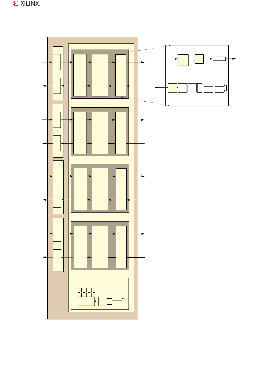
1000BASE-X PCS/PMA or SGMII v11.4 www.xilinx.com 275
PG047 October 16, 2012
Chapter 7: SGMII over LVDS
X-Ref Target - Figure 7-8
Figure 7-8: Virtex-6 FPGA Asynchronous Oversampling Example Design
(WKHUQHW
%$6(;
3&630$
&RUH
*0,,
,2%V
,Q
,2%V
2XW
*0,,VW\OH
ELW,)
6*0,,
$GDSWDWLRQ
0RGXOH
COMPONENT?NAME?IOBANK
FRPSRQHQWBQDPHBEORFN
,6$3TRANSCEIVER
3ERIAL'-))
3'-))
(WKHUQHW
%$6(;
3&630$
&RUH
*0,,
,2%V
,Q
,2%V
2XW
*0,,VW\OH
ELW,)
6*0,,
$GDSWDWLRQ
0RGXOH
FRPSRQHQWBQDPHBEORFN
,6$3TRANSCEIVER
3ERIAL'-))
3'-))
(WKHUQHW
%$6(;
3&630$
&RUH
*0,,
,2%V
,Q
,2%V
2XW
*0,,VW\OH
ELW,)
6*0,,
$GDSWDWLRQ
0RGXOH
FRPSRQHQWBQDPHBEORFN
,6$3TRANSCEIVER
3ERIAL'-))
3'-))
(WKHUQHW
%$6(;
3&630$
&RUH
*0,,
,2%V
,Q
,2%V
2XW
*0,,VW\OH
ELW,)
6*0,,
$GDSWDWLRQ
0RGXOH
FRPSRQHQWBQDPHBEORFN
,6$3TRANSCEIVER
3ERIAL'-))
3'-))
--#-
CLOCK
ALIGNMENT
STATE
MACHINE
CLOCKBUFFERS
VARIOUSCLOCK
FREQUENCIES
ANDPHASES
/3%2$%3
)3%2$%3
,2%DQN&ORFNLQJ
COMPONENT?NAME?EXAMPLE?DESIGN
6HULDO6*0,,
6*0,,
%%
(QFRGHU /3%2$%3
)/$%,!9
)3%2$%3
$25
#OMMA
!LIGNMENT
4X
0HASE
"UFFER
""
$ECODER
)/$%,!9
)3%2$%3
/9'6WUDQVFHLYHU
2X
%LASTIC
"UFFER
8

1000BASE-X PCS/PMA or SGMII v11.4 www.xilinx.com 276
PG047 October 16, 2012
Chapter 7: SGMII over LVDS
Example Design Top Level
The top-level example design for the core with SGMII using Asynchronous Oversampling
over Virtex-6 FPGA LVDS is described in the following files:
VHDL
<project_dir>/<component_name>/example_design/<component_name>_example_design.vhd
Verilog
<project_dir>/<component_name>/example_design/<component_name>_example_design.v
The example design HDL top level contains the following:
• An instance of the I/O Bank level HDL
• External GMII logic, including IOB and DDR register instances, where required
• The parameter NUM_ETH_PORTS; this value is set to 4 by default to create four unique
SGMII ports as illustrated in Figure 7-8. To decrease or increase the number of ports,
simply change the value of this parameter.
This module adds I/O logic to the GMII of the SGMII ports. This is included only to create a
standalone design that can be implemented in an FPGA and simulated in both functional
and timing simulation for the purposes of providing a complete SGMII design example.
IMPORTANT: Discard this level of hierarchy and instantiate the I/O Bank Level of the Example Design
in your own design.
I/O Bank Level of the Example Design
The I/O Bank level for the core with SGMII using Asynchronous Oversampling over Virtex-6
FPGA LVDS is described in the following files:
VHDL
<project_dir>/<component_name>/example_design/<component_name>_iobank.vhd
Verilog
<project_dir>/<component_name>/example_design/<component_name>_iobank.v
The I/O Bank level HDL contains the following:
• The parameter NUM_ETH_PORTS; this value is set to 4 by default to create four unique
SGMII ports (as illustrated in Figure 7-8). To decrease or increase the number of SGMII
ports used in a single I/O Bank, simply change the value of this parameter when
instancing this module.

1000BASE-X PCS/PMA or SGMII v11.4 www.xilinx.com 277
PG047 October 16, 2012
Chapter 7: SGMII over LVDS
• Instances of the Block Level to create unique SGMII ports (the number of instances is
set by the NUM_ETH_PORTS parameter).
• A single instance of the logic.
TIP: This is the most useful part of the example design and should be instantiated in all customer
designs that use the core in this mode.
Up to ten separate SGMII ports can be achieved in most device I/O Banks. If additional
SGMII ports are required (to be placed in additional I/O Banks), then a new instance of the
entire I/O Bank Level component is required per I/O Bank in use.
Block Level of the Example Design
The following files describe the block level for the Ethernet 1000BASE-X PCS/PMA core in
SGMII mode:
VHDL
<project_dir>/<component_name>/example_design/<component_name>_block.vhd
Verilog
<project_dir>/<component_name>/example_design/<component_name>_block.v
The block level of the example design connects together all of the components for a single
SGMII port. These are:
A core netlist (introduced in Ethernet 1000BASE-X PCS/PMA or SGMII Support Using a
Device Specific Transceiver).
•The LVDS Transceiver, connected to the PHY side of the core netlist, to perform the
SERDES functionality using the Asynchronous Oversampling method.
•The SGMII Adaptation Module Top Level, connected to the Ethernet MAC (GMII) side of
the core netlist, containing:
°The clock management logic required to enable the SGMII example design to
operate at 10 Mb/s, 100 Mb/s, and 1 Gb/s.
°GMII logic for both transmitter and receiver paths; the GMII style 8-bit interface is
run at 125 MHz for 1 Gb/s operation; 12.5 MHz for 100 Mb/s operation; 1.25 MHz
for 10 Mb/s operation.

1000BASE-X PCS/PMA or SGMII v11.4 www.xilinx.com 278
PG047 October 16, 2012
Chapter 7: SGMII over LVDS
LVDS Transceiver
The LVDS transceiver block fully replaces the functionality otherwise provided by a Virtex-6
FPGA GTX Transceiver. This is only possible at a serial line rate of 1.25 Gb/s. See Figure 7-8
for a block diagram of the LVDS transceiver. This is split up into several sub-blocks which are
described in further detail in the following sections.
On the transmitter path, data sourced by the core netlist is routed through the 8B/10B
Encoder to translate the 8-bit code groups into 10-bit data. The 10-bit data is then passed
through the Tx Phase Buffer, then routed into the parallel interfaces of a Virtex-6 FPGA
primitive master slave pair; the parallel 10-bit data is then clocked out serially at a line rate
of 1.25 Gb/s.
The receiver path has further complexity. Serial data received at 1.25 Gb/s is routed in
parallel to two IODELAYs and ISERDES elements as illustrated in Figure 7-8. Each of the two
ISERDES elements is used in a new oversampling mode to sample the input data. By
controlling the respective routing delays through the IODELAYs prior to the ISERDES, the
two ISERDES devices are each able to oversample at different points in time, resulting in a
combination of four times oversampling of each bit received.
The oversampled data is then routed through a Data Realignment Unit (DRU) to detect the
correct sampling point and to recover parallel data.
The functionality provided by the IODELAYs and ISERDES and Data Realignment Unit (DRU)
is covered in Xilinx Application Note XAPP881, 1.25Gbps 4x Asynchronous Oversampling
over Virtex-6 FPGA LVDS.
Having recovered parallel data from the serial stream, the Comma Alignment module, next
on the receiver path, detects specific 8b/10b bit patterns (commas) and uses these to
realign the 10-bit parallel data to contain unique 8b/10b code groups. These code groups
are then routed through the 8B/10B Encoder module to obtain the unencoded 8-bit code
groups that the core netlist can accept.
The final piece of the receiver path is to use a 8B/10B Encoder.
The datapath thus far, from the DRU through to the 8B/10B Encoder, is synchronous to a
312.5 MHz clock source; a clock enable sourced from the DRU indicates valid data. Using
the 312.5 MHz clock and associated clock enable, data is written into the elastic buffer. Data
is read out of the elastic buffer on a pure 125 MHz clock frequency; this is the clock source
used for the transmitter path and for all logic within the core netlist.

1000BASE-X PCS/PMA or SGMII v11.4 www.xilinx.com 279
PG047 October 16, 2012
Chapter 7: SGMII over LVDS
The following files describe the top level of the hierarchal levels of the LVDS transceiver:
VHDL
<project_dir>/<component_name>/example_design/lvds_transceiver/
lvds_transceiver.vhd
<project_dir>/<component_name>/example_design/lvds_transceiver/tx/
lvds_transceiver_tx.vhd
<project_dir>/<component_name>/example_design/lvds_transceiver/rx/
lvds_transceiver_rx.vhd
Verilog
<project_dir>/<component_name>/example_design/lvds_transceiver/
lvds_transceiver.v
<project_dir>/<component_name>/example_design/lvds_transceiver/tx/
lvds_transceiver_tx.v
<project_dir>/<component_name>/example_design/lvds_transceiver/rx/
lvds_transceiver_rx.v
8B/10B Encoder
The implemented 8B/10B coding scheme is an industry standard, DC-balanced,
byte-oriented transmission code ideally suited for high-speed local area networks and
serial data links. As such, the coding scheme is used in several networking standards,
including ethernet.
The 8B/10B Encoder block is taken from Xilinx Application Note XAPP1122, Parameterizable
8b/10b Encoder.
XAPP1122 provides two possible approaches: a choice of a block RAM-based
implementation or a LUT-based implementation. The SGMII LVDS example design uses the
LUT-based implementation, but XAPP1122 can be used to swap this for the block
RAM-based approach if this better suits device logic resources.
The following files describe the 8B/10B Encoder:
VHDL
<project_dir>/<component_name>/example_design/lvds_transceiver/tx/
encode_8b10b_pkg.vhd
encode_8b10b_lut_base.vhd
Verilog
<project_dir>/<component_name>/example_design/lvds_transceiver/tx/
encode_8b10b_lut_base.v

1000BASE-X PCS/PMA or SGMII v11.4 www.xilinx.com 280
PG047 October 16, 2012
Chapter 7: SGMII over LVDS
Tx Phase Buffer
The parallel data that is clocked into the OSERDES must use a 125 MHz BUFR regional clock
buffer. But the data received from the core netlist uses a 125 MHz global clock buffer
(BUFG). The job of the Tx Phase Buffer is therefore to account for the phase relationship
between the BUFG and BUFR 125 MHz clocks.
Data is written into the Tx Phase Buffer synchronously to the global clock and read out
synchronously to the regional clock. Because these clocks are derived from the same clock
source (see Clocking Logic), there is no frequency drift. So the Tx Phase Buffer is
implemented as a simple asynchronous FIFO. The occupancy of the FIFO is kept low to
minimize latency and no precautions are taken against underflow/overflow conditions.
The following files describe the Tx Phase FIFO:
VHDL
<project_dir>/<component_name>/example_design/lvds_transceiver/tx/
tx_phase_buffer.vhd
Verilog
<project_dir>/<component_name>/example_design/lvds_transceiver/tx/
tx_phase_buffer.v
OSERDES
The OSERDES primitive (actually a MASTER-SLAVE pair of primitives) is used in a standard
mode; 10-bit input parallel data synchronous to a 125 MHz regional clock buffer source
(BUFR) is clocked into the OSERDES. Internally within the OSERDES, the data is serialized
and output at a rate of 1.25 Gb/s. The clock source used for the serial data is a 625 MHz
clock source using a BUFIO regional clock buffer at double data rate.
• The 625 MHz BUFIO and 125 MHz BUFR clocks for serial and parallel data are both
derived from the same MMCM (see I/O Bank Clocking) so there is no frequency drift.
• The use of the BUFIO clock buffer for the serial data rate provides the OSERDES
primitives with a clock of lower duty cycle distortion than could be obtained by using a
global clock source.
• The use of the BUFR regional clock buffer for the parallel clock is a requirement of the
OSERDES: when using a BUFIO clock for serial data, a BUFR clock source, derived from
the same MMCM source, must be used for the parallel data to satisfy clock phase
alignment constraints within the OSERDES primitives.

1000BASE-X PCS/PMA or SGMII v11.4 www.xilinx.com 281
PG047 October 16, 2012
Chapter 7: SGMII over LVDS
IODELAYs and ISERDES
This logic, along with the DRU, have been taken from the accompanying reference design to
Xilinx Application Note XAPP881, 1.25 Gbps 4x Asynchronous Oversampling over Virtex-6
LVDS.
The ISERDES primitives are used in a new oversampling mode to oversample the input data;
the ISERDES can perform four times oversampling with respect to the input reference clock.
The reference clock used in this implementation is 625 MHz (half the frequency of the serial
data rate), resulting in each serial bit received being sampled, nominally, twice by each
ISERDES.
By controlling the respective routing delays through the IODELAYs prior to the two ISERDES
elements, the two ISERDES devices are each able to sample the input data at different
points in time, resulting in a combination of four times oversampling of each data bit
received. See IODELAYs and ISERDES.
Data Realignment Unit (DRU)
This logic, along with the IODELAY and ISERDES logic, have been taken from the
accompanying reference design to Xilinx Application Note XAPP881, 1.25Gbps 4x
Asynchronous Oversampling over Virtex-6 LVDS. See IODELAYs and ISERDES.
The four times oversampled data from the ISERDES pair is received synchronously to the
625 MHz ISERDES reference clock. Using a voter scheme that compares the oversampled
data and selects the best data sample, the module will output parallel data synchronously
to a 312.5 MHz clock source (frequency related to the 625 MHz clock). A clock enable will be
driven with the 312 MHz clock to indicate valid data to the downstream modules.
The following files describe the DRU:
VHDL
<project_dir>/<component_name>/example_design/lvds_transceiver/rx/dru.vhd
Verilog
<project_dir>/<component_name>/example_design/lvds_transceiver/rx/dru.v
Comma Alignment
Data received from the DRU is in parallel form, but the bits of the parallel bus have not been
aligned into correct 10-bit word boundaries.
By detecting a unique 7-bit serial sequence known as a ‘comma’ (however the commas can
fall across the 10-bit parallel words), the comma alignment logic will control bit shifting of
the data so as to provide correct alignment to the data leaving the module. The bitslip input
of the DRU is driven by the comma alignment module’s state machine, so the actual bit shift
logic is performed by the DRU.

1000BASE-X PCS/PMA or SGMII v11.4 www.xilinx.com 282
PG047 October 16, 2012
Chapter 7: SGMII over LVDS
In 8b/10b encoding, both +ve and -ve bit sequences exist for each defined code group. The
comma alignment logic is able to detect and control realignment on both +ve and -ve
comma versions.
The following files describe the Comma Alignment block:
VHDL
<project_dir>/<component_name>/example_design/lvds_transceiver/rx/bit_alignment.vhd
Verilog
<project_dir>/<component_name>/example_design/lvds_transceiver/rx/bit_alignment.v
8B/10B Decoder
The implemented 8b/10b coding scheme is an industry standard, DC-balanced,
byte-oriented transmission code ideally suited for high-speed local area networks and
serial data links. As such, the coding scheme is used in several networking standards,
including ethernet.
The 8B/10B Decoder block is taken from Xilinx Application Note XAPP1112, Parameterizable
8b10b Decoder.
XAPP1112 provides two possible approaches: a choice of a block RAM-based
implementation or a LUT-based implementation. The SGMII LVDS example design uses the
LUT-based implementation, but XAPP1112 can be used to swap this for the block
RAM-based approach if this better suits device logic resources.
The following files describe the 8B/10B Decoder:
VHDL
<project_dir>/<component_name>/example_design/lvds_transceiver/rx/
decode_8b10b_pkg.vhd
decode_8b10b_lut_base.vhd
Verilog
<project_dir>/<component_name>/example_design/lvds_transceiver/rx/
decode_8b10b_lut_base.v
Rx Elastic Buffer
The final piece of the receiver path is to use a Rx Elastic Buffer. The datapath thus far, from
the DRU through to the 8B/10B Encoder, is synchronous to a 312.5 MHz clock source; a
clock enable sourced from the DRU indicates valid data. Using the 312.5 MHz clock and
associated clock enable, data is written into the elastic buffer. The clock enable will be
active, on average, to clock enable the data stream written into the buffer at a rate of 125
MHz.

1000BASE-X PCS/PMA or SGMII v11.4 www.xilinx.com 283
PG047 October 16, 2012
Chapter 7: SGMII over LVDS
Data is read out of the elastic buffer on a pure 125 MHz clock frequency; this is the clock
source used for the transmitter path and for all logic with the core netlist. This clock is
asynchronous to the resultant 125 MHz data rate received by the LVDS receiver; Ethernet
clock sources are defined to be accurate to 100 parts per million.
To deal with the asynchronous nature of the data rates on its write and read ports, the
Receiver Elastic Buffer attempts to maintain a constant occupancy by inserting or removing
Idle sequences as necessary during the Inter Packet Gap between received Ethernet frames.
This causes no data corruption to the ethernet frames themselves.
The following files describe the Rx Elastic buffer:
VHDL
<project_dir>/<component_name>/example_design/lvds_transceiver/rx/
rx_elastic_buffer.vhd
Verilog
<project_dir>/<component_name>/example_design/lvds_transceiver/rx/
rx_elastic_buffer.v
I/O Bank Clocking
Figure 7-8 also illustrates the inclusion of the I/O Bank Clocking module that creates all of
the clock frequencies and clock phases that are required by the LVDS transceiver block.
The MMCM and associated logic in this module are based on clocking logic present within
Xilinx Application Note XAPP881, 1.25Gbps 4x Asynchronous Oversampling over Virtex-6
LVDS.
As the name of the block suggests, this logic can be shared across a single Virtex-6 FPGA
I/O Bank. This I/O Bank can be used for multiple instances of the core with LVDS I/O to
create several independent SGMII ports (as illustrated in Figure 7-8).
The HDL for this file contains the parameter TX_AND_RX_SHARE_CLOCK; this value is set to
TRUE by default, implying that the Tx and Rx logic of the SGMII ports will share the BUFIO
clocks. To minimize jitter in this implementation, the BUFIO clocks used by the logic must
only be used across a single Virtex-6 FPGA I/O Bank.
Therefore, setting the parameter TX_AND_RX_SHARE_CLOCK to TRUE necessitates that the
transmitter and receiver ports of the SGMII are LOC-ed into the same Virtex-6 FPGA I/O
bank.
Setting the parameter TX_AND_RX_SHARE_CLOCK to FALSE will duplicate the clock circuitry
that is required by the transmitter, allowing the receiver and transmitter ports to be
separated and placed into different Virtex-6 FPGA I/O banks.

1000BASE-X PCS/PMA or SGMII v11.4 www.xilinx.com 284
PG047 October 16, 2012
Chapter 7: SGMII over LVDS
The main component of the I/O Bank clocking logic required by the LVDS receiver is an
MMCM module. This should be provided with a high quality 125 MHz clock reference. The
MMCM is configured to provide the frequency related clocks which are described fully in
Clocking Logic.
The remaining logic within this block consists of a logical state machine to dynamically
control the variable phase shift which is applied to certain MMCM clock outputs. This is
designed to deskew the clock domain crossing of the oversampled data from the ISERDES
elements, to the FPGA logic flip-flops of the DRU and is described in the Clock Alignment
State Machine subsection of Clocking Logic.
The following files describe the logic provided in the I/O Bank Clocking block:
VHDL
<project_dir>/<component_name>/example_design/iobank_clocking/
iobank_clocking.vhd
bus_align_machine.vhd
Verilog
<project_dir>/<component_name>/example_design/iobank_clocking/
iobank_clocking.v
bus_align_machine.v
SGMII Adaptation Module
The SGMII Adaptation Module is described in the following files:
VHDL
<project_dir>/<component_name>/example_design/sgmii_adapt/
sgmii_adapt.vhd
clk_gen.vhd
johnson_cntr.vhd
tx_rate_adapt.vhd
rx_rate_adapt.vhd
Verilog
<project_dir>/<component_name>/example_design/sgmii_adapt/
sgmii_adapt.v
clk_gen.v
johnson_cntr.v
tx_rate_adapt.v
rx_rate_adapt.v
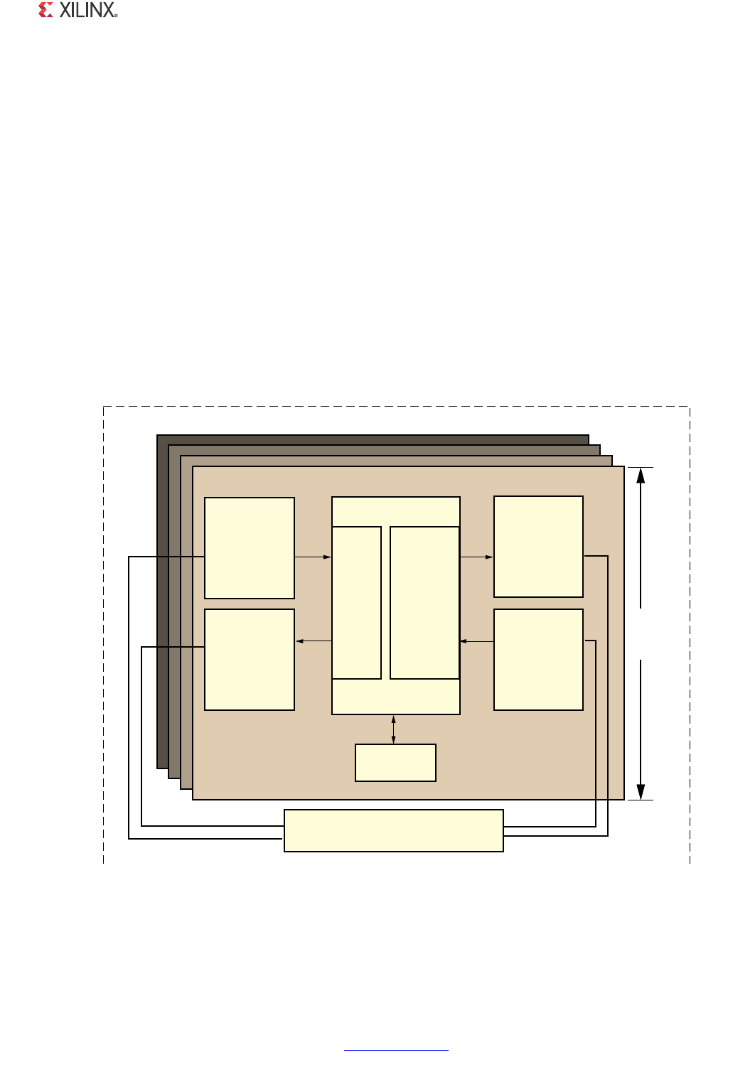
1000BASE-X PCS/PMA or SGMII v11.4 www.xilinx.com 285
PG047 October 16, 2012
Chapter 7: SGMII over LVDS
The GMII of the core always operates at 125 MHz. The core makes no differentiation
between the three speeds of operation; it always effectively operates at 1 Gb/s. However, at
100 Mb/s, every data byte run through the core should be repeated 10 times to achieve the
required bit rate; at 10 Mb/s, each data byte run through the core should be repeated 100
times to achieve the required bit rate. Dealing with this repetition of bytes is the function of
the SGMII adaptation module and its component blocks.
The SGMII adaptation module and component blocks are described in detail in the
Chapter 8, Additional Client-Side SGMII Logic Provided in the Example Design.
Demonstration Test Bench
Figure 7-9 illustrates the demonstration test bench for the Ethernet 1000BASE-X PCS/PMA
or SGMII core in SGMII mode with the Asynchronous Oversampling over Virtex-6 FPGA
LVDS. The demonstration test bench is a simple VHDL or Verilog program to exercise the
example design and the core itself.
X-Ref Target - Figure 7-9
Figure 7-9: Demonstration Test Bench for the Ethernet 1000BASE-X PCS/PMA or SGMII Core in SGMII
Using Asynchronous Oversampling with Virtex-6 FPGA LVDS
,6$3
4RANSCEIVER
$EMONSTRATION4EST"ENCH
3'-))
-ONITOR
3ERIALTO0ARALLEL
#ONVERSIONAND
""
$ECODING
3'-))
3TIMULUS
""%NCODING
AND0ARALLELTO
3ERIAL
#ONVERSION
'-))
3TIMULUS
'-))
-ONITOR
'-))
$54
#ONFIGURATION
3TIMULUS
PER
3'-))
PORT
#ONTROLAND$ATA3TRUCTURES

1000BASE-X PCS/PMA or SGMII v11.4 www.xilinx.com 286
PG047 October 16, 2012
Chapter 7: SGMII over LVDS
The top-level test bench entity instantiates the example design for the core, which is the
Device Under Test (DUT). A stimulus block (per SGMII port) is also instantiated and clocks,
resets and test bench semaphores are created. The following files describe the top-level of
the demonstration test bench.
VHDL
<project_dir>/<component_name>/simulation/demo_tb.vhd
Verilog
<project_dir>/<component_name>/simulation/demo_tb.v
The stimulus block entity, instantiated from within the top-level test bench, creates the
Ethernet stimulus in the form of four Ethernet frames, which are injected into GMII and
SGMII serial interfaces of the DUT. The output from the DUT is also monitored for errors.
The following files describe the stimulus block of the demonstration test bench.
VHDL
<project_dir>/<component_name>/simulation/stimulus_tb.vhd
Verilog
<project_dir>/<component_name>/simulation/stimulus_tb.v
Together, the top-level test bench file and the stimulus block combine to provide the full
test bench functionality which is described in the sections that follow.
Test Bench Functionality
The demonstration test bench performs the following tasks:
• Input clock signals are generated.
• A reset is applied to the example design.
• Then, for each SGMII port instantiated in the example design:
°The core is configured through its MDIO interface by injecting an MDIO frame into
the example design. This disables Auto-Negotiation and takes the core out of
Isolate state.
°The following frames are injected into the GMII transmitter by the GMII stimulus
block at 1 Gb/s.
- the first is a minimum length frame
- the second is a type frame
-the third is an errored frame
- the fourth is a padded frame

1000BASE-X PCS/PMA or SGMII v11.4 www.xilinx.com 287
PG047 October 16, 2012
Chapter 7: SGMII over LVDS
°The data received at the SGMII serial LVDS transceiver interface is 8B/10B decoded.
The resulting frames are checked by the SGMII Monitor against the stimulus frames
injected into the GMII transmitter to ensure data integrity.
°The same four frames are generated by the SGMII Stimulus block. These are 8B/10B
encoded and injected into the SGMII serial LVDS transceiver interface.
°Data frames received at the GMII receiver are checked by the GMII Monitor against
the stimulus frames injected into the LVDS transceiver to ensure data integrity.
Customizing the Test Bench
Note: The changes described in the following subsections are applied simultaneously to all SGMII
ports instantiated in the example design.
Changing Frame Data
You can change the contents of the four frames used by the demonstration test bench by
changing the data and valid fields for each frame defined in the stimulus block. New frames
can be added by defining a new frame of data. Modified frames are automatically updated
in both stimulus and monitor functions.
Changing Frame Error Status
Errors can be inserted into any of the predefined frames in any position by setting the error
field to ‘1’ in any column of that frame. Injected errors are automatically updated in both
stimulus and monitor functions.
Changing the Core Configuration
The configuration of the Ethernet 1000BASE-X PCS/PMA core used in the demonstration
test bench can be altered.
CAUTION! Certain configurations of the core cause the test bench to fail or cause processes to run
indefinitely. For example, the demonstration test bench does not auto-negotiate with the design
example. Determine the configurations that can safely be used with the test bench.
The core can be reconfigured by editing the injected MDIO frame in the demonstration test
bench top level. See Chapter 10, Configuration and Status for information about using the
MDIO interface.
Changing the Operational Speed
SGMII can be used to carry Ethernet traffic at 10 Mb/s, 100 Mb/s or 1 Gb/s. By default, the
demonstration test bench is configured to operate at 1 Gb/s. The speed of both the
example design and test bench can be set to the desired operational speed by editing the
following settings, recompiling the test bench, then running the simulation again.


1000BASE-X PCS/PMA or SGMII v11.4 www.xilinx.com 289
PG047 October 16, 2012
Chapter 8
Using the Client-Side GMII Datapath
This chapter provides general guidelines for using the client-side GMII of the Ethernet
1000BASE-X PCS/PMA or SGMII core. In most applications, the client-side GMII is expected
to be used as an internal interface, connecting to either:
• Proprietary customer logic
This chapter describes the GMII-styled interface that is present on the netlist of the core.
This interface operates identically for both 1000BASE-X and SGMII standards.
The chapter then also focuses on additional optional logic (which is provided by the
example design delivered with the core when SGMII mode is selected). This logic
enhances the internal GMII-styled interface to support 10 Mb/s and 100 Mb/s Ethernet
speeds in addition to the nominal 1Gb/s speed of SGMII.
• The Xilinx® LogiCORE™ IP Tri-Mode Ethernet MAC
• The Vivado™ IP catalog core Tri-Mode Ethernet MAC
The 1000BASE-X PCS/PMA or SGMII core can be integrated in a single device with the
Tri-Mode Ethernet MAC core to extend the system functionality to include the MAC
sublayer. See Chapter 12, Interfacing to Other Cores.
In rare applications, the Client-Side GMII datapath can be used as a true GMII, to connect
externally off-chip across a PCB. This external GMII functionality is included in the HDL
example design delivered with the core by the CORE Generator™ tool for 1000BASE-X
designs to act as an illustration. The extra logic required to create a true external GMII is
detailed in Appendix E, Implementing External GMII.
1000BASE-X PCS/PMA or SGMII v11.4 www.xilinx.com 290
PG047 October 16, 2012
Chapter 8: Using the Client-Side GMII Datapath
Using the Core Netlist Client-side GMII for the
1000BASE-X Standard
It is not within the scope of this document to define the Gigabit Media Independent
Interface (GMII)— see clause 35 of the IEEE 802.3-2008 specification for information about
the GMII. Timing diagrams and descriptions are provided only as an informational guide.
GMII Transmission
This section includes figures that illustrate GMII transmission. In these figures the clock is
not labeled. The source of this clock signal varies, depending on the options selected when
the core is generated. For more information on clocking, see Chapters 6, 7 and 8.
Normal Frame Transmission
Normal outbound frame transfer timing is illustrated in Figure 8-1. This figure shows that
an Ethernet frame is proceeded by an 8-byte preamble field (inclusive of the Start of Frame
Delimiter (SFD)), and completed with a 4-byte Frame Check Sequence (FCS) field. This frame
is created by the MAC connected to the other end of the GMII. The PCS logic itself does not
recognize the different fields within a frame and treats any value placed on
gmii_txd[7:0] within the gmii_tx_en assertion window as data.
Error Propagation
A corrupted frame transfer is illustrated in Figure 8-2. An error can be injected into the
frame by asserting gmii_tx_er at any point during the gmii_tx_en assertion window.
X-Ref Target - Figure 8-1
Figure 8-1: GMII Normal Frame Transmission
GMII?TXD;=
GMII?TX?EN
GMII?TX?ER
PREAMBLE 
3&$
8

1000BASE-X PCS/PMA or SGMII v11.4 www.xilinx.com 291
PG047 October 16, 2012
Chapter 8: Using the Client-Side GMII Datapath
The core ensures that all errors are propagated through both transmit and receive paths so
that the error is eventually detected by the link partner.
GMII Reception
This section includes figures that illustrate GMII reception. In these figures the clock is not
labelled. The source of this clock signal vary, depending on the options used when the core
is generated. For more information on clocking, see Chapters 6, 7 and 8.
Normal Frame Reception
The timing of normal inbound frame transfer is illustrated in Figure 8-3. This shows that
Ethernet frame reception is proceeded by a preamble field. The IEEE 802.3-2008
specification (see clause 35) allows for up to all of the seven preamble bytes that proceed
the Start of Frame Delimiter (SFD) to be lost in the network. The SFD is always present in
well-formed frames.
Normal Frame Reception with Extension Field
In accordance with the IEEE 802.3-2008, clause 36, state machines for the 1000BASE-X PCS,
gmii_rx_er can be driven high following reception of the end frame in conjunction with
gmii_rxd[7:0] containing the hexadecimal value of 0x0F to signal carrier extension. This
is illustrated in Figure 8-4. See Appendix C, 1000BASE-X State Machines for more
information.
X-Ref Target - Figure 8-2
Figure 8-2: GMII Error Propagation Within a Frame
X-Ref Target - Figure 8-3
Figure 8-3: GMII Normal Frame Reception
GMII?TXD;=
GMII?TX?EN
GMII?TX?ER
PREAMBLE 
3&$
8
GMII?RXD;=
GMII?RX?DV
GMII?RX?ER
PREAMBLE 
3&$
8

1000BASE-X PCS/PMA or SGMII v11.4 www.xilinx.com 292
PG047 October 16, 2012
Chapter 8: Using the Client-Side GMII Datapath
This is not an error condition and can occur even for full-duplex frames.
Frame Reception with Errors
The signal gmii_rx_er when asserted within the assertion window signals that a frame
was received with a detected error (Figure 8-5). In addition, a late error can also be detected
during the Carrier Extension interval. This is indicated by gmii_rxd[7:0] containing the
hexadecimal value 0x1F, also illustrated in Figure 8-5.
X-Ref Target - Figure 8-4
Figure 8-4: GMII Normal Frame Reception with Carrier Extension
X-Ref Target - Figure 8-5
Figure 8-5: GMII Frame Reception with Errors
GMII?RXD;=
GMII?RX?DV
GMII?RX?ER
PREAMBLE 
3&$
X&
8
GMII?RXD;=
GMII?RX?DV
GMII?RX?ER
PREAMBLE 
3&$
X& X&
X&
ERRORDURINGFRAME ERRORDURINGEXTENSION
8
1000BASE-X PCS/PMA or SGMII v11.4 www.xilinx.com 293
PG047 October 16, 2012
Chapter 8: Using the Client-Side GMII Datapath
False Carrier
Figure 8-6 illustrates the GMII signaling for a False Carrier condition. False Carrier is
asserted by the core in response to certain error conditions, such as a frame with a
corrupted start code, or for random noise.
status_vector[15:0] signals
Bit[0]: Link Status
This signal indicates the status of the link. This information is duplicated in the optional PCS
Management registers, if present (bit 1.2). However, this always serves a useful function as
a Link Status LED.
When high, the link is valid; synchronization of the link has been obtained and
Auto-Negotiation (if present and enabled) has completed.
When low, a valid link has not been established. Either link synchronization has failed or
Auto-Negotiation (if present and enabled) has failed to complete.
Bit[1]: Link Synchronization
This signal indicates the state of the synchronization state machine (IEEE 802.3-2008 figure
36-9). This signal is similar to Bit[0] (Link Status), but is not qualified with Auto-Negotiation.
When high, link synchronization has been obtained. When low, synchronization has failed.
Bit[7]: PHY Link Status (SGMII mode only)
When operating in SGMII mode, this bit represents the link status of the external PHY device
attached to the other end of the SGMII link. However, this bit is only valid after successful
completion of Auto-Negotiation across the SGMII link. If SGMII Auto-Negotiation is disabled,
then the status of this bit should be ignored.
X-Ref Target - Figure 8-6
Figure 8-6: False Carrier Indication
GMII?RXD;=
GMII?RX?DV
GMII?RX?ER
&ALSE#ARRIER)NDICATION
X%
8
1000BASE-X PCS/PMA or SGMII v11.4 www.xilinx.com 294
PG047 October 16, 2012
Chapter 8: Using the Client-Side GMII Datapath
• When high, the PHY has obtained a link with its link partner;
• When low, the PHY has not linked with its link partner.
When operating in 1000BASE-X mode this bit remains low and should be ignored.
Bits[6:2]: Code Group Reception Indicators
These signals indicate the reception of particular types of groups, as defined in the
following subsections. Figure 8-7 illustrates the timing of these signals, showing that they
are aligned with the code groups themselves, as they appear on the output
gmii_rxd[7:0] port
Bit[2]: RUDI(/C/)
The core is receiving /C/ ordered sets (Auto-Negotiation configuration sequences) as
defined in IEEE 802.3-2008 clause 36.2.4.10.
Bit[3]: RUDI(/I/)
The core is receiving /I/ ordered sets (Idles) as defined in IEEE 802.3-2008 clause 36.2.4.12.
Bit[4]: RUDI(INVALID)
The core has received invalid data whilst receiving/C/ or /I/ ordered set as defined in IEEE
802.3-2008 clause 36.2.5.1.6. This can be caused, for example, by bit errors occurring in any
clock cycle of the /C/ or /I/ ordered set. Figure 8-7 illustrates an error occurring in the
second clock cycle of an /I/ idle sequence.
X-Ref Target - Figure 8-7
Figure 8-7: status_vector[4:2] timing
GMII?RXD;= ) ) )
$ )$
#$ $
#
$ $
#$ $
# +
STATUS?VECTOR;=
h25$)#v
STATUS?VECTOR;=
h25$))v
STATUS?VECTOR;=
h25$)).6!,)$v
STATUS?VECTOR;=
h28$)30%22v
STATUS?VECTOR;=
h28./4).4!",%v
8

1000BASE-X PCS/PMA or SGMII v11.4 www.xilinx.com 295
PG047 October 16, 2012
Chapter 8: Using the Client-Side GMII Datapath
Bit[5]: RXDISPERR
The core has received a running disparity error during the 8B/10B decoding function.
Figure 8-7 illustrates a running disparity error occurring in the second clock cycle of an /I/
idle sequence.
Bit[6]: RXNOTINTABLE
The core has received a code group that is not recognized from the 8B/10B coding tables.
If this error is detected, the timing of the RXNOTINTABLE signal would be identical to that
of the RXDISPERR signal illustrated in Figure 8-7.
Bits[9:8]: Remote Fault Encoding
This signal indicates the remote fault encoding (IEEE 802.3-2008 table 37-3). This signal is
validated by bit 13 of status_vector and is only valid when Auto-Negotiation is enabled.
This signal has no significance when the core is in SGMII mode with PHY side
implementation and indicates "00". In all the remaining modes indicates the remote fault
encoding.
Bits [11:10]: SPEED
This signal indicates the speed negotiated and is only valid when Auto-Negotiation is
enabled. The signal encoding is as shown:
Bit[11] Bit[10]
1 1 Reserved
1 0 1000 Mb/s
0 1 100 Mb/s
0 0 10 Mb/s
Bit[12]: Duplex Mode
This bit indicates the Duplex mode negotiated with the link partner
1 = Full Duplex
0 = Half Duplex

1000BASE-X PCS/PMA or SGMII v11.4 www.xilinx.com 296
PG047 October 16, 2012
Chapter 8: Using the Client-Side GMII Datapath
Bit[13] Remote Fault
When this bit is logic one, it indicates that a remote fault is detected and the type of remote
fault is indicated by status_vector bits[9:8].
Note: This bit is only deasserted when an MDIO read is made to status register (register1
Table 10-4). This signal has no significance in SGMII PHY mode.
Bits[15;14]: Pause
These bits reflect the bits [8:7] of Register 5 (Link Partner Base AN Register)
Bit[15] Bit[14]
0 0 No Pause
0 1 Symmetric Pause
1 0 Asymmetric Pause towards Link partner
1 1 Both Symmetric Pause and Asymmetric Pause towards link partner
Using the Core Netlist Client-Side GMII for the
SGMII Standard
Overview
When the core is generated for the SGMII standard, changes are made to the core that
affect the PCS Management registers and the Auto-Negotiation function (see Component
Name). However, the datapath through both transmitter and receiver sections of the core
remains unchanged.
1000BASE-X PCS/PMA or SGMII v11.4 www.xilinx.com 297
PG047 October 16, 2012
Chapter 8: Using the Client-Side GMII Datapath
GMII Transmission
1 Gigabit per Second Frame Transmission
The timing of normal outbound frame transfer is illustrated in Figure 8-8. At 1 Gb/s speed,
the operation of the transmitter GMII signals remains identical to that described in Using
the Core Netlist Client-side GMII for the 1000BASE-X Standard.
100 Megabit per Second Frame Transmission
The operation of the core remains unchanged. It is the responsibility of the client logic (for
example, an Ethernet MAC) to enter data at the correct rate. When operating at a speed of
100 Mb/s, every byte of the MAC frame (from preamble field to the Frame Check Sequence
field, inclusive) should each be repeated for 10 clock periods to achieve the desired bit rate,
as illustrated in Figure 8-9. It is also the responsibility of the client logic to ensure that the
interframe gap period is legal for the current speed of operation.
X-Ref Target - Figure 8-8
Figure 8-8: GMII Frame Transmission at 1 Gb/s
X-Ref Target - Figure 8-9
Figure 8-9: GMII Data Transmission at 100 Mb/s
GMII?RXD;=
GMII?RX?DV
GMII?RX?ER
PREAMBLE 
3&$
$
$
USERCLK
8
GMII?TXD;=
GMII?TX?EN
GMII?TX?ER
PREAMBLE 3&$ $ $
CLOCKPERIODS
USERCLK
8
1000BASE-X PCS/PMA or SGMII v11.4 www.xilinx.com 298
PG047 October 16, 2012
Chapter 8: Using the Client-Side GMII Datapath
10 Megabit per Second Frame Transmission
The operation of the core remains unchanged. It is the responsibility of the client logic (for
example, an Ethernet MAC), to enter data at the correct rate. When operating at a speed of
10 Mb/s, every byte of the MAC frame (from destination address to the frame check
sequence field, inclusive) should each be repeated for 100 clock periods to achieve the
desired bit rate. It is also the responsibility of the client logic to ensure that the interframe
gap period is legal for the current speed of operation.
GMII Reception
1 Gigabit per Second Frame Reception
The timing of normal inbound frame transfer is illustrated in Figure 8-10. At 1 Gb/s speed,
the operation of the receiver GMII signals remains identical to that described in Using the
Core Netlist Client-side GMII for the 1000BASE-X Standard.
100 Megabit per Second Frame Reception
The operation of the core remains unchanged. When operating at a speed of 100 Mb/s,
every byte of the MAC frame (from destination address to the frame check sequence field,
inclusive) is repeated for 10 clock periods to achieve the desired bit rate. See Figure 8-11. It
is the responsibility of the client logic, for example an Ethernet MAC, to sample this data
correctly.
X-Ref Target - Figure 8-10
Figure 8-10: GMII Frame Reception at 1 Gb/s
GMII?RXD;=
GMII?RX?DV
GMII?RX?ER
PREAMBLE 
3&$
$
$
USERCLK
8
1000BASE-X PCS/PMA or SGMII v11.4 www.xilinx.com 299
PG047 October 16, 2012
Chapter 8: Using the Client-Side GMII Datapath
10 Megabit per Second Frame Reception
The operation of the core remains unchanged. When operating at a speed of 10 Mb/s, every
byte of the MAC frame (from destination address to the frame check sequence field,
inclusive) is repeated for 100 clock periods to achieve the desired bit rate. It is the
responsibility of the client logic (for example, an Ethernet MAC) to sample this data
correctly.
Additional Client-Side SGMII Logic Provided in
the Example Design
When the core is generated in SGMII or Dynamic Switching mode, the block level of the
core contains the SGMII Adaptation Module (this is illustrated in Figure 8-12 for a core
using a device specific transceiver as the physical interface). This SGMII adaptation module
is described in the remainder of this section.
X-Ref Target - Figure 8-11
Figure 8-11: GMII Data Reception at 100 Mb/s
GMII?RXD;=
GMII?RX?DV
GMII?RX?ER
PREAMBLE 3&$ $ $
CLOCKPERIODS
USERCLK
8
1000BASE-X PCS/PMA or SGMII v11.4 www.xilinx.com 300
PG047 October 16, 2012
Chapter 8: Using the Client-Side GMII Datapath
Because the GMII of the core always operates at 125 MHz, the core makes no differentiation
between the three SGMII speeds of operation, it always effectively operates at 1 Gb/s.
However, as described previously in Using the Core Netlist Client-side GMII for the
1000BASE-X Standard, at 100 Mb/s, every data byte run through the core is repeated ten
times to achieve the required bit rate; at 10 Mb/s, each data byte run through the core is
repeated 100 times to achieve the required bit rate. Dealing with this repetition of bytes is
the function of the SGMII adaptation module.
The provided SGMII adaptation module (Figure 8-13) creates a GMII-style interface that
drives/samples the GMII data and control signals at the following frequencies:
• 125 MHz when operating at a speed of 1 Gb/s (with no repetition of data bytes)
• 12.5 MHz at a speed of 100 Mb/s (each data byte is repeated and run through the core
10 times)
• 1.25 MHz at a speed of 10 Mb/s (each data byte is repeated and run through the core
100 times)
X-Ref Target - Figure 8-12
Figure 8-12: Block Level Diagram of an SGMII Example Design
(WKHUQHW
%$6(;
3&630$
&RUH
*0,,
,2%V
,Q
,2%V
2XW
'-))STYLE
BIT)&
3ERIAL'-))
3'-))
3'-))
!DAPTATION
-ODULE
#LOCK
-ANAGEMENT
,OGIC
4RANSCEIVER
&ABRIC
2X
%LASTIC
"UFFER
COMPONENT?NAME?EXAMPLE?DESIGN
COMPONENT?NAME?BLOCK
$EVICE
3PECIFIC
4RANSCEIVER
8
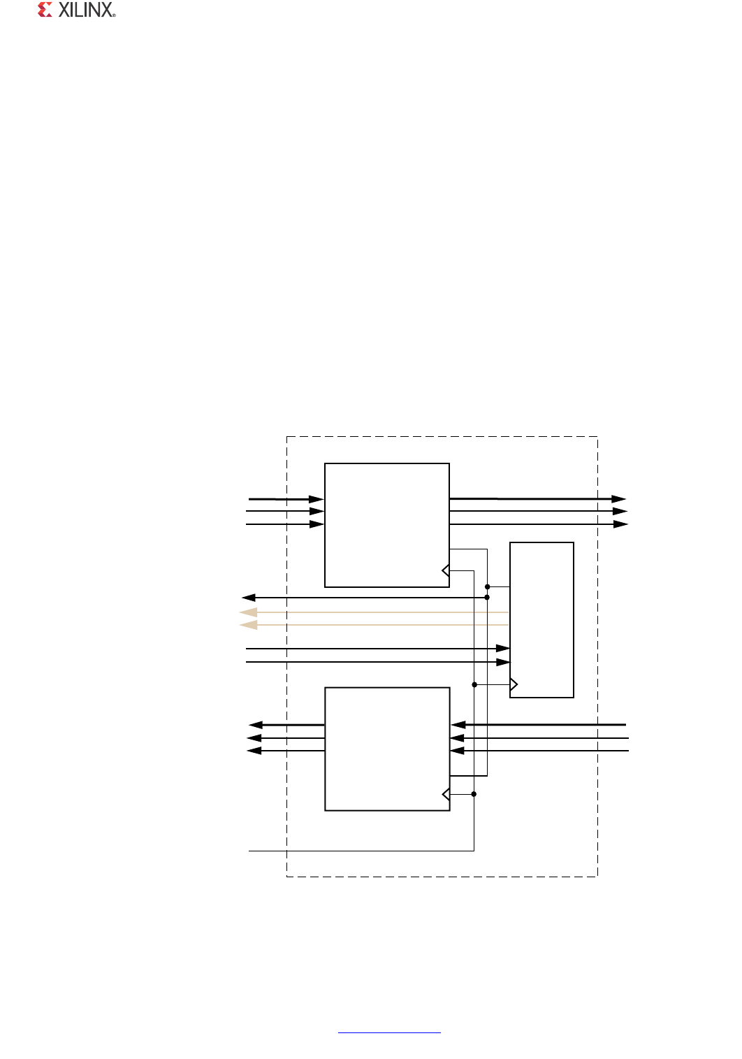
1000BASE-X PCS/PMA or SGMII v11.4 www.xilinx.com 301
PG047 October 16, 2012
Chapter 8: Using the Client-Side GMII Datapath
The result of the SGMII adaptation module is therefore to create a proprietary interface that
is based on GMII (true GMII only operates at a clock frequency of 125 MHz for an ethernet
line rate of 1.25 Gb/s). This interface then allows a straightforward internal connection to an
Ethernet MAC core when operating in MAC mode or the GMII can be brought out on pads
to connect to an external PHY when the core operates in PHY mode. For example, the SGMII
adaptation module can be used to interface the Ethernet 1000BASE-X PCS/PMA or SGMII
core, operating in SGMII configuration with MAC mode of operation, to the Xilinx Tri-Mode
Ethernet MAC core directly (see Chapter 12, Interfacing to Other Cores). The GMII interface
of the SGMII adaptation module can brought out to the pads and connected to external
PHY module that converts GMII to Physical Medium Dependent (PMD) signal when the
Ethernet 1000BASEX PCS/PMA or SGMII core, operating in SGMII configuration and PHY
mode of operation.
SGMII Adaptation Module Top Level
The SGMII adaptation module is described in several hierarchical submodules as illustrated
in Figure 8-13. These submodules are each described in separate HDL files and are
described in the following sections.
X-Ref Target - Figure 8-13
Figure 8-13: SGMII Adaptation Module
3'-))!DAPTATION-ODULE
4X2ATE!DAPT
#LOCK
'ENERATION
4O'-))
4XINPUTOFCORE
&ROM'-))
2XOUTPUTOFCORE
&ROM#LIENT-!#'-))
#LIENT0(93'-))
4O#LIENT-!#'-))
#LIENT0(9'-))
SGMII?CLK?EN
USERCLK
-(Z
REFERENCECLOCK
SGMII?CLK?EN
SGMII?CLK?R
CLKM
SPEED?IS??
SPEED?IS?
SGMII?CLK?F
CLKM
SGMII?CLK?EN
GMII?TXD?IN;= GMII?TXD?OUT;=
GMII?TX?EN?IN GMII?TX?EN?OUT
GMII?TX?ER?IN GMII?TX?ER?OUT
2X2ATE!DAPT
CLKM
SGMII?CLK?EN
GMII?RXD?OUT;= GMII?RXD?IN;=
GMII?RX?DV?OUT GMII?RX?DV?IN
GMII?RX?ER?OUT GMII?RX?ER?IN
3PEED#ONTROL
8
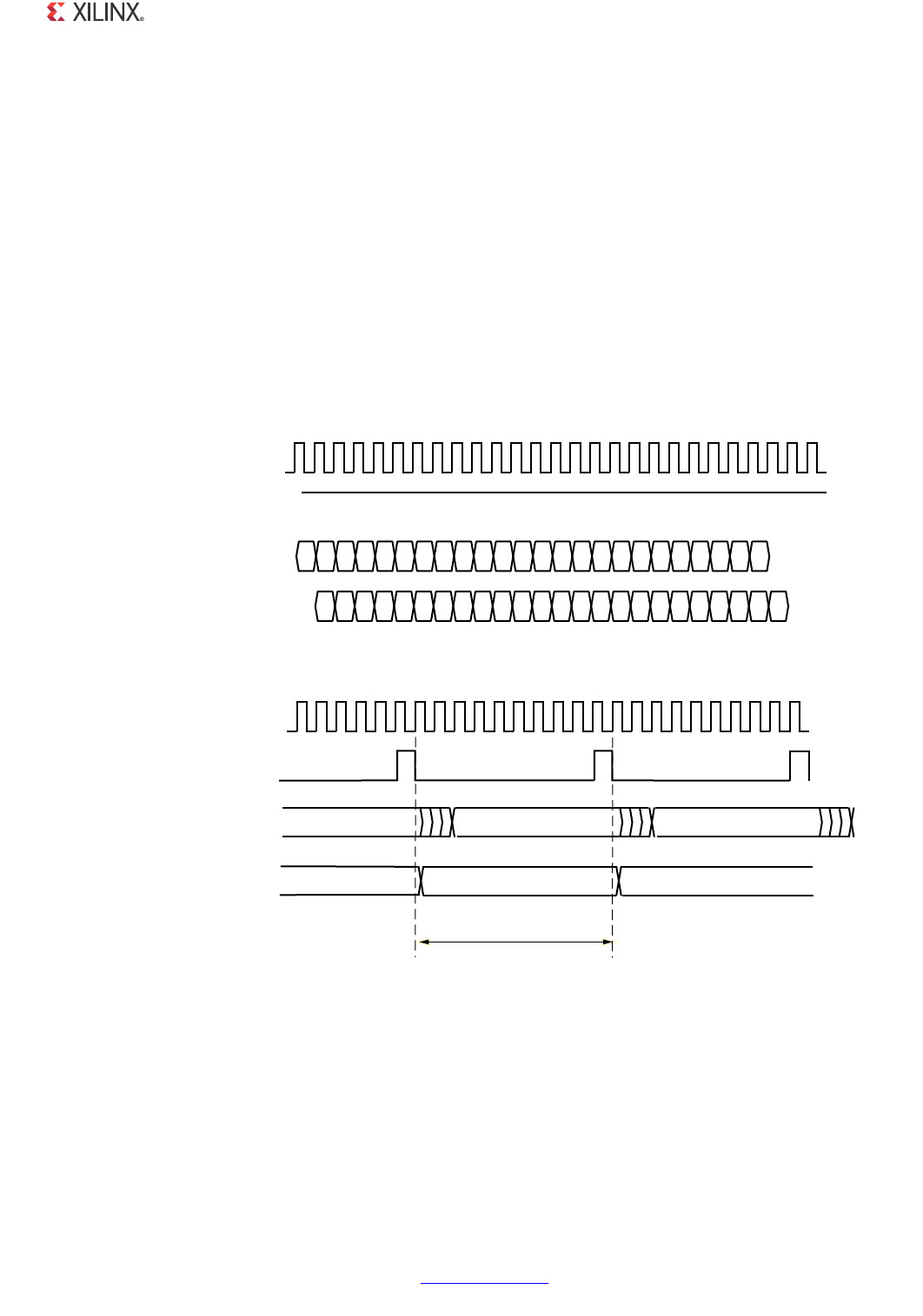
1000BASE-X PCS/PMA or SGMII v11.4 www.xilinx.com 302
PG047 October 16, 2012
Chapter 8: Using the Client-Side GMII Datapath
Transmitter Rate Adaptation Module
This module accepts transmitter data from the GMII-style interface from the attached client
MAC/External PHY, and samples the input data on the 125 MHz reference clock, clk125m.
This sampled data can then be connected directly to the input GMII of the Ethernet
1000BASE-X PCS/PMA, or SGMII netlist. The 1 Gb/s and 100 Mb/s cases are illustrated in
Figure 8-14.
At all speeds, the client MAC/External PHY logic should drive the GMII transmitter data
synchronously to the rising edge of the 125 MHz reference clock while using
sgmii_clk_en (derived from the Clock Generation module) as a clock enable. The
frequency of this clock enable signal ensures the correct data rate and correct data
sampling between the two devices.
X-Ref Target - Figure 8-14
Receiver Rate Adaptation Module
This module accepts received data from the Ethernet 1000BASE-X PCS or SGMII core. This
data is sampled and sent out of the GMII receiver interface for the attached client
MAC/External PHY. The 1 Gb/s and 100 Mb/s cases are illustrated in Figure 8-15.
Figure 8-14: Transmitter Rate Adaptation Module Data Sampling
SGMII?CLK?EN
FONP
6SHHGLV*ESV
' ' '
' ' '
JPLLBW[GBLQ>@
JPLLBW[GBRXW>@
SGMII?CLK?EN
6SHHGLV0ESV
JPLLBW[GBLQ>@
JPLLBW[GBRXW>@
'
' '
FONP
F\FOHV
FONP
$ $
8

1000BASE-X PCS/PMA or SGMII v11.4 www.xilinx.com 303
PG047 October 16, 2012
Chapter 8: Using the Client-Side GMII Datapath
At 1 Gb/s, the data is valid on every clock cycle of the 125 MHz reference clock (clk125m).
Data received from the core is clocked straight through the Receiver Rate Adaptation
module.
At 100 Mb/s, the data is repeated for a 10 clock period duration of clk125m; at 10 Mb/s,
the data is repeated for a 100 clock period duration of clk125m. The Receiver Rate
Adaptation Module samples this data using the sgmii_clk_en clock enable.
The Receiver Rate Adaptation module also performs a second function that accounts for the
latency inferred in Figure 8-15. The 8-bit Start of Frame Delimiter (SFD) code is detected,
and if required, it is realigned across the 8-bit datapath of gmii_rxd_out[7:0] before
being presented to the attached client MAC. It is possible that this SFD could have been
skewed across two separate bytes by MACs operating on a 4-bit datapath.
At all speeds, the client MAC/External PHY logic should sample the GMII receiver data
synchronously to the rising edge of the 125 MHz reference clock while using
sgmii_clk_en (derived from the Clock Generation module) as a clock enable. The
frequency of the sgmii_clk_en clock enable signal ensures the correct data rate and
correct data sampling between the two devices.
X-Ref Target - Figure 8-15
Figure 8-15: Receiver Rate Adaptation Module Data Sampling
SGMII?CLK?EN
CLKM
gg
'BPS3PEED
$ $ $
$ $ $
GMII?RXD?IN;=
GMII?RXD?OUT;=
SGMII?CLK?EN
-BPS3PEED
GMII?RXD?IN;=
GMII?TXD?OUT;= $ $
CLKM
CYCLES
CLKM
$ $ $
$ $ $$$$ $ $ $ $ $ $ $ $ $ $ $ $ $ $ $
8
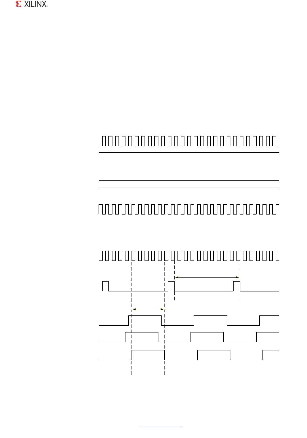
1000BASE-X PCS/PMA or SGMII v11.4 www.xilinx.com 304
PG047 October 16, 2012
Chapter 8: Using the Client-Side GMII Datapath
Clock Generation
This module creates the sgmii_clk_en clock enable signal for use throughout the SGMII
adaptation module. Clock enabled frequencies are:
• 125 MHz at an operating speed of 1 Gb/s
• 12.5 MHz at an operating speed of 100 Mb/s
• 1.25 MHz at an operating speed of 10 Mb/s
Figure 8-16 illustrates the output clock enable signal for the Clock Generation module at 1
Gb/s and 100 Mb/s speeds.
X-Ref Target - Figure 8-16
Figure 8-16: Clock Generator Output Clocks and Clock Enable
SGMII?CLK?R
CLKM
SGMII?CLK?F
SGMII?CLK?EN
SGMII?CLK?R
SGMII?CLK?F
SGMII?CLK?EN
CLKM
CYCLES
gg
gg
gg
3PEEDIS'BPS
3PEEDIS-BPS
CLKM
CLKM
CYCLES
SGMII?CLK
RESULTOF)/"
OUTPUT$$2
SGMII?CLK
RESULTOF)/"
OUTPUT$$2
8

1000BASE-X PCS/PMA or SGMII v11.4 www.xilinx.com 305
PG047 October 16, 2012
Chapter 8: Using the Client-Side GMII Datapath
Figure 8-16 also illustrates the formation of the sgmii_clk_r and sgmii_clk_f signals.
These are used only in the example design delivered with the core, where they are routed to
a device IOB DDR output register. This provides SGMII clock forwarding at the correct
frequency; these signal can be ignored when connecting the core and SGMII Adaptation
module to internal logic.

1000BASE-X PCS/PMA or SGMII v11.4 www.xilinx.com 306
PG047 October 16, 2012
Chapter 9
Auto-Negotiation
This chapter provides general guidelines for using the Auto-Negotiation function of the
Ethernet 1000BASE-X PCS/PMA or SGMII core. Auto-Negotiation is controlled and
monitored through the PCS Management registers. For more information, see Register
Space in Chapter 2.
Overview of Operation
For either standard, when considering Auto-Negotiation between two connected devices, it
must be remembered that:
• Auto-Negotiation must be either enabled in both devices, or:
• Auto-Negotiation must be disabled in both devices.
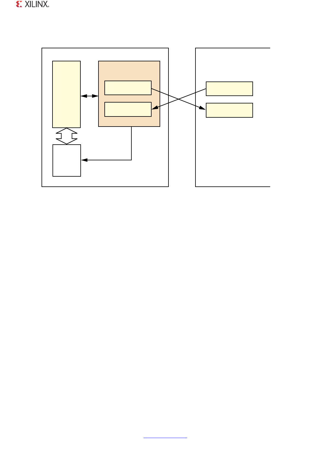
1000BASE-X PCS/PMA or SGMII v11.4 www.xilinx.com 307
PG047 October 16, 2012
Chapter 9: Auto-Negotiation
1000BASE-X Standard
IEEE 802.3-2008 clause 37 describes the 1000BASE-X Auto-Negotiation function that allows
a device to advertise the modes of operation that it supports to a device at the remote end
of a link segment (the link partner) and to detect corresponding operational modes that the
link partner advertises. Figure 9-1 illustrates the operation of 1000BASE-X
Auto-Negotiation.
The following describes typical operation when Auto-Negotiation is enabled.
1. Auto-Negotiation starts automatically when any of the following conditions are met.
°Power-up/reset
°Upon loss of synchronization
°The link partner initiates Auto-Negotiation
°An Auto-Negotiation Restart is requested (See MDIO Register 0: Control Register
and an_restart_config in Tab le 2 -14.)
2. During Auto-Negotiation, the contents of the Auto-Negotiation Advertisement register
are transferred to the link partner.
This register is writable through the MDIO, therefore enabling software control of the
systems advertised abilities. See MDIO Register 4: Auto-Negotiation Advertisement for
more information.
X-Ref Target - Figure 9-1
Figure 9-1: 1000BASE-X Auto-Negotiation Overview
%THERNET"!3%8
0#30-!OR3'-))
#ORE
&0'!$EVICE
%THERNET
-EDIA
!CCESS
#ONTROLLER
0OWER0#
-$)/
#ORE#ONNECT
AN?INTERRUPT
!UTO.EG!DV
2EG
,INK0ARTNER!BILITY
"ASE2EG
,INK0ARTNER
!UTO.EG!DV
2EG
,INK0ARTNER!BILITY
"ASE2EG
/PTICAL
&IBRE

1000BASE-X PCS/PMA or SGMII v11.4 www.xilinx.com 308
PG047 October 16, 2012
Chapter 9: Auto-Negotiation
This register is also writable through dedicated interface signal
an_adv_config_vector. If optional MDIO is present, the additional signal
an_adv_config_valid quantifies the contents of an_adv_config_vector. See
definitions of an_adv_config_vector and an_adv_config_valid in Table 2-14
for more information.
Information provided in this register includes:
°Fault Condition signaling
°Duplex Mode
°Flow Control capabilities for the attached Ethernet MAC.
3. The advertised abilities of the Link Partner are simultaneously transferred into the
Auto-Negotiation Link Partner Ability Base Register.
This register contains the same information as in the Auto-Negotiation Advertisement
Register. See MDIO Register 5: Auto-Negotiation Link Partner Base for more
information.
4. Under normal conditions, this completes the Auto-Negotiation information exchange.
It is now the responsibility of system management (for example, software running on an
embedded PowerPC® or MicroBlaze™ processor) to complete the cycle. The results of the
Auto-Negotiation should be read from Auto-Negotiation Link Partner Ability Base
Register. Other networking components, such as an attached Ethernet MAC, should be
configured accordingly. See MDIO Register 5: Auto-Negotiation Link Partner Base for
more information.
There are two methods that a host processor uses to learn of the completion of an
Auto-Negotiation cycle:
°Polling the Auto-Negotiation completion bit 1.5 in the Status Register (Register 1).
°Using the Auto-Negotiation interrupt port of the core (see Using the
Auto-Negotiation Interrupt).
SGMII Standard
Using the SGMII MAC Mode Configuration to Interface to an External
BASE-T PHY with SGMII Interface
Figure 9-2 illustrates the operation of SGMII Auto-Negotiation as described in Overview of
Operation. Additional information about SGMII Standard Auto-Negotiation is provided in
the following sections.
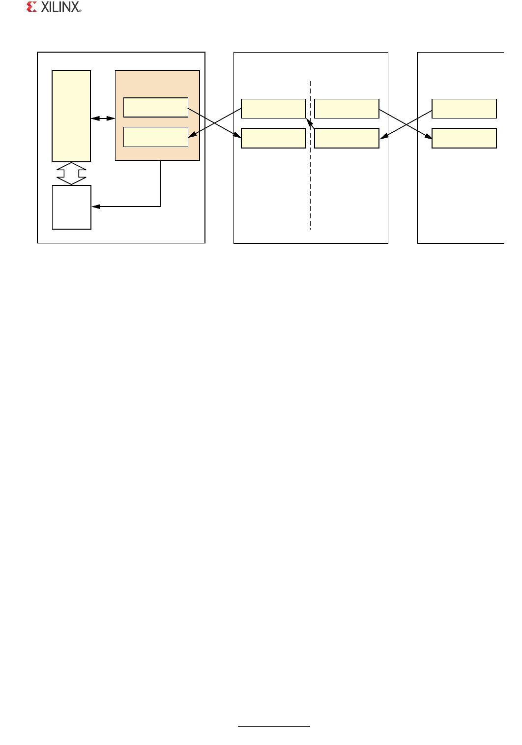
1000BASE-X PCS/PMA or SGMII v11.4 www.xilinx.com 309
PG047 October 16, 2012
Chapter 9: Auto-Negotiation
X-Ref Target - Figure 9-2
The SGMII capable PHY has two distinctive sides to Auto-Negotiation.
• The PHY performs Auto-Negotiation with its link partner using the relevant
Auto-Negotiation standard for the chosen medium (BASE-T Auto-Negotiation is
illustrated in Figure 9-2, using a twisted copper pair as its medium). This resolves the
operational speed and duplex mode with the link partner.
• The PHY then passes the results of the Auto-Negotiation process with the link partner
to the Ethernet 1000BASE-X PCS/PMA or SGMII core (in SGMII mode), by leveraging the
1000BASE-X Auto-Negotiation specification described in Figure 9-1. This transfers the
results of the Link Partner Auto-Negotiation across the SGMII and is the only
Auto-Negotiation observed by the core.
This SGMII Auto-Negotiation function, summarized previously, leverages the 1000BASEX
PCS/PMA Auto-Negotiation function but contains two differences.
• The duration of the Link Timer of the SGMII Auto-Negotiation is shrunk from 10 ms to
1.6 ms so that the entire Auto-Negotiation cycle is much faster. See Setting the
Configurable Link Timer.
• The information exchanged is different and now contains speed resolution in addition
to duplex mode. See MDIO Register 5: Auto-Negotiation Link Partner Base.
• There are no other differences and dealing with the results of Auto-Negotiation can be
handled as described previously in Figure 9-1.
Figure 9-2: SGMII Auto-Negotiation in MAC Mode
%THERNET"!3%8
0#30-!OR3'-))
#ORE
&0'!$EVICE
%THERNET
-EDIA
!CCESS
#ONTROLLER
0OWER0#
-$)/
#ORE#ONNECT
AN?INTERRUPT
!UTO.EG!DV
2EG
,INK0ARTNER!BILITY
"ASE2EG
3'-))CAPABLE
"!3%40(9
!UTO.EG!DV
2EG
,INK0ARTNER!BILITY
"ASE2EG
3'-))
LINK
!UTO.EG!DV
2EG
,INK0ARTNER!BILITY
"ASE2EG
3'-))SIDE "!3%4SIDE -EDIUM
4WISTED
#OPPER
0AIR
,INK0ARTNER
!UTO.EG!DV
2EG
,INK0ARTNER!BILITY
"ASE2EG
8
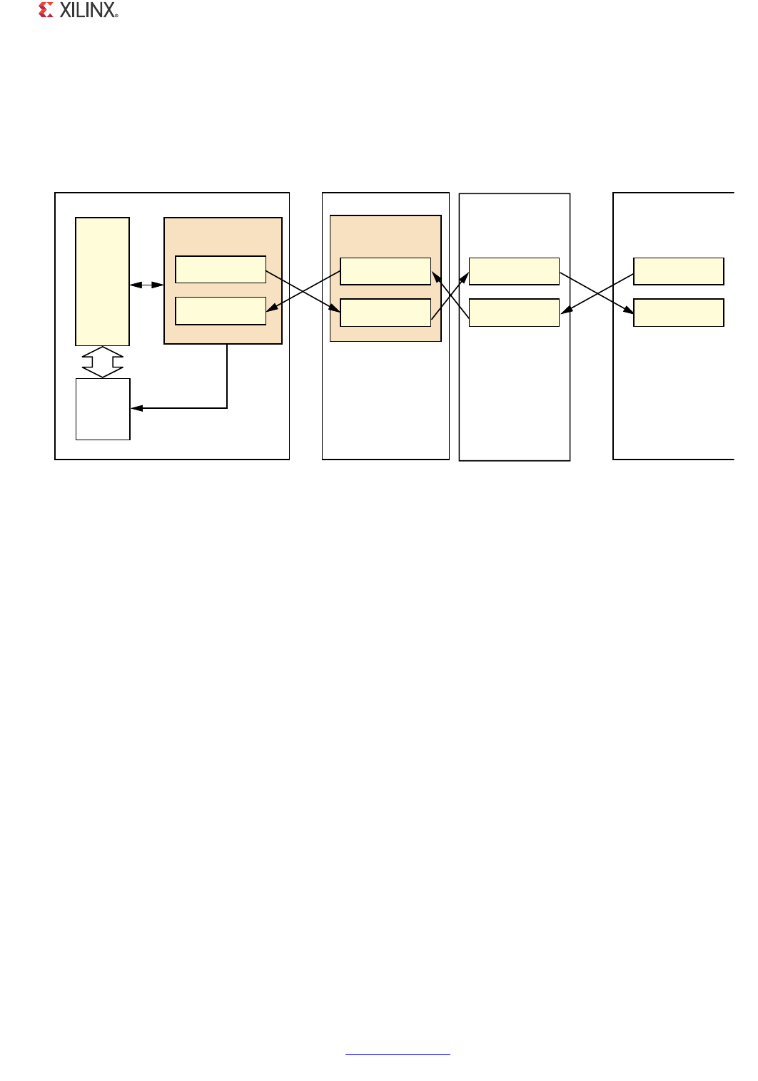
1000BASE-X PCS/PMA or SGMII v11.4 www.xilinx.com 310
PG047 October 16, 2012
Chapter 9: Auto-Negotiation
Using Both the SGMII MAC Mode and SGMII PHY Mode Configurations to
interface to an External BASE-T PHY with a GMII interface
Figure 9-3 illustrates the operation of SGMII Auto-Negotiation. Additional information
about SGMII Standard Auto-Negotiation is provided in the following sections.
The SGMII capable PHY has two distinctive sides to Auto-Negotiation.
• The PHY performs Auto-Negotiation with its link partner using the relevant
Auto-Negotiation standard for the chosen medium (BASE-T Auto-Negotiation is
illustrated in Figure 9-3, using a twisted copper pair as its medium). This resolves the
operational speed and duplex mode with the link partner. The BASE-T PHY transfers the
link partner abilities though the MDIO interface to the Ethernet 1000 BASE-X PCS/PMA
or SGMII core (in SGMII configuration and PHY mode).
• The Ethernet 1000 BASE-X PCS/PMA or SGMII core (in SGMII configuration and PHY
mode) then passes the results of the Auto-Negotiation process to the Ethernet
1000BASEX PCS/PMA or SGMII core (in SGMII configuration and MAC mode), by
leveraging the 1000BASE-X Auto-Negotiation specification described in Overview of
Operation. This transfers the results of the Link Partner Auto-Negotiation across the
SGMII and is the only Auto-Negotiation observed by the core.
X-Ref Target - Figure 9-3
Figure 9-3: SGMII Auto-Negotiation
%THERNET"!3%8
0#30-!OR3'-))
#ORE0(9-ODE
%THERNET"!3%8
0#30-!OR3'-))
#ORE-!#-ODE
&0'!$EVICE
%THERNET
-EDIA
!CCESS
#ONTROLLER
0OWER0#
-$)/
#ORE#ONNECT
AN?INTERRUPT
!UTO.EG!DV
2EG
,INK0ARTNER!BILITY
"ASE2EG
"!3%40(9
!UTO.EG!DV
2EG
,INK0ARTNER!BILITY
"ASE2EG
3'-))
LINK
!UTO.EG!DV
2EG
,INK0ARTNER!BILITY
"ASE2EG
-EDIUM
4WISTED
#OPPER
0AIR
,INK0ARTNER
!UTO.EG!DV
2EG
,INK0ARTNER!BILITY
"ASE2EG
&0'!$EVICE
8

1000BASE-X PCS/PMA or SGMII v11.4 www.xilinx.com 311
PG047 October 16, 2012
Chapter 9: Auto-Negotiation
This SGMII Auto-Negotiation function, summarized previously, leverages the 1000BASEX
PCS/PMA Auto-Negotiation function but contains two differences.
• The duration of the Link Timer of the SGMII Auto-Negotiation is shrunk from 10 ms to
1.6 ms so that the entire Auto-Negotiation cycle is much faster. See Setting the
Configurable Link Timer.
• The information exchanged is different and now contains speed resolution in addition
to duplex mode. See MDIO Register 5: Auto-Negotiation Link Partner Base. There are
no other differences and dealing with the results of Auto-Negotiation can be handled
as described previously in Overview of Operation.
Setting the Configurable Link Timer
The optional Auto-Negotiation function has a Link Timer (link_timer[8:0]) port. This
port sets the period of the Auto-Negotiation Link Timer. This port should be permanently
tied to a logical binary value, and a binary value should be placed on this port. The duration
of the timer is approximately equal to the binary value multiplied by 32.768 microseconds
(4096 clock periods of the 125 MHz clock provided to the core). See Auto-Negotiation
Signal Pinout.
Note: See Chapter 10, Dynamic Switching of 1000BASE-X and SGMII Standards for details of
programming the Auto-Negotiation Link Timer when performing dynamic switching between
1000BASE-X and SGMI Standards.
The accuracy of this Link Timer is within the following range.
+0 to -32.768 microseconds
1000BASE-X Standard
The Link-Timer is defined as having a duration somewhere between 10 and 20 milliseconds.
The example design delivered with the core sets the binary value as follows:
100111101 = 317 decimal
This corresponds to a duration of between 10.354 and 10.387 milliseconds.
SGMII Standard
The Link-Timer is defined as having a duration of 1.6 milliseconds. The example design
delivered with the core sets the binary value to
000110010 = 50 decimal
This corresponds to a duration of between 1.606 and 1.638 milliseconds.

1000BASE-X PCS/PMA or SGMII v11.4 www.xilinx.com 312
PG047 October 16, 2012
Chapter 9: Auto-Negotiation
Simulating Auto-Negotiation
Auto-Negotiation requires a minimum of three link timer periods for completion. If
simulating the Auto-Negotiation procedure, setting the link_timer[8:0] port to a low
value greatly reduces the simulation time required to complete Auto-Negotiation. See
Auto-Negotiation Signal Pinout
Using the Auto-Negotiation Interrupt
The Auto-Negotiation function has an an_interrupt port. This is designed to be used
with common microprocessor bus architectures (for example, the CoreConnect bus
interfacing to a MicroBlaze processor or the Virtex®-5 FXT FPGA embedded IBM PowerPC
processor).
The operation of this port is enabled or disabled and cleared through the MDIO Register 16,
the Vendor-specific Auto-Negotiation Interrupt Control Register.
• When disabled, this port is permanently tied to logic 0.
• When enabled, this port is set to logic 1 following the completion of an
Auto-Negotiation cycle. It remains high until it is cleared by writing 0 to bit 16.1
(Interrupt Status bit) of the Register 16: Vendor-Specific Auto-Negotiation Interrupt
Control.
Use of Clock Correction Sequences in Device
Specific Transceivers (1000BASE-X Standard)
The device-specific transceivers are configured by the appropriate transceiver wizard to
perform clock correction. The output of the transceiver wizard is provided as part of the
example design. Two different clock correction sequences can be employed:
1. The mandatory clock correction sequence is the /I2/ ordered set; this is a two byte
code-group sequence formed from /K28.5/ and /D16.2/ characters. The /I2/ ordered-set
is present in the inter-frame-gap. These sequences can therefore be removed or
inserted by the transceiver’s receiver elastic buffer without causing frame corruption.
2. The default transceiver wizard configuration for the device-specific transceivers varies
across device families. Some of the transceiver wizards enable the CLK_COR_SEQ_2_USE
attribute. When this is the case, the transceiver is also configured to perform clock
correction on the /K28.5/D21.5/ sequence; this is the first two code-groups from the
/C1/ ordered set (the /C1/ ordered-set is 4 code-groups in length). Because there are no
/I2/ ordered-sets present during much of the Auto-Negotiation cycle, this provides a
method of allowing clock correction to be performed during Auto-Negotiation.

1000BASE-X PCS/PMA or SGMII v11.4 www.xilinx.com 313
PG047 October 16, 2012
Chapter 9: Auto-Negotiation
Because this form of clock correction inserts or removes two-code groups into or from
a four-code group sequence, this causes ordered-set fragments to be seen by the cores
Auto-Negotiation state machine. It is therefore important that the transceivers
RXCLKCORCNT[2:0] port is correctly wired up to the core netlist; this indicates a clock
correction event (and type) to the core. Using this signal, the cores state machine can
interpret the clock-correction fragments and the Auto-Negotiation function can
complete cleanly.
When the device-specific transceivers CLK_COR_SEQ_2_USE attribute is not enabled, no
clock correction can be performed during much of the Auto-Negotiation cycle. When
this is the case, it is possible that the transceivers receiver elastic buffer could underflow
or overflow as asynchronous clock tolerances accumulate. This results in an elastic
buffer error. It is therefore important that the transceivers RXBUFSTATUS[2:0] port is
correctly wired up to the core netlist; this indicates a buffer error event to the core.
Using this signal, the cores state machine can interpret the buffer error and the
Auto-Negotiation function can complete cleanly.
Conclusion
The device-specific transceivers can be configured to optionally perform clock correction
during the Auto-Negotiation cycle, and their default configuration varies from family to
family. Regardless, if correctly connected, as per the example design, the core’s state
machine can determine the transceivers elastic buffer behavior and Auto-Negotiation will
complete cleanly.

1000BASE-X PCS/PMA or SGMII v11.4 www.xilinx.com 314
PG047 October 16, 2012
Chapter 10
Dynamic Switching of 1000BASE-X and
SGMII Standards
This chapter provides general guidelines for using the core to perform dynamic standards
switching between 1000BASE-X and SGMII. The core only provides this capability if
generated with the appropriate option, as described in Chapter 17, Customizing and
Generating the Core.
Typical Application
Figure 10-1 illustrates a typical application for the Ethernet 1000BASE-X PCS/PMA or SGMII
core with the ability to dynamically switch between 1000BASE-X and SGMII standards.
The FPGA is shown connected to an external, off-the-shelf PHY with the ability to perform
both BASE-X and BASE-T standards.
• The core must operate in 1000BASE-X mode to use the optical fibre.
• The core must operate in SGMII mode to provide BASE-T functionality and use the
twisted copper pair.
The GMII of the Ethernet 1000BASE-X PCS/PMA or SGMII core is shown connected to an
embedded Ethernet Media Access Controller (MAC), for example the Tri-Mode Ethernet
MAC core from Xilinx.
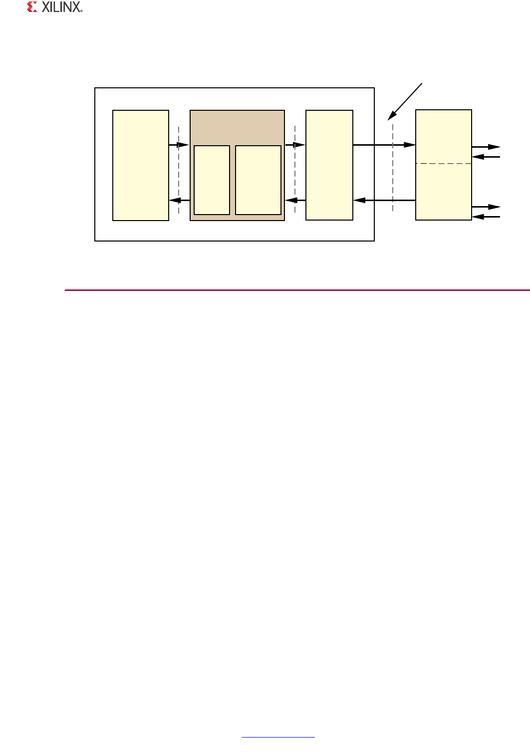
1000BASE-X PCS/PMA or SGMII v11.4 www.xilinx.com 315
PG047 October 16, 2012
Chapter 10: Dynamic Switching of 1000BASE-X and SGMII Standards
Operation of the Core
Selecting the Power-On / Reset Standard
The external port of the core, basex_or_sgmii (see Dynamic Switching Signal Pinout),
selects the default standard of the core as follows:
• Tie to logic ‘0’ in the core instantiation. The core powers-up and comes out of a reset
cycle operating in the 1000BASE-X standard.
• Tie to logic ‘1’ in the core instantiation. The core powers-up and comes out of a reset
cycle operating in the SGMII standard.
The basex_or_sgmii port of the core can be dynamically driven. In this configuration, it
is possible to drive a logical value onto the port, followed by a core reset cycle to switch the
core to the desired standard. However, it is expected that the standard will be switched
through the MDIO Management Registers.
X-Ref Target - Figure 10-1
Figure 10-1: Typical Application for Dynamic Switching
(WKHUQHW%$6(;
3&630$RU6*0,,
/RJL&25(
7UDQVFHLYHU
8VHU/RJLF
(WKHUQHW
0HGLD
$FFHVV
&RQWUROOHU
,QWHUQDO
*0,, ,QWHUIDFH
7;37;1
5;35;1
7ZLVWHG
&RSSHU
3DLU
%$6(;
RU
6*0,,
%$6(;
%$6(7
%$6(7
%$6(7
2SWLFDO
)LEUH
8ILINX&0'!
7UDQVFHLYHU
8

1000BASE-X PCS/PMA or SGMII v11.4 www.xilinx.com 316
PG047 October 16, 2012
Chapter 10: Dynamic Switching of 1000BASE-X and SGMII Standards
Switching the Standard Using MDIO
The 1000BASE-X or SGMII standard of the core can be switched at any time by writing to the
Register 17: Vendor-Specific Standard Selection Register. Following completion of this
write, the MDIO Management Registers immediately switch.
• Core set to 1000BASE-X standard. Management Registers 0 through 16 should be
interpreted according to 1000BASE-X Standard Using the Optional Auto-Negotiation.
• Core set to SGMII standard. Management Registers 0 through 16 should be interpreted
according to SGMII Standard Using the Optional Auto-Negotiation.
Auto-Negotiation State Machine
• Core set to the 1000BASE-X standard. The Auto-Negotiation state machine operates as
described in 1000BASE-X Standard.
• Core set to perform the SGMII standard. The Auto-Negotiation state machine operates
as described in SGMII Standard.
• Standard is switched during an Auto-Negotiation sequence. The Auto-Negotiation
state machine does not immediately switch standards, but attempt to continue to
completion at the original standard.
• Switching the standard using MDIO. This does not cause Auto-Negotiation to
automatically restart. Xilinx recommends that after switching to a new standard using
an MDIO write, immediately perform the following:
°If you have switched to the 1000BASE-X standard, reprogram the Auto-Negotiation
Advertisement Register (Register 4) to the desired settings.
°For either standard, restart the Auto-Negotiation sequence by writing to bit 0.9 of
the MDIO Control Register (Register 0).
Setting the Auto-Negotiation Link Timer
As described in Chapter 9, Auto-Negotiation, the duration of the Auto-Negotiation Link
Timer differs with the 1000BASE-X and the SGMII standards. To provide configurable link
timer durations for both standards, the following ports are available. These ports replace
the link_timer_value[8:0] port that is used when the core is generated for a single
standard.
•link_timer_basex[8:0] The value placed on this port is sampled at the beginning
of the Auto-Negotiation cycle by the Link Timer when the core is set to perform the
1000BASE-X standard.
•link_timer_sgmii[8:0] The value placed on this port is sampled at the beginning
of the Auto-Negotiation cycle by the Link Timer when the core is set to perform the
SGMII standard.
Both ports follow the same rules that are described in Setting the Configurable Link Timer.
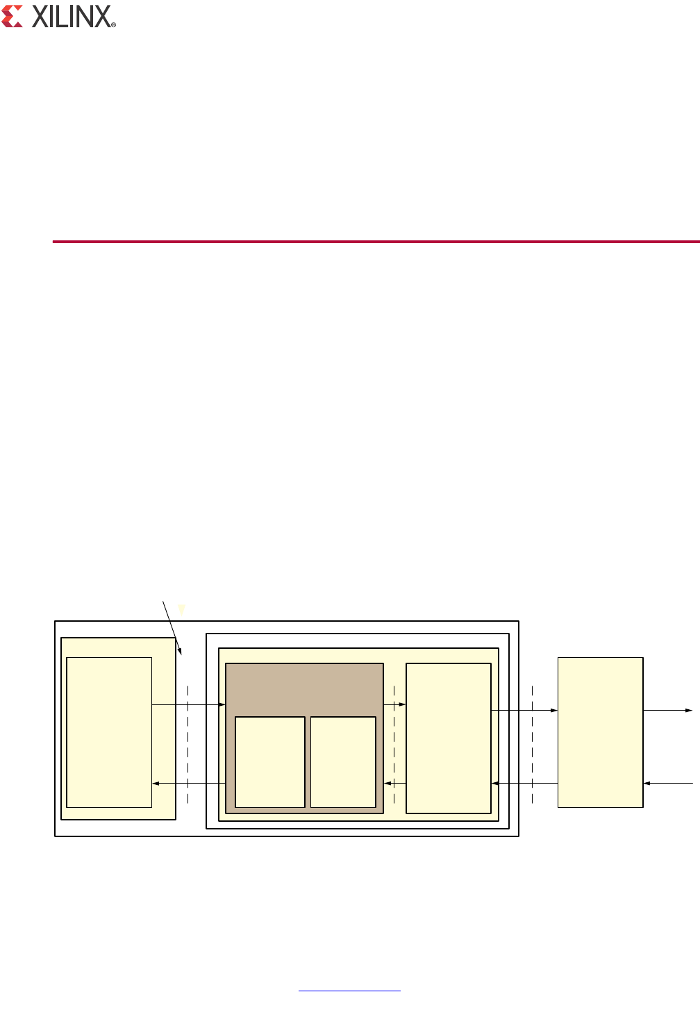
1000BASE-X PCS/PMA or SGMII v11.4 www.xilinx.com 317
PG047 October 16, 2012
Chapter 11
GMII to PHY EDK Application for
Zynq-7000 Device Processor Subsystem
Overview
This section describes the Gigabit Ethernet PCS/PMA EDK application customized to
interface with either of the two Gigabit Ethernet MAC (ENET0 or ENET1) hard blocks present
in Zynq™-7000 devices. Figure 11-1 shows the application.
EDK provides an alternate package to the netlist created by the CORE Generator™ Wizard.
The IP catalog in XPS contains the IP core gig_eth_pcs_pma with the same netlist provided
by CORE Generator tools. The difference is that the RTL is packaged as an EDK pcore
suitable for use with Zynq GigE systems.
The GigE controller must be configured to use EMIO pins which route the GMII interface of
the MAC to the PL. The gig_eth_pcs_pma IP can then be connected to this GMII interface in
PL.
X-Ref Target - Figure 11-1IFIFIF
Figure 11-1: Gigabit Ethernet PCS/PMA EDK Application Overview
%XTERNAL0(9
OR
0(9ON"OARD
4RANSCEIVER
48
'IG%
'-))
%THERNET0#30-!%$+!PPLICATION
'-))
)NTERFACE
4RANSCEIVER
)NTERFACE
03
'-))
:YNQDEVICE
%THERNET"!3%80#3
0-!OR3'-)),OGI#/2%
:YNQ&ABRIC
28028.
48048.
48
28
4WISTED
#OPPER
0AIR
/&#
8

1000BASE-X PCS/PMA or SGMII v11.4 www.xilinx.com 318
PG047 October 16, 2012
Chapter 11: GMII to PHY EDK Application for Zynq-7000 Device Processor Subsystem
The Gigabit Ethernet PCS/PMA EDK application can be configured to operate in the
following modes.
•GMII to 1000BASEX
•GMII to SGMII Using Zynq-7000 Device Gigabit Transceiver
•GMII to SGMII Using Zynq-7000 Device LVDS Transceiver
Each of the applications are explained in the following sections.
GMII to 1000BASEX
The IP is designed to integrate with the Zynq -7000 device GTX transceiver. Figure 11-2
illustrates the connections and logic required between the IP and the transceiver; the signal
names and logic in the figure precisely match those delivered with the EDK IP.
The 125 MHz differential reference clock output from IBUFDS_GTE2 is routed directly to
the Zynq-7000 device GTX Transceiver. The transceiver is configured to output a version of
this clock (62.5 MHz) on the TXOUTCLK port; this is then routed to an MMCM through a
BUFG (global clock routing). The MMCM outputs the following clocks on the clock output
ports, CLKOUT0 (125 MHz) and CLKOUT1 (62.5 MHz). The CLKOUT0 port (125 MHz) of
MMCM is placed onto global clock routing and can be used as the 125 MHz clock source for
all core logic. The CLKOUT1 port (62.5 MHz) is placed onto global clock routing and is input
back into the GTXE2 transceiver on the user interface clock ports rxusrclk, rxusrclk2,
txusrclk and txusrclk2.
The GMII and MDIO interfaces are connected to the respective interfaces on the Gigabit
Ethernet MAC (GigE) module in the Zynq-7000 device Processor Subsystem (PS). The
gmii_tx_clk and gmii_rx_clk signals are driven from CLKOUT0 port of MMCM.
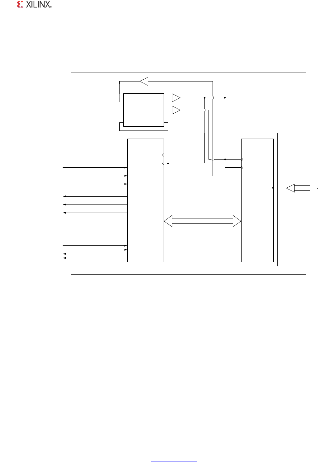
1000BASE-X PCS/PMA or SGMII v11.4 www.xilinx.com 319
PG047 October 16, 2012
Chapter 11: GMII to PHY EDK Application for Zynq-7000 Device Processor Subsystem
X-Ref Target - Figure 11-2
Figure 11-2: GMII to 1000BASEX EDK Application for Zynq-7000 Devices
REFCLK?P
REFCLK?N
)"5&$3?'4%
:YNQ
'48
4RANSCEIVER
GTREFCLK
-(Z
#,+).
#,+&"/54#,+&").
#,+/54
#,+/54
"5&'
"5&'
"5&'
-(Z
-(Z
GMII?TX?CLK
GMII?RX?CLK
"5&'
48/54#,+
48532#,+
48532#,+
USERCLK
USERCLK
4RANSCEVER) &
GMII?TXD;=
GMII?TX?EN
GMII?TX?ER
GMII?RXD;=
GMII?RX?DV
GMII?RX?ER
MDC
MDIO?IN
MDIO?OUT
MDIO?TRI
%THERNET"!3%8
0#30-!OR3'-))
,OGI#/2%
GIG?ETH?PCS?PMA?BASEX
?BLOCK
MDC
MDIO?I
MDIO?O
MDIO?T
GMII?TXD
GMII?TX?EN
GMII?TX?ER
GMII?RXD
GMII?RX?DV
GMII?RX?ER
GIG?ETHERNET?PCS?PMA
'-))TO"!3%8
%$+)0
8

1000BASE-X PCS/PMA or SGMII v11.4 www.xilinx.com 320
PG047 October 16, 2012
Chapter 11: GMII to PHY EDK Application for Zynq-7000 Device Processor Subsystem
GMII to SGMII Using Zynq-7000 Device Gigabit
Transceiver
The IP is designed to integrate with the Zynq-7000 device GTX transceiver. Figure 11-3
illustrates the connections and logic required between the IP and the transceiver; the signal
names and logic in the figure precisely match those delivered with the EDK IP.
The 125 MHz differential reference clock output from IBUFDS_GTE2 is routed directly to
the Zynq-7000 device GTX Transceiver. The transceiver is configured to output a version of
this clock (62.5 MHz) on the TXOUTCLK port; this is then routed to a MMCM through a
BUFG (global clock routing). The MMCM outputs the following clocks on the clock output
ports, CLKOUT0 (125 MHz), CLKOUT1 (62.5 MHz), CLKOUT2 (25 MHz) and CLKOUT3 (10
MHz). The CLKOUT0 port (125 MHz) of MMCM is placed onto global clock routing and can
be used as the 125 MHz clock source for all core logic.
The CLKOUT1 port (62.5 MHz) is placed onto global clock routing and is input back into the
GTXE2 transceiver on the user interface clock ports txusrclk and txusrclk2. The receive
path of the GTXE2 transceiver is clocked from RXOUTCLK port from the Transceiver.
A 2.5 MHz clock is generated from CLKOUT4 by using the DIV4 feature of BUFR. The correct
frequency gmii_tx_clk and gmii_rx_clk need to be generated and passed to the GigE
controller. The correct frequency is selected based on clk_select signals generated by
decoding the speed information on the MDIO interface by the Speed Decoding logic. The
speed selection is possible by writing into the write only speed bits of Control Register
(Register 0)
The GMII interface of the IP always operates at 125 MHz. The IP makes no differentiation
between the three SGMII speeds of operation; it always effectively operates at 1 Gb/s.
However, as described previously in Using the Core Netlist Client-Side GMII for the SGMII
Standard, at 100 Mb/s, every data byte run through the core is repeated ten times to
achieve the required bit rate; at 10 Mb/s, each data byte run through the core is repeated
100 times to achieve the required bit rate. Dealing with this repetition of bytes is the
function of the SGMII adaptation module.
The GMII interface of the SGMII adaptation module interfaces with the GMII interface of
GigE controller in Zynq-7000 device Processor Subsystem (PS). This module also converts
the 4-bits MII to 8-bit core data width in MII mode.
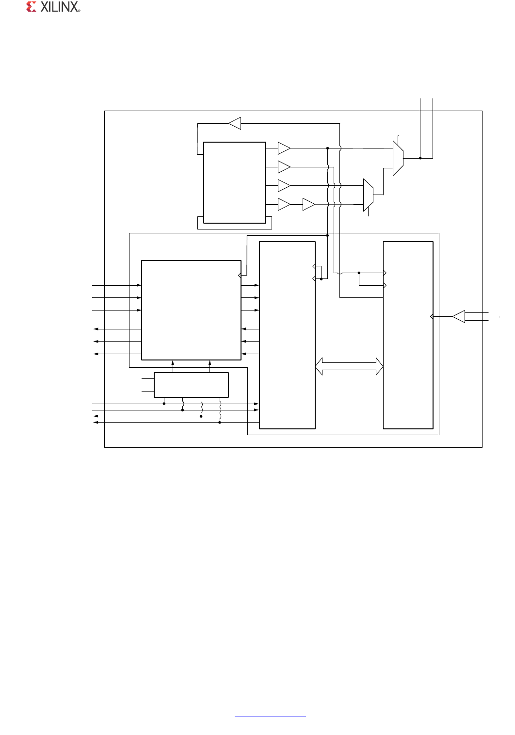
1000BASE-X PCS/PMA or SGMII v11.4 www.xilinx.com 321
PG047 October 16, 2012
Chapter 11: GMII to PHY EDK Application for Zynq-7000 Device Processor Subsystem
X-Ref Target - Figure 11-3
Figure 11-3: GMII to SGMII Using Gigabit Transceiver EDK Application for Zynq-7000 Devices
REFCLK?P
REFCLK?N
)"5&$3?'4%
:YNQ
'48
4RANSCEIVER
GTREFCLK
-(Z
#,+).
#,+&"/54#,+&").
#,+/54
#,+/54
#,+/54
#,+/54
"5&'
"5&'
"5&'
"5&'
"5&2
-(Z
-(Z
-(Z
-(Z
"5&'-58
"5&'-58
#,+
CLK?SELECT
CLK?SELECT
GMII?TX?CLK
GMII?RX?CLK
"5&'
48/54#,+
48532#,+
48532#,+
USERCLK
USERCLK
4RANSCEIVER) &
GMII?TXD;=
GMII?TX?EN
GMII?TX?ER
GMII?RXD;=
GMII?RX?DV
GMII?RX?ER
MDC
MDIO?IN
MDIO?OUT
MDIO?TRI
%THERNET"!3%8
0#30-!OR3'-))
,OGI#/2%
3'-))!DAPTATION
-ODULE
GMII?TXD?OUT;=
GMII?TX?EN?OUT
GMII?TX?ER?OUT
GMII?RXD?IN;=
GMII?RX?DV?IN
GMII?RX?ER?IN
GMII?TXD?IN;=
GMII?TX?EN?IN
GMII?TX?ER?IN
GMII?RXD?OUT;=
GMII?RX?DV?OUT
GMII?RX?ER?OUT
#,+
3PEED$ECODE,OGIC
CLK?SELECT
CLK?SELECT
GIG?ETH?PCS?PMA?SGMII?BLOCK
MDC
MDIO?I
MDIO?O
MDIO?T
GMII?TXD
GMII?TX?EN
GMII?TX?ER
GMII?RXD
GMII?RX?DV
GMII?RX?ER
GIG?ETHERNET?PCS?PMA
'-))TO3'-))
%$+)0
8

1000BASE-X PCS/PMA or SGMII v11.4 www.xilinx.com 322
PG047 October 16, 2012
Chapter 11: GMII to PHY EDK Application for Zynq-7000 Device Processor Subsystem
GMII to SGMII Using Zynq-7000 Device LVDS
Transceiver
The IP is designed to integrate with the Zynq-7000 device LVDS transceiver solution.
Figure 11-4 illustrates the connections and logic required between the IP and the
transceiver; the signal names and logic in the figure precisely match those delivered with
the EDK IP.
The 125 MHz differential reference clock output from IBUFDS is routed directly to a MMCM.
The MMCM outputs the following clocks on the clock output ports, CLKOUT0 (625 MHz),
CLKOUT1 (208 MHz), CLKOUT2 (104 MHz), CLKOUT3 (125 MHz), CLKOUT4 (25 MHz) and
CLKOUT5 (5 MHz).
CLKOUT0 (625 MHz), CLKOUT1 (208 MHz) and CLKOUT2 (104 MHz) are mapped to
global/regional clocking resources and used by the Zynq-7000 device LVDS Transceiver
solution.
The CLKOUT3 port (125 MHz) of MMCM is placed onto global clock routing and can be
used as the 125 MHz clock source for all core logic and Zynq-7000 device LVDS Transceiver
solution.
A 2.5 MHz clock is generated from CLKOUT5 by using the DIV2 feature of BUFR. The correct
frequencies gmii_tx_clk and gmii_rx_clk need to be generated and passed to the
GigE Controller. The correct frequency is selected based on clk_select signals generated
by decoding the speed information on the MDIO interface by the Speed Decoding logic.
The speed selection is possible by writing into the write only speed bits of Control Register
(Register 0)
The GMII interface of the IP always operates at 125 MHz, the IP makes no differentiation
between the three SGMII speeds of operation; it always effectively operates at 1 Gb/s.
However, as described previously in Using the Core Netlist Client-Side GMII for the SGMII
Standard, at 100 Mb/s, every data byte run through the core is repeated ten times to
achieve the required bit rate; at 10 Mb/s, each data byte run through the core is repeated
100 times to achieve the required bit rate. Dealing with this repetition of bytes is the
function of the SGMII adaptation module.
The GMII interface of the SGMII adaptation module interfaces with the GMII interface of
GigE controller in the Zynq-7000 device Processor Subsystem (PS). This module also
converts the 4 bits MII to 8 bit core data width in MII mode.
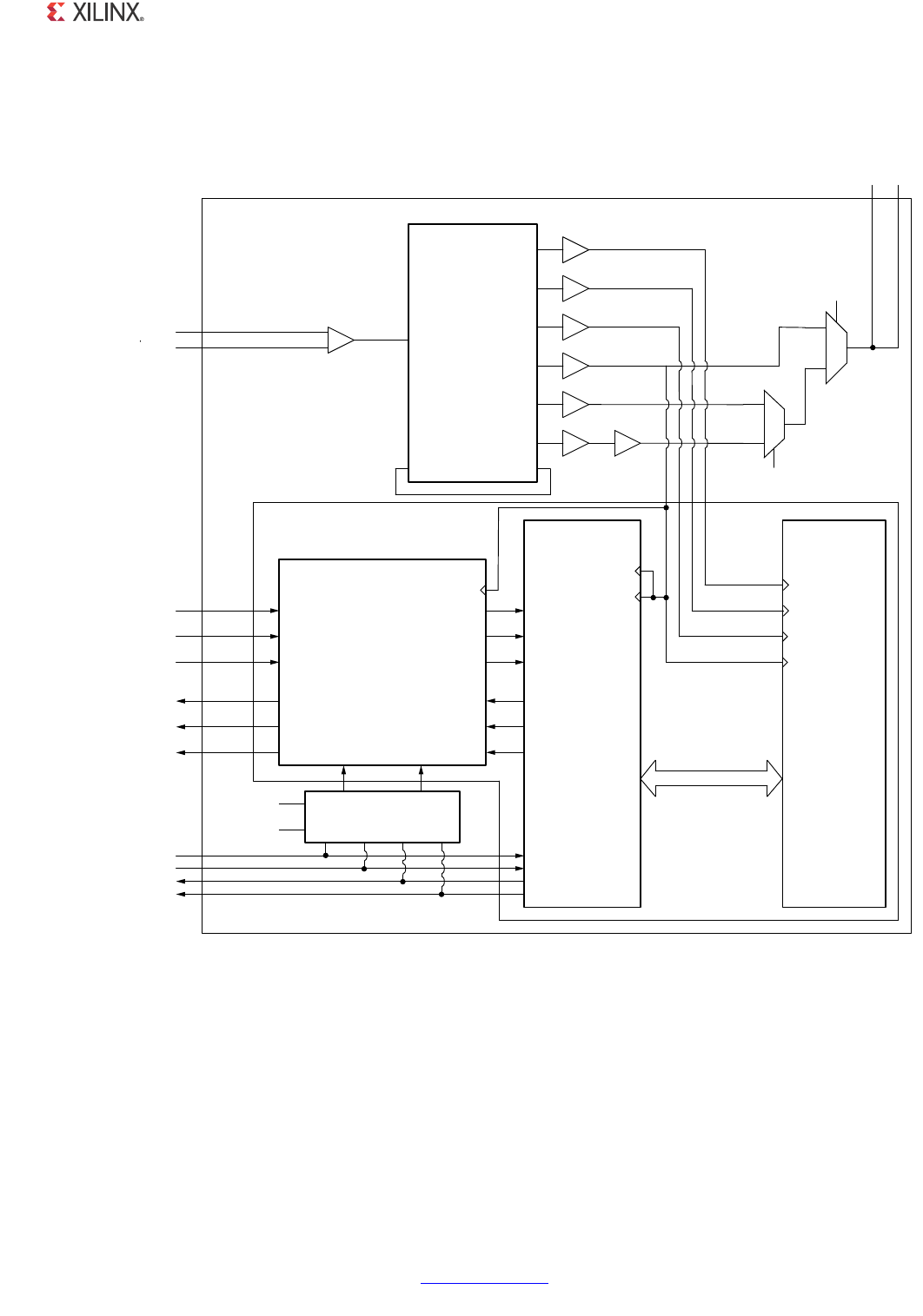
1000BASE-X PCS/PMA or SGMII v11.4 www.xilinx.com 323
PG047 October 16, 2012
Chapter 11: GMII to PHY EDK Application for Zynq-7000 Device Processor Subsystem
X-Ref Target - Figure 11-4
Figure 11-4: GMII to SGMII Using Zynq-7000 Device LVDS Transceiver Solution EDK Application
for Zynq-7000 Architectures
=\QT
/9'6
7UDQVFHLYHU
&/.,1
&/.)%287&/.)%,1
&/.287
&/.287
&/.287
&/.287
%8)*
%8)*
%8)*
%8)*
%8)5
·
0+]
0+]
0+]
0+]
%8)*08;
%8)*08;
&/.
FONBVHOHFW
FONBVHOHFW
JPLLBW[BFON
JPLLBU[BFON
FON
FON
FON
XVHUFON
XVHUFON
7UDQVFHYHU,)
JPLLBW[G>@
JPLLBW[BHQ
JPLLBW[BHU
JPLLBU[G>@
JPLLBU[BGY
JPLLBU[BHU
PGF
PGLRBLQ
PGLRBRXW
PGLRBWUL
(WKHUQHW%$6(;
3&630$RU6*0,,
/RJL&25(
6*0,,$GDSWDWLRQ
0RGXOH
JPLLBW[GBRXW>@
JPLLBW[BHQBRXW
JPLLBW[BHUBRXW
JPLLBU[GBLQ>@
JPLLBU[BGYBLQ
JPLLBU[BHUBLQ
JPLLBW[GBLQ>@
JPLLBW[BHQBLQ
JPLLBW[BHUBLQ
JPLLBU[GBRXW>@
JPLLBU[BGYBRXW
JPLLBU[BHUBRXW
&/.
6SHHG'HFRGH/RJLF
FONBVHOHFW
FONBVHOHFW
JLJBHWKBSFVBSPDBOYGVBEORFN
PGF
PGLRBL
PGLRBR
PGLRBW
JPLLBW[G
JPLLBW[BHQ
JPLLBW[BHU
JPLLBU[G
JPLLBU[BGY
JPLLBU[BHU
JLJBHWKHUQHWBSFVBSPD
*0,,WR6*0,,ZLWK/9'6;&95
('.,3
%8)*
%8)*
&/.287
&/.287
UHIFONBS
UHIFONBQ
,%8)'6
FON
0+]
0+]
8
1000BASE-X PCS/PMA or SGMII v11.4 www.xilinx.com 324
PG047 October 16, 2012
Chapter 12
Interfacing to Other Cores
The 1000BASE-X PCS/PMA or SGMII core can be integrated in a single device with the
Tri-Mode Ethernet MAC core to extend the system functionality to include the Ethernet
MAC sublayer. The Tri-Mode Ethernet MAC core provides support for operation at 10 Mb/s,
100 Mb/s, and 1 Gb/s.
A description of the latest available IP update containing the Tri-Mode Ethernet MAC core
and instructions can be found in the Tri-Mode Ethernet MAC product Web page:
www.xilinx.com/systemio/temac/index.htm
CAUTION! The Tri-Mode Ethernet MAC should always be configured for full-duplex operation when
used with the 1000BASE-X PCS/PMA or SGMII core. This constraint is due to the increased latency
introduced by the 1000BASE-X PCS/PMA or SGMII core. With half-duplex operation, the MAC response
to collisions will be late, violating the Code-Division Multiple Access (CDMA) protocol.
The Tri-Mode Ethernet MAC (TEMAC) core v4.5 and older) supports Virtex®-6, Virtex-5,
Virtex-4, Spartan®-6, Spartan-3, Spartan-3E, and Spartan-3A/3AN/3A DSP devices. The
Tri-Mode Ethernet MAC core version 5.1 (TEMAC core v5.1, AXI) and later supports
Zynq™-7000, Virtex-7, Kintex™-7, Artix™-7, Virtex-6, and Spartan-6 devices.
See the following sections as applicable:
•Integration of the Tri-Mode Ethernet MAC for 1000BASE-X Operation
•Integration of the Tri-Mode Ethernet MAC for Tri-speed SGMII Operation

1000BASE-X PCS/PMA or SGMII v11.4 www.xilinx.com 325
PG047 October 16, 2012
Chapter 12: Interfacing to Other Cores
Integration of the Tri-Mode Ethernet MAC for
1000BASE-X Operation
In this section, it is assumed that the Tri-Mode Ethernet MAC core is generated with only 1
Gb/s Ethernet speed and full-duplex only support. This provides the most optimal solution.
Integration of the Tri-Mode Ethernet MAC to Provide
1000BASE-X PCS with TBI
TEMAC Core v4.5 and older
Figure 12-1 illustrates the connections and clock management logic required to interface
the Ethernet 1000BASE-X PCS/PMA or SGMII core (when used in 1000BASE-X mode with the
parallel TBI) to the Tri-Mode Ethernet MAC core (TEMAC core v4.5 and older).
Features of this configuration include:
• Direct internal connections are made between the GMII interfaces between the two
cores.
• If both cores have been generated with the optional management interface, the MDIO
port can be connected to that of the Tri-Mode Ethernet MAC core, allowing the MAC to
access the embedded configuration and status registers of the Ethernet 1000BASE-X
PCS/PMA or SGMII core.
• Due to the embedded Receiver Elastic Buffer in the Ethernet 1000BASE-X PCS/PMA, the
entire GMII is synchronous to a single clock domain. Therefore, gtx_clk is used as the
125 MHz reference clock for both cores, and the transmitter and receiver logic of the
Tri-Mode Ethernet MAC core operates in the same clock domain.
X-Ref Target - Figure 12-1
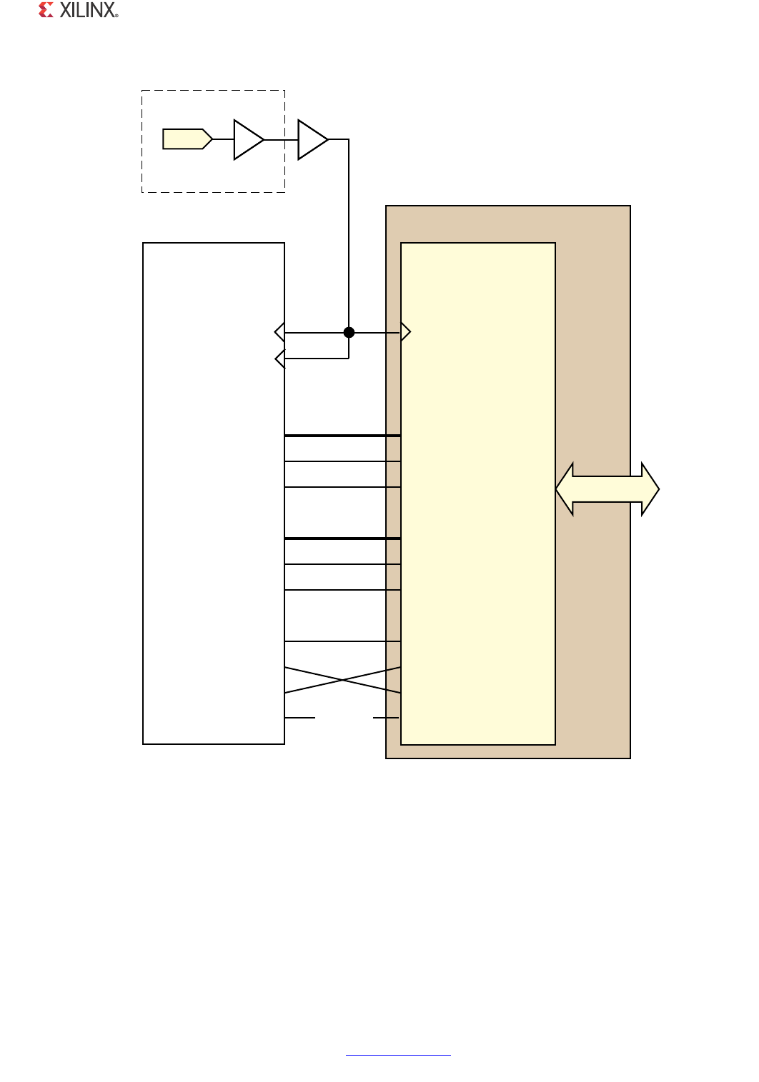
1000BASE-X PCS/PMA or SGMII v11.4 www.xilinx.com 326
PG047 October 16, 2012
Chapter 12: Interfacing to Other Cores
Figure 12-1: Tri-Mode Ethernet MAC Extended to Include 1000BASE-X PCS with TBI
7UL0RGH(WKHUQHW
0$&
/RJL&25(
RXGMIIMIICLK
PHYEMACRXD>@
PHYEMACRXDV
PHYEMACRXER
EMACPHYTXD>@
EMACPHYTXEN
EMACPHYTXER
TXGMIIMIICLK
EMACPHYMCLKOUT
PHYEMACMDIN
EMACPHYMDOUT
EMACPHYMDTRI
(WKHUQHW%$6(;
3&630$RU6*0,,
/RJL&25(
JPLLBU[G>@
JPLLBU[BGY
JPLLBU[BHU
JPLLBW[G>@
JPLLBW[BHQ
JPLLBW[BHU
PGF
PGLRBLQ
PGLRBRXW
PGLRBWUL
QR
FRQQHFWLRQ
JW[BFON
7%,
,3$'
,%8)*
,2%/2*,&
JW[BFON
JW[BFONBEXIJ0+]
%8)*
COMPONENT?NAME?BLOCK
"LOCK,EVELFROMEXAMPLEDESIGN
8

1000BASE-X PCS/PMA or SGMII v11.4 www.xilinx.com 327
PG047 October 16, 2012
Chapter 12: Interfacing to Other Cores
Tri-Mode Ethernet MAC core (TEMAC Core v5.1 and Later, AXI)
Figure 12-2 illustrates the connections and clock management logic required to interface
the Ethernet 1000BASE-X PCS/PMA or SGMII core (when used in 1000BASE-X mode with the
parallel TBI) to the Tri-Mode Ethernet MAC core (TEMAC core v5.1 and later, AXI).
TEMAC core v5.1 and later, Advanced eXtensible Interface (AXI), must be generated with the
“interface” variable set as “Internal” for interfacing with Ethernet 1000BASE-X PCS/PMA or
SGMII core.
Features of this configuration include:
• Direct internal connections are made between the GMII interfaces between the two
cores.
• If both cores have been generated with the optional management interface, the MDIO
port can be connected to that of the Tri-Mode Ethernet MAC core, allowing the MAC to
access the embedded configuration and status registers of the Ethernet 1000BASE-X
PCS/PMA or SGMII core.
• Due to the embedded Receiver Elastic Buffer in the Ethernet 1000BASE-X PCS/PMA, the
entire GMII is synchronous to a single clock domain. Therefore, gtx_clk is used as the
125 MHz reference clock for both cores, and the transmitter and receiver logic of the
Tri-Mode Ethernet MAC core operates in the same clock domain.
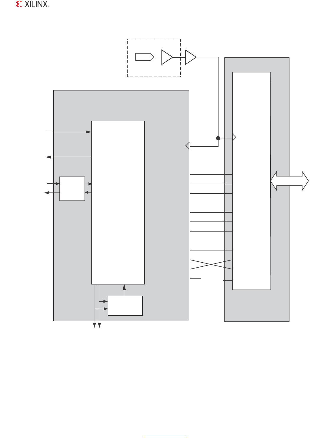
1000BASE-X PCS/PMA or SGMII v11.4 www.xilinx.com 328
PG047 October 16, 2012
Chapter 12: Interfacing to Other Cores
X-Ref Target - Figure 12-2
Figure 12-2: AXI Tri-Mode Ethernet MAC Extended to Include 1000BASE-X PCS with TBI
(WKHUQHW
%$6(;
3&630$
RU6*0,,
/RJL&25(
JPLLBU[G>@
JPLLBU[BGY
JPLLBU[BHU
JPLLBW[G>@
JPLLBW[BHQ
JPLLBW[BHU
PGF
PGLRBLQ
PGLRBRXW
PGLRBWUL
QR
FRQQHFWLRQ
XVHUFON
GTX?CLK
COMPONENT?NAME?BLOCK
"LOCK,EVELFROMEXAMPLEDESIGN
,3$'
,%8)*
,2%/2*,&
JW[BFON %8)*
7%,
JPLLBW[G@
JW[BFON
3TATISTICS6ECTORS
)NTERFACE
7(0$&/RJL&RUH
3TATISTICS
6ECTOR$ECODE
!8),ITE
TO)0)&
FRPSRQHQWBQDPHBEORFN
%ORFN/HYELFROM4RI-ODE%THERNET-!#,OGI#/2%
JPLLBW[BHQ
JPLLBW[BHU
JPLLBU[G@
JPLLBU[BGY
JPLLBU[BHU
-!#
!8)3TREAM
)&
PGF
PGLRBWUL
PGLRBLQ
PGLRBRXW
8
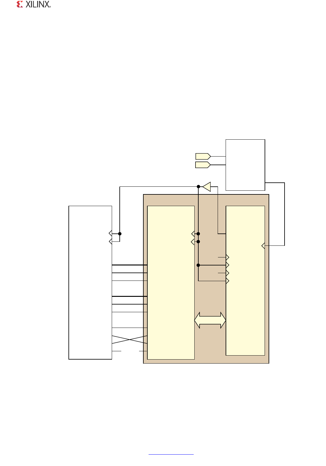
1000BASE-X PCS/PMA or SGMII v11.4 www.xilinx.com 329
PG047 October 16, 2012
Chapter 12: Interfacing to Other Cores
Integration of the Tri-Mode Ethernet MAC to Provide
1000BASE-X Using Transceivers
TEMAC Core v4.5 and Older
Virtex-4 Devices
Figure 12-3 illustrates the connections and clock management logic required to interface
the Ethernet 1000BASE-X PCS/PMA or SGMII core (when used in 1000BASE-X mode) to the
Tri-Mode Ethernet MAC core (TEMAC core v4.5 and older).
X-Ref Target - Figure 12-3
Figure 12-3: Tri-Mode Ethernet MAC Extended to Include 1000BASE-X PCS and PMA Using a
Virtex-4 FPGA RocketIO MGT Transceiver
7UL0RGH(WKHUQHW
0$&
/RJL&25(
RXGMIIMIICLK
PHYEMACRXD>@
PHYEMACRXDV
PHYEMACRXER
EMACPHYTXD>@
EMACPHYTXEN
EMACPHYTXER
TXGMIIMIICLK
EMACPHYMCLKOUT
PHYEMACMDIN
EMACPHYMDOUT
EMACPHYMDTRI
(WKHUQHW%$6(;
3&630$RU6*0,,
/RJL&25(
JPLLBU[G>@
JPLLBU[BGY
JPLLBU[BHU
JPLLBW[G>@
JPLLBW[BHQ
JPLLBW[BHU
PGF
PGLRBLQ
PGLRBRXW
PGLRBWUL
9LUWH[
*7
5RFNHW,2
QR
FRQQHFWLRQ
XVHUFON
XVHUFON
5RFNHW,2,)
,3$'
,3$'
EUHIFONQ
0+]
9LUWH[
*7&/.B0*7
0*7&/.3
0*7&/.1
6<1&/.287
EUHIFONS
0+]
5()&/.
XVHUFON
0+]
7;865&/.
7;865&/.
5;865&/.
5;865&/.
V\QFON
0+]
@
@
%8)*
48/54#,+
COMPONENT?NAME?BLOCK
"LOCK,EVELFROMEXAMPLEDESIGN
8

1000BASE-X PCS/PMA or SGMII v11.4 www.xilinx.com 330
PG047 October 16, 2012
Chapter 12: Interfacing to Other Cores
Features of this configuration include:
• Direct internal connections are made between the GMII interfaces between the two
cores.
• If both cores have been generated with the optional management interface, the MDIO
port can be connected up to that of the Tri-Mode Ethernet MAC core, allowing the MAC
to access the embedded configuration and status registers of the Ethernet 1000BASE-X
PCS/PMA or SGMII core.
• Due to the embedded Receiver Elastic Buffer in the serial transceiver, the entire GMII is
synchronous to a single clock domain. Therefore userclk2 is used as the 125 MHz
reference clock for both cores, and the transmitter and receiver logic of the 1 Tri-Mode
Ethernet MAC core now operate in the same clock domain.
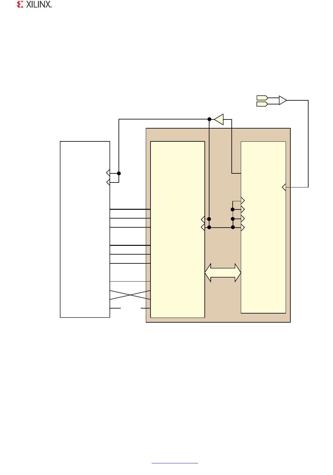
1000BASE-X PCS/PMA or SGMII v11.4 www.xilinx.com 331
PG047 October 16, 2012
Chapter 12: Interfacing to Other Cores
Virtex-5 LXT and SXT Devices
Figure 12-4 illustrates the connections and clock management logic required to interface
the Ethernet 1000BASE-X PCS/PMA or SGMII core (when used in 1000BASE-X mode) to the
Tri-Mode Ethernet MAC core (TEMAC core v4.5 and older).
Features of this configuration include:
• Direct internal connections are made between the GMII interfaces between the two
cores.
• If both cores have been generated with the optional management interface, the MDIO
port can be connected up to that of the Tri-Mode Ethernet MAC core, allowing the MAC
to access the embedded configuration and status registers of the Ethernet 1000BASE-X
PCS/PMA or SGMII core.
X-Ref Target - Figure 12-4
Figure 12-4: Tri-Mode Ethernet MAC Extended to Include 1000BASE-X PCS and
PMA Using a Virtex-5 FPGA RocketIO GTP Transceiver
(WKHUQHW%$6(;
3&630$RU6*0,,
/RJL&25(
JPLLBU[G>@
JPLLBU[BGY
JPLLBU[BHU
JPLLBW[G>@
JPLLBW[BHQ
JPLLBW[BHU
PGF
PGLRBLQ
PGLRBRXW
PGLRBWUL
9LUWH[
*73
5RFNHW,2
QR
FRQQHFWLRQ
XVHUFON
XVHUFON
5RFNHW,2,)
&/.,1
XVHUFON
0+]
7;865&/.
7;865&/.
5;865&/.
5;865&/.
%8)*
5()&/.287
FRPSRQHQWBQDPHBEORFN
%ORFN/HYHOIURPH[DPSOHGHVLJQ
FONLQ
0+]
,%8)*'6
,3$'
EUHIFONS
,3$'
EUHIFONQ
7UL0RGH(WKHUQHW
0$&
/RJL&25(
RXGMIIMIICLK
PHYEMACRXD>@
PHYEMACRXDV
PHYEMACRXER
EMACPHYTXD>@
EMACPHYTXEN
EMACPHYTXER
TXGMIIMIICLK
EMACPHYMCLKOUT
PHYEMACMDIN
EMACPHYMDOUT
EMACPHYMDTRI
8
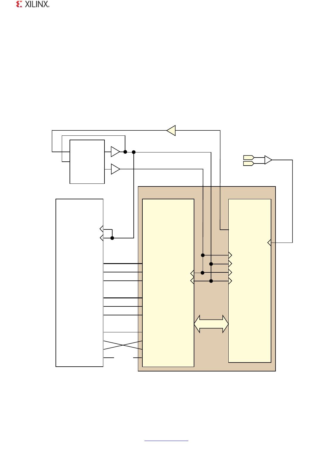
1000BASE-X PCS/PMA or SGMII v11.4 www.xilinx.com 332
PG047 October 16, 2012
Chapter 12: Interfacing to Other Cores
• Due to the embedded Receiver Elastic Buffer in the GTP transceiver, the entire GMII is
synchronous to a single clock domain. Therefore userclk2 is used as the 125 MHz
reference clock for both cores, and the transmitter and receiver logic of the Tri-Mode
Ethernet MAC core now operate in the same clock domain.
Virtex-5 FXT and TXT Devices
Figure 12-5 illustrates the connections and clock management logic required to interface
the Ethernet 1000BASE-X PCS/PMA or SGMII core (when used in 1000BASE-X mode) to the
Tri-Mode Ethernet MAC core (TEMAC core v4.5 and older).
X-Ref Target - Figure 12-5
Figure 12-5: Tri-Mode Ethernet MAC Extended to Include 1000BASE-X PCS and PMA Using a
Virtex-5 FPGA RocketIO GTX Transceiver
(WKHUQHW%$6(;
3&630$RU6*0,,
/RJL&25(
JPLLBU[G>@
JPLLBU[BGY
JPLLBU[BHU
JPLLBW[G>@
JPLLBW[BHQ
JPLLBW[BHU
PGF
PGLRBLQ
PGLRBRXW
PGLRBWUL
9LUWH[
*7;
5RFNHW,2
QR
FRQQHFWLRQ
XVHUFON
XVHUFON
5RFNHW,2,)
&/.,1
XVHUFON0+]
7;865&/.
7;865&/.
5;865&/.
5;865&/.
5()&/.287
FRPSRQHQWBQDPHBEORFN
%ORFN/HYHOIURPH[DPSOHGHVLJQ
FONLQ
0+]
,%8)*'6
,3$'
EUHIFONS
,3$'
EUHIFONQ
'&0
&/.,1 &/.
)%
%8)*
&/.'9
%8)* XVHUFON0+]
%8)*
7UL0RGH(WKHUQHW
0$&
/RJL&25(
RXGMIIMIICLK
PHYEMACRXD>@
PHYEMACRXDV
PHYEMACRXER
EMACPHYTXD>@
EMACPHYTXEN
EMACPHYTXER
TXGMIIMIICLK
EMACPHYMCLKOUT
PHYEMACMDIN
EMACPHYMDOUT
EMACPHYMDTRI
8

1000BASE-X PCS/PMA or SGMII v11.4 www.xilinx.com 333
PG047 October 16, 2012
Chapter 12: Interfacing to Other Cores
Features of this configuration include:
• Direct internal connections are made between the GMII interfaces between the two
cores.
• If both cores have been generated with the optional management interface, the MDIO
port can be connected up to that of the Tri-Mode Ethernet MAC core, allowing the MAC
to access the embedded configuration and status registers of the Ethernet 1000BASE-X
PCS/PMA or SGMII core.
• Due to the embedded Receiver Elastic Buffer in the GTX transceiver, the entire GMII is
synchronous to a single clock domain. Therefore userclk2 is used as the 125 MHz
reference clock for both cores, and the transmitter and receiver logic of the Tri-Mode
Ethernet MAC core now operate in the same clock domain.
Virtex-6 Devices
Figure 12-6 illustrates the connections and clock management logic required to interface
the Ethernet 1000BASE-X PCS/PMA or SGMII core (when used in 1000BASE-X mode) to the
Tri-Mode Ethernet MAC core (TEMAC core v4.5 and older).
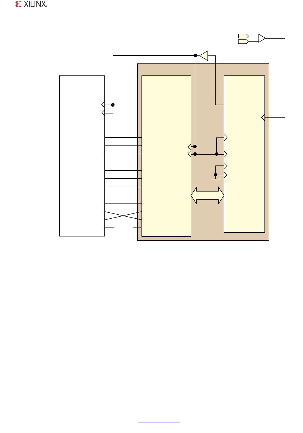
1000BASE-X PCS/PMA or SGMII v11.4 www.xilinx.com 334
PG047 October 16, 2012
Chapter 12: Interfacing to Other Cores
X-Ref Target - Figure 12-6
Features of this configuration include:
• Direct internal connections are made between the GMII interfaces between the two
cores.
• If both cores have been generated with the optional management interface, the MDIO
port can be connected up to that of the Tri-Mode Ethernet MAC core, allowing the MAC
to access the embedded configuration and status registers of the Ethernet 1000BASE-X
PCS/PMA or SGMII core.
• Due to the embedded Receiver Elastic Buffer in the transceiver, the entire GMII is
synchronous to a single clock domain. Therefore userclk2 is used as the 125 MHz
reference clock for both cores, and the transmitter and receiver logic of the Tri-Mode
Ethernet MAC core now operate in the same clock domain.
Figure 12-6: Tri-Mode Ethernet MAC Extended to Include 1000BASE-X PCS and PMA Using a
Virtex-6 FPGA GTX Transceiver
(WKHUQHW%$6(;
3&630$RU6*0,,
/RJL&25(
JPLLBU[G>@
JPLLBU[BGY
JPLLBU[BHU
JPLLBW[G>@
JPLLBW[BHQ
JPLLBW[BHU
PGF
PGLRBLQ
PGLRBRXW
PGLRBWUL
9LUWH[
*7;
7UDQVFHLYHU
QR
FRQQHFWLRQ
XVHUFON
XVHUFON
XVHUFON
0+]
48532#,+
28532#,+
%8)*
48/54#,+
FRPSRQHQWBQDPHBEORFN
%ORFN/HYHOIURPH[DPSOHGHVLJQ
MGTREFCLK
-(Z
,%8)'6B*7;(
,3$'
PJWUHIFONBS
,3$'
PJWUHIFONBQ
7UL0RGH(WKHUQHW
0$&
/RJL&25(
RXGMIIMIICLK
PHYEMACRXD>@
PHYEMACRXDV
PHYEMACRXER
EMACPHYTXD>@
EMACPHYTXEN
EMACPHYTXER
TXGMIIMIICLK
EMACPHYMCLKOUT
PHYEMACMDIN
EMACPHYMDOUT
EMACPHYMDTRI
48532#,+
28532#,+
'.$
-'42%&#,+48;=
-'42%&#,+28;=
7UDQVFHLYHU,)
8
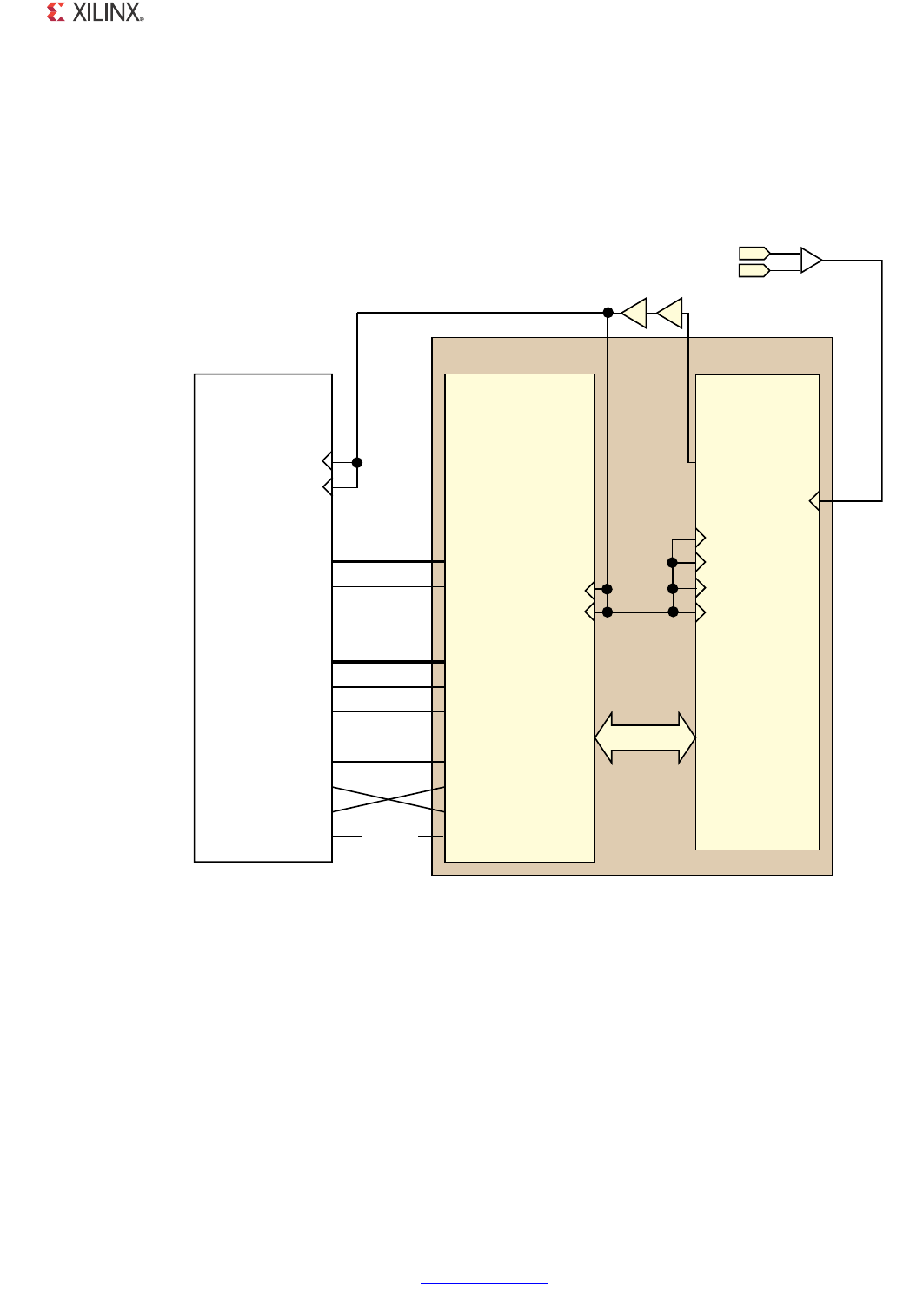
1000BASE-X PCS/PMA or SGMII v11.4 www.xilinx.com 335
PG047 October 16, 2012
Chapter 12: Interfacing to Other Cores
Spartan-6 LXT Devices
Figure 12-7 illustrates the connections and clock management logic required to interface
the Ethernet 1000BASE-X PCS/PMA or SGMII core (when used in 1000BASE-X mode) to the
Tri-Mode Ethernet MAC core (TEMAC core v4.5 and older).
X-Ref Target - Figure 12-7
Features of this configuration include:
• Direct internal connections are made between the GMII interfaces between the two
cores.
• If both cores have been generated with the optional management interface, the MDIO
port can be connected up to that of the Tri-Mode Ethernet MAC core, allowing the MAC
to access the embedded configuration and status registers of the Ethernet 1000BASE-X
PCS/PMA or SGMII core.
Figure 12-7: Tri-Mode Ethernet MAC Extended to Include 1000BASE-X PCS and PMA Using a
Spartan-6 FPGA GTP Transceiver
(WKHUQHW%$6(;
3&630$RU6*0,,
/RJL&25(
JPLLBU[G>@
JPLLBU[BGY
JPLLBU[BHU
JPLLBW[G>@
JPLLBW[BHQ
JPLLBW[BHU
PGF
PGLRBLQ
PGLRBRXW
PGLRBWUL
QR
FRQQHFWLRQ
XVHUFON
XVHUFON
#,+).
XVHUFON
0+]
7;865&/.
7;865&/.
5;865&/.
5;865&/.
%8)*
FRPSRQHQWBQDPHBEORFN
%ORFN/HYHOIURPH[DPSOHGHVLJQ
FONLQ
0+]
,%8)'6
,3$'
EUHIFONS
,3$'
EUHIFONQ
7UL0RGH(WKHUQHW
0$&
/RJL&25(
RXGMIIMIICLK
PHYEMACRXD>@
PHYEMACRXDV
PHYEMACRXER
EMACPHYTXD>@
EMACPHYTXEN
EMACPHYTXER
TXGMIIMIICLK
EMACPHYMCLKOUT
PHYEMACMDIN
EMACPHYMDOUT
EMACPHYMDTRI
3PARTAN
4RANSCEIVER
'40
'40#,+/54
7UDQVFHLYHU,)
%8),2
8
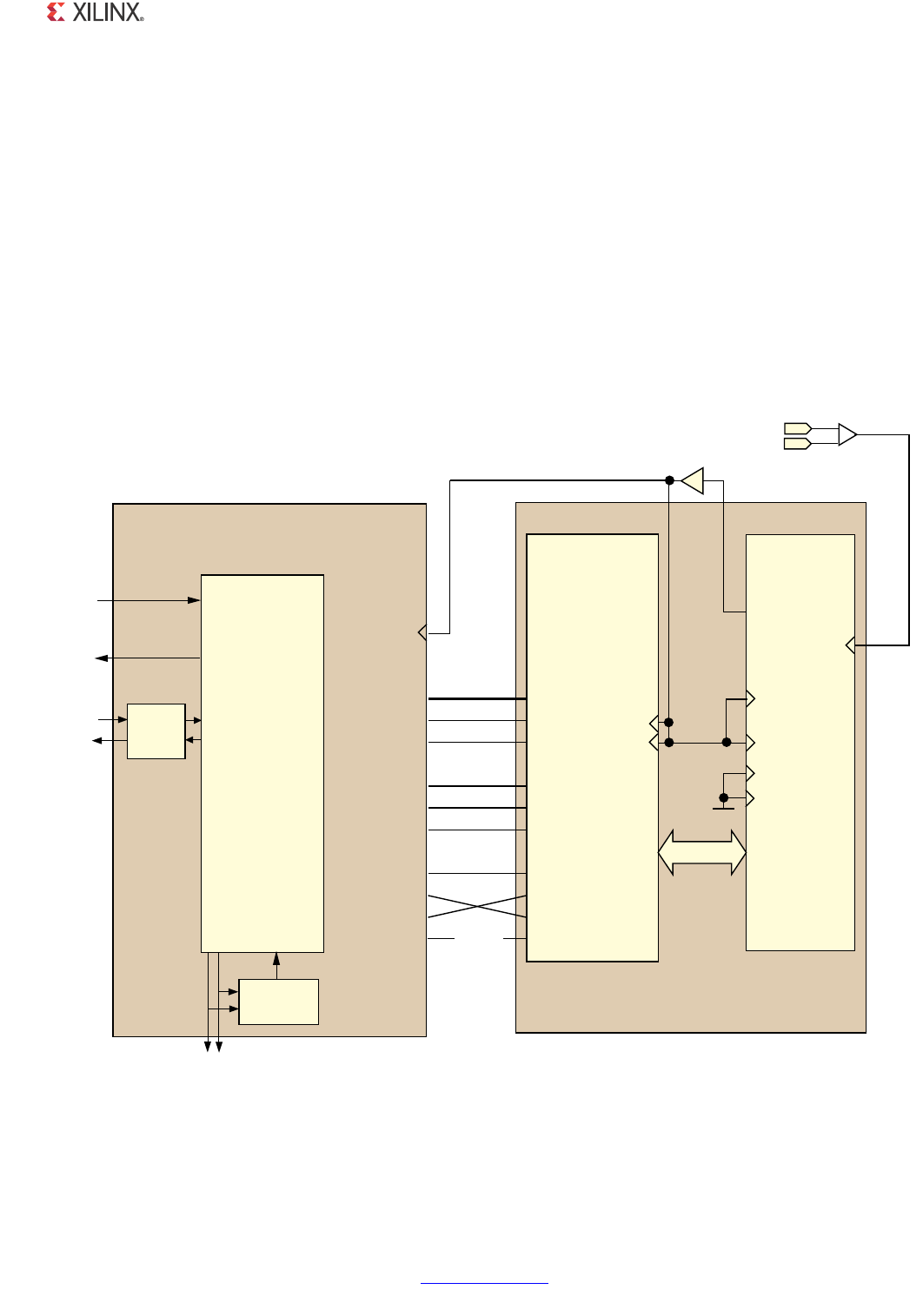
1000BASE-X PCS/PMA or SGMII v11.4 www.xilinx.com 336
PG047 October 16, 2012
Chapter 12: Interfacing to Other Cores
• Because of the embedded Receiver Elastic Buffer in the GTP transceiver, the entire GMII
is synchronous to a single clock domain. Therefore userclk2 is used as the 125 MHz
reference clock for both cores, and the transmitter and receiver logic of the Tri-Mode
Ethernet MAC core now operate in the same clock domain.
Tri-Mode Ethernet MAC Core (TEMAC Core v5.1 and Later, AXI)
Virtex-6 Devices
Figure 12-8 illustrates the connections and clock management logic required to interface
the Ethernet 1000BASE-X PCS/PMA or SGMII core (when used in 1000BASE-X mode) to the
Tri-Mode Ethernet MAC core: (TEMAC core v5.1 and later, AXI).
Features of this configuration include:
X-Ref Target - Figure 12-8
Figure 12-8: AXI Tri-Mode Ethernet MAC Extended to Include 1000BASE-X PCS
and PMA Using a Virtex-6 FPGA GTX Transceiver
(WKHUQHW%$6(;
3&630$RU6*0,,
/RJL&25(
JPLLBU[G>@
JPLLBU[BGY
JPLLBU[BHU
JPLLBW[G>@
JPLLBW[BHQ
JPLLBW[BHU
PGF
PGLRBLQ
PGLRBRXW
PGLRBWUL
9LUWH[
*7;
7UDQVFHLYHU
QR
FRQQHFWLRQ
XVHUFON
XVHUFON
XVHUFON
0+]
48532#,+
28532#,+
%8)*
48/54#,+
MGTREFCLK
-(Z
,%8)'6B*7;(
,3$'
PJWUHIFONBS
,3$'
PJWUHIFONBQ
48532#,+
28532#,+
'.$
-'42%&#,+48;=
-'42%&#,+28;=
7UDQVFHLYHU,)
FRPSRQHQWBQDPHBEORFN
%ORFN/HY
ELFROM%THERNET"!3%80#30-!,OGI#/2%
JPLLBW[G@
JW[BFON
3TATISTICS6ECTORS
)NTERFACE
7(0$&/RJL&RUH
3TATISTICS
6ECTOR$ECODE
!8),ITE
TO)0)&
FRPSRQHQWBQDPHBEORFN
%ORFN/HY
ELFROM4RI-ODE%THERNET-!#,OGI#/2%
JPLLBW[BHQ
JPLLBW[BHU
JPLLBU[G@
JPLLBU[BGY
JPLLBU[BHU
-!#
!8)3TREAM
)&
PGF
PGLRBWUL
PGLRBLQ
PGLRBRXW
8

1000BASE-X PCS/PMA or SGMII v11.4 www.xilinx.com 337
PG047 October 16, 2012
Chapter 12: Interfacing to Other Cores
• Observe that the “block” level of the TEMAC is instantiated. This provides the MAC with
extra functionality that is not provided by the TEMAC core netlist. When using the MAC
to connect the 1000BASE-X core, the “Internal” PHY Interface mode must be selected
from the TEMAC GUI prior to core generation. See the TEMAC documentation.
• Direct internal connections are made between the GMII interfaces between the two
cores.
• If both cores have been generated with the optional management interface, the MDIO
port can be connected up to that of the Tri-Mode Ethernet MAC core, allowing the MAC
to access the embedded configuration and status registers of the Ethernet 1000BASE-X
PCS/PMA or SGMII core.
• Because of the embedded Receiver Elastic Buffer in the transceiver, the entire GMII is
synchronous to a single clock domain. Therefore userclk2 is used as the 125 MHz
reference clock for both cores, and the transmitter and receiver.
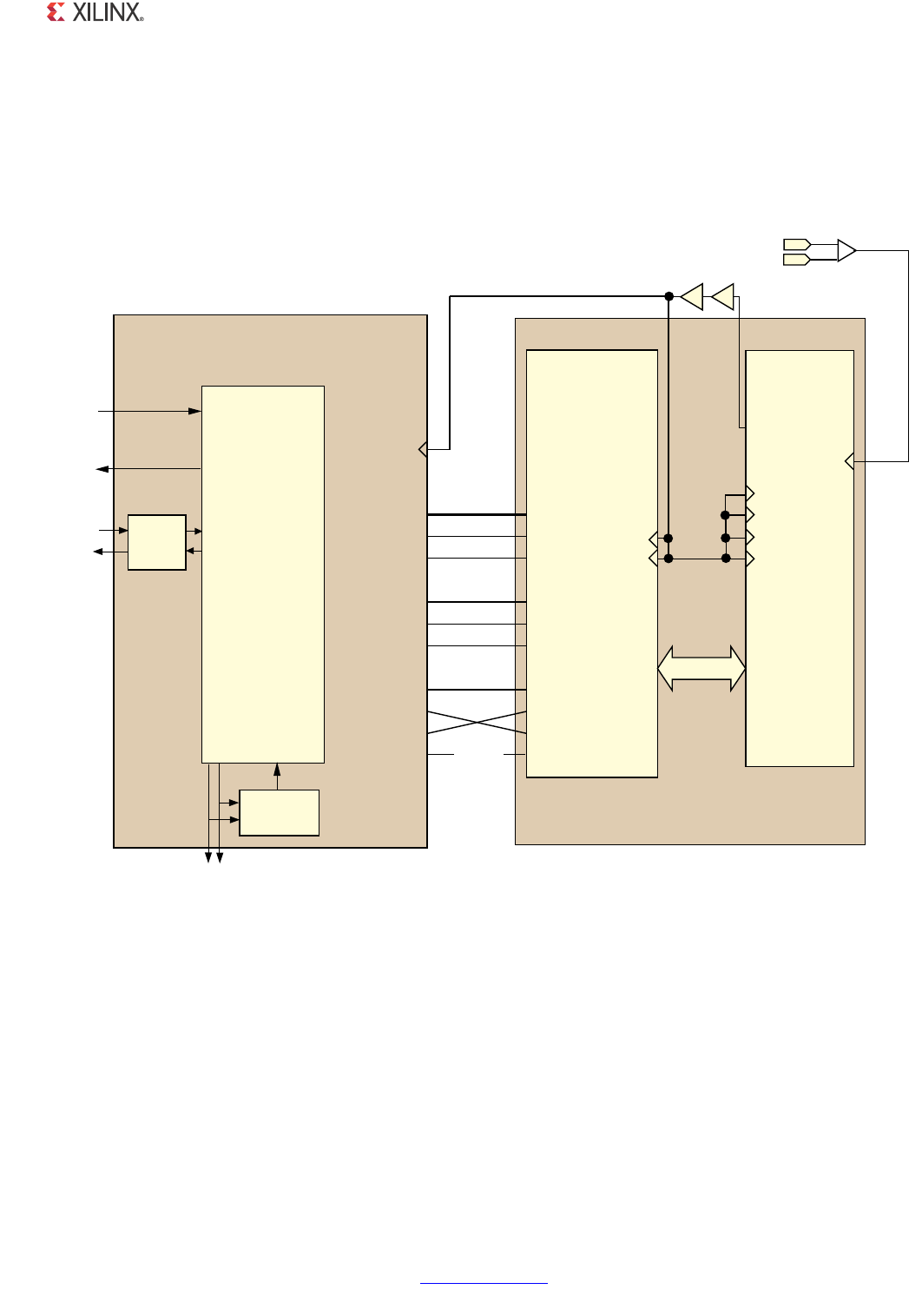
1000BASE-X PCS/PMA or SGMII v11.4 www.xilinx.com 338
PG047 October 16, 2012
Chapter 12: Interfacing to Other Cores
Spartan-6 Devices
Figure 12-9 illustrates the connections and clock management logic required to interface
the Ethernet 1000BASE-X PCS/PMA or SGMII core (when used in 1000BASE-X mode) to the
Tri-mode Ethernet MAC core (TEMAC core v5.1and later, AXI).
Features of this configuration include:
• Observe that the “block” level of the TEMAC is instantiated. This provides the MAC with
extra functionality that is not provided by the TEMAC core netlist When using the MAC
to connect the 1000BASE-X core, the “Internal” PHY Interface mode must be selected
from the TEMAC GUI prior to core generation. See the TEMAC documentation.
• Direct internal connections are made between the GMII interfaces between the two
cores.
X-Ref Target - Figure 12-9
Figure 12-9: AXI Tri-Mode Ethernet MAC Extended to Include 1000BASE-X PCS
and PMA Using a Spartan-6 FPGA GTP Transceiver
(WKHUQHW%$6(;
3&630$RU6*0,,
/RJL&25(
JPLLBU[G>@
JPLLBU[BGY
JPLLBU[BHU
JPLLBW[G>@
JPLLBW[BHQ
JPLLBW[BHU
PGF
PGLRBLQ
PGLRBRXW
PGLRBWUL
QR
FRQQHFWLRQ
XVHUFON
XVHUFON
#,+).
XVHUFON
0+]
7;865&/.
7;865&/.
5;865&/.
5;865&/.
%8)*
FONLQ
0+]
,%8)'6
,3$'
EUHIFONS
,3$'
EUHIFONQ
3PARTAN
4RANSCEIVER
'40
'40#,+/54
7UDQVFHLYHU,)
%8),2
JPLLBW[G@
JW[BFON
3TATISTICS6ECTORS
)NTERFACE
7(0$&/RJL&RUH
3TATISTICS
6ECTOR$ECODE
!8),ITE
TO)0)&
FRPSRQHQWBQDPHBEORFN
%ORFN/HY
ELFROM4RI-ODE%THERNET-!#,OGI#/2%
JPLLBW[BHQ
JPLLBW[BHU
JPLLBU[G@
JPLLBU[BGY
JPLLBU[BHU
-!#
!8)3TREAM
)&
PGF
PGLRBWUL
PGLRBLQ
PGLRBRXW
FRPSRQHQWBQDPHBEORFN
%ORFN/HY
ELFROM%THERNET"!3%80#30-!,OGI#/2%
8
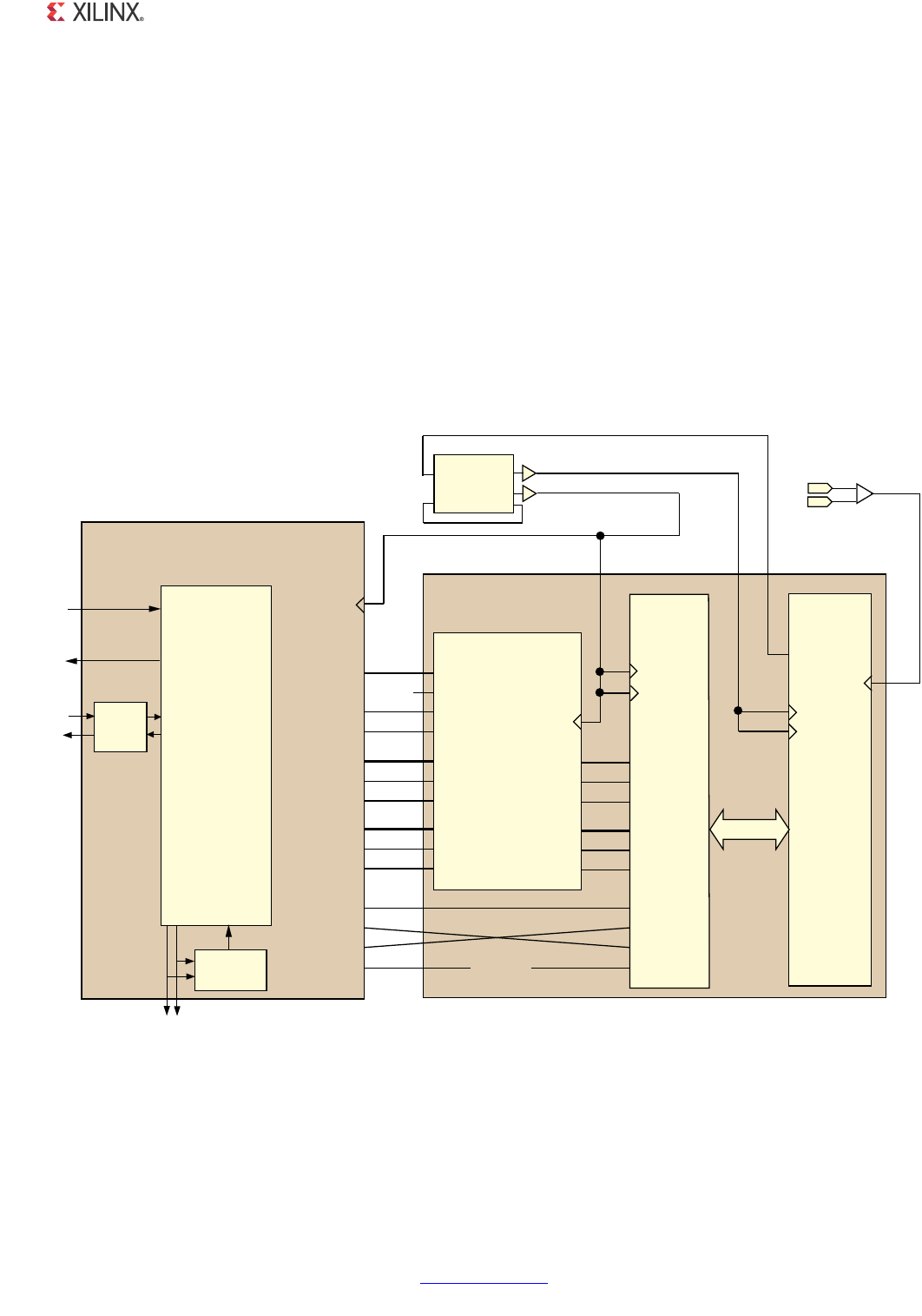
1000BASE-X PCS/PMA or SGMII v11.4 www.xilinx.com 339
PG047 October 16, 2012
Chapter 12: Interfacing to Other Cores
• If both cores have been generated with the optional management interface, the MDIO
port can be connected up to that of the Tri-Mode Ethernet MAC core, allowing the MAC
to access the embedded configuration and status registers of the Ethernet 1000BASE-X
PCS/PMA or SGMII core.
Because of the embedded Receiver Elastic Buffer in the transceiver, the entire GMII is
synchronous to a single clock domain. Therefore userclk2 is used as the 125 MHz
reference clock for both cores, and the transmitter and receiver.
Virtex-7 Devices
Figure 12-10 illustrates the connections and clock management logic required to interface
the Ethernet 1000BASE-X PCS/PMA or SGMII core (when used in 1000BASE-X mode) to the
Tri-Mode Ethernet MAC core (TEMAC core v5.and later, AXI).
X-Ref Target - Figure 12-10
Figure 12-10: AXI Tri-Mode Ethernet MAC Extended to Include 1000BASE-X PCS
and PMA Using a Virtex-7 FPGA GTX/GTH Transceiver
(WKHUQHW
%$6(;
3&630$
RU6*0,,
/RJL&25(
JPLLBU[G>@
JPLLBU[BGY
JPLLBU[BHU
JPLLBW[G>@
JPLLBW[BHQ
JPLLBW[BHU
PGF
PGLRBLQ
PGLRBRXW
PGLRBWUL
QR
FRQQHFWLRQ
XVHUFON
7UDQVFHLYHU,)
JPLLBU[GBRXW>@
JPLLBU[BGYBRXW
JPLLBU[BHUBRXW
JPLLBW[GBLQ>@
JPLLBW[BHQBLQ
JPLLBW[BHUBLQ
JPLLBU[GBLQ>@
JPLLBU[BGYBLQ
JPLLBU[BHUBLQ
JPLLBW[GBRXW>@
JPLLBW[BHQBRXW
JPLLBW[BHUBRXW
FONP
6*0,,$GDSWDWLRQ
PRGXOH
VJPLLBFONBHQ
VSHHGBLVBB
VSHHGBLVB
VJPLLBFONBU
1&
9LUWHX
'48'4(
4RANSCEIVER
48532#,+
48532#,+
XVHUFON
0+]
XVHUFON
GTREFCLK
-(Z
,%8)'6B*7(
,3$'
JWUHIFONBS
,3$'
JWUHIFONBQ
48/54#,+
'42%&#,+
0+]
--#-%?!$6
#,+/54
#,+/54
#,+).
#,+&"/54#,+&").
"5&'
"5&'
0+]
JPLLBW[G@
JW[BFON
3TATISTICS6ECTORS
)NTERFACE
7(0$&/RJL&RUH
3TATISTICS
6ECTOR$ECODE
!8),ITE
TO)0)&
FRPSRQHQWBQDPHBEORFN
%ORFN/HYELFROM4RI-ODE%THERNET-!#,OGI#/2%
JPLLBW[BHQ
JPLLBW[BHU
JPLLBU[G@
JPLLBU[BGY
JPLLBU[BHU
-!#
!8)3TREAM
)&
PGF
PGLRBWUL
PGLRBLQ
PGLRBRXW
VSHHGLV
FONBHQDEOH
VSHHGLV
FRPSRQHQWBQDPHBEORFN
%ORFN/HYELFROM%THERNET"!3%80#30-!,OGI#/2%
8

1000BASE-X PCS/PMA or SGMII v11.4 www.xilinx.com 340
PG047 October 16, 2012
Chapter 12: Interfacing to Other Cores
Features of this configuration include:
• Observe that the “block” level of the TEMAC is instantiated. This provides the MAC with
extra functionality that is not provided by the TEMAC core netlist. When using the MAC
to connect the 1000BASE-X core, the “Internal” PHY Interface mode must be selected
from the TEMAC GUI prior to core generation. See the TEMAC documentation.
• Direct internal connections are made between the GMII interfaces between the two
cores.
• If both cores have been generated with the optional management interface, the MDIO
port can be connected up to that of the Tri-Mode Ethernet MAC core, allowing the MAC
to access the embedded configuration and status registers of the Ethernet 1000BASE-X
PCS/PMA or SGMII core.
• Because of the embedded Receiver Elastic Buffer in the transceiver, the entire GMII is
synchronous to a single clock domain. Therefore userclk2 is used as the 125 MHz
reference clock for both cores, and the transmitter and receiver.
Kintex-7 and Zynq-7000 Devices
Figure 12-11 illustrates the connections and clock management logic required to interface
the Ethernet 1000BASE-X PCS/PMA or SGMII core (when used in 1000BASE-X mode) to the
Tri-Mode Ethernet MAC core.
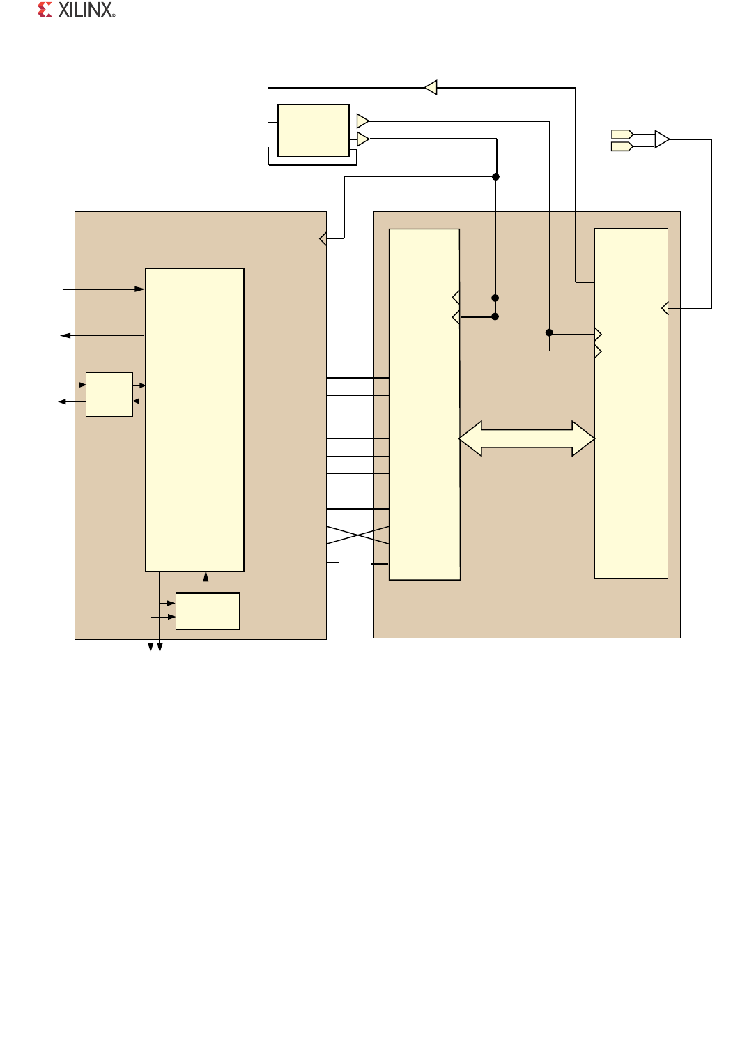
1000BASE-X PCS/PMA or SGMII v11.4 www.xilinx.com 341
PG047 October 16, 2012
Chapter 12: Interfacing to Other Cores
X-Ref Target - Figure 12-11
Figure 12-11: AXI Tri-Mode Ethernet MAC Extended to Include 1000BASE-X PCS
and PMA Using a Kintex-7 or Zynq-7000 Device GTX Transceiver
JPLLBW[G@
(WKHUQHW
%$6(;
3&630$
RU6*0,,
/RJL&25(
JPLLBU[G>@
JPLLBU[BGY
JPLLBU[BHU
JPLLBW[G>@
JPLLBW[BHQ
JPLLBW[BHU
PGF
PGLRBLQ
PGLRBRXW
PGLRBWUL
QR
FRQQHFWLRQ
XVHUFON
7UDQVFHLYHU,)
JW[BFON
48532#,+
48532#,+
XVHUFON
0+]
XVHUFON
FRPSRQHQWBQDPHBEORFN
%ORFN/HY
ELFROM%THERNET"!3%80#30-!,OGI#/2%
GTREFCLK
-(Z
,%8)'6B*7(
,3$'
JWUHIFONBS
,3$'
JWUHIFONBQ
48/54#,+
'42%&#,+
0+]
--#-%?!$6
#,+/54
#,+/54
#,+).
#,+&"/54#,+&").
"5&'
"5&'
0+]
"5&'
+INTEX:YNQ
'48
4RANSCEIVER
3TATISTICS6ECTORS
)NTERFACE
7(0$&/RJL&RUH
3TATISTICS
6ECTOR$ECODE
!8),ITE
TO)0)&
FRPSRQHQWBQDPHBEORFN
%ORFN/HY
ELFROM4RI-ODE%THERNET-!#,OGI#/2%
JPLLBW[BHQ
JPLLBW[BHU
JPLLBU[G@
JPLLBU[BGY
JPLLBU[BHU
-!#
!8)3TREAM
)&
PGF
PGLRBWUL
PGLRBLQ
PGLRBRXW
8

1000BASE-X PCS/PMA or SGMII v11.4 www.xilinx.com 342
PG047 October 16, 2012
Chapter 12: Interfacing to Other Cores
Features of this configuration include:
• Observe that the “block” level of the TEMAC is instantiated. This provides the MAC with
extra functionality that is not provided by the TEMAC core netlist. When using the MAC
to connect the 1000BASE-X core, the “Internal” PHY Interface mode must be selected
from the TEMAC GUI prior to core generation. See the TEMAC documentation.
• Direct internal connections are made between the GMII interfaces between the two
cores.
• If both cores have been generated with the optional management interface, the MDIO
port can be connected up to that of the Tri-Mode Ethernet MAC core, allowing the MAC
to access the embedded configuration and status registers of the Ethernet 1000BASE-X
PCS/PMA or SGMII core.
• Because of the embedded Receiver Elastic Buffer in the transceiver, the entire GMII is
synchronous to a single clock domain. Therefore userclk2 is used as the 125 MHz
reference clock for both cores, and the transmitter and receiver.
Artix-7 Devices
Figure 12-12 illustrates the connections and clock management logic required to interface
the Ethernet 1000BASE-X PCS/PMA or SGMII core (when used in 1000BASE-X mode) to the
Tri-Mode Ethernet MAC core.
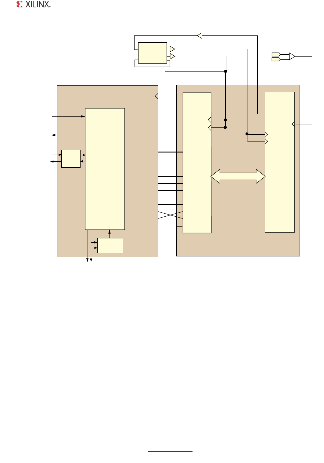
1000BASE-X PCS/PMA or SGMII v11.4 www.xilinx.com 343
PG047 October 16, 2012
Chapter 12: Interfacing to Other Cores
Features of this configuration include:
• Observe that the “block” level of the TEMAC is instantiated. This provides the MAC with
extra functionality that is not provided by the TEMAC core netlist. When using the MAC
to connect the 1000BASE-X core, the “Internal” PHY Interface mode must be selected
from the TEMAC GUI prior to core generation. See the TEMAC documentation.
• Direct internal connections are made between the GMII interfaces between the two
cores.
• If both cores have been generated with the optional management interface, the MDIO
port can be connected up to that of the Tri-Mode Ethernet MAC core, allowing the MAC
to access the embedded configuration and status registers of the Ethernet 1000BASE-X
PCS/PMA or SGMII core.
X-Ref Target - Figure 12-12
Figure 12-12: AXI Tri-Mode Ethernet MAC Extended to Include 1000BASE-X PCS and PMA Using
an Artix-7 FPGA GTP Transceiver
JPLLBW[G@
(WKHUQHW
%$6(;
3&630$
RU6*0,,
/RJL&25(
JPLLBU[G>@
JPLLBU[BGY
JPLLBU[BHU
JPLLBW[G>@
JPLLBW[BHQ
JPLLBW[BHU
PGF
PGLRBLQ
PGLRBRXW
PGLRBWUL
QR
FRQQHFWLRQ
XVHUFON
7UDQVFHLYHU,)
JW[BFON
48532#,+
48532#,+
XVHUFON
0+]
XVHUFON
FRPSRQHQWBQDPHBEORFN
%ORFN/HY
ELFROM%THERNET"!3%80#30-!,OGI#/2%
GTREFCLK
-(Z
,%8)'6B*7(
,3$'
JWUHIFONBS
,3$'
JWUHIFONBQ
48/54#,+
'42%&#,+
0+]
--#-%?!$6
#,+/54
#,+/54
#,+).
#,+&"/54#,+&").
"5&'
"5&'
0+]
"5&'
!RTIX
'40
4RANSCEIVER
3TATISTICS6ECTORS
)NTERFACE
7(0$&/RJL&RUH
3TATISTICS
6ECTOR$ECODE
!8),ITE
TO)0)&
FRPSRQHQWBQDPHBEORFN
%ORFN/HY
ELFROM4RI-ODE%THERNET-!#,OGI#/2%
JPLLBW[BHQ
JPLLBW[BHU
JPLLBU[G@
JPLLBU[BGY
JPLLBU[BHU
-!#
!8)3TREAM
)&
PGF
PGLRBWUL
PGLRBLQ
PGLRBRXW
8

1000BASE-X PCS/PMA or SGMII v11.4 www.xilinx.com 344
PG047 October 16, 2012
Chapter 12: Interfacing to Other Cores
• Because of the embedded Receiver Elastic Buffer in the transceiver, the entire GMII is
synchronous to a single clock domain. Therefore userclk2 is used as the 125 MHz
reference clock for both cores, and the transmitter and receiver.
Integration of the Tri-Mode Ethernet MAC for
Tri-speed SGMII Operation
In this section, it is assumed that the Tri-Mode Ethernet MAC core is generated for Tri-speed
operation and full-duplex only support. This provides the most optimal solution.
This section assumes only SGMII or Dynamic switching operation and MAC mode
configuration. PHY mode configuration of SGMII is used to interface to a external PHY
device. For SGMII in PHY mode configuration, see SGMII Example Design / Dynamic
Switching Example Design with Ten-Bit Interface and Chapter 6, SGMII / Dynamic Standards
Switching with Transceivers. For 1000BASEX only designs, see Integration of the Tri-Mode
Ethernet MAC for 1000BASE-X Operation.
Integration of the Tri-Mode Ethernet MAC to Provide SGMII (or
Dynamic Switching) Functionality with TBI
TEMAC Core v4.5 and Older
Figure 12-13 illustrates the connections and clock management logic required to interface
the Ethernet 1000BASE-X PCS/PMA or SGMII core (when used in SGMII mode with the TBI)
to the Tri-Mode Ethernet MAC core (TEMAC core v4.5 and older). The following is a
description of the functionality.
• The SGMII Adaptation module, provided in the example design for the Ethernet
1000BASE-X PCS/PMA or SGMII core when generated to the SGMII standard, can be
used to interface the two cores.
• If both cores have been generated with the optional management interface, the MDIO
port can be connected to that of the Tri-Speed Ethernet MAC core, allowing the MAC to
access the embedded configuration and status registers of the Ethernet 1000BASE-X
PCS/PMA or SGMII core.
• Due to the Receiver Elastic Buffer in the core, the entire GMII (transmitter and receiver
paths) is synchronous to a single clock domain. Therefore, the txcoreclk and
rxcoreclk inputs of the Tri-Speed Ethernet MAC core can always be driven from the
same clock source.
Figure 12-13 illustrates the Tri-Mode Ethernet MAC core generated with the optional clock
enable circuitry. This is the most efficient way to connect the two cores together in terms of
clock resource usage and so is recommended. See the Tri-Mode Ethernet MAC User Guide for
more information.

1000BASE-X PCS/PMA or SGMII v11.4 www.xilinx.com 345
PG047 October 16, 2012
Chapter 12: Interfacing to Other Cores
X-Ref Target - Figure 12-13
Figure 12-13: Legacy Tri-Speed Ethernet MAC Extended to Use an SGMII with TBI
7UL6SHHG
(WKHUQHW
0$&
/RJL&25(
SK\HPDFU[G>@
SK\HPDFU[GY
SK\HPDFU[HU
HPDFSK\W[G@
HPDFSK\W[HQ
HPDFSK\W[HU
HPDFSK\PFONRXW
SK\HPDFPGLQ
HPDFSK\PGRXW
HPDFSK\PGWUL
(WKHUQHW
%$6(;
3&630$
RU6*0,,
/RJL&25(
JPLLBU[G>@
JPLLBU[BGY
JPLLBU[BHU
JPLLBW[G>@
JPLLBW[BHQ
JPLLBW[BHU
PGF
PGLRBLQ
PGLRBRXW
PGLRBWUL
QR
FRQQHFWLRQ
XVHUFON
GTX?CLK
JPLLBU[GBRXW>@
JPLLBU[BGYBRXW
JPLLBU[BHUBRXW
JPLLBW[GBLQ>@
JPLLBW[BHQBLQ
JPLLBW[BHUBLQ
JPLLBU[GBLQ>@
JPLLBU[BGYBLQ
JPLLBU[BHUBLQ
JPLLBW[GBRXW>@
JPLLBW[BHQBRXW
JPLLBW[BHUBRXW
CLKM
6*0,,$GDSWDWLRQ
PRGXOH
VJPLLBFONBHQ
VSHHGBLVBB
VSHHGBLVB
VSHHGLV
VSHHGLV
U[JPLLPLLFON
W[JPLLPLLFON
FRUHKDVVJPLL
9&&
FOLHQWHPDFU[HQDEOH
FOLHQWHPDFW[HQDEOH
VJPLLBFONBU
1&
COMPONENT?NAME?BLOCK
"LOCK,EVELFROMEXAMPLEDESIGN
,3$'
,%8)*
,2%/2*,&
JW[BFON %8)*
7%,
8

1000BASE-X PCS/PMA or SGMII v11.4 www.xilinx.com 346
PG047 October 16, 2012
Chapter 12: Interfacing to Other Cores
Tri-Mode Ethernet MAC Core (TEMAC core v5.1 and Later, AXI)
Figure 12-14 illustrates the connections and clock management logic required to interface
the Ethernet 1000BASE-X PCS/PMA or SGMII core (when used in SGMII mode with the TBI)
to the Tri-Mode Ethernet MAC core (TEMAC core v5.1 and later, AXI).
TEMAC core v5.1 and later, AXI, must be generated with “interface” variable set as “Internal”
for interfacing with Ethernet 1000BASE-X PCS/PMA or SGMII core.
Features of this configuration include:
• The SGMII Adaptation module, provided in the example design for the Ethernet
1000BASE-X PCS/PMA or SGMII core when generated to the SGMII standard, can be
used to interface the two cores.
• If both cores have been generated with the optional management interface, the MDIO
port can be connected to that of the Tri-Speed Ethernet MAC core, allowing the MAC to
access the embedded configuration and status registers of the Ethernet 1000BASE-X
PCS/PMA or SGMII core
.
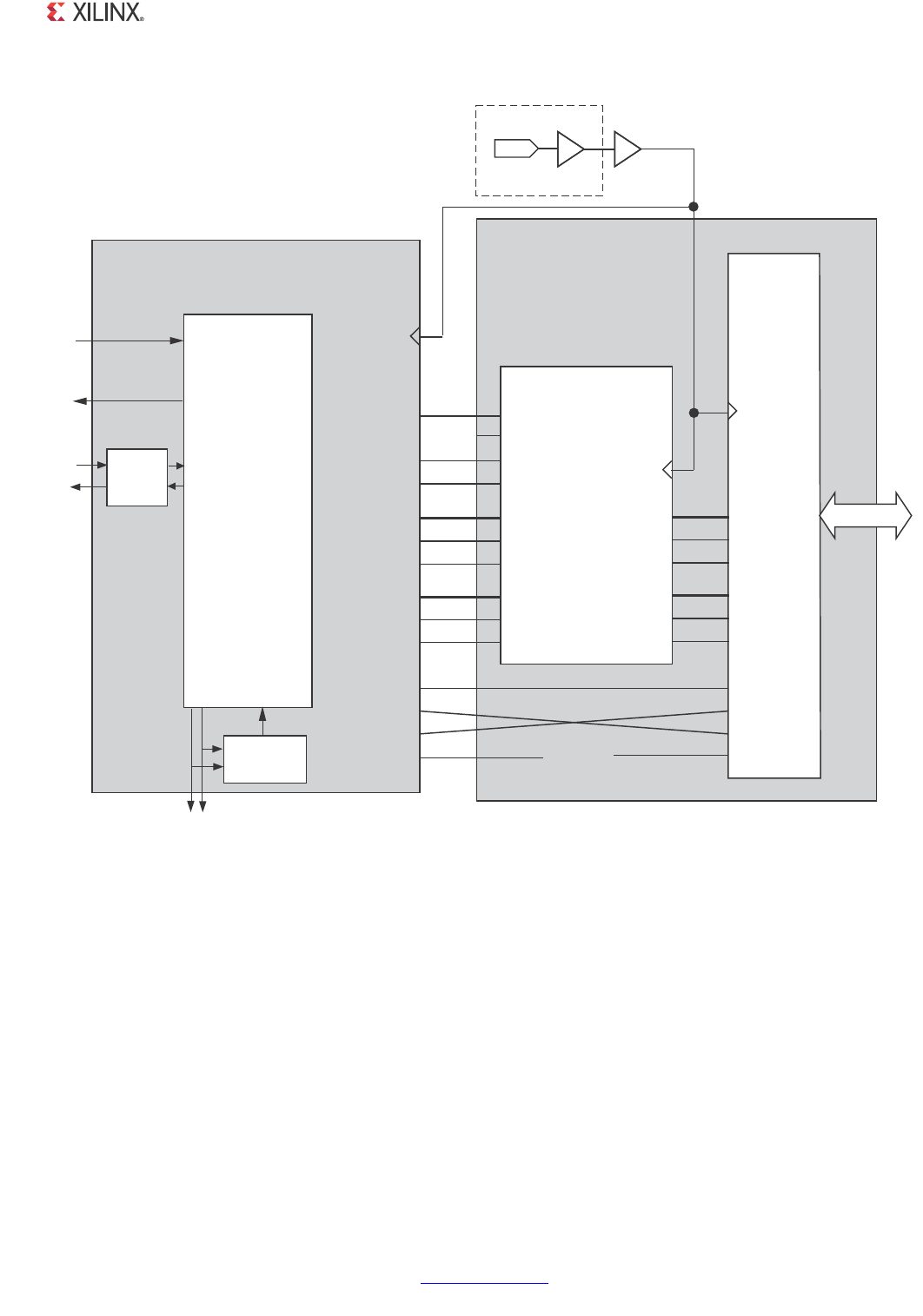
1000BASE-X PCS/PMA or SGMII v11.4 www.xilinx.com 347
PG047 October 16, 2012
Chapter 12: Interfacing to Other Cores
X-Ref Target - Figure 12-14
Figure 12-14: AXI Tri-Speed Ethernet MAC Extended to Use an SGMII with TBI
(WKHUQHW
%$6(;
3&630$
RU6*0,,
/RJL&25(
JPLLBU[G>@
JPLLBU[BGY
JPLLBU[BHU
JPLLBW[G>@
JPLLBW[BHQ
JPLLBW[BHU
PGF
PGLRBLQ
PGLRBRXW
PGLRBWUL
QR
FRQQHFWLRQ
X
VHUFON
GTX?CLK
JPLLBU[GBRXW>@
JPLLBU[BGYBRXW
JPLLBU[BHUBRXW
JPLLBW[GBLQ>@
JPLLBW[BHQBLQ
JPLLBW[BHUBLQ
JPLLBU[GBLQ>@
JPLLBU[BGYBLQ
JPLLBU[BHUBLQ
JPLLBW[GBRXW>@
JPLLBW[BHQBRXW
JPLLBW[BHUBRXW
CLKM
6*0,,$GDSWDWLRQ
PRGXOH
VJPLLBFONBHQ
VSHHGBLVBB
VSHHGBLVB
VJPLLBFONBU
1&
COMPONENT?NAME?BLOCK
"LOCK,EVELFROMEXAMPLEDESIGN
,3$'
,%8)*
,2%/2*,&
JW[BFON %8)*
7%,
JPLLBW[G@
JW[BFON
3TATISTICS6ECTORS
)NTERFACE
7(0$&/RJL&RUH
3TATISTICS
6ECTOR$ECODE
!8),ITE
TO)0)&
FRPSRQHQWBQDPHBEORFN
%ORFN/HY
ELFROM4RI-ODE%THERNET-!#,OGI#/2%
JPLLBW[BHQ
JPLLBW[BHU
JPLLBU[G@
JPLLBU[BGY
JPLLBU[BHU
-!#
!8)3TREAM
)&
PGF
PGLRBWUL
PGLRBLQ
PGLRBRXW
VSHHGLV
FONBHQDEOH
VSHHGLV
8

1000BASE-X PCS/PMA or SGMII v11.4 www.xilinx.com 348
PG047 October 16, 2012
Chapter 12: Interfacing to Other Cores
Integration of the Tri-Mode Ethernet MAC Using Device Specific
Transceivers
TEMAC Core v4.5 and Older
Virtex-4 Devices
Figure 12-15 illustrates the connections and clock management logic required to interface
the Ethernet 1000BASE-X PCS/PMA or SGMII core (when used in SGMII Configuration and
MAC mode with the Virtex-4 FPGA MGT transceiver) to the Tri-Mode Ethernet MAC core:
TEMAC core v4.5 and older.
The following conditions apply.
• The SGMII Adaptation module, as provided in the example design for the Ethernet
1000BASE-X PCS/PMA or SGMII core, can be used to interface the two cores when
generated to the SGMII standard.
• If both cores have been generated with the optional management interface, the MDIO
port can be connected up to that of the Tri-Speed Ethernet MAC core, allowing the
MAC to access the embedded configuration and status registers of the Ethernet
1000BASE-X PCS/PMA or SGMII core.
• Due to the Receiver Elastic Buffer, the entire GMII (transmitter and receiver paths) is
synchronous to a single clock domain. Therefore, the txcoreclk and rxcoreclk
inputs of the Tri-Speed Ethernet MAC core can always be driven from the same clock
source. The entire design is synchronous to the 125 MHz reference clock derived from
the CLK2X180 output of the DCM.
Figure 12-15 illustrates the Tri-Mode Ethernet MAC core generated with the optional clock
enable circuitry. This is the most efficient way to connect the two cores together in terms of
clock resource usage and so is recommended. See the Tri-Mode Ethernet MAC User Guide for
more information.
X-Ref Target - Figure 12-15

1000BASE-X PCS/PMA or SGMII v11.4 www.xilinx.com 349
PG047 October 16, 2012
Chapter 12: Interfacing to Other Cores
Figure 12-15: Tri-Speed Ethernet MAC Extended to Use an SGMII in a Virtex-4 FPGA
7UL6SHHG
(WKHUQHW
0$&
/RJL&25(
SK\HPDFU[G>@
SK\HPDFU[GY
SK\HPDFU[HU
HPDFSK\W[G@
HPDFSK\W[HQ
HPDFSK\W[HU
HPDFSK\PFONRXW
SK\HPDFPGLQ
HPDFSK\PGRXW
HPDFSK\PGWUL
(WKHUQHW
%$6(;
3&630$
RU6*0,,
/RJL&25(
JPLLBU[G>@
JPLLBU[BGY
JPLLBU[BHU
JPLLBW[G>@
JPLLBW[BHQ
JPLLBW[BHU
PGF
PGLRBLQ
PGLRBRXW
PGLRBWUL
QR
FRQQHFWLRQ
XVHUFON
5RFNHW,2,)
JPLLBU[GBRXW>@
JPLLBU[BGYBRXW
JPLLBU[BHUBRXW
JPLLBW[GBLQ>@
JPLLBW[BHQBLQ
JPLLBW[BHUBLQ
JPLLBU[GBLQ>@
JPLLBU[BGYBLQ
JPLLBU[BHUBLQ
JPLLBW[GBRXW>@
JPLLBW[BHQBRXW
JPLLBW[BHUBRXW
FONP
6*0,,$GDSWDWLRQ
PRGXOH
VJPLLBFONBHQ
VSHHGBLVBB
VSHHGBLVB
VSHHGLV
VSHHGLV
U[JPLLPLLFON
W[JPLLPLLFON
FRUHKDVVJPLL
9&&
FOLHQWHPDFU[HQDEOH
FOLHQWHPDFW[HQDEOH
VJPLLBFONBU
1&
9LUWH[
*7
5RFNHW,2
XVHG
,3$'
EUHIFONS
0+]
,3$'
EUHIFONQ
0+]
9LUWH[
*7&/.B0*7
0*7&/.3
0*7&/.1
6<1&/.287
5()&/.
7;865&/.
7;865&/.
XVHUFON
0+]
V\QFON
0+]
XVHUFON
µ
%8)*
7;287&/.
FRPSRQHQWBQDPHBEORFN
%ORFN/HYHOIURPH[DPSOHGHVLJQ
8

1000BASE-X PCS/PMA or SGMII v11.4 www.xilinx.com 350
PG047 October 16, 2012
Chapter 12: Interfacing to Other Cores
Virtex-5 LXT and SXT Devices
Figure 12-16 illustrates the connections and clock management logic required to interface
the Ethernet 1000BASE-X PCS/PMA or SGMII core (when used in SGMII Configuration and
MAC mode with the Virtex-5 FPGA GTP transceiver) to the Tri-Mode Ethernet MAC core
(TEMAC core v4.5 and older).
The following conditions apply.
• The SGMII Adaptation module, as provided in the example design for the Ethernet
1000BASE-X PCS/PMA or SGMII core, when generated to the SGMII standard and MAC
mode, can be used to interface the two cores.
• If both cores have been generated with the optional management interface, the MDIO
port can be connected up to that of the Tri-Speed Ethernet MAC core, allowing the
MAC to access the embedded configuration and status registers of the Ethernet
1000BASE-X PCS/PMA or SGMII core.
• Because of the embedded Receiver Elastic Buffer in the GTP transceiver, the entire GMII
is synchronous to a single clock domain. Therefore userclk2 is used as the 125 MHz
reference clock for both cores, and the transmitter and receiver logic of the Tri-Mode
Ethernet MAC core now operate in the same clock domain.
Figure 12-16 illustrates the Tri-Mode Ethernet MAC core generated with the optional clock
enable circuitry. This is the most efficient way to connect the two cores together in terms of
clock resource usage and so is recommended. See the Tri-Mode Ethernet MAC User Guide for
more information.
X-Ref Target - Figure 12-16
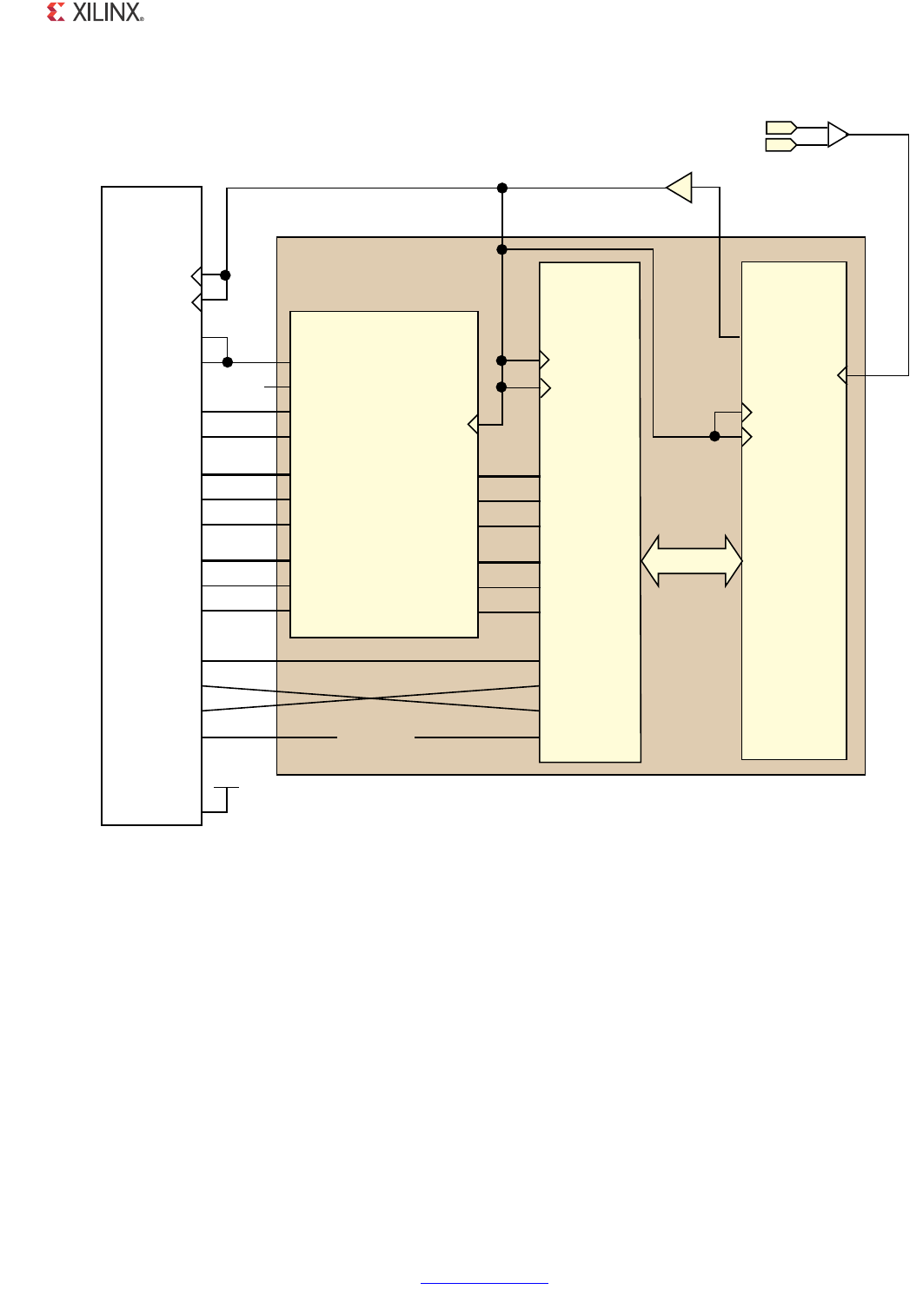
1000BASE-X PCS/PMA or SGMII v11.4 www.xilinx.com 351
PG047 October 16, 2012
Chapter 12: Interfacing to Other Cores
Figure 12-16: Tri-Speed Ethernet MAC Extended to Use an SGMII in a Virtex-5 LXT/SXT Device
7UL6SHHG
(WKHUQHW
0$&
/RJL&25(
SK\HPDFU[G>@
SK\HPDFU[GY
SK\HPDFU[HU
HPDFSK\W[G@
HPDFSK\W[HQ
HPDFSK\W[HU
HPDFSK\PFONRXW
SK\HPDFPGLQ
HPDFSK\PGRXW
HPDFSK\PGWUL
(WKHUQHW
%$6(;
3&630$
RU6*0,,
/RJL&25(
JPLLBU[G>@
JPLLBU[BGY
JPLLBU[BHU
JPLLBW[G>@
JPLLBW[BHQ
JPLLBW[BHU
PGF
PGLRBLQ
PGLRBRXW
PGLRBWUL
QR
FRQQHFWLRQ
XVHUFON
5RFNHW,2,)
JPLLBU[GBRXW>@
JPLLBU[BGYBRXW
JPLLBU[BHUBRXW
JPLLBW[GBLQ>@
JPLLBW[BHQBLQ
JPLLBW[BHUBLQ
JPLLBU[GBLQ>@
JPLLBU[BGYBLQ
JPLLBU[BHUBLQ
JPLLBW[GBRXW>@
JPLLBW[BHQBRXW
JPLLBW[BHUBRXW
FONP
6*0,,$GDSWDWLRQ
PRGXOH
VJPLLBFONBHQ
VSHHGBLVBB
VSHHGBLVB
VSHHGLV
VSHHGLV
U[JPLLPLLFON
W[JPLLPLLFON
FRUHKDVVJPLL
9&&
FOLHQWHPDFU[HQDEOH
FOLHQWHPDFW[HQDEOH
VJPLLBFONBU
1&
9LUWH[
*73
5RFNHW,2
&/.,1
7;865&/.
7;865&/.
XVHUFON
0+]
XVHUFON
%8)*
5()&/.287
FRPSRQHQWBQDPHBEORFN
%ORFN/HYHOIURPH[DPSOHGHVLJQ
FONLQ
0+]
,%8)*'6
,3$'
EUHIFONS
,3$'
EUHIFONQ
8

1000BASE-X PCS/PMA or SGMII v11.4 www.xilinx.com 352
PG047 October 16, 2012
Chapter 12: Interfacing to Other Cores
Virtex-5 FXT and TXT Devices
Figure 12-17 illustrates the connections and clock management logic required to interface
the Ethernet 1000BASE-X PCS/PMA or SGMII core (when used in SGMII Configuration and
MAC mode with the Virtex-5 FPGA GTX transceiver) to the Tri-Mode Ethernet MAC core
(TEMAC core v4.5 and older).
The following conditions apply.
• The SGMII Adaptation module, as provided in the example design for the Ethernet
1000BASE-X PCS/PMA or SGMII core, when generated to the SGMII standard and MAC
mode, can be used to interface the two cores.
• If both cores have been generated with the optional management interface, the MDIO
port can be connected up to that of the Tri-Speed Ethernet MAC core, allowing the
MAC to access the embedded configuration and status registers of the Ethernet
1000BASE-X PCS/PMA or SGMII core.
• Due to the Receiver Elastic Buffer, the entire GMII (transmitter and receiver paths) is
synchronous to a single clock domain. Therefore the txcoreclk and rxcoreclk
inputs of the Tri-Speed Ethernet MAC core can always be driven from the same clock
source. The entire design is synchronous to the 125 MHz reference clock derived from
the CLK2X180 output of the DCM.
Figure 12-17 illustrates the Tri-Mode Ethernet MAC core generated with the optional clock
enable circuitry. This is the most efficient way to connect the two cores together in terms of
clock resource usage and so is recommended. See the Tri-Mode Ethernet MAC User Guide for
more information.
X-Ref Target - Figure 12-17
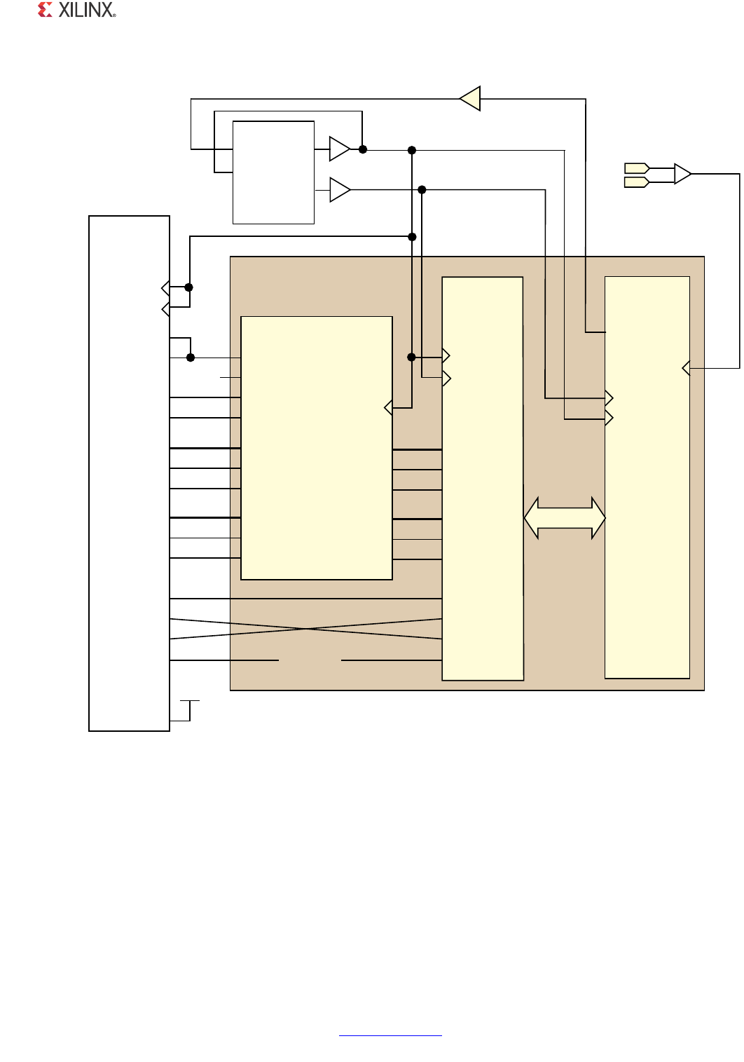
1000BASE-X PCS/PMA or SGMII v11.4 www.xilinx.com 353
PG047 October 16, 2012
Chapter 12: Interfacing to Other Cores
Figure 12-17: Tri-Speed Ethernet MAC Extended to Use an SGMII in a Virtex-5 FXT and TXT Device
7UL6SHHG
(WKHUQHW
0$&
/RJL&25(
SK\HPDFU[G>@
SK\HPDFU[GY
SK\HPDFU[HU
HPDFSK\W[G@
HPDFSK\W[HQ
HPDFSK\W[HU
HPDFSK\PFONRXW
SK\HPDFPGLQ
HPDFSK\PGRXW
HPDFSK\PGWUL
(WKHUQHW
%$6(;
3&630$
RU6*0,,
/RJL&25(
JPLLBU[G>@
JPLLBU[BGY
JPLLBU[BHU
JPLLBW[G>@
JPLLBW[BHQ
JPLLBW[BHU
PGF
PGLRBLQ
PGLRBRXW
PGLRBWUL
QR
FRQQHFWLRQ
XVHUFON
5RFNHW,2,)
JPLLBU[GBRXW>@
JPLLBU[BGYBRXW
JPLLBU[BHUBRXW
JPLLBW[GBLQ>@
JPLLBW[BHQBLQ
JPLLBW[BHUBLQ
JPLLBU[GBLQ>@
JPLLBU[BGYBLQ
JPLLBU[BHUBLQ
JPLLBW[GBRXW>@
JPLLBW[BHQBRXW
JPLLBW[BHUBRXW
FONP
6*0,,$GDSWDWLRQ
PRGXOH
VJPLLBFONBHQ
VSHHGBLVBB
VSHHGBLVB
VSHHGLV
VSHHGLV
U[JPLLPLLFON
W[JPLLPLLFON
FRUHKDVVJPLL
9&&
FOLHQWHPDFU[HQDEOH
FOLHQWHPDFW[HQDEOH
VJPLLBFONBU
1&
9LUWH[
'48
2OCKET)/
&/.,1
7;865&/.
7;865&/.
XVHUFON
5()&/.287
FRPSRQHQWBQDPHBEORFN
%ORFN/HYHOIURPH[DPSOHGHVLJQ
FONLQ
0+]
,%8)*'6
,3$'
EUHIFONS
,3$'
EUHIFONQ
XVHUFON0+]
'&0
&/.,1 &/.
)%
%8)*
&/.'9
%8)* XVHUFON0+]
%8)*
8

1000BASE-X PCS/PMA or SGMII v11.4 www.xilinx.com 354
PG047 October 16, 2012
Chapter 12: Interfacing to Other Cores
Virtex-6 Devices
Figure 12-18 illustrates the connections and clock management logic required to interface
the Ethernet 1000BASE-X PCS/PMA or SGMII core (when used in SGMII mode with the
Virtex-6 FPGA GTX transceiver) to the Tri-Mode Ethernet MAC core (TEMAC core v4.5 and
older).
The following conditions apply.
• The SGMII Adaptation module, as provided in the example design for the Ethernet
1000BASE-X PCS/PMA or SGMII core, can when generated to the SGMII standard and
MAC mode, can be used to interface the two cores.
• If both cores have been generated with the optional management interface, the MDIO
port can be connected up to that of the Tri-Speed Ethernet MAC core, allowing the
MAC to access the embedded configuration and status registers of the Ethernet
1000BASE-X PCS/PMA or SGMII core.
• Because of the embedded Receiver Elastic Buffer, the entire GMII is synchronous to a
single clock domain. Therefore userclk2 is used as the 125 MHz reference clock for
both cores, and the transmitter and receiver logic of the Tri-Mode Ethernet MAC core
now operate in the same clock domain.
See also the Tri-Mode Ethernet MAC User Guide for more information.
X-Ref Target - Figure 12-18
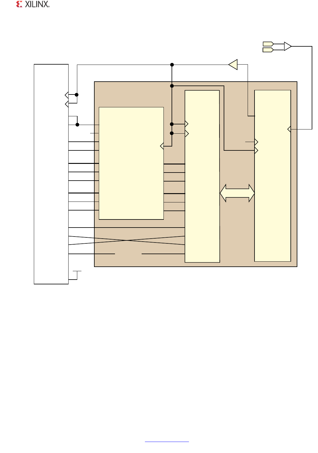
1000BASE-X PCS/PMA or SGMII v11.4 www.xilinx.com 355
PG047 October 16, 2012
Chapter 12: Interfacing to Other Cores
Figure 12-18: Tri-Speed Ethernet MAC Extended to use an SGMII in Virtex-6 Devices
7UL6SHHG
(WKHUQHW
0$&
/RJL&25(
SK\HPDFU[G>@
SK\HPDFU[GY
SK\HPDFU[HU
HPDFSK\W[G@
HPDFSK\W[HQ
HPDFSK\W[HU
HPDFSK\PFONRXW
SK\HPDFPGLQ
HPDFSK\PGRXW
HPDFSK\PGWUL
(WKHUQHW
%$6(;
3&630$
RU6*0,,
/RJL&25(
JPLLBU[G>@
JPLLBU[BGY
JPLLBU[BHU
JPLLBW[G>@
JPLLBW[BHQ
JPLLBW[BHU
PGF
PGLRBLQ
PGLRBRXW
PGLRBWUL
QR
FRQQHFWLRQ
XVHUFON
7UDQVFHLYHU,)
JPLLBU[GBRXW>@
JPLLBU[BGYBRXW
JPLLBU[BHUBRXW
JPLLBW[GBLQ>@
JPLLBW[BHQBLQ
JPLLBW[BHUBLQ
JPLLBU[GBLQ>@
JPLLBU[BGYBLQ
JPLLBU[BHUBLQ
JPLLBW[GBRXW>@
JPLLBW[BHQBRXW
JPLLBW[BHUBRXW
FONP
6*0,,$GDSWDWLRQ
PRGXOH
VJPLLBFONBHQ
VSHHGBLVBB
VSHHGBLVB
VSHHGLV
VSHHGLV
U[JPLLPLLFON
W[JPLLPLLFON
FRUHKDVVJPLL
9&&
FOLHQWHPDFU[HQDEOH
FOLHQWHPDFW[HQDEOH
VJPLLBFONBU
1&
9LUWHX
'48
4RANSCEIVER
48532#,+
48532#,+
XVHUFON
0+]
XVHUFON
%8)*
FRPSRQHQWBQDPHBEORFN
%ORFN/HYHOIURPH[DPSOHGHVLJQ
MGTREFCLK
-(Z
,%8)'6B*7;(
,3$'
PJWUHIFONBS
,3$'
PJWUHIFONBQ
*1'
48/54#,+
-'42%&#,+48;=
-'42%&#,+28;=
8

1000BASE-X PCS/PMA or SGMII v11.4 www.xilinx.com 356
PG047 October 16, 2012
Chapter 12: Interfacing to Other Cores
Spartan-6 LXT Devices
Figure 12-19 illustrates the connections and clock management logic required to interface
the Ethernet 1000BASE-X PCS/PMA or SGMII core (when used in SGMII configuration and
MAC mode with the Spartan-6 FPGA GTP transceiver) to the Tri-Mode Ethernet MAC core
(TEMAC core v4.5 and older).
The following conditions apply.
• The SGMII Adaptation module, as provided in the example design for the Ethernet
1000BASE-X PCS/PMA or SGMII core, when generated to the SGMII standard and MAC
mode, can be used to interface the two cores.
• If both cores have been generated with the optional management interface, the MDIO
port can be connected up to that of the Tri-Speed Ethernet MAC core, allowing the
MAC to access the embedded configuration and status registers of the Ethernet
1000BASE-X PCS/PMA or SGMII core.
• Due to the embedded Receiver Elastic Buffer in the GTP transceiver, the entire GMII is
synchronous to a single clock domain. Therefore userclk2 is used as the 125 MHz
reference clock for both cores, and the transmitter and receiver logic of the Tri-Mode
Ethernet MAC core now operate in the same clock domain.
Figure 12-19 illustrates the Tri-Mode Ethernet MAC core generated with the optional clock
enable circuitry. This is the most efficient way to connect the two cores together in terms of
clock resource usage and so is recommended. See the Tri-Mode Ethernet MAC User Guide for
more information.
X-Ref Target - Figure 12-19
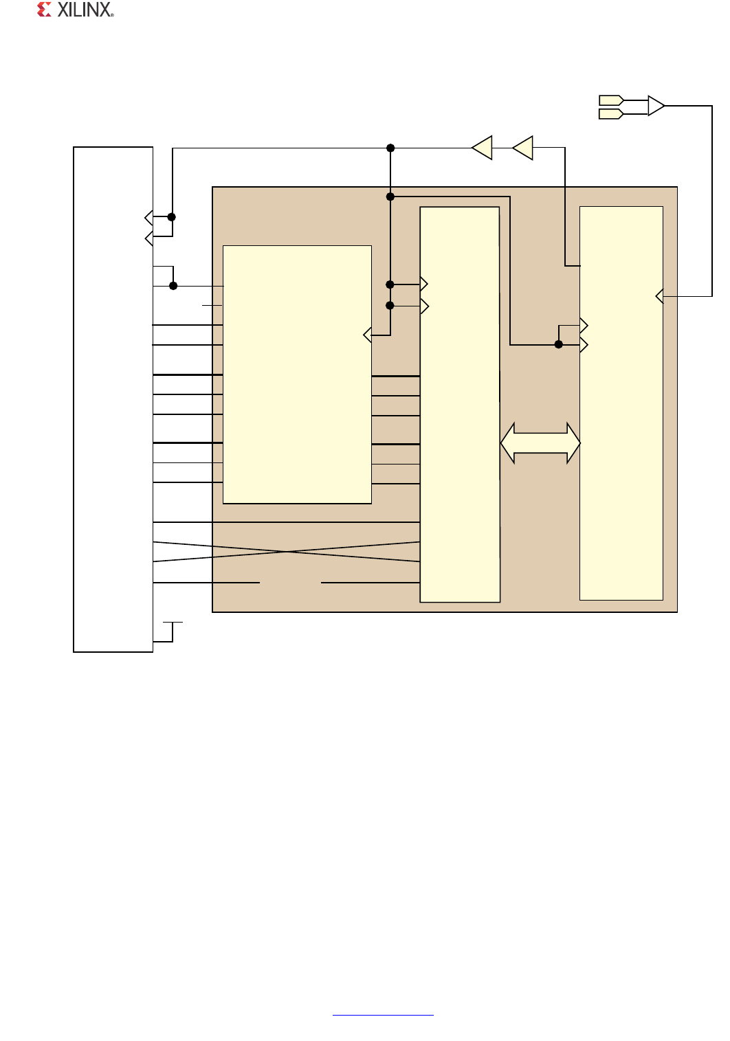
1000BASE-X PCS/PMA or SGMII v11.4 www.xilinx.com 357
PG047 October 16, 2012
Chapter 12: Interfacing to Other Cores
Figure 12-19: Tri-Speed Ethernet MAC Extended to Use an SGMII in a Spartan-6 LXT Device
7UL6SHHG
(WKHUQHW
0$&
/RJL&25(
SK\HPDFU[G>@
SK\HPDFU[GY
SK\HPDFU[HU
HPDFSK\W[G@
HPDFSK\W[HQ
HPDFSK\W[HU
HPDFSK\PFONRXW
SK\HPDFPGLQ
HPDFSK\PGRXW
HPDFSK\PGWUL
(WKHUQHW
%$6(;
3&630$
RU6*0,,
/RJL&25(
JPLLBU[G>@
JPLLBU[BGY
JPLLBU[BHU
JPLLBW[G>@
JPLLBW[BHQ
JPLLBW[BHU
PGF
PGLRBLQ
PGLRBRXW
PGLRBWUL
QR
FRQQHFWLRQ
XVHUFON
7UDQVFHLYHU,)
JPLLBU[GBRXW>@
JPLLBU[BGYBRXW
JPLLBU[BHUBRXW
JPLLBW[GBLQ>@
JPLLBW[BHQBLQ
JPLLBW[BHUBLQ
JPLLBU[GBLQ>@
JPLLBU[BGYBLQ
JPLLBU[BHUBLQ
JPLLBW[GBRXW>@
JPLLBW[BHQBRXW
JPLLBW[BHUBRXW
FONP
6*0,,$GDSWDWLRQ
PRGXOH
VJPLLBFONBHQ
VSHHGBLVBB
VSHHGBLVB
VSHHGLV
VSHHGLV
U[JPLLPLLFON
W[JPLLPLLFON
FRUHKDVVJPLL
9&&
FOLHQWHPDFU[HQDEOH
FOLHQWHPDFW[HQDEOH
VJPLLBFONBU
1&
#,+).
7;865&/.
7;865&/.
XVHUFON
0+]
XVHUFON
%8)*
'40#,+/54
FRPSRQHQWBQDPHBEORFN
%ORFN/HYHOIURPH[DPSOHGHVLJQ
FONLQ
0+]
,%8)'6
,3$'
EUHIFONS
,3$'
EUHIFONQ
3PARTAN
4RANSCEIVER
'40
%8),2
8

1000BASE-X PCS/PMA or SGMII v11.4 www.xilinx.com 358
PG047 October 16, 2012
Chapter 12: Interfacing to Other Cores
Tri-Mode Ethernet MAC Core (TEMAC core v5.1 and Later, AXI)
Virtex-6 Devices
Figure 12-20 illustrates the connections and clock management logic required to interface
the Ethernet 1000BASE-X PCS/PMA or SGMII core (when used in SGMII mode with the
Virtex-6 FPGA GTX transceiver) to the Tri-Mode Ethernet MAC core (TEMAC core v5.1 and
later, AXI).
Features of this configuration include:
• Observe that the “block” level of the TEMAC is instantiated. This provides the MAC with
extra functionality that is not provided by the TEMAC core netlist. When using the MAC
to connect the 1000BASE-X core, the “Internal” PHY Interface mode must be selected
from the TEMAC GUI prior to core generation. See the TEMAC documentation.
• The SGMII Adaptation module, as provided in the example design for the Ethernet
1000BASE-X PCS/PMA or SGMII core, when generated to the SGMII standard and MAC
mode, can be used to interface the two cores.
• If both cores have been generated with the optional management interface, the MDIO
port can be connected up to that of the Tri-Speed Ethernet MAC core, allowing the
MAC to access the embedded configuration and status registers of the Ethernet
1000BASE-X PCS/PMA or SGMII core.
• Because of the Receiver Elastic Buffer, the entire GMII (transmitter and receiver paths) is
synchronous to a single clock domain. Therefore, userclk2 is used as the 125 MHz
reference clock for both cores, and the transmitter and receiver logic of the Tri-Speed
Ethernet MAC core now operate in the same clock domain.

1000BASE-X PCS/PMA or SGMII v11.4 www.xilinx.com 359
PG047 October 16, 2012
Chapter 12: Interfacing to Other Cores
Spartan-6 Devices
Figure 12-21 illustrates the connections and clock management logic required to interface
the Ethernet 1000BASE-X PCS/PMA or SGMII core (when used in SGMII mode with the
Spartan-6 FPGA GTP) to the Tri-Mode Ethernet MAC core (TEMAC core v5.1 and later, AXI).
Features of this configuration include:
• Observe that the “block” level of the TEMAC is instantiated. This provides the MAC with
extra functionality that is not provided by the TEMAC core netlist. When using the MAC
to connect the 1000BASE-X core, the “Internal” PHY Interface mode must be selected
from the TEMAC GUI prior to core generation. See the TEMAC documentation.
• The SGMII Adaptation module, as provided in the example design for the Ethernet
1000BASE-X PCS/PMA or SGMII core when generated to the SGMII standard and MAC
mode, can be used to interface the two cores.
• If both cores have been generated with the optional management interface, the MDIO
port can be connected up to that of the Tri-Speed Ethernet MAC core, allowing the
MAC to access the embedded configuration and status registers of the Ethernet
1000BASE-X PCS/PMA or SGMII core.
X-Ref Target - Figure 12-20
Figure 12-20: AXI Tri-Speed Ethernet MAC Extended to use an SGMII in Virtex-6 Devices
(WKHUQHW
%$6(;
3&630$
RU6*0,,
/RJL&25(
JPLLBU[G>@
JPLLBU[BGY
JPLLBU[BHU
JPLLBW[G>@
JPLLBW[BHQ
JPLLBW[BHU
PGF
PGLRBLQ
PGLRBRXW
PGLRBWUL
QR
FRQQHFWLRQ
XVHUFON
7UDQVFHLYHU,)
JPLLBU[GBRXW>@
JPLLBU[BGYBRXW
JPLLBU[BHUBRXW
JPLLBW[GBLQ>@
JPLLBW[BHQBLQ
JPLLBW[BHUBLQ
JPLLBU[GBLQ>@
JPLLBU[BGYBLQ
JPLLBU[BHUBLQ
JPLLBW[GBRXW>@
JPLLBW[BHQBRXW
JPLLBW[BHUBRXW
FONP
6*0,,$GDSWDWLRQ
PRGXOH
VJPLLBFONBHQ
VSHHGBLVBB
VSHHGBLVB
VJPLLBFONBU
1&
9LUWHX
'48
4RANSCEIVER
48532#,+
48532#,+
XVHUFON
0+]
XVHUFON
%8)*
MGTREFCLK
-(Z
,%8)'6B*7;(
,3$'
PJWUHIFONBS
,3$'
PJWUHIFONBQ
*1'
48/54#,+
-'42%&#,+48;=
-'42%&#,+28;=
FRPSRQHQWBQDPHBEORFN
%ORFN/HYELFROM%THERNET"!3%80#30-!,OGI#/2%
JPLLBW[G@
JW[BFON
3TATISTICS6ECTORS
)NTERFACE
7(0$&/RJL&RUH
3TATISTICS
6ECTOR$ECODE
!8),ITE
TO)0)&
FRPSRQHQWBQDPHBEORFN
%ORFN/HYELFROM4RI-ODE%THERNET-!#,OGI#/2%
JPLLBW[BHQ
JPLLBW[BHU
JPLLBU[G@
JPLLBU[BGY
JPLLBU[BHU
-!#
!8)3TREAM
)&
PGF
PGLRBWUL
PGLRBLQ
PGLRBRXW
VSHHGLV
FONBHQDEOH
VSHHGLV
8
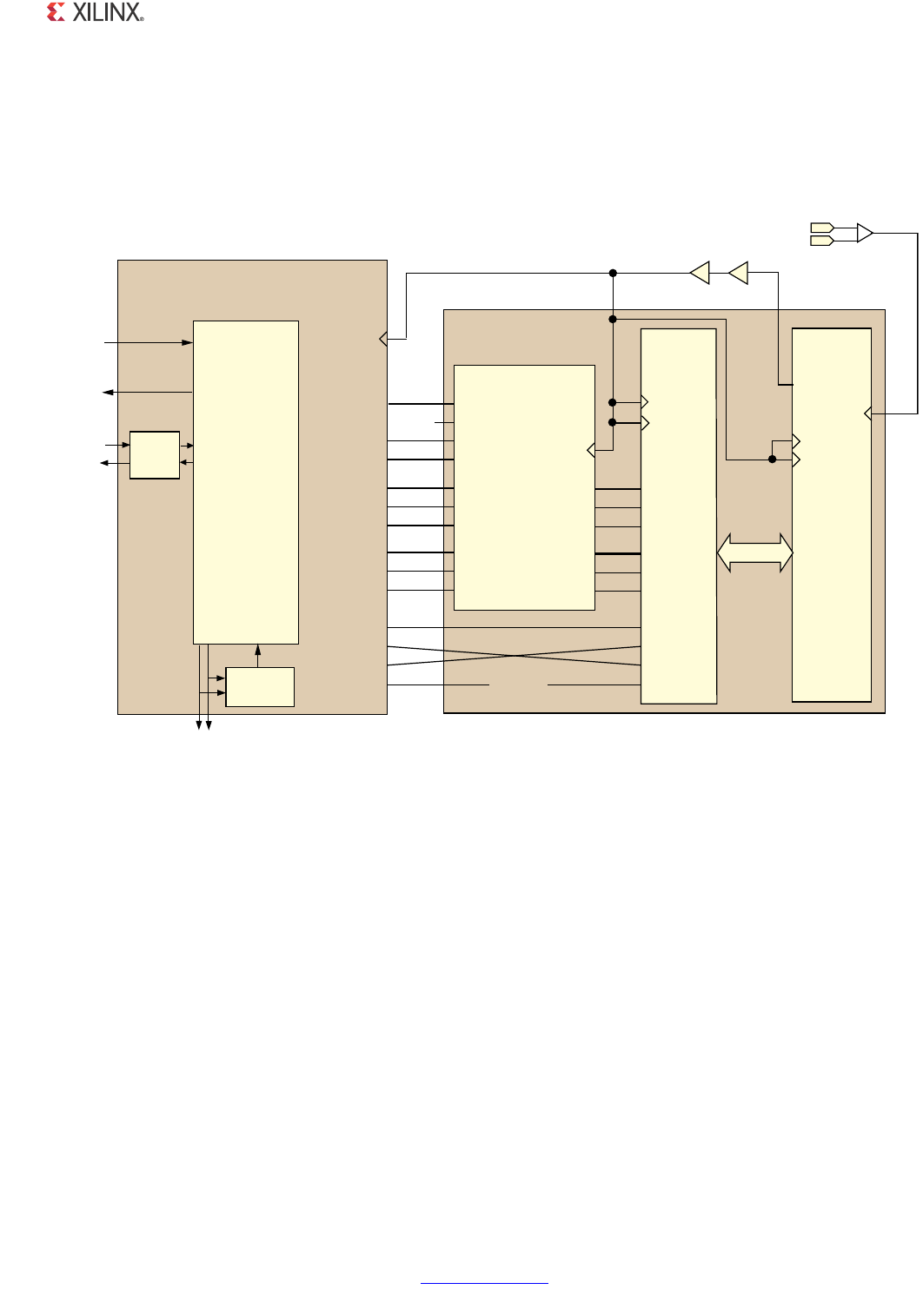
1000BASE-X PCS/PMA or SGMII v11.4 www.xilinx.com 360
PG047 October 16, 2012
Chapter 12: Interfacing to Other Cores
• Due to the Receiver Elastic Buffer, the entire GMII (transmitter and receiver paths) is
synchronous to a single clock domain. Therefore, userclk2 is used as the 125 MHz
reference clock for both cores, and the transmitter and receiver logic of the Tri-Speed
Ethernet MAC core now operate in the same clock domain.
Virtex-7 Devices
Figure 12-22 illustrates the connections and clock management logic required to interface
the Ethernet 1000BASE-X PCS/PMA or SGMII core (when used in SGMII Configuration and
MAC mode with the 7 series FPGA transceiver) to the Tri-Mode Ethernet MAC core (TEMAC
core v5.1and later, AXI).
Features of this configuration include:
• Observe that the “block” level of the TEMAC is instantiated. This provides the MAC with
extra functionality that is not provided by the TEMAC core netlist. When using the MAC
to connect the 1000BASE-X core, the “Internal” PHY Interface mode must be selected
from the TEMAC GUI prior to core generation. See the TEMAC documentation.
• The SGMII Adaptation module, as provided in the example design for the Ethernet
1000BASE-X PCS/PMA or SGMII core when generated to the SGMII standard and MAC
mode, can be used to interface the two cores.
X-Ref Target - Figure 12-21
Figure 12-21: Tri-Speed Ethernet MAC v5.1 and Later Extended to use an SGMII in Spartan-6 Devices
(WKHUQHW
%$6(;
3&630$
RU6*0,,
/RJL&25(
JPLLBU[G>@
JPLLBU[BGY
JPLLBU[BHU
JPLLBW[G>@
JPLLBW[BHQ
JPLLBW[BHU
PGF
PGLRBLQ
PGLRBRXW
PGLRBWUL
QR
FRQQHFWLRQ
XVHUFON
7UDQVFHLYHU,)
JPLLBU[GBRXW>@
JPLLBU[BGYBRXW
JPLLBU[BHUBRXW
JPLLBW[GBLQ>@
JPLLBW[BHQBLQ
JPLLBW[BHUBLQ
JPLLBU[GBLQ>@
JPLLBU[BGYBLQ
JPLLBU[BHUBLQ
JPLLBW[GBRXW>@
JPLLBW[BHQBRXW
JPLLBW[BHUBRXW
FONP
6*0,,$GDSWDWLRQ
PRGXOH
VJPLLBFONBHQ
VSHHGBLVBB
VSHHGBLVB
VJPLLBFONBU
1&
#,+).
7;865&/.
7;865&/.
XVHUFON
0+]
XVHUFON
%8)*
'40#,+/54
FONLQ
0+]
,%8)'6
,3$'
EUHIFONS
,3$'
EUHIFONQ
3PARTAN
4RANSCEIVER
'40
%8),2
FRPSRQHQWBQDPHBEORFN
%ORFN/HYELFROM%THERNET"!3%80#30-!,OGI#/2%
JPLLBW[G@
JW[BFON
3TATISTICS6ECTORS
)NTERFACE
7(0$&/RJL&RUH
3TATISTICS
6ECTOR$ECODE
!8),ITE
TO)0)&
FRPSRQHQWBQDPHBEORFN
%ORFN/HYELFROM4RI-ODE%THERNET-!#,OGI#/2%
JPLLBW[BHQ
JPLLBW[BHU
JPLLBU[G@
JPLLBU[BGY
JPLLBU[BHU
-!#
!8)3TREAM
)&
PGF
PGLRBWUL
PGLRBLQ
PGLRBRXW
VSHHGLV
FONBHQDEOH
VSHHGLV
8
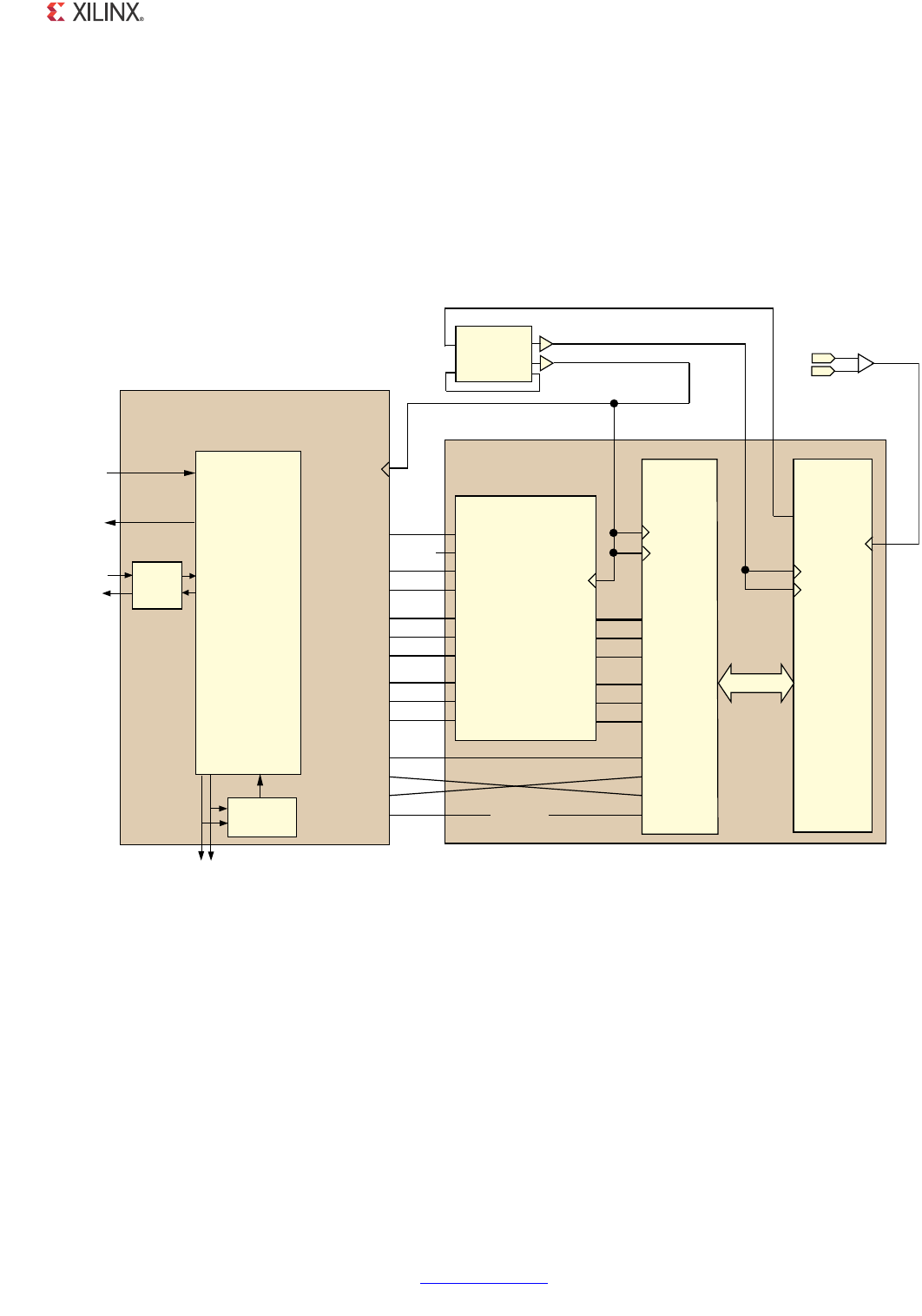
1000BASE-X PCS/PMA or SGMII v11.4 www.xilinx.com 361
PG047 October 16, 2012
Chapter 12: Interfacing to Other Cores
• If both cores have been generated with the optional management interface, the MDIO
port can be connected up to that of the Tri-Speed Ethernet MAC core, allowing the
MAC to access the embedded configuration and status registers of the Ethernet
1000BASE-X PCS/PMA or SGMII core.
• Because of the Receiver Elastic Buffer, the entire GMII (transmitter and receiver paths) is
synchronous to a single clock domain. Therefore, userclk2 is used as the 125 MHz
reference clock for both cores, and the transmitter and receiver logic of the Tri-Speed
Ethernet MAC core now operate in the same clock domain.
Kintex-7 and Zynq-7000 Devices
Figure 12-25 illustrates the connections and clock management logic required to interface
the Ethernet 1000BASE-X PCS/PMA or SGMII core (when used in SGMII Configuration and
MAC mode with the 7 series FPGA Transceiver) to the Tri-Mode Ethernet MAC core (TEMAC
core v5.1 and later, AXI).
X-Ref Target - Figure 12-22
Figure 12-22: Tri-Speed Ethernet MAC v5.1 and Later Extended to use an SGMII in Virtex-7 Devices
(WKHUQHW
%$6(;
3&630$
RU6*0,,
/RJL&25(
JPLLBU[G>@
JPLLBU[BGY
JPLLBU[BHU
JPLLBW[G>@
JPLLBW[BHQ
JPLLBW[BHU
PGF
PGLRBLQ
PGLRBRXW
PGLRBWUL
QR
FRQQHFWLRQ
XVHUFON
7UDQVFHLYHU,)
JPLLBU[GBRXW>@
JPLLBU[BGYBRXW
JPLLBU[BHUBRXW
JPLLBW[GBLQ>@
JPLLBW[BHQBLQ
JPLLBW[BHUBLQ
JPLLBU[GBLQ>@
JPLLBU[BGYBLQ
JPLLBU[BHUBLQ
JPLLBW[GBRXW>@
JPLLBW[BHQBRXW
JPLLBW[BHUBRXW
FONP
6*0,,$GDSWDWLRQ
PRGXOH
VJPLLBFONBHQ
VSHHGBLVBB
VSHHGBLVB
VJPLLBFONBU
1&
9LUWHX
'48'4(
4RANSCEIVER
48532#,+
48532#,+
XVHUFON
0+]
XVHUFON
GTREFCLK
-(Z
,%8)'6B*7(
,3$'
JWUHIFONBS
,3$'
JWUHIFONBQ
48/54#,+
'42%&#,+
0+]
--#-%?!$6
#,+/54
#,+/54
#,+).
#,+&"/54#,+&").
"5&'
"5&'
0+]
JPLLBW[G@
JW[BFON
3TATISTICS6ECTORS
)NTERFACE
7(0$&/RJL&RUH
3TATISTICS
6ECTOR$ECODE
!8),ITE
TO)0)&
FRPSRQHQWBQDPHBEORFN
%ORFN/HYELFROM4RI-ODE%THERNET-!#,OGI#/2%
JPLLBW[BHQ
JPLLBW[BHU
JPLLBU[G@
JPLLBU[BGY
JPLLBU[BHU
-!#
!8)3TREAM
)&
PGF
PGLRBWUL
PGLRBLQ
PGLRBRXW
VSHHGLV
FONBHQDEOH
VSHHGLV
FRPSRQHQWBQDPHBEORFN
%ORFN/HYELFROM%THERNET"!3%80#30-!,OGI#/2%
8

1000BASE-X PCS/PMA or SGMII v11.4 www.xilinx.com 362
PG047 October 16, 2012
Chapter 12: Interfacing to Other Cores
Features of this configuration include:
• Observe that the “block” level of the TEMAC is instantiated. This provides the MAC with
extra functionality that is not provided by the TEMAC core netlist. When using the MAC
to connect the 1000BASE-X core, the “Internal” PHY Interface mode must be selected
from the TEMAC GUI prior to core generation. See the TEMAC documentation.
• The SGMII Adaptation module, as provided in the example design for the Ethernet
1000BASE-X PCS/PMA or SGMII core when generated to the SGMII standard and MAC
mode, can be used to interface the two cores.
• If both cores have been generated with the optional management interface, the MDIO
port can be connected up to that of the Tri-Speed Ethernet MAC core, allowing the
MAC to access the embedded configuration and status registers of the Ethernet
1000BASE-X PCS/PMA or SGMII core.
• Because of the Receiver Elastic Buffer, the entire GMII (transmitter and receiver paths) is
synchronous to a single clock domain. Therefore, userclk2 is used as the 125 MHz
reference clock for both cores, and the transmitter and receiver logic of the Tri-Speed
Ethernet MAC core now operate in the same clock domain.
X-Ref Target - Figure 12-23
Figure 12-23: AXI Tri-Speed Ethernet MAC Extended to use an SGMII in Kintex-7 or Zynq-7000 Devices
(WKHUQHW
%$6(;
3&630$
RU6*0,,
/RJL&25(
JPLLBU[G>@
JPLLBU[BGY
JPLLBU[BHU
JPLLBW[G>@
JPLLBW[BHQ
JPLLBW[BHU
PGF
PGLRBLQ
PGLRBRXW
PGLRBWUL
QR
FRQQHFWLRQ
XVHUFON
7UDQVFHLYHU,)
JPLLBU[GBRXW>@
JPLLBU[BGYBRXW
JPLLBU[BHUBRXW
JPLLBW[GBLQ>@
JPLLBW[BHQBLQ
JPLLBW[BHUBLQ
JPLLBU[GBLQ>@
JPLLBU[BGYBLQ
JPLLBU[BHUBLQ
JPLLBW[GBRXW>@
JPLLBW[BHQBRXW
JPLLBW[BHUBRXW
FONP
6*0,,$GDSWDWLRQ
PRGXOH
VJPLLBFONBHQ
VSHHGBLVBB
VSHHGBLVB
VJPLLBFONBU
1&
+INTEX:YNQ
'48
4RANSCEIVER
48532#,+
48532#,+
XVHUFON
0+]
XVHUFON
GTREFCLK
-(Z
,%8)'6B*7(
,3$'
JWUHIFONBS
,3$'
JWUHIFONBQ
48/54#,+
'42%&#,+
0+]
--#-%?!$6
#,+/54
#,+/54
#,+).
#,+&"/54#,+&").
"5&'
0+]
JPLLBW[G@
JW[BFON
3TATISTICS6ECTORS
)NTERFACE
7(0$&/RJL&RUH
3TATISTICS
6ECTOR$ECODE
!8),ITE
TO)0)&
FRPSRQHQWBQDPHBEORFN
%ORFN/HYELFROM4RI-ODE%THERNET-!#,OGI#/2%
JPLLBW[BHQ
JPLLBW[BHU
JPLLBU[G@
JPLLBU[BGY
JPLLBU[BHU
-!#
!8)3TREAM
)&
PGF
PGLRBWUL
PGLRBLQ
PGLRBRXW
VSHHGLV
FONBHQDEOH
VSHHGLV
FRPSRQHQWBQDPHBEORFN
%ORFN/HYELFROM%THERNET"!3%80#30-!,OGI#/2%
"5&'
8

1000BASE-X PCS/PMA or SGMII v11.4 www.xilinx.com 363
PG047 October 16, 2012
Chapter 12: Interfacing to Other Cores
Artix-7 Devices
Figure 12-24 illustrates the connections and clock management logic required to interface
the Ethernet 1000BASE-X PCS/PMA or SGMII core (when used in SGMII Configuration and
MAC mode with the 7 series FPGA Transceiver) to the Tri-Mode Ethernet MAC core (TEMAC
core v5.1 and later, AXI).
Features of this configuration include:
• Observe that the “block” level of the TEMAC is instantiated. This provides the MAC with
extra functionality that is not provided by the TEMAC core netlist. When using the MAC
to connect the 1000BASE-X core, the “Internal” PHY Interface mode must be selected
from the TEMAC GUI prior to core generation. See the TEMAC documentation.
• The SGMII Adaptation module, as provided in the example design for the Ethernet
1000BASE-X PCS/PMA or SGMII core when generated to the SGMII standard and MAC
mode, can be used to interface the two cores.
• If both cores have been generated with the optional management interface, the MDIO
port can be connected up to that of the Tri-Speed Ethernet MAC core, allowing the
MAC to access the embedded configuration and status registers of the Ethernet
1000BASE-X PCS/PMA or SGMII core.
• Because of the Receiver Elastic Buffer, the entire GMII (transmitter and receiver paths) is
synchronous to a single clock domain. Therefore, userclk2 is used as the 125 MHz
reference clock for both cores, and the transmitter and receiver logic of the Tri-Speed
Ethernet MAC core now operate in the same clock domain.
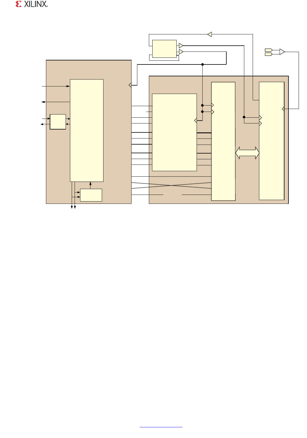
1000BASE-X PCS/PMA or SGMII v11.4 www.xilinx.com 364
PG047 October 16, 2012
Chapter 12: Interfacing to Other Cores
Integration of the Tri-Mode Ethernet MAC Using Asynchronous
Oversampling over Virtex-6 LVDS
Figure 12-25 illustrates the connections and clock management logic required to interface
the Ethernet 1000BASE-X PCS/PMA or SGMII core (when used in SGMII Asynchronous
Oversampling over Virtex-6 LVDS) to the Tri-Mode Ethernet MAC core.
The I/O Bank Level of the Example Design should be taken from the example design and
instantiated for connection to the Tri-Mode Ethernet MAC. This I/O Bank module can
contain multiple SGMII port instantiations (only one SGMII port is illustrated). Connections
from a unique Tri-Mode Ethernet MAC core to each unique SGMII port are identical and are
as shown in Figure 12-25.
X-Ref Target - Figure 12-24
Figure 12-24: AXI Tri-Speed Ethernet MAC Extended to use
an SGMII in Artix-7 Devices
(WKHUQHW
%$6(;
3&630$
RU6*0,,
/RJL&25(
JPLLBU[G>@
JPLLBU[BGY
JPLLBU[BHU
JPLLBW[G>@
JPLLBW[BHQ
JPLLBW[BHU
PGF
PGLRBLQ
PGLRBRXW
PGLRBWUL
QR
FRQQHFWLRQ
XVHUFON
7UDQVFHLYHU,)
JPLLBU[GBRXW>@
JPLLBU[BGYBRXW
JPLLBU[BHUBRXW
JPLLBW[GBLQ>@
JPLLBW[BHQBLQ
JPLLBW[BHUBLQ
JPLLBU[GBLQ>@
JPLLBU[BGYBLQ
JPLLBU[BHUBLQ
JPLLBW[GBRXW>@
JPLLBW[BHQBRXW
JPLLBW[BHUBRXW
FONP
6*0,,$GDSWDWLRQ
PRGXOH
VJPLLBFONBHQ
VSHHGBLVBB
VSHHGBLVB
VJPLLBFONBU
1&
!RTIX
'40
4RANSCEIVER
48532#,+
48532#,+
XVHUFON
0+]
XVHUFON
GTREFCLK
-(Z
,%8)'6B*7(
,3$'
JWUHIFONBS
,3$'
JWUHIFONBQ
48/54#,+
'42%&#,+
0+]
--#-%?!$6
#,+/54
#,+/54
#,+).
#,+&"/54#,+&").
"5&'
"5&'
0+]
"5&'
JPLLBW[G@
JW[BFON
3TATISTICS6ECTORS
)NTERFACE
7(0$&/RJL&RUH
3TATISTICS
6ECTOR$ECODE
!8),ITE
TO)0)&
FRPSRQHQWBQDPHBEORFN
%ORFN/HYELFROM4RI-ODE%THERNET-!#,OGI#/2%
JPLLBW[BHQ
JPLLBW[BHU
JPLLBU[G@
JPLLBU[BGY
JPLLBU[BHU
-!#
!8)3TREAM
)&
PGF
PGLRBWUL
PGLRBLQ
PGLRBRXW
VSHHGLV
FONBHQDEOH
VSHHGLV
FRPSRQHQWBQDPHBEORFN
%ORFN/HYELFROM%THERNET"!3%80#30-!,OGI#/2%
8

1000BASE-X PCS/PMA or SGMII v11.4 www.xilinx.com 365
PG047 October 16, 2012
Chapter 12: Interfacing to Other Cores
The following conditions apply to each connected Tri-Mode Ethernet MAC and SGMII port
pair:
• The SGMII Adaptation module, as provided in the example design for the Ethernet
1000BASE-X PCS/PMA or SGMII core when generated to the SGMII standard, can be
used to interface the two cores.
• If both cores have been generated with the optional management interface, the MDIO
port can be connected up to that of the Tri-Speed Ethernet MAC core, allowing the
MAC to access the embedded configuration and status registers of the Ethernet
1000BASE-X PCS/PMA or SGMII core.
• Due to the embedded Receiver Elastic Buffer in the LVDS transceiver, the entire GMII is
synchronous to a single clock domain. Therefore clk125m is used as the 125 MHz
reference clock for both cores, and the transmitter and receiver logic of the Tri-Mode
Ethernet MAC core now operate in the same clock domain.
Figure 12-25 illustrates a Tri-Mode Ethernet MAC core generated with the optional clock
enable circuitry. This is the most efficient way to connect the two cores together in terms of
clock resource usage and so is recommended. See the Tri-Mode Ethernet MAC User Guide for
more information.
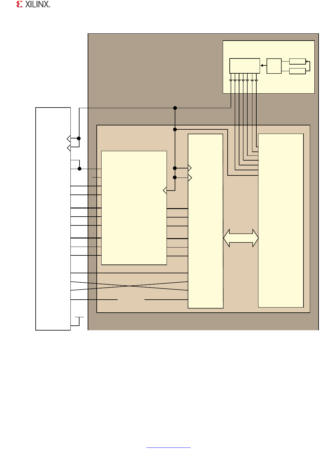
1000BASE-X PCS/PMA or SGMII v11.4 www.xilinx.com 366
PG047 October 16, 2012
Chapter 12: Interfacing to Other Cores
X-Ref Target - Figure 12-25
Figure 12-25: Tri-Speed Ethernet MAC Extended to Use SGMII Using Asynchronous Oversampling over
Virtex-6 LVDS
7UL6SHHG
(WKHUQHW
0$&
/RJL&25(
SK\HPDFU[G>@
SK\HPDFU[GY
SK\HPDFU[HU
HPDFSK\W[G@
HPDFSK\W[HQ
HPDFSK\W[HU
HPDFSK\PFONRXW
SK\HPDFPGLQ
HPDFSK\PGRXW
HPDFSK\PGWUL
(WKHUQHW
%$6(;
3&630$
RU6*0,,
/RJL&25(
JPLLBU[G>@
JPLLBU[BGY
JPLLBU[BHU
JPLLBW[G>@
JPLLBW[BHQ
JPLLBW[BHU
PGF
PGLRBLQ
PGLRBRXW
PGLRBWUL
QR
FRQQHFWLRQ
XVHUFON
7UDQVFHLYHU,)
JPLLBU[GBRXW>@
JPLLBU[BGYBRXW
JPLLBU[BHUBRXW
JPLLBW[GBLQ>@
JPLLBW[BHQBLQ
JPLLBW[BHUBLQ
JPLLBU[GBLQ>@
JPLLBU[BGYBLQ
JPLLBU[BHUBLQ
JPLLBW[GBRXW>@
JPLLBW[BHQBRXW
JPLLBW[BHUBRXW
FONP
6*0,,$GDSWDWLRQ
PRGXOH
VJPLLBFONBHQ
VSHHGBLVBB
VSHHGBLVB
VSHHGLV
VSHHGLV
U[JPLLPLLFON
W[JPLLPLLFON
FRUHKDVVJPLL
9&&
FOLHQWHPDFU[HQDEOH
FOLHQWHPDFW[HQDEOH
VJPLLBFONBUI
1&
9LUWEX
,6$3
4RANSCEIVER
FONP
XVHUFON
FRPSRQHQWBQDPHBEORFN
%ORFN/HYHOIURPHXAMPLEDESIGN
--#-
CLOCK
ALIGNMENT
STATE
MACHINE
CLOCKBUFFERS
VARIOUSCLOCK
FREQUENCIES
ANDPHASES
/3%2$%3
)3%2$%3
,2%DQN&ORFNLQJ
FONPBW[BEXILR
FONPBW[BEXIU
FONPBU[BEXILRB
FONPBU[BEXILRB
FONP
FONSP
FONP
COMPONENT?NAME?IOBANK
)/"ANK,EVELFROMEXAMPLEDESIGN
8

1000BASE-X PCS/PMA or SGMII v11.4 www.xilinx.com 367
PG047 October 16, 2012
Chapter 12: Interfacing to Other Cores
Integration of the Tri-Mode Ethernet MAC Using Sync SGMII
over Kintex-7/Virtex-7 LVDS
Figure 12-26 illustrates the connections and clock management logic required to interface
the Ethernet 1000BASE-X PCS/PMA or SGMII core (when used in Sync SGMII over
Kintex-7/Virtex-7 LVDS) to the Tri-Mode Ethernet MAC core. The Block Level of the Example
Design should be taken from the example design and instantiated for connection to the
Tri-Mode Ethernet MAC. Connections from a unique Tri-Mode Ethernet MAC core to SGMII
port are identical and are shown in Figure 12-26.
The following conditions apply to each connected Tri-Mode Ethernet MAC and SGMII port
pair:
• The SGMII Adaptation module, as provided in the example design for the Ethernet
1000BASE-X PCS/PMA or SGMII core when generated to the SGMII standard, can be
used to interface the two cores.
• If both cores have been generated with the optional management interface, the MDIO
port can be connected up to that of the Tri-Speed Ethernet MAC core, allowing the
MAC to access the embedded configuration and status registers of the Ethernet
1000BASE-X PCS/PMA or SGMII core.
• clk125 is used as the 125 MHz reference clock for both cores, and the transmitter and
receiver logic of the Tri-Mode Ethernet MAC core now operate in the same clock
domain. This is the clock derived by MMCM and IBUFDS from differential reference
clock.
Figure 12-26 illustrates a Tri-Mode Ethernet MAC core generated with the optional clock
enable circuitry. This is the most efficient way to connect the two cores together in terms of
clock resource usage and so is recommended. See the Tri-Mode Ethernet MAC User Guide for
more information.
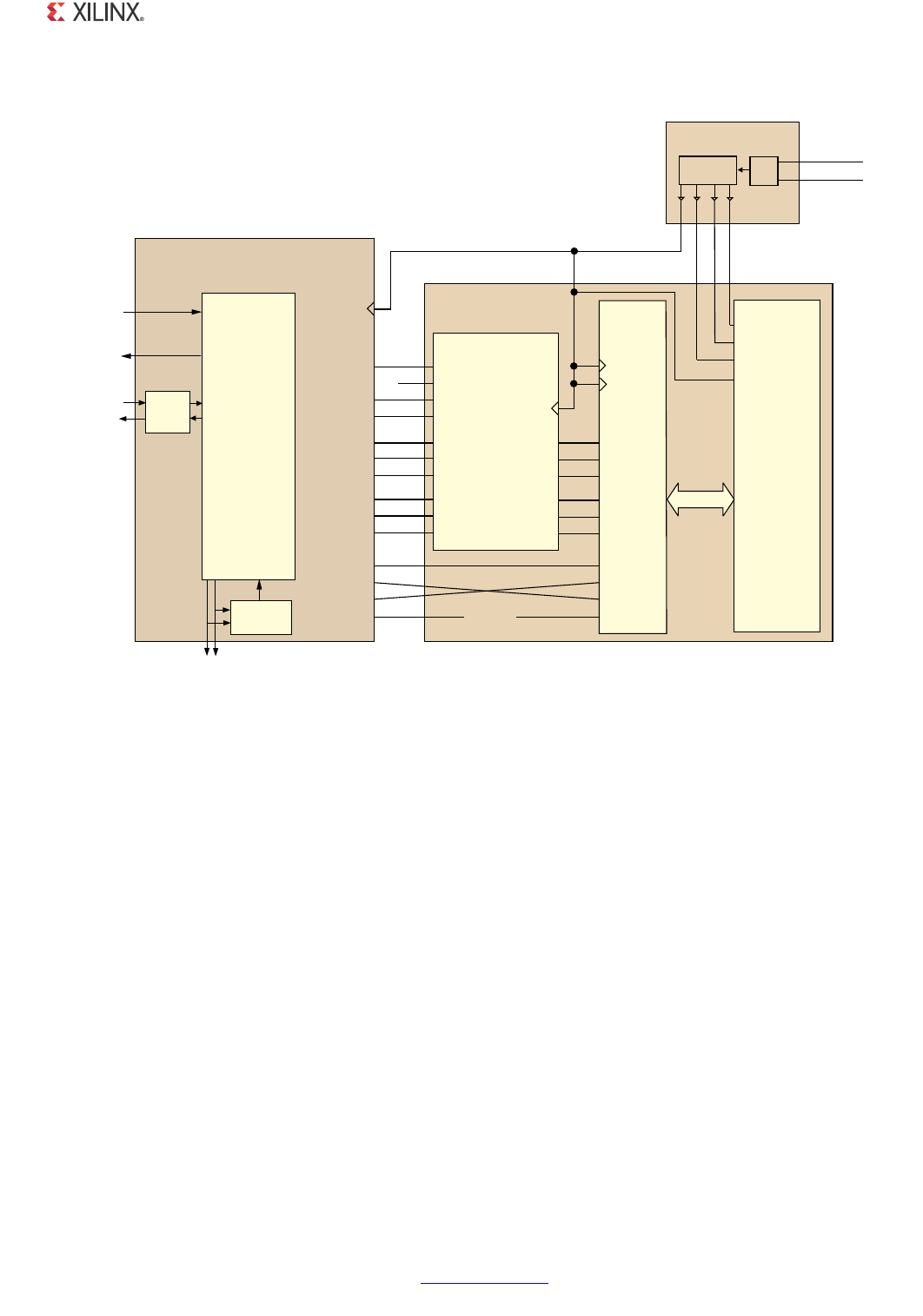
1000BASE-X PCS/PMA or SGMII v11.4 www.xilinx.com 368
PG047 October 16, 2012
Chapter 12: Interfacing to Other Cores
X-Ref Target - Figure 12-26
Figure 12-26: AXI Tri-Speed Ethernet MAC Extended to use SGMII over Virtex-7/Kintex7
Synchronous LVDS
(WKHUQHW
%$6(;
3&630$
RU6*0,,
/RJL&25(
JPLLBU[G>@
JPLLBU[BGY
JPLLBU[BHU
JPLLBW[G>@
JPLLBW[BHQ
JPLLBW[BHU
PGF
PGLRBLQ
PGLRBRXW
PGLRBWUL
QR
FRQQHFWLRQ
XVHUFON
7UDQVFHLYHU,)
JPLLBU[GBRXW>@
JPLLBU[BGYBRXW
JPLLBU[BHUBRXW
JPLLBW[GBLQ>@
JPLLBW[BHQBLQ
JPLLBW[BHUBLQ
JPLLBU[GBLQ>@
JPLLBU[BGYBLQ
JPLLBU[BHUBLQ
JPLLBW[GBRXW>@
JPLLBW[BHQBRXW
JPLLBW[BHUBRXW
FONP
6*0,,$GDSWDWLRQ
PRGXOH
VJPLLBFONBHQ
VSHHGBLVBB
VSHHGBLVB
VJPLLBFONBUI
1&
9LUWH[
.LQWH[
/9'6
7UDQVFHLYHU
FON
XVHUFON
XAMPLEDESIGN
--#- ,%8)'6
CLOCKBUFFERS
VARIOUSCLOCK
FREQUENCIES
ANDPHASES
FON
FON
FON
FON
FRPSRQHQWBQDPHBVJPLLBSK\BFONBJHQ
UHIFONBS
UHIFONBQ
FRPSRQHQWBQDPHBEORFN
%ORFN/HYHOIURPH
JPLLBW[G@
JW[BFON
3TATISTICS 6ECTORS
)NTERFACE
7(0$&/RJL&RUH
6WDWLVWLFV9HFWRU
'HFRGH
!8),ITE
TO)0)&
FRPSRQHQWBQDPHBEORFN
%ORFN/HYELFROM4RI-ODE%THERNET-!#,OGI#/2%
JPLLBW[BHQ
JPLLBW[BHU
JPLLBU[G@
JPLLBU[BGY
JPLLBU[BHU
-!#
!8)STREAM
)&
PGF
PGLRBWUL
PGLRBLQ
PGLRBRXW
VSHHGLV
FONBHQDEOH
VSHHGLV

1000BASE-X PCS/PMA or SGMII v11.4 www.xilinx.com 369
PG047 October 16, 2012
Chapter 13
Special Design Considerations
This chapter describes the unique design considerations associated with implementing the
Ethernet 1000BASE-X PCS/PMA or SGMII core.
Power Management
No power management considerations are recommended for the Ethernet 1000BASE-X
PCS/PMA or SGMII core when using it with the TBI. When using the Ethernet 1000BASE-X
PCS/PMA or SGMII core with a Zynq™-7000, Virtex® -7, Kintex™-7, Artix™-7, Virtex-6,
Spartan®-6 or Virtex-5 device, the transceiver can be placed in a low-power state in either
of the following ways:
• Writing to the PCS Configuration Register 0 (if using the core with the optional
Management Interface). The low-power state can only be removed by issuing the core
with a reset. This reset can be achieved either by writing to the software reset bit in the
PCS Configuration Register 0, or by driving the core reset port.
• Asserting the Power Down bit in the configuration_vector (if using the core
without the optional Management Interface). The low-power state can only be removed
by issuing the core with a reset by driving the reset port of the core.
Start-up Sequencing
IEEE 802.3-2008 clause 22.2.4.1.6 states that by default, a PHY should power-up in an isolate
state (electrically isolated from the GMII).
• If you are using the core with the optional Management Interface, it is necessary to
write to the PCS Configuration Register 0 to take the core out of the isolate state.
• If using the core without the optional Management interface, it is the responsibility of
the client to ensure that the isolate input signal in the configuration_vector is
asserted at power-on.
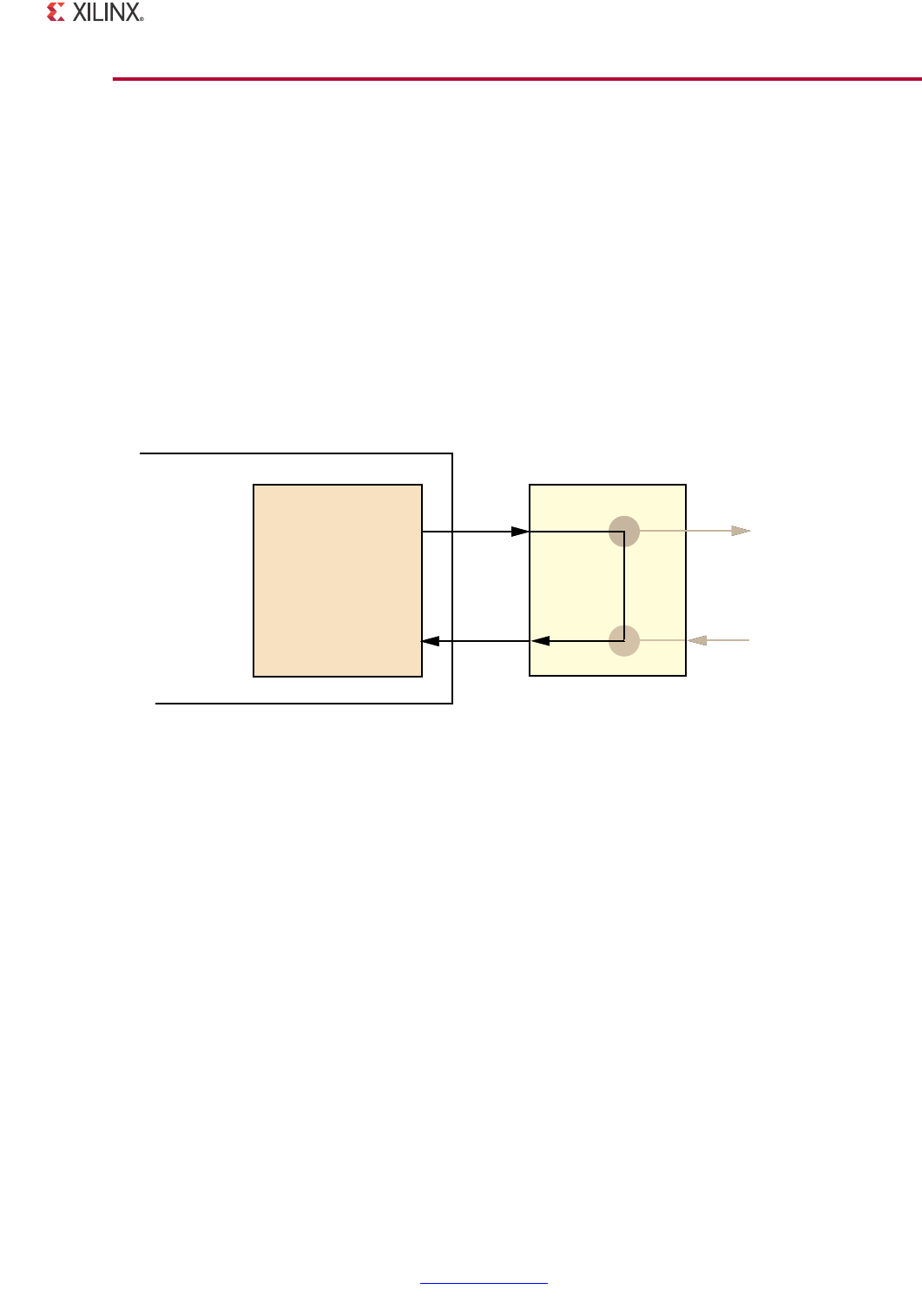
1000BASE-X PCS/PMA or SGMII v11.4 www.xilinx.com 370
PG047 October 16, 2012
Chapter 13: Special Design Considerations
Loopback
This section details the implementation of the loopback feature. Loopback mode is enabled
or disabled by either the MDIO Management Interface or by the Additional Configuration
Vector.
Core with the TBI
There is no physical loopback path in the core. Placing the core into loopback has the effect
of asserting logic 1 on the ewrap signal of the TBI (see 1000BASE-X PCS with TBI Pinout).
1000BASE-X PCS with TBI Pinout.) This instructs the attached PMA SERDES device to enter
loopback mode as illustrated in Figure 13-1.
X-Ref Target - Figure 13-1
Core with Transceiver
The loopback path is implemented in the core as illustrated in Figure 13-2. When placed
into loopback, the data is routed from the transmitter path to the receiver path at the last
possible point in the core. This point is immediately before the device-specific transceiver
(or LVDS transceiver) interface. When placed in loopback, the core creates a constant
stream of Idle code groups that are transmitted through the serial or GTP transceiver in
accordance with the IEEE 802.3-2008 specification.
Earlier versions (before v5.0) of the core implemented loopback differently. The serial
loopback feature of the device-specific transceiver was used by driving the
LOOPBACK[1:0] port of the device-specific (serial or GTP) transceiver. This is no longer the
case, and the loopback[1:0] output port of the core is now permanently set to logic “00.”
However, for debugging purposes, the LOOPBACK[1:0] input port of the device-specific
transceiver can be directly driven by the user logic to place it in either parallel or serial
loopback mode.
Figure 13-1: Loopback Implementation Using the TBI
%THERNET"!3%8
0#30-!OR3'-))
#ORE
"!3%80-!
3%2$%3
4X
2X
4")
&0'!
,OOPBACKOCCURSIN
EXTERNAL3%2$%3 8
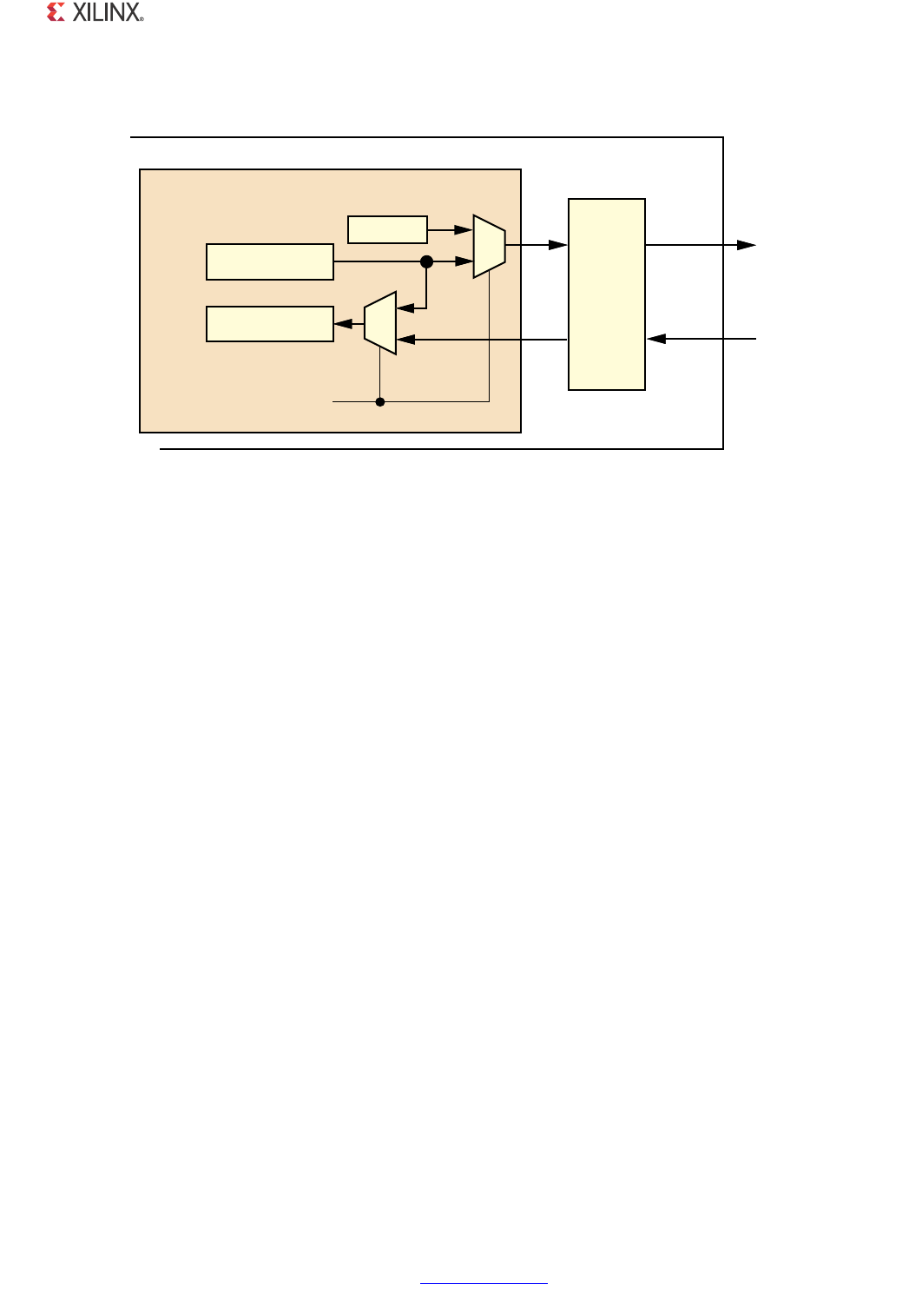
1000BASE-X PCS/PMA or SGMII v11.4 www.xilinx.com 371
PG047 October 16, 2012
Chapter 13: Special Design Considerations
X-Ref Target - Figure 13-2
Figure 13-2: Loopback Implementation When Using the Core with
Device-Specific Transceivers
%THERNET"!3%8
0#30-!OR3'-))#ORE
$EVICE
3PECIFIC
4RANSCEIVER
4X
2X
&0'!
,OOPBACKOCCURSINCORE
0#34X%NGINE
0#32X%NGINE
)DLE3TREAM
LOOPBACKCONTROL
8

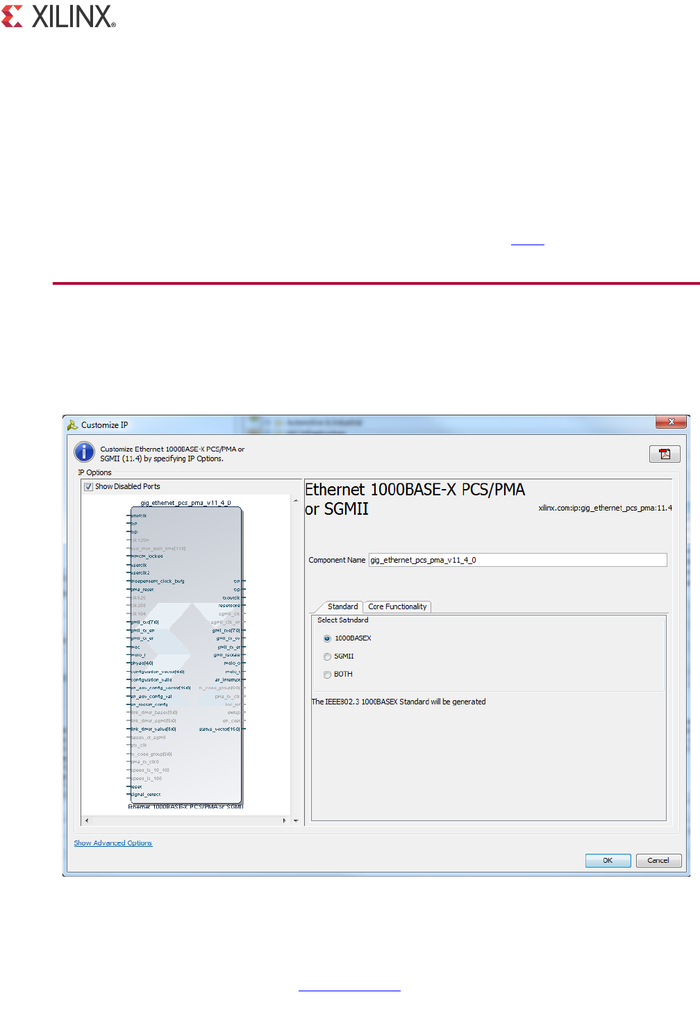
1000BASE-X PCS/PMA or SGMII v11.4 www.xilinx.com 373
PG047 October 16, 2012
Chapter 14
Customizing and Generating the Core
The Ethernet 1000BASE-X PCS/PMA or SGMII core is generated using the Vivado™ IP
catalog. This chapter describes the Graphical User Interface (GUI) options used to generate
and customize the core. For more Vivado tools documentation, click here.
GUI
Figure 14-1 displays the Ethernet 1000BASE-X PCS/PMA or SGMII customization screen,
used to set core parameters and options.
X-Ref Target - Figure 14-1
Figure 14-1: Core Customization Screen

1000BASE-X PCS/PMA or SGMII v11.4 www.xilinx.com 374
PG047 October 16, 2012
Chapter 14: Customizing and Generating the Core
Component Name
The component name is used as the base name of the output files generated for the core.
Names must begin with a letter and must be composed from the following characters: a
through z, 0 through 9 and "_."
Select Standard
Select from the following standards for the core:
• 1000BASE-X. 1000BASE-X Physical Coding Sublayer (PCS) functionality is designed to
the IEEE 802.3 specification. Depending on the choice of physical interface, the
functionality can be extended to include the 1000BASE-X Physical Medium Attachment
(PMA) sublayer. Default setting.
• SGMII. Provides the functionality to provide a Gigabit Media Independent Interface
(GMII) to Serial-GMII (SGMII) bridge, as defined in the Serial-GMII Specification (Cisco
Systems, ENG-46158). SGMII can be used to replace Gigabit Media Independent
Interface (GMII) at a much lower pin count and for this reason is often favored by
Printed Circuit Board (PCB) designers.
• Both (a combination of 1000BASE-X and SGMII). Combining the 1000BASE-X and SGMII
standards lets you dynamically configure the core to switch between 1000BASE-X and
SGMII standards. The core can be switched by writing through the Management Data
Input/Output (MDIO) Management Interface. For more information, see MDIO
Management Interface in Chapter 2
Core Functionality
Figure 14-2 displays the Ethernet 1000BASE-X PCS/PMA or SGMII functionality screen.
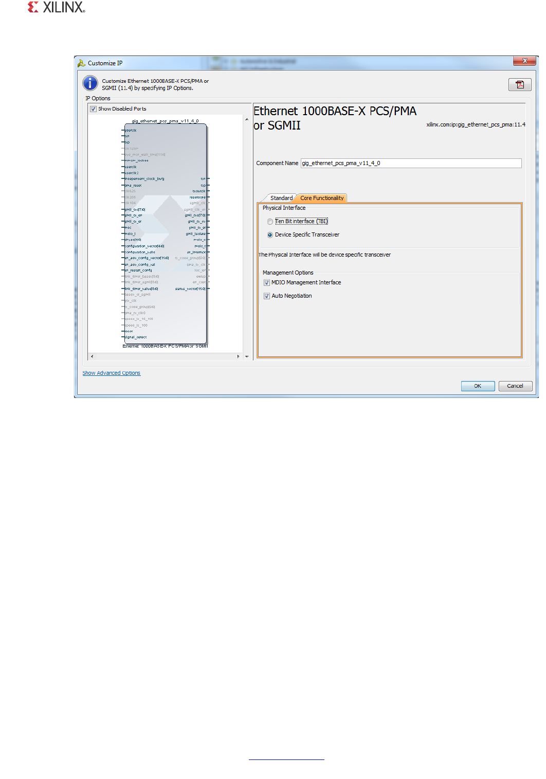
1000BASE-X PCS/PMA or SGMII v11.4 www.xilinx.com 375
PG047 October 16, 2012
Chapter 14: Customizing and Generating the Core
Physical Interface
Depending on the target architecture, up to three physical interface options are available
for the core.
•Device Specific Transceiver. Uses a transceiver specific to the selected device family
to extend the 1000BASE-X functionality to include both PCS and PMA sub-layers. It is
available for Zynq™-7000, Virtex®-7, Kintex™-7 and Artix™-7 devices. For additional
information, see Transceiver Logic in Chapter 5.
•Ten Bit Interface (TBI). Available in all supported families and provides 1000BASE-X or
SGMII functionality with a parallel TBI used to interface to an external
Serializer/Deserializer (SERDES.) For more information, see Ten-Bit-Interface Logic in
Chapter 4. Default setting. This is available for Kintex-7 devices.
•LVDS Serial. Only available in Virtex-7 and Kintex-7 devices, -2 speed grade or faster
for devices with HR Banks and -1 speed grade or faster for devices with HP Banks for
performing the SGMII Standard. This option uses Synchronous Oversampling over
Virtex-7/Kintex-7 FPGA Low Voltage Differential Signalling (LVDS) to implement full
SGMII functionality without the use of a FPGA GTX transceiver.
X-Ref Target - Figure 14-2
Figure 14-2: 1000Basex Standards Options Screen
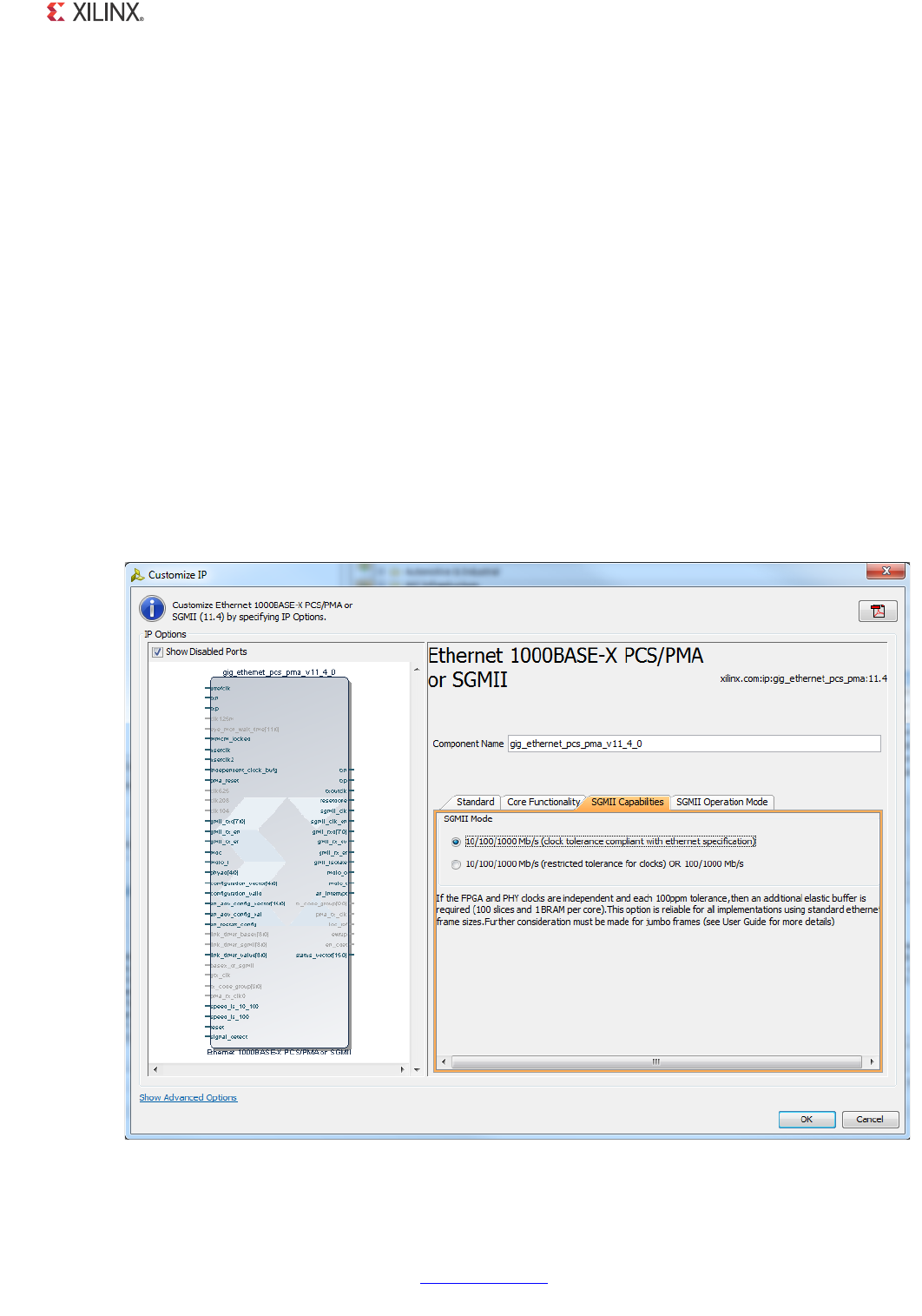
1000BASE-X PCS/PMA or SGMII v11.4 www.xilinx.com 376
PG047 October 16, 2012
Chapter 14: Customizing and Generating the Core
MDIO Management Interface
Select this option to include the MDIO Management Interface to access the PCS
Configuration registers. See MDIO Management Interface. An additional configuration
vector interface is provided to write into Management Registers 0 and 4. See Additional
Configuration Vector in Chapter 2.
Auto-Negotiation
Select this option to include Auto-Negotiation functionality with the core. For more
information, see Chapter 9, Auto-Negotiation. The default is to include Auto-Negotiation.
SGMII/Dynamic Standard Switching Elastic Buffer Options
The SGMII/Dynamic Standard Switching Options screen, used to customize the Ethernet
1000BASE-X PCS/PMA or SGMII core, is only displayed if either SGMII or Both is selected in
the Select Standard section of the initial customization screen, and only if the
device-specific transceiver is selected as the Physical Standard.
X-Ref Target - Figure 14-3
Figure 14-3: SGMII Dynamic Standard Switching Options

1000BASE-X PCS/PMA or SGMII v11.4 www.xilinx.com 377
PG047 October 16, 2012
Chapter 14: Customizing and Generating the Core
This screen lets you select the Receiver Elastic Buffer type to be used with the core. Before
selecting this option, see Receiver Elastic Buffer Implementations in Chapter 6.
SGMII/Dynamic Standard Mode of Operation
The SGMII/Dynamic Standard Operation Mode screen, used to customize the Ethernet
1000BASE-X PCS/PMA or SGMII core, is only displayed if either SGMII or Both is selected in
the Select Standard section of the initial customization screen.
This screen lets you select the core to operate in the PHY mode or Media Access Controller
(MAC) mode.
X-Ref Target - Figure 14-4
Figure 14-4: SGMII Operation Mode Options

1000BASE-X PCS/PMA or SGMII v11.4 www.xilinx.com 378
PG047 October 16, 2012
Chapter 14: Customizing and Generating the Core
Output Generation
The Ethernet 1000BASE-X PCS/PMA or SGMII solution delivers files into several filegroups.
By default the filegroups necessary for use of the Ethernet 1000BASE-X PCS/PMA or SGMII
or opening the IP Example design are generated when the core is generated. If additional
filegroups are required these can be selected using the generate option. The filegroups
generated can be seen in the IP Sources tab of the Sources window where they are listed for
each IP in the project. The filegroups available for the Ethernet 1000BASE-X PCS/PMA or
SGMII solution are described in the following subsections.
Examples
Includes all source required to be able to open and implement the IP example design
project. That is, example design HDL and the example design xdc file.
Examples Simulation
Includes all source required to be able to simulate the IP example design project. This is the
same list of HDL as the Examples filegroup with the addition of the demonstration test
bench HDL.
Synthesis
Includes all synthesis sources required by the core. For the Ethernet 1000BASE-X PCS/PMA
or SGMII solution this is a mix of both encrypted and unencrypted source. Only the
unencrypted sources are visible.
Simulation
Includes all simulation sources required by the core. Simulation of the Ethernet 1000BASE-X
PCS/PMA or SGMII solution at the core level is not supported without the addition of a test
bench (not supplied). Simulation of the example design is supported.
Instantiation Template
Example instantiation template
Miscellaneous
This provides simulations scripts and support files required for running netlist based
functional simulation. The files delivered as part of this filegroup are not used or
understood by Vivado tools and as such this filegroup is not displayed. These files are
delivered into the project source directory.

1000BASE-X PCS/PMA or SGMII v11.4 www.xilinx.com 379
PG047 October 16, 2012
Chapter 15
Constraining the Core
This chapter contains information about constraining the core in the Vivado™ Design Suite
environment. It defines the constraint requirements of the Ethernet 1000BASE-X PCS/PMA
or SGMII solution.
Required Constraints
The Ethernet 1000BASE-X PCS/PMA or SGMII solution is provided with a core level XDC file.
This provides constraints for the core that are expected to be applied in all instantiations of
the core. This XDC file, named <component name>.xdc, can be found in the IP Sources tab
of the Sources window in the Synthesis file group.
An example XDC is also provided with the HDL example design to provide the board level
constraints. This is specific to the example design and, as such, is only expected to be used
as a template for the user design. See Chapter 16, Detailed Example Design. This XDC file,
named <component name>_example_design.xdc, is found in the IP Sources tab of the
Sources window in the Examples file group.
The core level XDC file inherits some constraints from the example design XDC file. In any
system it is expected that the user would also provide an XDC file to constrain the logic in
which the Ethernet 1000BASE-X PCS/PMA or SGMII solution is instantiated.
Device, Package, and Speed Grade Selections
The core can be implemented in Zynq™-7000, Virtex®-7, Kintex™-7 and Artix™-7 devices
with these attributes:
• Large enough to accommodate the core
• Contains a sufficient number of IOBs
• Device has a supported speed grade

1000BASE-X PCS/PMA or SGMII v11.4 www.xilinx.com 380
PG047 October 16, 2012
Chapter 15: Constraining the Core
Clock Frequencies
The Ethernet 1000BASE-X PCS/PMA or SGMII solution has a variable number of clocks with
the precise number required being dependant upon the specific parameterization. As the
core targets various transceiver options, there are associated clock frequency requirements.
Table 15-1: Speed Grades
Device Family Speed Grade
Virtex-7 -1 or faster
Kintex-7 -1 or faster
Artix-7 -1 or faster
Zynq-7000 -1 or faster
Table 15-2: Clock Frequencies
Clock Name Parametrization Frequency Requirement
gtrefclk Present if serial transceiver is used 125 MHz
txoutclk Present if serial transceiver is used 62.5 or 125 MHz depending on serial
transceiver used
userclk Present if serial transceiver is used 62.5 or 125 MHz depending on serial
transceiver used
userclk2 Present if serial transceiver is used 125 MHz
sgmii_clk Present in SGMII Mode 1.25 MHz, 12.5 MHz or 125 MHz
gtx_clk Present in TBI Mode 125 MHz
pma_tx_clk Present in TBI Mode 125 MHz
pma_rx_clk Present in TBI Mode 125 MHz
clk625 Present in LVDS Mode 625 MHz
clk208 Present in LVDS Mode 208 MHz
clk104 Present in LVDS Mode 104 MHz

1000BASE-X PCS/PMA or SGMII v11.4 www.xilinx.com 381
PG047 October 16, 2012
Chapter 15: Constraining the Core
I/O Standard and Placement
There are no specific I/O standard/placement requirements on most interfaces. Depending
upon the device family, part and package chosen there are two types of I/O available for
use. HP I/O is intended for support of high-speed interfaces and as such is limited to 1.8 V
support. HP I/O support both Input and Output Delays components. HR I/O is intended for
interfaces with higher voltage requirements and has a more limited supported frequency
range. HR I/O only supports Input Delay components.
Both MII and GMII are 3.3 V standards. However the majority of PHYs are multi-standard
and operate at either 2.5 V or 3.3 V and this is also true of the PHYs selected for Xilinx
development boards. This means that for most applications the physical interfaces are
restricted to either using HR I/O, where available, or HP I/O with an external voltage
converter to translate between 1.8 V and the minimum level required by the PHY of 2.5 V.
For any board design it is therefore very important to identify which type of I/O is
available/being used.
In most of the applications the GMII interface of the core is interfaced to Xilinx TEMAC core
in the FPGA, which means that no IP standard/placement is required for that interface.

1000BASE-X PCS/PMA or SGMII v11.4 www.xilinx.com 382
PG047 October 16, 2012
Chapter 16
Detailed Example Design
This chapter contains information about the provided example design in the Vivado™
Design Suite environment.
Example Design
•Example Design for 1000BASE-X with Transceivers in Chapter 5
•SGMII Example Design / Dynamic Switching Example Design Using a Transceiver in
Chapter 6
•Example Design Implementation in Chapter 7 for SGMII over Synchronous LVDS
Demonstration Test Bench
See Demonstration Test Bench in Chapter 5.

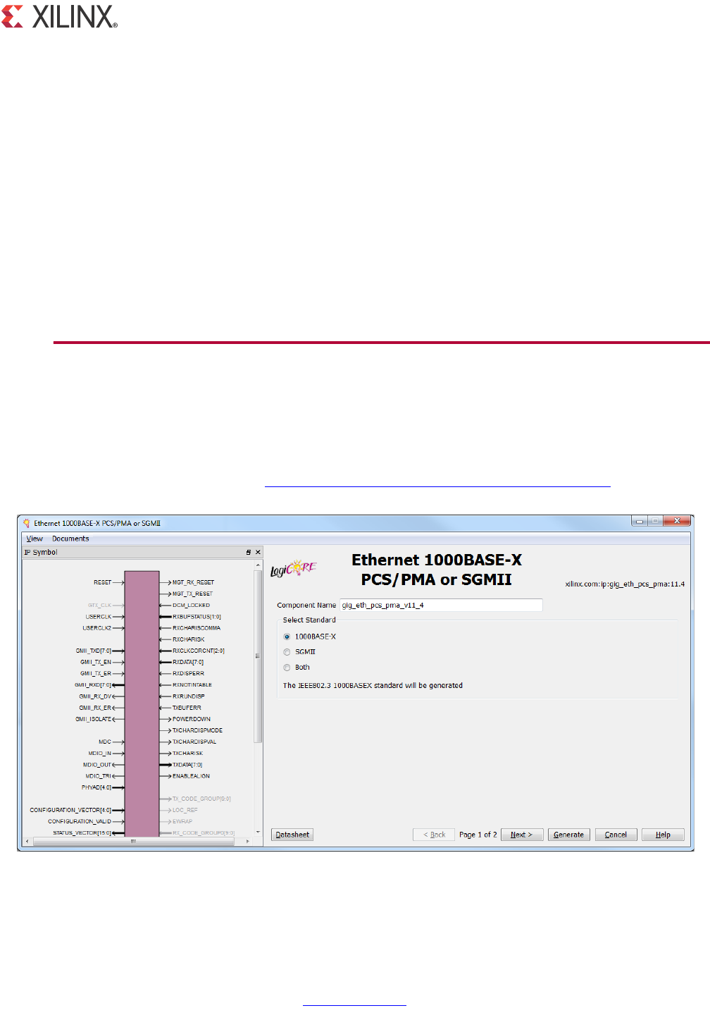
1000BASE-X PCS/PMA or SGMII v11.4 www.xilinx.com 384
PG047 October 16, 2012
Chapter 17
Customizing and Generating the Core
This chapter includes information about using Xilinx tools to customize and generate the
core in the ISE® Design Suite environment.
The Ethernet 1000BASE-X PCS/PMA or SGMII core is generated using the CORE Generator™
tool. This chapter describes the Graphical User Interface (GUI) options used to generate and
customize the core.
GUI
Figure 17-1 displays the Ethernet 1000BASE-X PCS/PMA or SGMII customization screen,
used to set core parameters and options. For help starting and using the CORE Generator
tool on your system, see the documentation included with the ISE® design suite, including
the CORE Generator Guide, at www.xilinx.com/support/software_manuals.htm.
X-Ref Target - Figure 17-1
Figure 17-1: Core Customization Screen

1000BASE-X PCS/PMA or SGMII v11.4 www.xilinx.com 385
PG047 October 16, 2012
Chapter 17: Customizing and Generating the Core
Component Name
The component name is used as the base name of the output files generated for the core.
Names must begin with a letter and must be composed from the following characters: a
through z, 0 through 9 and “_.”
Select Standard
Select from the following standards for the core:
•1000BASE-X. 1000BASE-X Physical Coding Sublayer (PCS) functionality is designed to
the IEEE 802.3 specification. Depending on the choice of physical interface, the
functionality can be extended to include the 1000BASE-X Physical Medium Attachment
(PMA) sublayer. Default setting.
•SGMII. Provides the functionality to provide a Gigabit Media Independent Interface
(GMII) to Serial-GMII (SGMII) bridge, as defined in the Serial-GMII Specification (Cisco
Systems, ENG-46158). SGMII can be used to replace Gigabit Media Independent
Interface (GMII) at a much lower pin count and for this reason is often favored by
Printed Circuit Board (PCB) designers.
•Both (a combination of 1000BASE-X and SGMII). Combining the 1000BASE-X and
SGMII standards lets you dynamically configure the core to switch between
1000BASE-X and SGMII standards. The core can be switched by writing through the
Management Data Input/Output (MDIO) Management Interface. For more information,
see Chapter 10, Configuration and Status.
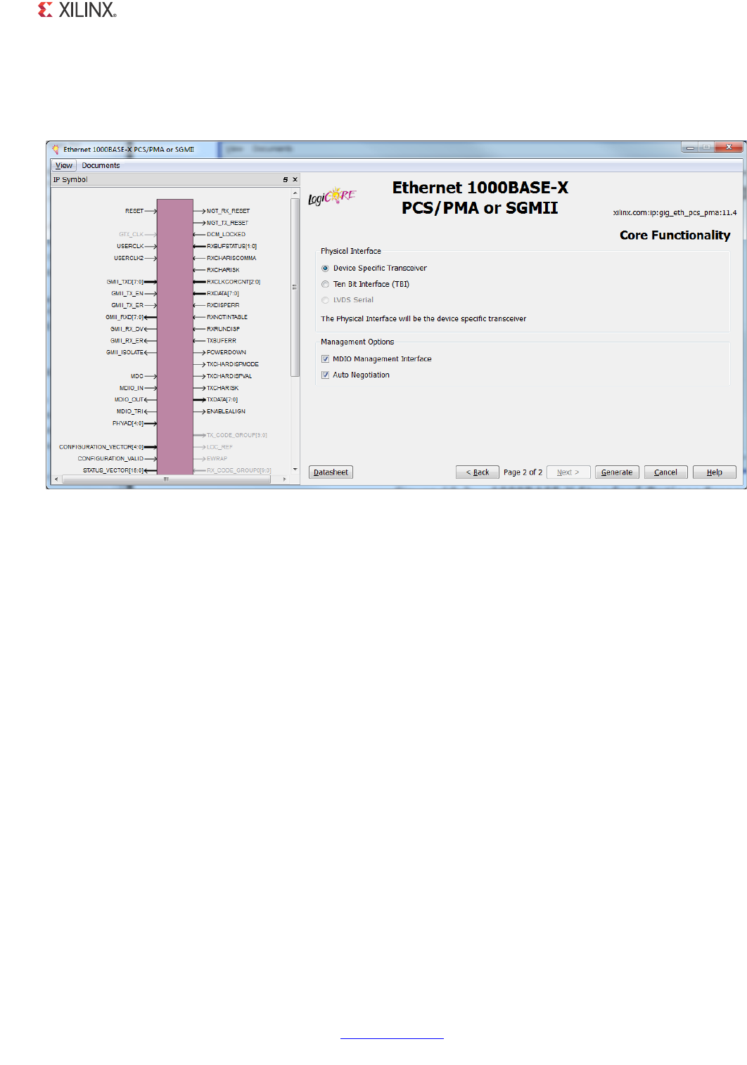
1000BASE-X PCS/PMA or SGMII v11.4 www.xilinx.com 386
PG047 October 16, 2012
Chapter 17: Customizing and Generating the Core
Core Functionality
Figure 17-2 displays the Ethernet 1000BASE-X PCS/PMA or SGMII functionality screen.
Physical Interface
Depending on the target architecture, up to three physical interface options are available
for the core.
•Device Specific Transceiver. Uses a transceiver specific to the selected device family
to extend the 1000BASE-X functionality to include both PCS and PMA sub-layers. For
this reason, it is available only for Virtex®-4 FX, Virtex-5 LXT, Virtex-5 SXT, Virtex-5 FXT
and Virtex-5 TXT, Spartan®-6 LXT, selective Virtex-6 devices, Zynq™-7000, Virtex-7,
Kintex™-7 and Artix™-7 devices. For additional information, see Transceiver Logic.
•Ten Bit Interface (TBI). Available in all supported families and provides 1000BASE-X or
SGMII functionality with a parallel TBI used to interface to an external
Serializer/Deserializer (SERDES.) For more information, see Ten-Bit-Interface Logic.
Default setting.
•LVDS Serial. Only available in Virtex-6 devices, -2 speed grade or faster for performing
the SGMII Standard. This option uses Asynchronous Oversampling over Virtex-6 FPGA
Low Voltage Differential Signalling (LVDS) to implement full SGMII functionality without
the use of a Virtex-6 FPGA GTX transceiver.
X-Ref Target - Figure 17-2
Figure 17-2: 1000BASE-X Standard Options Screen
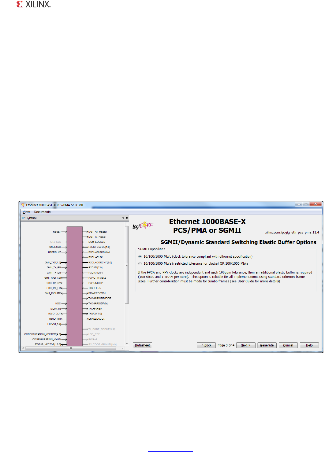
1000BASE-X PCS/PMA or SGMII v11.4 www.xilinx.com 387
PG047 October 16, 2012
Chapter 17: Customizing and Generating the Core
MDIO Management Interface
Select this option to include the MDIO Management Interface to access the PCS
Configuration registers. See MDIO Management Interface.
An additional configuration vector interface is provided to write into Management
Registers 0 and 4. See Additional Configuration Vector.
Auto-Negotiation
Select this option to include Auto-Negotiation functionality with the core. For more
information, see Chapter 9, Auto-Negotiation. The default is to include Auto-Negotiation.
SGMII/Dynamic Standard Switching Elastic Buffer Options
The SGMII/Dynamic Standard Switching Options screen, used to customize the Ethernet
1000BASE-X PCS/PMA or SGMII core, is only displayed if either SGMII or Both is selected in
the Select Standard section of the initial customization screen, and only if the
device-specific transceiver is selected as the Physical Standard.
This screen lets you select the Receiver Elastic Buffer type to be used with the core. Before
selecting this option, see Receiver Elastic Buffer Implementations in Chapter 6.
X-Ref Target - Figure 17-3
Figure 17-3: SGMII/Dynamic Standard Switching Options Screen
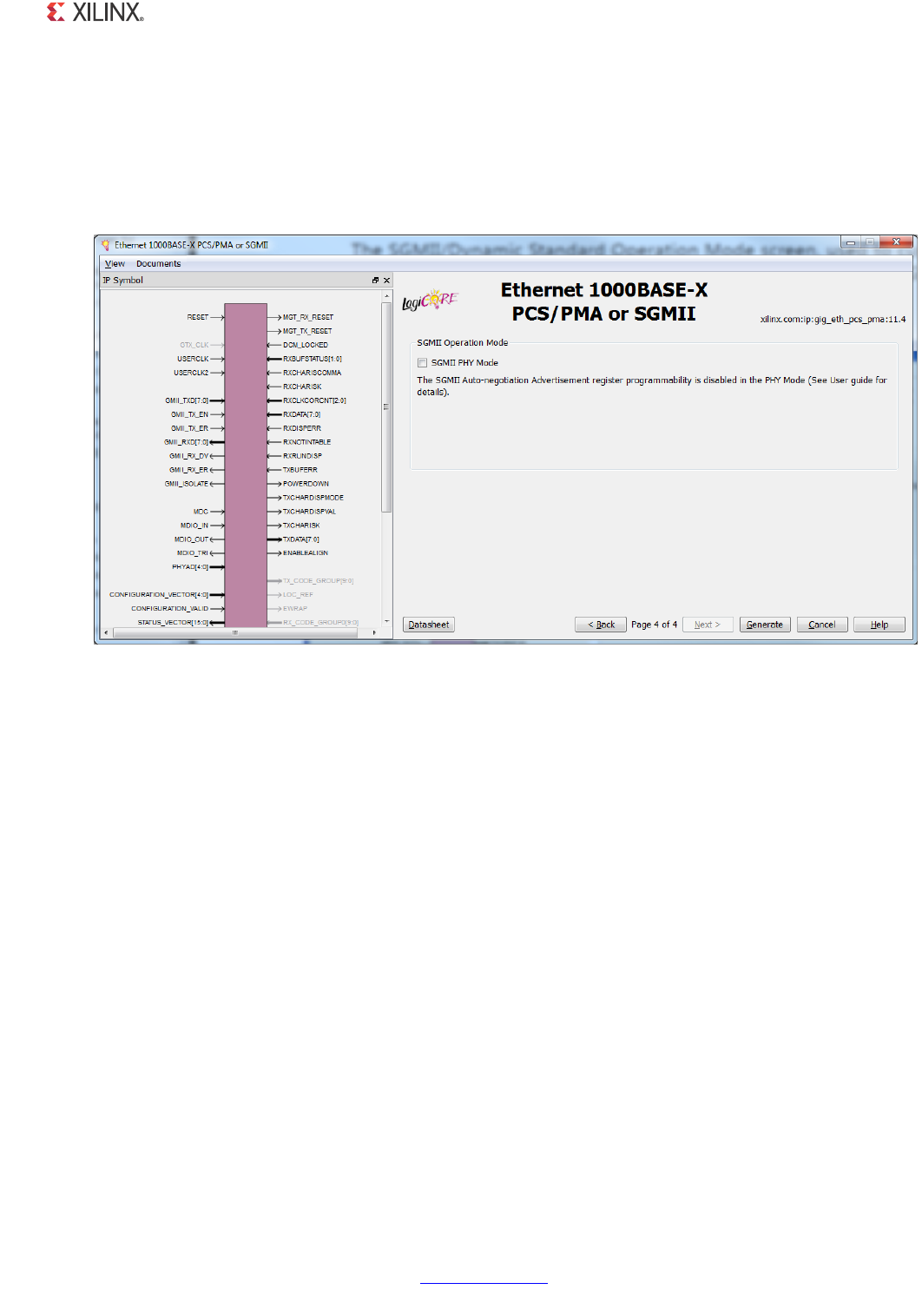
1000BASE-X PCS/PMA or SGMII v11.4 www.xilinx.com 388
PG047 October 16, 2012
Chapter 17: Customizing and Generating the Core
SGMII/Dynamic Standard Mode of Operation
The SGMII/Dynamic Standard Operation Mode screen, used to customize the Ethernet
1000BASE-X PCS/PMA or SGMII core, is only displayed if either SGMII or Both is selected in
the Select Standard section of the initial customization screen.
This screen lets you select the core to operate in the PHY mode or Media Access Controller
(MAC) mode.
Transceiver Tile Configuration
The Transceiver Tile Configuration screen is only displayed if the transceiver interface is
used with selective Virtex-4, Virtex-5 and Spartan-6 device families.
Transceivers for Virtex-4 FX, Virtex-5 and Spartan-6 device families are available in tiles,
each tile consisting of a pair of transceivers. The Transceiver Tile Selection has no effect on
the functionality of the core netlist, but determines the functionality of the example design
delivered with the core.
Depending on the option selected, the example design instantiates a single core netlist and
does one of the following:
•MGT A (0). Connects to device-specific transceiver A
•MGT B (1). Connects to device-specific transceiver B
X-Ref Target - Figure 17-4
Figure 17-4: SGMII Operation Mode Options Screen
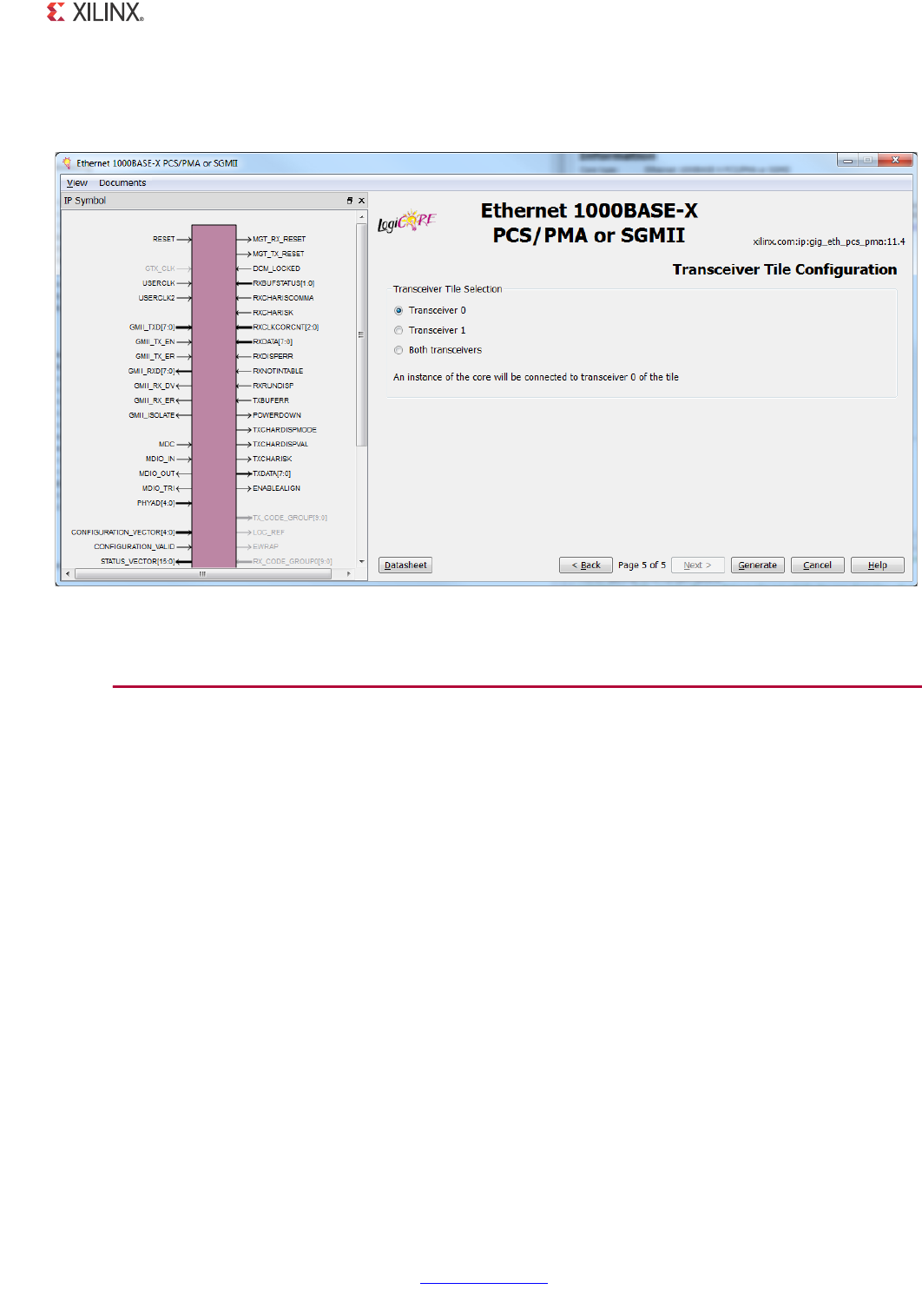
1000BASE-X PCS/PMA or SGMII v11.4 www.xilinx.com 389
PG047 October 16, 2012
Chapter 17: Customizing and Generating the Core
•Both MGTs. Two instantiations of the core are created in the example design and
connected to both device-specific transceiver A and B.
Parameter Values in the XCO File
XCO file parameters are used to run the CORE Generator tool from the command line. XCO
file parameter names and their values are similar to the names and values shown in the GUI,
except that underscore characters (_) can be used instead of spaces. The text in an XCO file
is not case sensitive.
Table 17-1 describes the Xilinx CORE Generator™ (XCO) file parameters, values and
summarizes the GUI defaults. The following is an example of the CSET parameters in an XCO
file:
CSET component_name=gig_eth_pcs_pma_v11_4
CSET standard=1000BASEX
CSET physical_interface=TBI
CSET management_interface=true
CSET auto_negotiation=true
CSET sgmii_mode=10_100_1000
CSET sgmii_phy_mode=false
CSET RocketIO_tile=A
X-Ref Target - Figure 17-5
Figure 17-5: Transceiver Tile Configuration Screen

1000BASE-X PCS/PMA or SGMII v11.4 www.xilinx.com 390
PG047 October 16, 2012
Chapter 17: Customizing and Generating the Core
Output Generation
See Chapter 20, Detailed Example Design.
Table 17-1: XCO File Values and Default Values
Parameter XCO File Values Default GUI Setting
component_name ASCII text starting with a letter and based upon
the following character set: a..z, 0..9 and _ gig_eth_pcs_pma_v11_4
standard One of the following keywords: 1000BASEX,
SGMII, Both 1000BASEX
physical_interface One of the following keywords: TBI, RocketIO,
LVDS TBI
management_interface One of the following keywords: true, false true
auto_negotiation One of the following keywords: true, false true
sgmii_mode
One of the following keywords: 10_100_1000,
100_1000
• 10_100_1000 corresponds to “10/100/1000
Mb/s (clock tolerance compliant with
Ethernet specification)“
• 100_1000 corresponds to “10/100/1000 Mb/s
(restricted tolerance for clocks) OR 100/1000
Mb/s“
10_100_1000
sgmii_phy_mode One of the following keywords: true, false false
RocketIO_tile One of the following keywords: A, B, Both A

1000BASE-X PCS/PMA or SGMII v11.4 www.xilinx.com 391
PG047 October 16, 2012
Chapter 18
Constraining the Core
This chapter contains information about constraining the core in the ISE® Design Suite
environment. This chapter defines the constraint requirements of the Ethernet 1000BASE-X
PCS/PMA or SGMII core. An example UCF is provided with the HDL example design for the
core to implement the constraints defined in this chapter.
Device, Package, and Speed Grade Selection
The Ethernet 1000BASE-X PCS/PMA or SGMII core can be implemented in Zynq™-7000,
Virtex®-7, Kintex™-7, Artix™-7, Virtex-6, Virtex-5, Virtex-4, Spartan®-6, Spartan-3,
Spartan-3E, Spartan-3A/3AN and Spartan-3 Digital Signal Processor (DSP) devices. When
selecting a device, be aware of the following considerations:
• Device must be large enough to accommodate the core.
• Device must contain a sufficient number of IOBs.
• –4 speed grade for Spartan-3, Spartan-3E, Spartan-3A/3AN/3A DSP devices
• –10 speed grade for Virtex-4 devices
• -1 speed grade for Virtex-5, Virtex-6, Zynq-7000, Virtex-7, Artix-7, and Kintex-7 devices
(except Chapter 7, SGMII over LVDS in which case a -2 speed grade or faster is
required).
• -2 speed grade for Spartan-6 devices
• The transceiver is only supported in Virtex-4 FX, Virtex-5 LXT, Virtex-5 SXT, and
Virtex-5 FXT and TXT FPGAs, Spartan-6 LXT, Virtex-6, Zynq-7000, Virtex-7, Artix-7, and
Kintex-7 devices.

1000BASE-X PCS/PMA or SGMII v11.4 www.xilinx.com 392
PG047 October 16, 2012
Chapter 18: Constraining the Core
I/O Location Constraints
No specific I/O location constraints required.
However, when employing BUFIO and BUFR regional clock routing (Zynq-7000, Virtex-7,
Kintex-7, Artix-7, Virtex-6, Virtex-5, and Spartan-6 devices), ensure that a BUFIO capable
clock input pin is selected for input clock sources and that all related input synchronous
data signals are placed in the respective BUFIO region. The device user guide should be
consulted.
Placement Constraints
No specific placement constraints required except for one exception; see Layout and
Placement when designing Chapter 7, SGMII over LVDS.
Virtex-4 FPGA MGT Transceivers for 1000BASE-X
Constraints
The constraints defined in this section are implemented in the UCF for the example designs
delivered with the core. Sections from the UCF are copied into the following descriptions to
serve as examples and should be studied in conjunction with the HDL source code for the
example design. See also Virtex-4 FX Devices.
Clock Period Constraints
The clock txoutclk is provided by the MGT transceiver for use in the FPGA logic. It is
connected to global clock routing to produce the usrclk2 signal. This is the main 125 MHz
clock used by all core logic and must be constrained.
DCLK is a clock with a frequency between 25 and 50 MHz, which must be provided to the
Dynamic Reconfiguration Port and to the calibration block of the MGT transceiver. In the
example design, this is constrained to 50 MHz.
The following UCF syntax shows these constraints being applied.
#***********************************************************
# PCS/PMA Clock period Constraints: please do not relax *
#***********************************************************
NET "userclk2" TNM_NET = "userclk2";

1000BASE-X PCS/PMA or SGMII v11.4 www.xilinx.com 393
PG047 October 16, 2012
Chapter 18: Constraining the Core
TIMESPEC "TS_userclk2" = PERIOD "userclk2" 8 ns HIGH 50 %;
NET "dclk" TNM_NET = "dclk";
TIMESPEC "TS_dclk" = PERIOD "dclk" 20 ns HIGH 50 %;
Setting MGT Transceiver Attributes
The Virtex-4 FPGA MGT transceiver has many attributes. These attributes are set directly
from HDL source code for the transceiver wrapper file delivered with the example design.
These are in the transceiver.vhd file (for VHDL design entry) or transceiver.v (for Verilog
design entry). See Chapter 20, Detailed Example Design for a detailed description of the
example design files provided with the core.
This HDL transceiver wrapper file was initially created using Architecture Wizard. See the
Virtex-4 RocketIO Multi-Gigabit Transceiver User Guide (UG076) for a description of available
attributes.
MGT Transceiver Placement Constraints
The following UCF syntax illustrates the MGT transceiver placement constraints for the
example design. Because Virtex-4 FPGA MGT transceivers are always available in pairs, two
MGT transceivers are always instantiated in the example design, even if one is inactive.
#***********************************************************
# Example Rocket I/O placement *
#***********************************************************
# Lock down the REFCLK pins:
NET brefclk_p LOC = F26;
NET brefclk_n LOC = G26;
# Lock down the GT11 pair and GT11 clock module
INST "core_wrapper/RocketIO/GT11_1000X_A" LOC = GT11_X0Y5;
INST "core_wrapper/RocketIO/GT11_1000X_B" LOC = GT11_X0Y4;
INST "GT11CLK_MGT_INST" LOC = GT11CLK_X0Y3;
# Lock down the RocketIO transceiver pins:
NET "rxp0" LOC = J26;
NET "rxn0" LOC = K26;
NET "txp0" LOC = M26;
NET "txn0" LOC = N26;
NET "rxp1" LOC = U26;
NET "rxn1" LOC = V26;
NET "txp1" LOC = P26;
NET "txn1" LOC = R26;

1000BASE-X PCS/PMA or SGMII v11.4 www.xilinx.com 394
PG047 October 16, 2012
Chapter 18: Constraining the Core
Virtex-4 FPGA RocketIO MGT Transceivers for
SGMII or Dynamic Standards Switching
Constraints
All the constraints described in the section Virtex-4 FPGA MGT Transceivers for 1000BASE-X
Constraints. In addition, if the FPGA Logic Rx Elastic Buffer is selected, an extra clock period
constraint of 16 ns is required for rxrecclk1.
With the MGT transceiver Rx Elastic Buffer bypassed, rxrecclk1 is provided by the MGT
transceiver to the FPGA logic for the recovered receiver data signals leaving the transceiver.
This data is then written into the replacement Rx Elastic Buffer implemented in the FPGA
logic. See Virtex-4 Devices for SGMII or Dynamic Standards Switching.
The following UCF syntax shows the necessary constraint being applied to GT11 A.
#***********************************************************
# PCS/PMA Clock period Constraints for the GT11 A *
# recovered clock: please do not relax *
#***********************************************************
NET "core_wrapper/RocketIO/rxrecclk10" TNM_NET = "rxrecclk10";
TIMESPEC "ts_rxrecclk10" = PERIOD "rxrecclk10" 16 ns;
Virtex-5 FPGA RocketIO GTP Transceivers for
1000BASE-X Constraints
The constraints defined in this section are implemented in the UCF for the example designs
delivered with the core. Sections from the UCF are copied into the following descriptions to
serve as examples and should be studied with the HDL source code for the example design.
See also Virtex-5 LXT and SXT Devices.
Clock Period Constraints
The clkin clock is provided to the GTP transceiver. It is a high-quality reference clock with
a frequency of 125 MHz and should be constrained.
The refclkout clock is provided by the GTP transceiver for use in the FPGA logic, which is
then connected to global clock routing to produce the usrclk2 signal. This is the main 125
MHz clock used by all core logic and must be constrained.
The following UCF syntax shows these constraints being applied.

1000BASE-X PCS/PMA or SGMII v11.4 www.xilinx.com 395
PG047 October 16, 2012
Chapter 18: Constraining the Core
#***********************************************************
# PCS/PMA Clock period Constraints: please do not relax *
#***********************************************************
NET "*clkin" TNM_NET = "clkin";
TIMESPEC "TS_clkin" = PERIOD "clkin" 8 ns HIGH 50 %;
NET "*refclkout" TNM_NET = "refclkout";
TIMESPEC "TS_refclkout" = PERIOD "refclkout" 8 ns HIGH 50 %;
Setting GTP Transceiver Attributes
The Virtex-5 FPGA RocketIO™ GTP transceiver has many attributes that are set directly from
HDL source code for the transceiver wrapper file delivered with the example design. These
can be found in the RocketIO_wrapper_gtp_tile.vhd file (for VHDL design entry) or the
RocketIO_wrapper_gtp_tile.v file (for Verilog design entry); these files were generated using
the GTP transceiver wizard. To change the attributes, re-run the wizard. See Virtex-5 FPGA
RocketIO GTX Wizard.
Virtex-5 FPGA RocketIO GTP Transceivers for
SGMII or Dynamic Standards Switching
Constraints
If the core is generated to use the GTP transceiver Rx Elastic Buffer, all of the constraints
apply, as defined in Virtex-5 FPGA RocketIO GTP Transceivers for 1000BASE-X Constraints.
However, if the FPGA Logic Rx Elastic Buffer is selected, an extra clock period constraint of
8 ns is required for rxrecclk: with the GTP transceiver Rx Elastic Buffer bypassed,
rxrecclk is provided by the GTP transceiver to the FPGA logic for the recovered receiver
data signals leaving the transceiver. This data is then written into the replacement Rx Elastic
Buffer implemented in the FPGA logic. See Virtex-5 LXT or SXT Devices for SGMII or
Dynamic Standards Switching for more information about this logic.
The following UCF syntax shows the necessary constraint being applied to the rxrecclk
signal sourced from GTP 0.
#***********************************************************
# PCS/PMA Clock period Constraints for the GTP 0 *
# recovered clock: please do not relax *
#***********************************************************
NET "core_wrapper/RocketIO/rxrecclk0" TNM_NET = "rxrecclk0";
TIMESPEC "ts_rxrecclk0" = PERIOD "rxrecclk0" 8 ns;

1000BASE-X PCS/PMA or SGMII v11.4 www.xilinx.com 396
PG047 October 16, 2012
Chapter 18: Constraining the Core
Setting GTP Transceiver Attributes
Additionally, if the FPGA Logic Rx Elastic Buffer is selected, then the attributes of the
Virtex-5 FPGA RocketIO™ GTP transceiver which are set directly from HDL source code do
differ from the standard case. These can be found in the RocketIO_wrapper_gtp_tile.vhd file
(for VHDL design entry) or the RocketIO_wrapper_gtp_tile.v file (for Verilog design entry);
these files were generated using the GTP RocketIO Transceiver Wizard. To change the
attributes, re-run the wizard. See Virtex-5 FPGA RocketIO GTX Wizard.
Virtex-5 FPGA RocketIO GTX Transceivers for 1000BASE-X
Constraints
The constraints defined in this section are implemented in the UCF for the example designs
delivered with the core. Sections from the UCF are copied into the following descriptions to
serve as examples, and should be studied with the HDL source code for the example design.
See also Virtex-5 FXT and TXT Devices.
Clock Period Constraints
The clkin clock is provided to the GTX transceiver. It is a high-quality reference clock with
a frequency of 125 MHz and should be constrained.
The refclkout clock is provided by the GTX transceiver for use in the FPGA logic; this is
the main 125 MHz clock reference source for the FPGA logic and should be constrained.
This is then connected to a DCM. The ports CLK0 (125 MHz) and CLKDV (62.5 MHz) of this
DCM are then placed onto global clock routing to produce the usrclk2 and usrclk clock
signals respectively. The Xilinx tools then trace the refclkout constraint through the DCM
and automatically generate clock period constraints for the DCM output clocks. So
constraints usrclk2 and usrclk do not need to be manually applied.
The following UCF syntax shows these constraints being applied.
#***********************************************************
# PCS/PMA Clock period Constraints: please do not relax *
#***********************************************************
NET "*clkin" TNM_NET = "clkin";
TIMESPEC "TS_clkin" = PERIOD "clkin" 8 ns HIGH 50 %;
NET "*refclkout" TNM_NET = "refclkout";
TIMESPEC "TS_refclkout" = PERIOD "refclkout" 8 ns HIGH 50 %;

1000BASE-X PCS/PMA or SGMII v11.4 www.xilinx.com 397
PG047 October 16, 2012
Chapter 18: Constraining the Core
Setting GTX Transceiver Attributes
The Virtex-5 FPGA RocketIO GTX transceiver has many attributes that are set directly from
HDL source code for the transceiver wrapper file delivered with the example design. These
can be found in the RocketIO_wrapper_gtx_tile.vhd file (for VHDL design entry) or the
RocketIO_wrapper_gtx_tile.v file (for Verilog design entry); these files were generated using
the GTX transceiver wizard. To change the attributes, re-run the wizard. See Virtex-5 FPGA
RocketIO GTX Wizard in Chapter 5.
Virtex-5 FPGA RocketIO GTX Transceivers for
SGMII or Dynamic Standards Switching
Constraints
If the core is generated to use the GTX transceiver Rx Elastic Buffer, then all of the
constraints documented in Virtex-5 FPGA RocketIO GTX Transceivers for 1000BASE-X
Constraints, apply.
However, if the FPGA Logic Rx Elastic Buffer is selected, then an extra clock period
constraint of 16 ns is required for rxrecclk. With the GTX transceiver Rx Elastic Buffer
bypassed, rxrecclk is provided by the GTX transceiver to the FPGA logic for the recovered
receiver data signals leaving the transceiver. This data is then written into the replacement
Rx Elastic Buffer implemented in the FPGA logic. See Virtex-5 FXT and TXT Devices for
SGMII or Dynamic Standards Switching for more information about this logic.
The following UCF syntax shows the necessary constraint being applied to the rxrecclk
signal sourced from GTX 0.
#***********************************************************
# PCS/PMA Clock period Constraints for the GTP/X 0 *
# recovered clock: please do not relax *
#***********************************************************
NET "core_wrapper/RocketIO/rxrecclk0" TNM_NET = "rxrecclk0";
TIMESPEC "ts_rxrecclk0" = PERIOD "rxrecclk0" 16 ns;
Additionally, if the FPGA Logic Rx Elastic Buffer is selected, then the attributes of the
Virtex-5 FPGA RocketIO GTX transceiver which are set directly from HDL source code do
differ from the standard case. These can be found in the RocketIO_wrapper_gtx_tile.vhd file
(for VHDL design entry) or the RocketIO_wrapper_gtx_tile.v file (for Verilog design entry);
these files were generated using the GTX RocketIO Transceiver Wizard. To change the
attributes, re-run the wizard. See Virtex-5 FPGA RocketIO GTX Wizard.

1000BASE-X PCS/PMA or SGMII v11.4 www.xilinx.com 398
PG047 October 16, 2012
Chapter 18: Constraining the Core
Virtex-6 FPGA GTX Transceivers for 1000BASE-X
Constraints
The constraints defined in this section are implemented in the UCF for the example designs
delivered with the core. Sections from the UCF are copied into the following descriptions to
serve as examples, and should be studied with the HDL source code for the example design.
See also Virtex-6 Devices.
Clock Period Constraints
The mgtrefclk clock is provided to the GTX transceiver. It is a high-quality reference clock
with a frequency of 125 MHz and should be constrained.
The txoutclk clock is provided by the GTX transceiver for use in the FPGA logic, which is
then connected to global clock routing to produce the usrclk2 signal. This is the main 125
MHz clock used by all core logic and must be constrained.
The following UCF syntax shows these constraints being applied.
#***********************************************************
# PCS/PMA Clock period Constraints: please do not relax *
#***********************************************************
NET "mgtrefclk" TNM_NET = "mgtrefclk";
TIMESPEC "ts_mgtrefclk" = PERIOD "mgtrefclk" 8 ns HIGH 50 %;
NET "*txoutclk" TNM_NET = "txoutclk";
TIMESPEC "TS_txoutclk" = PERIOD "txoutclk" 8 ns HIGH 50 %;
Setting Virtex-6 FPGA GTX Transceiver Attributes
The Virtex-6 FPGA GTX transceiver has many attributes that are set directly from HDL source
code for the transceiver wrapper file delivered with the example design. These can be found
in the gtx_wrapper_gtx.vhd file (for VHDL design entry) or the gtx_wrapper_gtx.v file (for
Verilog design entry); these files were generated using the Virtex-6 FPGA GTX Transceiver
Wizard. To change the attributes, re-run the wizard. See Virtex-6 FPGA GTX Transceiver
Wizard.

1000BASE-X PCS/PMA or SGMII v11.4 www.xilinx.com 399
PG047 October 16, 2012
Chapter 18: Constraining the Core
Virtex-6 FPGA GTX Transceivers for SGMII or
Dynamic Standards Switching Constraints
If the core is generated to use the Virtex-6 FPGA GTX transceiver Rx Elastic Buffer, all of the
constraints apply, as defined in Virtex-6 FPGA GTX Transceivers for 1000BASE-X Constraints.
However, if the FPGA Logic Rx Elastic Buffer is selected, an extra clock period constraint of
8 ns is required for rxrecclk: with the GTX transceiver Rx Elastic Buffer unused, RXRECCLK
is provided by the GTX transceiver to the FPGA logic for the recovered receiver data signals
leaving the transceiver. This data is then written into the replacement Rx Elastic Buffer
implemented in the FPGA logic. See Virtex-6 Devices for SGMII or Dynamic Standards
Switching for more information about this logic.
The following UCF syntax shows the necessary constraint being applied to the RXRECCLK
signal sourced from the GTX transceiver.
#***********************************************************
# PCS/PMA Clock period Constraints for the GTP 0 *
# recovered clock: please do not relax *
#***********************************************************
NET "core_wrapper/gtx/RXRECCLK" TNM_NET = "rxrecclk";
TIMESPEC "ts_rxrecclk" = PERIOD "rxrecclk" 8 ns;
Additionally, if the FPGA Logic Rx Elastic Buffer is selected, then the attributes of the
Virtex-6 FPGA GTX transceiver, which are set directly from HDL source code, do differ from
the standard case. These can be found in the gtx_wrapper_gtx.vhd file (for VHDL design
entry) or the gtx_wrapper_gtx.v file (for Verilog design entry): these files were generated
using the Virtex-6 FPGA GTX Transceiver Wizard. To change the attributes, re-run the
wizard. See Virtex-6 FPGA GTX Transceiver Wizard.

1000BASE-X PCS/PMA or SGMII v11.4 www.xilinx.com 400
PG047 October 16, 2012
Chapter 18: Constraining the Core
Spartan-6 FPGA GTP Transceivers for 1000BASE-X
Constraints
The constraints defined in this section are implemented in the UCF for the example designs
delivered with the core. Sections from the UCF are copied into the following descriptions to
serve as examples and should be studied with the HDL source code for the example design.
See also Spartan-6 LXT Devices.
Clock Period Constraints
The clkin clock is provided to the GTP transceiver. It is a high-quality reference clock with
a frequency of 125 MHz and should be constrained.
The refclkout clock is provided by the GTP transceiver for use in the FPGA logic, which is
then connected to global clock routing to produce the usrclk2 signal. This is the main 125
MHz clock used by all core logic and must be constrained.
The following UCF syntax shows these constraints being applied.
#***********************************************************
# PCS/PMA Clock period Constraints: please do not relax *
#***********************************************************
NET "*clkin" TNM_NET = "clkin";
TIMESPEC "TS_clkin" = PERIOD "clkin" 8 ns HIGH 50 %;
NET "*gtpclkout" TNM_NET = "gtpclkout";
TIMESPEC "TS_gtpclkout" = PERIOD "gtpclkout" 8 ns HIGH 50 %;
Setting Spartan-6 FPGA GTP Transceiver Attributes
The Spartan-6 FPGA GTP transceiver has many attributes that are set directly from HDL
source code for the transceiver wrapper file delivered with the example design. These can
be found in the gtp_wrapper_tile.vhd file (for VHDL design entry) or the gtp_wrapper_tile.v
file (for Verilog design entry): these files were generated using the Spartan-6 FPGA GTP
Transceiver Wizard. To change the attributes, re-run the wizard. See Spartan-6 FPGA GTP
Transceiver W izard.

1000BASE-X PCS/PMA or SGMII v11.4 www.xilinx.com 401
PG047 October 16, 2012
Chapter 18: Constraining the Core
Spartan-6 FPGA GTP Transceivers for SGMII or
Dynamic Standards Switching Constraints
If the core is generated to use the GTP transceiver Rx Elastic Buffer, all of the constraints
apply, as defined in Spartan-6 FPGA GTP Transceivers for 1000BASE-X Constraints. However,
if the FPGA Logic Rx Elastic Buffer is selected, an extra clock period constraint of 8 ns is
required for rxrecclk: with the GTP transceiver Rx Elastic Buffer bypassed, rxrecclk is
provided by the GTP transceiver to the FPGA logic for the recovered receiver data signals
leaving the transceiver. This data is then written into the replacement Rx Elastic Buffer
implemented in the FPGA logic. See Spartan-6 LXT Devices for SGMII or Dynamic Standards
Switching for more information about this logic.
The following UCF syntax shows the necessary constraint being applied to the rxrecclk
signal sourced from GTP 0.
#***********************************************************
# PCS/PMA Clock period Constraints for the GTP 0 *
# recovered clock: please do not relax *
#***********************************************************
NET "core_wrapper/gtp/rxrecclk0" TNM_NET = "rxrecclk0";
TIMESPEC "ts_rxrecclk0" = PERIOD "rxrecclk0" 8 ns;
Additionally, if the FPGA Logic Rx Elastic Buffer is selected, then the attributes of the
Virtex-5 FPGA GTP transceiver which are set directly from HDL source code do differ from
the standard case. These can be found in the gtp_wrapper_tile.vhd file (for VHDL design
entry) or the gtp_wrapper_tile.v file (for Verilog design entry); these files were generated
using the Spartan-6 FPGA GTP Transceiver Wizard. To change the attributes, re-run the
wizard. See Spartan-6 FPGA Transceiver GTP Wizard.

1000BASE-X PCS/PMA or SGMII v11.4 www.xilinx.com 402
PG047 October 16, 2012
Chapter 18: Constraining the Core
7 Series and Zynq-7000 Device Transceivers for
1000BASE-X Constraints
The constraints defined in this section are implemented in the UCF for the example designs
delivered with the core. Sections from the UCF are copied into the following descriptions to
serve as examples and should be studied with the HDL source code for the example design.
See also Virtex-7 Devices, Kintex-7 and Zynq-7000 Devices and Artix-7 Devices.
Clock Period Constraints
The gtrefclk clock is provided to the transceiver. It is a high-quality reference clock with
a frequency of 125 MHz and should be constrained.
The txoutclk clock is provided by the transceiver which this is then routed to a MMCM via
a BUFG (global clock routing). From the MMCM, the CLKOUT1 port (62.5 MHz) is placed
onto global clock routing and is input back into the transceiver on the user interface clock
ports rxusrclk, rxusrclk2, txusrclk and txusrclk2. The CLKOUT0 port (125 MHz)
of MMCM is placed onto global clock routing and can be used as the 125 MHz clock source
for all core logic.
#***********************************************************
# PCS/PMA Clock period Constraints: do not relax *
#***********************************************************
NET "gtrefclk" TNM_NET = "gtrefclk";
TIMESPEC "ts_gtrefclk" = PERIOD "gtrefclk" 8 ns HIGH 50 %;
NET "txoutclk" TNM_NET = "txoutclk";
TIMESPEC "TS_txoutclk" = PERIOD "txoutclk" 8 ns HIGH 50 %;
Setting 7 Series or Zynq-7000 Device Transceiver Attributes
The 7 series FPGA transceiver has many attributes that are set directly from HDL source
code for the transceiver wrapper file delivered with the example design. These can be found
in the gtwizard_gt.vhd file (for VHDL design entry) or the gtwizard_gt.vhd.v file (for Verilog
design entry); these files were generated using the 7 series FPGA Transceiver Wizard. To
change the attributes, re-run the wizard. See Zynq-7000, Virtex-7, Kintex-7, and Artix-7
Device Transceiver Wizard Files.

1000BASE-X PCS/PMA or SGMII v11.4 www.xilinx.com 403
PG047 October 16, 2012
Chapter 18: Constraining the Core
7 Series and Zynq-7000 Device Transceivers for
SGMII or Dynamic Standards Switching
Constraints
If the core is generated to use the 7 series FPGA Transceiver Rx Elastic Buffer, all of the
constraints apply, as defined in Zynq-7000, Virtex-7, Kintex-7, and Artix-7 Device
Transceiver W izard Files.
Constraints
However, if the FPGA Logic Rx Elastic Buffer is selected, an extra clock period constraint of
8 ns is required for rxrecclk: with the transceiver Rx Elastic Buffer unused, RXRECCLK is
provided by the transceiver to the FPGA logic for the recovered receiver data signals leaving
the transceiver. This data is then written into the replacement Rx Elastic Buffer implemented
in the FPGA logic. See Virtex-7 Devices for SGMII or Dynamic Standards Switching, Kintex-7
and Zynq-7000 Devices for SGMII or Dynamic Standards Switching, and Artix-7 Devices for
SGMII or Dynamic Standards Switching for more information about this logic.
The following UCF syntax shows the necessary constraint being applied to the RXRECCLK
signal sourced from the GTX transceiver.
#***********************************************************
# FPGA Logic Rx Elastic Buffer Timing Constraints: *
#***********************************************************
NET "core_wrapper/transceiver_inst/RXRECCLK" TNM_NET = "rxrecclk";
TIMESPEC "ts_rxrecclk" = PERIOD "rxrecclk" 8 ns;
Setting 7 Series or Zynq-7000 Device Transceiver Attributes
Additionally, if the FPGA Logic Rx Elastic Buffer is selected, then the attributes of the 7 series
FPGA transceiver, which are set directly from HDL source code, do differ from the standard
case. These can be found in the gtwizard_gt.vhd file (for VHDL design entry) or the
gtwizard_gt.v file (for Verilog design entry); these files were generated using the 7 series
FPGA Transceiver Wizard. To change the attributes, re-run the wizard. See Zynq-7000,
Virtex-7, Kintex-7, and Artix-7 Device Transceiver Wizard Files.

1000BASE-X PCS/PMA or SGMII v11.4 www.xilinx.com 404
PG047 October 16, 2012
Chapter 18: Constraining the Core
SGMII over LVDS Constraints
The constraints defined in this section are implemented in the UCF for the example designs
delivered with the core. The constraints should be studied in conjunction with the HDL
source code for the example design. See also Chapter 7, SGMII over LVDS.
Clock Period Constraints
The I/O Bank Clocking module uses an MMCM to create various frequency and phase
related clock sources. The input clock to this MMCM must be constrained appropriately and
the tools then automatically provide clock period constraints for all MMCM clock outputs.
The following UCF syntax shows this constraint being applied.
NET "*refclk125_p" TNM_NET = "refclk";
TIMESPEC "ts_refclk" = PERIOD "refclk" 8000 ps HIGH 50 %;
Clock Domain Crossing Constraints
The UCF provides constraints targeting specific paths using FROM-TO constraints. See the
UCF comments for guidance. All of these constraints additionally contain the text “DO NOT
EDIT” in their related comments.
Placement and Layout Constraints
See Layout and Placement for System Synchronous SGMII over LVDS.
See Layout and Placement for SGMII Support using Asynchronous LVDS
Ten-Bit Interface Constraints
The constraints defined in this section are implemented in the UCF for the example designs
delivered with the core. Sections from this UCF have been copied into the descriptions in
this section to serve as examples, and should be studied with the HDL source code for the
example design. See also Chapter 4, The Ten-Bit Interface.
Clock Period Constraints
The clocks provided to pma_rx_clk0 and pma_rx_clk1 must be constrained for a clock
frequency of 62.5 MHz. The clock provided to gtx_clk must be constrained for a clock
frequency of 125 MHz. The following UCF syntax shows the constraints being applied to the
example design.

1000BASE-X PCS/PMA or SGMII v11.4 www.xilinx.com 405
PG047 October 16, 2012
Chapter 18: Constraining the Core
############################################################
# TBI Clock period Constraints: do not relax #
############################################################
NET "pma_rx_clk0" TNM_NET = "pma_rx_clk0";
TIMESPEC "ts_pma_rx_clk0" = PERIOD "pma_rx_clk0" 16000 ps HIGH 50 %;
NET "pma_rx_clk1" TNM_NET = "pma_rx_clk1";
TIMESPEC "ts_pma_rx_clk1" = PERIOD "pma_rx_clk1" 16000 ps HIGH 50 %;
NET "gtx_clk_bufg" TNM_NET = "clk_tx";
TIMESPEC "ts_tx_clk" = PERIOD "clk_tx" 8000 ps HIGH 50 %;
Period constraints should be applied to cover signals into and out of the block memory
based 8B/10B encoder and decoder.
# Constrain between flip-flops and the Block Memory for the 8B/10B encoder and
decoder
INST "gig_eth_pcs_pma_core/BU2/U0/PCS_OUTPUT/DECODER/LOOK_UP_TABLE" TNM =
"codec8b10b";
INST "gig_eth_pcs_pma_core/BU2/U0/PCS_OUTPUT/ENCODER/LOOK_UP_TABLE" TNM =
"codec8b10b";
TIMESPEC "ts_ffs_to_codec8b10b" = FROM FFS TO "codec8b10b" 8000 ps;
TIMESPEC "ts_codec8b10b_to_ffs" = FROM "codec8b10b" TO FFS 8000 ps;
Ten-Bit Interface IOB Constraints
The following constraints target the flip-flops that are inferred in the top level HDL file for
the example design. Constraints are set to ensure that these are placed in IOBs.
INST "tx_code_group_reg*" IOB = true;
INST "ewrap_reg" IOB = true;
INST "en_cdet_reg" IOB = true;
INST "rx_code_group0_reg*" IOB = true;
INST "rx_code_group1_reg*" IOB = true;
Note: For Virtex-4, Virtex-5, Virtex-6, Kintex-7 and Spartan-6 devices, the example design directly
instantiate IOB DDR components and the previous constraints are not included.
Virtex-6 devices support TBI at 2.5 V only and the device default SelectIO™ technology
standard of LVCMOS25 is used. See the Virtex-6 FPGA Data Sheet: DC and Switching
Characteristics for more information. In Virtex-5, Virtex-4, Spartan-6 and Spartan-3 devices
support is 3.3 V by default and the UCF contains the following syntax. Use this syntax
together with the device I/O Banking rules.
INST "tx_code_group<?>" IOSTANDARD = LVTTL;
INST "pma_tx_clk" IOSTANDARD = LVTTL;
INST "rx_code_group<?>" IOSTANDARD = LVTTL;
INST "pma_rx_clk0" IOSTANDARD = LVTTL;
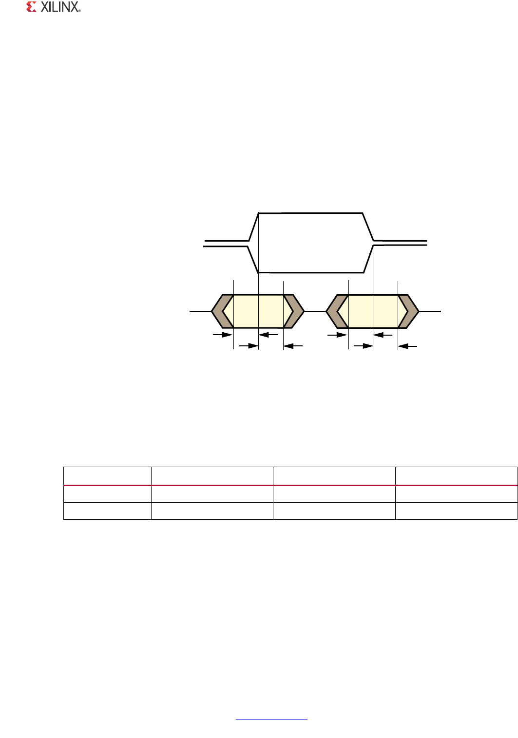
1000BASE-X PCS/PMA or SGMII v11.4 www.xilinx.com 406
PG047 October 16, 2012
Chapter 18: Constraining the Core
INST "loc_ref" IOSTANDARD = LVTTL;
INST "ewrap" IOSTANDARD = LVTTL;
INST "en_cdet" IOSTANDARD = LVTTL;
In addition, the example design provides pad locking on the TBI for several families. This is
included as a guideline only, and there are no specific I/O location constraints for this core.
TBI Input Setup/Hold Timing
Input TBI Timing Specification
Figure 18-1 and Table 18-1 illustrate the setup and hold time window for the input TBI
signals. These specify the worst-case data valid window presented to the FPGA pins. There
is only a 2 ns data valid window of guaranteed data presented across the TBI input bus. This
must be correctly sampled by the FPGA devices.
Spartan-3, Spartan-3E, and Spartan-3A Devices
Figure 4-3 illustrates the TBI input logic provided by the example design for the Spartan-3
class family. DCMs are used on the pma_rx_clk0 and pma_rx_clk1 clock paths as
illustrated. Phase-shifting is then applied to the DCMs to align the resultant clocks so that
they correctly sample the 2 ns TBI data valid window at the input DDR flip-flops.
X-Ref Target - Figure 18-1
Figure 18-1: Input TBI timing
Table 18-1: Input TBI Timing
Symbol Min Max Units
tSETUP 2.00 - ns
tHOLD 0.00 - ns
T3%450
T(/,$
RX?CODE?GROUP;=
0-!?28?#,+
T3%450T(/,$
0-!?28?#,+
8

1000BASE-X PCS/PMA or SGMII v11.4 www.xilinx.com 407
PG047 October 16, 2012
Chapter 18: Constraining the Core
The fixed phase shift is applied to the DCMs using the following UCF syntax.
INST "core_wrapper/tbi_rx_clk0_dcm" CLKOUT_PHASE_SHIFT = FIXED;
INST "core_wrapper/tbi_rx_clk0_dcm" PHASE_SHIFT = -10;
INST "core_wrapper/tbi_rx_clk0_dcm" DESKEW_ADJUST = 0;
INST "core_wrapper/tbi_rx_clk1_dcm" CLKOUT_PHASE_SHIFT = FIXED;
INST "core_wrapper/tbi_rx_clk1_dcm" PHASE_SHIFT = -10;
INST "core_wrapper/tbi_rx_clk1_dcm" DESKEW_ADJUST = 0;
The values of PHASE_SHIFT are preconfigured in the example designs to meet the setup and
hold constraints for the example TBI pinout in the particular device. The setup/hold timing
which is achieved after place-and-route is reported in the data sheet section of the Trace
(TRCE) report (created by the implement script).
For customers fixing their own pinout, the setup and hold figures reported in the TRCE
report can be used to initially setup the approximate DCM phase shift values. Appendix F,
Calculating the DCM Fixed Phase Shift or IODelay Tap Setting, describes a more accurate
method for fixing the phase shift by using hardware measurement of a unique PCB design.
Virtex-4 Devices
Figure 4-3 illustrates the TBI input logic provided by the example design for the Virtex-4
devices. A DCM is used on the pma_rx_clk0 clock path as illustrated. Phase-shifting is
then applied to the DCM to align the resultant clock so it correctly samples the 2 ns TBI data
valid window at the input DDR flip-flops.
The fixed phase shift is applied to the DCM using the following UCF syntax.
INST "core_wrapper/tbi_rx_clk0_dcm" CLKOUT_PHASE_SHIFT = FIXED;
INST "core_wrapper/tbi_rx_clk0_dcm" PHASE_SHIFT = -35;
INST "core_wrapper/tbi_rx_clk0_dcm" DESKEW_ADJUST = 0;
The value of PHASE_SHIFT is preconfigured in the example designs to meet the setup and
hold constraints for the example TBI pinout in the particular device. The setup/hold timing
which is achieved after place-and-route is reported in the data sheet section of the TRCE
report (created by the implement script).
For customers fixing their own pinout, the setup and hold figures reported in the TRCE
report can be used to initially setup the approximate DCM phase shift values. Appendix F,
Calculating the DCM Fixed Phase Shift or IODelay Tap Setting describes a more accurate
method for fixing the phase shift by using hardware measurement of a unique PCB design.

1000BASE-X PCS/PMA or SGMII v11.4 www.xilinx.com 408
PG047 October 16, 2012
Chapter 18: Constraining the Core
In addition, for Virtex-4 FPGA designs, the following UCF syntax is included:
#-----------------------------------------------------------
# To check (analyze) TBI Rx Input Setup/Hold Timing -
#-----------------------------------------------------------
NET "rx_code_group<?>" OFFSET = IN 2 ns VALID 2 ns BEFORE "pma_rx_clk0" RISING;
NET "rx_code_group<?>" OFFSET = IN 2 ns VALID 2 ns BEFORE "pma_rx_clk0" FALLING;
This syntax causes the Xilinx implementation tools to analyze the input setup and hold
constraints for the input TBI bus. If these constraints are not met, the tools do report timing
errors. However, the tools do not attempt to automatically correct the timing in the case of
failure. These must be corrected manually by changing the DCM PHASE_SHIFT value in the
UCF.
Virtex-5 Devices
Figure 4-7 illustrates the TBI input logic provided by the example design for the Virtex-5
devices. IODELAY elements are instantiated on the TBI data input path as illustrated. Fixed
tap delays are applied to these IODELAY elements to delay the rx_code_group[9:0] bus
so that data is correctly sampled at the IOB IDDR registers, thereby meeting TBI input setup
and hold timing constraints.
The number of tap delays are applied using the following UCF syntax.
#-----------------------------------------------------------
# To Adjust TBI Rx Input Setup/Hold Timing
#-----------------------------------------------------------
INST "core_wrapper/tbi_rx_data_bus[9].delay_tbi_rx_data" IDELAY_VALUE = "20";
INST "core_wrapper/tbi_rx_data_bus[8].delay_tbi_rx_data" IDELAY_VALUE = "20";
INST "core_wrapper/tbi_rx_data_bus[7].delay_tbi_rx_data" IDELAY_VALUE = "20";
INST "core_wrapper/tbi_rx_data_bus[6].delay_tbi_rx_data" IDELAY_VALUE = "20";
INST "core_wrapper/tbi_rx_data_bus[5].delay_tbi_rx_data" IDELAY_VALUE = "20";
INST "core_wrapper/tbi_rx_data_bus[4].delay_tbi_rx_data" IDELAY_VALUE = "20";
INST "core_wrapper/tbi_rx_data_bus[3].delay_tbi_rx_data" IDELAY_VALUE = "20";
INST "core_wrapper/tbi_rx_data_bus[2].delay_tbi_rx_data" IDELAY_VALUE = "20";
INST "core_wrapper/tbi_rx_data_bus[1].delay_tbi_rx_data" IDELAY_VALUE = "20";
INST "core_wrapper/tbi_rx_data_bus[0].delay_tbi_rx_data" IDELAY_VALUE = "20";
The number of tap delays are preconfigured in the example designs to meet the setup and
hold constraints for the example TBI pinout in the particular device. The setup/hold timing
which is achieved after place-and-route is reported in the data sheet section of the TRCE
report (created by the implement script). See Understanding Timing Reports for Setup/Hold
Timing.

1000BASE-X PCS/PMA or SGMII v11.4 www.xilinx.com 409
PG047 October 16, 2012
Chapter 18: Constraining the Core
In addition, for Virtex-5 FPGA designs, the following UCF syntax is included:
#-----------------------------------------------------------
# To check (analyze) TBI Rx Input Setup/Hold Timing -
#-----------------------------------------------------------
NET "rx_code_group<?>" OFFSET = IN 2 ns VALID 2 ns BEFORE "pma_rx_clk0" RISING;
NET "rx_code_group<?>" OFFSET = IN 2 ns VALID 2 ns BEFORE "pma_rx_clk0" FALLING;
This syntax causes the Xilinx implementation tools to analyze the input setup and hold
constraints for the input TBI bus. If these constraints are not met, the tools do report timing
errors. However, the tools do not attempt to automatically correct the timing in the case of
failure. These must be corrected manually by changing the number of tap delays for the
IODELAY elements in the UCF.
Kintex-7 and Virtex-6 Devices
Figure 4-9 illustrates the TBI input logic provided by the example design for the Kintex-7
and Virtex-6 devices. IODELAY elements are instantiated on the TBI data input path as
illustrated. Fixed tap delays are applied to these IODELAY elements to delay the
rx_code_group[9:0] bus so that data is correctly sampled at the IOB IDDR registers,
thereby meeting TBI input setup and hold timing constraints.
The number of tap delays are applied using the following UCF syntax.
#-----------------------------------------------------------
# To Adjust TBI Rx Input Setup/Hold Timing
#-----------------------------------------------------------
INST "core_wrapper/tbi_rx_data_bus[9].delay_tbi_rx_data" IDELAY_VALUE = "5";
INST "core_wrapper/tbi_rx_data_bus[8].delay_tbi_rx_data" IDELAY_VALUE = "5";
INST "core_wrapper/tbi_rx_data_bus[7].delay_tbi_rx_data" IDELAY_VALUE = "5";
INST "core_wrapper/tbi_rx_data_bus[6].delay_tbi_rx_data" IDELAY_VALUE = "5";
INST "core_wrapper/tbi_rx_data_bus[5].delay_tbi_rx_data" IDELAY_VALUE = "5";
INST "core_wrapper/tbi_rx_data_bus[4].delay_tbi_rx_data" IDELAY_VALUE = "5";
INST "core_wrapper/tbi_rx_data_bus[3].delay_tbi_rx_data" IDELAY_VALUE = "5";
INST "core_wrapper/tbi_rx_data_bus[2].delay_tbi_rx_data" IDELAY_VALUE = "5";
INST "core_wrapper/tbi_rx_data_bus[1].delay_tbi_rx_data" IDELAY_VALUE = "5";
INST "core_wrapper/tbi_rx_data_bus[0].delay_tbi_rx_data" IDELAY_VALUE = "5";
The number of tap delays are preconfigured in the example designs to meet the setup and
hold constraints for the example TBI pinout in the particular device. The setup/hold timing,
which is achieved after place-and-route, is reported in the data sheet section of the TRCE
report (created by the implement script). See Understanding Timing Reports for Setup/Hold
Timing.

1000BASE-X PCS/PMA or SGMII v11.4 www.xilinx.com 410
PG047 October 16, 2012
Chapter 18: Constraining the Core
In addition, the following UCF syntax is included:
#-----------------------------------------------------------
# To check (analyze) TBI Rx Input Setup/Hold Timing -
#-----------------------------------------------------------
NET "rx_code_group<?>" OFFSET = IN 2 ns VALID 2 ns BEFORE "pma_rx_clk0" RISING;
NET "rx_code_group<?>" OFFSET = IN 2 ns VALID 2 ns BEFORE "pma_rx_clk0" FALLING;
This syntax causes the Xilinx implementation tools to analyze the input setup and hold
constraints for the input TBI bus. If these constraints are not met, the tools do report timing
errors. However, the tools do not attempt to automatically correct the timing in the case of
failure. These must be corrected manually by changing the number of tap delays for the
IODELAY elements in the UCF.
Spartan-6 Devices
Figure 4-11 illustrates the TBI input logic provided by the example design for the Spartan-6
devices. IODELAY2 elements are instantiated on the TBI data input path as illustrated. Fixed
tap delays are applied to these IODELAY2 elements to delay the rx_code_group[9:0]
bus so that data is correctly sampled at the IOB IDDR registers, thereby meeting TBI input
setup and hold timing constraints.
The number of tap delays are applied using the following UCF syntax.
#-----------------------------------------------------------
# To Adjust TBI Rx Input Setup/Hold Timing
#-----------------------------------------------------------
INST "core_wrapper/tbi_rx_data_bus[9].delay_tbi_rx_data" IDELAY_VALUE = "20";
INST "core_wrapper/tbi_rx_data_bus[8].delay_tbi_rx_data" IDELAY_VALUE = "20";
INST "core_wrapper/tbi_rx_data_bus[7].delay_tbi_rx_data" IDELAY_VALUE = "20";
INST "core_wrapper/tbi_rx_data_bus[6].delay_tbi_rx_data" IDELAY_VALUE = "20";
INST "core_wrapper/tbi_rx_data_bus[5].delay_tbi_rx_data" IDELAY_VALUE = "20";
INST "core_wrapper/tbi_rx_data_bus[4].delay_tbi_rx_data" IDELAY_VALUE = "20";
INST "core_wrapper/tbi_rx_data_bus[3].delay_tbi_rx_data" IDELAY_VALUE = "20";
INST "core_wrapper/tbi_rx_data_bus[2].delay_tbi_rx_data" IDELAY_VALUE = "20";
INST "core_wrapper/tbi_rx_data_bus[1].delay_tbi_rx_data" IDELAY_VALUE = "20";
INST "core_wrapper/tbi_rx_data_bus[0].delay_tbi_rx_data" IDELAY_VALUE = "20";
The number of tap delays are preconfigured in the example designs to meet the setup and
hold constraints for the example TBI pinout in the particular device. The setup/hold timing,
which is achieved after place-and-route, is reported in the data sheet section of the TRCE
report (created by the implement script). See Understanding Timing Reports for Setup/Hold
Timing.

1000BASE-X PCS/PMA or SGMII v11.4 www.xilinx.com 411
PG047 October 16, 2012
Chapter 18: Constraining the Core
In addition, for Spartan-6 FPGA designs, the following UCF syntax is included:
#-----------------------------------------------------------
# To check (analyze) TBI Rx Input Setup/Hold Timing -
#-----------------------------------------------------------
NET "rx_code_group<?>" OFFSET = IN 2 ns VALID 2 ns BEFORE "pma_rx_clk0" RISING;
NET "rx_code_group<?>" OFFSET = IN 2 ns VALID 2 ns BEFORE "pma_rx_clk0" FALLING;
This syntax causes the Xilinx implementation tools to analyze the input setup and hold
constraints for the input TBI bus. If these constraints are not met then the tools do report
timing errors. However, the tools do not attempt to automatically correct the timing in the
case of failure. These must be corrected manually by changing the number of tap delays for
the IODELAY elements in the UCF.
Constraints When Implementing an External
GMII
The constraints defined in this section are implemented in the UCF for the example designs
delivered with the core. Sections from this UCF have been copied into the following
examples and should be studied in conjunction with the HDL source code for the example
design. See also Appendix E, Implementing External GMII.
Clock Period Constraints
When implementing an external GMII, the Transmitter Elastic Buffer delivered with the
example design (or similar logic) must be used. The input transmitter GMII signals are then
synchronous to their own clock domain (gmii_tx_clk is used in the example design). This
clock must be constrained for a clock frequency of 125 MHz. The following UCF syntax
shows the necessary constraints being applied to the example design.
############################################################
# GMII Clock period Constraints: do not relax #
############################################################
NET "gmii_tx_clk_bufg" TNM_NET = "gmii_tx_clk";
TIMESPEC "ts_gmii_tx_clk" = PERIOD "gmii_tx_clk" 8000 ps HIGH 50 %;

1000BASE-X PCS/PMA or SGMII v11.4 www.xilinx.com 412
PG047 October 16, 2012
Chapter 18: Constraining the Core
GMII IOB Constraints
The following constraints target the flip-flops that are inferred in the top level HDL file for
the example design. Constraints are set to ensure that these are placed in IOBs.
############################################################
# GMII Transmitter Constraints: place flip-flops in IOB #
############################################################
INST "gmii_txd*" IOB = true;
INST "gmii_tx_en" IOB = true;
INST "gmii_tx_er" IOB = true;
############################################################
# GMII Receiver Constraints: place flip-flops in IOB #
############################################################
INST "gmii_rxd_obuf*" IOB = true;
INST "gmii_rx_dv_obuf" IOB = true;
INST "gmii_rx_er_obuf" IOB = true;
Virtex-7 devices support GMII at 3.3 V or lower only in certain parts and packages; see the
Virtex-7 Device Documentation. Virtex-6 devices support GMII at 2.5 V only and the device
default SelectIO technology standard of LVCMOS25 is used. See the Virtex-6 FPGA Data
Sheet: DC and Switching Characteristics for more information. In Virtex-5, Virtex-4,
Spartan-6 and Spartan-3 devices, GMII by default is supported at 3.3 V and the UCF
contains the following syntax. Use this syntax together with the device I/O Banking rules.
INST "gmii_txd<?>" IOSTANDARD = LVTTL;
INST "gmii_tx_en" IOSTANDARD = LVTTL;
INST "gmii_tx_er" IOSTANDARD = LVTTL;
INST "gmii_rxd<?>" IOSTANDARD = LVTTL;
INST "gmii_rx_dv" IOSTANDARD = LVTTL;
INST "gmii_rx_er" IOSTANDARD = LVTTL;
INST "gmii_tx_clk" IOSTANDARD = LVTTL;
INST "gmii_rx_clk" IOSTANDARD = LVTTL;
In addition, the example design provides pad locking on the GMII for several families. This
is a provided as a guideline only; there are no specific I/O location constraints for this core.
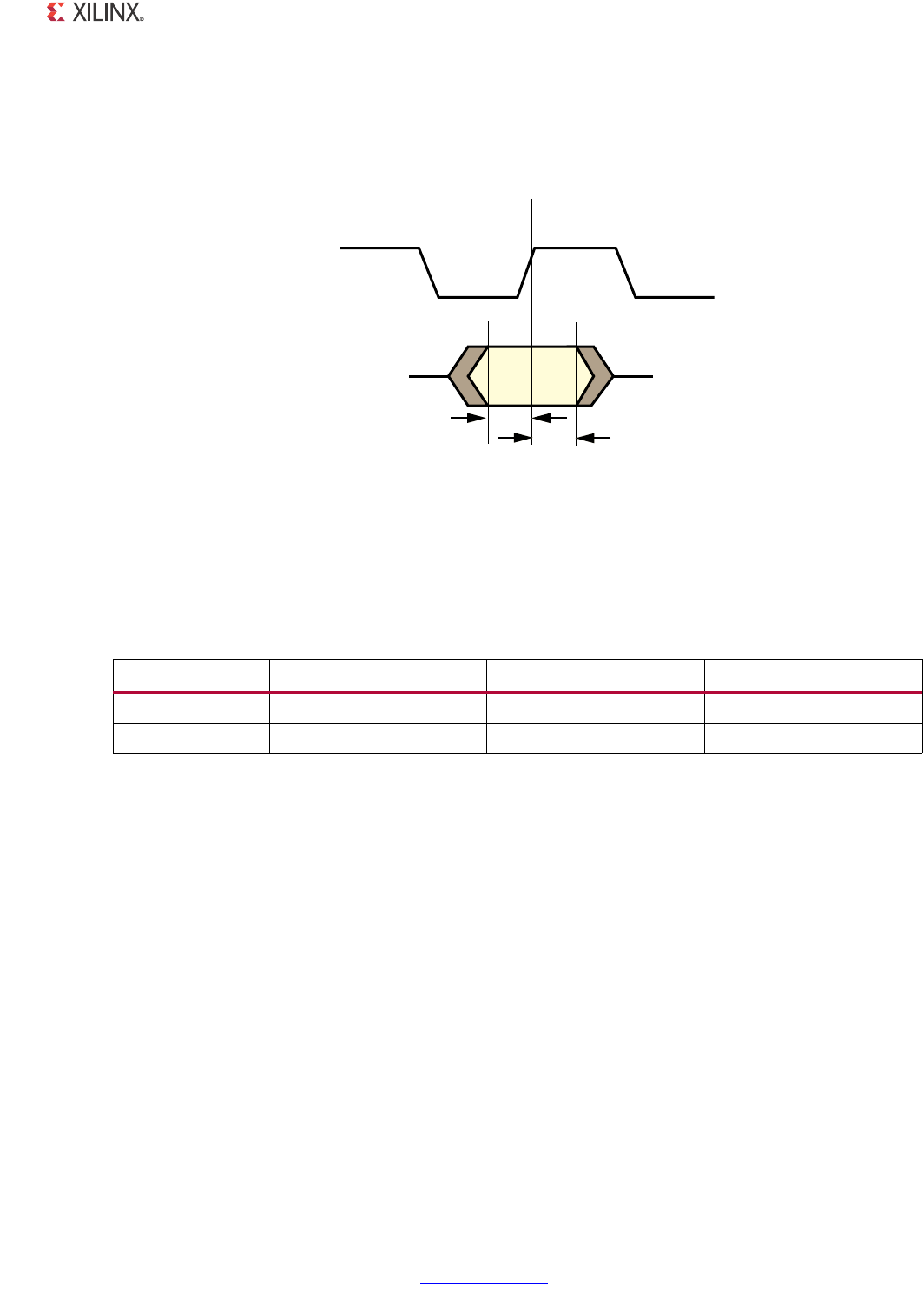
1000BASE-X PCS/PMA or SGMII v11.4 www.xilinx.com 413
PG047 October 16, 2012
Chapter 18: Constraining the Core
GMII Input Setup/Hold Timing
Input GMII Timing Specification
Figure 18-2 and Table 18-2 illustrate the setup and hold time window for the input GMII
signals. These are the worst-case data valid window presented to the FPGA pins.
Observe that there is, in total, a 2 ns data valid window of guaranteed data which is
presented across the GMII input bus. This must be correctly sampled by the FPGA devices.
Spartan-3, Spartan-3E, and Spartan-3A Devices
Figure E-1 illustrates the GMII input logic which is provided by the example design for the
Spartan-3 devices. A DCM must be used on the gmii_tx_clk clock path as illustrated.
Phase-shifting is then applied to the DCM to align the resultant clock so that it correctly
samples the 2 ns GMII data valid window at the input flip-flops.
The fixed phase shift is applied to the DCM using the following UCF syntax.
INST "gmii_tx_dcm" CLKOUT_PHASE_SHIFT = FIXED;
INST "gmii_tx_dcm" PHASE_SHIFT = -20;
INST "gmii_tx_dcm" DESKEW_ADJUST = 0;
The value of PHASE_SHIFT is preconfigured in the example designs to meet the setup and
hold constraints for the example GMII pinout in the particular device. The setup/hold timing
which is achieved after place-and-route is reported in the data sheet section of the TRCE
report (created by the implement script).
X-Ref Target - Figure 18-2
Figure 18-2: Input GMII Timing
Table 18-2: Input GMII Timing
Symbol Min Max Units
tSETUP 2.00 - ns
tHOLD 0.00 - ns
T
3%450
T
(/,$
'-))?48$;=
'-))?48?%.
'-))?48?%2
'-))?48?#,+
8

1000BASE-X PCS/PMA or SGMII v11.4 www.xilinx.com 414
PG047 October 16, 2012
Chapter 18: Constraining the Core
For customers fixing their own pinout, the setup and hold figures reported in the TRCE
report can be used to initially setup the approximate DCM phase shift. Appendix F,
Calculating the DCM Fixed Phase Shift or IODelay Tap Setting, describes a more accurate
method for fixing the phase shift by using hardware measurement of a unique PCB design.
Virtex-4 Devices
Figure E-1 illustrates the GMII input logic provided by the example design for the Virtex-4
devices. A DCM must be used on the gmii_tx_clk clock path as illustrated. Phase-shifting
is then applied to the DCM to align the resultant clock so that it correctly samples the 2 ns
GMII data valid window at the input flip-flops.
The fixed phase shift is applied to the DCM using the following UCF syntax.
INST "gmii_tx_dcm" CLKOUT_PHASE_SHIFT = FIXED;
INST "gmii_tx_dcm" PHASE_SHIFT = -20;
INST "gmii_tx_dcm" DESKEW_ADJUST = 0;
The value of PHASE_SHIFT is preconfigured in the example designs to meet the setup and
hold constraints for the example GMII pinout in the particular device. The setup/hold timing
which is achieved after place-and-route is reported in the data sheet section of the TRCE
report (created by the implement script).
For customers fixing their own pinout, the setup and hold figures reported in the TRCE
report can be used to initially setup the approximate DCM phase shift. Appendix F,
Calculating the DCM Fixed Phase Shift or IODelay Tap Setting, describes a more accurate
method for fixing the phase shift by using hardware measurement of a unique PCB design.
In addition, for Virtex-4 FPGA designs, the following UCF syntax is included:
#-----------------------------------------------------------
# To check (analyze) GMII Tx Input Setup/Hold Timing -
#-----------------------------------------------------------
INST "gmii_txd*" TNM = IN_GMII;
INST "gmii_tx_en" TNM = IN_GMII;
INST "gmii_tx_er" TNM = IN_GMII;
TIMEGRP "IN_GMII" OFFSET = IN 2 ns VALID 2 ns BEFORE "gmii_tx_clk";
This syntax causes the Xilinx implementation tools to analyze the input setup and hold
constraints for the input GMII bus. If these constraints are not met, the tools do report
timing errors. However, the tools do not attempt to automatically correct the timing in the
case of failure. These must be corrected manually by changing the DCM PHASE_SHIFT value
in the UCF.

1000BASE-X PCS/PMA or SGMII v11.4 www.xilinx.com 415
PG047 October 16, 2012
Chapter 18: Constraining the Core
Virtex-5 Devices
Figure E-2 illustrates the GMII input logic provided by the example design for the Virtex-5
devices. IODELAY elements are instantiated on the GMII data input path as illustrated. Fixed
tap delays are applied to these IODELAY elements to delay the GMII input data signals so
that data is correctly sampled at the IOB IDDR registers, thereby meeting GMII input setup
and hold timing constraints.
The number of tap delays are applied using the following UCF syntax.
#-----------------------------------------------------------
# To Adjust GMII Tx Input Setup/Hold Timing -
#-----------------------------------------------------------
INST "delay_gmii_tx_en" IDELAY_VALUE = "20";
INST "delay_gmii_tx_er" IDELAY_VALUE = "20";
INST "gmii_data_bus[7].delay_gmii_txd" IDELAY_VALUE = "20";
INST "gmii_data_bus[6].delay_gmii_txd" IDELAY_VALUE = "20";
INST "gmii_data_bus[5].delay_gmii_txd" IDELAY_VALUE = "20";
INST "gmii_data_bus[4].delay_gmii_txd" IDELAY_VALUE = "20";
INST "gmii_data_bus[3].delay_gmii_txd" IDELAY_VALUE = "20";
INST "gmii_data_bus[2].delay_gmii_txd" IDELAY_VALUE = "20";
INST "gmii_data_bus[1].delay_gmii_txd" IDELAY_VALUE = "20";
INST "gmii_data_bus[0].delay_gmii_txd" IDELAY_VALUE = "20";
The number of tap delays are preconfigured in the example designs to meet the setup and
hold constraints for the example GMII pinout in the particular device. The setup/hold timing
which is achieved after place-and-route is reported in the data sheet section of the TRCE
report (created by the implement script). See Understanding Timing Reports for Setup/Hold
Timing.
In addition, for Virtex-5 FPGA designs, the following UCF syntax is included:
#-----------------------------------------------------------
# To check (analyze) GMII Tx Input Setup/Hold Timing -
#-----------------------------------------------------------
INST "gmii_txd*" TNM = IN_GMII;
INST "gmii_tx_en" TNM = IN_GMII;
INST "gmii_tx_er" TNM = IN_GMII;
TIMEGRP "IN_GMII" OFFSET = IN 2 ns VALID 2 ns BEFORE "gmii_tx_clk";

1000BASE-X PCS/PMA or SGMII v11.4 www.xilinx.com 416
PG047 October 16, 2012
Chapter 18: Constraining the Core
This syntax causes the Xilinx implementation tools to analyze the input setup and hold
constraints for the input GMII bus. If these constraints are not met, the tools do report
timing errors. However, the tools do not attempt to automatically correct the timing in the
case of failure. These must be corrected manually by changing the number of tap delays for
the IODELAY elements in the UCF.
Zynq-7000, Virtex-7, Kintex-7, Artix-7, and Virtex-6 Devices
Figure E-2 illustrates the GMII input logic provided by the example design for the
Zynq-7000, Virtex-7, Kintex-7, Artix-7 and Virtex-6 devices. IODELAY elements are
instantiated on the GMII data input path as illustrated. Fixed tap delays are applied to these
IODELAY elements to delay the GMII input data signals so that data is correctly sampled at
the IOB IDDR registers, thereby meeting GMII input setup and hold timing constraints.
The number of tap delays are applied using the following UCF syntax.
#-----------------------------------------------------------
# To Adjust GMII Tx Input Setup/Hold Timing -
#-----------------------------------------------------------
INST "delay_gmii_tx_en" IDELAY_VALUE = "5";
INST "delay_gmii_tx_er" IDELAY_VALUE = "5";
INST "gmii_data_bus[7].delay_gmii_txd" IDELAY_VALUE = "5";
INST "gmii_data_bus[6].delay_gmii_txd" IDELAY_VALUE = "5";
INST "gmii_data_bus[5].delay_gmii_txd" IDELAY_VALUE = "5";
INST "gmii_data_bus[4].delay_gmii_txd" IDELAY_VALUE = "5";
INST "gmii_data_bus[3].delay_gmii_txd" IDELAY_VALUE = "5";
INST "gmii_data_bus[2].delay_gmii_txd" IDELAY_VALUE = "5";
INST "gmii_data_bus[1].delay_gmii_txd" IDELAY_VALUE = "5";
INST "gmii_data_bus[0].delay_gmii_txd" IDELAY_VALUE = "5";
The number of tap delays are preconfigured in the example designs to meet the setup and
hold constraints for the example GMII pinout in the particular device. The setup/hold
timing, which is achieved after place-and-route, is reported in the data sheet section of the
TRCE report (created by the implement script). See Understanding Timing Reports for
Setup/Hold Timing.
In addition, the following UCF syntax is included:
#-----------------------------------------------------------
# To check (analyze) GMII Tx Input Setup/Hold Timing -
#-----------------------------------------------------------
INST "gmii_txd*" TNM = IN_GMII;
INST "gmii_tx_en" TNM = IN_GMII;
INST "gmii_tx_er" TNM = IN_GMII;
TIMEGRP "IN_GMII" OFFSET = IN 2 ns VALID 2 ns BEFORE "gmii_tx_clk";

1000BASE-X PCS/PMA or SGMII v11.4 www.xilinx.com 417
PG047 October 16, 2012
Chapter 18: Constraining the Core
This syntax causes the Xilinx implementation tools to analyze the input setup and hold
constraints for the input GMII bus. If these constraints are not met then the tools do report
timing errors. However, the tools do not attempt to automatically correct the timing in the
case of failure. These must be corrected manually by changing the number of tap delays for
the IODELAY elements in the UCF.
Spartan-6 Devices
Figure E-3 illustrates the GMII input logic provided by the example design for the Spartan-6
devices. IODELAY2 elements are instantiated on the GMII data input path as illustrated.
Fixed tap delays are applied to these IODELAY2 elements to delay the GMII input data
signals so that data is correctly sampled at the IOB IDDR registers, thereby meeting GMII
input setup and hold timing constraints.
The number of tap delays are applied using the following UCF syntax.
#-----------------------------------------------------------
# To Adjust GMII Tx Input Setup/Hold Timing -
#-----------------------------------------------------------
INST "delay_gmii_tx_en" IDELAY_VALUE = "10";
INST "delay_gmii_tx_er" IDELAY_VALUE = "10";
INST "gmii_data_bus[7].delay_gmii_txd" IDELAY_VALUE = "10";
INST "gmii_data_bus[6].delay_gmii_txd" IDELAY_VALUE = "10";
INST "gmii_data_bus[5].delay_gmii_txd" IDELAY_VALUE = "10";
INST "gmii_data_bus[4].delay_gmii_txd" IDELAY_VALUE = "10";
INST "gmii_data_bus[3].delay_gmii_txd" IDELAY_VALUE = "10";
INST "gmii_data_bus[2].delay_gmii_txd" IDELAY_VALUE = "10";
INST "gmii_data_bus[1].delay_gmii_txd" IDELAY_VALUE = "10";
INST "gmii_data_bus[0].delay_gmii_txd" IDELAY_VALUE = "10";
The number of tap delays are preconfigured in the example designs to meet the setup and
hold constraints for the example GMII pinout in the particular device. The setup/hold timing
which is achieved after place-and-route is reported in the data sheet section of the TRCE
report (created by the implement script). See Understanding Timing Reports for Setup/Hold
Timing.
In addition, for Spartan-6 FPGA designs, the following UCF syntax is included:
#-----------------------------------------------------------
# To check (analyze) GMII Tx Input Setup/Hold Timing -
#-----------------------------------------------------------
INST "gmii_txd*" TNM = IN_GMII;
INST "gmii_tx_en" TNM = IN_GMII;
INST "gmii_tx_er" TNM = IN_GMII;
TIMEGRP "IN_GMII" OFFSET = IN 2 ns VALID 2 ns BEFORE "gmii_tx_clk";

1000BASE-X PCS/PMA or SGMII v11.4 www.xilinx.com 418
PG047 October 16, 2012
Chapter 18: Constraining the Core
This syntax causes the Xilinx implementation tools to analyze the input setup and hold
constraints for the input GMII bus. If these constraints are not met then the tools do report
timing errors. However, the tools do not attempt to automatically correct the timing in the
case of failure. These must be corrected manually by changing the number of tap delays for
the IODELAY elements in the UCF.
Understanding Timing Reports for Setup/Hold
Timing
Setup and Hold results for the TBI or GMII input buses for the following devices are defined
in the Data Sheet Report section of the Timing Report. The results are self-explanatory and
show an obvious correlation and relationship to Figure 18-1 and Figure 18-2.
The following example shows the GMII report from a Spartan-3A DSP device. The
implementation requires 1.531 ns of setup (this is less than the 2 ns required, to allow for
slack). The implementation requires -0.125 ns of hold (this is less than the 0 ns required, to
allow for slack).
Data Sheet report:
-----------------
All values displayed in nanoseconds (ns)
w
Setup/Hold to clock gmii_tx_clk
------------+------------+------------+------------------+--------+
| Setup to | Hold to | | Clock |
Source | clk (edge) | clk (edge) |Internal Clock(s) | Phase |
------------+------------+------------+------------------+--------+
gmii_tx_en | 1.531(R)| -0.141(R)|gmii_tx_clk_bufg | 0.000|
gmii_tx_er | 1.531(R)| -0.141(R)|gmii_tx_clk_bufg | 0.000|
gmii_txd<0> | 1.531(R)| -0.141(R)|gmii_tx_clk_bufg | 0.000|
gmii_txd<1> | 1.525(R)| -0.135(R)|gmii_tx_clk_bufg | 0.000|
gmii_txd<2> | 1.531(R)| -0.141(R)|gmii_tx_clk_bufg | 0.000|
gmii_txd<3> | 1.525(R)| -0.135(R)|gmii_tx_clk_bufg | 0.000|
gmii_txd<4> | 1.515(R)| -0.125(R)|gmii_tx_clk_bufg | 0.000|
gmii_txd<5> | 1.515(R)| -0.125(R)|gmii_tx_clk_bufg | 0.000|
gmii_txd<6> | 1.520(R)| -0.130(R)|gmii_tx_clk_bufg | 0.000|
gmii_txd<7> | 1.520(R)| -0.130(R)|gmii_tx_clk_bufg | 0.000|
------------+------------+------------+------------------+---------

1000BASE-X PCS/PMA or SGMII v11.4 www.xilinx.com 419
PG047 October 16, 2012
Chapter 19
Implementing the Design
This chapter describes how to simulate and implement your design containing the Ethernet
1000BASE-X PCS/PMA or SGMII core in the ISE® Design Suite.
Pre-implementation Simulation
A functional model of the Ethernet 1000BASE-X PCS/PMA or SGMII core netlist is generated
by the CORE Generator™ tool to allow simulation of the core in the design phase of the
project.
Using the Simulation Model
For information about setting up your simulator to use the pre-implemented model,
consult the Xilinx Synthesis and Verification Design Guide, included in your Xilinx software
installation.
The model is provided in the CORE Generator tool project directory.
VHDL Design Entry
<component_name>.vhd
Verilog Design Entry
<component_name>.v
This model can be compiled along with your code to simulate the overall system.

1000BASE-X PCS/PMA or SGMII v11.4 www.xilinx.com 420
PG047 October 16, 2012
Chapter 19: Implementing the Design
Synthesis
XST - VHDL
In the CORE Generator tool project directory, there is a <component_name>.vho file that is
a component and instantiation template for the core. Use this to help instance the Ethernet
1000BASE-X PCS/PMA or SGMII core into your VHDL source.
After the entire design is complete, create the following:
• An XST project file top_level_module_name.prj listing all the user source code files
• An XST script file top_level_module_name.scr containing your required synthesis
options.
To synthesize the design, run
$ xst -ifn top_level_module_name.scr
See the XST User Guide for more information on creating project and synthesis script files,
and running the xst program.
XST - Verilog
There is a module declaration for the Ethernet 1000BASE-X PCS/PMA or SGMII core in the
CORE Generator tool project directory:
<component_name>/implement/<component_name>_mod.v
Use this module to help instance the Ethernet 1000BASE-X PCS/PMA or SGMII core into
your Verilog source.
After the entire design is complete, do the following:
• Generate an XST project file top_level_module_name.prj listing all user source
code files.
Make sure to include the following as the first two files in the project list.
%XILINX%/verilog/src/iSE/unisim_comp.v
and
<component_name>/implement/component_name_mod.v
• Generate an XST script file top_level_module_name.scr containing your required
synthesis options.

1000BASE-X PCS/PMA or SGMII v11.4 www.xilinx.com 421
PG047 October 16, 2012
Chapter 19: Implementing the Design
To synthesize the design, run:
$ xst -ifn top_level_module_name.scr
See the XST User Guide for more information on creating project and synthesis script files,
and running the xst program.
Implementation
Generating the Xilinx Netlist
To generate the Xilinx netlist, the ngdbuild tool is used to translate and merge the
individual design netlists into a single design database—the NGD file. Also merged at this
stage is the UCF for the design. An example of the ngdbuild command is:
$ ngdbuild -sd path_to_core_netlist -sd path_to_user_synth_results \
-uc top_level_module_name.ucf top_level_module_name
Mapping the Design
To map the logic gates of the user design netlist into the Configurable Logic Blocks (CLBs)
and IOBs of the FPGA, run the map command. The map command writes out a physical
design to an Native Circuit Description (NCD) file. An example of the map command is:
$ map -o top_level_module_name_map.ncd top_level_module_name.ngd \
top_level_module_name.pcf
Placing and Routing the Design
The par command must be executed to place and route your design logic components
(mapped physical logic cells) within an NCD file, in accordance with the layout and timing
requirements specified within the Physical Constraints File (PCF) file. The par command
outputs the placed and routed physical design to an NCD file.
An example of the par command is:
$ par top_level_module_name_map.ncd top_level_module_name.ncd \
top_level_module_name.pcf
Static Timing Analysis
The trce command must be executed to evaluate timing closure on a design and create a
Timing Report file (TWR) that is derived from static timing analysis of the Physical Design
file (NCD). The analysis is typically based on constraints included in the optional PCF file.

1000BASE-X PCS/PMA or SGMII v11.4 www.xilinx.com 422
PG047 October 16, 2012
Chapter 19: Implementing the Design
An example of the trce command is:
$ trce -o top_level_module_name.twr top_level_module_name.ncd \
top_level_module_name.pcf
Generating a Bitstream
The bitgen command must be executed to create the configuration bitstream (BIT) file
based on the contents of a physical implementation file (NCD). The BIT file defines the
behavior of the programmed FPGA.
An example of the bitgen command is:
$ bitgen -w top_level_module_name.ncd
Post-Implementation Simulation
The purpose of post-implementation simulation is to verify that the design as implemented
in the FPGA works as expected.
Generating a Simulation Model
To generate a chip-level simulation netlist for your design, the netgen command must be
run.
VHDL
$ netgen -sim -ofmt vhdl -ngm top_level_module_name_map.ngm \
-tm netlist top_level_module_name.ncd \
top_level_module_name_postimp.vhd
Verilog
$ netgen -sim -ofmt verilog -ngm top_level_module_name_map.ngm \
-tm netlist top_level_module_name.ncd \
top_level_module_name_postimp.v
Using the Model
For information about setting up your simulator to use the pre-implemented model,
consult the Xilinx Synthesis and Verification Design Guide, included in your Xilinx software
installation.
In addition, use the following guidelines to determine the simulator type required.

1000BASE-X PCS/PMA or SGMII v11.4 www.xilinx.com 423
PG047 October 16, 2012
Chapter 19: Implementing the Design
Designs incorporating a device-specific transceiver require a Verilog LRM-IEEE 1364-2005
encryption-compliant simulator. Currently supported simulators are:
• Mentor Graphics ModelSim v6.6d
• Cadence Incisive Enterprise Simulator (IES) v10.2
• Synopsys VCS and VCS MX 2010.06
For VHDL simulation, a mixed HDL license is required.
Other Implementation Information
For more information about using the Xilinx implementation tool flow, including command
line switches and options, consult the software manuals provided with the Xilinx® ISE®
Design Suite.

1000BASE-X PCS/PMA or SGMII v11.4 www.xilinx.com 424
PG047 October 16, 2012
Chapter 20
Detailed Example Design
This chapter contains information about the provided example design in the ISE® Design
Suite environment. The chapter provides detailed information about the deliverables
provided by the CORE Generator™ tool for the Ethernet 1000BASE-X PCS/PMA or SGMII
core. The chapter begins with a directory and file list description for the deliverables,
followed by an overview of the purpose and contents of the provided scripts.
Deliverables for the core include the following:
• The netlist file for the core
• Supporting the CORE Generator tool files
• Release notes and documentation
• Subdirectories containing an HDL example design
• Scripts to run the core through the back-end tools and simulate the core using either
Mentor Graphics ModelSim, Cadence IES, and Synopsys simulators

1000BASE-X PCS/PMA or SGMII v11.4 www.xilinx.com 425
PG047 October 16, 2012
Chapter 20: Detailed Example Design
Directory Structure
top directory link - white text invisible
<project directory>
Top-level project directory; name is user-defined.
<project directory>/<component name>
Core release notes file
<component name>/doc
Product documentation
<component name>/example design
Verilog and VHDL design files
<component name>/implement
Implementation script files
implement/results
Results directory, created after implementation scripts are run, and contains
implement script results
implement/results
Simulation scripts
simulation/functional
Functional simulation files
1000BASE-X PCS/PMA or SGMII v11.4 www.xilinx.com 426
PG047 October 16, 2012
Chapter 20: Detailed Example Design
Directory and File Contents
The core directories and their associated files are defined in the following tables.
<project directory>
The project directory contains all the CORE Generator tool project files.
<project directory>/<component name>
The <component name> directory contains the release notes file provided with the core,
which can include last-minute changes and updates.
Table 20-1: Project Directory
Name Description
<project_dir>
<component_name>.ngc Top-level netlist. This is instantiated by the
Verilog or VHDL example design.
<component_name>.v[hd] Verilog or VHDL simulation model;
UNISIM-based
<component_name>.v{ho|eo} Verilog or VHDL instantiation template for
the core
<component_name>.xco Log file that records the settings used to
generate a core. An XCO file is generated by
the CORE Generator tool for each core that it
creates in the current project directory. An
XCO file can also be used as an input to the
CORE Generator tool.
<component_name>.xcp Similar to the XCO file except that it does
not specify project-specific settings, such as
target architecture and output products
<component_name>_flist.txt List of files delivered with the core
Table 20-2: Component Name Directory
Name Description
<project_dir>/<component_name>
gig_eth_pcs_pma_readme.txt Core release notes file
1000BASE-X PCS/PMA or SGMII v11.4 www.xilinx.com 427
PG047 October 16, 2012
Chapter 20: Detailed Example Design
<component name>/doc
The doc directory contains the PDF documentation provided with the core.
<component name>/example design
The example design directory contains the example design files provided with the core, and
can contain files and subdirectories other than those defined in Table 20-4. For more
information, see one of the following:
•Example Design for 1000BASE-X with Transceivers
•Example Designs for the Ten-Bit Interface (TBI)
•SGMII Example Design / Dynamic Switching Example Design with Ten-Bit Interface
•SGMII Example Design / Dynamic Switching Example Design Using a Transceiver
•Chapter 7, SGMII over LVDS
Table 20-3: Doc Directory
Name Description
<project_dir>/<component_name>/doc
pg047-gig-eth-pcs-pma.pdf Ethernet 1000BASE-X PCS/PMA or SGMII Product
Guide
Table 20-4: Example Design Directory
Name Description
<project_dir>/<component_name>/example_design
sync_block.v[hd] This is a synchronization flip-flop pair, used for
passing signals across a clock domain.
reset_sync.v[hd] This is a reset synchronization module for creating
a synchronous reset output signal from an
asynchronous input.
_example_design.ucf Example User Constraints File (UCF) provided for
the example design
_example_design.v[hd] Top-level file that allows example design to be
implemented in a device as a standalone design.
_block.v[hd] A block-level file that is a useful part of example
design and should be instantiated in all customer
designs.
1000BASE-X PCS/PMA or SGMII v11.4 www.xilinx.com 428
PG047 October 16, 2012
Chapter 20: Detailed Example Design
<component name>/implement
The implement directory contains the core implementation script files.
implement/results
The results directory is created by the implement script, after which the implement script
results are placed in the results directory.
<component name>/simulation
The simulation directory and subdirectories that provide the files necessary to test a Verilog
or VHDL implementation of the example design. For more information, see:
•Example Design for 1000BASE-X with Transceivers
•Example Designs for the Ten-Bit Interface (TBI)
•SGMII Example Design / Dynamic Switching Example Design with Ten-Bit Interface
•SGMII Example Design / Dynamic Switching Example Design Using a Transceiver
•SGMII over LVDS
Table 20-5: Implement Directory
Name Description
<project_dir>/<component_name>/implement
implement.sh Linux shell script that processes the example
design through the Xilinx tool flow. See
Implementation Scripts for more information.
implement.bat Windows batch file that processes the example
design through the Xilinx tool flow. See
Implementation Scripts for more information.
xst.prj XST project file for the example design (VHDL
only); it enumerates all of the VHDL files that need
to be synthesized.
xst.scr Xilinx Synthesis Technology (XST) script file for the
example design
Table 20-6: Results Directory
Name Description
<project_dir>/<component_name>/implement/results
routed.v[hd] Back-annotated SIMPRIM-based model used for
timing simulation
routed.sdf Timing information for simulation

1000BASE-X PCS/PMA or SGMII v11.4 www.xilinx.com 429
PG047 October 16, 2012
Chapter 20: Detailed Example Design
simulation/functional
The functional directory contains functional simulation scripts provided with the core.
Table 20-7: Simulation Directory
Name Description
<project_dir>/<component_name>/simulation
demo_tb.v[hd] Top-level file of the demonstration test bench for
the example design. Instantiates the example
design (the Device Under Test (DUT)), generates
clocks, resets, and test bench control semaphores.
stimulus_tb.v[hd] Creates test bench stimulus in the form of four
Ethernet frames, which are injected into the DUT.
The output from the DUT is also monitored for
errors.
Table 20-8: Functional Directory
Name Description
<project_dir>/<component_name>/simulation/functional
simulate_mti.do ModelSim macro file that compiles Verilog or
VHDL sources and runs the functional simulation to
completion.
wave_mti.do ModelSim macro file that opens a wave window
and adds signals of interest to it. It is called by the
simulate_mti.do macro file.
simulate_ncsim.sh IES script file that compiles the Verilog or VHDL
sources and runs the functional simulation to
completion.
wave_ncsim.sv IES macro file that opens a wave window and adds
signals of interest to it. It is called by the
simulate_ncsim.sh script file.
simulate_vcs.sh VCS script file that compiles the Verilog sources
and runs the functional simulation to completion.
ucli_commands.key This file is sourced by VCS at the start of
simulation; it configures the simulator.
vcs_session.tcl VCS macro file that opens a wave window and adds
signals of interest to it. It is called by the
simulate_vcs.sh script file.

1000BASE-X PCS/PMA or SGMII v11.4 www.xilinx.com 430
PG047 October 16, 2012
Chapter 20: Detailed Example Design
Example Designs
See the following sections for example designs:
•Example Designs for the Ten-Bit Interface (TBI) in Chapter 4
•Example Design for 1000BASE-X with Transceivers in Chapter 5
•SGMII Example Design / Dynamic Switching Example Design Using a Transceiver in
Chapter 6
•Example Design Implementation in Chapter 7
Demonstration Test Bench
See Demonstration Test Bench in Chapter 4.
Implementation Scripts
The implementation script is either a shell script or batch file that processes the example
design through the Xilinx tool flow. It is located at:
Linux
<project_dir>/<component_name>/implement/implement.sh
Windows
<project_dir>/<component_name>/implement/implement.bat
The implement script performs the following steps:
1. The HDL example design files are synthesized using XST.
2. NGDBuild is run to consolidate the core netlist and the example design netlist into the
Native Generic Database (NGD) file containing the entire design.
3. The design is mapped to the target technology.
4. The design is placed-and-routed on the target device.
5. Static timing analysis is performed on the routed design using trce.
6. A bitstream is generated.

1000BASE-X PCS/PMA or SGMII v11.4 www.xilinx.com 431
PG047 October 16, 2012
Chapter 20: Detailed Example Design
7. Netgen runs on the routed design to generate a VHDL or Verilog netlist (as appropriate
for the Design Entry project setting) and timing information in the form of SDF files.
The Xilinx tool flow generates several output and report files. These are saved in the
following directory, which is created by the implement script:
<project_dir>/<component_name>/implement/results
Simulation Scripts
The test script is a ModelSim, IES or VCS macro that automates the simulation of the test
bench and is in the following location:
<project_dir>/<component_name>/simulation/functional/
The test script performs the following tasks:
• Compiles the structural UNISIM simulation model
• Compiles HDL example design source code
• Compiles the demonstration test bench
• Starts a simulation of the test bench
• Opens a Wave window and adds signals of interest (wave_mti.do/wave_ncsim.sv)
• Runs the simulation to completion

1000BASE-X PCS/PMA or SGMII v11.4 www.xilinx.com 432
PG047 October 16, 2012
SECTION IV: APPENDICES
Verification, Compliance, and Interoperability
Migrating
1000BASE-X State Machines
Rx Elastic Buffer Specifications
Implementing External GMII
Calculating the DCM Fixed Phase Shift or
IODelay Tap Setting
Debugging
Additional Resources

1000BASE-X PCS/PMA or SGMII v11.4 www.xilinx.com 433
PG047 October 16, 2012
Appendix A
Verification, Compliance, and
Interoperability
Simulation
A highly parameterizable transaction based test bench was used to test the core. Testing
included the following:
• Register Access
• Loss of Synchronization
• Auto-Negotiation and error handling
• Frame Transmission and error handling
• Frame Reception and error handling
Hardware Testing
The core has been tested on many hardware test platforms at Xilinx to represent different
parameterizations, including the following:
• The core with device-specific transceiver and performing the 1000BASE-X standard was
tested with the Tri-Mode Ethernet MAC core from Xilinx.
This follows the architecture shown in Figure 12-3. A test platform was built around
these cores, including a back-end FIFO capable of performing a simple ping function,
and a test pattern generator. Software running on the embedded PowerPC® processor
was used to provide access to all configuration and status registers. Version 3.0 of this
core was taken to the University of New Hampshire Inter operability Lab (UNH IOL)
where conformance and inter operability testing was performed.
• The core with device-specific transceiver (all supported families) and performing the
SGMII standard was tested with the Tri-speed Ethernet MAC core from Xilinx.

1000BASE-X PCS/PMA or SGMII v11.4 www.xilinx.com 434
PG047 October 16, 2012
Appendix A: Verification, Compliance, and Interoperability
This was connected to an external PHY capable of performing 10BASE-T, 100BASE-T and
1000BASE-T. The system was tested at all three speeds, following the architecture shown
in Figure 12-8 and included the PowerPC® processor based test platform.
Verification
The Ethernet 1000BASE-X PCS/PMA or SGMII core has been verified with extensive
simulation and hardware verification.


1000BASE-X PCS/PMA or SGMII v11.4 www.xilinx.com 436
PG047 October 16, 2012
Appendix C
1000BASE-X State Machines
This appendix is intended to serve as a reference for the basic operation of the
1000BASE-X IEEE 802.3-2008 clause 36 transmitter and receiver state machines.
Introduction
Table C-1 illustrates the Ordered Sets defined in IEEE 802.3-2008 clause 36. These code
group characters are inserted by the PCS Transmit Engine into the transmitted data stream,
encapsulating the Ethernet frames indicated by the GMII transmit signals.
The PCS Receive Engine performs the opposite function; it uses the Ordered Sets to detect
the Ethernet frames and from them creates the GMII receive signals.
Cross reference Table C-1 with the remainder of this Appendix. See IEEE 802.3-2008 clause
36 for further information on these Orders Sets.
Table C-1: Defined Ordered Sets
Code Ordered_Set No. of Code-Groups Encoding
/C/ Configuration Alternating /C1/ and /C2/
/C1/ Configuration 1 4 /K28.5/D21.5/Config_Reg1
/C2/ Configuration 2 4 /K28.5/D2.2/Config_Reg1
/I/ IDLE Correcting /I1/,
Preserving /I2/
/I1/ IDLE_1 2 /K28.5/D5.6/
/I2/ IDLE_2 2 /K28.5/D16.2/
Encapsulation
/R/ Carrier_Extend 1 /K23.7/
/S/ Start_of_Packet 1 /K27.7/
/T/ End_of_Packet 1 /K29.7/
/V/ Error_Propagation 1 /K30.7/
1. Two data code-groups representing the Config_Reg value (contains Auto-Negotiation information)
1000BASE-X PCS/PMA or SGMII v11.4 www.xilinx.com 437
PG047 October 16, 2012
Appendix C: 1000BASE-X State Machines
Start of Frame Encoding
The Even Transmission Case
Figure C-1 illustrates the translation of GMII encoding into the code-group stream
performed by the PCS Transmit Engine. This stream is transmitted out of the core, either
serially using the device-specific transceiver or in parallel across the TBI.
IMPORTANT: The encoding of Idle periods /I2/ is constructed from a couple of code groups—the
/K28.5/ character (considered the even position) and the /D16.2/ character (considered the odd
position).
In this example, the assertion of the gmii_tx_en signal of the GMII occurs in the even
position. In response, the state machines insert a Start of Packet code group /S/ following
the Idle (in the even position). This is inserted in place of the first byte of the frame
preamble field.
X-Ref Target - Figure C-1
Reception of the Even Case
Figure C-2 illustrates the reception of the in-bound code-group stream, received either
serially using the device-specific transceiver, or in parallel across the TBI, and translation of
this code-group stream into the receiver GMII. This is performed by the PCS Receive Engine.
The Start of Packet code group /S/ is replaced with a preamble byte. This results in the
restoration of the full preamble field.
Figure C-1: 1000BASE-X Transmit State Machine Operation (Even Case)
GMII?TXD;=
GMII?TX?EN
GMII?TX?ER
PREAMBLE
3&$
0#34RANSMIT%NGINE%NCODING
PREAMBLE
3&$
TX?CODE?GROUP ) ) ) 3
8
1000BASE-X PCS/PMA or SGMII v11.4 www.xilinx.com 438
PG047 October 16, 2012
Appendix C: 1000BASE-X State Machines
X-Ref Target - Figure C-2
The Odd Transmission Case
Figure C-3 illustrates the translation of GMII encoding into the code-group stream
performed by the PCS Transmit Engine; this stream is transmitted out of the core, either
serially using the device-specific transceiver, or in parallel across the TBI.
In this example, the assertion of the gmii_tx_en signal of the GMII occurs in the odd
position; in response, the state machines are unable to immediately insert a Start-Of-Packet
code group /S/ as the Idle character must first be completed. The Start of Packet code
group /S/ is therefore inserted (in the even position) after completing the Idle. This results
in the /D16.2/ character of the Idle /I2/ sequence being inserted in place of the first byte of
the preamble field, and the Start-Of-Packet /S/ being inserted in place of the second byte of
preamble as illustrated.
Figure C-2: 1000BASE-X Reception State Machine Operation (Even Case)
GMII?RXD;=
GMII?RX?DV
GMII?RX?ER
PREAMBLE
3&$
PREAMBLE
3&$
RX?CODE?GROUP ) ) ) 3
0#32ECEIVE%NGINE$ECODING
8
1000BASE-X PCS/PMA or SGMII v11.4 www.xilinx.com 439
PG047 October 16, 2012
Appendix C: 1000BASE-X State Machines
X-Ref Target - Figure C-3
Reception of the Odd Case
Figure C-4 illustrates the reception of the in-bound code-group stream, received either
serially using the device-specific transceiver, or in parallel across the TBI, and translation of
this code-group stream into the receiver GMII. This is performed by the PCS Receive Engine.
The Start of Packet code group /S/ is again replaced with a preamble byte. However, the
first preamble byte of the original transmit GMII (see Figure C-3) frame (which was replaced
with the /D16.2/ character to complete the Idle sequence), has not been replaced. This has
resulted in a single byte of preamble loss across the system.
Figure C-3: 1000BASE-X Transmit State Machine Operation (Odd Case)
X-Ref Target - Figure C-4
Figure C-4: 1000BASE-X Reception State Machine Operation (Odd Case)
GMII?TXD;=
GMII?TX?EN
GMII?TX?ER
PREAMBLE
3&$
PREAMBLE
3&$
TX?CODE?GROUP ) ) ) 3
0#34RANSMIT%NGINE%NCODING
8
GMII?RXD;=
GMII?RX?DV
GMII?RX?ER
PREAMBLE
3&$
PREAMBLE
3&$
RX?CODE?GROUP ) ) ) 3
0#32ECEIVE%NGINE$ECODING
8

1000BASE-X PCS/PMA or SGMII v11.4 www.xilinx.com 440
PG047 October 16, 2012
Appendix C: 1000BASE-X State Machines
Preamble Shrinkage
As previously described, a single byte of preamble can be lost across the 1000BASE-X
system (the actual loss occurs in the 1000BASE-X PCS transmitter state machine).
• There is no specific statement for this preamble loss in the IEEE 802.3-2008
specification; the preamble loss falls out as a consequence of the state machines (see
figures 36-5 and 36-6 in the IEEE 802.3-2008 specification).
•IEEE 802.3ah-2004 does, however, specifically state in clause 65.1.3.2.1:
“NOTE 1 – The 1000BASE-X PCS transmit function replaces the first octet of preamble
with the /S/ code-group or it discards the first octet and replaces the second octet of
preamble with the /S/ code-group. This decision is based upon the even or odd
alignment of the PCS transmit state diagram (see Figure 36-5).“
End of Frame Encoding
The Even Transmission Case
Figure C-5 illustrates the translation of GMII encoding into the code-group stream
performed by the PCS Transmit Engine. This stream is transmitted out of the core, either
serially using the device-specific transceiver or in parallel across the TBI.
In response to the deassertion of gmii_tx_en, an End of Packet code group /T/ is
immediately inserted. The even and odd alignment described in Start of Frame Encoding
persists throughout the Ethernet frame. If the /T/ character occurs in the even position (the
frame contained an even number of bytes starting from the /S/ character), then this is
followed with a single Carrier Extend code group /R/. This allows the /K28.5/ character of
the following Idle code group to be aligned to the even position.
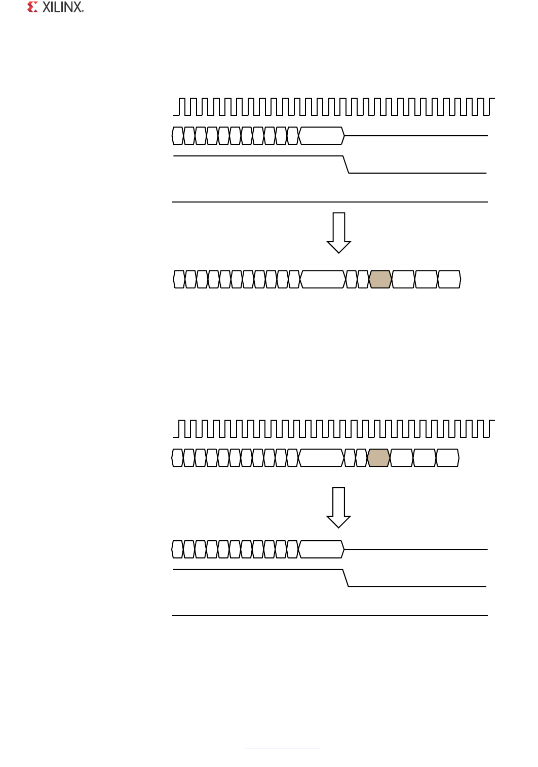
1000BASE-X PCS/PMA or SGMII v11.4 www.xilinx.com 441
PG047 October 16, 2012
Appendix C: 1000BASE-X State Machines
Note: The first Idle to follow the frame termination sequence will be a /I1/ if the frame ended with
positive running disparity or a /I2/ if the frame ended with negative running disparity. This is
illustrated as the shaded code group.
Reception of the Even Case
Figure C-6 illustrates the reception of the in-bound code-group stream, received either
serially using the device-specific transceiver, or in parallel across the TBI, and translation of
this code-group stream into the receiver GMII. This is performed by the PCS Receive Engine.
X-Ref Target - Figure C-5
Figure C-5: 1000BASE-X Transmit State Machine Operation (Even Case)
X-Ref Target - Figure C-6
Figure C-6: 1000BASE-X Reception State Machine Operation (Even Case)
GMII?TXD;=
GMII?TX?EN
GMII?TX?ER

 ) ) )
4 2 ))
TX?CODE?GROUP
0#34RANSMIT%NGINE%NCODING
8
GMII?RXD;=
GMII?RX?DV
GMII?RX?ER

 ) ) )4 2 ))
RX?CODE?GROUP
0#32ECEIVE%NGINE$ECODING
8
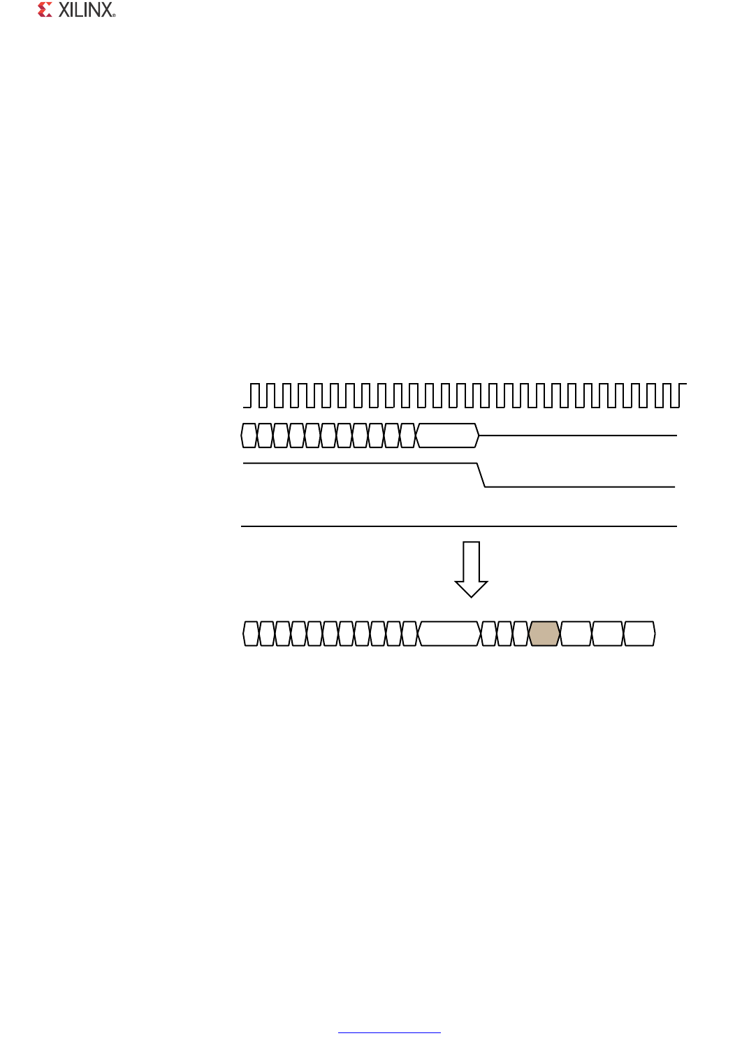
1000BASE-X PCS/PMA or SGMII v11.4 www.xilinx.com 442
PG047 October 16, 2012
Appendix C: 1000BASE-X State Machines
The Odd Transmission Case
Figure C-7 illustrates the translation of GMII encoding into the code-group stream
performed by the PCS Transmit Engine; this stream is transmitted out of the core, either
serially using the device-specific transceiver, or in parallel across the TBI.
In response to the deassertion of gmii_tx_en, an End of Packet code group /T/ is
immediately inserted. The even and odd alignment described in Start of Frame Encoding
persists throughout the Ethernet frame. If the /T/ character occurs in the odd position (the
frame contained an odd number of bytes starting from the /S/ character), then this is
followed with two Carrier Extend code groups /R/. This allows the /K28.5/ character of the
following Idle code group to be aligned to the even position.
Note: The first Idle to follow the frame termination sequence will be a /I1/ if the frame ended with
positive running disparity or a /I2/ if the frame ended with negative running disparity. This is
illustrated as the shaded code group.
Reception of the Odd Case
Figure C-8 illustrates the reception of the in-bound code-group stream, received either
serially using the device-specific transceiver, or in parallel across the TBI, and translation of
this code-group stream into the receiver GMII. This is performed by the PCS Receive Engine.
As defined in IEEE 802.3-2008 figure 36-7b, the combined /T/R/R/ sequence results in the
GMII encoding of Frame Extension. This occurs for a single clock cycle following the end of
frame reception; the gmii_rx_er signal is driven high and the frame extension code of
0x0F is driven onto gmii_rxd[7:0]. This occurs even in full-duplex mode.
X-Ref Target - Figure C-7
Figure C-7: 1000BASE-X Transmit State Machine Operation (Even Case)
GMII?TXD;=
GMII?TX?EN
GMII?TX?ER

 ) ) )
4 2 ))
2
TX?CODE?GROUP
0#34RANSMIT%NGINE%NCODING
8
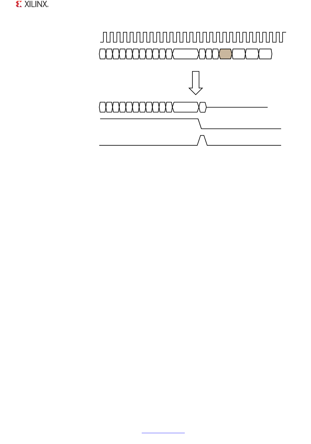
1000BASE-X PCS/PMA or SGMII v11.4 www.xilinx.com 443
PG047 October 16, 2012
Appendix C: 1000BASE-X State Machines
X-Ref Target - Figure C-8
Figure C-8: 1000BASE-X Reception State Machine Operation (Odd Case)
JPLLBU[G>@
JPLLBU[BGY
JPLLBU[BHU
)&6
U[BFRGHBJURXS )&6 , , ,
7 5 ,,
5
X&
3&65HFHLYH(QJLQH'HFRGLQJ
8

1000BASE-X PCS/PMA or SGMII v11.4 www.xilinx.com 444
PG047 October 16, 2012
Appendix D
Rx Elastic Buffer Specifications
This appendix is intended to serve as a reference for the Rx Elastic Buffer sizes used in the
core and the related maximum frame sizes that can be used without causing a buffer
underflow or overflow error.
Throughout this appendix, all analyses are based on 100 ppm clock tolerances on both
sides of the elastic buffer (200 ppm total difference). This corresponds to the Ethernet clock
tolerance specification.
Introduction
The need for an Rx Elastic Buffer is illustrated in The Requirement for the FPGA Logic Rx
Elastic Buffer. The analysis included in this chapter shows that for standard Ethernet clock
tolerances (100 ppm) there can be a maximum difference of one clock edge every 5000
clock periods of the nominal 125 MHz clock frequency.
This slight difference in clock frequency on either side of the buffer accumulates and either
starts to fill or empties the Rx Elastic Buffer over time. The Rx Elastic buffer copes with this
by performing clock correction during the interframe gaps by either inserting or removing
Idle characters. The Rx Elastic Buffer always attempts to restore the buffer occupancy to the
half full level during an interframe gap. See Clock Correction.
Rx Elastic Buffers: Depths and Maximum Frame
Sizes
Device Specific Transceiver Rx Elastic Buffers
Figure D-1 illustrates the transceiver Rx Elastic Buffer depths and thresholds in Virtex®-4
FX, Virtex-5 LXT, SXT, FXT and TXT families, Spartan®-6 LXT family, Virtex-6, Zynq™-7000,
Virtex-7, Artix™-7, and Kintex™-7 families. Each FIFO word corresponds to a single
character of data (equivalent to a single byte of data following 8B/10B decoding).
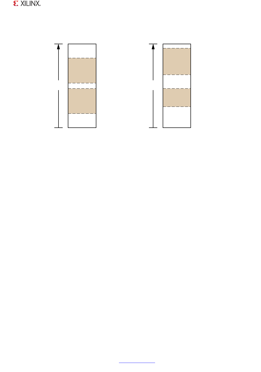
1000BASE-X PCS/PMA or SGMII v11.4 www.xilinx.com 445
PG047 October 16, 2012
Appendix D: Rx Elastic Buffer Specifications
X-Ref Target - Figure D-1
Zynq-7000, Virtex-7, Kintex-7, Artix-7, Virtex-6, Spartan-6, and Virtex-5
Devices
Consider the example, where the shaded area represents the usable buffer availability for
the duration of frame reception.
• If the buffer is filling during frame reception, there are 52-34 = 18 FIFO locations
available before the buffer reaches the overflow mark.
• If the buffer is emptying during reception, then there are 30-12 = 18 FIFO locations
available before the buffer reaches the underflow mark.
This analysis assumes that the buffer is approximately at the half-full level at the start of the
frame reception. As illustrated, there are two locations of uncertainty, above and below the
exact half-full mark of 32, resulting from the clock correction decision, and is based across
an asynchronous boundary.
Because there is a worst-case scenario of one clock edge difference every 5000 clock
periods, the maximum number of clock cycles (bytes) that can exist in a single frame
passing through the buffer before an error occurs is:
5000 x 18 = 90000 bytes
Table D-1 translates this into maximum frame size at different Ethernet speeds. At SGMII
speeds lower than 1 Gb/s, performance is diminished because bytes are repeated multiple
times (see Chapter 8, Using the Core Netlist Client-Side GMII for the SGMII Standard).
Figure D-1: Elastic Buffer Sizes for all Transceiver Families
2YHUIORZ0DUN
8QGHUIORZ0DUN
2YHUIORZ0DUN
8QGHUIORZ0DUN
&/.B&25B0$;B/$7
&/.B&25B0,1B/$7
6IRTEX6IRTEX6IRTEX
+INTEX!RTIXAND3PARTAN
$EVICE3PECIFIC4RANSCEIVER
2X%LASTIC"UFFER
9LUWH[);
5RFNHW,2 7UDQVFHLYHU
5[(ODVWLF%XIIHU
8

1000BASE-X PCS/PMA or SGMII v11.4 www.xilinx.com 446
PG047 October 16, 2012
Appendix D: Rx Elastic Buffer Specifications
Virtex-4 FX Device
Consider the Virtex-4 FX device case also illustrated in Figure D-1. The thresholds are
different to that of other families, but the overall size of the buffer is the same. Instead of
the half full point, there are configurable clock correction thresholds. During the interframe
gap, clock correction attempts to restore the occupancy to within these two thresholds.
However, by setting both CLK_COR_MAX_LAT and CLK_COR_MIN_LAT thresholds to the
same value, symmetrically between overflow and underflow marks, it is possible to obtain
the same figures as for other families. For this reason, by adjusting the threshold attributes
accordingly, Table D -1 is also applicable.
SGMII FPGA Logic Rx Elastic Buffer
Figure D-2 illustrates the FPGA logic Rx Elastic Buffer depth. This logic elastic buffer is used
with the core when:
• Performing SGMII over LVDS.
• This buffer can optionally be used to replace the Rx Elastic Buffers of the transceiver
when performing (see Chapter 6, SGMII / Dynamic Standards Switching with
Transceivers (see Receiver Elastic Buffer Implementations).
Table D-1: Maximum Frame Sizes: Transceiver Rx Elastic Buffers
(100ppm Clock Tolerance)
Standard / Speed Maximum Frame Size
1000BASE-X (1 Gb/s only) 90000
SGMII (1 Gb/s) 90000
SGMII (100 Mb/s) 9000
SGMII (10 Mb/s) 900

1000BASE-X PCS/PMA or SGMII v11.4 www.xilinx.com 447
PG047 October 16, 2012
Appendix D: Rx Elastic Buffer Specifications
The shaded area of Figure D-2 represents the usable buffer availability for the duration of
frame reception.
• If the buffer is filling during frame reception, there are 122-66 = 56 FIFO locations
available before the buffer reaches the overflow mark.
• If the buffer is emptying during reception, then there are 62-6 = 56 FIFO locations
available before the buffer reaches the underflow mark.
This analysis assumes the buffer is approximately at the half-full level at the start of the
frame reception. As illustrated, there are two locations of uncertainty, above and below the
exact half-full mark of 64. This is as a result of the clock correction decision, and is based
across an asynchronous boundary.
Because there is a worst-case scenario of one clock edge difference every 5000 clock
periods, the maximum number of clock cycles (bytes) that can exist in a single frame
passing through the buffer before an error occurs is:
5000 x 56 = 280000 bytes
Table D-2 translates this into maximum frame size at different Ethernet speeds. At SGMII
speeds lower than 1 Gb/s, performance is diminished because bytes are repeated multiple
X-Ref Target - Figure D-2
Figure D-2: Elastic Buffer Size for all Transceiver Families
/VERFLOW-ARK
5NDERFLOW-ARK
3'-))&0'!&ABRIC
2X%LASTIC"UFFER
8
1000BASE-X PCS/PMA or SGMII v11.4 www.xilinx.com 448
PG047 October 16, 2012
Appendix D: Rx Elastic Buffer Specifications
times. See Chapter 8, Using the Core Netlist Client-Side GMII for the SGMII Standard.
TBI Rx Elastic Buffer
For SGMII / Dynamic Switching
The Rx Elastic Buffer used for the SGMII or Dynamic Standards Switching is identical to the
method used in SGMII FPGA Logic Rx Elastic Buffer.
For 1000BASE-X
Figure D-3 illustrates the Rx Elastic Buffer depth and thresholds when using the
Ten-Bit-Interface with the 1000BASE-X standard. This buffer is intentionally smaller than the
equivalent buffer for SGMII/Dynamic Switching. Because a larger size is not required, the
buffer is kept smaller to save logic and keep latency low. Each FIFO word corresponds to a
single character of data (equivalent to a single byte of data following 8B/10B decoding).
Table D-2: Maximum Frame Sizes: Fabric Rx Elastic Buffers
(100ppm Clock Tolerance)
Standard / Speed Maximum Frame Size
1000BASE-X (1 Gb/s only) 280000
SGMII (1 Gb/s) 280000
SGMII (100 Mb/s) 28000
SGMII (10 Mb/s) 2800
X-Ref Target - Figure D-3
Figure D-3: TBI Elastic Buffer Size for All Families
/VERFLOW-ARK
5NDERFLOW-ARK
4")
2X%LASTIC"UFFER
8

1000BASE-X PCS/PMA or SGMII v11.4 www.xilinx.com 449
PG047 October 16, 2012
Appendix D: Rx Elastic Buffer Specifications
The shaded area of Figure D-3 represents the usable buffer availability for the duration of
frame reception.
• If the buffer is filling during frame reception, then there are 30-18 = 12 FIFO locations
available before the buffer reaches the overflow mark.
• If the buffer is emptying during reception, then there are 14-2 = 12 FIFO locations
available before the buffer reaches the underflow mark.
This analysis assumes that the buffer is approximately at the half-full level at the start of the
frame reception. As illustrated, there are two locations of uncertainty above and below the
exact half-full mark of 16. This is as a result of the clock correction decision, and is based
across an asynchronous boundary.
Because there is a worst-case scenario of 1 clock edge difference every 5000 clock periods,
the maximum number of clock cycles (bytes) that can exist in a single frame passing
through the buffer before an error occurs is:
5000 x 12 = 60000 bytes
This translates into a maximum frame size of 60000 bytes.

1000BASE-X PCS/PMA or SGMII v11.4 www.xilinx.com 450
PG047 October 16, 2012
Appendix D: Rx Elastic Buffer Specifications
Clock Correction
The calculations in all previous sections assumes that the Rx Elastic Buffers are restored to
approximately half occupancy at the start of each frame. This is achieved by the elastic
buffer performing clock correction during the interframe gaps either by inserting or
removing Idle characters as required.
• If the Rx Elastic Buffer is emptying during frame reception, there are no restrictions on
the number of Idle characters that can be inserted due to clock correction. The
occupancy will be restored to half full and the assumption holds true.
• If the Rx Elastic Buffer is filling during frame reception, Idle characters need to be
removed. Restrictions that need to be considered are described in the following
sections.
Idle Character Removal at 1 Gb/s (1000BASE-X and SGMII)
The minimum number of clock cycles that can be presented to an Ethernet receiver,
according to the IEEE 802.3-2008 specification, is 64-bit times at any Ethernet speed. At 1
Gb/s 1000BASE-X and SGMII, this corresponds to 8 bytes (8 clock cycles) of interframe gap.
However, an interframe gap consists of a variety of code groups, namely /T/, /R/, /I1/ and
/I2/ characters (see Appendix C, 1000BASE-X State Machines). Of these, only /I2/ can be
used as clock correction characters.
In a minimum interframe gap at 1 Gb/s, you can only assume that two /I2/ characters are
available for removal. This corresponds to 4 bytes of data.
Looking at this from another perspective, 4 bytes of data need to be removed in an elastic
buffer (which is filling during frame reception) for a frame which is 5000 x 4 = 20000 bytes
in length. So if the frame being received is 20000 bytes in length or shorter, at 1 Gb/s, you
can assume that the occupancy of the elastic buffer will always self correct to half full before
the start of the subsequent frame.
For frames that are longer than 20000 bytes, the assumption that the elastic buffer will be
restored to half full occupancy does not hold true. For example, for a long stream of 250000
byte frames, each separated by a minimum interframe gap, the Rx Elastic Buffer will
eventually fill and overflow. This is despite the 250000 byte frame length being less than the
maximum frame size calculated in the Rx Elastic Buffers: Depths and Maximum Frame Sizes
section.
However, because the legal maximum frame size for Ethernet frames is 1522 bytes (for a
VLAN frame), idle character removal restrictions are not usually an issue.

1000BASE-X PCS/PMA or SGMII v11.4 www.xilinx.com 451
PG047 October 16, 2012
Appendix D: Rx Elastic Buffer Specifications
Idle Character Removal at 100 Mb/s (SGMII)
At SGMII, 100 Mb/s, each byte is repeated 10 times. This also applies to the interframe gap
period. For this reason, the minimum of 8 bytes for the 1 Gb/s case corresponds to a
minimum of 80 bytes for the 100 Mb/s case.
Additionally, the majority of characters in this 80-byte interframe-gap period are going to
be the /I2/ clock correction characters. Because of the clock correction circuitry design, a
minimum of 20 /I2/ code groups will be available for removal. This translates into 40 bytes,
giving a maximum run size of 40 x 5000 = 200000 bytes. Because each byte at 100 Mb/s is
repeated ten times, this corresponds to an Ethernet frame size of 20000 bytes, the same size
as the 1 Gb/s case.
So in summary, at 100 Mb/s, for any frame size of 20000 bytes or less, it can still be assumed
that the Elastic Buffer will return to half full occupancy before the start of the next frame.
However, a frame size of 20000 is larger than can be received in the device-specific
transceiver Elastic Buffer (see Rx Elastic Buffers: Depths and Maximum Frame Sizes). Only
the SGMII FPGA Logic Rx Elastic buffer is large enough.
Idle Character Removal at 10 Mb/s (SGMII)
Using a similar argument to the 100 Mb/s case, it can be shown that clock correction
circuitry can also cope with a frame size up to 20000 bytes. However, this is larger than the
maximum frame size for any Elastic Buffer provided with the core (see Rx Elastic Buffers:
Depths and Maximum Frame Sizes).
Maximum Frame Sizes for Sustained Frame
Reception
Sustained frame reception refers to the maximum size of frames which can be continuously
received when each frame is separated by a minimum interframe gap.
The size of frames that can be reliably received is dependent on the two considerations
previously introduced in this appendix:
• The size of the Elastic Buffer, see Rx Elastic Buffers: Depths and Maximum Frame Sizes
• The number of clock correction characters present in a minimum interframe gap,
(see Clock Correction)
1000BASE-X PCS/PMA or SGMII v11.4 www.xilinx.com 452
PG047 October 16, 2012
Appendix D: Rx Elastic Buffer Specifications
Table D-3 summarizes the maximum frame sizes for sustained frame reception when used
with the different Rx Elastic Buffers provided with the core. All frame sizes are provided in
bytes.
Jumbo Frame Reception
A jumbo frame is an Ethernet frame which is deliberately larger than the maximum sized
Ethernet frame allowed in the IEEE 802.3-2008 specification. The size of jumbo frames that
can be reliably received is identical to the frame sizes defined in Maximum Frame Sizes for
Sustained Frame Reception.
Table D-3: Maximum Frame Size: (Sustained Frame Reception) Capabilities of the Rx Elastic Buffers
Ethernet Standard and
Speed
Rx Elastic Buffer Type
TBI Device Specific
Transceiver
SGMII FPGA Logic Buffer
(used with the Virtex-6
FPGA LVDS transceiver
and optional for use with
device specific
transceivers)
1000BASE-X (1 Gb/s) 20000 (limited by clock
correction)
20000 (limited by clock
correction)
20000 (limited by clock
correction)
SGMII 1 Gb/s 20000 (limited by clock
correction)
20000 (limited by clock
correction)
20000 (limited by clock
correction)
SGMII 100 Mb/s 20000 (limited by clock
correction)
9000 (limited by buffer
size)
20000 (limited by clock
correction)
SGMII 10 Mb/s 2800 (limited by buffer
size)
900 (limited by buffer size) 2800 (limited by buffer
size)

1000BASE-X PCS/PMA or SGMII v11.4 www.xilinx.com 453
PG047 October 16, 2012
Appendix E
Implementing External GMII
In certain applications, the client-side GMII datapath can be used as a true GMII to connect
externally off-device across a PCB. This external GMII functionality is included in the HDL
example design delivered with the core by the CORE Generator™ and Vivado™ IP catalog
tools for 1000BASE-X designs. This extra logic required to accomplish this is described in
this Appendix.
Note: Virtex®-7 devices support GMII at 3.3 V or lower only in certain parts and packages; see the
Virtex-7 Device Documentation. Virtex-6 devices support GMII at 2.5 V only. See the Virtex-6 FPGA
Data Sheet: DC and Switching Characteristics for more information. Zynq™-7000, Artix ™-7,
Kintex™-7, Virtex-5, Virtex-4, Spartan®-6 and Spartan-3 devices support GMII at 3.3 V or lower.
GMII Transmitter Logic
When implementing an external GMII, the GMII transmitter signals will be synchronous to
their own clock domain. The core must be used with a Transmitter Elastic Buffer to transfer
these GMII transmitter signals onto the cores internal 125 MHz reference clock (gtx_clk
when using the TBI; userclk2 when using the device-specific transceiver). A Transmitter
Elastic Buffer is provided for the 1000BASE-X standard by the example design provided with
the core.
Spartan-3, Spartan-3E, Spartan-3A/3A DSP and Virtex-4 Devices
A DCM must be used on the gmii_tx_clk clock path, as illustrated in Figure E-1. This is
performed by the top-level example design delivered with the core (all signal names and
logic match Figure E-1). This DCM circuitry can optionally be used in other families.
Phase-shifting should then be applied to the DCM to fine-tune the setup and hold times at
the GMII IOB input flip-flops. The fixed phase shift is applied to the DCM with the example
UCF for the example design. See Constraints When Implementing an External GMII.
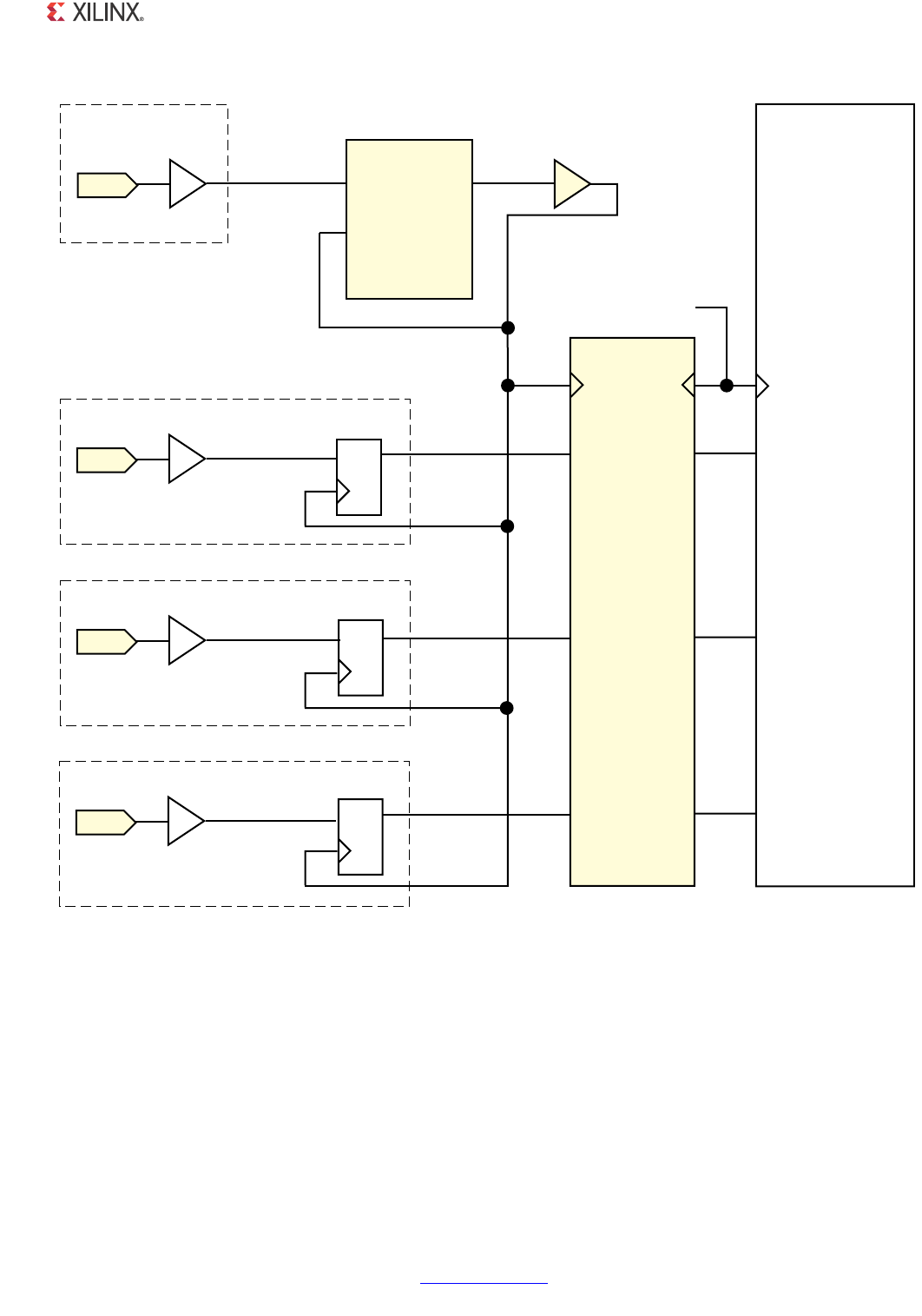
1000BASE-X PCS/PMA or SGMII v11.4 www.xilinx.com 454
PG047 October 16, 2012
Appendix E: Implementing External GMII
X-Ref Target - Figure E-1
Figure E-1: External GMII Transmitter Logic for Spartan-3, Spartan-3E, Spartan-3A/3A DSP and Virtex-4
Devices
JPLLBW[G>@ ,%8)
'4
JPLLBW[BHQ
JPLLBW[BHU
JPLLBW[G>@
JPLLBW[BHQ
JPLLBW[BHU
(WKHUQHW%$6(;
3&630$
RU6*0,,/RJL&25(
,3$'
,3$'
,3$'
,%8)
,%8)
'4
'4
JPLLBW[GBLQW>@
JPLLBW[BHQBLQW
JPLLBW[BHUBLQW
7UDQVPLWWHU
(ODVWLF
%XIIHU
XVHUFONLI5RFNHW,2LVXVHG
JW[BFONLI7%,LVXVHG
JPLLBW[BFON ,%8)*
,2%/2*,&
,3$'
%8)*
JPLLBW[BFONBEXIJ
'&0
&/.,1 &/.
)%
8

1000BASE-X PCS/PMA or SGMII v11.4 www.xilinx.com 455
PG047 October 16, 2012
Appendix E: Implementing External GMII
Virtex-5 Devices
Three possible solutions follow:
Case 1
For Virtex-5 devices, a DCM can be used on the gmii_tx_clk clock path, using global
clock routing, and illustrated in Figure E-1 for the Spartan-3 and Virtex-4 family.
Case 2
Input Delay Elements can be used on the GMII data and clock path, using global clock
routing (not illustrated). This implementation was provided as the default example design
for Virtex-5 devices in versions of this core prior to version 10.1.
Case 3
Use a combination of IODELAY elements on the data, and use BUFIO and BUFR regional
clock routing for the gmii_tx_clk input clock, as illustrated in Figure E-2.
The design for Case 3 provides a simpler solution than the DCM logic of Case 1 and
provides better input setup and hold time margins than Case 2. It has therefore been
chosen as the default example design from version 10.1 of the core onwards.
In this implementation, a BUFIO is used to provide the lowest form of clock routing delay
from input clock to input GMII Tx signal sampling at the device IOBs. Note, however, that
this creates placement constraints; a BUFIO capable clock input pin must be selected, and
all other input GMII Tx signals must be placed in the respective BUFIO region. The Virtex-5
FPGA User Guide should be consulted.
The clock is then placed onto regional clock routing using the BUFR component and the
input GMII Tx data immediately resampled as illustrated.
The IODELAY elements can be adjusted to fine-tune the setup and hold times at the GMII
IOB input flip-flops. The delay is applied to the IODELAY element using constraints in the
UCF; these can be edited if desired. See Constraints When Implementing an External GMII
for more information.
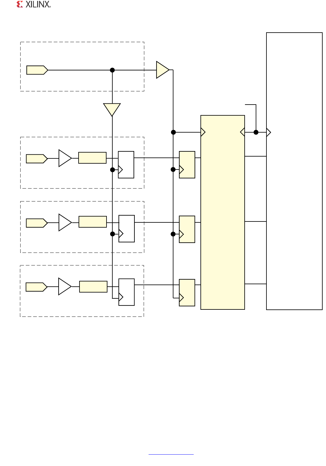
1000BASE-X PCS/PMA or SGMII v11.4 www.xilinx.com 456
PG047 October 16, 2012
Appendix E: Implementing External GMII
X-Ref Target - Figure E-2
Figure E-2: External GMII Transmitter Logic for Virtex-5, Virtex-6, Zynq-7000, Virtex-7, Artix-7, and
Kintex-7 Devices
JPLLBW[BFON
,2%/2*,&
,3$'
JPLLBW[G>@ ,%8)
'4
JPLLBW[BHQ
JPLLBW[BHU
JPLLBW[G>@
JPLLBW[BHQ
JPLLBW[BHU
%8)5
(WKHUQHW%$6(;
3&630$
RU6*0,,/RJL&25(
,3$'
,3$'
,3$'
,%8)
,%8)
'4
'4
JPLLBW[BFONBEXIU
7UDQVPLWWHU
(ODVWLF
%XIIHU
XVHUFONLIWUDQVFHLYHULVXVHG
JW[BFONLI7%,LVXVHG
,2'(/$<
,2'(/$<
,2'(/$<
%8),2
,2%/2*,&
'4
'4
'4
8

1000BASE-X PCS/PMA or SGMII v11.4 www.xilinx.com 457
PG047 October 16, 2012
Appendix E: Implementing External GMII
Zynq-7000, Virtex-7, Kintex-7, Artix-7, and Virtex-6 Devices
Two possible solutions follow:
Case 1
A MMCM can be used on the gmii_tx_clk clock path, using global clock routing. This is
illustrated in Figure E-1 for the Spartan-3 and Virtex-4 family; simply replace the DCM for a
MMCM.
Case 2
Use a combination of IODELAY elements on the data, and use BUFIO and BUFR regional
clock routing for the gmii_tx_clk input clock, as illustrated in Figure E-2.
The design for Case 2 provides a simpler solution than that of Case 1. It has therefore been
chosen as the default example design for Artix-7, Virtex-7, Kintex-7, Zynq-7000, and
Virtex-6 devices.
In this implementation, a BUFIO is used to provide the lowest form of clock routing delay
from input clock to input GMII Tx signal sampling at the device IOBs. Note, however, that
this creates placement constraints; a BUFIO capable clock input pin must be selected, and
all other input GMII Tx signals must be placed in the respective BUFIO region. The device
FPGA user guides should be consulted.
The clock is then placed onto regional clock routing using the BUFR component and the
input GMII Tx data immediately resampled as illustrated.
The IODELAY elements can be adjusted to fine-tune the setup and hold times at the GMII
IOB input flip-flops. The delay is applied to the IODELAY element using constraints in the
UCF; these can be edited if desired. See Constraints When Implementing an External GMII
for more information.
Spartan-6 Devices
Two possible solutions are:
Case 1
For Spartan-6 devices, a MMCM can be used on the gmii_tx_clk clock path, using global
clock routing, and illustrated in Figure E-1 for the Spartan-3 and Virtex-4 devices.

1000BASE-X PCS/PMA or SGMII v11.4 www.xilinx.com 458
PG047 October 16, 2012
Appendix E: Implementing External GMII
Case 2
Using a combination of IODELAY elements on the data, and using BUFIO2 and BUFG global
clock routing for the gmii_tx_clk input clock, as illustrated in Figure E-3.
The design for Case 2 provides a simpler solution than that of Case 1. It has therefore been
chosen as the default example design for Spartan-6 devices.
In this implementation, a BUFIO2 is used to provide the lowest form of clock routing delay
from input clock to input GMII Tx signal sampling at the device IOBs. Note, however, that
this creates placement constraints: a BUFIO capable clock input pin must be selected, and
all other input GMII Tx signals must be placed in the respective BUFIO2 region. The
Spartan-6 FPGA User Guide should be consulted.
The clock is then placed onto global clock routing using the BUFG component and the input
GMII Tx data immediately resampled as illustrated.
The IODELAY2 elements can be adjusted to fine-tune the setup and hold times at the GMII
IOB input flip-flops. The delay is applied to the IODELAY2 element using constraints in the
UCF; these can be edited if desired. See Constraints When Implementing an External GMII
for more information.

1000BASE-X PCS/PMA or SGMII v11.4 www.xilinx.com 459
PG047 October 16, 2012
Appendix E: Implementing External GMII
X-Ref Target - Figure E-3
Figure E-3: External GMII Transmitter Logic for Spartan-6 Devices
JPLLBW[BFON
,2%/2*,&
,3$'
JPLLBW[G>@
'4
JPLLBW[BHQ
JPLLBW[BHU
JPLLBW[G>@
JPLLBW[BHQ
JPLLBW[BHU
%8)*
(WKHUQHW%$6(;
3&630$
RU6*0,,/RJL&25(
,3$'
,3$'
,3$'
'4
'4
JPLLBW[BFONBEXIJ
7UDQVPLWWHU
(ODVWLF
%XIIHU
XVHUFONLIWUDQVFHLYHULVXVHG
JW[BFONLI7%,LVXVHG
%8),2
,2%/2*,&
'4
'4
'4
,2'(/$<
,2'(/$<
,2'(/$<
8

1000BASE-X PCS/PMA or SGMII v11.4 www.xilinx.com 460
PG047 October 16, 2012
Appendix E: Implementing External GMII
GMII Receiver Logic
Figure E-4 illustrates an external GMII receiver created in a Virtex-5 family device. The
signal names and logic shown in the figure exactly match those delivered with the example
design when the GMII is selected. If other families are selected, equivalent primitives and
logic specific to that family is automatically used in the example design.
Figure E-4 also shows that the output receiver signals are registered in device IOBs before
driving them to the device pads. The logic required to forward the receiver GMII clock is
also shown. This uses an IOB output Double-Data-Rate (DDR) register so that the clock
signal produced incurs exactly the same delay as the data and control signals. This clock
signal, gmii_rx_clk, is inverted so that the rising edge of gmii_rx_clk occurs in the
center of the data valid window, which maximizes setup and hold times across the interface.
All receiver logic is synchronous to a single clock domain.
The clock name varies depending on the core configuration options. When used with the
device-specific transceiver, the clock name is userclk2; when used with the TBI, the clock
name is gtx_clk. For more information on clocking, see Chapter 4, The Ten-Bit Interface,
and Chapter 5, 1000BASE-X with Transceivers.
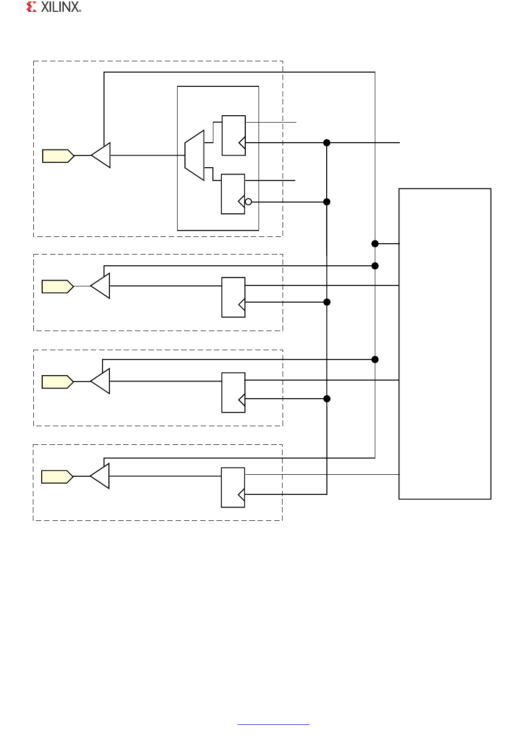
1000BASE-X PCS/PMA or SGMII v11.4 www.xilinx.com 461
PG047 October 16, 2012
Appendix E: Implementing External GMII
X-Ref Target - Figure E-4
Figure E-4: External GMII Receiver Logic
)/",/')#
/"5&4
&$$223%
/0!$
$
1
gg
gg
GMII?RXD?OBUF;=
/0!$
/0!$
/0!$
/"5&4
/"5&4
/"5&4
$
1
$
1
$
1
$
1
GMII?RX?DV?OBUF
GMII?RX?ER?OBUF
GMII?RXD;=
GMII?RX?DV
GMII?RX?ER
GMII?RX?CLK
GMII?RX?CLK?OBUF
GMII?RXD;=
GMII?RX?DV
GMII?RX?ER
%THERNET"!3%8
0#30-!
OR3'-)),OGI#/2%
GMII?ISOLATE
XVHUFONLIWUDQVFHLYHULVXVHG
GTX?CLKIF4")ISUSED
8

1000BASE-X PCS/PMA or SGMII v11.4 www.xilinx.com 462
PG047 October 16, 2012
Appendix F
Calculating the DCM Fixed Phase Shift or
IODelay Tap Setting
Two differing methods are used by the core to meet input bus (GMII or TBI) setup and hold
timing specifications. There are:
•DCM Usage
A DCM is used on the input bus synchronous clock path to meet the input setup and
hold requirements when implementing GMI and TBI using the core in Spartan®-3,
Spartan-3E, Spartan-3A, Spartan-3A DSP and Virtex®-4 devices.
•IODelay Usage
IODelays are used on the input bus synchronous clock path to meet the input setup and
hold requirements when implementing GMII and TBI using the core in Spartan-6,
Virtex-5 and Virtex-6 devices.
DCM Usage
Requirement for DCM Phase Shifting
A DCM is used in the clock path to meet the input setup and hold requirements when using
the core with a TBI (see Chapter 4, The Ten-Bit Interface) and with an external GMII
implementation in Spartan-3, Spartan-3E, Spartan-3A/3AN/3A DSP devices (see Spartan-3,
Spartan-3E, Spartan-3A/3A DSP and Virtex-4 Devices).
In these cases, a fixed phase shift offset is applied to the DCM to skew the clock. This
initiates a static alignment by using the clock DCM to shift the internal version of the clock
so that its edges are centered on the data eye at the IOB DDR flip-flops. The ability to shift
the internal clock in small increments is critical for sampling high-speed source
synchronous signals such as TBI and GMII. For statically aligned systems, the DCM output
clock phase offset (as set by the phase shift value) is a critical part of the system, as is the
requirement that the PCB is designed with precise delay and impedance-matching for all
the GMII/TBI data bus and control signals.

1000BASE-X PCS/PMA or SGMII v11.4 www.xilinx.com 463
PG047 October 16, 2012
Appendix F: Calculating the DCM Fixed Phase Shift or IODelay Tap Setting
Determine the best DCM setting (phase shift) to ensure that the target system has the
maximum system margin required to perform across voltage, temperature, and process
(multiple chips) variations. Testing the system to determine the best DCM phase shift
setting has the added advantage of providing a benchmark of the system margin based on
the UI (unit interval or bit time).
System margin is defined as:
System Margin (ps) = UI(ps) * (working phase shift range/128)
Finding the Ideal Phase Shift Value for Your System
Xilinx cannot recommend a singular phase shift value that is effective across all hardware
platforms. Xilinx does not recommend attempting to determine the phase shift setting
empirically. In addition to the clock-to-data phase relationship, other factors such as
package flight time (package skew) and clock routing delays (internal to the device) affect
the clock-to-data relationship at the sample point (in the IOB) and are difficult to
characterize.
Xilinx recommends extensive investigation of the phase shift setting during hardware
integration and debugging. The phase shift settings provided in the example design UCF is
a placeholder and works successfully in back-annotated simulation of the example design.
Perform a complete sweep of phase-shift settings during your initial system test. Use a test
range which covers at least half of the clock period or 128 taps. This does not imply that 128
phase-shift values must be tested; increments of 4 (52, 56, 60, and so forth) correspond to
roughly one DCM tap at 125 MHz, and consequently provide an appropriate step size.
Additionally, it is not necessary to characterize areas outside the working phase-shift range.
At the edge of the operating phase shift range, system behavior changes dramatically. In
eight phase shift settings or fewer, the system can transition from no errors to exhibiting
errors. Checking the operational edge at a step size of two (on more than one board) refines
the typical operational phase shift range. After the range is determined, choose the average
of the high and low working phase shift values as the default. During the production test,
Xilinx recommends that you re-examine the working range at corner case operating
conditions to determine whether any adjustments to the final phase shift setting are
needed.
You can use the FPGA Editor to generate the required test file set instead of resorting to
multiple PAR runs. Performing the test on design files that differ only in phase shift setting
prevents other variables from affecting the test results. FPGA Editor operations can even be
scripted further, reducing the effort needed to perform this characterization.

1000BASE-X PCS/PMA or SGMII v11.4 www.xilinx.com 464
PG047 October 16, 2012
Appendix F: Calculating the DCM Fixed Phase Shift or IODelay Tap Setting
IODelay Usage
IODelay Tap Setting Requirements
With this method, an IODelay is used on either the clock or Data (or both) to adjust the
Clock/Data relationship such that the input data is sampled at the optimum time. The ability
to adjust this relationship in small increments is critical for sampling high-speed source
synchronous signals. For statically aligned systems, the IODelay Tap setting is a critical part
of the system, as is the requirement that the PCB is designed with precise delay and
impedance-matching for all the GMII or TBI input data bus and control signals.
You must determine the best IODelay Tap setting to ensure that the target system has the
maximum system margin to perform across voltage, temperature, and process (multiple
chips) variations.
Finding the Ideal Tap Setting Value
Xilinx cannot recommend a singular tap value that is effective across all hardware families.
Xilinx does not recommend attempting to determine the tap setting empirically. In addition
to the clock-to-data phase relationship, other factors such as package flight time (package
skew) and clock routing delays (internal to the device) affect the clock to data relationship
at the sample point (in the IOB) and are difficult to characterize.
Xilinx recommends extensive investigation of the tap setting during hardware integration
and debugging. The tap settings provided in the example design constraint file are
placeholders, and work successfully in back-annotated simulation of the example design.
Perform a complete sweep of tap settings during your initial system test. If possible, use a
test range which covers at least half of the clock period. This does not imply that all values
must be tested as it might be simpler to use a large step size initially to identify a tighter
range for a subsequent run. Additionally, it is not necessary to characterize areas outside
the working range. If an IODelay is used on both Clock and Data then ensure this test range
covers both clock only and data only adjustments.
At the edge of the operating range, system behavior changes dramatically. In four tap
settings or less, the system can transition from no errors to exhibiting errors. Checking the
operational edge at a step size of two (on more than one board) refines the typical
operational range. After the range is determined, choose the average of the high and low
working values as the default. During the production test, Xilinx recommends that you
re-examine the working range at corner case operating conditions to determine whether
any final adjustments to the final setting are needed. Where IODelays are used on the data
it might be necessary or beneficial to use slightly different values for each bit.

1000BASE-X PCS/PMA or SGMII v11.4 www.xilinx.com 465
PG047 October 16, 2012
Appendix F: Calculating the DCM Fixed Phase Shift or IODelay Tap Setting
You can use the FPGA Editor to generate the required test file set instead of resorting to
multiple PAR runs. Performing the test on design files that differ only in tap setting prevents
other variables from affecting the test results. FPGA Editor operations can even be scripted
further, reducing the effort needed to perform this characterization.

1000BASE-X PCS/PMA or SGMII v11.4 www.xilinx.com 466
PG047 October 16, 2012
Appendix G
Debugging
This appendix provides assistance for debugging the core within a system. For additional
help, contact Xilinx by submitting a WebCase at support.xilinx.com/.
Solution Centers
See the Xilinx Solution Centers for support on devices, software tools, and intellectual
property at all stages of the design cycle. Topics include design assistance, advisories, and
troubleshooting tips.
The Solution Center specific to this core is located at Xilinx Ethernet IP Solution Center
General Checks
• Ensure that all the timing constraints for the core were met during Place and Route.
• Does it work in timing simulation? If problems are seen in hardware but not in timing
simulation, this could indicate a PCB issue.
• Ensure that all clock sources are clean. If using DCMs in the design, ensure that all
DCMs have obtained lock by monitoring the LOCKED port.
Problems with the MDIO
• Ensure that the MDIO is driven properly. See MDIO Management Interface for detailed
information about performing MDIO transactions.
•Check that the mdc clock is running and that the frequency is 2.5 MHz or less.
• Read from a configuration register that does not have all 0s as a default. If all 0s are
read back, the read was unsuccessful. Check that the PHYAD field placed into the MDIO
frame matches the value placed on the phyad[4:0] port of the core.

1000BASE-X PCS/PMA or SGMII v11.4 www.xilinx.com 467
PG047 October 16, 2012
Appendix G: Debugging
Problems with Data Reception or Transmission
When no data is being received or transmitted:
• Ensure that a valid link has been established between the core and its link partner,
either by Auto-Negotiation or Manual Configuration: status_vector[0] and
status_vector[1] should both be high. If no link has been established, see the
topics discussed in the next section.
°Problems with Auto-Negotiation
°Problems in Obtaining a Link (Auto-Negotiation Disabled)
Note: Transmission through the core is not allowed unless a link has been established. This
behavior can be overridden by setting the Unidirectional Enable bit.
• Ensure that the Isolate state has been disabled.
By default, the Isolate state is enabled after power-up. For an external GMII, the PHY will
be electrically isolated from the GMII; for an internal GMII, it will behave as if it is
isolated. This results in no data transfer across the GMII. See Start-up Sequencing for
more information.
If data is being transmitted and received between the core and its link partner, but with a
high rate of packet loss, see Chapter 13, Special Design Considerations.
Problems with Auto-Negotiation
Determine whether Auto-Negotiation has completed successfully by doing one of the
following.
• Poll the Auto-Negotiation completion bit 1.5 in Register 1: Status Register
• Use the Auto-Negotiation interrupt port of the core (see Using the Auto-Negotiation
Interrupt).
If Auto-Negotiation is not completing:
1. Ensure that Auto-Negotiation is enabled in both the core and in the link partner (the
device or test equipment connected to the core). Auto-Negotiation cannot complete
successfully unless both devices are configured to perform Auto-Negotiation.
The Auto-Negotiation procedure requires that the Auto-Negotiation handshaking
protocol between the core and its link partner, which lasts for several link timer periods,
occur without a bit error. A detected bit error causes Auto-Negotiation to go back to the
beginning and restart.

1000BASE-X PCS/PMA or SGMII v11.4 www.xilinx.com 468
PG047 October 16, 2012
Appendix G: Debugging
Therefore, a link with an exceptionally high bit error rate might not be capable of
completing Auto-Negotiation, or might lead to a long Auto-Negotiation period caused
by the numerous Auto-Negotiation restarts. If this appears to be the case, try the next
step and see Problems with a High Bit Error Rate
2. Try disabling Auto-Negotiation in both the core and the link partner and see if both
devices report a valid link and are able to pass traffic. If they do, it proves that the core
and link partner are otherwise configured correctly. If they do not pass traffic, see
Problems in Obtaining a Link (Auto-Negotiation Disabled)).
Problems in Obtaining a Link (Auto-Negotiation
Disabled)
Determine whether the device has successfully obtained a link with its link partner by doing
the following:
• Reading bit 1.2, Link Status, in MDIO Register 1: Status Register, (see MDIO Register 1:
Status Register) when using the optional MDIO management interface (or look at
status_vector[1]).
• Monitoring the state of status_vector[0]. If this is logic ‘1,’ then synchronization,
and therefore a link, has been established. See Bit[0]: Link Status.
If the devices have failed to form a link then do the following:
• Ensure that Auto-Negotiation is disabled in both the core and in the link partner (the
device or test equipment connected to the core).
• Monitor the state of the signal_detect signal input to the core. This should either
be:
°connected to an optical module to detect the presence of light. Logic ‘1’ indicates
that the optical module is correctly detecting light; logic ‘0’ indicates a fault.
Therefore, ensure that this is driven with the correct polarity.
°Signal must be tied to logic ‘1’ (if not connected to an optical module).
Note: When signal_detect is set to logic ‘0,’ this forces the receiver synchronization state
machine of the core to remain in the loss of sync state.
°See Problems with a High Bit Error Rate in a subsequent section.
When using a device-specific transceiver, perform these additional checks:
• Ensure that the polarities of the TXN/TXP and RXN/RXP lines are not reversed. If they
are, this can be easily fixed by using the TXPOLARITY and RXPOLARITY ports of the
device-specific transceiver.

1000BASE-X PCS/PMA or SGMII v11.4 www.xilinx.com 469
PG047 October 16, 2012
Appendix G: Debugging
• Check that the device-specific transceiver is not being held in reset by monitoring the
mgt_tx_reset and mgt_rx_reset signals between the core and the device-specific
transceiver. If these are asserted then this indicates that the PMA PLL circuitry in the
device-specific transceiver has not obtained lock; check the PLL Lock signals output
from the device-specific transceiver.
• Monitor the RXBUFERR signal when Auto-Negotiation is disabled. If this is being
asserted, the Elastic Buffer in the receiver path of the device-specific transceiver is
either under or overflowing. This indicates a clock correction issue caused by
differences between the transmitting and receiving ends. Check all clock management
circuitry and clock frequencies applied to the core and to the device-specific
transceiver.
Problems with a High Bit Error Rate
Symptoms
The severity of a high-bit error rate can vary and cause any of the following symptoms:
• Failure to complete Auto-Negotiation when Auto-Negotiation is enabled.
• Failure to obtain a link when Auto-Negotiation is disabled in both the core and the link
partner.
• High proportion of lost packets when passed between two connected devices that are
capable of obtaining a link through Auto-Negotiation or otherwise. This can usually be
accurately measured if the Ethernet MAC attached to the core contains statistic
counters.
Note: All bit errors detected by the 1000BASE-X PCS/PMA logic during frame reception show up
as Frame Check Sequence Errors in an attached Ethernet MAC.
Debugging
• Compare the problem across several devices or PCBs to ensure that the problem is not
a one-off case.
• Try using an alternative link partner or test equipment and then compare results.
• Try putting the core into loopback (both by placing the core into internal loopback, and
by looping back the optical cable) and compare the behavior. The core should always
be capable of Auto-Negotiating with itself and looping back with itself from transmitter
to receiver so direct comparisons can be made. If the core exhibits correct operation
when placed into internal loopback, but not when loopback is performed via an optical
cable, this can indicate a faulty optical module or a PCB problem.
• Try swapping the optical module on a misperforming device and repeat the tests.

1000BASE-X PCS/PMA or SGMII v11.4 www.xilinx.com 470
PG047 October 16, 2012
Appendix G: Debugging
Perform these additional checks when using a device-specific transceiver:
• Directly monitor the following ports of the device-specific transceiver by attaching
error counters to them, or by triggering on them using the ChipScope™ tool or an
external logic analyzer.
RXDISPERR
RXNOTINTABLE
These signals should not be asserted over the duration of a few seconds, minutes or
even hours. If they are frequently asserted, it might indicate a problem with the
device-specific transceiver. Consult Answer Record 19699 for debugging device-specific
transceiver issues.
• Place the device-specific transceiver into parallel or serial loopback.
°If the core exhibits correct operation in device-specific transceiver serial loopback,
but not when loopback is performed by an optical cable, it might indicate a faulty
optical module.
°If the core exhibits correct operation in device-specific transceiver parallel loopback
but not in serial loopback, this can indicate a device-specific transceiver problem.
See Answer Record 19699 for details.
• A mild form of bit error rate might be solved by adjusting the transmitter
TX_PREEMPHASIS, TX_DIFF_CTRL and TERMINATION_IMP attributes of the
device-specific transceiver.

1000BASE-X PCS/PMA or SGMII v11.4 www.xilinx.com 471
PG047 October 16, 2012
Appendix H
Additional Resources
Xilinx Resources
For support resources such as Answers, Documentation, Downloads, and Forums, see the
Xilinx Support website at:
www.xilinx.com/support.
For a glossary of technical terms used in Xilinx documentation, see:
www.xilinx.com/company/terms.htm.
References
To search for Xilinx documentation, go to
http://www.xilinx.com/support/documentation/index.htm.
1. 7 Series FPGAs GTX Transceivers User Guide
2. 7 Series FPGAs SelectIO Resources User Guide (UG471)
3. 7 Series FPGAs Transceivers User Guide (UG769)
4. Virtex-6 FPGA GTX Transceivers, User Guide (UG366)
5. Virtex-6 FPGA User Guide
6. Virtex-6 FPGA Clocking Resources User Guide (UG362)
7. Spartan-6 FPGA User Guide
8. Spartan-6 FPGA GTP Transceiver User Guide
9. Virtex-5 FPGA RocketIO GTP Transceiver User Guide (UG196)
10. Virtex-5 FPGA RocketIO GTX Transceiver User Guide (UG198)
11. Virtex-5 FPGA User Guide (UG190)
12. Virtex-4 FPGA RocketIO Multi-Gigabit Transceiver User Guide (UG076)

1000BASE-X PCS/PMA or SGMII v11.4 www.xilinx.com 472
PG047 October 16, 2012
Appendix H: Additional Resources
13. Virtex-4 FPGA User Guide (UG070)
14. Spartan-3, Spartan-3E, Spartan-3A FPGA Data Sheets
15. XST User Guide
16. CORE Generator Guide
17. Xilinx Synthesis and Verification Design Guide
18. Calibration Block User Guide
19. 1.25 Gbps 4x Asynchronous Oversampling over Virtex-6 LVDS (XAPP 881)
20. LVDS 4x Asynchronous Oversampling Using 7 Series FPGAs (XAPP523)
21. Vivado Documentation
Additional Core Resources
After generating the core, the Ethernet 1000BASE-X PCS/PMA or SGMII Release Notes are
available in the document directory
Related Xilinx Ethernet Products and Services
For information about all Xilinx Ethernet solutions, see
www.xilinx.com/products/design_resources/conn_central/protocols/gigabit_ethernet.htm.
Specifications
• IEEE 802.3-2008
•Serial-GMII Specification (CISCO SYSTEMS, ENG-46158, Revision 1.7)
Technical Support
Xilinx provides technical support at www.xilinx.com/support for this LogiCORE™ IP product
when used as described in the product documentation. Xilinx cannot guarantee timing,
functionality, or support of product if implemented in devices that are not defined in the
documentation, if customized beyond that allowed in the product documentation, or if
changes are made to any section of the design labeled DO NOT MODIFY.
See the IP Release Notes Guide (XTP025) for more information on this core. For each core,
there is a master Answer Record that contains the Release Notes and Known Issues list for
the core being used. The following information is listed for each version of the core:

1000BASE-X PCS/PMA or SGMII v11.4 www.xilinx.com 473
PG047 October 16, 2012
Appendix H: Additional Resources
• New Features
• Resolved Issues
• Known Issues
Feedback
Xilinx welcomes comments and suggestions about the Ethernet 1000BASE-X PCS/PMA or
SGMII core and the documentation supplied with the core.
Ethernet 1000BASE-X PCS/PMA or SGMII Core
For comments or suggestions about the core, submit a WebCase from
www.support.xilinx.com. Be sure to include the following information:
•Product name
• Core version number
• Explanation of your comments
Document
For comments or suggestions about this document, submit a WebCase from
www.support.xilinx.com. Be sure to include the following information:
• Document title
• Document number
• Page number(s) to which your comments refer
• Explanation of your comments

1000BASE-X PCS/PMA or SGMII v11.4 www.xilinx.com 474
PG047 October 16, 2012
Appendix H: Additional Resources
Revision History
The following table shows the revision history for this document.
Notice of Disclaimer
The information disclosed to you hereunder (the “Materials”) is provided solely for the selection and use of Xilinx products. To the
maximum extent permitted by applicable law: (1) Materials are made available “AS IS” and with all faults, Xilinx hereby DISCLAIMS
ALL WARRANTIES AND CONDITIONS, EXPRESS, IMPLIED, OR STATUTORY, INCLUDING BUT NOT LIMITED TO WARRANTIES OF
MERCHANTABILITY, NON-INFRINGEMENT, OR FITNESS FOR ANY PARTICULAR PURPOSE; and (2) Xilinx shall not be liable (whether
in contract or tort, including negligence, or under any other theory of liability) for any loss or damage of any kind or nature related
to, arising under, or in connection with, the Materials (including your use of the Materials), including for any direct, indirect,
special, incidental, or consequential loss or damage (including loss of data, profits, goodwill, or any type of loss or damage
suffered as a result of any action brought by a third party) even if such damage or loss was reasonably foreseeable or Xilinx had
been advised of the possibility of the same. Xilinx assumes no obligation to correct any errors contained in the Materials or to
notify you of updates to the Materials or to product specifications. You may not reproduce, modify, distribute, or publicly display
the Materials without prior written consent. Certain products are subject to the terms and conditions of the Limited Warranties
which can be viewed at http://www.xilinx.com/warranty.htm; IP cores may be subject to warranty and support terms contained in
a license issued to you by Xilinx. Xilinx products are not designed or intended to be fail-safe or for use in any application requiring
fail-safe performance; you assume sole risk and liability for use of Xilinx products in Critical Applications:
http://www.xilinx.com/warranty.htm#critapps.
© Copyright 2012 Xilinx, Inc. Xilinx, the Xilinx logo, Artix, ISE, Kintex, Spartan, Virtex, Vivado, Zynq, and other designated brands
included herein are trademarks of Xilinx in the United States and other countries. The PowerPC name and logo are registered
trademarks of IBM Corp. and used under license. All other trademarks are the property of their respective owners.
Date Version Revision
7/25/12 1.0 Initial Xilinx release in product guide format. This document is based on the
following documents:
• LogiCORE IP Ethernet 1000BASE-X PCS/PMA or SGMII v11.3 Product Guide
• LogiCORE IP Ethernet 1000BASE-X PCS/PMA or SGMII v11.3 Data Sheet
10/16/12 1.1 Updated for 14.3 and 2012.3.
Added Gigabit Ethernet EDK application for Zynq-7000 devices.
