Philips Chassis LC9.1A LA Service Manual. Www.s Manuals.com. Tv Ch Manual
User Manual: LCD TV Philips LC9.1A LA Chassis - Service manuals and Schematics. Free.
Open the PDF directly: View PDF ![]() .
.
Page Count: 88
- Contents
- 1. Revision List
- 2. Technical Specifications and Connections
- 3. Precautions, Notes, and Abbreviation List
- 3.1 Safety Instructions
- 3.2 Warnings
- 3.3 Notes
- 3.4 Abbreviation List
- 4. Mechanical Instructions
- 5. Service Modes, Error Codes, and Fault Finding
- 5.1 Test Points
- 5.2 Service Modes
- 5.3 Service Tools
- 5.4 Error Codes
- 5.5 The Blinking LED Procedure
- 5.6 Fault Finding and Repair Tips
- 5.6.1 Software Protections
- 5.6.2 Hardware Protections
- 5.6.3 NVM Editor
- 5.6.4 Load Default NVM Values
- 5.6.5 Display option code
- 5.6.6 Trouble Shooting Tuner section
- 5.6.7 Trouble Shooting Sound section
- 5.6.8 Trouble Shooting HDMI section
- 5.6.9 Start-up/Shut-down Flowcharts
- 5.6.10 SSB replacement
- 5.7 Software Upgrading
- 6. Alignments
- 7. Circuit Descriptions, Abbreviation List, and IC Data Sheets
- 8. IC Data Sheets
- 9. Block Diagrams
- 10. Circuit Diagrams and PWB Layouts
- Interface Ambilight: Interface + DC-DC
- Interface Ambilight: Dual DC-DC
- Interface Ambilight: Microcontroller
- Layout DC/DC Interface Ambilight
- 6 LED Low-Pow: Microcontroller Liteon
- 6 LED Low-Pow: Microcontroller Liteon
- 6 LED Low-Pow: LED Liteon
- Layout 6 LED Low-Pow
- 8 LED Low-Pow: Microcontroller Liteon
- 8 LED Low-Pow: Microcontroller Liteon
- 8 LED Low-Pow: LED Liteon
- 8 LED Low-Pow: LED Drive Liteon
- Layout 8 LED Low-Pow
- 12 LED Low-Pow: Microcontroller Liteon
- 12 LED Low-Pow: Microcontroller Liteon
- 12 LED Low-Pow: LED Liteon
- 12 LED Low-Pow: LED Drive
- Layout 12 LED Low-Pow
- SSB: DC/DC
- SSB: Tuner & Analog demodulator
- SSB: Class-D & Muting
- SSB: MTK Power
- SSB: GDDR3
- SSB: Flash & EJTAG
- SSB: Display interface - LVDS
- SSB: Ambilight
- SSB: HDMI & MUX
- SSB: Digital I/O - Ethernet (provisional)
- SSB: Analog I/O - YPbPr
- SSB: Analog I/O - Cinch
- SSB: Side - A/V & USB
- SSB: VGA
- SSB: BDS iTV
- SSB: SRP List Explanation
- SSB: SRP List
- Layout Small Signal Board (Overview top side)
- Layout Small Signal Board (Part 1 top side)
- Layout Small Signal Board (Part 2 top side)
- Layout Small Signal Board (Overview bottom side)
- Layout Small Signal Board (Part 1 bottom side)
- Layout Small Signal Board (Part 2 bottom side)
Published by ER/WS 0964 BU TV Consumer Care Printed in the Netherlands Subject to modification EN 3122 785 18490
2009-Apr-10
©
Copyright 2009 Koninklijke Philips Electronics N.V.
All rights reserved. No part of this publication may be reproduced, stored in a
retrieval system or transmitted, in any form or by any means, electronic, mechanical,
photocopying, or otherwise without the prior permission of Philips.
Colour Television Chassis
LC9.1A
LA
18560_000_090401.eps
090401
Contents Page Contents Page
1. Revision List 2
2. Technical Specifications and Connections 2
3. Precautions, Notes, and Abbreviation List 5
4. Mechanical Instructions 9
5. Service Modes, Error Codes, and Fault Finding 13
6. Alignments 27
7. Circuit Descriptions, Abbreviation List, and IC Data
Sheets 31
8. IC Data Sheets 36
9. Block Diagrams
Wiring Diagram 42" (Frame) 39
Wiring Diagram 47" (Frame) 40
Wiring Diagram 52" (Frame) 41
Block Diagram Video 42
Block Diagram Audio 43
Block Diagram Control & Clock Signals 44
Block Diagram I2C 45
Supply Lines Overview 46
10. Circuit Diagrams and PWB Layouts Diagram PWB
Interface Ambilight: Interface + DC-DC (AB1) 47 50
Interface Ambilight: Dual DC-DC (AB2) 48 50
Interface Ambilight: Microcontroller (AB3) 49 50
6 LED Low-Pow: Microcontroller Liteon (AL1) 51 54
6 LED Low-Pow: Microcontroller Liteon (AL2) 52 54
6 LED Low-Pow: LED Liteon (AL3) 53 54
8 LED Low-Pow: Microcontroller Liteon (AL1) 55 59
8 LED Low-Pow: Microcontroller Liteon (AL2) 56 59
8 LED Low-Pow: LED Liteon (AL3) 57 59
8 LED Low-Pow: LED Drive Liteon (AL4) 58 59
12 LED Low-Pow: Microcontroller Liteon (AL1) 60 64
12 LED Low-Pow: Microcontroller Liteon (AL2) 61 64
12 LED Low-Pow: LED Liteon (AL3) 62 64
12 LED Low-Pow: LED Drive (AL4) 63 64
SSB: DC/DC (B01) 65 82-87
SSB: Tuner & Analog demodulator (B02A) 66 82-87
SSB: Class-D & Muting (B03) 67 82-87
SSB: MTK Power (B04A) 68 82-87
SSB: GDDR3 (B04B) 69 82-87
SSB: Flash & EJTAG (B04C) 70 82-87
SSB: Display interface - LVDS (B04D) 71 82-87
SSB: Ambilight (B04E) 72 82-87
SSB: HDMI & MUX (B05) 73 82-87
SSB: Digital I/O - Ethernet (provisional) (B06A) 74 82-87
SSB: Analog I/O - YPbPr (B06B) 75 82-87
SSB: Analog I/O - Cinch (B06C) 76 82-87
SSB: Side - A/V & USB (B06D) 77 82-87
SSB: VGA (B06E) 78 82-87
SSB: BDS iTV (B07) 79 82-87
SSB: SRP List Explanation 80 82-87
SSB: SRP List 81 82-87

Revision List
EN 2 LC9.1A LA1.
2009-Apr-10
1. Revision List
Manual xxxx xxx xxxx.0
• First release.
2. Technical Specifications and Connections
Index of this chapter:
2.1 Technical Specifications
2.2 Directions for Use
2.3 Connections
2.4 Chassis Overview
Notes:
• Figures can deviate due to the different set executions.
• Specifications are indicative (subject to change).
2.1 Technical Specifications
For on-line product support please use the links in Table 2-1.
Here is product information available, as well as getting started,
user manuals, frequently asked questions and software &
drivers.
Table 2-1 Described Model numbers
2.2 Directions for Use
You can download this information from the following websites:
http://www.philips.com/support
http://www.p4c.philips.com
CTN Styling Published in:
42PFL9509/93 Frame 3122 785 18490
47PFL9509/93 3122 785 18490
52PFL9509/93 3122 785 18490
Technical Specifications and Connections EN 3LC9.1A LA 2.
2009-Apr-10
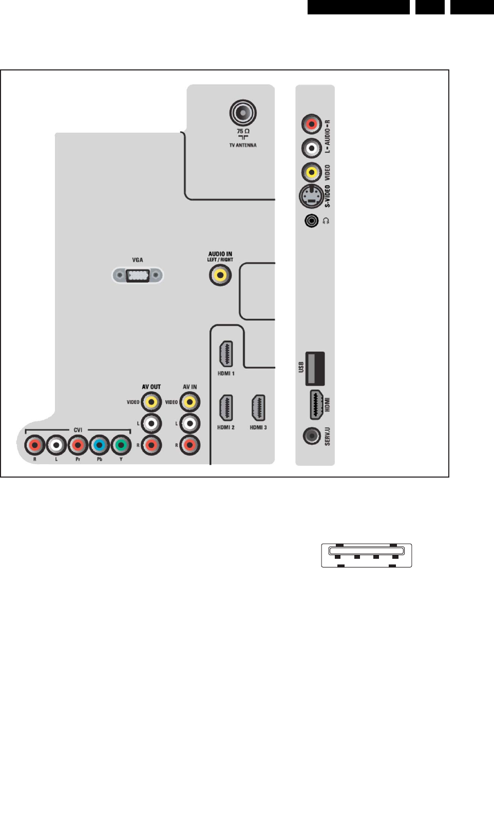
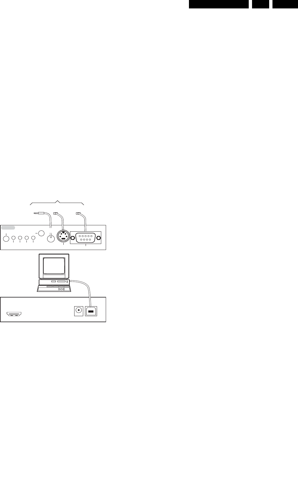
2.3 Connections
Figure 2-1 Connection overview
Note: The following connector colour abbreviations are used
(according to DIN/IEC 757): Bk= Black, Bu= Blue, Gn= Green,
Gy= Grey, Rd= Red, Wh= White, Ye= Yellow.
2.3.1 Side Connections
Cinch: Audio - In
Rd - Audio R 0.5 VRMS / 10 kΩ jq
Wh - Audio L 0.5 VRMS / 10 kΩ jq
Cinch: Video CVBS - In
Ye - Video CVBS 1 VPP / 75 Ω jq
S-Video (Hosiden): Video Y/C - In
1 - Ground Y Gnd H
2 - Ground C Gnd H
3 - Video Y 1 VPP / 75 Ω j
4 - Video C 0.3 VPP / 75 Ω j
Head phone (Output)
Bk - Head phone 32 - 600 Ω / 10 mW ot
USB2.0
Figure 2-2 USB (type A)
1-+5V k
2 - Data (-) jk
3 - Data (+) jk
4 - Ground Gnd H
HDMI: Digital Video, Digital Audio - In
(see HDMI 1, 2 & 3)
Service Connector (UART)
1 - Ground Gnd H
2 - UART_TX Transmit k
3 - UART_RX Receive j
18490_001_090409.eps
090409
Rear connectors
Side connectors
1 2 3 4
10000_022_090121.eps
090121

Technical Specifications and Connections
EN 4 LC9.1A LA2.
2009-Apr-10
2.3.2 Rear Connections
Aerial - In
- - IEC-type (EU) Coax, 75 Ω D
VGA: Video RGB - In
Figure 2-3 VGA Connector
1 - Video Red 0.7 VPP / 75 Ω j
2 - Video Green 0.7 VPP / 75 Ω j
3 - Video Blue 0.7 VPP / 75 Ω j
4-n.c.
5 - Ground Gnd H
6 - Ground Red Gnd H
7 - Ground Green Gnd H
8 - Ground Blue Gnd H
9-+5V
DC +5 V j
10 - Ground Sync Gnd H
11 - n.c.
12 - DDC_SDA DDC data j
13 - H-sync 0 - 5 V j
14 - V-sync 0 - 5 V j
15 - DDC_SCL DDC clock j
Mini Jack: Audio - In
Wh - Audio L 0.5 VRMS / 10 kΩjo
Rd - Audio R 0.5 VRMS / 10 kΩjo
CVI: Cinch: Video YPbPr - In, Audio - In
Gn - Video Y 1 VPP / 75 Ω jq
Bu - Video Pb 0.7 VPP / 75 Ω jq
Rd - Video Pr 0.7 VPP / 75 Ω jq
Rd - Audio - R 0.5 VRMS / 10 kΩ jq
Wh - Audio - L 0.5 VRMS / 10 kΩ jq
Cinch: Video CVBS - Out, Audio - Out
Ye - Video CVBS 1 VPP / 75 ohm kq
Wh - Audio L 0.5 VRMS /10 kohm kq
Rd - Audio R 0.5 VRMS / 10 kohm kq
Cinch: Video CVBS - In, Audio - In
Ye - Video CVBS 1 VPP / 75 ohm jq
Wh - Audio L 0.5 VRMS / 10 kohm jq
Rd - Audio R 0.5 VRMS / 10 kohm jq
HDMI 1, 2 & 3: Digital Video, Digital Audio - In
Figure 2-4 HDMI (type A) connector
1 - D2+ Data channel j
2 - Shield Gnd H
3 - D2- Data channel j
4 - D1+ Data channel j
5 - Shield Gnd H
6 - D1- Data channel j
7 - D0+ Data channel j
8 - Shield Gnd H
9 - D0- Data channel j
10 - CLK+ Data channel j
11 - Shield Gnd H
12 - CLK- Data channel j
13 - Easylink Control channel jk
14 - n.c.
15 - DDC_SCL DDC clock j
16 - DDC_SDA DDC data jk
17 - Ground Gnd H
18 - +5V j
19 - HPD Hot Plug Detect j
20 - Ground Gnd H
2.4 Chassis Overview
Refer to chapter 9. Block Diagrams for PWB/CBA locations.
1
610
11
5
15
10000_002_090121.eps
090127
19 1
18 2
E_06532_017.eps
250505

Precautions, Notes, and Abbreviation List EN 5LC9.1A LA 3.
2009-Apr-10
3. Precautions, Notes, and Abbreviation List
Index of this chapter:
3.1 Safety Instructions
3.2 Warnings
3.3 Notes
3.4 Abbreviation List
3.1 Safety Instructions
Safety regulations require the following during a repair:
• Connect the set to the Mains/AC Power via an isolation
transformer (> 800 VA).
• Replace safety components, indicated by the symbol h,
only by components identical to the original ones. Any
other component substitution (other than original type) may
increase risk of fire or electrical shock hazard. Of de set
ontploft!
Safety regulations require that after a repair, the set must be
returned in its original condition. Pay in particular attention to
the following points:
• Route the wire trees correctly and fix them with the
mounted cable clamps.
• Check the insulation of the Mains/AC Power lead for
external damage.
• Check the strain relief of the Mains/AC Power cord for
proper function.
• Check the electrical DC resistance between the Mains/AC
Power plug and the secondary side (only for sets that have
a Mains/AC Power isolated power supply):
1. Unplug the Mains/AC Power cord and connect a wire
between the two pins of the Mains/AC Power plug.
2. Set the Mains/AC Power switch to the “on” position
(keep the Mains/AC Power cord unplugged!).
3. Measure the resistance value between the pins of the
Mains/AC Power plug and the metal shielding of the
tuner or the aerial connection on the set. The reading
should be between 4.5 MΩ and 12 MΩ.
4. Switch “off” the set, and remove the wire between the
two pins of the Mains/AC Power plug.
• Check the cabinet for defects, to prevent touching of any
inner parts by the customer.
3.2 Warnings
• All ICs and many other semiconductors are susceptible to
electrostatic discharges (ESD w). Careless handling
during repair can reduce life drastically. Make sure that,
during repair, you are connected with the same potential as
the mass of the set by a wristband with resistance. Keep
components and tools also at this same potential.
• Be careful during measurements in the high voltage
section.
• Never replace modules or other components while the unit
is switched “on”.
• When you align the set, use plastic rather than metal tools.
This will prevent any short circuits and the danger of a
circuit becoming unstable.
3.3 Notes
3.3.1 General
• Measure the voltages and waveforms with regard to the
chassis (= tuner) ground (H), or hot ground (I), depending
on the tested area of circuitry. The voltages and waveforms
shown in the diagrams are indicative. Measure them in the
Service Default Mode with a colour bar signal and stereo
sound (L: 3 kHz, R: 1 kHz unless stated otherwise) and
picture carrier at 475.25 MHz for PAL, or 61.25 MHz for
NTSC (channel 3).
• Where necessary, measure the waveforms and voltages
with (D) and without (E) aerial signal. Measure the
voltages in the power supply section both in normal
operation (G) and in stand-by (F). These values are
indicated by means of the appropriate symbols.
3.3.2 Schematic Notes
• All resistor values are in ohms, and the value multiplier is
often used to indicate the decimal point location (e.g. 2K2
indicates 2.2 kΩ).
• Resistor values with no multiplier may be indicated with
either an “E” or an “R” (e.g. 220E or 220R indicates 220 Ω).
• All capacitor values are given in micro-farads (μ=× 10-6),
nano-farads (n =× 10-9), or pico-farads (p =× 10-12).
• Capacitor values may also use the value multiplier as the
decimal point indication (e.g. 2p2 indicates 2.2 pF).
• An “asterisk” (*) indicates component usage varies. Refer
to the diversity tables for the correct values.
• The correct component values are listed on the Philips
Spare Parts Web Portal.
3.3.3 Spare Parts
For the latest spare part overview, consult your Philips Spare
Part web portal.
3.3.4 BGA (Ball Grid Array) ICs
Introduction
For more information on how to handle BGA devices, visit this
URL: http://www.atyourservice-magazine.com. Select
“Magazine”, then go to “Repair downloads”. Here you will find
Information on how to deal with BGA-ICs.
BGA Temperature Profiles
For BGA-ICs, you must use the correct temperature-profile.
Where applicable and available, this profile is added to the IC
Data Sheet information section in this manual.
3.3.5 Lead-free Soldering
Due to lead-free technology some rules have to be respected
by the workshop during a repair:
• Use only lead-free soldering tin. If lead-free solder paste is
required, please contact the manufacturer of your soldering
equipment. In general, use of solder paste within
workshops should be avoided because paste is not easy to
store and to handle.
• Use only adequate solder tools applicable for lead-free
soldering tin. The solder tool must be able:
– To reach a solder-tip temperature of at least 400°C.
– To stabilize the adjusted temperature at the solder-tip.
– To exchange solder-tips for different applications.
• Adjust your solder tool so that a temperature of around
360°C - 380°C is reached and stabilized at the solder joint.
Heating time of the solder-joint should not exceed ~ 4 sec.
Avoid temperatures above 400°C, otherwise wear-out of
tips will increase drastically and flux-fluid will be destroyed.
To avoid wear-out of tips, switch “off” unused equipment or
reduce heat.
• Mix of lead-free soldering tin/parts with leaded soldering
tin/parts is possible but PHILIPS recommends strongly to
avoid mixed regimes. If this cannot be avoided, carefully
clear the solder-joint from old tin and re-solder with new tin.

Precautions, Notes, and Abbreviation List
EN 6 LC9.1A LA3.
2009-Apr-10
3.3.6 Alternative BOM identification
It should be noted that on the European Service website,
“Alternative BOM” is referred to as “Design variant”.
The third digit in the serial number (example:
AG2B0335000001) indicates the number of the alternative
B.O.M. (Bill Of Materials) that has been used for producing the
specific TV set. In general, it is possible that the same TV
model on the market is produced with e.g. two different types
of displays, coming from two different suppliers. This will then
result in sets which have the same CTN (Commercial Type
Number; e.g. 28PW9515/12) but which have a different B.O.M.
number.
By looking at the third digit of the serial number, one can
identify which B.O.M. is used for the TV set he is working with.
If the third digit of the serial number contains the number “1”
(example: AG1B033500001), then the TV set has been
manufactured according to B.O.M. number 1. If the third digit is
a “2” (example: AG2B0335000001), then the set has been
produced according to B.O.M. no. 2. This is important for
ordering the correct spare parts!
For the third digit, the numbers 1...9 and the characters A...Z
can be used, so in total: 9 plus 26= 35 different B.O.M.s can be
indicated by the third digit of the serial number.
Identification: The bottom line of a type plate gives a 14-digit
serial number. Digits 1 and 2 refer to the production centre (e.g.
AG is Bruges), digit 3 refers to the B.O.M. code, digit 4 refers
to the Service version change code, digits 5 and 6 refer to the
production year, and digits 7 and 8 refer to production week (in
example below it is 2006 week 17). The 6 last digits contain the
serial number.
Figure 3-1 Serial number (example)
3.3.7 Board Level Repair (BLR) or Component Level Repair
(CLR)
If a board is defective, consult your repair procedure to decide
if the board has to be exchanged or if it should be repaired on
component level.
If your repair procedure says the board should be exchanged
completely, do not solder on the defective board. Otherwise, it
cannot be returned to the O.E.M. supplier for back charging!
3.3.8 Practical Service Precautions
•It makes sense to avoid exposure to electrical shock.
While some sources are expected to have a possible
dangerous impact, others of quite high potential are of
limited current and are sometimes held in less regard.
•Always respect voltages. While some may not be
dangerous in themselves, they can cause unexpected
reactions that are best avoided. Before reaching into a
powered TV set, it is best to test the high voltage insulation.
It is easy to do, and is a good service precaution.
3.4 Abbreviation List
0/6/12 SCART switch control signal on A/V
board. 0 = loop through (AUX to TV),
6 = play 16 : 9 format, 12 = play 4 : 3
format
AARA Automatic Aspect Ratio Adaptation:
algorithm that adapts aspect ratio to
remove horizontal black bars; keeps
the original aspect ratio
ACI Automatic Channel Installation:
algorithm that installs TV channels
directly from a cable network by
means of a predefined TXT page
ADC Analogue to Digital Converter
AFC Automatic Frequency Control: control
signal used to tune to the correct
frequency
AGC Automatic Gain Control: algorithm that
controls the video input of the feature
box
AM Amplitude Modulation
AP Asia Pacific
AR Aspect Ratio: 4 by 3 or 16 by 9
ASF Auto Screen Fit: algorithm that adapts
aspect ratio to remove horizontal black
bars without discarding video
information
ATSC Advanced Television Systems
Committee, the digital TV standard in
the USA
ATV See Auto TV
Auto TV A hardware and software control
system that measures picture content,
and adapts image parameters in a
dynamic way
AV External Audio Video
AVC Audio Video Controller
AVIP Audio Video Input Processor
B/G Monochrome TV system. Sound
carrier distance is 5.5 MHz
BLR Board-Level Repair
BTSC Broadcast Television Standard
Committee. Multiplex FM stereo sound
system, originating from the USA and
used e.g. in LATAM and AP-NTSC
countries
B-TXT Blue TeleteXT
C Centre channel (audio)
CEC Consumer Electronics Control bus:
remote control bus on HDMI
connections
CL Constant Level: audio output to
connect with an external amplifier
CLR Component Level Repair
ComPair Computer aided rePair
CP Connected Planet / Copy Protection
CSM Customer Service Mode
CTI Color Transient Improvement:
manipulates steepness of chroma
transients
CVBS Composite Video Blanking and
Synchronization
DAC Digital to Analogue Converter
DBE Dynamic Bass Enhancement: extra
low frequency amplification
DDC See “E-DDC”
D/K Monochrome TV system. Sound
carrier distance is 6.5 MHz
DFI Dynamic Frame Insertion
DFU Directions For Use: owner's manual
DMR Digital Media Reader: card reader
DMSD Digital Multi Standard Decoding
DNM Digital Natural Motion
10000_024_090121.eps
090121
MODEL :
PROD.NO:
~
S
32PF9968/10
MADE IN BELGIUM
220-240V 50/60Hz
128W
AG 1A0617 000001
VHF+S+H+UHF
BJ3.0E LA

Precautions, Notes, and Abbreviation List EN 7LC9.1A LA 3.
2009-Apr-10
DNR Digital Noise Reduction: noise
reduction feature of the set
DRAM Dynamic RAM
DRM Digital Rights Management
DSP Digital Signal Processing
DST Dealer Service Tool: special remote
control designed for service
technicians
DTCP Digital Transmission Content
Protection; A protocol for protecting
digital audio/video content that is
traversing a high speed serial bus,
such as IEEE-1394
DVB-C Digital Video Broadcast - Cable
DVB-T Digital Video Broadcast - Terrestrial
DVD Digital Versatile Disc
DVI(-d) Digital Visual Interface (d= digital only)
E-DDC Enhanced Display Data Channel
(VESA standard for communication
channel and display). Using E-DDC,
the video source can read the EDID
information form the display.
EDID Extended Display Identification Data
(VESA standard)
EEPROM Electrically Erasable and
Programmable Read Only Memory
EMI Electro Magnetic Interference
EPLD Erasable Programmable Logic Device
EU Europe
EXT EXTernal (source), entering the set by
SCART or by cinches (jacks)
FDS Full Dual Screen (same as FDW)
FDW Full Dual Window (same as FDS)
FLASH FLASH memory
FM Field Memory or Frequency
Modulation
FPGA Field-Programmable Gate Array
FTV Flat TeleVision
Gb/s Giga bits per second
G-TXT Green TeleteXT
H H_sync to the module
HD High Definition
HDD Hard Disk Drive
HDCP High-bandwidth Digital Content
Protection: A “key” encoded into the
HDMI/DVI signal that prevents video
data piracy. If a source is HDCP coded
and connected via HDMI/DVI without
the proper HDCP decoding, the
picture is put into a “snow vision” mode
or changed to a low resolution. For
normal content distribution the source
and the display device must be
enabled for HDCP “software key”
decoding.
HDMI High Definition Multimedia Interface
HP HeadPhone
I Monochrome TV system. Sound
carrier distance is 6.0 MHz
I2C Inter IC bus
I2D Inter IC Data bus
I2S Inter IC Sound bus
IF Intermediate Frequency
IR Infra Red
IRQ Interrupt Request
ITU-656 The ITU Radio communication Sector
(ITU-R) is a standards body
subcommittee of the International
Telecommunication Union relating to
radio communication. ITU-656 (a.k.a.
SDI), is a digitized video format used
for broadcast grade video.
Uncompressed digital component or
digital composite signals can be used.
The SDI signal is self-synchronizing,
uses 8 bit or 10 bit data words, and has
a maximum data rate of 270 Mbit/s,
with a minimum bandwidth of 135
MHz.
ITV Institutional TeleVision; TV sets for
hotels, hospitals etc.
LS Last Status; The settings last chosen
by the customer and read and stored
in RAM or in the NVM. They are called
at start-up of the set to configure it
according to the customer's
preferences
LATAM Latin America
LCD Liquid Crystal Display
LED Light Emitting Diode
L/L' Monochrome TV system. Sound
carrier distance is 6.5 MHz. L' is Band
I, L is all bands except for Band I
LPL LG.Philips LCD (supplier)
LS Loudspeaker
LVDS Low Voltage Differential Signalling
Mbps Mega bits per second
M/N Monochrome TV system. Sound
carrier distance is 4.5 MHz
MIPS Microprocessor without Interlocked
Pipeline-Stages; A RISC-based
microprocessor
MOP Matrix Output Processor
MOSFET Metal Oxide Silicon Field Effect
Transistor, switching device
MPEG Motion Pictures Experts Group
MPIF Multi Platform InterFace
MUTE MUTE Line
NC Not Connected
NICAM Near Instantaneous Compounded
Audio Multiplexing. This is a digital
sound system, mainly used in Europe.
NTC Negative Temperature Coefficient,
non-linear resistor
NTSC National Television Standard
Committee. Color system mainly used
in North America and Japan. Color
carrier NTSC M/N= 3.579545 MHz,
NTSC 4.43= 4.433619 MHz (this is a
VCR norm, it is not transmitted off-air)
NVM Non-Volatile Memory: IC containing
TV related data such as alignments
O/C Open Circuit
OSD On Screen Display
OTC On screen display Teletext and
Control; also called Artistic (SAA5800)
P50 Project 50: communication protocol
between TV and peripherals
PAL Phase Alternating Line. Color system
mainly used in West Europe (color
carrier= 4.433619 MHz) and South
America (color carrier PAL M=
3.575612 MHz and PAL N= 3.582056
MHz)
PCB Printed Circuit Board (same as “PWB”)
PCM Pulse Code Modulation
PDP Plasma Display Panel
PFC Power Factor Corrector (or Pre-
conditioner)
PIP Picture In Picture
PLL Phase Locked Loop. Used for e.g.
FST tuning systems. The customer
can give directly the desired frequency
POD Point Of Deployment: a removable
CAM module, implementing the CA
system for a host (e.g. a TV-set)
POR Power On Reset, signal to reset the uP
PTC Positive Temperature Coefficient,
non-linear resistor
PWB Printed Wiring Board (same as “PCB”)

Precautions, Notes, and Abbreviation List
EN 8 LC9.1A LA3.
2009-Apr-10
PWM Pulse Width Modulation
QRC Quasi Resonant Converter
QTNR Quality Temporal Noise Reduction
QVCP Quality Video Composition Processor
RAM Random Access Memory
RGB Red, Green, and Blue. The primary
color signals for TV. By mixing levels
of R, G, and B, all colors (Y/C) are
reproduced.
RC Remote Control
RC5 / RC6 Signal protocol from the remote
control receiver
RESET RESET signal
ROM Read Only Memory
RSDS Reduced Swing Differential Signalling
data interface
R-TXT Red TeleteXT
SAM Service Alignment Mode
S/C Short Circuit
SCART Syndicat des Constructeurs
d'Appareils Radiorécepteurs et
Téléviseurs
SCL Serial Clock I2C
SCL-F CLock Signal on Fast I2C bus
SD Standard Definition
SDA Serial Data I2C
SDA-F DAta Signal on Fast I2C bus
SDI Serial Digital Interface, see “ITU-656”
SDRAM Synchronous DRAM
SECAM SEequence Couleur Avec Mémoire.
Color system mainly used in France
and East Europe. Color carriers=
4.406250 MHz and 4.250000 MHz
SIF Sound Intermediate Frequency
SMPS Switched Mode Power Supply
SoC System on Chip
SOG Sync On Green
SOPS Self Oscillating Power Supply
SPI Serial Peripheral Interface bus; a 4-
wire synchronous serial data link
standard
S/PDIF Sony Philips Digital InterFace
SRAM Static RAM
SRP Service Reference Protocol
SSB Small Signal Board
STBY STand-BY
SVGA 800x600 (4:3)
SVHS Super Video Home System
SW Software
SWAN Spatial temporal Weighted Averaging
Noise reduction
SXGA 1280x1024
TFT Thin Film Transistor
THD Total Harmonic Distortion
TMDS Transmission Minimized Differential
Signalling
TXT TeleteXT
TXT-DW Dual Window with TeleteXT
UI User Interface
uP Microprocessor
UXGA 1600x1200 (4:3)
V V-sync to the module
VESA Video Electronics Standards
Association
VGA 640x480 (4:3)
VL Variable Level out: processed audio
output toward external amplifier
VSB Vestigial Side Band; modulation
method
WYSIWYR What You See Is What You Record:
record selection that follows main
picture and sound
WXGA 1280x768 (15:9)
XTAL Quartz crystal
XGA 1024x768 (4:3)
Y Luminance signal
Y/C Luminance (Y) and Chrominance (C)
signal
YPbPr Component video. Luminance and
scaled color difference signals (B-Y
and R-Y)
YUV Component video
Mechanical Instructions EN 9LC9.1A LA 4.
2009-Apr-10
4. Mechanical Instructions
Index of this chapter:
4.1 Cable Dressing
4.2 Service Positions
4.3 Assy/Panel Removal
4.4 Set Re-assembly
Notes:
• Figures below can deviate slightly from the actual situation,
due to the different set executions.
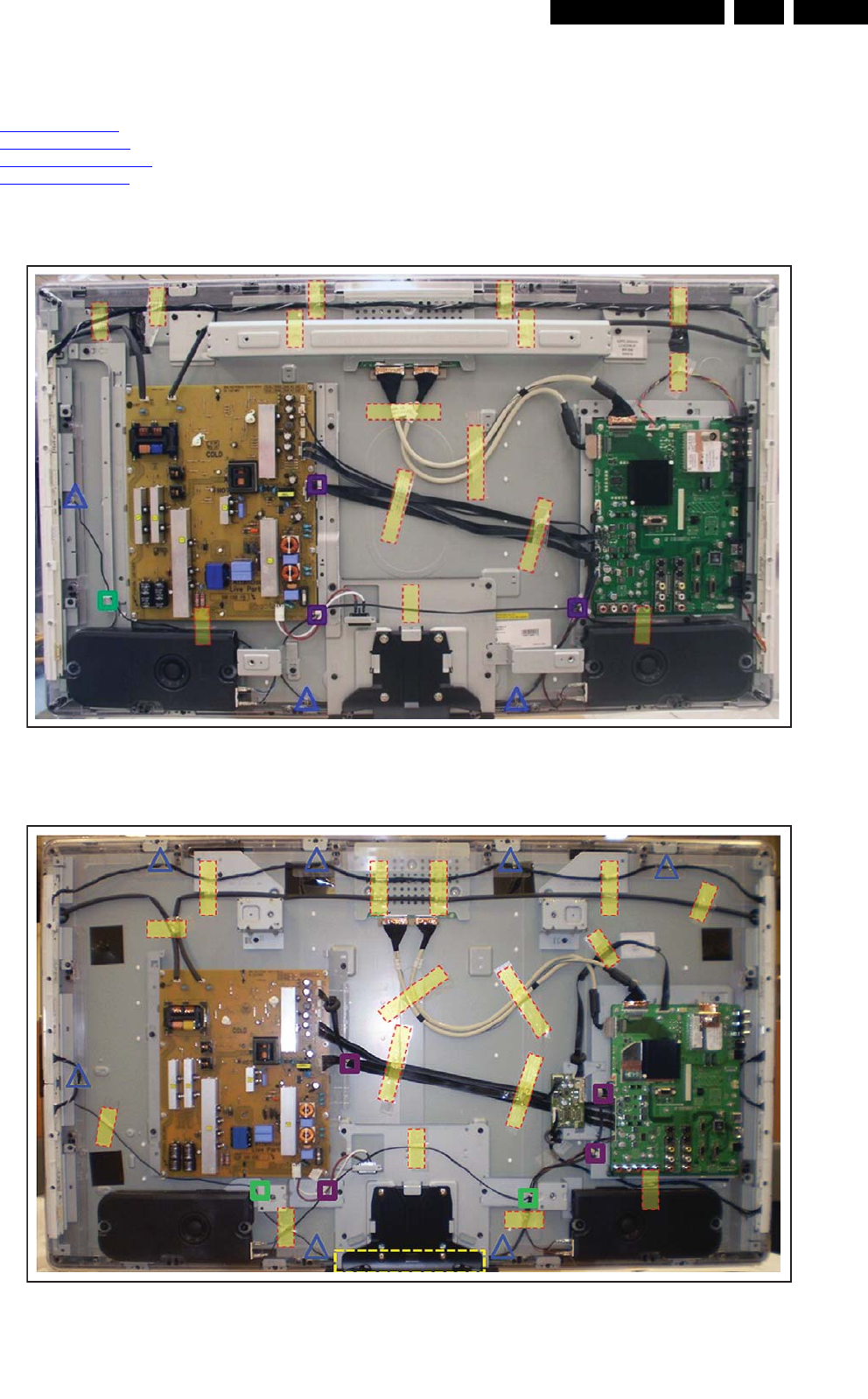
4.1 Cable Dressing
Figure 4-1 Cable dressing 42" (Frame styling)
Figure 4-2 Cable dressing 47" (Frame styling)
18490_100_090409.eps
090409
18490_101_090409.eps
090409
Mechanical Instructions
EN 10 LC9.1A LA4.
2009-Apr-10
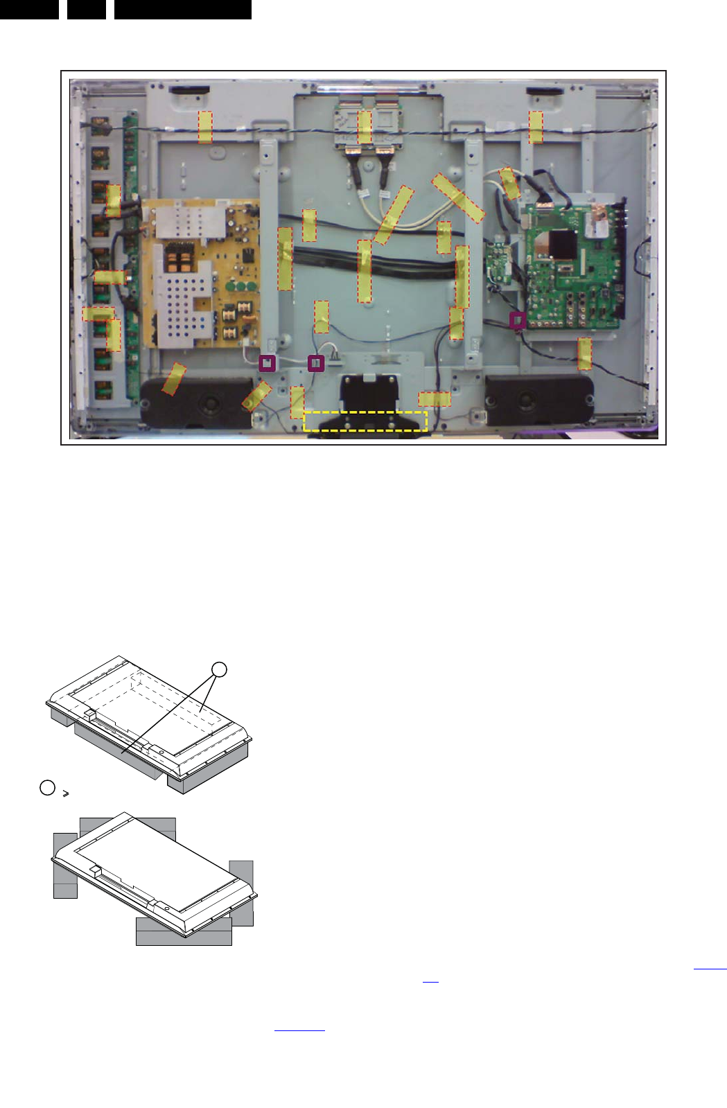
Figure 4-3 Cable dressing 52" (Frame styling)
4.2 Service Positions
For easy servicing of this set, there are a few possibilities
created:
• The buffers from the packaging.
• Foam bars (created for Service).
4.2.1 Foam Bars
Figure 4-4 Foam bars
The foam bars (order code 3122 785 90580 for two pieces) can
be used for all types and sizes of Flat TVs. See Figure 4-4 for
details. Sets with a display of 42" and larger, require four foam
bars [1]. Ensure that the foam bars are always supporting the
cabinet and never only the display.
Caution: Failure to follow these guidelines can seriously
damage the display!
By laying the TV face down on the (ESD protective) foam bars,
a stable situation is created to perform measurements and
alignments. By placing a mirror under the TV, you can monitor
the screen.
4.3 Assy/Panel Removal
The instructions apply to the Roadrunner styling - with
AmbiLight.
4.3.1 Rear Cover
Warning: Disconnect the mains power cord before you remove
the rear cover.
Note: it is not necessary to remove the stand while removing
the rear cover.
1. Remove all screws of the rear cover.
2. Lift the rear cover from the TV. Make sure that wires and
flat coils are not damaged while lifting the rear cover from
the set.
4.3.2 Speakers
Each speaker unit is mounted with two screws.
When defective, replace the whole unit.
4.3.3 Ambi Light
Each Ambi Light unit is mounted on a subframe. Refer to Figure
4-5 for details.
18490_102_090409.eps
090409
E_06532_018.eps
171106
1
Required for sets
42"
1
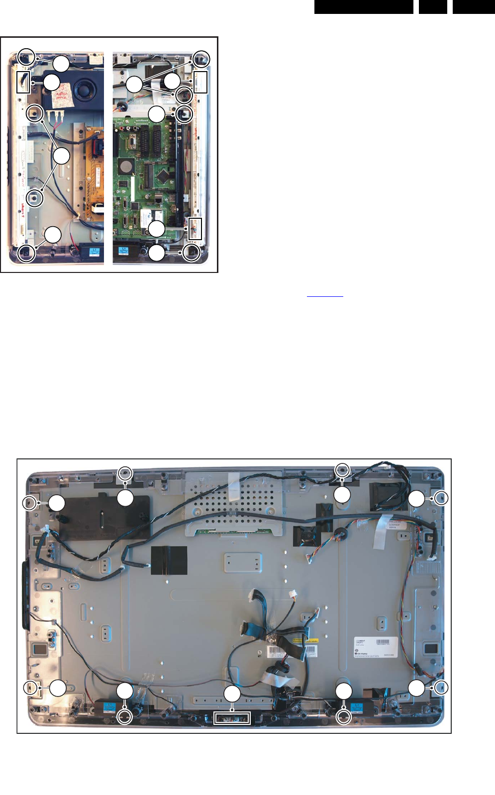
Mechanical Instructions EN 11LC9.1A LA 4.
2009-Apr-10
Figure 4-5 Ambi Light unit
1. Remove the Ambi Light cover [1].
2. Unplug the connector(s) [2].
3. Remove the subframe [3].
4. The PWB can now be taken from the subframe.
When defective, replace the whole unit.
4.3.4 Main Supply Panel
1. Unplug all connectors.
2. Remove the fixation screws.
3. Take the board out.
When defective, replace the whole unit.
4.3.5 IR & LED Board / Stand Support
For removing the IR & LED board, the stand including support
has to be removed
When defective, replace the whole unit.
4.3.6 Small Signal Board (SSB)
Caution: It is mandatory to remount screws at their original
position during re-assembly. Failure to do so may result in
damaging the SSB.
1. Unplug all connectors.
2. Remove the screws that secure the board.
3. The SSB can now be taken out of the set.
4.3.7 Keyboard Control Panel
1. Remove the right AmbiLight unit.
2. Remove the connector on the IR/LED board.
3. Release the cable.
4. Release the clip on top of the unit and take the unit out.
When defective, replace the whole unit.
4.3.8 LCD Panel
Refer to Figure 4-6 for details.
1. Remove the AmbiLight units as earlier described.
2. Remove the Top Support.
3. Release the LVDS - and other connectors from the SSB.
4. Remove the subframe of the SSB with the SSB still
mounted on it.
5. Release all connectors from the PSU.
6. Remove the subframe of the PSU with the PSU still
mounted on it.
7. Remove the stand + stand support as earlier described.
8. Release the connectors [1] on the IR & LED Panel.
9. Remove the clips that secure the flare [2].
10. Remove the flare.
11. Now the LCD Panel can be lifted from the front cabinet.
Figure 4-6 LCD Panel - panel removal
18560_408_090401.eps
090402
3
1
2
1
1
3
12
2
18490_103_090410.eps
090410
22
2
22122
2

Mechanical Instructions
EN 12 LC9.1A LA4.
2009-Apr-10
4.4 Set Re-assembly
To re-assemble the whole set, execute all processes in reverse
order.
Notes:
• While re-assembling, make sure that all cables are placed
and connected in their original position. See figure Figure
4-1, Figure 4-2 or Figure 4-3.
• Pay special attention not to damage the EMC foams on the
SSB shields. Ensure that EMC foams are mounted
correctly.
Service Modes, Error Codes, and Fault Finding EN 13LC9.1A LA 5.
2009-Apr-10
5. Service Modes, Error Codes, and Fault Finding
Index of this chapter:
5.1 Test Points
5.2 Service Modes
5.3 Service Tools
5.4 Error Codes
5.5 The Blinking LED Procedure
5.6 Fault Finding and Repair Tips
5.7 Software Upgrading
5.1 Test Points
In the chassis schematics and layout overviews, the test points
are mentioned. In the schematics, test points are indicated with
“Fxxx” or “Ixxx”, in the layout overviews with a “half-moon” sign.
As most signals are digital, it will be difficult to measure
waveforms with a standard oscilloscope. Several key ICs are
capable of generating test patterns, which can be controlled via
ComPair. In this way it is possible to determine which part is
defective.
Perform measurements under the following conditions:
• Service Default Mode.
• Video: Colour bar signal.
• Audio: 3 kHz left, 1 kHz right.
5.2 Service Modes
The Service Mode feature is split into four parts:
• Service Default Mode (SDM).
• Service Alignment Mode (SAM).
• Customer Service Mode (CSM).
• Computer Aided Repair Mode (ComPair).
SDM and SAM offer features, which can be used by the Service
engineer to repair/align a TV set. Some features are:
• A pre-defined situation to ensure measurements can be
made under uniform conditions (SDM).
• Activates the blinking LED procedure for error identification
when no picture is available (SDM).
• The possibility to overrule software protections when SDM
is entered via the Service pins.
• Make alignments (e.g. White Tone), (de)select options,
enter options codes, reset the error buffer (SAM).
• Display information (“SDM” or “SAM” indication in upper
right corner of screen, error buffer, software version,
operating hours, options and option codes, sub menus).
The CSM is a Service Mode that can be enabled by the
consumer. The CSM displays diagnosis information, which the
customer can forward to the dealer or call centre. In CSM
mode, “CSM”, is displayed in the top right corner of the screen.
The information provided in CSM and the purpose of CSM is to:
• Increase the home repair hit rate.
• Decrease the number of nuisance calls.
• Solved customers' problem without home visit.
ComPair Mode is used for communication between a computer
and a TV on I2C /UART level and can be used by a Service
engineer to quickly diagnose the TV set by reading out error
codes, read and write in NVMs, communicate with ICs and the
uP (PWM, registers, etc.), and by making use of a fault finding
database. It will also be possible to up and download the
software of the TV set via I2C with help of ComPair. To do this,
ComPair has to be connected to the TV set via the ComPair
connector, which will be accessible through the rear of the set
(without removing the rear cover).
5.2.1 General
Some items are applicable to all Service Modes or are general.
These are listed below.
Life Timer
During the life time cycle of the TV set, a timer is kept (called
“Op. Hour”). It counts the normal operation hours (not the
Stand-by hours). The actual value of the timer is displayed in
SDM and SAM in a decimal value. Every two soft-resets
increase the hour by +1. Standby hours are not counted.
Software Identification, Version, and Cluster
The software ID, version, and cluster will be shown in the main
menu display of SDM, SAM, and CSM.
The screen will show: “AAAABCD X.YY”, where:
•AAAA is the chassis name: LC91.
•B is the region indication: E= Europe, A= AP/China, U=
NAFTA, L= LATAM.
•C is the display indication: L= LCD, P= Plasma.
•D is the language/feature indication: 1= Standard, H= Full
HD.
•X is the main version number: this is updated with a major
change of specification (incompatible with the previous
software version). Numbering will go from 1 - 9 and A - Z.
– If the main version number changes, the new version
number is written in the NVM.
– If the main version number changes, the default
settings are loaded.
•YY is the sub version number: this is updated with a minor
change (backwards compatible with the previous versions)
Numbering will go from 00 - 99.
– If the sub version number changes, the new version
number is written in the NVM.
– If the NVM is fresh, the software identification, version,
and cluster will be written to NVM.
Display Option Code Selection
When after an SSB or display exchange, the display option
code is not set properly, it will result in a TV with “no display”.
Therefore, it is required to set this display option code after
such a repair.
To do so, press the following key sequence on a standard RC
transmitter: “062598” directly followed by MENU and “xxx”,
where “xxx” is a 3 digit decimal value of the panel type: see
column “Display Code” in Table 6-5 , or see sticker on the side/
bottom of the cabinet. When the value is accepted and stored
in NVM, the set will switch to Stand-by, to indicate that the
process has been completed.
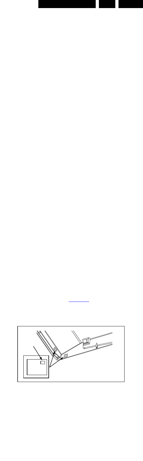
Figure 5-1 Location of Display Option Code sticker
During this algorithm, the NVM-content must be filtered,
because several items in the NVM are TV-related and not SSB-
related (e.g. Model and Prod. S/N). Therefore, “Model” and
“Prod. S/N” data is changed into “See Type Plate”.
In case a call centre or consumer reads “See Type Plate” in
CSM mode, he needs to look to the side/bottom sticker to
identify the set, for further actions.
PHILIPS
MODEL:
32PF9968/10
PROD.SERIAL NO:
AG 1A0620 000001
040
39mm
27mm
(CTN Sticker)
Display Option
Code
E_06532_038.eps
240108
Service Modes, Error Codes, and Fault Finding
EN 14 LC9.1A LA5.
2009-Apr-10
5.2.2 Service Default Mode (SDM)
Purpose
Set the TV in SDM mode in order to be able to create a pre-
defined setting for measurements to be made. In this platform,
a simplified SDM is introduced (without protection override and
without tuning to a frequency of 475.25 MHz).
Specifications
• Set linear video and audio settings to 50%, but volume to
25%. Stored user settings are not affected.
• All service-unfriendly modes (if present) are disabled, since
they interfere with diagnosing/repairing a set. These
service unfriendly modes are:
– (Sleep) timer.
– Blue mute/Wall paper.
– Auto switch “off” (when there is no “ident” signal).
– Hotel or hospital mode.
– Child lock or parental lock (manual or via V-chip).
– Skipping, blanking of “Not favourite”, “Skipped” or
“Locked” presets/channels.
– Automatic storing of Personal Preset or Last Status
settings.
– Automatic user menu time-out (menu switches back/
OFF automatically.
– Auto Volume levelling (AVL).
How to Activate
To activate SDM, use one of the following methods:
• Press the following key sequence on the remote control
transmitter: “062596” directly followed by the MENU button
(do not allow the display to time out between entries while
keying the sequence).
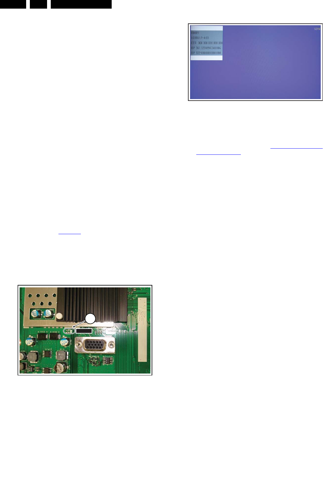
• Short one of the “Service” jumpers on the TV board during
cold start (see Figure 5-2). Then press the mains button
(remove the short after start-up).
Caution: Activating SDM by shorting “Service” jumpers will
override the DC speaker protection (error 1), the General
I2C error (error 4), and the Trident video processor error
(error 5). When doing this, the service-technician must
know exactly what he is doing, as it could damage the
television set.
Figure 5-2 Service jumper (SSB component side)
On Screen Menu
After activating SDM, the following screen is visible, with SDM
in the upper right corner of the screen to indicate that the
television is in Service Default Mode.
Figure 5-3 SDM menu
Menu explanation:
•HHHHH: Are the operating hours (in decimal).
•AAAABCD-X.YY: See paragraph Software Identification,
Version, and Cluster for the SW name definition.
•ERR: Shows all errors detected since the last time the
buffer was erased in format <xxx> <xxx> <xxx> <xxx>
<xxx> (five errors possible).
•OP: Used to read-out the option bytes. See “Options” in the
Alignments section for a detailed description. Ten codes (in
two rows) are possible.
How to Navigate
As this mode is read only, there is not much to navigate. To
switch to other modes, use one of the following methods:
• Command MENU from the user remote will enter the
normal user menu (brightness, contrast, colour, etc...) with
“SDM” OSD remaining, and pressing MENU key again will
return to the last status of SDM again.
• To prevent the OSD from interfering with measurements in
SDM, command “OSD” or “i+” (“STATUS” or “INFO” for
NAFTA and LATAM) from the user remote will toggle the
OSD “on/off” with “SDM” OSD remaining always “on”.
• Press the following key sequence on the remote control
transmitter: “062596” directly followed by the OSD/
STATUS/INFO/i+ button to switch to SAM (do not allow the
display to time out between entries while keying the
sequence).
How to Exit
Switch the set to STANDBY by pressing the mains button on
the remote control transmitter or on the television set.
If you switch the television set “off” by removing the mains (i.e.,
unplugging the television), the television set will remain in SDM
when mains is re-applied, and the error buffer is not cleared.
The error buffer will only be cleared when the “clear” command
is used in the SAM menu.
Note:
• If the TV is switched “off” by a power interrupt while in SDM,
the TV will show up in the last status of SDM menu as soon
as the power is supplied again. The error buffer will not be
cleared.
• In case the set is in Factory mode by accident (with “F”
displayed on screen), by pressing and hold “VOL-“ and
“CH-” together should leave Factory mode.
18490_201_090409.eps
090409
1
SDM
1
SDM
H_17740_030.eps
230108
Service Modes, Error Codes, and Fault Finding EN 15LC9.1A LA 5.
2009-Apr-10
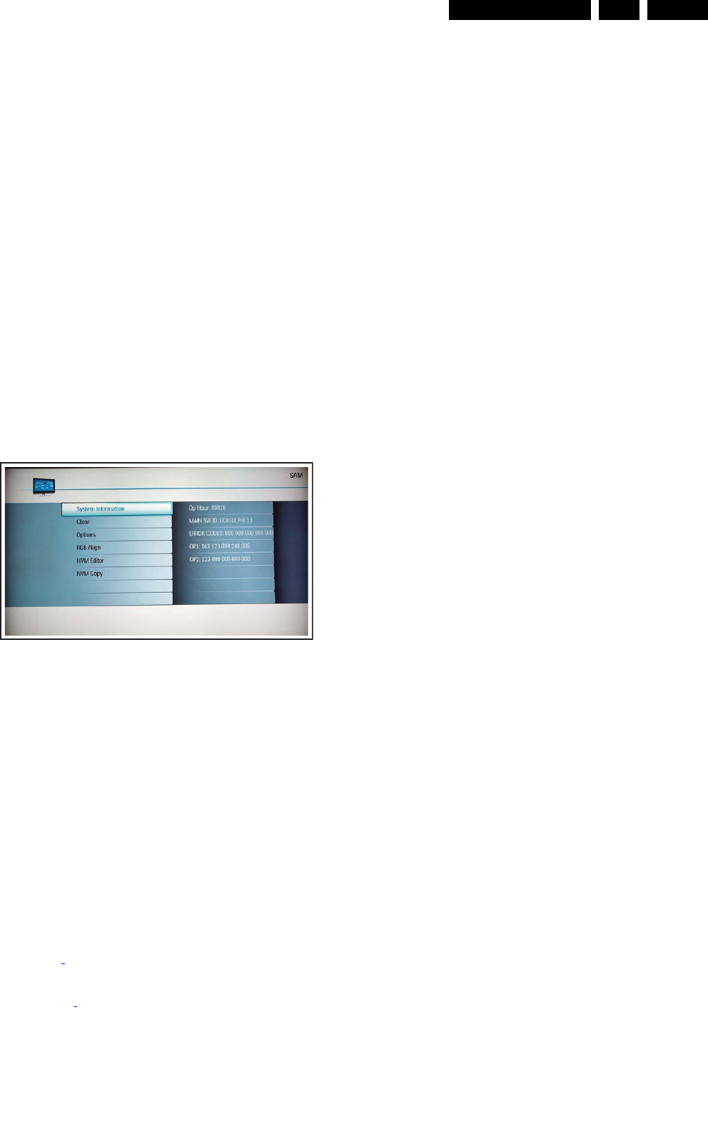
5.2.3 Service Alignment Mode (SAM)
Purpose
• To change option settings.
• To display / clear the error code buffer.
• To perform alignments.
Specifications
• Operation hours counter (maximum five digits displayed).
• Software version, error codes, and option settings display.
• Error buffer clearing.
• Option settings.
• Software alignments (White Tone).
• NVM Editor.
• Set screen mode to full screen (all content is visible).
How to Activate
To activate SAM, use one of the following methods:
• Press the following key sequence on the remote control
transmitter: “062596” directly followed by the OSD/
STATUS/INFO/i+ button (it depends on region which
button is present on the RC). Do not allow the display to
time out between entries while keying the sequence.
• Or via ComPair.
After entering SAM, the following screen is visible, with SAM in
the upper right corner of the screen to indicate that the
television is in Service Alignment Mode.
Figure 5-4 SAM menu
Menu explanation:
1. System Information:
•Op. Hour. This represents the life timer. The timer
counts normal operation hours, but does not count
Stand-by hours.
•MAIN SW ID. See paragraph Software Identification,
Version, and Cluster for the SW name definition.
•ERROR CODES. Shows all errors detected since the
last time the buffer was erased. Five errors possible.
•OP1 / OP2. Used to read-out the option bytes. See
paragraph 6.4 Option Settings in the Alignments
section for a detailed description. Ten codes are
possible.
2. Clear. Erases the contents of the error buffer. Select the
CLEAR menu item and press the MENU RIGHT key. The
content of the error buffer is cleared.
3. Options. To set the option bits. See paragraph 6.4 Option
Settings in the “Alignments” chapter for a detailed
description.
4. RGB Align. To align the White Tone. See White Tone
Alignment: for a detailed description.
5. NVM Editor. To change the NVM data in the television set.
See also paragraph 5.6 Fault Finding and Repair Tips.
6. NVM Copy. Gives the possibility to copy/load the NVM file
to/from an USB stick. NVM data copied to a USB memory
device is named “NVM_COPY.BIN”. When copied back to
a TV, the file first must have the same name.
How to Navigate
• In the SAM menu, select menu items with the UP/DOWN
keys on the remote control transmitter. The selected item
will be indicated. When not all menu items fit on the screen,
use the UP/DOWN keys to display the next / previous
menu items.
• With the LEFT/RIGHT keys, it is possible to:
– Activate the selected menu item.
– Change the value of the selected menu item.
– Activate the selected sub menu.
• When you press the MENU button twice while in top level
SAM, the set will switch to the normal user menu (with the
SAM mode still active in the background). To return to the
SAM menu press the MENU button.
• The “OSD/STATUS/INFO/i+” key from the user remote will
toggle the OSD “on/off” with “SAM” OSD remaining always
“on”.
• Press the following key sequence on the remote control
transmitter: “062596” directly followed by the MENU button
to switch to SDM (do not allow the display to time out
between entries while keying the sequence).
How to Store SAM Settings
To store the settings changed in SAM mode (except the
OPTIONS and RGB ALIGN settings), leave the top level SAM
menu by using the POWER button on the remote control
transmitter or the television set. The mentioned exceptions
must be stored separately via the STORE button.
How to Exit
Switch the set to STANDBY by pressing the mains button on
the remote control transmitter or the television set.
Note:
• When the TV is switched “off” by a power interrupt while in
SAM, the TV will show up in “normal operation mode” as
soon as the power is supplied again. The error buffer will
not be cleared.
• In case the set is in Factory mode by accident (with “F”
displayed on screen), by pressing and hold “VOL-“ and
“CH-” together should leave Factory mode.
H_17740_025.eps
230108

Service Modes, Error Codes, and Fault Finding
EN 16 LC9.1A LA5.
2009-Apr-10
5.2.4 Customer Service Mode (CSM)
Purpose
The Customer Service Mode shows error codes and
information on the TV’s operation settings. A call centre can
instruct the customer (by telephone) to enter CSM in order to
identify the status of the set. This helps them to diagnose
problems and failures in the TV before making a service call.
The CSM is a read-only mode; therefore, modifications are not
possible in this mode.
Specifications
• Ignore “Service unfriendly modes”.
• Line number for every line (to make CSM language
independent).
• Set the screen mode to full screen (all contents on screen
is visible).
• After leaving the Customer Service Mode, the original
settings are restored.
• Possibility to use “CH+” or “CH-” for channel surfing, or
enter the specific channel number on the RC.
How to Activate
To activate CSM, press the following key sequence on a
standard remote control transmitter: “123654” (do not allow the
display to time out between entries while keying the sequence).
Upon entering the Customer Service Mode, the following
screen will appear:
Figure 5-5 CSM menu -1- (example)
Figure 5-6 CSM menu -2- (example)
Menu Explanation
1. Model Number. Type number, e.g. 42PFL9509/93. (*)
2. Production Serial Number. Product serial no., e.g.
SV1A0908123456 (*). SV= Production centre, 1= BOM
code, A= Service version change code, 09= Production
year, 08= Production week, 123456= Serial number.
3. Software Version. Main software cluster and version is
displayed.
4. Option Code 1. Option code information (group 1).
5. Option Code 2. Option code information (group 2).
6. PSU. Indication of the PSU factory ID (= 12nc).
7. SSB. Indication of the SSB factory ID (= 12nc). (*)
8. Display. Indication of the display ID (=12 nc). (*)
9. NVM Version. The NVM software version no.
10. PQ Version. PQ (picture quality) data version. This is a
subset of the main SW.
11. Key (HDCP). Indicates if the HDMI keys (or HDCP keys)
are valid or not.
12. Audio System. Gives information about the audio system
of the selected transmitter.
13. Blank.
14. Video Format. Gives information about the video format of
the selected transmitter (480p30/720p60/1080i50/1080i60,
etc...). Is applicable to both HDMI and CVI sources.
15. Standby uP SW ID. Shows the Standby Processor
software version.
16. Bootloader ID. Shows the Bootloader software ID.
17. Panel code. Gives the number of the panel as stored in
NVM.
18. AP uP SW ID.Shows the AL uP software version.
(*) If an NVM IC is replaced or initialized, these items must be
re-written to the NVM. ComPair will foresee in a possibility to
do this.
How to Exit
To exit CSM, use one of the following methods:
• Press the MENU button twice on the remote control
transmitter.
• Press the POWER button on the remote control
transmitter.
• Press the POWER button on the television set.
18490_202_090409.eps
090409
18490_203_090409.eps
090409
Service Modes, Error Codes, and Fault Finding EN 17LC9.1A LA 5.
2009-Apr-10
5.3 Service Tools
5.3.1 ComPair
Introduction
ComPair (Computer Aided Repair) is a Service tool for Philips
Consumer Electronics products. and offers the following:
1. ComPair helps you to quickly get an understanding on how
to repair the chassis in a short and effective way.
2. ComPair allows very detailed diagnostics and is therefore
capable of accurately indicating problem areas. You do not
have to know anything about I2C or UART commands
yourself, because ComPair takes care of this.
3. ComPair speeds up the repair time since it can
automatically communicate with the chassis (when the uP
is working) and all repair information is directly available.
4. ComPair features TV software up possibilities.
Specifications
ComPair consists of a Windows based fault finding program
and an interface box between PC and the (defective) product.
The (new) ComPair II interface box is connected to the PC via
an USB cable. For the TV chassis, the ComPair interface box
and the TV communicate via a bi-directional cable via the
service connector(s).
How to Connect
This is described in the ComPair chassis fault finding database.
Figure 5-7 ComPair II interface connection
Caution: It is compulsory to connect the TV to the PC as
shown in the picture above (with the ComPair interface in
between), as the ComPair interface acts as a level shifter. If
one connects the TV directly to the PC (via UART), ICs will be
blown!
How to Order
ComPair II order codes:
• ComPair II interface: 3122 785 91020.
• ComPair UART interface cable: 3138 188 75051.
• Program software can be downloaded from the Philips
Service website.
Note: If you encounter any problems, contact your local
support desk.
5.3.2 LVDS Tool
Support of the LVDS Tool has been discontinued.
5.4 Error Codes
5.4.1 Introduction
Error codes are required to indicate failures in the TV set. In
principle a unique error code is available for every:
• Activated (SW) protection.
• Failing I2C device.
• General I2C error.
The last five errors, stored in the NVM, are shown in the
Service menu’s. This is called the error buffer.
The error code buffer contains all errors detected since the last
time the buffer was erased. The buffer is written from left to
right. When an error occurs that is not yet in the error code
buffer, it is displayed at the left side and all other errors shift one
position to the right.
An error will be added to the buffer if this error differs from any
error in the buffer. The last found error is displayed on the left.
An error with a designated error code may never lead to a
deadlock situation. This means that it must always be
diagnosable (e.g. error buffer via OSD or blinking LED
procedure, ComPair to read from the NVM).
In case a failure identified by an error code automatically
results in other error codes (cause and effect), only the error
code of the MAIN failure is displayed.
Example: In case of a failure of the I2C bus (CAUSE), the error
code for a “General I2C failure” and “Protection errors” is
displayed. The error codes for the single devices (EFFECT) is
not displayed. All error codes are stored in the same error
buffer (TV’s NVM) except when the NVM itself is defective.
5.4.2 How to Read the Error Buffer
You can read the error buffer in 3 ways:
• On screen via the SAM/SDM/CSM (if you have a picture).
Example:
–ERROR: 0 0 0 0 0 : No errors detected
–ERROR: 6 0 0 0 0 : Error code 6 is the last and only
detected error
–ERROR: 9 6 0 0 0 : Error code 6 was detected first and
error code 9 is the last detected (newest) error
• Via the blinking LED procedure (when you have no
picture). See paragraph 5.5 The Blinking LED Procedure.
•Via ComPair.
5.4.3 Error codes
The layer 1 error codes are pointing to the defective board.
They are triggered by LED blinking when CSM is activated. In
the LC09M platform, only two boards are present: the SSB and
the PSU, meaning only two layer 1 errors are defined (or three
in case an additional bolt-on module is added):
• 2: SSB
• 4: PSU
• 6: Bolt-on.
The following layer 2 errors have been assigned:
• 00: no error
• 11: DC protection of speakers, detected by MT539x
• 12: +12V protection error (or 12V failure), detected by
standby processor during start-up
• 13: POK line error
• 14: General I2C bus error when all the devices I2C devices
on the same bus had no response
• 15: I2C error while communicating with the main EEPROM
• 16: I2C error while communicating with the PLL/hybrid
tuner
• 17: I2C error while communicating with the HDMI Mux IC
ADV3002
• 18: IF demodulator TDA9886
• 19: Reserved
E_06532_036.eps
150208
TO
UART SERVICE
CONNECTOR
TO
UART SERVICE
CONNECTOR
TO
I2C SERVICE
CONNECTOR
TO TV
PC
HDMI
I
2
C only
Optional power
5V DC
ComPair II Developed by Philips Brugge
RC out
RC in
Optional
Switch
Power ModeLink/
Activity I
2
C
ComPair II
Multi
function
RS232 /UART

Service Modes, Error Codes, and Fault Finding
EN 18 LC9.1A LA5.
2009-Apr-10
• 21: Digital Bolt-on module communication error (where
applicable).
5.4.4 How to Clear the Error Buffer
The error code buffer is cleared in the following cases:
• By using the CLEAR command in the SAM menu:
• If the contents of the error buffer have not changed for 50
hours, the error buffer resets automatically.
Note: If you exit SAM by disconnecting the mains from the
television set, the error buffer is not reset.
5.5 The Blinking LED Procedure
5.5.1 Introduction
The software is capable of identifying different kinds of errors.
Because it is possible that more than one error can occur over
time, an error buffer is available, which is capable of storing the
last five errors that occurred. This is useful if the OSD is not
working properly.
Errors can also be displayed by the blinking LED procedure.
The method is to repeatedly let the front LED pulse with as
many pulses as the error code number, followed by a period of
1.5 seconds in which the LED is “off”. Then this sequence is
repeated.
Example (1): error code 4 will result in four times the sequence
LED “on” for 0.25 seconds / LED “off” for 0.25 seconds. After
this sequence, the LED will be “off” for 1.5 seconds. Any RC5
command terminates the sequence. Error code LED blinking is
in red colour.
Example (2): the content of the error buffer is “129600”
After entering SDM, the following occurs:
• 1 long blink of 5 seconds to start the sequence,
• 12 short blinks followed by a pause of 1.5 seconds,
• 9 short blinks followed by a pause of 1.5 seconds,
• 6 short blinks followed by a pause of 1.5 seconds,
• 1 long blink of 1.5 seconds to finish the sequence,
• The sequence starts again with 12 short blinks.
5.5.2 Displaying the Entire Error Buffer
Additionally, the entire error buffer is displayed when Service
Mode “SDM” is entered. In case the TV set is in protection or
Stand-by: The blinking LED procedure sequence (as in SDM-
mode in normal operation) must be triggered by the following
RC sequence: “MUTE” “062500” “OK”.
In order to avoid confusion with RC5 signal reception blinking,
this blinking procedure is terminated when a RC5 command is
received.
5.6 Fault Finding and Repair Tips
Notes:
• It is assumed that the components are mounted correctly
with correct values and no bad solder joints.
•Before any fault finding actions, check if the correct
options are set.
5.6.1 Software Protections
Most of the protections and errors use either the stand-by or the
micro processor as detection device. Since in these cases,
checking of observers, polling of ADCs, and filtering of input
values are all heavily software based, these protections are
referred to as software protections.
There are several types of software related protections, solving
a variety of fault conditions:
•Protections related to supplies: check of the 12V.
•Protections related to breakdown of the safety check
mechanism. E.g. since the protection detections are done
by means of software, failing of the software will have to
initiate a protection mode since safety cannot be
guaranteed any more.
Remark on the Supply Errors
The detection of a supply dip or supply loss during the normal
playing of the set does not lead to a protection, but to a cold
reboot of the set. If the supply is still missing after the reboot,
the TV will go to protection.
Protections during Start-up
During TV start-up, some voltages and IC observers are
actively monitored to be able to optimize the start-up speed,
and to assure good operation of all components. If these
monitors do not respond in a defined way, this indicates a
malfunction of the system and leads to a protection.
5.6.2 Hardware Protections
The only real hardware protection in this chassis is (in case of
an audio problem) the audio protection circuit that will trigger
the uP to switch “off” the TV.
Repair Tip
• It is also possible that you have an audio DC protection
because of an interruption in one or both speakers (the DC
voltage that is still on the circuit cannot disappear through
the speakers).
Caution: (dis)connecting the speaker wires during the ON
state of the TV at high volume can damage the audio
amplifier.
5.6.3 NVM Editor
In some cases, it can be convenient if one directly can change
the NVM contents. This can be done with the “NVM Editor” in
SAM mode. With this option, single bytes can be changed.
Caution:
•Do not change these, without understanding the
function of each setting, because incorrect NVM
settings may seriously hamper the correct functioning
of the TV set!
• Always write down the existing NVM settings, before
changing the settings. This will enable you to return to the
original settings, if the new settings turn out to be incorrect.

Service Modes, Error Codes, and Fault Finding EN 19LC9.1A LA 5.
2009-Apr-10
Table 5-1 NVM editor overview
5.6.4 Load Default NVM Values
It is possible to download default values automatically into the
NVM in case a blank NVM is placed or when the NVM first 20
address contents are “FF”. After the default values are
downloaded, it is possible to start-up and to start aligning the
TV set. To initiate a forced default download the following
action has to be performed:
1. Switch “off” the TV set with the mains cord disconnected
from the wall outlet (it does not matter if this is from “Stand-
by” or “Off” situation).
2. Short-circuit the SDM jumpers on the SSB (keep short
circuited).
3. Press “P+” or “CH+” on the local keyboard (and keep it
pressed).
4. Reconnect the mains supply to the wall outlet.
5. Release the “P+” or “CH+” when the set is started up and
has entered SDM.
When the downloading has completed successfully, the set
should be into Stand-by, i.e. red LED on.
Alternative method:
It is also possible to upload the default values to the NVM with
ComPair in case the SW is changed, the NVM is replaced with
a new (empty) one, or when the NVM content is corrupted.
After replacing an EEPROM (or with a defective/no EEPROM),
default settings should be used to enable the set to start-up and
allow the Service Default Mode and Service Alignment Mode to
be accessed.
5.6.5 Display option code
Caution: In case you have replaced the SSB, always check the
display option code in SAM, even if you have picture. With a
wrong display option code it is possible that you have picture,
but that in certain conditions you have unwanted side-effects.
5.6.6 Trouble Shooting Tuner section
When there is no picture in analog RF mode:
1. Check whether picture is present in AV mode. If not, tuner
section is okay. Check video processing section.
2. Check if option settings are correct. Tuner profile in OP10:
OPA7..OPA5=000 (China region), 010 (AP region).
3. Check if 5 V supply is available at test points F256, F228,
F229 and F219, and if 33 V is available at test point F257.
4. Check if the I2C lines are working correctly (3.3 V).
5. Manually store a known channel and check if there is IF
output at tuner pin 11. If not, tuner is faulty.
6. Feed in 105 dBuV at tuner pin 11 and check whether there
is CVBS output from IF demodulator IC. If not, IF
demodulator might be faulty. Check components in this
area.
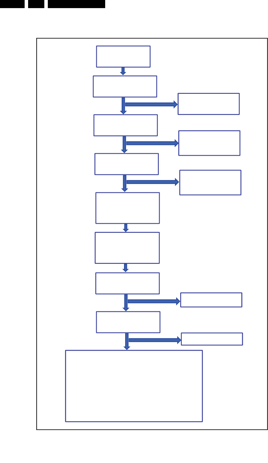
5.6.7 Trouble Shooting Sound section
Figure 5-8 Fault finding tree sound section
Hex Dec Description
Address 0x000A 10 Existing value
Value 0x0000 0 New value
Store Store?
18490_209_090409.eps
090409
Service Modes, Error Codes, and Fault Finding
EN 20 LC9.1A LA5.
2009-Apr-10
5.6.8 Trouble Shooting HDMI section
Figure 5-9 Fault finding tree HDMI section
No Video and Audio
for any HDMI input
(permanently)
Check TMDS signal at pin 1,
3, 4, 6, 7, 9, 10, 12 of
connector 1 (if HDMI 1)
Yes
No
Check TMDS signal at pin
37,38,41,42,44,45,47,48 of
ADV3002 (if HDMI 1)
Malfuntion of HDMI
connector, ensure
solderbility of Connector
Check TMDS signal at pin
25,26,28,29,31,32,34,35 of
ADV3002
Yes
No Malfuntion of PCB trace,
ensure no broken trace of
these signals between
connector and ADV3002
Yes
No
The video and audio path is
intact, no video & audio is
cause by MTK 5392
malfunction
Malfuntion of ADV3002
No Video and Audio for any
HDMI input
(Intermittent and differ
within various DVD player)
Go to CSM mode using RC
key "123654",
check item 11: Key(HDCP)
Valid
Invalid
check item 19:
EDID Version / Check sum
As per latest?
Reload HDCP key
Check the following possible hardware failure:
1) Supply of EEPROM IC (pin 8 of 7B02). Should be +5V.
2) Connectivity of I2C between EEPROM (7B02) and ADV3002
(7B05). Between pin 5, 6 of 7B02 and pin 61 , 62 of 7B05.
Should be +3.8V.
3) Connectivity of DDC line between HDMI connector and
ADV3002. (ex: pin 15, 16 of connector HDMI 1 to pin 69 , 70 of
ADV3002.)
4) Connectivity of DDC line between ADV3002 and MTK5392.
(pin 67, 68 of ADV3002 to test point F836 & F837)
No
Update EDID
Yes
18490_211_090409.eps
090409
Service Modes, Error Codes, and Fault Finding EN 21LC9.1A LA 5.
2009-Apr-10
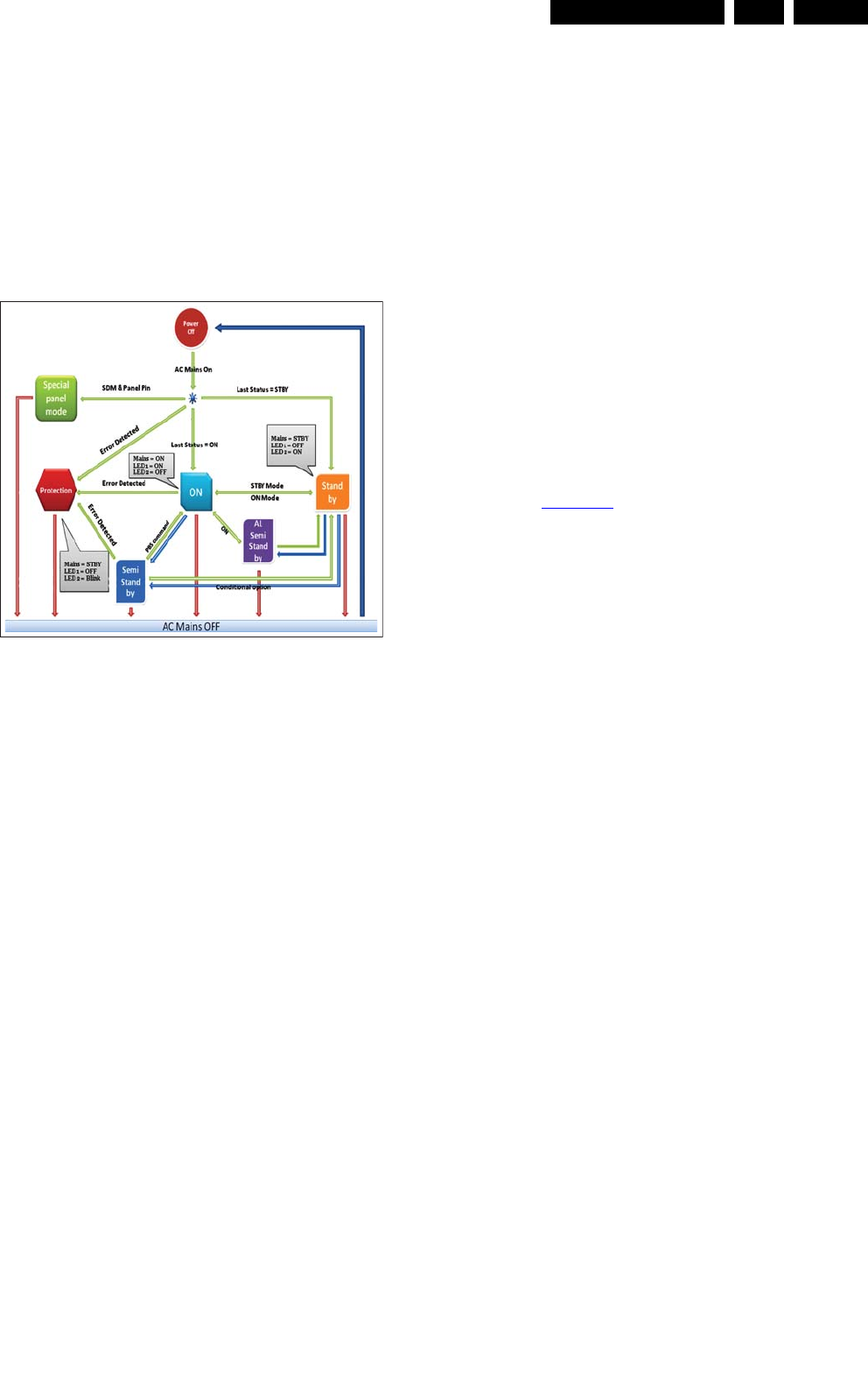
5.6.9 Start-up/Shut-down Flowcharts
On the next pages you will find start-up and shut-down
flowcharts, which might be helpful during fault finding.
POWER STATES
In this chassis, there are six possible power states as follows:
• Power OFF
• Power ON
• STANDBY
• SEMI-STANDBY
• Special Panel Mode
• PROTECTION
Figure 5-10 Power States
POWER OFF
In “Power OFF” mode, the system is completely switched “off”
from AC mains. When AC power is applied, the system checks
for last status. Depending on the last standby status stored in
the system EEPROM, this mode can then transit to “ON” or
“STANDBY” mode.
ON
This is the normal operating mode, indicated by the “on” LED.
All the power supply lines are available and depending on the
sub-mode, all the circuits in the system may be active. From
this mode it shall be possible to transit to “STANDBY” and
“PROTECTION” mode, or to “Power OFF” mode if AC mains
are switched “off”. The sub-modes are:
• Active Mode (Normal Consumer Mode)
• Service Modes
• Panel Modes
• Factory Modes
STANDBY
The total power consumption of the system in this mode shall
be equal or less than 150 mW. This state is indicated by white
LED when AC mains is switched “on”. Only the standby
controller is operational in this state, where only +3V3stby
power supply is available. From this mode it shall be possible
to transit to the “ACTIVE” or “Power OFF” mode if AC mains are
switched “off”.
SEMI-STANDBY
The semi-standby state is required to perform the following
tasks:
• AmbiLight wakeup control
• PBS SemiStandby.
SPECIAL PANEL MODE
The Special Panel Mode is only used during manufacturing
process to program the system EEPROM. In this mode, the
SDA0 and SCL0 ports of MT5392 are set to high impedance
after SDM and PANEL pins are both detected as “low” during
start-up. This mode can be exited using a power recycle.
PROTECTION
This state is entered when an error has been detected at start-
up or in the “ACTIVE” mode. All switched power supply lines
are turned “off” with only +3V3stby remaining “on”; similar to
“STANDBY” mode. This state is indicated by the blinking red
front LED with the blinking sequence denoting the type of error
detected.
When the system enters the protection mode due to a critical
error, it should be turned “off” and the failure cause needs to be
resolved. The system will function normally again after
performing a power recycling once all protection causing
failures have been resolved.
START-UP SEQUENCE
There are two cases of start-up sequences, namely:
• AC On and
• Standby Wake-up.
See also Figure 5-11.
AC ON
In the case of start-up from AC mains, all PSU voltages start to
turn “on” as the hardware default of the active “low” STANDBY
(controlled by Standby Controller STANDBY signal) signal to
the PSU is pulled “low” with respect to ground.
The MT5392 starts running boot loader once the hardware
reset circuit is released. The system will then check the last
standby status from the system EEPROM to determine
whether to complete the system start-up (load image, turn on
the audio, display etc) or proceed to standby and wait for wake-
up command from user. The Standby Controller then proceeds
to verify the power status of the +12V and sends the system to
protection in case of any failures. Special Panel, SDM, and
PANEL modes are detected as well.
STANDBY WAKEUP
When the system receives a command to wake-up from
standby, the Standby Controller sets the STANDBY signal
“low” to turn “on” the switched power, and similarly detects for
the presence of +12V. The MT5392 waits for +3V3_SW to be
available before loading its image. The significance of this
voltage detection is due to the flash is also being powered by
the same mentioned voltage.
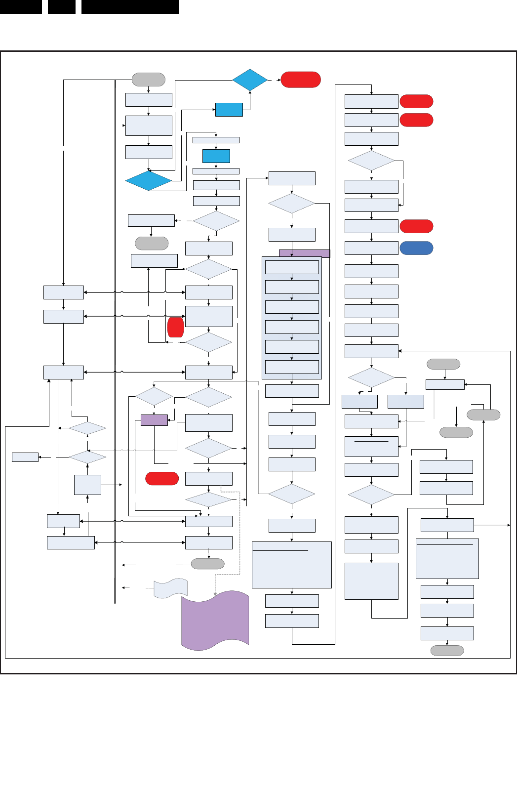
The following figure shows the start-up flowchart for both “AC
On” and “Standby Wake-up”:
18490_204_090409.eps
090409
Service Modes, Error Codes, and Fault Finding
EN 22 LC9.1A LA5.
2009-Apr-10
Figure 5-11 Start-up flowchart
START
HW Default PSU is ON, and
MT5392 POR
MT5392 POR and config
DRAM decompress
bootloader into DRAM
(preLoader)
MT5392 Bootloader
decompressed and running
from DRAM
Special Panel mode
Detection
SDM
& PANEL =
LOW?
All IIC Port set to High
Impedance Yes
END
Check T8032 Status
T8032 in reset State?
(Cold Boot?)
Yes
Download T8032 Code
And kick uP to start to run.
Check T8032/ARM
communication ready?
1. Version cmd ok.
2. Setup CEC parameters.
T8032/ARM
Communicate ok?
Communicate
Failed Count <= 3
Communicate
Failed Count > 3
Error #, failed into Protection
mode, Record error in NVM.
Yes
Cold Start?
No
Yes
Check Last Status and Boot
Ctrl Bits from NVM
Enter Standby?
Yes
Setup Wakeup Scenarios on
PDWNC module of 5392
Standby
(HW)
NVM Error
[ Protection ]
Enable T8032 receive IR key
No
5392 checks
POWER_DOWN =
HIGH ?
Wakeup
Events
(RC/LKB/CEC/Ambilight)
No
No
No
Wait 100ms
No
12V Error
[ Protection ]
No
To Reboot
SDM and PANEL Mode Detection
1. Check SDM Port and Set SDM Mode Flag
If SDM Pin = LOW and System EEPROM First 20
bytes = 0xFF or CH+ on LKB pressed, Load
Software Default System EEPROM Data (only
when cold start)
2. Check Panel Port
If Panel Pin = LoW, Set Panel Mode Flag
Enable POWER_DOWN INT
Enable DC_PROT INT
MT5392 begins initializing the
System
Initialize Tuner
Initialize HDMI Switch
Initialize Middleware Layer
Initialize Philips
drivers/Application
Initialize Application Layer
Switch RC/OPCTRL control
from T8032 to MT5392 and
Enable RC Key
Switch to Video Path
Blank Picture and Switch to Last
Source
Picture Mode Setup & Detection
UnBlank Picture and UnMute
Audio MUTEn = HIGH
SW_MUTE = HIGH
Set Last Status = ON
Start PWM_DIMMING and
BACKLIGHT_BOOST
Note: Startup time from image
decompression long enough to
satisfy 1sec high time after
LAMP ON for proper panel
startup
Initialize CEC driver
Check T8032 CEC buffer
T8032 with
CEC data
Copy CEC data from T8032 to
MT5392 CEC driver buffer
Switch CEC h/w control from
T8032 to MT5392
Initialize NVM
Yes
No
NVM Error
[ Protection ]
Tuner
HDMI Switch
Watchdog timeout
Reboot
Panel turn on Sequence
Turn on LED1
Retrieve/Display Startup
Logo
PWM_DIMMING keep at 100%
BACKLIGHT_BOOST at
nominal
Turn on LVDS Power
LCD_PWR_ON = LOW
Retrieve Panel ID from NVM
Retrieve Panel Info from Flash
data
Wait for Panel_On_Time_1
based on Panel ID in ms (from
Panel Info on Flash)
Switch on LVDS Signal
Wait for Panel_On_Time_2
based on Panel ID in ms (from
Panel Info on Flash)
BACKLIGHT_ON_OFF = HIGH
MT5392 Decompress Image
from Flash into DRAM
Successful?
Set Program Counter to
DRAM Image to boot into
TV Image
Yes
Notify T8032 that
MT5392 start up is OK
T8032 reset state
T8032
T8032 booting
T8032 main loop
T8032 main loop in standby
mode
Control PDWNC
module to
wakeup ARM11
Send error code info to
T8032 & CEC on/off status
Receive ARM info
(Error code etc)
Wakeup event
If not watchdog reboot,
Enable 20 seconds watchdog
Check Wakeup Reason from
PDWNC module (IR/Keypad
HW and CEC) and confirm
from T8032
Any of Upgrade
bits at NVM is on?
USB Upgrade
Upgrade
Failed
Upgrade success
AP: TV Navigator
Is it Ambilight wakeup?
No
Yes
1. If Boot Ctrl Bits to set always enter
standby, then go to standby directly.
2. If Boot Ctrl Bits to set always boot
directly, then continue booting.
3. If Boot Ctrl Bits to follow Last Status,
then check the Last status go decide to
enter standby or continue booting.
Drop All RC key received before
this block
NVM
Error
[ Protecti
on ]
AP: Reload UI parameter into
program
Timeout
= 6 Sec ? yes
No
2.568 second
3.774 second
Turn off Philips
logo
Video Ready
Initialize OSD
3.776 second
Enable 5392 Self-Watchdog thread
Thread action:
1. If watchdog reboot, delay 500
seconds to work.
2. Enable Self-watchdog and initial 15
seconds counter
3. Refresh watchdog counter / 0.5 sec
4. Alive check T8032 / 15 seconds
Check Boot Bank Flag in
EEPROM
Calculate Boot Bank address
Is it Ambilight wakeup?
Panel Initialization
Yes
Semi-Standby
Received wakeup event
Power on
Is it Ambilight
wakeup ?
Audio MUTEn = LOW
SW_MUTE = LOW
AP: Background Manager
Yes
No
DTV_IRQ = Low
Yes
DTV_IRQ = High
Wait 100ms
No
Standby
(HW)
Ambilight off
Check
PowerDown
Start up OK
Yes
Yes
Blinking LED No
NVM status to
check Upgrade bit
Yes
Yes
Standby
(HW)
BACKLIGHT_ON_OFF = HIGH
Panel Initialization
No
ON Mode
18490_205_090409.eps
090409
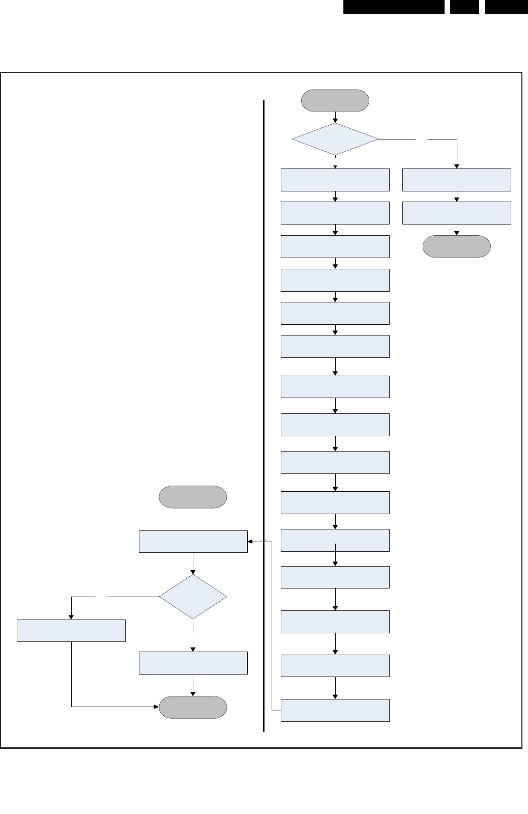
Service Modes, Error Codes, and Fault Finding EN 23LC9.1A LA 5.
2009-Apr-10
STANDBY SEQUENCE
The following flowchart depicts the Standby (plus Semi-
Standby condition) sequence:
Figure 5-12 Standby flowchart
RISC START
Disable AP RC/LKB key
Stop Backlight Dimming
PWM_DIMMING = 100%
Turn Off Backlight
BACKLIGHT_ON_OFF = LOW
Switch off LVDS Signal
Wait for Panel_Off_Time_3
based on Panel ID in ms (from
Panel Flash)
Turn Off LVDS Power,
LCD_PWR_ON = HIGH
PWM_Dimming = 0%
Disable DC_PROT &
POWER_DOWN INT
Pass Error Buffer and CEC Info
to T8032
Switch IR/GPIO control from
RISC to T8032
Mute Audio, MUTEn = HIGH
Notify T8032 to go to Standby
END
(STANDBY)
Wait 3000ms to block next
startup to ensure PSU properly
dischaged
T8032 blinks LED2 according to
Error Buffer
STANDBY due
to Protection?
No
Yes
Receive Standby Command
T8032 START
Turn off LED1
Set Last Status = STANDBY
No
Wait for Panel_Off_Time_2
based on Panel ID in ms (from
Panel Flash)
PBS Semistandby Yes
Turn off LED
Switch off backlight
SemiStandby
18490_206_090409.eps
090409
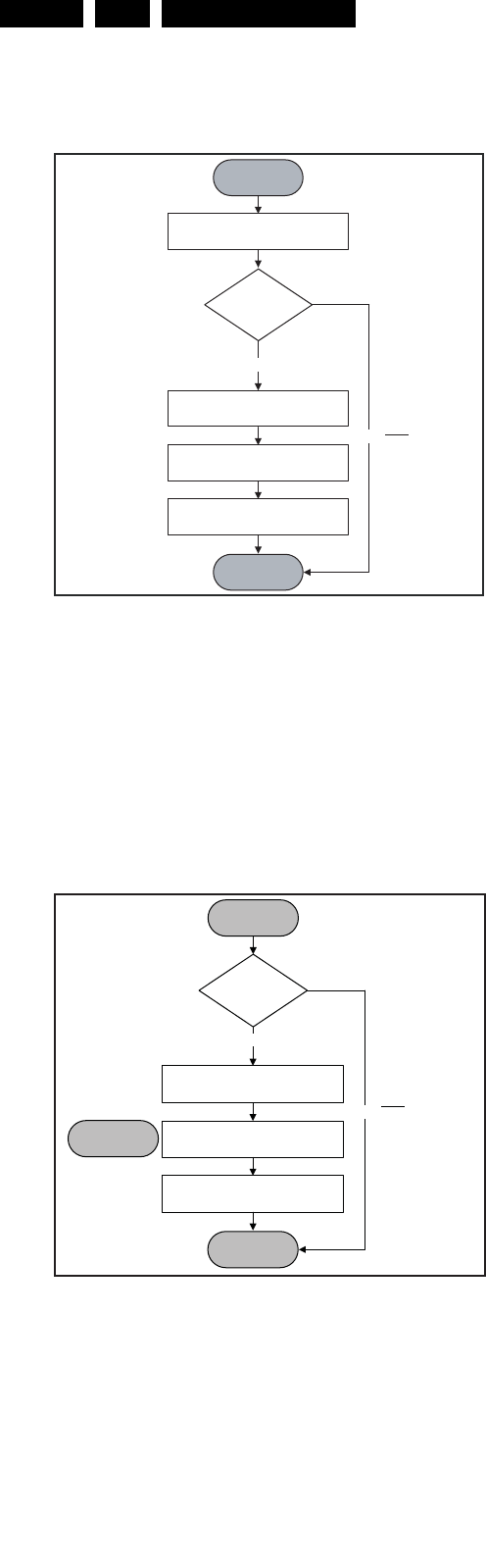
Service Modes, Error Codes, and Fault Finding
EN 24 LC9.1A LA5.
2009-Apr-10
POWERDOWN SEQUENCE
The following figure shows the power-down sequence
flowchart:
Figure 5-13 Power-down flowchart
The power-down condition is detected by the MT5392
POWER_DOWN signal which is an interrupt pin. A “low” level
on this line signifies that power-down is detected. The two
major activities that occur over this operation is the muting of
audio output and write protecting the system flash and
EEPROM.
DC PROTECTION
The following figure shows the DC_PROT interrupt flowchart:
Figure 5-14 DC Protection flowchart
5.6.10 SSB replacement
Follow the instructions in the flowchart in case a SSB has to be
swapped.
START
MT5392 Detects
POWER_DOWN INT
POWER_DOWN INT
based on falling
edge trigger
Wait for
impending
Power Off
Note: To
Avoid False
Triggering
Write Protect Flash and
System EEPROM
Mute Audio Output
System Idle
Reconfirm
POWER_DOWN
= LOW?
Ye s
No
END
18490_200_090408.eps
090408
START
Note: To
Avoid False
Tr i g g e r i n g
Log Error Code
Mute Audio Output
Go to STANDBY
Check
DC_PROT = LOW
for 3 sec?
Ye s
No
END
DC Protection
[Protection]
H_17740_037.eps
240108
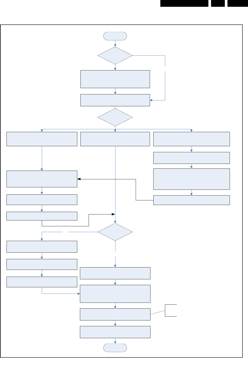
Service Modes, Error Codes, and Fault Finding EN 25LC9.1A LA 5.
2009-Apr-10
Figure 5-15 SSB replacement flowchart
START
Go to SAM mode and save the TV settings
via “NVM Copy to USB”.
Set is still
operating?
- Replace SSB board by a Service SSB.
- Make the SSB fit mechanically to the set.
Go to SAM mode, and reload settings
via “NVM Copy from USB”.
Saved settings
on USB stick?
Program “Display Option” code via 062598
MENU, followed by 3 digits code (this code
can be found on the side sticker of the set or
service manual).
Check and perform alignments in SAM
according to the Service Manual.
E.g. option codes, colour temperature...
Connect PC via ComPair interface to Service
connector at side-AV.
END
Yes
After entering “Display Option” code, set is
going to Standby (= validation of code).
Restart the set.
No
- Verify “Option Codes” according to back sticker of set
or service manual.
- Default settings for White drive see Table 6-1
No
Set is starting up & display is OK.
If not already done;
Check latest software on Service website.
Update all relevant software via USB.
Set is starting up normally but no
display.
Final check of all menus in CSM.
Special attention to “Model no. serial no.,
panel code & HDCP keys status”.
Program “Model no.”, “Serial no.”, “IPB/PSU
12NC” and “Display 12NC”.
Launch ComPair with correct FF database
Top right corner displayed “F” or “cF”
Press 5 s. the “Vol -” & “CH -“ button on the local
keyboard until the OSD “F” or “cF” dissappeared.
Unplug the mainscord to verify the correct
disabling of the factory-mode.
Set is starting up in “Factory” mode.
Start-up set.
Set behaviour?
18490_207_090409.eps
090409

Service Modes, Error Codes, and Fault Finding
EN 26 LC9.1A LA5.
2009-Apr-10
5.7 Software Upgrading
5.7.1 Introduction
It is possible for the user to upgrade the main software via the
USB port. This allows replacement of a software image in a
stand alone set, without the need of an E-JTAG debugger. A
description on how to upgrade the main software can be found
in the DFU or on the Philips website.
5.7.2 Main Software Upgrade
Automatic Software Upgrade
In “normal” conditions, so when there is no major problem with
the TV, the main software and the default software upgrade
application can be upgraded with the “autorun.upg” (FUS part
in the one-zip file). This can also be done by the consumers
themselves, but they will have to get their software from the
commercial Philips website or via the Software Update
Assistant in the user menu (see DFU). The “autorun.upg” file
must be placed in the root of your USB stick.
How to upgrade:
1. Copy “autorun.upg” to the root of your USB stick.
2. Insert USB stick in the side I/O while the set is in “On”
mode. The set will prompt for software upgrade
acknowledge, after which the upgrading will start
automatically. As soon as the programming is finished, you
have to give a “restart” command, after which the set will
restart. In the “Setup” menu you can check if the latest
software is running.
5.7.3 Content and Usage of the One-Zip Software File
Below you find a content explanation of the One-Zip file, and
instructions on how and when to use it.
•Ambi_clustername_version.zip. Not to be used by
Service technicians.
•Panel_clustername_version.zip. Not to be used by
Service technicians.
•EDID_clustername_version.zip. Contains the EDID
content of the different EDID NVMs. See ComPair for
further instructions.
•FUS_clustername_version.zip. Contains the
“autorun.upg” which is needed to upgrade the TV main
software and the software download application.
•NVM_clustername_version.zip. Default NVM content.
Must be programmed via ComPair.
5.7.4 How to Copy NVM Data to/from USB
Write NVM data to USB
1. Insert the USB stick into the USB slot while in SAM mode.
2. Execute the command "NVM Copy" > "NVM Copy to USB",
to copy the NVM data to the USB stick. The NVM filename
on the USB stick will be named "NVM_COPY.BIN" (this
takes a couple of seconds).
Write NVM data to TV
1. First, ensure (via a PC) that the filename on the USB stick
has the correct format: "NVM_COPY.BIN".
2. Insert the USB stick into the USB slot while in SAM mode.
3. Execute the command "NVM Copy" > "NVM Copy from
USB" to copy the USB data to NVM (this takes about a
minute to complete).
Important: The file must be located in the root directory of the
USB stick.
Alignments EN 27LC9.1A LA 6.
2009-Apr-10
6. Alignments
Index of this chapter:
6.1 General Alignment Conditions
6.2 Hardware Alignments
6.3 Software Alignments
6.4 Option Settings
Note: Figures below can deviate slightly from the actual
situation, due to the different set executions.
General: The Service Default Mode (SDM) and Service
Alignment Mode (SAM) are described in chapter 5. Menu
navigation is done with the CURSOR UP, DOWN, LEFT or
RIGHT keys of the remote control transmitter.
6.1 General Alignment Conditions
Perform all electrical adjustments under the following
conditions:
• Power supply voltage (depends on region):
– AP-NTSC: 120 VAC or 230 VAC / 50 Hz (± 10%).
– AP-PAL-multi: 120 - 230 VAC / 50 Hz (± 10%).
– EU: 230 VAC / 50 Hz (± 10%).
– LATAM-NTSC: 120 - 230 VAC / 50 Hz (± 10%).
– US: 120 VAC / 60 Hz (± 10%).
• Connect the set to the mains via an isolation transformer
with low internal resistance.
• Allow the set to warm up for approximately 15 minutes.
• Measure voltages and waveforms in relation to correct
ground (e.g. measure audio signals in relation to
AUDIO_GND).
Caution: It is not allowed to use heatsinks as ground.
• Test probe: Ri > 10 Mohm, Ci < 20 pF.
• Use an isolated trimmer/screwdriver to perform
alignments.
6.2 Hardware Alignments
There are no hardware alignments foreseen for this chassis,
but below find an overview of the most important DC voltages
on the SSB. These can be used for checking proper functioning
of the DC/DC converters.
6.3 Software Alignments
With the software alignments of the Service Alignment Mode
(SAM) the Tuner and RGB settings can be aligned.
To store the data: Use the RC button “Menu” to switch to the
main menu and next, switch to “Stand-by” mode.
6.3.1 Tuner Adjustment (RF AGC Take Over Point)
Purpose: To keep the tuner output signal constant as the input
signal amplitude varies.
The LC9.1A LA chassis comes with the UV1856 analogue
tuner. No alignment is necessary, as the AGC alignment is
done automatically (standard value: “15”). However in case of
problems use the following method (use multimeter and RF
generator):
• Apply a vision IF carrier of 38.9 MHz (105 dBuV = 178
mVrms) to injection point A258 (input via 50 ohm coaxial
cable terminated with an RC network of series 10nF with
120 ohm to ground).
• Measure voltage on pin 1 of the tuner (test point F250).
• Adjust AGC (via SAM menu: TUNER -> AGC), until voltage
on pin 1 is 3.3 +0.5/-1.0 V.
• Store settings and exit SAM.
6.3.2 RGB Alignment
Before alignment, choose “Setup” -> “Picture” and set:
• “Brightness” to “50”.
• “Colour” to “50”.
• “Contrast” to “100”.
White Tone Alignment:
• Activate SAM.
• Select “RGB Align“ and choose a colour temperature.
• Use a 100% white screen as input signal and set the
following values:
– All “White point” values initial to “256”.
– All “BlackL Offset” values to “0”.
In case you have a colour analyser:
• Measure with a calibrated (phosphor- independent) colour
analyser (e.g. Minolta CA-210) in the centre of the screen.
Consequently, the measurement needs to be done in a
dark environment.
• Adjust the correct x,y coordinates (while holding one of the
White point registers R, G or B on “256”) by means of
decreasing the value of one or two other white points to the
correct x,y coordinates (see Table 6-1 White D alignment
values). Tolerance: dx: ± 0.004, dy: ± 0.004.
• Repeat this step for the other colour Temperatures that
need to be aligned.
• When finished return to the SAM root menu and press
STANDBY on the RC to store the aligned values to the
NVM.
Table 6-1 White D alignment values
If you do not have a colour analyser, you can use the default
values. This is the next best solution. The default values are
average values coming from production (statistics).
• Set the RED, GREEN and BLUE default values per
temperature according to the values in the “Tint settings”
table.
• When finished return to the SAM root menu and press
STANDBY on the RC to store the aligned values to the
NVM.
Table 6-2 Tint settings 42"
Description Test Point Specifications (V) Diagram
Min. Typ. Max.
+12VS F124 11.40 12.00 12.60 B01_DC-DC
+3V3_STBY F101 3.20 3.30 3.40 B01_DC-DC
+3V3_SW F133 3.14 3.3 3.46 B01_DC-DC
+1V2_SW F131 1.18 1.25 1.31 B01_DC-DC
+5V_SW F132 4.94 5.2 5.46 B01_DC-DC
+1V8_SW F125 1.71 1.80 1.89 B01_DC-DC
+1V0_SW F134 0.99 1.05 1.10 B01_DC-DC
+8V_SW F122 7.6 8.0 8.4 B01_DC-DC
+5VS F228 4.75 5 5.25 B02_Tuner_IF
+VDISP F934 11.40 12.00 12.60 B04D_LVDS
+VTUN F123 30 33 36 B01_DC-DC
+5V_IF F229 4.75 5 5.25 B02_Tuner_IF
+5VTUN F219 4.75 5 5.25 B02_Tuner_IF
Value Cool (11000 K) Normal (9000 K) Warm (6500 K)
x0.278 0.289 0.314
y0.278 0.291 0.319
Colour Temp. R G B
Cool 246 248 255
Normal 255 236 180
Warm 210 226 255
Alignments
EN 28 LC9.1A LA6.
2009-Apr-10
Table 6-3 Tint settings 47"
Table 6-4 Tint settings 52"
6.4 Option Settings
6.4.1 Introduction
The microprocessor communicates with a large number of I2C
ICs in the set. To ensure good communication and to make
digital diagnosis possible, the microprocessor has to know
which ICs to address. The presence/absence of these specific
ICs (or functions) is made known by the option codes.
Notes:
• After changing the option(s), save them with the STORE
command.
• The new option setting becomes active after the TV is
switched “off” and “on” again with the mains switch (the
EAROM is then read again).
6.4.2 How To Set Option Codes
When the NVM is replaced, all options will require resetting. To
be certain that the factory settings are reproduced exactly, you
must set all option numbers. You can find the correct option
numbers in table “Option Codes OP1...OP7” below.
How to Change Options Codes
An option code (or “option byte”) represents eight different
options (bits). When you change these numbers directly, you
can set all options very quickly. All options are controlled via ten
option bytes (OP1... OPA).
Activate SAM and select “Options”. Now you can select the
option byte (OP1 to OPA) with the CURSOR UP/ DOWN keys,
and enter the new 3 digit (decimal) value. For the correct
factory default settings, see Table 6-5 Option code overview.
For more detailed information, see Table 6-6 Option codes at
bit level (OP1-OP7) . If an option is set (value “1”), it represents
a certain decimal value.
When all the correct options (bits) are set, the sum of the
decimal values of each Option Byte (OP) will give the option
code.
Table 6-5 Option code overview
Colour Temp. R G B
Cool tbf tbf tbf
Normal tbf tbf tbf
Warm tbf tbf tbf
Colour Temp. R G B
Cool tbf tbf tbf
Normal tbf tbf tbf
Warm tbf tbf tbf
CTN Option Code Display Code
42PFL9509/93 081 070 212 248 008 118 060 192 076 001 183
47PFL9509/93 081 070 212 248 008 118 060 192 076 001 186
52PFL9509/93 081 070 212 248 008 118 060 192 076 001 208
Alignments EN 29LC9.1A LA 6.
2009-Apr-10
Option Bit Overview
Below find an overview of the Option Codes on bit level.
Table 6-6 Option codes at bit level (OP1-OP7)
Option Byte & Bit Dec. Value Option Name Description - will follow in next issue of this manual
Byte OP1
Bit 7 (MSB) 128 Reserved
Bit 6 64 OPC_MJC_3
Bit 5 32 OPC_MJC_2
Bit 4 16 OPC_MJC
Bit 3 8 OPC_REGION_SPECIFIC2
Bit 2 4 OPC_REGION_SPECIFIC
Bit 1 2 OPC_REGION2
Bit 0 (LSB) 1 OPC_REGION
Byte OP2
Bit 7 (MSB) 128 OPC_AV2_SCART2_2
Bit 6 64 OPC_AV2_SCART2
Bit 5 32 Reserved
Bit 4 16 Reserved
Bit 3 8 OPC_CI_PLUS (Provision
Bit 2 4 OPC_LIGHT_SENSOR
Bit 1 2 OPC_AMBILIGHT_2
Bit 0 (LSB) 1 OPC_AMBILIGHT
Byte OP3
Bit 7 (MSB) 128 OPC_SideHDMI
Bit 6 64 OPC_SideAV_2
Bit 5 32 OPC_SideAV
Bit 4 16 OPC_VGA
Bit 3 8 Reserved
Bit 2 4 OPC_HDMI3
Bit 1 2 OPC_AV3_2
Bit 0 (LSB) 1 OPC_AV3
Byte OP4
Bit 7 (MSB) 128 OPC_SHOP_MODE
Bit 6 64 OPC_BACKLIGHT_DEEPDIMMING
Bit 5 32 OPC_BACKLIGHT_BOOST
Bit 4 16 OPC_BACKLIGHT_DIMMING
Bit 3 8 OPC_BBD
Bit 2 4 OPC_DRAM_IC_3
Bit 1 2 OPC_DRAM_IC_2
Bit 0 (LSB) 1 OPC_DRAM_IC
Byte OP5
Bit 7 (MSB) 128 OPC_DIGITAL_OPTION_2
Bit 6 64 OPC_DIGITAL_OPTION
Bit 5 32 Reserved
Bit 4 16 OPC_ADC (Provision)
Bit 3 8 OPC_LIP_SYNC
Bit 2 4 OPC_SURROUND_VDOLBY
Bit 1 2 Reserved
Bit 0 (LSB) 1 Reserved
Byte OP6
Bit 7 (MSB) 128 Reserved
Bit 6 64 OPC_VPB_4
Bit 5 32 OPC_VPB_3
Bit 4 16 OPC_VPB_2
Bit 3 8 OPC_VPB
Bit 2 4 OPC_MP3_PHOTO
Bit 1 2 OPC_VIEW_FOR_YOU
Bit 0 (LSB) 1 OPC_VIRGIN_MODE
Byte OP7
Bit 7 (MSB) 128 OPD_MHEG (Provision)
Bit 6 64 Reserved
Bit 5 32 OPC_PIXELPLUS_LINK
Bit 4 16 OPC_SYS_AUD_CTRL
Bit 3 8 OPC_RC_PASSTHROUGH
Bit 2 4 OPC_CEC
Bit 1 2 OPC_OAD2 (Provision)
Bit 0 (LSB) 1 OPC_OAD (Provision)
Byte OP8
Bit 7 (MSB) 128 OPC_DEMO_AMBILIGHT
Bit 6 64 OPC_DEMO_PP_PLUS
Bit 5 32 Reserved
Bit 4 16 Reserved

Alignments
EN 30 LC9.1A LA6.
2009-Apr-10
Bit 3 8 OPC_TXT2_5
Bit 2 4 OPC_TXT_CC
Bit 1 2 OPC_EPG
Bit 0 (LSB) 1 Reserved
Byte OP9
Bit 7 (MSB) 128 Reserved
Bit 6 64 OPC_SYS_RECVRY
Bit 5 32 Reserved
Bit 4 16 Reserved
Bit 3 8 OPC_SCENEA
Bit 2 4 OPC_ESTICKER
Bit 1 2 Reserved
Bit 0 (LSB) 1 Reserved
Byte OPA
Bit 7 (MSB) 128 Tuner Profile_2
Bit 6 64 Tuner Profile_1
Bit 5 32 Tuner Profile_0
Bit 4 16 Cabinet Profile_4
Bit 3 8 Cabinet Profile_3
Bit 2 4 Cabinet Profile_2
Bit 1 2 Cabinet Profile_1
Bit 0 (LSB) 1 Cabinet Profile_0
Option Byte & Bit Dec. Value Option Name Description - will follow in next issue of this manual
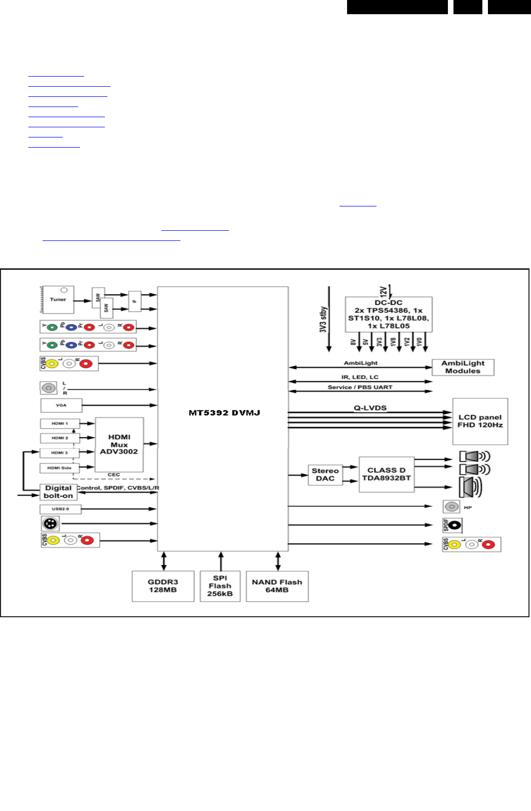
Circuit Descriptions, Abbreviation List, and IC Data Sheets EN 31LC9.1A LA 7.
2009-Apr-10
7. Circuit Descriptions, Abbreviation List, and IC Data Sheets
Index of this chapter:
7.1 Introduction
7.2 LCD Power Supply
7.3 DC/DC converters
7.4 Front-End
7.5 Video Processing
7.6 Audio Processing
7.7 HDMI
7.8 Ambi Light
Notes:
•Only new circuits (circuits that are not published recently)
are described.
• Figures can deviate slightly from the actual situation, due
to different set executions.
• For a good understanding of the following circuit
descriptions, please use chapter 9. Block Diagrams and
10. Circuit Diagrams and PWB Layouts. Where necessary,
you will find a separate drawing for clarification.
7.1 Introduction
The LC9.1A LA chassis (development name “LC09M”) is an
analogue chassis using a Mediatek chipset. It covers screen
sizes of 32" to 52" with stylings called “PnS” (xxPFL5xxx),
“Frame” (xxPFL7xxx) and “Roadrunner” (xxPFL9xxx).
Main key components are:
• Mediatek MT5392 video processor
• NXP TDA8932BT audio processor
• ADV3002BSTZ01 HDMI switch
• UV1856 tuner and TDA9886 demodulator.
Refer to Figure 7-1 for details.
Figure 7-1 LC09M Architecture
18490_208_090409.eps
090409
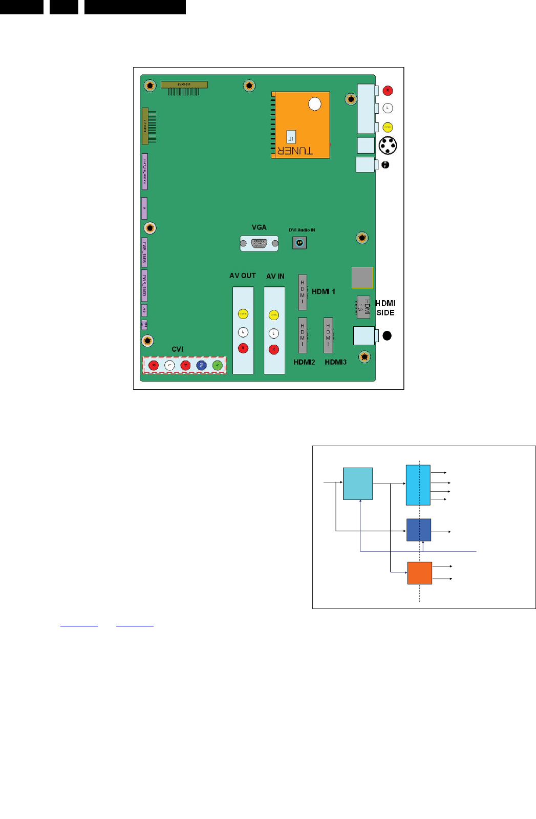
Circuit Descriptions, Abbreviation List, and IC Data Sheets
EN 32 LC9.1A LA7.
2009-Apr-10
7.1.1 SSB Cell Layout
Figure 7-2 SSB cell layout
7.2 LCD Power Supply
The Power Supply Unit (PSU) in this chassis is a buy-in and is
a black-box for Service. When defective, a new panel must be
ordered and the defective panel must be returned for repair,
unless the main fuse of the unit is broken. Always replace the
fuse with one with the correct specifications! This part is
commonly available in the regular market.
Different PSUs are used in this chassis:
• 42" sets use an “LG” PSU (LGIT PLHL-T814A) Integrated
Power Board
• 47" sets use an “LG” PSU (LGIT PLHL-T819A) Integrated
Power Board
• 52" sets use an “Delta” PSU (DPS-411AP4A B) Power
Supply Unit (without inverter).
Refer to Figure 7-3 and Figure 7-4 for details.
Figure 7-3 42" and 47" IPB block diagram
H
P
USB
2.0
18490_210_090409.eps
090409
99R 9
9B67$1'%<
9B',63
$XGLR6XSSO\9
$PELOLJKW9
$&,QSXW
1RQ
,VRODWHG+RW,VRODWHG&ROG
3)&
//&
)O\EDFN
%ROWRQ6XSSO\9
67$1'%<
+,*+ 2))/2: 21
,QYHUWHU
+9WR3DQHO
+9WR3DQHO
18490_213_090410.eps
090410
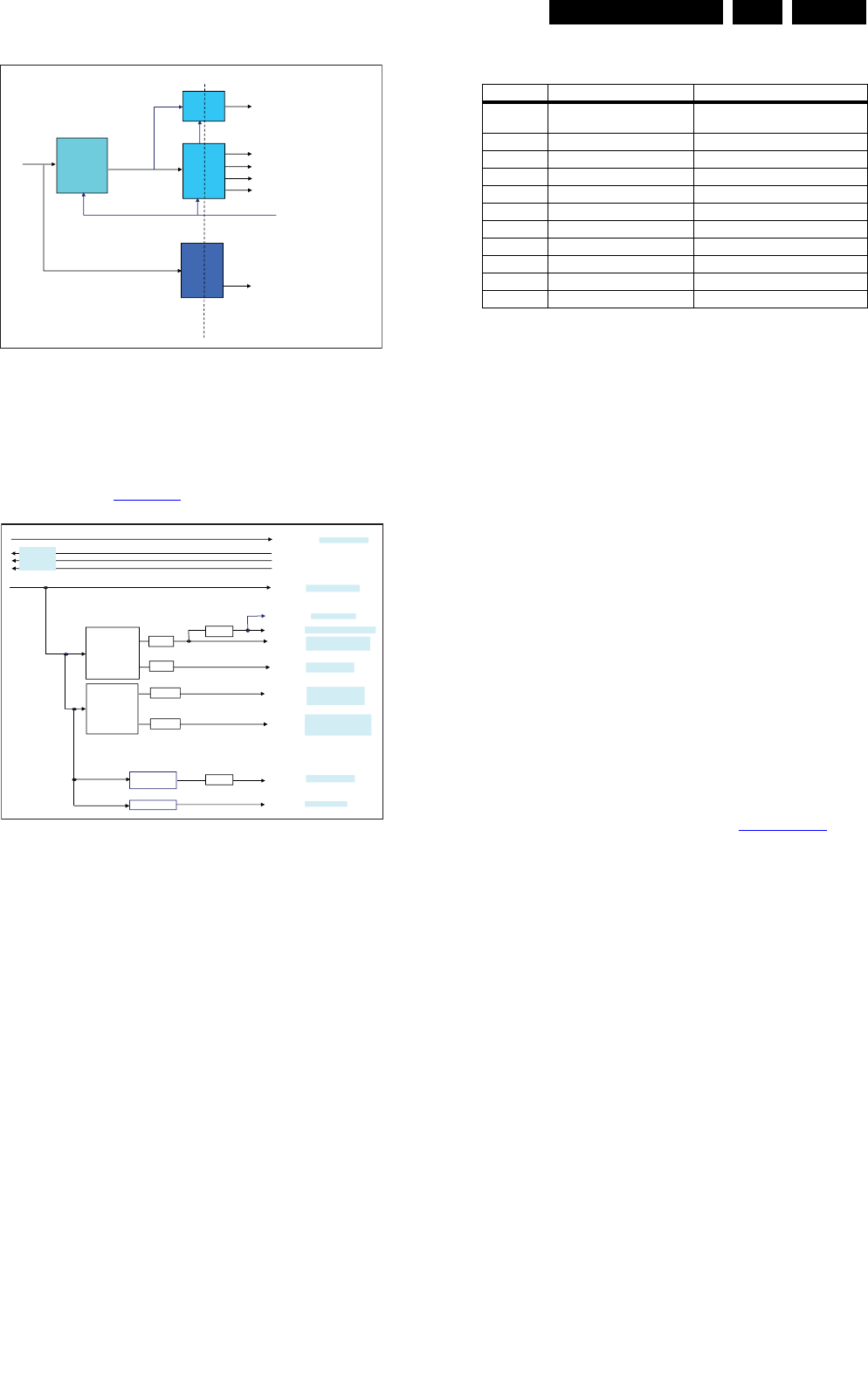
Circuit Descriptions, Abbreviation List, and IC Data Sheets EN 33LC9.1A LA 7.
2009-Apr-10
Figure 7-4 52" PSU block diagram
7.3 DC/DC converters
On-board DC-DC converters convert the +12 V coming from
the PSU. Refer to Figure 7-5 for details.
Figure 7-5 DC DC converter block diagram
7.4 Front-End
Key components for the analogue tuner section (AP region)
are:
• UV1816E tuner
• K7257 video SAW filter
• K9362 audio SAW filter
• TDA9886T analogue IF demodulator.
For trouble shooting info, refer to paragraph 5.6.6 Trouble
Shooting Tuner section.
Table 7-1 Pin assignment analogue tuners
7.5 Video Processing
The video processing is completely handled by the Mediatek
MT5392 video processor which features:
• Noise reduction
• Dynamic skin tone control
• White stretch
•Blue stretch
• Green enhancement
• Auto histogram
• Pixel Plus III / Perfect Pixel
• Active Backlight dimming
• Active contrast.
7.6 Audio Processing
In this chassis, the TDA8932BT Class D Power Amplifier is
implemented. For trouble shooting info, refer to paragraph
5.6.7 Trouble Shooting Sound section.
7.7 HDMI
7.7.1 Introduction
Note: Text below is an excerpt from the ”HDMI Specification”
that is issued by the HDMI founders (see www.hdmi.org).
The High-Definition Multimedia Interface is developed for
transmitting digital signals from audiovisual sources to
television sets, projectors and other video displays.
HDMI can carry high quality multi-channel audio data and can
carry all standard and high-definition consumer electronics
video formats. Content protection technology is available.
HDMI can also carry control and status information in both
directions.
HDMI is backward compatible with DVI (1.0). Compared with
DVI, HDMI offers extra:
• YUV 4:4:4 (3 × 8-bit) or 4:2:2 (up to 2 × 12-bit), where DVI
offers only RGB 4:4:4 (3 × 8 bit).
• Digital audio in CD quality (16-bit, 32/44.1/48 kHz), higher
quality available (8 channels, 192 kHz).
• Remote control via CEC bus (Consumer Electronics
Control): allows user to control all HDMI devices with the
TV's remote control and menus.
• Smaller connector (SCART successor).
• Less cables: e.g. from 10 audio/9 video cables to 3 HDMI
cables.
7.7.2 Implementation
In this chassis, the main "Mediatek" Video processor MT5392
combines the HDMI functionality together with the 4:1 "Analog
Device" HDMI switch ADV3002.
99R 9
9B67$1'%<
9B',63
$XGLR6XSSO\9
7R,QYHUWHU9
$&,QSXW
1RQ
,VRODWHG+RW,VRODWHG&ROG
3)&
5HVRQDQW
//&
)O\EDFN
%ROWRQ6XSSO\9
67$1'%<
+,*+ 2))/2: 21
$PEL/LJKW9
5HVRQDQW
//&
18490_214_090410.eps
090410
+3V3STBY
/ under 15mA
PSU/iPB : +3V3STBY
DC_DC
TPS54386
PWP
+1V0_SW
/ 2.1Amax
+5V_SW
/ 0.771Amax
DC_DC
TPS54386
PWP
+3V3_SW
/1.094Amax
+1V8_SW
/1.13Amax
+1V2_SW
/ 0.5Amax
+8V_SW
/ 12mAmax
L78M08CDT
+12Vdisp
/1000mA
+5V_Tuner
/ 0.17Amax
10uH+5VS
/ 0.07Amax
STBY
PWM dimming
Boost
To PSU/iPB
To PSU/iPB
To PSU/iPB
10uH
DC_DC
ST1S10PH 2uH
To IF Demodulator
To MT539X, USB,
HDMI
To MT539X
To Tuner
To MT539X
To MT539X, GDDR3
To MT539X, HDMi
MUX, Audio DAC,
To MT539X
To MT539X
To LCD Panel
10uH
10uH
10uH
PSU/iPB : +12VS
18490_212_090409.eps
090409
Pin number Description DC voltage (V)
1 RF AGC voltage 3.3 - 4.5 (weak or no signal)
< 3.3 (strong signal)
2n.c.
3I
2C-bus address select 0
4 SCL 0 to 3.3
5 SDA 0 to 3.3
6n.c.
7 supply voltage 5 +0.5/−0.25 V
8n.c.
9 fixed tuning voltage 33
10 n.c.
11 TV IF output
Circuit Descriptions, Abbreviation List, and IC Data Sheets
EN 34 LC9.1A LA7.
2009-Apr-10
The ADV3002 features:
• 4 HDMI inputs
• 1 HDMI output
• EDID replication
• 5 V combiner.
Refer to Figure 7-6 for the HDMI implementation.
Figure 7-6 HDMI implementation
Refer to 5.6.8 Trouble Shooting HDMI section for repair info.
7.7.3 EDID architecture
The ADV3002 HDMI switch combines the conventional
separate EDIDs (for each HDMI port) into one integrated EDID,
shared by all HDMI ports.
The EDID data can be copied to a USB stick for further analysis
or editing.
7.8 Ambi Light
The Ambi Light architecture in this platform has been entirely
renewed. The characteristics are:
• Additional DC/DC board generating 12/16/24 V (optional)
• ARM processor (on DC/DC panel or AL board)
• Low-power LEDs
• SPI interface from ARM to LED drivers
•I
2C upgradeable via USB
• Each AL module has a temperature sensor.
The use of the DC/DC board is optional. In case no DC/DC
board is implemented, the ARM processor is located on one of
the AL boards.
Refer to Figure 7-7 for the Ambi Light architecture.
Figure 7-7 Interface between Ambi Light and SSB
7.8.1 ARM controller
Refer to Figure 7-8 below for signal interfacing to and from the
ARM controller. The ARM controller is located on the DC/DC
board (item no. 7302) or AL panel (item no. 7102).
18490_215_090410.eps
090410
18310_203_090317.eps
090317
Circuit Descriptions, Abbreviation List, and IC Data Sheets EN 35LC9.1A LA 7.
2009-Apr-10
Figure 7-8 ARM controller interface
Data transfer between ARM processor and LED drivers is
executed by a Serial Peripheral Interface (SPI) bus interface.
The SPI bus is a synchronous serial data link standard that
operates in full duplex mode.
For debugging purposes, the working principle is given below:
• At start-up the controller will read-out matrix data from the
EEPROM devices (via SPI DATA RETURN)
• Before operation, the driver current is set via SPI, with
driver in DC mode
• During normal operation the controller receives RGB-,
configuration-, operation mode- and topology data via I2C
• The controller converts the I2C RGB data via the matrixes
to SPI LED data
• Via data return the controller receives error data (if
applicable).
Also PWM clock and BLANK signals are generated by the
controller. The controller can be reprogrammed via I2C (via
USB). The controller can receive matrix values via I2C, which
will be stored in the EEPROM of each AL module via the SPI
bus. The temperature sensor in each AL module controls the
TEMP line; in case of a too high temperature the controller will
reduce the overall brightness.
7.8.2 LED driver communication (via SPI bus)
Refer to Figure 7-9 below for signal interfacing between the
ARM controller and the LED drivers on the AL boards, and the
LED drivers and the EEPROMs on the AL boards.
Figure 7-9 SPI communication between ARM controller and LED drivers
The ARM controller communicates with the LED drivers (on
each AL module) via an SPI bus. For debugging purposes, the
working principle is given below:
• Data from the ARM controller is linked through the drivers,
which are connected in cascade
• SPI CLK, SPI LATCH, PROG, BLANK and PWM CLOCK
are going directly from the controller to each driver
• SPI DATA RETURN is linked from the last driver to the
controller: controller decides which driver returns data.
7.8.3 Temperature Control
Refer to Figure 7-10 for signal interfacing between the ARM
controller and the temperature sensor on the AL boards.
Figure 7-10 Communication between ARM controller and
temperature sensor
Each AL board is equipped with a temperature sensor. If one of
the sensors detects a temperature over the threshold, the
TEMP line is pulled LOW which results in brightness reduction.
18310_204_090318.eps
090318
ARM
SDA
SCL
SEL1
SEL2
SPI CLOCK
SPI LATCH
SPI DATA OUT
SPI DATA RETURN
PWM CLOCK
BLANK
PROG
SPI LATCH 2
(only on dc/dc for aurea)
CS EEPROM
TEM P
Scl1
Sda1
tbd
tbd
Sck
P0.7
MOSI
MISO
P0.8
TxD
RxD Rxd0
Txd0
MAT0.0
MAT1.0
tbd
tbd
P0.10
18310_205_090318.eps
090318
Ambilight module 1 Am bilight module 2 Ambilight module N
ARM
LED
DRIVER
1
LED
DRIVER
2
LED
DRIVER
N
SPI data in
SoutSin SoutSoutSin
SPI clock (SCLK)
SPI latch (XLAT )
PRO G (VPRG )
BLANK
PW M CLO CK ( G SCLK)
out16
out16
out16
SPI data return
18310_206_090318.eps
090318
Ambilight module 1 Ambilight module 2
ARM
TEMP
SENSOR
Vcc
Pull-upPull-upPull-up
TEMP
SENSOR
Vcc
Ambilight module N
TEMP
SENSOR
Vcc
IC Data Sheets
EN 36 LC9.1A LA8.
2009-Apr-10
8. IC Data Sheets
This section shows the internal block diagrams and pin layouts
of ICs that are drawn as "black boxes" in the electrical diagrams
(with the exception of "memory" and "logic" ICs).
8.1 Diagram B02, Type TDA9886T (IC7113), Demodulator
Figure 8-1 Internal block diagram and pin configuration
Block Diagram
Pin Configuration
G_16510_059.eps
090325
TAGC
CVAGC pos
CBL
VIF-PLL
4 MHz
external
AFC
video output 2 V (p-p)
[1.1 V (p-p) without trap]
AUD
CAF
de-emphasis
network
FM-PLL filter
sound intercarrier output
CAGC
AGND
VP
VIF1
VIF-AGC RC VCO DIGITAL VCO CONTROL AFC DETECTOR
VIDEO TRAPS
4.5 to 6.5 MHz
NARROW-BAND FM-PLL
DETECTOR
I2C-BUS TRANSCEIVER
VIF-PLL
SINGLE REFERENCE QSS MIXER/
INTERCARRIER MIXER AND
AM-DEMODULATOR
SIF-AGC
SUPPLY
1
2
14 16 19 15 21
17
8
6
5
4
12
7 11 10
1820
23
24
OUTPUT
PORTS
MAD
AUDIO PROCESSING
AND SWITCHES
9
TUNER AGC
CAGC neg
322
crystal
and MAD select
TDA9885
n.c.
13
L
L
P
M
F
D
AM
O
ISD
N
GDADS
L
C
S
2P
O1
P
O
CVBS
TOP
VIF2
SIF1
SIF2 DEEM
AFD
REF
VAGC VPLL
filter
TDA9886
(1)
(1) Not connected for TDA9885.
reference
or
TDA9885
TDA9886
1
2
3
4
5
6
7
8
9
10
11
12
VIF1
VIF2
OP1
FMPLL
DEEM
AFD
DGND
AUD
TOP
SDA
SCL
SIOMAD
SIF2
SIF1
OP2
AFC
VP
VPLL
AGND
CVBS
VAGC
(1)
REF
TAGC
n.c.
24
23
22
21
20
19
18
17
16
15
14
13
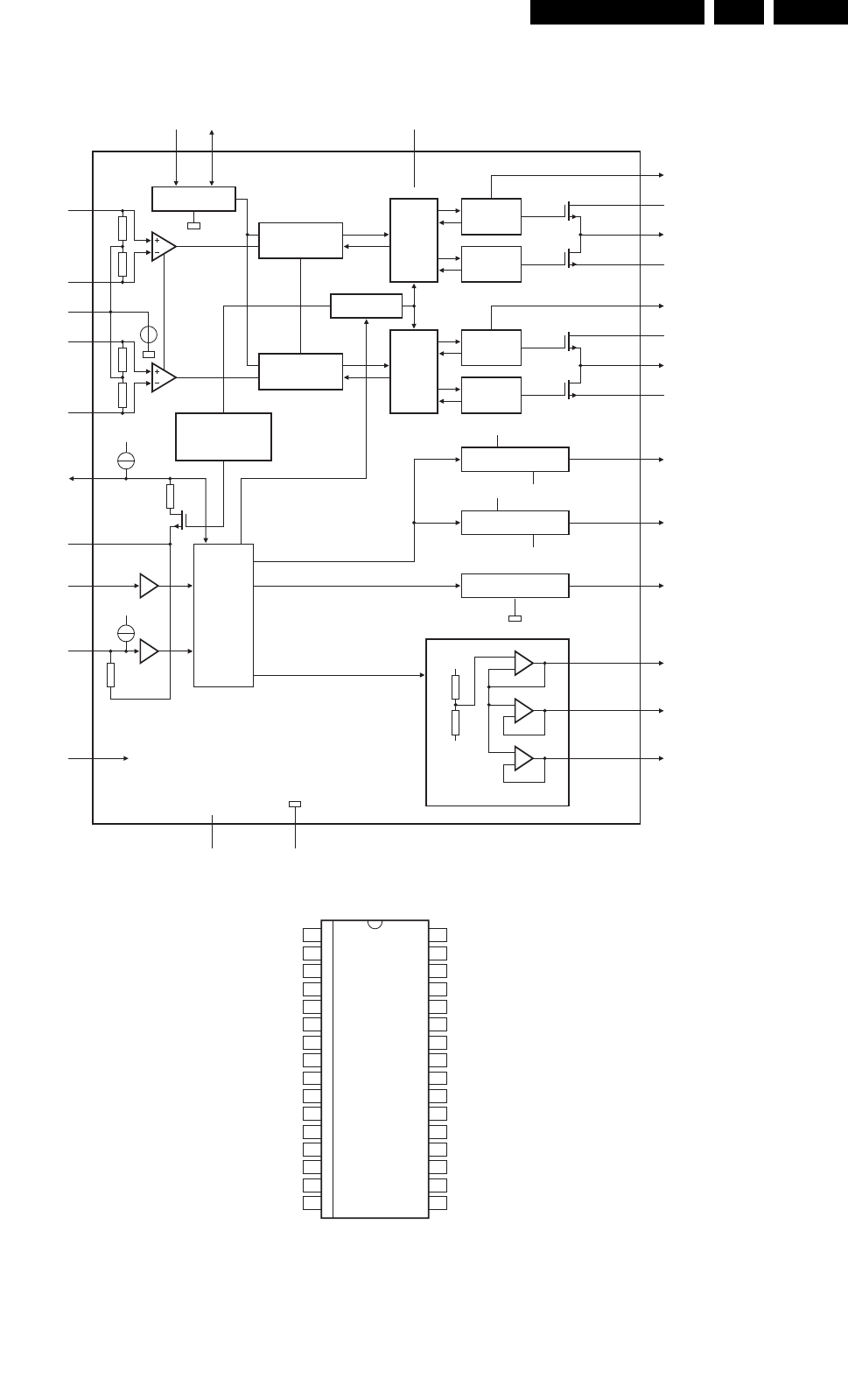
IC Data Sheets EN 37LC9.1A LA 8.
2009-Apr-10
8.2 Diagram B03, Type TDA8932BT (IC7510), Audio Amplifier
Figure 8-2 Internal block diagram and pin configuration
Block Diagram
Pin Configuration
G_16860_045.eps
300107
2
81301
28
29
27
3
12
TDA8932
OSCILLATOR
26
BOOT1
V
DDP1
OUT1
V
SSP1
PWM
MODULATOR
DRIVER
HIGH
DRIVER
LOW
CTRL
MANAGER
CTRL
PWM
MODULATOR
PROTECTIONS:
OVP, OCP, OTP,
UVP, TF, WP
STABILIZER 11 V
STABILIZER 11 V
REGULATOR 5 V
MODE
V
DDA
15
14
IN1P
VOICSOFERCSO
DDA
V
SSD
IN1N
INREF
IN2P
IN2N
6
POWERUP
4
DIAG
7
CGND
21
20
22
23
BOOT2
V
DDP2
OUT2
25 STAB1
24 STAB2
18
11
DREF
HVPREF
30 HVP1
19 HVP2
V
SSP2
DRIVER
HIGH
DRIVER
LOW
V
DDA
V
SSP1
V
SSP2
V
SSD
V
DDA
V
SSA
HALF SUPPLY VOLTAGE
5
ENGAGE
13
9
TEST
V
SSA
1, 16, 17, 32
V
SSD(HW)
TDA8932T
V
SSD(HW)
V
SSD(HW)
OICSOP1NI
1PVHN1NI
VGAID
DDP1
1TOOBEGAGNE
1TUOPUREWOP
VDNGC
SSP1
V
DDA
STAB1
V
SSA
STAB2
OSCREF V
SSP2
2TUOFERPVH
2TOOBFERNI
VTSET
DDP2
2PVHN2NI
FERDP2NI
V
SSD(HW)
V
SSD(HW)
1
2
3
4
5
6
7
8
9
10
11
12
13
14
15
16
18
17
20
19
22
21
24
23
26
25
32
31
30
29
28
27

IC Data Sheets
EN 38 LC9.1A LA8.
2009-Apr-10
Personal Notes:
10000_012_090121.eps
090121
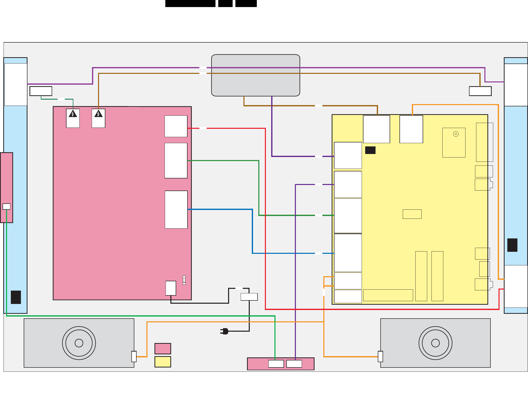
Block Diagrams EN 39LC9.1A LA 9.
2009-Apr-10
9. Block Diagrams
Wiring Diagram 42" (Frame)
1M83 (AL1)
1. SCL
2. SPI-DATA-IN
3. SDA
4. CONTROL-1
5. CONTROL-2
6. +3V3
7. BLANK
8. EEPROM-CS
9. TEMP-SENSOR
10. PROG
11. VLED1
12. GND
13. VLED2
14. GND
AMBI-LIGHT MODULE
(1176)
AL
1M99 (B01)
12. GND
11. N.C
10. N.C
9. POWER-OK
8. GND
7. BACKLIGHT_BOOST
6. PWM_DIMMING
5. BL_ON_OFF
4. GND
3. GND
2. +12VDISP
1. +12VDISP
1M95 (B01)
11. N.C
10. GNDSND
9. +24VAUDIO
8. +12VS
7. +12VS
6. +12VS
5. GND
4. GND
3. GND
2. STANDBY
1. +3V3STBY
CN4
11. FAN_PWM
10. GND_SND
9. +VSND
8. +12V
7. +12V
6. +12V
5. GND1
4. GND1
3. GND1
2. STANDBY
1. 3V3_ST
CN7
6. GND
5. +24V
4. GND
3. +24V
2. GND
1. +24V
CN5
12. GND1
11. I2C_DATA
10. I2C_SCL
9. INV_OK
8. A/P_DIM
7. BOOST
6. DIM
5. BL_ON_OFF
4. GND1
3. GND1
2. +12V
1. +12V
CN1
1. N
2. L
1M20 (B04c)
8. +5V_SW
7. KEYBOARD
6. LED1
5. +3V3STBY
4. LED2
3. IR
2. GND
1. LIGHT-SENSOR
1736 (B03)
3. SPEAKER_RIGHT-
2. N.C.
1. SPEAKER_LEFT+
1735 (B03)
4. SPEAKER_RIGHT-
3. SPEAKER_RIGHT+
2. SPEAKER_LEFT-
1. SPEAKER_LEFT+
WIRING DIAGRAM 42" (FRAME)
SSB
(1150)
B
INLET
MAIN POWER SUPPLY
IPB 42 PLHL-T814A
(1005)
TO
BACKLIGHT
CN2
1. HV1
2. N.C.
3. HV1
CN3
1. HV2
2. N.C.
3. HV2
IR LED PANEL
(1112)
LCD DISPLAY (1004)
P2
3P
KEYBOARD CONTROL
(1114)
P1
8P
FUSE
8M20
8M95
8M99
TO
BACKLIGHT
1G51 (B04D)
51. GND
...
...
...
4. +VDISP
3. +VDISP
2. +VDISP
1. +VDISP
1M59 (B04E)
1. AMBI_SCL_OUT
2. GND
3. AMBI_SDA_OUT
4. I2S_SEL1
5. I2S_SEL2
6. +3V3_SW
7. GND
1G50 (B04D)
1. GND
2. GND
...
...
38. +VDISP
39. +VDISP
40. +VDISP
41. +VDISP
18490_400_090401.eps
090410
Board Level Repair
Component Level Repair
Only For Authorized Workshop
8319
8316
SPEAKER RIGHT
(5212) SPEAKER LEFT
(5211)
+ -
+ -
8308
8735
8G51
8G50
1M85 (AL4)
14. GND
13. VLED2
12. GND
11. VLED1
10. PROG
9. TEMP-SENSOR
8. EEPROM-CS
7. BLANK-BUF
6. +3V3
5. PWM-CLOCK-BUF
4. SPI-LATCH
3. SPI-DATA-RETURN
2. SPI-DATA-OUT
1. SPI-CLOCK-BUF
1M83 (AL1)
14. GND
13. VLED2
12. GND
11. VLED1
10. PROG
9. TEMP-SENSOR
8. EEPROM-CS
7. GND
6. +3V3
5. CONTROL-2
4. CONTROL-1
3. SDA
2. GND
1. SCL
AMBI-LIGHT MODULE
(1175)
AL
8M59
8M85
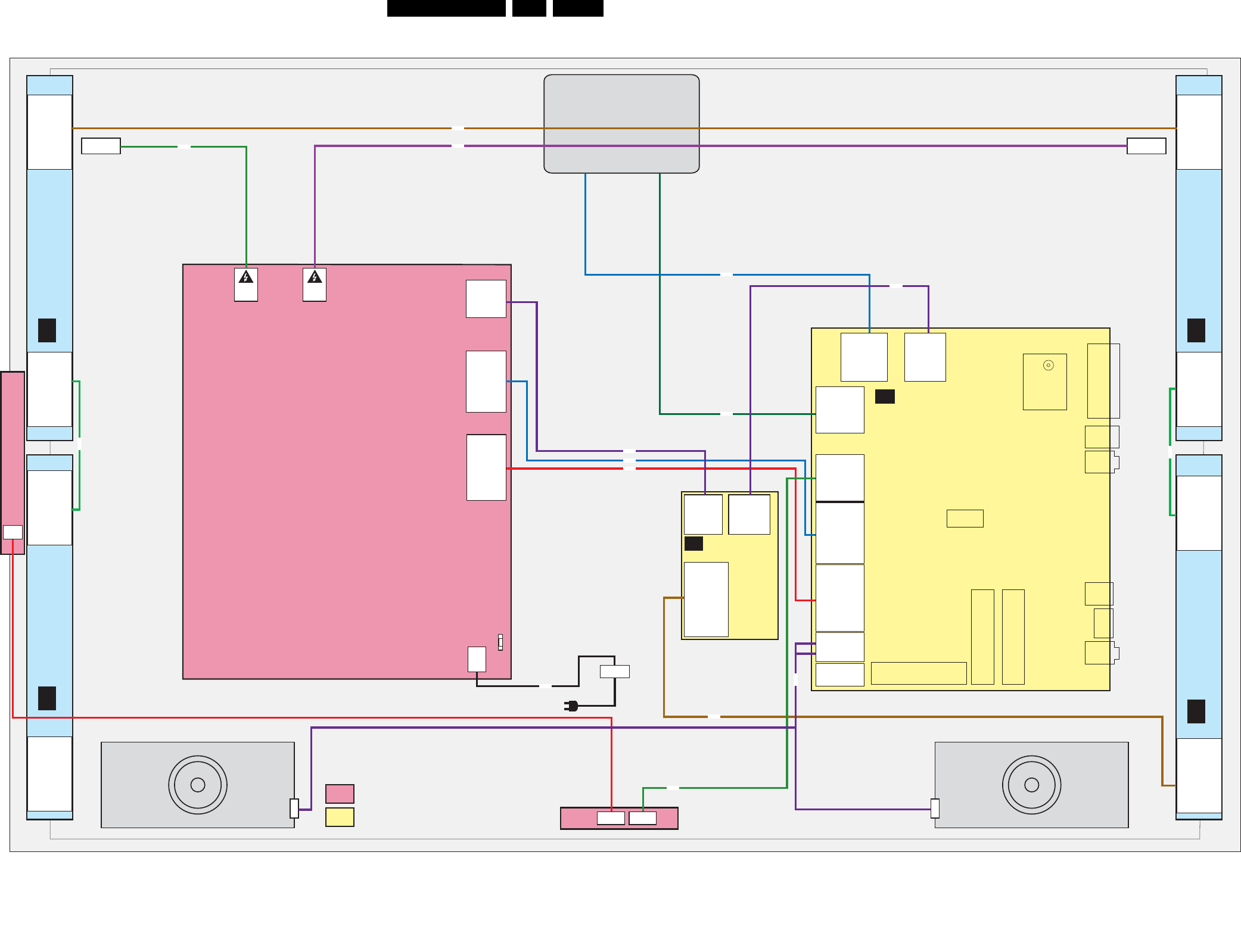
EN 40LC9.1A LA 9.
Block Diagrams
2009-Apr-10
Wiring Diagram 47" (Frame)
1M85 (AL1)
1. SPI-CLOCK-BUF
2. SPI-DATA-OUT
3. SPI-DATA-RETURN
4. SPI-LATCH
5. PWM-CLOCK-BUF
6. +3V3
7. BLANK-BU
8. EEPROM-CS
9. TEMP-SENSOR
10. PROG
11. VLED1
12. GND
13. VLED2
14. GND
1M83 (AL1)
1. SCL
2. SPI-DATA-IN
3. SDA
4. CONTROL-1
5. CONTROL-2
6. +3V3
7. BLANK
8. EEPROM-CS
9. TEMP-SENSOR
10. PROG
11. VLED1
12. GND
13. VLED2
14. GND
WIRING DIAGRAM 47"
(FRAME)
1M83 (AL1)
1. SCL
2. SPI-DATA-IN
3. SDA
4. CONTROL-1
5. CONTROL-2
6. +3V3
7. BLANK
8. EEPROM-CS
9. TEMP-SENSOR
10. PROG
11. VLED1
12. GND
13. VLED2
14. GND
1M85 (AL1)
14. GND
13. VLED2
12. GND
11. VLED1
10. PROG
9. TEMP-SENSOR
8. EEPROM-CS
7. BLANK-BU
6. +3V3
5. PWM-CLOCK-BUF
4. SPI-LATCH
3. SPI-DATA-RETURN
2. SPI-DATA-OUT
1. SPI-CLOCK-BUF
1M85 (AL1)
14. GND
13. VLED2
12. GND
11. VLED1
10. PROG
9. TEMP-SENSOR
8. EEPROM-CS
7. BLANK-BU
6. +3V3
5. PWM-CLOCK-BUF
4. SPI-LATCH
3. SPI-DATA-RETURN
2. SPI-DATA-OUT
1. SPI-CLOCK-BUF
1M83 (AL1)
14. GND
13. VLED2
12. GND
11. VLED1
10. PROG
9. TEMP-SENSOR
8. EEPROM-CS
7. BLANK
6. +3V3
5. CONTROL-2
4. CONTROL-1
3. SDA
2. SPI-DATA-IN
1. SCL
1M83 (AL1)
14. GND
13. VLED2
12. GND
11. VLED1
10. PROG
9. TEMP-SENSOR
8. EEPROM-CS
7. BLANK
6. +3V3
5. CONTROL-2
4. CONTROL-1
3. SDA
2. SPI-DATA-IN
1. SCL
1M85 (AL1)
1. SPI-CLOCK-BUF
2. SPI-DATA-OUT
3. SPI-DATA-RETURN
4. SPI-LATCH
5. PWM-CLOCK-BUF
6. +3V3
7. BLANK-BU
8. EEPROM-CS
9. TEMP-SENSOR
10. PROG
11. VLED1
12. GND
13. VLED2
14. GND
KEYBOARD CONTROL
(1114)
8M83
8M82
18490_401_090401.eps
090410
AMBI-LIGHT MODULE
(1078)
AL
AMBI-LIGHT MODULE
(1077)
AL
AMBI-LIGHT MODULE
(1078)
AL
AMBI-LIGHT MODULE
(1077)
AL
1M99 (B01)
12. GND
11. N.C
10. N.C
9. POWER-OK
8. GND
7. BACKLIGHT_BOOST
6. PWM_DIMMING
5. BL_ON_OFF
4. GND
3. GND
2. +12VDISP
1. +12VDISP
1M95 (B01)
11. N.C
10. GNDSND
9. +24VAUDIO
8. +12VS
7. +12VS
6. +12VS
5. GND
4. GND
3. GND
2. STANDBY
1. +3V3STBY
CN4
11. FAN_PWM
10. GND_SND
9. +VSND
8. +12V
7. +12V
6. +12V
5. GND1
4. GND1
3. GND1
2. STANDBY
1. 3V3_ST
CN7
6. GND
5. +24V
4. GND
3. +24V
2. GND
1. +24V
CN5
12. GND1
11. I2C_DATA
10. I2C_SCL
9. INV_OK
8. A/P_DIM
7. BOOST
6. DIM
5. BL_ON_OFF
4. GND1
3. GND1
2. +12V
1. +12V
CN1
1. N
2. L
1M20 (B04c)
8. +5V_SW
7. KEYBOARD
6. LED1
5. +3V3STBY
4. LED2
3. IR
2. GND
1. LIGHT-SENSOR
1736 (B03)
3. SPEAKER_RIGHT-
2. N.C.
1. SPEAKER_LEFT+
1735 (B03)
4. SPEAKER_RIGHT-
3. SPEAKER_RIGHT+
2. SPEAKER_LEFT-
1. SPEAKER_LEFT+
SSB
(1150)
B
INLET
MAIN POWER SUPPLY
IPB 47 PLHC-T819A
(1005)
TO
BACKLIGHT
IR LED PANEL
(1112)
LCD DISPLAY
(1004)
P2
3P
P1
8P
FUSE
TO
BACKLIGHT
1G51 (B04D)
51. GND
...
...
...
4. +VDISP
3. +VDISP
2. +VDISP
1. +VDISP
1M59 (B04E)
1. AMBI_SCL_OUT
2. GND
3. AMBI_SDA_OUT
4. I2S_SEL1
5. I2S_SEL2
6. +3V3_SW
7. GND
1G50 (B04D)
1. GND
2. GND
...
...
38. +VDISP
39. +VDISP
40. +VDISP
41. +VDISP
Board Level Repair
Component Level Repair
Only For Authorized Workshop
SPEAKER RIGHT (5212) SPEAKER LEFT (5211)
+ -
+ -
8308
1M90 (AB1)
6. GND
5. +24V
4. GND
3. +24V
2. GND
1. +24V
1M59 (AB1)
7. GND
6. +3V3
5. CONTROL2
4. CONTROL1
3. SDA
2. GND
1. SCL
DC-DC
INTERFACE
(1028)
AB
1M84 (AB1)
14. GND
13. VLED2
12. GND
11. VLED1
10. PROG
9. TEMP-SENSOR
8. EEPROM-CS
7. BLANK-BUF
6. +3V3
5. PWM-CLOCK-BUF
4. SPI-LATCH1CONN
3. SPI-DATA-RETURN
2. SPI-CLOCK-BUF
1. SPI-LATCH2CONN
8G51
8M59
8G50
8319
8M85
8M95
8M60
8M99
8316
8M84
8M20
8735
CN2
1. HV1
2. N.C.
3. HV1
CN3
1. HV2
2. N.C.
3. HV2
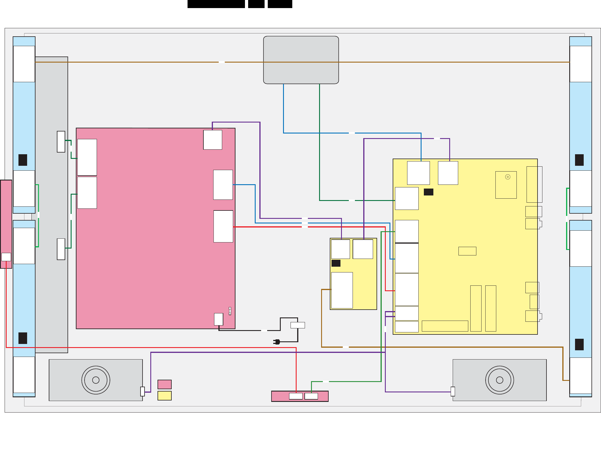
Block Diagrams EN 41LC9.1A LA 9.
2009-Apr-10
Wiring Diagram 52" (Frame)
1M85 (AL4)
1. SPI-CLOCK-BUF
2. SPI-DATA-OUT
3. SPI-DATA-RETURN
4. SPI-LATCH
5. PWM-CLOCK-BUF
6. +3V3
7. BLANK-BUF
8. EEPROM-CS
9. TEMP-SENSOR
10. PROG
11. VLED1
12. GND
13. VLED2
14. GND
1M83 (AL1)
1. SCL
2. SPI-DATA-IN
3. SDA
4. CONTROL-1
5. CONTROL-2
6. +3V3
7. BLANK
8. EEPROM-CS
9. TEMP-SENSOR
10. PROG
11. VLED1
12. GND
13. VLED2
14. GND
WIRING DIAGRAM 52"
(FRAME)
1M83 (AL1)
1. SCL
2. SPI-DATA-IN
3. SDA
4. CONTROL-1
5. CONTROL-2
6. +3V3
7. BLANK
8. EEPROM-CS
9. TEMP-SENSOR
10. PROG
11. VLED1
12. GND
13. VLED2
14. GND
1M85 (AL4)
14. GND
13. VLED2
12. GND
11. VLED1
10. PROG
9. TEMP-SENSOR
8. EEPROM-CS
7. BLANK-BUF
6. +3V3
5. PWM-CLOCK-BUF
4. SPI-LATCH
3. SPI-DATA-RETURN
2. SPI-DATA-OUT
1. SPI-CLOCK-BUF
1M85 (AL4
14. GND
13. VLED2
12. GND
11. VLED1
10. PROG
9. TEMP-SENSOR
8. EEPROM-CS
7. BLANK-BUF
6. +3V3
5. PWM-CLOCK-BUF
4. SPI-LATCH
3. SPI-DATA-RETURN
2. SPI-DATA-OUT
1. SPI-CLOCK-BUF
1M83 (AL1)
14. GND
13. VLED2
12. GND
11. VLED1
10. PROG
9. TEMP-SENSOR
8. EEPROM-CS
7. BLANK
6. +3V3
5. CONTROL-2
4. CONTROL-1
3. SDA
2. SPI-DATA-IN
1. SCL
1M83 (AL1)
14. GND
13. VLED2
12. GND
11. VLED1
10. PROG
9. TEMP-SENSOR
8. EEPROM-CS
7. BLANK
6. +3V3
5. CONTROL-2
4. CONTROL-1
3. SDA
2. SPI-DATA-IN
1. SCL
1M85 (AL4)
1. SPI-CLOCK-BUF
2. SPI-DATA-OUT
3. SPI-DATA-RETURN
4. SPI-LATCH
5. PWM-CLOCK-BUF
6. +3V3
7. BLANK-BUF
8. EEPROM-CS
9. TEMP-SENSOR
10. PROG
11. VLED1
12. GND
13. VLED2
14. GND
KEYBOARD CONTROL
(1114)
8M83
8M82
18490_402_090401.eps
090410
AMBI-LIGHT MODULE
(1178)
AL
AMBI-LIGHT MODULE
(1177)
AL
AMBI-LIGHT MODULE
(1178)
AL
AMBI-LIGHT MODULE
(1177)
AL
1M99 (B01)
12. GND
11. N.C
10. N.C
9. POWER-OK
8. GND
7. BACKLIGHT_BOOST
6. PWM_DIMMING
5. BL_ON_OFF
4. GND
3. GND
2. +12VDISP
1. +12VDISP
1M95 (B01)
11. N.C
10. GNDSND
9. +24VAUDIO
8. +12VS
7. +12VS
6. +12VS
5. GND
4. GND
3. GND
2. STANDBY
1. +3V3STBY
CN4
11. FAN_PWM
10. GND_SND
9. +VSND
8. +12V
7. +12V
6. +12V
5. GND1
4. GND1
3. GND1
2. STANDBY
1. 3V3_ST
CN5
12. GND1
11. I2C_DATA
10. I2C_SCL
9. INV_OK
8. A/P_DIM
7. BOOST
6. DIM
5. BL_ON_OFF
4. GND1
3. GND1
2. +12V
1. +12V
CN1
1. N
2. L
1M20 (B04c)
8. +5V_SW
7. KEYBOARD
6. LED1
5. +3V3STBY
4. LED2
3. IR
2. GND
1. LIGHT-SENSOR
1736 (B03)
3. SPEAKER_RIGHT-
2. N.C.
1. SPEAKER_LEFT+
1735 (B03)
4. SPEAKER_RIGHT-
3. SPEAKER_RIGHT+
2. SPEAKER_LEFT-
1. SPEAKER_LEFT+
SSB
(1150)
B
INLET
MAIN POWER SUPPLY
PSU DPS-411AP4A B
(1005)
IR LED PANEL
(1112)
LCD DISPLAY
(1004)
P2
3P
P1
8P
FUSE
1G51 (B04D)
51. GND
...
...
...
4. +VDISP
3. +VDISP
2. +VDISP
1. +VDISP
1M59 (B04E)
1. AMBI_SCL_OUT
2. GND
3. AMBI_SDA_OUT
4. I2S_SEL1
5. I2S_SEL2
6. +3V3_SW
7. GND
1G50 (B04D)
1. GND
2. GND
...
...
38. +VDISP
39. +VDISP
40. +VDISP
41. +VDISP
Board Level Repair
Component Level Repair
Only For Authorized Workshop
SPEAKER RIGHT (5212) SPEAKER LEFT (5211)
+ -
+ -
8308
1M90 (AB1)
6. GND
5. +24V
4. GND
3. +24V
2. GND
1. +24V
1M59 (AB1)
7. GND
6. +3V3
5. CONTROL2
4. CONTROL1
3. SDA
2. GND
1. SCL
DC-DC
INTERFACE
(1179)
AB
1M84 (AB1)
14. GND
13. VLED2
12. GND
11. VLED1
10. PROG
9. TEMP-SENSOR
8. EEPROM-CS
7. BLANK-BUF
6. +3V3
5. PWM-CLOCK-BUF
4. SPI-LATCH1CONN
3. SPI-DATA-RETURN
2. SPI-CLOCK-BUF
1. SPI-LATCH2CONN
8G51
8M59
8G50
8M85
8M95
8M60
8M99
8M84
8M20
8735
CN3/1316
12. N.C.
11. N.C.
10. GND3
9. GND3
8. GND3
7. GND3
6. GND3
5. 24Vinv
4. 24Vinv
3. 24Vinv
2. 24Vinv
1. 24Vinv
CN2/1319
14. PDIM_Select
13. PWM
12. On/Off
11. Vbri
10. GND3
9. GND3
8. GND3
7. GND3
6. GND3
5. 24Vinv
4. 24Vinv
3. 24Vinv
2. 24Vinv
1. 24Vinv
INVERTER
CONNECTOR
INVERTER
CONNECTOR
8319 8316
INVERTER
CN7
6. GND
5. +24V
4. GND
3. +24V
2. GND
1. +24V
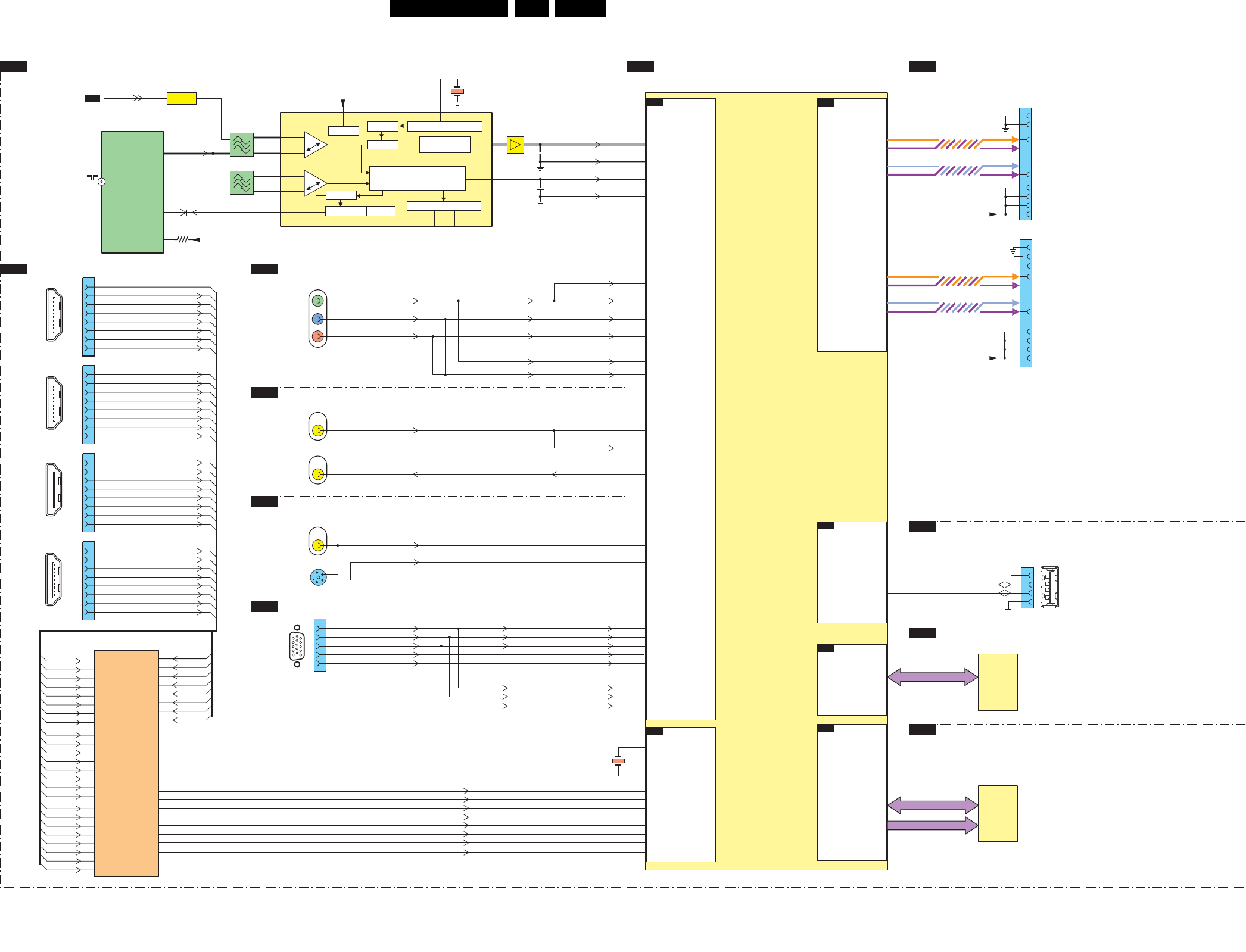
EN 42LC9.1A LA 9.
Block Diagrams
2009-Apr-10
Block Diagram Video
B02A TUNER & ANALOG DEMOD B04D DISPLAY INTERFACE - LVDS
B04 MT5392:
B05 HDMI & MUX B06B ANALOG I/O - YPBPR
B06C ANALOG I/O - CINCH
B06D SIDE-AV & USB
B06E VGA
B04B GDDR3
B04C FLASH & EJTAG
B06D SIDE-AV & USB
1D14
DDR3
7702
HYB18H1G321AF
7701
MT5392RHMJ
LVDS
B04D
AVI
B06B
HDMI_XTAL_LDO
B05
DREAM_IF
B04B
CVBS-SPDIF_USB
B06D
FLASH_IF
B04C
SPB1P_1
SY1P_1
CVBS4
SPB1P_1
Y1P
SOY
Y1N
PB1P
PB1R
PBR1N
SCART_CVBS1
SY1N
SPBR1N
SY1P
PB
PR
YAJ19
AJ18
AH17
35 RXC-
RX0+
RX0-
RX1+
RX1-
RX2+
RX2-
34
32
31
29
28
26
25
RXC+
AJ8
AK9
AJ9
AK8
AJ7
AJ6
AK6
AK7
HDMI_RX1_B_P
HDMI_RX2_B_N
HDMI_RX2_B_P
XTAL1
XTALO
HDMI_RX1_B_N
HDMI_RX0_B_P
HDMI_RXC_B_P
HDMI_RXC_B_N
HDMI_RX0_B_N
7B05
ADV3002BSTZ01
HDMI
SWITCH
OUT_CLK_-
OUT_CLK_+
IN_DIN_C
IN_B
IN_A
OUT_DATAD0_-
OUT_DATAD0_+
OUT_DATAD1_-
OUT_DATAD1_+
OUT_DATAD2_-
OUT_DATAD2_+
CRX2+
CRX2-
CRX1+
CRX1-
CRX0+
CRX0-
CRXC+
CRXC-
BRX2+
BRX2-
BRX1+
BRX1-
BRX0+
BRX0-
BRXC+
BRXC-
ARX2+
ARX2-
ARX1+
ARX1-
ARX0+
ARX0-
ARXC+
ARXC-
60
59
57
56
54
53
51
50
11
10
8
7
5
4
2
1
23
22
20
19
17
16
14
13
DRX2+
DRX2-
DRX1+
DRX1-
DRX0+
DRX0-
DRXC+
DRXC-
48
47
45
44
42
41
38
37
19 1
18 2
1
1B02
3
4
7
9
10
12
6
DRX2+
DRX2-
DRX1+
DRX1-
DRX0+
DRX0-
DRXC+
DRXC-
HDMI 1
CONNECTOR
19 1
18 2
1
1B07
3
4
7
9
10
12
6
CRX2+
CRX2-
CRX1+
CRX1-
CRX0+
CRX0-
CRXC+
CRXC-
HDMI 2
CONNECTOR
1
1B04
3
4
7
9
10
12
6
BRX2+
BRX2-
BRX1+
BRX1-
BRX0+
BRX0-
BRXC+
BRXC-
1
1B05
3
4
7
9
10
12
6
ARX2+
ARX2-
ARX1+
ARX1-
ARX0+
ARX0-
ARXC+
ARXC-
19 1
18 2
HDMI 3
CONNECTOR
19 1
18 2
HDMI SIDE
CONNECTOR
MT5392
7810
NAND512W3A2CN6E
FLASH
512Mx8
18490_403_090401.eps
090410
NAND_PDDD(0-7)
DQ(0-31)
RA(0-12)
4321
USB_DM0
USB_DP0
USB 2.0
CONNECTOR SIDE
SW UPLOAD
JPEG
MP3
AAJ5
AK5
VIDEO
7
12
9
CVBS0
CVBSN
MPX0_P
MPX0_N
1
5
SVHS IN
24
3
1F12
1F18
CVBS SY0
SC0
AF30
AF29
2SY_0
SC_0
SPR1P_1 SPR1P_1 AH19 PR1P
Y1P
SOY1
AH18 Y1N
AK19 PBR1N
CVBS_4
DACOUT1SC1_CVBS_OUT CVBS_4
SYNC_SCT1
PB1P
1
1G16
2
3
14
13
VGA_R
VGA_G
VGA_Rp
VGA_Rn
VGA_Gn
VGA_Bn
RN
GN
BN
VGA_Gp
VGA_B
H-SYNC
V-SYNC
VGA_Bp
HSYNC
VSYNC
RP
GP
BP
1
610
11
5
15
VGA
CONNECTOR
AJ14
AK14
AH15
AJ15
AJ16
AJ17
AK16
AK17 RP
VSYNC
GP
BP
HSYNC
BN
RN
GN
USB_DP0
USB_DM0
RDQ
RA
PDD
6210
1G50
LVDS_A_TXe
LVDS_A_TXo
LVDS_B_TXo
LVDS_B_TXe
QUAD LVDS
1920x1080
100/120Hz
1G51
+VDISP
+VDISP
TO DISPLAY
TO DISPLAY
I2C
1
2
3
32
38
40
39
41
50
51
49
40
11
3
4
2
1
1B10
27M W30
W29
1F21
1
2
4
3
1
5
4
1211
SIF1
SIF2
VIF1
VIF2
1
2
17
CVBS
DEMODULATOR
7212
TDA9886T/V4
IF_ATV
+VTUN
1204
UV1856/ABHN-5
TUNER
11
IF1
CVBS_RF
GND_CVBS_RF
AD29
AD28
SOUND TRAPS
4.5 to 6.5 Mhz
VIF-PLL
SINGLE REFERENCE QSS MIXER
INTERCARRIER MIXER AND
AM-DEMODULATOR
TUNER AGC VIF AGC
TA G C
SIF AGC
I2C-BUS TRANSCEIVER
MAD
SCL
SDA
SUPPLY
+5VS
1RF_AGC
DC_PWR
9
VST
DIDITAL VCO COTROLRC VCO
REF
38MHz
20
(I2C)
1
4
5
1212
38MHz
15
12134M0
SAW_SW SAW_SW
7211
B04C
(CONTROL)
2
23
24
14
12
SIOMAD
SIF_OUT
SIF_OUT_GND
AB27
AB26
1E19
VIDEO
IN AF28
AJ20
7
1E17
VIDEO
OUT AF28
7
3261
EF
7213
22402252
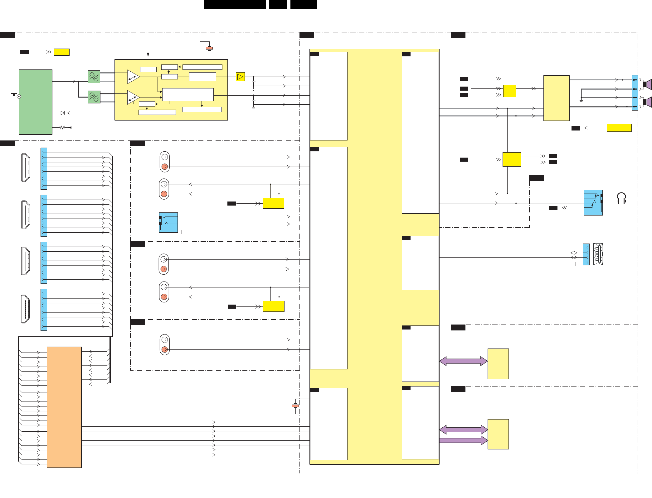
Block Diagrams EN 43LC9.1A LA 9.
2009-Apr-10
Block Diagram Audio
B02A TUNER & ANALOG DEMOD B03 CLASS-D & MUTING
B04 MT5392:
B05 HDMI & MUX B06B ANALOG I/O - YPBPR
B06C ANALOG I/O - CINCH
B06C ANALOG I/O - CINCH
B04B GDDR3
B04C FLASH & EJTAG
B06D SIDE-AV & USB
DDR3
7702
HYB18H1G321AF
7701
MT5392RHMJ
ALI_ADAC
B06B
AVI
B06B
ALI_DAC
B06B
HDMI_XTAL_LDO
B05
DREAM_IF
B04B
CVBS-SPDIF_USB
B06D
FLASH_IF
B04C
35 RXC-
RX0+
RX0-
RX1+
RX1-
RX2+
RX2-
34
32
31
29
28
26
25
RXC+
AJ8
AK9
AJ9
AK8
AJ7
AJ6
AK6
AK7
HDMI_RX1_B_P
HDMI_RX2_B_N
HDMI_RX2_B_P
XTAL1
XTALO
HDMI_RX1_B_N
HDMI_RX0_B_P
HDMI_RXC_B_P
HDMI_RXC_B_N
HDMI_RX0_B_N
7B05
ADV3002BSTZ01
HDMI
SWITCH
OUT_CLK_-
OUT_CLK_+
IN_DIN_C
IN_B
IN_A
OUT_DATAD0_-
OUT_DATAD0_+
OUT_DATAD1_-
OUT_DATAD1_+
OUT_DATAD2_-
OUT_DATAD2_+
CRX2+
CRX2-
CRX1+
CRX1-
CRX0+
CRX0-
CRXC+
CRXC-
BRX2+
BRX2-
BRX1+
BRX1-
BRX0+
BRX0-
BRXC+
BRXC-
ARX2+
ARX2-
ARX1+
ARX1-
ARX0+
ARX0-
ARXC+
ARXC-
60
59
57
56
54
53
51
50
11
10
8
7
5
4
2
1
23
22
20
19
17
16
14
13
DRX2+
DRX2-
DRX1+
DRX1-
DRX0+
DRX0-
DRXC+
DRXC-
48
47
45
44
42
41
38
37
19 1
18 2
1
1B02
3
4
7
9
10
12
6
DRX2+
DRX2-
DRX1+
DRX1-
DRX0+
DRX0-
DRXC+
DRXC-
HDMI 1
CONNECTOR
19 1
18 2
1
1B07
3
4
7
9
10
12
6
CRX2+
CRX2-
CRX1+
CRX1-
CRX0+
CRX0-
CRXC+
CRXC-
HDMI 2
CONNECTOR
1
1B04
3
4
7
9
10
12
6
BRX2+
BRX2-
BRX1+
BRX1-
BRX0+
BRX0-
BRXC+
BRXC-
1
1B05
3
4
7
9
10
12
6
ARX2+
ARX2-
ARX1+
ARX1-
ARX0+
ARX0-
ARXC+
ARXC-
19 1
18 2
HDMI 3
CONNECTOR
19 1
18 2
HDMI SIDE
CONNECTOR
MT5392
7810
NAND512W3A2CN6E
FLASH
512Mx8
18490_404_090401.eps
090410
NAND_PDDD(0-7)
DQ(0-31)
RA(0-12)
4321
USB_DM0
USB_DP0
USB 2.0
CONNECTOR SIDE
SW UPLOAD
JPEG
MP3
AAJ5
AK5
AUDIO
CVBS0
CVBSN
MPX0_P
MPX0_N
USB_DP0
USB_DM0
RDQ
RA
PDD
6210
1B10
27M W30
W29
1F21
1
2
4
3
1
5
4
1211
SIF1
SIF2
VIF1
VIF2
1
2
17
CVBS
DEMODULATOR
7212
TDA9886T/V4
IF_ATV
+VTUN
1204
UV1856/ABHN-5
TUNER
11
IF1
CVBS_RF
GND_CVBS_RF
AD29
AD28
SOUND TRAPS
4.5 to 6.5 Mhz
VIF-PLL
SINGLE REFERENCE QSS MIXER
INTERCARRIER MIXER AND
AM-DEMODULATOR
TUNER AGC VIF AGC
TA G C
SIF AGC
I2C-BUS TRANSCEIVER
MAD
SCL
SDA
SUPPLY
+5VS
1RF_AGC
DC_PWR
9
VST
DIDITAL VCO COTROLRC VCO
REF
38MHz
20
(I2C)
1
4
5
1212
38MHz
15
12134M0
SAW_SW SAW_SW
7211
B04C
(CONTROL)
2
23
24
14
12
SIOMAD
SIF_OUT
SIF_OUT_GND
AB27
AB26
3261
1D11
2
3
1
1F22
2
3
4
1
EF
7213
U29
U28
1D52
AUDIO
L/R OUT
N30 PGA_0OUTL
N29 PGA_0OUTR
L_MON_OUT
R_MON_OUT
AIN_2_L
AIN_2_R
AV3_L_IN
AV3_R_IN
DVI_AUL_IN
DVI_AUR_IN
1D14
AUDIO
L/R IN
1E17
R_MON_OUT
L_MON_OUT
52
53
SC2-IN-L
SC2-IN-R
37 SC1-OUT-L
36 SC1-OUT-R
AV OUT
AUDIO
L/R
1E19
AV IN
AUDIO
L/R AIN0_L
AIN0_L
5
3
R28
T28
AIN_6_L
AIN_6_R
SAV_L_IN
SAV_R_IN
1F18
SIDE AV
AUDIO
L/R
5
8
6
4
5
5
3
3
M30
M29
PGA_2OUTL
PGA_2OUTR
AOUTL
AOUTR
AUDIO_LS_L
AUDIO_LS_R
SPEAKER_LEFT+
SPEAKER_LEFT-
SPEAKER_RIGHT+
SPEAKER_RIGHT-
7510
TDA8932BTW/N2
CLASS D
POWER
AMPLIFIER
2
14
27
22
MUTE 5
1
2
1735
3
4
DC-DETECTION
HP_LOUT
HP_ROUT
SW_MUTE
MUTE_C
MUTE_M
M28
M27
HPOUTL
HPOUTR
HEADPHONE
STANDBYn 6
MUTEn
POWER_DOWN
B04A
B06C
B06B
B04A
B04A
B04A
DC_PROT
B04C
7511÷7513
HP_DET
B04C
(CONTROL)
(CONTROL)
(CONTROL)
(CONTROL)
ANTI_PLOP
MUTE
7A60
MUTE_C
7E02
B03
MUTE_C
MUTE_M
7D10
B03
MUTE_M
22402252

EN 44LC9.1A LA 9.
Block Diagrams
2009-Apr-10
Block Diagram Control & Clock Signals
CONTROL + CLOCK SIGNALS
B04B GDDR3
B04C FLASH & EJTAG
B06D SIDE-AV & USB
B04C FLASH & EJTAG
1812
3
2FOR
DEBUGGING
ONLY
TO IR/LED PANEL
AND
KEYBOARD CONTROL
+5V_SW
+3V3STBY
1
2
3
4
5
6
7
8
1M20
MT5392
7701
MT5392RHMJ
FLASH_IF
B04C
PM_DEMOD
B04A
5
NAND_PDD(1)
16M
FLASH
7810
M25P16
A13
M2 J11
6
NAND_POOE
B9
1
SERIAL_POCE
E10
2
NAND_PDD(0)
AJ4
OPWRSB
SPIO_UART_IIC
B04C
L32
L31
UART
SERVICE
CONNECTOR
UART_RX
UART_TX
UART_RX
UART_TX
UART_RX
UART_TX
1813
3
2
1
RES
AH14 STANDBYn
B03
B01
STANDBYn
PDD_1
POOE
POCE_0
PDD_0
OPWM_2 C5 PWM_DIMMMING
B01
AH5 GPIO_0
GPIO_16
GPIO_15
GPIO
B04C
GPIO_14 AK2 EDID_WC
B05 B06E
GPIO_20 B28LCD_PWR_ON
B04D
GPIO_20 B22 SAW_SW
B02A
GPIO_24 D28BL_ON_OFF
B01
DC_PROT
B03
AG6
AJ2
AJ1
GPIO_1
USB_PWE
B06D
AF7 GPIO_2
USB_OC
B06D
G30GPIO_17
G30GPIO_17
AK11 OIRI
HP_DET
B06D
AJ29 ADIN_3
CVBS_SPDIF_USB
B06D
LIGHT_SENSOR
AK29 ADIN_4
POWER-OK
B01
AJ28ADIN_5
KEYBOARD
AK28ADIN_6
RF_AGC_MON
B02A
IR
OPCTRL_0 AJ12 HDMI_CEC
B05
OPCTRL_2 AG12 LED1
OPCTRL_3AG11 MUTEn
B03
OPCTRL_4 AF13SW_MUTE
B03
B03
B03
OPCTRL_5 AF12 POWER_DOWN
B03
OPCTRL_8AH13LED2
DDR3
7702
HYB18H1G321AF
DREAM_IF
B04B
DQ(0-31)
RA(0-12)
RDQ
RA
RCLK0
7810
NAND512W3A2CN6E
FLASH
512Mx8
NAND_PDDD(0-7)
PDD
OPWM_1
D_1
K27 BACKLIGHT_BOOST
B01
7815
E9 LVDS_SELECT
B01
2843
SDM
2833
PANEL
RCLK0p
M3J10
RCLK0 RCLK0n
4321
USB20-DM0
OPCTRL_8AH13
USB_DM0 AJ5
USB_DP0 AK5 USB20-DP0
USB 2.0
CONNECTOR
SIDE
1F21
3
4
2
1
USB_PWE
7F01
TPS2041BD
USB_OC
EN
OUT
OC
18490_405_090401.eps
090407
7602
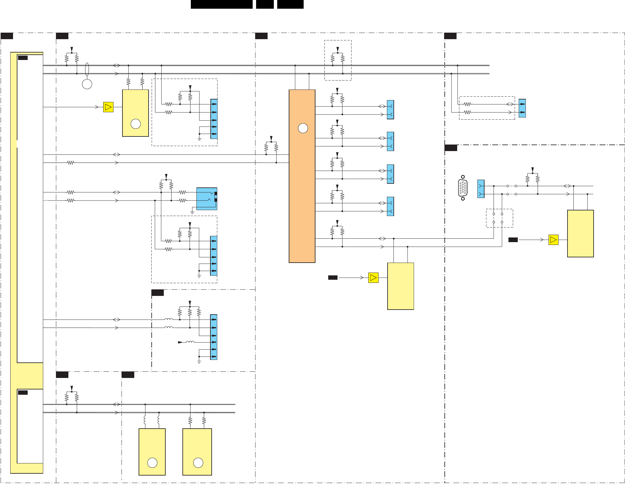
Block Diagrams EN 45LC9.1A LA 9.
2009-Apr-10
Block Diagram I2C
I²C
HDMI & MUX
B05
VGA
B06E
TUNER & ANALOG DEMOD
B02A
MTK POWER
B04A
FLASH & EJTAG
B04C
CONTROLLER
B04
DISPLAY INTERFACE - LVDS
B04D
AMBILIGHT
B04E
7701
MT5392RHMJ
OSDA0
OSCL0
GPIO-18
PM_DEMOD
SPIO_UART
IIC
L28
L287
68
67
J29
J30
L29
TUNER_SDA
TUNER_SCL
SYS_EEPROM_WE
SDA
SCL
3606
3607
+3V3_SW
3831
3830
+3V3_SW
389D
389F
+3V3_SW
UA0RX
UA0TX
CLK
DATA
18490_406_090401.eps
090407
10 11
7212
TDA9886T/V4
ANALOG
DEMODULATOR
3244
3241
54
1204
UV1856/ABHN
MAIN
TUNER
56
7812
M24C64
EEPROM
(NVM)
3839
3838
AJ10
AK10
DDC-SDA
DDC-SCL
OSCL2
OSDA2
K30
K29
AMBI-SDA
AMBI-SCL
AJ13
AK13
UART_RX
UART_TX
OSCL1
OSDA1
38A9
3823
38A8
3M09
3M10
+3V3STBY
UART
SERVICE
CONNECTOR
TO AMBILIGHT
DRIVERS
3864
3865
1813
3
2
1
1818
3
1
4
6
2
38A3
38A4
FOR DEBUGGING ONLY
1G51
49
50
3916
3917
3888
3889
+3V3STBY
3A11
3A10
3A13
+3V3_SW
+3V3_SW
1812
3
1
4
66
7
2
1M59
1
5
6
2
3
3890
3891
FOR DEBUGGING ONLY
RES
LVDS3_SDA_DISP
LVDS3_SCL_DISP
ERR
16
ERR
18
B04A
B04C
5214
5215
ERR
15
7815
5A14
5A16
5A10
40 27
7B05
ADV3002BSTZ
HDMI
MUX
3B38
3B39
VDDO_3V3
RES
L28
L29
EDID_SDA
EDID_SCL
3B35
3B34
+5V_COMBINED
56
7B02
M24C02
EEPROM
(EDID)
7
EDID_WC
7B07
HDMI
CONNECTOR 1
1B05
16
15
3B47
3B46
ARX-5V
3B19
3B20
+5V_COMBINED
76
75
HDMI
CONNECTOR 3
1B04
16
15
3B51
3B50
BRX-5V
74
73
HDMI
CONNECTOR 2
1B07
16
15
3B53
3B52
CRX-5V
72
71
HDMI
CONNECTOR
SIDE
1B02
16
15
3B55
3B54
DRX-5V
70
69
ARX-DDC-DAT
ARX-DDC-CLK
BRX-DDC-DAT
BRX-DDC-CLK
CRX-DDC-DAT
CRX-DDC-CLK
DRX-DDC-DAT
DRX-DDC-CLK
1
610
11
5
15
VGA
CONNECTOR
SDA_VGA
SCL_VGA
1G16
12
15
3G15
3G16
DC_5V
56
7G11
M24C02
EEPROM
ERR
17
4G12
4G11
4G14
4G13
RES
7
EDID_WC
7G12
B04C
B04C
MT539X
ERR
14
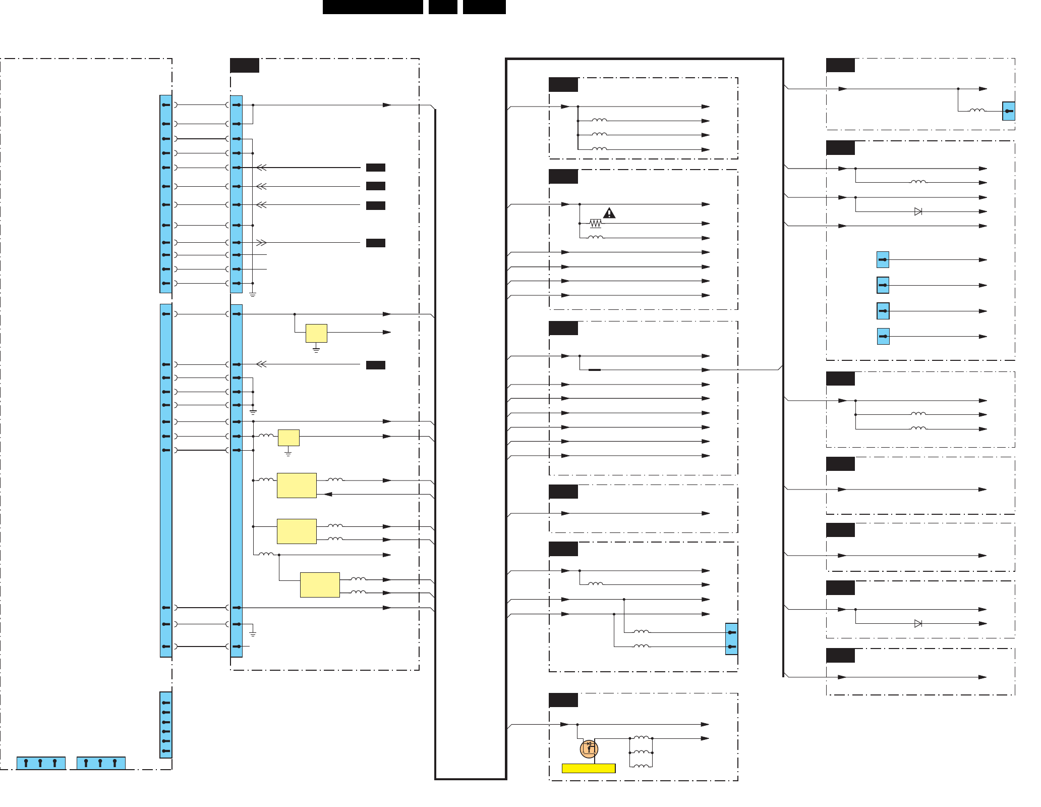
EN 46LC9.1A LA 9.
Block Diagrams
2009-Apr-10
Supply Lines Overview
SUPPLY LINES OVERVIEW
MAIN
POWER SUPPLY
B01 DC / DC B04E AMBILIGHT
B02A TUNER & ANALOG DEMOD
B04C FLASH & EJTAG
B03CLASS-D & MUTING
B04A MTK POWER
B04B GDDR3
B04D DISPLAY INTERFACE - LVDS
B06B ANALOG I/O - YPbPr
B06D SIDE-AV & USB
B06E VGA
B07 BDS iTV
B05 HDMI & MUX
B06A DIGITAL IO - ETHERNET (PROVISIONAL)
CN4
11
66
77
88
1M95
+3V3STBY
+1V2-STANDBY
+3V3_SW
+3V3_SW
TO DISPLAY
TO AMBILIGHT
MODULE
18490_407_090401.eps
090406
CN7
1
2
3
4
5
6
HV2
N.C.
HV2
HV1
N.C.
HV1
3V3_ST
+12V
B04d
B03,B04a
B03,B04a,c,
B07
B04a
B04a
B04a
B02a,B03,B04c,
B05,B06e
B04a,c,e,B05,
B06a,b,d
B04a,b
B04a,B05
B03
CN5
11
66
77
22
33
44
55
88
BL_ON_OFF
1M99
BACKLIGHT_BOOST
+12VDISP
PWM_DIMMING
B04C
B04C
+12V
+12V
GND1
GND1
BL-ON_OFF
A/P_DIM
DIM
BOOST
+12VS
+8V_SW
99 +24VAUDIO
10 10
+5V_IF
+5V_SW+5V_SW
+1V0_SW
+5V_SW
+3V3_SW
+12V_1
+12V
+12V
+VSND
GND_SND
CONTROL
CONTROL
B04C
CONTROL
B06D
CONTROL
99
INV_OK
10 10
I2C
11 11
I2C
12 12
GND1
POWER-OK
N.C.
N.C.
22
33
44
55
STANDBY
GNDSND
B04A
STANDBY
GND1
GND1
GND1
CONTROL
7201
IN OUT
COM
11 11
7117
TPS54386PWP
Non
Synchronous
Converter
7117
TPS54386PWP
DCDC
Converter
+24VAUDIO
+24VAUDIO
+3V3_SW+3V3_SW
B01
B01
B01
B01
B01
B01
B01
B01
B01
+3V3STBY+3V3STBY
+5V_SW+5V_SW
+12VS+12VS
B01
B01
N.C.N.C.
+24V
GND
GND
GND
+24V
+24V
5100
51085101
5117
1M59
6TO
AMBI
LIGHT
+3V3_SW
+3V3_SW
+3V3_SW
+3V3_SW
B01
B01
+5V_SW
+5V_SW
B01
DC_5V
B01
VDD
VDDA
5NA2 +3V3DN
+3V3_SW
+3V3_SW
5NA1 +3V3AN
B01
CRX-5V
1B04
18
HDMI 3
CONNECTOR BRX-5V
1B02
18
HDMI 1
CONNECTOR
ARX-5V
1B07
18
HDMI 2
CONNECTOR
+1V2_SW
+1V2_SW
+5V_SW
+5V_SW
+3V3_SW
+3V3_SW
DRX-5V
1B05
18
HDMI SIDE
CONNECTOR
+5V_COMBINED
VDDO_3V3
5B01
B01
B01
B01
5116
5103
31,14
12
7
3
+1V8_SW
+1V2_SW
7116
TPS54386PWP
Non
Synchronous
Converter
5104
5115
31,14
12
7201
IN OUT
COM
SENSE+1V0_MT5392
5218
+5VS
5217
+5VTUN
5216
5502
3530
+1V0_SW
+1V0_SW
+3V3_SW+3V3_SW
B01
+3V3_SW+3V3_SW
B01
+3V3STBY+3V3STBY
B01
+5V_SW+5V_SW
B01 +1V2_SW+1V2_SW
B01
+3V3STBY+3V3STBY
+1V8_SW+1V8_SW
+8V_SW+8V_SW
+12VS+12VS
SENCE+1V0_MT5392
+3V3_FLASH
B01
+1V8_SW+1V8_SW
5810
1M20
8
5TO
IR/LED
PA N E L
5814
5815
+VDISP
+12VDISP+12VDISP
7911
LCD_PWR_ON
7910
B01 5910
5911
5912
5A10
6B07
6G13
+3V3STBY
+3V3STBY
B01
B01
3
2
1
CN2
3
2
1
CN3

Circuit Diagrams and PWB Layouts EN 47LC9.1A LA 10.
2009-Apr-10
10. Circuit Diagrams and PWB Layouts
Interface Ambilight: Interface + DC-DC
C
VCC
GND GND_HS
SWI_EMIT
SWI_COL
VFB
LVI_OUT
VIA
LPK_SENSE
DRV_COL
BOOT_IN
2
1
TIM_CAP
NC
out
9
in
E
in
F
out
1M85
2 9
I
3104 328 58351
1
A
out
out
13
in
3104 328 58371
out
3109 D2
out
G
13
3110 D3
7
C
D
out
5103/5104
3104 328 58341
12V
2107 E9
2108 D3
2109 E3
3100 B5
owner.
7
E
3105 D5
3106 D5
3107 D5
3108 E9
12V
12
16V
116
c002 E2
85
34
STUFFING DIVERSITIES FOR DC/DC INTERFACE AMBI 2K9
F122 E2
F123 E2
F124 E2
F125 B3
F126 A2
I100 A6
I101 C6
I102 C6
I103 C6
B
I109 A8
c001 E2
1101
H
INTERFACE + SINGLE DC-DC
out
All rights reserved. Reproduction in whole or in parts
2
24V
10
out
out
2102 C6
2103 D6
out
F121 E2
F114 B5
F115 C2
3101 C5
3102 D6
3103 D9
3104 D6
F120 D2
I
3
8
123456789
12
5106 B8
5107 A6
567
in
6
12
J
VLED2
I104 D9
I105 D5
I106 D7
I108 D6
C
D
E
A
B
C
D
E
1100 A6
1101 A7
1M59 C2
1M84 A2
1M85 A2
1M90 D2
2100 A6
2101 B5
F109 B3
F110 B3
2104 D5
2105 D9
2106 D9
431
16V
3104 328 58361
F116 D2
F117 D2
F118 D2
F119 D2
16V
63V
C
RES
See the stuffing diversities table in the case of components marked with one star (*)
is prohibited without the written consent of the copyright
H
G
3111 E8
3112 B6
5100 A8
5101 A8
5102 A7
5103 B8
5104 B8
5105 B8
16V
5108 A6
6100 C8
7100 B7
5105/5106
in
B
DC/DC INTERFACE
8
D
9
A
B
10
J
11
9101 C3
9102 C3
9103 C3
9104 C3
F101 B3
F102 B3
F103 B3
F104 B3
F105 B3
F106 B3
F107 A7
F108 B3
F111 B3
F112 B3
F113 B3
A
5
4
F
VLED1
12V
RES
+16V
F118
5101
30R
VSW
I108
F103
+3V3
+24VF
F112
I100
+12V
RES
100R
3109
4
5
6
7
1735446-7
1M59
1
2
3
+24V
F107
(RES)
9103
I106
3K3
31081%
3102
15K
2102
F101
2n2
F104
5106
30R
*
+16V
+16V
F122
9104
1
SUPERS.
1
NAME
DATEMGr CHECK
3104 313 6325
AMBI 2K9
DC-DC INTERFACE
A3
08-08-06
08-06-19
08-12-06
08-10-23
08-09-18
08-08-06
5
4
3
2
***031**
3
2
08-10-23
Peter Van Hove
08-06-19
CT ROYAL PHILIPS ELECTRONICS N.V. 2008
08-06-06********
13
SETNAMECHN
CLASS_NO
100n
2105
1M0
3105
F115
I101
F123
F111
3101
47R
1
2
3
4
5
6
1735446-6
1M90
9102
F117
(RES)
3104
330R
F121
F120
+24V
220p
2103
12K
3107
F102
VLED2
*
F124
30R
5105
F126 +24V
c001
F108
F105
F109
30
31
21
22
23
24
25
26
27
28
10
11
12
13
1
3
17
16
20
29
5
18
19
514
2
6
7
8
9
NCP3163BMNR2G
7100
Φ
14
VLED1
+3V3
100n
2107
T2.0A
1101 I109
*
30R
5107 RES
30R
5108RES
F110
1%
33K
3106
30R
5100 RES
5
6
7
8
9
15 16
1
10
11
12
13
14
2
3
4
F113
502382-1470
1M84
100K
3111
2100
220n
2101
10n
3100
0R1
F114
RES
VLED2
2108
100p
100R
3112
VLED1
c002
2106
100n
1100
3.0A 32VT10u
5102
100p
2109
RES
9101
F116
+12V
3110
100R
RES
F106
+24V
F125
I103
I105
9
15 16
I104
13
14
2
3
4
5
6
7
8
1M85
502382-1470
*
1
10
11
12
100n
2104
+16V
SS24
6100
30R
5104
*
5103
30R
*
3103
3K3
F119
SPI-LATCH2CONN
SPI-LATCH1CONN
SPI-LATCH2CONN
SPI-LATCH1CONN
SPI-LATCH2
SPI-LATCH1
I102
CONTROL1
CONTROL2
SDA
SPI-CLOCK-BUF
SPI-DATA-RETURN
SPI-DATA-OUT
PWM-CLOCK-BUF
BLANK-BUF
EEPROM-CS
TEMP-SENSOR
PROG
SCL
18310_600_090305.eps
090305
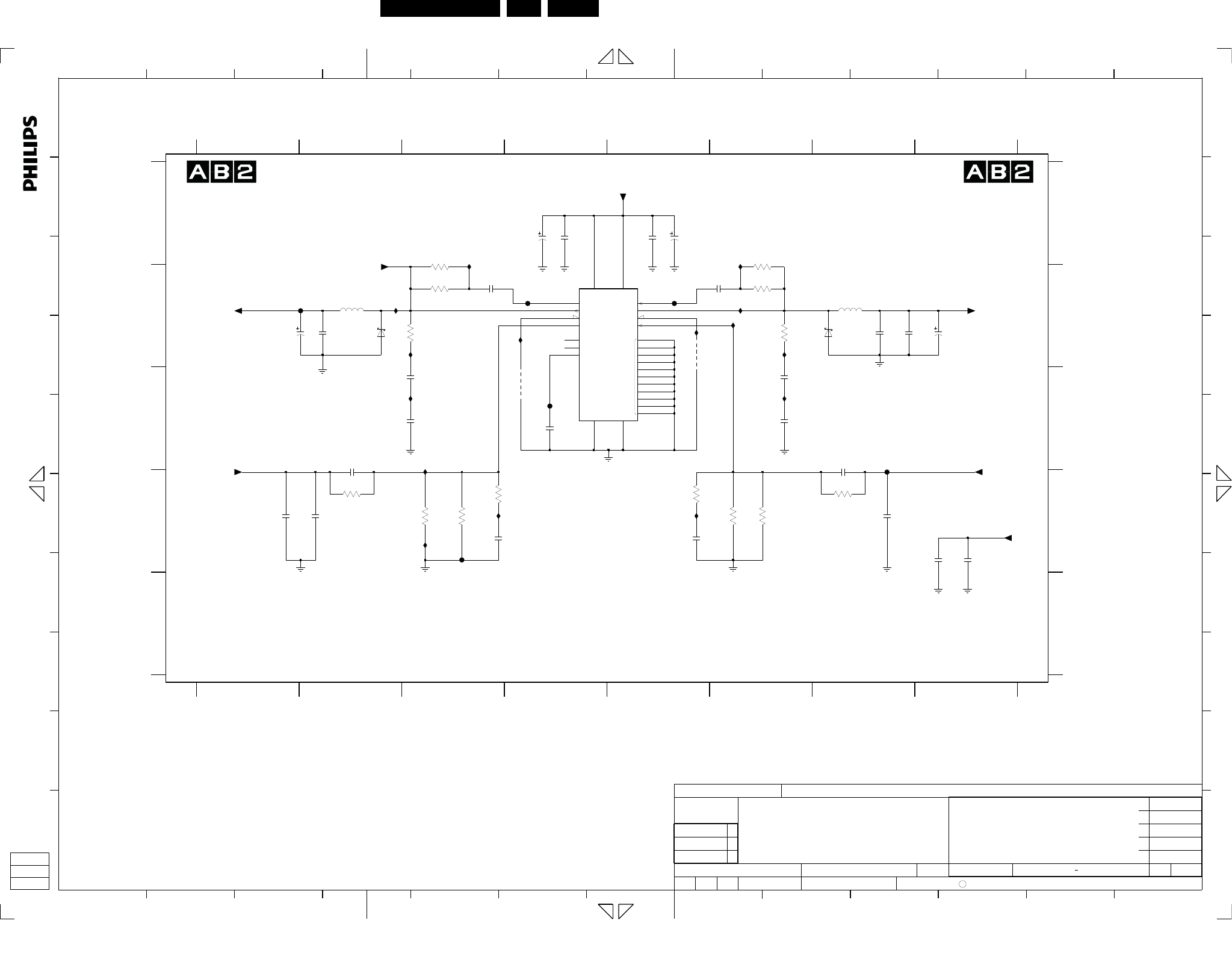
EN 48LC9.1A LA 10.
Circuit Diagrams and PWB Layouts
2009-Apr-10
Interface Ambilight: Dual DC-DC
C
PVDD1 PVDD2
EN1
SW1
BOOT1
SW2
FB2
EN2
BOOT2
FB1
ILIM2
SEQ
BP
GND GND_HS
VIA2
9202 C4
F200 B2
F201 C7
F203 B5
F207 C4
3
is prohibited without the written consent of the copyright
I212 C3
I213 D5
I205 B6
I206 B6
I208 B3
I209 B6
I210 C6
3204 B3
3205 B6
3206 D3
I211 C3
3208 D7
I214 D4
3210 D3
I215 D3
I216 B5
I217 B4
4
B
C
D
F
The components marked with two stars (**) belong to the 16V versions
12
B
13
A
All rights reserved. Reproduction in whole or in parts
6
G
7200 B4
9201 B5
1
(VLED1)
(VLED2)
F202 D3
2217 C7
F204 B4
2219 D2
I200 A3
7
5
11
7
2212 C4
2213 C6
2214 C3
H
6
9
8
D
DUAL DC-DC
10
I201 A6
I204 B2
3202 B3
3203 B6
(3104 328 58331, 3104 328 58341, 3104 328 58361, 3104 328 58371).
I
1
3207 D2
8
3209 D5
2
3211 D3
8
G
678
A
J
E
A
owner.
6200 B2
6201 B7 F
3
I
D
2216 C2
C
2218 D1
E
2220 D7
2208 B7
2209 B7
2210 B8
2211 C3
2207 B2
2215 C6
1
C
2 13
J
3200 A3
3201 A6
109
23
1
4567
345
2
B
C
D
7200 : TPS54383 in case of 16V or dual dc-dc converter
A
B
12
5
H
3212 D6
3213 D6
5200 B2
5201 B7
4
E
11
22u
2209
RES
2200 A4
2201 A4
2202 A5
2203 A5
2204 B3
2205 B6
2206 B1
E
The components marked with one star (*) belong to the 12V versions (3104 328 58351, 3104 328 58371).
2221 D3
2222 D5
2223 D8
2224 D8
3204
**
10R
*
33K
3213
I201
3207
68K
**
**
9202
1%
I217
100u
2206
**
F202
35V
3208
47K
1%
*
4u7
2207
** RES
+12V
2208
22u
F200
I214
F207
I209
2200
100u35V
+12V
4u7
I213
RES
2212
I200
3209
3K3
*
*
SS24
6201
1n0
2215
**
+16V
2214
1n0
1n0
2213
*
22n
2222 RES
*
2202
220n
10u
2224
3202
6R8
**
*
**
2223
10u
I205
10u
5200
220n
2201
**
+24VF
6200
SS24
I215
9201
*
F203
I210
2210
220u25V
*
3212
3K3
1%
*
47n
2205
*
F204
2218
4u7
RES
4u7
2219
RES
I206
100u
2203
3203
6R8
*
35V
*
3205
10R
47n
**
33K
**
2204
RES
3211
RES
2221
22n
22n
2216 2217
22n
RES
6R8
3201
RES
**
RES
2211
1n0
VLED1
3K3
3206
6R8
3200
RES
F201
*
I212
5201
10u
+16V
25
26
17
18
19
20
21
22
23
24
87
4
15
9
1
14
10
213
16
7200
TPS54283PWP
Φ
312
11
65
I204
I208
DATE
NAME
1
SUPERS.
1
CLASS_NO
EMANTESNHC
32
08-06-09 ROYAL PHILIPS ELECTRONICS N.V. 2008
08-06-19
Peter Van Hove
08-10-23
2
3
I211
130
2
3
4
5
08-08-06
08-09-18
08-10-23
08-12-06
08-06-19
08-08-06
A3
DC-DC INTERFACE
AMBI 2K9 3104 313 6325
CHECK
I216
1%
**
*
3210
3K9
VSW
2220
10u
18310_601_090305.eps
090305
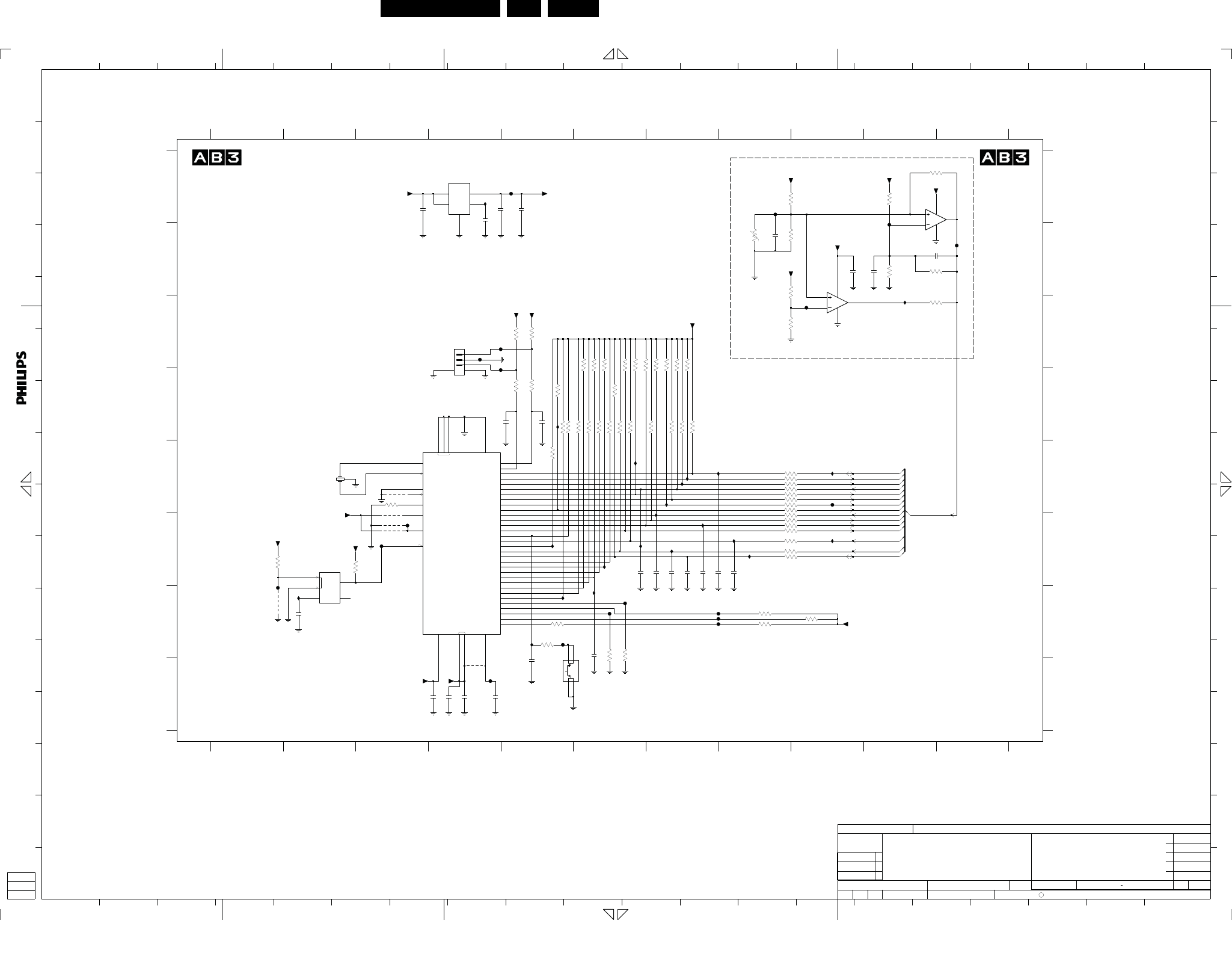
Circuit Diagrams and PWB Layouts EN 49LC9.1A LA 10.
2009-Apr-10
Interface Ambilight: Microcontroller
OUTIN
INH BP
COM
NC
GND
RST
IN
CD
C
-T
X2
RTXC1
RTXC2
RTCK
VBAT
DBGSEL
RST
VSS VSSA
VDDA
VDD_3V3
VDD_1V8
X1
2313 F7
3
4
19
6
14
20
15
2320 H5
2321 H4
2322 H4
2323 H4
2324 H4
G
H
3301-3 E6
O
711
A
1300 E2
1301 H5
2303 A4
2304 B8
2305 B10
2306 B9
2307 B10
E
E
F
1302 C4
2300 A3
2301 A4
2302 A5
3303-1 E6
3303-2 D6
3303-3 E6
3304-1 D6
3304-2 D7
2308 D4
2309 D5
2310 F6
2311 F7
2312 F7
3305-4 G8
2314 F7
2315 F7
F
G
All rights reserved. Reproduction in whole or in parts
910345
6
2
812
17
2316 F8
2318 G2
2319 G6
3308-2 F8
3308-4 F8
3309-1 F8
3309-4 F8
3310 A10
3300-2 D5
3300-3 D7
3300-4 D7
3301-1 D6
3301-2 E5
3316 B10
3301-4 D7
3302-1 D7
O
B
C
D
J
L
RES
B
C
D
J
3302-2 D6
3302-3 E6
3302-4 D6
3330 E8
3331 E8
3332 E3
3333 F2
3334 G5
3304-3 D7
3304-4 D7
3305-1 E7
3305-2 G8
3305-3 G9
7300-1 B9
3306-1 E8
3306-2 E8
10
123
1
91011
13
3307-1 E8
3307-2 F8
3307-4 F8
3308-1 F8
1256
3311 A8
3312 A10
3313 B8
3314 B8
3315 B10
9303 F3
3317 B8
3318 C10
11
E
F
G
H
A
14
H
3326 D6
3327 D6
3328 E5
3329 E5
F308 F3
F309 G6
F310 G6
F311 G8
F312 G8
3335 G5
3336 G6
3337 G6
3338 E8
3339 F1
F320 E9
7300-2 A10
7301 A4
M
98
is prohibited without the written consent of the copyright
45678
7
3306-3 E8
3306-4 E8
7
N
M
I310 D5
I311 E7
I312 E7
I313 E7
I314 F7
7302 E3
7303 F2
9300 E3
9301 F3
9302 F3
I320 F8
9305 G1
9307 H4
C
5
G
I
C
11 15
3324 D7
3325 D6
F304 C4
F305 C4
F306 D4
F307 F3
P
F313 G8
F314 G5
F315 H4
F316 C9
F317 F1
I305 E6
I300 E9
I302 F9
E
4
owner.
18
F
I
B
K
H
I306 E7
I307 G6
I308 G2
I309 G5
16
I315 F7
I316 F8
I317 F6
I318 F7
I319 F5
16
N
20
C300 B8
13
1
P
12
A
19
3321 C5
3322 D5
3323 D5
F300 A5
F301 A8
F302 A10
F303 B11
18
17
L
K
I303 A4
I304 C10
2
B
A
98
D
I321 F6
I322 G5
10
D
3
MICROCONTROLLER
3319 C8
3320 C5
100R
3307-4 4 5
3307-1
100R
18
I303
100n
2320
100K
3310
I321
RES
10K3304-2
27
9303RES
+3V3
F317
F320
27
2302
4u7
RES
10K3302-2
9302
5
3
2
4
1
7303
NCP303LSN10T1
1%1K8
RES
3319
4
2
1
3
5
I317
LD2985BM18R
7301
I314
3322
100R
100R
3307-2 2 7
2308
2309
100p
100p
10K3300-2
27
3306-3
100R
36
1300
3337
16M9
10K
10K
3336
3335
45
F306
100R
6
3305-4 10K
3300-310K
3
3327
10K
+1V8
+3V3
10K
RES
3326
10K3302-4
45
18
F310
27
100R
3308-1
345
3308-2
100R
1302
B3B-PH-SM4-TBT(LF)
1
2
+3V3
RES
3313
10K
8
2303
10n
3301-1 10K
1
I308
I304
I319
I313
1%
1K5
3311
54
3104 313 6325
AMBI 2K9
DC-DC INTERFACE
A2
08-08-06
08-06-19
08-12-06
08-10-23
08-09-18
08-08-06
5
4
3
2
130
3309-4
100R
3
2
08-10-23
Peter Van Hove
08-06-19
ROYAL PHILIPS ELECTRONICS N.V. 2008
08-06-09
33
SETNAMECHN
CLASS_NO
1
SUPERS.
1
NAME
DATECHECK
10K
3321
18
I318
10K
3305-1
2311
100n
F315
+3V3
1K0
3339
7
9305 RES
100R
3306-2 2
I300
+1V8
F312
2307
10n
4
2319
100p
3
2
1
8
LM393PT
7300-1
2322
100n
3323
100R
10K RES
3332
100R
3331
F303
RES9300
10n
F316
2304
3318
10K RES
1%
3317
RES
1K5
36
10K3305-3
3328
3329
10K
10K
+3V3
F309
F311
3308-4
100R
45
100p
2316
17
40
7
19
43
31
11
12
9307
28
P0.8|TXD1|MAT2.1 29
P0.9|RXD1|MAT2.2 30
6
26
20
25
4
42
5
P0.2|SCL0|CAP0.0 18
P0.30|TDI|MAT3.315
P0.31|TDO 16
P0.3|SDA0|MAT0.0 21
P0.4|SCK0|CAP0.1 22
P0.5|MISO0|MAT0.1 23
P0.6|MOSI0|CAP0.2 24
P0.7|SSEL0|MAT2.0
P0.22|AD0.0 32
P0.23|AD0.1 33
P0.24|AD0.2 34
P0.25|AD0.6 38
P0.26|AD0.7 39
P0.27|TRST|CAP2.0 8
P0.28|TMS|CAP2.1 9
P0.29|TCK|CAP2.2 10
P0.15|RI1|EINT2 45
P0.16|EINT0|MAT0.2 46
P0.17|CAP1.2|SCL1 47
P0.18|CAP1.3|SDA1 48
P0.19|MAT1.2|MISO1 1
P0.1|RXD0|MAT3.2 14
P0.20|MAT1.3|MOSI1 2
P0.21|SSEL1|MAT3.0 3
27
P0.0|TXD0|MAT3.1 13
P0.10|RTS1|CAP1.0|AD0.335
P0.11|CTS1|CAP1.1|AD0.4 36
P0.12|DSR1|MAT1.0|AD0.5 37
P0.13|DTR1|MAT1.1 41
P0.14|DCD1|SCK1|EINT1 44
5
7302
LPC2103FBD48
Φ
CTRL
MICRO-
10K
3301-4
4
I307
I320
I309
I316
3301-310K
36
100n
2323
F305
I322
I315
F308
F307
C300
47K
3315
RES
18
+3V3
27
3302-1 10K
3610K3303-2
+3V3
3303-310K
9301
F302
2306
100n
10K
F301
3333
27
27
10K
3301-2
3305-2 10K
100p
23136
3304-310K
3
10K3304-4
45
3309-1
100R
81
+3V3
22R
3334
2314
100p
10K3300-4
45
RES
+3V3
2312
100p
100n
2301
+3V3
2300
1u0
10K
F314
RES
3314
I306
F304
I305
18
I310
3304-1 10K
10n
2305
RES
100n
2321
+3V3
10K
RES3325
10K
3324
100R
3338
I311
10K
3320
F300
36
18
3302-310K
RES
3303-1 10K
100R
3330
I312
4
100p
2315
LM393PT
7300-2
5
6
7
8
3316
1%1K5
I302
+3V3
3312
1K5 1%
2310
+3V3
+3V3
100p
45
2318
100n
8
100R
3306-4
3306-1
100R
1
F313
2324
100n
SKHUBHE010
1301
1
2
3
4
PWM-CLOCK-BUF
RES
SPI-DATA-RETURN
SPI-DATA-OUT
SPI-LATCH1
SPI-LATCH2
TEMP-SENSOR
EEPROM-CS
BLANK-BUF
PROG
CONTROL2
SDA
SCL
UD-MD
CONTROL1
PWM-CLOCK-BUF
SPI-CLOCK-BUF
TEMP-SENSOR
18310_602_090305.eps
090410

EN 50LC9.1A LA 10.
Circuit Diagrams and PWB Layouts
2009-Apr-10
Layout DC/DC Interface Ambilight
31043136325.5
18310_550_090309.eps
090309
1100
1101
1301
1302
1M59
1M84
1M85
1M90
2200
2201 2202
2203
2206
2207
2208
2209
2210
2218
2219 2220
2223
2224
2300
2301
2302
2303
2310
2311
2312
2315
2316
2319
2321
2322
2323
3306
3307
3308
3309
3324
3326
3331
3338
5102
5200
5201
6200
6201
7200
7301
9101
9102
9103
9104
9201
9202
1300
2100
2101
2102
2103
2104
2105
2106
2107
2108
2109
2204
2205
2211
2212
2213
2214
2215
2216
2217
2221
2222
2304
2305
2306
2307
23082309
2313
2314
2318
2320
2324
3100
3101
3102
3103
3104
3105
3106
3107
3108
3109
3110
3111
3112
3200
3201
3202
3203
3204
3205
3206
3207
3208
3209
3210
3211
3212
3213
3300
3301
3302
3303
3304
3305
3310
3311
3312
3313
3314
3315
3316
3317
3318
3319
3320
3321
3322 3323
3325
3327
3328
3329
3330
3332
3333
3334
3335
3336
3337
3339
5100
5101
5103
51045105
5106
5107
5108
6100
7100
7300
7302
7303
9300
9301
9302
9303
9305
9307
C300
F101
F102
F103
F104
F105
F106
F107
F108
F109
F110 F111
F112
F113
F114
F115
F116
F117
F118
F119
F120
F121
F122
F123
F124
F125
F126
F200
F201
F202
F203
F204
F207
F300
F301
F302
F303
F304
F305
F306
F307
F308
F309
F310
F311
F312
F313
F314
F315
F316
F317
F320
I100
I101
I102
I103
I104
I105
I106
I108
I109
I200
I201
I204
I205
I206
I208
I209
I210
I211
I212
I213
I214
I215
I216
I217
I300
I302
I303
I304
I305
I306
I307
I308
I309
I310
I311
I312
I313
I314
I315
I316
I317
I318
I319
I320
I321
I322
c001
c002
Personal Notes:
10000_012_090121.eps
090121

Circuit Diagrams and PWB Layouts EN 51LC9.1A LA 10.
2009-Apr-10
6 LED Low-Pow: Microcontroller Liteon
NC
GND
RST
IN
CD
C
-T
OUTIN
INH BP
COM
X2
RTXC1
RTXC2
RTCK
VBAT
DBGSEL
RST
VSS VSSA
VDDA
VDD_3V3
VDD_1V8
X1
F135 E1
F137 F1
F138 F1
F139 F1
I110 G8
L
K
2
B
16
I111 G8
I113 G10
I114 G10
I115 G10
I124 E11
I125 E11
F104 F5
I126 F11
F106 B12
F127 B1
F108 D7
F129 B1
F112 G8
F131 B1
F117 B13
F133 E1
F120 A1
F121 A1
F122 A1
F123 A1
8
IN
6
3
O
D
E
15
F124 B1
F125 B1
F126 B1
9103 F5
F128 B1
9106 H8
F130 B1
9108 A5
F132 B1
9110 B5
F134 F1
9112 B2
F136 F1
9114 B2
9119 H6
9121 G4
C140 B10
89
12
F
12
16
A
13
F101 A8
F102 F5
F103 H7
3131 G7
F105 D7
3133 H8
F107 C7
3135 A11
F109 G3
3137 B11
F116 A10
3139 B12
F118 C11
3141 C13
3142 F11
7101 A7
7102 E6
All rights reserved. Reproduction in whole or in parts
H
103
4
N
MICROCONTROLLER LITEON
5
7110 F4
7116-1 B11
7116-2 A12
9101 E5
9102 F5
3120 F5
9104 F5
3124-1 E11
9107 A5
3124-3 E11
9109 A5
3125-1 F11
9111 A3
3125-4 F11
9113 B3
3126-2 F11
3126-4 F11
3127-1 F11
3127-4 F11
owner.
17
C
1
is prohibited without the written consent of the copyright
5
C
1
3128 E11
3129 E11
3130 G8
3132 H8
3134 A13
3106-3 E8
3136 A12
3108 C7
3138 B13
3110 D7
3140 C11
3112 D9
3113 D8
3114 E8
3115 E8
19
I
H
15
O
P
I
3116 E8
3117 E7
3118 E5
3119 F4
3123 C11
3103-3 G11
3124-2 E11
3104-1 D8
3124-4 E11
3104-3 E8
3125-2 F11
3105-1 E9
3126-1 F11
3105-3 E8
3105-4 D8
3106-1 E8
3106-2 D8
G
14
G
E
119
13
20
K
18
N
P
L
3107 C7
3109 D7
A
3111 B10
4
2126 F10
2127 B1
2128 B1
2129 B2
2130 F2
2131 F10
3101-2 D7
3101-3 D9
3101-4 E9
3102-1 D9
3102-2 D9
3102-3 E9
3102-4 D9
3103-1 E9
7
J
18
3103-2 G10
B
3103-4 G10
10
3104-2 E8
3104-4 D9
3105-2 D8
2108 B12
2109 D7
2110 D7
2111 G4
2112 H7
2113 H7
2114 F9
2115 F9
2116 F9
2117 F9
2118 H8
2119 H6
2120 H6
2121 H6
2122 F9
2123 F10
2124 F10
2125 B3
11
M
2
1
20
3
19
31211101975
12345678910111213
14
D
OUT
B
7
D
6
F
H
B
D
E
F
G
H
1101 E4
1105 B5
1M1A C1
1M2A G1
1M83 A1
1M84 E1
2101 A6
2102 A7
2103 A8
2104 B7
2105 B10
2106 B13
2107 B11
17
F
J
M
A
2
C
4
E
6
G
8
A
C
35V10u
2129
3127-1 1 8
3132
10K
100R
3123
1%1K8
RES
1%
1K5
3139
3102-2
10K
27
100n
2119
100n
2112
10K
3105-2 2 7
RES
9111
100p
2126
2103
4u7
2104
10n
+3V3
+3V3
2131
100p
3131
100R
F117
9121 RES
45
I115
100R
3124-4
F136
+3V3
1K5 1%
F132
RES
3140
100n
2102
100p
2114 RES
3115
27
10K
100R
3126-2
VLED1
+3V3
5
6
7
84
LM393PT
7116-2
45
F125
3104-4
10K
+3V3
F118
I114
100p
2123
2101
1u0
10n
100R
2105
3128
VLED1
2127
1u0
100R
3125-2 2 7
47K RES
3138
2122
100p
RES
3126-4
100R
45
100R
3142
18
10K
3104-1
5
3
2
4
1
F128
7110
NCP303LSN10T1
45
C140
3101-4
10K
F105
+3V3
2116
100p
3106-2
10K
27
10K
3120
1101
100n
2121
16M9
18
F137
F108
3125-1
100R
2115
100p
16
14
2
3
4
5
6
7
8
9
15
1
10
11
12
13
F138
1M83
5
F102
3105-4
10K
4
REF EMC HOLE
1X03
1
2
3
4
5
F123
F121
2113
100n
10K
3103-2
2
7
3102-33 6
10K
3137
RES
F131
10K
F126
27
9102
18
3124-2
100R
+3V3
10K
3102-1
F101
I125
2130
1u0
9119
3130
22R
2108
10n
3109
100R
2110
100p
3117
10K
18
10K
2111
100n
3106-1
VLED2
RES
10K
3108
10K
3114
3118
RES10K
VLED1
F127
+3V3
2128
10u35V
I113
100p
RES
F116
2124
10K
3119
2107
100n
1105
1.5A T
9110
F135
18
2125
33p
100R
3126-1
NAME
1
SUPERS.
CLASS_NO
EMANTESNHC
31
2008-06-02 ROYAL PHILIPS ELECTRONICS N.V. 2008
2008-06-10
Peter Van Hove
2008-10-27
2
3
7
2
130
2
3
2008-08-08
2008-10-27
2008-08-08
A2
DRIVER 6LED LITEON
2K9 8204 000 8857
CHECK DATE
10K
3101-2
3134
RES
100K
+1V8
F122
3105-3
10K
36
45
2
1
84
3102-4
10K
LM393PT
7116-1
3
F104
+3V3
I111
+3V3
9114
F133
45
100R
3125-4
F112
100p
2117
10K
3105-1 1 8
12
+3V3
4
42
5
17
40
7
19
43
31
11
P0.5|MISO0|MAT0.1 23
P0.6|MOSI0|CAP0.2 24
P0.7|SSEL0|MAT2.0 28
P0.8|TXD1|MAT2.1 29
P0.9|RXD1|MAT2.2 30
6
26
20
25
P0.27|TRST|CAP2.0 8
P0.28|TMS|CAP2.1 9
P0.29|TCK|CAP2.2 10
P0.2|SCL0|CAP0.0 18
P0.30|TDI|MAT3.315
P0.31|TDO 16
P0.3|SDA0|MAT0.0 21
P0.4|SCK0|CAP0.1 22
P0.1|RXD0|MAT3.2 14
P0.20|MAT1.3|MOSI1 2
P0.21|SSEL1|MAT3.0 3
P0.22|AD0.0 32
P0.23|AD0.1 33
P0.24|AD0.2 34
P0.25|AD0.6 38
P0.26|AD0.7 39
P0.13|DTR1|MAT1.1 41
P0.14|DCD1|SCK1|EINT1 44
P0.15|RI1|EINT2 45
P0.16|EINT0|MAT0.2 46
P0.17|CAP1.2|SCL1 47
P0.18|CAP1.3|SDA1 48
P0.19|MAT1.2|MISO1 1
7102
LPC2103FBD48
Φ
CTRL
MICRO-
27
P0.0|TXD0|MAT3.1 13
P0.10|RTS1|CAP1.0|AD0.335
P0.11|CTS1|CAP1.1|AD0.4 36
P0.12|DSR1|MAT1.0|AD0.5 37
27
36
10K
3104-2
16
3104-3
10K
14
2
3
4
5
6
7
8
9
15
1M1A
1
10
11
12
13
2
1
3
5
LD2985BM18R
7101
4
3110
100R
10K
3116
I110
3133
10K
9106
36
F103
RES
3106-3
10K
+1V8
+3V3
VLED2
3111
10K
I126
3103-1
10K
1
8
RES9103
18
3141
10K RES
100R
3124-1
3112
10K
RES
9113
VLED1
F120
100R
45
+3V3
5
6
7
8
9
15 16
3127-4
1
10
11
12
13
14
2
3
4
1M2A
10K
3107
RES
+3V3
10n
2106
F106
F129
RES
VLED2
2118
100p
3113
10K
RES
3135
1K5
4
5
1%
3103-4
10K
3136
F109
1K5 1%
9107
9108
9101
F130
+3V3
+3V3
9104
RES
100p
2109
100R
3129
VLED1-F
2
3
4
5
6
7
8
9
15 16
1M84
1
10
11
12
13
14
36
+3V3
100R
3124-3
F124
VLED1
F134
2120
100n
I124
36
VLED2
3101-3
10K
F107
6
9112
3103-3
10K3
+3V3
F139
9109
SPI-DATA-OUT
SPI-DATA-RETURN
SPI-LATCH
PWM-CLOCK-BUF
BLANK-BUF
EEPROM-CS
TEMP-SENSOR
SCL
PROG
SDA
CONTROL-1
CONTROL-2
EEPROM-CS
TEMP-SENSOR
SPI-CLOCK-BUF
PROG
SPI-CLOCK
SDA
CONTROL-2
EEPROM-CS
TEMP-SENSOR
CONTROL-2
CONTROL-1
SPI-DATA-RETURN
SCL
PROG
BLANK
CONTROL-1
SDA
SPI-DATA-IN
SCL
SPI-DATA-RETURN
SPI-LATCH
SPI-DATA-IN
PWM-CLOCK-BUF
PWM-CLOCK
SPI-LATCH
BLANK-BUF
PROG
CONTROL-2
SCL
TEMP-SENSOR
SPI-DATA-OUT
PWM-CLOCK-BUF
SPI-CLOCK-BUF
EEPROM-CS
TEMP-SENSOR
SPI-LATCH-2
SPI-CLOCK-BUF
SPI-DATA-RETURN
SPI-LATCH
BLANK-BUF
EEPROM-CS
TEMP-SENSOR
PROG
CONTROL-1
UD-MD
SDA
18310_610_090305.eps
090410
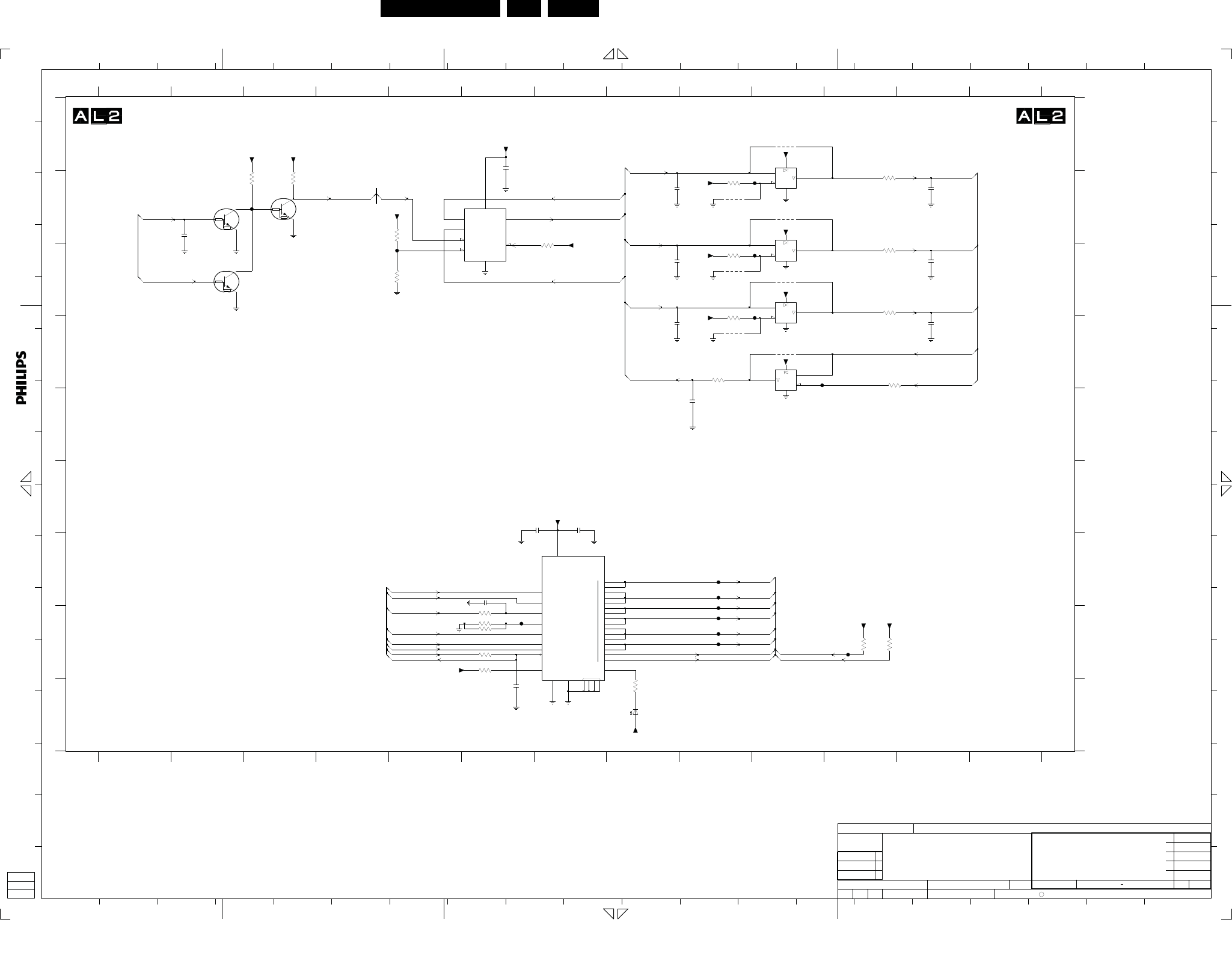
EN 52LC9.1A LA 10.
Circuit Diagrams and PWB Layouts
2009-Apr-10
6 LED Low-Pow: Microcontroller Liteon
EN
S
GND
Q
HOLD
W
VCC
C
D
EN
MODE
SIN
XHALF
XLAT
SCLK
VCC
SOUT
6
2
0
11
VIA
9
13
12
10
4
IREF
GND GND_HS
OUT
GSCLK
7
14
5
3
1
8
15
XERR
BLANK
C
EN
EN
F203 C5
F204 H6
F207 C10
F208 D10
F209 H11
F210 G9
F211 G9
F212 G9
F213 H9
F214 H9
INPUT BUFFER
A
All rights reserved. Reproduction in whole or in parts
I
1
H
3221 H11
3222 I8
11
F215 H9
6216 I8
7201-1 A10
7201-2 C10
7201-3 D10
7201-4 B10
7209 B2
7210 C2
7212 B3
12
12
10
11
7214 B6
7215 G7
9208 A10
9209 B9
9210 B10
9211 C9
9212 C10
9213 D9
9214 D10
F202 B3
C
F205 B10
F206 C10
2217 B12
2218 C12
2219 D12
2220 E9
3121 D9
3203 B5
3204 B7
3205 C5
3207 B9
3209 C9
3210 B3
3211 C9
3212 D11
3213 B3
3214 H6
3215 H6
7
16
F
3216 H6
3217 H6
3218 H6
3219 B11
3220 C11
17 18
3223 C11
3224 H11
N
D
E
F
G
H
I
A
B
C
D
E
F
O
P
O
N
L
M
K
B
20
6
J
18
P
20
789 10111213
A
B
C
L
J
78
4
A
is prohibited without the written consent of the copyright
F
9 10111213
123456
D
328
12
169
194
15
K
G
12345678
13
C
14
3
G
E E
owner.
5
H
14
G
H
I
2201 B8
2202 C8
2203 D8
2209 B2
2210 G6
2211 I6
2214 A6
2215 F7
2216 F7
9
D
6 15
1319
5
I
17
MICROCONTROLLER LITEON
M
10
B
RES
3207
1K0
1u0
2216
F202
10K
3210
+3V3
33p
2209
6216
SML-310
2211
33p
9212
+3V3
RES
100R
3121
3220
3223
100R
3217
27R
100R
3219
100R
33p
2202
+3V3
2215
100n
F212
F211
33p
2201
+3V3
9
7
10
14
8
74HCT125PW
7201-3
3214
10K
3215
1K2
5
4
7
2
1
8
3
9213
(64K)
Φ
7214
M95010-WDW6
6
12
7
13
14
11
74HCT125PW
7201-4
100R
3212
F207
3224
3K3
+3V3
F213
2217
100p100p
2218
3221
3K3
F209
F204
3204
10K
+3V3
RES
1K0
3209
F208
+3V3
+3V3
RES9214
9209
24
28
30
31
32
33
2326
3
9
10
11
12
13
14
15
16
4
5
27
6
7
8
17
18
19
20
21
22
7215
TLC5946PWP
Φ
PWM CONTROL
LED DRIVER
2
1
29
25
+3V3
PDTC144EU
+3V3
7212
470R
3222
7209
PDTC144EU
1
3
2
+3V3
F210
+3V3
10K
3203
3216
+3V3
14
3
100R
7201-1
74HCT125PW
2
7
1
100n
2214
3213
10K
+3V3
2219
100p
2008-10-27
2
3
RES
100p
2220
2008-08-08
A2
DRIVER 6LED LITEON
2K9 8204 000 8857
CHECK DATE
NAME
1
SUPERS.
18310_611_090305.eps
090410
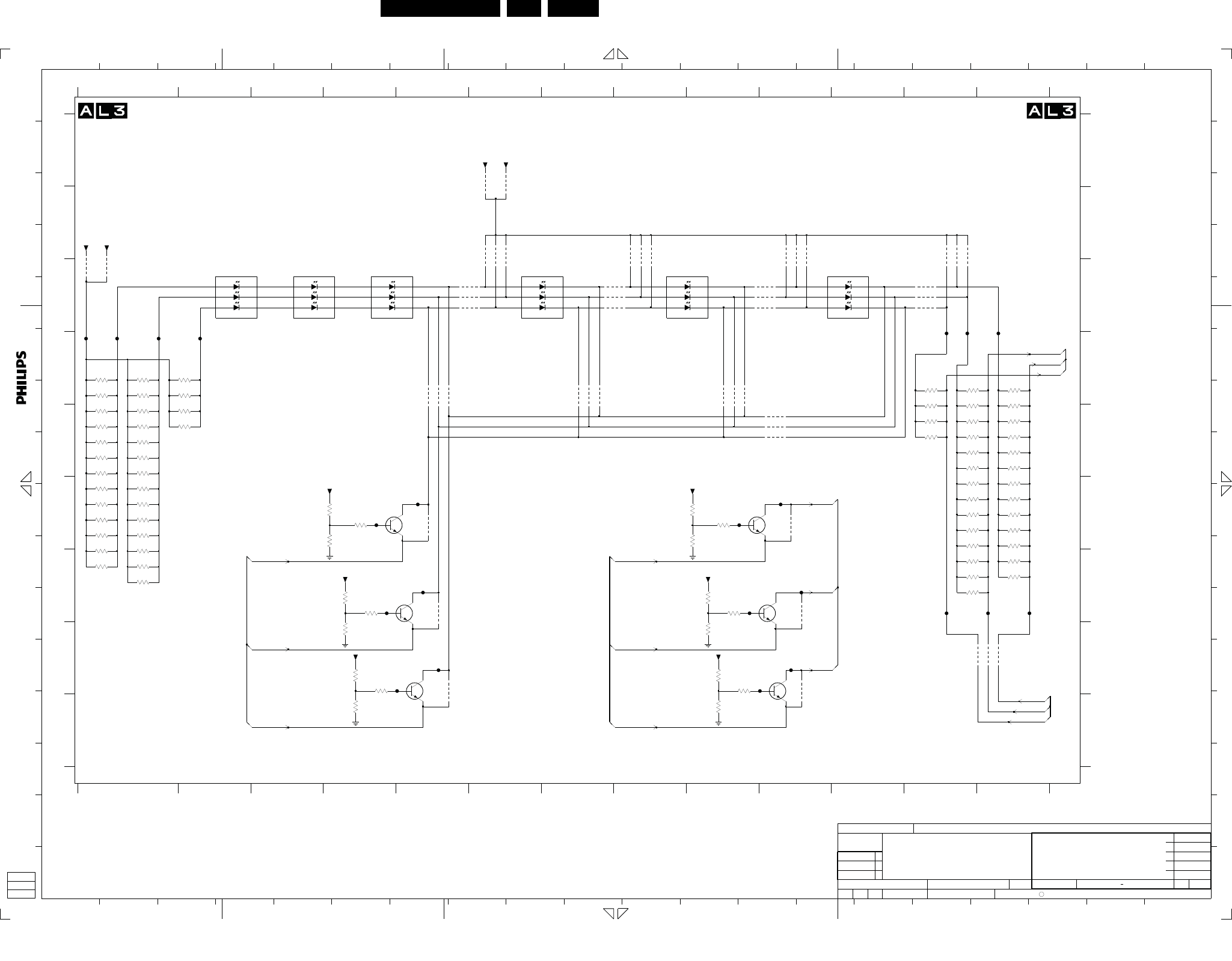
Circuit Diagrams and PWB Layouts EN 53LC9.1A LA 10.
2009-Apr-10
6 LED Low-Pow: LED Liteon
GND_HS
GREEN
RED
BLUE
GND_HS
GREEN
RED
BLUE
GND_HS
GREEN
RED
BLUE
GND_HS
GREEN
RED
BLUE
GND_HS
GREEN
RED
BLUE
C
GND_HS
GREEN
RED
BLUE
9304-1 E10
F343 D2
F344 D12
F345 D12
F346 D13
F342 D1
9304-4 E10
9305-1 C6
9305-2 C6
9305-4 C6
9315-1 C12
9315-2 C12
9315-4 C12
9312-3 B10
9312-4 B10
3360 E13
9306-1 D5
9306-3 D5
9306-4 D5
9325 F10
9326 G10
9327 H10
9309-2 B6
3369 F1
3370 F1
9310-2 B8
F304 H5
197
F308 F4
F325 F10
F326 F9
9319-4 D9
9313-1 B12
F302 G5
F303 G4
7004 C8
F327 G10
F328 G9
7002 C4
7003 C6
7005 C11
7305 G4
7306 H5
F329 H10
F330 H10
B
G
9319-3 D9
20
A
9310-1 B8
9313-4 B12
9314 G5
7317 F9
9301 C1
9302 C1
9316 H5
9317 F5
9318-1 C8
9320-1 D7
9320-2 D7
9312-1 B10
3358 E13
3359 E13
2
3361 E13
3362 E13
3363 F13
F341 D1
11
9320-4 D7
1
9308 A6
9309-1 B6
3368 G13
3334 F4
3335 D12
3371 F1
9318-3 C8
9311-1 H13
9311-3 H13
9311-4 H12
3385 F1
3386 F1
3387 F1
7
F305 H5
F340 D1
9303-4 C10
7001 C3
6
8
BRG
9319-1 D9
owner.
12 132
is prohibited without the written consent of the copyright
B
A
10 18
3311 D12
3312 E12
Place jumper 9325, 9326, 9327
F307 F5
7315 G9
7316 H10
3349 E1
3350 E1
3351 E12
9303-1 C10
F347 G12
F348 G13
F349 G13
9309-4 B6
3357 D13
C
11
E
4
9307 A6
16
3325 G4
3326 H4
63
3365 F13
3366 F13
3367 G13
3333 H4
B
C
3336 D2
9310-4 B8
3373 F1
3374 G1
3384 E1
3341 D1
3342 E2
3343 D1
3388 F1
9313-2 B12
3390 G1
3391 G1
9318-4 C8
5
1
K
7307 F4
M
12
I
L
All rights reserved. Reproduction in whole or in parts
3310 D12
13
1
3313 E12
L
3348 E12
3318 F12
3319 F12
3320 F12
3352 E1
9303-3 C10
3354 D13
3355 E1
9304-2 E10
N
J
18
I
O
3364 F13
15
3327 H4
3330 I4
3331 F4
3332 F4
A
J
D
3372 F1
3338 D1
3339 D2
3340 D1
I
A
B
3344 D1
3389 F1
3346 E1
16
7000 C2
F F
8
H
3347 D1
1320
12
F
G
2
17
3315 E12
3316 E12
3317 F12
789
3321 G12
3353 E1
3323 G12
N
3356 E1
B
LED LITEON
8
K
if VLED < 17V
1514
3328 G4
13
G
B
D
M
3337 D2
F
G
H
456
C
3345 D12
E
17
10 11
19
3305 G9
3306 H9
3307 H9
D
R
P
5
E
O
3
3314 E12
456
C
4
10
3322 G12
12
H
G
11
3309 I9
G
914
9
10
if VLED < 17V
E
123
H
I
3301 F9
3302 F9
3303 F9
3304 G9
3
3308 H9
7
D
9
Place jumper 9314, 9316, 9317
P
R
390R
3336
9320-4 54
9305-445
F325
3331
10K
3342
390R
3315
1K5
1K5
3341
3362
560R
BC847BW
3308
7315
1K0
1K5
3321
1K5
3387
560R
3354
9312-445
27
VLED1-F
F328
1K5
9305-2
3312
3320
1K5
LTW-E500T-PH1
16
43
7
25
27
7004
F329
9315-2
9306-1 1
8
3325
10K
F326
560R
3349
9310-445
16
43
7
25
LTW-E500T-PH1
7001
1
3335
390R
9320-1 8
3358
560R
F303
VLED1-F
3316
1K5
3311
VLED2
9304-227 1K5
9309-227
9310-118
3304
10K
9313-118
9319-11 8
560R
3340
560R
3366
1K5
3388
3334
1K0
9311-445
560R
3346
3357
560R
VLED1-F
7317
BC847BW
10K
3309
390R
3339
9311-118
45
9303-33 6
9303-4
3322
560R
1K5
3363
1K5
3353
9315-445
3344
1K5
9326
72
16
43
7
25
9320-2
7002
LTW-E500T-PH1
3301
10K
27
9301
9318-4 45
9310-2
F308
BC847BW
7316
1K5
4
5
3391
VLED1-F
9306-4
9327
9311-33 6
9318-1 18
DATE
NAME
1
SUPERS.
CLASS_NO
EMANTESNHC
33
2008-06-02 ROYAL PHILIPS ELECTRONICS N.V. 2008
2008-06-10
Peter Van Hove
2008-10-27
2
3
130
2
3
2008-08-08
2008-10-27
2008-08-08
A2
DRIVER 6LED LITEON
2K9 8204 000 8857
CHECK
1K5
3384
3385
1K5
10K
3306
3345
3348
390R
390R
3369
560R
F302
VLED1-F
36
3317
1K5
9312-3
3323
1K5
F307
1
43
7
25
3360
560R
7000
LTW-E500T-PH1
6
F330
10K
3326
3364
560R
9305-118
F348
10K
3303
560R
3370
3389
1K5
VLED2
3
7
25
1K5
3390
7003
6
18310_612_090305.eps
090305
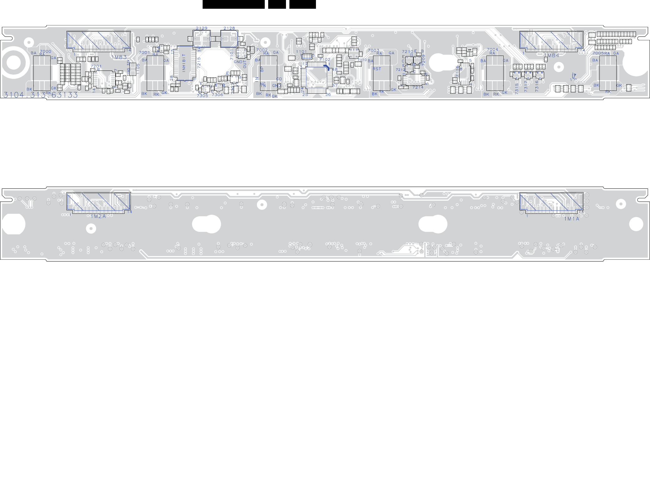
EN 54LC9.1A LA 10.
Circuit Diagrams and PWB Layouts
2009-Apr-10
Layout 6 LED Low-Pow
3104 313 6313.3
18310_551_090309
090309
1101
1105
1M83 1M84
2101
2102
2103
2104
2105
2106
2107
2108
2109
2110
2111
2112
2113
2114
2115
2116
2117
2118
2119
2120
2121
2122
21232124
2125
2126
2127
21282129
2130
2131
2201
2202
2203
2209
2210
2211
2214
2215
2216
2217
2218
2219
2220
3101
3102
3103
3104
3105
3106
3107
3108
3109
3110
3111
3112
3113
3114
3115
3116
3117
3118
3119
3120
3121
3123
3124
3125
3126
3127
3128
3129
3130
3131
3132
3133
3134
3135
3136
3137
3138
3139
3140
3141
3142
3203
3204
3205
3207
3209
3210
3211
3212
3213
3214
3215
3216
3217
3218
3219
3220
3221
3222
3223
3224
3301
3302
3303
3304
3305
3306
3307
3308
3309
3310
3311
3312
3313
3314
3315
3316
3317
3318
3319
3320
3321
3322
3323
3325
3326
3327
3328
3330
3331
3332
3333
3334
3335
3336
3337
3338
3339
3340
3341
3342
3343
3344
3345
3346
3347
3348
3349
3350
3351
3352
3353
3354
3355
3356
3357
3358
3359
3360
3361
3362
3363
3364
3365
3366
3367
3368
3369
3370
3371
3372
3373
3374
3384
3385
3386
3387
3388
3389
3390
3391
6216
7000
7001
7002
7003
7004
7005
7101
7102
7110
7116
7201
7209
7210
7212
7214
7215
7305
7306
7307
7315
7316
7317
9101
9102
9103
9104
9106
9107
9108
9109
9110
9111
9112
9113
9114
9119
9121
9208
9209
9210
9211
9212
9213
9214
9301 9302
9303
9304
9305
9306
9307
9308
9309
9310
9311
9312
9313
9314
9315
9316
9317
9318
9319
9320
9325
9326
9327
C140
I110
I111
I113
I114
I115
1M1A1M2A
F101
F102
F103
F104
F105
F106
F107 F108
F109
F112
F116
F117
F118
F120
F121
F122
F123
F124
F125
F126
F127
F128
F129
F130
F131
F132
F133
F134
F135
F136
F137
F138
F139
F202 F203
F204
F205
F206
F207
F208
F209
F210
F211
F212
F213
F214
F215
F302
F303
F304
F305
F307
F308
F325
F326
F327
F328
F329
F330
F340
F341
F342
F343
F344
F345
F346
F347F348F349
I124
I125
I126

Circuit Diagrams and PWB Layouts EN 55LC9.1A LA 10.
2009-Apr-10
8 LED Low-Pow: Microcontroller Liteon
-T
OUTIN
INH BP
COM
X2
RTXC1
RTXC2
RTCK
VBAT
DBGSEL
RST
VSS VSSA
VDDA
VDD_3V3
VDD_1V8
X1
C
NC
GND
RST
IN
CD
C
E
F
G
H
1101 E4
1105 B5
1M1A C1
1M2A G1
1M83 A1
1M84 E1
2101 A6
2102 A7
2103 A8
2104 B7
2105 B10
2106 B13
2107 B11
17
F
J
M
A
2
C
4
E
6
G
8
A
10 11 12 13
12345678910111213
14
D
OUT
B
7
D
6
F
H
B
D
2109 D7
2110 D7
2111 G4
2112 H7
2113 H7
2114 F9
2115 F9
2116 F9
2117 F9
2118 H8
2119 H6
2120 H6
2121 H6
2122 F9
2123 F10
2124 F10
2125 B3
11
M
2
1
20
3
19
975
2126 F10
2127 B1
2128 B1
2129 B2
2130 F2
2131 F10
3101-2 D7
3101-3 D9
3101-4 E9
3102-1 D9
3102-2 D9
3102-3 E9
3102-4 D9
3103-1 E9
7
J
18
3103-2 G10
B
3103-4 G10
10
3104-2 E8
3104-4 D9
3105-2 D8
2108 B12
3105-4 D8
3106-1 E8
3106-2 D8
G
14
G
E
119
13
20
K
18
N
P
L
3107 C7
3109 D7
A
3111 B10
4
3113 D8
3114 E8
3115 E8
19
I
H
15
O
P
I
3116 E8
3117 E7
3118 E5
3119 F4
3123 C11
3103-3 G11
3124-2 E11
3104-1 D8
3124-4 E11
3104-3 E8
3125-2 F11
3105-1 E9
3126-1 F11
3105-3 E8
3126-4 F11
3127-1 F11
3127-4 F11
owner.
17
C
1
is prohibited without the written consent of the copyright
5
C
1
3128 E11
3129 E11
3130 G8
3132 H8
3134 A13
3106-3 E8
3136 A12
3108 C7
3138 B13
3110 D7
3140 C11
3112 D9
3142 F11
7101 A7
7102 E6
All rights reserved. Reproduction in whole or in parts
H
103
4
N
MICROCONTROLLER LITEON
5
7110 F4
7116-1 B11
7116-2 A12
9101 E5
9102 F5
3120 F5
9104 F5
3124-1 E11
9107 A5
3124-3 E11
9109 A5
3125-1 F11
9111 A3
3125-4 F11
9113 B3
3126-2 F11
9119 H6
9121 G4
C140 B10
89
12
F
12
16
A
13
F101 A8
F102 F5
F103 H7
3131 G7
F105 D7
3133 H8
F107 C7
3135 A11
F109 G3
3137 B11
F116 A10
3139 B12
F118 C11
3141 C13
F121 A1
F122 A1
F123 A1
8
IN
6
3
O
D
E
15
F124 B1
F125 B1
F126 B1
9103 F5
F128 B1
9106 H8
F130 B1
9108 A5
F132 B1
9110 B5
F134 F1
9112 B2
F136 F1
9114 B2
F138 F1
F139 F1
I110 G8
L
K
2
B
16
I111 G8
I113 G10
I114 G10
I115 G10
I124 E11
I125 E11
F104 F5
I126 F11
F106 B12
F127 B1
F108 D7
F129 B1
F112 G8
F131 B1
F117 B13
F133 E1
F120 A1
F135 E1
F124
F137 F1
VLED1
F134
100n
2120
I124
36
VLED2
10K
3101-3
F107
9112
10K
3103-3
3
6
9109
+3V3
F139
1K5
3135
1%
10K
3103-4
4
5
3136
1%1K5
F109
9108
9101
9107
F130
+3V3
9104
+3V3
2109
100p
RES
3129
100R
5
6
7
8
9
15 16
VLED1-F
1
10
11
12
13
14
2
3
4
36
1M84
3124-3
100R
RES
10K
3141
+3V3
183124-1
100R
10K
3112
RES
9113
VLED1
F120
3127-4 4 5
+3V3
15 16
100R
13
14
2
3
4
5
6
7
8
9
1M2A
1
10
11
12
3107
10K
RES
2106
10n
F129
+3V3
F106
100p
2118
VLED2
10K
3113
RES
3
5
RES
7101
LD2985BM18R
4
2
1
3110
100R
3116
10K
3133
I110
RES
10K
F103
9106
10K
3106-33 6
+1V8
+3V3
10K
3111
VLED2
3103-1
1
8
I126
10K
RES9103
F104
+3V3
+3V3
I111
F133
5
9114
3125-4
100R
4
F112
100p
3105-1
10K
18
2117
12
+3V3
4
42
5
17
40
7
19
43
31
11
23
P0.5|MISO0|MAT0.1 24
P0.6|MOSI0|CAP0.2 28
P0.7|SSEL0|MAT2.0 29
P0.8|TXD1|MAT2.1 30
P0.9|RXD1|MAT2.2
6
26
20
25
8
P0.27|TRST|CAP2.0 9
P0.28|TMS|CAP2.1 10
P0.29|TCK|CAP2.2
18
P0.2|SCL0|CAP0.0
15
P0.30|TDI|MAT3.316
P0.31|TDO
21
P0.3|SDA0|MAT0.0 22
P0.4|SCK0|CAP0.1
14
P0.1|RXD0|MAT3.2
2
P0.20|MAT1.3|MOSI1 3
P0.21|SSEL1|MAT3.0 32
P0.22|AD0.0 33
P0.23|AD0.1 34
P0.24|AD0.2 38
P0.25|AD0.6 39
P0.26|AD0.7
41
P0.13|DTR1|MAT1.1 44
P0.14|DCD1|SCK1|EINT1 45
P0.15|RI1|EINT2 46
P0.16|EINT0|MAT0.2 47
P0.17|CAP1.2|SCL1 48
P0.18|CAP1.3|SDA1 1
P0.19|MAT1.2|MISO1
27
13
P0.0|TXD0|MAT3.1
35
P0.10|RTS1|CAP1.0|AD0.336
P0.11|CTS1|CAP1.1|AD0.4 37
P0.12|DSR1|MAT1.0|AD0.5
27
MICRO-
CTRL
Φ
LPC2103FBD48
7102
36
3104-2
10K
10K
3104-3
2
3
4
5
6
7
8
9
15 16
1
10
11
12
13
14
1M1A
35V10u
2128
2124
I113
RES
100p
10K
F116
3119
100n
2107
T1.5A
1105
F135
9110
33p
2125
18
3
2
130
3126-1
100R
ROYAL PHILIPS ELECTRONICS N.V. 2008
2008-06-02
13
SETNAMECHN
CLASS_NO
SUPERS.
1
NAME
DATECHECK
8204 000 8857
2K9
DRIVER 6LED LITEON
A2
2008-08-08
??
2008-08-08
10K
72
3
2
Peter Van Hove
2008-06-10
3101-2
100K RES
3134
+1V8
36
F122
10K
3105-3
10K
3102-4 4 5
7116-1
LM393PT
3
2
1
84
10n
2108
100R
3109
10K
100p
2110
18
3117
10K
3106-1
100n
2111
VLED2
3108
10K
3114
10K
RES
RES
3118
10K
F127
+3V3
VLED1
F121
100n
2113
3103-2
10K
2
7
10K
363102-3
RES
3137
10K
F126
F131
9102
3124-2 2 7
18
100R
+3V3
3102-1
10K
I125
1u0
2130
F101
9119
3130
22R
C140
10K
3101-4 45
+3V3
F105
27
100p
2116
10K
3106-2
3120
10K
2121
100n
F137
1101
16M9
3125-1 1 8
100R
F108
8
9
15 16
100p
2115
12
13
14
2
3
4
5
6
7
1M83
1
10
11
F138
45
F102
3
4
5
10K
3105-4
1X03
REF EMC HOLE
1
2
F123
2123
100p
1u0
2101
2105
10n
100R
3128
1u0
2127
27
VLED1
3125-2
100R
3138
RES
100p
2122
47K
45
RES
100R
3126-4
3142
100R
18
4
1
3104-1
10K
NCP303LSN10T1
7110
5
3
2
F128
F136
RES
F132
1%1K5
3140
2102
100n
RES
2114
100p
27
3115
10K
3126-2
100R
4
VLED1
+3V3
7116-2
LM393PT
5
6
7
8
F125
10K
3104-4 4 5
+3V3
I114
F118
35V
2129
10u
18
10K
3132
3127-1
100R
RES
1K81%
3123
1K5 1%
27
3139
10K
3102-2
2119
100n
9111
RES
2112
100n
27
3105-2
10K
2126
100p
4u7
2103
+3V3
+3V3
10n
2104
100p
2131
100R
3131
F117
9121
I115
RES
3124-4
100R
45
SPI-DATA-OUT
SPI-DATA-RETURN
SPI-LATCH
PWM-CLOCK-BUF
BLANK-BUF
EEPROM-CS
TEMP-SENSOR
+3V3
SCL
PROG
SDA
CONTROL-1
CONTROL-2
EEPROM-CS
TEMP-SENSOR
SPI-CLOCK-BUF
PROG
SPI-CLOCK
SDA
CONTROL-2
EEPROM-CS
TEMP-SENSOR
CONTROL-2
CONTROL-1
SPI-DATA-RETURN
SCL
PROG
BLANK
CONTROL-1
SDA
SPI-DATA-IN
SCL
SPI-DATA-RETURN
SPI-LATCH
SPI-DATA-IN
PWM-CLOCK-BUF
PWM-CLOCK
SPI-LATCH
BLANK-BUF
PROG
CONTROL-2
SCL
TEMP-SENSOR
SPI-DATA-OUT
PWM-CLOCK-BUF
SPI-CLOCK-BUF
EEPROM-CS
TEMP-SENSOR
SPI-LATCH-2
SPI-CLOCK-BUF
SPI-DATA-RETURN
SPI-LATCH
BLANK-BUF
EEPROM-CS
TEMP-SENSOR
PROG
CONTROL-1
UD-MD
SDA
18560_500_090403.eps
090410

EN 56LC9.1A LA 10.
Circuit Diagrams and PWB Layouts
2009-Apr-10
8 LED Low-Pow: Microcontroller Liteon
EN
C
EN
MODE
SIN
XHALF
XLAT
SCLK
VCC
SOUT
6
2
0
11
VIA
9
13
12
10
4
IREF
GND GND_HS
OUT
GSCLK
7
14
5
3
1
8
15
XERR
BLANK
EN
S
GND
Q
HOLD
W
VCC
C
D
EN
5
I
17
MICROCONTROLLER LITEON
M
10
B
owner.
5
H
14
G
H
I
2201 B8
2202 C8
2203 D8
2209 B2
2210 G6
2211 I6
2214 A6
2215 F7
2216 F7
9
D
6 15
1319
194
15
K
G
12345678
13
C
14
3
G
E E
A
is prohibited without the written consent of the copyright
F
910111213
123456
D
328
12
169
B
20
6
J
18
P
20
789 10111213
A
B
C
L
J
78
4
17 18
3223 C11
3224 H11
N
D
E
F
G
H
I
A
B
C
D
E
F
O
P
O
N
L
M
K
C
F205 B10
F206 C10
2217 B12
2218 C12
2219 D12
2220 E9
3121 D9
3203 B5
3204 B7
3205 C5
3207 B9
3209 C9
3210 B3
3211 C9
3212 D11
3213 B3
3214 H6
3215 H6
7
16
F
3216 H6
3217 H6
3218 H6
3219 B11
3220 C11
3221 H11
3222 I8
11
F215 H9
6216 I8
7201-1 A10
7201-2 C10
7201-3 D10
7201-4 B10
7209 B2
7210 C2
7212 B3
12
12
10
11
7214 B6
7215 G7
9208 A10
9209 B9
9210 B10
9211 C9
9212 C10
9213 D9
9214 D10
F202 B3
F203 C5
F204 H6
F207 C10
F208 D10
F209 H11
F210 G9
F211 G9
F212 G9
F213 H9
F214 H9
INPUT BUFFER
A
All rights reserved. Reproduction in whole or in parts
I
1
H
7
4
14
6
RES
10K
3205
7201-2
74HCT125PW
5
F205
RES
F206
+3V3
1K0
3211
F215
+3V3
9208RES
+3V3
2210
33p
2214
100n
10K
3213
100p
2219
+3V3
RES
8204 000 8857
2K9
DRIVER 6LED LITEON
A2
2008-08-08
??
2008-08-08
3
2
130
2220
100p
3
2
Peter Van Hove
2008-06-10
ROYAL PHILIPS ELECTRONICS N.V. 2008
2008-06-02
23
SETNAMECHN
CLASS_NO
SUPERS.
1
NAME
DATECHECK
RES
F203
3218
1K2
7210
PDTC144EU
1
3
2
2203
33p
9210 RES
F214
9211
RES
+3V3
9214
9209
28
30
31
32
33
2326
3
11
12
13
14
15
16
4
5
24
6
7
8
17
18
19
20
21
22
9
10
2
1
29
25
27
+3V3
LED DRIVER
PWM CONTROL
Φ
TLC5946PWP
7215
PDTC144EU
7212
3222
470R
+3V3
1
3
2
+3V3
PDTC144EU
7209
F210
3203
10K
100R
+3V3
+3V3
14
3
3216
2
7
1
74HCT125PW
7201-1
3K3
3224
F207
F213
+3V3
100p
22172218
100p
3K3
3221
F209
F204
10K
3204
RES
+3V3
3209
1K0
F208
+3V3
F212
F211
2201
33p
+3V3
7201-3
74HCT125PW
9
7
10
14
8
3214
10K
1K2
3215
9213
6
5
4
7
2
1
8
311
M95010-WDW6
7214
Φ
(64K)
7201-4
74HCT125PW
12
7
13
14
3212
100R
1K0
3207
RES
1u0
F202
2216
3210
10K
33p
2209
+3V3
2211
33p
RES
SML-310
6216
+3V3
9212
3121
100R
100R
3223
3220
27R
3217
100R
100R
3219
33p
2202
+3V3
100n
2215
PWM-CLOCK-BUF
BLANK-BUF
SPI-CLOCK-BUF
SPI-DATA-RETURN
SPI-CLOCK-BUF
EEPROM-CS
PWM-CLOCK
SPI-CLOCK
BLANK
DATA-RETURN-SWITCH
SPI-DATA-OUT-FIL
SPI-DATA-OUT-FIL
PWM-G1
PWM-B1
PWM-R2
PWM-G2
PWM-B2
EEPROM-CS-LOCAL
SPI-CS
SPI-LATCH
EEPROM-CS-LOCAL
DATA-RETURN-SWITCH
SPI-DATA-IN
SPI-DATA-OUT
PWM-CLOCK-BUF
EEPROM-CS-LOCAL
DATA-RETURN-SWITCH
PROG
PWM-R1
SPI-CS
SPI-DATA-RETURN
SPI-CLOCK-BUF
SPI-DATA-IN
BLANK-BUF
18560_501_090403.eps
090410
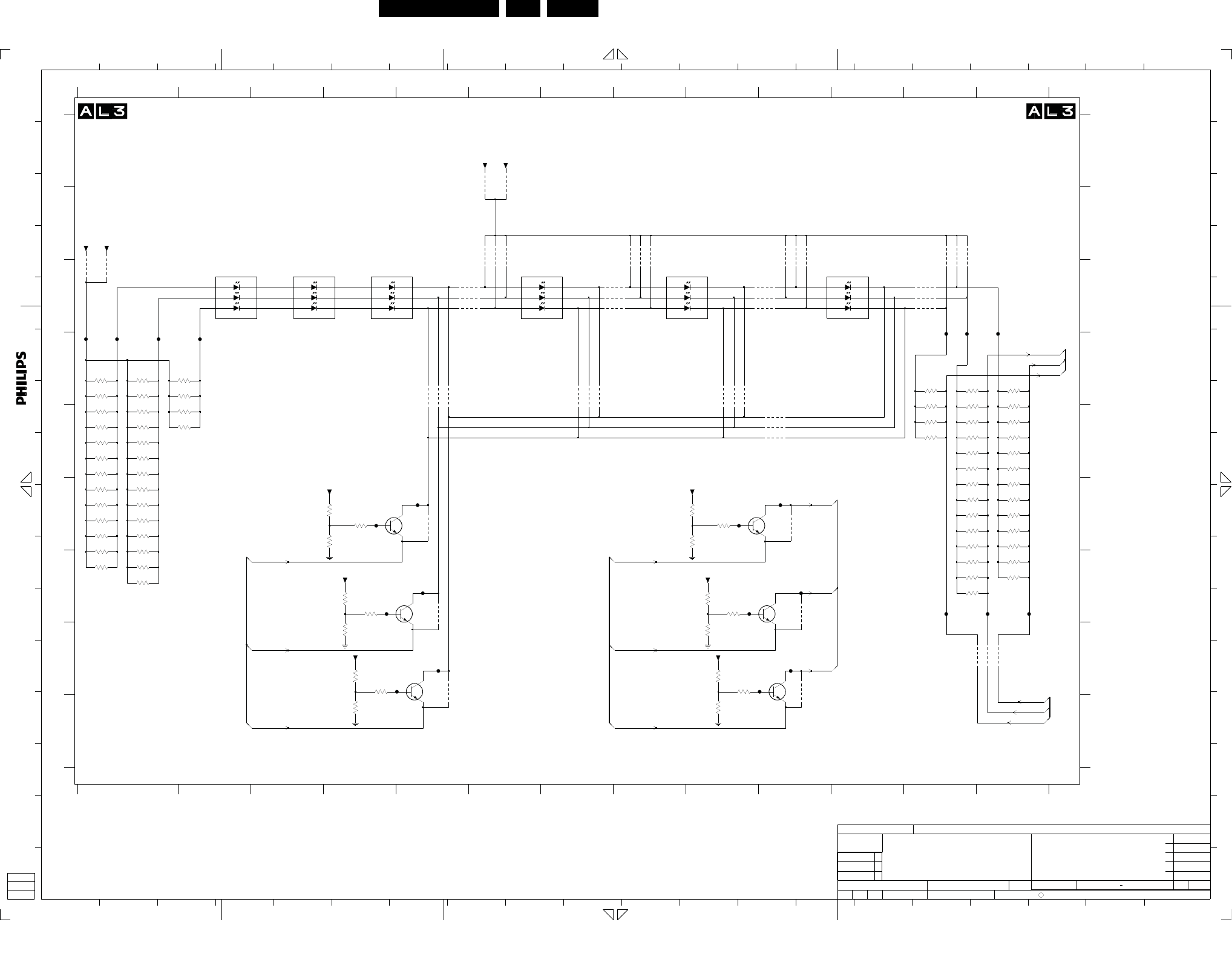
Circuit Diagrams and PWB Layouts EN 57LC9.1A LA 10.
2009-Apr-10
8 LED Low-Pow: LED Liteon
GND_HS
GREEN
RED
BLUE
GND_HS
GREEN
RED
BLUE
GND_HS
GREEN
RED
BLUE
C
GND_HS
GREEN
RED
BLUE
GND_HS
GREEN
RED
BLUE
GND_HS
GREEN
RED
BLUE
if VLED < 17V
E
123
H
I
3301 F9
3302 F9
3303 F9
3304 G9
3
3308 H9
7
D
9
Place jumper 9314, 9316, 9317
P
R
R
P
5
E
O
3
3314 E12
456
C
4
10
3322 G12
12
H
G
11
3309 I9
G
914
9
10
13
G
B
D
M
3337 D2
F
G
H
456
C
3345 D12
E
17
10 11
19
3305 G9
3306 H9
3307 H9
D
20
12
F
G
2
17
3315 E12
3316 E12
3317 F12
789
3321 G12
3353 E1
3323 G12
N
3356 E1
B
LED LITEON
8
K
if VLED < 17V
1514
3328 G4
3330 I4
3331 F4
3332 F4
A
J
D
3372 F1
3338 D1
3339 D2
3340 D1
I
A
B
3344 D1
3389 F1
3346 E1
16
7000 C2
F F
8
H
3347 D1
13
I
L
All rights reserved. Reproduction in whole or in parts
3310 D12
13
1
3313 E12
L
3348 E12
3318 F12
3319 F12
3320 F12
3352 E1
9303-3 C10
3354 D13
3355 E1
9304-2 E10
N
J
18
I
O
3364 F13
15
3327 H4
3365 F13
3366 F13
3367 G13
3333 H4
B
C3336 D2
9310-4 B8
3373 F1
3374 G1
3384 E1
3341 D1
3342 E2
3343 D1
3388 F1
9313-2 B12
3390 G1
3391 G1
9318-4 C8
5
1
K
7307 F4
M
12
B
A
10 18
3311 D12
3312 E12
Place jumper 9325, 9326, 9327
F307 F5
7315 G9
7316 H10
3349 E1
3350 E1
3351 E12
9303-1 C10
F347 G12
F348 G13
F349 G13
9309-4 B6
3357 D13
C
11
E
4
9307 A6
16
3325 G4
3326 H4
63
1
9308 A6
9309-1 B6
3368 G13
3334 F4
3335 D12
3371 F1
9318-3 C8
9311-1 H13
9311-3 H13
9311-4 H12
3385 F1
3386 F1
3387 F1
7
F305 H5
F340 D1
9303-4 C10
7001 C3
6
8
BRG
9319-1 D9
owner.
12 132
is prohibited without the written consent of the copyright
G
9319-3 D9
20
A
9310-1 B8
9313-4 B12
9314 G5
7317 F9
9301 C1
9302 C1
9316 H5
9317 F5
9318-1 C8
9320-1 D7
9320-2 D7
9312-1 B10
3358 E13
3359 E13
2
3361 E13
3362 E13
3363 F13
F341 D1
11
9320-4 D7
9325 F10
9326 G10
9327 H10
9309-2 B6
3369 F1
3370 F1
9310-2 B8
F304 H5
197
F308 F4
F325 F10
F326 F9
9319-4 D9
9313-1 B12
F302 G5
F303 G4
7004 C8
F327 G10
F328 G9
7002 C4
7003 C6
7005 C11
7305 G4
7306 H5
F329 H10
F330 H10
B
9304-1 E10
F343 D2
F344 D12
F345 D12
F346 D13
F342 D1
9304-4 E10
9305-1 C6
9305-2 C6
9305-4 C6
9315-1 C12
9315-2 C12
9315-4 C12
9312-3 B10
9312-4 B10
3360 E13
9306-1 D5
9306-3 D5
9306-4 D5
560R
3359
F349
VLED1-F
9316
3332
10K
9312-11 8
560R
3365
F305
BC847BW
7305
9302
3386
1K5
F304
1K5
3310
F347
390R
3351
3319
1K5
10K
3307
F341F340
1K5
F344
3318
45
1K5
3350
9313-4
560R
3361
3330
10K
560R
3367
3347
1K5
45
36
9309-4
3352
9319-3
3355
560R
560R
560R
3371
1K5
3314
2
9309-11 8
16
43
7
5
F343
LTW-E500T-PH1
7005
3333
1K0
560R
3368
45
3374
560R
9304-118
9304-4
9303-118
VLED1-F
3356
1K5
3327
560R
3338
10K
9308
9314
1K0
3302
9317
1K5
3313
9319-445
F346
27
F327
9313-2
BC847BW
7307
36
7306
BC847BW
560R
3373
9318-3
VLED1-F
1K0
3305
560R
3343
3372
560R
F345
9306-336
3306
10K
390R
3345
390R
3348
560R
3369
3317
VLED1-F
F302
36
1K5
F307
9312-3
3323
560R
3360
1K5
3
7
25
16
4
F330
LTW-E500T-PH1
7000
3326
10K
560R
3364
189305-1
3303
10K
F348
3370
560R
VLED2
1K5
3389
2
3390
1K5
LTW-E500T-PH1
16
43
7
5
7003
9325
9307
F342
18
1K0
3328
9315-1
390R
3337
9303-445
36
1K5
9303-3
3363
3322
560R
3353
1K5
5
1K5
3344
9315-44
9320-2 72
9326
3
7
25
LTW-E500T-PH1
7002
16
4
10K
3301
9301
9310-227
9318-4 45
F308
7316
BC847BW
1K5
3391
9306-4 45
9327
VLED1-F
36
9318-1 18
9311-3
8204 000 8857
2K9
DRIVER 6LED LITEON
A2
2008-08-08
??
2008-08-08
3
2
130
3
2
Peter Van Hove
2008-06-10
ROYAL PHILIPS ELECTRONICS N.V. 2008
2008-06-02
33
SETNAMECHN
CLASS_NO
SUPERS.
1
NAME
DATECHECK
3384
1K5
1K5
3385
390R
3335
9320-1 81
560R
3358
F303
VLED1-F
3316
VLED2
1K5
7
3311
1K5
27
9304-22
18
9309-2
9310-1
18
10K
3304
18
9313-1
9319-1
3340
560R
560R
3366
3388
1K5
9311-445
1K0
3334
560R
3346
560R
3357
BC847BW
7317
3309
10K
VLED1-F
3339
390R
9311-11 8
3336
390R
9305-445
54
F325
9320-4
10K
3331
390R
3342
3341
1K5
1K5
3315
560R
3362
BC847BW
7315
3308
1K0
1K5
3321
1K5
3387
560R
9312-445
3354
F328
9305-227
VLED1-F
3320
1K5
3312
3
7
25
1K5
7004
16
4 9315-227
LTW-E500T-PH1
F329
10K
3325
9306-1 18
3349
560R
45
F326
7
25
9310-4
7001
LTW-E500T-PH1
16
43
GREEN6GREEN6
PWM-G1
PWM-B1
BLUE6BLUE6
RED6RED6
RED-2
GREEN-2
RED-1
GREEN-1
BLUE-1
PWM-R1
RED-2
BLUE-2
GREEN-2
BLUE-2
PWM-R2
PWM-G2
PWM-B2
18560_502_090403.eps
090403
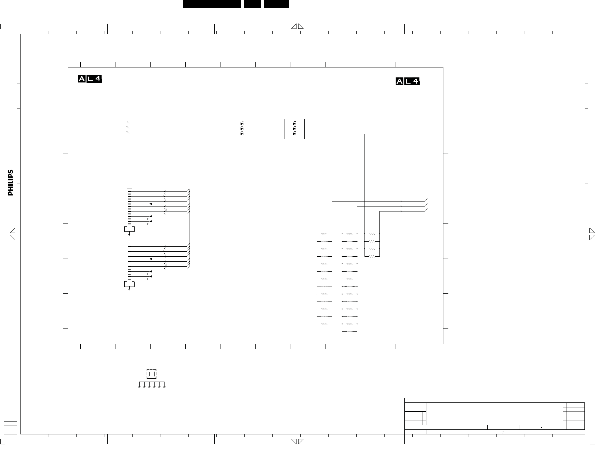
EN 58LC9.1A LA 10.
Circuit Diagrams and PWB Layouts
2009-Apr-10
8 LED Low-Pow: LED Drive Liteon
C
GND_HS
GREEN
RED
BLUE
GND_HS
GREEN
RED
BLUE
3571 G7
4121
I
NN
98
67
A
3539 E9
3550 E8
3552 F7
3543 E7
3544 E8
3546 E7
3547 E8
3549 F7
8910
123
M
L
3555 F7
3556 F8
3572 G7
3573 G7
3574 G7
3584 F8
3569 F7
3570 F7
3587 G8
3588 G8
15
P
O
E
F
G
1M3A E2
1M85 D2
3536 E9
8
B
F
O
P
11 12
G
C
D
I
3540 E7
3541 E8
18
567
All rights reserved. Reproduction in whole or in parts
E
4
3589 G8
G
H
2
8201954
1413
3585 F8
13
LED DRIVE
B
C
D
3
3537 E9
9
11
A
L
10
K
H
1819
B
F
4 20
3542 E9
34
is prohibited without the written consent of the copyright
J
owner.
K
3590 G8
3591 G8
17
6
D
5
17
10
1
9103
E
15 16
3586 F8
16
3553 F8
G
A
C
D
E
F
A
3538 E7
C
B
76
M
12
7006 A5
7007 A7
75
J
12
1K5
3
2
130
3550
ROYAL PHILIPS ELECTRONICS N.V. 2008
2008-04-20
11
SETNAMECHN
CLASS_NO
1
SUPERS.
1
NAME
DATECHECK
8204 000 8874
2K9
2LED + CONNECTOR
A2
2008-08-08
2008-05-230
2008-08-08
3
2
2008-10-31
Peter Van Hove
2008-05-23
560R
3572
3571
560R
1K5
3586
3537
VLED1
390R
1K5
3547
+3V3
16
43
7
5
2
3589
1K5
LTW-E500T-PH1
7006
3544
1K5
3553
560R
3555
1K5
VLED2
7
5
2
+3V3
7007
LTW-E500T-PH1
16
43
390R
3539
560R
3573
3585
1K5
3543
560R
VLED2
1X04
REF EMC HOLE
3569
560R
1K5
3584
VLED1
560R
3570
560R
3546
15 16
12
13
14
2
3
4
5
6
7
8
9
1
10
11
1M3A
15 16
12
13
14
2
3
4
5
6
7
8
9
1M85
1
10
11
3591
1K5
560R
3549
3552
560R
1K5
3588
3542
390R
3536
390R
3587
1K5
3556
1K5
560R
3574
3540
3538
560R
560R
3541
1K5
1K5
3590
SPI-DATA-RETURN
SPI-LATCH
PWM-CLOCK-BUF
BLANK-BUF
EEPROM-CS
TEMP-SENSOR
GREEN-2
RED-2
BLUE-2
SPI-CLOCK-BUF
PROG
SPI-DATA-OUT
RED-1
SPI-CLOCK-BUF
SPI-DATA-OUT
SPI-DATA-RETURN
SPI-LATCH
PWM-CLOCK-BUF
BLANK-BUF
EEPROM-CS
TEMP-SENSOR
PROG
GREEN-1
BLUE-1
18560_503_090403.eps
090403
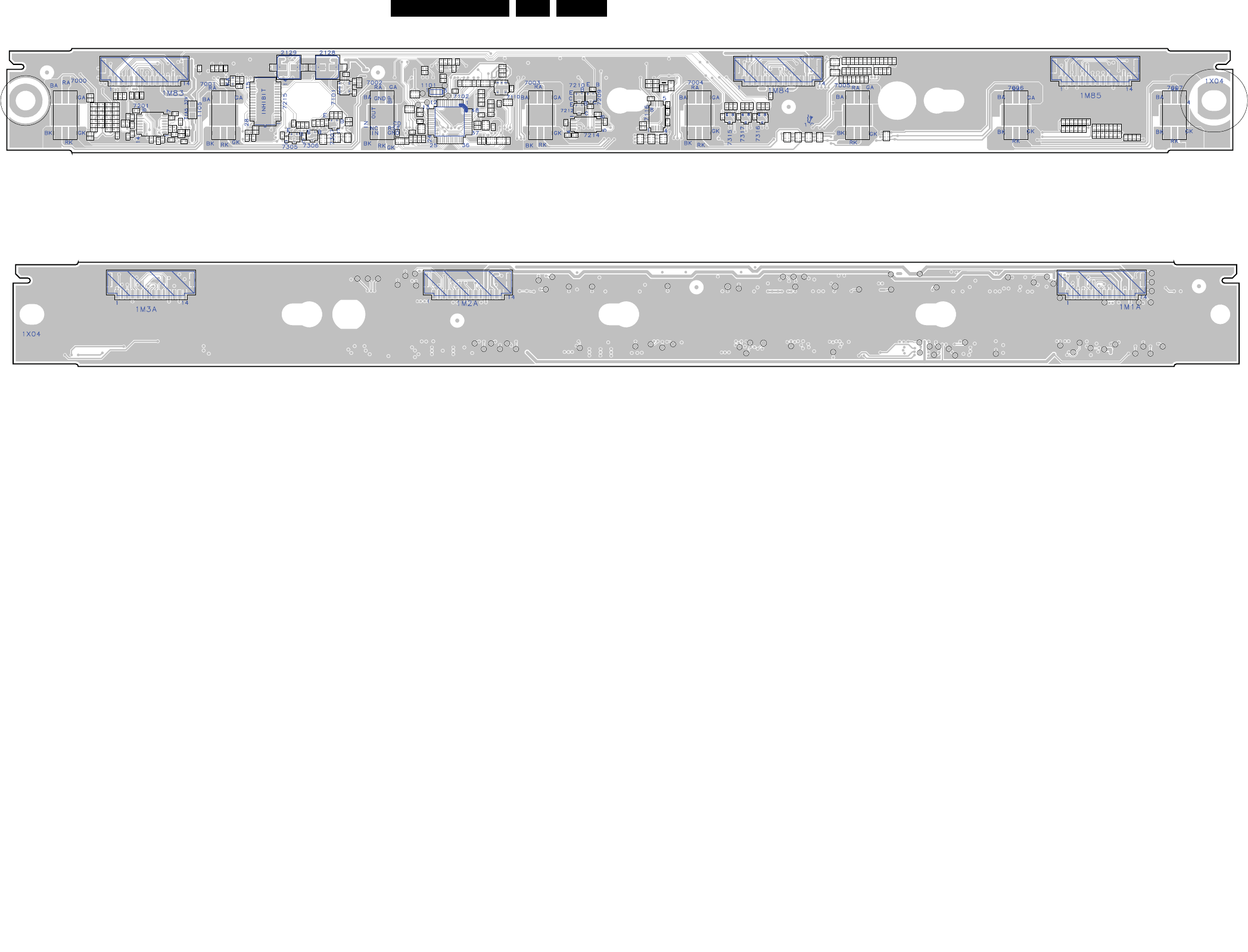
Circuit Diagrams and PWB Layouts EN 59LC9.1A LA 10.
2009-Apr-10
Layout 8 LED Low-Pow
31043136314.3
18490_550_090326.eps
090326
1101
1105
1M83 1M841M85
1X03
2101
2102
2103
2104
2105
2106
2107
2108
21092110
2111
2112
2113
2114
2115
2116
2117
2118
2119
2120
2121
2122
21232124
2125
2126
2127
21282129
2130
2131
2201
2202
2203
2209
2210
2211
2214
2215
2216
2217
2218
2219
2220
3101
3102
3103
3104
3105
3106
3107
3108
3109
3110
3111
3112
3113
3114
3115
3116
3117
3118
3119
3120
3121
3123
3124
3125
3126
3127
3128
3129
3130
3131
3132
3133
3134
3135
3136
3137
3138
3139
3140
3141
3142
3203
3204
3205
3207
3209
3210
3211
3212
3213
3214
3215
3216
3217
3218
3219
3220
3221
3222
3223
3224
3301
3302
3303
3304
3305
3306
3307
3308
3309
3310
3311
3312
3313
3314
3315
3316
3317
3318
3319
3320
3321
3322
3323
3325
3326
3327
3328
3330
3331
3332
3333
3334
3335
3336
3337
3338
3339
3340
3341
3342
3343
3344
3345
3346
3347
3348
3349
3350
3351
3352
3353
3354
3355
3356
3357
3358
3359
3360
3361
3362
3363
3364
3365
3366
3367
3368
3369
3370
3371
3372
3373
3374
3384
3385
3386
3387
3388
3389
3390
3391
3536
3537
3538
3539
3540
3541
3542
3543
3544
3546
3547
3549
3550
3552
3553
3555
3556
3569
3570
3571
3572
3573
3574
3584
3585
3586
3587
3588
3589
3590
3591
6216
7000
7001
7002
7003
7004
7005
7006
7007
7101
7102
7110
7116
7201
7209
7210
7212
7214
7215
7305
7306
7307
7315
7316
7317
9101
9102
9103
9104
9106
9107
9108
9109
9110
9111
9112
9113
9114
9119
9121
9208
9209
9210
9211
9212
9213
9214
9301 9302
9303
9304
9305
9306
9307
9308
9309
9310
9311
9312
9313
9314
9315
9316
9317
9318
9319
9320
9325
9326
9327
C140
I110
I111
I113
I114
I115
1X04
1M1A1M2A1M3A
F101
F102
F103
F104
F105
F106
F107 F108
F109
F112
F116
F117
F118
F120
F121
F122
F123
F124
F125
F126
F127
F128
F129
F130
F131
F132
F133
F134
F135
F136
F137
F138
F139
F202 F203
F204
F205
F206
F207
F208
F209
F210
F211
F212
F213
F214
F215
F302
F303
F304
F305
F307
F308
F325
F326
F327
F328
F329
F330
F340
F341
F342
F343
F344
F345
F346
F347F348F349
I124
I125
I126
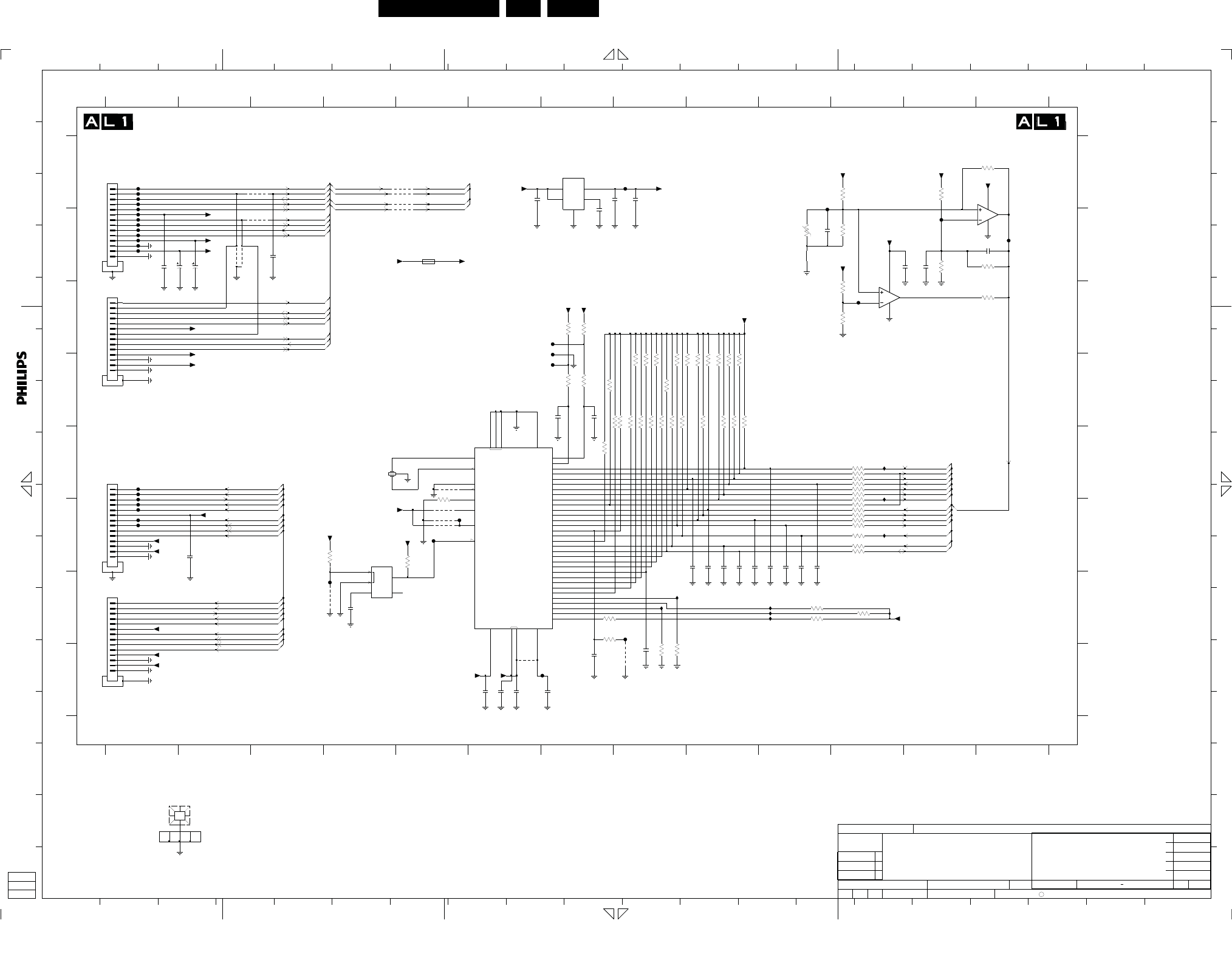
EN 60LC9.1A LA 10.
Circuit Diagrams and PWB Layouts
2009-Apr-10
12 LED Low-Pow: Microcontroller Liteon
-T
OUTIN
INH BP
COM
X2
RTXC1
RTXC2
RTCK
VBAT
DBGSEL
RST
VSS VSSA
VDDA
VDD_3V3
VDD_1V8
X1
C
NC
GND
RST
IN
CD
C
E
F
G
H
1101 E4
1105 B5
1M1A C1
1M2A G1
1M83 A1
1M84 E1
2101 A6
2102 A7
2103 A8
2104 B7
2105 B10
2106 B13
2107 B11
17
F
J
M
A
2
C
4
E
6
G
8
A
10 11 12 13
12345678910111213
14
D
OUT
B
7
D
6
F
H
B
D
2109 D7
2110 D7
2111 G4
2112 H7
2113 H7
2114 F9
2115 F9
2116 F9
2117 F9
2118 H8
2119 H6
2120 H6
2121 H6
2122 F9
2123 F10
2124 F10
2125 B3
11
M
2
1
20
3
19
975
2126 F10
2127 B1
2128 B1
2129 B2
2130 F2
2131 F10
3101-2 D7
3101-3 D9
3101-4 E9
3102-1 D9
3102-2 D9
3102-3 E9
3102-4 D9
3103-1 E9
7
J
18
3103-2 G10
B
3103-4 G10
10
3104-2 E8
3104-4 D9
3105-2 D8
2108 B12
3105-4 D8
3106-1 E8
3106-2 D8
G
14
G
E
119
13
20
K
18
N
P
L
3107 C7
3109 D7
A
3111 B10
4
3113 D8
3114 E8
3115 E8
19
I
H
15
O
P
I
3116 E8
3117 E7
3118 E5
3119 F4
3123 C11
3103-3 G11
3124-2 E11
3104-1 D8
3124-4 E11
3104-3 E8
3125-2 F11
3105-1 E9
3126-1 F11
3105-3 E8
3126-4 F11
3127-1 F11
3127-4 F11
owner.
17
C
1
is prohibited without the written consent of the copyright
5
C
1
3128 E11
3129 E11
3130 G8
3132 H8
3134 A13
3106-3 E8
3136 A12
3108 C7
3138 B13
3110 D7
3140 C11
3112 D9
3142 F11
7101 A7
7102 E6
All rights reserved. Reproduction in whole or in parts
H
103
4
N
MICROCONTROLLER LITEON
5
7110 F4
7116-1 B11
7116-2 A12
9101 E5
9102 F5
3120 F5
9104 F5
3124-1 E11
9107 A5
3124-3 E11
9109 A5
3125-1 F11
9111 A3
3125-4 F11
9113 B3
3126-2 F11
9119 H6
9121 G4
C140 B10
89
12
F
12
16
A
13
F101 A8
F102 F5
F103 H7
3131 G7
F105 D7
3133 H8
F107 C7
3135 A11
F109 G3
3137 B11
F116 A10
3139 B12
F118 C11
3141 C13
F121 A1
F122 A1
F123 A1
8
IN
6
3
O
D
E
15
F124 B1
F125 B1
F126 B1
9103 F5
F128 B1
9106 H8
F130 B1
9108 A5
F132 B1
9110 B5
F134 F1
9112 B2
F136 F1
9114 B2
F138 F1
F139 F1
I110 G8
L
K
2
B
16
I111 G8
I113 G10
I114 G10
I115 G10
I124 E11
I125 E11
F104 F5
I126 F11
F106 B12
F127 B1
F108 D7
F129 B1
F112 G8
F131 B1
F117 B13
F133 E1
F120 A1
F135 E1
F124
F137 F1
VLED1
F134
100n
2120
I124
36
VLED2
10K
3101-3
F107
9112
10K
3103-3
3
6
9109
+3V3
F139
1K5
3135
1%
10K
3103-4
4
5
3136
1%1K5
F109
9108
9101
9107
F130
+3V3
9104
+3V3
2109
100p
RES
3129
100R
5
6
7
8
9
15 16
VLED1-F
1
10
11
12
13
14
2
3
4
36
1M84
3124-3
100R
RES
10K
3141
+3V3
183124-1
100R
10K
3112
RES
9113
VLED1
F120
3127-4 4 5
+3V3
15 16
100R
13
14
2
3
4
5
6
7
8
9
1M2A
1
10
11
12
3107
10K
RES
2106
10n
F129
+3V3
F106
100p
2118
VLED2
10K
3113
RES
3
5
RES
7101
LD2985BM18R
4
2
1
3110
100R
3116
10K
3133
I110
RES
10K
F103
9106
10K
3106-33 6
+1V8
+3V3
10K
3111
VLED2
3103-1
1
8
I126
10K
RES9103
F104
+3V3
+3V3
I111
F133
5
9114
3125-4
100R
4
F112
100p
3105-1
10K
18
2117
12
+3V3
4
42
5
17
40
7
19
43
31
11
23
P0.5|MISO0|MAT0.1 24
P0.6|MOSI0|CAP0.2 28
P0.7|SSEL0|MAT2.0 29
P0.8|TXD1|MAT2.1 30
P0.9|RXD1|MAT2.2
6
26
20
25
8
P0.27|TRST|CAP2.0 9
P0.28|TMS|CAP2.1 10
P0.29|TCK|CAP2.2
18
P0.2|SCL0|CAP0.0
15
P0.30|TDI|MAT3.316
P0.31|TDO
21
P0.3|SDA0|MAT0.0 22
P0.4|SCK0|CAP0.1
14
P0.1|RXD0|MAT3.2
2
P0.20|MAT1.3|MOSI1 3
P0.21|SSEL1|MAT3.0 32
P0.22|AD0.0 33
P0.23|AD0.1 34
P0.24|AD0.2 38
P0.25|AD0.6 39
P0.26|AD0.7
41
P0.13|DTR1|MAT1.1 44
P0.14|DCD1|SCK1|EINT1 45
P0.15|RI1|EINT2 46
P0.16|EINT0|MAT0.2 47
P0.17|CAP1.2|SCL1 48
P0.18|CAP1.3|SDA1 1
P0.19|MAT1.2|MISO1
27
13
P0.0|TXD0|MAT3.1
35
P0.10|RTS1|CAP1.0|AD0.336
P0.11|CTS1|CAP1.1|AD0.4 37
P0.12|DSR1|MAT1.0|AD0.5
27
MICRO-
CTRL
Φ
LPC2103FBD48
7102
36
3104-2
10K
10K
3104-3
2
3
4
5
6
7
8
9
15 16
1
10
11
12
13
14
1M1A
35V10u
2128
2124
I113
RES
100p
10K
F116
3119
100n
2107
T1.5A
1105
F135
9110
33p
2125
18
3
2
130
3126-1
100R
ROYAL PHILIPS ELECTRONICS N.V. 2008
2008-06-02
13
SETNAMECHN
CLASS_NO
SUPERS.
1
NAME
DATECHECK
8204 000 8857
2K9
DRIVER 6LED LITEON
A2
2008-08-08
??
2008-08-08
10K
72
3
2
Peter Van Hove
2008-06-10
3101-2
100K RES
3134
+1V8
36
F122
10K
3105-3
10K
3102-4 4 5
7116-1
LM393PT
3
2
1
84
10n
2108
100R
3109
10K
100p
2110
18
3117
10K
3106-1
100n
2111
VLED2
3108
10K
3114
10K
RES
RES
3118
10K
F127
+3V3
VLED1
F121
100n
2113
3103-2
10K
2
7
10K
363102-3
RES
3137
10K
F126
F131
9102
3124-2 2 7
18
100R
+3V3
3102-1
10K
I125
1u0
2130
F101
9119
3130
22R
C140
10K
3101-4 45
+3V3
F105
27
100p
2116
10K
3106-2
3120
10K
2121
100n
F137
1101
16M9
3125-1 1 8
100R
F108
8
9
15 16
100p
2115
12
13
14
2
3
4
5
6
7
1M83
1
10
11
F138
45
F102
3
4
5
10K
3105-4
1X03
REF EMC HOLE
1
2
F123
2123
100p
1u0
2101
2105
10n
100R
3128
1u0
2127
27
VLED1
3125-2
100R
3138
RES
100p
2122
47K
45
RES
100R
3126-4
3142
100R
18
4
1
3104-1
10K
NCP303LSN10T1
7110
5
3
2
F128
F136
RES
F132
1%1K5
3140
2102
100n
RES
2114
100p
27
3115
10K
3126-2
100R
4
VLED1
+3V3
7116-2
LM393PT
5
6
7
8
F125
10K
3104-4 4 5
+3V3
I114
F118
35V
2129
10u
18
10K
3132
3127-1
100R
RES
1K81%
3123
1K5 1%
27
3139
10K
3102-2
2119
100n
9111
RES
2112
100n
273105-2
10K
2126
100p
4u7
2103
+3V3
+3V3
10n
2104
100p
2131
100R
3131
F117
9121
I115
RES
3124-4
100R
45
SPI-DATA-OUT
SPI-DATA-RETURN
SPI-LATCH
PWM-CLOCK-BUF
BLANK-BUF
EEPROM-CS
TEMP-SENSOR
+3V3
SCL
PROG
SDA
CONTROL-1
CONTROL-2
EEPROM-CS
TEMP-SENSOR
SPI-CLOCK-BUF
PROG
SPI-CLOCK
SDA
CONTROL-2
EEPROM-CS
TEMP-SENSOR
CONTROL-2
CONTROL-1
SPI-DATA-RETURN
SCL
PROG
BLANK
CONTROL-1
SDA
SPI-DATA-IN
SCL
SPI-DATA-RETURN
SPI-LATCH
SPI-DATA-IN
PWM-CLOCK-BUF
PWM-CLOCK
SPI-LATCH
BLANK-BUF
PROG
CONTROL-2
SCL
TEMP-SENSOR
SPI-DATA-OUT
PWM-CLOCK-BUF
SPI-CLOCK-BUF
EEPROM-CS
TEMP-SENSOR
SPI-LATCH-2
SPI-CLOCK-BUF
SPI-DATA-RETURN
SPI-LATCH
BLANK-BUF
EEPROM-CS
TEMP-SENSOR
PROG
CONTROL-1
UD-MD
SDA
18560_510_090403.eps
090410

Circuit Diagrams and PWB Layouts EN 61LC9.1A LA 10.
2009-Apr-10
12 LED Low-Pow: Microcontroller Liteon
EN
C
EN
MODE
SIN
XHALF
XLAT
SCLK
VCC
SOUT
6
2
0
11
VIA
9
13
12
10
4
IREF
GND GND_HS
OUT
GSCLK
7
14
5
3
1
8
15
XERR
BLANK
EN
S
GND
Q
HOLD
W
VCC
C
D
EN
5
I
17
MICROCONTROLLER LITEON
M
10
B
owner.
5
H
14
G
H
I
2201 B8
2202 C8
2203 D8
2209 B2
2210 G6
2211 I6
2214 A6
2215 F7
2216 F7
9
D
6 15
1319
194
15
K
G
12345678
13
C
14
3
G
E E
A
is prohibited without the written consent of the copyright
F
910111213
123456
D
328
12
169
B
20
6
J
18
P
20
789 10111213
A
B
C
L
J
78
4
17 18
3223 C11
3224 H11
N
D
E
F
G
H
I
A
B
C
D
E
F
O
P
O
N
L
M
K
C
F205 B10
F206 C10
2217 B12
2218 C12
2219 D12
2220 E9
3121 D9
3203 B5
3204 B7
3205 C5
3207 B9
3209 C9
3210 B3
3211 C9
3212 D11
3213 B3
3214 H6
3215 H6
7
16
F
3216 H6
3217 H6
3218 H6
3219 B11
3220 C11
3221 H11
3222 I8
11
F215 H9
6216 I8
7201-1 A10
7201-2 C10
7201-3 D10
7201-4 B10
7209 B2
7210 C2
7212 B3
12
12
10
11
7214 B6
7215 G7
9208 A10
9209 B9
9210 B10
9211 C9
9212 C10
9213 D9
9214 D10
F202 B3
F203 C5
F204 H6
F207 C10
F208 D10
F209 H11
F210 G9
F211 G9
F212 G9
F213 H9
F214 H9
INPUT BUFFER
A
All rights reserved. Reproduction in whole or in parts
I
1
H
7
4
14
6
RES
10K
3205
7201-2
74HCT125PW
5
F205
RES
F206
+3V3
1K0
3211
F215
+3V3
9208RES
+3V3
2210
33p
2214
100n
10K
3213
100p
2219
+3V3
RES
8204 000 8857
2K9
DRIVER 6LED LITEON
A2
2008-08-08
??
2008-08-08
3
2
130
2220
100p
3
2
Peter Van Hove
2008-06-10
ROYAL PHILIPS ELECTRONICS N.V. 2008
2008-06-02
23
SETNAMECHN
CLASS_NO
SUPERS.
1
NAME
DATECHECK
RES
F203
3218
1K2
7210
PDTC144EU
1
3
2
2203
33p
9210 RES
F214
9211
RES
+3V3
9214
9209
28
30
31
32
33
2326
3
11
12
13
14
15
16
4
5
24
6
7
8
17
18
19
20
21
22
9
10
2
1
29
25
27
+3V3
LED DRIVER
PWM CONTROL
Φ
TLC5946PWP
7215
PDTC144EU
7212
3222
470R
+3V3
1
3
2
+3V3
PDTC144EU
7209
F210
3203
10K
100R
+3V3
+3V3
14
3
3216
2
7
1
74HCT125PW
7201-1
3K3
3224
F207
F213
+3V3
100p
22172218
100p
3K3
3221
F209
F204
10K
3204
RES
+3V3
3209
1K0
F208
+3V3
F212
F211
2201
33p
+3V3
7201-3
74HCT125PW
9
7
10
14
8
3214
10K
1K2
3215
9213
6
5
4
7
2
1
8
311
M95010-WDW6
7214
Φ
(64K)
7201-4
74HCT125PW
12
7
13
14
3212
100R
1K0
3207
RES
1u0
F202
2216
3210
10K
33p
2209
+3V3
2211
33p
RES
SML-310
6216
+3V3
9212
3121
100R
100R
3223
3220
27R
3217
100R
100R
3219
33p
2202
+3V3
100n
2215
PWM-CLOCK-BUF
BLANK-BUF
SPI-CLOCK-BUF
SPI-DATA-RETURN
SPI-CLOCK-BUF
EEPROM-CS
PWM-CLOCK
SPI-CLOCK
BLANK
DATA-RETURN-SWITCH
SPI-DATA-OUT-FIL
SPI-DATA-OUT-FIL
PWM-G1
PWM-B1
PWM-R2
PWM-G2
PWM-B2
EEPROM-CS-LOCAL
SPI-CS
SPI-LATCH
EEPROM-CS-LOCAL
DATA-RETURN-SWITCH
SPI-DATA-IN
SPI-DATA-OUT
PWM-CLOCK-BUF
EEPROM-CS-LOCAL
DATA-RETURN-SWITCH
PROG
PWM-R1
SPI-CS
SPI-DATA-RETURN
SPI-CLOCK-BUF
SPI-DATA-IN
BLANK-BUF
18560_511_090403.eps
090410
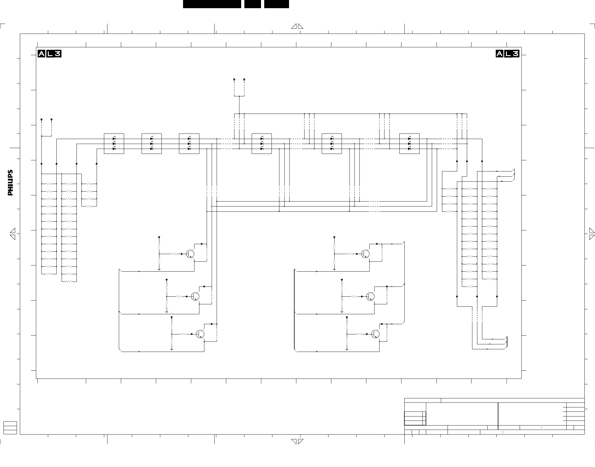
EN 62LC9.1A LA 10.
Circuit Diagrams and PWB Layouts
2009-Apr-10
12 LED Low-Pow: LED Liteon
GND_HS
GREEN
RED
BLUE
GND_HS
GREEN
RED
BLUE
GND_HS
GREEN
RED
BLUE
C
GND_HS
GREEN
RED
BLUE
GND_HS
GREEN
RED
BLUE
GND_HS
GREEN
RED
BLUE
if VLED < 17V
E
123
H
I
3301 F9
3302 F9
3303 F9
3304 G9
3
3308 H9
7
D
9
Place jumper 9314, 9316, 9317
P
R
R
P
5
E
O
3
3314 E12
456
C
4
10
3322 G12
12
H
G
11
3309 I9
G
914
9
10
13
G
B
D
M
3337 D2
F
G
H
456
C
3345 D12
E
17
10 11
19
3305 G9
3306 H9
3307 H9
D
20
12
F
G
2
17
3315 E12
3316 E12
3317 F12
789
3321 G12
3353 E1
3323 G12
N
3356 E1
B
LED LITEON
8
K
if VLED < 17V
1514
3328 G4
3330 I4
3331 F4
3332 F4
A
J
D
3372 F1
3338 D1
3339 D2
3340 D1
I
A
B
3344 D1
3389 F1
3346 E1
16
7000 C2
F F
8
H
3347 D1
13
I
L
All rights reserved. Reproduction in whole or in parts
3310 D12
13
1
3313 E12
L
3348 E12
3318 F12
3319 F12
3320 F12
3352 E1
9303-3 C10
3354 D13
3355 E1
9304-2 E10
N
J
18
I
O
3364 F13
15
3327 H4
3365 F13
3366 F13
3367 G13
3333 H4
B
C
3336 D2
9310-4 B8
3373 F1
3374 G1
3384 E1
3341 D1
3342 E2
3343 D1
3388 F1
9313-2 B12
3390 G1
3391 G1
9318-4 C8
5
1
K
7307 F4
M
12
B
A
10 18
3311 D12
3312 E12
Place jumper 9325, 9326, 9327
F307 F5
7315 G9
7316 H10
3349 E1
3350 E1
3351 E12
9303-1 C10
F347 G12
F348 G13
F349 G13
9309-4 B6
3357 D13
C
11
E
4
9307 A6
16
3325 G4
3326 H4
63
1
9308 A6
9309-1 B6
3368 G13
3334 F4
3335 D12
3371 F1
9318-3 C8
9311-1 H13
9311-3 H13
9311-4 H12
3385 F1
3386 F1
3387 F1
7
F305 H5
F340 D1
9303-4 C10
7001 C3
6
8
BRG
9319-1 D9
owner.
12 132
is prohibited without the written consent of the copyright
G
9319-3 D9
20
A
9310-1 B8
9313-4 B12
9314 G5
7317 F9
9301 C1
9302 C1
9316 H5
9317 F5
9318-1 C8
9320-1 D7
9320-2 D7
9312-1 B10
3358 E13
3359 E13
2
3361 E13
3362 E13
3363 F13
F341 D1
11
9320-4 D7
9325 F10
9326 G10
9327 H10
9309-2 B6
3369 F1
3370 F1
9310-2 B8
F304 H5
197
F308 F4
F325 F10
F326 F9
9319-4 D9
9313-1 B12
F302 G5
F303 G4
7004 C8
F327 G10
F328 G9
7002 C4
7003 C6
7005 C11
7305 G4
7306 H5
F329 H10
F330 H10
B
9304-1 E10
F343 D2
F344 D12
F345 D12
F346 D13
F342 D1
9304-4 E10
9305-1 C6
9305-2 C6
9305-4 C6
9315-1 C12
9315-2 C12
9315-4 C12
9312-3 B10
9312-4 B10
3360 E13
9306-1 D5
9306-3 D5
9306-4 D5
560R
3359
F349
VLED1-F
9316
3332
10K
9312-11 8
560R
3365
F305
BC847BW
7305
9302
3386
1K5
F304
1K5
3310
F347
390R
3351
3319
1K5
10K
3307
F341F340
1K5
F344
3318
45
1K5
3350
9313-4
560R
3361
3330
10K
560R
3367
3347
1K5
45
36
9309-4
3352
9319-3
3355
560R
560R
560R
3371
1K5
3314
2
9309-11 8
16
43
7
5
F343
LTW-E500T-PH1
7005
3333
1K0
560R
3368
45
3374
560R
9304-118
9304-4
9303-118
VLED1-F
3356
1K5
3327
560R
3338
10K
9308
9314
1K0
3302
9317
1K5
3313
9319-445
F346
27
F327
9313-2
BC847BW
7307
36
7306
BC847BW
560R
3373
9318-3
VLED1-F
1K0
3305
560R
3343
3372
560R
F345
9306-336
3306
10K
390R
3345
390R
3348
560R
3369
3317
VLED1-F
F302
36
1K5
F307
9312-3
3323
560R
3360
1K5
3
7
25
16
4
F330
LTW-E500T-PH1
7000
3326
10K
560R
3364
189305-1
3303
10K
F348
3370
560R
VLED2
1K5
3389
2
3390
1K5
LTW-E500T-PH1
16
43
7
5
7003
9325
9307
F342
18
1K0
3328
9315-1
390R
3337
9303-445
36
1K5
9303-3
3363
3322
560R
3353
1K5
5
1K5
3344
9315-44
9320-2 72
9326
3
7
25
LTW-E500T-PH1
7002
16
4
10K
3301
9301
9310-227
9318-4 45
F308
7316
BC847BW
1K5
3391
9306-4 45
9327
VLED1-F
36
9318-1 18
9311-3
8204 000 8857
2K9
DRIVER 6LED LITEON
A2
2008-08-08
??
2008-08-08
3
2
130
3
2
Peter Van Hove
2008-06-10
ROYAL PHILIPS ELECTRONICS N.V. 2008
2008-06-02
33
SETNAMECHN
CLASS_NO
SUPERS.
1
NAME
DATECHECK
3384
1K5
1K5
3385
390R
3335
9320-1 81
560R
3358
F303
VLED1-F
3316
VLED2
1K5
7
3311
1K5
27
9304-22
18
9309-2
9310-1
18
10K
3304
18
9313-1
9319-1
3340
560R
560R
3366
3388
1K5
9311-445
1K0
3334
560R
3346
560R
3357
BC847BW
7317
3309
10K
VLED1-F
3339
390R
9311-118
3336
390R
9305-445
54
F325
9320-4
10K
3331
390R
3342
3341
1K5
1K5
3315
560R
3362
BC847BW
7315
3308
1K0
1K5
3321
1K5
3387
560R
9312-445
3354
F328
9305-227
VLED1-F
3320
1K5
3312
3
7
25
1K5
7004
16
4 9315-227
LTW-E500T-PH1
F329
10K
3325
9306-1 18
3349
560R
45
F326
7
25
9310-4
7001
LTW-E500T-PH1
16
43
GREEN6GREEN6
PWM-G1
PWM-B1
BLUE6BLUE6
RED6RED6
RED-2
GREEN-2
RED-1
GREEN-1
BLUE-1
PWM-R1
RED-2
BLUE-2
GREEN-2
BLUE-2
PWM-R2
PWM-G2
PWM-B2
18560_512_090403.eps
090403
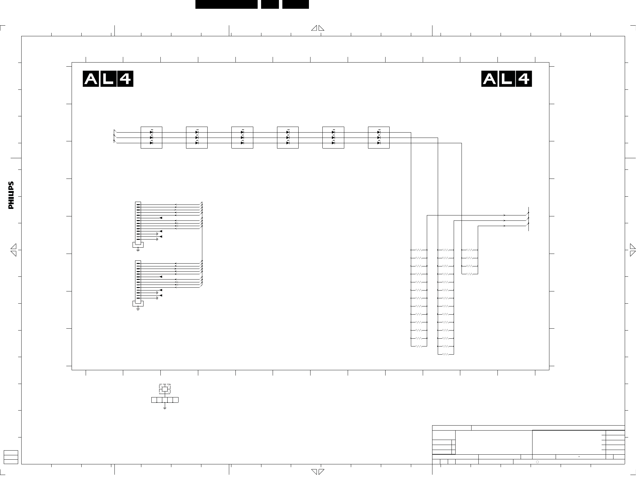
Circuit Diagrams and PWB Layouts EN 63LC9.1A LA 10.
2009-Apr-10
12 LED Low-Pow: LED Drive
C
GND_HS
GREEN
RED
BLUE
GND_HS
GREEN
RED
BLUE
GND_HS
GREEN
RED
BLUE
GND_HS
GREEN
RED
BLUE
GND_HS
GREEN
RED
BLUE
GND_HS
GREEN
RED
BLUE
3549 F9
3550 F10
10 11
7
7
3552 F9
3553 F10
B
C
5
3587 G10
D
3573 H9
G
H
A
34
17
6
9
G
H
C
H
F
1312
7006 B2
3556 F10
3547 F10
3589 H10
3590 H10
3591 H10
7011 B8
3555 G10
3546 F9
789
56
F
8
206
1918
10
4
12
A
E
3574 H9
3584 G10
3585 G10
M
3586 G10
3571 G9
3572 G9
F
12
12
3
1
11
O
16
13
K
10
L
A
1211
14
3538 E9
7007 B3
3588 G10
7008 B5
7009 B6
7010 B7
3543 F9
3544 F10
J
234
H
1M3A F2
G
E
16
15
P
O
45
owner.
M
L
8
3569 G9
3570 G9
D
E
3537 E11
1819
14
G
12
3539 F11
3540 F9
3541 E10
3542 F11
is prohibited without the written consent of the copyright
J
3
1M85 D2
3536 E11
LED DRIVE
15
B
D
NN
98
K
I
P
B
A
91011
All rights reserved. Reproduction in whole or in parts
B
C
20
I
F
E
D
5
17
67
12
C
3543
560R
1K5
3584
3569
560R
3
4
5
6
7
8
9
15 16
1M85
1
10
11
12
13
14
2
3587
1K5
560R
3549
3552
560R
560R
3555
1K5
3586
VLED2
1K5
3544
+3V3
1X04
REF EMC HOLE
3570
560R
560R
3572
3571
560R
16
+3V3
3542
390R
14
2
3
4
5
6
7
8
9
15
1
10
11
12
13
1M3A
NAME
DATECHECK
8204 000 8898
2K9 LITEON
6 LED + CONNECTOR
A2
2008-08-14
130
3
2
2008-10-29
Peter Van Hove
2008-10-29
ROYAL PHILIPS ELECTRONICS N.V. 2008
2008-07-30
11
SETNAMECHN
CLASS_NO
SUPERS.
2
3573
560R
VLED1
560R
3546
560R
3574
390R
3539
3589
1K5
390R
3536
1K5
3553
3585
16
43
7
5
2
1K5
7011
LTW-E500T-PH1
390R
3537
7006
16
43
7
5
2
3
7
5
2
LTW-E500T-PH1
7007
LTW-E500T-PH1
16
43
7
5
2
LTW-E500T-PH1
7010
16
4
3591
1K5
1K5
3588
16
43
7
5
2
5
2
7009
LTW-E500T-PH1
16
43
7
LTW-E500T-PH1
7008
1K5
1K5
3590
3541
VLED1
VLED2
3556
1K5
3538
560R
560R
3540
1K5
3547
3550
1K5
SPI-DATA-OUT
SPI-DATA-RETURN
SPI-LATCH
PWM-CLOCK-BUF
BLANK-BUF
EEPROM-CS
TEMP-SENSOR
RED-1
GREEN-1
BLUE-1
SPI-CLOCK-BUF
PROG
SPI-CLOCK-BUF
SPI-DATA-OUT
SPI-DATA-RETURN
SPI-LATCH
PWM-CLOCK-BUF
BLANK-BUF
EEPROM-CS
TEMP-SENSOR
PROG
GREEN-2
RED-2
BLUE-2
18560_513_090403.eps
090403
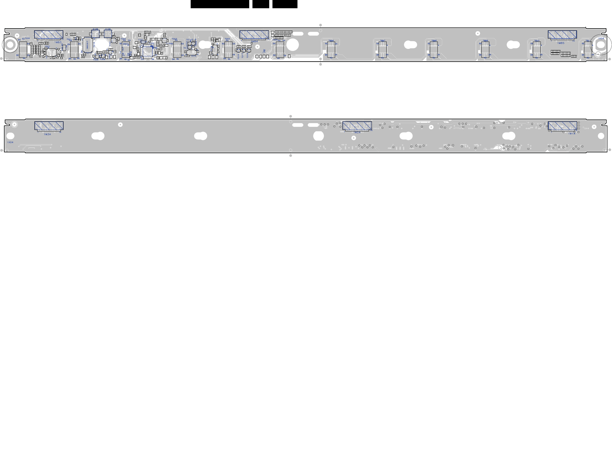
EN 64LC9.1A LA 10.
Circuit Diagrams and PWB Layouts
2009-Apr-10
Layout 12 LED Low-Pow
31043136335.2
18490_551_090326.eps
090331
1101
1105
1M83 1M84 1M85
1X03
2101
2102
2103
2104
2105
2106
2107
2108
21092110
2111
2112
2113
2114
2115
2116
2117
2118
2119
2120
2121
2122
21232124
2125
2126
2127
21282129
2130
2131
2201
2202
2203
2209
2210
2211
2214
2215
2216
2217
2218
2219
2220
3101
3102
3103
3104
3105
3106
3107
3108
3109
3110
3111
3112
3113
3114
3115
3116
3117
3118
3119
3120
3121
3123
3124
3125
3126
3127
3128
3129
3130
3131
3132
3133
3134
3135
3136
3137
3138
3139
3140
3141
3142
3203
3204
3205
3207
3209
3210
3211
3212
3213
3214
3215
3216
3217
3218
3219
3220
3221
3222
3223
3224
3301
3302
3303
3304
3305
3306
3307
3308
3309
3310
3311
3312
3313
3314
3315
3316
3317
3318
3319
3320
3321
3322
3323
3325
3326
3327
3328
3330
3331
3332
3333
3334
3335
3336
3337
3338
3339
3340
3341
3342
3343
3344
3345
3346
3347
3348
3349
3350
3351
3352
3353
3354
3355
3356
3357
3358
3359
3360
3361
3362
3363
3364
3365
3366
3367
3368
3369
3370
3371
3372
3373
3374
3384
3385
3386
3387
3388
3389
3390
3391
3536
3537
3538
3539
3540
3541
3542
3543
3544
3546
3547
3549
3550
3552
3553
3555
3556
3569
3570
3571
3572
3573
3574
3584
3585
3586
3587
3588
3589
3590
3591
6216
7000
7001
7002
7003
7004
7005
7006
7007
7008
7009
7010
7011
7101
7102
7110
7116
7201
7209
7210
7212
7214
7215
7305
7306
7307
7315
7316
7317
9101
9102
9103
9104
9106
9107
9108
9109
9110
9111
9112
9113
9114
9119
9121
9208
9209
9210
9211
9212
9213
9214
9301 9302
9303
9304
9305
9306
9307
9308
9309
9310
9311
9312
9313
9314
9315
9316
9317
9318
9319
9320
9325
9326
9327
C140
I110
I111
I113
I114
I115 1X04
1M1A1M2A1M3A
F101
F102
F103
F104
F105
F106
F107 F108
F109
F112
F116
F117
F118
F120
F121
F122
F123
F124
F125
F126
F127
F128
F129
F130
F131
F132
F133
F134
F135
F136
F137
F138
F139
F202 F203
F204
F205
F206
F207
F208
F209
F210
F211
F212
F213
F214
F215
F302
F303
F304
F305
F307
F308
F325
F326
F327
F328
F329
F330
F340
F341
F342
F343
F344
F345
F346
F347F348F349
I124
I125
I126
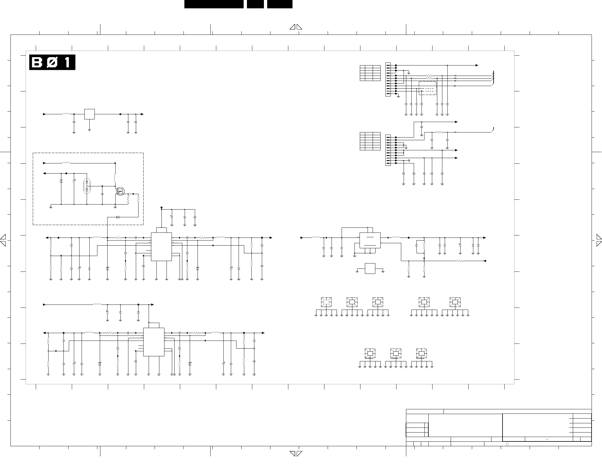
Circuit Diagrams and PWB Layouts EN 65LC9.1A LA 10.
2009-Apr-10
SSB: DC/DC
C
PVDD1 PVDD2
EN1
SW1
BOOT1
SW2
FB2
EN2
BOOT2
FB1
ILIM2
SEQ
BP
GND GND_HS
VIA2
VIA1
PVDD1 PVDD2
EN1
SW1
BOOT1
SW2
FB2
EN2
BOOT2
FB1
ILIM2
SEQ
BP
GND GND_HS
VIA2
VIA1
COM
OUTIN
VIA
GND
VIN
HSPA
INH
SYNC
SW
VFB
A
SW
34
RES
1817
F
G
H
20
12
C
D
E
F
G
H
I
2105 F13
2106 F8
2107 F9
B
A
B
C
D
E
F
G
1X05 G9
1X03 G11
2124 B11
2125 B2
12 567891011
2137 I2
2138 I3
2139 I4
13
12345
J
1
13
A
12
2163 F1
2164 F6
1X06 G9
1X07 I11
1X08 G12
1X12 G10
2100 F11
2101 F12
2102 F12
2103 F12
2104 F13
3103 D3
3104 D3
3105 H1
2108 F9
2109 B11
2110 C11
2111 C12
H
I
1M95 C10
1M99 A10
1X01 I10
1X02 I10
2119 B11
RES
RES
RES
2120 B12
2121 B12
2122 B12
2123 E5
3171 F12
3172 F11
2127 B3
2128 D2
2129 D2
2131 H3
2132 H3
2133 H3
2134 H1
2135 I1
2136 I1
5107 C1
5108 F8
5115 H5
2140 I6
2141 I3
2142 I7
2144 I6
67891011
2157 F5
STBY
RES
2158 F2
2159 F6
2160 F3
2161 F7
2162 F2
43
2165 H4
2166 H7
4100 A11
4101 A11
5100 B1
5101 F10
5102 D3
5103 G2
5104 H2
L
E
17
3106 I1
3107 F1
3108 H2
3109 I3
2112 D11
2113 D11
2114 D11
2115 D12
2116 B11
2118 B11
3134 H5
0V
ON
3135 E3
3136 E5
3138 F1
3139 H6
3140 F1
1917
3173 F11
3199 F11
I
L
M
K
C
B
A
342
5116 F6
5117 F2
6100 E3
6101 D1
2150 E4
2152 E3
2153 E5
2154 F1
2155 F7
2156 F3
F109 C11
0V25V9
0V12V8
L
I105 H2
I106 H3
21
A
B
C
D
E
5 14
I122 I3
I123 I5
I124 F2
161514
19
3119 I6
3122 F6
3125 F6
3129 I4
3130 F3
3131 F5
F116 A11
O
8
M
N
O
P
20
E
F
16
1165432
A
B
P
2019
D
A
K
F
F103 C11
F104 C11
F105 C11
F106 C11
F107 C11
F108 C11
F133 F7
3V31
F134 F11
I100 C3
I102 D3
I103 D2
I104 I1
12
I107 H3
I108 E9
I109 E10
I110 F11
I111 B2
I117 H4
I118 H5
I119 H5
I120 H5
12 1314
I125 E3
I126 E3
I127 E4
I128 E5
F110 C11
F111 A11
F112 A11
F113 A11
F114 A11
F115 A11
I136 I3
G
F
E
D
B
C
D
G
H
I
J
K
L
M
N
O
18171615
3V3
F124 G3
F125 H1
F126 A11
F131 H6
F132 F1
M
L
J
I
H
321
34567891011 15161718
I129 E5
I130 F5
I131 F1
I132 F3
I134 F3
I135 F5
K
A
14
7
4
1810 141312
P
O
N
87654
RES
RES
Round screw hole of 4.5mm
Oval screw hole of
5mm x 4.02mm
Round screw hole of 4.02mm
123
RES
BD 12NC : 3139_123_64512
MULTI 12NC : 3139_123_64502
19 20
C
B
A
E
D
13
H
G
65
O
N
MM
16
1513126
12V
1197
3V
11109
J
I
H
G
F
11 12
RES
10
RES
RES
16 17 1819 20
C
K
C
20
14
9
0V53V
19
9
1M95
F
P
5
PIN ON STBY
1
18
513167
RES
RES
RES
RES
20V 3V
1
B
H
NN
K
L
O
789
7 1.5V
12
E
2167 H3
2168 E5
2169 D11
2171 B3
3100 C12
3101 A11
3102 A11
7103-1 E10
G
F117 A11
F118 A11
F119 A11
F120 B11
F122 B3
F123 D1
12V 0V
0V
111098
I
J
>1.5V
10
6102 D2
6103 I2
612V
7103-2 F10
7116 H4
7117 E4
F100 C11
F101 C11
P
P
6
7
0V
8
0V
1M99
RES
1312
D
J
I
15
6122 I5
6123 F2
6124 F5
7100 B2
7101 D3
34V
ONLY FOR ANALOG TUNER
F102 C11
DC / DC
0V
PIN
33n2167
REF EMC HOLE
1X12
2
REF EMC HOLE
1X03
2N7002
7101
3
1
+12VS
+VTUN
5107
10u
I100
2128
100p
REF EMC HOLE
1X01
F123
2129
22u35V
I102
GNDTUN
220u
5102
I103
6101
PDZ33-B
15
+12VS_1
3106
1%
1K2
2165 33n5115
CLASS_NO
1
SUPERS.
2
NAME
DATECHECK
3139 123 6451
PCB SB SSB
LC09M
A2
2008-11-21
-- -- --
2009-02-031
03101
10u
3
2
2009-02-03
Tee Chor Kimp
DC377215
2009-03-05
SVROYAL PHILIPS ELECTRONICS N.V. 2008
2008-11-21
3PC332
SETNAMECHN
6122
SS34
100u
6.3V
2140
2166
10p
10u
2137
1%
3139
220R
+8V_SW
30R
5100
+12VS
1u0
2127
100n
2125
1
F122
2156
470p
10u
5103
10u
2132
+12VS
3108
1R0
3105
1K5
1%
SS34
6123
+1V8_SW
10p
2134
470p
2138
100u
6.3V
2158
3136
1R0
4u7
2141
2136
SS34
6103
6.3V100u
3109
10R
3103
220R
1n0
2169
+3V3_SW
3122
1%
4K7
1
1R03134
7100
L78L08ACU
2
3
10R
3129
10p
+12VS_1
2135
2144
10u
14
10
213
16
17
13
11
65
87
415
9
17116
TPS54386PWP
Φ
2
F124
F125
10p
2142
10
213
16
17
65
87
415
9
114
Φ
TPS54386PWP
7117
312
11
+1V2_SW
1%
390R
3119
2123
10u
5117
10u
1R0
31352152
33n
2154
10p
+5V_SW
2150
16V
100u
10u
I126
5104
100u
16V
2131
2160
I120
4u7
I135
10R
3130
I128
I130
I123
33n
2153
470p
+12VS
2139
3173
1K0
1%
5116
10u
470p
2157
SS34
6124
3131
10R
6.3V
100u
2159
2162
10u
10u
2164
2155
10p
1K81%
SENSE+1V0_MT5392
3107
2161
10p
I108
3125
1K5
10u
2107
2106
10u
10p
2163
+3V3STBY
F104
F101
F131
F132
I106
F133
I117 I118
I105
I122I104
I136
I107 I119
I111
I131
F111
F114
F116
I132
I129I125 I127
F108
F115
2120 100p
2u0
2
8
7
35
16
5101
ST1S10PH
7103-1
49
7103-2
ST1S10PH
10 11
3102 68R
2110
RES
1n0
2102 22u
+1V0_SW
3199
10K 1%
2103
220u25V
F134
2100
4n7
I109
2K2
3172
1%
100K
3140
3138
18K
1%
2108
10u
68R
3100
33R
5108
22u2101
2119 100p
+12VS
GNDSND
F100
100p2118
F107
+12VDISP
F112
F113
3171
2105 22u
1%
220R
10u
2168
22u2104
2133
10u
I124
I134
F103
F106
F105
RES
1n0
2112
100p2116
100p2121
2124 100p
F110 GNDSND
2113
100n
RES
100n
2114
RES
3101 68R
F109 +24VAUDIO
2122 10n
2
3
4
5
6
7
8
9
1M95
1-1735446-1
1
10
11
I110
RES
1n0
1n0
2111
2109
RES
REF EMC HOLE
1X06
REF EMC HOLE
1X08
4101
F126
6102
BAV99
REF EMC HOLE
1X02
1K0
3104
F118
F119
F120
F117
RES
4100
2115
1n0
F102
6100
BZX384-C6V2
2171
10u
REF EMC HOLE
1X07
REF EMC HOLE
1X05
11
12
2
3
4
5
6
7
8
9
1-1735446-2
1M99
1
10
PWM_DIMMING
BACKLIGHT_BOOST
POWER-OK
STANDBY
BL_ON_OFF
18490_500_090402.eps
090402
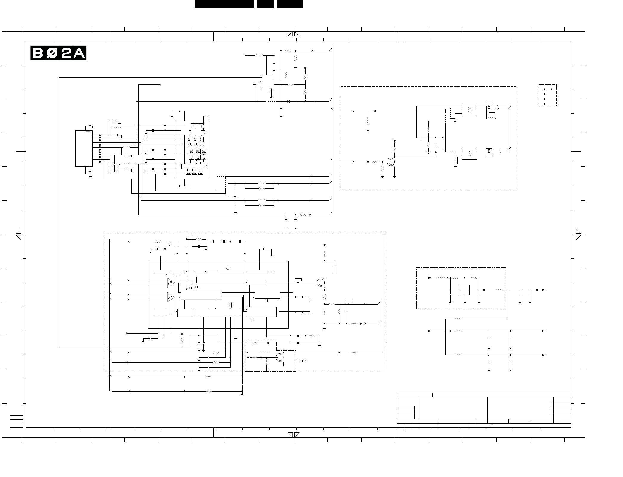
EN 66LC9.1A LA 10.
Circuit Diagrams and PWB Layouts
2009-Apr-10
SSB: Tuner & Analog demodulator
C
L
H
M
L
H
M
PLL
RF OUT
E
Φ
VCC
B0
B1
GND
A
S
TUNER AGC VIF AGC
SUPPLY OUTPUT
VIF-PLL
SINGLE REFERENCE QSS MIXER
AND SWITCHES
DEMODULATOR
SIF
AGC
AFC DETECTOR
PORTS
INTERCARRIER MIXER AND
AM-DEMODULATOR
I C-BUS TRANSCEIVER
2
RC VCO
NARROW-BAND FM-PLL
DIGITAL VCO CONTROL
SOUND TRAPS
4.5 to 6.5 Mhz
AUDIO PROCESSING
MAD
COM
OUTIN
I
O2ISWI
O1
GND
I
O2IGND
O1
GND
MTMT
D
F
H
I
J
P
201918171
P
2
O
456
N
M
L
J
I
12 13 14 15 16
H
G
F
E
D
C
B
A
K
A
B
C
E
G
K
L
M
N
O
1615141312111098765432
31 7891011 17 18 19 20
I247 J7
I244 I6
I249 J6
I242 I6
I245 I8
C
D
E
F
G
4V9
2229 G7
F216 C11
F214 G5
F208 D3
RESERVED
F203 D3
F204 D3
F205 D3
F206 D3
TUNER & ANALOG DEMODULATOR
I248 J10
I241 I13
3222 D12
I243 I9
3226 E11
I250 J8
3230 F7
3231 G6
3232 G4
14 15 16
A
B
3241 J6
2V
3240 J7
3238 I9
RES
H
I
J
K
L
A
B
C
D
E
F
G
H
I
2228 G6
2212 E4
RES
2214 C3
F215 H9
2216 D3
2218 H15
2219 H16
F213 C2
F211 D3
F210 D3
F209 D3
Test Keep spaceing 3.5mm
RES
With LC09M Analog
F260 I10
F255 D5
F257 D5
F207 D3
2263 F9
2265 E3
2266 E3
2267 E3
2268 D4
3210 J5
3211 H13
3212 H14
3213 B9
3214 B9
3215 A8
3217 A9
3219 C13
3221 D12
MULTI 12NC : 3139_123_64502
3223 D11
I239 I9
3228 E7
TDA9886/V3
I240 I9
I215 B8
3234 G9
3235 H9
3236 I9
2V
2V1
I228 G5
I230 G7
I231 G6
I232 G7
I233 G5
"200" ~ "299"
DIA 1.2MM FT
RES
32
J
K
L
1201 C2
1204 C6
1211 C14
1212 D14
1213 G6
2210 H13
2211 H14
I213 H13
2213 C8
5216 I13
2215 C4
5218 J13
5219 A7
6210 C8
2221 D12
2225 E7
2226 F7
1
SAW FILTERS
7214 J8
7215 B8
A210 C14
A211 C14
A212 D14
F256 D5
F217 D11
F218 H14
F219 H16
F227 H10
F228 I15
F229 J15
F230 D13
F234 B16
F235 B16
F236 B16
F237 C16
F250 C5
F251 C5
F252 E5
3245 J8
RES
3247 K6
I238 H9
3254 I10
3255 I10
3256 I10
I216 B9
I218 D13
I222 D11
I226 E8
I227 E8
4207 E6
4208 C8
4209 E6
4210 D4
4211 C13
I234 G8
I235 G5
I237 H10
I253 K5
I261 B16
2V
2V3
I251 J7
I252 K5
I210 A9
I214 H14
I211 A8
I212 A8
RES
Common Testpoints
2233 G8
5215 E7
2236 H9
5217 I13
2240 I10
2241 I15
2242 I14
6211 D13
7210 H14
7211 D12
7212 G4
7213 H9
2248 J14
2249 J15
2250 J6
2251 J6
2252 K7
A213 D14
A214 D3
A225 E3
A258 E5
A259 E5
F201 D3
F202 D3
RES
2V
RES
RES
1V5
3242 J10
3243 J7
3244 J6
7
3246 K6
9
3251 B8
11 12 13
3261 F9
3262 B8
4204 C13
4205 D13
4206 D13
34567
4214 J8
5206 C3
5207 D3
5208 D4
0V
RES
1.2mm dia FT, with 2.5mm spacing
5210 H13
5211 H15
5212 C14
5213 C11
5214 E7
2230 G4
2231 G5
2232 G5
10
2235 G10
11
2237 I9
12
RES
2243 I9
2244 I4
2245 J9
2246 J6
2247 J6
RES
RES
2V1
BD 12NC : 3139_123_64512
13
2253 A8
2258 D4
2259 E3
2260 D4
Note:
RES
RES
DEMODULATOR
0R
RES
2261 E3
2262 F8
456
47p
2240
018 14 15 16
12 89
10u
5218
3213
8K2
3226
18K
F230
F210
22n
BAS316
2230
F202
6210
I233
F214
I210
2232
220n
I239
2228
1n5
2263
10u
3235
1R0
5216
33R
2215
1
03101
100n
ROYAL PHILIPS ELECTRONICS N.V. 2008
2008-11-21
2
3PC332
15
SETNAMECHN
CLASS_NO
1
SUPERS.
2
NAME
DATECHECK
3139 123 6451
PCB SB SSB
LC09M
A2
2008-11-21
-- -- --
2009-02-03
3
2
2009-02-03
Evelyn/Lee Boon Hiong
DC377215
2009-03-05
SV
120R5214
I215
F235
F236
F234
7
6
2
3
4
5
8
74LVC2G53DC
7215
1
I228
I253
SCL4
SDA5
TU2
VS7
9VST
11
MT1 12
MT2 13
MT3
14
MT4
15
NC1
6
NC2
8
NC3
10
1204
AGC1
AS3
IF1
+5VS
+5V_SW
100n
2216
2233
1n0
22u
2213
330K
3215
2210
1u0
A259
330R
4M0
3231
F204
1213
18K
3245
150R
3242
I232
3251
5K6
F207
4208
+5VS
+5VS
I218
+5V_IF
BC847B
7214
5217
10u
3236
220R
3232
100R
2265
I231
100n
2250
3212
47R
390n
5213
A258
F257
F256
3262
F255
I241
22p
2229
2252
15p
3238
A210
5K6
A213
F250
F251
I249
A214
F211
330K
3217
I235
22K
3210
F217
5208
33R
F227
F205
22K
3223
1
2 VIF2
20 VP
VPLL 19
SDA
10
23 SIF1
SIF224
SIOMAD12
TAGC 14
TOP 9
16
VAGC
VIF1
5
DGND
7
FMPLL4
NC
13
OP1
3
OP2
22
REF 15
SCL11
7212
AFC 21
AFD 6
AGND18
AUD 8
CVBS 17
DEEM
F228
2251
1R0
3246
+5V_IF
I245
F213
+12VS
4204
4205
I242
22u
2248
A212
3221
2K2
F216
100n
2262
+5V_IF
3
L78M05CDT
7210
2
1
I243
100n2267
39K
3214
2242
22u
3254
75R
F218
F201
5212
390p
+5V_IF
2245
2219
10n
+5VS
470n
2231
F219
K7280M
1211
38M
3
1
2
5
4
2259 100n
I240
10n
2236
3222
+5V_IF
2K2
BC847B
7211
22K
3243
3247
1R0
I227
F215
F203
3219
6K8
A211
15p
2225
4214
7213
BC847B
5206
33R
I244
1n0
2247
75R
3255
2211
100n
+5VTUN
10R3230
5215
4206
120R
F206
I237
4211
2226
15p
2249
10n
10R3228
22K
3240
10n
2241
5211
33R
22u
2218
I238
2261 100n
F229
4n7
2214
I234
I247
4210
1SS356
4207
6211
4209
2253
100n
I213
1R0
+5VS
3256
F260
I250
I212
3234
15R
I252
1n0
2246
F237
3211
47R
1K0
3261
100n
2260
10n
2235
I214
I248
A225
2
14
1516
8
NC
RF_AGC 3
4
SCL
SDA 5
VTU_TP 7
F209
12
AIF
1
ANT_PWR 2
B1
B2 6
11
DIF1
DIF2 10
IF_AGC 9
13
1201
TUNER
TDTC-G321D
F208
I216
2243
10n
470n
2237
I211
I251
3
1
2
4
5
38M0
1212
OFWK9352M
2200
4n7
I226
3244
100R
I222
5207
33R
10n
2221
100R
3241
2244
F252
10n
100n
2212
I261
+5VTUN
2266 100n
30R
5219
33R
5210
I230
2258
100n
SIF1
IF_ATV
SIF2
+VTUN
IF_ATV
RF_AGC_MON
RF_AGC
GND_CVBS_RF
SIF_OUT_GND
SIF_OUT
CVBS_RF
TUNER_SCL
TUNER_SDA
VIF1
SAW_SW
VIF2
VIF1
SIF2
SIF1
VIF2
RF_AGC
TUNER_SCL
TUNER_SDA
18490_501_090402.eps
090402
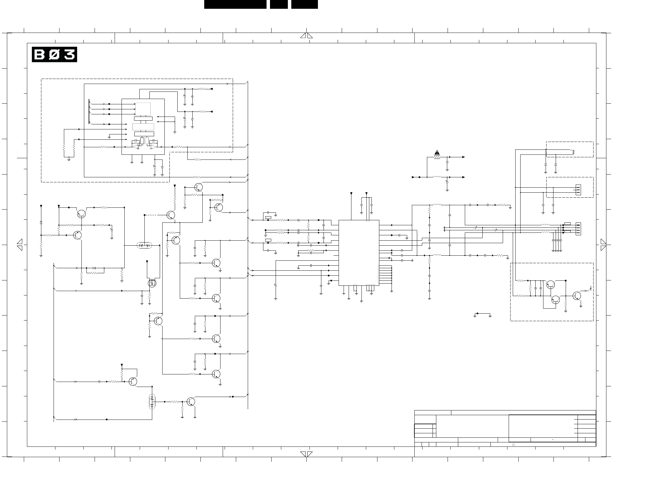
Circuit Diagrams and PWB Layouts EN 67LC9.1A LA 10.
2009-Apr-10
SSB: Class-D & Muting
DIGITAL
DE-EMPHASIS
INTERPOLATION
DAC
NOISE SHAPER
FILTER
INTERFACE
DAC
C
IN1P
VSSD|HW
IN1N
IN2P
IN2N
INREF
OSCREF
OSCIO
HVPREF
DREF
ENGAGE
POWERUP VIA
TEST
GND_HS
VDDP
VSSP
VDDA
STAB2
STAB1
BOOT2
BOOT1
HVP2
HVP1
DIAG
OUT2
OUT1
CGND VSSA
3552 H4
3553 H4
3554 D5
7501-1 E2
I585 F14
I581 F9
I582 F11
F580 D6
F593 G9
F522 E2
F523 E4
3558 C3
3559 C5
12345
RES
-2V6
-2V8
0V
2501 A5
2502 B5
2503 B5
3555 D5
2560 C16
2561 F15
2520 D15
2510 H5
2511 E3
3542 F12
3544 G15
3548 G16
3549 G15
3550 G15
5503 D12
5505 F12
5507 E15
5508 E15
6500 E4
7501-2 E2
I516 C5
I518 D2
I519 D3
I521 E2
3560 E5
-2V8
I523 H5
BD 12NC : 3139_123_64512
2521 D15
LEFT-
RIGHT+
4V7
EMC
CLASS-D & MUTING
RES2V6
RES
RIGHT -
I510 A5
I583 F13
I584 F12
2566 E7
2567 F7
2568 F5
2569 G5
3500 A5
I562 F2
I563 C13
I564 D13
3540 F8
3541 F14
I543 I3
I544 I3
I546 J4
I596 G15
I597 D5
67
RES
RES
2500 A5
A
B
2523 E10
2524 E13
2527 E8
2528 E12
2529 E9
2512 I5
4502 E4
5502 D12
2533 E9
2534 E12
2536 F8
2537 F13
6501 E1
6502 F3
6503 J4
7102 F5
7500 A4
1234
P7507 J5
7508 G16
I
H
G
RES
3563 F5
3562 F6
3561 F5
3566 D5
RES
7510 E10
RES
2565 G4
I512 B2
I513 C2
I515 C3
I525 E4
I526 F5
3531 D14
3532 E12
14 15 16
I
I598 D6
I599 H4
K
O
P
20
C
D
E
F
G
H
2530 E8
2531 E8
2532 E11
109876
5
O
N
M
L
J
11 12 13
F
E
D
C
B
A
3565 G5
3564 G6
I511 B5
RES
RES
I527 G5
I530 G3
I535 I5
9
1314 15
J
K
L
M
N
19181716151413121154321
3535 E8
3536 E8
3537 E8
3538 F8
16
678910
F
H
I
14 15 16 17 1819 20
I560 E3
I590 F12
I595 G12
I524 E1
2539 F8
12
3501 B5
3502 C5
3516 H5
3517 F1
3519 F2
3520 F3
2541 F11
641
24V
I565 D13
A
B
C
D
E
I573 E9
I575 E9
I576 E12
J
K
L
1502 C16
1735 E16
1736 D16
"500 - 599"
3V2
NC
I554 J5
I552 J5
1310 11 12
2518 D13
2519 D14
I
9
-2V8
2540 F8
C
D
10 11
8V9
2
2513 I3
3507 C2
3508 C2
3509 D5
3510 E3
3511 H6
3512 E2
3513 E3
3514 E1
3515 E1
I522 E2
I589 F9
RES
RES
3V3
2542 F13
E
F
G
-8V2
3527 I3
3528 J5
3529 J5
3530 C12
7503 H6
I566 D14
I568 E8
I570 E12
I571 E11
I572 E8
24V
-2V8
-7V6
I577 E8
I578 E8
I580 F9
F569 E9
F579 E9
7506 I4
2522 E10
RES
RES
2546 F11
2547 F12
2549 G9
2550 G8
2552 G12
RES
RES
RES
TO SUBWOOFER OUT
I559 F4
3557 E6
2562 F16
2563 F16
2564 F16
8
75 83
RES
F536 F9
F538 K3
F539 H13
2515 C13
2516 D13
G
H
2508 C4
2509 C4
F524 H6
F535 J6
F525 I6
7505 I6
3524 I6
3525 I5
3526 I3
RES
RES
MUTING CIRCUIT
I586 F11
I587 F11
I588 F9
TO INDIA SUBWOOFER
F540 D12
F541 E7
F542 E16
F543 E16
3521 F2
3523 G4
2543 F14
2544 F11
2545 F8
3V9
LEFT +
TO SPEAKERS
DC-DETECTION
7511 F15
7513 G16
7515-1 H5
7515-2 D5
7516 D6
K
J
RES
RES
RES
RES
RES
2553 G15
2554 E13
2555 E14
2556 G15
2559 C15
F544 E16
F545 E7
MULTI 12NC : 3139_123_64502
RES
A
L
B
3533 E8
3534 E8
7517 E4
7518 F6
7519 G6
F512 B3
F515 B3
F516 B3
F518 B3
3556 D6
F546 E16
F547 E11
F548 F7
F550 G16
7504 F4
F544
F543
GNDSND
3514
4K7
GNDSND
I525
I527
22R
3531
PCB SB SSB
LC09M
A2
2008-11-21
-- -- --
2009-02-031
03101
3
2
2009-02-03
Roger Poon & Jason Ong
DC377215
2009-03-05
SVROYAL PHILIPS ELECTRONICS N.V. 2008
2008-11-21
3PC332
SETNAMECHN
CLASS_NO
1
SUPERS.
2
NAME
DATECHECK
3139 123 6451
F593F550
BC857BW
7511
25V
2554 470u
470u
2555
25V
F548
3566
1K0
VDDD
14 VOL 16VOR
12
VREF-DAC
15
VSSA
5
VSSD
2WS
8MUTE
10 PCS
11SFOR0
7SFOR1
6SYSCLK
13
VDDA
4
1 BCK
3DATAI
9 DEEM
7500
UDA1334BTS
5507
220R
I590
GNDSND
GNDSND
GNDSND
GNDSND
7506
BC857BW
3527
4K7
I575
3541
22R
I560
3526
4K7
1u02536
2546 100n
1u0
2544 15n
2531
100n
2509
I519
16V
353712K
2508
47u
22u
5503
1n0
2534
1
7515-1
BC857BS
2
6
2518
220n
16V47u
2500
1R03508
1R03507
470n
2524
F542
F547
10R
3532
I562
BC847BW
7507
3560
47K
3561
10K
GNDSND
I526
10R3530
I577
I572
I559
1
3
2
+12VS
BC847BW
7517 220n
2519
I513
2533
220p
5508
220R
2502
47u16V
1n0
2561
3549
100K
47u
2550
I595
25V
100K
3521
4502
7515-2
BC857BS
5
3
4
470R
2521
1n0
I583
3559
I571
I588
I596
F523
7505
2SD2653K
35V
GNDSND
220u
2516
2556 4u7
3512
I530
GNDSND
4K7
GNDSND
BC847BW
7508
BC857BW
7102
1
3
2
I523
1K0
3510
2515
100n
GNDSND
I584
I566
2567
10n
47K
3524
32
26
23
2527 1u0
38
39
40
41
9
1
16
17
25
24
13
8
29
20
34
35
36
37
3
2
14
15
12
31
10
27
22
6
28
21
7
4
18
5
33
30
19
11
Φ
7510
TDA8932BTW
AMPLIFIER
POWER
CLASS D
I570
+3V3_SW
I518
I510
470n
2537
F580
I546
I599
GNDSND
I573
100n
2503
1u0
10K
2513
3553
2560
1n0
3548
100K
3520
100K
I598
+3V3STBY
10n
2566
100n
2523
4n7
2512
I516
I511
F541
I515
10K
3535
2501
100n
GNDSND
F545
I522
39K
VDD
3540
10K
I589
+3V3STBY
3555
+3V3_SW
3511
47K
2528
1n0
GNDSND
I563
I535
I585
I582
25534u7
GNDSND
3550
100K
I597
3529
22K
10K
3557
1n0
2520
2532
1n0
I564
5502
2563
30R
I552
1n0
I544
GNDSND
10K
3523
6502
BAS316
F515
VDDA
F516
F538
2510
4n7
1
1R0
3519
7501-1
BC857BS
2
6
BC857BW
7513
470R
47K
3552
3558
+5V_SW
10K
10K
3533
3538
6500
BAT54C
1K0
3525
3556
47K
1n0
2552
220n
2543
1n0
2562
F579
GNDSND
I578
100n
2565
GNDSND
5
3
4
7501-2
BC857BS
+24VAUDIO
GNDSND
F540
470R3509
F546
F524
VDD
2539100n
220n
2542
1R0
3500
3
1
2
BSS84
7504
3502
470R
2529
220p
VDDA
F522
I521
F512
1
2
GNDSND
5505
22u
MTJ-032-21B-43 NI FE LF
1502
F535
I581
I512
2SD2653K
7519
3565
1K0
F518
1R0
3501
I554
F536
1u02530
3536
10K
3515
56K
3517
47K
100n2540
1K8
3513
GNDSND
+12VS
GNDSND
2SD2653K
7503
440054-4
1735
1
2
3
4
GNDSND
BAS316
6501
2549
470n
7516
BC857BW
1
3
2
I568
F539
F525
GNDSND
2511
470u16V
10K
3528
100n2545
4n7
2568
3516
1K0
47K
3562
1
2
3
1736
1735446-3
I587
3544 100K
I543
1n02564
6503
BAT54C
353412K
7518
2SD2653K
1K0
356310R
3542
GNDSND
GNDSND
1n0
2559
1n0
2547
3554
47K
I524
100n
2522
2541 15n
F569
I580
I586
2569
4n7
3564
47K
I576
I565
315
AOUTR
AOUTL
AOUTR
AUDIO_LS_R
AOUTR
MUTE_M
MUTE_C
AOUTL
POWER_DOWN
AOBCK
AOUTL
SW_MUTE
HP_ROUT
AUDIO_LS_L
SPEAKER_RIGHT-
SPEAKER_RIGHT+
SPEAKER_LEFT-
SPEAKER_LEFT+
DC_PROT
HP_LOUT
STANDBYn
MUTE
OFF_MUTE
MUTE
MUTEn
AOSDATA0
AOLRCK
AOMCLK
18490_502_090402.eps
090402
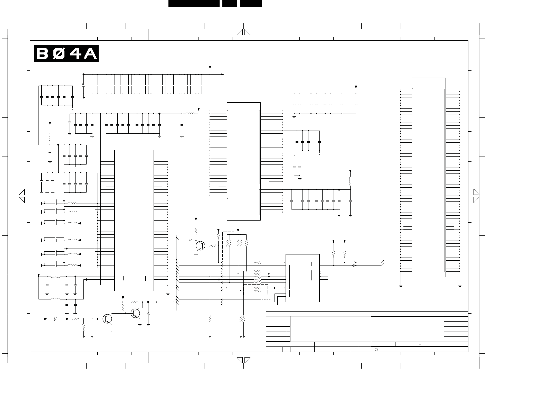
EN 68LC9.1A LA 10.
Circuit Diagrams and PWB Layouts
2009-Apr-10
SSB: MTK Power
C
DVSSDVSS
VCC3IO
VCC2IO
VCCK
AVDD12
AVSS12
AVDD33
AVSS33
AVDD80 AVSS80
CVBS1
CVBS2
CVBS3
DEMOD1
DIG
HDMI
LVDS_1
LVDS_2
LVDS_3
LVDS_4
LVDS_5
REF_AADC
REG
SRV
STB
SYSPLL1
SYSPLL2
USB_1
USB_2
VDAC
VDAC_BG
XTAL
ADAC1
ADAC2
DVSS12_VGA
DLL1
DLL2
HDMI
LVDSA
LVDSB
MEMPLL
PLLG
RGBADC_1
RGBADC_2
RGBFE
SYSPLL
USB
VGAPLL
VOPLL
XTAL
VDAC_BG
VDAC
USB_2
USB_1
SYSPLL2
SYSPLL1
STB
SRV
REG
REF_AADC
ADAC1
ADAC2
DVDD12_VGA
LVDSD
LVDSC
LVDSB
LVDSA
HDMI
DIG
DEMOD1
CVBS3
CVBS2
CVBS1
APLL
ADAC2
ADAC1
AADC
DLL1
DLL2
LVDSA
LVDSB
MEMPLL
PLLG
RGBADC_1
RGBADC_2
RGBFE
SYSPLL
USB
VGAPLL
VOPLL
AADC
ADAC1
ADAC2
APLL
OPCTRL
OPWR_5V
TS0
TUNER CLK
DATA
IF_AGC
CLK
VALID
SYNC
DATA
OPWRSB
0
1
2
3
4
5
6
7
8
0
1
2
7701-13 B11
7701-14 C4
7701-4 E8
F611 A2
F612 B4
F613 C2
F614 D9
F615 G2
F616 G4
I614 F7
I616 F7
I617 F7
I618 E2
I623 F2
I629 G3
I630 G3
2609 A3
3626 E6
I636 F2
I637 F3
3602 E6
3603 E6
3604 E6
3605 E6
3606 E9
5609 F2
3614 F7
3615 F7
3617 G6
3618 G6
3619 G6
3621 G4
3622 G3
3623 G2
3624 G2
3625 E6
8
4601 G7
4602 G7
4603 G7
5600 B5
5606 E2
5607 E2
5608 F2
5604 D2
5605 E2
RES
BD 12NC : 3139_123_64512
F
G
H
5610 G2
6600 G4
6601 G2
7602 E5
7605-1 G4
7605-2 G3
7701-12 B6
H
2600 B8
2601 B8
2602 B8
2603 B8
2604 B9
2605 B9
2606 B9
2607 B9
2608 A3
2641 B2
2610 A3
2611 A3
2612 A3
2613 A3
I631 D2
I632 D2
I633 E2
2617 A4
2618 A4
RES
MULTI 12NC : 3139_123_64502
MTK POWER
12
3607 E9
3608 F7
3609 F7
3610 F7
3611 F7
3612 F7
3613 F7
10 11 12
1234567
2672 A1
9101112
5601 B1
5602 D9
5603 D2
D
E
2619 A4
2620 A4
2621 A4
2622 A4
2623 A4
A
B
C
D
E
F
G
2631 A5
2632 A5
2633 A5
2634 A5
2635 B8
2636 B8
2637 B8
2638 B8
2639 B2
2640 B2
2698 G2
2642 B3
2643 B3
2644 B3
2645 B3
2614 A3
2615 A4
2616 A4
2648 B4
2649 B4
2650 B4
2651 B4
2652 B4
2653 B5
2654 C1
3456789
2662 D8
2663 D8
2664 D8
2665 D9
2666 D9
2667 D9
2668 D9
2669 D2
2670 D2
2671 A1
26A3 D1
2673 A2
2674 A2
2675 A2
2676 A2
A
B
C
"600 - 699"
2677 B2
2678 D2
2679 D2
2680 D2
2624 A4
2625 A5
2626 A5
2627 A5
2628 A5
2629 A5
2630 A5
2688 E2
2689 E2
2690 E2
2691 F2
2692 F2
2693 F1
2694 F2
2695 F2
2696 G2
2697 G2
12
2699 C8
26A0 C8
26A1 A3
26A2 D1
RES FOR ITV
2646 B3
2647 B4
2655 C2
2656 C2
2657 C2
2658 C2
2659 C2
2660 D8
2661 D8
A
26A4 E2
26A5 A2
3600 E5
3601 E6
RES FOR ITV
J
I
H
2681 D1
2682 D1
2683 D2
2684 D2
2685 D2
2686 E2
2687 E2
17
65432 13111098
131211108
7
654321
J
I
H
G
F
E
D
C
B
G
F
E
D
C
B
A
+3V3STBY
9
4K7
3626
F616
3623
1K0
2684
4u7
2644
100n
4u7
2654
+3V3STBY
5601
30R
3622
15K
2682 100n
3603
2620
100n
10K
2656100n
100n 2616
2669100n
100n 2659
03101
BC847BW
7602
3PC332
15
SETNAMECHN
CLASS_NO
1
SUPERS.
2
NAME
DATECHECK
3139 123 6451
PCB SB SSB
LC09M
A3
2008-11-21
-- -- --
2009-02-031
3
2
2009-02-03
Hwang Zhen
DC377215
2009-03-05
SV ROYAL PHILIPS ELECTRONICS N.V. 2008
2008-11-21
4
30R
5606
I633
2665100n
5607
30R
100n 2666
+3V3STBY
26A4100n
2632
100n
100n 2633
2601100n
100n 26A1
100n
2681
2641
100n
4K7
2680
100n
3600
100n 2642
+3V3STBY
6.3V100u
26A5
2685 I632
4u7
100n 2677
D3
D4
D5
Y11
K13
AA12
AB15
B1
AA10
AA14
AB13
B2
C2
C3
L12
L15
M19
A2
P19
P10
R11
M11
R18
V18
AH4
AG5
AF6
A1
E4
E5
E6
F5
F6
G6
L11
H6
L2
L3
E8
F26
G8
G25
H25
F9
AJ3
AC4
AD2
AD3
AE6
AF5
AG4
AB3
E3
V4
F4
G5
M4
N6
P6
T2
U4
U3
U5
AB6
D2
AB5
Y16
7701-12
MT5391
DIGITAL POWER
Φ
C1 K5
W14
W15
W16
W17
Y10
Y12
Y13
Y14
Y15
J6
U18
V10
V12
V13
V14
V15
V16
V17
W12
W13
J4
T15
T16
T17
U10
U12
U13
U14
U15
U16
U17
R17
T11
L19
L17
N19
R19
T19
T12
T13
T14
P15
P16
P17
P18
R10
R12
R13
R14
R15
R16
H3
N12
N13
N14
N15
N16
N17
P11
P12
P13
P14
H2
L14
L16
M12
M13
M14
M15
M16
M17
M18
G3
L18
AA3
AA5
AB17
AD6
AE5
AF4
AG2
AG3
F11
L13
T23
T24
M10
N18
D27
E26
W11
AA15
AB14
T18
K12
W23
W24
Y6
Y20
Y21
Y22
Y23
Y24
T21
W18
U23
U24
V20
V21
V22
V23
V24
W20
W21
R6
W22
Y18
AA4
AA11
AA13
AA16
AA17
AA18
AB16
U21
R5
U22
MT5391
7701-13
Φ
DIGITAL GROUND
E1
R4
Y17
2668
4u7
100n 2675
2691
1u0
100n 2692
4601
26A0100n
2634
100n
3625 4K7
2661100n
100n 2660
30R
5602
100n 2645 100n 2612
100n26A3
F615
15
I617
2690
100n
100n 2621
2622
100n
AF20
1u0
2697
AH26
Y29
Y28
AG8
AG7
AF23
AG22
Y30
L25
K25
AG20
V26
AH8
K14
K15
K16
K17
K18
T26
AF16
AG26
AB11
AH25
E20
R25
N25
P25
Y27
AD26
AC27
AC26
AB28
K26
N10
V11
E16
E23
U11
AB18
AF17
AG17
AF19
AG24
AG27
AJ27
AA28
AA27
AH6
AH7
AG23
AG21
W28
L26
AC28
AC29
AC30
U25
AH9
E18
E15
E24
E21
R26
AG16
AG18
AG19
AH24
AB10
AJ25
E19
T25
N26
P26
Y26
AD27
N11
W10
AB12
E17
E22
T10
AB20
AF18
Φ
POWER & GROUND
MT5391
7701-14
4K7
3607
3624
1K0
3606
4K7
100n 2662
100n 2638
2637
100n
100n 2636
100n 2635
1u0
2689
30R
5604
10K
F612
3602
I630
I629
4602
I636
100n 2631
F613
F614
100R3609
1u0 2674
100n 2699
3615 100R AH13
AH11
AG10
AH10
AH14
B30
C29
C30
A30
L29
L28
K28
AJ12
AF11
AG12
AG11
AF13
AF12
AG13
AH12
7701-4
MT5391
PM_DEMOD
Φ
BZX384-C8V2
6601
220n
2698
5603
30R
I631
5610
30R
10K
3605
100n 2611
2607
F611
4u7
30R
5608
4
4603
100R3611
2667100n
100n 2664
2663100n
100n 2678
+3V3_SW
100n 2679
100n
2608
2600
4u7
2673
1u0
100n 2672
I623
BZX384-C3V3
6600
I618
3601
10K
100n 2676
100n 2603
2602100n
100n 2651
2630
100n
3612 100R
100R3614
3608 100R
2652100n
7605-2
BC847BS
5
3
4BC847BS
2
6
1
7605-1
100n 2657
2613
100n
100n 2640
2639100n
3617
4K7
I616
2646
100n
100n 2688
100n 2643
+1V8_SW
2605
100n 2606
100n
2604100n
100n 2649
10K
+12VS
3619
26871u0
100n 2655
100n 2614
36211K0
2617
100n
100n2683
100n 2629
4u7
2650
2653
100n
3610 100R
100n 2623
100n
2624
100n
2625
2626
100n
+1V0_SW
I614
2615
100n
26A2 100n
2648100n
I637
+3V3STBY
10K3618
100n 2618
100R3613
2686
1u0
2693
4u7
100n 2647
100n 2609
2610
100n
100n 2619
+3V3STBY
100n 2627
100n 2628
2695
1u0
100n
2694
3604 10K
100n 2670
30R
5609
30R
5600
2658100n
5605
30R
+3V3STBY +3V3STBY
2671100n
2696
100n
STANDBY
POWER_DOWN
POWER_DOWN
LCD_CLK_SDA
LCD_CLK_SCL
DTV_IRQ
ARX-5V
BRX-5V
CRX-5V
SENSE+1V0_MT5392
LED2
STANDBYn
+1V2_SW
+3V3_SW
+8V_SW
SW_MUTE
TUNER_SDAHDMI_CEC
+3V3_SW
TUNER_SCL
+3V3_SW
LED1
MUTEn
18490_503_090402.eps
090402
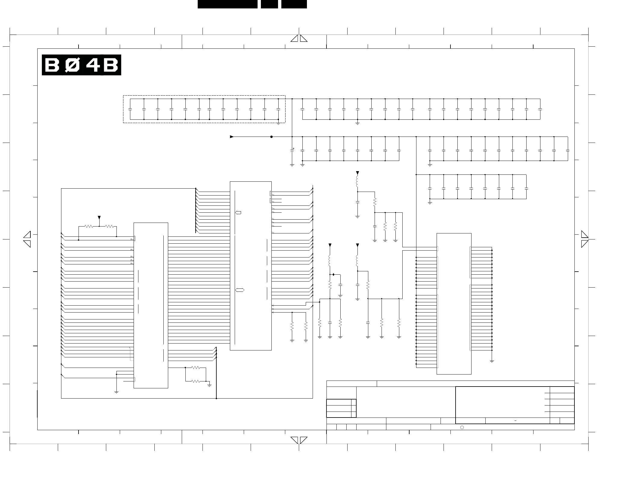
Circuit Diagrams and PWB Layouts EN 69LC9.1A LA 10.
2009-Apr-10
SSB: GDDR3
19
20
21
22
23
24
25
26
27
28
29
30
31
0
1
2
3
ZQ
0
1
2
3
4
CK
4
CKE
CS
RAS
CAS
WE
0
1
2
3
3
2
1
0
0
1
2
5
6
7
8
9
10
11
12
13
14
15
16
17
18
DM
0
1
2
3
WDQS
BA
AP
RDQS
DQ
5
6
7
8
9
10
11
RESET
MF
SEN
RFU
C
VDDQ
VREF
VDD
VSSQ
VSS
15
16
17
18
19
20
21
22
23
24
RA
RDQ
RCLK1
RDQM
RBA
RDQS
WDQS
RCLK0
1
0
2
RCKE
RCS
RRAS
RCAS
RWE
0
1
2
3
0
6
7
8
9
10
11
12
0
1
2
1
2
3
0
1
2
3
RVREF
RRESET
REXTDN
3
4
5
6
7
8
9
10
11
12
13
14
RCS1
RCAS1
25
26
27
28
29
30
31
0
1
2
3
4
5
131254321
JJ
I
H
G
F
E
D
A
17
65432 1312
111098
7
6
2739 C11
2740 B10
1110
2743 E7
2745 F8
98
G
F
E
D
C
B
A
456789
1
D
2712 B6
2713 B7
C
B
D
F
A
B
C
H
7
2737 C11
2738 C11
B
C
2741 C8
2742 D8
F
GI
H
2749 B12
2750 E8
D
C
98
13
G
12123
E
2
3721 F9
3722 F7
3723 G4
3724 D2
10 11
F
23
E
8
7
2710 B9
2711 B10
BD 12NC : 3139_123_64512
RES
2716 B8
2717 B8
2719 B8
2720 B8
2722 B9
2724 B10
2725 B11
2726 B11
2727 B11
2101
E
2776 A5
2777 A5
2778 A5
2779 A6
2780 A6
3710 C8
89101112
A
J
1
D
E
3711 D3
3712 D8
2746 F7
2747 B6
654
NC
2728 B11
2729 B12
2731 C9
2732 C9
2734 C10
2735 C10
2736 C10
3
3717 F6
3718 F4
3719 D8
H
1312
5712 C8
2766 A11
2767 A11
2768 A11
RES
GDDR3
6
2751 A7
6
RES
A
G
2714 B7
2715 B7
MULTI 12NC : 3139_123_64502
H
A
B
C
5
2770 A3
2771 A4
2772 A4
2773 A4
2774 A4
2775 A5
2754 A7
2755 A8
2756 A8
2757 A8
2758 A9
2759 A9
9
34
G
H
I
2760 A9
2761 A9
2 11
2762 A10
2763 A10
54
2764 A10
2765 A11
3713 E7
3714 E8
3715 F8
3716 F7
2769 A3
RES FOR EMC
3720 F7
5713 D7
5714 D8
7701-5 C6
7702-1 C3
7702-2 D10
F710 B6
I714 E7
1110
J
17
F
B
I
2752 A7
2753 A7
"700 - 799"
NC
2734
100n
150R
3717
1%
2767
100n
2713
100n
100n
2763
2762
100n
2740
100n
2742
100n
2710
100n
5714
30R
515
270R 1%
3718
2719
100n
100n
2724
2715
100n
2711
100n
62R
3711
2747
6.3V100u
3722
2K2
1%
2k4
3716
30R
5712
100n
2753
2754
100n
100n
2741
100n
2745
2743
100n
100n
2729
+1V8_SW
100n
2728
3724
62R
3712
2k4 1%
2732
100n
100n
2731
2752
100n
100n
2751
100n
2720
NAME
DATECHECK
3139 123 6451
PCB SB SSB
LC09M
A3
2008-11-21
-- -- --
2009-02-031
03101
3
2
2009-02-03
Hwang Zhen
DC377215
2009-03-05
SVROYAL PHILIPS ELECTRONICS N.V. 2008
2008-11-21
3PC332
SETNAMECHN
CLASS_NO
1
SUPERS.
2
2725
100n
+1V8_SW
F710
2750
100n
100n
2714
+1V8_SW
100n
2712
100n
2722
2717
100n
100n
2716
100n
2739
2755
2756
100n
P2
H9
A4
100n
D10
P10
P3
V9
J2
J3
V4
D2
D11
P11
T2
T3
E2
F3
F2
G3
B11
B10
A9
H3
D3
R11
R10
T11
T10
M2
L3
N2
M3
R2
R3
C3
C10
E11
F10
F11
G10
M11
L10
N11
M10
C2
J11
H4
J10
F9
E3
E10
N10
N3
B2
B3
C11
M4
K9
H11
K10
L9
K11
M9
G4
G9
H10
F4
K4
H2
K2
L4
K3
Φ
MAIN
HYB18H512321BF-14
7702-1
3723
2K2
30R
5713
100n
31736472
1%
1K0
1%
1K0
3714
2766
100n
1%
3710
1K0
100n
2749
D12
G2
T1
T4
T9
B4
T12
B9
B12
D1
D4
D9
L1
L12
V3
B1
G11
L2
L11
P1
P4
P9
P12
E4
E9
H1
H12
A3
V10
A10
G1
G12
J1
J12
A12
R12
V1
V12
C1
C4
C9
C12
E1
A1
E12
J4
J9
N1
N4
N9
N12
R1
R4
R9
V11
A11
F1
F12
K1
K12
M1
M12
V2
7702-2
HYB18H512321BF-14
POWER
Φ
A2
2779
100n
2778
100n
2775
100n
100n
2774
1%
2k4
3715
100n
2771
100n
2770
2727
100n
AC2
G2
J3
AB1
AC3
G1
AG1
N2
N4
V5
U1
J2
AB2
D1
M6
M5
L4
L5
AA1
Y2
K4
AB4
AC5
H1
AE1
AE3
H5
J5
G4
H4
F2
E2
K3
F3
W4
W5
Y4
Y5
AD5
AA6
AE4
AD4
K2
AD1
AE2
N1
M2
M3
AF2
AF3
T5
W2
K1
L1
AA2
Y3
V1
U2
T3
V2
T1
P3
W1
W3
N5
P4
DRAM_IF
MT5391
7701-5
P2
P5
N3
R2
R3
P1
T4
V3
Φ
47K
3720
+1V8_SW
+1V8_SW
100n
2759
2758
100n
100n
2757
100n
2768
2780
100n
100n
2765
2764
100n
2777
100n
2761
2776
100n
100n
2760
100n
100n
2773
100n
2772
100n
2769
100n
2726
I714
2738
100n
100n
2737
2736
100n
100n
2735
47K
3719
3721
47K
RCLK0n
RRESET
D_RVREF0
DQ15
DQ16
DQ17
DQ18
DQ19
DQ20
DQ6
DQ7
DQ8
DQ9
DQ10
DQ11
DQ12
DQ13
DQ14
RDQM0
RBA1
RBA0
RRESET
DQ3
DQ4
DQ5
WDQS3
RDQS1
RDQS2
RDQS3
WDQS2
WDQS1
WDQS0
RDQM2
RDQM1
RA(10)
RA(11)
RBA2
RCAS
RCKE
RCS
RDQM3
RDQS0
RRAS
RWE
RA(2)
RA(3)
RA(4)
RA(5)
RA(6)
RA(7)
RA(8)
RA(9)
DQ30
DQ31
RCLK0n
RDQM1
RDQM2
RDQM3
RBA1
RBA2
RA(3)
RA(4)
RA(5)
RA(6)
RA(7)
RA(8)
RA(9)
RA(10)
RA(11)
RA(12)
RA(0)
RA(1)
DQ21
DQ22
DQ23
DQ24
DQ25
DQ26
DQ27
DQ28
DQ29
DQ0
DQ1
DQ2
RDQM0
RDQS0
RRAS
RWE
WDQS0
RA(12)
D_RVREF2
RDQS1
RDQS2
RDQS3
WDQS1
WDQS2
WDQS3
D_RVREF1
RCLK0p
RA(0)
RA(1)
RA(2)
RBA0
RCAS
RCKE
RCLK0p
RCS
18490_504_090402.eps
090402
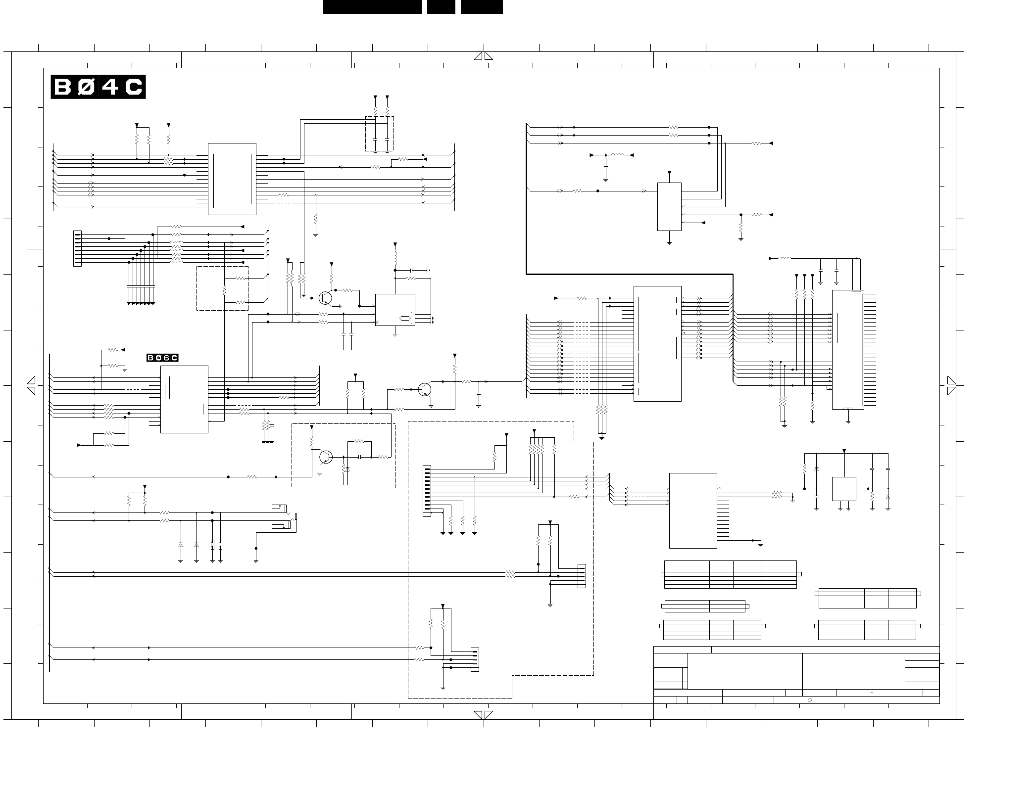
EN 70LC9.1A LA 10.
Circuit Diagrams and PWB Layouts
2009-Apr-10
SSB: Flash & EJTAG
B
R
WP
VCC
VSS
IO
NC
0
1
2
3
4
5
6
7
CLE
ALE
CE
RE
WE
GPIO GPIO
14
15
16
17
18
19
20
21
22
23
24
25
26
13
0
1
2
3
4
5
6
7
8
9
10
11
12
EVSS
JTMS
JTDI
JTDO
JTCK
JTRST
ORESET
TN_0
TP_0
TN_1
TP_1
TN_2
TP_2
TN_HDMI
TP_HDMI
TN_VGA
TP_VGA
TN_PLLG
TP_PLLG
C
D
C
S
W
HOLD
VSS
Q
VCC
SUB
ER
GND
VOUT
VDD
POCE
PDD
PDD
ONDA
ONDD
ONDCE
10
11
12
13
14
15
ONDOE
0
1
0
1
2
3
4
5
6
7
8
9
10
11
12
13
8
9
3
4
5
6
7
0
1
POOE
0
1
POWE
PALE
PCLE
PARB
2
SCL
ADR
0
1
2SDA
WC
1
2
CLK
CMD
0
1
2
3
U0RX
U0TX
U2RX
U2TX
U2CTS
U2RTS
D
SDIO
OPWM
OIRI
OSDA0
OSCL0
OSDA1
OSCL1
OSDA2
OSCL2
0
0
G
H
I
J
K
L
A
B
C
D
E
F
G
H
I
J
K
L
1811 I4
1812 K8
1813 H5
1814 I4
1817 H7
1818 I10
2810 B11
OPCTRL8(0)
0
PDWNC Normal
0
1 2 3 4 5 6 7 8 9 10111213141516
12345678910
XTAL 60MHZ
12
RES
1
14 15 16
A
B
C
1M20 C1
E
2811 D15
OneNAND Boot
0
1
0
PWM DIMMING
RES
1
0
1
0
0
ICE mode
0
1
PALE(0)
0
1
2812 D15
2813 D7
2815 D2
2816 D2
2817 D2
2818 D2
2819 D2
2820 D2
2821 D2
2822 E6
2823 E6
2824 F8
11
2827 H14
13
0
CPU model mode
2834 B7
2835 H15
2836 H16
2837 G5
3810 B2
3811 B2
3812 B3
3813 B7
3814 B3
3816 A12
3818 B7
3820 B12
3821 C10
3822 C13
3823 F2
3824 C3
3825 C3
3826 D6
3827 D3
3828 D3
3829 D6
3830 D5
3831 D5
3832 D5
3833 D5
3834 D14
3835 D3
D
3838 E5
F
TRAP0
0
FLASH & EJTAG
TRAP1
RES
NAND Boot
3840 F8
3841 F8
3842 F7
3845 G7
3846 G4
3847 G5
3848 G5
3850 G7
3851 G9
3852-1 G10
3852-2 G9
3852-3 G9
3852-4 G9
3856 G10
3857 H14
3858 H6
3859 H4
3861 H15
3863 H10
3864 H2
3865 H2
3866 C5
3868 H3
2826 G6
3871 I8
2833 B7
TRAP3
MULTI 12NC : 3139 123 64502
TN0
RES
ONDA[ 2 ]
XTAL 27MHZ
0
SCAN mode
TEST MODE
0
XTAL 48MHZ
3873 I8
3874 C5
3876 H14
3877 H14
3878 F6
3879 F6
3880 D10
3881 G11
3882 G11
3883 G11
3884 G2
3885 G2
3888 J8
3889 J8
3890 K7
3891 K7
3892 B3
3893 G2
3837 E14
3897 C13
3839 E5
RES
RES
RES
TRAP2
OLT TEST MODE
FRONT CONTROL
PCLE(0)
0
"800 - 899"
Normal mode
1
3899 F14
389A G14
389B G14
389C G6
389D I9
389F I10
389G B13
389H A7
389I A7
389J D7
389K E2
389L F2
38A1 G4
38A2 G4
38A3 I9
38A4 J9
38A5 D4
38A6 D4
3869 I3
1
3872 I8
RES
UART (SERVICE)
38A7 E4
38A8 G2
38A9 F5
4102 F2
4800 C5
4802 E10
4803 E10
4804 E10
4805 E10
4806 E10
4807 E10
4808 E10
4809 E10
4810 F10
4811 F10
4812 F10
4813 F10
4814 F10
4815 F10
4816 F10
4817 F10
4818 F10
4819 F10
4820 H11
4822 F4
5810 B11
5811 D14
3894 G2
FT MODE
3898 E14
1
1
OPWM2 (0)
TP0
RES
TRAP4
OPWM1 (0)
NORMAL
Large NAND Boot (1G bit)
ONDA[ 1 ]
BD 12NC : 3139 123 64512
ONDA[ 0 ]
RES
Serial Boot
1
RES
XTAL 54MHZ
5812 D7
5813 D3
5814 D3
5815 D3
6810 H14
6811 H6
6812 I3
6813 I3
6814 H16
7701-1 H12
7701-2 D12
7701-3 F3
OLT Mode
0
PDWNC SCAN
PANEL
1
7701-8 B4
7810 D16
7812 D7
7814 E6
7815 F8
7816 G6
7820 H15
7822 B12
F810 A13
F811 C11
F812 B13
F813 B13
F814 C13
F819 C2
F820 C2
F821 D2
F822 D2
F823 D2
F824 D2
F825 D7
F826 D6
F827 D2
F828 D2
F829 E5
F831 E5
F832 E5
F835 F4
0
0
1
I
RES
SDM
F836 F4
F837 F4
F841 H4
F843 H14
F847 H4
F848 H4
F849 I4
F853 K8
F855 K8
F856 K8
F859 I10
F860 E6
F861 G2
F862 G2
F864 J10
F865 B5
F867 B5
F868 B3
I810 B11
I811 A10
I812 B3
I813 B3
I814 B7
I816 B10
I819 D15
I820 C3
0
1
1
14
0
0
1
FOR DEBUGGING ONLY
RES
RES
I821 D3
I822 D3
I823 D3
I824 D3
I825 E11
I827 E11
I829 E6
I832 F14
I833 F8
I834 F14
I835 F7
I838 G7
I839 G7
I840 G6
I841 G6
I842 H5
I843 H15
I849 K2
I850 K2
I852 I13
I853 J10
I855 F14
0
L
1
19
H
G
F
E
D
C
B
A
K
A
B
C
D
E
F
G
H
I
J
N
O
P
201918
0
16
1
13121110987654321
123456
P
O
N
10 11 12 13 14 15
M
17
J
0281
K
L
M
17
6
15
789 16
15
I843
I825
I827
BAS316
6810
1
3
2
BC847BW
7815
5812
30R
3832 10K
2824 1u0
+3V3_SW
1R0
389C
3825 100R
4814
4K7
3878
3828
F811
100R
I838
3884 100R
+3V3STBY
F862
3885
4K7
3899
38A4 100R
I835
389L
4K7
+5V_SW
4102
1K0
3840
10K3852-2
1R0
3845
4817
F855
F856
BAS316
6814
8
7
12
37
13
36
18
19
3
4
5
6
10
11
14
35
38
39
40
45
46
47
48
24
25
26
27
28
2
33
34
44
1
15
20
21
22
23
9
16
29
30
31
32
41
42
43
7810
NAND512W3A2CN6
Φ
[FLASH]
512Mx8
17
3811
I842
10K
100n
F837
2810
I852
I855
4803
I829
10K
3871
F820
F829
F860
AK26
AG14
+3V3_SW
AF27
K6
AB7
AF9
AJ26
AF14
AE27
L6
AC6
AG9
AF8
B27
C26
A27
C27
D26
AK27
4u7
2835
7701-1
MT5391
MISC_JTAG
Φ
2836
4u7
3814 100R
+3V3_SW
4K7
3888
4K7
389G
F853
D28
E28
H29
AH2
G29
AH1
E29
F29
F30
F28
AJ1
AJ2
G30
H28
A28
AF7
B28
A29
B29
D30
AH5
AG6
G28
D29
E27
AH3
AK2
7701-8
MT5391
GPIO
Φ
10K3852-4
3856 10K
1R0
38A6
+3V3_SW
10K
3818
F849
4819
38A2 1R0
F823
2834 100n
1
130
3881 4K7
2008-11-21
3PC332
SETNAMECHN
CLASS_NO
1
SUPERS.
2
NAME
DATECHECK
3139 123 6451
PCB SB SSB
LC09M
A2
2008-11-21
-- -- --
2009-02-03
3
2
2009-02-03
Hwang Zhen
DC377215
2009-03-05
ROYAL PHILIPS ELECTRONICS N.V. 2008
1R0
38A5
3837 330R
F868
4822
F828
F827
4808
4802
4805
1n02815
2816 1n0
1K0
3851
+3V3_SW
I850
1n02821
I819
2u2
2826
220R
5811
I840
F848
+3V3_SW
+3V3_SW
389D
4K7
F865
1814
1811
I821
4K7
3847
5
7
2
1
84
3
Φ
16M
FLASH
M25P16
7822
6
3831
2
3
4
5
7
8
10K
MSJ-035-10A B AG PPO
1813
1
3827 100R
3889
4K7
3823
+3V3_SW
+3V3_SW
100R
I812
F831
4815
2820 1n0
F825
F826
I849
1K0
3841
1R03820
1R03816
+3V3STBY
I810
+3V3_SW
F867
3822
10K
3883 4K7
I811
I816
F824
F861
F819
680R 1%
3824
I823
5
14
3
2
Φ
7820
BD45292G
100n
2827
10K
3861
5810
7816
BC847BW
30R
100R
3859
38A1 1R0
+3V3_FLASH
+3V3_SW
389J
4K7
4816
I822
BZX384-C6V8
6812
+3V3_SW
100R38A8
F832
10K3813
4K7
3864
5814 30R
5815
+3V3_SW
30R
4809
10K
3842
F810
3879
4K7
3850
4K7
3892
10K
I841
F864
4K7
3882
I813
I814
33R
3863
4818
389K
4K7
F841
+3V3_SW
4813
4812
1K0
3857
F843
B12
E10
B10
B9
E14
+3V3_SW
+3V3_SW
C4
C12
A3
B13
B11
A13
C10
A11
C13
A10
C11
C8
C6
B3
D11
E11
F12
E12
E13
D10
D13
F13
F10
A4
B4
B7
D8
B5
B6
A8
B8
C9
7701-2
MT5391
FLASH_IF
A5
C7
A7
3833
Φ
10K
1
2
3
4
56
I833
B4B-PH-SM4-TBT(LF)
1818
4K73876
F821
+3V3_SW
33R 3868
+3V3STBY
I820
4810
4
5
6
7
8
9
12 13
502382-1170
1817
1
10
11
2
3
4K7
3893
4K7
3877
4K7
389F
4804
4800
33R
3829
4811
30R5813
3874
+3V3_SW
100R
1
2
3
6
5
8
4
7
7812
EEPROM
Φ
(8Kx8)
M24C64-RDW
3872
10K
3852-1 10K
22R38A9
3894
+3V3_FLASH
4K7
2822 10p
100n
2833
F822
386933R
F835
F836
3898 10K
4K7389B
389A 4K7
3897
4K7
3858 1K0
6811
BAS316
680R
3848
2837 47p
+3V3STBY
100n2813
4K7
389H
3830 10K
+3V3_SW
F813
1n02817
2818 1n0
I824
100R3812
7
8
1735446-8
1
2
3
4
5
6
1M20
4K7
3846
10K
I832
3826
+3V3_FLASH
I834
+3V3_SW
I839
F812
100R3835
2
3
4
56
1812
B4B-PH-SM4-TBT(LF)
1
4K7
389I
3891
1R0
4K7
3880
BC847BW
7814
4807
4806
1R0
22R
3821
+3V3_SW
3838
+3V3_SW
+3V3STBY
4K7
3866
4820
+3V3_SW
38A7
1R0
22R3839
10p
2823
4K7
F814
3865
3834
4K7
1n0
2819 10K
3810
D6
E7
AJ13
AK13
H27
G27
H26
G26
J29
K29
AK10
J30
K30
AJ10
F8
D7
F7
E9
AK11
AJ11
K27
C5
Φ
SPIO_UART_IIC
MT5391
7701-3
38A3 100R
100n
2811
100n
2812
3873
10K
3852-3 10K
F847
6813
BZX384-C6V8
+3V3_SW
F859
3890
I853
SERIAL_POOE
NAND_PDD(0)
1R0
DDC-SCL
SERIAL_POCE
SERIAL_PDD1
LVDS_SELECT
SCL
JTDO
JTCK
JTMS
JTDI
JTRST
USB_OC
USB_PWE
UART_TX
UART_RX
BL_ON_OFF
SAW_SW
UART_TX
PBS_SPI_CLK
PBS_SPI_DI
PBS_SPI_DO
DRX-5V
LAN-RST
MII-MDINT
MII-RXD(3)
MII-RXCLK
MII-RX-ER
BOLT_ON_UART_TXD
BOLT_ON_UART_RXD
HDMI_RESET
MII-TXCLK
MII-TXD(0)
MII-TXD(1)
MII-TXD(2)
MII-TXD(3)
MII-RXD(2)
MII-RX-DV
MII-RXD(0)
MII-RXD(1)
MII-TXEN
MII-COL
RC1
RC2
MII-MDC
MII-MDIO
MII-CRS
SDA
DC_PROT
UART_RX
UART_TX
UART_RX
DDC-SDA
HP_DET
ORESET
KEYBOARD
LED2
LIGHT_SENSOR
LED1
BACKLIGHT_CONTROL
PWM_DIMMING
BACKLIGHT_BOOST
AMBI_SDA
AMBI_SCL
SPDIF_IN
PBS_I2C_SCL
BOOST_CONTROL
IR
AOSDATA0
HP_DETECTDDC_RESET
AOMCLK
AOLRCK
AOBCK
SYS_EEPROM_WE
EDID_WC
JTDI
LCD_PWR_ON
SDA
SCL
NAND_PDD(6)
NAND_PDD(7)
SERIAL_POCE
NAND_POOE
NAND_PDD(1)
JTMS
JTCK
JTRST
JTDO
NAND_POOE
NAND_PDD(0)
NAND_PDD(1)
NAND_POWE
NAND_PALE
NAND_PCLE
NAND_PARB
NAND_PDD(2)
NAND_PDD(3)
NAND_PDD(4)
NAND_PDD(5)
NAND_PCLE
NAND_PALE
NAND_POWE
NAND_POCE
NAND_PARB
NAND_PDD(0)
NAND_PDD(1)
NAND_PDD(2)
NAND_PDD(3)
NAND_PDD(4)
NAND_PDD(5)
NAND_PDD(6)
NAND_PDD(7)
NAND_POOE
NAND_POCE
18490_505_090402.eps
090402

Circuit Diagrams and PWB Layouts EN 71LC9.1A LA 10.
2009-Apr-10
SSB: Display interface - LVDS
C
AO BO
AE BE
3N
4P
4N
CKP
CKN
0P
0N
1P
1N
2P
2N
3P
3N
4P
4N
CKP
CKN
0P
0N
1P
1N
2P
2N
3P
4N
CKP
CKN
0P
0N
1P
1N
2P
2N
3P
3N
4P
4N
CKP
CKN
TP_VPLL
TN_VPLL
0P
0N
1P
1N
2P
2N
3P
3N
4P
F923 I10
F924 I10
1930 K8
1931 K8
1932 K8
1933 L8
LVDS
NC
# RESERVED FOR
1G50 B11
F925 I10
F930 J10
LVDS_A_TXe4n_1
LVDS_A_TXe3p_1
LVDS_A_TXe3n_1
LVDS_A_TXeCLKp_1
LVDS_A_TXeCLKn_1
LVDS_A_TXe2p_1
LVDS_A_TXe2n_1
LVDS_A_TXe1p_1
6912 C15
100HZ
1G50
1G51
YES
YESYES
NO
LVDS CONNECTOR
LVDS_A_TXe1n_1
F929 I10
F915 H10
F916 H10
7701-6 A3
12
1922 H8
1923 H8
1924 I8
1925 I8
1926 I8
LVDS_B_TXo1p_1
F917 H10
F918 H10
F919 H10
F920 I10
F921 I10
DISPLAY I2C CONTROL
RES
LVDS#2
F922 I10
ITEM #
1927 J8
2901 G10
LVDS_B_TXo2n_1
LVDS_B_TXo2p_1
LVDS_B_TXo0n_1
LVDS_B_TXe0p_1
LVDS_B_TXo1n_1
LVDS_B_TXo1p_1
2916 C13
2904 K11
F926 I10
LVDS_A_TXo0n_1
LVDS_A_TXe4p_1
F972 B9
F969 B9
F970 B9
F928 I10
F927 I10
7911 C15
7910 C14
LVDS#1
4918 B13
LVDS_A_TXe0p_1
LVDS_A_TXe0n_1
1909 E8
1910 E8
F
G
3456
50HZ
8910
1911 E8
1912 F8
F910 H10
F911 H10
F912 H10
F913 H10
F914 H10
2919 E11
6915 G10
MULTI 12NC : 3139_123_64502
RES
RES
LVDS_A_TXo3n_1
LVDS_A_TXo3p_1
LVDS_B_TXo0p_1
LVDS_B_TXe0n_1
LVDS_B_TXo1n_1
1906 D8
1928 J8
1929 J8
LVDS_B_TXeCLKn_1
LVDS_B_TXeCLKp_1
LVDS_B_TXe3n_1
LVDS_B_TXe3p_1
LVDS_B_TXe4n_1
LVDS_B_TXe4p_1
F980 C9
F979 C9
1G51 F12
F983 C9
F982 C9
F981 C9
LVDS_B_TXo4n_1
LVDS_B_TXo4p_1
LVDS_A_TXoCLKp_1
LVDS_A_TXoCLKn_1
LVDS_A_TXo2p_1
LVDS_A_TXo2n_1
LVDS_A_TXo0p_1
3917 G10
F971 B9
4910 B14
4911 B14
4912 B14
4913 B12
4914 B12
4915 B12
4916 B13
4917 B13
RES
6913 C13
6914 F10
5912 C14
2920 C10
2921 I10
3912 C15
3913 C13
B
C
F987 D9
7
567
11 12 1314
2903 K11
2902 G10
2917 D11
15 16
NC
RES
LVDS_B_TXo3p_1
LVDS_B_TXo3n_1
LVDS_B_TXoCLKp_1
LVDS_A_TXoCLKn_1
F986 C9
1907 D8
LVDS_A_TXo4p_1
LVDS_A_TXo4n_1
17
LVDS_B_TXo2n_1
LVDS_B_TXo2p_1
H
I
J
K
L
F984 C9
1902 B8
1903 C8
1904 C8
F973 B9
F974 B9
F976 C9
F977 C9
F978 C9
F975 B9
3916 G10
D
E
J
K
L
A
B
C
D
E
5910 B14
5911 B14
17
A
12
LVDS_A_TXo1p_1
LVDS_A_TXo1n_1
F989 D9
F990 D9
F988 D9
F992 E12
F993 F10
F994 G10
891011121314
BD 12NC : 3139_123_64512
RES
17
1908 D8
F985 C9
1901 B8
F931 J10
F932 J10
F933 J10
1905 C8
RES
RES
RES
DISPLAY INTERFACE - LVDS
F966 C16
F968 B9
H
I
18
15 16
F991 D9
I910 B14
I911 B13
I912 C14
I913 C13
I914 C13
I915 C15
RES
91011121314 15 16
I
20
F934 J11
3914 C14
3915 C13
34
F
G
K
L
M
N
O
P
2019
J
131211109876432
I
H
G
F
1
123456 1819
E
D
C
B
A
K
owner.
is prohibited without the written consent of the copyright
78
RES
RES
FOR DEV. USE ONLY
D
E
F
G
H
All rights reserved. Reproduction in whole or in parts
A
B
C
17161514
P
O
N
M
L
J
5
F929
2916
1u0
+12VDISP
F918
DLW21S
1932
F921
F988
F914
F973
F972
1911
DLW21SDLW21S
1912
F986
+VDISP
30R5912
F966
F991
1n0
2917
F969
7911
PDTC114ET
F925
30R5911
F989
1K0
F990
3912
F919
1925
DLW21S
F982
42
51
43
44 45
46 47
4849
50
38
39
4
40
41
5
6
7
8
9
28
29
3
30
31
32
33
34
35
36
37
19
2
20
21
22
23
24
25
26
27
1
10
11
12
13
14
15
16
17
18
FX15SC-41S-0.5SH
1G50
F977
F992
I915
F933
F926
10n2920
4918
1933
DLW21S
1930
DLW21S
I910
F934
DLW21S
1910
F971
DLW21S
1904
F923
F987
F979
F978
F994
F983
4911
4910
4914
4915
1922
DLW21S
1926
DLW21S
DLW21S
19011902
DLW21S
F974
F975
F931
1903
DLW21S
5910 30R
2903100u
+VDISP
16V
1929
DLW21S
4913
DLW21S
1931
DLW21S
1928
F928
F970
F993
6915
100n
BZX384-C6V8
2904
2901 10p
F981
F980
+5V_SW
54 55
56 57
5859
60
50
51
6
7
8
9
52
61
53
40
41
42
43
44
45
46
47
48
49
5
31
32
33
34
35
36
37
38
39
4
21
22
23
24
25
26
27
28
29
3
30
11
12
13
14
15
16
17
18
19
2
20
FI-RE51S-HF
1G51
1
10
I913
F984
4912
F932
F930
47K
3914
DLW21S
1905
I911
F917
DLW21S
1927
DLW21S
1924
F910
DLW21S
1923
C22
D24
C24
D25
C25
D23
C23
B20
A20
A25
B26
A26
B24
A24
D20
C20
D21
C21
D22
D19
C19
D17
C17
B21
A21
B22
A22
B23
A23
B25
A19
B17
A17
D14
C14
D15
C15
D16
C16
D18
C18
B14
A14
B15
A15
B16
A16
B18
A18
B19
7701-6
MT5391
LVDS
Φ
F985
6912
SML-310
4917
6913
BZX384-C6V8
47K
3913
100n
2919
2008-11-21 ROYAL PHILIPS ELECTRONICS N.V. 2008
SV
2009-03-05
DC377215
Kyaw Aung Aung
2009-02-03
2
3
22R3916
2009-02-03
-- -- --
2008-11-21
A2
LC09M
PCB SB SSB3139 123 6451
CHECK DATE
NAME
2
SUPERS.
1
CLASS_NO
EMANTESNHC
3PC332
13010
1
6914
BZX384-C6V8
F911
1906
DLW21S
1907
DLW21S
F915
F927
47R
3915
F916
I914
I912
10p
2902
4916
F913
4
1
2
3
SI4835BDY
5
6
7
8
7910
+VDISP
F922
3917 22R
F924
F920
DLW21S
1908
10n2921
F912
DLW21S
1909
F976
F968
715
LVDS_B_TXoCLKp
LVDS_B_TXo3n
LVDS_B_TXo3p
LVDS_B_TXo4n
LVDS_B_TXo4p
LVDS_B_TXo0n
LVDS_B_TXo1p
LVDS_SELECT
LVDS_B_TXo0p
LVDS_B_TXo1n
LVDS_B_TXo2n
LVDS_B_TXo2p
LVDS_B_TXoCLKn
LVDS_A_TXo0p
LVDS_A_TXo0n
LVDS_A_TXe0p
LVDS_A_TXe0n
LVDS_A_TXe1p
LVDS_A_TXe1n
LVDS_A_TXe2p
LVDS_A_TXe2n
LVDS_A_TXeCLKp
LVDS_A_TXeCLKn
LVDS_A_TXo3p
LVDS_A_TXo3n
LVDS_A_TXo4n
LVDS_A_TXe3p
LVDS_A_TXe4p
LVDS_A_TXo1p
LVDS_A_TXo1n
LVDS_A_TXo2p
LVDS_A_TXoCLKn
LVDS_A_TXo2n
LVDS_A_TXoCLKp
LVDS_A_TXe4n
LVDS_A_TXe3n
LVDS_A_TXo4p
LVDS_A_TXe3p
LVDS_A_TXe2n
LVDS_A_TXe2p
LVDS_A_TXe1n
LVDS_A_TXe1p
LVDS_A_TXe0n
LVDS_A_TXeCLKn
LVDS_A_TXeCLKp
LVDS_A_TXe4n
LVDS_A_TXe4p
LVDS_A_TXe3n
LVDS_B_TXe0p
LVDS_B_TXe1n
LVDS_B_TXe1p
LVDS_B_TXe2n
LVDS_B_TXe2p
LVDS_B_TXe0n
LVDS_B_TXe4n
LVDS_B_TXe4p
LVDS_B_TXeCLKp
LVDS_B_TXe3n
LVDS_B_TXe3p
SCL
SDA LVSD3_SDA_DISP
LVDS3_SCL_DISP
LVDS_SELECT
LVDS_B_TXeCLKn
LVDS_A_TXo3p
LVDS_A_TXo2p
LVDS_A_TXo1n
LVDS_A_TXo1p
LVDS_A_TXo0n
LVDS_A_TXo0p
LVDS_A_TXo2n
LVDS_A_TXe0p
LVDS_A_TXoCLKn
LVDS_A_TXoCLKp
LVDS_A_TXo4n
LVDS_A_TXo4p
LVDS_A_TXo3n
LVDS_B_TXe4p
LVDS_B_TXe3n
LVDS_B_TXe3p
LVDS_B_TXe2n
LVDS_B_TXe2p
LVDS_B_TXe1n
LVDS_B_TXe1p
LVDS_B_TXe0n
LVDS_B_TXo1p
LVDS_B_TXo0n
LVDS_B_TXo0p
LVDS_B_TXeCLKn
LVDS_B_TXeCLKp
LVDS_B_TXe4n
LVDS_B_TXoCLKn
LVDS_B_TXoCLKp
LVDS_B_TXo4n
LVDS_B_TXo4p
LVDS_B_TXo3n
LVDS_B_TXo3p
LVDS_B_TXo2p
LVDS_B_TXo1n
LVDS_B_TXo2n
LVDS_B_TXe0p
LCD_PWR_ON
18490_506_090403.eps
090403
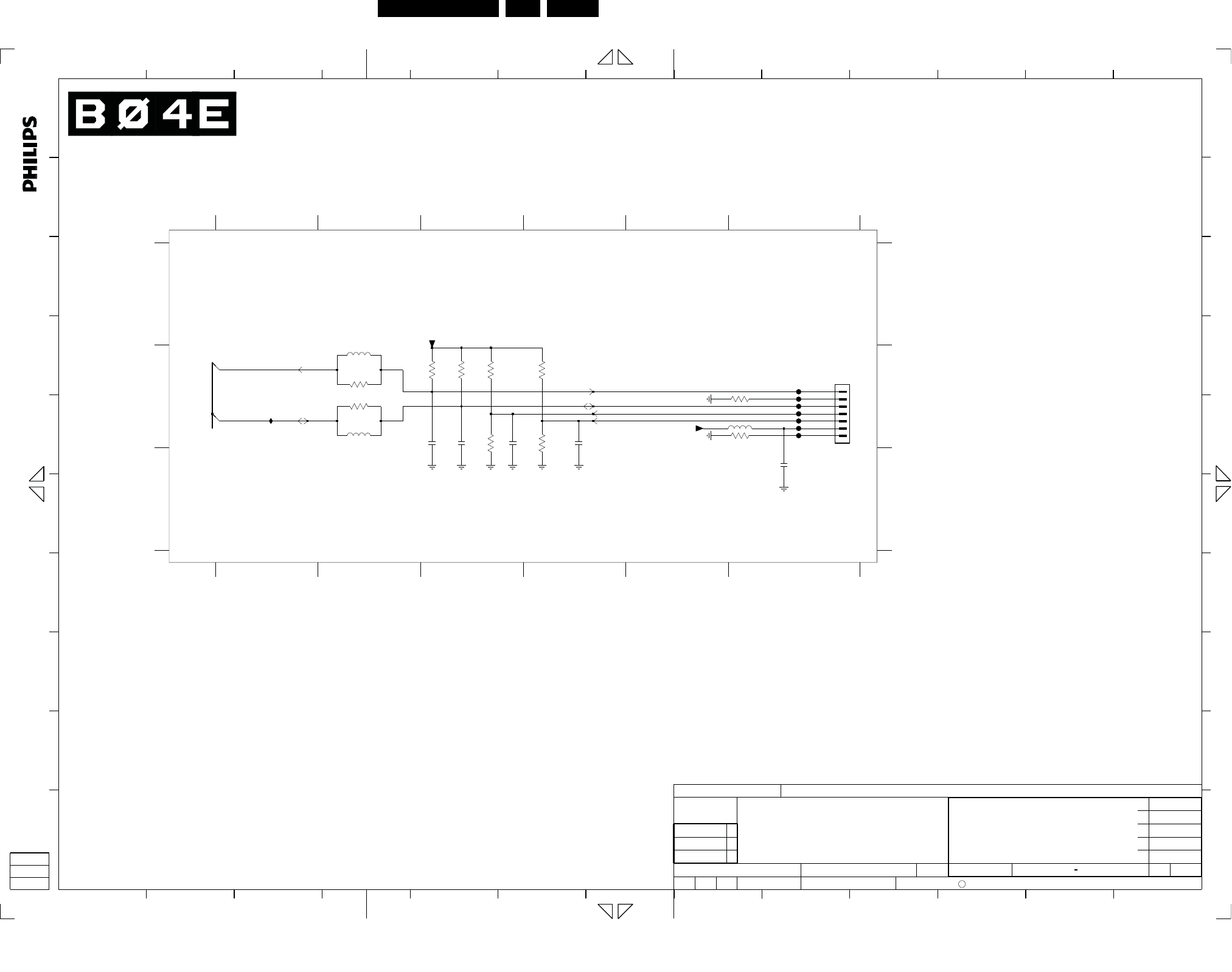
EN 72LC9.1A LA 10.
Circuit Diagrams and PWB Layouts
2009-Apr-10
SSB: Ambilight
C
3A12 B3
3A13 B4
3A14 B2
RES
C
2A12 B3
2A11 B3
2A13 B4
2A14 C6
62 345
FA15 B6
642
FA20 B1
3A19 B4
5A10 B5
5A14 B2
5A16 B2
FA13 B6
FA14 B6
3A15 B5
3A16 B2
654321
J
I
H
FA16 B6
FA17 B6
RES
B
A
"A00 - A99"
TO DRIVE AMBILIGHT DRIVERS
B
3A10 B3
1M59 B6
3A11 B3
AMBILIGHT
BD 12NC : 3139_123_64512
FA18 B6
FA19 B6
3A17 B5
3A18 B3
MULTI 12NC : 3139_123_64502
1
All rights reserved. Reproduction in whole or in parts
I
H
G
F
E
D
C
B
531
RES
5432 1312111098
1312
G
F
E
D
C
B
A
11
C
10
2A10 B3
98
7
J
A
RES
A
owner.
is prohibited without the written consent of the copyright
17
6
33p
2A13
2A12
33p
3A14
100R
33p
2A10
4K7
3A10
100R
3A16
FA16
1R0
3A19
3A11
4K7
2A14
1n0
3A13
1R0
FA15
FA14
FA13
FA19
FA18
5A10
+3V3_SW
4
5
6
7
30R
1735446-7
1M59
1
2
3
3A17 1R0
1R0
3A15
3A18
1R0
+3V3_SW
FA17
1R0
3A12
NAME
2
SUPERS.
1
CLASS_NO
EMANTESNHC
15
3PC332
8
2008-11-21 ROYAL PHILIPS ELECTRONICS N.V. 2008
SV
2009-03-05
DC377215
Fong King Hou
2009-02-03
2
3
13010
1 2009-02-03
-- -- --
2008-11-21
A3
LC09M
PCB SB SSB3139 123 6451
CHECK DATE
120R
5A14
120R
5A16
2A11
33p
15 8
AMBI_SDA_OUT
FA20
AMBI_SDA
AMBI_SCL_OUT
AMBI_SCL
I2S_SEL2
I2S_SEL1
18490_507_090403.eps
090403
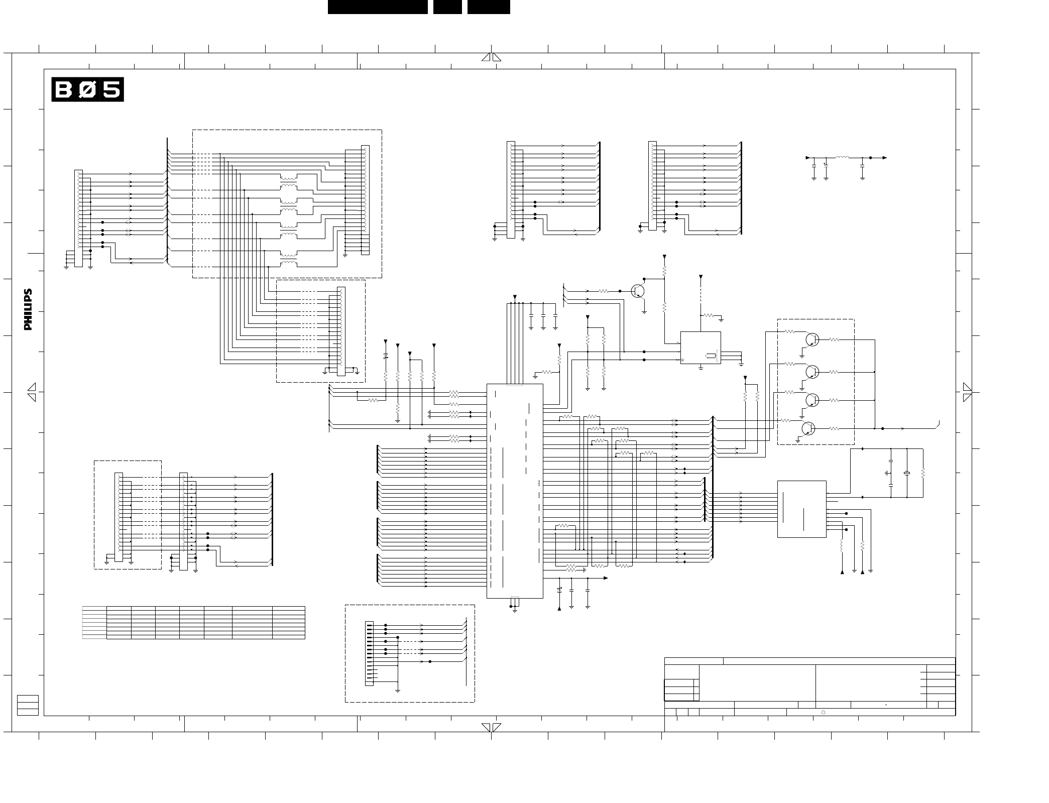
Circuit Diagrams and PWB Layouts EN 73LC9.1A LA 10.
2009-Apr-10
SSB: HDMI & MUX
SCL
ADR
0
1
2SDA
WC
C
RX0
LDO
XTALI
XTALO
VCXO
STB_SCAN
VOUT12_STB
ACT_SCAN
VOUT12_ACT
SCAN_MAIN
VOUT10
C
CB
0
0B
1
1B
2
2B
-
+
OUT_DATA0
-
+
OUT_CLK
DDC_SCL
DDC_SDA
D
DDC_SCL
DDC_SDA
COM
OUT_DATA1
-
+
OUT_DATA2
HPD
A
B
C
D
PSV
AVEE
AVCC
DATA1
ENABLE
AMUXVCC
TX_EN
D
-
+
A
B
C
SCL
SDA
DDC_SCL
DDC_SDA
-
IN
OUT
RESETB
0
1
SCL
SDA
0
1
IN_C
-
+
+
CLK
DATA0
-
+
DATA2
-
+
-
DATA1
IN_D
-
+
+
CLK
DATA0
-
+
DATA2
-
+
EDID
A
DDC_SCL
DDC_SDA
B
DDC_SCL
DDC_SDA
C
CEC
SEL
I2C
I2C_ADDR
IN_A
-
+
+
CLK
DATA0
-
+
DATA2
-
+
-
DATA1
IN_B
-
+
+
CLK
DATA0
-
+
DATA2
-
+
-
DATA1
RES
RES
RES FOR FLECS
P
O
N
M
K
L
M
N
O
P
C
B
A
K
owner.
is prohibited without the written consent of the copyright
All rights reserved. Reproduction in whole or in parts
12111098765
G
H
I
J
RES FOR FLECS
3456789 101112
L
J
I
H
G
F
E
D
A
B
C
D
E
F
Y
A
20191817161514134321
12
FB17 C9
FB23 D2
1314 15 16 17 1819 20
13
N
IB03 H12
HDMI 2
VERTICAL
12
1H03
D
10 111
1613
HORIZONTAL
1234 11
BD 12NC : 3139_123_64512
FB45 I3
N
FB18 C2
FB19 C9
FB24 D2
FB25 C8
FB26 C9
FB21 C9
IB11 G8
N
N
IB16 I12
RES
Y
HDMI CONNECTOR 1
MULTI 12NC : 3139_123_64502
E
C
B
161514
IB01 G15
IB02 H12
4B40 D12
5B01 B15
HDMI PNS 2+1
VERTICAL
3
Y
"B00 - B99"
For DTV only
9
14
N
VERTICAL
HDMI & MUX
12 15
2
HDMI FLECS 2+0 32"_42"
Y
FB10 G15
FB09 F11
FB11 B15
FB06 K7
FB07 D11
FB08 E11
5678910
FB48 K7
FB47 J9
HDMI CONNECTOR 3
Y
FB27 D2
FB28 C12
FB29 C12
FB30 C12
FB31 C12
FB32 C11
FB22 C9
FB20 C2
FB16 C2
N
HDMI-DTV
IB12 G8
IB14 I12
IB10 G8
7B03 E14
7B04 F14
N
N
HORIZONTAL
7B05 F9
4B18 B3
4B28 K7
IB09 G8
IB04 H15
FB54 J7
FB55 J7
FB56 K7
FB57 D11
4B38 I2
4B39 I2
4B02-1 I2
4B02-2 I2
5B07 I15
6B06 F7
6B07 J10
7701-7 H14
HDMI CONNECTOR 2
HDMI CONNECTOR SIDE
56487
FB05 K7
7B09 F14
7B07 D11
Y
N
1H05
HDMI PNS 1+1
N
Y
4B17-3 C3
4B17-2 D3
FB53 J7
1H04
FB49 K7
FB52 I15
FB51 H15
HDMI 1
HORIZONTAL
HDMI FLECS 2+0 22"
1B13 C5
1B14 D5
N
Y
N
3B22 H16
3B24 I15
3B32 E14
FB33 C12
FB37 I4
FB38 I4
FB40 I4
FB42 I4
FB44 I3
7B06 G14
7B02 E12
3B41 F7
3B43 F14
3B44 F15
3B45 F8
3B46 G10
NY
RES
4B29 K7
4B30 K7
4B34 E5
4B35 E5
4B36 E5
4B37 I2
N
4B01-4 H2
K
L
4B02-3 I2
4B02-4 H2
4B03-1 E5
4B03-2 E5
4B03-3 E5
4B03-4 D5
HDMI 3
4B17-1 D3
4B16-3 C3
4B16-4 B3
HDMI 1
1H00
1H02
HDMI SIDE
4B16-1 C3
4B16-2 C3
N
3B20 F13
3B19 F13
3B11 F7
3B10 F10
2B51 J10
N
4B17-4 C3
3B47 G10
3B48 G14
3B49 G15
Y
1B11 B5
1B12 C5
3B76 F9
4B01-1 H2
2B11 B15
2B16 B14
2B17 B14
2B24 E9
2B25 E9
2B26 E10
3B33 E15
3B34 E10
3B35 E10
3B36 F14
3B37 F15
3B38 F7
3B39 F7
3B40 F7
G
H
I
J
K
L
A
B
RES
ITEM NO
RES
NC
1H01
Y
I
J
RES
1B01 B6
1B02 B9
1B03 D6
1B04 B1
HDMI 2
3B50 G10
3B51 G11
4B04-1 E5
4B04-2 E5
4B04-3 E5
4B04-4 E5
4B11-1 B3
4B11-2 B3
4B11-3 B3
4B11-4 B3
3B59 I11
3B60 D12
3B61 E12
3B62 D10
3B63 G8
3B64 G8
3B65 I10
3B66 G8
2B50 J10
2B48 H16
Y
1B07 H3
1B08 J6
1B10 H16
3B73 F10
3B75 E12
3B52 G11
3B53 G11
3B54 G11
3B55 G11
3B56 I10
3B57 I10
3B58 I10
2B29 G16
HDMI FRAME 3+1CONNECTOR
Y
1B06 H2
1B05 B11
Y
F
3B67 G8
3B68 F8
3B69 F8
3B70 F6
3B71 F7
3B72 F10
4B01-2 H2
C
D
E
F
G
H
4B01-3 H2
RES
RES
915
30R
18
5B07
4B02-1
21
22 23
BAT54
6B07
18
19
2
3
4
5
6
7
8
9
20
1
10
11
12
13
14
15
16
17
DC1R019JBAR190
1B03
7
8
9
2021
2223
15
16
17
18
19
2
3
4
5
6
1B06
DC1R019JBAR190
1
10
11
12
13
14
IB11
+3V3_SW
2B26
1n0
IB16
2K2
3B44
1u0
2B11
3K3
3B41
BC847BW
7B09
3B34
3K3
36
18
4B04-3
FB49
4B04-1
4B11-4
FB51
7
8
9
2021
2223
2425
26
16
17
18
19
2
3
4
5
6
1B02
1
10
11
12
13
14
15
DC1R019WBER220
+5V_COMBINED
100R
3B48
3B35
3K3
1B12
DLW21S
1
2
4
3
6
5
8
4
7
(256x8)
Φ
EEPROM
7B02
M24C02-WMN6
1
2
3
27K
3B71
1R0
3B69
FB52
FB06
+3V3STBY
4B30
4B29
3
BAT54
6B06
DLW21S
1B111
2
4
26
6
7
8
9
2021
2223
2425
13
14
15
16
17
18
19
2
3
4
5
DC1R019WBER220
1B04
1
10
11
12
6
7
8
9
2021
2223
14
15
16
17
18
19
2
3
4
5
1
10
11
12
13
DC1R019JBAR190
1B05
+3V3_SW
FB33
4B02-33 6
45
3B57 1K0
+1V2_SW
4B01-4
3B59 1K0
30R
5B01
4B03-1 18
FB32
10n
2B51
2K2
3B49
W30
2K0
3B38
AJ8
AK9
AJ9
AK6
AJ6
AE26
J27
AF15
W27
AF26
W29
HDMI_XTAL_LDO
W26
AG15
AK7
AJ7
AK8
7
7701-7
MT5391
Φ
1
03101
4B02-22
3PC332
SETNAMECHN
CLASS_NO
1
SUPERS.
2
NAME
DATECHECK
3139 123 6451
PCB SB SSB
LC09M
A2
2008-11-21
-- -- --
2009-02-03
IB03
3
2
2009-02-03
Fong King Hou
DC377215
2009-03-05
SVROYAL PHILIPS ELECTRONICS N.V. 2008
2008-11-21
4B16-4
1
2
4
3
DLW21S
1B13
FB24
FB47
4B17-4
4B11-1
4B11-3
7B07
BC847BW
FB26
2K0
3B39
3B76
6K8
4B03-336
IB14
FB11
3B61
33R
3B11
10K
10K
3B60
FB30
36
FB29
4B01-3
45
4B17-3
4B03-4
+5V_COMBINED
FB22 FB31
7B06
BC847BW
FB25
FB20
2B25
10n
47K 3B51
3B19
2K2
FB09
IB01
+5V_COMBINED
1K03B56
47K 3B52
FB17
4B16-1
IB12
BC847BW
7B03
+5V_COMBINED
FB45
3B70 1R0
1R0
3B68
3B65 10K
FB38
7B04
BC847BW
3B5447K
18
FB07
27
4B01-1
36
12
15
24
4B01-2
35
31
32
28
29
25
26
80
79
78
77
59
38
37
42
41
45
44
48
47
34
7
11
10
51
50
54
53
57
56
60
16
20
19
23
22
2
1
5
4
8
6
3
58
55
49
39
27
40
14
13
17
67
69
76
74
72
68
70
63
61
62
43
52
21
30
46
66
65
75
73
71
Φ
7B05
ADV3002BST
64
9
18
33
FB19
FB08
FB37
2K2
3B33
820K
3B22
3B5047K
45 4B04-4
3B10
1K0
4B18
FB40
100R
3B45
FB44
3B62
10K
100R
3B36
3B24
4K7
3B32
100R
4B17-2
3B64 10K
23
24
25
26
2
3
4
5
6
7
8
9
20
21
22
1
10
11
12
13
14
15
16
17
18
19
DC1R019WBER220
1B07
FB05
4B28
FB23
4B34
2K2
3B37
IB02
FB48
VDDO_3V3
27 4B04-2
3B5347K
4B38
4B37
FB18
VDDO_3V3
6K8
3B40
+5V_COMBINED
3
1B14
DLW21S
1
2
4
45
10K3B63
15 16
4B02-4
12
13
14
2
3
4
5
6
7
8
9
501331-1409
1B08
1
10
11
3B4747K
27p
2B48
FB27
2K2
3B20
1u0
2B50
FB56
FB55
FB53
FB54
4B11-2
+5V_COMBINED
3B43
100R
FB42
2B29
27p
47K 3B55
100n
2B24
VDDO_3V3
4B36
4B35
3B46
47K
6K8
3B75
3B73
10K
3B72
10K
26 27
2829
30
+5V_COMBINED
5
6
7
8
9
22
31
23
24 25
14
15
16
17
18
19
2
20
21
3
4
1
10
11
12
13
FI-RE21S-HF-R1500
1B01
4B40
4B17-1
27 4B03-2
FB28
+5V_SW
FB21
IB10
FB57
IB09
3B66 10K
FB10
IB04
10K3B67
1B10
27M0
2B16
470n
+5V_COMBINED
4B16-2
1K03B58
4B16-3
25V220u
2B17
4B39
FB16
RX1+
RX1-
RX2+
RX2-
DDC-SDA
DDC-SCL
EDID_SDA
EDID_SCL
HDMI_CEC
RXC+
RXC-
RX0+
RX0-
BRX-HPD
BRX-5V
BRXC+
BRX0-
BRX0+
BRX1-
BRX1+
BRXC-
BRX2-
BRX2+
CEC
BRX-DDC-CLK
BRX-DDC-DAT
CEC
CRX-DDC-DAT
CRX-DDC-CLK
CEC
BRX2+
BRX2-
BRX1+
BRX1-
BRX0+
BRX0-
BRXC+
BRXC-
CEC
DRX-HPD
DRX-5V
DRX-DDC-DAT
DRX-DDC-CLK
DRX1+
DRX1-
DRX0+
DRX0-
DRXC+
DRXC-
DRX2-
DRX2+
BRX-DDC-CLK
BRX-DDC-DAT
BRX-5V
BRX-HPD
DRXC+
DRXC-
ARX0+
ARX0-
ARX1+
ARX1-
ARX2+
ARX2-
ARXC+
ARXC-
HDMI_RESET
DRX0+
DRX0-
DRX1+
DRX1-
DRX2+
DRX2-
DDC_RESET
EDID_WC
SCL
SDA
ARX-DDC-CLK
BRX-DDC-CLK
CRX-DDC-CLK
DRX-DDC-CLK
ARX-HPD
ARX-DDC-CLK
ARX-DDC-DAT
ARX-5V
BRX-HPD
BRX-DDC-CLK
BRX-DDC-DAT
BRX-5V
CRX-HPD
DRX-HPD
CRX-DDC-CLK
CRX-5V
CRX-DDC-DAT
DRX-DDC-CLK
DRX-5V
DRX-DDC-DAT
DTV_L_IN
DTV_R_IN
SPDIF_IN
DTV_IRQ
CVBS_IN_DTV
BOLT_ON_UART_RXD
BOLT_ON_UART_TXD
DDC-SCL
ARX2+
ARX2-
ARXC-
ARXC+
ARX0-
ARX0+
ARX1-
ARX1+
CEC
ARX-DDC-CLK
ARX-DDC-DAT
ARX-5V
ARX-HPD
CRX-5V
CRX-HPD
DDC-SDA
CRXC+
CRXC-
CRX2+
CRX2-
CRXC-
CRXC+
CRX0-
CRX0+
CRX1-
CRX1+
CEC
RXC-
RXC+
CRX0+
CRX0-
CRX1+
CRX1-
CRX2+
CRX2-
BRX2-
BRXC+
BRXC-
RX0-
RX0+
RX1-
RX1+
RX2-
RX2+
XTALI
XTALO
BRX0+
BRX0-
BRX1+
BRX1-
BRX2+
18490_508_090406.eps
090406
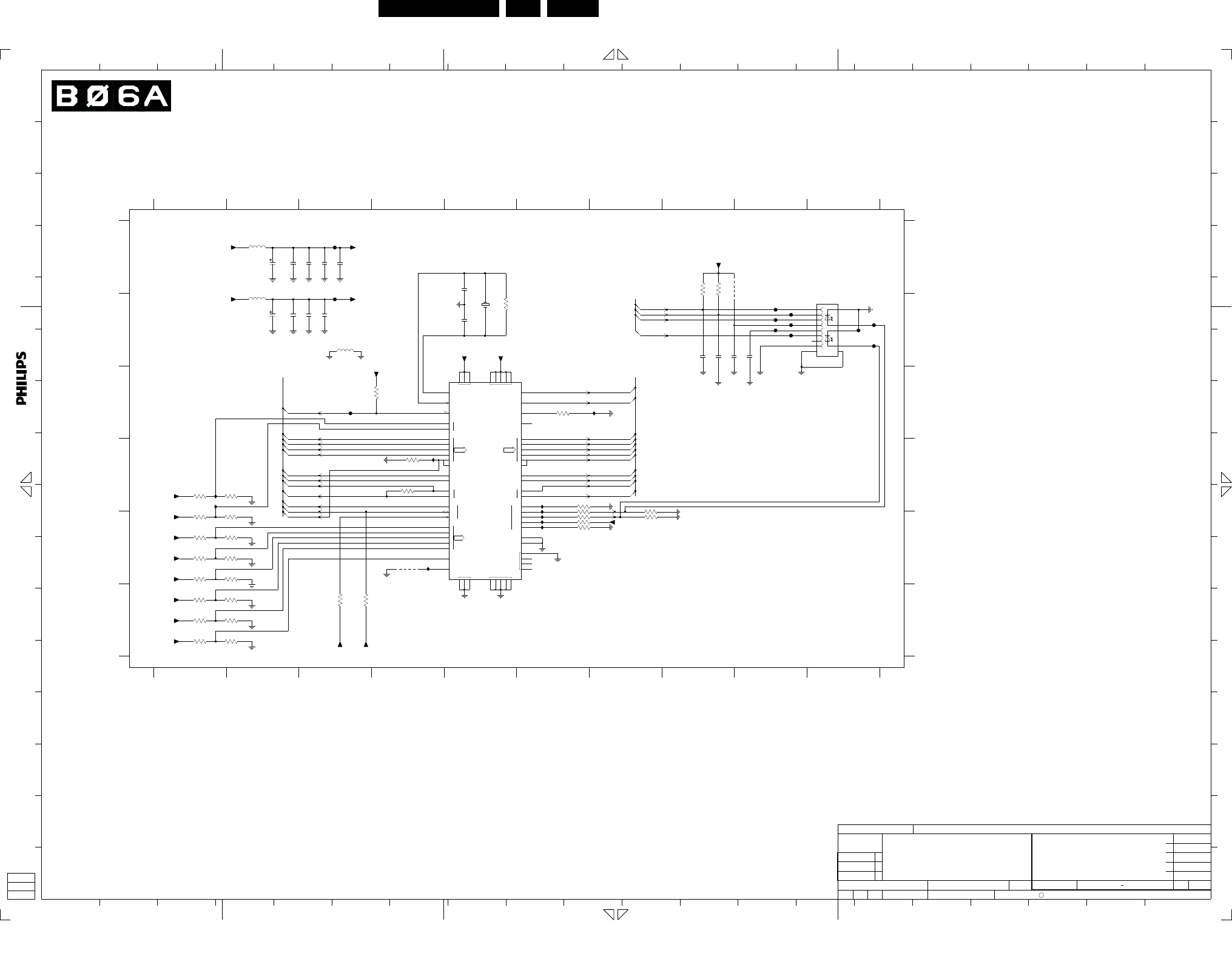
EN 74LC9.1A LA 10.
Circuit Diagrams and PWB Layouts
2009-Apr-10
SSB: Digital I/O - Ethernet (provisional)
C
0
RE_XRRE_XT
CFG
TXD
RX
MD
MF
LED
TX
RXD
VCCE VCCA
GNDA
0
GNDE
N
0
1
2
3
4
RX_CLK
RX_DV
COL
CRS
NC
IREF
TEST_SE
TEST
S
C
L
TR
R10
RIP
P
X1
PWRDWN
FDE
4
3
1
2
X2
RESET
1
0
1
2
3
4
TX_EN
TX_CLK
P
N
C
IO
INT
10 11 12 13
L
J
I
H
G
F
E
D
C
B
A
K
owner.
is prohibited without the written consent of the copyright
All rights reserved. Reproduction in whole or in parts
A
J
K
L
M
19181716151413121110987654
N
O
P
20
P
O
N
M
6789 141516171819 20
B
C
D
E
F
G
H
I
9NA2 A8
9NA3 E4
FNA7 B9
FNA6 B9
321
12345
1234
INAW E6
3NAB E6
3NA9 E6
5NA3 B3
7NA1 C5
RES
C
D
E
FNA5 B9
FNA4 B9
INAU E6
INAT D6
INAS C7
INAR D4
INAQ D1
INAP D1
FNAF C3
INAV E6
3NAK E1
3NAL E2
3NAM E1
3NAN E2
3NAP E1
NC
3NA5 C6
3NA6 D6
910
D
123
56
BD 12NC : 3139_123_64512
MULTI 12NC : 3139_123_64502
RES
RES
RES
NC
RES
3NAV F2
3NAU F1
3NAT E2
3NAR E1
3NB2 F2
3NB1 F1
3NAY F2
INAY D6
INAZ E4
3NAE A8
3NAH D1
3NAJ D2
3NAD A8
3NAC E6
3NAA E7
2NAA B8
2NA9 B3
" XNA0 ~ XNBZ "
RES
910
B
A
F
1NA1 B10
1NA2 B5
2NAB B8
2NAC B8
2NAD B9
2NAE A5
3NA2 C3
2NAF B5
3NA7 D6
3NA8 D7
E
F
A
B
RES
RES
NC
2NA5 A3
2NA6 B2
2NA7 B2
2NA8 B3
3NA3 D4
3NA4 D4
FNAB B10
FNAC B10
DIGITAL I/O - ETHERNET (PROVISIONAL)
C
RJ45
2NA3 A3
2NA4 A3
2NA1 A2
2NA2 A2
FNA8 B9
FNA9 B9
FNAA B10
4567
3NAW F1
FNAD A3
FNAE B3
3NB3 B5
3NB4 F3
3NB5 F3
5NA1 A2
5NA2 B2
8
3NAQ E2
78
INAR
1K53NA8
GNDLAN
27p
2NAF
INAT
+3V3DN INAU
3NAL
1K0
FNA8
FNA7
FNAA
10p
2NAA
100n
2NAC
FNAD
INAS
INAQ
INAP
49R9
3NAE
270R3NA7
INAZ
INAY
FNA5
GNDLAN
+3V3_SW
5NA1
30R
3NA31K0
3NA6 1K5
10K
3NA2
9NA3
1K0
3NAM
1%
+3V3AN+3V3DN
3NA5
4K99
2NAE
27p
+3V3DN
820K
3NB3
3NB2
1K0
SETNAMECHN
CLASS_NO
1
SUPERS.
2
NAME
DATECHECK
3139 123 6451
PCB SB SSB
LC09M
A2
2008-11-21
-- -- --
2009-02-031
03101
+3V3DN
3
2
2009-02-03
Hwang Zhen
DC377215
2009-03-05
SVROYAL PHILIPS ELECTRONICS N.V. 2008
2008-11-21
3PC332
+3V3DN
1K0
+3V3DN
3NAK
3NAJ
1K01K0
3NAH
1u0
5NA3
1K0
3NAU
+3V3DN
+3V3DN
3NB1
1K0
100u16V
FNA6
2NA1
INAV
FNA9
3NAB +3V3DN
3NAC
1K5
+3V3AN
1K5
10n
GNDLAN GNDLAN
2NA9
2NA8
10n
30R
GNDLAN
+3V3_SW
5NA2
1NA2
25M
10n
2NA4
2NA5
1314
10n
3
4
5
6
7
8
9
11
10
12
1840419-1
1NA1
1
2
3NAQ
GREEN
YELLOW
1K0
+3V3DN
3NAP
1K0
3NAN
FNAF
1K0
FNAE
INAW
GNDLAN
2NA7
10n
2NA6
16V100u
+3V3AN
GNDLAN
FNA4
GNDLAN
10n
2NA3
+3V3DN
2NA2
10n
1K0
3NAY
3NAD
49R9
FNAB
FNAC
10p
2NAB
100n
2NAD
GNDLAN
+3V3DN
3NA9 270R
62
12
11
9
13
16
17
22
39
45
56
57
58
52
23
21
53
54
18
19
49
48
26
33
55
3227
28
29
47
46
44
43
51
4
3
2
1
8
30
31
36
38
34
37
42
61
41
5
14
20
24
25
40
50
15
35
64
63
59
60
6
7
10
7NA1
E-STE100P
TRANSCEIVER
ETHERNET
Φ
3NAW
+3V3DN
1K0
1K0
GNDLAN
3NAV
4K7
3NB5
3NB4
4K7
1K0
1015
1K0
3NAT3NAR
+3V3DN
9NA2
3NAA 1K5
3NA4 100R
MII-MDIO
RJLED_G
RJLED_Y
MII-RX-DV
MII-TXD(0)
MII-TXD(1)
MII-TXD(2)
MII-TXD(3)
TPIM
MII-MDC
MII-MDINT
MII-COL
MII-CRS
MII-RXD(0)
MII-RXD(1)
MII-RXD(2)
MII-RXD(3)
MII-RX-ER
MII-RXCLK
TPOP
TPOM
TPOP
TPOM
TPIP
TPIM
LAN-RST
MII-TXEN
MII-TXCLK
TPIP
18490_509_090406.eps
090406

Circuit Diagrams and PWB Layouts EN 75LC9.1A LA 10.
2009-Apr-10
SSB: Analog I/O - YPbPr
C
AIN
PGA
ALI_ADAC
ADAC_VCM
VCMCOUPLE
0OUTR
0OUTL
1OUTR
1OUTL
2OUTR
2OUTL
HPOUTR
HPOUTL
Φ
5_R
5_L
6_R
6_L
VMID_AADC
0_R
0_L
1_R
1_L
2_R
2_L
3_R
3_L
4_R
4_L
2
3
4
N
AF
P
N
D2S
DC_DEMOD
N_DEMOD
RP
RN
SOG
GP
GN
BP
BN
SOY0
Y0P
Y0N
PB0P
PBR0N
PR0P
SOY1
Y1P
Y1N
PB1P
PBR1N
PR1P
P_DEMOD
HSYNC
VSYNC
0
1
0
1
2
0
1
2
0
1
SY
SC
CVBS
MPX0
ADCIN
FB
SYNC
SCT0
SCT1
RES
1D14 B1
1D15 B2
1D17 G1
1D18 C2
1D19 G13
1D20 D2
1D21 D2
12 13
RES
1D13 F1
1
1D25-2 E13
D
E
3D52 B4
2D65 G4
B
C
2D34 F10
3D26 F10
E
F
G
1D01 D13
1D03 F13
1D04 C13
1D08 D12
1D11 F1 3D27 F12
2D38 F2
2D39 G2
2D40 D3
2D41 D3
2D46 G8
2D47 G8
2D48 E9
7D11 E8
3D47 E11
ANALOG I/O - YPbPr
ID12 C13
ID13 C13
ID25 D4
ID26 D4
ID28 D4
2D49 F9
2D50 B3
2D51 C3
2D52 C4
2D53 D4
2D54 F3
RES
BD 12NC : 3139_123_64512
ID38 F10
ID42 G31D23 D2
2D35 F10
2D37 G2
2D63 F71D24 D12
1D25-3 F13
1D22 E12 2D61 E7
2D62 E8
3D51 E9
891011
2D13 C3
2D14 B4
2D15 B6
2D16 B12
2D17 B6
2D18 B12
2D19 B12
2D20 C4
RES
RES
F
G
A
B
C
D
2D29 D4
FD28 E133D48 F11
3D46 G3
FD29 F13
RES
6D13 G1
6D14 C2
1D25-1 E13
MULTI 12NC : 3139_123_64502
34
6D22 E12
7701-11 F6
7D10-1 E12
7D10-2 F12
FD21 C3
FD22 C1
FD23 D12
FD24 E13
FD25 F1
FD26 F12
FD27 G1
2
ID29 D4
ID30 E9
ID31 E10
ID32 F12
ID34 F2
ID35 F3
ID36 F3
ID37 F9
11 12 13
1234
RES
2D64 F8
567
A
2D10 A6 2D67 A11
2D68 F7
3D53 B11
3D28 C12
3D29 B11
3D30 F2
3D32 G2
3D33 D4
3D34 D4
3D35 E4
2D21 C6
2D22 C4
2D25 D4
2D27 D13
2D28 C12
3D23 D11
2D33 F2
3D22 C5
2D59 F11
RU / AP
RES
2D55 G3
2D56 E10
2D57 F11
2D58 F10
SPDIF
6D15 G13
6D16 D2
6D17 D2
6D18 D2
FD17 B1
FD18 B4
FD19 B1
FD20 C1
3D14 B5
3D15 B4
3D16 B5
3D21 C4
3D24 D11
RES
Near IC
RES
2D11 B6
2D12 B11
5678910
5D00 C13
5D01 B2
5D02 B2
5D03 C2
5D05 E11
6D09 D12
6D10 F1
6D11 F13
RES
2D31 B11
2D30 C6
RES
3D18 C4
3D17 C33D25 F12
3D50 D8
3D36 E4
3D41 G8
3D42 G8
3D43 E10
3D44 F10
3D45 F3
3D49 F10
2D60 C11
RES
FD13 B4
FD12 D11
2D66 G4
3D55 E11
3D56 E11
2D69 G7
2D70 D12
RES
ID43 F12FD14 B1
FD15 B1
3D10 A5
3D11 B4
3D12 B5
3D13 B3
3D20 C3
3D54 A11
RES
NC
3D57 B4
3D58 B4
3D59 C4
4D00 D12
6D12 B2
RESERVE FOR FLEX
"D00 - D99"
3D19 C5
16 17 1819 20
RES
ID14 E11
ID22 C4
2D71 D11
2D72 E11
2D73 E11
2D74 E12
17161514131211101
1234 5 6 7 12 1314 15
I
H
G
F
E
D
C
B B
C
D
E
F
G
H
I
P
201918
J
K
L
M
N
O
P
O
98765432
891011
N
M
L
J
A
K
owner.
is prohibited without the written consent of the copyright
All rights reserved. Reproduction in whole or in parts
A
FD23
9
11
12
2
3
4
5
6
7
8
1D14
MSP-636H2-01
1
10
ID12
FD12
ID32
1D01
CON_JACK
MTJ-032-21B-43 NI FE LF
1
2
ID37
1n0
2D57
2D56
1n0
ID42
47n2D12
15p
2D50
15p
2D20
1115
3D25
RES
2D29
1n0
1K0
ID36
10n
2D11
3D44
470R
3D49
47K
2D65
100n
1D15
ID35
3D53100R
2D34
4n7
47K
3D26
1D19
2D1910n
3D12
68R
2D33
1n0
PESD5V0S1BA
6D12
PESD5V0S1BA
6D11
1D21
60R
5D01
ID43
1D13
RES
1n0
2D25
100R
3D14
2D22
15p
180R
3D50
3D52
1R0
PESD5V0S1BA
6D17
ID38
2D62
10u
1K0
3D27
10n
2D30
2D53
10u
3D16
68R
2D63
100n
2D48
10u
YKB21-5157V
1D11
2
1
3
ID31
10u2D68
10K
3D51
10n 2D18
5
6
1D22
1D25-3
RED
MSP-303H-BBB-432-03 NI
1n0
2D39
FD19
3D19
100R
FD17
47p
2D73
30K
3D36
+3V3_SW
3D47
1R0
30K
3D35
FD14
3D54 100R
ID34
6D09
PESD5V0S1BA
2D55
10u
ID28
60R
5D02
100R
3D29
100R3D24
4n7
2D35
GND
IN
VS
1734806-2
1D04
FD13
6
1
2D31 47n
7D10-1
BC847BS
2
10n
2D15
2D69 10u
2D71 33p
1R0
3D59
1R0
3D58
3D57
1R0
2D66
10u
CLASS_NO
EMANTESNHC
3PC332
2008-11-21 ROYAL PHILIPS ELECTRONICS N.V. 2008
SV
2009-03-05
DC377215
Kyaw Aung Aung
2009-02-03
2
3
13010
1 2009-02-03
-- -- --
2008-11-21
A2
LC09M
PCB SB SSB3139 123 6451
CHECK DATE
NAME
2
SUPERS.
1
1R0
3D30
1u02D16
ID26
ID29
30K
3D46
3D45
30K
6.3V220u
2D46
1R0
3D32
FD29
15p
2D74
6D10
PESD5V0S1BA
75R
3D13
75R
3D56
47p
2D72
3
4
2D40
1n0
1D25-2
WHITE
MSP-303H-BBB-432-03 NI
2D70
100p
ID13
FD28
6.3V
2D47 220u
1R0
3D48
1n0
2D58
1R0
3D55
2D61
100n
6D16
PESD5V0S1BA
33R3D41
ID22
FD26
3D20
75R
2D51
15p
3D23100R
3D34
1R0
3D33
1R0
ID30
2D10
4n7
BC847BW
7D11
1R0
ID25
3D15
3D11
1R0
2D59
1n0
10n
2D21
FD25
5D05
1u8
1n0
2D37
1R0
3D18
60R
5D03
ID14
1D08
1D23
10u
2D64
5
3
4
7D10-2
BC847BS
1D24
1D03
2D14
15p
10u
2D52
3D28
100R
10u
2D49
1n0
2D41
2D38
1n0
FD27
FD15
100n
2D60
4D00
47n2D67
N28
M30
M29
P29
T27
T30
T29
R30
R29
R28
T28
M28
M27
N30
N29
N27
P28
V28
V27
V30
V29
U29
U28
U27
U26
MT5391
7701-11
2D28100n
6D18
FD20
PESD5V0S1BA
3D42 33R
1D18
10n
2D17
3D17
75R
6D15
PESD5V0S1BA
1D17
6D14
PESD5V0S1BA
1
2
3D21
1R0
MSP-303H-BBB-432-03 NI
YELLOW
1D25-1
33p
2D27
10u
2D54
15p
2D13
3D22
68R
PESD5V0S1BA
6D22
FD18
1R0
3D10
470R
3D43
PESD5V0S1BA
6D13
1D20
AJ21
AH18
AJ18
FD21
AH23
AJ20
AH16
AH20
AH17
AF30
AG29
AH30
AJ14
AH21
AJ22
AJ19
AK22
AK19
AH22
AH19
AJ17
AK17
AF29
AG28
AH29
AE30
AF28
AD28
AJ30
AJ23
AK20
AJ16
AK16
AK14
AB26
AB27
AB30
AB29
AA29
AA26
AJ15
AH15
AD29
AE28
AE29
MT5391
Φ
AVI
FD22
FD24
30R
5D00
SC2_CVBS_OUT
DACOUT2
VSYNC
SY1P_1
SPB1P_1
SPR1P_1
ASPDIF_OUT
PR
PB
R_MON_OUT
L_MON_OUT
CVBS_IN_DTV
DTV_L_IN
DTV_R_IN
AUDIO_LS_R
AUDIO_LS_L
RP
RN
GP
GN
BP
BN
CVBS_RF
SY1P
SPB1P
SPR1P
SPBR1N
SY1N
SOY0
SOG
OFF_MUTE
SIF_OUT
SIF_OUT_GND
HP_ROUT
HP_LOUT
AV3_L_IN
AV3_R_IN
DVI_AUL_IN
DVI_AUR_IN
SAV_L_IN
SAV_R_IN
L_MON_OUT
R_MON_OUT
GND_CVBS_RF
SCART_CVBS1
SY0
Y0N
Y0P
AIN0_L
AIN0_R
AIN1_L
AIN1_R
HSYNC
PB0P
PBR0N
PR0P
SC0
SCART_CVBS0
SPBR1N PBR1N
S0Y1
SY1N Y1N
CVBS2
CVBS3
CVBS4
SC1_FB
Y1P
PB1P
PR1P
MUTE_M
MUTE_M
18490_510_090406.eps
090406
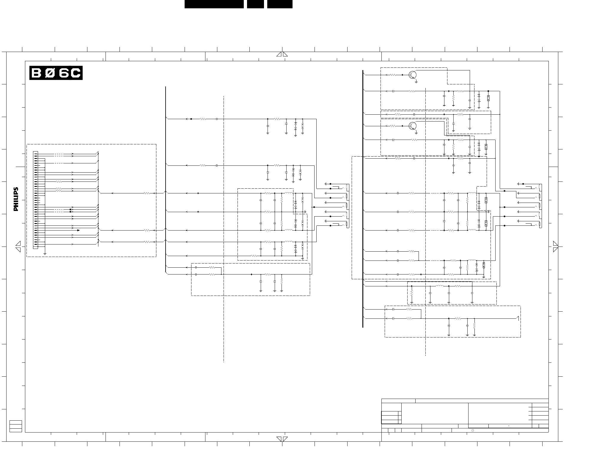
EN 76LC9.1A LA 10.
Circuit Diagrams and PWB Layouts
2009-Apr-10
SSB: Analog I/O - Cinch
C
3E66 B14
3E67 C8
3E68 C14
3E70 D14
3E71 D8
3E73 F14
2E72 I14
Near IC
1E19 D10
1E20 G15
1E24 F15
1E26 E15
3E01 F8
3E02 G8
3E03 G8
3E04 F8
2E63 F13
2E65 E13
2E69 H13
3E10 B12
3E12 E8
3E17 C13
B
7891011121314
3E27 G14
3E35 F12
3E36 F14
3E38 G12
3E42 E12
RES
RES
BD 12NC : 3139_123_64512
78
H
FE49 E9
FE50 E2
FE51 E2
2019
O
2E39 E12
2E40 E14
3E54 H12
3E59 I12
3E60 I14
3E64 B14
RES
LA
G
181716
9
2E43 E12
2E46 G6
3E75 E14
3E78 I14
3E79 G8
3E81 G14
3E90 B14
2E83 B6
19 20
2E57 D14
2E58 D8
2E59 G13
IE18 B8
IE20 H14
IE21 C14
3E06 F8
3E07 E8
3E08 E8
1816
G
3E23 G12
3E24 G14
3E26 G12
IE89 I14
IE95 A12
IE96 C12
IE99 E6
CVI-1
3E99 A12
3EA0 C12
3EA2 G6
3EA3 H12
15 16
123456
FE39 E15
FE47 F10
FE48 F10
10 11 12
2E82 B13
2E80 B12
2E35 G12
LOCATION NEAR 1D14
P
P
3E55 G6
3E56 H14
3E57 H8
F
G
H
I
J
K
1187
2E47 H8
2E48 I12
2E49 I14
2E50 H14
2E51 B14
2E53 C14
2E54 C8
2E55 C14
RES
IE16 B13
IE17 H12
I
J
K
2E70 H14
2E71 H8
17
IE29 D8
IE34 G13
IE42 G13
I
L
A
14
Near IC
RES
RES
RES
15
F
56
FE14 E10
FE15 E10
FE18 E10
FE26 E16
FE32 B15
FE35 E15
FE36 F15
FE38 F15
A
B
C
3E93 C6
3E94 C14
MULTI 12NC : 3139_123_64502
IE01 E6
IE11 B14
IE13 G14
16
A
B
LA
RES
AP
3EA9 F4
4E06 E2
4E07 E2
4E08 D2
4E09 D2
4E10 D2
4E11 E13
4E12 F13
4E13 G13
109
LA
6E32 D9
7E02-1 C13
7E02-2 A13
FE11 C6
RES
F
G
H
AVout
AP
6E14 F15
IE24 G8
IE25 E8
IE26 D14
1E03 E9
1E10 B15
1E13 C9
IE56 F13
IE72 E13
IE78 E13
6E04 E9
2E84 C12
2E86 D12
2E87 D6
2E88 G6
2E89 H12
3E96 D12
21
7
K
E
10
RES
RES
1413
3E97 D6
RES
3E92 B12
11
NC
8
1314 15
3E47 E14
3EA4 D1
3EA5 E1
C
D
E
2E02 G8
2E03 G8
2E04 F8
2E05 F8
2E06 E8
2E07 E8
2E10 B13
2E14 C14
2E16 C9
5E12 G14
5E13 F9
5E14 F9
LA
AP
C
D
E
6E16 E15
RES
6E10 G14
RES
IE14 F14
1
L
1E01 F9
1E02 F9
5E15 F14
5E16 E14
5E17 E9
1E14 C15
1E17 D16
1E18 D9
O
K
2
M
D
B
C
N
J
H
I
J
3
L
N
RES
"E00 - E99"
F
6
4
RES
3E43 E14
3E46 E12
4 125
3EA6 E1
3EA7 E4
3EA8 F4
2E18 C13
2E23 D14
2E24 D9
2E25 G12
2E26 G14
2E28 G12
2E32 F12
2E33 F14
RES
RES
RES
6E30 C9
6E28 B15
6E26 C15
12
ANALOG I/O - CINCH
AVin
5E19 H13
6E02 G9
6E03 F9
L
3
15
13
12
D
E
1
12
9
Near IC
M
56
1E35 D1
12 1314 15 16 17 1819 20
D
E
F
A
34
RES
CVI-2
AP
P
2019181716151413432
H
G
F
678
E
D
C
B
A
K
owner.
is prohibited without the written consent of the copyright
All rights reserved. Reproduction in whole or in parts
A
B
C
G
H
I
J
K
L
M
N
O
RES FOR FLECS
12111098765
P
O
N
M
L
J
I
345 91011
IE89
1n0
2E24
1n0
2E57
60R
5E13
15p
2E33
PESD5V0S1BA
6E02
1R0
3E08
10n
2E39
FE48
3E90
47K
4E13
4E12
4E11
1R0
3E02
3E54
75R
FE36
PESD5V0S1BA
6E26
75R
3E03
IE11
FE47
15p
2E05
2E80
10u
3E07
1R0
10u
2E82
IE13
1E20
15p
2E63
2E26
15p
IE99
3E24
75R
470R
3E10
2E83
10u
75R
3E12
100R
3EA3
FE11
75R
3E57
IE29
60R
5E14
3E96
30K
6E03
PESD5V0S1BA
2E07
15p
FE35
1E26
60R
5E17
IE25
1E24
30K
3E92
2E86
10u
4n7
2E18
47p
2E47
3E78
1R0
6E10
PESD5V0S1BA
PESD5V0S1BA
6E16
3E46
100R
1R0
IE42
3E81
2E59
15p
IE95
60R
5E12
IE34
3E23
68R
1R0
3E64
IE01
10n
2E32
IE16
4
5
6
7
8
9
1E19
1
10
11
12
2
3
MSP-636H1-01
47n
2E88
15p
2E02
1R0
3E66
IE56
3E59
1R0
1R0
10n
2E28
3E75
6E04
PESD5V0S1BA
10u
2E84
2E40
FE51
15p
2E54
1n0
60R
5E15
FE49
1E10
1E13
0001
1R0
3E71
2E49
47p
1K0
3EA0
IE20
15p
2E65
47K
3E94
3E35
68R
2
6
1
BC847BS
7E02-1
2E43
10n
10u
2E87
6E14
PESD5V0S1BA
3E70
1R0
1E03
3E93
30K
PESD5V0S1BA
6E28
FE15
IE21
3E99
1K0
6E32
IE17
IE18
PESD5V0S1BA
2E69
0001
1E18
47p
15p
2E06
1R0
3E68
5
3
4
7E02-2
BC847BS
5E16
60R
IE14
1E01
4E06
1n0
2E16
FE50
FE26
IE24
IE72
3EA2
100R
3E43
75R
2E23
1n0
3E47
4
5
6
7
8
9
1R0
1E17
MSP-636H1-01
1
10
11
12
2
3
FE39
1R0
3E73
1u8
5E19
DATE
NAME
2
SUPERS.
1
CLASS_NO
EMANTESNHC
3PC332
2008-11-21 ROYAL PHILIPS ELECTRONICS N.V. 2008
SV
2009-03-05
DC377215
Kyaw Aung Aung/Roger Poon
2009-02-03
2
3
13010
1 2009-02-03
-- -- --
2008-11-21
A2
LC09M
PCB SB SSB3139 123 6451
CHECK
FE32
1R0
3E04
3E27
1R0
75R
3E36
IE96
3EA7
1R0
30K
3E97
IE26
2E48
4n7
2E71
15p
3E17
470R
2E03
15p
2E14
1n0
1R0
3E67
68R
IE78
3E42
4E07
3EA8
1R0
+3V3_SW
3E79
1R0
40
5
6
7
8
9
41 42
30
31
32
33
34
35
36
37
38
39
4
21
22
23
24
25
26
27
28
29
3
11
12
13
14
15
16
17
18
19
2
20
DF13-40DP-1.25V
1E35
1
10
4E10
4E09
2E55
1n0
3E01
1R0
15p
2E72
2E04
15p
1R03EA4
4E08
3E56
1R0
6E30
PESD5V0S1BA
3E06
75R
1n0
2E58
2E25
10n
FE18
2E89
47n
4n7
2E46 1R0
3E55
1E02
FE14
2E35
4n7 1R0
3E38
1R0
3EA9
100R
3E26
FE38
1R03EA6
3EA5 1R0
1215
15p
2E50
75R
3E60
4n7
2E10
1n0
2E53
2E51
1n0
2E70
47p
1E14
AIN0_R-SC2
AIN0_L-SC2
CVBS_SC2
SPR1P_1
SY1P_1
SPB1P_1
CVBS_SC1
PGA0OUTR-SC1
SPR1P_1
PB0P-SC1
Y0P-SC1
PGA0OUTL-SC1
PR0P-SC1
VSYNC_B
HSYNC_B
VSYNC
HSYNC
SC1_CVBS_OUT
AIN1_R-SC1
AIN1_L-SC1
ASPDIF_OUT
SC2_CVBS_OUT
L_MON_OUT
PB1P_SC2
SY1P_SC2
SC1_B
SC1_G
SPR1P
SPR1P
SPB1P_1 SPB1P
SY1P_1 SY1P
PR1P_SC2
PGA0OUTR-SC1
PGA0OUTL-SC1
SC1_CVBS_OUT
SC1_CVBS_OUT
PR
MUTE_C
MUTE_C
R_MON_OUT
Y0P-SC1
Y0P
PR0P-SC1
PBR0N
PR0P
PBR0N-SC1
CVBS4
CVBS_SC2
SCART_CVBS1
SOY0
Y0N YON-SC1
SPBR1N
SY1P
SY1N
SPB1P
DACOUT1
PB0P-SC1
AIN1_R-SC1
AIN1_L-SC1
AIN0_R-SC2
AIN0_L-SC2
CVBS3
CVBS_SC1
PB0P
AIN1_R
AIN1_L
SCART_CVBS0
AIN0_R
AIN0_L
18490_511_090406.eps
090406
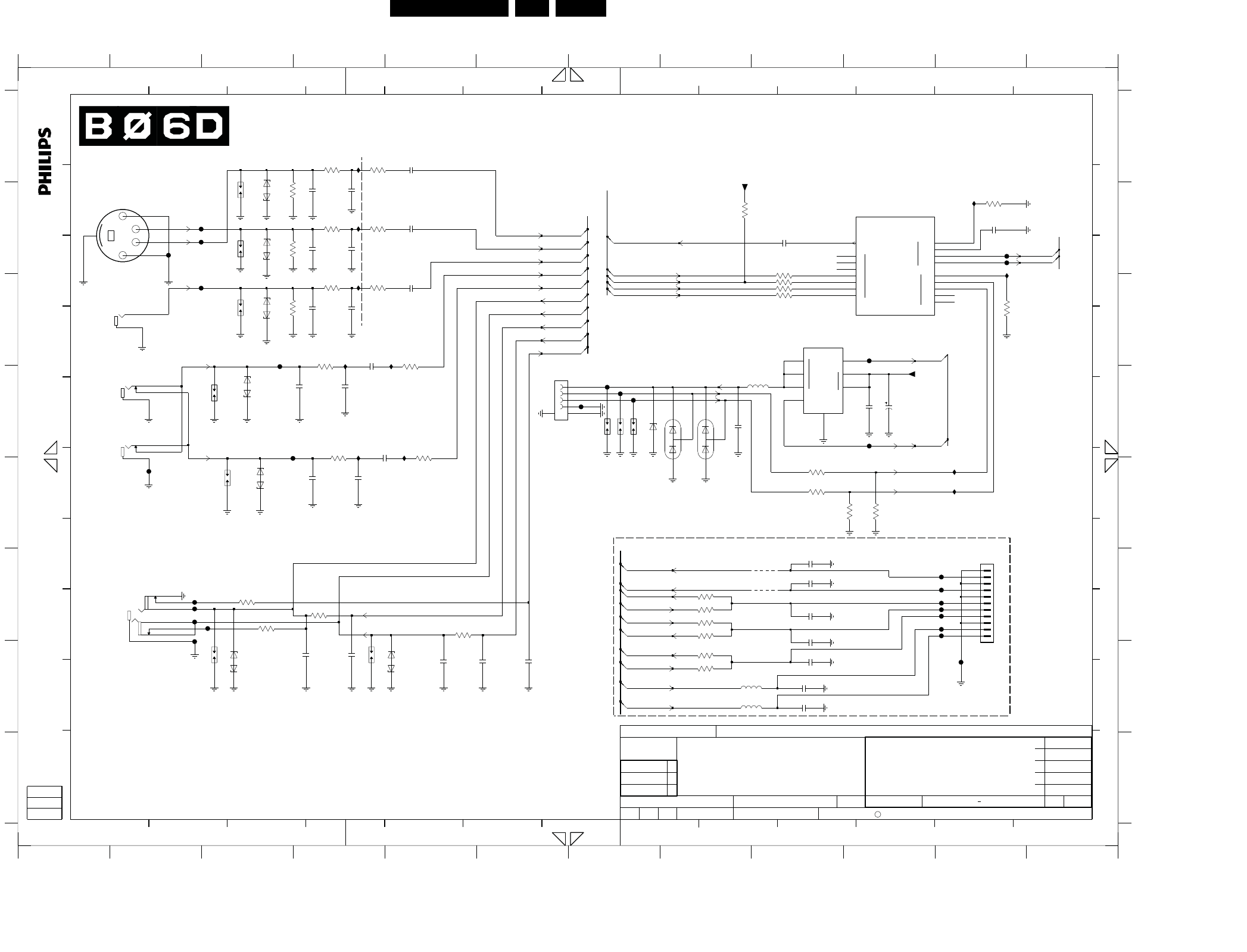
Circuit Diagrams and PWB Layouts EN 77LC9.1A LA 10.
2009-Apr-10
SSB: Side - A/V & USB
1
2
IN
1
2
3
OUT
USB
ADIN
DAC
CVBS_SPDIF_USB
FS
VREF
OUT1
OUT2
VRT
DP0
DM0
DP1
DM1
Φ
ASPDIF_OUT
0
1
2
3
4
5
6
C
IF21 D5
IF22 E11
IF23 E11
IF24 B11
FF13 B3
FF14 C3
FF15 C10
FF16 D7
FF17 D7
FF18 D4
FF19 D7
FF20 D2
98
1312111098
FF34 F11
FF35 F11
FF36 F11
FF37 G11
FF38 F3
IF10 A4
IF12 B4
IF14 B11
FF26 F2
FF27 B3
FF28 B11
FF29 D7
12
1234567
1F02 D7
1F03 D7
1F10 A3
1F11 B3
1F12 B2
1F14 C3
1F16 D3
1F18-1 C2
FF21 D10
FF23 F2
FF24 F2
FF25 F2
13121110
1F22 F2
1F23 F4
1F24 F3
1M36 F11
2F10 A5
2F11 A4
2F12 B5
2F13 B4
7
654
FF30 F11
FF31 F11
FF32 F11
FF33 F11
MULTI 12NC : 3139_123_64502
RES
123456
IF16 B4
IF18 C4
IF19 C5
IF20 D4
RIGHT
0R
RES
11
2F36 F9
2F37 F9
2F38 F9
2F39 G9
2F40 G9
2F41 G9
2F42 G9
891011
C
RES
H
1F01 D7
D
E
F
G
H
A
B
C
1F18-2 D2
1F18-3 D2
1F19 D3
1F21 D6
RES
RES
RES
(WHITE)
SVHS IN
CVBS
LEFT
RES
2F14 B5
2F15 C4
2F16 C4
2F17 D10
RES
LEFT
"F00 - F99"
RES
2F22 B4
2F23 C4
2F24 C4
2F25 D4
2F28 F6
2F29 F4
2F30 F4
2F31 F5
78910
RIGHT
(RED)
RES
SIDE - A/V & USB
HEADPHONE
Near IC
BD 12NC : 3139_123_64512
RES
(YELLOW)
2F43 B9
3F10 A4
3F11 A3
3F13 B4
12
A
B
C
3F22 C9
3F23 C9
3F24 E9
3F25 E9
3F26 F3
3F27 E10
3F28 E10
3F29 A4
D
E
F
G
G
F
E
D
C
B
A
owner.
RES
USB
RES
RES
2F18 D4
2F19 D10
2F20 D8
2F21 A4
3F39 B11
3F40 C11
3F41 F3
3F42 F8
3F43 F8
3F44 F8
3F45 F8
3F46 G8
2F32 D5
2F33 C4
2F34 B11
2F35 F6
0R
Y
RES
RES
321
J
I
H
G
F
RES
4F01 F9
5F13 D9
5F14 G9
3F14 B3
3F16 B4
3F19 C9
3F21 C3
6F13 D3
6F15 D7
6F16 D8
6F17 D8
6F18 F5
6F19 F3
6F20 C3
7701-10 B10
3F30 B4
3F31 B4
3F32 C4
3F33 D4
J
All rights reserved. Reproduction in whole or in parts
I
H
7F01 C10
FF10 B3
FF11 B2
FF12 B11
A
is prohibited without the written consent of the copyright
17
6
3F35 F4
3F36 F5
3F37 D5
3F38 C5
3F47 G8
3F48 B8
3F49 C9
4F00 F9
5432
E
D
C
B
5F15 G9
6F10 A3
6F11 B3
6F12 C3
13
1F02
3F10
100R
47n
2F12
2F13
47p
+5V_SW
100p
2F39
47R3F47
FF31
1R0
3F36
FF33
FF26
3F31
3
4
56
1R0
1F21
292303-4
1
2
6F12
PESD5V0S1BA
10u
2F32
FF37
FF36
FF34
FF35
+3V3_SW
15
PESD5V0S1BA
IF16
6F11
PESD5V0S1BA
6F10
FF29
47p
2F15
PESD5V0S1BA
6F20
30K
3F38
1GND
2
3
5OC_
6
7
8
7F01
TPS2041BD
EN_ 4
6F13
PESD5V0S1BA
FF17
2F24
1n0
15K
3F28
1F01
IF20
1n0
2F28
2F16
1n0
FF16
1n0
2F18
1%5K1
3F40
3F39
560R
3
4
5
6
7
8
9
1M36
1-1735446-1
1
10
11
2
PESD5V0S1BA
6F18
FF30
1F22
1
2
3
4
5
7
8
MSJ-035-10A B AG PPO
6F19
PESD5V0S1BA
FF18
2F37 100p
4F01
IF23
3F32
1R0
2F29
1n0
IF14
1R0
3F29
3F14
75R
FF28
47n
2F14
1n0
2F30
IF10
100R
3F46
15K
3F27
FF25
75R
3F21
3F13
100R
5F14
30R
BZX384-C6V8
6F15
7
8
2F19
100n
1F18-3
RED
MTJ-032-37BAA-432 NI
9
6F16
NUP1301ML3
100p2F36
IF19
NUP1301ML3
6F17
IF21
FF23
3F16
100R
100p
2F38
47n
2F10
IF18
10K
3F48
FF27
1R03F26
100p
2F42
30R
5F15
100p2F41
10u
2F20
100n
3F19
2F43
100R
FF32
1F19
FF11
1F03
AJ4
AK5
AK4
AK3
1R0
3F41
AJ29
AK29
AJ28
AK28
J28AF22
AJ24
AK24
AF21
AJ5
7701-10
MT5391
AH28
AH27
AK30
1F11
3F11
75R
FF21
FF13
2F40
100p
FF19
FF38
100R3F49
100R
3F42
IF24
30K
5F13
30R
3F37
3F35 1R0
FF12
1F16
3F25
1n0
2F25
2F35
1n0
1
CLASS_NO
EMANTESNHC
3PC332
2008-11-21 ROYAL PHILIPS ELECTRONICS N.V. 2008
SV
2009-03-05
DC377215
Kyam Aung Aung/Roger Poon
2009-02-03
2
3
13010
1 2009-02-03
-- -- --
2008-11-21
A3
LC09M
PCB SB SSB3139 123 6451
CHECK DATE
NAME
2
SUPERS.
3F30
1R0
2F21
15p
10u
2F33
6
4
5
1
2
1F18-2
WHITE
MTJ-032-37BAA-432 NI
1F18-1
YELLOW
MTJ-032-37BAA-432 NI
100n
2F34
1F24
5
1
3
4
2
1F12
MDC-013V1-B
2F23
15p
3F24
FF24
15p
2F22
2F17
16V100u
3F22 100R
1F23
47p
2F11
FF15
IF22
IF12
4F00
1F10
3F45 47R
3F44 100R
FF20
FF10
47R
3F43
2F31
1n0
FF14
1F14
1R03F23
1R0
3F33
RC1
RC2
CVBS2
CVBS2
SAV_R_IN
POWER-OK
HP_LOUT
SC2_CVBS_OUT
MUTE
L_MON_OUT
SAV_L_IN
SC0
HP_LOUT
HP_ROUT
R_MON_OUT
HP_DET
DM
DP
DACOUT1
DACOUT2
LIGHT_SENSOR
KEYBOARD
RF_AGC_MON
ASPDIF_OUT
USB_OC
5V
USB_DM0
USB_DP0
USB_PWE
SY0
SAV_L_IN
SAV_R_IN
HP_ROUT
SC0
18490_512_090406.eps
090406
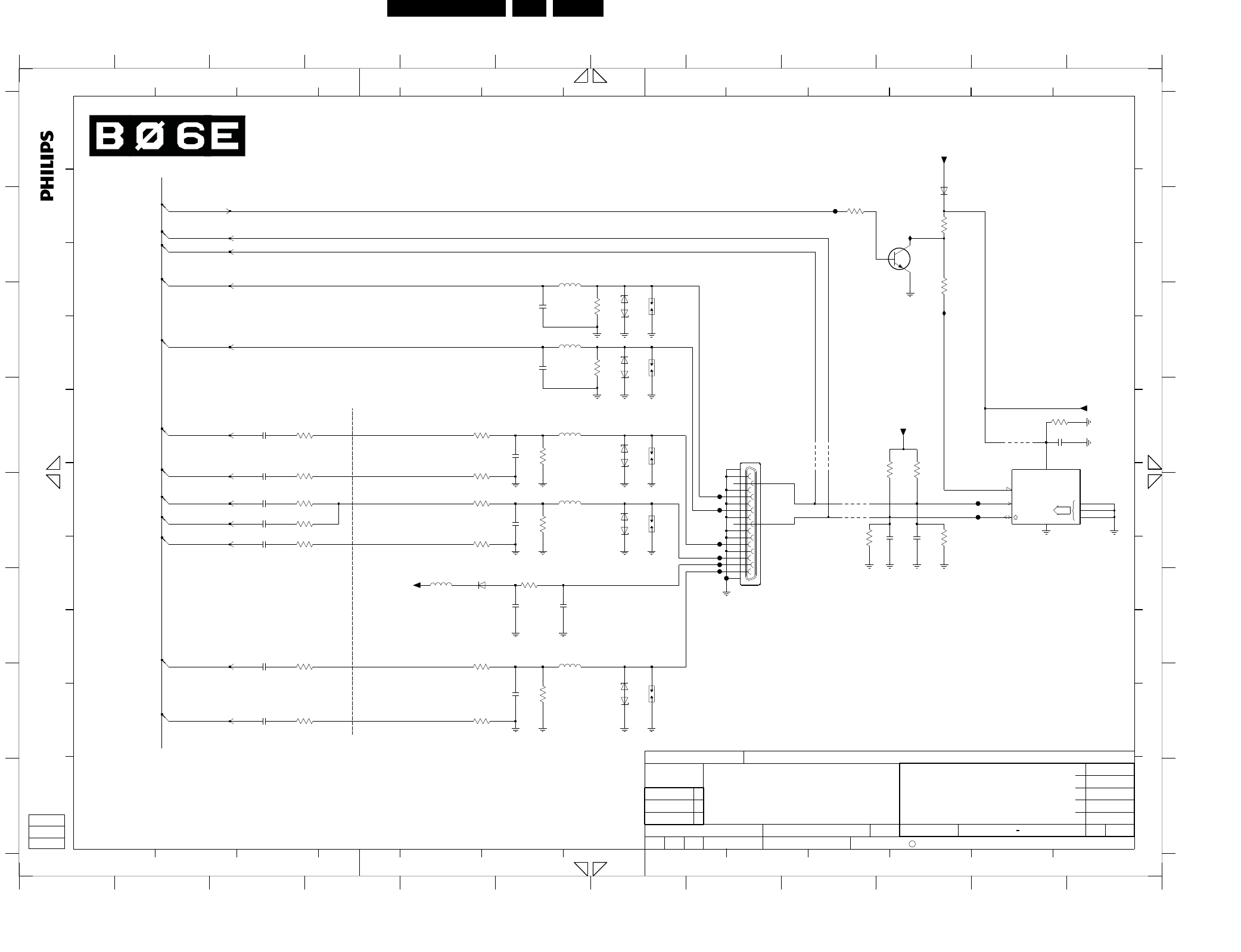
EN 78LC9.1A LA 10.
Circuit Diagrams and PWB Layouts
2009-Apr-10
SSB: VGA
SCL
ADR
0
1
2SDA
WC
C
6G11 C7
3G13 D4
3G14 D6
3G15 D10
121110
34
A
B
C
7G11 D11
D
C
A
G
H
B
E
10
2G25 F6
2G26 F3
FG18 E11
FG19 E8
2G21 E10
2G19 E3
2G29 G3
3G10 D5
3G11 C7
3G12 B7
1G14 E7
VGA
2G11 C6
2G10 D6
2G27 F6
3G30 G4
3G31 G5
3G32 B10
3G33 A9
3G34 B10
6978
21
3G24 E4
3G25 E5
3G27 F4
3G22 E4
3G26 E6
4G15 D11
5G11 C6
5G16 F6
3G16 D10
7G12 B10
FG11 E8
FG12 D8
FG13 E8
FG14 E8
3G18 D4
3G19 D5
D
E
F
G
RES
4
RES
5321
5G12 B6
1G13 D7
FG20 E8
IG01 B10
IG02 B10
RES
FG15 E8
FG16 A9
FG17 D11
H
G
F
E3G35 D11
3G37 E9
3G38 E10
4G11 D9
4G12 E9
4G13 D9
4G14 D9
2G22 E10
"G00" - "G99"
1G11 C7
56789
1G16 E8
1G15 F7
H
3G28 F5
3G29 F6
C
B
A
owner.
3G20 D4
3G21 D5
F
1211
MULTI 12NC : 3139_123_64502
6G12 B7
6G13 A10
6G14 D7
6G15 E7
6G16 E5
6G17 F7
654321
J
I
8
7
J
RES
D
C
B
A
2G23 E3
2G24 F6
2G12 B6
2G13 D3
2G14 D11
2G16 D3
2G17 D3
2G18 E6
5G13 E5
5G14 D6
5G15 D6
3G23 E6
All rights reserved. Reproduction in whole or in parts
I
RES
H
G
F
E
D
is prohibited without the written consent of the copyright
17
65432 131211
1G12 B7
BD 12NC : 3139_123_64512
1098
131211109
1G13
IG02
IG01
4G13
4G14
+5V_SW
150R
3G26
10n
4G15
2G26
1G11
2
3
6
5
84
7
7G11
EEPROM
Φ
(256×8)
1
M24C02-WMN6
5G13
60R
1415
BAS316
6G16
DC_5V
FG12
33R
3G34
BC847BW
7G12
68R
3G13
6G15
PESD5V0S1BA
2G29
10n
2G11
15p
3G24
100R
10n
2G13
1R0
3G19
3G31
1R0
10K
3G33
5p6
2G10
75R
3G29
100R
3G30
30R
5G12
5p6
2G27 2G18
5p6
10K
3G16
1R0
3G21
3G10
1R0
FG17
2G24
1n0
FG19
1G12
100n
2G14
4G12
4G11
2G16
10n
6G13
BAS316
3G32
10K
1R0
3G25
3G12
2K2
6G12
PESD5V0S1BA
68R
3G20
3G28
1R0
3G35
6K2
3G15
10K
60R
5G14
6G17
PESD5V0S1BA
10n
2G23
3G22
1R0
60R
5G16
1G14
3G37
6K2
3G38
6K2
FG14
1G15
2G21
330p
330p
2G22
FG20
FG15
3G18
100R
DC_5V
FG18
3G23
75R
100n
2G25
FG11
FG16
DATE
NAME
2
SUPERS.
1
CLASS_NO
EMANTESNHC
3PC332
2008-11-21 ROYAL PHILIPS ELECTRONICS N.V. 2008
SV
2009-03-05
DC377215
Kyaw Aung Aung/ Roger Poon
2009-02-03
2
3
13010
1 2009-02-03
-- -- --
2008-11-21
A3
LC09M
PCB SB SSB3139 123 6451
CHECK
60R
5G15
DC_5V
6G11
PESD5V0S1BA
3G27
68R
30R
2K2
5G11
3G11
2G17
10n
4n7
2G19
16
17
15
2
3
4
5
6
7
8
9
1
10
11
12
13
14
1G16
1226-00B-15S-FAE-02
75R
3G14
FG13
2G12
15p
6G14
PESD5V0S1BA
SCL_VGA
EDID_SDA
EDID_SCL
EDID_WC
SDA_VGA
H_SYNC
HSYNC
V_SYNC
VSYNC
VGA_G
VGA_B
GN
VGA_Bp
VGA_Gp
VGA_Gn
VGA_Rn
VGA_R
BP
BN VGA_Bn
GP
VGA_Rp
SOG
RP
RN
18490_513_090406.eps
090406
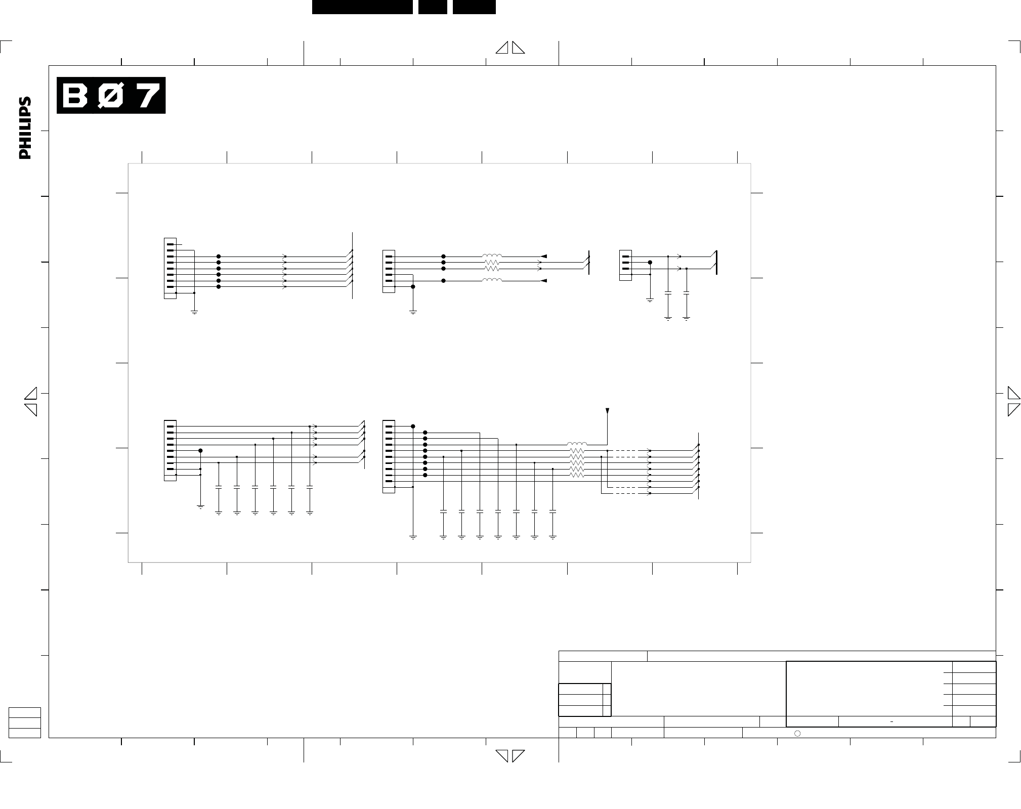
Circuit Diagrams and PWB Layouts EN 79LC9.1A LA 10.
2009-Apr-10
SSB: BDS iTV
C
MULTI 12NC : 3139_123_64502
BD 12NC : 3139_123_64512
RES
BDS iTV
31
7
FH14 A4
FH15 A4
FH16 A4
FH17 B4
FH18 C4
FH19 C4
FH20 C4
B
C
D
1H11 C1
1H12 C3
2H12 D4
FH30 A7
RES
65
FH35 B1
FH34 A1
FH33 A1
FH25 D4
FH26 D4
4321
7
2H13 D5
2H14 D5
2H15 D5
2H19 B7
2H20 B7
2H21 D1
2H22 D2
2H23 D2
2H24 D2
3H17 A4
3H20 D5
3H21 D5
3H22 D5
2H25 D2
4H10 D6
4H11 D6
4H12 D6
2
98
131211
FH21 C4
FH22 D4
FH23 D4
FH24 D4
A
B
C
D
A
RES
1H16 A1
1H14 A6
FH31 A1
RES
FH32 A1
1H13 A3
FH36 B1
C
B
A
FH27 B4
All rights reserved. Reproduction in whole or in parts
I
H
G
F
654
3H23 D5
2H26 D2
2H27 D4
2H28 D4
2H29 D5
3H16 A4
5432
10
13121110
98
7
65
"H00" - "H99"
5H11 B4
5H12 C5
3H24 D5
5H10 A4
4H13 D6
FH11 D1
1
J
I
H
G
F
E
D
432
J
E
D
C
B
A
owner.
is prohibited without the written consent of the copyright
17
6
1515
2H12
100p
1n0
2H22
100R3H17
FH31
2H20
1n0
4H11
3H23100R
FH16
FH15
1H14
BM03B-SRSS-TBT
1
2
3
45
FH32
FH27
FH19
FH20
FH25
3H20 100R
Alexi Jebakumar
2009-02-03
2
3
-- -- --
2008-11-21
A3
LC09M
PCB SB SSB3139 123 6451
CHECK DATE
NAME
2
SUPERS.
1
CLASS_NO
EMANTESNHC
3PC332
2008-11-21 ROYAL PHILIPS ELECTRONICS N.V. 2008
SV
2009-03-05
DC377215
FH34
13010
1 2009-02-03
FH33
FH35
100p
2H13
100p
2H24
1n0
2H19
3H16 100R
FH11
67
BM05B-SRSS-TBT
1H13
1
2
3
4
530R
5H11
FH26
FH23
5H10 30R
2H21
1n0
12
100p
2H26
10
2
3
4
5
6
7
8
9
11
BM10B-SRSS-TBT
1H12
1
910
100R3H24
1
2
3
4
5
6
7
8
1H16
BM08B-SRSS-TBT
FH22 4H10
15p
2H28
30R
5H12
2H25
100p
100R3H22
FH14
FH24
2H29
100p
FH18
FH17
100R3H21
FH36
100p
2H14
4H12
4H13
2H15
100p
2H23
100p
FH21
10
FH30
BM08B-SRSS-TBT
1
2
3
4
5
6
7
8
9
1H11
2H27
15p
PBS_SPI_DO
SCL
SDA
AMBI_SDA
AMBI_SCL
PBS_SPI_DI
PBS_SPI_CLK
PBS_I2C_SCL
RC1
RC2
SC1_FB
SC1_CVBS_OUT
SC1_G
SC1_B
SC1_AOUTL
SC1_AOUTR
AOUTR
AOUTL
SCL_CLOCK
LCD_CLK_SDA
LCD_CLK_SCL
+3V3STBY
+5V_SW
SC1_CVBS_OUT
+3V3STBY
RC1
DDC_RESET
STANDBY
SDA_CLOCK
18490_514_090406.eps
090406

EN 80LC9.1A LA 10.
Circuit Diagrams and PWB Layouts
2009-Apr-10
SSB: SRP List Explanation
1 . 1 . Introduction
Example
SRP (Service Re ference Protocol) is a softw are too l that creates a list w i th all refer e n c es to signal lines. The list contains
references to the signals w i thin all schemat ics of a PWB. It replaces the text refe r ences currentl y p r inted next t o the signal
names in the schematics. These printed refe rences are created man ually an d are t h e r efore n o t guar an teed to be 100 %
correct. In additio n , in the current crowded schema t ics there is often none or ver y little pl ace for these references.
Some of the PW
B schematics w ill use SRP while others w ill sti ll use the manual refe rences. Either there w
ill be an SRP
r e fer ence list for a schematic, or ther e w ill be pr inted r e ferences in the schematic.
1.2. No n - SRP Schematics
There a r e severa l different signals available in a schematic:
1.2.1. Po w e r Supply Lines
All pow er suppl y lines are available in t he suppl y line overview (see chapter 6). I n th e schematics (se e chapter 7) is n o t
indicated w h e r e supplies are coming from or going to.
It is how ever indi cated if a supply is incoming (created elsew h e r e), o r outgoing (cr eat ed or adapt ed in the current sche m atic).
+5 V +5 V
Outgoing Incoming
1.2.2. Normal Signals
For no rmal signals, a schematic r e ference (e. g . B1 4b) is placed next to the signals.
si gnal _nam e
B 14b
1.2.3. Grounds
For no rmal and s pecial grounds (e .g. GN DH OT o r GND3V3 etc.), n o thing is indicate d.
1.3. SRP Schematics
SRP is a tool, w h ich automatically creates a list w i th signal reference s , indicating on which sc hematic t he signals are used.
A reference is cr eated for all signals indicat ed w i th an SRP s y mbol, these s y mbols are:
+5 V +5 V Power suppl y li ne.
na m e na m e Stand alone signal or sw itching li ne (used as less as possible).
na m e na m e
Signal line into a w i re tree.
na m e na m e
Sw itching line into a w i re tre e .
na m e
Bi-directional lin e (e.g. SDA ) into a w i r e tree.
na m e
Signal line into a w i r e tree, its dir e ction depends on t he circuit (e.g. ingoing for PD P, outgoing for L C D sets).
Remarks:
• When there is a black dot on the "signal dire ction arrow" it is an SRP symbol, so there will be a reference to the signal
name in the SRP list.
• All references to normal grounds (Ground symbols without additi onal text) are not listed in the reference list, this to keep
it concise.
• Signals that are not used in multiple schematics, but only onc e or several times in the same schematic, are included
in the SRP reference list, but only with one reference.
Additional Tip:
When using the PDF service manual file, you can very easily search for signal names and follow the signal over all the
schematics. In Adobe PDF reader:
• Select the signal name you want to sear ch for, with the "Select text" tool.
• Copy and paste the signal name in the "Search PDF" tool.
• Search for all occurrences of the signal name.
• Now you can quickly jump between the different occurrences and follow the signal over all schematics. It is advised to
"zoom in" to e.g. 150% to see clearly, which text is select
ed. Then you can zoom out, to get an overview of the complete
schematic.
PS. It is recommended to use at least Adobe PDF (reader) version 6. x, due to better search possibilities in this version.
10000_031_090121.eps
090121
Net Name Diagram
+12-15V AP1 (4x)
+12-15V AP4 (4x)
+12-15V AP5 (12x)
+12-15V AP6 (4x)
+12-15V AP7 (8x)
+12V AP1 (4x)
+12V_NF AP1 (2x)
+12VAL AP1 (2x)
+25VLP AP1 (4x)
+25VLP AP2 (1x)
+3V3-STANDBY AP5 (3x)
+400V-F AP1 (2x)
+400V-F AP2 (2x)
+400V-F AP3 (2x)
+5V2 AP1 (6x)
+5V2 AP2 (1x)
+5V2-NF AP1 (1x)
+5V2-NF AP2 (1x)
+5V-SW AP1 (6x)
+5V-SW AP2 (1x)
+8V6 AP1 (3x)
+AUX AP1 (2x)
+AUX AP2 (1x)
+DC-F AP1 (2x)
+DC-F AP3 (2x)
+SUB-SPEAKER AP5 (1x)
+SUB-SPEAKER AP6 (2x)
-12-15V AP1 (4x)
-12-15V AP4 (6x)
-12-15V AP5 (14x)
-12-15V AP6 (6x)
-12-15V AP7 (8x)
AL-OFF AP1 (2x)
AUDIO-L AP4 (1x)
AUDIO-L AP5 (1x)
AUDIO-PROT AP5 (3x)
AUDIO-R AP4 (1x)
AUDIO-R AP5 (1x)
AUDIO-SW AP5 (1x)
AUDIO-SW AP7 (1x)
BOOST AP1 (2x)
CPROT AP4 (2x)
CPROT AP5 (1x)
CPROT-SW AP5 (1x)
CPROT-SW AP6 (2x)
-DC-F AP1 (2x)
-DC-F AP3 (2x)
DC-PROT AP1 (1x)
DC-PROT AP5 (2x)
DIM-CONTROL AP1 (2x)
FEEDBACK+SW AP6 (2x)
FEEDBACK-L AP4 (2x)
FEEDBACK-R AP4 (2x)
FEEDBACK-SW AP6 (2x)
GND-AL AP1 (2x)
GNDHA AP1 (40x)
GNDHA AP2 (20x)
GNDHA AP3 (2x)
GNDHOT AP3 (2x)
GND-L AP1 (2x)
GND-L AP4 (4x)
GND-L AP5 (34x)
GND-LL AP4 (7x)
GND-LL AP5 (1x)
GND-LR AP4 (7x)
GND-LR AP5 (1x)
GND-LSW AP5 (1x)
GND-LSW AP6 (15x)
GND-S AP1 (11x)
GND-SA AP4 (8x)
GND-SA AP5 (2x)
GND-SA AP6 (8x)
GND-SA AP7 (6x)
GNDscrew AP3 (2x)
GNDscrew AP5 (2x)
GND-SSB AP5 (3x)
GND-SSP AP1 (51x)
GND-SSP AP2 (15x)
IN+SW AP6 (2x)
IN-L AP4 (2x)
IN-R AP4 (2x)
IN-SW AP6 (2x)
INV-MUTE AP4 (1x)
INV-MUTE AP5 (1x)
INV-MUTE AP6 (1x)
LEFT-SPEAKER AP4 (1x)
LEFT-SPEAKER AP5 (1x)
MUTE AP4 (2x)
MUTE AP5 (1x)
MUTE AP6 (2x)
ON-OFF AP1 (3x)
OUT AP6 (1x)
OUT AP7 (2x)
OUTN AP6 (1x)
OUTN AP7 (1x)
POWER-GOOD AP1 (2x)
POWER-OK-PLATFORM AP1 (2x)
RIGHT-SPEAKER AP4 (1x)
RIGHT-SPEAKER AP5 (1x)
SOUND-ENABLE AP5 (3x)
STANDBY AP1 (5x)
STANDBY AP2 (1x)
-SUB-SPEAKER AP5 (1x)
-SUB-SPEAKER AP6 (2x)
V-CLAMP AP1 (1x)
V-CLAMP AP3 (2x)
Personal Notes:
Circuit Diagrams and PWB Layouts EN 81LC9.1A LA 10.
2009-Apr-10
SSB: SRP List
3139 123 6451.1
18490_600_090406.eps
090406
Netname Diagram
+12VDISP B01 (1×)
+12VDISP B04D (1×)
+12VS B01 (5×)
+12VS B02A (1×)
+12VS B03 (2×)
+12VS B04A (1×)
+12VS_1 B01 (2×)
+1V0_SW B01 (1×)
+1V0_SW B04A (1×)
+1V2_SW B01 (1×)
+1V2_SW B05 (1×)
+1V8_SW B01 (1×)
+1V8_SW B04A (1×)
+1V8_SW B04B (5×)
+24VAUDIO B01 (1×)
+24VAUDIO B03 (1×)
+3V3_FLASH B04C (3×)
+3V3_SW B01 (1×)
+3V3_SW B03 (2×)
+3V3_SW B04A (1×)
+3V3_SW B04C (24×)
+3V3_SW B04E (2×)
+3V3_SW B05 (2×)
+3V3_SW B06A (2×)
+3V3_SW B06B (1×)
+3V3_SW B06C (1×)
+3V3_SW B06D (1×)
+3V3AN B06A (3×)
+3V3DN B06A (14×)
+3V3STBY B01 (1×)
+3V3STBY B03 (2×)
+3V3STBY B04A (9×)
+3V3STBY B04C (5×)
+3V3STBY B05 (1×)
+5V_COMBINED B05 (8×)
+5V_IF B02A (5×)
+5V_SW B01 (1×)
+5V_SW B02A (1×)
+5V_SW B03 (1×)
+5V_SW B04C (1×)
+5V_SW B04D (1×)
+5V_SW B05 (1×)
+5V_SW B06D (1×)
+5V_SW B06E (1×)
+5VS B02A (5×)
+5VTUN B02A (2×)
+8V_SW B01 (1×)
+VDISP B04D (3×)
+VTUN B01 (1×)
5V B06D (1×)
AIN0_L B06B (1×)
AIN0_L B06C (1×)
AIN0_L-SC2 B06C (1×)
AIN0_R B06B (1×)
AIN0_R B06C (1×)
AIN0_R-SC2 B06C (1×)
AIN1_L B06B (1×)
AIN1_L B06C (1×)
AIN1_L-SC1 B06C (1×)
AIN1_R B06B (1×)
AIN1_R B06C (1×)
AIN1_R-SC1 B06C (1×)
AMBI_SCL B04C (1×)
AMBI_SCL B04E (1×)
AMBI_SCL B07 (1×)
AMBI_SCL_OUT B04E (1×)
AMBI_SDA B04C (1×)
AMBI_SDA B04E (1×)
AMBI_SDA B07 (1×)
AMBI_SDA_OUT B04E (1×)
AOBCK B03 (1×)
AOBCK B04C (1×)
AOLRCK B03 (1×)
AOLRCK B04C (1×)
AOMCLK B03 (1×)
AOMCLK B04C (1×)
AOSDATA0 B03 (1×)
AOSDATA0 B04C (1×)
AOUTL B03 (3×)
AOUTL B07 (1×)
AOUTR B03 (3×)
AOUTR B07 (1×)
ARX0- B05 (2×)
ARX0+ B05 (2×)
ARX1- B05 (2×)
ARX1+ B05 (2×)
ARX2- B05 (2×)
ARX2+ B05 (2×)
ARX-5V B04A (1×)
ARX-5V B05 (2×)
ARXC- B05 (2×)
ARXC+ B05 (2×)
ARX-DDC-CLK B05 (2×)
ARX-DDC-DAT B05 (2×)
ARX-HPD B05 (2×)
ASPDIF_OUT B06B (1×)
ASPDIF_OUT B06C (1×)
ASPDIF_OUT B06D (1×)
AUDIO_LS_L B03 (1×)
AUDIO_LS_L B06B (1×)
AUDIO_LS_R B03 (1×)
AUDIO_LS_R B06B (1×)
AV3_L_IN B06B (1×)
AV3_R_IN B06B (1×)
BACKLIGHT_BOOST B01 (1×)
BACKLIGHT_BOOST B04C (1×)
BACKLIGHT_CONTROL B04C (1×)
BL_ON_OFF B01 (1×)
BL_ON_OFF B04C (1×)
BN B06B (1×)
BN B06E (1×)
BOLT_ON_UART_RXD B04C (1×)
BOLT_ON_UART_RXD B05 (1×)
BOLT_ON_UART_TXD B04C (1×)
BOLT_ON_UART_TXD B05 (1×)
BOOST_CONTROL B04C (1×)
BP B06B (1×)
BP B06E (1×)
BRX0- B05 (2×)
BRX0+ B05 (2×)
BRX1- B05 (2×)
BRX1+ B05 (2×)
BRX2- B05 (2×)
BRX2+ B05 (2×)
BRX-5V B04A (1×)
BRX-5V B05 (2×)
BRXC- B05 (2×)
BRXC+ B05 (2×)
BRX-DDC-CLK B05 (2×)
BRX-DDC-DAT B05 (2×)
BRX-HPD B05 (2×)
CEC B05 (4×)
CRX0- B05 (2×)
CRX0+ B05 (2×)
CRX1- B05 (2×)
CRX1+ B05 (2×)
CRX2- B05 (2×)
CRX2+ B05 (2×)
CRX-5V B04A (1×)
CRX-5V B05 (2×)
CRXC- B05 (2×)
CRXC+ B05 (2×)
CRX-DDC-CLK B05 (2×)
CRX-DDC-DAT B05 (2×)
CRX-HPD B05 (2×)
CVBS_IN_DTV B05 (1×)
CVBS_IN_DTV B06B (1×)
CVBS_RF B02A (1×)
CVBS_RF B06B (1×)
CVBS_SC1 B06C (1×)
CVBS_SC2 B06C (1×)
CVBS2 B06B (1×)
CVBS2 B06D (2×)
CVBS3 B06B (1×)
CVBS3 B06C (1×)
CVBS4 B06B (1×)
CVBS4 B06C (1×)
DACOUT1 B06C (1×)
DACOUT1 B06D (1×)
DACOUT2 B06B (1×)
DACOUT2 B06D (1×)
DC_5V B06E (3×)
DC_PROT B03 (1×)
DC_PROT B04C (1×)
DDC_RESET B04C (1×)
DDC_RESET B05 (1×)
DDC_RESET B07 (1×)
DDC-SCL B04C (1×)
DDC-SCL B05 (2×)
DDC-SDA B04C (1×)
DDC-SDA B05 (2×)
DM B06D (1×)
DP B06D (1×)
DRX0- B05 (2×)
DRX0+ B05 (2×)
DRX1- B05 (2×)
DRX1+ B05 (2×)
DRX2- B05 (2×)
DRX2+ B05 (2×)
DRX-5V B04C (1×)
DRX-5V B05 (2×)
DRXC- B05 (2×)
DRXC+ B05 (2×)
DRX-DDC-CLK B05 (2×)
DRX-DDC-DAT B05 (1×)
DRX-HPD B05 (2×)
DTV_IRQ B04A (1×)
DTV_IRQ B05 (1×)
DTV_L_IN B05 (1×)
DTV_L_IN B06B (1×)
DTV_R_IN B05 (1×)
DTV_R_IN B06B (1×)
DVI_AUL_IN B06B (1×)
DVI_AUR_IN B06B (1×)
EDID_SCL B05 (1×)
EDID_SCL B06E (1×)
EDID_SDA B05 (1×)
EDID_SDA B06E (1×)
EDID_WC B04C (1×)
EDID_WC B05 (1×)
EDID_WC B06E (1×)
GN B06B (1×)
GN B06E (1×)
GND_CVBS_RF B02A (1×)
GND_CVBS_RF B06B (1×)
GNDLAN B06A (10×)
GNDSND B01 (2×)
GNDSND B03 (26×)
GNDTUN B01 (1×)
GP B06B (1×)
GP B06E (1×)
HDMI_CEC B04A (1×)
HDMI_CEC B05 (1×)
HDMI_RESET B04C (1×)
HDMI_RESET B05 (1×)
HP_DET B04C (1×)
HP_DET B06D (1×)
HP_DETECT B04C (1×)
HP_LOUT B03 (1×)
HP_LOUT B06B (1×)
HP_LOUT B06D (2×)
HP_ROUT B03 (1×)
HP_ROUT B06B (1×)
HP_ROUT B06D (2×)
HSYNC B06B (1×)
HSYNC B06C (1×)
HSYNC B06E (1×)
I2S_SEL1 B04E (1×)
I2S_SEL2 B04E (1×)
IF_ATV B02A (2×)
IR B04C (1×)
JTCK B04C (2×)
JTDI B04C (2×)
JTDO B04C (2×)
JTMS B04C (2×)
JTRST B04C (2×)
KEYBOARD B04C (1×)
KEYBOARD B06D (1×)
L_MON_OUT B06B (2×)
L_MON_OUT B06C (1×)
L_MON_OUT B06D (1×)
LAN-RST B04C (1×)
LAN-RST B06A (1×)
LCD_CLK_SCL B04A (1×)
LCD_CLK_SCL B07 (1×)
LCD_CLK_SDA B04A (1×)
LCD_CLK_SDA B07 (1×)
LCD_PWR_ON B04C (1×)
LCD_PWR_ON B04D (1×)
LED1 B04A (1×)
LED1 B04C (1×)
LED2 B04A (1×)
LED2 B04C (1×)
LIGHT_SENSOR B04C (1×)
LIGHT_SENSOR B06D (1×)
LVDS_A_TXe0n B04D (2×)
LVDS_A_TXe0p B04D (2×)
LVDS_A_TXe1n B04D (2×)
LVDS_A_TXe1p B04D (2×)
LVDS_A_TXe2n B04D (2×)
LVDS_A_TXe2p B04D (2×)
LVDS_A_TXe3n B04D (2×)
LVDS_A_TXe3p B04D (2×)
LVDS_A_TXe4n B04D (2×)
LVDS_A_TXe4p B04D (2×)
LVDS_A_TXeCLKn B04D (2×)
LVDS_A_TXeCLKp B04D (2×)
LVDS_A_TXo0n B04D (2×)
LVDS_A_TXo0p B04D (2×)
LVDS_A_TXo1n B04D (2×)
LVDS_A_TXo1p B04D (2×)
LVDS_A_TXo2n B04D (2×)
LVDS_A_TXo2p B04D (2×)
LVDS_A_TXo3n B04D (2×)
LVDS_A_TXo3p B04D (2×)
LVDS_A_TXo4n B04D (2×)
LVDS_A_TXo4p B04D (2×)
LVDS_A_TXoCLKn B04D (2×)
LVDS_A_TXoCLKp B04D (2×)
LVDS_B_TXe0n B04D (2×)
LVDS_B_TXe0p B04D (2×)
LVDS_B_TXe1n B04D (2×)
LVDS_B_TXe1p B04D (2×)
LVDS_B_TXe2n B04D (2×)
LVDS_B_TXe2p B04D (2×)
LVDS_B_TXe3n B04D (2×)
LVDS_B_TXe3p B04D (2×)
LVDS_B_TXe4n B04D (2×)
LVDS_B_TXe4p B04D (2×)
LVDS_B_TXeCLKn B04D (2×)
LVDS_B_TXeCLKp B04D (2×)
LVDS_B_TXo0n B04D (2×)
LVDS_B_TXo0p B04D (2×)
LVDS_B_TXo1n B04D (2×)
LVDS_B_TXo1p B04D (2×)
LVDS_B_TXo2n B04D (2×)
LVDS_B_TXo2p B04D (2×)
LVDS_B_TXo3n B04D (2×)
LVDS_B_TXo3p B04D (2×)
LVDS_B_TXo4n B04D (2×)
LVDS_B_TXo4p B04D (2×)
LVDS_B_TXoCLKn B04D (2×)
LVDS_B_TXoCLKp B04D (2×)
LVDS_SELECT B04C (1×)
LVDS_SELECT B04D (2×)
MII-COL B04C (1×)
MII-COL B06A (1×)
MII-CRS B04C (1×)
MII-CRS B06A (1×)
MII-MDC B04C (1×)
MII-MDC B06A (1×)
MII-MDINT B04C (1×)
MII-MDINT B06A (1×)
MII-MDIO B04C (1×)
MII-MDIO B06A (1×)
MII-RXCLK B04C (1×)
MII-RXCLK B06A (1×)
MII-RXD(0) B04C (1×)
MII-RXD(0) B06A (1×)
MII-RXD(1) B04C (1×)
MII-RXD(1) B06A (1×)
MII-RXD(2) B04C (1×)
MII-RXD(2) B06A (1×)
MII-RXD(3) B04C (1×)
MII-RXD(3) B06A (1×)
MII-RX-DV B04C (1×)
MII-RX-DV B06A (1×)
MII-RX-ER B04C (1×)
MII-RX-ER B06A (1×)
MII-TXCLK B04C (1×)
MII-TXCLK B06A (1×)
MII-TXD(0) B04C (1×)
MII-TXD(0) B06A (1×)
MII-TXD(1) B04C (1×)
MII-TXD(1) B06A (1×)
MII-TXD(2) B04C (1×)
MII-TXD(2) B06A (1×)
MII-TXD(3) B04C (1×)
MII-TXD(3) B06A (1×)
MII-TXEN B04C (1×)
MII-TXEN B06A (1×)
MUTE B03 (2×)
MUTE B06D (1×)
MUTE_C B03 (1×)
MUTE_C B06C (2×)
MUTE_M B03 (1×)
MUTE_M B06B (2×)
MUTEn B03 (1×)
MUTEn B04A (1×)
NAND_PALE B04C (2×)
NAND_PARB B04C (2×)
NAND_PCLE B04C (2×)
NAND_PDD(0) B04C (3×)
NAND_PDD(1) B04C (3×)
NAND_PDD(2) B04C (2×)
NAND_PDD(3) B04C (2×)
NAND_PDD(4) B04C (2×)
NAND_PDD(5) B04C (2×)
NAND_PDD(6) B04C (2×)
NAND_PDD(7) B04C (2×)
NAND_POCE B04C (2×)
NAND_POOE B04C (3×)
NAND_POWE B04C (2×)
OFF_MUTE B03 (1×)
OFF_MUTE B06B (1×)
PB0P B06B (1×)
PB0P B06C (1×)
PB0P-SC1 B06C (1×)
PB1P B06B (1×)
PBR0N B06B (1×)
PBR0N B06C (1×)
PBR1N B06B (1×)
PBS_I2C_SCL B04C (1×)
PBS_I2C_SCL B07 (1×)
PBS_SPI_CLK B04C (1×)
PBS_SPI_CLK B07 (1×)
PBS_SPI_DI B04C (1×)
PBS_SPI_DI B07 (1×)
PBS_SPI_DO B04C (1×)
PBS_SPI_DO B07 (1×)
PGA0OUTL-SC1 B06C (1×)
PGA0OUTR-SC1 B06C (1×)
POWER_DOWN B03 (1×)
POWER_DOWN B04A (2×)
POWER-OK B01 (1×)
POWER-OK B06D (1×)
PR0P B06B (1×)
PR0P B06C (1×)
PR0P-SC1 B06C (1×)
PR1P B06B (1×)
PWM_DIMMING B01 (1×)
PWM_DIMMING B04C (1×)
R_MON_OUT B06B (2×)
R_MON_OUT B06C (1×)
R_MON_OUT B06D (1×)
RC1 B04C (1×)
RC1 B06D (1×)
RC1 B07 (2×)
RC2 B04C (1×)
RC2 B06D (1×)
RC2 B07 (1×)
RF_AGC B02A (2×)
RF_AGC_MON B02A (1×)
RF_AGC_MON B06D (1×)
RJLED_G B06A (1×)
RJLED_Y B06A (1×)
RN B06B (1×)
RN B06E (1×)
RP B06B (1×)
RP B06E (1×)
RX0- B05 (2×)
RX0+ B05 (2×)
RX1- B05 (2×)
RX1+ B05 (2×)
RX2- B05 (2×)
RX2+ B05 (2×)
RXC- B05 (2×)
RXC+ B05 (2×)
S0Y1 B06B (1×)
SAV_L_IN B06B (1×)
SAV_L_IN B06D (2×)
SAV_R_IN B06B (1×)
SAV_R_IN B06D (2×)
SAW_SW B02A (1×)
SAW_SW B04C (1×)
SC0 B06B (1×)
SC0 B06D (2×)
SC1_AOUTL B07 (1×)
SC1_AOUTR B07 (1×)
SC1_B B06C (1×)
SC1_B B07 (1×)
SC1_CVBS_OUT B06C (2×)
SC1_CVBS_OUT B07 (2×)
SC1_FB B06B (1×)
SC1_FB B07 (1×)
SC1_G B06C (1×)
SC1_G B07 (1×)
SC2_CVBS_OUT B06B (1×)
SC2_CVBS_OUT B06C (1×)
SC2_CVBS_OUT B06D (1×)
SCART_CVBS0 B06B (1×)
SCART_CVBS0 B06C (1×)
SCART_CVBS1 B06B (1×)
SCART_CVBS1 B06C (1×)
SCL B04C (3×)
SCL B04D (1×)
SCL B05 (1×)
SCL B07 (1×)
SDA B04C (3×)
SDA B04D (1×)
SDA B05 (1×)
SDA B07 (1×)
SENSE+1V0_MT5392 B01 (1×)
SERIAL_PDD0 B04C (1×)
SERIAL_POCE B04C (2×)
SIF_OUT B02A (1×)
SIF_OUT B06B (1×)
SIF_OUT_GND B02A (1×)
SIF_OUT_GND B06B (1×)
SIF1 B02A (2×)
SIF2 B02A (2×)
SOG B06B (1×)
SOG B06E (1×)
SOY0 B06B (1×)
SOY0 B06C (1×)
SPB1P B06B (1×)
SPB1P B06C (2×)
SPB1P_1 B06B (1×)
SPB1P_1 B06C (2×)
SPBR1N B06B (1×)
SPBR1N B06C (1×)
SPDIF_IN B04C (1×)
SPDIF_IN B05 (1×)
SPR1P B06B (1×)
SPR1P B06C (2×)
SPR1P_1 B06B (1×)
SPR1P_1 B06C (2×)
STANDBY B01 (1×)
STANDBY B04A (1×)
STANDBY B07 (1×)
STANDBYn B03 (1×)
STANDBYn B04A (1×)
SW_MUTE B03 (1×)
SW_MUTE B04A (1×)
SY0 B06B (1×)
SY0 B06D (1×)
SY1N B06B (1×)
SY1N B06C (1×)
SY1P B06B (1×)
SY1P B06C (2×)
SY1P_1 B06B (1×)
SY1P_1 B06C (2×)
TPIM B06A (2×)
TPIP B06A (2×)
TPOM B06A (2×)
TPOP B06A (2×)
TUNER_SCL B02A (2×)
TUNER_SCL B04A (1×)
TUNER_SDA B02A (2×)
TUNER_SDA B04A (1×)
UART_RX B04C (3×)
UART_TX B04C (3×)
USB_OC B04C (1×)
USB_OC B06D (1×)
USB_PWE B04C (1×)
USB_PWE B06D (1×)
VDD B03 (2×)
VDDA B03 (2×)
VDDO_3V3 B05 (3×)
VIF1 B02A (2×)
VIF2 B02A (2×)
VSYNC B06B (1×)
VSYNC B06C (1×)
VSYNC B06E (1×)
Y0N B06B (1×)
Y0N B06C (1×)
Y0P B06B (1×)
Y0P B06C (1×)
Y0P-SC1 B06C (1×)
Y1N B06B (1×)
Y1P B06B (1×)

EN 82LC9.1A LA 10.
Circuit Diagrams and PWB Layouts
2009-Apr-10
Layout Small Signal Board (Overview top side)
31391236451.2 18490_552_090326.eps
090327
Part 1
18490_552a_090326.eps
Part 2
18490_552b_090326.eps
1201
1204
1211
1212
1502
1735
1736
1812
1813
1817
1818
1901
1902
1903
1904
1905
1906
1907
1908
1909
1910
1911
1912
1922
1923
1924
1925
1926
1927
1928
1929
1930
1931
1932
1933
1B01
1B02
1B03
1B04
1B05
1B06
1B07
1B08
1B10
1D01
1D03
1D04
1D11
1D13
1D14
1D19
1D22
1D24
1D25
1E17 1E19
1E35
1F10
1F11
1F12
1F14
1F18
1F21
1F22
1G16
1G50
1G51
1H11 1H12
1H13
1H14
1H16
1M20
1M36
1M59
1M951M99
1NA1
1X01 1X02
1X05
1X06
1X07
1X12
2103
2106
2107
2129
2131
2136
2140
2150
21582159
2210 2211
2219
2221
2500
2501
2502
2508
2509
2511
2516
2527
2528
2529
2530
2531
2533
2534
2536
2541
2544
2545
2546
2547
2550
2552
2554
2555
2566
2567
2626
26A5
2741
2742
2745
2747
2750
2753
2760 2765 27692770
2771
2772
277327742775
2776
2777
2778
2779
2780
2813
2822
2823
2833
2834
29012902
2903
2904
2916
2919
2A12 2A13
2A14
2B17
2B29 2B48
2D10
2D11
2D12
2D15
2D16
2D17
2D18
2D19
2D21
2D27
2D30
2D31
2D33
2D34
2D35
2D37
2D38
2D39
2D46 2D47
2D48
2D49
2D54
2D55
2D56
2D57
2D58
2D59
2D61 2D62
2D632D64
2D67
2D68
2D69
2D71
2D72
2D73
2D74
2E25
2E28
2E32
2E35
2E39
2E43
2E46
2E48
2E80
2E82
2E83
2E84
2E86
2E87
2E88
2E89
2F10
2F11
2F12
2F13
2F14
2F15
2F17
2F19
2F21
2F22
2F23
2F36
2F37
2F38
2F39
2F402F41
2F42
2F43
2G10 2G13
2G14
2G16
2G17
2G18
2G19
2G21
2G22
2G23
2G24
2G25
2G26
2G27
2G29
2H12
2H13
2H14
2H15
2H19
2H20 2H21 2H22
2H27
2H28
2H29
2NA1
2NA6
2NAA
2NAB
2NAC
2NAD
3211
3212
3219
3221
3222
32233226
3513
3532
3533
35343535
3536
35373538
3542
3558
3600
3601
3602
36063607
3608
3710
3712
3714
3715
3719
3721
38133818
3826
3829
38303831
3832
3833
3838
3839
38933894
389J
38A538A6 38A7
38A8
3912
3913
3914
3915
3916
3917
3A12 3A13
3A183A19
3B19
3B20
3B22
3B46
3B47
3B50
3B51
3B52
3B53
3B54
3B55
3B56
3B57
3B59
3B68
3B69
3B70
3B71
3D10
3D12
3D14
3D16
3D19
3D22
3D23
3D24
3D25
3D26
3D27
3D29
3D30
3D32
3D43
3D44
3D45
3D46
3D47
3D48
3D49
3D50 3D51
3D53
3D54
3D55
3D56
3E10
3E17
3E23
3E26
3E35
3E38
3E42
3E46
3E54
3E55
3E59
3E92
3E93
3E96
3E97
3EA2
3EA3
3F10
3F11
3F13
3F14
3F16
3F19
3F21
3F23
3F29
3F30
3F31
3F44
3F45
3F47
3F48
3F49
3G10 3G13
3G14
3G15
3G16
3G18
3G19
3G20
3G21 3G22
3G23
3G24
3G25
3G26
3G27
3G28
3G29
3G30
3G31
3G32
3G33
3G34
3G35
3G37
3G38
3H16
3H17
3H20
3H21
3H22
3H23
3H24
3NAD
3NAE
4204 4205
42064211
4B01 4B02
4B03
4B04
4B114B164B17
4F00
4F01
4G15
4H10
4H11
4H12
4H13
5100
5101
5103
5104
5107
5108
5115
5116
5117
5210 5211
5212
5213
5216
5503
5505
5712
5714
5812
5910
5911
5912
5A10
5D05
5F14
5F15
5G13
5G14
5G15
5G16
5NA1
5NA2
5NA3
61036122
61236124
6211
6912
6913
6914
6915
6B06
6D10
6D11
6D13
6D15 6D22
6F10
6F11
6F12
6G13
6G16
7100
7103
7116
7117
7210
7211
7510
7602
7701
7702
7812
7814
7910
7911
7B05
7D10
7D11
7G11
7G12
9NA2
1X03
1X08
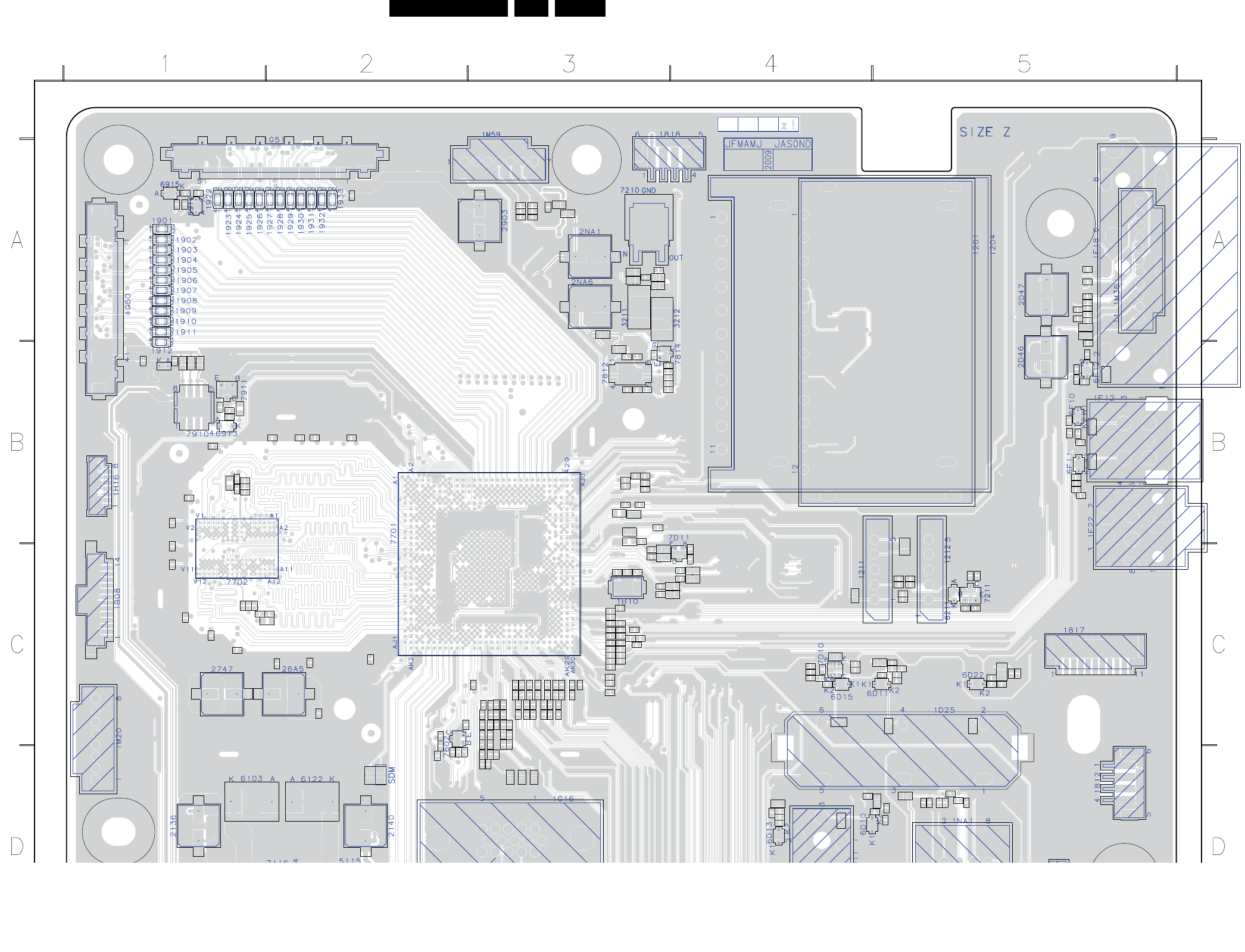
Circuit Diagrams and PWB Layouts EN 83LC9.1A LA 10.
2009-Apr-10
Layout Small Signal Board (Part 1 top side)
Part 1
1201
1204
1211
1212
1812
1817
1818
1901
1902
1903
1904
1905
1906
1907
1908
1909
1910
1911
1912
1922
1923
1924
1925
1926
1927
1928
1929
1930
1931
1932
1933
1B08
1B10
1D03
D11
1D13
1D19
1D22
1D25
1F10
1F11
1F12
1F14
1F18
1F22
1G16
1G50
1G51
3
1H16
1M20
1M36
1M59
1X01 1X02
1X12
2136
2140
2210 2211
2219
2221
2626
26A5
2741
2742
2745
2747
2750
2753
2760 2765 27692770
2771
2772
277327742775
2776
2777
2778
2779
2780
2813
2822
2823
2833
2834
29012902
2903
2904
2916
2919
2A12 2A13
2A14
2B29 2B48
2D10
2D11
2D12
2D15
2D16
2D17
2D18
2D19
2D21
2D30
2D31
2D33
2D34
2D35
2D37
2D38
2D39
2D46 2D47
2D48
2D49
2D54
2D55
2D56
2D57
2D58
2D59
2D61 2D62
2D632D64
2D67
2D68
2D69
2D72
2D73
2D74
2E25
2E28
2E32
2E35
2E39
2E43
2E46
2E48
2E80
2E82
2E83
2E84
2E86
2E87
2E88
2E89
2F10
2F11
2F12
2F13
2F14
2F15
2F21
2F22
2F23
2F36
2F37
2F38
2F39
2F402F41
2F42
2F43
2G10 2G13
2G16
2G17
2G18
2G19
2G23
2G26
2G27
2G29
2NA1
2NA6
2NAA
2NAB
2NAC
2NAD
3211
3212
3219
3221
3222
32233226
3600
3601
3602
36063607
3608
3710
3712
3714
3715
3719
3721
38133818
3826
3829
38303831
3832
3833
3838
3839
38933894
389J
38A538A6 38A7
38A8
3912
3913
3914
3915
3916
3917
3A12 3A13
3A183A19
3B22
3D10
3D12
3D14
3D16
3D19
3D22
3D25
3D26
3D27
3D29
3D30
3D32
3D43
3D44
3D45
3D46
3D47
3D48
3D49
3D50 3D51
3D53
3D54
3D55
3D56
3E10
3E17
3E23
3E26
3E35
3E38
3E42
3E46
3E54
3E55
3E59
3E92
3E93
3E96
3E97
3EA2
3EA3
3F10
3F11
3F13
3F14
3F16
3F19
3F21
3F23
3F29
3F30
3F31
3F44
3F45
3F47
3F48
3F49
3G10 3G13
3G14
3G18
3G19
3G20
3G21 3G22
3G23
3G24
3G25
3G27
3G28
3G29
3G30
3G31
3NAD
3NAE
4204 4205
42064211
4F00
4F01
5210 5211
5212
5213
5216
5712
5714
5812
5910
5911
5912
5A10
5D05
5F14
5F15
5G14
5G15
5G16
5NA1
5NA2
5NA3
61036122
6211
6912
6913
6914
6915
6D10
6D11
6D13
6D15 6D22
6F10
6F11
6F12
7210
7211
7602
7701
7702
7812
7814
7910
7911
7D10
7D11
9NA2
1X03
18490_552a_090326.eps
090627

EN 84LC9.1A LA 10.
Circuit Diagrams and PWB Layouts
2009-Apr-10
Layout Small Signal Board (Part 2 top side)
18490_552b_090326.eps
090327
Part 2
1502
1735
1736
1
1813
1B01
1B02
1B03
1B04
1B05
1B06
1B07
1D01
1D04
1D11
1D13
1D14
1D24
1E17 1E19
1E35
1F21
1G16
1H11 1H12
1H13
1H14
1M951M99
1NA1 1X05
1X06
1X07
2103
2106
2107
2129
2131
2136
2140
2150
21582159
2500
2501
2502
2508
2509
2511
2516
2527
2528
2529
2530
2531
2533
2534
2536
2541
2544
2545
2546
2547
2550
2552
2554
2555
2566
2567
2B17
2D27
2D33
2D37
2D38
2D39
2D
2D55
2D71
2F17
2F19
2G14
2G21
2G22
2G24
2G25
2H12
2H13
2H14
2H15
2H19
2H20 2H21 2H22
2H27
2H28
2H29
2NAA
2NAB
2NAC
2NAD
3513
3532
3533
35343535
3536
35373538
3542
3558
3B19
3B20
3B46
3B47
3B50
3B51
3B52
3B53
3B54
3B55
3B56
3B57
3B59
3B68
3B69
3B70
3B71
3D23
3D24
3D30
3D32
3D46
3G15
3G16
3G26
3G32
3G33
3G34
3G35
3G37
3G38
3H16
3H17
3H20
3H21
3H22
3H23
3H24
3NAD
3NAE
4B01 4B02
4B03
4B04
4B114B164B17
4G15
4H10
4H11
4H12
4H13
5100
5101
5103
5104
5107
5108
5115
5116
5117
5503
5505
5G13
61036122
61236124
6B06
6D10
6D13
6G13
6G16
7100 7103
7116
7117
7510
7B05
7G11
7G12
1X03
1X08
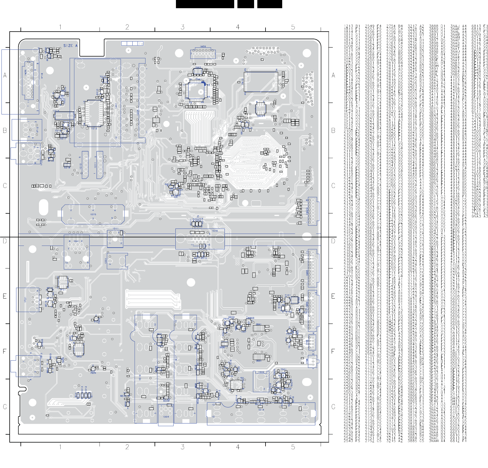
Circuit Diagrams and PWB Layouts EN 85LC9.1A LA 10.
2009-Apr-10
Layout Small Signal Board (Overview bottom side)
31391236451.2 18490_553_090326.eps
090327
1213
1811
1814
1B11
1B12
1B13
1B14
1D081D15
1D17
1D181D20 1D21
1D23
1E01
1E02
1E03
1E10
1E13
1E14
1E18
1E20
1E24
1E26
1F01 1F02 1F031F16
1F19
1F231F24
1G11
1G12
1G13
1G14
1G15
1NA2
2100
2101
2102
2104
2105
2108
2109
2110
2111
2112
2113
2114
2115
2116
2118
2119
21202121
2122
2123
2124
2125
2127
2128
21322133
2134
2135
2137
2138
2139
2141
2142
2144
2152
2153
2154
2155
2156
2157
2160
2161
2162
2163
2164
2165
2166
2167
2168
2169
2171
2200
2212
2213
2214
2215
2216
2218
2225 2226
2228
2229
2230
2231
2232
2233
2235
2236
2237
2240
2241
2242
2243
2244
2245
2246
2247
2248
2249
2250
2251
2252
2253
2258
2259
2260
2261
2262
2263
2265
2266
2267
2503
2510
2512
2513
2515
2518
2519
2520
2521
2522
2523
2524
2532
2537
2539
2540
2542
2543
2549
2553
2556
2559
2560
2561
2562
2563
2564
2565
2568
2569
2600
2601
2602
2603
2604
2605
2606
2607
2608
2609
2610
2611
2612
2613
2614
2615
2616
2617
2618
2619
2620
2621
2622
2623
2624
2625
2627
2628
2629
2630
2631
26322633
2634
2635
2636
2637
2638
2639
2640
2641
2642
2643
2644
2645
2646
2647
2648
2649
2650
2651
2652
2653
2654
2655
2656
2657
2658
2659
2660
2661
2662
2663
2664
2665
2666
2667
2668
2669
2670
2671
2672
2673
2674
2675
2676
2677 2678
2679
2680
2681
2682
2683
2684
2685
2686
2687
2688
2689
2690 2691
2692
2693
2694
2695
2696
2697
2698
2699
26A0
26A1
26A2
26A3
26A4
2710
2711
2712
2713
2714
2715
2716
2717
2719
2720
2722
2724
2725
2726
2727
2728
2729
2731
2732
2734
2735
2736
2737
2738
2739
2740
2743
2746
2749
2751
2752
2754
2755
2756
2757
2758
2759
2761
2762
2763
2764
2766
2767
2768
2810
2811 2812
2815
2816
2817
2818
2819
2820
2821
2824
2826
2827
2835
2836
2837
2917
2920
2921
2A10
2A11
2B11
2B16
2B24
2B25
2B26
2B50
2B51
2D13
2D14
2D20 2D22
2D25
2D28
2D29
2D40
2D41
2D50
2D51
2D52
2D53
2D60
2D65
2D66
2D70
2E02
2E03
2E04
2E05
2E06
2E07
2E10
2E14
2E16
2E18
2E23
2E24
2E26
2E33
2E40
2E47
2E49
2E50
2E51
2E53
2E54
2E55
2E57
2E58
2E59
2E63
2E65
2E69
2E70
2E71
2E72
2F16
2F18
2F20
2F24
2F25
2F28
2F29
2F30
2F31
2F32
2F33
2F34
2F35
2G11 2G12
2H23
2H24
2H25
2H26
2NA2
2NA3
2NA4
2NA5
2NA7
2NA8
2NA9
2NAE2NAF
3100
3101
3102
3103
3104
3105
3106
3107
3108
3109
3119
3122
3125
3129
3130
3131
3134
3135
3136
3138
3139
3140
3171
3172
3173
3199
3210
3213
3214
3215
3217
3228
3230
3231
3232
3234
3235
3236
3238
3240
3241
3242
3243
3244
3245
3246
3247
3251
3254
3255
3256
3261
3262
3500
3501
3502
3507 3508
3509
3510
3511
3512
35143515
3516
3517
3519
3520
3521
3523
3524
3525
3526
3527
3528
3529
3530
3531
3540
3541
3544
3548
3549
3550
3552
3553
3554
3555
35563557
3559
3560
3561
3562
3563
3564
3565
3566
3603
3604
3605
3609
3610
3611
3612
3613
3614
3615
3617
3618
3619
3621
3622
3623
3624
3625
3626
3711
3713
3716
3717
3718
3720
3722
3723
3724
3810
3811
3812
3814
3816
3820
3821 3822
3823
3824
3825
3827
3828
3834
3835
3837
3840
3841
3842
3845
3846
3847
3848
3850
3851
3852
3856
3857
3858
3859
3861
3863
3864
3865
3866
3868
3869
3871
3872
3873
3874
3876
3877
3878
3879
3880
3881
3882
3883
3884
3885
3888
3889
3890
3891
3892
3897
3898
3899
389A
389B
389C
389D
389F
389G
389H
389I
389K
389L
38A1
38A2
38A3
38A4
38A9
3A10
3A11
3A14
3A15
3A16
3A17
3B10
3B11
3B24
3B32
3B33
3B34
3B35
3B36
3B37
3B38
3B39
3B40
3B41
3B43
3B44
3B45
3B48
3B49
3B58
3B60
3B61
3B62
3B63
3B64
3B65
3B663B67
3B72
3B73
3B75
3B76
3D11
3D13
3D15
3D17
3D18
3D20
3D21
3D28
3D33
3D34
3D35
3D36
3D41 3D42
3D52
3D57
3D58
3D59
3E01
3E02
3E03
3E04
3E06
3E07
3E08
3E12
3E24
3E27
3E36
3E43
3E47
3E56
3E57
3E60
3E64
3E66
3E67
3E68
3E70
3E71
3E73
3E75
3E78
3E79
3E81
3E90 3E94
3E99
3EA0
3EA4
3EA5
3EA6
3EA7
3EA8
3EA9
3F22
3F24
3F25
3F26
3F273F28
3F32
3F33
3F35
3F36
3F37
3F38
3F39
3F40
3F41
3F42
3F43
3F46
3G11 3G12
3NA2
3NA3
3NA4
3NA5
3NA6
3NA7
3NA8
3NA9
3NAA
3NAB
3NAC
3NAH
3NAJ
3NAK
3NAL
3NAM
3NAN
3NAP
3NAQ
3NAR
3NAT
3NAU
3NAV
3NAW
3NAY
3NB1
3NB2
3NB3
3NB4
3NB5
4100
4101
4102
4207
4208
4209
4210
4214
4502
4601
4602 4603
4800
4802
4803
4804
4805
4806
4807
4808
4809
4810
4811
4812 4813
4814 4815
4816
4817
4818
4819
4820
4822
4910
4911
4912
4913
4914
4915
4916
4917
4918
4B18
4B28
4B29
4B30
4B34
4B35
4B36
4B37
4B38
4B39
4B40
4D00
4E06
4E07
4E08
4E09
4E10
4E11
4E12
4E13
4G11
4G12
4G13
4G14
5102
5206
5207
5208
5214
5215
5217
5218
5219
5502
5507
5508
5600
5601
5602
5603
5604
5605
5606
5607 5608
5609
5610
5713
5810
5811
5813
5814
5815
5A14
5A16
5B01
5B07
5D00
5D01
5D02
5D03
5E12
5E13
5E14
5E15
5E16
5E17
5E19
5F13
5G11
5G12
5H10
5H11
5H12
6100
6101
6102
6210
6500
6501
6502
6503
6600
6601
6810
6811
6812 6813
6814
6B07
6D09
6D12
6D14
6D16
6D17
6D18
6E02
6E03
6E04
6E10
6E14
6E16
6E26
6E28
6E30
6E32
6F13
6F15
6F16 6F17
6F18
6F19
6F20
6G11
6G12
6G14
6G15
6G17
7101
7102
7212
7213
7214
7215
7500
7501
7503
7504
7505
7506
7507
7508
7511
7513
7515
7516
7517
7518
7519
7605
7810
7815
7816
7820
7822
7B02
7B03
7B04
7B06
7B07
7B09
7E02
7F01
7NA1
9NA3
A210
A211
A212
A213
A214
A225
A258
A259
C002
C051
CXXX
F100
F101
F102
F103
F104
F105
F106
F107
F108
F109
F110
F111
F112
F113
F114
F115
F116
F117
F118
F119
F120
F122
F123
F124
F125
F126
F131
F132
F133
F134
F201
F202
F203
F204
F205
F206
F207
F208
F209
F210
F211
F213
F214
F215
F216F217
F218
F219
F227
F228
F229
F230
F234
F235
F236
F237
F250
F251
F252
F255
F256
F257
F260
F512
F515
F516
F518
F522
F523
F524
F525
F535
F536
F538
F539
F540
F541
F542
F543
F544
F545
F546
F547
F548
F550
F569
F579
F580
F593
F611
F612
F613
F614
F615
F616
F710
F810
F811
F812
F813
F814
F819
F820
F821
F822
F823
F824
F825
F826
F827
F828
F829
F831
F832
F835
F836
F837
F841
F843
F847
F848
F849
F853
F855
F856
F859
F860
F861
F862
F864
F865
F867
F868
F910
F911
F912
F913
F914
F915
F916
F917
F918
F919
F920
F921
F922
F923
F924
F925
F926
F927
F928
F929
F930
F931
F932
F933
F934
F966
F968
F969
F970
F971
F972
F973
F974
F975
F976
F977
F978
F979
F980
F981
F982
F983
F984
F985
F986
F987
F988
F989
F990
F991
F992
F993F994
FA13FA14FA15 FA16 FA17FA18
FA19
FA20
FB05
FB06
FB07
FB08FB09
FB10
FB11
FB16
FB17
FB18
FB19
FB20
FB21
FB22
FB23
FB24
FB25
FB26
FB27
FB28
FB29
FB30
FB31
FB32
FB33
FB37
FB38 FB40
FB42
FB44
FB45
FB47
FB48
FB49
FB51
FB52
FB53
FB54
FB55
FB56
FB57
FD12
FD13
FD14
FD15
FD17
FD18
FD19
FD20
FD21
FD22
FD23
FD24
FD25
FD26
FD27
FD28
FD29
FE11
FE14
FE15
FE18
FE26
FE32
FE35
FE36
FE38
FE39
FE47
FE48
FE49
FE50
FE51
FF10
FF11
FF12
FF13
FF14
FF15
FF16
FF17
FF18
FF19
FF20
FF21
FF23
FF24
FF25
FF26
FF27
FF28
FF29
FF30
FF31
FF32
FF33
FF34
FF35
FF36
FF37
FF38
FG11 FG12
FG13FG14FG15
FG16
FG17
FG18
FG19
FG20
FH11
FH14
FH15
FH16
FH17
FH18
FH19
FH20
FH21
FH22
FH23
FH24
FH25
FH26
FH27
FH30
FH31
FH32
FH33
FH34
FH35
FH36
FNA4
FNA5
FNA6
FNA7
FNA8
FNA9
FNAA
FNAB
FNAC
FNAD
FNAE
FNAF
I100
I102
I103
I104
I105 I106
I107
I108
I109
I110
I111
I117
I118
I119
I120
I122
I123
I124
I125
I126
I127
I128
I129
I130
I131
I132
I134
I135
I136
I210
I211
I212
I213
I214
I215
I216
I218
I222
I226
I227
I228
I230
I231
I232
I233
I234
I235
I237
I238
I239
I240
I241
I242
I243
I244
I245
I247
I248
I249
I250
I251
I252
I253
I261
I510
I511
I512
I513
I515
I516 I518
I519
I521
I522
I523
I524
I525
I526
I527
I530
I535
I543
I544
I546
I552
I554
I559
I560
I562
I563
I564
I565
I566
I568
I570
I571
I572
I573
I575
I576
I577
I578
I580
I581
I582
I583
I584
I585
I586
I587
I588
I589
I590
I595
I596
I597
I598
I599
I614
I616
I617
I618
I623
I629
I630
I631
I632
I633
I636
I637
I714
I810
I811
I812
I813
I814
I816
I819
I820
I821
I822
I823
I824
I825
I827
I829
I832
I833
I834
I835
I838
I839
I840
I841
I842
I843
I849
I850
I852
I853
I855
I910
I911
I912
I913I914
I915
IB01
IB02
IB03
IB04
IB09
IB10 IB11
IB12
IB14
IB16
ID12
ID13
ID14
ID22
ID25
ID26
ID28
ID29
ID30
ID31
ID32
ID34
ID35
ID36
ID37
ID38
ID42
ID43
IE01
IE11
IE13
IE14
IE16
IE17
IE18
IE20
IE21
IE24
IE25
IE26
IE29
IE34
IE42
IE56
IE72 IE78
IE89
IE95
IE96
IE99
IF10
IF12
IF14
IF16
IF18IF19
IF20
IF21
IF22
IF23
IF24
IG01
IG02
INAP
INAQ
INAR
INAS
INAT
INAU
INAV
INAW
INAY
INAZ
Part 1
18490_552a_090326.eps
Part 2
18490_552b_090326.eps
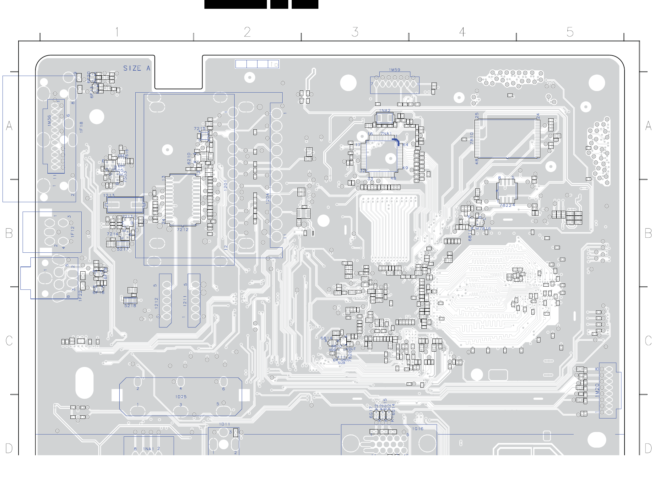
EN 86LC9.1A LA 10.
Circuit Diagrams and PWB Layouts
2009-Apr-10
Layout Small Signal Board (Part 1 bottom side)
1213
1D17
1F16
1F19
1F231F24
2
1G13
1G14
1G15
1NA2
2200
2212
2213
2214
2215
2216
2218
2225 2226
2228
2229
2230
2231
2232
2233
2235
2236
2237
2240
2241
2242
2243
2244
2245
2246
2247
2248
2249
2250
2251
2252
2253
2258
2259
2260
2261
2262
2263
2265
2266
2267
2510
2512
2600
2601
2602
2603
2604
2605
2606
2607
2608
2609
2610
2611
2612
2613
2614
2615
2616
2617
2618
2619
2620
2621
2622
2623
2624
2625
2627
2628
2629
2630
2631
26322633
2634
2635
2636
2637
2638
2639
2640
2641
2642
2643
2644
2645
2646
2647
2648
2649
2650
2651
2652
2653
2654
2655
2656
2657
2658
2659
2660
2661
2662
2663
2664
2665
2666
2667
2668
2669
2670
2671
2672
2673
2674
2675
2676
2677 2678
2679
2680
2681
2682
2683
2684
2685
2686
2687
2688
2689
2690 2691
2692
2693
2694
2695
2696
2697
2699
26A0
26A1
26A2
26A3
26A4
2710
2711
2712
2713
2714
2715
2716
2717
2719
2720
2722
2724
2725
2726
2727
2728
2729
2731
2732
2734
2735
2736
2737
2738
2739
2740
2743
2746
2749
2751
2752
2754
2755
2756
2757
2758
2759
2761
2762
2763
2764
2766
2767
2768
2810
2811 2812
2815
2816
2817
2818
2819
2820
2821
2826
2827
2835
2836
2837
2917
2920
2921
2A10
2A11
2D60
2D65
2D66
2F16
2F18
2F24
2F25
2F28
2F29
2F30
2F31
2F32
2F33
2F34
2F35
2NA2
2NA3
2NA4
2NA5
2NA7
2NA8
2NA9
2NAE2NAF
3210
3213
3214
3215
3217
3228
3230
3231
3232
3234
3235
3236
3238
3240
3241
3242
3243
3244
3245
3246
3247
3251
3254
3255
3256
3261
3262
3511
3516
3524
3525
3552
3553
3554
3555
3603
3604
3605
3609
3610
3611
3612
3613
3614
3615
3617
3618
3619
3625
3626
3711
3713
3716
3717
3718
3720
3722
3723
3724
3812
3814
3816
3820
3821 3822
3823
3824
3825
3827
3828
3834
3835
3837
3846
3847
3848
3850
3851
3852
3856
3857
3858
3859
3861
3863
3866
3871
3872
3873
3874
3876
3877
3878
3880
3881
3882
3883
3884
3885
3888
3889
3890
3891
3892
3897
3898
3899
389A
389B
389C
389D
389F
389G
389H
389I
389K
389L
38A1
38A2
38A3
38A4
38A9
3A10
3A11
3A14
3A15
3A16
3A17
3B24
3D41 3D42
3F22
3F26
3F32
3F33
3F35
3F36
3F37
3F38
3F39
3F40
3F41
3F42
3F43
3F46
3NA2
3NA3
3NA4
3NA5
3NA6
3NA7
3NA8
3NA9
3NAA
3NAB
3NAC
3NAH
3NAJ
3NAK
3NAL
3NAM
3NAN
3NAP
3NAQ
3NAR
3NAT
3NAU
3NAV
3NAW
3NAY
3NB1
3NB2
3NB3
3NB4
3NB5
4102
4207
4208
4209
4210
4214
4601
4602 4603
4800
4802
4803
4804
4805
4806
4807
4808
4809
4810
4811
4812 4813
4814 4815
4816
4817
4818
4819
4820
4822
4910
4911
4912
4913
4914
4915
4916
4917
4918
4B28
4B29
4B30
5206
5207
5208
5214
5215
5217
5218
5219
5600
5601
5602
5603
5604
5605
5606
5607 5608
5609
5610
5713
5810
5811
5813
5814
5815
5A14
5A16
5B07
6210
6810
6811
6814
6F13
6F18
6F19
6F20
6G14
6G15
6G17
7212
7213
7214
7215
7503
7505
7515
7810
7816
7820
7822
7NA1
9NA3
A210
A211
A212
A213
A214
A225
A258
A259
C002
CXXX
F134
F201
F202
F203
F204
F205
F206
F207
F208
F209
F210
F211
F213
F214
F215
F216F217
F218
F219
F227
F228
F229
F230
F234
F235
F236
F237
F250
F251
F252
F255
F256
F257
F260
F524
F525
F612
F613
F614
F710
F810
F811
F812
F813
F814
F819
F820
F821
F822
F823
F824
F825
F826
F827
F828
F829
F831
F832
F835
F836
F837
F841
F843
F853
F855
F856
F859
F860
F861
F862
F864
F865
F867
F910
F911
F912
F913
F914
F915
F916
F917
F918
F919
F920
F921
F922
F923
F924
F925
F926
F927
F928
F929
F930
F931
F932
F933
F934
F966
F968
F969
F970
F971
F972
F973
F974
F975
F976
F977
F978
F979
F980
F981
F982
F983
F984
F985
F986
F987
F988
F989
F990
F991
F992
F993F994
FA13FA14FA15 FA16 FA17FA18
FA19
FA20
FB05
FB06
FB48
FB49
FB51
FB52
FB53
FB54
FB55
FB56
FD24
FD25
FD26
FD27
FD29
FE11
FF10
FF11
FF13
FF14
FF18
FF20
FF23
FF24
FF25
FF26
FF27
FF28
FF30
FF31
FF32
FF33
FF34
FF35
FF36
FF37
FF38
FG13FG14FG15
FG19
FH27
FH31
FH32
FH33
FH34
FH35
FH36
FNA5
FNA7FNA9
FNAC
FNAD
FNAE
FNAF
I210
I211
I212
I213
I214
I215
I216
I218
I222
I226
I227
I228
I230
I231
I232
I233
I234
I235
I237
I238
I239
I240
I241
I242
I243
I244
I245
I247
I248
I249
I250
I251
I252
I253
I261
I523
I535
I562
I597
I599
I614
I616
I617
I618
I623
I631
I632
I633
I636
I637
I714
I810
I811
I812
I813
I814
I816
I819
I820
I821
I822
I823
I824
I825
I827
I829
I832
I834
I839
I840
I841
I842
I843
I849
I850
I852
I853
I855
I910
I911
I912
I913I914
I915
IB01
IB04
ID14
ID30
ID31
ID32
ID34
ID35
ID36
ID37
ID38
ID42
ID43
IF10
IF12
IF14
IF16
IF18IF19
IF20
IF21
IF24
INAP
INAQ
INAR
INAS
INAT
INAU
INAV
INAW
INAY
INAZ
Part 1
18490_553a_090326.eps
090326
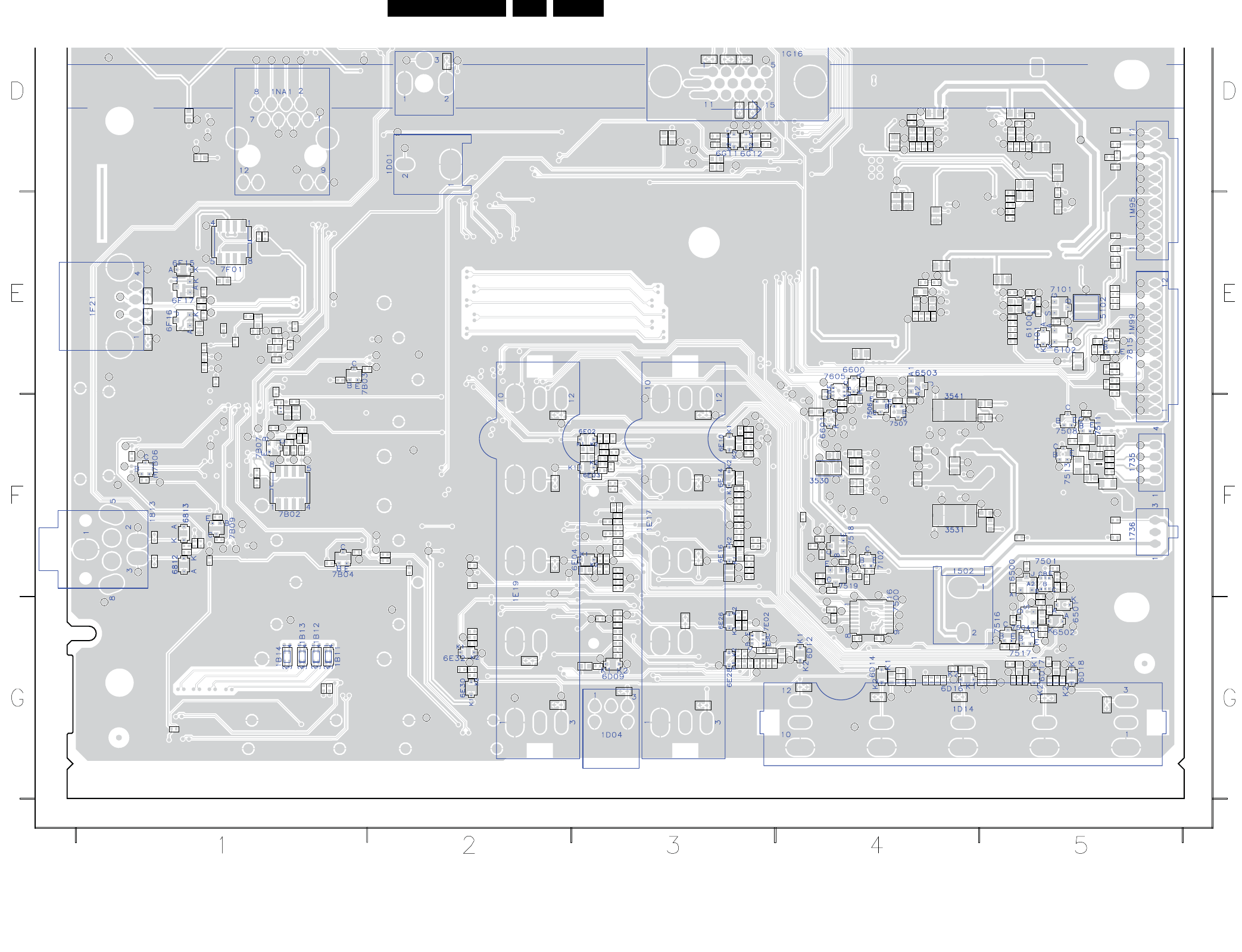
Circuit Diagrams and PWB Layouts EN 87LC9.1A LA 10.
2009-Apr-10
Layout Small Signal Board (Part 2 bottom side)
1811
1814
1B11
1B12
1B13
1B14
1D081D15
1D17
1D181D20 1D21
1D23
1E01
1E02
1E03
1E10
1E13
1E14
1E18
1E20
1E24
1E26
1F01 1F02 1F03
1G11
1G12
1G13
1G14
1G15
2100
2101
2102
2104
2105
2108
2109
2110
2111
2112
2113
2114
2115
2116
2118
2119
21202121
2122
2123
2124
2125
2127
2128
2132 2133
2134
2135
2137
2138
2139
2141
2142
2144
2152
2153
2154
2155
2156
2157
2160
2161
2162
2163
2164
2165
2166
2167
2168
2169
2171
2503
2513
2515
2518
2519
2520
2521
2522
2523
2524
2532
2537
2539
2540
2542
2543
2549
2553
2556
2559
2560
2561
2562
2563
2564
2565
2568
2569
2698
2824
2B11
2B16
2B24
2B25
2B26
2B50
2B51
2D13
2D14
2D20 2D22
2D25
2D28
2D29
2D40
2D41
2D50
2D51
2D52
2D53
2D70
2E02
2E03
2E04
2E05
2E06
2E07
2E10
2E14
2E16
2E18
2E23
2E24
2E26
2E33
2E40
2E47
2E49
2E50
2E51
2E53
2E54
2E55
2E57
2E58
2E59
2E63
2E65
2E69
2E70
2E71
2E72
2F20
2G11 2G12
2H23
2H24
2H25
2H26
3100
3101
3102
3103
3104
3105
3106
3107
3108
3109
3119
3122
3125
3129
3130
3131
3134
3135
3136
3138
3139
3140
3171
3172
3173
3199
3500
3501
3502
3507 3508
3509
3510
3512
35143515
3517
3519
3520
3521
3523
3526
3527
3528
3529
3530
3531
3540
3541
3544
3548
3549
3550
35563557
3559
3560
3561
3562
3563
3564
3565
3566
3621
3622
3623
3624
3810
3811
3840
3841
3842
3845
3864
3865
3868
3869
3879
3B10
3B11
3B32
3B33
3B34
3B35
3B36
3B37
3B38
3B39
3B40
3B41
3B43
3B44
3B45
3B48
3B49
3B58
3B60
3B61
3B62
3B63
3B64
3B65
3B663B67
3B72
3B73
3B75
3B76
3D11
3D13
3D15
3D17
3D18
3D20
3D21
3D28
3D33
3D34
3D35
3D36
3D52
3D57
3D58
3D59
3E01
3E02
3E03
3E04
3E06
3E07
3E08
3E12
3E24
3E27
3E36
3E43
3E47
3E56
3E57
3E60
3E64
3E66
3E67
3E68
3E70
3E71
3E73
3E75
3E78
3E79
3E81
3E90 3E94
3E99
3EA0
3EA4
3EA5
3EA6
3EA7
3EA8
3EA9
3F24
3F25
3F273F28
3G11 3G12
4100
4101
4502
4B18
4B34
4B35
4B36
4B37
4B38
4B39
4B40
4D00
4E06
4E07
4E08
4E09
4E10
4E11
4E12
4E13
4G11
4G12
4G13
4G14
5102
5502
5507
5508
5B01
5D00
5D01
5D02
5D03
5E12
5E13
5E14
5E15
5E16
5E17
5E19
5F13
5G11
5G12
5H10
5H11
5H12
6100
6101
6102
6500
6501
6502
6503
6600
6601
6812 6813
6B07
6D09
6D12
6D14
6D16
6D17
6D18
6E02
6E03
6E04
6E10
6E14
6E16
6E26
6E28
6E30
6E32
6F15
6F16 6F17
6G11
6G12
7101
7102
7500
7501
7504
7506
7507
7508
7511
7513
7516
7517
7518
7519
7605
7815
7B02
7B03
7B04
7B06
7B07
7B09
7E02
7F01
C051
F100
F101
F102
F103
F104
F105
F106
F107
F108
F109
F110
F111
F112
F113
F114
F115
F116
F117
F118
F119
F120
F122
F123
F124
F125
F126
F131
F132
F133
F512
F515
F516
F518
F522
F523
F535
F536
F538
F539
F540
F541
F542
F543
F544
F545
F546
F547
F548
F550
F569
F579
F580
F593
F611
F615
F616
F847
F848
F849
F856
F868
FB07
FB08FB09
FB10
FB11
FB16
FB17
FB18
FB19
FB20
FB21
FB22
FB23
FB24
FB25
FB26
FB27
FB28
FB29
FB30
FB31
FB32
FB33
FB37
FB38 FB40
FB42
FB44
FB45
FB47
FB57
FD12
FD13
FD14
FD15
FD17
FD18
FD19
FD20
FD21
FD22
FD23
FD25 FD27
FD28
FE14
FE15
FE18
FE26
FE32
FE35
FE36
FE38
FE39
FE47
FE48
FE49
FE50
FE51
FF12
FF15
FF16
FF17
FF19
FF21
FF29
FG11 FG12
FG16
FG17
FG18
FG19
FG20
FH11
FH14
FH15
FH16
FH17
FH18
FH19
FH20
FH21
FH22
FH23
FH24
FH25
FH26
FH30
FNA4
FNA5
FNA6
FNA7
FNA8
FNA9
FNAA
FNAB
I100
I102
I103
I104
I105 I106
I107
I108
I109
I110
I111
I117
I118
I119
I120
I122
I123
I124
I125
I126
I127
I128
I129
I130
I131
I132
I134
I135
I136
I510
I511
I512
I513
I515
I516 I518
I519
I521
I522
I524
I525
I526
I527
I530
I543
I544
I546
I552
I554
I559
I560
I563
I564
I565
I566
I568
I570
I571
I572
I573
I575
I576
I577
I578
I580
I581
I582
I583
I584
I585
I586
I587
I588
I589
I590
I595
I596
I598
I629
I630
I833
I835
I838
IB02
IB03
IB09
IB10 IB11
IB12
IB14
IB16
ID12
ID13
ID22
ID25
ID26
ID28
ID29
ID34
IE01
IE11
IE13
IE14
IE16
IE17
IE18
IE20
IE21
IE24
IE25
IE26
IE29
IE34
IE42
IE56
IE72 IE78
IE89
IE95
IE96
IE99
IF22
IF23
IG01
IG02
INAS
Part 2
18490_553b_090326.eps
090410