PN512 Datasheet. Www.s Manuals.com. Nxp
User Manual: Datasheets PN5120A0HN/C1, PN5120A0HN/C2, PN5120A0HN1/C1, PN5120A0HN1/C2, PN512AA0HN1/C2, PN512AA0HN1/C2BI.
Open the PDF directly: View PDF ![]() .
.
Page Count: 133 [warning: Documents this large are best viewed by clicking the View PDF Link!]
- 1. Introduction
- 2. General description
- 3. Features and benefits
- 4. Quick reference data
- 5. Ordering information
- 6. Block diagram
- 7. Pinning information
- 8. Functional description
- 9. PN512 register SET
- 10. Digital interfaces
- 10.1 Automatic microcontroller interface detection
- 10.2 Serial Peripheral Interface
- 10.3 UART interface
- 10.4 I2C Bus Interface
- 10.4.1 Data validity
- 10.4.2 START and STOP conditions
- 10.4.3 Byte format
- 10.4.4 Acknowledge
- 10.4.5 7-Bit addressing
- 10.4.6 Register write access
- 10.4.7 Register read access
- 10.4.8 High-speed mode
- 10.4.9 High-speed transfer
- 10.4.10 Serial data transfer format in HS mode
- 10.4.11 Switching between F/S mode and HS mode
- 10.4.12 PN512 at lower speed modes
- 11. 8-bit parallel interface
- 12. Analog interface and contactless UART
- 13. FIFO buffer
- 14. Interrupt request system
- 15. Timer unit
- 16. Power reduction modes
- 17. Oscillator circuitry
- 18. Reset and oscillator start-up time
- 19. PN512 command set
- 20. Testsignals
- 21. Errata sheet
- 22. Application design-in information
- 23. Limiting values
- 24. Recommended operating conditions
- 25. Thermal characteristics
- 26. Characteristics
- 27. Package information
- 28. Package outline
- 29. Abbreviations
- 30. Glossary
- 31. References
- 32. Revision history
- 33. Legal information
- 34. Contact information
- 35. Tables
- 36. Figures
- 37. Contents

1. Introduction
This document describes the functionality and electrical specifications of the
transceiver IC PN512.
The PN512 is a highly integrated transceiver IC for contactless communication at
13.56 MHz. This transceiver IC utilizes an outstanding modulation and demodulation
concept completely integrated for different kinds of contactless communication methods
and protocols at 13.56 MHz.
1.1 Different available versions
The PN512 is available in three versions:
•PN5120A0HN1/C2 (HVQFN32) and PN5120A0HN/C2 (HVQFN40), hereafter named
as version 2.0
•PN512AA0HN1/C2 (HVQFN32) and PN512AA0HN1/C2BI (HVQFN32 with Burn In),
hereafter named as industrial version, fulfilling the automotive qualification stated in
AEC-Q100 grad 3 from the Automotive Electronics Council, defining the critical stress
test qualification for automotive integrated circuits (ICs).
•PN5120A0HN1/C1(HVQFN32) and PN5120A0HN/C1 (HVQFN40), hereafter named
as version 1.0
The data sheet describes the functionality for the industrial version and version 2.0. The
differences of the version 1.0 to the version 2.0 are summarized in Section 21. The
industrial version has only differences within the outlined characteristics and limitations.
2. General description
The PN512 transceiver ICs support 4 different operating modes
•Reader/Writer mode supporting ISO/IEC 14443A/MIFARE and FeliCa scheme
•Reader/Writer mode supporting ISO/IEC 14443B
•Card Operation mode supporting ISO/IEC 14443A/MIFARE and FeliCa scheme
•NFCIP-1 mode
Enabled in Reader/Writer mode for ISO/IEC 14443A/MIFARE, the PN512’s internal
transmitter part is able to drive a reader/writer antenna designed to communicate with
ISO/IEC 14443A/ MIFARE cards and transponders without additional active circuitry. The
receiver part provides a robust and efficient implementation of a demodulation and
PN512
Transmission module
Rev. 4.2 — 28 August 2012
111342 Product data sheet
COMPANY PUBLIC

PN512 All information provided in this document is subject to legal disclaimers. © NXP B.V. 2012. All rights reserved.
Product data sheet
COMPANY PUBLIC Rev. 4.2 — 28 August 2012
111342 2 of 132
NXP Semiconductors PN512
Transmission module
decoding circuitry for signals from ISO/IEC 14443A/MIFARE compatible cards and
transponders. The digital part handles the complete ISO/IEC 14443A framing and error
detection (Parity & CRC).
The PN512 supports MIFARE 1K or MIFARE 4K emulation products. The PN512 supports
contactless communication using MIFARE higher transfer speeds up to 424 kbit/s in both
directions.
Enabled in Reader/Writer mode for FeliCa, the PN512 transceiver IC supports the FeliCa
communication scheme. The receiver part provides a robust and efficient implementation
of the demodulation and decoding circuitry for FeliCa coded signals. The digital part
handles the FeliCa framing and error detection like CRC. The PN512 supports contactless
communication using FeliCa Higher transfer speeds up to 424 kbit/s in both directions.
The PN512 supports all layers of the ISO/IEC 14443B reader/writer communication
scheme, given correct implementation of additional components, like oscillator, power
supply, coil etc. and provided that standardized protocols, e.g. like ISO/IEC 14443-4
and/or ISO/IEC 14443B anticollision are correctly implemented.
In Card Operation mode, the PN512 transceiver IC is able to answer to a reader/writer
command either according to the FeliCa or ISO/IEC 14443A/MIFARE card interface
scheme. The PN512 generates the digital load modulated signals and in addition with an
external circuit the answer can be sent back to the reader/writer. A complete card
functionality is only possible in combination with a secure IC using the S2C interface.
Additionally, the PN512 transceiver IC offers the possibility to communicate directly to an
NFCIP-1 device in the NFCIP-1 mode. The NFCIP-1 mode offers different communication
mode and transfer speeds up to 424 kbit/s according to the Ecma 340 and ISO/IEC 18092
NFCIP-1 Standard. The digital part handles the complete NFCIP-1 framing and error
detection.
Various host controller interfaces are implemented:
•8-bit parallel interface1
•SPI interface
•serial UART (similar to RS232 with voltage levels according pad voltage supply)
•I2C interface.
A purchaser of this NXP IC has to take care for appropriate third party patent licenses.
1. 8-bit parallel Interface only available in HVQFN40 package.

PN512 All information provided in this document is subject to legal disclaimers. © NXP B.V. 2012. All rights reserved.
Product data sheet
COMPANY PUBLIC Rev. 4.2 — 28 August 2012
111342 3 of 132
NXP Semiconductors PN512
Transmission module
3. Features and benefits
Highly integrated analog circuitry to demodulate and decode responses
Buffered output drivers for connecting an antenna with the minimum number of
external components
Integrated RF Level detector
Integrated data mode detector
Supports ISO/IEC 14443 A/MIFARE
Supports ISO/IEC 14443 B Read/Write modes
Typical operating distance in Read/Write mode up to 50 mm depending on the
antenna size and tuning
Typical operating distance in NFCIP-1 mode up to 50 mm depending on the antenna
size and tuning and power supply
Typical operating distance in ISO/IEC 14443A/MIFARE card or FeliCa Card Operation
mode of about 100 mm depending on the antenna size and tuning and the external
field strength
Supports MIFARE 1K or MIFARE 4K emulation encryption in Reader/Writer mode
ISO/IEC 14443A higher transfer speed communication at 212 kbit/s and 424 kbit/s
Contactless communication according to the FeliCa scheme at 212 kbit/s and
424 kbit/s
Integrated RF interface for NFCIP-1 up to 424 kbit/s
S2C interface
Additional power supply to directly supply the smart card IC connected via S2C
Supported host interfaces
SPI up to 10 Mbit/s
I2C-bus interface up to 400 kBd in Fast mode, up to 3400 kBd in High-speed mode
RS232 Serial UART up to 1228.8 kBd, with voltage levels dependant on pin
voltage supply
8-bit parallel interface with and without Address Latch Enable
FIFO buffer handles 64 byte send and receive
Flexible interrupt modes
Hard reset with low power function
Power-down mode per software
Programmable timer
Internal oscillator for connection to 27.12 MHz quartz crystal
2.5 V to 3.6 V power supply
CRC coprocessor
Programmable I/O pins
Internal self-test

PN512 All information provided in this document is subject to legal disclaimers. © NXP B.V. 2012. All rights reserved.
Product data sheet
COMPANY PUBLIC Rev. 4.2 — 28 August 2012
111342 4 of 132
NXP Semiconductors PN512
Transmission module
4. Quick reference data
[1] Supply voltages below 3 V reduce the performance in, for example, the achievable operating distance.
[2] VDDA, VDDD and VDD(TVDD) must always be the same voltage.
[3] VDD(PVDD) must always be the same or lower voltage than VDDD.
[4] Ipd is the total current for all supplies.
[5] IDD(PVDD) depends on the overall load at the digital pins.
[6] IDD(TVDD) depends on VDD(TVDD) and the external circuit connected to pins TX1 and TX2.
[7] During typical circuit operation, the overall current is below 100 mA.
[8] Typical value using a complementary driver configuration and an antenna matched to 40 between pins TX1 and TX2 at 13.56 MHz.
Table 1. Quick reference data
Symbol Parameter Conditions Min Typ Max Unit
VDDA analog supply voltage VDD(PVDD) VDDA = VDDD = VDD(TVDD);
VSSA =V
SSD =V
SS(PVSS) =V
SS(TVSS) =0V
[1][2] 2.5 - 3.6 V
VDDD digital supply voltage
VDD(TVDD) TVDD supply voltage
VDD(PVDD) PVDD supply voltage [3] 1.6 - 3.6 V
VDD(SVDD) SVDD supply voltage VSSA =V
SSD =V
SS(PVSS) =V
SS(TVSS) = 0 V 1.6 - 3.6 V
Ipd power-down current VDDA =V
DDD = VDD(TVDD) =V
DD(PVDD) =3V
hard power-down; pin NRSTPD set LOW [4] --5A
soft power-down; RF level detector on [4] --10A
IDDD digital supply current pin DVDD; VDDD =3V - 6.5 9 mA
IDDA analog supply current pin AVDD; VDDA = 3 V, CommandReg register’s
RcvOff bit = 0
-710mA
pin AVDD; receiver switched off; VDDA =3V,
CommandReg register’s RcvOff bit = 1
-35mA
IDD(PVDD) PVDD supply current pin PVDD [5] --40mA
IDD(TVDD) TVDD supply current pin TVDD; continuous wave [6][7][8] -60100mA
Tamb ambient temperature HVQFN32, HVQFN40 30 +85 C
lndustrial version:
Ipd power-down current VDDA =V
DDD = VDD(TVDD) =V
DD(PVDD) =3V
hard power-down; pin NRSTPD set LOW [4] --15A
soft power-down; RF level detector on [4] --30A
Tamb ambient temperature HVQFN32 40 - +90 C

PN512 All information provided in this document is subject to legal disclaimers. © NXP B.V. 2012. All rights reserved.
Product data sheet
COMPANY PUBLIC Rev. 4.2 — 28 August 2012
111342 5 of 132
NXP Semiconductors PN512
Transmission module
5. Ordering information
Table 2. Ordering information
Type number Package
Name Description Version
PN5120A0HN1/C2 HVQFN32 plastic thermal enhanced very thin quad flat package; no leads;
32 terminal; body 5 5 0.85 mm
SOT617-1
PN5120A0HN/C2 HVQFN40 plastic thermal enhanced very thin quad flat package; no leads;
40 terminals; body 6 6 0.85 mm
SOT618-1
PN512AA0HN1/C2 HVQFN32 plastic thermal enhanced very thin quad flat package; no leads;
32 terminal; body 5 5 0.85 mm
SOT617-1
PN512AA0HN1/C2BI HVQFN32 plastic thermal enhanced very thin quad flat package; no leads;
32 terminal; body 5 5 0.85 mm
SOT617-1
PN5120A0HN1/C1 HVQFN32 plastic thermal enhanced very thin quad flat package; no leads;
32 terminal; body 5 5 0.85 mm
SOT617-1
PN5120A0HN/C1 HVQFN40 plastic thermal enhanced very thin quad flat package; no leads;
40 terminals; body 6 6 0.85 mm
SOT618-1
PN512 All information provided in this document is subject to legal disclaimers. © NXP B.V. 2012. All rights reserved.
Product data sheet
COMPANY PUBLIC Rev. 4.2 — 28 August 2012
111342 6 of 132
NXP Semiconductors PN512
Transmission module
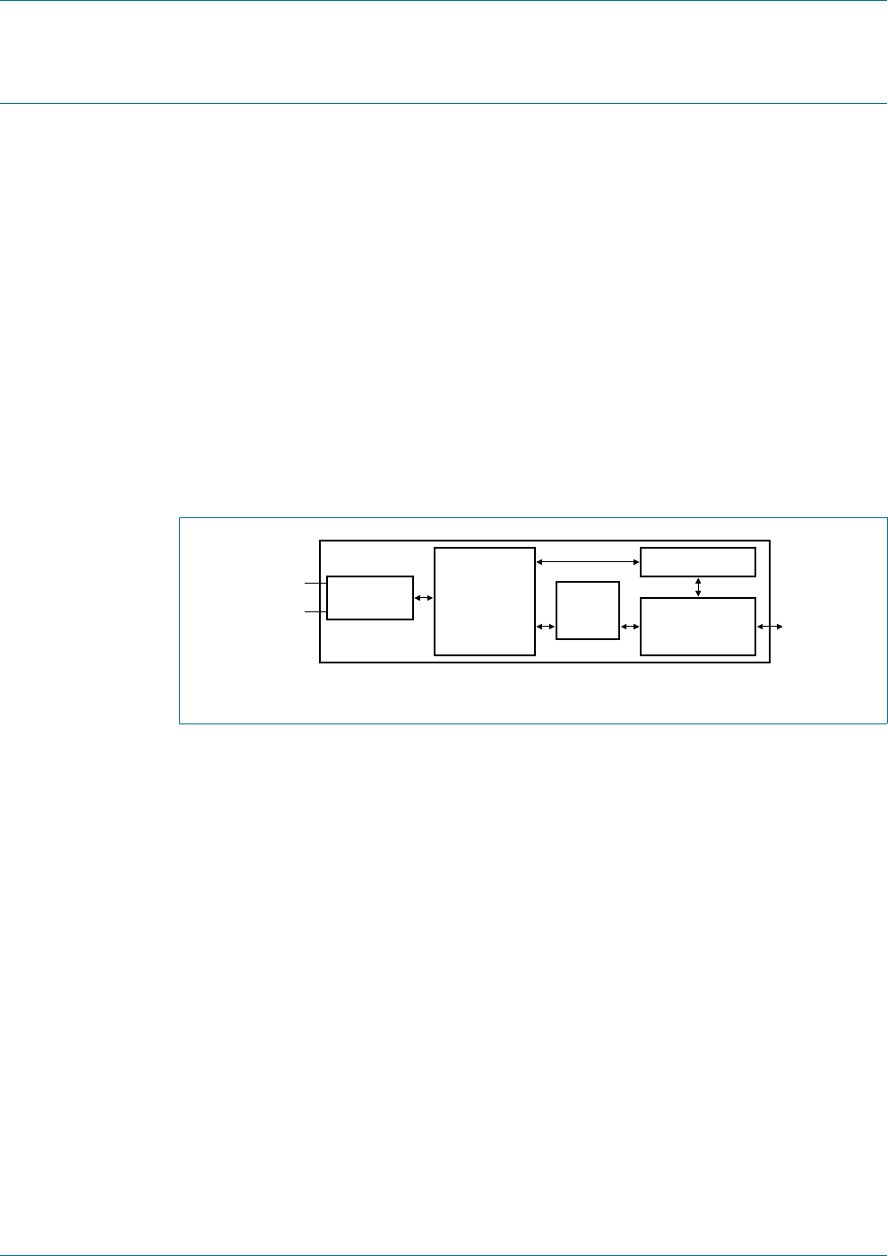
6. Block diagram
The analog interface handles the modulation and demodulation of the analog signals
according to the Card Receiving mode, Reader/Writer mode and NFCIP-1 mode
communication scheme.
The RF level detector detects the presence of an external RF-field delivered by the
antenna to the RX pin.
The Data mode detector detects a MIFARE, FeliCa or NFCIP-1 mode in order to prepare
the internal receiver to demodulate signals, which are sent to the PN512.
The communication (S2C) interface provides digital signals to support communication for
transfer speeds above 424 kbit/s and digital signals to communicate to a secure IC.
The contactless UART manages the protocol requirements for the communication
protocols in cooperation with the host. The FIFO buffer ensures fast and convenient data
transfer to and from the host and the contactless UART and vice versa.
Various host interfaces are implemented to meet different customer requirements.
Fig 1. Simplified block diagram of the PN512
001aaj627
HOST
ANTENNA FIFO
BUFFER
ANALOG
INTERFACE CONTACTLESS
UART SERIAL UART
SPI
I
2
C-BUS
REGISTER BANK
PN512 All information provided in this document is subject to legal disclaimers. © NXP B.V. 2012. All rights reserved.
Product data sheet
COMPANY PUBLIC Rev. 4.2 — 28 August 2012
111342 7 of 132
NXP Semiconductors PN512
Transmission module
Fig 2. Detailed block diagram of the PN512
001aak602
DVDD
NRSTPD
IRQ
MFIN
MFOUT
SVDD
OSCIN
OSCOUT
VMID AUX1 AUX2 RX TVSS TX1 TX2 TVDD
16 19 20 17 10, 14 11 13 12
DVSS
AVDD
PVSSPVDDSDA/NSS/RX EA I2C
5224 32 1
D1/ADR_5
25
D2/ADR_4
26
D3/ADR_3
27
D4/ADR_2
28
D5/ADR_1/
SCK/DTRQ
29
D6/ADR_0/
MOSI/MX
30
D7/SCL/
MISO/TX
31
AVSS
3
6
23
7
8
9
21
22
4
15
18
FIFO CONTROL
MIFARE CLASSIC UNIT
STATE MACHINE
COMMAND REGISTER
PROGRAMABLE TIMER
INTERRUPT CONTROL
CRC16
GENERATION AND CHECK
PARALLEL/SERIAL
CONVERTER
SERIAL DATA SWITCH
TRANSMITTER CONTROL
BIT COUNTER
PARITY GENERATION AND CHECK
FRAME GENERATION AND CHECK
BIT DECODING BIT ENCODING
RANDOM NUMBER
GENERATOR
ANALOG TO DIGITAL
CONVERTER
I-CHANNEL
AMPLIFIER
ANALOG TEST
MULTIPLEXOR
AND
DIGITAL TO
ANALOG
CONVERTER
I-CHANNEL
DEMODULATOR
Q-CHANNEL
AMPLIFIER
CLOCK
GENERATION,
FILTERING AND
DISTRIBUTION
Q-CLOCK
GENERATION
OSCILLATOR
TEMPERATURE
SENSOR
Q-CHANNEL
DEMODULATOR
AMPLITUDE
RATING
REFERENCE
VOLTAGE
64-BYTE FIFO
BUFFER
CONTROL REGISTER
BANK
SPI, UART, I2C-BUS INTERFACE CONTROL
VOLTAGE
MONITOR
AND
POWER ON
DETECT
RESET
CONTROL
POWER-DOWN
CONTROL
PN512 All information provided in this document is subject to legal disclaimers. © NXP B.V. 2012. All rights reserved.
Product data sheet
COMPANY PUBLIC Rev. 4.2 — 28 August 2012
111342 8 of 132
NXP Semiconductors PN512
Transmission module
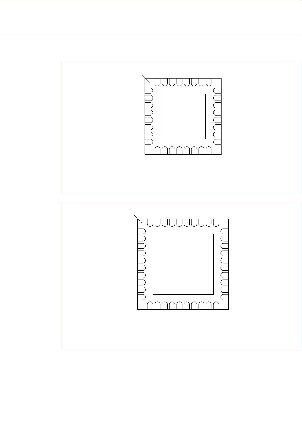
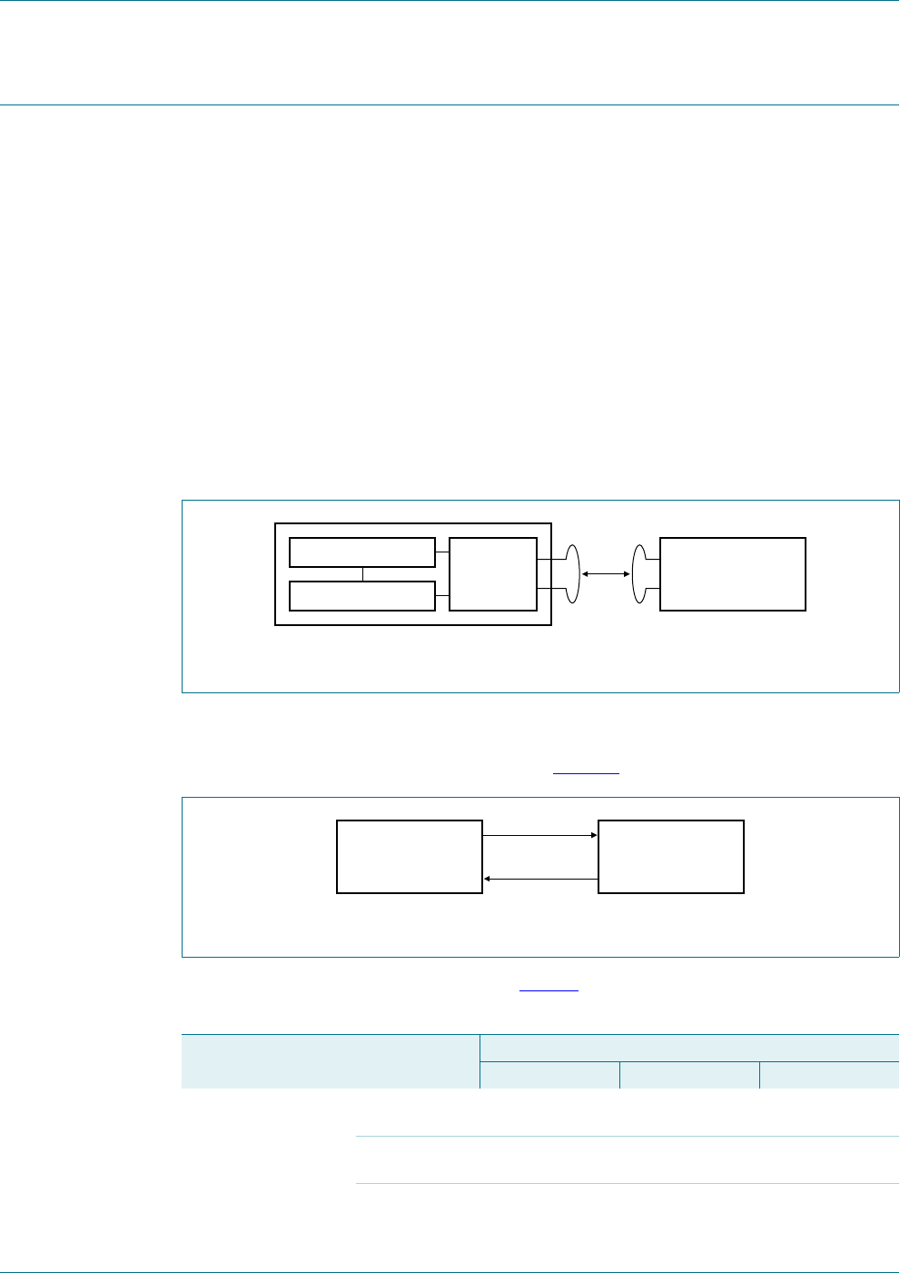
7. Pinning information
7.1 Pinning
Fig 3. Pinning configuration HVQFN32 (SOT617-1)
Fig 4. Pinning configuration HVQFN40 (SOT618-1)
001aan212
PN512
Transparent top view
RX
SIGIN
SIGOUT
AVSS
NRSTPD AUX1
PVSS AUX2
DVSS OSCIN
DVDD OSCOUT
PVDD IRQ
A1 ALE
SVDD
TVSS
TX1
TVDD
TX2
TVSS
AVDD
VMID
A0
D7
D6
D5
D4
D3
D2
D1
8 17
7 18
6 19
5 20
4 21
3 22
2 23
1 24
9
10
11
12
13
14
15
16
32
31
30
29
28
27
26
25
terminal 1
index area
001aan213
PN512
AVSS
NRSTPD
SIGIN
AUX1
PVSS AUX2
DVSS OSCIN
DVDD OSCOUT
PVDD IRQ
A5 NWR
A4 NRD
A3 ALE
A2 NCS
SIGOUT
SVDD
TVSS
TX1
TVDD
TX2
TVSS
AVDD
VMID
RX
A1
A0
D7
D6
D5
D4
D3
D2
D1
D0
10 21
9 22
8 23
7 24
6 25
5 26
4 27
3 28
2 29
1 30
11
12
13
14
15
16
17
18
19
20
40
39
38
37
36
35
34
33
32
31
terminal 1
index area
Transparent top view

PN512 All information provided in this document is subject to legal disclaimers. © NXP B.V. 2012. All rights reserved.
Product data sheet
COMPANY PUBLIC Rev. 4.2 — 28 August 2012
111342 9 of 132
NXP Semiconductors PN512
Transmission module
7.2 Pin description
Table 3. Pin description HVQFN32
Pin Symbol Type Description
1A1IAddress Line
2 PVDD PWR Pad power supply
3DVDDPWRDigital Power Supply
4 DVSS PWR Digital Ground
5 PVSS PWR Pad power supply ground
6 NRSTPD I Not Reset and Power Down: When LOW, internal current sinks are switched off, the
oscillator is inhibited, and the input pads are disconnected from the outside world. With
a positive edge on this pin the internal reset phase starts.
7 SIGIN I Communication Interface Input: accepts a digital, serial data stream
8 SIGOUT O Communication Interface Output: delivers a serial data stream
9 SVDD PWR S2C Pad Power Supply: provides power to the S2C pads
10 TVSS PWR Transmitter Ground: supplies the output stage of TX1 and TX2
11 TX1 O Transmitter 1: delivers the modulated 13.56 MHz energy carrier
12 TVDD PWR Transmitter Power Supply: supplies the output stage of TX1 and TX2
13 TX2 O Transmitter 2: delivers the modulated 13.56 MHz energy carrier
14 TVSS PWR Transmitter Ground: supplies the output stage of TX1 and TX2
15 AVDD PWR Analog Power Supply
16 VMID PWR Internal Reference Voltage: This pin delivers the internal reference voltage.
17 RX I Receiver Input
18 AVSS PWR Analog Ground
19 AUX1 O Auxiliary Outputs: These pins are used for testing.
20 AUX2 O
21 OSCIN I Crystal Oscillator Input: input to the inverting amplifier of the oscillator. This pin is
also the input for an externally generated clock (fosc = 27.12 MHz).
22 OSCOUT O Crystal Oscillator Output: Output of the inverting amplifier of the oscillator.
23 IRQ O Interrupt Request: output to signal an interrupt event
24 ALE I Address Latch Enable: signal to latch AD0 to AD5 into the internal address latch
when HIGH.
25 to 31 D1 to D7 I/O 8-bit Bi-directional Data Bus.
Remark: An 8-bit parallel interface is not available.
Remark: If the host controller selects I2C as digital host controller interface, these pins
can be used to define the I2C address.
Remark: For serial interfaces this pins can be used for test signals or I/Os.
32 A0 I Address Line

PN512 All information provided in this document is subject to legal disclaimers. © NXP B.V. 2012. All rights reserved.
Product data sheet
COMPANY PUBLIC Rev. 4.2 — 28 August 2012
111342 10 of 132
NXP Semiconductors PN512
Transmission module
Table 4. Pin description HVQFN40
Pin Symbol Type Description
1 to 4 A2 to A5 I Address Line
5 PVDD PWR Pad power supply
6DVDDPWRDigital Power Supply
7 DVSS PWR Digital Ground
8 PVSS PWR Pad power supply ground
9 NRSTPD I Not Reset and Power Down: When LOW, internal current sinks are switched off, the
oscillator is inhibited, and the input pads are disconnected from the outside world. With
a positive edge on this pin the internal reset phase starts.
10 SIGIN I Communication Interface Input: accepts a digital, serial data stream
11 SIGOUT O Communication Interface Output: delivers a serial data stream
12 SVDD PWR S2C Pad Power Supply: provides power to the S2C pads
13 TVSS PWR Transmitter Ground: supplies the output stage of TX1 and TX2
14 TX1 O Transmitter 1: delivers the modulated 13.56 MHz energy carrier
15 TVDD PWR Transmitter Power Supply: supplies the output stage of TX1 and TX2
16 TX2 O Transmitter 2: delivers the modulated 13.56 MHz energy carrier
17 TVSS PWR Transmitter Ground: supplies the output stage of TX1 and TX2
18 AVDD PWR Analog Power Supply
19 VMID PWR Internal Reference Voltage: This pin delivers the internal reference voltage.
20 RX I Receiver Input
21 AVSS PWR Analog Ground
22 AUX1 O Auxiliary Outputs: These pins are used for testing.
23 AUX2 O
24 OSCIN I Crystal Oscillator Input: input to the inverting amplifier of the oscillator. This pin is
also the input for an externally generated clock (fosc = 27.12 MHz).
25 OSCOUT O Crystal Oscillator Output: Output of the inverting amplifier of the oscillator.
26 IRQ O Interrupt Request: output to signal an interrupt event
27 NWR I Not Write: strobe to write data (applied on D0 to D7) into the PN512 register
28 NRD I Not Read: strobe to read data from the PN512 register (applied on D0 to D7)
29 ALE I Address Latch Enable: signal to latch AD0 to AD5 into the internal address latch
when HIGH.
30 NCS I Not Chip Select: selects and activates the host controller interface of the PN512
31 to 38 D0 to D7 I/O 8-bit Bi-directional Data Bus.
Remark: For serial interfaces this pins can be used for test signals or I/Os.
Remark: If the host controller selects I2C as digital host controller interface, these pins
can be used to define the I2C address.
39 to 40 A0 to A1 I Address Line
PN512 All information provided in this document is subject to legal disclaimers. © NXP B.V. 2012. All rights reserved.
Product data sheet
COMPANY PUBLIC Rev. 4.2 — 28 August 2012
111342 11 of 132
NXP Semiconductors PN512
Transmission module
8. Functional description
The PN512 transmission module supports the Read/Write mode for
ISO/IEC 14443 A/MIFARE and ISO/IEC 14443 B using various transfer speeds and
modulation protocols.
PN512 transceiver IC supports the following operating modes:
•Reader/Writer mode supporting ISO/IEC 14443A/MIFARE and FeliCa scheme
•Card Operation mode supporting ISO/IEC 14443A/MIFARE and FeliCa scheme
•NFCIP-1 mode
The modes support different transfer speeds and modulation schemes. The following
chapters will explain the different modes in detail.
Note: All indicated modulation indices and modes in this chapter are system parameters.
This means that beside the IC settings a suitable antenna tuning is required to achieve the
optimum performance.
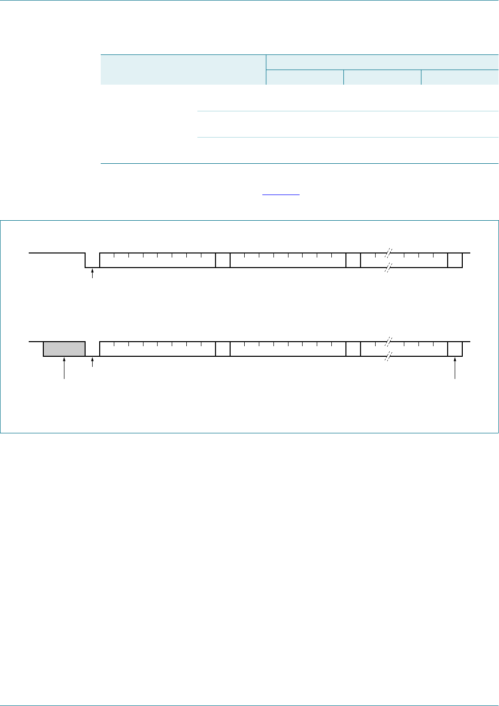
8.1 ISO/IEC 14443 A/MIFARE functionality
The physical level communication is shown in Figure 6.
The physical parameters are described in Table 4.
Fig 5. PN512 Read/Write mode
001aan218
BATTERY
reader/writer contactless card
MICROCONTROLLER
PN512
ISO/IEC 14443 A CARD
Fig 6. ISO/IEC 14443 A/MIFARE Read/Write mode communication diagram
Table 5. Communication overview for ISO/IEC 14443 A/MIFARE reader/writer
Communication
direction Signal type Transfer speed
106 kBd 212 kBd 424 kBd
Reader to card (send
data from the PN512
to a card)
reader side
modulation
100 % ASK 100 % ASK 100 % ASK
bit encoding modified Miller
encoding
modified Miller
encoding
modified Miller
encoding
bit length 128 (13.56 s) 64 (13.56 s) 32 (13.56 s)
(1)
(2)
001aan219
PN512
ISO/IEC 14443 A CARD
ISO/IEC 14443 A
READER
PN512 All information provided in this document is subject to legal disclaimers. © NXP B.V. 2012. All rights reserved.
Product data sheet
COMPANY PUBLIC Rev. 4.2 — 28 August 2012
111342 12 of 132
NXP Semiconductors PN512
Transmission module
The PN512’s contactless UART and dedicated external host must manage the complete
ISO/IEC 14443 A/MIFARE protocol. Figure 7 shows the data coding and framing
according to ISO/IEC 14443 A/MIFARE.
The internal CRC coprocessor calculates the CRC value based on ISO/IEC 14443 A
part 3 and handles parity generation internally according to the transfer speed. Automatic
parity generation can be switched off using the ManualRCVReg register’s ParityDisable
bit.
8.2 ISO/IEC 14443 B functionality
The MFRC523 reader IC fully supports international standard ISO 14443 which includes
communication schemes ISO 14443 A and ISO 14443 B.
Refer to the ISO 14443 reference documents Identification cards - Contactless integrated
circuit cards - Proximity cards (parts 1 to 4).
Remark: NXP Semiconductors does not offer a software library to enable design-in of the
ISO 14443 B protocol.
Card to reader
(PN512 receives data
from a card)
card side
modulation
subcarrier load
modulation
subcarrier load
modulation
subcarrier load
modulation
subcarrier
frequency
13.56 MHz/16 13.56 MHz/16 13.56 MHz/16
bit encoding Manchester
encoding
BPSK BPSK
Table 5. Communication overview for ISO/IEC 14443 A/MIFARE reader/writer …continued
Communication
direction Signal type Transfer speed
106 kBd 212 kBd 424 kBd
Fig 7. Data coding and framing according to ISO/IEC 14443 A
001aak585
ISO/IEC 14443 A framing at 106 kBd
8-bit data 8-bit data 8-bit data
odd
parity
odd
parity
start
odd
parity
start bit is 1
ISO/IEC 14443 A framing at 212 kBd, 424 kBd and 848 kBd
8-bit data 8-bit data 8-bit data
odd
parity
odd
parity
start
even
parity
start bit is 0
burst of 32
subcarrier clocks even parity at the
end of the frame

PN512 All information provided in this document is subject to legal disclaimers. © NXP B.V. 2012. All rights reserved.
Product data sheet
COMPANY PUBLIC Rev. 4.2 — 28 August 2012
111342 13 of 132
NXP Semiconductors PN512
Transmission module
8.3 FeliCa reader/writer functionality
The FeliCa mode is the general reader/writer to card communication scheme according to
the FeliCa specification. The following diagram describes the communication on a
physical level, the communication overview describes the physical parameters.
The contactless UART of PN512 and a dedicated external host controller are required to
handle the complete FeliCa protocol.
8.3.1 FeliCa framing and coding
To enable the FeliCa communication a 6 byte preamble (00h, 00h, 00h, 00h, 00h, 00h)
and 2 bytes Sync bytes (B2h, 4Dh) are sent to synchronize the receiver.
The following Len byte indicates the length of the sent data bytes plus the LEN byte itself.
The CRC calculation is done according to the FeliCa definitions with the MSB first.
To transmit data on the RF interface, the host controller has to send the Len- and data-
bytes to the PN512's FIFO-buffer. The preamble and the sync bytes are generated by the
PN512 automatically and must not be written to the FIFO by the host controller. The
PN512 performs internally the CRC calculation and adds the result to the data frame.
Example for FeliCa CRC Calculation:
Fig 8. FeliCa reader/writer communication diagram
Table 6. Communication overview for FeliCa reader/writer
Communication
direction FeliCa FeliCa Higher
transfer speeds
Transfer speed 212 kbit/s 424 kbit/s
PN512 card Modulation on reader side 8-30 % ASK 8-30 % ASK
bit coding Manchester Coding Manchester Coding
Bitlength (64/13.56) s (32/13.56) s
card PN512 Loadmodulation on card side > 12 % ASK > 12 % ASK
bit coding Manchester coding Manchester coding
2. PICC to PCD, > 12 % ASK loadmodulation
Manchester coded, baudrate 212 to 424 kbaud
1. PCD to PICC, 8-30 % ASK
Manchester coded, baudrate 212 to 424 kbaud
001aan214
PN512
FeliCa CARD
(PICC)
Felica READER
(PCD)
Table 7. FeliCa framing and coding
Preamble Sync Len n-Data CRC
00h 00h 00h 00h 00h 00h B2h 4Dh
Table 8. Start value for the CRC Polynomial: (00h), (00h)
Preamble Sync Len 2 Data Bytes CRC
00h 00h 00h 00h 00h 00h B2h 4Dh 03h ABh CDh 90h 35h
PN512 All information provided in this document is subject to legal disclaimers. © NXP B.V. 2012. All rights reserved.
Product data sheet
COMPANY PUBLIC Rev. 4.2 — 28 August 2012
111342 14 of 132
NXP Semiconductors PN512
Transmission module
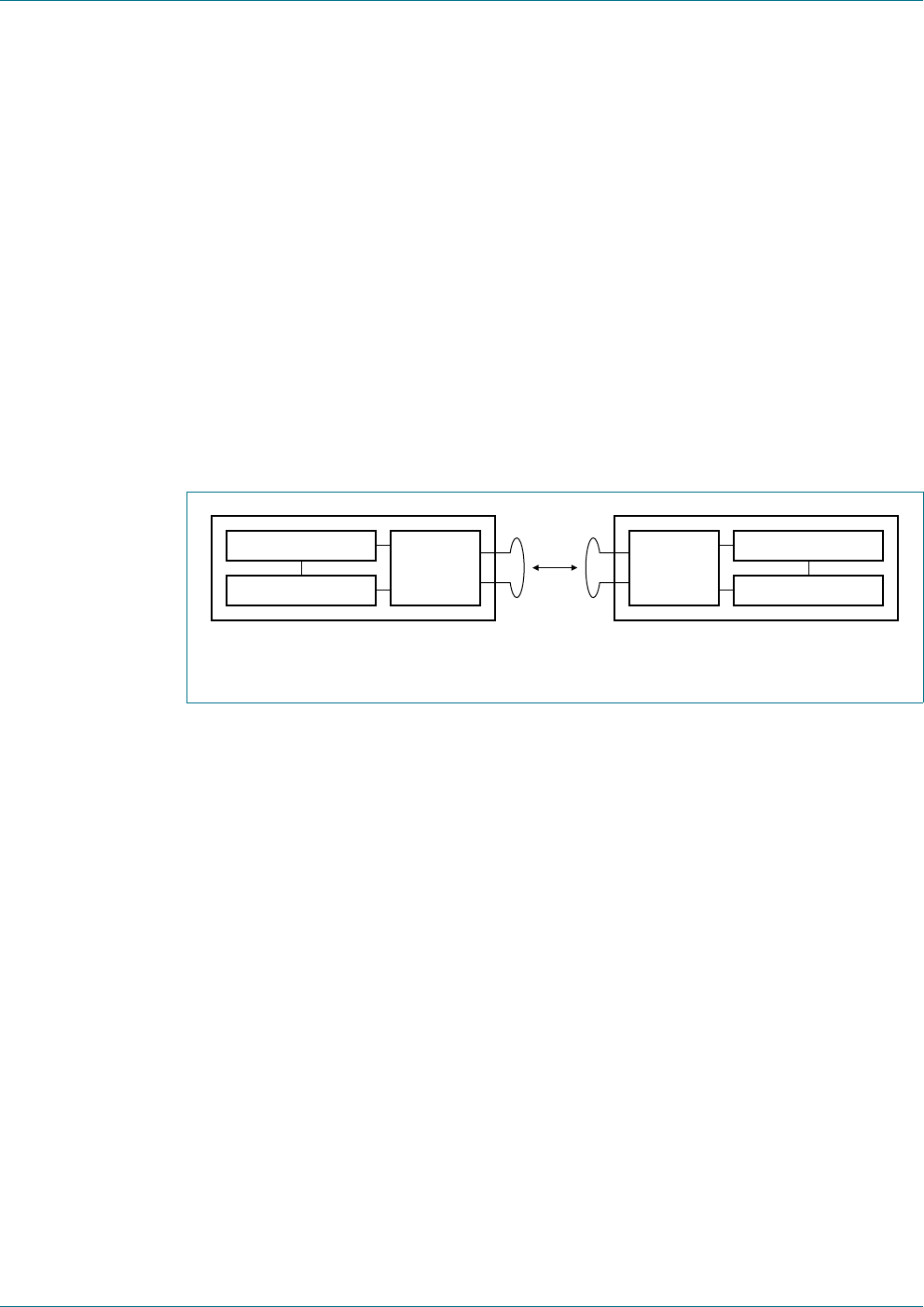
8.4 NFCIP-1 mode
The NFCIP-1 communication differentiates between an active and a Passive
Communication mode.
•Active Communication mode means both the initiator and the target are using their
own RF field to transmit data.
•Passive Communication mode means that the target answers to an initiator command
in a load modulation scheme. The initiator is active in terms of generating the RF field.
•Initiator: generates RF field at 13.56 MHz and starts the NFCIP-1 communication
•Target: responds to initiator command either in a load modulation scheme in Passive
Communication mode or using a self generated and self modulated RF field for Active
Communication mode.
In order to fully support the NFCIP-1 standard the PN512 supports the Active and Passive
Communication mode at the transfer speeds 106 kbit/s, 212 kbit/s and 424 kbit/s as
defined in the NFCIP-1 standard.
Fig 9. NFCIP-1 mode
001aan215
BATTERY
initiator: active target:
passive or active
MICROCONTROLLER
PN512
BATTERY
MICROCONTROLLER
PN512
PN512 All information provided in this document is subject to legal disclaimers. © NXP B.V. 2012. All rights reserved.
Product data sheet
COMPANY PUBLIC Rev. 4.2 — 28 August 2012
111342 15 of 132
NXP Semiconductors PN512
Transmission module
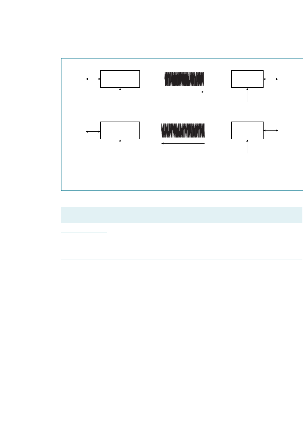
8.4.1 Active communication mode
Active communication mode means both the initiator and the target are using their own
RF field to transmit data.
The contactless UART of PN512 and a dedicated host controller are required to handle
the NFCIP-1 protocol.
Note: Transfer Speeds above 424 kbit/s are not defined in the NFCIP-1 standard. The
PN512 supports these transfer speeds only with dedicated external circuits.
Fig 10. Active communication mode
Table 9. Communication overview for Active communication mode
Communication
direction 106 kbit/s 212 kbit/s 424 kbit/s 848 kbit/s 1.69 Mbit/s,
3.39 Mbit/s
Initiator Target According to
ISO/IEC 14443A
100 % ASK,
Modified
Miller Coded
According to FeliCa, 8-30 %
ASK Manchester Coded
digital capability to handle
this communication
Target Initiator
host NFC INITIATOR
powered to
generate RF field
1. initiator starts communication at
selected transfer speed
Initial command
response
2. target answers at
the same transfer speed
host NFC INITIATOR
powered for digital
processing
host
host
NFC TARGET
NFC TARGET
powered for
digital processing
powered to
generate RF field
001aan216
PN512 All information provided in this document is subject to legal disclaimers. © NXP B.V. 2012. All rights reserved.
Product data sheet
COMPANY PUBLIC Rev. 4.2 — 28 August 2012
111342 16 of 132
NXP Semiconductors PN512
Transmission module
8.4.2 Passive communication mode
Passive Communication mode means that the target answers to an initiator command in a
load modulation scheme. The initiator is active meaning generating the RF field.
The contactless UART of PN512 and a dedicated host controller are required to handle
the NFCIP-1 protocol.
Note: Transfer Speeds above 424 kbit/s are not defined in the NFCIP-1 standard. The
PN512 supports these transfer speeds only with dedicated external circuits.
Fig 11. Passive communication mode
Table 10. Communication overview for Passive communication mode
Communication
direction 106 kbit/s 212 kbit/s 424 kbit/s 848 kbit/s 1.69 Mbit/s,
3.39 Mbit/s
Initiator Target According to
ISO/IEC 14443A
100 % ASK,
Modified
Miller Coded
According to FeliCa, 8-30
% ASK Manchester Coded
digital capability to handle
this communication
Target Initiator According to
ISO/IEC 14443A
subcarrier load
modulation,
Manchester Coded
According to FeliCa, > 12 %
ASK Manchester Coded
host NFC INITIATOR
powered to
generate RF field
1. initiator starts communication
at selected transfer speed
2. targets answers using
load modulated data
at the same transfer speed
host
NFC TARGET
powered for
digital processing
001aan217

PN512 All information provided in this document is subject to legal disclaimers. © NXP B.V. 2012. All rights reserved.
Product data sheet
COMPANY PUBLIC Rev. 4.2 — 28 August 2012
111342 17 of 132
NXP Semiconductors PN512
Transmission module
8.4.3 NFCIP-1 framing and coding
The NFCIP-1 framing and coding in Active and Passive Communication mode is defined
in the NFCIP-1 standard.
8.4.4 NFCIP-1 protocol support
The NFCIP-1 protocol is not completely described in this document. For detailed
explanation of the protocol refer to the NFCIP-1 standard. However the datalink layer is
according to the following policy:
•Speed shall not be changed while continuum data exchange in a transaction.
•Transaction includes initialization and anticollision methods and data exchange (in
continuous way, meaning no interruption by another transaction).
In order not to disturb current infrastructure based on 13.56 MHz general rules to start
NFCIP-1 communication are defined in the following way.
1. Per default NFCIP-1 device is in Target mode meaning its RF field is switched off.
2. The RF level detector is active.
3. Only if application requires the NFCIP-1 device shall switch to Initiator mode.
4. Initiator shall only switch on its RF field if no external RF field is detected by RF Level
detector during a time of TIDT.
5. The initiator performs initialization according to the selected mode.
8.4.5 MIFARE Card operation mode
Table 11. Framing and coding overview
Transfer speed Framing and Coding
106 kbit/s According to the ISO/IEC 14443A/MIFARE scheme
212 kbit/s According to the FeliCa scheme
424 kbit/s According to the FeliCa scheme
Table 12. MIFARE Card operation mode
Communication
direction ISO/IEC 14443A/
MIFARE MIFARE Higher transfer speeds
transfer speed 106 kbit/s 212 kbit/s 424 kbit/s
reader/writer
PN512
Modulation on
reader side
100 % ASK 100 % ASK 100 % ASK
bit coding Modified Miller Modified Miller Modified Miller
Bitlength (128/13.56) s (64/13.56) s (32/13.56) s
PN512 reader/
writer
Modulation on
PN512 side
subcarrier load
modulation
subcarrier load
modulation
subcarrier load
modulation
subcarrier
frequency
13.56 MHz/16 13.56 MHz/16 13.56 MHz/16
bit coding Manchester coding BPSK BPSK

PN512 All information provided in this document is subject to legal disclaimers. © NXP B.V. 2012. All rights reserved.
Product data sheet
COMPANY PUBLIC Rev. 4.2 — 28 August 2012
111342 18 of 132
NXP Semiconductors PN512
Transmission module
8.4.6 FeliCa Card operation mode
9. PN512 register SET
9.1 PN512 registers overview
Table 13. FeliCa Card operation mode
Communication
direction FeliCa FeliCa Higher
transfer speeds
Transfer speed 212 kbit/s 424 kbit/s
reader/writer
PN512
Modulation on reader side 8-30 % ASK 8-30 % ASK
bit coding Manchester Coding Manchester Coding
Bitlength (64/13.56) s (32/13.56) s
PN512 reader/
writer
Load modulation on PN512
side
> 12 % ASK load
modulation
> 12 % ASK load
modulation
bit coding Manchester coding Manchester coding
Table 14. PN512 registers overview
Addr
(hex) Register Name Function
Page 0: Command and Status
0 PageReg Selects the register page
1 CommandReg Starts and stops command execution
2 ComlEnReg Controls bits to enable and disable the passing of Interrupt Requests
3 DivlEnReg Controls bits to enable and disable the passing of Interrupt Requests
4 ComIrqReg Contains Interrupt Request bits
5 DivIrqReg Contains Interrupt Request bits
6 ErrorReg Error bits showing the error status of the last command executed
7 Status1Reg Contains status bits for communication
8 Status2Reg Contains status bits of the receiver and transmitter
9 FIFODataReg In- and output of 64 byte FIFO-buffer
A FIFOLevelReg Indicates the number of bytes stored in the FIFO
B WaterLevelReg Defines the level for FIFO under- and overflow warning
C ControlReg Contains miscellaneous Control Registers
D BitFramingReg Adjustments for bit oriented frames
E CollReg Bit position of the first bit collision detected on the RF-interface
F RFU Reserved for future use
Page 1: Command
0 PageReg Selects the register page
1 ModeReg Defines general modes for transmitting and receiving
2 TxModeReg Defines the data rate and framing during transmission
3 RxModeReg Defines the data rate and framing during receiving
4 TxControlReg Controls the logical behavior of the antenna driver pins TX1 and TX2
5 TxAutoReg Controls the setting of the antenna drivers

PN512 All information provided in this document is subject to legal disclaimers. © NXP B.V. 2012. All rights reserved.
Product data sheet
COMPANY PUBLIC Rev. 4.2 — 28 August 2012
111342 19 of 132
NXP Semiconductors PN512
Transmission module
6 TxSelReg Selects the internal sources for the antenna driver
7 RxSelReg Selects internal receiver settings
8 RxThresholdReg Selects thresholds for the bit decoder
9 DemodReg Defines demodulator settings
A FelNFC1Reg Defines the length of the valid range for the receive package
B FelNFC2Reg Defines the length of the valid range for the receive package
C MifNFCReg Controls the communication in ISO/IEC 14443/MIFARE and NFC
target mode at 106 kbit
D ManualRCVReg Allows manual fine tuning of the internal receiver
E TypeBReg Configure the ISO/IEC 14443 type B
F SerialSpeedReg Selects the speed of the serial UART interface
Page 2: CFG
0 PageReg Selects the register page
1 CRCResultReg Shows the actual MSB and LSB values of the CRC calculation
2
3 GsNOffReg Selects the conductance of the antenna driver pins TX1 and TX2 for
modulation, when the driver is switched off
4 ModWidthReg Controls the setting of the ModWidth
5 TxBitPhaseReg Adjust the TX bit phase at 106 kbit
6 RFCfgReg Configures the receiver gain and RF level
7 GsNOnReg Selects the conductance of the antenna driver pins TX1 and TX2 for
modulation when the drivers are switched on
8 CWGsPReg Selects the conductance of the antenna driver pins TX1 and TX2 for
modulation during times of no modulation
9 ModGsPReg Selects the conductance of the antenna driver pins TX1 and TX2 for
modulation during modulation
A TModeReg
TPrescalerReg
Defines settings for the internal timer
B
C TReloadReg Describes the 16-bit timer reload value
D
E TCounterValReg Shows the 16-bit actual timer value
F
Page 3: TestRegister
0 PageReg selects the register page
1 TestSel1Reg General test signal configuration
2 TestSel2Reg General test signal configuration and PRBS control
3 TestPinEnReg Enables pin output driver on 8-bit parallel bus (Note: For serial
interfaces only)
4TestPin
ValueReg
Defines the values for the 8-bit parallel bus when it is used as I/O bus
5 TestBusReg Shows the status of the internal testbus
6 AutoTestReg Controls the digital selftest
Table 14. PN512 registers overview …continued
Addr
(hex) Register Name Function

PN512 All information provided in this document is subject to legal disclaimers. © NXP B.V. 2012. All rights reserved.
Product data sheet
COMPANY PUBLIC Rev. 4.2 — 28 August 2012
111342 20 of 132
NXP Semiconductors PN512
Transmission module
9.1.1 Register bit behavior
Depending on the functionality of a register, the access conditions to the register can vary.
In principle bits with same behavior are grouped in common registers. In Table 15 the
access conditions are described.
7 VersionReg Shows the version
8 AnalogTestReg Controls the pins AUX1 and AUX2
9 TestDAC1Reg Defines the test value for the TestDAC1
A TestDAC2Reg Defines the test value for the TestDAC2
B TestADCReg Shows the actual value of ADC I and Q
C-F RFT Reserved for production tests
Table 14. PN512 registers overview …continued
Addr
(hex) Register Name Function
Table 15. Behavior of register bits and its designation
Abbreviation Behavior Description
r/w read and write These bits can be written and read by the -Controller. Since they
are used only for control means, there content is not influenced by
internal state machines, e.g. the PageSelect-Register may be
written and read by the -Controller. It will also be read by internal
state machines, but never changed by them.
dy dynamic These bits can be written and read by the -Controller.
Nevertheless, they may also be written automatically by internal
state machines, e.g. the Command-Register changes its value
automatically after the execution of the actual command.
r read only These registers hold bits, which value is determined by internal
states only, e.g. the CRCReady bit can not be written from
external but shows internal states.
w write only Reading these registers returns always ZERO.
RFU - These registers are reserved for future use.
In case of a PN512 Version version 2.0 (VersionReg = 82h) a
read access to these registers returns always the value “0”.
Nevertheless this is not guaranteed for future chips versions
where the value is undefined. In case of a write access, it is
recommended to write always the value “0”.
RFT - These registers are reserved for production tests and shall not be
changed.

PN512 All information provided in this document is subject to legal disclaimers. © NXP B.V. 2012. All rights reserved.
Product data sheet
COMPANY PUBLIC Rev. 4.2 — 28 August 2012
111342 21 of 132
NXP Semiconductors PN512
Transmission module
9.2 Register description
9.2.1 Page 0: Command and status
9.2.1.1 PageReg
Selects the register page.
9.2.1.2 CommandReg
Starts and stops command execution.
Table 16. PageReg register (address 00h); reset value: 00h, 0000000b
7 6543210
UsePage Select 0 0 0 0 0 PageSelect
Access
Rights
r/w RFU RFU RFU RFU RFU r/w r/w
Table 17. Description of PageReg bits
Bit Symbol Description
7 UsePageSelect Set to logic 1, the value of PageSelect is used as register address A5
and A4. The LSB-bits of the register address are defined by the
address pins or the internal address latch, respectively.
Set to logic 0, the whole content of the internal address latch defines
the register address. The address pins are used as described in
Section 10.1 “Automatic microcontroller interface detection”.
6 to 2 - Reserved for future use.
1 to 0 PageSelect The value of PageSelect is used only if UsePageSelect is set to
logic 1. In this case it specifies the register page (which is A5 and A4
of the register address).
Table 18. CommandReg register (address 01h); reset value: 20h, 00100000b
7 6 5 4 3 2 1 0
0 0 RcvOff Power Down Command
Access
Rights
RFURFUr/w dy dydydydy
Table 19. Description of CommandReg bits
Bit Symbol Description
7 to 6 - Reserved for future use.
5 RcvOff Set to logic 1, the analog part of the receiver is switched off.
4 PowerDown Set to logic 1, Soft Power-down mode is entered.
Set to logic 0, the PN512 starts the wake up procedure. During this
procedure this bit still shows a 1. A 0 indicates that the PN512 is ready
for operations; see Section 16.2 “Soft power-down mode”.
Note: The bit Power Down cannot be set, when the command
SoftReset has been activated.
3 to 0 Command Activates a command according to the Command Code. Reading this
register shows, which command is actually executed (see Section 19.3
“PN512 command overview”).

PN512 All information provided in this document is subject to legal disclaimers. © NXP B.V. 2012. All rights reserved.
Product data sheet
COMPANY PUBLIC Rev. 4.2 — 28 August 2012
111342 22 of 132
NXP Semiconductors PN512
Transmission module
9.2.1.3 CommIEnReg
Control bits to enable and disable the passing of interrupt requests.
Table 20. CommIEnReg register (address 02h); reset value: 80h, 10000000b
7 6 5 4 3 2 1 0
IRqInv TxIEn RxIEn IdleIEn HiAlertIEn LoAlertIEn ErrIEn TimerIEn
Access
Rights
r/w r/w r/w r/w r/w r/w r/w r/w
Table 21. Description of CommIEnReg bits
Bit Symbol Description
7 IRqInv Set to logic 1, the signal on pin IRQ is inverted with respect to bit IRq in the
register Status1Reg. Set to logic 0, the signal on pin IRQ is equal to bit IRq.
In combination with bit IRqPushPull in register DivIEnReg, the default value
of 1 ensures, that the output level on pin IRQ is 3-state.
6 TxIEn Allows the transmitter interrupt request (indicated by bit TxIRq) to be
propagated to pin IRQ.
5 RxIEn Allows the receiver interrupt request (indicated by bit RxIRq) to be
propagated to pin IRQ.
4 IdleIEn Allows the idle interrupt request (indicated by bit IdleIRq) to be propagated to
pin IRQ.
3 HiAlertIEn Allows the high alert interrupt request (indicated by bit HiAlertIRq) to be
propagated to pin IRQ.
2 LoAlertIEn Allows the low alert interrupt request (indicated by bit LoAlertIRq) to be
propagated to pin IRQ.
1 ErrIEn Allows the error interrupt request (indicated by bit ErrIRq) to be propagated
to pin IRQ.
0 TimerIEn Allows the timer interrupt request (indicated by bit TimerIRq) to be
propagated to pin IRQ.

PN512 All information provided in this document is subject to legal disclaimers. © NXP B.V. 2012. All rights reserved.
Product data sheet
COMPANY PUBLIC Rev. 4.2 — 28 August 2012
111342 23 of 132
NXP Semiconductors PN512
Transmission module
9.2.1.4 DivIEnReg
Control bits to enable and disable the passing of interrupt requests.
Table 22. DivIEnReg register (address 03h); reset value: 00h, 00000000b
7 6 5 4 3 2 1 0
IRQPushPull 0 0 SiginActIEn ModeIEn CRCIEn RFOnIEn RFOffIEn
Access
Rights
r/w RFU RFU r/w r/w r/w r/w r/w
Table 23. Description of DivIEnReg bits
Bit Symbol Description
7 IRQPushPull Set to logic 1, the pin IRQ works as standard CMOS output pad.
Set to logic 0, the pin IRQ works as open drain output pad.
6 to 5 - Reserved for future use.
4 SiginActIEn Allows the SIGIN active interrupt request to be propagated to pin IRQ.
3 ModeIEn Allows the mode interrupt request (indicated by bit ModeIRq) to be
propagated to pin IRQ.
2 CRCIEn Allows the CRC interrupt request (indicated by bit CRCIRq) to be
propagated to pin IRQ.
1 RfOnIEn Allows the RF field on interrupt request (indicated by bit RfOnIRq) to
be propagated to pin IRQ.
0 RfOffIEn Allows the RF field off interrupt request (indicated by bit RfOffIRq) to
be propagated to pin IRQ.

PN512 All information provided in this document is subject to legal disclaimers. © NXP B.V. 2012. All rights reserved.
Product data sheet
COMPANY PUBLIC Rev. 4.2 — 28 August 2012
111342 24 of 132
NXP Semiconductors PN512
Transmission module
9.2.1.5 CommIRqReg
Contains Interrupt Request bits.
Table 24. CommIRqReg register (address 04h); reset value: 14h, 00010100b
7 6 5 4 3 2 1 0
Set1 TxIRq RxIRq IdleIRq HiAlertIRq LoAlertIRq ErrIRq TimerIRq
Access
Rights
w dydydy dy dy dydy
Table 25. Description of CommIRqReg bits
All bits in the register CommIRqReg shall be cleared by software.
Bit Symbol Description
7 Set1 Set to logic 1, Set1 defines that the marked bits in the register CommIRqReg
are set.
Set to logic 0, Set1 defines, that the marked bits in the register CommIRqReg
are cleared.
6 TxIRq Set to logic 1 immediately after the last bit of the transmitted data was sent out.
5 RxIRq Set to logic 1 when the receiver detects the end of a valid datastream.
If the bit RxNoErr in register RxModeReg is set to logic 1, bit RxIRq is only set
to logic 1 when data bytes are available in the FIFO.
4 IdleIRq Set to logic 1, when a command terminates by itself e.g. when the
CommandReg changes its value from any command to the Idle Command.
If an unknown command is started, the CommandReg changes its content to
the idle state and the bit IdleIRq is set. Starting the Idle Command by the
-Controller does not set bit IdleIRq.
3 HiAlertIRq Set to logic 1, when bit HiAlert in register Status1Reg is set. In opposition to
HiAlert, HiAlertIRq stores this event and can only be reset as indicated by bit
Set1.
2 LoAlertIRq Set to logic 1, when bit LoAlert in register Status1Reg is set. In opposition to
LoAlert, LoAlertIRq stores this event and can only be reset as indicated by bit
Set1.
1 ErrIRq Set to logic 1 if any error bit in the Error Register is set.
0 TimerIRq Set to logic 1 when the timer decrements the TimerValue Register to zero.

PN512 All information provided in this document is subject to legal disclaimers. © NXP B.V. 2012. All rights reserved.
Product data sheet
COMPANY PUBLIC Rev. 4.2 — 28 August 2012
111342 25 of 132
NXP Semiconductors PN512
Transmission module
9.2.1.6 DivIRqReg
Contains Interrupt Request bits
Table 26. DivIRqReg register (address 05h); reset value: XXh, 000X00XXb
7 6 5 4 3 2 1 0
Set2 0 0 SiginActIRq ModeIRq CRCIRq RFOnIRq RFOffIRq
Access
Rights
wRFURFU dy dy dy dy dy
Table 27. Description of DivIRqReg bits
All bits in the register DivIRqReg shall be cleared by software.
Bit Symbol Description
7 Set2 Set to logic 1, Set2 defines that the marked bits in the register
DivIRqReg are set.
Set to logic 0, Set2 defines, that the marked bits in the register
DivIRqReg are cleared
6 to 5 - Reserved for future use.
4 SiginActIRq Set to logic 1, when SIGIN is active. See Section 12.6 “S2C interface
support”. This interrupt is set when either a rising or falling signal edge
is detected.
3 ModeIRq Set to logic 1, when the mode has been detected by the Data mode
detector.
Note: The Data mode detector can only be activated by the AutoColl
command and is terminated automatically having detected the
Communication mode.
Note: The Data mode detector is automatically restarted after each RF
Reset.
2 CRCIRq Set to logic 1, when the CRC command is active and all data are
processed.
1 RFOnIRq Set to logic 1, when an external RF field is detected.
0 RFOffIRq Set to logic 1, when a present external RF field is switched off.

PN512 All information provided in this document is subject to legal disclaimers. © NXP B.V. 2012. All rights reserved.
Product data sheet
COMPANY PUBLIC Rev. 4.2 — 28 August 2012
111342 26 of 132
NXP Semiconductors PN512
Transmission module
9.2.1.7 ErrorReg
Error bit register showing the error status of the last command executed.
[1] Command execution will clear all error bits except for bit TempErr. A setting by software is impossible.
Table 28. ErrorReg register (address 06h); reset value: 00h, 00000000b
7 6 5 4 3 2 1 0
WrErr TempErr RFErr BufferOvfl CollErr CRCErr ParityErr ProtocolErr
Access
Rights
rrrr rrr r
Table 29. Description of ErrorReg bits
Bit Symbol Description
7 WrErr Set to logic 1, when data is written into FIFO by the host controller
during the AutoColl command or MFAuthent command or if data is
written into FIFO by the host controller during the time between
sending the last bit on the RF interface and receiving the last bit on the
RF interface.
6 TempErr[1] Set to logic 1, if the internal temperature sensor detects overheating.
In this case, the antenna drivers are switched off automatically.
5 RFErr Set to logic 1, if in Active Communication mode the counterpart does
not switch on the RF field in time as defined in NFCIP-1 standard.
Note: RFErr is only used in Active Communication mode. The bits
RxFraming or the bits TxFraming has to be set to 01 to enable this
functionality.
4 BufferOvfl Set to logic 1, if the host controller or a PN512’s internal state machine
(e.g. receiver) tries to write data into the FIFO-bufferFIFO-buffer
although the FIFO-buffer is already full.
3 CollErr Set to logic 1, if a bit-collision is detected. It is cleared automatically at
receiver start-up phase. This bit is only valid during the bitwise
anticollision at 106 kbit. During communication schemes at 212 and
424 kbit this bit is always set to logic 1.
2 CRCErr Set to logic 1, if bit RxCRCEn in register RxModeReg is set and the
CRC calculation fails. It is cleared to 0 automatically at receiver
start-up phase.
1 ParityErr Set to logic 1, if the parity check has failed. It is cleared automatically
at receiver start-up phase. Only valid for ISO/IEC 14443A/MIFARE or
NFCIP-1 communication at 106 kbit.
0 ProtocolErr Set to logic 1, if one out of the following cases occur:
•Set to logic 1 if the SOF is incorrect. It is cleared automatically at
receiver start-up phase. The bit is only valid for 106 kbit in Active
and Passive Communication mode.
•If bit DetectSync in register ModeReg is set to logic 1 during
FeliCa communication or active communication with transfer
speeds higher than 106 kbit, the bit ProtocolErr is set to logic 1 in
case of a byte length violation.
•During the AutoColl command, bit ProtocolErr is set to logic 1, if
the bit Initiator in register ControlReg is set to logic 1.
•During the MFAuthent Command, bit ProtocolErr is set to logic 1,
if the number of bytes received in one data stream is incorrect.
•Set to logic 1, if the Miller Decoder detects 2 pulses below the
minimum time according to the ISO/IEC 14443A definitions.

PN512 All information provided in this document is subject to legal disclaimers. © NXP B.V. 2012. All rights reserved.
Product data sheet
COMPANY PUBLIC Rev. 4.2 — 28 August 2012
111342 27 of 132
NXP Semiconductors PN512
Transmission module
9.2.1.8 Status1Reg
Contains status bits of the CRC, Interrupt and FIFO-buffer.
Table 30. Status1Reg register (address 07h); reset value: XXh, X100X01Xb
7 6 5 4 3 2 1 0
RFFreqOK CRCOk CRCReady IRq TRunning RFOn HiAlert LoAlert
Access
Rights
rrrrrrrr
Table 31. Description of Status1Reg bits
Bit Symbol Description
7 RFFreqOK Indicates if the frequency detected at the RX pin is in the range of
13.56 MHz.
Set to logic 1, if the frequency at the RX pin is in the range
12 MHz < RX pin frequency < 15 MHz.
Note: The value of RFFreqOK is not defined if the external RF
frequency is in the range from 9 to 12 MHz or in the range from
15 to 19 MHz.
6 CRCOk Set to logic 1, if the CRC Result is zero. For data transmission and
reception the bit CRCOk is undefined (use CRCErr in register
ErrorReg). CRCOk indicates the status of the CRC co-processor,
during calculation the value changes to ZERO, when the calculation is
done correctly, the value changes to ONE.
5 CRCReady Set to logic 1, when the CRC calculation has finished. This bit is only
valid for the CRC co-processor calculation using the command
CalcCRC.
4 IRq This bit shows, if any interrupt source requests attention (with respect
to the setting of the interrupt enable bits, see register CommIEnReg
and DivIEnReg).
3 TRunning Set to logic 1, if the PN512’s timer unit is running, e.g. the timer will
decrement the TCounterValReg with the next timer clock.
Note: In the gated mode the bit TRunning is set to logic 1, when the
timer is enabled by the register bits. This bit is not influenced by the
gated signal.
2 RFOn Set to logic 1, if an external RF field is detected. This bit does not store
the state of the RF field.
1 HiAlert Set to logic 1, when the number of bytes stored in the FIFO-buffer
fulfills the following equation:
Example:
FIFOLength = 60, WaterLevel = 4 HiAlert = 1
FIFOLength = 59, WaterLevel = 4 HiAlert = 0
0 LoAlert Set to logic 1, when the number of bytes stored in the FIFO-buffer
fulfills the following equation:
Example:
FIFOLength = 4, WaterLevel = 4 LoAlert = 1
FIFOLength = 5, WaterLevel = 4 LoAlert = 0
HiAlert 64 FIFOLength– WaterLevel=
LoAlert FIFOLength WaterLevel=

PN512 All information provided in this document is subject to legal disclaimers. © NXP B.V. 2012. All rights reserved.
Product data sheet
COMPANY PUBLIC Rev. 4.2 — 28 August 2012
111342 28 of 132
NXP Semiconductors PN512
Transmission module
9.2.1.9 Status2Reg
Contains status bits of the Receiver, Transmitter and Data mode detector.
Table 32. Status2Reg register (address 08h); reset value: 00h, 00000000b
7 6 5 4 3 2 1 0
TempSensClear I2CForceHS 0 TargetActivated MFCrypto1On Modem State
Access
Rights
r/w r/w RFU dy dy r r r
Table 33. Description of Status2Reg bits
Bit Symbol Description
7 TempSensClear Set to logic 1, this bit clears the temperature error, if the temperature
is below the alarm limit of 125 C.
6I
2CForceHS I2C input filter settings. Set to logic 1, the I2C input filter is set to the
High-speed mode independent of the I2C protocol. Set to logic 0, the
I2C input filter is set to the used I2C protocol.
5 - Reserved for future use.
4 TargetActivated Set to logic 1 if the Select command or if the Polling command was
answered. Note: This bit can only be set during the AutoColl
command in Passive Communication mode.
Note: This bit is cleared automatically by switching off the external
RF field.
3 MFCrypto1On This bit indicates that the MIFARE Crypto1 unit is switched on and
therefore all data communication with the card is encrypted.
This bit can only be set to logic 1 by a successful execution of the
MFAuthent Command. This bit is only valid in Reader/Writer mode
for MIFARE cards. This bit shall be cleared by software.
2 to 0 Modem State ModemState shows the state of the transmitter and receiver state
machines.
Value Description
000 IDLE
001 Wait for StartSend in register BitFramingReg
010 TxWait: Wait until RF field is present, if the bit TxWaitRF is
set to logic 1. The minimum time for TxWait is defined by the
TxWaitReg register.
011 Sending
100 RxWait: Wait until RF field is present, if the bit RxWaitRF is
set to logic 1. The minimum time for RxWait is defined by the
RxWaitReg register.
101 Wait for data
110 Receiving

PN512 All information provided in this document is subject to legal disclaimers. © NXP B.V. 2012. All rights reserved.
Product data sheet
COMPANY PUBLIC Rev. 4.2 — 28 August 2012
111342 29 of 132
NXP Semiconductors PN512
Transmission module
9.2.1.10 FIFODataReg
In- and output of 64 byte FIFO-buffer.
9.2.1.11 FIFOLevelReg
Indicates the number of bytes stored in the FIFO.
Table 34. FIFODataReg register (address 09h); reset value: XXh, XXXXXXXXb
7 6 5 4 3 2 1 0
FIFOData
Access
Rights
dy dy dy dy dy dy dy dy
Table 35. Description of FIFODataReg bits
Bit Symbol Description
7 to 0 FIFOData Data input and output port for the internal 64 byte FIFO-buffer. The
FIFO-buffer acts as parallel in/parallel out converter for all serial data
stream in- and outputs.
Table 36. FIFOLevelReg register (address 0Ah); reset value: 00h, 00000000b
7 6 5 4 3 2 1 0
FlushBuffer FIFOLevel
Access
Rights
w rrrrrrr
Table 37. Description of FIFOLevelReg bits
Bit Symbol Description
7 FlushBuffer Set to logic 1, this bit clears the internal FIFO-buffer’s read- and
write-pointer and the bit BufferOvfl in the register ErrReg immediately.
Reading this bit will always return 0.
6 to 0 FIFOLevel Indicates the number of bytes stored in the FIFO-buffer. Writing to the
FIFODataReg increments, reading decrements the FIFOLevel.

PN512 All information provided in this document is subject to legal disclaimers. © NXP B.V. 2012. All rights reserved.
Product data sheet
COMPANY PUBLIC Rev. 4.2 — 28 August 2012
111342 30 of 132
NXP Semiconductors PN512
Transmission module
9.2.1.12 WaterLevelReg
Defines the level for FIFO under- and overflow warning.
9.2.1.13 ControlReg
Miscellaneous control bits.
Table 38. WaterLevelReg register (address 0Bh); reset value: 08h, 00001000b
7 6 5 4 3 2 1 0
0 0 WaterLevel
Access
Rights
RFU RFU r/w r/w r/w r/w r/w r/w
Table 39. Description of WaterLevelReg bits
Bit Symbol Description
7 to 6 - Reserved for future use.
5 to 0 WaterLevel This register defines a warning level to indicate a FIFO-buffer over- or
underflow:
The bit HiAlert in Status1Reg is set to logic 1, if the remaining number
of bytes in the FIFO-buffer space is equal or less than the defined
number of WaterLevel bytes.
The bit LoAlert in Status1Reg is set to logic 1, if equal or less than
WaterLevel bytes are in the FIFO.
Note: For the calculation of HiAlert and LoAlert see Table 30
Table 40. ControlReg register (address 0Ch); reset value: 00h, 00000000b
7 6 5 4 3 2 1 0
TStopNow TStartNow WrNFCIDtoFIFO Initiator 0 RxLastBits
Access
Rights
w w dy r/wRFUrrr
Table 41. Description of ControlReg bits
Bit Symbol Description
7 TStopNow Set to logic 1, the timer stops immediately.
Reading this bit will always return 0.
6 TStartNow Set to logic 1 starts the timer immediately.
Reading this bit will always return 0.
5 WrNFCIDtoFIFO Set to logic 1, the internal stored NFCID (10 bytes) is copied into the
FIFO.
Afterwards the bit is cleared automatically
4 Initiator Set to logic 1, the PN512 acts as initiator, otherwise it acts as target
3 - Reserved for future use.
2 to 0 RxLastBits Shows the number of valid bits in the last received byte. If zero, the
whole byte is valid.

PN512 All information provided in this document is subject to legal disclaimers. © NXP B.V. 2012. All rights reserved.
Product data sheet
COMPANY PUBLIC Rev. 4.2 — 28 August 2012
111342 31 of 132
NXP Semiconductors PN512
Transmission module
9.2.1.14 BitFramingReg
Adjustments for bit oriented frames.
Table 42. BitFramingReg register (address 0Dh); reset value: 00h, 00000000b
7 6 5 4 3 2 1 0
StartSend RxAlign 0 TxLastBits
Access
Rights
w r/w r/w r/w RFU r/w r/w r/w
Table 43. Description of BitFramingReg bits
Bit Symbol Description
7 StartSend Set to logic 1, the transmission of data starts.
This bit is only valid in combination with the Transceive command.
6 to 4 RxAlign Used for reception of bit oriented frames: RxAlign defines the bit position
for the first bit received to be stored in the FIFO. Further received bits are
stored at the following bit positions.
Example:
RxAlign = 0: the LSB of the received bit is stored at bit 0, the second
received bit is stored at bit position 1.
RxAlign = 1: the LSB of the received bit is stored at bit 1, the second
received bit is stored at bit position 2.
RxAlign = 7: the LSB of the received bit is stored at bit 7, the second
received bit is stored in the following byte at bit position 0.
This bit shall only be used for bitwise anticollision at 106 kbit/s in Passive
Communication mode. In all other modes it shall be set to logic 0.
3 - Reserved for future use.
2 to 0 TxLastBits Used for transmission of bit oriented frames: TxLastBits defines the
number of bits of the last byte that shall be transmitted. A 000 indicates
that all bits of the last byte shall be transmitted.

PN512 All information provided in this document is subject to legal disclaimers. © NXP B.V. 2012. All rights reserved.
Product data sheet
COMPANY PUBLIC Rev. 4.2 — 28 August 2012
111342 32 of 132
NXP Semiconductors PN512
Transmission module
9.2.1.15 CollReg
Defines the first bit collision detected on the RF interface.
Table 44. CollReg register (address 0Eh); reset value: XXh, 101XXXXXb
7 6 5 4 3 2 1 0
Values
AfterColl
0CollPos
NotValid
CollPos
Access
Rights
r/wRFUrrrrrr
Table 45. Description of CollReg bits
Bit Symbol Description
7 ValuesAfterColl If this bit is set to logic 0, all receiving bits will be cleared after a
collision. This bit shall only be used during bitwise anticollision at
106 kbit, otherwise it shall be set to logic 1.
6 - Reserved for future use.
5 CollPosNotValid Set to logic 1, if no Collision is detected or the Position of the
Collision is out of the range of bits CollPos. This bit shall only be
interpreted in Passive Communication mode at 106 kbit or
ISO/IEC 14443A/MIFARE Reader/Writer mode.
4 to 0 CollPos These bits show the bit position of the first detected collision in a
received frame, only data bits are interpreted.
Example:
00h indicates a bit collision in the 32th bit
01h indicates a bit collision in the 1st bit
08h indicates a bit collision in the 8th bit
These bits shall only be interpreted in Passive Communication mode
at 106 kbit or ISO/IEC 14443A/MIFARE Reader/Writer mode if bit
CollPosNotValid is set to logic 0.

PN512 All information provided in this document is subject to legal disclaimers. © NXP B.V. 2012. All rights reserved.
Product data sheet
COMPANY PUBLIC Rev. 4.2 — 28 August 2012
111342 33 of 132
NXP Semiconductors PN512
Transmission module
9.2.2 Page 1: Communication
9.2.2.1 PageReg
Selects the register page.
Table 46. PageReg register (address 10h); reset value: 00h, 00000000b
7 6 5 4 3 2 1 0
UsePage Select00000 PageSelect
Access
Rights
r/w RFU RFU RFU RFU RFU r/w r/w
Table 47. Description of PageReg bits
Bit Symbol Description
7 UsePage Select Set to logic 1, the value of PageSelect is used as register address A5
and A4. The LSB-bits of the register address are defined by the
address pins or the internal address latch, respectively.
Set to logic 0, the whole content of the internal address latch defines
the register address. The address pins are used as described in
Section 10.1 “Automatic microcontroller interface detection”.
6 to 2 - Reserved for future use.
1 to 0 PageSelect The value of PageSelect is used only, if UsePageSelect is set to
logic 1. In this case it specifies the register page (which is A5 and A4
of the register address).

PN512 All information provided in this document is subject to legal disclaimers. © NXP B.V. 2012. All rights reserved.
Product data sheet
COMPANY PUBLIC Rev. 4.2 — 28 August 2012
111342 34 of 132
NXP Semiconductors PN512
Transmission module
9.2.2.2 ModeReg
Defines general mode settings for transmitting and receiving.
Table 48. ModeReg register (address 11h); reset value: 3Bh, 00111011b
7 6 5 4 3 2 1 0
MSBFirst Detect Sync TxWaitRF RxWaitRF PolSigin ModeDetOff CRCPreset
Access
Rights
r/w r/w r/w r/w r/w r/w r/w r/w
Table 49. Description of ModeReg bits
Bit Symbol Description
7 MSBFirst Set to logic 1, the CRC co-processor calculates the CRC with MSB
first and the CRCResultMSB and the CRCResultLSB in the
CRCResultReg register are bit reversed.
Note: During RF communication this bit is ignored.
6 Detect Sync If set to logic 1, the contactless UART waits for the value F0h before
the receiver is activated and F0h is added as a Sync-byte for
transmission.
This bit is only valid for 106 kbit during NFCIP-1 data exchange
protocol.
In all other modes it shall be set to logic 0.
5 TxWaitRF Set to logic 1 the transmitter in reader/writer or initiator mode for
NFCIP-1 can only be started, if an RF field is generated.
4 RxWaitRF Set to logic 1, the counter for RxWait starts only if an external RF field
is detected in Target mode for NFCIP-1 or in Card Communication
mode.
3 PolSigin PolSigin defines the polarity of the SIGIN pin. Set to logic 1, the
polarity of SIGIN pin is active high. Set to logic 0 the polarity of SIGIN
pin is active low.
Note: The internal envelope signal is coded active low.
Note: Changing this bit will generate a SiginActIRq event.
2 ModeDetOff Set to logic 1, the internal mode detector is switched off.
Note: The mode detector is only active during the AutoColl command.
1 to 0 CRCPreset Defines the preset value for the CRC co-processor for the command
CalCRC.
Note: During any communication, the preset values is selected
automatically according to the definition in the bits RxMode and
TxMode.
Value Description
00 0000
01 6363
10 A671
11 FFFF

PN512 All information provided in this document is subject to legal disclaimers. © NXP B.V. 2012. All rights reserved.
Product data sheet
COMPANY PUBLIC Rev. 4.2 — 28 August 2012
111342 35 of 132
NXP Semiconductors PN512
Transmission module
9.2.2.3 TxModeReg
Defines the data rate and framing during transmission.
Table 50. TxModeReg register (address 12h); reset value: 00h, 00000000b
7 6 5 4 3 2 1 0
TxCRCEn TxSpeed InvMod TxMix TxFraming
Access
Rights
r/w dy dy dy r/w r/w dy dy
Table 51. Description of TxModeReg bits
Bit Symbol Description
7 TxCRCEn Set to logic 1, this bit enables the CRC generation during data
transmission.
Note: This bit shall only be set to logic 0 at 106 kbit.
6 to 4 TxSpeed Defines the bit rate while data transmission.
Value Description
000 106 kbit
001 212 kbit
010 424 kbit
011 848 kbit
100 1696 kbit
101 3392 kbit
110 Reserved
111 Reserved
Note: The bit coding for transfer speeds above 424 kbit is equivalent to
the bit coding of Active Communication mode 424 kbit (Ecma 340).
3 InvMod Set to logic 1, the modulation for transmitting data is inverted.
2 TxMix Set to logic 1, the signal at pin SIGIN is mixed with the internal coder
(see Section 12.6 “S2C interface support”).
1 to 0 TxFraming Defines the framing used for data transmission.
Value Description
00 ISO/IEC 14443A/MIFARE and Passive Communication mode
106 kbit
01 Active Communication mode
10 FeliCa and Passive communication mode 212 and 424 kbit
11 ISO/IEC 14443B

PN512 All information provided in this document is subject to legal disclaimers. © NXP B.V. 2012. All rights reserved.
Product data sheet
COMPANY PUBLIC Rev. 4.2 — 28 August 2012
111342 36 of 132
NXP Semiconductors PN512
Transmission module
9.2.2.4 RxModeReg
Defines the data rate and framing during reception.
Table 52. RxModeReg register (address 13h); reset value: 00h, 00000000b
7 6 5 4 3 2 1 0
RxCRCEn RxSpeed RxNoErr RxMultiple RxFraming
Access
Rights
r/w dydydyr/w r/w dy dy
Table 53. Description of RxModeReg bits
Bit Symbol Description
7 RxCRCEn Set to logic 1, this bit enables the CRC calculation during reception.
Note: This bit shall only be set to logic 0 at 106 kbit.
6 to 4 RxSpeed Defines the bit rate while data transmission.
The PN512’s analog part handles only transfer speeds up to 424 kbit
internally, the digital UART handles the higher transfer speeds as well.
Value Description
000 106 kbit
001 212 kbit
010 424 kbit
011 848 kbit
100 1696 kbit
101 3392 kbit
110 Reserved
111 Reserved
Note: The bit coding for transfer speeds above 424 kbit is equivalent to
the bit coding of Active Communication mode 424 kbit (Ecma 340).
3 RxNoErr If set to logic 1 a not valid received data stream (less than 4 bits
received) will be ignored. The receiver will remain active.
For ISO/IEC14443B also RxSOFReq logic 1 is required to ignore a non
valid datastream.
2 RxMultiple Set to logic 0, the receiver is deactivated after receiving a data frame.
Set to logic 1, it is possible to receive more than one data frame. Having
set this bit, the receive and transceive commands will not terminate
automatically. In this case the multiple receiving can only be deactivated
by writing any command (except the Receive command) to the
CommandReg register or by clearing the bit by the host controller.
At the end of a received data stream an error byte is added to the FIFO.
The error byte is a copy of the ErrorReg register.
The behaviour for version 1.0 is described in Section 21 “Errata sheet”
on page 106.

PN512 All information provided in this document is subject to legal disclaimers. © NXP B.V. 2012. All rights reserved.
Product data sheet
COMPANY PUBLIC Rev. 4.2 — 28 August 2012
111342 37 of 132
NXP Semiconductors PN512
Transmission module
9.2.2.5 TxControlReg
Controls the logical behavior of the antenna driver pins Tx1 and Tx2.
1 to 0 RxFraming Defines the expected framing for data reception.
Value Description
00 ISO/IEC 14443A/MIFARE and Passive Communication
mode 106 kbit
01 Active Communication mode
10 FeliCa and Passive Communication mode 212 and 424 kbit
11 ISO/IEC 14443B
Table 53. Description of RxModeReg bits
Bit Symbol Description
Table 54. TxControlReg register (address 14h); reset value: 80h, 10000000b
7 6 5 4 3 2 1 0
InvTx2RF
On
InvTx1RF
On
InvTx2RF
Off
InvTx1RF
Off
Tx2CW CheckRF Tx2RF
En
Tx1RF
En
Access
Rights
r/w r/w r/w r/w r/w w r/w r/w
Table 55. Description of TxControlReg bits
Bit Symbol Description
7 InvTx2RFOn Set to logic 1, the output signal at pin TX2 will be inverted, if driver TX2
is enabled.
6 InvTx1RFOn Set to logic 1, the output signal at pin TX1 will be inverted, if driver TX1
is enabled.
5 InvTx2RFOff Set to logic 1, the output signal at pin TX2 will be inverted, if driver TX2
is disabled.
4 InvTx1RFOff Set to logic 1, the output signal at pin TX1 will be inverted, if driver TX1
is disabled.
3 Tx2CW Set to logic 1, the output signal on pin TX2 will deliver continuously the
un-modulated 13.56 MHz energy carrier.
Set to logic 0, Tx2CW is enabled to modulate the 13.56 MHz energy
carrier.
2 CheckRF Set to logic 1, Tx2RFEn and Tx1RFEn can not be set if an external RF
field is detected. Only valid when using in combination with bit
Tx2RFEn or Tx1RFEn
1 Tx2RFEn Set to logic 1, the output signal on pin TX2 will deliver the 13.56 MHz
energy carrier modulated by the transmission data.
0 Tx1RFEn Set to logic 1, the output signal on pin TX1 will deliver the 13.56 MHz
energy carrier modulated by the transmission data.

PN512 All information provided in this document is subject to legal disclaimers. © NXP B.V. 2012. All rights reserved.
Product data sheet
COMPANY PUBLIC Rev. 4.2 — 28 August 2012
111342 38 of 132
NXP Semiconductors PN512
Transmission module
9.2.2.6 TxAutoReg
Controls the settings of the antenna driver.
Table 56. TxAutoReg register (address 15h); reset value: 00h, 00000000b
7 6 5 4 3 2 1 0
AutoRF
OFF
Force100
ASK
Auto
WakeUp
0 CAOn InitialRF
On
Tx2RFAut
oEn
Tx1RFAuto
En
Access
Rights
r/w r/w r/w RFU r/w r/w r/w r/w
Table 57. Description of TxAutoReg bits
Bit Symbol Description
7 AutoRFOFF Set to logic 1, all active antenna drivers are switched off after the last
data bit has been transmitted as defined in the NFCIP-1.
6 Force100ASK Set to logic 1, Force100ASK forces a 100% ASK modulation
independent of the setting in register ModGsPReg.
5 AutoWakeUp Set to logic 1, the PN512 in soft Power-down mode will be started by
the RF level detector.
4 - Reserved for future use.
3 CAOn Set to logic 1, the collision avoidance is activated and internally the
value n is set in accordance to the NFCIP-1 Standard.
2 InitialRFOn Set to logic 1, the initial RF collision avoidance is performed and the bit
InitialRFOn is cleared automatically, if the RF is switched on.
Note: The driver, which should be switched on, has to be enabled by
bit Tx2RFAutoEn or bit Tx1RFAutoEn.
1 Tx2RFAutoEn Set to logic 1, the driver Tx2 is switched on after the external RF field
is switched off according to the time TADT. If the bits InitialRFOn and
Tx2RFAutoEn are set to logic 1, Tx2 is switched on if no external RF
field is detected during the time TIDT.
Note: The times TADT and TIDT are defined in the NFC IP-1 standard
(ISO/IEC 18092).
0 Tx1RFAutoEn Set to logic 1, the driver Tx1 is switched on after the external RF field
is switched off according to the time TADT. If the bit InitialRFOn and
Tx1RFAutoEn are set to logic 1, Tx1 is switched on if no external RF
field is detected during the time TIDT.
Note: The times TADT and TIDT are defined in the NFC IP-1 standard
(ISO/IEC 18092).

PN512 All information provided in this document is subject to legal disclaimers. © NXP B.V. 2012. All rights reserved.
Product data sheet
COMPANY PUBLIC Rev. 4.2 — 28 August 2012
111342 39 of 132
NXP Semiconductors PN512
Transmission module
9.2.2.7 TxSelReg
Selects the sources for the analog part.
Table 58. TxSelReg register (address 16h); reset value: 10h, 00010000b
7 6 5 4 3 2 1 0
0 0 DriverSel SigOutSel
Access
Rights
RFU RFU r/w r/w r/w r/w r/w r/w
Table 59. Description of TxSelReg bits
Bit Symbol Description
7 to 6 - Reserved for future use.
5 to 4 DriverSel Selects the input of driver Tx1 and Tx2.
Value Description
00 Tristate
Note: In soft power down the drivers are only in Tristate mode
if DriverSel is set to Tristate mode.
01 Modulation signal (envelope) from the internal coder
10 Modulation signal (envelope) from SIGIN
11 HIGH
Note: The HIGH level depends on the setting of InvTx1RFOn/
InvTx1RFOff and InvTx2RFOn/InvTx2RFOff.

PN512 All information provided in this document is subject to legal disclaimers. © NXP B.V. 2012. All rights reserved.
Product data sheet
COMPANY PUBLIC Rev. 4.2 — 28 August 2012
111342 40 of 132
NXP Semiconductors PN512
Transmission module
3 to 0 SigOutSel Selects the input for the SIGOUT Pin.
Value Description
0000 Tristate
0001 Low
0010 High
0011 TestBus signal as defined by bit TestBusBitSel in register
TestSel1Reg.
0100 Modulation signal (envelope) from the internal coder
0101 Serial data stream to be transmitted
0110 Output signal of the receiver circuit (card modulation signal
regenerated and delayed). This signal is used as data output
signal for SAM interface connection using 3 lines.
Note: To have a valid signal the PN512 has to be set to the
receiving mode by either the Transceive or Receive
command. The bit RxMultiple can be used to keep the PN512
in receiving mode.
Note: Do not use this setting in MIFARE mode. Manchester
coding as data collisions will not be transmitted on the
SIGOUT line.
0111 Serial data stream received.
Note: Do not use this setting in MIFARE mode. Miller coding
parameters as the bit length can vary.
1000-1011 FeliCa Sam modulation
1000 RX*
1001 TX
1010 Demodulator comparator output
1011 RFU
Note: * To have a valid signal the PN512 has to be set to the
receiving mode by either the Transceive or Receive
command. The bit RxMultiple can be used to keep the PN512
in receiving mode.
1100-1111 MIFARE Sam modulation
1100 RX* with RF carrier
1101 TX with RF carrier
1110 RX with RF carrier un-filtered
1111 RX envelope un-filtered
Note: *To have a valid signal the PN512 has to be set to the
receiving mode by either the Transceive or Receive
command. The bit RxMultiple can be used to keep the PN512
in receiving mode.
Table 59. Description of TxSelReg bits …continued
Bit Symbol Description

PN512 All information provided in this document is subject to legal disclaimers. © NXP B.V. 2012. All rights reserved.
Product data sheet
COMPANY PUBLIC Rev. 4.2 — 28 August 2012
111342 41 of 132
NXP Semiconductors PN512
Transmission module
9.2.2.8 RxSelReg
Selects internal receiver settings.
9.2.2.9 RxThresholdReg
Selects thresholds for the bit decoder.
Table 60. RxSelReg register (address 17h); reset value: 84h, 10000100b
7 6 5 4 3 2 1 0
UartSel RxWait
Access
Rights
r/w r/w r/w r/w r/w r/w r/w r/w
Table 61. Description of RxSelReg bits
Bit Symbol Description
7 to 6 UartSel Selects the input of the contactless UART
Value Description
00 Constant Low
01 Envelope signal at SIGIN
10 Modulation signal from the internal analog part
11 Modulation signal from SIGIN pin. Only valid for transfer
speeds above 424 kbit
5 to 0 RxWait After data transmission, the activation of the receiver is delayed for
RxWait bit-clocks. During this ‘frame guard time’ any signal at pin RX
is ignored. This parameter is ignored by the Receive command. All
other commands (e.g. Transceive, Autocoll, MFAuthent) use this
parameter. Depending on the mode of the PN512, the counter starts
different. In Passive Communication mode the counter starts with the
last modulation pulse of the transmitted data stream. In Active
Communication mode the counter starts immediately after the external
RF field is switched on.
Table 62. RxThresholdReg register (address 18h); reset value: 84h, 10000100b
7 6 5 4 3 2 1 0
MinLevel 0 CollLevel
Access
Rights
r/w r/w r/w r/w RFU r/w r/w r/w
Table 63. Description of RxThresholdReg bits
Bit Symbol Description
7 to 4 MinLevel Defines the minimum signal strength at the decoder input that shall be
accepted. If the signal strength is below this level, it is not evaluated.
3 - Reserved for future use.
2 to 0 CollLevel Defines the minimum signal strength at the decoder input that has to be
reached by the weaker half-bit of the Manchester-coded signal to
generate a bit-collision relatively to the amplitude of the stronger half-bit.

PN512 All information provided in this document is subject to legal disclaimers. © NXP B.V. 2012. All rights reserved.
Product data sheet
COMPANY PUBLIC Rev. 4.2 — 28 August 2012
111342 42 of 132
NXP Semiconductors PN512
Transmission module
9.2.2.10 DemodReg
Defines demodulator settings.
Table 64. DemodReg register (address 19h); reset value: 4Dh, 01001101b
7 6 5 4 3 2 1 0
AddIQ FixIQ TPrescal
Even
TauRcv TauSync
Access
Rights
r/w r/w r/w r/w r/w r/w r/w r/w
Table 65. Description of DemodReg bits
Bit Symbol Description
7 to 6 AddIQ Defines the use of I and Q channel during reception
Note: FixIQ has to be set to logic 0 to
enable the following settings.
Value Description
00 Select the stronger channel
01 Select the stronger and freeze the selected during communication
10 combines the I and Q channel
11 Reserved
5 FixIQ If set to logic 1 and the bits of AddIQ are set to X0, the reception is fixed to
I channel.
If set to logic 1 and the bits of AddIQ are set to X1, the reception is fixed to
Q channel.
NOTE: If SIGIN/SIGOUT is used as S2C interface FixIQ set to 1 and AddIQ
set to X0 is rewired.
4 TPrescalE
ven
If set to logic 0 the following formula is used to calculate fTimer of the
prescaler:
fTimer = 13.56 MHz / (2 * TPreScaler + 1).
If set to logic 1 the following formula is used to calculate fTimer of the
prescaler:
fTimer = 13.56 MHz / (2 * TPreScaler + 2).
(Default TPrescalEven is logic 0)
The behaviour for the version 1.0 is described in Section 21 “Errata
sheet” on page 106.
3 to 2 TauRcv Changes the time constant of the internal during data reception.
Note: If set to 00, the PLL is frozen during data reception.
1 to 0 TauSync Changes the time constant of the internal PLL during burst.

PN512 All information provided in this document is subject to legal disclaimers. © NXP B.V. 2012. All rights reserved.
Product data sheet
COMPANY PUBLIC Rev. 4.2 — 28 August 2012
111342 43 of 132
NXP Semiconductors PN512
Transmission module
9.2.2.11 FelNFC1Reg
Defines the length of the FeliCa Sync bytes and the minimum length of the received
packet.
Table 66. FelNFC1Reg register (address 1Ah); reset value: 00h, 00000000b
7 6 5 4 3 2 1 0
FelSyncLen DataLenMin
Access
Rights
r/w r/w r/w r/w r/w r/w r/w r/w
Table 67. Description of FelNFC1Reg bits
Bit Symbol Description
7 to 6 FelSyncLen Defines the length of the Sync bytes.
Value Sync- bytes in hex
00 B2 4D
01 00 B2 4D
10 00 00 B2 4D
11 00 00 00 B2 4D
5 to 0 DataLenMin These bits define the minimum length of the accepted packet length:
DataLenMin * 4 data packet length
This parameter is ignored at 106 kbit if the bit DetectSync in register
ModeReg is set to logic 0. If a received data packet is shorter than the
defined DataLenMin value, the data packet will be ignored.

PN512 All information provided in this document is subject to legal disclaimers. © NXP B.V. 2012. All rights reserved.
Product data sheet
COMPANY PUBLIC Rev. 4.2 — 28 August 2012
111342 44 of 132
NXP Semiconductors PN512
Transmission module
9.2.2.12 FelNFC2Reg
Defines the maximum length of the received packet.
Table 68. FelNFC2Reg register (address1Bh); reset value: 00h, 00000000b
7 6 5 4 3 2 1 0
WaitForSelected ShortTimeSlot DataLenMax
Access
Rights
r/w r/w r/w r/w r/w r/w r/w r/w
Table 69. Description of FelNFC2Reg bits
Bit Symbol Description
7 WaitForSelected Set to logic 1, the AutoColl command is only terminated
automatically when:
1. A valid command has been received after performing a valid
Select procedure according ISO/IEC 14443A.
2. A valid command has been received after performing a valid
Polling procedure according to the FeliCa specification.
Note: If this bit is set, no active communication is possible.
Note: Setting this bit reduces the host controller interaction in case
of a communication to another device in the same RF field during
Passive Communication mode.
6 ShortTimeSlot Defines the time slot length for Passive Communication mode at
424 kbit. Set to logic 1 a short time slot is used (half of the timeslot
at 212 kbit). Set to logic 0 a long timeslot is used (equal to the
timeslot for 212 kbit).
5 to 0 DataLenMax These bits define the maximum length of the accepted packet
length: DataLenMax * 4 data packet length
Note: If set to logic 0 the maximum data length is 256 bytes.
This parameter is ignored at 106 kbit if the bit DetectSync in
register ModeReg is set to logic 0. If a received packet is larger
than the defined DataLenMax value, the packet will be ignored.

PN512 All information provided in this document is subject to legal disclaimers. © NXP B.V. 2012. All rights reserved.
Product data sheet
COMPANY PUBLIC Rev. 4.2 — 28 August 2012
111342 45 of 132
NXP Semiconductors PN512
Transmission module
9.2.2.13 MifNFCReg
Defines ISO/IEC 14443A/MIFARE/NFC specific settings in target or Card Operating
mode.
Table 70. MifNFCReg register (address 1Ch); reset value: 62h, 01100010b
7 6 5 4 3 2 1 0
SensMiller TauMiller MFHalted TxWait
Access
Rights
r/w r/w r/w r/w r/w r/w r/w r/w
Table 71. Description of MifNFCReg bits
Bit Symbol Description
7 to 5 SensMiller These bits define the sensitivity of the Miller decoder.
4 to 3 TauMiller These bits define the time constant of the Miller decoder.
2 MFHalted Set to logic 1, this bit indicates that the PN512 is set to HALT mode in
Card Operation mode at 106 kbit. This bit is either set by the host
controller or by the internal state machine and indicates that only the
code 52h is accepted as a request command. This bit is cleared
automatically by a RF reset.
1 to 0 TxWait These bits define the additional response time for the target at 106 kbit
in Passive Communication mode and during the AutoColl command.
Per default 7 bits are added to the value of the register bit.

PN512 All information provided in this document is subject to legal disclaimers. © NXP B.V. 2012. All rights reserved.
Product data sheet
COMPANY PUBLIC Rev. 4.2 — 28 August 2012
111342 46 of 132
NXP Semiconductors PN512
Transmission module
9.2.2.14 ManualRCVReg
Allows manual fine tuning of the internal receiver.
Remark: For standard applications it is not recommended to change this register settings.
Table 72. ManualRCVReg register (address 1Dh); reset value: 00h, 00000000b
7 6 5 4 3 2 1 0
0FastFilt
MF_SO
Delay
MF_SO
Parity
Disable
LargeBW
PLL
Manual
HPCF
HPFC
Access
Rights
RFU r/w r/w r/w r/w r/w r/w r/w
Table 73. Description of ManualRCVReg bits
Bit Symbol Description
7 - Reserved for future use.
6FastFilt
MF_SO
If this bit is set to logic 1, the internal filter for the Miller-Delay Circuit is
set to Fast mode.
Note: This bit should only set to logic 1, if Millerpulses of less than
400 ns Pulse length are expected. At 106 kBaud the typical value is
3us.
5 Delay MF_SO If this bit is set to logic 1, the Signal at SIGOUT-pin is delayed, so that
in SAM mode the Signal at SIGIN must be 128/fc faster compared to
the ISO/IEC 14443A, to reach the ISO/IEC 14443A restrictions on the
RF-Field.
Note: This delay shall only be activated for setting bits SigOutSel to
(1110b) or (1111b) in register TxSelReg.
4 Parity Disable If this bit is set to logic 1, the generation of the Parity bit for
transmission and the Parity-Check for receiving is switched off. The
received Parity bit is handled like a data bit.
3 LargeBWPLL Set to logic 1, the bandwidth of the internal PLL used for clock
recovery is extended.
2 ManualHPCF Set to logic 0, the HPCF bits are ignored and the HPCF settings are
adapted automatically to the receiving mode. Set to logic 1, values of
HPCF are valid.
1 to 0 HPFC Selects the High Pass Corner Frequency (HPCF) of the filter in the
internal receiver chain
00 For signals with frequency spectrum down to 106 kHz.
01 For signals with frequency spectrum down to 212 kHz.
10 For signals with frequency spectrum down to 424 kHz.
11 For signals with frequency spectrum down to 848 kHz

PN512 All information provided in this document is subject to legal disclaimers. © NXP B.V. 2012. All rights reserved.
Product data sheet
COMPANY PUBLIC Rev. 4.2 — 28 August 2012
111342 47 of 132
NXP Semiconductors PN512
Transmission module
9.2.2.15 TypeBReg
9.2.2.16 SerialSpeedReg
Selects the speed of the serial UART interface.
Table 74. TypeBReg register (address 1Eh); reset value: 00h, 00000000b
7 6 5 4 3 2 1 0
RxSOF
Req
RxEOF
Req
0EOFSO
FWidth
NoTxSOF NoTxEOF TxEGT
Access
Rights
r/w r/w RFU r/w r/w r/w r/w r/w
Table 75. Description of TypeBReg bits
Bit Symbol Description
7 RxSOFReq If this bit is set to logic 1, the SOF is required. A datastream starting
without SOF is ignored.
If this bit is cleared, a datastream with and without SOF is accepted.
The SOF will be removed and not written into the FIFO.
6 RxEOFReq If this bit is set to logic 1, the EOF is required. A datastream ending
without EOF will generate a Protocol-Error. If this bit is cleared, a
datastream with and without EOF is accepted. The EOF will be
removed and not written into the FIFO.
For the behaviour in version 1.0, see Section 21 “Errata sheet” on
page 106.
5 - Reserved for future use.
4 EOFSOFWidth If this bit is set to logic 1 and EOFSOFAdjust bit is logic 0, the SOF
and EOF will have the maximum length defined in ISO/IEC 14443B.
If this bit is cleared and EOFSOFAdjust bit is logic 0, the SOF and
EOF will have the minimum length defined in ISO/IEC 14443B.
If this bit is set to 1 and the EOFSOFadjust bit is logic 1 will result in
SOF low = (11etu 8 cycles)/fc
SOF high = (2 etu + 8 cycles)/fc
EOF low = (11 etu 8 cycles)/fc
If this bit is set to 0 and the EOFSOFAdjust bit is logic 1 will result in
an incorrect system behavior in respect to ISO specification.
For the behaviour in version 1.0, see Section 21 “Errata sheet” on
page 106.
3 NoTxSOF If this bit is set to logic 1, the generation of the SOF is suppressed.
2 NoTxEOF If this bit is set to logic 1, the generation of the EOF is suppressed.
1 to 0 TxEGT These bits define the length of the EGT.
Value Description
00 0 bit
01 1 bit
10 2 bits
11 3 bits

PN512 All information provided in this document is subject to legal disclaimers. © NXP B.V. 2012. All rights reserved.
Product data sheet
COMPANY PUBLIC Rev. 4.2 — 28 August 2012
111342 48 of 132
NXP Semiconductors PN512
Transmission module
Table 76. SerialSpeedReg register (address 1Fh); reset value: EBh, 11101011b
7 6 5 4 3 2 1 0
BR_T0 BR_T1
Access
Rights
r/w r/w r/w r/w r/w r/w r/w r/w
Table 77. Description of SerialSpeedReg bits
Bit Symbol Description
7 to 5 BR_T0 Factor BR_T0 to adjust the transfer speed, for description see Section
10.3.2 “Selectable UART transfer speeds”.
3 to 0 BR_T1 Factor BR_T1 to adjust the transfer speed, for description see Section
10.3.2 “Selectable UART transfer speeds”.

PN512 All information provided in this document is subject to legal disclaimers. © NXP B.V. 2012. All rights reserved.
Product data sheet
COMPANY PUBLIC Rev. 4.2 — 28 August 2012
111342 49 of 132
NXP Semiconductors PN512
Transmission module
9.2.3 Page 2: Configuration
9.2.3.1 PageReg
Selects the register page.
9.2.3.2 CRCResultReg
Shows the actual MSB and LSB values of the CRC calculation.
Note: The CRC is split into two 8-bit register.
Note: Setting the bit MSBFirst in ModeReg register reverses the bit order, the byte order is
not changed.
Table 78. PageReg register (address 20h); reset value: 00h, 00000000b
7 6 5 4 3 2 1 0
UsePageSelect 0 0 0 0 0 PageSelect
Access Rights r/w RFU RFU RFU RFU RFU r/w r/w
Table 79. Description of PageReg bits
Bit Symbol Description
7 UsePageSelect Set to logic 1, the value of PageSelect is used as register address A5
and A4. The LSB-bits of the register address are defined by the
address pins or the internal address latch, respectively.
Set to logic 0, the whole content of the internal address latch defines
the register address. The address pins are used as described in
Section 10.1 “Automatic microcontroller interface detection”.
6 to 2 - Reserved for future use.
1 to 0 PageSelect The value of PageSelect is used only if UsePageSelect is set to
logic 1. In this case, it specifies the register page (which is A5 and
A4of the register address).
Table 80. CRCResultReg register (address 21h); reset value: FFh, 11111111b
76543210
CRCResultMSB
Access Rightsrrrrrrrr
Table 81. Description of CRCResultReg bits
Bit Symbol Description
7 to 0 CRCResultMSB This register shows the actual value of the most significant byte of
the CRCResultReg register. It is valid only if bit CRCReady in
register Status1Reg is set to logic 1.
Table 82. CRCResultReg register (address 22h); reset value: FFh, 11111111b
76543210
CRCResultLSB
Access Rightsrrrrrrrr
Table 83. Description of CRCResultReg bits
Bit Symbol Description
7 to 0 CRCResultLSB This register shows the actual value of the least significant byte of
the CRCResult register. It is valid only if bit CRCReady in register
Status1Reg is set to logic 1.

PN512 All information provided in this document is subject to legal disclaimers. © NXP B.V. 2012. All rights reserved.
Product data sheet
COMPANY PUBLIC Rev. 4.2 — 28 August 2012
111342 50 of 132
NXP Semiconductors PN512
Transmission module
9.2.3.3 GsNOffReg
Selects the conductance for the N-driver of the antenna driver pins TX1 and TX2 when the
driver is switched off.
Table 84. GsNOffReg register (address 23h); reset value: 88h, 10001000b
7 6 5 4 3 2 1 0
CWGsNOff ModGsNOff
Access
Rights
r/w r/w r/w r/w r/w r/w r/w r/w
Table 85. Description of GsNOffReg bits
Bit Symbol Description
7 to 4 CWGsNOff The value of this register defines the conductance of the output
N-driver during times of no modulation.
Note: The conductance value is binary weighted.
Note: During soft Power-down mode the highest bit is forced to 1.
Note: The value of the register is only used if the driver is switched
off. Otherwise the bit value CWGsNOn of register GsNOnReg is
used.
Note: This value is used for LoadModulation.
3 to 0 ModGsNOff The value of this register defines the conductance of the output
N-driver for the time of modulation. This may be used to regulate the
modulation index.
Note: The conductance value is binary weighted.
Note: During soft Power-down mode the highest bit is forced to 1.
Note: The value of the register is only used if the driver is switched
off. Otherwise the bit value ModGsNOn of register GsNOnReg is
used
Note: This value is used for LoadModulation.

PN512 All information provided in this document is subject to legal disclaimers. © NXP B.V. 2012. All rights reserved.
Product data sheet
COMPANY PUBLIC Rev. 4.2 — 28 August 2012
111342 51 of 132
NXP Semiconductors PN512
Transmission module
9.2.3.4 ModWidthReg
Controls the modulation width settings.
9.2.3.5 TxBitPhaseReg
Adjust the bitphase at 106 kbit during transmission.
Table 86. ModWidthReg register (address 24h); reset value: 26h, 00100110b
7 6 5 4 3 2 1 0
ModWidth
Access
Rights
r/w r/w r/w r/w r/w r/w r/w r/w
Table 87. Description of ModWidthReg bits
Bit Symbol Description
7 to 0 ModWidth These bits define the width of the Miller modulation as initiator in Active
and Passive Communication mode as multiples of the carrier
frequency (ModWidth + 1/fc). The maximum value is half the bit
period.
Acting as a target in Passive Communication mode at 106 kbit or in
Card Operating mode for ISO/IEC 14443A/MIFARE these bits are
used to change the duty cycle of the subcarrier frequency.
The resulting number of carrier periods are calculated according to the
following formulas:
LOW value: #clocksLOW = (ModWidth modulo 8) + 1.
HIGH value: #clocksHIGH = 16-#clocksLOW.
Table 88. TxBitPhaseReg register (address 25h); reset value: 87h, 10000111b
7 6543210
RcvClkChange TxBitPhase
Access
Rights
r/w r/w r/w r/w r/w r/w r/w r/w
Table 89. Description of TxBitPhaseReg bits
Bit Symbol Description
7 RcvClkChange Set to logic 1, the demodulator’s clock is derived by the external RF
field.
6 to 0 TxBitPhase These bits are representing the number of carrier frequency clock
cycles, which are added to the waiting period before transmitting
data in all communication modes. TXBitPhase is used to adjust the
TX bit synchronization during passive NFCIP-1 communication mode
at 106 kbit and in ISO/IEC 14443A/MIFARE card mode.

PN512 All information provided in this document is subject to legal disclaimers. © NXP B.V. 2012. All rights reserved.
Product data sheet
COMPANY PUBLIC Rev. 4.2 — 28 August 2012
111342 52 of 132
NXP Semiconductors PN512
Transmission module
9.2.3.6 RFCfgReg
Configures the receiver gain and RF level detector sensitivity.
Table 90. RFCfgReg register (address 26h); reset value: 48h, 01001000b
7 6 5 4 3 2 1 0
RFLevelAmp RxGain RFLevel
Access
Rights
r/w r/w r/w r/w r/w r/w r/w r/w
Table 91. Description of RFCfgReg bits
Bit Symbol Description
7 RFLevelAmp Set to logic 1, this bit activates the RF level detectors’ amplifier.
6 to 4 RxGain This register defines the receivers signal voltage gain factor:
Value Description
000 18 dB
001 23 dB
010 18 dB
011 23 dB
100 33 dB
101 38 dB
110 43 dB
111 48 dB
3 to 0 RFLevel Defines the sensitivity of the RF level detector, for description see
Section 12.3 “RF level detector”.

PN512 All information provided in this document is subject to legal disclaimers. © NXP B.V. 2012. All rights reserved.
Product data sheet
COMPANY PUBLIC Rev. 4.2 — 28 August 2012
111342 53 of 132
NXP Semiconductors PN512
Transmission module
9.2.3.7 GsNOnReg
Selects the conductance for the N-driver of the antenna driver pins TX1 and TX2 when the
driver is switched on.
9.2.3.8 CWGsPReg
Defines the conductance of the P-driver during times of no modulation
Table 92. GsNOnReg register (address 27h); reset value: 88h, 10001000b
7 6 5 4 3 2 1 0
CWGsNOn ModGsNOn
Access
Rights
r/w r/w r/w r/w r/w r/w r/w r/w
Table 93. Description of GsNOnReg bits
Bit Symbol Description
7 to 4 CWGsNOn The value of this register defines the conductance of the output
N-driver during times of no modulation. This may be used to regulate
the output power and subsequently current consumption and
operating distance.
Note: The conductance value is binary weighted.
Note: During soft Power-down mode the highest bit is forced to 1.
Note: This value is only used if the driver TX1 or TX2 are switched on.
Otherwise the value of the bits CWGsNOff of register GsNOffReg is
used.
3 to 0 ModGsNOn The value of this register defines the conductance of the output
N-driver for the time of modulation. This may be used to regulate the
modulation index.
Note: The conductance value is binary weighted.
Note: During soft Power-down mode the highest bit is forced to 1.
Note: This value is only used if the driver TX1 or Tx2 are switched on.
Otherwise the value of the bits ModsNOff of register GsNOffReg is
used.
Table 94. CWGsPReg register (address 28h); reset value: 20h, 00100000b
7 6 5 4 3 2 1 0
00 CWGsP
Access
Rights
RFU RFU r/w r/w r/w r/w r/w r/w
Table 95. Description of CWGsPReg bits
Bit Symbol Description
7 to 6 - Reserved for future use.
5 to 0 CWGsP The value of this register defines the conductance of the output
P-driver. This may be used to regulate the output power and
subsequently current consumption and operating distance.
Note: The conductance value is binary weighted.
Note: During soft Power-down mode the highest bit is forced to 1.

PN512 All information provided in this document is subject to legal disclaimers. © NXP B.V. 2012. All rights reserved.
Product data sheet
COMPANY PUBLIC Rev. 4.2 — 28 August 2012
111342 54 of 132
NXP Semiconductors PN512
Transmission module
9.2.3.9 ModGsPReg
Defines the driver P-output conductance during modulation.
[1] If Force100ASK is set to logic 1, the value of ModGsP has no effect.
9.2.3.10 TMode Register, TPrescaler Register
Defines settings for the timer.
Note: The Prescaler value is split into two 8-bit registers
Table 96. ModGsPReg register (address 29h); reset value: 20h, 00100000b
7 6 5 4 3 2 1 0
00 ModGsP
Access
Rights
RFU RFU r/w r/w r/w r/w r/w r/w
Table 97. Description of ModGsPReg bits
Bit Symbol Description
7 to 6 - Reserved for future use.
5 to 0 ModGsP[1] The value of this register defines the conductance of the output
P-driver for the time of modulation. This may be used to regulate the
modulation index.
Note: The conductance value is binary weighted.
Note: During soft Power-down mode the highest bit is forced to 1.
Table 98. TModeReg register (address 2Ah); reset value: 00h, 00000000b
7 6 5 4 3 2 1 0
TAuto TGated TAutoRestart TPrescaler_Hi
Access
Rights
r/w r/w r/w r/w r/w r/w r/w r/w
Table 99. Description of TModeReg bits
Bit Symbol Description
7 TAuto Set to logic 1, the timer starts automatically at the end of the transmission
in all communication modes at all speeds or when bit InitialRFOn is set to
logic 1 and the RF field is switched on.
In mode MIFARE and ISO14443-B 106kbit/s the timer stops after the 5th
bit (1 startbit, 4 databits) if the bit RxMultiple in the register RxModeReg is
not set. In all other modes, the timer stops after the 4th bit if the bit
RxMultiple the register RxModeReg is not set.
If RxMultiple is set to logic 1, the timer never stops. In this case the timer
can be stopped by setting the bit TStopNow in register ControlReg to 1.
Set to logic 0 indicates, that the timer is not influenced by the protocol.

PN512 All information provided in this document is subject to legal disclaimers. © NXP B.V. 2012. All rights reserved.
Product data sheet
COMPANY PUBLIC Rev. 4.2 — 28 August 2012
111342 55 of 132
NXP Semiconductors PN512
Transmission module
6 to 5 TGated The internal timer is running in gated mode.
Note: In the gated mode, the bit TRunning is 1 when the timer is enabled
by the register bits. This bit does not influence the gating signal.
Value Description
00 Non gated mode
01 Gated by SIGIN
10 Gated by AUX1
11 Gated by A3
4 TAutoRestart Set to logic 1, the timer automatically restart its count-down from
TReloadValue, instead of counting down to zero.
Set to logic 0 the timer decrements to ZERO and the bit TimerIRq is set
to logic 1.
3 to 0 TPrescaler_Hi Defines higher 4 bits for TPrescaler.
The following formula is used to calculate fTimer if TPrescalEven bit in
Demot Reg is set to logic 0:
fTimer = 13.56 MHz/(2*TPreScaler+1).
Where TPreScaler = [TPrescaler_Hi:TPrescaler_Lo] (TPrescaler value
on 12 bits) (Default TPrescalEven is logic 0)
The following formula is used to calculate fTimer if TPrescalEven bit in
Demot Reg is set to logic 1:
fTimer = 13.56 MHz/(2*TPreScaler+2).
For detailed description see Section 15 “Timer unit”. For the behaviour
within version 1.0, see Section 21 “Errata sheet” on page 106.
Table 100. TPrescalerReg register (address 2Bh); reset value: 00h, 00000000b
7 6 5 4 3 2 1 0
TPrescaler_Lo
Access
Rights
r/w r/w r/w r/w r/w r/w r/w r/w
Table 101. Description of TPrescalerReg bits
Bit Symbol Description
7 to 0 TPrescaler_Lo Defines lower 8 bits for TPrescaler.
The following formula is used to calculate fTimer if TPrescalEven bit in
Demot Reg is set to logic 0:
fTimer = 13.56 MHz/(2*TPreScaler+1).
Where TPreScaler = [TPrescaler_Hi:TPrescaler_Lo] (TPrescaler value
on 12 bits)
The following formula is used to calculate fTimer if TPrescalEven bit in
Demot Reg is set to logic 1:
fTimer = 13.56 MHz/(2*TPreScaler+2).
Where TPreScaler = [TPrescaler_Hi:TPrescaler_Lo] (TPrescaler value
on 12 bits)
For detailed description see Section 15 “Timer unit”.
Table 99. Description of TModeReg bits …continued
Bit Symbol Description

PN512 All information provided in this document is subject to legal disclaimers. © NXP B.V. 2012. All rights reserved.
Product data sheet
COMPANY PUBLIC Rev. 4.2 — 28 August 2012
111342 56 of 132
NXP Semiconductors PN512
Transmission module
9.2.3.11 TReloadReg
Describes the 16-bit long timer reload value.
Note: The Reload value is split into two 8-bit registers.
Table 102. TReloadReg (Higher bits) register (address 2Ch); reset value: 00h, 00000000b
7 6 5 4 3 2 1 0
TReloadVal_Hi
Access
Rights
r/w r/w r/w r/w r/w r/w r/w r/w
Table 103. Description of the higher TReloadReg bits
Bit Symbol Description
7 to 0 TReloadVal_Hi Defines the higher 8 bits for the TReloadReg.
With a start event the timer loads the TReloadVal. Changing this
register affects the timer only at the next start event.
Table 104. TReloadReg (Lower bits) register (address 2Dh); reset value: 00h, 00000000b
7 6 5 4 3 2 1 0
TReloadVal_Lo
Access
Rights
r/w r/w r/w r/w r/w r/w r/w r/w
Table 105. Description of lower TReloadReg bits
Bit Symbol Description
7 to 0 TReloadVal_Lo Defines the lower 8 bits for the TReloadReg.
With a start event the timer loads the TReloadVal. Changing this
register affects the timer only at the next start event.

PN512 All information provided in this document is subject to legal disclaimers. © NXP B.V. 2012. All rights reserved.
Product data sheet
COMPANY PUBLIC Rev. 4.2 — 28 August 2012
111342 57 of 132
NXP Semiconductors PN512
Transmission module
9.2.3.12 TCounterValReg
Contains the current value of the timer.
Note: The Counter value is split into two 8-bit register.
9.2.4 Page 3: Test
9.2.4.1 PageReg
Selects the register page.
Table 106. TCounterValReg (Higher bits) register (address 2Eh); reset value: XXh,
XXXXXXXXb
7 6 5 4 3 2 1 0
TCounterVal_Hi
Access
Rights
rrrrrrrr
Table 107. Description of the higher TCounterValReg bits
Bit Symbol Description
7 to 0 TCounterVal_Hi Current value of the timer, higher 8 bits.
Table 108. TCounterValReg (Lower bits) register (address 2Fh); reset value: XXh,
XXXXXXXXb
7 6 5 4 3 2 1 0
TCounterVal_Lo
Access
Rights
rrrrrrrr
Table 109. Description of lower TCounterValReg bits
Bit Symbol Description
7 to 0 TCounterVal_Lo Current value of the timer, lower 8 bits.
Table 110. PageReg register (address 30h); reset value: 00h, 00000000b
7 6 5 4 3 2 1 0
UsePageSelect 0 0 0 0 0 PageSelect
Access
Rights
r/w RFU RFU RFU RFU RFU r/w r/w

PN512 All information provided in this document is subject to legal disclaimers. © NXP B.V. 2012. All rights reserved.
Product data sheet
COMPANY PUBLIC Rev. 4.2 — 28 August 2012
111342 58 of 132
NXP Semiconductors PN512
Transmission module
Table 111. Description of PageReg bits
Bit Symbol Description
7 UsePageSelect Set to logic 1, the value of PageSelect is used as register address
A5 and A4. The LSB-bits of the register address are defined by the
address pins or the internal address latch, respectively.
Set to logic 0, the whole content of the internal address latch defines
the register address. The address pins are used as described in
Section 10.1 “Automatic microcontroller interface detection”.
6 to 2 - Reserved for future use.
1 to 0 PageSelect The value of PageSelect is used only if UsePageSelect is set to
logic 1. In this case, it specifies the register page (which is A5 and
A4 of the register address).

PN512 All information provided in this document is subject to legal disclaimers. © NXP B.V. 2012. All rights reserved.
Product data sheet
COMPANY PUBLIC Rev. 4.2 — 28 August 2012
111342 59 of 132
NXP Semiconductors PN512
Transmission module
9.2.4.2 TestSel1Reg
General test signal configuration.
9.2.4.3 TestSel2Reg
General test signal configuration and PRBS control
Table 112. TestSel1Reg register (address 31h); reset value: 00h, 00000000b
7 6 5 4 3 2 1 0
- - SAMClockSel SAMClkD1 TstBusBitSel
Access
Rights
r/w r/w r/w r/w r/w r/w r/w r/w
Table 113. Description of TestSel1Reg bits
Bit Symbol Description
7 to 6 - Reserved for future use.
5 to 4 SAMClockSel Defines the source for the 13.56 MHz SAM clock
Value Description
00 GND- Sam Clock switched off
01 clock derived by the internal oscillator
10 internal UART clock
11 clock derived by the RF field
3 SAMClkD1 Set to logic 1, the SAM clock is delivered to D1.
Note: Only possible if the 8bit parallel interface is not used.
2 to 0 TstBusBitSel Select the TestBus bit from the testbus to be propagated to SIGOUT.
Table 114. TestSel2Reg register (address 32h); reset value: 00h, 00000000b
7 6 5 4 3 2 1 0
TstBusFlip PRBS9 PRBS15 TestBusSel
Access
Rights
r/w r/w r/w r/w r/w r/w r/w r/w
Table 115. Description of TestSel2Reg bits
Bit Symbol Description
7 TstBusFlip If set to logic 1, the testbus is mapped to the parallel port by the
following order:
D4, D3, D2, D6, D5, D0, D1. See Section 20 “Testsignals”.
6 PRBS9 Starts and enables the PRBS9 sequence according ITU-TO150.
Note: All relevant registers to transmit data have to be configured
before entering PRBS9 mode.
Note: The data transmission of the defined sequence is started by the
send command.
5 PRBS15 Starts and enables the PRBS15 sequence according ITU-TO150.
Note: All relevant registers to transmit data have to be configured
before entering PRBS15 mode.
Note: The data transmission of the defined sequence is started by the
send command.
4 to 0 TestBusSel Selects the testbus. See Section 20 “Testsignals”

PN512 All information provided in this document is subject to legal disclaimers. © NXP B.V. 2012. All rights reserved.
Product data sheet
COMPANY PUBLIC Rev. 4.2 — 28 August 2012
111342 60 of 132
NXP Semiconductors PN512
Transmission module
9.2.4.4 TestPinEnReg
Enables the pin output driver on the 8-bit parallel bus.
9.2.4.5 TestPinValueReg
Defines the values for the 7-bit parallel port when it is used as I/O.
Table 116. TestPinEnReg register (address 33h); reset value: 80h, 10000000b
7 6543210
RS232LineEn TestPinEn
Access
Rights
r/w r/w r/w r/w r/w r/w r/w r/w
Table 117. Description of TestPinEnReg bits
Bit Symbol Description
7 RS232LineEn Set to logic 0, the lines MX and DTRQ for the serial UART are
disabled.
6 to 0 TestPinEn Enables the pin output driver on the 8-bit parallel interface.
Example:
Setting bit 0 to 1 enables D0
Setting bit 5 to 1 enables D5
Note: Only valid if one of serial interfaces is used.
If the SPI interface is used only D0 to D4 can be used. If the serial
UART interface is used and RS232LineEn is set to logic 1 only D0 to
D4 can be used.
Table 118. TestPinValueReg register (address 34h); reset value: 00h, 00000000b
7 6 5 4 3 2 1 0
UseIO TestPinValue
Access
Rights
r/w r/w r/w r/w r/w r/w r/w r/w
Table 119. Description of TestPinValueReg bits
Bit Symbol Description
7 UseIO Set to logic 1, this bit enables the I/O functionality for the 7-bit parallel
port in case one of the serial interfaces is used. The input/output
behavior is defined by TestPinEn in register TestPinEnReg. The value
for the output behavior is defined in the bits TestPinVal.
Note: If SAMClkD1 is set to logic 1, D1 can not be used as I/O.
6 to 0 TestPinValue Defines the value of the 7-bit parallel port, when it is used as I/O. Each
output has to be enabled by the TestPinEn bits in register
TestPinEnReg.
Note: Reading the register indicates the actual status of the pins D6 -
D0 if UseIO is set to logic 1. If UseIO is set to logic 0, the value of the
register TestPinValueReg is read back.

PN512 All information provided in this document is subject to legal disclaimers. © NXP B.V. 2012. All rights reserved.
Product data sheet
COMPANY PUBLIC Rev. 4.2 — 28 August 2012
111342 61 of 132
NXP Semiconductors PN512
Transmission module
9.2.4.6 TestBusReg
Shows the status of the internal testbus.
9.2.4.7 AutoTestReg
Controls the digital selftest.
9.2.4.8 VersionReg
Shows the version.
Table 120. TestBusReg register (address 35h); reset value: XXh, XXXXXXXXb
7 6 5 4 3 2 1 0
TestBus
Access Rightsrrrrrrrr
Table 121. Description of TestBusReg bits
Bit Symbol Description
7 to 0 TestBus Shows the status of the internal testbus. The testbus is selected by the
register TestSel2Reg. See Section 20 “Testsignals”.
Table 122. AutoTestReg register (address 36h); reset value: 40h, 01000000b
7 6 5 4 3 2 1 0
0AmpRcvEOFSO
FAdjust
- SelfTest
Access Rights RFT r/w RFU RFU r/w r/w r/w r/w
Table 123. Description of bits
Bit Symbol Description
7 - Reserved for production tests.
6 AmpRcv If set to logic 1, the internal signal processing in the receiver chain is
performed non-linear. This increases the operating distance in
communication modes at 106 kbit.
Note: Due to the non linearity the effect of the bits MinLevel and
CollLevel in the register RxThreshholdReg are as well non linear.
5 EOFSOFAdjust If set to logic 0 and the EOFSOFwidth is set to 1 will result in the
Maximum length of SOF and EOF according to ISO/IEC14443B
If set to logic 0 and the EOFSOFwidth is set to 0 will result in the
Minimum length of SOF and EOF according to ISO/IEC14443B
If this bit is set to 1 and the EOFSOFwidth bit is logic 1 will result in
SOF low = (11 etu 8 cycles)/fc
SOF high = (2 etu + 8 cycles)/fc
EOF low = (11 etu 8 cycles)/fc
For the behaviour in version 1.0, see Section 21 “Errata sheet” on
page 106.
4 - Reserved for future use.
3 to 0 SelfTest Enables the digital self test. The selftest can be started by the selftest
command in the command register. The selftest is enabled by 1001.
Note: For default operation the selftest has to be disabled by 0000.

PN512 All information provided in this document is subject to legal disclaimers. © NXP B.V. 2012. All rights reserved.
Product data sheet
COMPANY PUBLIC Rev. 4.2 — 28 August 2012
111342 62 of 132
NXP Semiconductors PN512
Transmission module
Table 124. VersionReg register (address 37h); reset value: XXh, XXXXXXXXb
7 6 5 4 3 2 1 0
Version
Access Rightsrrrrrrrr
Table 125. Description of VersionReg bits
Bit Symbol Description
7 to 0 Version 80h indicates PN512 version 1.0, differences to version 2.0 are
described within Section 21 “Errata sheet” on page 106.
82h indicates PN512 version 2.0, which covers also the industrial
version.

PN512 All information provided in this document is subject to legal disclaimers. © NXP B.V. 2012. All rights reserved.
Product data sheet
COMPANY PUBLIC Rev. 4.2 — 28 August 2012
111342 63 of 132
NXP Semiconductors PN512
Transmission module
9.2.4.9 AnalogTestReg
Controls the pins AUX1 and AUX2
Table 126. AnalogTestReg register (address 38h); reset value: 00h, 00000000b
7 6 5 4 3 2 1 0
AnalogSelAux1 AnalogSelAux2
Access Rights r/w r/w r/w r/w r/w r/w r/w r/w
Table 127. Description of AnalogTestReg bits
Bit Symbol Description
7 to 4
3to 0
AnalogSelAux1
AnalogSelAux2
Controls the AUX pin.
Note: All test signals are described in Section 20 “Testsignals”.
Value Description
0000 Tristate
0001 Output of TestDAC1 (AUX1), output of TESTDAC2 (AUX2)
Note: Current output. The use of 1 k pull-down resistor on AUX is recommended.
0010 Testsignal Corr1
Note: Current output. The use of 1 k pull-down resistor on AUX is recommended.
0011 Testsignal Corr2
Note: Current output. The use of 1 k pull-down resistor on AUX is recommended.
0100 Testsignal MinLevel
Note: Current output. The use of 1 k pull-down resistor on AUX is recommended.
0101 Testsignal ADC channel I
Note: Current output. The use of 1 k pull-down resistor on AUX is recommended.
0110 Testsignal ADC channel Q
Note: Current output. The use of 1 k pull-down resistor on AUX is recommended.
0111 Testsignal ADC channel I combined with Q
Note: Current output. The use of 1 k pull-down resistor on AUX is recommended.
1000 Testsignal for production test
Note: Current output. The use of 1 k pull-down resistor on AUX is recommended.
1001 SAM clock (13.56 MHz)
1010 HIGH
1011 LOW
1100 TxActive
At 106 kbit: HIGH during Startbit, Data bit, Parity and CRC. At 212 and 424 kbit: High
during Preamble, Sync, Data and CRC.
1101 RxActive
At 106 kbit: High during databit, Parity and CRC.
At 212 and 424 kbit: High during data and CRC.
1110 Subcarrier detected
106 kbit: not applicable
212 and 424 kbit: High during last part of Preamble, Sync data and CRC
1111 TestBus-Bit as defined by the TstBusBitSel in register TestSel1Reg.

PN512 All information provided in this document is subject to legal disclaimers. © NXP B.V. 2012. All rights reserved.
Product data sheet
COMPANY PUBLIC Rev. 4.2 — 28 August 2012
111342 64 of 132
NXP Semiconductors PN512
Transmission module
9.2.4.10 TestDAC1Reg
Defines the testvalues for TestDAC1.
9.2.4.11 TestDAC2Reg
Defines the testvalue for TestDAC2.
9.2.4.12 TestADCReg
Shows the actual value of ADC I and Q channel.
Table 128. TestDAC1Reg register (address 39h); reset value: XXh, 00XXXXXXb
7 6 5 4 3 2 1 0
0 0 TestDAC1
Access
Rights
RFT RFU r/w r/w r/w r/w r/w r/w
Table 129. Description of TestDAC1Reg bits
Bit Symbol Description
7 - Reserved for production tests.
6 - Reserved for future use.
5 to 0 TestDAC1 Defines the testvalue for TestDAC1. The output of the DAC1 can be
switched to AUX1 by setting AnalogSelAux1 to 0001 in register
AnalogTestReg.
Table 130. TestDAC2Reg register (address 3Ah); reset value: XXh, 00XXXXXXb
7 6 5 4 3 2 1 0
0 0 TestDAC2
Access
Rights
RFU RFU r/w r/w r/w r/w r/w r/w
Table 131. Description ofTestDAC2Reg bits
Bit Symbol Description
7 to 6 - Reserved for future use.
5 to 0 TestDAC2 Defines the testvalue for TestDAC2. The output of the DAC2 can be
switched to AUX2 by setting AnalogSelAux2 to 0001 in register
AnalogTestReg.
Table 132. TestADCReg register (address 3Bh); reset value: XXh, XXXXXXXXb
7 6 5 4 3 2 1 0
ADC_I ADC_Q
Access
Rights
Table 133. Description of TestADCReg bits
Bit Symbol Description
7 to 4 ADC_I Shows the actual value of ADC I channel.
3 to 0 ADC_Q Shows the actual value of ADC Q channel.

PN512 All information provided in this document is subject to legal disclaimers. © NXP B.V. 2012. All rights reserved.
Product data sheet
COMPANY PUBLIC Rev. 4.2 — 28 August 2012
111342 65 of 132
NXP Semiconductors PN512
Transmission module
9.2.4.13 RFTReg
10. Digital interfaces
10.1 Automatic microcontroller interface detection
The PN512 supports direct interfacing of hosts using SPI, I2C-bus or serial UART
interfaces. The PN512 resets its interface and checks the current host interface type
automatically after performing a power-on or hard reset. The PN512 identifies the host
interface by sensing the logic levels on the control pins after the reset phase. This is done
using a combination of fixed pin connections. Table 140 shows the different connection
configurations.
Table 134. RFTReg register (address 3Ch); reset value: FFh, 11111111b
7 6 5 4 3 2 1 0
11111111
Access
Rights
RFT RFT RFT RFT RFT RFT RFT RFT
Table 135. Description of RFTReg bits
Bit Symbol Description
7 to 0 - Reserved for production tests.
Table 136. RFTReg register (address 3Dh, 3Fh); reset value: 00h, 00000000b
7 6 5 4 3 2 1 0
00000000
Access
Rights
RFT RFT RFT RFT RFT RFT RFT RFT
Table 137. Description of RFTReg bits
Bit Symbol Description
7 to 0 - Reserved for production tests.
Table 138. RFTReg register (address 3Eh); reset value: 03h, 00000011b
7 6 5 4 3 2 1 0
00000011
Access
Rights
RFT RFT RFT RFT RFT RFT RFT RFT
Table 139. Description of RFTReg bits
Bit Symbol Description
7 to 0 - Reserved for production tests.

PN512 All information provided in this document is subject to legal disclaimers. © NXP B.V. 2012. All rights reserved.
Product data sheet
COMPANY PUBLIC Rev. 4.2 — 28 August 2012
111342 66 of 132
NXP Semiconductors PN512
Transmission module
[1] only available in HVQFN 40.
[2] not available in HVQFN 32.
Table 140. Connection protocol for detecting different interface types
Pin Interface type
UART (input) SPI (output) I2C-bus (I/O)
SDA RX NSS SDA
I2C001
EA01EA
D7 TX MISO SCL
D6 MX MOSI ADR_0
D5 DTRQ SCK ADR_1
D4 - - ADR_2
D3 - - ADR_3
D2 - - ADR_4
D1 - - ADR_5
Table 141. Connection scheme for detecting the different interface types
PN512 Parallel Interface Type Serial Interface Types
Separated Read/Write Strobe Common Read/Write Strobe
Pin Dedicated
Address Bus Multiplexed
Address Bus Dedicated
Address Bus Multiplexed
Address Bus UART SPI I2C
ALE 1 ALE 1 AS RX NSS SDA
A5[1] A5 0 A5 0 000
A4[1] A4 0 A4 0 000
A3[2] A3 0 A3 0 000
A2[2] A2 1 A2 1 000
A1A1 1 A1 1 001
A0A0 1 A0 0 01EA
NRD[2] NRD NRD NDS NDS 1 1 1
NWR[2] NWR NWR RD/NWR RD/NWR 1 1 1
NCS[2] NCS NCS NCS NCS NCS NCS NCS
D7 D7 D7 D7 D7 TX MISO SCL
D6 D6 D6 D6 D6 MX MOSI ADR_0
D5 D5 AD5 D5 AD5 DTRQ SCK ADR_1
D4 D4 AD4 D4 AD4 --ADR_2
D3 D3 AD3 D3 AD3 --ADR_3
D2 D2 AD2 D2 AD2 --ADR_4
D1 D1 AD1 D1 AD1 --ADR_5
D0 D0 AD0 D0 AD0 --ADR_6
Remark: Overview on the pin behavior
Pin behavior Input Output In/Out
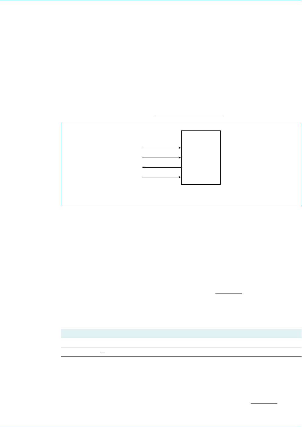
PN512 All information provided in this document is subject to legal disclaimers. © NXP B.V. 2012. All rights reserved.
Product data sheet
COMPANY PUBLIC Rev. 4.2 — 28 August 2012
111342 67 of 132
NXP Semiconductors PN512
Transmission module
10.2 Serial Peripheral Interface
A serial peripheral interface (SPI compatible) is supported to enable high-speed
communication to the host. The interface can handle data speeds up to 10 Mbit/s. When
communicating with a host, the PN512 acts as a slave, receiving data from the external
host for register settings, sending and receiving data relevant for RF interface
communication.
An interface compatible with SPI enables high-speed serial communication between the
PN512 and a microcontroller. The implemented interface is in accordance with the SPI
standard.
The timing specification is given in Section 26.1 on page 113.
The PN512 acts as a slave during SPI communication. The SPI clock signal SCK must be
generated by the master. Data communication from the master to the slave uses the
MOSI line. The MISO line is used to send data from the PN512 to the master.
Data bytes on both MOSI and MISO lines are sent with the MSB first. Data on both MOSI
and MISO lines must be stable on the rising edge of the clock and can be changed on the
falling edge. Data is provided by the PN512 on the falling clock edge and is stable during
the rising clock edge.
10.2.1 SPI read data
Reading data using SPI requires the byte order shown in Table 142 to be used. It is
possible to read out up to n-data bytes.
The first byte sent defines both the mode and the address.
[1] X = Do not care.
Remark: The MSB must be sent first.
10.2.2 SPI write data
To write data to the PN512 using SPI requires the byte order shown in Table 143. It is
possible to write up to n data bytes by only sending one address byte.
Fig 12. SPI connection to host
001aan220
PN512
SCK
SCK
MOSI
MOSI
MISO
MISO
NSS
NSS
Table 142. MOSI and MISO byte order
Line Byte 0 Byte 1 Byte 2 To Byte n Byte n + 1
MOSI address 0 address 1 address 2 ... address n 00
MISO X[1] data 0 data 1 ... data n 1data n

PN512 All information provided in this document is subject to legal disclaimers. © NXP B.V. 2012. All rights reserved.
Product data sheet
COMPANY PUBLIC Rev. 4.2 — 28 August 2012
111342 68 of 132
NXP Semiconductors PN512
Transmission module
The first send byte defines both the mode and the address byte.
[1] X = Do not care.
Remark: The MSB must be sent first.
10.2.3 SPI address byte
The address byte has to meet the following format.
The MSB of the first byte defines the mode used. To read data from the PN512 the MSB is
set to logic 1. To write data to the PN512 the MSB must be set to logic 0. Bits 6 to 1 define
the address and the LSB is set to logic 0.
10.3 UART interface
10.3.1 Connection to a host
Remark: Signals DTRQ and MX can be disabled by clearing TestPinEnReg register’s
RS232LineEn bit.
10.3.2 Selectable UART transfer speeds
The internal UART interface is compatible with an RS232 serial interface.
The default transfer speed is 9.6 kBd. To change the transfer speed, the host controller
must write a value for the new transfer speed to the SerialSpeedReg register. Bits
BR_T0[2:0] and BR_T1[4:0] define the factors for setting the transfer speed in the
SerialSpeedReg register.
The BR_T0[2:0] and BR_T1[4:0] settings are described in Table 9. Examples of different
transfer speeds and the relevant register settings are given in Table 10.
Table 143. MOSI and MISO byte order
Line Byte 0 Byte 1 Byte 2 To Byte n Byte n + 1
MOSI address 0 data 0 data 1 ... data n 1data n
MISO X[1] X[1] X[1] ... X[1] X[1]
Table 144. Address byte 0 register; address MOSI
7 (MSB) 6543210 (LSB)
1 = read
0 = write
address 0
Fig 13. UART connection to microcontrollers
001aan221
PN512
RX
RX
TX
TX
DTRQ
DTRQ
MX
MX

PN512 All information provided in this document is subject to legal disclaimers. © NXP B.V. 2012. All rights reserved.
Product data sheet
COMPANY PUBLIC Rev. 4.2 — 28 August 2012
111342 69 of 132
NXP Semiconductors PN512
Transmission module
[1] The resulting transfer speed error is less than 1.5 % for all described transfer speeds.
The selectable transfer speeds shown in Table 10 are calculated according to the
following equations:
If BR_T0[2:0] = 0:
(1)
If BR_T0[2:0] > 0:
(2)
Remark: Transfer speeds above 1228.8 kBd are not supported.
10.3.3 UART framing
Table 145. BR_T0 and BR_T1 settings
BR_Tn Bit 0 Bit 1 Bit 2 Bit 3 Bit 4 Bit 5 Bit 6 Bit 7
BR_T0 factor11248163264
BR_T1 range 1 to 32 33 to 64 33 to 64 33 to 64 33 to 64 33 to 64 33 to 64 33 to 64
Table 146. Selectable UART transfer speeds
Transfer speed (kBd) SerialSpeedReg value Transfer speed accuracy (%)[1]
Decimal Hexadecimal
7.2 250 FAh 0.25
9.6 235 EBh 0.32
14.4 218 DAh 0.25
19.2 203 CBh 0.32
38.4 171 ABh 0.32
57.6 154 9Ah 0.25
115.2 122 7Ah 0.25
128 116 74h 0.06
230.4 90 5Ah 0.25
460.8 58 3Ah 0.25
921.6 28 1Ch 1.45
1228.8 21 15h 0.32
transfer speed 27.12 106
BR_T0 1+
--------------------------------
=
transfer speed 27.12 106
BR_T1 33+
2BR_T0 1–
-----------------------------------
-----------------------------------
=
Table 147. UART framing
Bit Length Value
Start 1-bit 0
Data 8 bits data
Stop 1-bit 1
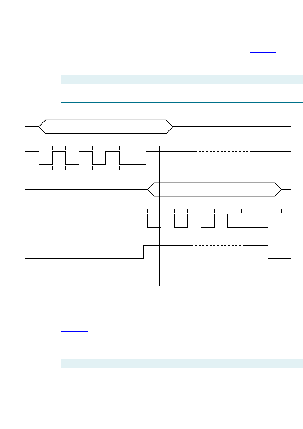
PN512 All information provided in this document is subject to legal disclaimers. © NXP B.V. 2012. All rights reserved.
Product data sheet
COMPANY PUBLIC Rev. 4.2 — 28 August 2012
111342 70 of 132
NXP Semiconductors PN512
Transmission module
Remark: The LSB for data and address bytes must be sent first. No parity bit is used
during transmission.
Read data: To read data using the UART interface, the flow shown in Table 148 must be
used. The first byte sent defines both the mode and the address.
Write data: To write data to the PN512 using the UART interface, the structure shown in
Table 149 must be used.
The first byte sent defines both the mode and the address.
Table 148. Read data byte order
Pin Byte 0 Byte 1
RX (pin 24) address -
TX (pin 31) - data 0
(1) Reserved.
Fig 14. UART read data timing diagram
001aak588
SA
ADDRESS
RX
TX
MX
DTRQ
A0 A1 A2 A3 A4 A5 (1) SO
SA D0 D1 D2 D3 D4 D5 D6 D7 SO
DATA
R/W
Table 149. Write data byte order
Pin Byte 0 Byte 1
RX (pin 24) address 0 data 0
TX (pin 31) - address 0
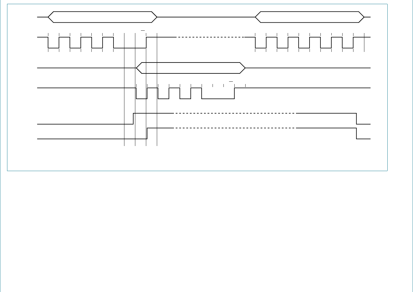
xxxxxxxxxxxxxxxxxxxxx xxxxxxxxxxxxxxxxxxxxxxxxxx xxxxxxx x x x xxxxxxxxxxxxxxxxxxxxxxxxxxxxxx xxxxxxxxxxxxxxxxxxx xx xx xxxxx
xxxxxxxxxxxxxxxxxxxxxxxxxxx xxxxxxxxxxxxxxxxxxx xxxxxx xxxxxxxxxxxxxxxxxxxxxxxxxxxxxxxxxxx xxxxxxxxxxxx x x
xxxxxxxxxxxxxxxxxxxxx xxxxxxxxxxxxxxxxxxxxxxxxxxxxxx xxxxx xxxxxxxxxxxxxxxxxxxxxxxxxxxxxxxxxxxxxxxxxxxxxxxxxx xxxxxxxx
xxxxxxxxxxxxxxxxxxxxxxxxx xxxxxxxxxxxxxxxxxxxx xxx
PN512 All information provided in this document is subject to legal disclaimers. © NXP B.V. 2012. All rights reserved.
Product data sheet
COMPANY PUBLIC Rev. 4.2 — 28 August 2012
111342 71 of 132
NXP Semiconductors PN512
Transmission module
Remark: The data byte can be sent directly after the address byte on pin RX.
Address byte: The address byte has to meet the following format:
(1) Reserved.
Fig 15. UART write data timing diagram
001aak589
SA
ADDRESS
RX
TX
MX
DTRQ
A0 A1 A2 A3 A4 A5
(1)
SO SA D0 D1 D2 D3 D4 D5 D6 D7 SO
SA A0 A1 A2 A3 A4 A5
(1)
SO
DATA
ADDRESS
R/W
R/W
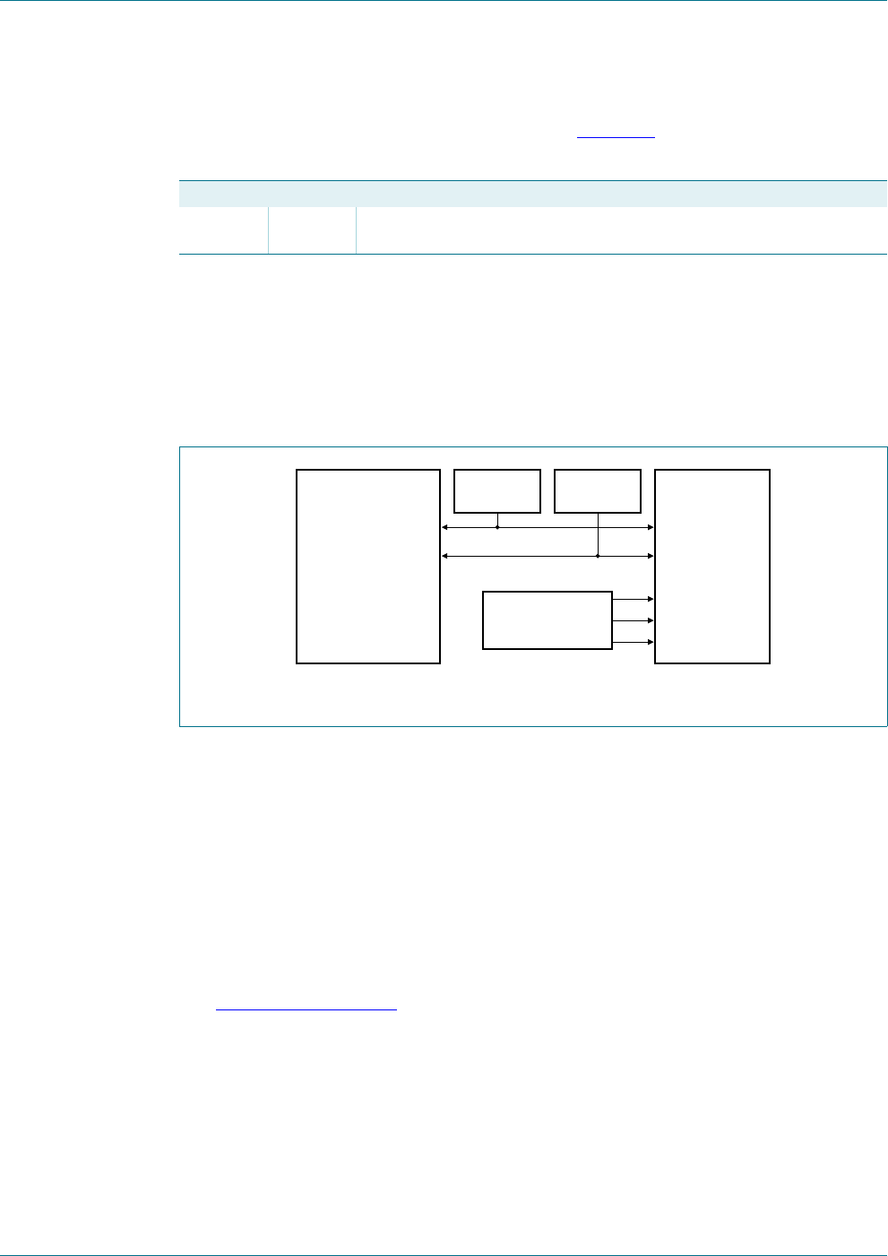
PN512 All information provided in this document is subject to legal disclaimers. © NXP B.V. 2012. All rights reserved.
Product data sheet
COMPANY PUBLIC Rev. 4.2 — 28 August 2012
111342 72 of 132
NXP Semiconductors PN512
Transmission module
The MSB of the first byte sets the mode used. To read data from the PN512, the MSB is
set to logic 1. To write data to the PN512 the MSB is set to logic 0. Bit 6 is reserved for
future use, and bits 5 to 0 define the address; see Table 150.
10.4 I2C Bus Interface
An I2C-bus (Inter-IC) interface is supported to enable a low-cost, low pin count serial bus
interface to the host. The I2C-bus interface is implemented according to
NXP Semiconductors’ I2C-bus interface specification, rev. 2.1, January 2000. The
interface can only act in Slave mode. Therefore the PN512 does not implement clock
generation or access arbitration.
The PN512 can act either as a slave receiver or slave transmitter in Standard mode, Fast
mode and High-speed mode.
SDA is a bidirectional line connected to a positive supply voltage using a current source or
a pull-up resistor. Both SDA and SCL lines are set HIGH when data is not transmitted. The
PN512 has a 3-state output stage to perform the wired-AND function. Data on the I2C-bus
can be transferred at data rates of up to 100 kBd in Standard mode, up to 400 kBd in Fast
mode or up to 3.4 Mbit/s in High-speed mode.
If the I2C-bus interface is selected, spike suppression is activated on lines SCL and SDA
as defined in the I2C-bus interface specification.
See Table 170 on page 114 for timing requirements.
Table 150. Address byte 0 register; address MOSI
7 (MSB) 6543210 (LSB)
1 = read
0 = write
reserved address
Fig 16. I2C-bus interface
001aan222
PN512
SDA
SCL
I2C
EA
ADR_[5:0]
PULL-UP
NETWORK
CONFIGURATION
WIRING
PULL-UP
NETWORK
MICROCONTROLLER
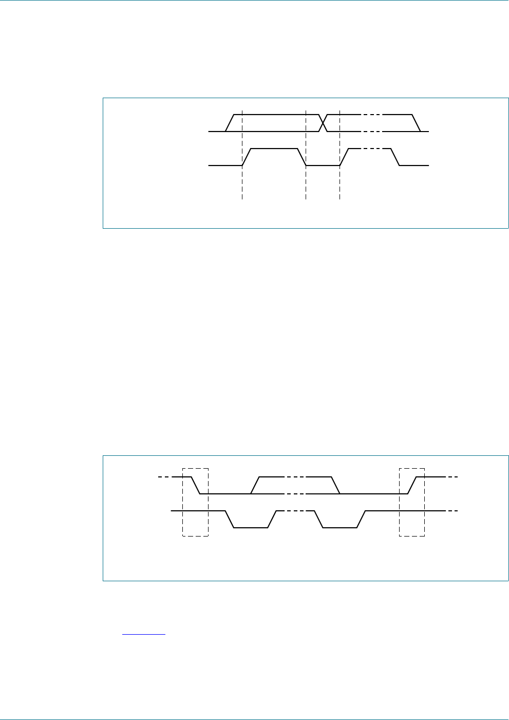
PN512 All information provided in this document is subject to legal disclaimers. © NXP B.V. 2012. All rights reserved.
Product data sheet
COMPANY PUBLIC Rev. 4.2 — 28 August 2012
111342 73 of 132
NXP Semiconductors PN512
Transmission module
10.4.1 Data validity
Data on the SDA line must be stable during the HIGH clock period. The HIGH or LOW
state of the data line must only change when the clock signal on SCL is LOW.
10.4.2 START and STOP conditions
To manage the data transfer on the I2C-bus, unique START (S) and STOP (P) conditions
are defined.
•A START condition is defined with a HIGH-to-LOW transition on the SDA line while
SCL is HIGH.
•A STOP condition is defined with a LOW-to-HIGH transition on the SDA line while
SCL is HIGH.
The I2C-bus master always generates the START and STOP conditions. The bus is busy
after the START condition. The bus is free again a certain time after the STOP condition.
The bus stays busy if a repeated START (Sr) is generated instead of a STOP condition.
The START (S) and repeated START (Sr) conditions are functionally identical. Therefore,
S is used as a generic term to represent both the START (S) and repeated START (Sr)
conditions.
10.4.3 Byte format
Each byte must be followed by an acknowledge bit. Data is transferred with the MSB first;
see Figure 21. The number of transmitted bytes during one data transfer is unrestricted
but must meet the read/write cycle format.
Fig 17. Bit transfer on the I2C-bus
mbc621
data line
stable;
data valid
change
of data
allowed
SDA
SCL
Fig 18. START and STOP conditions
mbc622
SDA
SCL P
STOP condition
SDA
SCL
S
START condition
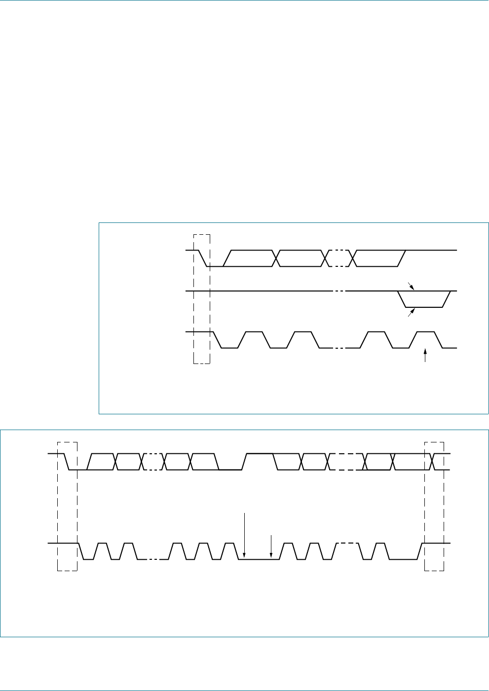
PN512 All information provided in this document is subject to legal disclaimers. © NXP B.V. 2012. All rights reserved.
Product data sheet
COMPANY PUBLIC Rev. 4.2 — 28 August 2012
111342 74 of 132
NXP Semiconductors PN512
Transmission module
10.4.4 Acknowledge
An acknowledge must be sent at the end of one data byte. The acknowledge-related clock
pulse is generated by the master. The transmitter of data, either master or slave, releases
the SDA line (HIGH) during the acknowledge clock pulse. The receiver pulls down the
SDA line during the acknowledge clock pulse so that it remains stable LOW during the
HIGH period of this clock pulse.
The master can then generate either a STOP (P) condition to stop the transfer or a
repeated START (Sr) condition to start a new transfer.
A master-receiver indicates the end of data to the slave-transmitter by not generating an
acknowledge on the last byte that was clocked out by the slave. The slave-transmitter
releases the data line to allow the master to generate a STOP (P) or repeated START (Sr)
condition.
Fig 19. Acknowledge on the I2C-bus
mbc602
S
START
condition
9821
clock pulse for
acknowledgement
not acknowledge
acknowledge
data output
by transmitter
data output
by receiver
SCL from
master
Fig 20. Data transfer on the I2C-bus
msc608
Sr
or
P
SDA
Sr
P
SCL
STOP or
repeated START
condition
S
or
Sr
START or
repeated START
condition
1 2 3 - 8 9
ACK
9
ACK
7812
MSB acknowledgement
signal from slave
byte complete,
interrupt within slave
clock line held LOW while
interrupts are serviced
acknowledgement
signal from receiver

PN512 All information provided in this document is subject to legal disclaimers. © NXP B.V. 2012. All rights reserved.
Product data sheet
COMPANY PUBLIC Rev. 4.2 — 28 August 2012
111342 75 of 132
NXP Semiconductors PN512
Transmission module
10.4.5 7-Bit addressing
During the I2C-bus address procedure, the first byte after the START condition is used to
determine which slave will be selected by the master.
Several address numbers are reserved. During device configuration, the designer must
ensure that collisions with these reserved addresses cannot occur. Check the I2C-bus
specification for a complete list of reserved addresses.
The I2C-bus address specification is dependent on the definition of pin EA. Immediately
after releasing pin NRSTPD or after a power-on reset, the device defines the I2C-bus
address according to pin EA.
If pin EA is set LOW, the upper 4 bits of the device bus address are reserved by
NXP Semiconductors and set to 0101b for all PN512 devices. The remaining 3 bits
(ADR_0, ADR_1, ADR_2) of the slave address can be freely configured by the customer
to prevent collisions with other I2C-bus devices.
If pin EA is set HIGH, ADR_0 to ADR_5 can be completely specified at the external pins
according to Table 140 on page 66. ADR_6 is always set to logic 0.
In both modes, the external address coding is latched immediately after releasing the
reset condition. Further changes at the used pins are not taken into consideration.
Depending on the external wiring, the I2C-bus address pins can be used for test signal
outputs.
10.4.6 Register write access
To write data from the host controller using the I2C-bus to a specific register in the PN512
the following frame format must be used.
•The first byte of a frame indicates the device address according to the I2C-bus rules.
•The second byte indicates the register address followed by up to n-data bytes.
In one frame all data bytes are written to the same register address. This enables fast
FIFO buffer access. The Read/Write (R/W) bit is set to logic 0.
Fig 21. First byte following the START procedure
001aak591
slave address
bit 6 bit 5 bit 4 bit 3 bit 2 bit 1 bit 0 R/W
MSB LSB
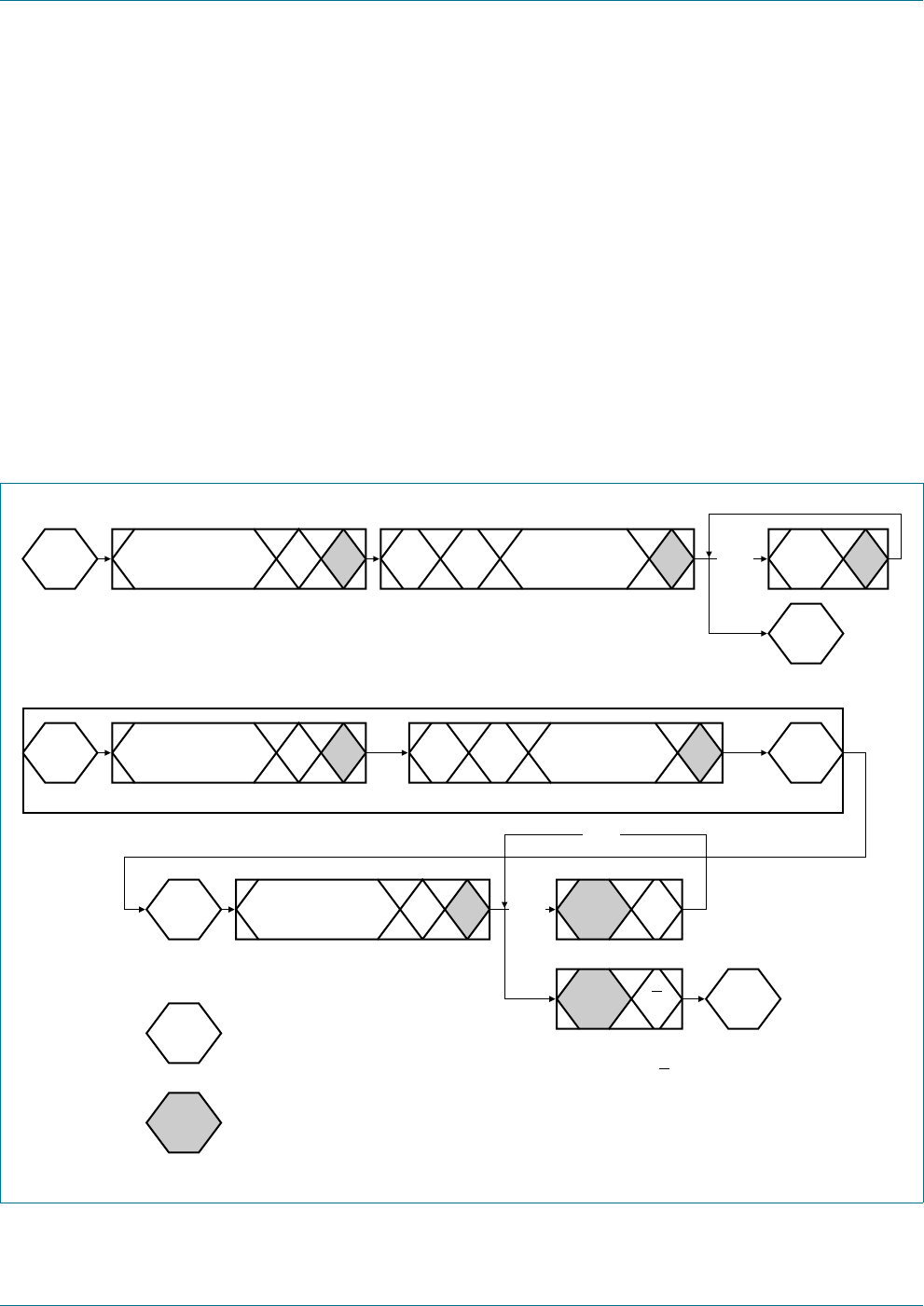
PN512 All information provided in this document is subject to legal disclaimers. © NXP B.V. 2012. All rights reserved.
Product data sheet
COMPANY PUBLIC Rev. 4.2 — 28 August 2012
111342 76 of 132
NXP Semiconductors PN512
Transmission module
10.4.7 Register read access
To read out data from a specific register address in the PN512, the host controller must
use the following procedure:
•Firstly, a write access to the specific register address must be performed as indicated
in the frame that follows
•The first byte of a frame indicates the device address according to the I2C-bus rules
•The second byte indicates the register address. No data bytes are added
•The Read/Write bit is 0
After the write access, read access can start. The host sends the device address of the
PN512. In response, the PN512 sends the content of the read access register. In one
frame all data bytes can be read from the same register address. This enables fast FIFO
buffer access or register polling.
The Read/Write (R/W) bit is set to logic 1.
Fig 22. Register read and write access
001aak592
SA00
I
2
C-BUS
SLAVE ADDRESS
[A7:A0]
JOINER REGISTER
ADDRESS [A5:A0]
write cycle
0
(W) ADATA
[7:0]
[0:n]
[0:n]
[0:n]
A
P
SA00
I
2
C-BUS
SLAVE ADDRESS
[A7:A0]
JOINER REGISTER
ADDRESS [A5:A0]
read cycle
optional, if the previous access was on the same register address
0
(W) AP
P
S
S start condition
P stop condition
A acknowledge
A not acknowledge
W write cycle
R read cycle
A
I
2
C-BUS
SLAVE ADDRESS
[A7:A0]
sent by master
sent by slave
DATA
[7:0]
1
(R) A
DATA
[7:0] A
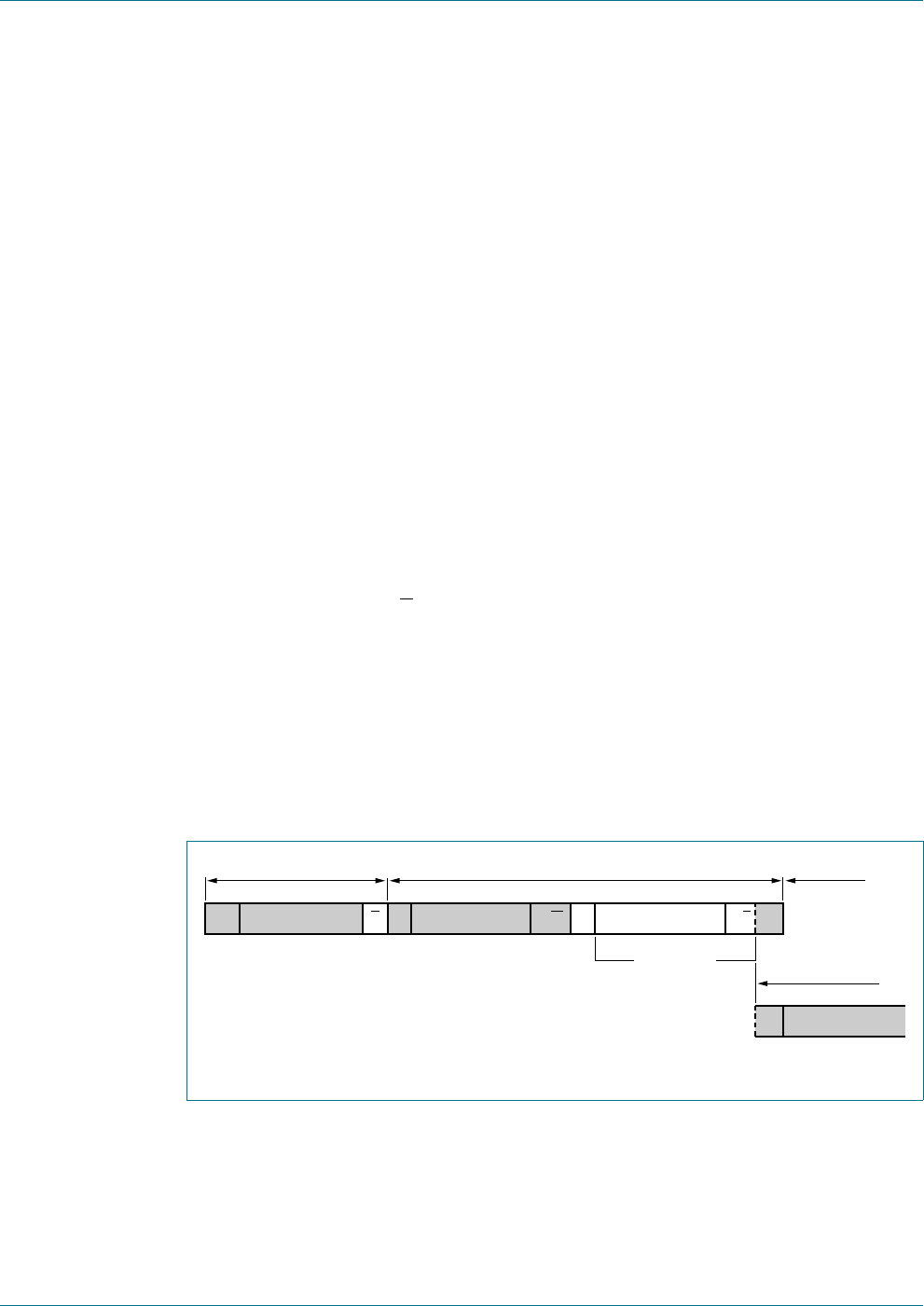
PN512 All information provided in this document is subject to legal disclaimers. © NXP B.V. 2012. All rights reserved.
Product data sheet
COMPANY PUBLIC Rev. 4.2 — 28 August 2012
111342 77 of 132
NXP Semiconductors PN512
Transmission module
10.4.8 High-speed mode
In High-speed mode (HS mode), the device can transfer information at data rates of up to
3.4 Mbit/s, while remaining fully downward-compatible with Fast or Standard mode
(F/S mode) for bidirectional communication in a mixed-speed bus system.
10.4.9 High-speed transfer
To achieve data rates of up to 3.4 Mbit/s the following improvements have been made to
I2C-bus operation.
•The inputs of the device in HS mode incorporate spike suppression, a Schmitt trigger
on the SDA and SCL inputs and different timing constants when compared to
F/S mode
•The output buffers of the device in HS mode incorporate slope control of the falling
edges of the SDA and SCL signals with different fall times compared to F/S mode
10.4.10 Serial data transfer format in HS mode
The HS mode serial data transfer format meets the Standard mode I2C-bus specification.
HS mode can only start after all of the following conditions (all of which are in F/S mode):
1. START condition (S)
2. 8-bit master code (00001XXXb)
3. Not-acknowledge bit (A)
When HS mode starts, the active master sends a repeated START condition (Sr) followed
by a 7-bit slave address with a R/W bit address and receives an acknowledge bit (A) from
the selected PN512.
Data transfer continues in HS mode after the next repeated START (Sr), only switching
back to F/S mode after a STOP condition (P). To reduce the overhead of the master code,
a master links a number of HS mode transfers, separated by repeated START conditions
(Sr).
Fig 23. I2C-bus HS mode protocol switch
F/S mode HS mode (current-source for SCL HIGH enabled) F/S mode
001aak749
AA A/ADATA
(n-bytes + A)
S R/WMASTER CODE Sr SLAVE ADDRESS
HS mode continues
Sr SLAVE ADDRESS
P
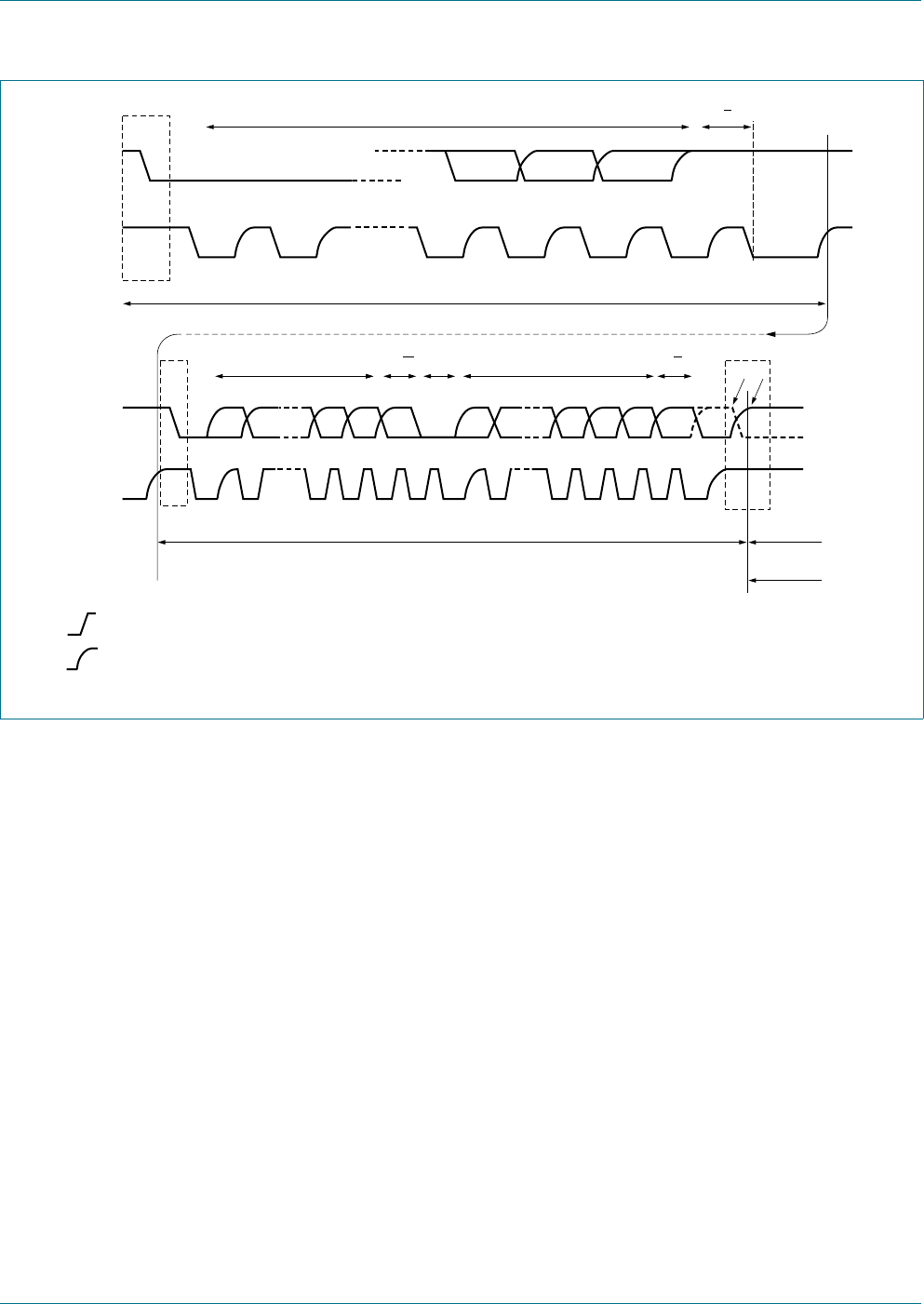
PN512 All information provided in this document is subject to legal disclaimers. © NXP B.V. 2012. All rights reserved.
Product data sheet
COMPANY PUBLIC Rev. 4.2 — 28 August 2012
111342 78 of 132
NXP Semiconductors PN512
Transmission module
Fig 24. I2C-bus HS mode protocol frame
msc618
8-bit master code 0000 1xxx AtH
t1
S
F/S mode
HS mode If P then
F/S mode
If Sr (dotted lines)
then HS mode
16789 67891
1 2 to 5
2 to 5
2 to 5
67 89
SDA high
SCL high
SDA high
SCL high
tHtFS
Sr Sr P
n + (8-bit data + A/A)
7-bit SLA R/W A
= Master current source pull-up
= Resistor pull-up

PN512 All information provided in this document is subject to legal disclaimers. © NXP B.V. 2012. All rights reserved.
Product data sheet
COMPANY PUBLIC Rev. 4.2 — 28 August 2012
111342 79 of 132
NXP Semiconductors PN512
Transmission module
10.4.11 Switching between F/S mode and HS mode
After reset and initialization, the PN512 is in Fast mode (which is in effect F/S mode as
Fast mode is downward-compatible with Standard mode). The connected PN512
recognizes the “S 00001XXX A” sequence and switches its internal circuitry from the Fast
mode setting to the HS mode setting.
The following actions are taken:
1. Adapt the SDA and SCL input filters according to the spike suppression requirement
in HS mode.
2. Adapt the slope control of the SDA output stages.
It is possible for system configurations that do not have other I2C-bus devices involved in
the communication to switch to HS mode permanently. This is implemented by setting
Status2Reg register’s I2CForceHS bit to logic 1. In permanent HS mode, the master code
is not required to be sent. This is not defined in the specification and must only be used
when no other devices are connected on the bus. In addition, spikes on the I2C-bus lines
must be avoided because of the reduced spike suppression.
10.4.12 PN512 at lower speed modes
PN512 is fully downward-compatible and can be connected to an F/S mode I2C-bus
system. The device stays in F/S mode and communicates at F/S mode speeds because a
master code is not transmitted in this configuration.
11. 8-bit parallel interface
The PN512 supports two different types of 8-bit parallel interfaces, Intel and Motorola
compatible modes.
11.1 Overview of supported host controller interfaces
The PN512 supports direct interfacing to various -Controllers. The following table shows
the parallel interface types supported by the PN512.
Table 151. Supported interface types
Supported interface types Bus Separated Address and
Data Bus Multiplexed Address
and Data Bus
Separated Read and Write
Strobes (INTEL compatible)
control NRD, NWR, NCS NRD, NWR, NCS, ALE
address A0 … A3 [..A5*] AD0 … AD7
data D0 … D7 AD0 … AD7
Multiplexed Read and Write
Strobe (Motorola compatible)
control R/NW, NDS, NCS R/NW, NDS, NCS, AS
address A0 … A3 [..A5*] AD0 … AD7
data D0 … D7 AD0 … AD7

PN512 All information provided in this document is subject to legal disclaimers. © NXP B.V. 2012. All rights reserved.
Product data sheet
COMPANY PUBLIC Rev. 4.2 — 28 August 2012
111342 80 of 132
NXP Semiconductors PN512
Transmission module
11.2 Separated Read/Write strobe
For timing requirements refer to Section 26.2 “8-bit parallel interface timing”.
11.3 Common Read/Write strobe
For timing requirements refer to Section 26.2 “8-bit parallel interface timing”
Fig 25. Connection to host controller with separated Read/Write strobes
001aan223
PN512
NCS
A0...A3[A5*]
D0...D7
A0
A1
A2
A3
A4*
A5*
address bus (A0...A3[A5*])
ALE
NRD
NWR
ADDRESS
DECODER
data bus (D0...D7)
high
not data strobe (NRD)
not write (NWR)
address bus
remark: *depending on the package type.
multiplexed address/data AD0...AD7)
PN512
NCS
D0...D7
ALE
NRD
NWR
ADDRESS
DECODER
low
low
high
high
high
low
address latch enable (ALE)
not read strobe (NRD)
not write (NWR)
non multiplexed
address
Fig 26. Connection to host controller with common Read/Write strobes
001aan224
PN512
NCS
A0...A3[A5*]
D0...D7
A0
A1
A2
A3
A4*
A5*
address bus (A0...A3[A5*])
ALE
NRD
NWR
ADDRESS
DECODER
Data bus (D0...D7)
high
not data strobe (NDS)
read not write (RD/NWR)
address bus
remark: *depending on the package type.
multiplexed address/data AD0...AD7)
PN512
NCS
D0...D7
ALE
NRD
NWR
ADDRESS
DECODER
low
low
high
high
low
low
address strobe (AS)
not data strobe (NDS)
read not write (RD/NWR)
non multiplexed
address

PN512 All information provided in this document is subject to legal disclaimers. © NXP B.V. 2012. All rights reserved.
Product data sheet
COMPANY PUBLIC Rev. 4.2 — 28 August 2012
111342 81 of 132
NXP Semiconductors PN512
Transmission module
12. Analog interface and contactless UART
12.1 General
The integrated contactless UART supports the external host online with framing and error
checking of the protocol requirements up to 848 kBd. An external circuit can be connected
to the communication interface pins MFIN and MFOUT to modulate and demodulate the
data.
The contactless UART handles the protocol requirements for the communication
protocols in cooperation with the host. Protocol handling generates bit and byte-oriented
framing. In addition, it handles error detection such as parity and CRC, based on the
various supported contactless communication protocols.
Remark: The size and tuning of the antenna and the power supply voltage have an
important impact on the achievable operating distance.
12.2 TX driver
The signal on pins TX1 and TX2 is the 13.56 MHz energy carrier modulated by an
envelope signal. It can be used to drive an antenna directly using a few passive
components for matching and filtering; see Section 15 on page 93. The signal on pins TX1
and TX2 can be configured using the TxControlReg register; see Section 9.2.2.5 on
page 37.
The modulation index can be set by adjusting the impedance of the drivers. The
impedance of the p-driver can be configured using registers CWGsPReg and
ModGsPReg. The impedance of the n-driver can be configured using the GsNReg
register. The modulation index also depends on the antenna design and tuning.
The TxModeReg and TxSelReg registers control the data rate and framing during
transmission and the antenna driver setting to support the different requirements at the
different modes and transfer speeds.
[1] X = Do not care.
Table 152. Register and bit settings controlling the signal on pin TX1
Bit
Tx1RFEn Bit
Force
100ASK
Bit
InvTx1RFOn Bit
InvTx1RFOff Envelope Pin
TX1 GSPMos GSNMos Remarks
0X
[1] X[1] X[1] X[1] X[1] X[1] X[1] not specified if RF is
switched off
100 X
[1] 0 RF pMod nMod 100 % ASK: pin TX1
pulled to logic 0,
independent of the
InvTx1RFOff bit
1RFpCWnCW
01 X
[1] 0 RF pMod nMod
1RFpCWnCW
11 X
[1] 0 0 pMod nMod
1RF_npCWnCW

PN512 All information provided in this document is subject to legal disclaimers. © NXP B.V. 2012. All rights reserved.
Product data sheet
COMPANY PUBLIC Rev. 4.2 — 28 August 2012
111342 82 of 132
NXP Semiconductors PN512
Transmission module
[1] X = Do not care.
The following abbreviations have been used in Table 152 and Table 153:
•RF: 13.56 MHz clock derived from 27.12 MHz quartz crystal oscillator divided by 2
•RF_n: inverted 13.56 MHz clock
•GSPMos: conductance, configuration of the PMOS array
•GSNMos: conductance, configuration of the NMOS array
•pCW: PMOS conductance value for continuous wave defined by the CWGsPReg
register
•pMod: PMOS conductance value for modulation defined by the ModGsPReg register
•nCW: NMOS conductance value for continuous wave defined by the GsNReg
register’s CWGsN[3:0] bits
•nMod: NMOS conductance value for modulation defined by the GsNReg register’s
ModGsN[3:0] bits
•X = do not care.
Remark: If only one driver is switched on, the values for CWGsPReg, ModGsPReg and
GsNReg registers are used for both drivers.
12.3 RF level detector
The RF level detector is integrated to fulfill NFCIP1 protocol requirements (e.g. RF
collision avoidance). Furthermore the RF level detector can be used to wake up the
PN512 and to generate an interrupt.
Table 153. Register and bit settings controlling the signal on pin TX2
Bit
Tx1RFEn Bit
Force
100ASK
Bit
Tx2CW Bit
InvTx2RFOn Bit
InvTx2RFOff Envelope Pin
TX2 GSPMos GSNMos Remarks
0X
[1] X[1] X[1] X[1] X[1] X[1] X[1] X[1] not specified if
RF is switched
off
1000 X
[1] 0 RF pMod nMod -
1RFpCWnCW
1X
[1] 0 RF_n pMod nMod
1RF_npCWnCW
10 X
[1] X[1] RF pCW nCW conductance
always CW for
the Tx2CW bit
1X
[1] X[1] RF_n pCW nCW
100 X
[1] 0 0 pMod nMod 100 % ASK: pin
TX2 pulled
to logic 0
(independent of
the
InvTx2RFOn/Inv
Tx2RFOff bits)
1RFpCWnCW
1X
[1] 0 0 pMod nMod
1RF_npCWnCW
10 X
[1] X[1] RF pCW nCW
1X
[1] X[1] RF_n pCW nCW

PN512 All information provided in this document is subject to legal disclaimers. © NXP B.V. 2012. All rights reserved.
Product data sheet
COMPANY PUBLIC Rev. 4.2 — 28 August 2012
111342 83 of 132
NXP Semiconductors PN512
Transmission module
The sensitivity of the RF level detector is adjustable in a 4-bit range using the bits RFLevel
in register RFCfgReg. The sensitivity itself depends on the antenna configuration and
tuning.
Possible sensitivity levels at the RX pin are listed in the Table 153.
To increase the sensitivity of the RF level detector an amplifier can be activated by setting
the bit RFLevelAmp in register RFCfgReg to 1.
Remark: During soft Power-down mode the RF level detector amplifier is automatically
switched off to ensure that the power consumption is less than 10 Aat3V.
Remark: With typical antennas lower sensitivity levels can provoke misleading results
because of intrinsic noise in the environment.
Note: It is recommended to use the bit RFLevelAmp only with higher RF level settings.
12.4 Data mode detector
The Data mode detector gives the possibility to detect received signals according to the
ISO/IEC 14443A/MIFARE, FeliCa or NFCIP-1 schemes at the standard transfer speeds
for 106 kbit, 212 kbit and 424 kbit in order to prepare the internal receiver in a fast and
convenient way for further data processing.
The Data mode detector can only be activated by the AutoColl command. The mode
detector resets, when no external RF field is detected by the RF level detector. The Data
mode detector could be switched off during the AutoColl command by setting bit
ModeDetOff in register ModeReg to 1.
Table 154. Setting of the bits RFlevel in register RFCfgReg (RFLevel amplifier deactivated)
V~Rx [Vpp] RFLevel
~2 1111
~1.4 1110
~0.99 1101
~0.69 1100
~0.49 1011
~0.35 1010
~0.24 1001
~0.17 1000
~0.12 0111
~0.083 0110
~0.058 0101
~0.041 0100
~0.029 0011
~0.020 0010
~0.014 0001
~0.010 0000
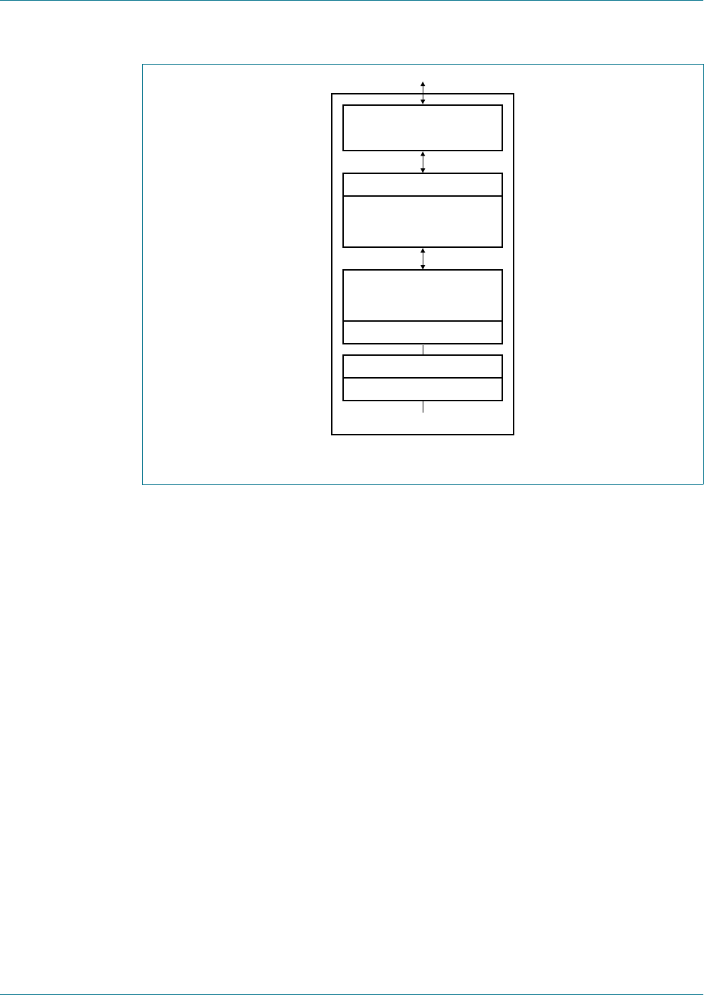
PN512 All information provided in this document is subject to legal disclaimers. © NXP B.V. 2012. All rights reserved.
Product data sheet
COMPANY PUBLIC Rev. 4.2 — 28 August 2012
111342 84 of 132
NXP Semiconductors PN512
Transmission module
Fig 27. Data mode detector
001aan225
HOST INTERFACES
RECEIVER
I/Q DEMODULATOR
REGISTERS
REGISTERSETTING
FOR THE
DETECTED MODE
DATA MODE DETECTOR
RX
PN512
NFC @ 106 kbit/s
NFC @ 212 kbit/s
NFC @ 424 kbit/s
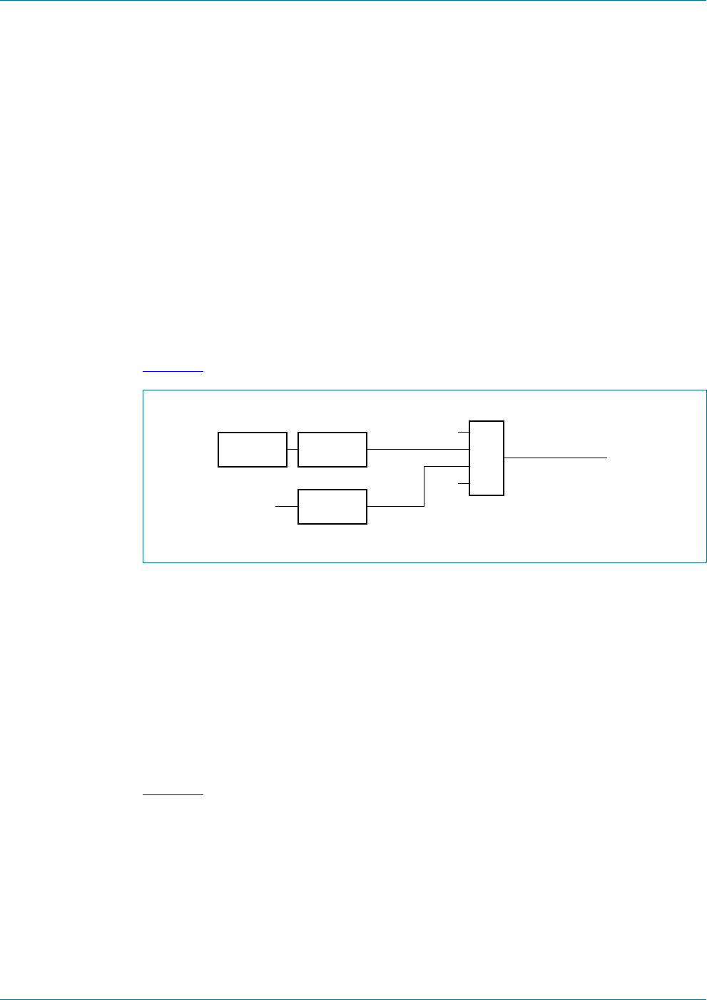
PN512 All information provided in this document is subject to legal disclaimers. © NXP B.V. 2012. All rights reserved.
Product data sheet
COMPANY PUBLIC Rev. 4.2 — 28 August 2012
111342 85 of 132
NXP Semiconductors PN512
Transmission module
12.5 Serial data switch
Two main blocks are implemented in the PN512. The digital block comprises the state
machines, encoder/decoder logic. The analog block comprises the modulator and
antenna drivers, the receiver and amplifiers. The interface between these two blocks can
be configured in the way, that the interfacing signals may be routed to the pins SIGIN and
SIGOUT. SIGIN is capable of processing digital NFC signals on transfer speeds above
424 kbit. The SIGOUT pin can provide a digital signal that can be used with an additional
external circuit to generate transfer speeds above 424 kbit (including 106, 212 and
424 kbit). Furthermore SIGOUT and SIGIN can be used to enable the S2C interface in the
card SAM mode to emulate a card functionality with the PN512 and a secure IC. A secure
IC can be the SmartMX smart card controller IC.
This topology allows the analog block of the PN512 to be connected to the digital block of
another device.
The serial signal switch is controlled by the TxSelReg and RxSelReg registers.
Figure 28 shows the serial data switch for TX1 and TX2.
12.6 S2C interface support
The S2C provides the possibility to directly connect a secure IC to the PN512 in order act
as a contactless smart card IC via the PN512. The interfacing signals can be routed to the
pins SIGIN and SIGOUT. SIGIN can receive either a digital FeliCa or digitized
ISO/IEC 14443A signal sent by the secure IC. The SIGOUT pin can provide a digital
signal and a clock to communicate to the secure IC. A secure IC can be the smart card IC
provided by NXP Semiconductors.
The PN512 has an extra supply pin (SVDD and PVSS as Ground line) for the SIGIN and
SIGOUT pads.
Figure 30 outlines possible ways of communications via the PN512 to the secure IC.
Fig 28. Serial data switch for TX1 and TX2
001aak593
INTERNAL
CODER INVERT IF
InvMod = 1
DriverSel[1:0]
00
01
10
11
3-state
to driver TX1 and TX2
0 = impedance = modulated
1 = impedance = CW
1
INVERT IF
PolMFin = 0
MFIN
envelope
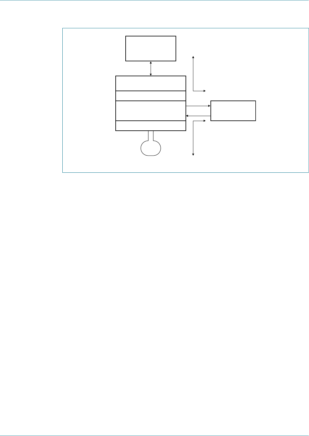
PN512 All information provided in this document is subject to legal disclaimers. © NXP B.V. 2012. All rights reserved.
Product data sheet
COMPANY PUBLIC Rev. 4.2 — 28 August 2012
111342 86 of 132
NXP Semiconductors PN512
Transmission module
Configured in the Secure Access Mode the host controller can directly communicate to
the Secure IC via SIGIN/SIGOUT. In this mode the PN512 generates the RF clock and
performs the communication on the SIGOUT line. To enable the Secure Access module
mode the clock has to be derived by the internal oscillator of the PN512, see bits
SAMClockSel in register TestSel1Reg.
Configured in Contactless Card mode the secure IC can act as contactless smart card IC
via the PN512. In this mode the signal on the SIGOUT line is provided by the external RF
field of the external reader/writer. To enable the Contactless Card mode the clock derived
by the external RF field has to be used.
The configuration of the S2C interface differs for the FeliCa and MIFARE scheme as
outlined in the following chapters.
Fig 29. Communication flows using the S2C interface
001aan226
CONTACTLESS UART
SERIAL SIGNAL SWITCH
FIFO AND STATE MACHINE
SPI, I
2
C, SERIAL UART
HOST CONTROLLER
PN512
SECURE CORE IC
SIGOUT
SIGIN
2. contactless
card mode
1. secure access
module (SAM) mode
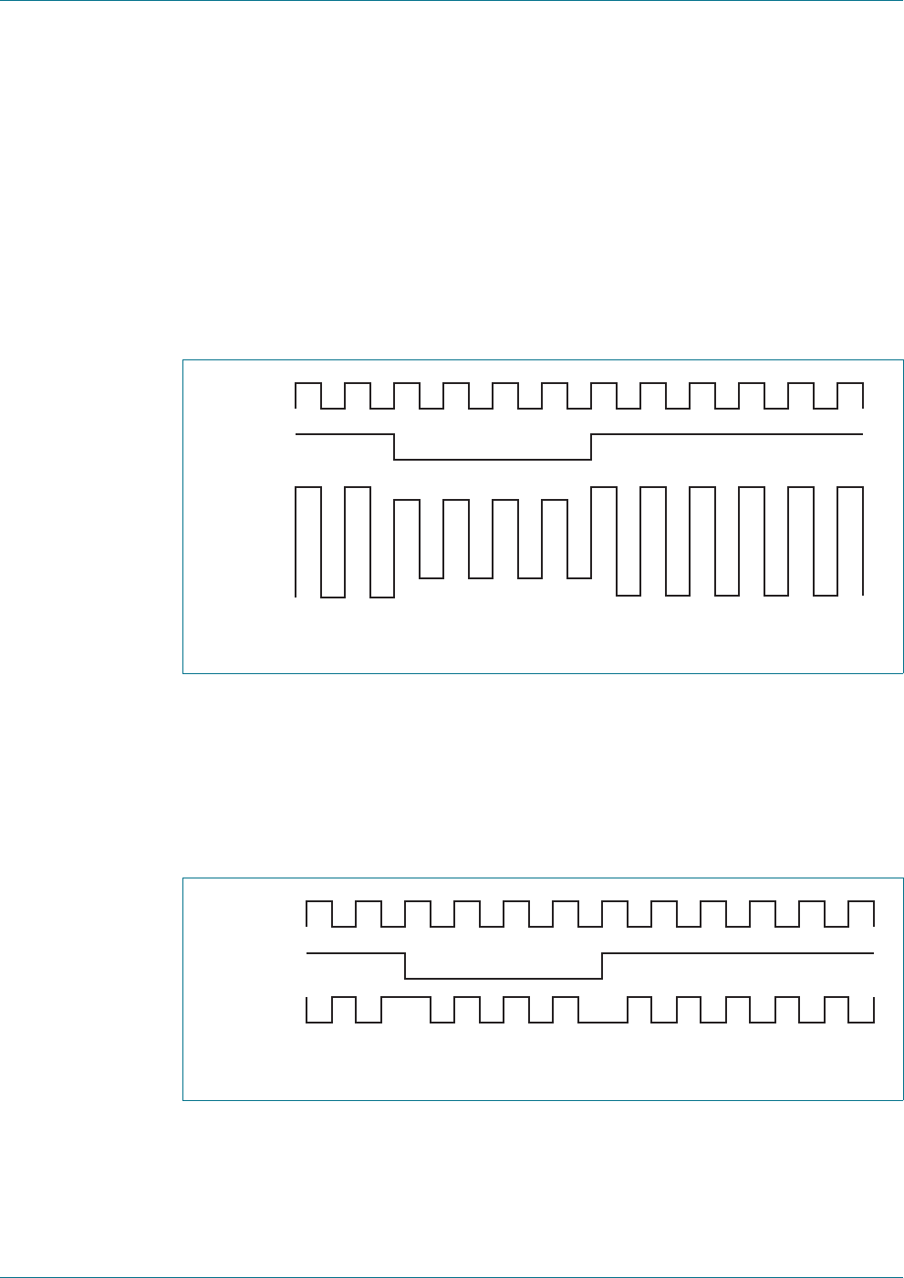
PN512 All information provided in this document is subject to legal disclaimers. © NXP B.V. 2012. All rights reserved.
Product data sheet
COMPANY PUBLIC Rev. 4.2 — 28 August 2012
111342 87 of 132
NXP Semiconductors PN512
Transmission module
12.6.1 Signal shape for Felica S2C interface support
The FeliCa secure IC is connected to the PN512 via the pins SIGOUT and SIGIN.
The signal at SIGOUT contains the information of the 13.56 MHz clock and the digitized
demodulated signal. The clock and the demodulated signal is combined by using the
logical function exclusive or.
To ensure that this signal is free of spikes, the demodulated signal is digitally filtered first.
The time delay for that digital filtering is in the range of one bit length. The demodulated
signal changes only at a positive edge of the clock.
The register TxSelReg controls the setting at SIGOUT.
The answer of the FeliCa SAM is transferred from SIGIN directly to the antenna driver.
The modulation is done according to the register settings of the antenna drivers.
The clock is switched to AUX1 or AUX2 (see AnalogSelAux).
Note: A HIGH signal on AUX1 and AUX2 has the same level as AVDD. A HIGH signal at
SIGOUT has the same level as SVDD. Alternatively it is possible to use pin D0 as clock
output if a serial interface is used. The HIGH level at D0 is the same as PVDD.
Note: The signal on the antenna is shown in principle only. In reality the waveform is
sinusoidal.
Fig 30. Signal shape for SIGOUT in FeliCa card SAM mode
Fig 31. Signal shape for SIGIN in SAM mode
001aan227
clock
signal on
SIGIN
signal on
antenna
001aan228
clock
demodulated
signal
signal on
SIGOUT
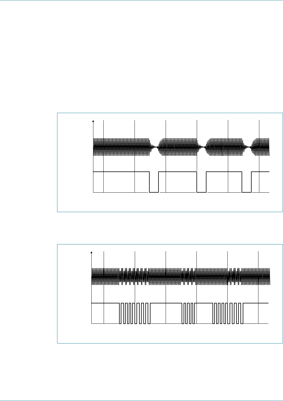
PN512 All information provided in this document is subject to legal disclaimers. © NXP B.V. 2012. All rights reserved.
Product data sheet
COMPANY PUBLIC Rev. 4.2 — 28 August 2012
111342 88 of 132
NXP Semiconductors PN512
Transmission module
12.6.2 Waveform shape for ISO/IEC 14443A and MIFARE S2C support
The secure IC, e.g. the SmartMX is connected to the PN512 via the pins SIGOUT and
SIGIN.
The waveform shape at SIGOUT is a digital 13.56 MHz Miller coded signal with levels
between PVSS and PVDD derived out of the external 13.56 MHz carrier signal in case of
the Contactless Card mode or internally generated in terms of Secure Access mode.
The register TxSelReg controls the setting at SIGOUT.
Note: The clock settings for the Secure Access mode and the Contactless Card mode
differ, refer to the description of the bits SAMClockSel in register TestSel1Reg.
The signal at SIGIN is a digital Manchester coded signal according to the requirements of
the ISO/IEC 14443A with the subcarrier frequency of 847.5 kHz generated by the secure
IC.
Fig 32. Signal shape for SIGOUT in MIFARE Card SAM mode
Fig 33. Signal shape for SIGIN in MIFARE Card SAM mode
001aan229
1
0
bit
value RF
signal on
antenna
signal on
SIGOUT
01001
001aan230
0
1
0
0011
bit
value
signal on
antenna
signal on
SIGIN

PN512 All information provided in this document is subject to legal disclaimers. © NXP B.V. 2012. All rights reserved.
Product data sheet
COMPANY PUBLIC Rev. 4.2 — 28 August 2012
111342 89 of 132
NXP Semiconductors PN512
Transmission module
12.7 Hardware support for FeliCa and NFC polling
12.7.1 Polling sequence functionality for initiator
1. Timer: The PN512 has a timer, which can be programmed in a way that it generates
an interrupt at the end of each timeslot, or if required an interrupt is generated at the
end of the last timeslot.
2. The receiver can be configured in a way to receive continuously. In this mode it can
receive any number of packets. The receiver is ready to receive the next packet
directly after the last packet has been received. This mode is active by setting the bit
RxMultiple in register RxModeReg to 1 and has to be stopped by software.
3. The internal UART adds one byte to the end of every received packet, before it is
transferred into the FIFO-buffer. This byte indicates if the received byte packet is
correct (see register ErrReg). The first byte of each packet contains the length byte of
the packet.
4. The length of one packet is 18 or 20 bytes (+ 1 byte Error-Info). The FIFO has a
length of 64 bytes. This means three packets can be stored in the FIFO at the same
time. If more than three packets are expected, the host controller has to empty the
FIFO, before the FIFO is filled completely. In case of a FIFO-overflow data is lost (See
bit BufferOvfl in register ErrorReg).
12.7.2 Polling sequence functionality for target
1. The host controller has to configure the PN512 with the correct polling response
parameters for the polling command.
2. To activate the automatic polling in Target mode, the AutoColl Command has to be
activated.
3. The PN512 receives the polling command send out by an initiator and answers with
the polling response. The timeslot is selected automatically (The timeslot itself is
randomly generated, but in the range 0 to TSN, which is defined by the Polling
command). The PN512 compares the system code, stored in byte 17 and 18 of the
Config Command with the system code received by the polling command of an
initiator. If the system code is equal, the PN512 answers according to the configured
polling response. The system code FF (hex) acts as a wildcard for the system code
bytes, i.e. a target of a system code 1234 (hex) answers to the polling command with
one of the following system codes 1234 (hex), 12FF (hex), FF34 (hex) or FFFF (hex).
If the system code does not match no answer is sent back by the PN512.
If a valid command is received by the PN512, which is not a Polling command, no
answer is sent back and the command AutoColl is stopped. The received packet is
stored in the FIFO.

PN512 All information provided in this document is subject to legal disclaimers. © NXP B.V. 2012. All rights reserved.
Product data sheet
COMPANY PUBLIC Rev. 4.2 — 28 August 2012
111342 90 of 132
NXP Semiconductors PN512
Transmission module
12.7.3 Additional hardware support for FeliCa and NFC
Additionally to the polling sequence support for the Felica mode, the PN512 supports the
check of the Len-byte.
The received Len-byte in accordance to the registers FelNFC1Reg and FelNFC2Reg:
DataLenMin in register FelNFC1Reg defines the minimum length of the accepted packet
length. This register is six bit long. Each bit represents a length of four bytes.
DataLenMax in register FelNFC2Reg defines the maximum length of the accepted
package. This register is six bit long. Each bit represents a length of four bytes. If set to
logic 1 this limit is ignored. If the length is not in the supposed range, the packet is not
transferred to the FIFO and receiving is kept active.
Example 1:
•DataLenMin = 4
–The length shall be greater or equal 16.
•DataLenMax = 5
–The length shall be smaller than 20. Valid area: 16, 17, 18, 19
Example 2:
•DataLenMin = 9
–The length shall be greater or equal 36.
•DataLenMax = 0
–The length shall be smaller than 256. Valid area: 36 to 255
12.7.4 CRC coprocessor
The following CRC coprocessor parameters can be configured:
•The CRC preset value can be either 0000h, 6363h, A671h or FFFFh depending on
the ModeReg register’s CRCPreset[1:0] bits setting
•The CRC polynomial for the 16-bit CRC is fixed to x16 +x
12 +x
5+1
•The CRCResultReg register indicates the result of the CRC calculation. This register
is split into two 8-bit registers representing the higher and lower bytes.
•The ModeReg register’s MSBFirst bit indicates that data will be loaded with the MSB
first.
Table 155. CRC coprocessor parameters
Parameter Value
CRC register length 16-bit CRC
CRC algorithm algorithm according to ISO/IEC 14443 A and ITU-T
CRC preset value 0000h, 6363h, A671h or FFFFh depending on the setting of the
ModeReg register’s CRCPreset[1:0] bits

PN512 All information provided in this document is subject to legal disclaimers. © NXP B.V. 2012. All rights reserved.
Product data sheet
COMPANY PUBLIC Rev. 4.2 — 28 August 2012
111342 91 of 132
NXP Semiconductors PN512
Transmission module
13. FIFO buffer
An 8 64 bit FIFO buffer is used in the PN512. It buffers the input and output data stream
between the host and the PN512’s internal state machine. This makes it possible to
manage data streams up to 64 bytes long without the need to take timing constraints into
account.
13.1 Accessing the FIFO buffer
The FIFO buffer input and output data bus is connected to the FIFODataReg register.
Writing to this register stores one byte in the FIFO buffer and increments the internal FIFO
buffer write pointer. Reading from this register shows the FIFO buffer contents stored in
the FIFO buffer read pointer and decrements the FIFO buffer read pointer. The distance
between the write and read pointer can be obtained by reading the FIFOLevelReg
register.
When the microcontroller starts a command, the PN512 can, while the command is in
progress, access the FIFO buffer according to that command. Only one FIFO buffer has
been implemented which can be used for input and output. The microcontroller must
ensure that there are not any unintentional FIFO buffer accesses.
13.2 Controlling the FIFO buffer
The FIFO buffer pointers can be reset by setting FIFOLevelReg register’s FlushBuffer bit
to logic 1. Consequently, the FIFOLevel[6:0] bits are all set to logic 0 and the ErrorReg
register’s BufferOvfl bit is cleared. The bytes stored in the FIFO buffer are no longer
accessible allowing the FIFO buffer to be filled with another 64 bytes.
13.3 FIFO buffer status information
The host can get the following FIFO buffer status information:
•Number of bytes stored in the FIFO buffer: FIFOLevelReg register’s FIFOLevel[6:0]
•FIFO buffer almost full warning: Status1Reg register’s HiAlert bit
•FIFO buffer almost empty warning: Status1Reg register’s LoAlert bit
•FIFO buffer overflow warning: ErrorReg register’s BufferOvfl bit. The BufferOvfl bit
can only be cleared by setting the FIFOLevelReg register’s FlushBuffer bit.
The PN512 can generate an interrupt signal when:
•ComIEnReg register’s LoAlertIEn bit is set to logic 1. It activates pin IRQ when
Status1Reg register’s LoAlert bit changes to logic 1.
•ComIEnReg register’s HiAlertIEn bit is set to logic 1. It activates pin IRQ when
Status1Reg register’s HiAlert bit changes to logic 1.
If the maximum number of WaterLevel bytes (as set in the WaterLevelReg register) or less
are stored in the FIFO buffer, the HiAlert bit is set to logic 1. It is generated according to
Equation 3:
(3)
HiAlert 64 FIFOLength–WaterLevel=

PN512 All information provided in this document is subject to legal disclaimers. © NXP B.V. 2012. All rights reserved.
Product data sheet
COMPANY PUBLIC Rev. 4.2 — 28 August 2012
111342 92 of 132
NXP Semiconductors PN512
Transmission module
If the number of WaterLevel bytes (as set in the WaterLevelReg register) or less are
stored in the FIFO buffer, the LoAlert bit is set to logic 1. It is generated according to
Equation 4:
(4)
14. Interrupt request system
The PN512 indicates certain events by setting the Status1Reg register’s IRq bit and, if
activated, by pin IRQ. The signal on pin IRQ can be used to interrupt the host using its
interrupt handling capabilities. This allows the implementation of efficient host software.
14.1 Interrupt sources overview
Table 156 shows the available interrupt bits, the corresponding source and the condition
for its activation. The ComIrqReg register’s TimerIRq interrupt bit indicates an interrupt set
by the timer unit which is set when the timer decrements from 1 to 0.
The ComIrqReg register’s TxIRq bit indicates that the transmitter has finished. If the state
changes from sending data to transmitting the end of the frame pattern, the transmitter
unit automatically sets the interrupt bit. The CRC coprocessor sets the DivIrqReg
register’s CRCIRq bit after processing all the FIFO buffer data which is indicated by
CRCReady bit = 1.
The ComIrqReg register’s RxIRq bit indicates an interrupt when the end of the received
data is detected. The ComIrqReg register’s IdleIRq bit is set if a command finishes and
the Command[3:0] value in the CommandReg register changes to idle (see Table 157 on
page 98).
The ComIrqReg register’s HiAlertIRq bit is set to logic 1 when the Status1Reg register’s
HiAlert bit is set to logic 1 which means that the FIFO buffer has reached the level
indicated by the WaterLevel[5:0] bits.
The ComIrqReg register’s LoAlertIRq bit is set to logic 1 when the Status1Reg register’s
LoAlert bit is set to logic 1 which means that the FIFO buffer has reached the level
indicated by the WaterLevel[5:0] bits.
The ComIrqReg register’s ErrIRq bit indicates an error detected by the contactless UART
during send or receive. This is indicated when any bit is set to logic 1 in register ErrorReg.
LoAlert FIFOLength WaterLevel=
Table 156. Interrupt sources
Interrupt flag Interrupt source Trigger action
TimerIRq timer unit the timer counts from 1 to 0
TxIRq transmitter a transmitted data stream ends
CRCIRq CRC coprocessor all data from the FIFO buffer has been processed
RxIRq receiver a received data stream ends
IdleIRq ComIrqReg register command execution finishes
HiAlertIRq FIFO buffer the FIFO buffer is almost full
LoAlertIRq FIFO buffer the FIFO buffer is almost empty
ErrIRq contactless UART an error is detected

PN512 All information provided in this document is subject to legal disclaimers. © NXP B.V. 2012. All rights reserved.
Product data sheet
COMPANY PUBLIC Rev. 4.2 — 28 August 2012
111342 93 of 132
NXP Semiconductors PN512
Transmission module
15. Timer unit
A timer unit is implemented in the PN512. The external host controller may use this timer
to manage timing relevant tasks. The timer unit may be used in one of the following
configurations:
•Time-out counter
•Watch-dog counter
•Stop watch
•Programmable one-shot
•Periodical trigger
The timer unit can be used to measure the time interval between two events or to indicate
that a specific event occurred after a specific time. The timer can be triggered by events
which will be explained in the following, but the timer itself does not influence any internal
event (e.g. A time-out during data reception does not influence the reception process
automatically). Furthermore, several timer related bits are set and these bits can be used
to generate an interrupt.
Timer
The timer has an input clock of 13.56 MHz (derived from the 27.12 MHz quartz). The timer
consists of two stages: 1 prescaler and 1 counter.
The prescaler is a 12-bit counter. The reload value for TPrescaler can be defined between
0 and 4095 in register TModeReg and TPrescalerReg.
The reload value for the counter is defined by 16 bits in a range of 0 to 65535 in the
register TReloadReg.
The current value of the timer is indicated by the register TCounterValReg.
If the counter reaches 0 an interrupt will be generated automatically indicated by setting
the TimerIRq bit in the register CommonIRqReg. If enabled, this event can be indicated on
the IRQ line. The bit TimerIRq can be set and reset by the host controller. Depending on
the configuration the timer will stop at 0 or restart with the value from register
TReloadReg.
The status of the timer is indicated by bit TRunning in register Status1Reg.
The timer can be manually started by TStartNow in register ControlReg or manually
stopped by TStopNow in register ControlReg.
Furthermore the timer can be activated automatically by setting the bit TAuto in the
register TModeReg to fulfill dedicated protocol requirements automatically.
The time delay of a timer stage is the reload value +1.
The definition of total time is: t = ((TPrescaler*2+1)*TReload+1)/13.56MHz or if
TPrescaleEven bit is set: t = ((TPrescaler*2+2)*TReload+1)/13.56MHz
Maximum time: TPrescaler = 4095,TReloadVal = 65535
=> (2*4095 +2)*65536/13.56 MHz = 39.59 s
Example:

PN512 All information provided in this document is subject to legal disclaimers. © NXP B.V. 2012. All rights reserved.
Product data sheet
COMPANY PUBLIC Rev. 4.2 — 28 August 2012
111342 94 of 132
NXP Semiconductors PN512
Transmission module
To indicate 25 us it is required to count 339 clock cycles. This means the value for
TPrescaler has to be set to TPrescaler = 169.The timer has now an input clock of 25 us.
The timer can count up to 65535 timeslots of each 25 s. For the behaviour in version
1.0, see Section 21 “Errata sheet” on page 106.

PN512 All information provided in this document is subject to legal disclaimers. © NXP B.V. 2012. All rights reserved.
Product data sheet
COMPANY PUBLIC Rev. 4.2 — 28 August 2012
111342 95 of 132
NXP Semiconductors PN512
Transmission module
16. Power reduction modes
16.1 Hard power-down
Hard power-down is enabled when pin NRSTPD is LOW. This turns off all internal current
sinks including the oscillator. All digital input buffers are separated from the input pins and
clamped internally (except pin NRSTPD). The output pins are frozen at either a HIGH or
LOW level.
16.2 Soft power-down mode
Soft Power-down mode is entered immediately after the CommandReg register’s
PowerDown bit is set to logic 1. All internal current sinks are switched off, including the
oscillator buffer. However, the digital input buffers are not separated from the input pins
and keep their functionality. The digital output pins do not change their state.
During soft power-down, all register values, the FIFO buffer content and the configuration
keep their current contents.
After setting the PowerDown bit to logic 0, it takes 1024 clocks until the Soft power-down
mode is exited indicated by the PowerDown bit. Setting it to logic 0 does not immediately
clear it. It is cleared automatically by the PN512 when Soft power-down mode is exited.
Remark: If the internal oscillator is used, you must take into account that it is supplied by
pin AVDD and it will take a certain time (tosc) until the oscillator is stable and the clock
cycles can be detected by the internal logic. It is recommended for the serial UART, to first
send the value 55h to the PN512. The oscillator must be stable for further access to the
registers. To ensure this, perform a read access to address 0 until the PN512 answers to
the last read command with the register content of address 0. This indicates that the
PN512 is ready.
16.3 Transmitter power-down mode
The Transmitter Power-down mode switches off the internal antenna drivers thereby,
turning off the RF field. Transmitter power-down mode is entered by setting either the
TxControlReg register’s Tx1RFEn bit or Tx2RFEn bit to logic 0.
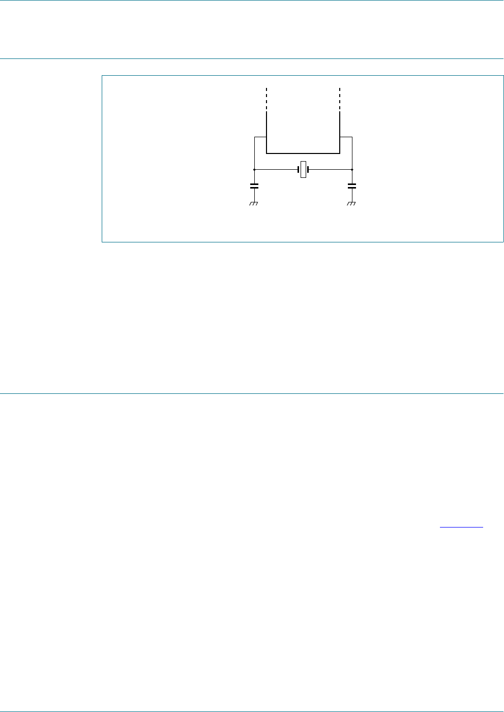
PN512 All information provided in this document is subject to legal disclaimers. © NXP B.V. 2012. All rights reserved.
Product data sheet
COMPANY PUBLIC Rev. 4.2 — 28 August 2012
111342 96 of 132
NXP Semiconductors PN512
Transmission module
17. Oscillator circuitry
The clock applied to the PN512 provides a time basis for the synchronous system’s
encoder and decoder. The stability of the clock frequency, therefore, is an important factor
for correct operation. To obtain optimum performance, clock jitter must be reduced as
much as possible. This is best achieved using the internal oscillator buffer with the
recommended circuitry.
If an external clock source is used, the clock signal must be applied to pin OSCIN. In this
case, special care must be taken with the clock duty cycle and clock jitter and the clock
quality must be verified.
18. Reset and oscillator start-up time
18.1 Reset timing requirements
The reset signal is filtered by a hysteresis circuit and a spike filter before it enters the
digital circuit. The spike filter rejects signals shorter than 10 ns. In order to perform a reset,
the signal must be LOW for at least 100 ns.
18.2 Oscillator start-up time
If the PN512 has been set to a Power-down mode or is powered by a VDDX supply, the
start-up time for the PN512 depends on the oscillator used and is shown in Figure 35.
The time (tstartup) is the start-up time of the crystal oscillator circuit. The crystal oscillator
start-up time is defined by the crystal.
The time (td) is the internal delay time of the PN512 when the clock signal is stable before
the PN512 can be addressed.
The delay time is calculated by:
(5)
The time (tosc) is the sum of td and tstartup.
Fig 34. Quartz crystal connection
001aan231
PN512
27.12 MHz
OSCOUT OSCIN
td1024
27 s
--------------37.74 s==

PN512 All information provided in this document is subject to legal disclaimers. © NXP B.V. 2012. All rights reserved.
Product data sheet
COMPANY PUBLIC Rev. 4.2 — 28 August 2012
111342 97 of 132
NXP Semiconductors PN512
Transmission module
19. PN512 command set
The PN512 operation is determined by a state machine capable of performing a set of
commands. A command is executed by writing a command code (see Table 157) to the
CommandReg register.
Arguments and/or data necessary to process a command are exchanged via the FIFO
buffer.
19.1 General description
The PN512 operation is determined by a state machine capable of performing a set of
commands. A command is executed by writing a command code (see Table 157) to the
CommandReg register.
Arguments and/or data necessary to process a command are exchanged via the FIFO
buffer.
19.2 General behavior
•Each command that needs a data bit stream (or data byte stream) as an input
immediately processes any data in the FIFO buffer. An exception to this rule is the
Transceive command. Using this command, transmission is started with the
BitFramingReg register’s StartSend bit.
•Each command that needs a certain number of arguments, starts processing only
when it has received the correct number of arguments from the FIFO buffer.
•The FIFO buffer is not automatically cleared when commands start. This makes it
possible to write command arguments and/or the data bytes to the FIFO buffer and
then start the command.
•Each command can be interrupted by the host writing a new command code to the
CommandReg register, for example, the Idle command.
Fig 35. Oscillator start-up time
001aak596
tstartup td
tosc
t
device activation
oscillator
clock stable
clock ready

PN512 All information provided in this document is subject to legal disclaimers. © NXP B.V. 2012. All rights reserved.
Product data sheet
COMPANY PUBLIC Rev. 4.2 — 28 August 2012
111342 98 of 132
NXP Semiconductors PN512
Transmission module
19.3 PN512 command overview
19.3.1 PN512 command descriptions
19.3.1.1 Idle
Places the PN512 in Idle mode. The Idle command also terminates itself.
19.3.1.2 Config command
To use the automatic MIFARE Anticollision, FeliCa Polling and NFCID3 the data used for
these transactions has to be stored internally. All the following data have to be written to
the FIFO in this order:
SENS_RES (2 bytes); in order byte 0, byte 1
NFCID1 (3 Bytes); in order byte 0, byte 1, byte 2; the first NFCID1 byte is fixed to 08h and
the check byte is calculated automatically.
SEL_RES (1 Byte)
polling response (2 bytes (shall be 01h, FEh) + 6 bytes NFCID2 + 8 bytes Pad + 2 bytes
system code)
NFCID3 (1 byte)
In total 25 bytes are transferred into an internal buffer.
The complete NFCID3 is 10 bytes long and consists of the 3 NFCID1 bytes, the 6 NFCID2
bytes and the one NFCID3 byte which are listed above.
To read out this configuration the command Config with an empty FIFO-buffer has to be
started. In this case the 25 bytes are transferred from the internal buffer to the FIFO.
Table 157. Command overview
Command Command
code Action
Idle 0000 no action, cancels current command execution
Configure 0001 Configures the PN512 for FeliCa, MIFARE and NFCIP-1
communication
Generate RandomID 0010 generates a 10-byte random ID number
CalcCRC 0011 activates the CRC coprocessor or performs a self test
Transmit 0100 transmits data from the FIFO buffer
NoCmdChange 0111 no command change, can be used to modify the
CommandReg register bits without affecting the command,
for example, the PowerDown bit
Receive 1000 activates the receiver circuits
Transceive 1100 transmits data from FIFO buffer to antenna and automatically
activates the receiver after transmission
AutoColl 1101 Handles FeliCa polling (Card Operation mode only) and
MIFARE anticollision (Card Operation mode only)
MFAuthent 1110 performs the MIFARE standard authentication as a reader
SoftReset 1111 resets the PN512

PN512 All information provided in this document is subject to legal disclaimers. © NXP B.V. 2012. All rights reserved.
Product data sheet
COMPANY PUBLIC Rev. 4.2 — 28 August 2012
111342 99 of 132
NXP Semiconductors PN512
Transmission module
The PN512 has to be configured after each power up, before using the automatic
Anticollision/Polling function (AutoColl command). During a hard power down (reset pin)
this configuration remains unchanged.
This command terminates automatically when finished and the active command is idle.
19.3.1.3 Generate RandomID
This command generates a 10-byte random number which is initially stored in the internal
buffer. This then overwrites the 10 bytes in the internal 25-byte buffer. This command
automatically terminates when finished and the PN512 returns to Idle mode.
19.3.1.4 CalcCRC
The FIFO buffer content is transferred to the CRC coprocessor and the CRC calculation is
started. The calculation result is stored in the CRCResultReg register. The CRC
calculation is not limited to a dedicated number of bytes. The calculation is not stopped
when the FIFO buffer is empty during the data stream. The next byte written to the FIFO
buffer is added to the calculation.
The CRC preset value is controlled by the ModeReg register’s CRCPreset[1:0] bits. The
value is loaded in to the CRC coprocessor when the command starts.
This command must be terminated by writing a command to the CommandReg register,
such as, the Idle command.
If the AutoTestReg register’s SelfTest[3:0] bits are set correctly, the PN512 enters Self
Test mode. Starting the CalcCRC command initiates a digital self test. The result of the
self test is written to the FIFO buffer.
19.3.1.5 Transmit
The FIFO buffer content is immediately transmitted after starting this command. Before
transmitting the FIFO buffer content, all relevant registers must be set for data
transmission.
This command automatically terminates when the FIFO buffer is empty. It can be
terminated by another command written to the CommandReg register.
19.3.1.6 NoCmdChange
This command does not influence any running command in the CommandReg register. It
can be used to manipulate any bit except the CommandReg register Command[3:0] bits,
for example, the RcvOff bit or the PowerDown bit.
19.3.1.7 Receive
The PN512 activates the receiver path and waits for a data stream to be received. The
correct settings must be chosen before starting this command.
This command automatically terminates when the data stream ends. This is indicated
either by the end of frame pattern or by the length byte depending on the selected frame
type and speed.
Remark: If the RxModeReg register’s RxMultiple bit is set to logic 1, the Receive
command will not automatically terminate. It must be terminated by starting another
command in the CommandReg register.

PN512 All information provided in this document is subject to legal disclaimers. © NXP B.V. 2012. All rights reserved.
Product data sheet
COMPANY PUBLIC Rev. 4.2 — 28 August 2012
111342 100 of 132
NXP Semiconductors PN512
Transmission module
19.3.1.8 Transceive
This command continuously repeats the transmission of data from the FIFO buffer and the
reception of data from the RF field. The first action is transmit and after transmission the
command is changed to receive a data stream.
Each transmit process must be started by setting the BitFramingReg register’s StartSend
bit to logic 1. This command must be cleared by writing any command to the
CommandReg register.
Remark: If the RxModeReg register’s RxMultiple bit is set to logic 1, the Transceive
command never leaves the receive state because this state cannot be cancelled
automatically.
19.3.1.9 AutoColl
This command automatically handles the MIFARE activation and the FeliCa polling in the
Card Operation mode. The bit Initiator in the register ControlReg has to be set to logic 0
for correct operation. During this command also the mode detector is active if not
deactivated by setting the bit ModeDetOff in the ModeReg register. After the mode
detector detects a mode, all the mode dependent registers are set according to the
received data. In case of no external RF field the command resets the internal state
machine and returns to the initial state but it will not be terminated. When the command
terminates the transceive command gets active.
During protocol processing the IRQ bits are not supported. Only the last received frame
will serve the IRQ’s. The treatment of the TxCRCEn and RxCRCEn bits is different to the
protocol. During ISO/IEC 14443A activation the enable bits are defined by the command
AutoColl. The changes cannot be observed at the register TXModeReg and RXModeReg.
After the Transceive command is active, the value of the register bit is relevant.
The FIFO will also receive the two CRC check bytes of the last command even if they
already checked and correct, if the state machine (Anticollision and Select routine) has to
not been executed and 106 kbit is detected.
During Felica activation the register bit is always relevant and is not overruled by the
command settings. This command can be cleared by software by writing any other
command to the CommandReg register, e.g. the idle command. Writing the same content
again to the CommandReg register resets the state machine.
PN512 All information provided in this document is subject to legal disclaimers. © NXP B.V. 2012. All rights reserved.
Product data sheet
COMPANY PUBLIC Rev. 4.2 — 28 August 2012
111342 101 of 132
NXP Semiconductors PN512
Transmission module
NFCIP-1 106 kbps Passive Communication mode:
The MIFARE anticollision is finished and the command has automatically changed to
Transceive. The FIFO contains the ATR_REQ frame including the start byte F0h. The bit
TargetActivated in the Status2Reg register is set to logic 1.
NFCIP-1 212/424 kbps Passive Communication mode:
The FeliCa polling command is finished and the command has automatically changed to
Transceive. The FIFO contains the ATR_REQ. The bit TargetActivated in the Status2Reg
register is set to logic 1.
NFCIP-1 106/212/424 kbps Active Communication mode:
This command is changing the automatically to the command Transceive. The FIFO
contains the ATR REQ The bit TargetActivated in the Status2Reg register is set to logic 0.
For 106 kbps only, the first byte in the FIFO indicates the start byte F0h and the CRC is
added to the FIFO.
Fig 36. Autocoll Command
NFCIP-1 106 kB aud
ISO14443-3 NPCIP-1 > 106 kB aud
FELICA
IDLE MODEO
MODE
detection
RXF
raming
MFHalted = 1
HALT
AC
nAC
SELECT
nSELECT
HLTA
AC
polling,
polling response
next frame
received next frame
received
REQA, WUPA
READY
ACTIVE
WUPA
SELECT SELECT
READY*
ACTIVE*
TRANSCEIVE
wait for
transmit
next frame
received
N
J
HLTA
REQA,
WUPA,
AC,
nAC,
SELECT,
nSELECT,
error
REQA,
AC,
nAC,
SELECT,
nSELECT,
HLTA
REQA,
WUPA,
nAC,
nSELECT,
HLTA,
error
REQA,
WUPA,
nAC,
nSELECT,
HLTA,
error
REQA,
WUPA,
AC,
SELECT,
nSELECT,
error
00 10
AC
aaa-001826

PN512 All information provided in this document is subject to legal disclaimers. © NXP B.V. 2012. All rights reserved.
Product data sheet
COMPANY PUBLIC Rev. 4.2 — 28 August 2012
111342 102 of 132
NXP Semiconductors PN512
Transmission module
MIFARE (Card Operation mode):
The MIFARE anticollision is finished and the command has automatically changed to
transceive. The FIFO contains the first command after the Select. The bit TargetActivated
in the Status2Reg register is set to logic 1.
Felica (Card Operation mode):
The FeliCa polling command is finished and the command has automatically changed to
transceive. The FIFO contains the first command followed after the Poling by the FeliCa
protocol. The bit TargetActivated in the Status2Reg register is set to logic 1.
19.3.1.10 MFAuthent
This command manages MIFARE authentication to enable a secure communication to
any MIFARE Mini, MIFARE 1K and MIFARE 4K card. The following data is written to the
FIFO buffer before the command can be activated:
•Authentication command code (60h, 61h)
•Block address
•Sector key byte 0
•Sector key byte 1
•Sector key byte 2
•Sector key byte 3
•Sector key byte 4
•Sector key byte 5
•Card serial number byte 0
•Card serial number byte 1
•Card serial number byte 2
•Card serial number byte 3
In total 12 bytes are written to the FIFO.
Remark: When the MFAuthent command is active all access to the FIFO buffer is
blocked. However, if there is access to the FIFO buffer, the ErrorReg register’s WrErr bit is
set.
This command automatically terminates when the MIFARE card is authenticated and the
Status2Reg register’s MFCrypto1On bit is set to logic 1.
This command does not terminate automatically if the card does not answer, so the timer
must be initialized to automatic mode. In this case, in addition to the IdleIRq bit, the
TimerIRq bit can be used as the termination criteria. During authentication processing, the
RxIRq bit and TxIRq bit are blocked. The Crypto1On bit is only valid after termination of
the MFAuthent command, either after processing the protocol or writing Idle to the
CommandReg register.
If an error occurs during authentication, the ErrorReg register’s ProtocolErr bit is set to
logic 1 and the Status2Reg register’s Crypto1On bit is set to logic 0.

PN512 All information provided in this document is subject to legal disclaimers. © NXP B.V. 2012. All rights reserved.
Product data sheet
COMPANY PUBLIC Rev. 4.2 — 28 August 2012
111342 103 of 132
NXP Semiconductors PN512
Transmission module
19.3.1.11 SoftReset
This command performs a reset of the device. The configuration data of the internal buffer
remains unchanged. All registers are set to the reset values. This command automatically
terminates when finished.
Remark: The SerialSpeedReg register is reset and therefore the serial data rate is set to
9.6 kBd.

PN512 All information provided in this document is subject to legal disclaimers. © NXP B.V. 2012. All rights reserved.
Product data sheet
COMPANY PUBLIC Rev. 4.2 — 28 August 2012
111342 104 of 132
NXP Semiconductors PN512
Transmission module
20. Testsignals
20.1 Selftest
The PN512 has the capability to perform a digital selftest. To start the selftest the following
procedure has to be performed:
1. Perform a soft reset.
2. Clear the internal buffer by writing 25 bytes of 00h and perform the Config Command.
3. Enable the Selftest by writing the value 09h to the register AutoTestReg.
4. Write 00h to the FIFO.
5. Start the Selftest with the CalcCRC Command.
6. The Selftest will be performed.
7. When the Selftest is finished, the FIFO contains the following bytes:
Version 1.0 has a different Selftest answer, explained in Section 21.
Correct answer for VersionReg equal to 82h:
00h, EBh, 66h, BAh, 57h, BFh, 23h, 95h, D0h, E3h, 0Dh, 3Dh, 27h, 89h, 5Ch, DEh,
9Dh, 3Bh, A7h, 00h, 21h, 5Bh, 89h, 82h, 51h, 3Ah, EBh, 02h, 0Ch, A5h, 00h,
49h, 7Ch, 84h, 4Dh, B3h, CCh, D2h, 1Bh, 81h, 5Dh, 48h, 76h, D5h, 71h, 61h,
21h, A9h, 86h, 96h, 83h, 38h, CFh, 9Dh, 5Bh, 6Dh, DCh, 15h, BAh, 3Eh, 7Dh,
95h, 3Bh, 2Fh
20.2 Testbus
The testbus is implemented for production test purposes. The following configuration can
be used to improve the design of a system using the PN512. The testbus allows to route
internal signals to the digital interface. The testbus signals are selected by accessing
TestBusSel in register TestSel2Reg.
Table 158. Testsignal routing (TestSel2Reg = 07h)
Pins D6 D5 D4 D3 D2 D1 D0
Testsignal sdata scoll svalid sover RCV_reset RFon,
filtered
Envelope
Table 159. Description of Testsignals
Pins Testsignal Description
D6 sdata shows the actual received data stream.
D5 scoll shows if in the actual bit a collision has been detected (106 kbit only)
D4 svalid shows if sdata and scoll are valid
D3 sover shows that the receiver has detected a stop condition
(ISO/IEC 14443A/ MIFARE mode only).
D2 RCV_reset shows if the receiver is reset
D1 RFon, filtered shows the value of the internal RF level detector
D0 Envelope shows the output of the internal coder

PN512 All information provided in this document is subject to legal disclaimers. © NXP B.V. 2012. All rights reserved.
Product data sheet
COMPANY PUBLIC Rev. 4.2 — 28 August 2012
111342 105 of 132
NXP Semiconductors PN512
Transmission module
20.3 Testsignals at pin AUX
Table 160. Testsignal routing (TestSel2Reg = 0Dh)
Pins D6 D5 D4 D3 D2 D1 D0
Testsignal clkstable clk27/8 clk27rf/8 clkrf13rf/4 clk27 clk27rf clk13rf
Table 161. Description of Testsignals
Pins Testsignal Description
D6 clkstable shows if the oscillator delivers a stable signal.
D5 clk27/8 shows the output signal of the oscillator divided by 8
D4 clk27rf/8 shows the clk27rf signal divided by 8
D3 clkrf13/4 shows the clk13rf divided by 4.
D2 clk27 shows the output signal of the oscillator
D1 clk27rf shows the RF clock multiplied by 2.
D0 clk13rf shows the RF clock of 13.56 MHz
Table 162. Testsignal routing (TestSel2Reg = 19h)
Pins D6 D5 D4 D3 D2 D1 D0
Testsignal - TRunning - - - - -
Table 163. Description of Testsignals
Pins Testsignal Description
D6 - -
D5 TRunning TRunning stops 1 clockcycle after TimerIRQ is raised
D4 - -
D3 - -
D2 - -
D1 - -
D0 - -
Table 164. Testsignals description
SelAux Description for Aux1 / Aux2
0000 Tristate
0001 DAC: register TestDAC 1/2
0010 DAC: testsignal corr1
0011 DAC: testsignal corr2
0100 DAC: testsignal MinLevel
0101 DAC: ADC_I
0110 DAC: ADC_Q
0111 DAC: testsignal ADC_I combined with ADC_Q
1000 Testsignal for production test
1001 SAM clock
1010 High
1011 low
1100 TxActive

PN512 All information provided in this document is subject to legal disclaimers. © NXP B.V. 2012. All rights reserved.
Product data sheet
COMPANY PUBLIC Rev. 4.2 — 28 August 2012
111342 106 of 132
NXP Semiconductors PN512
Transmission module
Each signal can be switched to pin AUX1 or AUX2 by setting SelAux1 or SelAux2 in the
register AnalogTestReg.
Note: The DAC has a current output, it is recommended to use a 1 k pull-down
resistance at pins AUX1/AUX2.
20.4 PRBS
Enables the PRBS9 or PRBS15 sequence according to ITU-TO150. To start the
transmission of the defined datastream the command send has to be activated. The
preamble/Sync byte/start bit/parity bit are generated automatically depending on the
selected mode.
Note: All relevant register to transmit data have to be configured before entering PRBS
mode according ITU-TO150.
21. Errata sheet
This data sheet is describing the functionality for version 2.0 and the industrial version.
This chapter lists all differences from version 1.0 to version 2.0:
The value of the version in Section 9.2.4.8 is set to80h.
The behaviour ‘RFU’ for the register is undefined.
The answer to the Selftest (see Section 20.1) for version 1.0 (VersionReg equal to 80h):
00h, AAh, E3h, 29h, 0Ch, 10h, 29zhh, 6Bh,
76h, 8Dh, AFh, 4Bh, A2h, DAh, 76h, 99h
C7h, 5Eh, 24h, 69h, D2h, BAh, FAh, BCh
3Eh, DAh, 96h, B5h, F5h, 94h, B0h, 3Ah
4Eh, C3h, 9Dh, 94h, 76h, 4Ch, EAh, 5Eh
38h, 10h, 8Fh, 2Dh, 21h, 4Bh, 52h, BFh
4Eh, C3h, 9Dh, 94h, 76h, 4Ch, EAh, 5Eh
38h, 10h, 8Fh, 2Dh, 21h, 4Bh, 52h, BFh
FBh, F4h, 19h, 94h, 82h, 5Ah, 72h, 9Dh
BAh, 0Dh, 1Fh, 17h, 56h, 22h, B9h, 08h
Only the default setting for the prescaler (see Section 15 “Timer unit” on page 93): t =
((TPreScaler*2+1)*TReload+1)/13,56 MHz is supported. As such only the formula fTimer =
13,56 MHz/(2*PreScaler+1) is applicable for the TPrescalerHigh in Table 99 “Description
of TModeReg bits” on page 54 and TPrescalerLo in Table 100 “TPrescalerReg register
(address 2Bh); reset value: 00h, 00000000b” on page 55. As there is no option for the
prescaler available, also the TPrescalEven is not available Section 9.2.2.10 on page 42.
This bit is set to ‘RFU’.
1101 RxActive
1110 Subcarrier detected
1111 TstBusBit
Table 164. Testsignals description
SelAux Description for Aux1 / Aux2
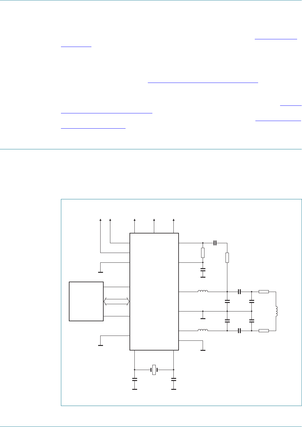
PN512 All information provided in this document is subject to legal disclaimers. © NXP B.V. 2012. All rights reserved.
Product data sheet
COMPANY PUBLIC Rev. 4.2 — 28 August 2012
111342 107 of 132
NXP Semiconductors PN512
Transmission module
Especially when using time slot protocols, it is needed that the error flag is copied into the
status information of the frame. When using the RxMultiple feature (see Section 9.2.2.4
on page 36) within version 1.0 the protocol error flag is not included in the status
information for the frame. In addition the CRCOk is copied instead of the CRCErr. This
can be a problem in frames without length information e.g. ISO/IEC 14443-B.
The version 1.0 does not accept a Type B EOF if there is no 1 bit after the series of 0 bits,
as such the configuration within Section 9.2.2.15 “TypeBReg” on page 47 bit 4 for
RxEOFReq does not exist. In addition the IC only has the possibility to select the
minimum or maximum timings for SOF/EOF generation defined in ISO/IEC14443B. As
such the configuration possible in version 2.0 through the EOFSOFAdjust bit (see Section
9.2.4.7 “AutoTestReg” on page 61) does not exist and the configuration is limited to only
setting minimum and maximum length according ISO/IEC 14443-B, see Section 9.2.2.15
“TypeBReg” on page 47, bit 4.
22. Application design-in information
The figure below shows a typical circuit diagram, using a complementary antenna
connection to the PN512.
The antenna tuning and RF part matching is described in the application note “NFC
Transmission Module Antenna and RF Design Guide”.
Fig 37. Typical circuit diagram
AVDD TVDD
RX
VMID
supply
TX1
TVSS
TX2
DVSS
DVDD
DVDD
PVDD
SVDD
AVSS
IRQ
NRSTPD
R1R2
L0
C0
C0
C2
C1
CRX
RQ
RQ
C1
C2
L0
Cvmid
001aan232
27.12 MHz
OSCIN OSCOUT
HOST
CONTROLLER
interface PN512
antenna
Lant

PN512 All information provided in this document is subject to legal disclaimers. © NXP B.V. 2012. All rights reserved.
Product data sheet
COMPANY PUBLIC Rev. 4.2 — 28 August 2012
111342 108 of 132
NXP Semiconductors PN512
Transmission module
23. Limiting values
24. Recommended operating conditions
[1] Supply voltages below 3 V reduce the performance (the achievable operating distance).
[2] VDDA, VDDD and VDD(TVDD) must always be the same voltage.
[3] VDD(PVDD) must always be the same or lower voltage than VDDD.
Table 165. Limiting values
In accordance with the Absolute Maximum Rating System (IEC 60134).
Symbol Parameter Conditions Min Max Unit
VDDA analog supply voltage 0.5 +4.0 V
VDDD digital supply voltage 0.5 +4.0 V
VDD(PVDD) PVDD supply voltage 0.5 +4.0 V
VDD(TVDD) TVDD supply voltage 0.5 +4.0 V
VDD(SVDD) SVDD supply voltage 0.5 +4.0 V
VIinput voltage all input pins except pins SIGIN
and RX
VSS(PVSS) 0.5 VDD(PVDD) + 0.5 V
pin MFIN VSS(PVSS) 0.5 VDD(SVDD) + 0.5 V
Ptot total power dissipation per package; and VDDD in shortcut
mode
- 200 mW
Tjjunction temperature - 100 C
VESD electrostatic discharge voltage HBM; 1500 , 100 pF;
JESD22-A114-B
- 2000 V
MM; 0.75 H, 200 pF;
JESD22-A114-A
- 200 V
Field induced model;
JESC22-C101-A
500 V
Table 166. Operating conditions
Symbol Parameter Conditions Min Typ Max Unit
VDDA analog supply voltage VDD(PVDD) VDDA = VDDD = VDD(TVDD);
VSSA =V
SSD =V
SS(PVSS) =V
SS(TVSS) =0V
[1][2] 2.5- 3.6V
VDDD digital supply voltage VDD(PVDD) VDDA = VDDD = VDD(TVDD);
VSSA =V
SSD =V
SS(PVSS) =V
SS(TVSS) =0V
[1][2] 2.5- 3.6V
VDD(TVDD) TVDD supply voltage VDD(PVDD) VDDA = VDDD = VDD(TVDD);
VSSA =V
SSD =V
SS(PVSS) =V
SS(TVSS) =0V
[1][2] 2.5- 3.6V
VDD(PVDD) PVDD supply voltage VDD(PVDD) VDDA = VDDD = VDD(TVDD);
VSSA =V
SSD =V
SS(PVSS) =V
SS(TVSS) =0V
[3] 1.6- 3.6V
VDD(SVDD) SVDD supply voltage VSSA =V
SSD =V
SS(PVSS) =V
SS(TVSS) =0V 1.6 - 3.6 V
Tamb ambient temperature HVQFN32, HVQFN40 30 - +85 C
Industrial version:
Tamb ambient temperature HVQFN32 40 - +90 C

PN512 All information provided in this document is subject to legal disclaimers. © NXP B.V. 2012. All rights reserved.
Product data sheet
COMPANY PUBLIC Rev. 4.2 — 28 August 2012
111342 109 of 132
NXP Semiconductors PN512
Transmission module
25. Thermal characteristics
26. Characteristics
Table 167. Thermal characteristics
Symbol Parameter Conditions Package Typ Unit
Rthj-a Thermal resistance from
junction to ambient
In still air with exposed pad
soldered on a 4 layer Jedec PCB
In still air
HVQFN32 40 K/W
HVQFN40 35 K/W
Table 168. Characteristics
Symbol Parameter Conditions Min Typ Max Unit
Input characteristics
Pins A0, A1 and NRSTPD
ILI input leakage current 1-+1 A
VIH HIGH-level input voltage 0.7VDD(PVDD) -- V
VIL LOW-level input voltage - - 0.3VDD(PVDD) V
Pin SIGIN
ILI input leakage current 1-+1 A
VIH HIGH-level input voltage 0.7VDD(SVDD) -- V
VIL LOW-level input voltage - - 0.3VDD(SVDD) V
Pin ALE
ILI input leakage current 1-+1 A
VIH HIGH-level input voltage 0.7VDD(PVDD) -- V
VIL LOW-level input voltage - - 0.3VDD(PVDD) V
Pin RX[1]
Viinput voltage 1-V
DDA +1 V
Ciinput capacitance VDDA = 3 V; receiver active;
VRX(p-p) = 1V; 1.5V (DC)
offset
-10- pF
Riinput resistance VDDA = 3 V; receiver active;
VRX(p-p) =1V; 1.5V (DC)
offset
- 350 -
Input voltage range; see Figure 38
Vi(p-p)(min) minimum peak-to-peak input
voltage
Manchester encoded;
VDDA =3V
- 100 - mV
Vi(p-p)(max) maximum peak-to-peak input
voltage
Manchester encoded;
VDDA =3V
-4- V
Input sensitivity; see Figure 38
Vmod modulation voltage minimum Manchester
encoded; VDDA =3V;
RxGain[2:0] = 111b (48 dB)
-5- mV
Pin OSCIN
ILI input leakage current 1-+1 A
VIH HIGH-level input voltage 0.7VDDA -- V
VIL LOW-level input voltage - - 0.3VDDA V

PN512 All information provided in this document is subject to legal disclaimers. © NXP B.V. 2012. All rights reserved.
Product data sheet
COMPANY PUBLIC Rev. 4.2 — 28 August 2012
111342 110 of 132
NXP Semiconductors PN512
Transmission module
Ciinput capacitance VDDA = 2.8 V; DC = 0.65 V;
AC = 1 V (p-p)
-2- pF
Input/output characteristics
pins D1, D2, D3, D4, D5, D6 and D7
ILI input leakage current 1-+1 A
VIH HIGH-level input voltage 0.7VDD(PVDD) -- V
VIL LOW-level input voltage - - 0.3VDD(PVDD) V
VOH HIGH-level output voltage VDD(PVDD) =3V; I
O=4mA V
DD(PVDD)
0.4
-V
DD(PVDD) V
VOL LOW-level output voltage VDD(PVDD) =3V; I
O=4mA V
SS(PVSS) -V
SS(PVSS) +
0.4
V
IOH HIGH-level output current VDD(PVDD) =3V - - 4 mA
IOL LOW-level output current VDD(PVDD) =3V - - 4 mA
Output characteristics
Pin SIGOUT
VOH HIGH-level output voltage VDD(SVDD) =3V; I
O=4mA V
DD(SVDD)
0.4
-V
DD(SVDD) V
VOL LOW-level output voltage VDD(SVDD) =3V; I
O=4mA V
SS(PVSS) -V
SS(PVSS) +
0.4
V
IOL LOW-level output current VDD(SVDD) =3V - - 4 mA
IOH HIGH-level output current VDD(SVDD) =3V - - 4 mA
Pin IRQ
VOH HIGH-level output voltage VDD(PVDD) =3V; I
O=4mA V
DD(PVDD)
0.4
-V
DD(PVDD) V
VOL LOW-level output voltage VDD(PVDD) =3V; I
O=4mA V
SS(PVSS) -V
SS(PVSS) +
0.4
V
IOL LOW-level output current VDD(PVDD) =3V - - 4 mA
IOH HIGH-level output current VDD(PVDD) =3V - - 4 mA
Pins AUX1 and AUX2
VOH HIGH-level output voltage VDDD =3V; I
O=4mA V
DDD 0.4 - VDDD V
VOL LOW-level output voltage VDDD =3V; I
O=4mA V
SS(PVSS) -V
SS(PVSS) +
0.4
V
IOL LOW-level output current VDDD =3V - - 4 mA
IOH HIGH-level output current VDDD =3V - - 4 mA
Table 168. Characteristics …continued
Symbol Parameter Conditions Min Typ Max Unit

PN512 All information provided in this document is subject to legal disclaimers. © NXP B.V. 2012. All rights reserved.
Product data sheet
COMPANY PUBLIC Rev. 4.2 — 28 August 2012
111342 111 of 132
NXP Semiconductors PN512
Transmission module
Pins TX1 and TX2
VOL LOW-level output voltage VDD(TVDD) =3V;
IDD(TVDD) =32mA;
CWGsP[5:0] = 0Fh
- - 0.15 V
VDD(TVDD) =3V;
IDD(TVDD) =80mA;
CWGsP[5:0] = 0Fh
--0.4V
VDD(TVDD) = 2.5 V;
IDD(TVDD) =32mA;
CWGsP[5:0] = 0Fh
- - 0.24 V
VDD(TVDD) = 2.5 V;
IDD(TVDD) =80mA;
CWGsP[5:0] = 0Fh
- - 0.64 V
VOH HIGH-level output voltage VDD(TVDD) =3V;
IDD(TVDD) =32mA;
CWGsP[5:0] = 3Fh
VDD(TVDD)
0.15
-- V
VDD(TVDD) =3V;
IDD(TVDD) =80mA;
CWGsP[5:0] = 3Fh
VDD(TVDD)
0.4
-- V
VDD(TVDD) = 2.5 V;
IDD(TVDD) =32mA;
CWGsP[5:0] = 3Fh
VDD(TVDD)
0.24
-- V
VDD(TVDD) = 2.5 V;
IDD(TVDD) =80mA;
CWGsP[5:0] = 3Fh
VDD(TVDD)
0.64
-- V
Industrial version:
VOL LOW-level output voltage VDD(TVDD) = 2.5 V;
IDD(TVDD) =32mA;
CWGsP[5:0] = 3Fh
- - 0.18 V
VDD(TVDD) = 2.5 V;
IDD(TVDD) =80mA;
CWGsP[5:0] = 3Fh
--0.44V
VOH HIGH-level output voltage VDD(TVDD) =3V;
IDD(TVDD) =32mA;
CWGsP[5:0] = 3Fh
VDD(TVDD)
0.18
-- V
VDD(TVDD) =3V;
IDD(TVDD) =80mA;
CWGsP[5:0] = 3Fh
VDD(TVDD)
0.44
-- V
Output resistance for TX1/TX2,
Industrial Version:
ROP,01H High level output resistance TVDD = 3 V, VTX = TVDD -
100 mV, CWGsP = 01h
123 180 261
ROP,02H High level output resistance TVDD = 3 V, VTX = TVDD -
100 mV, CWGsP = 02h
61 90 131
ROP,04H High level output resistance TVDD = 3 V, VTX = TVDD -
100 mV, CWGsP = 04h
30 46 68
ROP,08H High level output resistance TVDD = 3 V, VTX = TVDD -
100 mV, CWGsP = 08h
15 23 35
Table 168. Characteristics …continued
Symbol Parameter Conditions Min Typ Max Unit

PN512 All information provided in this document is subject to legal disclaimers. © NXP B.V. 2012. All rights reserved.
Product data sheet
COMPANY PUBLIC Rev. 4.2 — 28 August 2012
111342 112 of 132
NXP Semiconductors PN512
Transmission module
ROP,10H High level output resistance TVDD = 3 V, VTX = TVDD -
100 mV, CWGsP = 10h
7.5 12 19
ROP,20H High level output resistance TVDD = 3 V, VTX = TVDD -
100 mV, CWGsP = 20h
4.2 6 9
ROP,3FH High level output resistance TVDD = 3 V, VTX = TVDD -
100 mV, CWGsP = 3Fh
235
RON,10H Low level output resistance TVDD = 3 V, VTX = TVDD -
100 mV, CWGsN = 10h
30 46 68
RON,20H Low level output resistance TVDD = 3 V, VTX = TVDD -
100 mV, CWGsN = 20h
15 23 35
RON,40H Low level output resistance TVDD = 3 V, VTX = TVDD -
100 mV, CWGsN = 40h
7.5 12 19
RON,80H Low level output resistance TVDD = 3 V, VTX = TVDD -
100 mV, CWGsN = 80h
4.2 6 9
RON,F0H Low level output resistance TVDD = 3 V, VTX = TVDD -
100 mV, CWGsN = F0h
235
Current consumption
Ipd power-down current VDDA =V
DDD = VDD(TVDD) =
VDD(PVDD) =3V
hard power-down; pin
NRSTPD set LOW
[2] --5A
soft power-down; RF
level detector on
[2] --10A
IDD(PVDD) PVDD supply current pin PVDD [3] --40mA
IDD(TVDD) TVDD supply current pin TVDD; continuous wave [4][5][6] -60100mA
IDD(SVDD) SVDD supply current pin SVDD [7] --4mA
IDDD digital supply current pin DVDD; VDDD =3V - 6.5 9 mA
IDDA analog supply current pin AVDD; VDDA =3V,
CommandReg register’s
RcvOff bit = 0
-710mA
pin AVDD; receiver
switched off; VDDA =3V,
CommandReg register’s
RcvOff bit = 1
-35mA
Industrial version:
IDDD digital supply current pin DVDD; VDDD =3V - 6.5 9,5 mA
Ipd power-down current VDDA =V
DDD = VDD(TVDD) =
VDD(PVDD) =3V
hard power-down; pin
NRSTPD set LOW
[2] --15A
soft power-down; RF
level detector on
[2] --30A
Clock frequency
fclk clock frequency - 27.12 - MHz
clk clock duty cycle 40 50 60 %
tjit jitter time RMS - - 10 ps
Table 168. Characteristics …continued
Symbol Parameter Conditions Min Typ Max Unit

PN512 All information provided in this document is subject to legal disclaimers. © NXP B.V. 2012. All rights reserved.
Product data sheet
COMPANY PUBLIC Rev. 4.2 — 28 August 2012
111342 113 of 132
NXP Semiconductors PN512
Transmission module
[1] The voltage on pin RX is clamped by internal diodes to pins AVSS and AVDD.
[2] Ipd is the total current for all supplies.
[3] IDD(PVDD) depends on the overall load at the digital pins.
[4] IDD(TVDD) depends on VDD(TVDD) and the external circuit connected to pins TX1 and TX2.
[5] During typical circuit operation, the overall current is below 100 mA.
[6] Typical value using a complementary driver configuration and an antenna matched to 40 between pins TX1 and TX2 at 13.56 MHz.
[7] IDD(SVDD) depends on the load at pin MFOUT.
26.1 Timing characteristics
Crystal oscillator
VOH HIGH-level output voltage pin OSCOUT - 1.1 - V
VOL LOW-level output voltage pin OSCOUT - 0.2 - V
Ciinput capacitance pin OSCOUT - 2 - pF
pin OSCIN - 2 - pF
Typical input requirements
fxtal crystal frequency - 27.12 - MHz
ESR equivalent series resistance - - 100
CLload capacitance - 10 - pF
Pxtal crystal power dissipation - 50 100 W
Table 168. Characteristics …continued
Symbol Parameter Conditions Min Typ Max Unit
Fig 38. Pin RX input voltage range
Table 169. SPI timing characteristics
Symbol Parameter Conditions Min Typ Max Unit
tWL pulse width LOW line SCK 50 - - ns
tWH pulse width HIGH line SCK 50 - - ns
th(SCKH-D) SCK HIGH to data input
hold time
SCK to changing
MOSI
25 - - ns

PN512 All information provided in this document is subject to legal disclaimers. © NXP B.V. 2012. All rights reserved.
Product data sheet
COMPANY PUBLIC Rev. 4.2 — 28 August 2012
111342 114 of 132
NXP Semiconductors PN512
Transmission module
tsu(D-SCKH) data input to SCK HIGH
set-up time
changing MOSI to
SCK
25 - - ns
th(SCKL-Q) SCK LOW to data output
hold time
SCK to changing
MISO
- - 25 ns
t(SCKL-NSSH) SCK LOW to NSS HIGH
time
0- - ns
Table 170. I2C-bus timing in Fast mode
Symbol Parameter Conditions Fast mode High-speed
mode Unit
Min Max Min Max
fSCL SCL clock frequency 0 400 0 3400 kHz
tHD;STA hold time (repeated) START
condition
after this period,
the first clock pulse
is generated
600 - 160 - ns
tSU;STA set-up time for a repeated
START condition
600 - 160 - ns
tSU;STO set-up time for STOP condition 600 - 160 - ns
tLOW LOW period of the SCL clock 1300 - 160 - ns
tHIGH HIGH period of the SCL clock 600 - 60 - ns
tHD;DAT data hold time 0 900 0 70 ns
tSU;DAT data set-up time 100 - 10 - ns
trrise time SCL signal 20 300 10 40 ns
tffall time SCL signal 20 300 10 40 ns
trrise time SDA and SCL
signals
20 300 10 80 ns
tffall time SDA and SCL
signals
20 300 10 80 ns
tBUF bus free time between a STOP
and START condition
1.3 - 1.3 - s
Table 169. SPI timing characteristics …continued
Symbol Parameter Conditions Min Typ Max Unit
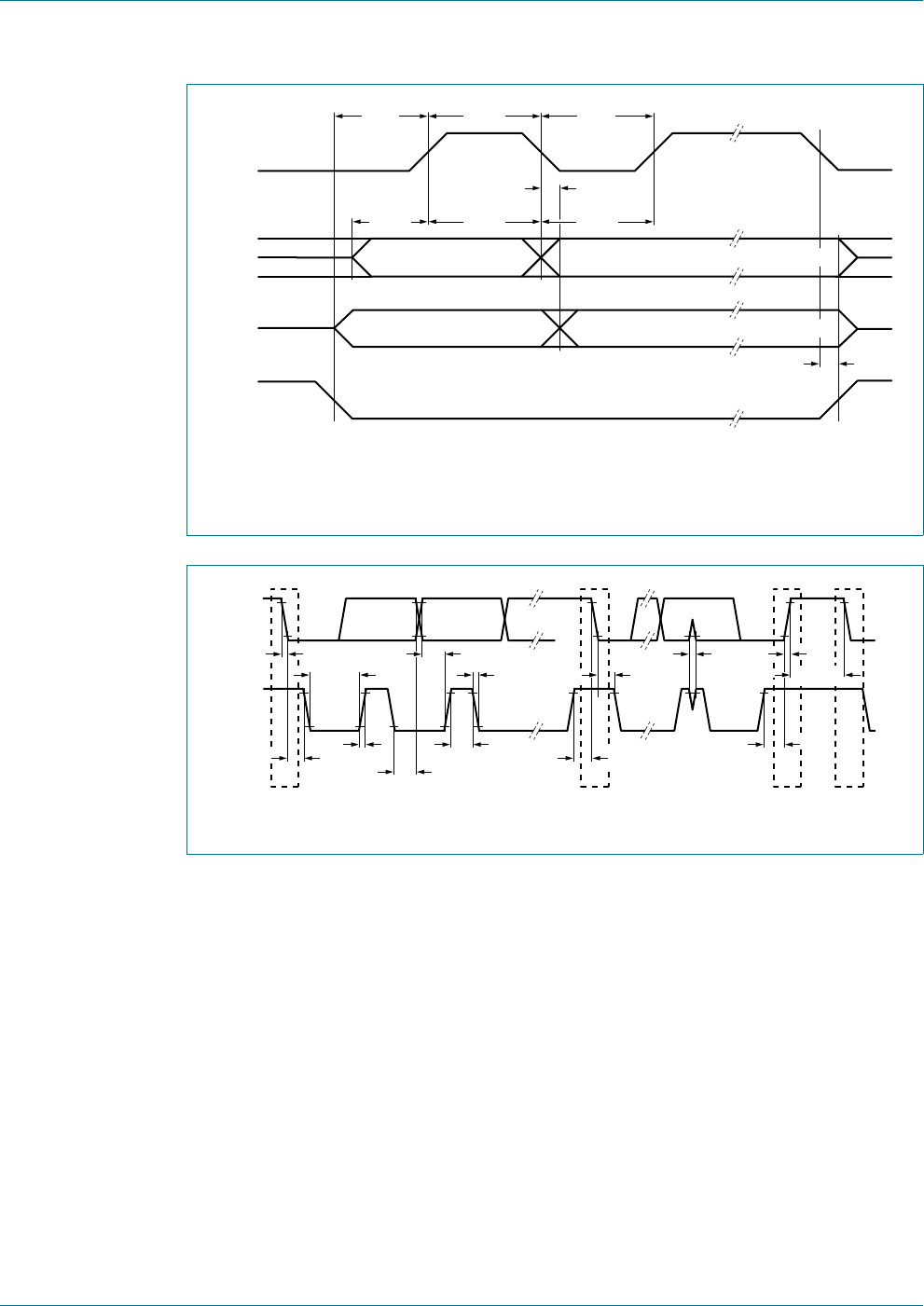
PN512 All information provided in this document is subject to legal disclaimers. © NXP B.V. 2012. All rights reserved.
Product data sheet
COMPANY PUBLIC Rev. 4.2 — 28 August 2012
111342 115 of 132
NXP Semiconductors PN512
Transmission module
Remark: The signal NSS must be LOW to be able to send several bytes in one data stream.
To send more than one data stream NSS must be set HIGH between the data streams.
Fig 39. Timing diagram for SPI
Fig 40. Timing for Fast and Standard mode devices on the I2C-bus
001aaj634
tSCKL tSCKH tSCKL
tDXSH tSHDX tDXSH
tSLDX
tSLNH
MOSI
SCK
MISO
MSB
MSB
LSB
LSB
NSS
001aaj635
SDA
tf
SCL
tLOW tf
tSP tr
tHD;STA tHD;DAT
tHD;STA
trtHIGH
tSU;DAT
SSrPS
tSU;STA
tSU;STO
tBUF

PN512 All information provided in this document is subject to legal disclaimers. © NXP B.V. 2012. All rights reserved.
Product data sheet
COMPANY PUBLIC Rev. 4.2 — 28 August 2012
111342 116 of 132
NXP Semiconductors PN512
Transmission module
26.2 8-bit parallel interface timing
26.2.1 AC symbols
Each timing symbol has five characters. The first character is always 't' for time. The other
characters indicate the name of a signal or the logic state of that signal (depending on
position):
Example: tAVLL = time for address valid to ALE low
26.2.2 AC operating specification
26.2.2.1 Bus timing for separated Read/Write strobe
Table 171. AC symbols
Designation Signal Designation Logic Level
A address H HIGH
D data L LOW
W NWR or nWait Z high impedance
R NRD or R/NW or nWrite X any level or data
L ALE or AS V any valid signal or data
C NCS N NSS
S NDS or nDStrb and nAStrb, SCK
Table 172. Timing specification for separated Read/Write strobe
Symbol Parameter Min Max Unit
tLHLL ALE pulse width 10 - ns
tAVLL Multiplexed Address Bus valid to ALE low (Address Set Up Time) 5 - ns
tLLAX Multiplexed Address Bus valid after ALE low (Address Hold Time) 5 - ns
tLLWL ALE low to NWR, NRD low 10 - ns
tCLWL NCS low to NRD, NWR low 0 - ns
tWHCH NRD, NWR high to NCS high 0 - ns
tRLDV NRD low to DATA valid - 35 ns
tRHDZ NRD high to DATA high impedance - 10 ns
tDVWH DATA valid to NWR high 5 - ns
tWHDX DATA hold after NWR high (Data Hold Time) 5 - ns
tWLWH NRD, NWR pulse width 40 - ns
tAVWL Separated Address Bus valid to NRD, NWR low (Set Up Time) 30 - ns
tWHAX Separated Address Bus valid after NWR high (Hold Time) 5 - ns
tWHWL period between sequenced read/write accesses 40 - ns
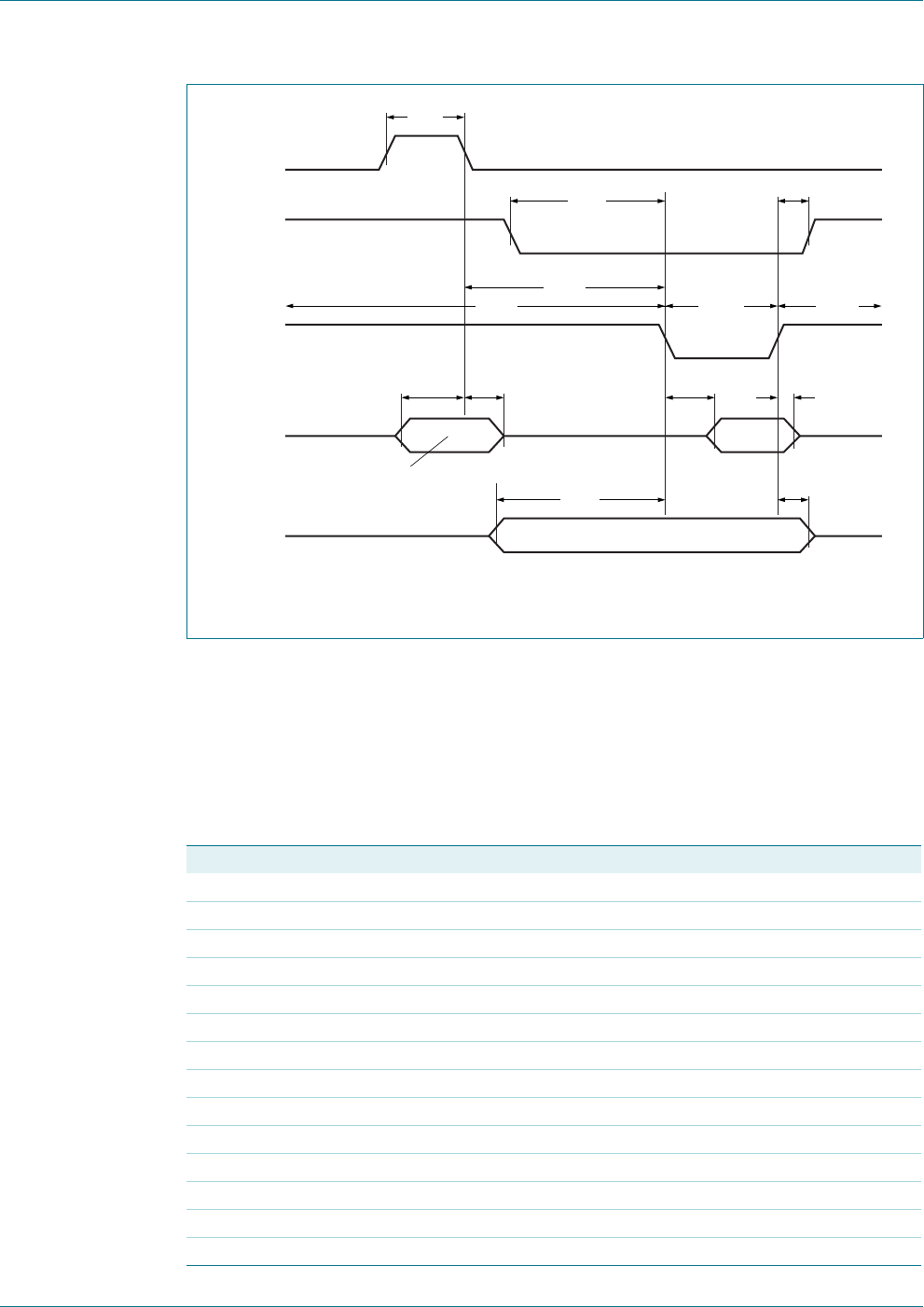
PN512 All information provided in this document is subject to legal disclaimers. © NXP B.V. 2012. All rights reserved.
Product data sheet
COMPANY PUBLIC Rev. 4.2 — 28 August 2012
111342 117 of 132
NXP Semiconductors PN512
Transmission module
Remark: For separated address and data bus the signal ALE is not relevant and the
multiplexed addresses on the data bus don’t care.
For the multiplexed address and data bus the address lines A0 to A3 have to be
connected as described in chapter Automatic host controller Interface Type Detection.
26.2.2.2 Bus timing for common Read/Write strobe
Fig 41. Timing diagram for separated Read/Write strobe
001aan233
tLHLL
tCLWL
tLLWL
tWHWL tWLWH tWHWL
tWHDX
tRHDZ
tWLDV
tRLDV
tWHCH
tWHAX
tAVLL tLLAX
tAVWL
ALE
NCS
NWR
NRD
D0...D7 D0...D7
A0...A3
multiplexed
addressbus
A0...A3
SEPARATED ADDRESSBUS A0...A3
Table 173. Timing specification for common Read/Write strobe
Symbol Parameter Min Max Unit
tLHLL AS pulse width 10 - ns
tAVLL Multiplexed Address Bus valid to AS low (Address Set Up Time) 5 - ns
tLLAX Multiplexed Address Bus valid after AS low (Address Hold Time) 5 - ns
tLLSL AS low to NDS low 10 - ns
tCLSL NCS low to NDS low 0 - ns
tSHCH NDS high to NCS high 0 - ns
tSLDV,R NDS low to DATA valid (for read cycle) - 35 ns
tSHDZ NDS low to DATA high impedance (read cycle) - 10 ns
tDVSH DATA valid to NDS high (for write cycle) 5 - ns
tSHDX DATA hold after NDS high (write cycle, Hold Time) 5 - ns
tSHRX R/NW hold after NDS high 5 - ns
tSLSH NDS pulse width 40 - ns
tAVSL Separated Address Bus valid to NDS low (Hold Time) 30 - ns
tSHAX Separated Address Bus valid after NDS high (Set Up Time) 5 - ns
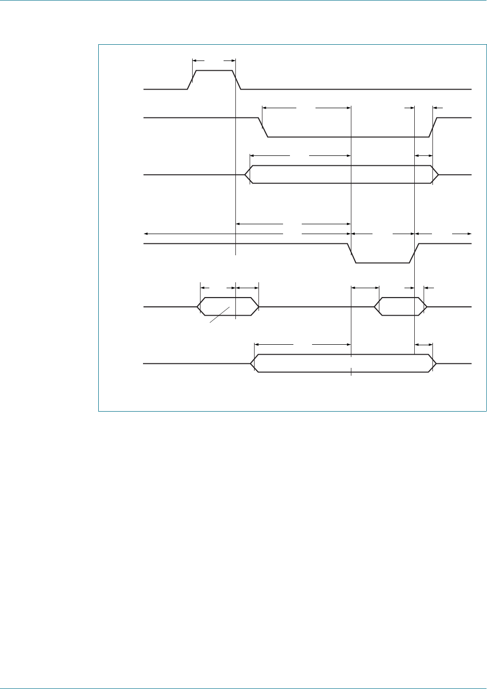
PN512 All information provided in this document is subject to legal disclaimers. © NXP B.V. 2012. All rights reserved.
Product data sheet
COMPANY PUBLIC Rev. 4.2 — 28 August 2012
111342 118 of 132
NXP Semiconductors PN512
Transmission module
Remark: For separated address and data bus the signal ALE is not relevant and the
multiplexed addresses on the data bus don’t care. For the multiplexed address and data
bus the address lines A0 to A3 have to be connected as described in Automatic
-Controller Interface Type Detection.
Fig 42. Timing diagram for common Read/Write strobe
SEPARATED ADDRESSBUS A0...A3
multiplexed
addressbus
A0...A3
ALE
tLHLL
tCLSL
R/NW
NDS
D0...D7
D0...D7
A0...A3
NCS
tSHCH
tSHRX
tRVSL
tLLSL
tSLSH tSHSL
tAVLL tLLAX
tSLDV, R
tSLDV, W tSHDX
tSHDZ
tSHAX
tAVSL
tSHSL
001aan234

PN512 All information provided in this document is subject to legal disclaimers. © NXP B.V. 2012. All rights reserved.
Product data sheet
COMPANY PUBLIC Rev. 4.2 — 28 August 2012
111342 119 of 132
NXP Semiconductors PN512
Transmission module
27. Package information
The PN512 can be delivered in 2 different packages.
Table 174. Package information
Package Remarks
HVQFN32 8-bit parallel interface not supported
HVQFN40 Supports the 8-bit parallel interface
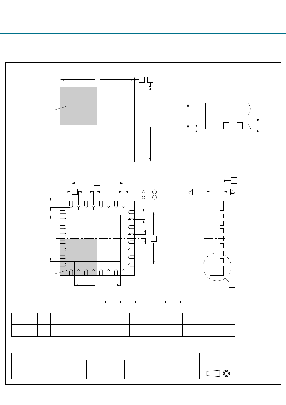
PN512 All information provided in this document is subject to legal disclaimers. © NXP B.V. 2012. All rights reserved.
Product data sheet
COMPANY PUBLIC Rev. 4.2 — 28 August 2012
111342 120 of 132
NXP Semiconductors PN512
Transmission module
28. Package outline
Fig 43. Package outline package version (HVQFN32)
0.51
A1Eh
b
UNIT ye
0.2
c
REFERENCES
OUTLINE
VERSION EUROPEAN
PROJECTION ISSUE DATE
IEC JEDEC JEITA
mm 5.1
4.9
Dh
3.25
2.95
y1
5.1
4.9 3.25
2.95
e1
3.5
e2
3.5
0.30
0.18
0.05
0.00 0.05 0.1
DIMENSIONS (mm are the original dimensions)
SOT617-1 MO-220- - - - - -
0.5
0.3
L
0.1
v
0.05
w
0 2.5 5 mm
scale
SOT617-1
HVQFN32: plastic thermal enhanced very thin quad flat package; no leads;
32 terminals; body 5 x 5 x 0.85 mm
A(1)
max.
AA1c
detail X
y
y1C
e
L
Eh
Dh
e
e1
b
916
32 25
24
17
8
1
X
D
E
C
BA
e2
terminal 1
index area
terminal 1
index area
01-08-08
02-10-18
1/2 e
1/2 e AC
C
B
vM
wM
E(1)
Note
1. Plastic or metal protrusions of 0.075 mm maximum per side are not included.
D(1)
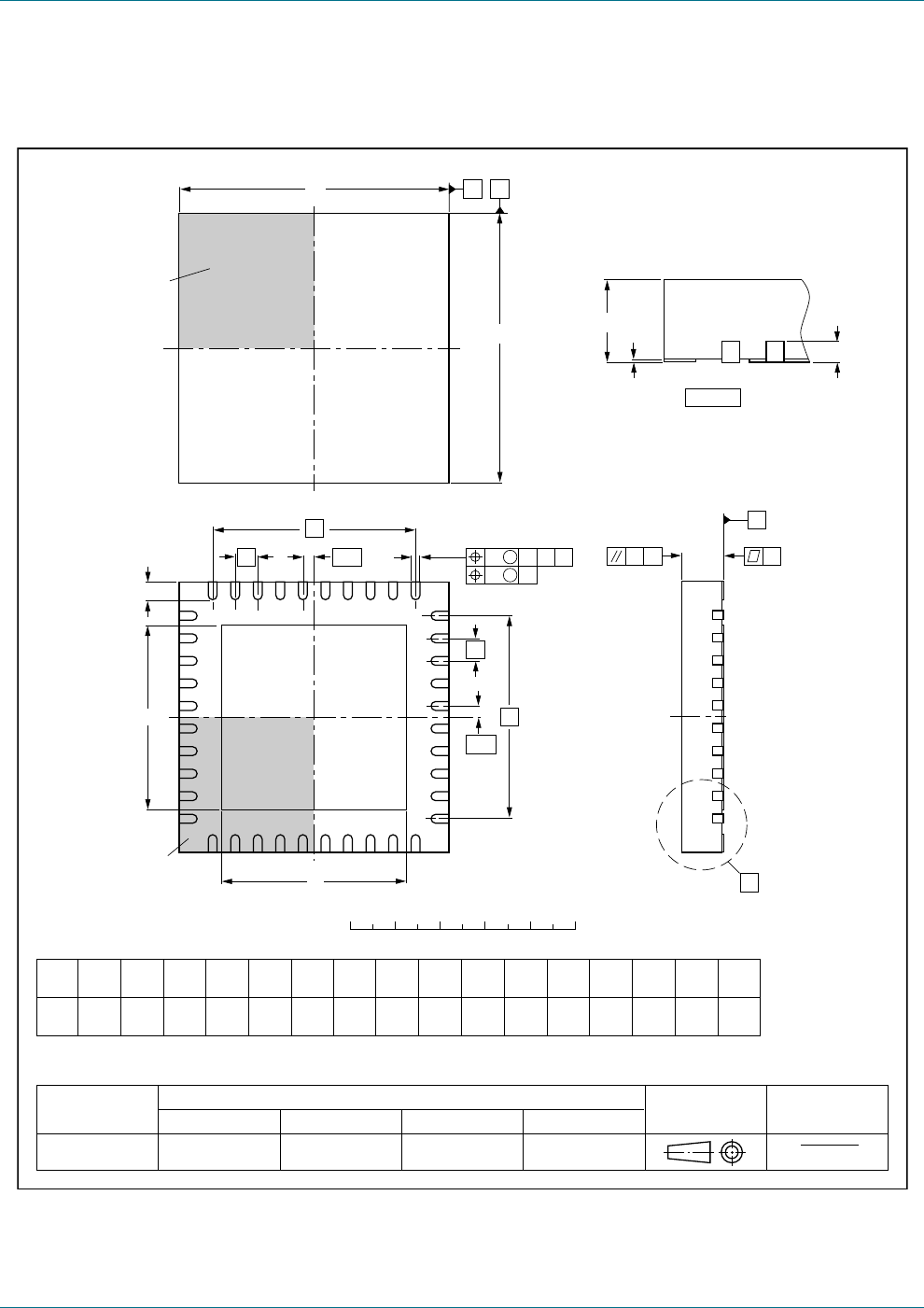
PN512 All information provided in this document is subject to legal disclaimers. © NXP B.V. 2012. All rights reserved.
Product data sheet
COMPANY PUBLIC Rev. 4.2 — 28 August 2012
111342 121 of 132
NXP Semiconductors PN512
Transmission module
Fig 44. Package outline package version (HVQFN40)
terminal 1
index area
0.51
A1Eh
b
UNIT ye
0.2
c
REFERENCES
OUTLINE
VERSION EUROPEAN
PROJECTION ISSUE DATE
IEC JEDEC JEITA
mm 6.1
5.9
Dh
4.25
3.95
y1
6.1
5.9 4.25
3.95
e1
4.5
e2
4.5
0.30
0.18
0.05
0.00 0.05 0.1
DIMENSIONS (mm are the original dimensions)
SOT618-1 MO-220- - - - - -
0.5
0.3
L
0.1
v
0.05
w
0 2.5 5 mm
scale
SOT618-1
HVQFN40: plastic thermal enhanced very thin quad flat package; no leads;
40 terminals; body 6 x 6 x 0.85 mm
A(1)
max.
AA1c
detail X
y
y1C
e
L
Eh
Dh
e
e1
b
11 20
40 31
30
21
10
1
X
D
E
C
BA
e2
01-08-08
02-10-22
terminal 1
index area
1/2 e
1/2 e
AC
C
B
vM
wM
Note
1. Plastic or metal protrusions of 0.075 mm maximum per side are not included.
D(1) E(1)

PN512 All information provided in this document is subject to legal disclaimers. © NXP B.V. 2012. All rights reserved.
Product data sheet
COMPANY PUBLIC Rev. 4.2 — 28 August 2012
111342 122 of 132
NXP Semiconductors PN512
Transmission module
29. Abbreviations
30. Glossary
Modulation index — Defined as the voltage ratio (Vmax Vmin) / (Vmax + Vmin).
Load modulation index — Defined as the voltage ratio for the card
(Vmax Vmin)/(V
max +V
min) measured at the card’s coil.
Initiator — Generates RF field at 13.56 MHz and starts the NFCIP-1 communication.
Target — Responds to command either using load modulation scheme (RF field
generated by Initiator) or using modulation of self generated RF field (no RF field
generated by initiator).
31. References
[1] Application note — NFC Transmission Module Antenna and RF Design Guide
Table 175. Abbreviations
Acronym Description
ADC Analog-to-Digital Converter
ASK Amplitude Shift keying
BPSK Binary Phase Shift Keying
CRC Cyclic Redundancy Check
CW Continuous Wave
DAC Digital-to-Analog Converter
EOF End of frame
HBM Human Body Model
I2C Inter-integrated Circuit
LSB Least Significant Bit
MISO Master In Slave Out
MM Machine Model
MOSI Master Out Slave In
MSB Most Significant Bit
NSS Not Slave Select
PCB Printed-Circuit Board
PLL Phase-Locked Loop
PRBS Pseudo-Random Bit Sequence
RX Receiver
SOF Start Of Frame
SPI Serial Peripheral Interface
TX Transmitter
UART Universal Asynchronous Receiver Transmitter

PN512 All information provided in this document is subject to legal disclaimers. © NXP B.V. 2012. All rights reserved.
Product data sheet
COMPANY PUBLIC Rev. 4.2 — 28 August 2012
111342 123 of 132
NXP Semiconductors PN512
Transmission module
32. Revision history
Table 176. Revision history
Document ID Release date Data sheet status Change notice Supersedes
PN512 v.4.2 20120828 Product data sheet - PN512 v.4.1
Modifications: •Table 122 “AutoTestReg register (address 36h); reset value: 40h, 01000000b”: description of
bits 4 and 5 corrected
PN512 v.4.1 20120821 Product data sheet - PN512 v.4.0
Modifications: •Table 123 “Description of bits”: description of bits 4 and 5 corrected
PN512 v.4.0 20120712 Product data sheet - PN512 v.3.9
Modifications: •Section 33.4 “Licenses”: updated
PN512 v.3.9 20120201 Product data sheet - PN512 v.3.8
Modifications: •Adding information on the different version in General description.
•Adding Section 21 “Errata sheet” on page 106 for explanation of differences between 1.0 and
2.0.
•Adding ordering information for version 1.0 and industrial version in Table 2 “Ordering
information” on page 5
•Adding the limitations and characteristics for the industrial version, see Table 1 “Quick
reference data” on page 4, Table 165 “Limiting values” on page 108, Table 1 “Quick reference
data” on page 4
•Referring to the Section 21 “Errata sheet” on page 106 within the following sections: Section
9.2.2.4 “RxModeReg” on page 36, Section 9.2.2.10 “DemodReg” on page 42, Section 9.2.2.15
“TypeBReg” on page 47, Section 9.2.3.10 “TMode Register, TPrescaler Register” on page 54,
Section 9.2.4.7 “AutoTestReg” on page 61, Section 9.2.4.8 “VersionReg” on page 61, Section
9.1.1 “Register bit behavior” on page 20, Section 15 “Timer unit” on page 93, Section 20
“Testsignals” on page 104;
•Update of command ‘Mem’ to ‘Configure’ and ‘RFU’ to ‘Autocoll’ in Table 157 “Command
overview” on page 98.
•Change of ‘Mem’ to ‘Configure’ in ‘Mem’ in Section 19.3.1.2 “Config command” on page 98
•Adding Autocoll in Section 19.3.1.9 “AutoColl” on page 100
PN512 v.3.8 20111025 Product data sheet - PN512 v.3.7
Modifications: •Table 168 “Characteristics”: unit of Pxtal corrected
111310 June 2005 Objective data sheet -
Modifications: •Initial version

PN512 All information provided in this document is subject to legal disclaimers. © NXP B.V. 2012. All rights reserved.
Product data sheet
COMPANY PUBLIC Rev. 4.2 — 28 August 2012
111342 124 of 132
NXP Semiconductors PN512
Transmission module
33. Legal information
33.1 Data sheet status
[1] Please consult the most recently issued document before initiating or completing a design.
[2] The term ‘short data sheet’ is explained in section “Definitions”.
[3] The product status of device(s) described in this document may have changed since this document was published and may differ in case of multiple devices. The latest product status
information is available on the Internet at URL http://www.nxp.com.
33.2 Definitions
Draft — The document is a draft version only. The content is still under
internal review and subject to formal approval, which may result in
modifications or additions. NXP Semiconductors does not give any
representations or warranties as to the accuracy or completeness of
information included herein and shall have no liability for the consequences of
use of such information.
Short data sheet — A short data sheet is an extract from a full data sheet
with the same product type number(s) and title. A short data sheet is intended
for quick reference only and should not be relied upon to contain detailed and
full information. For detailed and full information see the relevant full data
sheet, which is available on request via the local NXP Semiconductors sales
office. In case of any inconsistency or conflict with the short data sheet, the
full data sheet shall prevail.
Product specification — The information and data provided in a Product
data sheet shall define the specification of the product as agreed between
NXP Semiconductors and its customer, unless NXP Semiconductors and
customer have explicitly agreed otherwise in writing. In no event however,
shall an agreement be valid in which the NXP Semiconductors product is
deemed to offer functions and qualities beyond those described in the
Product data sheet.
33.3 Disclaimers
Limited warranty and liability — Information in this document is believed to
be accurate and reliable. However, NXP Semiconductors does not give any
representations or warranties, expressed or implied, as to the accuracy or
completeness of such information and shall have no liability for the
consequences of use of such information. NXP Semiconductors takes no
responsibility for the content in this document if provided by an information
source outside of NXP Semiconductors.
In no event shall NXP Semiconductors be liable for any indirect, incidental,
punitive, special or consequential damages (including - without limitation - lost
profits, lost savings, business interruption, costs related to the removal or
replacement of any products or rework charges) whether or not such
damages are based on tort (including negligence), warranty, breach of
contract or any other legal theory.
Notwithstanding any damages that customer might incur for any reason
whatsoever, NXP Semiconductors’ aggregate and cumulative liability towards
customer for the products described herein shall be limited in accordance
with the Terms and conditions of commercial sale of NXP Semiconductors.
Right to make changes — NXP Semiconductors reserves the right to make
changes to information published in this document, including without
limitation specifications and product descriptions, at any time and without
notice. This document supersedes and replaces all information supplied prior
to the publication hereof.
Suitability for use — NXP Semiconductors products are not designed,
authorized or warranted to be suitable for use in life support, life-critical or
safety-critical systems or equipment, nor in applications where failure or
malfunction of an NXP Semiconductors product can reasonably be expected
to result in personal injury, death or severe property or environmental
damage. NXP Semiconductors and its suppliers accept no liability for
inclusion and/or use of NXP Semiconductors products in such equipment or
applications and therefore such inclusion and/or use is at the customer’s own
risk.
Applications — Applications that are described herein for any of these
products are for illustrative purposes only. NXP Semiconductors makes no
representation or warranty that such applications will be suitable for the
specified use without further testing or modification.
Customers are responsible for the design and operation of their applications
and products using NXP Semiconductors products, and NXP Semiconductors
accepts no liability for any assistance with applications or customer product
design. It is customer’s sole responsibility to determine whether the NXP
Semiconductors product is suitable and fit for the customer’s applications and
products planned, as well as for the planned application and use of
customer’s third party customer(s). Customers should provide appropriate
design and operating safeguards to minimize the risks associated with their
applications and products.
NXP Semiconductors does not accept any liability related to any default,
damage, costs or problem which is based on any weakness or default in the
customer’s applications or products, or the application or use by customer’s
third party customer(s). Customer is responsible for doing all necessary
testing for the customer’s applications and products using NXP
Semiconductors products in order to avoid a default of the applications and
the products or of the application or use by customer’s third party
customer(s). NXP does not accept any liability in this respect.
Limiting values — Stress above one or more limiting values (as defined in
the Absolute Maximum Ratings System of IEC 60134) will cause permanent
damage to the device. Limiting values are stress ratings only and (proper)
operation of the device at these or any other conditions above those given in
the Recommended operating conditions section (if present) or the
Characteristics sections of this document is not warranted. Constant or
repeated exposure to limiting values will permanently and irreversibly affect
the quality and reliability of the device.
Terms and conditions of commercial sale — NXP Semiconductors
products are sold subject to the general terms and conditions of commercial
sale, as published at http://www.nxp.com/profile/terms, unless otherwise
agreed in a valid written individual agreement. In case an individual
agreement is concluded only the terms and conditions of the respective
agreement shall apply. NXP Semiconductors hereby expressly objects to
applying the customer’s general terms and conditions with regard to the
purchase of NXP Semiconductors products by customer.
No offer to sell or license — Nothing in this document may be interpreted or
construed as an offer to sell products that is open for acceptance or the grant,
conveyance or implication of any license under any copyrights, patents or
other industrial or intellectual property rights.
Document status[1][2] Product status[3] Definition
Objective [short] data sheet Development This document contains data from the objective specification for product development.
Preliminary [short] data sheet Qualification This document contains data from the preliminary specification.
Product [short] data sheet Production This document contains the product specification.

PN512 All information provided in this document is subject to legal disclaimers. © NXP B.V. 2012. All rights reserved.
Product data sheet
COMPANY PUBLIC Rev. 4.2 — 28 August 2012
111342 125 of 132
NXP Semiconductors PN512
Transmission module
Export control — This document as well as the item(s) described herein
may be subject to export control regulations. Export might require a prior
authorization from competent authorities.
Quick reference data — The Quick reference data is an extract of the
product data given in the Limiting values and Characteristics sections of this
document, and as such is not complete, exhaustive or legally binding.
Non-automotive qualified products — Unless this data sheet expressly
states that this specific NXP Semiconductors product is automotive qualified,
the product is not suitable for automotive use. It is neither qualified nor tested
in accordance with automotive testing or application requirements. NXP
Semiconductors accepts no liability for inclusion and/or use of
non-automotive qualified products in automotive equipment or applications.
In the event that customer uses the product for design-in and use in
automotive applications to automotive specifications and standards, customer
(a) shall use the product without NXP Semiconductors’ warranty of the
product for such automotive applications, use and specifications, and (b)
whenever customer uses the product for automotive applications beyond
NXP Semiconductors’ specifications such use shall be solely at customer’s
own risk, and (c) customer fully indemnifies NXP Semiconductors for any
liability, damages or failed product claims resulting from customer design and
use of the product for automotive applications beyond NXP Semiconductors’
standard warranty and NXP Semiconductors’ product specifications.
33.4 Licenses
33.5 Trademarks
Notice: All referenced brands, product names, service names and trademarks
are the property of their respective owners.
I2C-bus — logo is a trademark of NXP B.V.
MIFARE — is a trademark of NXP B.V.
34. Contact information
For more information, please visit: http://www.nxp.com
For sales office addresses, please send an email to: salesaddresses@nxp.com
Purchase of NXP ICs with ISO/IEC 14443 type B functionality
This NXP Semiconductors IC is ISO/IEC 14443 Type B
software enabled and is licensed under Innovatron’s
Contactless Card patents license for ISO/IEC 14443 B.
The license includes the right to use the IC in systems
and/or end-user equipment.
RATP/Innovatron
Technology
Purchase of NXP ICs with NFC technology
Purchase of an NXP Semiconductors IC that complies with one of the Near
Field Communication (NFC) standards ISO/IEC 18092 and ISO/IEC 21481
does not convey an implied license under any patent right infringed by
implementation of any of those standards.

PN512 All information provided in this document is subject to legal disclaimers. © NXP B.V. 2012. All rights reserved.
Product data sheet
COMPANY PUBLIC Rev. 4.2 — 28 August 2012
111342 126 of 132
NXP Semiconductors PN512
Transmission module
35. Tables
Table 1. Quick reference data . . . . . . . . . . . . . . . . . . . . .4
Table 2. Ordering information . . . . . . . . . . . . . . . . . . . . .5
Table 3. Pin description HVQFN32 . . . . . . . . . . . . . . . . .9
Table 4. Pin description HVQFN40 . . . . . . . . . . . . . . . .10
Table 5. Communication overview for
ISO/IEC 14443 A/MIFARE reader/writer . . . . . 11
Table 6. Communication overview for FeliCa
reader/writer . . . . . . . . . . . . . . . . . . . . . . . . . . .13
Table 7. FeliCa framing and coding . . . . . . . . . . . . . . . .13
Table 8. Start value for the CRC Polynomial: (00h),
(00h) . . . . . . . . . . . . . . . . . . . . . . . . . . . . . . . . .13
Table 9. Communication overview for Active
communication mode . . . . . . . . . . . . . . . . . . . .15
Table 10. Communication overview for Passive
communication mode . . . . . . . . . . . . . . . . . . . .16
Table 11. Framing and coding overview. . . . . . . . . . . . . .17
Table 12. MIFARE Card operation mode . . . . . . . . . . . . .17
Table 13. FeliCa Card operation mode . . . . . . . . . . . . . .18
Table 14. PN512 registers overview . . . . . . . . . . . . . . . .18
Table 15. Behavior of register bits and its designation. . .20
Table 16. PageReg register (address 00h); reset value:
00h, 0000000b . . . . . . . . . . . . . . . . . . . . . . . . .21
Table 17. Description of PageReg bits . . . . . . . . . . . . . . .21
Table 18. CommandReg register (address 01h); reset
value: 20h, 00100000b . . . . . . . . . . . . . . . . . . .21
Table 19. Description of CommandReg bits. . . . . . . . . . .21
Table 20. CommIEnReg register (address 02h); reset
value: 80h, 10000000b . . . . . . . . . . . . . . . . . . .22
Table 21. Description of CommIEnReg bits . . . . . . . . . . .22
Table 22. DivIEnReg register (address 03h); reset
value: 00h, 00000000b . . . . . . . . . . . . . . . . . . .23
Table 23. Description of DivIEnReg bits. . . . . . . . . . . . . .23
Table 24. CommIRqReg register (address 04h); reset
value: 14h, 00010100b . . . . . . . . . . . . . . . . . . .24
Table 25. Description of CommIRqReg bits . . . . . . . . . . .24
Table 26. DivIRqReg register (address 05h); reset
value: XXh, 000X00XXb. . . . . . . . . . . . . . . . . .25
Table 27. Description of DivIRqReg bits . . . . . . . . . . . . .25
Table 28. ErrorReg register (address 06h); reset value:
00h, 00000000b . . . . . . . . . . . . . . . . . . . . . . . .26
Table 29. Description of ErrorReg bits . . . . . . . . . . . . . . .26
Table 30. Status1Reg register (address 07h); reset
value: XXh, X100X01Xb. . . . . . . . . . . . . . . . . .27
Table 31. Description of Status1Reg bits . . . . . . . . . . . . .27
Table 32. Status2Reg register (address 08h); reset
value: 00h, 00000000b . . . . . . . . . . . . . . . . . . .28
Table 33. Description of Status2Reg bits . . . . . . . . . . . . .28
Table 34. FIFODataReg register (address 09h); reset
value: XXh, XXXXXXXXb. . . . . . . . . . . . . . . . .29
Table 35. Description of FIFODataReg bits . . . . . . . . . . .29
Table 36. FIFOLevelReg register (address 0Ah); reset
value: 00h, 00000000b . . . . . . . . . . . . . . . . . . .29
Table 37. Description of FIFOLevelReg bits. . . . . . . . . . .29
Table 38. WaterLevelReg register (address 0Bh); reset
value: 08h, 00001000b . . . . . . . . . . . . . . . . . . .30
Table 39. Description of WaterLevelReg bits . . . . . . . . . .30
Table 40. ControlReg register (address 0Ch); reset
value: 00h, 00000000b . . . . . . . . . . . . . . . . . . 30
Table 41. Description of ControlReg bits . . . . . . . . . . . . 30
Table 42. BitFramingReg register (address 0Dh); reset
value: 00h, 00000000b . . . . . . . . . . . . . . . . . . 31
Table 43. Description of BitFramingReg bits . . . . . . . . . . 31
Table 44. CollReg register (address 0Eh); reset value:
XXh, 101XXXXXb . . . . . . . . . . . . . . . . . . . . . . 32
Table 45. Description of CollReg bits. . . . . . . . . . . . . . . . 32
Table 46. PageReg register (address 10h); reset value:
00h, 00000000b. . . . . . . . . . . . . . . . . . . . . . . . 33
Table 47. Description of PageReg bits . . . . . . . . . . . . . . 33
Table 48. ModeReg register (address 11h); reset value:
3Bh, 00111011b . . . . . . . . . . . . . . . . . . . . . . . . 34
Table 49. Description of ModeReg bits . . . . . . . . . . . . . . 34
Table 50. TxModeReg register (address 12h); reset
value: 00h, 00000000b . . . . . . . . . . . . . . . . . . 35
Table 51. Description of TxModeReg bits . . . . . . . . . . . . 35
Table 52. RxModeReg register (address 13h); reset
value: 00h, 00000000b . . . . . . . . . . . . . . . . . . 36
Table 53. Description of RxModeReg bits . . . . . . . . . . . . 36
Table 54. TxControlReg register (address 14h); reset
value: 80h, 10000000b . . . . . . . . . . . . . . . . . . 37
Table 55. Description of TxControlReg bits . . . . . . . . . . . 37
Table 56. TxAutoReg register (address 15h); reset
value: 00h, 00000000b . . . . . . . . . . . . . . . . . . 38
Table 57. Description of TxAutoReg bits . . . . . . . . . . . . . 38
Table 58. TxSelReg register (address 16h); reset value:
10h, 00010000b. . . . . . . . . . . . . . . . . . . . . . . . 39
Table 59. Description of TxSelReg bits . . . . . . . . . . . . . . 39
Table 60. RxSelReg register (address 17h); reset value:
84h, 10000100b. . . . . . . . . . . . . . . . . . . . . . . . 41
Table 61. Description of RxSelReg bits . . . . . . . . . . . . . . 41
Table 62. RxThresholdReg register (address 18h);
reset value: 84h, 10000100b . . . . . . . . . . . . . . 41
Table 63. Description of RxThresholdReg bits . . . . . . . . 41
Table 64. DemodReg register (address 19h); reset
value: 4Dh, 01001101b . . . . . . . . . . . . . . . . . . 42
Table 65. Description of DemodReg bits . . . . . . . . . . . . . 42
Table 66. FelNFC1Reg register (address 1Ah); reset
value: 00h, 00000000b . . . . . . . . . . . . . . . . . . 43
Table 67. Description of FelNFC1Reg bits . . . . . . . . . . . 43
Table 68. FelNFC2Reg register (address1Bh); reset
value: 00h, 00000000b . . . . . . . . . . . . . . . . . . 44
Table 69. Description of FelNFC2Reg bits . . . . . . . . . . . 44
Table 70. MifNFCReg register (address 1Ch); reset
value: 62h, 01100010b. . . . . . . . . . . . . . . . . . . 45
Table 71. Description of MifNFCReg bits. . . . . . . . . . . . . 45
Table 72. ManualRCVReg register (address 1Dh);
reset value: 00h, 00000000b . . . . . . . . . . . . . . 46
Table 73. Description of ManualRCVReg bits . . . . . . . . . 46
Table 74. TypeBReg register (address 1Eh); reset
value: 00h, 00000000b . . . . . . . . . . . . . . . . . . 47
Table 75. Description of TypeBReg bits. . . . . . . . . . . . . . 47
Table 76. SerialSpeedReg register (address 1Fh);
reset value: EBh, 11101011b . . . . . . . . . . . . . . 48

PN512 All information provided in this document is subject to legal disclaimers. © NXP B.V. 2012. All rights reserved.
Product data sheet
COMPANY PUBLIC Rev. 4.2 — 28 August 2012
111342 127 of 132
NXP Semiconductors PN512
Transmission module
Table 77. Description of SerialSpeedReg bits . . . . . . . . .48
Table 78. PageReg register (address 20h); reset value:
00h, 00000000b . . . . . . . . . . . . . . . . . . . . . . . .49
Table 79. Description of PageReg bits . . . . . . . . . . . . . . .49
Table 80. CRCResultReg register (address 21h); reset
value: FFh, 11111111b. . . . . . . . . . . . . . . . . . . . 49
Table 81. Description of CRCResultReg bits . . . . . . . . . .49
Table 82. CRCResultReg register (address 22h); reset
value: FFh, 11111111b. . . . . . . . . . . . . . . . . . . . 49
Table 83. Description of CRCResultReg bits . . . . . . . . . .49
Table 84. GsNOffReg register (address 23h); reset
value: 88h, 10001000b . . . . . . . . . . . . . . . . . . .50
Table 85. Description of GsNOffReg bits . . . . . . . . . . . . .50
Table 86. ModWidthReg register (address 24h); reset
value: 26h, 00100110b . . . . . . . . . . . . . . . . . . .51
Table 87. Description of ModWidthReg bits . . . . . . . . . . .51
Table 88. TxBitPhaseReg register (address 25h); reset
value: 87h, 10000111b . . . . . . . . . . . . . . . . . . .51
Table 89. Description of TxBitPhaseReg bits . . . . . . . . . .51
Table 90. RFCfgReg register (address 26h); reset
value: 48h, 01001000b . . . . . . . . . . . . . . . . . . .52
Table 91. Description of RFCfgReg bits . . . . . . . . . . . . .52
Table 92. GsNOnReg register (address 27h); reset
value: 88h, 10001000b . . . . . . . . . . . . . . . . . . .53
Table 93. Description of GsNOnReg bits . . . . . . . . . . . . .53
Table 94. CWGsPReg register (address 28h); reset
value: 20h, 00100000b . . . . . . . . . . . . . . . . . . .53
Table 95. Description of CWGsPReg bits. . . . . . . . . . . . .53
Table 96. ModGsPReg register (address 29h); reset
value: 20h, 00100000b . . . . . . . . . . . . . . . . . . .54
Table 97. Description of ModGsPReg bits . . . . . . . . . . . .54
Table 98. TModeReg register (address 2Ah); reset
value: 00h, 00000000b . . . . . . . . . . . . . . . . . . .54
Table 99. Description of TModeReg bits . . . . . . . . . . . . .54
Table 100. TPrescalerReg register (address 2Bh); reset
value: 00h, 00000000b . . . . . . . . . . . . . . . . . . .55
Table 101. Description of TPrescalerReg bits . . . . . . . . . .55
Table 102. TReloadReg (Higher bits) register (address
2Ch); reset value: 00h, 00000000b . . . . . . . . .56
Table 103. Description of the higher TReloadReg bits . . .56
Table 104. TReloadReg (Lower bits) register (address
2Dh); reset value: 00h, 00000000b . . . . . . . . .56
Table 105. Description of lower TReloadReg bits . . . . . . .56
Table 106. TCounterValReg (Higher bits) register
(address 2Eh); reset value: XXh,
XXXXXXXXb . . . . . . . . . . . . . . . . . . . . . . . . . .57
Table 107. Description of the higher
TCounterValReg bits. . . . . . . . . . . . . . . . . . . . .57
Table 108. TCounterValReg (Lower bits) register
(address 2Fh); reset value: XXh,
XXXXXXXXb . . . . . . . . . . . . . . . . . . . . . . . . . .57
Table 109. Description of lower TCounterValReg bits . . . .57
Table 110. PageReg register (address 30h); reset value:
00h, 00000000b . . . . . . . . . . . . . . . . . . . . . . . .57
Table 111. Description of PageReg bits. . . . . . . . . . . . . . .58
Table 112. TestSel1Reg register (address 31h); reset
value: 00h, 00000000b . . . . . . . . . . . . . . . . . . .59
Table 113. Description of TestSel1Reg bits . . . . . . . . . . . .59
Table 114. TestSel2Reg register (address 32h); reset
value: 00h, 00000000b . . . . . . . . . . . . . . . . . . 59
Table 115. Description of TestSel2Reg bits. . . . . . . . . . . . 59
Table 116. TestPinEnReg register (address 33h); reset
value: 80h, 10000000b . . . . . . . . . . . . . . . . . . 60
Table 117. Description of TestPinEnReg bits . . . . . . . . . . 60
Table 118. TestPinValueReg register (address 34h);
reset value: 00h, 00000000b . . . . . . . . . . . . . . 60
Table 119. Description of TestPinValueReg bits . . . . . . . . 60
Table 120. TestBusReg register (address 35h); reset
value: XXh, XXXXXXXXb . . . . . . . . . . . . . . . . 61
Table 121. Description of TestBusReg bits . . . . . . . . . . . . 61
Table 122. AutoTestReg register (address 36h); reset
value: 40h, 01000000b . . . . . . . . . . . . . . . . . . 61
Table 123. Description of bits . . . . . . . . . . . . . . . . . . . . . . 61
Table 124. VersionReg register (address 37h); reset
value: XXh, XXXXXXXXb . . . . . . . . . . . . . . . . 62
Table 125. Description of VersionReg bits . . . . . . . . . . . . 62
Table 126. AnalogTestReg register (address 38h); reset
value: 00h, 00000000b . . . . . . . . . . . . . . . . . . 63
Table 127. Description of AnalogTestReg bits . . . . . . . . . 63
Table 128. TestDAC1Reg register (address 39h); reset
value: XXh, 00XXXXXXb . . . . . . . . . . . . . . . . . 64
Table 129. Description of TestDAC1Reg bits . . . . . . . . . . 64
Table 130. TestDAC2Reg register (address 3Ah); reset
value: XXh, 00XXXXXXb . . . . . . . . . . . . . . . . . 64
Table 131. Description ofTestDAC2Reg bits. . . . . . . . . . . 64
Table 132. TestADCReg register (address 3Bh); reset
value: XXh, XXXXXXXXb . . . . . . . . . . . . . . . . 64
Table 133. Description of TestADCReg bits . . . . . . . . . . . 64
Table 134. RFTReg register (address 3Ch); reset value:
FFh, 11111111b . . . . . . . . . . . . . . . . . . . . . . . . 65
Table 135. Description of RFTReg bits . . . . . . . . . . . . . . . 65
Table 136. RFTReg register (address 3Dh, 3Fh); reset value:
00h, 00000000b. . . . . . . . . . . . . . . . . . . . . . . . 65
Table 137. Description of RFTReg bits . . . . . . . . . . . . . . . 65
Table 138. RFTReg register (address 3Eh); reset value:
03h, 00000011b . . . . . . . . . . . . . . . . . . . . . . . . 65
Table 139. Description of RFTReg bits . . . . . . . . . . . . . . . 65
Table 140. Connection protocol for detecting different
interface types . . . . . . . . . . . . . . . . . . . . . . . . . 66
Table 141. Connection scheme for detecting the
different interface types . . . . . . . . . . . . . . . . . . 66
Table 142. MOSI and MISO byte order . . . . . . . . . . . . . . 67
Table 143. MOSI and MISO byte order . . . . . . . . . . . . . . 68
Table 144. Address byte 0 register; address MOSI . . . . . 68
Table 145. BR_T0 and BR_T1 settings . . . . . . . . . . . . . . 69
Table 146. Selectable UART transfer speeds . . . . . . . . . 69
Table 147. UART framing . . . . . . . . . . . . . . . . . . . . . . . . . 69
Table 148. Read data byte order . . . . . . . . . . . . . . . . . . . 70
Table 149. Write data byte order . . . . . . . . . . . . . . . . . . . 70
Table 150. Address byte 0 register; address MOSI . . . . . 72
Table 151. Supported interface types . . . . . . . . . . . . . . . . 79
Table 152. Register and bit settings controlling the
signal on pin TX1 . . . . . . . . . . . . . . . . . . . . . . 81
Table 153. Register and bit settings controlling the
signal on pin TX2 . . . . . . . . . . . . . . . . . . . . . . 82
Table 154. Setting of the bits RFlevel in register

PN512 All information provided in this document is subject to legal disclaimers. © NXP B.V. 2012. All rights reserved.
Product data sheet
COMPANY PUBLIC Rev. 4.2 — 28 August 2012
111342 128 of 132
NXP Semiconductors PN512
Transmission module
RFCfgReg (RFLevel amplifier deactivated) . . .83
Table 155. CRC coprocessor parameters . . . . . . . . . . . .90
Table 156. Interrupt sources . . . . . . . . . . . . . . . . . . . . . . .92
Table 157. Command overview . . . . . . . . . . . . . . . . . . . .98
Table 158. Testsignal routing (TestSel2Reg = 07h) . . . . .104
Table 159. Description of Testsignals . . . . . . . . . . . . . . .104
Table 160. Testsignal routing (TestSel2Reg = 0Dh) . . . .105
Table 161. Description of Testsignals . . . . . . . . . . . . . . .105
Table 162. Testsignal routing (TestSel2Reg = 19h) . . . . .105
Table 163. Description of Testsignals . . . . . . . . . . . . . . .105
Table 164. Testsignals description. . . . . . . . . . . . . . . . . .105
Table 165. Limiting values . . . . . . . . . . . . . . . . . . . . . . .108
Table 166. Operating conditions . . . . . . . . . . . . . . . . . . .108
Table 167. Thermal characteristics . . . . . . . . . . . . . . . . .109
Table 168. Characteristics . . . . . . . . . . . . . . . . . . . . . . .109
Table 169. SPI timing characteristics . . . . . . . . . . . . . . . 113
Table 170. I2C-bus timing in Fast mode . . . . . . . . . . . . .114
Table 171. AC symbols . . . . . . . . . . . . . . . . . . . . . . . . . . 116
Table 172. Timing specification for separated
Read/Write strobe. . . . . . . . . . . . . . . . . . . . . . 116
Table 173. Timing specification for common
Read/Write strobe. . . . . . . . . . . . . . . . . . . . . . 117
Table 174. Package information . . . . . . . . . . . . . . . . . . .119
Table 175. Abbreviations . . . . . . . . . . . . . . . . . . . . . . . .122
Table 176. Revision history . . . . . . . . . . . . . . . . . . . . . . .123

PN512 All information provided in this document is subject to legal disclaimers. © NXP B.V. 2012. All rights reserved.
Product data sheet
COMPANY PUBLIC Rev. 4.2 — 28 August 2012
111342 129 of 132
NXP Semiconductors PN512
Transmission module
36. Figures
Fig 1. Simplified block diagram of the PN512 . . . . . . . . .6
Fig 2. Detailed block diagram of the PN512 . . . . . . . . . .7
Fig 3. Pinning configuration HVQFN32 (SOT617-1) . . . .8
Fig 4. Pinning configuration HVQFN40 (SOT618-1) . . . .8
Fig 5. PN512 Read/Write mode. . . . . . . . . . . . . . . . . . . 11
Fig 6. ISO/IEC 14443 A/MIFARE Read/Write mode
communication diagram. . . . . . . . . . . . . . . . . . . .11
Fig 7. Data coding and framing according to
ISO/IEC 14443 A . . . . . . . . . . . . . . . . . . . . . . . . .12
Fig 8. FeliCa reader/writer communication diagram . . .13
Fig 9. NFCIP-1 mode. . . . . . . . . . . . . . . . . . . . . . . . . . .14
Fig 10. Active communication mode . . . . . . . . . . . . . . . .15
Fig 11. Passive communication mode . . . . . . . . . . . . . . .16
Fig 12. SPI connection to host. . . . . . . . . . . . . . . . . . . . .67
Fig 13. UART connection to microcontrollers . . . . . . . . .68
Fig 14. UART read data timing diagram . . . . . . . . . . . . .70
Fig 15. UART write data timing diagram . . . . . . . . . . . . .71
Fig 16. I2C-bus interface . . . . . . . . . . . . . . . . . . . . . . . . .72
Fig 17. Bit transfer on the I2C-bus . . . . . . . . . . . . . . . . . .73
Fig 18. START and STOP conditions . . . . . . . . . . . . . . .73
Fig 19. Acknowledge on the I2C-bus . . . . . . . . . . . . . . . .74
Fig 20. Data transfer on the I2C-bus . . . . . . . . . . . . . . . .74
Fig 21. First byte following the START procedure . . . . . .75
Fig 22. Register read and write access . . . . . . . . . . . . . .76
Fig 23. I2C-bus HS mode protocol switch . . . . . . . . . . . .77
Fig 24. I2C-bus HS mode protocol frame. . . . . . . . . . . . .78
Fig 25. Connection to host controller with separated
Read/Write strobes . . . . . . . . . . . . . . . . . . . . . . .80
Fig 26. Connection to host controller with common
Read/Write strobes . . . . . . . . . . . . . . . . . . . . . . .80
Fig 27. Data mode detector . . . . . . . . . . . . . . . . . . . . . . .84
Fig 28. Serial data switch for TX1 and TX2 . . . . . . . . . . .85
Fig 29. Communication flows using the S2C interface. . .86
Fig 30. Signal shape for SIGOUT in FeliCa card SAM
mode . . . . . . . . . . . . . . . . . . . . . . . . . . . . . . . . . .87
Fig 31. Signal shape for SIGIN in SAM mode . . . . . . . . .87
Fig 32. Signal shape for SIGOUT in MIFARE Card
SAM mode . . . . . . . . . . . . . . . . . . . . . . . . . . . . . .88
Fig 33. Signal shape for SIGIN in MIFARE Card SAM
mode . . . . . . . . . . . . . . . . . . . . . . . . . . . . . . . . . .88
Fig 34. Quartz crystal connection . . . . . . . . . . . . . . . . . .96
Fig 35. Oscillator start-up time. . . . . . . . . . . . . . . . . . . . .97
Fig 36. Autocoll Command . . . . . . . . . . . . . . . . . . . . . .101
Fig 37. Typical circuit diagram . . . . . . . . . . . . . . . . . . . .107
Fig 38. Pin RX input voltage range . . . . . . . . . . . . . . . .113
Fig 39. Timing diagram for SPI . . . . . . . . . . . . . . . . . . .115
Fig 40. Timing for Fast and Standard mode devices
on the I2C-bus . . . . . . . . . . . . . . . . . . . . . . . . . .115
Fig 41. Timing diagram for separated Read/Write
strobe. . . . . . . . . . . . . . . . . . . . . . . . . . . . . . . . .117
Fig 42. Timing diagram for common Read/Write strobe 118
Fig 43. Package outline package version (HVQFN32) .120
Fig 44. Package outline package version (HVQFN40) .121

PN512 All information provided in this document is subject to legal disclaimers. © NXP B.V. 2012. All rights reserved.
Product data sheet
COMPANY PUBLIC Rev. 4.2 — 28 August 2012
111342 130 of 132
continued >>
NXP Semiconductors PN512
Transmission module
37. Contents
1 Introduction . . . . . . . . . . . . . . . . . . . . . . . . . . . . 1
1.1 Different available versions. . . . . . . . . . . . . . . . 1
2 General description . . . . . . . . . . . . . . . . . . . . . . 1
3 Features and benefits . . . . . . . . . . . . . . . . . . . . 3
4 Quick reference data . . . . . . . . . . . . . . . . . . . . . 4
5 Ordering information. . . . . . . . . . . . . . . . . . . . . 5
6 Block diagram . . . . . . . . . . . . . . . . . . . . . . . . . . 6
7 Pinning information. . . . . . . . . . . . . . . . . . . . . . 8
7.1 Pinning . . . . . . . . . . . . . . . . . . . . . . . . . . . . . . . 8
7.2 Pin description . . . . . . . . . . . . . . . . . . . . . . . . . 9
8 Functional description . . . . . . . . . . . . . . . . . . 11
8.1 ISO/IEC 14443 A/MIFARE functionality . . . . . 11
8.2 ISO/IEC 14443 B functionality . . . . . . . . . . . . 12
8.3 FeliCa reader/writer functionality . . . . . . . . . . 13
8.3.1 FeliCa framing and coding . . . . . . . . . . . . . . . 13
8.4 NFCIP-1 mode . . . . . . . . . . . . . . . . . . . . . . . . 14
8.4.1 Active communication mode . . . . . . . . . . . . . 15
8.4.2 Passive communication mode . . . . . . . . . . . . 16
8.4.3 NFCIP-1 framing and coding . . . . . . . . . . . . . 17
8.4.4 NFCIP-1 protocol support. . . . . . . . . . . . . . . . 17
8.4.5 MIFARE Card operation mode . . . . . . . . . . . . 17
8.4.6 FeliCa Card operation mode . . . . . . . . . . . . . 18
9 PN512 register SET . . . . . . . . . . . . . . . . . . . . . 18
9.1 PN512 registers overview. . . . . . . . . . . . . . . . 18
9.1.1 Register bit behavior. . . . . . . . . . . . . . . . . . . . 20
9.2 Register description . . . . . . . . . . . . . . . . . . . . 21
9.2.1 Page 0: Command and status . . . . . . . . . . . . 21
9.2.1.1 PageReg. . . . . . . . . . . . . . . . . . . . . . . . . . . . . 21
9.2.1.2 CommandReg . . . . . . . . . . . . . . . . . . . . . . . . 21
9.2.1.3 CommIEnReg . . . . . . . . . . . . . . . . . . . . . . . . . 22
9.2.1.4 DivIEnReg . . . . . . . . . . . . . . . . . . . . . . . . . . . 23
9.2.1.5 CommIRqReg. . . . . . . . . . . . . . . . . . . . . . . . . 24
9.2.1.6 DivIRqReg . . . . . . . . . . . . . . . . . . . . . . . . . . . 25
9.2.1.7 ErrorReg . . . . . . . . . . . . . . . . . . . . . . . . . . . . . 26
9.2.1.8 Status1Reg . . . . . . . . . . . . . . . . . . . . . . . . . . . 27
9.2.1.9 Status2Reg . . . . . . . . . . . . . . . . . . . . . . . . . . . 28
9.2.1.10 FIFODataReg . . . . . . . . . . . . . . . . . . . . . . . . . 29
9.2.1.11 FIFOLevelReg . . . . . . . . . . . . . . . . . . . . . . . . 29
9.2.1.12 WaterLevelReg . . . . . . . . . . . . . . . . . . . . . . . . 30
9.2.1.13 ControlReg . . . . . . . . . . . . . . . . . . . . . . . . . . . 30
9.2.1.14 BitFramingReg . . . . . . . . . . . . . . . . . . . . . . . . 31
9.2.1.15 CollReg. . . . . . . . . . . . . . . . . . . . . . . . . . . . . . 32
9.2.2 Page 1: Communication . . . . . . . . . . . . . . . . . 33
9.2.2.1 PageReg. . . . . . . . . . . . . . . . . . . . . . . . . . . . . 33
9.2.2.2 ModeReg . . . . . . . . . . . . . . . . . . . . . . . . . . . . 34
9.2.2.3 TxModeReg . . . . . . . . . . . . . . . . . . . . . . . . . . 35
9.2.2.4 RxModeReg . . . . . . . . . . . . . . . . . . . . . . . . . . 36
9.2.2.5 TxControlReg. . . . . . . . . . . . . . . . . . . . . . . . . 37
9.2.2.6 TxAutoReg . . . . . . . . . . . . . . . . . . . . . . . . . . . 38
9.2.2.7 TxSelReg . . . . . . . . . . . . . . . . . . . . . . . . . . . . 39
9.2.2.8 RxSelReg. . . . . . . . . . . . . . . . . . . . . . . . . . . . 41
9.2.2.9 RxThresholdReg . . . . . . . . . . . . . . . . . . . . . . 41
9.2.2.10 DemodReg. . . . . . . . . . . . . . . . . . . . . . . . . . . 42
9.2.2.11 FelNFC1Reg . . . . . . . . . . . . . . . . . . . . . . . . . 43
9.2.2.12 FelNFC2Reg . . . . . . . . . . . . . . . . . . . . . . . . . 44
9.2.2.13 MifNFCReg . . . . . . . . . . . . . . . . . . . . . . . . . . 45
9.2.2.14 ManualRCVReg . . . . . . . . . . . . . . . . . . . . . . . 46
9.2.2.15 TypeBReg . . . . . . . . . . . . . . . . . . . . . . . . . . . 47
9.2.2.16 SerialSpeedReg . . . . . . . . . . . . . . . . . . . . . . . 47
9.2.3 Page 2: Configuration . . . . . . . . . . . . . . . . . . 49
9.2.3.1 PageReg . . . . . . . . . . . . . . . . . . . . . . . . . . . . 49
9.2.3.2 CRCResultReg . . . . . . . . . . . . . . . . . . . . . . . 49
9.2.3.3 GsNOffReg . . . . . . . . . . . . . . . . . . . . . . . . . . 50
9.2.3.4 ModWidthReg . . . . . . . . . . . . . . . . . . . . . . . . 51
9.2.3.5 TxBitPhaseReg . . . . . . . . . . . . . . . . . . . . . . . 51
9.2.3.6 RFCfgReg . . . . . . . . . . . . . . . . . . . . . . . . . . . 52
9.2.3.7 GsNOnReg . . . . . . . . . . . . . . . . . . . . . . . . . . 53
9.2.3.8 CWGsPReg . . . . . . . . . . . . . . . . . . . . . . . . . . 53
9.2.3.9 ModGsPReg . . . . . . . . . . . . . . . . . . . . . . . . . 54
9.2.3.10 TMode Register, TPrescaler Register . . . . . . 54
9.2.3.11 TReloadReg. . . . . . . . . . . . . . . . . . . . . . . . . . 56
9.2.3.12 TCounterValReg . . . . . . . . . . . . . . . . . . . . . . 57
9.2.4 Page 3: Test. . . . . . . . . . . . . . . . . . . . . . . . . . 57
9.2.4.1 PageReg . . . . . . . . . . . . . . . . . . . . . . . . . . . . 57
9.2.4.2 TestSel1Reg. . . . . . . . . . . . . . . . . . . . . . . . . . 59
9.2.4.3 TestSel2Reg. . . . . . . . . . . . . . . . . . . . . . . . . . 59
9.2.4.4 TestPinEnReg . . . . . . . . . . . . . . . . . . . . . . . . 60
9.2.4.5 TestPinValueReg . . . . . . . . . . . . . . . . . . . . . . 60
9.2.4.6 TestBusReg . . . . . . . . . . . . . . . . . . . . . . . . . . 61
9.2.4.7 AutoTestReg . . . . . . . . . . . . . . . . . . . . . . . . . 61
9.2.4.8 VersionReg . . . . . . . . . . . . . . . . . . . . . . . . . . 61
9.2.4.9 AnalogTestReg. . . . . . . . . . . . . . . . . . . . . . . . 63
9.2.4.10 TestDAC1Reg . . . . . . . . . . . . . . . . . . . . . . . . 64
9.2.4.11 TestDAC2Reg . . . . . . . . . . . . . . . . . . . . . . . . 64
9.2.4.12 TestADCReg . . . . . . . . . . . . . . . . . . . . . . . . . 64
9.2.4.13 RFTReg . . . . . . . . . . . . . . . . . . . . . . . . . . . . . 65
10 Digital interfaces . . . . . . . . . . . . . . . . . . . . . . . 65
10.1 Automatic microcontroller interface detection 65
10.2 Serial Peripheral Interface . . . . . . . . . . . . . . . 67
10.2.1 SPI read data. . . . . . . . . . . . . . . . . . . . . . . . . 67
10.2.2 SPI write data. . . . . . . . . . . . . . . . . . . . . . . . . 67
10.2.3 SPI address byte . . . . . . . . . . . . . . . . . . . . . . 68
10.3 UART interface . . . . . . . . . . . . . . . . . . . . . . . 68
10.3.1 Connection to a host . . . . . . . . . . . . . . . . . . . 68

PN512 All information provided in this document is subject to legal disclaimers. © NXP B.V. 2012. All rights reserved.
Product data sheet
COMPANY PUBLIC Rev. 4.2 — 28 August 2012
111342 131 of 132
continued >>
NXP Semiconductors PN512
Transmission module
10.3.2 Selectable UART transfer speeds . . . . . . . . . 68
10.3.3 UART framing. . . . . . . . . . . . . . . . . . . . . . . . . 69
10.4 I2C Bus Interface . . . . . . . . . . . . . . . . . . . . . . 72
10.4.1 Data validity . . . . . . . . . . . . . . . . . . . . . . . . . . 73
10.4.2 START and STOP conditions . . . . . . . . . . . . . 73
10.4.3 Byte format . . . . . . . . . . . . . . . . . . . . . . . . . . . 73
10.4.4 Acknowledge . . . . . . . . . . . . . . . . . . . . . . . . . 74
10.4.5 7-Bit addressing . . . . . . . . . . . . . . . . . . . . . . . 75
10.4.6 Register write access . . . . . . . . . . . . . . . . . . . 75
10.4.7 Register read access . . . . . . . . . . . . . . . . . . . 76
10.4.8 High-speed mode . . . . . . . . . . . . . . . . . . . . . . 77
10.4.9 High-speed transfer . . . . . . . . . . . . . . . . . . . . 77
10.4.10 Serial data transfer format in HS mode . . . . . 77
10.4.11 Switching between F/S mode and HS mode . 79
10.4.12 PN512 at lower speed modes . . . . . . . . . . . . 79
11 8-bit parallel interface . . . . . . . . . . . . . . . . . . . 79
11.1 Overview of supported host controller
interfaces . . . . . . . . . . . . . . . . . . . . . . . . . . . . 79
11.2 Separated Read/Write strobe . . . . . . . . . . . . . 80
11.3 Common Read/Write strobe . . . . . . . . . . . . . . 80
12 Analog interface and contactless UART . . . . 81
12.1 General. . . . . . . . . . . . . . . . . . . . . . . . . . . . . . 81
12.2 TX driver . . . . . . . . . . . . . . . . . . . . . . . . . . . . . 81
12.3 RF level detector . . . . . . . . . . . . . . . . . . . . . . 82
12.4 Data mode detector . . . . . . . . . . . . . . . . . . . . 83
12.5 Serial data switch . . . . . . . . . . . . . . . . . . . . . . 85
12.6 S2C interface support . . . . . . . . . . . . . . . . . . . 85
12.6.1 Signal shape for Felica S2C interface support 87
12.6.2 Waveform shape for ISO/IEC 14443A and
MIFARE S2C support . . . . . . . . . . . . . . . . . . . 88
12.7 Hardware support for FeliCa and NFC polling 89
12.7.1 Polling sequence functionality for initiator. . . . 89
12.7.2 Polling sequence functionality for target. . . . . 89
12.7.3 Additional hardware support for FeliCa
and NFC . . . . . . . . . . . . . . . . . . . . . . . . . . . . . 90
12.7.4 CRC coprocessor . . . . . . . . . . . . . . . . . . . . . . 90
13 FIFO buffer . . . . . . . . . . . . . . . . . . . . . . . . . . . . 91
13.1 Accessing the FIFO buffer . . . . . . . . . . . . . . . 91
13.2 Controlling the FIFO buffer . . . . . . . . . . . . . . . 91
13.3 FIFO buffer status information . . . . . . . . . . . . 91
14 Interrupt request system. . . . . . . . . . . . . . . . . 92
14.1 Interrupt sources overview . . . . . . . . . . . . . . . 92
15 Timer unit . . . . . . . . . . . . . . . . . . . . . . . . . . . . . 93
16 Power reduction modes . . . . . . . . . . . . . . . . . 95
16.1 Hard power-down . . . . . . . . . . . . . . . . . . . . . . 95
16.2 Soft power-down mode. . . . . . . . . . . . . . . . . . 95
16.3 Transmitter power-down mode. . . . . . . . . . . . 95
17 Oscillator circuitry. . . . . . . . . . . . . . . . . . . . . . 96
18 Reset and oscillator start-up time . . . . . . . . . 96
18.1 Reset timing requirements. . . . . . . . . . . . . . . 96
18.2 Oscillator start-up time. . . . . . . . . . . . . . . . . . 96
19 PN512 command set. . . . . . . . . . . . . . . . . . . . 97
19.1 General description . . . . . . . . . . . . . . . . . . . . 97
19.2 General behavior . . . . . . . . . . . . . . . . . . . . . . 97
19.3 PN512 command overview . . . . . . . . . . . . . . 98
19.3.1 PN512 command descriptions. . . . . . . . . . . . 98
19.3.1.1 Idle . . . . . . . . . . . . . . . . . . . . . . . . . . . . . . . . . 98
19.3.1.2 Config command . . . . . . . . . . . . . . . . . . . . . . 98
19.3.1.3 Generate RandomID . . . . . . . . . . . . . . . . . . . 99
19.3.1.4 CalcCRC . . . . . . . . . . . . . . . . . . . . . . . . . . . . 99
19.3.1.5 Transmit . . . . . . . . . . . . . . . . . . . . . . . . . . . . . 99
19.3.1.6 NoCmdChange . . . . . . . . . . . . . . . . . . . . . . . 99
19.3.1.7 Receive . . . . . . . . . . . . . . . . . . . . . . . . . . . . . 99
19.3.1.8 Transceive . . . . . . . . . . . . . . . . . . . . . . . . . . 100
19.3.1.9 AutoColl . . . . . . . . . . . . . . . . . . . . . . . . . . . 100
19.3.1.10 MFAuthent . . . . . . . . . . . . . . . . . . . . . . . . . . 102
19.3.1.11 SoftReset . . . . . . . . . . . . . . . . . . . . . . . . . . . 103
20 Testsignals. . . . . . . . . . . . . . . . . . . . . . . . . . . 104
20.1 Selftest . . . . . . . . . . . . . . . . . . . . . . . . . . . . . 104
20.2 Testbus. . . . . . . . . . . . . . . . . . . . . . . . . . . . . 104
20.3 Testsignals at pin AUX . . . . . . . . . . . . . . . . . 105
20.4 PRBS . . . . . . . . . . . . . . . . . . . . . . . . . . . . . . 106
21 Errata sheet . . . . . . . . . . . . . . . . . . . . . . . . . . 106
22 Application design-in information. . . . . . . . 107
23 Limiting values . . . . . . . . . . . . . . . . . . . . . . . 108
24 Recommended operating conditions . . . . . 108
25 Thermal characteristics . . . . . . . . . . . . . . . . 109
26 Characteristics . . . . . . . . . . . . . . . . . . . . . . . 109
26.1 Timing characteristics . . . . . . . . . . . . . . . . . . 113
26.2 8-bit parallel interface timing . . . . . . . . . . . . . 116
26.2.1 AC symbols . . . . . . . . . . . . . . . . . . . . . . . . . . 116
26.2.2 AC operating specification . . . . . . . . . . . . . . . 116
26.2.2.1 Bus timing for separated Read/Write strobe . 116
26.2.2.2 Bus timing for common Read/Write strobe . . 117
27 Package information. . . . . . . . . . . . . . . . . . . . 119
28 Package outline. . . . . . . . . . . . . . . . . . . . . . . 120
29 Abbreviations . . . . . . . . . . . . . . . . . . . . . . . . 122
30 Glossary. . . . . . . . . . . . . . . . . . . . . . . . . . . . . 122
31 References. . . . . . . . . . . . . . . . . . . . . . . . . . . 122
32 Revision history . . . . . . . . . . . . . . . . . . . . . . 123
33 Legal information . . . . . . . . . . . . . . . . . . . . . 124
33.1 Data sheet status . . . . . . . . . . . . . . . . . . . . . 124
33.2 Definitions . . . . . . . . . . . . . . . . . . . . . . . . . . 124
33.3 Disclaimers . . . . . . . . . . . . . . . . . . . . . . . . . 124
33.4 Licenses. . . . . . . . . . . . . . . . . . . . . . . . . . . . 125
33.5 Trademarks . . . . . . . . . . . . . . . . . . . . . . . . . 125

NXP Semiconductors PN512
Transmission module
© NXP B.V. 2012. All rights reserved.
For more information, please visit: http://www.nxp.com
For sales office addresses, please send an email to: salesaddresses@nxp.com
Date of release: 28 August 2012
111342
Please be aware that important notices concerning this document and the product(s)
described herein, have been included in section ‘Legal information’.
34 Contact information. . . . . . . . . . . . . . . . . . . . 125
35 Tables . . . . . . . . . . . . . . . . . . . . . . . . . . . . . . . 126
36 Figures . . . . . . . . . . . . . . . . . . . . . . . . . . . . . . 129
37 Contents . . . . . . . . . . . . . . . . . . . . . . . . . . . . . 130