QM3002N3 Datasheet. Www.s Manuals.com. Ra.03 Ubiq
User Manual: Marking of electronic components, SMD Codes M3, M3*, M3002N, M3014M, M3014N, M3016M, M3016N, M3018M, M3018N, M3022M, M33, M36, M3=***, M3T, M3V. Datasheets 2SA812, ADM1813-10AKS, ADM1813-10ART, ADM1813-5AKS, ADM1813-5ART, BZX384-B16, DTB743XE, DTB743XM, LM258ADGKR, MMSZ5258, QM3002N3, QM3014M6, QM3014N6, QM3016M6, QM3016N6, QM3018M6, QM3018N6, QM3022M6, RT9818D-13GV, SM36.
Open the PDF directly: View PDF ![]() .
.
Page Count: 5
1
QM3002N3
N-Ch 30V Fast Switching MOSFETs
Symbol Parameter
Rating
Units
10s Steady State
VDS Drain-Source Voltage 30 V
VGS Gate-Source Voltage ±20 V
ID@TC=25℃ Continuous Drain Current, VGS @ 10V1 28 A
ID@TC=100℃ Continuous Drain Current, VGS @ 10V1 18 A
ID@TA=25℃ Continuous Drain Current, VGS @ 10V1 11.7 7.4 A
ID@TA=70℃ Continuous Drain Current, VGS @ 10V1 9.4 6 A
IDM Pulsed Drain Current2 56 A
EAS Single Pulse Avalanche Energy3 72 mJ
IAS Avalanche Current 21 A
PD@TC=25℃ Total Power Dissipation4 20.8 W
PD@TA=25℃ Total Power Dissipation4 4.2 1.67 W
TSTG Storage Temperature Range -55 to 150 ℃
TJ Operating Junction Temperature Range -55 to 150 ℃
Symbol Parameter Typ. Max. Unit
RθJA Thermal Resistance Junction-Ambient 1 --- 75
℃/W
RθJA Thermal Resistance Junction-Ambient 1 (t ≤10s) --- 30 ℃/W
RθJC Thermal Resistance Junction-Case1 --- 6
℃/W
BVDSS RDSON ID
30V 18mΩ 28A
Absolute Maximum Ratings
Thermal Data
Rev A.03 D061611
The QM3002N3 is the highest performance
trench N-ch MOSFETs with extreme high cell
density , which provide excellent RDSON and
gate charge for most of the synchronous buck
converter applications .
The QM3002N3 meet the RoHS and Green
Product requirement , 100% EAS guaranteed
with full function reliability approved.
z Advanced high cell density Trench technology
z Super Low Gate Charge
z Excellent CdV/dt effect decline
z 100% EAS Guaranteed
z Green Device Available
General Description
Features
Applications
z High Frequency Point-of-Load Synchronous
Buck Converter for MB/NB/UMPC/VGA
z Networking DC-DC Power System
z Load Switch
DFN3X3 Pin Configuration
Product Summery
D
G
S
S
S
2
QM3002N3
N-Ch 30V Fast Switching MOSFETs
Symbol Parameter Conditions Min. Typ. Max. Unit
BVDSS Drain-Source Breakdown Voltage VGS=0V , ID=250uA 30 --- --- V
△BVDSS/△TJ BVDSS Temperature Coefficient Reference to 25℃ , ID=1mA --- 0.022 --- V/℃
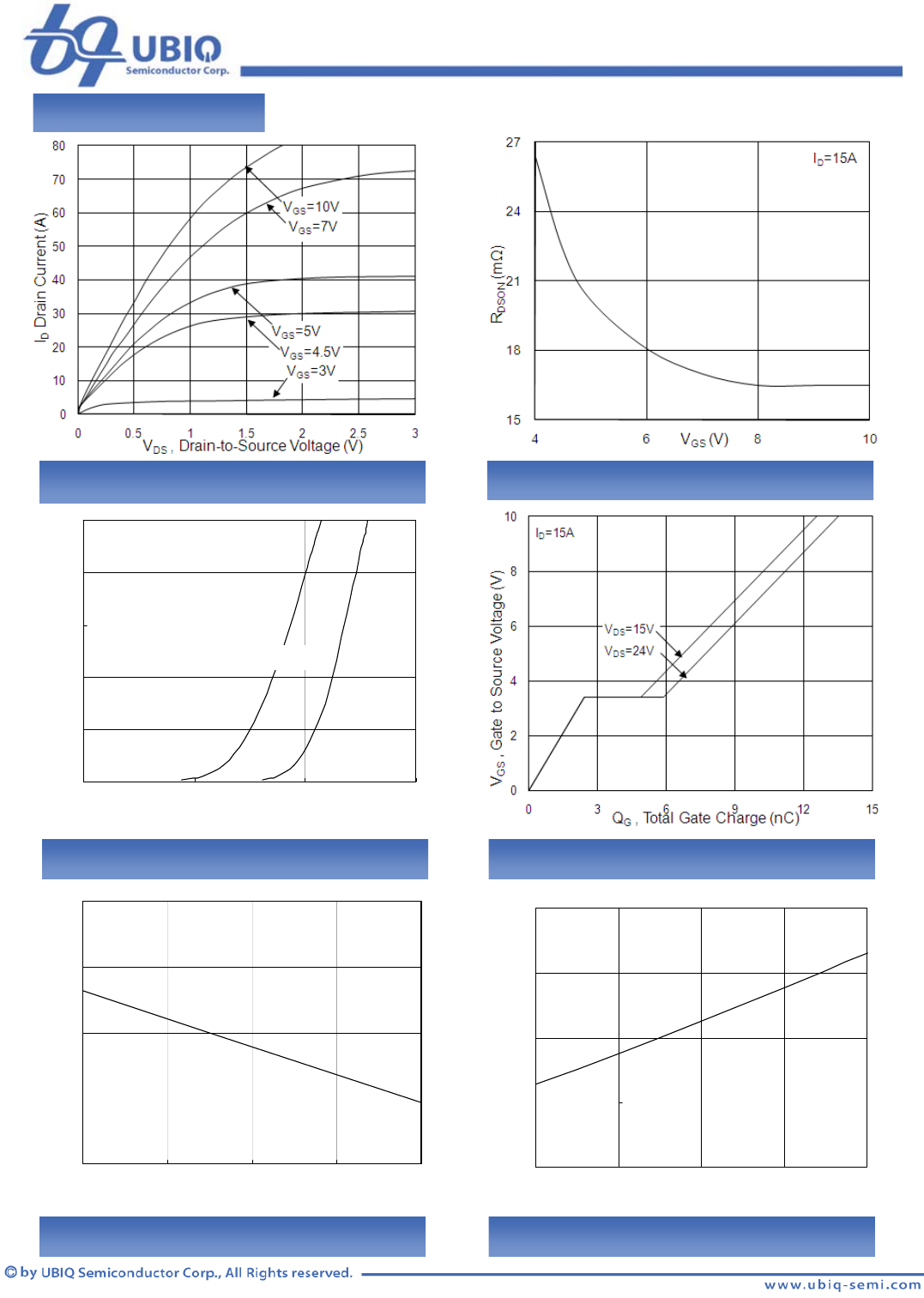
RDS(ON) Static Drain-Source On-Resistance2 VGS=10V , ID=15A --- 16 18
mΩ
VGS=4.5V , ID=10A --- 24 30
VGS(th) Gate Threshold Voltage VGS=VDS , ID =250uA 1.0 1.5 2.5 V
△VGS(th) VGS(th) Temperature Coefficient --- -5.1 ---
mV/℃
IDSS Drain-Source Leakage Current VDS=24V , VGS=0V , TJ=25℃ --- --- 1 uA
VDS=24V , VGS=0V , TJ=55℃ --- --- 5
IGSS Gate-Source Leakage Current VGS=±20V , VDS=0V --- ---
±100 nA
gfs Forward Transconductance VDS=5V , ID=30A --- 19.4 --- S
Rg Gate Resistance VDS=0V , VGS=0V , f=1MHz --- 2.5 5 Ω
Qg Total Gate Charge (4.5V)
VDS=15V , VGS=4.5V , ID=15A
--- 6.2 8.7
nC
Qgs Gate-Source Charge --- 2.4 3.4
Qgd Gate-Drain Charge --- 2.5 3.5
Td(on) Turn-On Delay Time
VDD=10V , VGS=10V , RG=3.3Ω
ID=15A
--- 3 6.0
ns
Tr Rise Time --- 7.6 14
Td(off) Turn-Off Delay Time --- 20.8 42
Tf Fall Time --- 4 8
Ciss Input Capacitance
VDS=15V , VGS=0V , f=1MHz
--- 572 801
pF
Coss Output Capacitance --- 80 112
Crss Reverse Transfer Capacitance --- 65 91
Symbol Parameter Conditions Min. Typ. Max. Unit
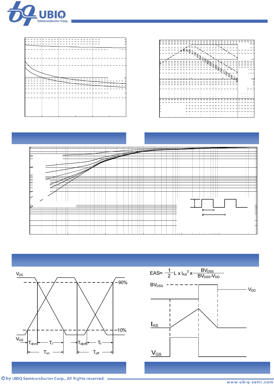
EAS Single Pulse Avalanche Energy5 VDD=25V , L=0.1mH , IAS=10A 16 --- --- mJ
Symbol Parameter Conditions Min. Typ. Max. Unit
IS Continuous Source Current1,6 VG=VD=0V , Force Current --- --- 28 A
ISM Pulsed Source Current2,6 --- --- 56 A
VSD Diode Forward Voltage2 VGS=0V , IS=1A , TJ=25℃ --- --- 1.2 V
trr Reverse Recovery Time
IF=30A , dI/dt=100A/µs , TJ=25℃
--- 17 --- nS
Qrr Reverse Recovery Charge --- 3 --- nC
Note :
1.The data tested by surface mounted on a 1 inch2 FR-4 board with 2OZ copper.
2.The data tested by pulsed , pulse width ≦ 300us , duty cycle ≦ 2%
3.The EAS data shows Max. rating . The test condition is VDD=25V,VGS=10V,L=0.1mH,IAS=21A
4.The power dissipation is limited by 150℃ junction temperature
5.The Min. value is 100% EAS tested guarantee.
6.The data is theoretically the same as ID and IDM , in real applications , should be limited by total power dissipation.
Electrical Characteristics (TJ=25 ℃, unless otherwise noted)
Diode Characteristics
Guaranteed Avalanche Characteristics
3
QM3002N3
N-Ch 30V Fast Switching MOSFETs
0
2
4
6
8
10
00.30.60.9
VSD , Source-to-Drain Voltage (V)
I
S
Source Current(A)
T
J
=150℃T
J
=25℃
0.2
0.6
1
1.4
1.8
-50 0 50 100 150
T
J
,Junction Temperature (℃ )
Normalized V
GS(th)
0.2
0.6
1.0
1.4
1.8
-50 0 50 100 150
T
J
, Junction Temperature (℃)
Normalized on resistanc
e
Typical Characteristics
Fig.1 Typical Output Characteristics Fig.2 On-Resistance vs. Gate-Source
Fig.3 Forward Characteristics Of Reverse Fig.4 Gate-Charge Characteristics
Fig.5 Normalized VGS(th) vs. TJ Fig.6 Normalized RDSON vs. TJ
4
QM3002N3
N-Ch 30V Fast Switching MOSFETs
10
100
1000
1 5 9 13172125
V
DS
Drain to Source Voltage (V)
Capacitance (pF)
F=1.0MHz
Ciss
Coss
Crss
0.01
0.10
1.00
10.00
100.00
0.1 1 10 100
V
DS
(V)
I
D
(A)
10us
100us
10ms
100ms
DC
T
C
=25℃
Single Pulse
1ms
0.001
0.01
0.1
1
0.00001 0.0001 0.001 0.01 0.1 1 10
t , Pulse Width (s)
Normalized Thermal Response (R
θJC
)
P
DM
D = T
ON
/T
T
J
peak = T
C
+ P
DM
x R
θJC
T
ON
T
0.02
0.01
0.05
0.1
0.2
DUTY=0.5
SINGLE PULSE
Fig.8 Safe Operating Area
Fig.9 Normalized Maximum Transient Thermal Impedance
Fig.7 Capacitance
Fig.10 Switching Time Waveform Fig.11 Unclamped Inductive Switching Waveform