RJK03B9DPA Data Sheet Renesas
User Manual: Marking of electronic components, SMD Codes K0, K0-***, K01, K02, K0355, K0389, K0390, K0391, K0392, K0393, K0394, K0395, K0396, K0397, K03B7, K03B8, K03B9, K04, K06, K0=***. Datasheets BST86, EM6K6, QS5K2, QS6K1, RJK0355DPA, RJK0389DPA, RJK0390DPA, RJK0391DPA, RJK0392DPA, RJK0393DPA, RJK0394DPA, RJK0395DPA, RJK0396DPA, RJK0397DPA, RJK03B7DPA, RJK03B8DPA, RJK03B9DPA, RT9818C-29GVL, RT9818C-29PVL, US6K1, US6K2, US6K4.
Open the PDF directly: View PDF ![]() .
.
Page Count: 7
REJ03G1791-0320 Rev.3.20 Page 1 of 6
May 12, 2010
Preliminary Datasheet
RJK03B9DPA
Silicon N Channel Power MOS FET
Power Switching
Features
High speed switching
Capable of 4.5 V gate drive
Low drive current
High density mounting
Low on-resistance
RDS(on) = 8.3 m typ. (at VGS = 10 V)
Pb-free
Halogen-free
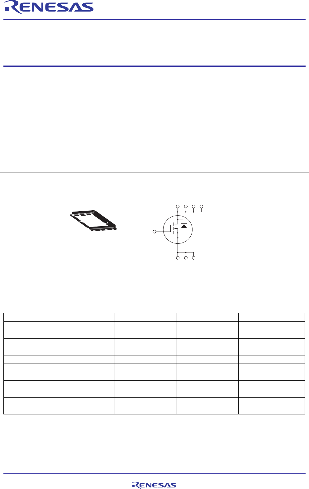
Outline
RENESAS Package code: PWSN0008DC-A
(Package name: WPAK(2))
G
D
SSS
DDD
4
123
5678
1, 2, 3 Source
4 Gate
5, 6, 7, 8 Drain
876
5
21
34
Absolute Maximum Ratings
(Ta = 25°C)
Item Symbol Ratings Unit
Drain to source voltage VDSS 30 V
Gate to source voltage VGSS ±20 V
Drain current ID 30 A
Drain peak current ID(pulse)Note1 120 A
Body-drain diode reverse drain current IDR 30 A
Avalanche current IAP Note 2 8 A
Avalanche energy EAR Note 2 6.4 mJ
Channel dissipation Pch Note3 25 W
Channel to case thermal impedance ch-c Note3 5 C/W
Channel temperature Tch 150 C
Storage temperature Tstg –55 to +150 C
Notes: 1. PW 10 s, duty cycle 1%
2. Value at Tch = 25C, Rg 50
3. Tc = 25C
REJ03G1791-0320
Rev.3.20
May 12, 2010
RJK03B9DPA Preliminary
REJ03G1791-0320 Rev.3.20 Page 2 of 6
May 12, 2010
Electrical Characteristics
(Ta = 25°C)
Item Symbol Min Typ Max Unit Test Conditions
Drain to source breakdown voltage V(BR)DSS 30 — — V ID = 10 mA, VGS = 0
Gate to source leak current IGSS — — ± 0.1 A VGS = ±20 V, VDS = 0
Zero gate voltage drain current IDSS — — 1 A VDS = 30 V, VGS = 0
Gate to source cutoff voltage VGS(off) 1.2 — 2.5 V VDS = 10 V, I D = 1 mA
RDS(on) — 8.3 10.6 m I
D = 15 A, VGS = 10 V Note4
Static drain to source on state
resistance RDS(on) — 10.9 15.1 m I
D = 15 A, VGS = 4.5 V Note4
Forward transfer admittance |yfs| — 65 — S ID = 15 A, VDS = 10 V Note4
Input capacitance Ciss — 1110 — pF
Output capacitance Coss — 160 — pF
Reverse transfer capacitance Crss — 80 — pF
VDS = 10 V
VGS = 0
f = 1 MHz
Gate Resistance Rg — 1.2 —
Total gate charge Qg — 7.4 — nC
Gate to source charge Qgs — 3.2 — nC
Gate to drain charge Qgd — 1.9 — nC
VDD = 10 V
VGS = 4.5 V
ID = 30 A
Turn-on delay time td(on) — 8.8 — ns
Rise time tr — 4 — ns
Turn-off delay time td(off) — 31 — ns
Fall time tf — 4.8 — ns
VGS = 10 V, ID = 15 A
VDD 10 V
RL = 0.67
Rg = 4.7
Body–drain diode forward voltage VDF — 0.88 1.15 V IF = 30 A, VGS = 0 Note4
Body–drain diode reverse recovery
time
trr — 13 — ns
IF =30 A, VGS = 0
diF/ dt = 100 A/ s
Notes: 4. Pulse test
RJK03B9DPA Preliminary
REJ03G1791-0320 Rev.3.20 Page 3 of 6
May 12, 2010
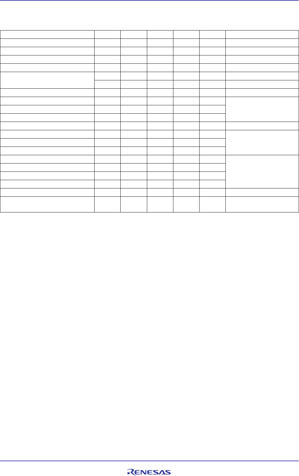
Main Characteristics
100
0246810
20
16
12
8
4
012 345
10
3
1
30 3001 10 100 1000
3
400
300
200
04 8 12 16 20
10 A
100
30
10 V
5 A
40
30
20
10
050 100 150 200 0.1 1 10 100
10
100
1000
1
0.1
DC Operation
PW = 10 ms
1 ms
2.6 V
2.8 V
3.0V
10 V
4.5 V
20
16
12
8
4
Channel Dissipation Pch (W)
Case Temperature Tc (°C)
Power vs. Temperature Derating
Drain to Source Voltage V
DS
(V)
Drain Current ID (A)
Maximum Safe Operation Area
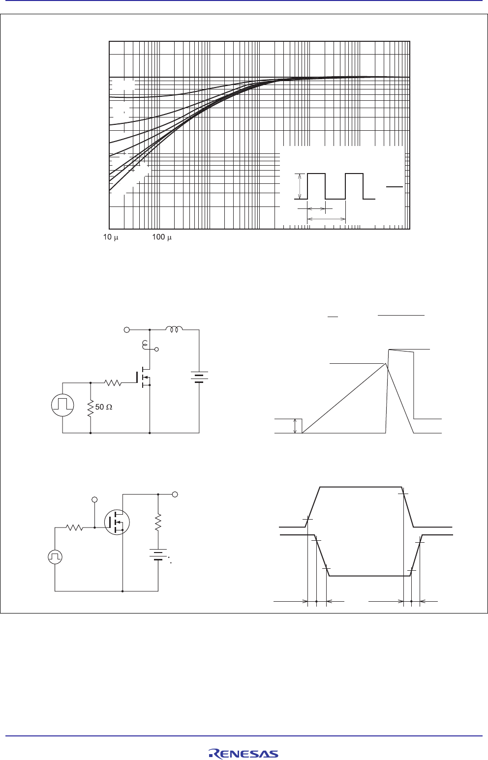
10 μs
100 μs
Tc = 25 °C
1 shot Pulse
Operation in
this area is
limited by R
DS(on)
Gate to Source Voltage V
GS
(V)
Drain to Source Voltage V
DS
(V)
Drain Current ID (A)
Typical Output Characteristics
Drain Current ID (A)
Typical Transfer Characteristics
V
DS
= 10 V
Pulse Test
Pulse Test
V
GS
= 2.4 V
Tc = 75°C
25°C
–25°C
Gate to Source Voltage V
GS
(V)
Drain to Source Saturation Voltage
V
DS(on)
(mV)
Static Drain to Source On State Resistance
R
DS(on)
(mΩ)
Drain to Source Saturation Voltage vs.
Gate to Source Voltage
Drain Current I
D
(A)
Static Drain to Source On State Resistance
vs. Drain Current
Pulse Test Pulse Test
I
D
= 20 A
V
GS
= 4.5 V
RJK03B9DPA Preliminary
REJ03G1791-0320 Rev.3.20 Page 4 of 6
May 12, 2010
20
8
4
–25 0 25 50 75 100 125 150
0
10 V
25 50 75 100 125 150
00.4 0.8 1.2 1.6 2.0
010 3020
10000
3000
1000
300
100
30
10
V
GS
= 0
f = 1 MHz
Crss
Coss
Ciss
50
40
30
20
10
0
20
16
12
8
4
816243240
00
12
16
10
8
6
4
2
0
50
40
30
20
10
5 V
10 V
Case Temperature Tc (°C)
Static Drain to Source On State Resistance
vs. Temperature
Capacitance C (pF)
Drain to Source Voltage V
DS
(V)
Typical Capacitance vs.
Drain to Source Voltage
Static Drain to Source On State Resistance
R
DS(on)
(mΩ)
Pulse Test
I
D
= 5 A, 10 A, 20 A
5 A, 10 A, 20 A
V
GS
= 4.5 V
Gate Charge Qg (nc)
Drain to Source Voltage V
DS
(V)
Gate to Source Voltage V
GS
(V)
Dynamic Input Characteristics
Source to Drain Voltage V
SD
(V)
Reverse Drain Current I
DR
(A)
Reverse Drain Current vs.
Source to Drain Voltage
I
D
= 30 A
V
GS
V
DS
V
DD
= 25 V
10 V
V
DD
= 25 V
10 V
Pulse Test
V
GS
= 0, –5 V
Channel Temperature Tch (°C)
Repetitive Avalanche Energy E
AR
(mJ)
Maximum Avalanche Energy vs.
Channel Temperature Derating
I
AP
= 8 A
V
DD
= 15 V
duty < 0.1%
Rg ≥ 50 Ω
RJK03B9DPA Preliminary
REJ03G1791-0320 Rev.3.20 Page 5 of 6
May 12, 2010
D. U. T
Rg
IAP
Monitor
VDS
Monitor
VDD
Vin
15 V
0
I
D
VDS
IAP
V(BR)DSS
L
VDD
EAR = L • IAP2 •
2
1VDSS
VDSS – VDD
Vin Monitor
D.U.T.
Vin
10 V
RL
VDS
= 10 V
tr
td(on)
Vin
90% 90%
10%
10%
Vout
td(off)
Vout
Monitor 90%
10%
tf
Rg
3
1
0.3
0.1
0.03
0.01 1 m 10 m 100 m 1 10
D = 1
0.5
0.2
0.1
0.05
0.02
0.01
1shot pulse
DM
P
PW
T
D = PW
T
θch – c(t) = γs (t) • θch – c
θch – c = 5.0°C/W, Tc = 25°C
Pulse Width PW (S)
Normalized Transient Thermal Impedance vs. Pulse Width
Normalized Transient Thermal Impedance γs (t)
Avalanche Test Circuit Avalanche Waveform
Switching Time Test Circuit Switching Time Waveform
RJK03B9DPA Preliminary
REJ03G1791-0320 Rev.3.20 Page 6 of 6
May 12, 2010
Package Dimensions
4.21Typ
5.9
0.2Typ
0.8Max
6.1
1.27Typ
0.7Typ
0.04Min
+0.1
-0.2
+0.1
-0.3
1.27Typ
0.05Max
0Min
0.545Typ
Stand-off
5.1 ± 0.2
4.90 ± 0.1
0.5 ± 0.15 3.6 ± 0.2 0.5 ± 0.15
0.4 ± 0.06
3.9 ± 0.2
⎯PWSN0008DC-A WPAK(2)V 0.07g
MASS[Typ.]RENESAS CodeJEITA Package Code Previous Code
(Ni/Pd/Au plating)
Notice:The reverse pattern of die-pad
support lead described above exists.
Unit: mm
Package Name
WPAK(2)
Ordering Information
Part No. Quantity Shipping Container
RJK03B9DPA-00-J53 3000 pcs Taping
Notice
1. All information included in this document is current as of the date this document is issued. Such information, however, is subject to change without any prior notice. Before purchasing or using any Renesas
Electronics products listed herein, please confirm the latest product information with a Renesas Electronics sales office. Also, please pay regular and careful attention to additional and different information to
be disclosed by Renesas Electronics such as that disclosed through our website.
2. Renesas Electronics does not assume any liability for infringement of patents, copyrights, or other intellectual property rights of third parties by or arising from the use of Renesas Electronics products or
technical information described in this document. No license, express, implied or otherwise, is granted hereby under any patents, copyrights or other intellectual property rights of Renesas Electronics or
others.
3. You should not alter, modify, copy, or otherwise misappropriate any Renesas Electronics product, whether in whole or in part.
4. Descriptions of circuits, software and other related information in this document are provided only to illustrate the operation of semiconductor products and application examples. You are fully responsible for
the incorporation of these circuits, software, and information in the design of your equipment. Renesas Electronics assumes no responsibility for any losses incurred by you or third parties arising from the
use of these circuits, software, or information.
5. When exporting the products or technology described in this document, you should comply with the applicable export control laws and regulations and follow the procedures required by such laws and
regulations. You should not use Renesas Electronics products or the technology described in this document for any purpose relating to military applications or use by the military, including but not limited to
the development of weapons of mass destruction. Renesas Electronics products and technology may not be used for or incorporated into any products or systems whose manufacture, use, or sale is
prohibited under any applicable domestic or foreign laws or regulations.
6. Renesas Electronics has used reasonable care in preparing the information included in this document, but Renesas Electronics does not warrant that such information is error free. Renesas Electronics
assumes no liability whatsoever for any damages incurred by you resulting from errors in or omissions from the information included herein.
7. Renesas Electronics products are classified according to the following three quality grades: "Standard", "High Quality", and "Specific". The recommended applications for each Renesas Electronics product
depends on the product's quality grade, as indicated below. You must check the quality grade of each Renesas Electronics product before using it in a particular application. You may not use any Renesas
Electronics product for any application categorized as "Specific" without the prior written consent of Renesas Electronics. Further, you may not use any Renesas Electronics product for any application for
which it is not intended without the prior written consent of Renesas Electronics. Renesas Electronics shall not be in any way liable for any damages or losses incurred by you or third parties arising from the
use of any Renesas Electronics product for an application categorized as "Specific" or for which the product is not intended where you have failed to obtain the prior written consent of Renesas Electronics.
The quality grade of each Renesas Electronics product is "Standard" unless otherwise expressly specified in a Renesas Electronics data sheets or data books, etc.
"Standard": Computers; office equipment; communications equipment; test and measurement equipment; audio and visual equipment; home electronic appliances; machine tools;
personal electronic equipment; and industrial robots.
"High Quality": Transportation equipment (automobiles, trains, ships, etc.); traffic control systems; anti-disaster systems; anti-crime systems; safety equipment; and medical equipment not specifically
designed for life support.
"Specific": Aircraft; aerospace equipment; submersible repeaters; nuclear reactor control systems; medical equipment or systems for life support (e.g. artificial life support devices or systems), surgical
implantations, or healthcare intervention (e.g. excision, etc.), and any other applications or purposes that pose a direct threat to human life.
8. You should use the Renesas Electronics products described in this document within the range specified by Renesas Electronics, especially with respect to the maximum rating, operating supply voltage
range, movement power voltage range, heat radiation characteristics, installation and other product characteristics. Renesas Electronics shall have no liability for malfunctions or damages arising out of the
use of Renesas Electronics products beyond such specified ranges.
9. Although Renesas Electronics endeavors to improve the quality and reliability of its products, semiconductor products have specific characteristics such as the occurrence of failure at a certain rate and
malfunctions under certain use conditions. Further, Renesas Electronics products are not subject to radiation resistance design. Please be sure to implement safety measures to guard them against the
possibility of physical injury, and injury or damage caused by fire in the event of the failure of a Renesas Electronics product, such as safety design for hardware and software including but not limited to
redundancy, fire control and malfunction prevention, appropriate treatment for aging degradation or any other appropriate measures. Because the evaluation of microcomputer software alone is very difficult,
please evaluate the safety of the final products or system manufactured by you.
10. Please contact a Renesas Electronics sales office for details as to environmental matters such as the environmental compatibility of each Renesas Electronics product. Please use Renesas Electronics
products in compliance with all applicable laws and regulations that regulate the inclusion or use of controlled substances, including without limitation, the EU RoHS Directive. Renesas Electronics assumes
no liability for damages or losses occurring as a result of your noncompliance with applicable laws and regulations.
11. This document may not be reproduced or duplicated, in any form, in whole or in part, without prior written consent of Renesas Electronics.
12. Please contact a Renesas Electronics sales office if you have any questions regarding the information contained in this document or Renesas Electronics products, or if you have any other inquiries.
(Note 1) "Renesas Electronics" as used in this document means Renesas Electronics Corporation and also includes its majority-owned subsidiaries.
(Note 2) "Renesas Electronics product(s)" means any product developed or manufactured by or for Renesas Electronics.
http://www.renesas.com
Refer to "http://www.renesas.com/" for the latest and detailed information.
Renesas Electronics America Inc.
2880 Scott Boulevard Santa Clara, CA 95050-2554, U.S.A.
Tel: +1-408-588-6000, Fax: +1-408-588-6130
Renesas Electronics Canada Limited
1101 Nicholson Road, Newmarket, Ontario L3Y 9C3, Canada
Tel: +1-905-898-5441, Fax: +1-905-898-3220
Renesas Electronics Europe Limited
Dukes Meadow, Millboard Road, Bourne End, Buckinghamshire, SL8 5FH, U.K
Tel: +44-1628-585-100, Fax: +44-1628-585-900
Renesas Electronics Europe GmbH
Arcadiastrasse 10, 40472 Düsseldorf, Germany
Tel: +49-211-65030, Fax: +49-211-6503-1327
Renesas Electronics (China) Co., Ltd.
7th Floor, Quantum Plaza, No.27 ZhiChunLu Haidian District, Beijing 100083, P.R.China
Tel: +86-10-8235-1155, Fax: +86-10-8235-7679
Renesas Electronics (Shanghai) Co., Ltd.
Unit 204, 205, AZIA Center, No.1233 Lujiazui Ring Rd., Pudong District, Shanghai 200120, China
Tel: +86-21-5877-1818, Fax: +86-21-6887-7858 / -7898
Renesas Electronics Hong Kong Limited
Unit 1601-1613, 16/F., Tower 2, Grand Century Place, 193 Prince Edward Road West, Mongkok, Kowloon, Hong Kong
Tel: +852-2886-9318, Fax: +852 2886-9022/9044
Renesas Electronics Taiwan Co., Ltd.
7F, No. 363 Fu Shing North Road Taipei, Taiwan
Tel: +886-2-8175-9600, Fax: +886 2-8175-9670
Renesas Electronics Singapore Pte. Ltd.
1 harbourFront Avenue, #06-10, keppel Bay Tower, Singapore 098632
Tel: +65-6213-0200, Fax: +65-6278-8001
Renesas Electronics Malaysia Sdn.Bhd.
Unit 906, Block B, Menara Amcorp, Amcorp Trade Centre, No. 18, Jln Persiaran Barat, 46050 Petaling Jaya, Selangor Darul Ehsan, Malaysia
Tel: +60-3-7955-9390, Fax: +60-3-7955-9510
Renesas Electronics Korea Co., Ltd.
11F., Samik Lavied' or Bldg., 720-2 Yeoksam-Dong, Kangnam-Ku, Seoul 135-080, Korea
Tel: +82-2-558-3737, Fax: +82-2-558-5141
SALES OFFICES
© 2010 Renesas Electronics Corporation. All rights reserved.
Colophon 1.0
