RT7291A, RT7291B Datasheet. Www.s Manuals.com. R02 Richtek
User Manual: Marking of electronic components, SMD Codes 3906, 393I, 3958NL, 399*, 39=**, 39=***, 39A, 39A*, 39B*, 39C*, 39D*, 39E*, 39F*, 39G*, 39H*, 39I*, 39J*, 39K*, 39L*, 39M*, 39N*, 39O*, 39P*, 39Q*, 39R*, 39S*, 39T, 39T*, 39U*, 39V*, 39Y. Datasheets 1.5SMC39AT3, APL5309-15A, APL5309-15B, APL5309-16A, APL5309-16B, APL5309-17A, APL5309-17B, APL5309-18A, APL5309-18B, APL5309-19A, APL5309-19B, APL5309-20A, APL5309-20B, APL5309-21A, APL5309-21B, APL5309-22A, APL5309-22B, APL5309-23A, APL5309-23B, APL5309-24A, APL5309-2
Open the PDF directly: View PDF ![]() .
.
Page Count: 19

RT7291A/B
®
DS7291A/B-02 September 2015 www.richtek.com
1
©
Copyright 2014 Richtek Technology Corporation. All rights reserved. is a registered trademark of Richtek Technology Corporation.
6A, 23V, 500kHz, ACOTTM Synchronous Buck Converter
with LDO for System 5V
General Description
The RT7291A/B is a synchronous Buck converter with
Advanced Constant On-Time (ACOTTM) mode control. The
main control loop of RT7291A/B uses an ACOTTM mode
control which provides a very fast transient response with
no external compensators. The RT7291A/B operates from
5V to 23V input voltage, provides a 5V LDO and a 300kHz
CLK to drive an external charge pump. OCP, UVP and
OVP are included in the RT7291A/B. This IC also provides
a 1.5ms internal soft-start function and an open-drain power
good indicator.
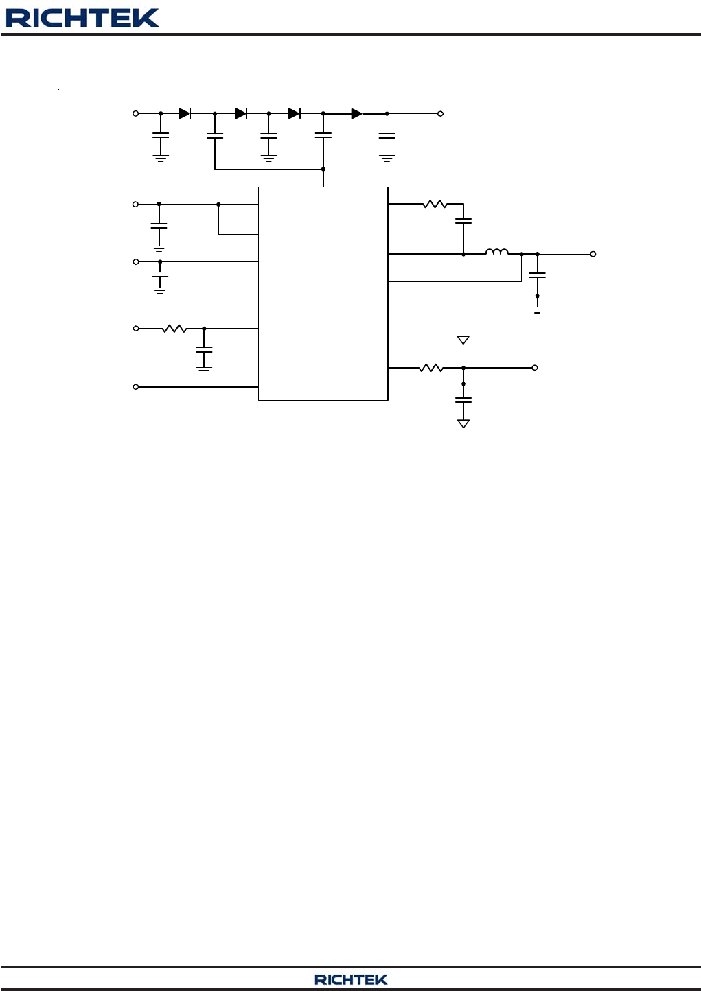
Simplified Application Circuit
Features
--
--
-5V to 23V Input Voltage Range
--
--
-Up to 98% Duty for 2S Battery Application
--
--
-PWM Frequency Fixed 500kHz
--
--
-ACOTTM Mode Performs Fast Transient Response
--
--
-Integrated MOSFETs
31mΩΩ
ΩΩ
Ω of High-Side MOSFET
20mΩΩ
ΩΩ
Ω of Low-Side MOSFET
--
--
-Support Output MLCC Stable
--
--
-Internal Soft-Start (1.5ms typ)
--
--
-Built-in OVP/UVP/OCP
--
--
-Power Good Indicator
--
--
-Fixed 300kHz VCLK to Support Charge Pump
--
--
-Individual EN for PWM and LDO
--
--
-Thermal Shutdown
Applications
-Laptop Computers
-Tablet PCs
-Networking Systems
-Servers
-Personal Video Recorders
-Flat Panel Television and Monitors
-Distributed Power Systems
RT7291A/B
EN
VIN BOOT
ENLDO
VBYP
LDO
CLK
SW
VOUT
PGND
AGND
VOUT
PGOOD
VCC
VCP
VOUT
VIN
VOUT
VLDO
VCC
D1
C1 C2
D2 D3
C3 C4
D4
C5
CIN
RB
CBL
COUT
RPGOOD
CVCC
CLDO
CBYP
RBYP

RT7291A/B
2
DS7291A/B-02 September 2015www.richtek.com
©
Copyright 2014 Richtek Technology Corporation. All rights reserved. is a registered trademark of Richtek Technology Corporation.
Functional Pin Description
Pin No. Pin Name Pin Function
1 VIN Power Input Connect to High-Side MOSFET Drain.
2 PGND Power Ground.
3 VBYP
Switch Over Source Voltage for VCC. A low pass filter should be connected to
AGND, if VBYP is applied. If VBYP is not used, then connect to AGND. Do not
connect to VCC pin.
4 PGOOD Open-Drain Power Good Indicator Output.
5 CLK 300kHz Clock Output to Drive the External Charge Pump.
6 LDO 5V Linear Regulator Output. Decouple with a minimum 4.7F ceramic capacitor.
7 VOUT
Output Voltage Sense Input. An internal discharging circuit is connected to this
pin.
8, 9, 15, 16 SW Switch Node.
10 BOOT Bootstrap Supply for High-Side Gate Driver. A capacitor is needed to drive the
power switch's gate above the supply voltage. It is connected between the SW
and BOOT pins to form a floating supply across the power switch driver.
11 VCC 5V Linear Regulator Output for Internal Control Circuit. A capacitor (typical 2.2F)
should be connected to AGND. VCC can only supply internal circuits. Do not
connect to external loads.
12 ENLDO
Enable Control Input for Linear Regulator. This pin is internally pulled up to high by
10A.
13 EN Enable Control Input. Do not leave this pin floating.
14 AGND Analog Ground.
Pin Configurations
(TOP VIEW)
UQFN-16L 3x3 (FC)
Ordering Information
Note :
Richtek products are :
RoHS compliant and compatible with the current require-
ments of IPC/JEDEC J-STD-020.
Suitable for use in SnPb or Pb-free soldering processes.
PGND
VIN
PGOOD
SW
SW
LDO
EN
VCC
BOOT
VBYP
ENLDO
CLK
VOUT
AGND
1
2
3 4 5 6 7
14 13 12 11 10
15
16 8
9
SW
SW
Marking Information
RT7291AGQUF RT7291BGQUF
39=YM
DNN 4M=YM
DNN
39= : Product Code
YMDNN : Date Code
4M= : Product Code
YMDNN : Date Code
Package Type
QUF : UQFN-16L 3x3 (FC) (U-Type)
RT7291A/B
Lead Plating System
G : Green (Halogen Free and Pb Free)
Output Voltage
A : 5V
B : 5.1V

RT7291A/B
3
DS7291A/B-02 September 2015 www.richtek.com
©
Copyright 2014 Richtek Technology Corporation. All rights reserved. is a registered trademark of Richtek Technology Corporation.
Function Block Diagram
Operation
Overall
The RT7291A/B is a synchronous step-down converter
with advanced constant on-time control mode. Using the
ACOTTM control mode can reduce the output capacitance
and provide fast transient response. It can minimize the
component size without additional external compensation
network.
Internal VCC Regulator
The regulator provides 5V power to supply the internal
control circuit. Connecting a 2.2μF ceramic capacitor for
decoupling and stability is required.
Soft-Start
In order to prevent the converter output voltage from
overshooting during the startup period, the soft-start
function is necessary. The soft-start time is internal setting
and the duration is around 1.5ms
OCP
The inductor valley current is monitored via the internal
switches in cycle-by-cycle. Once the output voltage drops
below UV threshold, the device enters latch mode.
Power Good
After soft-start is finished, the power good function will be
activated. The PGOOD pin is an open-drain output.
CLK Generator
Provide a 300kHz clock to drive external charge pump.
VCC Switch-Over
The internal regulator output will switch over to VBYP if
VBYP level is higher than 4.6V.
LDO
Built-in 5V, 100mA LDO with 1% accuracy. The LDO output
will switch over to VOUT once PGOOD goes high.
POR &
Reference
VOUT
VCC
On-Time
One shot
EN
VIN LDO
VBYP
SW
Gate
Control
Logic
Fault
Logic
CLK
PGND
VIN
BSTREG BOOT
PGOOD
AGND
Min off Time
+
-
+
Soft-Start
VOUT
+
-
OCP
SW
+
-
+
-
UVP
60% x VREF
POK
OVP
90% x VREF
+
-
120% x VREF
VREF
VFB
LDO
Switch-Over
LDO
Control
VCC
Regulator
VCC VOUT
CLK
Generator
VOUT
ENLDO
VCC
Switch-Over
VIN
VOC
VCC
RT7291A/B
4
DS7291A/B-02 September 2015www.richtek.com
©
Copyright 2014 Richtek Technology Corporation. All rights reserved. is a registered trademark of Richtek Technology Corporation.
Parameter Symbol Test Conditions Min Typ Max Unit
Supply Current
Shutdown Current V
EN = VENLDO = 0V -- 2.5 5 A
Quiescent Current V
EN = 2V, VENLDO = 2V, No Switching -- 100 130 A
Standby Current VEN = 0V, VENLDO = 2V, LDO Load
Current = 0A -- 35 45 A
Switch On-Resistance
Switch On-Resistance RDS(ON)_H V
BOOT – VSW = 5V -- 31 --
m
RDS(ON)_L -- 20 --
Current Limit
Current Limit IOC Valley current of low-side switch 7.6 -- 11.4 A
Switching Frequency and Minimum Off Timer
Switching Frequency fSW 450 500 550 kHz
Minimum Off-Time TOFF -- 200 -- ns
Protections
OVP Trip Threshold VOVP With respect to output voltage 115 120 125 %
OVP Propagation Delay TOVPDLY -- 5 -- s
Electrical Characteristics
(VIN = 12V, TA = 25°C, unless otherwise specified)
Absolute Maximum Ratings (Note 1)
-Supply Input Voltage, VIN ---------------------------------------------------------------------------------- −0.3V to 27V
-Switch Voltage, SW ----------------------------------------------------------------------------------------- −0.3V to (VIN + 0.3V)
<30ns ----------------------------------------------------------------------------------------------------------- −5V to 28V
-BOOT Switch Voltage ---------------------------------------------------------------------------------------(VSW − 0.3V) to (VSW + 6V)
-EN, ENLDO Pin Voltages ---------------------------------------------------------------------------------- −0.3V to 27V
-Other I/O Pin Voltages -------------------------------------------------------------------------------------- −0.3V to 6V
-Power Dissipation, PD @ TA = 25°C
UQFN-16L 3x3 (FC) ------------------------------------------------------------------------------------------1.4W
-Package Thermal Resistance (Note 2)
UQFN-16L 3x3 (FC), θJA ------------------------------------------------------------------------------------ 70°C/W
UQFN-16L 3x3 (FC), θJC ------------------------------------------------------------------------------------ 15°C/W
-Lead Temperature (Soldering, 10 sec.)------------------------------------------------------------------260°C
-Junction Temperature ----------------------------------------------------------------------------------------150°C
-Storage Temperature Range ------------------------------------------------------------------------------- −65°C to 150°C
-ESD Susceptibility (Note 3)
HBM (Human Body Model)--------------------------------------------------------------------------------- 2kV
MM (Machine Model) ---------------------------------------------------------------------------------------- 200V
Recommended Operating Conditions (Note 4)
-Supply Input Voltage, VIN ----------------------------------------------------------------------------------5V to 23V
-Junction Temperature Range------------------------------------------------------------------------------- −40°C to 125°C
-Ambient Temperature Range ------------------------------------------------------------------------------- −40°C to 85°C

RT7291A/B
5
DS7291A/B-02 September 2015 www.richtek.com
©
Copyright 2014 Richtek Technology Corporation. All rights reserved. is a registered trademark of Richtek Technology Corporation.
Parameter Symbol Test Conditions Min Typ Max Unit
UVP Trip Threshold VUVP With respect to output voltage 55 60 65 %
UVP Propagation Delay TUVPDLY -- 5 -- s
Reference and Soft-Start
Output Voltage Valley VOUT RT7291A 4.95 5 5.05
V
RT7291B 5.049 5.1 5.151
Soft-Start Time TSS From EN high to PGOOD high 1 1.5 2 ms
Enable and UVLO
EN Input High Voltage VENH RT7291A 1.25 1.35 1.45
V
RT7291B 1.3 1.4 1.5
EN Hysteresis VENHYS -- 200 -- mV
EN Input Current IEN VEN = 2V -- 1 -- A
VEN = 0V -- 0 --
VCC UVLO Rising VCCUVLO -- 4.2 -- V
VCC UVLO Hysteresis VCCHYS -- 400 -- mV
CLK Output
CLK Output
Voltage
High-Level VCLKH I
VCLK = 10mA RT7291A -- -- 5.05
V
RT7291B -- -- 5.151
Low-Level VCLKL I
VCLK = 10mA 0 0.1 0.2
CLK Frequency fCLK -- 300 -- kHz
LDO Regulator
LDO Regulator VLDO RT7291A 4.95 5 5.05
V
RT7291B 5.049 5.1 5.151
LDO Load Regulation
EN = GND,
LDO Load Current = 5mA -- 1 --
%
EN = GND,
LDO Load Current = 100mA -- 5 --
Switch On-Resistance RSW -- 3 5
VCC Regulator
VCC Regulator VVCC RT7291A 4.805 5 5.295
V
RT7291B 4.905 5.1 5.395
VCC Switch Over Threshold to
VBYP VBYP Rising
Edge
RT7291A 4.45 4.6 4.75 V
RT7291B 4.542 4.692 4.842
VCC Switch Over Hysteresis VBYP Falling Edge -- 200 -- mV
Switch Over On-Resistance -- 3 5

RT7291A/B
6
DS7291A/B-02 September 2015www.richtek.com
©
Copyright 2014 Richtek Technology Corporation. All rights reserved. is a registered trademark of Richtek Technology Corporation.
Note 1. Stresses beyond those listed “Absolute Maximum Ratings” may cause permanent damage to the device. These are
stress ratings only, and functional operation of the device at these or any other conditions beyond those indicated in
the operational sections of the specifications is not implied. Exposure to absolute maximum rating conditions may
affect device reliability.
Note 2. θJA is measured at TA = 25°C on a high effective thermal conductivity four-layer test board per JEDEC 51-7.
Note 3. Devices are ESD sensitive. Handling precaution is recommended.
Note 4. The device is not guaranteed to function outside its operating conditions.
Parameter Symbol Test Conditions Min Typ Max Unit
Power Good Indicator
PGOOD Threshold From Lower VOUT Rising 85 90 95 %
PGOOD Low Hysteresis VOUT Falling -- 10 -- %
PGOOD Low to High Delay TPGDLY -- 0.5 -- ms
PGOOD Sink Current Capability VPGSINK Sink 4mA -- -- 0.4 V
PGOOD Leakage Current IPGLEAK V
PGOOD = 5V -- -- 100 nA
Thermal Shutdown
Thermal Shutdown Threshold TSD 135 150 -- °C
Thermal Shutdown Hysteresis -- 25 -- °C
RT7291A/B
7
DS7291A/B-02 September 2015 www.richtek.com
©
Copyright 2014 Richtek Technology Corporation. All rights reserved. is a registered trademark of Richtek Technology Corporation.
Typical Application Circuit
Figure 1. Typical Application Circuit with Pure MLCC Solution
RT7291A/B
EN
VIN BOOT
ENLDO
12
VBYP
3
LDO
6
13
10µF
/25V x 2
CLK
SW
VOUT
PGND
AGND
(Optional)
0.1µF / 50V
1.5µH
22µF /
6.3V x 4
VOUT
5V/6A
PGOOD
VCC
2.2µF /
10V
100k
VCP
VOUT
100nF
/ 50V
VIN
5.2V to 23V
4.7µF /10V
VOUT
VLDO
5V
110
8, 9, 15, 16
7
2
14
4
11 VCC
D1
C1 C2
D2 D3
C3 C4
D4
C5
CIN
RB
CB
L
COUT
RPGOOD
CVCC
5
CLDO
2.2
CBYP
2.2µF /
10V
RBYP
5.1
100nF
/ 50V 100nF
/ 50V 100nF
/ 50V 100nF
/ 50V

RT7291A/B
8
DS7291A/B-02 September 2015www.richtek.com
©
Copyright 2014 Richtek Technology Corporation. All rights reserved. is a registered trademark of Richtek Technology Corporation.
Efficiency vs. Load Current
80
85
90
95
100
0.001 0.01 0.1 1 10
Load Current (A)
Efficiency (%)
Efficiency vs. Load Current
70
75
80
85
90
95
100
0.001 0.01 0.1 1 10
Load Current (A)
Efficiency (%)
Efficiency vs. Load Current
70
75
80
85
90
95
100
0.001 0.01 0.1 1 10
Load Current (A)
Efficiency (%)
Switching Frequency vs. Load Current
0
50
100
150
200
250
300
350
400
450
500
550
0.001 0.01 0.1 1 10
Load Current (A)
Switching Frequency (kHz) 1
Switching Frequency vs. Load Current
0
50
100
150
200
250
300
350
400
450
500
550
0.001 0.01 0.1 1 10
Load Current (A)
Switching Frequency (kHz) 1
Switching Frequency vs. Load Current
0
50
100
150
200
250
300
350
400
450
500
550
0.001 0.01 0.1 1 10
Load Current (A)
Switching Frequency (kHz) 1
Typical Operating Characteristics
VIN = 7.4V, EN = 2V, ENLDO = floating VIN = 12V, EN = 2V, ENLDO = floating
VIN = 19V, EN = 2V, ENLDO = floating
VIN = 12V, EN = 2V, ENLDO = floating VIN = 19V, EN = 2V, ENLDO = floating
VIN = 7.4V, EN = 2V, ENLDO = floating

RT7291A/B
9
DS7291A/B-02 September 2015 www.richtek.com
©
Copyright 2014 Richtek Technology Corporation. All rights reserved. is a registered trademark of Richtek Technology Corporation.
Quiescent Current vs. Input Voltage
0
10
20
30
40
50
60
70
80
90
100
5 7 9 11131517192123
Input Voltage (V)
Quiescent Current (µA) 1
Standby Current vs. Input Voltage
0
10
20
30
40
50
60
70
80
5 7 9 11131517192123
Input Voltage (V)
Standby Current (µA
)
Shutdown Current vs. Input Voltage
0
1
2
3
4
5
6
7
8
9
10
5 7 9 11131517192123
Input Voltage (V)
Shutdown Current (µA) 1
Output Voltage vs. Load Current
4.75
4.80
4.85
4.90
4.95
5.00
5.05
5.10
5.15
5.20
5.25
0.001 0.01 0.1 1 10
Load Current (A)
Output Voltage (V)
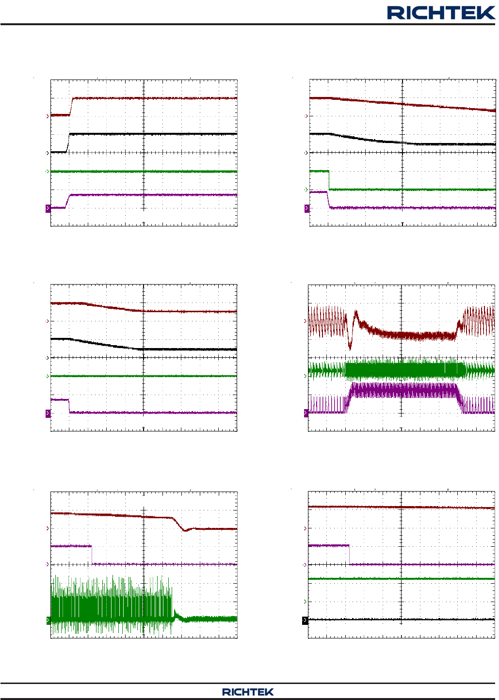
Time (500μs/Div)
Start Up Through EN
EN
(5V/Div)
VOUT
(5V/Div)
VCC
(5V/Div)
PGOOD
(5V/Div)
VIN = 12V, ENLDO = GND, No Load
VIN = 12V, EN = 2V, ENLDO = floating
EN = ENLDO = 0V
EN = 0V, ENLDO = 2V, ILDO = 0AEN = 2V, ENLDO = floating, No Switching
LDO Output Voltage vs. Input Voltage
4.75
4.80
4.85
4.90
4.95
5.00
5.05
5.10
5.15
5.20
5.25
4 6 8 1012141618202224
Input Voltage (V)
LDO Output Voltage (V)
ILDO = 0mA
ILDO = 50mA
ILDO = 100mA
RT7291A/B
10
DS7291A/B-02 September 2015www.richtek.com
©
Copyright 2014 Richtek Technology Corporation. All rights reserved. is a registered trademark of Richtek Technology Corporation.
Time (500μs/Div)
Start Up Through ENLDO
ENLDO
(5V/Div)
VLDO
(5V/Div)
VCC
(5V/Div)
VIN = 12V, EN = GND, No Load
VCP
(5V/Div)
Time (500μs/Div)
Power Off Through EN
VIN = 12V, ENLDO = GND, No Load
EN
(5V/Div)
VOUT
(5V/Div)
VCC
(5V/Div)
PGOOD
(5V/Div)
Time (500μs/Div)
Power Off Through ENLDO
VIN = 12V, EN = GND, No Load
ENLDO
(5V/Div)
VLDO
(5V/Div)
VCP
(5V/Div)
VCC
(5V/Div)
Time (50μs/Div)
Load Transient Response
SW
(20V/Div)
VOUT
(30mV/Div)
VIN = 12V, EN = ENLDO = High
IL
(5A/Div)
Time (50μs/Div)
UVP
SW
(10V/Div)
VOUT
(5V/Div)
VIN = 12V, EN = ENLDO = High
PGOOD
(5V/Div)
Time (50μs/Div)
OVP
PGOOD
(5V/Div)
VOUT
(5V/Div)
VIN
(10V/Div)
IL
(5A/Div) VIN = 12V, VOUT = 6V, EN = ENLDO = High
RT7291A/B
11
DS7291A/B-02 September 2015 www.richtek.com
©
Copyright 2014 Richtek Technology Corporation. All rights reserved. is a registered trademark of Richtek Technology Corporation.
Application Information
The RT7291A/B is high-performance 500kHz 6A step-down
regulators with internal power switches and synchronous
rectifiers. It features an Advanced Constant On-Time
(ACOTTM) control architecture that provides stable
operation for ceramic output capacitors without
complicated external compensation, among other benefits.
The input voltage range is from 5V to 23V, and the output
voltage is fixed 5V.
The proprietary ACOTTM control scheme improves
conventional constant on-time architectures, achieving
nearly constant switching frequency over line, load, and
output voltage ranges. Since there is no internal clock,
response to transients is nearly instantaneous and inductor
current can ramp quickly to maintain output regulation
without large bulk output capacitance.
ACOTTM Control Architecture
In order to achieve good stability with low-ESR ceramic
capacitors, ACOTTM uses a virtual inductor current ramp
generated inside the IC. This internal ramp signal replaces
the ESR ramp normally provided by the output capacitor's
ESR. The ramp signal and other internal compensations
are optimized for low-ESR ceramic output capacitors.
Making the on-time proportional to VOUT and inversely
proportional to VIN is not sufficient to achieve good
constant-frequency behavior for several reasons. First,
voltage drops across the MOSFET switches and inductor
cause the effective input voltage to be less than the
measured input voltage and the effective output voltage to
be greater than the measured output voltage as sensing
input and output voltage. When the load changes, the
switch voltage drops change causing a switching
frequency variation with load current. Also, at light loads
if the inductor current goes negative, the switch dead-
time between the synchronous rectifier turn-off and the
high-side switch turn-on allows the switching node to rise
to the input voltage. This increases the effective on-time
and causes the switching frequency to drop noticeably.
One way to reduce these effects is to measure the actual
switching frequency and compare it to the desired range.
This has the added benefit eliminating the need to sense
the actual output voltage, potentially saving one pin
connection. The ACOTTM uses this method, measuring
the actual switching frequency and modifying the on-time
with a feedback loop to keep the average switching
frequency in the desired range.
ACOTTM One-shot Operation
The RT7291A/B control algorithm is simple to understand.
The feedback voltage, with the virtual inductor current ramp
added, is compared to the reference voltage. When the
combined signal is less than the reference, the on-time
one-shot is triggered, as long as the minimum off-time
one-shot is clear and the measured inductor current
(through the synchronous rectifier) is below the current
limit. The on-time one-shot turns on the high-side switch
and the inductor current ramps up linearly. After the on-
time, the high-side switch is turned off and the synchronous
rectifier is turned on and the inductor current ramps down
linearly. At the same time, the minimum off-time one-shot
is triggered to prevent another immediate on-time during
the noisy switching time and allow the feedback voltage
and current sense signals to settle. The minimum off-time
is kept short (200ns typical) so that rapidly-repeated on-
times can raise the inductor current quickly when needed.
Diode Emulation Mode
In diode emulation mode, the RT7291A/B automatically
reduces switching frequency at light load conditions to
maintain high efficiency. This reduction of frequency is
achieved smoothly. As the output current decreases from
heavy load conditions, the inductor current is also reduced,
and eventually comes to the point that its current valley
touches zero, which is the boundary between continuous
conduction and discontinuous conduction modes. To
emulate the behavior of diodes, the low-side MOSFET
allows only partial negative current to flow when the
inductor free wheeling current becomes negative. As the
load current is further decreased, it takes longer and longer
time to discharge the output capacitor to the level that
requires the next “ON” cycle. In reverse, when the output
current increases from light load to heavy load, the
switching frequency increases to the preset value as the
RT7291A/B
12
DS7291A/B-02 September 2015www.richtek.com
©
Copyright 2014 Richtek Technology Corporation. All rights reserved. is a registered trademark of Richtek Technology Corporation.
inductor current reaches the continuous conduction. The
transition load point to the light load operation is shown in
Figure 2 and can be calculated as follows :
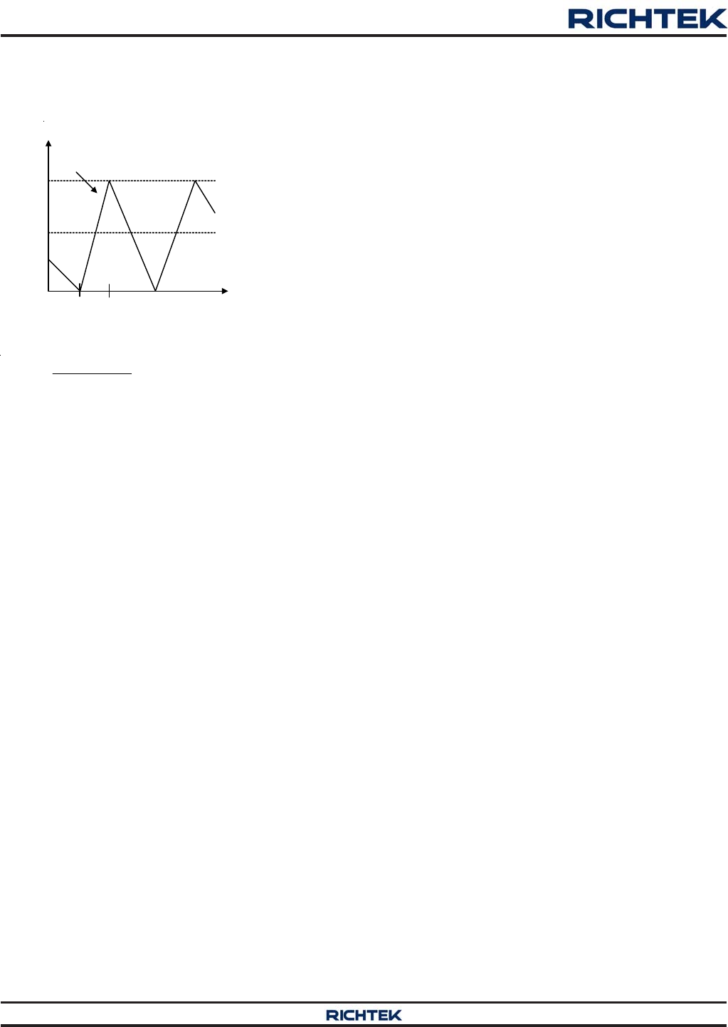
Figure 2. Boundary Condition of CCM/DEM
t
IL
Slope = (VIN - VOUT) / L
IPEAK
ILOAD = IPEAK / 2
tON
IN OUT
LOAD ON
(V V )
It
2L
where tON is the on-time.
The switching waveforms may appear noisy and
asynchronous when light load causes diode emulation
operation. This is normal and results in high efficiency.
Trade offs in DEM noise vs. light load efficiency is made
by varying the inductor value. Generally, low inductor values
produce a broader efficiency vs. load curve, while higher
values result in higher full load efficiency (assuming that
the coil resistance remains fixed) and less output voltage
ripple. Penalties for using higher inductor values include
larger physical size and degraded load transient response
(especially at low input voltage levels).
During discontinuous switching, the on-time is immediately
increased to add “hysteresis” to discourage the IC from
switching back to continuous switching unless the load
increases substantially. The IC returns to continuous
switching as soon as an on-time is generated before the
inductor current reaches zero. The on-time is reduced back
to the length needed for 500kHz switching and encouraging
the circuit to remain in continuous conduction, preventing
repetitive mode transitions between continuous switching
and discontinuous switching.
Linear Regulators (LDO & VCC)
The RT7291A/B includes a 5V linear regulator (LDO). The
LDO regulator can supply up to 100mA for external loads.
Bypass LDO with a minimum 4.7μF ceramic capacitor.
When VOUT is powered on and PGOOD is pulled high,
an internal 3Ω P-MOSFET switch connects VOUT to the
LDO pin while the internal linear regulator is simultaneously
turned off.
The RT7291A/B also includes a 5V linear regulator (VCC).
The VCC regulator steps down input voltage to supply
both internal circuitry and gate drivers. Do not connect
the VCC pin to external loads. When PGOOD is pulled
high and BYP pin voltage is above 4.6V, an internal 3Ω
P-MOSFET switch connects VCC to the BYP pin while
the VCC linear regulator is simultaneously turned off.
Current Limit
The RT7291A/B current limit is a cycle-by-cycle “valley”
type, measuring the inductor current through the
synchronous rectifier during the off-time while the inductor
current ramps down. The current is determined by
measuring the voltage between Source and Drain of the
synchronous rectifier, adding temperature compensation
for greater accuracy. If the current exceeds the current
limit, the on-time one-shot is inhibited until the inductor
current ramps down below the current limit. Thus, only
when the inductor current is well below the current limit,
another on-time is permitted. If the output current exceeds
the available inductor current (controlled by the current
limit mechanism), the output voltage will drop. If it drops
below the output under-voltage protection level (see next
section), the IC will stop switching to avoid excessive
heat.
The RT7291A/B also features a negative current limit to
protect the IC against sinking excessive current and
possibly damage. If the voltage across the synchronous
rectifier indicates the negative current is too high, the
synchronous rectifier turns off.
Output Over-Voltage Protection and Under-Voltage
Protection
The RT7291A/B features an output Over-Voltage Protection
(OVP). If the output voltage rises above the regulation
level, the IC stops switching and is latched off. The
RT7291A/B also features an output Under-Voltage
Protection (UVP). If the output voltage drops below the
UVP trip threshold for longer than 2μs (typical), the UVP

RT7291A/B
13
DS7291A/B-02 September 2015 www.richtek.com
©
Copyright 2014 Richtek Technology Corporation. All rights reserved. is a registered trademark of Richtek Technology Corporation.
Soft-Start
The RT7291A/B provides an internal soft-start function to
prevent large inrush current and output voltage overshoot
when the converter starts up. The soft-start (SS)
automatically begins once the chip is enabled. During soft-
start, it clamps the ramp of internal reference voltage which
is compared with FB signal. The typical soft-start duration
is 1.5ms.
Power Off
When VEN is pulled to GND or lower than the logic-low
level of 1.15V, there is an internal discharging resistor to
discharge the residual charge inside the output capacitors.
Besides, the value of discharging resistor is about twenty
ohms.
Power Good Output (PGOOD)
The power good output is an open-drain output that requires
a pull-up resistor. When the output voltage is 20% (typical)
below its set voltage, PGOOD will be pulled low. It is held
low until the output voltage returns to 90% of its set voltage
once more. During soft-start, PGOOD is actively held low
and only allowed to be pulled high after soft-start is over
and the output reaches 90% of its set voltage. There is a
2μs delay built into PGOOD circuitry to prevent false
transition.
External Bootstrap Capacitor (CBOOT)
Connect a 0.22μF low ESR ceramic capacitor between
the BOOT and SW pins. This bootstrap capacitor provides
the gate driver supply voltage for the high-side N-MOSFET
switch.
The internal power MOSFET switch gate driver is
optimized to turn the switch on fast enough for low power
loss and good efficiency, and slow enough to reduce EMI.
Switch turn-on is when most EMI occurs since VSW rises
rapidly. During switch turn-off, SW is discharged relatively
slowly by the inductor current during the dead-time
between high-side and low-side switch on-times. In some
cases it is desirable to reduce EMI further, at the expense
of some additional power dissipation. The switch turn-on
can be slowed by placing a small (<10Ω) resistance
between BOOT and the external bootstrap capacitor. This
will slow the high-side switch turn-on and VSW's rise.
is triggered, and the IC will shut down. The IC stops
switching and is latched off. To restart operation, toggle
EN or power the IC off and then on again.
Input Under-Voltage Lockout
In addition to the enable function, the RT7291A/B features
an Under-Voltage Lockout (UVLO) function that monitors
the input voltage. To prevent operation without fully-
enhanced internal MOSFET switches, this function inhibits
switching when input voltage drops below the UVLO-falling
threshold. The IC resumes switching when input voltage
exceeds the UVLO-rising threshold.
Over-Temperature Protection
The RT7291A/B features an Over-Temperature Protection
(OTP) circuitry to prevent overheating due to excessive
power dissipation. The OTP shuts down switching
operation when the junction temperature exceeds 150°C.
Once the junction temperature cools down by
approximately 25°C the IC resumes normal operation with
a complete soft-start. For continuous operation, provide
adequate cooling so that the junction temperature does
not exceed 150°C. Note that the VCC and LDO regulator
remains on as the OTP is triggered.
Enable and Disable
The enable input (EN) has a logic-low level of 1.15V. When
VEN is below this level, the IC enters shutdown mode and
supply current drops to less than 5μA (typical). When
VEN exceeds its logic-high level of 1.35V, the IC is fully
operational. The logics of EN and ENLDO to control the
VOUT, CLK, LDO and VCC are stated in Table 1.
Table 1. EN/ENLDO Control Logics
EN ENLDO VOUT/CLK LDO VCC
1 1 ON ON ON
1 0 ON ON ON
0 1 OFF ON ON
0 0 OFF OFF OFF

RT7291A/B
14
DS7291A/B-02 September 2015www.richtek.com
©
Copyright 2014 Richtek Technology Corporation. All rights reserved. is a registered trademark of Richtek Technology Corporation.
Inductor Selection
Selecting an inductor involves specifying its inductance
and also its required peak current. The exact inductor value
is generally flexible and is ultimately chosen to obtain the
best mix of cost, physical size, and circuit efficiency.
Lower inductor values benefit from reduced size and cost
and they can improve the circuit's transient response.
However, they increase the inductor ripple current and
output voltage ripple and reduce the efficiency due to the
resulting higher peak currents. Conversely, higher inductor
values increase efficiency, but the inductor will either be
physically larger or have higher resistance since more
turns of wire are required and transient response will be
slower since more time is required to change current (up
or down) in the inductor. A good compromise between
size, efficiency, and transient response is to use a ripple
current (ΔIL) about 20-50% of the desired full output load
current. Calculate the approximate inductor value by
selecting the input and output voltages, the switching
frequency (fSW), the maximum output current (IOUT(MAX))
and estimating a ΔIL as some percentage of that current.
OUT IN OUT
IN SW L
V(VV)
LVf I
Once an inductor value is chosen, the ripple current (ΔIL)
is calculated to determine the required peak inductor
current.
OUT IN OUT L
L L(PEAK) OUT(MAX)
IN SW
V(VV) I
I and I I
Vf L 2
To guarantee the required output current, the inductor
needs a saturation current rating and a thermal rating that
exceeds IL(PEAK). These are minimum requirements. To
maintain control of inductor current in overload and short-
circuit conditions, some applications may desire current
ratings up to the current limit value. However, the IC's
output under-voltage shutdown feature make this
unnecessary for most applications.
For best efficiency, choose an inductor with a low DC
resistance that meets the cost and size requirements.
For low inductor core losses some type of ferrite core is
usually best and a shielded core type, although possibly
larger or more expensive, it will probably give fewer EMI
and other noise problems.
2
2
OUT OUT L
RMS OUT
IN IN
VV I
I(1)I
VV 12
The next step is to select a proper capacitor for RMS
current rating. One good design uses more than one
capacitor with low Equivalent Series Resistance (ESR) in
parallel to form a capacitor bank. The input capacitance
value determines the input ripple voltage of the regulator.
The input voltage ripple can be approximately calculated
using the following equation :
OUT IN OUT
IN IN SW OUT IN
IV V
V(1)
Cf V V
The typical operating circuit is recommended to use two
10μF low ESR ceramic capacitors on the input.
Output Capacitor Selection
The RT7291A/B is optimized for ceramic output capacitors
and best performance will be obtained by using them. The
total output capacitance value is usually determined by
the desired output voltage ripple level and transient response
requirements for sag (undershoot on positive load steps)
and soar (overshoot on negative load steps).
Output ripple at the switching frequency is caused by the
inductor current ripple and its effect on the output
capacitor's ESR and stored charge. These two ripple
components are called ESR ripple and capacitive ripple.
Since ceramic capacitors have extremely low ESR and
relatively little capacitance, both components are similar
in amplitude and both should be considered if ripple is
critical.
Input Capacitor Selection
High quality ceramic input decoupling capacitor, such as
X5R or X7R, with values greater than 20μF are
recommended for the input capacitor. The X5R and X7R
ceramic capacitors are usually selected for power regulator
capacitors because the dielectric material has less
capacitance variation and more temperature stability.
Voltage rating and current rating are the key parameters
when selecting an input capacitor. Generally, selecting an
input capacitor with voltage rating 1.5 times greater than
the maximum input voltage is a conservatively safe design.
The input capacitor is used to supply the input RMS
current, which can be approximately calculated using the
following equation :
RT7291A/B
15
DS7291A/B-02 September 2015 www.richtek.com
©
Copyright 2014 Richtek Technology Corporation. All rights reserved. is a registered trademark of Richtek Technology Corporation.
RIPPLE RIPPLE(ESR) RIPPLE(C)
RIPPLE(ESR) L ESR
L
RIPPLE(C) OUT SW
VV V
VIR
I
V8C f
In addition to voltage ripple at the switching frequency,
the output capacitor and its ESR also affect the voltage
sag (undershoot) and soar (overshoot) when the load steps
up and down abruptly. The ACOT transient response is
very quick and output transients are usually small.
However, the combination of small ceramic output
capacitors (with little capacitance), low output voltages
(with little stored charge in the output capacitors), and
low duty cycle applications (which require high inductance
to get reasonable ripple currents with high input voltages)
increases the size of voltage variations in response to
very quick load changes. Typically, load changes occur
slowly with respect to the IC's 500kHz switching frequency.
However, some modern digital loads can exhibit nearly
instantaneous load changes and the following section
shows how to calculate the worst-case voltage swings in
response to very fast load steps.
The amplitude of the ESR step up or down is a function of
the load step and the ESR of the output capacitor :
The amplitude of the capacitive sag is a function of the
load step, the output capacitor value, the inductor value,
the input-to-output voltage differential, and the maximum
duty cycle. The maximum duty cycle during a fast transient
is a function of the on-time and the minimum off-time since
the ACOTTM control scheme will ramp the current using
on-times spaced apart with minimum off-times, which is
as fast as allowed. Calculate the approximate on-time
(neglecting parasitics) and maximum duty cycle for a given
input and output voltage as :
ESR_STEP OUT ESR
VIR
OUT ON
ON MAX
IN SW ON OFF(MIN)
Vt
t and D
Vf t t
The actual on-time will be slightly longer as the IC
compensates for voltage drops in the circuit, but we can
neglect both of these since the on-time increases
compensations for the voltage losses. Calculate the output
voltage sag as :
()
()
2
OUT
SAG OUT IN(MIN) MAX OUT
LI
V2C V D V
The amplitude of the capacitive soar is a function of the
load step, the output capacitor value, the inductor value
and the output voltage :
()
2
OUT
SOAR OUT OUT
LI
V2C V
Most applications never experience instantaneous full load
steps and the RT7291A/B's high switching frequency and
fast transient response can easily control voltage regulation
at all times. Therefore, sag and soar are seldom an issue
except in very low-voltage CPU core or DDR memory
supply applications, particularly for devices with high clock
frequencies and quick changes into and out of sleep
modes. In such applications, simply increasing the amount
of ceramic output capacitor (sag and soar are directly
proportional to capacitance) or adding extra bulk
capacitance can easily eliminate any excessive voltage
transients.
In any application with large quick transients, it should
calculate soar and sag to make sure that over-voltage
protection and under-voltage protection will not be triggered.
Thermal Considerations
For continuous operation, do not exceed absolute
maximum junction temperature. The maximum power
dissipation depends on the thermal resistance of the IC
package, PCB layout, rate of surrounding airflow, and
difference between junction and ambient temperature. The
maximum power dissipation can be calculated by the
following formula :
PD(MAX) = (TJ(MAX) − TA) / θJA
where TJ(MAX) is the maximum junction temperature, TA is
the ambient temperature, and θJA is the junction to ambient
thermal resistance.
For recommended operating condition specifications, the
maximum junction temperature is 125°C. The junction to
ambient thermal resistance, θJA, is layout dependent. For
UQFN-16L 3x3 (FC) package, the thermal resistance, θJA,
is 70°C/W on a standard JEDEC 51-7 four-layer thermal
test board. The maximum power dissipation at TA = 25°C
can be calculated by the following formula :
PD(MAX) = (125°C − 25°C) / (70°C/W) = 1.4W for
UQFN-16L 3x3 (FC) package
RT7291A/B
16
DS7291A/B-02 September 2015www.richtek.com
©
Copyright 2014 Richtek Technology Corporation. All rights reserved. is a registered trademark of Richtek Technology Corporation.
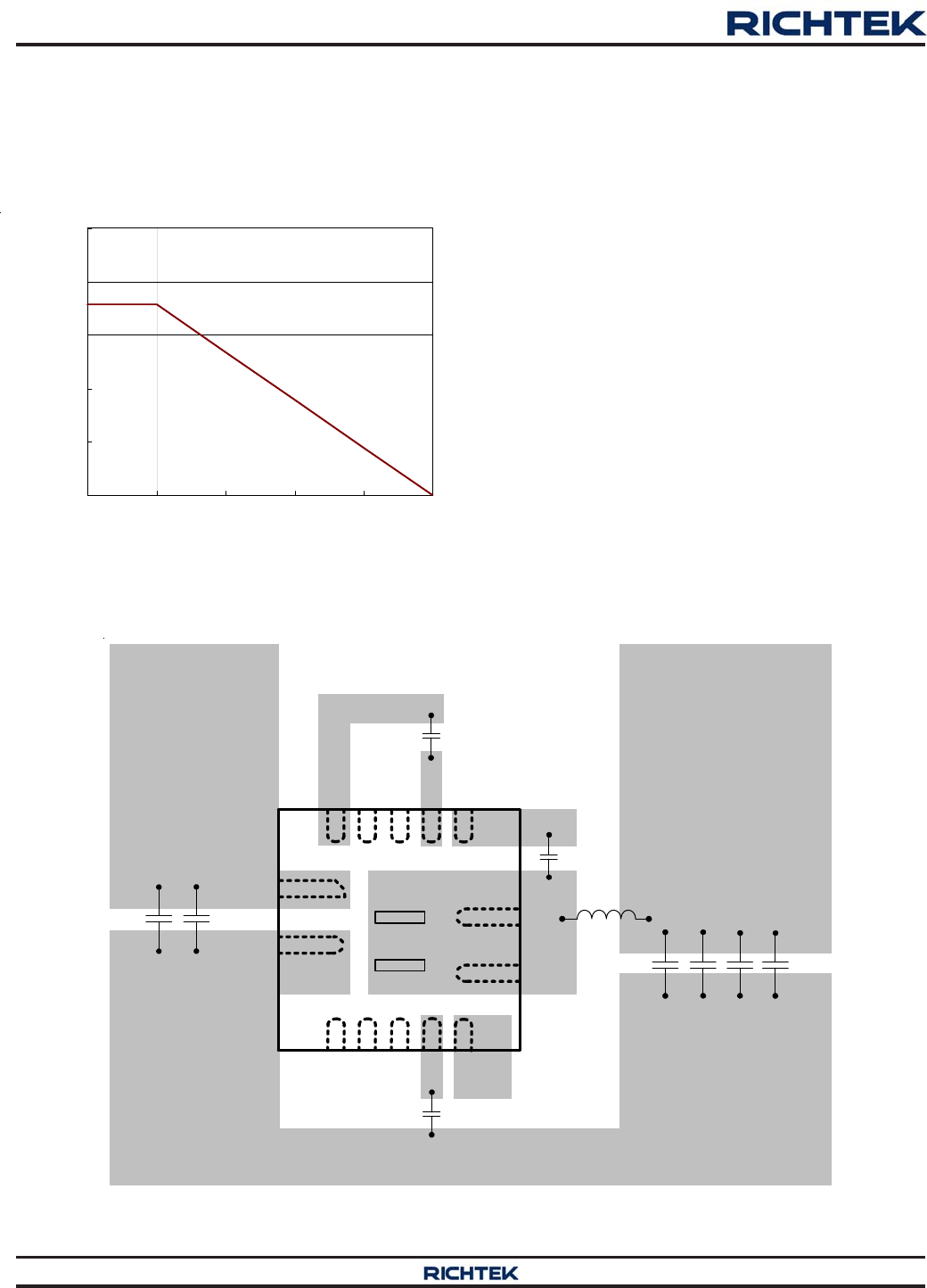
Layout Considerations
Layout is very important in high frequency switching
converter design. The PCB can radiate excessive noise
and contribute to converter instability with improper layout.
Certain points must be considered before starting a layout
using the RT7291A/B.
Make traces of the main current paths as short and wide
as possible.
Put the input capacitor as close as possible to the device
pins (VIN and PGND).
SW node encounters high frequency voltage swings so
it should be kept in a small area. Keep sensitive
components away from the SW node to prevent stray.
The PGND pin should be connected to a strong ground
plane for heat sinking and noise protection.
Avoid using vias in the power path connections that have
switched currents (from CIN to PGND and CIN to VIN)
and the switching node (SW).
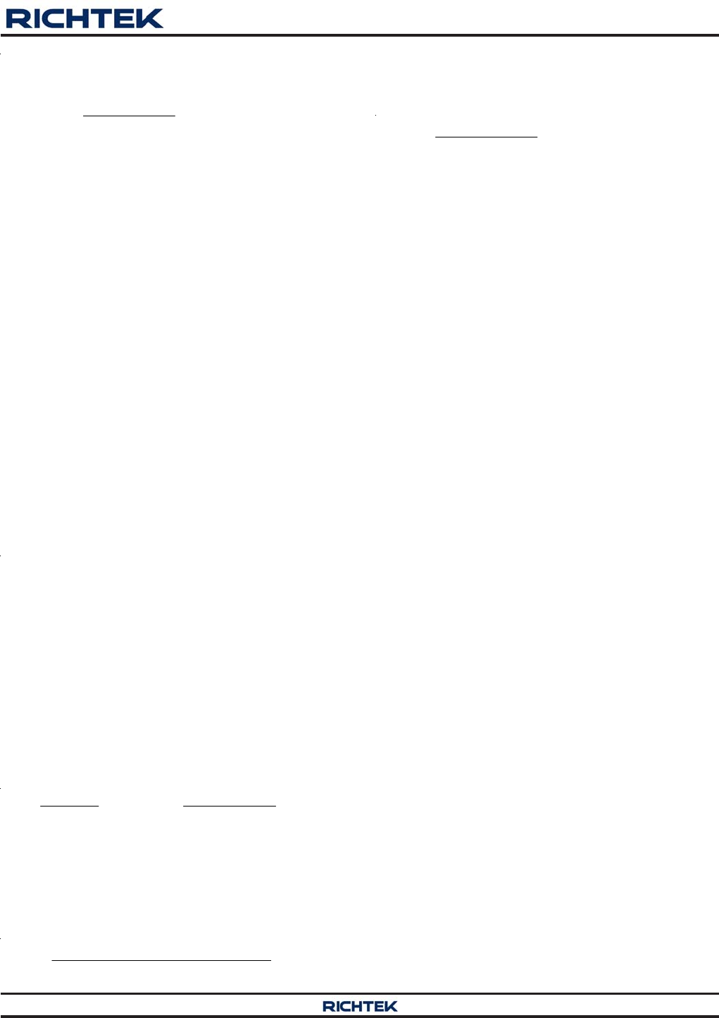
Figure 3. Derating Curve of Maximum Power Dissipation
0.0
0.4
0.8
1.2
1.6
2.0
0 25 50 75 100 125
Ambient Temperature (°C)
Maximum Power Dissipation (W) 1
Four-Layer PCB
The maximum power dissipation depends on the operating
ambient temperature for fixed TJ(MAX) and thermal
resistance, θJA. The derating curve in Figure 3 allows the
designer to see the effect of rising ambient temperature
on the maximum power dissipation.
Figure 4. Layout Guide
The output capacitor must
be placed near the IC
The input capacitor must
be placed as close to the
IC as possible.
SW should be connected to
inductor by wide and short
trace.
Keep sensitive components
away from this trace.
VOUT
COUT
GND
AGND
EN
ENLDO
VCC
BOOT
1
2
34567
8
9
1
0
1
1
1
2
1
3
1
4
15
16
SW
SW
VIN
PGND
VBYP
PGOOD
CLK
LDO
VOUT
L
SW
SW
CIN
VOUT
GND
CBOOT
CLDO
CVCC
VIN
Impedance between PGND and AGND should be as small as possible for unified ground voltage.

RT7291A/B
17
DS7291A/B-02 September 2015 www.richtek.com
©
Copyright 2014 Richtek Technology Corporation. All rights reserved. is a registered trademark of Richtek Technology Corporation.
Outline Dimension
U-Type 16L QFN 3x3 (FC) Package
Min. Max. Min. Max.
A 0.500 0.600 0.020 0.024
A1 0.000 0.050 0.000 0.002
A3 0.100 0.175 0.004 0.007
D 2.900 3.100 0.114 0.122
E 2.900 3.100 0.114 0.122
b 0.150 0.250 0.006 0.010
b1 0.100 0.200 0.004 0.008
L 0.350 0.450 0.014 0.018
L1 0.750 0.850 0.030 0.033
L2 0.550 0.650 0.022 0.026
e
K
K1
K2
K3
K4
K5
0.975 0.038
1.675 0.066
1.675 0.066
1.935 0.076
0.975 0.038
1.335 0.053
Symbol Dimensions In Millimeters Dimensions In Inches
0.400 0.016

RT7291A/B
18
DS7291A/B-02 September 2015www.richtek.com
Richtek Technology Corporation
14F, No. 8, Tai Yuen 1st Street, Chupei City
Hsinchu, Taiwan, R.O.C.
Tel: (8863)5526789
Richtek products are sold by description only. Richtek reserves the right to change the circuitry and/or specifications without notice at any time. Customers should
obtain the latest relevant information and data sheets before placing orders and should verify that such information is current and complete. Richtek cannot
assume responsibility for use of any circuitry other than circuitry entirely embodied in a Richtek product. Information furnished by Richtek is believed to be
accurate and reliable. However, no responsibility is assumed by Richtek or its subsidiaries for its use; nor for any infringements of patents or other rights of third
parties which may result from its use. No license is granted by implication or otherwise under any patent or patent rights of Richtek or its subsidiaries.