RT8856 Datasheet. Www.s Manuals.com. R04 Richtek
User Manual: Datasheets RT8856, RT8856GQW.
Open the PDF directly: View PDF ![]() .
.
Page Count: 25
RT8856
®
DS8856-04 August 2014 www.richtek.com
1
Copyright 2014 Richtek Technology Corporation. All rights reserved. is a registered trademark of Richtek Technology Corporation.
©
Multi-Phase PWM Controller for CPU Core Power Supply
Features
--
--
-1/2 Phase PWM Controller with 2 Integrated
MOSFET Drivers
--
--
-IMVP6.5 Compatible Power Management States
(DPSRLVR, PSI, Extended Deeper Sleep Mode)
--
--
-NAVP (Native AVP) Topology
--
--
-7-bit DAC
--
--
-0.8% DAC Accuracy
--
--
-Fixed VBOOT (1.1V)
--
--
-Differential Remote Voltage Sensing
--
--
-Programmable Output Transition Slew Rate Control
--
--
-Accurate Current and Thermal Balance
--
--
-System Thermal Compensation AVP
--
--
-Ringing Free Mode at Light Load Conditions
--
--
-Fast Transient Response
--
--
-Power Good
--
--
-Clock Enable Output
--
--
-Thermal Throttling
--
--
-Current Monitor Output
--
--
-Switching Frequency up to 1MHz Per Phase
--
--
-OVP, UVP, NVP, OCP, OTP, UVLO
--
--
-40-Lead WQFN Package
--
--
-RoHS Compliant and Halogen Free
General Description
The RT8856 is a single/dual phase PWM controller with
two integrated MOSFET drivers. Moreover, it is compliant
with Intel IMVP6.5 Voltage Regulator Specification to fulfill
its mobile CPU Vcore power supply requirements. The
RT8856 adopts NAVPTM (Native AVP) which is Richtek's
proprietary topology derived from finite DC gain
compensator peak current mode, making it an easy setting
PWM controller that meets all Intel AVP (Active Voltage
Positioning) mobile CPU requirements.
The output voltage of the RT8856 is set by 7-bit VID code.
The built-in high accuracy DAC converts the VID code
ranging from 0V to 1.5V with 12.5mV per step. The system
accuracy of the controller can reach 1.5%. The part
supports VID on-the-fly and mode change on-the-fly
functions that are fully compliant with IMVP6.5
specification. It operates in single phase, dual phase and
RFM. It can reach up to 90% efficiency in different modes
according to different loading conditions. The droop load
line can be easily programmed by setting the DC gain of
the error amplifier. With proper compensation, the load
transient can achieve optimized AVP performance. This
chip controls soft-start and output transition slew rate via
a capacitor. It supports both DCR and sense resistor
current sensing. The current mode NAVPTM topology with
high accuracy current sensing amplifier well balances the
RT8856's channel currents.
The RT8856 provides power good, clock enabling and
thermal throttling output signals for IMVP6.5 specification.
It also features complete fault protection functions
including over voltage, under voltage, negative voltage, over
current, thermal shutdown, and under voltage lockout.
The RT8856 is available in a WQFN-40L 6x6 small foot
print package.
Applications
-IMVP6.5 Core Supply
-Multi-phase CPU Core Supply
-AVP Step-Down Converter
-Notebook/ Desktop Computer/ Servers
Ordering Information
Note :
Richtek products are :
RoHS compliant and compatible with the current require-
ments of IPC/JEDEC J-STD-020.
Suitable for use in SnPb or Pb-free soldering processes.
Package Type
QW : WQFN-40L 6X6 (W-Type)
(Exposed Pad-Option 1)
RT8856
Lead Plating System
G : Green (Halogen Free and Pb Free)
RT8856
2
DS8856-04 August 2014www.richtek.com
©
Copyright 2014 Richtek Technology Corporation. All rights reserved. is a registered trademark of Richtek Technology Corporation.
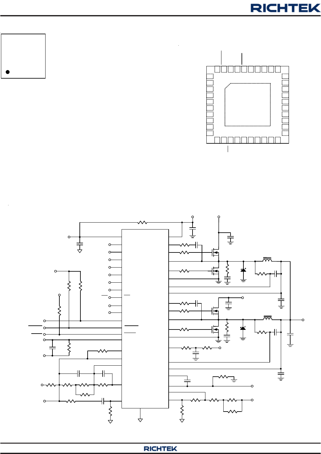
Typical Application Circuit
Pin Configurations
(TOP VIEW)
WQFN-40L 6x6
30
29
28
27
26
25
24
23
22
21
31323334353637383940
1
2
3
4
5
6
7
8
9
10
20191817161514131211
UGATE2
PHASE2
PGND2
LGATE2
PVCC
LGATE1
PGND1
PHASE1
UGATE1
BOOT1
DPRSLPVR
VRON
FS
CM
VID6
VID5
VID4
VID3
VID2
VID1
VID0
COMP
FB
VSEN
RGND
SOFT
ISEN1
ISEN1_N
GND
PSI
CMSET
41
PGOOD
VCC
TON
NTC
OCSET
ISEN2
ISEN2_N
BOOT2
VRTT
CLKEN
VOUT
VID0
VID1
VID2
VID3
VID4
5V
10
22
23
25
7
8
9
6
24
20
31
1
13
230
29
27
28
16
39
40
36
33
15
VID0
VID1
VID2
VID3
UGATE1
UGATE2
ISEN1_N
RT8856
VID4
VID5
DPRSLPVRBOOT2
LGATE1
PGND1
ISEN2
VRON
NTC
PHASE2
ISEN2_N
GND
PGND2
SOFT
VID5
12
11
PVCC
21
26
COMP
VCC
RGND
BOOT1
PGOOD
VID6
14
38
35
32
18
17
34
VID6
PHASE1
LGATE2
VSEN
FB
OCSET
ISEN119
R8
R7
R11
DPRSLPVR
VRON
PWRGD
3.3V
R23
R22
VCC
L1
VIN
C8
L2
VIN
C2
R6C6
R14C10
C17
R26
R29
VCC
C11
R19
CPU VSS SENSE
C3
C14C15
C1
C9
R1
C4Q1
Q2
Q3
Q4
R2
R3
R4
7V to 24V
R5
C5
D1
R9
R10
R12
7V to 21V
R13
C9
D2
R27R28
NTC2
Vccp
CM
4
CM
C12R15
R21
NTC1
FS
3
R25
C18
R24
CPU V
CC
SENSE
R20
VOUT
CLKENCLKEN
VRTTVRTT
PSIPSI
41 (Exposed pad)
C7
VIN
37
TONR16R17
C13
C16
CPU VSS SENSE
5
CMSET
R18
Marking Information
RT8856
GQW
YMDNN
RT8856GQW : Product Number
YMDNN : Date Code

RT8856
3
DS8856-04 August 2014 www.richtek.com
©
Copyright 2014 Richtek Technology Corporation. All rights reserved. is a registered trademark of Richtek Technology Corporation.
Table 1. IMVP6.5 VID code table
VID6 VID5 VID4 VID3 VID2 VID1 VID0 Output
0 0 0 0 0 0 0 1.5000V
0 0 0 0 0 0 1 1.4875V
0 0 0 0 0 1 0 1.4750V
0 0 0 0 0 1 1 1.4625V
0 0 0 0 1 0 0 1.4500V
0 0 0 0 1 0 1 1.4375V
0 0 0 0 1 1 0 1.4250V
0 0 0 0 1 1 1 1.4125V
0 0 0 1 0 0 0 1.4000V
0 0 0 1 0 0 1 1.3875V
0 0 0 1 0 1 0 1.3750V
0 0 0 1 0 1 1 1.3625V
0 0 0 1 1 0 0 1.3500V
0 0 0 1 1 0 1 1.3375V
0 0 0 1 1 1 0 1.3250V
0 0 0 1 1 1 1 1.3125V
0 0 1 0 0 0 0 1.3000V
0 0 1 0 0 0 1 1.2875V
0 0 1 0 0 1 0 1.2750V
0 0 1 0 0 1 1 1.2625V
0 0 1 0 1 0 0 1.2500V
0 0 1 0 1 0 1 1.2375V
0 0 1 0 1 1 0 1.2250V
0 0 1 0 1 1 1 1.2125V
0 0 1 1 0 0 0 1.2000V
0 0 1 1 0 0 1 1.1875V
0 0 1 1 0 1 0 1.1750V
0 0 1 1 0 1 1 1.1625V
0 0 1 1 1 0 0 1.1500V
0 0 1 1 1 0 1 1.1375V
0 0 1 1 1 1 0 1.1250V
0 0 1 1 1 1 1 1.1125V
0 1 0 0 0 0 0 1.1000V
VID6 VID5 VID4 VID3 VID2 VID1 VID0 Output
0 1 0 0 0 0 1 1.0875V
0 1 0 0 0 1 0 1.0750V
0 1 0 0 0 1 1 1.0625V
0 1 0 0 1 0 0 1.0500V
0 1 0 0 1 0 1 1.0375V
0 1 0 0 1 1 0 1.0250V
0 1 0 0 1 1 1 1.0125V
0 1 0 1 0 0 0 1.0000V
0 1 0 1 0 0 1 0.9875V
0 1 0 1 0 1 0 0.9750V
0 1 0 1 0 1 1 0.9625V
0 1 0 1 1 0 0 0.9500V
0 1 0 1 1 0 1 0.9375V
0 1 0 1 1 1 0 0.9250V
0 1 0 1 1 1 1 0.9125V
0 1 1 0 0 0 0 0.9000V
0 1 1 0 0 0 1 0.8875V
0 1 1 0 0 1 0 0.8750V
0 1 1 0 0 1 1 0.8625V
0 1 1 0 1 0 0 0.8500V
0 1 1 0 1 0 1 0.8375V
0 1 1 0 1 1 0 0.8250V
0 1 1 0 1 1 1 0.8125V
0 1 1 1 0 0 0 0.8000V
0 1 1 1 0 0 1 0.7875V
0 1 1 1 0 1 0 0.7750V
0 1 1 1 0 1 1 0.7625V
0 1 1 1 1 0 0 0.7500V
0 1 1 1 1 0 1 0.7375V
0 1 1 1 1 1 0 0.7250V
0 1 1 1 1 1 1 0.7125V
1 0 0 0 0 0 0 0.7000V
1 0 0 0 0 0 1 0.6875V

RT8856
4
DS8856-04 August 2014www.richtek.com
©
Copyright 2014 Richtek Technology Corporation. All rights reserved. is a registered trademark of Richtek Technology Corporation.
VID6 VID5 VID4 VID3 VID2 VID1 VID0 Output
1 0 0 0 0 1 0 0.6750V
1 0 0 0 0 1 1 0.6625V
1 0 0 0 1 0 0 0.6500V
1 0 0 0 1 0 1 0.6375V
1 0 0 0 1 1 0 0.6250V
1 0 0 0 1 1 1 0.6125V
1 0 0 1 0 0 0 0.6000V
1 0 0 1 0 0 1 0.5875V
1 0 0 1 0 1 0 0.5750V
1 0 0 1 0 1 1 0.5625V
1 0 0 1 1 0 0 0.5500V
1 0 0 1 1 0 1 0.5375V
1 0 0 1 1 1 0 0.5250V
1 0 0 1 1 1 1 0.5125V
1 0 1 0 0 0 0 0.5000V
1 0 1 0 0 0 1 0.4875V
1 0 1 0 0 1 0 0.4750V
1 0 1 0 0 1 1 0.4625V
1 0 1 0 1 0 0 0.4500V
1 0 1 0 1 0 1 0.4375V
1 0 1 0 1 1 0 0.4250V
1 0 1 0 1 1 1 0.4125V
1 0 1 1 0 0 0 0.4000V
1 0 1 1 0 0 1 0.3875V
1 0 1 1 0 1 0 0.3750V
1 0 1 1 0 1 1 0.3625V
1 0 1 1 1 0 0 0.3500V
1 0 1 1 1 0 1 0.3375V
1 0 1 1 1 1 0 0.3250V
1 0 1 1 1 1 1 0.3125V
1 1 0 0 0 0 0 0.3000V
VID6 VID5 VID4 VID3 VID2 VID1 VID0 Output
1 1 0 0 0 0 1 0.2875V
1 1 0 0 0 1 0 0.2750V
1 1 0 0 0 1 1 0.2625V
1 1 0 0 1 0 0 0.2500V
1 1 0 0 1 0 1 0.2375V
1 1 0 0 1 1 0 0.2250V
1 1 0 0 1 1 1 0.2125V
1 1 0 1 0 0 0 0.2000V
1 1 0 1 0 0 1 0.1875V
1 1 0 1 0 1 0 0.1750V
1 1 0 1 0 1 1 0.1625V
1 1 0 1 1 0 0 0.1500V
1 1 0 1 1 0 1 0.1375V
1 1 0 1 1 1 0 0.1250V
1 1 0 1 1 1 1 0.1125V
1 1 1 0 0 0 0 0.1000V
1 1 1 0 0 0 1 0.0875V
1 1 1 0 0 1 0 0.0750V
1 1 1 0 0 1 1 0.0625V
1 1 1 0 1 0 0 0.0500V
1 1 1 0 1 0 1 0.0375V
1 1 1 0 1 1 0 0.0250V
1 1 1 0 1 1 1 0.0125V
1 1 1 1 0 0 0 0.0000V
1 1 1 1 0 0 1 0.0000V
1 1 1 1 0 1 0 0.0000V
1 1 1 1 0 1 1 0.0000V
1 1 1 1 1 0 0 0.0000V
1 1 1 1 1 0 1 0.0000V
1 1 1 1 1 1 0 0.0000V
1 1 1 1 1 1 1 0.0000V
RT8856
5
DS8856-04 August 2014 www.richtek.com
©
Copyright 2014 Richtek Technology Corporation. All rights reserved. is a registered trademark of Richtek Technology Corporation.
Functional Pin Description
Pin No. Pin Name Pin Function
1 DPRSLPVR
Deeper Sleep Mode Signal. Together with PSI, the combination of these two pins
indicates the power management states.
2 VRON Voltage Regulator Enabler.
3 FS Frequency Setting. Connect this pin with a resistor to ground to set the operating
frequency.
4 CM Current Monitor Output. This pin outputs a voltage proportional to the output
current.
5 CMSET
Current Monitor Output Gain Externally Setting. Connect this pin with one resistor
to VSEN while CM pin is connected to ground with another resistor. The current
monitor output gain can be set by the ratio of these two resistors.
6 to 12 VID[6:0]
Voltage ID. DAC voltage identification inputs for IMVP6.5.
The logic threshold is 30% of VCCP as the maximum value for low state and 70%
of VCCP as the minimum value for the high state. VCCP is 1.05V.
13 PSI Power Status Indicator II. Together with DPRSLPVR, the combination of these two
pins indicates the power management states.
14 COMP Compensation. This pin is the output node of the error amplifier.
15 FB Feedback. This is the negative input node of the error amplifier.
16 VSEN Positive Voltage Sensing Pin. This pin is the positive node of the differential
voltage sensing.
17 RGND Return Ground. This pin is the negative node of the differential remote voltage
sensing.
18 SOFT
Soft-Start. This pin provides soft-start function and slew rate control. The
capacitance of the slew rate control capacitor is restricted to be larger than 10nF.
The feedback voltage of the converter follows the ramping voltage on the SOFT pin
during soft-start and other voltage transitions according to different modes of
operation and VID change.
19 ISEN1 Positive Input of Phase1 Current Sense.
20 ISEN1_N Negative Input of Phase1 Current Sense.
21 BOOT1
Bootstrap Power Pin of Phase1. This pin powers the high side MOSFET drivers.
Connect this pin to the junction of the bootstrap capacitor with the cathode of the
bootstrap diode. Connect the anode of the bootstrap diode to the PVCC pin.
22 UGATE1 Upper Gate Drive of Phase1. This pin drives the gate of the high side MOSFETs.
23 PHASE1
Return Node of Phase1 High Side Driver. Connect this pin to high side MOSFET
sources together with the low side MOSFET drains and the inductor.
24 PGND1 Driver Ground of Phase1.
25 LGATE1 Lower Gate Drive of Phase1. This pin drives the gate of the low side MOSFETs.
26 PVCC Driver Power.
27 LGATE2 Lower Gate Drive of Phase2. This pin drives the gate of the low side MOSFETs.
28 PGND2 Driver Ground of Phase2.
29 PHASE2
Return Node of Phase2 High Side Driver. Connect this pin to high side MOSFET
sources together with the low side MOSFET drains and the inductor.
RT8856
6
DS8856-04 August 2014www.richtek.com
©
Copyright 2014 Richtek Technology Corporation. All rights reserved. is a registered trademark of Richtek Technology Corporation.
Pin No. Pin Name Pin Function
30 UGATE2
Upper Gate Drive of Phase2. This pin drives the gate of the high side
MOSFETs.
31 BOOT2
Bootstrap Power Pin of Phase2. This pin powers the high side MOSFET drivers.
Connect this pin to the junction of the bootstrap capacitor with the cathode of the
bootstrap diode. Connect the anode of the bootstrap diode to the PVCC pin.
32 ISEN2_N Negative Input of Phase2 Current Sense.
33 ISEN2 Positive input of Phase2 Current Sense.
34 OCSET
Over Current Protection Setting. Connect a resistive voltage divider from VCC to
ground and connect the joint of the voltage divider to the OCSET pin. The
voltage, VOCSET, determines the over current threshold, ILIM.
35 NTC
Thermal Detection Input for VRTT Circuit. Connect this pin with a resistive
voltage divider from VCC using NTC on the top to set the thermal management
threshold level.
36 VRTT Voltage Regulator Thermal Throttling. This open-drain output pin indicates the
temperature exceeding the preset level when it is pulled low.
37 TON
Connect this pin to VIN with one resistor. This resistor value sets the ripple size
in ringing free mode.
38 VCC Chip Power.
39 CLKEN Inverted Clock Enable. This open-drain pin is an output indicating the start of the
PLL locking of the clock chip.
40 PGOOD Power Good Indicator.
41 (Exposed Pad) GND Ground. The exposed pad must be soldered to a large PCB and connected to
GND for maximum power dissipation.
RT8856
7
DS8856-04 August 2014 www.richtek.com
©
Copyright 2014 Richtek Technology Corporation. All rights reserved. is a registered trademark of Richtek Technology Corporation.
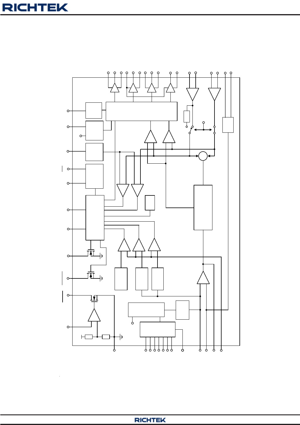
Function Block Diagram
COMP
RGND
SOFT
OVP Trip
Point
VID1
VID3
VID4
VID5
VID0
VID2
FB
PGOOD VCC
GND
ERROR
AMP
OCP
Setting OSC
SOFT
START
NVP Trip
Point
FS
Power On Reset
&
Central Logic
VSEN
VRON OCSET
NTC
VID6
Mode
Selection
DPRSLPVR
1.2V
UVP Trip
Point
OTP
+
-
VCC
MUX
DAC
+
-
+
-
+
-
+
-
+
-
+
-
ISEN1_N
PWMCP
PWMCP
Driver
Logic
Control
PGND2
LGATE2
PHASE2
UGATE2
BOOT2
PGND1
LGATE1
PVCC
PHASE1
UGATE1
BOOT1
ISEN1
ISEN2_N
ISEN2
CM
ONE_PHASE
-
+
-
+
1/2 +
-
20
+
-
20
+
CLKEN
VRTTPSI
CM CMSET
Ringing
Free
Mode
TON
FB
Offset Cancellation
RT8856
8
DS8856-04 August 2014www.richtek.com
©
Copyright 2014 Richtek Technology Corporation. All rights reserved. is a registered trademark of Richtek Technology Corporation.
Electrical Characteristics
Parameter Symbol Test Conditions Min Typ Max Unit
Supply Input
Supply Current IVCC + IPVCC RFS = 33k, VVRON = 3.3V,
Not Switching -- -- 10 mA
Shutdown Current ICC + IPVCC V
VRON = 0V -- -- 5 A
Soft-Start/Slew Rate Control (based on 10nF CSS)
Soft-Start / Soft-Shutdown ISS1 V
SOFT = 1.5V 16 20 24 A
Deeper Sleep Exit/VID
Change Slew Current ISS2 V
SOFT = 1.5V 80 100 120 A
Recommended Operating Conditions (Note 4)
-Supply Voltage, VCC -------------------------------------------------------------------------------------- 4.5V to 5.5V
-Battery Voltage, VIN -------------------------------------------------------------------------------------- 7V to 24V
-Junction Temperature Range---------------------------------------------------------------------------- −40°C to 125°C
-Ambient Temperature Range---------------------------------------------------------------------------- −40°C to 85°C
Absolute Maximum Ratings (Note 1)
-VCC to GND ------------------------------------------------------------------------------------------------ −0.3V to 6.5V
-RGND, PGNDx to GND ---------------------------------------------------------------------------------- −0.3V to 0.3V
-VIDx to GND ------------------------------------------------------------------------------------------------ −0.3V to (VCC + 0.3V)
-PSI, VRON to GND --------------------------------------------------------------------------------------- −0.3V to (VCC + 0.3V)
-PGOOD, CLKEN, VRTT to GND----------------------------------------------------------------------- −0.3V to (VCC + 0.3V)
-VSEN, FB, COMP, SOFT, FS, OCSET, CM, CMSET, NTC to GND --------------------------- −0.3V to (VCC + 0.3V)
-ISENx, ISEN1_N, ISEN2_N to GND ----------------------------------------------------------------- −0.3V to (VCC + 0.3V)
-PVCC to PGNDx ------------------------------------------------------------------------------------------ −0.3V to 6.5V
-LGATEx to PGNDx --------------------------------------------------------------------------------------- −0.3V to (PVCC + 0.3V)
-PHASEx to PGNDx -------------------------------------------------------------------------------------- −3V to 28V
-BOOTx to PHASEx --------------------------------------------------------------------------------------- −0.3V to 6.5V
-UGATEx to PHASEx ------------------------------------------------------------------------------------- −0.3V to (BOOTx − PHASEx)
-PGOOD ------------------------------------------------------------------------------------------------------ −0.3V to (VCC + 0.3V)
-Power Dissipation, PD @ TA = 25°C
WQFN−40L 6x6 -------------------------------------------------------------------------------------------- 2.941W
-Package Thermal Resistance (Note 2)
WQFN-40L 6x6, θJA --------------------------------------------------------------------------------------- 34°C/W
WQFN-40L 6x6, θJC -------------------------------------------------------------------------------------- 6°C/W
-Junction Temperature ------------------------------------------------------------------------------------- 150°C
-Lead Temperature (Soldering, 10 sec.)--------------------------------------------------------------- 260°C
-Storage Temperature Range ---------------------------------------------------------------------------- −65°C to 150°C
-ESD Susceptibility (Note 3)
HBM (Human Body Mode) ------------------------------------------------------------------------------ 2kV
MM (Machine Mode) -------------------------------------------------------------------------------------- 200V
(VCC = 5V, TA = 25°C, unless otherwise specified)
RT8856
9
DS8856-04 August 2014 www.richtek.com
©
Copyright 2014 Richtek Technology Corporation. All rights reserved. is a registered trademark of Richtek Technology Corporation.
Parameter Symbol Test Conditions Min Typ Max Unit
Oscillator
Frequency fOSC R
FS = 33k, VDAC > 1.05 270 300 330 kHz
Frequency Variation RFS = 5k to 50k 20 -- 20 %
Frequency Range Per phase 200 -- 1000 kHz
Maximum Duty Cycle Per phase -- 50 -- %
FS pin Output Voltage VFS R
FS = 33k, VDAC > 1.05 1 1.05 1.1 V
Reference and DAC
VDAC = 0.7500 1.5000
(No Load, Active Mode ) 0.8 0 0.8 %VID
DC Accuracy VFB
VDAC = 0.5000 0.7500 7.5 0 7.5 mV
Boot Voltage VBOOT 1.089 1.1 1.111 V
Error Amplifier
DC Gain RL = 47k 70 80 -- dB
Gain-Bandwidth Product GBW CLOAD = 5pF -- 10 -- MHz
Slew Rate SR CLOAD = 10pF (Gain = 4,
RF = 47k, VOUT = 0.5V 3V) -- 5 -- V/s
Output Voltage Range VCOMP R
L = 47k 0.5 -- 3.6 V
MAX Source/Sink Current IOUTEA V
COMP = 2V -- 250 -- A
Current Sense Amplifier
Input Offset Voltage VOSCS 1 -- 1 mV
Impedance at Neg. Input RISENx_N 1 -- -- M
Impedance at Pos. Input RISENx 1 -- -- M
DC Gain AI -- 10 -- V/V
Input Range VISENx_IN 50 -- 100 mV
RFM TON Setting
TON Pin Output Voltage VTON R
TON = 80k, VTON = VDAC = 0.75V 5 0 5 %
DEM ON-Time Setting tON I
RTON = 80A -- 350 -- ns
RTON Current Range IRTON 25 -- 280 A
Protection
Under Voltage Lockout
Threshold VUVLO Falling edge 4.1 4.3 4.5 V
Under Voltage Lockout
Threshold Hysteresis VUVLO -- 200 -- mV
Absolute Over Voltage
Protection Threshold VOVABS (With respect to 1.5V, ±50mV) 1.45 1.5 1.55 V
Relative Over Voltage
Protection Threshold VOV (With respect to VVID, ±50mV) 150 200 250 mV
Under Voltage Protection
Threshold VUV Measured at VSEN with respect to
unloaded output voltage (UOV)
(for 0.8 < UOV < 1.5)
350 300 250 mV
Negative Voltage
Protection Threshold VNV Measured at VSEN with respect to
GND 100 -- -- mV
RT8856
10
DS8856-04 August 2014www.richtek.com
©
Copyright 2014 Richtek Technology Corporation. All rights reserved. is a registered trademark of Richtek Technology Corporation.
Parameter Symbol Test Conditions Min Typ Max Unit
Current Limit Threshold Voltage
(Average) VILIM
(VISENx VISENx_N) / N,
VOCSET = 0.625V,
VILIMT(nom) = 25mV 23 25 27 mV
Current Limit Threshold Voltage
(per phase) VILIM_PH V
ILIMITPH / VILIMIT -- 150 -- %
Thermal Shutdown Threshold TSD -- 160 -- °C
Thermal Shutdown Hysteresis TSD -- 10 -- °C
Logic Inputs
Logic-High VIH With respect to 3.3V, 70% 2.31 -- --
VRON Input Threshold
Voltage Logic-Low VIL With respect to 3.3V, 30% -- -- 0.99 V
Leakage Current of VRON 1 -- 1 A
Logic-High VIH With respect to 1.1V, 70% 0.77 -- --
DAC (VID0 VID6),
PSI and DPRSLPVR
Input Threshold Voltage Logic-Low VIL With respect to 1.1V, 30% -- -- 0.33 V
Leakage Current of DAC (VID0
VID6), PSI and DPRSLPVR 1 -- 1 A
Power Good
PGOOD Threshold VTH_PGOOD -- 1 -- V
PGOOD Low Voltage VPGOOD I
PGOOD = 4mA -- -- 0.4 V
PGOOD Delay tPGOOD CLKEN Low to PGOOD High 3 -- 20 ms
Clock Enable
CLKEN Low Voltage VCLKEN I
CLKEN = 4mA -- -- 0.4 V
Thermal Throttling
Thermal Throttling Threshold VOT Measure at NTC with respect
to VCC -- 80 -- %VDD
Thermal Throttling Threshold
Hysteresis VOT_HY At VCC = 5V -- 100 -- mV
VRTT Output Voltage VVRTT I
VRTT = 40mA -- -- 0.4 V
Current Monitor
Current Monitor Maximum Output
Voltage in Operating Range VDAC = 1V, VRCMSET = 90mV,
RCM = 50k, RCMSET = 10k 0.855 0.9 0.945 V
Current Monitor Maximum Output
Voltage -- -- 1.15 V
Gate Driver
UGATE Driver Source RUGATEsr VBOOTx VPHASEx = 5V
VBOOTx VUGATEx = 1V -- 0.7 --
UGATE Driver Sink RUGATEsk V
UGATE = 1V -- 0.6 --
LGATE Driver Source RLGATEsr VPVCC = 5V,
VPVCC VLGATE = 1V -- 0.7 --
LGATE Driver Sink RLGATEsk V
LGATE = 1V -- 0.3 --
UGATE Driver Source/Sink Current IUGATE VBOOT VPHASE = 5V
VUGATE = 2.5V -- 3 -- A
LGATE Driver Source Current ILGATEsr V
LGATE = 2.5V -- 3 -- A
RT8856
11
DS8856-04 August 2014 www.richtek.com
©
Copyright 2014 Richtek Technology Corporation. All rights reserved. is a registered trademark of Richtek Technology Corporation.
Note 1. Stresses listed as the above “Absolute Maximum Ratings” may cause permanent damage to the device. These are for
stress ratings. Functional operation of the device at these or any other conditions beyond those indicated in the
operational sections of the specifications is not implied. Exposure to absolute maximum rating conditions for extended
periods may remain possibility to affect device reliability.
Note 2. θJA is measured in natural convection at TA = 25°C on a high effective thermal conductivity four-layer test board of
JEDEC 51-7 thermal measurement standard. The measured case position of θJC is on the exposed pad of the
package.
Note 3. Devices are ESD sensitive. Handling precaution is recommended.
Note 4. The device is not guaranteed to function outside its operating conditions.
Parameter Symbol Test Conditions Min Typ Max Unit
LGATE Driver Sink Current ILGATEsk V
LGATE = 2.5V -- 5 -- A
Internal Boost Charging Switch
On-Resistance RBOOT PVCC to BOOTx -- 30 --
RT8856
12
DS8856-04 August 2014www.richtek.com
©
Copyright 2014 Richtek Technology Corporation. All rights reserved. is a registered trademark of Richtek Technology Corporation.
Typical Operating Characteristics
CCM VCC_SENSE vs. Load Current
1.04
1.06
1.08
1.1
1.12
1.14
1.16
0 1020304050
Load Current (A)
VCC_SENSE (V)
CCM Efficiency vs. Load Current
0
10
20
30
40
50
60
70
80
90
100
0 1020304050
Load Current (A)
Efficiency (%)
VIN = 8V
VIN = 12V
VIN = 19V
VID = 0.9375V, RFS = 33 kΩ,
DPRSLPVR = GND, PSI = High
CCM Efficiency vs. Load Current
0
10
20
30
40
50
60
70
80
90
100
0 1020304050
Load Current (A)
Efficiency (%)
VIN = 8V
VIN = 12V
VIN = 19V
VID = 1.15V, RFS = 33 kΩ,
DPRSLPVR = GND, PSI = High
DEM Efficiency vs. Load Current
50
55
60
65
70
75
80
85
90
95
00.511.522.53
Load Current (A)
Efficiency (%)
VIN = 8V
VIN = 12V
VIN = 19V
VID = 0.85V, RFS = 33 kΩ,
DPRSLPVR = GND, PSI = High
VIN = 8V
VIN = 12V
VIN = 19V
VID = 1.15V, RFS = 33 kΩ,
DPRSLPVR = GND, PSI = High
CCM VCC_SENSE vs. Load Current
0.84
0.86
0.88
0.90
0.92
0.94
0.96
0 1020304050
Load Current (A)
VCC_SENSE (V)
VIN = 8V
VIN = 12V
VIN = 19V
VID = 0.9375V, RFS = 33 kΩ,
DPRSLPVR = GND, PSI = High
VCM vs. Load Current
0.0
0.1
0.2
0.3
0.4
0.5
0.6
0.7
0.8
0.9
1.0
1.1
0 1020304050
Load Current (A)
VCM (mV)
VIN = 8V
VIN = 12V
VIN = 19V
VID = 0.9375V, RFS = 33 kΩ,
DPRSLPVR = GND, PSI = High
RT8856
13
DS8856-04 August 2014 www.richtek.com
©
Copyright 2014 Richtek Technology Corporation. All rights reserved. is a registered trademark of Richtek Technology Corporation.
CCM VID Change Up
Time (20μs/Div)
VCC SENSE
(100mV/Div)
VID0
(2V/Div)
VIN = 12V, VID change from 0.85V to 0.9375V
LGATE1
(1V/Div)
UGATE1
(20V/Div)
DPRSLPVR = GND, PSI = High, No Load
Power Off from VRON
Time (1ms/Div)
VCC SENSE
(500mV/Div)
VRON
(5V/Div)
VIN = 12V, VID = 0.9375V
PGOOD
(1V/Div)
UGATE
(2V/Div) DPRSLPVR = GND, PSI = High, No Load
RFM VID Change Down
Time (40μs/Div)
VCC SENSE
(100mV/Div)
LGATE1
(5V/Div)
VIN = 12V, VID change 0.9375V to 0.85V,
UGATE1
(20V/Div)
VID0
(2V/Div)
DPRSLPVR = High, No Load
CCM VID Change Down
Time (20μs/Div)
VCC SENSE
(100mV/Div)
VID0
(2V/Div)
VIN = 12V, VID change from 0.9375V to 0.85V
LGATE1
(5V/Div)
UGATE1
(20V/Div)
DPRSLPVR = GND, PSI = High, No Load
CCM Load Transient Response
Time (4μs/Div)
VCC SENSE
(50mV/Div)
LGATE1
(5V/Div)
VIN = 12V, VID = 0.95V, ILOAD = 12A to 51A,
DPRSLPVR = GND, PSI = High
UGATE1
(20V/Div)
Power On from VRON
Time (1ms/Div)
VCC SENSE
(500mV/Div)
VRON
(5V/Div)
VIN = 12V, VID = 0.9375V
PGOOD
(1V/Div)
UGATE
(20V/Div) DPRSLPVR = GND, PSI = High, No Load
RT8856
14
DS8856-04 August 2014www.richtek.com
©
Copyright 2014 Richtek Technology Corporation. All rights reserved. is a registered trademark of Richtek Technology Corporation.
Over Current Protection
Time (10μs/Div)
VCC SENSE
(500mV/Div)
LGATE1
(10V/Div) VIN = 12V, VID = 0.9375V, DPRSLPVR = GND
ILOAD
(50A/Div)
PGOOD
(1V/Div)
Under Voltage Protection
Time (10μs/Div)
VCC SENSE
(1V/Div)
LGATE1
(5V/Div) VIN = 12V, VID = 0.9375V, DPRSLPVR = GND
UGATE1
(20V/Div)
PGOOD
(2V/Div)
Over Voltage Protection
Time (10μs/Div)
VCC SENSE
(1V/Div)
LGATE1
(5V/Div) VIN = 12V, VID = 0.9375V, DPRSLPVR = GND
UGATE1
(20V/Div)
PGOOD
(2V/Div)
DPRSLPVR = GND, PSI = High
CCM Load Transient Response
Time (4μs/Div)
VCC SENSE
(50mV/Div)
LGATE1
(5V/Div)
VIN = 12V, VID = 0.95V, ILOAD = 51A to 12A,
UGATE1
(20V/Div)
RT8856
15
DS8856-04 August 2014 www.richtek.com
©
Copyright 2014 Richtek Technology Corporation. All rights reserved. is a registered trademark of Richtek Technology Corporation.
Application Information
The RT8856 is a 1/2-phase DC/DC controller and includes
embedded gate drivers for reduced system cost and board
area. The number of phases is not only user selectable,
but also dynamically changeable based on Intel's
IMVP6.5 control signals to optimize efficiency. Phase
currents are continuously sensed for loop control, droop
tuning, and over current protection. The internal 7-bit VID
DAC and a low offset differential amplifier allow the
controller to maintain high voltage regulating accuracy
to meet Intel's IMVP6.5 specification.
Design Tool
To reduce the efforts and errors caused by manual
calculations, a user friendly design tool is now available
on request.
This design tool calculates all necessary design
parameters by entering user's requirements. Please
contact Richtek's representatives for details.
Phase Selection and Operation Modes
The maximum number of operating phase is programmable
by setting ISEN2_N. After the initial turn-on of the RT8856,
an internal comparator checks the voltage at the ISEN2_N
pin. To set the RT8856 as a pure single phase PWM
controller, connect ISEN2_N to a voltage higher than (VCC
- 1V) at power on. The controller will then disable phase 2
(hold UGATE2 and LGATE2 low) and operate as a single
phase PWM controller.
The RT8856 also works in conjunction with Intel's IIMVP6.5
control signals, such as PSI and DPRSLPVR. Table 2
shows the control signal truth table for operation modes
of the RT8856.
For high current demand, the controller will operate with
both phases active. These two phase gate signals are
interleaved. This achieves minimal output voltage ripple
and best transient performance.
For reduced current demand, only one phase is active.
For 1-phase operation, the power stage can minimize
switching losses and maintain transient response
capability.
At lowest current levels, the controller enters single phase
Ringing-Free Mode (RFM) to achieve highest efficiency.
Table 2. Control signal truth table for operation
modes
DPRSLPVR PSI Operation mode
0 1
Multi-phase CCM
0 0
Single-phase CCM
1 1
S Single-phase RFM,
slow C4E
1 0
Single-phase RFM,
slow C4E
Differential Remote Sense Setting
The RT8856 includes differential, remote sense inputs to
eliminate the effects of voltage drops along the PC board
traces, CPU internal power routes and socket contacts.
The CPU contains on-die sense pin voltages, VCC_SENSE
and VSS_SENSE. VSS_SENSE is connected to RGND pin. The
VCC_SENSE is connected to FB pin with a resistor to build
the negative input path of the error amplifier. Connect VSEN
to VCC_SENSE for CLKEN, PGOOD, OVP, and UVP sense.
The 7-bit VID DAC and the precision voltage reference are
referred to RGND for accurate remote sensing.
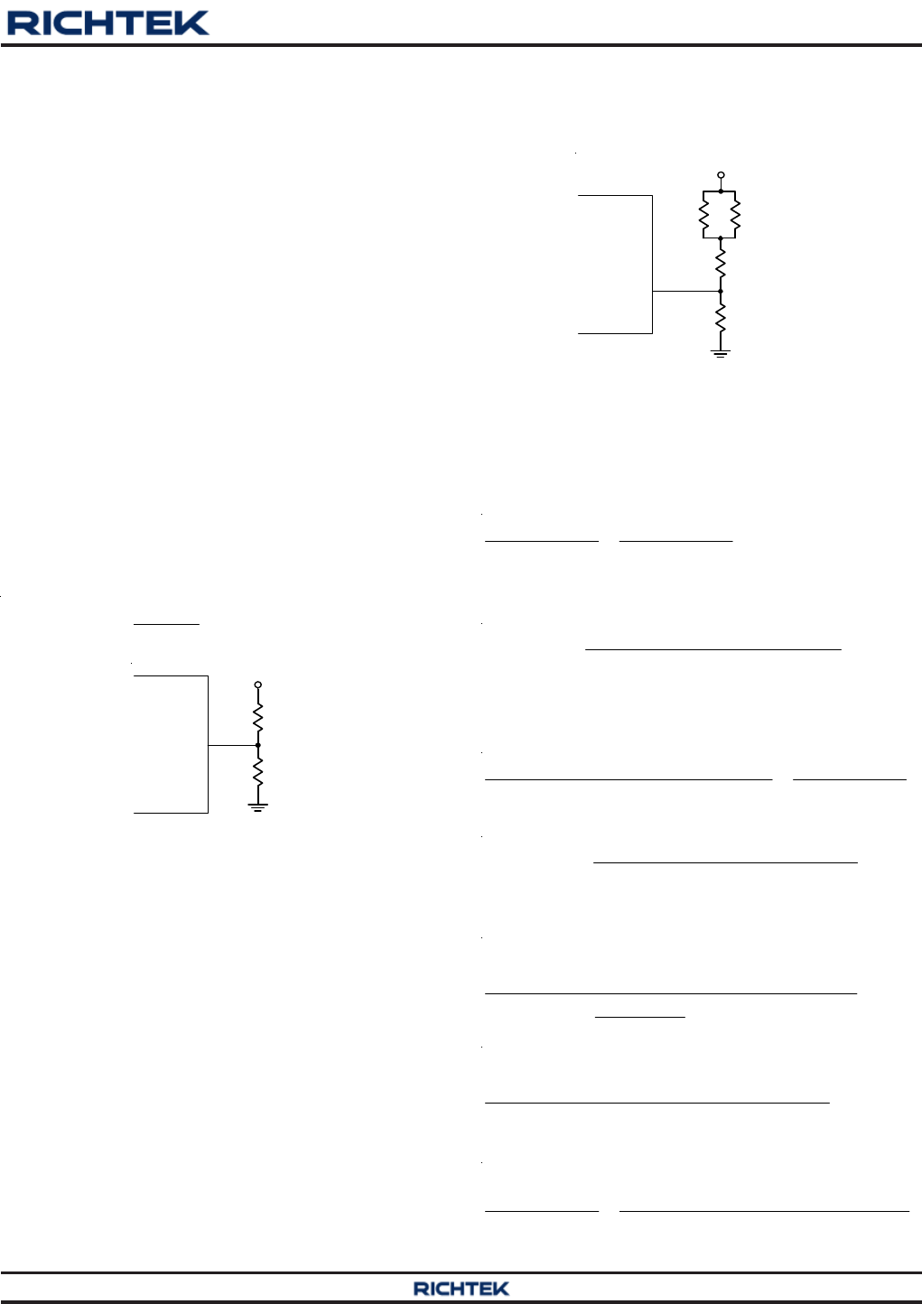
Current Sense Setting
The RT8856 continuously sense the output current of each
phase. Therefore, the controller can be less noise sensitive
and get more accurate current sharing between phases.
Low offset amplifiers are used for loop control and current
limit. The internal current sense amplifier gain (AI) is fixed
to be 10. The ISENx and ISENx_N denote the positive
and negative input of the current sense amplifier of each
phase, respectively. Users can either use a current-sense
resistor or the inductor's DCR for current sensing.
Using inductor's DCR allows higher efficiency as shown
in Figure 1. If
XX
LRC
DCR (1)
then the current sense performance will be optimum. For
example, choosing L = 0.36μH with 1mΩ DCR and
CX = 100nF, yields RX :
X0.36 H
R3.6k
1.0m 100nF (2)
RT8856
16
DS8856-04 August 2014www.richtek.com
©
Copyright 2014 Richtek Technology Corporation. All rights reserved. is a registered trademark of Richtek Technology Corporation.
Similar to the peak current mode control with finite
compensator gain, the HS_FET on-time is determined by
both the internal clock and the PWM comparator which
compares the EA output with the output of current sense
amplifier. When load current increases, VCS increases,
the steady state COMP voltage also increases and makes
the VOUT decrease, hence achieving AVP. A near-DC offset
(VOFS) is added to the output EA to cancel the inherent
output offset of finite-gain peak current mode controller.
In RFM, HS_FET is turned on with constant TON when
VCS is lower than VCOMP2. Once the HS_FET is turned off,
LS_FET is turned on automatically. By Ringing-Free
Technique, the LS_FET allows only partial of negative
current when the inductor free-wheeling current reaches
negative. The switching frequency will be proportionately
reduced, thus the conduction and switching losses will
be greatly reduced.
Droop Setting (with Temperature Compensation)
It's very easy to achieve Active Voltage Positioning (AVP)
by properly setting the error amplifier gain with respect to
the native droop characteristics. The target is to have
Equation (3)
VOUT = VSOFT − ILOAD x RDROOP (3)
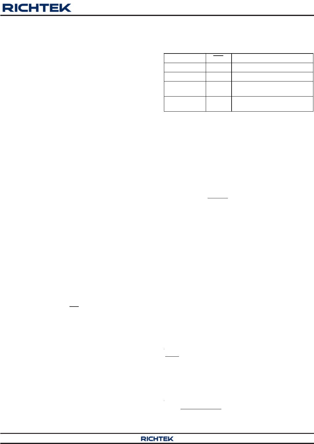
Figure 1. Lossless Inductor Sensing
Since the inductance tolerances are normally observed
to be 20%, the resistor, RX, has to be tuned on board by
examining the transient voltage. If the output voltage
transient has an initial dip below the minimum load line
requirement with a slow recovery, RX is chosen too small.
Vice versa, with a resistance too large, the output voltage
transient has only a small initial dip and the recovery is
too fast, thus causing a ring-back.
Using current sense resistor in series with the inductor
can have better accuracy, but the efficiency is a trade-off.
Considering the equivalent inductance (LESL) of the current
sense resistor, an RC filter is recommended. The RC filter
calculation method is similar to the above-mentioned
inductor DCR sensing method .
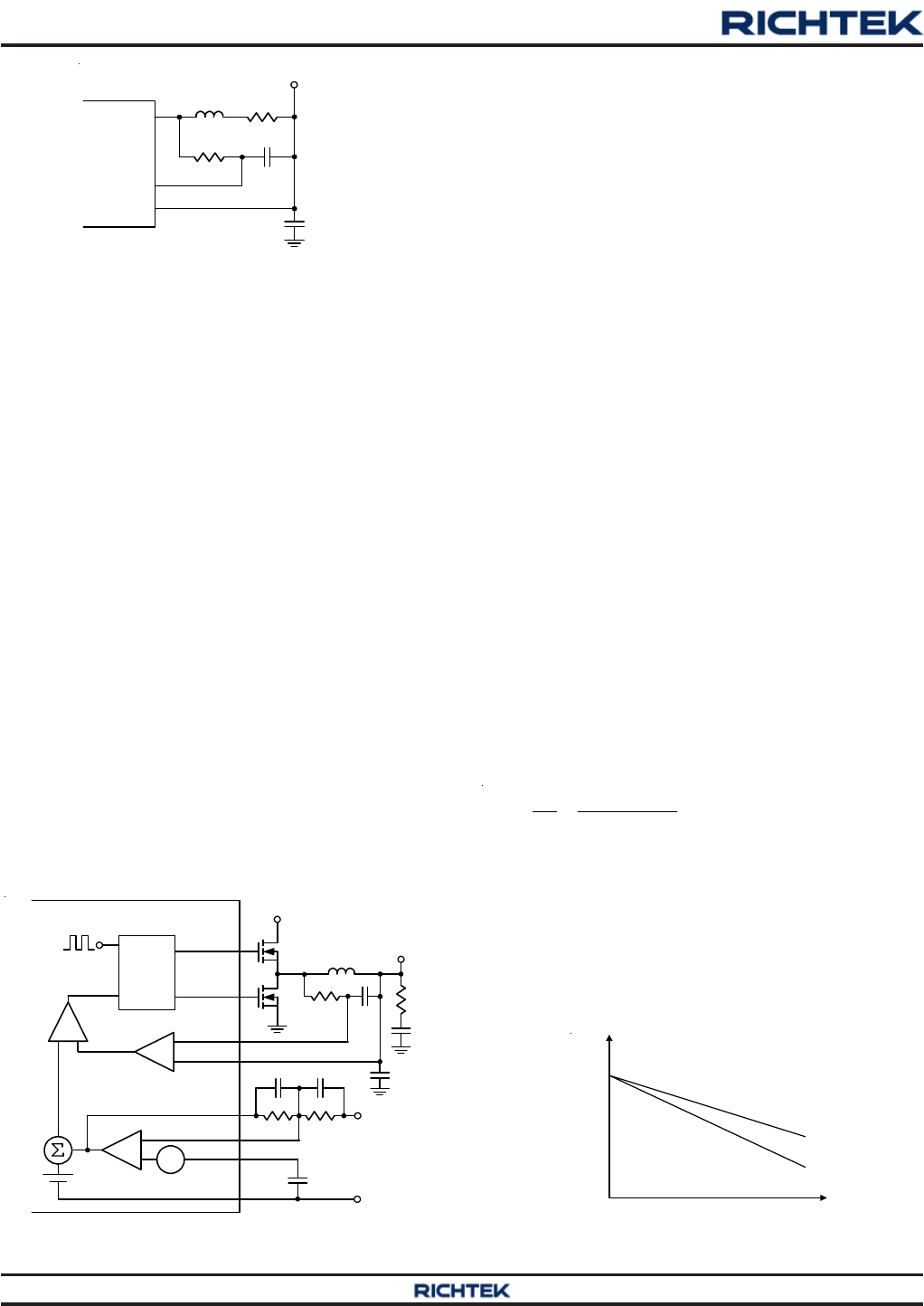
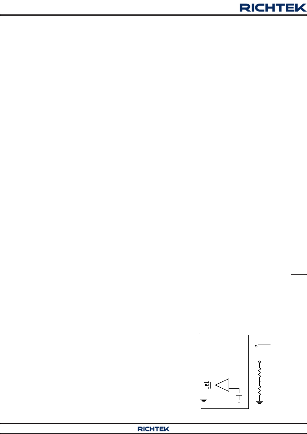
Loop Control
The RT8856 adopts Richtek's proprietary NAVPTM topology.
NAVPTM is based on the finite-gain peak current mode
PWM topology. The output voltage, VOUT, will decrease
with increasing output load current. The control loop
consists of PWM modulator with power stage, current
sense amplifier and error amplifier as shown in Figure 2.
Figure 2. Simplified Schematic for Droop and Remote
Sense in CCM
then solving the switching condition VCOMP2 = VCS in
Figure 2 yields the desired error amplifier gain as
I SENSE
VDROOP
AR
R2
AR1 R
(4)
where AI is the internal current sense amplifier gain. RSENSE
is the current sense resistor. If there is no external sense
resistor, it is the DCR of the inductor. RDROOP is the
resistive slope value of the converter output and is the
desired static output impedance, e.g. −1.9mΩ or −3mΩ
for IMVP6.5 specification. Increasing AV can make load
line more shallow as shown in Figure 3.
AV1
AV2
AV2 > AV1
VOUT
Load Current
0
Figure 3. Error Amplifier Gain (AV) Influence on VOUT
Accuracy
PHASEx
ISENx
ISENx_N
VOUT
LDCR
RXCX
+ VX -
CBYPASS
VOUT
VCC_SENSE
PWM
Logic
UGATEx
LGATEx
+
-
ISENx
ISENx_N
AI
-
+
R
S
Clock
CMP
VCS
COMP2
-
+
VSS_SENSE
VIN
FB
SOFT
RGND
COMP
RT8856
HS_FET
LS_FET
L
RXCXRC
C
C2 C1
R2 R1
CSOFT
VOFS
EA
+
-
VDAC
RT8856
17
DS8856-04 August 2014 www.richtek.com
©
Copyright 2014 Richtek Technology Corporation. All rights reserved. is a registered trademark of Richtek Technology Corporation.
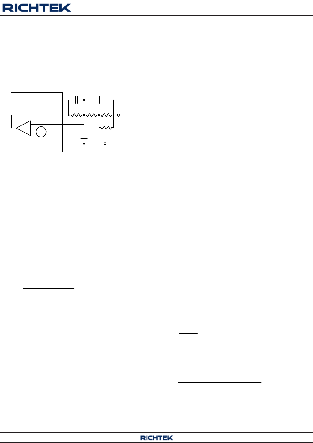
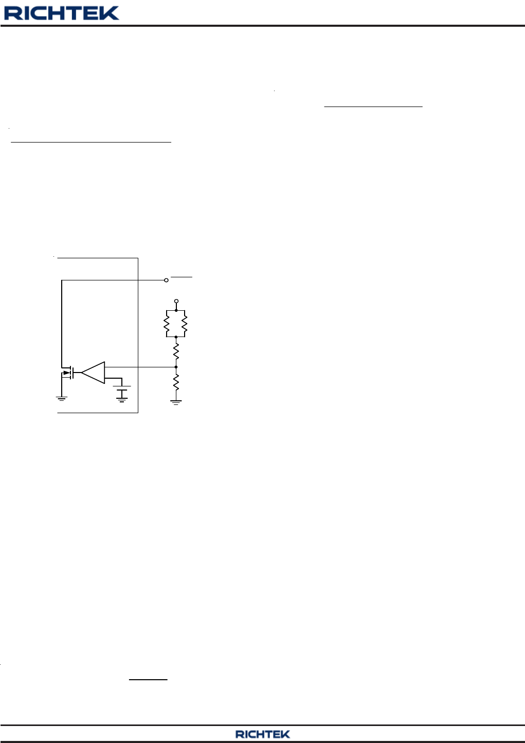
Since the DCR of inductor is highly temperature dependent,
it affects the output accuracy at hot conditions.
Temperature compensation is recommended for the
lossless inductor DCR current sense method. Figure 4
shows a simple but effective way of compensating the
temperature variations of the sense resistor using an NTC
thermistor placed in the feedback path.
Figure 4. Loop Setting with Temperature Compensation
Usually, R1a is set to equal RNTC (25°C). R1b is selected
to linearize the NTC's temperature characteristic. For a
given NTC, design is to get R1b and R2 and then C1 and
C2. According to Equation (4), to compensate the
temperature variations of the sense resistor, the error
amplifier gain (AV) should have the same temperature
coefficient with RSENSE. Hence,
V, HOT SENSE, HOT
V, COLD SENSE, COLD
AR
AR
(5)
From Equation (4), Av can be obtained at any temperature
(T) as shown below :
V, T NTC, T
R2
AR1a // R R1b
(6)
The standard formula for the resistance of NTC thermistor
as a function of temperature compensation is given by :
11
T+273 298
NTC, T 25
RR e
(7)
where R25 is the thermistor's nominal resistance at room
temperature, β (beta) is the thermistor's material constant
in Kelvins, and T is the thermistor's actual temperature in
Celsius.
To calculate DCR value at different temperature, use the
equation below :
DCRT = DCR25 x [1 + 0.00393 x (T − 25)] (8)
where the 0.00393 is the temperature coefficient of the
copper. For a given NTC thermistor, solving Equation (6)
at room temperature (25°C) yields
R2 = AV, 25 x (R1b + R1a // RNTC, 25) (9)
where AV, 25 is the error amplifier gain at room temperature
and can be obtained from Equation (4). R1b can be obtained
by substituting Equation (9) to (5),
SENSE, HOT NTC, HOT NTC, HOT
SENSE, COLD
SENSE, HOT
SENSE, COLD
R1b
R(R1a // R ) (R1a //R )
R
R
1R
(10)
Loop Compensation
Optimized compensation of the RT8856 allows for best
possible load step response of the regulator's output. A
type-II compensator with one pole and one zero is
adequate for a proper compensation. Figure 4 shows the
compensation circuit. Prior design procedure shows how
to select the resistive feedback components for the error
amplifier gain. Next, the C1 and C2 must be calculated for
the compensation. The target is to achieve constant
resistive output impedance over the widest possible
frequency range.
The pole frequency of the compensator must be set to
compensate the output capacitor ESR zero :
PC
1
f2CR
(11)
where C is the capacitance of output capacitor, and RC is
the ESR of output capacitor. C2 can be calculated as
follows :
C
CR
C2 R2
(12)
The zero of compensator has to be placed at half of the
switching frequency to filter the switching related noise.
such that,
(13)
NTC, 25 SW
1
C1 R1b R1a // R f
VCC_SENSE
-
+
VSS_SENSE
FB
SOFT
RGND
COMP
RT8856 C2 C1
R2 R1b
CSOFT
10nF
EA
R1a
NTC
+
-
VDAC
RT8856
18
DS8856-04 August 2014www.richtek.com
©
Copyright 2014 Richtek Technology Corporation. All rights reserved. is a registered trademark of Richtek Technology Corporation.
Frequency Setting
High frequency operation optimizes the application for
smaller component size, but trads off efficiency due to
higher switching losses. This may be acceptable in ultra-
portable devices where the load currents are lower and
the controller is powered from a lower voltage supply. Low
frequency operation offers the best overall efficiency at
the expense of component size and board space.
Connect a resistor (RFS) between FS and ground to set
the switching frequency (fSW) per phase :
(14)
FS SW
300(kHz) 33(k )
R(k) f(kHz)
A resistor of 5kΩ to 50kΩ corresponds to switching
frequency of 1MHz to 200kHz, respectively.
Soft-Start and Mode Change Slew Rates
The RT8856 uses 2 slew rates for various modes of
operation. These two slew rates are internally determined
by commanding one of two bi-directional current sources
on to the SOFT pin (ISS). The 7-bit VID DAC and the
precision voltage reference are referred to RGND for
accurate remote sensing. Hence, connect a capacitor
(CSOFT) from SOFT pin to RGND for controlling the slew
rate as shown in Figure 4. The capacitance of capacitor is
restricted to be larger than 10nF. The voltage on SOFT
pin (VSOFT) is higher than the reference voltage of the error
amplifier at about 0.9V.
The first current of typically 20μA is used to charge or
discharge the CSOFT during soft-start, soft-shutdown. The
second current of typically 100μA is used during other
voltage transitions, including VID change and transitions
between operation modes.
The IMVP6.5 specification specifies the critical timing
associated with regulating the output voltage. The symbol,
SLEWRATE, as given in the IMVP6.5 specification will
determine the choice of the SOFT capacitor, CSOFT, by the
following equation :
(15)
SS
SOFT I(A)
C(nF)
SLEWRATE(mV / s)
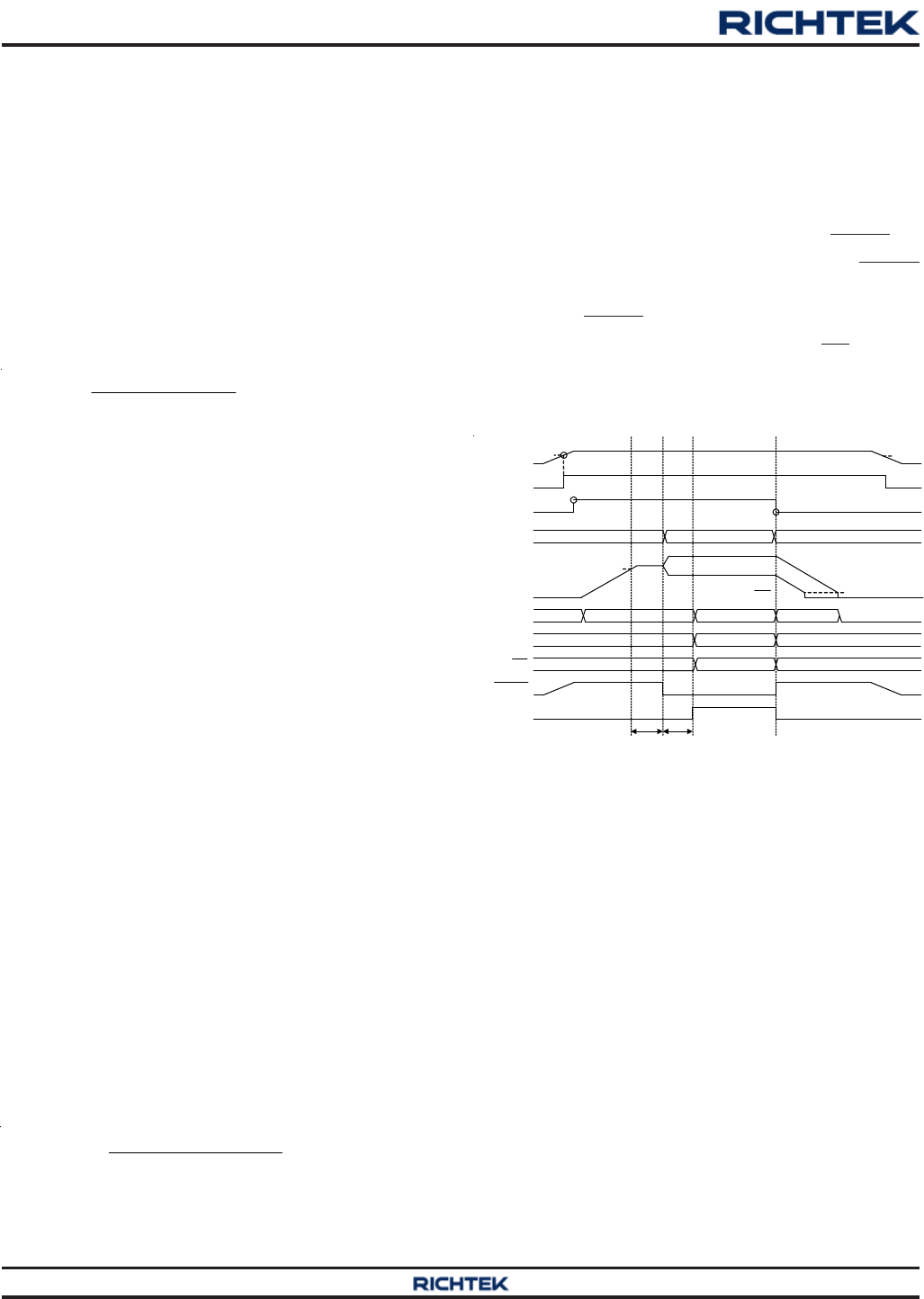
Power Up Sequence
With the controller's VCC voltage above the POR threshold
(typ. 4.3V), the power-up sequence begins when VRON
exceeds the 3.3V logic high threshold. Approximately
20μs later, SOFT and VCORE starts ramping up to boot
voltage (1.1V) with maximum phases. The slew rate during
power-up is 20μA/CSOFT. The RT8856 pulls CLKEN low
after VVSEN rises above 1V for 73μs. Right after CLKEN
goes low, SOFT and VCORE starts ramping to first DAC
value. After CLKEN goes low for approximate 4.7ms,
PGOOD is asserted HIGH. DPRSLPVR and PSI are valid
right after PGOOD is asserted. UVP is masked as long
as VSOFT is less than 1V.
Figure 5. Timing Diagram for Power-Up and Power-Down
Power Down
When VRON goes low, the RT8856 enters low-power
shutdown mode. PGOOD is pulled low immediately and
VSOFT ramps down with slew rate of 20μA/CSOFT. VVSEN
also ramps down following VSOFT with maximum phases.
After VVSEN falls below 200mV, the RT8856 turns off both
high side and low side MOSFETs. A discharging resistor
at VSEN will be enabled and the analog part will be turned
off.
Deeper Sleep Mode Transitions
After DPRSLPVR goes high, the RT8856 immediately
disables phase 2 (UGATE2 and LGATE2 forced low) and
enters 1-phase deeper sleep mode operation. If the VIDs
are set to a lower voltage setting, the output drops at a
rate determined by the load and the output capacitance.
The internal target VSOFT still ramps as before, and UVP,
OCP and OVP are masked for 73μs.
VRON
VCC 4.3V 4.1V
VID Valid x
x
XX
VCORE
PGOOD
73µs typ. 4.7ms typ.
POR
0.2V
1.1V
1V
ValidXX XX
ValidXX XX
PWM MAX Phases Pull Low
MAX Phases
Hi-Z
DPRSLPVR/PSI
Defined
PSI
CLKEN
DPRSLPVR
RT8856
19
DS8856-04 August 2014 www.richtek.com
©
Copyright 2014 Richtek Technology Corporation. All rights reserved. is a registered trademark of Richtek Technology Corporation.
The RT8856 provides 2 slew rates for deeper sleep mode
entry/ exit. For standard deeper sleep exit, the RT8856
immediately activates all enabled phases and ramps the
output voltage to the DAC code provided by the processor
at the slew rate of 100μA/CSOFT. The RT8856 remains in
1-phase ringing free mode and ramps the output voltage
to the DAC code provided by the processor at the slew
rate of 20μA/CSOFT.
Current Limit Setting
The RT8856 compares a programmable current limit set
point to the voltage from the current sense amplifier output
for Over Current Protection (OCP). The voltage applied to
OCSET pin defines the desired current limit threshold,
ILIM :
VOCSET = 25 x ILIM x RSENSE (16)
Connect a resistive voltage divider from VCC to GND, with
the joint of the voltage divider connected to OCSET pin as
shown in Figure 6. For a given ROC2,
(17)
CC
OC1 OC2 OCSET
V
RR 1
V
VCC
OCSET
RT8856
ROC1
ROC2
Figure 6. OCP Setting Without Temperature
Compensation
The OCP works in two stages :
Stage 1 : Average inductor current exceeds the current
limit threshold, ILIM, defined by VOCSET, but remains
smaller than 150% of ILIM If the over current condition
remains valid for 16 cycles, the OCP latches and the
system shuts down.
Stage 2 : Any inductor current exceeds 150% of ILIM
then OCP latches instantaneously.
Latched OCP forces driver high impedance with
UGATEx = 0 and LGATEx = 0. After latched OCP happens,
VVSEN will be monitored. When VVSEN falls below 200mV,
a discharging resistor at VSEN will be enabled.
If inductor DCR is used as current sense component, then
temperature compensation is recommended to protect
under all conditions. Figure 7 shows a typical OCP setting
with temperature compensation.
Figure 7. OCP Setting with Temperature Compensation
VCC
OCSET
RT8856
ROC1b
ROC2
ROC1a NTC
Usually, select ROC1a equal to thermistor's nominal
resistance at room temperature. Ideally, VOCSET should
have same temperature coefficient as RSENSE (Inductor
DCR) :
OCSET, HOT SENSE, HOT
OCSET, COLD SENSE, COLD
VR
VR
(18)
According to the basic circuit calculation, VOCSET can be
obtained at any temperature :
OC2
OCSET, T OC1a NTC, T OC1b OC2
R
VR//R R R
(19)
Re-write Equation (18) from (19), and get VOCSET at room
temperature
OC1a NTC, COLD OC1b OC2 SENSE, HOT
OC1a NTC, HOT OC1b OC2 SENSE, COLD
R//R R R R
R//R R R R
(20)
(21)
OC2
OCSET, 25 OC1a NTC, 25 OC1b OC2
R
VR//R R R
Solving Equation (20) and (21) yields ROC1b and ROC2
(22)
OC2
EQU, HOT EQU, COLD EQU, 25
CC
OCSET, 25
R
RR (1)R
V(1 )
V
(23)
OC1b
OC2 EQU, HOT EQU, COLD
R
(1)R R R
(1 )
where
SENSE, HOT 25 HOT
SENSE, COLD 25 COLD
RDCR [1 0.00393 (T 25)]
R DCR [1 0.00393 (T 25)]
(24)
RT8856
20
DS8856-04 August 2014www.richtek.com
©
Copyright 2014 Richtek Technology Corporation. All rights reserved. is a registered trademark of Richtek Technology Corporation.
REQU, T = R1a // RNTC, T (25)
For example, the following design parameters are given :
DCR =1mΩ, VCC = 5V, IL, Ripple = 5A
ROC1a = RNTC, 25 = 10kΩ, βNTC = 2400
For −20°C to 100°C operation range, to set OCP trip current
ITRIP = 57A when operating with maximum phases :
LIM
OCSET, 25
57A
I5A33.5A
2
V 25 33.5A 1m 0.8375V
RNTC, −20 =41.89kΩ, RNTC, 100 = 1.98kΩ
RSENSE, −20 =0.82 mΩ, RSENSE, 100 =1.29mΩ
ROC2 = 2.437kΩ, ROC1b = 7.113kΩ
Over Voltage Protection (OVP)
The OVP circuit is triggered under two conditions :
Condition 1 : When VVSEN exceeds 1.55V.
Condition 2 : When VVSEN exceeds VDAC by 200mV.
If either condition is valid, the RT8856 latches the
LGATEx =1 and UGATEx = 0 as crowbar to the output
voltage of VR. Turning on all LS_FETs can lead to very
large reverse inductor current and potentially result in
negative output voltage of VR. To prevent damage of the
CPU by negative voltage, the RT8856 turns off all LS_FETs
when VVSEN has fallen below −100mV.
Under Voltage Protection (UVP)
If VVSEN is less than VDAC by 300mV or more, a UVP fault
is latched and the RT8856 turns off both upper side and
lower side MOSFETs. VVSEN is monitored after UVP is
valid. When VVSEN falls below 200mV, a discharging
resistor at VSEN will be enabled.
Negative Voltage Protection (NVP)
During shutdown or protection state, when VVSEN is lower
than −100mV, the controller will force LGATEx = 0 and
UGATEx = 0 for preventing negative voltage. Once VVSEN
recovers to be more than 0mV, NVP will be suspended
and LGATEx = 1 will be enabled again.
Over Temperature Protection (OTP)
Over Temperature Protection prevents the VR from
damage. OTP is considered to be the final protection stage
against overheating of the VR. The thermal throttling VRTT
should be set to assert prior to OTP to manage the VR
power. When this measure is insufficient to keep the die
temperature of the controller below the OTP threshold,
OTP will be asserted and latched. The die temperature of
the controller is monitored internally by a temperature
sensor. As a result of OTP triggering, a soft shutdown will
be launched and VVSEN will be monitored. When VVSEN is
less than 200mV, the driver remains in high impedance
state and the discharging resistor at VSEN pin will be
enabled. A reset can be executed by cycling VCC or
VRON.
Thermal Throttling Control
Intel IMVP6.5 technology supports thermal throttling of
the processor to prevent catastrophic thermal damage.
The RT8856 includes a thermal monitoring circuit to detect
an exceeded user defined temperature on a VR point.
The thermal monitoring circuit senses the voltage change
across the NTC pin. Figure 8 shows the principle of setting
the temperature threshold. Connect an external resistive
voltage divider between Vcc and GND. This divider uses a
Negative Temperature Coefficient (NTC) thermistor and a
resistor. The joint of the voltage divider is connected to
the NTC pin in order to generate a voltage that is
proportional to the temperature. The RT8856 pulls VRTT
low if the voltage on the NTC pin is greater than 0.8 x VCC.
The internal VRTT comparator has a hysteresis of 100mV
to prevent high frequency VRTT oscillation when the
temperature is near the setting point. The minimum
assertion/de-assertion time for VRTT toggling is 1.5ms.
VCC
NTC
RT8856
+
-
0.8 x VCC
ROC1b
ROC2
VRTT
CMP
Figure 8. Thermal Throttling Setting Principle
RT8856
21
DS8856-04 August 2014 www.richtek.com
©
Copyright 2014 Richtek Technology Corporation. All rights reserved. is a registered trademark of Richtek Technology Corporation.
Users can use the same NTC thermistor for both thermal
throttling and current limit setting as shown in Figure 9.
Just divide the ROC1b into RTTa and RTTb, and write the
VNTC equation at thermal throttling temperature TT°C :
RTTa + RTTb = ROC1b (26)
OC2 TTb CC
OC2 OC1b OC1a NTC, TT C
CC
RR V
RR R//R
0.8 V
(27)
Solving (26) and (27) for RTTa and RTTb as :
RTTb = 4 x (ROC1a // RNTC, TT°C )−ROC2 (28)
RTTa = ROC1b − RTTb (29)
NTC
RT8856
+
-
0.8 x VCC
VRTT
CMP
VCC
ROC1b
ROC2
ROC1a NTC
Figure 9. Using single NTC Thermistor for Thermal
Throttling and Current Limit Setting
Current Monitor
The current monitor allows the system to accurately
monitor the CPU's current dissipation and quickly predict
whether the system is about to overheat before the
significantly slower temperature sensor signals an over
temperature alert. The voltage output of CM pin is
proportional to the output current. This pin is connected
to ground with one resistor while CMSET pin is connected
to VVSEN with another resistor. By choosing the appropriate
ratio of these two resistors, current monitor gain can be
set and VCM will be 1V with maximum output current.
Maximum value of VCM is clamped at 1.15V.
CM
CM LOAD DROOP CMSET
R
VI R 2
R (30)
Inductor Selection
The switching frequency and ripple current determine the
inductor value as follows :
OUT(MIN) MIN
MIN SW Ripple
V(1D)
LN fI
(31)
where N is the total number of phases. DMIN is the minimum
duty at highest input voltage VIN.
Higher inductance yields in less ripple current and hence
in higher efficiency. The flaw is the slower transient
response of the power stage to load transients. This might
increase the need for more output capacitors driving the
cost up. Find a low loss inductor having the lowest possible
DC resistance that fits in the allotted dimensions. The
core must be large enough not to saturate at the peak
inductor current.
Output Capacitor Selection
Output capacitors are used to obtain high bandwidth for
the output voltage beyond the bandwidth of the converter
itself. Usually, the CPU manufacturer recommends a
capacitor configuration. Two different kinds of output
capacitors can be found, bulk capacitors closely located
to the inductors and ceramic output capacitors in close
proximity to the load. The latter ones are for mid frequency
decoupling with especially small ESR and ESL values
while the bulk capacitors have to provide enough stored
energy to overcome the low frequency bandwidth gap
between the regulator and the CPU.
Thermal Considerations
For continuous operation, do not exceed absolute
maximum junction temperature. The maximum power
dissipation depends on the thermal resistance of the IC
package, PCB layout, rate of surrounding airflow, and
difference between junction and ambient temperature. The
maximum power dissipation can be calculated by the
following formula :
PD(MAX) = (TJ(MAX) − TA) / θJA
where TJ(MAX) is the maximum junction temperature, TA is
the ambient temperature, and θJA is the junction to ambient
thermal resistance.
RT8856
22
DS8856-04 August 2014www.richtek.com
©
Copyright 2014 Richtek Technology Corporation. All rights reserved. is a registered trademark of Richtek Technology Corporation.
Layout Considerations
Careful PC board layout is critical to achieve low switching
losses and clean, stable operation. The switching power
stage requires particular attention. If possible, mount all
of the power components on the top side of the board
with their ground terminals flush against one another.
Follow these guidelines for optimum PC board layout :
Keep the high current paths short, especially at the
ground terminals.
Keep the power traces and load connections short. This
is essential for high efficiency.
Connect slew rate control capacitor at SOFT pin to
RGND.
When trade offs in trace lengths must be made, it's
preferable to allow the inductor charging path to be made
longer than the discharging path.
Place the current sense component close to the
controller. ISENx and ISENx_N connections for current
limit and voltage positioning must be made using Kelvin
sense connections to guarantee the current sense
accuracy. PCB trace from the sense nodes should be
paralleled back to controller.
Route high speed switching nodes away from sensitive
analog areas (SOFT, COMP, FB, VSEN, ISENx,
ISENx_N, CM, CMSET, etc...)
Figure 10. Derating Curves for RT8856 Packages
0.0
0.4
0.8
1.2
1.6
2.0
2.4
2.8
3.2
0 25 50 75 100 125
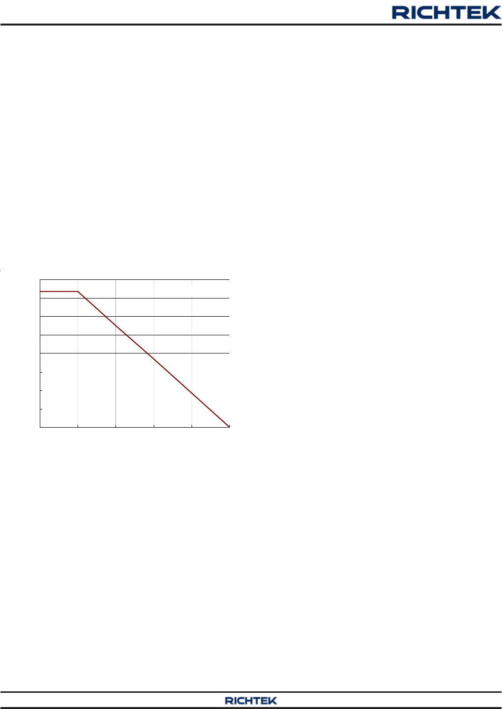
Ambient Temperature (°C)
Maximum Power Dissipation (W) 1
Four Layers PCB
For recommended operating condition specifications of
RT8856, the maximum junction temperature is 125°C and
TA is the ambient temperature. The junction to ambient
thermal resistance, θJA, is layout dependent. For
WQFN-40L 6x6 packages, the thermal resistance, θJA, is
34°C/W on a standard JEDEC 51-7 four-layer thermal test
board. The maximum power dissipation at TA = 25°C can
be calculated by the following formula :
PD(MAX) = (125°C − 25°C) / (34°C/W) = 2.941W for
WQFN-40L 6x6 package
The maximum power dissipation depends on the operating
ambient temperature for fixed TJ(MAX) and thermal
resistance, θJA. For RT8856 package, the derating curve
in Figure 10 allows the designer to see the effect of rising
ambient temperature on the maximum power dissipation.
RT8856
23
DS8856-04 August 2014 www.richtek.com
©
Copyright 2014 Richtek Technology Corporation. All rights reserved. is a registered trademark of Richtek Technology Corporation.
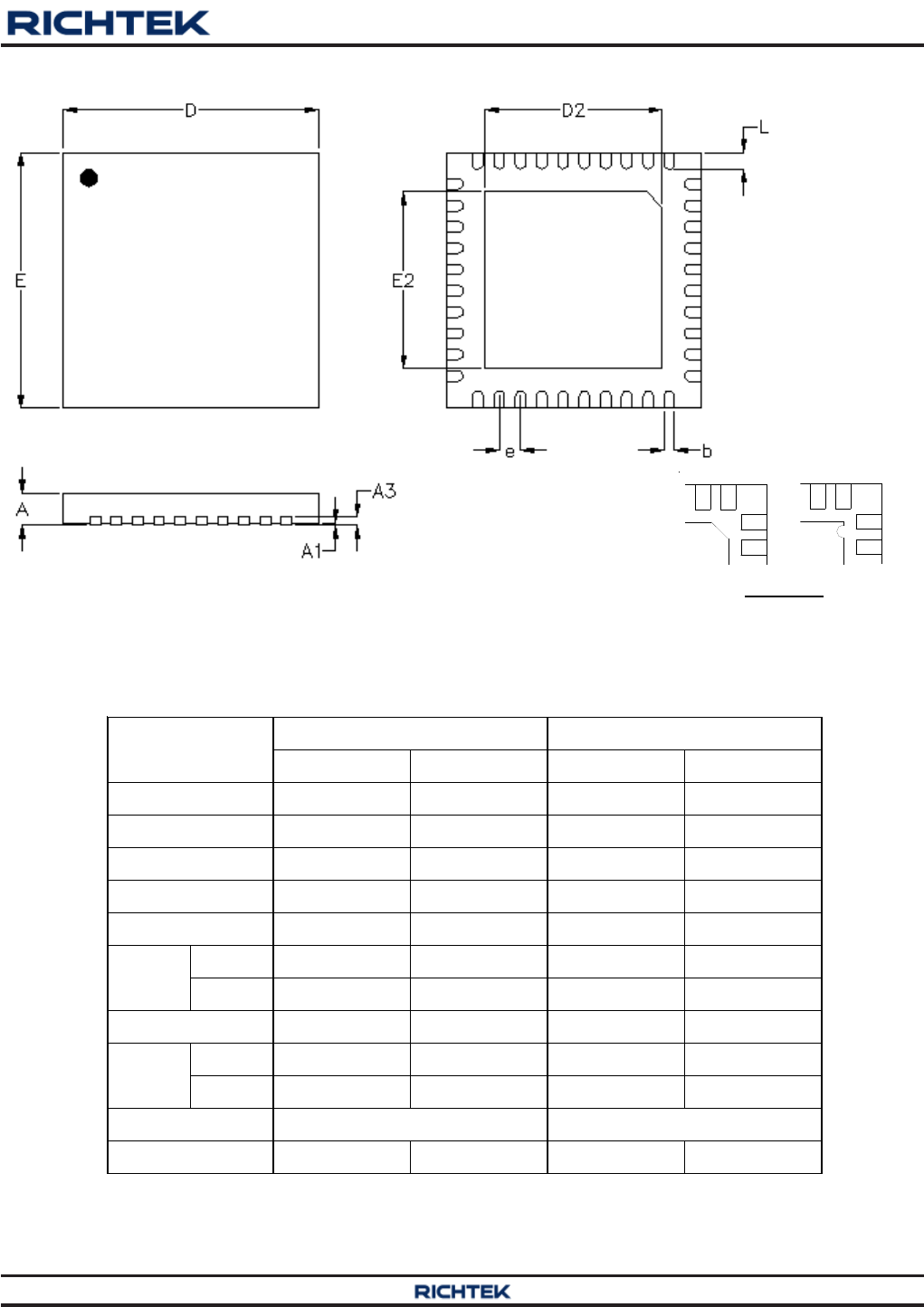
Outline Dimension
Min. Max. Min. Max.
0.700 0.800 0.028 0.031
0.000 0.050 0.000 0.002
0.175 0.250 0.007 0.010
0.180 0.300 0.007 0.012
5.950 6.050 0.234 0.238
Option1 4.000 4.750 0.157 0.187
Option2 3.470 3.570 0.137 0.141
5.950 6.050 0.234 0.238
Option1 4.000 4.750 0.157 0.187
Option2 2.570 2.670 0.101 0.105
0.350 0.450 0.014 0.018
0.500 0.020
L
b
D
D2
E
E2
e
Symbol Dimensions In Millimeters Dimensions In Inches
A
A1
A3
W-Type 40L QFN 6x6 Package
Note : The configuration of the Pin #1 identifier is optional,
but must be located within the zone indicated.
DETAIL A
Pin #1 ID and Tie Bar Mark Options
1
1
22

RT8856
24
DS8856-04 August 2014www.richtek.com
Richtek Technology Corporation
14F, No. 8, Tai Yuen 1st Street, Chupei City
Hsinchu, Taiwan, R.O.C.
Tel: (8863)5526789
Richtek products are sold by description only. Richtek reserves the right to change the circuitry and/or specifications without notice at any time. Customers should
obtain the latest relevant information and data sheets before placing orders and should verify that such information is current and complete. Richtek cannot
assume responsibility for use of any circuitry other than circuitry entirely embodied in a Richtek product. Information furnished by Richtek is believed to be
accurate and reliable. However, no responsibility is assumed by Richtek or its subsidiaries for its use; nor for any infringements of patents or other rights of third
parties which may result from its use. No license is granted by implication or otherwise under any patent or patent rights of Richtek or its subsidiaries.