RT9913A, RT9913B Datasheet. Www.s Manuals.com. Richtek
User Manual: Marking of electronic components, SMD Codes B0, B0*, B0**, B0-**, B0-***, B0=***. Datasheets ELM9710NBA, RT9011-FSPJ6, RT9011-JPPQV, RT9011-PMPQWC, RT9013-31PU5, RT9013A-28GY, RT9014A-PPPQV, RT9913BPQV, SST5460.
Open the PDF directly: View PDF ![]() .
.
Page Count: 19

RT9913A/B
Preliminary
1
DS9913A/B-00 February 2006 www.richtek.com
Integrated Multi-Channel DC-DC Converter for
TFT LCD Panels
General Description
The RT9913A/B includes a high-performance boost
regulator, one linear-regulator controller for VGL, one low
dropout linear regulator, a gate pulse modulator (GPM), a
voltage detector and a VCOM Buffer (Unity- gain OPA) for
active-matrix thin-film transistor (TFT) liquid-crystal displays
(LCDs).
The boost converter provides the regulated supply voltage
for the panel source driver ICs. With integrated 16V
N-Channel 0.2Ω MOSFET it allows the use of ultra-small
inductors and ceramic capacitors and provides fast transient
response to pulsed loads. The VGL linear-regulator
controller provides regulated TFT Gate-Off . The low-dropout
linear regulator (LDO) using an internal PMOS as the pass
device can supply up to 350mA current is suitable for the
supply voltage to the T-CON ASIC. And the GPM is
controlled by frame signals from timing controller to
modulate the Gate-On voltage. Voltage detector monitors
the supply voltage to issue a reset signal while the
detected voltage is too low. The VCOM Buffer (Unity-gain)
high-performance operation amplifier) can drive the LCD
backplane (VCOM) and features high short-circuit current
(140mA), fast slew rate (12V/μs), wide bandwidth (12MHz)
and rail-to-rail input and output.
Features
zz
zz
z2.5V to 5.5V Input Supply Voltage
zz
zz
z640kHz/1.2MHz (A/B version) Current-Mode Step-Up
Boost Regulator
Fast Transient Response to Pulsed Load
High Accuracy Output Voltage (±±
±±
±2%)
Built-In 16V, 2.0A, 0.2ΩΩ
ΩΩ
Ω N-Channel MOSFET
High Efficiency Up to 90%
Programmable Soft-Start
Programmable Over-Current Protection
zz
zz
zLinear-Regulator Controller for VGL
zz
zz
zLow Drop-Out Voltage Linear Regulator
Adjustable Output Voltage (2.5V to 3.3V)
350mA Maximum Output Current
zz
zz
zOn-Chip GPM Controller with Adjustable Falling
Time
Flicker Compensator
Power-On Sequence Control
zz
zz
zLow Voltage Detector
Programmable Detecting Voltage and Delay Time
zz
zz
zUnity-Gain Operation Amplifier for VCOM Buffer
zz
zz
zOver-Temperature Protection
zz
zz
zThin 24-Lead VQFN Package
zz
zz
zRoHS Compliant and 100% Lead (Pb)-Free
Marking Information
For marking information, contact our sales representative
directly or through a RichTek distributor located in your
area, otherwise visit our website for detail.
Ordering Information
Note :
RichTek Pb-free products are :
`RoHS compliant and compatible with the current require-
ments of IPC/JEDEC J-STD-020.
`Suitable for use in SnPb or Pb-free soldering processes.
`100% matte tin (Sn) plating.
RT9913A/B
Package Type
QV : VQFN-24L 4x4 (V-Type)
Operating Temperature Range
P : Pb Free with Commercial Standard
Switching Frequency
A : 640kHz
B : 1.2MHz
RT9913A/B Preliminary
2
DS9913A/B-00 February 2006www.richtek.com
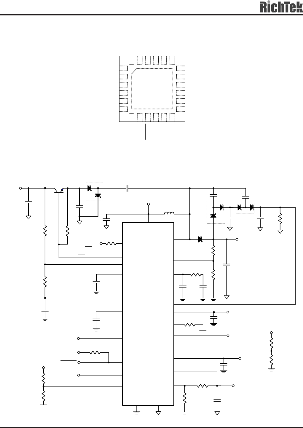
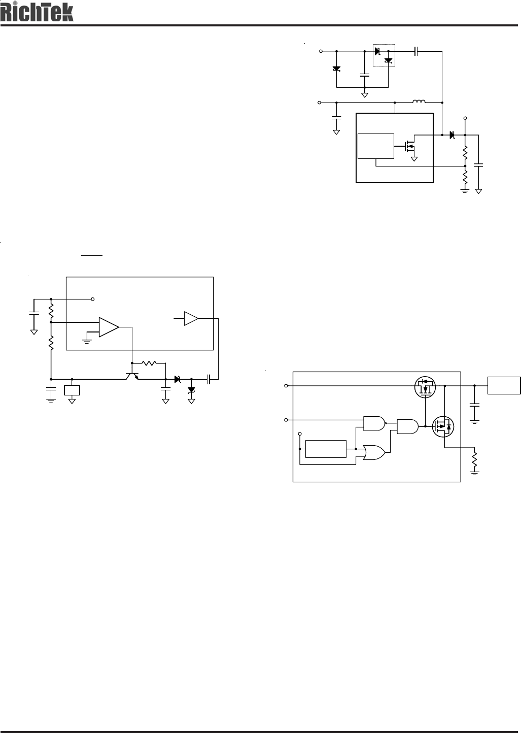
Typical Application Circuit
LX
VIN
FB
VIN
AGND
VAVDD
COMP
EN
L1
8.5V
DRVN
SS
RT9913
25V
VGH
VGHM VGHM
VFLK
RESET
VFLK
RESET
CD
AVDD
VDIV
VAVDD
D1
C1
C2
R1
R2
R3
C3
C4
R6
R7
C10
VGL
-6V
C12
D4
C13
C11
R8
PGND
C5
C7 C8
D2
D3
RE
R11
VLDO
R4
R5
ADJ
Chip Enable
17
19
7
15
8
1
9
10
11 21
12
4
3
2
16
20
18
22
C6
FBN
6
VREF
5
R9
R10
C14
VDIN
2.5V
LDOO
LDOI
OPAI
OPAO VCOM_OUT
VCOM_IN
VIN
14
24
23
13
C9
VAVDD
0.22uF
240k
50k
0.22uF
6.8k
0.1uF
Q1
MMBT3904 BAT54S 0.1uF
10uF
27nF
0.1uF
65k
110k
4.7uH
3.3V 0.1uF
BAT54S 0.1uF
0.1uF
BAT54S
0.1uF
SS12
330k
56k
56k
1nF
4.7uF x 3
C15
1.5nF
1.2k
3.3V
C16
1uF
56k
56k 1uF
56k
56k
R12
R13
RSET
VLDO
R14
CCOMP
100k
RGH
30k
NC
Pin Configurations (TOP VIEW)
VQFN-24L 4x4
VFLK
VGH
VGHM
RE
VREF
FBN
LX
VIN
COMP
SS
LDOI
LDOO
PGND
EN
OPAI
OPAO
AVDD
FB
ADJ
DRVN
CD
RESET
AGND
VDIV
1
2
3
4
5
6
7
21 20 19
18
17
16
15
8 9 10 12
14
13
24 2223
11
GND
RT9913A/B
Preliminary
3
DS9913A/B-00 February 2006 www.richtek.com
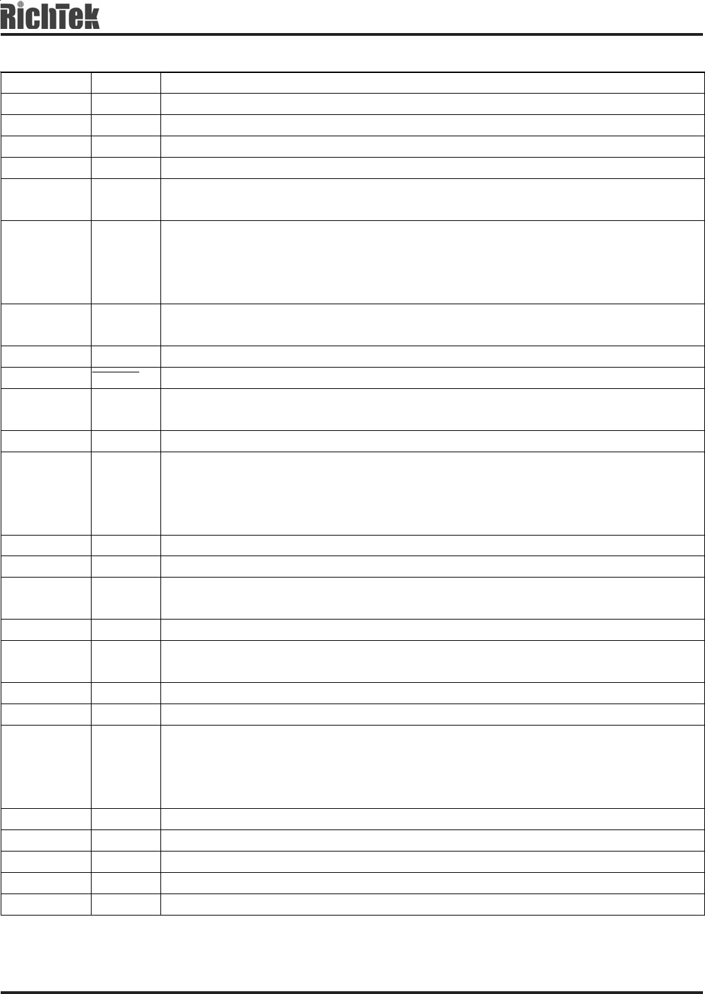
Functional Pin Description
Pin Number Pin Name Pin Function
1 VFLK VFLK is produced by timing controller for charging or discharging VGHM.
2 VGH Switch input for charge VGHM
3 VGHM VGHM is the supply voltage for the gate driver ICs.
4 RE Switch input for discharge VGHM
5 VREF
Internal Reference Bypass Terminal. Connect a 0.22uF ceramic capacitor from the VREF
to analog ground (AGND). The source capability is 100uA.
6 FBN
Negative Linear-Regulator Feedback Input. Connect FBN to the center of a resistive
voltage-divider between the negative output voltage VGL and the VREF to set the
negative linear-regulator output voltage. Place the resistive voltage-divider close to the
pin.
7 DRVN
Negative Linear-Regulator Base Drive. Open drain of an internal PMOS. Connect DRVN
to the base of the external linear-regulator NPN pass transistor.
8 CD Pin for external capacitor setting the delay time for voltage detector reset delay time.
9 RESET Voltage Detector open-drain Output for Reset.
10 VDIV Voltage Detector Divider Input. Connect VDIV to the center of a resistive voltage-divider
between the detected voltage input (VDIN) and analog ground (AGND).
11 AGND Analog Ground.
12 ADJ
Low-Dropout Linear Regulator (LDO) Feedback Input. ADJ regulates to 1.24V nominal.
Connect ADJ to the center of a resistive voltage-divider between the LDO output voltage
LDOO and the analog ground (AGND) the LDO output voltage. Place the resistive
voltage-divider close to the pin.
13 LDOO Voltage Output of the LDO.
14 LDOI Voltage Input of the LDO.
15 SS Soft-Start Control Pin. Connect a soft-start capacitor (CSS) to this pin. The soft-start
capacitor is charged with a constant current 4uA.
16 COMP Compensation Error Amplifier Pin. Connect a compensation network to ground.
17 VIN Supply Input. The supply voltage powers all the control circuits including the boost
converter, negative linear-regulator, gate pulse regulator and voltage detector.
18 LX Switching pin. Drain of the internal power NMOS for the main step-up regulator.
19 EN Active-High Enable Control Input and OCP level setting.
20 FB
Main Boost Regulator Feedback Input. FB regulates to 1.24V nominal. Connect FB to the
center of a resistive voltage-divider between the main output AVDD and the analog
ground (AGND) the boost regulator output voltage. Place the resistive voltage-divider
close to the pin.
21 PGND Power Ground. PGND is the source of the power NMOS.
22 AVDD VDD for Source Driver Power. It also supplies OP power and GPM level shift voltage.
23 OPAO Unit-Gain OPA Output Pin.
24 OPAI Unit-Gain OPA Input Pin.
Exposed Pad GND Exposed pad should be soldered to PCB board and connected to GND.
RT9913A/B Preliminary
4
DS9913A/B-00 February 2006www.richtek.com
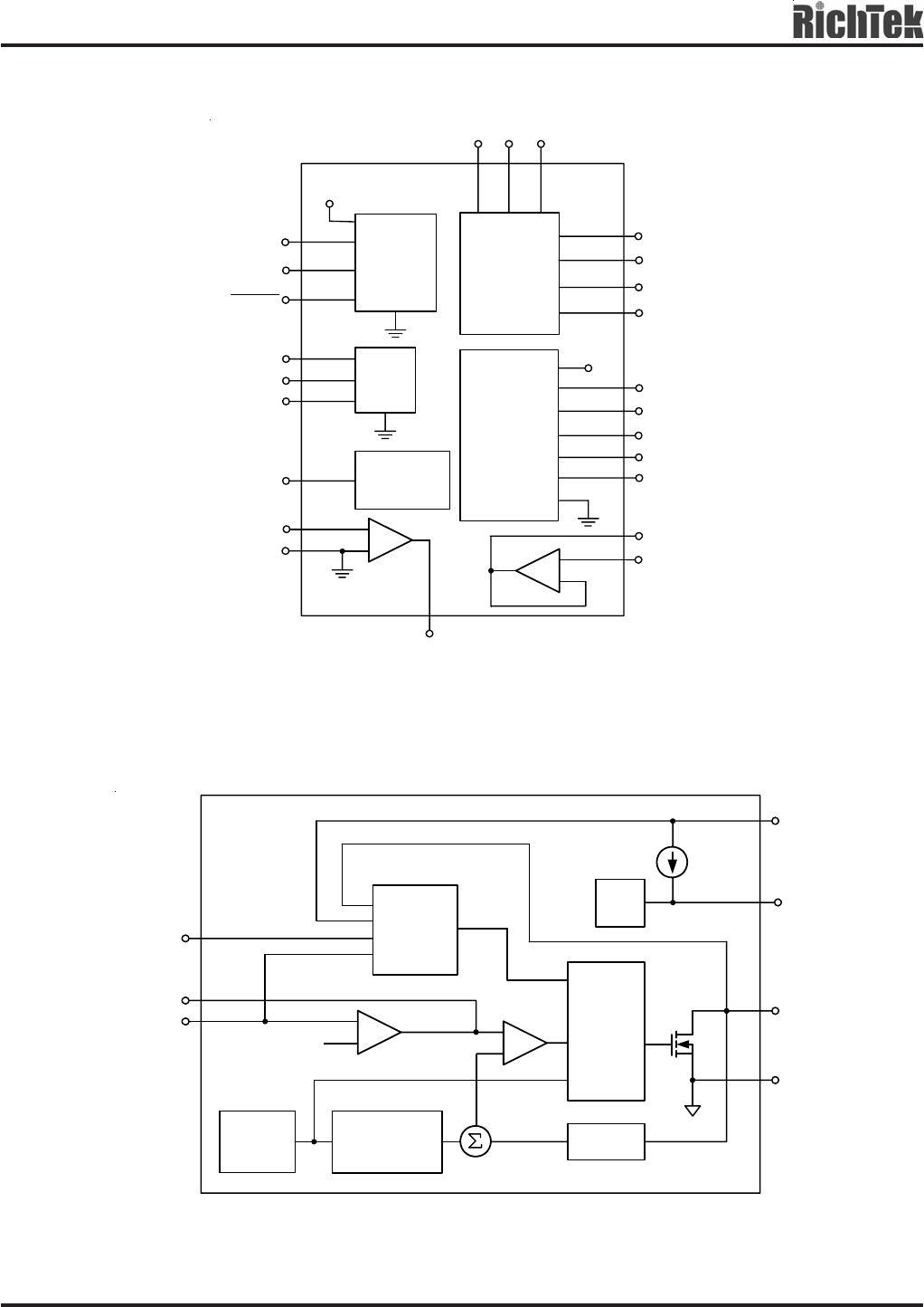
Function Block Diagram
Boost Regulator Block Diagram
Boost
Regulator
GPM
Voltage
Detector
VIN
LDO
+
-
1.24V
Voltage
Reference
+
-
VFLK
VGH
VGHM
RE
VREF
FBN
PGND
EN
OPAI
OPAO
AVDD
ADJ
DRVN
CD
RESET
AGND
VDIV LX
COMP
SS
LDOI
LDOO
FB
VIN
VIN
Control
and
Driver
Logic
Current
Sense
Protection
+
-
+
-
Slope
Compensation
Oscillator
1.24V
Clock
Summing
Comparator
Error
Amplifier
LX
PGND
COMP
FB
EN
Soft-
Start
4uA
VIN
SS
RT9913A/B
Preliminary
5
DS9913A/B-00 February 2006 www.richtek.com
Electrical Characteristics
To be continued
Absolute Maximum Ratings (Note 1)
zSupply Input Voltage, VIN ----------------------------------------------------------------------------------- −0.3V to 7V
zVGH-AVDD, VGHM-AVDD ---------------------------------------------------------------------------------- 18V
zLX ---------------------------------------------------------------------------------------------------------------- −0.3V to 16V
zVGH, VGHM RE ---------------------------------------------------------------------------------------------- −0.3V to 30V
zAVDD ------------------------------------------------------------------------------------------------------------ −0.3V to 16V
zOPAI, OPAO --------------------------------------------------------------------------------------------------- −0.3V to (AVDD + 0.3V)
zDRVN ------------------------------------------------------------------------------------------------------------ (VIN − 16V) to (VIN + 0.3V)
zVFLK, VREF, FBN, CD, RESET_, VDIV, SS, COMP, EN, FB ------------------------------------ −0.3V to (VIN + 0.3V)
zLDOI ------------------------------------------------------------------------------------------------------------- −0.3V to 7V
zADJ, LDOO ---------------------------------------------------------------------------------------------------- −0.3V to (LDOI + 0.3V)
zPower Dissipation, PD @ TA = 25°C
VQFN-24L 4x4 ------------------------------------------------------------------------------------------------ 1.786W
zPackage Thermal Resistance (Note 4)
VQFN-24L 4x4, θJA ------------------------------------------------------------------------------------------- 56°C/W
zLead Temperature (Soldering, 10 sec.) ------------------------------------------------------------------ 260°C
zStorage Temperature Range ------------------------------------------------------------------------------- −65°C to 150°C
zJunction Temperature ---------------------------------------------------------------------------------------- 150°C
zESD Susceptibility (Note 2)
HBM (Human Body Mode) --------------------------------------------------------------------------------- 2kV
MM (Machine Mode) ----------------------------------------------------------------------------------------- 200V
(VIN = 3.3V, VOUT = 8.5V, TA = 25°C, unless otherwise specification)
Recommended Operating Conditions (Note 3)
zAmbient Temperature Range ------------------------------------------------------------------------------- −40°C to 85°C
zJunction Temperature Range ------------------------------------------------------------------------------- −40°C to 125°C
Parameter Symbol Test Condition Min Typ Max Units
System Supply
Input Supply Voltage VIN 2.5 -- 5.5 V
VIN rising 1.8 2.0 2.2
VIN Under Voltage Lockout Threshold VUVLO Hysteresis 0.05 0.1 0.15
V
VFB = 1.3V, LX no switching 0.15 0.4 1 mA
VIN Quiescent Current IQ
VFB = 1.1V, LX switching 1 2 3.5 mA
Shut Down Current IIN V
IN = 3.3V -- 1 5 μA
Logic-High Voltage VIH -- -- 1.5
EN Threshold
Logic-Low Voltage VIL 0.8 -- --
V
Main Boost Regulator
RT9913 A -- 640 -- kHz
Operation Frequency FOSC RT9913 B 0.9 1.2 1.4 MHz
Maximum Duty Cycle 86 90 94 %
RT9913A/B Preliminary
6
DS9913A/B-00 February 2006www.richtek.com
Parameter Symbol Test Condition Min Typ Max Units
Feedback Voltage VFB No load, TA = 25°C 1.22 1.24 1.26 V
FB Input Bias Current VFB = 1.5V -40 -- +40 nA
Transconductance of Error Amplifier Gm ICOMP = 5μA -- 160 --
μA/V
Voltage Gain of Error Amplifier AV -- 700 -- V/V
Feedback Voltage Line Regulation VIN = 2.5V to 5.5V -- 0.1 0.15 %/V
Output Voltage Load Regulation VIN = 3.3V,
ILOAD = 20 to 200mA −1 -- 0 %
LX ON-Resistance RLX(ON) 50 200 500
mΩ
Current Sense Transresistance -- 0.5 -- A/V
Soft-Start Charge Current ISS 2 4 6
μA
Thermal Shutdown Temperature TSD -- 170 --
°C
Thermal Shutdown Hysteresis ΔTSD -- 20 --
°C
Current Limit ILIM -- 2 -- A
Gate-Off Regulation Controller
VREF source current capability IREF -- 100 1000
μA
FBN Regulation Voltage VFBN −20 0 20 mV
FBN Effective Load Regulation Error VDRVN = −10V,
IDRVN = 50uA to 1mA −30 −5 0 mV
FBN Line Regulation Error IDRVN = 0.1mA, 2.5V<VIN<5.5V -- 1 6 mV
DRVN Source Current IDRVN 1 4 6 mA
Power-On-Delay Time TVGL Refer to VFB > 1V 25 32 39 ms
Low Drop-Out Linear Regulator (LDO)
Input Voltage VLDOI 2.5 -- 5.5 V
Dropout Voltage VDROP V
IN = 3.3V, IOUT = 350mA 200 300 500 mV
Feedback Voltage VADJ 1.22 1.24 1.26 V
Current Limit ILIM 350 500 650 mA
Quiescent Current ILDO -- 60 100
μA
Line Regulation VIN = 2.8V to 5.5V,
IOUT = 100mA, VLDO = 2.5V
-- 0.1 0.3 %/V
Load Regulation IOUT = 1mA to 300mA 0 0.2 0.5 %
Gate Pulse Modulator
VFLK Input High Voltage VIH_FLK 1.5 -- -- V
VFLK Input Low Voltage VIL FLK -- -- 0.6 V
Power-On-Delay Time (Note 5) TVGHM Refer to VFB > 1V 50 64 78 ms
To be continued
RT9913A/B
Preliminary
7
DS9913A/B-00 February 2006 www.richtek.com
Parameter Symbol Test Condition Min Typ Max Units
Gate Pulse Modulator
VGH Switch On-Resistance RP1 10 30 50 Ω
RE Switch On-Resistance RN2 10 25 50 Ω
Voltage Detector
Minimum Operating Voltage 1.6 -- -- V
Detecting voltage adjustment VDIV -- 1.1 -- V
Detecting voltage accuracy −2% -- 2% %
Adjustable delay time-constant k tD = k(Ω)*C10(F) 80k 120k 160k
Ω
VCOM Buffer
Supply Voltage Range VSUP AVDD -- 15 V
Supply Current IOP -- 0.5 0.9 mA
Input Offset Voltage VOS V
COM = AVDD/2, TA = 25°C −15 0 15 mV
Input Bias Current IBIAS -- 1 50 nA
IOUT = 100μA AVDD-20 AVDD-5 -- mV
Output Voltage Swing High VOH
IOUT = 75mA AVDD-1.5 AVDD-1.3 -- V
IOUT = −100μA -- 2 20 mV
Output Voltage Swing Low VOL
IOUT = −75mA -- 1.5 1.8 V
Source 100 140 180 mA
Short-Circuit Current To AVDD/2
Sink 100 140 180 mA
-3dB Bandwidth F3db -- 12 -- MHz
Gain Bandwidth Product GBW -- 8 -- MHz
Slew Rate SR 8 12 16 V/μs
Note 1. Stresses listed as the above “Absolute Maximum Ratings” may cause permanent damage to the device. These are for
stress ratings. Functional operation of the device at these or any other conditions beyond those indicated in the
operational sections of the specifications is not implied. Exposure to absolute maximum rating conditions for extended
periods may remain possibility to affect device reliability.
Note 2. Devices are ESD sensitive. Handling precaution recommended.
Note 3. The device is not guaranteed to function outside its operating conditions.
Note 4. θJA is measured in the natural convection at TA = 25°C on a low effective thermal conductivity test board of
JEDEC 51-3 thermal measurement standard.
Note 5. It is guaranteed by design.
RT9913A/B Preliminary
8
DS9913A/B-00 February 2006www.richtek.com
Typical Application Circuit
Boost Efficiency vs. Output Current
76
78
80
82
84
86
88
90
0 20 40 60 80 100 120 140 160 180 200
Output Current (mA)
Efficiency (%)
VIN = 3V, f = 1.2MHz
C1 = 6.9μF, C2 = 30μF
VAVDD = 7V
= 7.5V
= 8V
= 8.5V
Boost Output Voltage vs. Output Current
8.48
8.5
8.52
8.54
8.56
8.58
8.6
8.62
0 20 40 60 80 100 120 140 160 180 200
Output Current (mA)
Output Voltage (V)
VAVDD = 8.5V, f = 1.2MHz
VIN = 2.7V
VIN = 3.0V
VIN = 3.3V
Boost Efficiency vs. Output Current
50
55
60
65
70
75
80
85
90
95
0 20 40 60 80 100 120 140 160 180 200
Output Current (mA)
Efficiency (%)
VAVDD = 8.5V, f = 1.2MHz
VIN = 3.3V
VIN = 3.0V
VIN = 2.7V
Boost Output Voltage vs. Output Current
6.6
6.8
7
7.2
7.4
7.6
7.8
8
8.2
8.4
8.6
0 20 40 60 80 100 120 140 160 180 200
Output Current (mA)
Output Voltage (V)
VIN = 3V, f = 1.2MHz, C1 = 6.9μF, C2 = 30μF
VAVDD = 7V
VAVDD = 7.5V
VAVDD = 8V
VAVDD = 8.5V
Boost Output Voltage vs. Output Current
11.76
11.8
11.84
11.88
11.92
11.96
12
12.04
0 20 40 60 80 100 120 140 160 180 200
Output Current (mA)
Output Voltage (V)
VIN = 3.0V
VIN = 3.3V
VAVDD = 12V, f = 1.2MHz
Boost Efficiency vs. Output Current
50
55
60
65
70
75
80
85
90
95
0 20 40 60 80 100 120 140 160 180 200
Output Current (mA)
Efficiency(%)
VIN = 3.0V
VIN = 3.3V
VAVDD = 12V, f = 1.2MHz
RT9913A/B
Preliminary
9
DS9913A/B-00 February 2006 www.richtek.com
VGL Regulator Load Regulation
-5.87
-5.85
-5.83
-5.81
-5.79
-5.77
-5.75
0 102030405060708090100
Load Current (mA)
VGL Voltage (V)
Boost Feedback vs. Temperature
1.205
1.210
1.215
1.220
1.225
1.230
1.235
1.240
1.245
1.250
1.255
-40-30-20-100 102030405060708090
Temperature
Boost Feedback (V)
(°C)
Time (400ns/Div)
VLX
(5V/Div)
ILOAD = 100mA
IL
(200mA/Div)
VAVDD ripple
ac coupled
(50mV/Div)
f = 1.2MHz
Boost Regulator Stability
Boost Regulator Stability
Time (400ns/Div)
VLX
(5V/Div)
ILOAD = 10mA, f = 1.2MHz
IL
(200mA/Div)
VAVDD ripple
ac coupled
(50mV/Div)
ILOAD = 10mA to 200mA
Boost Regulator Load
Transient Response
Time (200μs/Div)
ILOAD
(100mA/Div)
IL
(500mA/Div)
VAVDD
ac coupled
(500mV/Div)
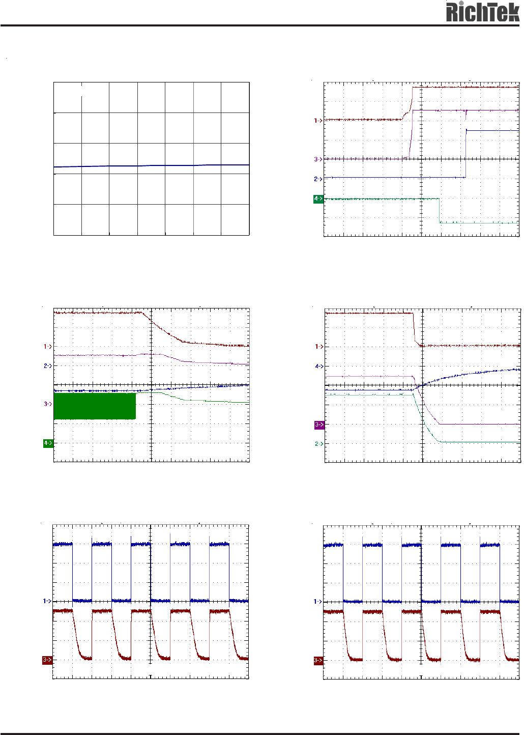
Boost Regulator Soft-Start
Time (2.5ms/Div)
VAVDD
(5V/Div)
VIN
(5V/Div)
ILOAD = 200mA
IIN
(500mA/Div)
EN
(2V/Div)
RT9913A/B Preliminary
10
DS9913A/B-00 February 2006www.richtek.com
VGHM
Time (10μs/Div)
VFLK
(1V/Div)
VGHM
(10V/Div)
R11 = 670Ω, C15 = 1.5nF
VGHM
Time (10μs/Div)
VFLK
(1V/Div)
VGHM
(10V/Div)
R11 = 1.2kΩ, C15 = 680pF
Power On Sequence
Time (25ms/Div)
VAVDD
(5V/Div)
VGL
(5V/Div)
VGH
(10V/Div)
VGHM
(10V/Div)
Power Off Sequence
Time (25ms/Div)
(5V/Div)
(5V/Div)
(10V/Div)
(10V/Div)
VAVDD
VGL
VGHM
VGH
FLK = VIN
VGL Regulator Line Regulation
-5.85
-5.83
-5.81
-5.79
-5.77
-5.75
-14 -13 -12 -11 -10 -9 -8 -7
Input Voltage(V)
VGL Output Voltage (V)
IGL = 50mA
Power Off Sequence
with GPM Function
Time (2.5ms/Div)
(5V/Div)
FLK = 50kHz/50%
(5V/Div)
(10V/Div)
(10V/Div)
VAVDD
VGL
VGHM
VGH
RT9913A/B
Preliminary
11
DS9913A/B-00 February 2006 www.richtek.com
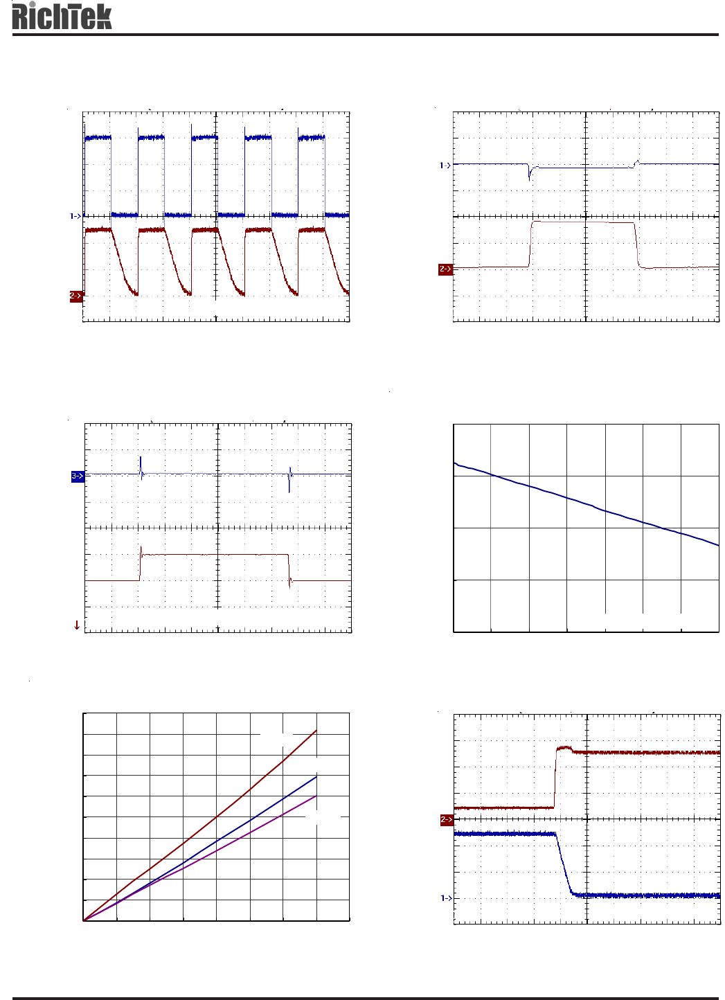
LDO Load Transient
Time (100μs/Div)
VLDOO
ac coupled
(50mV/Div)
ILDOO
(200mA/Div)
ILDOO = 10mA to 350mA
LDO Load Regulation
2.57
2.575
2.58
2.585
2.59
0 50 100 150 200 250 300 350
LDO Loading Current (mA)
LDO Output Voltage (V)
VLDOO = 2.5V, VLDOI = 3.3V
VGHM
Time (10μs/Div)
VFLK
(1V/Div)
VGHM
(10V/Div)
R11 = 1.2kΩ, C15 = 2.2nF
LDO Line Transient
Time (100μs/Div)
VLDOO
ac coupled
(100mV/Div)
VLDOI
(1V/Div)
VLDOO = 2.5V, VLDOI = 3V to 4V, ILDOO = 50mA
4
3
LDO OCP
Time (100μs/Div)
VLDO
(1V/Div)
ILDO
(200mA/Div)
IOUT = 100mA to 600mA
LDO Dropout Voltage
0
50
100
150
200
250
300
350
400
450
500
0 0.05 0.1 0.15 0.2 0.25 0.3 0.35 0.4
Load Current (A)
Dropout Voltage (mV)
85°C
25°C
-40°C
RT9913A/B Preliminary
12
DS9913A/B-00 February 2006www.richtek.com
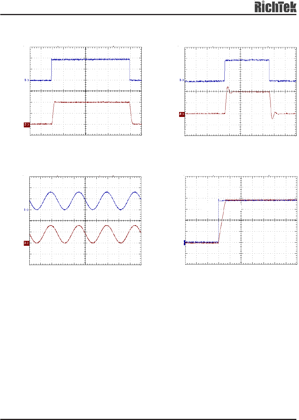
OPA Slew Rate
Time (1μs/Div)
(2V/Div)
VOPAO
VOPAI
OPA Rail-to-Rail Input/Output
Time (400μs/Div)
VOPAO
(5V/Div)
VOPAI
(5V/Div)
OPA Large-Signal Step Response
Time (1μs/Div)
VOPAO
(1V/Div)
VOPAI
(1V/Div)
OPA Small-Signal Step Response
Time (500ns/Div)
VOPAO
(100mV/Div)
VOPAI
(100mV/Div)

RT9913A/B
Preliminary
13
DS9913A/B-00 February 2006 www.richtek.com
Application Information
The RT9913 contains a high performance boost regulator
to generate voltage for output voltage, gate-on driver and
negative voltage regulated by linear regulator controller
for gate-off driver. It also includes of a high-current rail-to-
rail operation amplifier, a gate pulse modulator (GPM), a
programmable timing control voltage detector, and a low
dropout linear regulator. The following content contains
the detailed description and the information of component
selection.
Boost Regulator
The boost regulator is a high efficiency current-mode PWM
architecture with 1.2MHz or 640kHz operation frequency.
It performs fast transient responses to generate gate driver
supplies for TFT LCD display. The high operation frequency
allows smaller components used to minimize the
thickness of LCD panel. To regulate the output voltage is
to set resistive voltage-divider sensing at FB pin. The error
amplifier varies the COMP voltage by sensing FB pin to
regulate the output voltage. For better stability, the slope
compensation signal summed with the current-sense
signal will be compared with the COMP voltage to
determine the current trip point and duty cycle.
Soft-Start
The RT9913 provides soft-start function to minimize the
inrush current. When EN pin is connected to high, an
internal constant current charges an external capacitor.
The rising voltage rate on COMP pin is limited during the
charging period and the inductor peak current also limited
at the same time. In the meanwhile, the frequency
increases slowly at the beginning. When the EN pin is
connected to GND, the external capacitor will be
discharged for next soft start time.
The soft-start function is implemented by the external
capacitor with a 4μA constant current charging to the soft-
start capacitor. Therefore, the capacitor should be large
enough for output voltage regulation. Typical value for soft-
start capacitor range is 27nF. The available soft start
capacitor range is from 10nF to 200nF.
Inductor Selection & Maximum output current
capability
The minimum inductance value, peak current rating and
series resistance are factors to consider when selecting
the inductor. These factors influence the converter's
efficiency, maximum output load capability, transient-
response time and output voltage ripple. Physical size
and cost are also important factors to be considered. The
maximum output current, input voltage, output voltage and
switching frequency determine the inductor value. Very
high inductance values minimize the current ripple and
therefore reduce the peak current, which decreases core
losses in the inductor and I2R losses in the entire power
path. However, large inductor values also require more
energy storage and more turns of wire, which increase
physical size and can increase I2R losses in the inductor.
Low inductance values decrease the physical size but
increase the current ripple and peak current.
Finding the best inductor involves choosing the best
compromise between circuit efficiency, inductor size and
cost.
Choose an available inductor value from an appropriate
inductor family. Calculate the maximum DC input current
at the minimum input voltage VIN(MIN) using the following
equation.
(MIN)IN(MIN)
AVDDAVDD(MAX)
MAX) IN(DC, V
VI
I
η
×
×
=
The expected efficiency at that operating point (ηMIN) can
be taken from an appropriate curve in the Typical Operating
Characteristics. Calculate the ripple current at that
operating point and the peak current required for the
inductor :
2
I
I I
fVL
)V(VV
I
RIPPLE
MAX) IN(DC,PEAK
OSCAVDD
IN(MIN)AVDDIN(MIN)
RIPPLE
+=
××
−×
=
The inductor's saturation current rating and the LX over-
current protection (IOCP) should exceed IPEAK and the
inductor DC current rating should exceed IIN(DC,MAX). For
good efficiency, choosing an inductor with less than 0.1Ω
series resistance is suggested.
RT9913A/B Preliminary
14
DS9913A/B-00 February 2006www.richtek.com
Figure 1. OCP settings versus RSET @ VEN = 2.5V
Over Temperature Protection
The RT9913 main boost converter has thermal protection
function to prevent the excessive power dissipation from
overheating. When the junction temperature exceeds
170°C, it will shut down the device. Once the device cools
down by approximately 20°C, it will start to operate
normally. For continuous operation, do not operate over
the maximum junction temperature rating around 150°C.
Diode Selection
To achieve high efficiency, Schottky diode is the
recommended diode for lower forward drop voltage and
faster switching time. The output diode rating should be
large enough for maximum output voltage, average power
dissipation and the pulsating diode peak current.
Output Capacitor Selection
For lower output voltage ripple, low-ESR ceramic capacitor
is recommended. The output voltage ripple consists of
two components: one is the pulsating output ripple current
flowing through the ESR, and the other is the capacitive
ripple caused by charging and discharging.
⎟
⎠
⎞
⎜
⎝
⎛
×
−
+×≅
+=
fV
VV
C
I
RI
VVV
AVDD
INAVDD
OUT
PEAK
ESRPEAK
RIPPLE_CRIPPLE_ESRRIPPLE
Input Capacitor Selection
For better input bypassing, low-ESR ceramic capacitor is
recommended for better performance. A 10μF input
capacitor is sufficient and it is flexible to reduce the value
for a lower output power requirement.
Output Voltage
The regulated output voltage is the following formula :
⎟
⎠
⎞
⎜
⎝
⎛+×= R2
R1
11.24VVOUT
The recommended value for R2 should be up to 100kΩ
without some sacrificing. To place the resistor-divider as
close as possible to the chip can reduce noise sensitivity.
Loop Compensation
The voltage feedback loop can be compensated with an
external compensation network consisted of R3, C3 and
CCOMP (As Figure 1). Choose R3 to set high frequency
integrator gain for fast transient response and C3 to set
the integrator zero to maintain loop stability.
Place CCOMP between COMP and GND to add an additional
high-frequecncy pole. The value is between 10pF and
47pF. For typical application VIN = 3.3V , VOUT = 8.5V
,COUT = 4.7μF x 3 , L = 4.7μH, the recommened value
for compensation is as below:
R3 = 56kΩ , C3 = 1nF , Ccomp=NC
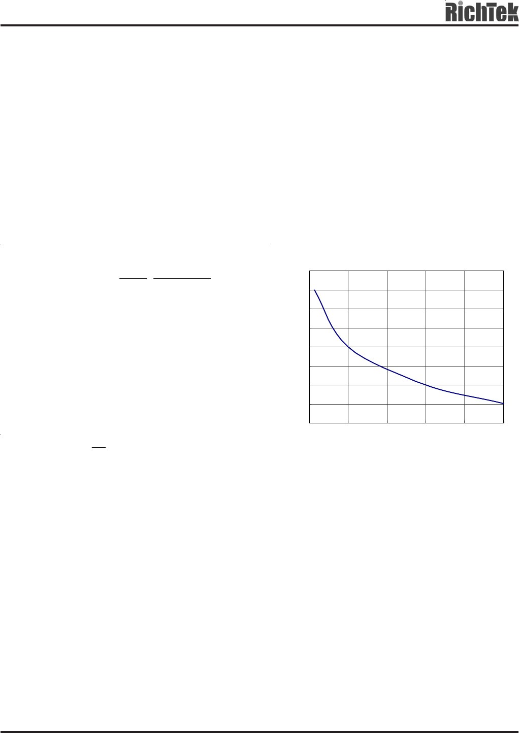
Over Current Protection
The RT9913 main boost converter has over-current
protection to limit peak inductor current. It prevents large
current damaging the inductor and diode. During the
ON-time, once the inductor current exceeds the current
limit, the internal LX switch turns off immediately and
shortens the duty cycle. Therefore, the output voltage
drops if the over-current condition occurs. Actual current
limit is always larger than nominal value because of the
internal circuit delay. Current limit is also affected by the
input voltage, duty cycle, and inductor value. The following
figure shows the different over-current settings and the
corresponding RSET resistance while OCP function works
and VAVDD falls to 90%.
OCP Current vs. RSET
0.6
0.8
1
1.2
1.4
1.6
1.8
2
2.2
50 100 150 200 250 300
RSET
OCP Current (A)
(kΩ)
RT9913A/B
Preliminary
15
DS9913A/B-00 February 2006 www.richtek.com
)
R8
V
-(I I BE
DRVNLOAD
β
=
Gate-Low Linear Regulator Controller
The gate-low linear regulator controller is to provide the
TFT-LCD gate off voltage. One stage charge pump can
provide a negative voltage. Using the gate-low regulator
after the produced negative voltage can regulate the
exceeded voltage. With a 6.8kΩ base to emitter resistor
it can drive an extra NPN pass transistor and at least 4mA
source current. VGL can be regulated by the voltage-divider
resistor and 0.22μF ceramic output capacitor. The output
load current (ILOAD) can be decided by the current gain
(β), drive current (IDRVN), base-to-emitter forward voltage
drop (VBE) and base-to-emitter resistor (R8) as the following
equation :
The VGL regulator controls the intermediate charge-pump
stage and regulates the final charge-pump's output voltage
as the following equation :
VGL = −VREF (R9/R10)
Zener Diode for the Negative Regulator
Instead of the gate-low linear regulator controller,
bypassing a zener diode(ZD1) after the charge-pump satge
can also stable the negative voltage. However, for better
efficiency, using the gate-low linear regulator controller is
recommended.
VGL = −(VAVDD− VD)
VD : forward voltage drop of the charge pump diode
+
-
PWM LX
VGL Regulation Circuit
DRVN
1.24V
RL
C14
R10
R9
C13 Q1 C12
R8
C11
VREF
FBN
VGL
Figure 2
LX
VIN
FB
VIN VAVDD
RT9913A/B
Boost
Regulator
VGL
ZD1
GPM
The GPM function is controlled by frame signals from
timing controller to modulate the Gate-On voltage (VGHM).
According to the different loading capacitor (C16), the
falling slope of the Gate-On voltage is programmable by
an external resistor (R11) .The VGL lags 32ms (typ.) behind
AVDD and the VGHM lags 64ms (typ.) behind AVDD while
power on.
Pos-edge
64ms delay
Gate
Driver IC
VGHM
C15
R11
RE
VGH
VFLK
PGOOD
PGOOD
Delay
Gate Pulse Modulator
N2
P1
The GPM operation sequence is shown in Figure 5.
PGOOD is the logic signal detecting the feedback voltage
(VFB). If VFB is below 1V, PGOOD becomes low ;
otherwise, PGOOD is high while VFB is above 1V. When
PGOOD is high lasting more than 64ms, PGOOD Delay
signal is built and then VGHM is controled by VFLK signal.
Figure 3
Figure 4
RT9913A/B Preliminary
16
DS9913A/B-00 February 2006www.richtek.com
Charge Pumps
The charge pump stages can be achieved by the flying
capacitors and the Schottky diodes. According to the
application circuit, the positive and negative charge-pump
output voltages can be determined by the following
equations :
VGH = 3VAVDD − 2VD
VD : the forward voltage drop of the charge pump diodes
The flying capacitor requires the voltage rating larger than
16V and 0.1uF ceramic capacitors are enough for the low-
current applications (10mA) . Besides, Schottky diodes
with a current rating should equal to or greater than two
times the average charge-pump input current. Note that
the voltage difference between VGH (VGHM) and AVDD
should not exceed 18V.
Operational Amplifier
The operational amplifier to drive the LCD backplane VCOM.
The operational amplifier features +/- 140mA output short-
circuit current, 12V/μs slew rate, and 12MHz bandwidth.
An internal short-circuit protection circuit is implemented
to protect the device from output short circuit. The
operational amplifier limits the short circuit current while
the output is directly shorted.
LDO
The low-dropout linear regulator (LDO) can supply up to
350mA current while input voltage is 3.3V. It uses an
internal PMOS as the pass device. The output current
limitation is 500mA. It is suitable for the supply voltage
for the T-CON ASIC.
Current
Limit
+
-
LDOI
LDOO
ADJ
AGND
R4
R5
Figure 7
VGH
adjustable falling slope
VGH
PGOOD
VFLK
VGHM
64ms
PGOOD Delay
VIN
AVDD
VGHM
RE
RT9913A/B
GPM
VGHM
1uF
VIN
VGH
VFLK
VGH
GPM for Power Sequence
The GPM function also achieves the power-on sequence
control. The GPM internal delay time (64ms) can be used
for VGH built-up delay. The application circuit is shown in
Figure 6 connecting input voltage to VFLK and bypassing
a 1uF to VGHM .VGH will lag 64ms after VAVDD built.
VGH
VGL
VGHM
VIN
AVDD
64ms
32ms
Figure 5
Figure 6
RT9913A/B
Preliminary
17
DS9913A/B-00 February 2006 www.richtek.com
Delay
Circuit
VIN
+
-
VREF2 = 1.1V
VDIN
VDIV
CD
RESET
VLDO
R6
R7
R14
C10
Voltage Detector
The voltage detector monitors the VDIN voltage to generate
a reset signal while VDIN is lower than the detecting level.
The detecting level is decided by an external resistor divider.
VDET = VREF2 (1+R6/R7) = 1.1V x (1+R6/R7)
VHYS = 50mV (1+R6/R7)
The delay time is programmable by an external capacitor
(C10) as equation. For example, setting C10 = 100nF can
generate 12ms delay for reset signal.
tD = 120k x C10
VDET+VHYS Release Voltage
VDET Detecting Voltage
Min Operating Voltage
GND
RESET
VHYS
VDI
GND
tD
Figure 8
Layout Guideline
For high frequency switching power supplies, the PCB
layout is important to get good regulation, high efficiency
and stability. The following descriptions are the guidelines
for better PCB layout.
zFor good regulation place the power components as
close as possible. The traces should be wide and short
especially for the high-current output loop.
zThe current limit setting resistor RSET must be near the
EN pin, The trace must be shorter and avoid the trace
near any switching nodes.
zThe feedback voltage-divider resistors must be near the
feedback pin. The divider center trace must be shorter
and avoid the trace near any switching nodes.
zThe compensation circuit should be kept away from
the power loops and be shielded with a ground trace to
prevent any noise coupling.
zMinimize the size of the Lx node and keep it wide and
shorter. Keep the Lx node away from the FB and analog
ground.
zThe power ground (PGND) consists input and output
capacitor grounds, the components' ground of charge
pump and GPM. The PGND should be wide and short
connected to a ground plane.
zThe analog ground (AGND) consists the grounds of
compensation, soft-stat capacitor, FB divider, and OP
divider. The AGND should be separated from PGND and
connected to the ground of the input capacitor.
zThe exposed pad of the chip should be connected to
ground plane for thermal consideration.
RT9913A/B Preliminary
RICHTEK TECHNOLOGY CORP.
Headquarter
5F, No. 20, Taiyuen Street, Chupei City
Hsinchu, Taiwan, R.O.C.
Tel: (8863)5526789 Fax: (8863)5526611
RICHTEK TECHNOLOGY CORP.
Taipei Office (Marketing)
8F-1, No. 137, Lane 235, Paochiao Road, Hsintien City
Taipei County, Taiwan, R.O.C.
Tel: (8862)89191466 Fax: (8862)89191465
Email: marketing@richtek.com
18
DS9913A/B-00 February 2006www.richtek.com
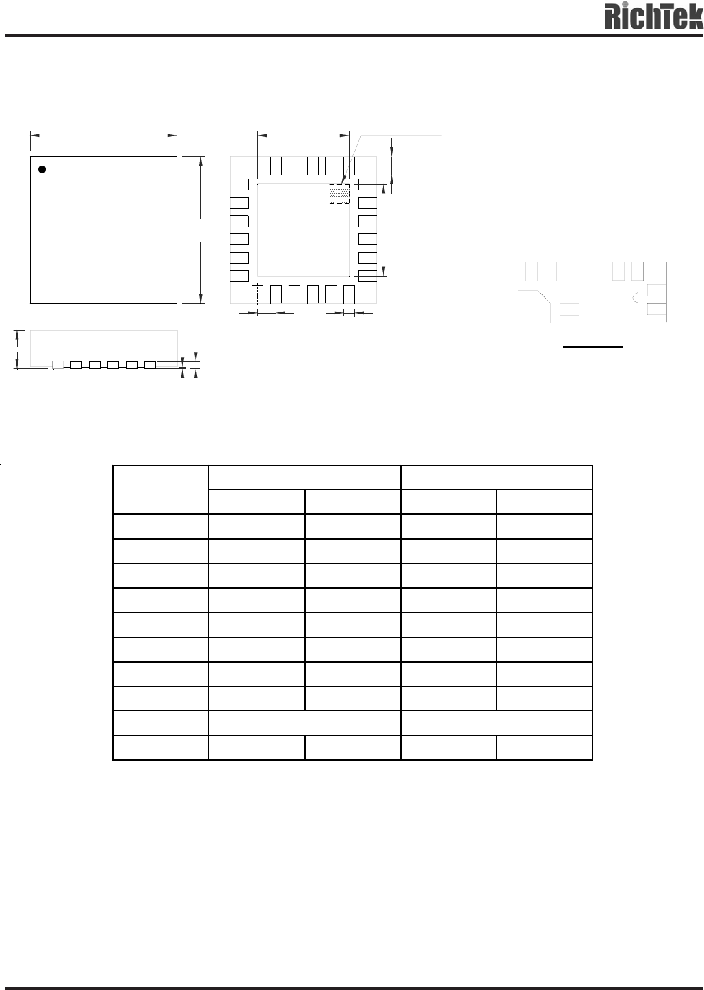
Outline Dimension
A
A1
A3
D
E
D2
E2
L
be
1
SEE DETAIL A
Dimensions In Millimeters Dimensions In Inches
Symbol Min Max Min Max
A 0.800 1.000 0.031 0.039
A1 0.000 0.050 0.000 0.002
A3 0.175 0.250 0.007 0.010
b 0.180 0.300 0.007 0.012
D 3.950 4.050 0.156 0.159
D2 2.300 2.750 0.091 0.108
E 3.950 4.050 0.156 0.159
E2 2.300 2.750 0.091 0.108
e 0.500 0.020
L 0.350 0.450
0.014 0.018
V-Type 24L QFN 4x4 Package
Note : The configuration of the Pin #1 identifier is optional,
but must be located within the zone indicated.
DETAIL A
Pin #1 ID and Tie Bar Mark Options
1
1
22