Samsung SGH X495 Service Manual. Www.s Manuals.com. Manual
User Manual: Phone Samsung SGH-X495 - Service manuals and Schematics, Disassembly / Assembly. Free.
Open the PDF directly: View PDF ![]() .
.
Page Count: 63
GSMTELEPHONE
SGH-X495
GSMTELEPHONECONTENTS
1.Specification
2.Circuit Description
3. ExplodedViews and PartsList
4. ElectricalPartsList
5.BlockDiagrams
6.PCB Diagrams
7. FlowChartofTroubleshooting

Samsung ElectronicsCo.,Ltd.June.2005
Printedin Korea.
CodeNo.:GH68-07423A
BASIC.
T
hisServiceManual isa propertyofSamsung ElectronicsCo.,Ltd.
A
nyunauthorized use ofManualcan bepunished underapplicable
I
nternationaland/ordomesticlaw.
ⓒ
SAMSUNG Proprietary-Contents may change without notice
1. Specification
ThisDocumentcan notbe used withoutSamsung'sauthorization
1-1
GSM850
Phase1
DCS1800
Phase1
PC1900
Phase1
Freq.Band[MHz]
Uplink/Downlink
824~849
869~894
1710~1785
1805~1880
1850~1910
1930~1990
ARFCNrange128~251 512~885 512~810
Tx/Rxspacing 45MHz95MHz80MHz
Mod.Bit rate/
Bit Period
270.833kbps
3.692us
270.833kbps
3.692us
270.833kbps
3.692us
TimeSlot
Period/FramePeriod
576.9us
4.615ms
576.9us
4.615ms
576.9us
4.615ms
Modulation 0.3GMSK0.3GMSK0.3GMSK
MS Power33dBm~5dBm30dBm~0dBm30dBm~0dBm
PowerClass 5pcl~19pcl0pcl~15pcl0pcl~15pcl
Sensitivity-102dBm-100dBm-100dBm
TDMAMux 8 8 8
Cell Radius35Km2Km2Km
1-1.GSMGeneralSpecification
SAMSUNG Proprietary-Contents may change without notice
ThisDocumentcan notbe used withoutSamsung'sauthorization
Specification
1-2
TXPower
control levelGSM850
5 33±2 dBm
6 31±2 dBm
7 29±2 dBm
8 27±2 dBm
9 25±2 dBm
10 23±2 dBm
11 21±2 dBm
12 19±2 dBm
13 17±2 dBm
14 15±2 dBm
15 13±2 dBm
16 11±3 dBm
17 9±3dBm
18 7±3 dBm
19 5±3 dBm
TXPower
control levelDCS1800
0 30±3 dBm
1 28±3 dBm
2 26±3 dBm
3 24±3 dBm
4 22±3 dBm
5 20±3 dBm
6 18±3 dBm
7 16±3 dBm
8 14±3 dBm
9 12±4 dBm
10 10±4 dBm
11 8±4dBm
12 6±4 dBm
13 4±4 dBm
14 2±5 dBm
15 0±5 dBm
1-2.GSMTXpowerclass
TXPower
control levelPCS1900
0 30±3 dBm
1 28±3 dBm
2 26±3 dBm
3 24±3 dBm
4 22±3 dBm
5 20±3 dBm
6 18±3 dBm
7 16±3 dBm
8 14±3 dBm
9 12±4 dBm
10 10±4 dBm
11 8±4dBm
12 6±4 dBm
13 4±4 dBm
14 2±5 dBm
15 0±5 dBm
SAMSUNG Proprietary-Contents may change without notice
2. Circuit Description
2-1
ThisDocumentcan notbe used withoutSamsung'sauthorization
2-1.SGH-X495 RFCircuitDescription
2-1-1.RX PART
-ASM(U100)→Switching Tx,Rx pathforGSM850,DCS1800,PCS1900 by logic controlling.
-ASMControlLogic(U100)→TruthTable
VC1VC2VC3
TxMode(GSM850)HL L
TxMode(DCS1800/1900)LHL
RxMode(GSM850)L L L
RxMode(DCS1800)L L L
RxMode(PCS1900)L L H
-FILTER
ToconvertElectromagneticFieldWavetoAcousticWave and then pass thespecificfrequency band.
-GSMFILTER(F101)→For filtering thefrequency band between 869 and 894 MHz
-DCS FILTER(F102)→For filtering thefrequency band between 1805 and 1880 MHz.
-PCS FILTER(F100)→For filtering thefrequency band between 1930 and 1990 MHz.
-VC-TCXO (OSC101)
Thismodulegeneratesthe26MHzreference clockto drivethelogic and RF.Afterdivision by twoareference clock of
13MHzis suppliedtotheotherpartsofthesystemthrough thepinCLKOUT.Afteradditionalprocess,thereference
clockappliestotheU100 RxIQdemodulatorand TxIQmodulator.And then,theoscillatoriscontrolled by serialdata
toselectchanneland usefast lockmodeforGPRShigh class operation.
-Transceiver (U101)
Thereceiver front-end whichamplifiestheGSM,DCSaerialsignal,convertsthe chosenchanneldowntoalowIFsignal
of100 kHz.Thefirststagesaresymmetrical lownoise amplifiers(LNAs).TheLNAsarefollowed by anIQdownmixer.
Itconsistsoftwomixersin parallelbutdriven by quadratureoutofphaseLOsignals.TheIn phase(I) and Quadrature
phase(Q) IFsignalsarelowpass filteredto provideprotection fromhigh frequency offset interferes.ThelowIFIand Q
signalsarethenfedintothe channelfilter.Thefront-end lowIFIand Qoutputsentertheintegrated bandpass channel
filterwith provision for five8 dBgainstepsinfrontofthefilter.
2-1-2.TX PART
Iand Qbaseband signalsare appliedtotheIQmodulatorthatshiftsthemodulation spectrumup tothetransmit IF.It is
designedforlowharmonicdistortion,lowcarrierleakage and high imagerejection to keepthephase erroras small as
possible.

SAMSUNG Proprietary-Contents may change without notice
CircuitDescription
2-2
ThisDocumentcan notbe used withoutSamsung'sauthorization
Themodulatorisloadedat itsIFoutputby anintegratedlowpass filterthatsuppress unwantedspurspriorto get into
thephasedetector.The clock driveisgenerated by division oftheRFLOsignalprovidedforthetransmit offsetmixer.
Baseband IQsignalfedinto offsetPLL,thisfunction isincludedinsideofU101 chip.OSC100 chip generatesmodulator
signalwhich powerlevel isabout6.5dBmand fedintoPowerAmplifier(U102).ThePAoutputpowerand power ramping
arewell controlled by AutoPowerControlcircuit.WeuseoffsetPLL belowtable.
Modulation Spectrum
200kHzoffset
30 kHzbandwidth
GSM-35dBc
DCS-35dBc
400kHzoffset
30 kHzbandwidth
GSM-66dBc
DCS-65dBc
600kHz~1.8MHzoffset
30 kHzbandwidth
GSM-75dBc
DCS-68dBc
2-2.Baseband Circuitdescription ofSGH-X495
2-2-1.PCF50601
-PowerManagement
Tenlow-dropoutregulatorsdesignedspecificallyforGSMapplicationspowertheterminaland helpensureoptimalsystem
performance and long batterylife.Aprogrammableboostconverterprovides supportfor1.8V,3.0VSIMs,while a self-
resetting,electronicallyfusedswitchsuppliespowertoexternalaccessories.Ancillarysupportfunctions,suchasRTC
module and High VoltageChargepump,Clock generator,aidinreducing both boardarea and systemcomplexity.
I2C BUSserial interface providesaccess tocontroland configuration registers.Thisinterface givesamicroprocessor full
controlofthePCF50601 and enables systemdesignerstomaximize bothstandby and talktimes.
Supervisoryfunctions.including aresetgenerator,aninputvoltagemonitor,and atemperaturesensor,supportreliable
systemdesign.Thesefunctionsworktogethertoensurepropersystembehaviorduring start-up orinthe eventofafault
condition(lowmicroprocessorvoltage,insufficientbatteryenergy,orexcessivedietemperature).
-BacklightBrightness Modulator
TheBacklightBrightness Modulator(BBM)containsaprogrammablePulse-widthmodulator (PWM)and FET
tomodulatetheintensity ofaseriesofLED?sortocontrolaDC/DCconverterthatdrivesLCDbacklight.
Thisphone(SGH-X495)usePWMcontrol tocontrast thebacklightbrightness.
-ClockGenerator
TheClockGenerator(CG)generatesall clocksforinternaland externalusage.The32768 Hzcrystal
oscillatorprovidesanaccuratelowclockfrequencyfor thePCF50601 andothercircuitry.

SAMSUNG Proprietary-Contents may change without notice
CircuitDescription
2-3
ThisDocumentcan notbe used withoutSamsung'sauthorization
2-2-2.LCD Connector
LCDisconsisted ofmainLCD(color65K UFBLCD)and sub LCD(B/WLCD).
ChipselectsignalsLCD_MAIN_CSand LCD_SUB_CS,canenableEachLCD.BACKLIGHTsignalenableswhiteLED
ofmainLCD."LCD_RESET"signal initiatestheresetprocess oftheLCD.
16-bit datalines(HD(0)~HD(15)) transfersdata and commandstoLCD.Data and commandsuse"HA(1)"signal.If this
signal islow,inputstoLCDare commands.If it ishigh,inputstoLCDaredata.
ThesignalwhichinformsthestateofLCDiswhetherinputoroutput,isrequired.But inthis system,thereisno input
statefromLCD.So only"HA(1)"signal isusedtoindicatewritedataorcommand toLCD.PowersignalsforLCDare
"VBATand "VDD3".
"SPK_P"and "SPK_N"areusedforaudiospeakercontaining voice ormelody.And "VDD_VIB"fromPCF50601
enablesthemotor.
2-2-3.Key
Thisisconsisted ofkeyinterface pinsamong OM6359,KBIO(0:7).Thesesignalscomposethematrix.Result ofmatrix
informsthekeystatusto keyinterface intheOM6359.Poweron/off keyis separatedfromthematrix.So poweron/off
signal isconnectedwithPCF50601 toenablePCF50601.TwelvekeyLEDsareusethe"VDD_KEY"as supply voltage.
"FLIP"informsthestatusof folder (open orclosed)totheOM6359.Thisusesthehall effectIC,A321ELH-SAMSUNG.
AmagnetundermainLCDenablesA321ELH-SAMSUNG.
2-2-4.EMIESDFilter
This systemusestheEMIESDfilter,EMIF09 to protectnoisefromIFCONNECTORpart.
2-2-5. IFconnetor
It is18-pinconnector.Theyaredesignedto useVBAT,V_EXT_CHARGE,TXD0,RXD0,RTS0,CTS0,JIG_REC,
CHARGER_OK,RXD1,TXD1,AUX_MIC,AUX_SPKand GND.Theyconnectedto powersupplyIC,microprocessor
and signalprocessor IC.
2-2-6.BatteryCharge Management
Acompleteconstant-current/constant-voltagelinearchargerisused forsinglecell lithium-ionbatteries.
IfTAconnected tophone,"+DCVOLT"enablechargerICandsupplycurrent tobattery.
Whenfaultconditioncaused,"CHG_ON"signal levelchangelowtohighandchargerICstopcharging
process.
2-2-7.Audio
EARP_Pand EARP_NfromOM6359 are connectedtothemainspeaker.MIC_Pand MIC_Nare connectedtothemain
MIC.YMU788 isasynthesizerLSI formobilephones.It isaLSIasaninput/outputdevice forsound sources,whichis
themobilephones,suchasMP3,AAC,etc,inaddition toringing-melodies.
Asasynthesis,YMU788 isequipped 32 voiceswith different tones.Since thedevice iscapableofsimultaneously
generating up tosynchronouswiththeplay oftheFMsynthesizer,various sampled voicescan beusedas sound effects.
Since theplay dataofYMU788 areinterpretedatanytimethrough FIFO,thelength ofthedata(playing period)isnot
limited,sothedevice canflexiblysupportapplication suchasincoming call melody musicdistribution service.

SAMSUNG Proprietary-Contents may change without notice
CircuitDescription
2-4
ThisDocumentcan notbe used withoutSamsung'sauthorization
Thehardwaresequencerbuilt inthisdevice allowsplaying ofthe complexmusicwithoutgiving excessiveloadtothe
CPUoftheportabletelephones.
Forthepurposeofenabling YMU788 to demonstrateitsfull capabilities,Yamahapurposeto use"SMAF:Syntheticmusic
MobileApplication Format"asadatadistribution format that iscompatiblewithmultimedia.Since theSMAFtakesa
structurethatsetsimportance on thesynchronization betweensound and images,variouscontentscan bewrittenintoit
including incoming call melody withwordsthatcan beusedfortraining karaoke,and commercialchannel thatcombines
texts,imagesand sounds,and others.ThehardwaresequencerofYMU788 directlyinterpretsand playsblocksrelevant to
synthesis(playing music and reproducing ADPCMwithFMsynthesizer) thatareincludedin datadistributedinSMAF.
2-2-8.Memory
SignalsintheOM6359 enabletwomemories.They usetwo volt supply voltage,VDD3inthePCF50601 &VDD_1.9V
withaLDO.This systemusesIntel'smemory,RD38F3050LOZTQ0.It isconsisted of128MbitsflashNORmemoryand
64MbitsSRAM.Ithas16 bit dataline,HD[0~15]whichisconnectedtoOM6359.Ithas26 bit address lines,
HA[1~26].NCSFLASH&NCSRAMsignalsare chipselect.Writing process,HWR_Nislowand it enableswriting
process toflashmemoryand SRAM.During reading process,HRD_Nislowand it enablesreading process toflash
memoryand SRAM.Reading orwriting procedureisprocessedafterHWR_NorHRD_Nisenabled.
2-2-9. OM6359
OM6359 isconsisted ofARMcore and DSP core.Ithas8x1Kwordon-chip program/dataRAM,55 Kwords
on-chip programROMintheDSP.Ithas4K*32bitsROMand 2K*32bitsRAMintheARMcore.DSP isconsisted
ofKBS,JTAG,EMIand UART.ARMcoreisconsisted ofEMI,PIC(ProgrammableInterruptController),
reset/power/clock unit,DMAcontroller,TIC(TestInterface Controller),peripheralbridge,PPI,SSI(SynchronousSerial
Interface),ACC(Asynchronouscommunicationscontrollers),timer,ADC,RTC(Real-TimeClock)and keyboardinterface.
KBIO(0:7),address linesofDSP core and HD[0~15].HA[1~26],address linesofARMcore and HD[0~15],datalinesof
ARMcore are connectedtomemory,YMU788.
NCSRAM,NCSFLASHintheARMcore are connectedtoeachmemory.HWR_Nand HRD_Ncontrol theprocess of
memory.ExternalIRQ(InterruptReQuest)signalsfromeach units,suchas,PMUneedthe compatibleprocess.
KBIO[0~7] receivethestatusfromkeyand RXD0/TXD0areusedforthe communication using datalink
cable(DEBUG_DTR/RTS/TXD/RXD/CTS/DSR).
Ithas JTAG controlpins(TDI/TDO/TCK) forARMcore and DSP core.Itreceives13MHz clockinCKIpinfrom
externalTCXO.ADC(Analog toDigitalConvertor) partreceivesthestatusoftemperature,batterytype and battery voltage.
2-2-10.TOH2600DGI4KRA(26MHz)
This systemusesthe26MHzTCXO,TOH2600DGI4KRA,SEM.AFCcontrolsignalfromOM6359 controlsfrequency
from26MHzx-tal.The clock outputfrequency ofUAA3536 is13MHz.ThisclockisconnectedtoOM6359,YMU788.
SAMSUNG Proprietary-Contents may change without notice
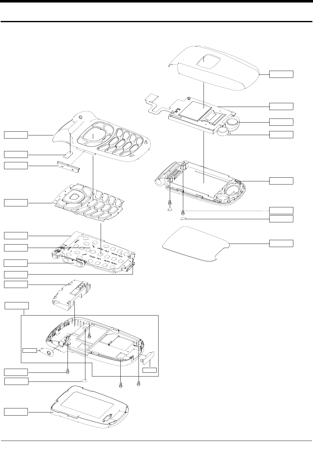
3.Exploded View and Parts List
3-1
ThisDocumentcan notbe used withoutSamsung'sauthorization
3-1. Exploded View
QIF01
QFR01
QSC14
QMP01
QKP01
QVO01
QME01
QAN02
QRE01
QCR11
QRF03
QMI01
QBA01
QFU01
QSP01
QMO01
QLC01
QFL01
QMW02
QSC01
QCR17
QRF01
QVK01
SAMSUNG Proprietary-Contents may change without notice
Exploded view and PartList
3-2
ThisDocumentcan notbe used withoutSamsung'sauthorization
Location NO. Description SEC CODE
QAN02
ㅤ
INTENNA-SGHX495;IAPT0GDP4020HA,SGH-X GH42-00574A
QBA01
ㅤ
BATTERY-1000MAH,SIL,MAIN;BST471ASA,S GH43-01788A
QCR11
ㅤ
SCREW-MACHINE;PH,+,M1.7,L4,ZPC(BLK), 6001-001654
QCR17
ㅤ
SCREW-MACHINE;CH,+,M1.7,L5,ZPC(BLK), 6001-001639
QFL01
ㅤ
MEC-FOLDER LOWER;SGH-X495,EU,-,-,-,- GH75-06454A
QFR01
ㅤ
MEC-FRONT COVER;SGH-X495,EU,-,-,-,-, GH75-06966B
QFU01
ㅤ
MEC-FOLDER UPPER;SGH-X495,T-MOBILE,- GH75-06471B
QKP01
ㅤ
MEC-KEYPAD;SGH-X495,T-MOBILE,-,-,-,- GH75-06617A
QLC01
ㅤ
LCD-SGH-X497 MODULE;UG-12R168-C,SGH- GH07-00763A
QME01
ㅤ
UNIT-METAL DOME;SGH-X497,SSM5017P850 GH59-02046A
QMI01
ㅤ
MICROPHONE-ASSY-SGHX497;2,130~500uA, GH30-00198A
QMO01
ㅤ
MOTOR DC-SGHZ130;DMJBRK20C,SGH-Z130, GH31-00154D
QMP01
ㅤ
PBA MAIN-SGHX495;SGH-X495,TMB,USA,PB GH92-02214A
QMW02
ㅤ
PCT-WINDOW MAIN;SGH-X495,ACRYLIC SHE GH72-19918B
QRF01
ㅤ
MPR-RF SHEET;SGH-X495,PC SHEET 0.3T, GH74-14435C
QSC01
ㅤ
MPR-SCREW SHEET;SGH-X495,PC SHEET 0. GH74-13610B
QSC14
ㅤ
MPR-TAPE FRONT FPC;SGH-E330,3M 1352 GH74-08876A
QSP01
ㅤ
SPEAKER;0.5W,8ohm,89dB,800Hz,17X13mm 3001-001779
QVK01
ㅤ
UNIT-VOLUME KEY;SGH-X497,SSV5017P860 GH59-02053A
QVO01
ㅤ
MEC-VOLUME KEY;SGH-X495,T-MOBILE,-,- GH75-07274B
QRE01
ㅤ
MEC-REAR COVER;SGH-X495,USA,-,-,-,-, GH75-06959B
ㅤ
QRF03 PMO-EAR COVER;SGH-X495,PC W91543+ELA GH72-23535B
ㅤ
QIF01 PMO-IF COVER;SGH-X495,PC G73797+ELAS GH72-23556B
ㅤ
QMI03 RMO-RUBBER MIC REAR;SGH-X497,CR RUBB GH73-04847A
3-2. Parts List
SAMSUNG Proprietary-Contents may change without notice
Exploded view and PartList
3-3
ThisDocumentcan notbe used withoutSamsung'sauthorization
Description SEC CODE
BAG PE;LDPE,T0.05,W120,L300,TRP,-,- 6902-000296
BAG PE;LDPE,T0.05,W80,L140,TRP,-,-1- 6902-000297
BAG PP;PP,T0.05,W140,L300,TRP,-,-1-P 6902-000377
LCD-SGHX497 MAIN;UG-12R168-B,SGH-X49 GH07-00707A
LCD-SGHX497 SUB;UG-09B125-A,SGH-X497 GH07-00708A
ADAPTOR-SGHR225 TAD;TAD037JBE,SGH-R2 GH44-00184G
UNIT-AWB SIM CARD;SGH-X105,87444394, GH59-00943A
UNIT-EARPHONE;SGH-X475,AEP131SLE,-,E GH59-01700A
LABEL(R)-WATER SOAK T_MOBILE;COMM,-, GH68-05914A
LABEL(R)-T_MOBILE GUIDE;SGH-X475,-,M GH68-06581A
LABEL(R)-MAIN(TMB);SGH-X495,TMB,POLY GH68-06971A
MANUAL-USER;SGH-X495,TMB,ENGLISH,USA GH68-06976A
MANUAL-USER;SGH-X495,TMB,SPANISH,USA GH68-06977A
MANUAL-AGC GUIDE;SGH-X495,TMB,ENGLIS GH68-06978A
MANUAL-ACTIVATION CARD;SGH-X495,TMB, GH68-07399A
LABEL-DR;SGH-X495,-,PE,T1.5,45,11,SI GH68-07547A
LABEL-RF;SGH-X495,-,ART,T0.2,42,38,S GH68-07548A
LABEL(R)-UNIT IMEI(TMB);SGH-X495,TMB GH68-07687A
CUSHION-SGHX495(UNIT CLAM);SGH-X495, GH69-03058A
CUSHION-SGHX495(UP CLAM);SGH-X495,HI GH69-03059A
CUSHION-SGHX495(LOW CLAM);SGH-X495,H GH69-03060A
BOX(P)-SGHX495(IN/BOX_WALL);SGH-X495 GH69-03076B
BOX(P)-SGHX495(CLAM_MASTER);SGH-X495 GH69-03130A
BOX(P)-SGHX495(PATTION);SGH-X495,SC3 GH69-03132A
PMO-BATT LOCKER;SGH-X495,PC K2261,BL GH72-19954B
PCT-WINDOW SUB;SGH-X495,ACRYIC SHEET GH72-19964A
PMO-STOPPER;SGH-X495,POLY URETHANE,W GH72-21517B
RMO-RUBBER TOP LCD A;SGH-X495,CR RUB GH73-04923A
RMO-RUBBER TOP LCD B;SGH-X495,CR RUB GH73-04924A
MPR-BOHO VINYL SUB(S-R);SGH-X495,STA GH74-03429B
MPR-BOHO VINYL REAR;SGH-S342i,3M 418 GH74-12905A
MPR-TAPE WINDOW SUB;SGH-X495,TESA #4 GH74-13223A
MPR-BOHO VINYL IF;SGH-E720,#950,85X1 GH74-13606A
MPR-TAPE WINDOW MAIN;SGH-X495,3M 949 GH74-13608A
MPR-BOHO VINYL MAIN;SGH-X495,3M 4187 GH74-14431A
MPR-BOHO VINYL MAIN(S);SGH-X497,SP-1 GH74-14431B
MPR-BOHO VINYL SUB;SGH-X495,ST-5555, GH74-14432A
MPR-TAPE EL;SPH-B1200,3M 851,5X3.5XT GH74-14881A
MPR-TAPE PBA EMI;SGH-X495,GOLD PU T0 GH74-15484A
MPR-BOHO VINYL M/TMB(S);SGH-X495,STA GH74-15517B
MPR-SPONGE MOTOR;SGH-X495,SRS,D8XT0. GH74-15610A
MPR-SPONGE PBA;SGH-X495,SRS,38X64XT5 GH74-15911A
MPR-TAPE PBA A;SGH-X495,3M851,3X2XT0 GH74-16066A
MPR-BOHO VINYL SUB;SGH-X495,ST-5555, GH74-17302A
AS-LCD PCB SVC;SGH-X497,LJ96-02137A, GH81-01219A
A/S-LCD FPCB SVC;SGH-X497,POLYMIDE,2 GH81-01956A
PAA ETC-MANUAL;SGH-X495,TMB,USA,MANU GH99-10352A
SAMSUNG Proprietary-Contents may change without notice
Exploded view and PartList
3-4
ThisDocumentcan notbe used withoutSamsung'sauthorization
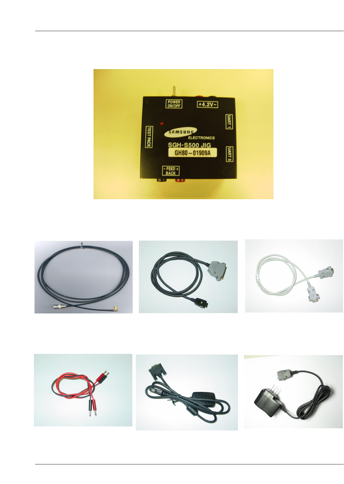
3-3. Test Jig (GH80-01909A)
3-3-1. RF Test Cable
(GH39-00283A)
3-3-2. Test Cable
(GH39-00217A)
3-3-3. Serial Cable
3-3-4. Power Supply Cable 3-3-5. DATA CABLE
(GH39-00219A)
3-3-6. TA
(GH44-00184G)
SAMSUNG Proprietary-Contents may change without notice
4. Electrical Parts List
4-1
This Document can not be used without Samsung's authorization
Design LOC Description SEC CODE
BAT300 BATTERY 4302-001180
C101 C-CERAMIC,CHIP 2203-000278
C102 C-CERAMIC,CHIP 2203-000812
C103 C-CERAMIC,CHIP 2203-000854
C104 C-CERAMIC,CHIP 2203-000854
C105 C-CERAMIC,CHIP 2203-000278
C106 C-CERAMIC,CHIP 2203-000278
C107 C-CERAMIC,CHIP 2203-000854
C108 C-CERAMIC,CHIP 2203-005057
C109 C-CERAMIC,CHIP 2203-005482
C110 C-CERAMIC,CHIP 2203-005057
C111 C-CERAMIC,CHIP 2203-005482
C112 C-CERAMIC,CHIP 2203-000233
C113 C-CERAMIC,CHIP 2203-000233
C114 C-CERAMIC,CHIP 2203-005482
C115 C-CERAMIC,CHIP 2203-005057
C116 C-CERAMIC,CHIP 2203-005138
C117 C-CERAMIC,CHIP 2203-001383
C118 C-CERAMIC,CHIP 2203-000359
C119 C-CERAMIC,CHIP 2203-000696
C120 C-CERAMIC,CHIP 2203-000836
C121 C-CERAMIC,CHIP 2203-001101
C122 C-CERAMIC,CHIP 2203-005482
C123 C-CERAMIC,CHIP 2203-005057
C124 C-CERAMIC,CHIP 2203-006053
C125 C-CERAMIC,CHIP 2203-000438
C126 C-CERAMIC,CHIP 2203-000233
C127 C-TA,CHIP 2404-001239
C128 C-CERAMIC,CHIP 2203-006141
C129 C-CERAMIC,CHIP 2203-000438
C130 C-CERAMIC,CHIP 2203-006190
C132 C-CERAMIC,CHIP 2203-005503
C133 C-CERAMIC,CHIP 2203-000311
C134 C-CERAMIC,CHIP 2203-000233
C135 C-CERAMIC,CHIP 2203-000254
C136 C-CERAMIC,CHIP 2203-001153
C137 C-CERAMIC,CHIP 2203-000550

SAMSUNG Proprietary-Contents may change without notice
Electrical Parts List
4-2
This Document can not be used without Samsung's authorization
Design LOC Description SEC CODE
C138 C-CERAMIC,CHIP 2203-006137
C139 C-CERAMIC,CHIP 2203-005482
C140 C-CERAMIC,CHIP 2203-000679
C141 C-CERAMIC,CHIP 2203-005482
C142 C-CERAMIC,CHIP 2203-005057
C143 C-CERAMIC,CHIP 2203-000233
C144 C-CERAMIC,CHIP 2203-000254
C145 C-CERAMIC,CHIP 2203-000438
C146 C-CERAMIC,CHIP 2203-000438
C147 C-CERAMIC,CHIP 2203-000438
C152 C-CERAMIC,CHIP 2203-000278
C153 C-CERAMIC,CHIP 2203-000278
C154 C-CERAMIC,CHIP 2203-000995
C155 C-CERAMIC,CHIP 2203-000995
C156 C-CERAMIC,CHIP 2203-000438
C157 C-CERAMIC,CHIP 2203-001239
C158 C-CERAMIC,CHIP 2203-001239
C200 C-CERAMIC,CHIP 2203-005061
C203 C-CERAMIC,CHIP 2203-005061
C204 C-CERAMIC,CHIP 2203-000254
C206 C-CERAMIC,CHIP 2203-005061
C207 C-CERAMIC,CHIP 2203-000254
C208 C-CERAMIC,CHIP 2203-000254
C210 C-CERAMIC,CHIP 2203-006423
C212 C-CERAMIC,CHIP 2203-005061
C213 C-CERAMIC,CHIP 2203-005482
C214 C-CERAMIC,CHIP 2203-000854
C215 C-CERAMIC,CHIP 2203-006423
C216 C-CERAMIC,CHIP 2203-000854
C218 C-CERAMIC,CHIP 2203-005061
C219 C-CERAMIC,CHIP 2203-005482
C220 C-CERAMIC,CHIP 2203-000254
C221 C-CERAMIC,CHIP 2203-006423
C222 C-CERAMIC,CHIP 2203-006423
C223 C-CERAMIC,CHIP 2203-005482
C224 C-CERAMIC,CHIP 2203-000438
C225 C-CERAMIC,CHIP 2203-005482

SAMSUNG Proprietary-Contents may change without notice
Electrical Parts List
4-3
This Document can not be used without Samsung's authorization
Design LOC Description SEC CODE
C300 C-CERAMIC,CHIP 2203-005482
C301 C-CERAMIC,CHIP 2203-006105
C302 C-CERAMIC,CHIP 2203-005482
C304 C-TA,CHIP 2404-001394
C305 C-CERAMIC,CHIP 2203-005482
C306 C-CERAMIC,CHIP 2203-005482
C307 C-TA,CHIP 2404-001374
C308 C-CERAMIC,CHIP 2203-006257
C309 C-CERAMIC,CHIP 2203-005482
C310 C-CERAMIC,CHIP 2203-006208
C311 C-TA,CHIP 2404-001225
C312 C-CERAMIC,CHIP 2203-005395
C313 C-CERAMIC,CHIP 2203-000386
C314 C-CERAMIC,CHIP 2203-005482
C315 C-CERAMIC,CHIP 2203-006257
C316 C-CERAMIC,CHIP 2203-000628
C317 C-CERAMIC,CHIP 2203-006562
C318 C-CERAMIC,CHIP 2203-000628
C319 C-CERAMIC,CHIP 2203-006562
C320 C-CERAMIC,CHIP 2203-006053
C321 C-CERAMIC,CHIP 2203-000885
C322 C-CERAMIC,CHIP 2203-006208
C323 C-CERAMIC,CHIP 2203-006324
C324 C-CERAMIC,CHIP 2203-000812
C325 C-CERAMIC,CHIP 2203-005065
C326 C-TA,CHIP 2404-001225
C327 C-TA,CHIP 2404-001225
C328 C-CERAMIC,CHIP 2203-005482
C329 C-CERAMIC,CHIP 2203-005482
C330 C-CERAMIC,CHIP 2203-005482
C332 C-CERAMIC,CHIP 2203-006257
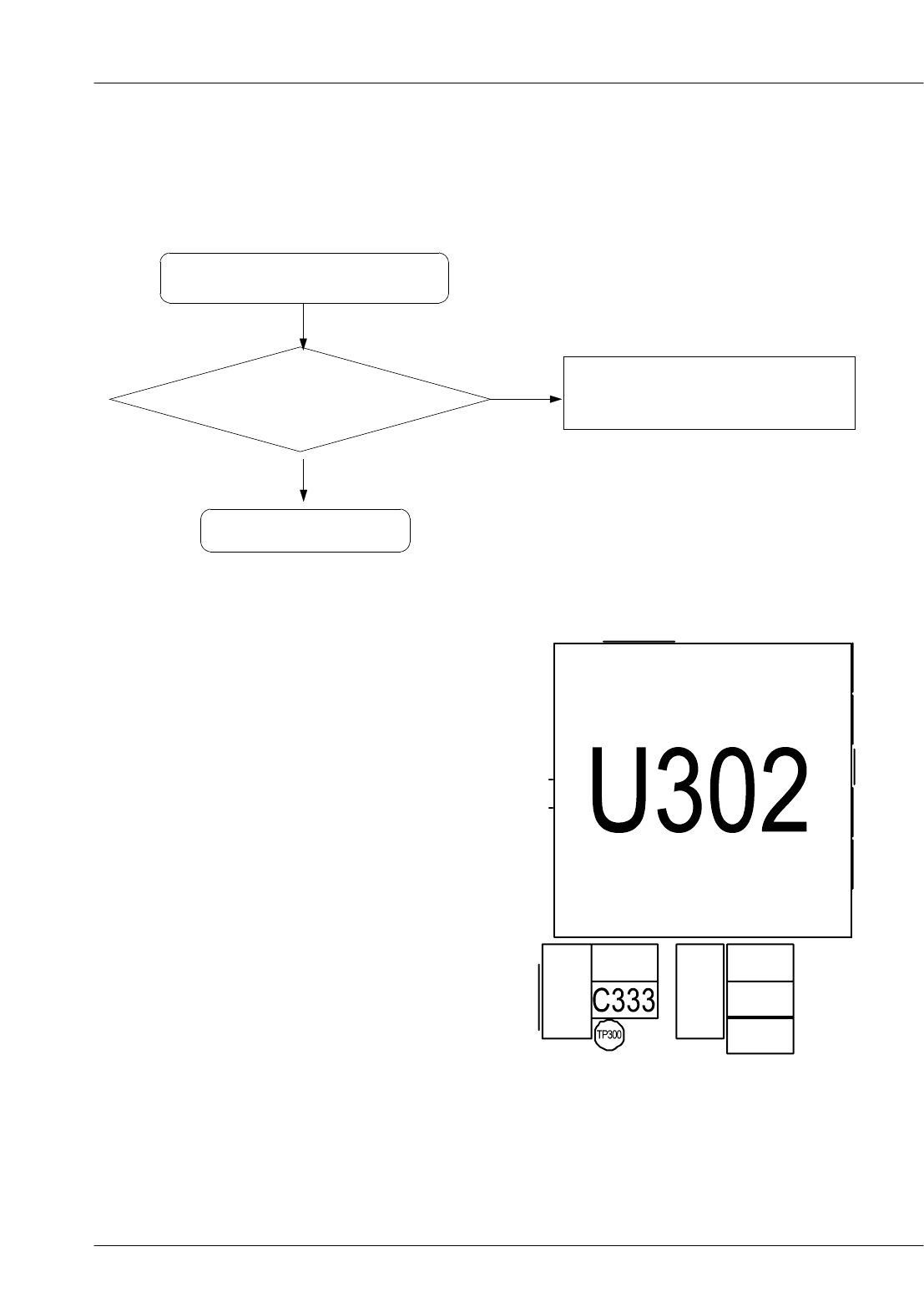
C333 C-CERAMIC,CHIP 2203-006562
C334 C-CERAMIC,CHIP 2203-006208
C335 C-CERAMIC,CHIP 2203-006208
C336 C-CERAMIC,CHIP 2203-000679
C337 C-CERAMIC,CHIP 2203-006053
C338 C-CERAMIC,CHIP 2203-006208

SAMSUNG Proprietary-Contents may change without notice
Electrical Parts List
4-4
This Document can not be used without Samsung's authorization
Design LOC Description SEC CODE
C339 C-CERAMIC,CHIP 2203-006208
C340 C-CERAMIC,CHIP 2203-006053
C400 C-TA,CHIP 2404-001348
C401 C-CERAMIC,CHIP 2203-000995
C402 C-CERAMIC,CHIP 2203-005482
C403 C-CERAMIC,CHIP 2203-005061
C404 C-CERAMIC,CHIP 2203-006562
C406 C-CERAMIC,CHIP 2203-000278
C407 C-CERAMIC,CHIP 2203-000679
C408 C-CERAMIC,CHIP 2203-005482
C409 C-CERAMIC,CHIP 2203-005061
C410 C-CERAMIC,CHIP 2203-005736
C411 C-CERAMIC,CHIP 2203-000679
C412 C-CERAMIC,CHIP 2203-005482
C413 C-CERAMIC,CHIP 2203-000679
C415 C-CERAMIC,CHIP 2203-000489
C416 C-CERAMIC,CHIP 2203-000679
C418 C-CERAMIC,CHIP 2203-000278
C419 C-CERAMIC,CHIP 2203-006423
C420 C-CERAMIC,CHIP 2203-005736
C421 C-CERAMIC,CHIP 2203-000885
C422 C-CERAMIC,CHIP 2203-000254
C423 C-CERAMIC,CHIP 2203-001153
C424 C-CERAMIC,CHIP 2203-005483
C425 C-CERAMIC,CHIP 2203-005483
C426 C-CERAMIC,CHIP 2203-006562
C429 C-CERAMIC,CHIP 2203-000995
C430 C-CERAMIC,CHIP 2203-000995
C433 C-CERAMIC,CHIP 2203-006562
C435 C-CERAMIC,CHIP 2203-000995
C437 C-CERAMIC,CHIP 2203-006053
C438 C-CERAMIC,CHIP 2203-005482
C439 C-TA,CHIP 2404-001352
C501 C-CERAMIC,CHIP 2203-002443
C502 C-CERAMIC,CHIP 2203-005482
C503 C-CERAMIC,CHIP 2203-005482
C504 C-CERAMIC,CHIP 2203-000278

SAMSUNG Proprietary-Contents may change without notice
Electrical Parts List
4-5
This Document can not be used without Samsung's authorization
Design LOC Description SEC CODE
C505 C-CERAMIC,CHIP 2203-000679
C507 C-CERAMIC,CHIP 2203-000995
C508 C-CERAMIC,CHIP 2203-000278
C509 C-CERAMIC,CHIP 2203-000995
C510 C-CERAMIC,CHIP 2203-000995
C511 C-CERAMIC,CHIP 2203-000278
C513 C-CERAMIC,CHIP 2203-006562
C514 C-CERAMIC,CHIP 2203-006562
C515 C-CERAMIC,CHIP 2203-006562
CN300 CONNECTOR-CARD EDGE 3709-001355
CN502 CONNECTOR-SOCKET 3710-001611
CN503 CONNECTOR-HEADER 3711-005783
CON101 CONNECTOR-COAXIAL 3705-001358
EAR400 JACK-PHONE 3722-002067
F100 FILTER-SAW 2904-001571
F101 FILTER-SAW 2904-001580
F102 FILTER-SAW 2904-001570
HEA1 CONNECTOR-HEADER 3711-005728
L101 INDUCTOR-SMD 2703-002207
L102 INDUCTOR-SMD 2703-002199
L103 INDUCTOR-SMD 2703-002207
L104 INDUCTOR-SMD 2703-002203
L105 INDUCTOR-SMD 2703-002700
L106 INDUCTOR-SMD 2703-001726
L107 INDUCTOR-SMD 2703-002308
L108 INDUCTOR-SMD 2703-002700
L109 INDUCTOR-SMD 2703-002308
L110 INDUCTOR-SMD 2703-002308
L111 INDUCTOR-SMD 2703-002199
L112 INDUCTOR-SMD 2703-002368
L113 INDUCTOR-SMD 2703-002201
L114 INDUCTOR-SMD 2703-002368
L115 INDUCTOR-SMD 2703-002203
L116 INDUCTOR-SMD 2703-002368
L117 INDUCTOR-SMD 2703-001708
L300 CORE-FERRITE BEAD 3301-001105
L400 CORE-FERRITE BEAD 3301-001362

SAMSUNG Proprietary-Contents may change without notice
Electrical Parts List
4-6
This Document can not be used without Samsung's authorization
Design LOC Description SEC CODE
L401 CORE-FERRITE BEAD 3301-001362
L402 CORE-FERRITE BEAD 3301-001105
L403 CORE-FERRITE BEAD 3301-001105
L501 CORE-FERRITE BEAD 3301-001438
LED501 LED 0601-001790
LED502 LED 0601-001790
LED503 LED 0601-001790
LED504 LED 0601-001790
LED505 LED 0601-001790
LED506 LED 0601-001790
LED507 LED 0601-001790
LED508 LED 0601-001790
LED509 LED 0601-001790
LED510 LED 0601-001790
LED511 LED 0601-001790
LED512 LED 0601-001790
OSC100 OSCILLATOR-VCO 2806-001326
OSC101 OSCILLATOR-VCTCXO 2809-001281
Q100 TR-DIGITAL 0504-001151
R101 R-CHIP 2007-000162
R102 R-CHIP 2007-000162
R103 R-CHIP 2007-000162
R104 R-CHIP 2007-007148
R105 R-CHIP 2007-000141
R106 R-CHIP 2007-007528
R107 R-CHIP 2007-001288
R108 R-CHIP 2007-000171
R109 R-CHIP 2007-001329
R110 R-CHIP 2007-000144
R111 R-CHIP 2007-001308
R112 R-CHIP 2007-001308
R113 R-CHIP 2007-000566
R114 R-CHIP 2007-000148
R115 R-CHIP 2007-001288
R116 R-CHIP 2007-007311
R117 R-CHIP 2007-000566
R118 R-CHIP 2007-007699

SAMSUNG Proprietary-Contents may change without notice
Electrical Parts List
4-7
This Document can not be used without Samsung's authorization
Design LOC Description SEC CODE
R119 R-CHIP 2007-007699
R120 R-CHIP 2007-001308
R121 R-CHIP 2007-001308
R122 R-CHIP 2007-000171
R123 R-CHIP 2007-000171
R125 R-CHIP 2007-008672
R126 R-CHIP 2007-001308
R127 R-CHIP 2007-000142
R128 R-CHIP 2007-000148
R129 R-CHIP 2007-000138
R130 R-CHIP 2007-008213
R131 R-CHIP 2007-008213
R132 R-CHIP 2007-008213
R133 R-CHIP 2007-008213
R134 R-CHIP 2007-000140
R135 R-CHIP 2007-000140
R136 R-CHIP 2007-000171
R200 R-CHIP 2007-000174
R201 R-CHIP 2007-008055
R204 R-CHIP 2007-000162
R205 R-CHIP 2007-008055
R206 R-CHIP 2007-008055
R207 R-CHIP 2007-008055
R208 R-CHIP 2007-008052
R209 R-CHIP 2007-008516
R210 R-CHIP 2007-008055
R211 R-CHIP 2007-007107
R212 R-CHIP 2007-007142
R213 R-CHIP 2007-007001
R214 R-CHIP 2007-007142
R215 R-CHIP 2007-001284
R216 R-CHIP 2007-000148
R217 R-CHIP 2007-001284
R218 R-CHIP 2007-000162
R219 R-CHIP 2007-000162
R220 R-CHIP 2007-007107
R221 R-CHIP 2007-007001

SAMSUNG Proprietary-Contents may change without notice
Electrical Parts List
4-8
This Document can not be used without Samsung's authorization
Design LOC Description SEC CODE
R222 R-CHIP 2007-000171
R223 R-CHIP 2007-008588
R224 R-CHIP 2007-008588
R225 R-CHIP 2007-008542
R227 R-CHIP 2007-008542
R228 R-CHIP 2007-008542
R300 R-CHIP 2007-000157
R301 R-CHIP 2007-000148
R302 R-CHIP 2007-007573
R303 R-CHIP 2007-007334
R304 R-CHIP 2007-008117
R305 R-CHIP 2007-000151
R306 R-CHIP 2007-007100
R400 R-CHIP 2007-002796
R401 R-CHIP 2007-000140
R402 R-CHIP 2007-000148
R403 R-CHIP 2007-008054
R404 R-CHIP 2007-000140
R405 R-CHIP 2007-008542
R406 R-CHIP 2007-008055
R407 R-CHIP 2007-002796
R408 R-CHIP 2007-008055
R409 R-CHIP 2007-007334
R410 R-CHIP 2007-001313
R411 R-CHIP 2007-008542
R412 R-CHIP 2007-007334
R413 R-CHIP 2007-007589
R414 R-CHIP 2007-007138
R415 R-CHIP 2007-007981
R416 R-CHIP 2007-007529
R417 R-CHIP 2007-007489
R418 R-CHIP 2007-000138
R422 R-CHIP 2007-000138
R424 R-CHIP 2007-008542
R500 R-CHIP 2007-000162
R501 R-CHIP 2007-008055
R502 R-CHIP 2007-008531

SAMSUNG Proprietary-Contents may change without notice
Electrical Parts List
4-9
This Document can not be used without Samsung's authorization
Design LOC Description SEC CODE
R503 R-CHIP 2007-008531
R504 R-CHIP 2007-008531
R505 R-CHIP 2007-008531
R506 R-CHIP 2007-008531
R507 R-CHIP 2007-000162
R508 R-CHIP 2007-008531
R510 R-CHIP 2007-001301
R511 R-CHIP 2007-001301
R512 R-CHIP 2007-001301
R513 R-CHIP 2007-001301
R514 R-CHIP 2007-001301
R515 R-CHIP 2007-001301
R516 R-CHIP 2007-001301
R517 R-CHIP 2007-001301
R518 R-CHIP 2007-001301
R519 R-CHIP 2007-001301
R520 R-CHIP 2007-001301
R521 R-CHIP 2007-001301
R522 R-CHIP 2007-008055
R529 R-CHIP 2007-008055
R530 R-CHIP 2007-008055
R531 R-CHIP 2007-009084
R532 R-CHIP 2007-009084
R533 R-CHIP 2007-009084
R534 R-CHIP 2007-009084
R535 R-CHIP 2007-009084
R536 R-CHIP 2007-009084
R537 R-CHIP 2007-009084
R538 R-CHIP 2007-009084
R539 R-CHIP 2007-009084
R540 R-CHIP 2007-009084
R541 R-CHIP 2007-009084
R542 R-CHIP 2007-009084
R543 R-CHIP 2007-009084
R544 R-CHIP 2007-009084
R545 R-CHIP 2007-009084
R546 R-CHIP 2007-009084

SAMSUNG Proprietary-Contents may change without notice
Electrical Parts List
4-10
This Document can not be used without Samsung's authorization
Design LOC Description SEC CODE
R547 R-CHIP 2007-000162
SW500 IC 1009-001010
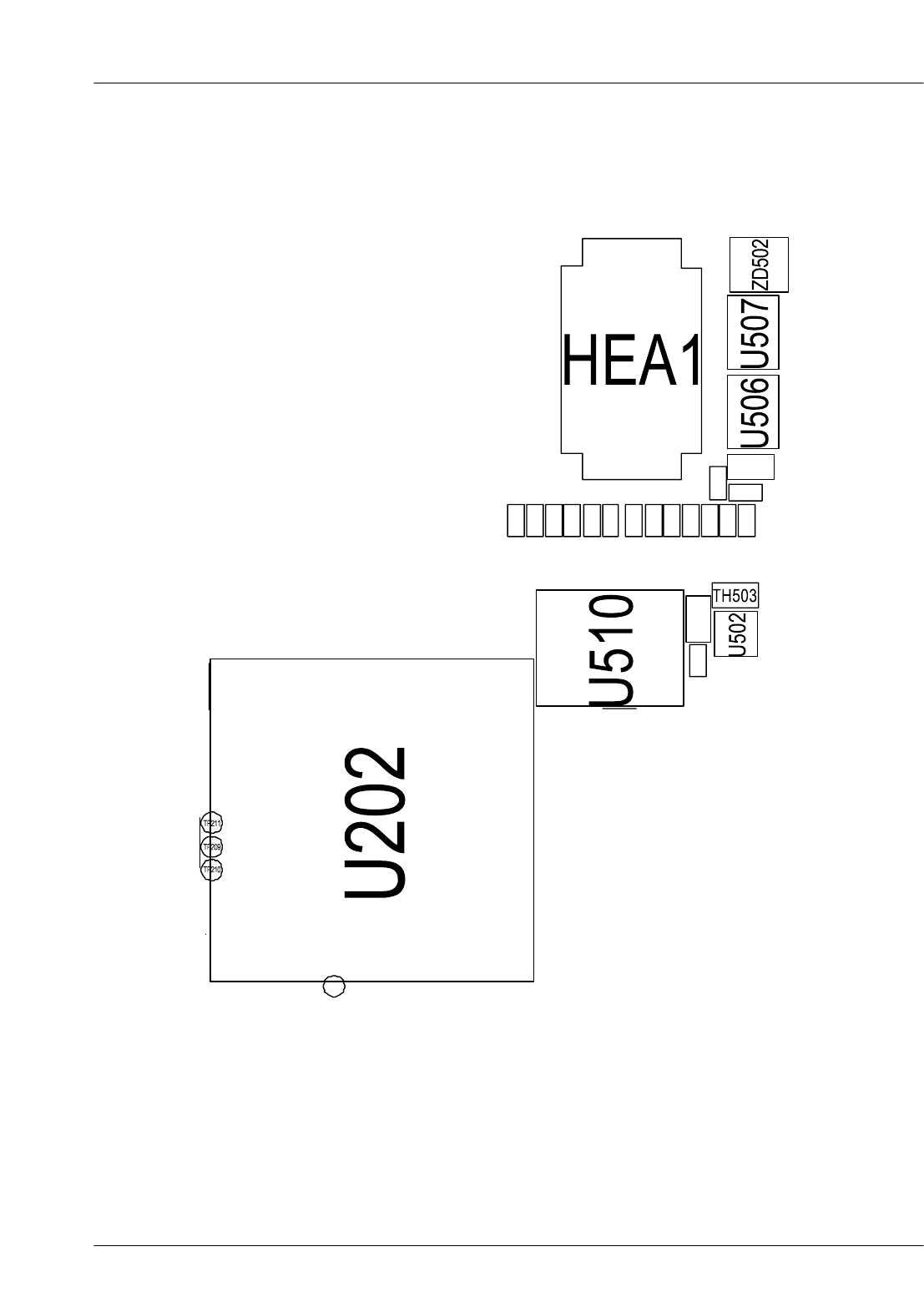
TH200 THERMISTOR 1404-001221
TH501 VARISTOR 1405-001093
TH502 VARISTOR 1405-001093
TH503 VARISTOR 1405-001093
U100 FILTER-DUPLEXER 2909-001246
U101 IC 1205-002327
U102 IC 1201-002075
U201 IC 1108-000019
U202 IC 1205-002607
U300 IC 1203-003109
U301 DIODE-TVS 0406-001200
U302 IC 1205-002350
U303 IC 1203-003808
U401 IC 1202-001036
U402 IC 1001-001306
U404 TR-DIGITAL 0504-001100
U406 IC 1204-002461
U407 IC 1001-001231
U408 IC 0801-002237
U501 FILTER-EMI SMD 2901-001325
U502 IC 0801-002882
U503 FILTER-EMI SMD 2901-001246
U504 FILTER-EMI SMD 2901-001325
U506 FILTER-EMI SMD 2901-001325
U507 FILTER-EMI SMD 2901-001325
U508 IC 0801-002882
U510 IC 1205-002747
U511 IC 1205-002747
U512 IC 1205-002747
V401 DIODE-TVS 0406-001201
V402 DIODE-TVS 0406-001201
V501 VARISTOR 1405-001121
V502 VARISTOR 1405-001121
V504 VARISTOR 1405-001121
V505 VARISTOR 1405-001121
SAMSUNG Proprietary-Contents may change without notice
Electrical Parts List
4-11
This Document can not be used without Samsung's authorization
Design LOC Description SEC CODE
V506 VARISTOR 1405-001121
V507 VARISTOR 1405-001121
V509 VARISTOR 1405-001121
X300 CRYSTAL-UNIT 2801-004373
ZD300 DIODE-ZENER 0403-001427
ZD401 DIODE-TVS 0406-001201
ZD402 DIODE-TVS 0406-001197
ZD406 DIODE-TVS 0406-001201
ZD501 DIODE-ZENER 0403-001387
ZD502 DIODE-TVS 0406-001167
ZD503 DIODE-TVS 0406-001197
ZD504 DIODE-TVS 0406-001197

SAMSUNG Proprietary-Contents may change without notice
Electrical Parts List
4-12
This Document can not be used without Samsung's authorization
SAMSUNG Proprietary-Contents may change without notice
This Document can not be used without Samsung's authorization
5. Block Diagrams
5-1
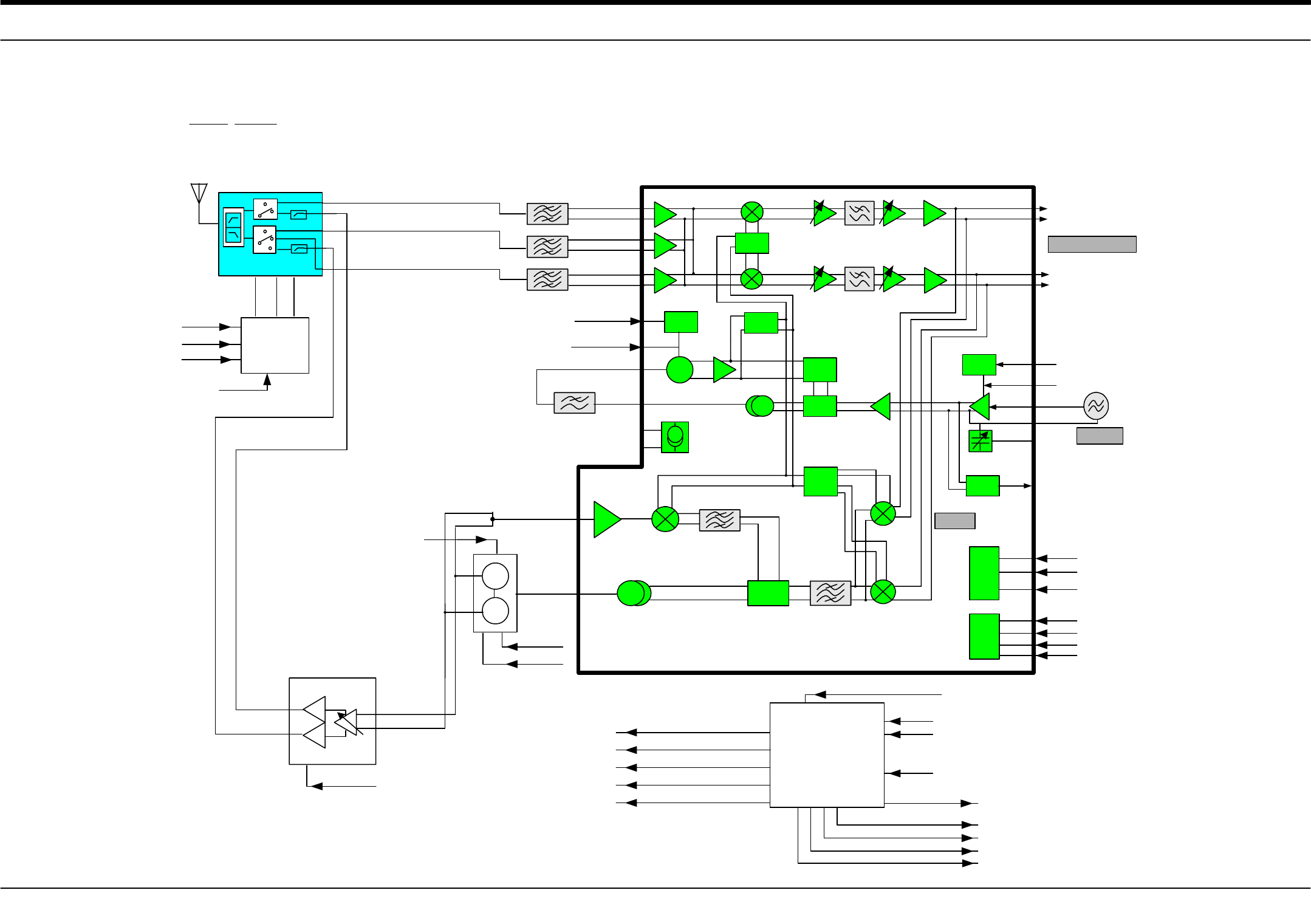
5-1. RF Solution Block Diagram
100 kHz+fmod
REFIN VC-TCXO
GSM
DCS/PCS
I+
fmod
I-
Q+
Q-
~
~
VAPC
EPCOS GSM RX SAW Filter
B7845 (2.0X1.4)
IL=1.4dB typ 1.5dB max
Ripple=0.5dB typ 0.6dB max
Vcc_RF_VCO
Discrete
3rd Order
Loop Filter
fc = ?
kHz
TX VCO
VOT1810F27KRA (6.0X5.0X1.7)
GSM = 880 ~ 915MHz
(Vt=0.5V ~ 3.0V )
Tuning Sensitivity = 55±11MHz/V
DCS = 1710 ~ 1785MHz
(Vt=0.5V ~ 3.0V )
Tuning Sensitivity = 115±23 MHz/V
Pout= 6.5±3 dBm typ.,Ic <= 30mA
Harmonics <= -10dBc
Micro Devices Quadband PAM
RF3146 (7 X 7)
GSM: Pout = 34.2 dBm , E = 55%
DCS: Pout= 32.0 dBm , E = 55%
RXON
Vcc_Tx_BURST
VBAT
HITACHI METAL ANT S/W
ESHS-C090T
Imax = 8 mA
Freq (MHz) Loss(typ.)
880 - 915 1.2 dB
925 - 960 0.8 dB
1710 -1910 1.5 dB
1805 -1880 1.2dB
Atten 2xfo : 43dB,26dB(GSM,DCS/PCS)
3xfo : 40dB,26dB(GSM,DCS/PCS)
EN
CLK
DATA
DCS/PCS S/W
OFFSET Mixer input power
-16dBm max, -22dBm min
fcompRF =26MHz
Philips Transceiver
UAA3536
Pins IA,IB,QA and QB
VI
Q : 1.25V ty
p. , 1.15Vmi
n, 1.35Vmax
Vmod : 0.5Vp
p
QUAD
DIV
PFD
CP
VREG
~
Vcc_RF_LO
FracN
DIV
1:1/
2
VREG
26MHz
Vcc_REF(2.4V typ.)
Vcc_SYN
FE_SW1
FE_SW2
3W
BUS
CTL
REG
PWR
EN
GSM/DCS/PCS
DIV
QUAD
PFD
CP
fTXIF
60MHz
+I OUT
-
-
+
FESWON
SYNON
TXON
GSM S/W
PMU
HV
S
VDD1 (1.35V min 2.95V max , 150mA )
VBat (3.6V typ 3.0V min)
V_MODE
RF1_VDD
RF2_VDD
RF1_VDDS
RF2_VDDS
VDD2 (1.35V min 3.45V max , 150mA )
VDD3 (1.35V min 3.45V max , 100mA )
VDD4 (1.35V min 3.45V max , 150mA )
AVDD(1.35V min 2.65V max , 100mA )
VCC_RX_TX (2.7V ,100mA )
VCC_SYN (2.7V , 100mA )
VCC_RF_VCO (2.7V , 100mA )
VCC_CP (4.0V , 25mA )
VCC_TX_BURST (2.7V , 100mA )
PON_SYNT
PON_TX
IL=1.5dB typ 2.1dB max
Ripple=0.5dB typ 1.0dB max
I OUT
Q OUT
Q OUT
GSM_TX_MODE_SW
VCC_RX_TX
DCS/PCS_TX_MODE_SW
Inverter
circuits
PCS_RX_MODE_SW
Vc_GSM Vc_DCS Vc_PCS
(2.7V) Ripple=0.5dB typ 1.0dB max
IL=1.4dB typ 2.1dB max
EPCOS DCS RX SAW Filter
B7852 (2.0X1.4)
EPCOS PCS RX SAW Filter
B7851 (2.0X1.4)
1930 -1990 1.2dB
PCS: Pout= 32.0 dBm , E = 52%
(2.7V)
SAMSUNG Proprietary-Contents may change without notice
Block Diagrams
This Document can not be used without Samsung's authorization
5-2
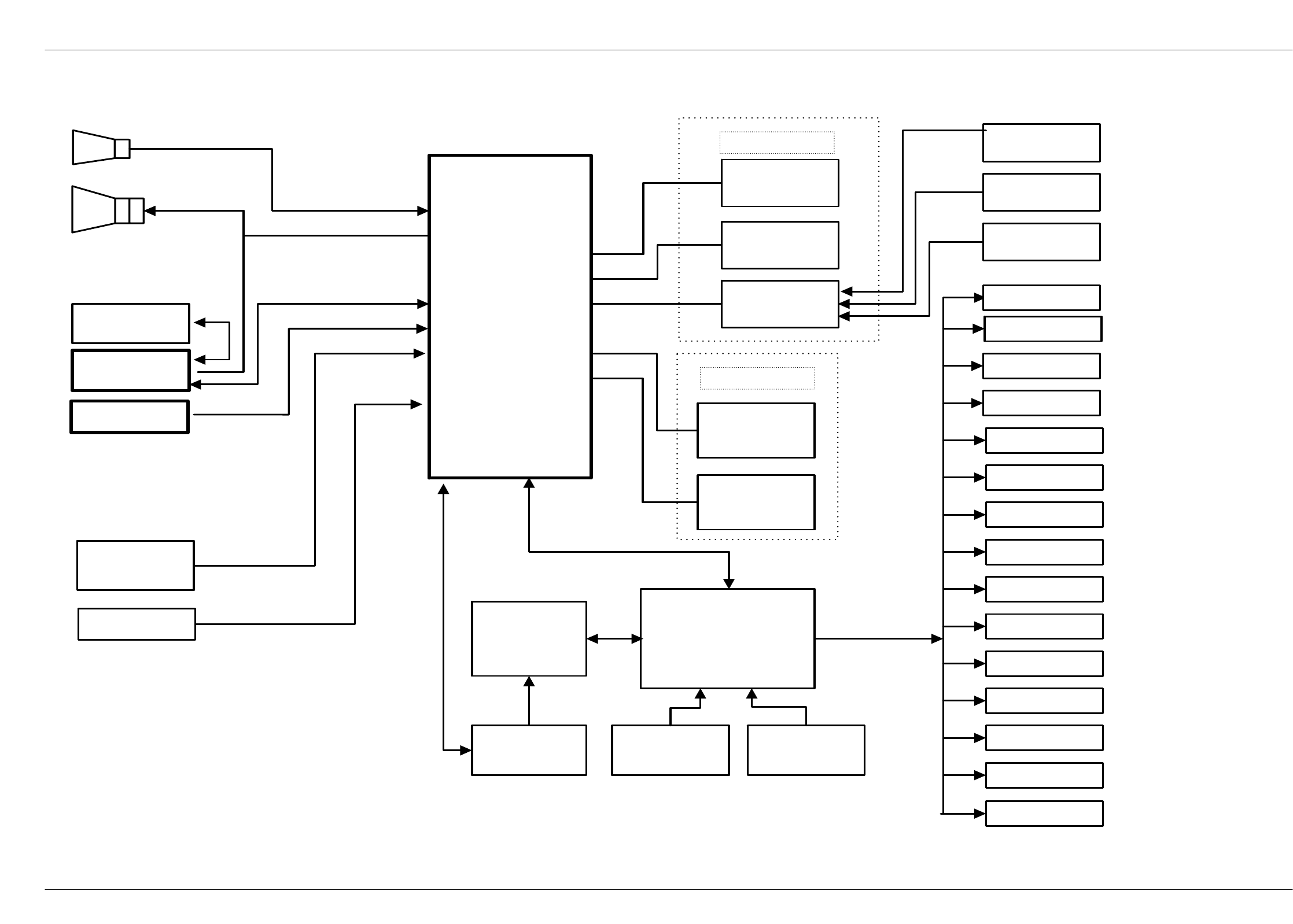
5-2. Base Band Solution Block Diagram
Battery
Type
Battery
Voltage
Battery
Temperature
AFC
RAMP
Charging Circuit
Li-Ion Battery
(Standard)
OM6359
VIBRATOR
SYSTEM CLOCK
(13MHz)
RTC_CLOCK
(32.768KHz)
KEY_BOARD
RECEIVER
MIC
LCD
RF INTERFACE VCC_RX_TX
VCC_RF_VCO
VCC_TX_BURST
PMU
VCC_SYN
Serial Data
Interface
I/O
Interface
A/D
Interface
BB INTERFACE
MELODY IC
(40 Poly)
SPEAKER
VDD1
VDD2
VDD3
VDD_VIB
MIC_BIAS
VCC_CP
VDD_KEY
VDD_AMP
AVDD
AVDD_TEMP
SIM CARD
BL_VDD
SAMSUNG Proprietary-Contents may change without notice
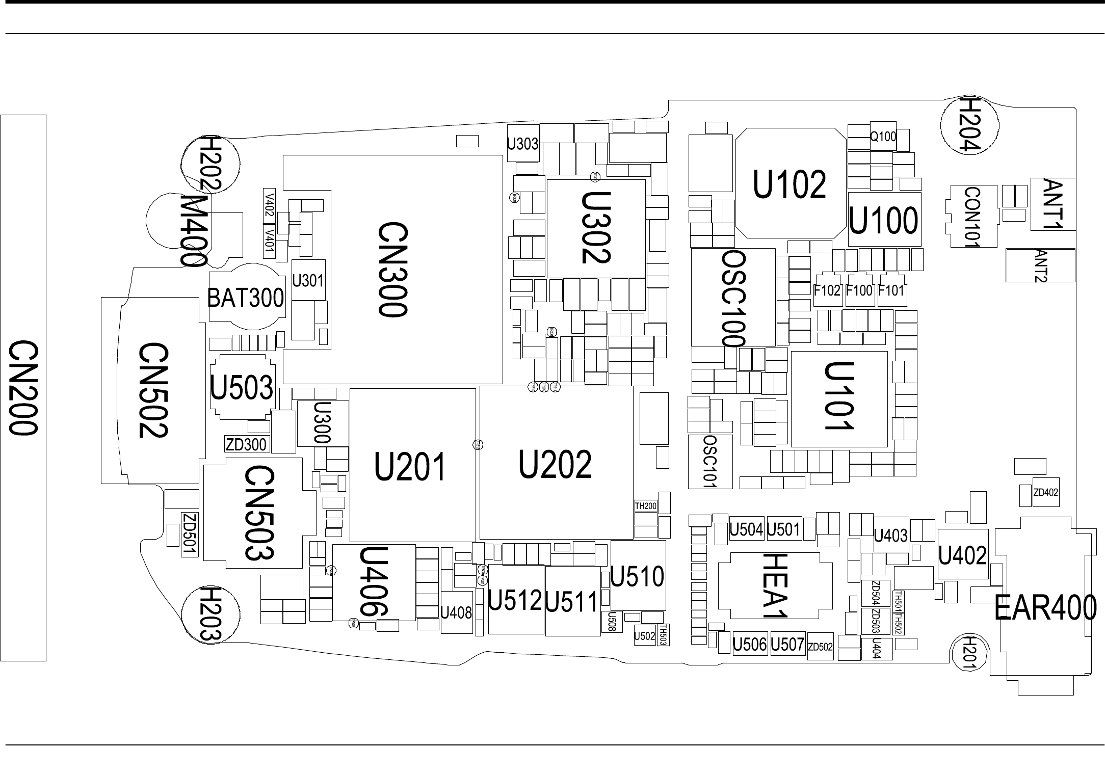
6. PCB Diagrams
6-1
ThisDocumentcan notbe used withoutSamsung'sauthorization
6-1.PCBTop Diagram
SAMSUNG Proprietary-Contents may change without notice
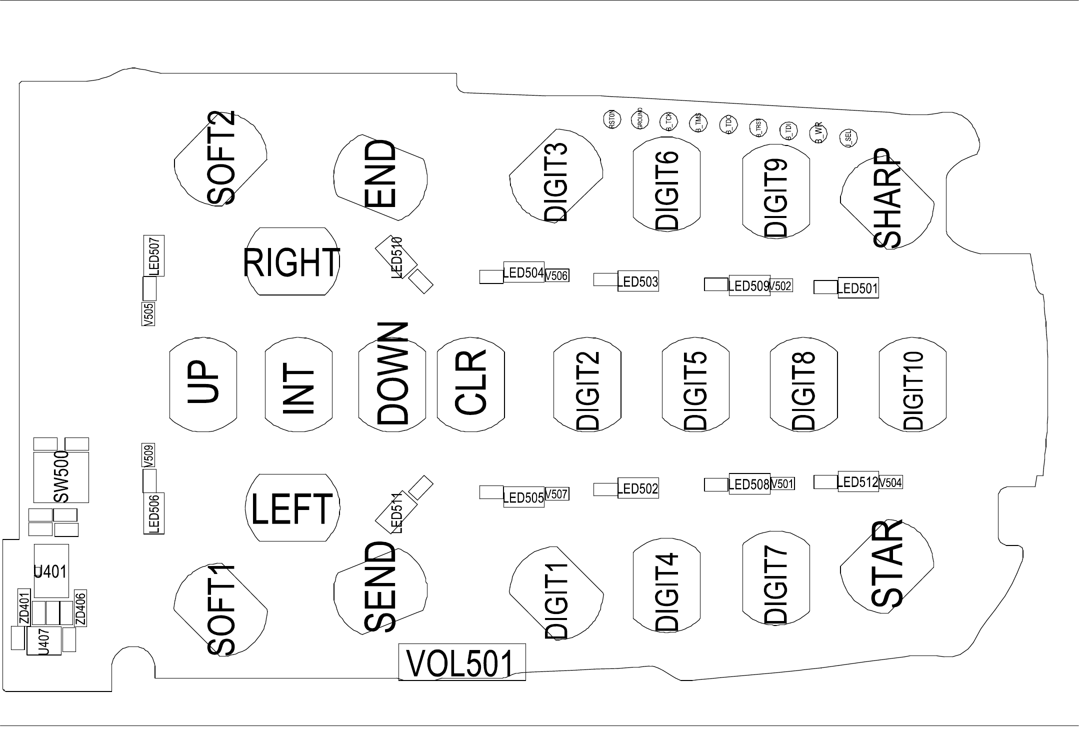
PCB Diagrams
6-2
ThisDocumentcan notbe used withoutSamsung'sauthorization
6-2.PCB BottomDiagram
SAMSUNG Proprietary-Contents may change without notice
7. Flow Chart of Troubleshooting
This Document can not be used without Samsung's authorization
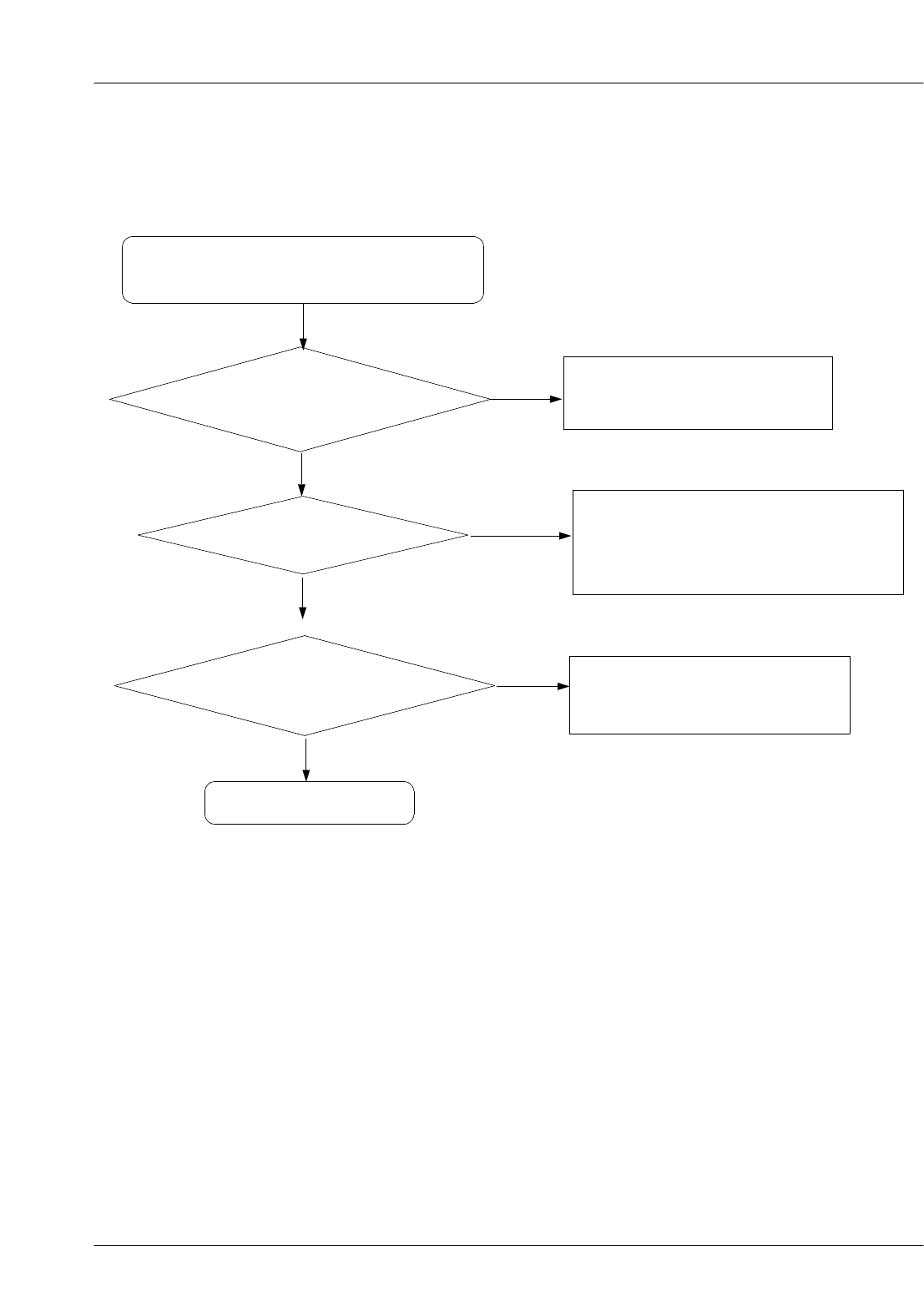
7-1
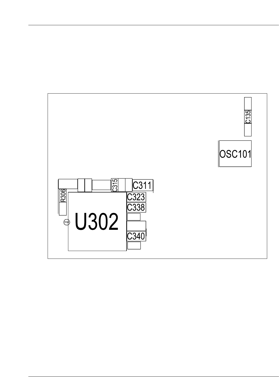
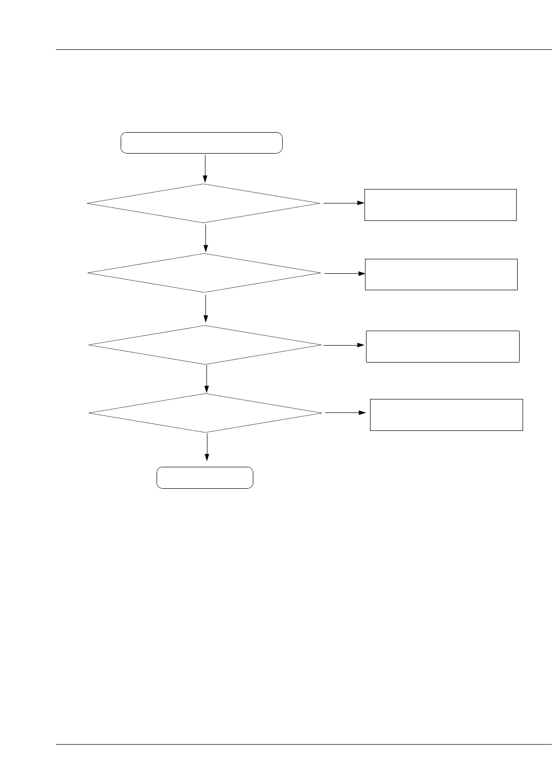
7-1. Power On
Check the Battery Voltage
is more than 3.4V
' Power On ' does not work
Change the Battery
END
No
Yes
C315(V_ISUP) = 2.7V? Check the PMU related to V_ISUP
No
Yes
Check the Clock at
R306=32KHZ Resolder X300
No
Yes
C340 (VDD1) = "H"? Check the VDD1 circuit
No
Yes
C339(VDD2) & C338(VDD3)
= 2.85V? Check the VDD2,VDD3 circuit
No
Yes
Check for the clock at C135
= 13MHz Check the clock generation circuit
(related to U101)
No
Yes
Check the initial operation
Yes
Yes
SAMSUNG Proprietary-Contents may change without notice
This Document can not be used without Samsung's authorization
Flow Chart of Troubleshooting
7-2
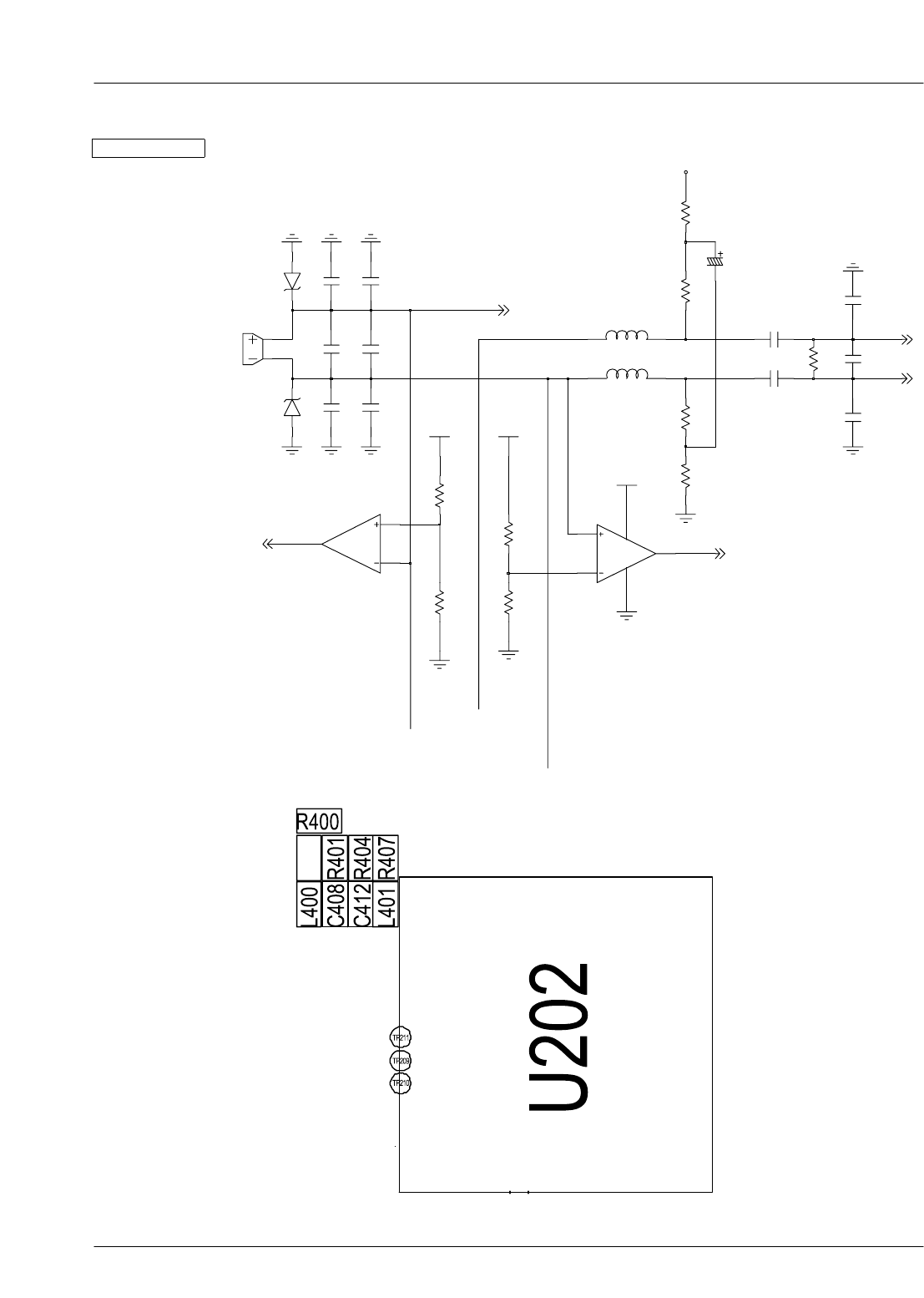
Power On
SIM
PUMP+
BATTERY
refgnd
GENERATOR
LINREG)
CONTROL
data
SENSOR
ON/OFF
SIM
internal
12C
PLL
VBAT VOLTAGE
DVDD2
CLOCK
ovdd
control
32KHz XTAL
SUPPLY &
INTERFACE
SUPPLY
clocks
AVDD
CHARGE
INTERRUPT
SUPPLY
DVDD3
REFERENCE
HFA
(CHARGE
CONTROL
BACKLIGHT
INTERNAL
htmp
bias currents
LINREG
INTERFACE
ON-CHIP
reference
MODULE
OSCILLATOR
TEMP HIGH
htmp
POWER MANAGERMENT UNIT(PMU IC)
supply
CHARGE
&
VIB
MIC BIAS
calibration
MONITOR
internal
DVDD1
HIGH VOLTAGE
CLOCK
voltage
PUMP
DVDD4
REAL-TIME
CONTROL
status
GENERATOR
SWITCH
C323
VCC_SYN_2V7
AVDD_2V65
VBAT
VBAT
C324
C305
VDD_VIB_3V05
BLVDD_3V25
VDD3_2V85
C339
C320
TP300
CLOCK 6
GND
2
IO
1
NC 5
3SIM VCC 4
VDD2_2V85
BAT300
VBAT
U301
C337
C309
VDD1_1V8
VCC_RX_TX_2V7
VCC_RF_VCO_2V7
V_ISUP_2V5
C310
C316
C318
C341
C314
C322
C336
VBAT
VBAT
21
VDD1_1V8
R301
CC7V-T1A
X300
C328
TP301
C315
VCC_TX_BURST_2V7
C326 C330
C333
C313
R305
C335
V_ISUP_2V5
L300
C329
C327
C302
MIC_BIAS_2V1
C338
C325
C340
AVDD_TEMP_2V65
C321
VBAT
VDD_KEY_2V95
C301
C312
34 4
55
66
7
GG
89
GG
10
G6
VCC_CP_4V
CN300
11
22
3
D4
VSS20
VSS21
C4F4
VSS3
G4
VSS4
VSS5
J3G5
VSS6
VSS7
K5F6
VSS8
VSS9
E6 E7
VSS14
VSS15
D7C7
VSS16
D6
VSS17
E5
VSS18
VSS19
D5F5
VSS2
C2
VCC
VIBVBAT
B3 A3
VIBVDD
H7
VPROG
VSS1
E4 G7
VSS10
VSS11
G8F7
VSS12
VSS13
B8
A1
SIMSCN
B1
SIMSCP
B2
SIMVBAT
SLPMOD
D10H5
TM
VBACK
J5
K4 VBAT
C1
RSTO
D9
E3 SCL
F2 SDA
SEL12RB
E9 H4
SEL3RB
C6
SIMCLK
A2
SIMGND
SIMIO
E8
G10 RF1VDD
F9 RF1VDDS
H9 RF2SNS
RF2SWS
E10
H10 RF2VDD
J10 RF2VDDS
G9 RFVBAT
RST
OSC32I K8
OSC32O K9
K1
REC1
J2
REC2
K2
REC3
H8 REFC
K6 REFGND
F10 RF1SNS
RF1SWS
C10
D2
IO
H6 ISUPA
J4 ISUPD
MICBIAS
J6
1
NC
2
NC
ONKEY
H3
HFAVDD
A6B6
HFAVDD
B9
HVSGND
B10
HVSOC
HVSSCN A10
C9
HVSSCP
C8
HVSVBAT
D8
HVSVDD
INT
H1
DVDD3
DVDD3
J1H2
DVDD3VBAT
A4
DVDD4
DVDD4ON
F8 B4
DVDD4VBAT
A5
HFAVBAT
HFAVBAT
B5
C3
CLK
A9
CLK32
D1
CPRES
F1
DVDD1
DVDD1VBAT
F3 G2
DVDD2
DVDD2
G1G3
DVDD2VBAT
J9
A8 BBMGND
C5 BBMSW
B7 BLVBAT
A7 BLVDD
E1
CHRIV
CHRREG E2
D3
CHRVBAT
AUXON
K3
AVDD
J7K7
AVDD
AVDDS
K10J8
AVDDVBAT
AVDDVBAT
C332
U302
C311
R306
C334
32K
CHARGER_OK
PON_SYNT
PON_TX
SDA
SCL
BACKLIGHT
VIB
BLVDD_3V25
SIMCLK
SIMIO
REF_ON
RSTON
JIG_REC
JACK_IN
RECO1
ONKEY_N
IT_PMU
SAMSUNG Proprietary-Contents may change without notice
Flow Chart of Troubleshooting
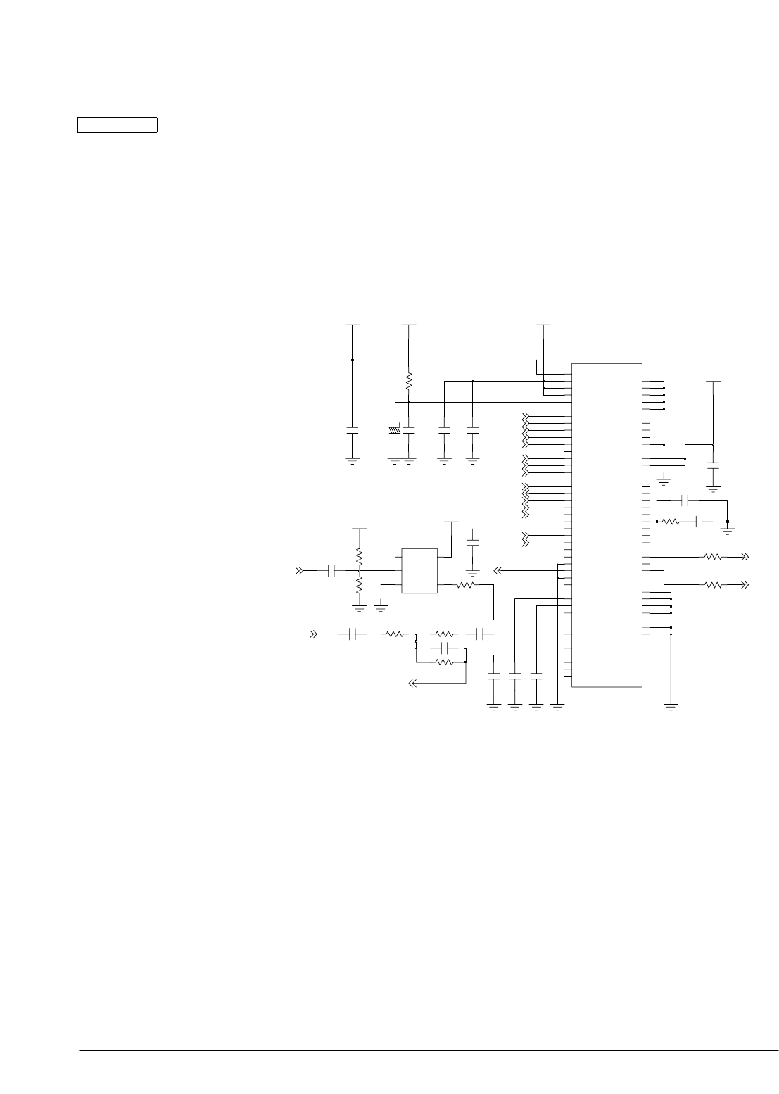
This Document can not be used without Samsung's authorization
7-3
C339
SAMSUNG Proprietary-Contents may change without notice
This Document can not be used without Samsung's authorization
Flow Chart of Troubleshooting
7-4
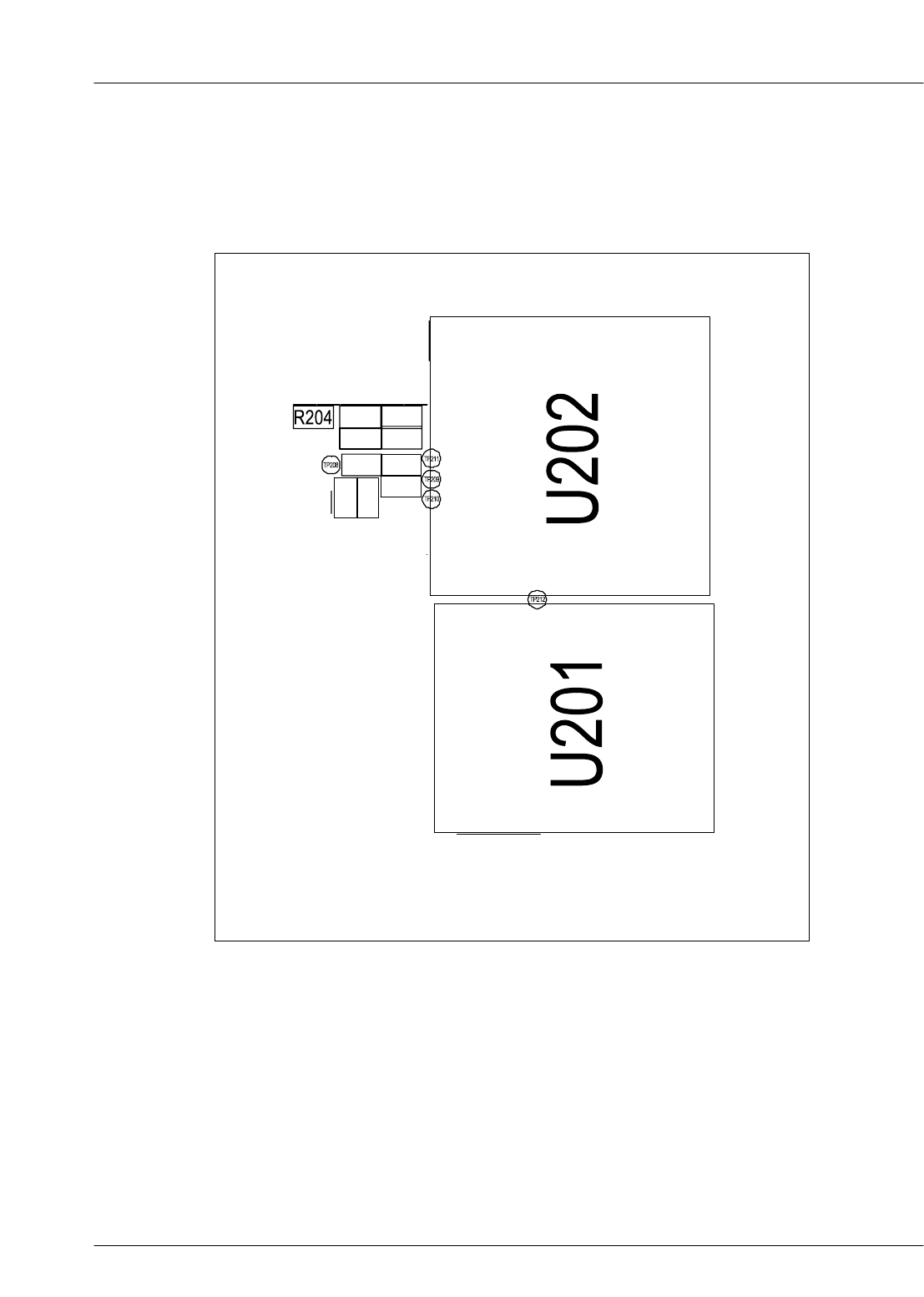
7-2. Initial
R204 (RSTON) ="H"?
Initial Failure
Check the circuit related to reset
END
No
Yes
Is U201 Pin
(memory CE) OK?
Yes
Yes
No
Check the U201
Check the circuit around
LCD & U201 (Short or not solder)
Yes
SAMSUNG Proprietary-Contents may change without notice
Flow Chart of Troubleshooting
This Document can not be used without Samsung's authorization
7-5
Initial
R218
VDD3_2V85
C207
R219
VDD1_1V8
VDD2_2V85
VDD1_1V8
R223
VSS_N
K1
VSS_O
P1
N5VSS_P
C13VSS_REF
A12VSS_VB
C11VSS_VBOUT
C206
M7
D11VSS_D
N10VSS_E
N14VSS_F
N11VSS_G
VSS_H
G13
E8VSS_I
C3VSS_K
G1VSS_M
C9
D14
VDD_REF
VDD_VBB12
C12
VDD_VBOUT
C14
VREF
K7VSS_A
J1VSS_B
E13VSS_BB
VSS_C
H11
VDDE2_CP8
VDDE2_EC1
VDDE3_AP4
VDDE3_BM6
VDDE3_FG2
L3
VDDE3_G
F12
VDD_BB
VDD_D
F5
VDDC_AN13
VDDC_BM8
VDDC_CK6
VDDC_D
P9
VDDE1_AN12
VDDE1_B
VDDE1_CC8
VDDE1_D
A3TCK
D2TDI
TDO
D3
TMS
A2
A1TRST_N
C5TXD0
TXD
A4
G12
TXON
C4RXD0
D4RXD1
H12
RXON
C2
SCK
SDA B3
SIMCLK M14
SIMERR M11
M13
SIMIO
RFSIG5 C7
B7
RFSIG6
RFSIG7 C6
E7
RFSIG8
RFSIG9 K10
M10 RSTO_N
RST_N
H10
RXT0_N
A5
C10
J12
RFE_N0 K12
RFE_N2
D5
RFSIG0 A6
RFSIG1
RFSIG10 D7
D6
RFSIG2
RFSIG3 B6
A7
RFSIG4
KBIO7
D10
MCLK
MICN B13
A13
MICP
PWM0 F4
E6
PWM1
QN H14
QP H13
RESETN
J_SEL
KBIO0
K11 KBIO1
J10 KBIO2
K13
J11 KBIO3
L11 KBIO4
L13 KBIO5
L12 KBIO6
L14
E4 HD7
F3 HD8
HD9
F2
HRD_N
H5
L5 HWR_N
IN J14
IP J13
B4
D1
E3 HD13
HD14
E2
HD15
B2
H2 HD2
HD3
J3
HD4
E5
HD5
H1
B1 HD6
M3
HA7
P2
HA8
N2
M1 HA9
H4 HD0
H3 HD1
HD10
F1
HD11
E1
HD12
HA22
L6 HA23
HA24
J7
J6 HA25
HA26
H6
HA3
L4
HA4
N3
HA5
K5
HA6
HA16
K3
J4 HA17
HA18
K4
K2 HA19
P3 HA2
G4 HA20
HA21
P5
N6
GPON2 N9
M4 HA1
HA10
N1
L2 HA11
L1 HA12
M2 HA13
HA14
J2
J5 HA15
GPIO3
M9
GPIO4
P7
L7 GPIO5
GPIO6
L9
GPIO7
N7
GPIO8
P6
GPIO9
N8
GPON1 L10
CS_N2
CS_N3
G3
B5CTS0_N
A11
EARN
EARP B10
M12 GPIO0
K9 GPIO1
K8 GPIO10
GPIO2
L8
D8
E9
CDO
D9
CEN
CKI
P11
P13 CKI32I
CKI32O
P14
CS_N0
N4 CS_N1
G5
M5
P10AVSS
BDIO E11
BIEN F10
F11
BIOCLK
BOEN G11
B11
BUZ
CCLK E10
CDI
E12
D13
AUXDAC2 D12
AUXDAC3
AUXMICN A14
B14
AUXMICP
K14 AUXON
AUXSP A10
AUXST G10
P12
AVDD
ACLK
ADI A8
ADO A9
AFS B9
F14
AUXADC1
AUXADC2 G14
E14
AUXADC3
AUXADC4 F13
AUXDAC1
U202
B8
VDD1_1V8
C200
TP207
VDD2_2V85
R227
VDD2_2V85
R224
TP210
C203
R204
R214
TP206
VDD3_2V85
TP208
VDD1_1V8
R225
C219
R211
R217
TP209
TH200
VDD1_1V8
VDD3_2V85
VDD2_2V85
R228
R221
AVDD_TEMP_2V65
C204
TP211
R220
C213
AVDD_2V65
VDD2_2V85
VDD1_1V8 VDD1_1V8
C214
R200
C229
R212
C208
C216
C215
R215
HWR_N
VDD2_2V85
R226
TTY_MODE_SEL
LCD_RESET
FLIP
VF
EARP_N
EARP_P
AUXSP
AUX_MIC_P
AUX_MIC_N
HA(10)
HA(9)
HA(8)
HA(7)
HA(6)
HA(5)
HA(4)
HD(15)
HD(14)
HD(13)
HD(12)
HD(11)
HD(10)
HD(9)
HD(8)
HD(7)
HD(6)
HD(5)
HD(4)
HD(3)
HD(2)
HD(1)
HD(0)
HD(0:15)
AMP_EN
KBIO(2)
KBIO(3)
KBIO(4)
KBIO(5)
KBIO(6)
KBIO(7)
KBIO(0:7)
HA(22)
HA(21)
HA(20)
HA(19)
HA(18)
HA(17)
HA(16)
HA(15)
HA(14)
HA(13)
HA(12)
HA(11)
SDA
RXD0
TXD0
CTS0
BIEN
BDIO
BOEN
BIOCLK
ANT_SW2
PON_SYNT
PON_TX
NCSRAM
MELODY_CS
HRD_N
RSTON
D_REF_13M
KBIO(0)
KBIO(1)
D_REF_13M
RAMP
AFC
32K
TXD1
TRST_N
TMS
TDO
TDI
TCK
RXD1
RTS0
J_SEL
REF_ON
CTS0
SIMCLK
SIMIO
IT_PMU
SCL
MES_BATT
LCD_CS
CHG_ON
END_OF_CHARGE
A
FSC
DU
DCL
DD
MIC_N
MIC_P
IRX_TX_N
IRX_TX_P
QRX_TX_N
QRX_TX_P
V_MODE
HA(26)
HA(25)
HA(24)
ANT_SW3
TXVCO_SW1
NCSFLASH
ANT_SW1
PAM_TX_EN
PON_RX
RF_EN_SYNT
HA(3)
HA(23)
HA(2)
HA(1)
RF_BBI_DATA
RF_BBI_CLK
LINE_OUT
M_RST
LCD_MAIN_EN
M_INT
B
TXVCO_SW2
HA(1:26)
SAMSUNG Proprietary-Contents may change without notice
This Document can not be used without Samsung's authorization
Flow Chart of Troubleshooting
7-6
SAMSUNG Proprietary-Contents may change without notice
Flow Chart of Troubleshooting
This Document can not be used without Samsung's authorization
7-7
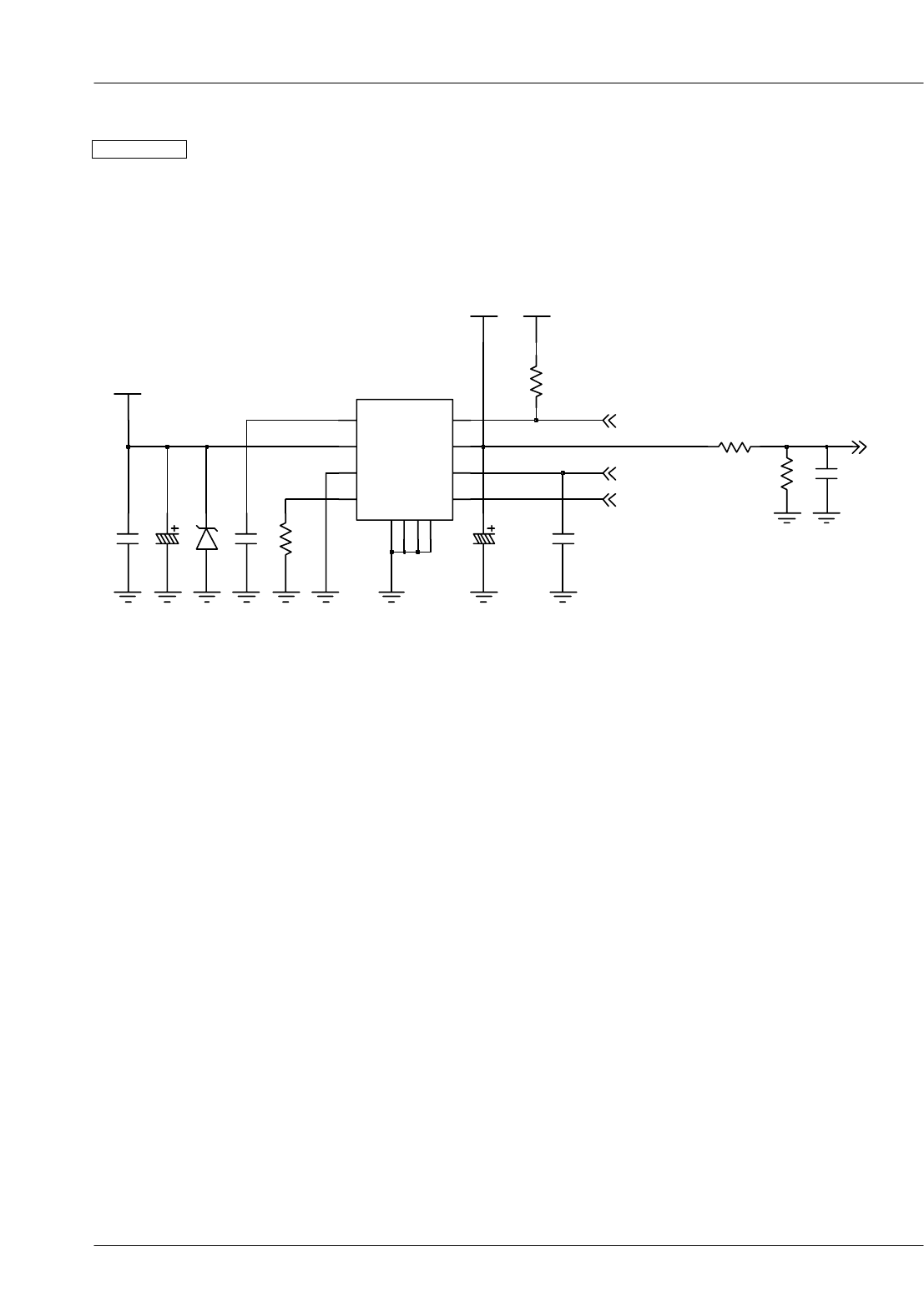
7-3. Charging Part
Check the U300 pin 2
>4.9V
Abnormal charging part
END
No
Yes
U300 pin 4 = "H"? No
Yes
Check the C300
≒4.2V
No
Yes
Check the the circuit related to
+DCVOLT
Resolder or replace U300
Check the circuit related to
CHG_ON signal
Yes
U300 pin 5 = "L"?
Yes
No
Resolder or replace U300
SAMSUNG Proprietary-Contents may change without notice
This Document can not be used without Samsung's authorization
Flow Chart of Troubleshooting
7-8
Charging
CHARGER IC
R302
R303
VDD2_2V85VBAT
C306
UDZS8.2B
+DCVOLT_5V
C307
R300
C308
C300
C303
C304
R304
12
G
3GND
IN
2
ISET
4
1VL
6
_ACOK
_CHG 8
5
_EN
U300
7
BATT
9
G10
GG
11
MES_BATT
CHARGER_OK
END_OF_CHARGE
CHG_ON
SAMSUNG Proprietary-Contents may change without notice
Flow Chart of Troubleshooting
This Document can not be used without Samsung's authorization
7-9
SAMSUNG Proprietary-Contents may change without notice
This Document can not be used without Samsung's authorization
Flow Chart of Troubleshooting
7-10
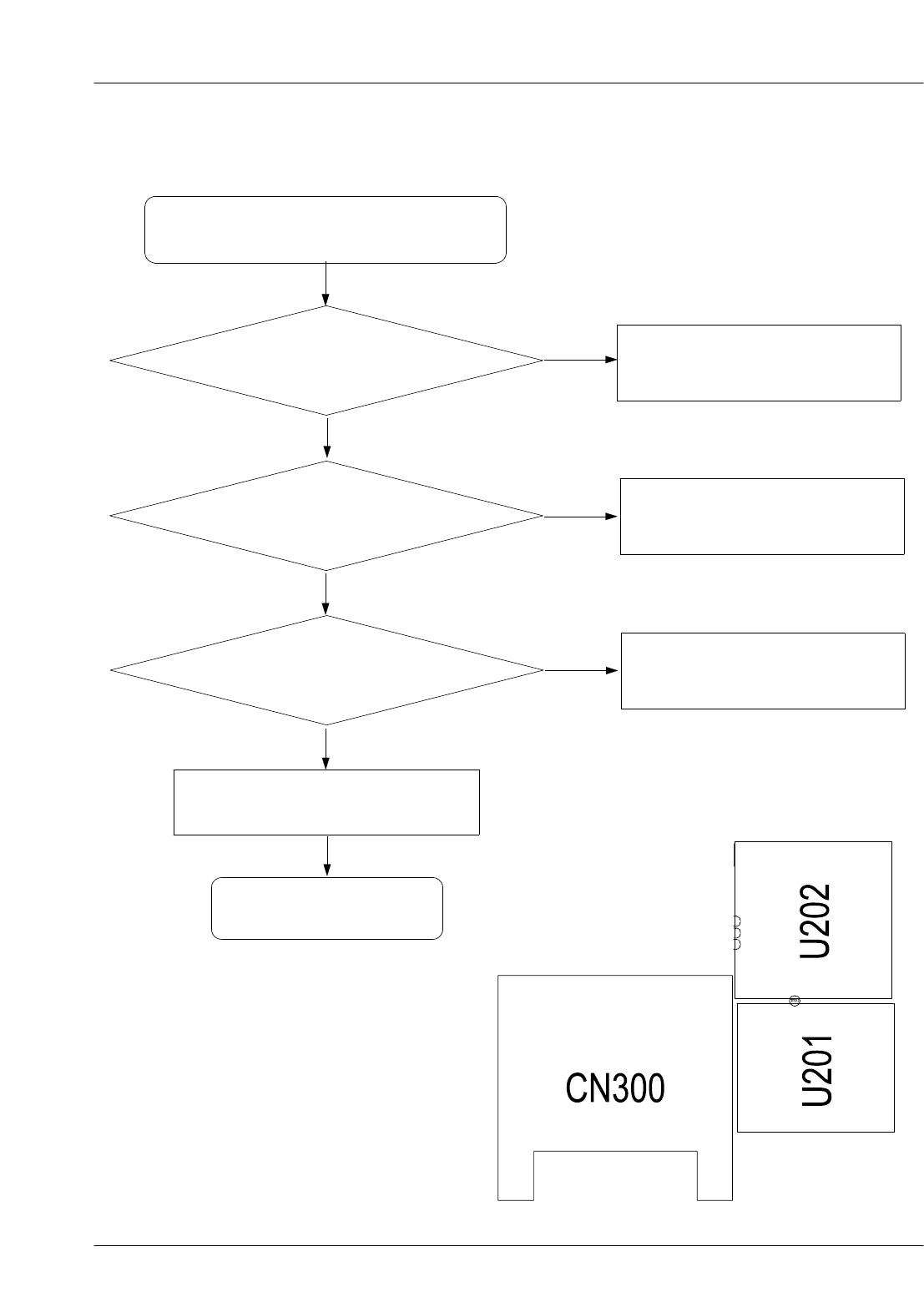
7-4. Sim Part
CN300 pin 1,5 = "H"?
Phone can't access SIM Card
Check the sim charge pump
Check the SIM Card
END
No
Yes
Yes
Yes
No
Check the 32k OSC
After Power ON,
Check SIMCLK Signal on
CN300 pin3 in a few second
Yes
No
Replace PBA
After SIM card insert,
CN300 pin 2 = "H(SIM_RST)"?
Yes
SAMSUNG Proprietary-Contents may change without notice
Flow Chart of Troubleshooting
This Document can not be used without Samsung's authorization
7-11
7-5. Microphone Part
Check the connection
from MIC
Check the circuit
from U202 to MIC
Resolder MIC
Resolder the R400, R401, R404, R407,
L400, L401, C408 and C412
END
No
Yes
Yes
Yes
Yes
No
Check the MIC
No
Replace the MIC
Microphone does not work
SAMSUNG Proprietary-Contents may change without notice
This Document can not be used without Samsung's authorization
Flow Chart of Troubleshooting
7-12
Close to MCP
Close to microphone
MICROPHONE
R400
C405
C412
VDD2_2V85
MIC_BIAS_2V1
R401 C407
V402
C400
C414
C411
V401
5
6
7
R409
U401-2
C418
R416
L401
VDD2_2V85
C408
R415
R404
C406
C417
R412
VDD2_2V85
R402
L400
2
8
1
U401-1
4
3
C416
C413
R407
M400
MIC+
MIC_P
MIC_N
JACK_IN EAR_SWITCH
Microphone
SAMSUNG Proprietary-Contents may change without notice
Flow Chart of Troubleshooting
This Document can not be used without Samsung's authorization
7-13
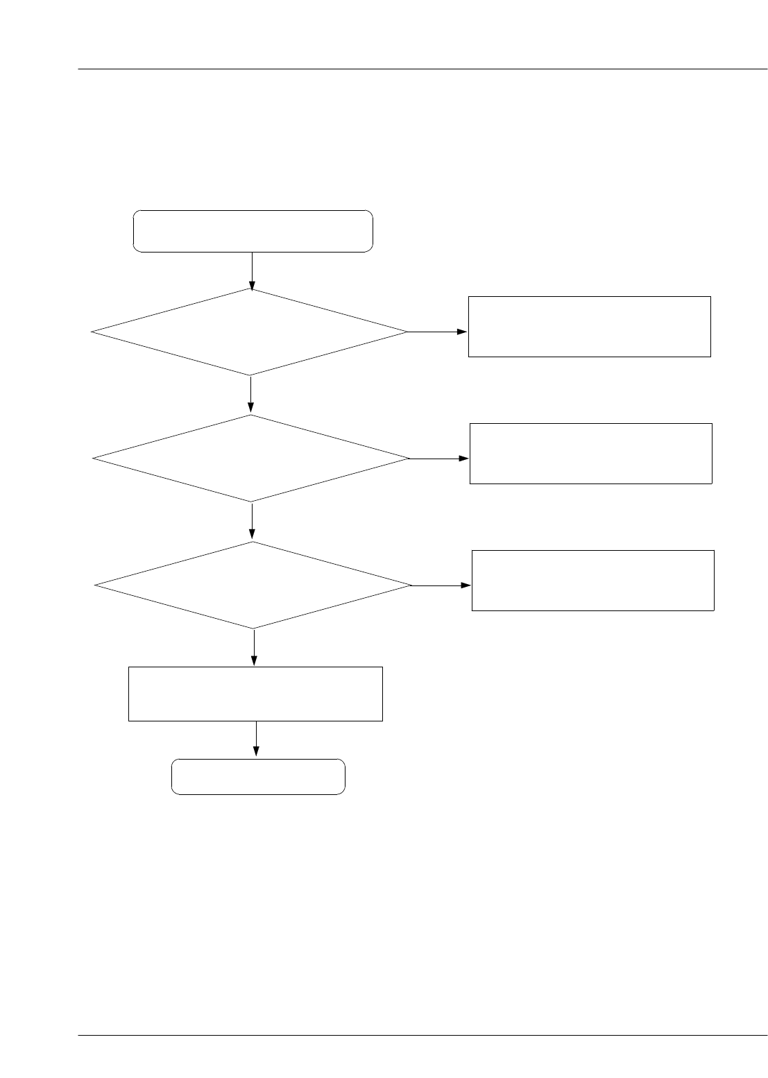
7-6. Speaker Part(Melody)
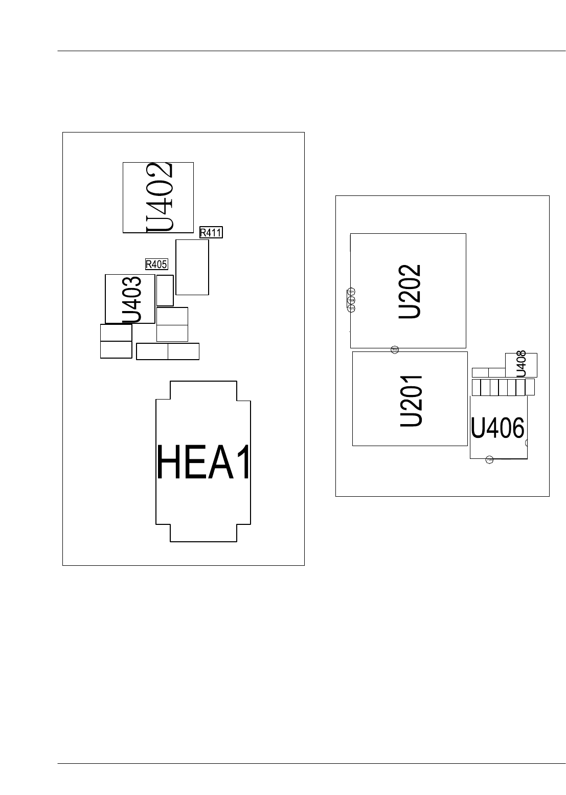
U408 pin 5 = 1.9V?
Speaker does not work
Check the Clock signal
at E2(CLKI) of
U406(13MHz) Check the clock generation circuit
(related to OSC101 and U406)
END
No
Yes
No
Resolder or replace U408
R405 & R411 Around
U406 ≒ 1.8V?
(When U406 operate) Resolder U406
Yes
No
HEA1 pin 24,26
≒1.8V? Check the circuit related to
"SPK_P/SPK_N" signal
Yes
No
Is Speaker working?
No
Yes
Change the Speaker
Yes
Yes
SAMSUNG Proprietary-Contents may change without notice
This Document can not be used without Samsung's authorization
Flow Chart of Troubleshooting
7-14
Speaker
MELODY IC
VDD_1.9V
R411
C422
C401
R410
C402
R414
C439
VDD3_2V85
R403
/WR,SCK
J5
J6 SO
LED2 J7
MTR J8
H5 SMODE
GPIO
H6
LED1 H7
LED0 H8
J1 D4
D1
J2
J3 DVDD J4
DVSS
G5 IFSEL
TESTI2 G6
G7 MTR
BCLK
G8
D4
H1
D2
H2
IOVDD2 H3
/CS,_SS
H4
D5
F3
TESTI1 F6
LRCK F7
SDIN F8
D6
G1
D3
G2
D0
G3
/RD,SI
G4
DVDD
E1
CLKI
E2
E3 A1
MCLK
E6
/IRQ
E7
IOVDD1 E8
A0
F1
D7
F2
C8 SPVDD
DVSS D1
PLLC D2
/RST
D3
D4 INDEX
D6
TESTI0
DVDD
D7
DVSS D8
SPVSS B8
AVDD
C1
TXOUT
C2
RXIN C3
EXTIN
C4
BBR
C5
EXTOUT
C6
TESTI3 C7
SPOUT1 A8
AVSS B1
VREF
B2
HPC B3
EQ1
B4
BBL
B5
HPOUTL B6
SPOUT1 B7
NC 2
A1
RXIN
EXC
A2
EQ2
A3
EQ3
A4
A5
HPVSS
HPOUTR A6
SPOUT2 A7
U406
YMU788
NC 1
C424
VDD_1.9V
R417
R405
VDD_1.9V
C421
C420 R406
R408
C409
C419
C425
C423
C403
C415
C404
C426
C410
U408
GND
3
IN
2
NC
1
OUT 4
VCC 5
R424
R413
VBAT
VDD2_2V85
AMP_IN
AMP_P
AMP_N
LINE_OUT
HRD_N
VIB
HD(4)
HD(2)
MELODY_CS
HD(1)
HWR_N
MEL_13M
HD(6)
HD(7)
HD(5)
M_RST
HA(2)
M_INT
HA(1)
HD(3)
HD(0)
SAMSUNG Proprietary-Contents may change without notice
Flow Chart of Troubleshooting
This Document can not be used without Samsung's authorization
7-15
SAMSUNG Proprietary-Contents may change without notice
This Document can not be used without Samsung's authorization
Flow Chart of Troubleshooting
7-16
7-7. Key Data Input
When one of the keys is
pushed,
is it displayed on LCD?
Check the Dome sheet & Key rubber
END
No
Yes
Yes
Check Initial Operation
When one of the keys is
pushed,
KBIO signal is OK? Replace the PBA
No
Yes
SAMSUNG Proprietary-Contents may change without notice
Flow Chart of Troubleshooting
This Document can not be used without Samsung's authorization
7-17
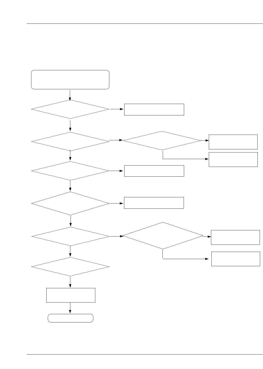
7-8. Receiver Part
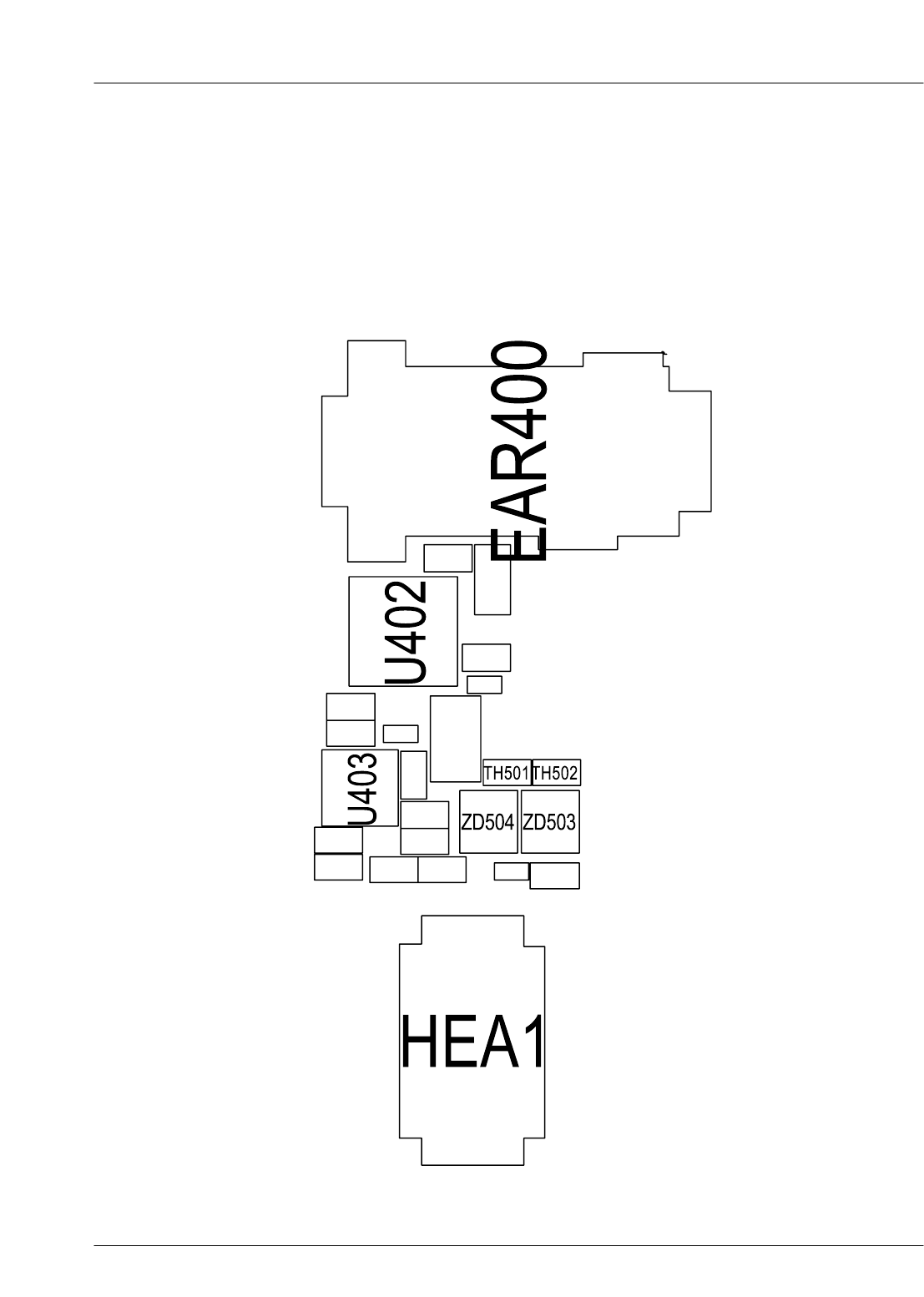
U402 pin 3, 15 = 1.5V? Resolder or replace U402
END
No
Yes
Yes
Receiver does not work
SPK +,- PAD = 1.5V? Change LCD module
No
Yes
Is Receiver working? Replace the Receiver
No
Yes
No
Resolder or replace U402
Yes
No
Resolder EAR400
EAR400 pin 5, 2 = short?
Yes
HEA1 pin 24, 26 = 1.5V?
No
Resolder HEA1
Yes
Check the soldering of the
speaker wire
No
Modify the speaker wire soldering
Yes
U402 pin 8, 12 = 1.5?
SAMSUNG Proprietary-Contents may change without notice
This Document can not be used without Samsung's authorization
Flow Chart of Troubleshooting
7-18
SAMSUNG Proprietary-Contents may change without notice
Flow Chart of Troubleshooting
This Document can not be used without Samsung's authorization
7-19
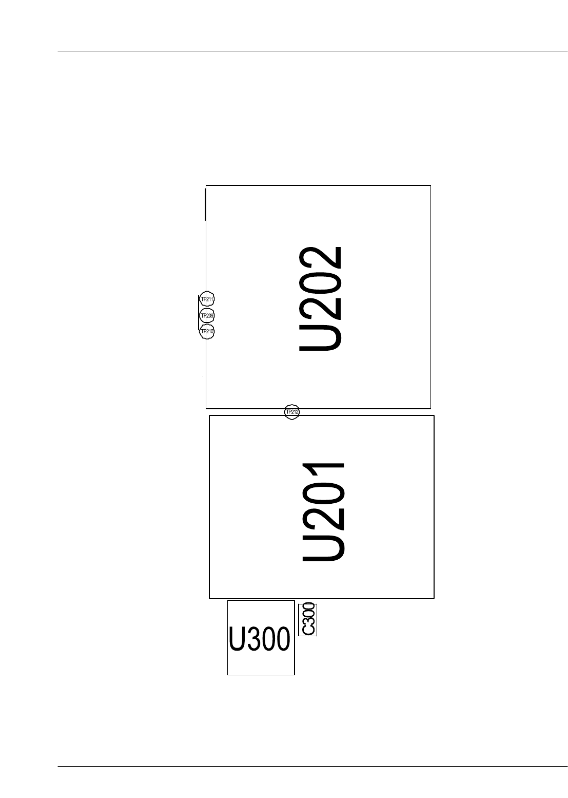
7-9. LCD Part (for Color Main )
Is LCD Contrast set on
high level in the Menu? Set LCD Contrast on high level
END
No
Yes
Yes
LCD does not work
HEA1 pin 2 = 2.8V? Check the U502
No
Yes
HEA1 pin 19(HWR_N)
21(HA(1)) is OK? Check the U202
No
Yes
Yes
Replace the LCD Module
SAMSUNG Proprietary-Contents may change without notice
This Document can not be used without Samsung's authorization
Flow Chart of Troubleshooting
7-20
TP212
SAMSUNG Proprietary-Contents may change without notice
Flow Chart of Troubleshooting
This Document can not be used without Samsung's authorization
7-21
7-10. Key Back Light
C333 = "H"? Check the PMU related to "VDD_KEY"
END
No
Yes
Key Backlight does not work
Yes
SAMSUNG Proprietary-Contents may change without notice
This Document can not be used without Samsung's authorization
Flow Chart of Troubleshooting
7-22
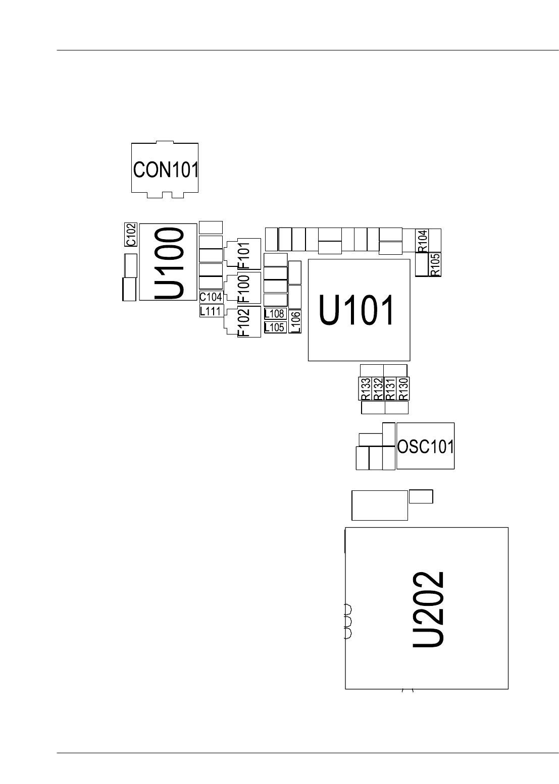
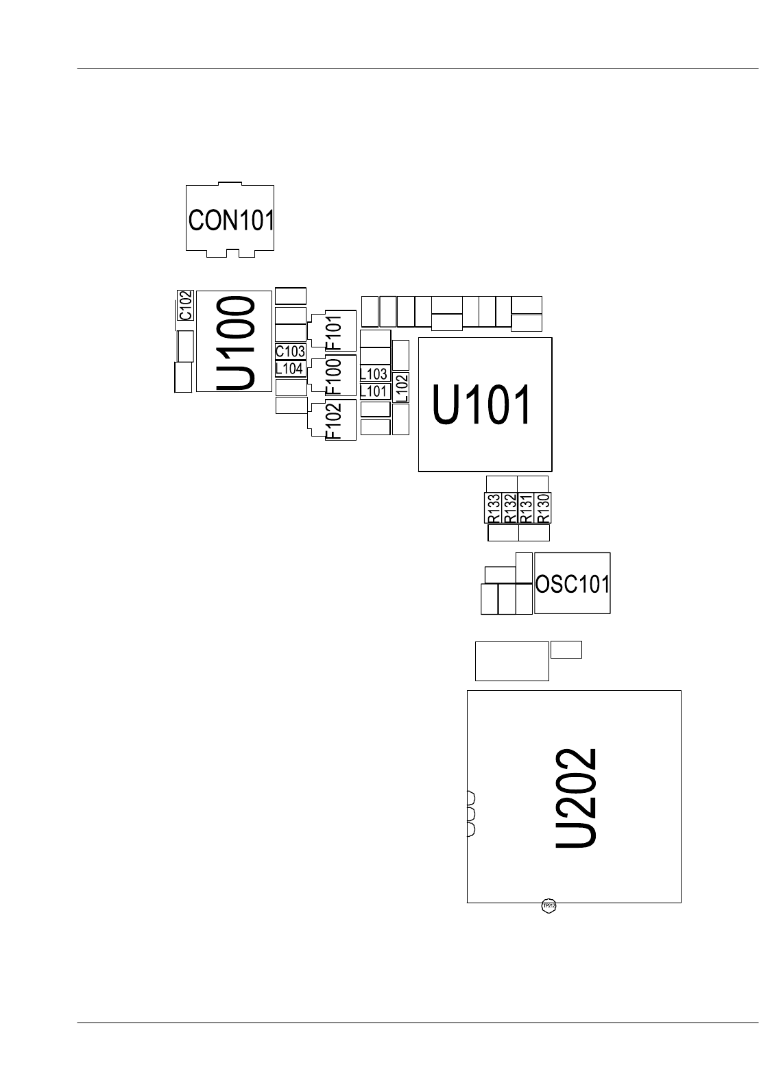
7-11. GSM Receiver
U100 Pin7
>= -65dBm Resolder CN101, C102
END
No
Yes
RX ON
RF input : CH center freq
Amp : -50dBm
Check U100
pin2=L,pin4=L,pin8=L
U100 pin5
>= -65dBm
F101 pin1
>= -70dBm
U101pin6,7,8,9
>= 1V
U101
pin32 >= -70dBm
pin33 >= -70dBm
Check ANT Switch
control circuit
Resolder U100
Resolder F101, C107, L115
Resolder L112, L113, L114
Check U101
pin10,22,28 >=2.7V
pin20 >=4.0V Check & Resolder
RF PSU Part
Check &Resolder
U101, RF26MHz part,
R104, R105
R130,R131,R132
,R133 >= 1V
Yes
Yes
Yes
Yes
Yes
Yes
Yes
Yes
No
No
No
No No
No
Check U202
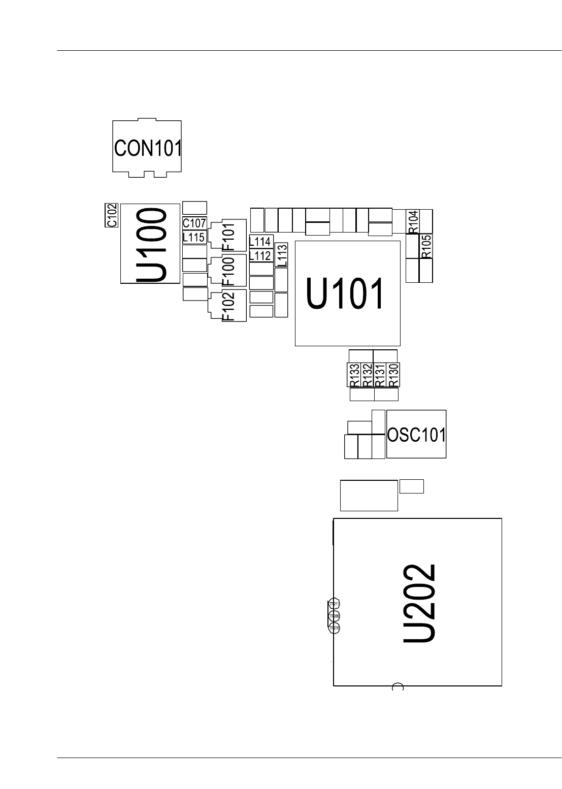
SAMSUNG Proprietary-Contents may change without notice
Flow Chart of Troubleshooting
This Document can not be used without Samsung's authorization
7-23
SAMSUNG Proprietary-Contents may change without notice
This Document can not be used without Samsung's authorization
Flow Chart of Troubleshooting
7-24
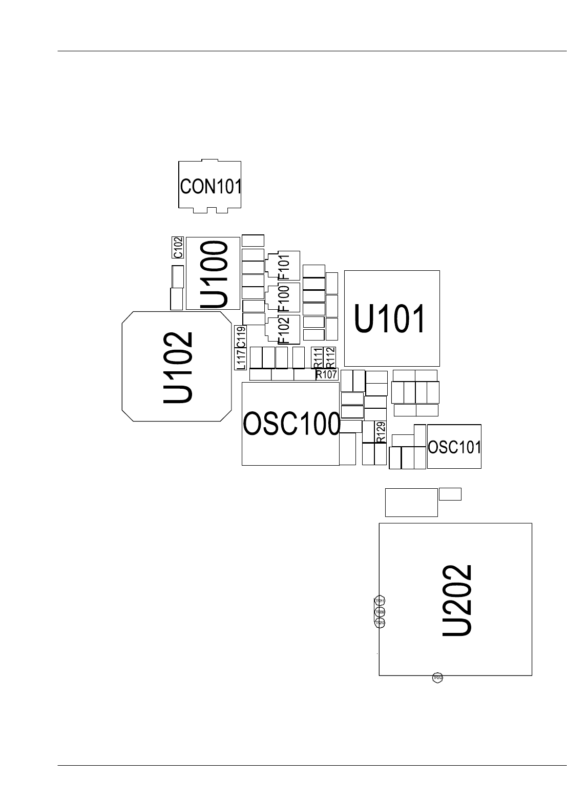
7-12. GSM Transmitterv
TX ON (5Level)
U100 Pin7
>= 20dBm
U100 Pin11
>= 20dBm
U102 Pin6
>= 20dBm
U102 Pin48
>= 3dBm
OSC100 pin1
>= 6Bm
U101Pin6,7,8,9
>= 500mV
Resolder CN101, C102
Check U100
pin2=L,pin4=H,pin8=L
Resolder C119, L117
Check U101
pin4 >= 4.0V
pin22, 28 >= 2.7V
Change
or Resolder U100
Check ANT Switch
control circuit
Check & Resolder
RF PSU part
Resolder U101
or check Txcpo(R129)
Yes
No
Yes
Yes
Yes
Yes
Yes
Yes
No
No
No
No
No
No
No
Check U102
+VBATT(pin42,43)
OK?
Resolder or change U102
or check PAM control
signal
Check +VBATT
Yes
No
Resolder R107, R111, R112
Yes
Check U202
END
SAMSUNG Proprietary-Contents may change without notice
Flow Chart of Troubleshooting
This Document can not be used without Samsung's authorization
7-25
SAMSUNG Proprietary-Contents may change without notice
This Document can not be used without Samsung's authorization
Flow Chart of Troubleshooting
7-26
7-13. DCS Receiver
RX ON
RF input : CH center freq
Amp : -50dBm
U100 Pin7
>= -65dBm
U100 pin1
>= -65dBm
F102 pin1
>= -70dBm
U101Pin38>=-70dBm
Pin39>=-70dBm
U101pin6,7,8,9
>= 1V
R130,R131,R132
,R133 >= 1V
Check U202
END
Resolder CN101, C102
Check U100
pin2=L,pin4=L,pin8=L Check ANT Switch
control circuit
Resolder U100
No
Yes
Resolder F102, C104, L111
Resolder L105, L106, L108
Check U101
pin22,28 >= 2.7V
pin4 >= 4.0V
Check & Resolder
RF PSU Part
Check & Resolder
U101, RF26MHz part
R104, R105
Yes
Yes
Yes
Yes
Yes
Yes
Yes
No No
No
No
No No
Yes
SAMSUNG Proprietary-Contents may change without notice
Flow Chart of Troubleshooting
This Document can not be used without Samsung's authorization
7-27
SAMSUNG Proprietary-Contents may change without notice
This Document can not be used without Samsung's authorization
Flow Chart of Troubleshooting
7-28
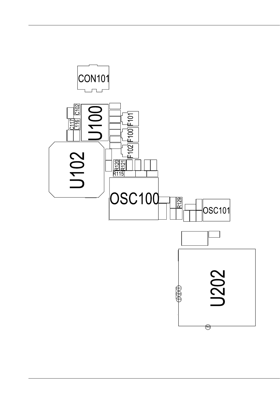
7-14. DCS Transmitter
TX ON (0Level)
Resolder C117, L116
Check ANT Switch
control circuit
Change
or Resolder U100
Check U100
pin2=L,pin4=L,pin8=H
Yes Resolder CN101, C102
END
Check U202
U101Pin6,7,8,9
>= 500mV
OSC100 pin2
>= 6Bm
U102 Pin37
>= 3dBm
U102 Pin31
>= 20dBm
U100 Pin9
>= 20dBm
U100 Pin7
>= 20dBm
Resolder U101
or check Txcpo(R129)
Check & Resolder
RF PSU part
Check U101
pin4 >= 4.0V
pin22, 28 >= 2.7V
Resolder R115, R120, R121
No
Yes
Yes
Yes
Check U102
+VBATT(pin42,43)
OK?
Resolder or change U102
or check PAM control
signal
Check +VBATT
No
No
No
No
No
Yes
Yes
Yes Yes
Yes
No
No
No
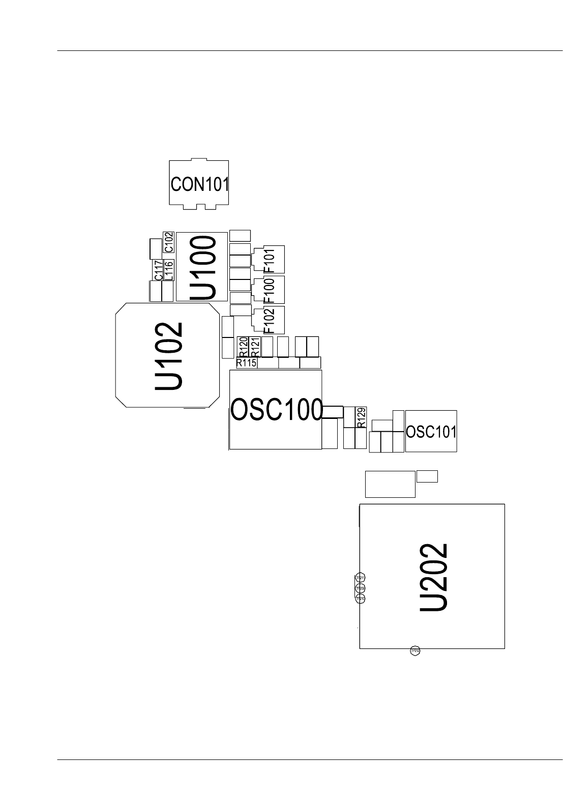
SAMSUNG Proprietary-Contents may change without notice
Flow Chart of Troubleshooting
This Document can not be used without Samsung's authorization
7-29
SAMSUNG Proprietary-Contents may change without notice
This Document can not be used without Samsung's authorization
Flow Chart of Troubleshooting
7-30
7-15. PCS Receiver
RX ON
RF input : CH center freq
Amp : -50dBm
Resolder F100, C103, L104
Check ANT Switch
control circuit
Change
or Resolder U100
Check U100
pin2=H,pin4=L,pin8=L
Resolder CN101, C102
END
Check U202
R130,R131,R132,
R133 >= 1V
U101 Pin 6,7,8,9
>= 1V
U101 Pin35,36
>= -70dBm
F100 Pin1
>= -70dBm
U100 Pin3
>= -65dBm
U100 Pin7
>= -65dBm
Check & Resolder
U101, RF 26MHz part,
R104, R105
Check & Resolder
RF PSU part
Check U101
pin4 >= 4.0V
pin22, 28 >= 2.7V
Resolder L101, L102, L103
Yes
No
Yes
Yes
Yes
Yes
Yes
Yes
No
No
No
No
No
Yes
SAMSUNG Proprietary-Contents may change without notice
Flow Chart of Troubleshooting
This Document can not be used without Samsung's authorization
7-31
SAMSUNG Proprietary-Contents may change without notice
This Document can not be used without Samsung's authorization
Flow Chart of Troubleshooting
7-32
7-16. PCS Transmitter
TX ON (0Level)
Resolder U101
or check Txcpo(R129)
Check & Resolder
RF PSU part
Check U101
pin4 >= 4.0V
pin22, 28 >= 2.7V
Resolder R115, R120, R121
Check +VBATT
Check U102
+VBATT(pin42,43)
OK?
Resolder or change U102
or check PAM control
signal
Resolder C117, L116
Check ANT Switch
control circuit
Change
or Resolder U100
Check U100
pin2=L,pin4=L,pin8=H
Yes Resolder CN101, C102
END
Check U202
U101Pin6,7,8,9
>= 500mV
OSC100 pin2
>= 6Bm
U102 Pin37
>= 3dBm
U102 Pin31
>= 20dBm
U100 Pin9
>= 20dBm
U100 Pin7
>= 20dBm
No
No
No
No
No
No
Yes
Yes
Yes
Yes
Yes Yes
Yes
Yes
No
No
No
SAMSUNG Proprietary-Contents may change without notice
Flow Chart of Troubleshooting
This Document can not be used without Samsung's authorization
7-33
SAMSUNG Proprietary-Contents may change without notice
This Document can not be used without Samsung's authorization
Flow Chart of Troubleshooting
7-34
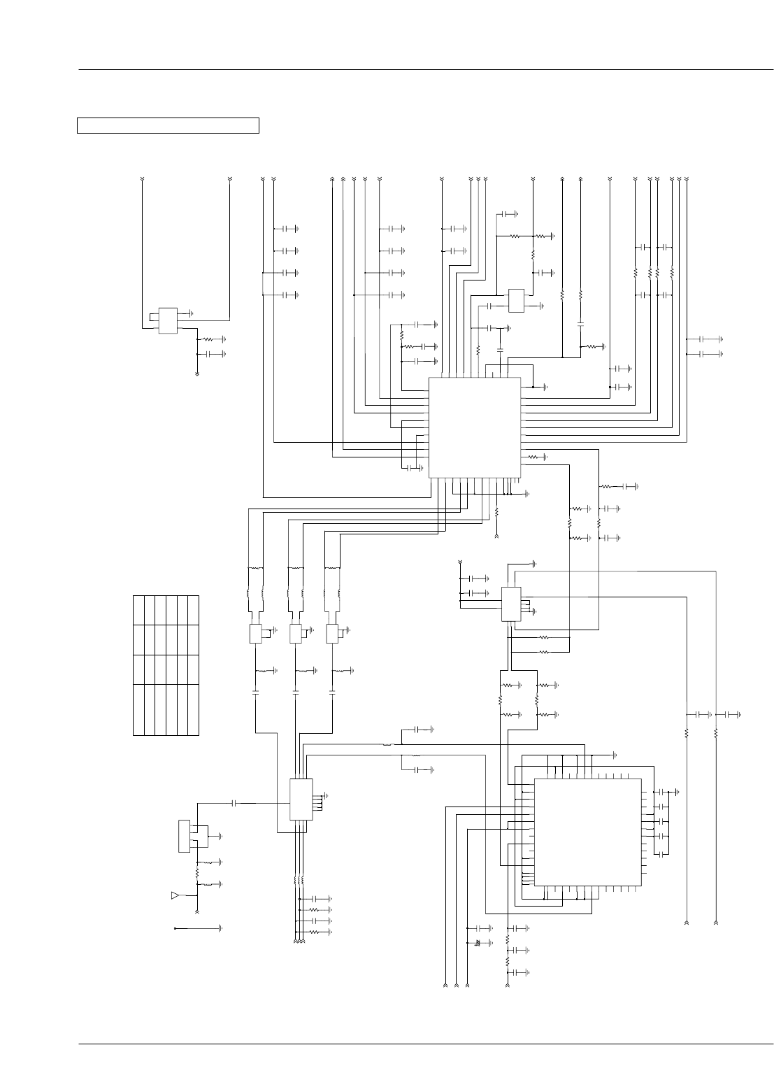
Transmitter & Receiver
L
L
LDCS/PCS Tx H
_ECOS
L
VC1
L
VC3
L
L
LLH
L
LDCS Rx
GSM 850/900 Tx
L
PCS Rx H
GSM Rx
VC2
C101
C108
R105
C115
C158
R112
L102
L103
C112
1OUT1
OUT2
5
11
VCC1
7
VCC2
C157
GND 2
4
BAND
9CONTROL
3
BAND
GND
6
GND
810
GND
GND
12
L108
OSC100
R120
C134
C138
R123
C120
C119
R117
C122
C127
C156
C152
ANT2
C144
L110
C110
L118
R114
F100
B7851
2
GG 5
IN
13
OUT
OUT 4
C129
R133
C125
1NF
50V
C143
C103
R102
C137
L115
C111
C109
R132
L105
R101
L119
R136
R134
C147
R118
R106
R109
C121
C136
C117
C105
C130
0
R108
R128
B7845
2
GG 5
1IN OUT 3
4
OUT
F101
C104
R121
R129
22K,1%
C154
R116
R115
R135
L101
L113
L109
GND
OUT
34
VCC
1
VCON
R122
OSC101
2
C135
R110
R125
C124
1UF
10V
R113
4
OUT
C145
B7852 F102
2
GG
5
1IN
3
OUT
C155
L111
L107
C1
6
C2
3
E1
1
E2
4
ANT1
L104
Q100
PEMD10
B1
2
B2
5
C114
L116
C131
C106
1.8NF
C116
C153
50V
R126
L112
R111
C126
C132
R127
C139
C141
1
TXRFI
R107
37 RFGND2
RFLOVCC
28
RFTUNE
26
RFVCC
31 25
RFVCOVCC
RXON
2324
SYNON
22
SYNVCC
TXCPO
3
TXCPVCC
45
TXON
46
35 PCSIA
36 PCSIB
8
QA
QB
9
REFGND 14
15
REFIN
REFVCC 16
RFCPO
21
20
RFCPVCC
34 RFGND1
GND2
42
43 GND3
GND4
44
27
GNDTUNE
32 GSMIA
33 GSMIB
6
IA
7
IB
IFVCC
10
45 NC1
NC2
CLKFDBX
11
CLKOUT
DATA 17
38 DCSIA
39 DCSIB
EN 19
EXTRES
2
FESW1
2930
FESW2
40 FESWON
41
GND1
U101
12
CAFCSUP
18
CLK
13
R124
VCC3DCS/PCS
2118
VCC3GSM
VCCOUT
19
VCCOUT
20
VRAMP
45
NC
15
TXENABLE
41
VBATT
4243
VBATT
VCC1
39
VCC1GSM
46
VCC2DCS/PCS 35
VCC2GSM
2
NC
38
NC
44
NC
9
NC
10
NC
11
NC
12
NC
13
NC
14
NC 25
NC 26
NC 27
28
NC
NC 29
NC
8
NC 33
NC 36
GSM850/900OUT
6
GSMINTERGND
1
NC
3
NC
16
NC
17
NC
22
NC
23
NC
24
7GND
GND 30
GND 32
34
GND
49
GND
50
GND
GND
51
GSM850/900IN
48
DCS/PCSIN
37
DCS/PCSOUT 31
GND
4
GND
52
GND
53
GND
54
GND1GSM
47
GND
5U102
BANDSEL
40
C133
L106
C140
C123
KMS-512
2
A
C3
G1
G4
C102
CON101
R104
C146
100K
C142
R119
C107
C113
C118
R130
L117
C128
G5
1314
G6
GSM_RX 5
GSM_TX 11
3PCS_RX
4VC1
VC2
8
2VC3
U100
ANT
7
1
DCS_RX
DCS|PCS_T 9
6
G2G3
10
G4
12
R131
VCC_CP_4V
L114
VCC_RX_TX_2V7
FE_SW1
FE_SW2
ANT
FE_SW1
FE_SW2
VCC_SYN_2V7
PON_TX
IRX_TX_P
IRX_TX_N
QRX_TX_P
QRX_TX_N
MEL_13M
VBAT
PCS_RX
ANT_SW2
ANT_SW1
PCS_RX
ANT_SW3
PAM_TX_EN
RAMP
TXVCO_SW1
TXVCO_SW2
VCC_TX_BURST_2V7
AFC
D_REF_13M
RF_BBI_CLK
RF_BBI_DATA
RF_EN_SYNT
VCC_CP_4V
VCC_RF_VCO_2V7
VCC_RX_TX_2V7
PON_RX
PON_SYNT
VCC_SYN_2V7