SDBN500B01 Datasheet. Www.s Manuals.com. R3 2 Diodes
User Manual: Marking of electronic components, SMD Codes RD, RD**, RD-, RD07, RDW, RDp, RDt, Rd. Datasheets BD53E46G, BZB84-B47, RP130K151A, SDBN500B01, Si1551DL.
Open the PDF directly: View PDF ![]() .
.
Page Count: 7
SDBN500B01
500mA NPN TRANSISTOR SWITCH WITH SNUBBER DIODE
NEW PRODUCT
General Description
• SDBN500B01 is best suited for switching inductive loads
in power switching applications. It improves efficiency
and reliability of power switching systems and it can
support continuous maximum current of 500 mA. It
features NPN transistor with high breakdown voltage
and discrete switching diode with high forward surge
current. It reduces component count, consumes less
space and minimizes parasitic losses. The component
devices can be used as a part of a circuit or as a stand
alone discrete device.
Features
• NPN Transistor with High Break-Down Voltage
• Switching Diode with High Forward Surge
• Low Switching and Conduction Losses
• Surface Mount Package Suited for Automated Assembly
• Lead Free By Design/RoHS Compliant (Note 1)
• "Green" Device (Note 2)
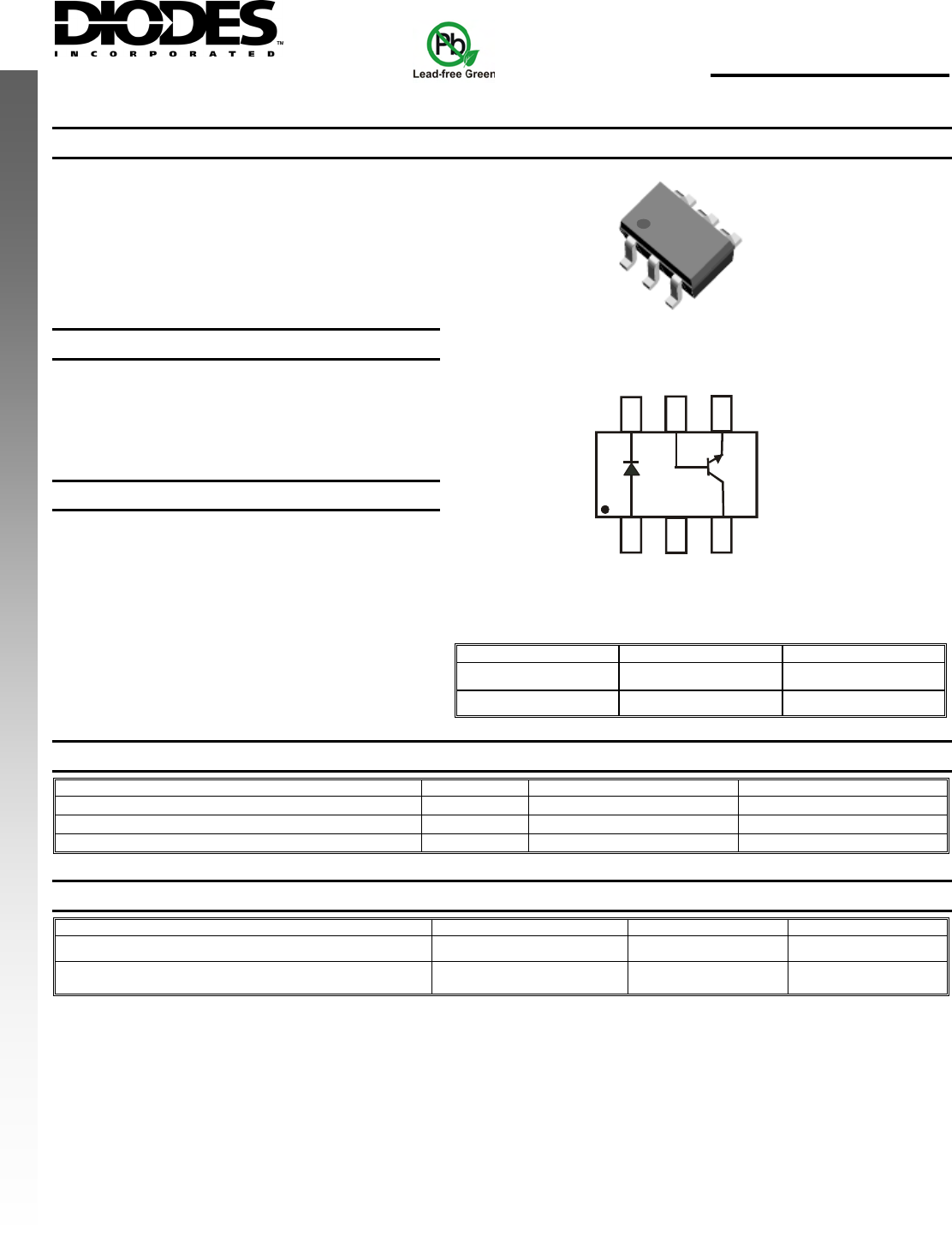
Mechanical Data
• Case: SOT-363
• Case Material: Molded Plastic, "Green" Molding
Compound. UL Flammability Classification Rating 94V-0
• Moisture Sensitivity: Level 1 per J-STD-020C
• Terminal Connections: See Figure
• Terminals: Finish ⎯ Matte Tin annealed over Alloy 42
leadframe. Solderable per MIL-STD-202, Method 208
• Marking and Type Code Information: See Page 6
• Ordering Information: See Page 6
• Weight: 0.016 grams (approximate)
Sub-Component P/N Reference Device Type
MMBTA06_DIE Q1 NPN Transistor
BAS31_DIE D1 Switching Diode
SOT-363
1
2
3
4
5
6
4
EQ1
BQ1
3
6
CD1
D1
1
AD1 NC CQ1
Q1
5
2
Schematic and Pin Configuration
Maximum Ratings: Total Device @TA = 25°C unless otherwise specified
Characteristic Symbol Value Unit
Power Dissipation (Note 3) Pd200 mW
Power Derating Factor above 25°C Pder 1.6 mW / °C
Output Current Iout 500 mA
Thermal Characteristics
Characteristic Symbol Value Unit
Junction Operating and Storage Temperature Range Tj, TSTG -55 to +150 °C
Thermal Resistance, Junction to Ambient Air (Note 3)
(Equivalent to One Heated Junction of NPN Transistor) RθJA 625 °C/W
Notes: 1. No purposefully added lead.
2. Diodes Inc.'s "Green" policy can be found on our website at http://www.diodes.com/products/lead_free/index.php.
3. Device mounted on FR-4 PCB, 1" x 0.85" x 0.062"; pad layout as shown on Diodes Inc. suggested pad layout document AP02001, which
can be found on our website at http://www.diodes.com/datasheets/ap02001.pdf.
DS30835 Rev. 3 - 2 1 of 6
www.diodes.com
SDBN500B01
© Diodes Incorporated
Please click here to visit our online spice models database.
Maximum Ratings:
NEW PRODUCT
Sub-Component Device – Switching Diode (D1) @TA = 25°C unless otherwise specified
Characteristic Symbol Value Unit
Non-Repetitive Peak Reverse Voltage VRM 100 V
Peak Repetitive Reverse Voltage
Working Peak Reverse Voltage
DC Blocking Voltage
VRRM
VRWM
VR
75 V
RMS Reverse Voltage VR(RMS) 53 V
Forward Continuous Current (Page 1: Note 3) IFM 500 mA
Average Rectified Output Current (Page 1: Note 3) IO250 mA
Non-Repetitive Peak Forward Surge Current @ t = 1.0 us 4 A
@ t = 1.0 s
IFSM 2 A
Sub Component Device - Discrete NPN Transistor (Q1) @TA = 25°C unless otherwise specified
Characteristic Symbol Value Unit
Collector-Base Voltage VCBO 80 V
Collector-Emitter Voltage VCEO 80 V
Emitter-Base Voltage VEBO 4 V
Output Current - continuous (Page 1: Note 3) IC500 mA
Electrical Characteristics:
Switching Diode (D1) @TA = 25°C unless otherwise specified
Characteristic Symbol Min Typ Max Unit Test Condition
Reverse Breakdown Voltage (Note 4) V(BR)R 75 ⎯ ⎯ V IR = 10 μA
0.62 ⎯ 0.37 IF = 5 mA
⎯ ⎯ 0.855 IF = 10 mA
⎯ ⎯ 1 IF = 100 mA
Forward Voltage Drop (Note 4) VFM
⎯ ⎯ 1.25
V
IF = 150 mA
⎯ ⎯ 2.5 VR = 75V
⎯ ⎯ 50 VR = 75V, Tj = 150 °C
⎯ ⎯ 30 VR = 25V, Tj = 150 °C
Reverse Current (Note 4) IR
⎯ ⎯ 25
μA
VR = 20V
Total Capacitance CT⎯ ⎯ 4 pF VR = 0V, f = 1.0 MHz
Reverse Recovery Time trr ⎯ ⎯ 4 ns IF = IR = 10mA, Irr = 0.1xIR, RL = 100 Ω
Notes: 4. Short duration pulse test used to minimize self-heating effect.
NEW PRODUCT
DS30835 Rev. 3 - 2 2 of 6
www.diodes.com
SDBN500B01
© Diodes Incorporated
Discrete NPN Transistor (Q1) @TA = 25°C unless otherwise specified
NEW PRODUCT
Characteristic Symbol Min Max Unit Test Condition
OFF CHARACTERISTICS (Note 4)
Collector-Base Breakdown Voltage VBR(CBO) 80 ⎯ V IC = 10 μA, IE = 0
Collector-Emitter Breakdown Voltage VBR(CEO) 80 ⎯ V IC = 1.0 mA, IB = 0
Emitter-Base Breakdown Voltage V(BR)EBO 4 ⎯ V IE = 100 μA, IC = 0
Collector Cutoff Current ICEX ⎯ 100 nA VCE = 60V, VEB(OFF) = 3.0V
Base Cutoff Current (IBEX) IBL ⎯ 100 nA VCE = 60V, VEB(OFF) = 3.0V
Collector-Base Cut Off Current ICBO ⎯ 100 nA VCB = 80V, IE = 0
Collector-Emitter Cut Off Current, IO(OFF) ICEO ⎯ 100 nA
VCE = 80V, IB = 0
Emitter-Base Cut Off Current IEBO ⎯ 100 nA
VEB = 5V, IC = 0
ON CHARACTERISTICS (Note 4)
60 ⎯ ⎯ V
CE = 1V, IC = 100 μA
80 ⎯ ⎯ V
CE = 1V, IC = 1 mA
100 ⎯ ⎯ V
CE = 1V, IC = 10 mA
100 ⎯ ⎯ V
CE = 1V, IC = 50 mA
90 ⎯ ⎯ V
CE = 1V, IC = 100 mA
DC Current Gain hFE
80 ⎯ ⎯ V
CE = 1V, IC = 200 mA
⎯ 0.1 V
IC = 10 mA, IB = 1 mA
⎯ 0.25 V
IC = 100 mA, IB = 10 mA
Collector-Emitter Saturation Voltage VCE(SAT)
⎯ 0.35 V
IC = 200 mA, IB = 20 mA
Base-Emitter Turn-on Voltage VBE(ON) ⎯ 0.98 V
VCE = 5V, IC = 2 mA
⎯ 0.95 V
IC = 10 mA, IB = 1 mA
Base-Emitter Saturation Voltage VBE(SAT) ⎯ 1.2 V
IC = 100 mA, VCE = 1V
SMALL SIGNAL CHARACTERISTICS
Output Capacitance COBO ⎯ 4 pF
VCB = 5.0 V, f = 1.0MHz, IE = 0
Input Capacitance CIBO ⎯ 6 pF
VEB = 5.0 V, f = 1.0MHz, IC = 0
Current Gain-Bandwidth Product fT100 ⎯ MHz VCE = 2 V, IC = 10mA, f = 100MHz
SWITCHING CHARACTERISTICS
Delay Time td⎯ 35 ns
Rise Time tr⎯ 35 ns
VCC = 3.0 V, IC = 10mA,
VBE(OFF) = 0.5V, IB1 = 1.0mA
Pulse Test: Pulse width, tp<300uS, Duty Cycle, d<=2%
Notes: 4. Short duration pulse test used to minimize self-heating effect.
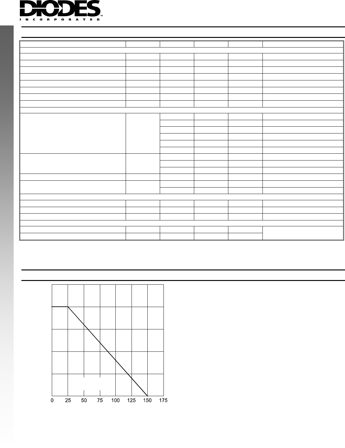
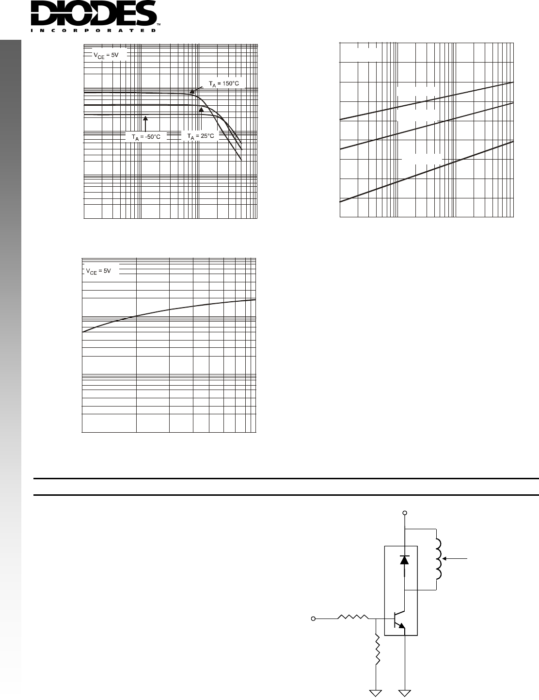
Typical Characteristics
0
50
100
P
,
P
O
WE
R
DISSI
P
A
T
I
O
N
(mW)
D
T , AMBIENT TEMPERATURE (°C)
Fig. 1, Maximum Power Dissipation vs.
Ambient Temperature
A
150
200
250
R = 625°C/W
θ
JA
DS30835 Rev. 3 - 2 3 of 6
www.diodes.com
SDBN500B01
© Diodes Incorporated
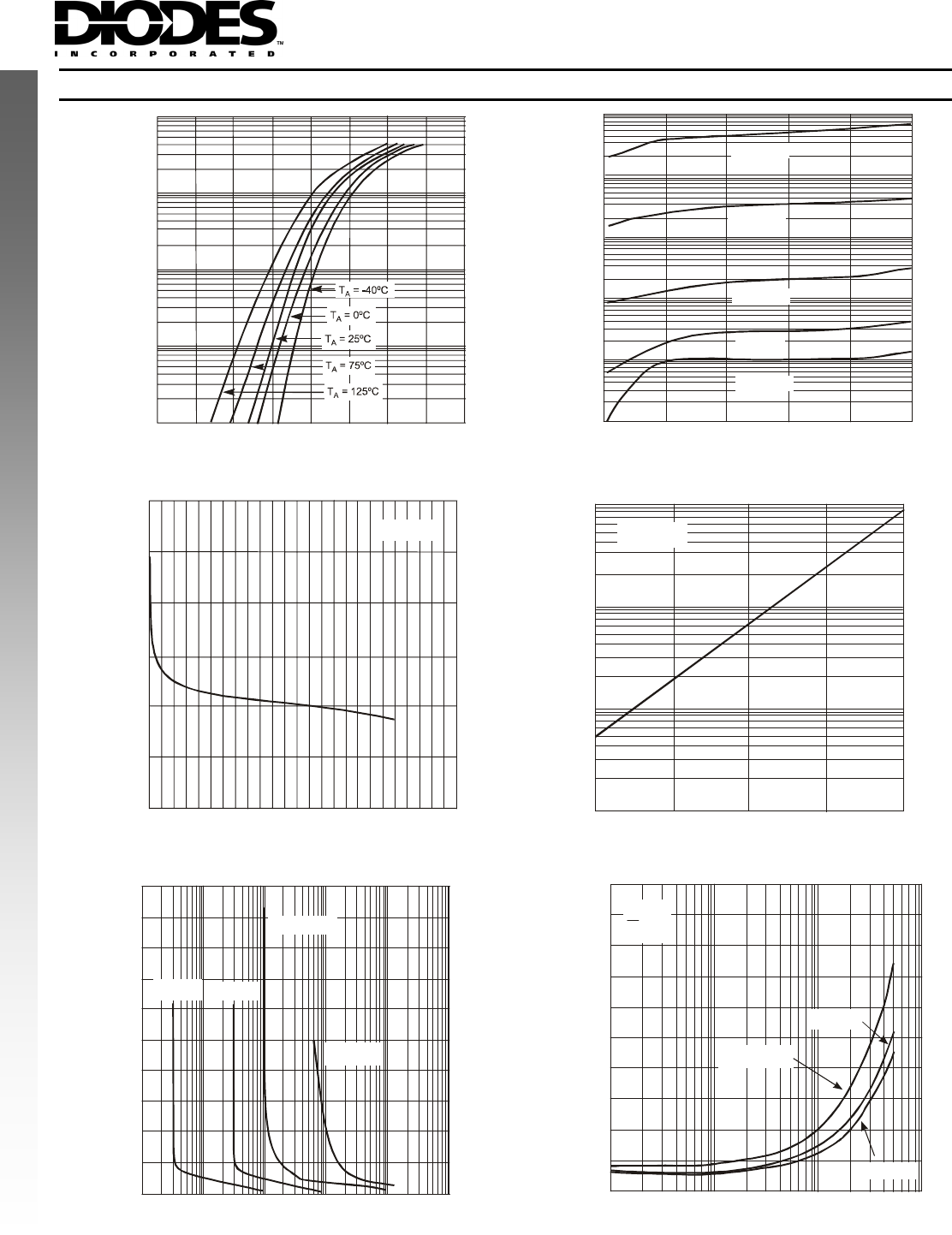
Switching Diode (D1) Characteristics
NEW PRODUCT
10
100
1,000
1
0.1 01.61.20.4 0.8
I , INS
T
AN
T
ANE
O
U
S
F
O
R
WA
R
D
C
U
R
R
EN
T
(mA)
F
V , INSTANTANEOUS FORWARD VOLTAGE (V)
Fig. 2, Typical Forward Characteristics
F
0.1
1
10
100
1,000
10,000
020 40 60 80 100
V , REVERSE VOLTAGE (V)
Fig. 3, Typical Reverse Characteristics
R
I, I
N
S
T
A
N
T
A
N
E
O
U
S
R
EVE
R
SE
C
U
R
R
E
N
T
(nA)
R
T = -40ºC
A
T = 25ºC
A
T = 75ºC
A
T = 125ºC
A
T = 0ºC
A
0
0.5
1
2.5
2
1.5
3
01020 40
30 50
C
,
T
O
T
AL
C
A
P
A
C
I
T
AN
C
E (p
F
)
T
V , REVERSE VOLTAGE (V)
Fig. 4, Typical Capacitance vs. Reverse Voltage
R
f = 1MHz
I,
C
O
LLE
C
T
O
R
-BASE
C
U
R
R
EN
T
(nA)
CBO
T , AMBIENT TEMPERATURE (ºC)
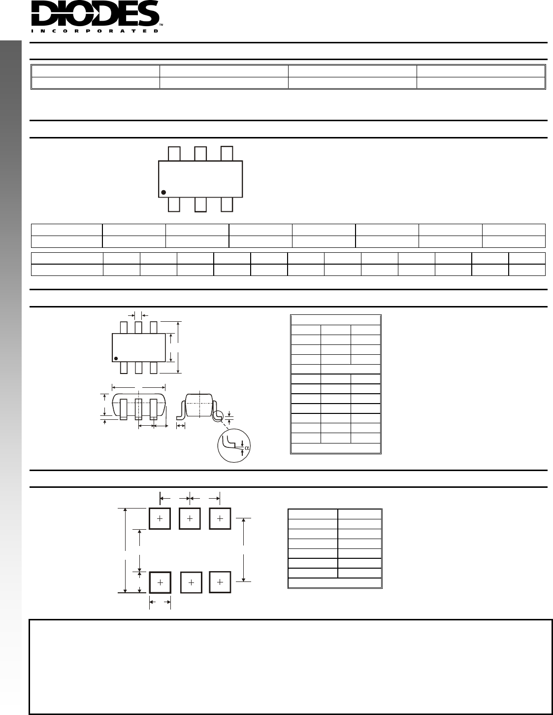
Fig. 5, I vs T
A
CBO A
10
0.01
0.1
1
25 50 75 100 125
V = 80V
CB
0.001 0.01
I BASE CURRENT (mA)
Fig. 6, V vs I
B,
CE B
0
0.2
0.4
0.6
0.8
1.0
1.2
1.4
1.6
1.8
2.0
0.1 1 10 100
V,
C
O
LLE
C
T
O
R
EMI
T
T
E
R
V
O
L
T
A
G
E (V)
CE
I = 1mA
C
I = 10mA
C
I = 30mA
C
I = 100mA
C
110
100 1,000
V,
C
O
LL
E
C
T
O
R
T
O
E
M
I
T
T
E
R
SATURATION VOLTAGE (V)
CE(SAT)
I , COLLECTOR CURRENT (mA)
Fig. 7, V vs I
C
CE(SAT) C
T = 25°C
A
T = -50°C
A
T = 150°C
A
0.050
0
0.100
0.150
0.200
0.250
0.300
0.350
0.400
0.450
0.500
I
I
C
B
= 10
DS30835 Rev. 3 - 2 4 of 6
www.diodes.com
SDBN500B01
© Diodes Incorporated
1
10
1,000
10,000
100
110 1,000
100
h, D
C
C
U
R
R
E
N
T
G
AI
N
FE
I , COLLECTOR CURRENT (mA)
Fig. 8, h vs I
C
FE C
0.1
0.2
0.1 110
V , BASE EMI
100
T
T
E
R
V
O
L
T
A
G
E (V)
BE(ON)
0.3
0.4
0.5
0.6
0.7
0.8
0.9
1.0
V = 5V
CE
I , COLLECTOR CURRENT (mA)
Fig. 9, V vs I
C
BE(ON) C
T = -50°C
A
T = 25°C
A
T = 150°C
A
1
10
1,000
100
110
f,
G
AIN BANDWID
T
H
P
R
O
D
U
C
T
(M
H
z)
T
I , COLLECTOR CURRENT (mA)
Fig. 10, f vs I
C
T
C
NEW PRODUCT
Application Details:
NPN transistor (MMBTA06) and Switching diode (BAV70) integrated as
one in SDBN500B01 can be used as a discrete entity for general
applications or part of a circuit to function as low side switch for sinking
current. NPN is selected based on high break-down voltage and
maximum collector current range. Switching diode is selected based
on instantaneous forward surge current. The Switching diode
dissipates very little power because it is on for only a small portion of
the switching cycle. It is designed to replace the discrete NPN
transistor and a Switching diode in two separate packages into one
small package as shown in Figure. It consumes less board space and
also helps to minimize conduction or switching losses due to parasitic
inductances (e.g. PCB traces) in power switch applications. (Please
see Fig. 11 for one example of typical application circuit used in
conjunction with DC-DC converter as a part of the power management
system).
R1
R2
SDBN500B01
Inductive Load
V supply
Fig. 11, Typical Application Circuit
DS30835 Rev. 3 - 2 5 of 6
www.diodes.com
SDBN500B01
© Diodes Incorporated
Ordering Information (Note 5)
NEW PRODUCT
Device Marking Code Packaging Shipping
SDBN500B01-7 RD07 SOT-363 3000/Tape & Reel
Notes: 5. For packaging details, please see below or go to our website at http://www.diodes.com/datasheets/ap02007.pdf.
Marking Information
RD07
YM
RD07 = Product Type Marking Code,
YM = Date Code Marking
Y = Year e.g. T = 2006
M = Month e.g. 9 = September
Date Code Key
Year 2006 2007 2008 2009 2010 2011 2012
Code T U V W X Y Z
Month Jan Feb Mar Apr May Jun Jul Aug Sep Oct Nov Dec
Code 1 2 3 4 5 6 7 8 9 O N D
Mechanical Details
DS30835 Rev. 3 - 2 6 of 6
www.diodes.com
SDBN500B01
© Diodes Incorporated
Suggested Pad Layout: (Based on IPC-SM-782)
MPORTANT NOTICE
Diodes Incorporated and its subsidiaries reserve the right to make modifications, enhancements, improvements, corrections or other changes
without further notice to any product herein. Diodes Incorporated does not assume any liability arising out of the application or use of any product
described herein; neither does it convey any license under its patent rights, nor the rights of others. The user of products in such applications shall
assume all risks of such use and will agree to hold Diodes Incorporated and all the companies whose products are represented on our website,
harmless against all damages. LIFE SUPPORT
Diodes Incorporated products are not authorized for use as critical components in life support devices or systems without the expressed written
approval of the President of Diodes Incorporated.
A
M
JL
DF
BC
H
K
SOT-363
Dim Min Max
A 0.10 0.30
B 1.15 1.35
C 2.00 2.20
D 0.65 Nominal
F 0.30 0.40
H 1.80 2.20
J – 0.10
K 0.90 1.00
L 0.25 0.40
M 0.10 0.25
α 0° 8°
All Dimensions in mm
X
Z
Y
C
EE
G
Dimensions Value
Z 2.5
G 1.3
X 0.42
Y 0.6
C 1.9
E 0.65
All Dimensions in mm